Embed Size (px)
Citation preview
LECTURE NOTES
ON
EMBEDDED SYSTEMS
(R18A0464)
For
III-(CSE & IT) - I semester
Faculty Members
Dr.S.SASIKANTH & N.SURESH
Professor
Department of Electronics and Communication Engineering
MALLA REDDY COLLEGE OF ENGINEERING & TECHNOLOGY
III Year B. Tech CSE & IT–I Sem L T/P/D C 3 -/-/- 3
(R18A0464)EMBEDDEDSYSTEMS
COURSE OBJECTIVE S:
For embedded systems, the course will enable the students to:
1) To understand the basics of microprocessors and microcontrollers architecture and its
functionalities
2) Understand the core of an embedded system
3) To learn the design process of embedded system applications.
4) To understands the RTOS and inter-process communication.
UNIT-I: INTRODUCTION TO MICROPROCESSORS AND MICROCONTROLLERS:
8086 Microprocessor: Architecture of 8086, Register Organization, Programming Model,
Memory Segmentation, Signal descriptions of 8086, Addressing modes, Instruction Set.
8051 Microcontroller: 8051 Architecture, I/O Ports, Memory Organization, Instruction set of
8051.
UNIT-II: INTRODUCTION TO EMBEDDED SYSTEMS: History of embedded systems,
Classification of embedded systems based on generation and complexity, Purpose of embedded
systems, Applications of embedded systems, and characteristics of embedded systems,
Operational and Non-operational attributes of embedded systems.
UNIT-III: TYPICAL EMBEDDED SYSTEM: Core of the embedded system, Sensors and
actuators, Onboard communication interfacesI2C, SPI, parallel interface; External
communication interfaces-RS232, USB, infrared, Bluetooth, Wi-Fi, ZigBee, GPRS.
UNIT-IV: EMBEDDED FIRMWARE DESIGN AND DEVELOPMENT: Embedded
firmware design approaches-super loop based approach, operating system based approach;
embedded firmware development languages-assembly language based development, high level
language based development.
UNIT-V EMBEDDED PROGRAMMING CONCEPTS: Data types, Structures, Modifiers,
Loops and Pointers, Macros and Functions, object oriented Programming, Embedded
Programming in C++ &JAVA
TEXT BOOKS:
1. Embedded Systems, Raj Kamal, SecondEditionTMH.
2. Kenneth. J. Ayala, The 8051 Microcontroller , 3rd Ed.,CengageLearning
3. Introduction to Embedded Systems - shibu k v, Mc GrawHillEducation.
REFERENCE BOOKS:
1. Advanced Microprocessors and Peripherals – A. K. Ray and K.M. Bhurchandi, TMH, 2nd
Edition2006
2. Embedded Systems- An integrated approach - Lyla B Das, Pearsoneducation2012.
Unit-1
INTRODUCTION TO MICROPROCESSORS AND
MICROCONTROLLERS
MRCET CSE & IT UNIT-1 ES NOTES
Page 1
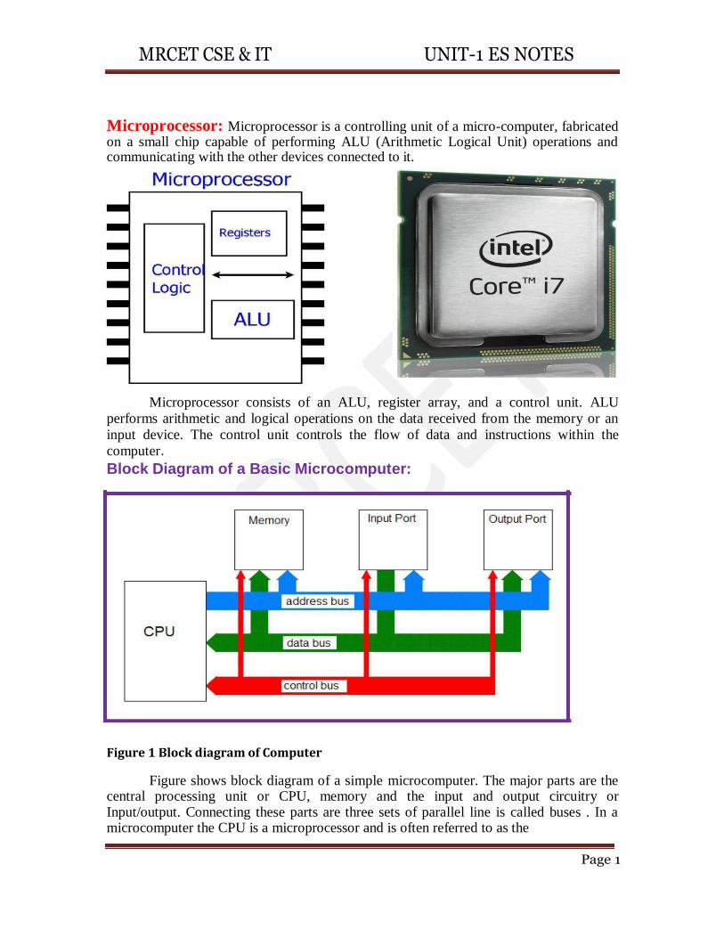
Microprocessor: Microprocessor is a controlling unit of a micro-computer, fabricated on a small chip capable of performing ALU (Arithmetic Logical Unit) operations and communicating with the other devices connected to it.
Figure 1 Block diagram of Computer
Figure shows block diagram of a simple microcomputer. The major parts are the central processing unit or CPU, memory and the input and output circuitry or Input/output. Connecting these parts are three sets of parallel line is called buses . In a microcomputer the CPU is a microprocessor and is often referred to as the
Microprocessor consists of an ALU, register array, and a control unit. ALU
performs arithmetic and logical operations on the data received from the memory or an
input device. The control unit controls the flow of data and instructions within the
computer.
Block Diagram of a Basic Microcomputer:
MRCET CSE & IT UNIT-1ESNOTES
Page 2
microprocessor unit (MPU). Its purpose is to decode the instruction and use them to control the activity within the system. It performs all arithmetic and logical computations. Memory: Memory section usually consists of a mixture of RAM and ROM. It may also magnetic floppy disks, magnetic hard disks or optical disks, to store the data.
Input/output: The input/output section allows the computer to take in data from the outside world or send data to the outside world. Peripherals such as keyboards, video display terminals. Printers and modem are connected to the input/output section. These allow the user and computer to communicate with each other. The actual physical devices used to interface the computer buses to external systems are often called ports. An input/output port allows data from keyboard, an analog to digital converter (ADC) or some other source to be read into the computer under the control of the CPU. An output port is used to send data from the computer to some peripheral, such as a video display terminal, a printer or a digital to analog converter (DAC).
Central processing Unit (CPU): CPU controls the operation of the computer .In a microcomputer the CPU is a microprocessor. The CPU fetches the binary coded instructions from memory, decodes the instructions into a series of simple action and carries out these actions in sequence of steps.
CPU contains an a address counter or instruction pointer register which holds the address of the next instruction or data item to be fetched from memory, general purpose register, which are used for temporary storage or binary data and circuitry, which generates the control bus signals.
Address bus: The address bus consists of 16, 20, 24 or 32 parallel lines. On these lines the CPU sends out the address of the memory locations that are to be written to or read from. The number of memory locations that the CPU can addresses is determined by the
number of address lines, then it can directly address 2n
memory location. When the CPU reads data from or writes data to a port, it sends the port address on the address bus.
Ex: CPU has 16 address lines can address 216
or 65536 memory locations.
Data bus: It consists of 8, 16, 32 parallel signal lines. The data bus lines are bidirectional. This means that the CPU can read, data from memory or from a port on these lines, or it can send data out to memory or to port on these lines.
Control bus: The control bus consists of 4 to 10 parallel signals lines. The CPU sends out signals on the control bus enable the outputs of addressed memory devices or port
devices. Typical control bus signal are memory read, memory write, I/O read and I/O write.
Hardware, software and Firmware: hardware is the given to the physical devices and circuitry of the computer. Software refers to collection of programs written for the computer. Firmware is the term given programs stored in ROM’s or in other devices which permanently keep their stored information.
MRCET CSE & IT UNIT-1ESNOTES
Page 3
8086 Microprocessor
8086 Microprocessor is an enhanced version of 8085Microprocessor that was designed by Intel in 1976.
Features of 8086 Microprocessor: Itisa16-bitMicroprocessor(μp).It‟sALU,internalregistersworkswith 16bit
binaryword.
8086 has a 20 bit address bus can access up to220= 1MB memory locations.
8086 has a 16bit data bus. It can read or write data to a memory/port either 16bits
or 8 bit at atime.
It can support up to 64K I/O ports.
It provides 14, 16 -bit registers.
Frequency range of 8086 is 6-10 MHz
It has multiplexed address and data bus AD0- AD15.
It requires single phase clock with 33% duty cycle to provide internal timing.
It can prefetch up to 6 instruction bytes from memory and queues them in order
to speed up instruction execution.
It requires +5V power supply.
A 40 pin dual in line package.
It has 256 vectored interrupts
It consists of 29,000 transistors.
8086 is designed to operate in two modes, Minimum mode and Maximum mode.
o The minimum mode is selected by applying logic 1 to the MN /MX inputpin. This is a single microprocessor configuration.
o The maximum mode is selected by applying logic 0 to the MN / MX
inputpin. This is a multi micro processors configuration.
MRCET CSE & IT UNIT-1ESNOTES
Page 4
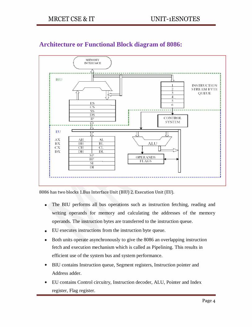
Architecture or Functional Block diagram of 8086:
fetch and execution mechanism which is called as Pipelining. This results in
efficient use of the system bus and system performance.
BIU contains Instruction queue, Segment registers, Instruction pointer and
Address adder.
EU contains Control circuitry, Instruction decoder, ALU, Pointer and Index
register, Flag register.
8086 has two blocks 1.Bus Interface Unit (BIU) 2. Execution Unit (EU).
The BIU performs all bus operations such as instruction fetching, reading and
writing operands for memory and calculating the addresses of the memory
operands. The instruction bytes are transferred to the instruction queue.
EU executes instructions from the instruction byte queue.
Both units operate asynchronously to give the 8086 an overlapping instruction
MRCET CSE & IT UNIT-1ESNOTES
Page 5
BIU (Bus Interface Unit):
BIU takes care of all data and addresses transfers on the buses for the EU like sending
addresses, fetching instructions from the memory, reading data from the ports and the
memory as well as writing data to the ports and the memory and computes the 20-bit
address.EU has no direction connection with System Buses so this is possible with the
BIU. EU and BIU are connected with the Internal Bus. It has the following functional
parts:
Instruction queue: BIU contains the instruction queue. BIU gets up to 6 bytes of next
instructions and stores them in the instruction queue. When EU executes instructions and
is ready for its next instruction, then it simply reads the instruction from this instruction
queue resulting in increased execution speed.
Address Adder: The BIU also contains a dedicated adder which is used to generate the
20bit physical address that is output on the address bus. This address is formed by adding
an appended 16 bit segment address and a 16 bit offset address.
Segment register: BIU has 4 segment registers, i.e. CS, DS, SS & ES. It holds the
addresses of instructions and data in memory, which are used by the processor to access
memory locations. It also contains 1 pointer register IP, which holds the address of the
next instruction to executed by the EU.
Instruction pointer: It is a 16-bit register used to hold the address of the next instruction
to be executed.
EU (Execution Unit):
Execution unit gives instructions to BIU stating from where to fetch the data and then
decode and execute those instructions. Its function is to control operations on data using
the instruction decoder & ALU. EU has no direct connection with system buses as
shown in the above figure, it performs operations over data through BIU. Let us now
discuss the functional parts of 8086 microprocessors.
ALU: It handles all arithmetic and logical operations, like +,-,×,/, OR, AND, NOT
operations.
MRCET CSE & IT UNIT-1ESNOTES
Page 6
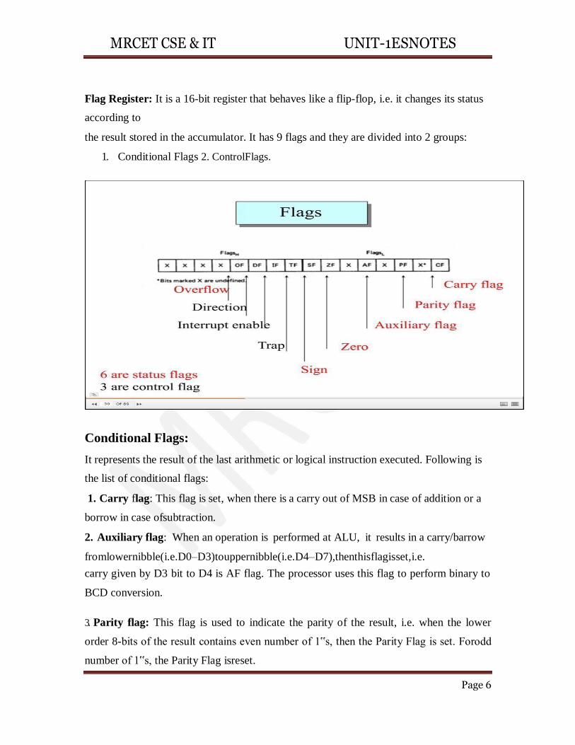
Flag Register: It is a 16-bit register that behaves like a flip-flop, i.e. it changes its status
according to
the result stored in the accumulator. It has 9 flags and they are divided into 2 groups:
1. Conditional Flags 2. ControlFlags.
carry given by D3 bit to D4 is AF flag. The processor uses this flag to perform binary to
BCD conversion.
3. Parity flag: This flag is used to indicate the parity of the result, i.e. when the lower
order 8-bits of the result contains even number of 1‟s, then the Parity Flag is set. Forodd
number of 1‟s, the Parity Flag isreset.
Conditional Flags:
It represents the result of the last arithmetic or logical instruction executed. Following is
the list of conditional flags:
1. Carry flag: This flag is set, when there is a carry out of MSB in case of addition or a
borrow in case ofsubtraction.
2. Auxiliary flag: When an operation is performed at ALU, it results in a carry/barrow
fromlowernibble(i.e.D0–D3)touppernibble(i.e.D4–D7),thenthisflagisset,i.e.
MRCET CSE & IT UNIT-1ESNOTES
Page 7
4. Zero flag: This flag is set to 1 when the result of arithmetic or logical operation is zero
else it is set to0.
5. Sign flag: This flag holds the sign of the result, i.e. when the result of the operation is
negative, then the sign flag is set to 1 else set to0.
6. Overflow flag: This flag represents the result when the system capacity isexceeded.
Control Flags:
Control flags controls the operations of the execution unit. Following is the list of control
flags:
1. Trap flag: It is used for single step control and allows the user to execute one
instruction at a time for debugging. If it is set, then the program can be run in a single
stepmode.
2. Interrupt flag: It is an interrupt enable/disable flag, i.e. used to allow/prohibit the
interruption of a program. It is set to 1 for interrupt enabled condition and set to 0 for
interrupt disabledcondition.
3. Direction flag: It is used in string operation. As the name suggests when it is set then
string bytes are accessed from the higher memory address to the lower memory address
andvice-a-versa.
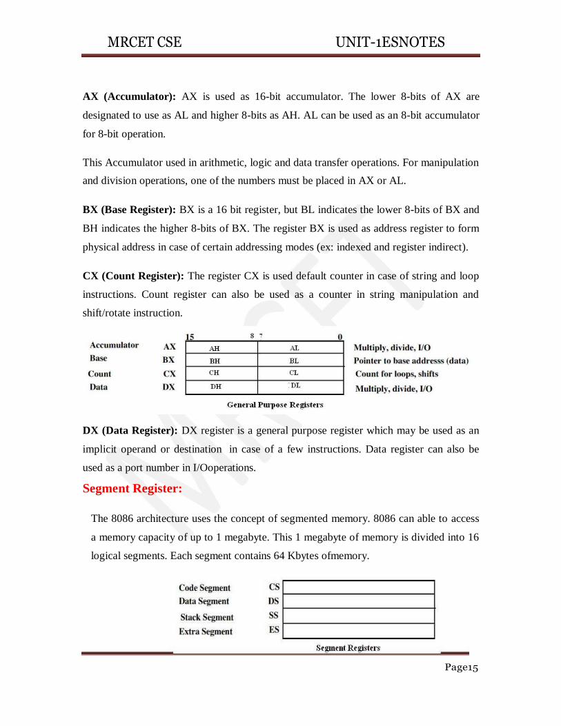
General Purpose Register (GPR):
There are 8 general purpose registers, i.e., AH, AL, BH, BL, CH, CL, DH, and DL. These
registers can be used individually to store 8-bit data and can be used in pairs to store 16-
bit data. The valid register pairs are AH and AL, BH and BL, CH and CL, and DH and
DL. It is referred to the AX, BX, CX, and DX respectively.
AX register: It is also known as accumulator register. It is used to store operands for
arithmetic operations.
BX register: It is used as a base register. It is used to store the starting base address
of the memory area within the data segment.
CX register: It is referred to as counter. It is used in loop instruction to store the loop
counter.
DX register: This register is used to hold I/O port address for I/O instruction.
MRCET CSE & IT UNIT-1ESNOTES
Page 8
Stack pointer register: It is a 16-bit register, which holds the address from the start of
the segment to the memory location,(stack top) where a word was most recently stored
on the stack.
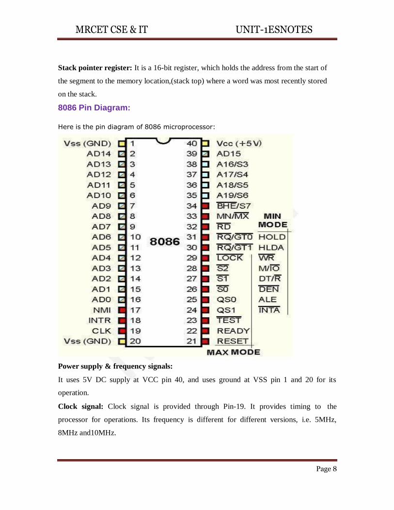
8086 Pin Diagram:
Here is the pin diagram of 8086 microprocessor:
Power supply & frequency signals:
It uses 5V DC supply at VCC pin 40, and uses ground at VSS pin 1 and 20 for its
operation.
Clock signal: Clock signal is provided through Pin-19. It provides timing to the
processor for operations. Its frequency is different for different versions, i.e. 5MHz,
8MHz and10MHz.
MRCET UNIT-1ESNOTES
Address/data bus: AD0-AD15. These are 16 address/data bus. AD0-AD7 carries low
order byte data and AD8-AD15 carries higher order byte data. During the first clock
cycle, it carries 16-bit address and after that it carries 16-bitdata.
Address/status bus: A16-A19/S3-S6. These are the 4 address/status buses. During the
first clock cycle, it carries 4-bit address and later it carries status signals.
S7/BHE: BHE stands for Bus High Enable. It is available at pin 34 and used to indicate
the transfer of data using data bus D8-D15. This signal is low during the first clock cycle,
thereafter it is active.
Read( ): It is available at pin 32 and is used to read signal for Read operation.
Ready: It is available at pin 32. It is an acknowledgement signal from I/O devices that
data is transferred. It is an active high signal. When it is high, it indicates that the device
is ready to transfer data. When it is low, it indicates waitstate.
RESET: It is available at pin 21 and is used to restart the execution. It causes the
processor to immediately terminate its present activity. This signal is active high for the
first 4 clock cycles to RESET the microprocessor.
INTR: It is available at pin 18. It is an interrupt request signal, which is sampled during
the last clock cycle of each instruction to determine if the processor considered this as an
interrupt or not.
NMI: It stands for non-maskable interrupt and is available at pin 17. It is an edge
triggered input, which causes an interrupt request to the microprocessor.
:This signal is like wait state and is available at pin 23. When this signal is high,
then the processor has to wait for IDLE state, else the execution continues.
MN/ : It stands for Minimum/Maximum and is available at pin 33. It indicates what mode the processor is to operate in; when it is high, it works in the minimum mode andvice-aversa.
INTA: It is an interrupt acknowledgement signal and id available at pin 24. When the
microprocessor receives this signal, it acknowledges the interrupt.
ALE: It stands for address enable latch and is available at pin 25. A positive pulse is
generated each time the processor begins any operation. This signal indicates the
availability of a valid address on the address/data lines.
Page9
MRCET CSE UNIT-1ESNOTES
Page10
DEN: It stands for Data Enable and is available at pin 26. It is used to enable
Transreceiver 8286. The transreceiver is a device used to separate data from the
address/data bus.
DT/R:It stands for Data Transmit/Receive signal and is available at pin 27. It decides the
direction of data flow through the transreceiver. When it is high, data is transmitted out
andvice-a-versa.
M/IO:This signal is used to distinguish between memory and I/O operations. When it is
high, it indicates I/O operation and when it is low indicates the memory operation. It is
available at pin 28.
WR:It stands for write signal and is available at pin 29. It is used to write the data into
the memory or the output device depending on the status of M/IO signal.
HLDA: It stands for Hold Acknowledgement signal and is available at pin 30. This
signal acknowledges the HOLDsignal.
HOLD: This signal indicates to the processor that external devices are requesting to
access the address/data buses. It is available at pin 31.
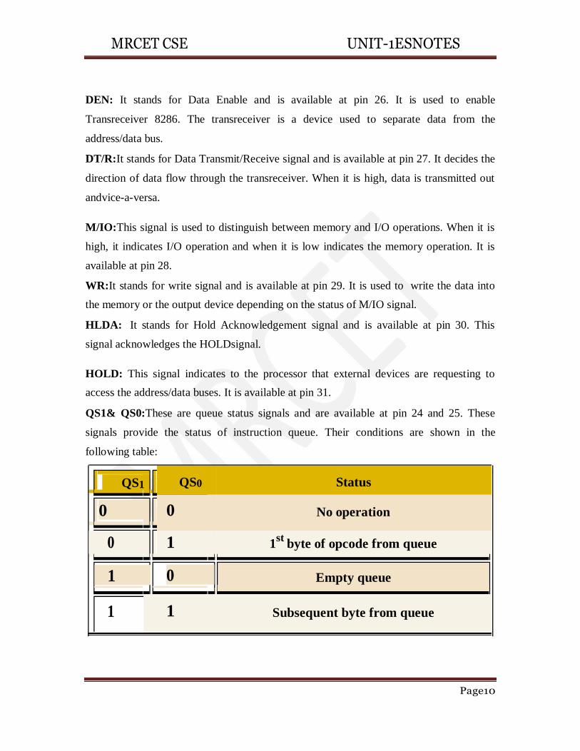
QS1& QS0:These are queue status signals and are available at pin 24 and 25. These
signals provide the status of instruction queue. Their conditions are shown in the
following table:
QS0 Status
0 No operation
0 1 1st
byte of opcode from queue
0
1 1 Subsequent byte from queue
Empty queue 1
0
QS1
MRCET CSE UNIT-1ESNOTES
Page11
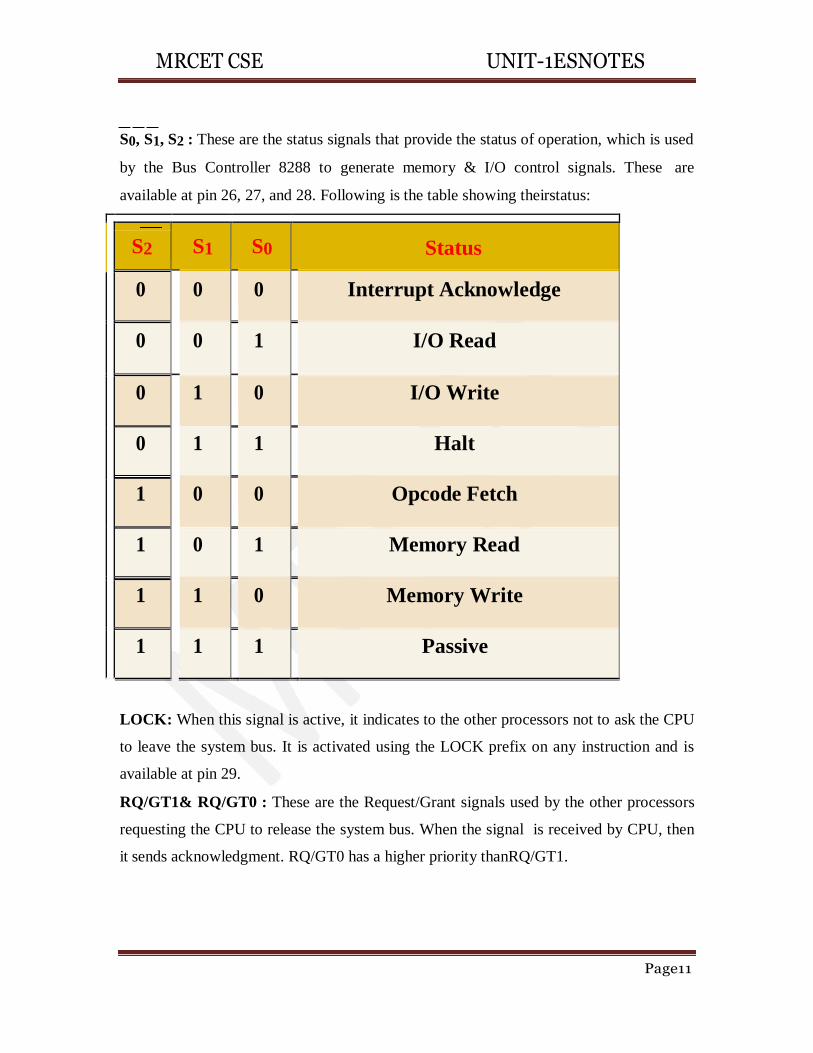
S0, S1, S2 : These are the status signals that provide the status of operation, which is used
by the Bus Controller 8288 to generate memory & I/O control signals. These are
available at pin 26, 27, and 28. Following is the table showing theirstatus:
S1 S0 Status S2
0
0
0
Interrupt Acknowledge
0
0
1
I/O Read
0 1 0 I/O Write
0 1 1 Halt
1 0 0 Opcode Fetch
1 0 1 Memory Read
1 1 0 Memory Write
1 1 1 Passive
LOCK: When this signal is active, it indicates to the other processors not to ask the CPU
to leave the system bus. It is activated using the LOCK prefix on any instruction and is
available at pin 29.
RQ/GT1& RQ/GT0 : These are the Request/Grant signals used by the other processors
requesting the CPU to release the system bus. When the signal is received by CPU, then
it sends acknowledgment. RQ/GT0 has a higher priority thanRQ/GT1.
MRCET CSE UNIT-1ESNOTES
Page12
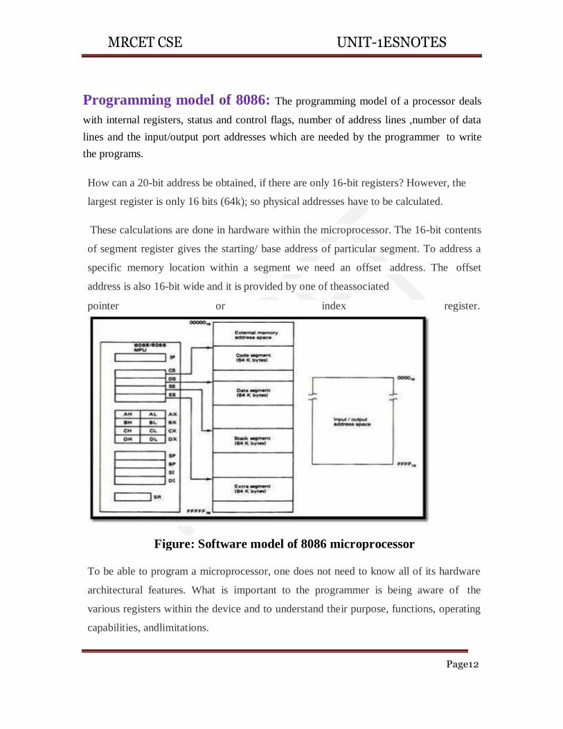
Programming model of 8086: The programming model of a processor deals
with internal registers, status and control flags, number of address lines ,number of data
lines and the input/output port addresses which are needed by the programmer to write
the programs.
How can a 20-bit address be obtained, if there are only 16-bit registers? However, the
To be able to program a microprocessor, one does not need to know all of its hardware
architectural features. What is important to the programmer is being aware of the
various registers within the device and to understand their purpose, functions, operating
capabilities, andlimitations.
largest register is only 16 bits (64k); so physical addresses have to be calculated.
These calculations are done in hardware within the microprocessor. The 16-bit contents
of segment register gives the starting/ base address of particular segment. To address a
specific memory location within a segment we need an offset address. The offset
address is also 16-bit wide and it is provided by one of theassociated
pointer or index register.
Figure: Software model of 8086 microprocessor
MRCET CSE UNIT-1ESNOTES
Page13
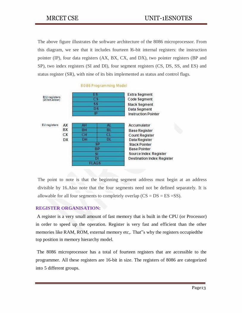
The above figure illustrates the software architecture of the 8086 microprocessor. From
this diagram, we see that it includes fourteen l6-bit internal registers: the instruction
pointer (IP), four data registers (AX, BX, CX, and DX), two pointer registers (BP and
SP), two index registers (SI and DI), four segment registers (CS, DS, SS, and ES) and
status register (SR), with nine of its bits implemented as status and control flags.
top position in memory hierarchy model.
The 8086 microprocessor has a total of fourteen registers that are accessible to the
programmer. All these registers are 16-bit in size. The registers of 8086 are categorized
into 5 different groups.
The point to note is that the beginning segment address must begin at an address
divisible by 16.Also note that the four segments need not be defined separately. It is
allowable for all four segments to completely overlap (CS = DS = ES =SS).
REGISTER ORGANISATION:
A register is a very small amount of fast memory that is built in the CPU (or Processor)
in order to speed up the operation. Register is very fast and efficient than the other
memories like RAM, ROM, external memory etc,. That‟s why the registers occupiedthe
MRCET CSE UNIT-1ESNOTES
Page14
Base Pointer(BP)
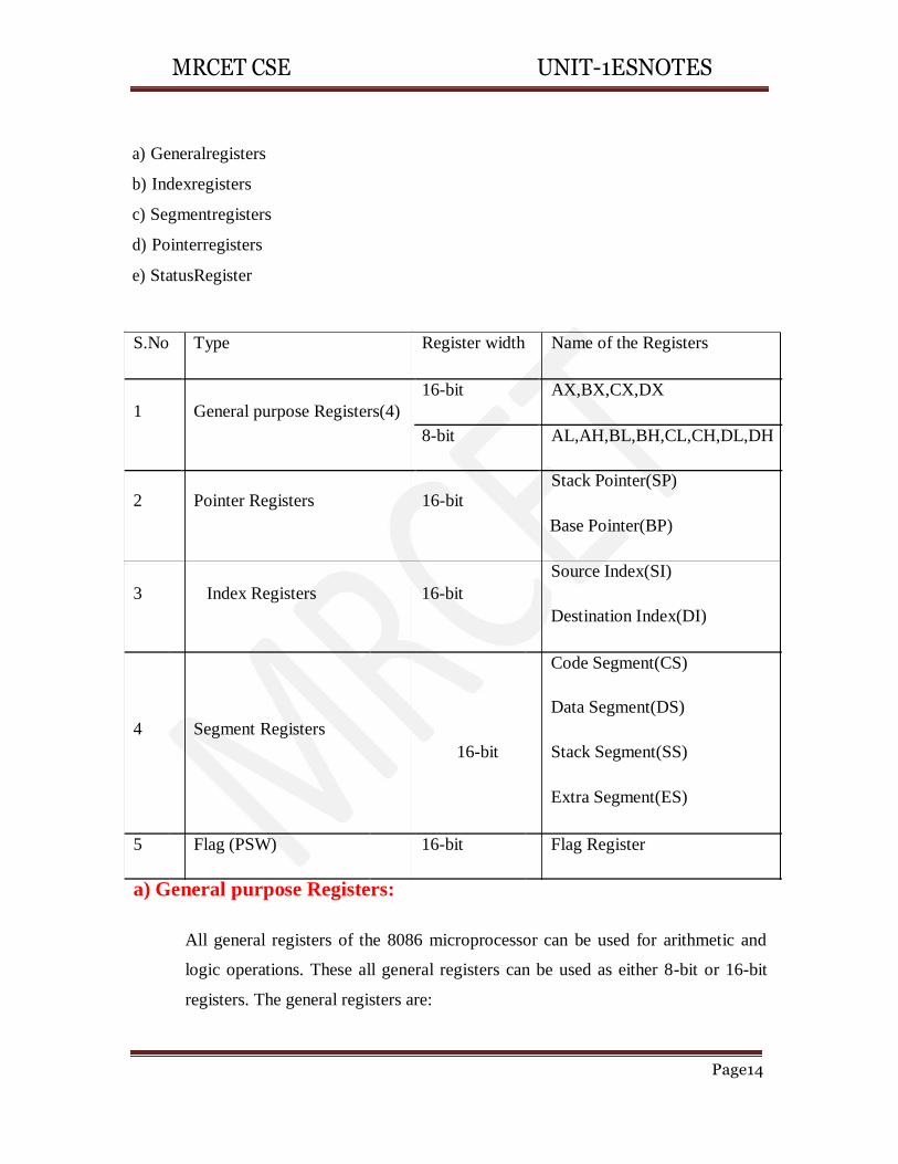
a) Generalregisters
b) Indexregisters
c) Segmentregisters
d) Pointerregisters
e) StatusRegister
S.No Type Register width Name of the Registers
16-bit AX,BX,CX,DX
1 General purpose Registers(4)
8-bit AL,AH,BL,BH,CL,CH,DL,DH
Stack Pointer(SP)
2 Pointer Registers 16-bit
Source Index(SI)
3 Index Registers 16-bit
Destination Index(DI)
Code Segment(CS)
Data Segment(DS)
4 Segment Registers
16-bit Stack Segment(SS)
Extra Segment(ES)
5 Flag (PSW) 16-bit Flag Register
a) General purpose Registers:
All general registers of the 8086 microprocessor can be used for arithmetic and
logic operations. These all general registers can be used as either 8-bit or 16-bit
registers. The general registers are:
MRCET CSE UNIT-1ESNOTES
Page15
AX (Accumulator): AX is used as 16-bit accumulator. The lower 8-bits of AX are
designated to use as AL and higher 8-bits as AH. AL can be used as an 8-bit accumulator
for 8-bit operation.
This Accumulator used in arithmetic, logic and data transfer operations. For manipulation
and division operations, one of the numbers must be placed in AX or AL.
BX (Base Register): BX is a 16 bit register, but BL indicates the lower 8-bits of BX and
BH indicates the higher 8-bits of BX. The register BX is used as address register to form
physical address in case of certain addressing modes (ex: indexed and register indirect).
CX (Count Register): The register CX is used default counter in case of string and loop
instructions. Count register can also be used as a counter in string manipulation and
shift/rotate instruction.
DX (Data Register): DX register is a general purpose register which may be used as an
implicit operand or destination in case of a few instructions. Data register can also be
used as a port number in I/Ooperations.
Segment Register:
The 8086 architecture uses the concept of segmented memory. 8086 can able to access
a memory capacity of up to 1 megabyte. This 1 megabyte of memory is divided into 16
logical segments. Each segment contains 64 Kbytes ofmemory.
MRCET CSE UNIT-1ESNOTES
Page16
This memory segmentation concept will discuss later in this document. There are four
segment registers to access this 1 megabyte of memory. The segment registers of 8086
are:
CS(Code Segment): Code segment (CS) is a 16-bit register that is used for addressing
memory location in the code segment of the memory (64Kb), where the executable
program is stored. CS register cannot be changed directly. The CS register is
automatically updated during far jump, far call and far return instructions.
Stack segment (SS): Stack Segment (SS) is a 16-bit register that used for addressing
stack segment of the memory (64kb) where stack data is stored. SS register can be
changed directly using POPinstruction.
Data segment (DS): Data Segment (DS) is a 16-bit register that points the data segment
of the memory (64kb) where the program data is stored. DS register can be changed
directly using POP and LDS instructions.
Extra segment (ES): Extra Segment (ES) is a 16-bit register that also points the data
segment of the memory (64kb) where the program data is stored. ES register can be
changed directly using POP and LES instructions.
b) IndexRegisters: The index registers can be used for arithmetic operations but their use is usually
concerned with the memory addressing modes of the 8086 microprocessor (indexed, base
indexed and relative base indexed addressing modes).
The index registers are particularly useful for string manipulation.
SI (Source Index):
SI is a 16-bit register. This register is used to store the offset of source data in data
segment. In other words the Source Index Register is used to point the memory locations
in the data segment.
DI (Destination Index):
DI is a 16-bit register. This is destination index register performs the same function as SI.
There is a class of instructions called string operations that use DI to access the memory
locations in Data or Extra Segment.
MRCET CSE UNIT-1ESNOTES
Page17
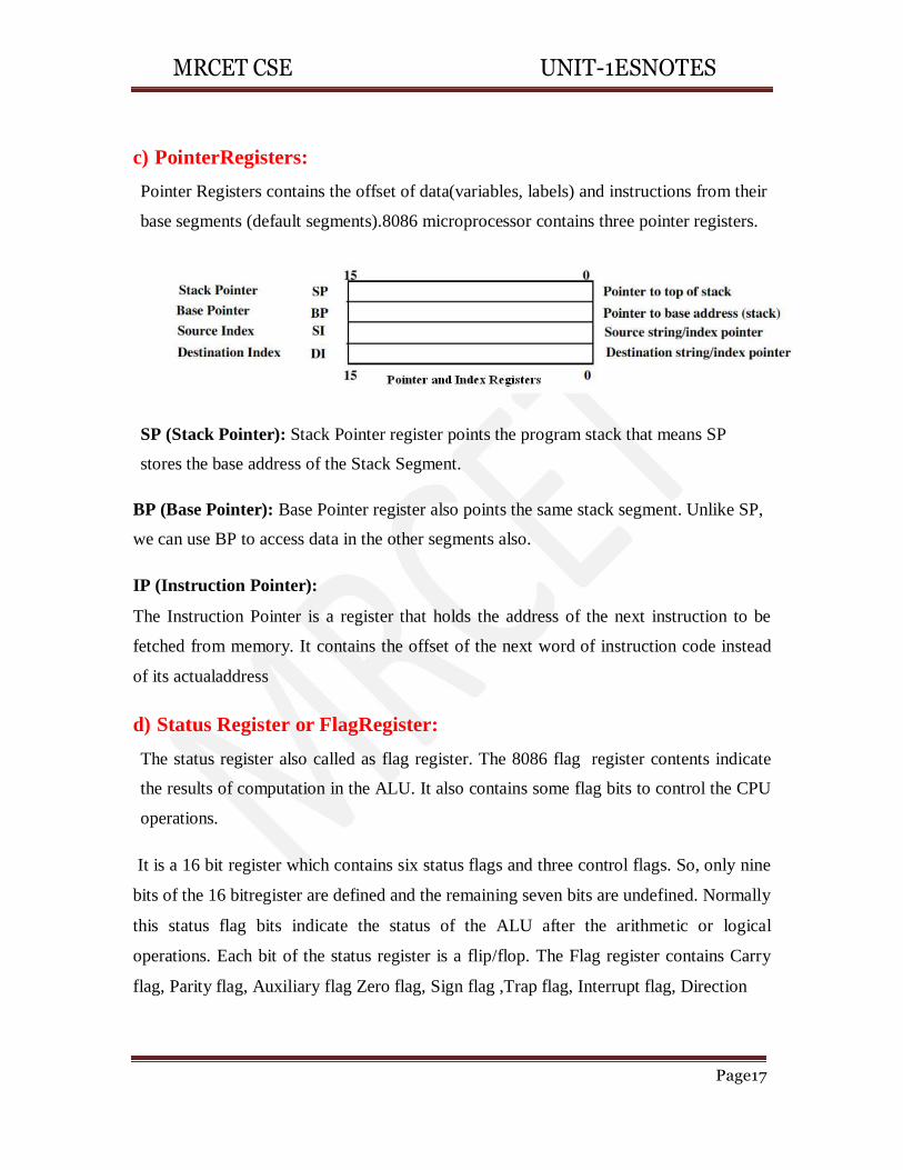
c) PointerRegisters:
Pointer Registers contains the offset of data(variables, labels) and instructions from their
base segments (default segments).8086 microprocessor contains three pointer registers.
SP (Stack Pointer): Stack Pointer register points the program stack that means SP
stores the base address of the Stack Segment.
BP (Base Pointer): Base Pointer register also points the same stack segment. Unlike SP,
we can use BP to access data in the other segments also.
IP (Instruction Pointer):
The Instruction Pointer is a register that holds the address of the next instruction to be
fetched from memory. It contains the offset of the next word of instruction code instead
of its actualaddress
d) Status Register or FlagRegister:
The status register also called as flag register. The 8086 flag register contents indicate
the results of computation in the ALU. It also contains some flag bits to control the CPU
operations.
It is a 16 bit register which contains six status flags and three control flags. So, only nine
bits of the 16 bitregister are defined and the remaining seven bits are undefined. Normally
this status flag bits indicate the status of the ALU after the arithmetic or logical
operations. Each bit of the status register is a flip/flop. The Flag register contains Carry
flag, Parity flag, Auxiliary flag Zero flag, Sign flag ,Trap flag, Interrupt flag, Direction
MRCET CSE UNIT-1ESNOTES
Page18
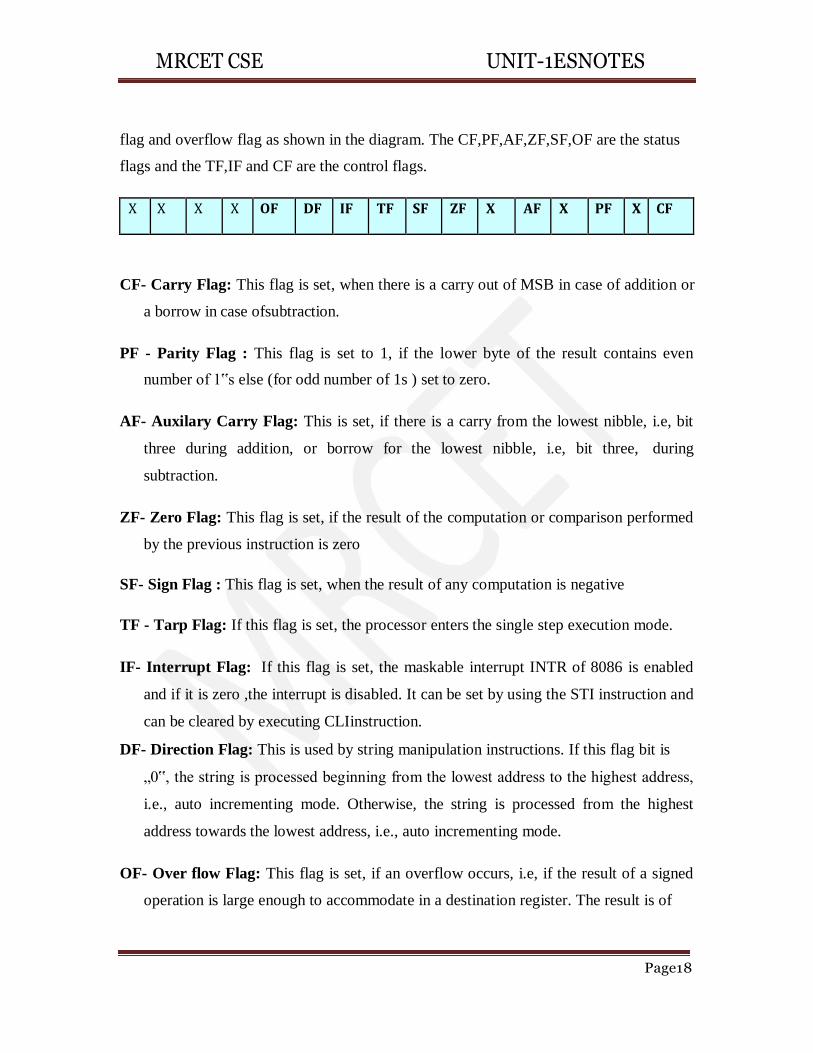
flag and overflow flag as shown in the diagram. The CF,PF,AF,ZF,SF,OF are the status
flags and the TF,IF and CF are the control flags.
X X X X OF DF IF TF SF ZF X AF X PF X CF
CF- Carry Flag: This flag is set, when there is a carry out of MSB in case of addition or
a borrow in case ofsubtraction.
PF - Parity Flag : This flag is set to 1, if the lower byte of the result contains even
number of 1‟s else (for odd number of 1s ) set to zero.
AF- Auxilary Carry Flag: This is set, if there is a carry from the lowest nibble, i.e, bit
three during addition, or borrow for the lowest nibble, i.e, bit three, during
subtraction.
ZF- Zero Flag: This flag is set, if the result of the computation or comparison performed
by the previous instruction is zero
SF- Sign Flag : This flag is set, when the result of any computation is negative
TF - Tarp Flag: If this flag is set, the processor enters the single step execution mode.
IF- Interrupt Flag: If this flag is set, the maskable interrupt INTR of 8086 is enabled
and if it is zero ,the interrupt is disabled. It can be set by using the STI instruction and
can be cleared by executing CLIinstruction.
DF- Direction Flag: This is used by string manipulation instructions. If this flag bit is
„0‟, the string is processed beginning from the lowest address to the highest address,
i.e., auto incrementing mode. Otherwise, the string is processed from the highest
address towards the lowest address, i.e., auto incrementing mode.
OF- Over flow Flag: This flag is set, if an overflow occurs, i.e, if the result of a signed
operation is large enough to accommodate in a destination register. The result is of
MRCET CSE UNIT-1ESNOTES
Page19
more than 7-bits in size in case of 8-bit signed operation and more than 15-bits in size
in case of 16-bit sign operations, then the overflow will be set.
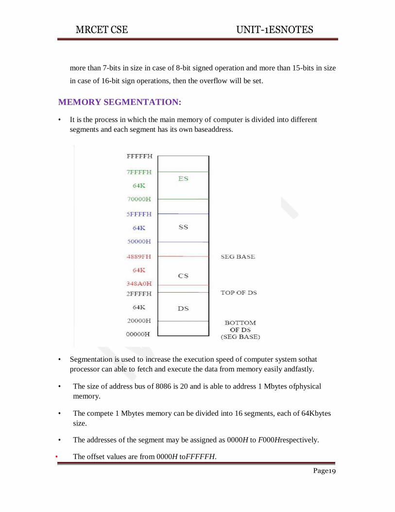
MEMORY SEGMENTATION:
• It is the process in which the main memory of computer is divided into different
segments and each segment has its own baseaddress.
• Segmentation is used to increase the execution speed of computer system sothat
processor can able to fetch and execute the data from memory easily andfastly.
• The size of address bus of 8086 is 20 and is able to address 1 Mbytes ofphysical
memory.
• The compete 1 Mbytes memory can be divided into 16 segments, each of 64Kbytes
size.
• The addresses of the segment may be assigned as 0000H to F000Hrespectively.
• The offset values are from 0000H toFFFFFH.
MRCET CSE UNIT-1ESNOTES
Page 20
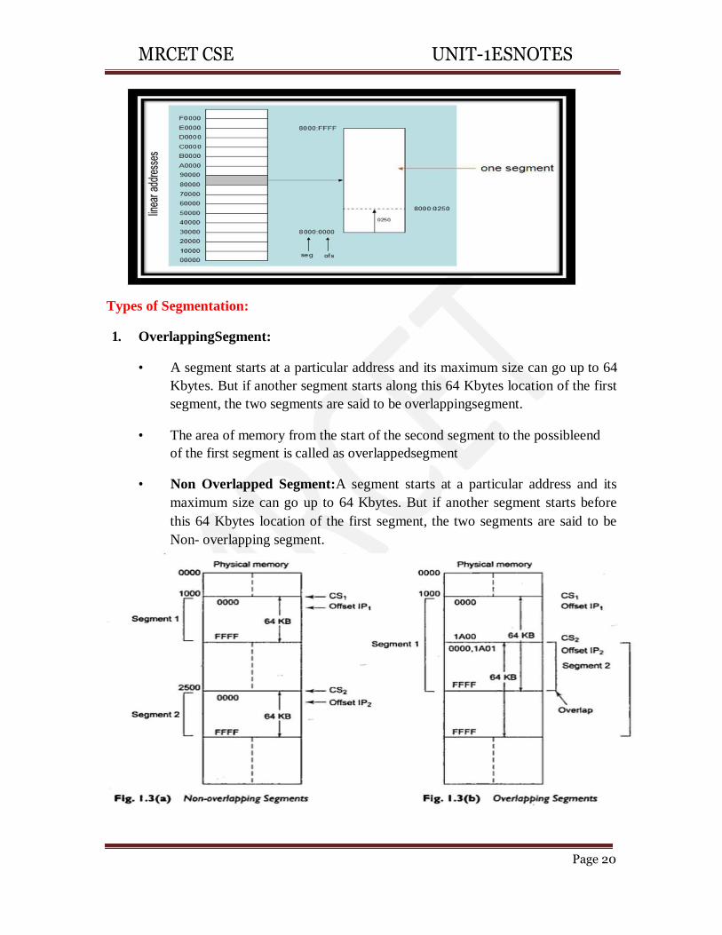
Types of Segmentation:
1. OverlappingSegment:
• A segment starts at a particular address and its maximum size can go up to 64
Kbytes. But if another segment starts along this 64 Kbytes location of the first
segment, the two segments are said to be overlappingsegment.
• The area of memory from the start of the second segment to the possibleend
of the first segment is called as overlappedsegment
• Non Overlapped Segment:A segment starts at a particular address and its
maximum size can go up to 64 Kbytes. But if another segment starts before
this 64 Kbytes location of the first segment, the two segments are said to be
Non- overlapping segment.
MRCET CSE UNIT-1ESNOTES
Page 21
Advantages of Segmented memory:
• Allows the memory capacity to be 1MB although the actual addresses to behandled
are of 16 bitsize.
• Allows the placing of code, data and stack portions of the same program indifferent
parts (segments) of the memory, for data and code protection.
• Permits a program and/or its data to be put into different areas of memory eachtime
program is executed, i.e. provision for relocation may bedone.
• The segment registers are used to allow the instruction, data or stack portion of a
program to be more than 64Kbytes long. The above can be achieved by using more
than one code, data or stacksegments.
Addressing Modes of 8086:
Addressing mode indicates a way of locating data or operands. Depending up on
the data type used in the instruction and the memory addressing modes, any instruction
may belong to one or more addressing modes or same instruction may not belong to any
of the addressing modes.
The addressing mode describes the types of operands and the way they are accessed for
executing an instruction. According to the flow of instruction execution, theinstructions
may be categorizedas
1. Sequential control flow instructionsand
2. Control transferinstructions.
Sequential control flow instructions are the instructions in which after execution
of current instruction, control will be transferred to the next instruction appearing
immediately after it (in the sequence) in the program. For example the arithmetic, logic,
data transfer and processor control instructions are Sequential control flow instructions.
The control transfer instructions on the other hand transfer control to some predefined
address or the address somehow specified in the instruction, after their execution. For
example INT, CALL, RET & JUMP instructions fall under this category.
The addressing modes for Sequential and control flow instructions are explained as
follows.
MRCET CSE UNIT-1ESNOTES
Page 22
1. Immediate addressing mode: In this type of addressing, immediate data is a part of
instruction, and appears in the form of successive byte orbytes.
In the above example, 0005H is the immediate data. The immediate data may be 8- bit or
16-bit in size.
2. Direct addressing mode: In the direct addressing mode, a 16-bit memoryaddress
(offset) directly specified in the instruction as a part ofit.
3. Register addressing mode: In the register addressing mode, the data is stored in a
register and it is referred using the particular register. All the registers, except IP, may be
used in thismode.
4. Register indirect addressing mode: Sometimes, the address of the memory location
which contains data or operands is determined in an indirect way, using the offset
registers. The mode of addressing is known as register indirectmode.
In this addressing mode, the offset address of data is in either BX or SI or DI
Register. The default segment is either DS or ES.
5. Indexed addressing mode: In this addressing mode, offset of the operand is stored
one of the index registers. DS & ES are the default segments for index registers SI & DI
respectively.
6. Register relative addressing mode: In this addressing mode, the data is available at
an effective address formed by adding an 8-bit or 16-bit displacement with the content of
any one of the register BX, BP, SI & DI in the default (either in DS & ES)segment.
7. Based indexed addressing mode: The effective address of data is formed in this
addressing mode, by adding content of a base register (any one of BX or BP) tothe
MRCET CSE UNIT-1ESNOTES
Page 23
content of an index register (any one of SI or DI). The default segment register may be
ES or DS.
Example: MOV AX, [BX][SI]
8. Relative based indexed: The effective address is formed by adding an 8 or 16-bit
displacement with the sum of contents of any of the base registers (BX or BP) and any
one of the index registers, in a defaultsegment.
Example: MOV AX, 50H [BX] [SI]
For the control transfer instructions, the addressing modes depend upon whether
the destination location is within the same segment or in a different one. It also depends
upon the method of passing the destination address to the processor. Basically, there are
two addressing modes for the control transfer instructions, viz. intersegment and
intrasegment addressing modes.
If the location to which the control is to be transferred lies in a different segment
other than the current one, the mode is called intersegment mode. If the destination
location lies in the same segment, the mode is called intrasegment mode.
Addressing Modes for control transfer instructions:
9. Intersegment
a) Intersegment direct b) Intersegmentindirect
10Intrasegment
a) Intrasegment direct b) Intrasegmentindirect
9. (a) Intersegment direct: In this mode, the address to which the control is to be
transferred is in a different segment. This addressing mode provides a means of
branching from one code segment to another code segment. Here, the CS and IP of the
destination address are specified directly in theinstruction.
9. (b) Intersegment indirect: In this mode, the address to which the control is to be
transferred lies in a different segment and it is passed to the instruction indirectly, i.e.
contents of a memory block containing four bytes, i.e. IP(LSB), IP(MSB), CS(LSB) and
MRCET CSE UNIT-1ESNOTES
Page 24
CS(MSB) sequentially. The starting address of the memory block may be referred using
any of the addressing modes, except immediate mode. Example: JMP [2000H].
Jump to an address in the other segment specified at effective address 2000H in DS.
10.(a) Intrasegment direct mode: In this mode, the address to which the control is to be
transferred lies in the same segment in which the control transfers instruction lies and
appears directly in the instruction as an immediate displacement value. In this addressing
mode, the displacement is computed relative to the content of the instructionpointer.
The effective address to which the control will be transferred is given by the sum of 8 or
16 bit displacement and current content of IP. In case of jump instruction, if the signed
displacement (d) is of 8-bits (i.e. -128<d<+127), it as short jump and if it is of 16 bits (i.e.
-32768<d<+32767), it is termed as long jump. Example: JMP SHORT LABEL.
10.(b) Intrasegment indirect mode: In this mode, the displacement to which the control
is to be transferred is in the same segment in which the control transfer instruction lies,
but it is passed to the instruction directly. Here, the branch address is found as the content
of a register or a memory location.This addressing mode may be used in unconditional
branchinstructions.
Example: JMP [BX]; Jump to effective address stored in BX.
Instruction set of 8086 The Instruction set of 8086 microprocessor is classified into 8, they are:-
Data transfer instructions
Arithmetic instructions
Logical instructions
Shift / rotate instructions
Flag manipulation instructions
Program control transfer instructions
Machine Control Instructions
String instructions
MRCET CSE UNIT-1ESNOTES
Page 25
Data Transfer Instructions:
Data transfer instruction, as the name suggests is for the transfer of data from memory to
internal register, from internal register to memory, from one register to another register,
from input port to internal register, from internal register to output port etc
1. MOVinstruction:
It is a general purpose instruction to transfer byte or word from register to register,
memory to register, register to memory or with immediate addressing.
Syntax:
MOV destination, source
Here the source and destination needs to be of the same size, that is both 8 bit and both 16
bit.
MOV instruction does not affect any flags.
Example:-
MOV BX, 00F2H ; load the immediate number 00F2H in BX register
MOV CL, [2000H] ; Copy the 8 bit content of the memory location, at a displacement of
2000H from data segment base to the CL register
MOV [589H], BX ; Copy the 16 bit content of BX register on to the memory location,
which at a displacement of 589H from the data segment base. MOV DS, CX ; Move the
content of CX to DS
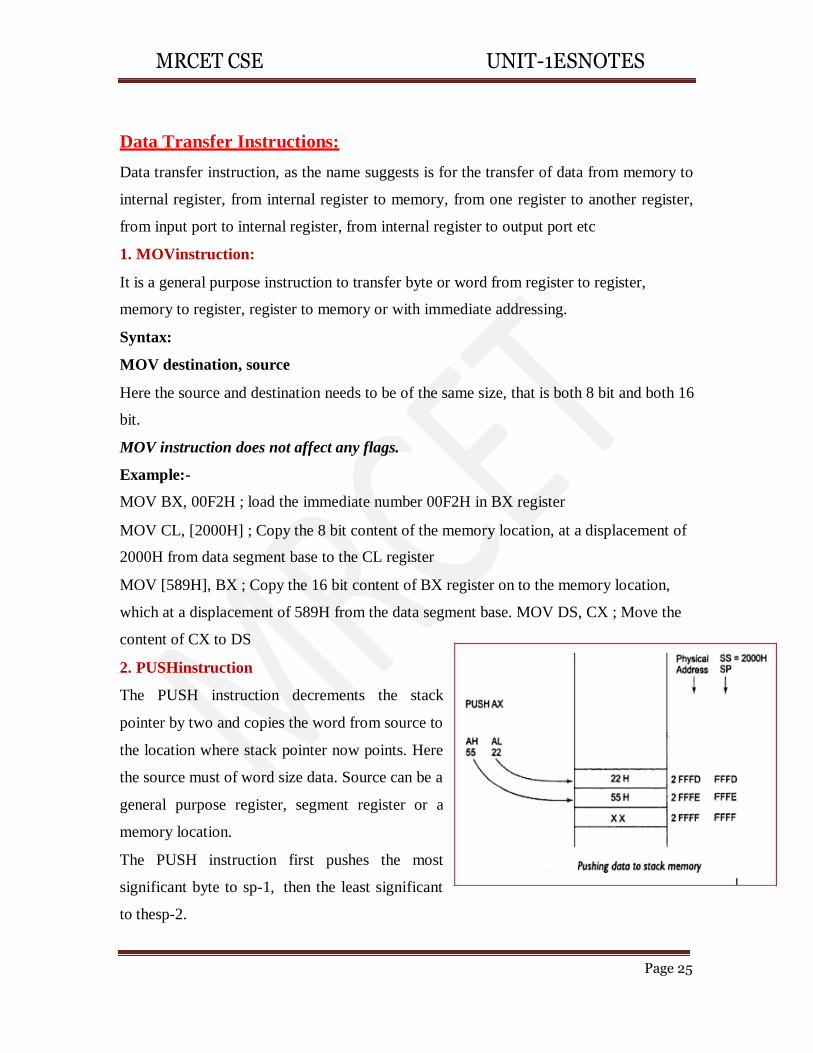
2. PUSHinstruction
The PUSH instruction decrements the stack
pointer by two and copies the word from source to
the location where stack pointer now points. Here
the source must of word size data. Source can be a
general purpose register, segment register or a
memory location.
The PUSH instruction first pushes the most
significant byte to sp-1, then the least significant
to thesp-2.
MRCET CSE UNIT-1ESNOTES
Push instruction does not affect any flags.
Example:-
PUSH AX ; Decrements SP by 2, copy content of AX to the stack
(figure shows execution of this instruction)
PUSH DS ; Decrement SP by 2 and copy DS to stack
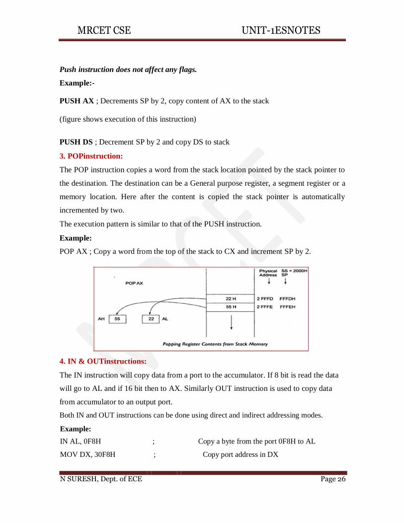
3. POPinstruction:
The POP instruction copies a word from the stack location pointed by the stack pointer to
the destination. The destination can be a General purpose register, a segment register or a
memory location. Here after the content is copied the stack pointer is automatically
incremented by two.
The execution pattern is similar to that of the PUSH instruction.
Example:
POP AX ; Copy a word from the top of the stack to CX and increment SP by 2.
4. IN & OUTinstructions:
The IN instruction will copy data from a port to the accumulator. If 8 bit is read the data
will go to AL and if 16 bit then to AX. Similarly OUT instruction is used to copy data
from accumulator to an output port.
Both IN and OUT instructions can be done using direct and indirect addressing modes.
Example:
IN AL, 0F8H ; Copy a byte from the port 0F8H to AL
MOV DX, 30F8H ; Copy port address in DX
N SURESH, Dept. of ECE Page 26
MRCET CSE UNIT-1ESNOTES
IN AL, DX ; Move 8 bit data from 30F8H port
IN AX, DX ; Move 16 bit data from 30F8H port
OUT 047H, AL ; Copy contents of AL to 8 bit port 047H
MOV DX, 30F8H ; Copy port address in DX
OUT DX, AL ; Move 8 bit data to the 30F8H port
OUT DX, AX ; Move 16 bit data to the 30F8H port
5. XCHGinstruction
The XCHG instruction exchanges contents of the destination and source. Heredestination
and source can be register and register or register and memory location, but XCHG
cannot interchange the value of 2 memorylocations.
Syntax:
XCHG Destination, Source
Example:
XCHGBX,CX ; exchange word in CX with the word inBX
XCHG AL,CL ; exchange byte in CL with the byte inAL
6. LAHF: Load (copy to) AH with the low byte the flagregister.
[AH] [ Flags low
byte] Eg.LAHF
7. SAHF: Store (copy) AH register to low byte of flag register.
[Flagslowbyte] [AH]
Eg. SAHF
8. PUSHF: Copy flag register to top ofstack.
[SP] [SP] –2
[SP] [Flags]
Eg.PUSHF
9. POPF : Copy word at top of stack to flag register.
[Flags] [SP]
[SP] [SP] + 2
N SURESH, Dept. of ECE Page 27
MRCET CSE UNIT-1ESNOTES
NSURESH,Dept.ofECE Page 28
Arithmetic Instructions:
The arithmetic and logic logical group of instruction include,
1. ADD instruction
Add instruction is used to add the current contents of destination with that of source and
store the result in destination. Here we can use register and/or memory locations. AF, CF,
OF, PF, SF, and ZF flags are affected
Syntaxat:
ADD Destination, Source
Example:
ADD AL, 0FH ; Add the immediate content, 0FH to the content of AL and store the
result in AL
ADD AX,BX ; AX <= AX+BX
ADDAX,0100H ; IMMEDIATE
ADDAX,BX ;REGISTER
ADDAX,[SI] ; REGISTER INDIRECT ORINDEXED
ADD AX,[5000H] ;DIRECT
2. ADC: ADD WITHCARRY
This instruction performs the same operation as ADD instruction, but adds the carry flag
bit (which may be set as a result of the previous calculation) to the result. All the
condition code flags are affected by this instruction. The examples of this instruction
along with the modes are asfollows:
Example:
ADC AX,BX – REGISTER
ADC AX,[SI] – REGISTER INDIRECT OR INDEXED
ADC AX, [5000H] – DIRECT
MRCET CSE UNIT-1ESNOTES
NSURESH,Dept.ofECE Page 29
3. SUBinstruction:
SUB instruction is used to subtract the current contents of destination with that of source
and store the result in destination. Here we can use register and/or memory locations. AF,
CF, OF, PF, SF, and ZF flags are affected
Syntaxat:
SUB Destination, Source
Example:
SUB AL, 0FH ; subtract the immediate content, 0FH from the content of AL and
store the result in AL
SUB AX, BX ; AX <=AX-BX
SUB AX,0100H ; IMMEDIATE (DESTINATIONAX)
SUB AX,BX ;REGISTER
SUB AX,[5000H] ;DIRECT
4. SBB: SUBTRACT WITH BORROW
The subtract with borrow instruction subtracts the source operand and the borrow flag
(CF) which may reflect the result of the previous calculations, from the destination
operand. Subtraction with borrow, here means subtracting 1 from the subtraction
obtained by SUB, if carry (borrow) flag isset.
The result is stored in the destination operand. All the flags are affected (condition code)
by this instruction. The examples of this instruction are as follows:
Example:
SBBAX,0100H ;IMMEDIATE (DESTINATIONAX)
SBBAX,BX ;REGISTER
SBB AX,[5000H] ;DIRECT
5. CMP:COMPARE
The instruction compares the source operand, which may be a register or an immediate
data or a memory location, with a destination operand that may be a register or a memory
MRCET CSE UNIT-1ESNOTES
location. For comparison, it subtracts the source operand from the destination operand but
does not store the result anywhere. The flags are affected depending upon the result of the
subtraction. If both of the operands are equal, zero flag is set. If the source operand is
greater than the destination operand, carry flag is set or else, carry flag is reset. The
examples of this instruction are as follows:
Example:
CMP BX,0100H – IMMEDIATE
CMP AX,0100H
CMP BX,[SI]
– IMMEDIATE
– REGISTER INDIRECT ORINDEXED
CMPBX,CX – REGISTER
6. INC & DEC instructions
INC and DEC instructions are used to increment and decrement the content of the
specified destination by one. AF, CF, OF, PF, SF, and ZF flags are affected.
Example:
INC AL
INCAX
AL<= AL + 1
AX<=AX + 1
DECAL AL<= AL –1
DECAX AX<=AX–1
7. NEG : Negate
The negate instruction forms 2‟s complement of the specified destination in the
instruction. The destination can be a register or a memory location. This instruction can
be implemented by inverting each bit and adding 1 toit.
Eg. NEG AL
AL = 0011 0101 35H Replace number in AL with its 2‟s
complement AL = 1100 1011 = CBH
8. MUL :Unsigned Multiplication Byte orWord
This instruction multiplies an unsigned byte or word by the contents of AL.
Eg. MUL BH ; (AX) (AL) x (BH)
MUL CX ; (DX)(AX) (AX) x (CX)
N SURESH, Dept. of ECE Page 30
MRCET CSE UNIT-1ESNOTES
NSURESH,Dept.ofECE Page 31
9. IMUL :SignedMultiplication
This instruction multiplies a signed byte in source operand by a signed byte in AL or a signed word in source operand by a signed word in AX.
Eg. IMUL BH IMUL CX IMUL [SI]
10. CBW : Convert Signed Byte toWord
This instruction copies the sign of a byte in AL to all the bits in AH. AH is then said to be sign extension of AL.
Eg. CBW
AX= 0000 0000 1001 1000 Convert signed byte in AL signed word in AX. Result in AX = 1111 1111 1001 1000
11. CWD : Convert Signed Word to DoubleWord
This instruction copies the sign of a byte in AL to all the bits in AH. AH is then said to be sign extension of AL.
Eg. CWD
Convert signed word in AX to signed double word in DX : AX DX= 1111 1111 1111 1111
Result in AX = 1111 0000 1100 0001
12. DIV : Unsigneddivision
This instruction is used to divide an unsigned word by a byte or to divide an unsigned double word by a word.
Eg.DIVCL ; Word in AX / byte inCL
; Quotient in AL, remainder in AH
DIV CX ; Double word in DX and AX / word
; in CX, and Quotient in AX,
; remainder inDX
Logical Instructions:
1. AND instruction
This instruction logically ANDs each bitof the source byte/word with the
corresponding bit in the destination and stores the result in destination. The source can be
an immediate number, register or memory location, register can be a register or memory
location.
The CF and OF flags are both made zero, PF, ZF, SF are affected by the operation and
AF isundefined.
MRCET CSE UNIT-1ESNOTES
NSURESH,Dept.ofECE Page 32
Syntax:
AND Destination, Source
Example:
AND BL, AL ; suppose BL=1000 0110 and AL = 1100 1010 then after the operation
BL would be BL= 1000 0010.
ANDCX,AX ; CX <= CX ANDAX
AND CL, 08H ; CL<= CL AND (0000 1000)
2. ORinstruction:
This instruction logically ORs each bitof the source byte/word with the
corresponding bit in the destination and stores the result in destination. The source can be
an immediate number, register or memory location, register can be a register or memory
location.
The CF and OF flags are both made zero, PF, ZF, SF are affected by the operation and
AF isundefined.
Syntaxat:
OR Destination, Source
Example:
OR BL, AL ; suppose BL=1000 0110 and AL = 1100 1010 then after the operation BL
would be BL= 11001110.
ORCX,AX ; CX <= CX ANDAX
ORCL,08H ; CL<= CL AND (00001000)
3. NOTinstruction:
The NOT instruction complements (inverts) the contents of an operand register or
a memory location, bit by bit. The examples are as follows:
Example:
NOT AX (BEFORE AX= (1011)2= 0BH ; AFTER EXECUTION AX= (0100)2= 04H.
4. XORinstruction
The XOR operation is again carried out in a similar way to the AND and OR
operation. The constraints on the operands are also similar. The XOR operation gives a
MRCET CSE UNIT-1ESNOTES
NSURESH,Dept.ofECE Page 33
high output, when the 2 input bits are dissimilar. Otherwise, the output is zero. The
example instructions are as follows:
Example: XOR AX, 0098H
XOR AX, BX
5. TEST : Logical CompareInstruction
The TEST instruction performs a bit by bit logical AND operation on the two operands. The result of this ANDing operation is not available for further use, but flags are affected.
Eg. TEST AX, BX
Shift / Rotate Instructions:
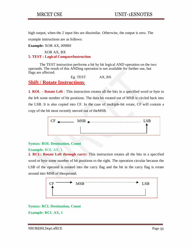
1. ROL – Rotate Left : This instruction rotates all the bits in a specified word or byte to
the left some number of bit positions. The data bit rotated out of MSB is circled back into
the LSB. It is also copied into CF. In the case of multiple-bit rotate, CF will contain a
copy of the bit most recently moved out of theMSB.
Syntax: ROL Destination, Count
Example: ROL AX, 1
2. RCL: Rotate Left through carry: This instruction rotates all the bits in a specified
word or byte some number of bit positions to the right. The operation circular because the
LSB of the operand is rotated into the carry flag and the bit in the carry flag is rotate
around into MSB of theoperand.
Syntax: RCL Destination, Count
Example: RCL AX, 1
MRCET CSE UNIT-1ESNOTES
NSURESH,Dept.ofECE Page 34
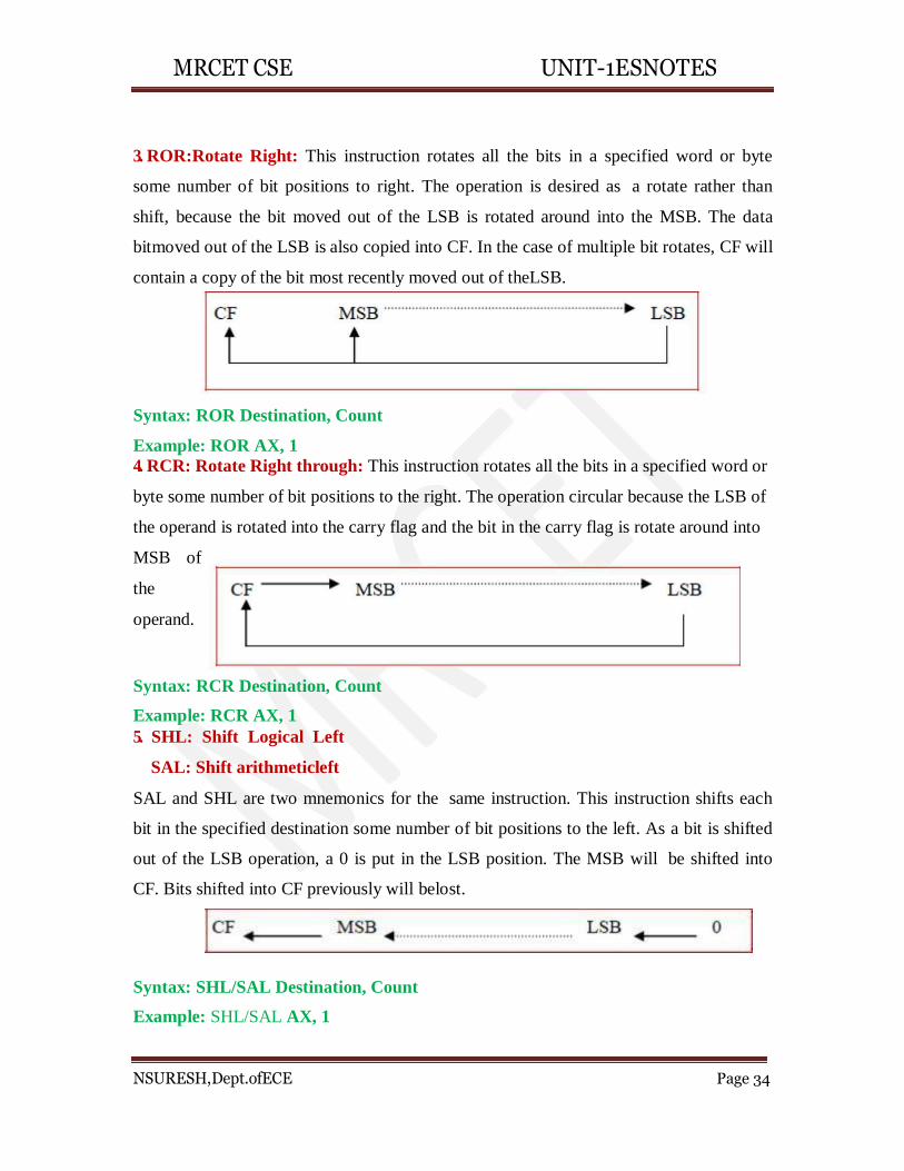
3. ROR:Rotate Right: This instruction rotates all the bits in a specified word or byte
some number of bit positions to right. The operation is desired as a rotate rather than
shift, because the bit moved out of the LSB is rotated around into the MSB. The data
bitmoved out of the LSB is also copied into CF. In the case of multiple bit rotates, CF will
contain a copy of the bit most recently moved out of theLSB.
Syntax: ROR Destination, Count
Example: ROR AX, 1
4. RCR: Rotate Right through: This instruction rotates all the bits in a specified word or
byte some number of bit positions to the right. The operation circular because the LSB of
the operand is rotated into the carry flag and the bit in the carry flag is rotate around into
MSB of
the
operand.
Syntax: RCR Destination, Count
Example: RCR AX, 1
5. SHL: Shift Logical Left
SAL: Shift arithmeticleft
SAL and SHL are two mnemonics for the same instruction. This instruction shifts each
bit in the specified destination some number of bit positions to the left. As a bit is shifted
out of the LSB operation, a 0 is put in the LSB position. The MSB will be shifted into
CF. Bits shifted into CF previously will belost.
Syntax: SHL/SAL Destination, Count
Example: SHL/SAL AX, 1
MRCET CSE UNIT-1ESNOTES
NSURESH,Dept.ofECE Page 35
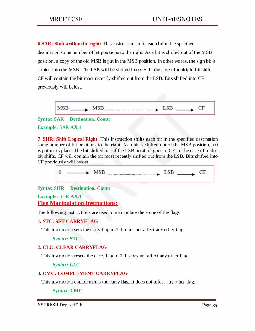
6. SAR: Shift arithmetic right: This instruction shifts each bit in the specified
destination some number of bit positions to the right. As a bit is shifted out of the MSB
position, a copy of the old MSB is put in the MSB position. In other words, the sign bit is
copied into the MSB. The LSB will be shifted into CF. In the case of multiple-bit shift,
CF will contain the bit most recently shifted out from the LSB. Bits shifted into CF
previously will belost.
Syntax:SAR Destination, Count
Example: SAR AX,1
7. SHR: Shift Logical Right: This instruction shifts each bit in the specified destination
some number of bit positions to the right. As a bit is shifted out of the MSB position, a 0
is put in its place. The bit shifted out of the LSB position goes to CF. In the case of multi-
bit shifts, CF will contain the bit most recently shifted out from the LSB. Bits shifted into
CF previously will belost.
Syntax:SHR Destination, Count
Example: SHR AX,1
Flag Manipulation Instructions:
The following instructions are used to manipulate the some of the flags
1. STC: SET CARRYFLAG
This instruction sets the carry flag to 1. It does not affect any other flag.
Syntax: STC
2. CLC: CLEAR CARRYFLAG
This instruction resets the carry flag to 0. It does not affect any other flag.
Syntax: CLC
3. CMC: COMPLEMENT CARRYFLAG
This instruction complements the carry flag. It does not affect any other flag.
Syntax: CMC
MRCET CSE UNIT-1ESNOTES
NSURESH,Dept.ofECE Page 36
4. STD: SET DIRECTIONFLAG
This instruction sets the direction flag to 1. It does not affect any other flag.
Syntax: STD
5. CLD: CLEAR DIRECTIONFLAG
This instruction resets the direction flag to 0. It does not affect any other flag.
Syntax: CLD
6. STI : SET INTERRUPTFLAG
Setting the interrupt flag to a 1 enables the INTR interrupt input of the 8086. The
instruction will not take affect until the next instruction after STI. When the INTR input
is enabled, an interrupt signal on this input will then cause the 8086 to interrupt program
execution, push the return address and flags on the stack, and execute an interrupt service
procedure. An IRET instruction at the end of the interrupt service procedure will restore
the return address and flags that were pushed onto the stack and return execution to the
interrupted program. STI does not affect any otherflag.
Syntax: STI
7. CLI : CLEAR INTERRUPTFLAG
This instruction resets the interrupt flag to 0. If the interrupt flag is reset, the 8086
will not respond to an interrupt signal on its INTR input. The CLI instructions, however,
has no effect on the non-maskable interrupt input, NMI. It does not affect any other flag.
Syntax: CLI
Machine Control Instructions
1. HLTinstruction
The HLT instruction will cause the 8086 microprocessor stop fetching and executing
instructions. The 8086 will enter a halt state. The processor gets out of this Halt signal
upon an interrupt signal in INTR pin/NMI pin or a reset signal on RESET input.
Syntax :- HLT
2. WAITinstruction
When this instruction is executed, the 8086 enters into an idle state. This idle state is
continued till a high is received on the TEST input pin or a valid interrupt signal is
MRCET CSE UNIT-1ESNOTES
NSURESH,Dept.ofECE Page 37
received. Wait affects no flags. It generally is used to synchronize the 8086 with a
peripheral device(s).
Syntax :- WAIT
3. ESCinstruction
This instruction is used to pass instruction to a coprocessor like 8087. There is a 6 bit
instruction for the coprocessor embedded in the ESC instruction. In most cases the 8086
treats ESC and a NOP, but in some cases the 8086 will access data items in memory for
the coprocessor
Syntax :- ESC
4. LOCKinstruction
In multiprocessor environments, the different microprocessors share a system bus, which
is needed to access external devices like disks. LOCK Instruction is given as prefix in the
case when a processor needs exclusive access of the system bus for a particular
instruction. It affects no flags.
Example:
LOCK XCHG SEMAPHORE, AL : The XCHG instruction requires two bus accesses.
The lock prefix prevents another processor from taking control of the system bus between
the 2 accesses
5. NOPinstruction:
At the end of NOP instruction, no operation is done other than the fetching and decoding
of the instruction. It takes 3 clock cycles. NOP is used to fill in time delays or to provide
space for instructions while trouble shooting. NOP affects no flags
Syntax :- NOP
Program control transfer instructions
There are 2 types of such instructions. They are:
1. Unconditional transfer instructions – CALL, RET,JMP
2. Conditional transfer instructions – Jump oncondition
MRCET CSE UNIT-1ESNOTES
NSURESH,Dept.ofECE Page 38
1. Unconditional transferinstructions:
(a). CALL instruction: The CALL instruction is used to transfer execution to a
subprogram or procedure. There are two types of CALL instructions, near andfar.
A near CALL is a call to a procedure which is in the same code segment as the
CALL instruction. 8086 when encountered a near call, it decrements the SP by 2 and
copies the offset of the next instruction after the CALL on the stack. It loads the IP with
the offset of the procedure then to start the execution of the procedure.
A far CALL is the call to a procedure residing in a different segment. Here value
of CS and offset of the next instruction both are backed up in the stack. And then
branches to the procedure by changing the content of CS with the segment base
containing procedure and IP with the offset of the first instruction of theprocedure.
Example:
Near call
CALL PRO ; PRO is the name of the procedure
CALL CX ; Here CX contains the offset of the first instruction of the procedure, that is
replaces the content of IP with the content of CX Far call
CALL DWORD PTR[8X] ; New values for CS and IP are fetched from four memory
locations in the DS. The new value for CS is fetched from [8X] and [8X+1], the new IP is
fetched from [8X+2] and [8X+3].
(b). RETinstruction
RET instruction will return execution from a procedure to the next instruction
after the CALL instruction in the calling program. If it was a near call, then IP is replaced
with the value at the top of the stack, if it had been a far call, then another POP of the
stack is required. This second popped data from the stack is put in the CS, thus resuming
the execution of the calling programpassed.
A RET instruction can be followed by a number, to specifythe
parameters RET instruction does not affect anyflags.
MRCET CSE UNIT-1ESNOTES
NSURESH,Dept.ofECE Page 39
General format: RET
Example:
p1 PROC ; procedure declaration.
MOV AX, 1234h ;
RET ; return to caller.
p1 ENDP
(c) JMP instruction: This is also called as unconditional jump instruction, because the
processor jumps to the specified location rather than the instruction after the JMP
instruction. Jumps can be short jumps when the target address is in the same segment as
the JMP instruction or far jumps when it is in a different segment.
General Format: JMP <target address>
2. Conditional transfer instructions – Jump on condition: Conditional
jumps are always short jumps in 8086. Here jump is done only if the condition specified
is true/false. If the condition is not satisfied, then the execution proceeds in the normal
way.
Example: There are many conditional jump instructions like
JC : Jump on carry (CF=set)
JNC : Jump on non carry (CF=reset)
JZ : Jump on zero (ZF=set)
JNO : Jump on overflow (OF=set)
Iteration control(LOOP) instructions :
These instructions are used to execute a series of instructions some number of
times. The number is specified in the CX register, which will be automatically
decremented in course of iteration. But here the destination address for the jump must be
in the range of -128 to 127 bytes.
Example: Instructions here are:-
LOOP : loop through the set of instructions until CX is 0
LOOPE/LOOPZ : here the set of instructions are repeated until CX=0 or ZF=0
MRCET CSE UNIT-1ESNOTES
NSURESH,Dept.ofECE Page 40
LOOPNE/LOOPNZ: here repeated until CX=0 or ZF=1
String Instructions
1. MOVS/MOVSB/MOVSW: These instructions copy a word or byte from a location in
the data segment to a location in the extra segment. The offset of the source is in SI and
that of destination is in DI. For multiple word/byte transfers the count is stored in the CX
register.
When direction flag is 0, SI and DI are incremented and when it is 1, SI and DI are
decremented.
MOVS affect no flags. MOVSB is used for byte sized movements while MOVSW is for
word sized.
2. REP/REPE/REP2/REPNE/REPNZ
REP is used with string instruction; it repeats an instruction until the specified condition becomes false. Example:
REP => CX=0
REPE/REPZ => CX=0 OR ZF=0 REPNE/REPNZ => CX=0 OR ZF=1
3. LODS/LODSB/LODSW:
This instruction copies a byte from a string location pointed to by SI to AL or a
word from a string location pointed to by SI to AX.LODS does not affect any flags.
LODSB copies byte and LODSW copies word.
4. STOS/STOSB/STOSW:
The STOS instruction is used to store a byte/word contained in AL/AX to the
offset contained in the DI register. STOS does not affect any flags. After copying the
content DI is automatically incremented or decremented, based on the value of direction
flag
5. CMPS/CMPSB/CMPSW
CMPS is used to compare the strings, byte wise or word wise. The comparison is
affected by subtraction of content pointed by DI from that pointed by SI. The AF, CF,
OF, PF, SF and ZF flags are affected by this instruction, but neither operand isaffected.
MRCET CSE UNIT-1ESNOTES
NSURESH,Dept.ofECE Page 41
INTEL 8051 MICRCONTROLLER
Introduction: A decade back the process and control operations were totally
implemented by the Microprocessors only. But now a days the situation is totally
changed and it is occupied by the new devices called Microcontroller. The development
is so drastic that we can‟t find any electronic gadget without the use of amicrocontroller.
This microcontroller changed the embedded system design so simple and advanced that
the embedded market has become one of the most sought after for not only entrepreneurs
but for design engineersalso.
What is a Microcontroller?
A single chip computer or A CPU with all the peripherals like RAM, ROM, I/O
Ports, Timers , ADCs etc... on the same chip. For ex: Motorola‟s 6811, Intel‟s 8051,
Zilog‟s Z8 and PIC 16X etc…
MICROPROCESSORS & MICROCONTROLLERS:
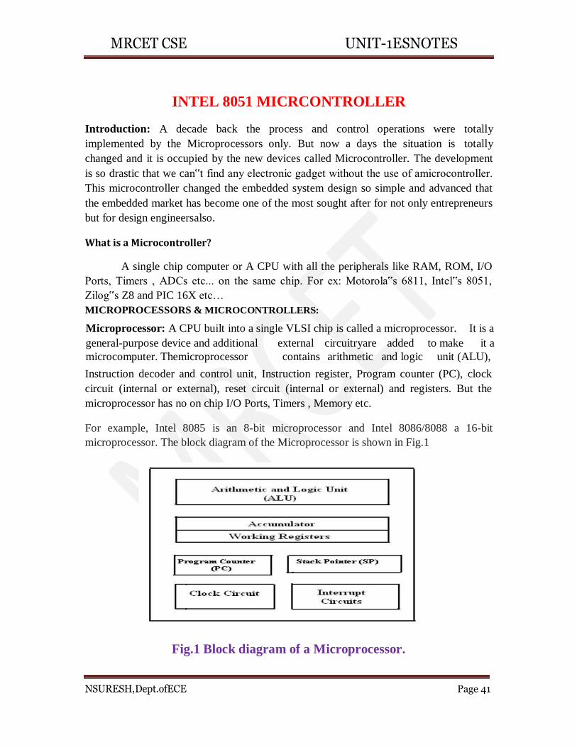
Microprocessor: A CPU built into a single VLSI chip is called a microprocessor. It is a
general-purpose device and additional external circuitryare added to make it a
microcomputer. Themicroprocessor contains arithmetic and logic unit (ALU),
Instruction decoder and control unit, Instruction register, Program counter (PC), clock
circuit (internal or external), reset circuit (internal or external) and registers. But the
microprocessor has no on chip I/O Ports, Timers , Memory etc.
For example, Intel 8085 is an 8-bit microprocessor and Intel 8086/8088 a 16-bit
microprocessor. The block diagram of the Microprocessor is shown in Fig.1
Fig.1 Block diagram of a Microprocessor.
MRCET CSE UNIT-1ESNOTES
NSURESH,Dept.ofECE Page 42
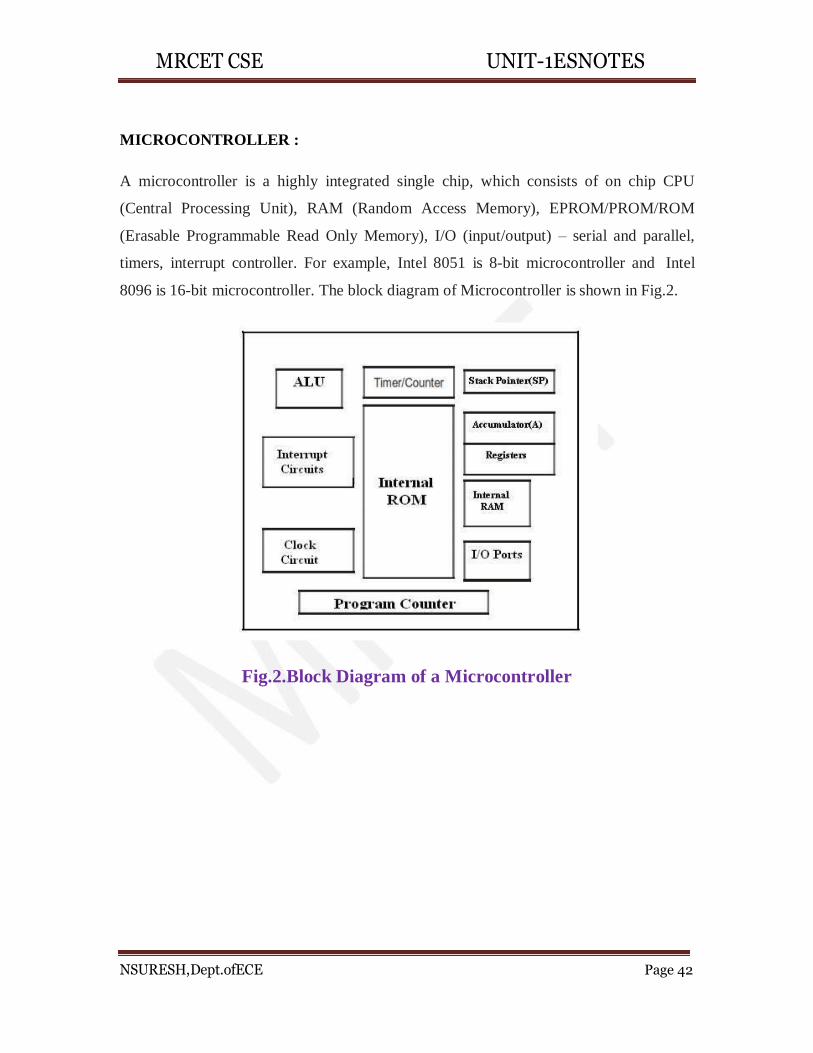
Fig.2.Block Diagram of a Microcontroller
MICROCONTROLLER :
A microcontroller is a highly integrated single chip, which consists of on chip CPU
(Central Processing Unit), RAM (Random Access Memory), EPROM/PROM/ROM
(Erasable Programmable Read Only Memory), I/O (input/output) – serial and parallel,
timers, interrupt controller. For example, Intel 8051 is 8-bit microcontroller and Intel
8096 is 16-bit microcontroller. The block diagram of Microcontroller is shown in Fig.2.
MRCET CSE UNIT-1ESNOTES
NSURESH,Dept.ofECE Page 43
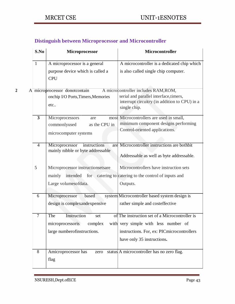
Distinguish between Microprocessor and Microcontroller
S.No Microprocessor Microcontroller
1 A microprocessor is a general A microcontroller is a dedicated chip which
purpose device which is called a is also called single chip computer.
CPU
2 A microprocessor donotcontain A microcontroller includes RAM,ROM,
onchip I/O Ports,Timers,Memories serial and parallel interface,timers,
etc..
interrupt circuitry (in addition to CPU) in a
single chip.
3 Microprocessors are most Microcontrollers are used in small,
commonlyused as the CPU in minimum component designs performing
microcomputer systems
Control-oriented applications.
4 Microprocessor instructions are Microcontroller instructions are bothbit mainly nibble or byte addressable
Addressable as well as byte addressable.
5 Microprocessor instructionsetsare Microcontrollers have instruction sets
mainly intended for catering to catering to the control of inputs and
Large volumesofdata. Outputs.
6 Microprocessor based system Microcontroller based system design is
design is complexandexpensive rather simple and costeffective
7 The Instruction set of The instruction set of a Microcontroller is
microprocessoris complex with very simple with less number of
large numberofinstructions. instructions. For, ex: PICmicrocontrollers
have only 35 instructions.
8 Amicroprocessor has zero status A microcontroller has no zero flag.
flag
MRCET CSE UNIT-1ESNOTES
NSURESH,Dept.ofECE Page 44
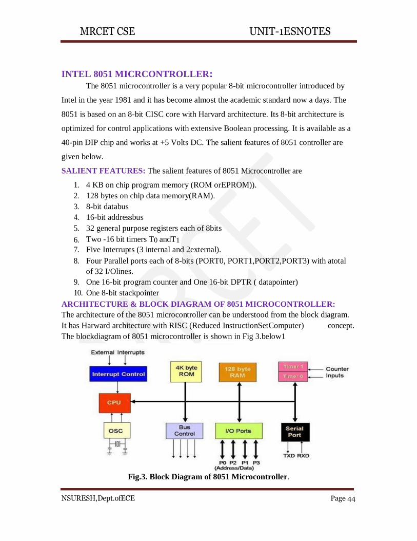
INTEL 8051 MICRCONTROLLER: The 8051 microcontroller is a very popular 8-bit microcontroller introduced by
Intel in the year 1981 and it has become almost the academic standard now a days. The
8051 is based on an 8-bit CISC core with Harvard architecture. Its 8-bit architecture is
optimized for control applications with extensive Boolean processing. It is available as a
40-pin DIP chip and works at +5 Volts DC. The salient features of 8051 controller are
given below.
SALIENT FEATURES: The salient features of 8051 Microcontroller are
1. 4 KB on chip program memory (ROM orEPROM)).
2. 128 bytes on chip data memory(RAM).
3. 8-bit databus
4. 16-bit addressbus
5. 32 general purpose registers each of 8bits
6. Two -16 bit timers T0 andT1
7. Five Interrupts (3 internal and 2external).
8. Four Parallel ports each of 8-bits (PORT0, PORT1,PORT2,PORT3) with atotal
of 32 I/Olines.
9. One 16-bit program counter and One 16-bit DPTR ( datapointer)
10. One 8-bit stackpointer
ARCHITECTURE & BLOCK DIAGRAM OF 8051 MICROCONTROLLER:
The architecture of the 8051 microcontroller can be understood from the block diagram.
It has Harward architecture with RISC (Reduced InstructionSetComputer) concept.
The blockdiagram of 8051 microcontroller is shown in Fig 3.below1
Fig.3. Block Diagram of 8051 Microcontroller.
MRCET CSE UNIT-1ESNOTES
NSURESH,Dept.ofECE Page 45
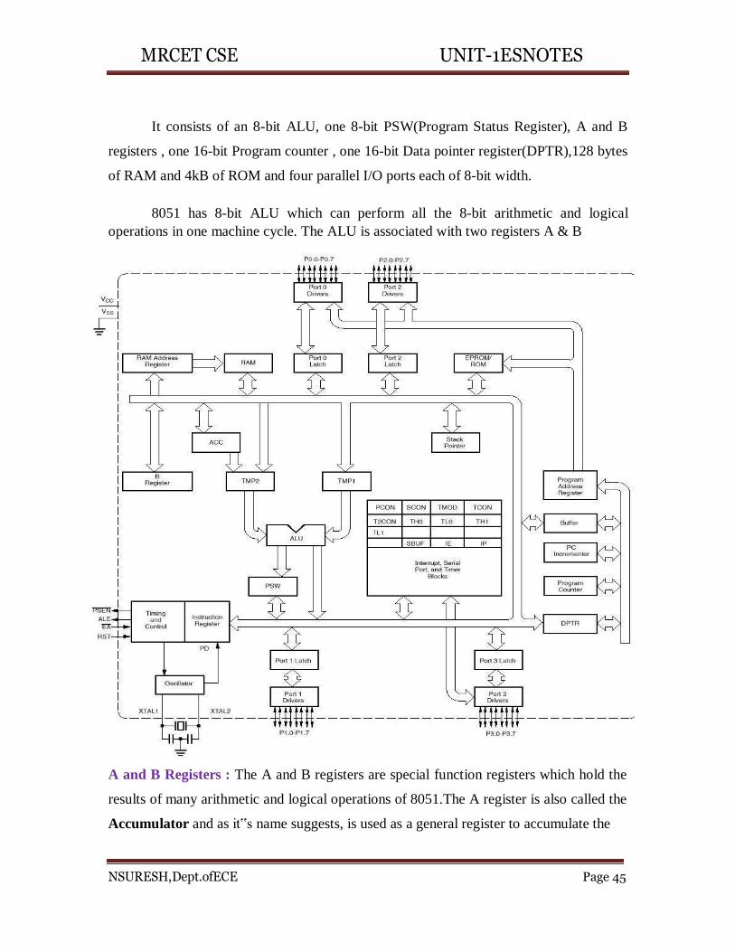
It consists of an 8-bit ALU, one 8-bit PSW(Program Status Register), A and B
registers , one 16-bit Program counter , one 16-bit Data pointer register(DPTR),128 bytes
of RAM and 4kB of ROM and four parallel I/O ports each of 8-bit width.
8051 has 8-bit ALU which can perform all the 8-bit arithmetic and logical
operations in one machine cycle. The ALU is associated with two registers A & B
A and B Registers : The A and B registers are special function registers which hold the
results of many arithmetic and logical operations of 8051.The A register is also called the
Accumulator and as it‟s name suggests, is used as a general register to accumulate the
MRCET CSE UNIT-1ESNOTES
NSURESH,Dept.ofECE Page 46
results of a large number of instructions. By default it is used for all mathematical
operations and also data transfer operations between CPU and any external memory.
The B register is mainly used for multiplication and division operations along with A
register. MULAB : DIVAB.
It has no other function other than as a location where data may be stored.
The R registers: The "R" registers are a set of eight registers that are named R0, R1, etc.
up to and including R7. These registers are used as auxillary registers in manyoperations.
The "R" registers are also used to temporarily storevalues.
Program Counter (PC) : 8051 has a 16-bit program counter .The program counter
always points to the address of the next instruction to be executed. After execution of one
instruction the program counter is incremented to point to the address of the next
instruction to be executed. It is the contents of the PC that are placed on the address bus
to find and fetch the desired instruction. Since the PC is 16-bit width ,8051 can access
program addresses from 0000H to FFFFH ,a total of 6kB ofcode.
Stack Pointer Register (SP) : It is an 8-bit register which stores the address of the stack
top. i.e the Stack Pointer is used to indicate where the next value to be removed from the
stack should be taken from. When a value is pushed onto the stack, the 8051 first
increments the value of SP and then stores the value at the resulting memory location.
Similarly when a value is popped off the stack, the 8051 returns the value from the
memory location indicated by SP, and then decrements the value of SP. Since the SP is
only 8-bit wide it is incremented or decremented by two. SP is modified directly by the
8051 by six instructions: PUSH, POP, ACALL, LCALL, RET, and RETI. It is also used
intrinsically whenever an interrupt is triggered.
STACK in 8051 Microcontroller : The stack is a part of RAM used by the CPU to store
information temporarily. This information may be either data or an address .The CPU
needs this storage area as there are only limited number of registers. The register used to
access the stack is called the Stack pointer which is an 8-bit register..So,it can take values
of 00 to FF H. When the 8051 is powered up ,the SP register contains the
MRCET CSE UNIT-1ESNOTES
NSURESH,Dept.ofECE Page 47
value 07.i.e the RAM location value 08 is the first location being used for the stack by the
8051 controller
There are two important instructions to handle this stack. One is the PUSH and
the other is the POP. The loading of data from CPU registers to the stack is done by
PUSH and the loading of the contents of the stack back into a CPU register is done by
POP.
EX : MOV R6 ,#35 H
MOV R1 ,#21 H
PUSH6
PUSH1
In the above instructions the contents of the Registers R6 and R1 are moved to stack
and they occupy the 08 and 09 locations of the stack. Now the contents of the SP are
incremented by two and it is 0A
Similarly POP 3 instruction pops the contents of stack into R3 register. Now the contents
of the SP is decremented by 1
In 8051 the RAM locations 08 to 1F (24 bytes) can be used for the Stack. In any program
if we need more than 24 bytes of stack ,we can change the SP point to RAM locations 30-
7F H. this can be done with the instruction MOV SP,# XX.
Data Pointer Register (DPTR) : It is a 16-bit register which is the only user-accessible.
DPTR, as the name suggests, is used to point to data. It is used by a number of commands
which allow the 8051 to access external memory. When the 8051 accesses external
memory it will access external memory at the address indicated by DPTR. This DPTR
can also be used as two 8-registers DPH andDPL.
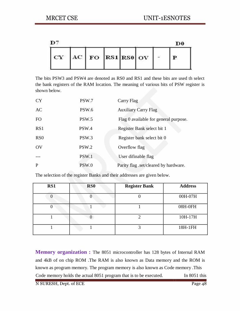
Program Status Register (PSW): The 8051 has a 8-bit PSW register which is also
known as Flag register. In the 8-bit register only 6-bits are used by 8051.The two unused
bits are user definable bits. In the 6-bits four of them are conditional flags .They are
Carry –CY, Auxiliary Carry-AC, Parity-P, and Overflow-OV .These flag bits indicate
some conditions that resulted after an instruction wasexecuted.
MRCET CSE UNIT-1ESNOTES
The bits PSW3 and PSW4 are denoted as RS0 and RS1 and these bits are used th select
the bank registers of the RAM location. The meaning of various bits of PSW register is
shown below.
CY PSW.7 Carry Flag
AC PSW.6 Auxiliary Carry Flag
FO PSW.5 Flag 0 available for general purpose.
RS1 PSW.4 Register Bank select bit 1
RS0 PSW.3 Register bank select bit 0
OV PSW.2 Overflow flag
--- PSW.1 User difinable flag
P PSW.0 Parity flag .set/cleared by hardware.
The selection of the register Banks and their addresses are given below.
RS1 RS0 Register Bank Address
0 0 0 00H-07H
0 1 1 08H-0FH
1 0 2 10H-17H
1 1 3 18H-1FH
Memory organization : The 8051 microcontroller has 128 bytes of Internal RAM
and 4kB of on chip ROM .The RAM is also known as Data memory and the ROM is
known as program memory. The program memory is also known as Code memory .This
Code memory holds the actual 8051 program that is to be executed. In 8051 this
N SURESH, Dept. of ECE Page 48
MRCET CSE UNIT-1ESNOTES
NSURESH,Dept.ofECE Page 49
memory is limited to 64K .Code memory may be foundon-chip, as ROM or EPROM.
It may also be stored completely off-chip in an external ROM or, more commonly, an
external EPROM. The 8051 has only 128 bytes of Internal RAM but it supports 64kB of
external RAM. As the name suggests, external RAM is any random access memory
which is off-chip. Since the memory is off-chip it is not as flexible interms of accessing,
and is also slower. For example, to increment an Internal RAM location by 1,it requires
only 1 instruction and 1 instruction cyclebutto increment a 1-byte value stored in
External RAM requires 4 instructions and 7 instruction cycles. So,herethe external
memory is 7 timesslower.
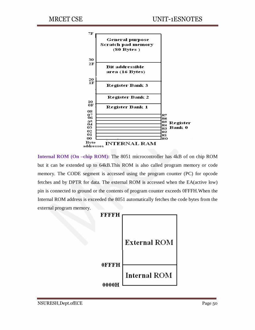
Internal RAM OF 8051 : This Internal RAM is found on-chip on the 8051 .So it is the
fastest RAM available, and it is also the most flexible in terms of reading, writing, and
modifying it’s contents. Internal RAM is volatile, so when the 8051 is reset this
memory is cleared. The 128 bytes of internal RAM is organized as below.
(i) Four register banks (Bank0, Bank1, Bank2 and Bank3) each of 8-bits (total 32
bytes). The default bank register is Bank0. The remaining Banks are selected with the
help of RS0 and RS1 bits of PSWRegister.
(i) 16 bytes of bit addressable areaand
(ii) 80 bytes of general purpose area (Scratch pad memory) as shown in the diagram
below. This area is also utilized by the microcontroller as a storage area for the operating
stack.
The 32 bytes of RAM from address 00 H to 1FH are used as working registersorganized
as four banks of eight registers each.The registers are named as R0-R7 .Each register
can be addressed by its name or by its RAMaddress.
For EX: MOV A,R7 or MOVR7,#05H
MRCET CSE UNIT-1ESNOTES
NSURESH,Dept.ofECE Page 50
Internal ROM (On –chip ROM): The 8051 microcontroller has 4kB of on chip ROM
but it can be extended up to 64kB.This ROM is also called program memory or code
memory. The CODE segment is accessed using the program counter (PC) for opcode
fetches and by DPTR for data. The external ROM is accessed when the EA(active low)
pin is connected to ground or the contents of program counter exceeds 0FFFH.When the
Internal ROM address is exceeded the 8051 automatically fetches the code bytes from the
external program memory.

MRCET CSE UNIT-1ESNOTES
PARALLEL I /O PORTS :
The 8051 microcontroller has four parallel I/O ports , each of 8-bits .So, it provides the
user 32 I/O lines for connecting the microcontroller to the peripherals. The four ports are
P0 (Port 0), P1(Port1) ,P2(Port 2) and P3 (Port3). Upon reset all the ports are output
ports. In order to make them input, all the ports must be set i.e a high bit must be sent to
all the port pins. This is normally done by the instruction“SETB”.
Ex: MOVA,#0FFH ; A =FF
MOV P0,A ; make P0 an inputport
PORT 0: Port 0 is an 8-bit I/O port with dual purpose. If external memory is used, these
port pins are used for the lower address byte address/data (AD0-AD7), otherwise all bits
of the port are either input or output..
Dual role of port 0: Port 0 can also be used as address/data bus(AD0-AD7), allowing it
to be used for both address and data. When connecting the 8051 to an external memory,
port 0 provides both address and data. The 8051 multiplexes address and data through
port 0 to save the pins. ALE indicates whether P0 has address or data. When ALE = 0, it
provides data D0-D7, and when ALE =1 it providesaddress
Port 1: Port 1 occupies a total of 8 pins (pins 1 through 8). It has no dual applicationand
acts only as input or output port. Upon reset, Port 1 is configured as an output port. To
configure it as an input port , port bits must be set i.e a high bit must be sent to all the
port pins. This is normally done by the instruction“SETB”.
For Ex :
MOV A, #0FFH ; A=FF HEX
MOV P1,A ; make P1 an input port by writing 1‟s to all of its pins
Port 2: Port 2 is also an eight bit parallel port. (pins 21- 28). It can be used as input or
output port. Upon reset, Port 2 is configured as an output port. If the port is to be used as
input port, all the port bits must be made high by sending FF to the port. For ex,
MOV A, #0FFH ; A=FF hex
MOV P2, A ; make P2 an input port by writing all 1‟s to it
N SURESH, Dept. of ECE Page 51
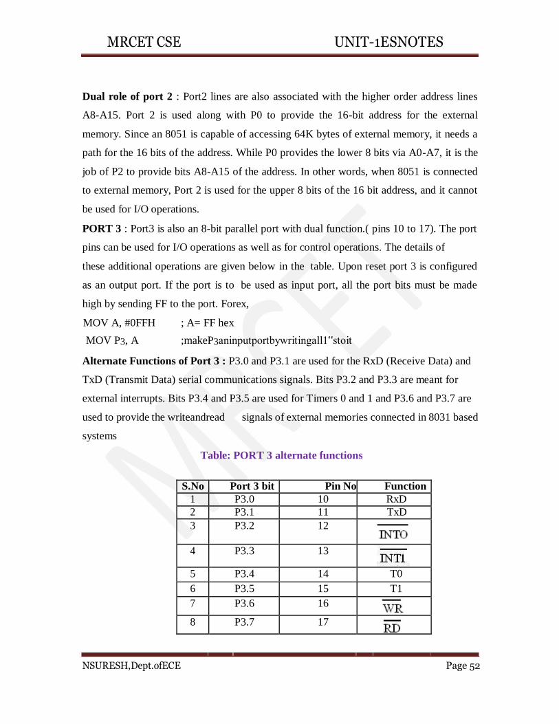
MRCET CSE UNIT-1ESNOTES
NSURESH,Dept.ofECE Page 52
Dual role of port 2 : Port2 lines are also associated with the higher order address lines
A8-A15. Port 2 is used along with P0 to provide the 16-bit address for the external
memory. Since an 8051 is capable of accessing 64K bytes of external memory, it needs a
path for the 16 bits of the address. While P0 provides the lower 8 bits via A0-A7, it is the
job of P2 to provide bits A8-A15 of the address. In other words, when 8051 is connected
to external memory, Port 2 is used for the upper 8 bits of the 16 bit address, and it cannot
be used for I/O operations.
PORT 3 : Port3 is also an 8-bit parallel port with dual function.( pins 10 to 17). The port
pins can be used for I/O operations as well as for control operations. The details of
these additional operations are given below in the table. Upon reset port 3 is configured
as an output port. If the port is to be used as input port, all the port bits must be made
high by sending FF to the port. Forex,
MOV A, #0FFH ; A= FF hex
MOV P3, A ;makeP3aninputportbywritingall1‟stoit
Alternate Functions of Port 3 : P3.0 and P3.1 are used for the RxD (Receive Data) and
TxD (Transmit Data) serial communications signals. Bits P3.2 and P3.3 are meant for
external interrupts. Bits P3.4 and P3.5 are used for Timers 0 and 1 and P3.6 and P3.7 are
used to provide the writeandread signals of external memories connected in 8031 based
systems
Table: PORT 3 alternate functions
S.No Port 3 bit Pin No Function
1 P3.0 10 RxD
2 P3.1 11 TxD
3 P3.2 12
4 P3.3 13
5 P3.4 14 T0
6 P3.5 15 T1
7 P3.6 16
8 P3.7 17
MRCET CSE UNIT-1ESNOTES
NSURESH,Dept.ofECE Page 53
8051 Instructions: The process of writing program for the microcontroller mainly consists of giving instructions (commands) in the specific order in which they should be executed in order to
carry out a specific task. All commands are known as INSTRUCTION SET. All
microcontrollers compatibile with the 8051 have in total of 255 instructions
These can be grouped into the following categories
1. Arithmetic Instructions
2. LogicalInstructions
3. Data Transferinstructions
4. Boolean VariableInstructions
5. Program Branching Instructions
The following nomenclatures for register, data, address and variables are used while write instructions.
A: Accumulator
B: "B" register
C: Carry bit
Rn: Register R0 - R7 of the currently selected register bank
Direct: 8-bit internal direct address for data. The data could be in lower 128bytes of RAM (00 - 7FH) or it could be in the special function register (80 - FFH).
@Ri: 8-bit external or internal RAM address available in register R0 or R1. This is used for indirect addressing mode.
#data8: Immediate 8-bit data available in the instruction.
#data16: Immediate 16-bit data available in the instruction.
Addr11: 11-bit destination address for short absolute jump. Used by instructions AJMP & ACALL. Jump range is 2 kbyte (one page).
Addr16: 16-bit destination address for long call or long jump.
bit: Directly addressed bit in internal RAM or SFR
The first part of each instruction, called MNEMONIC refers to the operation an instruction performs
(copy, addition, logic operation etc.). Mnemonics are abbreviations of the name of operation being executed.
The other part of instruction, called OPERAND is separated from mnemonic by at least one
whitespace and defines data being processed by instructions. Some of the instructions have no
operand, while some of them have one, two or three. If there is more than one operand in an instruction, they are separated by acomma
1. Arithmetic Instructions: Arithmetic instructions perform several basic arithmeticoperations such as addition, subtraction, division, multiplication etc. After execution, the result is stored in the firstoperand.
For example:
ADD A,R1 - The result of addition (A+R1) will be stored in the accumulator.
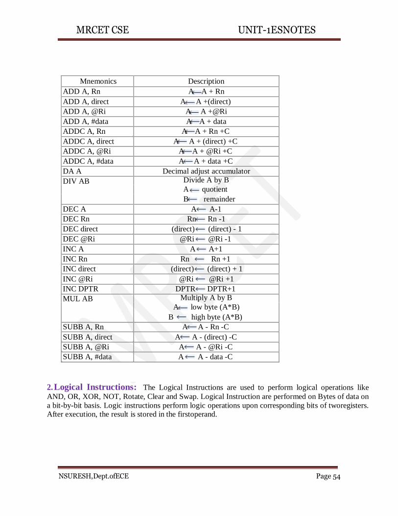
MRCET CSE UNIT-1ESNOTES
NSURESH,Dept.ofECE Page 54
Mnemonics Description
ADD A, Rn A A + Rn
ADD A, direct A A +(direct)
ADD A, @Ri A A +@Ri
ADD A, #data A A + data
ADDC A, Rn A A + Rn +C
ADDC A, direct A A + (direct) +C
ADDC A, @Ri A A + @Ri +C
ADDC A, #data A A + data +C
DA A Decimal adjust accumulator
DIV AB Divide A by B
A quotient
B remainder
DEC A A A-1
DEC Rn Rn Rn -1
DEC direct (direct) (direct) - 1
DEC @Ri @Ri @Ri -1
INC A A A+1
INC Rn Rn Rn +1
INC direct (direct) (direct) + 1
INC @Ri @Ri @Ri +1
INC DPTR DPTR DPTR+1
MUL AB Multiply A by B
A low byte (A*B)
B high byte (A*B)
SUBB A, Rn A A - Rn -C
SUBB A, direct A A - (direct) -C
SUBB A, @Ri A A - @Ri -C
SUBB A, #data A A - data -C
2. Logical Instructions: The Logical Instructions are used to perform logical operations like
AND, OR, XOR, NOT, Rotate, Clear and Swap. Logical Instruction are performed on Bytes of data on
a bit-by-bit basis. Logic instructions perform logic operations upon corresponding bits of tworegisters. After execution, the result is stored in the firstoperand.
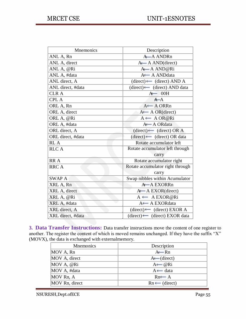
MRCET CSE UNIT-1ESNOTES
NSURESH,Dept.ofECE Page 55
Mnemonics Description
ANL A, Rn A A ANDRn
ANL A, direct A A AND(direct)
ANL A, @Ri A A AND@Ri
ANL A, #data A A ANDdata
ANL direct, A (direct) (direct) AND A
ANL direct, #data (direct) (direct) AND data
CLR A A 00H
CPL A A A
ORL A, Rn A A ORRn
ORL A, direct A A OR(direct)
ORL A, @Ri A A OR@Ri
ORL A, #data A A ORdata
ORL direct, A (direct) (direct) OR A
ORL direct, #data (direct) (direct) OR data
RL A Rotate accumulator left
RLC A Rotate accumulator left through
carry
RR A Rotate accumulator right
RRC A Rotate accumulator right through carry
SWAP A Swap nibbles within Acumulator
XRL A, Rn A A EXORRn
XRL A, direct A A EXOR(direct)
XRL A, @Ri A A EXOR@Ri
XRL A, #data A A EXORdata
XRL direct, A (direct) (direct) EXOR A
XRL direct, #data (direct) (direct) EXOR data
3. Data Transfer Instructions: Data transfer instructions move the content of one register to
another. The register the content of which is moved remains unchanged. If they have the suffix “X”
(MOVX), the data is exchanged with externalmemory.
Mnemonics Description
MOV A, Rn A Rn
MOV A, direct A (direct)
MOV A, @Ri A @Ri
MOV A, #data A data
MOV Rn, A Rn A
MOV Rn, direct Rn (direct)
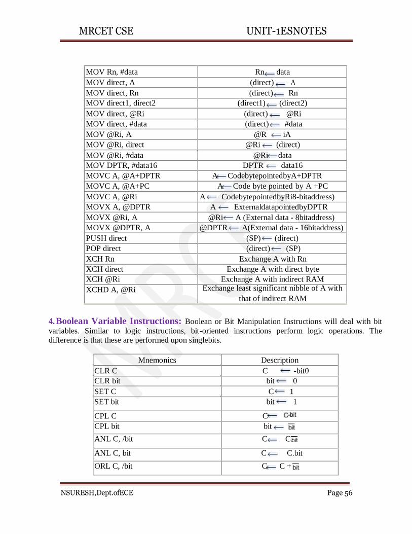
MRCET CSE UNIT-1ESNOTES
NSURESH,Dept.ofECE Page 56
MOV Rn, #data Rn data
MOV direct, A (direct) A
MOV direct, Rn (direct) Rn
MOV direct1, direct2 (direct1) (direct2)
MOV direct, @Ri (direct) @Ri
MOV direct, #data (direct) #data
MOV @Ri, A @R iA
MOV @Ri, direct @Ri (direct)
MOV @Ri, #data @Ri data
MOV DPTR, #data16 DPTR data16
MOVC A, @A+DPTR A CodebytepointedbyA+DPTR
MOVC A, @A+PC A Code byte pointed by A +PC
MOVC A, @Ri A CodebytepointedbyRi8-bitaddress)
MOVX A, @DPTR A ExternaldatapointedbyDPTR
MOVX @Ri, A @Ri A (External data - 8bitaddress)
MOVX @DPTR, A @DPTR A(External data - 16bitaddress)
PUSH direct (SP) (direct)
POP direct (direct) (SP)
XCH Rn Exchange A with Rn
XCH direct Exchange A with direct byte
XCH @Ri Exchange A with indirect RAM
XCHD A, @Ri Exchange least significant nibble of A with
that of indirect RAM
4. Boolean Variable Instructions: Boolean or Bit Manipulation Instructions will deal with bit
variables. Similar to logic instructions, bit-oriented instructions perform logic operations. The
difference is that these are performed upon singlebits.
Mnemonics Description
CLR C C -bit0
CLR bit bit 0
SET C C 1
SET bit bit 1
CPL C C
CPL bit bit
ANL C, /bit C C.
ANL C, bit C C.bit
ORL C, /bit C C +
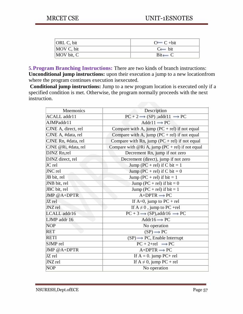
MRCET CSE UNIT-1ESNOTES
NSURESH,Dept.ofECE Page 57
ORL C, bit C C +bit
MOV C, bit C bit
MOV bit, C Bit C
5. Program Branching Instructions: There are two kinds of branch instructions: Unconditional jump instructions: upon their execution a jump to a new locationfrom where the program continues execution isexecuted.
Conditional jump instructions: Jump to a new program location is executed only if a specified condition is met. Otherwise, the program normally proceeds with the next instruction.
Mnemonics
ACALL addr11
AJMPaddr11
CJNE A, direct, rel
CJNE A, #data, rel
CJNE Rn, #data, rel
CJNE @Ri, #data, rel
DJNZ Rn,rel
DJNZ direct, rel
JC rel
JNC rel
JB bit, rel
JNB bit, rel
JBC bit, rel
JMP @A+DPTR
JZ rel
JNZ rel
LCALL addr16
LJMP addr 16
NOP
RET
RETI
SJMP rel
JMP @A+DPTR
JZ rel
JNZ rel
NOP
Description
PC + 2 (SP) ;addr11 PC
Addr11 PC
Compare with A, jump (PC + rel) if not equal
Compare with A, jump (PC + rel) if not equal
Compare with Rn, jump (PC + rel) if not equal
Compare with @Ri A, jump (PC + rel) if not equal
Decrement Rn, jump if not zero
Decrement (direct), jump if not zero
Jump (PC + rel) if C bit = 1
Jump (PC + rel) if C bit = 0
Jump (PC + rel) if bit = 1
Jump (PC + rel) if bit = 0
Jump (PC + rel) if bit = 1
A+DPTR PC
If A=0, jump to PC + rel
If A ≠ 0 , jump to PC +rel
PC + 3 (SP),addr16 PC
Addr16 PC
No operation
(SP) PC
(SP) PC, Enable Interrupt
PC + 2+rel PC
A+DPTR PC
If A = 0. jump PC+ rel
If A ≠ 0, jump PC + rel
No operation
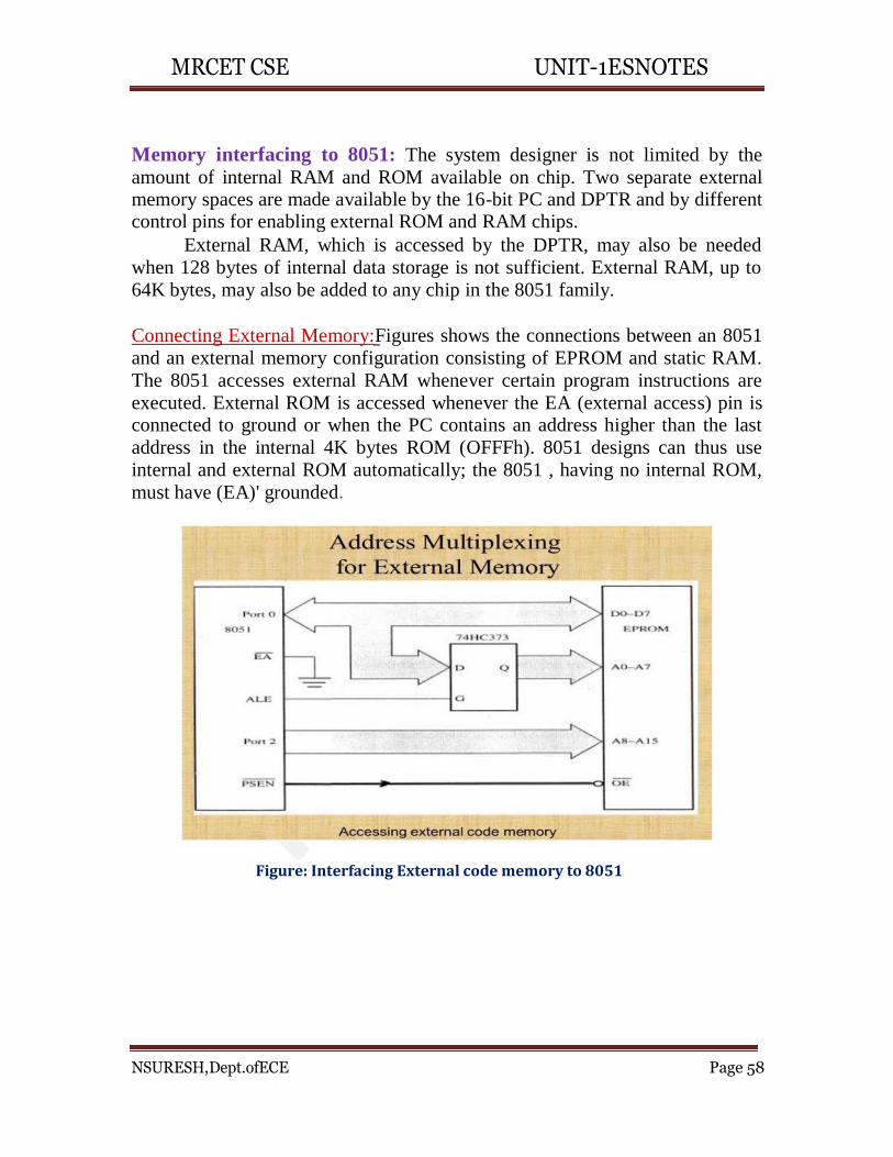
MRCET CSE UNIT-1ESNOTES
NSURESH,Dept.ofECE Page 58
Memory interfacing to 8051: The system designer is not limited by the
amount of internal RAM and ROM available on chip. Two separate external memory spaces are made available by the 16-bit PC and DPTR and by different control pins for enabling external ROM and RAM chips.
External RAM, which is accessed by the DPTR, may also be needed
when 128 bytes of internal data storage is not sufficient. External RAM, up to
64K bytes, may also be added to any chip in the 8051 family.
Connecting External Memory:Figures shows the connections between an 8051
and an external memory configuration consisting of EPROM and static RAM.
The 8051 accesses external RAM whenever certain program instructions are
executed. External ROM is accessed whenever the EA (external access) pin is connected to ground or when the PC contains an address higher than the last
address in the internal 4K bytes ROM (OFFFh). 8051 designs can thus use
internal and external ROM automatically; the 8051 , having no internal ROM,
must have (EA)' grounded.
Figure: Interfacing External code memory to 8051
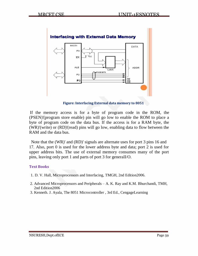
NSURESH,Dept.ofECE Page 59
MRCET CSE UNIT-1ESNOTES
Figure: Interfacing External data memory to 8051
If the memory access is for a byte of program code in the ROM, the (PSEN)'(program store enable) pin will go low to enable the ROM to place a
byte of program code on the data bus. If the access is for a RAM byte, the
(WR)'(write) or (RD)'(read) pins will go low, enabling data to flow between the
RAM and the data bus.
Note that the (WR)' and (RD)' signals are alternate uses for port 3 pins 16 and
17. Also, port 0 is used for the lower address byte and data; port 2 is used for
upper address bits. The use of external memory consumes many of the port
pins, leaving only port 1 and parts of port 3 for generalI/O.
Text Books
1. D. V. Hall, Microprocessors and Interfacing, TMGH, 2nd Edition2006.
2. Advanced Microprocessors and Peripherals – A. K. Ray and K.M. Bhurchandi, TMH, 2nd Edition2006
3. Kenneth. J. Ayala, The 8051 Microcontroller , 3rd Ed., CengageLearning
N SURESH T Vinay Simha Reddy
Department of ECE
MRCET CSE ES unit-2 Notes
NSURESH,Dept.ofECE,MRCET Page 1
1. Introduction to EmbeddedSystems
What isEmbeddedSystem? (DEC2016,March-2017.)
An Electronic/Electro mechanical system which is designed to perform a specific function and is
a combination of both hardware and firmware (Software)
E.g. Electronic Toys, Mobile Handsets, Washing Machines, Air Conditioners, Automotive
Control Units, Set Top Box, DVD Player etc…
Embedded Systems are:
Unique in character andbehavior
With specialized hardware andsoftware
Embedded Systems Vs GeneralComputingSystems: (March-2017)
General Purpose Computing System Embedded System
A system which is a combination ofgeneric A system which is a combination of special
hardware and General Purpose Operating System purpose hardware and embedded OSfor
for executing a variety of applications executing a specific set of applications
Contain a General Purpose Operating System May or may not contain an operating system
(GPOS) for functioning
Applications are alterable (programmable)by The firmware of the embedded systemis
user (It is possible for the end user to re-install the pre-programmed and it is non-alterable by
Operating System, and add or removeuser end-user
applications)
Performance is the key deciding factor onthe Application specific requirements (like
selection of the system. Always „Faster is Better‟ performance, power requirements, memory
usage etc) are the key deciding factors
Less/not at all tailored towards reduced operating Highly tailored to take advantage of the
power requirements, options for different levels power saving modes supported by hardware
of power management. and Operating System
Response requirements are not time critical For certain category of embedded systems
like mission critical systems, the response
time requirement is highly critical
Need not be deterministic in execution behavior Execution behavior is deterministic for
certain type of embedded systems like „Hard
Real Time‟ systems
MRCET CSE ES unit-2 Notes
NSURESH,Dept.ofECE,MRCET Page 2
History of Embedded Systems:
First Recognized Modern Embedded System: Apollo Guidance Computer (AGC) developed by Charles Stark Draperat the MIT InstrumentationLaboratory.
It has twomodules
1.Command module(CM) 2.LunarExcursion
module(LEM)
RAM size 256 , 1K ,2Kwords
ROM size 4K,10K,36Kwords
Clock frequency is1.024MHz
5000 ,3-input RTL NOR gates areused
User interface isDSKY(display/Keyboard)
First Mass Produced Embedded System: Autonetics D-17 Guidance computer for Minuteman-I missile
Classification ofEmbeddedSystems: (March-2017)
Based onGeneration
Based on Complexity & PerformanceRequirements
Based on deterministicbehavior
Based onTriggering
1. Embedded Systems - Classification based onGeneration
First Generation: The early embedded systems built around 8-bit microprocessors like
8085 and Z80 and 4-bit microcontrollers
EX. stepper motor control units, Digital Telephone Keypads etc.
Second Generation: Embedded Systems built around 16-bit microprocessors and 8 or
16-bit microcontrollers, following the first generation embedded systems
EX.SCADA, Data Acquisition Systems etc.
Third Generation: Embedded Systems built around high performance 16/32 bit
Microprocessors/controllers, Application Specific Instruction set processors like Digital
Signal Processors (DSPs), and Application Specific Integrated Circuits (ASICs).The
instruction set is complex and powerful.
EX. Robotics, industrial process control, networking etc.

MRCET CSE ES unit-2 Notes
NSURESH,Dept.ofECE,MRCET Page 3
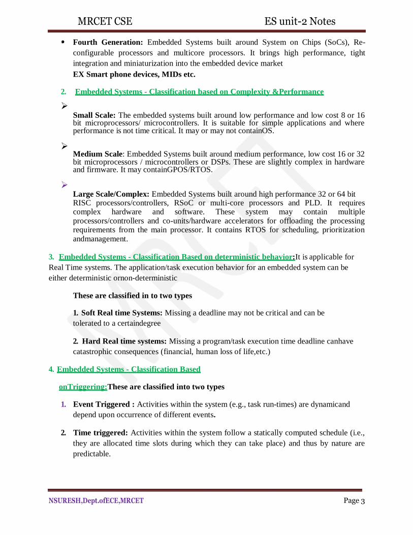
MRCET CSE ES unit-2 Notes
NSURESH,Dept.ofECE,MRCET Page 3
Fourth Generation: Embedded Systems built around System on Chips (SoCs), Re-
configurable processors and multicore processors. It brings high performance, tight
integration and miniaturization into the embedded device market
EX Smart phone devices, MIDs etc.
2. Embedded Systems - Classification based on Complexity &Performance
Small Scale: The embedded systems built around low performance and low cost 8 or 16 bit microprocessors/ microcontrollers. It is suitable for simple applications and where performance is not time critical. It may or may not containOS.
Medium Scale: Embedded Systems built around medium performance, low cost 16 or 32 bit microprocessors / microcontrollers or DSPs. These are slightly complex in hardware and firmware. It may containGPOS/RTOS.
Large Scale/Complex: Embedded Systems built around high performance 32 or 64 bit RISC processors/controllers, RSoC or multi-core processors and PLD. It requires complex hardware and software. These system may contain multiple processors/controllers and co-units/hardware accelerators for offloading the processing requirements from the main processor. It contains RTOS for scheduling, prioritization andmanagement.
3. Embedded Systems - Classification Based on deterministic behavior:It is applicable for
Real Time systems. The application/task execution behavior for an embedded system can be
either deterministic ornon-deterministic
These are classified in to two types
1. Soft Real time Systems: Missing a deadline may not be critical and can be
tolerated to a certaindegree
2. Hard Real time systems: Missing a program/task execution time deadline canhave
catastrophic consequences (financial, human loss of life,etc.)
4. Embedded Systems - Classification Based
onTriggering:These are classified into two types
1. Event Triggered : Activities within the system (e.g., task run-times) are dynamicand
depend upon occurrence of different events.
2. Time triggered: Activities within the system follow a statically computed schedule (i.e.,
they are allocated time slots during which they can take place) and thus by nature are
predictable.
MRCET CSE ES unit-2 Notes
NSURESH,Dept.ofECE,MRCET Page 4
Major Application Areas of Embedded Systems:
Consumer Electronics: Camcorders, Camerasetc.
Household Appliances: Television, DVD players, washing machine, Fridge,Microwave Ovenetc.
Home Automation and Security Systems: Air conditioners, sprinklers, Intruder detection alarms, Closed Circuit Television Cameras, Fire alarmsetc.
Automotive Industry: Anti-lock breaking systems (ABS), Engine Control, Ignition Systems, Automatic Navigation Systemsetc.
Telecom: Cellular Telephones, Telephone switches, Handset MultimediaApplications etc.
Computer Peripherals: Printers, Scanners, Fax machinesetc.
Computer Networking Systems: Network Routers, Switches, Hubs, Firewallsetc.
Health Care: Different Kinds of Scanners, EEG, ECG Machines etc.
Measurement & Instrumentation: Digital multi meters, Digital CROs, LogicAnalyzers PLC systems etc.
Banking & Retail: Automatic Teller Machines (ATM) and Currency counters, Point of Sales (POS)
Card Readers: Barcode, Smart Card Readers, Hand held Devicesetc.
Purpose of Embedded Systems: (DEC2016)
Each Embedded Systems is designed to serve the purpose of any one or a combination of the
following tasks.
o Data Collection/Storage/Representation
o Data Communication
o Data (Signal)Processing
o Monitoring
o Control
o Application Specific User Interface
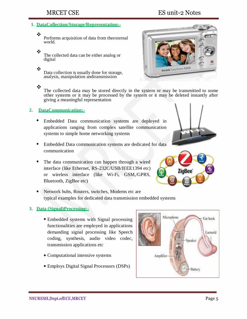
MRCET CSE ES unit-2 Notes
NSURESH,Dept.ofECE,MRCET Page 5
1. DataCollection/Storage/Representation:-
Performs acquisition of data from theexternal world.
The collected data can be either analog or digital
Data collection is usually done for storage, analysis, manipulation andtransmission
The collected data may be stored directly in the system or may be transmitted to some other systems or it may be processed by the system or it may be deleted instantly after giving a meaningful representation
2. DataCommunication:-
Embedded Data communication systems are deployed in
applications ranging from complex satellite communication
systems to simple home networking systems
Embedded Data communication systems are dedicated for data
communication
The data communication can happen through a wired
interface (like Ethernet, RS-232C/USB/IEEE1394 etc)
or wireless interface (like Wi-Fi, GSM,/GPRS,
Bluetooth, ZigBee etc)
Network hubs, Routers, switches, Modems etc are
typical examples for dedicated data transmission embedded systems
3. Data (Signal)Processing:-
Embedded systems with Signal processing
functionalities are employed in applications
demanding signal processing like Speech
coding, synthesis, audio video codec,
transmission applications etc
Computational intensive systems
Employs Digital Signal Processors (DSPs)
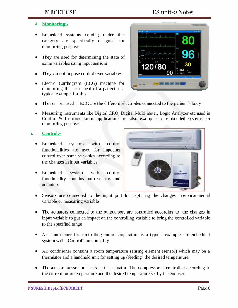
MRCET CSE ES unit-2 Notes
NSURESH,Dept.ofECE,MRCET Page 6
4. Monitoring:-
Embedded systems coming under this
category are specifically designed for
monitoring purpose
They are used for determining the state of
some variables using input sensors
They cannot impose control over variables.
Electro Cardiogram (ECG) machine for monitoring the heart beat of a patient is a typical example for this
The sensors used in ECG are the different Electrodes connected to the patient‟s body
Measuring instruments like Digital CRO, Digital Multi meter, Logic Analyzer etc used in
Control & Instrumentation applications are also examples of embedded systems for monitoring purpose
5. Control:-
Embedded systems with control
functionalities are used for imposing
control over some variables according to
the changes in input variables
Embedded system with control
functionality contains both sensors and
actuators
Sensors are connected to the input port for capturing the changes in environmental
variable or measuring variable
The actuators connected to the output port are controlled according to the changes in
input variable to put an impact on the controlling variable to bring the controlled variable
to the specified range
Air conditioner for controlling room temperature is a typical example for embedded
system with „Control‟ functionality
Air conditioner contains a room temperature sensing element (sensor) which may be a
thermistor and a handheld unit for setting up (feeding) the desired temperature
The air compressor unit acts as the actuator. The compressor is controlled according to
the current room temperature and the desired temperature set by the enduser.
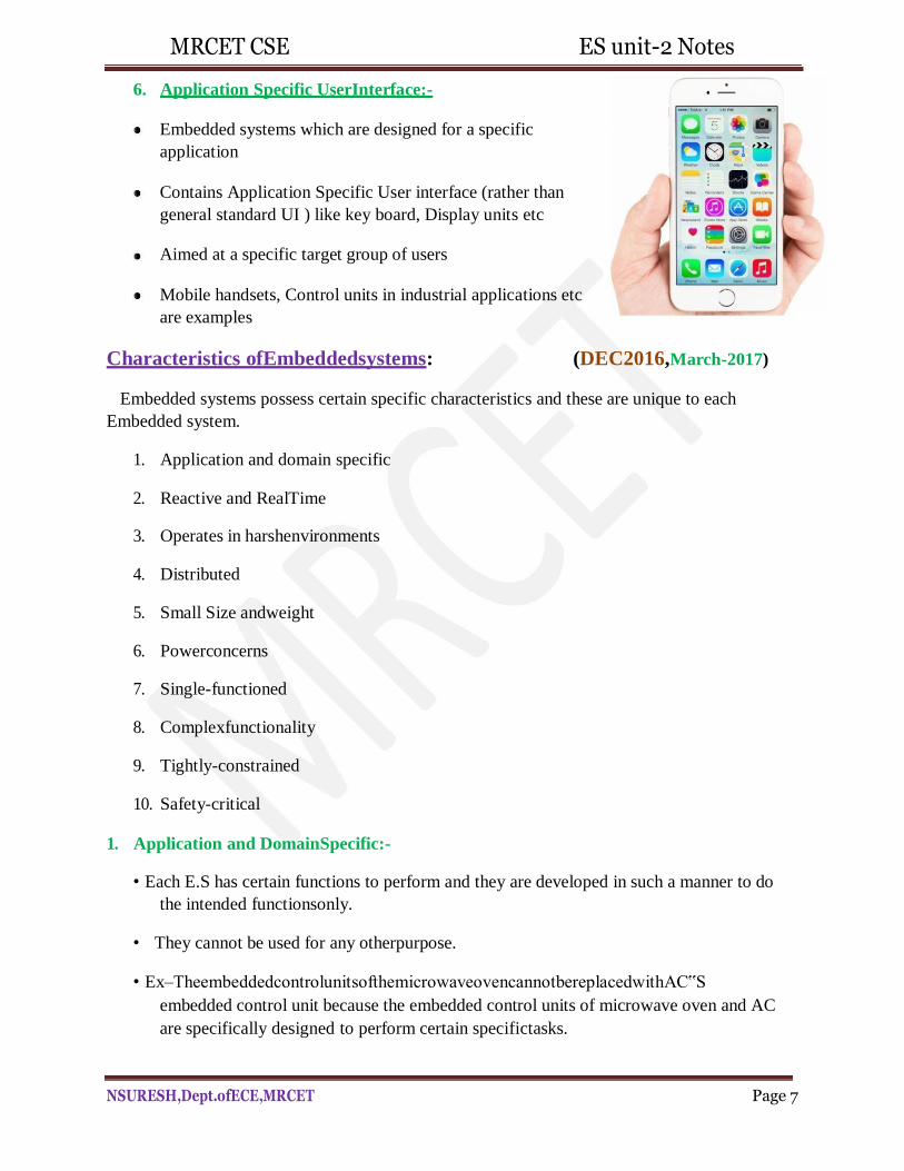
MRCET CSE ES unit-2 Notes
NSURESH,Dept.ofECE,MRCET Page 7
6. Application Specific UserInterface:-
Embedded systems which are designed for a specific
application
Contains Application Specific User interface (rather than
general standard UI ) like key board, Display units etc
Aimed at a specific target group of users
Mobile handsets, Control units in industrial applications etc
are examples
Characteristics ofEmbeddedsystems: (DEC2016,March-2017)
Embedded systems possess certain specific characteristics and these are unique to each
Embedded system.
1. Application and domain specific
2. Reactive and RealTime
3. Operates in harshenvironments
4. Distributed
5. Small Size andweight
6. Powerconcerns
7. Single-functioned
8. Complexfunctionality
9. Tightly-constrained
10. Safety-critical
1. Application and DomainSpecific:-
• Each E.S has certain functions to perform and they are developed in such a manner to do
the intended functionsonly.
• They cannot be used for any otherpurpose.
• Ex–TheembeddedcontrolunitsofthemicrowaveovencannotbereplacedwithAC‟S
embedded control unit because the embedded control units of microwave oven and AC
are specifically designed to perform certain specifictasks.
MRCET CSE ES unit-2 Notes
NSURESH,Dept.ofECE,MRCET Page8
2. Reactive and RealTime:-
• E.S are in constant interaction with the real world through sensors and user-defined input
devices which are connected to the input port of thesystem.
• Any changes in the real world are captured by the sensors or input devices in real time
and the control algorithm running inside the unit reacts in a designed manner to bring the
controlled output variables to the desiredlevel.
• E.S produce changes in output in response to the changes in the input, so they are referred
as reactive systems.
• Real Time system operation means the timing behavior of the system should be
deterministic ie the system should respond to requests in a known amount oftime.
• Example – E.S which are mission critical like flight controlsystems, Antilock Brake
Systems (ABS) etc are Real Timesystems.
3. Operates in Harsh Environment:–
• The design of E.S should take care of the operating conditions of the area where the
system is going toimplement.
• Ex – If the system needs to be deployed in a high temperature zone, then all the
components used in the system should be of high temperaturegrade.
• Also proper shock absorption techniques should be provided to systems which aregoing
to be commissioned in places subject to highshock.
4. Distributed:–
• It means that embedded systems may be a part of a largersystem.
• Many numbers of such distributed embedded systems form a single largeembedded
controlunit.
• Ex – Automatic vending machine. It contains a card reader, a vending unit etc. Each of
them are independent embedded units but they work together to perform the overall
vendingfunction.
5. Small Size and Weight:-
• Product aesthetics (size, weight, shape, style, etc) is an important factor in choosing a
product.
• It is convenient to handle a compact device than a bulkyproduct.
• In embedded domain compactness is a significant decidingfactor.
MRCET CSE ES unit-2 Notes
NSURESH,Dept.ofECE,MRCET Page9
6. PowerConcerns:-
• Power management is another important factor that needs to be considered in designing
embeddedsystems.
• E.S should be designed in such a way as to minimize the heat dissipation by thesystem.
7. Single-functioned:- Dedicated to perform a singlefunction
8. Complex functionality: - We have to run sophisticated algorithms or multiple algorithms in
some applications.
9. Tightly-constrained:-
Low cost, low power, small, fast, etc
10. Safety-critical:-
Must not endanger human life and the environment
Quality Attributes of Embedded System:Quality attributes are the non-functional
requirements that need to be documented properly in any system design.(DEC16,March-2017)
Quality attributes can be classified as
I. Operational qualityattributes
II. Non-operational qualityattributes.
I. Operational Quality Attributes: The operational quality attributes represent the relevant
quality attributes related to the embedded system when it is in the operational mode or online
mode.
Operational Quality Attributes are:
1. Response :-
It is the measure of quickness of the system.
It tells how fast the system is tracking thechangesin inputvariables.
Most of the E.S demands fast response which should be almost real time.
Ex – Flight control application.
MRCET CSE ES unit-2 Notes
NSURESH,Dept.ofECE,MRCET Page10
2. Throughput:-
It deals with the efficiency of a system.
It can be defined as the rate of production or operation of a defined process over a
stated period of time.
The rates can be expressed in terms of products, batches produced or any other
meaningful measurements.
Ex – In case of card reader throughput means how many transactions the reader
can perform in a minute or in an hour or in a day.
Throughput is generally measured in terms of “Benchmark”.
A Benchmark is a reference point by which something can be measured
3. Reliability:-
• It is a measure of how much we can rely upon the proper functioning of thesystem.
• Mean Time Between Failure (MTBF) and Mean Time To Repair (MTTR) are the
terms used in determining systemreliability.
• MTBF gives the frequency of failures inhours/weeks/months.
• MTTR specifies how long the system is allowed to be out of order following a
failure.
• For embedded system with critical application need, it should be of the order of
minutes.
4. Maintainability:-
• It deals with support and maintenance to the end user or client in case of technical
issues and product failure or on the basis of a routine systemcheckup.
• Reliability and maintainability are complementary to eachother.
• A more reliable system means a system with less corrective maintainability requirements
and viceversa.
• Maintainability can be broadly classified into twocategories
1. Scheduled or Periodic maintenance (Preventivemaintenance)
2. Corrective maintenance to unexpectedfailures
MRCET CSE ES unit-2 Notes
NSURESH,Dept.ofECE,MRCET Page11
5. Security:-
• Confidentiality, Integrity and availability are the three major measures ofinformation
security.
• Confidentiality deals with protection of data and application fromunauthorized
disclosure.
• Integrity deals with the protection of data and application fromunauthorized
modification.
• Availability deals with protection of data and application from unauthorizedusers.
6. Safety:-
Safety deals with the possible damages that can happen to the operator, public and the
environment due to the breakdown of an Embedded System.
The breakdown of an embedded system may occur due to a hardware failure or a
firmwarefailure.
Safety analysis is a must in product engineering to evaluate the anticipated damages and
determine the best course of action to bring down the consequences of damage to an
acceptablelevel.
II. Non-Operational Quality Attributes: The quality attributes that needs to be addressed for
the product not on the basis of operational aspects are grouped under thiscategory.
1. Testability and Debug-ability:-
• Testability deals with how easily one can test the design, application and by which means
it can bedone.
• For an E.S testability is applicable to both the embedded hardware andfirmware.
• Embedded hardware testing ensures that the peripherals and total hardware functions in
the desired manner, whereas firmware testing ensures that the firmware is functioning in
the expectedway.
• Debug-ability is a means of debugging the product from unexpected behavior inthe
system
• Debug-ability is two levelprocess
• 1.Hardwarelevel 2.softwarelevel
• 1.Hardwarelevel: It is used for finding the issues created by hardwareproblems.
• 2. Software level: It is employed for finding the errors created by the flaws in thesoftware.

MRCET CSE ES unit-2 Notes
NSURESH,Dept.ofECE,MRCET Page12
2. Evolvability:-
• It is a term which is closely related toBiology.
• It is referred as the non-heritablevariation.
• For an embedded system evolvability refers to the ease with which the embeddedproduct
can be modified to take advantage of new firmware or hardwaretechnologies.
3. Portability:-
• It is the measure of systemindependence.
• An embedded product is said to be portable if the product is capable of functioning in
various environments, target processors and embedded operatingsystems.
• „Porting‟representsthemigrationofembeddedfirmwarewrittenforonetargetprocessor to a
different targetprocessor.
4. Time-to-Prototype andMarket:-
• It is the time elapsed between the conceptualization of a product and the time at which
the product is ready forselling.
• The commercial embedded product market is highly competitive and time to market the
product is critical factor in the success of commercial embeddedproduct.
• There may be multiple players in embedded industry who develop products of the same
category (like mobilephone).
5. Per Unit Cost andRevenue:-
• Cost is a factor which is closely monitored by both end user and productmanufacturer.
• Cost is highly sensitive factor for commercialproducts
• Any failure to position the cost of a commercial product at a nominal rate may lead to the
failure of the product in themarket.
• Proper market study and cost benefit analysis should be carried out before taking a
decision on the per-unit cost of the embeddedproduct.
• The ultimate aim of the product is to generate marginal profit so the budget and totalcost
should be properly balanced to provide a marginalprofit.
MRCET CSE ES unit-2 Notes
NSURESH,Dept.ofECE,MRCET Page13
SUMMARY
1. An embedded system is an electronic/electromechanical system designed to perform a
specific function and is a combination of both hardware and firmware(software).
2. A general purpose computing system is a combination of generic hardware and general
purpose operating system for executing a variety of applications, whereas anembedded
3. System is a combination of special purpose hardware and embedded OS/firmwarefor
executing a specific set ofapplications.
4. Apollo Guidance Computer (AGC) is the first recognized modern embedded system and
Autonetics D-17, the guidance computer for the Minuteman-I missile, was the first mass
produced embeddedsystem.
5. Based on the complexityand performance requirements, embedded systems are classified
into small-scale, medium-scale andlarge-scale/complex.
6. The presences of embedded system vary from simple electronic system toys tocomplex
flight and missile controlsystems.
7. Embedded systems are designed to serve the purpose of any one or combination of data
collection/storage/representation, data processing, monitoring, control or application
specific userinterface.
8. Wearable devices refer to embedded systems which are incorporated into accessoriesand apparels. It envisions the bonding of embedded technology in our day to daylives.
OBJECTIVE QUESTIONS
1. Embedded systems are
(a) General Purpose (b) Special Purpose
2. Embedded system is
(a) An electronic system (b) A pure mechanical system
(c)An electro-mechanical system (d) (a) or (c)
3. Which of the following is not true about embedded systems?
(a)Built around specialized hardware (b) Always contain an operating system
(c)Execution behavior may be deterministic (d) All of these (e) none of these
4. Which of the following is not an example of small scale embedded system?
(a) Electronic Barbie doll (b) Simple calculator
(c) Cell Phone (d) Electronic toy car
NSURESH,Dept.ofECE,MRCET Page14
MRCET CSE ES unit-2 Notes
5. The first recognized modern embedded system is
(a) Apple computer (b) Apollo Guidance Computer
(c) Calculator (d) Radio navigation system
6. The first mass produced embedded system is
(a) Minuteman-I (b) Minuteman-II
(c) Autonetics D17 (d) Apollo Guidance Computer
7. Which of the following is (are) an intended purpose of embedded systems?
(a) Data collection (b) Data processing
(c) Data communication (d) All of these (e) None of these
8. Which of the following is an example of an embedded system for data communication?
9
10. Which of the following is an example of an embedded system for signalprocessing?
(a) AppleiPOD (b) Sandisk USB mass storagedevice
(c) both aandb (d) None ofthese
Reference Text Books:-
1. Introduction to Embedded Systems – Shibu K.V Mc GrawHill
2. Embedded System Design-Raj KamalTMH
(a) USB mass storage device (b) Network router (c) Digital camera
(d)Music player (e) All of these (f) None of these
. A digital multimeter is an example of embedded system for
(a) Data communication (b) Monitoring (c) Control
(d) All of these (e) None of these
N.SURESH Department of ECE
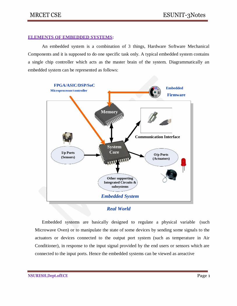
MRCET CSE ESUNIT-3Notes
NSURESH,Dept.ofECE Page 1
ELEMENTS OF EMBEDDED SYSTEMS:
An embedded system is a combination of 3 things, Hardware Software Mechanical
Components and it is supposed to do one specific task only. A typical embedded system contains
a single chip controller which acts as the master brain of the system. Diagrammatically an
embedded system can be represented as follows:
FPGA/ASIC/DSP/SoC
Microprocessor/controller
Embedded
Firmware
Memory
Communication Interface
System
I/p Ports Core O/p Ports
(Sensors)
(Actuators)
Other supporting
Integrated Circuits &
subsystems
Embedded System
Real World
Embedded systems are basically designed to regulate a physical variable (such
Microwave Oven) or to manipulate the state of some devices by sending some signals to the
actuators or devices connected to the output port system (such as temperature in Air
Conditioner), in response to the input signal provided by the end users or sensors which are
connected to the input ports. Hence the embedded systems can be viewed as areactive
MRCET CSE ESUNIT-3Notes
NSURESH,Dept.ofECE Page
system. The control is achieved by processing the information coming from the sensors and
user interfaces and controlling some actuators that regulate the physical variable.
Keyboards, push button, switches, etc. are Examples of common user interface input
devices and LEDs, LCDs, Piezoelectric buzzers, etc examples for common user interface
output devices for a typical embedded system. The requirement of type of user interface
changes from application to application based on domain.
Some embedded systems do not require any manual intervention for their operation.
They automatically sense the input parameters from real world through sensors which are
connected at input port. The sensor information is passed to the processor after signal
conditioning and digitization. The core of the system performs some predefined operations
on input data with the help of embedded firmware in the system and sends some actuating
signals to the actuator connect connected to the output port of thesystem.
The memory of the system is responsible for holding the code (control algorithm and
other important configuration details). There are two types of memories are used in any
embedded system. Fixed memory (ROM) is used for storing code or program. The user
cannot change the firmware in this type of memory. The most common types of memories
used in embedded systems for control algorithm storage are
OTP,PROM,UVEPROM,EEPROM and FLASH
An embedded system without code (i.e. the control algorithm) implemented memory has
all the peripherals but is not capable of making decisions depending on the situational as well
as real worldchanges.
Memory for implementing the code may be present on the processor or may be
implemented as a separate chip interfacing the processor
In a controller based embedded system, the controller may contain internal memory for
storing code Such controllers are called Micro-controllers with on-chip ROM, eg. Atmel
AT89C51.
MRCET CSE ESUNIT-3Notes
NSURESH,Dept.ofECE Page
The Core of the Embedded Systems: The core of the embedded system falls into any one
of the following categories.
General Purpose and Domain SpecificProcessors
o Microprocessors
o Microcontrollers
o Digital SignalProcessors
Programmable Logic Devices(PLDs)
Application Specific Integrated Circuits(ASICs)
Commercial off the shelf Components(COTS)
GENERALPURPOSE AND DOMAINSPECIFIC PROCESSOR:
Almost 80% of the embedded systems are processor/ controller based.
The processor may be microprocessor or a microcontroller or digital signal processor,
depending on the domain and application.
Microprocessor:
A silicon chip representing a Central Processing Unit (CPU), which is capable of
performing arithmetic as well as logical operations according to a pre-defined set of
Instructions, which is specific to the manufacturer
In general the CPU contains the Arithmetic and Logic Unit (ALU), Control Unit and
Working registers
Microprocessor is a dependant unit and it requires the combination of other hardware like
Memory, Timer Unit, and Interrupt Controller etc for proper functioning.
Intel claims the credit for developing the first Microprocessor unit Intel 4004, a 4
bitprocessor which was released in Nov 1971
· Developers ofmicroprocessors.
Intel – Intel 4004 – November 1971(4-bit) Intel – Intel 4040.
Intel – Intel 8008 – April 1972.
Intel – Intel 8080 – April 1974(8-bit).
Motorola – Motorola 6800.
Intel – Intel 8085 – 1976.
Zilog - Z80 – July 1976
MRCET CSE ESUNIT-3Notes
Microcontroller:
A highly integrated silicon chip containing a CPU, scratch pad RAM, Special and General purpose Register Arrays, On Chip ROM/FLASH memory for program storage, Timer and Interrupt control units and dedicated I/Oports
Microcontrollers can be considered as a super set ofMicroprocessors
Microcontroller can be general purpose (like Intel 8051, designed for generic applications and domains) or application specific (Like Automotive AVR from Atmel Corporation. Designed specifically for automotiveapplications)
Since a microcontroller contains all the necessary functional blocks for independentworking, they found greater place in the embedded domain in place ofmicroprocessors
Microcontrollers are cheap, cost effective and are readily available in themarket
Texas Instruments TMS 1000 is considered as the world‟s firstmicrocontroller
Microprocessor Vs Microcontroller:
Microprocessor Microcontroller
A silicon chip representing a Central Processing Unit A microcontroller is a highly integrated chip that
(CPU), which is capable of performing arithmetic as contains a CPU, scratch pad RAM, Special and
well as logical operations according to a pre-defined set General purpose Register Arrays, OnChip
of Instructions ROM/FLASH memory for program storage, Timer
and Interrupt control units and dedicated I/O ports
It is a dependent unit. It requires the combination of It is a self contained unit and it doesn‟t require
other chips like Timers, Program and data memory external Interrupt Controller, Timer, UART etc for
chips, Interrupt controllers etc for functioning its functioning
Most of the time general purpose in design and Mostly application oriented or domain specific
operation
Doesn‟t contain a built in I/O port. The I/O Port Most of the processors contain multiple built-in I/O
functionality needs to be implemented with the help of ports which can be operated as a single 8 or 16 or 32
external Programmable Peripheral Interface Chips like bit Port or as individual port pins
8255
Targeted for high end market where performanceis Targeted for embedded market where performance is
important not so critical (At present this demarcation is invalid)
Limited power saving options comparedto Includes lot of power saving features
microcontrollers
N SURESH, Dept. of ECE
Page 4
MRCET CSE ESUNIT-3Notes
NSURESH,Dept.ofECE Page5
General Purpose Processor (GPP) Vs Application Specific Instruction Set Processor (ASIP)
General Purpose Processor or GPP is a processor designed for general computationaltasks
GPPs are produced in large volumes and targeting the general market. Due to the high volume production, the per unit cost for a chip is low compared to ASIC or other specific ICs
A typical general purpose processor contains an Arithmetic and Logic Unit (ALU) and Control Unit(CU)
Application Specific Instruction Set processors (ASIPs) are processors with architecture and instruction set optimized to specific domain/application requirements like Network processing, Automotive, Telecom, media applications, digital signal processing, control applicationsetc.
ASIPs fill the architectural spectrum between General Purpose Processors andApplication Specific Integrated Circuits(ASICs)
The need for an ASIP arises when the traditional general purpose processor are unable to meet the increasing applicationneeds
Some Microcontrollers (like Automotive AVR, USB AVR from Atmel), System on Chips, Digital Signal Processors etc are examples of Application Specific Instruction Set Processors(ASIPs)
ASIPs incorporate a processor and on-chip peripherals, demanded by the applicationrequirement, program and datamemory
Digital Signal Processors (DSPs):
Powerful special purpose 8/16/32 bit microprocessors designed specifically to meet the
computational demands and power constraints of today's embedded audio, video, and
communications applications
Digital Signal Processors are 2 to 3 times faster than the general purpose microprocessors
in signal processing applications
DSPs implement algorithms in hardware which speeds up the execution whereas general
purpose processors implement the algorithm in firmware and the speed of execution
depends primarily on the clock for the processors
DSP can be viewed as a microchip designed for performing high speed computational
operations for „addition‟, „subtraction‟, „multiplication‟ and „division‟
MRCET CSE ESUNIT-3Notes
NSURESH,Dept.ofECE Page6
A typical Digital Signal Processor incorporates the following key units
Program Memory
DataMemory
ComputationalEngine
I/O Unit
Audio video signal processing, telecommunication and multimedia applications are
typical examples where DSP is employed
RISC V/s CISC Processors/Controllers:
RISC CISC
Lesser no. of instructions Greater no. of Instructions
Instruction Pipelining and increasedexecution Generally no instruction pipelining feature
speed
Orthogonal Instruction Set (Allows each instruction Non Orthogonal Instruction Set (All instructions
to operate on any register and use any addressing are not allowed to operate on any register and
mode) use any addressing mode. It is instruction
specific)
Operations are performed on registers only, the Operations are performed on registersor
only memory operations are load and store memory depending on the instruction
Large number of registers are available Limited no. of general purpose registers
Programmer needs to write more code to execute a . A programmer can achieve thedesired
task since the instructions are simpler ones functionality with a single instruction which in
turn provides the effect of using more simpler
single instructions in RISC
Single, Fixed length Instructions Variable length Instructions
Less Silicon usage and pin count More silicon usage since moreadditional
decoder logic is required to implement the
complex instruction decoding.
With Harvard Architecture Can be Harvard or Von-Neumann Architecture
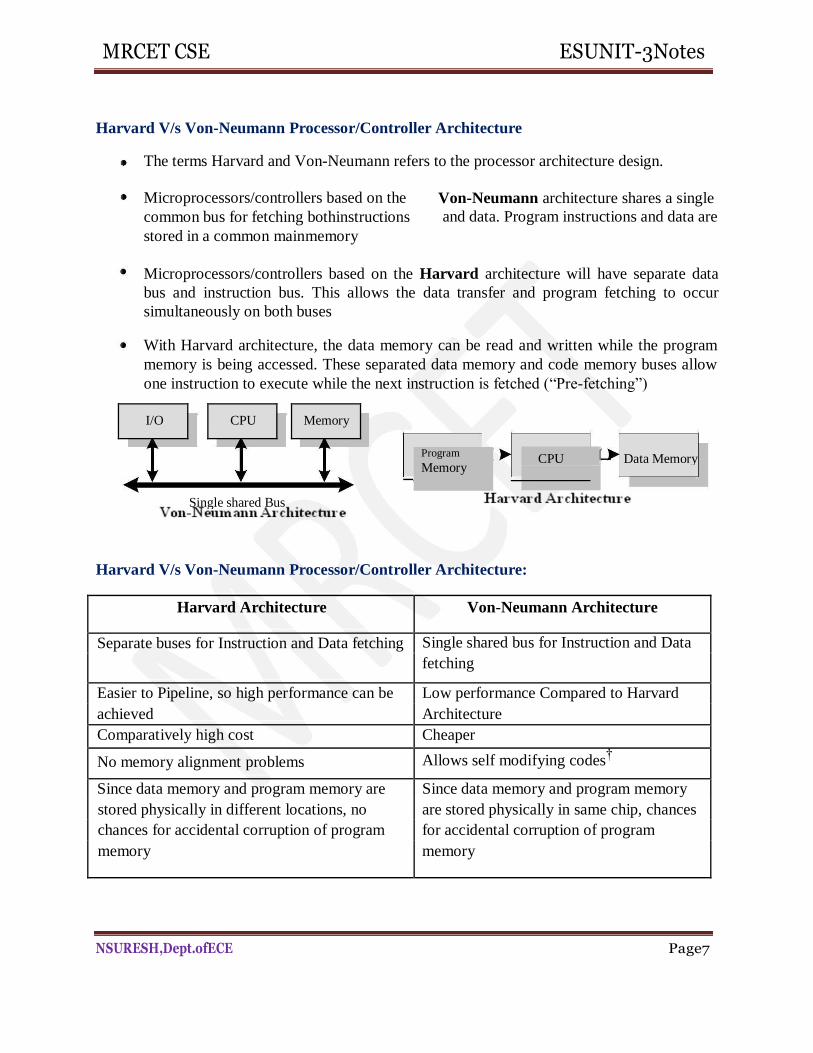
MRCET CSE ESUNIT-3Notes
NSURESH,Dept.ofECE Page7
Microprocessors/controllers based on the Harvard architecture will have separate data
bus and instruction bus. This allows the data transfer and program fetching to occur
simultaneously on both buses
With Harvard architecture, the data memory can be read and written while the program
memory is being accessed. These separated data memory and code memory buses allow
one instruction to execute while the next instruction is fetched (“Pre-fetching”)
Program
Memory CPU Data Memory
Single shared Bus
Harvard V/s Von-Neumann Processor/Controller Architecture:
Harvard V/s Von-Neumann Processor/Controller Architecture
The terms Harvard and Von-Neumann refers to the processor architecture design.
Microprocessors/controllers based on the
common bus for fetching bothinstructions
stored in a common mainmemory
Von-Neumann architecture shares a single
and data. Program instructions and data are
I/O
CPU
Memory
Harvard Architecture Von-Neumann Architecture
Separate buses for Instruction and Data fetching Single shared bus for Instruction and Data
fetching
Easier to Pipeline, so high performance can be Low performance Compared to Harvard
achieved Architecture
Comparatively high cost Cheaper
No memory alignment problems Allows self modifying codes†
Since data memory and program memory are Since data memory and program memory
stored physically in different locations, no are stored physically in same chip, chances
chances for accidental corruption of program for accidental corruption of program
memory memory
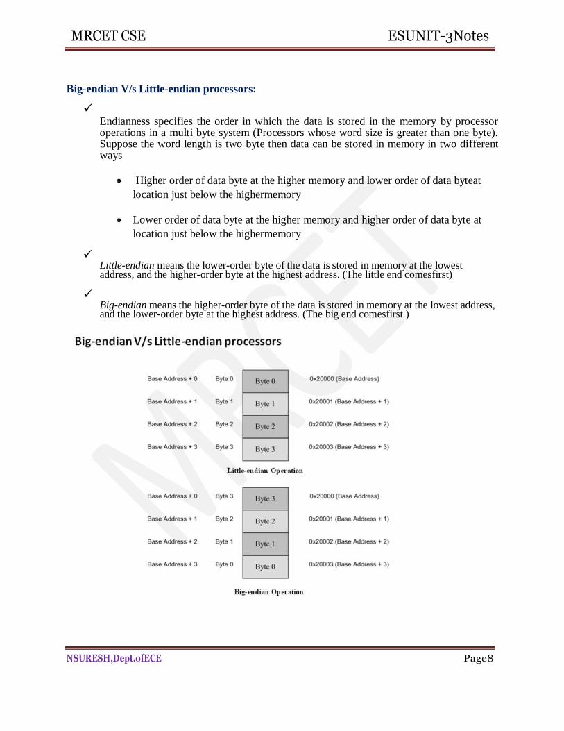
MRCET CSE ESUNIT-3Notes
NSURESH,Dept.ofECE Page8
Big-endian V/s Little-endian processors:
Endianness specifies the order in which the data is stored in the memory by processor operations in a multi byte system (Processors whose word size is greater than one byte). Suppose the word length is two byte then data can be stored in memory in two different ways
Higher order of data byte at the higher memory and lower order of data byteat
location just below the highermemory
Lower order of data byte at the higher memory and higher order of data byte at
location just below the highermemory
Little-endian means the lower-order byte of the data is stored in memory at the lowest address, and the higher-order byte at the highest address. (The little end comesfirst)
Big-endian means the higher-order byte of the data is stored in memory at the lowest address, and the lower-order byte at the highest address. (The big end comesfirst.)
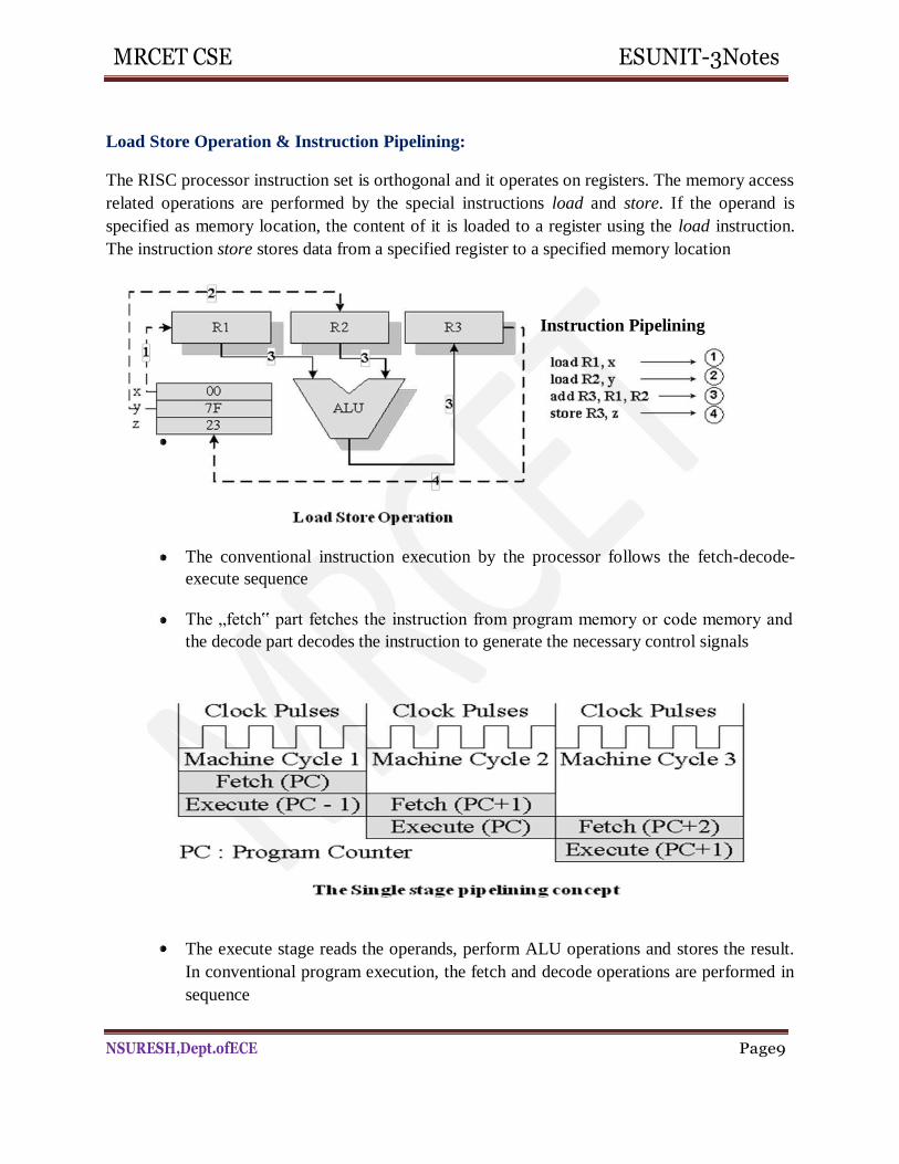
MRCET CSE ESUNIT-3Notes
NSURESH,Dept.ofECE Page9
Load Store Operation & Instruction Pipelining:
The RISC processor instruction set is orthogonal and it operates on registers. The memory access
related operations are performed by the special instructions load and store. If the operand is
specified as memory location, the content of it is loaded to a register using the load instruction.
The instruction store stores data from a specified register to a specified memory location
Instruction Pipelining
The conventional instruction execution by the processor follows the fetch-decode-
execute sequence
The „fetch‟ part fetches the instruction from program memory or code memory and
the decode part decodes the instruction to generate the necessary control signals
The execute stage reads the operands, perform ALU operations and stores the result.
In conventional program execution, the fetch and decode operations are performed in
sequence
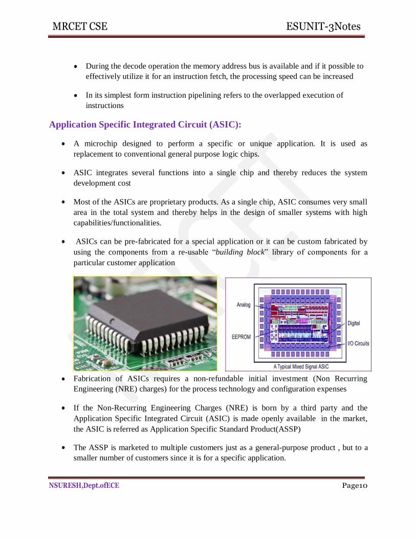
MRCET CSE ESUNIT-3Notes
NSURESH,Dept.ofECE Page10
During the decode operation the memory address bus is available and if it possible to
effectively utilize it for an instruction fetch, the processing speed can be increased
In its simplest form instruction pipelining refers to the overlapped execution of
instructions
Application Specific Integrated Circuit (ASIC):
A microchip designed to perform a specific or unique application. It is used as
replacement to conventional general purpose logic chips.
ASIC integrates several functions into a single chip and thereby reduces the system
development cost
Most of the ASICs are proprietary products. As a single chip, ASIC consumes very small
area in the total system and thereby helps in the design of smaller systems with high
capabilities/functionalities.
ASICs can be pre-fabricated for a special application or it can be custom fabricated by
using the components from a re-usable “building block‟ library of components for a
particular customer application
Fabrication of ASICs requires a non-refundable initial investment (Non Recurring
Engineering (NRE) charges) for the process technology and configuration expenses
If the Non-Recurring Engineering Charges (NRE) is born by a third party and the
Application Specific Integrated Circuit (ASIC) is made openly available in the market,
the ASIC is referred as Application Specific Standard Product(ASSP)
The ASSP is marketed to multiple customers just as a general-purpose product , but to a
smaller number of customers since it is for a specific application.
MRCET CSE ESUNIT-3Notes
NSURESH,Dept.ofECE Page11
Some ASICs are proprietary products , the developers are not interested in revealing the
internal details.
Programmable Logic Devices (PLDs):
Logic devices provide specific functions, including device-to-device interfacing, data communication, signal processing, data display, timing and control operations, and almost every other function a system must perform.
Logic devices can be classified into two broad categories - Fixed and Programmable. The circuits in a fixed logic device are permanent, they perform one function or set of functions - once manufactured, they cannot bechanged
Programmable logic devices (PLDs) offer customers a wide range of logic capacity, features, speed, and voltage characteristics - and these devices can be re-configured to perform any number of functions at any time
Designers can use inexpensive software tools to quickly develop, simulate, and test their logic designs in PLD based design. The design can be quickly programmed into a device, and immediately tested in a livecircuit
PLDs are based on re-writable memory technology and the device is reprogrammed to change thedesign
Programmable Logic Devices (PLDs) – CPLDs and FPGA
Field Programmable Gate Arrays (FPGAs) and Complex Programmable Logic Devices
(CPLDs) are the two major types of programmable logic devices
FPGA:
FPGA is an IC designed to be configured by a designer after manufacturing.
FPGAs offer the highest amount of logic density, the most features, and the highest
performance.
Logic gate is Medium to high density ranging from 1K to 500K system gates
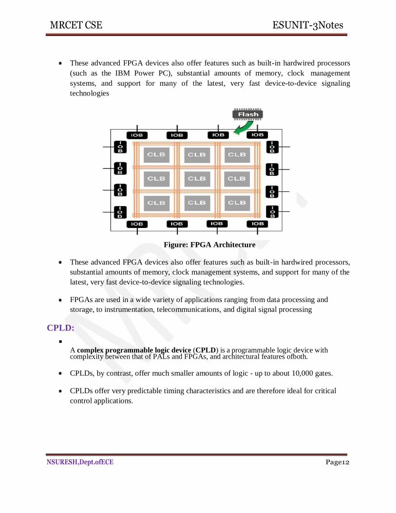
MRCET CSE ESUNIT-3Notes
NSURESH,Dept.ofECE Page12
These advanced FPGA devices also offer features such as built-in hardwired processors
(such as the IBM Power PC), substantial amounts of memory, clock management
systems, and support for many of the latest, very fast device-to-device signaling
technologies
Figure: FPGA Architecture
These advanced FPGA devices also offer features such as built-in hardwired processors,
substantial amounts of memory, clock management systems, and support for many of the
latest, very fast device-to-device signaling technologies.
FPGAs are used in a wide variety of applications ranging from data processing and
storage, to instrumentation, telecommunications, and digital signal processing
CPLD:
A complex programmable logic device (CPLD) is a programmable logic device with complexity between that of PALs and FPGAs, and architectural features ofboth.
CPLDs, by contrast, offer much smaller amounts of logic - up to about 10,000 gates.
CPLDs offer very predictable timing characteristics and are therefore ideal for critical
control applications.
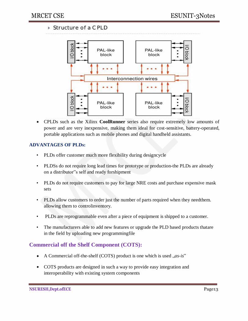
MRCET CSE ESUNIT-3Notes
NSURESH,Dept.ofECE Page13
CPLDs such as the Xilinx CoolRunner series also require extremely low amounts of
power and are very inexpensive, making them ideal for cost-sensitive, battery-operated,
portable applications such as mobile phones and digital handheld assistants.
ADVANTAGES OF PLDs:
• PLDs offer customer much more flexibility during designcycle
• PLDSs do not require long lead times for prototype or production-the PLDs are already
on a distributor‟s self and ready forshipment
• PLDs do not require customers to pay for large NRE costs and purchase expensive mask
sets
• PLDs allow customers to order just the number of parts required when they needthem.
allowing them to controlinventory.
• PLDs are reprogrammable even after a piece of equipment is shipped to a customer.
• The manufacturers able to add new features or upgrade the PLD based products thatare
in the field by uploading new programmingfile
Commercial off the Shelf Component (COTS):
A Commercial off-the-shelf (COTS) product is one which is used „as-is‟
COTS products are designed in such a way to provide easy integration and
interoperability with existing system components
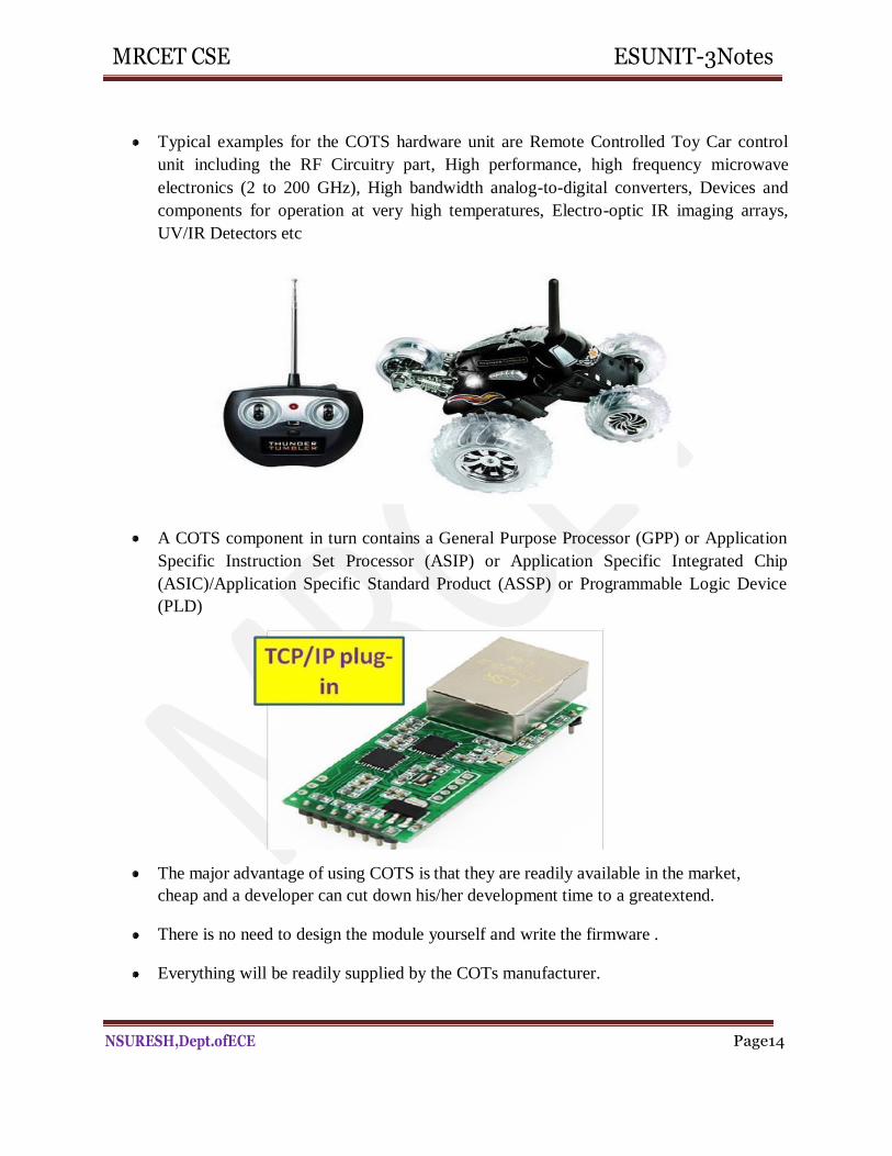
MRCET CSE ESUNIT-3Notes
NSURESH,Dept.ofECE Page14
Typical examples for the COTS hardware unit are Remote Controlled Toy Car control
unit including the RF Circuitry part, High performance, high frequency microwave
electronics (2 to 200 GHz), High bandwidth analog-to-digital converters, Devices and
components for operation at very high temperatures, Electro-optic IR imaging arrays,
UV/IR Detectors etc
A COTS component in turn contains a General Purpose Processor (GPP) or Application
Specific Instruction Set Processor (ASIP) or Application Specific Integrated Chip
(ASIC)/Application Specific Standard Product (ASSP) or Programmable Logic Device
(PLD)
The major advantage of using COTS is that they are readily available in the market,
cheap and a developer can cut down his/her development time to a greatextend.
There is no need to design the module yourself and write the firmware .
Everything will be readily supplied by the COTs manufacturer.
MRCET CSE ESUNIT-3Notes
NSURESH,Dept.ofECE Page15
The major problem faced by the end-user is that there are no operational and
manufacturing standards.
The major drawback of using COTs component in embedded design is that the
manufacturer may withdraw the product or discontinue the production of the COTs at any
time if rapid change in technology
This problem adversely affect a commercial manufacturer of the embedded system which
makes use of the specific COTs
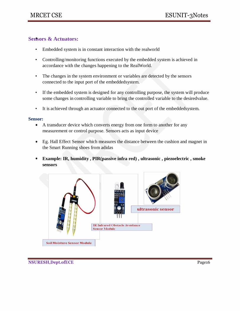
MRCET CSE ESUNIT-3Notes
Sensors & Actuators:
• Embedded system is in constant interaction with the realworld
• Controlling/monitoring functions executed by the embedded system is achieved in
accordance with the changes happening to the RealWorld.
• The changes in the system environment or variables are detected by the sensors
connected to the input port of the embeddedsystem.
• If the embedded system is designed for any controlling purpose, the system will produce
some changes in controlling variable to bring the controlled variable to the desiredvalue.
• It is achieved through an actuator connected to the out port of the embeddedsystem.
Sensor:
A transducer device which converts energy from one form to another for any
measurement or control purpose. Sensors acts as input device
Eg. Hall Effect Sensor which measures the distance between the cushion and magnet in
the Smart Running shoes from adidas
Example: IR, humidity , PIR(passive infra red) , ultrasonic , piezoelectric , smoke
sensors
NSURESH,Dept.ofECE Page16
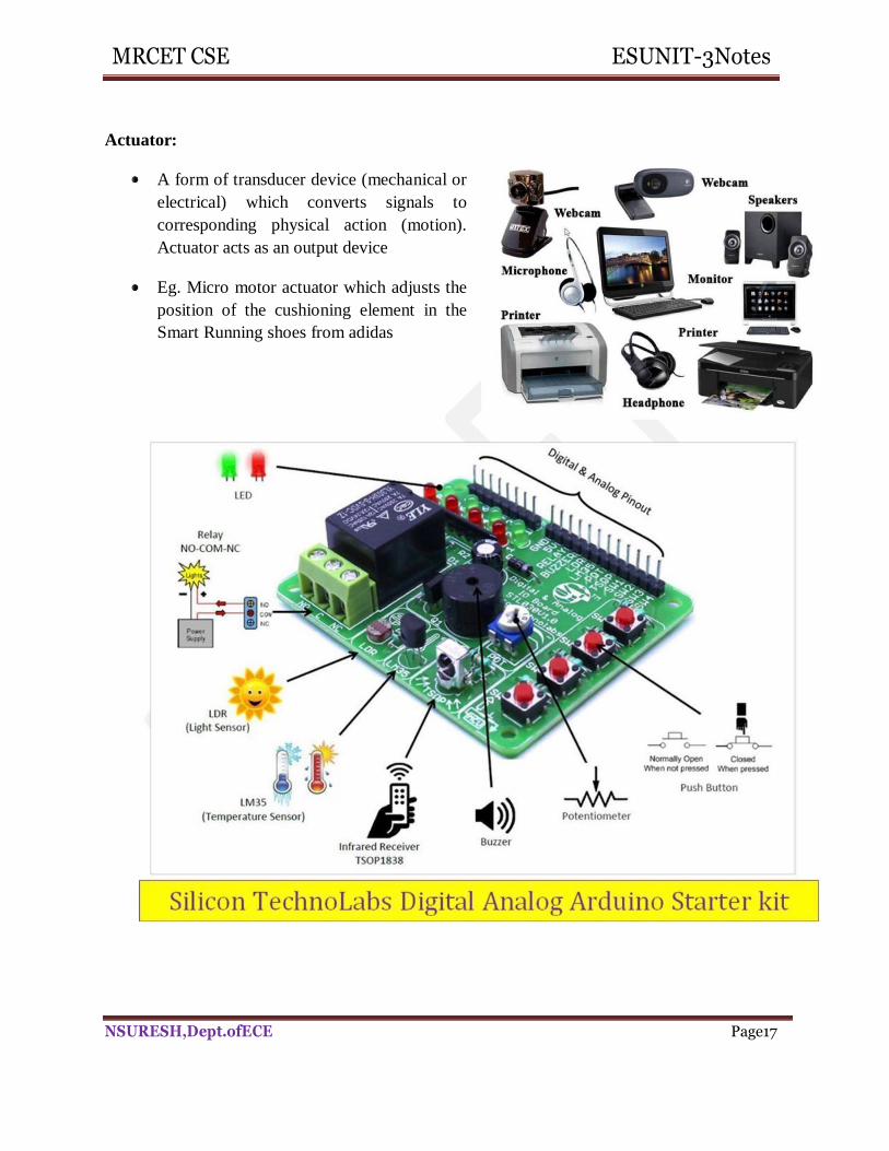
MRCET CSE ESUNIT-3Notes
Actuator:
A form of transducer device (mechanical or
electrical) which converts signals to
corresponding physical action (motion).
Actuator acts as an output device
Eg. Micro motor actuator which adjusts the
position of the cushioning element in the
Smart Running shoes from adidas
NSURESH,Dept.ofECE Page17
MRCET CSE ESUNIT-3Notes
Communication Interface :
• Communication interface is essential for communicating with various subsystems ofthe
embedded system and with the externalworld
• The communication interface can be viewed in two different perspectives; namely;
1.Device/board level communication interface (Onboard Communication Interface)
2.Product level communication interface (External CommunicationInterface)
1. Device/board level communication interface (Onboard CommunicationInterface):
The communication channel which interconnects the various components within an
embedded product is referred as Device/board level communication interface (Onboard
Communication Interface)
Examples: Serial interfaces like I2C,SPI, UART, 1-Wire etc and Parallel businterface
2. Product level communication interface (External CommunicationInterface):
• The „Product level communication interface‟ (External Communication Interface) is
responsible for data transfer between the embedded system and other devices ormodules
• The external communication interface canbe either wired media or wireless media and
it can be a serial or parallelinterface.
Examples for wireless communication interface: Infrared (IR), Bluetooth (BT), Wireless
LAN (Wi-Fi), Radio Frequency waves (RF), GPRS etc.
Examples for wired interfaces: RS-232C/RS-422/RS 485, USB, Ethernet (TCP-IP),
IEEE 1394 port, Parallel port etc.
1. Device/board level or On board communication interface:
The communication channel which interconnects the various components within an embedded
product is referred as Device/board level communication interface (Onboard Communication
Interface)
These are classified into
1.1 I2C (Inter Integrated Circuit )Bus
1.2 SPI(Serial Peripheral Interface)Bus
1.3 ParallelInterface
NSURESH,Dept.ofECE Page18
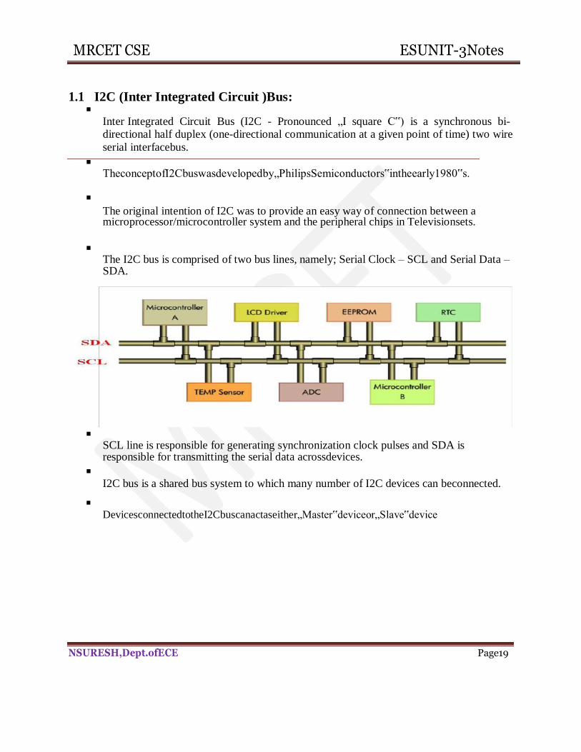
MRCET CSE ESUNIT-3Notes
1.1 I2C (Inter Integrated Circuit )Bus:
Inter Integrated Circuit Bus (I2C - Pronounced „I square C‟) is a synchronous bi- directional half duplex (one-directional communication at a given point of time) two wire
serial interfacebus.
TheconceptofI2Cbuswasdevelopedby„PhilipsSemiconductors‟intheearly1980‟s.
The original intention of I2C was to provide an easy way of connection between a microprocessor/microcontroller system and the peripheral chips in Televisionsets.
The I2C bus is comprised of two bus lines, namely; Serial Clock – SCL and Serial Data – SDA.
SCL line is responsible for generating synchronization clock pulses and SDA is responsible for transmitting the serial data acrossdevices.
I2C bus is a shared bus system to which many number of I2C devices can beconnected.
DevicesconnectedtotheI2Cbuscanactaseither„Master‟deviceor„Slave‟device
NSURESH,Dept.ofECE Page19
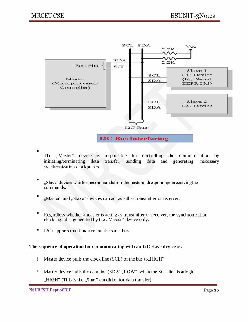
MRCET CSE ESUNIT-3Notes
NSURESH,Dept.ofECE Page 20
The sequence of operation for communicating with an I2C slave device is:
1. Master device pulls the clock line (SCL) of the bus to„HIGH‟
2. Master device pulls the data line (SDA) „LOW‟, when the SCL line is atlogic
„HIGH‟ (This is the „Start‟ condition for data transfer)
The „Master‟ device is responsible for controlling the communication by
initiating/terminating data transfer, sending data and generating necessary
synchronization clockpulses.
„Slave‟deviceswaitforthecommandsfromthemasterandresponduponreceivingthe commands.
„Master‟ and „Slave‟ devices can act as either transmitter or receiver.
Regardless whether a master is acting as transmitter or receiver, the synchronization clock signal is generated by the „Master‟ device only.
I2C supports multi masters on the same bus.
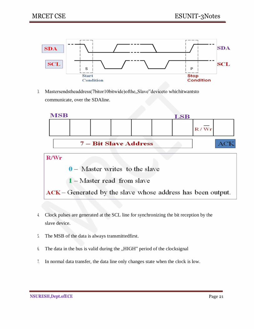
MRCET CSE ESUNIT-3Notes
NSURESH,Dept.ofECE Page 21
3. Mastersendstheaddress(7bitor10bitwide)ofthe„Slave‟deviceto whichitwantsto
communicate, over the SDAline.
4. Clock pulses are generated at the SCL line for synchronizing the bit reception by the
slave device.
5. The MSB of the data is always transmittedfirst.
6. The data in the bus is valid during the „HIGH‟ period of the clocksignal
7. In normal data transfer, the data line only changes state when the clock is low.
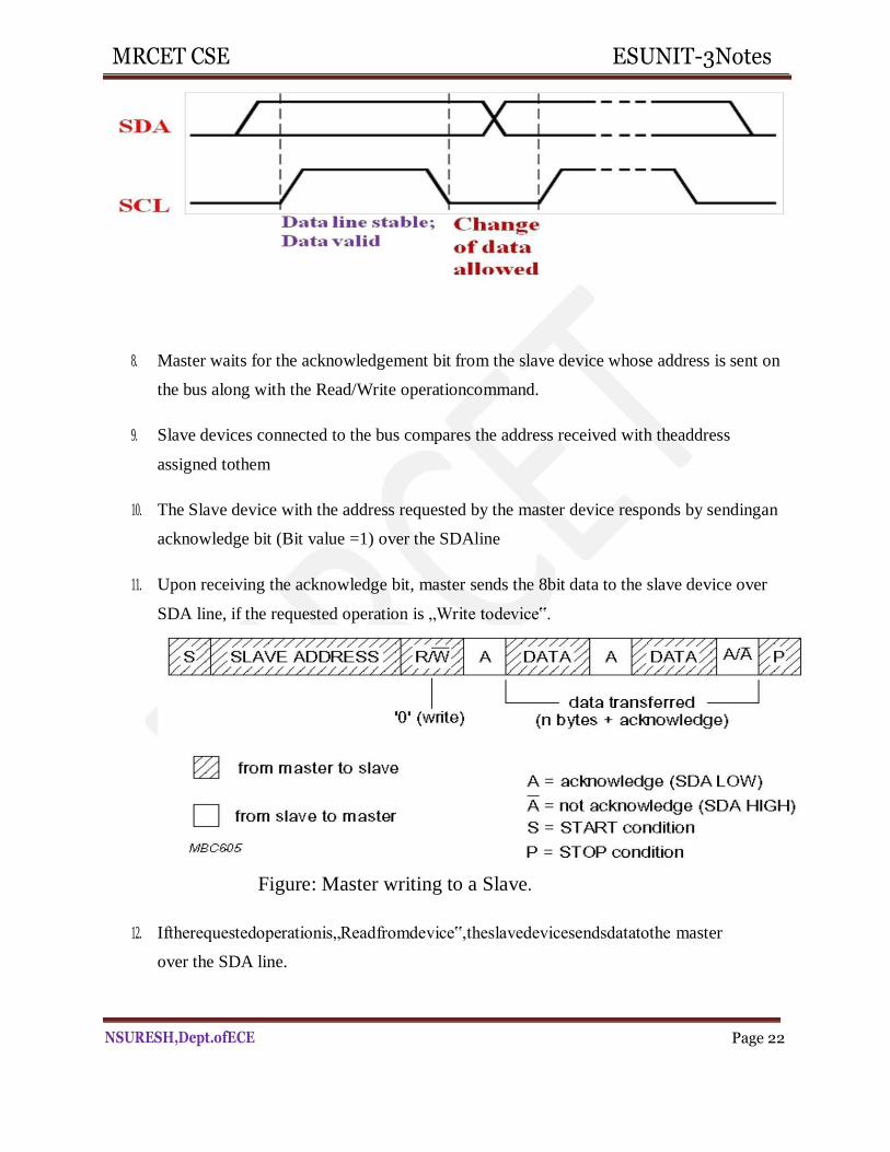
MRCET CSE ESUNIT-3Notes
NSURESH,Dept.ofECE Page 22
8. Master waits for the acknowledgement bit from the slave device whose address is sent on
the bus along with the Read/Write operationcommand.
9. Slave devices connected to the bus compares the address received with theaddress
assigned tothem
10. The Slave device with the address requested by the master device responds by sendingan
acknowledge bit (Bit value =1) over the SDAline
11. Upon receiving the acknowledge bit, master sends the 8bit data to the slave device over
SDA line, if the requested operation is „Write todevice‟.
Figure: Master writing to a Slave.
12. Iftherequestedoperationis„Readfromdevice‟,theslavedevicesendsdatatothe master
over the SDA line.
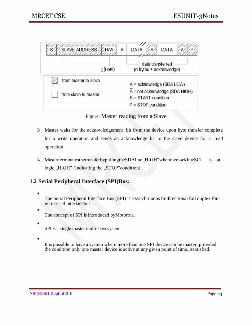
MRCET CSE ESUNIT-3Notes
NSURESH,Dept.ofECE Page 23
Figure: Master reading from a Slave
13. Master waits for the acknowledgement bit from the device upon byte transfer complete
for a write operation and sends an acknowledge bit to the slave device for a read
operation
14. MasterterminatesthetransferbypullingtheSDAline„HIGH‟whentheclocklineSCL is at
logic „HIGH‟ (Indicating the „STOP‟condition).
1.2 Serial Peripheral Interface (SPI)Bus:
The Serial Peripheral Interface Bus (SPI) is a synchronous bi-directional full duplex four wire serial interfacebus.
The concept of SPI is introduced byMotorola.
SPI is a single master multi-slavesystem.
It is possible to have a system where more than one SPI device can be master, provided the condition only one master device is active at any given point of time, issatisfied.
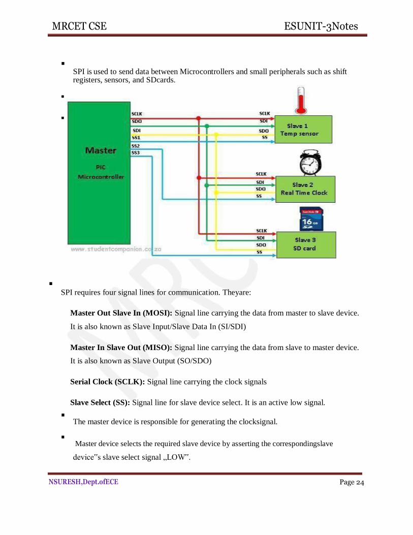
MRCET CSE ESUNIT-3Notes
NSURESH,Dept.ofECE Page 24
SPI is used to send data between Microcontrollers and small peripherals such as shift registers, sensors, and SDcards.
SPI requires four signal lines for communication. Theyare:
Master Out Slave In (MOSI): Signal line carrying the data from master to slave device.
It is also known as Slave Input/Slave Data In (SI/SDI)
Master In Slave Out (MISO): Signal line carrying the data from slave to master device.
It is also known as Slave Output (SO/SDO)
Serial Clock (SCLK): Signal line carrying the clock signals
Slave Select (SS): Signal line for slave device select. It is an active low signal.
The master device is responsible for generating the clocksignal.
Master device selects the required slave device by asserting the correspondingslave
device‟s slave select signal „LOW‟.
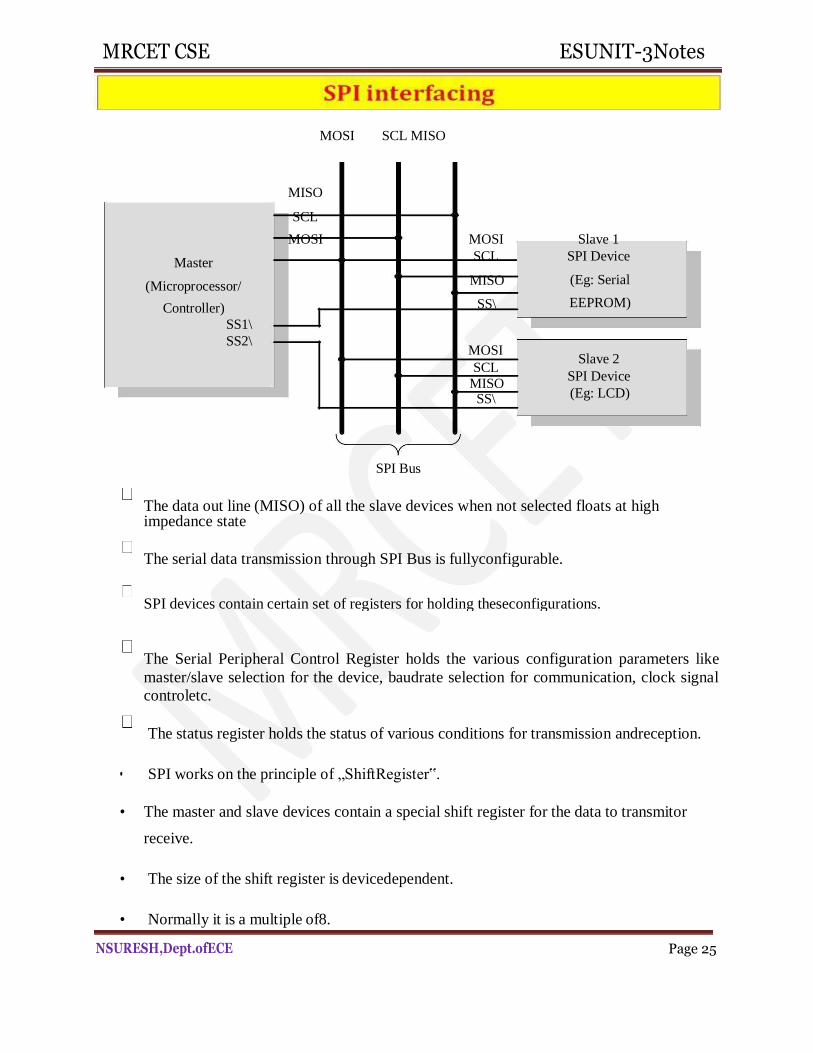
MRCET CSE ESUNIT-3Notes
NSURESH,Dept.ofECE Page 25
SPI Bus
The data out line (MISO) of all the slave devices when not selected floats at high impedance state
The serial data transmission through SPI Bus is fullyconfigurable.
SPI devices contain certain set of registers for holding theseconfigurations.
The Serial Peripheral Control Register holds the various configuration parameters like
master/slave selection for the device, baudrate selection for communication, clock signal
controletc.
The status register holds the status of various conditions for transmission andreception.
• SPI works on the principle of „ShiftRegister‟.
MOSI SCL MISO
MISO
SCL
MOSI MOSI Slave 1
Master SCL SPI Device
(Microprocessor/ MISO (Eg: Serial
Controller) SS\ EEPROM)
SS1\
SS2\ MOSI
Slave 2
SCL
SPI Device
MISO
(Eg: LCD) SS\
• The master and slave devices contain a special shift register for the data to transmitor
receive.
• The size of the shift register is devicedependent.
• Normally it is a multiple of8.
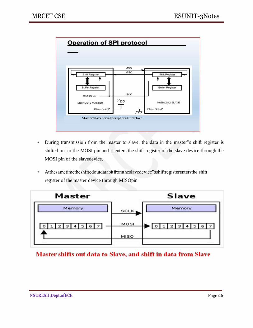
MRCET CSE ESUNIT-3Notes
NSURESH,Dept.ofECE Page 26
• During transmission from the master to slave, the data in the master‟s shift register is
shifted out to the MOSI pin and it enters the shift register of the slave device through the
MOSI pin of the slavedevice.
• Atthesametimetheshiftedoutdatabitfromtheslavedevice‟sshiftregisterentersthe shift
register of the master device through MISOpin
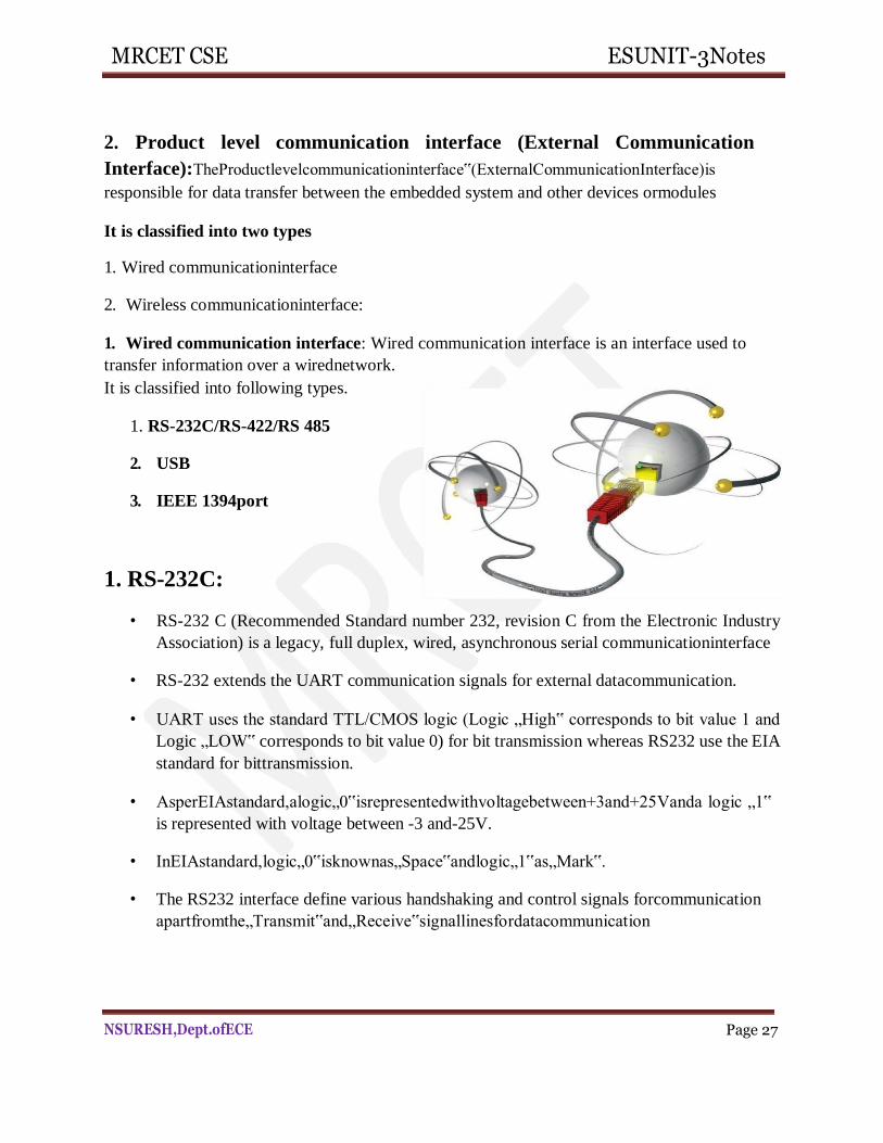
MRCET CSE ESUNIT-3Notes
NSURESH,Dept.ofECE Page 27
2. Product level communication interface (External Communication
Interface):TheProductlevelcommunicationinterface‟(ExternalCommunicationInterface)is
responsible for data transfer between the embedded system and other devices ormodules
It is classified into two types
1. Wired communicationinterface
2. Wireless communicationinterface:
1. Wired communication interface: Wired communication interface is an interface used to
transfer information over a wirednetwork.
It is classified into following types.
1. RS-232C/RS-422/RS 485
2. USB
3. IEEE 1394port
1. RS-232C:
• RS-232 C (Recommended Standard number 232, revision C from the Electronic Industry
Association) is a legacy, full duplex, wired, asynchronous serial communicationinterface
• RS-232 extends the UART communication signals for external datacommunication.
• UART uses the standard TTL/CMOS logic (Logic „High‟ corresponds to bit value 1 and
Logic „LOW‟ corresponds to bit value 0) for bit transmission whereas RS232 use the EIA
standard for bittransmission.
• AsperEIAstandard,alogic„0‟isrepresentedwithvoltagebetween+3and+25Vanda logic „1‟
is represented with voltage between -3 and-25V.
• InEIAstandard,logic„0‟isknownas„Space‟andlogic„1‟as„Mark‟.
• The RS232 interface define various handshaking and control signals forcommunication
apartfromthe„Transmit‟and„Receive‟signallinesfordatacommunication
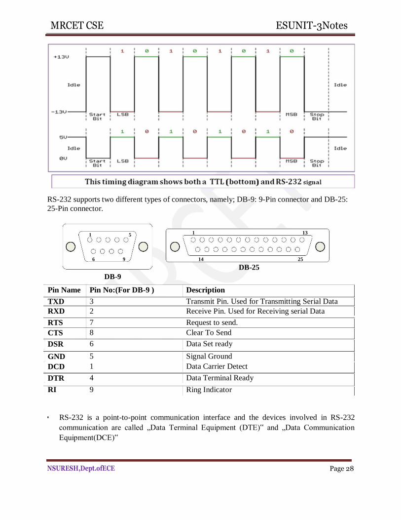
MRCET CSE ESUNIT-3Notes
NSURESH,Dept.ofECE Page 28
RS-232 supports two different types of connectors, namely; DB-9: 9-Pin connector and DB-25:
25-Pin connector.
1 5 1 13
6
9
14
25
DB-25
DB-9
Pin Name Pin No:(For DB-9 ) Description
TXD 3 Transmit Pin. Used for Transmitting Serial Data
RXD 2 Receive Pin. Used for Receiving serial Data
RTS 7 Request to send.
CTS 8 Clear To Send
DSR 6 Data Set ready
GND 5 Signal Ground
DCD 1 Data Carrier Detect
DTR 4 Data Terminal Ready
RI 9 Ring Indicator
• RS-232 is a point-to-point communication interface and the devices involved in RS-232
communication are called „Data Terminal Equipment (DTE)‟ and „Data Communication
Equipment(DCE)‟
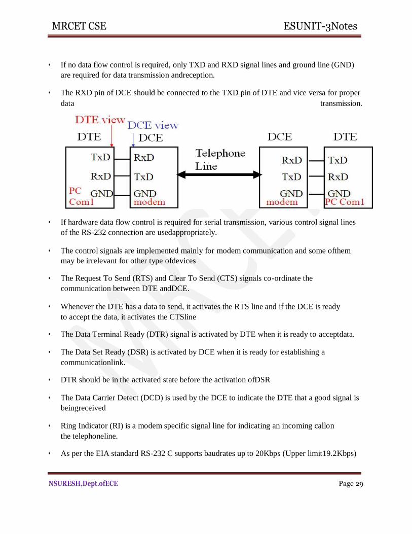
MRCET CSE ESUNIT-3Notes
NSURESH,Dept.ofECE Page 29
• If no data flow control is required, only TXD and RXD signal lines and ground line (GND)
are required for data transmission andreception.
• The RXD pin of DCE should be connected to the TXD pin of DTE and vice versa for proper
data transmission.
• If hardware data flow control is required for serial transmission, various control signal lines
of the RS-232 connection are usedappropriately.
• The control signals are implemented mainly for modem communication and some ofthem
may be irrelevant for other type ofdevices
• The Request To Send (RTS) and Clear To Send (CTS) signals co-ordinate the
communication between DTE andDCE.
• Whenever the DTE has a data to send, it activates the RTS line and if the DCE is ready
to accept the data, it activates the CTSline
• The Data Terminal Ready (DTR) signal is activated by DTE when it is ready to acceptdata.
• The Data Set Ready (DSR) is activated by DCE when it is ready for establishing a
communicationlink.
• DTR should be in the activated state before the activation ofDSR
• The Data Carrier Detect (DCD) is used by the DCE to indicate the DTE that a good signal is
beingreceived
• Ring Indicator (RI) is a modem specific signal line for indicating an incoming callon
the telephoneline.
• As per the EIA standard RS-232 C supports baudrates up to 20Kbps (Upper limit19.2Kbps)
MRCET CSE ESUNIT-3Notes
NSURESH,Dept.ofECE Page 30
• The commonly used baudrates by devices are 300bps, 1200bps,2400bps,
9600bps, 11.52Kbps and19.2Kbps
• The maximum operating distance supported in RS-232 communication is 50 feet at
the highest supportedbaudrate.
• Embedded devices contain a UART for serial communication and they generate signallevels
conforming to TTL/CMOSlogic.
• A level translator IC like MAX 232 from Maxim Dallas semiconductor is used for converting
the signal lines from the UART to RS-232 signal lines forcommunication.
• On the receiving side the received data is converted back to digital logic level by a converter
IC.
• Converter chips contain converters for both transmitter andreceiver
• RS-232 uses single ended data transfer and supports only point-to-point communicationand
not suitable for multi-dropcommunication
2. Wireless communication interface:
Wireless communication interface is an interface used to transmission of information
over a distance without help of wires, cables or any other forms of electrical conductors.
They are basically classified into following types
1. IrDA
2. Bluetooth
3. Wi-Fi
4. Zigbee
5. GPRS
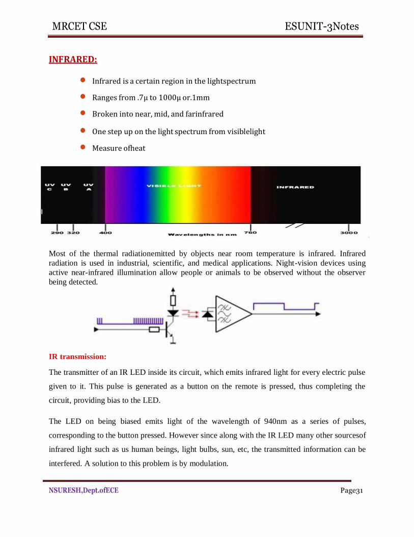
MRCET CSE ESUNIT-3Notes
NSURESH,Dept.ofECE Page31
INFRARED:
Infrared is a certain region in the lightspectrum
Ranges from .7µ to 1000µ or.1mm
Broken into near, mid, and farinfrared
One step up on the light spectrum from visiblelight
Measure ofheat
Most of the thermal radiationemitted by objects near room temperature is infrared. Infrared
radiation is used in industrial, scientific, and medical applications. Night-vision devices using
active near-infrared illumination allow people or animals to be observed without the observer
being detected.
IR transmission:
The transmitter of an IR LED inside its circuit, which emits infrared light for every electric pulse
given to it. This pulse is generated as a button on the remote is pressed, thus completing the
circuit, providing bias to the LED.
The LED on being biased emits light of the wavelength of 940nm as a series of pulses,
corresponding to the button pressed. However since along with the IR LED many other sourcesof
infrared light such as us human beings, light bulbs, sun, etc, the transmitted information can be
interfered. A solution to this problem is by modulation.
NSURESH,Dept.ofECE Page 32
MRCETCSE ES UNIT-3Notes
The transmitted signal is modulated using a carrier frequency of 38 KHz (or any other frequency
between 36 to 46 KHz). The IR LED is made to oscillate at this frequency for the time duration
of the pulse. The information or the light signals are pulse width modulated and are contained in
the 38 KHzfrequency.
IR supports data rates ranging from 9600bits/second to 16Mbps
Serial infrared: 9600bps to 115.2 kbps
Medium infrared: 0.576Mbps to 1.152 Mbps
Fast infrared: 4Mbps
BLUETOOTH:
Bluetooth is a wireless technology standard for short distances (using short-wavelengthUHFband
from 2.4 to 2.485 GHz)for exchanging data over radio waves in the ISMand mobiledevices,
andbuilding personal area networks(PANs).Invented by telecom vendor Ericssonin
1994, it was originally conceived as a wireless alternative to RS- 232 data cables.
Bluetooth uses a radio technology called frequency- hopping spread spectrum.
Bluetoothdividestransmitted data into packets, andtransmitseach packet on one of 79 designated
Bluetooth channels. Each channel has a bandwidth of 1 MHz. It usually performs 800 hops per
second, with Adaptive Frequency-Hopping (AFH)enabled
Originally, Gaussian frequency-shift keying (GFSK) modulation was the only modulation
scheme available. Since the introduction of Bluetooth 2.0+EDR, π/4-DQPSK(Differential
Quadrature Phase Shift Keying) and 8DPSK modulation may also be used between compatible
devices. Bluetooth is a packet-based protocol with a master- slave structure. One master may
communicate with up to seven slaves in a piconet. All devices share the master's clock. Packet
exchange is based on the basic clock, defined by the master, which ticks at312.5 µs intervals.
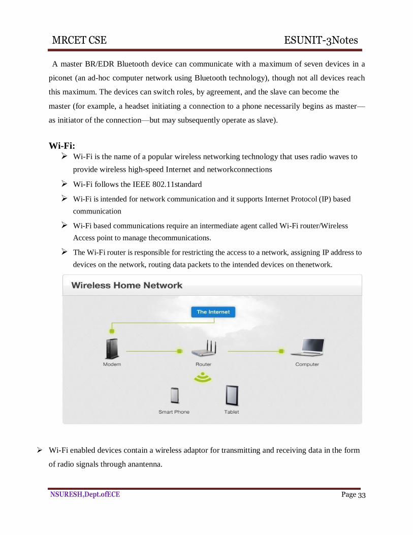
MRCET CSE ESUNIT-3Notes
NSURESH,Dept.ofECE Page 33
A master BR/EDR Bluetooth device can communicate with a maximum of seven devices in a
piconet (an ad-hoc computer network using Bluetooth technology), though not all devices reach
this maximum. The devices can switch roles, by agreement, and the slave can become the
master (for example, a headset initiating a connection to a phone necessarily begins as master—
as initiator of the connection—but may subsequently operate as slave).
Wi-Fi: Wi-Fi is the name of a popular wireless networking technology that uses radio waves to
provide wireless high-speed Internet and networkconnections
Wi-Fi follows the IEEE 802.11standard
Wi-Fi is intended for network communication and it supports Internet Protocol (IP) based
communication
Wi-Fi based communications require an intermediate agent called Wi-Fi router/Wireless
Access point to manage thecommunications.
The Wi-Fi router is responsible for restricting the access to a network, assigning IP address to
devices on the network, routing data packets to the intended devices on thenetwork.
Wi-Fi enabled devices contain a wireless adaptor for transmitting and receiving data in the form
of radio signals through anantenna.
MRCET CSE ESUNIT-3Notes
NSURESH,Dept.ofECE Page 34
Wi-Fi operates at 2.4GHZ or 5GHZ of radio spectrum and they co-exist with other ISM
band devices likeBluetooth.
A Wi-Fi network is identified with a Service Set Identifier (SSID). A Wi-Fi device can
connect to a network by selecting the SSID of the network and by providing the
credentials if the network is securityenabled
Wi-Fi networks implements different security mechanisms for authentication and data
transfer.
Wireless Equivalency Protocol (WEP), Wireless Protected Access (WPA) etc are someof
the security mechanisms supported by Wi-Fi networks in datacommunication.
ZIGBEE:
Zigbee is an IEEE 802.15.4-based specificationfor a suite of high- level communication
protocols used to create personal area networks with small, low-power digital radios, such as for
home automation, medical device data collection, and other low-power low-bandwidth needs,
designed for small scale projects which need wireless connection.Hence, zigbee is a low-power,
low data rate, and close proximity(i.e., personal area) wireless ad hoc network.
The technology defined by the zigbee specification is intended to be simpler and
lessexpensive than otherwireless personal areanetworks (WPANs), such as BluetoothorWi-Fi
.Applications include wireless light switches, electrical meters with in-home-displays, traffic
management systems, and other consumer and industrial equipment that require short-range low-
rate wireless data transfer.
Its low power consumption limits transmission distances to 10– 100 meters line-of-sight,
depending on power output and environmental characteristics. Zigbee devices can transmit data
over long distances by passing data through a mesh network of intermediate devices to reach
more distant ones.
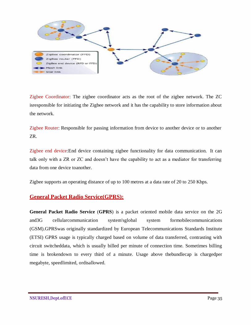
NSURESH,Dept.ofECE Page 35
Zigbee Coordinator: The zigbee coordinator acts as the root of the zigbee network. The ZC
isresponsible for initiating the Zigbee network and it has the capability to store information about
the network.
Zigbee Router: Responsible for passing information from device to another device or to another
ZR.
Zigbee end device:End device containing zigbee functionality for data communication. It can
talk only with a ZR or ZC and doesn’t have the capability to act as a mediator for transferring
data from one device toanother.
Zigbee supports an operating distance of up to 100 metres at a data rate of 20 to 250 Kbps.
General Packet Radio Service(GPRS):
General Packet Radio Service (GPRS) is a packet oriented mobile data service on the 2G
and3G cellularcommunication system'sglobal system formobilecommunications
(GSM).GPRSwas originally standardized by European Telecommunications Standards Institute
(ETSI) GPRS usage is typically charged based on volume of data transferred, contrasting with
circuit switcheddata, which is usually billed per minute of connection time. Sometimes billing
time is brokendown to every third of a minute. Usage above thebundlecap is chargedper
megabyte, speedlimited, ordisallowed.
NSURESH,Dept.ofECE Page36
MRCETCSE ES UNIT-3Notes
Services offered:
GPRS extends the GSM Packet circuit switched data capabilities and makes the
following servicespossible:
SMS messaging andbroadcasting
"Always on" internetaccess
Multimedia messaging service(MMS)
Push-to-talk over cellular(PoC)
Instant messagingand presence-wireless villageInternetapplications for smart
devicesthrough wireless application protocol(WAP).
Point-to-point (P2P) service: inter-networking with the Internet(IP).
Point-to-multipoint (P2M) service]: point-to- multipoint multicast and point-to-multipoint
groupcalls.
Text Book:-
1. Introduction to Embedded Systems – Shibu K.V Mc GrawHill
UNIT-4
EMBEDDED FIRMWARE DESIGN &
DEVELOPMENT
N.SURESH
Department of ECE
Embedded Systems Unit-4 Notes
N.SURESH, Assistant Professor, Dept. of ECE, MRCET Page 1
Introduction:
Embedded Firmware
The control algorithm (Program instructions) and or the configuration
settings that an embedded system developer dumps into the code (Program)
memory of the embedded system
It is an un-avoidable part of an embedded system.
The embedded firmware can be developed in various methods like
o Write the program in high level languages like Embedded C/C++
using an Integrated Development Environment (The IDE will contain
an editor, compiler, linker, debugger, simulator etc. IDEs are different
for different family ofprocessors/controllers.
o Write the program in Assembly Language using the Instructions Supported by your application’s targetprocessor/controller
Embedded Firmware Design & Development:
The embedded firmware is responsible for controlling the various
peripherals of the embedded hardware and generating response in
accordance with the functional requirements of theproduct.
The embedded firmware is the master brain of the embedded system.
The embedded firmware imparts intelligence to an Embedded system.
It is a onetime process and it can happen at any stage.
The product starts functioning properly once the intelligence imparted to the
product by embedding the firmware in the hardware.
The product will continue serving the assigned task till hardware breakdown
occurs or a corruption in embedded firmware.
In case of hardware breakdown , the damaged component may need to be
replaced and for firmware corruptions the firmware should be re-loaded, to
bring back the embedded product to the normal functioning.
Embedded Systems Unit-4 Notes
N.SURESH, Assistant Professor, Dept. of ECE, MRCET Page 2
The embedded firmware is usually stored in a permanent memory (ROM)
and it is non alterable by end users.
Designing Embedded firmware requires understanding of the particular
embedded product hardware, like various component interfacing, memory
map details, I/O port details, configuration and register details of various
hardware chips used and some programming language (either low level
Assembly Language or High level language like C/C++ or a combination of
the two)
The embedded firmware development process starts with the conversion of
the firmware requirements into a program model using various modeling
tools.
The firmware design approaches for embedded product is purely dependent
on the complexity of the functions to be performed and speed of operation
required.
There exist two basic approaches for the design and implementation of
embedded firmware, namely;
The Super loop basedapproach
The Embedded Operating System basedapproach
The decision on which approach needs to be adopted for firmware
development is purely dependent on the complexity and system
requirements
1. Embedded firmware Design Approaches – The Superloop:
The Super loop based firmware development approach is Suitable for
applications that are not time critical and where the response time is not so
important (Embedded systems where missing deadlines are acceptable).
Embedded Systems Unit-4 Notes
N.SURESH, Assistant Professor, Dept. of ECE, MRCET Page 3
It is very similar to a conventional procedural programming where the code
is executed task by task
The tasks are executed in a never ending loop.
The task listed on top on the program code is executed first and the tasks just
below the top are executed after completing the first task
A typical super loop implementation will look like:
1. Configure the common parameters and perform initializationfor
various hardware components memory, registersetc.
2. Start the first task and executeit
3. Execute the secondtask
4. Execute the next task
5.:
6. :
7. Execute the last definedtask
8. Jump back to the first task and follow the sameflow.
The ‘C’ program code for the super loop is given below
void main ()
{
Configurations ();
Initializations ();
while (1)
{
Task 1();
Task 2();
:
Embedded Systems Unit-4 Notes
N.SURESH, Assistant Professor, Dept. of ECE, MRCET Page 4
:
Task n ();
}
}
Pros:
Cons:
Doesn’t require an Operating System for task scheduling and monitoring and
free from OS related overheads
Simple and straight forward design
Reduced memory footprint
Non Real time in execution behavior (As the number of tasks increases the
frequency at which a task gets CPU time for execution also increases)
Any issues in any task execution may affect the functioning of the product
(This can be effectively tackled by using Watch Dog Timers for task
execution monitoring)
Enhancements:
Combine Super loop based technique withinterrupts
Execute the tasks (like keyboard handling) which require Real timeattention
as Interrupt Serviceroutines.
2. Embedded firmware Design Approaches – Embedded OS basedApproach:
The embedded device contains an Embedded Operating System which can
be one of:
AReal Time Operating System(RTOS)
A Customized General Purpose Operating System(GPOS)
Embedded Systems Unit-4 Notes
N.SURESH, Assistant Professor, Dept. of ECE, MRCET Page 5
The Embedded OS is responsible for scheduling the execution of user tasks
and the allocation of system resources among multiple tasks
It Involves lot of OS related overheads apart from managing and executing
user defined tasks
Microsoft® Windows XP Embedded is an example of GPOS for embedded
devices
Point of Sale (PoS) terminals, Gaming Stations, Tablet PCs etc are examples
of embedded devices running on embedded GPOSs
‘Windows CE’, ‘Windows Mobile’,‘QNX’, ‘VxWorks’, ‘ThreadX’,
‘MicroC/OS-II’, ‘Embedded Linux’, ‘Symbian’ etc are examples of RTOSs
employed in Embedded Product development
Mobile Phones, PDAs, Flight Control Systems etc are examples of
embedded devices that runs onRTOSs
Embedded firmware Development Languages/Options
Assembly Language
High Level Language
o Subset of C (EmbeddedC)
o Subset of C++ (EmbeddedC++)
o Anyother high level language with supportedCross-compiler
Mix of Assembly & High level Language
o Mixing High Level Language (Like C) with AssemblyCode
o Mixing Assembly code with High Level Language (LikeC)
o InlineAssembly
Embedded Systems Unit-4 Notes
N.SURESH, Assistant Professor, Dept. of ECE, MRCET Page 6
1. Embedded firmware Development Languages/Options – Assembly
Language
‘Assembly Language’ is the human readable notation of ‘machine
language’
‘Machine language’ is a processor understandable language
Machine language is a binary representation and it consists of 1s and 0s
Assembly language and machine languages are processor/controller
dependent
An Assembly language program written for one processor/controller family
will not work with others
Assembly language programming is the process of writing processor specific
machine code in mnemonic form, converting the mnemonics into actual
processor instructions (machine language) and associated data using an
assembler
The general format of an assembly language instruction is an Opcode
followed by Operands
The Opcode tells the processor/controller what to do and the Operands
provide the data and information required to perform the action specified by
the opcode
It is not necessary that all opcode should have Operands following them.
Some of the Opcode implicitly contains the operand and in such situation no
operand is required. The operand may be a single operand, dual operand or
more
The 8051 Assembly Instruction
MOV A, #30
Moves decimal value 30 to the 8051 Accumulator register. Here MOV A is the
Opcode and 30 is the operand (single operand). The same instruction when written
in machine language will look like
Embedded Systems Unit-4 Notes
N.SURESH, Assistant Professor, Dept. of ECE, MRCET Page 7
01110100 00011110
The first 8 bit binary value 01110100 represents the opcode MOV A and the second
8 bit binary value 00011110 represents the operand 30.
Assembly language instructions are written one per line
A machine code program consists of a sequence of assembly language
instructions, where each statement contains a mnemonic (Opcode +
Operand)
Each line of an assembly language program is split into four fields as:
LABEL OPCODE OPERANDCOMMENTS
LABEL is an optional field. A ‘LABEL’ is an identifier used extensively in
programs to reduce the reliance on programmers for remembering where
data or code is located. LABEL is commonly used forrepresenting
A memory location, address of a program, sub-routine, code portionetc.
The maximum length of a label differs between assemblers.
Assemblers insist strict formats for labeling. Labels are always
suffixed by a colon and begin with a valid character. Labels can
contain number from 0 to 9 and special character _(underscore).
;###############################################################
; SUBROUTINE FOR GENERATINGDELAY
; DELAY PARAMETR PASSED THROUGH REGISTERR1
; RETURN VALUE NONE,REGISTERS USED: R0,R1
;###############################################################
##### DELAY: MOVR0,#255 ; Load Register R0 with255
DJNZ R1, DELAY; Decrement R1 andlooptill R1= 0
RET ; Return to callingprogram
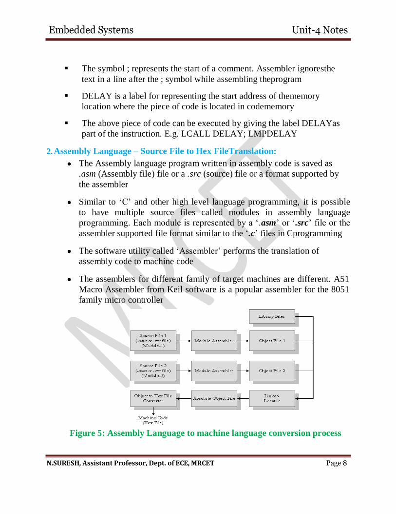
Embedded Systems Unit-4 Notes
N.SURESH, Assistant Professor, Dept. of ECE, MRCET Page 8
The symbol ; represents the start of a comment. Assembler ignoresthe
text in a line after the ; symbol while assembling theprogram
DELAY is a label for representing the start address of thememory
location where the piece of code is located in codememory
The above piece of code can be executed by giving the label DELAYas
part of the instruction. E.g. LCALL DELAY; LMPDELAY
2. Assembly Language – Source File to Hex FileTranslation:
The Assembly language program written in assembly code is saved as
.asm (Assembly file) file or a .src (source) file or a format supported by
the assembler
Similar to ‘C’ and other high level language programming, it is possible
to have multiple source files called modules in assembly language
programming. Each module is represented by a ‘.asm’ or ‘.src’ file or the
assembler supported file format similar to the ‘.c’ files in Cprogramming
The software utility called ‘Assembler’ performs the translation of
assembly code to machine code
The assemblers for different family of target machines are different. A51
Macro Assembler from Keil software is a popular assembler for the 8051
family micro controller
Figure 5: Assembly Language to machine language conversion process
Embedded Systems Unit-4 Notes
N.SURESH, Assistant Professor, Dept. of ECE, MRCET Page 9
Each source file can be assembled separately to examine the syntax errors
and incorrect assembly instructions
Assembling of each source file generates a corresponding object file. The
object file does not contain the absolute address of where the generated
code needs to be placed (a re-locatable code) on the program memory
The software program called linker/locater is responsible for assigning
absolute address to object files during the linking process
The Absolute object file created from the object files corresponding to
different source code modules contain information about the address
where each instruction needs to be placed in code memory
A software utility called ‘Object to Hex file converter’ translates the
absolute object file to corresponding hex file (binary file)
Advantages:
1.Efficient Code Memory & Data Memory Usage (MemoryOptimization):
The developer is well aware of the target processor architecture and
memory organization, so optimized code can be written for
performingoperations.
This leads to less utilization of code memory and efficientutilization
of datamemory.
2.HighPerformance:
Optimized code not only improves the code memory usage butalso
improves the total systemperformance.
Through effective assembly coding, optimum performance canbe
achieved for targetprocessor.
3.Low level HardwareAccess:
Most of the code for low level programming like accessing external
device specific registers from OS kernel ,device drivers, and low level
interrupt routines, etc are making use of direct assemblycoding.
Embedded Systems Unit-4 Notes
N.SURESH, Assistant Professor, Dept. of ECE, MRCET Page 10
4.Code ReverseEngineering:
It is the process of understanding the technology behind a product by
extracting the information from the finishedproduct.
It can easily be converted into assembly code using a dis-assembler
program for the target machine.
Drawbacks:
1.High Developmenttime:
The developer takes lot of time to study about architecture ,memory
organization, addressing modes and instruction set of target
processor/controller.
More lines of assembly code is required for performing a simple
action.
2.Developerdependency:
There is no common written rule for developing assembly language
based applications.
3.Nonportable:
Target applications written in assembly instructions are valid only for
that particular family of processors and cannot be re-used for another
targetprocessors/controllers.
If the target processor/controller changes, a complete re-writing of the
application using assembly language for new target
processor/controller isrequired.
2. Embedded firmware Development Languages/Options – High Level
Language
The embedded firmware is written in any high level language like C, C++
A software utility called ‘cross-compiler’ converts the high level language to
target processor specific machine code
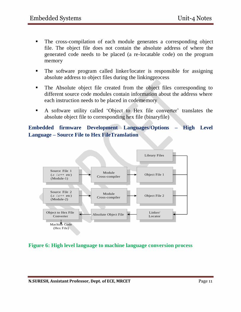
Embedded Systems Unit-4 Notes
N.SURESH, Assistant Professor, Dept. of ECE, MRCET Page 11
The cross-compilation of each module generates a corresponding object
file. The object file does not contain the absolute address of where the
generated code needs to be placed (a re-locatable code) on the program
memory
The software program called linker/locater is responsible for assigning
absolute address to object files during the linkingprocess
The Absolute object file created from the object files corresponding to
different source code modules contain information about the address where
each instruction needs to be placed in codememory
A software utility called ‘Object to Hex file converter’ translates the
absolute object file to corresponding hex file (binaryfile)
Embedded firmware Development Languages/Options – High Level
Language – Source File to Hex FileTranslation
Machine Code
(Hex File)
Figure 6: High level language to machine language conversion process
Library Files
Source File 1
(.c /.c++ etc)
(Module-1)
Module
Cross-compiler
Object File 1
Source File 2
(.c /.c++ etc)
(Module-2)
Module
Cross-compiler
Object File 2
Object to Hex File
Converter
Absolute Object File Linker/
Locator

Embedded Systems Unit-4 Notes
N.SURESH, Assistant Professor, Dept. of ECE, MRCET Page 12
Advantages:
Reduced Development time: Developer requires less or little
Drawbacks:
knowledge on internal hardware details and architecture of the target
processor/Controller.
Developer independency: The syntax used by most of the high level
languages are universal and a program written high level can easily
understand by a second person knowing the syntax of the language
Portability: An Application written in high level language for
particular target processor /controller can be easily be converted to
another target processor/controller specific application with little or
less effort
• The cross compilers may not be efficient in generating the optimized
target processor specific instructions.
• Target images created by such compilers may be messy and non-
optimized in terms of performance as well as codesize.
• The investment required for high level language based development
tools (IDE) is high compared to Assembly Language based firmware
development tools.
Embedded firmware Development Languages/Options – Mixing of Assembly
Language with High Level Language
Embedded firmware development may require the mixing of Assembly
Language with high level language or vice versa.
Interrupt handling, Source code is already available in high level
language\Assembly Language etc areexamples
Embedded Systems Unit-4 Notes
N.SURESH, Assistant Professor, Dept. of ECE, MRCET Page 13
High Level language and low level language can be mixed in three different
ways
Mixing Assembly Language with High level language like‘C’
Mixing High level language like ‘C’ with AssemblyLanguage
In lineAssembly
The passing of parameters and return values between the high level and low
level language is cross-compiler specific
1. Mixing Assembly Language with High level language like ‘C’
(Assembly Language with‘C’):
Assembly routines are mixed with ‘C’ in situations where the entire program
is written in ‘C’ and the cross compiler in use do not have built in support
for implementing certain features likeISR.
If the programmer wants to take advantage of the speed and optimized code
offered by the machine code generated by hand written assembly rather than
cross compiler generated machine code.
For accessing certain low level hardware ,the timing specifications may be
very critical and cross compiler generated machine code may not be able to
offer the required time specifications accurately.
Writing the hardware/peripheral access routine in processor/controller
specific assembly language and invoking it from ‘C’ is the most advised
method.
Mixing ‘C’ and assembly is little complicated.
The programmer must be aware of how to pass parameters from the ‘C’
routine to assembly and values returned from assembly routine to ‘C’ and
how Assembly routine is invoked from the ‘C’ code.
Embedded Systems Unit-4 Notes
N.SURESH, Assistant Professor, Dept. of ECE, MRCET Page 14
Passing parameter to the assembly routine and returning values from the
assembly routine to the caller ‘C’ function and the method of invoking the
assembly routine from ‘C’ code is cross compiler dependent.
There is no universal written rule for purpose.
We can get this information from documentation of the cross compiler.
Different cross compilers implement these features in different ways
depending on GPRs and memory supported by target processor/controller
2. Mixing High level language like ‘C’ with Assembly Language
(‘C’ with AssemblyLanguage)
The source code is already available in assembly language and routine
written in a high level language needs to be included to the existing code.
The entire source code is planned in Assembly code for various reasons like
optimized code, optimal performance, efficient code memory utilization and
proven expertise in handling the assembly.
The functions written in ‘C’ use parameter passing to the function and
returns values to the calling functions.
The programmer must be aware of how parameters are passed to the
function and how values returned from the function and how function is
invoked from the assembly language environment.
Passing parameter to the function and returning values from the function
using CPU registers , stack memory and fixed memory.
Its implementation is cross compiler dependent and varies across compilers.
Embedded Systems Unit-4 Notes
N.SURESH, Assistant Professor, Dept. of ECE, MRCET Page 15
3. In lineAssembly:
• Inline assembly is another technique for inserting the target
processor/controller specific assembly instructions at any location of source
code written in high level language‘C’
• Inline Assembly avoids the delay in calling an assembly routine from a ‘C’
code.
• Special keywords are used to indicate the start and end of Assembly
instructions
• E.g #pragmaasm
Mov A,#13H
#pragma ensasm
• Keil C51 uses the keywords #pragma asm and #pragma endasm to indicate
a block of code written inassembly.
TextBooks:
1. Introduction to Embedded Systems – Shibu K.V Mc GrawHill
2. Embedded System Design-Raj KamalTMH
1
Unit -5
Embedded Programming Concept using C, C++ and Java
Assembly language coding of an application has the following advantages:
1. It gives a precise control of the processor internal devices and full use of processor specific
features in its instruction set and its addressing modes.
2. The machine codes are compact. This is because the codes for declaring the conditions, rules,
and data type do not exist. The system thus needs a smaller memory. Excess memory needed
does not depend on the programmer data type selection and rule-declarations. It is also not
the compiler specific and library functions specific.
3. Device driver codes may need only a few assembly instructions. For example, consider a
small- embedded system, a timer device in a microwave oven or an automatic washing
machine or an automatic chocolate vending machine. Assembly codes for these can be
compact and precise, and are conveniently written.
It becomes convenient to develop the source files in C or C++ or Java for complex systems
because of the following advantages of high-level languages for such systems.
1. The development cycle is short for complex systems due to the use of functions (procedures),
standard library functions, modular programming approach and top down design. Application
programs are structured to ensure that the software is based on sound software engineering
principles.
(a) Let us recall Example 4.8 of a UART serial line device driver. Direct use of this function
makes the repetitive coding redundant as this device is used in many systems. We simply
change some of the arguments (for the variables) passed when needed and use it at another
instance of the device use.
(b) Should the square root codes be written again whenever the square root of another value
(argument) is to be taken? The use of the standard library function, square root ( ), saves
the programmer time for coding. New sets of library functions exist in an embedded system
specific C or C++ compiler. Exemplary functions are the delay ( ), wait ( ) and sleep ( ).
(c) Modular programming approach is an approach in which the building blocks are reusable
software components. Consider an analogy to an IC (Integrated Circuit). Just as an IC has
several circuits integrated into one, similarly a building block may call several functions and
library functions. A module should however, be well tested. It must have a well-defined
goal and the well-defined data inputs and outputs. It should have only one calling procedure.
There should be one return point from it. It should not affect any data other than that which
is targeted. [Data Encapsulation.] It must return (report) error conditions encountered
during its execution.
(d) Bottom up design is a design approach in which programming is first done for the sub-
modules of the specific and distinct sets of actions. An example of the modules for specific
sets of actions is a program for a software timer, RTCSWT:: run. Programs for delay,
counting, finding time intervals and many applications can be written. Then the final
program is designed. The approach to this way of designing a program is to first code the
basic functional modules and then use these to build a bigger module.
(e) Top-Down design is another programming approach in which the main program is first
designed, then its modules, sub-modules, and finally, the functions.
2. Data type declarations provide programming ease. For example, there are four types of
integers, int, unsigned int, short and long. When dealing with positive only values, we declare a
variable as unsigned int. For example, numTicks (Number of Ticks of a clock before the
timeout) has to be unsigned. We need a signed integer, int (32 bit) in arithmetical calculations.
An integer can also be declared as data type, short (16 bit) or long (64 bit).To manipulate the
text and strings for a character, another data type is char. Each data type is an abstraction for
the methods to use, to manipulate, to represent, and for a set of permissible operations.
5.1 SOFTWARE PROGRAMMING IN ASSEMBLY LANGUAGE
(ALP) AND IN HIGH LEVEL LANGUAGE ‘C’
2
3. Type checking makes the program less prone to error. For example, type checking does not
permit subtraction, multiplication and division on the char data types. Further, it lets + be used
for concatenation. [For example, micro + controller concatenates into microcontroller, where
micro is an array of char values and controller is another array of char values.]
4. Control Structures (for examples, while, do - while, break and for) and Conditional Statements
(for examples, if, if- else, else - if and switch - case) make the program-flow path design tasks
simple.
5. Portability of non-processor specific codes exists. Therefore, when the hardware changes,
only the modules for the device drivers and device management, initialization and locator
modules and initial boot up record data need modifications.
Additional advantages of C as a high level languages are as follows:
1. It is a language between low (assembly) and high level language. Inserting the assembly
language codes in between is called in-line assembly. A direct hardware control is thus also
feasible by in-line assembly, and the complex part of the program can be in high-level
language. Example 4.5 showed the use of in-line assembly codes in C for a Port A Driver
Program.
The ‘C’ program elements, header and source files and preprocessor directives are as follows:
Include Directive for the Inclusion of Files
Any C program first includes the header and source files that are readily available. One does not
keep a cow at home when milk is readily available! A case study of sending a stream of bytes
through a network driver card using a TCP/IP protocol is given in Example 11.2. Its program starts
with the codes given in Example 4.5 and Example 5.1. The purpose of each included file is
mentioned in the comments within the * symbols as per ‘C’ practice.
Example 5.1
# include “vxWorks.h” /* Include VxWorks functions*/
# include “semLib.h” /* Include Semaphore functions Library */
# include “taskLib.h” /* Include multitasking functions
Library */
# include “msgQLib.h” /* Include Message Queue functions Library */
# include “fioLib.h” /* Include File-Device Input-Output functions Library */ # include “sysLib.c” /* Include system library for system functions */
# include “netDrvConfig.txt” /* Include a text file that provides the ‘Network Driver Configuration’. It
provides the frame format protocol (SLIP or PPP or Ethernet) description, card description/make, ad-
dress at the system, IP address (s) of the node (s) that drive the card for transmitting or receiving from
the network. */ # include “prctlHandlers.c” /* Include file for the codes for handling and actions as per the protocols used for driving streams to the network. */
Include is a preprocessor directive to include the contents (codes or data) of a file. The files that
can be included are given below. Inclusion of all files and specific header files has to be as per
require- ments.
! High level language programming makes the program development cycle short, enables use of
the modular programming approach and lets us follow sound software engineering principles. It
facilitates the program development with ‘Bottom up design’ and ‘top down design’ approaches.
Embedded system programmers have long preferred C for the following reasons: (i) The feature
of embedding assembly codes using in-line assembly. (ii) Readily available modules in C compilers
forthe embedded system and library codes thatcan directly portinto the system-programmer
codes.
5.2 ‘C’ PROGRAM ELEMENTS: HEADER AND SOURCE
FILES AND PREPROCESSOR DIRECTIVES
3
(i) Including Codes Files: These are the files for the codes already available. For example, # include
“prctlHandlers.c”. (ii) Including Constant data Files: These are the files for the codes and may have the extension
‘.const’.
(iii) Including Stings data Files: These are the files for the strings and may have the extension
‘.strings’ or ‘.str.’ or ‘.txt. For example, # include “netDrvConfig.txt” in Example 5.1.
(iv) Including initial data Files: Recall Section 2.4.3 and Examples 2.13 to 2.15. There are files for the initial or default data for the shadow ROM of the embedded system. The boot-up program is
copied later into the RAM and may have the extension ‘.init’. On the other hand, RAM data files
have the extension, ‘.data’.
(v) Including basic variables Files: These are the files for the local or global static variables that are
stored in the RAM because they do not posses the initial (default) values. The static means that
there is a common not more than one instance of that variable address and it has a static memory
allocation. There is only one real time clock, and therefore only one instance of that variable
address. [Refer case (iv) Section 5.4.3.] These basic variables are stored in the files with the
extension ‘.bss’.
(vi) Including Header Files: It is a preprocessor directive, which includes the contents (codes or
data) of a set of source files. These are the files of a specific module. A header file has the
extension ‘.h’. Examples are as follows. The string manipulation functions are needed in a program using strings. These become available once a header file called “string.h” is included. The
mathematical functions, square root, sin, cos, tan, atan and so on are needed in programs using
mathematical expressions. These become available by including a header file, called “math.h”. The pre-processor directives will be ‘# include <string.h>’ and ‘# include <math.h>’. Also included
are the header files for the codes in assembly, and for the I/O operations (conio.h),
for the OS functions and RTOS functions. # include “vxWorks.h” in Example 5.1 is directive to
compiler, which includes VxWorks RTOS functions.
Note: Certain compilers provide for conio.h in place of stdio.h. This is because embedded systems usually
do not need the file functions for opening, closing, read and write. So when including stdio.h, it makes the
code too big.
What is the difference between inclusion of a header file, and a text file or data file or constants file?
Consider the inclusion of netDrvConfig.txt.txt and math.h. (i) The header files are well tested and
debugged modules. (ii) The header files provide access to standard libraries. (iii) The header file can
include several text file or C files. (iv) A text file is description of the texts that contain specific
information.
Source Files
Source files are program files for the functions of application software. The source files need to be
compiled. A source file will also possess the preprocessor directives of the application and have the
first function from where the processing will start. This function is called main function. Its codes
start with void main ( ). The main calls other functions. A source file holds the codes as like the ones
given earlier in Examples 4.3 to 4.5.
Configuration Files
Configuration files are the files for the configuration of the system. Device configuration codes can be put
in a file of basic variables and included when needed. If these codes are in the file “serialLine_cfg.h” then
# include “serialLine_cfg.h” will be preprocessor directive. Consider another example. I# include
“os_cfg.h”. It will include os_cfg header file.
Preprocessor Directives
A preprocessor directive starts with a sharp (hash) sign. These commands are for the following
directives to the compiler for processing.
1. Preprocessor Global Variables: “# define volatile boolean IntrEnable” is a preprocessor directive in
Example 4.6, It means it is a directive before processing to consider IntrEnable a global variable of
boolean data type and is volatile IntrDisable, IntrPortAEnable, IntrPortADisable, STAF and STAI are
the other global variables in Example 4.5.
2. Preprocessor Constants: “# define false 0” is a preprocessor directive in example 4.3. It means it is
a directive before processing to assume ‘false’ as 0. The directive ‘define ‘ is for allocating pointer
value(s) in the program. Consider # define portA (volatile unsigned char *) 0x1000 and # define PIOC
(volatile unsigned char *) 0x1001. [Refer to Section 4.2.] 0x1000 and 0x1000 are for the fixed ad-
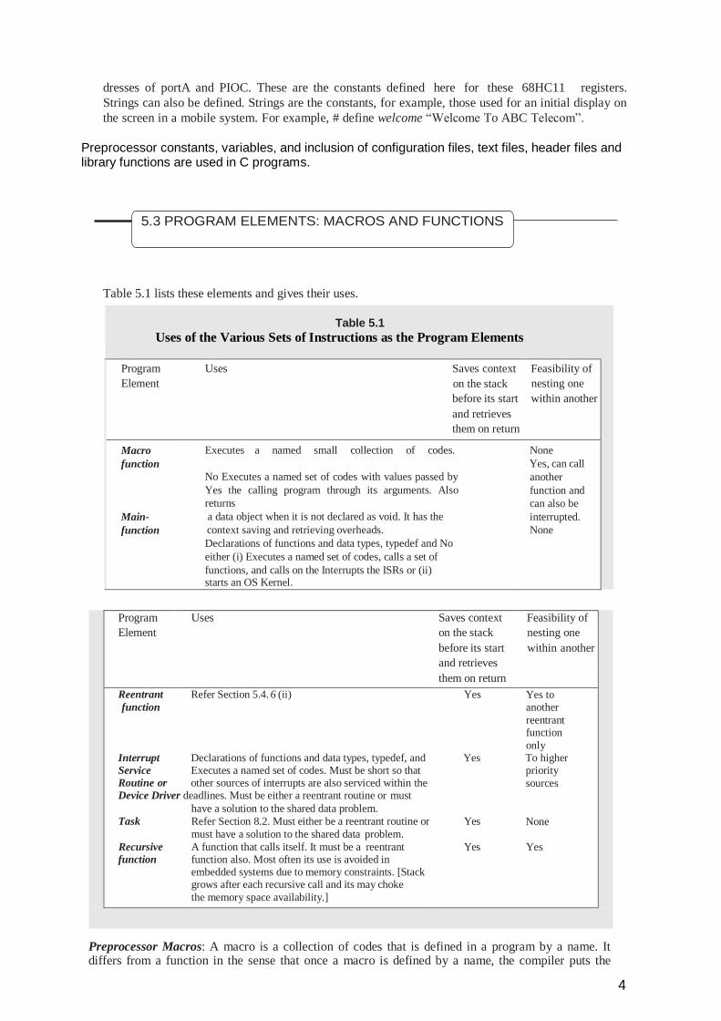
4
dresses of portA and PIOC. These are the constants defined here for these 68HC11 registers.
Strings can also be defined. Strings are the constants, for example, those used for an initial display on
the screen in a mobile system. For example, # define welcome “Welcome To ABC Telecom”.
Preprocessor constants, variables, and inclusion of configuration files, text files, header files and library functions are used in C programs.
Table 5.1 lists these elements and gives their uses.
Table 5.1
Uses of the Various Sets of Instructions as the Program Elements
Program Uses Saves context Feasibility of
Element on the stack nesting one
before its start within another
and retrieves
them on return
Macro
function
Main-
function
Executes a named small collection of codes.
No Executes a named set of codes with values passed by
Yes the calling program through its arguments. Also
returns
a data object when it is not declared as void. It has the
context saving and retrieving overheads.
Declarations of functions and data types, typedef and No
either (i) Executes a named set of codes, calls a set of
functions, and calls on the Interrupts the ISRs or (ii) starts an OS Kernel.
None
Yes, can call
another
function and
can also be
interrupted.
None
Program Uses Saves context Feasibility of
Element on the stack nesting one
before its start within another
and retrieves
them on return
Reentrant Refer Section 5.4. 6 (ii)
function
Interrupt Declarations of functions and data types, typedef, and Service Executes a named set of codes. Must be short so that Routine or other sources of interrupts are also serviced within the Device Driver deadlines. Must be either a reentrant routine or must
have a solution to the shared data problem.
Task Refer Section 8.2. Must either be a reentrant routine or
must have a solution to the shared data problem.
Recursive A function that calls itself. It must be a reentrant function function also. Most often its use is avoided in
embedded systems due to memory constraints. [Stack grows after each recursive call and its may choke
the memory space availability.]
Yes
Yes
Yes
Yes
Yes to another
reentrant function
only To higher priority
sources
None
Yes
Preprocessor Macros: A macro is a collection of codes that is defined in a program by a name. It differs from a function in the sense that once a macro is defined by a name, the compiler puts the
5.3 PROGRAM ELEMENTS: MACROS AND FUNCTIONS
5
corresponding codes for it at every place where that macro name appears. The ‘enable_Maskable_Intr ( )’ and ‘disable_Maskable_Intr ( )’ are the macros in Example 4.5. [The pair of brackets is optional. If it is present, it improves readability as it distinguishes a macro from a constant]. Whenever the name enable_Maskable_Intr appears, the compiler places the codes designed for it. Macros, called test macros or test vectors are also designed and used for debugging a system. [Refer Section 7.6.3.]
How does a macro differ from a function? The codes for a function are compiled once only. On calling that function, the processor has to save the context, and on return restore the context. Further, a function may return nothing (void declaration case) or return a Boolean value, or an integer or any primitive or reference type of data. [Primitive means similar to an integer or character. Reference type means similar to an array or structure.] The enable_PortA_Intr ( ) and disable_PortA_Intr ( ) are the function calls in Example 4.5. [The brackets are now not optional]. Macros are used for short codes only. This is because, if a function call is used instead of macro, the overheads (context saving and other actions on function call and return) will take a time, Toverheads that is the same order of magnitude as the time, Texec for execution of short codes within a function. We use a function when the Toverheads
<< Texec, and a macro when Toverheads ~= or > Texec.
Use of Data Types
Whenever a data is named, it will have the address(es) allocated at the memory. The number of
addresses allocated depends upon the data type. ‘C’ allows the following primitive data types. The
char (8 bit) for characters, byte (8 bit), unsigned short (16 bit), short (16 bit), unsigned int (32 bit),
int (32 bit), long double (64 bit), float (32 bit) and double (64 bit). [Certain compilers do not take
the ‘byte’ as a data type definition. The ‘char’ is then used instead of ‘byte’. Most C compilers do
not take a Boolean variable as data type. As in second line of Example 4.6, typedef is used to create
a Boolean type variable in the C program.]
A data type appropriate for the hardware is used. For example, a 16-bit timer can have only the
unsigned short data type, and its range can be from 0 to 65535 only. The typedef is also used. It is
made clear by the following example. A compiler version may not process the declaration as an
unsigned byte. The ‘unsigned character’ can then be used as a data type. It can then be declared as
follows:
typedef unsigned character portAdata #define Pbyte portAdata Pbyte = 0xF1
Use of Data Structures: Queues, Stacks, Lists and Trees
Marks (or grades) of a student in the different subjects studied in a semester are put in a proper
table. The table in the mark-sheet shows them in an organised way. When there is a large amount of
data, it must be organised properly. A data structure is a way of organising large amounts of data. A
data element can then be identified and accessed with the help of a few pointers and/or indices
and/or functions. [The reader may refer to a standard textbook for the data structure algorithms in C
and C++. For example, “Data Structures and Algorithms in C++” by Adam Drozdek from
Brooks/Cole Thomson Learning (2001).]
A data structure is an important element of any program. Section 2.5. defines and describes a few
important data structures, stack, one-dimensional array, queue, circular queue, pipe, a table (two
dimensional array), lookup table, hash table and list. Figures 2.3 to 2.5 showed different data struc-
tures and how it is put in the memory blocks in an organised way. Any data structure element can be
retrieved.
! Macros and functions are used in C programs. Functions are used when the requirement is that the codes should be compiled once only. However, on calling a function, the processor has to save the context, and on return, restore the context. Further, a function may return nothing (void declaration case) or return a Boolean value, or an integer or any primitive or reference type of data. Macros are usedwhen short functional codes are to beinserted ina number of places or functions.
5.4 PROGRAM ELEMENTS: DATA TYPES, DATA
STRUCTURES, MODIFIERS, STATEMENTS,
LOOPS AND POINTERS
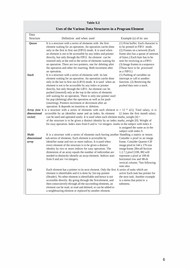
6
Table 5.2
Uses of the Various Data Structures in a Program Element
Data
Structure Definition and when used Example (s) of its use
Queue It is a structure with a series of elements with the first (1) Print buffer. Each character is
element waiting for an operation. An operation can be done to be printed in FIFO mode.
only in the first in first out (FIFO) mode. It is used when (2) Frames on a network [Each
an element is not to be accessible by any index and pointer frame also has a queue of astream
directly, but only through the FIFO. An element can be of bytes.] Each byte has to be
inserted only at the end in the series of elements waiting for sent for receiving as a FIFO.
an operation. There are two pointers, one for deleting after (3) Image frames in a sequence.
the operation and other for inserting. Both increment after [These have to be processed
an operation. as a FIFO.]
Stack It is a structure with a series of elements with its last (1) Pushing of variables on
element waiting for an operation. An operation can be done interrupt or call to another
only in the last in first out (LIFO) mode. It is used when an function. (2) Retrieving the
element is not to be accessible by any index or pointer pushed data onto a stack.
directly, but only through the LIFO. An element can be
pushed (inserted) only at the top in the series of elements
still waiting for an operation. There is only one pointer used
for pop (deleting) after the operation as well as for push
(inserting). Pointers increment or decrement after an
operation. It depends on insertion or deletion.
Array (one It is a structure with a series of elements with each element ts = 12 * s(1); Total salary, ts is
dimensional accessible by an identifier name and an index. Its element 12 times the first month salary.
vector) can be used and operated easily. It is used when each element marks_weight [4] =
of the structure is to be given a distinct identity by an index marks_weight [0]; Weight of
for easy operation. Index stars from 0 and is +ve integers. marks in the subject with index 4
is assigned the same as in the
subject with index 0.
Multi- It is a structure with a series of elements each having another Handling a matrix or tensor.
dimensional sub-series of elements. Each element is accessible by Consider a pixel in an image
array identifier name and two or more indices. It is used when frame. Consider Quarter-CIF
every element of the structure is to be given a distinct image pixel in 144 x 176 size
identity by two or more indices for easy operation. The image frame. [Recall Section
dimension of an array equals the number of indicesthat are 1.2.7.] pixel [108, 88] will
needed to distinctly identify an array-element. Indices start represent a pixel at 108-th
from 0 and are +ve integers. horizontal row and 88-th
vertical column. #See following
note also.
List Each element has a pointer to its next element. Only the first A series of tasks which are
element is identifiable and it is done by list-top pointer active Each task has pointer for
(Header). No other element is identifiable and hence is not the next task. Another example
accessible directly. By going through the first element, and is a menu that point to a
then consecutively through all the succeeding elements, an submenu.
element can be read, or read and deleted, or can be added to
a neighbouring element or replaced by another element.
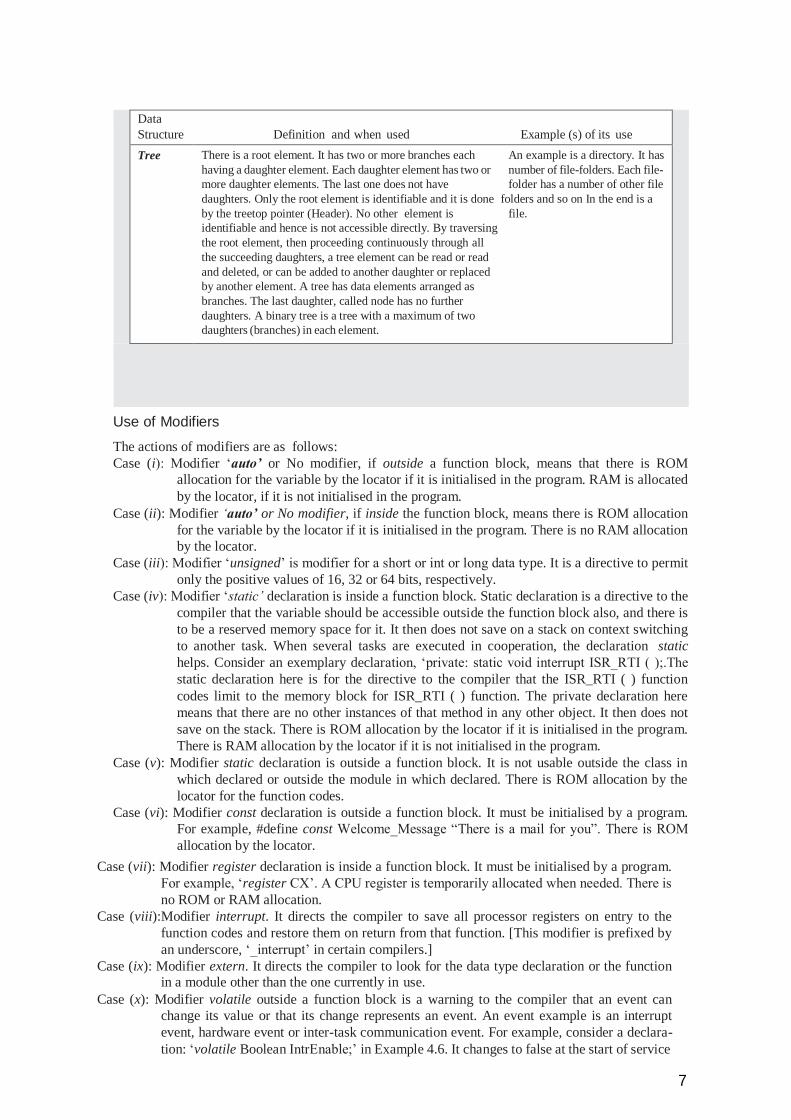
7
Data
Structure Definition and when used Example (s) of its use
Tree There is a root element. It has two or more branches each An example is a directory. It has
having a daughter element. Each daughter element has two or number of file-folders. Each file-
more daughter elements. The last one does not have folder has a number of other file
daughters. Only the root element is identifiable and it is done folders and so on In the end is a
by the treetop pointer (Header). No other element is file.
identifiable and hence is not accessible directly. By traversing
the root element, then proceeding continuously through all
the succeeding daughters, a tree element can be read or read
and deleted, or can be added to another daughter or replaced
by another element. A tree has data elements arranged as
branches. The last daughter, called node has no further
daughters. A binary tree is a tree with a maximum of two
daughters (branches) in each element.
Use of Modifiers
The actions of modifiers are as follows:
Case (i): Modifier ‘auto’ or No modifier, if outside a function block, means that there is ROM
allocation for the variable by the locator if it is initialised in the program. RAM is allocated
by the locator, if it is not initialised in the program.
Case (ii): Modifier ‘auto’ or No modifier, if inside the function block, means there is ROM allocation
for the variable by the locator if it is initialised in the program. There is no RAM allocation
by the locator.
Case (iii): Modifier ‘unsigned’ is modifier for a short or int or long data type. It is a directive to permit
only the positive values of 16, 32 or 64 bits, respectively.
Case (iv): Modifier ‘static’ declaration is inside a function block. Static declaration is a directive to the
compiler that the variable should be accessible outside the function block also, and there is
to be a reserved memory space for it. It then does not save on a stack on context switching
to another task. When several tasks are executed in cooperation, the declaration static
helps. Consider an exemplary declaration, ‘private: static void interrupt ISR_RTI ( );.The
static declaration here is for the directive to the compiler that the ISR_RTI ( ) function
codes limit to the memory block for ISR_RTI ( ) function. The private declaration here
means that there are no other instances of that method in any other object. It then does not
save on the stack. There is ROM allocation by the locator if it is initialised in the program.
There is RAM allocation by the locator if it is not initialised in the program.
Case (v): Modifier static declaration is outside a function block. It is not usable outside the class in
which declared or outside the module in which declared. There is ROM allocation by the
locator for the function codes.
Case (vi): Modifier const declaration is outside a function block. It must be initialised by a program.
For example, #define const Welcome_Message “There is a mail for you”. There is ROM
allocation by the locator.
Case (vii): Modifier register declaration is inside a function block. It must be initialised by a program.
For example, ‘register CX’. A CPU register is temporarily allocated when needed. There is
no ROM or RAM allocation.
Case (viii):Modifier interrupt. It directs the compiler to save all processor registers on entry to the
function codes and restore them on return from that function. [This modifier is prefixed by
an underscore, ‘_interrupt’ in certain compilers.]
Case (ix): Modifier extern. It directs the compiler to look for the data type declaration or the function in a module other than the one currently in use.
Case (x): Modifier volatile outside a function block is a warning to the compiler that an event can
change its value or that its change represents an event. An event example is an interrupt
event, hardware event or inter-task communication event. For example, consider a declara-
tion: ‘volatile Boolean IntrEnable;’ in Example 4.6. It changes to false at the start of service
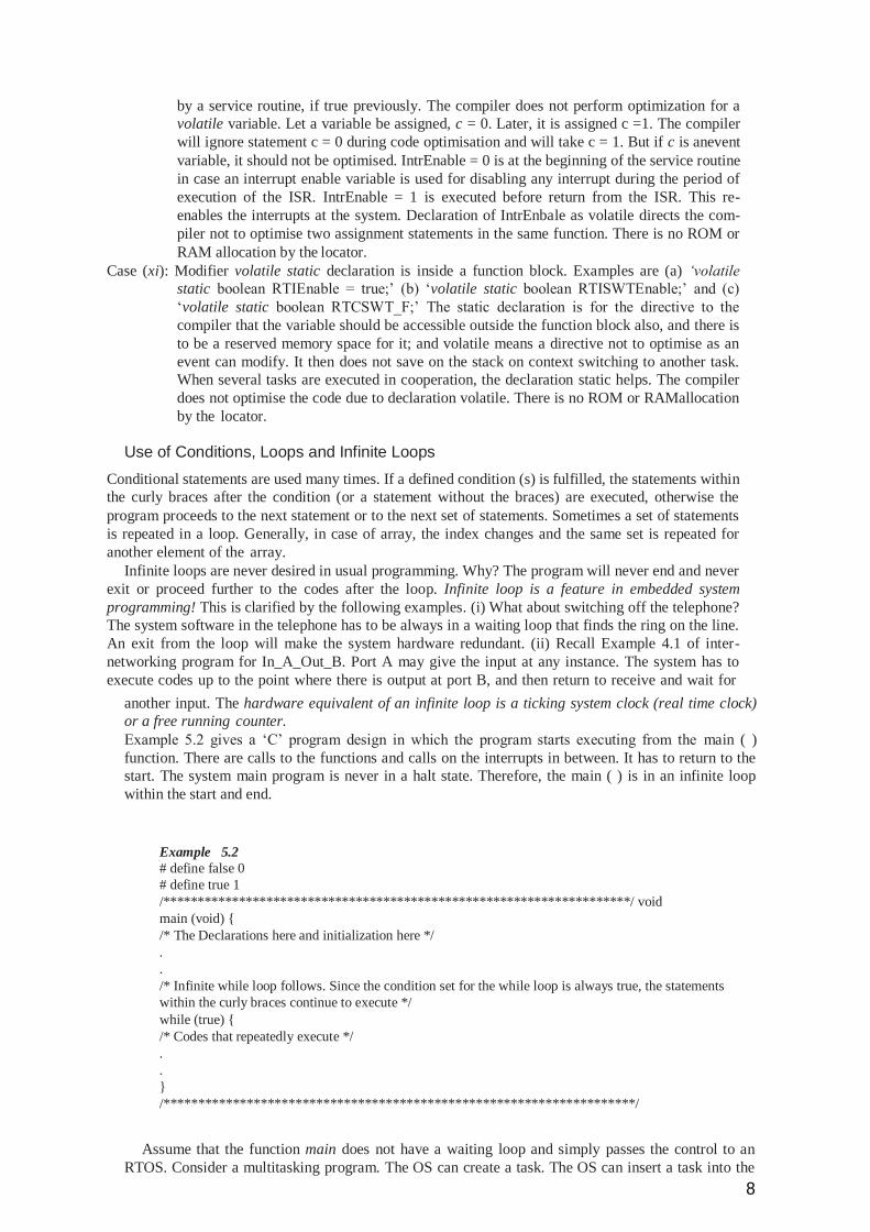
8
by a service routine, if true previously. The compiler does not perform optimization for a
volatile variable. Let a variable be assigned, c = 0. Later, it is assigned c =1. The compiler
will ignore statement c = 0 during code optimisation and will take c = 1. But if c is anevent
variable, it should not be optimised. IntrEnable = 0 is at the beginning of the service routine
in case an interrupt enable variable is used for disabling any interrupt during the period of
execution of the ISR. IntrEnable = 1 is executed before return from the ISR. This re-
enables the interrupts at the system. Declaration of IntrEnbale as volatile directs the com-
piler not to optimise two assignment statements in the same function. There is no ROM or
RAM allocation by the locator.
Case (xi): Modifier volatile static declaration is inside a function block. Examples are (a) ‘volatile
static boolean RTIEnable = true;’ (b) ‘volatile static boolean RTISWTEnable;’ and (c)
‘volatile static boolean RTCSWT_F;’ The static declaration is for the directive to the
compiler that the variable should be accessible outside the function block also, and there is
to be a reserved memory space for it; and volatile means a directive not to optimise as an
event can modify. It then does not save on the stack on context switching to another task.
When several tasks are executed in cooperation, the declaration static helps. The compiler
does not optimise the code due to declaration volatile. There is no ROM or RAMallocation
by the locator.
Use of Conditions, Loops and Infinite Loops
Conditional statements are used many times. If a defined condition (s) is fulfilled, the statements within
the curly braces after the condition (or a statement without the braces) are executed, otherwise the
program proceeds to the next statement or to the next set of statements. Sometimes a set of statements
is repeated in a loop. Generally, in case of array, the index changes and the same set is repeated for
another element of the array.
Infinite loops are never desired in usual programming. Why? The program will never end and never
exit or proceed further to the codes after the loop. Infinite loop is a feature in embedded system
programming! This is clarified by the following examples. (i) What about switching off the telephone?
The system software in the telephone has to be always in a waiting loop that finds the ring on the line.
An exit from the loop will make the system hardware redundant. (ii) Recall Example 4.1 of inter-
networking program for In_A_Out_B. Port A may give the input at any instance. The system has to
execute codes up to the point where there is output at port B, and then return to receive and wait for
another input. The hardware equivalent of an infinite loop is a ticking system clock (real time clock)
or a free running counter.
Example 5.2 gives a ‘C’ program design in which the program starts executing from the main ( )
function. There are calls to the functions and calls on the interrupts in between. It has to return to the
start. The system main program is never in a halt state. Therefore, the main ( ) is in an infinite loop
within the start and end.
Example 5.2
# define false 0
# define true 1
/********************************************************************/ void
main (void) {
/* The Declarations here and initialization here */
.
.
/* Infinite while loop follows. Since the condition set for the while loop is always true, the statements
within the curly braces continue to execute */
while (true) {
/* Codes that repeatedly execute */
.
.
}
/********************************************************************/
Assume that the function main does not have a waiting loop and simply passes the control to an
RTOS. Consider a multitasking program. The OS can create a task. The OS can insert a task into the
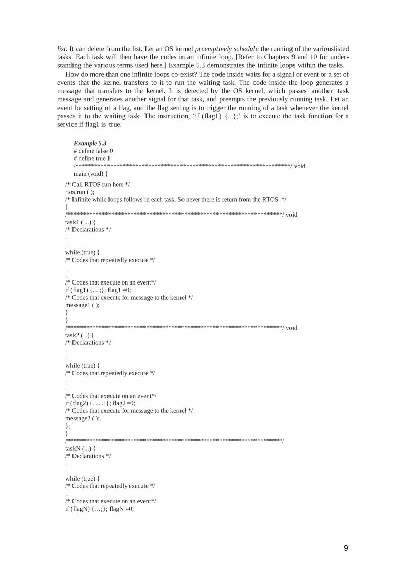
9
list. It can delete from the list. Let an OS kernel preemptively schedule the running of the variouslisted
tasks. Each task will then have the codes in an infinite loop. [Refer to Chapters 9 and 10 for under-
standing the various terms used here.] Example 5.3 demonstrates the infinite loops within the tasks.
How do more than one infinite loops co-exist? The code inside waits for a signal or event or a set of
events that the kernel transfers to it to run the waiting task. The code inside the loop generates a
message that transfers to the kernel. It is detected by the OS kernel, which passes another task
message and generates another signal for that task, and preempts the previously running task. Let an
event be setting of a flag, and the flag setting is to trigger the running of a task whenever the kernel
passes it to the waiting task. The instruction, ‘if (flag1) {...};’ is to execute the task function for a
service if flag1 is true.
Example 5.3
# define false 0
# define true 1
/********************************************************************/ void
main (void) {
/* Call RTOS run here */
rtos.run ( );
/* Infinite while loops follows in each task. So never there is return from the RTOS. */
}
/********************************************************************/ void
task1 ( ...) {
/* Declarations */
.
.
while (true) {
/* Codes that repeatedly execute */
.
.
/* Codes that execute on an event*/
if (flag1) {. .. ;}; flag1 =0;
/* Codes that execute for message to the kernel */
message1 ( );
}
}
/********************************************************************/ void
task2 ( ..) {
/* Declarations */
.
.
while (true) {
/* Codes that repeatedly execute */
.
.
/* Codes that execute on an event*/ if (flag2) {. ..... ;}; flag2 =0;
/* Codes that execute for message to the kernel */
message2 ( );
}; }
/********************************************************************/
taskN (...) {
/* Declarations */ .
.
while (true) { /* Codes that repeatedly execute */
..
/* Codes that execute on an event*/
if (flagN) {. .. ;}; flagN =0;
10
/* Codes that execute for message to the kernel */
message2 ( );
};
}
/********************************************************************/
Use of Pointers, NULL Pointers
Pointers are powerful tools when used correctly and according to certain basic principles. Exemplary uses are as follows. Let a byte each be stored at a memory address.
1. Let a port A in system have a buffer register that stores a byte. Now a program using a pointer declares the byte at port A as follows: ‘unsigned byte *portA’. [or Pbyte *portA.] The * means ‘the contents at’. This declaration means that there is a pointer and an unsigned byte for portA, The compiler will reserve one memory address for that byte. Consider ‘unsigned short
*timer1’. A pointer timer1 will point to two bytes, and the compiler will reserve two memory addresses for contents of timer1.
2. Consider declarations as follows. void *portAdata; The void means the undefined data type for portAdata. The compiler will allocate for the *portAdata without any type check.
3. A pointer can be assigned a constant fixed address as in Example 4.5. Recall two preprocessor directives: ‘# define portA (volatile unsigned byte *) 0x1000’ and ‘# define PIOC (volatile unsigned byte *) 0x1001’. Alternatively, the addresses in a function can be assigned as follows. ‘volatile unsigned byte * portA = (unsigned byte *) 0x1000’ and ‘volatile unsigned byte *PIOC
= (unsigned byte *) 0x1001’. An instruction, ‘portA ++;’ will make the portA pointer point to the next address and to which is the PIOC.
4. Consider, unsigned byte portAdata; unsigned byte *portA = &portAdata. The first statement directs the compiler to allocate one memory address for portAdata because there is a byte each at an address. The & (ampersand sign) means ‘at the address of’. This declaration means the
positive number of 8 bits (byte) pointed by portA is replaced by the byte at the address of portAdata. The right side of the expression evaluates the contained byte from the address, and the left side puts that byte at the pointed address. Since the right side variable portAdata is not a declared pointer, the ampersand sign is kept to point to its address so that the right side pointer
gets the contents (bits) from that address. [Note: The equality sign in a program statement means ‘is replaced by’].
5. Consider two statements, ‘unsigned short *timer1;’ and ‘timer1++;’. The second statement adds 0x0002 in the address of timer1. Why? timer1 ++ means point to next address, and unsigned short declaration allocated two addresses for timer1. [timer1 ++; or timer1 +=1 or timer = timer +1; will have identical actions.] Therefore, the next address is 0x0002 more than
the address of timer1 that was originally defined. Had the declaration been ‘unsigned int’ (in case of 32 bit timer), the second statement would have incremented the address by 0x0004. When the index increments by 1 in case of an array of characters, the pointer to the previous element actually increments by 1, and thus the address will increment by 0x0004 in case of an
array of integers. For array data type, * is never put before the identifier name, but an index is put within a pair of square brackets after the identifier. Consider a declaration, ‘unsigned char portAMessageString [80];’. The port A message is a string, which is an array of 80 characters. Now, portAMessageString is itself a pointer to an address without the star sign before it.
However, *portAMessageString will now refer to all the 80 characters in the string. portAMessageString [20] will refer to the twentieth element (character) in the string. Assume that there is a list of RTCSWT (Real Time Clock interrupts triggered Software Timers) timers that are active at an instant. The top of the list can be pointed as ‘*RTCSWT_List.top’ using the pointer. RTCSWT_List.top is now the pointer to the top of the contents in a memory for a list of the active RTCSWTs.
6. Consider the statement ‘RTCSWT_List.top ++;’ It increments this pointer in a loop. It will not point to the next top of another object in the list (another RTCSWT) but to some address that depends on the memory addresses allocated to an item in the RTCSWT_List. Let ListNow be a pointer within the memory block of the list top element. A statement ‘*RTCSWT_List. ListNow = *RTCSWT_List.top;’ will do the following. RTCSWT_List pointer is now replaced by
RTCSWT list-top pointer and now points to the next list element (object). [Note:
RTCSWT_List.top ++ for pointer to the next list-object can only be used when RTCSWT_List
11
elements are placed in an array. This is because an array is analogous to consecutively located
elements of the list at the memory. Recall Table 5.2.]
7. A NULL pointer declares as following: ‘#define NULL (void*) 0x0000’. [We can assign any
address instead of 0x0000 that is not in use in a given hardware.] NULL pointer is very useful.
Consider a statement: ‘while (* RTCSWT_List. ListNow -> state != NULL) { numRunning
++;’. When a pointer to ListNow in a list of software timers that are running at present is not
NULL, then only execute the set of statements in the given pair of opening and closing curly
braces. One of the important uses of the NULL pointer is in a list. The last element to point to
the end of a list, or to no more contents in a queue or empty stack, queue or list.
Use of Function Calls
Table 5.1 gives the meanings of the various sets of instructions in the C program. There are functions
and a special function for starting the program execution, ‘void main (void)’. Given below are the
steps to be followed when using a function in the program.
1. Declaring a function: Just as each variable has to have a declaration, each function must be
declared. Consider an example. Declare a function as follows: ‘int run (int indexRTCSWT,
unsigned int maxLength, unsigned int numTicks, SWT_Type swtType, SWT_Action swtAction,
boolean loadEnable);’. Here int specifies the returned data type. The run is the function name.
There are arguments inside the brackets. Data type of each argument is also declared. A
modifier is needed to specify the data type of the returned element (variable or object) from any
function. Here, the data type is specified as an integer. [A modifier for specifying the returned
element may be also be static, volatile, interrupt and extern.]
2. Defining the statements in the function: Just as each variable has to be given the contents or
value, each function must have its statements. Consider the statements of the function ‘run’.
These are within a pair of curly braces as follows: ‘int RTCSWT:: run (int indexRTCSWT,
unsigned int maxLength, unsigned int numTicks, SWT_Type swtType, SWT_Action swtAction,
boolean loadEnable) {...};’. The last statement in a function is for the return and may also be
for returning an element.
3. Call to a function: Consider an example: ‘if (delay_F = = true & & SWTDelayIEnable = = true)
ISR_Delay ( );’. There is a call on fulfilling a condition. The call can occur several times and
can be repeatedly made. On each call, the values of the arguments given within the pair of
bracket pass for use in the function statements.
12
(i) Passing the Values (elements) The values are copied into the arguments of the functions. When the function is executed in this way, it does not change a variable’s value at the called program. A function can only use the copied values
in its own variables through the arguments. Consider a statement, ‘run (int indexRTCSWT, unsigned int maxLength, unsigned int numTicks, SWT_Type swtType, SWT_Action swtAction, boolean loadEnable) {...}’. Function ‘run’ arguments indexRTCSWT, maxLength, numTick, swtType, and
loadEnable original values in the calling program during execution of the codes will remain unchanged. The advantage is that the same values are present on return from the function. The arguments that are passed by the values are saved temporarily on a stack and retrieved on return from the function.
(ii) Reentrant Function Reentrant function is usable by the several tasks and routines synchronously (at the same time). This is because all its argument values are retrievable from the stack. A function is called reentrant func- tion when the following three conditions are satisfied.
1. All the arguments pass the values and none of the argument is a pointer (address) whenever a calling function calls that function. There is no pointer as an argument in the above example of function ‘run’.
2. When an operation is not atomic, that function should not operate on any variable, which is declared outside the function or which an interrupt service routine uses or which is a global variable but passed by reference and not passed by value as an argument into the function. [The value of such a variable or variables, which is not local, does not save on the stack when there is call to another program.] Recall Section 2.1 for understanding atomic operation. The following is an example that clarifies it further. Assume that at a server (software), there is a 32 bit variable count to count
the number of clients (software) needing service. There is no option except to declare the count as a global variable that shares with all clients. Each client on a connection to a server sends a call to increment the count. The implementation by the assembly code for increment at that
memory location is non-atomic when (i) the processor is of eight bits, and (ii) the server- compiler design is such that it does not account for the possibility of interrupt in-between the four instructions that implement the increment of 32-bit count on 8-bit processor. There will be a wrong value with the server after an instance when interrupt occurs midway during
implementing an increment of count. 3. That function does not call any other function that is not itself Reentrant. Let RTI_Count be a
global declaration. Consider an ISR, ISR_RTI. Let an ‘RTI_Count ++;’ instruction be where the RTI_Count is variable for counts on a real-time clock interrupt. Here ISR_RTI is a not a
Reentrant routine because the second condition may not be fulfilled in the given processor hardware. There is no precaution that may be taken here by the programmer against shared data problems at the address of the RTI_Count because there may be no operation that modifies RTI_Counts in any other routine or function than the IST_RTI. But if there is another operation
that modifies the RTI_Count the shared-data problem will arise. [Refer to Section 8.2.1 for a solution.]
(iii) Passing the References When an argument value to a function passes through a pointer, the function can change this value. On returning from this function, the new value will be available in the calling program or another function called by this function. [There is no saving on stack of a value that either (a) passes through a pointer in the function-arguments or (b) operates in the function as a global variable or (c) operates through a variable declared outside the function block.]
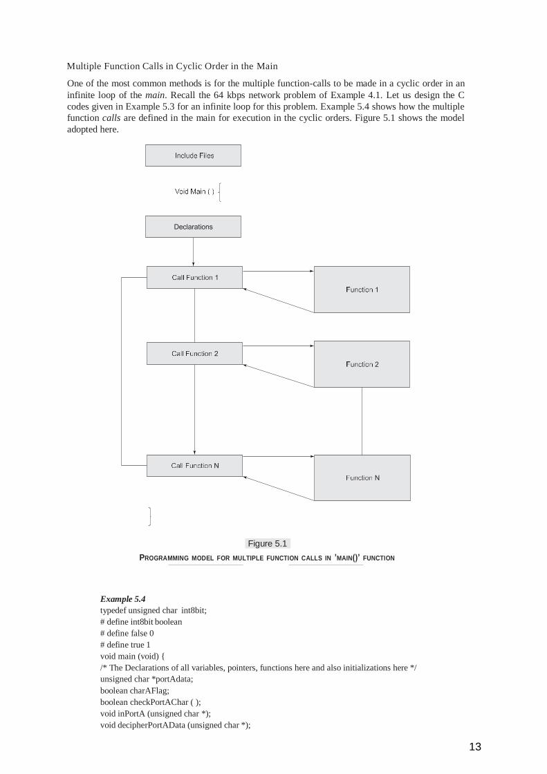
13
Multiple Function Calls in Cyclic Order in the Main
One of the most common methods is for the multiple function-calls to be made in a cyclic order in an
infinite loop of the main. Recall the 64 kbps network problem of Example 4.1. Let us design the C
codes given in Example 5.3 for an infinite loop for this problem. Example 5.4 shows how the multiple
function calls are defined in the main for execution in the cyclic orders. Figure 5.1 shows the model
adopted here.
Figure 5.1
PROGRAMMING MODEL FOR MULTIPLE FUNCTION CALLS IN ’MAIN()’ FUNCTION
Example 5.4
typedef unsigned char int8bit;
# define int8bit boolean
# define false 0
# define true 1
void main (void) {
/* The Declarations of all variables, pointers, functions here and also initializations here */
unsigned char *portAdata;
boolean charAFlag;
boolean checkPortAChar ( );
void inPortA (unsigned char *);
void decipherPortAData (unsigned char *);
14
void encryptPortAData (unsigned char *);
void outPortB (unsigned char *);
.
while (true) {
/* Codes that repeatedly execute */
/* Function for availability check of a character at port A*/
while (charAFlag != true) checkPortAChar ( );
/* Function for reading PortA character*/
inPortA (unsigned char *portAdata);
/* Function for deciphering */
decipherPortAData (unsigned char *portAdata);
/* Function for encoding */
encryptPortAData (unsigned char *portAdata);
/* Function for retransmit output to PortB*/
outPort B (unsigned char *portAdata);
};
}
Objected Oriented Programming
An objected oriented language is used when there is a need for re-usability of the defined object or set
of objects that are common within a program or between the many applications. When a large pro-
gram is to be made, an object-oriented language offers many advantages. Data encapsulation, design
of reusable software components and inheritance are the advantages derived from the OOPs.
An object-oriented language provides for defining the objects and methods that manipulate the
objects without modifying their definitions. It provides for the data and methods for encapsulation. An
object can be characterised by the following:
1. An identity (a reference to a memory block that holds its state and behavior).
2. A state (its data, property, fields and attributes).
3. A behavior (method or methods that can manipulate the state of the object).
In a procedure-based language, like FORTRAN, COBOL, Pascal and C, large programs are split
into simpler functional blocks and statements. In an object-oriented language like Smalltalk, C++ or
Java, logical groups (also known as classes) are first made. Each group defines the data and the
methods of using the data. A set of these groups then gives an application program. Each group has
internal user-level fields for the data and the methods of processing that data at these fields. Each
group can then create many objects by copying the group and making it functional. Each object is
functional. Each object can interact with other objects to process the user’s data. The language pro-
vides for formation of classes by the definition of a group of objects having similar attributes and
common behavior. A class creates the objects. An object is an instance of a class.
Embedded Programming in C++
1. Programming advantages of C++
C++ is an object oriented Program (OOP) language, which in addition, supports the procedure ori-
ented codes of C. Program coding in C++ codes provides the advantage of objected oriented program-
ming as well as the advantage of C and in-line assembly. Programming concepts for embedded pro-
gramming in C++ are as follows:
(i) A class binds all the member functions together for creating objects. The objects will have
memory allocation as well as default assignments to its variables that are not declared static. Let
us assume that each software timer that gets the count input from a real time clock is an object.
Now consider the codes for a C++ class RTCSWT. A number of software timer objects can be
created as the instances of RTCSWT.
(i) A class can derive (inherit) from another class also. Creating a child class from RTCSWT as a
parent class creates a new application of the RTCSWT.
5.8 EMBEDDED PROGRAMMING IN C++
15
(ii) Methods (C functions) can have same name in the inherited class. This is called method
overloading. Methods can have the same name as well as the same number and type of
arguments in the inherited class. This is called method overriding. These are the two significant
features that are extremely useful in a large program.
(iv) Operators in C++ can be overloaded like in method overloading. Recall the following statements
and expressions in Example 5.8. The operators ++ and ! are overloaded to perform a set of
operations. [Usually the++ operator is used for post-increment and pre-increment and the !
operator is used for a not operation.]
const OrderedList & operator ++ ( ) {if (ListNow != NULL) ListNow = ListNow -> pNext;
return *this;}
boolean int OrderedList & operator ! ( ) const {return (ListNow != NULL) ;};
[Java does not support operator overloading, except for the + operator. It is used for summation as
well string-concatenation.]
There is struct that binds all the member functions together in C. But a C++ class has object
features. It can be extended and child classes can be derived from it. A number of child classes can be
derived from a common class. This feature is called polymorphism. A class can be declared as public
or private. The data and methods access is restricted when a class is declared private. Struct does not
have these features.
2. Disadvantages of C++
Program codes become lengthy, particularly when certain features of the standard C++ are used.
Examples of these features are as follows:
(a) Template.
(b) Multiple Inheritance (Deriving a class from many parents).
(c) Exceptional handling.
(d) Virtual base classes.
(e) Classes for IO Streams. [Two library functions are cin (for character (s) in) and cout (for
character (s) out). The I/O stream class library provides for the input and output streams of
characters (bytes). It supports pipes, sockets and file management features. Refer to Section
8.3 for the use of these in inter task communications.]
3. Can optimization codes be used in Embedded C++ programs to eliminate the disadvan-
tages?
Embedded system codes can be optimised when using an OOP language by the following
(a) Declare private as many classes as possible. It helps in optimising the generated codes.
(b) Use char, int and boolean (scalar data types) in place of the objects (reference data types) as
arguments and use local variables as much as feasible.
(c) Recover memory already used once by changing the reference to an object to NULL.
A special compiler for an embedded system can facilitate the disabling of specific features provided
in C++. Embedded C++ is a version of C++ that provides for a selective disabling of the above features
so that there is a less runtime overhead and less runtime library. The solutions for the library functions
are available and ported in C directly. The IO stream library functions in an embedded C++ compiler
are also reentrant. So using embedded C++ compilers or the special compilers make the C++ a signifi-
cantly more powerful coding language than C for embedded systems.
GNU C/C++ compilers (called gcc) find extensive use in the C++ environment in embedded soft-
ware development. Embedded C++ is a new programming tool with a compiler that provides a small
runtime library. It satisfies small runtime RAM needs by selectively de-configuring features like, tem-
plate, multiple inheritance, virtual base class, etc. when there is a less runtime overhead and when the
less runtime library using solutions are available. Selectively removed (de-configured) features could
16
be template, run time type identification, multiple Inheritance, exceptional handling, virtual base
classes, IO streams and foundation classes. [Examples of foundation classes are GUIs (graphic user
interfaces). Exemplary GUIs are the buttons, checkboxes or radios.]
An embedded system C++ compiler (other than gcc) is Diab compiler from Diab Data. It also provides
the target (embedded system processor) specific optimisation of the codes. [Section 5.12] The run-
time analysis tools check the expected run time error and give a profile that is visually interactive.
Java has advantages for embedded programming as follows:
1. Java is completely an OOP language.
2. Java has in-built support for creating multiple threads. [For the definition of thread and its
similarity in certain respects to task refer to Section 8.1.] It obviates the need for an operating
system (OS) based scheduler [Section I.5.6] for handling the tasks.
3. Java is the language for most Web applications and allows machines of different types to
communicate on the Web.
4. There is a huge class library on the network that makes program development quick.
5. Platform independence in hosting the compiled codes on the network is because Java generates
the byte codes. These are executed on an installed JVM (Java Virtual Machine) on a machine.
[Virtual machines (VM) in embedded systems are stored at the ROM.] Platform independence
gives portability with respect to the processor used.
6. Java does not permit pointer manipulation instructions. So it is robust in the sense that memory
leaks and memory related errors do not occur. A memory leak occurs, for example, when
attempting to write to the end of a bounded array.
7. Java byte codes that are generated need a larger memory when a method has more than 3 or 4
local variables.
8. Java being platform independent is expected to run on a machine with an RISC like instruction
execution with few addressing modes only.
Disadvantages of Java
An embedded Java system may need a minimum of 512 kB ROM and 512 kB RAM because of the need
to first install JVM and run the application.
Java Card
Use of J2ME (Java 2 Micro Edition) or Java Card or EmbeddedJava helps in reducing the code size
to 8 kB for the usual applications like smart card. How? The following are the methods.
1. Use core classes only. Classes for basic run time environment form the VM internal format and
only the programmer’s new Java classes are not in internal format.
2. Provide for configuring the run time environment. Examples of configuring are deleting the
exception handling classes, user defined class loaders, file classes, AWT classes, synchronized
threads, thread groups, multidimensional arrays, and long and floating data types. Other
configuring examples are adding the specific classes for connections when needed, datagrams,
input output and streams.
3. Create one object at a time when running the multiple threads.
4. Reuse the objects instead of using a larger number of objects.
5. Use scalar types only as long as feasible.
! Embedded C++ is a C++ version, which makes large program development simpler by providing
object-oriented programming (OOP) features of using an object, which binds state and behavior
and which is defined by an instance of a class. We use objects in a way that minimises memory
needs and run-time overheads in the system. Embedded system programmers use C ++ due to
the OOP features of software re-usability, extendibility, polymorphism, function overriding and
overloading along portability of C codes and in-line assembly codes. C++ also provides for
overloading of operators. A compiler, gcc, is popularly used for embedded C++ codes compila-
tion. Diab compiler has two special features: (i) processor specific code optimisation and (ii)
Run time analysis tools for finding expected run-time errors.
5.9 EMBEDDED PROGRAMMING IN JAVA
17
A smart card (Section 11.4) is an electronic circuit with a memory and CPU or a synthesised VLSI
circuit. It is packed like an ATM card. For smart cards, there is Java card technology. [Refer to http:/
/ www.java.sun.com/ products/ javacard.] Internal formats for the run time environments are available
mainly for the few classes in Java card technology. Java classes used are the connections, datagrams,
input output and streams, security and cryptography.
Described above are the advantages and disadvantages of Java applications in the embedded sys-
tem. JavaCard, EmbeddedJava and J2ME (Java 2 Micro Edition) are three versions of Java that gener-
ate a reduced code size.
Consider an embedded system such as a smart card. It is a simple application that uses a running
JavaCard. The Java advantage of platform independency in byte codes is an asset. The smart card
connects to a remote server. The card stores the user account past balance and user details for the
remote server information in an encrypted format. It deciphers and communicates to the server the
user needs after identifying and certifying the user. The intensive codes for the complex application
run at the server. A restricted run time environment exists in Java classes for connections, datagrams,
character-input output and streams, security and cryptography only.
[For EmbeddedJava, refer to http://www.sun.java.com/embeddedjava. It provides an embedded
run time environment and a closed exclusive system. Every method, class and run time library is
optional].
J2ME provides the optimised run-time environment. Instead of the use of packages, J2ME provides
for the codes for the core classes only. These codes are stored at the ROM of the embedded system.
It provides for two alternative configurations, Connected Device Configuration (CDC) and Connected
Limited Device Configurations (CLDC). CDC inherits a few classes from packages for net, security,
io, reflect, security.cert, text, text.resources, util, jar and zip. CLDC does not provide for the applets,
awt, beans, math, net, rmi, security and sql and text packages in java.lang. There is a separate
javax.mircoedition.io package in CLDC configuration. A PDA (personal digital assistant) uses CDCor
CLDC.
There is a scaleable OS feature in J2ME. There is a new virtual machine, KVM as an alternative to
JVM. When using the KVM, the system needs a 64 kB instead of 512 kB run time environment. KVM
features are as follows:
1. Use of the following data types is optional. (i) Multidimensional arrays, (ii) long 64-bit integer
and (iii) floating points.
2. Errors are handled by the program classes, which inherit only a few needed error handling
classes from the java I/O package for the Exceptions.
3. Use of a separate set of APIs (application program interfaces) instead of JINI. JINI is portable.
But in the embedded system, the ROM has the application already ported and the user does not
change it.
4. There is no verification of the classes. KVM presumes the classes as already validated.
5. There is no object finalization. The garbage collector does not have to do time consuming
changes in the object for finalization
6. The class loader is not available to the user program. The KVM provides the loader.
7. Thread groups are not available.
8. There is no use of java.lang.reflection. Thus, there are no interfaces that do the object
serialization, debugging andprofiling.
J2ME need not be restricted to configure the JVM to limit the classes. The configuration can be
augmented by Profiler classes. For example, MIDP (Mobile Information Device Profiler). A profile
defines the support of Java to a device family. The profiler is a layer between the application and the
configuration. For example, MIDP is between CLDC and application. Between the device and configu-
ration, there is an OS, which is specific to the device needs.
A mobile information device has the followings.
1. A touch screen or keypad.
2. A minimum of 96 x 54 pixel color or monochrome display.
3. Wireless networking.
4. A minimum of 32 kB RAM, 8 kB EEPROM or flash for data and 128 kB ROM.
5. MIDP used as in PDAs, mobile phones and pagers.
MIDP classes describe the displaying text. It describes the network connectivity. For example, for
HTTP, it provides support for small databases stored in EEPROM or flash memory. It schedules the
applications and supports the timers.


