Embed Size (px)
Citation preview

Sreenivasa Instityte of Technology and Mangement studies,
(Autonomous)
CHITTOOR. AP.
Engineering Physics(18SAH112)
Lecture Notes PREPARED BY
P V Ramana Moorthy
ASSOCIATE PROFESSOR
DEPARTMENT OF SCIENCE AND HUMANITIES
SREENIVASA INSTITUTE OF TECHNOLOGY AND MANAGEMENT STUDIES
BANGALORE-TIRUPATHI HIGHWAY, MURAKAMBATTU-517127 PHONE: 08572-246298,
246299 FAX: 08572-246297 EMAIL: [email protected] Website: www.sitams.org

UNIT-I
OPTICS, LASERS
AND
FIBER OPTICS

OPTICS
Introduction
Basically optics is the branch of science which deals with the study of light.
It is also known as the branch of physics, which deals with the study of properties
and nature of light. Optics is mainly divided into two parts.
i) Geometrical optics which deals with the image formation by optical systems.
That is the Geometrical optics concerns with the formation of images, when light rays
passes through an optical system, such as a lens and a prism.
ii) Physical optics which deals with the nature of light.
That is the physical optics deals with the nature of light, such as Interference, Diffraction
and polarization.
Interference
Interference is that phenomena in which two wave trains, when superposed at a
point, produce collinear oscillations such that the resultant intensity at the point of
superposition not only depends on the amplitudes of the component waves but also on
their phase difference at the point of interference.
The interfered effect at any point can be observed by the eye, only if the effect is
steady over sufficiently long intervals of observation.
The effect is steady only if the phase relations between the interfering waves remain
constant over that time interval.
The phase emission of a wave train from a source, change at random. This random
change in the emission phase changes the phase of waves train at the given point.
The phase difference between two wave trains at a point of their superposition will
vary with time, if their frequencies are not equal.
Thus constant phase relations between the interfering waves requires sources of
i) Same and single frequency and
ii) Constant emission phase difference.
The condition (i) is fulfilled if the sources are monochromatic and of the same frequency.
The condition (ii) requires coherent sources.

Coherent source
Coherent sources are those sources, which maintain their emission phase
difference constant for al time although each one may change its emission phase abruptly
and at random.
Constructive interference If two wave trains at the point of superposition produced collinear vibrations
interfere in the same phase, then the interference is said to be constructive. This is
possible when the phase difference of the two wave trains at the point of superposition is
2nπ, where n is an integer.
In that case the resultant amplitude is the sum of the individual amplitudes and the
intensity is maximum. The corresponding path difference between the two interfering
wave trains is an integral multiple of the wavelength, provided the sources are
equiphased.
Path difference = n , n = 1,2,3,……
Destructive Interference
If the two wave trains interfere in the opposite phase, then the interference is said
to be destructive. This is possible when the phase difference of the two wave trains at the
point of super position is (2n+1), Where n = an integer.
In this case the resultant amplitude is the difference of the individual amplitudes and the
intensity is minimum.
The corresponding path difference between the interfering waves should be an odd
multiple of half the wavelength, if the sources are equally phased.
Path difference = 2 1 , 1,2,3,.....2
n n
Interference in thin films
The colours of thin films, soap bubbles and oil slicks can be explained as due to
the phenomena of interference.
Let a plane wave front be allowed to incident normally on a thin film of uniform
thickness t.
The plane wave front is obtained with the help of a partially reflecting a glass plate G
inclined at an angle 450
with the parallel monochromatic beam of light.
The plane wave front is partly reflected at the upper surface of the film and partly
transmitted into the film. This is shown in figure (1).

The transmitted wave front is reflected again from the bottom surface of the film and
emerges through the first surface.
The wavefront reflected from the upper surface and the lower surface interfere with each
other. The resultant interference pattern can be observed with eye without obstructing the
incident wave front.
Here the following two points are observed.
i) The wavelength reflected from the lower surface of the film, traverses an
additional path 2 t.
(t from upper surface to lower surface and t from lower surface to upper surface).
Where is the refractive index of the film.
ii) When the film is placed in air, the wave front reflected from the upper surface
undergoes an additional phase change of (Because the reflection takes place
at the surface of a denser medium). Here it should be noted that no phase
change takes place at lower surface because the reflection takes place at the
surface of rarer medium.
Now when the path difference, 2 t = n, Constructive interference takes place and the
film appears bright.
Here n = 1,2,3,……
When the path difference, 22 (2 1)t n ,destructive interference takes place and the
film appears dark.
Here n = 0,1,2,3……
Note : t is the optical thickness of the film.
Constructive interference
Destructive interference
The constructive and destructive interferences are shown
Above.
B
t
D
A
C
Eye
G
Glass Plate
Figure (1) Interference in thin films

Types of Interference
Interference takes place in two ways.
i) Due to divisions of wave forms or wave front.
ii) Due to division of Amplitude.
i) Division of wave front
The phenomenon such as reflection, refraction or diffraction aids in splitting the
incident wave front into two parts. This is division of wave front.
These two parts of the same wave front transverse equal distances and combines at
some angle to produce interference.
Fresnel Biprism, Lloyd‟s mirror etc are examples of this class.
ii) Division of Amplitude.
The amplitude of the incident beam is split into two parts either by parallel
reflection or refraction.
These divided parts combine after travelling different paths and produce
interference.
Unlike the phenomenon of division of wavefront where a point or a narrow line
source is used, broad light source may be used to produce bright bands.
Newton‟s Rings, Michelson Interferometer, interferences in thin films by
Reflection etc are examples of this class.
Analytical Treatment of Interference
Division of wave front
Let A and B be the
two coherent sources
separated by a distance „d‟
and „D‟ is the distance
between source and screen.
Consider a point P (where
interference is taking place)
at a distance y, from centre of
screen „C‟ and 2y from E.
This is shown in figure (2).
Fig.2: Interference – Analytical treatment
d
D
s
A
B
y1
C
E
y2
AC= BC

S is the source of light.
Now 1 siny a t ------- (1)
And 2 siny a t -------- (2)
But according to the principle of superposition
1 2y y y
sin siny a t a t
sin sin cos cos siny a t a t t
sin sin cos cos siny a t a t a t
sin 1 cos cos siny a t a t ------ (3)
Now let a 1 cos cosA ------ (4)
sin sina A ------ (5)
Now sin cos sin cosy A t A t
siny A t ------- (6)
Equation (6) represent the equation of two superposed waves.
Now squaring and Adding equations (4) and (5), we get
22 2 2 2 2 2 2sin cos sin 1 cosA A a a
2 2 2 2 2 2 2sin cos sin 1 cos 2cosA a a
2 2 2 2 2 2 2
2 2 2 2
2 2 2 2
2 2
2 2 2
2 2
sin cos 2 cos
sin 1 cos 2cos
sin cos 1 2cos
1 1 2cos
2 2cos
2 1 cos
A a a a a
A a
A a
A a
A a
A a
Now 2cos 2cos / 2 1
2 22 1A a 22cos / 2 1
2 2 22 2cos / 2A a
2 2 24 cos / 2A a ------ (7)
Where A = Amplitude of the Result and superposed waves.
But Intensity 2I A , Square of the Amplitude
2 24 cos / 2I a
Now the Intensity of the Resultant wave depends on the term 2cos / 2 and the value
/ 2 .
Case (i) : When 0,2 ,2 2 ,...... 2n Where n=1,2,3….
(OR) path difference , 0, , 2 ,......,x n Then 24I a

Case (ii) : when
,3 ,...... 2 1 : 0,1,2,3,n n
(OR) path difference
3
, ,......., 2 12 2 2
x n
Energy distribution
curve of the resultant
wave is shown in the
figure (3).
Interference in the films by Reflection: Let us consider a plane parallel film, as shown in
figure (4) below.
Let PA be a ray of light incidenting on the upper
surface as shown in the figure (4).
PA light ray makes an angle of incidence i.
Now part of the light is reflected into the film in
the direction AB and the other part is refracted
into film
In the direction AC.
The light AC which is refracted, is reflected at C
and emerges at D. The emerged light DF is
parallel to AB.
At the Normal incidence, the path difference
between rays AB and DF is the two times the
optical thickness of the film 2 t .
The two parallel rays of light AB and DF will
interfere in the field of Eye and produce
interference pattern.
Now the path difference between the rays AB
and DF, for Normal Incidence is given by
2 t ------ (1)
At oblique incidence the path difference is given
by
AC CD AB ----- (2)
Now from the figure (4), triangle AEC is a right angled triangle.
900
P
B
H
E i
r r
D
F
A
C
t
No phase
change Fig. 4: Interference in thin films
(thin parallel films)
Phase change
of π
i
1
2
4a2
-4 -3 -2 - 0 2 3 4
| | | | | | | | |
X
Figure 3 : Energy distribution curve.

cosEC
rAC
=> cos
ECAC
r ----- (3)
Triangle CED and Triangle AEC are similar and are right angled triangles.
cosEC
rCD
=>cos
ECCD
r ----------(4)
Now cos cos
EC ECAC CD
r r
2
cos
ECAC CD
r
But EC =t, thickness of the film. 2
cos
tAC CD
r ------ (5)
Also from the right angled triangle ABD,
sinAB
iAD
=> sinAB AD i
sin ,
2 sin
AB AE ED i AE ED AE ED AD
AB AE i
Also Tan r = AE
EC from the right anlged triangle AEC
nAE EC Ta r
2AB t TanrSini ------- (6)
From equations (2), (5) and (6), we get
But we know that (Snell‟s Law) sin
sin
i
r ,µ=Refractive index of material of the Film.
sin sini r
22 an sin
cos
tt T r r
r
22 an sin
cos
tt T r r
r
12 an sin
cost T r r
r
2 cost r ----- (7)
Where is the refractive index of the
medium between the surfaces of the film.
For the reflected ray AB, the reflection is
occurring in the denser medium, a phase
change of occurs. This phase change
is equivalent to path difference of 2
.
21 sin2
cos
rt
r
2cos2
cos
rt
r
C ^ ^ ^
^ ^
^^ ^ ^
^ ^
^
^ ^
^ ^ ^ ^
L
C
S
G2
450
M
Figure (5) Experimental
setup for Newton’s Rings
^
^ ^
^^ ^ ^ ^
L
S
G2
450
M
Figure (5) Experimental
setup for Newton’s Rings
G1
^
^^ ^ ^
^ ^
^
^ ^
^ ^ ^ ^
L
C
S
G2
450
M
Figure (5) Experimental
setup for Newton’s Rings
^

The condition for maxima for the air film to appear bright is
2 cos2
2 cos2
t r n
t r n
2 cos 2 12
t r n
------ (8)
For the reflected ray CD and transmitted ray of light DF, No phase change occurs.
Because, the reflection of light CD takes place at a surface of lower refractive index.
The film appear dark in the reflected light
When
2 cos 2 12 2
2 cos 2 12 2
2 cos 2 1 12
2 cos
t r n
t r n
t r n
t r n
Where 0,1,2,3,....n

2
H F
L
G
D
B
C
G E
1 A
Newton’s Rings
When a Plano convex lens with its convex surface is placed on a plane glass plate, an air film of
gradually increasing thickness is formed between the two. The thickness of the film at the point
of contact is zero. If a monochromatic light is allowed to fall normally and viewed as shown in
figure (5), then alternative dark and bright circular fringes are observed.
The fringes are circular because the air film has a circular symmetry.
Newton‟s Rings are formed because of the interference between the waves reflected from the top
and bottom surfaces of the air film between the curved surface and the glass plate as shown in
figure (5).
figure (5) shows the experimental setup for Newton‟s Rings. In the setup
G, is the plane glass plate. L is a Plano convex lens. S is a monochromatic
source of light. G2 is the glass plate inclined at an angle 450 with the
incident parallel light from the source S. C is a double convex lens. M is
the microscope, through which we can observe interference fringes.
Theory: Newton‟s rings are formed due to interference
between the waves reflected from the top and
bottom surfaces of the air film formed between the
glass plate and curved surface of the plano convex
lens. The formation of Newton‟s Rings can be
explained by using the Figure (6).
L is the Plano Convex lens. G is a plane glass,
plate. AB is the monochromatic Ray of light,
which is incidenting on the system.
A part of the light is reflected at C (glass air boundary), which goes out in the form of
rays (1). Without any phase reversal.
This is because at the point „C‟ a light ray is reflected from a rarer medium.
The other part is refracted along CD, at the point D it is again reflected and goes out in the form
of ray (2). (DEF Ray of light).
The ray (2) suffers a phase reversal of . This is because at the point D, the light ray is reflected
from the denser medium glass.
The reflected rays (1) and (2) [GH and EF] are in a position to produce interference fringes as
they have been derived from the same ray AB. Hence they fulfill the condition of interference.
As the rings are formed in the reflected light, the path difference between them is
2 cos2
r
---- (1)
Since the interference is taking place because of the air film, for air film 1 .
Figure (6): Interference in Newton’s rings setup.

And for Normal incidence, r=0.
Now the path difference 2 1 cos 02
t
22
t
---- (2)
Where t= thickness of the air film.
At the point of contact, t=0, and the path difference 2
.
This is the condition of minimum intensity. Hence the central spot is dark.
Now the condition for bright fringe is
22
t n
22
t n
22
2
nt
2 2 12
t n
, ----- (3)
Where n= 1,2,3,……
The condition for dark fringe is
2 2 12 2
t n
2 2 12 2
t n
2 2 1 12
t n
2t n ---- (4) Here n= 0,1,2,….

Calculation of the Diameters of the
Fringes
Let LOL‟ be the plano convex lens
placed on the glass plate AB. Here the
curved surface is touching the plane
surface of the glass plate.
The curved surface LOL1 is part of the
spherical surface with the centre at C.
Let R be the Radius of curvature of the
curved surface.
Let r be Radius of Newton‟s Rings
corresponding to constant film thickness
t. From the property of the circle.
PN NQ ON ND
r r ON OD QN
2 2r t R t
2 22r Rt t
As t is very small, 2t is also very very small.
Hence 2t can be neglected.
2 2r Rt 2
2
rt
R ------- (5)
For a
Brighter Fringe
2 2 12
t n
the condition is
Now substituting the value of t, we get
22
2
r 2 1
2n
R
22 1
2
n Rr
----- (6)
Here r Radius of the Ring.
If D = diameter of the Brighter Ring, then
2
Dr
22 1
2 2
n RD
2
4 2 1
2
n RD
2 2 2 1D n R
t
O M
Q
A B
C
R
P
L1
L
D
r
PM=t
PN= r
QN = r
N
Figure (7) calculation of the Diameter of the Ring

2 2 1D R n ---- (7)
From Equation (7) 2 1D n
The diameter of the Bright Ring is proportional to the Square root of odd natural number.
For mth
Bright Ring (m is a higher order fringe).
2 2 1mD R m
For nth
the Bright Ring (n is a lower order fringe).
2 2 1nD R n
Similarly 2 2 2 1mD R m
2 2 2 1nD R n
2 2 2 2 1 2 2 1m nD D R m R n
2 2 2 2 1 2 1m nD D R m n
2 2 2 2 1m nD D R m 2 1n
2 2 4m nD D R m n
2
2
4
m nD D
Rm n
----- (8)
Also for a dark fringe, the condition is 2t n ------ (9)
But 2
2
rt
R
22
2
rn
R
2r n R
But 2
Dr
Diameter of the Ring is given by 2
2
Dn R
2
4
Dn R
2 4D n R
2D n R --- (10)
Thus the diameter of the rings are proportional to the square root of the Natural Numbers.
Now Diameter of the mth
Dark Ring is given by 2 4mD m R ---- (11)
Diameter of the nth
Dark ring is given by 2 4nD n R ----- (12)
By measuring the diameters of the dark rings.
We can calculate the Radius of curvature of the Plano convex lens.

From Equations (11) and (12), we have 2 2 4 4m nD D m R n R
2 2 4m nD D R m n
Radius of curvature of the Plano convex lens
2 2
4
m nD DR
m n
---- (13)
Here m n .
If R is known, the wavelength of the source can be calculated as follows.
2 2
4
m nD D
R m n
----- (14)
Note : 1. To show that PN NQ ON ND .
Now consider 2 2 2PN PC CN
2 2 2PN R CN (from the right angled triangle PNC)
Also from the Right angle triangle, QNC 2 2 2QN QC CN 2 2 2QN R CN
2 2PN R CN and 2 2QN R CN
2 2 2 2PN QN R CN R CN 2 2PN QN R CN ------ (1)
Now consider ND CN CD
ND CD CN
ND R CN
Also ON OC CN
Q
C
P
D
N
O
Q
C
P
D
N
O
R R
Fig 8 Fig 9

But OC R
ON R CN
Now ( )ON ND R CN R CN
2 2ON ND R CN ------ (2)
from (1) & (2), we have
PN QN ON ND
Note: 2. Determination of wave length of a
light source
Let R be the Radius of curvature of a Plano
convex lens. Let be the wavelength of
Monochromatic light used.
Let mD and nD are the diameters of thm
and thn dark Rings respectively.
Then 2 4mD m R
and 2 4nD n R
Now 2 2 4m nD D m n R
2 2
4
m nD Dm n
R m n
Newton‟s Rings are formed with Newton‟s
Rings setup. By using a traveling
microscope, the readings of the different
orders of dark rings were noted from one
edge of the Rings to other edge. The
diameters of different orders of the Rings
are calculated.
A graph between 2D and the order of the
Rings in drawn. A straight line graph is
obtained as shown in figure (10).
From the graph 2 2
m nAB D D
From the graph, the values of m n and 2 2
m nD D are calculated.
The radius of curvature R of the Plano Convex lens can be obtained with the help of the
spherometer. Substituting these values in the formulae.
2 2
,4
m nD D
R m n
can be calculated.
CD m n
Fig 10: Graph between D 2 and order of ring
Dm2 B
Dm2-Dn2
(m-n)
Dn2
D2
O n m Y
X
Order of the Rings
A
D C

Note 3: Determine of Refractive Index of a Liquid.
Now the Newton‟s Rings system is placed into a containers containing a liquid of
refractive index . Now we have to find the value of refractive index of the liquid.
Now the air film is replaced by the liquid film.
Now again the experiment is repeated. The diameters of thm and
thn dark Rings are now
obtained.
Then we have
2 21 1
4m n
m n RD D
--- (1)
Also for air film, we have
2 2 4m nD D m n R ---- (2)
From equations (1) and (2), we get
Using this formulae, we can calculate .
2 2
2 21 1
m n
m n
D D
D D

DIFFRACTION
Introduction
Diffraction confirm the wave nature of light. Usually waves bend round the corner of the
obstacles their path. For example, water waves coming from a small hole spread out in all
directions as if they have originated at the hole. Similarly sound waves pass round obstacles of
moderate dimensions. Similarly light waves bends round the corners of an obstacle is called
diffraction.
Diffraction – Explanation
Figure (1) Diffraction at a straight edge.
Light from a monochromatic source „s‟ is allowed to fall on a lens L. Now the light is rendered
parallel. 1S is a slit. AB is a straight edge. The parallel beam of light passes through slit
1S . The
light from the slit 1S falls on the straight edge. Now a geometrical shadow is observed on the
screen. The shadow is not a sharp one. Above the shadow, parallel to the edge A, several bright
and dark bands are seen due to diffraction. Thus the bending of light waves round the edges of
opaque obstacle or narrow slits and spreading of light into geometrical shadow region is known
as diffraction of light.
Types of diffraction
Fresnel Diffraction
In this class of diffraction, the source of light and the screen are at finite distance from the
aperture or obstacle having sharp edge. The incident wave front on the aperture or obstacle is
either spherical or cylindrical. For the study of this diffraction lenses are not required.
Fraunhofer Diffraction: In this class of diffraction the source of light and the screen are at
infinite distance from the diffraction aperture or obstacle. Due to this for focusing the light, we
need a lens. This diffraction can be studied in any direction. Here the incident wavefront is a
plane wave front.
Fresnel Diffraction Fraunhofer Diffraction
1. Point source of light or an illuminated
narrow slit is used as light source
1. Extended source of light at infinite distance is
used as light source.
2. Light incident on the obstacle or
aperture is a spherical wave front.
2. Light incident an the obstacle or aperture is a
plane wave front.
3. The source and screen are at finite
distance from the aperture or obstacle
producing diffraction.
3. The source and screen are at infinite distance
from the aperture or obstacle.
4. Lenses are not used to focus the light
rays.
4. Converging lens is used to focus the light rays.
^ ^ ^
L
S1 A
B
Straight edge
Screen
Geometrical shadow
S

Fraunhofer Diffraction at a Single site
Figure (2) Fraunhofer diffraction at a single
Consider a slit AB of width „e‟. 'ww is a plane wavefront of monochromatic light of wavelength
is incidenting normally on the slit. The diffracted light through the slit is focused by using a
convex lens on to a screen placed in the focal plane of the lens. According to Huygens – Fresnel
every point on the wavefront in the plane of the slits a source of secondary wavelet. These
secondary wavelets spread out in all directions to the right.
The secondary wavelets traveling normal to the slit, along the direction 0OP are brought
to focus at 0P by the convex lens L. Thus 0P is a central bright image.
The central bright image is formed because there is no path difference for the Ray traveling
normal to the slit.
The secondary wavelets traveling at an angle with the normal are brought to focus at a point
1p on the screen.
The intensity of point 1p depends upon the path difference between the secondary waves
originating from the corresponding points of the wavefront.
To find intensity at 1p , draw a normal AC from A to the light ray at B.
Now the path difference between the secondary wavelets from A and B in the direction is
given by
Path difference = BC.
From the figure (2) triangle ABC is a right angled triangle.
sinBC
AB
sinBC AB But AB = e
sinBC e ------ (1)
Now the phase difference 2
path difference.
A
B
e
Lens
L
P1
P0
W
W1
WW1=Plane wave front
AB= Rectangular slit
L=Lens
o C

2
sine
---- (2)
Now let the width of the slit is divided into „n‟ equal parts. The amplitude of the wave from each
part is „a‟.
The phase difference between any two successive waves from these parts will be given by
1 1 2
total phase sine dn n
----- (3)
By the method of vector addition of amplitudes, the Resultant amplitude R is given by
sin2
sin2
nda
Rd
---- (4)
From equations (3) and (4)
sina n
R
1
n
2
2sin
2sin
e
sin
2
e
n
sinsin
sinsin
ea
Re
n
Now let sine
----- (5)
sin
sin
aR
n
In the above expression n
is very small
Hence sinn
n
.
sinaR
n
sinnaR
sinAR
, Here A na ---- (6)
We know that intensity of light is proportional to square of the amplitude.
Intensity 2I R

2
2 sinI A
---- (7)
1
Analysis of Intensity Distribution Princial Maximum
The resultant amplitude is given by
sin
R A
3 5 7
.........3! 5! 7!
AR
2 4 6
1 .........3! 5! 7!
R A
If the negative terms vanish, the values of R will be maximum i.e. 0
sin
0e
sin 0
0 ------ (8)
Now the maximum value of R is A, R=A
Now maximum intensity 2 2
maxI R A
The condition 0 means that the maximum intensity is formed at op .
This maximum intensity is known as Principal maxium.
Minimum Intensity Positions
Resultant amplitude sin
R A
Intensity I will be minimum when sin 0 .
i.e. when R=0, I will be minimum
now sin 0
, 2 , 3 , 4 ,......, m
But sine
m
sine m -------(9)
Where m=1,2,3,….
Therefore we get the points of minimum intensity on either side of principal maximum.
For m=0, sin 0. This correspondents to Principal Maximum.
1Note: When ‘n’ no. of S.H.M. are acting at a point simultaneously, having equal amplitude ‘a’ and same phase
difference ‘d’, then the resultant amplitude is given by vector addition as
sin2
sin / 2
nda
Rd

Intensity Distribution: The variation of intensity with report to is shown in figure (4).
The diffraction pattern consist of a central principal maximum for 0
There are secondary maxima of decreasing intensity on either sides of it at positions
3 5,
2 2
.
Between secondary maxima there are positions of minima at , 2 , 3 ,......
Figure (4): Intensity DistributionDiffraction Grating
7
2
3
5
2
2
3
2
0
3
2
2
5
2
3
7
2
020201210
011 5
2
5
2
0 0
2
3
2
5
2
| | | | | | | | | | | |
I
Y
X

Diffraction Grating: Diffraction grating is an arrangement which consists of a large number of parallel slits of the
same width. These parallel slits are separated by equal and opaque spacings, known as
diffraction grating.
Fraunhofer used the first grating consisting of large number of parallel wires placed side
by side very closely at regular intervals.
The gratings are designed by ruling equidistant parallel lines on a transparent material
such as Glass with a fine diamond tip.
The ruled lines are opaque to light while the space between any two lines is transparent to
light and act as a slit. This is shown in figure (1).
Usually gratings are designed by taking the cost of an actual grating on a transparent film
like that of cellulose acetate.
Figure (8): Diffraction Grating
Now solution of cellulose acetate is poured on the ruled surface and allowed to dry, for the
formation of a thin film. This thin film is easily detachable from the surface. These impressions
of a grating are preserved by mounting the film between two glass plate thin.
Let e be the width of each line.
Let d be the width of the slit.
Now e d is known as grating element.
If „N‟ is the number of lines per inch on the grating, then
N e d grating elements are there per inch.
i.e. N e d 1" 2.54cms
2.54
e d cmN
(e+d) Transparent (slit)
Ruled lines
Opaque d
e
Transparent
material glass
(e+d) = grating
element

Usually there will be 15,000 lines per inch (or) 30,000 lines per inch on the grating. Due to the
narrow width of the slit, it is comparable to wavelength of light.
When light falls on the grating, the light is diffracted through each slit.
As a result, both diffraction and interference of diffracted light gets enhanced and forms a
diffraction pattern. This pattern is known as Diffraction pattern.

LASERS
Laser an acronym for light amplification by stimulated emission of radiation.
In 1958 Schalow and Townes put forward the idea of constructing a laser using the
process of stimulated emission.
In 1960 Maiman of Hughes Research Laboratory obtained pulsed laser action at 6943 Å
in the Red region of the spectrum using a ruby crystal as the active medium.
Characteristics of laser
1. Directionality: The laser beam is highly directional. For example a laser beam ray 10
cm in diameter when beamed at the moon surface, which is 3,84,000 km away is not
more than 5 km wide. A conventional light source emits light in all directions due to
spontaneous emission. Due to stimulated emission of radiation the laser light is highly
directional. The directionality is measured in angular divergence . The leave light of
wavelength emerges through a laser source aperture diameter d, then it propagates as a
parallel been up to 2d
and gets diverged.
Figure (1) Divergence of laser beam
2 1
2 1
d d
S S
Where 2d and 1d are the diameter of the laser beam spots at distances of 2s and 1s
respectively from the laser source.
For a laser beam 310 radians.
The spread in laser beam is less than 0.01 mm for a distance of 1 m.
2. Manochromaticity
The laser light is highly mono chromatic i.e. the output light is having only one single
color or single wavelength.
d d1 d2
S1
s2

The spread in spectral width is very narrow. In a laser, all the photons emitted between
discrete energy levels and hence they have same wavelength. Let the spread in frequency
be .
The spread in frequency is related to its wavelength spread y as
2
C
.For a laser, 0.001nm . Hence a laser light is highly mono chromatic.
Also far a stable laser 50Hz and 145 10 Hz
For any laser
or
is very small.
The degree of non-monochromaticity
13
14
5010
5 10
The laser is highly monochromatic.
For a conventional sodium monochromatic source of light, the degree of non-
chromaticity is about 10-13
.
3. Coherence
Laser light is highly coherent i.e. the light waves coming from the laser source will
be in phase or will have a constant phase difference over a period of time and space.
Coherence is the prediction of amplitude and phase at any point on the wave
knowing the amplitude and phase at any other point on the same wave.
If laser light is to be coherent, it should be temporally coherent and spatially
coherent.
Temporal coherence
Temporal coherence is the ability to predict amplitude and phase over a period of time
t between initial and final observations.
In this time interval. The wave train must maintain a constant phase difference.
Longer this time, greater is the coherence.
Here amplitude and phase can be predicted at a point on the wave with respect to
another point on the same wave over a period of time t .
For a laser radiation, all the emitted photons are in phase, the result and radiation
will have temporal coherence.
Spatial coherence
The relative phrases between two points in space, on the wave front must remain
constant over some long interval of time.
The spatial coherence refers to the correlation of phrase between two light fields at
two different points in space will maintain a constant phrase difference over a period of
time t , then they are said to be spatially coherent.
For higher coherence v
v
must be small.

4. Intensity
In a laser beam more light energy is concentrated in a small region.
The concentration of energy exists both spatially and spectrally. Therefore high intensity
of laser beam. Now let there be „n‟ number of coherent photons of amplitude „a‟ in the
emitted laser radiation. These photons reinforce together and the amplitude of the
resulting wave becomes na.
Since the intensity is proportional to 2 2n a , the laser light will have high intensity.
Also the number of photos delivered from a laser per second per unit area is given by
22 34
210 10l
PN
h r photons 2 1m s
Here h= 1910 Joule, Power p 3 910 10 w
Radius r= 0.5 x 10⁻³
m
According to Planck‟s theory of Black body radiation, the number of photons emitted per
second per unit area by a body with a temperature T is given by
16
0 4
1
2 110
T
h
K
CN d
e
Photons 2 1m s
. Here T =1000T, 6000 Å
This shows that laser is highly intense.
5. Brightness
Laser light will have higher brightness.
This is due to the fact that laser light is highly intense, temporally coherent and spatially
coherent.
Spontaneous and stimulated emission of radiation
When the incident Radiation (Photons) interacts with the atoms in the energy levels then
three district processes can take place.
Before Emission After Emission
Figure (2) spontaneous emission
Consider a two level energy system. The energies of the levels are E1 and E2. Here E2>E1.
The population of the energy levels E1 and E2 are N1 and N2. This is shown in figure (2).
Photon emitted
N2
N1
E2
EE
EE
EE
EE
2
E1
E2
E1 N1
N2

The excited atom s in the higher energy level con stay up to 10-8
seconds. This is called
life time.
The life time of an atom is the average time it exists in an excited state before it
makes spontaneous transition to a lower energy state.
Immediately, after the life time of the excited atoms it makes a transition to the
lower energy level E1 by emitting a photon. Energy is the emitted photon.
2 1E E h ,
2 1E E
h
The process of emission of radiation by the transition of an excited atom to the lower
energy level on its own is known spontaneous emission. The no. of spontaneous emission
2N
21 2A N
Where A21 is a constant of proportionality known as Einstein‟s A coefficient of
spontaneous emission.
Stimulated absorption
Let us consider a two level energy system with energies E1 and E2. Here E2> E1.
Let N1 and N2 are the populations of the energy levels E1 and E2. This shown in the
figure (3).
Fig. 3(a) Before absorption b) After absorption
Fig(3) Stimulated Absorption
Stimulated absorption
The incident radiation consists of photons of energy equal to the energy difference
between E1 and E2.
The number of photons per unit volume of incident radiation is known as
Radiation density .
The incident photons interact with the atoms present in the lower energy level E1.
The energy of photons is absorbed by the atoms in E1. After absorbing energy the atoms
make a transition to the upper energy level E2.
This process of exciting the atoms to higher energy level by the absorption of
stimulating incident photons energy is known as stimulated absorption of radiation
N2
N1
E2
E1
E2
E1 N1
N2
Incident
Radiation

The number of stimulated absorption depend upon the number of atoms per unit volume
N1 in E1 and the incident radiation density
Number of stimulated absorptions 1N
1
12 1
N
B N
Where B12 is a constant of proportionality known as Einstein‟s B coefficient for
stimulated absorption of radiation.
If the atoms are excited from E1 to E2, makes a transition to lower energy level E1, then
radiation is emitted.
The emission of radiation takes place in two forms one spontaneous emission and
Second stimulated emission.
Stimulated emission
When a photon having energy equal to the energy difference between the two
energy levels interacts with the atom in the upper state and causes it to change to the
lower state with the creation of a second photon. This process is converse of absorption.
This is known as stimulated emission of Radiation.
This is shown in figure (4).
E2
Figure 4(a) Before emission 4 (b) After emission
Figure (4) stimulated emission
During the transition a photon is emitted out in addition to the incident photon.
The frequency of emitted photons will have 2 1 ,E E
h
2 1E E h
The number of stimulated emissions depends on the number of atoms in the
energy level 2E i.e. 2W and the radiation density of incident photons P( )
Number of stimulated emission 2N
N2
N1
E2
E1
E2
E1 N1
N2 E
h
,
E
h
E
h

Number of stimulated emission
Number of stimulated emissions 2N
Number of stimulated emissions 21 2B N
21B is a constant of proportionality.
21B is known as Einstein‟s B coefficient for stimulated emitted of radiation.
The following are the points.
1) The photon produced by stimulated emission is of almost equal energy to that
which caused stimulated emission.
Here the light waves associated with them must be of nearly the same
frequency.
2) The light waves associated with the two photons are in phase, they are said to be
coherent.
Difference between spontaneous emission and stimulated emission
Spontaneous emission Stimulated emission
1. This was proposed by Neil‟s Bohr.
2. Incoherent radiation.
3. Less intensity .
4. Polychromatic radiation.
5. Emission of light photon takes place
immediately (10-8
sec) without any
inducement during the transition of
atoms from higher energy level to
lower energy level.
6. Less directionality
7. More angular spread during
propagation Ex. Light from a
sodium or mercury vapor lamp.
1. This was proposed by Einstein.
2. Coherent radiation
3. High intensity
4. Highly monochromatic radiation.
5. Emission light photon takes place by
inducement. A photon having energy
equal to the energy difference between
two energy levels interacts with the
atom in the upper level and censes it to
make a transition to the lower energy
level.
6. High directionality.
7. Less angular spread during propagation.
Ex. Light from a laser source.
Population inversion
Consider a two level energy system. Also consider that there are N atoms per unit
volume exist in a given energy state.

This N is known as population and is given by
Boltzmann‟s equation N2-------E2
/
0
E KTN N e --- (1) N1-------E1
A two level system.
Where N0= Population in the ground state
K= Boltz mann‟s constant
T= Absolute temperature
And E= Energy of the level with population N.
From the above it is clear that population is the maximum in the ground state.
Population decreases exponentially as we go to higher energy states.
This experimental decrease is shown in figure (5).
i.e. At the ground level the population is
high and at the higher level population is
low.
Let N1 = population in the energy
state E1.
N2= Population in the energy state E2.
Note that E2>E1.
From Bottzmann‟s law, we have
2 /
2 0
E KTN N e
----(2)
1 /
1 0
E KTN N e ----(3)
Now
2
1
/
2
/
1
T
T
E K
E K
N e
N e
Fig. (5) Exponential decrease of
population

2 1 /2
1
TE E KNe
N
2 1 /
2 1TE E K
N N e
/
2 1TE K
N N e
-----(4)
Where 2 1E E E
From the Boltzmann‟s low / TE K
oN N and equation (4) it is clear that 2 1 1 2N N N N
Since 1 2N N , when ever and electromagnetic radiation incidents on the system, there is a
net absorption.
For laser action to take place, it is important that stimulated emission predominate over
spontaneous emission.
i.e. The system will act like an absorptive system rather than an emissive system.
For predominance of stimulated emission over spontaneous emission, we should have the
condition N2>N1.
That is the upper level should be more populated then the lower levels.
This stimulation where N2>N1 is called
population inversion.
This concept can be best illustrated by
considering a three level energy system.
Consider a system with three energy levels E1,
E2, E3…. When the system is in equilibrium the
uppermost state E3 is populated least and the
lower state E1 is populated most as shown in the
figure (6).
Fig. (6) Exponential decrease of
population
E3 N3
N2
N1 E1
O
E2
Energy

This is a Boltzmann distribution curve. Since the population in the various states is such
that N3<N2<N1 the system is absorptive rather than emissive.
But an excitation by outside energy, it is possible that N2 exceeds N1.
This is possible if E2 happens to be a metastable state. I.e. An energy state with a large
time and the transition probability between levels 3 and 2 is very high.
The population inversion is achieved and is shown in figure (7).
N2>N1
Population
Usually E3 is very close to E2. E2 and E1 are wall separated.
The life times are shown in the diagram.
Conditions for population inversion
The important conditions for population inversion are
1) There must be at least a pair of energy levels in the system.
2) The energy must be supplied continuously to the system.
Usually population inversion is achieved by a process called pumping
Ruby laser
In the year 1960 Maiman constructed a laser using a Ruby crystal. Ruby is a synthetic
material.
Fig. (7) Population inversion in a three
level system
E3
N3
N2
X
E1
O
E2 Energy
Y
Life time 10-8 sec
Life time 10-3 sec

Ruby is a synthetic Aluminum oxide (Al2O3) with 0.05% weight of chromium oxide
Cr2O3 added to it. The chromium ions (Cr+3
) are the active medium, the aluminum and
oxygen atoms are interest.
Construction
Ruby consists of a matrix of Aluminum oxide in which some of aluminum ions are
replaced by chromium ions.
Between the energy levels of chromium ions only losing action takes place.
The ruby crystal cut into a cylindrical rod. The length of ruby rod is around
2-20 cm and diameter around 0.1-2 cm.
The ruby crystal is Al2O3 which is doped with 0.05% weight of chromium oxide
(Cr2O3).
The ends of the Ruby rod are made flat and parallel. On end of the ruby rod is
fully silvered, the other end is made partially reflecting and partially transmitting.
i.e. one end will at like totally reflecting surface and the other end is 90% reflecting and
10% transmitting in order to obtain same output from the device.
The Ruby rod is enclosed in an envelope. The entire system is surrounded by a helical
Xenon flash lamp. The helical Xenon flash lamp is supplied with a high voltage DC
source.
The DC high voltage source is connected to a resistance R and a capacitor „C‟ as shown
in the figure (8).
Due to C-R element in the power circuit, a pulsating voltage will be supplied to the flash
lamp. The two ends of the Ruby rod will act as an optical resonator.
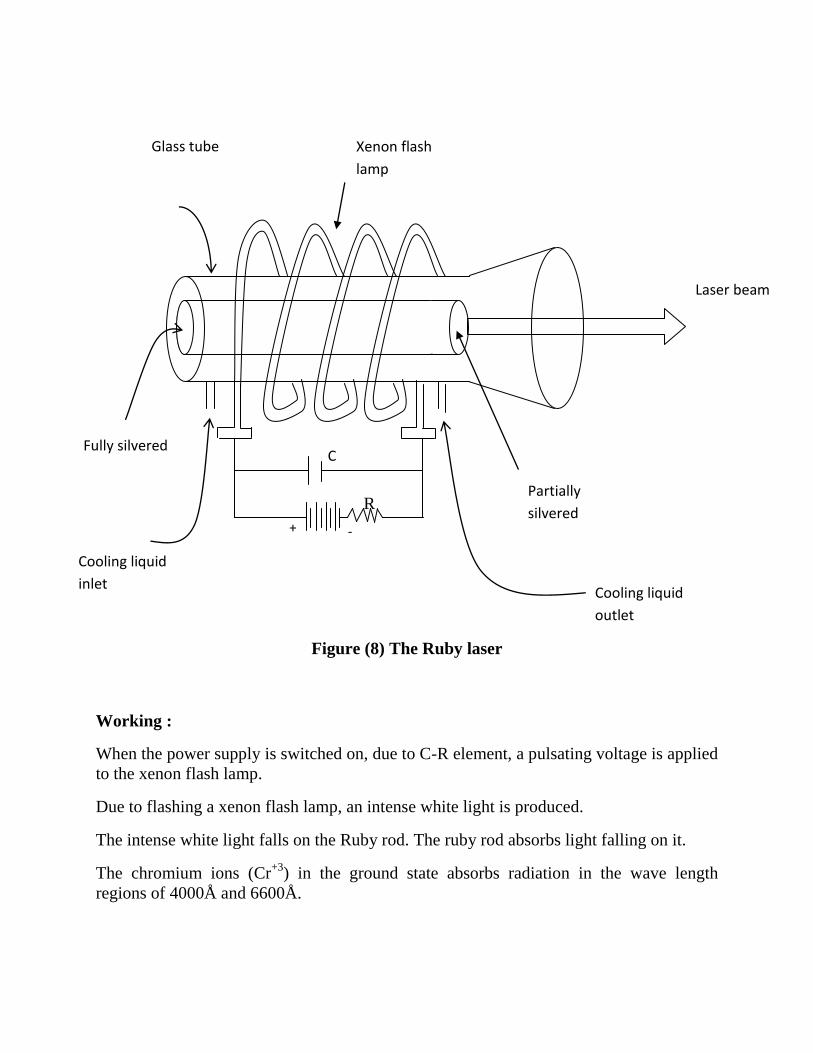
R
Figure (8) The Ruby laser
Working :
When the power supply is switched on, due to C-R element, a pulsating voltage is applied
to the xenon flash lamp.
Due to flashing a xenon flash lamp, an intense white light is produced.
The intense white light falls on the Ruby rod. The ruby rod absorbs light falling on it.
The chromium ions (Cr+3
) in the ground state absorbs radiation in the wave length
regions of 4000Å and 6600Å.
Cooling liquid
inlet
Fully silvered
+ -
Partially
silvered
Cooling liquid
outlet
Laser beam
Xenon flash
lamp
Glass tube
C

Chromium ions are excited to the higher energy levels E2 and E3 as shown in the figure
(9).
The energy levels E2 and E3 are containing bonds of energy levels.
Energy levels E2 and E3 accommodate all the chromium ions pumped from the ground
level.
The chromium ions excited to the energy levels E2 and E3 decays rapidly through non
radiative transition to a metal stable state in a time of 10-8
sec.
The meta stable state M accumulated with chromium ions, since the life time is
around 10-3
sec.
If energy is supplied continuously to the system, a stage is reached where the population
inversion takes place between E1 (ground state) and the metastable state M.
The stimulated emission of radiation dominates over spontaneous emission due to
NE1<NM or NM >NE1. This results in the emission of laser radiation of wavelength
6943Å.
This output of laser is in the red region of the electromagnetic spectrum. Due to rapid
non-radiative transmission from E2, E3 to M, heat will be liberated.
This liberated heat will be absorbed by the surrounding Ruby lattice.
To avoid heating of the Ruby rod, the device is cooled in liquid nitrogen.
310 sect
M
Figure (9) The energy level diagram of ruby laser with chromium ions.
E3 Rapid decay
X
E1
E2 E
T=10-8 sec
Laser beam
6943 Å
M=Metastable state
6600 Å 4000 Å
Ground level

Due to metastable characteristic of level M. population in M will be building up and
inversion is achieved.
The output of the laser is pulsating since charging and discharging of capacitor takes
place through the resistor.
Helium – Neon Gas laser
Helium – Neon Gas laser is a mixed gas laser. The first continuously operating
laser was constructed in 1960 by Javan, Bennet and Herriot and the Bell telephone
laboratories.
In this laser the actuallaser action takes place between excited levels of Neon.
Helium Gas is present to excite the Neon Atoms to a higher level.
Construction of Helium – Neon Gas laser
The Helium – neon gas laser consists of a quartz discharge tube of 100 cm length.
The internal diameter of the discharge tube is around 2-8 mm.
The discharge tube is filled with a mixture of Helium at 1 torr pressure and Neon at 0.1
torr pressure. Helium and Neon gases are mixed in the ratio 10:1. The length of the
discharge in the tube is nearly about 80 cm.
The important components of the He-Ne gas laser are shown in the figure (10).
One end of the tube is arranged with 100% reflecting concave mirror and the other end is
arranged with a partially reflecting and partially transmitting concave mirror.
From the second end, we get laser output.
The end windows are maintained at the Brewster angle and have they are known as
Brewster windows.
The discharge tube is having two electrodes. The electrodes are connected with a high
voltage source of 1kv – 2 kv, through a resistor.
1 torr = 1 mm of mercury
1 torr = 133.32 pascal

Figure : (10) Helium – Neon Gas laser
Working of the laser
When a high voltage dc sensor is switched on, an electrical discharge is passed through
the gas.
During this discharge, electrons are accelerated down the discharge tube.
The electrons collides with Helium and neon atoms. Helium and Neon atoms are in the
ratio of 10:1.
Helium atoms are excited to higher energy levels. The energy level diagram of the laser is
shown in figure (11).
This diagram shows the energy levels of Helium and Neon Atoms.
+ - R
100%
Reflecting
mirror
Partially
Reflecting and
transmitting
mirror
He+ Ne
Quartz discharge tube
End windows maintained
at Brewster Angle
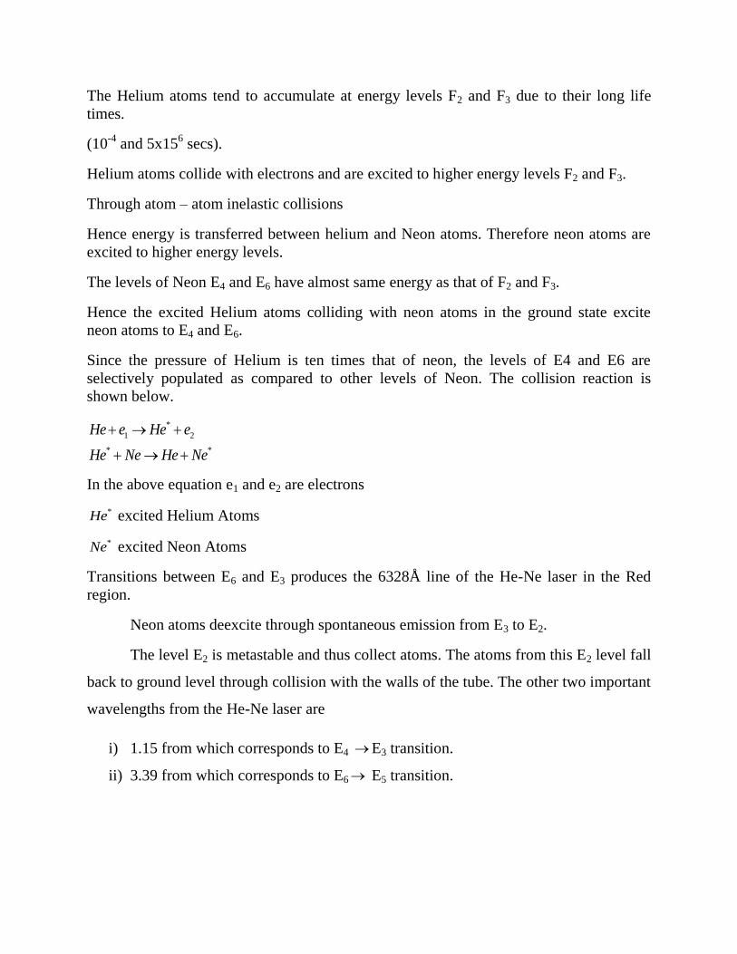
The Helium atoms tend to accumulate at energy levels F2 and F3 due to their long life
times.
(10-4
and 5x156 secs).
Helium atoms collide with electrons and are excited to higher energy levels F2 and F3.
Through atom – atom inelastic collisions
Hence energy is transferred between helium and Neon atoms. Therefore neon atoms are
excited to higher energy levels.
The levels of Neon E4 and E6 have almost same energy as that of F2 and F3.
Hence the excited Helium atoms colliding with neon atoms in the ground state excite
neon atoms to E4 and E6.
Since the pressure of Helium is ten times that of neon, the levels of E4 and E6 are
selectively populated as compared to other levels of Neon. The collision reaction is
shown below.
*
1 2
* *
He e He e
He Ne He Ne
In the above equation e1 and e2 are electrons
*He excited Helium Atoms
*Ne excited Neon Atoms
Transitions between E6 and E3 produces the 6328Å line of the He-Ne laser in the Red
region.
Neon atoms deexcite through spontaneous emission from E3 to E2.
The level E2 is metastable and thus collect atoms. The atoms from this E2 level fall
back to ground level through collision with the walls of the tube. The other two important
wavelengths from the He-Ne laser are
i) 1.15 from which corresponds to E4 E3 transition.
ii) 3.39 from which corresponds to E6 E5 transition.

Here a perfect population inversion is achieved between the energy levels
E6 and E3.
Neon energy levels
Figure (11) Energy level diagram of Helium – Neon laser
The emitted laser wave consists of two components called perpendicular polarized wave
and parallel polarized wave.
To avoid the perpendicular polarized component, the end windows are maintained at
Brewster Angle.
The Brewster angle B is given by
1 2
1
B
nTan
n
10-8 sec
19 –
--
17 --
--
15--
--
13--
--
11--
Helium Energy
levels
F3
F2
Excitation by
collision with
electrons
E6
E4
10-7sec
1.15µm
3.39 µm
6328Å
E5
E3 10-8s
Spontaneous Emission (~6000Å)
Laser
Through atomic
collisions
E6
E4
E2
E1
Deexcitation
by collision
Helium ground
level
Neon ground level

Where 1n Refractive index of the gas mixture.
2n Refractive index of glass
The perpendicular polarized wave is completely attenuated by the windows plate.
The parallel polarized wave is transmitted by the window is same direction.
The parallel polarized wave is repeatedly reflected by the resonator mirrors situated
behind the Brewster windows. Here correspondingly the light passes repeatedly through
the active medium.
Advantages
1. The laser light emitted by the Gas lasers is highly monochromatic and directional
when compared to solid state lasers.
2. He-Ne laser emits continuous wave of laser light.
3. Due to the presence of Brewster windows at the ends, the output laser light is linearly
polarized.
4. In put power is 5-10 watts.
5. Output power is 1-50 mw.
Semi conductor PN junction laser
GaAs and GaAsP lasers were the first PN junction semi conductor lasers built in 1962.
When a PN junction is forward biased at emits coherent radiation.
Principle
When a PN junction is formed between P and N materials of a semiconductor, depletion
layer is formed across the junction.
When the junction is forward biased, the width of depletion layer decreases. Due to this
electrons will flow from will flow from N side the P side of the junction, Here electron –
hole recombination takes place.
Due to this recombination of electrons with holes, light is emitted out from the junction.
The Pn junction which is forward biased and the energy bond diagram showing in the
figure (1)a and (1) b.
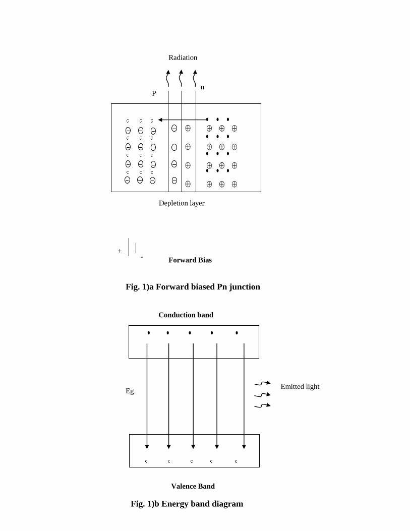
Depletion layer
+ -
Forward Bias
P n
Radiation
Valence Band
Conduction band
Emitted light Eg
Fig. 1)a Forward biased Pn junction
Fig. 1)b Energy band diagram

The energy band diagram, showing the movement of carriers, is shown in the figure (2)
Conduction band
N region
Valence band
Figure (2) Energy level diagram of Pn junction laser device.
Electron
hole
Laser
P region
Conduction band
Laser
Valence band
Electrons
Holes

The valence bond in P-region has holes and the conduction bond in N-Region
has free electrons -. When the junction is forward biased, current flows. The electrons
from the conduction bond of N-region make a transition to the valence Band of P-Region.
During this transition, electrons recombine with holes, emitting radiation corresponding
to the energy gap.
This process is called Radiative combination. During this process radiation is emitted out.
When current is increased beyond threshold current, stimulated emission occurs. This
ensures a laser light beam.
The energy of the emitted radiation is given by
E h Eg
The frequency of the emitted laser light is given by
Eg
h
We know that c
C
C Eg
h
The wavelength of emitted laser light is given by
hc
Eg
Where h= planck‟s constant
C= Velocity of light
Eg= Energy band gap of the semi conductor.
From Equation (1), it is clear that, the wave length of the emitted laser light
depends on the energy gap of the semi conductor.
Usually, GaAs semi conductors is used as a direct Band gap semi conductors.
Construction

The Basic structure of a pn-junction semiconductors laser is shown in figure (3). A
GaAs semi conductors is taken and is doped with impurities such that a p and n regions
are formed in the GaAs. Semi conductor.
A pair of parallel planes is cleaved or polished perpendicular to the plane of the
junction. The two remaining sides of the diode (front and rear face) are roughened to
eliminate lasing. The lasing action takes place in one direction only i.e. perpendicular to
the plane of polished surface.
Fig(3): Basic structure of PN junction semiconductor Laser
Front roughened
surface (Rear also)
Active region
Metal contact
I Terminal
I Terminal Metal contact
P-type
Optically flat and
parallel faces
N-type

This structure is called a Fabry- perot cavity. The others two sides are used for Metal
contacts. One metal contact serves the purpose of heat sink. Here the junction is formed
between P and n materials in the same host lattice. In the semi conductors laser doping
concentration levels are high.
Two flat polished parallel planes will serve the purpose of optical resonator.
Working
When P-type is connected to the positive terminal of a Battery and N-type is connected to
the negative terminal then the pn junction will be is forward bias condition.
Due to forward Bias, a current flows in the diode.
Initially at low current there is spontaneous emission in all directions.
When the forward bias increases, eventually a threshold current is reached at which the
stimulated emission occurs. A highly name chromatic radiation is emitted from the
junction. Here electron – hole recombination takes place across the junction.
The source of excitation is in the Battery (Forward Bias). The actual pumping process is
direct conversion.
The output of the semi conductor laser is in the infra red region wavelength range of
9000Å.
Advantages
1. The efficiency of the laser is high.
2. Laser output can be modulated by modulating the junction current.
3. The lasers output is tunable to a continuous wave or pulsed wave.

Applications of Lasers
Industry
1. Two dissimilar metals can be weld using a laser.
2. Laser used to cut glass and quality.
3. Lasers are used to drill holes in Quartz and ceramics.
4. Lasers are used for heat treatment in the tooling and automotive industry.
Medicine
1. To attach a detached retina, it is used in ophthalmology.
2. Lasers are used in correcting short sight.
3. Used for cataract removed.
4. Lasers are used in bloodless surgery.
5. Lasers are used in cosmetic surgery called mammoplasty.
6. Lasers are used in Angioplasty for the Removal of artery Block.
7. Used in the diagnosis of cancer therapy.
8. For removing stones in Kidneys and Gall Bladder.
Science
1. Lasers are used in Isotope separation.
2. Recording and Reconstruction of Holograms.
3. Used to create plasma.
4. Used to produce chemical reactions.
5. To study internal structure of micro organisms and cells.
6. To study the structure of molecules.

FIBRE OPTICS
Introduction
Fibre is a material that can be drawn into a number of threads.
The thin like fibre are bundled and used as carriers of light energy.
Optical fibre is a thin transparent medium which carries information in the form of
light.
The propagation of light through the optical fibre will be in the form of multiple
total internal reflections.
The fibre basically consists of two regions namely core and cladding.
The core region of the fibre having higher refractive index carries most of the
light. The core is surrounded by a cladding of lower refractive index.
These fibers improved the efficiency of transmission, reduced cross talk between
fibers.
The optical signals will have frequency of light; therefore fibres can be used as
carriers of information.
Advantages of optical fibres in communication
1. Fibres are having higher information carrying capacity i.e. band width is high.
This means that a greater volume of information or messages can be carried over
in a fibre optic system.
This is because the rate at which information can be transmitted is directly related
to signal frequency. Light has a frequency in the range of 1014
-1015
Hz, compared to radio
frequency of 106Hz and microwave frequencies 10
8-10
10Hz.
Therefore a transmission system that operates at the frequency of light can
theoretically transmit information at higher rate than systems that operate at radio
frequencies or micro wave frequencies.
2. They are small in size and are very light in weight.
3. No possibility of internal noise and cross talk generation along with immunity to
ambient electrical noise or electromagnetic induction.
4. No short circuit hazards as in the case of material wires.
5. In explosive environments, it can be used safely.
6. Immunity to adverse moisture and temperature conditions.
7. The cost of fibre optic cable is low when compared to copper / G.I. cables.
8. No need of additional equipment to protect against grounding and voltage problems.
9. The installation cost is nominal.
10. Fewer problems in space applications such as space radiation shielding and line to
line data isolations.
Principle of optical fibre – total internal reflection
When ever a ray of light travelling from a medium of high refractive index to a
medium of low refractive index, the light ray bends away from the normal.
When a ray of light is travelling from a denser medium to rarer medium, making
an angle of incidence i, it will be refracted into the air medium ,with angle of refraction

r. this is shown in the figure (1) a. If the angle of incidence further increases, the angle of
refraction also increases. This is shown in figure (1) b. At the interface, when the ray of
light incidents at an angle called critical angle, the ray will not be reflected, but it will
graze the interface. This is shown in fig (1)C.
When i>c , the ray will be totally reflected back internally into the same medium.
This is shown in figure (1) d.
Figure (1) Light ray suffering total internal reflection.
Applying Snell‟s law for the the ray of light suffering total internal reflection,
21 2
1
sin sin sin sinn
n i n r i rn
----------- (1)
In the case of a fibre, the ray of light travelling from a denser medium to rarer medium,
will be totally internally reflected into the same medium (i.e. into core).
Now consider the incident ray for which r=900
(i.ei=c) then 02
1
sin sin90c
n
n
21 2
1
sin c
nn n
n ---------------(2)

therefore for any ray of light whose angle of incidence is greater than this critical angle,
total internal reflection takes place.
Fibre construction
An optical fibre consists of a thin central thread of transparent plastic or glass,
which is surrounded by a second dielectric. The thin thread of central cylindrical material
is called the core. The core is surrounded by another material called cladding. The
refractive index of the core is slightly greater than that of cladding material such that the
guidance of the light is only through the fibre of the core material. The refractive index of
the core and cladding materials decides the properties of communication fibres. The size
of the core and cladding also determines the characteristics of a fibre to some extent. The
buffer Jacket (protective jacket) over the optical fibre is made of plastic and protects the
fibre from moisture and abrasion. In between the buffer jacket and optial fibre, there is
silicon coating. Due to this further isolation is achieved. Surrounding the buffer jacket
there is a layer of strength member (Kevlar) which provides toughness and tensile
strength. Here the fibre optic cable withstands without any brittleness during hard pulling,
bending, stretching or
rolling, through the fibre is
made from brittle glass.
Finally the cable is
covered by black
polyurethane outer
Jacket.
Figure (2) Fibre construction.
The fibre structure is shown in figure (2) for a typical fibre. Usually fibres are made with
either plastic or glass. Thus there are two types of fibres. 1. Glass fibre 2. Plastic fibre
Glass fibre
Glass fibres are made by fusing mixtures of metal oxides and silica glass.
The most common material used in glass fibre is silica (oxide glasses). It has a refractive
index of 1.458 at 850 nm. For producing two same materials having slightly different
refractive indices for the core and cladding, either fluorine or various oxides such as
B2O3, Ge2O2 or P2O5 are added to silica.
Examples of Glass fibre compositions
1. 2 2 2;GeO SiO Core SiO Cladding
2. 2 5 2 2;P O SiO Core SiO Cladding
3. 2 2 5 2;SiO Core P O SiO Cladding
Another type of silica glasses are made with low melting silicates. Such optical fibres are
made of soda-silicates, germane silicates and borosilicate.
Plastic fibre : The plastic fibres are typically made of plastics, are cheap and can be
handled without special care due to their toughness and durability.
Examples of plastic fibres.
1. A Polystyrene core (n1=1.60) and methyl methacrylate cladding (n2=1.49).
2. A Polymethylmethacrylate core (n1=1.49) and a cladding made of its co-polymer
(n2=1.40).
Propagation of light in fibres
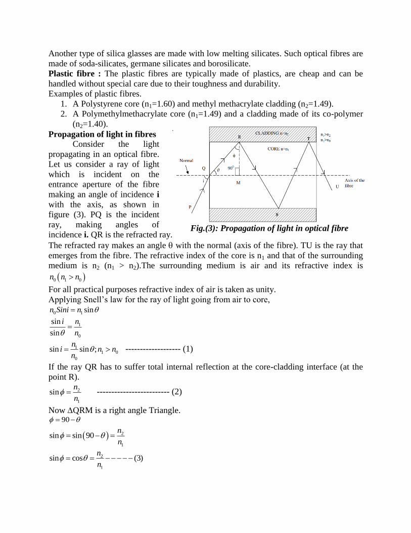
Consider the light
propagating in an optical fibre.
Let us consider a ray of light
which is incident on the
entrance aperture of the fibre
making an angle of incidence i
with the axis, as shown in
figure (3). PQ is the incident
ray, making angles of
incidence i. QR is the refracted ray.
The refracted ray makes an angle with the normal (axis of the fibre). TU is the ray that
emerges from the fibre. The refractive index of the core is n1 and that of the surrounding
medium is n2 (n1 > n2).The surrounding medium is air and its refractive index is
0 1 0n n n
For all practical purposes refractive index of air is taken as unity.
Applying Snell‟s law for the ray of light going from air to core,
0 1 sinn Sini n
1
0
sin
sin
ni
n
11 0
0
sin sin ;n
i n nn
------------------- (1)
If the ray QR has to suffer total internal reflection at the core-cladding interface (at the
point R).
2
1
sinn
n ------------------------- (2)
Now QRM is a right angle Triangle. 90
2
1
sin sin 90n
n
2
1
sin cos (3)n
n
Fig.(3): Propagation of light in optical fibre

But, 1/2
2 2 2sin 1 cos sin 1 cos
1/22
2
2
1
sin 1n
n
--------------------- (4)
From equations (1) and (4), we get
2
1/22
1
2
0 1
sin 1nn
in n
1/22 2
1 1 2
2
0 1
sinn n n
in n
1sin
ni
2 2 1/ 2
1 2
0 1
( )n n
n n
1/22 2
1 2
2
0
sinn n
in
If 2 2 2
1 2 0n n n , then for all values of i, total internal reflection will occur.
We know that for air, n0=1.
The maximum value of i for which the ray of light guided through the fibre is given by
acceptance angle A.
1/ 2
2 2
1 2sin A n n
Acceptance angle 1/2
1 2 2
1 2sinA n n
Acceptance cone
A cone obtained by rotating a ray of light at the end face of optical fibre, around
the fibre axis with acceptance angle is known as accepnace cone.
Acceptable angle
It is the maximum angle with which a ray of light can enter one end of the fibre
and guided through the fibre with total internal reflection. The acceptance angle is
denoted by A.
1/2
1 2 2
1 2sinA n n
It is a measure of light gathering power of the fibre.
Numerical aperture (NA)
Numerical aperture is the light gathering power of an optical fibre.
Numerical aperture is defined as the sine of acceptance angle.
Numerical Aperture = sinA
1/2
2 2
1 2. .N A n n

Types of optical fibres
Depending on the variation of refractive index of core of an optial fibre, the fibres are
classified into two types.
1. Step index fibre
2. Graded index fibre
Again basing on the number of modes (paths) available for the light rays
propagating inside the core, the fibres are classified into.
i) Single mode step index fibre.
ii) Multimode step index fibre.

Differences between single mode step index fibre and multimode step index fibre
Single mode step index fibre Multimode step index fibre
1. The refractive index of the core is
uniform throughout. In such a fibre
the refractive index profile abruptly
changes or step changes at the
cladding boundary.
2. The diameter of the core is 8-12 µm
and that of cladding is 125µm.
3. In a single mode fibre only one
mode or path can propagate through
the fibre.
1. The refractive index of the core is
uniform throughout. The refractive
index profile abruptly changes or step
changes at the cladding boundary.
2. The diameter of the core is 50-200 µm
and that of cladding is 125-400µm.
3. Multimode fibre allows a large
number of paths or modes for the light
rays travelling through it.
4. Index profile diagram for the single
mode step index fibre is shown
below.
1& 2 are cladding regions.
Fig. (1) Index profile diagram for step
index single mode fibre.
5. The light rays are propagating in the
fibre as shown below.
Fig. 2. Propagation of light in a
single mode step index fibre (or)
Fig.2. prorogation of light in a
4. Index profile diagram for the single
mode step index fibre is shown below.
1& 2 are cladding regions.
Fig. (1) Index profile diagram for step
index single mode fibre.
5. The light rays are propagating in the
fibre as shown below.
Fig. 2. Propagation of light in a
multi mode step index fibre (or)
Since the core is wider, greater
number of light rays enters into the
fibrefrom input signal and takes
multiple paths, as shown in fig(2).The
light ray (1) which makes greater
angle with the axis of the fibre,
suffers more number of reflections
through the fibre.It takes more time to

single mode step index fibre
Since it has got are mode of
propagation, only one ray of light
enters into the fibre and traverses a
single path or the light ray
transverses along the axis of the
fibre.
Here the light ray takes only one
path, hence there is no signed
distortion at the output end.
6. Signal distortion is shown below
(No. distortion)
Distortion the single mode step
index fibre
7. The difference between the refract-
tive indices of the core and cladding
is very small.
8. Value is small.
9. These fibres are more suitable for
communication. This is because of
less distortion.
10. Projection of light in to single mode
fibres and joining of two fibres are
very difficult.
11. Fabrication is very difficult and so
the fibre is costly.
12. It is a reflective type of fibre.
13. The light rays travel in the form of
meridional rays.
reach the exit end.Here light travels
more distance in the fibre.The ray (2)
makes smaller angle with the axis of
the fibre, it suffers less number of
reflections in a short time.Light ray(2)
traverses a short distance through the
fibre. Ray(2) reaches the exit end
quickly. Due to a path difference
between these two rays, they
superimpose at the output end. Hence
signals are overlapped.
6.Signal distortion is shown below
(Having distortion)
Distortion the single mode step index
fibre
7. The difference between the refractive
indices of the core and cladding is very
large..
8. Value is large.
9. These fibres are less suitable for
communication. This is because of large
distortion.
10. Projection of light into multi mode
fibres and joining of two multimode
fibres are very easy.
11. Fabrication is less difficult and so the
fibre is not expansive.
12. It is a reflective type of fibre.
13. The light rays travel in the form of
meridional rays.
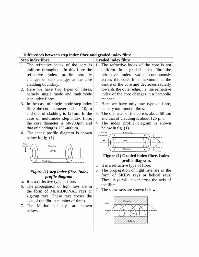
Differences between step index fibre and graded index fibre
Step index fibre Graded index fibre
1. The refractive index of the core is
uniform throughout. In this fibre the
refractive index profile abruptly
changes or step changes at the core
cladding boundary.
2. Here we have two types of fibres,
namely single mode and multimode
step index fibres.
3. In the case of single mode step index
fibre, the core diameter is about 10µm
and that of cladding is 125µm. In the
case of multimode step index fibre,
the core diameter is 50-200µm and
that of cladding is 125-400µm.
4. The index profile diagram is shown
below in fig. (1).
Figure (1) step index fibre. Index
profile diagram.
5. It is a reflective type of fibre.
6. The propagation of light rays are in
the form of MERIDIONAL rays or
zig-zag rays. These rays croses the
axis of the fibre a number of times.
7. The Meriodional rays are shown
below.
1. The refractive index of the core is not
uniform. In a graded index fibre the
refractive index varies continuously
across the core. It is maximum at the
centre of the core and decreases radially
towards the outer edge. i.e. the refractive
index of the core changes in a parabolic
manner.
2. Here we have only one type of fibre,
namely multimode fibres.
3. The diameter of the core is about 50 µm
and that of cladding is about 125 µm.
4. The index profile diagram is shown
below in fig. (1).
Figure (1) Graded index fibre. Index
profile diagram.
5. It is a refractive type of fibre.
6. The propagation of light rays are in the
form of SKEW rays or helical rays.
These rays will never cross the axis of
the fibre.
7. The skew rays are shown below.

Fig (2) step index fibre meridional
rays.
In the case of step index fibre, the
light rays propagate through the fibre
by way of total internal reflection.
8. In a step index fibre the light rays are
propagated as shown in figure (3).
Fig.3 propagation of light in a step
index fibre
The two rays will not reach the output
and simultaneously there is
intermodal distortion. The output and
input signals are shown in the figure
below.
Fig (2) Graded index fibre skew rays.
In a graded index fibre, the refractive
index of the core decreases from the
fibre axis to the cladding interface in a
parabolic manner. When a light ray
enters into the core and moves towards
the cladding interface, it encounters a
more and more rarer medium due to
decrease of refractive index.
As a result, the light ray bends away
from the normal and finally bends
towards the axis of the fibre. Now it
moves towards the core-cladding
interface at the bottom.
Again the light ray bends in the upward
direction. Thus due to continuous
refraction on the light ray takes
sinusoidal (or) helical path.
8. In a graded index the light rays are
propagated as shown in figure (3)
Fig.3 propagation of light in a graded
index fibre
When the two light rays (1) and (2) enter
into the fibre, by making different angles
with the axis of the fibre, their velocities
will change continuously and reach the
output end simultaneously at the same
time i.e. the light rays will come to focus
at the same point.
Here there is no intermodal dispersion.
The output and the input signals are
shown in the figure below.

Fig.( 4) Input and output signals in a
step index fibre
9. Distortion is more due to intermodal
dispersion.
10. Here there is no self refocusing effect.
11. Numerical aperture is more in a
multimode step index fibre.
Fig. (4)Input and output signals in a
step index fibre
9. Distortion is less.
10. Self refocusing effect takes place due to
continuous refraction. Hence the helical
path for the light rays.
11. Numerical aperture is less in a graded
index fibre.
Fibre optic communication system
The block diagram of a fibre optic communication system is shown in figure (1).
Figure (1) block diagram optical fibre communication system.

The fibre optic communication system consists of the following.
i) Transmitter
ii) Repeaters (or) fibre repeaters and
iii) Reciever iv) couplers and connectors v) fibre cable.
I) The transmitter : or an optical transmitter consists of an Encoder, a source of light
and modulator. The input signal in the form of speech or song is fed to an encoder. The
encoder converts the analog signal into a digital signal.
The digital signal is given to the source of light. The source of light can be a light
emitting diode (LED) or a pn junction laser diode.
The optical carrier signal is now finally fed to modulator. The modulator modulates the
signal depending on the requirement.
The type of modulation may be amplitude or frequency or phase modulation.
The optical signal finally coupled to the optical fibre with the help of couplers.
The couplers launche the optical signal in the fibre without any distortion.
The fibre is connected to the repeater with the help of connector.
ii) The repeater: It consists of an amplifier and a regenerator.
During the transmission of the signal, along the optical fibre, there will be loss in the
signal due to dispersion in the fibre. As a result we get a weak signal at the output end of
the fibre. To minimize the losses, repeaters are employed at regular intervals along the
fibre. Now in the repeater the amplifier amplifies the signal and is reconstructed through
the fibre.
Finally the optical signal is fed to the receiver.
iii) The receiver consists of a photo detector. The photo detector consists of a PIN diode
or avalanche photo diode.
From the fibre the optical signal is fed to the photo detector. The photo detector detects
the optical signal and converts it into an electrical signal.
The electrical is the amplified by the amplifier the amplified signal is fed to the
Demodulator. The demodulator demodulates the signal to get a digital signal. This digital
signal is decoded by a Decoder.
The output of the decoder is a pure form of the original signal. This is taken as final
output.
Applications of optical fibres
1. Optical fibres are used in fibre optic communication systems.
2. Optical fibres are used in exchange of information between different terminals in a
network of computers.
3. They are used to carry information and exchange information in cable television
networks. Space vehicles and submarines etc.
4. Optical fibres are used in industry in security alarm systems, process control and
industrial automation.
5. Optical fibres are used in optical fibre gyroscopes and are used in automotive
navigation systems.
6. They are used in pressure sensors in biomedical applications.

7. Used in pressure sensors in Engine control applications.
8. Optical fibres are used in medicine in the fabrication of fiberscope in endoscopy.
The endoscopy is used to visualise internal parts of the body.
9. They are used in fuel tanks to sense the liquid levels as a liquid level sensor.
10. They will be used as chemical sensors.

Unit – II
CRYSTAL STRUCTURES
AND X-RAY DIFFRACTION
AND
ULTRASONICS

Crystal Structures and X-Ray Diffraction
Matter exists in three different states, viz. solid state, liquid state and gaseous state.
In gaseous and liquid states the atoms or molecules will be moving from one place to other place.
The positions of the atoms or molecules are not fixed in them.
i.e. In liquid and gaseous states there is no proper orientation of atoms or molecules.
In solids the positions of the atoms or molecules are fixed, but they may have or may not be
having regular periodic arrangement.
If the atoms or molecules in a solid are periodically arranged at regular intervals in three
dimensional space then the solid is known as crystalline solid.Ex.Iron, NaCl.
If the atoms or molecules in a solid do not have periodical arrangement then the solid is known
as amorphous solid.Ex.Plastic, polymers
When the periodicity of atoms or molecules is extended throughout the solid then the solid
is known as single crystalline solid.
If the periodicity of atoms or molecules is extended up to small regions called grains, such a
solid is called polycrystalline solid.
Space lattice
A space lattice is defined as an infinite three dimensional arrangement of points (i.e.
atoms or molecules or ions) in which every point has surroundings or environment identical to
that of every other point in the array.
The crystal structure can be studied in terms of a space lattice.
Consider the two dimensional array of points as shown in figure (1).
Fig (1) A two dimensional array of lattice points.
2
2
B 1
1
1
1 A
X
Y
O

b
Fig (2) A two dimensional array of points.
Consider the point „O‟ as the origin. Join this origin to a successive lattice points along x and y
directions. Let the position vectors of these points be a and b .
When a is repeated regularly in the x-direction, then we get the lattice points along the x-
direction i.e. 2a , 3a , 4a ,……
Similarly when b is repeated regularly in the y-direction, then we get lattice points along y-
direction i.e. 2 b , 3b ,4b ,…….
Here a and b are used and repeated regularly to get the lattice points in space lattice, they are
known as fundamental translation vectors or primitive vectors.
This shown in figure (1) and (2).
Now the position of the point P can be given by a position vectorT .
i.e. T a b
Similarly the position vector of the lattice point Q is given by
2T a b
For a two dimensional space lattice, the position vector of any lattice point is given by
T na mb
Where n, m are integers.
For a three dimensional lattice, the position vectors of any lattice point is represented by
T na mb pc
T Q
a
O
P

Where n, m and p are the integers.
a ,b and c are the translational vectors along x, y and z directions.
From figure (1), consider a lattice point A. the point
A has got two nearest points at a distance of 1 unit in the x,y
directions. Diagonally it is having nearest point at a distance
of 2 units.
Let us consider another point B in the lattice array. B
is also having two nearest points at a distance of 1unit in x
and y directions. Diagonally it is having a nearest point at a
distance of 2 units.
i.e. Here Both A and B are having the same
environment. Hence figure (1) represents a two dimensional
space lattice.
In this same way we can represent a three dimensional lattice.
In three dimensions a space lattice can be represented by the
figure (3).
Unit Cell
The unit cell is the smallest block or smallest geometric figure, from which the crystal is
formed when repeated regularly in three dimensions.
It is also defined as the fundamental elementary pattern, which when repeated again and again in
three dimensions forms a lattice structure of crystal.
Let us consider a two dimensional crystal lattice with periodic arrangement of atoms, as shown
in figure (4). Here ABCD represent the smallest geometrical figure. This smallest geometrical
figure is a square. When this is repeated again and again regularly in XY space, we get a square.
In three dimensions, a unit cell is shown in figure (5). ABCDEFGH is the cubical unit cell. When
this is repeated in three dimensions regularly, we get a three dimensional crystal structure.
A B
C D
X
Y
Atoms
A
D
E
G H
B
F
C
Atoms
Fig (3) three dimensional lattice
Fig. (4) Two dimensional crystal
structure – unit cell
Fig. (5) Unit cell – three dimensional
crystal structure

Parameters of the unit cell.
Crystallographic Axes.
The lines drawn parallel to the lines of
intersection of any three faces of the unit cell
which do not lie in the same plane are called
crystallographic axes.
From the figure (6) OX, OY and OZ are the
three crystallographic axes.
Interfacial angles
The angles between the three crystallographic
axes are known as interfacial angles.
In the figure (6), , and are the
interfacial angles.
Primitives
The three sides a, b and c of a unit cell are known as primitives.
From figure (6), a, b and c are the three primitives.
Primitive cell: The unit cell formed by the primitives a, b and c and having only one lattice
point is called primitive cell.
Example: A unit cell containing one lattice point.
Coordination Number (N)
The coordination number is defined as the number of equidistant nearest neighbors that
an atom has in the given structure.
Greater is the coordination Number, the more closely packed up will be the structure.
Nearest neighbors distance (2 r)
The distance between the centers of two nearest neighboring atoms is called nearest
neighbor distance. If r is the radius of the Atom, nearest neighbor distance will be 2 r.
Atomic Radius (r)
Atomic radius is defined as half of the distance between nearest neighbors in a crystal of
pure element.
Atomic radius2
2
rr .
Atomic packing factor (APF)
The fraction of space occupied by atoms in a unit cell is known as atomic packing factor
or packing factor.
It is the ratio of volume of the atoms occupying the unit cell to the volume of the unit cell
relating to that crystal structure.
Volume of the Atoms present in the unit cell
APF=Volume of the unit cell
Y
B
o
ᵞ c
a A
X
Z
C
b
Fig (6): Lattice parameters

Density
Density is defined as Ratio between Mass and Volume.
3
A
nMDensity =
a N
Where n = No. of atoms per unit cell.
M = Molecule Weight of the unit cell.
a = Lattice constant
NA = Avogadro‟s number.
Void (or) interstitial space Figure (7) Void
The empty space between the Atoms in a unit cell is known as void or interstitial space.
Void is shown in figure(7) above.
Basis
A Basis is an assembly of atoms with identical composition, arrangement and orientation.
A crystal structure is formed by associating every lattice point with a unit assembly known as
basis. For a lattice to represent a crystal structure every lattice point must be linked with one or
more atoms called the Basis or pattern.
When the Basis is repeated with exact periodicity in all directions, it gives the actual
crystal structure.
Usually Lattice + Basis Crystal structure.
The basis is real and the crystal structure is real. The lattice is imaginary.
The following diagram illustrates basis representing each lattice point.
From the figure(8), it is clear that the basis consists of two different atoms.
Basis
Lattice point
Fig.( 8) Basis
Void

In crystalline solids like copper and sodium, the basis is a single atom.
In NaCl and CsCl, the basis is diatomic.
In crystals like2CaF , the basis is triatomic.
Bravais Space Lattices
The atoms can be grouped together to form different crystalline structures.
Here the unit cells containing atoms or molecules are repeated in a space lattice, we get
crystal structures. The scheme of repetitions of atoms or molecules in a space lattice is limited in
number.
There are 14 ways of arranging points in three dimensional space. These 14 space lattices
are known as Bravais space lattices or Bravais lattices.
Note: The space lattices formed by unit cells are marked by the following symbols.
Primitive Lattice - P or S (simple Lattice)
Body centered lattice - I
Face centered lattice - F
Base centered lattice - C
Simple Crystal Systems
All the crystals based on the geometrical shapes of their unit cells classified into seven
crystal systems.
They are
1. Cubic crystal system.
2. Tetragonal Crystal system
3. Orthorhombic crystal system
4. Rhombohedral crystal system (Trigonal)
5. Monoclinic Crystal System
6. Triclinic Crystal system Figure(9)a
7. Hexagonal crystal system
1. Cubic Crystal system
In this system, the sides of the cube are equal, b
I.e. a=b=c
The crystallographic axes are perpendicularly to one another.
The interfacial angles are equal to090 .
i.e. 090 c
Cubic lattices may be simple, body- centered or face centered.
The diagrams are shown in the figures.
α
a
Simple cubic (p), Ex: Polonium

In the case of simple cubic lattice, the atoms are present at the corners of the unit cell.
Simple cubic lattice is shown in figure(9)a.
Figure(9)b Body centered Cube-I Figure(9)c Face centered cube F
Example: Ba, Fe, Na, Cu20, W Example. Al, Ag, Au, Pb, Cu
In the case of Body centered lattice, there will be a body centered atom and eight corners atoms
as shown in the figure(9)b.
In the case face centered lattice, atoms are present at all corners and at all face centers. This is
shown in figure(9)c.
2. Tetragonal Crystal System
In this case, two sides are equal. i.e. a=b and ,a c b c
All the interfacial angles are equal to 900. i.e. 090
Here the crystal axes are perpendicular to each other. Tetragonal lattices may be simple
or body-centered. They are shown in figures(10)a and (10)b.
Figure (10)a Simple (or) primitive lattice Figure (10)b Body centered lattice (I)
Ex: TiO2, SnO2, Indium etc. Ex: KH2P04, NiSO4
c
900
900
900
b
a
c
b
a

3. Orthorhombic Crystal system
In this system the three sides of the unit cell are unqual.i.e. a b c . The crystal axes are
perpendicular to each other. All the interfacial angles are equal to 900i.e. 090 .
Orthorhombic lattices may be simple, base centered, body centered or face centered. They are
shown in figures(11)a,(11)b,(11)c and (11)d.
4. Rhombohedral crystal system
This is also known as Trigonal system. In this crystal system,
the three sides of the unit cell are equal .i.e. a=b=c.
The interfacial angles are not equal to 900.
i.e. 0 090 120 . 0 0 090 , 90 and 90
The trigonal lattice is only a primitive cell,shown in fig(12).
900
900
900 a
b
c
Figure11(a)Simple lattice (p)
Ex: hydro carbons of High
molecular weight
Figure(11)b.Base centered (c)
Ex: PbCo3,BaSo4
Figure(11)c body centered (I)
Ex: - Sulphur
Figure (11)d Face centered (F)
Ex: KN03, K2So4
b
a
a
α
c
a
a
α
c

Example: 4 , , , ,CaSo As Sb Bi Calcite.
5. Monoclinic Crystal system In this crystal system, the sides of the unit cell are unequal. Here the two interfacial angles are
equal to 900. The third interfacial angle is not equal to 90
0. 090 , 090 and a b c
Monoclinic crystal lattices may be primitive or base centered. They are shown in figures (13)a,
and (13)b.
c
6. Triclinic Crystal System
In this crystal system, the three sides of the unit cell are not equal.
i.e. a b c and .All the three angles are different.
All the interfacial angles are not equal to 900
. i.e. 090
Example: 4 2.5CuSo H O 2 2 7, K Cr O
This crystal lattice is only a primitive lattice,shown in figure(14).
c
7. Hexagonal Crystal system
In this crystal system two sides the unit cell are equal.
a b , a c and b c . However the two interfacial angles
are equal to 900.
Third angle is equal to 1200. i.e. 090 ,
0120 . This is shown figure(15).
This crystal lattice is a primitive lattice only.
Example: Quartz, Zinc, Magnesium and SiO2.
This is only a primitive Lattice. b
900
090
900 a
b
b
a
c
Figure(13)a Simple (or) primitive
lattice
Ex: Na2So4, Gypsum
Figure(13)b Base centered
Ex: K2MgSo4, 6H2O
c
a 900
1200
900
1200
900 b
c
b
a a
Fig (14) Simple lattice
β α
b
a

The 14 Bravais Lattices are now summarized as follows.
S.No Name of the crystal
system
No. of bravais lattices Types of bravais
lattices
1. Cubic 3 P,I,F
2. Tetragonal 2 P,I
3. Orthorhombic 4 P,I,F,C
4. Rhombohedral or Trigonal 1 P
5. Monoclinic 2 P,C
6. Triclinic 1 P
7. Hexagonal 1 P
Simple Cubic Crystal Structures (SCC)
The simplest structure to describe is the simple cubic crystal structure. Figure (1) shows the unit
cell of simple cubic structure.
Usually in a simple cubic lattice, there is only one lattice point in the unit cell. At all the corners
there will be corner Atoms. If we take an Atom at one corner as a reference atom, it is
surrounded by six equidistant nearest neighbours.
Coordination Number of SCC, N=6.A simple cube has eight corner atoms.
Each Corner atom is shared by eight surrounding unit cells.
Share of an Atom to each corner of unit cell = 1
8 of an Atom.
i.e. Each corner of the unit cell = 1
8 of an Atom. No. of corners of the unit cell = 8.
Total Number of Atoms per unit cell of SCC = No. of corners of the unit cell Share of each
corner.
Total Number of Atoms per unit cell of SCC. 1
88
n 1n
Effective number of lattice points in simple cubic unit cell is one.
Fig (1) Unit cell of simple cubic
crystal structure.
1
8
of an
Fig (2) Top view – touching of the corner
atoms along the edges
r
r
a

Thus a simple Cubic unit cell is a primitive cell. The top view of the SCC structure is shown in
fig (2). Here the corners atoms touch each other along the edges.
From the figure (2) nearest neighbour distance = 2r.
But 2r a
Lattice constant a = 2r
Atomic Radius2
ar .
Atomic Packing Factor:
Let r be radius of each atom. Volume of each Atom 34
3r Number of atoms per unit cell of
SCC, n=1.
Volume of all the Atoms present in the unit cell of SCC = 341
3r --------------(1)
Side of the unit cell of SCC = a.
Volume of the unit cell = a3 -------------------(2)
Now, APF Volume of all the Atoms present in the unit cell
=Volume of the unit cell
From (1) and(2), we get
33
3 3
41
43APF=a 3 2 2
ra a
ra
4
33 a
3a
80.52
62
i.e. 52% of the Volume of the unit cells is occupied the Atoms in the unit cell.
Also void space or Interstitial space = 48%.
Density = 3
A
M
a N (Number of Atoms,n=1)
Example : Polonium.

Body centered cubic structure (BCC)
The unit cell of BCC is shown in figure (1). In this unit cell a=b=c, 0= = =90 .
In this structure of the unit cell, there are eight corners. At all the corners, we have corner atoms.
In addition to the corner atoms, there will be a body centered Atom at the body centre of the unit
cell.
Now if we take an Atom as a reference Atom, it is surrounded by 8 unit cells.
Share of a corner Atom to each unit cell 1
8 of corner Atom.
i.e. Each corner of the unit cell 1
8 of an Atom.
No. of corners of the unit cell = 8.
Total No. of Atoms contributed by 8 corners.
= No. of corners Share of each corner
1
88
=1
Now Total Number of Atoms per unit cell of BCC =
One body centered Atom + contribution made by the corner Atoms.
11 8 1 1 2
8
Coordinate Number (N)
Any corner reference Atom is surrounded by 8 number of unit cells. For any corner Atom the
nearest neighbouring Atom is the Body centered Atom. Each unit cell is having one body
centered Atom. Hence the coordination number N= 8.
Lattice Constant (a) and Atomic Radius (r)
The corner Atoms will not touch each other. The corner atoms touch the Body centered
atom along the body diagonal.
This is shown in the figure (2).
aR
Fig (2) Touching of the corner atoms with the
body centered atom along the body diagonal
Fig (1) Unit cell of BCC structure
1
8
of an atom
Body centered
atom
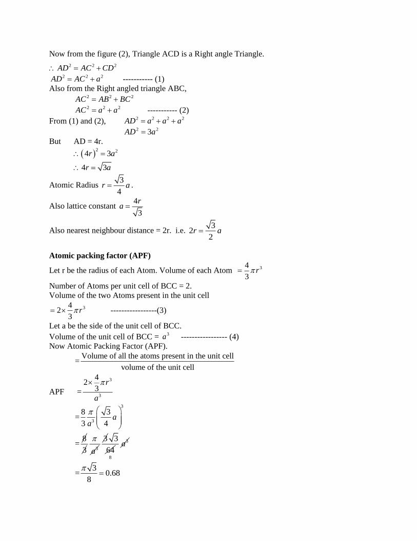
Now from the figure (2), Triangle ACD is a Right angle Triangle.
2 2 2AD AC CD 2 2 2AD AC a ----------- (1)
Also from the Right angled triangle ABC,
2 2 2AC AB BC
2 2 2AC a a ----------- (2)
From (1) and (2), 2 2 2 2AD a a a
2 23AD a
But AD = 4r.
2 24 3r a
4 3r a
Atomic Radius 3
4r a .
Also lattice constant 4
3
ra
Also nearest neighbour distance = 2r. i.e. 3
22
r a
Atomic packing factor (APF)
Let r be the radius of each Atom. Volume of each Atom 34
3r
Number of Atoms per unit cell of BCC = 2.
Volume of the two Atoms present in the unit cell
342
3r -----------------(3)
Let a be the side of the unit cell of BCC.
Volume of the unit cell of BCC = 3a ----------------- (4)
Now Atomic Packing Factor (APF).
Volume of all the atoms present in the unit cell
=volume of the unit cell
APF
3
3
42
3=
r
a
3
3
8 3=
3 4a
a
8
=3 3a
3 3
64
3
8
a
3
= 0.688

68% of the volume of the unit cell is occupied by the atoms present in the unit cell.
Now void space (or) interstitial space = 32%.
Density : Density 3
A
nM
a N and for BCC structure, n=2,
3
2
A
M
a N
Examples: Barium ,Iron and Sodium etc.
Face Centered Cubic Crystal Structure (FCC)
The face centered cubic crystal structure is shown in the figure (1)
In this FCC structure, the unit cell is a cube i.e. a=b=c=a and 090 At all the eight corners, we will have corner
atoms and in addition to them at each and every face centre,
there is a face centered atom.
The unit cell structure of FCC crystal with their atoms at the
corners and at the face centre are shown in figure (2).
Total Number of Atoms per Unit Cell (or) Effective Lattice Points
If we take any corner atom as a reference atom, it is surrounded by
eight number of unit cells. Therefore a corner Atom is shared by
eight number of surrounding unit cells.
Also every face will have a face centered Atom.
Share contributed by an Atom to each corner 1
8 of an Atom.
Total Number of corners = 8.
Contribution made by all the eight corners.
= Total corners share of each corner.
= 1
88
=1
Share of a face centered Atom to each face
1
2 Of an Atom.
Total number of faces = 6
Contribution made by all the six faces = 1
6 3Atoms3
Effective Number of atoms per unit cell of FCC 1 1
6 82 8
= 3+1
= 4 Atoms.
Fig (1) : FCC Crystal structure
– Unit cell
a
1
8
of an
Face centered atom
(½ of an atom )
Fig (2) Unit cell structure
of FCC crystal

Atomic Radius (r)
In a FCC cell there are eight corners and eight corner atoms. There will be one atom at
the centre of each face of the unit cell. The corner atoms touch the face centered atoms along the
face diagonal AC as shown in figure (3).
The atoms A and N are the nearest neighbouring Atoms.
By definition 2
ANr
OR AN = 2r and AC = 4r
From the figure triangle ABC is a right angled triangle.
2 2 2
2 2 2
2 22 , but AC=4r
AC AB BC
AC a a
AC a
2 24 2
4 2
2
4
2 2
r a
r a
r a
ar
Lattice constant (a)
Now lattice constant a = 2 2 r i.e. 4
2
ra
Coordination Number (N)
In the FCC unit cell. The nearest neighbours of any corner atom are face centered atoms.
Consider the atom at the face centre as origin; it can be observed that this face is common to two
unit cells.
If we take one corner atom as a reference atom, it is surrounded by 8 unit cells.
Here there are twelve atoms surrounding corner atom situated at a distance equal to half
the face diagonal of the unit cell.
Thus the coordination number of FCC lattice is 12
i.e. Any corner atom has Four face centered atoms in its own plane, four in a plane above it and
four in a plane below it.
Atomic Packing Factor (APF)
Let r be the radius of each Atom.
Volume of one atom 34
3r
Number of atoms per unit cell of FCC = 4
Fig (3) Touching of the corner
atoms with the face centered
atom along the face diagonal.

Volume of all the atoms per unit cell of FCC = 344
3r ---------- (1)
FCC = 344
3r ------------ (1)
Let a = side of the unit cell of FCC
Volume of the unit cell of FCC 3a ------------ (2)
Atomic packing factor is given by
Volume of all the atoms occupying the unit cellAPF =
Volume of the unit cell
3
3
44
3APF =
r
a
But 4r
a=2
APF 3
3
16
43
2
r
r
3
3
16
643
2 2
r
r
16
3r 2 2
3 644
3
2
r
2
6
=0.74
74% volume of the unit cells is occupied by the Atoms present in the unit cell.
Void space : The free space is 0.26. 26% Volume of the unit cell is free space.
Density : Density 3
A
nM
a N . For FCC structure n=4
3
4
A
M
a N
Examples : Copper, Aluminum, Lead, Gold, Silver etc.

X-RAY DIFFRACTION
X-Rays are electromagnetic waves like ordinary light. Similar to light they exhibit
interference and diffraction.
The wave length of X-rays is of the order of 0.1 nm, so that ordinary devices such as
ruled diffraction gratings don‟t produce observable effects with X-Rays.
Laue suggested that a crystal with a three dimensional array of regularly spaced atoms
could serve the purpose of a grating.
The crystal differs from the plane grating in the sense that the diffracting centers in the
crystal are lying in different planes. Hence the crystal acts as a space grating rather than a plane
grating.
Friedrich and knipping succeeded in diffracting X-rays by passing them through a thin
crystal of Zinc Blend (ZnS).
The diffraction pattern obtained consists of a central spot and a series of spots arranged in
a definite pattern around the central spot.
This symmetrical pattern of spots is known as Laue pattern and it proves that X-Rays are
electromagnetic in nature.
A simple interpretation of the diffraction pattern was given by W.L. Bragg.
According to Bragg, the spots are produced due to the reflection of some of the incident
X-Rays from the various sets of parallel crystal planes.
These sets of parallel planes contain a large number of atoms. These planes are called
Bragg’s Planes.
Bragg’s Law
When a beam of monochromatic X-Rays falls on a crystal, the X-Rays are scattered by
individual atoms present in the set of parallel planes. When path difference between two
reflected rays equal to integer multiple of incident wavelength of X-rays, constructive
interference occurs. This is called Braggs law.
Bragg assumed that the combined scattering of X-Rays from the planes can be looked
upon as a reflection from the planes.
Hence Bragg‟s scattering is known as Bragg‟s reflections and the different planes are
known as Bragg‟s planes.
Let us consider a crystal containing a set of parallel planes with interplanar spacing d.
When X-Rays of wavelength fall on these crystal planes, the atoms in the planes
diffract the X-Rays in all directions.
Let the X-Ray PQ incident at a glancing angle with the plane XY. This PQ X-Ray is
reflected by the atom at Q in the direction QR. This is shown in figure (1).
Another X-Ray ' 'P Q is reflected by the atom at 'Q in the Direction ' 'Q R .

i.e. PQR and ' ' 'P Q R are the two parallel X-Rays incident and diffracted from the atoms Q and 'Q .
X Y
d
Figure (1): Braggs Law of X-Ray Diffraction
These diffracted X-Rays will interfere constructively or destructively depending on the path
difference between the X-Rays PQR and ' ' 'P Q R .
Now for finding the path difference, normal QS and QT are drawn from Q on to ' 'P Q
and ' 'Q R .
Now the path difference = ' 'SQ QT n ------------ (1)
Here constructive interference takes place. Where n = 1, 2, 3…
If the two reflected waves are out of phase, then they produce zero intensity spots.
Now the triangle 'QTQ and 'QSQ are two similar right angled triangles.
Hence ' 'SQ QT
Also from the figure, triangle 'QTQ and 'QSQ are right angled triangles.
'' '
'sin sin
SQSQ QQ
QQ --------------- (2)
Also from the right angled triangle 'QTQ , '
'sin
QT
' ' sinQT QQ --------------------- (3)
Q
Q1
T S
P1 P R R1
Normal

Now for maximum intensity, the two reflected rays must be in phase.
Also the path difference should be equal to integer multiple of for constructive
interference.
From equations (1), (2) and (3), we get
' 'sin sinQQ QQ n
'2 sinQQ n
But 'QQ d
2 sind n --------------- (4)
This is known as Bragg‟s Law.
Here d = Interplanar spacing
= Angle of Diffraction
n = order of Diffraction
= Wavelength of incident X-Rays.
Corresponding to n=1, 2, 3… we get 1st order, 2
nd order and third order diffraction sports.
Now maximum value of sin is 1, from equation (4), we have
2
2 ,d
n dn
For any order, the wavelength shouldn‟t exceed two times the interplanar spacing.
Significance of Bragg’s Law
1. From Bragg‟s Law 2d sin n , we get 2sin
nd
Knowing the wavelength of X-Rays, angle of diffraction and order of diffraction n,
d can be calculated.
2. Knowing the value of d, the lattice constant „a‟ can be calculated for a cubic crystal, using
2 2 2
ad
h k l
3. For 1st order maximum, n=1, 1sin
2d
For 2nd
order maximum, n=2, 2
2sin
2d
For 3rd
order maximum, n=3, 3
3sin
2d
-------------- ---- ------- ------ --- ------- ---
Here the intensity goes on decreases as the order of spectrum increases.

3. If we know lattice constant a, density and molecular weight M of the crystal. Then
number of atoms (or) molecules in the unit cell can be calculated.
4. For a cubic crystal, 2 2 2
ad
h k l
If we know the values of d and a, the value of 2 2 2h k l can be calculated.
5. Depending on the value of2 2 2h k l , we can classify the crystals as SCC, BCC, and
FCC etc.
Laue Method of X-Ray diffraction
The Laue method is one of the X-Ray diffraction techniques used for the study of crystal
structures.
The white X-Rays beam incidents on a stationary single crystal as shown in the figure (2).
Crystal is held stationary with the help of a stand. The white X-Rays are allowed to fall on
the crystal. Fine beam of X-Rays can be obtained by passing the X-Rays through pin holes of
lead diaphragms. These X-Rays of fine beam now allowed to fall on the crystal.
The crystal planes in the crystal diffract the X-Rays satisfying Bragg‟s Law. The diffracted
X-Rays are allowed to fall on the photographic plate.
The diffraction pattern consists of a series of bright spots corresponding to interference
maximum for a set of crystal planes satisfying the Bragg‟s law 2 d sin = n for a particular
wavelength of incident X-Rays.
A set of planes diffracts a particular wavelength which satisfies the Bragg‟s law for particular
dhkl values.Here we get a number of diffracted beams, each corresponding to a set of planes
for a particular wavelength.
Laue pattern can be obtained either by transmission method or back reflection method. Both the
methods are shown in figure (2) and figure (3).
Figure (2) Laue Transmission method of X-Ray Diffraction
Crystal
Lead of diaphragms
Pin hole
White X-Ray Beam
Photographic plate
Laue spot

Figure (3): Laue Back reflection method of X-Ray diffraction
Here the wavelength of X-Rays = 0.20
2 A . The dimensions of the crystal are usually less
than 1mm. The distribution of spots on the photographic plate depends on the symmetry of
the crystal and its orientation with respect to X-Ray beam.
In the case of transmission method, the spots lie on Ellipses. The Bragg angle for any
transmission Laue spot is given by
12r
TanD
----- (1)
Where 1r = Distance between the centre of the film and the diffraction spot.
D= Distance between the specimen and the film or photographic plate.
D is usually 5 cm.
In the case of back reflection method, the spots lie on Hyperbolas. The Bragg angle for any
spot on a back reflection pattern is given by 2(180 2 )r
Tand
---- (2).
Where 2r = Distance between the centre of the photographic plate and the diffraction spot.
D= Distance between the specimen and photographic plate.
D is usually 3 cm.
Back reflections give weak spots. Here the photographic plate requires longer exposure.
The Laue spots near the centre of the photographic plate correspond to the 1st order reflections
from the planes inclined at very small angles to the incident beam. In this case only lower
wavelengths can satisfy the Bragg condition.
White X-Ray Beam
Photographic plate
Lead diaphragms Laue spot
Crystal

The Laue photograph for a simple cubic crystal is shown in figure (4).
Figure (4) Laue photograph for a simple cubic crystal
Merits
1. The Laue method is suitable for the rapid determination of Crystal Structures.
2. This method is also useful for studying the crystal defects under mechanical and thermal
treatment.
Demerits
1. The Interpretation of Laue photograph requires the concept of reciprocal lattice, which is
cumbersome.
2. This method is not convenient for the study of actual crystal structure ,because X-Rays
are diffracted in different order from the same plane and they superimpose as a single
Laue spot.

POWDER METHOD OF X-RAY DIFFRACTION
Many materials that are used in industry are polycrystalline materials. They are used in
powder form. The powder patterns are simple and are used for the characterization of crystals.
In the Laue method, we get spots. The powder photograph of X-Ray diffraction consists
of arcs.
The powder method is an X-Ray diffraction technique used to study the structure of
crystals in the form of powder. This method gives information regarding the size and orientations
of the crystallites in the powder.
This method is also known as Debye and Scherrer method. In this method a cylindrical
camera will be employed. The cross sectional view of the camera is shown in figure (1).
X-Xrays
Filter
Figure. (1) Debye- Sherrer cylindrical camera
The inner curvature of the camera is mounted with a photographic film. The width of the film is
1 inch.
The polycrystalline material (or) the given crystal which is made into fine powder and is stacked
into a capillary tube.
The material of the capillary tube should not diffract X-Rays.
The diameter of the capillary tube is around 0.3 to 0.5 mm. The powder will have a
particle size equal to 1-3 m .
The sample of powder can also be arranged on a thin wire and bound with a small
quantity of binding material.
The binding material and thin wire should not diffract X-Ray beam.
Now the sample is placed exactly at the centre of the cylindrical camera.
The camera contains a filter and diaphragms containing pin holes.
The filter allows only one wave length of X-Rays. The other wavelength will be cut off.
P
Photographic film
Cones of diffracted
X-Rays
Luminescent screen
P= Powder sample Lead diaphragms
Monochromatic
X-Rays

The X-Rays are allowed to pass through the filter such that monochromatic X-Rays are
allowed to pass through the pinholes present in lead diaphragms. Now the emergent beam is a
fine narrow and sharp X-Ray beam.
Usually the powder is prepared by crushing polycrystalline material. Now the powder
consists of crystallites.
These crystallites are randomly oriented so that they make all possible angles with the
incident X-Rays.
Thus all orders of reflections from all possible atomic planes are recorded at the same
time.
The fine beam after passing through the entry hole falls on the capillary tube P containing
the powdered crystals.
The powder consists of randomly oriented particles, all possible and d values are
available for diffraction of incident X-Rays.
The diffraction takes place for those values of and d, satisfying the Bragg‟s law of
diffraction 2 sind n . For a particular value of glancing angle , different orientation of a
particular set of planes is possible.
The diffracted X-Rays corresponding to certain values of and d lie on the surface of a cone
with its apex at the sample p. The semi vertical angle of the cone is 2 .
Different cones are observed for different sets of and d for a particular order n.
Different cones of X-Ray diffraction are also formed for different combinations of and n for a
particular value of d.
The powder method is shown in figure (2).
Figure (2): Powder photograph Method
The transmitted X-Rays come out through the exit hole.
The diffracted cones make impression on the film in the form of arcs on either side of the exit
and entry holes. Here the centers of the arc coincide with the holes.
S P
Mono chromatic X-
Ray Beam Pin hole
X-Rays
Lead diaphragms Entry hole Exit hole
X-Rays
2 2
Filter
Film

The diffraction pattern is shown in the figure (3).
Figure (3): Diffraction pattern
The angle corresponding to a particular pair of arcs in relation to the distance„s‟ between the
pair of arcs is given by
S Arc
4θ Radians = Angle = R Radius
Here R = Radius of the cylindrical camera.
S = Distance between a pair of Arcs.
Now 4 θ (Degrees) = S 180
R
4 θ (Degrees) = 57.3 S
R
Where is the angle of diffraction.
From the above expression can be calculated. Now the interplanar spacing for first order
diffraction is given by
2sind
By knowing all the parameters, the crystal structure can be studied.
Entry hole Exit hole
Arcs on the film

ULTRASONICS
Introduction to Ultrasonics
(1) The word ultrasonic combines the Latin roots ultra, meaning ‘beyond’ and
sonic, or sound.
(2) The sound waves having frequencies above the audible range i.e. above
20000Hz are called ultrasonic waves.
(3) Generally these waves are known as high frequency waves.
(4) The field of ultrasonics has applications for imaging, detection and
navigation.
(5) The broad sectors of society that regularly apply ultrasonic technology are
the medical community, industry, and the military and private citizens.
Properties ultrasonic waves
(1) They have high energy content. Since E= hυ and frequency is very high.
(2) Just like ordinary sound waves, ultrasonic waves get reflected, refracted and
absorbed.
(3) They can be transmitted over large distances with no appreciable loss of
energy.
(4) If an arrangement is made to form stationary waves of ultrasonic‟s in a liquid,
it serves as a diffraction grating. It is called an acoustic grating.
(5) They produce intense heating effect when passed through a substance.
(6) When they travel in a medium, the particles of the medium will have two
modes of vibrations.
They are longitudinal mode of vibration and transverse mode of vibration.
(7) Velocity of Ultrasonic waves is constant in a homogeneous medium.
Production Of ultrasonics
Ultrasonic waves are produced by the following methods.
(1) Magneto striction generator or oscillator
(2) Piezo electric generator or oscillator
Piezo electric method
Principle: Inverse piezo electric effect
Piezo electric effect:
If mechanical pressure is applied to one pair of opposite faces of certain crystals
like quartz, equal and opposite electrical charges appear across its other faces. This
is called piezo electric effect. The converse of piezo electric effect is also true.

Inverse Piezo electric effect:
If an electric field is applied to one pair of parallel faces, the corresponding
changes in the dimensions of the other pair of parallel faces of the crystal are
produced. This is known as inverse piezo electric effect or electrostriction.
The circuit diagram is shown in Figure (1)
Fig(1)Cicuit diagram
Piezo electric oscillator
The quartz crystal is placed between two metal plates A and B.The plates are
connected to the primary (L3) of a transformer which is inductively coupled to the
electronics oscillator.
The electronic oscillator circuit is a base tuned oscillator circuit. The coils L1 and
L2 of oscillator circuit are taken from the secondary of a transformer T.
The collector coil L2 is inductively coupled to base coil L1. The coil L1 and
variable capacitor C1 form the tank circuit of the oscillator.
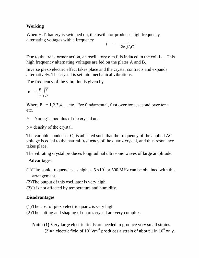
Working
When H.T. battery is switched on, the oscillator produces high frequency
alternating voltages with a frequency
Due to the transformer action, an oscillatory e.m.f. is induced in the coil L3. This
high frequency alternating voltages are fed on the plates A and B.
Inverse piezo electric effect takes place and the crystal contracts and expands
alternatively. The crystal is set into mechanical vibrations.
The frequency of the vibration is given by
n = 2
P Y
l
Where P = 1,2,3,4 … etc. For fundamental, first over tone, second over tone
etc.
Y = Young‟s modulus of the crystal and
ρ = density of the crystal.
The variable condenser C1 is adjusted such that the frequency of the applied AC
voltage is equal to the natural frequency of the quartz crystal, and thus resonance
takes place.
The vibrating crystal produces longitudinal ultrasonic waves of large amplitude.
Advantages
(1) Ultrasonic frequencies as high as 5 x10⁸ or 500 MHz can be obtained with this
arrangement.
(2) The output of this oscillator is very high.
(3) It is not affected by temperature and humidity.
Disadvantages
(1) The cost of piezo electric quartz is very high
(2) The cutting and shaping of quartz crystal are very complex.
Note: (1) Very large electric fields are needed to produce very small strains.
(2)An electric field of 104 Vm-1 produces a strain of about 1 in 108 only.
1 1
1
2f
LC

Applications of Ultrasonic Waves in Engineering
1) Detection of flaws in metals (Non Destructive Testing –NDT)
Ultrasonic waves are used to detect the presence of flaws or defects in the form
of air cracks, cracks, blowholes porosity etc., in the internal structure of a
material
By sending out ultrasonic beam and by measuring the time interval of the
reflected beam, flaws in the metal block can be determined.
(2) Ultrasonic Drilling
Ultrasonics are used for making holes in very hard materials like glass, diamond
etc.
(3) Ultrasonic welding
• The properties of some metals change on heating and therefore, such metals
cannot be welded by electric or gas welding.
• In such cases, the metallic sheets are welded together at room temperature by
using ultrasonic waves. This is called cold welding.
• (4) Ultrasonic soldering
• Metals like aluminum cannot be directly soldered. However it is possible to
solder such metals by ultrasonic waves.
• (5) Ultrasonic cutting and machining
• Ultrasonic waves are used for cutting
• (6) Ultrasonic cleaning
• It is the most cheap technique employed for cleaning various parts of the
machine, electronic assembles, armatures, watches etc., which cannot be
easily cleaned by other methods.

• (7) SONAR
• SONAR is a technique which stands for Sound Navigation and Ranging.
• It uses ultrasonics for the detection and identification of underwater objects.
• The method consists of sending a powerful beam of ultrasonics in the
suspected direction in water.
• By noting the time interval between the emission and receipt of beam after
reflection, the distance of the object can be easily calculated.
• The change in frequency of the echo signal due to the Doppler Effect helps to
determine the velocity of the body and its direction.
Measuring the time interval (t) between the transmitted pulses and the
received pulse, distance between the transmitter and the remote object is
determined using the formula,
2
v td
Where v is the velocity of sound in sea water.
The same principle is used to find the depth of the sea.
Applications of SONAR
• Sonar is used in the location of shipwrecks and submarines on the bottom of
the sea.
• It is used for fish-finding application.
• It is used for seismic survey. Measuring Earths properties by using magnetic,
electric, gravitational, thermal and elastic theories.
• Obstetric ultrasound is primarily used to:
• Date the pregnancy
• Check the location of the placenta
• Check for the number of fetuses
• Check for physical abnormities
• Check the sex of the baby
• Check for fetal movement, breathing, and heartbeat.
Ultrasonics in Research
• Scientists often use in research, for instant to break up high molecular weight
polymers, thus creating new plastic materials.

• Ultrasound is used to determine the molecular weight of liquid polymers, and
to conduct other forms of investigation on the physical properties of materials
such as density and viscosity.
• Ultrasonics can also speed up certain chemical reactions. Hence it has gained
application in agriculture, that seeds subjected to ultrasound may germinate
more rapidly and produce higher yields.
Piezo electric Effect:
If mechanical pressure is applied to one pair of opposite faces of certain crystals
like quartz, equal and opposite electrical charges appear across its other faces. This
is called as piezo electric effect. The converse of piezo electric effect is also true
Explanation: As shown in the figure a mechanical pressure is applied on pair of
Faces. Mechanical pressure is defined as force per unit area. Now it said to be stressed.
Now a change in dimensions of the crystal takes place. Due to this electronic
structure of the crystal changes. As a result of this opposite charges will be
induced on pair of other faces. This phenomenon is called Piezoelectric effect.

Inverse Piezo electric effect:
If an electric field is applied to one pair of faces, the corresponding changes in
the dimensions of the other pair of faces of the crystal are produced. This is
known as inverse piezo electric effect or electrostriction.
Explanation: As shown in the figure an electric field is applied on a pair of
opposite faces of the Quartz crystal. Due to this electronic structure of the
crystal changes.
Here the crystal is strained and there is a stress in the crystal. Due to this
ultrasonic waves are generated.

UNIT-III
QUANTUM MECHANICS
And
SEMICONDUCTORS

QUANTUM MECHANICS
The physical concept of a particle is characterized by mass and velocity.
Experiments dealing with particles, usually interpreted in terms of mass and
Velocity by using Newton‟s Laws of Motion. This classical approach is not
sufficient to describe some experiments. The results of some of the experiments are
contrary to Newton‟s Laws
The experiments like Photo Electric Effect, Black Body Radiation and
Compton Effect confirmed the particle nature of Photons.
Interference, diffraction and Polarization of light confirmed that light is
having wave nature.
Louis De Broglie extended the idea of dual nature of radiation to matter.
According to De Broglie matter possesses wave as well as particle characteristics.
The concept of dual nature of radiation can be understood by knowing relationship
between particle as well as the wave and their characteristics.
Waves and Particles:
PARTICLES WAVES
1. A particle occupies space
2. A particle will have a definite mass
3. The particle will have position
4. Due to change in position of the
particle, it will have velocity.
5. Due to Mass and Velocity , the
particle posses momentum
Momentum P= m X v
6. A Particle will have Energy
1. The transmission of disturbance
from one point to other point in a
material medium is known as
Wave.
2. A Wave will have amplitude
3. It will have time period
4. It will have frequency
5. It will have wave length
6. It will have phase
7. It will have intensity 2AI

The particle and wave nature can be explained by using Planck‟s Quantum Theory.
According to this theory emission of radiation is in the form of photons. A photon
will have velocity of light and mass which is in motion. i.e., it will have both
momentum and energy. Thus a photon behaves like a particle. The energy of a
photon is given by
nhE Where n=1, 2, 3… i.e., the energy of the photon is quantized.
h= Planck‟s constant, Frequency of radiation
Therefore in addition to frequency, the other parameters attribute wave nature to a
photon. i.e., a photon will have dual nature.
The De Broglie Hypothesis:
The dual nature of light possessing both wave and particle properties was
explained by combining plank‟s expression for the energy and Einstein‟s Mass –
Energy relation.
The Energy of a photon according to Plank is given by
E = h ----------------- (1)
Einstein‟s Mass – Energy relation is given by
2mcE ------------------ (2)
Here h= Plank‟s constant
= Frequency of Radiation
m = Mass of Photon
c = Velocity of light
From equations (1) & (2)
2h mc ------------------ (3)
Also the velocity of light is given by
c = λ
=
c ------------------------ (4)
From (3) & (4) we have
2mchc
mc
h

p
h ------------------------------- (5)
Where = wave length of the Photon
p = Momentum of Photon
Using this concept, De Broglie proposed the concept of matter waves.
According to this the material particle of mass „m‟ moving with a velocity
„v‟ should have an associated wave length .
This wave length is called the De Broglie wave length.
Now = momentum
h
= mv
h =
p
h ------------------ (6)
Where h = Plank‟s constant, p=momentum
Equation (6) is known as De Broglie wave equation and is called De Broglie
wave length.
If the particle is moving with a velocity comparable to the velocity of light
then the mass of the particle is always changes. The mass „m‟according to theory
of relativity is not an invariable entity as in Newtonian Physics.The relativistic
mass „m „ is given by Here 0m rest mass of the electron
2
2
0
1c
v
mm
c = Velocity of Light
From equation (6) it is found that if the particles are accelerated to various
velocities, we can produce waves of various wave lengths.
Higher the electron velocity, smaller the De Broglie wave length and vice versa.
Ralation between DeBroglie Wavelength and KiniticEnergy of the particle
Let us assume m is the mass of the particle. Now the particle is moving with
velocity „v‟
Kinetic Energy of the particle 2
2
1mvE
m
pE
2
2
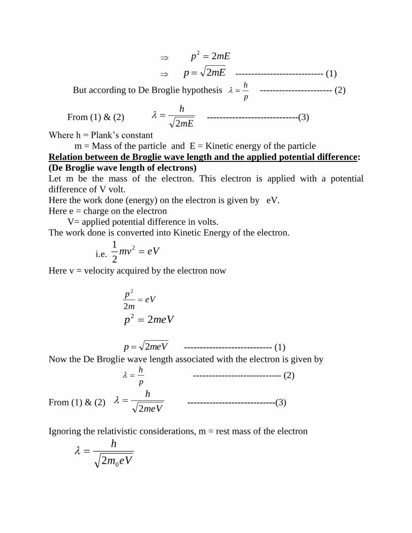
mEp 22
mEp 2 ---------------------------- (1)
But according to De Broglie hypothesis p
h ----------------------- (2)
From (1) & (2) mE
h
2 -----------------------------(3)
Where h = Plank‟s constant
m = Mass of the particle and E = Kinetic energy of the particle
Relation between de Broglie wave length and the applied potential difference:
(De Broglie wave length of electrons)
Let m be the mass of the electron. This electron is applied with a potential
difference of V volt.
Here the work done (energy) on the electron is given by eV.
Here e = charge on the electron
V= applied potential difference in volts.
The work done is converted into Kinetic Energy of the electron.
i.e. eVmv 2
2
1
Here v = velocity acquired by the electron now
eVm
p
2
2
meVp 22
meVp 2 ---------------------------- (1)
Now the De Broglie wave length associated with the electron is given by
p
h ---------------------------- (2)
From (1) & (2) meV
h
2 ----------------------------(3)
Ignoring the relativistic considerations, m = rest mass of the electron
eVm
h
02

Here m=mass of an electron
v=linear Velocity of Electron
r=Radius of the orbit
form (1)&(2) ,now we have
L = mvr = 2
nh………(3)
mv
nhr 2
p
nhr 2
…………..( 4)
mvp , momentum of electron.
34 10
31 19
6.625 10 12.26 10
2 9.1 10 1.602 10
X X
VX X X X V
meter
026.12
AV
V = Applied Voltage in Volts
Matter Waves:
According to Debroglie concept that a moving particle is associated with
wave nature. This can be explained by Bohr‟s atomic model.
The angular momentum (L) of a moving electron in an Atomic orbit of radius „r‟ is
quantized.
i.e. L=2
nh ………………………………(1)
n=1, 2, 3, 4……………
Now Angular momentum L=m v r ………... (2)
In the equation (4), r2 is the circumference
length of the orbit in which the electron is revolving.
Figure (1) Bohr’s orbit and deBroglie
Waves of an electron in the orbit

This circumference is equal to the „n‟ times the wave length of the associated wave
of a moving electron in the orbit.
i.e nr 2 …………………………. (5)
This is shown diagrammatically for n=4 and n=6 in figure (1).
According to the deBroglie, a moving particle will have both particle and wave
nature. The waves associated with a moving material particle are called matter
waves or deBroglie waves. The deBroglie waves are associated with materialistic
particles such as electrons, protons, neutrons etc.
Properties of Matter Waves:
1. DeBroglie waves are not electromagnetic waves.
They are called pilot waves.
The waves that guide the particles are called matter waves or pilot waves.
2. Matter waves consist of a group of waves or a wave packet associated with a
particle. The group has the velocity of particle.
3. Each wave of the group travel with a velocity known as phase velocity given
by Vph =K
where = Angular frequency, K = Wave vector or wave
Number.
4. These waves cannot be observed.
5. The wave length of matter waves is given by
p
h h = Planck‟s constant, p = momentum of the particle
m
h
6. Lighter the particle, greater will be the wave length associated with it.
7. Smaller the velocity of the particle, longer will be the wave length.
8. When ,0V . Also if 0, V

9. Matter waves can be produced whenever the particles in motion are charged
or uncharged.
10. Matter waves travel faster than velocity of light.
11. The wave nature of the matter introduces uncertainty in the location of the
position of the particle.
HeisenBerg’s Uncertainty Principle:
Usually the moving particle must be regarded as a deBroglie wave group rather
than a localized particle.
This suggests that there is a fundamental limit to the accuracy with which we can
measure its particle properties.
According to classical Mechanics, a moving particle at any instant has a fixed
position in space and a definite momentum which can be determined
simultaneously with accuracy.
But we know that a moving particle is similar to a wave, we cannot determine the
position and momentum simultaneously, accurately.
The measurement of position and moment of a moving particle is impossible
Let x denotes the error in the measurements of the position of the particle along
x-axis and p represents the error in the measurement of momentum, then
2
))((h
px Here h=Planks Constant.
If we locate the particle exactly 0x only at the expense of imparting to it
an infinite momentum p
The uncertainty principle can also be written as 2
))((h
tE
Applications:
1. It explains the absence of electrons in the nucleus.
2. It gives proof for the existence of protons and neutrons inside the nucleus
3. Explains uncertainty in the frequency of highest emitted radiation by an
Atom
4. It explains Energy of an electron in an Atom

Differences between Matter waves and Electromagnetic Waves:
Matter Waves Electromagnetic waves
1. These waves are associated with the
moving particles.
2.wavelentgth depends upon mass of the
particle mv
h
P
h
3. Can travel with a velocity greater
than velocity of light.
4. These waves are not electromagnetic
waves.
1.Oscillating charged particles gives
electromagnetic
radiation(electromagnetic waves)
2. Wavelength depends upon the energy
of the photon.
hE ,
cc
hcE ,,
E
hc
3. These waves travel with with a
velocity of light.
C= sm /103 8
4.In this wave electric and magnetic
fields oscillate perpendicular to each
other.
Note on Simple Harmonic Motion :
If a particle executing simple Harmonic motion, then its motion is periodic,
acceleration is directed towards an equilibrium point and acceleration is
proportional to displacement. ( a -x)
The general equation of motion for SHM is given by
y = A Sin (t - ) ……………………………( 1 )
Here y = displacement of the particle executing simple harmonic motion
A = Amplitude of the particle executing simple harmonic motion
ω = Angular frequency

Φ = Phase difference
Now Phase difference =
2 X Path difference
x
2
……………………………………… (2)
From equations (1) & (2) we get
)2
( xtASiny
)2
2( xtASiny
)(2
x
tASiny
Since we have to solve problems by Schrödinger‟s time independent Wave
Equation, we choose wave equation involving no time.
2 ( )x
y ASin
)(2
x
ASiny
)(2
x
ASiny .
Schrodinger’s Wave equation
Let us consider a particle of mass m, moving with a velocity along the positive
X-direction.
The wave function for a particle moving freely in the positive x-direction
has the same form as the wave equation for simple harmonic motion and simple
harmonic waves in the positive x-direction.
)(2
x
ASin …………………….(1)
Here is a function of x only.
Differentiating equation (1) with respect to x once and two times, we get
xA
dx
d 2cos
2
Again differentiating, we get

xA
dx
d 2sin
42
2
2
2
.
xA
dx
d 2sin
42
2
2
2
But
xA
2sin
2
2
2
2 4
dx
d ……………………………..(2)
DeBroglie wavelength associated with the particle is
mv
h
h
m
1
2
2
2
22 )2/1(21
2 h
mvm
h
vm
………………….(3)
Let E be the total energy of the particle and V be the potential energy of the
particle and T be the kinetic energy.
Then total energy ,E=T+V
T, KE = 2
2
1mv = E – V ……………………………….(4)
Substituting the above value of K.E. in Equation (3), we get
2
)(212 h
VEm
……………………………(5)
From equations (5) and (2), we get
)(8 2
22
2
VEh
m
dx
d
0)(8
2
2
2
2
VEh
m
dx
d
0)(
4
2
2
22
2
VE
h
m
dx
d

0)(
)2
(
2
22
2
VE
h
m
dx
d
0)(2
22
2
VEm
dx
d
( )
2(
h ) ………………….(6)
This is the Schrödinger‟s time independent one dimensional wave equation.
Wave number:
In Spectroscopy In wave mechanics
wave Number of an Electromagnetic
wave is given by
1K , But
p
h
h
P
P
hK
)(
1
12 mh
mEK
For the special case of an
electromagnetic wave,
2K .
hC
hE
E
hC
hC
EK
2
C
EK
Wave velocity:
Wave velocity is defined as the velocity with which a particular
crest or trough or a particular phase of a wave advances in a medium.
The wave Velocity u of the matter waves can be obtained from the energy of
photon.
Now hE ……………………………….(1)
Or frequency, h
Xm
p
h
mv
h
E 1
2
)( 222
1
Multiplying and dividing the numerator and the denominator by h, we get
Frequency, 22
2 1
22 X
m
h
h
pX
m
h ……………..(2)

There fore, the wave velocity,
u = frequency X wave length
u
XXm
h2
1
2
The wave velocity of the electron
m
hu
2 ……………………………(3)
Physical Significance of Wave Function
The wave function is a Complex function. This does not have a direct
physical meaning. The square of its absolute magnitude 2
can be taken as
definite meaning by considering the case of an electromagnetic wave.
The intensity of a light wave is proportional to the square of the amplitude.
(2AI )
2 Is the probability density of the particle associated with the deBroglie wave
described by the wave function .
That is the probability of finding a particle is proportional to2
at the point x,
and at any instant of time t.
The wave function is given by
( )x a ib , * is its complex conjugate,
* = iba
Now * = ( iba ) ( iba ).
* = 22 ba ,
* is denoted by P
2 is called the probability density.
The probability of finding a particle is real.
The probability of a particle being present in a volume dx dy dz is 2
dx dy dz.
The total probability of finding the particle somewhere is unity.

Since the probability of finding a particle somewhere in the space is certain.
12
dxdydz
Or 1*dxdydz
The triple integral extends overall possible values of x, y and z.
A wave function satisfying the above relation is known as normalized wave
function.
Particle in a One-Dimensional Potential Box:
(OR Electron in a Potential Well): Consider an electron of mass „m‟ this is bound to move in a one dimensional
crystal of length L.
The electron is prevented from leaving the crystal by the presence of a large
potential energy barrier at its surface.
Though the barriers extend over a few atomic layers near the surface, these are
taken infinitely large for the sake of simplicity. The problem is similar to that of
an electron moving in a one-dimensional potential Box.
This is represented by a line and is bounded by infinite potential energy as shown
in figure (2).
Fig (2) Electron in a one dimensional
Potential well.
The potential energy within the crystal or box is assumed to be zero
Thus we have
V(x) = 0 for 0<x<L ………………… (1)
V(x) = for Landxx 0
The wave function n of the electron occupying the nth
state is given by

0)(2
22
2
nnn VE
m
dx
d
…………… (2)
Here also En= Total energy of the electron in the nth state.
V= Potential energy.
Inside the box, v=o
02
22
2
nnn E
m
dx
d
-------------------------- (3)
02
2
2
nn k
dx
d
------------------------------- (4)
Where 2
2
2n
mk E
nEmk
2 --------------(5)
Equation (4) is a differential equation. The general solution of the equation (4) is
given by
BCoskxASinkxxn )( ……………………………….. (6)
In equation (6), A and B are arbitrary constants,
These constants are to be determined from the boundary conditions.
Since the electron is constrained by infinitely high potential barriers at x=0 and
x=L, v . We assume that (0) 0 ( ) 0n nand L
The product V(x) n (x) in equation (2) also approaches infinity.
Thus in order that the wave function n (x) may be continuous, the kinetic energy
must also become infinite which is not feasible.
Hence n (x) must vanish for x=0 and x=L.
For x=0 equation (6) gives B=0
0=A SinK (0) +B CosK (0)
0=A (0) +B (1)
B=0
Now equation (6) becomes
n (x)=A SinK(x) -------------------------------- (8)
Also since n (L) =0, equation (8) becomes
A SinKL=0
0A But SinKL=0 nKL
Or K=L
n …………………………………….(9)

Where n=1, 2, 3…
Thus the expression for the allowed wave function becomes.
n (x)=A Sin (L
n ) x ……………………. (10)
Eigen Energy Values:
The allowed energy values can be obtained from equations (5) & (9) as
nEmk
2
L
nEmk
n
2
2
2
2
L
nEm n
22
2
L
n
mEn
2
222
2 L
n
mEn
2
22
2
2
24 L
n
m
hEn
2
22
8mL
hnEn …………………… (11)
i.e En n2
Some Features:
1. The lowest energy of the particle is given putting n=1
2
2
18mL
hE
1
2EnEn
This known as zero point energy.
2. For n=1, 2, 3…We get discrete energy values of the particle in the one
dimensional box.

2
2
18mL
hE
12
22
2 48
2 EmL
hE
12
22
3 98
3 EmL
hE
…………………….
3. It is apparent from equations (10) and (11) that the allowed wave functions
n (x) and the allowed energy values nE exist only for integral values of n.
The number n is called quantum number.
4. The spacing between the nth energy level and next highest energy level
[n+1] th level is given by
1
2
2
22
1 )1(8
)1(En
mL
hnEn
1
2
2
22
8En
mL
hnEn
1
2
1
2
1 )1( EnEnEE nn
1
2
1
2
1 )21( EnEnnEE nn
11 )12( EnEE nn
5. The energy spectrum consists of discrete energy levels. The spacing between
the levels is determined by the values of n and L.
The Spacing decreases with increase in L.
If L is of the order of a few centimeters, the energy lever from almost a continuum.
But if L has atomic dimensions, the spacing between the levels becomes
appreciable.
The energy levels corresponding to n=1, 2, 3 and 4 are shown in fig (3).
E4 n=4
E3 n=3
E2 n=2
E1 n=1
E0 n=0
Fig (3) First four energy levels of an electron in a one dimensional Box.

Determination of constant A in n (x)=A Sin (L
n )x (Normalization of the
wave function):
The constant A in n (x) =A Sin (L
n )x is determined by using the condition that
the probability of finding an electron some where on the line is unity
1)()(..0
* dxxxei n
L
n
1|)(|0
2 dxx
L
n
10
22
dxx
L
nSinA
L
10
22
dxx
L
nSinA
L
12
21
0
2
dx
xL
nCos
A
L
12
220 0
22
dxx
L
nCos
Adx
AL L
Now 02
0
dxx
L
nCos
L
12
0
2
dxA
L
12
][2
2
0
2
LA
xA L
L
A22
LA
2
Now from the equation xL
nSinAxn
)(
xL
nSin
Lxn
2)( …............ (1)
This is the normalized wave function. The first four wave functions and the wave functions of the
electron in a one dimensional Box are shown in the figure (4)

Fig (4) First three wave functions Fig.(5) the probability density of
of an electron in a one an electron in a one dimensional
dimensional box
The probability density of the particle in the one dimensional Box.
The probability of finding the particle in a small length dx along x is given
bydxAdxxP nn
2||)(
dxxPn )( dxxL
nSin
L
22
Also Probability Density xL
nSin
LxPn
22)(
This is maximum when ,2
5,
2
3,
2
x
L
n
,2
5,
2
3,
2 n
L
n
L
n
Lxor
For n=1, the most probable positions of the particle is at x=2
L
For n=2, the most probable positions are at x=4
L and
4
3L
The probability density of the particle in the one dimensional Box is shown for
various values of „n‟ in the figure (5).
Fermi-Dirac Distribution:
According to free electron theory, Electrons in a solid move in all possible
directions like gas molecules in a container. These free electrons contribute for
electrical conduction.
The free electron model of a metal has survived to the actual situation in
metals, particularly the monovalent atoms such as Alkali metals.
Quantum mechanics requires that all valence or free electrons should be specified
by the three quantum numbers nx , ny , nz together with the spin.
The spin can have either 2
1 or
2
1
The Pauli Exclusion Principle does not permit more than one electron to have same
four quantum numbers.
Many of the occupied states in a metal containing 1023
free electrons must be
described with fairly large quantum numbers.
Now it is most convenient to discuss the metallic state with statistical mechanics.
The probability that a particular quantum state having an energy E is occupied is
given by Fermi-Dirac function.
TK
EfEEf
B
exp1
1)(
Here f (E) is called probability of occupying a state
EF is the energy of the Fermi level.
E is the energy of the state in which the electron is occupied at T K0 .
BK is the Boltzmann constant.
Properties:
1. The Fermi-Dirac function also valid for semiconductors. In a
semiconductor, the probability of occupancy of states by electrons is given
by the F-D distribution function.
TK
EfEEfEP
B
e
exp1
1)()(
2. The distribution function is valid only in equilibrium.
3. The Fermi level is absolutely valid in equilibrium only.
4. Fermi-Dirac distribution function is valid for all the particles obeying
Pauli‟s exclusion principle. This is equally applicable regardless of the type
of the solid, doping of the semiconductor, etc.

Any particle obeying F-D distribution function is called Fermions.
The Fermi-Dirac distribution function considers statistically the entire collection of
fermions in the volume.
Thus it considers all electrons in the semi conducting solid and not merely
electrons in a Band.
5. An empty electron state is called a HOLE. The Fermi-Dirac distribution
function for holes in the solid would correspond to the statistical distribution
of vacant sites.
The hole distribution function is denoted as
Ph (E) =1-PFD (E)
TK
EEEP
B
f
h
exp1
1)(
6. AT E = Ef,
2
1
11
1)()(
EPEP eh
i.e. the probability of occupancy of the electron or hole is 2
1
This also gives a definition for the Fermi level.
7. Fermi level is the energy level where the probability of occupation is 2
1
8. At 00 K, Pe (E) =1 for E E f
And Pe (E) = 0 for E > E f
This implies that at 00 K all states up to the Fermi level are completely occupied by
the electrons. All the states above the Fermi level are empty.
9. The distribution function is a strong function of temperature only at energies
close to Ef.
Plots of Pe (E) and E at different temperatures are shown in figure (6).
Y T
T2>T1>T in 0 K
T1
P(E)
T2
1/2
X
O E Ef

Fig (6). Pe (E) versus E for various T values. At all temperatures, the curves
passes through the point 1
,2
fE
.
Note on Fermi-Dirac Distribution function: The Fermi-Dirac distribution for
Electrons is given by
TK
EEEfEP
B
F
e
exp1
1)()(
Now at the Absolute zero (T = 00K ), there are two situations
(i) For E < EF ,
TK
EEEP
B
F
e
exp1
1)(
)0(1
1)(
BK
Xe
e
EP
eEPe
1
1)(
e
EPe 11
1)( But 0
1
e
Pe (E) = 1, for E < EF at T = 00
(ii) For E > EF
TK
EEEP
B
F
e
exp1
1)(
)(exp1
1)(
oK
XEP
B
e
eEPe
1
1)(

1
1)(EPe
1)(EPe
0)( EPe
This means that no electrons have energy greater than EF at 00 K.
i.e the Fermi energy EF is the maximum energy that a free electron in the metal can
have at absolute zero.

SEMICONDUCTORS
Semiconductors and classified basing on their conductivities and resistivity‟s.
Electrical resistivity of semi conductors lies in between those of conductors and resistors.
In semiconductors, there are two types of carriers namely semi conductors and holes.
Hence semiconductors are bipolar.
The current in semiconductors is due to two types of carriers namely electros and holes.
Pure semi conductors are known as intrinsic semiconductors.
Example : Silicon and Germanium.
The electrical conductivity can be enhanced by a process called doping. i.e. the number of
carriers can be increased by a process called doping. Doping is the process of adding an
impurity to a pure semi conductor. By adding a suitable impurity to an intrinsic semi conductors,
it will become an extrinsic semi conductor. The transportation of charge carriers (movement)
takes place due to drift and diffusion.
The extrinsic semi conductors are widely used in solid state electronic devices and semi
conductor electronic devices.
To study electronic devices, it is important to study the fundamental electronic transportation
properties in semi conductors.
Intrinsic semi conductors
Usually pure semi conductors are known as intrinsic semi conductors. Examples are
Silicon (Si) and Germanium (Ge) Silicon (Si) and Germanium belongs to IV group of periodic
table.
Atomic Number of Silicon is 14.
Electronic configuration 1s2 2s
2 2p
6 3s
2 3p
2
Atomic number of Germanium is 32.
Atomic number of Germanium is 32.
Electronic configuration is
1s2 2s
2 2p
6 3s
2 3p
2 3p
6 3d
10 4s
2 4p
2
In Silicon and Germanium, there are four valence electrons. Bonding in these semiconductors is
covalent bonding.
Each silicon Atom forms four covalent bonds with the surrounding from neighboring Silicon
atoms in the silicon Semiconductor crystal.
Here no electrons are available freely for conduction and the semi conductor acts like an
insulator.
The conduction process can be understood with the help of energy bond diagram.
In the energy bond diagram, we have conduction bond and valence bond.

The conduction bond and valence bond are separated by a forbidden energy gap Eg., known as
energy and gap. The bond representation and the energy band structure is shown in figure (1) at
O0K.
At O0K, all valence electrons are tightly bound to their atoms and are taking part in covalent
bond formation.
For Silicon Eg = 1.12 ev.
Germanium Eg = 0.69 ev.
In the figure (1) a Ec= Energy level corresponding to Bottom of the conduction bond.
Ev = Energy of the energy level corresponding to the top of the
Valence bond.
Ef = Fermi energy level.
At O0K, the valence bond is completely filled and the conduction bond is empty.
At O0K, the semi conductors behave like insulators.
Above O0K (i.e. At Room temperature), the valence electrons acquire sufficient amount of
thermal energy. Due to this they break the covalent bonds and make themselves available as free
electrons. Against to creation are free electron, a vacancy is created in its initial position in the
crystal structure. This vacancy is known as a hole.
The hole is a virtual positive charge, having the magnitude of charge of the electron.
The free electrons after acquiring sufficient thermal energy, and closes the energy gap.
These electrons will enter into the conduction band from valence bond and occupy
energy levels in the conduction bond.
The electrons leaving the valence bond create holes in its original place.
Now the valence bond will have holes and the conduction bond contains electrons.
The crystal structure and energy bond structure above O0K is shown in figure (2).
Si
Si
Si
Si
Si
Si
Si
Si
Empty
EC
EF
EV
Egg
Conduction bond
Valence bond
(filled)
Fig. (1)a: Intrinsic silicon at O0k –
Two dimensional Representation.
Fig (1)b: Energy band structure of Intrinsic
Semiconductor Silicon at O0k.

In an intrinsic semi conductor,
Number of holes = No. of electrons = ni.
n=p=ni ;
n = Number of electrons per unit volume (or) electron concentration (or) electron density.
p = Number of holes per unit volume (or) hole concentration (or) hole density.
n; = Intrinsic concentration.
Now np = ni2
Intrinsic carrier concentration
Above O0K, in an intrinsic semi conductor, each broken bond leads to generation of two carriers.
They are electron and hole.
At any temperature T, the number of electrons generated will be therefore equal to the number of
generated Holes.
Let n = Number of electrons per unit volume or electron concentration in the
conduction bond.
P = Number of holes per unit volume or Hole concentration in the valence bond.
For an intrinsic semiconductors;
n = p = ni ; --- (1)
Where ni = intrinsic carrier concentration.
Now the electron concentration in the conduction band is given by
/
/
c F B
F C B
E E K T
c
E E K T
c
n N e
n N e
--- (2)
The Hole concentration in the valence bond is given by
/
/
F V B
V F B
E E K T
v
E E K T
v
P N e
n N e
--- (3)
Here ,c VN N are known as pseudo constants, depends on temperature.
Free electron
Broken bond
Vacant site (hole)
Si
Si
Si
Si
Si
Si
Si
Si
Si
Figure (2) a: Two dimensional crystal structure of
intrinsic semi conductor silicon above O0K
EC
EF
EV
Electron
Hole
Electron
Conduction bond
Eg
Figure (2) b: Intrinsic Silicon – Energy band
structure above O0K.
BK = Boltzmann constant
T = Temperature in 0K of the intrinsic semiconductor.
Now 2
in np
/ /2 .F C B V F BE E K T E E K T
c Vni N e N e
2
F C V F
B
E E E E
K T
cni N e
2
2
2
F C
B
F C
B
g
B
E E
K T
c V
E E
K T
c V
E
K T
c V
ni N N e
ni N N e
ni N N e
Where c vE E Eg
1/ 2
2c v
B
Egni N N e
K T
---- 4
From equation (4), It is clear that
i) Intrinsic carrier concentration is independent of fermilevel.
ii) Intrinsic carrier concentration in is a function of temperature T.
iii) Intrinsic carrier concentration in is a function of Energy gap Eg.
Fermi level expression
The Fermi level is the top most occupied energy level. The Fermi level indicates the probability
of occupation of energy levels of the electrons in conduction and valence bands.
In intrinsic semiconductors, electron and hole concentrations are equal.
i.e. it indicates that the probability of occupation of energy levels in conduction bond and
valence bond are equal.
Usually in an intrinsic semiconductors, the Fermi level lies in the middle of the energy gap Eg.
For an intrinsic semiconductors, n=p.
Now
/
/
c f B
c f B
E E K T
c
E E K T
c
n N e
n N e
---(1)
/f v BE E K T
vp N e
/V f BE E K T
vp N e
--- (2)
Equations (1) and (2) represent electron and hole concentrations for intrinsic semiconductors.
Since n=p. / /f c B v f BE E K T E E K T
c VN e N e
f c
V BT
v fC
BT
e E E
N K
E ENe
K

.
f c v fV
C BT BT
e E E E ENe
N K K
f c v fV
C BT
e E E E EN
N K
2 /f c v BTE E E KV
C
Ne
N
--- (3)
Taking Naparian Logarithm an both sides.
2 /log C BTe EF E EV KV
e e
C
NLog
N
2log
CVe
C B
EF E EVN
N K T
2 log
2 log
log2 2
VF C V B
C
VF C V B
C
C V VBF
C
NE E E K T
N
NE E E K T
N
E E NK TE
N
For an intrinsic semiconductor * *me mn
Hence V eN N
log 12 2
2
C V BF
c VF
E E K TE
E EE
Therefore Fermi level lies exactly midway between
conduction bond and valence bond.
Expression for intrinsic conductivity
Let us consider intrinsic semiconductors. This is
applied with a potential difference of V volts. Electric field
Fig. 3 Conduction in an intrinsic semiconductor
Electron flow
Hole flow
+ -
v

Due to the applied voltage an electric field E
will be established as shown in the figure.
Now the charge carriers drift as indicated in figure (3). This constitutes an electric current I.
The drift velocity acquired by the charge carriers is given by.
dV E ---- (1)
Where = Mobility of charge carriers.
Also the current density due to drift of electrons is given by
n dJ nev ---- (2)
Where n= electron concentration
E = charge on the electron.
dv = drift velocity of the electrons.
Also /n nJ ne E ---- (3)
Where n = Mobility of electrons.
Current density Current I
J= =Area ^
Also the holes will drift in a direction opposite by electrons, the hole current density is given by
pJ e Pp E ----- (4)
Where p = Hole concentration.
e = charge on the hole.
p = Mobility of holes.
Now the total current density is given by
n p
n
n
J J J
J ne E Pe pE
J n P p eE
----- (5)
But according the classical theory, ohms law is given by
J E ---- (6)
Where = Electrical conductivity
From equations (5) and (6), we have
n
n
E n P p eE
n P p e
But according to law of mass Action, for an intrinsic semiconductors in p n
n ini n p e
i nn e n p ---- (7)
Where in = Intrinsic concentration.
But 1/ 2 / 2 BEg K T
i C Vn N N e ---- (8)
Substituting (8) in (7), we get
1/ 2 / 2 BEg K T
C V n pN N e e

Electrical conductivity for intrinsic semi conductors is given by / 2 BEg K TAe ---- (9)
Where 1/ 2
C V n pA N N e
A = a constant
Determination of Energy Gap (Eg) for intrinsic semiconductors
The energy gap between the conduction Band and the valence bond is represented as band gap
Eg. For intrinsic semi conductors, the energy gap is given by
/ 2 BEg K TAe ---- (1)
Where A = a constant
Eg= Energy band Gap.
KB= Boltzmann constant.
T = Absolute scale of temperature.
Let P = Electrical Resistivity.
1
P
/ 2
1BEg K T
PAe
/ 21BEg K TP e
A
/ 2 BEg K TP Be ---- (2)
Where1
BA
, a new constant.
Taking Neparian logarithm an both sides,
/ 2log log BEg K T
e ep Be
/ 2log log log BEg K T
e e ep B
ln ln2 B
Egp B
K T
ln ln2 B
Egp B
K T --- (3)
Where m = shape of the straight line
From figure (1), 2 B
Eg ym
K x
2 B
yEg K
x
---- (4)
If a graph is plotted between 1
T an X-axis and ln
an y-axis, a straight line graph is obtained. The
straight line graph is shown in figure (4).
Extrinsic semi conductors
O X
Y
∆y
∆x
ln
1/T
Fig 4: Plot of 1/T and ln

Extrinsic semi conductors are an impure semiconductors. With the addition of impurities, a pure
semi conductors becomes an extrinsic semiconductors, a pure semi conductors becomes an
extrinsic semi conductors.
An extrinsic semi conductor shows good conducting properties due the presence of impurities.
Depending on the type of impurity present in the intrinsic semi conductors, extrinsic semi
conductors are classified into two types.
1) N – type extrinsic semi conductors. 2) P - type extrinsic semi conductors.
N-Type semi conductors
For silicon if a small amount of pentavalent impurity such as phosphorous, arsenic or antimony
or Bismuth is added, we get N-type semiconductors.
Four valence electrons of phosphorous form covalent bonds with the adjacent four silicon atoms.
The fifth electron is left free. It cannot form bond with any other electron in the lattice structure.
This is shown in figure (1).
At O0k, this fifth electron is bond to phosphorous with 0.045 ev.
The corresponding energy Band diagram and lattice structure are shown in figure (1) at O0k. At
O0k, the valence Bond and the conduction band are separated by an Energy Gap Eg.
The donor energy level Ed lies below the bottom of conduction band. This donor energy level
contains phosphorous atoms. Which denotes electrons at T>O0k The donor energy level in
shown in the figure (1) b. Above O0k, when temperature is increased. The 5
th bond electron
becomes a free electron. This free electron enters into the conduction band. Due to this the Donor
Atoms will get ionized, by denoting an electron to the conduction band. When temperature is
further increased, the covalent bonds will break down. Here electron hole pairs will be generated.
Electrons will move from valence bond to conduction bond, leaving holes in the valence bond.
At higher temperatures, the energy band diagram of N-type silicon is shown in figure (2)
The Fermi level varies as shown in fig (2) b at 3000k.

Figure (5)a: N-type silicon at O0k
Now the concentration of electrons increases in the conduction bond when compared to holes.
Hence the electrons become the majority charge carriers and holes the minority charge carriers.
The variation of Fermi level is also shown in figure 2( b).
P-type semi conductors
For silicon if a small amount of trivalent impurity such as indium, Gallium, Thallium or
Aluminum or Boron is added, we get an Fi- Type semi conductors.
Three valence electrons of Boron form covalent bonds with the adjacent three silicon Atoms.
There is not fourth electron to form a covalent bond with the neighboring silicon atom. This is
like a missing bond. This is represented as a missing electron or vacant site.
5th
electron
Si
Si
Si
Si
Si
Si
Si
P
Si
P=Phosphorous
Conduction bond
Valence bond
Ec
Ev
vc
Ed Donor levels
Eg
Ef
Figure (1) b: Energy band diagram of N-type
semiconductor at O0k
Figure (2)b: Energy band diagram of N-type silicon at
T=3000K and above
Figure (2)a: Energy band diagram of N-type semiconductor
at T>O0k
+ve
Donor
ions
Conduction Band
Ec
Valence bond
Ed
Ei
Ev
Ef
+ve
Donor
ions
Conduction Band
Ec
Valence bond
Ed
Ei
Ev
Ef

This is shown in figure (1)
Fig. (1)a: P-type silicon at O0K fig.(1)b: Energy band structure of P-type
silicon at 00k
This missing electron is called Hole. The energy B and structure of P-type semi conductors is
shown in figure (1) b.
At O0k, the conduction Band is empty and the valence B and contains electrons.
The acceptor energy level EA is just above the top of the valence Band.
Acceptor energy level EA contains the acceptor atoms.
Here cE = Bottom of the conduction band.
VE = Top of the valence band.
iE = Intrinsic energy level.
The Energy band structure of P-type silicon is shown in figure (2) a above O0k.
When the temperature is above O0k, the covalent bonds with the silicon are broken down.
Si
Si
Si
Si
Si
Si
Si
B
Si
Vacant site
Vacant site
(hole)
Hole
Conduction bond
Valence bond
EC
EA
EV
Acceptor level
Ei
Acceptor level
contains acceptor
atoms
Ef
Eg

Fig.(2)a: Energy band structure of P-type silicon at O0k
Here same electrons are released and the acceptor atoms accept three electrons and there by they
become negatively charged ions. There are called negative acceptor ions. Here the Fermi energy
level lies just above the top of the valence bond and below the acceptor level.
The energy band diagram of P-type semi conductors is shown in the figure (2) b. at T = 3000k.At
3000k, the bands in silicon with further breakdown and the electrons will move from valence
band to conduction band. Therefore electrons are available in the conduction band. At 3000k the
Fermi level varies as shown in the figure.
Fig.(2)b: Energy band diagram of P-type silicon at 3000k
Law of Mass Action
The electron concentration in intrinsic semi conductors is given by
/c fE E
c Bn N e K T
/f cE E
c Bn N e K T
---- (1)
Similarly in an intrinsic semiconductors, the hole concentration is given by
/f cE E
v BP N e K T
/v fE E
v BP N e K T
---- (2)
Where cN and vN are pseudo constants.
Conduction band
Ec
EA
Ev
Valence band
Ei
EF
Holes
Eg
EF= Fermi energy level
Conduction band
Ec
EA
Ev
Valence band
Ei
EF
Holes
Eg
EF= Fermi energy level

BK is the Boltzmann constant.
T is temperature in 0K.
EF is the energy of Fermi level.
EC is the bottom of the conduction band.
Ev is the top of the valence band.
In an intrinsic semiconductors n=p=ni
/ /.f c B v f BE E K T E E K T
c vnp N e N e
/ /2
/2
/2
.
Where
f c B v f B
f c B
B
E E K T E E K T
c v
E E K T
c V
Eg K T
c V c v g
np ni N e N e
np ni N N e
np ni N N e E E E
1/ 2 / 2 BEg K T
c vni N N e --- (3)
The above relation shows that for any arbitrary value of Eg the product of n and p is a constant.
This is known as Law of Mass Action
For an extrinsic semiconductors, the electrons and hole concentrations are given by expressions
similar to Equations (1) and (2)
For an N-type semiconductor
/f c BE E K T
n cN N e
----- (4)
/v f BE E K T
n vP N e
----- (5)
Where nn Electron concentration.
nP Hole concentration.
Now / /
.f c B v f BE E K T E E K T
n n C V vN P N N e N e
/f c BE E K T
n n C Vn P N N e
/g BE K T
n n C Vn P N N e
------ (6)
Where c v gE E E
2
n nn P ni ---- (7)
The above expression (7) is known as Law of Mass action for N-type semi conductors.
For P-type semi conductors, the law of mass action is given by
2
p pp n ni ----- (8)
Equations (7) and (8) imply that the product of majority and minority carrier concentrations in
extrinsic semi conductors at a given temperature is equal to the square of Intrinsic carrier
concentration at that temperature.
The law of mass action is very important in conjunction with charge neutrality condition.. This
enables us to calculate minority carrier concentration. This law states that the addition of
impurities to intrinsic semi conductors increases the concentration of one type of carrier, which

consequently becomes majority carrier and simultaneously decreases the concentration of the
other carriers, which is known as the minority carrier.
The minority carriers decrease in number below the intrinsic value.
This is because there is an increase of majority charge carriers Recombination rate.
According to the law of Mass action, the product of majority and minority carriers remains
constant in an extrinsic semi conductors and it is independent of the amount of donor and
acceptor impurity concentrations. When the doping concentration levels are high, the minority
carrier concentration will be law and the majority carrier concentration will be high when the
doping concentration levels are low, the majority carrier concentration is low and the minority
carrier concentration is high.
Hall Effect
Some times it is necessary to determine whether a material is n-type or p-type. Measured
conductivity of a specimen will not give this information since it cannot distinguish between
positive hole and electron conduction.
The Hall Effect can be utilized to distinguish between the two types of carriers, and it is also
useful in the determination of density of charge carriers.
Hall Effect definition
“If a piece conductor (metal or semiconductor) carrying current is subjected to a transverse
magnetic field, an electric field is generated inside the specimen in a direction normal to both the
current and the magnetic field”
This phenomenon is known as Hall Effect. The generated voltage is known as Hall
Effect. The corresponding electric field is known as Hall Effect field.
Let us consider a sample having thickness t and with b. the sample is a rectangle sample,
as shown in the figure.
Figure (1) Hall effect
Assuming that the material is an n-type semiconductor, the current flow consists of
almost due to electrons, moving from right to left.
This corresponds to the direction of conventional current from left to right as shown in
figure (1).
I t
y
z
F
I or Ix
Electrons
experience a
force F in the
down ward
direction due to
B
X
B
Face (1)
Face (2)
b
Fig (2) Motion of electrons in an n-type
semiconductors
eEH
Be

Current I is in the positive X-direction and the magnetic field B is applied in the positive Z
direction. According to Flemings, left hand Rule, The electrons experience a force, called
Lorentz force. This Lorentz force acts in the negative Y-direction.
Now Lorentz force vLF B E
sinLF Bev
Where v = velocity of electrons.
Since the velocity of electrons and B are perpendicular downwards in the negative Y-direction
and the positive charges drift upwards in the positive Y-direction. As a consequence, the lower
surface collects negative charge and upper surface becomes positively charged. Due to this an
electric field called Hall electric field will be established between upper and lower surface of the
specimen.
This hall electric field EH establishes a potential called the Hall Voltage VH.
The hall field EH exerts an upward force FH on the electrons as shown in figure (2).
H HF eE ---- (2)
But total force on the electrons, is given by
0HBev eE ---- (3)
The above equation is called Lorentz equation. Under equilibrium conditions.
HE Bv ---- (4)
Now the current density in the X-direction is given by
xJ nev ----- (5)
Now (5) nJv
ne ---- (6)
Here n = electron density (electron concentration)
E = charge on the electrons.
Now from (4) and (6),
xH
BJE
ne ------ (7)
Now the Hall coefficient RH can be described as follows.
For a given semiconductor electron concentration n is constant and charge on the electron e is
constant.
H xE BJ
H H xE R BJ ----- (8)
Where HR is a constant of proportionality.
1
HRne
----- (9)
Here ,HE B and xJ are measurable. Hence hall coefficient HR and carrier density „n‟ can be
found.
Determination of Hall coefficient
Let t be the thickness of the rectangles slab.
b be the width of the sample.
Now the Relation between HE and HV is given by
H HV E t ----- (10)

Also (8) H H xE R BJ ----- (8)
Now from (8) and (10), we get
H H xV R BJ t ----- (9)
But xJ = current density
xx
IJ
A , x
x
IJ
bt (Since A = Area of cross section
A = bt)
Equation (9) becomes
xH H
IV R B
b t t
xH H
I BV R
b
HH
x
V bR
I B ----- (10)
HV , b , xI and B all are measurable and substituting them in equation (10), we can obtain the
value of Hall coefficient HR .
Note that the polarity of HV will be opposite for n and p type semiconductors.
Carrier concentration and mobility
Hall coefficient 1
HRne
1
HRne
(Magnitude)
Electron concentration 1
H
nR e
can be determined.
Now electrical conductivity ne .
Where mobility
Mobilityne
HR
For a P-type material Hall coefficient is positive.
1HR
pe
Where p= hole concentration.
Application of the Hall Effect
1. Useful in determining whether the given semiconductor is n-type or p-type.
2. Hall Effect can be used to find the carrier concentration and mobility of carriers.
3. Hall Effect is used to measure the magnetic field.
4. Hall Effect semi conducting devices are used as sensors to sense the magnetic fields.
5. The Hall Effect is used in magnetically activated electronic switches. They are used as
non contacting key boards and panel switches.

PN Junction
When a P type material is suitably joined with an n type material, a Pn junction is formed.
When an intrinsic semi conductors is simultaneously doped with P-type and n-type
impurities, a Pn junction is formed.
The Pn junction may be formed by crystal growth or alloying or diffusion method.
The plane dividing the two zones is called Pn junction.
The Pn junction is shown in figure (1)
+ ve ionized Donors
- ve ionized Acceptor
+ Hole
- Electron
Fig (1) b: Diffraction of electrons and holes
Fig (1) a: a Pn junction
VB Holes
Electrons
Co
nce
ntr
atio
n
Electrons
1024
1020
1016
X
Y
X
Fig (1) c: Space charge region for an alloy or abrupt
junction
Space charge region
X Fig (1) d: Electric field due to space charge region Electric
field E
X Fig (1) e: Barrier potential (or) contact
potential Voltage V
x2
v1
VB x1
v2
Space
charge
density ---
+
P
n
E
+
+
+
+
+
-
-
+ + -- --
+ + -- - -
-- --

In the p side „+‟ represents holes. In the n side „-‟ represents electrons.
In the n-side there is a high concentration of electrons.
In the P- region there is a high concentration of holes.
Therefore, at the junction there is a tendency for the electrons to diffuse from n-region to p-
region and holes from p-region to n-region. This process is called diffusion. When the free
electrons move across the junction from n-side to p-side. The demotions become positively
charged. Hence a not positive charge is built on the n-side of the junction.
The free electrons that cross the junction uncover the negative acceptor ions by combining with
the holes.
Therefore a not negative charge is established on the p-side of the junction.
This not negative charge n the p-side prevents further diffusion of electrons from n-side to p-
side.
Similarly the net positive charge on the n side prevents further diffusion of holes from p side to n
side.
Due to this a barrier is set up near the junction.
This barrier prevents further movement of charge carriers i.e. electrons and holes. This barrier is
called potential barrier.
It should be noted that outside this barrier an each side of the junction. The material is still
neutral.
Only inside the barrier, there is positive charge on n side and negative charge on p-side.
This region is called depletion layer. This is so because mobile charge carriers are
depleted in this region.
It is clear that a potential barrier VO or VB is set up.
As a consequence of this an electric field is established across the depletion layer.
The Barrier potential is about 0.3v for Germanium and 0.72V for silicon.
The depletion layer and the Barrier potential are shown in the fig (1)a and Fig (1)e.
The width of the depletion region is less than 1 m (~0.5 m ). Since the depletion region has
immobile ions which are electrically charged it is known as space charge region. The space
charge region is shown in figure (1) c. the established electric field is shown in figure (1) d.
Hence across the junction no current flows and the system is in equilibrium.
To the left of this depletion layer (in the P side), the carrier concentration is P ~ NA.
To the right of the depletion layer (in the n side), the carrier concentration is n~ ND.
Diode Current Equations
The diode current pertaining to VI characteristics is given by
0 1VT
V
I I e
Where I = Diode current
0I = Diode reverse saturation current at room temperature.
V = External voltage applied to the diode.
= A constant
=1 for Germanium
=2 for Silicon
x=0
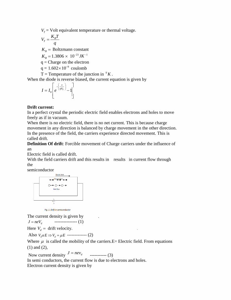
TV = Volt equivalent temperature or thermal voltage.
BT
K TV
q
BK Boltzmann constant
BK 1.3806
23 110 JK
q = Charge on the electron
q = 91.602 10 coulomb
T = Temperature of the junction in 0 K .
When the diode is reverse biased, the current equation is given by
0 1T
v
VI I e
Drift current:
In a perfect crystal the periodic electric field enables electrons and holes to move
freely as if in vacuum.
When there is no electric field, there is no net current. This is because charge
movement in any direction is balanced by charge movement in the other direction.
In the presence of the field, the carriers experience directed movement. This is
called drift.
Definition Of drift: Forcible movement of Charge carriers under the influence of
an
Electric field is called drift.
With the field carriers drift and this results in results in current flow through
the
semiconductor
The current density is given by
dJ neV --------------- (1)
Here dV drift velocity.
Also d dV E V E ------------- (2)
Where is called the mobility of the carriers.E= Electric field. From equations
(1) and (2),
Now current density dJ nev ----------- (3)
In semi conductors, the current flow is due to electrons and holes.
Electron current density is given by

n nJ drift ne E ------------- (4)
Hole current density is given by
p nJ drift pe E ----------- (6)
The two charge carriers move in the opposite direction.
Now the total drift current density is given by
n pJ drift J drift J drift
n pJ drift ne E pe E
( ) nJ drift E ne pe p -------- (7)
For an intrinsic semiconductors in p n
( ) i nJ drift En e e p ------------- (8)
Equation(8) gives current density equation.
Diffusion current :
Usually directed movement of charge carriers will give rise to electric current.
The movement of charge carriers may be due to either drift or diffusion.
Usually non-uniform concentration of carriers gives rise to diffusion.
Definition: Movement of charge carriers from high concentration region to low
Concentration region in a semiconductor is known as diffusion.
Let us suppose that the concentration of electrons varies with distance x in the
semi conductors. Here the concentration gradient is given by n
x
.
Ficks low states that the rate at which carriers diffuse is proportional to the
density gradient and the movement is in the direction of negative gradient.
Mathematically, the rate of flow of electrons can be written as
n
nf
x
, Here nf = rate of flow of electrons across unit area.
The rate of flow of electrons is given by
n n
nf D
x
----------- (1)
Here nD = Diffusion coefficient for electrons.
Partial derivatives are used because n is a function of temperature and distance.
This flow of electrons constitutes an electron diffusion current density. Since
conventional current in the rate of negative charge, we have
Rate of flow of electrons across unit areanJ diffusion e
( )n n
nJ diffusion e D
x
n n
nJ diffusion eD
x
----------- (2)
If an excess hole concentration is created in the same region, hole diffusion takes
place in the same direction at a rate per unit area.
The rate of flow of holes per unit area is given by
p p
pf D
x
------------- (3)
This results in a hole diffusion current density
Now rate of flow of holes across unit areapJ diffusion e
(4)p p
pJ diffusion e D
x
Here pD Hole diffusion coefficient for holes.
Einstein Relations or Einstein Equations
At equilibrium with no field, the free electron distribution is uniform and there is
no net current flow. Any tendency to disturb the state of equilibrium which would
lead to diffusion current creates an internal electric field.
This internal electric field creates a drift current balancing the diffusion current
component.
Under equilibrium conditions, we have therefore the drift and diffusion currents.
These currents are due to an excess density of electrons.
Now driftnJ n eE----------------------- (1)
diffn n
nJ eD
x
--------------- (2)
Under equilibrium conditions, ( ) ( )n nJ drift J diff
(3)n n
nn eE eD
x
The force F on excess carriers restoring equilibrium is given by the product of
excess charge and Electric field.
F ne E --------------- (4)
(3)n
n
nD
xnE
----------- (5)
Now from (4) and (5),we get
n
Dn E nF e
E x
n
e Dn nF
x
------------- (6)
This force F depends on the thermal energy of the excess carriers.
By making can analogy between the excess carriers in a semiconductors and gas
molecules in a low pressure gas, the force F corresponds to pressure gradient.
Pressure gradient = B
nK T
x
nB
n
eDn nK T
x x
nB
n
eDK T
n
n BD K Te

Bn n
K TD
e --------------- (7)
Similarly for holesp
Bp
K TD
e ---------- (8)
7
8
n n
p p
D
D
------------ (9)
Equations (7), (8) and (9) are called Einstein‟s Relations.
UNIT-IV
Magnetism
And
Super Conductivity

Super Conductivity Introduction
Usually materials exhibit electrical resistance and resistivity. This is due to scattering of
electrons by the positive ions present in the materials. When the temperature of certain materials
decreased to lower values, the resistance and resistivity decreases. Hence conductivity increases.
This is because scattering of electrons decreases due to lower energy. The phenomenon of
attaining zero resistivity or infinite conductivity at low temperatures is known as super
conductivity. Here the state of the material is known as super conducting state. The temperature
at which the material transforms into super conductor from normal state is known as super
conducting transition temperature (or) critical temperature (or) transition temperature Tc. This
was first observed by Heike Kammerlingh Onnes in 1911 in mercury. When temperature of
mercury decreased by cooling it in liquid Helium, the resistivity completely disappeared at 4.20k.
This is shown in figure (1).
NC=Normal Conductor
SC= Superconductor
Figure (1) variation of resistivity with temperature in mercury.
The super conductor will have zero electrical resistance below a well defined temperature Tc.
The materials exhibiting super conductivity are called super conductors. Same examples of
super conductors and their Tc values are given below.
Element / material Tc in 0k Element / material Tc in
0k
Aluminum 1.19 Lead 7.175
Cadmium 0.52 Zinc 0.9
Gallium 1.09 Zirconium 0.8
Indium 3.4 Niobium 9.3
Tin 3.72 NbN 16
Mercury 4.12 Vanadium 5.03
Temperature TOK
Resistivity
Y
X O
4.2
Tc
NC SC
Cooled to

General properties 1. The super conductivity is a low temperature phenomenon.
2. The transistor from normal state to super conducting state occurs below the critical
temperature.
3. The transition temperature is different for different materials.
4. The current that is set up in a super conductor persists for a long time due to zero
electrical resistivity.
5. Super conductivity is found to occur in metallic elements in which the number of valence
electrons (Z) lies between 2 and 8.
6. Materials having high normal resistivities exhibit super conductivity.
The condition is n> 106 is a good criterion for the existence of super conductivity.
Here n = number of valence electrons per cc.
= Resistivity in esu at 200c.
7. Super conductors when placed in magnetic field, they do not allow magnetic lines of
force to pass through them. Now they behave as diamagnetic i.e. they expel magnetic
field. This property of expulsion of magnetic field is known as Meissner effect.
8. With increase in magnetic field, the material looses its super conductivity. The field at
which the superconductor looses superconductivity and becomes a normal conductor is
called critical magnetic field Hc.
9. Monovalent, Ferro magnetic and Antiferro magnetic materials are not super conductors.
10. The induced current in a super conductor induces a magnetic field in it. If the magnetic
field is equal to the critical magnetic field then it converts into a normal conductor.
Now the current through the super conductors is known as the critical current Ic.
The critical current is given by Ic = 2 cr H
Where r= radius of the super conductor.
11. Super conductors are not good conductors at room temperature.
12. Good conductors like Cu, Ag, Au when cooled to 0.07, 0.35 and 0.05k; they are
exhibiting still resistivities.
13. In the case of Tin, the variation of electrical resistivity with respect to temperature is
shown in figure (2).
Fig (2). Electrical resistivity of Tin as a function of temperature.
X 10-11 -m
20 –
10 –
0
| | | | |
2 4 6 8 10
T
0K

Effect of Magnetic field (critical magnetic field)
When a magnetic field is applied to a super conductor, then at a particular magnetic field value,
the super conductivity disappears. Here the material becomes a Normal conductor.
At a sufficiently higher magnetic field, the super conductivity will be destroyed. At this stage the
material will restore to their normal conducting state.
The amount of magnetic field that is required to destroy super conductivity is called the critical
field. This is denoted by Hc. The functional relationship of Hc with temperature is given by 2
0 1c
C
TH H
T
Where H0= Field required to destroy the super conductivity at 00k.
H0= is a definite value for every material.
Tc= critical temperature
Hc= the maximum critical field strength at T0k.
* At T=Tc, Hc=0
* when T=00k, then Hc=H0
The variation of critical magnetic field Hc as a function of temperature is shown in figure (3).
+
Figure (3). Variation of Hc as a function of temperature T in 0K
H
cc
T
0K
0
H0
Tc
Normal
State
Super
conducting
state

The Meissner effect – flux exclusion :
Meissner and ochsenfeld in 1933 found that if a long super conductor is cooled in a longitudinal
magnetic field, below the critical transition temperature, then the lines of force or lines of
magnetic induction B are pushed out of the body of super conductor at the transition temperature.
Here the applied magnetic field H must be less than the critical magnetic field value Hc. The
magnetic field exclusion is shown in the figure (4).
Figure(4) Meissner effect
This magnetic field expulsion phenomenon by the super conductor at Tc and below Tc is
called the Meissiner effect. Now inside the super conductor, magnetic induction field
strength B is zero. That is the magnetic flux is excluded from the body of the super
conductor.
Also for a super conductor r = 0
Also we know that magnetic induction B is given by
0B H M -------------------- (1)
But B=0
0 0
0
1
H M
H M
M H
M
H
Cooled
B=0
T<TC
H<HC
Super conducting
T > Tc, , H < Hc

But 1M
xH
Where χ= magnetic susceptibility.
For a super conductor magnetic susceptibility is negative. Hence a perfect super
conductor is a perfect diamagnetic material.
Note: Usually a diamagnetic material will have negative magnetization. Hence it will
have a negative magnetic susceptibility.
Penetration Depth
Let us consider a super conductor. Consider that a magnetic field H0 is applied to one of
its faces as shown in the figure (5).
But according to Meissner effect, it will not allow magnetic lines of force to pass through
it. But in practice a small portion of H0 penetration to a small distance into the
superconductor.
Figure 5. Penetration of field through are face of super conductor
The applied field does not suddenly drop to zero at the surface of the super conductor, but decays
exponentially. The penetration of the magnetic field at a distance x from the surface is given by
/
0
xH H e
Where H = field at a distance x from the surface into the material.
0H = Field at the surface.
= Characteristic length known as a penetration depth.
X= distance from the surface into the material.
is the distance for H to fall from 00
HH H to
e
When x , then 0H H e
---------------------(1)
1
0H H e
0HH
e
x
H0
Mag
net
ic f
ield
Super conductor

The penetration depth is the distance into the super conductor at which the magnetic field is
equal to 1
e
of the applied magnetic field 0H . The magnetic field is likely to penetrate through
a super conductor to a depth of 10-100 nm.
Penetration depth is more in thin film type of superconductors. When compared to bulk type
super conductors. The variation of magnetic field H with the distance x is shown in figure (6).
0H
e
Figure (6).Variation of magnetic field H with distance x into the super conductor
The variation of penetration depth with temperature T is given by
0
1/ 24
(2)
1C
T
T
Penetration depth at 0T K
0 Penetration depth at 00T k
cT Critical transition temperature
The penetration depth varies with applied field. According to pippard, there is only a few
percentage change of with H, even up to Hc.
Y
X O
X
H0
H

This is of the form. 2
0 21 0.02c H
C
HT H
H
(Pippard relation)
The variation of penetration depth with temperature T in Tin is shown in figure 7.
Figure (7) variation of penetration depth in Tin. In equation (2)
The percentage depth of same materials at 00K are given below.
Super conductor (in nm)
Mercury 70
Indium 64
Lead 39
Tin 50
Aluminum 50
Types of super conductors
When a super conductor placed in a magnetic field, at critical magnetic field, it transforms from
super conducting state to normal state.
Basing on this transformation, superconductors are classified into two types.
Type – I super conductors
Type – II super conductors
Types – I Super conductors
Let us consider a cylindrical form of super conductor. Now a magnetic field H is applied along
the axis of the super conductor.
But according to Meissner effect. The super conductor does not allow the magnetic lines of
force to pass through it. Here H =- M; shown in figure (7)a i..e inside the super conductor, the
magnetization acts in a direction apposite to magnetic field H.
When the magnetic field H is equal to the critical magnetic field Hc, then the magnetization (-M)
becomes equal to zero.
| | | |
1 2 3 4
TC
5 --
4 --
3 --
2 --
1 --
0 --
0
Pen
etra
tio
n d
epth
X 1
0-5
cm
T 0k

In this state the magnetic lines of force penetrates through the super conductor completely. Here
the super conductor completely transforms into a normal conductor. This is shown in figure (7)b.
Hc=0.1Tesla
Hc
The variation of – M with respect to H is shown in figure (8). This curve is called Magnetization
curve. Type – I Super conductors exhibit complete Meissner effect.
Type – I super conductors are soft super conductors. Here they are completely diamagnetic and
hence the flux is completely excluded. If the superconductor is an ideal one, the magnetization
curve is reversible. For non ideal superconductors the magnetization curves are irreversible.
Below Hc, the critical field, the material is a super conductor. Above the critical magnetic field
the super conductor becomes a normal conductor. At Hc, the super conductivity in type- I super
conductors suddenly falls to zero.
Examples
Lead, Aluminum, zinc, mercury, cadmium, indium, Sn etc.
This was first observed by Silsbee in 1916.
Type – II Super conductors
Let us consider a spherical form of super conductor. Now let a magnetic field is applied
along the diametrical axis of the super conductor. But according to Messier effect, the super
conductor expels the magnetic lines of force and H=-M. i.e. The magnetization inside the
superconductor opposes the passage of lines of force through it. Now the magnetic lines of force
are concentrated at the two curved ends of the spherical super conductor as shown in figure (9)a.
Here the intensity of magnetic field H is predominant at these ends.
For applied magnetic fields below lower critical magnetic field Hc1, the specimen
behaves like a superconductor. Here the magnetic flux is completely excluded in this range of
field. At HC1 the magnetic flux begins to penetrate the specimen and the penetration increases
until HC2 is reached. At HC2 the magnetization vanishes and the specimen becomes a normal
conductor. HC2 is known as upper critical magnetic field.
Y
Super
conducting state Normal
state
H
C
X O
-
M
H
-M
Figure 7 (b) Normal
conductor H>Hc, T>Tc
Figure (8) Magnetization curve for
Te – I super conductor
Figure 7 (a) a super
conductor H < Hc, T<TC
Figure (7) b Type – I Super conductor
Y
Superconducting
state Normal
state
H
C
X O
-
M
H

Between HC1 and HC2, the penetration of the flux is at the curved ends of the spherical
superconductor. At HC2 above HC2 the specimen completely transforms from super conducting
state the normal state.
Between HC1 and HC2 the material is having super conducting as well as Normal conducting
properties i.e. between HC1 and HC2 the specimen is in the mixed state or vortex state.
Above HC2 the specimen becomes a normal conductor. Here – M = 0. This is shown in figure
(9)c.The mixed state is also shown in figure (9)b.
Figure (9) Type II super conductor
-M -M
-M=0
Fig. (9) c. Normal conducting
H>Hc2.
Figure (9)a Superconductor ,
H<Hc1
Fig. (9) b. Superconducting +
Normal conducting (mixed state)
H<HC2 & H>HC1

The magnetization curve for Type – II super conductors is shown in figure (10).
Figure (10) Magnetization curve for type II superconductor
Figure (11) Magnetic phase diagram of type-II superconductors
In type – II super conductors, the transformation process from super conducting state to
normal state is slow.Ttype-II. Super conductors are hard super conductors.
The magnetic phase diagram of type – II superconductors is shown in figure (11).
-M
Y
X H
Super conducting
State
Vortex state
(or) mined
state
Normal
state
HC1 O
HC2=10 tesla
HC2
O X
T0K
HC2
Y
HC1

Type – II super conductivity was first discovered by Schubnikov in 1930.
Examples : Osmium, Zirconium, Thorium, Thallium, Tantalum etc.
Flux quantization
Let us consider a hollow normal conducting ring in a magnetic field H. This ring now
allows magnetic flux through it.
The magnetic flux will be present inside the hollow space, on the ring and outside the
ring, shown in fig. 12a. When the ring is cooled up to Tc and below Tc. (It‟s critical
temperature), it becomes a super conductor. Now it obeys Messier effect.
In the superconducting ring ,persistent currents will be set up.As a result of Meissner
effect H= - M, Magnetic flux will be excluded.
In this case, it is observed that the flux is present outside and inner hollow space of the
ring only. This is shown in figure (12)b.
Fig. (12)a. Hollow ring normal
conducting in a magnetic field H (T>Tc).
Persistent
current super
Magnetic flux
Fig. (12)b. Hollow supercoducting Ring
in a magnetic field H (T<Tc).

When the applied magnetic field is removed, then the persistent current will exist in the
specimen. Due to this same magnetic flux is retained in the inner walls of the super
conductor. This is shown in the figure (12) C.
Figure (12) C. Hollow super and conducting ring when no field (H) (T<TC)
The trapped magnetic flux will have quantized values. This is given by
, 1, 2,3,....2
nhn
e
Where h = Planck‟s constant
e= charge on the electron.
2 3, , ,...
2 2 2
h h h
e e e
The unit of flux is called fluxoid.
1 fluxoid = 2.07 x 10⁻¹⁵
weber.
1 fluxoid =2
h
e
The flux through the ring is the sum of the flux due to the external source ext and flux due to the
super current flowing through that ring sc
i.e. scext
This flux is quantized.
ext is usually not quantized and sc adjusts such that is always quantized.
Super
current
persistent
current

Josephson Effect
Let us consider two super conductors joined suitably with a thin insulating layer, as shown in
figure (13). This constitutes a junction called Josephson junction.
Fig.(13) Josephson effect
SC I - super conductor I, SC II- super conductor II
Usually in a super conductor, we will have cooper pairs. Cooper pairs are nothing but
electrons occurring in Pairs.
Tunneling of electron pairs across an insulating gap between two superconductors was
predicted by Josephson.
This prediction was experimentally verified by Anderson and Rowell, using lead –
insulation lead sand witches. The cooper pair will penetrate or tunnel across the thin
insulator and causes a small amount of current. This is current is known as super current.
This effect is known as Josephson effect.
The Josephson Effect is of two types.
(i) DC Josephson effect and (ii) AC Josephson effect.
DC Josephson Effect
A DC current flows across the junction in the absence of voltage across the junction.
Here the cooper pairs tunnel across the thin layer of insulating medium. Due to this a DC
current flows across the junction.
This effect is known as DC Josephson effect. This is shown in figure (14).
Figure (14) DC Josephson effect
SC – I SC – II
Thin insulating layer
Thin insulating layer
SC – I SC – II
Copper
pairs
Thin insulator
.
.
. .
.
.
. .
.
.
. .
.
.
. .
.
.
. .
.
.
. .
.
.
. .
.
.
. .
.
.
. .
.
.
. .
.
.
. .
.
.
. .
.
.
. .
.
.
. .
.
.
. .
SC = Super conductor

Super currents flow through the junction even in the absence of voltage difference.
The current through the Josephson junction is given by
I= Im sin
Where mI maximum current flowing across the junction.
mI Depends on the thickness of the insulating layer.
is the phase difference in the state of waves describing the cooper pairs on both sides
of the insulator.
2 1
AC Josephson effect
When a DC voltage is applied across the junction of two super conductors separated by a
thin insulating layer, then the cooper pairs oscillates through the insulating layer.
Due to this radio frequency oscillations will be set up across the junction.
This effect is known as AC Josephson effect.This is shown in fig(15)
This frequency of the AC signal produced is given by 2ev
f Hzh
Fig 15. AC Josephson effect
A DC voltage of 1 v produces a frequency of 486.6 MHz.
The applied DC voltage introduces an additional phrase of
Et
Where E= Total energy of the system
t = given time in seconds
Here E= (2e) V0
V0= Applied DC voltage
Since a cooper pair contains „2‟ electrons, the factor 2 appears in the above equation.
Now 02eV
t
Now the tunneling current can be written as
+ -
V0
SC -1 SC – 2
Thin insulator
.
.
. .
.
.
. .
.
.
. .
.
.
. .
.
.
. .
.
.
. .
.
.
. .
.
.
. .
.
.
. .
.
.
. .
.
.
. .
.
.
. .

I= Im sin 0
I= 00
2m
eV tI Sin
0mI I Sin t
Where, 02eV the angular frequency.Current voltage characteristics of a Josephson
junction are shown in figure (16).
i) When V0=0 there is a current flow if DC current Ic through the junction. This
current is called superconducting currents. This effect is called DC Josephson effect.
ii) If V0<VC, a constant dc current flows.
iii) If V0>Vc the junction has a finite resistance and the current oscillates with a
frequency 02eVw
This effect is called AC Josephson effect.
Figure (16) V-I characteristics of a Josephson junction
iv) When V0=0 there is a current flow of DC current Ic through the junction.
This current is called superconducting current. This effect is called DC Josephson
effect.
v) If V0<VC, a constant dc current flows.
vi) If V0>Vc the junction has a finite resistance and the current oscillates with a
frequency 02eV
This effect is called AC Josephson effect.
Applications of Josephson’s effect
1. By using Josephson junction, microwaves can be generated having frequency.
02eV
2. A.C. Josephson effect is used to define a standard voltage.
Current
I
Y
IC
VC Voltage V O
X

3.A.C. Josephson effect is used to measure very low temperatures based on the
variation of frequency of the emitted radiation with temperature.
4.A Josephson junction is used for switching of signals from one circuit to
another circuit. The switching time is of the order of 1PS. They are useful in high speed
computers.
The BCs theory (Bardeen, Cooper and shrieffer theory)
Bardeen, Cooper and Schrieffer proposed a theory regarding super conductors, known as
BCs theory. They investigated the electron – phonon interaction in super conductors.
In normal conductors, the electrons are moving at random in all possible directions.
Usually the positive ion cores, the electrons get scattered in all directions. Due to this the
electrons scattering, the materials will posses some electrical resistance, the materials will
possess some electrical resistance. Here the force between two electrons is always a
repulsive force.
When the normal metal transforms to the super conducting state at and below critical
transition temperature, the scattering of electrons decreases. Hence there is a decrease of
scattering energy. In superconducting state the electrons paired. These paired electrons
are called cooper pairs. This is shown in figure (17). The formation of cooper pairs can be
understood from the following.
Consider an electron passes near an ion core; there is a mutual attraction between the
electron and the ion core.
This is due to columbic interaction and as a result the ion core is set into motion.
Let us consider that another electron now passes nearby. The second electron feels the
effect of the motion of the ion core.
Due to this both the electrons are entering into attractive field region.
The ion core motion has provided the mutual interaction between two electrons despite of
their mutual repulsion.
Under very restrictive circumstances, the attraction exceeds the repulsive interaction.
(i) The electrons entering into such an attractive field are having opposite moments
and opposite spins with equal magnitudes.
i.e. K1= -K2 and S1= -S2
(ii) The temperature is low enough such that T0.
Such paired electrons are called cooper pairs. The attractive interaction between two
electrons takes place in the presence of phonon field.
The interaction between the electron and the distorted lattice (settled lattice) occurs,
which in turn lowers the energy of the second electron.
That is the two electrons interact via the phonon field. This is shown in figure (18).
This results in lowering of energy for the electrons. The lowering of energy implies that
the force between the two electrons is attractive.
Salient features of BCs theory
1) The total energy of the BCs state is lower with respect to the normal state. The total
energy of the BCS state comprises of the kinetic energy and the attractive potential
energy. The attractive potential energy acts to reduce total energy of the BCS state. The
normal state comprises of the kinetic energy. As a consequence of this BCS state is more
stable than the Fermi state.
2)The one particle states are occupied with pairs. If a state with a wave vector K and spin
up is occupied then the state with wave vector – K and spin down is also occupied.
Applications of super conductors
Josephson Junction devices
The emf of standard cells using conventional materials, usually drift (changes).
AC Josephson effect can be used to generate voltage standards.
The DC Josephson effect has been used to fabricate sensitive magnetometers with an
accuracy of 10-11 gauss.
Super conductors can be used to generate and detect electromagnetic radiations from
radio to infrared frequencies using AC Josephson effects.
Electric Generators
Super conducting generators are smaller in size, with less weight.
They consume low energy. The low-loss superconducting coil is rotated in a strong
magnetic field. Due to this an electric current is generated.
This is the basis of new generation of energy – saving power systems.
High field magnets
Super conducting materials can be used for producing high magnetic fields with low
power consumption.
Magnetic bearings
The possibility of flux trapping and flux exclusion suggests that a super conducting
cylinder and disc may be used as magnetic bearing.
The bearing is restricted in its lateral movement but can spin on a cushion of flux.
If the material of the moving part of the bearing is chosen so that no flux will penetrate
into it.
The friction in the bearing will come from the viscosity of the surrounding medium.
Energy storage
A super conducting coil can be used to store energy. A trapped magnetic field of
H oersted stores energy of 2
8
H
ergs / cm
3.

Super conductor fuse and breaker
Some insulating materials exhibit super conductivity at lower temperature. Thin films of
such materials can be used instead of fuse because when more current greater than critical
current pass through them, then they change into normal state.
In normal state, they are insulators they would not conduct current, so it will act as
a fuse.
In breaker, a long thin film of superconductor is used. In normal state, thin film
possess high resistance. In this situation lead is used.

Fig. (18) Electron – Electron interaction through phonons
SQUIDS
SQUIDS are fundamentally superconducting Rings that act as storage devices for
magnetic flux. SQUIDS can be used to store and measure magnetic fields.
SQUIDS are known as super conducting Quantum interference devices
These SQUIDS are used to localize epileptic centers deep within the brain.
The short-circuiting action of an epileptic centre produces electrical currents that generate
a distinctive magnetic signature.
Doctors place an array of a dozen SQUID magnetometers around the patients head.
Computer can analyze the data from all the sensors together a three dimensional picture
activity within the brain.
This technique is known as magnetic Encephalography (MEG).
SQUIDS are used for detecting ORE deposits.
SQUIDS are used for detecting earthquakes.
Cooled
1K q
1K 2K
q
Virtual
phonon
2K q
Fig. (17) a scattering of electrons
in
normal conductor
Fig (17)b. Formation of cooper
pairs in a super conductor
e
e
e e
+ve ion cores
Electrons
Cooper pairs
.
.
. .
.
.
. .
.
.
. .
.
.
. .
.
.
. .
.
.
. .
.
.
. .
Ion core

Fast electrical switching (Cryotron) Applying a magnetic field greater than (Hc),
changes the super conductor to normal state and when the field is removed it regains the
superconducting state. This principle is used in cryotron switch.
Superconductors in computers
A super conducting ring is used in memory cell. When persistent current passes through a
super conducting state, then it is said to be in „1‟ state.
In normal state, current will not pass through it, and it is in „0‟ state.
Thus a super conducting can be used as a memory device.
Magnetic levitation (Meg Lev Vehicles)
Meg lev vehicles mean magnetically levitated vehicles.
The diamagnetic property of a super conductor (Meissonier effect) is the Basis for
magnetic levitation.
This concept is used for high speed transportation.
Fast electrical switching (Cryotron)
Applying a magnetic field greater than (Hc), changes the super conductor to normal state
and when the field is removed it regains the superconducting state. This principle is used
in cryotron switch.

UNIT-V PHYSICS OF
NANOMATERIALS
PHYSICS OF NANOMATERIALS Introduction:-
Nano meaning that 10-9.
A manometer is one thousand millionth of a meter. i.e. a nanometer equal to 10-9
m. In elements
of atoms are very small. The diameter of a single atom can vary from 0.1 to 0.5 nm depending
on the type of the element. For example carbon atom is approximately 0.15nm in diameter.
Also diameter of Red Blood Cell (RBC) is approximately 7000nm.
Diameter of water molecule is around 0.3 nm. Thickness of human hair is around 80,000nm.
Nanomaterials could be defined as those materials which have structured components with size
less than 100nm at least in one dimension.
Nanoscience:-
Nano science can be defined as the study of phenomena and manipulation of materials at
atomic, molecular and macro molecular scales, where properties differ significantly from those at
a larger scale.
Nano technology:-
Nano technology can be defined as the design, characterization, production and application of
structures, devices and systems by controlling shape and size at the nano scale.
Nano materials’:-
If we take any material it will be composed of grains, which in turn comprise of many atoms.
depending on the size, the grains may be visible or invisible to the naked eye.
Conventional materials have grains of size varying from hundred of microns to centimeters.
Nano materials could be defined as those materials which have structured components with size
less than 100nm at least in one dimension.
Examples:-
One dimensional Nanomaterail:-
Materials that are on nanoscale in one dimension are layers such as thin films or surface coatings
.In these materials, the particles are layered on layers or multilayer‟s.
Two dimensional nano materials:-
Materials that are on nano scale in two dimensions are called two dimensional Nanomaterials.
Ex. nanowires and nano tubes.
This consists of ultrafine grains laid over layers.
Three dimensional nano materials:-
Materials that are on nanoscale in three dimensions are particles or grains.
Examples are precipitates, colloids and quantum dots.
Basic principles of nanometerials:
The properties of namo meterials are different from those of bulk materials.
Two important factors that make the nanometerials to differ significantly from other materials
are increased surface area and quantum effects.
1. Increase in surface area to volume ratio:
Nano materials have a relatively larger surface face area when compared to the same volume (or
mass) of the material produced in a larger form
Let us cosider a shpere of radius 'r'
Surface area = 24 r and Volume =
34
3r

Surface area to volume ratio = 2
3
4 3
4
3
surfacearea r
Volume rr
Thus when the radius of the sphere decreases its surface area to volume ratio increases.
Let us consider another example.
For a cube of 1 unit volume shown in figure (1)
the surface area is 6m2
When it is divided into eight pieces its suface area becomes 12m2.
When the same volume is divided into 27 pieces its surface ares becomes 18m2
When a given volume is divided into smaller pieces the surface area increases.
As particle size decreases, a greater proportion of atoms are fand at the surfcae compared to there
inside. for example a particle of size 30nm has 5% of its atoms on its surface at 10nm 20% of its
atoms, and at 3nm 50% of its atoms on its surface.
Diue to this, nano materials are more chemically reactive. Some materials in bulk form are inert;
when they are in nano form they are reactive.
This affects their properties.
Quantum confinement: When Atoms are isolated the energy levels are discrete. when very
large number of atoms are closely packed to form solid the enery levels split and form bands.
Nano materials represent intermediate stage when the material is of nano size and nano scale, the
energies of the electron changes.
The quantum confinement effect is observed when the size of the particle is too small to be
comparable to the wavelength of electrons. Here motion of electrons is restricted in specific
energy levels.

Here band gap also increases.( Eg 1/ )
This effect is called quantum confinement
Due to this the electrical, optical and megnetic properties of the nanomaterials changes.
Fabrication of nanomaterails:-
The nanometerials can be synthesized by two techniques namely top-down and bottom up
techniques
In the bottom-up approach, the nanomaterials are syntherized by assembling the atoms or
moleculers together to form the nanomaterials

In the top-down approach the bulk solids are disassembled (broken down to pieces) into finer
pieces until the particles are in the order of nanoscale. The schematic representation of the
synthesis and fabrication of nanomaterials are shown in figure above.
I n top down method there are different techniques to fabricate nonmaterial‟s
For example Ball milling and sol-gas are the methods used for fabricating nonmaterials in top-
down approach
The chemical vapor disposition method, and plasma arching method are the methods employed
in the fabrication of nanomaterials in bottom up approach
Fabrication of nanomaterials:-
Ball Milling method
Ball milling method is a top down method. It is also known as mechanical crushing. This is a
simple method to synthesize all classes of nano materials. This method is used to produce nano
crystalline or amorphous materials.
The mechanical attrition mechanism or mechanical crushing mechanism is used to obtain
nanocrystalline strctures.The nano materails are prepared from single phase powders or
dissimilar powders or amorphase materials. The ball milling method is shown in figure above.
Depending on the material to be synthesised refractory balls or steel balls or plastic balls are
used.
When the balls are rotating with certain RPM, the enery is transferred to the powders.
This redues the size to the powder particles to the nanoscaled particles. Here the nano particles
are produced due to shear action between the balls and the metal pieces. The energy transferrred
to the powder from the balls depends on the factors such as rotational speed of the balls, size of
the balls number of balls, milling time, the ratio of the ball to the powder mass and milling
atmosphere.
By using a cryogenic liquid the brittleness of the particles can be increased.
Care should be taken to prevent oxidation during the process of milling. For fabricating softer
materials, usually harder balls will be chosen. Usually alumina and zirconium are used widely as
balls for synthesizing the nanomaterial. This is because they have high grinding restistance
values.
In this method scaling can be achieved up to tonnage quantity of materials. in this technique non
metal oxides cannot be fabricated due to contamination of milling media.

Sol- Gel method:The sol-gel method is a wet chemical technique. That is here chemical solution
deposition technique is used for the production of high purity and homogeneous nanomaterials.
Here in this method metal oxide nano particles are fabricated
The starting material from a chemical solution leads to the formation of colloidal suspensions
know as SOL. Then the sol evolves toward the formation of an inorganic network containing a
liquid phase called the Gel. The removal of the liquid phase from the sol yields the gel.
The particle size and shape are controlled by the sol/gel transition
Usually metal alkoxides and metal chlorides are used as starting (precursor) is diluted or
dissolved in water or dilute acid in an alkaline solvent. This process is called hydrolysis..
From the sol containing a liquid phase, water molecules are removed by a process called
dehydration now a gel is formed.
The gel is dried up rapidly by heating it and the Nan particles are formed.
The schematic representation of the synthesis of nano particles using sol-gel method is shown in
the figure below.
Aero gel is a highly performs material like glass and glass ceramics.
Sol-gel derived particles find applications in optics, electronics, energy, space etc.,
Chemical Vapor Deposition Method: Ina chemical vapor deposition (CVD) the atoms or molecules which are in gaseous state are
allowed to react homogenously or heterogeneously.
In a homogenous CVD, the particles or atoms or molecules in the gas phase are diffused towards
the cold surface. This occurs only due to thermophoreic forces.

The diffused particles can be scrapped from the cold surface to get nano powder
Also the differed particles are deposited into a subtract to form a film know as Particulate Film.
In a heterogeneous CVD, a dense film of nano particles is obtained on the surface of substrate
.In CVD method particle size crystal structure and chemical composition can be controlled
The schematic representation of CVD is shown in figure above. The metal organic precursor is
introduced into the hot zone of the reactor with flow controller.
The precursor is vaporized by using inductive heating or resistive heating. An inert gas like
argon or neon is used as carrier gas. The evaporated matter consists of hot atoms which undergo
condensation into small clusters through a homogenous nucleation,.
Other reactants are added to the clusters to control the chemical reactions. The cluster size is
controlled by controlling rate of evaporation rate of condensation and rate of gas flow. The
condensed clusters are allowed to pass through the cold finger.
The nano particles are collected by using a scrapper this is shown in figure above.
The CVD method is used to produce defect free nano particles.
Properties of Nano materials.
Physcial propereties: Usually for nano particles, surface to volume ratio increases due to this there is a variation in
material properties. The following are the physical properties.
1. The inter atomic spacing decreases with the nano scale. This is because of short range
core-core repulsion
2. Melting paint decreases due to decrease in size of the particle
3. Due to increase in surface area surface pressure decreases.
CHEMICAL PROPERTIES:-
1. When particle size is reduced to nano scale the electronic bands in the metals becomes
narrow. This leads to the transformation of the delocalized electronic states into more
localized molecular bands. This results in the increase of ionization potential.
2. The large surface to volume ratio, the variations in geometry and electronic structures
takes place. This will have a strong effect an catalytic properties
3. The chemical potential increases
4. When particles size decreases the hydrogen absorbing capacity increases.

Mechanical properties:-
Most metals are made up of small crystalline grains. If there grains are nanoscale in size the
interface area within the material greatly increases, which enhances its strength.
For example nano crystalline nickel is as strong as hardened steel.
It low temperatures a reduction in grain size lowers the transition temperature in steel from
ductile to brittle the average grain size and yield strength are given by Hall petch relation
0
K
d
= yield strength.
0 =Friction Stress.
K= Constant of Proportionality.
d= Average grain size.
The relation between Hardness and average grain is given by
i
KH H
d
H= Hardness.
iH = Vickers hardness
K= Constant of Proportionality.
d= Average grain size.
At high temperatures, the nonmaterials behave like superplasitc materials. Super plastic
materials will have extensive tensile deformation without fracture. In nonmaterial‟s the
occurrence of super plastic temperature decreases due to the decrease in grain size. MAGNETIC PROPERTIES:-
In nano magnetic particles the magnetic properties are different from the bulk material.
When the material is at nanoscale, the particle will have only single domain
The coercivityl and saturated value of magnetization values increases with a decrease in
grain size. Nano particles are more magnetic than bulk material. The magnetic moment of
nano cobolt particles of size 2nm is found to have 20% higher value than that of bulk cobalt.
Nano particles of non magnetic solids are found to be magnetic.
At small size the cluster become spontaneously magnetic.
The following table illustrates the behaviour of nano particles.
Metal Bulk Cluster
Na,K Paramagnetic Ferromagnetic
Fe,W,Ni Ferromagnetic Super paramagnetic
Rh Paramagnetic Ferromagnetic
Electrical properties:--
The ionization potential at small sizes is higher than that for the bulk materials.
This is become of quantum confinement effect the electronic bands in metals become narrower
In nano ceranics and magnetic composites the electrical conductivity increases with reduction in
particle size. Bulk silicon is an insulator which becomes a conductor in nano phase.
Usually the electrical conductivity increases with reduction in particle size.
OPTICAL PROPERTIES:-
Nano crystalline systems have novel optical properties. If semi conductor particles are
made small enough quantum effects come into play. This limits the energies of particles at which
electrons and holes can exist.
Golden nano shperes of 100nm size appears orange in color.
Gold nano spheres of 50nm size appear green in color.
Therefore the optical properties can be changes by controlling the particle size.
Nano matericles can be used as large electro chrome devices.
Thermal Properties:
Thermal conductivity increases with decrease in size of particle.
Melting of gold decreases from 1200K to 800K when the size decreases from 300 0A to 200
0
A.
Stable aluminium becomes combustible in nanophase.
Solid gold becomes liquid gold in nano phase.
APPLICATIONS OF NANO MATERIALS:-
Materials technology:-
1. Magnets made of nano crystalline yttrium- samarium-cobalt grains possess unusual
magnetic properties. This is because they are having large interface area. Nono
magnetic crystals will have high coactivity .they are used in motors and analytical
instruments like magnetic resonance imaging (MRI)
2. Nano sized titanium diozide and zincoxide are currently used in sunscreens. They
absorb and reflect ultra violet rays (UV). They are transparent to visible light.
3. Nano engineered membrane could potentially lead to more energy- efficient water
purification processes. They are used in desalination water plants by reverse osmosis.
4. Nano sized iron oxide is used in lipsticks as a pigment
5. Ceramics are hard, brittle and difficult to machine. However with a reduction in a
grain size to the nano scale ductility in ceramics can be increased. Zirconia, normally
a hard, brittle ceramic, and can be rendered super plastic. If can be deformed up to
300%
6. An important use of nano particles and nano tubes in composites carbon fibres and
bundles of multiwall CNTs are used in composites having potential long term
applications.
7. Carbon nano particle act as fillers in a matrix. They are used as a filter to reinforce car
tires.
8. Clay particles based composites containing plastics and nano-sized flakes of clay also
used in the fabrication of car bumpers.
9. Improved control porosity at the nanoscale has applications in textiles. Breathable
water proof and stain resistant fabrics can be fabricated using nano materials.
10. Nano particles are having high surface area. They can be used as catalytically active
agents.
11. Nano magnetic fluids can be prepared by using nano magnetic materials. Smart
magnetic fluids are used as Vacuum seals. Viscous dampers cooling fluids magnetic
separators.
12. Unusual color paints can be prepared by using nano particles; this is because nano
particles exhibit different optical properties.

INFORMATION TECHNOLOGY:-
1. Nano scale fabricated magnetic materials are used in storage of data.
2. Nano crystalline zinc selenide, zinc sulphide, cds and telluride fabricated by
sol-gel technique are the materials for high emitting phosphors and are used in
flat panel displays.
3. Nano particles are used for information storage.
4. Nano dimensional photonic crystals are used in chemical/optical computer.
5. Coatings with thickness controlled at the nano scale are used in optoelectronic
devices.
BIOMEDICALS:-
1. nano crystalline silicon carbide is used for artificial values of heart
because of low weight high strength and inertness
2. Biosensitive nano particles are used for tagging of DNA and DNA
chips.
3. Nano structured ceramics readily interact with bone cells and hence are
used as implant material
4. Controlled during delivery and controlling the decrase are possible with
nano technology.
5. Nano materials are used as agents in cancer therapy
ENERGY STORAGE:-
1. Addition of nano particles (Cerium oxide) to diesel fuel improves fuel
economy by reducing the degradation of fuel consumption over time
2. Nano particles are having high absorbing capacity nano particles of nickel,
platinum are used in hydrogen storage devices
3. Nano particles are used in magnetic refrigeration
4. Metal nano particles are very useful in the fabrication of Ionic batteries.


