Embed Size (px)
Citation preview

15
communications
Nano-electronics
Complementary-Like Graphene Logic Gates Controlled by Electrostatic Doping
Song-Lin Li , * Hisao Miyazaki , Michael V. Lee , Chuan Liu , Akinobu Kanda , and Kazuhito Tsukagoshi *
5
The isolation of graphene offers an emerging candidate to
nanoelectronics, [ 1 ] because it exhibits a range of remarkable
properties, such as high carrier mobility, [ 2 , 3 ] shorter scaling
length, [ 4 , 5 ] and compatibility with planar lithography process.
Although the ambipolar conduction behavior intrinsic to
graphene hinders the feasibility of logic devices directly in a
conventional complementary (CMOS) architecture, several
methods have been recently developed. [ 6–11 ] Among them,
a self-adaptive complementary-like architecture based on
ambipolar transistors is especially interesting, [ 12–16 ] because
the ambipolar nature is used as a benefi t rather than a draw-
back to form logic devices. Free of doping, charge neutrality
points (CNPs) of two involved transistors are controlled by
a supply bias ( V DD ) and the intrinsic p- and n-conduction
branches are delicately combined to construct a complemen-
tary geometry. Following this route, we previously demon-
strated the fi rst example of graphene voltage inverters with
voltage gain greater than one. [ 10 ] Enhanced device perform-
ance was achieved by introducing a bandgap into the chan-
nels. [ 11 ] It would be interesting for graphene nanoelectronics
if component integration and logic devices advanced than
inverters can be realized.
With constant miniaturation of chip size, the V DD level in
microelectronics has presently scaled down to about 1 V. In an
attempt to fabricate advanced logic gates, we found that the
self-adaptive architecture has an intrinsic limitation for the
integration of complicated structure under low V DD bias, [ 10–12 ]
because the CNP splitting rely solely on the magnitude of
V DD and is rather small as V DD is 1 V or less, which makes the
complementary transistor pairs indistinguishable in compli-
cated integration structures with more than two transistors. A
direct consequence includes low performance of NAND and
NOR gates in which four transistors are involved. [ 12 ] Surely,
2 © 2011 Wiley-VCH Vewileyonlinelibrary.com
DOI: 10.1002/smll.201100318
Dr. S.-L. Li , Dr. H. Miyazaki , Dr. M. V. Lee , Dr. C. Liu , Prof. K. Tsukagoshi International Center for Materials Nanoarchitectonics (MANA)National Institute for Materials ScienceTsukuba, Ibaraki 305–0044, JapanCREST, JST, Kawaguchi, Saitama 332–0012, Japan E-mail: [email protected]; [email protected]
Prof. A. Kanda Institute of PhysicsUniversity of TsukubaTsukuba, Ibaraki 305–8571, JapanCREST, JST, Kawaguchi, Saitama 332–0012, Japan
the issues can be solved by impurity dopings on graphene as
on conventional silicon, but it will cause severe mobility deg-
radation of the channels since graphene is very sensitive to
defects and impurities. In this work, we report a novel method
to electrostatically control the CNP positions with modulated
gating capacitances and apply it to construct logic gates with
semiconducting graphene. The channel regions covered with
thick and thin dielectric layers are used as equivalent p- and
n-type components, respectively. This technique allows large
CNP splitting at low V DD and continuous tuning of the CNP
splitting, which offers great fl exibility for component integra-
tion. For the fi rst time, complementary-like graphene NOR
and NAND gates were demonstrated, which are building pil-
lars for various logic functions. This method provides a pos-
sible route for future graphene logic circuits.
The fabrication fl ow and corresponding optical images at
each step are shown in Figure 1 . First, graphene fl akes were
mechanically exfoliated and transferred onto highly doped
silicon substrates with 90 nm thermally grown SiO 2 capping
layers (Figure 1 a). The numbers of layers of graphene were
identifi ed by an optical contrast method and confi rmed by
Raman spectra (Supporting Information, Figure S1). Pris-
tine large-area graphenes often contain fl akes with various
numbers of layers (Figure 1 b). Thus, standard electron beam
lithography and oxygen plasma etching were employed
to remove extra graphene fl akes and to defi ne appro-
priate channel patterns (Figure 1 c). In order to introduce a
bandgap [ 17–20 ] and increase switching performance of the
channels, bilayer graphene (BLG) was adopted. In Figure 1 d,
three independent devices with six BLG channels in each
device were formed for the integration for NOR and NAND
gates. After depositing the Au/Ti source and drain electrodes
( Figures 1 e,f), a 1 nm Al and a 4 nm SiO 2 were deposited
on some graphene channels through resist masks defi ned by
electron beam lithography (Figure 1 g,h). The ultrathin Al
layer is used both as a seed layer for SiO 2 nucleation and also
as a protection layer for residual carrier suppression. [ 21 ] The
SiO 2 layer is used to modulate the top gate (TG) coupling
capacitance to form equivalent p-type components in the
complementary-like geometry. Finally, the AlO x dielectric and
Al top gate were simultaneously defi ned by directly evapo-
rating 30 nm aluminum metal (Figure 1 i) with a postpassi-
vation. [ 22 ] As shown in Figure 1 j, three out of six channels
in each device are covered with AlO x /SiO 2 /AlO x dielectric
stacks (capacitance C TG-p ), while the remaining three are
covered only with AlO x (capacitance C TG-n ). For the TG
rlag GmbH & Co. KGaA, Weinheim small 2011, 7, No. 11, 1552–1556

Complementary-Like Graphene Logic Gates Controlled by Electrostatic Doping
Figure 1 . Fabrication fl ow and corresponding optical images at each step. a,b) Exfoliated graphene fl akes on 90 nm SiO 2 surface. The as-prepared sample contains graphene fl akes with different numbers of layers. c,d) Oxygen plasma etching with resist masks defi ned by electron beam lithography. e,f) Deposition of source and drain electrodes. g,h) Formation of transistors with small top gate coupling capacitance by additionally depositing 1 nm Al and 4 nm SiO 2 , which serve as the p-type component in the complementary-like devices. i,j) Simultaneous formation of Al TG metal and AlO x dielectric stack by depositing 30 nm metal Al.
Highly doped Si back gate90 nm SiO2
Graphene
Highly doped Si back gate90 nm SiO2
Resist
Oxygenplasmaetching
Highly doped Si back gate90 nm SiO2
4 nm SiO2
a
c
e
30 nm Al: top gatei
g
b
d
f
j
h
SLG
TLG BLG
Drain
Source
Topgate
SiO2+AlOX
10 µm
BLG channels
n-type p-type
Highly doped Si back gate90 nm SiO2
Source/Drain
1 nm Al
Highly doped Si back gate90 nm SiO2
n-type p-type
Device 1 Device 2 Device 3
coupling capacitances, C TG-p is modulated with a smaller
value than C TG-n by inserting a SiO 2 layer, which is the basis
for the electrostatic doping modulation.
It was theoretically predicted that the bandgap in biased
BLG is given by [ 18 ] �g = [e2V 2t2
⊥/(e2V 2 + t2⊥)
]1/2 , where t⊥
and eV represent the interplane hopping energy and the
interplane energy difference caused by perpendicular elec-
tric fi elds, respectively. The band structure and resultant
bandgap for transistors covered with different dielectric
layers should be essentially same and have no correlation
with top dielectric capacitances. The availability of sizable
bandgaps and high switching ratios in the pure AlO x insu-
lated BLG transistors have been demonstrated previously. [ 23 ]
The same behavior is expected in the AlO x /SiO 2 /AlO x insu-
lated transistors; we confi rmed the presence of bandgaps in
this confi guration, as shown in Figure 2 a. The resistance ( R )
peak shows a sharp enhancement with bottom gate voltages
© 2011 Wiley-VCH Verlag GmbH & Co. KGaA, Weinheismall 2011, 7, No. 11, 1552–1556
( V BG ) (from 0 to − 30 V), consistent with
the predicted creation and expansion of
the bandgap relative to the perpendicular
electric fi eld. [ 17–20 ] The highest switching
ratio is about 100 at V BG = − 30 V, which
is close to the pure AlO x insulated tran-
sistors. Figure 2 b shows the CNP traces
for the transistors with different dielec-
tric stacks, which serve as the equivalent
p- and n-transistors, to estimate the TG
coupling capacitances. According to the
relation C TG = C BG Δ V BG / Δ V TG , the C TG-n
and C TG-p are ∼ 920 and ∼ 430 nF cm − 2 ,
respectively.
The key idea of this work is that the rel-
ative positions of CNPs for the equivalent
p- and n-type transistors are electrostati-
cally controlled by different TG coupling
capacitances. This can lead to larger CNP
splitting and makes the equivalent p- and
n-type transistors more distinguishable on
polarities and more effective to mimic the
complementary function required by logic
devices. The principle for the formation
of CNP splitting between transistors is as
follows. For a graphene channel initially
doped with charge density n 0 , the gated
carriers correlate with both gate volt-
ages. At CNP, there is a relation between
the two voltages CTGVCNPTG = −n0−CBGVBG .
Thus, the CNP position VCNPTG can be elec-
trostatically controlled by V BG . For chan-
nels with two types of top dielectrics,
the charge neutrality condition requires
CTG−nV CNPTG−n = CTG−pV CNP
TG−p = − n0−C ,BGVBG
where VCNPTG−n and VCNP
TG−p represent the CNP
positions for n- and p-transistors. Under
large negative V BG , the term −n0−CBGVBG
is positive, which makes VCNPTG−p > VCNP
TG−n
due to CTG−p < CTG−n and leads to an elec-
trostatic CNP splitting (horizontal arrows
in Figure 2 b). Interestingly, both the mag-
nitude and position of the splitting can be tuned by V BG ,
offering an additional control on the resulting complemen-
tary region. Together with the original V DD induced splitting,
this electrostatic splitting largely increases the total split-
ting magnitude and makes the complementary transistors
more distinguishable in polarity for complicated transistor
integration.
The electrostatic doping method is fi rstly checked on
a NOT gate, which is the simplest logic gate, composed of
only a complementary transistor pair (Figure 2 c). Figure 2 d
shows typical R curves for each involved transistor. At V BG =
− 25 V and V DD = 0.6 V, the two CNPs of the transistors are
located around 0.5 and 1.2 V on the axis of input voltage
( V IN ), giving rise to a CNP splitting of 0.7 V, much larger than
the value obtained in the pure V DD -driven geometry. [ 10 , 11 ]
Figure 2 f compares the magnitudes of CNP splitting with and
without electrostatic splitting. With electrostatic splitting, the
1553m www.small-journal.com

S.-L. Li et al.
155
communications
Figure 2 . a) R curves of a transistor with AlO x /SiO 2 /AlO x dielectric stacks under different V BG biasing conditions (from 0 to − 30 V, 0.5 V step). The dramatic increase of R peak is an indication of the expansion of bandgap with V BG . The inset is the 2D R plot of R versus V TG and V BG to show the CNP trace by which the effective C TG can be estimated. b) Traces of CNP for the BLG transistors insulated by thin (pure AlO x ) and thick (AlO x /SiO 2 /AlO x mixed) dielectric layers. They serve as the equivalent n- and p-type components in the complementary-like architecture. c) Schematic diagram, symbol, truth table, d) R curves, and e) voltage transfer characteristic for a graphene NOT gate. f) Comparison of the magnitude of CNP splitting with and without employing the electrostatic modulation technique. The shaded area indicates the splitting enhancement gained from this technique.
p
A nVOUT
VDD
A
A VOUT
NOT gate
VOUT = A
VOUT
1 0
A01
Figure 3 . Performance of a logic NOT gate. Dependence of the voltage transfer characteristic on a) V DD (from 0.1 to 1 V) at fi xed V BG = − 23 V and b) V BG (from − 15 to − 25 V) at fi xed V DD = 0.3 V. c,d) The 2D plots of voltage gain and output swing as functions of V BG and V DD .
CNP splitting exhibits about 0.6 V enhancement for all V DD at
V BG = − 30 V. Figure 2 e presents the voltage transfer curve cor-
responding to the CNP splitting in Figure 2 d. Minimum and
maximum values for output voltage ( V OUT ) are also located
at V IN ∼ 0.5 and ∼ 1.2 V, respectively, which correspond to the
CNP positions of the transistor pair. Within the CNP splitting
region, a sharp voltage inversion forms due to the variation
of resistance ratio between two transistors. Outside the CNP
splitting region, a V OUT degradation arises, which is a unique
feature of the ambipolar-transistor based complementary-like
architecture; [ 12–16 ] this feature originates from the overlap of
same carrier polarity (pp or nn combination). Two param-
eters are needed to evaluate the performance of this type
of NOT gate. One is the voltage gain which is defi ned as the
maximum value of −dVOUT/dVIN , and the other is the output
swing defi ned as (VmaxOUT − Vmin
OUT)/VDD × 100% .
Here we focus on the logic characteristics at low V DD
region (≤1 V), which is required by device design and integra-
tion on nanometer scale. Figure 3 a shows the V DD depend-
ence at a fi xed V BG . As V DD changes from 0.1 to 1 V, the
voltage gain increases from 0.4 to 2.5. In Figure 3 b with V DD
fi xed, the output swing is enhanced from 50 to 90% as V BG
changes from − 15 to − 25 V. Figure 3 c–d systematically sum-
marize the performance dependence on V BG and V DD . For
most measured conditions, the NOT gate exhibits voltage gain
> 1 and output swing > 60%. The output swing is improved as
compared with previous pure V DD -driven devices under same
biasing conditions. [ 10 , 11 ] Systematically, voltage gain increases
with both V BG and V DD ; whereas output swing increases with
V BG , but fi rst increases and then decreases with V DD . The fact
4 www.small-journal.com © 2011 Wiley-VCH Verlag G
that both parameters increase with V BG is attributed to the
enhancement of bandgap with V BG . The inverse relationship
between output swing and V DD in high V DD region is due
to the minority carrier injection effect, which increases the
off-state current and degrades switching ratio (Supporting
Information, Figure S2), as observed in small-bandgap carbon
nanotube (CNT) transistors. [ 24 , 25 ] Conversely, the effect of
minority carrier is trivial in large-bandgap CNT transistors
with suffi ciently large channel/drain Schottky barriers. Min-
imal effect of minority carrier is anticipated in graphene chan-
nels when a large enough bandgap is introduced in future.
mbH & Co. KGaA, Weinheim small 2011, 7, No. 11, 1552–1556
Complementary-Like Graphene Logic Gates Controlled by Electrostatic Doping
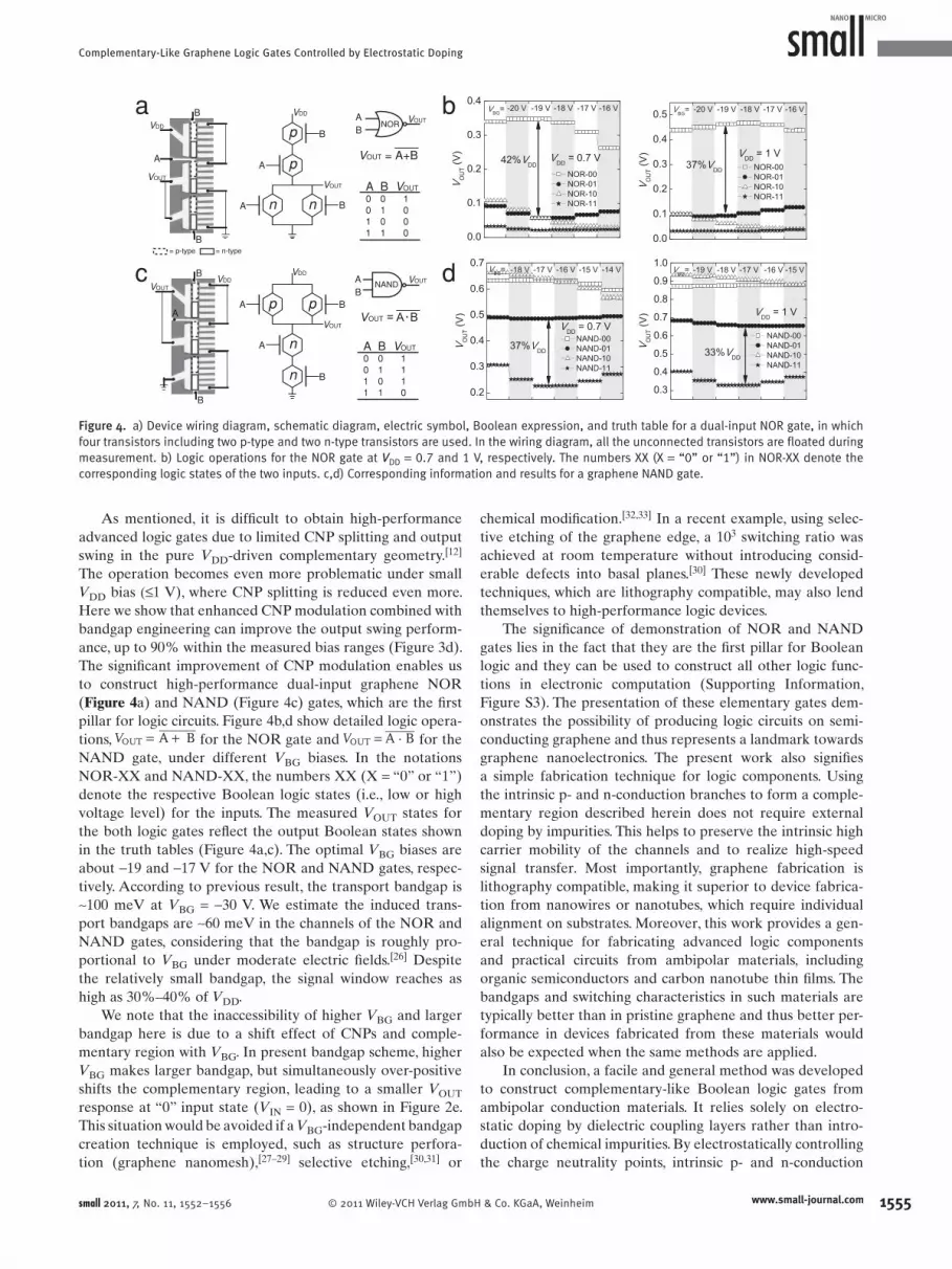
Figure 4 . a) Device wiring diagram, schematic diagram, electric symbol, Boolean expression, and truth table for a dual-input NOR gate, in which four transistors including two p-type and two n-type transistors are used. In the wiring diagram, all the unconnected transistors are fl oated during measurement. b) Logic operations for the NOR gate at V DD = 0.7 and 1 V, respectively. The numbers XX (X = “0” or “1”) in NOR-XX denote the corresponding logic states of the two inputs. c,d) Corresponding information and results for a graphene NAND gate.
VOUT = A+B
Bn
A n
Bp
VDD
VOUT
p
AB
VOUTNAND
AB
VOUTNOR
A
Bp
p
BnA n
VOUT
VDDa b
dc
VOUT
1 0 0 0
A0011
B0101
VOUT
1 1 1 0
A0011
B0101
VDD
B
B
A
VOUT
= p-type = n-type
VDDB
B
A
VOUT
A
As mentioned, it is diffi cult to obtain high-performance
advanced logic gates due to limited CNP splitting and output
swing in the pure V DD -driven complementary geometry. [ 12 ]
The operation becomes even more problematic under small
V DD bias (≤1 V), where CNP splitting is reduced even more.
Here we show that enhanced CNP modulation combined with
bandgap engineering can improve the output swing perform-
ance, up to 90% within the measured bias ranges (Figure 3 d).
The signifi cant improvement of CNP modulation enables us
to construct high-performance dual-input graphene NOR
( Figure 4 a) and NAND (Figure 4 c) gates, which are the fi rst
pillar for logic circuits. Figure 4 b,d show detailed logic opera-
tions, VOUT = A + B for the NOR gate and VOUT = A · B for the
NAND gate, under different V BG biases. In the notations
NOR-XX and NAND-XX, the numbers XX (X = “0” or “1”)
denote the respective Boolean logic states (i.e., low or high
voltage level) for the inputs. The measured V OUT states for
the both logic gates refl ect the output Boolean states shown
in the truth tables (Figure 4 a,c). The optimal V BG biases are
about − 19 and − 17 V for the NOR and NAND gates, respec-
tively. According to previous result, the transport bandgap is
∼ 100 meV at V BG = − 30 V. We estimate the induced trans-
port bandgaps are ∼ 60 meV in the channels of the NOR and
NAND gates, considering that the bandgap is roughly pro-
portional to V BG under moderate electric fi elds. [ 26 ] Despite
the relatively small bandgap, the signal window reaches as
high as 30%–40% of V DD .
We note that the inaccessibility of higher V BG and larger
bandgap here is due to a shift effect of CNPs and comple-
mentary region with V BG . In present bandgap scheme, higher
V BG makes larger bandgap, but simultaneously over-positive
shifts the complementary region, leading to a smaller V OUT
response at “0” input state ( V IN = 0), as shown in Figure 2 e.
This situation would be avoided if a V BG -independent bandgap
creation technique is employed, such as structure perfora-
tion (graphene nanomesh), [ 27–29 ] selective etching, [ 30 , 31 ] or
© 2011 Wiley-VCH Verlag Gmbsmall 2011, 7, No. 11, 1552–1556
chemical modifi cation. [ 32 , 33 ] In a recent example, using selec-
tive etching of the graphene edge, a 10 3 switching ratio was
achieved at room temperature without introducing consid-
erable defects into basal planes. [ 30 ] These newly developed
techniques, which are lithography compatible, may also lend
themselves to high-performance logic devices.
The signifi cance of demonstration of NOR and NAND
gates lies in the fact that they are the fi rst pillar for Boolean
logic and they can be used to construct all other logic func-
tions in electronic computation (Supporting Information,
Figure S3). The presentation of these elementary gates dem-
onstrates the possibility of producing logic circuits on semi-
conducting graphene and thus represents a landmark towards
graphene nanoelectronics. The present work also signifi es
a simple fabrication technique for logic components. Using
the intrinsic p- and n-conduction branches to form a comple-
mentary region described herein does not require external
doping by impurities. This helps to preserve the intrinsic high
carrier mobility of the channels and to realize high-speed
signal transfer. Most importantly, graphene fabrication is
lithography compatible, making it superior to device fabrica-
tion from nanowires or nanotubes, which require individual
alignment on substrates. Moreover, this work provides a gen-
eral technique for fabricating advanced logic components
and practical circuits from ambipolar materials, including
organic semiconductors and carbon nanotube thin fi lms. The
bandgaps and switching characteristics in such materials are
typically better than in pristine graphene and thus better per-
formance in devices fabricated from these materials would
also be expected when the same methods are applied.
In conclusion, a facile and general method was developed
to construct complementary-like Boolean logic gates from
ambipolar conduction materials. It relies solely on electro-
static doping by dielectric coupling layers rather than intro-
duction of chemical impurities. By electrostatically controlling
the charge neutrality points, intrinsic p- and n-conduction
1555H & Co. KGaA, Weinheim www.small-journal.com

S.-L. Li et al.
15
communications
branches are delicately combined to construct a complemen-tary geometry. This avoids external doping processes and
largely simplifi es fabrication. For the fi rst time, elementary
NOR and NAND logic gates were realized on semicon-
ducting bilayer graphene channels. Not limited to graphene,
this method also provides a general route in development of
logic devices for other ambipolar materials.
Experimental Section
The samples were mounted on chip carriers and sealed in a vacuum sample tube. During measurement, the sample tube was immersed in liquid nitrogen, and the sample temperature was about 79 K. The low-temperature environment has two implications. First, it reduces the thermal activation energy to demonstrate the effect of small bandgaps (60–100 meV) in our graphene samples. Second, it allows for applying a high electric fi eld on both top and back gates without dielectric breakdown.
Supporting Information
Supporting Information is available from the Wiley Online Library or from the author.
Acknowledgements
We acknowledge Dr. H. Hiura for fruitful discussions. This work was supported in part by a Grant-in-Aid for Scientifi c Research (No. 21241038) from the Ministry of Education, Culture, Sports, Science and Technology (MEXT) of Japan, and by the Funding Program for World-Leading Innovative R&D on Science and Technology (FIRST Program) from the Japan Society for the Promotion of Science (JSPS).
[ 1 ] K. Novoselov , A. Geim , S. Morozov , D. Jiang , Y. Zhang , S. Dubonos , I. Grigorieva , A. Firsov , Science 2004 , 306 , 666 .
[ 2 ] X. Du , I. Skachko , F. Duerr , A. Luican , E. Y. Andrei , Nature 2009 , 462 , 192 .
[ 3 ] K. I. Bolotin , K. J. Sikes , J. Hone , H. L. Stormer , P. Kim , Phys. Rev. Lett. 2008 , 101 , 096802 .
[ 4 ] F. Schwierz , Nat. Nanotechnol. 2010 , 5 , 487 . [ 5 ] D. Frank , Y. Taur , H.-S. Wong , IEEE Electron Dev. Lett. 1998 , 19 ,
385 . [ 6 ] R. Sordan , F. Traversi , V. Russo , Appl. Phys. Lett. 2009 , 94 ,
073305 . [ 7 ] F. Traversi , V. Russo , R. Sordan , Appl. Phys. Lett. 2009 , 94 ,
223312 . [ 8 ] N. Harada , K. Yagi , S. Sato , N. Yokoyama , Appl. Phys. Lett. 2010 ,
96 , 012102 .
56 www.small-journal.com © 2011 Wiley-VCH Verlag G
[ 9 ] L. Liao , J. Bai , Y.-C. Lin , Y. Qu , Y. Huang , X. Duan , Adv. Mater. 2010 , 22 , 1941 .
[ 10 ] S.-L. Li , H. Miyazaki , A. Kumatani , A. Kanda , K. Tsukagoshi , Nano Lett. 2010 , 10 , 2357 .
[ 11 ] S.-L. Li , H. Miyazaki , H. Hiura , C. Liu , K. Tsukagoshi , ACS Nano 2011 , 5 , 500 .
[ 12 ] W. J. Yu , U. J. Kim , B. R. Kang , I. H. Lee , E.-H. Lee , Y. H. Lee , Nano Lett. 2009 , 9 , 1401 .
[ 13 ] M. Ha , Y. Xia , A. A. Green , W. Zhang , M. J. Renn , C. H. Kim , M. C. Hersam , C. D. Frisbie , ACS Nano 2010 , 4 , 4388 .
[ 14 ] T. D. Anthopoulos , S. Setayesh , E. Smits , M. Coelle , E. Cantatore , B. deBoer , P. W. M. Blom , D. M. deLeeuw , Adv. Mater. 2006 , 18 , 1900 .
[ 15 ] T. B. Singh , P. Senkarabacak , N. S. Sariciftci , A. Tanda , C. Lackner , R. Hagelauer , G. Horowitz , Appl. Phys. Lett. 2006 , 89 , 033512 .
[ 16 ] C.-Y. Yang , Dhananjay , S.-S. Cheng , C.-W. Ou , Y.-C. Chuang , M.-C. Wu , C.-W. Chu , Appl. Phys. Lett. 2008 , 92 , 253307 .
[ 17 ] E. McCann , Phys. Rev. B 2006 , 74 , 161403 . [ 18 ] E. V. Castro , K. S. Novoselov , S. V. Morozov , N. M. R. Peres ,
J. M. B. L. DosSantos , J. Nilsson , F. Guinea , A. K. Geim , A. H. C. Neto , Phys. Rev. Lett. 2007 , 99 , 216802 .
[ 19 ] H. Min , B. Sahu , S. K. Banerjee , A. H. MacDonald , Phys. Rev. B 2007 , 75 , 155115 .
[ 20 ] G. Giovannetti , P. A. Khomyakov , G. Brocks , P. J. Kelly , J. van den Brink , Phys. Rev. B 2007 , 76 , 073103 .
[ 21 ] S. Kim , J. Nah , I. Jo , D. Shahrjerdi , L. Colombo , Z. Yao , E. Tutuc , S. K. Banerjee , Appl. Phys. Lett. 2009 , 94 , 062107 .
[ 22 ] H. Miyazaki , S. Li , A. Kanda , K. Tsukagoshi , Semicond. Sci. Technol. 2010 , 25 , 034008 .
[ 23 ] H. Miyazaki , K. Tsukagoshi , A. Kanda , M. Otani , S. Okada , Nano Lett. 2010 , 10 , 3888 .
[ 24 ] S. Heinze , M. Radosavljevic , J. Tersoff , P. Avouris , Phys. Rev. B 2003 , 68 , 235418 .
[ 25 ] M. Radosavljevic , S. Heinze , J. Tersoff , P. Avouris , Appl. Phys. Lett. 2003 , 83 , 2435 .
[ 26 ] Y. Zhang , T.-T. Tang , C. Girit , Z. Hao , M. C. Martin , A. Zettl , M. F. Crommie , Y. R. Shen , F. Wang , Nature 2009 , 459 , 820 .
[ 27 ] J. Bai , X. Zhong , S. Jiang , Y. Huang , X. Duan , Nat. Nanotechnol. 2010 , 5 , 190 .
[ 28 ] X. Liang , Y.-S. Jung , S. Wu , A. Ismach , D. L. Olynick , S. Cabrini , J. Bokor , Nano Lett. 2010 , 10 , 2454 .
[ 29 ] M. Kim , N. S. Safron , E. Han , M. S. Arnold , P. Gopalan , Nano Lett. 2010 , 10 , 1125 .
[ 30 ] L. Xie , L. Jiao , H. Dai , J. Am. Chem. Soc. 2010 , 132 , 14751 . [ 31 ] R. Yang , L. Zhang , Y. Wang , Z. Shi , D. Shi , H. Gao , E. Wang ,
G. Zhang , Adv. Mater. 2010 , 22 , 4014 . [ 32 ] R. R. Nair , W. Ren , R. Jalil , I. Riaz , V. G. Kravets , L. Britnell , P. Blake ,
F. Schedin , A. S. Mayorov , S. Yuan , M. I. Katsnelson , H.-M. Cheng , W. Strupinski , L. G. Bulusheva , A. V. Okotrub , I. V. Grigorieva , A. N. Grigorenko , K. S. Novoselov , A. K. Geim , Small 2010 , 6 , 2877 .
[ 33 ] J. T. Robinson , J. S. Burgess , C. E. Junkermeier , S. C. Badescu , T. L. Reinecke , F. K. Perkins , M. K. Zalalutdniov , J. W. Baldwin , J. C. Culbertson , P. E. Sheehan , E. S. Snow , Nano Lett. 2010 , 10 , 3001 .
Received: February 12, 2011 Revised: March 9, 2011 Published online: April 29, 2011
mbH & Co. KGaA, Weinheim small 2011, 7, No. 11, 1552–1556

S1
SUPPORTING INFORMATION
Complementary-like Semiconducting Graphene
Logic Gates Controlled by Electrostatic Doping
Song-Lin Li1, Hisao Miyazaki1,2, Michael V. Lee1, Chuan Liu1, Akinobu Kanda1,3 and Kazuhito Tsukagoshi1,2
1 MANA, National Institute for Materials Science, Tsukuba, Ibaraki 305-0044, Japan 2 CREST, Japan Science and Technology Agency, Kawaguchi, Saitama 332-0012, Japan 3 Institute of Physics, University of Tsukuba, Tsukuba, Ibaraki 305-8571, Japan
Content
1. Identification of graphene layer number by optical contrast
2. Origin of bipolar conduction and VDS effect on switching ratio
3. Realization of all logic functions from NAND gates
1. Identification of graphene layer number by optical contrast
According to Ref. R1, the contrast spectra show excellent dependence with layer number up to
10 and exhibit highest resolution for wavelength around 550 nm. After obtaining the optical images
under white light (Fig.S1a), we isolated and extracted the corresponding green-channel images,
which are used for contrast comparison (Fig.S1b). In Fig.S1b, some areas including intended
graphene and suitable substrate nearby were selected (e.g., regions c or d). The substrate region was
used as a contrast reference. In the contrast histograms of the selected regions, several peaks appear
(Fig.S1 c and d) which correspond to the reflectance contrasts of the SiO2 substrate and graphene
flaks. We calculated that the theoretical contrast values for the 1 to 4 layer flakes on 90 nm SiO2
substrates are 94.0, 87.5, 81.1 and 74.6, respectively, normalizing the substrate to 100. In Fig.S1 c
and d, the longitudinal axis (green contrast) delivers information about layer numbers, while the
horizontal axis (pixel numbers) only reflects the size of the selected areas and thus is irrelated to
layer numbers. In Fig.S1c, only an individual graphene peak with contrast ~92 shows up, indicating
that the flake in region c is single layer. In contrast, two pronounced peaks near 87 and 81 are
shown in Fig.S1d, implying that the region d contains both large 2- and 3-layer flakes.
As an alternative way, Raman spectrum was also employed to confirm the layer numbers
determined by the optical method used above. Figure S1e presents the corresponding Raman spectra
for the indentified graphene layers. Both the intensity ratios of G band (~1600 cm-1) to 2D band
S2
(~2700 cm-1) and the shape evolution of 2D band show an excellent consistency with the optical
method. The optical contrast spectrum is a fast and nondestructive way to identify the layer
numbers of graphene flakes.
2. Origin of bipolar conduction and VDS effect on switching ratio
The bipolar conduction behavior in the graphene transistors can be understood within the
Schottky barrier transistor model previously proposed for carbon nanotube (CNT) transistors.R2 The
band diagram for such a transistor is schematically shown in Fig. S2c, where the graphene or CNT
channel has a band gap Eg (Eg ≥ 0) and the drain has a Fermi level EF. In transport process, the
electrons (e) should overcome a Schottky barrier Φe to reach conductance band (EC) of the channel
at the channel/drain interface. Similarly, there is a barrier Φh for holes transport. In the case of large
Eg, the transistor often becomes unipolar, being p-type when the EF of drain approaches the EV of
channel (Φh~0, Φe~Eg) and being n-type when EF approaches EC (Φe~0, Φh~Eg). The minority
carriers are well blocked by the corresponding Schottky barriers and thus well-defined polarity is
exhibited.
In the case of graphene channels, the Eg is very small. Eg = 0 for single layer (SLG) and Eg <
100 meV for bilayer graphene (BLG). Accordingly, the Schottky barrier is small, because Φh, Φe ≤
Eg. Therefore, the graphene transistors often show bipolar conduction behavior. Only large enough
Eg is formed, can a unipolar conduction be obtained. Therefore, it is more accurate to conclude that
our graphene transistors operate as normal channel-controlled devices, since the contact barriers
cannot efficiently limit carrier injection in small-gap graphene transistors. The conduction
characteristics should be understood on the basis of resistance variation of the channels, which is
related to the carrier distribution along the channels.
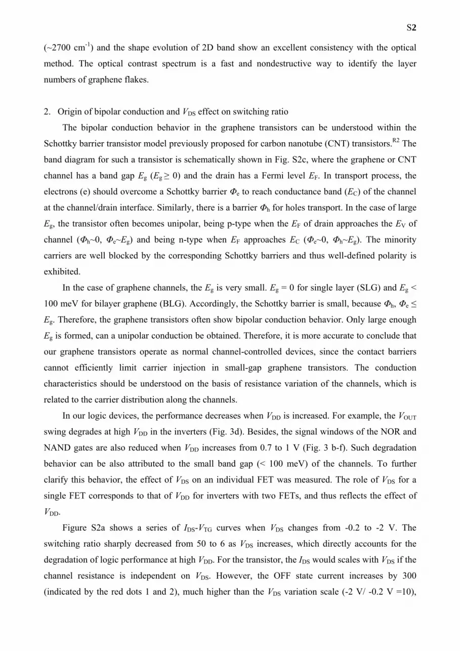
In our logic devices, the performance decreases when VDD is increased. For example, the VOUT
swing degrades at high VDD in the inverters (Fig. 3d). Besides, the signal windows of the NOR and
NAND gates are also reduced when VDD increases from 0.7 to 1 V (Fig. 3 b-f). Such degradation
behavior can be also attributed to the small band gap (< 100 meV) of the channels. To further
clarify this behavior, the effect of VDS on an individual FET was measured. The role of VDS for a
single FET corresponds to that of VDD for inverters with two FETs, and thus reflects the effect of
VDD.
Figure S2a shows a series of IDS-VTG curves when VDS changes from -0.2 to -2 V. The
switching ratio sharply decreased from 50 to 6 as VDS increases, which directly accounts for the
degradation of logic performance at high VDD. For the transistor, the IDS would scales with VDS if the
channel resistance is independent on VDS. However, the OFF state current increases by 300
(indicated by the red dots 1 and 2), much higher than the VDS variation scale (-2 V/ -0.2 V =10),

S3
suggesting a large VDS effect on the channel resistance. The variation of channel resistance can be
more clearly seen in Fig. S2b.
This observed VDS effect can be understood in terms of the charge redistribution model.R3
When VDS becomes comparable to VTG, it produces a substantial position-related potential
distribution )(Ch xV along the channel. The effective potential between the TG and channel,
)()( ChTGTG,eff xVVxV −= , is thus strongly dependent on the channel position x. At any position, the
carrier concentration can be roughly expressed as
[ ]2TG
0TGeffTG,
20
220 ))(()()()()( CVxVxnxnxnxn g −+=+= ,
where )(0 xn is the density of residual carriers and )(xng is the density of gate induced carriers.
Fig. S2 c and d schematically depict the carrier distributions for the OFF states shown by the red
dots 1 and 2 in Fig. S2a. In the point 2, more carriers are accumulated in the channel due to the
higher VDS applied, resulting in a lower channel resistance and a degraded OFF state.
According to the analysis above, we conclude that the adverse VDS effect on logic performance
is due to the lack of effective Schottky barriers at drain/channel interface. Larger band gaps and
effective Schottky barriers are necessary to achieve high-performance logic devices.
3. Realization of all logic functions from NAND gates
All other types of Boolean logic gates (i.e., AND, OR, NOT, XOR, XNOR) can be created
from a suitable network of NAND gates. Similarly all gates can be created from a network of NOR
gates. Historically, NAND gates were easier to construct from silicon MOS technology and thus
NAND gates served as the first pillar of Boolean logic in electronic computation.
Reference
(R1) Z. H. Ni, H. M. Wang, J. Kasim, H. M. Fan, T. Yu, Y. H. Wu, Y. P. Feng and Z. X. Shen,
Graphene thickness determination using reflection and contrast spectroscopy, Nano Lett. 7 (2007)
2758-2763.
(R2) S. Heinze, J. Tersoff, R. Martel, V. Derycke, J. Appenzeller and P. Avouris Carbon nanotubes
as Schottky barrier transistors, Phys. Rev. Lett. 89 (2002) 106801.
(R3) I. Meric, M. Y. Han, A. F. Young, B. Ozyilmaz, P. Kim and K. L. Shepard, Current saturation
in zero-bandgap, top-gated graphene field-effect transistors, Nat. Nanotechnol. 3 (2008) 654-659.

S4
Figures
1200 1600 2600 2800
ex. = 532 nm
Graphite
3 layers
2 layers
Ram
an In
tens
ity (a
.u.)
Raman Shift (cm-1)
1 layer
e
d
b
0 10 2070
80
90
100
Gre
en in
tens
ity
Num of Pixels /1000
01234
Layer Number
0 10 2070
80
90
100
Gre
en in
tens
ity
Num of Pixels /1000
01234
Layer Number
a
c d
c
Figure S1. Optical images with (a) all RGB channels and (b) individual green channel for graphene samples with multiple flakes on 90 nm SiO2 substrates. The square gold markers are 2 μm in dimension. (c) and (d) show the histograms of green contrast for the regions c and d selected in (b). The substrate contrast is normalized to 100. (e) Raman spectra for graphene flakes with 1-3 layers and a graphite flake.

S5
-1 0 1 2
10-7
10-6
10-5
10-4
1
-2 V
VDS= -0.2 VI DS (A
)
VTG (V)
a
-1 0 1 2
104
105
106
Graphene or CNT
2
+ -
Schottky barrier transistor
e
d
cbφe EF
R (Ω
)
VTG (V)
-2 V
VDS= -0.2V
ng(x) ~ 0 VDS~ 0, CNP-1
S
⏐VDS⏐ >> 0, CNP-2
ng(x) ≠ 0++ - - D
S D
S D
Eg φh
EC
EV
e
h
-- -+++
Figure S2. (a) Channel current and (b) resistance versus VTG at different drain voltage VDS from -0.2 to -2 V (Step = -0.2 V). (c) Schematic diagram of band lineup for a graphene or nanotube transistor. (d) and (e) Schematic carrier distributions in graphene channels with different VDS biases. The higher the absolute values of VDS, the more carriers are induced and the lower channel resistance is obtained.

S6
Number of NAND employed
Gate
NOT
AND
OR
XOR
XNOR
Symbol Diagram
1
2
3
6
7
Figure S3. The electrical diagram for combination of other types of Boolean logic gates (i.e., AND, OR, NOT, XOR, XNOR) from NAND networks.


