Embed Size (px)
Citation preview
38
Chapter 2
Boolean Algebra and Logic Gates
2 . 1 I N T R O D U C T I O N
Because binary logic is used in all of today’s digital computers and devices, the cost of
the circuits that implement it is an important factor addressed by designers—be they
computer engineers, electrical engineers, or computer scientists. Finding simpler and
cheaper, but equivalent, realizations of a circuit can reap huge payoffs in reducing the
overall cost of the design. Mathematical methods that simplify circuits rely primarily on
Boolean algebra. Therefore, this chapter provides a basic vocabulary and a brief founda-
tion in Boolean algebra that will enable you to optimize simple circuits and to under-
stand the purpose of algorithms used by software tools to optimize complex circuits
involving millions of logic gates.
2 . 2 B A S I C D E F I N I T I O N S
Boolean algebra, like any other deductive mathematical system, may be defined with a
set of elements, a set of operators, and a number of unproved axioms or postulates. A set of elements is any collection of objects, usually having a common property. If S is a set,
and x and y are certain objects, then the notation x H S means that x is a member of the
set S and y x S means that y is not an element of S. A set with a denumerable number
of elements is specified by braces: A = {1, 2, 3, 4} indicates that the elements of set A
are the numbers 1, 2, 3, and 4. A binary operator defined on a set S of elements is a rule
that assigns, to each pair of elements from S, a unique element from S. As an example,
consider the relation a*b = c. We say that * is a binary operator if it specifies a rule
for finding c from the pair (a, b) and also if a, b, c H S. However, * is not a binary operator
if a, b H S, and if c x S.
Section 2.2 Basic Definitions 39
The postulates of a mathematical system form the basic assumptions from which it
is possible to deduce the rules, theorems, and properties of the system. The most com-
mon postulates used to formulate various algebraic structures are as follows:
1. Closure. A set S is closed with respect to a binary operator if, for every pair of
elements of S, the binary operator specifies a rule for obtaining a unique element
of S. For example, the set of natural numbers N = {1, 2, 3, 4, c} is closed with
respect to the binary operator + by the rules of arithmetic addition, since, for any
a, b H N, there is a unique c H N such that a + b = c. The set of natural numbers
is not closed with respect to the binary operator - by the rules of arithmetic
subtraction, because 2 - 3 = -1 and 2, 3 H N, but (-1) x N.
2. Associative law. A binary operator * on a set S is said to be associative whenever
(x*y)*z = x* (y*z) for all x, y, z, H S
3. Commutative law. A binary operator * on a set S is said to be commutative when-
ever
x*y = y*x for all x, y H S
4. Identity element. A set S is said to have an identity element with respect to a binary
operation * on S if there exists an element e H S with the property that
e*x = x*e = x for every x H S
Example: The element 0 is an identity element with respect to the binary operator
+ on the set of integers I = {c , -3, -2, -1, 0, 1, 2, 3,c}, since
x + 0 = 0 + x = x for any x H I
The set of natural numbers, N, has no identity element, since 0 is excluded from the set.
5. Inverse. A set S having the identity element e with respect to a binary operator *
is said to have an inverse whenever, for every x H S, there exists an element y H S
such that
x *y = e
Example: In the set of integers, I, and the operator + , with e = 0, the inverse of
an element a is (-a), since a + (-a) = 0.
6. Distributive law. If * and # are two binary operators on a set S, * is said to be dis-
tributive over # whenever
x* (y # z) = (x*y) # (x*z)
A field is an example of an algebraic structure. A field is a set of elements, together with
two binary operators, each having properties 1 through 5 and both operators combining
to give property 6. The set of real numbers, together with the binary operators + and # ,
40 Chapter 2 Boolean Algebra and Logic Gates
forms the field of real numbers. The field of real numbers is the basis for arithmetic and
ordinary algebra. The operators and postulates have the following meanings:
The binary operator + defines addition.
The additive identity is 0.
The additive inverse defines subtraction.
The binary operator # defines multiplication.
The multiplicative identity is 1.
For a � 0, the multiplicative inverse of a = 1>a defines division (i.e., a # 1>a = 1 ).
The only distributive law applicable is that of # over + :
a # (b + c) = (a # b) + (a # c)
2 . 3 A X I O M AT I C D E F I N I T I O N O F B O O L E A N A L G E B R A
In 1854, George Boole developed an algebraic system now called Boolean algebra. In
1938, Claude E. Shannon introduced a two‐valued Boolean algebra called switching algebra that represented the properties of bistable electrical switching circuits. For the
formal definition of Boolean algebra, we shall employ the postulates formulated by
E. V. Huntington in 1904.
Boolean algebra is an algebraic structure defined by a set of elements, B, together
with two binary operators, + and # , provided that the following (Huntington) postulates
are satisfied:
1. (a) The structure is closed with respect to the operator + .
(b) The structure is closed with respect to the operator # .
2. (a) The element 0 is an identity element with respect to + ; that is, x + 0 =
0 + x = x .
(b) The element 1 is an identity element with respect to # ; that is, x # 1 = 1 # x = x.
3. (a) The structure is commutative with respect to + ; that is, x + y = y + x .
(b) The structure is commutative with respect to # ; that is, x # y = y # x.
4. (a) The operator # is distributive over + ; that is, x # (y + z) = (x # y) + (x # z).
(b) The operator + is distributive over # ; that is, x + (y # z) = (x + y) # (x + z).
5. For every element x H B, there exists an element x� H B (called the complement of x)
such that (a) x + x� = 1 and (b) x # x� = 0.
6. There exist at least two elements x, y H B such that x � y.
Comparing Boolean algebra with arithmetic and ordinary algebra (the field of real
numbers), we note the following differences:
1. Huntington postulates do not include the associative law. However, this law holds for
Boolean algebra and can be derived (for both operators) from the other postulates.
2. The distributive law of + over # (i.e., x + (y # z) = (x + y) # (x + z) ) is valid for
Boolean algebra, but not for ordinary algebra.
Section 2.3 Axiomatic Definition of Boolean Algebra 41
3. Boolean algebra does not have additive or multiplicative inverses; therefore, there
are no subtraction or division operations.
4. Postulate 5 defines an operator called the complement that is not available in
ordinary algebra.
5. Ordinary algebra deals with the real numbers, which constitute an infinite set of
elements. Boolean algebra deals with the as yet undefined set of elements, B, but
in the two‐valued Boolean algebra defined next (and of interest in our subse-
quent use of that algebra), B is defined as a set with only two elements, 0 and 1.
Boolean algebra resembles ordinary algebra in some respects. The choice of the
symbols + and # is intentional, to facilitate Boolean algebraic manipulations by persons
already familiar with ordinary algebra. Although one can use some knowledge from
ordinary algebra to deal with Boolean algebra, the beginner must be careful not to
substitute the rules of ordinary algebra where they are not applicable.
It is important to distinguish between the elements of the set of an algebraic structure
and the variables of an algebraic system. For example, the elements of the field of real
numbers are numbers, whereas variables such as a, b, c, etc., used in ordinary algebra,
are symbols that stand for real numbers. Similarly, in Boolean algebra, one defines the
elements of the set B, and variables such as x, y, and z are merely symbols that represent the elements. At this point, it is important to realize that, in order to have a Boolean
algebra, one must show that
1. the elements of the set B,
2. the rules of operation for the two binary operators, and
3. the set of elements, B, together with the two operators, satisfy the six Huntington
postulates.
One can formulate many Boolean algebras, depending on the choice of elements of
B and the rules of operation. In our subsequent work, we deal only with a two‐valued Boolean algebra (i.e., a Boolean algebra with only two elements). Two‐valued Boolean
algebra has applications in set theory (the algebra of classes) and in propositional logic.
Our interest here is in the application of Boolean algebra to gate‐type circuits commonly
used in digital devices and computers.
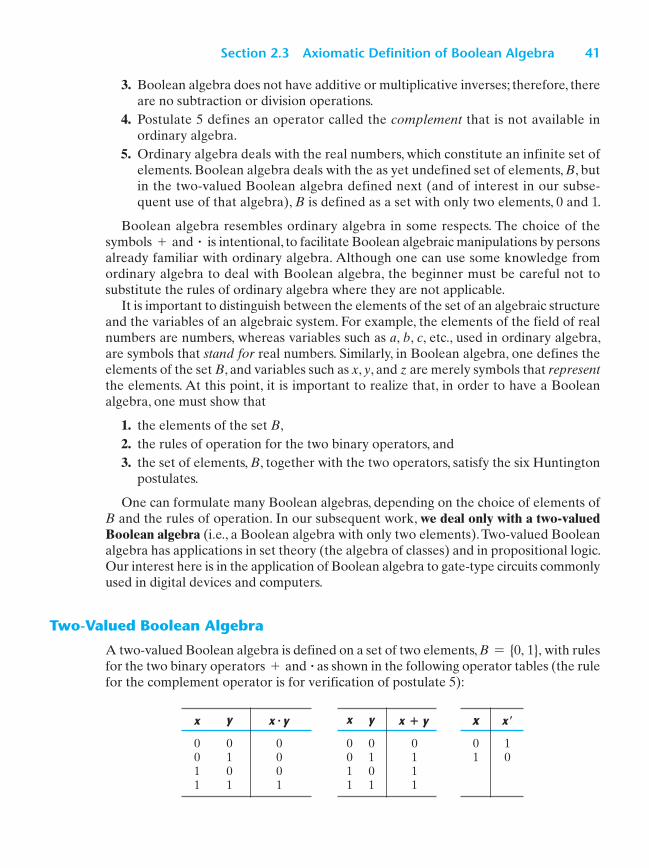
Two‐Valued Boolean Algebra
A two‐valued Boolean algebra is defined on a set of two elements, B = {0, 1}, with rules
for the two binary operators + and # as shown in the following operator tables (the rule
for the complement operator is for verification of postulate 5):
x y x # y x y x � y x x�
0 0 0 0 0 0 0 1 0 1 0 0 1 1 1 0 1 0 0 1 0 1 1 1 1 1 1 1
42 Chapter 2 Boolean Algebra and Logic Gates
These rules are exactly the same as the AND, OR, and NOT operations, respectively,
defined in Table 1.8. We must now show that the Huntington postulates are valid for the
set B = {0, 1} and the two binary operators + and # .
1. That the structure is closed with respect to the two operators is obvious from the
tables, since the result of each operation is either 1 or 0 and 1, 0 H B.
2. From the tables, we see that
(a) 0 + 0 = 0 0 + 1 = 1 + 0 = 1;
(b) 1 # 1 = 1 1 # 0 = 0 # 1 = 0.
This establishes the two identity elements, 0 for + and 1 for # , as defined by
postulate 2.
3. The commutative laws are obvious from the symmetry of the binary operator tables.
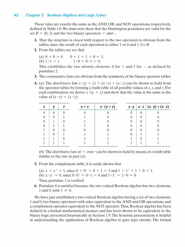
4. (a) The distributive law x # (y + z) = (x # y) + (x # z) can be shown to hold from
the operator tables by forming a truth table of all possible values of x, y, and z. For
each combination, we derive x # (y + z) and show that the value is the same as the
value of (x # y) + (x # z):
x y z y � z x # (y �z) x # y x # z (x # y) �(x # z)
0 0 0 0 0 0 0 0
0 0 1 1 0 0 0 0
0 1 0 1 0 0 0 0
0 1 1 1 0 0 0 0
1 0 0 0 0 0 0 0
1 0 1 1 1 0 1 1
1 1 0 1 1 1 0 1
1 1 1 1 1 1 1 1
(b) The distributive law of + over # can be shown to hold by means of a truth table
similar to the one in part (a).
5. From the complement table, it is easily shown that
(a) x + x � = 1, since 0 + 0� = 0 + 1 = 1 and 1 + 1� = 1 + 0 = 1.
(b) x # x� = 0, since 0 # 0� = 0 # 1 = 0 and 1 # 1� = 1 # 0 = 0.
Thus, postulate 1 is verified.
6. Postulate 6 is satisfied because the two‐valued Boolean algebra has two elements,
1 and 0, with 1 � 0.
We have just established a two‐valued Boolean algebra having a set of two elements,
1 and 0, two binary operators with rules equivalent to the AND and OR operations, and
a complement operator equivalent to the NOT operator. Thus, Boolean algebra has been
defined in a formal mathematical manner and has been shown to be equivalent to the
binary logic presented heuristically in Section 1.9. The heuristic presentation is helpful
in understanding the application of Boolean algebra to gate‐type circuits. The formal
Section 2.4 Basic Theorems and Properties of Boolean Algebra 43
presentation is necessary for developing the theorems and properties of the algebraic
system. The two‐valued Boolean algebra defined in this section is also called “switching
algebra” by engineers. To emphasize the similarities between two‐valued Boolean alge-
bra and other binary systems, that algebra was called “binary logic” in Section 1.9. From
here on, we shall drop the adjective “two‐valued” from Boolean algebra in subsequent
discussions.
2 . 4 B A S I C T H E O R E M S A N D P R O P E R T I E S O F B O O L E A N A L G E B R A
Duality
In Section 2.3, the Huntington postulates were listed in pairs and designated by part
(a) and part (b). One part may be obtained from the other if the binary operators and
the identity elements are interchanged. This important property of Boolean algebra is
called the duality principle and states that every algebraic expression deducible from
the postulates of Boolean algebra remains valid if the operators and identity elements
are interchanged. In a two‐valued Boolean algebra, the identity elements and the ele-
ments of the set B are the same: 1 and 0. The duality principle has many applications. If
the dual of an algebraic expression is desired, we simply interchange OR and AND
operators and replace 1’s by 0’s and 0’s by 1’s.
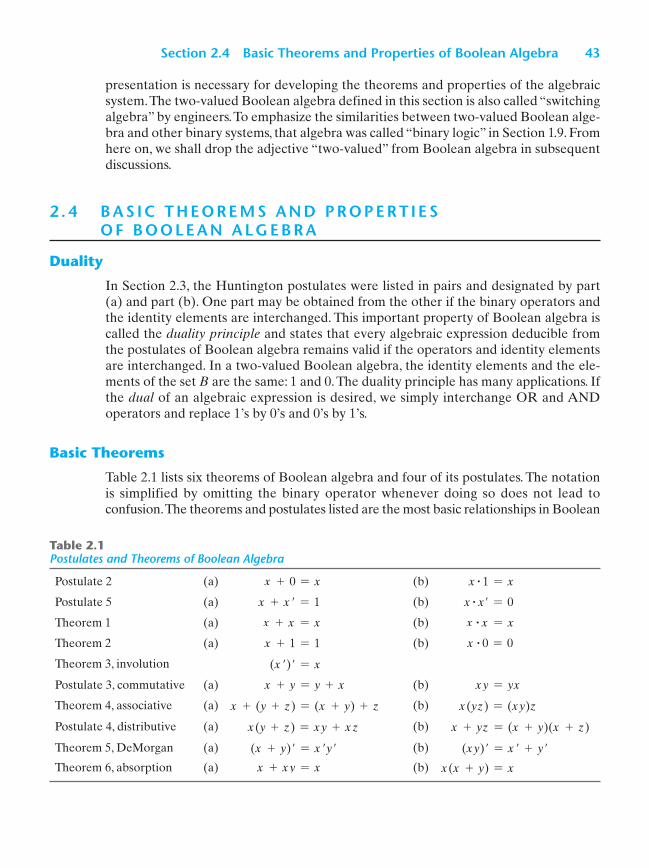
Basic Theorems
Table 2.1 lists six theorems of Boolean algebra and four of its postulates. The notation
is simplified by omitting the binary operator whenever doing so does not lead to
confusion. The theorems and postulates listed are the most basic relationships in Boolean
Table 2.1 Postulates and Theorems of Boolean Algebra
Postulate 2 (a) x + 0 = x (b) x # 1 = x
Postulate 5 (a) x + x � = 1 (b) x # x� = 0
Theorem 1 (a) x + x = x (b) x # x = x
Theorem 2 (a) x + 1 = 1 (b) x # 0 = 0
Theorem 3, involution (x �)� = x
Postulate 3, commutative (a) x + y = y + x (b) xy = yx
Theorem 4, associative (a) x + (y + z) = (x + y) + z (b) x(yz) = (xy)z
Postulate 4, distributive (a) x(y + z) = xy + xz (b) x + yz = (x + y)(x + z)
Theorem 5, DeMorgan (a) (x + y)� = x �y� (b) (xy)� = x � + y�
Theorem 6, absorption (a) x + xy = x (b) x(x + y) = x
44 Chapter 2 Boolean Algebra and Logic Gates
algebra. The theorems, like the postulates, are listed in pairs; each relation is the dual of
the one paired with it. The postulates are basic axioms of the algebraic structure and
need no proof. The theorems must be proven from the postulates. Proofs of the theorems
with one variable are presented next. At the right is listed the number of the postulate
which justifies that particular step of the proof.
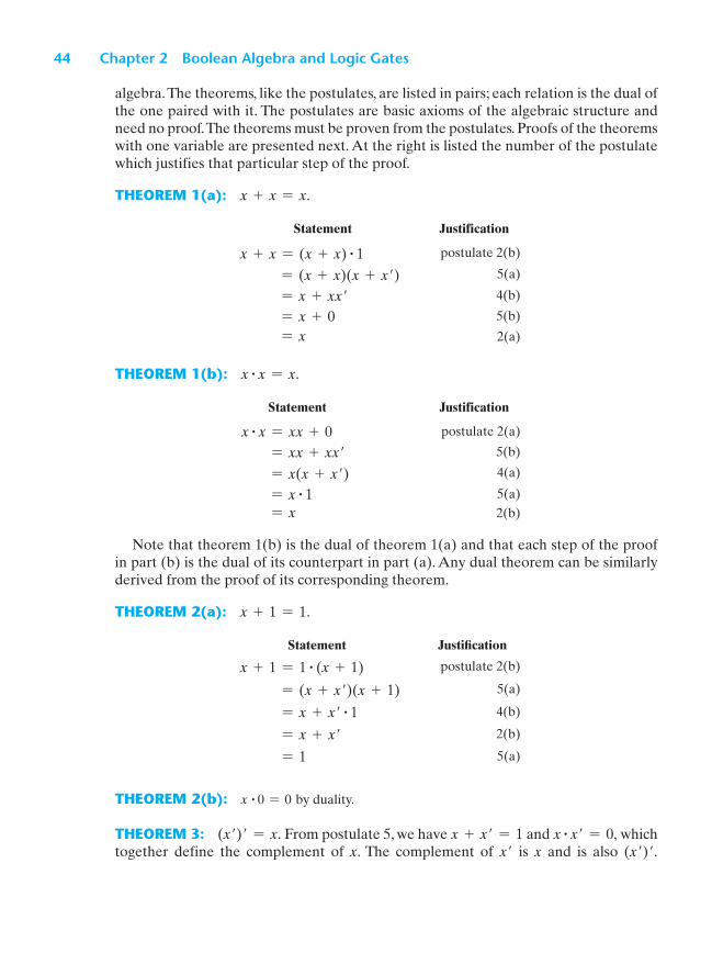
THEOREM 1(a): x + x = x.
Statement Justification
x + x = (x + x) # 1 postulate 2(b)
= (x + x)(x + x�) 5(a)
= x + xx� 4(b)
= x + 0 5(b)
= x 2(a)
THEOREM 1(b): x # x = x.
Statement Justification
x # x = xx + 0 postulate 2(a)
= xx + xx� 5(b)
= x(x + x�) 4(a)
= x # 1 5(a)
= x 2(b)
Note that theorem 1(b) is the dual of theorem 1(a) and that each step of the proof
in part (b) is the dual of its counterpart in part (a). Any dual theorem can be similarly
derived from the proof of its corresponding theorem.
THEOREM 2(a): x + 1 = 1.
Statement Justifi cation
x + 1 = 1 # (x + 1) postulate 2(b)
= (x + x�)(x + 1) 5(a)
= x + x� # 1 4(b)
= x + x� 2(b)
= 1 5(a)
THEOREM 2(b): x # 0 = 0 by duality.
THEOREM 3: (x�)� = x. From postulate 5, we have x + x� = 1 and x # x� = 0, which
together define the complement of x. The complement of x� is x and is also (x�)�.
Section 2.4 Basic Theorems and Properties of Boolean Algebra 45
Therefore, since the complement is unique, we have (x�)� = x. The theorems involv-
ing two or three variables may be proven algebraically from the postulates and the
theorems that have already been proven. Take, for example, the absorption theorem:
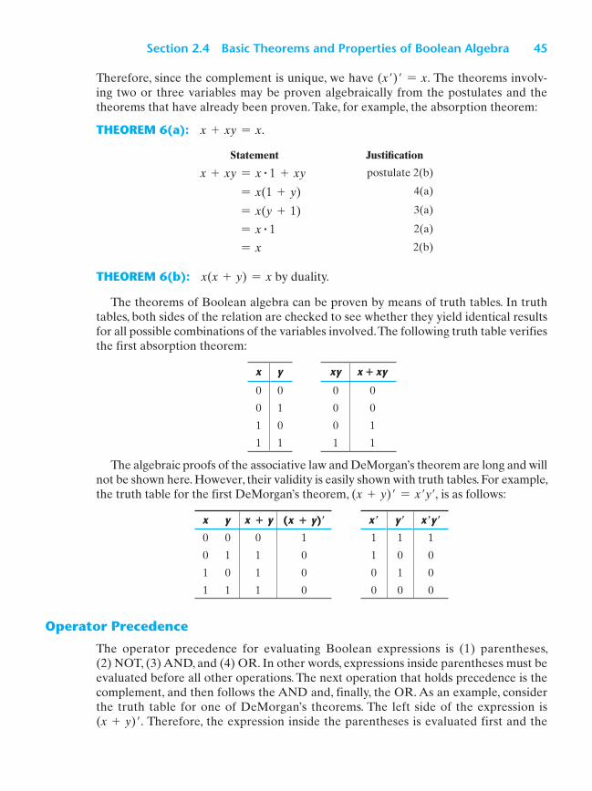
THEOREM 6(a): x + xy = x.
Statement Justifi cation
x + xy = x # 1 + xy postulate 2(b)
= x(1 + y) 4(a)
= x(y + 1) 3(a)
= x # 1 2(a)
= x 2(b)
THEOREM 6(b): x(x + y) = x by duality.
The theorems of Boolean algebra can be proven by means of truth tables. In truth
tables, both sides of the relation are checked to see whether they yield identical results
for all possible combinations of the variables involved. The following truth table verifies
the first absorption theorem:
x y xy x � xy
0 0 0 0
0 1 0 0
1 0 0 1
1 1 1 1
The algebraic proofs of the associative law and DeMorgan’s theorem are long and will
not be shown here. However, their validity is easily shown with truth tables. For example,
the truth table for the first DeMorgan’s theorem, (x + y)� = x�y�, is as follows:
x y x � y (x � y)� x� y� x�y�
0 0 0 1 1 1 1
0 1 1 0 1 0 0
1 0 1 0 0 1 0
1 1 1 0 0 0 0
Operator Precedence
The operator precedence for evaluating Boolean expressions is (1) parentheses,
(2) NOT, (3) AND, and (4) OR. In other words, expressions inside parentheses must be
evaluated before all other operations. The next operation that holds precedence is the
complement, and then follows the AND and, finally, the OR. As an example, consider
the truth table for one of DeMorgan’s theorems. The left side of the expression is
(x + y)�. Therefore, the expression inside the parentheses is evaluated first and the
46 Chapter 2 Boolean Algebra and Logic Gates
Table 2.2 Truth Tables for F1 and F2
x y z F1 F2
0 0 0 0 0
0 0 1 1 1
0 1 0 0 0
0 1 1 0 1
1 0 0 1 1
1 0 1 1 1
1 1 0 1 0
1 1 1 1 0
result then complemented. The right side of the expression is x�y�, so the complement
of x and the complement of y are both evaluated first and the result is then ANDed.
Note that in ordinary arithmetic, the same precedence holds (except for the comple-
ment) when multiplication and addition are replaced by AND and OR, respectively.
2 . 5 B O O L E A N F U N C T I O N S
Boolean algebra is an algebra that deals with binary variables and logic operations. A
Boolean function described by an algebraic expression consists of binary variables, the
constants 0 and 1, and the logic operation symbols. For a given value of the binary variables,
the function can be equal to either 1 or 0. As an example, consider the Boolean function
F1 = x + y�z
The function F1 is equal to 1 if x is equal to 1 or if both y� and z are equal to 1. F1 is equal
to 0 otherwise. The complement operation dictates that when y� = 1, y = 0. Therefore,
F1 = 1 if x = 1 or if y = 0 and z = 1. A Boolean function expresses the logical rela-
tionship between binary variables and is evaluated by determining the binary value of
the expression for all possible values of the variables.
A Boolean function can be represented in a truth table. The number of rows in the
truth table is 2n, where n is the number of variables in the function. The binary combina-
tions for the truth table are obtained from the binary numbers by counting from 0
through 2n - 1. Table 2.2 shows the truth table for the function F1. There are eight pos-
sible binary combinations for assigning bits to the three variables x, y, and z. The column
labeled F1 contains either 0 or 1 for each of these combinations. The table shows that
the function is equal to 1 when x = 1 or when yz = 01 and is equal to 0 otherwise.
A Boolean function can be transformed from an algebraic expression into a circuit
diagram composed of logic gates connected in a particular structure. The logic‐circuit
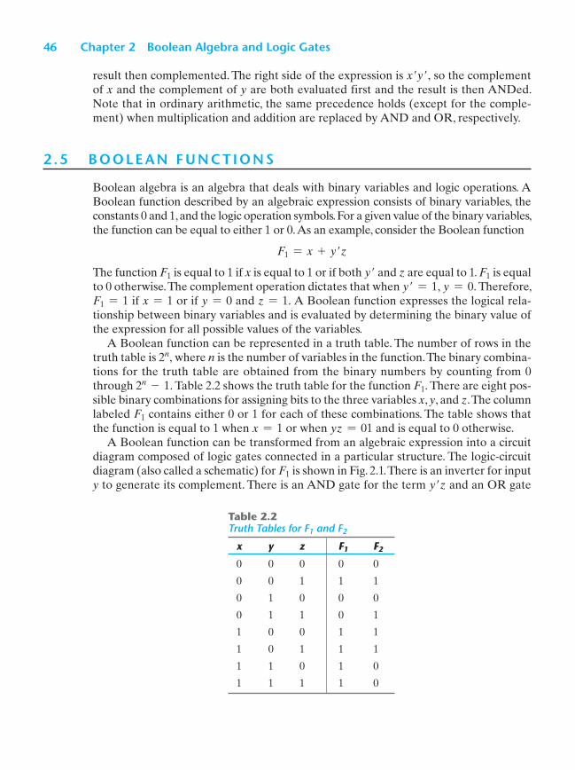
diagram (also called a schematic) for F1 is shown in Fig. 2.1 . There is an inverter for input y to generate its complement. There is an AND gate for the term y�z and an OR gate
Section 2.5 Boolean Functions 47
that combines x with y�z. In logic‐circuit diagrams, the variables of the function are taken
as the inputs of the circuit and the binary variable F1 is taken as the output of the circuit.
The schematic expresses the relationship between the output of the circuit and its inputs.
Rather than listing each combination of inputs and outputs, it indicates how to compute
the logic value of each output from the logic values of the inputs. There is only one way that a Boolean function can be represented in a truth table.
However, when the function is in algebraic form, it can be expressed in a variety of ways,
all of which have equivalent logic. The particular expression used to represent the function
will dictate the interconnection of gates in the logic‐circuit diagram. Conversely, the inter-
connection of gates will dictate the logic expression. Here is a key fact that motivates our
use of Boolean algebra: By manipulating a Boolean expression according to the rules of
Boolean algebra, it is sometimes possible to obtain a simpler expression for the same
function and thus reduce the number of gates in the circuit and the number of inputs to
the gate. Designers are motivated to reduce the complexity and number of gates because
their effort can significantly reduce the cost of a circuit. Consider, for example, the fol-
lowing Boolean function:
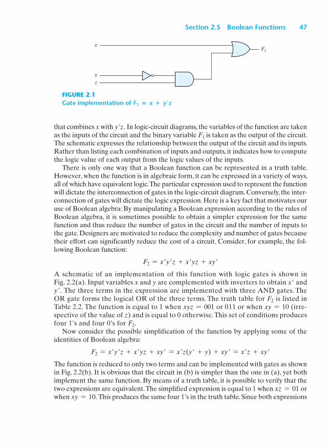
F2 = x�y�z + x�yz + xy�
A schematic of an implementation of this function with logic gates is shown in
Fig. 2.2 (a). Input variables x and y are complemented with inverters to obtain x� and
y�. The three terms in the expression are implemented with three AND gates. The
OR gate forms the logical OR of the three terms. The truth table for F2 is listed in
Table 2.2 . The function is equal to 1 when xyz = 001 or 011 or when xy = 10 (irre-
spective of the value of z) and is equal to 0 otherwise. This set of conditions produces
four 1’s and four 0’s for F2. Now consider the possible simplification of the function by applying some of the
identities of Boolean algebra:
F2 = x�y�z + x�yz + xy� = x�z(y� + y) + xy� = x�z + xy�
The function is reduced to only two terms and can be implemented with gates as shown
in Fig. 2.2 (b). It is obvious that the circuit in (b) is simpler than the one in (a), yet both
implement the same function. By means of a truth table, it is possible to verify that the
two expressions are equivalent. The simplified expression is equal to 1 when xz = 01 or
when xy = 10. This produces the same four 1’s in the truth table. Since both expressions
F1x
yz
FIGURE 2.1 Gate implementation of F1 � x � y�z
48 Chapter 2 Boolean Algebra and Logic Gates
produce the same truth table, they are equivalent. Therefore, the two circuits have the
same outputs for all possible binary combinations of inputs of the three variables. Each
circuit implements the same identical function, but the one with fewer gates and fewer
inputs to gates is preferable because it requires fewer wires and components. In general,
there are many equivalent representations of a logic function. Finding the most eco-
nomic representation of the logic is an important design task.
Algebraic Manipulation
When a Boolean expression is implemented with logic gates, each term requires a gate
and each variable within the term designates an input to the gate. We define a literal to
be a single variable within a term, in complemented or uncomplemented form. The
function of Fig. 2.2 (a) has three terms and eight literals, and the one in Fig. 2.2 (b) has
two terms and four literals. By reducing the number of terms, the number of literals, or
both in a Boolean expression, it is often possible to obtain a simpler circuit. The manip-
ulation of Boolean algebra consists mostly of reducing an expression for the purpose of
obtaining a simpler circuit. Functions of up to five variables can be simplified by the
map method described in the next chapter. For complex Boolean functions and many
(a) F2 � x�y�z � x�yz � xy�
(b) F2 � xy� � x�z
x
y
zF2
x
y
z
F2
FIGURE 2.2 Implementation of Boolean function F2 with gates
Section 2.5 Boolean Functions 49
different outputs, designers of digital circuits use computer minimization programs that
are capable of producing optimal circuits with millions of logic gates. The concepts intro-
duced in this chapter provide the framework for those tools. The only manual method
available is a cut‐and‐try procedure employing the basic relations and other manipulation
techniques that become familiar with use, but remain, nevertheless, subject to human
error. The examples that follow illustrate the algebraic manipulation of Boolean algebra
to acquaint the reader with this important design task.
EXAMPLE 2.1
Simplify the following Boolean functions to a minimum number of literals.
1. x(x� + y) = xx� + xy = 0 + xy = xy.
2. x + x�y = (x + x�)(x + y) = 1(x + y) = x + y.
3. (x + y)(x + y�) = x + xy + xy� + yy� = x(1 + y + y�) = x.
4. xy + x�z + yz = xy + x�z + yz(x + x�)
= xy + x�z + xyz + x�yz
= xy(1 + z) + x�z(1 + y)
= xy + x�z.
5. (x + y)(x� + z)(y + z) = (x + y)(x� + z), by duality from function 4.
■
Functions 1 and 2 are the dual of each other and use dual expressions in correspond-
ing steps. An easier way to simplify function 3 is by means of postulate 4(b) from
Table 2.1 : (x + y)(x + y�) = x + yy� = x. The fourth function illustrates the fact that
an increase in the number of literals sometimes leads to a simpler final expression.
Function 5 is not minimized directly, but can be derived from the dual of the steps used
to derive function 4. Functions 4 and 5 are together known as the consensus theorem.
Complement of a Function
The complement of a function F is F� and is obtained from an interchange of 0’s for 1’s
and 1’s for 0’s in the value of F. The complement of a function may be derived algebraically
through DeMorgan’s theorems, listed in Table 2.1 for two variables. DeMorgan’s theo-
rems can be extended to three or more variables. The three‐variable form of the first
DeMorgan’s theorem is derived as follows, from postulates and theorems listed in Table 2.1 :
(A + B + C)� = (A + x)� let B + C = x
= A�x� by theorem 5(a) (DeMorgan)
= A�(B + C)� substitute B + C = x
= A�(B�C�) by theorem 5(a) (DeMorgan)
= A�B�C� by theorem 4(b) (associative)
50 Chapter 2 Boolean Algebra and Logic Gates
DeMorgan’s theorems for any number of variables resemble the two‐variable case in
form and can be derived by successive substitutions similar to the method used in the
preceding derivation. These theorems can be generalized as follows:
(A + B + C + D + g + F)� = A�B�C�D�c F�
(ABCDc F)� = A� + B� + C� + D� + g + F�
The generalized form of DeMorgan’s theorems states that the complement of a func-
tion is obtained by interchanging AND and OR operators and complementing each
literal.
EXAMPLE 2.2
Find the complement of the functions F1 = x�yz� + x�y�z and F2 = x(y�z� + yz). By
applying DeMorgan’s theorems as many times as necessary, the complements are
obtained as follows:
F =1 = (x�yz� + x�y�z)� = (x�yz�)�(x�y�z)� = (x + y� + z)(x + y + z�)
F =2 = [x(y�z� + yz)]� = x� + (y�z� + yz)� = x� + (y�z�)�(yz)�
= x� + (y + z)(y� + z�)
= x� + yz� + y�z
■
A simpler procedure for deriving the complement of a function is to take the dual of
the function and complement each literal. This method follows from the generalized
forms of DeMorgan’s theorems. Remember that the dual of a function is obtained from
the interchange of AND and OR operators and 1’s and 0’s.
EXAMPLE 2.3
Find the complement of the functions F1 and F2 of Example 2.2 by taking their duals
and complementing each literal.
1. F1 = x�yz� + x�y�z.
The dual of F1 is (x� + y + z�)(x� + y� + z).
Complement each literal: (x + y� + z)(x + y + z�) = F =1.
2. F2 = x(y�z� + yz).
The dual of F2 is x + (y� + z�)(y + z).
Complement each literal: x� + (y + z)(y� + z�) = F =2.
■
Section 2.6 Canonical and Standard Forms 51
2 . 6 C A N O N I C A L A N D S TA N D A R D F O R M S
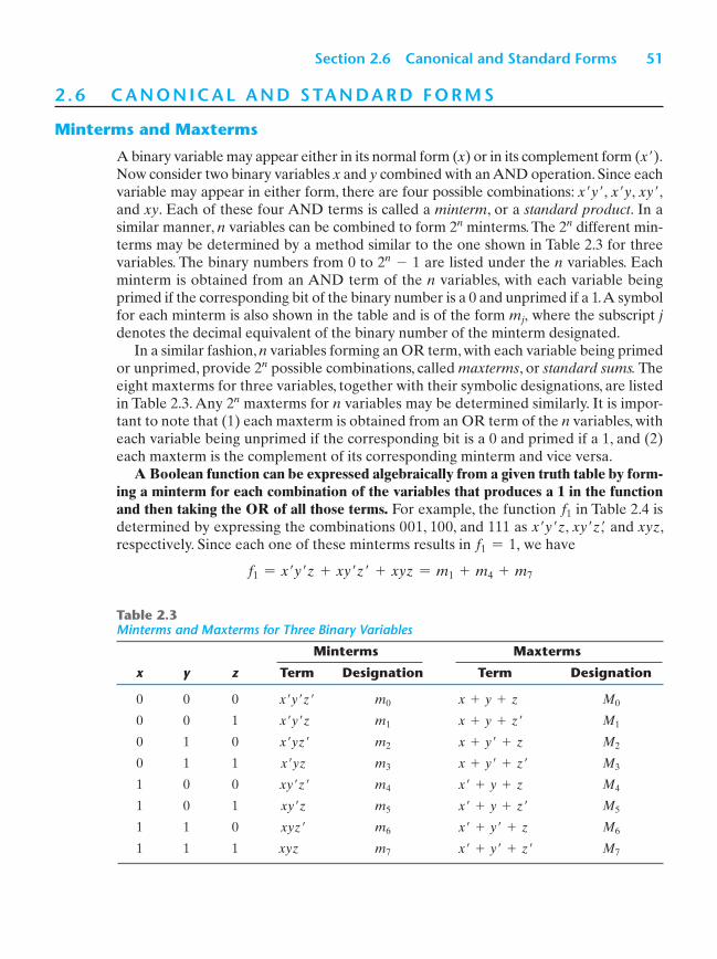
Minterms and Maxterms
A binary variable may appear either in its normal form (x) or in its complement form (x�).
Now consider two binary variables x and y combined with an AND operation. Since each
variable may appear in either form, there are four possible combinations: x�y�, x�y, xy�, and xy. Each of these four AND terms is called a minterm, or a standard product. In a
similar manner, n variables can be combined to form 2n minterms. The 2n different min-
terms may be determined by a method similar to the one shown in Table 2.3 for three
variables. The binary numbers from 0 to 2n - 1 are listed under the n variables. Each
minterm is obtained from an AND term of the n variables, with each variable being
primed if the corresponding bit of the binary number is a 0 and unprimed if a 1. A symbol
for each minterm is also shown in the table and is of the form mj, where the subscript j denotes the decimal equivalent of the binary number of the minterm designated.
In a similar fashion, n variables forming an OR term, with each variable being primed
or unprimed, provide 2n possible combinations, called maxterms, or standard sums. The
eight maxterms for three variables, together with their symbolic designations, are listed
in Table 2.3 . Any 2n maxterms for n variables may be determined similarly. It is impor-
tant to note that (1) each maxterm is obtained from an OR term of the n variables, with
each variable being unprimed if the corresponding bit is a 0 and primed if a 1, and (2)
each maxterm is the complement of its corresponding minterm and vice versa.
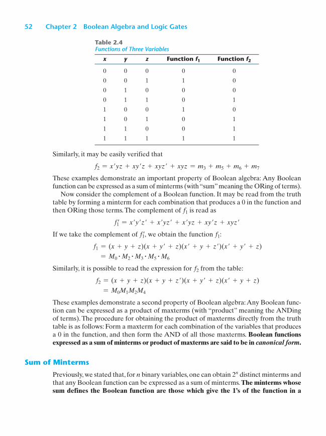
A Boolean function can be expressed algebraically from a given truth table by form-ing a minterm for each combination of the variables that produces a 1 in the function and then taking the OR of all those terms. For example, the function f1 in Table 2.4 is
determined by expressing the combinations 001, 100, and 111 as x�y�z, xy�z�, and xyz,
respectively. Since each one of these minterms results in f1 = 1, we have
f1 = x�y�z + xy�z� + xyz = m1 + m4 + m7
Table 2.3Minterms and Maxterms for Three Binary Variables
Minterms Maxterms
x y z Term Designation Term Designation
0 0 0 x�y�z� m0 x + y + z M0
0 0 1 x�y�z m1 x + y + z� M1
0 1 0 x�yz� m2 x + y� + z M2
0 1 1 x�yz m3 x + y� + z� M3
1 0 0 xy�z� m4 x� + y + z M4
1 0 1 xy�z m5 x� + y + z� M5
1 1 0 xyz� m6 x� + y� + z M6
1 1 1 xyz m7 x� + y� + z� M7
52 Chapter 2 Boolean Algebra and Logic Gates
Similarly, it may be easily verified that
f2 = x�yz + xy�z + xyz� + xyz = m3 + m5 + m6 + m7
These examples demonstrate an important property of Boolean algebra: Any Boolean
function can be expressed as a sum of minterms (with “sum” meaning the ORing of terms).
Now consider the complement of a Boolean function. It may be read from the truth
table by forming a minterm for each combination that produces a 0 in the function and
then ORing those terms. The complement of f1 is read as
f =1 = x�y�z� + x�yz� + x�yz + xy�z + xyz�
If we take the complement of f =1, we obtain the function f1:
f1 = (x + y + z)(x + y� + z)(x� + y + z�)(x� + y� + z)
= M0# M2
# M3# M5
# M6
Similarly, it is possible to read the expression for f2 from the table:
f2 = (x + y + z)(x + y + z�)(x + y� + z)(x� + y + z)
= M0M1M2M4
These examples demonstrate a second property of Boolean algebra: Any Boolean func-
tion can be expressed as a product of maxterms (with “product” meaning the ANDing
of terms). The procedure for obtaining the product of maxterms directly from the truth
table is as follows: Form a maxterm for each combination of the variables that produces
a 0 in the function, and then form the AND of all those maxterms. Boolean functions expressed as a sum of minterms or product of maxterms are said to be in canonical form .
Sum of Minterms
Previously, we stated that, for n binary variables, one can obtain 2n distinct minterms and
that any Boolean function can be expressed as a sum of minterms. The minterms whose sum defines the Boolean function are those which give the 1’s of the function in a
Table 2.4Functions of Three Variables
x y z Function f1 Function f2
0 0 0 0 0
0 0 1 1 0
0 1 0 0 0
0 1 1 0 1
1 0 0 1 0
1 0 1 0 1
1 1 0 0 1
1 1 1 1 1
Section 2.6 Canonical and Standard Forms 53
truth table. Since the function can be either 1 or 0 for each minterm, and since there are
2n minterms, one can calculate all the functions that can be formed with n variables to
be 22n. It is sometimes convenient to express a Boolean function in its sum‐of‐minterms
form. If the function is not in this form, it can be made so by first expanding the expres-
sion into a sum of AND terms. Each term is then inspected to see if it contains all the
variables. If it misses one or more variables, it is ANDed with an expression such as
x + x�, where x is one of the missing variables. The next example clarifies this procedure.
EXAMPLE 2.4
Express the Boolean function F = A + B�C as a sum of minterms. The function has
three variables: A, B, and C. The first term A is missing two variables; therefore,
A = A(B + B�) = AB + AB�
This function is still missing one variable, so
A = AB(C + C�) + AB�(C + C�)
= ABC + ABC� + AB�C + AB�C�
The second term B�C is missing one variable; hence,
B�C = B�C(A + A�) = AB�C + A�B�C
Combining all terms, we have
F = A + B�C
= ABC + ABC� + AB�C + AB�C� + A�B�C
But AB�C appears twice, and according to theorem 1 (x + x = x), it is possible to
remove one of those occurrences. Rearranging the minterms in ascending order, we
finally obtain
F = A�B�C + AB�C + AB�C + ABC� + ABC
= m1 + m4 + m5 + m6 + m7
■
When a Boolean function is in its sum‐of‐minterms form, it is sometimes convenient to
express the function in the following brief notation:
F(A, B, C) = �(1, 4, 5, 6, 7)
The summation symbol g stands for the ORing of terms; the numbers following it are
the indices of the minterms of the function. The letters in parentheses following F form
a list of the variables in the order taken when the minterm is converted to an AND term.
An alternative procedure for deriving the minterms of a Boolean function is to obtain the truth table of the function directly from the algebraic expression and then read the minterms from the truth table. Consider the Boolean function given in Example 2.4:
F = A + B�C
The truth table shown in Table 2.5 can be derived directly from the algebraic expres-
sion by listing the eight binary combinations under variables A, B, and C and inserting
54 Chapter 2 Boolean Algebra and Logic Gates
1’s under F for those combinations for which A = 1 and BC = 01. From the truth table,
we can then read the five minterms of the function to be 1, 4, 5, 6, and 7.
Product of Maxterms
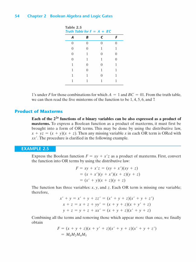
Each of the 22n functions of n binary variables can be also expressed as a product of maxterms. To express a Boolean function as a product of maxterms, it must first be
brought into a form of OR terms. This may be done by using the distributive law,
x + yz = (x + y)(x + z). Then any missing variable x in each OR term is ORed with
xx�. The procedure is clarified in the following example.
EXAMPLE 2.5
Express the Boolean function F = xy + x�z as a product of maxterms. First, convert
the function into OR terms by using the distributive law:
F = xy + x�z = (xy + x�)(xy + z)
= (x + x�)(y + x�)(x + z)(y + z)
= (x� + y)(x + z)(y + z)
The function has three variables: x, y, and z. Each OR term is missing one variable;
therefore,
x� + y = x� + y + zz� = (x� + y + z)(x� + y + z�)
x + z = x + z + yy� = (x + y + z)(x + y� + z)
y + z = y + z + xx� = (x + y + z)(x� + y + z)
Combining all the terms and removing those which appear more than once, we finally
obtain
F = (x + y + z)(x + y� + z)(x� + y + z)(x� + y + z�)
= M0M2M4M5
Table 2.5Truth Table for F � A � B�C
A B C F
0 0 0 0
0 0 1 1
0 1 0 0
0 1 1 0
1 0 0 1
1 0 1 1
1 1 0 1
1 1 1 1
Section 2.6 Canonical and Standard Forms 55
A convenient way to express this function is as follows:
F(x, y, z) = �(0, 2, 4, 5)
The product symbol, �, denotes the ANDing of maxterms; the numbers are the indices
of the maxterms of the function.
■
Conversion between Canonical Forms
The complement of a function expressed as the sum of minterms equals the sum of min-
terms missing from the original function. This is because the original function is expressed
by those minterms which make the function equal to 1, whereas its complement is a 1 for
those minterms for which the function is a 0. As an example, consider the function
F(A, B, C) = �(1, 4, 5, 6, 7)
This function has a complement that can be expressed as
F�(A, B, C) = �(0, 2, 3) = m0 + m2 + m3
Now, if we take the complement of F� by DeMorgan’s theorem, we obtain F in a differ-
ent form:
F = (m0 + m2 + m3)� = m=0# m=
2# m=
3 = M0M2M3 = �(0, 2, 3)
The last conversion follows from the definition of minterms and maxterms as shown in
Table 2.3 . From the table, it is clear that the following relation holds:
m=j = Mj
That is, the maxterm with subscript j is a complement of the minterm with the same subscript j and vice versa.
The last example demonstrates the conversion between a function expressed in sum‐
of‐minterms form and its equivalent in product‐of‐maxterms form. A similar argument
will show that the conversion between the product of maxterms and the sum of minterms
is similar. We now state a general conversion procedure: To convert from one canonical
form to another, interchange the symbols � and � and list those numbers missing from
the original form. In order to find the missing terms, one must realize that the total number
of minterms or maxterms is 2n, where n is the number of binary variables in the function.
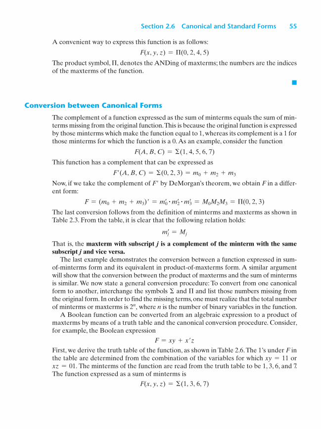
A Boolean function can be converted from an algebraic expression to a product of
maxterms by means of a truth table and the canonical conversion procedure. Consider,
for example, the Boolean expression
F = xy + x�z
First, we derive the truth table of the function, as shown in Table 2.6 . The 1’s under F in
the table are determined from the combination of the variables for which xy = 11 or
xz = 01. The minterms of the function are read from the truth table to be 1, 3, 6, and 7.
The function expressed as a sum of minterms is
F(x, y, z) = �(1, 3, 6, 7)
56 Chapter 2 Boolean Algebra and Logic Gates
Since there is a total of eight minterms or maxterms in a function of three variables, we
determine the missing terms to be 0, 2, 4, and 5. The function expressed as a product of
maxterms is
F(x, y, z) = �(0, 2, 4, 5)
the same answer as obtained in Example 2.5.
Standard Forms
The two canonical forms of Boolean algebra are basic forms that one obtains from read-
ing a given function from the truth table. These forms are very seldom the ones with the
least number of literals, because each minterm or maxterm must contain, by definition,
all the variables, either complemented or uncomplemented.
Another way to express Boolean functions is in standard form. In this configuration,
the terms that form the function may contain one, two, or any number of literals. There
are two types of standard forms: the sum of products and products of sums.
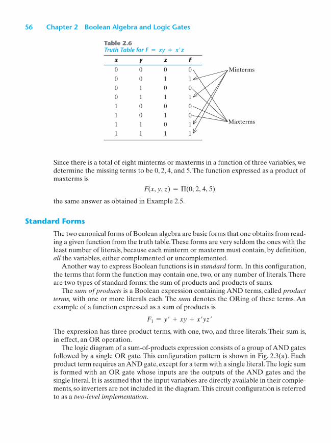
The sum of products is a Boolean expression containing AND terms, called product terms, with one or more literals each. The sum denotes the ORing of these terms. An
example of a function expressed as a sum of products is
F1 = y� + xy + x�yz�
The expression has three product terms, with one, two, and three literals. Their sum is,
in effect, an OR operation.
The logic diagram of a sum‐of‐products expression consists of a group of AND gates
followed by a single OR gate. This configuration pattern is shown in Fig. 2.3 (a). Each
product term requires an AND gate, except for a term with a single literal. The logic sum
is formed with an OR gate whose inputs are the outputs of the AND gates and the
single literal. It is assumed that the input variables are directly available in their comple-
ments, so inverters are not included in the diagram. This circuit configuration is referred
to as a two‐level implementation.
Table 2.6Truth Table for F � xy � x�z
x y z F
0 0 0 0
0 0 1 1
0 1 0 0
0 1 1 1
1 0 0 0
1 0 1 0
1 1 0 1
1 1 1 1
Minterms
Maxterms
Section 2.6 Canonical and Standard Forms 57
A product of sums is a Boolean expression containing OR terms, called sum terms.
Each term may have any number of literals. The product denotes the ANDing of these
terms. An example of a function expressed as a product of sums is
F2 = x(y� + z)(x� + y + z�)
This expression has three sum terms, with one, two, and three literals. The product is an
AND operation. The use of the words product and sum stems from the similarity of the
AND operation to the arithmetic product (multiplication) and the similarity of the OR
operation to the arithmetic sum (addition). The gate structure of the product‐of‐sums
expression consists of a group of OR gates for the sum terms (except for a single literal),
followed by an AND gate, as shown in Fig. 2.3 (b). This standard type of expression results in a two‐level structure of gates.
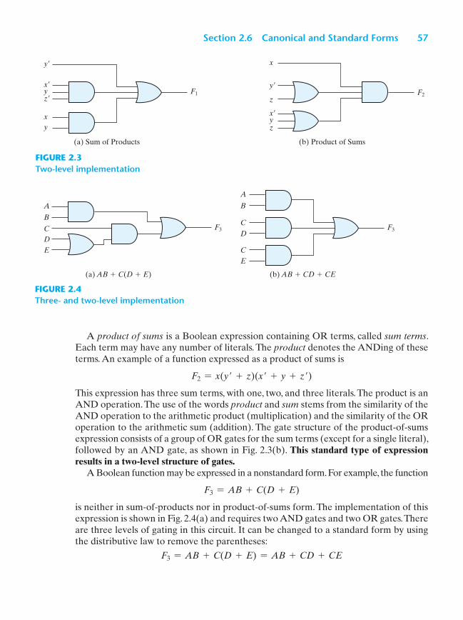
A Boolean function may be expressed in a nonstandard form. For example, the function
F3 = AB + C(D + E)
is neither in sum‐of‐products nor in product‐of‐sums form. The implementation of this
expression is shown in Fig. 2.4 (a) and requires two AND gates and two OR gates. There
are three levels of gating in this circuit. It can be changed to a standard form by using
the distributive law to remove the parentheses:
F3 = AB + C(D + E) = AB + CD + CE
y�
F1
x�
z�y
xy
F2
x
y�
y
z
z
x�
(a) Sum of Products (b) Product of Sums
FIGURE 2.3Two‐level implementation
F3
A
B
CDE
(a) AB � C(D � E) (b) AB � CD � CE
A
F3
B
DC
CE
FIGURE 2.4Three‐ and two‐level implementation
58 Chapter 2 Boolean Algebra and Logic Gates
The sum‐of‐products expression is implemented in Fig. 2.4 (b). In general, a two‐level
implementation is preferred because it produces the least amount of delay through the
gates when the signal propagates from the inputs to the output. However, the number
of inputs to a given gate might not be practical.
2 . 7 O T H E R L O G I C O P E R AT I O N S
When the binary operators AND and OR are placed between two variables, x and y,
they form two Boolean functions, x # y and x + y, respectively. Previously we stated that
there are 22n functions for n binary variables. Thus, for two variables, n = 2, and the
number of possible Boolean functions is 16. Therefore, the AND and OR functions
are only 2 of a total of 16 possible functions formed with two binary variables. It would
be instructive to find the other 14 functions and investigate their properties.
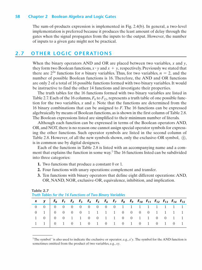
The truth tables for the 16 functions formed with two binary variables are listed in
Table 2.7 . Each of the 16 columns, F0 to F15, represents a truth table of one possible func-
tion for the two variables, x and y. Note that the functions are determined from the
16 binary combinations that can be assigned to F. The 16 functions can be expressed
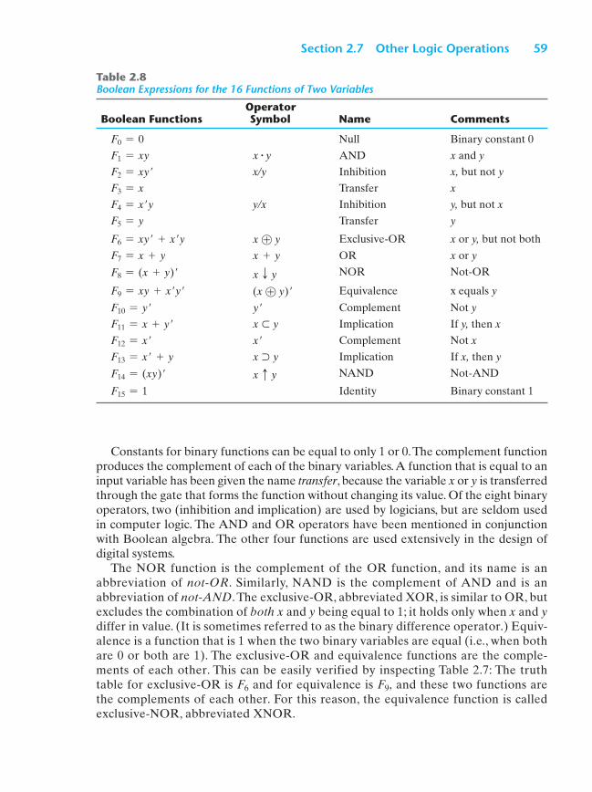
algebraically by means of Boolean functions, as is shown in the first column of Table 2.8 .
The Boolean expressions listed are simplified to their minimum number of literals.
Although each function can be expressed in terms of the Boolean operators AND,
OR, and NOT, there is no reason one cannot assign special operator symbols for express-
ing the other functions. Such operator symbols are listed in the second column of
Table 2.8 . However, of all the new symbols shown, only the exclusive‐OR symbol, �,
is in common use by digital designers.
Each of the functions in Table 2.8 is listed with an accompanying name and a com-
ment that explains the function in some way.1 The 16 functions listed can be subdivided
into three categories:
1. Two functions that produce a constant 0 or 1.
2. Four functions with unary operations: complement and transfer.
3. Ten functions with binary operators that define eight different operations: AND,
OR, NAND, NOR, exclusive‐OR, equivalence, inhibition, and implication.
Table 2.7Truth Tables for the 16 Functions of Two Binary Variables
x y F0 F1 F2 F3 F4 F5 F6 F7 F8 F9 F10 F11 F12 F13 F14 F15
0 0 0 0 0 0 0 0 0 0 1 1 1 1 1 1 1 1
0 1 0 0 0 0 1 1 1 1 0 0 0 0 1 1 1 1
1 0 0 0 1 1 0 0 1 1 0 0 1 1 0 0 1 1
1 1 0 1 0 1 0 1 0 1 0 1 0 1 0 1 0 1
1 The symbol ˆ is also used to indicate the exclusive or operator, e.g., xˆy. The symbol for the AND function is
sometimes omitted from the product of two variables, e.g., xy.
Section 2.7 Other Logic Operations 59
Constants for binary functions can be equal to only 1 or 0. The complement function
produces the complement of each of the binary variables. A function that is equal to an
input variable has been given the name transfer, because the variable x or y is transferred
through the gate that forms the function without changing its value. Of the eight binary
operators, two (inhibition and implication) are used by logicians, but are seldom used
in computer logic. The AND and OR operators have been mentioned in conjunction
with Boolean algebra. The other four functions are used extensively in the design of
digital systems.
The NOR function is the complement of the OR function, and its name is an
abbreviation of not‐OR. Similarly, NAND is the complement of AND and is an
abbreviation of not‐AND. The exclusive‐OR, abbreviated XOR, is similar to OR, but
excludes the combination of both x and y being equal to 1; it holds only when x and y differ in value. (It is sometimes referred to as the binary difference operator.) Equiv-
alence is a function that is 1 when the two binary variables are equal (i.e., when both
are 0 or both are 1). The exclusive‐OR and equivalence functions are the comple-
ments of each other. This can be easily verified by inspecting Table 2.7 : The truth
table for exclusive‐OR is F6 and for equivalence is F9, and these two functions are
the complements of each other. For this reason, the equivalence function is called
exclusive‐NOR, abbreviated XNOR.
Table 2.8Boolean Expressions for the 16 Functions of Two Variables
Boolean FunctionsOperator Symbol Name Comments
F0 = 0 Null Binary constant 0
F1 = xy x # y AND x and y
F2 = xy� x/y Inhibition x, but not y
F3 = x Transfer x
F4 = x�y y/x Inhibition y, but not x
F5 = y Transfer y
F6 = xy� + x�y x � y Exclusive‐OR x or y, but not both
F7 = x + y x + y OR x or y
F8 = (x + y)� x T y NOR Not‐OR
F9 = xy + x�y� (x � y)� Equivalence x equals y
F10 = y� y� Complement Not y
F11 = x + y� x � y Implication If y, then x
F12 = x� x� Complement Not x
F13 = x� + y x � y Implication If x, then y
F14 = (xy)� x c y NAND Not‐AND
F15 = 1 Identity Binary constant 1
60 Chapter 2 Boolean Algebra and Logic Gates
Boolean algebra, as defined in Section 2.2, has two binary operators, which we have
called AND and OR, and a unary operator, NOT (complement). From the definitions,
we have deduced a number of properties of these operators and now have defined other
binary operators in terms of them. There is nothing unique about this procedure. We
could have just as well started with the operator NOR (T), for example, and later
defined AND, OR, and NOT in terms of it. There are, nevertheless, good reasons for
introducing Boolean algebra in the way it has been introduced. The concepts of “and,”
“or,” and “not” are familiar and are used by people to express everyday logical ideas.
Moreover, the Huntington postulates reflect the dual nature of the algebra, emphasizing
the symmetry of + and # with respect to each other.
2 . 8 D I G I TA L L O G I C G AT E S
Since Boolean functions are expressed in terms of AND, OR, and NOT operations, it is
easier to implement a Boolean function with these type of gates. Still, the possibility of
constructing gates for the other logic operations is of practical interest. Factors to be
weighed in considering the construction of other types of logic gates are (1) the feasibil-
ity and economy of producing the gate with physical components, (2) the possibility of
extending the gate to more than two inputs, (3) the basic properties of the binary oper-
ator, such as commutativity and associativity, and (4) the ability of the gate to implement
Boolean functions alone or in conjunction with other gates.
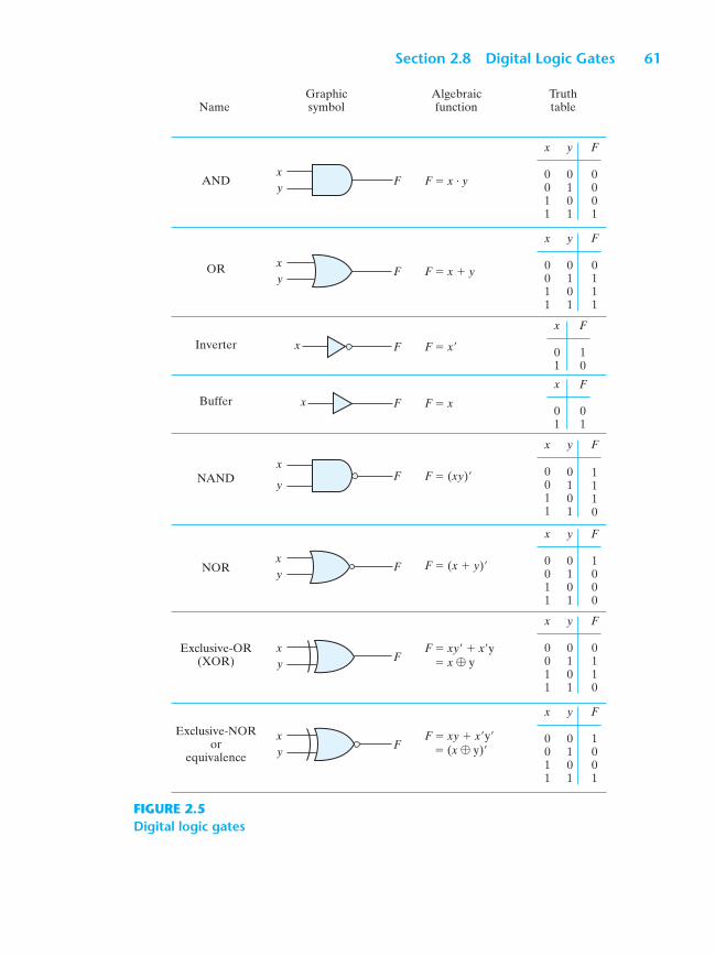
Of the 16 functions defined in Table 2.8 , two are equal to a constant and four are
repeated. There are only 10 functions left to be considered as candidates for logic gates.
Two—inhibition and implication—are not commutative or associative and thus are
impractical to use as standard logic gates. The other eight—complement, transfer, AND,
OR, NAND, NOR, exclusive‐OR, and equivalence—are used as standard gates in
digital design.
The graphic symbols and truth tables of the eight gates are shown in Fig. 2.5 . Each
gate has one or two binary input variables, designated by x and y, and one binary output
variable, designated by F. The AND, OR, and inverter circuits were defined in Fig. 1.6.
The inverter circuit inverts the logic sense of a binary variable, producing the NOT, or
complement, function. The small circle in the output of the graphic symbol of an inverter
(referred to as a bubble) designates the logic complement. The triangle symbol by itself
designates a buffer circuit. A buffer produces the transfer function, but does not produce
a logic operation, since the binary value of the output is equal to the binary value of the
input. This circuit is used for power amplification of the signal and is equivalent to two
inverters connected in cascade.
The NAND function is the complement of the AND function, as indicated by a
graphic symbol that consists of an AND graphic symbol followed by a small circle. The
NOR function is the complement of the OR function and uses an OR graphic symbol
followed by a small circle. NAND and NOR gates are used extensively as standard logic
gates and are in fact far more popular than the AND and OR gates. This is because
NAND and NOR gates are easily constructed with transistor circuits and because digital
circuits can be easily implemented with them.
Section 2.8 Digital Logic Gates 61
NameGraphicsymbol
Algebraicfunction
Truthtable
AND
OR
Inverter
Buffer
NAND
NOR
Exclusive-OR(XOR)
Exclusive-NORor
equivalence
F � x · y
F � x � y
F � (xy)�
F � x�
F � x
x y F
x y F
x y F
x y F
x y F
x y F
x F
x F
F � (x � y)�
F � xy� � x�y
F � xy � x�y�
F
F
Fx
Fx
F
F
F
Fx
y
xy
xy � x � y
� (x � y)�
0011
0101
0011
0101
0111
01
10
01
01
0011
0101
1110
0011
0101
1000
0011
0101
0110
0011
0101
1001
0001
xy
xy
xy
FIGURE 2.5Digital logic gates
62 Chapter 2 Boolean Algebra and Logic Gates
The exclusive‐OR gate has a graphic symbol similar to that of the OR gate, except
for the additional curved line on the input side. The equivalence, or exclusive‐NOR, gate
is the complement of the exclusive‐OR, as indicated by the small circle on the output
side of the graphic symbol.
Extension to Multiple Inputs
The gates shown in Fig. 2.5 —except for the inverter and buffer—can be extended to
have more than two inputs. A gate can be extended to have multiple inputs if the binary
operation it represents is commutative and associative. The AND and OR operations,
defined in Boolean algebra, possess these two properties. For the OR function, we have
x + y = y + x (commutative)
and
(x + y) + z = x + (y + z) = x + y + z (associative)
which indicates that the gate inputs can be interchanged and that the OR function can
be extended to three or more variables.
The NAND and NOR functions are commutative, and their gates can be extended
to have more than two inputs, provided that the definition of the operation is modified
slightly. The difficulty is that the NAND and NOR operators are not associative
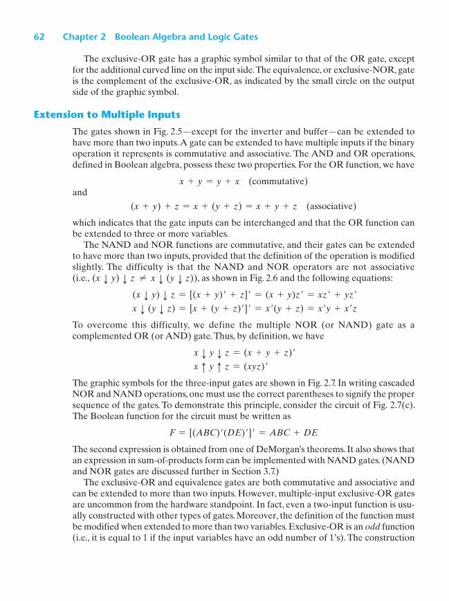
(i.e., (x T y) T z � x T (y T z) ), as shown in Fig. 2.6 and the following equations:
(x T y) T z = [(x + y)� + z]� = (x + y)z� = xz� + yz�
x T (y T z) = [x + (y + z)�]� = x�(y + z) = x�y + x�z
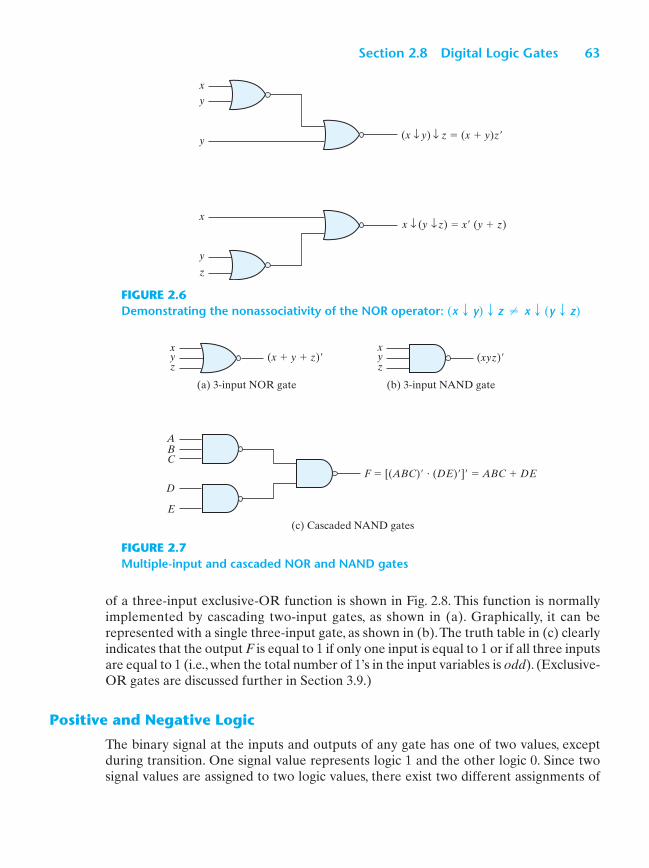
To overcome this difficulty, we define the multiple NOR (or NAND) gate as a
complemented OR (or AND) gate. Thus, by definition, we have
x T y T z = (x + y + z)�
x c y c z = (xyz)�
The graphic symbols for the three‐input gates are shown in Fig. 2.7 . In writing cascaded
NOR and NAND operations, one must use the correct parentheses to signify the proper
sequence of the gates. To demonstrate this principle, consider the circuit of Fig. 2.7 (c).
The Boolean function for the circuit must be written as
F = [(ABC)�(DE)�]� = ABC + DE
The second expression is obtained from one of DeMorgan’s theorems. It also shows that
an expression in sum‐of‐products form can be implemented with NAND gates. (NAND
and NOR gates are discussed further in Section 3.7.)
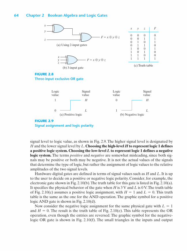
The exclusive‐OR and equivalence gates are both commutative and associative and
can be extended to more than two inputs. However, multiple‐input exclusive‐OR gates
are uncommon from the hardware standpoint. In fact, even a two‐input function is usu-
ally constructed with other types of gates. Moreover, the definition of the function must
be modified when extended to more than two variables. Exclusive‐OR is an odd function
(i.e., it is equal to 1 if the input variables have an odd number of 1’s). The construction
Section 2.8 Digital Logic Gates 63
of a three‐input exclusive‐OR function is shown in Fig. 2.8 . This function is normally
implemented by cascading two‐input gates, as shown in (a). Graphically, it can be
represented with a single three‐input gate, as shown in (b). The truth table in (c) clearly
indicates that the output F is equal to 1 if only one input is equal to 1 or if all three inputs
are equal to 1 (i.e., when the total number of 1’s in the input variables is odd). (Exclusive‐
OR gates are discussed further in Section 3.9.)
Positive and Negative Logic
The binary signal at the inputs and outputs of any gate has one of two values, except
during transition. One signal value represents logic 1 and the other logic 0. Since two
signal values are assigned to two logic values, there exist two different assignments of
(x y) z � (x � y)z�
x
y
y
x (y z) � x� (y � z)x
y
z
FIGURE 2.6Demonstrating the nonassociativity of the NOR operator: (x T y) T z � x T (y T z)
(a) 3-input NOR gate
y (x � y � z)�x
z
(b) 3-input NAND gate
(xyz)�yx
z
(c) Cascaded NAND gates
D
B
F � [(ABC)� � (DE)�]� � ABC � DE
A
C
E
FIGURE 2.7Multiple‐input and cascaded NOR and NAND gates
64 Chapter 2 Boolean Algebra and Logic Gates
signal level to logic value, as shown in Fig. 2.9 . The higher signal level is designated by
H and the lower signal level by L. Choosing the high‐level H to represent logic 1 defines a positive logic system. Choosing the low‐level L to represent logic 1 defines a negative logic system. The terms positive and negative are somewhat misleading, since both sig-
nals may be positive or both may be negative. It is not the actual values of the signals
that determine the type of logic, but rather the assignment of logic values to the relative
amplitudes of the two signal levels.
Hardware digital gates are defined in terms of signal values such as H and L. It is up
to the user to decide on a positive or negative logic polarity. Consider, for example, the
electronic gate shown in Fig. 2.10 (b). The truth table for this gate is listed in Fig. 2.10 (a).
It specifies the physical behavior of the gate when H is 3 V and L is 0 V. The truth table
of Fig. 2.10 (c) assumes a positive logic assignment, with H = 1 and L = 0. This truth
table is the same as the one for the AND operation. The graphic symbol for a positive
logic AND gate is shown in Fig. 2.10 (d).
Now consider the negative logic assignment for the same physical gate with L = 1
and H = 0. The result is the truth table of Fig. 2.10 (e). This table represents the OR
operation, even though the entries are reversed. The graphic symbol for the negative‐
logic OR gate is shown in Fig. 2.10 (f). The small triangles in the inputs and output
(a) Using 2-input gates
(b) 3-input gate(c) Truth table
xF � x � y � zy
z
y
zF � x � y � z
xx y z F
0
0
00
11
1
1
0
1
10
10
0
1
0
1
01
01
0
1
011
0
0
1
0
1
FIGURE 2.8Three‐input exclusive‐OR gate
(a) Positive logic
Logicvalue
1
0
Signalvalue
H
L(b) Negative logic
Logicvalue
0
1
Signalvalue
H
L
FIGURE 2.9Signal assignment and logic polarity
Section 2.8 Digital Logic Gates 65
designate a polarity indicator, the presence of which along a terminal signifies that
negative logic is assumed for the signal. Thus, the same physical gate can operate either
as a positive‐logic AND gate or as a negative‐logic OR gate.
The conversion from positive logic to negative logic and vice versa is essentially
an operation that changes 1’s to 0’s and 0’s to 1’s in both the inputs and the output
of a gate. Since this operation produces the dual of a function, the change of all ter-
minals from one polarity to the other results in taking the dual of the function. The
upshot is that all AND operations are converted to OR operations (or graphic sym-
bols) and vice versa. In addition, one must not forget to include the polarity‐indicator
triangle in the graphic symbols when negative logic is assumed. In this book, we will
not use negative logic gates and will assume that all gates operate with a positive logic
assignment.
(c) Truth table for positive logic
(e) Truth table for negative logic
(d) Positive logic AND gate
(f) Negative logic OR gate
(b) Gate block diagram
xzDigital
gatey
zx
y
zx
y
(a) Truth table with H and L
x y z
LLLL L
LLHH
H
HH
x y z
000
0 0
0011
1
11
x y z
111
1 1
1100
0
00
FIGURE 2.10Demonstration of positive and negative logic
66 Chapter 2 Boolean Algebra and Logic Gates
2 . 9 I N T E G R AT E D C I R C U I T S
An integrated circuit (IC) is fabricated on a die of a silicon semiconductor crystal, called
a chip, containing the electronic components for constructing digital gates. The complex
chemical and physical processes used to form a semiconductor circuit are not a subject
of this book. The various gates are interconnected inside the chip to form the required
circuit. The chip is mounted in a ceramic or plastic container, and connections are welded
to external pins to form the integrated circuit. The number of pins may range from 14
on a small IC package to several thousand on a larger package. Each IC has a numeric
designation printed on the surface of the package for identification. Vendors provide
data books, catalogs, and Internet websites that contain descriptions and information
about the ICs that they manufacture.
Levels of Integration
Digital ICs are often categorized according to the complexity of their circuits, as mea-
sured by the number of logic gates in a single package. The differentiation between those
chips which have a few internal gates and those having hundreds of thousands of gates
is made by customary reference to a package as being either a small‐, medium‐, large‐,
or very large‐scale integration device.
Small‐scale integration (SSI) devices contain several independent gates in a single
package. The inputs and outputs of the gates are connected directly to the pins in the
package. The number of gates is usually fewer than 10 and is limited by the number of
pins available in the IC.
Medium‐scale integration (MSI) devices have a complexity of approximately 10 to
1,000 gates in a single package. They usually perform specific elementary digital opera-
tions. MSI digital functions are introduced in Chapter 4 as decoders, adders, and multi-
plexers and in Chapter 6 as registers and counters.
Large‐scale integration (LSI) devices contain thousands of gates in a single package.
They include digital systems such as processors, memory chips, and programmable logic
devices. Some LSI components are presented in Chapter 7 .
Very large‐scale integration (VLSI) devices now contain millions of gates within a
single package. Examples are large memory arrays and complex microcomputer chips.
Because of their small size and low cost, VLSI devices have revolutionized the computer
system design technology, giving the designer the capability to create structures that
were previously uneconomical to build.
Digital Logic Families
Digital integrated circuits are classified not only by their complexity or logical operation,
but also by the specific circuit technology to which they belong. The circuit technology
is referred to as a digital logic family. Each logic family has its own basic electronic
circuit upon which more complex digital circuits and components are developed. The
basic circuit in each technology is a NAND, NOR, or inverter gate. The electronic
Section 2.9 Integrated Circuits 67
components employed in the construction of the basic circuit are usually used to name
the technology. Many different logic families of digital integrated circuits have been
introduced commercially. The following are the most popular:
TTL transistor–transistor logic;
ECL emitter‐coupled logic;
MOS metal‐oxide semiconductor;
CMOS complementary metal‐oxide semiconductor.
TTL is a logic family that has been in use for 50 years and is considered to be stan-
dard. ECL has an advantage in systems requiring high‐speed operation. MOS is suitable
for circuits that need high component density, and CMOS is preferable in systems
requiring low power consumption, such as digital cameras, personal media players, and
other handheld portable devices. Low power consumption is essential for VLSI design;
therefore, CMOS has become the dominant logic family, while TTL and ECL continue
to decline in use. The most important parameters distinguishing logic families are listed
below; CMOS integrated circuits are discussed briefly in the appendix.
Fan‐out specifies the number of standard loads that the output of a typical gate can
drive without impairing its normal operation. A standard load is usually defined as the
amount of current needed by an input of another similar gate in the same family.
Fan‐in is the number of inputs available in a gate.
Power dissipation is the power consumed by the gate that must be available from the
power supply.
Propagation delay is the average transition delay time for a signal to propagate from
input to output. For example, if the input of an inverter switches from 0 to 1, the output
will switch from 1 to 0, but after a time determined by the propagation delay of the
device. The operating speed is inversely proportional to the propagation delay.
Noise margin is the maximum external noise voltage added to an input signal that
does not cause an undesirable change in the circuit output.
Computer‐Aided Design of VLSI Circuits
Integrated circuits having submicron geometric features are manufactured by optically
projecting patterns of light onto silicon wafers. Prior to exposure, the wafers are coated
with a photoresistive material that either hardens or softens when exposed to light.
Removing extraneous photoresist leaves patterns of exposed silicon. The exposed
regions are then implanted with dopant atoms to create a semiconductor material hav-
ing the electrical properties of transistors and the logical properties of gates. The design
process translates a functional specification or description of the circuit (i.e., what it must
do) into a physical specification or description (how it must be implemented in silicon).
The design of digital systems with VLSI circuits containing millions of transistors and
gates is an enormous and formidable task. Systems of this complexity are usually impos-
sible to develop and verify without the assistance of computer‐aided design (CAD)
68 Chapter 2 Boolean Algebra and Logic Gates
tools, which consist of software programs that support computer‐based representations
of circuits and aid in the development of digital hardware by automating the design
process. Electronic design automation (EDA) covers all phases of the design of inte-
grated circuits. A typical design flow for creating VLSI circuits consists of a sequence of
steps beginning with design entry (e.g., entering a schematic) and culminating with the
generation of the database that contains the photomask used to fabricate the IC. There
are a variety of options available for creating the physical realization of a digital circuit
in silicon. The designer can choose between an application‐specific integrated circuit
(ASIC), a field‐programmable gate array (FPGA), a programmable logic device (PLD),
and a full‐custom IC. With each of these devices comes a set of CAD tools that provide
the necessary software to facilitate the hardware fabrication of the unit. Each of these
technologies has a market niche determined by the size of the market and the unit cost
of the devices that are required to implement a design.
Some CAD systems include an editing program for creating and modifying schematic
diagrams on a computer screen. This process is called schematic capture or schematic
entry. With the aid of menus, keyboard commands, and a mouse, a schematic editor can
draw circuit diagrams of digital circuits on the computer screen. Components can be
placed on the screen from a list in an internal library and can then be connected with
lines that represent wires. The schematic entry software creates and manages a database
containing the information produced with the schematic. Primitive gates and functional
blocks have associated models that allow the functionality (i.e., logical behavior) and
timing of the circuit to be verified. Verification is performed by applying inputs to the
circuit and using a logic simulator to determine and display the outputs in text or wave-
form format.
An important development in the design of digital systems is the use of a hardware
description language (HDL). Such a language resembles a computer programming
language, but is specifically oriented to describing digital hardware. It represents logic
diagrams and other digital information in textual form to describe the functionality
and structure of a circuit. Moreover, the HDL description of a circuit’s functionality
can be abstract, without reference to specific hardware, thereby freeing a designer to
devote attention to higher level functional detail (e.g., under certain conditions the
circuit must detect a particular pattern of 1’s and 0’s in a serial bit stream of data) rather
than transistor‐level detail. HDL‐based models of a circuit or system are simulated to
check and verify its functionality before it is submitted to fabrication, thereby reducing
the risk and waste of manufacturing a circuit that fails to operate correctly. In tandem
with the emergence of HDL‐based design languages, tools have been developed to
automatically and optimally synthesize the logic described by an HDL model of a
circuit. These two advances in technology have led to an almost total reliance by indus-try on HDL‐based synthesis tools and methodologies for the design of the circuits of complex digital systems. Two HDLs—Verilog and VHDL—have been approved as
standards by the Institute of Electronics and Electrical Engineers (IEEE) and are in
use by design teams worldwide. The Verilog HDL is introduced in Section 3.10, and
because of its importance, we include several exercises and design problems based on
Verilog throughout the book.
Problems 69
P R O B L E M S
(Answers to problems marked with * appear at the end of the text.)
2.1 Demonstrate the validity of the following identities by means of truth tables:
(a) DeMorgan’s theorem for three variables: (x + y + z)� = x�y�z� and (xyz)� =x� + y� + z�
(b) The distributive law: x + yz = ( x + y )( x + z )
(c) The distributive law: x(y + z) = xy + xz
(d) The associative law: x + (y + z) = (x + y) + z
(e) The associative law and x(yz) = (xy)z
2.2 Simplify the following Boolean expressions to a minimum number of literals:
(a) * xy + xy � (b) * (x + y) (x + y�)
(c) * xyz + x � y + xyz � (d) * (A + B)� (A� + B�)� (e) (a + b + c�)(a� b� + c) (f) a�bc + abc� + abc + a�bc�
2.3 Simplify the following Boolean expressions to a minimum number of literals:
(a) * ABC + A�B + ABC� (b)* x � yz + xz
(c) * (x + y)� (x� + y�) (d) * xy + x(wz + wz�)
(e) * (BC� + A�D) (AB� + CD�) (f) (a� + c�) (a + b� + c�)
2.4 Reduce the following Boolean expressions to the indicated number of literals:
(a) * A�C� + ABC + AC� to three literals
(b) * (x�y� + z)� + z + xy + wz to three literals
(c) * A�B(D� + C�D) + B(A + A�CD) to one literal
(d) * (A� + C) (A� + C�) (A + B + C�D) to four literals
(e) ABC'D + A'BD + ABCD to two literals
2.5 Draw logic diagrams of the circuits that implement the original and simplified expressions
in Problem 2.2.
2.6 Draw logic diagrams of the circuits that implement the original and simplified expressions
in Problem 2.3.
2.7 Draw logic diagrams of the circuits that implement the original and simplified expressions
in Problem 2.4.
2.8 Find the complement of F = wx + yz; then show that FF� = 0 and F + F� = 1.
2.9 Find the complement of the following expressions:
(a) * xy� + x�y (b) (a + c) (a + b�) (a� + b + c�)
(c) z + z�(v�w + xy)
2.10 Given the Boolean functions F1 and F 2 , show that
(a) The Boolean function E = F1 + F2 contains the sum of the minterms of F1 and F2.
(b) The Boolean function G = F1F2 contains only the minterms that are common to F1
and F2.
2.11 List the truth table of the function:
(a) * F = xy + xy� + y�z (b) F = bc + a�c�
2.12 We can perform logical operations on strings of bits by considering each pair of correspond-
ing bits separately (called bitwise operation). Given two eight‐bit strings A = 10110001
and B = 10101100, evaluate the eight‐bit result after the following logical operations:
(a)* AND (b) OR (c)* XOR (d)* NOT A (e) NOT B
70 Chapter 2 Boolean Algebra and Logic Gates
2.13 Draw logic diagrams to implement the following Boolean expressions:
(a) y = [(u + x�) (y� + z)]
(b) y = (u � y)� + x
(c) y = (u� + x�) (y + z�)
(d) y = u(x � z) + y� (e) y = u + yz + uxy
(f) y = u + x + x�(u + y�)
2.14 Implement the Boolean function
F = xy + x�y� + y�z
(a) With AND, OR, and inverter gates
(b) * With OR and inverter gates
(c) With AND and inverter gates
(d) With NAND and inverter gates
(e) With NOR and inverter gates
2.15* Simplify the following Boolean functions T1 and T2 to a minimum number of literals:
A B C T 1 T 2
0 0 0 1 0 0 0 1 1 0
0 1 0 1 0
0 1 1 0 1
1 0 0 0 1
1 0 1 0 1
1 1 0 0 1
1 1 1 0 1
2.16 The logical sum of all minterms of a Boolean function of n variables is 1.
(a) Prove the previous statement for n = 3.
(b) Suggest a procedure for a general proof.
2.17 Obtain the truth table of the following functions, and express each function in sum‐of‐min-
terms and product‐of‐maxterms form:
(a) * (b + cd)(c + bd) (b) (cd + b�c + bd�)(b + d)
(c) (c� + d)(b + c�) (d) bd� + acd� + ab�c + a�c�
2.18 For the Boolean function
F = xy�z + x�y�z + w�xy + wx�y + wxy
(a) Obtain the truth table of F. (b) Draw the logic diagram, using the original Boolean expression.
(c) * Use Boolean algebra to simplify the function to a minimum number of literals.
(d) Obtain the truth table of the function from the simplified expression and show that
it is the same as the one in part (a).
(e) Draw the logic diagram from the simplified expression, and compare the total number
of gates with the diagram of part (b).
Problems 71
2.19* Express the following function as a sum of minterms and as a product of maxterms:
F(A, B, C, D) = B�D + A�D + BD
2.20 Express the complement of the following functions in sum‐of‐minterms form:
(a) F(A,B ,C, D) = g(2, 4, 7, 10, 12, 14)
(b) F ( x, y, z ) = w (3, 5, 7)
2.21 Convert each of the following to the other canonical form:
(a) F(x, y, z) = g(1, 3, 5)
(b) F(A, B, C, D) = w (3, 5, 8, 11)
2.22* Convert each of the following expressions into sum of products and product of sums:
(a) ( u + xw )( x + u�v )
(b) x� + x(x + y�)(y + z�)
2.23 Draw the logic diagram corresponding to the following Boolean expressions without sim-
plifying them:
(a) BC� + AB + ACD
(b) (A + B)(C + D)(A� + B + D)
(c) (AB + A�B�)(CD� + C�D)
(d) A + CD + (A + D')(C' + D)
2.24 Show that the dual of the exclusive‐OR is equal to its complement.
2.25 By substituting the Boolean expression equivalent of the binary operations as defined in
Table 2.8 , show the following:
(a) The inhibition operation is neither commutative nor associative.
(b) The exclusive‐OR operation is commutative and associative.
2.26 Show that a positive logic NAND gate is a negative logic NOR gate and vice versa.
2.27 Write the Boolean equations and draw the logic diagram of the circuit whose outputs are
defined by the following truth table:
Table P2.27
f 1 f 2 a b c
1 1 0 0 0
0 1 0 0 1
1 0 0 1 0
1 1 0 1 1
1 0 1 0 0
0 1 1 0 1
1 0 1 1 1
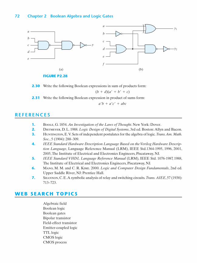
2.28 Write Boolean expressions and construct the truth tables describing the outputs of the
circuits described by the logic diagrams in Fig. P2.28.
2.29 Determine whether the following Boolean equation is true or false.
x�y� + x�z + x�z� = x�z� + y�z� + x�z
72 Chapter 2 Boolean Algebra and Logic Gates
2.30 Write the following Boolean expressions in sum of products form:
(b + d)(a� + b� + c)
2.31 Write the following Boolean expression in product of sums form:
a�b + a�c� + abc
R E F E R E N C E S
1. B oole, G. 1854. An Investigation of the Laws of Thought. New York: Dover.
2. D ietmeyer, D. L. 1988. Logic Design of Digital Systems, 3rd ed. Boston: Allyn and Bacon.
3. H untington, E. V. Sets of independent postulates for the algebra of logic. Trans. Am. Math. Soc., 5 (1904): 288–309.
4. IEEE Standard Hardware Description Language Based on the Verilog Hardware Descrip-tion Language, Language Reference Manual (LRM), IEEE Std.1364‐1995, 1996, 2001,
2005, The Institute of Electrical and Electronics Engineers, Piscataway, NJ.
5. IEEE Standard VHDL Language Reference Manual (LRM), IEEE Std. 1076‐1987, 1988,
The Institute of Electrical and Electronics Engineers, Piscataway, NJ.
6. M ano, M. M. and C. R. K ime . 2000. Logic and Computer Design Fundamentals, 2nd ed.
Upper Saddle River, NJ: Prentice Hall.
7. S hannon, C. E. A symbolic analysis of relay and switching circuits. Trans. AIEE, 57 (1938):
713–723.
WEB SEARCH TOP ICS
Algebraic field
Boolean logic
Boolean gates
Bipolar transistor
Field-effect transistor
Emitter-coupled logic
TTL logic
CMOS logic
CMOS process
a
b
c
d
e
y
a
b
c
d
e
f
y2
y1
(b)(a)
FIGURE P2.28


