Embed Size (px)
Citation preview

eScholarship provides open access, scholarly publishingservices to the University of California and delivers a dynamicresearch platform to scholars worldwide.
Lawrence Berkeley National Laboratory
Title:Structure, Magnetism, and Transport of CuCr2Se4 Thin Films
Author:Bettinger, J.S.Chopdekar, R.V.Liberati, M.Neulinger, J.R.Chshiev, M.Takamura, Y.Alldredge, L.M.B.Arenholz, E.Idzerda, Y.U.Stacy, A.M.Butler, W.H.Suzuki, Y.
Publication Date:06-24-2008
Publication Info:Lawrence Berkeley National Laboratory
Permalink:http://escholarship.org/uc/item/7cf7f723
Keywords:advanced light source als

Structure, Magnetism, and Transport of CuCr2Se4 Thin Films
J.S. Bettinger1, R.V. Chopdekar1,2, M. Liberati3,4, J.R. Neulinger5, M. Chshiev6, Y. Takamura1,
L.M.B. Alldredge1,2, E. Arenholz4, Y.U. Idzerda3, A.M. Stacy5, W.H. Butler6,7, Y. Suzuki1
1Department of Materials Science and Engineering, UC Berkeley, Berkeley, California; 2School of Applied Physics, Cornell University, Ithaca, New York;
3Department of Physics, Montana State University, Bozeman, Montana;4Advanced Light Source, Lawrence Berkeley National Laboratory, Berkeley, California;
5Department of Chemistry, UC Berkeley, Berkeley, California; 6MINT Center, University of Alabama, Tuscaloosa, Alabama;
7Department of Physics and Astronomy, University of Alabama, Tuscaloosa, Alabama.
ABSTRACT
We report the successful growth of highly spin-polarized chalcogenide thin films of CuCr2Se4,
which are promising candidates for spin-based electronic applications. We also present electronic
structure calculations for CuCr2Se4 that, together with magnetic and transport data, imply that the
stoichiometric compound is a metallic ferromagnet with a relatively low density of hole-like
carriers at the Fermi energy. These calculations also predict that a deficiency of Se will deplete
the minority density of states at the Fermi energy perhaps leading to a half-metal. We have
successfully grown thin films of CuCr2Se4 by pulsed laser deposition on isostructural MgAl2O4
substrates followed by an anneal in a Se-rich environment. X-ray diffraction confirms the
structure of CuCr2Se4 on MgAl2O4 substrates as well as a secondary phase of Cr2Se3. X-ray
absorption spectroscopy indicates that the chemical structure at the surface of the films is similar
to that of bulk CuCr2Se4 single crystals. Magnetization measurements indicate that these films
saturate with a magnetic moment close to 5 µB per formula unit and a Tc above 400 K. X-ray
magnetic circular dichroism shows that the magnetism persists to the surface of the film.
Resistivity and Hall effect measurements are consistent with a p-type ferromagnetic metallic
behavior and with the electronic structure calculations.
1

1. Introduction
Recently, there has been an enormous amount of research on the development of highly
spin-polarized materials in light of their potential incorporation into spin-based electronic
applications. However, there remain fundamental questions associated with highly spin polarized
materials such as the nature of magnetism at surfaces and interfaces. Many of these materials
studies have been focused on binary and ternary oxides, including CrO2, Fe3O4, La0.7Sr0.3MnO3,
and SrFeMoO6.[1] They have been successfully synthesized in thin film form and incorporated
into prototypical spin-based devices.
While complex oxide materials have been well studied to this end, complex
chalcogenides have not been explored for magnetic devices. Of particular interest is the family of
chalcogenide spinels, AB2X4, where X is one of S, Se, or Te. In contrast to the oxide spinels,
one may hope that the decrease in the ionic character of the bonds in the chalcogenides may lead
to transport properties more similar to ordinary metals and semiconductors. The bulk properties
of most chalcogenide spinels were examined in the 1960s. They exhibit a wide range of
electronic and magnetic behavior.[2-6] Within the family of chalcogenide spinels, the basic
structural parameters, such as the S-S or Se-Se distances, as well as thermal properties such as
thermal expansion are very similar for most members of the family, so epitaxial growth of thin
isostructural layers is generally possible. Therefore, one can imagine synthesizing and
fabricating an all-chalcogenide spinel multilayer magnetic device. More recently these materials
have been the objects of renewed study as high magnetoresistance materials.[7]
Of the many known chalcogenide spinel materials, CuCr2Se4 is a promising candidate for
magnetic devices. It is a ferromagnetic metallic material that has been synthesized in bulk form
since the 1960s but has yet to be grown in thin film form.[5] Bulk forms of CuCr2Se4 have
2

magnetization near 5 µB per formula unit at low temperatures and have a relatively high Curie
temperature (TC) of 444 K.[8] The crystal structure is a normal spinel, made of an fcc lattice of
Se with Cu cations in 1/8 of the tetrahedral sites and Cr cations in 1/2 of the octahedral sites.
Bulk studies indicate that deviations from stoichiometry can give rise to poorer metallic
conductivity and even semiconducting behavior.[9]
2. Electronic Structure Calculations
The calculated electronic structure of CuCr2Se4 is shown in Figures (1-3). The
calculations were performed using the Generalized Gradient Approximation (GGA) within
Density Functional Theory (DFT). The Vienna ab-initio simulation program (VASP) [10-15]
implementation of DFT using Projector Augmented Waves was employed for the calculations.
The calculations shown here are based on a fully relaxed structure (a=10.395 Å, u=0.00767) but
differed only slightly from those based on the experimental structure (a=10.334 Å, u=0.00739).
The spin-orbit interaction was not included in the calculations and possible orbital contributions
to the magnetization were neglected.
Figure 1 shows the total density of states. Figure 2 shows the density of states
decomposed by site and angular momentum component. The Se-p states are spread over a range
of approximately 9 eV due to their hybridization with the Cr and Cu -d states. The Cr majority-d
states hybridize with the Se-p states and spread from approximately 4 eV below the Fermi level
to 2 eV above it. The Cr minority d-states are almost all above the Fermi-energy. The Se-p states
are largely, but not completely filled. The Cu-d states also hybridize strongly with the Se-p
states, but lie somewhat higher on average than the Cr-d states. The Cu-d states are filled except
for a few unfilled majority states. The magnetic moment lies mainly on the Cr atoms which have
3

a moment of nearly 3 µB per ion and are aligned ferromagnetically. The Cr moments are partially
compensated by small moments of opposite sign on the Cu and Se atoms so that the total
calculated moment is slightly greater than 5 µB per formula unit (5.12 µB or 338 emu/cm3). It
should be noted that this picture is similar to that deduced from neutron diffraction studies in
reference [3] and from XMCD in reference [16].
We also performed LDA+U calculations (not shown) in which a Coulomb U of 5 eV was
applied to the d-states of the Cu and Cr ions. Interestingly, the electronic structure did not change
qualitatively from the GGA result. The moment increased to 5.61 µB. Otherwise the electronic
structure was qualitatively similar. We expect correlation effects to be less important in the
chalcogenides than the oxides because of the more extended nature of the ligand wave functions.
For CuCr2Se4, the fact that the system is basically ferromagnetic with a very delocalized anti-
ferromagnetic component (spread over the Se and Cu ions) rather than a ferrimagnetic system
like most magnetic spinels, probably helps to delocalize the electrons and reduce the correlation
effects that cannot be treated by the mean-field DFT-GGA approach.
The unfilled energy bands for both the majority and minority spin channels near the
Fermi energy indicate that CuCr2Se4 is predicted to be metallic. The Fermi surface (Fig. 3) is
relatively simple for the minority channel which has three closed hole surfaces centered at the Γ-
point. These three surfaces have relatively high dispersion as evidenced by the low and smooth
density of states in the minority channel at the Fermi energy. We estimate based on the
calculated integrated DOS that these three surfaces contain 0.065 holes per formula unit. The
smallest hole surface has a Fermi velocity of 5.5 x 10⁵ m/sec and an effective mass of 0.26 me in
the Γ-X direction. In this direction, the larger hole surfaces have a Fermi velocity of
approximately 3.5x10⁵ m/sec and a mass of 0.65 me. We emphasize that the conduction electrons
4

in this material differ qualitatively from the massive, low velocity electrons commonly
encountered in transition metal oxides. Our calculated electronic structure in the vicinity of the
Fermi energy is similar to that obtained by Ogata et al. [17] using the DV-Xα method.
Relativistic calculations [18] however, do not show the smallest minority hole surface because of
a splitting which leaves the Γ point just above the Fermi energy doubly rather than triply
degenerate.
The majority bands that cross the Fermi energy consist of a single highly dispersive band
that forms a closed hole surface surrounding the Γ-point, and two additional, less dispersive
bands that are degenerate along Γ-X and Γ-L. These two bands give the structure in the majority
DOS that extends from just below the Fermi surface to a narrow gap in the majority DOS that
begins approximately 0.2 eV above EF. We estimate that the closed hole surface contains
approximately 0.02 electrons per formula unit. The electrical conductivity will depend not only
on the number and velocities of the carriers but also on the scattering mechanisms which will
depend on the temperature and on the concentration and types of defects. However, based on the
Fermi surface alone, we would expect the current to be carried primarily by down-spin holes,
thus making it a candidate for highly spin polarized electrodes for magnetic tunnel junctions.
The reason for this is that there are more minority holes than majority holes (not counting the
less dispersive bands) and the much higher density of states for majority than for minority is
expected to increase the scattering rate for majority. An additional reason that we expect higher
conductance from the minority bands is the absence of localized Cr-d states near the Fermi
energy for the minority channel. The minority states near the Fermi energy seem to be quite
delocalized, having contributions from all of the ions in the cell. Our picture of delocalized
electrons at the Fermi energy seems to be consistent with the measured resistivity [9] which is
5

reported to be as low as 25 µΩcm at low temperature, rising to approximately 300 µΩcm at
room temperature. Thus CuCr2Se4 is a surprisingly good metal for a transition metal based
material with such a large unit cell.
An estimate of the carrier density based on the estimated volumes of the closed hole
surfaces yields 4.1 x 10²⁰/cm3 for the minority hole surfaces and 1.4x10²⁰/cm3 for the majority
closed hole surface. In addition, there are two majority open surfaces for which the designation
hole or electron is ambiguous but which are likely to have larger regions with negative curvature
(holes) than positive. We have not attempted a rigorous calculation of the low field hall constant,
which would require an average over the Fermi surface of the mean curvature weighted by the
square of the electron velocity.[19-21] The experimental value of the Hall carrier density, nH,
obtained by the extrapolation of measurements on CuCr2Se4-xBrx to x=0 [9], is consistent with
hole conduction, but is an order of magnitude greater than our estimate of the carrier density
based on the closed surfaces only. It should be emphasized, however, that the Hall carrier
density, nH=-1/(RHec) is only equal to the number of carriers for spherical Fermi surfaces.
3. CuCr2Se4 Thin Films
In the context of the calculated electronic structure, we present our study on the
successful growth of crystalline magnetic thin films of CuCr2Se4 via a two step process, first
using pulsed laser deposition (PLD) to grow stoichiometric films, and then performing an anneal
in a Se-rich environment to promote the correct phase of CuCr2Se4. X-ray diffraction, as well as
magnetic and electronic transport characterization, indicates that as-grown films are a
combination of CuCrSe2 and ferrimagnetic Cr3-xSe4. Following the Se-rich anneal, we can
successfully synthesize metallic ferrimagnetic CuCr2Se4 films. Soft X-ray absorption
6

spectroscopy (XAS) indicates that the chemical structure at the surface of the films is similar to
that of bulk CuCr2Se4. Bulk magnetic measurements indicate that these films saturate with a
magnetic moment close to 5 µB per formula unit and have a Tc above 400 K. X-ray magnetic
circular dichroism (XMCD) measurements, which probe about 5-10 nm into the sample, reveal
strong circular dichroism in the post-annealed films, thus suggesting that the magnetic properties
of the CuCr2Se4 persist to the surface and would thus be suitable for spin-based devices.
Resistivity and Hall effect measurements are consistent with p-type ferromagnetic metallic
behavior.
(a) Thin Film Synthesis
We have synthesized these chalcogenide films by PLD followed by a post-deposition
annealing step in a vacuum-sealed quartz tube with a Se source. For PLD, sintered ceramic
targets of CuCr2Se4 were pressed from hand-ground CuCr2.003Se4.089 powder. The powder was
prepared by mixing the elements in a vacuum-sealed quartz tube and heating to 800 ºC for 7
days. This was then pressed into a target with a 0.5 inch inner diameter stainless steel die at room
temperature to a pressure of 2500 lbs with a hydraulic laboratory press. The pellet was then
sintered for 22 hours at 1150 ºC in an evacuated quartz tube. We have determined that optimal
thin film growth occurs in vacuum (base pressure of 1 x 10⁻⁶ Torr) at 600 °C-650 °C on an
isostructural substrate of (100) MgAl2O4. The KrF excimer laser (248 nm) was operated at 3 Hz
and a fluence of 5-6 J/cm2. Post-deposition annealing ex-situ in vacuum-sealed quartz tubes with
Se for 48 hours at 475 °C promotes the growth of the spinel CuCr2Se4. This two-step process has
enabled not only successful growth and characterization of CuCr2Se4, but also the investigation
of other selenides which have not previously been studied in thin film form.
7

(b) Structure
The structure of our films has been characterized through X-ray diffraction. In as-
deposited films (Fig. 4a), we see reflections at 2θ values of 27.72° and 30.68°, corresponding to
the CuCrSe2 0 0 6 and Cr2.8Se4 4 0 0 planes. We also see higher order reflections at 2θ
values of 57.12° and 63.80°, corresponding to the CuCrSe2 0 0 12 and Cr2.8Se4 8 0 0 planes.
Both crystal structures are similar to the spinel CuCr2Se4. CuCrSe2 is made of an fcc lattice of Se
with Cr in ½ of the octahedral voids making CrSe2 sandwiches, and Cu in ½ of the tetrahedral
voids between these sandwiches.[22,23] Cr3-δSe4 is an off-stoichiometric version of Cr3Se4 [24]
which has a NiAs-like structure. Here, the Se anions make an hcp lattice with Cr in ¾ of the
octahedral voids. Cr3-δSe4 is missing some of the Cr cations in the stoichiometric structure. After
the Se anneal (Fig. 4b), we observe the reflections corresponding to the CuCr2Se4 111 lattice
planes. Additional reflections in the diffraction pattern are most likely attributed to Cr2Se3, an
antiferromagnetic material with a Neel temperature (TN) of 45 K.[25] From Rutherford
backscattering spectroscopy, we routinely find Cu deficiency in our films. This finding is
consistent with the synthesis of Cr2Se3 along with CuCr2Se4 in the post-annealed films.
Through our two-step process, we have grown two different magnetic chalcogenides,
CuCr2Se4 and Cr3-δSe4. CuCr2Se4 is a highly spin-polarized spinel that has a Tc of 444 K. The
magnetic moment comes from the occupation of the majority Cr d-states, but not the minority as
described above. Cr3-δSe4 is an off-stoichiometric form of Cr3Se4. By changing the Cr content, it
is possible to obtain an antiferromagnet or a ferrimagnet.[24] Cr3+δSe4 (0 ≤ δ ≤ 0.2) is an
antiferromagnet with TN of 88K for δ=0 and a decreasing TN for increasing Cr content. Cr3-δSe4
8

(0 < δ ≤ 0.2), such as Cr2.8Se4 or Cr2.9Se4, is a ferrimagnet with a Tc of 88 K. The magnetism
here was suggested to be approximately 2 µB per formula unit.
(c) Magnetization
A Quantum Design superconducting quantum interference device (SQUID)
magnetometer was used to apply a magnetic field in the film plane and measure the
magnetization as a function of applied field for as-grown and post-annealed films (Fig. 5a). The
magnetic properties of the as-grown films are dominated by ferrimagnetic Cr2.8Se4; CuCrSe2 only
contributes a weak paramagnetic signal. The as-grown films saturate at 84 emu/cm3, and
magnetization versus temperature measurements indicate a magnetic transition around 70K
which is depressed from the bulk value of 88 K. Post-annealed films show saturation
magnetization values of 293 emu/cm3, or 4.4 µB per formula unit, comparable with bulk values
of approximately 5 µB per formula unit for CuCr2Se4. After anneal (Fig. 5b), magnetization
versus temperature shows a Brillouin-like dependence with a magnetic transition above 400 K-
the temperature limit of the SQUID magnetometer. The Curie temperature (Tc) is estimated to be
approximately 405-410 K from the temperature dependence of magnetization slightly below 400
K.
We have also probed the chemical and magnetic properties within 5-10 nm of the surface
of the post-annealed films at a temperature of 14 K by X-ray absorption spectroscopy (XAS) and
X-ray magnetic circular dichroism (XMCD) measurements using total electron yield detection in
30 degree grazing X-ray incidence at ALS beamline 4.0.2. For the XMCD measurement, an
external field of 0.53 T was applied. XAS (Fig. 6a) indicates that the chemical composition at the
surface of post-annealed films is similar to that of the bulk.[16] XMCD spectra of Cr indicate
9

magnetism persists to the surface of the post-annealed films (Fig. 6b). Moreover, the XMCD
lineshape is characteristic of Cr in an octahedral environment and compares well to bulk
data.[16]
(d) Transport
The electronic transport properties of these films have been studied by measuring
resistivity as a function of temperature at different fields applied out of plane. Both as-grown and
post-annealed films exhibit metallic behavior (Fig. 7). As-grown films exhibit a kink in the
metallic behavior that is coincident with the Curie temperature of Cr2.8Se4. Such a kink is
characteristic of ferromagnets at their Tc’s and corresponds to the disappearance of scattering due
to long-range spin disorder below Tc. The resistivity values of approximately 1.8x10⁻³ Ω-cm at
320 K and 1.4x10⁻³ Ω-cm at 10 K are those of a poor metal and all of these observations are
consistent with bulk studies of Cr2.8Se4.[24] The transport properties of as-grown films are nearly
identical to bulk Cr2.8Se4 measurements, suggesting that the transport is dominated by Cr2.8Se4
and not CuCrSe2. In contrast, the post-annealed samples exhibit metallic behavior similar to bulk
CuCr2Se4 with resistivity values from 5x10⁻⁴ Ω-cm at 400K to 2x10⁻⁴ Ω-cm at 5 K.[9] We also
observe a flattening out of the resistivity curve at low temperatures. We fit the low temperature
resistivity data to the Bloch-Gruneissen formula, A + BTn, and found the coefficient n to be
approximately 2.7, implying that the scattering is largely electron-electron and electron-magnon
scattering. The relatively high resistivity together with a metal-like increase in the resistivity
with temperature suggests a low carrier density.
We have also studied both the anomalous and ordinary Hall Effect as a function of
temperature in post-annealed thin films in order to probe carrier concentration of CuCr2Se4 as
10

well as the effects of impurity scattering. Figure 8a shows both the anomalous and ordinary
contributions to the Hall resistance at 5 K and 300 K. The ordinary contribution indicates that
this material is a p-type metal with an average carrier concentration of about 3 x 10²⁰ /cm3 over
the entire temperature range. The anomalous Hall effect (AHE) is examined by subtracting out
the linear background representing the contribution of the ordinary Hall effect (Fig. 8b), and
there is a crossover in the sign of the AHE resistivity at 287 K. Bulk crystal data [9] also
indicates that CuCr2Se4 is a p-type metal but with a much higher carrier concentration. We
acknowledge that the ordinary Hall effect is not a good measure of the actual carrier
concentration for materials with complicated electronic structure. However, the differences in
these values between bulk single crystal and their films need to be addressed. We attribute these
differences to the effects of impurities due to the presence of Cr2Se3 and a Se deficiency. A
reduction in carrier concentration is also found in single crystals of CuCr2Se4-xBrx where Br is
introduced as a dopant on the Se site.[9] The anomalous contribution nearly saturates at
temperatures below 100 K with a small decrease in magnitude at very low temperature, and
decreases in magnitude as a function of increasing temperature above 100 K; the anomalous Hall
signal eventually switches sign at higher temperatures as seen in Fig. 7c. We measured
anomalous Hall coefficients, Rs, as a function of temperature (Fig. 8c) and found that the
temperature dependence and magnitude of Rs is consistent with recent data of bulk CuCr2Se4-
xBrx for small values of x. Therefore, impurity scattering in our films must be taken into
consideration due to the presence of nonmagnetic Cr2Se3.
4. Se Vacancies in CuCr2Se4
11

In order to model the effect of Se vacancies in CuCr2Se4, we calculated the electronic
structure of Cu2Cr4Se7. One Se atom was removed from the 14 atom basis of the fcc spinel cell
and the resulting structure was relaxed. The structural relaxation resulted in a cell with a small
trigonal distortion and a 3.6% increase in volume. Just as in the stoichiometric spinel structure,
each Se atom is surrounded by 1 Cu and 3 Cr ions. However, there are small changes in the
nearest neighbor distances that generate three slightly different Se environments. One of the Cu
atoms retains four Se neighbors while the other has only three. One of the Cr atoms retains six
neighboring Se atoms while the other three have only five.
The density of states is shown in Figures 9 and 10. The most noticeable effect of the Se
vacancy is that the Fermi energy falls in a gap for the minority implying that the
substoichiometric material (at least in this ordered form) is a half-metal. The magnetic moment
increases to 6 µB (382 emu/cm3). Compared to the stoichiometric system, it appears that all of the
ions, (except for one Se) have lost minority spins (or gained majority spins) .
The Cu-d states for the Cu atom adjacent to a Se vacancy rise by approximately 0.2 eV,
there is a narrow peak in the majority just above the Fermi energy that arises from Cr-d states on
Cr ions adjacent to the vacancy, and from Se-p states on Se ions that are adjacent to the 3 Cr,
each of which lost a Se neighbor. For the minority channel, the vacancy causes the Se-p states to
narrow slightly at the upper edge resulting in a gap at the Fermi energy.
The Fermi surface properties are strongly modified (Fig. 11). The three minority hole
surfaces disappear. The closed majority hole surface also is also gone leaving only open majority
surfaces at the Fermi energy. It is difficult to compare the calculations for the ordered Se-
deficient material with the experimental measurements because the vacancies are presumably
disordered and their concentration is not determined. However, the calculations do indicate that
12
Se vacancies will likely decrease the density of hole-like carriers. This is qualitatively consistent
with our experimental result of nH=3 x 10²⁰/cm3 which is much lower than the reported bulk
value of 7 x 10²¹/cm3.
5. Conclusions
In this work, we have demonstrated the successful synthesis of spin polarized thin films
of CuCr2Se4. The structural, chemical, magnetic, and transport characterization confirm that we
have been successful in CuCr2Se4 film growth. We have also confirmed that their magnetic
properties persist to the surface. Electronic structure calculations indicate delocalized electrons
at the Fermi energy and the possibility of half-metallic behavior for substoichiometric films.
These films are promising candidates for future spin based electronic devices.
The authors thank Kin Man Yu for RBS characterization and Jennifer E. Johnson for
fruitful discussions. This work was funded by the NIRT program of the National Science
Foundation (#0303774). The Advanced Light Source is supported by the U.S. Department of
Energy, Basic Energy Sciences, under contract No. DE-AC02-05CH11231. Work at UA was
also supported by MRSEC grant DMR0213985 and by the INSIC EHDR Program.
13

Figure Captions:
Figure 1: Calculated density of electronic states for stoichiometric CuCr2Se4. Inset shows
zoomed area around origin.
Figure 2: Site and angular-momentum decomposed density of electronic states (Cr d, Cu d and
Se p) for CuCr2Se4.
Figure 3: Majority and minority energy bands near Fermi Energy (dashed line) along Γ-X, Γ-K
and Γ-L directions.
Figure 4: X-ray diffraction peaks of (a) as deposited films of CuCrSe2 and Cr2.8Se4 and (b) post-
annealed films of the chalcogenide spinel CuCr2Se4 and Cr2Se3.
Figure 5: (a) Magnetization vs. field measurements for as-deposited films containing Cr2.8Se4
and post-annealed films of CuCr2Se4; (b) Magnetization vs. temperature of the post-annealed
film of CuCr2Se4.
Figure 6: (a) XAS measurement of CuCr2Se4 showing a characteristic lineshape for Cr in an
octahedral environment; (b) XMCD of CuCr2Se4 showing the persistence of magnetism to the
surface of the film.
Figure 7: Resistivity vs. temperature transport data demonstrating the poor metallic behavior of
as-grown Cr2.8Se4 films and metallic behavior of CuCr2Se4 films.
14

Figure 8: (a) Total Hall effect, containing both the ordinary and anomalous contributions to the
Hall effect at 5K and 300K of CuCr2Se4 films; (b) anomalous contribution to the Hall effect from
5K through 350K of CuCr2Se4 films; (c) anomalous Hall coefficient, Rs, from 5K through 350K
in CuCr2Se4 films.
Figure 9: Calculated density of electronic states for substoichiometric CuCr2Se3.5 with a Se
vacancy. Inset shows zoomed area around origin.
Figure 10: Site and angular-momentum decomposed density of electronic states (Cr d, Cu d and
Se p) for substoichiometric CuCr2Se3.5.
Figure 11: Majority and minority energy bands near Fermi Energy (dashed line) along Γ-X, Γ-K
and Γ-L directions for substoichiometric CuCr2Se3.5.
15

REFERENCES
1 J. M. D. Coey and C. L. Chien, Mrs Bulletin 28, 720-724 (2003). 2 P. F. Bongers, C. Haas, A. M. J. Vanrun, and G. Zanmarch, Journal of Applied Physics
40, 958-963 (1969). 3 C. Colominas, Physical Review 153, 558-560 (1967). 4 J. B. Goodenough, Solid State Communications 5, 577-580 (1967). 5 F. K. Lotgering, Solid State Communications 2, 55-56 (1964). 6 M. Robbins, H. W. Lehmann, and J. G. White, Journal of Physics and Chemistry of
Solids 28, 897-902 (1967). 7 A. P. Ramirez, R. J. Cava, and J. Krajewski, Nature 386, 156-159 (1997). 8 J. R. Neulinger, (Unpublished). 9 W. L. Lee, S. Watauchi, V. L. Miller, R. J. Cava, and N. P. Ong, Science 303, 1647-1649
(2004). 10 G. Kresse and J. Hafner, Physical Review B 47, 558-561 (1993). 11 G. Kresse and J. Hafner, Physical Review B 49, 14251-14269 (1994). 12 G. Kresse and J. Furthmuller, Computational Materials Science 6, 15-50 (1996). 13 G. Kresse and J. Furthmuller, Physical Review B 54, 11169-11186 (1996). 14 P. E. Blochl, Physical Review B 50, 17953-17979 (1994). 15 G. Kresse and D. Joubert, Physical Review B 59, 1758-1775 (1999). 16 A. Kimura, J. Matsuno, J. Okabayashi, A. Fujimori, T. Shishidou, E. Kulatov, and T.
Kanomata, Physical Review B 63, 224420 (2001). 17 F. Ogata, T. Hamajima, T. Kambara, and K. Ichiro, Journal of Physics C-Solid State
Physics 15, 3483-3492 (1982). 18 V. N. Antonov, V. P. Antropov, B. N. Harmon, A. N. Yaresko, and A. Y. Perlov,
Physical Review B 59, 14552-14560 (1999). 19 W. H. Butler, Physical Review B 29, 4224-4229 (1984). 20 M. Tsuji, Journal of the Physical Society of Japan 13, 818-827 (1958). 21 M. Tsuji, Journal of the Physical Society of Japan 13, 979-986 (1958). 22 F. M. R. Engelsman, G. A. Wiegers, F. Jellinek, and B. Van Laar, Journal of Solid State
Chemistry 6, 574-582 (1973). 23 P. F. Bongers, C. F. Van Bruggen, J. Koopstra, W. P. F. A. M. Omloo, G. A. Wiegers,
and F. Jellinek, Journal of Physics and Chemistry of Solids 29, 977-984 (1968). 24 A. Maurer and G. Collin, Journal of Solid State Chemistry 34, 23-30 (1980). 25 M. Yuzuri, Journal of the Physical Society of Japan 35, 1252-1252 (1973).
16

Figure 1:
-6 -4 -2 0 2 4
-40
-20
0
20
40
D
OS
(Sta
tes/
eV)
Energy (eV)
majority
minority
-1 0 1-10
0
10
17
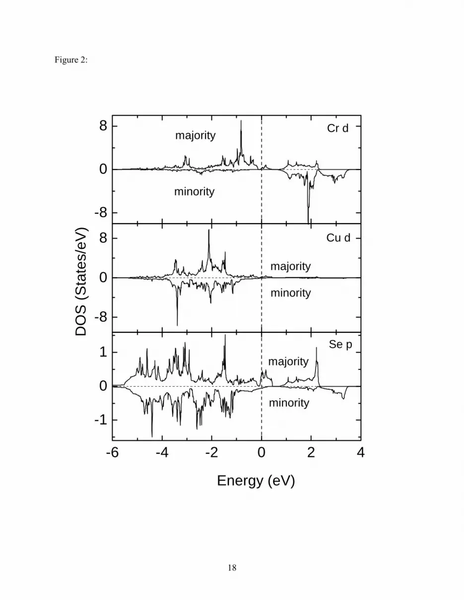
Figure 2:
-6 -4 -2 0 2 4
-1
0
1
-8
0
8
-8
0
8
minority
majority
Energy (eV)
Se p
Cu d
minority
majority
D
OS
(Sta
tes/
eV)
Cr d
minority
majority
18

Figure 3:
0 .2 0 .5 0 .83
4
5
E F
Γ -X
k /k B Zm ax
E
nerg
y (e
V)
0 .2 0 .5 0 .8
Γ -K
k /k B Zm ax
M a jo rity
0 .2 0 .5 0 .8
Γ -L
k /k B Zm ax
0 .2 0 .5 0 .83
4
5
E F
Γ -X
k /k B Zm ax
E
nerg
y (e
V)
0 .2 0 .5 0 .8
Γ -K
k /k B Zm ax
M in o rity
0 .2 0 .5 0 .8
Γ -L
k /k B Zm ax
19

Figure 4:
20

Figure 5:
21

Figure 6:
22

Figure 7:
23

Figure 8:
24

Figure 9:
-6 -4 -2 0 2 4-40
-20
0
20
40
D
OS
(Sta
tes/
eV)
Energy (eV)
majority
minority
-1 0 1-10
0
10
25

Figure 10:
-6 -4 -2 0 2 4
-1
0
1
-8
0
8-8
0
8
minority
majority
Energy (eV)
Se p
Cu d
minority
majority
D
OS
(Sta
tes/
eV)
Cr d
minority
majority
26

Figure 11:
0 .2 0 .5 0 .82
3
4Γ -X
k /k B Zm ax
Ene
rgy
(eV
)
0 .2 0 .5 0 .8
Γ -K
k /k B Zm ax
0 .2 0 .5 0 .8
G -L
k /k B Zm ax
M a jo rity
0 .2 0 .5 0 .82
3
4
E F
Γ -X
k /k B Zm ax
Ene
rgy
(eV
)
0 .2 0 .5 0 .8
Γ -K
k /k B Zm ax
M ino rity
0 .2 0 .5 0 .8
Γ -L
k /k B Zm ax
27


