Embed Size (px)
Citation preview
This content has been downloaded from IOPscience. Please scroll down to see the full text.
Download details:
IP Address: 218.27.204.75
This content was downloaded on 19/10/2013 at 17:49
Please note that terms and conditions apply.
Structure and magnetism of ultra-thin chromium layers on W(110)
View the table of contents for this issue, or go to the journal homepage for more
2008 New J. Phys. 10 013005
(http://iopscience.iop.org/1367-2630/10/1/013005)
Home Search Collections Journals About Contact us My IOPscience

T h e o p e n – a c c e s s j o u r n a l f o r p h y s i c s
New Journal of Physics
Structure and magnetism of ultra-thin chromiumlayers on W(110)
B Santos 1,2, J M Puerta 3, J I Cerda 3, R Stumpf 4,K von Bergmann 5, R Wiesendanger 5, M Bode 5,6,K F McCarty 4 and J de la Figuera 1,2
1 Centro de Microanálisis de Materiales, Universidad Autónoma de Madrid,Madrid 28049, Spain2 Instituto de Química-Física ‘Rocasolano’, CSIC, Madrid 28006, Spain3 Instituto de Ciencia de Materiales, CSIC, Madrid 28049, Spain4 Sandia National Laboratories, Livermore, California 94550, USA5 Institute of Applied Physics and Microstructure Research Center,University of Hamburg, Jungiusstrasse 11, 20355 Hamburg, Germany6 Center for Nanoscale Materials, Argonne National Laboratory, Argonne,Illinois 60439, USAE-mail:[email protected]
New Journal of Physics 10 (2008) 013005 (16pp)Received 17 September 2007Published 14 January 2008Online athttp://www.njp.org/doi:10.1088/1367-2630/10/1/013005
Abstract. We have investigated the structural and magnetic properties ofultra-thin Cr films on W(110) by means of low-energy electron diffractionintensity-versus-voltage (LEED IV) data acquired using selected-area diffractionwithin a low-energy electron microscope (LEEM), spin-polarized scanningtunneling microscopy (SP-STM), andab initio calculations. The interlayerdistances as obtained from LEED IV data are compared toab initio calculations.The first-principles calculations predict very different interlayer spacingsdepending on whether the Cr films are antiferromagnetic or non-magnetic.Only antiferromagnetic spin ordering leads to interlayer spacings similar to theexperimental spacings determined by LEED IV. This strongly suggests that filmsof one, two and three atomic layers of Cr on W(110) have antiferromagneticshort-range order. SP-STM data confirm this finding: the Cr monolayer onW(110) shows characteristic stripes along the [001] direction due to theantiferromagnetic order of nearest-neighbor Cr atoms. Additionally, the SP-STMdata of the Cr monolayer reveal a periodically varying magnetic amplitudethat peaks every 7.7± 0.5 nm. On thick Cr(110) films the signature of an
New Journal of Physics 10 (2008) 0130051367-2630/08/013005+16$30.00 © IOP Publishing Ltd and Deutsche Physikalische Gesellschaft

2
incommensurate spin density wave, existing in two different orientations, isfound. We also compare the LEED IV andab initio relaxations of bare W(110)and bulk-like Cr(110) surfaces.
Contents
1. Introduction 22. Experimental and theoretical calculation details 3
2.1. Low-energy electron microscopy and diffraction. . . . . . . . . . . . . . . . . 32.2. Ab initio calculations. . . . . . . . . . . . . . . . . . . . . . . . . . . . . . . 42.3. SP-STM. . . . . . . . . . . . . . . . . . . . . . . . . . . . . . . . . . . . . . 4
3. Results and discussion 53.1. Growth of Cr on W(110). . . . . . . . . . . . . . . . . . . . . . . . . . . . . 53.2. The bare W(110) surface. . . . . . . . . . . . . . . . . . . . . . . . . . . . . 63.3. The Cr(110) surface. . . . . . . . . . . . . . . . . . . . . . . . . . . . . . . . 63.4. Thin Cr films on W . . . . . . . . . . . . . . . . . . . . . . . . . . . . . . . . 10
4. Summary 13Acknowledgments 14References 14
1. Introduction
Chromium is a transition metal with a rich variety of magnetic properties that has been thefocus of many studies. It is an itinerant antiferromagnet (AFM) in the bulk and presents anincommensurate spin density wave (SDW) [1]. In thin films the coupling with the substratetransforms this AFM SDW from an incommensurate to a commensurate one [2, 3]. Furthermore,the current interest in spintronics [4] has been partially initiated by the discovery of the giantmagnetoresistance effect in Fe/Cr multilayers [5]. Further progress in this area depends onatomic level control in the manufacturing of spintronic devices.
Surprisingly, structural and magnetic characterizations of ultra-thin Cr films on W(110),a common substrate for thin metal films because of its resistance to alloying, are scarce [6].Most studies actually focus on the thick-Cr regime [3], where the surface is assumed to be aproxy of bulk Cr. One open basic question is whether ultra-thin films of Cr on W(110) presentmagnetic ordering, and if so, what kind? The problem is challenging because few methodsare capable of detecting antiferromagnetism in such thin layers. Recentab initio calculationsseem to indicate that a monolayer might be magnetic [7]. We note that spin-polarized scanningtunneling microscopy (SP-STM) has shown that a monolayer of Mn on W(110) exhibits localantiferromagnetic order [8]–[10].
Here we present a combined low-energy electron diffraction intensity-versus-voltage(LEED IV), SP-STM, andab initio calculation study with the aim of obtaining a thoroughunderstanding of the atomic and magnetic structure of Cr films a few atomic layers thick onW(110). LEED IV is the classic tool for determining the interlayer spacings between the firstfew atomic surface layers with errors in the 0.01–0.02 Å range. A satisfactory comparisonof LEED with ab initio density functional theory (DFT) is also a mature approach and, ingeneral, is considered the gold standard for surface structure determinations. Well-converged
New Journal of Physics 10 (2008) 013005 (http://www.njp.org/)

3
spin-polarized (SP) DFT calculations usually predict surface relaxations in good agreement withexperiment even for magnetic materials. In the past, a systematic discrepancy has been reportedbetween experimental andab initio calculations for particular transition metal surfaces [11].To check for any of the presumed effects that caused those discrepancies [12], we also includein our LEED IV study the limiting cases of the bare W(110) and bulk-like Cr(110) surfaces.Finally, SP-STM is one of the few techniques able to measure local antiferromagnetic orderon surfaces [13]. By depositing a ferromagnetic film on the tunneling tip, images with contrastrelated to the magnetic structure of the surface can be acquired. The sensitivity of the tip toeither in-plane or out-of-plane surface magnetic moments can be tuned by applying magneticfields.
2. Experimental and theoretical calculation details
2.1. Low-energy electron microscopy and diffraction
A low-energy electron microscope (LEEM) [14] was used both to characterize the growth ofCr on W(110) and to acquire the LEED IV curves [15, 16]. While imaging, Cr was evaporatedby electron-bombardment at a typical flux of 0.14 AL min−1 for the ultra-thin films and up to1 AL min−1 for thick films. The background pressure remained in the 10−10 torr range during theexperiments. The W(110) crystal was cleaned by exposure to O2 followed by repeated flashesto 2200 K. Terraces wider than a few microns could be routinely found on the surface.
The first 3 AL of Cr grow layer-by-layer on W(110). As soon as the 4th layer nucleates, thefilms break up, giving rise to tall three-dimensional (3D) islands surrounded by a monoatomicCr wetting layer on W(110) [3, 6]. For Cr films with thickness below 3 AL the LEED dataalways showed a 1×1 pattern, indicating in-plane pseudomorphic growth of Cr on W(110) inultra-thin films. To obtain a film surface with properties equivalent to the (110) surface of bulkCr, relatively thick Cr films (15–40 AL Cr) were first grown on W(110) with the substrate held atroom temperature (RT), and subsequently annealed to 600◦C while observed in LEEM. ThickCr films also exhibit a 1× 1 pattern, but with the in-plane lattice spacing of a bulk-Cr (110)surface.
The IV curves are acquired within the LEEM instrument by changing the power of thelenses in order to image the back-focal plane of the objective lens. The use of LEEM as a LEEDdiffractometer provides several advantages over a conventional LEED system, among them theability to acquire the specular beam in normal incidence. The LEED IV data was obtained from2µm diameter areas using an illumination aperture to limit the electron beam size on the sample.The sample was cooled to RT before measuring the IV data.
The (00), four symmetry-equivalent (01) and two symmetry-equivalent (11) beams weremeasured at primary electron energies of 50–350 eV, giving a total energy range1E of 900 eV,which is more than enough to provide accurate estimates of the last layers’ relaxations [12].Equivalent beams were averaged. The Pendry factorRP between equivalent beams was alwayslower than 0.10.
Fully dynamical LEED IV curve calculations were performed with a modified version ofthe Van Hove–Tong package [17]. The surface was modeled by stacking the necessary numberof Cr layers over five layers of W bulk, using the renormalized forward scattering (RFS)approach. Relativistic phase-shifts [18] were calculated and subsequently spin-averaged.We
New Journal of Physics 10 (2008) 013005 (http://www.njp.org/)

4
explored the parameter space comprised of the topmost three interlayer spacings,d1–3 (up tothe 4th layer distance for the 3 AL Cr case) by calculating the IV curves over fine 3D parametergrids. The interlayer spacings were swept over wide ranges.
All simulations were performed for a temperature of 300 K. The experiment–theoryagreement was quantified via Pendry’sR-factor [19], RP, while the error bars for each parameterwere obtained from its variance [20] 1RP = RPmin
√8Ei/1E, whereEi gives the optical (inner)
potential. Correlations between the structural parameters were taken into account for theestimation of error limits. We note that all structural parameters derived in this work representwell-defined minima in their respectiveR-factor plots. Non-structural parameters such as themuffin-tin radius, the optical potential or the Debye temperatures at the surface planes werealso varied.
2.2. Ab initio calculations
Modeling of thin magnetic films on a non-magnetic material within DFT requires a carefulchoice of approximations and estimates of the overall accuracy. As we will see, especially howthe electronic exchange and correlation is treated (local density approximation (LDA) or gen-eralized gradient approximation (GGA)) crucially affects the interplay between heteroepitaxialstress, relaxation and magnetic structure. We calculate the ideal bulk W and Cr lattice para-meters using both LDA and the Perdew–Burke–Ernzerhof (PBE) GGA [21], using the ViennaVASP code [22]. The clean slab calculations are performed using eight-layer slabs for W(110)and nine for Cr(110), at the ideal in-plane lattice constants. Nine layers is the minimum numberof Cr layers required to obtain in-plane antiferromagnetic coupling with magnetic moments likein bulk Cr in the center of the slab. Only GGA finds an antiferromagnetic ground state for Cr(m = 1.08µB atom−1). The LDA result is always non-magnetic, a well-know issue with LDA.
The lattice constants determined by SP GGA-PBE reproduce the experimental numbersbetter than LDA. Still, the calculated lattice mismatch between W and Cr is 9.9%, comparedto 8.8% for literature bulk values. The larger mismatch should lower the tendency forpseudomorphic wetting in SP-GGA-PBE and even more so for non-magnetic GGA and LDA.
The different strain-energy cost is reflected in the calculations of bulk Cr strained to theW(110) in-plane lattice constant. In non-magnetic LDA the energy cost is 0.290 eV per Cratom with thez-layer (out-of-plane) spacing compressed by 23.3%. In non-magnetic GGAthese values reduce to 0.259 eV and 21.8%, respectively. In SP-GGA, finally, they are 0.218 eVand 15.3%. To estimate the effect of the exaggeration of the W–Cr lattice mismatch in W–Crpseudomorphic slabs, the latter calculation was repeated for an in-plane strain correspondingto only 8.8%, instead of a 9.9%, mismatch. Now the strain costs only 0.180 eV per Cr atom.Therefore, the calculations of pseudomorphic Cr layers on W(110) are expected to be 0.038 eVtoo high in energy.
Finally we note that all the slab calculations for W(110) and films of Cr on W(110) aredone at the fixed, theoretical W in-plane lattice constant. All other geometry parameters, whichinclude the separation between layers, are allowed to relax. The layer relaxation is reportedrelative to the theoretical bulk layer separation.
2.3. SP-STM
The SP-STM measurements were performed at the University of Hamburg in a five chamberultra-high vacuum (UHV) system with separate chambers for sample and tip preparation,
New Journal of Physics 10 (2008) 013005 (http://www.njp.org/)

5
Figure 1. (a)–(f) Sequence of LEEM images taken during growth of Cr onW(110) at 360◦C. The field of view is 7µm. The detailed evolution of the LEEMimages during Cr deposition onto W(110) is illustrated in movie 1 (availablefrom stacks.iop.org/njp/10/013005/mmedia).
thin-film deposition, conventional surface analysis (LEED, Auger electron spectroscopy, etc),and low-temperature STM using a home-built instrument [23]. During the STM measurementsthe tip and the sample were held at a temperatureT = 13± 1 K. Tips were prepared byelectrochemically etching a polycrystalline W wire. Upon introduction of the tip into the UHVsystem via a load lock, the tip was briefly heated at a temperatureT > 2200 K to removetungsten oxides. For spin-sensitive experiments the tips were coated by a thin Fe film. Thesubstrate is cleaned by cycles of oxidation atT = 1500 K and subsequent high-temperatureflashing (T > 2200 K) [24]. Cr films were grown by thermal evaporation from a W crucibleat a pressurep6 3× 10⁻¹⁰ mbar. All STM data presented here were recorded in the constantcurrent mode.
3. Results and discussion
3.1. Growth of Cr on W(110)
At temperatures between 200 and 360◦C the growth of Cr on W(110) takes place layerby layer, but only for the first three monolayers [3]. Figure 1 shows a growth series takenby LEEM at 360◦C. Within the field of view of the images shown (7µm, although 20µmimages were also acquired), all the growth proceeds by step flow. But before the third layer iscompleted, four-layer thick islands appear in the film, and a dewetting process takes place by
New Journal of Physics 10 (2008) 013005 (http://www.njp.org/)

6
which further growth removes the second and third layers and produces tall 3D islands in theStranski–Kranstanov growth mode (see figure7(a)). The LEED pattern of the films between oneand three monolayers is the same as that of the substrate indicating a common in-plane latticeparameter7. This pattern indicates a relaxed spacing [6]. A similar behavior has been observedon Cr/Mo(110) by STM [25].
As the interlayer distance between the surface layer and the first sub-surface layer,d1–2,of unreconstructed transition metals has been the subject of a lively debate [11], we firstfocus on the bare W(110) and bulk-like Cr(110) surfaces to check our agreement betweentheory and experiment. A systematic discrepancy between LEED experiments andab initiocalculations was reported for transition-metal surfaces: in most available cases, the first layerDFT contractions were larger than the experimental ones. This disagreement is—given thesimplicity of the problem—surprising and prompted suggestions that the smaller experimentalrelaxation could be related to contamination, for example by hydrogen absorption [26].Currently, many of the previous discrepancies have been resolved, including W(110), Rh(100)and Ti(0001) [12] as well as for Ru(0001) [15]8.
3.2. The bare W(110) surface
Given its role as a model system, W(110) has been the subject of recent detailed STM [24]and LEED studies [27, 28]. To test for the effect of surface roughness, which is not included inthe multiple scattering programs currently in use, flat [27] and stepped substrates [28] havebeen investigated. All the more recent experimental studies agree in a contraction ofd1–2
of ≈3%, which is also in agreement with surface x-ray diffraction studies [29]. Our resultsshown in figure2 are in the same range. Our best fit (shown in figure2(b)) to d1–2 resultsin a contraction of(−2.8± 1.2)%, with a RP = 0.13. We note that roughness cannot play arole in our results as we employ selected-area diffraction with at most two atomic steps in thesurface area 2µm in diameter where the LEED IV data were acquired. Our comparison withthe ab initio calculations (−3.8%) is actually within the error bars of our experimental data.Nevertheless, the difference follows the same trend that other studies have observed on W(110):the experimental contractions tend to be at least 1% smaller than the theoretical predictions. Thetheory/experiment discrepancy seems to be particular to the case of the W(110) surface [29],and does not extend to other transition-metal surfaces.
3.3. The Cr(110) surface
The Cr(110) surface was obtained by growing thick films of Cr on W(110) (between 15–40 ALin the LEEM experiments, and close to 100 AL for the SP-STM experiments). As thick-film
7 In a minority of local regions containing 2 and 3 AL of Cr examined by selected area diffraction the (00),and first-order spots were weakly split (‘streaked’) along the [001] direction. These streaks disappeared with mildannealing (well below the growth temperature). In addition, the 3 AL regions contained linear defects visible inthe LEEM images. These observations suggest that 3 AL of Cr can exist in a metastable, non-pseudomorphicstructure, which is likely a precursor to the moiré structure of thicker films. We emphasize, however, that ourLEED IV analysis was performed on pseudomorphic regions.8 Most of the resolved discrepancies have been attributed so far to experimental problems rather thanab initiocalculation issues. Either hydrogen contamination or a dataset of insufficient energy range have been singled outas responsible in selected cases.
New Journal of Physics 10 (2008) 013005 (http://www.njp.org/)

7
Figure 2. (a) LEED pattern of W(110). (b) LEED IV curves of clean W(110).(c) LEEM image of a 15 AL Cr film on W(110) after annealing to 633◦C. Thefield of view is 20µm. The dark features are trenches extending down to the 1 ALCr wetting layer (one is marked by an arrow), which formed during annealing.The circle shows the area where the diffraction data was obtained. (d) LEED IVcurves of the thick Cr(110) film.
growth at elevated temperatures produces 3D islands, the growth was performed at RT. Afterthe growth of a few atomic layers, the backscattered electron intensity decreases greatly, untilnothing can be seen in LEEM images. Even the diffraction pattern was featureless. To obtaina smooth surface, annealing of the RT-grown film was performed. In agreement with previousreports [3] we found that the backscattered electron intensity increased greatly close to 600◦C.Annealing at this temperature yielded a locally flat film conformal to the substrate, i.e. theatomic surface steps of the Cr film are mainly located over the substrate steps. However, thefilm also started to scarify in the same temperature range, with deep trenches extending down tothe one-layer-thick wetting layer. By means of the LEEM apparatus we could measure easily thediffraction pattern of the Cr film by performing selected-area diffraction, as shown in figure2(c).Caution should be applied, however, when using spatially averaging diffraction techniques sincethis (rather typical) procedure to obtain a flat Cr film as a proxy of a Cr(110) bulk terminatedsurface can produce trenches that extend down up to the Cr/W(110) wetting layer.
The LEED IV data acquired from the surface of the thick Cr(110) is shown in figure2(d).From the multiple-scattering fit to the data (RP = 0.10) we obtained a last-layer relaxation of−2.2± 1.4% relative to the bulk Cr(110) interlayer spacing (see table1), to be compared to theSP-GGA prediction of−2.1%. The second layer is also observed to contract in the LEED bestfit, although theab initio result indicates a very small expansion.
New Journal of Physics 10 (2008) 013005 (http://www.njp.org/)

8
Table 1. Changes in the interplanar spacings as determined from experimentalLEED studies andab initio simulations, both spin-polarized (sp) and non-spin-polarized (np), given in percent relative to the W(110) bulk interlayer spacing.Results for the Cr(110) surface are given relative to the Cr(110) bulk spacing.
Surface Method d1–2 d2–3 d3–4 d4–5
W(110) LEED −2.8± 1.2 +0.2± 1.0 −0.7± 2.2GGA −3.8 0.0
Cr(110) LEED −2.2± 1.4 −1.3± 1.3GGA-sp −2.1 0.24 −0.01
1 AL Cr/W(110) LEED −8.0± 0.7 +0.3± 1.4GGA-sp −8.55 0.04GGA-np −15.4 +1.46
2 AL Cr/W(110) LEED −17.0± 0.7 −7.4± 1.3 +0.4± 1.4GGA-sp −18.3 −6.82 −0.16GGA-np 30.1 −6.28 −0.27
3 AL Cr/W(110) LEED −16.0± 1.3 −13.6± 1.4 −7.0± 3.6 −1.9± 4.4GGA-sp −18.1 −15.6 −7.37 −0.16GGA-np −30.6 −16.9 −10.2 −0.07
We have also investigated the surface of thick Cr(110) films on W(110) by means ofSTM. Figure3(a) shows an STM image of a≈100 AL thick flat Cr film grown on W(110).At the measurement temperature of the SP-STM experiments,T = 13± 1 K, this film thicknessresults in an incommensurable SDW [3]. Although we cannot exclude that the film showedannealing-induced trenches on a meso- or macroscopic scale, it was homogeneous on a lateralscale of microns with some very wide atomically flat terraces. For example, figure3(b) showsan image (250 nm× 250 nm) taken from such a terrace. In general, two surface patterns canbe recognized, which have been identified as different domains of the charge-density wave(CDW) in an earlier spin-averaged STM study employing non-magnetic probe tips [30]. Thefirst pattern, labeled A in the lower part of figure3(b), is less common. It is characterizedby stripes along the [1̄10] direction with a periodicityP of about 30 Å. The vast majority ofthe sample surface exhibits another pattern (B,C) with stripes along the [001] direction anda periodicity of about 42 Å. In [30] these patterns were interpreted as the manifestation ofCDWs with wave fronts propagating in different directions. Our data fully agree with thisinterpretation. In the bulk all three{100} directions are degenerate and equally probable. Atthe surface, however, the CDW with the wave vectorEQ ‖ [001] is strongly damped and lessfrequent. Since it propagates within the sample surface, its apparent periodicity is consistentwith the periodicity of the CDW, i.e. 30 Å. The surface is dominated by the CDWs that arepropagating along the other two{100} directions, which are tilted by 45◦ with respect to thesurface plane. Therefore, the apparent periodicity of these CDWs (B,C) is
√2× 30 Å ≈ 42 Å,
corresponding to 10–11 times the lattice constant. Both domains can be recognized as spots inthe Fourier-transformed image (figure3(c)).
As stated in [30] ‘a fascinating, however challenging, goal to achieve is the directobservation of the SDW with the help of ferromagnetic STM tips’. In this spirit we haveperformed spin-resolved STM measurements with Fe-coated probe tips. Figure4(a) shows
New Journal of Physics 10 (2008) 013005 (http://www.njp.org/)

9
Figure 3. (a) Large-scale STM image of an approximately 100 AL thick Cr filmon W(110). Wide atomically flat terraces and single atomic step edges are clearlyresolved. (b) Atomically flat terraces of a Cr(110) film on W(110) taken with anon-magnetic W tip (U = −10 mV andI = 0.3 nA). Similar to previous studiesthat were performed on the surface of bulk Cr(110) [30], two different regionscan be distinguished: wherever the wave vectorEQ of the charge-density wave(CDW) is within the film plane along the [001] direction, stripes along the [11̄0]direction with a periodicityP = 30 Å and a relatively small corrugation can berecognized (see region A). If, however,EQ is along the{100} directions, whichare not within the surface plane, the periodicity amounts toP = 42 Å and thecorrugation is larger (region B, C). (c) These domains give rise to discrete spotsin the Fourier-transformed image.
a constant-current SP-STM image as measured on a thick Cr(110) film on W(110) beingvery similar to the one presented in figure3. Figure4(b) displays the same image but fullydifferentiated along the fast scan direction. The measurements were taken at a bias voltageU = −2 mV, i.e. essentially at the Fermi level. While the contrast observed in the constant-current SP-STM image of figure4(a) is clearly dominated by the CDW, the existence of aweak additional short-range modulation with wave fronts parallel to the CDW (arrows) becomesclearly visible in the differentiated image of figure4(b). This additional modulation is caused bySP tunneling between the ferromagnetic Fe tip and the antiferromagnetic surface with maximaand minima of the lines representing atomic rows of spins being oriented parallel or antiparallelwith respect to the tip magnetization direction, respectively. From earlier investigations on
New Journal of Physics 10 (2008) 013005 (http://www.njp.org/)

10
Figure 4. (a) Constant-current SP-STM image of a thick Cr(110) film on W(110)measured with a magnetic Fe-coated probe tip (U = −2 mV and I = 40 nA).The image contrast is dominated by the CDW state exhibiting a period ofabout 42 Å. (b) Differentiated image of (a) making the SP contribution to thetunneling current visible. The observed small-scale periodicity corresponds toan anitferromagnetically ordered state about 0.1 times the period of the CDW.(c) Fourier-transformation of (a) shows satellites (arrows), which are character-istic for the incommensurate SDW of Cr. The inset shows a magnification of thecentral region with small reciprocal lattice vectors.
Cr(001) [31] we know that the spin-flip transition between a transverse (T) and a longitudinal-SDW (L-SDW), which in the bulk occurs when cooling belowTsf = 123 K, is suppressed atthe surface, probably due to a strong in-plane surface anisotropy. We expect a similar behaviorfor the Cr(110) surface. Furthermore, the Fe-coated probe tips used here are known to be in-plane sensitive [32]. Therefore, we believe that the atomic scale magnetic contrast in figure4(b)represents the in-plane component of magnetization. As already mentioned in the introduction,Cr exhibits an incommensurate SDW that gives rise to characteristic satellites in neutrondiffraction experiments [1]. The Fourier transform of figure4(a) is shown in figure4(c). Wecan recognize a set of spots close to the central region of figure4(c), representing the CDW(between arrows on inner circle) and a pair of satellites at much larger reciprocal lattice vectors(outer arrows). The latter are arranged around the positions where the atomic lattice peaks ina non-spin-resolved measurement are to be expected (outer circle). Thus the satellite peaks arecaused by the incommensurate SDW and only visible in spin-resolved measurements. Detailedanalysis reveals the relative distances are in full agreement with the expected periodicities ofthe CDW and SDW at low temperatures, i.e. 10–11 lattice constants for the CDW and 20–22lattice constants for the SDW [2]. Interestingly, the maximal SDW contrast is observed wherethe CDW exhibits a minimum charge density at the Fermi level.
3.4. Thin Cr films on W
LEED IV data (see figure5) were acquired in perfect 1 and 2 AL films on W(110) (grown,respectively, at 200 and 360◦C) from single terrace areas. The structures that best fit the LEEDIV data have anRP of 0.10 and 0.08, respectively. Theab initio calculations (see table1)
New Journal of Physics 10 (2008) 013005 (http://www.njp.org/)

11
Figure 5. (a) LEED IV curves of 1 AL Cr/W(110). (b) LEED IV curves of 2 ALCr/W(110).
have been obtained both without and with spin polarization9. There is a large difference inthe predicted relaxations depending on whether the spin polarization is included or not. In factthe differences are much larger than the error bars of the LEED fits. As seen in table1, theexperimental results are only compatible with the calculations that include spin-polarization,i.e. the calculations of an antiferromagnetic unit cell. Based on this strong effect of magnetismon the structure of the films, we predict that films of one and two atomic layers of Cr on W(110)are antiferromagnetic10.
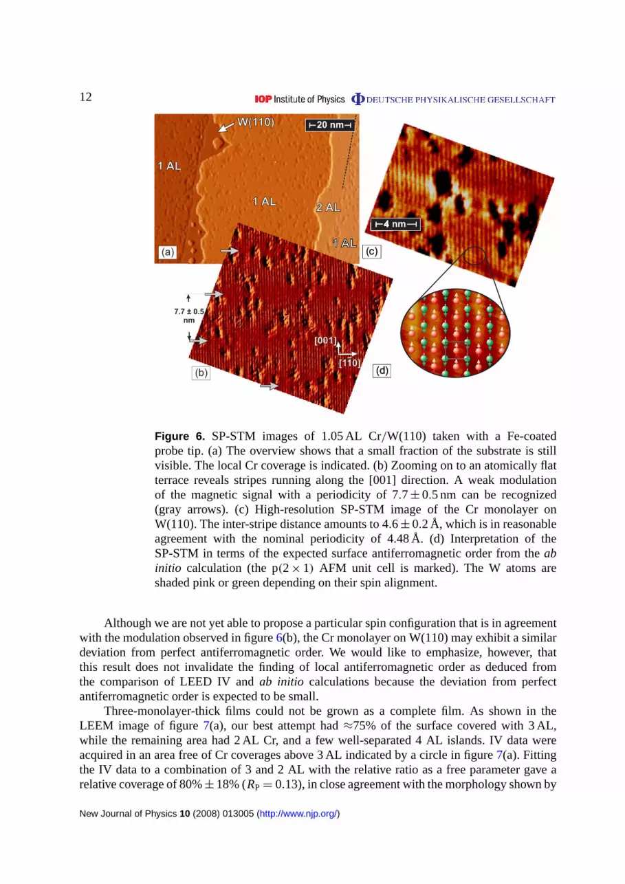
This result is in agreement with the SP-STM data shown in figure6. The data weremeasured on a sample with an average coverage of 1.05 AL Cr grown on W(110) at slightlyelevated temperature. The overview of figure6(a) shows that only a small fraction of the W(110)substrate, mainly on the upper terrace around atomic step edges, remains visible. Large areas ofthe three visible atomically flat terraces exhibit monolayer coverage (1 AL). On the right sideof the image a stripe with a local coverage of two atomic layers (2 AL) can be recognized. Aswe zoom on to a terrace covered by a Cr monolayer, stripes running along the [001] directionbecome visible (figure6(b)). These stripes, being visible with magnetic probe tips only, arecharacteristic of row-wise antiferromagnetic order [8]. The same local magnetic superstructurewas observed for 2 AL Cr/W(110) (not shown). In the high-resolution SP-STM image of theCr monolayer on W(110) shown in figure6(c), the inter-stripe distance was determined to be4.6± 0.2 Å, in agreement with the nominal periodicity along the [11̄0] direction of 4.48 Å andthe antiferromagnetic order found on the basis of the LEED andab initio calculations mentionedabove. Closer examination of figure6(b) reveals, however, that the magnetic corrugation of thestripes along the [001] direction is not constant but exhibits a weak modulation resulting inareas of blurred contrast every 7.7± 0.5 nm. The observed structure resembles recent SP-STMdata measured on the pseudomorphic Mn monolayer on W(110), where the magnetic orderwas not perfectly antiferromagnetic but slightly canted, resulting in a spiral spin structure witha period of about 12 nm [10, 37]. However, in this case the modulation is along a differentcrystallographic direction, i.e. along the [11̄0] direction (Cr) instead of the [001] direction (Mn).
9 In the SPab initio calculation, the lowest energy structure was the one shown in the inset of figure6.10 Besides using SP STM, we also tried to detect signatures of the magnetic ordering of the surface using LEED.Observations of this type, predicted by theory [33, 34] have been reported for surfaces of bulk AFMs, such asNiO [35], as well as for thin films [36]. We find indeed weak half order spots, however, they correlate withincreasing contamination, and annealing temperature. For the cleanest Cr film at low temperature these spotsdisappear completely. We thus conclude that they are not of magnetic origin.
New Journal of Physics 10 (2008) 013005 (http://www.njp.org/)
12
Figure 6. SP-STM images of 1.05 AL Cr/W(110) taken with a Fe-coatedprobe tip. (a) The overview shows that a small fraction of the substrate is stillvisible. The local Cr coverage is indicated. (b) Zooming on to an atomically flatterrace reveals stripes running along the [001] direction. A weak modulationof the magnetic signal with a periodicity of 7.7± 0.5 nm can be recognized(gray arrows). (c) High-resolution SP-STM image of the Cr monolayer onW(110). The inter-stripe distance amounts to 4.6± 0.2 Å, which is in reasonableagreement with the nominal periodicity of 4.48 Å. (d) Interpretation of theSP-STM in terms of the expected surface antiferromagnetic order from theabinitio calculation (the p(2× 1) AFM unit cell is marked). The W atoms areshaded pink or green depending on their spin alignment.
Although we are not yet able to propose a particular spin configuration that is in agreementwith the modulation observed in figure6(b), the Cr monolayer on W(110) may exhibit a similardeviation from perfect antiferromagnetic order. We would like to emphasize, however, thatthis result does not invalidate the finding of local antiferromagnetic order as deduced fromthe comparison of LEED IV andab initio calculations because the deviation from perfectantiferromagnetic order is expected to be small.
Three-monolayer-thick films could not be grown as a complete film. As shown in theLEEM image of figure7(a), our best attempt had≈75% of the surface covered with 3 AL,while the remaining area had 2 AL Cr, and a few well-separated 4 AL islands. IV data wereacquired in an area free of Cr coverages above 3 AL indicated by a circle in figure7(a). Fittingthe IV data to a combination of 3 and 2 AL with the relative ratio as a free parameter gave arelative coverage of 80%± 18% (RP = 0.13), in close agreement with the morphology shown by
New Journal of Physics 10 (2008) 013005 (http://www.njp.org/)

13
Figure 7. (a) LEEM image, 7µm wide, of an incomplete 3 AL Cr film. (b) LEEDIV curves of the area marked by a circle in (a).
Table 2. Calculated magnetic moments of Cr films (all in units ofµB /atom).
Film Top W 1st Cr 2nd Cr 3rd Cr 4th Cr
8 AL W + 1 AL Cr 0.31 2.688 AL W + 2 AL Cr 0.26 1.76 2.848 AL W + 3 AL Cr 0.25 1.64 1.95 2.898 AL W + 4 AL Cr 0.24 1.56 1.88 2.05 2.91
LEEM. The theory/experiment comparison (table1) follows the same trend as the 1 and 2 ALfilms: only the SP calculations are in reasonable agreement with the experimental structure.
We have no measurement of the Néel temperature of ultra-thin Cr films on W(110). Ourdirect observations of the antiferromagnetic order in the SP-STM experiments were performedat 13 K. The Néel temperature of bulk Cr is 308 K. In theory, at constant magnetic couplingstrengthJ, a thin Cr film should have a reduced or at best unchanged Néel temperature [38].This could be counteracted ifJ increases. The Néel temperature, like the Curie temperature,is proportional toJ, which in turn is proportional to the magnetic moment per atom [38, 39].Table2 lists the calculated magnetic moments (GGA-sp) of each layer of the different ultra-thin Cr films. For comparison, the calculated magnetic moment of a Cr atom in bulk bcc-Cr is1.08µB. If the bulk Cr is strained in-plane by 9.9% to match the W(110) substrate, the increasein the effective volume per atom results in a magnetic moment of 1.99µB. For the ultra-thin Crfilms we find an even higher value of 2.7–2.9µB for the top Cr layer. While intermediate Crlayers are close to the strained bulk value, the magnetic moment of the Cr layer at the Cr/W(110)interface is reduced to 1.7µB. The top W layer picks up about 0.3µB from contact with Cr. Theenhanced moments of the surface Cr compared to bulk can again be explained by the increasedeffective volume per atom in that case [39].
4. Summary
We have followed the growth of ultra-thin films of Cr on W(110) by LEEM. The growth islayer-by-layer over a wide range of temperature until the fourth layer starts to nucleate. Then3D islands grow, and the third and second layers are removed.
New Journal of Physics 10 (2008) 013005 (http://www.njp.org/)

14
By means of selected-area diffraction, we have measured the LEED IV curves on bothclean surfaces of W(110) and Cr(110) and films of one, two and three atomic layers of Cr/W.For the W(110) and Cr(110) surfaces the experimentally determined last-layer contractions arein good agreement with theab initio calculations of the same surfaces by GGA-PBE. For theCr films, theab initio calculations are quite different depending on whether the calculationis SP with antiferromagnetic ordering or not, with last-layer out-of-plane relaxations that aretwice as large for the non-SP calculations. Our experimental results are in good agreementwith the ab initio predictions with spin polarization implying that Cr ultra-thin films areantiferromagnetically ordered.
By SP-STM we proved that the 1 and 2 AL films are indeed antiferromagnetically orderedon a short range: using a Fe-coated tip we detect in-plane magnetic contrast that alternates everyatomic row in the [1̄10] directions. This agreement validates the proposed method of detectingmagnetism in thin films by the effect of the magnetic structure on the interlayer relaxation.Furthermore, on 1 AL Cr films we have detected a long-range modulation along [001] with7.7± 0.5 nm periodicity. We also presented the first real-space observations of the SDW of theCr(110) surface by means of SP-STM experiments. The periodicity of the SDW is consistentwith the CDWs observed on the same surface.
Acknowledgments
This research was partly supported by the US Department of Energy, Office of Science, Officeof Basic Energy Sciences, under contract no. DE-AC02-06CH11357, by the Spanish Ministryof Science and Technology under project no. MAT2006-13149-C02-02, and by the DeutscheForschungsgemeinschaft (SFB 668-A1).
References
[1] Fawcett E 1998 Spin-density-wave antiferromagnetism in chromiumRev. Mod. Phys.60209–83[2] Zabel H 1999 Magnetism of chromium at surfaces, at interfaces and in thin filmsJ. Phys.: Condens. Matter
119303–46[3] Rotenberg E, Freelon B K, Koh H, Bostwick A, Rossnagel K, Schmid A and Kevan S D 2005 Electron states
and the spin density wave phase diagram in Cr(110) filmsNew J. Phys.7 114[4] Wolf S A, Awschalom D D, Buhrman R A, Daughton J M, von Molnar S, Roukes M L, Chtchelkanova A Y
and Treger D M 2001 Spintronics: a spin-based electronics vision for the futureScience2941488–95[5] Baibich M N, Broto J M, Fert A, Nguyen Van Dau F, Petroff F, Eitenne P, Creuzet G, Friederich A and
Chazelas J 1988 Giant magnetoresistance of (001)Fe/(001)Cr magnetic superlatticesPhys. Rev. Lett.612472–5
[6] Berlowitz P and Shinn N 1989 Growth and atomic-structure of chromium overlayers on W(110) and W(100)Surf. Sci.209345–63
[7] Wei X, Jiang P and Che J-G 2005 First-principles study of structural and magnetic properties for ultrathinCr films on W(100) and W(110)Chin. Phys. Lett.221232–5
[8] Heinze S, Bode M, Kubetzka A, Pietzsch O, Nie X, Blugel S and Wiesendanger R 2000 Real-space imagingof two-dimensional antiferromagnetism on the atomic scaleScience2881805–8
[9] Bode M, Heinze S, Kubetzka A, Pietzsch O, Hennefarth M, Getzlaff M, Wiesendanger R, Nie X, BihlmayerG and Blugel S 2002 Structural, electronic, and magnetic properties of a Mn monolayer on W(110)Phys.Rev.B 66014425
New Journal of Physics 10 (2008) 013005 (http://www.njp.org/)

15
[10] Bode M, Heide M, von Bergmann K, Ferriani P, Heinze S, Bihlmayer G, Kubetzka A, Pietzsch O, Blugel Sand Wiesendanger R 2007 Chiral magnetic order at surfaces driven by inversion symmetryNature447190–3
[11] Feibelman P J 1996 Disagreement between experimental and theoretical metal surface relaxationsSurf. Sci.360297–301
[12] Teeter G and Erskine J L 1999 Studies of clean metal surface relaxation experiment-theory discrepanciesSurf. Rev. Lett.6 813–7
[13] Bode M 2003 Spin-polarized scanning tunnelling microscopyRep. Prog. Phys.66523–82[14] Bauer E 1994 Low energy electron microscopyRep. Prog. Phys.57895–938[15] de la Figuera J, El Gabaly F, Puerta J M, Cerda J I and McCarty K F 2006 Determining the structure of
Ru(0001) from low-energy electron diffraction of a single terraceSurf. Sci.600L105[16] El Gabaly F, Puerta J, Klein C, Saa A, Schmid A, McCarty K, Cerda J and de la Figuera J 2007 Structure and
morphology of ultrathin Co/Ru(0001) filmsNew J. Phys.9[17] Van Hove M A and Tong S Y 1979Surface Crystallography by LEED(Berlin: Springer)[18] Van Hove M A and Baraldi A 1993 private communication[19] Pendry J B 1980 Reliability factors for LEED calculationsJ. Phys. C: Solid State Phys.13937-44[20] Cerdá J 1995 Surface structure determination by LEEDPhD thesisUniversidad Autónoma de Madrid[21] Perdew J P, Burke K and Ernzerhof M 1996 Generalized gradient approximation made simplePhys. Rev. Lett.
773865–8[22] Kresse G and Joubert D 1999Phys. Rev.B 591758[23] Pietzsch O, Kubetzka A, Haude D, Bode M and Wiesendanger R 2000 A LT UHV STM with a split-coil
magnet and a rotary motion stepper motor for high spatial resolution studies of surface magnetismRev. Sci.Instrum.71424
[24] Bode M, Krause S, Berbil-Bautista L, Heinze S and Wiesendanger R 2007 On the preparation and electronicproperties of clean W(110) surfacesSurf. Sci.6013308–14
[25] Cazacu A, Murphy S and Shvets I V 2006 Epitaxial growth of ultrathin Cr films on Mo(110) at elevatedtemperaturePhys. Rev.B 73045413
[26] Feibelman P J, Houston J E, Davis H L and Oneill D G 1994 Relaxation of the clean, Cu-covered andH-covered Ru(0001) surfaceSurf. Sci.30281–92
[27] Arnold M, Sologub S, Hupfauer G, Bayer P, Frie W, Hammer L and Heinz K 1997 LEED structureanalyses of the clean and fully hydrogen-covered W(110) and Mo(110) surfacesSurf. Rev. Lett.4 1291–5
[28] Teeter G, Erskine J L, Shi F and Van Hove M A 1999 Surface roughness and LEED crystallography: Analysisof flat and vicinal W(110)Phys. Rev.B 601975–81
[29] Meyerheim H L, Sander D, Popescu R, Steadman P, Ferrer S and Kirschner J 2001 Interlayer relaxation ofW(110) studied by surface x-ray diffractionSurf. Sci.475103–8
[30] Braun K-F, Fölsch S, Meyer G and Rieder K-H 2000 Observation of charge-density wave domains on theCr(110) surface by low-temperature scanning tunneling microscopyPhys. Rev. Lett.853500–3
[31] Hänke T, Krause S, Berbil-Bautista L, Bode M, Wiesendanger R, Wagner V, Lott D and Schreyer A 2005Absence of spin-flip transition at the Cr(001) surface: a combined spin-polarized scanning tunnelingmicroscopy and neutron scattering studyPhys. Rev.B 71184407
[32] Kubetzka A, Pietzsch O, Bode M and Wiesendanger R 2003 Spin-polarized scanning tunneling microscopystudy of 360◦ walls in an external magnetic fieldPhys. Rev.B 67020401
[33] Feder R 1981 Spin-polarised low-energy electron diffractionJ. Phys. C: Solid State Phys.142049–91[34] Tamura E, Blugel S and Feder R 1988 On the determination of surface antiferromagnetism by low-energy
electron-diffractionSolid State Commun.651255–7[35] Palmberg P W, DeWames R E and Vredevoe L A 1968 Direct observation of coherent exchange scattering by
low-energy electron diffraction from antiferromagnetic NiOPhys. Rev. Lett.21682–5
New Journal of Physics 10 (2008) 013005 (http://www.njp.org/)

16
[36] Hanf M C, Krembel C, Bolmont D and Gewinner G 2003 Two-dimensional Ising behavior in c(2× 2)antiferromagnetic Mn and Cr monolayers on Ag(001)Phys. Rev.B 68144419
[37] Heinze S 2006 Simulation of spin-polarized scanning tunneling microscopy images of nanoscale non-collinear magnetic structuresAppl. Phys.A 85407–14
[38] Jensen P J and Bennemann K H 2006 Magnetic structure of films: dependence on anisotropy and atomicmorphologySurf. Sci. Rep.61129–99
[39] Fecher G H, Kandpal H C, Wurmehl S, Felser C and Schönhense G 2006 Slater-Pauling rule and Curietemperature of Co2-based heusler compoundsJ. Appl. Phys.9908J106
New Journal of Physics 10 (2008) 013005 (http://www.njp.org/)
![Magnetism, Spectroscopy and Structure of Tri-mu-hydroxobis{[N,N',N''-trimethyl-1,1,1-tris(aminomethyl)ethane]chromium(III)} Chloride Tetrahydrate](https://img.pdfslide.net/doc/110x75/635a1a6e0f31679e830c617e/magnetism-spectroscopy-and-structure-of-tri-mu-hydroxobisnnn-trimethyl-111-trisaminomethylethanechromiumiii.jpg)


