Embed Size (px)
Citation preview

UNIVERSITY OF OSLODepartment of Informatics
Master ThesisA Focal Plane Array ToModel The ColorProcessing of the Retina
Łukasz Farian
July 21, 2014


Abstract
This thesis presents a bio-inspired color camera chip. It is the first focalplane array of photo-pixels that react to temporal color contrast of threedifferent color spectra and thus this vision sensor emulates the color oppo-nencies in the human retina. The array has been designed, implementedand thoroughly characterised in TSMC 90nm CMOS technology. The threedifferent spectra are transduced into photocurrents by stacked photodi-odes and temporal changes of the contrast of these three spectra are rep-resented as asynchronous pixels event streams which are read-out off-chipby the Address Event Representation (AER) protocol. The implemented fo-cal plane consists of 16x16 pixels. A single pixel measures 82µm x 82µm andhas a fill factor of 27%. The experimental results proved that the designedsensor can discriminate between temporal color contrasts. In comparisonto traditional frame-based cameras, the designed vision sensor relaxed thepost processing load of a CPU preforming moving objects color recognition.
i

ii

Preface
This master thesis was submitted as a long thesis contributing 60 creditsto my Master of Science degree in Nanoelectronics and Robotics at theDepartment of Informatics, Faculty of Mathematics and Natural Sciences,University of Oslo. This work was started during the Spring semester 2013and was submitted in July 2014.I would like to express my deepest gratitude to my supervisors, JuanAntonio Leñero-Bardallo, Philipp Häfliger and Trygve Willassen for greatsupport and the patience to answer all my questions. In moments of doubt Icould always count on their help and suggestions how to solve encounteredobstacles. I would also like to thank Thanh Trung Nguyen, Deyan Levskiand Kristian Gjertsen Kjelgård for contribution to making the camera work.I would like to thank my sister Malwina for putting the idea of studying inNorway into my head and my parents for a boundless support.Last but not least, I would like to express my deep thanks to Malihe ZarreDooghabadi for making my life more colorful.
iii

iv

Basic Constants
Parameter Equation Parameter name
q 1.602 ·10−19C electrical charge of the electron
k 1.38 ·10−23 JK −1 Boltzmann constant
ε0 8.854 ·10−12F /m absolute permittivity
h 6.626 ·10−34 J s Plank’s constant
c 299792458m/s speed of light in vacuum
eV 1.602176565 ·10−19 J electronvolt
Table 1: Basic constants used further in this thesis.
v

vi

Contents
1 Introduction 11.1 Commercial frame-based vision sensors . . . . . . . . . . . . . 11.2 Biological Vision Perception . . . . . . . . . . . . . . . . . . . . . 31.3 Frame-Based Camera vs. Retina . . . . . . . . . . . . . . . . . . 31.4 Event-based Vision Sensors . . . . . . . . . . . . . . . . . . . . . 4
1.4.1 Spatial Contrast Sensors . . . . . . . . . . . . . . . . . . 51.4.2 Temporal Contrast Sensors . . . . . . . . . . . . . . . . . 51.4.3 Event-Based Vision Sensors in Color . . . . . . . . . . . 6
1.5 Goals and Outline . . . . . . . . . . . . . . . . . . . . . . . . . . . 7
2 Background 92.1 Photosensors . . . . . . . . . . . . . . . . . . . . . . . . . . . . . . 92.2 Logarithmic photoreceptors . . . . . . . . . . . . . . . . . . . . . 12
2.2.1 Subthreshold Region Operation . . . . . . . . . . . . . . 122.2.2 Passive Logarithmic Photoreceptors . . . . . . . . . . . 132.2.3 Photoreceptors With Negative feedback . . . . . . . . . 152.2.4 Small Signal Analysis . . . . . . . . . . . . . . . . . . . . 17
2.3 AER Protocol . . . . . . . . . . . . . . . . . . . . . . . . . . . . . . 202.3.1 Retina AER Communication Protocol . . . . . . . . . . 212.3.2 Arbitration . . . . . . . . . . . . . . . . . . . . . . . . . . . 212.3.3 Handshake . . . . . . . . . . . . . . . . . . . . . . . . . . . 232.3.4 Address encoders . . . . . . . . . . . . . . . . . . . . . . . 242.3.5 Pixel case . . . . . . . . . . . . . . . . . . . . . . . . . . . . 24
3 Tri-Color Change Bio-Inspired Sensor - 3C-TVS 293.1 3C-Pixel . . . . . . . . . . . . . . . . . . . . . . . . . . . . . . . . . 29
3.1.1 The 3C-Pixel block diagram . . . . . . . . . . . . . . . . 293.1.2 Modelling Stacked Photo Diodes . . . . . . . . . . . . . 303.1.3 Front-end Photoreceptor . . . . . . . . . . . . . . . . . . 313.1.4 Source Followers . . . . . . . . . . . . . . . . . . . . . . . 383.1.5 Differencing amplifier . . . . . . . . . . . . . . . . . . . . 403.1.6 Comparators . . . . . . . . . . . . . . . . . . . . . . . . . . 433.1.7 3C-Pixel circuitry . . . . . . . . . . . . . . . . . . . . . . . 44
3.2 Color recognition in 3C-Pixel . . . . . . . . . . . . . . . . . . . . 473.3 Vision Sensor Design . . . . . . . . . . . . . . . . . . . . . . . . . 47
3.3.1 Test 3C-Pixel and Test Stacked Photo Diodes . . . . . . 483.4 Bias voltages and interface pins . . . . . . . . . . . . . . . . . . . 493.5 Simulations . . . . . . . . . . . . . . . . . . . . . . . . . . . . . . . 49
3.5.1 3C-Pixel test . . . . . . . . . . . . . . . . . . . . . . . . . . 493.5.2 AER periphery test . . . . . . . . . . . . . . . . . . . . . . 55
3.6 Layout . . . . . . . . . . . . . . . . . . . . . . . . . . . . . . . . . . 56
vii
3.6.1 Good layout guidelines . . . . . . . . . . . . . . . . . . . 563.6.2 Stacked photodiode . . . . . . . . . . . . . . . . . . . . . 583.6.3 3C-Pixel . . . . . . . . . . . . . . . . . . . . . . . . . . . . 593.6.4 Matrix and AER Peripheries . . . . . . . . . . . . . . . . 603.6.5 Microscope on-chip cell images . . . . . . . . . . . . . . 60
3.7 Chip summary . . . . . . . . . . . . . . . . . . . . . . . . . . . . . 60
4 Experimental Results 654.1 Laboratory Setup . . . . . . . . . . . . . . . . . . . . . . . . . . . 65
4.1.1 3C-Pixel and photodiode measurement setup . . . . . . 654.1.2 3C-TVS vision sensor measurement setup . . . . . . . . 66
4.2 Spectral characterisation of the stacked photodiode . . . . . . 674.3 Test 3C-Pixel . . . . . . . . . . . . . . . . . . . . . . . . . . . . . . 71
4.3.1 Logarithmic photoreceptors. . . . . . . . . . . . . . . . . 714.3.2 Pixel bandwidth . . . . . . . . . . . . . . . . . . . . . . . . 724.3.3 Color change representation . . . . . . . . . . . . . . . . 734.3.4 Intensity change . . . . . . . . . . . . . . . . . . . . . . . 774.3.5 Close look on two events . . . . . . . . . . . . . . . . . . 774.3.6 Refractory time functionality . . . . . . . . . . . . . . . . 78
4.4 Vision sensor . . . . . . . . . . . . . . . . . . . . . . . . . . . . . 794.4.1 Fixed-Pattern Noise . . . . . . . . . . . . . . . . . . . . . 794.4.2 Uniformity of the response . . . . . . . . . . . . . . . . . 804.4.3 Monochromatic image . . . . . . . . . . . . . . . . . . . . 834.4.4 Color image . . . . . . . . . . . . . . . . . . . . . . . . . . 844.4.5 Greediness of the arbiters . . . . . . . . . . . . . . . . . . 844.4.6 Power consumption . . . . . . . . . . . . . . . . . . . . . 854.4.7 Substrate Coupling . . . . . . . . . . . . . . . . . . . . . . 864.4.8 Instability issues . . . . . . . . . . . . . . . . . . . . . . . 86
5 Conclusion 875.1 Further Work . . . . . . . . . . . . . . . . . . . . . . . . . . . . . . 89
Appendices 95
Appendix A Drawings in SolidWorks 95
Appendix B Testing PCBs layout 99
Appendix C Layout and microscope photos of the chip 101
Appendix D Alternative layout of the pixel 105
Appendix E BioCAS 2014 paper:A Bio-Inspired AER Temporal Tri-Color Differentiator 107
Appendix F BioCAS 2014 paper:Live Demo: A Bio-Inspired AER Temporal Tri-Color Dif-ferentiator 113
viii

Chapter 1
Introduction
A human body is a result of billions of years of evolution. Throughout suchlong time we and other natural organisms have evolved in order to adapt tothe surrounding environment. The human body is a very complex systemwhich we do not completely understand. Especially, we have still a longway to understand how our brain works. However there are fields of humanbody, we understand well, like a visual perception. Hence, today we try totake an inspiration from biological vision systems and create more powerefficient faster and adaptive video cameras.The point of this chapter is to give an introduction and a motivation why itis desirable to implement bio-inspired vision sensors, which are so differentfrom the frame-based cameras used nowadays. This chapter provides ashort description of the circuitry used in modern vision sensors, then itshows the difference between them and the human eye. Next, so called, bio-inspired vision sensors are introduced and divided into two main groups.Finally, Goals and Outline of this thesis are provided.
1.1 Commercial frame-based vision sensors
By the time of writing of this thesis the dominant part of moderncommercial image sensors use as their sensing element an active pixelsensor (APS). Figure 1.1 shows the simplest three transistor variant of anAPS. There exist improved versions of APSs but their operation principleis the same as the three transistor topology. ’Active’ means here thatthe amplification of the small photocurrent is performed inside the pixel.Active pixels sensor consists of a photodiode, reset transistor M1, source-follower transistor M2 and a row select transistor M3.The charge accumulates over the photodiode. The reset transistor M1 clearsthe accumulated charge under the photo diode by connecting it to the powersupply. Next, the transistor M1 is turned off and the transistor’s source(initially equal to power supply) can be now effectively discharged by thephotocurrent. Transistor M2 realises a source follower amplifier whichbuffers the accumulated charge. Since the source follower has high inputimpedance, the read-out does not affect the accumulated charge. Finally,transistor M3 enables to select this pixel (actually a row of the pixels) to beread-out. The read-out line is driven by an external current source to makethe source followers operate correctly. Such pixels are organised in a two-dimensional array and additional access transistors enable to read out onerow of such pixels at time.
1

select
read
ou
tlin
e
reset M1 M2
M3
Fig. 1.1: Three transistor active pixel sensor topology.
Today’s video cameras vary in number of pixels, quantum efficiency ofthe photodiodes, fill factor or speed, but the principle of their operationis the same, namely they are all so called frame-based architectures. Thekey word frame means that all these cameras read a series of frames ata constant rate, regardless if the pixels values has change or not. As aresult, the frame-based vision sensors produce huge amount of data whichcontains a lot of redundant information. All pixels hold the same globalamplification and the global exposure time. The exposure time is the timehow long the charge under the photo diode is accumulated. Hence, suchcamera is not able to capture image where brightness varies widely at onescene - dynamic range is limited 1. Most conventional frame-based vision
Fig. 1.2: Bayer masks. Different color filters are situated over each singlepixel and organised into a color mosaic pattern. Masks are band-pass filterscentred a red, green and blue colors (RGB). Our eyes have more sensitivityto green light. For this reason the green filter is placed twice more.
sensors use color filter arrays (CFA) to extract color information from thevisual scene. Filters are placed over each pixel. Typically they are band-pass filters centred a red, green, and blue colors (RGB). They are usuallyarranged in groups of four filters (RGBG) called Bayer masks shown inFigure 1.2
1There exist frame-based approaches aimed to extend dynamic range, as for instancedual exposure, or multiple exposure.
2

1.2 Biological Vision Perception
On the first sight, visual system seems to be uncomplicated, since it isconsidered to project an image, similarly to the picture obtained by thecamera. In fact, the image which reaches our brain, is a result of a complexprocess, such that we receive only relevant information. “The most vitalpart of our vision perception system is the retina, which is the part ofthe brain, (...) where we begin to put together the relationships betweenthe outside world represented by a visual sense, its physical image (...)and the first neural images” [1]. The retina is located under eyeballand consists of a thin photosensitive tissue located under eyeball and itconverts an optical image into a neural image[2]. There are two types ofphotoreceptors: rods and cons. The cons are mostly placed in the centerof retina, they are responsible for color vision and operate best in brightillumination. Rods are almost entirely responsible for night vision, sincethey are very sensitive to low illumination of light. High resolution visionis achieved with cones, while rods provide better motion sensing and bettersensitivity to low light levels. Very important quality of our vision system isthat it has high dynamic range of illumination levels, achieved by horizontalstructures located in the lower areas of the retina, called horizontal cellsand bipolar cells. Horizontal cells average input from a group of adjacentphoto receptors in the eye. In other words they create a diffusive network,which performs averaging of the light level falling on the retina. Then, thebipolar cells can track the difference between the averaged light from thehorizontal cells and from a single photoreceptor and get excited basing onthis difference. Such solution helps photoreceptors to adapt to differentlight levels and, as a result, the eye can sense an image with a dynamicrange of over 8 decades[3]. Beyond the retina there can be found neuronalstructures performing complex image extractions, i.e. cells in VR area ofvisual cortex, responsible for selective attention [4] cells in V1 area, alsolocated in visual cortex responsive to bars of a particular orientation anddirection, cells in MT area sensitive to motion. These structures are basedon spike-based nature, i.e. if there is a particular pattern or light intensityvariation detected, it will be indicated by a neuronal spiking.
1.3 Frame-Based Camera vs. Retina
The human vision system is much more sophisticated than it might seemand is much more different from a frame-based camera than is evident. Itshould not be surprising that human’s eye outperforms present commercialcameras. High dynamic range is probably the greatest advantage of humaneye over commercial cameras. Even though cameras are able to take im-ages of darks scenes, for instance inside a dark room and also take imagesoutdoor in strong light, it is not possible to capture image where bright-ness varies widely at one scene. The reason is a global adaptation to thelight conditions. It can be seen, for instance, while taking picture in a darkroom with window, where the outside scene is very bright. Typical camerasare only able to capture details outside the window, while keeping the in-side room very dark, or conversely inside room being bright and detailed,while the outside view too bright (overexposed). By contrast, cells in thehuman retina have local adaptation. As a result, we can see the interior of
3

the mentioned room, as well as the outside window view. Our adaptation tobrightness levels is practically instantaneous due to horizontal connections,performing local area averaging process. What is more, thanks to edge en-hancement, our vision system can amplify edges, such that they look morevisible to us than in fact they are. It is achieved by illusive colors enhance-ment of two adjacent areas to increase contrast between them.Another difference between frame-based cameras and the biological per-ception system is how much data is extracted from them. Cameras canboast higher and higher resolution nowadays. Unfortunately, with greaternumber of pixels, it becomes more and more challenging for the camera’sbandwidth to transfer and process such huge amount of data from the pix-els matrix. The problem is hidden under the frame-based nature of presentcameras. Since they simply take series of snapshots at a constant rate, agreat number of pixels are sampled repetitively even though their read-out values don’t change. Interestingly, the human vision system performsmuch preprocessing already in the eye and applies filtering in order to bringonly relevant information to brain. For instance, a spatio-temporal filter-ing in the eye helps to subtract details about movement and then focus eye’sattention on this moving object. Such approach is much more efficient interms of bandwidth. Finally, electronic circuits dissipate a lot of energy,and very often they need additional cooling system. On the other hand, hu-man body is much more power efficient.
1.4 Event-based Vision Sensors
The advantages listed in the previous section give a good reasoning for adesire to emulate biology’s system. There are already implemented bio-inspired vision sensors, which perform local gain control and computation,and generate asynchronous stream of data with only a relevant informationregarding the image. They are called Event-Based or Address EventRepresentation (AER) Vision Sensors, because they abandon a frame-basedarchitecture and respond asynchronously in form of events. In other words,each pixel generates events independently represented by their uniqueaddress resulting in a stream of pixel address-events on the output2.The pioneer of the neuromorphic vision sensors was Carver Mead andMisha Mahowald [5, 6]. Later, Boahen’s group in [7] modelled the fourpredominant ganglion-cell types in the cat retina by microcircuits in silicon.Another significant work was published by Lazzaro in [8], focused onbuilding neuromorphic systems without conventional processor. Later,more and more bio-inspired vision sensors were implemented with betterperformance and lower mismatch, for instance the first AER vision sensorused in industry [9]. Finally, a famous high dynamic range temporalcontrast vision sensor developed by Lichsteiner et al. in [10] startedfaster development of the bio-inspired vision sensors with a reasonablespecification.In the biological vision system a lot of processing happens in the verybeginning of the image sensing. As it was mentioned before, in the retinawe can find the cells responsible for local averaging helping to adapt to
2More detailed description of the AER operation principle will be described later in nextchapter.
4

different brightness levels. Similarly, based on what kind of processing isperformed inside their pixels, most of the AER vision sensors can be dividedinto two main groups: spatial contrast vision sensors and temporal contrastvision sensors
1.4.1 Spatial Contrast Sensors
Spatial contrast sensors mimic the processing performed by the horizontaldiffusive network in the retina. Good example is a work of Misha Mahowaldin [11]. She implemented the vision sensor with a resistive horizontalnetwork and pixels operating similarly to the bipolar cells. The pixelscompared their inputs with a local averaged value through the resistivenetwork, resulting in contrast enhancement. Alternative implementation ofa spatial contrast sensor was proposed by Boahen in [12]. He replaced thelinear resistive network with much more practical to implement in CMOSprocess current mode diffuser network. Further improved version of thisvision sensor proposed Leñero-Bardallo et al. in [13, 14]. The latter workshowed a dual mode vision sensor with pixels which spike with a frequencyproportional to the difference between their photocurrent and the averagephotocurrent from a 4-pixel neighbourhood. Alternatively pixels couldoperate as contrast detectors, where pixels with sufficient spatial contrastspiked only once (Time to First Spike).
1.4.2 Temporal Contrast Sensors
The above described spatial contrast sensors produce events continuouslywhen the contrast in the image is detected. Another type of the vision sen-sors, called Temporal Contrast Sensors, produce events only if the changeis detected. As a result they transmit always vital information. TemporalContrast Sensors mimic rods, which strongly react to a change/movement.Rods are sensitive enough to react to a single photon of light stimuli [15].Hence, they are capable of attracting our attention to movement even invery dark light conditions. In order to mimic such behaviour pixels com-pute a “temporal contrast”, i.e. they compare their current output with theoutput from the moment before and respond if these values differ. Sinceeach pixel responds according to the local relative illumination changes,the Temporal Contrast Sensors are independent from the variations of thescene illumination. Lichtsteiner et al in [10] implemented a Dynamic Vi-sion Sensor (DVS), which produced events proportional to the rate of theillumination change. Figure 1.3 shows an operation principle of temporalcontrast pixel. The pixel generates ON events and OFF events, which rep-resent increase and decrease of the light intensity respectively. It operatesas a pulse density modulator, where number of ON and OFF events gen-erated depends on the rate of the change of the illumination. Due to useof logarithmic amplification and differencing circuits, this design can boastof having low mismatch, high dynamic range, good sensitivity and low la-tency. Additionally, since the sensor operates as a differentiator, only vitalinformation is encoded by the events.
5

Vdiff
V in
time
voltage
ON
OFF
MRESET
Fig. 1.3: Operation of the single pixel in temporal contrast vision sensor. Vi n
is a transduced photocurrent from the incident light. Vdi f f is a result of thedifferentiation of Vi n , meaning it only senses changes. Vdi f f is comparedagainst the positive and the negative threshold by the comparators. If thethreshold is exceeded it is indicated by the ON or OFF events (each spikerepresents one event). A reset signal MRESET balances the differencingamplifier back to the fixed voltage (usually mid-point between power rails).
1.4.3 Event-Based Vision Sensors in Color
Complete image needs to contain information about spectrum of the fallinglight. Color information is not only vital for a consumer digital cameras in-dustry, but it is critical in many manufacturing processes where robots andautomotive devices are involved. For instance, it is essential matching sam-ples of various colored materials or operating mobile equipment for whichthe operating signals are colored lights [16].All the spatial contrast and temporal contrast bio-inspired vision sensorsdescribed so far are monochromatic. The limitation of the bio-inspired vi-sion sensors to only one color shade is mainly due to their low fill factor andlow resolution. Placing discrete color filters (Bayer mask) over bio-inspiredpixels to extract color information would further reduce the sensor reso-lution at least three times. Hence, an alternative method comprised fromstacked photodiodes was implemented in bio-inspired vision sensors. Theidea of using stacked photodiodes for color filtering was commercialised bycompany Foveon in 1980. Good example of such sensor is an implementedby Olsson and Häfliger camera using a buried double junction (BDJ) andan integrate-and-fire topology [17]. The information about the color ofthe incident light is extracted there from the spiking frequencies. In 2011,Leñero-Bardallo et al. published the first tri-color AER vision sensor [18]employing three stacked photodiodes representing color filtered light in-tensities by a pulse density modulation. Recently this vision sensor wasused to indicate the presence of flames by monitoring variations of near in-frared radiation [19].But the neural processing of color is not just based on filtering light at threedifferent wavelengths and representing them by a pulse density modula-tion. We do have cones with three different pigments that can filter lightapproximately at red, green, and blue colors, but we do not perceive col-
6

ors as separate hues [20]. Certain pairs of colors are mutually exclusive.Actually there is an opponency between red and green and between blueand yellow colors. So far there has been implemented vision sensor [21]whose pixels spike when they detect transitions between two colors: redand blue. It emits digital events indicating whether the wavelength of theincident light becomes bluer or redder, what is equivalent to the red-greenopponency.
1.5 Goals and Outline
The overall goal of this thesis was to model the color visual processing ofthe retina by implementing a temporal contrast vision sensor able to mimicfull color opponencies in human eye. The designed sensor should trackchanges between three primary colors and report whenever the ratios be-tween these three color intensities has changed and became bluer, redderor greener. The reason to mimic the human retina behaviour was to exploitthe advantages of the eye listed in the previous sections. This work can betreated as an extension of the design implemented by Berner and Delbrückin [22]. They implemented a single pixel made up by two stacked photodiodes (buried double junction) providing two different color spectra.
The first chapter, Background, describes how the light is measured andamplified by electronic circuits, called photoreceptors. Later, different ap-proaches and topologies of photoreceptors are explained and their perfor-mances are compared. In most details this chapter focuses on the pho-toreceptor design which was implemented in this work. The rest of thischapter explains the Address Event Representation protocol principle anddescribes its building blocks. The next chapter, Tri-Color Change Bio-Inspired Sensor - 3C-TVS, describes the steps taken to design the visionsensor called 3C-TVS. It explains the principle of operation of a singletemporal contrast pixel which employs three stacked photo diodes. Thischapter provides also simulation results, design considerations of buildingblocks, the pixel characterisation, and finally describes layout design of theimplemented vision sensor. In chapter Experimental Results, a laboratorysetup is shown and experimental results are presented. The results havebeen submitted for publication (two papers available in Appendix E and F).Finally, the work is concluded in the last chapter and future work is dis-cussed. In appendixes additional work is documented, for instance: thedeveloped PCBs, 3D printed custom mounts and the measurement setups.Also, additional photos of the actual chip and figures showing the layout ofthe implemented sensor are provided.
7

8

Chapter 2
Background
This chapter explains how the light is converted into a current and describeshow this current is amplified by, so called, logarithmic photoreceptors.Different approaches and topologies of photoreceptors are explained andtheir performances are compared. In most details this chapter focuses onthe photoreceptor design which was implemented in this work. The rest ofthis chapter explains the Address Event Representation protocol principleand describes its building block.
2.1 Photosensors
In order to measure the intensity of the incident light, it has to beconverted into different physical form able to be quantified. Sensing lightin semiconductor process is realized by the photo active structures able toabsorb energy from the falling photons and convert it into a photocurrent.This process is called a photoelectric effect. Figure 2.1 shows a simplifiedmodel of a photodiode. The photodiode is formed by a PN junction.
-
-
-
-
-
-
-
--
- - -
-
-
-
-
-
-
+
+
+
+
+
+
+
+
+
+ + +
+
+
+
+
+
+
+
+
+
+
+
+
+
+
+
+ + +
+
+
+
+
+
+
+
+
+
+
+
+
+
+
+
+
+
-
-
-
-
-
-
-
-
-
- - -
-
-
-
-
-
-
-
-
-
-
-
-
-
-
-
-
-
-
-
-
-
-
Depletion regionn p+
Immobile positive charge
Immobile negative charge
phot
on
Fig. 2.1: Simplified model of a photodiode and a depletion regionformation.
Close to the PN junction mobile charges diffuse and form a depletionregion. A falling photon excites an electron from the valence band intothe conduction band and forms an electron-hole pair. The energy of onephoton is described by [23]:
Eph = hc
λ(2.1)
where h is Plank’s constant, c speed of light in vacuum and λ the lightwavelength. The minimum energy for photon to interact with silicon isequal 1.1eV, called the silicon band gap. From the Equation 2.1 we can find
9

the maximum wavelength boundary providing enough energy to interactwith silicon. The maximum wavelength is 1125nm [23], what means thatthe silicon photosensors can detect light within the visual spectra andalso near infrared light. Silicon for wavelengths longer than 1125nm istransparent.The charge created in this way usually recombines immediately, unlessthere exhibits an electric field. Due to a depletion region the electron-hole pairs created in this way are separated by the electric field resultingin reverse current called photocurrent. The photodiode can be modelledas a current source linear with a incident light intensity. Figure 2.2 shows
I
V
Iph
dark photocurrent
Fig. 2.2: Current-voltage photodiode characteristics.
a current-voltage photodiode characteristics divided into four quadrants.The lower curves show behaviour of the photodiode under differentillumination. The photodiode operates usually in quadrant III, because itbehaves as a stable current source in this region. The top curve in Figure 2.2shows a photodiode behaviour with no incident light. Even though there areno photons recombining the photodiode generates a small reverse current,called dark current. The dark current is regarded as a noise because it limitsa minimum detectable photocurrent. The values of the dark current inphotodiodes is reasonably small due to a depletion region which sufficientlyseparated charges and limits a random generation of electrons and holes[24] in PN junction.It should be mentioned that the number of electrons is always lowerthan the number of incident photons. The measure of efficiency howmuch charge is collected from the incident photon is called a quantumefficiency. It depends on many semiconductor process parameters, forinstance absorption coefficient of the semiconductor, diffusion length,recombination life.
Wavelength-Dependent Absorption Depth
Stacked photodiodes on different depths can be used to extract color infor-mation because the absorption coefficient of photons in silicon depends ontheir wavelength [25]. How deep a photon can penetrate silicon withoutbeing absorbed depends on its available power. The photon’s power as a
10

Fig. 2.3: Comparison of a Foveon X3 image sensor (left figure) with atraditional CMOS image sensor (right figure). Figure adapted from [26].
function of a depth x from the surface is [25]:
ρ(x) = ρ0 ·e−αx (2.2)
ρ0 is the incident power per unit area of monochromatic light incident onthe semiconductor surface and parameter α is an optical absorption coeffi-cient which depends on photon wavelength. Based on this equation thereis a higher probability that photons with longer wavelengths penetrate sili-con deeper before they are absorbed and conversely, photons with shorterwavelengths get absorbed closer to the surface. Already in 1980 companyFoveon commercialised the use of stacked photo diodes for color filtering.Figure 2.3 compares a Foveon X3 image sensor with a traditional CMOSimage sensor with a Bayer mask. Area of one pixel in Foveon X3 imagesensor is equivalent to three traditional pixels. Detailed structure of a sin-gle pixel realised by stacking three photodiodes in a standard 90nm CMOSprocess is shown in Figure 2.4. The cross section in Figure 2.4a illustrates
s
NWL NWL
DNWLPSUB
NPPW
s
P-
N+P
a)
b) N-
c)i
i
ired
green
blue
ib
ir+ig
ib+ig
Fig. 2.4: a) Cross section of the stacked photo diodes, b) Formation of PNjunctions, c) Equivalent schematic of the stacked photo diodes.
how the stacked photo diodes structure is realized in CMOS process witha deep nwell option. Three PN junctions are formed: N+/PW, PW/DNWL
11

and DNW/PSUB (Figure 2.4b) . Equivalent schematic for the stacked pho-todiodes in Figure 2.4c shows that these photo diodes are connected in se-ries. They provide three photo currents. Keeping in mind that photons withshorter wavelengths recombine closer to the surface, these three photo cur-rents can be identified as follows. The top photo diode provides a photocurrent Ib proportional to blue spectrum, the middle photo diode providesthe sum of photo currents Ib + Ig proportional blue and green spectrum andthe last photo current Ir + Ig represents green and red spectrum.The buried double junction (BDJ) mentioned before is also an example ofstacked photo diodes but using only two PN junctions instead of three.
2.2 Logarithmic photoreceptors
The photoreceptors are transducing light into an electrical signal. Anideal photoreceptor should have a great dynamic range, stable gain, highsensitivity and high speed for different light conditions. Only a biologicalphotoreceptor can boast of such figures of merit. That is why so calledbio-inspired vision sensors built in CMOS try to take an inspiration fromnature. The basic idea behind the bio-inspired photoreceptor is to usea transistor operating in the subthreshold region. Using a transistoroperating in the subthreshold region region, due to its logarithmic I-Vdependency, improves a dynamic range of a photoreceptor. Since thelight intensity in a typical scene can vary over a wide range, logarithmiccompression helps to encapsulate widespread input signal into the smalleroutput. The performance of the logarithmic photoreceptors will bedescribed from the most basic one, up to the photoreceptor implementedin this work.
2.2.1 Subthreshold Region Operation
Circuits shown in this thesis are based on keeping some transistors in asubthreshold region. The drain current of the transistor in a subthresholdregion can be approximated by the EKV model [27]:
ID = IS ·eVG−VT 0−nVS
nUT (2.3)
Parameters used for modelling the transistor are given in Table. 2.1. Theabove equation indicates that the drain current in the subthreshold regionincreases exponentially with VGS .
12

Parameter Equation Parameter nameVT 0 the gate threshold voltage
nCox+C j 0
Coxa subthreshold slope factor
tox thickness of the thin oxideunder the gate
CoxKoxε0
toxa gate capacitance per unit area
C j 0 W L√
qε0Nsub/(4ΦF ) a depletion capacitanceβ W
L µCox
IS 2nβU 2T specific current
UTkTq thermal voltage
VG gate voltageVS source voltage
Nsub channel dopingΦF Fermi potential
Table 2.1: Parameters used further in the thesis.
The subthreshold slope factor n in exponent of Equation 2.3 measuresthe effect that the source voltage VS has on the drain current[28]. FromEquation 2.3 the transconductance gm and the conductance gs (visible fromthe source) can be derived:
gm = ∂IDS
∂Vg= IDS
nUT(2.4)
gs = ∂IDS
∂Vs= IDS
UT(2.5)
2.2.2 Passive Logarithmic Photoreceptors
Figure. 2.5 shows a simple source-follower photoreceptor [29], from groupof passive logarithmic photoreceptors. It consists of a single NMOStransistor M1. Equation 2.3 for the drain current of the transistor operatingin the subthreshold region in now:
Iph = IS ·eVbi as−VT 0−nVout
nUT (2.6)
Equation 2.6 can be rewritten now with respect to the output signal Vout .
Vout = Vbi as
n− VT 0
n−UT ln(
Iph
IS) (2.7)
This expression reveals the logarithmic dependency between the photocur-rent Iph and the output voltage Vout . For the e-fold change of the light in-tensity, the voltage at the source of this transistor decreases with a factorof a thermal voltage UT . Such approach makes possible to compress widerange of a light intensity into output voltage limited only to power rails. Atune-able voltage Vbi as can be used for adjusting the output DC level of thephotoreceptor. A similar configuration of a passive logarithmic photore-ceptor is shown in Figure 2.6. By shorting the gate with the source of thetransistor M1, Vbi as is avoided. The appropriate range of operation is sethere by choosing the right dimensions of the transistor M1.
13

Ipd
D1
M1
Vout
Vbi as
Fig. 2.5: Photoreceptor with an adjustable bias, Iph −photocur r ent
VDD
Ipd
D1
M1
Vout
Fig. 2.6: Diode connected logarithmic photoreceptor
If we assume that the transistor M1 always operates in subthreshold region,the Equation 2.3 for the drain current of the transistor operating in thesubthreshold region can be rewritten as follows:
Iph = IS ·en·VDD−VT 0−Vout
nUT (2.8)
Equation 2.8 can be rewritten now with respect to the output signal Vout .
Vout = n ·VDD −VT 0 −UT ·n · ln(Iph
IS) (2.9)
Similarly to the the previous configuration, the photocurrent Iph islogarithmically amplified. This time, the output voltage changes by factorof UT ·n per each e-fold light intensity change.Both described photoreceptors have a significant drawback. Since theThermal Voltage ( kT
q ) depends on temperature, the gain also dependson temperature changes. A typical gain coming from the sub thresholdslope for CMOS is approximately 60mV /decade at 273K and will vary withtemperature. Additionally, there is a possibility that for high photocurrentsIph transistor M1 will leave a subthreshold region, resulting in gain
14

distortion.The gate-source capacitance of transistor M1 is usually much smaller thanthe junction capacitance of the photodiode: Cp >> Cg s . Hence, the sourcefollower photoreceptor shown in Figure 2.5 can be simplified in a smallsignal analysis to a first order system consisting of a source conductance gs
in parallel with a reverse biased diode capacitance CP - Figure 2.7. Using
Fig. 2.7: Small signal model of a Photoreceptor from Figure 2.5
Equation 2.5, the nodal analysis gives a time constant:
τ1 = CP
gs= CPUT
Iph(2.10)
It means that the bandwidth of this circuit is inversely proportional to thebackground photocurrent. For a small photocurrents (low illumination)it takes too much time to charge the relatively big capacitance of thephotodiode.
2.2.3 Photoreceptors With Negative feedback
So called transimpedance amplifier shown in Figure 2.8 [10] has morestable and robust gain thanks to a beneficial effect of a negative feedback.The photoreceptor in Figure 2.8 is a modified version of the adaptivelogarithmic photoreceptor originally described in [29] by Delbrück andMead. The difference here is a resignation from the capacitive feedbackwhich gives higher gain for transient stimuli described as adaptiveness.Resignation from these capacitors however decreases the area needed toimplement the pixel and, hence, improves a fill factor of the pixels array.Similarly to the previous circuits, it converts a photocurrent into voltagelogarithmically. The input stage is realized in the same way as in Figure 2.5,using transistor M1 as a source-follower sourced by a photodiode D1. Theoutput voltage, Vp of the input stage is amplified by a common sourceamplifier (transistors M2 and M3), of amplification equal Aamp . Finally,the amplified and inverted voltage Vout is fed back to the gate of transistorM1. Additionally, the voltage Vbi as can be used to adjust the gain of thecommon source amplifier. Figure 2.9 gives a conceptual understanding ofthe circuit. The photocurrent is considered (from a small signal point ofview) as consisting of the background constant current IB (setting the biasconditions) and a small changing signal i. Recalling Equation 2.5, for a
15

IB + iD1
M1
M2
M3
Vout
Vbi as
VP
Fig. 2.8: Photoreceptor with negative feedback
Vp ↗
i ↗D1
M1
M2
M3
Vout ↗Vbi as
VP ↘
Fig. 2.9: Conceptual explanation of the photoreceptor from Figure 2.8.
small increase of the photocurrent i, the source of transistor M1, Vp willchange by UT . This gives a gain of the first stage equal Thermal Voltage- UT . Voltage Vout is amplified −Aamp times and fed back to transistorM1. Since the common source amplifier has much higher gain, the gatevoltage of transistor M1 increases, forcing VP to raise, instead of droppingas indicated by a blue label VP . The negative feedback can be simplifiedto the inverter with gain −A, as shown in Figure 2.10. Thanks to thissolutions the source of transistor M1 does not hit the rails as it was in thePassive Photoreceptors and transistor M1 remains longer in subthresholdregion, resulting in bigger dynamic range. This circuit is much moreuseful to model a biological system, because it adapts to the light intensitysimilarly as a photoreceptor in human eye. For low frequency signals theamplification can be calculated as follows. Recalling Equation 2.3 andEquation 2.7, the gain coming from transistor M1 is UT . Assuming the gainof the common source amplifier to be infinite, the gate of the transistor M1
16

IB + iD1
M1
−A
Fig. 2.10: Abstracted schematic of photoreceptor from Figure 2.8
has to change UT ·n to follow the e-fold change of photocurrent, resultingin the low frequency gain [29]:
Alow_ f =UT ·n (2.11)
Please note that the gain is not linear, as the Equation 2.11 suggests, becausewe specify the gain per the e-fold change of the photocurrent. In contrast,the change in output voltage in response to a linear change in the inputphotocurrent is:
∆Vout =UT ·n · ln(∆i
IS) (2.12)
IS is a specific current of the transistor operating in subthreshold region.
2.2.4 Small Signal Analysis
The small-signal model of the Photoreceptor with Negative Feedback isshown in Figure 2.11. The small signal model and analysis is based on [30].According to [30], the following time constants can be recognised :
τp = C j
gm1(2.13)
τo = Co
gm2(2.14)
τm = Cm
gm2(2.15)
τn = Cm
gm1(2.16)
The common source amplifier gain is:
A = gm2
gm2 + gm3. (2.17)
Assuming infinitely high amplifier gain the nodal analysis conducted in [30]gives a simplified low-pass transfer function:
vout /UT
i /Ib= −n
1+ sτn(2.18)
17

Fig. 2.11: Small-signal model of the Photoreceptor With Negative feedback.Cm - Miller capacitance of the gate-source capacitance of transistor M1and gate-drain capacitance of transistor M2, Co - output capacitanceconsisting of source-bulk capacitance of transistor M2 and drain-bulkcapacitance of transistor M3, C j - capacitance of the depletion region of thephotodiode, gm1 - transconductance of transistor in subthreshold region asin Equation 2.4
Time constant coming from the diode is inversely proportional to the loopgain, so it becomes very small and can be omitted. The dominant timeconstant comes from the Miller capacitance:
τn = Cm
gm1(2.19)
Equation 2.19 shows that the increase of the amplifier gain will not improvethe bandwidth. Photoreceptor with negative feedback and with a cascodetransistor M3 shown in Figure 2.12 can further improve the bandwidth.The reason of adding the cascode transistor M3 is to further decrease the
IB + iD1
M1
M2
M3
Vout
Mbi as
Vcas
VP
M4
Fig. 2.12: Photoreceptor with negative feedback, with a cascode transistor.
dominant time constant thanks to limiting the Miller effect on the gate-drain parasitic capacitance of transistor M2. Based on a small signal
18

analysis shown in Figure 2.13 and assuming that transistors M2 and M3introduce the same resistance rd s Equation 2.18 becomes:
vout /UT
i /Ib= −n
1+ s τn2
(2.20)
This indicates that adding a cascode transistor improves a speed of thephotoreceptor twice. Additionally the gain of the common source amplifierincreases what results in further increase of speed (by further decreasingof voltage swing at Vp). When compared with Passive Photoreceptors, the
cj
i
g (v -v )
c mp
co
-g v m3
m1 rds
rds
out
g v m2 rds
out p 4
3
2
cas
p
vv
Fig. 2.13: Small signal circuit of a Photoreceptor with Negative Feedback,and with a cascode transistor.
bias current of this photoreceptor is higher then the photocurrent and it ismore suitable for driving the capacitive outputs.In fact, the gain of this amplifier is lower, because the negative feedbackcancels any change of the input. However, the more important is the factthat because of the negative feedback, the gain of the amplifier is morestable. Since the next stage serves high-gain amplification, much moreimportant is the linearity of the front-end stage. The Passive LogarithmicAmplifier can easily hit the rails of a power supply, what results in biggerdistortion. The Photoreceptor with Negative Feedback stays in linearregion for much wider range of intensities and has wider bandwidth asit was shown in Equation 2.18. The simulation of the bandwidth ofthis photoreceptor is included in Chapter Tri-Color Change Bio-InspiredSensor. From the vision sensor design perspective, only stability of thegain of the front-end plays a crucial role. Any nonidealities on this stagewill be amplified with high gain resulting in fixed-pattern noise (FPN),i.e. different photoreceptors having different output signal levels for thesame illumination. Naturally, because of the process variations there willDC mismatch in Vout . However, it will be removed by differencing circuit,which amplifies only a changes of Vout .
19

Fig. 2.14: The basic idea of AER Protocol[32].
2.3 AER Protocol
The neural communication is based on a point-to-point communication,what leads to an extensive branching between neurons. Human brainhas roughly 1011 neurons and each neuron has around 104 connectionsto others [31]. The most convenient and natural would be to implementthis approach also in so called bio-inspired electronic circuits. However,giving to each neuron an individual connection to the other neurons,such that each ’wire’ is unique and dedicated for every single neuron isimpossible from the PCB and ASIC design point of view. Even mostadvances chips are far from providing such dense wiring. Electronic boards,because of their two dimensional layout organisation are impossible toprovide such staggering number of connections. An elegant solutionof mimicking such dense communication in the asynchronous nervoussystem is to use the Address Event Representation protocol (AER). Thebasic idea of AER is shown in Figure 2.14 [32]. Instead of implementingphysically all mentioned connections, the AER Protocol takes advantageof speed of digital circuits and imitates densely wired neural networks.Since the output information of each neuron is represented by its spikes,the AER protocol assigns each neuron its unique address. Any time aparticular neuron spikes, it is represented in the AER bus by his address.In Figure 2.14 [32] the AER protocol is used to realise a communicationbetween two two-dimensional neural networks. The left block can betreated as a sender, the right one as a receiver. The neurons send a requestto the bus if they generate an action potential. If they obtain acknowledge,their addresses are send through the bus. The final result is a stream ofaddresses sent to the bus. Even though the transmission of the addressesthrough the bus is realised serially, statistically the communication shouldnot suffer from delays. That is because the AER communication is muchfaster than the neuron activity1. For a high enough speed the AER protocolgives an impression of a real-time communication.
1"Refractoriness limits the number of action potentials that a neuron can produce perunit time ..."[33, p.56]
20

Fig. 2.15: Block level view of the pixel array and the AER communicationperiphery. The number of pixels is decreased for clarity. Each pixelhas 3 horizontal and 2 vertical signals. Handshake logic blocks handlethe communication between the array and the AER periphery. Addressencoders generate bit address of the pixel which has generated a spike.
2.3.1 Retina AER Communication Protocol
Retina AER communication protocol is a solution implemented in an event-based asynchronous bio-inspired vision sensor. The array of pixels is infact a two dimensional matrix of cells (rods and cons in the retina). Pixelsare spike-generators, whose output (action potential - AP, alternativelycalled event) needs to be read out and sent through the bus to the receiver.The more detailed description of this structure is given in the Figure 2.15,which shows a block level view of the pixel array combined with AERperiphery implemented in this work. The vision sensor embedded withthe AER communication periphery can be treated as a sender - left blockin Figure 2.14. Each pixels shares connections with pixels in the same rowand column.
2.3.2 Arbitration
Matrix of pixels create a multiple point-to-point system, where only onebus is shared. It becomes clear that it is possible, that two or morepixels generate an event at the same time. As a result the generated busaddress can be lost or become wrong. In order to avoid such problemsarbitration needs to be implemented . Whenever one pixel generates AP
21

(event), first it has to generate a request to the bus for transmission. Afterthe acknowledge, the address of this pixel is exposed on the bus. Thearbitration implemented in this work is a full arbitration with a ’Greedy’Arbiter [32] shown in Figure 2.16.
NAND1
NAND2
NOR1
NOR3
NOR2
INV1
REQ1
REQ2
ACK1
ACK2
ACK
REQ
M3 M4
M5
Fig. 2.16: The glitch-free ’greedy’ arbiter.
REQ1
ACK1
REQ2
ACK2
REQ
ACK
Fig. 2.17: Symbol of the corre-sponding arbiter.
The basic idea of this arbiter is to usea RS flipflop with active high inputs -NAND1 and NAND2 in Figure 2.16. Ifthere is no request, RS flipflop operatesin its restricted combination, whereboth outputs are high. If REQ1 sig-nal comes low first, the higher input ofNAND2 becomes low what blocks sig-nal REQ2. REQ1 signal is the winnerand the output REQ signal is gener-ated to the next level. Additional cir-cuit similar to a NAND gate (transis-tors M1-M5) is used to prevent glitchesdescribed in [32]. The arbiters are or-ganised into a binary tree in order toprovide a full arbitration, as it is shownin Figure 2.18. The last arbiter has itsACK and REQ ports shorted. In or-der to provide arbitration of 8 signals,
3 levels of arbiters are used. For instance, if the REQ4 obtains acknowledge,it means that it won over REQ5 in the first level, with REQ6 and REQ7 inthe next level and REQ0, REQ1, REQ2 and REQ3 in the last level. Themain disadvantage of such arbitration is the greediness. When looking onthe table of truth for RS flipflop, the arbiter which grants acknowledge tothe one of the requests, for instance REQ1, will then grant the acknowledgefor the second request REQ2. As a result, rows which are most active canbe favoured.
22

REQ1
ACK1
REQ2
ACK2
REQ
ACK
REQ1
ACK1
REQ2
ACK2
REQ
ACK
REQ1
ACK1
REQ2
ACK2
REQ
ACK
REQ1
ACK1
REQ2
ACK2
REQ
ACK
REQ1
ACK1
REQ2
ACK2
REQ
ACK
REQ1
ACK1
REQ2
ACK2
REQ
ACK
REQ1
ACK1
REQ2
ACK2
REQ
ACK
REQ7ACK7
REQ6ACK6
REQ5ACK5
REQ4ACK4
REQ3ACK3
REQ2ACK2
REQ1ACK1
REQ0ACK0
Fig. 2.18: A binary tree of arbiters, handling 8 requests.
2.3.3 Handshake
The handshake circuitry used in this thesis is based on the PhD workof Philipp Häfliger [34]. This is an improved version of the topologyimplemented by Mahowald in her PhD work [5]. The handshake logicpasses through internal signals between the pixel array and arbiters. Theorganisation of the matrix and the handshake logic is shown in Figure 2.19.The pixel spike initiates the communication procedure by pulling downthe REQ_Y signal along the entire row. If the acknowledge is grantedby signal ACK_Y, the column request is generated and a bus request isgenerated by REQ signal. Signal REQ is illustrated by a blue wire in Figure2.20. After the acknowledge signal comes, the pixel address is read-out andthe pixel is reset. It means that the handshake logic handles the externalcommunication, such that it ensures that address of the currently handledpixel is correctly read-out. In Häfliger’s approach the handshaking is speedup thanks to latching and pipeline operations in the row level. Namely,in Mahowald’s approach the handshake and arbitration of the next pixelis performed no sooner than the previous pixel is handled. In Häfliger’sapproach the internal handshake can be performed simultaneously duringthe read-out. As a result. the address of the next pixel is prepared to besent before the previous pixel is handled. This makes a delay between nextaddresses read-out shorter and improves a speed.
23

Fig. 2.19: Integration of the handshaking logic and pixels along the x-axis.Also the internal communication circuitry of pixels is shown.
2.3.4 Address encoders
Address encoders are generating appropriate addresses of the currentlyacknowledged pixel. The principle of their operation is explained inFigure 2.21. Two types of address encoders can be distinguished: bit 0and bit 1. Bit 0 consists of a single NMOS transistor which acts as a pull-down and Bit 1 consists of a single PMOS transistor acting as a pull-upresistor. The designed vision sensor in this work needs 10 bits to encodepixel addresses, e.g. 5 bits are assigned to the row addresses and another 5bits to the column addresses.
2.3.5 Pixel case
The AER communication protocol with basic blocks was shown in thissection. Pixel designed in this work generates 4 independent outputs. Eachoutput needs an unique address assigned. The communication protocolshown in this section is still valid if 4 pixel cells shown in Figure 2.15are treated as a one pixel. This is illustrated in Figure 2.22. The pixelcan be divided into upper and lower part. The lower part has twooutputs: ON_down, OF F _down and the upper part: ON, OFF. The onlydifference when compared with the single output case is that the NANDgate responsible for balancing the pixel after successful address read-out isreplaced by the circuit shown in Figure 2.23a. The table of truth shows thatthe pixel is in reset mode for (RES_Y &&(RES_X _ON ||RES_X _OF F )) == 12. The pixel is balanced for active high RESET. V _r e f r is a global controlvoltage adjusting a conductivity of a pull-up transistor, and hence a timeneeded for a RESET signal to return to VDD after resting a pixel. The less
2&& is logic OR, || - logic AND
24
Fig. 2.20: An external handshake communication
conductive transistor is, the more time is needed resulting in longer time ofa reset mode.
25
BIT 1 BIT 0 BIT 1 BIT 0
BIT 0 BIT 0 BIT 0BIT 1
BIT 0 BIT 1 BIT 0BIT 0
AR
BIT
ER
Y-A
XIS
ACK
ACK
ACK
BIT
N
BIT
3
BIT
2
BIT
1
N BIT WORD
PIXEL
PIXEL
HA
ND
SHA
KE
LOG
IC
ACK
ACK
ACKPIXEL
Fig. 2.21: Block diagram showing the principle of address encoders.Address encoders can be distinguished into BIT0 and BIT1. Each rowhas different configuration of these bits. When one row receives anacknowledge, signal ACK becomes high. As a result, BIT0 blocks pulldown and BIT1 pull up vertical lines. These lines represent an N-bit word.Another signals were omitted for clarity.
26

ANALOGPART
OFF_down
RESET_down
PIXEL
ON_down
OFFON
RESET
REQ_Y_down
REQ_Y
ACK_Y_down
ACK_Y
RES_Y_down
RES_Y
REQ
_X_O
FF
REQ
_X_O
N
RES_X
_OFF
RES_X
_ON
V_refr
V_refr
Fig. 2.22: Pixel handshaking internal circuitry. Pixel generates 4 outputs,which need a unique address: ON, ON_down, OFF, OF F _down. NANDgate responsible for balancing the pixel in Figure 2.20 is replaced by a 6transistor circuit shown in Figure 2.23a
V_refr
RES_Y
RES_X_ON RES_X_OFF
RESET
(a) V _r e f controls a conductivity of apull-up transistor, it is used to controlhow long the pixel is reset.
RES_Y RES_X_ON RES_X_OFF RESET
0
0
0
0
0
1
0
1
0
0
0
0
0
1
1
1
0
0
1
0
1
0
0
1
1
1
1
1
0
1
1
1
(b) Table of truth for the balancing circuit.Reset mode is indicated by a red color.
Fig. 2.23: Balancing circuit for a 4 output pixel case
27

28

Chapter 3
Tri-Color ChangeBio-Inspired Sensor -3C-TVS
3.1 3C-Pixel
This chapter describes a design and principle of operation of a single tem-poral contrast pixel which employs three stacked photo diodes. Further,this pixel is called 3C-Pixel (where 3C stands for 3 colors). Also, this chapterprovides simulation results and design considerations of building blocks.Finally whole pixel is tested and characterised by a Monte-Carlo analysis.Second part of this chapter focuses on the entire vision sensor, called 3C-TVS (3-Color Temporal Vision Sensor).
3.1.1 The 3C-Pixel block diagram
The 3C-Pixel can detect changes in color contrast. The output binary eventrates indicate the increase/decrease in spectra ratios. Figure 3.1 showsa block diagram of one 3C-Pixel. The pixel topology can be treated asan extension of the design implemented by Berner and Delbrück in [22].Their pixel comprises two stacked photo diodes (buried double junction)providing two different color spectra, whereas the pixel implementedhere is made up by 3 different photo diodes stacked at different depths,providing three different color spectra [18]. The first stage of the 3C-Pixelare the three stacked photo diodes, which provide three photocurrents:Ib , Ib + Ig and Ir + Ig . Letter ’b’ stands for blue, ’g’ - green, ’r’ -red. These photo currents are the result of the different absorptionspectra of the stacked photo diodes which depend on their depths inthe substrate. Photoreceptors convert logarithmically photo currents intovoltages Vox . These photoreceptors have high dynamic range and highbandwidth. The photo receptor output Vox is then buffered by a sourcefollower to the second stage - a differencing amplifier. The reason ofusing the source follower is to isolate the differencing amplifier from thephotoreceptor. The second stage amplifiers can produce high frequencynoise during a reset mode, which can affect very sensitive output of thephotoreceptor. The differencing amplifiers amplify only changes in theratio of the photocurrents:(Ib)/(Ib + Ig ) and (Ib + Ig )/(Ig + Ir ). The gains ofthe differencing amplifiers are determined by the ratio between the input
29

N-type photoreceptor
P-type photoreceptor
N-type photoreceptor
ib
ib
+ ig
ig + ir
N-type source follower
N-type source follower
P-type source follower
ON1∝ B/G↗
Vo1
Vo2
Vo3
Vb
Vg
Vr
Vdiff1
Vdiff2
C1
C2
C3
C4
D3
D2
D1
RESET2
-A
C5
-+Vamp
RESET1
-A
C6
-+Vamp
Differencing amplifier no. 1
ComparatorsDifferencing amplifier no. 2
VON1
VOFF1
VON2
VOFF2
OFF1∝ B/G↘
ON2∝ R/G↗
OFF2∝ R/G↘
Vso1
Vso2
Vso3
Fig. 3.1: Block diagram of the 3C-Pixel. Capacitors C1-C4 are part of thedifferencing amplifiers.
and the feedback capacitors. As a result outputs Vdi f f x indicate if theratios (Ib)/(Ib + Ig ) and (Ib + Ig )/(Ig + Ir ) have increased whether decreased.If the light level of the pixel changes without a change in the spectrum,the pixel will not react because the ratio remains constant. Thus, thepixel is independent from the global illumination level of the input. Iffor instance (Ib)/(Ib + Ig ) ratio increases, then Vdi f f 1 drops, and if Vdi f f 1
exceeds the adjustable threshold VON 1, the pixel produces positive eventON1 1. Conversely, if the ratio decreases, the pixel produces OFF1 event.Similarly changes in the second ratio are indicated by ON2 and OFF2events. After event is generated the differencing amplifier is reset byRESETx signal and the process repeats.The reason of providing N-type and P-type photoreceptors is the fact thatthe direction of the middle photocurrent is opposite to the two remaining.The currents Ib and Ir + Ig are drawn from photoreceptors, when Ib +Ig is supplied to the photoreceptor. This yields a need to implementa complementary circuit working identically as the N-type circuit, butdrawing an input photocurrent. The reason of implementing a P-typesource follower is a linearity, discussed further.
3.1.2 Modelling Stacked Photo Diodes
Stacked diode consists of three different photodiodes stacked at differentdepths as it is shown in Figure 3.2. Three junction capacitances ofdiodes can be distinguished: N+/PW, PW/DNWL and DNW/PSUB. Asit was shown in Chapter Background, the diode capacitance affects thespeed of the photoreceptor. Hence, when simulating a Photoreceptorperformance, the junction capacitance value should be assumed to bethe worst case. The junction resistance is not critical, because fora reverse biased diode, it is infinitely big. Table 3.1 compares thetheoretical approximated junction capacitances per area. It also showsestimates of junction capacitances for a stacked diode of size 50µx50µ.These values are very approximated, because only a horizontal area
1The differencing amplifier is inverting, hence decrease in the ratio results in drop ofVdi f f x
30

s
NWL NWL
DNWL
PSUB
NPPW
Fig. 3.2: a) A cross section of stacked photodiodes
Junction C j [mF /m2] area [µm2] C j o[pF ]
N+/PW 2.09 2106 4.4
PW/DNWL 0.76 2401 1.82
DNW/PSUB 0.137 2714 0.371
Table 3.1: C j - junction capacitance
was taken into consideration. Additionaly, the junction capacitanceC j is an 0V bias capacitance (only for built-in voltage of junction).
c
D1 I ph
Fig. 3.3: Assumed modelof the photodiode used infurther simulations.
In the real application these diodes are reversebiased, what leads to the increase of the de-pletion region and hence decrease of the junc-tion capacitance. In order to include the influ-ence of the photodiodes in the simulations anN+/PW diode D1 of size 49µx49µ is added inparallel to the source emulating photocurrentin Figure 3.3. This type of the diode has thehighest capacitance expected from the N+/PWjunction. The size 49µx49µ is an initially as-sumed size of the stacked photodiodes used inthe pixel design. The photodiode is very big,however based on results in [35], for such area,photocurrent values should be reasonably high.The typical photocurrents are roughly around10p A−1n the order of magnitude.
3.1.3 Front-end Photoreceptor
The front-end photoreceptor is the photoreceptor with the negative feed-back and with the cascode transistor described in chapter Background (Fig-ure 3.4) [10]. There are two ground reference voltages: 0V and 0.8V. Thesize of the transistors are collected in Table 3.2.
31

Transistor W [µm] L [µm]M1 0.4 2M2 1 0.5M3 2 0.5M4 0.5 5
Table 3.2: Sizes of the transistors of the photoreceptor from Figure 3.4
0.8V
M1
M2
M3
Vout
2.5V
iph
Vbi as
Vcas
VP
M4
Fig. 3.4: Schematic of the N-type photoreceptor. Vbi as = 1.7V ,Vcas = 1.6V
The N-type Photoreceptor supplies a photocurrent to the photodiodes, thatis consistent with the current direction Ib and Ir +Ig in Figure 3.1. However,the direction of the middle photocurrent Ib + Ig is opposite to the tworemaining. This yields a need to design a photoreceptor able to sink aphotocurrent.
Transistor W [µm] L [µm]M1 0.4 0.5M2 1 0.4M3 2 0.4M4 0.5 5.7
Table 3.3: Sizes of the transistors of the Photoreceptor from Figure 3.5
Probably the easiest possible solution would be simply to invert the currentIb + Ig by a current mirror. However mismatch of the drain currents inthe current mirrors is inversely proportional to the current [27]. Since thephotocurrents are of magnitude below nanoampers, the mismatch comingfrom the current mirror would be unacceptable. Much better solution is toimplement a complementary circuit working identically as the one shownin Figure 3.4, but now drawing an input photocurrent. This is achievedby replacing all NMOS transistors by PMOS and vice versa. The resultingcomplementary Photoreceptor shown in Figure 3.5 works similarly as theN-type photoreceptor, but with an opposite sign in gain. N-type and P-typePhotoreceptors were used to sense the three different photocurrents, as it
32

M2
M3
M4
M1 Vout
iph
Vbi as_pt y pe
Vcas_pt y pe
1.9V
Fig. 3.5: Schematic of a P-type Photoreceptor.Vbi as_pt y pe = 0.8V ,Vcas_pt y pe = 1V . Sizes of the transistors collected in Table 3.3
is shown in Figure 3.6.
Gain compensation
In order to measure the gain of both photoreceptors, the photoccurent ofthe diode D2 was swept while keeping other diodes photocurrents constant.Since the ratio of the input photocurrents was kept constant, the sum of thevoltages was expected to be flat. The resulting output voltages Vo2 and Vo3
are plotted in Figure 3.24a. Since the photoreceptor has a logarithmic I-Vdependency, the output voltages are straight lines for the logarithmic X-axis. Vo3 is close to 2V and Vo2 close 1V in order to provide proper biasingof the photodiodes, discussed further in this section. The slope of V03 issteeper, what results in a non-flat sum of these voltages illustrated by theblue curves in Figure 3.24b, meaning that there is a gain mismatch betweenthese photoreceptors.In [30] the problem with the gain mismatch between the complementarycircuits was solved by manipulating the gain of the second stage amplifica-tion. In this work I used a weak dependency between the size of the tran-sistor in subthreshold region and a slope factor. The subthreshold slopefactor measures the effect that the gate-source voltage VGS has on the draincurrent[28]. The subthreshold slope factor equation from Table 2.1 is:
n = (Cox +C j 0)/Cox (3.1)
Assuming the gate capacitance be constant, differences in the depletioncapacitance affects the slope factor. The depletion capacitance is[36]:
C j 0 =W L√
qε0Nsub/(4ΦF ) (3.2)
In the N-type Photoreceptor an NMOS transistor is kept in subthresholdregion, while in P-type Photoreceptor this is a PMOS transistor. Typically,the NWELL has higher doping level Nsub then the substrate - PSUB. As aresult the depletion capacitance C j 0 for the PMOS transistor is bigger. Inorder to compensate it, the length of transistor M1 in Figure 3.5 has beendecreased from 2000nm to 500nm. The resulting sum output voltages afterthis modification is illustrated by the blue curves in Figure 3.24b. It should
33

M1
M2
M3
Vo1
Vbi as1
Vcas1
Vp1
D1
Vp2
D2
D3
Vp3
M4
M5
M6
M7
M8 Vo2
Vbi as_pt y pe
Vcas_pt y pe
M9
M10
M11
Vo3
Vbi as2
Vcas2
M12
ib
ib+g
ir+g
1.9V
0.8V
0V
2.5V
Fig. 3.6: Circuit of the 3C-pixel logarithmic photoreceptors amplifyingthree different photocurrents.
be mentioned that the equation for the subthreshold slope factor shown inEquation 3.1 is only an approximation. In fact the subthreshold slope factoris also a function of the gate voltage[28]. However the simulation resultssuggest that after this modification the mismatch is canceled.
Bandwidth
The design considerations regarding the bandwidth refer to both N-typeand P-type Photoreceptors.In chapter Background it was shown that the dominant time constantcomes from the Miller capacitance Cm and the transconductance oftransistor in subthreshold region - gm:
τn = Cm
gm1(3.3)
This capacitance is Cg s - the gate-source capacitance of the transistor M1,as shown in Figure 3.8. The capacitance Cg s couples the output of thecommon source amplifier with the input of the Photoreceptor. Since thecapacitor node from the input side has to follow big changes of the outputvoltage, the capacitance visible from the input side becomes A(1+C ), where
34

10−4
10−2
100
0.8
1
1.2
1.4
1.6
1.8
2
2.2
Photocurrent [nA]
[V]
Vo2
− P−type Photoreceptor
Vo3
− N−type Photoreceptor
increase Vbias
increase Vbias_ptype
(a) Response of the N-type photore-ceptor - blue colour, and the P-typephotoreceptor - red colour for differ-ent bias voltages
10−4
10−2
100
2.95
3
3.05
3.1
3.15
Photocurrent [nA]V
o2+
Vo3
[V]
After size adjustments
Before size adjustments
(b) Sum of Vo2 and Vo3, before thesize adjustments - blue color, afterthe size adjustments - red color.
Fig. 3.7: DC responses of the complementary photoreceptors. Vbi as2 andVbi as_pt y pe bias voltages do not affect the slopes of the output voltages, butonly a dc offsets.
A is the gain of the common source amplifier. In subthreshold regionparasitic capacitances depend mostly on the size of the transistor as shownin Equation 3.4:
Cg s =W Cov (3.4)
This is because the conduction between drain and source comes from adiffusion, not from the channel formation, as it is in strong inversion. Inorder to limit the Cg s capacitance the transistors M1 in Figure 3.4 andin Figure 3.5 was chosen to be narrow. The second parasitic capacitanceaffecting bandwidth of the photoreceptor is the gate-drain capacitanceof transistor M2. However, thanks to the cascade transistor M3, thiscapacitance is successfully limited. Transistor M4 acts as a current source.Based on the simulations, the choice of a such size of this transistor ensuresthat the common source amplifier will be biased properly. Additionally,Vbi as gives freedom of adjusting a DC offset of the Photoreceptor. Vcas
should be chosen such that the cascode transistor stays in saturationfor a typical operation of the photoreceptors. Figures 3.9a and 3.9bshow a frequency responses of the photoreceptors for different levels ofphotocurrents. Combining Equation 2.4 with Equation 2.19 the timeconstant τn becomes:
τn = CmIDS
nUT
= CmnUT
IDS(3.5)
The above equation indicates that the bandwidth is proportional tothe photocurrents, what is illustrated by the frequency response of thephotoreceptors in Figure 3.9a and Figure 3.9b . The arrow shows thatwith the decrease of the photocurrent, the bandwidth also decreases. Inorder to show clearly this dependency the responses were normalised,such that the DC gain is equal 1. Figures 3.9c and 3.9d show the samefrequency response but now without a normalisation. Both P-type andN-type photoreceptors have almost identical frequency responses, whatproves rational assumptions for the gain compensation. The gain depends
35
M1
M2
M3
Vout
iph
Cg s
Vbi as
Vcas
VP
M4
Fig. 3.8: Most significant parasitic capacitor affecting the bandwidth by theMiller Effect.
inversely on the photocurrents, such that highest gain is achieved when thetransistor M1 is in deep subthreshold region. The subthreshold slope factoris also a function of the gate voltage[28]:
n =
1− γ
2√
VG −VT 0 + ((γ2 )+pΦ)2
−1
⇒Vg ↗−→ n ↘ (3.6)
0 2 4 6−50
−45
−40
−35
−30
−25
−20
−15
−10
−5
0
log10
(freq)
H [d
B]
Iph
source follower =16p
Iph
source follower=251p
Iph
=16p
Iph
=251p
Fig. 3.10: Bandwidth comparison ofthe simple source follower and imple-mented photoreceptor.
For the higher photocurrent thefeedback rises the gate voltage VG ofthe transistor M1, what decreasesthe subthreshold slope factor.Figure 3.10 shows a positive effectof a negative feedback. The band-width of the Photoreceptor imple-mented in the 3C-Pixel has over 4decades higher bandwidth than thesimple source follower photorecep-tor from Figure 2.5. Only two pho-tocurrent values are shown becausefor bigger photocurrents the sourcefollower photoreceptor did not op-erate properly (the sourced transis-tor did not operate in subthresholdregion any more).
Proper biasing of the photodi-odes
The three stacked photodiodes needa proper biasing to ensure that during the pixel operation they will remainreverse biased. The voltages: Vb , Vr and Vg from Figure 3.1 need to fulfill
36

100
105
0.9
0.92
0.94
0.96
0.98
1
Frequency [Hz]
Hno
rmal
ized
Iph
=1nA
Iph
=251pA
Iph
=63pA
Iph
=16pA
Iph
=4pA
Iph
=1pA
decrease Iph
(a) Normalised frequency response ofthe N-type Photoreceptor
100
105
0.9
0.92
0.94
0.96
0.98
1
Frequency [Hz]H
norm
aliz
ed
Iph
=1nA
Iph
=251pA
Iph
=63pA
Iph
=16pA
Iph
=4pA
Iph
=1pA
decrease Iph
(b) Normalised frequency response ofthe P-type Photoreceptor
100
105
38
39
40
41
42
43
44
45
46
47
Frequency [Hz]
H [d
B]
Iph
=1nA
Iph
=251pA
Iph
=63pA
Iph
=16pA
Iph
=4pA
Iph
=1pA
(c) Frequency response of the N-typePhotoreceptor
100
105
37
38
39
40
41
42
43
44
45
46
47
Frequency [Hz]
H [d
B]
Iph
=1nA
Iph
=251pA
Iph
=63pA
Iph
=16pA
Iph
=4pA
Iph
=1pA
(d) Frequency response of the P-typePhotoreceptor
Fig. 3.9: Frequency responses of the Photoreceptors.
the following conditions
Vb >Vg +300mV (3.7)
Vr >Vg +300mV (3.8)
From the DC analysis (Figure 3.24a) we know that the bias voltages Vbi as
and Vbias_ptype can be used to control DC levels in the photoreceptors.However this gives very limited freedom of control, because for too highbias voltages transistor M1 acting as a current source can leave a saturationregion resulting in a non-linear gain. Another way of adjusting thesevoltages is to increase a source voltage of the transistor M2 in an N-typePhotoreceptor and decrease in the P-type Photoreceptor. Any offset on thesource side of the transistor M2 is reflected on the photoreceptor input.The simulations for different offsets suggested to set the source of thetransistor M2 to 1.9V and 0.8V for the P-type and the N-type Photoreceptorrespectively. This ensures that the stacked diodes being reverse biasedand operating as a reliable photodiodes. The resulting voltages are nowVb ≈ 1.5V , Vg ≈ 1.1V and Vr ≈ 1.5V Further, in Monte Carlo simulations thereverse bias voltages will be tested.
37
Stability
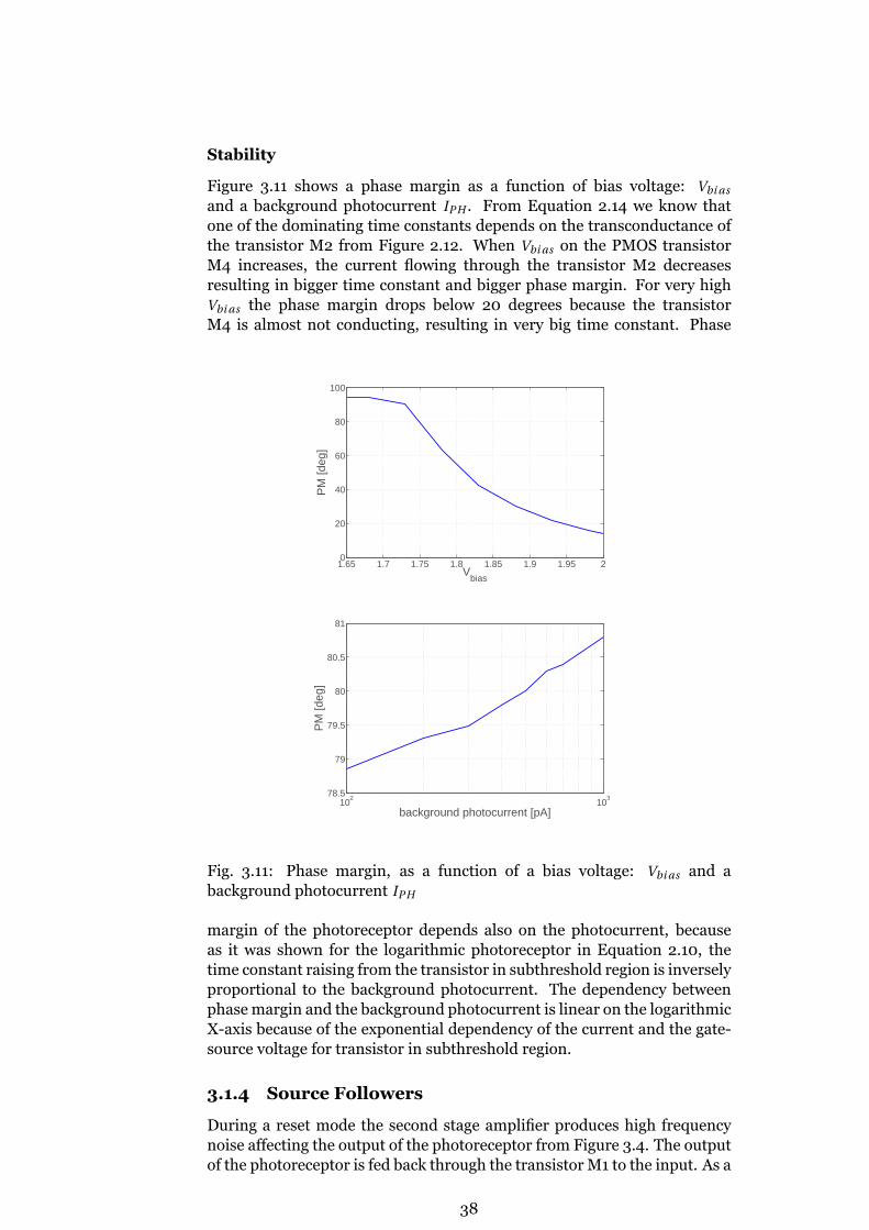
Figure 3.11 shows a phase margin as a function of bias voltage: Vbi as
and a background photocurrent IPH . From Equation 2.14 we know thatone of the dominating time constants depends on the transconductance ofthe transistor M2 from Figure 2.12. When Vbi as on the PMOS transistorM4 increases, the current flowing through the transistor M2 decreasesresulting in bigger time constant and bigger phase margin. For very highVbi as the phase margin drops below 20 degrees because the transistorM4 is almost not conducting, resulting in very big time constant. Phase
1.65 1.7 1.75 1.8 1.85 1.9 1.95 20
20
40
60
80
100
PM
[deg
]
Vbias
102
103
78.5
79
79.5
80
80.5
81
PM
[deg
]
background photocurrent [pA]
Fig. 3.11: Phase margin, as a function of a bias voltage: Vbi as and abackground photocurrent IPH
margin of the photoreceptor depends also on the photocurrent, becauseas it was shown for the logarithmic photoreceptor in Equation 2.10, thetime constant raising from the transistor in subthreshold region is inverselyproportional to the background photocurrent. The dependency betweenphase margin and the background photocurrent is linear on the logarithmicX-axis because of the exponential dependency of the current and the gate-source voltage for transistor in subthreshold region.
3.1.4 Source Followers
During a reset mode the second stage amplifier produces high frequencynoise affecting the output of the photoreceptor from Figure 3.4. The outputof the photoreceptor is fed back through the transistor M1 to the input. As a
38

result, noise on the output of the Photoreceptor is reflected on its sensitiveinput, affecting the linearity of its gain. In order to limit this effect, thesource followers (SF) from Figure 3.12 are used to isolate the differencingamplifier from the photoreceptor.
M1Vi nput
Vbi as_nt y peM2
Vout_nmos
(a) N-type SF
M2Vbi as_pt y pe
Vi nput M1
Vout_pmos
(b) P-type SF
Fig. 3.12: Schematic of the source follower. The bias voltages Vbi as_pt y pe =0.7V and Vbi as_nt y pe = 1.9V keep the transistors M2 in saturation during thenormal operation.
Linearity
0 0.5 1 1.5 2 2.50
0.5
1
1.5
2
2.5
Vinput
[Vou
t]
Vout_ptype
Vout_ntype
operation region
operation region
(a) Comparison of the operation re-gions for P-type and N-type SFs
0 0.5 1 1.5 2 2.5−1.5
−1.4
−1.3
−1.2
−1.1
−1
−0.9
−0.8
Vinput
Vou
t_pt
ype−
Vou
t_nt
ype [V
]
N−type SF out of the linear region
P−type SF out of the linear region
(b) Sum of Vout_pmos and Vout_nmos .
Fig. 3.13: Comparison of P-type and N-type SFs.
After adjustments aimed to obtain proper biasing of the photodiodes, theoutputs of the N-type Photoreceptor (Vo1 and Vo3) has raised to 1.6V - 2.2V and the output of the P-type Photoreceptor (Vo2) has fallen to 0.7V -1.1V. Since Vo1 and Vo3 output voltages are close to VDD it is better to usean N-type source follower to buffer them, whereas Vo2 output should bebuffered by a P-type source follower. The source followers do not operateproperly until the input voltage is high enough (low enough for P-type SF)to supply (sink for P-type SF) the current equal to the current of the loadtransistor M2. Figure 3.13a illustrates the operation of P-type and N-typeSFs. After this condition is met the source followers operate properly, whatis indicated by the arrows. Since the source of the transistor M1 is not
39

connected to ground (and VDD for P-type SF), the Body Effect will make thethreshold voltage to vary with the input voltage, resulting in lower linearity.The Body Effect for the P-type SF could be eliminated by connecting theNWELL of the transistor M1 to the output. However this is not a goodsolution, because it is not possible to connect a substrate to source of NMOSin N-type SF2. Hence, rational solution is to let the Body Effect affectingboth types of SFs in the similar way such that the non-linearities of N-type and P-type SFs are similar. Finally, the most important is that all SFsattenuate the buffered signals Vo1,Vo2 and Vo3 in the same way.
3.1.5 Differencing amplifier
The second stage amplification is realised by an inverting amplifier witha feedback determined by a capacitive divider C1/C2. It only amplifieschanges of the ratio of Vo1/Vo2 and Vo2/Vo3
3. As a result outputs Vdi f f x
in Figure 3.1 indicate only if the change of the light illumination is redder,bluer whether greener.
M1
VampM2
Vdi f f
C1
C2
M3M4Mg rMr eset
Vi n
Fig. 3.14: A differencing amplifier.
Gain
The operation of the differencing amplifier can be explained by theabstracted schematic in Figure 3.15. Assuming infinitely high inputimpedance of the amplifier, the input current flowing through the capacitorC1 will also flow through the capacitor C2:
C1dVi n
d t=−C2
dVdi f f
d t(3.9)
Equation 3.9 can be simplified:
C1dVi n =−C2dVdi f f (3.10)
dVdi f f =−C1
C2dVi n (3.11)
2Deep-nwell could be used to separate the source of NMOS M1, but this costs additionalspace.
3Ratio Vo1/Vo2 corresponds to the ratio between photocurrents (Ib )/(Ib + Ig ) and Vo2/Vo3to (Ib + Ig )/(Ig + Ir )
40

M1
Vamp M2
Vdi f f
C1
C2
Vi nVx
(a) Schematic.
C1 C2
RESET
VoutV in Vx
Vamp
-+
(b) Abstracted schematic of the dif-ferencing amplifier
Fig. 3.15: Differencing amplifier normal operation.
Equation 3.11 indicated that the gain is determined by a ratio betweencapacitors: C1/C2. Since a DC voltage is cancelled by an input capacitorC1, the differencing amplifier amplifies only changes of the input dVi n . Ithelps to achieve low mismatch between pixels because the DC mismatchcoming from the first stage photoreceptors is removed.
Reset mode
When the differencing amplifier’s output reaches a threshold value (ON orOFF), it is balanced by the RESET switch by shorting the input with theoutput. The amplifier should be balanced to the mid point between powerrails, e.g. 1.25V in order to a provide symmetrical headroom for ON andOFF thresholds. In order to determine the sizes of the transistors M1 andM2, the operation of the differencing amplifier during RESET mode will beanalysed. Based on Figure 3.16 current flowing through the transistors M1
M1
Vamp M2
Vdi f f
Fig. 3.16: Reset mode of the differencing amplifier.
and M2 are4:
1
2
W1
L1µpCox (|VGS1 |−VT p )2 = 1
2
W2
L2µnCox (|VGS2 |−VT n)2 (3.12)
4Second order effects were omitted.
41

Further, the Equation can be simplified:
W1
L1µp (|VGS1 |−VT p )2 = W2
L2µn(VGS2 −VT n)2 (3.13)
W1
L1µp (|Vdi f f −V DD|−VT p )2 = W2
L2µn(Vamp −VT n)2 (3.14)
The threshold voltages from the Spice Model are extracted:
VT n = 0.51,VT p = 0.61 (3.15)
The amplifier during reset should be balanced to 1.25V and Vdi f f for theconvenience is chosen to be also 1.25V. Hence:
W1
L1µp (1.25−0.61)2 = W2
L2µn(1.25−0.51)2 (3.16)
After rearranging Equation 3.17 becomes:
W1L1
W2L2
= µn
µp·1.336 (3.17)
In order to compare charge mobilities un and up , a transconductance pa-rameter β was extracted for identically sized PMOS and NMOS transistors.Transconductance parameter β is:
βn/p = 1
2
W
Lµn/pCox (3.18)
For the same sizes of PMOS and NMOS transistors, the information aboutthe ratio un/up is obtained in the following way:
βn
βp=
12
W1L1µnCox
12
W2L2µpCox
= un
up(3.19)
From the simulation the ratio is unup
= 3.267. Including this results in the
Equation 3.17:W1L1
W2L2
= 4.368 (3.20)
Finally, taking into consideration the threshold difference and the chargemobility,the output voltage after reset will be equal 1.25V for the ratioW1/L1W2/L2
= 4.368. The sizes of the transistors were chosen according to thesecalculations and collected in the Table 3.4. The simulations confirmed sizeschoice.
Transistor W [um] L [um]
M1 1.1 0.6
M2 1 2.3
Table 3.4: Sizes of the transistors of the Differencing Amplifier fromFigure 3.14
42

Capacitor Capacitance [ f F ]
C1 416.432
C2 70.98
Table 3.5: Specification of capacitors used in the design of a differencingamplifier.
Capacitors ratio
Capacitors values chosen in this design are shown in Table 3.5. Based onthe Equation 3.11, differencing amplifier amplifies the changes of the inputwith a gain determined by a ratio C1/C2. It is desirable to create capacitorC1 as big as possible and capacitor C2 as small as possible in order to obtainhigh gain of the differencing amplifier. However if the capacitor C2 is verysmall the mismatch becomes to big and the resulting gain of the pixel hasto high deviation. The choice of 70.98 f F appears to be optimal trade-offbetween the gain, the capacitors ratio mismatch and area. The capacitorswere organised in common centroid structure described in Layout section.
3.1.6 Comparators
The differencing amplifier’s output is compared against two thresholdvalues (ON and OFF) by comparators. The comparator is realised by acommon source amplifier shown in Figure 3.17. The gate of transistor M1acts as an input, while the gate of transistor M2 is used to set the thresholdvalue for the comparator. The sizes of transistors realising the common
M1Vi nput
Von/o f f M2
ON /OF F
Fig. 3.17: Comparator - ON/OFF event generator.
source amplifier (Table 3.6) were chosen to be identical to the transistorsrealising a differencing amplifier from Figure 3.14. Recalling that in
Transistor W [um] L [um]
M1 1.100 0.6
M2 1 2.3
Table 3.6: Sizes of the transistors of comparator from Figure 3.17
order to provide a symmetrical headroom for ON and OFF thresholds,the differencing amplifier is balanced to 1.25V for Vamp = 1.25. Since the
43

comparator and the differencing amplifier are sized identically they havethe same operating points, e.g. any increase or decrease of Von/o f f ±Vo f f set
will decrease weather increase the threshold of the comparator respectively.This is illustrated in Figure 3.18. Since the common source amplifier
0 0.5 1 1.5 2 2.50
0.5
1
1.5
2
2.5
Vinput
[V]
ON
_OF
F [V
]
Von
= 0.9
Von
= 1.1
Von
= 1.15
Voff
= 1.35
Voff
= 1.4
Voff
= 1.6
Vinput
decrease − OFF event Vinput
increase − ON event
M1 not strong enough
Fig. 3.18: ON/OFF vs. Vi nput for different Von/o f f .
has high gain, the transition when one of the transistors becomes moreconductive is very steep. The threshold value for which this transitionoccurs is shifted by Von/o f f . For Von/o f f > 1.25V the threshold decreases,what is indicated by the direction of the arrow of OFF event. Similarly,for ON event the condition is Von/o f f < 1.25V . As a result, ON event isindicated by the comparator by V DD → GN D and OFF event by GN D →V DD transitions. For high thresholds transistor M1 is not strong enough topull up the output to 2.5V. However it does not cause any problems becauseOFF event is later pulled up by an inverter.
Differencing amplifier with comparators
Figure 3.19 explains the principle of operation of the differencing amplifiertogether with comparators. The entire process of handshake communica-tion and arbitration in AER protocol is omitted in order to show a basicprinciple how the events are generated in 3C-Pixel. Timing diagram illus-trates, that the steeper transition of the input signal is, the more events aregenerated. This is a critical stage for the 3C-Pixel performance, because forsubstantial mismatch in capacitor ratio or comparators’ threshold the pixelwill suffer from poor FPN5. The robustness against mismatch will be testedby Monte Carlo simulations in Simulations section.
3.1.7 3C-Pixel circuitry
So far we have described single building blocks of the pixel. Now theoperation of the entire pixel will be described, with division into analog
5FPN in this design is described as a different number of ON/OFF events for the samestimuli
44
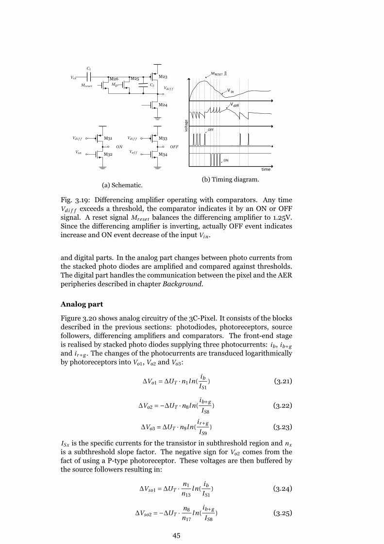
M23
M24
Vdi f f
C1
C2
M25M26Mg rMr eset
Vi n
M31
Von
Vdi f f
M32
ON
M33
Vo f f
Vdi f f
M34
OF F
(a) Schematic.
Vdiff
V in
time
voltage
ON
OFF
MRESET
(b) Timing diagram.
Fig. 3.19: Differencing amplifier operating with comparators. Any timeVdi f f exceeds a threshold, the comparator indicates it by an ON or OFFsignal. A reset signal Mr eset balances the differencing amplifier to 1.25V.Since the differencing amplifier is inverting, actually OFF event indicatesincrease and ON event decrease of the input Vi n .
and digital parts. In the analog part changes between photo currents fromthe stacked photo diodes are amplified and compared against thresholds.The digital part handles the communication between the pixel and the AERperipheries described in chapter Background.
Analog part
Figure 3.20 shows analog circuitry of the 3C-Pixel. It consists of the blocksdescribed in the previous sections: photodiodes, photoreceptors, sourcefollowers, differencing amplifiers and comparators. The front-end stageis realised by stacked photo diodes supplying three photocurrents: ib , ib+g
and ir+g . The changes of the photocurrents are transduced logarithmicallyby photoreceptors into Vo1, Vo2 and Vo3:
∆Vo1 =∆UT ·n1ln(ib
IS1) (3.21)
∆Vo2 =−∆UT ·n8ln(ib+g
IS8) (3.22)
∆Vo3 =∆UT ·n9ln(ir+g
IS9) (3.23)
ISx is the specific currents for the transistor in subthreshold region and nx
is a subthreshold slope factor. The negative sign for Vo2 comes from thefact of using a P-type photoreceptor. These voltages are then buffered bythe source followers resulting in:
∆Vso1 =∆UT · n1
n13l n(
ib
IS1) (3.24)
∆Vso2 =−∆UT · n8
n17ln(
ib+g
IS8) (3.25)
45

STACKED
PHOTODIODE
PHOTORECEPTORS SOURCE
FOLLOWERS
DIFFERENCINGAMPLIFIFERS
COMPARATORS
COMPARATORS
M1
M2
M3
Vo1
Vbi as
Vcas
Vp1
D1
Vp2
D2
D3
Vp3
M4
M5
M6
M7
M8Vo2
Vbi as_pt y pe
Vcas_pt y pe
M9
M10
M11
Vo3
Vbi as
Vcas
M12
ib
ib+g
ir+g
1.9V
0.8V
0V
2.5V
M13
Vs f M14C3
M15
Vs f M16
C5
C6
M18Vs f _p
M17
C4
M19
M20
Vdi f f 1C1
M21M22Mg rMr eset
M23
M24
Vdi f f 2C2
M25M26Mg rMr eset_down
M27
Von
Vdi f f 1
M28
ON 1
M29
Vo f f
Vdi f f 1
M30
OF F 1
M31
Von
Vdi f f 2
M32
ON 2
M33
Vo f f
Vdi f f 2
M34
OF F 2
Fig. 3.20: Circuit of the 3C-pixel logarithmic photoreceptors amplifyingthree different photocurrents - analog part
∆Vso3 =∆UT · n9
n15l n(
ir+g
IS9) (3.26)
The resulting pairs of changes of voltages Vso1 −Vso2 and Vso2 −Vso3 areamplified by the differencing amplifiers:
∆Vdi f f 1 = A1∆UT · n1
n13ln(
ib
IS1)− A2∆UT · n8
n17l n(
ib+g
IS8) (3.27)
∆Vdi f f 2 = A3∆UT · n9
n15l n(
ir+g
IS9)− A4∆UT · n8
n17ln(
ib+g
IS8) (3.28)
It can be proved that [10]:
A1n1
n13= A2
n8
n17= A3
n9
n15= A4
n8
n17= A (3.29)
This assumption is valid because the photoreceptors gains and sourcefollowers were compensated. Also the gain A1, A2, A3 and A4 is specifiedby a known and identical ratio between capacitors C3/C1, C4/C1, C6/C2 and
46

C5/C2 respectively. Equations 3.27 simplifies:
∆Vdi f f 1 = A ·UT (∆ln(ib
IS1)−∆ln(
ib+g
IS8))
= A ·UT ·∆(ln(ib
ib+g)− ln(
iS1
IS8))
= A ·UT ·∆(l n(ib
ib+g)) (3.30)
Similarly ∆Vdi f f 2 becomes:
∆Vdi f f 2 = A ·UT ·∆(l n(ir+g
ib+g)) (3.31)
Equations 3.30 and 3.31 indicate that the 3C-Pixel responds only to changesin the photocurrents ratios. A change in overall intensity without achange in color spectrum will keep the ratio ir+g /ib+g and ib/ib+g constant.The changes ∆Vdi f f 1 and ∆Vdi f f 2 are finally compared against thresholdsadjusted by Von and Vo f f in comparators, and if the threshold is exceededONx or OFFx event is generated.
Digital part
A digital circuitry is realised such that it can handle a communication withan AER periphery - Figure 3.21. Events ON1, ON2, OFF1 and OFF2 begin acycle during which an address of the corresponding event is read out. TheAER peripheries are explained in chapter Background. The bias voltageVr e f r controls the refractory time of the pixel, by changing the conductivityof the pull-up transistor equivalent to the refractory time of the neuron.This is an additional time how long the pixel is in reset mode and it can notgenerate another request.
3.2 Color recognition in 3C-Pixel
Equations 3.30 and 3.31 indicate that the 3C-Pixel amplifies changes inratio between ib/ib+g and ir+g /ib+g photocurrents. Table 3.7 shows how thechanges in these two ratios are represented by ONx, OFFx events and howthey can be translated into color changes. Even though the photocurrentsare mixtures of different spectra we can simplify and assume those threespectra as red, green, and blue light and denote the filtered intensities asR, G, and B. Changes in spectra (R, G and B) and photo currents (Ir+g , Ib+g
and Ib) can be now used interchangeably because of the linear dependencebetween these two quantities. We will check if these assumptions arevalid in chapter Experimental Results, where the stacked photo diodesimplemented in silicon are characterised in terms of spectral response.
3.3 Vision Sensor Design
The implemented vision sensor consisting of 16 raws and 16 columns of3C-Pixels and AER peripherals. Further the vision sensor is called 3C-TVS (abbreviation from a Three Color Temporal Vision Sensor). A 3C-TVS periphery consists of an AER building blocks described in section
47

ANALOGPART
OFF2
RESET_down
PIXEL
ON2
OFF1ON1
RESET
REQ_Y_down
REQ_Y
ACK_Y_down
ACK_Y
RES_Y_down
RES_Y
REQ
_X_O
FF
REQ
_X_O
N
RES_X
_OFF
RES_X
_ON
V_refr
V_refr
Fig. 3.21: Pixel handshaking internal circuitry. Pixel generates 4 outputs,which need a unique address: ON1, ON2, OFF1, OFF2.
Background. Since 4 different events are generated by a single 3C-Pixel,1024 different addresses must be handled by the AER periphery.
3.3.1 Test 3C-Pixel and Test Stacked Photo Diodes
Additionally, a single test photo diodes structure and the separate test 3C-Pixel were implemented in order to characterise the stacked photo diodesspectral response and the behavior of a single pixel. The following signalsare sensed in the test pixel: Vo2, Vo3, Vdi f f 1 and Vdi f f 2 (all analog signals)and ON/OFF events, Mr eset_down , Mr eset (digital signals). Analog signalsare buffered by the unity gain amplifier and the digital signals are bufferedby digital buffers. The unity gain amplifier is realised by the two stageamplifier from Figure 3.22, where Vi n− is shorted with Vout . The designedamplifier was tested in terms of stability and current consumption, andit is summarised in Table 3.8. The digital buffers are realised by stronginverters. The digital circuitry of the test pixel is modified in order toomit a handshake communication with the AER peripheries. Pull downtransistors, from Figure 3.21, generating REQ_Y and REQ_X are replacedwith a simple 3 input AND gate from Figure 3.23. Thanks to this solutionthe pixel is self-reseting: it is being reset immediately after it sends an ON
48

Event Photocurrents ratio Assumed spectra Color changeratio
ON1 ib/ib+g ↗ ∝ BG ↗ bluer
OFF1 ib/ib+g ↘ ∝ BG ↘ greener
ON2 ir+g /ib+g ↗ ∝ RG ↗ redder
OFF2 ir+g /ib+g ↘ ∝ RG ↘ greener
Table 3.7: Translation of ONx, OFFx events into color changes. The densityof ONx/OFFx events is proportional to the rate of the color changes.
M1 Vi n+
M2
M3Vi n−
M4
M5Vbi as_amp M6
M7
C 1
R1
Vout
Fig. 3.22: Two stage amplifier with compensation, the design is based onthe design guide from [37]
whether OFF event. The additional INIT input signal allows to keep thepixel in reset mode.
3.4 Bias voltages and interface pins
All bias voltages of the implemented vision sensor are connected to theexternal pads of the chip in order to be able to make off-chip biasadjustments. The bias voltages and power supplies with descriptionand the values used during simulations are gathered in Table 3.9. Theimplemented chip has three separate power domains: for a pad frame withESD protection, for buffers with a test pixel and the actual power for thevision sensor. Such solution enables to measure a power consumption ofthe designed vision sensor excluding irrelevant peripheries.
3.5 Simulations
3.5.1 3C-Pixel test
In order to test the 3C-Pixel response, a transient simulation was runwith the photocurrents stimulus parameters included in Table 3.10. Westimulate the pixel only by a photocurrent Ir from a photo diode D3,what corresponds to illuminating the pixel surface by the ideal red light.Naturally, such conditions can not be achieved in real life because it is rare
49

Parameter Value
Tail current 10µA
DC gain 90dB
Phase margin 52 deg
GB product 4MHz
Table 3.8: Specification of the two stage amplifier designed to realise a unitygain amplifier for buffering the analog outputs.
INITON
OFFRES_X,RES_Y
Fig. 3.23: Reset circuitry in a test 3C-Pixel.
to illuminate the pixel by so narrow band light. Secondly, the stacked photodiodes do not have such ideal response to the narrow band light and theexperimental results will show later that the spectral responses of the photodiodes overlap. However, for test purposes such stimuli gives meaningfulinformation about the symmetry of the response of the 3C-Pixel and gaincompensations of the differencing amplifiers and source followers. FromEquations 3.30 and 3.31 we know that outputs of differencing amplifiersare proportional to the ratio between photocurrents:
∆Vdi f f 1 =∝∆ib
ib+g(3.32)
Since there is no red photocurrent, the ratio in Equation 3.32 is alwaysconstant, meaning that there are expected no ON1/OFF1 events from thedifferencing amplifier no. 1. The second ratio is:
∆Vdi f f 2 =∝∆ir+g
ib+g(3.33)
For our stimuli, only a nominator is changing, hence the pixel shouldgenerate equal number of ON2 and OFF2 events.Figure 3.24b shows outputs of three photoreceptors in the 3C-Pixel whenstimulated with the stimuli from Figure 3.24b. Only Vo3 follows the changesof Ir . Figure 3.25 shows the outputs of the differencing amplifiers: Vdi f f 1
and Vdi f f 2, and digital outputs ON1, ON2, OFF1 and OFF2. As expected,only Vdi f f 2 generates events ON2 and OFF2. ON2 events indicate when thephotocurrent has positive slope and OFF2 events indicate negative slope.Event though we kept the same thresholds for ON and OFF events (1.21Vand 1.29V respectively) number of ON and OFF events is not the same(4 ON2 events and 6 OFF2 events for each cycle). The reason of non-symmetrical response is a charge injection from the reset transistor.
Charge injection
NMOS Transistors M22 and M26 in Figure 3.20 balance the differencingamplifiers by shorting their outputs with inputs. After balancing the gate
50

Bias voltage Voltage [V] DescriptionVON < 1.25 threshold value for ON eventsVOF F > 1.25 threshold value for OFF events
Refractory ≈ 1.9 refractory time controlVamp 1.25 internal bias of the differencing amplifier
Tuned_vdd 1.9 P-type photoreceptor internal biasto ensure proper biasing of the photodiode
Tuned_gnd 0.8 N-type photoreceptor internal biasto ensure proper biasing of the photodiode
Vs f 0.7 Source follower N-type biasingVs f _p 1.9 Source follower P-type biasingVbi as 1.7 N-type photoreceptor internal
Vbi as_pt y pe 0.7 P-type photoreceptor internalVcas 1.6 N-type photoreceptor cascode transistor
Vcas_pt y pe 1 P-type photoreceptor cascode transistorPubi as_ f r ame 1.9 AER periphery pull-up transistorsPdbi as_ f r ame 0.6 AER periphery pull-down transistors
V DDpad f r ame 2.5 Power supply for a chip pad frameV DDBu f f er s 2.5 Power supply for analog and digital buffers
V DDV i si onSensor 2.5 Power supply for the vision sensor
Table 3.9: Bias voltages and power supplies used during simulations of the3C-TVS Vision Sensor.
Diode Photocurrent DC [pA] Amplitude [pA] Frequency [Hz]D1 - blue Ib 0 0 -
D2 - green Ig 0 0 -D3 - red Ir 400 380 50
Table 3.10: Photocurrents stimulus used to test the 3C-Pixel response.
voltage of these transistors moves from 2.5V to 0V in order to turn them off.During switching unwanted negative charge is injected into the invertinginput of the amplifier. As a result output voltages Vdi f f 1 and Vdi f f 2 moveapproximately 3mV after balancing, as it is shown in Figure 3.26. Thisresults in statistical offset and higher sensitivity of the pixel to OFF events,shown later in Monte Carlo Simulations. This is not a substantial problem,because this offset can be compensated by proper adjusting thresholds.
Monte Carlo Simulations
While designing the 3C-Pixel, each block was simulated including MonteCarlo simulations. Especially, it was a case to compare responses to mis-match of complementary circuits, e.g. P-type and N-type photoreceptorsand source followers. However, due to staggering amount of data resultsincluding Monte Carlo simulations of each single block are omitted in thisthesis and most meaningful results including Monte Carlo simulations ofentire pixel are presented.The 3C-Pixel was stimulated with the same photocurrents stimulus as inthe previous simulation (Table 3.10). Hence, again we expect only ON2and OFF2 events. Threshold values Von and Vo f f were set to 1.3V and 1.2V
51

0 0.01 0.02 0.03 0.04 0.05 0.06 0.07 0.08 0.09 0.10
200
400
600
800
Time [s]
Cur
rent
[pA
]
green stimuliblue stimulired stimuli
(a) Stimuli
0 0.01 0.02 0.03 0.04 0.05 0.06 0.07 0.08 0.09 0.11.9
1.95
2
Vol
tage
[V]
Time [s]
Vo1
0 0.01 0.02 0.03 0.04 0.05 0.06 0.07 0.08 0.09 0.1
0.36
0.38
0.4
0.42
Vol
tage
[V]
Time [s]
Vo2
0 0.01 0.02 0.03 0.04 0.05 0.06 0.07 0.08 0.09 0.12.1
2.15
2.2
2.25
Vol
tage
[V]
Time [s]
Vo3
(b) Outputs of three photoreceptors in the 3C-Pixel when stimulated with thephotocurrent corresponding to illumination by the ideal blue spectrum light.
Fig. 3.24: Response of the photoreceptors to one photocurrent stimuli.
respectively. A 400ms transient simulation was run in order to record 20cycles of the sinusoidal stimuli used to characterise the performance of thepixel. Further, the analysis was repeated 1000 times including process mis-match. The results were normalized to one sinus period.
ON1+OFF1 vs. ON2+OFF2 events
Figure 3.27 shows histogram and Table 3.11 includes mean values andstandard deviations of ON+OFF events from both differencing amplifiers6.As expected, staggering number of iterations gave zero ON1+OFF1 events,namely in 95% of MC iterations there were no events registered. Also, a lowstandard deviation indicates low spread of ON1+OFF1 events. Numbersof ON1+OFF1 events in histogram 3.28a are not integers, because of thenormalisation of results to one sinus period. It means that the pixel needsfew cycles to generate one event. The differencing amplifier no. 2 generatesON2+OFF2 events with a mean value of 10.45 and standard deviation of0.4 event per sinus cycle. Again, a low standard deviation indicates low
6# - number of.
52

0 0.02 0.04 0.061.2
1.22
1.24
1.26
1.28
1.3V
olta
ge [V
]
Time [s]
Vdiff2
0 0.02 0.04 0.061.2
1.22
1.24
1.26
1.28
1.3
Vol
tage
[V]
Time [s]
Vdiff1
0 0.02 0.04 0.06
0
0.5
1
1.5
Vol
tage
[V]
Time [s]
ONOFF
0 0.02 0.04 0.06
0
0.5
1
1.5
Vol
tage
[V]
Time [s]
ONOFF
Fig. 3.25: The pixel response when stimulated with the photocurrentcorresponding to illumination by the ideal blue spectrum light.
9.5349 9.535 9.535 9.5351 9.53511.248
1.249
1.25
1.251
1.252
1.253
[V]
[ms]
Vdiff2
RESET MODE
Charge injection
Fig. 3.26: Close look up on the output Vdi f f 2 after balancing reveals aneffect of charge injection from the reset transistor M26.
spread of ON2+OFF2 events. The ON1+OFF1 vs. ON2+OFF2 events testproves the 3C-Pixel robustness against mismatch in terms of ability indetecting color intensity changes between red and blue color: ig /ib anddiscriminating a change in overall intensity: ib/ib . No spikes registeredfrom the differencing amplifier no.1 prove correct gain compensationprocedure of the photoreceptors and good design of the source followers.
ON vs. OFF events
Figure 3.28 shows histograms and Table 3.12 includes mean values andstandard deviations of ONx and OFFx events from both differencingamplifiers. This test shows closer look on the symmetry of the responseof the 3C-Pixel, e.g. equal number of ON2 and OFF2 events. As expected, astaggering number of iterations gave zero ON1/OFF1 events, namely 96.2%of ON1 events and 96.5% of OFF1 events were equal zero. Also, a lowstandard deviation indicates low spread of ON1 and OFF1 events. The
53

0 0.1 0.2 0.3 0.4 0.5 0.6 0.70
100
200
300
400
500
600
700
800
900
1000
# ev
ents
#ON1+#OFF18 9 10 11 12 13 14
0
100
200
300
400
500
600
# ev
ents
#ON2+#OFF2
Fig. 3.27: Monte Carlo simulation, count of ON+OFF events. Number ofiterations 1000.
mean # σ #ON1+OFF1 0.081 0.054ON2+OFF2 10.45 0.402
Table 3.11: Statistical properties of data shown in Histogram fromFigure 3.27.
differencing amplifier no. 2 generates OFF2 events with a mean value of5.54 and ON2 events with 5.1 events per sinus cycle with a low standarddeviation.
mean # σ #OFF1 0.008 0.045ON1 0.050 0.310
OFF2 5.5315 0.2662ON2 5.105 0.2413
Table 3.12: Statistical properties of data shown in Histogram fromFigure 3.28.
Histogram in Figure 3.29 illustrates the symmetry of the response of the3C-Pixel in form of the ratio between OFF2 and ON2 events. Ideally, theratio should be equal 1, meaning that number of ON2 and OFF2 events isequal. In fact, average ratio is 1.125, meaning that the pixel is more sensitiveto the negative changes 7. Not uniform distribution of ON and OFF events isexplained by a charge injection from a reset transistor after a reset mode, asexplained in previous section. The charge injected by a reset transistor aftera reset mode increases the probability of OFFx event occurrence. The ONvs.OFF events test shows that the 3C-Pixel robustness against mismatchin terms of uniform distribution of positive and negative events. Thestatistical constant difference between number of ON2 and OFF2 eventsis very small and does not affect the performance of the pixel substantially.What is more, this problem can be easily solved by manipulating threshold
7Since the differencing amplifier is inverting OFF event means increase in ratio, whileON event means decrease in colour ratio.
54

−1 0 1 2 3 40
100
200
300
400
500
600
700
800
900
1000
# ev
ents
#ON1−0.1 0 0.1 0.2 0.3 0.4 0.5 0.6
0
100
200
300
400
500
600
700
800
900
1000
# ev
ents
#OFF1
(a) Number of ON/OFF events from the differencing amplifier no.1.
4.5 5 5.5 6 6.5 7 7.50
100
200
300
400
500
600
700
# ev
ents
#ON24.5 5 5.5 6 6.5 70
50
100
150
200
250
300
# ev
ents
#OFF2
(b) Number of ON/OFF events from the differencing amplifier no.2.
Fig. 3.28: Monte Carlo simulation, count of ON/OFF events. Number ofiterations 1000.
voltages.
Reverse biasing of the photodiodes.
Monte Carlo simulation was run in order to test if the three photodiodesin the stacked photodiode remain properly biased when the processmismatch is included. The resulting histogram is shown in Figure 3.30.The conditions assumed in Equations 3.7 and 3.8 are met, because thephotodiodes reverse bias voltage does not drop below 300mV. The diodeD1 has much higher reverse bias voltage, because its anode is connected toground.
3.5.2 AER periphery test
In order to test the AER peripheries, a test bench consisting of 16 pixels andthe AER peripheries was created. Figure 3.31 illustrates a test bench setupwith position of stimulated pixels. The columns encode the event type: ONwhether OFF and rows indicate the number of pair: 1 whether 2. Since bothstimuli are an ideal red light, we expect from stimuli 1:·000110 - ON2·001110 - OFF2
55

0.8 0.9 1 1.1 1.2 1.3 1.4 1.50
50
100
150
200
250
300
350
400
# ev
ents
ratio (#OFF2) / (#ON2)
Fig. 3.29: Monte Carlo simulation, ratio between ON2/OFF2 events.
1.4 1.5 1.60
20
40
60
80
100
120
140
160
180
# ev
ents
Reverse bias − diode D3 [V]0.35 0.4 0.45 0.5
0
20
40
60
80
100
120
140
160
180
# ev
ents
Reverse bias − diode D2 [V]0.35 0.4 0.45 0.5
0
20
40
60
80
100
120
140
160
180
# ev
ents
Reverse bias − diode D1 [V]
Fig. 3.30: Monte Carlo simulation, value of the reverse bias voltage in thestacked photodiode.
and from stimuli 2:·100010 - ON2·101010 - OFF2.
Figure 3.32 shows both stimuli and registered output bits. As expected,obtained addresses are 000110, 001110, 101010 and 100010.
3.6 Layout
3.6.1 Good layout guidelines
Even if the simulation results are very satisfactory, bad layout can worsenthe results or, in the worst case, make the circuit stop working. Hence,the following general layout guidelines were taken into consideration whiledrawing layout:1. Good methodology is to localise most sensitive and critical parts in thecircuit, design them with considerable attention and isolate them from thenoisy parts. Especially good approach is to separate the analog part from
56

PIXEL
REQ
ACK
PIXEL PIXEL PIXEL
PIXELPIXELPIXELPIXEL
PIXEL
PIXEL
PIXEL
PIXEL
PIXEL
PIXEL PIXEL
PIXEL0 1
0 1
0 0
BIT
2
BIT
1
3 BIT WORD
HA
ND
SHA
KE
LOG
ICY-
AX
IS
0 0
BIT 5
BIT 4
3 B
IT WO
RD
1
0
1
0
BIT 3
AR
BIT
ERY-
AX
IS
1 1
1 1
1 0
1 0
1
0
1
0
10
11
0 0
00
01
0 0
00
1
01
1
10
1
ARBITERX-AXIS
HANDSHAKE LOGICX-AXIS
11
1
BIT
0
STIMULI 1
STIMULI 2
ONx OFFx
1
2
ONx OFFx
1
2
ONx OFFx
1
2
ONx OFFx
1
2
ONx OFFx
1
2
ONx OFFx
1
2
ONx OFFx
1
2
ONx OFFx
1
2
ONx OFFx
1
2
ONx OFFx
1
2
ONx OFFx
1
2
ONx OFFx
1
2
ONx OFFx1
2
ONx OFFx1
2
ONx OFFx1
2
ONx OFFx1
2
Fig. 3.31: Simplified test bench of the AER periphery with an array of4x4 3C-Pixels. Stimuli 2 - only red photocurrent, Stimuli 1 - only redphotocurrent
the noisy digital circuitry, and if possible, provide them separate groundpads to avoid substrate coupling between them. Another good methodis to shield sensitive circuitry by guard rings, which later are properlyterminated.2. When designing an array of pixels, power supply distribution mustbe taken into consideration: if the metal wires distributing power in thearray are not placed carefully, voltage drop can result in unwanted powergradient through the pixels, affecting their performance. Similar problemscan cause not sufficient number of contact ties to substrate, resulting innot uniform ground potential reference for pixels. Also, tie contacts andwires widths have to be carefully considered to provide sufficient paths tosink currents. 3. The wires transmitting sensitive analog signals need to beproperly isolated/guarded to avoid loss of information and digital signalsneed to be sufficiently buffered if they are transmitted for long distances.Good methodology is to minimise distribution of critical signals.4. Wherever it is possible, decoupling capacitors should be placed in thelayout. Decoupling capacitors help in reducing effect of the noise by highpass filtering it and, hence, reduce substrate coupling.5. A common centroid structures should be used to ensure that theprocess/temperature gradients have zero net effect on device performance
57
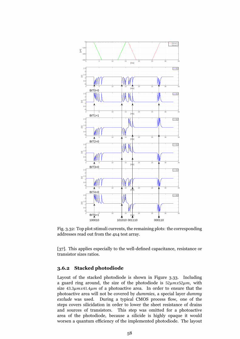
0 5 10 15 20 25 30 35−300
−200
−100
0
[pA
]
[ms]
Stimuli 1Stimuli 2
0 5 10 15 20 25 30 35
0
0.5
1
1.5
2
2.5
[V]
[ms]
B0
0 5 10 15 20 25 30 35
0
0.5
1
1.5
2
2.5
[V]
[ms]
B1
0 5 10 15 20 25 30 35
0
0.5
1
1.5
2
2.5
[V]
[ms]
B2
0 5 10 15 20 25 30 35
0
0.5
1
1.5
2
2.5
[V]
[ms]
B3
0 5 10 15 20 25 30 35
0
0.5
1
1.5
2
2.5
[V]
[ms]
B4
0 5 10 15 20 25 30 35
0
0.5
1
1.5
2
2.5
[V]
[ms]
B6
BIT0=0
BIT1=1
BIT2=0
BIT3=0
BIT4=0
BIT5=1
100010 101010 001110 000110
Fig. 3.32: Top plot:stimuli currents, the remaining plots: the correspondingaddresses read out from the 4x4 test array.
[37]. This applies especially to the well-defined capacitance, resistance ortransistor sizes ratios.
3.6.2 Stacked photodiode
Layout of the stacked photodiode is shown in Figure 3.33. Includinga guard ring around, the size of the photodiode is 52µmx52µm, withsize 43.3µmx41.4µm of a photoactive area. In order to ensure that thephotoactive area will not be covered by dummies, a special layer dummyexclude was used. During a typical CMOS process flow, one of thesteps covers silicidation in order to lower the sheet resistance of drainsand sources of transistors. This step was omitted for a photoactivearea of the photodiode, because a silicide is highly opaque it wouldworsen a quantum efficiency of the implemented photodiode. The layout
58

PHOTOACTIVE AREA 43.3um x 41.4um
SUBSTRATE TIE
DNWL
BLUE
GREEN+BLUE
RED+GREEN
M2
Fig. 3.33: Layout of the stacked photodiode. Metals M3-M9 are not shownfor clarity.
is straightforward with the schematic of the stacked photodiode fromFigure 2.4. Photocurrents from the three stacked photodiodes are routedon the right side in metal M2. The column closest to the photoactivearea conducts current from N + /PW junction, the second column fromN + /PW and PW/DNWL and the most right one from PW/DNWL andDNWL/PSUB.
3.6.3 3C-Pixel
Figure 3.34b shows a the photoactive area occupation of one pixel, locationof digital and analog circuitry and organisation of capacitors segments.
Capacitor* Segments** Capacitance
[ f F ]
C1 S1 70.98
C2 S3 70.98
C3 S5 161.42+2 ·127.51
C4 S8 161.42+2 ·127.51
C5 S7 161.42+2 ·127.51
C6 S6 161.42+2 ·127.51
Table 3.13: Segment organisation of capacitors used in the design of adifferencing amplifier. ∗ - number of capacitors from Figure 3.6, ∗∗ -capacitors segments from Figure 3.34b
Pixel contains 6 capacitors (schematic Figure 3.6). These capacitors aredivided into segments and organised in a centroid-like structure. Suchorganisation should help to make the capacitors ratios more robust againstprocess mismatch and temperature gradients through the pixels array.Also, analog and digital circuitry of four adjacent pixels are localised ingroups with a longest possible distance from each other in order to limitthe effect of the digital noise on the sensitive analog signals. Table 3.13shows MIM capacitors sizes and segments organisation.
59

DIGITA
L
ANALOG
(a) Single pixel layout.
Photodiode
S1 S5 S5 S8 S5 S8 S8
S3S7
S7S6
S7S6
S6ANALOG
DIGITA
L
Photodiode
S1S5S5S8S5S8S8
S3S7
S7S6
S7S6
S6
ANALOG
DIGITAL
Photodiode
S1 S5 S5 S8 S5 S8 S8
S3S7
S7S6
S7S6
S6
ANALOG
DIGITAL
Photodiode
S1S5S5S8S5S8S8
S3S7
S7S6
S7S6
S6
ANALOG
DIGITA
L
(b) Common centroid organisation.
Metal organisation
Thanks to a large number of metal layers (M1-M9) available in TSMC90nm, different functions were assigned to different metal layers toproperly organise signals and power distribution. At the end of this chaptera summary of each metal function in the matrix is provided (Table 3.16and Table 3.17). Mainly, bias voltages and AER communication signals arerouted by horizontal and vertical wires in different layers. In order to aprovide uniform power distribution in the matrix, metals from each layerare used to distribute VDD. In order to meet a maximum density rules, aspecial square structure described in Tables 3.16 and 3.17 was designed.Such solution enabled a flexible creation of vast areas of metals meetingdensity rules.
3.6.4 Matrix and AER Peripheries
An array of 16x16 pixels organised in common centroid structure wascreated. Around the matrix peripheries responsible for handling theAER communication were implemented. Full chip layout is shown inAppendix C.
3.6.5 Microscope on-chip cell images
A microscope with zoom lenses and high resolution camera was used tomake on-chip cell images. Figure 3.35a a chip surface. Locations of thetest photodiode and the test pixel are indicated by arrows. Black squaresrepresent photoactive area. There is no metal wiring nor dummy structuresover the photodiodes in order to keep the quantum efficiency as high aspossible. Figure 3.35b shows a closer look on pixels, we can distinguish 4common centroids. Bronze horizontal and vertical lines across the arrayare top metal M9 lines distributing power.
3.7 Chip summary
Tables 3.15 and 3.14 summarise the chip size, pixels dimensions, analogand digital area occupation. The fill factor is reasonably high for suchtype of pixel (with processing circuitry inside the pixel). The fill factor is
60

1450um
Test 3C-Pixel Test photodiode
(a) An array consisting of 16x163C-pixels, a single Test 3c-Pixel(bottom-left) and a single Test Pho-todiodes (bottom-right).
43
um
2x2 centroid
(b) 4 common centroid pixel struc-tures. A a stacked photodiode size43umx43um. Bronze horizontal andvertical lines across the array are M9lines distributing power.
limited because of the used MIM capacitors. Even though MIM capacitors
Chip size 1394µx1394µ
Array size 1312µx1338µ
Table 3.14: Chip dimensions, technology TSMC 90nm rf.
are located over the circuity in top metals and their sizes are the smallestpossible which met the Monte Carlo simulations, they occupy almost40% of the pixel area and limit further fill factor improvement. Thealternative capacitor type which could be used is a MOM (Metal-Oxide-Metal) capacitor. In the used process MOM capacitors can create a multi-metal structures resulting in higher capacitance per area. Appendix Dshows an alternative layout of the pixel with MOM capacitors used.However finally this design was not implemented in the array. The reasonis the fact that MOM capacitors occupied six top metal layers and there wasnot enough place for proper wires routing. As a result wires transmittingdigital and analog signals were to thin and the post-layout simulations werenot satisfactory.
61

Pixel size 82µx82µ
Photodiode size 41.5µx43.4µ
Fill factor [%] 27
Area 1
digital part [%]
Area 13
analog part [%]
Area 39
MIM capacitors [%]
Table 3.15: Pixel specification.
62

Mx Usage Example
M1
M1 is used for internal local connec-tions in analog and digital circuitry ofthe pixel, as shown in the figure on theright side. The right side of the fig-ure shows part of the decoupling MOScapacitor. The digital and analog cir-cuitry is guarded by substrate contactsorganised net structures connected byM1. Such solution always meets M1maximum density rules.
M2
M2 is used to distribute bias volt-ages along vertical direction inwhole array, as it is shown inthe first Figure on the right side.Also, M2 is used to distributeVDD in the array by the structureshown in the second and third Fig-ure. A designed square in M2 hasthree rectangular holes to ensureto meet maximum density rules,when creating extensive structuresdistributing VDD in the array.
M3
M3 is used to realise internal routingbetween distantly located digital andanalog circuitry in the pixel. Theyconduct 4 signals: ON1, OFF1, ON2,OFF2. The width of the wires isapproximately 1.8µm. Also, identicalsquare structure as in M2 is created todistribute power in the array.
M4
M4 is also used to realise internalrouting between digital and analogcircuitry. Hence, signals ON1, OFF1,ON2, OFF2 are routed identically asin M3. M3 is also used to distributeground in the array in order to cre-ate VDD-GND a sandwich structurefor signals above and in order to cre-ate additional parasitic decoupling ca-pacitance.
Table 3.16: Metals M1-M4 usage. Figures show sections of the 3C-Pixel.For clarity only described metal is turned on in the Figures.
63

Mx Usage Example
M5
Metal M5 is used to route betweenpixels and AER peripheries in hor-izontal direction - long horizontallines in the first Figure are REQ,ACK and RES signals handlinghandshake communication of twopixels in Y-axis. M5 is used also todistribute GND.
M6
Metal M6 is used to realise hand-shake communication in verticaldirection and internal connectionsbetween MIM capacitors in thepixels.
M7
Metal M7 is used for internal rout-ing in the higher levels of the pixel,especially between MIM capaci-tors.
M8
Metal M8 is used to create MIM ca-pacitors together with Capacitor Bot-tom Metal layer and Capacitor TopMetal Layer. The Figure shows twoset of of capacitors of the adjacentpixels in matrix. CBM layer is illus-trated by orange colour in the Figure.M8 wires are wide, because minimumwidth rules are very restricted.
M9
M9 realises power supply distribu-tion. Similarly to M8, wires routed inM9 are wide, because minimum widthrules are very restricted.
Table 3.17: Metals M5-M9 usage. Figures show sections of the 3C-Pixel.For clarity only described metal is turned on in the Figures.
64
Chapter 4
Experimental Results
4.1 Laboratory Setup
The designed chip was fabricated and bonded in PLCC84 package. Acustom PCB was designed (Appendix Test PCB Layout) in order to install achip into a socket and carry out measurements. The test PCB contains:· chip socket PLCC84,· interface pins,· reference bias voltages generators realised by potentiometers,· test outputs realised by pinout and BNC connectors,· separate power pins for 3C-TVS vision sensor, buffers and pad frame ESDprotection,· IDC-40 bus for AER communication with a data logger. The test PCBenables to setup all bias voltages. The fabricated vision sensor wascharactesized using different laboratory setups.
4.1.1 3C-Pixel and photodiode measurement setup
In order to characterise a single test 3C-Pixel a setup able to dynamicallychange input colors was built. Two high-power full color LEDs (F50360)from Seoul Semiconductor were used described in Table 4.1. Two F50360
Minimum Typical Maximal Unitwavelength wavelength wavelength
Red light 618 625 630 nmGreen light 520 525 535 nmBlue light 455 460 465 nm
Table 4.1: high-power full color LEDs (F50360) from Seoul Semiconductor
LEDs were installed on a designed PCB ( Appendix LED PCBs). The lightintensity of the diodes is controlled by a waveform generator, as shownin Figure 4.1. Such solution enables to vary different colors ratios ofemitted light in order to measure a pixel sensitivity to change in colorsratios. The light from two separate RGB diodes is mixed and transmittedby a dual branch light guide (Dolan-Jenner E809). A light guide mountfrom a LED side and a custom PCB side was designed in SolidWorks and3D printed (assembly drawing in (Appendix Drawings in SolidWorks).Measurement used to characterise stacked photodiode included a BPS101Optical Feedback Controlled Tungsten Halogen Light Source and color
65

POT
Waveform
generatorDC
Fig. 4.1: Schematic of a LED driver.
Fig. 4.2: Experimental setup to test a single pixel response and thephotodiode. Light from RGB LEDs is transmitted by a fiber cable. Thefiber cable is attached to PCBs by a 3D printed housing.
filters centred between 400nm, 450nm, 500nm, 600nm, 650nm, 700nm and880nm. The filters centred at 450nm and 880nm have 80nm bandwidth andthe other 50nm. In order to measure a DC gain of the photoreceptors in3C-Pixel neutral density filters with different light attenuations were used.
4.1.2 3C-TVS vision sensor measurement setup
In order to read out an image from a designed vision sensor a custom PCBwas equipped with an IDC-40 bus realising an AER communication withthe USBAERmini2 board [38], which is a part of an open source projectjAER[39]. The USBAERmini2 board is equipped with a microcontrollerhandling the AER communication with the vision sensor and sending outthe AER addresses to computer through a USB port. A software in JAVAlanguage was written in order to display an image from a vision sensor.The vision sensor was stimulated by a beam of a collimated light (strong
66

Fig. 4.3: Left photo: designed PCB with a 4mmF /1.2 C-mount lens. Rightphoto: Designed PCB connected by a bus with the board USBAERmini2.
light dot) on the different background color. The background color wasprojected by another PCB equipped with six single color LEDs (2 x red -SZR05A0A, 2 x green - SZG05A0A, 2 x blue - SZB05A0A). Such solutionprovided a scattered light suitable to project a background light. Thecamera was tested with a 4mm F/1.2 C-mount lens installed on a designedin SolidWorks and 3D printed custom mount.
4.2 Spectral characterisation of the stackedphotodiode
The stacked photodiode realises a front-end stage supplying three pho-tocurrents: ib , ib+g and ir+g . It is important to characterise a spec-tral sensitivity of the stacked photodiode in order to properly decode theON/OFF events into colour changes. A surface of the implemented chipwas illuminated by the BPS101 Tungsten Halogen Light Source with dif-ferent colour filters centred between 400nm and 950nm. For each colourfilter, three photocurrents: ib , ib+g and ir+g from a test photodiode weremeasured. The values were corrected by the Halogen Light Source irradi-ance factor as a function of wavelength, shown Figure 4.6a, and the colourfilters transmission efficiency from Figure 4.6b. The reverse bias currentsfrom the diodes used for the ESD protection of the padframe were not sub-tracted from the measured values of the photocurrents because we are onlyinterested in ratios between the photocurrents and not the absolute values.The resulting spectral characterisation of the test photodiode is shown inFigure 4.5. Based on these results a relative light energies could be recon-structed. Figure 4.7a shows a relative response of each photodiode. Thered photodiode is the photodiode located deepest in substrate, whereas theblue one is located on the surface of the substrate. Ideally, each photodi-ode should be sensitive only to the light of the corresponding colour result-
67

Fig. 4.4: Experimental setup to test a matrix response. A light sourceattached to the motor projects a fast rotating dot on the white sheet ofpaper.
ing in the photocurrents peaks around 620−750nm for the red photodiode,495−570nm for the green photodiode and 450−495nm for the blue photo-diode. Places where these peaks are expected are indicated by arrows. Infact we can observe that peaks are indeed located in the indicated places.The results from Figure 4.7a indicate that stacked photodiode has muchhigher sensitivity to long wavelengths rather than the short wavelengthsfrom a visible spectrum. This behaviour may be explained by the structureof the photodiode: the size of the red photodiode is biggest and hence itsdepletion region is bigger than the other ones. As a result, the red photo-diode has the biggest volume where the electric field close to the depletionregion can catch electrons generated by the incident photons and there-fore produce a photocurrent. Possibly the top photodiode PN junction andthe middle PN junction are not located very deep, thus only very energeticphotons can be caught by these photodiodes. This may explain worse sen-sitivity to the green and blue light. Another reason may be the fact that thebiggest depletion area is obtained from the junction PSUB and DNWL be-cause the dopants density in substrate is low and hence the depletion regionis more extensive. Figure 4.7b shows relative responses of the stacked pho-todiode including mixtures of photocurrents in form of normalised blue,r ed + g r een and blue + g r een photocurrents. In order to be able to distin-guish between colours, it is important to analyse photocurrents fractions:(Ib)/(Ib + Ig ), (Ir + Ig )/(Ig + Ib) as a function of wavelength as shown in Fig-ure 4.8. This plot is very important because it shows how the stacked photodiodes can be used to discriminate between colors: the (Ir + Ig )/(Ig + Ib) ra-tio increases when a the dominating light wavelength increases (the color
68

400 500 600 700 800 900 100010
2
103
104
105
Wavelength (nm)
Pho
tocu
rren
t (pA
)
IbIg+bIr+g
Fig. 4.5: Corrected diode photocurrents
400 500 600 700 800 900 10000
5
10
15
20
25
30
Wavelength (nm)
Irra
dian
ce (
W/m
2 )
(a) White Source Irradiance
400 500 600 700 800 900 10000
0.1
0.2
0.3
0.4
0.5
0.6
0.7
0.8
0.9
1
Wavelength (nm)
Filt
ers
Per
cent
Tra
nsm
issi
on
(b) Filters transmission efficiency
Fig. 4.6: Halogen Light Source irradiance and the colour filters transmis-sion efficiency correction factors.
spectrum becomes redder) and the ratio (Ib)/(Ib + Ig ) decreases when thedominating light wavelength decreases (the color spectrum becomes bluer).The ratio (Ib)/(Ib + Ig ) exhibits weaker dependence on color spectra, it hassteepest slope up to 650nm and after that is flat, while the (Ir + Ig )/(Ig + Ib)ratio has almost constant slope over the entire tested spectrum. Thus if forinstance a narrow band light source moves from 600nm to 900nm wave-length, it would lead to positive (Ir + Ig )/(Ig + Ib) events and a few negative(Ib)/(Ib + Ig ) events. These observations are consistent with Table 3.7 fromthe previous chapter. This Table is repeated here for the convenience be-low. According to this table, we simplify and assume the photocurrentsIr+g , Ib+g and Ib to represent red, green, and blue spectra respectively. As aresult, the photocurrents ratios become R/G and B/G and their changes canbe now translated into bluer, greener or redder color change. Finally, theON1 events is assumed to be translated into a blue colour increase becausethe fraction Ib
Ib+Igincrease is strongest for a blue light. The OFF2 and OFF1
events are assumed to be translated into an increase of a green colour. TheON2 event will be translated into a red light change increase.In order to compare experimental results with a simulation, the coefficientsdescribing behaviour of the stacked photodiode are extracted from Fig-
69

400 500 600 700 800 900 10000
0.1
0.2
0.3
0.4
0.5
0.6
0.7
0.8
0.9
1
Wavelength (nm)
Rel
ativ
e va
lues
IbIgIr
RED
GREEN
BLUE
(a) Relative responses of single pho-todiodes in the stacked photodiode.
400 500 600 700 800 900 10000
0.1
0.2
0.3
0.4
0.5
0.6
0.7
0.8
0.9
1
Wavelength (nm)
IbIg+bIr+g
(b) Relative responses of the stackedphotodiode.
Fig. 4.7: Spectral response of a stacked photodiode in TSMC 90nm process.
400 500 600 700 800 90010
−1
100
101
102
Wavelength (nm)
Ib / I
b+gIr+g
/ Ig+b
greenerbluer
redder greener
Fig. 4.8: Photo currents ratios amplified by the differencing amplifiers(Equations 3.30,3.31). The values were corrected by the Halogen LightSource irradiance factor and color filters transmission efficiency.
ure 4.7a. These coefficients indicate how much photocurrent is obtainedfrom each photodiode when illuminated by different light colors. Further,these coefficients will be used to emulate the actual stacked photodiodewhile simulating the 3C-Pixel and compare the simulation results with theexperimental results. The coefficients are gathered in Table 4.3.
Red Green Bluephotodiode photodiode photodiode
Red light 625nm 0.68 0.16 0.16Green light 525nm 0.47 0.22 0.31Blue light 460nm 0.175 0.275 0.55
Table 4.3: Extracted coefficients of the photocurrents for the stackedphotodiode, when illuminated by different light colors: red light - 625nm,green light - 525nm, blue light - 460nm
70

Event Photocurrents ratio Assumed spectra Color changeratio
ON1 ib/ib+g ↗ ∝ BG ↗ bluer
OFF1 ib/ib+g ↘ ∝ BG ↘ greener
ON2 ir+g /ib+g ↗ ∝ RG ↗ redder
OFF2 ir+g /ib+g ↘ ∝ RG ↘ greener
Table 4.2: Translation of ONx, OFFx events into color changes. The densityof ONx/OFFx events is proportional to the rate of the color changes.
4.3 Test 3C-Pixel
4.3.1 Logarithmic photoreceptors.
DC response
In order to test if the complementary photoreceptors have the samegain, their DC responses was measured. The surface of the camerawas illuminated by the coherent flat spectrum light source. Different
0 1 2 3
0.8
1
1.2
1.4
1.6
1.8
2
Relative intensity log10
(intensity)
Vol
tage
[V]
Vo2
− P−type Photoreceptor
Vo3
− N−type Photoreceptorincrease V
bias
increase Vbias_ptype
(a) Response of an N-type Photorecep-tor - Vo3, and P-type Photoreceptor - Vo2
for different bias voltages as function oflight intensity.
0 1 2 3 41
1.5
2
2.5
3
3.5
4
Relative intensity log10
(intensity)
Vo2
+V
o3 [V
]
(b) Sum of Vo2 and Vo3 as function oflight intensity.
Fig. 4.9: DC responses of the complementary Photoreceptors - experimen-tal results.
attenuating filters were placed in front of the chip in order to sweep thelight intensity. The resulting responses of the logarithmic photoreceptorsfrom the test pixel are shown in Figure 4.9a. Ideally, the sum of thesetwo responses should give a flat line. Figure 4.9b shows that bothphotoreceptors have very similar DC gain. It is impossible to compare theDC gain from simulations from Figure 3.7 with these experimental resultsbecause we do not know the absolute values of the photoccurents from thetest diodes (we know only the relative changes). Since the photoreceptorsare logarithmic amplifiers, their responses on the logarithmic x-axis scalegive a straight line what is also shown in Figure 4.9a.
71
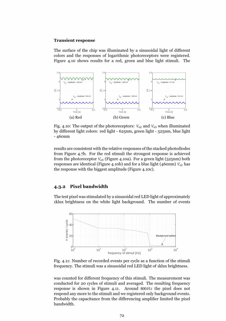
Transient response
The surface of the chip was illuminated by a sinusoidal light of differentcolors and the responses of logarithmic photoreceptors were registered.Figure 4.10 shows results for a red, green and blue light stimuli. The
−0.5 0 0.50.5
1
1.5
2
2.5
Time [s]
[V]
Vo2
− amplitude = 84 mV
Vo3
− amplitude = 128 mV
(a) Red
−0.5 0 0.50.5
1
1.5
2
2.5
Time [s]
[V]
Vo2
− amplitude = 109 mV
Vo3
− amplitude = 109 mV
(b) Green
−0.5 0 0.50.5
1
1.5
2
2.5
Time [s]
[V]
Vo2
− amplitude = 81 mV
Vo3
− amplitude = 47 mV
(c) Blue
Fig. 4.10: The output of the photoreceptors: Vo2 and Vo3 when illuminatedby different light colors: red light - 625nm, green light - 525nm, blue light- 460nm
results are consistent with the relative responses of the stacked photodiodesfrom Figure 4.7b. For the red stimuli the strongest response is achievedfrom the photoreceptor Vo3 (Figure 4.10a). For a green light (525nm) bothresponses are identical (Figure 4.10b) and for a blue light (460nm) Vo2 hasthe response with the biggest amplitude (Figure 4.10c).
4.3.2 Pixel bandwidth
The test pixel was stimulated by a sinusoidal red LED light of approximately1klux brightness on the white light background. The number of events
100
101
102
103
104
0
20
40
60
frequency of stimuli [Hz]
# ev
ents
/ cy
cle
Background spikes
Fig. 4.11: Number of recorded events per cycle as a function of the stimulifrequency. The stimuli was a sinusoidal red LED light of 1klux brightness.
was counted for different frequency of this stimuli. The measurement wasconducted for 20 cycles of stimuli and averaged. The resulting frequencyresponse is shown in Figure 4.11. Around 800H z the pixel does notrespond any more to the stimuli and we registered only background events.Probably the capacitance from the differencing amplifier limited the pixelbandwidth.
72

4.3.3 Color change representation
The designed pixel monitors three different color spectra and it generatesfour different events whenever the ratio of the light intensity filtered bythose three spectra changes. Based on the spectral characterisation of thestacked photodiodes we decided to assign events to the colour changesaccording to Table 4.2. Now we will illuminate the chip surface by twosinusoidal out-of-face different colour LED light sources. In this way wewill test the pixel response to three different colour opponencies: R/G, B/Gand R/B and we will compare those resposes to the pre-layout and post-layout simulations. Generally, we observed higher sensitivity of the pixel
0.01 0.02 0.03 0.04 0.05 0.06 0.07 0.08 0.09 0.10
200
400
600
800
[pA]
[s]
IrIg,Ib
0.01 0.02 0.03 0.04 0.05 0.06 0.07 0.08 0.09 0.11.15
1.2
1.25
1.3
1.35
[V]
[s]
Vdiff1 pre layout simulation
0.01 0.02 0.03 0.04 0.05 0.06 0.07 0.08 0.09 0.11.15
1.2
1.25
1.3
1.35
[V]
[s]
Vdiff1 post layout simulation
0.01 0.02 0.03 0.04 0.05 0.06 0.07 0.08 0.09 0.11.15
1.2
1.25
1.3
1.35
[V]
[s]
Vdiff1 experimental result
0.01 0.02 0.03 0.04 0.05 0.06 0.07 0.08 0.09 0.11.15
1.2
1.25
1.3
1.35
[V]
[s]
Vdiff2 pre layout simulation
0.01 0.02 0.03 0.04 0.05 0.06 0.07 0.08 0.09 0.11.15
1.2
1.25
1.3
1.35
[V]
[s]
GREENER
REDDER
Vdiff2 post layout simulation
0.01 0.02 0.03 0.04 0.05 0.06 0.07 0.08 0.09 0.11.15
1.2
1.25
1.3
1.35
[V]
[s]
GREENER
REDDER
Vdiff2 experimental result
Fig. 4.12: A single pixel response to the continuous red-green contrastchange. From top: modelled input photocurrents, Vdi f f 1 pre layout tran-sient simulation, Vdi f f 1 post layout transient simulation, Vdi f f 1 experimen-tal result,Vdi f f 2 pre layout transient simulation, Vdi f f 2 post layout transientsimulation, Vdi f f 2 experimental result.
in the post-layout simulations, meaning that the differencing amplifiershave higher gain. Higher gain can be explained by higher capacitancefrom C3, C4, C5, C6 because of the parasitic capacitors. Under the C3, C4,C5, C6 Capacitor-Bottom-Metal (CBM) layer there is a long wide metal M7routed which is connected to the Capacitor-Top-Metal (CTM) layer. Such
73

metal organisation created so called sandwich structure CTM-CBM-CTMwhich increased the overals capacitance of C3, C4, C5, C6 and resulted inhigher differencing amplifier gain. On the other hand, number of spikesin the experimental results differs from the results in simulations becausewe do not know the absolute values of the photoccurents from the testphotodiodes (we know only the relative changes).
Red-Green Contrast Change
First, we characterised the pixel response to the continuous red-greenintensity change. The top plot in Figure 4.12 shows the modelled inputphotocurrents and the other plots show pixel (pre-layout, post-layoutand experimental) response to such stimuli. The thresholds used duringsimulations were: VON = 1.29 and VOF F = 1.22. Coefficients from Table 4.3were used in order to emulate the actual stacked photodiode responsewhile simulating the 3C-Pixel and compare the simulation results withthe experimental results. The experimental results were obtained byilluminating the chip surface with a sinusoidal out-of-phase red and greenlight sources of the similar frequency used in simulations. The thresholdsfor the tested chip were: VON = 1.3 and VOF F = 1.2. The transient plotsfor experimental results of Vdi f f x suggest that the actual thresholds werelower. However, it has to be taken into consideration that the outputvoltages are buffered by non ideal analog buffers and the scope resolutionwas not high enough to track peaks of Vdi f f x right before the reset signal.For the red-green intensity change stimuli we observed only ON2 andOFF2 events. For the pre layout and the post layout simulations weobserved 4-6 events per a sinusoid cycle, while for the experimental results2 per a sinusoid cycle. The difference between experimental results andsimulations can be explained by the fact that actually we do not knowthe real values of photocurrent generated by the stacked photodiodesimplemented in silicon. Since we were changing the red and green spectrainversely, the change of the R/G ratio is most substantial and hencethe output Vdi f f 2 exceeds the VON 2 and VOF F 2 thresholds. Vdi f f 1 movesbetween the thresholds but it does not exceed them, and hence, no ON1 norOFF1 events are generated. Since there has not been any blue light changein the stimulus (the blue LED was off), the nominator and denominator inthe B/G ratio change by the same amount, and ideally this ratio shouldremain constant. In fact, the output Vdi f f 1 fluctuates only because thephoto currents ratio B/G exhibits weak dependence on longer spectrumwavelengths, as was shown in Figure 4.8.
Blue-Red Contrast Change
Next, we characterised in the same way the pixel response to the continuousblue-red intensity change. Figure 4.13 shows the modelled input photocur-rents and the pixel (pre-layout and post-layout) response to such stimuli.In this case we observed four types of events: events ON1 occur when theblue light positive transient is biggest (B/G increases) and conversely, ON2events occur at the maximum red positive transient (R/G increases). Be-sides, we observed OFF1 and OFF2 events that might be confusing at firstglance. However, OFF1 events indicate a shift to longer wavelengths fromblue and OFF2 events indicate a shift to shorter wavelengths from red and
74

0.01 0.02 0.03 0.04 0.05 0.06 0.07 0.08 0.09 0.10
200
400
600
800
[pA]
[s]
IrIg,Ir
0.01 0.02 0.03 0.04 0.05 0.06 0.07 0.08 0.09 0.11.15
1.2
1.25
1.3
1.35
[V]
[s]
GREENER
BLUER
Vdiff1 pre layout simulation
0.01 0.02 0.03 0.04 0.05 0.06 0.07 0.08 0.09 0.11.15
1.2
1.25
1.3
1.35
[V]
[s]
Vdiff1 post layout simulation
0.01 0.02 0.03 0.04 0.05 0.06 0.07 0.08 0.09 0.11.15
1.2
1.25
1.3
1.35
[V]
[s]
GREENER
BLUER
Vdiff1 experimental result
0.01 0.02 0.03 0.04 0.05 0.06 0.07 0.08 0.09 0.11.15
1.2
1.25
1.3
1.35
[V]
[s]
GREENER
REDDER
Vdiff2 pre layout simulation
0.01 0.02 0.03 0.04 0.05 0.06 0.07 0.08 0.09 0.11.15
1.2
1.25
1.3
1.35
[V]
[s]
Vdiff2 post layout simulation
0.01 0.02 0.03 0.04 0.05 0.06 0.07 0.08 0.09 0.11.15
1.2
1.25
1.3
1.35
[V]
[s]
GREENER
REDDER
Vdiff2 experimental result
Fig. 4.13: A single pixel response to the continuous red-blue contrastchange. From top: modelled input photocurrents, Vdi f f 1 pre layout tran-sient simulation, Vdi f f 1 post layout transient simulation, Vdi f f 1 experimen-tal result,Vdi f f 2 pre layout transient simulation, Vdi f f 2 post layout transientsimulation, Vdi f f 2 experimental result.
thus, the responses are as expected and correct. We observed more ON2and OFF2 events because, as shown in Figure 4.8, the R/G ratio has steeperslope. As a result, if the light spectra is changing towards longer wave-lengths (redder), we should observe more ON2 and OFF2 events.We observed that Vdi f f 1 slowly drifts towards VOF F threshold what pro-vokes unwanted events. The explanation of such behaviour may be an issuewith wrong layout and a parasitic capacitance at the input of the amplifier.This problem applied only to the single test pixel, not pixels in the array(tested later). The test pixel has probes connected to its sensitive nodes,and this could lead to the increase of parasitic capacitances and make thesource follower to charge the input of the differencing amplifier and in-crease its output, resulting in unwanted events.
75

Blue-Green Contrast Change
Finally, we characterised the pixel response to the continuous blue-greenintensity change. Figure 4.14 shows the results. Directly responsible for
0.01 0.02 0.03 0.04 0.05 0.06 0.07 0.08 0.09 0.10
200
400
600
[pA]
[s]
IbIg,Ir
0.01 0.02 0.03 0.04 0.05 0.06 0.07 0.08 0.09 0.11.15
1.2
1.25
1.3
1.35
[V]
[s]
GREENER
BLUER
Vdiff1 pre layout simulation
0.01 0.02 0.03 0.04 0.05 0.06 0.07 0.08 0.09 0.11.15
1.2
1.25
1.3
1.35
[V]
[s]
Vdiff1 post layout simulation
0.01 0.02 0.03 0.04 0.05 0.06 0.07 0.08 0.09 0.11.15
1.2
1.25
1.3
1.35
[V]
[s]
GREENER
BLUER
Vdiff1 experimental result
0.01 0.02 0.03 0.04 0.05 0.06 0.07 0.08 0.09 0.11.15
1.2
1.25
1.3
1.35
[V]
[s]
REDDER
GREENER Vdiff2 pre layout simulation
0.01 0.02 0.03 0.04 0.05 0.06 0.07 0.08 0.09 0.11.15
1.2
1.25
1.3
1.35
[V]
[s]
Vdiff2 post layout simulation
0.01 0.02 0.03 0.04 0.05 0.06 0.07 0.08 0.09 0.11.15
1.2
1.25
1.3
1.35
[V]
[s]
REDDER
GREENER Vdiff2 experimental result
Fig. 4.14: A single pixel response to the continuous blue-green contrastchange. From top: modelled input photocurrents, Vdi f f 1 pre layout tran-sient simulation, Vdi f f 1 post layout transient simulation, Vdi f f 1 experimen-tal result,Vdi f f 2 pre layout transient simulation, Vdi f f 2 post layout transientsimulation, Vdi f f 2 experimental result.
sensing the blue-green contrast change are events ON1 and OFF1. Indeed,out of all three different colour opponencies tested, the B/G opponencyresults in the pixel strongest response in terms of ON1 and OFF1 events.We observe OFF1 events for the positive slope of Ig , and conversely, ON1events for the positive slope of Ib . This same applies to the experimentalresults. Regarding the second R/G opponency we observed ON2 and OFF2events that again might be confusing. However, we should recall that wesimplified the ratio Ir + Ig /Ig + Ib into Ir /Ig as shown in Table 4.2. In thedenominator of the ratio Ir + Ig /Ig + Ib there is actually a photocurrent froma blue spectra. Hence for the positive slope of Ib stimuli we observe OFF2events and for negative slope of Ib stimuli we observe ON2 events.
76

4.3.4 Intensity change
The differencing amplifiers amplify photo currents ratios according toEquations 3.30,3.31). If there is only one narrow band light sourcechanging its intensity, the nominator and the denominator should changeproportionally and the the color change ratios should remain constant.Hence, we should not observe any events. Figure 4.15 shows simulation
0 0.005 0.01 0.015 0.02 0.025 0.030
100
200
300
400
500
600
[pA
]
[s]
IrIgIb
0 0.005 0.01 0.015 0.02 0.025 0.031.15
1.2
1.25
1.3
1.35
[V]
[s]
0 0.005 0.01 0.015 0.02 0.025 0.031.15
1.2
1.25
1.3
1.35
[V]
[s]
Vdiff1
Vdiff2
0 0.005 0.01 0.015 0.02 0.025 0.030
100
200
300
400
500
600[p
A]
[s]
IgIrIb
0 0.005 0.01 0.015 0.02 0.025 0.031.15
1.2
1.25
1.3
1.35
[V]
[s]
Vdiff1
0 0.005 0.01 0.015 0.02 0.025 0.031.15
1.2
1.25
1.3
1.35
[V]
[s]
Vdiff2
0.005 0.01 0.015 0.02 0.025 0.030
100
200
300
400
500
600
[pA
]
[s]
IbIgIr
0.005 0.01 0.015 0.02 0.025 0.031.15
1.2
1.25
1.3
1.35
[V]
[s]
Vdiff1
0.005 0.01 0.015 0.02 0.025 0.031.15
1.2
1.25
1.3
1.35
[V]
[s]
Vdiff2
Fig. 4.15: Intensity change simulation. The pixel is stimulated by only onephotocurrent Ir , Ig or Ib at the time.
results when the pixel is stimulated by only one sinusoidal photocurrent Ir ,Ig or Ib at the time. For all three cases Vdi f f x fluctuate between thresholdvalues set between 1.2V − 1.3V . Figure 4.16 shows the same test, butperformed on the chip. The test pixel was illuminated by only one colorLED light (R, G or B) at the time with no background light. The firstthree top plots show the current consumption of the LEDs. As it was insimulations, Vdi f f x fluctuate and does not exceed the threshold values setbetween 1.2V −1.3V . The outputs are noisy because, in this case even fewrandom photons of different wavelength which incident on the chip canmake both ratios vary a lot.
4.3.5 Close look on two events
Figure 4.17 shows a close look on Vdi f f 2 and RESET signals. During theRESET signal is low Vdi f f 2 is roughly 1.22V . When the RESET signalgoes high, Vdi f f 2 rises almost 2mV because of the charge injection and thetransistor feedthrough. During switching the reset transistor (M22 andM26 in Figure 3.20), an unwanted negative charge from this transistor
77

0 0.02 0.04 0.06 0.08 0.140
50
60
70
80
90
100
[mA
]
[s]
RED LED current consumptionGREEN LED current consumptionBLUE LED current consumption
0 0.02 0.04 0.06 0.08 0.11.15
1.2
1.25
1.3
1.35
[V]
[s]
Vdiff1
0 0.02 0.04 0.06 0.08 0.11.15
1.2
1.25
1.3
1.35
[V]
[s]
Vdiff2
0 0.02 0.04 0.06 0.08 0.140
50
60
70
80
90
100
[s]
[mA
]
GREEN LED current consumptionRED LED current consumptionBLUE LED current consumption
0 0.02 0.04 0.06 0.08 0.11.15
1.2
1.25
1.3
1.35
[V]
[s]
Vdiff1
0 0.02 0.04 0.06 0.08 0.11.15
1.2
1.25
1.3
1.35
[V]
[s]
Vdiff2
0 0.02 0.04 0.06 0.08 0.140
50
60
70
80
90
100
[s]
[mA
]
BLUE LED current consumptionRED LED current consumptionGREEN LED current consumption
0 0.02 0.04 0.06 0.08 0.11.15
1.2
1.25
1.3
1.35
[V]
[s]
Vdiff1
0 0.02 0.04 0.06 0.08 0.11.15
1.2
1.25
1.3
1.35
[V]
[s]
Vdiff2
Fig. 4.16: Intensity change test - experimental results. The test pixel wasilluminated by only one color LED light (R, G or B) at the time in absolutelydark light conditions.
channel is injected into the inverting input of the amplifier. Also, the gate-source capacitance of this reset transistor couples the RESET and Vdi f f 2
signals. For high speed switching RESET signal from GND to VDD thisgate-source capacitance acts temporarily as a short. As a result, outputVdi f f 2 moves up after balancing. This results in statistical offset and highersensitivity of the pixel to OFF events. This is not a substantial problem,because this offset can be compensated by proper adjusting thresholds.
4.3.6 Refractory time functionality
Figure 4.18 shows that the number of spikes increases when the Vr e f r
decreases. The bias voltage Vr e f r controls the refractory time of the pixel,by changing the conductivity of the pull-up transistor equivalent to therefractory time of the neuron. The chip was illuminated by a constantgreen-red color change stimuli and number of spikes for different Vr e f r
was counted. For instance, for Vr e f r = 2.12V we observed only 2 events percycle and the refractory time was approximately 14ms. For Vr e f r = 1.62V weobserved roughly 12 events per cycle with the refractory time below 100µs.
78

−40 −20 01.16
1.18
1.2
1.22
1.24
1.26
1.28
ms
[V]
RESET
Charge injection
Vdiff2
−40 −20 00
0.5
1
1.5
2
2.5
ms
[V]
Reset
Fig. 4.17: Close look on Vdi f f 2 and RESET signals. During the RESETsignal is low Vdi f f 2 is roughly 1.22V . When the RESET signal goes high,Vdi f f 2 rises almost 2mV because of the charge injection and the transistorfeedthrough.
4.4 Vision sensor
4.4.1 Fixed-Pattern Noise
As for the traditional cameras, we want to test a Fixed-Pattern Noise (FPN)figure of the designed vision sensor. For the frame-based cameras FPNdescribes if for the constant illumination level, all pixels have the sameoutput levels or some pixels respond stronger or weaker than the rest. Forthe temporal contrast vision sensor the same test was performed with theflat spectrum light source set in front of the vision senor. All possiblesources of unwanted noise, as flickering light bulbs, computer displays,were turned off. Such test should provide uniform scene conditions forall pixels. Number of ON1 and OFF1 events from each pixel was counted.The measurement lasted 3 minutes for the background light intensity of100lux . Figure 4.19 shows number of ON1 and OFF1 spikes recorded byeach pixel. The first and the last row of the pixels was not included in thetest because those pixels were located close to the AER peripheries and thetest buffers, what increased their mismatch. Mean number of ON1 eventsis 22, standard deviation: 28 and mean number of OFF1 events is 18.8 andstandard deviation 24. The Fixed-Pattern Noise was counted as a fraction
79

0 100 200 300 400 5001
1.5
2
time [ms]
[V]
Differencing amplifier in reset mode
Vdiff2
0 100 200 300 400 500
0
1
2
3
time [ms]
[V]
Refractory time − 14.25ms
Vreset_down
(a) V_refr=2.12V. 2 events per cycle.
0 100 200 300 400 5001
1.5
2
time [ms]
[V]
Differencing amplifier in reset mode
Vdiff2
0 100 200 300 400 500
0
1
2
3
time [ms]
[V]
Refractory time − 9.4ms
Vreset_down
(b) V_refr=2.11V. 4 events per cycle.
0 100 200 300 400 5001
1.5
2
time [ms]
[V]
Vdiff2
0 100 200 300 400 500
0
1
2
3
time [ms]
[V]
Refractory time − 2ms
Vreset_down
(c) V_refr=2.01V. ≈ 6 events percycle.
0 50 100 150 2001
1.5
2
time [ms]
[V]
Vdiff2
0 50 100 150 200
0
1
2
3
time [ms]
[V]
Refractory time ≈ 100µ s
Vreset_down
(d) V_refr=1.62V. ≈ 12 events percycle.
Fig. 4.18: V _di f f 2 and V _r eset_down transient plot for different V _r e f r- test of a refractory time change functionality.
between a standard deviation of all pixels and the average number of spikes:
F P N = σx,y
n(4.1)
Fixed-Pattern Noise for ON1 and OFF1 is::
F P NOF F 1 = 78%. (4.2)
F P NON 1 = 78% (4.3)
The Fixed-Pattern Noise is very high for the static 100lux white light stimulibecause few pixels spike with much higher frequency then the average.We observed that FPN improves proportionally to the background lightintensity and the average spiking rate decreases if the background lightincreases.
4.4.2 Uniformity of the response
The next test is similar to the previous one, but this time we want totest a uniformity of the pixels response to a slow (below 1H z) blue-greenbackground light change. We used again the measurement setup shown in
80

12
34
56
78
910
1112
1314
12
34
56
78
910
1112
1314
0
50
100
150
200
X
ON1
Y
#ON
1
12
34
56
78
910
1112
1314
12
34
56
78
910
1112
1314
0
50
100
150
200
X
OFF1
Y#O
FF
1
Fig. 4.19: Response of the camera to the static flat spectrum backgroundlight measured during 3 minutes.
Figure 4.3 and we did not project any pattern on the sheet of paper, but weslowly changed the background light from blue to green and vice versa, andcounted number of ON1 and OFF1 spikes from each pixel. Such test shouldprovide slow and uniform contrast change conditions for all pixels. Themeasurement was repeated 20 times and the results were normalised to onebackground light change. Figure 4.20a shows number of spikes recordedper one slow blue-green background light change. The visual inspectionsuggests that the pixels have uniform response.Figure 4.20b shows a distribution of events recorded per one blue-greenbackground change. The shape of the events distribution is similar to theGaussian distribution function. The Fixed-Pattern Noise for ON1 and OFF1for a slow background light change is:
F P NOF F 1 = 39%. (4.4)
F P NON 1 = 30% (4.5)
For this test we obtained better FPN than for a static white light.
Two colours change stimuli
Figure 4.21 shows the response of the vision sensor to a rotating red doton a green background and Figure 4.22 shows the response of the visionsensor to a rotating blue dot on a red background. According to Table 4.2we assigned green color to OFF1 and OFF2 events, red color to ON2 events,and blue color to ON1 events. Comparing Figures 4.21 and 4.22 we canobserve that for a rotating red dot roughly 5 times more events representingchange of R/G ratio are registered. For a rotating blue dot the visionsensor generates much less events representing change of R/G ratio. InFigure.4.21 the red events preceded the center of the red dot stimulus whilethe green and blue events are trailing. On the other hand, in Figure 4.22 theblue and green events preceed the center of the red dot, while red events aretrailing.
81

12
34
56
78
910
1112
1314
1516
0
2
4
6
8
10
12
14
16
18
0
10
20
30
X
ON1
Y
#ON
11
23
45
67
89
1011
1213
1415
16
0
2
4
6
8
10
12
14
16
18
0
10
20
30
X
OFF1
Y
#OF
F1
(a) Normalised respone of the matrix to the slowly changingblue-green background light. Entire number of ON1 events:868, OFF1 events: 842.
0 5 10 15 20 250
5
10
15
20
25
30
35
40
45
50
# pi
xels
# events
ON1
0 5 10 15 20 25 300
10
20
30
40
50
60OFF1
# pi
xels
# events
(b) Histogram showing a distribution of events ON1 and OFF1recorded per one blue-green slow background change. Meannumber of ON1 events: 14.7 and standard deviation: 4.4.Mean number of OFF1 events 14.5 and standard deviation:5.7.
Fig. 4.20: Matrix uniformity test.
White light stimuli
Figure 4.23 shows the response of the vision sensor to a rotating white doton a white background. Ideally, if we change only white light intensity,both ratios amplified inside the pixels should remain constant and weshould not register any events. However, for this experiment we observedevents. The same behavior was observed in [18], for a white light stimuli, aleading edge appeared red and a blue-green tail was trailing. Probably, thereason of such behavior is the difference between the speed of the stackedphotodiodes. Each junction differs in thickness of the depletion regions,and hence in parasitic capacitances of these junctions. As a result, bothratios amplified inside the pixels do not remain constant for a flat spectrumlight stimuli. Another reason of observing spikes may be wrong setup: for abackground light we used a work-lamp fluorescent lamps when the rotatingdot was created by a coherent flat spectrum light source. Probably spectraof these two light sources was not identical.
82

5 10 15 5 10 15500
400
300
200
100
0
XY
time
[ms]
OFF1 ON2 OFF2
5 10 15 5 10 15500
400
300
200
100
0
XY
time
[ms]
ON1 red dot trace
Fig. 4.21: Space-time plot of the rotating red dot on the green background.Number of events: ON1=924, OFF1=1107, ON2=5060, OFF2=5210.
5 10 15 5 10 15400
300
200
100
0
XY
time
[ms]
OFF1 ON2 OFF2
5 10 15 5 10 15400
300
200
100
0
XY
time
[ms]
ON1 blue dot trace
Fig. 4.22: Space-time plot of the rotating blue dot on the red background.Number of events: ON1=1208, OFF1=1353, ON2=2845, OFF2=2795.
4.4.3 Monochromatic image
We tried to use the camera to display monochromatic image, by showingall events as separate pixels. Figure 4.24 shows outputs of the vision sensorfor different scenes. Figures 4.24a and 4.24b show the camera responsefor a red LED moving in front of the camera for different background lightconditions. After a closer inspection we can distinguish ONx and OFFxevent. ONx events are localised at rows with odd addresses and OFFxevents are localised at rows with even addresses. We can easily distinguishhead and tail of the moving stimuli. The head and the tail are the placeswith a high temporal color contrast between the diode and the background.The head and the tail are smaller for the image in Figure 4.24b becausethis image was taken with much stronger background light illumination(15klux). As a result the glow from the LED is smaller and the temporalcolor contrast is registered closer to the center of the LED. The lightillumination in these images varied from 0.1l ux up to 15klux, suggestingthat the pixel has a dynamic range equal at least 5 decades. Figure 4.24cshows an image of a fast rotating led dot with a white background light.These figures show that the camera can be also used to sense a temporalcontrast in one color.
83

510
15 510
150
50
100
150
200
250
300
350
400
XY
time
[ms]
OFF1 ON2 OFF2
510
15 510
150
50
100
150
200
250
300
350
400
XY
time
[ms]
ON1 white dot trace
Fig. 4.23: Space-time plot of the rotating white dot on the whitebackground. Number of events: ON1=2537, OFF1=4376, ON2=4030,OFF2=4058.
(a) Moving red LED fromthe right to left side.White background lightillumination 0.1lux
(b) Moving red LED fromthe right to left side.White background lightillumination 15klux
(c) Clockwise directionrotating red dot on thewhite background. Visi-ble head and lagging tail.
Fig. 4.24: Monochromatic images recorded from the camera.
4.4.4 Color image
Figure 4.25 shows a color image obtained by the vision sensor. Wecustomised a JAVA program from the open source project jAER[39] inorder to display color changes according to Table 3.7. Red square wasmoved from right to left in front of the camera and the background lightwas set green. We can easily distinguish a red head of the rectangle whichindicated the movement direction. The head indicates the place wherethe color contrast changes towards red spectrum. To the right from thehead we can observe a green tail, which indicates the end of the rectangle.Thetail is green because when the red stimuli moves away, the red spectrumdecreases, and hence it is translated into increase of the green spectrum.We can observe blue events because the photocurrents ratio (Ib)/(Ib + Ig )from the stacked photodiodes exhibits a weak dependence on red light.
4.4.5 Greediness of the arbiters
The arbitration implemented in this work is a full arbitration with a’Greedy’ Arbiter [32] shown in Figure 2.16 and discussed in chapterBackground. The disadvantage of such arbitration is the greediness. Thearbiters can continuously favour the same requests if the arbiters are
84

Fig. 4.25: Red stimuli on green background.
overrun. We tried to provoke such behaviour by the same measurementsetup used to test a uniformity of response. This time the rate of thebackground color changes was much higher (over 200H z). In this caseall pixel should generate multiple events at the same time, such that thearbiters should become overrun. The resulting events distribution of ONxand OFFx events is shown in Figure 4.26.
510
15
0
10
20
0
500
1000
X
ON2
Y
#ON
2
510
15
0
10
20
0
50
100
150
X
ON1
Y
#ON
1
510
15
0
10
20
0
50
100
150
X
OFF1
Y
#OF
F1
510
15
0
10
20
0
200
400
600
X
OFF2
Y
#OF
F2
Fig. 4.26: Events distribution of the vision sensor response to fastbackground color changes.
Only half of the pixels received an acknowledge. We can easily guess thatthe most right Y axis arbiter in the arbiters tree, shown in Figure 2.18,favoures the top 8 pixels when it is flooded by a series of multipleconsecutive requests.
4.4.6 Power consumption
The power consumption of the chip (excluding analog and digital buffersof the test pixel) varied between 19 ÷ 29m A. The power consumptiondepends on comparators thresholds VON and VOF F from Figure 3.17. Thesethresholds control number of spikes generated by the sensor, however thepower consumption does not depend on the number of spikes generated.The power consumption increases when VON or VOF F increases because thecomparators are realized by common-source amplifiers and the amountof current they consume is proportional to these thresholds. The powerconsumption of a single pixel for pre-layout and post-layout simulations
85

was approximately 90µA. Multiplying this value times the number ofpixels gives entire power consumption of 23m A, which is similar to theexperimental measurement.
4.4.7 Substrate Coupling
We observed that the voltage representing the ratio between the photocur-rents from the photodiodes located deepest in the substrate is distorted bynoise. The main reason of this noise is the fact that the photodiode lo-cated deepest in the substrate is formed by a PN junction between deepnwell and the substrate. The substrate is not isolated but shared betweenother photodiodes. As a result, any current injected from an adjacent cir-cuitry (especially digital circuitry) can be easily coupled by the substrate toa very sensitive photodiodes and amplified by the logarithmic photorecep-tor. This coupling lead to a cross-talk between two channels inside the pixeland between the adjacent pixels. We observed a correlation between spikes,meaning that there was a high possibility to observe spikes xxx1 and xxx2consecutively.
4.4.8 Instability issues
The photoreceptor passed tests in terms of stability when it was simulated.However, for very low photocurrents the photoreceptors in the actual 3C-Pixel start oscillating within approximately 100mV, what generates randomON/OFF events on the output of the pixel. Interestingly, according to theFigure 4.8 the phase margin for small photocurrents is very big, and thethe photoreceptor is not expected to oscillate Even more interestingly, theoscillations disappear when the Vbi as increases, what is also not consistentwith the observations in Figure 3.11. After thorough tests of the pixel, itturned out that the photodiodes where not sufficiently reverse biased. Fromthe conceptual explanation performed in Figure 2.9 we know that for lowphotocurrents the voltage on the cathode of the photodiode is smallest.Similarly for the complementary P-type photoreceptor the anode on theanode of the photoreceptor higher. As a result voltages Vp1 and Vp3 were toclose to the voltage Vp2, (from Figure 3.20) resulting in moderate forwardbiased diodes. The currents injected by the forward biased diodes causedoscillations in the photoreceptors. Adjustments of Vbi as and Vbi as_pt y pe
helped to ensure that the diodes are properly reverse biased what solvedthe problem of the instability.
86

Chapter 5
Conclusion
The main goal of this thesis was to build and test the first focal plain arrayof bio-inspired AER pixels which mimic color opponencies between threeprimary colors in the retina.The vision sensor was implemented in the TSMC 90nm CMOS processand tested by different measurement setups. The stacked photodiodeswere characterised in terms of spectral response and proved to be capableof sensing three different color spectra. Although the test photodiodesprovided much more photocurrent for long wavelengths rather thanthe short wavelengths, the photocurrent ratios could be used to extractinformation about color contrast changes. The implemented logarithmicphotoreceptors and differencing amplifiers differentiated and amplifiedthose photocurrent ratios resulting in streams of four different types ofevents/spikes. We managed to find unique spiking behaviour for differentcolor transitions and we assigned color change meanings to those events.As a result the pixel spikes were translated directly into information,whether the incident light is bluer, greener or redder. Such behaviouris similar to the neuronal rate coding communication method: for theincrease of the intensity of a stimulus, the frequency of a neuron spikefiring increases. A simple visualizing algorithm plotting images in color wasimplemented and different color rotating objects were tracked and plottedas 2D images with a time scale. The speed of the AER peripheries usedin this work was limited to 10Meps for pixels of different rows, what wasmore than enough for the implemented array. During normal operationnumber of events rarely exceeded 2000 events per second. We managedto provoke a saturation of the handshake circuitry by stimulating all pixelsat once and observe the greediness of the arbiters. However for normaloperation conditions all pixels are not stimulated simultaneously and thesaturation does not occur. Due to abandoning the frame-based read-outarchitecture, the vision sensor could track fast moving objects and its speedwas only limited by a single pixel bandwidth which is much higher thanthe frame rate in traditional cameras. Also, the post processing load on aCPU performing object recognition based on colour code or coloured objectoutlines is much relaxed, because each pixel communicates individuallyand asynchronously only if it detects temporal colour contrast. Otherwisethe pixels remain silent.The results have been submitted for publication in form of a conferencepaper and a linked demonstration proposal (both included in Appendix Eand F):
87

• Ł. Farian, J. A. Leñero-Bardallo, and P. Häfliger, A bio-inspiredAER temporal tri-color differentiator, Submitted to IEEE BiomedicalCircuits and Systems Conference (BioCAS), Lausanne, Switzerland.October 2014.
• Ł. Farian, J. A. Leñero-Bardallo, and P. Häfliger, Live Demonstra-tion: A bio-inspired AER temporal tri-color differentiator, Submit-ted to IEEE Biomedical Circuits and Systems Conference (BioCAS),Lausanne, Switzerland. October 2014.
The tests of the chip revealed few issues:
• The analog part located close to the photodiodes was not properlyshielded from the incident light. As a result, when the chip wasstimulated by high intensity static blue light, the pixel generatedunexpected spikes proportional to the light intensity. The bluelight has highest dispersion coefficient, meaning that it reflects anddissipates most on the chip surface from all the wavelengths of thevisible spectrum. Probably, blue light propagated and recombinednear to the channel of the transistor of the differencing amplifierand resulted in injected photocurrent which provoked fake spikes.Another explanation of such behaviour may be an issue with wronglayout and a parasitic capacitance at the input of the circuit. Thisproblem applied only to the single test pixel, not pixels in the array.The test pixel layout differs from the layout of the pixels implementedin the array because the test pixel has probes connected to its sensitivenodes. This could lead to increase of parasitic capacitances and makethe source follower to charge the input of the differencing amplifierand increase its output.
• We observed pixels to be unstable for low light conditions. Thisproblem was solved by increasing reverse voltage on the photodiodes,as described in the previous section.
• Some digital buffers did not send the pixels addresses or they had verylimited output swing. As a result, it was impossible to read out thepixels addresses from the AER peripheries and display an image. Theproblem turned out to be not sufficient power distribution for analogbuffers in the test pixel. They consumed to much power, resultingin substantial voltage drop on the power net what affected the digitalbuffers using the same net. The problem was solved by turning off theanalog buffers.
This vision sensor has good potential for automotive robotics applicationswhere high speed temporal color contrast recognition, especially of fastmoving objects, is critical. We observed very strong response of the camerato blinking light sources of different colors. Such behaviour opens uppossibilities to the interesting application for the camera, for instance torecognise the traffic lights colours in real time. Traffic lights are realisednowadays by high frequency blinking LEDs, which may be easily recognisedby this camera. High dynamic range of this camera makes it even moresuitable for such applications. For the frame-based cameras, on the otherhand, it is possible that the frame rate is in phase with the frequency
88

of the stimuli and the stimuli may not be recorded at all. The powerconsumption of the implemented vision sensor is much smaller than thetypical power consumption of traditional vision sensors. This is anotherimportant advantage of the sensor in terms of automotive applications.
5.1 Further Work
The future work considerations:
• The implemented visualizing algorithm translating events into colorchanges is very simple and it does not take into considerationdifferent sensitivities of the stacked photodiodes nor the substratecoupling between pixels. Hence, future work shall involve moreresearch to properly represent color changes in a reconstructed videostream by improving the visualizing algorithm.
• Since the light sensing in TSMC 90nm CMOS process was notexplored, we decided to implement reasonably big photodiodes fortest purposes. The photodiodes size was approximately 45x45µm.After a spectral characterisation of these photodiodes, we knowthat also smaller photodiodes size would provide still reasonablephotocurrents. Smaller size could help to improve the future cameraresolution.
• More research may be required to study how to limit the substratecoupling which leads to the current injection into the PN junction andthe cross-talk in the array.
• The charge injection from the reset transistor may be limited byadding a dummy complementary switch in parallel, which would helpto prevent this charge from traveling to the sensitive input of theamplifier.
• The bandwidth of the reset transistor can be improved by limiting theswing of the gate voltage used to turn on and turn off this transistor.
89

90

Bibliography
[1] S. Haykin, Neural Networks: A Comprehensive Foundation. NJ,USA: Prentice Hall PTR: Upper Saddle River, second edition ed.,1998.
[2] F. H. Netter, Atlas of Human Anatomy. Arsley, USA: Ciba-GeigyCorp., 1989.
[3] B. A. Wandell, Foundations of vision / Brian A. Wandell. Sunderland,Mass. : Sinauer Associates, 1995. Includes bibliographical references(p. 445-462) and indexes.
[4] J. Moran and R. Desimone, “Selective attention gates visual process-ing in the extrastriate cortex,” Science, New Series, 1985.
[5] M. A. Mahowald, “VLSI analogs of neuronal visual processing: asynthesis of form and function,” Computation and Neural Systems,Caltech, Pasadena, California, pp. 27–44, 1992.
[6] C. A. Mead and M. Mahowald, “A silicon model of early visualprocessing,” Neural Networks, vol. 1, no. 1, pp. 91 – 97, 1988.
[7] K. Boahen and P. Bioengineering, “A retinomorphic chip with parallelpathways: Encoding,” in INCREASING, ON, DECREASING, and OFFvisual signals, Analog Integrated Circuits and Signal Processing,pp. 121–135, Press, 2002.
[8] J. Lazzaro, J. Wawrzynek, M. Mahowald, M. Sivilotti, and D. Gille-spie, “Silicon auditory processors as computer peripherals,” NeuralNetworks, IEEE Transactions on, vol. 4, pp. 523–528, May 1993.
[9] E. Grenet, S. Gyger, P. Heim, F. Heitger, F. Kaess, P. Nussbaum,and P.-F. Ruedi, “High dynamic range vision sensor for automotiveapplications,” Proc. SPIE, vol. 5663, pp. 246–253, 2005.
[10] P. Lichtsteiner, C. Posch, and T. Delbruck, “A 128× 128 120dB 15µslatency asynchronous temporal contrast vision sensor,” IEEE Journalof Solid-State Circuits, vol. 43, pp. 566–576, February 2008.
[11] M. Mahowald, An Analog VLSI System for Stereoscopic Vision.Norwell, MA, USA: Kluwer Academic Publishers, 1994.
[12] K. Boahen, “The retinomorphic approach: Pixel-parallel adaptiveamplification, filtering, and quantization,” Analog Integrated Circuitsand Signal Processing, vol. 13, no. 1-2, pp. 53–68, 1997.
91

[13] J. A. Leñero-Bardallo, T.Serrano-Gotarredona, and B. Linares-Barranco, “A five-decade dynamic-range ambient-light-independentcalibrated signed-spatial-contrast aer retina with 0.1-ms latency andoptional time-to-first-spike mode,” Circuits and Systems I: RegularPapers, IEEE Transactions on, vol. 57, pp. 2632–2643, Oct 2010.
[14] J. A. Leñero-Bardallo and P. Häfliger, “A dual operation mode bio-inspired vision sensor,” Biomedical Circuits and Systems Conference(BioCAS), 2013 IEEE, pp. 310–313, Oct 2013.
[15] H. Okawa and A. P. Sampath, “Optimization of single-photon re-sponse transmission at the rod-to-rod bipolar synapse,” Physiology,vol. 22, no. 4, pp. 279–286, 2007.
[16] J. Tiffin and H. S. Kuhn, “Color discrimination in industry,” Archivesof Ophthalmology, vol. 28, pp. 851–859, November 1942.
[17] J. M. A. Olsson and P. Hafliger, “Two color asynchronous event photpixel,” in ISCAS, pp. 169–172, 2008.
[18] J. A. Leñero-Bardallo, D. H. Bryn, and P. Häfliger, “Live demonstra-tion: A bio-inspired asynchronous pixel event tri-color vision sensor,”in Circuits and Systems (ISCAS), 2012 IEEE International Sympo-sium on, pp. 726–726, May 2012.
[19] J. A. Leñero-Bardallo, D. H. Bryn, and P. Häfliger, “Flame monitoringwith an aer color vision sensor,” in IEEE International Symposiumon Circuits and Systems, ISCAS 2013, Beijing, China, 2013.
[20] J. E. Dowling, The Retina: An Approachable Part of the Brain. TheBelknap Press of Harvard University Press, 2 ed., 2012.
[21] R.Berner, P. Lichtsteiner, and T. Delbruck, “Event-based color changepixel in standard CMOS,” in ISCAS, 2010.
[22] R. Berner and T. Delbruck, “Event-based pixel sensitive to changes ofcolor and brightness,” IEEE Transactions On Circuits and Systems I,vol. 58, no. 7, pp. 1581–1590, 2011.
[23] A. Darmont and Aphesa, “Spectral response of silicon image sensors,”Analog Integrated Circuits and Signal Processing, 2009.
[24] J. K. e. a. Shih-Chii Liu, Analog VLSI: Circuits and Principles.Cambridge, Massachusetts, London, England: A Bradford Book, TheMIT Press, 2002.
[25] R. F. Lyon and P. M. Hubel, “Eyeing the camera: Into the nextcentury,” in 10th Color Imaging Conf., pp. 349–355, 2002.
[26] “What’s a pixel.” http://www.foveon.com/article.php?a=68.Accessed: 2014-07-01.
[27] E. A. Vittoz, “Analog VLSI signal processing: Why, where, and how?,”Journal of VLSI signal processing systems for signal, image andvideo technology, vol. 8, no. 1, pp. 27–44, 1994.
92

[28] C. C. Enz, F. Krummenacher, and E. A. Vittoz, “An analytical mostransistor model valid in all regions of operation and dedicated to low-voltage and low-current applications,” Analog Integr. Circuits SignalProcess., vol. 8, pp. 83–114, July 1995.
[29] M. C. Delbrück, T., “Analog VLSI phototransduction by continuous-time, adaptive, logarithmic photoreceptor circuits,” tech. rep., Cali-fornia Institute of Technology, Pasadena, CA, 1994.
[30] B. R., “Building-blocks for event-based vision sensor,” tech. rep., ETHZurich, 2011.
[31] S. Herculano-Houzel, “The human brain in numbers: a linearlyscaled-up primate brain,” Frontiers in Human Neuroscience, vol. 3,no. 31, 2009.
[32] P. H. Juan A. Leñero Bardallo, Neuromorphic Electronics: LectureNotes, Fall 2012, [Available at]: http://www.uio.no/studier/emner/matnat/ifi/INF5470/h12/timeplan/index.html.
[33] D. Purves, G. J. Augusstine, and et al., Neuroscience. Sunderlan:Sinauer Associates, Inc., fourth edition ed., 2008.
[34] P. Häfliger, A spike based learning rule and its implementation inanalog hardware. PhD thesis, ETH Zürich,Switzerland, Sunderlan,2000.
[35] J. Leñero Bardallo, D. Bryn, and P. Häfliger, “Bio-inspired asyn-chronous pixel event tricolor vision sensor,” Biomedical Circuits andSystems, IEEE Transactions on, vol. PP, no. 99, pp. 1–1, 2013.
[36] B. Razavi, Design of Analog CMOS Integrated Circuits. New York,NY, USA: McGraw-Hill, Inc., 1 ed., 2001.
[37] T. C. Carusone, K. Martin, and D. Johns, Analog integrated circuitdesign. Hoboken, N.J.: Wiley, 2013. 2nd ed., International studented.
[38] R. Berner, T. Delbruck, A. Civit-Balcells, and A. Linares-Barranco,“A 5 meps $100 usb2.0 address-event monitor-sequencer interface,”in Circuits and Systems, 2007. ISCAS 2007. IEEE InternationalSymposium on, pp. 2451–2454, May 2007.
[39] jAER Open Source Project. [online], “Available: http://www.sourceforge.net/apps/jaer/wiki.”
93

94

Appendix A
Drawings in SolidWorks
95

B
Q.A
MFG
APPV'D
CHK'D
C
2 31 4
E
ANGULAR:
D
F
A
camera_lukaszWEIGHT:
A4
SHEET 1 OF 1SCALE:1:1
DWG NO.
TITLE:
REVISIONDO NOT SCALE DRAWINGFINISH:
EDGES
DATESIGNATURE
BREAK SHARP
MATERIAL:
DEBUR AND
NAME
UNLESS OTHERWISE SPECIFIED:
DIMENSIONS ARE IN MILLIMETERS
SURFACE FINISH:
TOLERANCES:
LINEAR:
DRAWN
96

APPV'D
SHEET 1 OF 1
C
2 31 4
B
A
D
E
CHK'D
F
WEIGHT:
camera_lukasz_fibreA4
SCALE:1:1
DWG NO.
TITLE:
REVISIONDO NOT SCALE DRAWING
MATERIAL:
DATESIGNATURE
MFG
Q.A
DEBUR AND
EDGES
BREAK SHARP
NAME
ANGULAR:
FINISH:UNLESS OTHERWISE SPECIFIED:
DIMENSIONS ARE IN MILLIMETERS
SURFACE FINISH:
TOLERANCES:
LINEAR:
DRAWN
97

CHK'D
C
2 31 4
B
A
D
E
F
LED_double_lukaszWEIGHT:
A4
SHEET 1 OF 1SCALE:1:1
DWG NO.
TITLE:
REVISIONDO NOT SCALE DRAWING
MATERIAL:
DATESIGNATURENAME
APPV'D
MFG
EDGES
FINISH:
BREAK SHARP
DEBUR AND
Q.A
ANGULAR:
UNLESS OTHERWISE SPECIFIED:
DIMENSIONS ARE IN MILLIMETERS
SURFACE FINISH:
TOLERANCES:
LINEAR:
DRAWN
98

Appendix B
Testing PCBs layout
12
40
13
1 3
1 3
1 3
13
13
13
13
13
13
13
13
13
13
13
13
13
13
13
13
13
13
13
13
13
13
13
13
13
13
12
12
12
12 1 2
1 2
1 2
1 2
X1
R1
SV1
IC2
J2
J3
J4
J5J6J7
J8
R2J1
R3J9
R4J10
R5
J11
R7J13
R8J14
R9J15R10
J16
R11
J17
R12J18
R13J19
J20
R15J21
J22
X2
J23
X3
J24
X4
J25
X5
J26
X6
J27
X7
J28
X8
J29
X9
J30
C1
C2
C3
C4
R6J12
J35
J37
J38
J31
J32
J33
J34
J39
22-27-2021-02
22u
22u
22u
22u
22u
22u
22u
22u
22u
22u
22u
22u
22u
22u
22u
R14
J36
C5
C6
C7
C8
C9
C10
C11
C12
C13
C14
C15
C16
C17
C18
C19
1
2
99

22-23-2081
X1
LED1
LED2
R2R3R4
X2
X3
X4
X5
F50360
F50360
22-23-2031
22-23-2031
22-23-2031
22-23-2031
22-23-2081
X1
R2R3R4
X2
X3
X4
X5
LED1
LED2
LED3LED4
LED5
LED6
22-23-2031
22-23-2031
22-23-2031
22-23-2031
F50360
F50360
F50360F50360
F50360
F50360
100

Appendix C
Layout and microscopephotos of the chip
Fig. C.1: Vision sensor chip with bond wires threaded to the pads
101
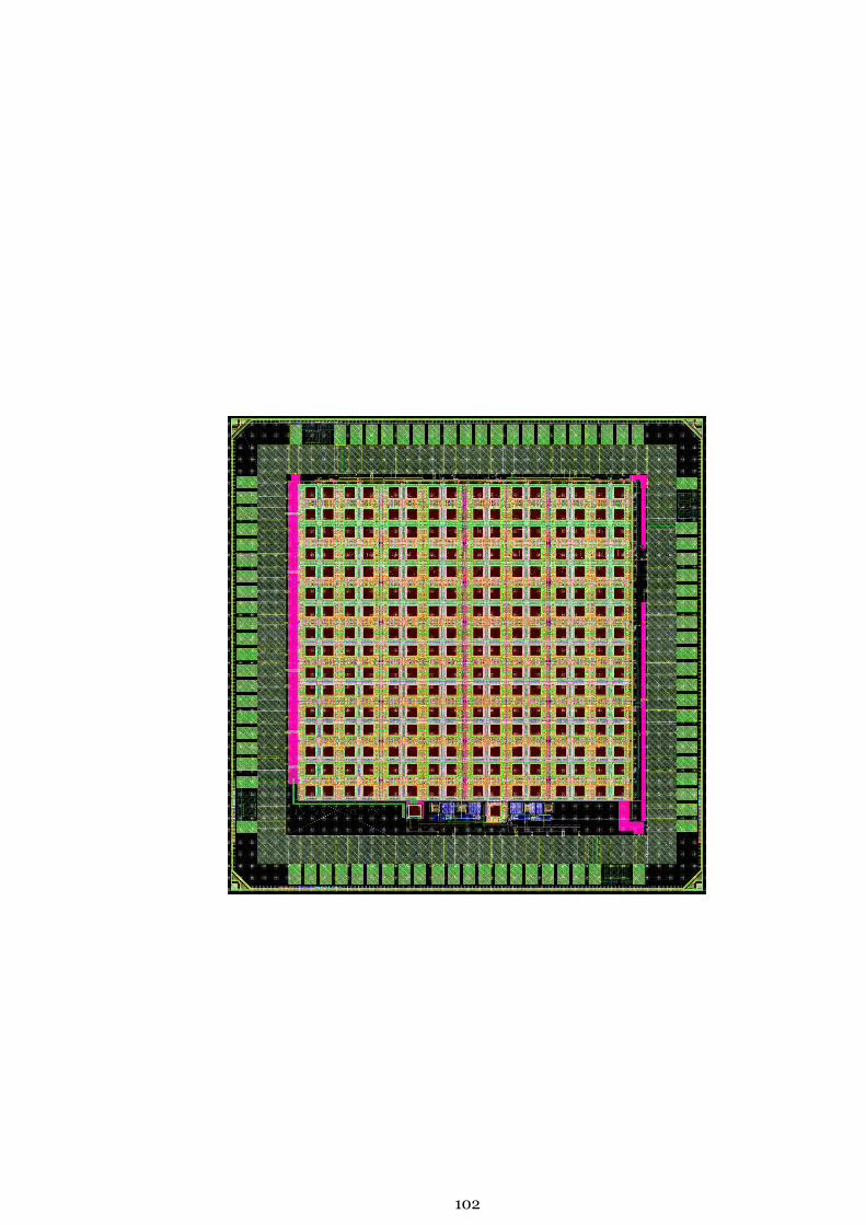
102

M6
M8
103

104

Appendix D
Alternative layout of thepixel
The alternative pixel layout including MOM capacitors.
105

106

Appendix E
BioCAS 2014 paper:A Bio-Inspired AERTemporal Tri-ColorDifferentiator
107

A Bio-Inspired AER Temporal Tri-ColorDifferentiator
Łukasz Farian, Juan Antonio Lenero-Bardallo, Philipp HafligerDepartment of Informatics, University of Oslo, Norway, email: [email protected]
Abstract—The paper presents the first focal plane array ofasynchronous event pixels that react to temporal color contrastof three different color spectra. The three different spectra aretransduced into photo currents by stacked photo diodes andtemporal changes of the contrast of these three spectra arequantified as pulse density modulated signals and conveyed off-chip by the Address Event Representation (AER) protocol. 16x16pixel array has been implemented and tested in a 90nm TSMCCMOS process. A single pixel measures 82µm x 82µm andhas a fill factor of 27% and a dynamic range of 5 decades. Thepaper presents single pixel characteristics and shows visualizationexamples of the pixel array.
I. INTRODUCTION
Color contrast detection is important in many industrial pro-cesses where robots are involved. For instance, it is essentialto match samples of various colored materials or to operatemobile equipment for which the operating signals are coloredlights [1].
Conventional color image sensors are frame-based and usecolor filters to extract color information from the visual scene.Filters are placed over each pixel. Typically, they are band-passfilters centered a red, green, and blue colors (RGB), usuallyarranged in groups of four filters (RGBG) called Bayer masks.
In the last years, we have seen an increase of bio-inspiredvision sensors that try to emulate some features of the humanretina [2]–[5], just to mention but a few. Typically they detectspatio-temporal contrast or light intensity. However, such sen-sors have been traditionally limited to black-and-white sensors.This limitation is mainly due to their low resolution arrays.Placing discrete color filters over pixels implies reducing thesensor resolution at least three times. RGB color processingwith bio-inspired vision sensors is recent [6] and authors preferstacked photodiodes at different depths to sense the colorinformation instead of discrete optic filters.
However, neural processing of color is not just based onfiltering light at three different wavelengths. We do have coneswith three different pigments that can filter light approximatelyat red, green, and blue colors, but we do not perceive colorsas separate hues [7]. Certain pairs of colors are mutuallyexclusive. Actually there is an opponency between red andgreen and between blue and yellow colors. To our knowledge,the neural full color processing has not been modeled withvision sensors yet.
This work presents a two-dimensional pixel array whosepixels spike when they detect transitions between three dif-ferent color spectra, trying to emulate the color opponenciesin the human retina. The sensor is a prototype with stacked
photodiodes [6] with different spectral sensitivity. Outputsprovide information about the different color transitions. Thesensor can detect transitions between colors at high speed,which generate asynchronous pixel events that are conveyedoff-chip by the Address Event Representation (AER) protocol.Possible applications are for example automated industrialprocesses where transitions between colors need to be detectedfor appropriate processing [1], automotive systems, or evensystems that need to detect transitions between radiation inthe near-infrared band and the visible spectrum [8].
II. OPERATION PRINCIPLE
The designed pixel monitors three different color spectraand it reports whenever the ratio of the light intensity filteredby those three spectra changes. For illustration you may thinkof those three spectra as red, green, and blue light and denotethe filtered intensities R, G, and B. Each pixel reports quantita-tive changes in the ratios R/G and G/B. The third ratio R/B canbe indirectly obtained from the relationship R/B=R/G*G/B.A change in spectrum is reported as an asynchronous pixelevent on the AER bus: if R/G has increased the pixel producespositive R/G events on the AER bus. If G/B has decreased,the pixel reports a negative G/B events. The density of theseevents is proportional to the rate of the change. Please notethat if the light level of the pixel changes without a change inthe spectrum, the pixel will not react at all. Thus, its outputwill be independent from the illumination level of the input.Later we will refer to the changes in spectra (R, G and B)and photo currents (IR, IG and IB) interchangeably becauseof the linear dependence between these two quantities [9].
III. VISION SENSOR DESIGN
This section describes the design of a single pixel and afocal plain array.
A. Pixel Design
Fig. 1 shows a block diagram of a single pixel. It can bedivided into three stages: photoreceptor, differencing amplifierand comparators. The pixel topology can be treated as anextension of the design implemented by Berner and Delbruckin [10]. Their pixel comprises two stacked photo diodes(buried double junction) providing two different color spectra,whereas we implemented a pixel made up by 3 different photodiodes stacked at different depths, providing three differentcolor spectra [11]. The cross section of the implementedstacked photo diodes in Fig. 2 shows that these photo diodes
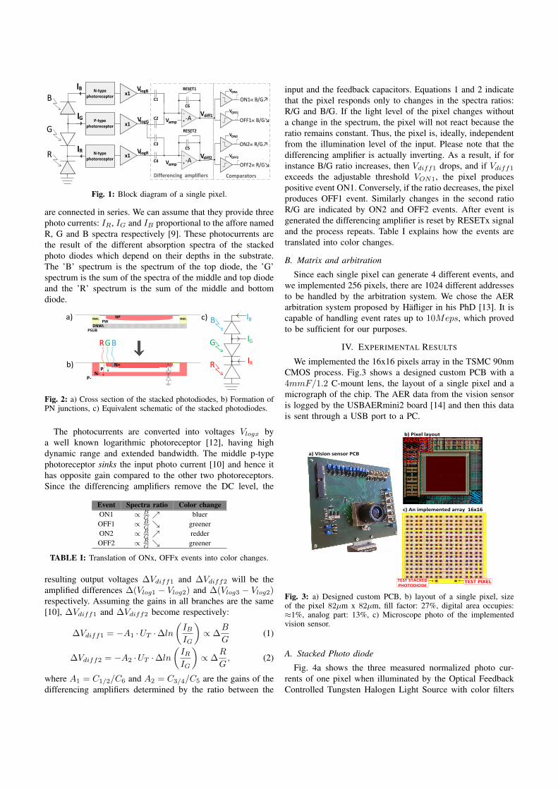
B
G
R
N-type photoreceptor
x1
P-type photoreceptor
N-type photoreceptor
ON1∝ B/G↗
VlogB
VlogG
VlogR
Vdiff1
Vdiff2
C1
C2
C3
C4
RESET2
C5
-A-
Vamp
RESET1
C6
-A-+Vamp
ComparatorsDifferencing amplifiers
VON1
VOFF1
VON2
VOFF2
OFF1∝ B/G↘
ON2∝ R/G↗
OFF2∝ R/G↘
I
I
I
B
G
R
x1
x1+
Fig. 1: Block diagram of a single pixel.
are connected in series. We can assume that they provide threephoto currents: IR, IG and IB proportional to the affore namedR, G and B spectra respectively [9]. These photocurrents arethe result of the different absorption spectra of the stackedphoto diodes which depend on their depths in the substrate.The ’B’ spectrum is the spectrum of the top diode, the ’G’spectrum is the sum of the spectra of the middle and top diodeand the ’R’ spectrum is the sum of the middle and bottomdiode.
NWL NWL
DNWLPSUB
NPPW
s
P-
N+P
a)
b)N-
c)
BRG
R
G
B
RI
GI
BI
Fig. 2: a) Cross section of the stacked photodiodes, b) Formation ofPN junctions, c) Equivalent schematic of the stacked photodiodes.
The photocurrents are converted into voltages Vlogx bya well known logarithmic photoreceptor [12], having highdynamic range and extended bandwidth. The middle p-typephotoreceptor sinks the input photo current [10] and hence ithas opposite gain compared to the other two photoreceptors.Since the differencing amplifiers remove the DC level, the
Event Spectra ratio Color changeON1 ∝ B
G↗ bluer
OFF1 ∝ BG↘ greener
ON2 ∝ RG↗ redder
OFF2 ∝ RG↘ greener
TABLE I: Translation of ONx, OFFx events into color changes.
resulting output voltages ∆Vdiff1 and ∆Vdiff2 will be theamplified differences ∆(Vlog1 − Vlog2) and ∆(Vlog3 − Vlog2)respectively. Assuming the gains in all branches are the same[10], ∆Vdiff1 and ∆Vdiff2 become respectively:
∆Vdiff1 = −A1 ·UT ·∆ln
(IBIG
)∝ ∆
B
G(1)
∆Vdiff2 = −A2 ·UT ·∆ln
(IRIG
)∝ ∆
R
G, (2)
where A1 = C1/2/C6 and A2 = C3/4/C5 are the gains of thedifferencing amplifiers determined by the ratio between the
input and the feedback capacitors. Equations 1 and 2 indicatethat the pixel responds only to changes in the spectra ratios:R/G and B/G. If the light level of the pixel changes withouta change in the spectrum, the pixel will not react because theratio remains constant. Thus, the pixel is, ideally, independentfrom the illumination level of the input. Please note that thedifferencing amplifier is actually inverting. As a result, if forinstance B/G ratio increases, then Vdiff1 drops, and if Vdiff1
exceeds the adjustable threshold VON1, the pixel producespositive event ON1. Conversely, if the ratio decreases, the pixelproduces OFF1 event. Similarly changes in the second ratioR/G are indicated by ON2 and OFF2 events. After event isgenerated the differencing amplifier is reset by RESETx signaland the process repeats. Table I explains how the events aretranslated into color changes.
B. Matrix and arbitration
Since each single pixel can generate 4 different events, andwe implemented 256 pixels, there are 1024 different addressesto be handled by the arbitration system. We chose the AERarbitration system proposed by Hafliger in his PhD [13]. It iscapable of handling event rates up to 10Meps, which provedto be sufficient for our purposes.
IV. EXPERIMENTAL RESULTS
We implemented the 16x16 pixels array in the TSMC 90nmCMOS process. Fig.3 shows a designed custom PCB with a4mmF/1.2 C-mount lens, the layout of a single pixel and amicrograph of the chip. The AER data from the vision sensoris logged by the USBAERmini2 board [14] and then this datais sent through a USB port to a PC.
DIGITAL
TEST PIXELTEST STACKED PHOTODIODE
a) Vision sensor PCB
b) Pixel layout
c) An implemented array 16x16
Fig. 3: a) Designed custom PCB, b) layout of a single pixel, sizeof the pixel 82µm x 82µm, fill factor: 27%, digital area occupies:≈1%, analog part: 13%, c) Microscope photo of the implementedvision sensor.
A. Stacked Photo diode
Fig. 4a shows the three measured normalized photo cur-rents of one pixel when illuminated by the Optical FeedbackControlled Tungsten Halogen Light Source with color filters
centered between 400 nm and 950 nm. Normalized means herethat the sum of the currents is normalized to 1.0. The truespectra of the pixel do indeed have center frequencies rangingfrom the lowest for what we called ’R’ to the highest thatwe called ’B’, but are in truth much more wide band thantrue RGB filters. So for example a narrow band light sourcemoving from 500nm to 600nm wavelength would clearly leadto positive R/G events. More subtly, it would also lead toa few positive G/B events, as the green and the blue linedecrease in parallel on this linear scale, that means theirG/B ratio will increase. Fig.4b shows the calculated photo
400 500 600 700 800 9000
0.2
0.4
0.6
0.8
1
Wavelength (nm)
IB
IG
IR
(a) Photo currents relative values.
400 500 600 700 800 90010
−1
100
101
102
Wavelength (nm)
IB / I
GIR
/ IG
greenerbluer
redder greener
(b) Photo currents ratio,
Fig. 4: Spectral response of 3 stacked photo diodes: a) relative valuesof their photo currents, b) photo currents ratios amplified by thedifferencing amplifiers (Equations 1,2). The values were correctedby the Halogen Light Source irradiance factor and color filterstransmission efficiency.
current ratios and illustrates how these ratios can be used todiscriminate between colors: the R/G ratio increases when athe dominating light wavelength increases (the color spectrumbecomes redder) and B/G decreases when the dominating lightwavelength decreases (the color spectrum becomes bluer). Theratio B/G exhibits weaker dependence on color spectra, it hassteepest slope up to 650 nm and after that is flat, while the R/Gratio has almost constant slope over the entire tested spectrum.Thus if for instance a narrow band light source moves from600 nm to 900 nm wavelength, it would lead to positive R/Gevents and a few negative B/G events.
B. Color recognition
We used high-power full color LEDs F50360 from SeoulSemiconductor to characterize a single pixel response tochanges in the ratio of light intensities. These photodiodesemit light centered in 625nm, 525nm and 460nm wavelengths.
First, we characterized the pixel response to a continuousred-green intensity change by illuminating its surface with70Hz sinusoidal out-of-phase red and green lights. Fig.5 showsthe current through the LEDs and the response of a single
pixel to the stimulus. We observed two ON2 and two OFF2events per cycle. Since we were changing the R and G spectrainversely, the change of the R/G ratio is most substantialand hence the output ∆Vdiff2 exceeds the VON2 and VOFF2
thresholds. The VONx threshold was ≈ 1.2V and VOFF
threshold ≈ 1.3V
0
20
40
60
80
[mA]
red stimuligreen simuli,blue stimuli
1.15
1.2
1.25
1.3
1.35
[V]
Vdiff1
transient voltage
0.02 0.04 0.06 0.08 0.11.15
1.2
1.25
1.3
1.35
[V]
Time [s]
GREENER (OFF2)
REDDER (ON2)
Vdiff2
transient voltage
Fig. 5: Current consumption of the photodiodes and a single pixelresponse to the continuous red-green contrast change.
∆Vdiff1 moves between threshold values, but does notexceed them and, hence, no ON1 nor OFF1 events aregenerated. Since there has not been any blue light changein the stimulus (the blue LED was off), the nominator anddenominator in the B/G ratio change by the same amount, andideally this ratio should remain constant. In fact, the output∆Vdiff1 fluctuates only because the photo currents ratio B/Gexhibits weak dependence on longer spectrum wavelengths,as was shown in Fig.4b. Next, we tested a response of the
0
20
40
60
80
[mA]
red stimuligreen simuli,blue stimuli
1.15
1.2
1.25
1.3
1.35
[V]
GREENER (OFF1)
BLUER (ON1)BLUER (ON1)
Vdiff1
transient voltage
0.02 0.04 0.06 0.08 0.11.15
1.2
1.25
1.3
1.35
[V]
Time [s]
GREENER (OFF2)
REDDER (ON2)
Vdiff2
transient voltage
Fig. 6: Current consumption of the photodiodes and a single pixelresponse to the continuous red-blue contrast change.
pixel to the continuous blue-red contrast change (Fig.6). Thistime we observed 4 types of events. Events ON1 occur whenthe blue light positive transient is biggest (B/G increases) andconversely, ON2 events occur at the maximum red positivetransient (R/G increases). Besides, we observed OFF1 and

OFF2 events that might be confusing at first glance. However,OFF1 events indicate a shift to longer wavelengths from blueand OFF2 events indicate a shift to shorter wavelengths fromred and thus, the responses are as expected and correct.
5 10 15 5 10 1550
40
30
20
10
0
XY
time
[ms]
OFF1 ON2 OFF2
5 10 15 5 10 1550
40
30
20
10
0
XY
time
[ms]
ON1 red dot trace
Fig. 7: Space-time plot of the rotating red dot on the greenbackground. Number of events: ON1=924, OFF1=1107, ON2=5060,OFF2=5210
Fig.7 shows the response to a rotating red dot on a greenbackground and Fig.8 shows the response to a rotating blue doton a red background. According to Table I we assigned greencolor to OFF1 and OFF2 events, red color to ON2 events,and blue color to ON1 events. Comparing Fig.7 and Fig.8we can observe that for a rotating red dot roughly 5 timesmore events representing change of R/G ratio are registered.For a rotating blue dot the vision sensor generates much lessevents representing change of R/G ratio. In Fig.7 the red eventspreceed the center of the red dot stimulus while the green andblue events are trailing. On the other hand, in Fig.8 the blueand green events preceed the center of the red dot, while redevents are trailing. We repeated this experiment for differentbackground light conditions, ranging from 0.1lux up to 15kluxand we obtained similar behavior, meaning that the visionsensor has a dynamic range of > 5 decades.
V. CONCLUSION
We built and tested the first focal plain array of bio-inspired AER pixels which mimics full color opponenciesbetween three primary colors in the retina. Its pixels arecapable of detecting temporal contrast of three different colorspectra sensed from three stacked photo diodes. We obtainedexperimental results from a single test pixel and from the array.Since the vision sensor abandons a global integration timeand each pixel communicates individually and asynchronouslywhenever it detects temporal color contrast, the post pro-cessing load on a CPU performing object recognition basedon color codes or colored object outlines is much relaxed.We implemented a simple visualizing algorithm translatingevents into color changes. Future work shall involve moreresearch to properly represent color changes in a reconstructedvideo stream. This vision sensor has good potential for an
5 10 15 5 10 1540
30
20
10
0
XY
time
[ms]
OFF1 ON2 OFF2
5 10 15 5 10 1540
30
20
10
0
XY
time
[ms]
ON1 blue dot trace
Fig. 8: Space-time plot of the rotating blue dot on the red background.Number of events: ON1=1208, OFF1=1353, ON2=2845, OFF2=2795
automotive robotics applications where a high speed temporalcolor contrast recognition, especially of fast moving objects,is critical.
REFERENCES
[1] J. Tiffin and H. S. Kuhn, “Color discrimination in industry,” Archives ofOphthalmology, vol. 28, no. 5, pp. 851–859, November 1942.
[2] J. A. Lenero-Bardallo, T. Serrano-Gotarredona, and B. Linares-Barranco, “A 5-decade dynamic range ambient-light-independient cali-brated signed-spatial-contrast aer retina with 0.1ms latency and optionaltime-to-first-spike mode,” Transactions on Circuits and Systems, Part-I,2010.
[3] C. Posch, D. Matolin, and R. Wohlgenannt, “A QVGA 143dB dynamicrange asynchronous address-event PWM dynamic image sensor withlossless pixel-level video compression,” IEEE Journal of Solid StateCircuits, vol. 46, no. 1, pp. 259–275, January 2010.
[4] T. Serrano-Gotarredona and B. Linares-Barranco, “A 128 × 128 1.5%contrast sensitivity 0.9% FPN 3µs latency 4mW asynchronous frame-free dynamic vision sensor using transimpedance preamplifiers,” IEEEJournal of Solid-State Circuits, vol. 48, no. 3, pp. 827–838, March 2013.
[5] P. Lichtsteiner, C. Posch, and T. Delbruck, “A 128× 128 120dB 15µslatency asynchronous temporal contrast vision sensor,” IEEE Journal ofSolid-State Circuits, vol. 43, no. 2, pp. 566–576, February 2008.
[6] J. A. Lenero-Bardallo, D. H. Bryn, and P. Hafliger, “Bio-inspiredasynchronous pixel event tri-color vision sensor,” IEEE Transactionson Biomedical Circuit and Systems, pp. 1–13, August 2013.
[7] J. E. Dowling, The Retina: An Approachable Part of the Brain, 2nd ed.The Belknap Press of Harvard University Press, 2012.
[8] J. A. Lenero-Bardallo, D. H. Bryn, and P. Hafliger, “Flame monitoringwith an aer color vision sensor,” in IEEE International Symposium onCircuits and Systems, ISCAS 2013, Beijing, China, 2013.
[9] B. Tabbert and A. Goushcha, “Linearity of the photocurrent responsewith light intensity for silicon pin photodiode array,” in Nuclear ScienceSymposium Conference Record, 2006. IEEE, vol. 2, Oct 2006, pp. 1060–1063.
[10] R. Berner and T. Delbruck, “Event-based pixel sensitive to changes ofcolor and brightness,” IEEE Transactions On Circuits and Systems I,vol. 58, no. 7, pp. 1581–1590, 2011.
[11] J. A. Lenero-Bardallo, D. H. Bryn, and P. Hafliger, “Bio-inspiredasynchronous pixel event tri-color vision sensor,” in IEEE Transactionson Biomedical Circuit and Systems, August 2013, pp. 1–13.
[12] M. C. Delbruck, T., “Adaptive photoreceptor with wide dynamic range,”in Circuits and Systems, 1994. ISCAS ’94., 1994 IEEE InternationalSymposium on, vol. 4, May 1994, pp. 339–342 vol.4.
[13] P. Hafliger, “A spike based learning rule and its implementation in ana-log hardware,” Ph.D. dissertation, ETH Zurich,Switzerland, Sunderlan,2000.
[14] R. Berner, T. Delbruck, A. Civit-Balcells, and A. Linares-Barranco, “A5Meps $100 USB 2.0 address-event monitor-sequencer interface,” inISCAS 2007, New Orleans, 2007, pp. 2451–2454.

112

Appendix F
BioCAS 2014 paper:Live Demo: A Bio-InspiredAER Temporal Tri-ColorDifferentiator
113

Live Demonstration: A Bio-Inspired AER TemporalTri-Color Differentiator
Łukasz Farian, Juan A. Leñero-Bardallo, Philipp HäfligerNanoelectronics group, Department of Informatics, University of Oslo, Norway
E-mails: [email protected]
Fig. 1. Experimental setup.
Abstract—We demonstrate the first array of asynchronousevent pixels that react to temporal color contrast of three differentcolor spectra. The three different spectra are transduced intophoto currents by stacked photo diodes. Temporal changes ofthe contrast of these three spectra are quantified as pulse densitymodulated signals and conveyed off-chip by the Address EventRepresentation (AER) protocol. The 16× 16 pixel array hasbeen fabricated in the standard TSMC 90nm CMOS process.
I. DEMONSTRATION SETUP
The demonstration system is composed of a laptop, 2 PCBboards, a light source attached to a motor and a white sheet ofpaper, as shown in Fig. 1. One PCB contains a lens mount andthe sensor. The other one is a data logger USBAERmini2 [1]that stores the data and sends it via USB port to the laptop. Thelaptop has installed a dedicated Java interface [2] to displayreal-time color images.
II. VISITOR EXPERIENCE
The new sensor emulates the neural processing of colorin the human retina. Neural processing of color is not justbased on filtering light at three different wavelengths howcommercial frame-based sensor do. Humans have cones withthree different pigments that can filter light approximately atred, green, and blue colors, but we do not perceive colorsas separate hues [3]. Certain pairs of colors are mutuallyexclusive. Actually there is an opponency between red andgreen and between blue and yellow colors.
This demonstration presents a two-dimensional pixel arraywhose pixels spike when they detect transitions betweenprimary colors, trying to emulate the color opponencies inthe human retina. The sensor is a prototype with stackedphoto diodes with different spectral sensitivity [4]. Pixeloutput spikes provide information about the transient currentvariations of three stacked photo diodes with different spectralsensitivity.The visitor will directly interact with the sensor and observehow temporal transitions between primary colors are detected.A moving light source will be projected on the white sheetof paper in front of the sensor. It will react depending onthe incident light spectra. White light will not provoke outputevents. Colored light (blue, green or red) will make pixelsspike out, because they detect transient spectra variations.Furthermore, a high frequency blinking light source (blue,green or red) will be placed in front of the sensor. The visitorwill observe that the camera strongly responds to the highfrequency color changes and generates many output events.Pixel outputs events will be displayed on a laptop screen usinga custom Java interface. Furthermore, the visitors will be ableto interact freely with the system and experiment how it reactsto the colored moving objects.
III. REFERENCE PUBLICATIONS
The article of Farian et al. [5] describes the sensor indetail. It has been invited for presentation to the specialsession "Bio-Inspired Circuits and Architectures for Robotics"at BioCAS 2014. The board used to store and transmit thesensor information to a PC is described in [1]. A dedicatedJava custom interface [2] was adapted and programmed toshow real-time color transitions on a computer screen.
REFERENCES
[1] R. Berner, T. Delbruck, A. Civit-Balcells, and A. Linares-Barranco, “A5Meps $100 USB 2.0 address-event monitor-sequencer interface,” inISCAS 2007, New Orleans, 2007, pp. 2451–2454.
[2] “jAER open source project,” http://sourceforge.net/projects/jaer/.[3] J. E. Dowling, The Retina: An Approachable Part of the Brain, 2nd ed.
The Belknap Press of Harvard University Press, 2012.[4] J. A. Leñero-Bardallo, D. H. Bryn, and P. Häfliger, “Bio-inspired asyn-
chronous pixel event tri-color vision sensor,” IEEE Transactions onBiomedical Circuit and Systems, pp. 1–13, August 2013.
[5] L. Farian, J. A. Leñero-Bardallo, and P. Häfliger, “A bio-inspired AERtemporal tri-color differentiator,” Submitted to IEEE Biomedical Cir-cuits and Systems Conference (BioCAS), Lausanne, Switzerland. Preprintavailable at http://folk.uio.no/juanle/Downloads/BioCAS2014.pdf, Octo-ber 2014.


