Embed Size (px)
Citation preview
Mathematical Compact Models of Advanced Transistors forNumerical Simulation and Hardware Design
Juan Duarte
Electrical Engineering and Computer SciencesUniversity of California at Berkeley
Technical Report No. UCB/EECS-2018-24http://www2.eecs.berkeley.edu/Pubs/TechRpts/2018/EECS-2018-24.html
May 2, 2018

Copyright © 2018, by the author(s).All rights reserved.
Permission to make digital or hard copies of all or part of this work forpersonal or classroom use is granted without fee provided that copies arenot made or distributed for profit or commercial advantage and that copiesbear this notice and the full citation on the first page. To copy otherwise, torepublish, to post on servers or to redistribute to lists, requires prior specificpermission.
Mathematical Compact Models of Advanced Transistors for NumericalSimulation and Hardware Design
by
Juan Pablo Duarte Sepulveda
A dissertation submitted in partial satisfaction of the
requirements for the degree of
Doctor of Philosophy
in
Engineering - Electrical Engineering and Computer Sciences
in the
Graduate Division
of the
University of California, Berkeley
Committee in charge:
Dr. Chenming Hu, ChairDr. Ali M. NiknejadDr. Tarek Zohdi
Spring 2018
Mathematical Compact Models of Advanced Transistors for Numerical Simulationand Hardware Design
Copyright c© 2018
by
Juan Pablo Duarte Sepulveda
1
Abstract
Mathematical Compact Models of Advanced Transistors for Numerical Simulationand Hardware Design
by
Juan Pablo Duarte SepulvedaDoctor of Philosophy in Engineering - Electrical Engineering and Computer Sciences
University of California, BerkeleyDr. Chenming Hu, Chair
Mathematical compact models play a key role in designing integrated circuits. Theyserve as a medium of information exchange between foundries and designers. Acompact model, which is a set of long mathematical equations based on the physics ofeach transistor, is capable of reproducing the very complex transistor characteristics inan accurately, fast, and robust manner. This dissertation presents the latest researchon compact models for advanced transistor technologies: FinFETs, Ultra-thin bodySOIs (UTBSOIs), Gate-All-Around (GAA) FETs, and Negative Capacitance (NC)FETs.
Since traditional transistor scaling had reached limitations due short-channeleffects and oxide tunneling, the introduction of FinFET and UTBSOIs in high-volumemanufacturing at 20nm, 14nm and 10nm technology nodes had let the electronicindustry to keep obtaining performance and density advantages in technology scaling.For smaller nodes such as 5nm, and 3nm, GAA FETs transistors are expected toreplace traditional transistors. Production ready compact model for current andfuture FinFETs are presented in this thesis. The Unified Compact Model can modelFinFETs with realistic fin shapes including rectangle, triangle, circle and any shapein between. A new quantum effects model will also be presented, it enables accuratemodeling of III-V FinFETs. Shape agnostic short-channel effect model for aggressiveLG scaling and body bias model for FinFETs on bulk substrates are also includedin this work. This computationally efficient model is an ideal turn-key solution forsimulation and design of future heterogeneous circuits.
For extremely scaled technologies, NC-FETs are quickly emerging as preferredcandidates for digital and analog applications. The recent discovery of ferroelectric(FE) materials using conventional CMOS fabrication technology has led to the firstdemonstrations of FE based NC-FETs. The ferroelectric material layer added overthe transistor gate insulator help in several device aspects, it suppress short-channeleffects, increase on-current due voltage amplification, increase output resistance inshort-channel devices, etc. These exciting characteristics has created an urgency
2
for analysis and understanding of device operation and circuit performance, wherenumerical simulation and compact models are playing a key role.
This thesis gives insights into the device physics and behavior of FE based nega-tive capacitance FinFETs (NC-FinFETs) by presenting numerical simulations, com-pact models, and circuit evaluation of these devices. NC-FinFETs may have a floatingmetal between FE and the dielectric layers, where a lumped charge model representssuch a device. For a NC-FinFET without a floating metal, the distributed chargemodel should be used, and at each point in the channel the FE layer will impact thelocal channel charge. This distributed effect has important implications on devicecharacteristics. These device differences are explained using numerical simulationand correctly captured by the proposed compact models. The presented compactmodels have been implemented in commercial circuit simulators for exploring circuitsbased on NC-FinFET technology. Circuit simulations show that a quasi-adiabaticmechanism of the ferroelectric layer in the NC-FinFET recovers part of the energyduring the switching process of transistors, helping to minimize the energy losses ofthe wasteful energy dissipation nature of conventional transistor circuits. As circuitload capacitances further increase, VDD scaling becomes more dominant on energyreduction of NC-FinFET based circuits.

i
To my family: Past, Present and Future.

Contents
Contents ii
List of Figures v
List of Tables xvi
1 Introduction 11.1 Mathematical Models for FinFETs and UTBSOIs . . . . . . . . . . . 31.2 Negative Capacitances FETs . . . . . . . . . . . . . . . . . . . . . . . 6
2 Model for Double-Gate FinFETs 102.1 Introduction . . . . . . . . . . . . . . . . . . . . . . . . . . . . . . . . 102.2 Model Derivation . . . . . . . . . . . . . . . . . . . . . . . . . . . . . 122.3 Conclusion . . . . . . . . . . . . . . . . . . . . . . . . . . . . . . . . . 18
3 Unified FinFET Compact Model 193.1 Introduction . . . . . . . . . . . . . . . . . . . . . . . . . . . . . . . . 193.2 Core Model . . . . . . . . . . . . . . . . . . . . . . . . . . . . . . . . 203.3 Global Scaling Model . . . . . . . . . . . . . . . . . . . . . . . . . . 303.4 Speed Results . . . . . . . . . . . . . . . . . . . . . . . . . . . . . . . 333.5 Benchmark Tests . . . . . . . . . . . . . . . . . . . . . . . . . . . . . 333.6 Conclusion . . . . . . . . . . . . . . . . . . . . . . . . . . . . . . . . . 33
4 Variability Modeling 384.1 Introduction . . . . . . . . . . . . . . . . . . . . . . . . . . . . . . . . 384.2 Description of the Unified Model . . . . . . . . . . . . . . . . . . . . 394.3 Device Simulation and Model Parameter Set Up . . . . . . . . . . . . 414.4 10nm vs. 14nm Variability Using Predictive Modeling . . . . . . . . 414.5 14nm Node SRAM Variability Evaluation . . . . . . . . . . . . . . . 444.6 Conclusion . . . . . . . . . . . . . . . . . . . . . . . . . . . . . . . . . 45
iii
5 Model for Independent Gate MOSFETs 495.1 Introduction . . . . . . . . . . . . . . . . . . . . . . . . . . . . . . . . 495.2 Independent Multi-Gate MOSFETs . . . . . . . . . . . . . . . . . . . 505.3 Core Model . . . . . . . . . . . . . . . . . . . . . . . . . . . . . . . . 525.4 Initial Guess . . . . . . . . . . . . . . . . . . . . . . . . . . . . . . . . 555.5 Iteration Update . . . . . . . . . . . . . . . . . . . . . . . . . . . . . 595.6 Complete Model . . . . . . . . . . . . . . . . . . . . . . . . . . . . . . 635.7 Conclusion . . . . . . . . . . . . . . . . . . . . . . . . . . . . . . . . . 63
6 Model for Negative Capacitance FETs 676.1 Introduction . . . . . . . . . . . . . . . . . . . . . . . . . . . . . . . . 676.2 Unified Compact Model . . . . . . . . . . . . . . . . . . . . . . . . . 676.3 Ferroelectric Material Model . . . . . . . . . . . . . . . . . . . . . . . 686.4 Lumped NC-FinFET Model . . . . . . . . . . . . . . . . . . . . . . . 706.5 Distributed NC-FinFET Model . . . . . . . . . . . . . . . . . . . . . 716.6 Lumped versus Distributed NC-FinFETs . . . . . . . . . . . . . . . . 766.7 Time-Dependent Ferroelectric Model . . . . . . . . . . . . . . . . . . 766.8 Model Robustness . . . . . . . . . . . . . . . . . . . . . . . . . . . . . 786.9 Conclusion . . . . . . . . . . . . . . . . . . . . . . . . . . . . . . . . . 78
7 Numerical Simulation of Negative Capacitance FETs 817.1 Introduction . . . . . . . . . . . . . . . . . . . . . . . . . . . . . . . . 817.2 Quasi 2-Dimensional NC-FET Simulation . . . . . . . . . . . . . . . . 827.3 NC-FET LG Scaling . . . . . . . . . . . . . . . . . . . . . . . . . . . 837.4 NC-FET with Low Coercive Field: lowering effective EOT . . . . . . 86
8 Energy Analysis of Negative Capacitance FETs 938.1 Introduction . . . . . . . . . . . . . . . . . . . . . . . . . . . . . . . . 938.2 SPICE Model for NCFETs . . . . . . . . . . . . . . . . . . . . . . . . 948.3 Single NC-FinFET Energy Simulation Analysis . . . . . . . . . . . . 958.4 NC-FinFET Ring-Oscillator Analysis . . . . . . . . . . . . . . . . . . 998.5 Conclusion . . . . . . . . . . . . . . . . . . . . . . . . . . . . . . . . . 104
9 Summary 1069.1 Chapters Summary . . . . . . . . . . . . . . . . . . . . . . . . . . . . 1069.2 Future Work . . . . . . . . . . . . . . . . . . . . . . . . . . . . . . . . 107
A 1D Numerical Simulation of Symmetric FinFET 117
B Explicit Surface Potential Model 121B.1 Continuous Starting Function . . . . . . . . . . . . . . . . . . . . . . 121B.2 Quartic Modified Iteration: Implementation and Evaluation . . . . . 124
iv
C Unified Model Implementation in Verilog-A 130
D 1D Numerical Simulation for UTBSOIs 132
E Energy Calculation with Hspice 137
v
List of Figures
1.1 The gate length of transistor has been continuously shrank from 10µmto 10nm [30]. . . . . . . . . . . . . . . . . . . . . . . . . . . . . . . . 2
1.2 Left: Nokia 3310, 2000, with half million transistors. Right: iPhone X[4], 2017, with more than 4.3 billion transistors. . . . . . . . . . . . . 3
1.3 Compact Model vs.: Look-Up Table, TCAD Simulation, and Exper-iment. The advantage of compact models, for hardware design, overother design and simulation approaches are accuracy (∼1% RSM), sim-ulation robustness (smooth and continuous), speed ( ∼ 10µs), andaffordability (open source). . . . . . . . . . . . . . . . . . . . . . . . 4
1.4 Technology node, year, device, metal layers, die, and number of tran-sistor for different Intel processes. . . . . . . . . . . . . . . . . . . . . 4
1.5 Cross-sectional views of device structures modeled in this thesis: UTB-SOI, FinFETs, and GAA FETs. . . . . . . . . . . . . . . . . . . . . . 5
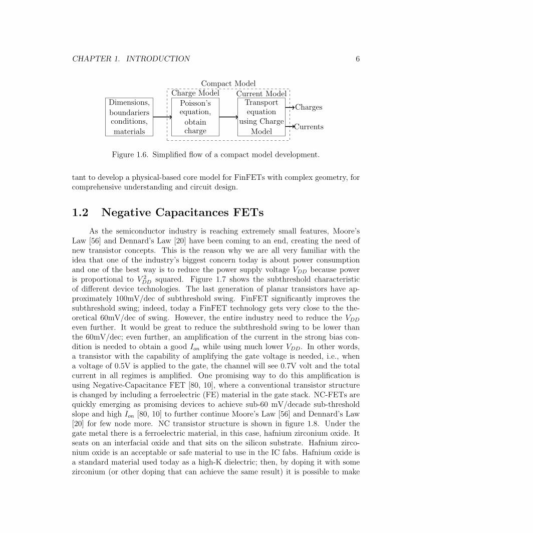
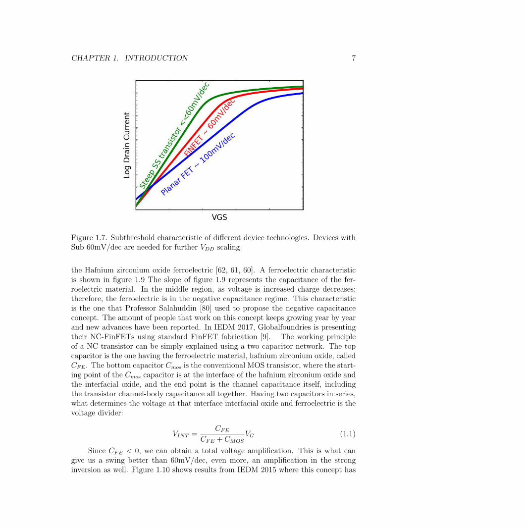
1.6 Simplified flow of a compact model development. . . . . . . . . . . . 61.7 Subthreshold characteristic of different device technologies. Devices
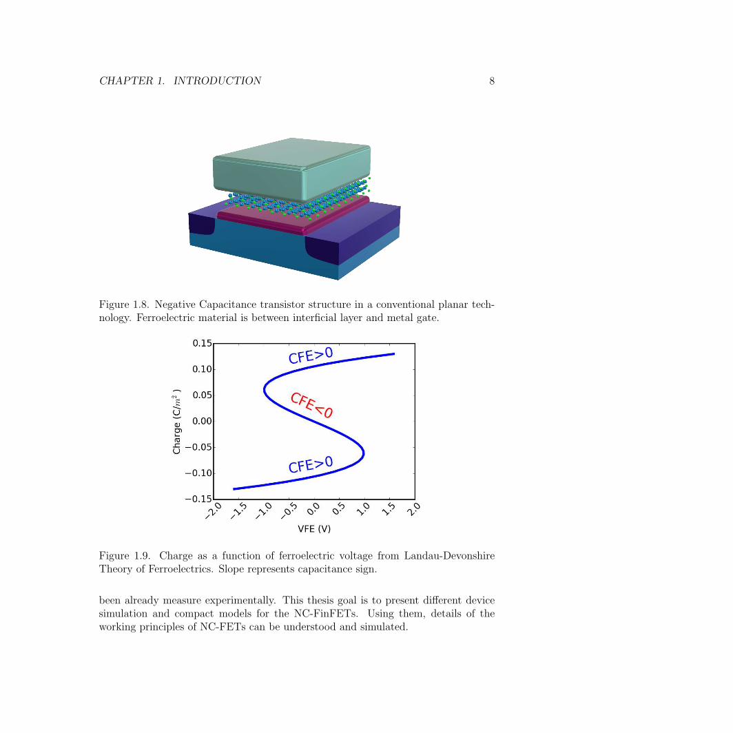
with Sub 60mV/dec are needed for further VDD scaling. . . . . . . . 71.8 Negative Capacitance transistor structure in a conventional planar
technology. Ferroelectric material is between interficial layer and metalgate. . . . . . . . . . . . . . . . . . . . . . . . . . . . . . . . . . . . . 8
1.9 Charge as a function of ferroelectric voltage from Landau-DevonshireTheory of Ferroelectrics. Slope represents capacitance sign. . . . . . 8
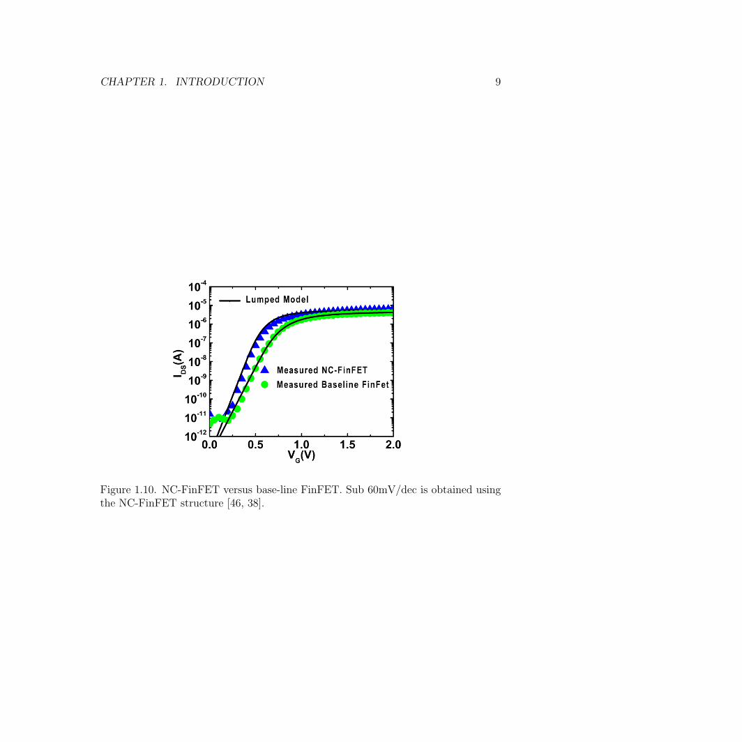
1.10 NC-FinFET versus base-line FinFET. Sub 60mV/dec is obtained usingthe NC-FinFET structure [46, 38]. . . . . . . . . . . . . . . . . . . . 9
2.1 Schematic of a symmetric Double-Gate FinFET. . . . . . . . . . . . 112.2 Fin potential versus position obtained from the numerical solution of
equation (2.1) for a lightly doped fin. Nch = 1 × 1015cm−3, TFIN =20nm, tox = 1nm and Vch = 0V have been used for simulation. . . . 12
2.3 Fin potential versus position obtained from the numerical solution ofequation (2.1) for a doped fin. Nch = 5 × 1018cm−3, TFIN = 20nm,tox = 1nm and Vch = 0V have been used for simulation. . . . . . . . 13
LIST OF FIGURES vi
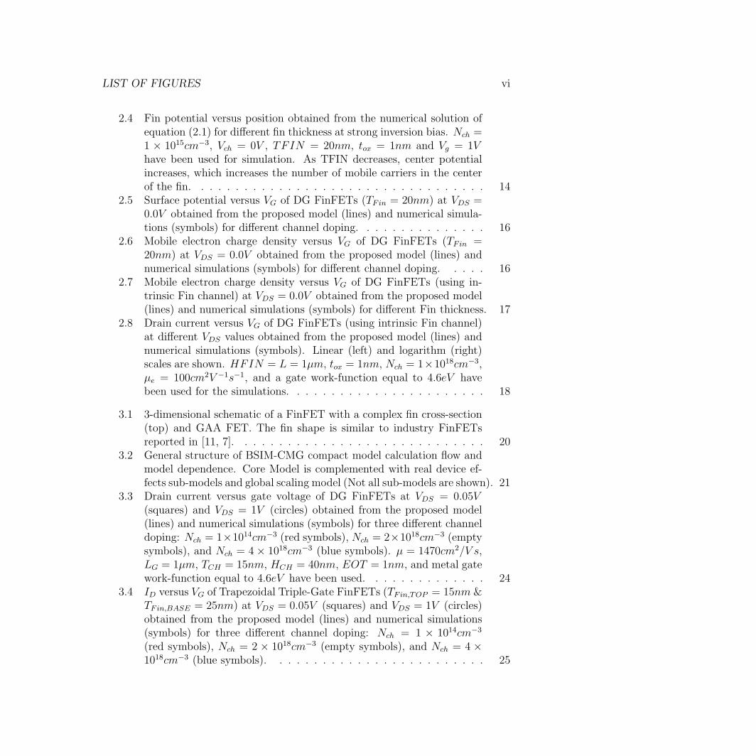
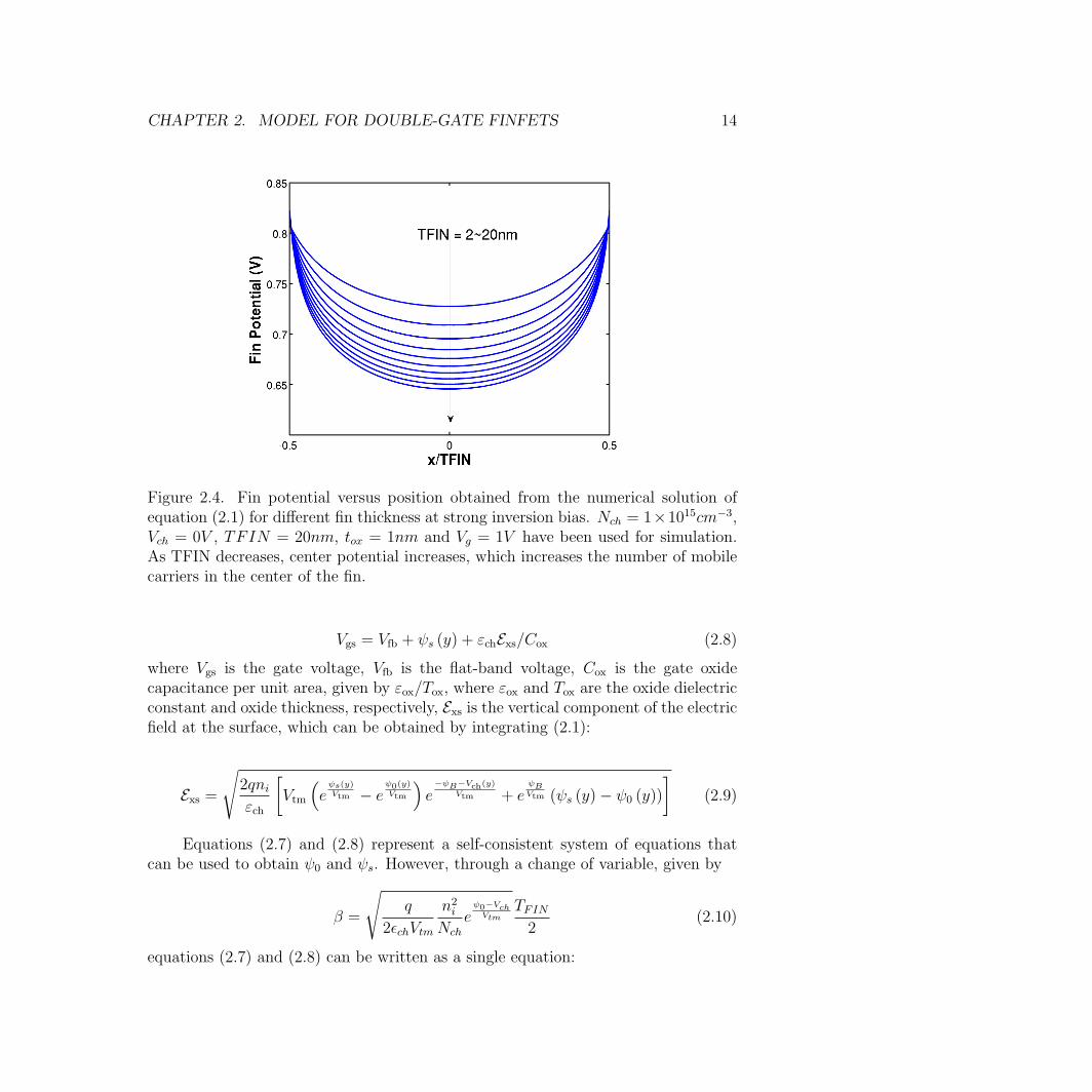
2.4 Fin potential versus position obtained from the numerical solution ofequation (2.1) for different fin thickness at strong inversion bias. Nch =1 × 1015cm−3, Vch = 0V , TFIN = 20nm, tox = 1nm and Vg = 1Vhave been used for simulation. As TFIN decreases, center potentialincreases, which increases the number of mobile carriers in the centerof the fin. . . . . . . . . . . . . . . . . . . . . . . . . . . . . . . . . . 14
2.5 Surface potential versus VG of DG FinFETs (TFin = 20nm) at VDS =0.0V obtained from the proposed model (lines) and numerical simula-tions (symbols) for different channel doping. . . . . . . . . . . . . . . 16
2.6 Mobile electron charge density versus VG of DG FinFETs (TFin =20nm) at VDS = 0.0V obtained from the proposed model (lines) andnumerical simulations (symbols) for different channel doping. . . . . 16
2.7 Mobile electron charge density versus VG of DG FinFETs (using in-trinsic Fin channel) at VDS = 0.0V obtained from the proposed model(lines) and numerical simulations (symbols) for different Fin thickness. 17
2.8 Drain current versus VG of DG FinFETs (using intrinsic Fin channel)at different VDS values obtained from the proposed model (lines) andnumerical simulations (symbols). Linear (left) and logarithm (right)scales are shown. HFIN = L = 1µm, tox = 1nm, Nch = 1×1018cm−3,µe = 100cm2V −1s−1, and a gate work-function equal to 4.6eV havebeen used for the simulations. . . . . . . . . . . . . . . . . . . . . . . 18
3.1 3-dimensional schematic of a FinFET with a complex fin cross-section(top) and GAA FET. The fin shape is similar to industry FinFETsreported in [11, 7]. . . . . . . . . . . . . . . . . . . . . . . . . . . . . 20
3.2 General structure of BSIM-CMG compact model calculation flow andmodel dependence. Core Model is complemented with real device ef-fects sub-models and global scaling model (Not all sub-models are shown). 21
3.3 Drain current versus gate voltage of DG FinFETs at VDS = 0.05V(squares) and VDS = 1V (circles) obtained from the proposed model(lines) and numerical simulations (symbols) for three different channeldoping: Nch = 1×1014cm−3 (red symbols), Nch = 2×1018cm−3 (emptysymbols), and Nch = 4× 1018cm−3 (blue symbols). µ = 1470cm2/V s,LG = 1µm, TCH = 15nm, HCH = 40nm, EOT = 1nm, and metal gatework-function equal to 4.6eV have been used. . . . . . . . . . . . . . 24
3.4 ID versus VG of Trapezoidal Triple-Gate FinFETs (TFin,TOP = 15nm &TFin,BASE = 25nm) at VDS = 0.05V (squares) and VDS = 1V (circles)obtained from the proposed model (lines) and numerical simulations(symbols) for three different channel doping: Nch = 1 × 1014cm−3
(red symbols), Nch = 2 × 1018cm−3 (empty symbols), and Nch = 4 ×1018cm−3 (blue symbols). . . . . . . . . . . . . . . . . . . . . . . . . 25
LIST OF FIGURES vii
3.5 Normalized (IDS/IDS,MAX) on (circles) and off (triangles) drain cur-rents. . . . . . . . . . . . . . . . . . . . . . . . . . . . . . . . . . . . 26
3.6 Drain current versus gate voltage (left figure) of a long channel SOI Fin-FET obtained from experimental data and from the proposed modelonly using the ideal unified long channel core model. Transconduc-tance (right figure) also shows good agreement between model andexperimental data. Symbols are the experimental data and lines theproposed model. . . . . . . . . . . . . . . . . . . . . . . . . . . . . . 27
3.7 Drain current versus drain voltage (left figure) of a long channel SOIFinFET obtained from experimental data and from the proposed modelonly using the ideal unified long channel core model. Output conduc-tance (right figure) also shows good agreement between model andexperimental data. Symbols are the experimental data and lines theproposed model. . . . . . . . . . . . . . . . . . . . . . . . . . . . . . 28
3.8 Drain current versus gate voltage of a Bulk Trapezoidal trig-gate Fin-FET with rounded corners for different body bias values. TFIN, top =20nm, TFIN, bottom = 50nm, HFIN = 25nm, 10nm corner curva-tures, Nch = 1x1015cm−3, EOT = 1nm, and gate workfunction equalto 4.6 eV were used for the simulation and model. In order to highlightthe body bias effect a short fin was used . . . . . . . . . . . . . . . . . 29
3.9 Gate capacitance (Cgg) versus gate voltage at Vds = 0V obtained fromproposed model with and without quantum confinement effects (lines),and from measured data (symbols). . . . . . . . . . . . . . . . . . . 30
3.10 The unified model accurately models the triangular fin InGaAs Fin-FETs [40, 35]. With the quantum effects model turned off, the modelover-predicts channel charge and hence current . . . . . . . . . . . . 31
3.11 Drain current versus gate voltage of FinFETs devices with Lg = 20, 50, 250, 500, 1000nm.BSIM-CMGmodel accurately captures the FinFET short-channel char-acteristics. . . . . . . . . . . . . . . . . . . . . . . . . . . . . . . . . . 32
3.12 Intel 14 nm FinFET device modeled with new BSIM-CMG model.Experimental data from [63]. . . . . . . . . . . . . . . . . . . . . . . . 32
3.13 Calculation time of core model, bias dependent calculations, bias in-dependent, and total BSIM-CMG Verilog-A code. Over ∼30% speedimprovement is achieved with the new proposed model. . . . . . . . . 33
3.14 Slope ratio calculated using BSIM-CMG model at room temperature.Tfin = 15 nm, L = 1 µm and Nfin = 10. This test checks if a compactmodel takes care of the different drain-to-source voltage dependence ofdrain-to-source current in weak- and strong-inversion regions. . . . . . 34
LIST OF FIGURES viii
3.15 Sub-threshold current simulated from BSIM-CMG model. Current in-creases with increase in fin thickness due to volume inversion effect. Inthe sub-threshold region of thin-body transistors, the gate bias movesthe energy bands not just at the surface but across the full body-thickness of the device. This causes inversion to occur in the full bodythickness of the device as opposed to only the surface in case of bulkMOSFETs. This phenomenon is called volume inversion. It occursonly in the sub-threshold region as in strong inversion the carriers atthe surface screens the electric field from reaching deep inside the sili-con body. . . . . . . . . . . . . . . . . . . . . . . . . . . . . . . . . . 35
3.16 Results of Gummel symmetry test from BSIM-CMGmodel. The modelshows smooth and continuous derivatives of drain-current and passessymmetry test. Gummel symmetry test is a standard way of testingthe symmetry of drain-current model. . . . . . . . . . . . . . . . . . 36
3.17 Harmonic balance simulation results showing fundamental (f0) , second(2f0), third (3f0), fourth (4f0) and fifth-harmonic (5f0) from BSIM-CMG model, which match very well with theoretical calculations. f0= 1 MHz and Vg = 1 V. If a compact model has singularities in drain-current derivatives, it will produce unphysical harmonic balance simu-lations results. Theoretically second harmonic is proportional to squareof the input signal, third harmonic is proportional to cube of the inputsignal and so on . . . . . . . . . . . . . . . . . . . . . . . . . . . . . . 37
4.1 Variability Modeling . . . . . . . . . . . . . . . . . . . . . . . . . . . 394.2 A 3-dimensional schematic of a Bulk FinFET together with its complex
Fin cross-section. The fin shape has been set to be similar to industryFinFETs reported in [7, 63]. . . . . . . . . . . . . . . . . . . . . . . . 40
4.3 Different source of device variability. . . . . . . . . . . . . . . . . . . 404.4 IDS-VG of FinFETs with LG= 20, 50, 250, 500, 1000nm. BSIM-CMG
model accurately captures the FinFET characteristics. . . . . . . . . 424.5 IDS-VG generated by TCAD varying each parameter in Table 4.1 from
-10% to +10%. Model generated nominal, lowest and highest Ioffcurves are also shown. . . . . . . . . . . . . . . . . . . . . . . . . . . 42
4.6 Scatter plot of Ion vs. Ioff obtained by TCAD and by BSIM-CMGmodel. The model shows excellent agreement in correlations, extremevalues, and shapes of scatter plot. Correlations are ρTCAD = 0.36,ρModel = 0.35. . . . . . . . . . . . . . . . . . . . . . . . . . . . . . . . 43
4.7 Scatter plot of Ioff vs. DIBL obtained by TCAD and by BSIM-CMGmodel. The model shows excellent agreement in correlations, extremevalues, and shapes of scatter plot. Correlations are ρTCAD = 0.91,ρModel = 0.85. . . . . . . . . . . . . . . . . . . . . . . . . . . . . . . . 43
LIST OF FIGURES ix
4.8 Scatter plot of SS vs. VTH,SAT obtained by TCAD and by BSIM-CMGmodel. The model shows excellent agreement in correlations, extremevalues, and shapes of scatter plot. Correlations are ρTCAD = −0.89,ρModel = −0.85. . . . . . . . . . . . . . . . . . . . . . . . . . . . . . . 44
4.9 14nm FinFET from Fig. 1 and assumed 10nm node FinFETs (EOT =0.7nm, TFIN = 5nm). Assume same carrier mobility and S/D resistance 45
4.10 14nm and 10nm nodes scatter plot Ion vs. Ioff generated by MonteCarlo simulations using predictive new model. Correlations are ρ14nm =0.84, ρ10nm = 0.81. . . . . . . . . . . . . . . . . . . . . . . . . . . . . 45
4.11 14nm and 10nm nodes scatter plot Ioff vs. DIBL generated by MonteCarlo simulations using predictive new model. Correlations are ρ14nm =0.21, ρ10nm = 0.27. . . . . . . . . . . . . . . . . . . . . . . . . . . . . 46
4.12 14nm and 10nm nodes scatter plot SS vs. VTH,SAT generated byMonte Carlo simulations using predictive new model. Correlations areρ14nm = −0.75, ρ10nm = −0.79. . . . . . . . . . . . . . . . . . . . . . . 46
4.13 (a) Schematic of 6T SRAM bit cell. (b) layout with 1-1-1 fin. . . . . . 474.14 40000 butterfly curves used to extract static noise margin for the 6T
SRAM bit cell. They are generated by the new model in 4500 CPUseconds for the 14nm node FinFET with variability described in Fig. 6. 47
4.15 Static noise margin distribution. . . . . . . . . . . . . . . . . . . . . . 48
5.1 3-dimensional schematic of a ultra-thin-body silicon-on-insulator de-vice. . . . . . . . . . . . . . . . . . . . . . . . . . . . . . . . . . . . . 50
5.2 1-dimensional cross-sectional view of a UTBSOI with independent po-tential control of the channel from front and back gates. . . . . . . . 51
5.3 1-dimensional cross-sectional view of the energy diagram of a UTB-SOI. Two different boundary conditions defines the energy shape inthe semiconductor channel. . . . . . . . . . . . . . . . . . . . . . . . 51
5.4 1-dimensional cross-sectional view of a UTBSOI where channel is inthe substhreshold condition. . . . . . . . . . . . . . . . . . . . . . . 52
5.5 1-dimensional cross-sectional view of a UTBSOI where only front sur-face is in strong inversion condition. . . . . . . . . . . . . . . . . . . 52
5.6 1-dimensional cross-sectional view of a UTBSOI where only back sur-face is in strong inversion condition. . . . . . . . . . . . . . . . . . . 53
5.7 1-dimensional cross-sectional view of a UTBSOI where back and frontsurfaces are in strong inversion condition. . . . . . . . . . . . . . . . 53
5.8 Evaluation of f(φf ) for different values of φf . True versus false solu-tions are apart by few mV proving that the initial guess is extremely im-portant to obtain good model convergence. VGF = 1V, VGB = −0.5V,EOTf = 2.4nm, EOTb = 12nm, Tch = 12nm, ∆Φf = −82mV, and∆Φb = −82mV. . . . . . . . . . . . . . . . . . . . . . . . . . . . . . 56
LIST OF FIGURES x
5.9 Front surface potential approximation in the subthreshold bias condi-tion versus front surface potential solution. EOTf = 2.4nm, EOTb =12nm, Tch = 12nm, ∆Φf = −39mV, and ∆Φb = 0.45V. . . . . . . . . 57
5.10 Initial front surface potential approximation in the strong inversionbias condition (φf,sat0) versus front surface potential solution. EOTf =2.4nm, EOTb = 12nm, Tch = 12nm, ∆Φf = −39mV, and ∆Φb = 0.45V. 58
5.11 Back surface potential guess versus final solution. EOTf = 2.4nm,EOTb = 12nm, Tch = 12nm, ∆Φf = −39mV, and ∆Φb = 0.45V. . . . 58
5.12 Approximate saturation values of α2 versus α2 final solution. EOTf =2.4nm, EOTb = 12nm, Tch = 12nm, ∆Φf = −39mV, and ∆Φb = 0.45V. 60
5.13 Front surface potential initial guess versus final solution. EOTf =2.4nm, EOTb = 12nm, Tch = 12nm, ∆Φf = −39mV, and ∆Φb = 0.45V. 60
5.14 Front surface potential solution after three Newton-Raphson’s itera-tions applied to initial guess versus full Newton solution. Full Newtonmethod is implemented taking care the cases where α2 turns less than−4π. EOTf = 2.4nm, EOTb = 12nm, Tch = 12nm, ∆Φf = −39mV,and ∆Φb = 0.45V. . . . . . . . . . . . . . . . . . . . . . . . . . . . . . 61
5.15 Front surface potential value after three Newton-Raphson’s iterationsapplied to initial guess using φf,sat = φf,sat0−2mV versus front surfacepotential final solution. EOTf = 2.4nm, EOTb = 12nm, Tch = 12nm,∆Φf = −39mV, and ∆Φb = 0.45V. . . . . . . . . . . . . . . . . . . . 62
5.16 Mobile charge obtained from proposed front surface potential solutionand TCAD for different VGB values (-3, -1.5, 0, 1.5 and 3V). EOTf =2.4nm, EOTb = 12nm, Tch = 12nm, ∆Φf = −39mV, and ∆Φb = 0.45V. 63
5.17 BSIM-IMG model versus measured data of IDS − VGF characteristicsat different values of VGB at linear VDS bias condition. . . . . . . . . 64
5.18 BSIM-IMG model versus measured data of IDS − VGF characteristicsat different values of VGB at saturation VDS bias condition. . . . . . 64
5.19 New BSIM-IMG model versus TCAD data of front gate capacitanceat different values of VGB. Previous version of BSIM-IMG model [43]is plotted as reference. EOTf = 1nm, EOTb = 20nm, Tch = 6nm,∆Φf = −39mV, and ∆Φb = 0.45V. TCAD and BSIM-IMG modelinclude real device effects such as back gate depletion, quantum effects,etc. [43, 49]. . . . . . . . . . . . . . . . . . . . . . . . . . . . . . . . 65
5.20 New BSIM-IMG model versus TCAD data of front gate capacitanceat different values of Tch. TCAD and BSIM-IMG model include realdevice effects such as back gate depletion, quantum effects, etc. [43, 49]. 66
6.1 Schematic of NC-FinFETs: 3D and 2D device cut. Lumped NC-FinFET (top) has a floating gate between insulator and FE. The dis-tributed NC-FET (bottom) does not have a floating gate. . . . . . . . 68
LIST OF FIGURES xi
6.2 14nm Ultra-Low-Power FinFETs [36] versus the fitted BSIM-CMGModel. . . . . . . . . . . . . . . . . . . . . . . . . . . . . . . . . . . . 69
6.3 Energy landscape and polarization of the FE with red dots showingthe negative capacitance regime. . . . . . . . . . . . . . . . . . . . . 70
6.4 Channel charge versus VG for different tFE obtained from the model.Note that all curves meet at a given VG where VFE = 0V ( see fig. 6.5).Cparasitic = 0 in Figs. 6.4 to 6.7. . . . . . . . . . . . . . . . . . . . . 71
6.5 VFE versus VG for different tFE obtained from the model. At VFE = 0V ,qm = −(−a0/b0)0.5. VFE peak is obtained at qm,VFEPEAK = −(−a0/(3b0))0.5,making VFE,max linearly dependent on tFE. . . . . . . . . . . . . . . 72
6.6 Lumped model generated I − V of NC-FinFETs for several tFE. An-ticlockwise hysterisis is present for FE NC-FinFET with overly largetFE. . . . . . . . . . . . . . . . . . . . . . . . . . . . . . . . . . . . . 72
6.7 Modeled VFE versus VG of lumped NC-FinFETs for different tFE. FortFE = 10nm the FE is not stabilized, producing anticlockwise hystere-sis. . . . . . . . . . . . . . . . . . . . . . . . . . . . . . . . . . . . . 73
6.8 Model generated I − V of lumped NC-FinFETs for different Cparasitic.The larger Cmos increase the voltage gain in the subthreshold region. 74
6.9 Model generated VFE versus VG of lumped NC-FinFETs for differentCparasitic. Note that the peak magnitude of VFE is not affected. . . . . 74
6.10 Experimental validation of the lumped model against FE NC-FinFET[46, 38]. . . . . . . . . . . . . . . . . . . . . . . . . . . . . . . . . . . 75
6.11 Modeled I−V of distributed NC-FinFETs for different tFE. Hysterisisis present overly large tFE but smoother than the case of lumped NC-finFET. . . . . . . . . . . . . . . . . . . . . . . . . . . . . . . . . . . 75
6.12 Channel charge (Top) and ferroelectric voltage along the channel lengthfor different gate voltages in the distruted charge NC-FinFET shownin fig. 6.11 with tFE = 10nm. . . . . . . . . . . . . . . . . . . . . . . 76
6.13 I − V lumped and distributed NC-FinFETs. Subthreshold behaviorsare similiar; however, strong inversion characteristics are different. . 77
6.14 Transconductance (gm) versus gate voltage in lumped and distributedconfigurations. A larger larger gm peak is presented in the lumpeddevice compared to the distributed configuration; however, the largerpeak rapidly decreases as VG increases. . . . . . . . . . . . . . . . . . 77
6.15 Simulation of lumped NC-FinFETs including resistive term in LKequations for FE. Model can capture the extra device delay. . . . . . 78
6.16 Simulation of lumped NC-FinFETs including resistive term in LKequations for FE. Delay induces hysterisis-like I-V curve simulations. 79
6.17 Delay versus supply voltage of 17-stage ring-oscillator. This exampleshows the benefits trends, not the maximum potential improvement. 79
LIST OF FIGURES xii
7.1 Negative Capacitance transistor structure in a conventional planartechnology. . . . . . . . . . . . . . . . . . . . . . . . . . . . . . . . . . 82
7.2 Self-consistence diagram of 2D transistor simulation with ferroelectric. 837.3 Diagram of 2D transistor simulation with ferroelectric. Boundary con-
ditions at insulator-ferroelectric interface are updated using Laundau’scalculations. . . . . . . . . . . . . . . . . . . . . . . . . . . . . . . . . 83
7.4 Numerical results of the quasi 2-Dimensional NC-FET simulation. Thefigure shows conductance and valence bands together with quasi-fermilevels of electrons and holes. VDD = 1.05V . . . . . . . . . . . . . . . . 84
7.5 Drain current characteristics of FinFETs for different technology nodes(“10/9”, “8/7”, “6/5”, and “4/3” nodes) with physical LG = 16nm, 14nm, 12nm, 10nm.VDD = 1.05V . . . . . . . . . . . . . . . . . . . . . . . . . . . . . . . . 85
7.6 Drain current characteristics of NC-FinFETs for different technologynodes (“10/9”, “8/7”, “6/5”, and “4/3” nodes) with physical LG =16nm, 14nm, 12nm, 10nm. tFE = 3nm, PR = 15µC/cm2 and EC =1.4MV/cm. VDD = 1.05V . . . . . . . . . . . . . . . . . . . . . . . . 85
7.7 IOFF for FinFETs (blue circles) and NC-FinFETs (green squares) fordifferent technology nodes (“10/9”, “8/7”, “6/5”, and “4/3” nodes)with physical LG = 16nm, 14nm, 12nm, 10nm. tFE = 3nm, PR =15µC/cm2 and EC = 1.4MV/cm. VDD = 1.05V . . . . . . . . . . . . 86
7.8 Subthreshold swing for FinFETs (blue circles) and NC-FinFETs (greensquares) for different technology nodes (“10/9”, “8/7”, “6/5”, and“4/3” nodes) with physical LG = 16nm, 14nm, 12nm, 10nm. tFE =3nm, PR = 15µC/cm2 and EC = 1.4MV/cm. VDD = 1.05V . . . . . . 87
7.9 Threshold voltage for FinFETs (blue circles) and NC-FinFETs (greensquares) for different technology nodes (“10/9”, “8/7”, “6/5”, and“4/3” nodes) with physical LG = 16nm, 14nm, 12nm, 10nm. tFE =3nm, PR = 15µC/cm2 and EC = 1.4MV/cm. VDD = 1.05V . . . . . . 88
7.10 DIBL for FinFETs (blue circles) and NC-FinFETs (green squares) fordifferent technology nodes (“10/9”, “8/7”, “6/5”, and “4/3” nodes)with physical LG = 16nm, 14nm, 12nm, 10nm. tFE = 3nm, PR =15µC/cm2 and EC = 1.4MV/cm. VDD = 1.05V . . . . . . . . . . . . 88
7.11 Ferroelectric voltage (VFE) of a NC-FinFET for different gate voltages(VG = 0 to 1V ) with LG = 16nm. tFE = 3nm, PR = 15µC/cm2 andEC = 1.4MV/cm. VDD = 0.05V . Top curve represents lowest VG value. 89
7.12 Ferroelectric voltage (VFE) of a NC-FinFET for different gate voltages(VG = 0 to 1V ) with LG = 16nm. tFE = 3nm, PR = 15µC/cm2
and EC = 1.4MV/cm. VDD = 1.05V . Top curve represents lowest VGvalue. . . . . . . . . . . . . . . . . . . . . . . . . . . . . . . . . . . . 89
LIST OF FIGURES xiii
7.13 Charge versus Ferroelectric voltage (VFE) at source side of a NC-FinFET for different gate voltages (VG = 0 to 1V ) with LG = 16nm.Symbols are ferroelectric charge from simulation and lines from Landau-Khalatnikov model. . . . . . . . . . . . . . . . . . . . . . . . . . . . 90
7.14 Charge versus Ferroelectric voltage (VFE) at drain side of a NC-FinFETfor different gate voltages (VG = 0 to 1V ) with LG = 16nm. Sym-bols are ferroelectric charge from simulation and lines from Landau-Khalatnikov model. . . . . . . . . . . . . . . . . . . . . . . . . . . . 90
7.15 Drain current characteristics of a base-line FinFET (dash lines) withEOT=0.8nm, 0.5nm interfacial layer and 1.5nm high-k material, andNC-FinFETs (lines) with different FE thickness TFE = 0, 3nm, 5nmand interfacial layer of 0.5nm. VDD = 0.05, 1.05V . . . . . . . . . . . . 91
7.16 Subthreshold swing characteristics of a base-line FinFET (top line)with EOT=0.8nm, 0.5nm interfacial layer and 1.5nm high-k mate-rial, and NC-FinFETs (lower lines) with different FE thickness TFE =0, 3nm, 5nm and interfacial layer of 0.5nm. VDD = 1.05V . . . . . . . . 91
7.17 DIBL of a base-line FinFET (greem square) with EOT=0.8nm, 0.5nminterfacial layer and 1.5nm high-k material, and NC-FinFETs (bluecircles) with different FE thickness TFE = 0, 3nm, 5nm and interfaciallayer of 0.5nm. VDD = 1.05V . . . . . . . . . . . . . . . . . . . . . . . 92
7.18 Charge versus Ferroelectric voltage (VFE) at source side of a NC-FinFET for different gate voltages (VG = 0 to 1V ) and TFE = 0, 3nm, 5nm.Symbols are ferroelectric charge from simulation and lines from Landau-Khalatnikov model. VDD = 1.05V . . . . . . . . . . . . . . . . . . . . . 92
8.1 Schematic of a NC-FinFET with a lumped configuration (floating metalgate between insulator and ferroelectric layer). . . . . . . . . . . . . . 94
8.2 Schematic of two different polarization states of an orthorhombic phaseferroelectric, where large atoms are oxygen and small atoms are hafnium[72]. . . . . . . . . . . . . . . . . . . . . . . . . . . . . . . . . . . . . 95
8.3 Drain current versus VGS for nmos and pmos base-line 14nm ULPFinFET [36], and NC-FinFETs with parasitic capacitance. α1 = −3×10⁹m/F , α11 = 6× 10¹¹C2m5/F , and α111 = 0. . . . . . . . . . . . . . 96
8.4 Single NC-FinFET set-up simulation. . . . . . . . . . . . . . . . . . 968.5 Applied gate voltage, internal gate voltage, and ferroelectric voltage
for a nmos NC-FinFET without parasitic capacitance at VDD = 0.45V . 978.6 Energy delivered by the FE layer as a function of time. . . . . . . . . 978.7 Single NC-FinFET set-up simulation. . . . . . . . . . . . . . . . . . 988.8 Applied gate voltage and internal gate voltage for nmos NC-FinFET
with parasitic capacitance at VDD = 0.45V and VDD = 0.01V . . . . . 988.9 Energy used by the FE layer as a function of time for VDD = 0.45V
and VDD = 0.01V . . . . . . . . . . . . . . . . . . . . . . . . . . . . . 99
LIST OF FIGURES xiv
8.10 17-stage Ring-Oscillator set-up. 11 and 10 Fins are used for pmos anmos, respectively. . . . . . . . . . . . . . . . . . . . . . . . . . . . . 99
8.11 Voltages at the first node of a 17-stage ring oscillator utilizing base-lineULP 14nm FinFETs versus NC-FinFETs. . . . . . . . . . . . . . . . 100
8.12 FE voltage as a function of time for nmos and pmos NC-FinFETs atthe first stage of the RO under study. . . . . . . . . . . . . . . . . . . 101
8.13 Effective gate to source voltage for nmos and pmos NC-FinFETs atthe first stage of the RO under study. . . . . . . . . . . . . . . . . . 101
8.14 Energy deliver by each FE layer as a function of time. 0.1fJ is deliveredby each nmos and pmos, energy that is later recover by the FE layers. 102
8.15 Energy as a function of time used by a single stage of the RO. . . . . 1028.16 Total energy as a function of time used by the 17-stage ROs using
base-line FinFETs and NC-FinFETs. The later saves 19% of energyat equal RO speed. . . . . . . . . . . . . . . . . . . . . . . . . . . . 103
8.17 Ring oscillator period (left axis) and VDD (right axis) versus load ca-pacitance per node for base-line and NC-FinFETs. . . . . . . . . . . 104
8.18 Stage energy per cycle (left axis) and energy reduction (right axis)versus load capacitance per node for base-line and NC-FinFETs. . . 104
B.1 β obtained from equation (2.11) solved using Newton-Raphson iter-ation (symbols) and from initial guess expressed by equation (B.7)(lines) using (B.8) in a linear scale, for different doping concentra-tions. Equation (B.7) should be extended to cover lightly doped de-vices. TFIN = 20nm, tox = 1nm, and a gate work-function equal to4.4eV have been used for simulations. . . . . . . . . . . . . . . . . . 124
B.2 β obtained from equation (2.11) solved using Newton-Raphson iter-ation (symbols) and from initial guess expressed by equation (B.7)(lines) using (B.8) in a logarithm scale, for different doping concen-trations. Equation (B.7) should be extended to cover lightly dopeddevices. TFIN = 20nm, tox = 1nm, and a gate work-function equal to4.4eV have been used for simulations. . . . . . . . . . . . . . . . . . . 125
B.3 β obtained from equation (2.11) solved using Newton-Raphson iter-ation (symbols) and from the proposed CSF expressed by equation(B.10) (lines) in a linear scale, for different doping concentrations.Equation (B.10) is valid for devices with lightly or heavily doped chan-nels. Note that for lightly doped devices β has a similar behaviour,which changes as doping is increased. TFIN = 20nm, tox = 1nm, anda gate work-function equal to 4.4eV have been used for simulations. 126
LIST OF FIGURES xv
B.4 β obtained from equation (2.11) solved using Newton-Raphson iter-ation (symbols) and from the proposed CSF expressed by equation(B.10) (lines) in a logarithm scale, for different doping concentrations.Equation (B.10) is valid for devices with lightly or heavily doped chan-nels. Note that for lightly doped devices β has a similar behaviour,which changes as doping is increased. TFIN = 20nm, tox = 1nm, anda gate work-function equal to 4.4eV have been used for simulations. . 127
B.5 Error of β obtained from the proposed explicit surface potential modelwith one (lines) and two (symbols) iterations with respect to β ob-tained using Netwon-Raphson method under all different combinationsof doping concentration (1×10¹⁵ to 1×1019cm−3), channel width (1 to30nm), dielectric thickness (0.5 to 5nm), gate voltage (−0.2 to 1.5V ),and temperature (−100 to 100◦C). . . . . . . . . . . . . . . . . . . . 128
B.6 β obtained from equation (2.11) solved using Newton-Raphson itera-tion (symbols) and from the proposed explicit surface potential modelusing two Householder’s iterations (lines) in a linear scale, for differ-ent doping concentrations. TFIN = 20nm, tox = 1nm, and a gatework-function equal to 4.4eV have been used for simulations. . . . . . 129
E.1 Energy of a capacitance in a RC circuit as a function of time calcu-lated using analytical formula, and numerical integration of V ∗I usingdefault and accurate simulation settings. . . . . . . . . . . . . . . . . 138

xvi
List of Tables
3.1 Field penetration length λ . . . . . . . . . . . . . . . . . . . . . . . . 30
4.1 Structural parameters of FinFET under study, similar to the device in[63]. The three Unified Model fin shape parameters (*) are also shown. 41
5.1 Model Variables . . . . . . . . . . . . . . . . . . . . . . . . . . . . . . 55
6.1 Unified compact model and FE model variables . . . . . . . . . . . . 69
xvii
Acknowledgments
First of all, I would like to express, with all my heart, my gratitude to my advisor,Professor Chenming Hu. He has been my support, in my professional and personallife, from the very beginning to the very end of my Doctorate time. He firstly dida tremendous effort to help me get admitted into Berkeley, to then continuing sup-porting me in all the years as his student. During the last six years, he has kept aconstant and big enthusiasm to our work, spending a lot of time, every week, dis-cussing and generating new ideas and solutions to our research. He has helped meto develop a better way to understand, analyze and express engineering problems,and more importantly, he has always encouraged me to be creative with my work,at a point to support all my crazy ideas. In this process, he has been also very pa-tient and confident with my work style by letting me take a bit more time to obtainresults with difficult problems. That gave me a lot of freedom and confident in mywork, which played a key role in my final results. He also always showed a lot ofappreciation, respect, and enthusiasm to my research and effort, that made me feelcomfortable and confident during all my research time. In a more personal aspect, byhis example, he has confirmed that being nice and respectful to everyone is maybe oneof the key ingredients to have a better life, and create trueful personal relationshipsshould be as important as having good research results. I really enjoyed how well hetreated his family, students, stuff, other professors, sponsors, basically, any personwho would like to have a chat with him (which are many in conferences). From dayone at Berkeley until my very last day as a PhD, I have the same feeling that I ama very lucky person, and Prof. Hu has been the main person to make this possible,thank you very much.
I would also like to show my gratitude to all my thesis committee members:Prof. Ali M. Niknejad, Prof. Jan M. Rabaey, and Prof. Tarek Zohdi. I had thepleasure to work with Prof. Niknejad at the beginning of my PhD and to have himin my committee at the end of it. He always impressed my with his sharp commentand suggestions, without them, this work would not have the quality that it has. Iappreciated how much effort he put during my thesis writing process, he gave me manygood comment and suggestions. I have the pleasure to take two graduate classes withProf. Rabaey, these classes really marked me in my research. Since they were systemoriented, it helped me to have a global vision of my research, and to understand thatwhy and how my research should impact the final semiconductor system. It was anhonor to have him in my committee and obtain great suggestions during my qualifyingexaminations as well. Prof. Tarek Zohdi, from Mechanical Engineering, served as myexternal committee since I got a lot of ideas and knowledge from the course I tookfrom him, Finite Element Method. There are many numerical tricks that I learnedin his course that are being used in this thesis, thanks for all of them. It was great tohave him in my committee and also received very good feedback of my work duringquals, he really impressed me how well he understood what I was doing and how I
LIST OF TABLES xviii
could improve it.I had the pleasure to work with Prof. Sayeef Salahuddin in the negative capac-
itance project, I appreciate this time and his support very much. Getting involvedwith his research reshaped my thesis work, and without his guidance this thesis wouldnot have been completed. I really appreciated the fact that he was present during mythesis presentation and was supportive also during my IEDM presentation on mod-eling of negative capacitance transistors. Thank you for support me to in somethingnew and relevant that is negative capacitance. I am sure there is a lot more excitingstuff to come from that.
I would also like to mention and show my gratitude to several other professors atBerkeley. I had the pleasure to take two classes with Prof. Jaijeet Roychowdhury andto later have collaborations on research. Taking his classes was extremely fundamentalin all my research, I have used a lot of what I learned there, from numerical techniquesto understanding of circuit simulators. Thank you also to invite me to give severaltalks, like the one in MIT, those talks also reshape my professional life and help meto see other works and get to know more people in the field. I also had the pleasureto meet with prof. Ana Claudia Arias during my preliminary exam and at the endof my PhD. Her kindness helped me a lot during such streful process of preliminary,I remember how calm and nice she was to me when I entered the room, sweatingand nervous, but after she talked to me everything changed and I could pass theexam with excellent feelings and score. She was also kind to let me join her groupresearch meetings. I really enjoyed her research topics and her work style in general,I am looking forward to get to know more about it. Prof. Bjorn Hartman was alsofundamental in my PhD path, I took Interactive Device Design class with him. Takinghis class reminded me the love that I have with hardware and that I should continuedoing that. He also support me and encouraged me to prepare a DeCal course inhardware, ‘Hardware Makers’, which I successfully tough during spring 2017, thatwas a unique experience that confirmed my love to teach and work with enthusiasticpeople.
Financial support was very important in my PhD and I would like to thankall the companies who supported our work during all these years: SemiconductorResearch Corporation, Compact Modeling Council, Berkeley Device Modeling Center(BDMC) with its sponsors, and Berkeley Center for Negative Capacitance Transistors(BCNCT) with its sponsors. I would like to thanks the people at Intel who took a lotof time to understand and test my results Dr. Sivakumar Mudanai and Dr. AnandaRoy. Also I would like to thank Dr. Chung-Hsun Lin, now at Globalfoundries. Hegave me the great opportunity to get an intership at IBM Watson, this was a greatexperience where I got to learn a lot and meet great people such as Dr. AmlanMajumdar, who spent a lot of time helping me out during my internship. FromCompact Modeling Council, I would like to give special thanks to Geoffrey Coram(from Analog Devices), in a professional and personal way, Geoffrey has been alwaysclose to our research group, giving us important feedback and checking carefully our
LIST OF TABLES xix
models.I would like to give a special thanks to Shirley Salanio, Patrick Hernan, Lydia
Raya and all the stuff members of the EECS department. They truly have a lotof passion for their work and without it I would have probably either not enter toBerkeley, or then graduate in few years more. I just do not have words to expresshow important their commitment was to my PhD life.
Friends were key in my PhD life. Life as a grad student is hard when you havebeen away from home for more than 10 years, so I have to thanks every one, sorry ifI miss someone, you as friend, may know when I am writing this. Dr. Sung-Jin Choi,my friend, he came with me to Berkeley as post-doc, now a professor in Korea. Thankyou for hosting me when I got to Berkeley and continue being my friend all these years.In I-House I made many many friends, Mam, Chris, Jessy, Kamila, Charles, Yosen,Yuhling, Natsumi, Haruna, Reenee, Ai, Justin, Koshi, Asa, Krista, JungMin, Kester,Jenny, Gerd tall, Gerd short, Hokeun, Bastian, Desiree, Gabriela, Kota, Anothai,and many many more. It is great to keep in touch with them, visit them and meetthem as we were still living there. I miss you all and thank you for your support. Iwould like to specially thank Mam for being always proactive in our friendship andbeing such a good friend all these years. Natsumi visited Berkeley during my lastyear, and at a moment where I had a lot of stress due work and personal life, I amvery thankful of your visit and friendship. In those few days we got to talk a lot andshare together. You showed me how important is to have a life-work balance. Afterthat, I got my life more organized and that was key for me to finish my PhD. Thankyou, I miss you my friend, I wish you have never left Berkeley. Also thank you Chrisfor visit me many times, you are awesome and crazy, and I love you. Finally, duringmy last months at Berkeley, I was very lucky to reconnect with my friend Yuh-Ling.We are friends since my first year in Berkeley, and I am so happy that I was ableto share with you once again. Thank you for putting time and effort on keeping ourfriendship, you are very important for me.
I would like to thanks all friends I made during research. Navid, Sourabh,Angada, Yen-Kai, Huan-Lin, Harshit, Pragya, Adittiya, Yogesh, Ming-Yen, Korok,Jason, Daweon, Han, Yu-Hung, Jaeduk, and many more. I enjoyed with them my timeduring research and all the conferences we went together. Navid in Santa Barbara,Sourabh in Chicago, and other in all the IEDM conferences, such a great time toget closer. Specially Varun and his twin brother Vivek. I had the pleasure to shareoffice with Varun and share so many adventures: conferences, bike rides, ski trips,surf trips, salsa, way too many, maybe we should have work more but life is shortand we did enjoyed our time at Berkeley. Thank you all for your support, without it,I truly say this thesis would have been not completed.
Thanks to all my students. First during my GSI time in EE16B during twosemesters and later as a lecturer in the Hardware Maker course. I learned a lot fromyou all and thank you for being very good students. It was great to see that you wereaware of my efforts to help you be better students, that gave me a lot of energy. This
LIST OF TABLES xx
marked me a lot and encourage me to keep teaching.Cycling was something that was very important in my life as a graduate student.
During my internship in IBM I got to do road cycling again. After that I joined theCal Cycling team where I got to make many friends and live awesome experiences.This maybe the only thing I regret during my PhD life, to join the team way toolate. There, I got to meet amazing friends, Ram, Eleonore, Arielle, Alex, Reese,Gael, Ryan, Ben, Donald, Ridhuan, Jocelyn, Jacob, Eric, Cameron, Daniel, Jason,Megan, Sebastian (both), Jessica, and many more. It was awesome to race all overCalifornia for two years, and being able to go to nationals in North Carolina and laterin Colorado. Thank you every one of you for keeping Cal Cycling such a great cluband for all the support, I would never forget all what we raced and lived together.Thanks to Ram too for being friend outside cycling, you have been an awesome friendand support me in many aspects.
Chilean friends made me feel a bit closer to Chile. It was also great to share withall of you in Chile Seminars, Chilean conferences and at different parties. Thank yoCesar to being so nice to me since I met my first year at Berkeley to later live with himduring my last year at Berkeley. I really appreciate your friendship. Antonia, Tito,Elisa, Tati, Jose, Javier, Pola, Miguel, Juan Pablo, Darko, Paz, Ricardo, Natalia,Nacho, Patricio, Gabriela, and many many mores. It is very beautiful to keep theChilean community together, thank you all for being good friends. I would also liketo thanks all my friends back home, they always do a huge effort to keep in touchwith me and keep our friendship strong. Ema, Juan Pablo, Jesus, Jorge, Patito, Coto,Simon, Cristian, Jani, Catalina Pia, Francisca, Gonzalo, Javi, and many many more.Special thanks to Juampi and Catalina for visiting me in Berkeley.
I would like to thanks and show my love for Victor and Eva. I met Victor manyyears ago in Indonesia, later in Chile and finally here again in Bay Area. Having youhere meant to have family in town. It was great to share many surfing moments andfriendship with you, Eva, and the rest of your family. I hope to visit you soon inBarcelona.
I would like to express my love and gratitude to my entire family. My parentsLaura and Gustavo and my siblings Macarena, Gustavo, and Daniel. I left Chilewhen I was 19 years old and my family took the hardest part, missing me all theseyears. I am very sorry for being absent in so many important moments. I want to letyou know that I appreciate all the effort to support me and encourage me to followmy crazy dreams. They have showed me what means true love, letting the personthat you love to go and live his/her dreams. Family is such an important part in aperson life and having you showed me how lucky I was as a kid, growing up full of loveand support. I would like to mention that they have always supported me in everyactivity and idea I have had, study, sport, trips, everything, they have giving me thefreedom to choose my own path, and I am here because of them. Also the rest of myfamily, all my aunts and uncles, and cousins, they always try to keep in touch withme and showed me support all these years. I love when we all meet together. I would
LIST OF TABLES xxi
like to thanks a special person, Mina. I met her in Korea and we married during mygraduate time in Berkeley. She was my partner and my friend the last 10 years. Itis crazy how times fly. We have lived and experience many moments together, andwe will continue doing so. Thank you for your support to first get into Berkeley, andthen to support me while I was here. You made sure to support me in key momentssuch as my quals, thesis defend, and my bike races. You always are going to be anawesome person. You are a very smart and lovely woman, I am lucky to have hadyou in my life, thank you for all the support and love you have gave to me. You andyour family was an important part in my life as a grad student, without it, this workwould have not been possible. Please know all my love and appreciation to you andyour family, you are going to be a great mother!
Finally, I would like to remember my dear friend Patricio Mora. He was my bestfriend in my childhood, we did bike a lot. Sadly you passed away during my studyat Berkeley, but before that you showed the entire world how strong you were. Pato,was the best cyclist Chile could have had, he hold many national records on trackcycling, and no one could beat him in the road. The last 10 years of his life he foughtcancer as a true warrior, you never gave it up, and no one could have done so. I wantto thank you for letting me study so far away from you, I know it was difficult foryou, and I am sorry for not being there as much as you needed. I am happy we gotto say goodbye. Just after the week you passed away, I got to bike, for real, and tolater compete. I would always think about you when I am riding and have chats aswe did as kids. Thank you for being my inspiration all these years. We will meetagain my friend.
1
Chapter 1
Introduction
Since the early 60’s, the entire semiconductor industry, including design andfabrication of semiconductor devices and circuits, have become one of the most im-portant industry driving the economy, reaching to a $339 Billion industry in 2016[3]. Indeed, the semiconductor industry is widely recognized as a key driver andtechnology enabler for the whole electronics value chain [2]. However, the biggestimpact of the semiconductor industry may not be in the economic aspect but in theprofound social effects of it in our lives. We are constantly rethinking and changingmost of our living styles of the past decades due new semiconductor products andservices. Nowadays, technology is strongly present in every aspect of our lives. Weuse semiconductor technology to travel, to communicate, to learn, to do business,to diagnostic diseases, and to live in comfort; therefore, it is clear that needs anddemands for technology will keep on rising.
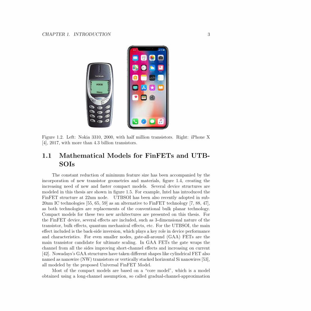
The main factor of the rapidly increasing impact of semiconductor industry is theconstant transistor miniaturization. The minimum feature size has been reduced overthree order of magnitude since the 60’s, as shown in figure 1.1, reaching the nanoscaleregime in the past few years [30]. The ever-increasing density of transistors per chip,called Moore’s Law [56], has allowed the constant addition of new functionality underthe same footprint of semiconductor. In the same direction, each new generation ofscaled-down transistors could actually perform better and better, called Dennard’sLaw [20], leading to faster products or designs where energy is better utilized. Tounderstand the impact of semiconductor scaling in our lives, let’s compare two familiarproducts shown in figure 1.2: the Nokia 3310 and the iPhone X [4]. The Nokia 3310,a popular phone of the year 2000, used an ARM7TDMI processor with a minimumfeature transistor size of 1µm, approximately. It contained around half a milliontransistors with a die size of 68.51mm2. The phone was quite simple, it used GSMmobile technology, it had a 84x84 pixel pure monochrome display, and, off course,it had the popular Snake II game. 17 years later, the iPhone X was launched [4].It uses an Apple A11 Bionic chip, with a minimum feature transistor size of 10nm.It contains over 4.3 billions transistor with a die size of 87.66mm2. This phone is
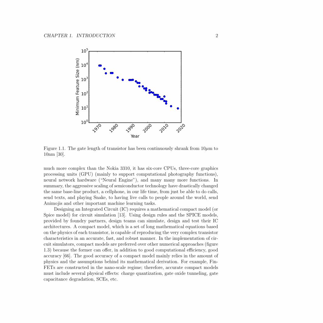
CHAPTER 1. INTRODUCTION 2
Figure 1.1. The gate length of transistor has been continuously shrank from 10µm to10nm [30].
much more complex than the Nokia 3310, it has six-core CPUs, three-core graphicsprocessing units (GPU) (mainly to support computational photography functions),neural network hardware (“Neural Engine”), and many many more functions. Insummary, the aggressive scaling of semiconductor technology have drastically changedthe same base-line product, a cellphone, in our life time, from just be able to do calls,send texts, and playing Snake, to having live calls to people around the world, sendAnimojis and other important machine learning tasks.
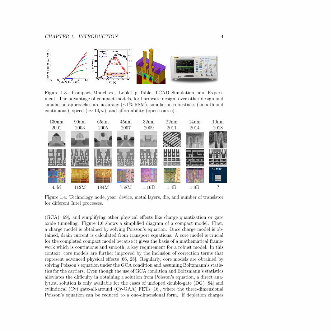
Designing an Integrated Circuit (IC) requires a mathematical compact model (orSpice model) for circuit simulation [13]. Using design rules and the SPICE models,provided by foundry partners, design teams can simulate, design and test their ICarchitectures. A compact model, which is a set of long mathematical equations basedon the physics of each transistor, is capable of reproducing the very complex transistorcharacteristics in an accurate, fast, and robust manner. In the implementation of cir-cuit simulators, compact models are preferred over other numerical approaches (figure1.3) because the former can offer, in addition to good computational efficiency, goodaccuracy [66]. The good accuracy of a compact model mainly relies in the amount ofphysics and the assumptions behind its mathematical derivation. For example, Fin-FETs are constructed in the nano-scale regime; therefore, accurate compact modelsmust include several physical effects: charge quantization, gate oxide tunneling, gatecapacitance degradation, SCEs, etc.
CHAPTER 1. INTRODUCTION 3
Figure 1.2. Left: Nokia 3310, 2000, with half million transistors. Right: iPhone X[4], 2017, with more than 4.3 billion transistors.
1.1 Mathematical Models for FinFETs and UTB-
SOIs
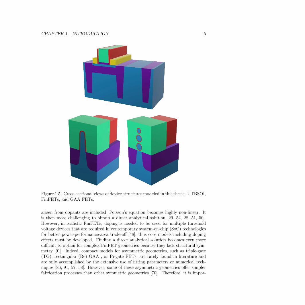
The constant reduction of minimum feature size has been accompanied by theincorporation of new transistor geometries and materials, figure 1.4, creating theincreasing need of new and faster compact models. Several device structures aremodeled in this thesis are shown in figure 1.5. For example, Intel has introduced theFinFET structure at 22nm node. UTBSOI has been also recently adopted in sub-20nm IC technologies [55, 65, 59] as an alternative to FinFET technology [7, 88, 47],as both technologies are replacements of the conventional bulk planar technology.Compact models for these two new architectures are presented on this thesis. Forthe FinFET device, several effects are included, such as 3-dimensional nature of thetransistor, bulk effects, quantum mechanical effects, etc. For the UTBSOI, the maineffect included is the back-side inversion, which plays a key role in device performanceand characteristics. For even smaller nodes, gate-all-around (GAA) FETs are themain transistor candidate for ultimate scaling. In GAA FETs the gate wraps thechannel from all the sides improving short-channel effects and increasing on current[42]. Nowadays’s GAA structures have taken different shapes like cylindrical FET alsonamed as nanowire (NW) transistors or vertically stacked horizontal Si nanowires [53],all modeled by the proposed Universal FinFET Model.
Most of the compact models are based on a “core model”, which is a modelobtained using a long-channel assumption, so called gradual-channel-approximation
CHAPTER 1. INTRODUCTION 4
Figure 1.3. Compact Model vs.: Look-Up Table, TCAD Simulation, and Experi-ment. The advantage of compact models, for hardware design, over other design andsimulation approaches are accuracy (∼1% RSM), simulation robustness (smooth andcontinuous), speed ( ∼ 10µs), and affordability (open source).
130nm 90nm 65nm 45nm 32nm 22nm 14nm 10nm2001 2003 2005 2007 2009 2011 2014 2018
45M 112M 184M 758M 1.16B 1.4B 1.9B ?
Figure 1.4. Technology node, year, device, metal layers, die, and number of transistorfor different Intel processes.
(GCA) [69], and simplifying other physical effects like charge quantization or gateoxide tunneling. Figure 1.6 shows a simplified diagram of a compact model. First,a charge model is obtained by solving Poisson’s equation. Once charge model is ob-tained, drain current is calculated from transport equations. A core model is crucialfor the completed compact model because it gives the basis of a mathematical frame-work which is continuous and smooth, a key requirement for a robust model. In thiscontext, core models are further improved by the inclusion of correction terms thatrepresent advanced physical effects [66, 28]. Regularly, core models are obtained bysolving Poisson’s equation under the GCA condition and assuming Boltzmann’s statis-tics for the carriers. Even though the use of GCA condition and Boltzmann’s statisticsalleviates the difficulty in obtaining a solution from Poisson’s equation, a direct ana-lytical solution is only available for the cases of undoped double-gate (DG) [84] andcylindrical (Cy) gate-all-around (Cy-GAA) FETs [16], where the three-dimensionalPoisson’s equation can be reduced to a one-dimensional form. If depletion charges
CHAPTER 1. INTRODUCTION 5
Figure 1.5. Cross-sectional views of device structures modeled in this thesis: UTBSOI,FinFETs, and GAA FETs.
arisen from dopants are included, Poisson’s equation becomes highly non-linear. Itis then more challenging to obtain a direct analytical solution [29, 54, 28, 51, 50].However, in realistic FinFETs, doping is needed to be used for multiple thresholdvoltage devices that are required in contemporary system-on-chip (SoC) technologiesfor better power-performance-area trade-off [48], thus core models including dopingeffects must be developed. Finding a direct analytical solution becomes even moredifficult to obtain for complex FinFET geometries because they lack structural sym-metry [91]. Indeed, compact models for asymmetric geometries, such as triple-gate(TG), rectangular (Re) GAA , or Pi-gate FETs, are rarely found in literature andare only accomplished by the extensive use of fitting parameters or numerical tech-niques [86, 91, 57, 58]. However, some of these asymmetric geometries offer simplerfabrication processes than other symmetric geometries [70]. Therefore, it is impor-
CHAPTER 1. INTRODUCTION 6
Dimensions,
boundariersconditions,
materials
Compact ModelCharge Model
Poisson’sequation,
obtaincharge
Current ModelTransportequation
using Charge
Model
Charges
Currents
Figure 1.6. Simplified flow of a compact model development.
tant to develop a physical-based core model for FinFETs with complex geometry, forcomprehensive understanding and circuit design.
1.2 Negative Capacitances FETs
As the semiconductor industry is reaching extremely small features, Moore’sLaw [56] and Dennard’s Law [20] have been coming to an end, creating the need ofnew transistor concepts. This is the reason why we are all very familiar with theidea that one of the industry’s biggest concern today is about power consumptionand one of the best way is to reduce the power supply voltage VDD because poweris proportional to V 2
DD squared. Figure 1.7 shows the subthreshold characteristicof different device technologies. The last generation of planar transistors have ap-proximately 100mV/dec of subthreshold swing. FinFET significantly improves thesubthreshold swing; indeed, today a FinFET technology gets very close to the the-oretical 60mV/dec of swing. However, the entire industry need to reduce the VDDeven further. It would be great to reduce the subthreshold swing to be lower thanthe 60mV/dec; even further, an amplification of the current in the strong bias con-dition is needed to obtain a good Ion while using much lower VDD. In other words,a transistor with the capability of amplifying the gate voltage is needed, i.e., whena voltage of 0.5V is applied to the gate, the channel will see 0.7V volt and the totalcurrent in all regimes is amplified. One promising way to do this amplification isusing Negative-Capacitance FET [80, 10], where a conventional transistor structureis changed by including a ferroelectric (FE) material in the gate stack. NC-FETs arequickly emerging as promising devices to achieve sub-60 mV/decade sub-thresholdslope and high Ion [80, 10] to further continue Moore’s Law [56] and Dennard’s Law[20] for few node more. NC transistor structure is shown in figure 1.8. Under thegate metal there is a ferroelectric material, in this case, hafnium zirconium oxide. Itseats on an interfacial oxide and that sits on the silicon substrate. Hafnium zirco-nium oxide is an acceptable or safe material to use in the IC fabs. Hafnium oxide isa standard material used today as a high-K dielectric; then, by doping it with somezirconium (or other doping that can achieve the same result) it is possible to make
CHAPTER 1. INTRODUCTION 7
Figure 1.7. Subthreshold characteristic of different device technologies. Devices withSub 60mV/dec are needed for further VDD scaling.
the Hafnium zirconium oxide ferroelectric [62, 61, 60]. A ferroelectric characteristicis shown in figure 1.9 The slope of figure 1.9 represents the capacitance of the fer-roelectric material. In the middle region, as voltage is increased charge decreases;therefore, the ferroelectric is in the negative capacitance regime. This characteristicis the one that Professor Salahuddin [80] used to propose the negative capacitanceconcept. The amount of people that work on this concept keeps growing year by yearand new advances have been reported. In IEDM 2017, Globalfoundries is presentingtheir NC-FinFETs using standard FinFET fabrication [9]. The working principleof a NC transistor can be simply explained using a two capacitor network. The topcapacitor is the one having the ferroelectric material, hafnium zirconium oxide, calledCFE. The bottom capacitor Cmos is the conventional MOS transistor, where the start-ing point of the Cmos capacitor is at the interface of the hafnium zirconium oxide andthe interfacial oxide, and the end point is the channel capacitance itself, includingthe transistor channel-body capacitance all together. Having two capacitors in series,what determines the voltage at that interface interfacial oxide and ferroelectric is thevoltage divider:
VINT =CFE
CFE + CMOS
VG (1.1)
Since CFE < 0, we can obtain a total voltage amplification. This is what cangive us a swing better than 60mV/dec, even more, an amplification in the stronginversion as well. Figure 1.10 shows results from IEDM 2015 where this concept has
CHAPTER 1. INTRODUCTION 8
Figure 1.8. Negative Capacitance transistor structure in a conventional planar tech-nology. Ferroelectric material is between interficial layer and metal gate.
Figure 1.9. Charge as a function of ferroelectric voltage from Landau-DevonshireTheory of Ferroelectrics. Slope represents capacitance sign.
been already measure experimentally. This thesis goal is to present different devicesimulation and compact models for the NC-FinFETs. Using them, details of theworking principles of NC-FETs can be understood and simulated.
CHAPTER 1. INTRODUCTION 9
Figure 1.10. NC-FinFET versus base-line FinFET. Sub 60mV/dec is obtained usingthe NC-FinFET structure [46, 38].
10
Chapter 2
Model for Double-Gate FinFETs
2.1 Introduction
The core model used in previous versions of BSIM-CMG was based on a solutionof Poisson’s equation for a long-channel double-gate FinFET, assuming a finite dopingin the channel to mimic the doped channels currently used in FinFET fabrication[48]. It is challenging to obtain a direct analytical solution of the Poisson equation ofdoped FinFETs due to the high non-linearity of the equation; therefore, to overcomethis limitation, perturbation approach was used to approximately solve the Poisson’sequation in the presence of body doping [29, 28]. The work presented in this chaptershows improvements from models in [29, 28], and the final implementation of theproposed code is implemented in Verilog-A code for the BSIM-CMG108 version [1].
Figure 2.1 shows a 2-D cross-section of a double-gate FinFET which is beingused as a reference for the model derivation. Poisson’s equation, assuming gradualchannel approximation (GCA), Boltzmann’s distribution for the inversion carriers,and considering only mobile carries (e.g. electrons in an NMOS FinFET), can beexpressed as:
∂2ψ (x, y)
∂x2=
q
εch
(
nieψ(x,y)−ψB−Vch(y)
Vtm +Nch
)
(2.1)
where ψ(x, y) is the electrostatic potential in the channel, q is the magnitude ofthe electronic charge, ni is the intrinsic carrier concentration, εch is the dielectricconstant of the channel (fin), Vtm is the thermal voltage given by kBT/q, where kBand T are the Boltzmann constant and the temperature, respectively; Vch is thequasi-Fermi potential of the channel (Vch(0) =Vs and Vch(L) =Vd) which only hasa y spacial dependence, Nch is the channel doping, and ψB=Vtmln (Nch/ni ) . Notethat equation (2.1) is a 1-dimensional Poisson equation, the other two dimensionshave been neglected due the long length of the channel (GCA condition) and thesymmetry of the double-gate structure in the z direction. In other FinFET geometries,
CHAPTER 2. MODEL FOR DOUBLE-GATE FINFETS 11
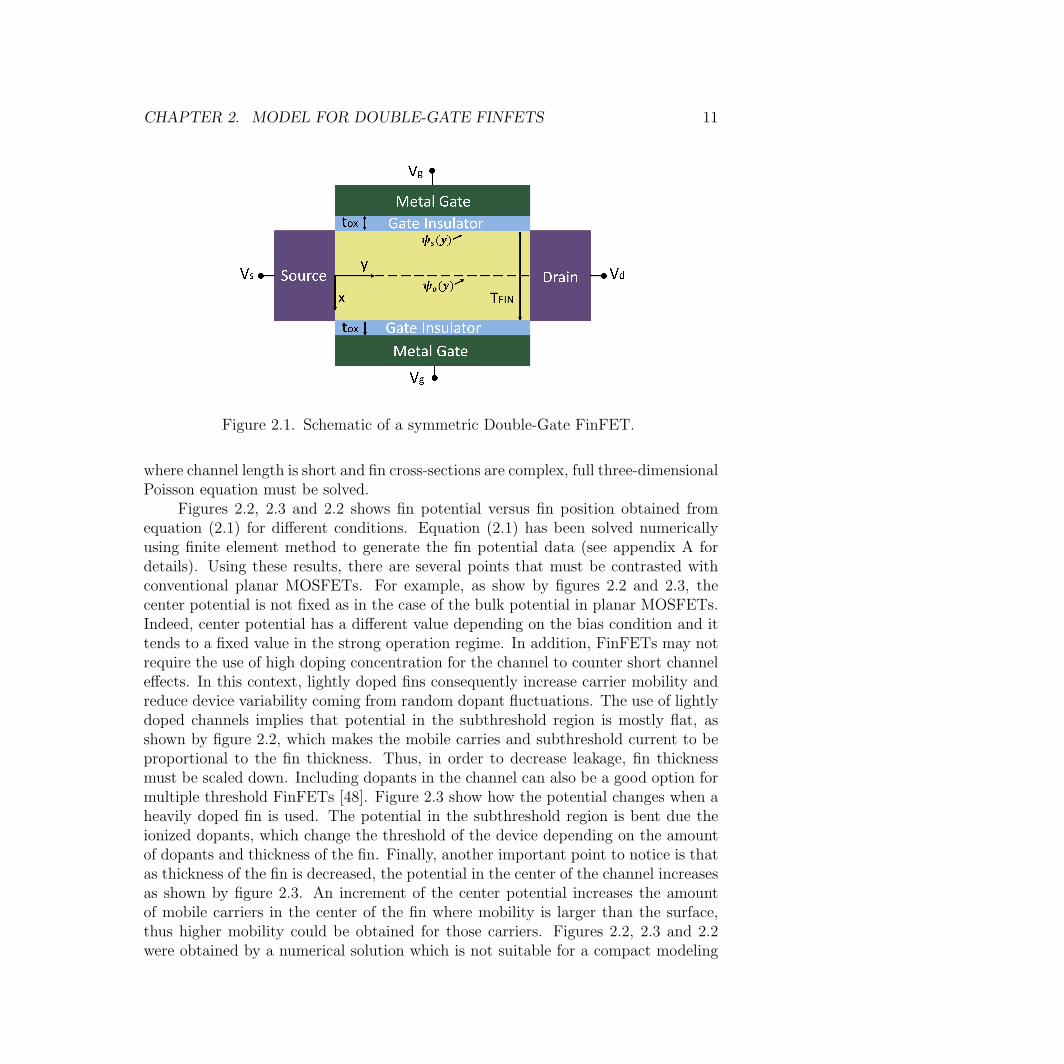
Figure 2.1. Schematic of a symmetric Double-Gate FinFET.
where channel length is short and fin cross-sections are complex, full three-dimensionalPoisson equation must be solved.
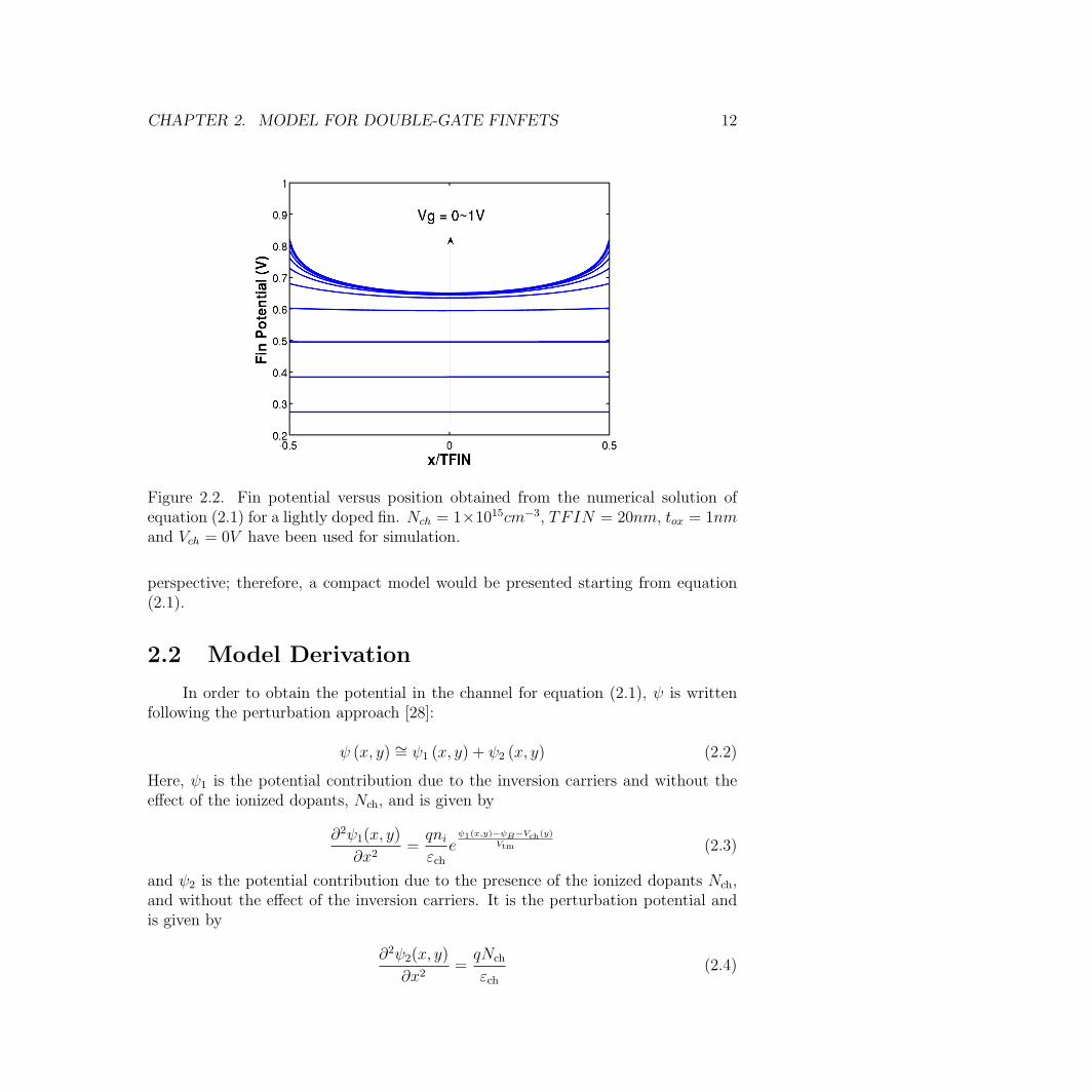
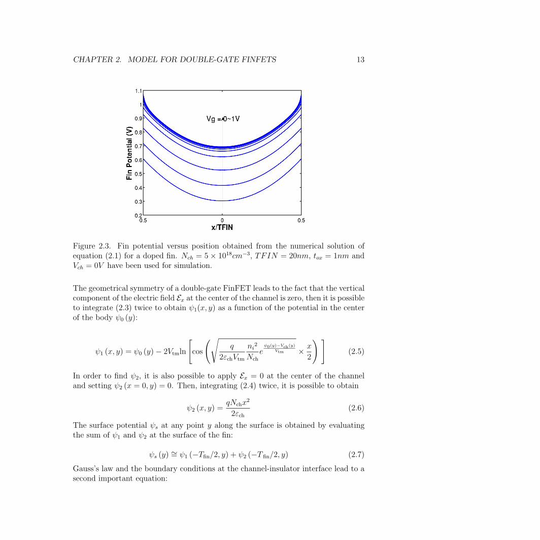
Figures 2.2, 2.3 and 2.2 shows fin potential versus fin position obtained fromequation (2.1) for different conditions. Equation (2.1) has been solved numericallyusing finite element method to generate the fin potential data (see appendix A fordetails). Using these results, there are several points that must be contrasted withconventional planar MOSFETs. For example, as show by figures 2.2 and 2.3, thecenter potential is not fixed as in the case of the bulk potential in planar MOSFETs.Indeed, center potential has a different value depending on the bias condition and ittends to a fixed value in the strong operation regime. In addition, FinFETs may notrequire the use of high doping concentration for the channel to counter short channeleffects. In this context, lightly doped fins consequently increase carrier mobility andreduce device variability coming from random dopant fluctuations. The use of lightlydoped channels implies that potential in the subthreshold region is mostly flat, asshown by figure 2.2, which makes the mobile carries and subthreshold current to beproportional to the fin thickness. Thus, in order to decrease leakage, fin thicknessmust be scaled down. Including dopants in the channel can also be a good option formultiple threshold FinFETs [48]. Figure 2.3 show how the potential changes when aheavily doped fin is used. The potential in the subthreshold region is bent due theionized dopants, which change the threshold of the device depending on the amountof dopants and thickness of the fin. Finally, another important point to notice is thatas thickness of the fin is decreased, the potential in the center of the channel increasesas shown by figure 2.3. An increment of the center potential increases the amountof mobile carriers in the center of the fin where mobility is larger than the surface,thus higher mobility could be obtained for those carriers. Figures 2.2, 2.3 and 2.2were obtained by a numerical solution which is not suitable for a compact modeling
CHAPTER 2. MODEL FOR DOUBLE-GATE FINFETS 12
Figure 2.2. Fin potential versus position obtained from the numerical solution ofequation (2.1) for a lightly doped fin. Nch = 1×1015cm−3, TFIN = 20nm, tox = 1nmand Vch = 0V have been used for simulation.
perspective; therefore, a compact model would be presented starting from equation(2.1).
2.2 Model Derivation
In order to obtain the potential in the channel for equation (2.1), ψ is writtenfollowing the perturbation approach [28]:
ψ (x, y) ∼= ψ1 (x, y) + ψ2 (x, y) (2.2)
Here, ψ1 is the potential contribution due to the inversion carriers and without theeffect of the ionized dopants, Nch, and is given by
∂2ψ1(x, y)
∂x2=qniεch
eψ1(x,y)−ψB−Vch(y)
Vtm (2.3)
and ψ2 is the potential contribution due to the presence of the ionized dopants Nch,and without the effect of the inversion carriers. It is the perturbation potential andis given by
∂2ψ2(x, y)
∂x2=qNch
εch(2.4)
CHAPTER 2. MODEL FOR DOUBLE-GATE FINFETS 13
Figure 2.3. Fin potential versus position obtained from the numerical solution ofequation (2.1) for a doped fin. Nch = 5× 1018cm−3, TFIN = 20nm, tox = 1nm andVch = 0V have been used for simulation.
The geometrical symmetry of a double-gate FinFET leads to the fact that the verticalcomponent of the electric field Ex at the center of the channel is zero, then it is possibleto integrate (2.3) twice to obtain ψ1(x, y) as a function of the potential in the centerof the body ψ0 (y):
ψ1 (x, y) = ψ0 (y)− 2Vtmln
[
cos
(√
q
2εchVtm
ni2
Nch
eψ0(y)−Vch(y)
Vtm × x
2
) ]
(2.5)
In order to find ψ2, it is also possible to apply Ex = 0 at the center of the channeland setting ψ2 (x = 0, y) = 0. Then, integrating (2.4) twice, it is possible to obtain
ψ2 (x, y) =qNchx
2
2εch(2.6)
The surface potential ψs at any point y along the surface is obtained by evaluatingthe sum of ψ1 and ψ2 at the surface of the fin:
ψs (y) ∼= ψ1 (−Tfin/2, y) + ψ2 (−T fin/2, y) (2.7)
Gauss’s law and the boundary conditions at the channel-insulator interface lead to asecond important equation:
CHAPTER 2. MODEL FOR DOUBLE-GATE FINFETS 14
Figure 2.4. Fin potential versus position obtained from the numerical solution ofequation (2.1) for different fin thickness at strong inversion bias. Nch = 1×1015cm−3,Vch = 0V , TFIN = 20nm, tox = 1nm and Vg = 1V have been used for simulation.As TFIN decreases, center potential increases, which increases the number of mobilecarriers in the center of the fin.
Vgs = Vfb + ψs (y) + εchExs/Cox (2.8)
where Vgs is the gate voltage, Vfb is the flat-band voltage, Cox is the gate oxidecapacitance per unit area, given by εox/Tox, where εox and Tox are the oxide dielectricconstant and oxide thickness, respectively, Exs is the vertical component of the electricfield at the surface, which can be obtained by integrating (2.1):
Exs =√
2qniεch
[
Vtm
(
eψs(y)Vtm − e
ψ0(y)Vtm
)
e−ψB−Vch(y)
Vtm + eψBVtm (ψs (y)− ψ0 (y))
]
(2.9)
Equations (2.7) and (2.8) represent a self-consistent system of equations thatcan be used to obtain ψ0 and ψs. However, through a change of variable, given by
β =
√
q
2ǫchVtm
n2i
Nch
eψ0−VchVtm
TFIN2
(2.10)
equations (2.7) and (2.8) can be written as a single equation:
CHAPTER 2. MODEL FOR DOUBLE-GATE FINFETS 15
f (β) ≡ ln (β) − ln (cos (β) )− Vgs−Vfb−V ch
2Vtm+ ln
(
2Tfin
√
2εchVtmNch
qni2
)
+ 2εchTfinCox
√
√
√
√β2
(
e
ψpertVtm
cos2(β)− 1
)
+ ψpert
Vtm2 [ψpert − 2V tmln (cos (β) )] = 0(2.11)
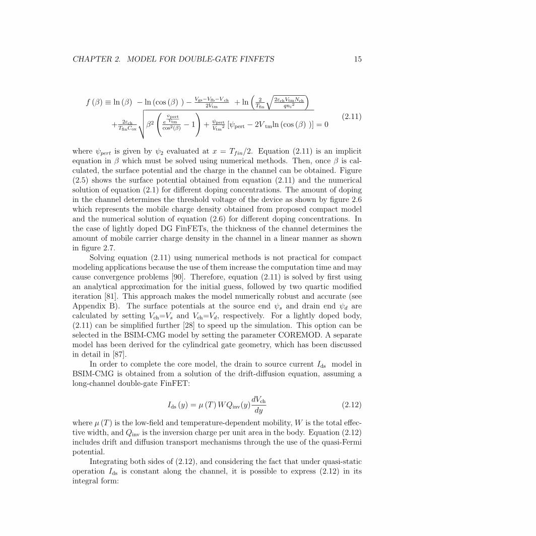
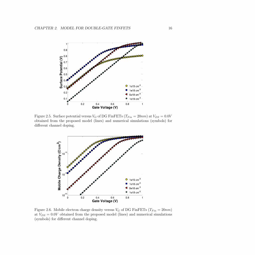
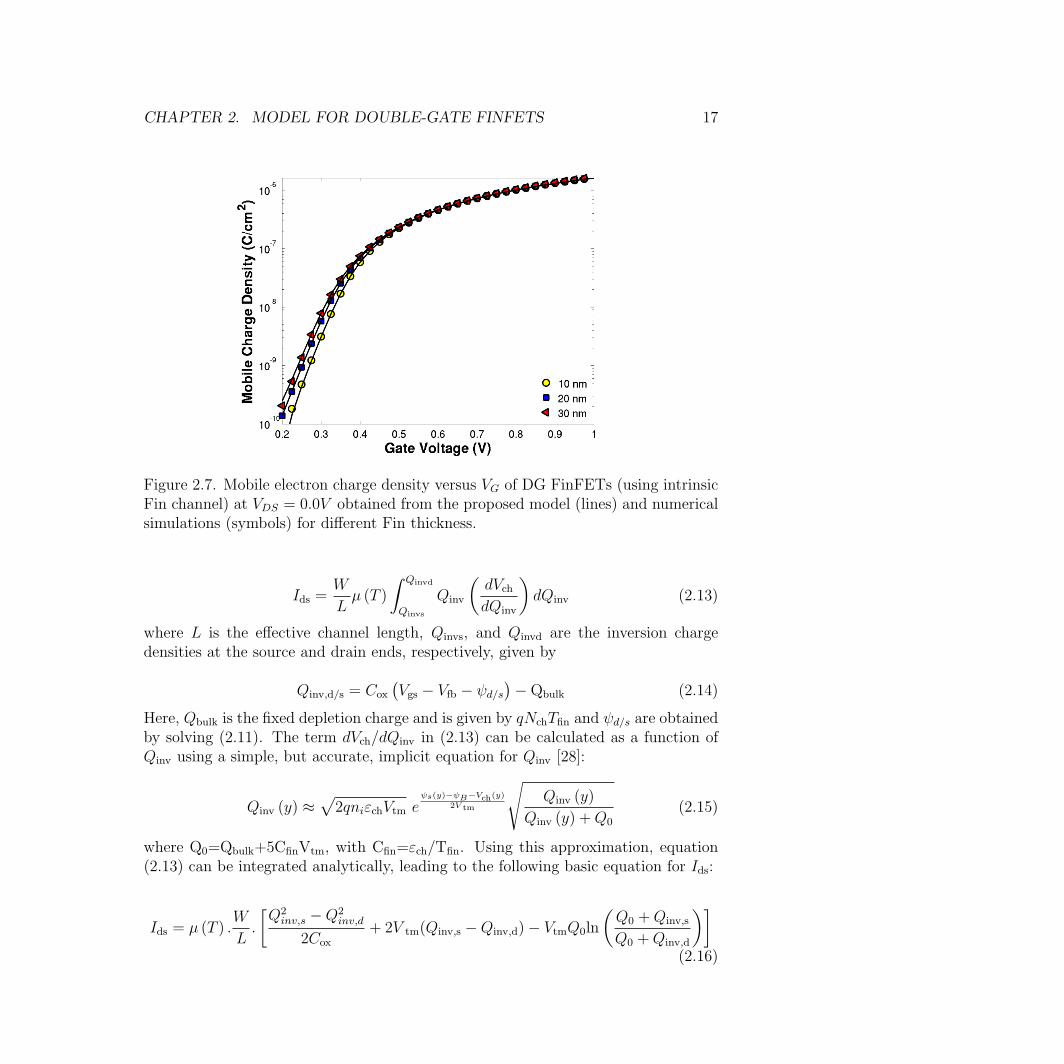
where ψpert is given by ψ2 evaluated at x = Tfin/2. Equation (2.11) is an implicitequation in β which must be solved using numerical methods. Then, once β is cal-culated, the surface potential and the charge in the channel can be obtained. Figure(2.5) shows the surface potential obtained from equation (2.11) and the numericalsolution of equation (2.1) for different doping concentrations. The amount of dopingin the channel determines the threshold voltage of the device as shown by figure 2.6which represents the mobile charge density obtained from proposed compact modeland the numerical solution of equation (2.6) for different doping concentrations. Inthe case of lightly doped DG FinFETs, the thickness of the channel determines theamount of mobile carrier charge density in the channel in a linear manner as shownin figure 2.7.
Solving equation (2.11) using numerical methods is not practical for compactmodeling applications because the use of them increase the computation time and maycause convergence problems [90]. Therefore, equation (2.11) is solved by first usingan analytical approximation for the initial guess, followed by two quartic modifiediteration [81]. This approach makes the model numerically robust and accurate (seeAppendix B). The surface potentials at the source end ψs and drain end ψd arecalculated by setting Vch=Vs and Vch=Vd, respectively. For a lightly doped body,(2.11) can be simplified further [28] to speed up the simulation. This option can beselected in the BSIM-CMG model by setting the parameter COREMOD. A separatemodel has been derived for the cylindrical gate geometry, which has been discussedin detail in [87].
In order to complete the core model, the drain to source current Ids model inBSIM-CMG is obtained from a solution of the drift-diffusion equation, assuming along-channel double-gate FinFET:
Ids (y) = µ (T )WQinv(y)dVchdy
(2.12)
where µ (T ) is the low-field and temperature-dependent mobility, W is the total effec-tive width, and Qinv is the inversion charge per unit area in the body. Equation (2.12)includes drift and diffusion transport mechanisms through the use of the quasi-Fermipotential.
Integrating both sides of (2.12), and considering the fact that under quasi-staticoperation Ids is constant along the channel, it is possible to express (2.12) in itsintegral form:
CHAPTER 2. MODEL FOR DOUBLE-GATE FINFETS 16
Figure 2.5. Surface potential versus VG of DG FinFETs (TFin = 20nm) at VDS = 0.0Vobtained from the proposed model (lines) and numerical simulations (symbols) fordifferent channel doping.
Figure 2.6. Mobile electron charge density versus VG of DG FinFETs (TFin = 20nm)at VDS = 0.0V obtained from the proposed model (lines) and numerical simulations(symbols) for different channel doping.
CHAPTER 2. MODEL FOR DOUBLE-GATE FINFETS 17
Figure 2.7. Mobile electron charge density versus VG of DG FinFETs (using intrinsicFin channel) at VDS = 0.0V obtained from the proposed model (lines) and numericalsimulations (symbols) for different Fin thickness.
Ids =W
Lµ (T )
∫ Qinvd
Qinvs
Qinv
(
dVchdQinv
)
dQinv (2.13)
where L is the effective channel length, Qinvs, and Qinvd are the inversion chargedensities at the source and drain ends, respectively, given by
Qinv,d/s = Cox
(
Vgs − Vfb − ψd/s)
−Qbulk (2.14)
Here, Qbulk is the fixed depletion charge and is given by qNchTfin and ψd/s are obtainedby solving (2.11). The term dVch/dQinv in (2.13) can be calculated as a function ofQinv using a simple, but accurate, implicit equation for Qinv [28]:
Qinv (y) ≈√
2qniεchVtm eψs(y)−ψB−Vch(y)
2V tm
√
Qinv (y)
Qinv (y) +Q0
(2.15)
where Q0=Qbulk+5CfinVtm, with Cfin=εch/Tfin. Using this approximation, equation(2.13) can be integrated analytically, leading to the following basic equation for Ids:
Ids = µ (T ) .W
L.
[
Q2inv,s −Q2
inv,d
2Cox
+ 2V tm(Qinv,s −Qinv,d)− VtmQ0ln
(
Q0 +Qinv,s
Q0 +Qinv,d
)]
(2.16)
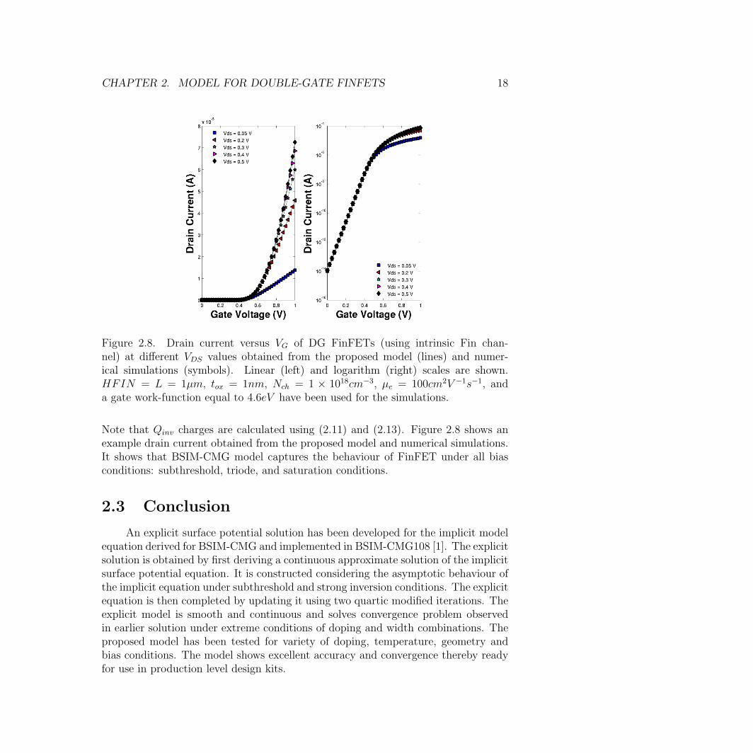
CHAPTER 2. MODEL FOR DOUBLE-GATE FINFETS 18
Figure 2.8. Drain current versus VG of DG FinFETs (using intrinsic Fin chan-nel) at different VDS values obtained from the proposed model (lines) and numer-ical simulations (symbols). Linear (left) and logarithm (right) scales are shown.HFIN = L = 1µm, tox = 1nm, Nch = 1 × 1018cm−3, µe = 100cm2V −1s−1, anda gate work-function equal to 4.6eV have been used for the simulations.
Note that Qinv charges are calculated using (2.11) and (2.13). Figure 2.8 shows anexample drain current obtained from the proposed model and numerical simulations.It shows that BSIM-CMG model captures the behaviour of FinFET under all biasconditions: subthreshold, triode, and saturation conditions.
2.3 Conclusion
An explicit surface potential solution has been developed for the implicit modelequation derived for BSIM-CMG and implemented in BSIM-CMG108 [1]. The explicitsolution is obtained by first deriving a continuous approximate solution of the implicitsurface potential equation. It is constructed considering the asymptotic behaviour ofthe implicit equation under subthreshold and strong inversion conditions. The explicitequation is then completed by updating it using two quartic modified iterations. Theexplicit model is smooth and continuous and solves convergence problem observedin earlier solution under extreme conditions of doping and width combinations. Theproposed model has been tested for variety of doping, temperature, geometry andbias conditions. The model shows excellent accuracy and convergence thereby readyfor use in production level design kits.
19
Chapter 3
Unified FinFET Compact Model
3.1 Introduction
Due to its excellent low power and scaling characteristics, FinFET technology[34] has been adopted in all sub-20nm IC technologies [7, 63, 88, 47] as a replacementof the conventional bulk planar technology. For FinFET transistor technology, theCompact Model Coalition (CMC) has chosen BSIM-CMG [73] as the first and onlyindustry-standard compact model for advanced circuit design. Fast speed, numericalrobustness, and good accuracy of a compact model relies on several factors such asthe amount of physics in the model or the kind of algorithm used to solve the phys-ical equations. BSIM-CMG compact model includes several physical effects [73, 13]:device geometry effects, charge quantization, gate oxide tunneling, gate capacitancedegradation, short-channel effects, etc. It can be used to model different structuresas those shown in figure 3.1. Figure 3.2 shows a general diagram of BSIM-CMG com-pact model. The compact model must be able to calculate terminal (drain, source,gate, bulk/back) currents and charges, which are then utilized by circuit simulatorengines to solve a complete circuit under various analyses such as dc, ac, or transient.Terminal voltages are taken as electrical inputs for the compact model (Figure 3.2);thereafter, the model calculates the charge density in the channel of the simulatedtransistor, part that also requires threshold voltage (VTH) and subhtreshold-swing(SS) calculations. After charge densities are calculated, these quantities are used bythe transport model to obtain charge currents for each terminal. The terminal chargemodel assigns total charge quantities to each terminal, based on the charge densityacross the device [73]. The following sections are intended to give a background foun-dation of the new compact models for charge and current modeling that complementthe current features of BSIM-CMG [73, 13].
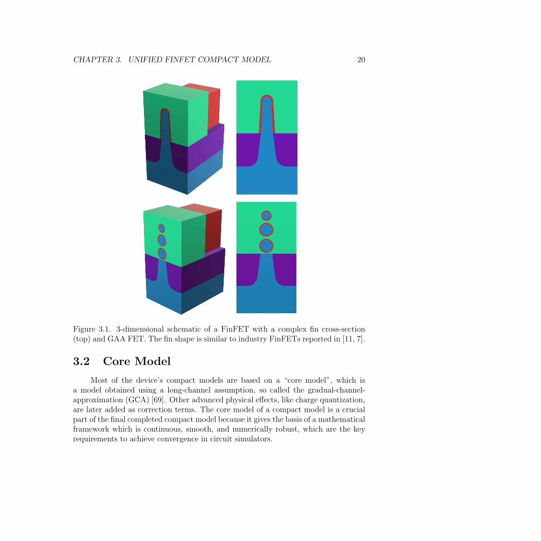
CHAPTER 3. UNIFIED FINFET COMPACT MODEL 20
Figure 3.1. 3-dimensional schematic of a FinFET with a complex fin cross-section(top) and GAA FET. The fin shape is similar to industry FinFETs reported in [11, 7].
3.2 Core Model
Most of the device’s compact models are based on a “core model”, which isa model obtained using a long-channel assumption, so called the gradual-channel-approximation (GCA) [69]. Other advanced physical effects, like charge quantization,are later added as correction terms. The core model of a compact model is a crucialpart of the final completed compact model because it gives the basis of a mathematicalframework which is continuous, smooth, and numerically robust, which are the keyrequirements to achieve convergence in circuit simulators.
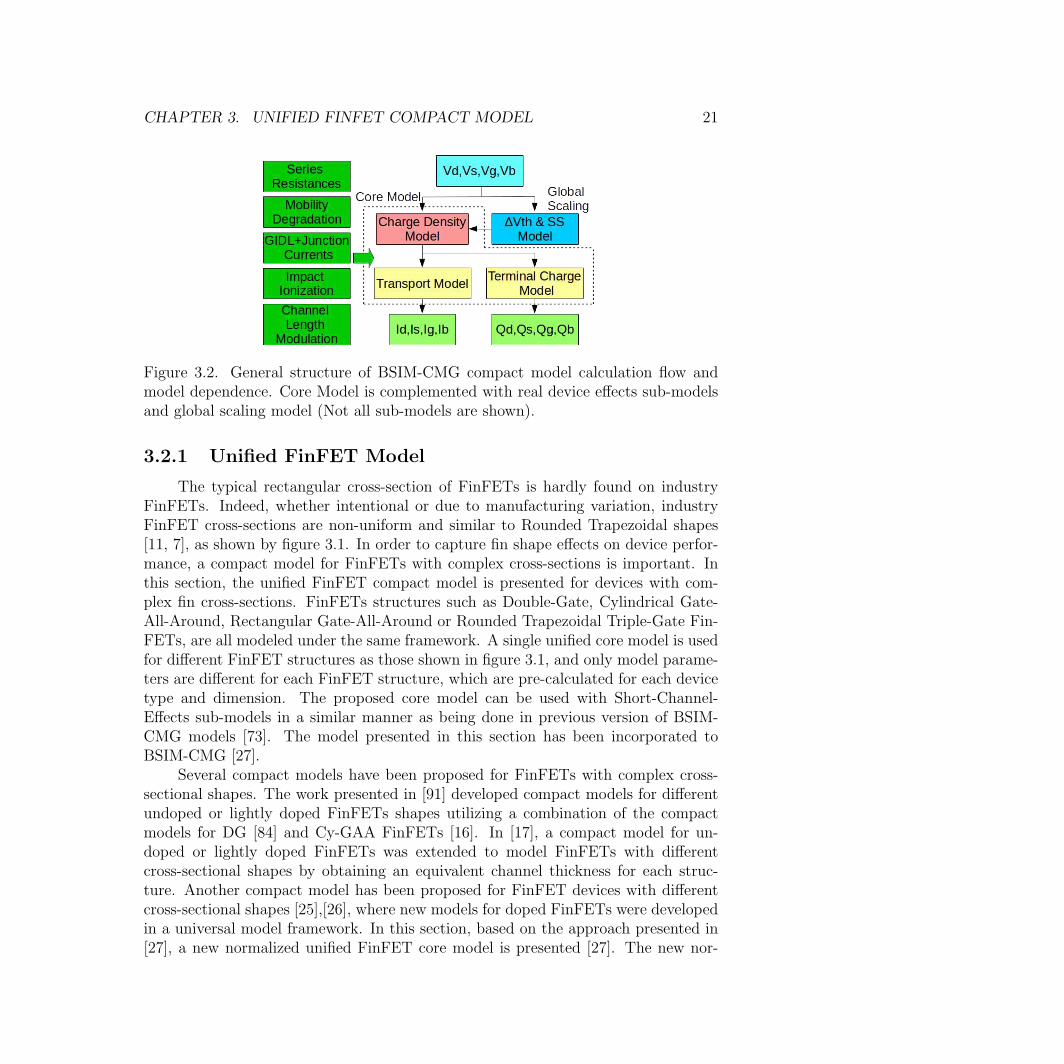
CHAPTER 3. UNIFIED FINFET COMPACT MODEL 21
Figure 3.2. General structure of BSIM-CMG compact model calculation flow andmodel dependence. Core Model is complemented with real device effects sub-modelsand global scaling model (Not all sub-models are shown).
3.2.1 Unified FinFET Model
The typical rectangular cross-section of FinFETs is hardly found on industryFinFETs. Indeed, whether intentional or due to manufacturing variation, industryFinFET cross-sections are non-uniform and similar to Rounded Trapezoidal shapes[11, 7], as shown by figure 3.1. In order to capture fin shape effects on device perfor-mance, a compact model for FinFETs with complex cross-sections is important. Inthis section, the unified FinFET compact model is presented for devices with com-plex fin cross-sections. FinFETs structures such as Double-Gate, Cylindrical Gate-All-Around, Rectangular Gate-All-Around or Rounded Trapezoidal Triple-Gate Fin-FETs, are all modeled under the same framework. A single unified core model is usedfor different FinFET structures as those shown in figure 3.1, and only model parame-ters are different for each FinFET structure, which are pre-calculated for each devicetype and dimension. The proposed core model can be used with Short-Channel-Effects sub-models in a similar manner as being done in previous version of BSIM-CMG models [73]. The model presented in this section has been incorporated toBSIM-CMG [27].
Several compact models have been proposed for FinFETs with complex cross-sectional shapes. The work presented in [91] developed compact models for differentundoped or lightly doped FinFETs shapes utilizing a combination of the compactmodels for DG [84] and Cy-GAA FinFETs [16]. In [17], a compact model for un-doped or lightly doped FinFETs was extended to model FinFETs with differentcross-sectional shapes by obtaining an equivalent channel thickness for each struc-ture. Another compact model has been proposed for FinFET devices with differentcross-sectional shapes [25],[26], where new models for doped FinFETs were developedin a universal model framework. In this section, based on the approach presented in[27], a new normalized unified FinFET core model is presented [27]. The new nor-
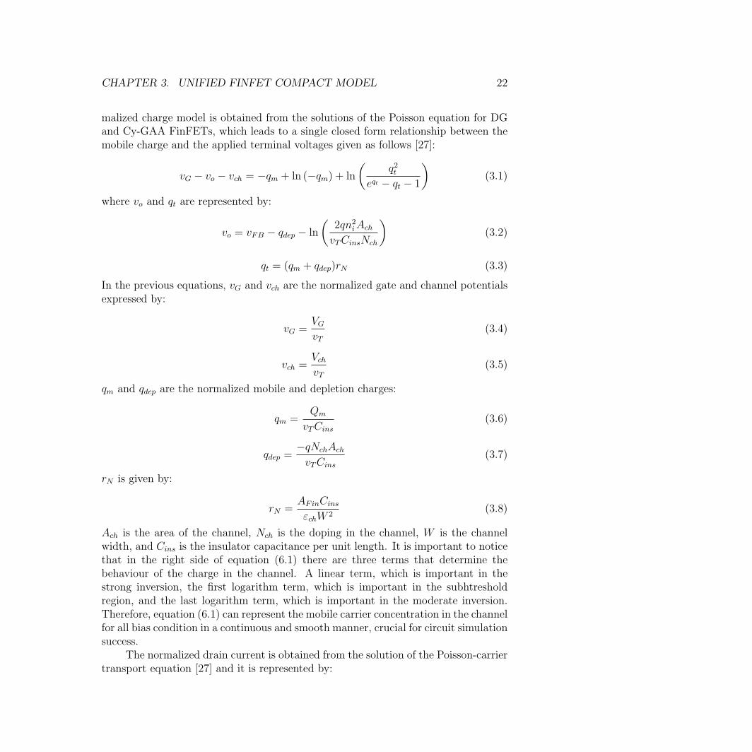
CHAPTER 3. UNIFIED FINFET COMPACT MODEL 22
malized charge model is obtained from the solutions of the Poisson equation for DGand Cy-GAA FinFETs, which leads to a single closed form relationship between themobile charge and the applied terminal voltages given as follows [27]:
vG − vo − vch = −qm + ln (−qm) + ln
(
q2teqt − qt − 1
)
(3.1)
where vo and qt are represented by:
vo = vFB − qdep − ln
(
2qn2iAch
vTCinsNch
)
(3.2)
qt = (qm + qdep)rN (3.3)
In the previous equations, vG and vch are the normalized gate and channel potentialsexpressed by:
vG =VGvT
(3.4)
vch =VchvT
(3.5)
qm and qdep are the normalized mobile and depletion charges:
qm =Qm
vTCins(3.6)
qdep =−qNchAchvTCins
(3.7)
rN is given by:
rN =AFinCinsεchW 2
(3.8)
Ach is the area of the channel, Nch is the doping in the channel, W is the channelwidth, and Cins is the insulator capacitance per unit length. It is important to noticethat in the right side of equation (6.1) there are three terms that determine thebehaviour of the charge in the channel. A linear term, which is important in thestrong inversion, the first logarithm term, which is important in the subhtresholdregion, and the last logarithm term, which is important in the moderate inversion.Therefore, equation (6.1) can represent the mobile carrier concentration in the channelfor all bias condition in a continuous and smooth manner, crucial for circuit simulationsuccess.
The normalized drain current is obtained from the solution of the Poisson-carriertransport equation [27] and it is represented by:
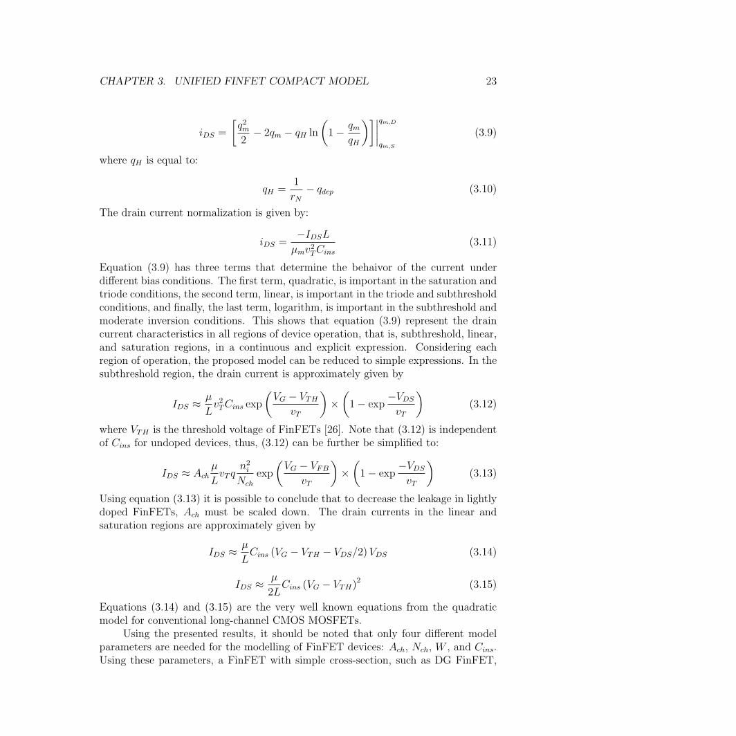
CHAPTER 3. UNIFIED FINFET COMPACT MODEL 23
iDS =
[
q2m2
− 2qm − qH ln
(
1− qmqH
)]∣
∣
∣
∣
qm,D
qm,S
(3.9)
where qH is equal to:
qH =1
rN− qdep (3.10)
The drain current normalization is given by:
iDS =−IDSLµmv2TCins
(3.11)
Equation (3.9) has three terms that determine the behaivor of the current underdifferent bias conditions. The first term, quadratic, is important in the saturation andtriode conditions, the second term, linear, is important in the triode and subthresholdconditions, and finally, the last term, logarithm, is important in the subthreshold andmoderate inversion conditions. This shows that equation (3.9) represent the draincurrent characteristics in all regions of device operation, that is, subthreshold, linear,and saturation regions, in a continuous and explicit expression. Considering eachregion of operation, the proposed model can be reduced to simple expressions. In thesubthreshold region, the drain current is approximately given by
IDS ≈ µ
Lv2TCins exp
(
VG − VTHvT
)
×(
1− exp−VDSvT
)
(3.12)
where VTH is the threshold voltage of FinFETs [26]. Note that (3.12) is independentof Cins for undoped devices, thus, (3.12) can be further be simplified to:
IDS ≈ Achµ
LvT q
n2i
Nch
exp
(
VG − VFBvT
)
×(
1− exp−VDSvT
)
(3.13)
Using equation (3.13) it is possible to conclude that to decrease the leakage in lightlydoped FinFETs, Ach must be scaled down. The drain currents in the linear andsaturation regions are approximately given by
IDS ≈ µ
LCins (VG − VTH − VDS/2)VDS (3.14)
IDS ≈ µ
2LCins (VG − VTH)
2 (3.15)
Equations (3.14) and (3.15) are the very well known equations from the quadraticmodel for conventional long-channel CMOS MOSFETs.
Using the presented results, it should be noted that only four different modelparameters are needed for the modelling of FinFET devices: Ach, Nch, W , and Cins.Using these parameters, a FinFET with simple cross-section, such as DG FinFET,
CHAPTER 3. UNIFIED FINFET COMPACT MODEL 24
Figure 3.3. Drain current versus gate voltage of DG FinFETs at VDS = 0.05V(squares) and VDS = 1V (circles) obtained from the proposed model (lines) and nu-merical simulations (symbols) for three different channel doping: Nch = 1×1014cm−3
(red symbols), Nch = 2× 1018cm−3 (empty symbols), and Nch = 4× 1018cm−3 (bluesymbols). µ = 1470cm2/V s, LG = 1µm, TCH = 15nm, HCH = 40nm, EOT = 1nm,and metal gate work-function equal to 4.6eV have been used.
can be accurately modelled for different channel doping concentrations as shown infigure 3.3. The model parameters used for DG FinFETs are given as follows [27]:
Ach = HFinTFin (3.16)
W = 2HFin (3.17)
Cins =εinsEOT
W (3.18)
Nch (3.19)
A Trapezoidal Triple-Gate FinFET is a good example of a FinFET with a com-plex cross-section. Indeed, the industry transistors reported in [11] and [7] have fincross-sections similar to trapezoidal shapes. The proposed model can be used tomodel these type of devices through the use of the following four model parameters:
Ach = HFin(TFin,top + TFin,base)
2(3.20)
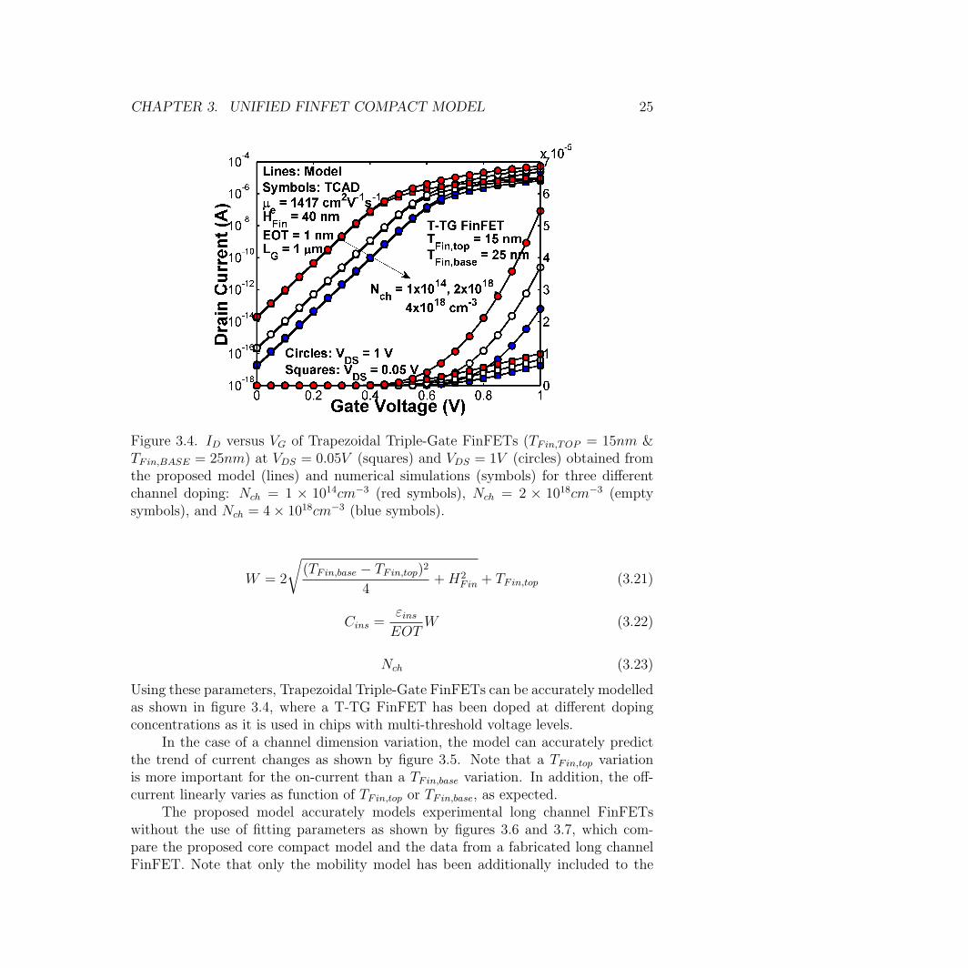
CHAPTER 3. UNIFIED FINFET COMPACT MODEL 25
Figure 3.4. ID versus VG of Trapezoidal Triple-Gate FinFETs (TFin,TOP = 15nm &TFin,BASE = 25nm) at VDS = 0.05V (squares) and VDS = 1V (circles) obtained fromthe proposed model (lines) and numerical simulations (symbols) for three differentchannel doping: Nch = 1 × 1014cm−3 (red symbols), Nch = 2 × 1018cm−3 (emptysymbols), and Nch = 4× 1018cm−3 (blue symbols).
W = 2
√
(TFin,base − TFin,top)2
4+H2
Fin + TFin,top (3.21)
Cins =εinsEOT
W (3.22)
Nch (3.23)
Using these parameters, Trapezoidal Triple-Gate FinFETs can be accurately modelledas shown in figure 3.4, where a T-TG FinFET has been doped at different dopingconcentrations as it is used in chips with multi-threshold voltage levels.
In the case of a channel dimension variation, the model can accurately predictthe trend of current changes as shown by figure 3.5. Note that a TFin,top variationis more important for the on-current than a TFin,base variation. In addition, the off-current linearly varies as function of TFin,top or TFin,base, as expected.
The proposed model accurately models experimental long channel FinFETswithout the use of fitting parameters as shown by figures 3.6 and 3.7, which com-pare the proposed core compact model and the data from a fabricated long channelFinFET. Note that only the mobility model has been additionally included to the
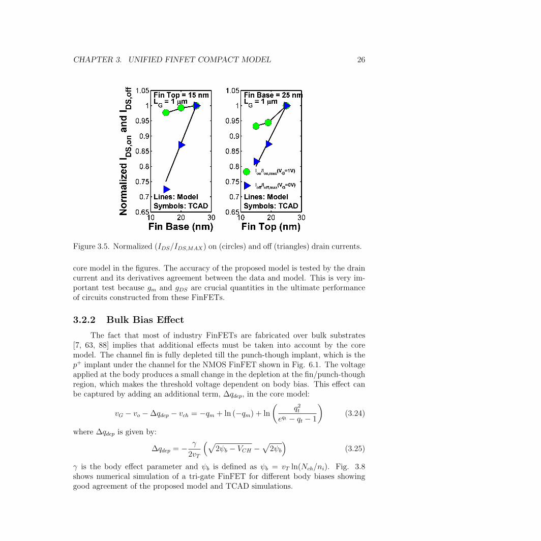
CHAPTER 3. UNIFIED FINFET COMPACT MODEL 26
Figure 3.5. Normalized (IDS/IDS,MAX) on (circles) and off (triangles) drain currents.
core model in the figures. The accuracy of the proposed model is tested by the draincurrent and its derivatives agreement between the data and model. This is very im-portant test because gm and gDS are crucial quantities in the ultimate performanceof circuits constructed from these FinFETs.
3.2.2 Bulk Bias Effect
The fact that most of industry FinFETs are fabricated over bulk substrates[7, 63, 88] implies that additional effects must be taken into account by the coremodel. The channel fin is fully depleted till the punch-though implant, which is thep+ implant under the channel for the NMOS FinFET shown in Fig. 6.1. The voltageapplied at the body produces a small change in the depletion at the fin/punch-thoughregion, which makes the threshold voltage dependent on body bias. This effect canbe captured by adding an additional term, ∆qdep, in the core model:
vG − vo −∆qdep − vch = −qm + ln (−qm) + ln
(
q2teqt − qt − 1
)
(3.24)
where ∆qdep is given by:
∆qdep = − γ
2vT
(
√
2ψb − VCH −√
2ψb
)
(3.25)
γ is the body effect parameter and ψb is defined as ψb = vT ln(Nch/ni). Fig. 3.8shows numerical simulation of a tri-gate FinFET for different body biases showinggood agreement of the proposed model and TCAD simulations.
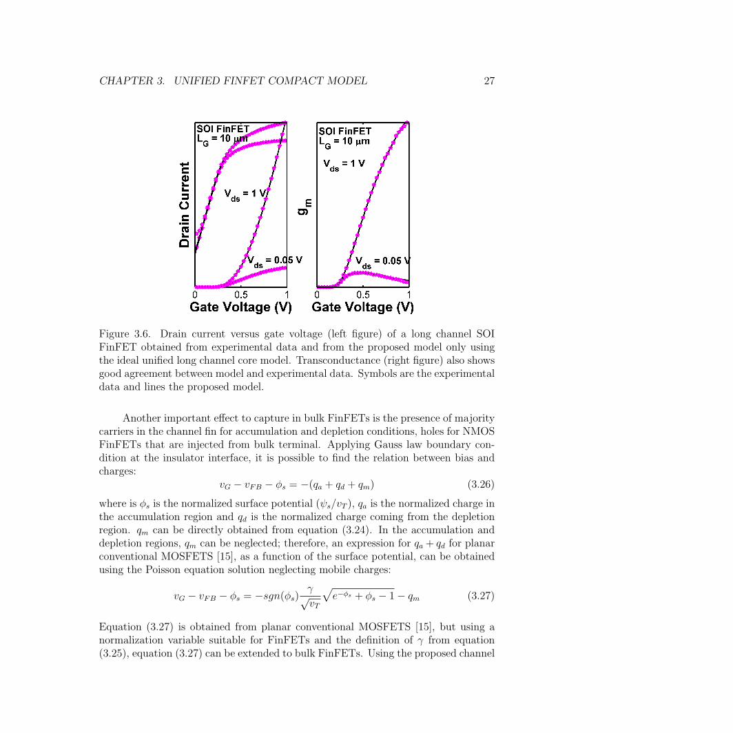
CHAPTER 3. UNIFIED FINFET COMPACT MODEL 27
Figure 3.6. Drain current versus gate voltage (left figure) of a long channel SOIFinFET obtained from experimental data and from the proposed model only usingthe ideal unified long channel core model. Transconductance (right figure) also showsgood agreement between model and experimental data. Symbols are the experimentaldata and lines the proposed model.
Another important effect to capture in bulk FinFETs is the presence of majoritycarriers in the channel fin for accumulation and depletion conditions, holes for NMOSFinFETs that are injected from bulk terminal. Applying Gauss law boundary con-dition at the insulator interface, it is possible to find the relation between bias andcharges:
vG − vFB − φs = −(qa + qd + qm) (3.26)
where is φs is the normalized surface potential (ψs/vT ), qa is the normalized charge inthe accumulation region and qd is the normalized charge coming from the depletionregion. qm can be directly obtained from equation (3.24). In the accumulation anddepletion regions, qm can be neglected; therefore, an expression for qa + qd for planarconventional MOSFETS [15], as a function of the surface potential, can be obtainedusing the Poisson equation solution neglecting mobile charges:
vG − vFB − φs = −sgn(φs)γ√vT
√
e−φs + φs − 1− qm (3.27)
Equation (3.27) is obtained from planar conventional MOSFETS [15], but using anormalization variable suitable for FinFETs and the definition of γ from equation(3.25), equation (3.27) can be extended to bulk FinFETs. Using the proposed channel
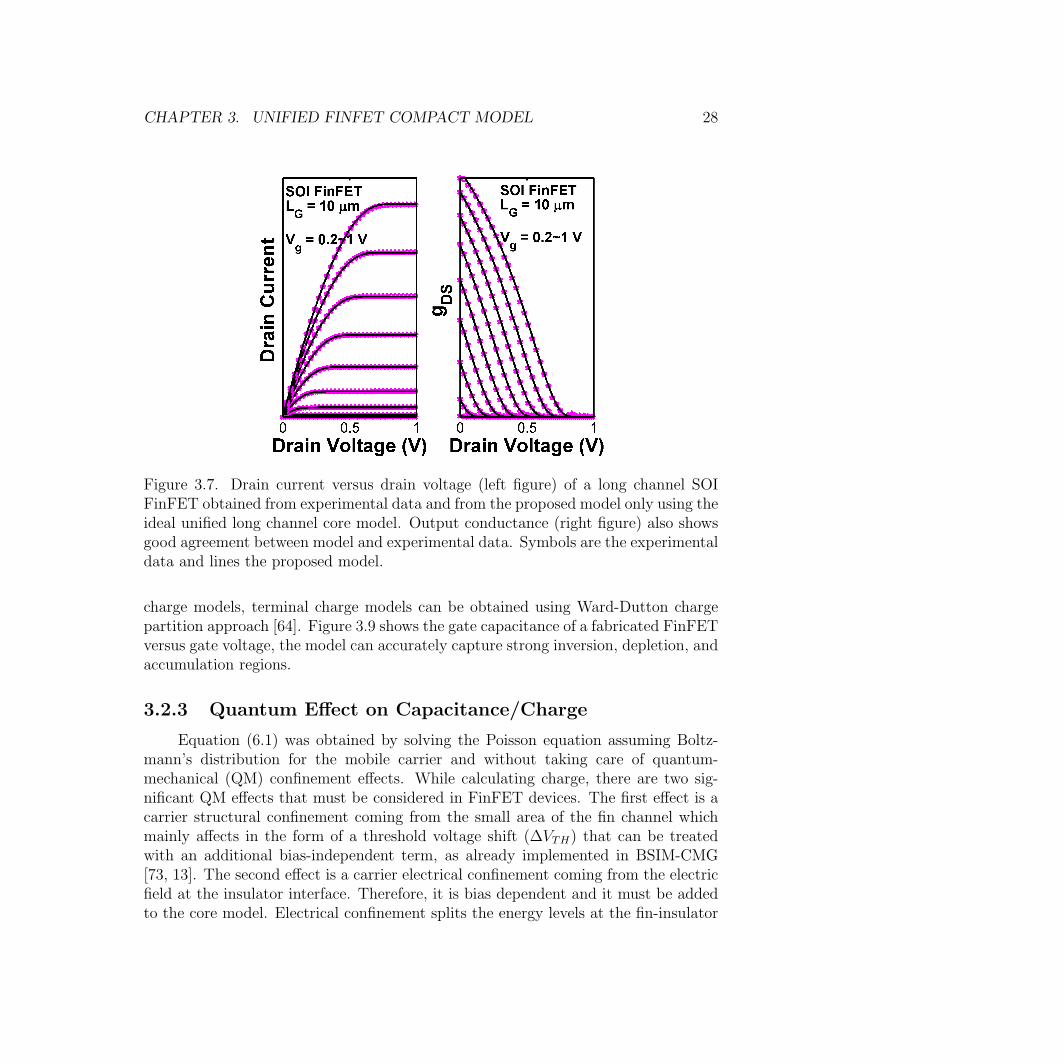
CHAPTER 3. UNIFIED FINFET COMPACT MODEL 28
Figure 3.7. Drain current versus drain voltage (left figure) of a long channel SOIFinFET obtained from experimental data and from the proposed model only using theideal unified long channel core model. Output conductance (right figure) also showsgood agreement between model and experimental data. Symbols are the experimentaldata and lines the proposed model.
charge models, terminal charge models can be obtained using Ward-Dutton chargepartition approach [64]. Figure 3.9 shows the gate capacitance of a fabricated FinFETversus gate voltage, the model can accurately capture strong inversion, depletion, andaccumulation regions.
3.2.3 Quantum Effect on Capacitance/Charge
Equation (6.1) was obtained by solving the Poisson equation assuming Boltz-mann’s distribution for the mobile carrier and without taking care of quantum-mechanical (QM) confinement effects. While calculating charge, there are two sig-nificant QM effects that must be considered in FinFET devices. The first effect is acarrier structural confinement coming from the small area of the fin channel whichmainly affects in the form of a threshold voltage shift (∆VTH) that can be treatedwith an additional bias-independent term, as already implemented in BSIM-CMG[73, 13]. The second effect is a carrier electrical confinement coming from the electricfield at the insulator interface. Therefore, it is bias dependent and it must be addedto the core model. Electrical confinement splits the energy levels at the fin-insulator
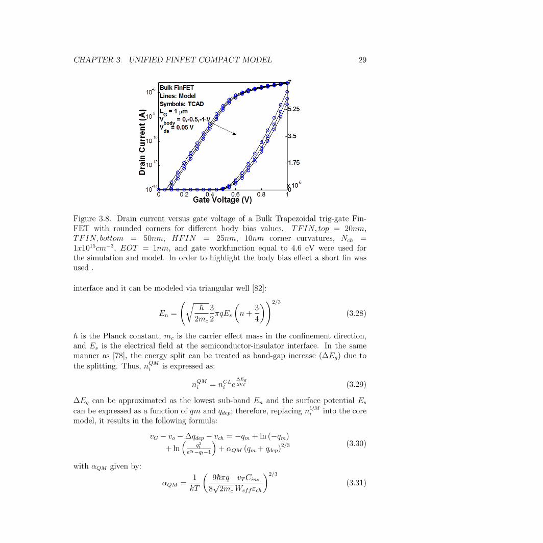
CHAPTER 3. UNIFIED FINFET COMPACT MODEL 29
Figure 3.8. Drain current versus gate voltage of a Bulk Trapezoidal trig-gate Fin-FET with rounded corners for different body bias values. TFIN, top = 20nm,TFIN, bottom = 50nm, HFIN = 25nm, 10nm corner curvatures, Nch =1x1015cm−3, EOT = 1nm, and gate workfunction equal to 4.6 eV were used forthe simulation and model. In order to highlight the body bias effect a short fin wasused .
interface and it can be modeled via triangular well [82]:
En =
(
√
~
2mc
3
2πqEs
(
n+3
4
)
)2/3
(3.28)
~ is the Planck constant, mc is the carrier effect mass in the confinement direction,and Es is the electrical field at the semiconductor-insulator interface. In the samemanner as [78], the energy split can be treated as band-gap increase (∆Eg) due to
the splitting. Thus, nQMi is expressed as:
nQMi = nCLi e∆Eg2kT (3.29)
∆Eg can be approximated as the lowest sub-band En and the surface potential Escan be expressed as a function of qm and qdep; therefore, replacing n
QMi into the core
model, it results in the following formula:
vG − vo −∆qdep − vch = −qm + ln (−qm)+ ln
(
q2teqt−qt−1
)
+ αQM (qm + qdep)2/3 (3.30)
with αQM given by:
αQM =1
kT
(
9~πq
8√2mc
vTCinsWeffεch
)2/3
(3.31)
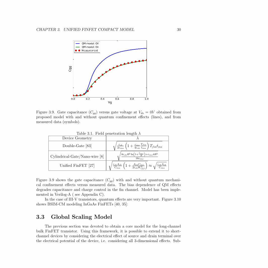
CHAPTER 3. UNIFIED FINFET COMPACT MODEL 30
Figure 3.9. Gate capacitance (Cgg) versus gate voltage at Vds = 0V obtained fromproposed model with and without quantum confinement effects (lines), and frommeasured data (symbols).
Table 3.1. Field penetration length λDevice Geometry λ
Double-Gate [83]
√
εch2εins
(
1 + εins4εch
Tfintins
)
Tfintins
Cylindrical-Gate/Nano-wire [8]
√
8εchR2 ln(1+ tinsR )+εins4R2
16εins
Unified FinFET [27]
√
εchAchCins
(
1 + AchCins2εchW
2eff
)
≈√
εchAchCins
Figure 3.9 shows the gate capacitance (Cgg) with and without quantum mechani-cal confinement effects versus measured data. The bias dependence of QM effectsdegrades capacitance and charge control in the fin channel. Model has been imple-mented in Verilog-A ( see Appendix C).
In the case of III-V transistors, quantum effects are very important. Figure 3.10shows BSIM-CM modeling InGaAs FinFETs [40, 35]:
3.3 Global Scaling Model
The previous section was devoted to obtain a core model for the long-channelbulk FinFET transistor. Using this framework, it is possible to extend it to short-channel devices by considering the electrical effect of source and drain terminal overthe electrical potential of the device, i.e. considering all 3-dimensional effects. Sub-
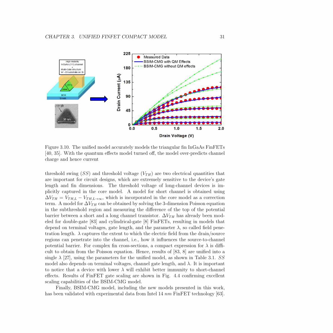
CHAPTER 3. UNIFIED FINFET COMPACT MODEL 31
Figure 3.10. The unified model accurately models the triangular fin InGaAs FinFETs[40, 35]. With the quantum effects model turned off, the model over-predicts channelcharge and hence current
threshold swing (SS) and threshold voltage (VTH) are two electrical quantities thatare important for circuit designs, which are extremely sensitive to the device’s gatelength and fin dimensions. The threshold voltage of long-channel devices is im-plicitly captured in the core model. A model for short channel is obtained using∆VTH = VTH,L − VTH,L→∞, which is incorporated in the core model as a correctionterm. A model for ∆VTH can be obtained by solving the 3-dimension Poisson equationin the subthreshold region and measuring the difference of the top of the potentialbarrier between a short and a long channel transistor. ∆VTH has already been mod-eled for double-gate [83] and cylindrical-gate [8] FinFETs, resulting in models thatdepend on terminal voltages, gate length, and the parameter λ, so called field pene-tration length. λ captures the extent to which the electric field from the drain/sourceregions can penetrate into the channel, i.e., how it influences the source-to-channelpotential barrier. For complex fin cross-sections, a compact expression for λ is diffi-cult to obtain from the Poisson equation. Hence, results of [83, 8] are unified into asingle λ [27], using the parameters for the unified model, as shown in Table 3.1. SSmodel also depends on terminal voltages, channel gate length, and λ. It is importantto notice that a device with lower λ will exhibit better immunity to short-channeleffects. Results of FinFET gate scaling are shown in Fig. 4.4 confirming excellentscaling capabilities of the BSIM-CMG model.
Finally, BSIM-CMG model, including the new models presented in this work,has been validated with experimental data from Intel 14 nm FinFET technology [63].
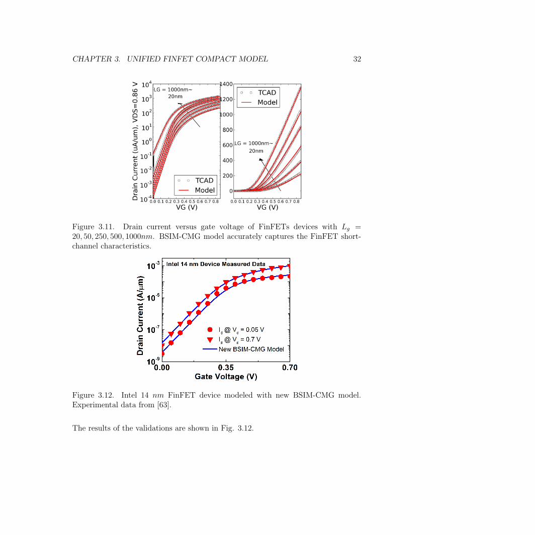
CHAPTER 3. UNIFIED FINFET COMPACT MODEL 32
Figure 3.11. Drain current versus gate voltage of FinFETs devices with Lg =20, 50, 250, 500, 1000nm. BSIM-CMG model accurately captures the FinFET short-channel characteristics.
Figure 3.12. Intel 14 nm FinFET device modeled with new BSIM-CMG model.Experimental data from [63].
The results of the validations are shown in Fig. 3.12.
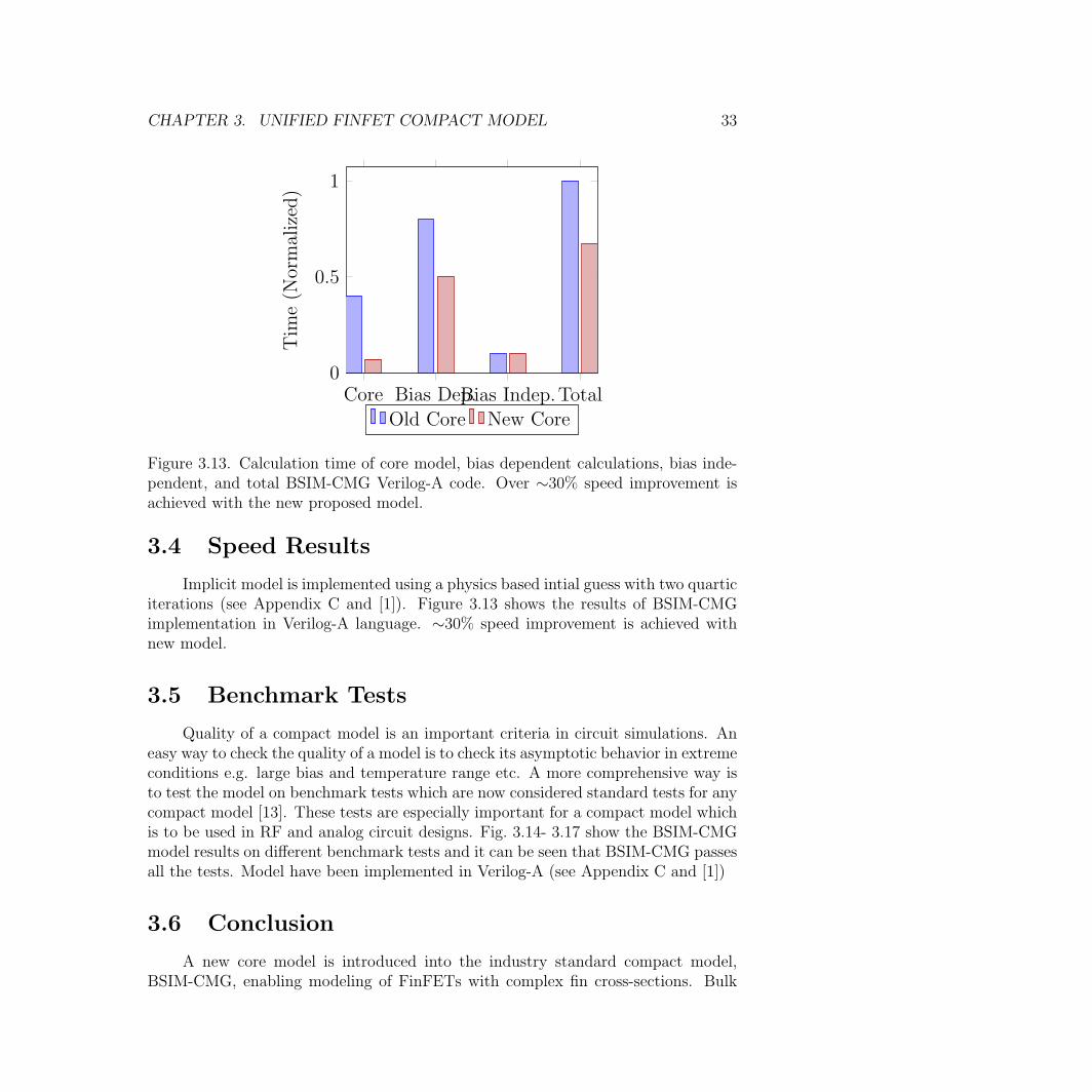
CHAPTER 3. UNIFIED FINFET COMPACT MODEL 33
Core Bias Dep.Bias Indep.Total0
0.5
1
Tim
e(N
ormalized)
Old Core New Core
Figure 3.13. Calculation time of core model, bias dependent calculations, bias inde-pendent, and total BSIM-CMG Verilog-A code. Over ∼30% speed improvement isachieved with the new proposed model.
3.4 Speed Results
Implicit model is implemented using a physics based intial guess with two quarticiterations (see Appendix C and [1]). Figure 3.13 shows the results of BSIM-CMGimplementation in Verilog-A language. ∼30% speed improvement is achieved withnew model.
3.5 Benchmark Tests
Quality of a compact model is an important criteria in circuit simulations. Aneasy way to check the quality of a model is to check its asymptotic behavior in extremeconditions e.g. large bias and temperature range etc. A more comprehensive way isto test the model on benchmark tests which are now considered standard tests for anycompact model [13]. These tests are especially important for a compact model whichis to be used in RF and analog circuit designs. Fig. 3.14- 3.17 show the BSIM-CMGmodel results on different benchmark tests and it can be seen that BSIM-CMG passesall the tests. Model have been implemented in Verilog-A (see Appendix C and [1])
3.6 Conclusion
A new core model is introduced into the industry standard compact model,BSIM-CMG, enabling modeling of FinFETs with complex fin cross-sections. Bulk
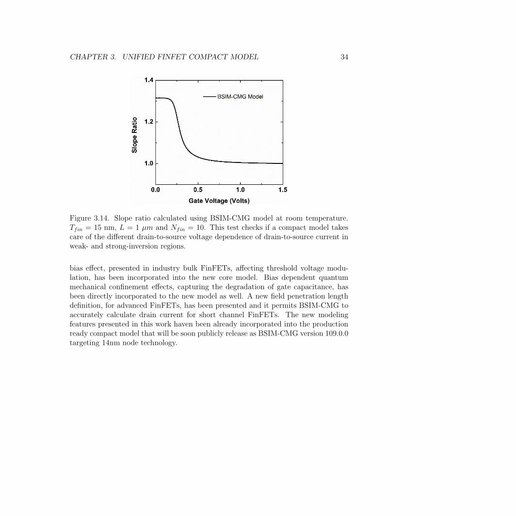
CHAPTER 3. UNIFIED FINFET COMPACT MODEL 34
Figure 3.14. Slope ratio calculated using BSIM-CMG model at room temperature.Tfin = 15 nm, L = 1 µm and Nfin = 10. This test checks if a compact model takescare of the different drain-to-source voltage dependence of drain-to-source current inweak- and strong-inversion regions.
bias effect, presented in industry bulk FinFETs, affecting threshold voltage modu-lation, has been incorporated into the new core model. Bias dependent quantummechanical confinement effects, capturing the degradation of gate capacitance, hasbeen directly incorporated to the new model as well. A new field penetration lengthdefinition, for advanced FinFETs, has been presented and it permits BSIM-CMG toaccurately calculate drain current for short channel FinFETs. The new modelingfeatures presented in this work haven been already incorporated into the productionready compact model that will be soon publicly release as BSIM-CMG version 109.0.0targeting 14nm node technology.
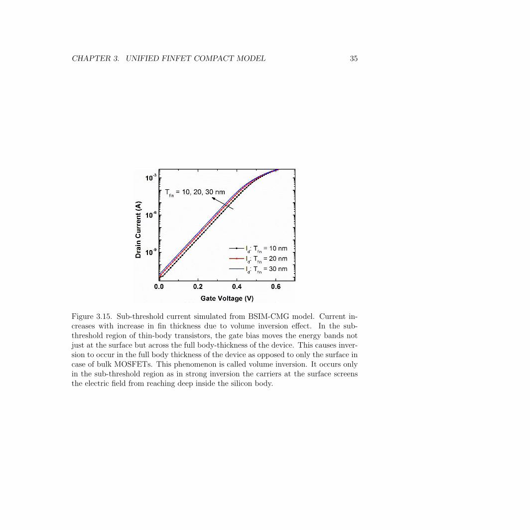
CHAPTER 3. UNIFIED FINFET COMPACT MODEL 35
Figure 3.15. Sub-threshold current simulated from BSIM-CMG model. Current in-creases with increase in fin thickness due to volume inversion effect. In the sub-threshold region of thin-body transistors, the gate bias moves the energy bands notjust at the surface but across the full body-thickness of the device. This causes inver-sion to occur in the full body thickness of the device as opposed to only the surface incase of bulk MOSFETs. This phenomenon is called volume inversion. It occurs onlyin the sub-threshold region as in strong inversion the carriers at the surface screensthe electric field from reaching deep inside the silicon body.
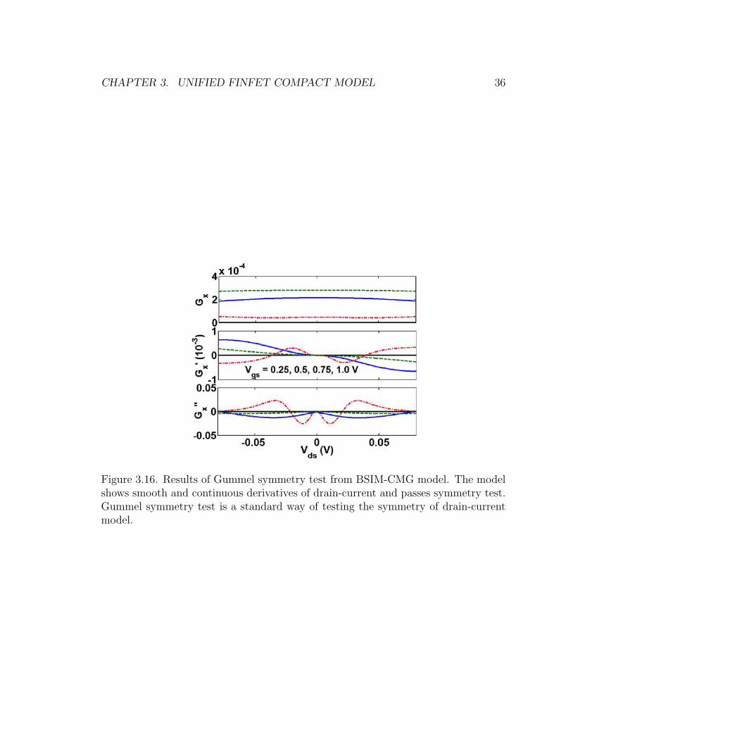
CHAPTER 3. UNIFIED FINFET COMPACT MODEL 36
Figure 3.16. Results of Gummel symmetry test from BSIM-CMG model. The modelshows smooth and continuous derivatives of drain-current and passes symmetry test.Gummel symmetry test is a standard way of testing the symmetry of drain-currentmodel.
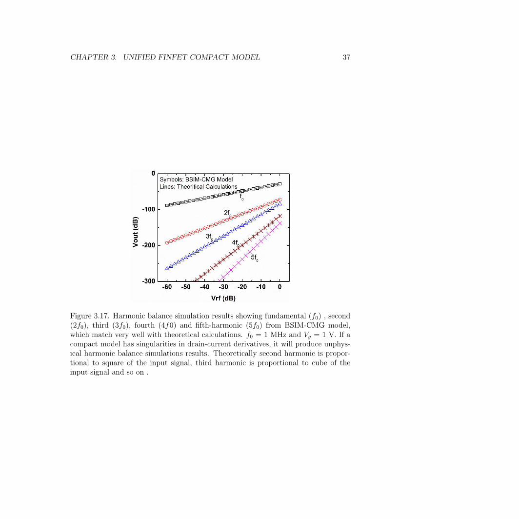
CHAPTER 3. UNIFIED FINFET COMPACT MODEL 37
Figure 3.17. Harmonic balance simulation results showing fundamental (f0) , second(2f0), third (3f0), fourth (4f0) and fifth-harmonic (5f0) from BSIM-CMG model,which match very well with theoretical calculations. f0 = 1 MHz and Vg = 1 V. If acompact model has singularities in drain-current derivatives, it will produce unphys-ical harmonic balance simulations results. Theoretically second harmonic is propor-tional to square of the input signal, third harmonic is proportional to cube of theinput signal and so on .
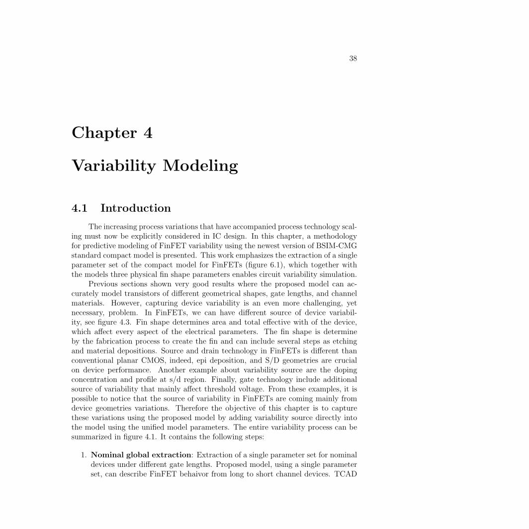
38
Chapter 4
Variability Modeling
4.1 Introduction
The increasing process variations that have accompanied process technology scal-ing must now be explicitly considered in IC design. In this chapter, a methodologyfor predictive modeling of FinFET variability using the newest version of BSIM-CMGstandard compact model is presented. This work emphasizes the extraction of a singleparameter set of the compact model for FinFETs (figure 6.1), which together withthe models three physical fin shape parameters enables circuit variability simulation.
Previous sections shown very good results where the proposed model can ac-curately model transistors of different geometrical shapes, gate lengths, and channelmaterials. However, capturing device variability is an even more challenging, yetnecessary, problem. In FinFETs, we can have different source of device variabil-ity, see figure 4.3. Fin shape determines area and total effective with of the device,which affect every aspect of the electrical parameters. The fin shape is determineby the fabrication process to create the fin and can include several steps as etchingand material depositions. Source and drain technology in FinFETs is different thanconventional planar CMOS, indeed, epi deposition, and S/D geometries are crucialon device performance. Another example about variability source are the dopingconcentration and profile at s/d region. Finally, gate technology include additionalsource of variability that mainly affect threshold voltage. From these examples, it ispossible to notice that the source of variability in FinFETs are coming mainly fromdevice geometries variations. Therefore the objective of this chapter is to capturethese variations using the proposed model by adding variability source directly intothe model using the unified model parameters. The entire variability process can besummarized in figure 4.1. It contains the following steps:
1. Nominal global extraction: Extraction of a single parameter set for nominaldevices under different gate lengths. Proposed model, using a single parameterset, can describe FinFET behaivor from long to short channel devices. TCAD
CHAPTER 4. VARIABILITY MODELING 39
Nominalparameter
extraction:14nm (TCAD)
Includeprocess
variation:σ:Hfin,Lg,...
Producevariabilitymodelingσ:Ion,Ioff ,...
Refinementvariability
modelσ,ρ
Figure 4.1. Variability Modeling
simulation have been used in this step; however, experimental data can be usedas well.
2. Include process variation: Obtain device geometry variations from manu-facturer’s estimation including variation parameters of fin dimensions, channellength, doping, work function, etc.
3. Produce variability modeling Proposed compact can take geometry vari-ations as input parameters and generate electrical parameter variation distri-butions, such as Ion, Ioff , Vth, SS, etc. It is very important to point out thatcomplex correlation are well estimated by the proposed model, such SS and Vthcorrelation which is highly dependent in subtle variation of fin geometry andchannel length.
4. Refinement of variability model: In the case that more accurate resultsare needed, it is possible to refine the global parameter extraction includingnot just nominal device but extreme devices. For example, a single parameterset can be re-extracted including nominal and devices with highest and lowestIoff . A device with lowest Ioff is normally a results of a larger gate length,thinner EOT, and smaller fin area. On the other hand, larger Ioff are normallyobtained for FinFETs with larger area, shorter gate length, and thicker EOT.
4.2 Description of the Unified Model
The new Unified FinFET Model [27, 23] has three physical fin shape parameters(Table 4.1): Ach, the cross-sectional area of the fin; Weff , the effective electricalwidth of the fin; and Cins, the total gate insulator capacitance. The new model, withthese three parameters, can describe the electrical behavior of realistic FinFETs withcomplex fin cross sections such as those reported in [7, 63] (Fig. 6.1). Short channeleffects (SCEs), such as drain induced barrier lowering (DIBL) and subthreshold swing(SS) degradation, are accurately modeled with a new field penetration length [27]described by λ, which is determined by the same three fin shape parameters:
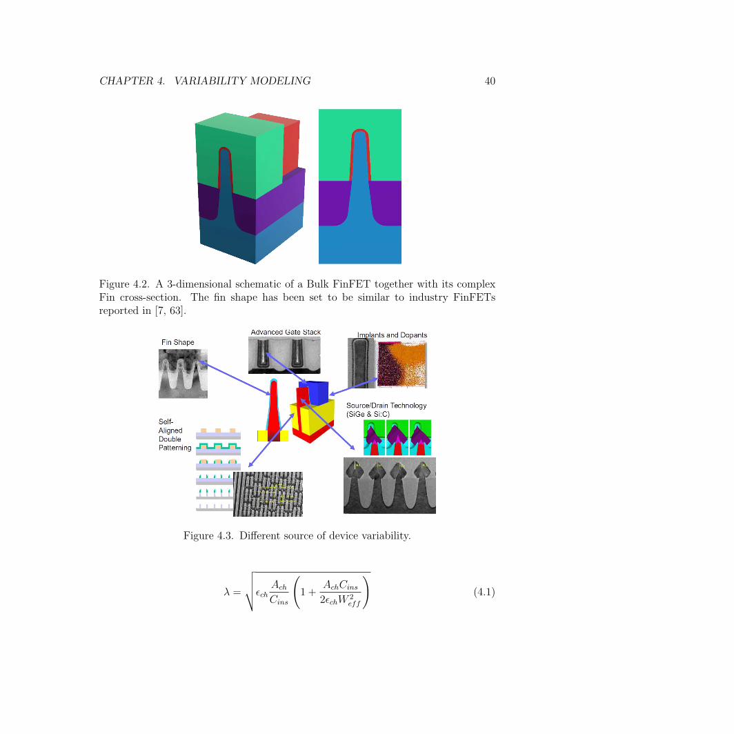
CHAPTER 4. VARIABILITY MODELING 40
Figure 4.2. A 3-dimensional schematic of a Bulk FinFET together with its complexFin cross-section. The fin shape has been set to be similar to industry FinFETsreported in [7, 63].
Figure 4.3. Different source of device variability.
λ =
√
√
√
√ǫchAchCins
(
1 +AchCins2ǫchW 2
eff
)
(4.1)
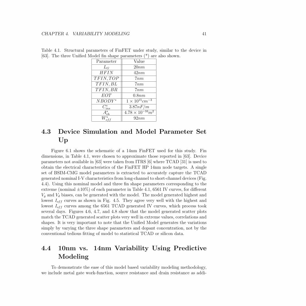
CHAPTER 4. VARIABILITY MODELING 41
Table 4.1. Structural parameters of FinFET under study, similar to the device in[63]. The three Unified Model fin shape parameters (*) are also shown.
Parameter ValueLG 20nm
HFIN 42nmTFIN, TOP 7nmTFIN,BL 7nmTFIN,BR 7nmEOT 0.8nm
NBODY ∗ 1× 1015cm−3
C∗
ins 3.87nF/mA∗
ch 4.78× 10⁻¹⁶m2
W ∗
eff 92nm
4.3 Device Simulation and Model Parameter Set
Up
Figure 6.1 shows the schematic of a 14nm FinFET used for this study. Findimensions, in Table 4.1, were chosen to approximate those reported in [63]. Deviceparameters not available in [63] were taken from ITRS [6] where TCAD [31] is used toobtain the electrical characteristics of the FinFET HP 14nm node targets. A singleset of BSIM-CMG model parameters is extracted to accurately capture the TCADgenerated nominal I-V characteristics from long-channel to short-channel devices (Fig.4.4). Using this nominal model and three fin shape parameters corresponding to theextreme (nominal ±10%) of each parameter in Table 4.1, 6561 IV curves, for differentVg and Vd biases, can be generated with the model. The model generated highest andlowest Ioff curves as shown in Fig. 4.5. They agree very well with the highest andlowest Ioff curves among the 6561 TCAD generated IV curves, which process tookseveral days. Figures 4.6, 4.7, and 4.8 show that the model generated scatter plotsmatch the TCAD generated scatter plots very well in extreme values, correlations andshapes. It is very important to note that the Unified Model generates the variationssimply by varying the three shape parameters and dopant concentration, not by theconventional tedious fitting of model to statistical TCAD or silicon data.
4.4 10nm vs. 14nm Variability Using Predictive
Modeling
To demonstrate the ease of this model based variability modeling methodology,we include metal gate work-function, source resistance and drain resistance as addi-
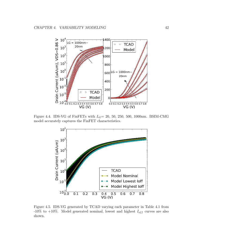
CHAPTER 4. VARIABILITY MODELING 42
Figure 4.4. IDS-VG of FinFETs with LG= 20, 50, 250, 500, 1000nm. BSIM-CMGmodel accurately captures the FinFET characteristics.
Figure 4.5. IDS-VG generated by TCAD varying each parameter in Table 4.1 from-10% to +10%. Model generated nominal, lowest and highest Ioff curves are alsoshown.
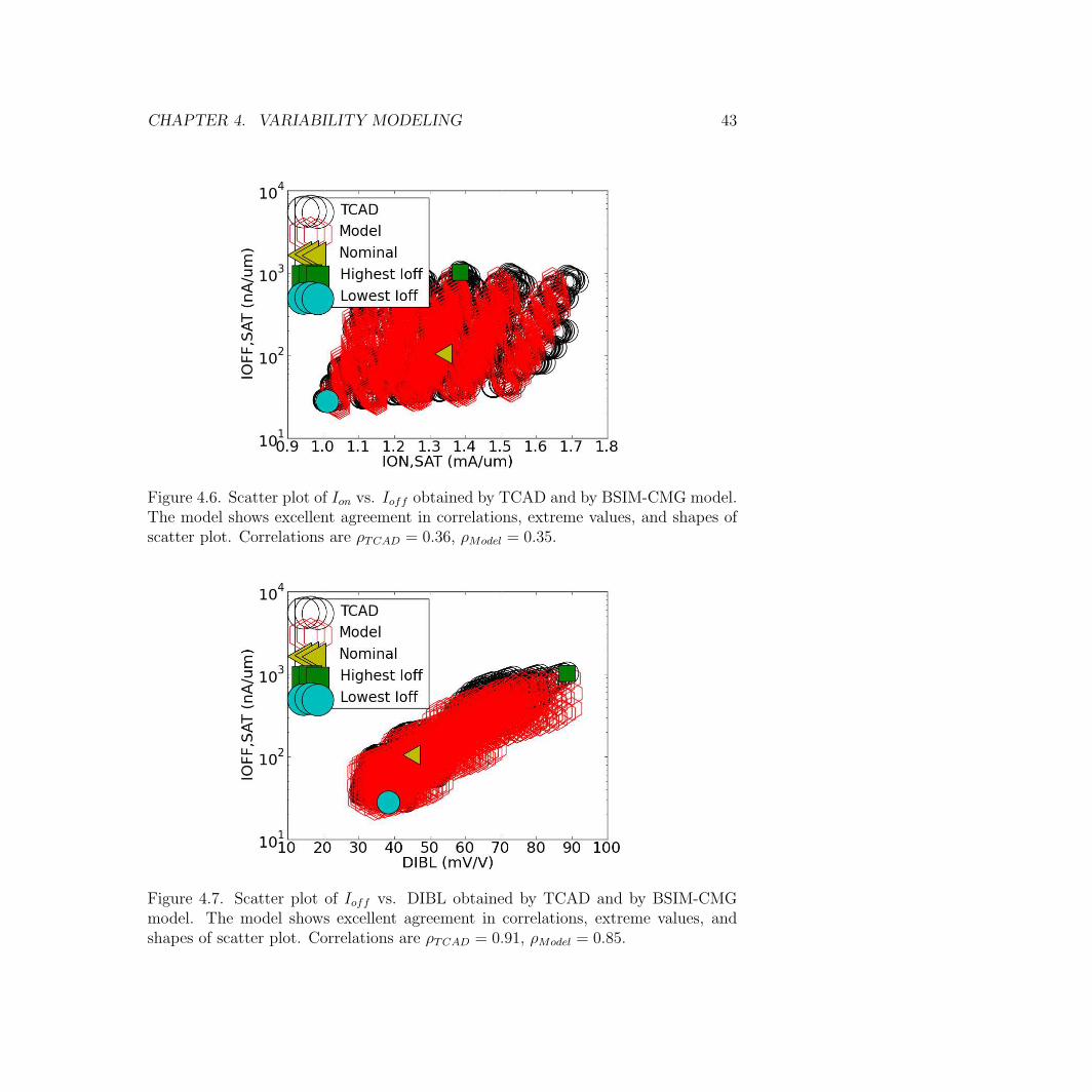
CHAPTER 4. VARIABILITY MODELING 43
Figure 4.6. Scatter plot of Ion vs. Ioff obtained by TCAD and by BSIM-CMG model.The model shows excellent agreement in correlations, extreme values, and shapes ofscatter plot. Correlations are ρTCAD = 0.36, ρModel = 0.35.
Figure 4.7. Scatter plot of Ioff vs. DIBL obtained by TCAD and by BSIM-CMGmodel. The model shows excellent agreement in correlations, extreme values, andshapes of scatter plot. Correlations are ρTCAD = 0.91, ρModel = 0.85.
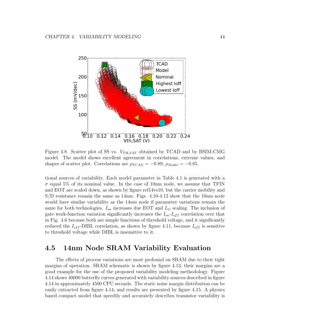
CHAPTER 4. VARIABILITY MODELING 44
Figure 4.8. Scatter plot of SS vs. VTH,SAT obtained by TCAD and by BSIM-CMGmodel. The model shows excellent agreement in correlations, extreme values, andshapes of scatter plot. Correlations are ρTCAD = −0.89, ρModel = −0.85.
tional sources of variability. Each model parameter in Table 4.1 is generated with aσ equal 5% of its nominal value. In the case of 10nm node, we assume that TFINand EOT are scaled down, as shown by figure ref14vs10, but the carrier mobility andS/D resistance remain the same as 14nm. Figs. 4.10-4.12 show that the 10nm nodewould have similar variability as the 14nm node if parameter variations remain thesame for both technologies. Ion increases due EOT and LG scaling. The inclusion ofgate work-function variation significantly increases the Ion-Ioff correlation over thatin Fig. 4.6 because both are simple functions of threshold voltage, and it significantlyreduced the Ioff -DIBL correlation, as shown by figure 4.11, because Ioff is sensitiveto threshold voltage while DIBL is insensitive to it.
4.5 14nm Node SRAM Variability Evaluation
The effects of process variations are most profound on SRAM due to their tightmargins of operation. SRAM schematic is shown by figure 4.13, their margins are agood example for the use of the proposed variability modeling methodology. Figure4.14 shows 40000 butterfly curves generated with variability sources described in figure4.14 in approximately 4500 CPU seconds. The static noise margin distribution can beeasily extracted from figure 4.14, and results are presented by figure 4.15. A physicsbased compact model that speedily and accurately describes transistor variability is
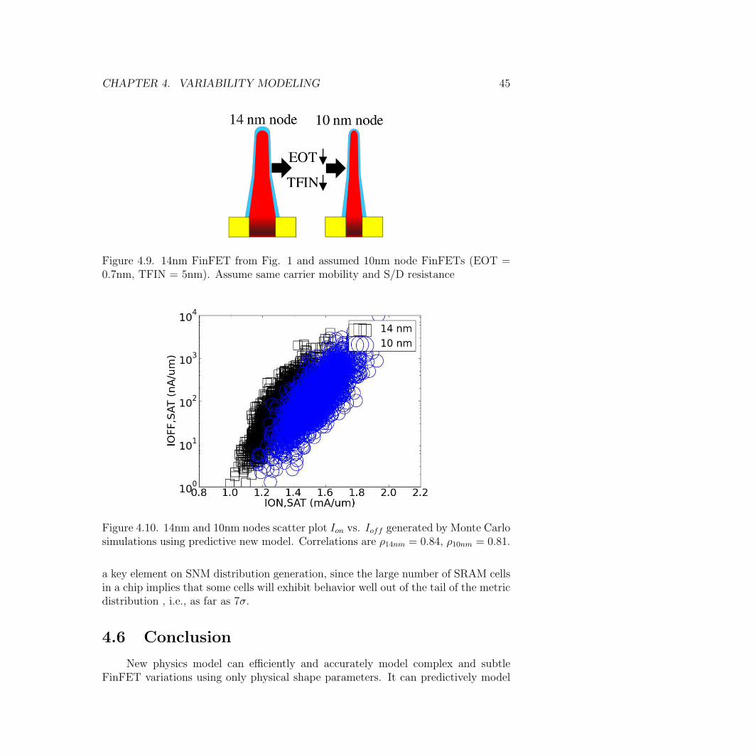
CHAPTER 4. VARIABILITY MODELING 45
Figure 4.9. 14nm FinFET from Fig. 1 and assumed 10nm node FinFETs (EOT =0.7nm, TFIN = 5nm). Assume same carrier mobility and S/D resistance
Figure 4.10. 14nm and 10nm nodes scatter plot Ion vs. Ioff generated by Monte Carlosimulations using predictive new model. Correlations are ρ14nm = 0.84, ρ10nm = 0.81.
a key element on SNM distribution generation, since the large number of SRAM cellsin a chip implies that some cells will exhibit behavior well out of the tail of the metricdistribution , i.e., as far as 7σ.
4.6 Conclusion
New physics model can efficiently and accurately model complex and subtleFinFET variations using only physical shape parameters. It can predictively model
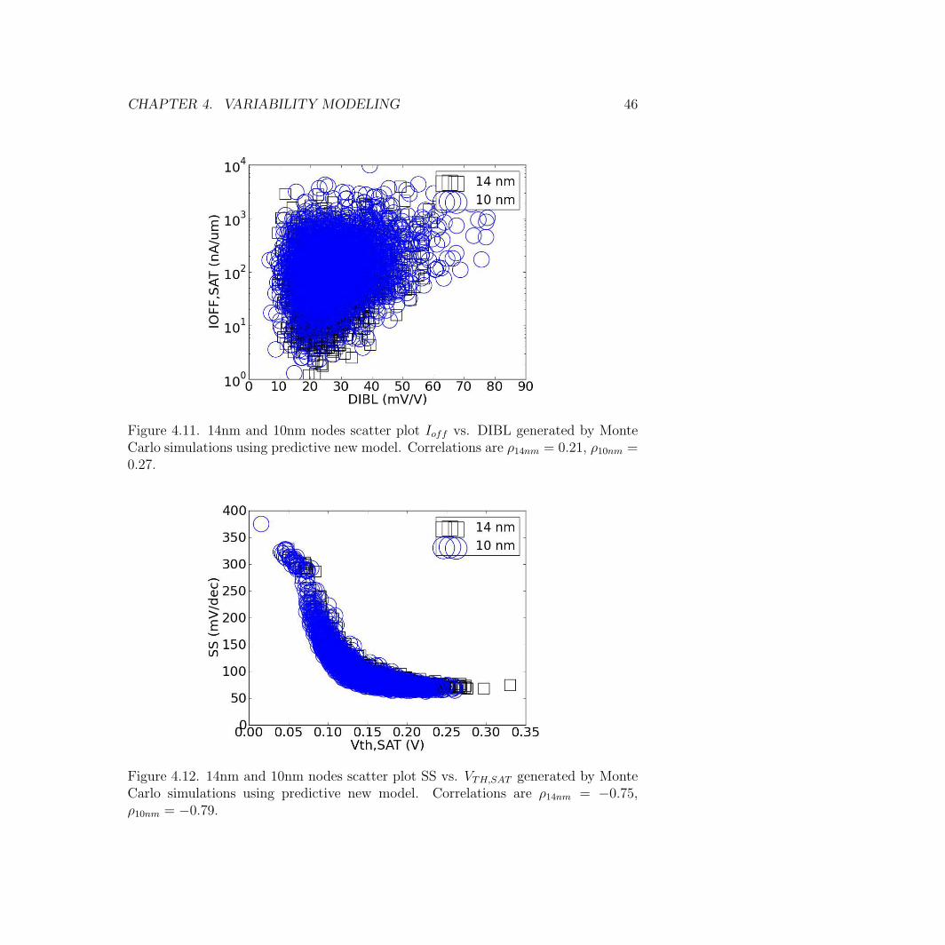
CHAPTER 4. VARIABILITY MODELING 46
Figure 4.11. 14nm and 10nm nodes scatter plot Ioff vs. DIBL generated by MonteCarlo simulations using predictive new model. Correlations are ρ14nm = 0.21, ρ10nm =0.27.
Figure 4.12. 14nm and 10nm nodes scatter plot SS vs. VTH,SAT generated by MonteCarlo simulations using predictive new model. Correlations are ρ14nm = −0.75,ρ10nm = −0.79.
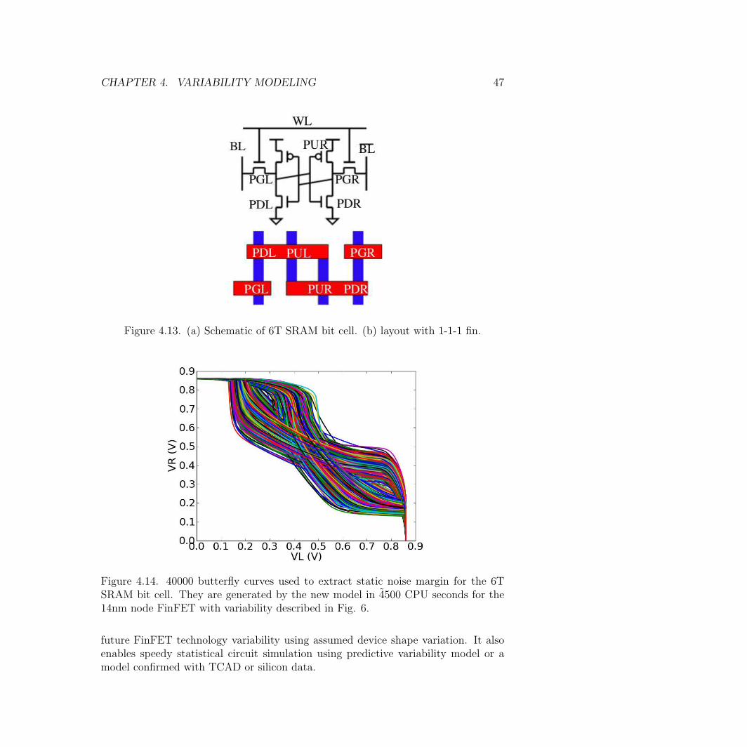
CHAPTER 4. VARIABILITY MODELING 47
Figure 4.13. (a) Schematic of 6T SRAM bit cell. (b) layout with 1-1-1 fin.
Figure 4.14. 40000 butterfly curves used to extract static noise margin for the 6TSRAM bit cell. They are generated by the new model in 4500 CPU seconds for the14nm node FinFET with variability described in Fig. 6.
future FinFET technology variability using assumed device shape variation. It alsoenables speedy statistical circuit simulation using predictive variability model or amodel confirmed with TCAD or silicon data.
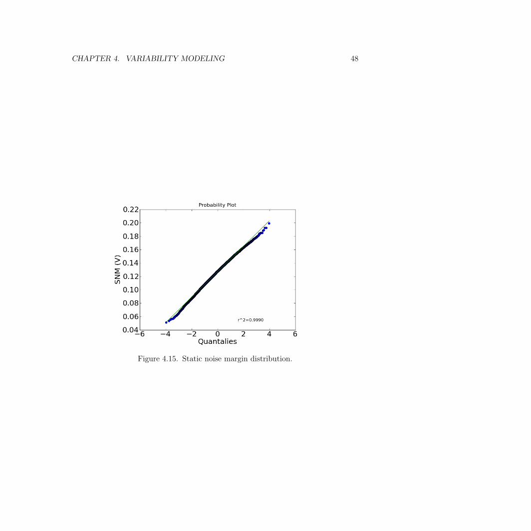
CHAPTER 4. VARIABILITY MODELING 48
Figure 4.15. Static noise margin distribution.
49
Chapter 5
Model for Independent GateMOSFETs
5.1 Introduction
Independent multi-gate MOSFETs (front- and back-gate) are enabling new novelapplications wherein the back-gate can be in depletion or inversion. Indeed, ultrathinBody silicon-on-insulator (UTBSOI) technology has been developed with excellentlow power, scaling and, variability characteristics [18]. UTBSOI has been recentlyadopted in sub-20nm IC technologies [55, 65, 59] as an alternative to FinFET tech-nology [7, 88, 47], as both technologies are replacements of the conventional bulkplanar technology. For UTBSOI transistor technology, the Compact Model Coalition(CMC) has chosen BSIM-IMG [52, 37, 43, 14] as one of the first industry-standardcompact model for advanced circuit design.
The compact model for independent multi-gate MOSFETs (figure 5.1) is ob-tained from the Poisson’s solution with front- and back-gate boundaries conditions[52, 21, 67, 74]. Once front- and back-surface potentials are obtained, they can beutilized to obtain the mobile charge in the channel that eventually leads to the compu-tation of the drain current of the device. It is well known that the Poisson’s solutionfor these devices lies in trigonometric and hyperbolic domains, making the desirednumerical robustness extremely difficult; however, fast speed, numerical robustness,and accuracy are fundamental characteristics of compact models for circuit designand technology development. An industry compact model must be able to calculateterminal (drain, source, front/back-gate) currents and charges, which are then uti-lized by circuit simulator engines to solve a complete circuit under various analysessuch as DC, AC, transient, etc. This work presents a new analytical model for thecore model of BSIM-IMG compact model for UTBSOI technologies. It is based in
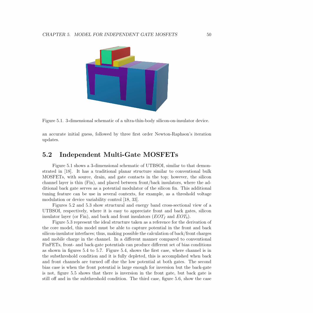
CHAPTER 5. MODEL FOR INDEPENDENT GATE MOSFETS 50
Figure 5.1. 3-dimensional schematic of a ultra-thin-body silicon-on-insulator device.
an accurate initial guess, followed by three first order Newton-Raphson’s iterationupdates.
5.2 Independent Multi-Gate MOSFETs
Figure 5.1 shows a 3-dimensional schematic of UTBSOI, similar to that demon-strated in [18]. It has a traditional planar structure similar to conventional bulkMOSFETs, with source, drain, and gate contacts in the top; however, the siliconchannel layer is thin (Fin), and placed between front/back insulators, where the ad-ditional back gate serves as a potential modulator of the silicon fin. This additionaltuning feature can be use in several contexts, for example, as a threshold voltagemodulation or device variability control [18, 33].
Figures 5.2 and 5.3 show structural and energy band cross-sectional view of aUTBSOI, respectively, where it is easy to appreciate front and back gates, siliconinsulator layer (or Fin), and back and front insulators (EOTf and EOTb).
Figure 5.3 represent the ideal structure taken as a reference for the derivation ofthe core model, this model must be able to capture potential in the front and backsilicon-insulator interfaces; thus, making possible the calculation of back/front chargesand mobile charge in the channel. In a different manner compared to conventionalFinFETs, front- and back-gate potentials can produce different set of bias conditionsas shown in figures 5.4 to 5.7. Figure 5.4, shows the first case, where channel is inthe substhreshold condition and it is fully depleted, this is accomplished when backand front channels are turned off due the low potential at both gates. The secondbias case is when the front potential is large enough for inversion but the back-gateis not, figure 5.5 shows that there is inversion in the front gate, but back gate isstill off and in the subthreshold condition. The third case, figure 5.6, show the case
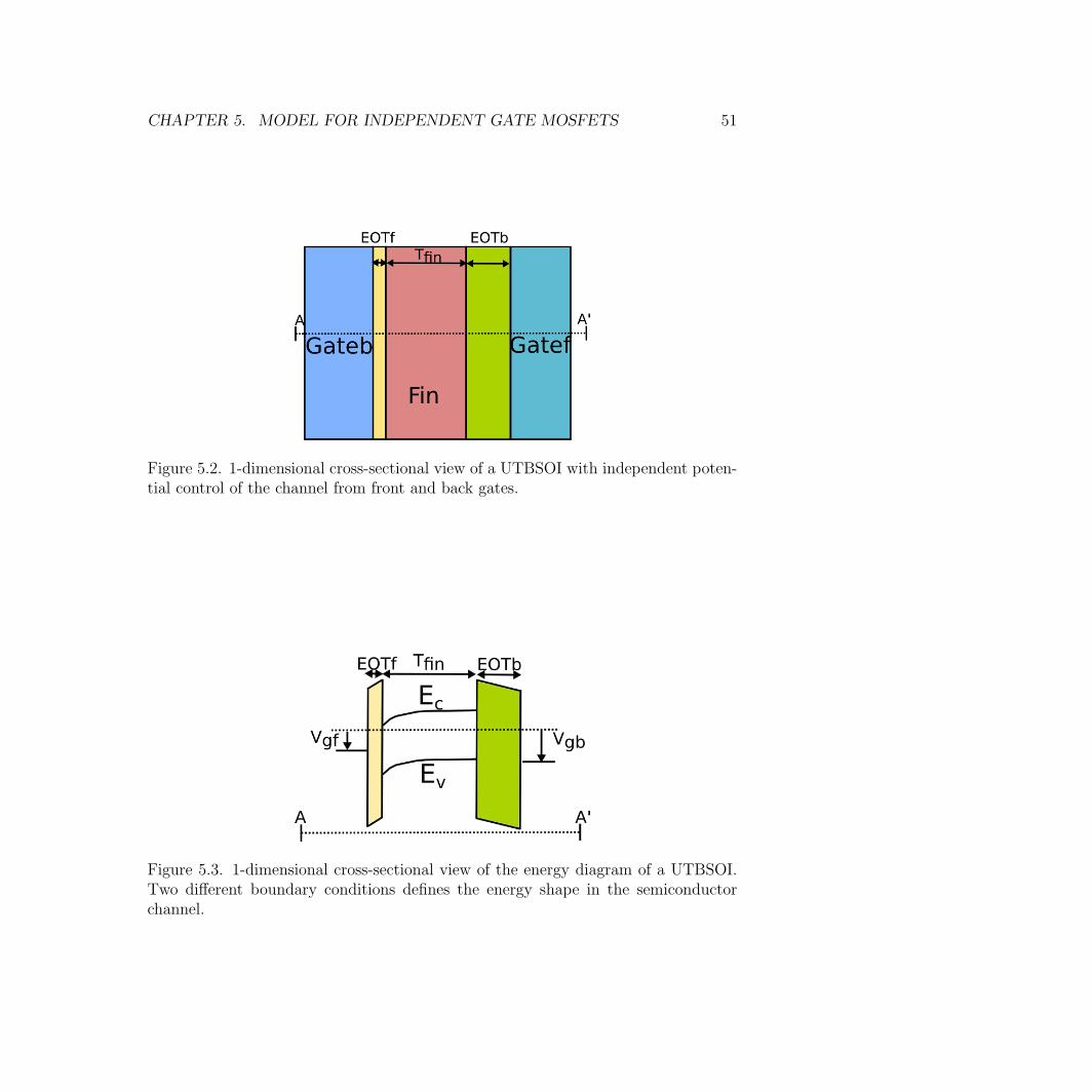
CHAPTER 5. MODEL FOR INDEPENDENT GATE MOSFETS 51
Figure 5.2. 1-dimensional cross-sectional view of a UTBSOI with independent poten-tial control of the channel from front and back gates.
Figure 5.3. 1-dimensional cross-sectional view of the energy diagram of a UTBSOI.Two different boundary conditions defines the energy shape in the semiconductorchannel.
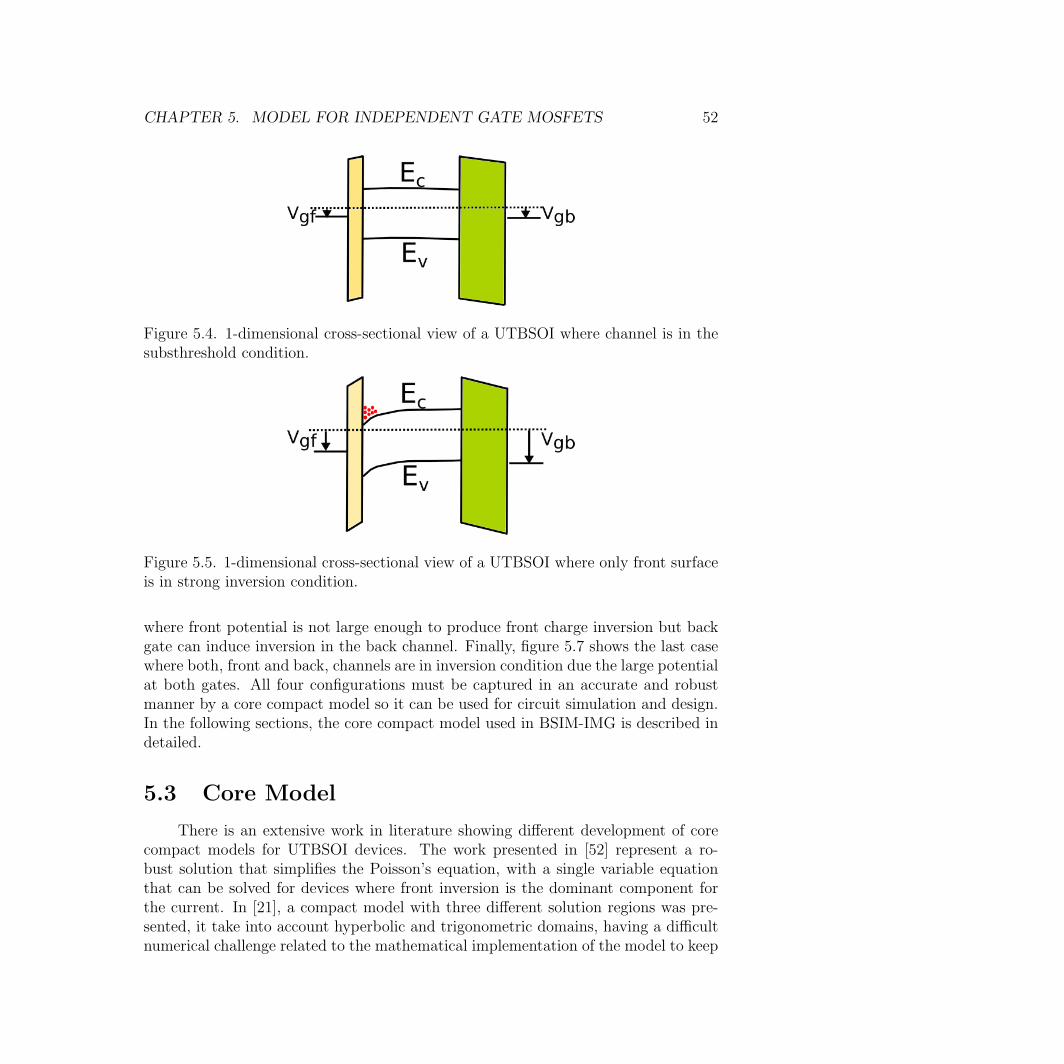
CHAPTER 5. MODEL FOR INDEPENDENT GATE MOSFETS 52
Figure 5.4. 1-dimensional cross-sectional view of a UTBSOI where channel is in thesubsthreshold condition.
Figure 5.5. 1-dimensional cross-sectional view of a UTBSOI where only front surfaceis in strong inversion condition.
where front potential is not large enough to produce front charge inversion but backgate can induce inversion in the back channel. Finally, figure 5.7 shows the last casewhere both, front and back, channels are in inversion condition due the large potentialat both gates. All four configurations must be captured in an accurate and robustmanner by a core compact model so it can be used for circuit simulation and design.In the following sections, the core compact model used in BSIM-IMG is described indetailed.
5.3 Core Model
There is an extensive work in literature showing different development of corecompact models for UTBSOI devices. The work presented in [52] represent a ro-bust solution that simplifies the Poisson’s equation, with a single variable equationthat can be solved for devices where front inversion is the dominant component forthe current. In [21], a compact model with three different solution regions was pre-sented, it take into account hyperbolic and trigonometric domains, having a difficultnumerical challenge related to the mathematical implementation of the model to keep
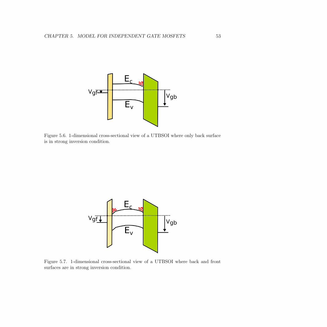
CHAPTER 5. MODEL FOR INDEPENDENT GATE MOSFETS 53
Figure 5.6. 1-dimensional cross-sectional view of a UTBSOI where only back surfaceis in strong inversion condition.
Figure 5.7. 1-dimensional cross-sectional view of a UTBSOI where back and frontsurfaces are in strong inversion condition.
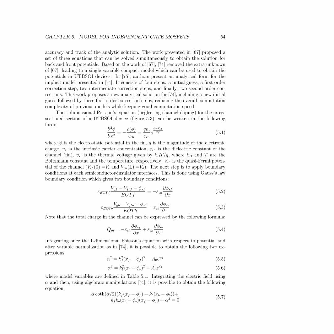
CHAPTER 5. MODEL FOR INDEPENDENT GATE MOSFETS 54
accuracy and track of the analytic solution. The work presented in [67] proposed aset of three equations that can be solved simultaneously to obtain the solution forback and front potentials. Based on the work of [67], [74] removed the extra unknownof [67], leading to a single variable compact model which can be used to obtain thepotentials in UTBSOI devices. In [75], authors present an analytical form for theimplicit model presented in [74]. It consists of four steps: a initial guess, a first ordercorrection step, two intermediate correction steps, and finally, two second order cor-rections. This work proposes a new analytical solution for [74], including a new initialguess followed by three first order correction steps, reducing the overall computationcomplexity of previous models while keeping good computation speed.
The 1-dimensional Poisson’s equation (neglecting channel doping) for the cross-sectional section of a UTBSOI device (figure 5.3) can be written in the followingform:
∂2φ
∂x2= −ρ(φ)
εch=qniεch
eφ−VchvT (5.1)
where φ is the electrostatic potential in the fin, q is the magnitude of the electroniccharge, ni is the intrinsic carrier concentration, εch is the dielectric constant of thechannel (fin), vT is the thermal voltage given by kBT/q, where kB and T are theBoltzmann constant and the temperature, respectively; Vch is the quasi-Fermi poten-tial of the channel (Vch(0) =Vs and Vch(L) =Vd). The next step is to apply boundaryconditions at each semiconductor-insulator interfaces. This is done using Gauss’s lawboundary condition which gives two boundary conditions:
εEOTfVgf − Vfbf − φsf
EOTf= −εch
∂φsf∂x
(5.2)
εEOTbVgb − Vfbb − φsb
EOTb= εch
∂φsb∂x
(5.3)
Note that the total charge in the channel can be expressed by the following formula:
Qm = −εch∂φsf∂x
+ εch∂φsb∂x
(5.4)
Integrating once the 1-dimensional Poisson’s equation with respect to potential andafter variable normalization as in [74], it is possible to obtain the following two ex-pressions:
α2 = k2f (xf − φf )2 − A0e
φf (5.5)
α2 = k2b (xb − φb)2 − A0e
φb (5.6)
where model variables are defined in Table 5.1. Integrating the electric field usingα and then, using algebraic manipulations [74], it is possible to obtain the followingequation:
α coth(α/2)(kf (xf − φf ) + kb(xb − φb))+kfkb(xb − φb)(xf − φf ) + α2 = 0
(5.7)
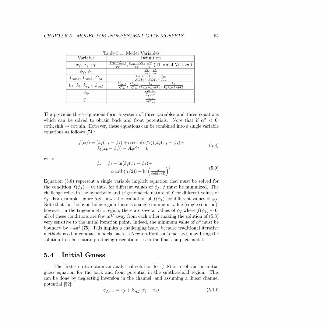
CHAPTER 5. MODEL FOR INDEPENDENT GATE MOSFETS 55
Table 5.1. Model VariablesVariable Definition
xf , xb, vTVGF−∆Φf
vT,VGB−∆Φb
vT,kTq
(Thermal Voltage)
φf , φbϕfvT, ϕbvT
Cox,f , Cox,b, Cchεox,fEOTf
,εox,bEOTb
, εchTch
kf , kb, keq,f , keq,bCox,fCch
,Cox,bCch
, kbkfkb+kf+kb
,kf
kfkb+kf+kb
A02qniεchCchvT
qmQmvTCch
The previous three equations form a system of three variables and three equationswhich can be solved to obtain back and front potentials. Note that if α2 < 0:coth, sinh → cot, sin. However, these equations can be combined into a single variableequations as follows [74]:
f(φf ) = (kf (xf − φf ) + α coth(α/2))(kf (xf − φf )+kb(xb − φb))− A0e
φf = 0(5.8)
with:φb = φf − ln(kf (xf − φf )+
α coth(α/2)) + ln(
αsinh(α/2)
)2 (5.9)
Equation (5.8) represent a single variable implicit equation that must be solved forthe condition f(φf ) = 0; thus, for different values of φf , f must be minimized. Thechallenge relies in the hyperbolic and trigonometric nature of f for different values ofφf . For example, figure 5.8 shows the evaluation of f(φf ) for different values of φf .Note that for the hyperbolic region there is a single minimum value (single solution);however, in the trigonometric region, there are several values of φf where f(φf ) ∼ 0,all of these conditions are few mV away from each other making the solution of (5.8)very sensitive to the initial iteration point. Indeed, the minimum value of α2 must bebounded by −4π2 [75]. This implies a challenging issue, because traditional iterativemethods used in compact models, such as Newton-Raphson’s method, may bring thesolution to a false state producing discontinuities in the final compact model.
5.4 Initial Guess
The first step to obtain an analytical solution for (5.8) is to obtain an initialguess equation for the back and front potential in the subthreshold region. Thiscan be done by neglecting inversion in the channel, and assuming a linear channelpotential [52]:
φf,sub = xf + keq,f (xf − xb) (5.10)
CHAPTER 5. MODEL FOR INDEPENDENT GATE MOSFETS 56
Figure 5.8. Evaluation of f(φf ) for different values of φf . True versus false solutionsare apart by few mV proving that the initial guess is extremely important to obtaingood model convergence. VGF = 1V, VGB = −0.5V, EOTf = 2.4nm, EOTb = 12nm,Tch = 12nm, ∆Φf = −82mV, and ∆Φb = −82mV.
φb,sub = xb + keq,b(xb − xf ) (5.11)
Figure 5.9 shows a comparison of the approximation (5.10) in the subthreshold regionfor the front potential. The next step is to obtain a close approximation for thepotential in the strong inversion condition (φf,sat). This is obtained in two steps,first a rough approximation is calculated (φf,sat0) and then an update to this valueis obtained. φf,sat0 can be obtained by solving (5.5) for the lower limit value of α2,which is bounded to −4π2:
−4π2 = k2f (xf − φf,sat0)2 − A0e
φf,sat0 (5.12)
An accurate solution for φf,sat0 requires numerical iteration; therefore, an approxima-tion is used to obtain an estimation to its value:
φf,sat0 ≃ ln(
(k2f (xf − φ0)2 + 4π2)/A0
)
(5.13)
where φ0 is given by:φ0 = ln
(
4π2/A0
)
(5.14)
Note that φ0 is the minimum value of φf,sat0. Figure 5.10 shows that the value ofφf,sat0 is very close to the front saturation potential; however, as shown in figure5.8, even mV of difference between initial guess to final solution may produce wrongsolutions. φf,sat0 is obtained assuming α2 = −4π2; therefore, the next step is to obtain
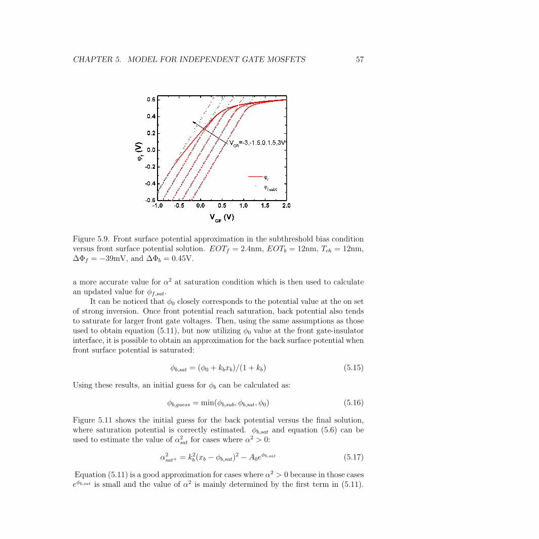
CHAPTER 5. MODEL FOR INDEPENDENT GATE MOSFETS 57
Figure 5.9. Front surface potential approximation in the subthreshold bias conditionversus front surface potential solution. EOTf = 2.4nm, EOTb = 12nm, Tch = 12nm,∆Φf = −39mV, and ∆Φb = 0.45V.
a more accurate value for α2 at saturation condition which is then used to calculatean updated value for φf,sat.
It can be noticed that φ0 closely corresponds to the potential value at the on setof strong inversion. Once front potential reach saturation, back potential also tendsto saturate for larger front gate voltages. Then, using the same assumptions as thoseused to obtain equation (5.11), but now utilizing φ0 value at the front gate-insulatorinterface, it is possible to obtain an approximation for the back surface potential whenfront surface potential is saturated:
φb,sat = (φ0 + kbxb)/(1 + kb) (5.15)
Using these results, an initial guess for φb can be calculated as:
φb,guess = min(φb,sub, φb,sat, φ0) (5.16)
Figure 5.11 shows the initial guess for the back potential versus the final solution,where saturation potential is correctly estimated. φb,sat and equation (5.6) can beused to estimate the value of α2
sat for cases where α2 > 0:
α2sat+ = k2b (xb − φb,sat)
2 − A0eφb,sat (5.17)
Equation (5.11) is a good approximation for cases where α2 > 0 because in those caseseφb,sat is small and the value of α2 is mainly determined by the first term in (5.11).
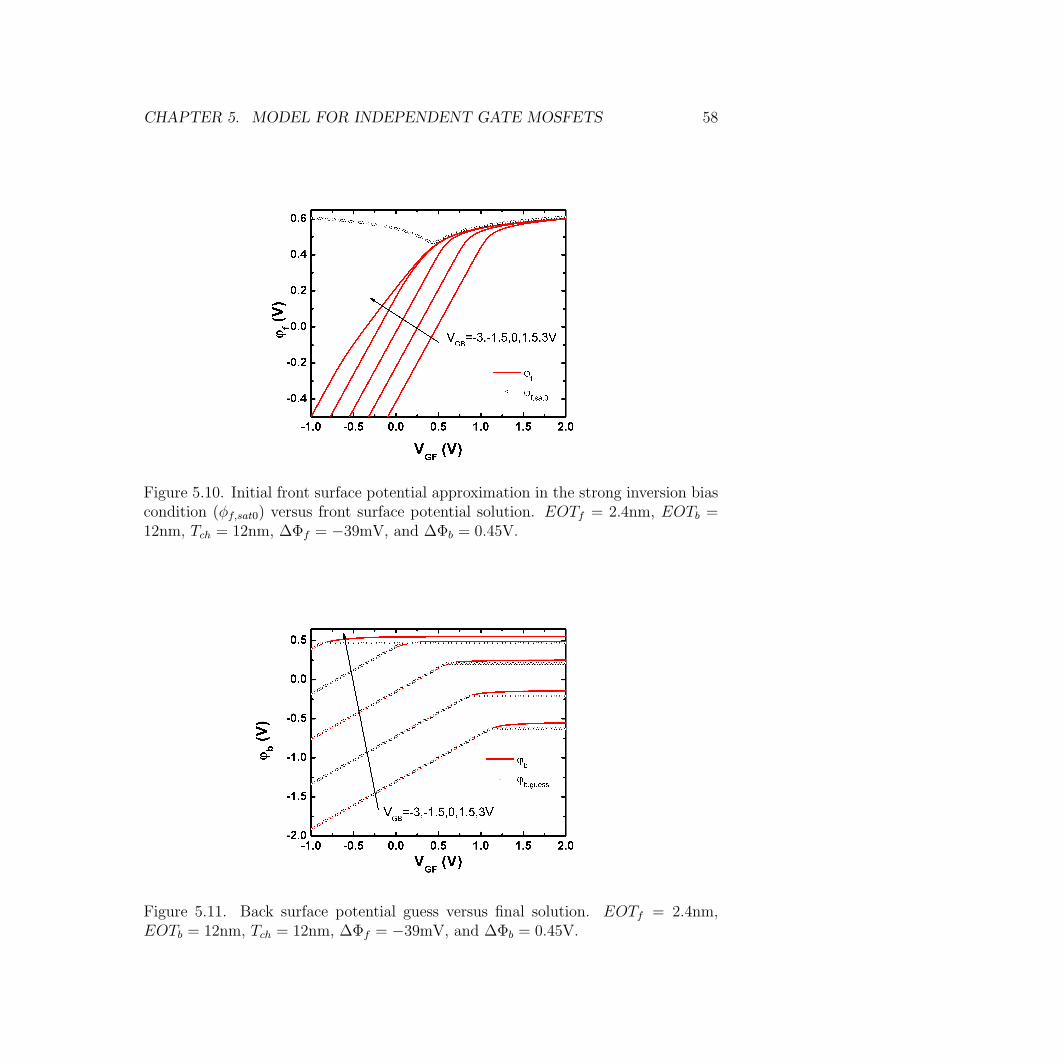
CHAPTER 5. MODEL FOR INDEPENDENT GATE MOSFETS 58
Figure 5.10. Initial front surface potential approximation in the strong inversion biascondition (φf,sat0) versus front surface potential solution. EOTf = 2.4nm, EOTb =12nm, Tch = 12nm, ∆Φf = −39mV, and ∆Φb = 0.45V.
Figure 5.11. Back surface potential guess versus final solution. EOTf = 2.4nm,EOTb = 12nm, Tch = 12nm, ∆Φf = −39mV, and ∆Φb = 0.45V.
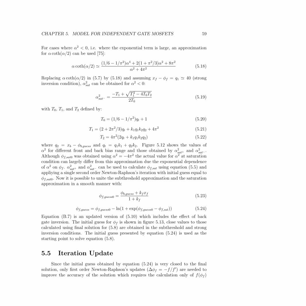
CHAPTER 5. MODEL FOR INDEPENDENT GATE MOSFETS 59
For cases where α2 < 0, i.e. where the exponential term is large, an approximationfor α coth(α/2) can be used [75]:
α coth(α/2) ≃ (1/6− 1/π2)α4 + 2(1 + π2/3)α2 + 8π2
α2 + 4π2(5.18)
Replacing α coth(α/2) in (5.7) by (5.18) and assuming xf − φf = q1 ≃ 40 (stronginversion condition), α2
sat can be obtained for α2 < 0:
α2sat− =
−T1 +√
T 21 − 4T0T2
2T0(5.19)
with T0, T1, and T2 defined by:
T0 = (1/6− 1/π2)qt + 1 (5.20)
T1 = (2 + 2π2/3)qt + k1q1k2q2 + 4π2 (5.21)
T2 = 4π2(2qt + k1q1k2q2) (5.22)
where q2 = xb − φb,guess and qt = q1k1 + q2k2. Figure 5.12 shows the values ofα2 for different front and back bias range and those obtained by α2
sat+ and α2sat− .
Although φf,sat0 was obtained using α2 = −4π2 the actual value for α2 at saturationcondition can largely differ from this approximation due the exponential dependenceof α2 on φf . α
2sat+ and α2
sat− can be used to calculate φf,sat using equation (5.5) andappliying a single second order Newton-Raphson’s iteration with initial guess equal toφf,sat0. Now it is possible to unite the subthreshold approximation and the saturationapproximation in a smooth manner with:
φf,guess0 =φb,guess + kfxf
1 + kf(5.23)
φf,guess = φf,guess0 − ln(1 + exp(φf,guess0 − φf,sat)) (5.24)
Equation (B.7) is an updated version of (5.10) which includes the effect of backgate inversion. The initial guess for φf is shown in figure 5.13, close values to thosecalculated using final solution for (5.8) are obtained in the subthreshold and stronginversion conditions. The initial guess presented by equation (5.24) is used as thestarting point to solve equation (5.8).
5.5 Iteration Update
Since the initial guess obtained by equation (5.24) is very closed to the finalsolution, only first order Newton-Raphson’s updates (∆φf = −f/f ′) are needed toimprove the accuracy of the solution which requires the calculation only of f(φf )
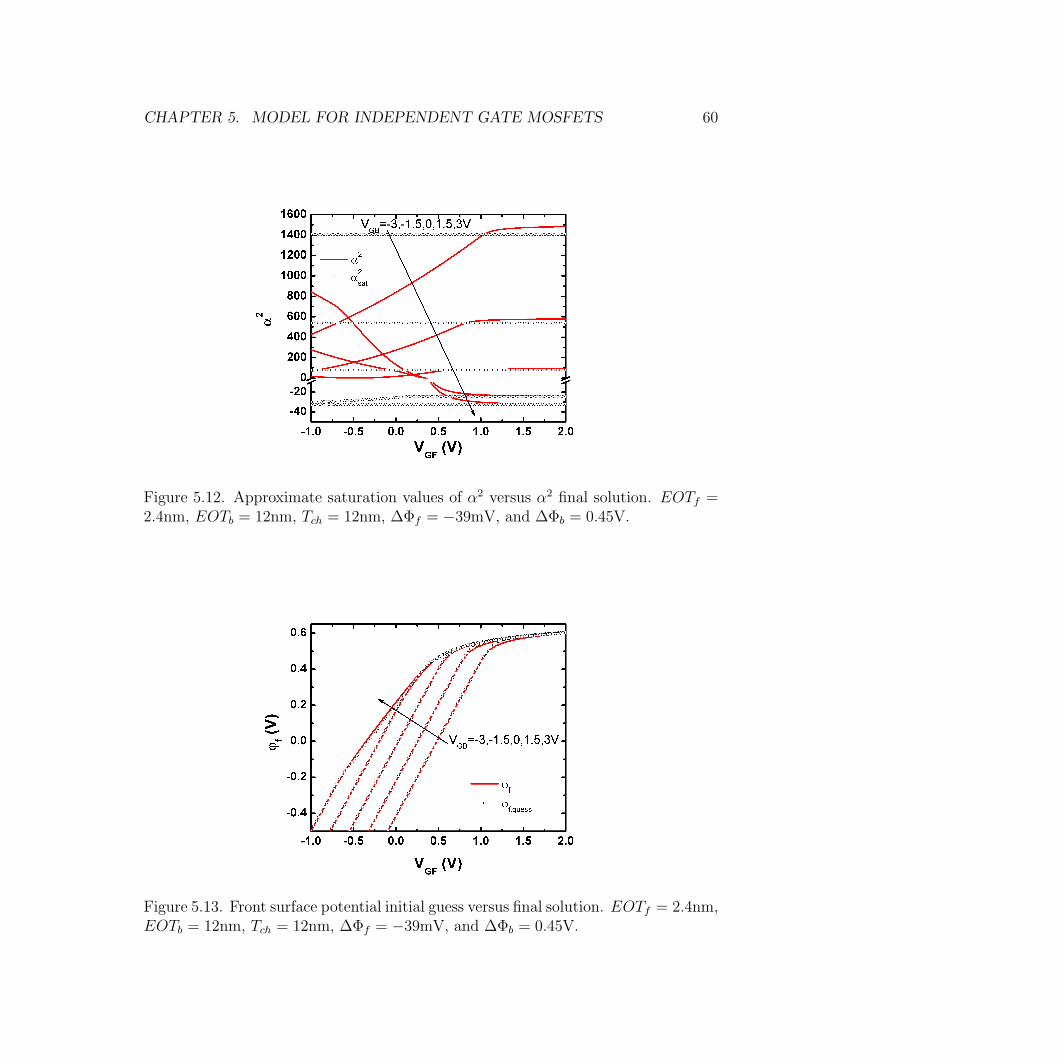
CHAPTER 5. MODEL FOR INDEPENDENT GATE MOSFETS 60
Figure 5.12. Approximate saturation values of α2 versus α2 final solution. EOTf =2.4nm, EOTb = 12nm, Tch = 12nm, ∆Φf = −39mV, and ∆Φb = 0.45V.
Figure 5.13. Front surface potential initial guess versus final solution. EOTf = 2.4nm,EOTb = 12nm, Tch = 12nm, ∆Φf = −39mV, and ∆Φb = 0.45V.
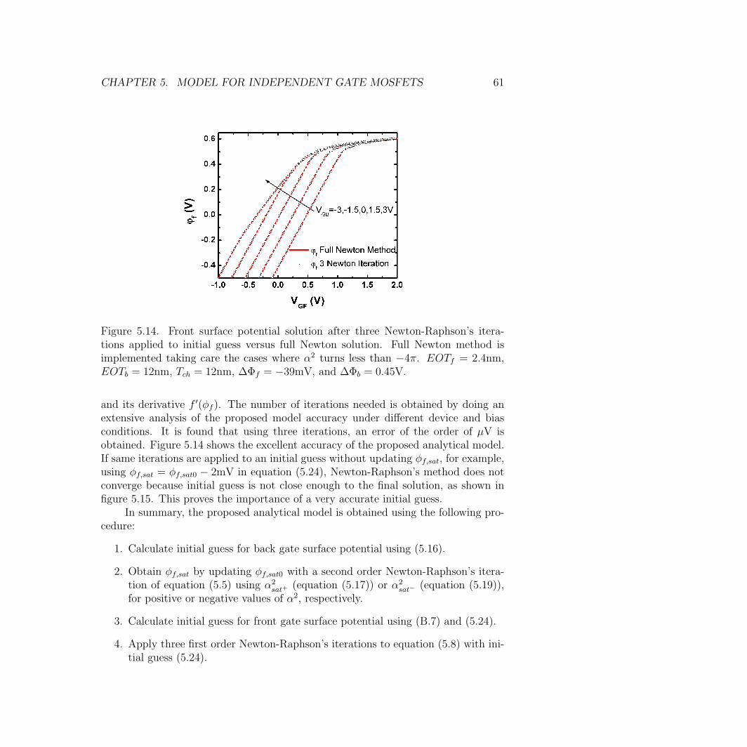
CHAPTER 5. MODEL FOR INDEPENDENT GATE MOSFETS 61
Figure 5.14. Front surface potential solution after three Newton-Raphson’s itera-tions applied to initial guess versus full Newton solution. Full Newton method isimplemented taking care the cases where α2 turns less than −4π. EOTf = 2.4nm,EOTb = 12nm, Tch = 12nm, ∆Φf = −39mV, and ∆Φb = 0.45V.
and its derivative f ′(φf ). The number of iterations needed is obtained by doing anextensive analysis of the proposed model accuracy under different device and biasconditions. It is found that using three iterations, an error of the order of µV isobtained. Figure 5.14 shows the excellent accuracy of the proposed analytical model.If same iterations are applied to an initial guess without updating φf,sat, for example,using φf,sat = φf,sat0 − 2mV in equation (5.24), Newton-Raphson’s method does notconverge because initial guess is not close enough to the final solution, as shown infigure 5.15. This proves the importance of a very accurate initial guess.
In summary, the proposed analytical model is obtained using the following pro-cedure:
1. Calculate initial guess for back gate surface potential using (5.16).
2. Obtain φf,sat by updating φf,sat0 with a second order Newton-Raphson’s itera-tion of equation (5.5) using α2
sat+ (equation (5.17)) or α2sat− (equation (5.19)),
for positive or negative values of α2, respectively.
3. Calculate initial guess for front gate surface potential using (B.7) and (5.24).
4. Apply three first order Newton-Raphson’s iterations to equation (5.8) with ini-tial guess (5.24).
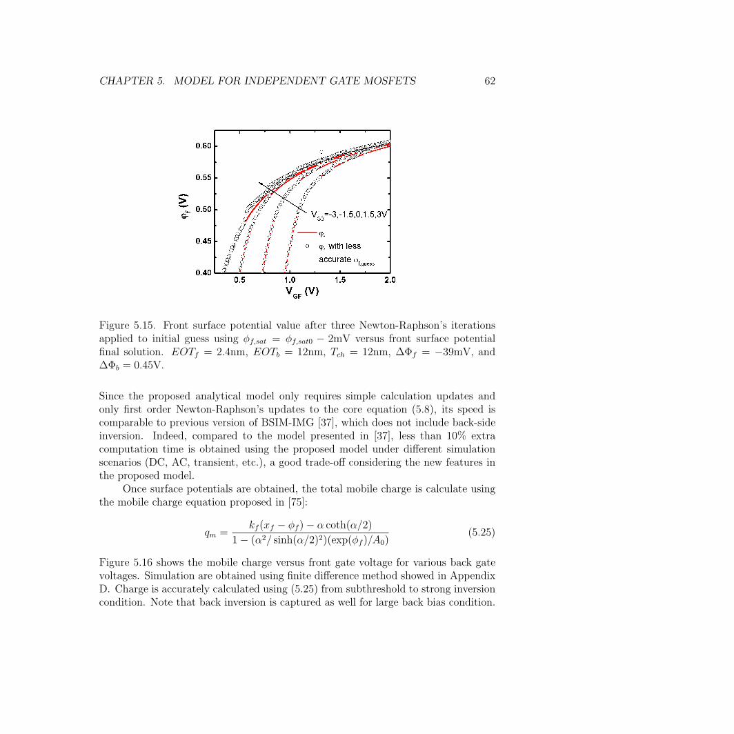
CHAPTER 5. MODEL FOR INDEPENDENT GATE MOSFETS 62
Figure 5.15. Front surface potential value after three Newton-Raphson’s iterationsapplied to initial guess using φf,sat = φf,sat0 − 2mV versus front surface potentialfinal solution. EOTf = 2.4nm, EOTb = 12nm, Tch = 12nm, ∆Φf = −39mV, and∆Φb = 0.45V.
Since the proposed analytical model only requires simple calculation updates andonly first order Newton-Raphson’s updates to the core equation (5.8), its speed iscomparable to previous version of BSIM-IMG [37], which does not include back-sideinversion. Indeed, compared to the model presented in [37], less than 10% extracomputation time is obtained using the proposed model under different simulationscenarios (DC, AC, transient, etc.), a good trade-off considering the new features inthe proposed model.
Once surface potentials are obtained, the total mobile charge is calculate usingthe mobile charge equation proposed in [75]:
qm =kf (xf − φf )− α coth(α/2)
1− (α2/ sinh(α/2)2)(exp(φf )/A0)(5.25)
Figure 5.16 shows the mobile charge versus front gate voltage for various back gatevoltages. Simulation are obtained using finite difference method showed in AppendixD. Charge is accurately calculated using (5.25) from subthreshold to strong inversioncondition. Note that back inversion is captured as well for large back bias condition.
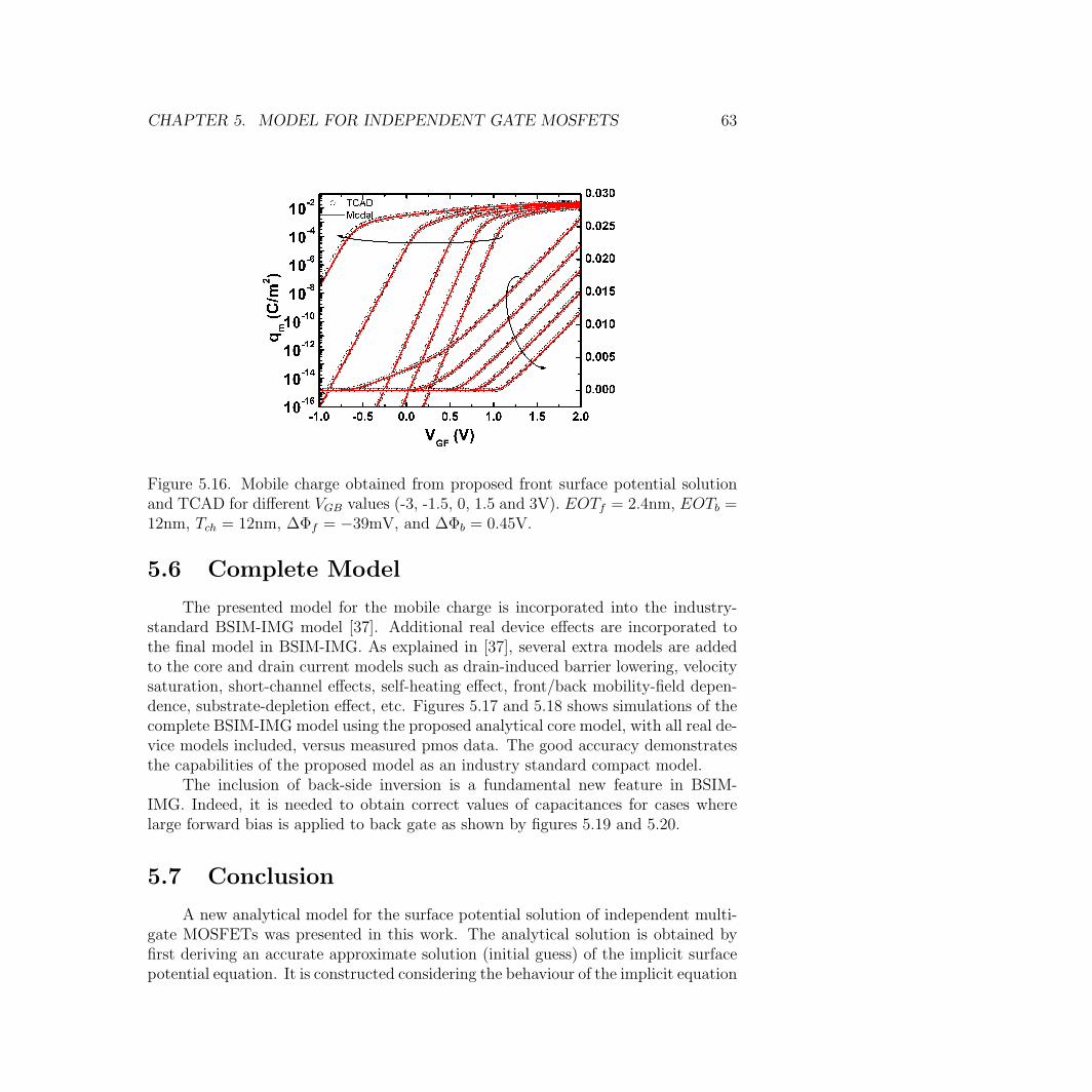
CHAPTER 5. MODEL FOR INDEPENDENT GATE MOSFETS 63
Figure 5.16. Mobile charge obtained from proposed front surface potential solutionand TCAD for different VGB values (-3, -1.5, 0, 1.5 and 3V). EOTf = 2.4nm, EOTb =12nm, Tch = 12nm, ∆Φf = −39mV, and ∆Φb = 0.45V.
5.6 Complete Model
The presented model for the mobile charge is incorporated into the industry-standard BSIM-IMG model [37]. Additional real device effects are incorporated tothe final model in BSIM-IMG. As explained in [37], several extra models are addedto the core and drain current models such as drain-induced barrier lowering, velocitysaturation, short-channel effects, self-heating effect, front/back mobility-field depen-dence, substrate-depletion effect, etc. Figures 5.17 and 5.18 shows simulations of thecomplete BSIM-IMG model using the proposed analytical core model, with all real de-vice models included, versus measured pmos data. The good accuracy demonstratesthe capabilities of the proposed model as an industry standard compact model.
The inclusion of back-side inversion is a fundamental new feature in BSIM-IMG. Indeed, it is needed to obtain correct values of capacitances for cases wherelarge forward bias is applied to back gate as shown by figures 5.19 and 5.20.
5.7 Conclusion
A new analytical model for the surface potential solution of independent multi-gate MOSFETs was presented in this work. The analytical solution is obtained byfirst deriving an accurate approximate solution (initial guess) of the implicit surfacepotential equation. It is constructed considering the behaviour of the implicit equation
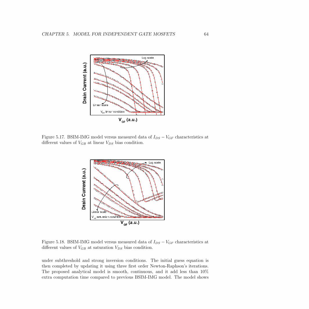
CHAPTER 5. MODEL FOR INDEPENDENT GATE MOSFETS 64
Figure 5.17. BSIM-IMG model versus measured data of IDS − VGF characteristics atdifferent values of VGB at linear VDS bias condition.
Figure 5.18. BSIM-IMG model versus measured data of IDS − VGF characteristics atdifferent values of VGB at saturation VDS bias condition.
under subthreshold and strong inversion conditions. The initial guess equation isthen completed by updating it using three first order Newton-Raphson’s iterations.The proposed analytical model is smooth, continuous, and it add less than 10%extra computation time compared to previous BSIM-IMG model. The model shows
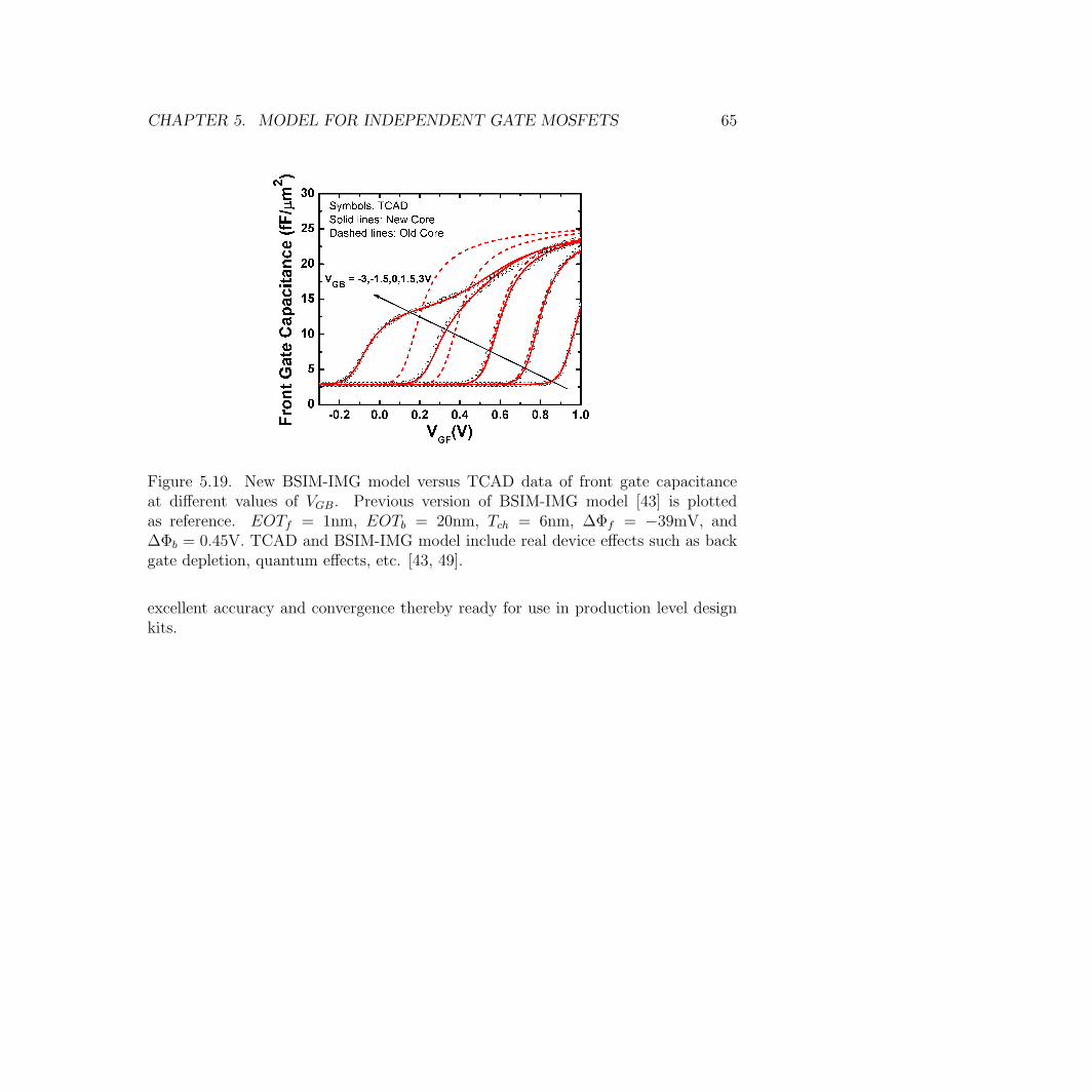
CHAPTER 5. MODEL FOR INDEPENDENT GATE MOSFETS 65
Figure 5.19. New BSIM-IMG model versus TCAD data of front gate capacitanceat different values of VGB. Previous version of BSIM-IMG model [43] is plottedas reference. EOTf = 1nm, EOTb = 20nm, Tch = 6nm, ∆Φf = −39mV, and∆Φb = 0.45V. TCAD and BSIM-IMG model include real device effects such as backgate depletion, quantum effects, etc. [43, 49].
excellent accuracy and convergence thereby ready for use in production level designkits.
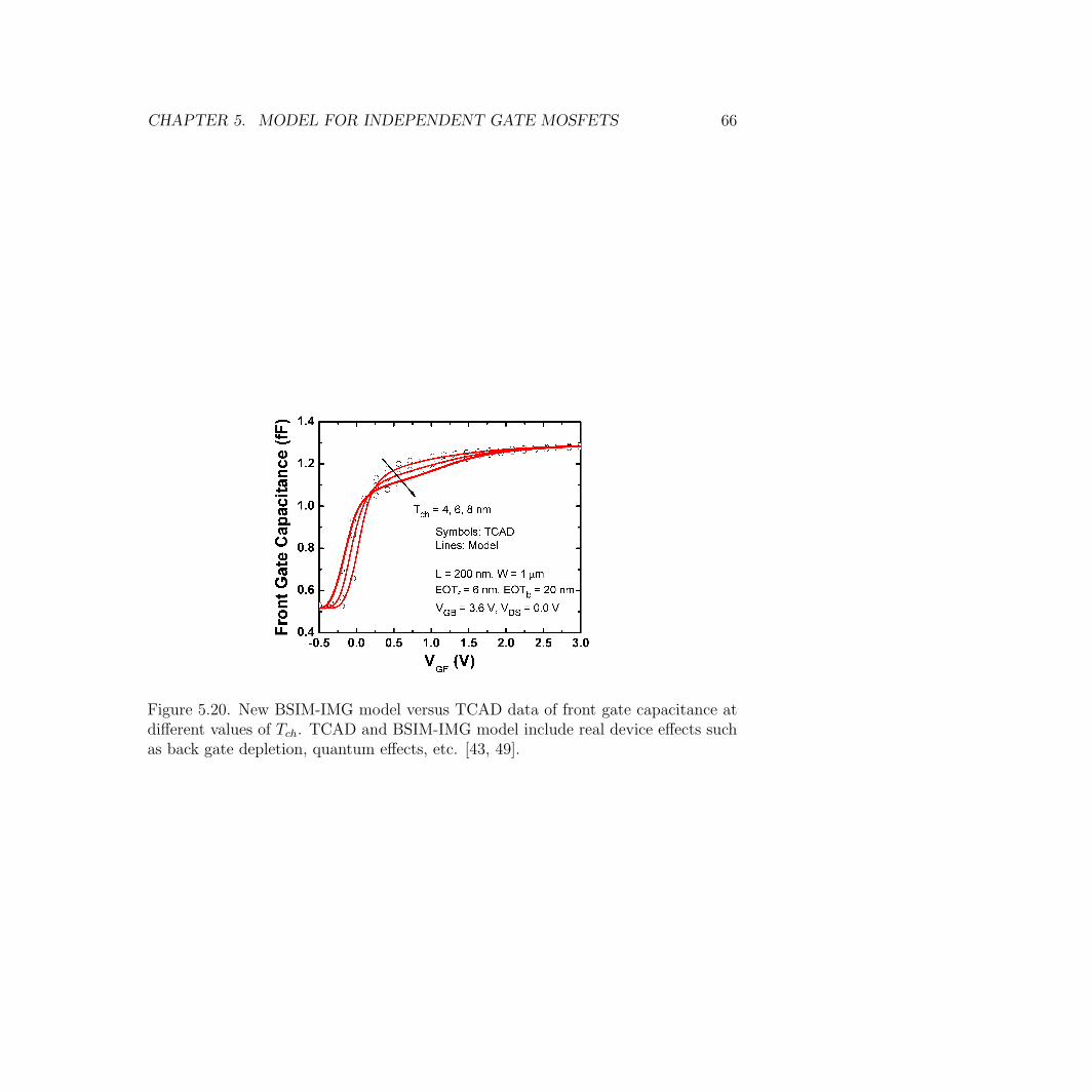
CHAPTER 5. MODEL FOR INDEPENDENT GATE MOSFETS 66
Figure 5.20. New BSIM-IMG model versus TCAD data of front gate capacitance atdifferent values of Tch. TCAD and BSIM-IMG model include real device effects suchas back gate depletion, quantum effects, etc. [43, 49].
67
Chapter 6
Model for Negative CapacitanceFETs
6.1 Introduction
Negative capacitance FETs (fig. 6.1) are quickly emerging as promising devicesto achieve sub-60 mV/decade sub-threshold slope and high Ion [80, 10]. With recentexperimental demonstrations of FE based NC-FETs [46, 45], there is an urgent needfor analysis of device operation and circuit performance via compact models. Inour previous work [38], we presented a lumped charge model NC-FinFETs. In thiswork we derive new insights into the device operation by analyzing and modelingboth devices with floating metal gate and without it. The distributed charge modelneeds to be used for device without the floating metal. Significant differences in thecharacteristics of these two types of NC-FinFETs will be presented.
6.2 Unified Compact Model
The unified compact model, BSIM-CMG accurately predicts the charge andcurrent voltage characteristics of different FinFETs and gate-all-around structures[23]. BSIM-CMG’s core equation is a single unified charge model (UCM), a closedform relationship between the mobile charge (Qm) and the applied terminal voltages(VG,VD,VS,VB) given in a normalized form as follows:
vG − vo − vch = −qm + ln (−qm) + ln
(
q2teqt − qt − 1
)
(6.1)
where vch is the normalized channel potential. vo and qt are defined in table 6.1.TheUCM requires only four different model parameters [23]: insulator capacitance (Cins),

CHAPTER 6. MODEL FOR NEGATIVE CAPACITANCE FETS 68
Figure 6.1. Schematic of NC-FinFETs: 3D and 2D device cut. Lumped NC-FinFET(top) has a floating gate between insulator and FE. The distributed NC-FET (bottom)does not have a floating gate.
channel area (Ach), channel doping (Nch) and effective channel width (Weff ). Usingthese parameters, we accurately modeled the characteristics of a 14nm node Ultra-Low-Power FinFET [36], which is the baseline FinFET technology used in this work.
6.3 Ferroelectric Material Model
A compact model of FE materials, which captures the negative capacitancecorrectly, is obtained using the Landau Khalatnikov (LK) equation [44]. LK expressesthe relationship between electric-field (E) and polarization (P ) of a FE:
E = 2αP + 4βP 3 + 6γP 5 (6.2)
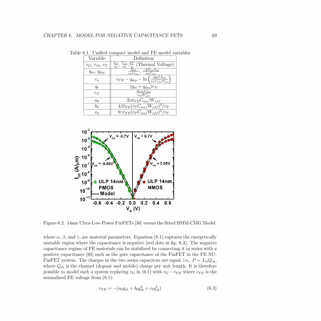
CHAPTER 6. MODEL FOR NEGATIVE CAPACITANCE FETS 69
Table 6.1. Unified compact model and FE model variablesVariable Definition
vG, vch, vTVGvT, VchvT
,kTq
(Thermal Voltage)
qm, qdepQm
vTCins, −qNchAch
vTCins
vo vFB − qdep − ln(
2qn2iAch
vTCinsNch
)
qt (qm + qdep)rNrN
AFinCinsεchW
2eff
a0 2αtFECins/Weff
b0 4βtFE(vTCins/Weff )3/vT
c0 6γtFE(vTCins/Weff )5/vT
Figure 6.2. 14nm Ultra-Low-Power FinFETs [36] versus the fitted BSIM-CMGModel.
where α, β, and γ, are material parameters. Equation (8.1) captures the energeticallyunstable region where the capacitance is negative (red dots in fig. 6.3). The negativecapacitance regime of FE materials can be stabilized by connecting it in series with apositive capacitance [80] such as the gate capacitance of the FinFET in the FE NC-FinFET system. The charges in the two series capacitors are equal, i.e., P = LGQch,where Qch is the channel (dopant and mobile) charge per unit length. It is thereforepossible to model such a system replacing vG in (6.1) with vG− vFE where vFE is thenormalized FE voltage from (8.1):
vFE = −(a0qch + b0q3ch + c0q
5ch) (6.3)
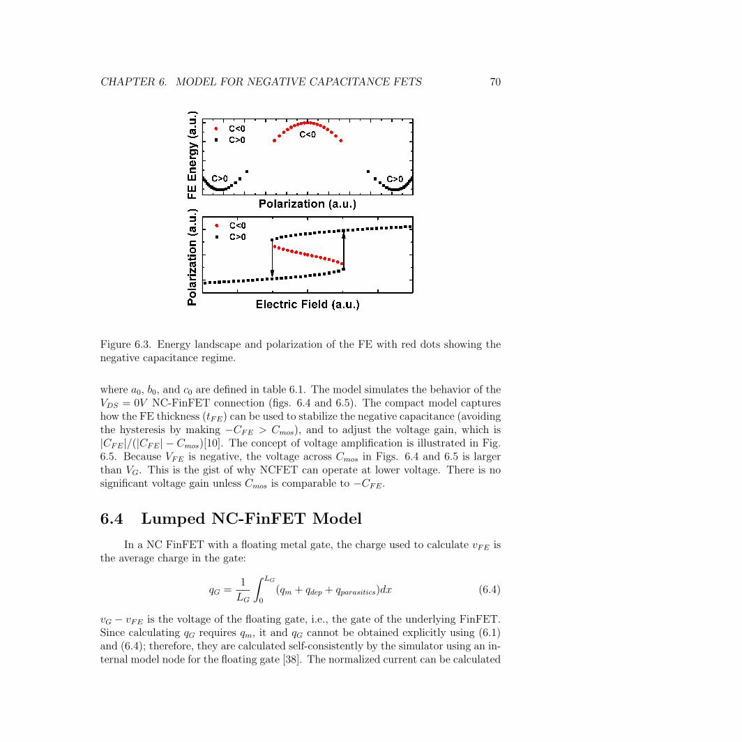
CHAPTER 6. MODEL FOR NEGATIVE CAPACITANCE FETS 70
Figure 6.3. Energy landscape and polarization of the FE with red dots showing thenegative capacitance regime.
where a0, b0, and c0 are defined in table 6.1. The model simulates the behavior of theVDS = 0V NC-FinFET connection (figs. 6.4 and 6.5). The compact model captureshow the FE thickness (tFE) can be used to stabilize the negative capacitance (avoidingthe hysteresis by making −CFE > Cmos), and to adjust the voltage gain, which is|CFE|/(|CFE| − Cmos)[10]. The concept of voltage amplification is illustrated in Fig.6.5. Because VFE is negative, the voltage across Cmos in Figs. 6.4 and 6.5 is largerthan VG. This is the gist of why NCFET can operate at lower voltage. There is nosignificant voltage gain unless Cmos is comparable to −CFE.
6.4 Lumped NC-FinFET Model
In a NC FinFET with a floating metal gate, the charge used to calculate vFE isthe average charge in the gate:
qG =1
LG
∫ LG
0
(qm + qdep + qparasitics)dx (6.4)
vG − vFE is the voltage of the floating gate, i.e., the gate of the underlying FinFET.Since calculating qG requires qm, it and qG cannot be obtained explicitly using (6.1)and (6.4); therefore, they are calculated self-consistently by the simulator using an in-ternal model node for the floating gate [38]. The normalized current can be calculated
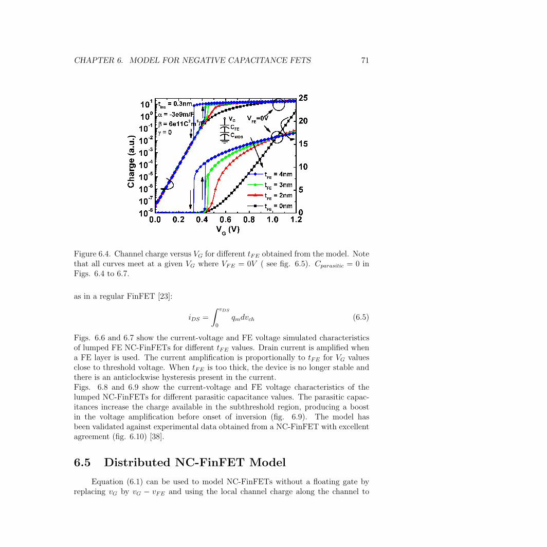
CHAPTER 6. MODEL FOR NEGATIVE CAPACITANCE FETS 71
Figure 6.4. Channel charge versus VG for different tFE obtained from the model. Notethat all curves meet at a given VG where VFE = 0V ( see fig. 6.5). Cparasitic = 0 inFigs. 6.4 to 6.7.
as in a regular FinFET [23]:
iDS =
∫ vDS
0
qmdvch (6.5)
Figs. 6.6 and 6.7 show the current-voltage and FE voltage simulated characteristicsof lumped FE NC-FinFETs for different tFE values. Drain current is amplified whena FE layer is used. The current amplification is proportionally to tFE for VG valuesclose to threshold voltage. When tFE is too thick, the device is no longer stable andthere is an anticlockwise hysteresis present in the current.Figs. 6.8 and 6.9 show the current-voltage and FE voltage characteristics of thelumped NC-FinFETs for different parasitic capacitance values. The parasitic capac-itances increase the charge available in the subthreshold region, producing a boostin the voltage amplification before onset of inversion (fig. 6.9). The model hasbeen validated against experimental data obtained from a NC-FinFET with excellentagreement (fig. 6.10) [38].
6.5 Distributed NC-FinFET Model
Equation (6.1) can be used to model NC-FinFETs without a floating gate byreplacing vG by vG − vFE and using the local channel charge along the channel to
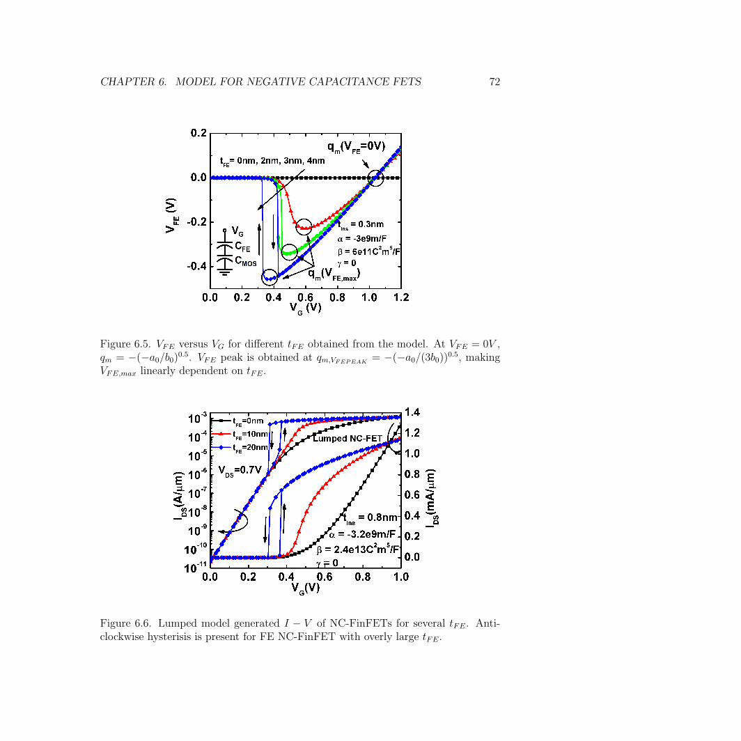
CHAPTER 6. MODEL FOR NEGATIVE CAPACITANCE FETS 72
Figure 6.5. VFE versus VG for different tFE obtained from the model. At VFE = 0V ,qm = −(−a0/b0)0.5. VFE peak is obtained at qm,VFEPEAK = −(−a0/(3b0))0.5, makingVFE,max linearly dependent on tFE.
Figure 6.6. Lumped model generated I − V of NC-FinFETs for several tFE. Anti-clockwise hysterisis is present for FE NC-FinFET with overly large tFE.
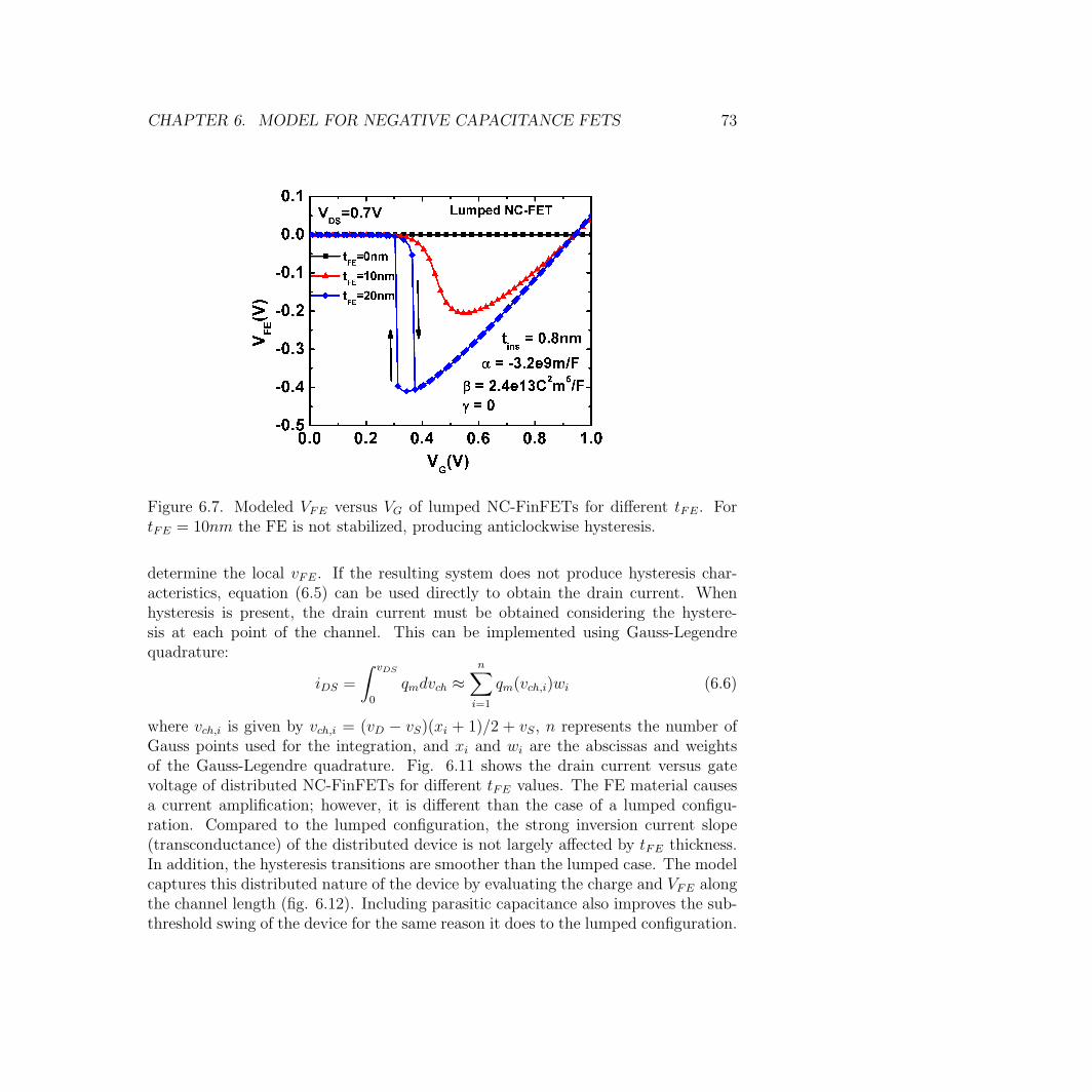
CHAPTER 6. MODEL FOR NEGATIVE CAPACITANCE FETS 73
Figure 6.7. Modeled VFE versus VG of lumped NC-FinFETs for different tFE. FortFE = 10nm the FE is not stabilized, producing anticlockwise hysteresis.
determine the local vFE. If the resulting system does not produce hysteresis char-acteristics, equation (6.5) can be used directly to obtain the drain current. Whenhysteresis is present, the drain current must be obtained considering the hystere-sis at each point of the channel. This can be implemented using Gauss-Legendrequadrature:
iDS =
∫ vDS
0
qmdvch ≈n∑
i=1
qm(vch,i)wi (6.6)
where vch,i is given by vch,i = (vD − vS)(xi + 1)/2 + vS, n represents the number ofGauss points used for the integration, and xi and wi are the abscissas and weightsof the Gauss-Legendre quadrature. Fig. 6.11 shows the drain current versus gatevoltage of distributed NC-FinFETs for different tFE values. The FE material causesa current amplification; however, it is different than the case of a lumped configu-ration. Compared to the lumped configuration, the strong inversion current slope(transconductance) of the distributed device is not largely affected by tFE thickness.In addition, the hysteresis transitions are smoother than the lumped case. The modelcaptures this distributed nature of the device by evaluating the charge and VFE alongthe channel length (fig. 6.12). Including parasitic capacitance also improves the sub-threshold swing of the device for the same reason it does to the lumped configuration.
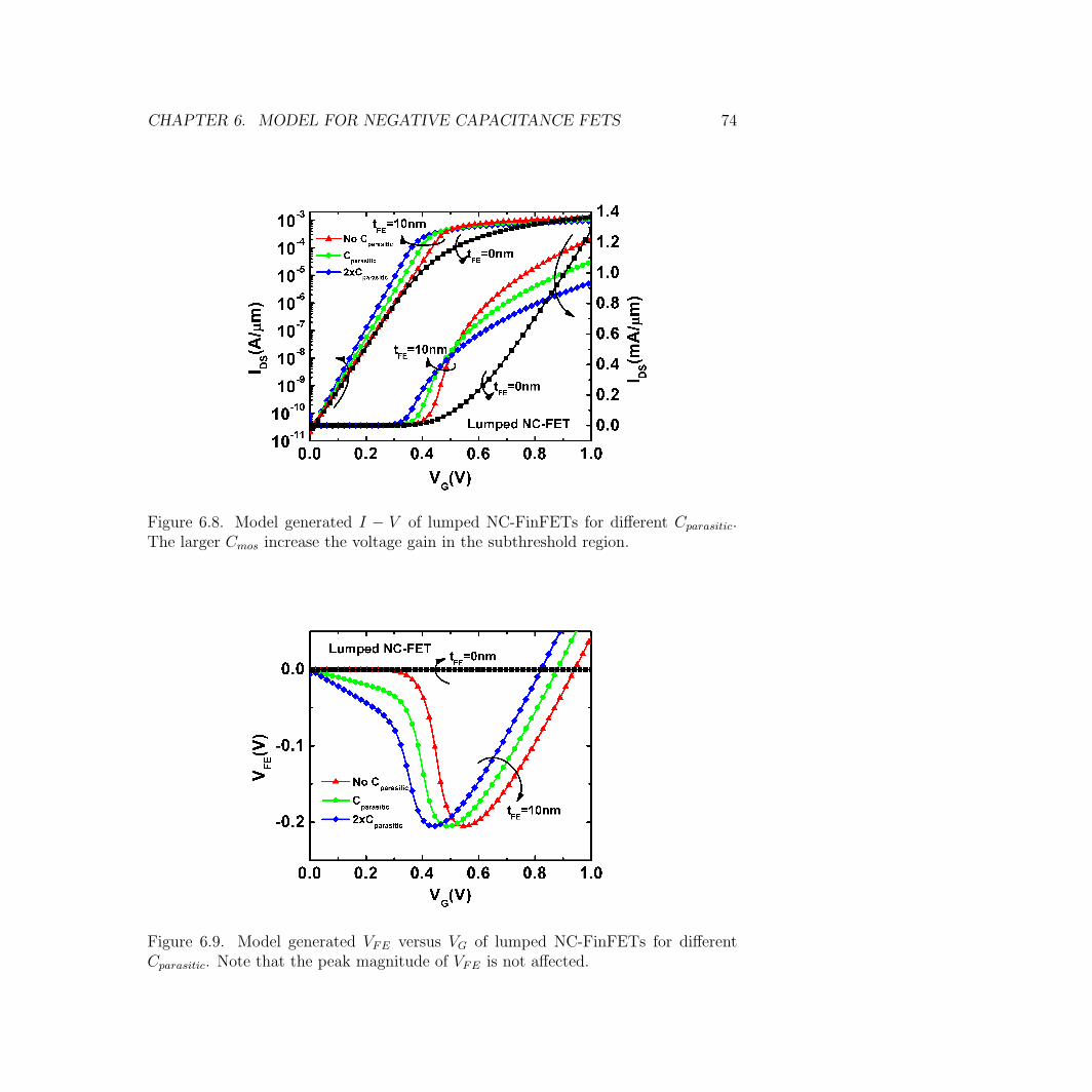
CHAPTER 6. MODEL FOR NEGATIVE CAPACITANCE FETS 74
Figure 6.8. Model generated I − V of lumped NC-FinFETs for different Cparasitic.The larger Cmos increase the voltage gain in the subthreshold region.
Figure 6.9. Model generated VFE versus VG of lumped NC-FinFETs for differentCparasitic. Note that the peak magnitude of VFE is not affected.
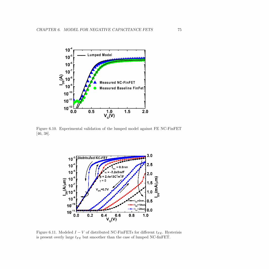
CHAPTER 6. MODEL FOR NEGATIVE CAPACITANCE FETS 75
Figure 6.10. Experimental validation of the lumped model against FE NC-FinFET[46, 38].
Figure 6.11. Modeled I − V of distributed NC-FinFETs for different tFE. Hysterisisis present overly large tFE but smoother than the case of lumped NC-finFET.
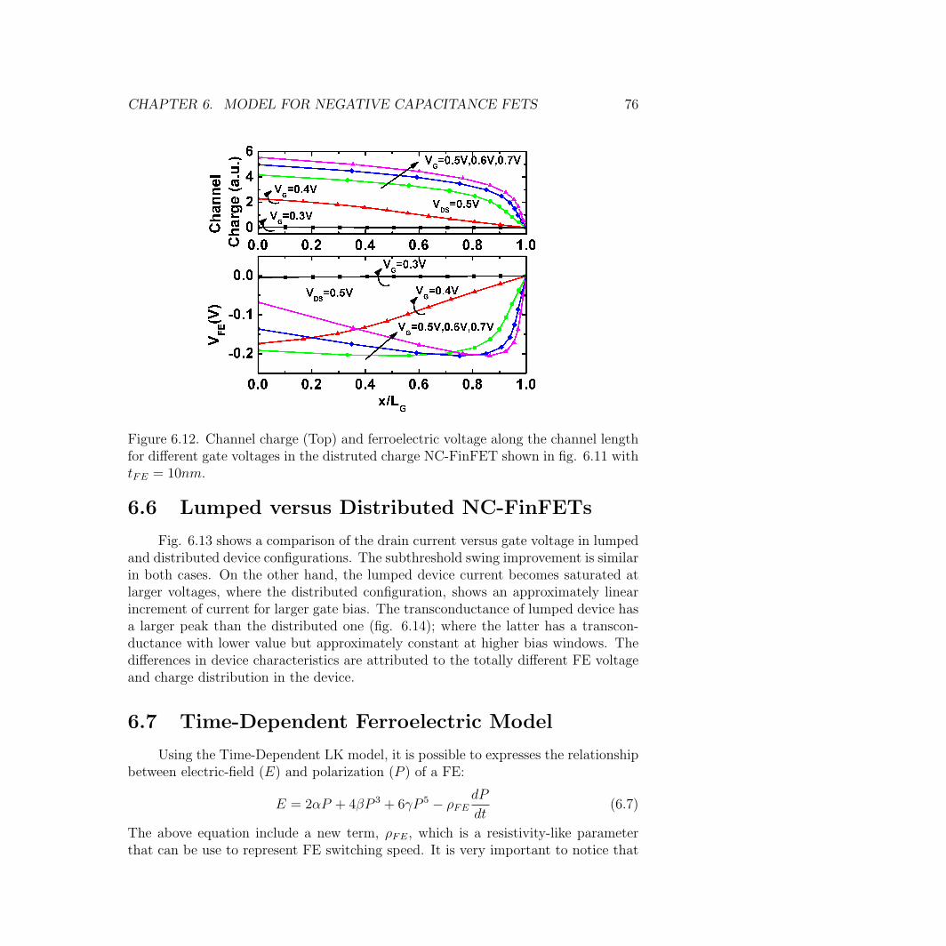
CHAPTER 6. MODEL FOR NEGATIVE CAPACITANCE FETS 76
Figure 6.12. Channel charge (Top) and ferroelectric voltage along the channel lengthfor different gate voltages in the distruted charge NC-FinFET shown in fig. 6.11 withtFE = 10nm.
6.6 Lumped versus Distributed NC-FinFETs
Fig. 6.13 shows a comparison of the drain current versus gate voltage in lumpedand distributed device configurations. The subthreshold swing improvement is similarin both cases. On the other hand, the lumped device current becomes saturated atlarger voltages, where the distributed configuration, shows an approximately linearincrement of current for larger gate bias. The transconductance of lumped device hasa larger peak than the distributed one (fig. 6.14); where the latter has a transcon-ductance with lower value but approximately constant at higher bias windows. Thedifferences in device characteristics are attributed to the totally different FE voltageand charge distribution in the device.
6.7 Time-Dependent Ferroelectric Model
Using the Time-Dependent LK model, it is possible to expresses the relationshipbetween electric-field (E) and polarization (P ) of a FE:
E = 2αP + 4βP 3 + 6γP 5 − ρFEdP
dt(6.7)
The above equation include a new term, ρFE, which is a resistivity-like parameterthat can be use to represent FE switching speed. It is very important to notice that
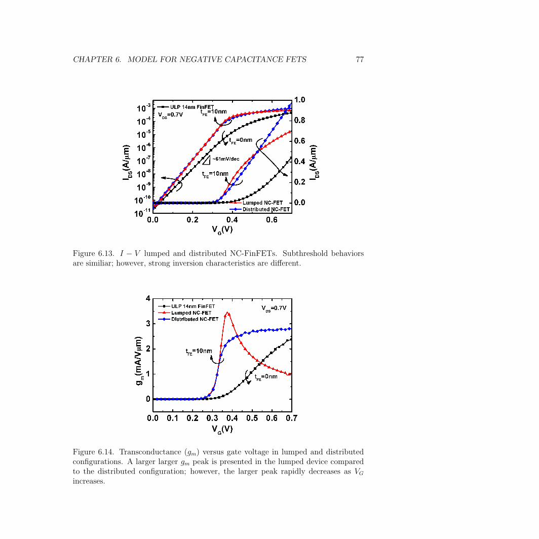
CHAPTER 6. MODEL FOR NEGATIVE CAPACITANCE FETS 77
Figure 6.13. I − V lumped and distributed NC-FinFETs. Subthreshold behaviorsare similiar; however, strong inversion characteristics are different.
Figure 6.14. Transconductance (gm) versus gate voltage in lumped and distributedconfigurations. A larger larger gm peak is presented in the lumped device comparedto the distributed configuration; however, the larger peak rapidly decreases as VGincreases.
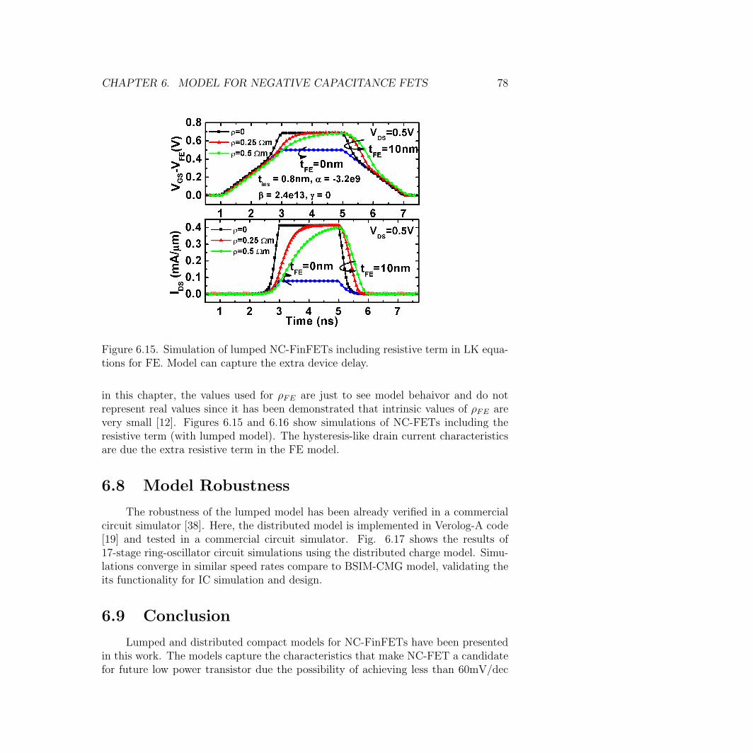
CHAPTER 6. MODEL FOR NEGATIVE CAPACITANCE FETS 78
Figure 6.15. Simulation of lumped NC-FinFETs including resistive term in LK equa-tions for FE. Model can capture the extra device delay.
in this chapter, the values used for ρFE are just to see model behaivor and do notrepresent real values since it has been demonstrated that intrinsic values of ρFE arevery small [12]. Figures 6.15 and 6.16 show simulations of NC-FETs including theresistive term (with lumped model). The hysteresis-like drain current characteristicsare due the extra resistive term in the FE model.
6.8 Model Robustness
The robustness of the lumped model has been already verified in a commercialcircuit simulator [38]. Here, the distributed model is implemented in Verolog-A code[19] and tested in a commercial circuit simulator. Fig. 6.17 shows the results of17-stage ring-oscillator circuit simulations using the distributed charge model. Simu-lations converge in similar speed rates compare to BSIM-CMG model, validating theits functionality for IC simulation and design.
6.9 Conclusion
Lumped and distributed compact models for NC-FinFETs have been presentedin this work. The models capture the characteristics that make NC-FET a candidatefor future low power transistor due the possibility of achieving less than 60mV/dec
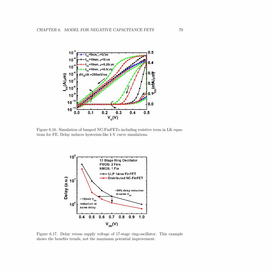
CHAPTER 6. MODEL FOR NEGATIVE CAPACITANCE FETS 79
Figure 6.16. Simulation of lumped NC-FinFETs including resistive term in LK equa-tions for FE. Delay induces hysterisis-like I-V curve simulations.
Figure 6.17. Delay versus supply voltage of 17-stage ring-oscillator. This exampleshows the benefits trends, not the maximum potential improvement.

CHAPTER 6. MODEL FOR NEGATIVE CAPACITANCE FETS 80
and higher on-current. Floating metal gate case is modeled via lumped compactmodel, while a distributed compact model is used for devices without floating metal.Clear I − V and gm differences between lumped and distributed devices are presentin the strong inversion condition. The proposed models are implemented and testedin circuit simulators.
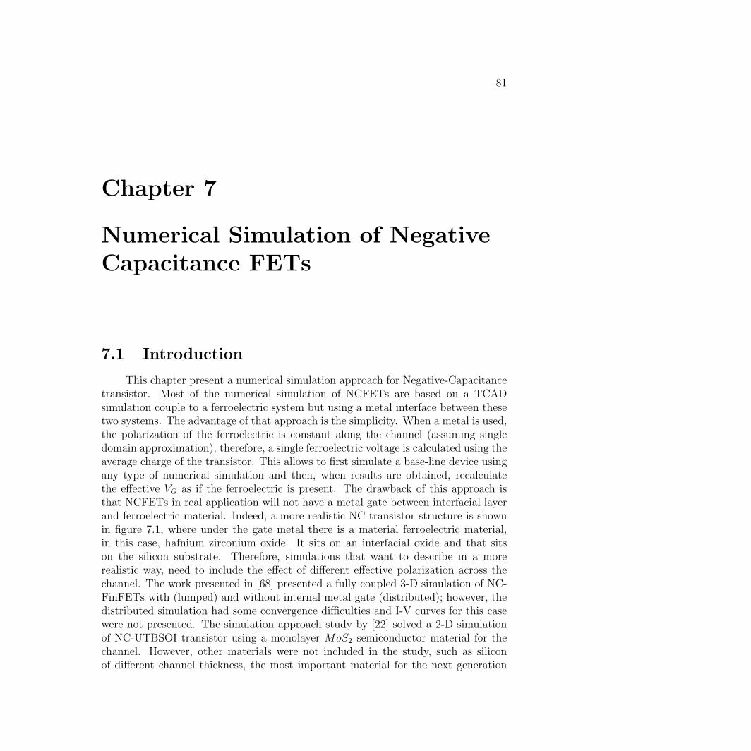
81
Chapter 7
Numerical Simulation of NegativeCapacitance FETs
7.1 Introduction
This chapter present a numerical simulation approach for Negative-Capacitancetransistor. Most of the numerical simulation of NCFETs are based on a TCADsimulation couple to a ferroelectric system but using a metal interface between thesetwo systems. The advantage of that approach is the simplicity. When a metal is used,the polarization of the ferroelectric is constant along the channel (assuming singledomain approximation); therefore, a single ferroelectric voltage is calculated using theaverage charge of the transistor. This allows to first simulate a base-line device usingany type of numerical simulation and then, when results are obtained, recalculatethe effective VG as if the ferroelectric is present. The drawback of this approach isthat NCFETs in real application will not have a metal gate between interfacial layerand ferroelectric material. Indeed, a more realistic NC transistor structure is shownin figure 7.1, where under the gate metal there is a material ferroelectric material,in this case, hafnium zirconium oxide. It sits on an interfacial oxide and that sitson the silicon substrate. Therefore, simulations that want to describe in a morerealistic way, need to include the effect of different effective polarization across thechannel. The work presented in [68] presented a fully coupled 3-D simulation of NC-FinFETs with (lumped) and without internal metal gate (distributed); however, thedistributed simulation had some convergence difficulties and I-V curves for this casewere not presented. The simulation approach study by [22] solved a 2-D simulationof NC-UTBSOI transistor using a monolayer MoS2 semiconductor material for thechannel. However, other materials were not included in the study, such as siliconof different channel thickness, the most important material for the next generation
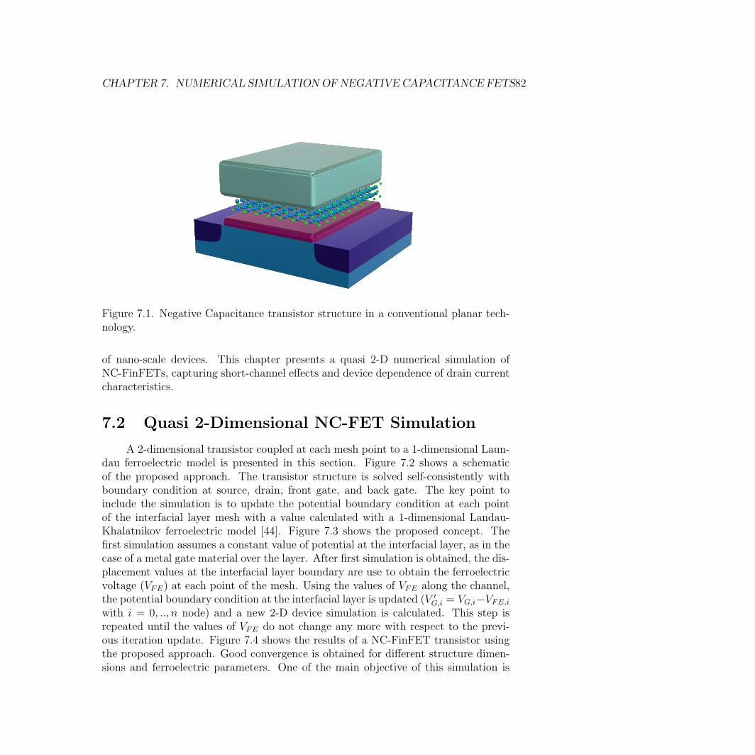
CHAPTER 7. NUMERICAL SIMULATIONOF NEGATIVE CAPACITANCE FETS82
Figure 7.1. Negative Capacitance transistor structure in a conventional planar tech-nology.
of nano-scale devices. This chapter presents a quasi 2-D numerical simulation ofNC-FinFETs, capturing short-channel effects and device dependence of drain currentcharacteristics.
7.2 Quasi 2-Dimensional NC-FET Simulation
A 2-dimensional transistor coupled at each mesh point to a 1-dimensional Laun-dau ferroelectric model is presented in this section. Figure 7.2 shows a schematicof the proposed approach. The transistor structure is solved self-consistently withboundary condition at source, drain, front gate, and back gate. The key point toinclude the simulation is to update the potential boundary condition at each pointof the interfacial layer mesh with a value calculated with a 1-dimensional Landau-Khalatnikov ferroelectric model [44]. Figure 7.3 shows the proposed concept. Thefirst simulation assumes a constant value of potential at the interfacial layer, as in thecase of a metal gate material over the layer. After first simulation is obtained, the dis-placement values at the interfacial layer boundary are use to obtain the ferroelectricvoltage (VFE) at each point of the mesh. Using the values of VFE along the channel,the potential boundary condition at the interfacial layer is updated (V ′
G,i = VG,i−VFE,iwith i = 0, .., n node) and a new 2-D device simulation is calculated. This step isrepeated until the values of VFE do not change any more with respect to the previ-ous iteration update. Figure 7.4 shows the results of a NC-FinFET transistor usingthe proposed approach. Good convergence is obtained for different structure dimen-sions and ferroelectric parameters. One of the main objective of this simulation is
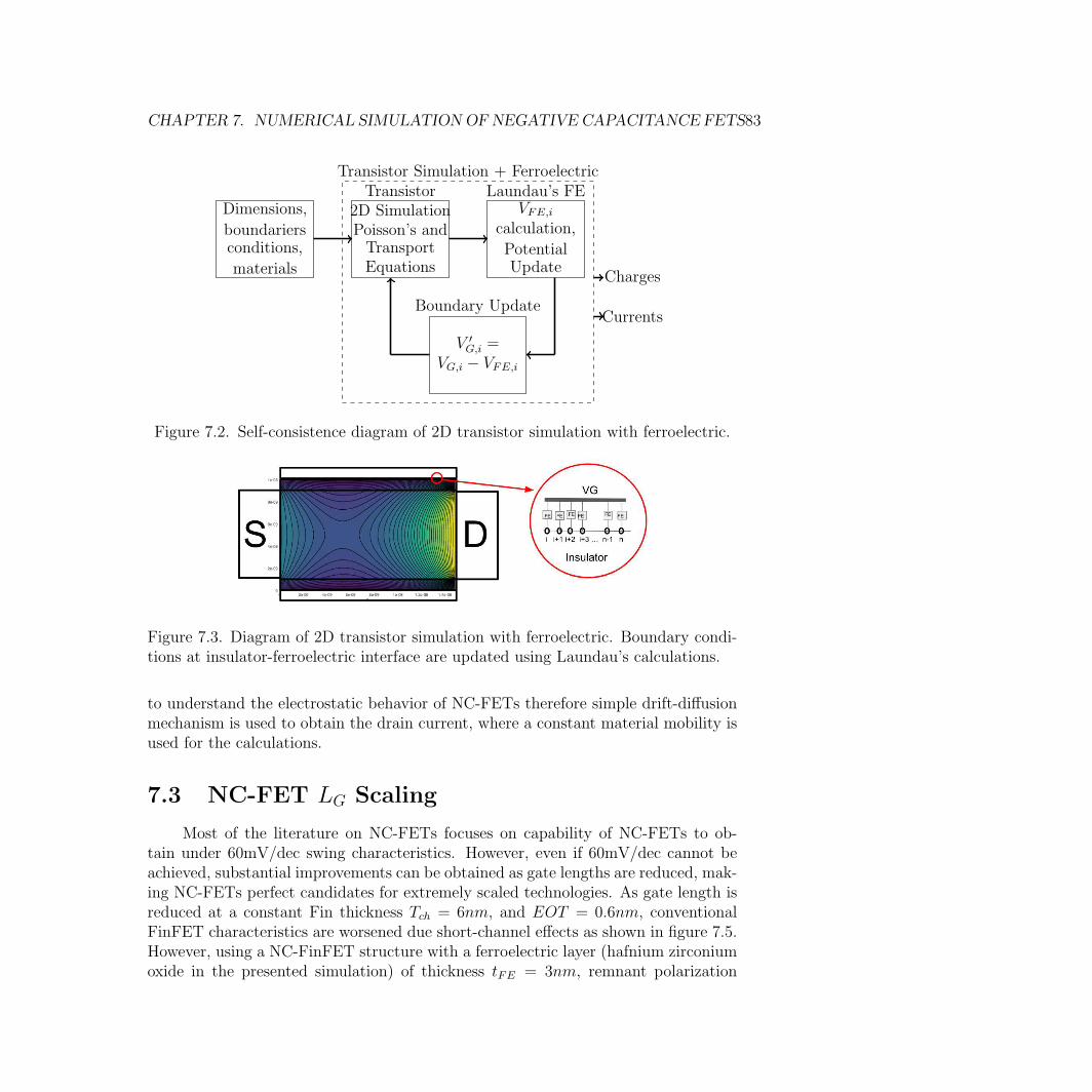
CHAPTER 7. NUMERICAL SIMULATIONOF NEGATIVE CAPACITANCE FETS83
Dimensions,
boundariersconditions,
materials
Transistor Simulation + FerroelectricTransistor
2D SimulationPoisson’s andTransportEquations
Laundau’s FEVFE,i
calculation,
PotentialUpdate
Charges
CurrentsBoundary Update
V ′
G,i =VG,i − VFE,i
Figure 7.2. Self-consistence diagram of 2D transistor simulation with ferroelectric.
Figure 7.3. Diagram of 2D transistor simulation with ferroelectric. Boundary condi-tions at insulator-ferroelectric interface are updated using Laundau’s calculations.
to understand the electrostatic behavior of NC-FETs therefore simple drift-diffusionmechanism is used to obtain the drain current, where a constant material mobility isused for the calculations.
7.3 NC-FET LG Scaling
Most of the literature on NC-FETs focuses on capability of NC-FETs to ob-tain under 60mV/dec swing characteristics. However, even if 60mV/dec cannot beachieved, substantial improvements can be obtained as gate lengths are reduced, mak-ing NC-FETs perfect candidates for extremely scaled technologies. As gate length isreduced at a constant Fin thickness Tch = 6nm, and EOT = 0.6nm, conventionalFinFET characteristics are worsened due short-channel effects as shown in figure 7.5.However, using a NC-FinFET structure with a ferroelectric layer (hafnium zirconiumoxide in the presented simulation) of thickness tFE = 3nm, remnant polarization
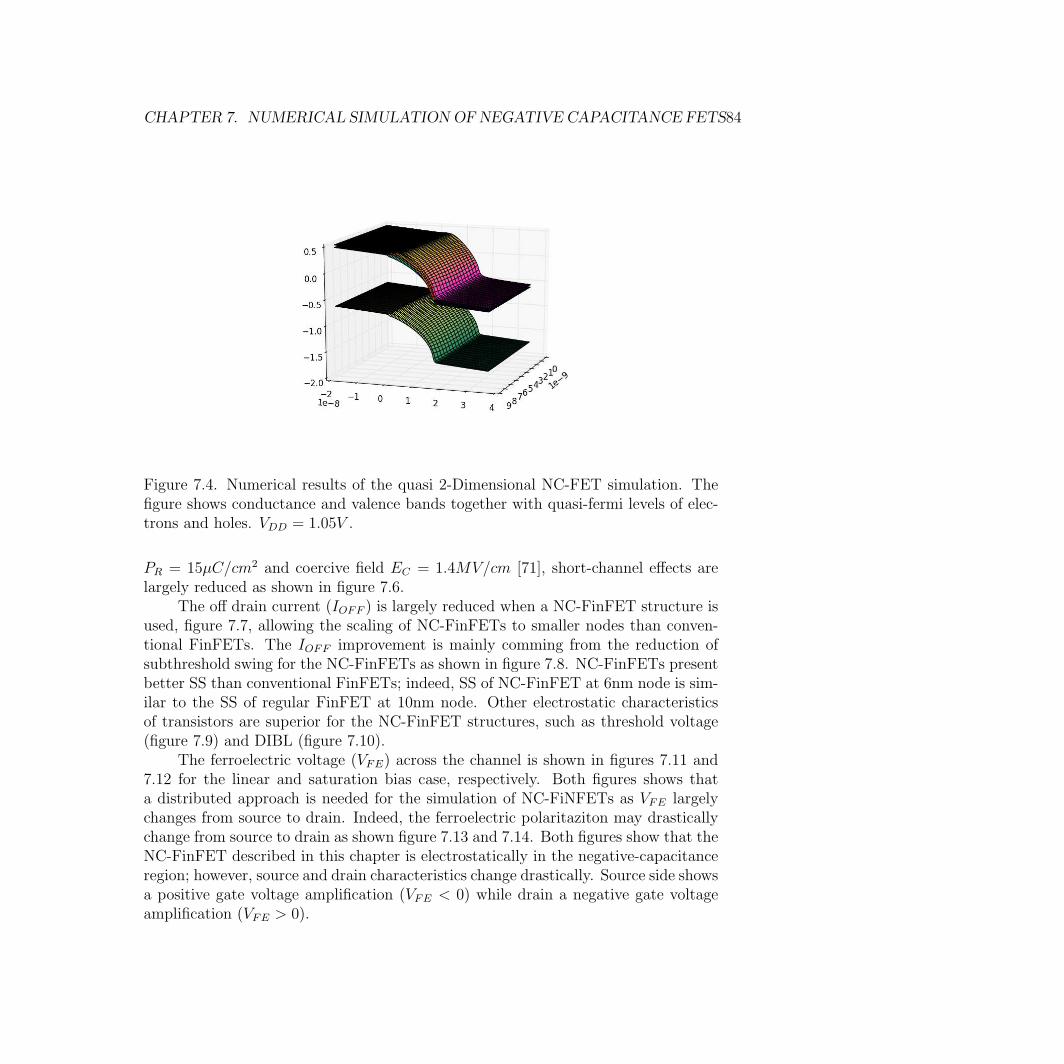
CHAPTER 7. NUMERICAL SIMULATIONOF NEGATIVE CAPACITANCE FETS84
Figure 7.4. Numerical results of the quasi 2-Dimensional NC-FET simulation. Thefigure shows conductance and valence bands together with quasi-fermi levels of elec-trons and holes. VDD = 1.05V .
PR = 15µC/cm2 and coercive field EC = 1.4MV/cm [71], short-channel effects arelargely reduced as shown in figure 7.6.
The off drain current (IOFF ) is largely reduced when a NC-FinFET structure isused, figure 7.7, allowing the scaling of NC-FinFETs to smaller nodes than conven-tional FinFETs. The IOFF improvement is mainly comming from the reduction ofsubthreshold swing for the NC-FinFETs as shown in figure 7.8. NC-FinFETs presentbetter SS than conventional FinFETs; indeed, SS of NC-FinFET at 6nm node is sim-ilar to the SS of regular FinFET at 10nm node. Other electrostatic characteristicsof transistors are superior for the NC-FinFET structures, such as threshold voltage(figure 7.9) and DIBL (figure 7.10).
The ferroelectric voltage (VFE) across the channel is shown in figures 7.11 and7.12 for the linear and saturation bias case, respectively. Both figures shows thata distributed approach is needed for the simulation of NC-FiNFETs as VFE largelychanges from source to drain. Indeed, the ferroelectric polaritaziton may drasticallychange from source to drain as shown figure 7.13 and 7.14. Both figures show that theNC-FinFET described in this chapter is electrostatically in the negative-capacitanceregion; however, source and drain characteristics change drastically. Source side showsa positive gate voltage amplification (VFE < 0) while drain a negative gate voltageamplification (VFE > 0).
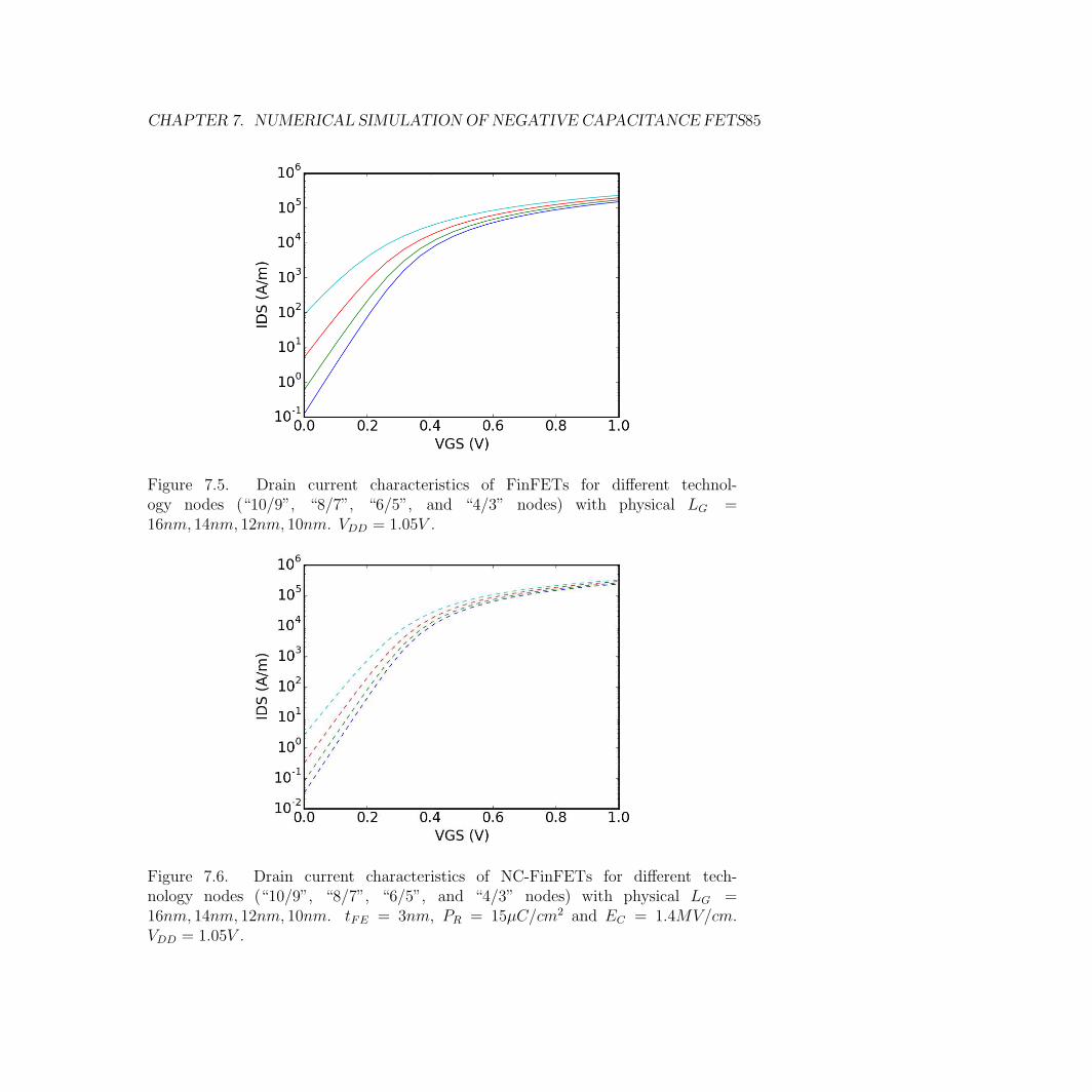
CHAPTER 7. NUMERICAL SIMULATIONOF NEGATIVE CAPACITANCE FETS85
Figure 7.5. Drain current characteristics of FinFETs for different technol-ogy nodes (“10/9”, “8/7”, “6/5”, and “4/3” nodes) with physical LG =16nm, 14nm, 12nm, 10nm. VDD = 1.05V .
Figure 7.6. Drain current characteristics of NC-FinFETs for different tech-nology nodes (“10/9”, “8/7”, “6/5”, and “4/3” nodes) with physical LG =16nm, 14nm, 12nm, 10nm. tFE = 3nm, PR = 15µC/cm2 and EC = 1.4MV/cm.VDD = 1.05V .
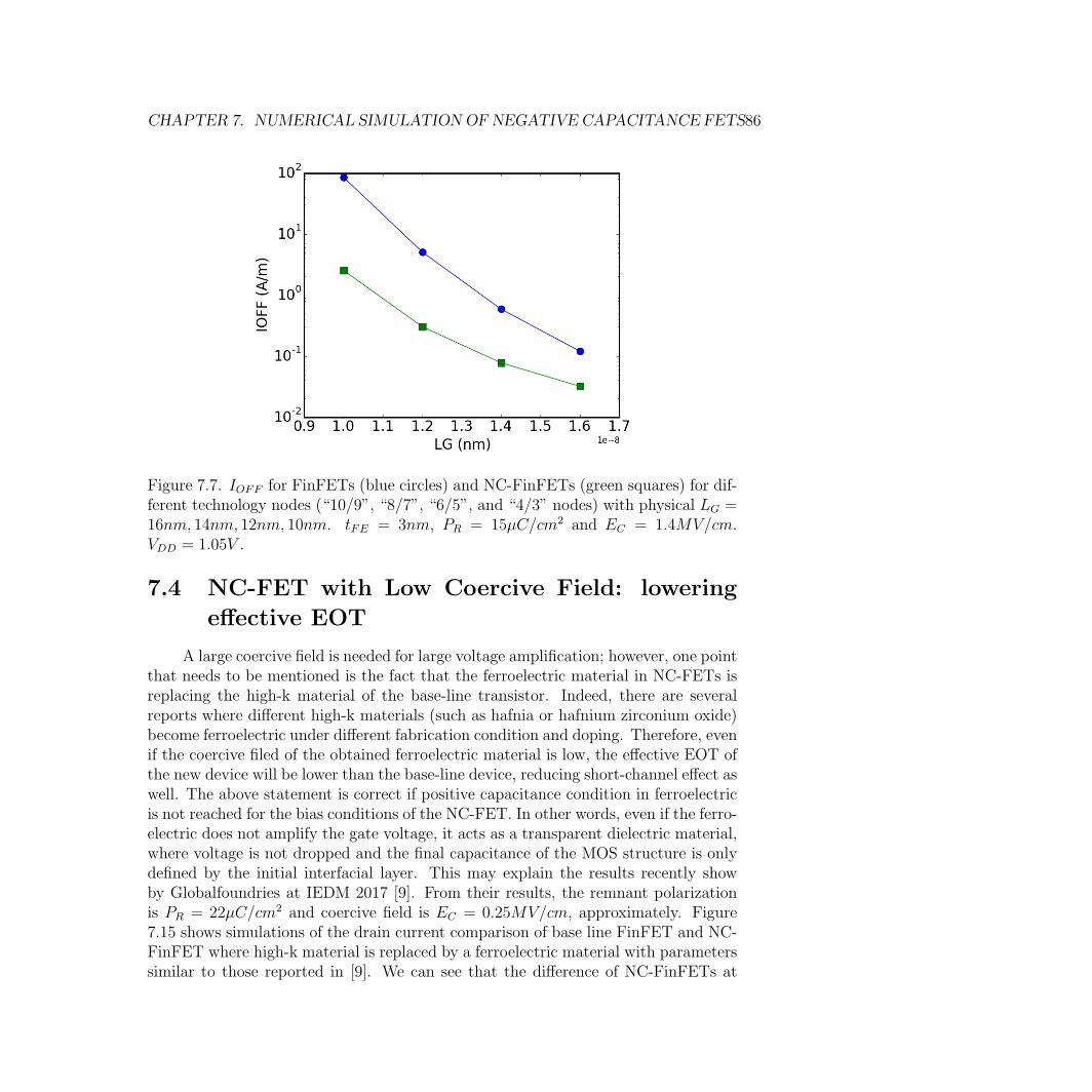
CHAPTER 7. NUMERICAL SIMULATIONOF NEGATIVE CAPACITANCE FETS86
Figure 7.7. IOFF for FinFETs (blue circles) and NC-FinFETs (green squares) for dif-ferent technology nodes (“10/9”, “8/7”, “6/5”, and “4/3” nodes) with physical LG =16nm, 14nm, 12nm, 10nm. tFE = 3nm, PR = 15µC/cm2 and EC = 1.4MV/cm.VDD = 1.05V .
7.4 NC-FET with Low Coercive Field: lowering
effective EOT
A large coercive field is needed for large voltage amplification; however, one pointthat needs to be mentioned is the fact that the ferroelectric material in NC-FETs isreplacing the high-k material of the base-line transistor. Indeed, there are severalreports where different high-k materials (such as hafnia or hafnium zirconium oxide)become ferroelectric under different fabrication condition and doping. Therefore, evenif the coercive filed of the obtained ferroelectric material is low, the effective EOT ofthe new device will be lower than the base-line device, reducing short-channel effect aswell. The above statement is correct if positive capacitance condition in ferroelectricis not reached for the bias conditions of the NC-FET. In other words, even if the ferro-electric does not amplify the gate voltage, it acts as a transparent dielectric material,where voltage is not dropped and the final capacitance of the MOS structure is onlydefined by the initial interfacial layer. This may explain the results recently showby Globalfoundries at IEDM 2017 [9]. From their results, the remnant polarizationis PR = 22µC/cm2 and coercive field is EC = 0.25MV/cm, approximately. Figure7.15 shows simulations of the drain current comparison of base line FinFET and NC-FinFET where high-k material is replaced by a ferroelectric material with parameterssimilar to those reported in [9]. We can see that the difference of NC-FinFETs at
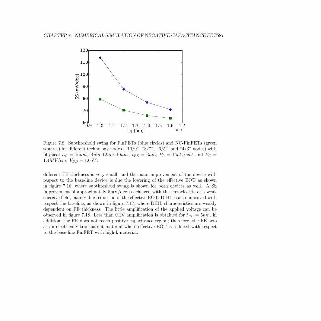
CHAPTER 7. NUMERICAL SIMULATIONOF NEGATIVE CAPACITANCE FETS87
Figure 7.8. Subthreshold swing for FinFETs (blue circles) and NC-FinFETs (greensquares) for different technology nodes (“10/9”, “8/7”, “6/5”, and “4/3” nodes) withphysical LG = 16nm, 14nm, 12nm, 10nm. tFE = 3nm, PR = 15µC/cm2 and EC =1.4MV/cm. VDD = 1.05V .
different FE thickness is very small, and the main improvement of the device withrespect to the base-line device is due the lowering of the effective EOT as shownin figure 7.16, where subthreshold swing is shown for both devices as well. A SSimprovement of approximately 5mV/dec is achieved with the ferroelectric of a weakcoercive field, mainly due reduction of the effective EOT. DIBL is also improved withrespect the baseline, as shown in figure 7.17, where DIBL characteristics are weaklydependent on FE thickness. The little amplification of the applied voltage can beobserved in figure 7.18. Less than 0.1V amplification is obtained for tFE = 5nm, inaddition, the FE does not reach positive capacitance region; therefore, the FE actsas an electrically transparent material where effective EOT is reduced with respectto the base-line FinFET with high-k material.
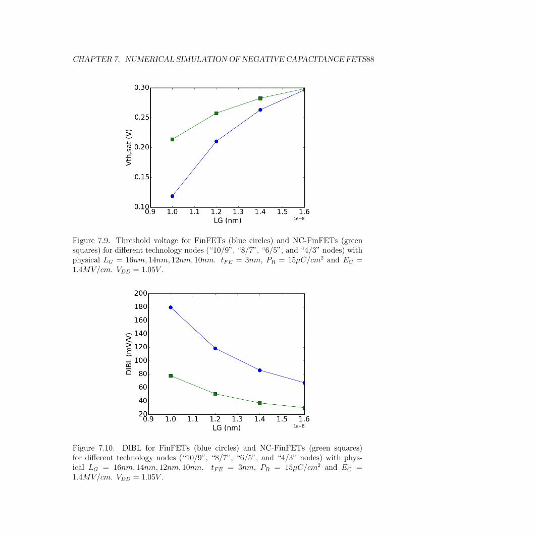
CHAPTER 7. NUMERICAL SIMULATIONOF NEGATIVE CAPACITANCE FETS88
Figure 7.9. Threshold voltage for FinFETs (blue circles) and NC-FinFETs (greensquares) for different technology nodes (“10/9”, “8/7”, “6/5”, and “4/3” nodes) withphysical LG = 16nm, 14nm, 12nm, 10nm. tFE = 3nm, PR = 15µC/cm2 and EC =1.4MV/cm. VDD = 1.05V .
Figure 7.10. DIBL for FinFETs (blue circles) and NC-FinFETs (green squares)for different technology nodes (“10/9”, “8/7”, “6/5”, and “4/3” nodes) with phys-ical LG = 16nm, 14nm, 12nm, 10nm. tFE = 3nm, PR = 15µC/cm2 and EC =1.4MV/cm. VDD = 1.05V .
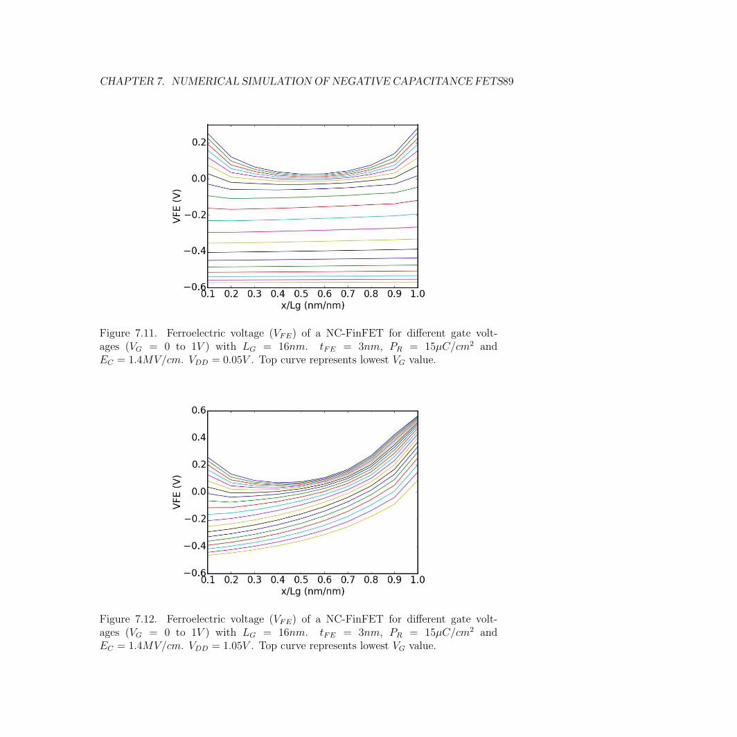
CHAPTER 7. NUMERICAL SIMULATIONOF NEGATIVE CAPACITANCE FETS89
Figure 7.11. Ferroelectric voltage (VFE) of a NC-FinFET for different gate volt-ages (VG = 0 to 1V ) with LG = 16nm. tFE = 3nm, PR = 15µC/cm2 andEC = 1.4MV/cm. VDD = 0.05V . Top curve represents lowest VG value.
Figure 7.12. Ferroelectric voltage (VFE) of a NC-FinFET for different gate volt-ages (VG = 0 to 1V ) with LG = 16nm. tFE = 3nm, PR = 15µC/cm2 andEC = 1.4MV/cm. VDD = 1.05V . Top curve represents lowest VG value.
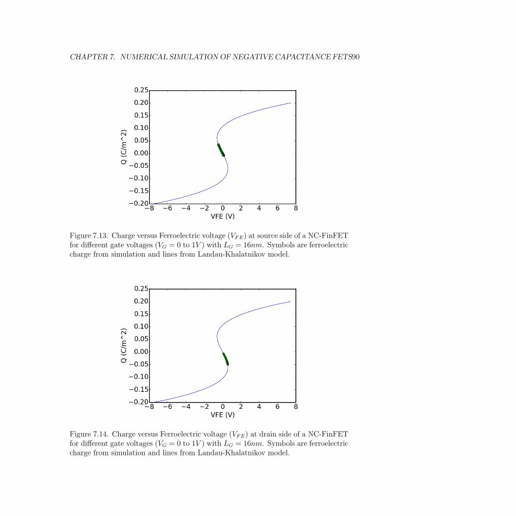
CHAPTER 7. NUMERICAL SIMULATIONOF NEGATIVE CAPACITANCE FETS90
Figure 7.13. Charge versus Ferroelectric voltage (VFE) at source side of a NC-FinFETfor different gate voltages (VG = 0 to 1V ) with LG = 16nm. Symbols are ferroelectriccharge from simulation and lines from Landau-Khalatnikov model.
Figure 7.14. Charge versus Ferroelectric voltage (VFE) at drain side of a NC-FinFETfor different gate voltages (VG = 0 to 1V ) with LG = 16nm. Symbols are ferroelectriccharge from simulation and lines from Landau-Khalatnikov model.
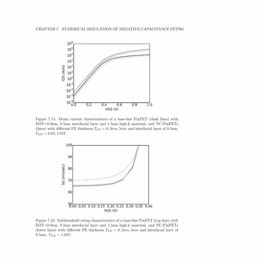
CHAPTER 7. NUMERICAL SIMULATIONOF NEGATIVE CAPACITANCE FETS91
Figure 7.15. Drain current characteristics of a base-line FinFET (dash lines) withEOT=0.8nm, 0.5nm interfacial layer and 1.5nm high-k material, and NC-FinFETs(lines) with different FE thickness TFE = 0, 3nm, 5nm and interfacial layer of 0.5nm.VDD = 0.05, 1.05V .
Figure 7.16. Subthreshold swing characteristics of a base-line FinFET (top line) withEOT=0.8nm, 0.5nm interfacial layer and 1.5nm high-k material, and NC-FinFETs(lower lines) with different FE thickness TFE = 0, 3nm, 5nm and interfacial layer of0.5nm. VDD = 1.05V .
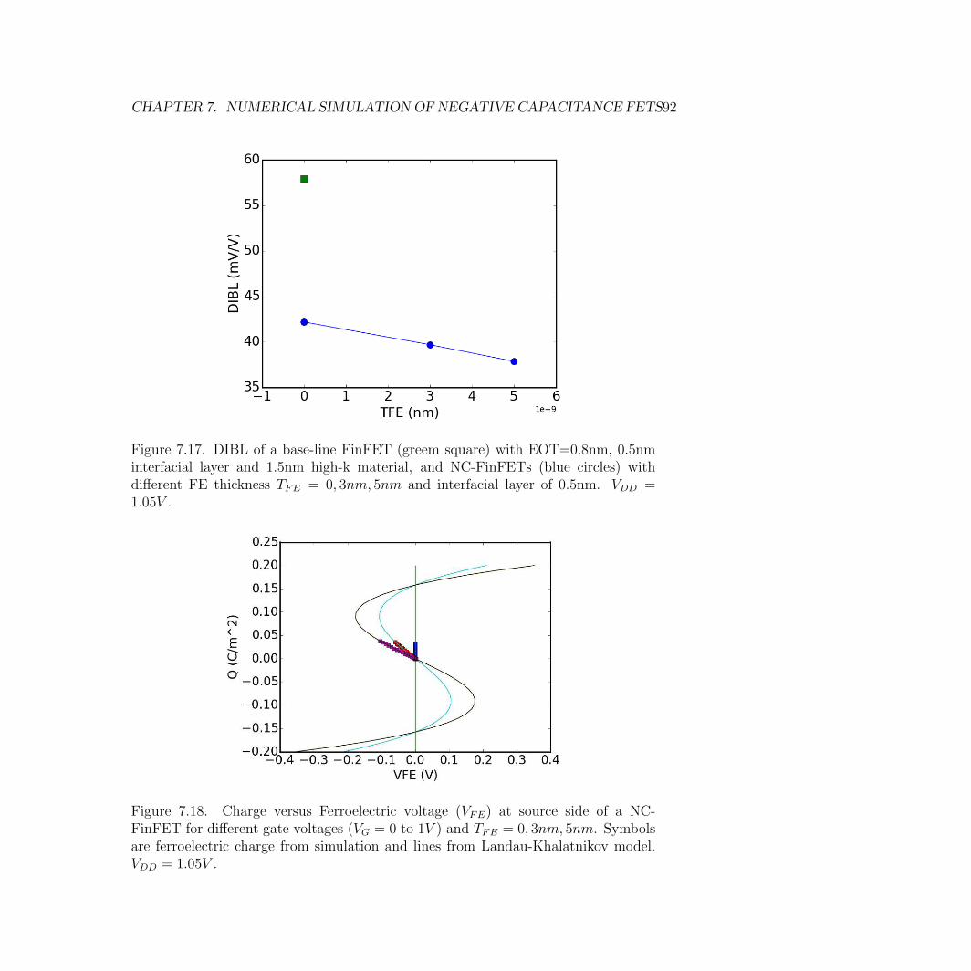
CHAPTER 7. NUMERICAL SIMULATIONOF NEGATIVE CAPACITANCE FETS92
Figure 7.17. DIBL of a base-line FinFET (greem square) with EOT=0.8nm, 0.5nminterfacial layer and 1.5nm high-k material, and NC-FinFETs (blue circles) withdifferent FE thickness TFE = 0, 3nm, 5nm and interfacial layer of 0.5nm. VDD =1.05V .
Figure 7.18. Charge versus Ferroelectric voltage (VFE) at source side of a NC-FinFET for different gate voltages (VG = 0 to 1V ) and TFE = 0, 3nm, 5nm. Symbolsare ferroelectric charge from simulation and lines from Landau-Khalatnikov model.VDD = 1.05V .
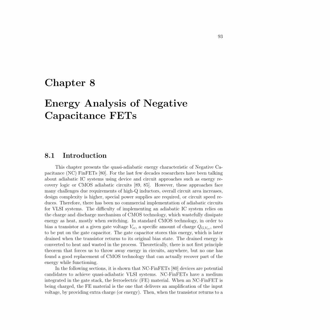
93
Chapter 8
Energy Analysis of NegativeCapacitance FETs
8.1 Introduction
This chapter presents the quasi-adiabatic energy characteristic of Negative Ca-pacitance (NC) FinFETs [80]. For the last few decades researchers have been talkingabout adiabatic IC systems using device and circuit approaches such as energy re-covery logic or CMOS adiabatic circuits [89, 85]. However, these approaches facemany challenges due requirements of high-Q inductors, overall circuit area increases,design complexity is higher, special power supplies are required, or circuit speed re-duces. Therefore, there has been no commercial implementation of adiabatic circuitsfor VLSI systems. The difficulty of implementing an adiabatic IC system relies onthe charge and discharge mechanism of CMOS technology, which wastefully dissipateenergy as heat, mostly when switching. In standard CMOS technology, in order tobias a transistor at a given gate voltage Vcc, a specific amount of charge QG,Vcc , needto be put on the gate capacitor. The gate capacitor stores this energy, which is laterdrained when the transistor returns to its original bias state. The drained energy isconverted to heat and wasted in the process. Theoretically, there is not first principletheorem that forces us to throw away energy in circuits, anywhere, but no one hasfound a good replacement of CMOS technology that can actually recover part of theenergy while functioning.
In the following sections, it is shown that NC-FinFETs [80] devices are potentialcandidates to achieve quasi-adiabatic VLSI systems. NC-FinFETs have a mediumintegrated in the gate stack, the ferroelectric (FE) material. When an NC-FinFET isbeing charged, the FE material is the one that delivers an amplification of the inputvoltage, by providing extra charge (or energy). Then, when the transistor returns to a
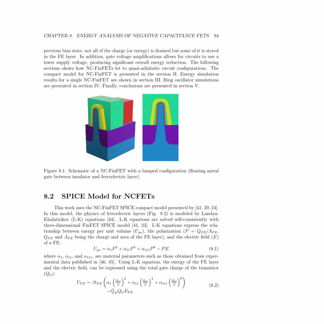
CHAPTER 8. ENERGY ANALYSIS OF NEGATIVE CAPACITANCE FETS 94
previous bias state, not all of the charge (or energy) is drained but some of it is storedin the FE layer. In addition, gate voltage amplifications allows for circuits to use alower supply voltage, producing significant overall energy reduction. The followingsections shows how NC-FinFETs let to quasi-adiabatic circuit configurations. Thecompact model for NC-FinFET is presented in the section II. Energy simulationresults for a single NC-FinFET are shown in section III. Ring oscillator simulationsare presented in section IV. Finally, conclusions are presented in section V.
Figure 8.1. Schematic of a NC-FinFET with a lumped configuration (floating metalgate between insulator and ferroelectric layer).
8.2 SPICE Model for NCFETs
This work uses the NC-FinFET SPICE compact model presented by [41, 39, 24].In this model, the physics of ferroelectric layers (Fig. 8.2) is modeled by Landau-Khalatnikov (L-K) equations [44]. L-K equations are solved self-consistently withthree-dimensional FinFET SPICE model [41, 23]. L-K equations express the rela-tionship between energy per unit volume (Upu), the polarization (P = QFE/AFE,QFE and AFE being the charge and area of the FE layer), and the electric field (E)of a FE:
Upu = α1P2 + α11P
4 + α111P6 − PE (8.1)
where α1, α11, and α111, are material parameters such as those obtained from exper-imental data published in [46, 45]. Using L-K equation, the energy of the FE layerand the electric field, can be expressed using the total gate charge of the transistor(QG):
UFE = βtFE
(
α1
(
QGβ
)2
+ α11
(
QGβ
)4
+ α111
(
QGβ
)6)
−t2FEQGEFE
(8.2)
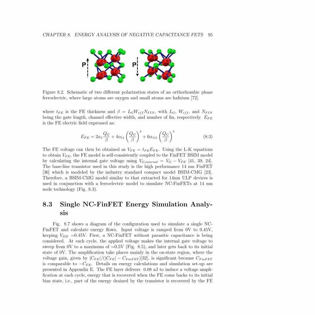
CHAPTER 8. ENERGY ANALYSIS OF NEGATIVE CAPACITANCE FETS 95
Figure 8.2. Schematic of two different polarization states of an orthorhombic phaseferroelectric, where large atoms are oxygen and small atoms are hafnium [72].
where tFE is the FE thickness and β = LGWeffNFIN , with LG, Weff , and NFIN
being the gate length, channel effective width, and number of fin, respectively. EFEis the FE electric field expressed as:
EFE = 2α1QG
β+ 4α11
(
QG
β
)3
+ 6α111
(
QG
β
)5
(8.3)
The FE voltage can then be obtained as VFE = tFEEFE. Using the L-K equationsto obtain VFE, the FE model is self-consistently coupled to the FinFET BSIM modelby calculating the internal gate voltage using VG,internal = VG − VFE [41, 39, 24].The base-line transistor used in this study is the high performance 14 nm FinFET[36] which is modeled by the industry standard compact model BSIM-CMG [23].Therefore, a BSIM-CMG model similar to that extracted for 14nm ULP devices isused in conjunction with a ferroelectric model to simulate NC-FinFETs at 14 nmnode technology (Fig. 8.3).
8.3 Single NC-FinFET Energy Simulation Analy-
sis
Fig. 8.7 shows a diagram of the configuration used to simulate a single NC-FinFET and calculate energy flows. Input voltage is ramped from 0V to 0.45V,keeping VDD =0.45V. First, a NC-FinFET without parasitic capacitance is beingconsidered. At each cycle, the applied voltage makes the internal gate voltage tosweep from 0V to a maximum of ∼0.5V (Fig. 8.5), and later gets back to its initialstate of 0V. The amplification take places mainly in the on-state region, where thevoltage gain, given by |CFE|/(|CFE| − CFinFET )[32], is significant because CFinFETis comparable to −CFE. Details on energy calculations and simulation set-up arepresented in Appendix E. The FE layer delivers 0.08 aJ to induce a voltage ampli-fication at each cycle, energy that is recovered when the FE come backs to its initialbias state, i.e., part of the energy drained by the transistor is recovered by the FE
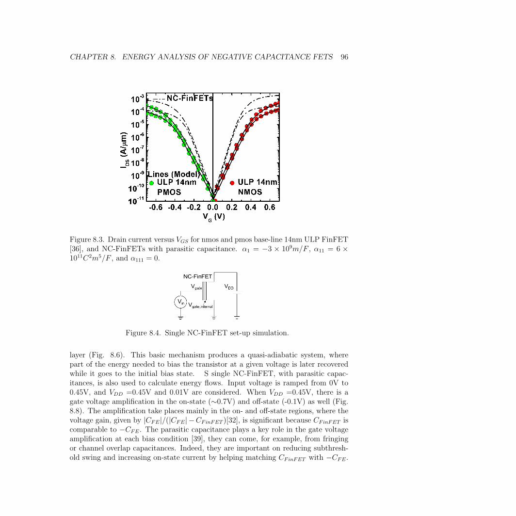
CHAPTER 8. ENERGY ANALYSIS OF NEGATIVE CAPACITANCE FETS 96
Figure 8.3. Drain current versus VGS for nmos and pmos base-line 14nm ULP FinFET[36], and NC-FinFETs with parasitic capacitance. α1 = −3 × 10⁹m/F , α11 = 6 ×10¹¹C2m5/F , and α111 = 0.
Figure 8.4. Single NC-FinFET set-up simulation.
layer (Fig. 8.6). This basic mechanism produces a quasi-adiabatic system, wherepart of the energy needed to bias the transistor at a given voltage is later recoveredwhile it goes to the initial bias state. S single NC-FinFET, with parasitic capac-itances, is also used to calculate energy flows. Input voltage is ramped from 0V to0.45V, and VDD =0.45V and 0.01V are considered. When VDD =0.45V, there is agate voltage amplification in the on-state (∼0.7V) and off-state (-0.1V) as well (Fig.8.8). The amplification take places mainly in the on- and off-state regions, where thevoltage gain, given by |CFE|/(|CFE| −CFinFET )[32], is significant because CFinFET iscomparable to −CFE. The parasitic capacitance plays a key role in the gate voltageamplification at each bias condition [39], they can come, for example, from fringingor channel overlap capacitances. Indeed, they are important on reducing subthresh-old swing and increasing on-state current by helping matching CFinFET with −CFE.
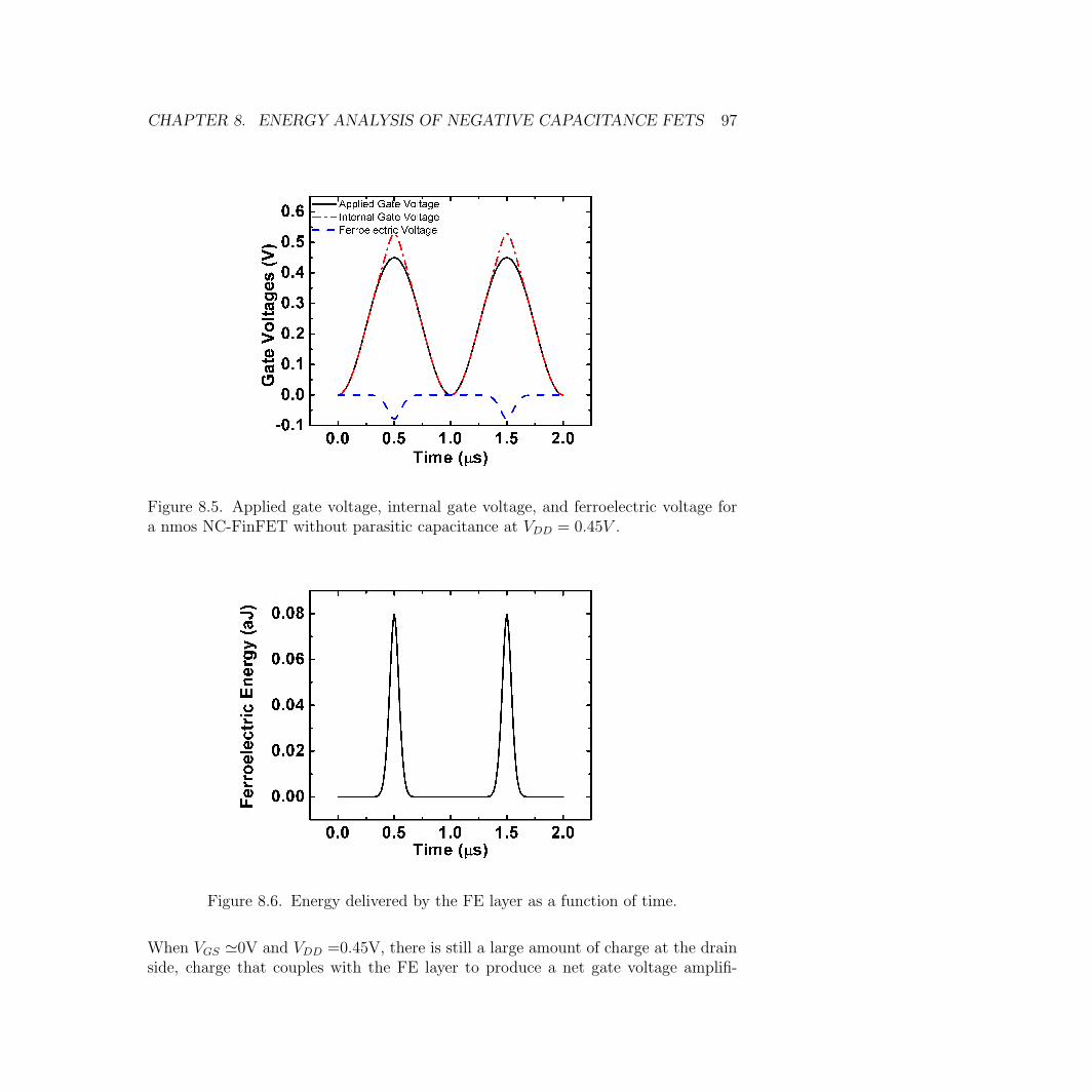
CHAPTER 8. ENERGY ANALYSIS OF NEGATIVE CAPACITANCE FETS 97
Figure 8.5. Applied gate voltage, internal gate voltage, and ferroelectric voltage fora nmos NC-FinFET without parasitic capacitance at VDD = 0.45V .
Figure 8.6. Energy delivered by the FE layer as a function of time.
When VGS ≃0V and VDD =0.45V, there is still a large amount of charge at the drainside, charge that couples with the FE layer to produce a net gate voltage amplifi-
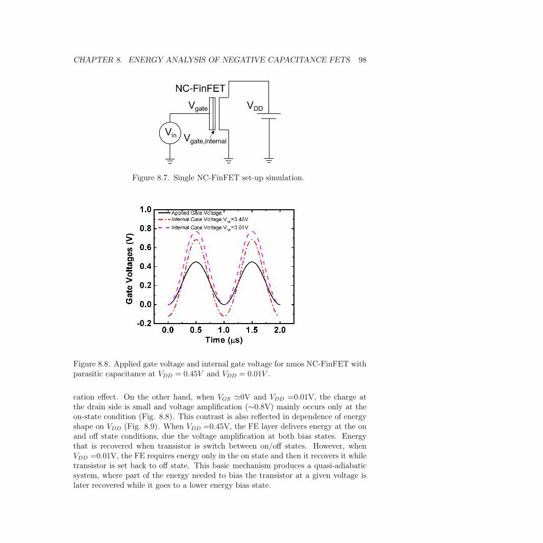
CHAPTER 8. ENERGY ANALYSIS OF NEGATIVE CAPACITANCE FETS 98
Figure 8.7. Single NC-FinFET set-up simulation.
Figure 8.8. Applied gate voltage and internal gate voltage for nmos NC-FinFET withparasitic capacitance at VDD = 0.45V and VDD = 0.01V .
cation effect. On the other hand, when VGS ≃0V and VDD =0.01V, the charge atthe drain side is small and voltage amplification (∼0.8V) mainly occurs only at theon-state condition (Fig. 8.8). This contrast is also reflected in dependence of energyshape on VDD (Fig. 8.9). When VDD =0.45V, the FE layer delivers energy at the onand off state conditions, due the voltage amplification at both bias states. Energythat is recovered when transistor is switch between on/off states. However, whenVDD =0.01V, the FE requires energy only in the on state and then it recovers it whiletransistor is set back to off state. This basic mechanism produces a quasi-adiabaticsystem, where part of the energy needed to bias the transistor at a given voltage islater recovered while it goes to a lower energy bias state.
CHAPTER 8. ENERGY ANALYSIS OF NEGATIVE CAPACITANCE FETS 99
Figure 8.9. Energy used by the FE layer as a function of time for VDD = 0.45V andVDD = 0.01V .
Figure 8.10. 17-stage Ring-Oscillator set-up. 11 and 10 Fins are used for pmos anmos, respectively.
8.4 NC-FinFET Ring-Oscillator Analysis
Ring-Oscillators (ROs) are widely use to evaluate, validate, and monitor perfor-mance of a given technology. Indeed, the frequency of ROs provides indications oftechnology speed and can be measured in the early stages of production. A 17-stageRO is utilized in this work (Fig. 8.10). First, a RO without interconnection loadcapacitances is considered; i.e., only intrinsic switching characteristics are analysed.Fig. 8.11 shows a comparison of the voltages at the first node of the RO understudy utilizing base-line ULP 14nm FinFETs versus NC-FinFETs. VDD has been
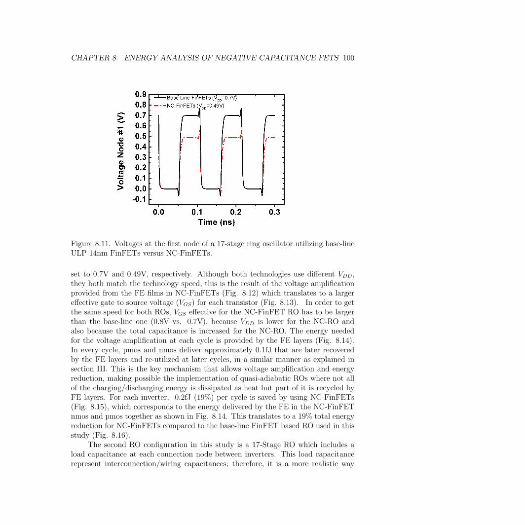
CHAPTER 8. ENERGY ANALYSIS OF NEGATIVE CAPACITANCE FETS 100
Figure 8.11. Voltages at the first node of a 17-stage ring oscillator utilizing base-lineULP 14nm FinFETs versus NC-FinFETs.
set to 0.7V and 0.49V, respectively. Although both technologies use different VDD,they both match the technology speed, this is the result of the voltage amplificationprovided from the FE films in NC-FinFETs (Fig. 8.12) which translates to a largereffective gate to source voltage (VGS) for each transistor (Fig. 8.13). In order to getthe same speed for both ROs, VGS effective for the NC-FinFET RO has to be largerthan the base-line one (0.8V vs. 0.7V), because VDD is lower for the NC-RO andalso because the total capacitance is increased for the NC-RO. The energy neededfor the voltage amplification at each cycle is provided by the FE layers (Fig. 8.14).In every cycle, pmos and nmos deliver approximately 0.1fJ that are later recoveredby the FE layers and re-utilized at later cycles, in a similar manner as explained insection III. This is the key mechanism that allows voltage amplification and energyreduction, making possible the implementation of quasi-adiabatic ROs where not allof the charging/discharging energy is dissipated as heat but part of it is recycled byFE layers. For each inverter, 0.2fJ (19%) per cycle is saved by using NC-FinFETs(Fig. 8.15), which corresponds to the energy delivered by the FE in the NC-FinFETnmos and pmos together as shown in Fig. 8.14. This translates to a 19% total energyreduction for NC-FinFETs compared to the base-line FinFET based RO used in thisstudy (Fig. 8.16).
The second RO configuration in this study is a 17-Stage RO which includes aload capacitance at each connection node between inverters. This load capacitancerepresent interconnection/wiring capacitances; therefore, it is a more realistic way
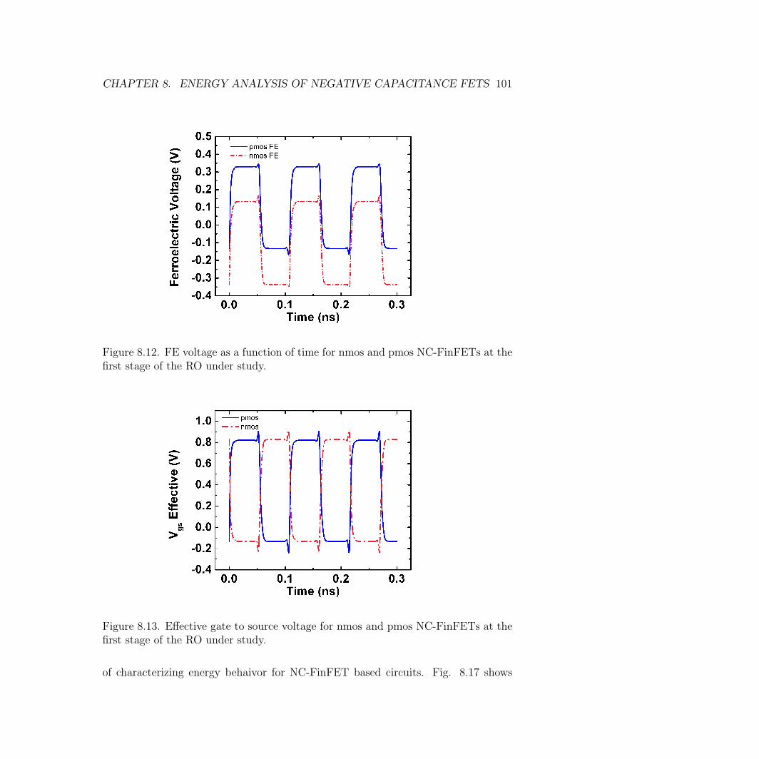
CHAPTER 8. ENERGY ANALYSIS OF NEGATIVE CAPACITANCE FETS 101
Figure 8.12. FE voltage as a function of time for nmos and pmos NC-FinFETs at thefirst stage of the RO under study.
Figure 8.13. Effective gate to source voltage for nmos and pmos NC-FinFETs at thefirst stage of the RO under study.
of characterizing energy behaivor for NC-FinFET based circuits. Fig. 8.17 shows
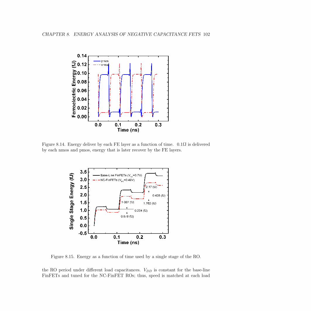
CHAPTER 8. ENERGY ANALYSIS OF NEGATIVE CAPACITANCE FETS 102
Figure 8.14. Energy deliver by each FE layer as a function of time. 0.1fJ is deliveredby each nmos and pmos, energy that is later recover by the FE layers.
Figure 8.15. Energy as a function of time used by a single stage of the RO.
the RO period under different load capacitances. VDD is constant for the base-lineFinFETs and tuned for the NC-FinFET ROs; thus, speed is matched at each load
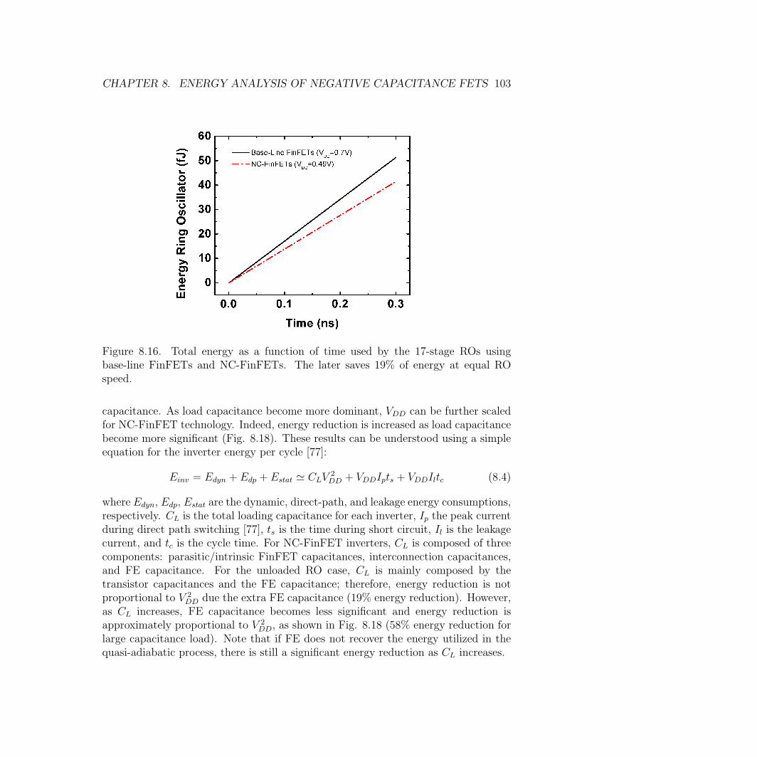
CHAPTER 8. ENERGY ANALYSIS OF NEGATIVE CAPACITANCE FETS 103
Figure 8.16. Total energy as a function of time used by the 17-stage ROs usingbase-line FinFETs and NC-FinFETs. The later saves 19% of energy at equal ROspeed.
capacitance. As load capacitance become more dominant, VDD can be further scaledfor NC-FinFET technology. Indeed, energy reduction is increased as load capacitancebecome more significant (Fig. 8.18). These results can be understood using a simpleequation for the inverter energy per cycle [77]:
Einv = Edyn + Edp + Estat ≃ CLV2DD + VDDIpts + VDDIltc (8.4)
where Edyn, Edp, Estat are the dynamic, direct-path, and leakage energy consumptions,respectively. CL is the total loading capacitance for each inverter, Ip the peak currentduring direct path switching [77], ts is the time during short circuit, Il is the leakagecurrent, and tc is the cycle time. For NC-FinFET inverters, CL is composed of threecomponents: parasitic/intrinsic FinFET capacitances, interconnection capacitances,and FE capacitance. For the unloaded RO case, CL is mainly composed by thetransistor capacitances and the FE capacitance; therefore, energy reduction is notproportional to V 2
DD due the extra FE capacitance (19% energy reduction). However,as CL increases, FE capacitance becomes less significant and energy reduction isapproximately proportional to V 2
DD, as shown in Fig. 8.18 (58% energy reduction forlarge capacitance load). Note that if FE does not recover the energy utilized in thequasi-adiabatic process, there is still a significant energy reduction as CL increases.
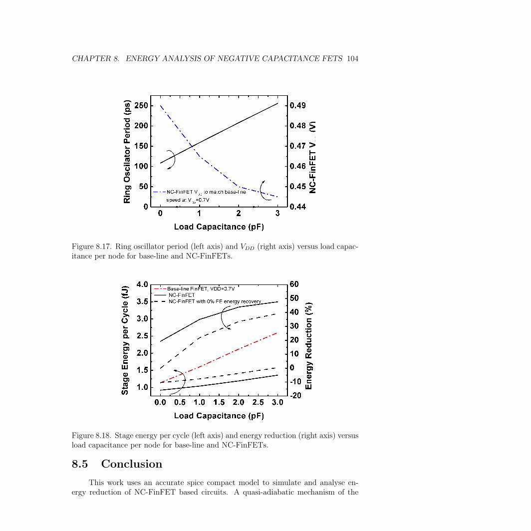
CHAPTER 8. ENERGY ANALYSIS OF NEGATIVE CAPACITANCE FETS 104
Figure 8.17. Ring oscillator period (left axis) and VDD (right axis) versus load capac-itance per node for base-line and NC-FinFETs.
Figure 8.18. Stage energy per cycle (left axis) and energy reduction (right axis) versusload capacitance per node for base-line and NC-FinFETs.
8.5 Conclusion
This work uses an accurate spice compact model to simulate and analyse en-ergy reduction of NC-FinFET based circuits. A quasi-adiabatic mechanism of the

CHAPTER 8. ENERGY ANALYSIS OF NEGATIVE CAPACITANCE FETS 105
ferroelectric layer in the NC-FinFET recovers part of the energy during the switchingprocess of transistors, helping minimizing the energy losses of the wasteful energydissipation nature of conventional transistor circuits. As load capacitances furtherincrease, VDD scaling becomes more dominant. This is the case of scaled transistortechnologies where interconnect/wire capacitance become dominant. In the exampleprovided in this work, a 58% energy reduction is achieved for the ring oscillator withlargest load capacitance.
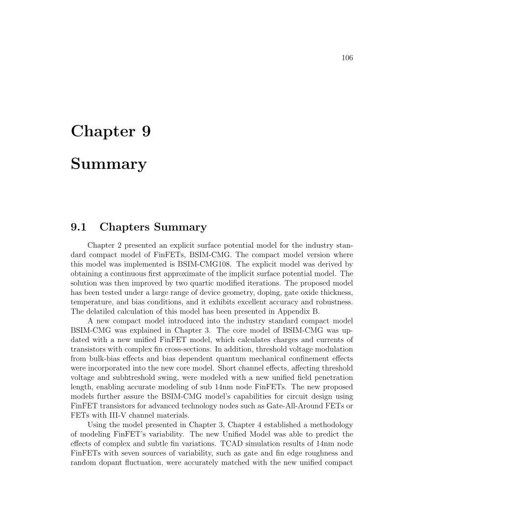
106
Chapter 9
Summary
9.1 Chapters Summary
Chapter 2 presented an explicit surface potential model for the industry stan-dard compact model of FinFETs, BSIM-CMG. The compact model version wherethis model was implemented is BSIM-CMG108. The explicit model was derived byobtaining a continuous first approximate of the implicit surface potential model. Thesolution was then improved by two quartic modified iterations. The proposed modelhas been tested under a large range of device geometry, doping, gate oxide thickness,temperature, and bias conditions, and it exhibits excellent accuracy and robustness.The delatiled calculation of this model has been presented in Appendix B.
A new compact model introduced into the industry standard compact modelBSIM-CMG was explained in Chapter 3. The core model of BSIM-CMG was up-dated with a new unified FinFET model, which calculates charges and currents oftransistors with complex fin cross-sections. In addition, threshold voltage modulationfrom bulk-bias effects and bias dependent quantum mechanical confinement effectswere incorporated into the new core model. Short channel effects, affecting thresholdvoltage and subhtreshold swing, were modeled with a new unified field penetrationlength, enabling accurate modeling of sub 14nm node FinFETs. The new proposedmodels further assure the BSIM-CMG model’s capabilities for circuit design usingFinFET transistors for advanced technology nodes such as Gate-All-Around FETs orFETs with III-V channel materials.
Using the model presented in Chapter 3, Chapter 4 established a methodologyof modeling FinFET’s variability. The new Unified Model was able to predict theeffects of complex and subtle fin variations. TCAD simulation results of 14nm nodeFinFETs with seven sources of variability, such as gate and fin edge roughness andrandom dopant fluctuation, were accurately matched with the new unified compact
CHAPTER 9. SUMMARY 107
model using only shape variation parameters. Due to the physical foundation of theunified model, it can predictively model the performance variability of future FinFETtechnology nodes using expected shape variations.
Compact models for UTBSOIs are presented in Chapter 5. It developed a newanalytical form of the core model for the industry standard compact model BSIM-IMG, a fully-featured turn-key compact model for independent multi-gate MOSFETs.An explicit model was derived by obtaining a continuous first approximate of the im-plicit surface potential model. This solution was then improved by three first orderiterations, leading to a numerically robust, accurate, and fast core model. This newcore model includes back-side inversion. To represent real device effects, several extramodels were later incorporated such as drain-induced barrier lowering, velocity satu-ration, short-channel effects, self-heating effect, mobility-field dependence, substrate-depletion effect, etc.
Negative Capacitance FETs are studied from Chapter 6. Chapter 6 first pre-sented insights into the device physics and behaviors of ferroelectric based negativecapacitance FinFETs using lumped and distributed compact models for its simula-tion. For NC-FinFETs having a floating metal between ferroelectric (FE) and thedielectric layers, lumped charge model were used. For NC-FinFETs without a floatingmetal, a distributed charge model was used, where at each point in the channel theferroelectric layer impacts the local channel charge. This distributed effect have shownimportant implications on device characteristics. The proposed compact models havebeen implemented in circuit simulators for exploring circuits based on NC-FinFETtechnology.
Numerical simulations of NC-FETs were developed in Chapter 7. A self-consistenceframework of 2D simulation of transistors with a 1D ferroelectric formulation wasproposed. Different effective polarization across the channel was captured by thenumerical simulations. Simulation were used to compare base-line FinFET againstNC-FinFETs. It results showed how NC-FinFETs can help scaling of transistors tounder 5nm node. For the case of FE with small Ec, the FE layer help to reduce theeffective EOT which also helps on device scaling.
The last part of this thesis, Chapter 8, presented a detailed analysis, from anenergy perspective, of the gate voltage amplification of NC-FinFETs. The modelspresented in Chapter 6 were used for this study. Results explained how the ferroelec-tric layer in transistors use a quasi-adiabatic mechanism to recover the energy neededfor gate voltage amplification. This voltage amplification leads to energy reduction bysupply voltage scaling, which becomes the main energy reduction factor for circuitsloaded with parasitic capacitances as those found in scaled technologies.
9.2 Future Work

108
Bibliography
[1] Bsim group. http://bsim.berkeley.edu/. Accessed: 2017-12-05.
[2] Global semiconductor market outlook 2022. https://www.prnewswire.com/
news-releases/global-semiconductor-market-outlook-2022-300248672.
html. Accessed: 2017-11-26.
[3] Global semiconductor sales reach 339 billion in 2016. http://www.
semiconductors.org/news/2017/02/02/global_sales_report_2015/
global_semiconductor_sales_reach_339_billion_in_2016/. Accessed:2017-11-26.
[4] iphone x. https://www.apple.com/iphone-x/. Accessed: 2017-11-26.
[5] Matlab automatic differentiation. https://
www.mathworks.com/matlabcentral/fileexchange/
15235-automatic-differentiation-for-matlab?focused=5092251&tab=
function. Accessed: 2017-12-05.
[6] Semiconductor Industry Association et al. International technology roadmap forsemiconductors (itrs), 2001 edition, 2001.
[7] Chris Auth et al. A 22nm high performance and low-power cmos technologyfeaturing fully-depleted tri-gate transistors, self-aligned contacts and high densitymim capacitors. In VLSI Technology (VLSIT), 2012 Symposium on, pages 131–132. IEEE, 2012.
[8] C.P. Auth and J.D. Plummer. Scaling theory for cylindrical, fully-depleted,surrounding-gate mosfet’s. Electron Device Letters, IEEE, 18(2):74–76, 1997.
[9] Krivokapic U. Rana R. Galatage A. Razavieh A. Aziz J.Liu J.Shi H.J. Kim R.Sporer C. Serrao A.Busquet P. Polakowski J. Muller W. Kleemeier A. JacobD. Brown A. Knorr R. Carter S. Banna. 14nm ferroelectric finfet technologywith steep subthreshold slope for ultra low power applications. In 2017 IEEEInternational Electron Devices Meeting (IEDM), pages 0–0, Dec 2017.
BIBLIOGRAPHY 109
[10] C-I. Lin A Khan C. Hu, S. Salahuddin. 0.2v adiabatic nc-finfet with 0.6ma/umion and 0.1na/um ioff. In DRC, pages 39–40, 2015.
[11] Chang-Yun Chang, Tsung-Lin Lee, C Wann, Li-Shyue Lai, Hung-Ming Chen,Chih-Chieh Yeh, Chih-Sheng Chang, Chia-Cheng Ho, Jyh-Cherng Sheu, Tsz-Mei Kwok, et al. A 25-nm gate-length finfet transistor module for 32nm node.In Electron Devices Meeting (IEDM), 2009 IEEE International, pages 1–4. IEEE,2009.
[12] Korok Chatterjee, Alexander John Rosner, and Sayeef Salahuddin. Intrinsicspeed limit of negative capacitance transistors. IEEE Electron Device Letters,38(9):1328–1330, 2017.
[13] Y. S. Chauhan, D. D. Lu, S. Vanugopalan, S. Khandelwal, J. P. Duarte, A. Nikne-jad, and C. Hu. FinFET Modeling for IC Simulation and Design. AcademicPress, 2015.
[14] Y. S. Chauhan, S. Venugopalan, M. A. Karim, S. Khandelwal, N. Paydavosi,P. Thakur, A. M. Niknejad, and C. C. Hu. BSIM-Industry; Industry standardcompact MOSFET models. In 2012 Proceedings of the ESSCIRC (ESSCIRC),pages 30–33, Sept 2012. 10.1109/ESSCIRC.2012.6341249.
[15] Yogesh S. Chauhan et al. Bsim6: Analog and rf compact model for bulk mosfet.2014.
[16] Y. Chen and J. Luo. A comparative study of double-gate and surrounding-gate mosfets in strong inversion and accumulation using an analytical model.Integration, 1(2):6, 2001.
[17] Nicolas Chevillon, J-M Sallese, Christophe Lallement, Fabien Pregaldiny, Mor-gan Madec, Josef Sedlmeir, and Jasmin Aghassi. Generalization of the conceptof equivalent thickness and capacitance to multigate mosfets modeling. ElectronDevices, IEEE Transactions on, 59(1):60–71, 2012.
[18] Y.K. Choi, K. Asano, N. Lindert, V. Subramanian, T.J. King, J. Bokor, andC. Hu. Ultra-thin body soi mosfet for deep-sub-tenth micron era. In ElectronDevices Meeting, 1999. IEDM Technical Digest. International, pages 919–921.IEEE, 1999.
[19] Geoffrey J Coram. How to (and how not to) write a compact model in verilog-a.In BMAS, pages 97–106. IEEE, 2004.
[20] R.H. Dennard, F.H. Gaensslen, VL Rideout, E. Bassous, and AR LeBlanc. De-sign of ion-implanted mosfet’s with very small physical dimensions. Solid-StateCircuits, IEEE Journal of, 9(5):256–268, 1974.
BIBLIOGRAPHY 110
[21] Gajanan Dessai and Gennady Gildenblat. Solution space for the independent-gate asymmetric dgfet. Solid-State Electronics, 54(4):382–384, 2010.
[22] Z. Dong and J. Guo. A simple model of negative capacitance fet with electrostaticshort channel effects. IEEE Transactions on Electron Devices, 64(7):2927–2934,July 2017.
[23] J. P. Duarte, S. Khandelwal, A. Medury, C. Hu, P. Kushwaha, H. Agarwal,A. Dasgupta, and Y. S. Chauhan. Bsim-cmg: Standard finfet compact model foradvanced circuit design. In ESSCIRC Conference 2015 - 41st European Solid-State Circuits Conference (ESSCIRC), pages 196–201, Sept 2015.
[24] Juan P Duarte et al. Compact models of negative-capacitance finfets: Lumpedand distributed charge models. In IEDM, 2016.
[25] Juan Pablo Duarte, Sung-Jin Choi, Dong-Il Moon, Jae-Hyuk Ahn, Jee-YeonKim, Sungho Kim, and Yang-Kyu Choi. A universal core model for multiple-gatefield-effect transistors. part i: Charge model. Electron Devices, IEEE Transac-tions on, 60(2):840–847, 2013.
[26] Juan Pablo Duarte, Sung-Jin Choi, Dong-Il Moon, Jae-Hyuk Ahn, Jee-YeonKim, Sungho Kim, and Yang-Kyu Choi. A universal core model for multiple-gate field-effect transistors. part ii: Drain current model. Electron Devices, IEEETransactions on, 60(2):848–855, 2013.
[27] Juan Pablo Duarte, Navid Paydavosi, Sriramkumar Venugopalan, AngadaSachid, and Chenming Hu. Unified finfet compact model: Modelling trapezoidaltriple-gate finfets. SISPAD, 2013.
[28] M.V. Dunga. Nanoscale cmos modeling. EECS Department, University of Cali-fornia, Berkeley, 2008.
[29] M.V. Dunga, C.H. Lin, X. Xi, D.D. Lu, A.M. Niknejad, and C. Hu. Modeling ad-vanced fet technology in a compact model. Electron Devices, IEEE Transactionson, 53(9):1971–1978, 2006.
[30] I. Ferain, C.A. Colinge, and J.P. Colinge. Multigate transistors as the fu-ture of classical metal-oxide-semiconductor field-effect transistors. Nature,479(7373):310–316, 2011.
[31] Sentaurus Device User Guide and E Version. Synopsys. Inc., Mountain View,CA, 2007.
[32] Chenming Hu et al. 0.2 v adiabatic nc-finfet with 0.6 ma/µm i on and 0.1 na/µmi off. In DRC, pages 39–40. IEEE, 2015.
BIBLIOGRAPHY 111
[33] Vita Pi-Ho Hu, Ming-Long Fan, Pin Su, and Ching-Te Chuang. Thresholdvoltage design of utb soi sram with improved stability/variability for ultralowvoltage near subthreshold operation. Nanotechnology, IEEE Transactions on,12(4):524–531, 2013.
[34] X. Huang et al. Sub 50-nm finfet: Pmos. In Electron Devices Meeting, 1999.IEDM Technical Digest. International, pages 67–70. IEEE, 1999.
[35] T Irisawa, M Oda, K Ikeda, Y Moriyama, E Mieda, W Jevasuwan, T Maeda,O Ichikawa, T Osada, M Hata, et al. High electron mobility triangular ingaas-oi nmosfets with (111) b side surfaces formed by movpe growth on narrow finstructures. In Electron Devices Meeting (IEDM), 2013 IEEE International, pages2–2. IEEE, 2013.
[36] C. H. Jan, F. Al-amoody, H. Y. Chang, T. Chang, Y. W. Chen, N. Dias,W. Hafez, D. Ingerly, M. Jang, E. Karl, S. K. Y. Shi, K. Komeyli, H. Kilambi,A. Kumar, K. Byon, C. G. Lee, J. Lee, T. Leo, P. C. Liu, N. Nidhi, R. Olac-vaw, C. Petersburg, K. Phoa, C. Prasad, C. Quincy, R. Ramaswamy, T. Rana,L. Rockford, A. Subramaniam, C. Tsai, P. Vandervoorn, L. Yang, A. Zainuddin,and P. Bai. A 14 nm soc platform technology featuring 2nd generation tri-gatetransistors, 70 nm gate pitch, 52 nm metal pitch, and 0.0499 um2 sram cells,optimized for low power, high performance and high density soc products. In2015 Symposium on VLSI Technology (VLSI Technology), pages T12–T13, June2015.
[37] S. Khandelwal, Y. S. Chauhan, D. D. Lu, S. Venugopalan, M. Ahosan Ul Karim,A. B. Sachid, B. Y. Nguyen, O. Rozeau, O. Faynot, A. M. Niknejad, and C. C.Hu. BSIM-IMG: A Compact Model for Ultrathin-Body SOI MOSFETs WithBack-Gate Control. IEEE Transactions on Electron Devices, 59(8):2019–2026,Aug 2012. 10.1109/TED.2012.2198065.
[38] S. Khandelwal, A. I. Khan, J. P. Duarte, A. B. Sachid, S. Salahuddin, andC. Hu. Circuit performance analysis of negative capacitance finfets. In 2016IEEE Symposium on VLSI Technology, pages 1–2, June 2016.
[39] Sourabh Khandelwal. Impact of parasitic capacitance and ferroelectric parame-ters on negative capacitance finfet characteristics. IEEE EDL.
[40] Sourabh Khandelwal, Juan P Duarte, Aditya Medury, YS Chauhan, and Chen-ming Hu. New industry standard finfet compact model for future technologynodes. In VLSI Technology (VLSI Technology), 2015 Symposium on, pages T62–T63. IEEE, 2015.
[41] Sourabh Khandelwal et al. Circuit performance analysis of negative capacitancefinfets. In VLSI Technology,, pages 1–2. IEEE, 2016.
BIBLIOGRAPHY 112
[42] Kelin J Kuhn. Considerations for ultimate cmos scaling. IEEE transactions onElectron Devices, 59(7):1813–1828, 2012.
[43] P. Kushwaha, C. Yadav, H. Agarwal, Y. S. Chauhan, J. Srivatsava, S. Khan-delwal, J. P. Duarte, and C. Hu. BSIM-IMG with improved surface potentialcalculation recipe. In 2014 Annual IEEE India Conference (INDICON), pages1–4, Dec 2014. 10.1109/INDICON.2014.7030498.
[44] LD Landau and IM Khalatnikov. On the anomalous absorption of sound near asecond order phase transition point. 1954.
[45] MH Lee et al. In IEDM, pages 22–5. IEEE, 2015.
[46] K. S. Li, P. G. Chen, T. Y. Lai, C. H. Lin, C. C. Cheng, C. C. Chen, Y. J.Wei, Y. F. Hou, M. H. Liao, M. H. Lee, M. C. Chen, J. M. Sheih, W. K. Yeh,F. L. Yang, S. Salahuddin, and C. Hu. Sub-60mv-swing negative-capacitancefinfet without hysteresis. In 2015 IEEE International Electron Devices Meeting(IEDM), pages 22.6.1–22.6.4, Dec 2015.
[47] C.-H. Lin et al. High performance 14nm soi finfet cmos technology with 0.0174um2 embedded dram and 15 levels of cu metallization. In Electron DevicesMeeting (IEDM), 2014 IEEE International, pages 3.8.1–3.8.3, Dec 2014.
[48] C-H Lin, R Kambhampati, RJ Miller, TB Hook, A Bryant, W Haensch,P Oldiges, I Lauer, T Yamashita, V Basker, et al. Channel doping impacton finfets for 22nm and beyond. In VLSI Technology (VLSIT), 2012 Symposiumon, pages 15–16. IEEE, 2012.
[49] Y. K. Lin, P. Kushwaha, H. Agarwal, H. L. Chang, J. P. Duarte, A. B. Sachid,S. Khandelwal, S. Salahuddin, and C. Hu. Modeling of back-gate effects on gate-induced drain leakage and gate currents in utb soi mosfets. IEEE Transactionson Electron Devices, 64(10):3986–3990, Oct 2017. 10.1109/TED.2017.2735455.
[50] F. Liu, J. He, L. Zhang, J. Zhang, J. Hu, C. Ma, and M. Chan. A charge-based model for long-channel cylindrical surrounding-gate mosfets from intrin-sic channel to heavily doped body. Electron Devices, IEEE Transactions on,55(8):2187–2194, 2008.
[51] F. Liu, L. Zhang, J. Zhang, J. He, and M. Chan. Effects of body doping onthreshold voltage and channel potential of symmetric dg mosfets with continuoussolution from accumulation to strong-inversion regions. Semiconductor Scienceand Technology, 24:085005, 2009.
[52] Darsen Lu. Compact models for future generation cmos. 2011.
BIBLIOGRAPHY 113
[53] Hans Mertens, Romain Ritzenthaler, Andriy Hikavyy, Min-Soo Kim, Zheng Tao,Kurt Wostyn, Soon Aik Chew, An De Keersgieter, Geert Mannaert, Erik Rosseel,et al. Gate-all-around mosfets based on vertically stacked horizontal si nanowiresin a replacement metal gate process on bulk si substrates. In VLSI Technology,2016 IEEE Symposium on, pages 1–2. IEEE, 2016.
[54] O. Moldovan, A. Cerdeira, D. Jimenez, J.P. Raskin, V. Kilchytska, D. Flan-dre, N. Collaert, and B. Iniguez. Compact model for highly-doped double-gate soi mosfets targeting baseband analog applications. Solid-state electronics,51(5):655–661, 2007.
[55] S. Monfray, M. Samson, D. Dutartre, T. Ernst, E. Rouchouze, D. Renaud,B. Guillaumot, D. Chanemougame, G. Rabille, S. Borel, J. Colonna, C. Arvet,N. Loubet, Y. Campidelli, J. Hartmann, L. Vandroux, D. Bensahel, A. Toffoli,F. Allain, A. Margin, L. Clement, A. Quiroga, S. Deleonibus, and T. Skot-nicki. Localized soi technology: an innovative low cost self-aligned processfor ultra thin si-film on thin box integration for low power applications. In2007 IEEE International Electron Devices Meeting, pages 693–696, Dec 2007.10.1109/IEDM.2007.4419040.
[56] G.E. Moore et al. Cramming more components onto integrated circuits. Pro-ceedings of the IEEE, 86(1):82–85, 1998.
[57] E. Moreno, JB Roldan, FG Ruiz, D. Barrera, A. Godoy, and F. Gamiz. Ananalytical model for square gaa mosfets including quantum effects. Solid-StateElectronics, 54(11):1463–1469, 2010.
[58] E. Moreno Perez, J.B. Roldan Aranda, F.J. Garcia Ruiz, D. Barrera Rosillo,M.J. Ibanez Perez, A. Godoy, and F. Gamiz. An inversion-charge analyticalmodel for square gate-all-around mosfets. Electron Devices, IEEE Transactionson, 58(9):2854–2861, 2011.
[59] Y. Morita, R. Tsuchiya, T. Ishigaki, N. Sugii, T. Iwamatsu, T. Ipposhi, H. Oda,Y. Inoue, K. Torii, and S. Kimura. Smallest vth variability achieved by intrinsicsilicon on thin box (sotb) cmos with single metal gate. In 2008 Symposium onVLSI Technology, pages 166–167, June 2008. 10.1109/VLSIT.2008.4588604.
[60] J Muller, P Polakowski, S Mueller, and T Mikolajick. Ferroelectric hafnium oxidebased materials and devices: Assessment of current status and future prospects.ECS Journal of Solid State Science and Technology, 4(5):N30–N35, 2015.
[61] J Muller, E Yurchuk, T Schlosser, J Paul, R Hoffmann, S Muller, D Martin,S Slesazeck, P Polakowski, J Sundqvist, et al. Ferroelectricity in hfo 2 enablesnonvolatile data storage in 28 nm hkmg. In VLSI Technology (VLSIT), 2012Symposium on, pages 25–26. IEEE, 2012.
BIBLIOGRAPHY 114
[62] Johannes Muller, Tim S Boscke, Uwe Schroder, Stefan Mueller, DennisBrauhaus, Ulrich Bottger, Lothar Frey, and Thomas Mikolajick. Ferroelectricityin simple binary zro2 and hfo2. Nano letters, 12(8):4318–4323, 2012.
[63] S Natarajan, M Agostinelli, S Akbar, M Bost, A Bowonder, V Chikarmane,S Chouksey, A Dasgupta, K Fischer, Q Fu, et al. A 14nm logic technologyfeaturing 2 nd-generation finfet, air-gapped interconnects, self-aligned doublepatterning and a 0.0588 µm 2 sram cell size. In Electron Devices Meeting (IEDM),2014 IEEE International, pages 3–7. IEEE, 2014.
[64] Soo-Young Oh, Donald E Ward, and Robert W Dutton. Transient analysis ofmos transistors. Electron Devices, IEEE Transactions on, 27(8):1571–1578, 1980.
[65] T. Ohtou, N. Sugii, and T. Hiramoto. Impact of parameter variations andrandom dopant fluctuations on short-channel fully depleted soi mosfets withextremely thin box. IEEE Electron Device Letters, 28(8):740–742, Aug 2007.10.1109/LED.2007.901276.
[66] A. Ortiz-Conde, F.J. Garcia-Sanchez, J. Muci, S. Malobabic, and J.J. Liou. Areview of core compact models for undoped double-gate soi mosfets. ElectronDevices, IEEE Transactions on, 54(1):131–140, 2007.
[67] Adelmo Ortiz-Conde and Francisco J Garcıa-Sanchez. Generic complex-variablepotential equation for the undoped asymmetric independent double-gate mosfet.Solid-State Electronics, 57(1):43–51, 2011.
[68] H. Ota, T. Ikegami, J. Hattori, K. Fukuda, S. Migita, and A. Toriumi. Fullycoupled 3-d device simulation of negative capacitance finfets for sub 10 nm in-tegration. In 2016 IEEE International Electron Devices Meeting (IEDM), pages12.4.1–12.4.4, Dec 2016.
[69] H.C. Pao and C.T. Sah. Effects of diffusion current on characteristics of metal-oxide (insulator)-semiconductor transistors. Solid-State Electronics, 9(10):927–937, 1966.
[70] J.T. Park, J.P. Colinge, and C.H. Diaz. Pi-gate soi mosfet. Electron DeviceLetters, IEEE, 22(8):405–406, 2001.
[71] Min Hyuk Park, Han Joon Kim, Yu Jin Kim, Woongkyu Lee, Taehwan Moon,Keum Do Kim, and Cheol Seong Hwang. Study on the degradation mechanismof the ferroelectric properties of thin hf0. 5zr0. 5o2 films on tin and ir electrodes.Applied Physics Letters, 105(7):072902, 2014.
BIBLIOGRAPHY 115
[72] Min Hyuk Park, Young Hwan Lee, Han Joon Kim, Yu Jin Kim, Taehwan Moon,Keum Do Kim, Johannes MA1
4ller, Alfred Kersch, Uwe Schroeder, Thomas Miko-
lajick, and Cheol Seong Hwang. Ferroelectricity and antiferroelectricity of dopedthin hfo2-based films. Advanced Materials, 27(11):1811–1831, 2015.
[73] NAVID Paydavosi, SRIRAMKUMARVenugopalan, YOGESH SINGH Chauhan,JP Duarte, S Jandhyala, AM Niknejad, and C Hu. Bsim-spice models enablefinfet and utb ic designs. IEEE Access, 1:201, 2013.
[74] T. Poiroux, O. Rozeau, S. Martinie, P. Scheer, S. Puget, M. A. Jaud, S. E.Ghouli, J. C. BarbA c©, A. Juge, and O. Faynot. UTSOI2: A complete physicalcompact model for UTBB and independent double gate MOSFETs. In 2013IEEE International Electron Devices Meeting, pages 12.4.1–12.4.4, Dec 2013.10.1109/IEDM.2013.6724616.
[75] T. Poiroux, O. Rozeau, P. Scheer, S. Martinie, M. A. Jaud, M. Minondo,A. Juge, J. C. BarbA c©, and M. Vinet. Leti-UTSOI2.1: A CompactModel for UTBB-FDSOI Technologies-Part I: Interface Potentials AnalyticalModel. IEEE Transactions on Electron Devices, 62(9):2751–2759, Sept 2015.10.1109/TED.2015.2458339.
[76] William H Press, Brian P Flannery, Saul A Teukolsky, WT Vetterling, andBP Flannery. Numerical recipes-the art of scientific computing (fortran), 1989.
[77] Jan M Rabaey et al. Digital integrated circuits.
[78] R. Rios, N.D. Arora, Cheng-Linag Huang, N. Khalil, J. Faricelli, and L. Gruber.A physical compact mosfet model, including quantum mechanical effects, forstatistical circuit design applications. In Electron Devices Meeting, 1995. IEDM’95., International, pages 937–940, Dec 1995.
[79] Jaijeet Roychowdhury. Numerical simulation and modelling of electronic andbiochemical systems. Now Publishers Inc, 2009.
[80] Sayeef Salahuddin and Supriyo Datta. Use of negative capacitance to providevoltage amplification for low power nanoscale devices. Nano letters, 8(2):405–410,2008.
[81] Pascal Sebah and Xavier Gourdon. Newton’s method and high order iterations.Technical report, Technical report, 2001. http://numbers. computation. free. fr/-Constants/Algorithms/newton. html, 2001.
[82] Frank Stern. Self-consistent results for n-type si inversion layers. Phys. Rev. B,5:4891–4899, Jun 1972.
BIBLIOGRAPHY 116
[83] K. Suzuki, T. Tanaka, Y. Tosaka, H. Horie, and Y. Arimoto. Scaling theory fordouble-gate soi mosfet’s. Electron Devices, IEEE Transactions on, 40(12):2326–2329, 1993.
[84] Y. Taur. An analytical solution to a double-gate mosfet with undoped body.Electron Device Letters, IEEE, 21(5):245–247, 2000.
[85] Ing Philip Teichmann. Fundamentals of adiabatic logic. In Adiabatic Logic, pages5–22. Springer, 2012.
[86] A. Tsormpatzoglou, C.A. Dimitriadis, R. Clerc, G. Pananakakis, andG. Ghibaudo. Semianalytical modeling of short-channel effects in lightly dopedsilicon trigate mosfets. Electron Devices, IEEE Transactions on, 55(10):2623–2631, 2008.
[87] S. Venugopalan, D.D. Lu, Y. Kawakami, P.M. Lee, A.M. Niknejad, and C. Hu.Bsim-cg: A compact model of cylindrical/surround gate mosfet for circuit simu-lations. Solid-State Electronics, 2011.
[88] Shien-Yang Wu et al. An enhanced 16nm cmos technology featuring 2nd gen-eration finfet transistors and advanced cu/low-k interconnect for low power andhigh performance applications. In Electron Devices Meeting (IEDM), 2014 IEEEInternational, pages 3.1.1–3.1.4, Dec 2014.
[89] Saed G Younis. Asymptotically zero energy computing using split-level chargerecovery logic. PhD thesis, Massachusetts Institute of Technology, 1994.
[90] B. Yu, H. Lu, M. Liu, and Y. Taur. Explicit continuous models for double-gate and surrounding-gate mosfets. Electron Devices, IEEE Transactions on,54(10):2715–2722, 2007.
[91] B. Yu, J. Song, Y. Yuan, W.Y. Lu, and Y. Taur. A unified analytic drain–current model for multiple-gate mosfets. Electron Devices, IEEE Transactionson, 55(8):2157–2163, 2008.
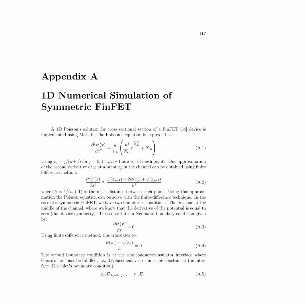
117
Appendix A
1D Numerical Simulation ofSymmetric FinFET
A 1D Poisson’s solution for cross sectional section of a FinFET [34] device isimplemented using Matlab. The Poisson’s equation is expressed as:
∂2ψ (x)
∂x2=
q
εch
n2i
Nch
e
ψ(x)Vtm
+Nch
(A.1)
Using xj = j/(n+1) for j = 0, 1, ..., n+1 as a set of mesh points. One approximationof the second derivative of ψ at a point xj in the channel can be obtained using finitedifference method:
∂2ψ (x)
∂x2≈ ψ(xj−1)− 2ψ(xj) + ψ(xj+1)
h2(A.2)
where h = 1/(n + 1) is the mesh distance between each point. Using this approxi-mation the Poisson equation can be solve with the finite-difference technique. In thecase of a symmetric FinFET, we have two boundaries conditions. The first one at themiddle of the channel, where we know that the derivative of the potential is equal tozero (due device symmetry). This constitutes a Neumann boundary condition givenby:
∂ψ (x)
∂x= 0 (A.3)
Using finite difference method, this translates to:
ψ(x1)− ψ(x0)
h= 0 (A.4)
The second boundary condition is at the semiconductor-insulator interface whereGauss’s law must be fulfilled, i.e., displacement vector must be constant at the inter-face (Dirichlet’s boundary condition):
εchEch,interface = εoxEox (A.5)
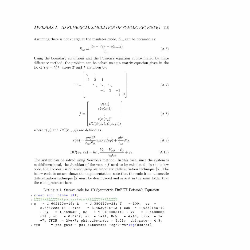
APPENDIX A. 1D NUMERICAL SIMULATION OF SYMMETRIC FINFET 118
Assuming there is not charge at the insulator oxide, Eox can be obtained as:
Eox =VG − VFB − ψ(xn+1)
tox(A.6)
Using the boundary conditions and the Poisson’s equation approximated by finitedifference method, the problem can be solved using a matrix equation given in thefor of Tψ = h2f , where T and f are given by:
T =
2 1−1 2 1
. . . . . . . . .
−1 2 −1−1 2
(A.7)
f =
ψ(x1)r(ψ(x2))
...r(ψ(xn))
BC(ψ(xn), ψ(xn+1))
(A.8)
where r(ψ) and BC(ψ1, ψ2) are defined as:
r(ψ) =qn2
ih2
εchNch
exp(ψ/vT ) +qh2
εchNch (A.9)
BC(ψ1, ψ2) = hεoxVG − VFB − ψ2
εchtox+ ψ1 (A.10)
The system can be solved using Newton’s method. In this case, since the system ismultidimensional, the Jacobian of the vector f need to be calculated. In the belowcode, the Jacobian is obtained using an automatic differentiation technique [5]. Thebelow code in octave shows the implementation, note that the code from automaticdifferentiation technique [5] must be downloaded and save it in the same folder thatthe code presented here.
Listing A.1. Octave code for 1D Symmetric FinFET Poisson’s Equation
1 clear all; close all;
2 %%%%%%%%%%%%%% parameters %%%%%%%%%%%%%%%
3 q = 1.602190e-19; k = 1.380650e-23; T = 300; eo =
8.854000e-14 ; eins = 3.453060e-13 ; ech = 1.035918e-12
; Eg = 1.169640 ; Nc = 2.540000e+19 ; Nv = 3.140000e
+19 ; vt = 0.0259; ni = 1e11; Nch = 4e18; tins = 1e
-7; TFIN = 20e-7; phi_substrate = 4.05; phi_gate = 4.3;
4 Vfb = phi_gate - phi_substrate -Eg/2-vt*log(Nch/ni);
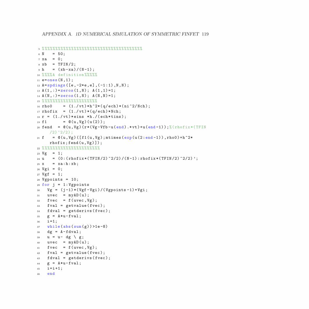
APPENDIX A. 1D NUMERICAL SIMULATION OF SYMMETRIC FINFET 119
5 %%%%%%%%%%%%%%%%%%%%%%%%%%%%%%%%%%%%%%
6 N = 50;
7 xa = 0;
8 xb = TFIN /2;
9 h = (xb -xa)/(N-1);
10 %%%%A definition %%%%%
11 e=ones(N,1);
12 A=spdiags ([e,-2*e,e],(-1:1),N,N);
13 A(1,:)=zeros(1,N); A(1,1)=1;
14 A(N,:)=zeros(1,N); A(N,N)=1;
15 %%%%%%%%%%%%%%%%%%%%%
16 rho0 = (1./vt)*h^2*(q/ech)*(ni^2/ Nch);
17 rhofix = (1./vt)*(q/ech)*Nch;
18 r = (1./vt)*eins *h./(ech*tins);
19 f1 = @(u,Vg)(u(2));
20 fend = @(u,Vg)(r*(Vg-Vfb -u(end).*vt)+u(end -1));%(rhofix *(TFIN
/2) ^2/2);
21 f = @(u,Vg)([f1(u,Vg);mtimes(exp(u(2:end -1)),rho0)+h^2*
rhofix;fend(u,Vg)]);
22 %%%%%%%%%%%%%%%%%%%%%%
23 Vg = 1;
24 u = (0:(rhofix *(TFIN /2) ^2/2) /(N-1):rhofix *(TFIN /2) ^2/2) ’;
25 x = xa:h:xb;
26 Vgi = 0;
27 Vgf = 1;
28 Vgpoints = 10;
29 for j = 1:Vgpoints
30 Vg = (j-1)*(Vgf -Vgi)/(Vgpoints -1)+Vgi;
31 uvec = myAD(u);
32 fvec = f(uvec ,Vg);
33 fval = getvalue(fvec);
34 fdval = getderivs(fvec);
35 g = A*u-fval;
36 i=1;
37 while(abs(sum(g)) >1e-8)
38 dg = A-fdval;
39 u = u- dg \ g;
40 uvec = myAD(u);
41 fvec = f(uvec ,Vg);
42 fval = getvalue(fvec);
43 fdval = getderivs(fvec);
44 g = A*u-fval;
45 i=i+1;
46 end

APPENDIX A. 1D NUMERICAL SIMULATION OF SYMMETRIC FINFET 120
47 u_all(:,j) = u;
48 end

121
Appendix B
Explicit Surface Potential Model
The surface potential model use in BSIM-CMG was initially derived in an im-plicit form in chapter 2, which relies on numerical calculations to be solved, such asNewton-Raphson method [76, 81]. Newton-Raphson method is an iterative algorithmthat start from an initial guess to then keep refining it until the method arrives toa final solution. This refinement is done by approximating the function to be solvedat the given guess by a linear system which is then used to obtain the new guessfor the solution [79]. Although Newton-Raphson method could potentially have arapid convergence (e.g. quadratic [81, 79]), its convergence is no guarantee. Indeed,it could potentially fail by, for example, getting into an infinite loop. This is notpractical for compact models, where convergence and speed are key requirements.However, by making sure that the initial guess is close enough to the final solutionand that the solution is not singular, i.e. the derivative of the function is non zero atthe solution, it could be assured that the Newton-Raphson method will converge [81].Therefore, in order to implement the model proposed in section 2 in a circuit simu-lator, a good initial guess formula, so called continuous starting function (CSF) [90],for equation (2.11) is presented in this section. In addition, Newton-Raphson methodcould be replaced for a higher order method such as the quartic modified iteration[81]. The main difference between quartic modified and Newton-Raphson iterations isthat the first refine the initial guess by approximating the function to be solved usinga high order approximation, instead of the linear one used in Newton-Raphson itera-tion. Therefore, quartic modified iteration could give a faster convergence rate whichwould reduce the iterations needed to solve equation (2.11), making the proposedcompact model fast.
B.1 Continuous Starting Function
A initial guess for equation (2.11) has been already proposed in [28]. It wasderived by considering the asymptotic behaviour of β in equation (2.11) under the
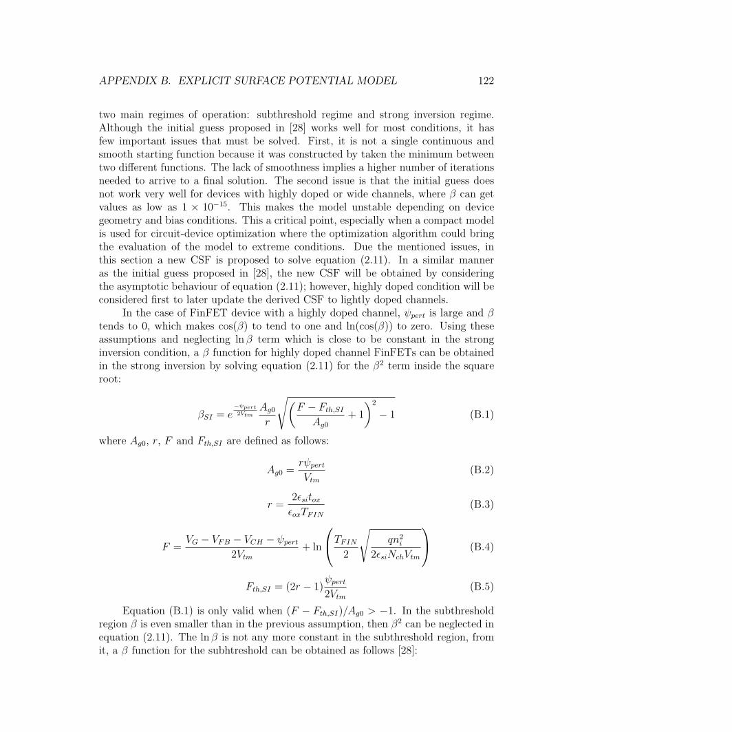
APPENDIX B. EXPLICIT SURFACE POTENTIAL MODEL 122
two main regimes of operation: subthreshold regime and strong inversion regime.Although the initial guess proposed in [28] works well for most conditions, it hasfew important issues that must be solved. First, it is not a single continuous andsmooth starting function because it was constructed by taken the minimum betweentwo different functions. The lack of smoothness implies a higher number of iterationsneeded to arrive to a final solution. The second issue is that the initial guess doesnot work very well for devices with highly doped or wide channels, where β can getvalues as low as 1 × 10⁻¹⁵. This makes the model unstable depending on devicegeometry and bias conditions. This a critical point, especially when a compact modelis used for circuit-device optimization where the optimization algorithm could bringthe evaluation of the model to extreme conditions. Due the mentioned issues, inthis section a new CSF is proposed to solve equation (2.11). In a similar manneras the initial guess proposed in [28], the new CSF will be obtained by consideringthe asymptotic behaviour of equation (2.11); however, highly doped condition will beconsidered first to later update the derived CSF to lightly doped channels.
In the case of FinFET device with a highly doped channel, ψpert is large and βtends to 0, which makes cos(β) to tend to one and ln(cos(β)) to zero. Using theseassumptions and neglecting ln β term which is close to be constant in the stronginversion condition, a β function for highly doped channel FinFETs can be obtainedin the strong inversion by solving equation (2.11) for the β2 term inside the squareroot:
βSI = e−ψpert2Vtm
Ag0r
√
(
F − Fth,SIAg0
+ 1
)2
− 1 (B.1)
where Ag0, r, F and Fth,SI are defined as follows:
Ag0 =rψpertVtm
(B.2)
r =2ǫsitoxǫoxTFIN
(B.3)
F =VG − VFB − VCH − ψpert
2Vtm+ ln
TFIN2
√
qn2i
2ǫsiNchVtm
(B.4)
Fth,SI = (2r − 1)ψpert2Vtm
(B.5)
Equation (B.1) is only valid when (F − Fth,SI)/Ag0 > −1. In the subthresholdregion β is even smaller than in the previous assumption, then β2 can be neglected inequation (2.11). The ln β is not any more constant in the subthreshold region, fromit, a β function for the subhtreshold can be obtained as follows [28]:
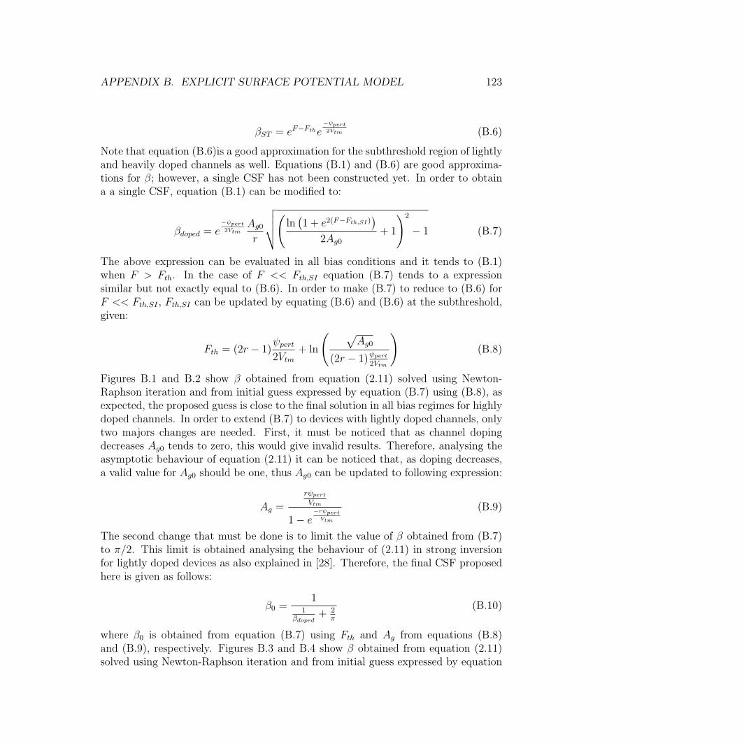
APPENDIX B. EXPLICIT SURFACE POTENTIAL MODEL 123
βST = eF−Fthe−ψpert2Vtm (B.6)
Note that equation (B.6)is a good approximation for the subthreshold region of lightlyand heavily doped channels as well. Equations (B.1) and (B.6) are good approxima-tions for β; however, a single CSF has not been constructed yet. In order to obtaina a single CSF, equation (B.1) can be modified to:
βdoped = e−ψpert2Vtm
Ag0r
√
√
√
√
(
ln(
1 + e2(F−Fth,SI))
2Ag0+ 1
)2
− 1 (B.7)
The above expression can be evaluated in all bias conditions and it tends to (B.1)when F > Fth. In the case of F << Fth,SI equation (B.7) tends to a expressionsimilar but not exactly equal to (B.6). In order to make (B.7) to reduce to (B.6) forF << Fth,SI , Fth,SI can be updated by equating (B.6) and (B.6) at the subthreshold,given:
Fth = (2r − 1)ψpert2Vtm
+ ln
(
√
Ag0
(2r − 1)ψpert2Vtm
)
(B.8)
Figures B.1 and B.2 show β obtained from equation (2.11) solved using Newton-Raphson iteration and from initial guess expressed by equation (B.7) using (B.8), asexpected, the proposed guess is close to the final solution in all bias regimes for highlydoped channels. In order to extend (B.7) to devices with lightly doped channels, onlytwo majors changes are needed. First, it must be noticed that as channel dopingdecreases Ag0 tends to zero, this would give invalid results. Therefore, analysing theasymptotic behaviour of equation (2.11) it can be noticed that, as doping decreases,a valid value for Ag0 should be one, thus Ag0 can be updated to following expression:
Ag =
rψpertVtm
1− e−rψpertVtm
(B.9)
The second change that must be done is to limit the value of β obtained from (B.7)to π/2. This limit is obtained analysing the behaviour of (2.11) in strong inversionfor lightly doped devices as also explained in [28]. Therefore, the final CSF proposedhere is given as follows:
β0 =1
1βdoped
+ 2π
(B.10)
where β0 is obtained from equation (B.7) using Fth and Ag from equations (B.8)and (B.9), respectively. Figures B.3 and B.4 show β obtained from equation (2.11)solved using Newton-Raphson iteration and from initial guess expressed by equation
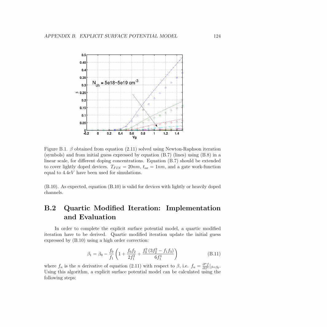
APPENDIX B. EXPLICIT SURFACE POTENTIAL MODEL 124
Figure B.1. β obtained from equation (2.11) solved using Newton-Raphson iteration(symbols) and from initial guess expressed by equation (B.7) (lines) using (B.8) in alinear scale, for different doping concentrations. Equation (B.7) should be extendedto cover lightly doped devices. TFIN = 20nm, tox = 1nm, and a gate work-functionequal to 4.4eV have been used for simulations.
(B.10). As expected, equation (B.10) is valid for devices with lightly or heavily dopedchannels.
B.2 Quartic Modified Iteration: Implementation
and Evaluation
In order to complete the explicit surface potential model, a quartic modifiediteration have to be derived. Quartic modified iteration update the initial guessexpressed by (B.10) using a high order correction:
β1 = β0 −f0f1
(
1 +f0f22f 2
1
+f 20 (3f
22 − f1f3)
6f 41
)
(B.11)
where fn is the n derivative of equation (2.11) with respect to β, i.e. fn = ∂nf∂βn
|β=β0 .Using this algorithm, a explicit surface potential model can be calculated using thefollowing steps:
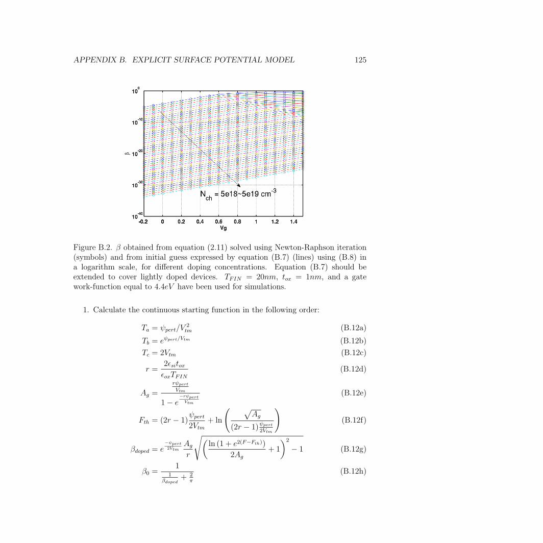
APPENDIX B. EXPLICIT SURFACE POTENTIAL MODEL 125
Figure B.2. β obtained from equation (2.11) solved using Newton-Raphson iteration(symbols) and from initial guess expressed by equation (B.7) (lines) using (B.8) ina logarithm scale, for different doping concentrations. Equation (B.7) should beextended to cover lightly doped devices. TFIN = 20nm, tox = 1nm, and a gatework-function equal to 4.4eV have been used for simulations.
1. Calculate the continuous starting function in the following order:
Ta = ψpert/V2tm (B.12a)
Tb = eψpert/Vtm (B.12b)
Tc = 2Vtm (B.12c)
r =2ǫsitoxǫoxTFIN
(B.12d)
Ag =
rψpertVtm
1− e−rψpertVtm
(B.12e)
Fth = (2r − 1)ψpert2Vtm
+ ln
(
√
Ag
(2r − 1)ψpert2Vtm
)
(B.12f)
βdoped = e−ψpert2Vtm
Agr
√
(
ln (1 + e2(F−Fth))
2Ag+ 1
)2
− 1 (B.12g)
β0 =1
1βdoped
+ 2π
(B.12h)
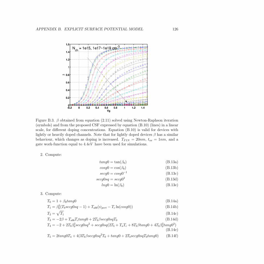
APPENDIX B. EXPLICIT SURFACE POTENTIAL MODEL 126
Figure B.3. β obtained from equation (2.11) solved using Newton-Raphson iteration(symbols) and from the proposed CSF expressed by equation (B.10) (lines) in a linearscale, for different doping concentrations. Equation (B.10) is valid for devices withlightly or heavily doped channels. Note that for lightly doped devices β has a similarbehaviour, which changes as doping is increased. TFIN = 20nm, tox = 1nm, and agate work-function equal to 4.4eV have been used for simulations.
2. Compute:
tang0 = tan(β0) (B.13a)
cosg0 = cos(β0) (B.13b)
secg0 = cosg0−1 (B.13c)
secg0sq = secg02 (B.13d)
lng0 = ln(β0) (B.13e)
3. Compute:
T0 = 1 + β0tang0 (B.14a)
T1 = β20(Tbsecg0sq − 1) + Tabb(ψpert − Tc ln(cosg0)) (B.14b)
T2 =√
T1 (B.14c)
T3 = −2β + TabbTctang0 + 2Tbβsecg0sqT0 (B.14d)
T4 = −2 + 2Tbβ20secg0sq
2 + secg0sq(2Tb + TaTc + 8Tbβtang0 + 4Tbβ20tang0
2)(B.14e)
T5 = 2tang0T4 + 4(3Tbβsecg0sq2T0 + tang0 + 2Tbsecg0sqT0tang0) (B.14f)
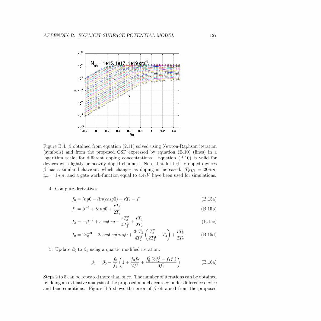
APPENDIX B. EXPLICIT SURFACE POTENTIAL MODEL 127
Figure B.4. β obtained from equation (2.11) solved using Newton-Raphson iteration(symbols) and from the proposed CSF expressed by equation (B.10) (lines) in alogarithm scale, for different doping concentrations. Equation (B.10) is valid fordevices with lightly or heavily doped channels. Note that for lightly doped devicesβ has a similar behaviour, which changes as doping is increased. TFIN = 20nm,tox = 1nm, and a gate work-function equal to 4.4eV have been used for simulations.
4. Compute derivatives:
f0 = lng0− lln(cosg0) + rT2 − F (B.15a)
f1 = β−1 + tang0 +rT32T2
(B.15b)
f2 = −β−20 + secg0sq − rT 2
3
4T 32
+rT42T2
(B.15c)
f0 = 2β−30 + 2secg0sqtang0 +
3rT34T 3
2
(
T 23
2T 22
− T4
)
+rT52T2
(B.15d)
5. Update β0 to β1 using a quartic modified iteration:
β1 = β0 −f0f1
(
1 +f0f22f 2
1
+f 20 (3f
22 − f1f3)
6f 41
)
(B.16a)
Steps 2 to 5 can be repeated more than once. The number of iterations can be obtainedby doing an extensive analysis of the proposed model accuracy under difference deviceand bias conditions. Figure B.5 shows the error of β obtained from the proposed
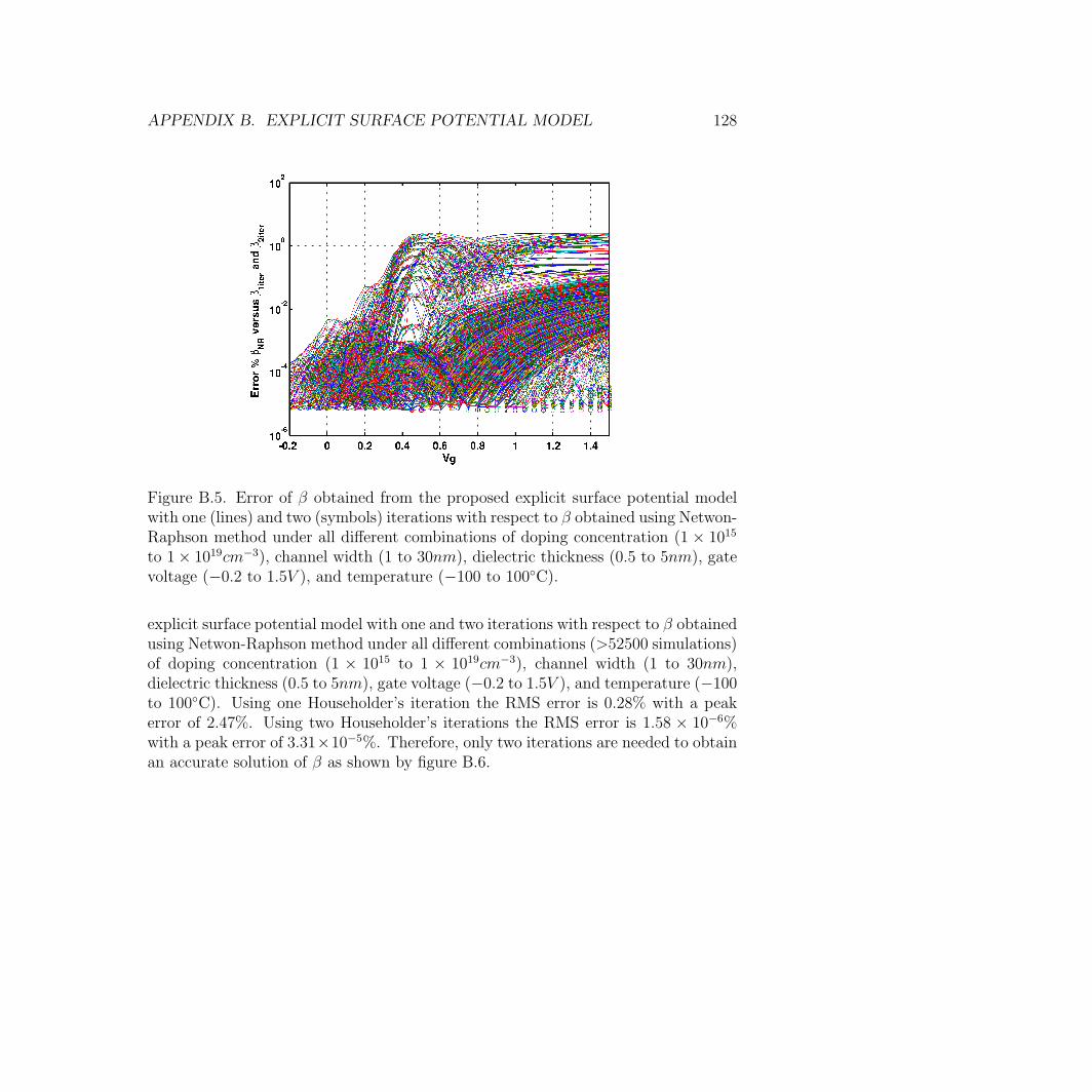
APPENDIX B. EXPLICIT SURFACE POTENTIAL MODEL 128
Figure B.5. Error of β obtained from the proposed explicit surface potential modelwith one (lines) and two (symbols) iterations with respect to β obtained using Netwon-Raphson method under all different combinations of doping concentration (1 × 10¹⁵
to 1× 1019cm−3), channel width (1 to 30nm), dielectric thickness (0.5 to 5nm), gatevoltage (−0.2 to 1.5V ), and temperature (−100 to 100◦C).
explicit surface potential model with one and two iterations with respect to β obtainedusing Netwon-Raphson method under all different combinations (>52500 simulations)of doping concentration (1 × 10¹⁵ to 1 × 1019cm−3), channel width (1 to 30nm),dielectric thickness (0.5 to 5nm), gate voltage (−0.2 to 1.5V ), and temperature (−100to 100◦C). Using one Householder’s iteration the RMS error is 0.28% with a peakerror of 2.47%. Using two Householder’s iterations the RMS error is 1.58 × 10⁻⁶%with a peak error of 3.31×10⁻⁵%. Therefore, only two iterations are needed to obtainan accurate solution of β as shown by figure B.6.
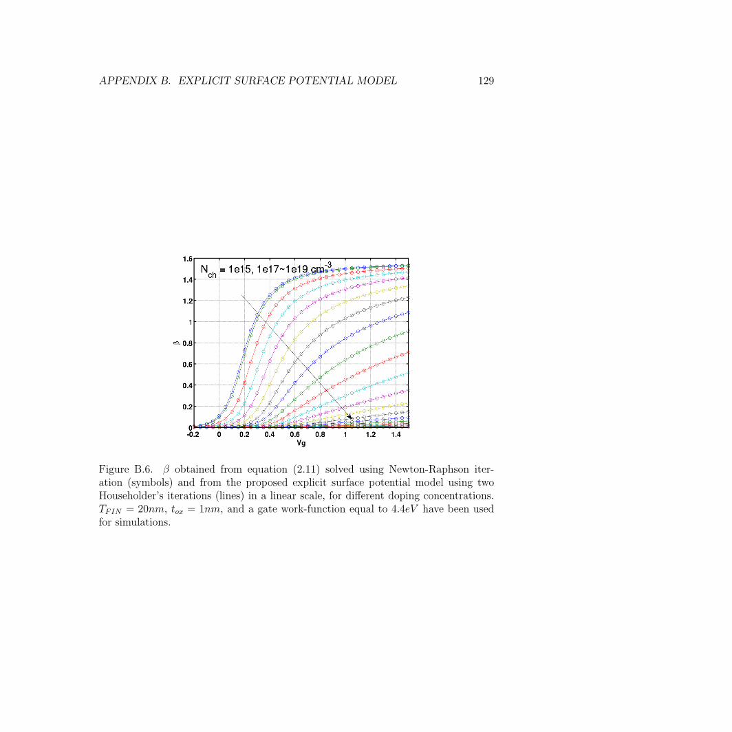
APPENDIX B. EXPLICIT SURFACE POTENTIAL MODEL 129
Figure B.6. β obtained from equation (2.11) solved using Newton-Raphson iter-ation (symbols) and from the proposed explicit surface potential model using twoHouseholder’s iterations (lines) in a linear scale, for different doping concentrations.TFIN = 20nm, tox = 1nm, and a gate work-function equal to 4.4eV have been usedfor simulations.
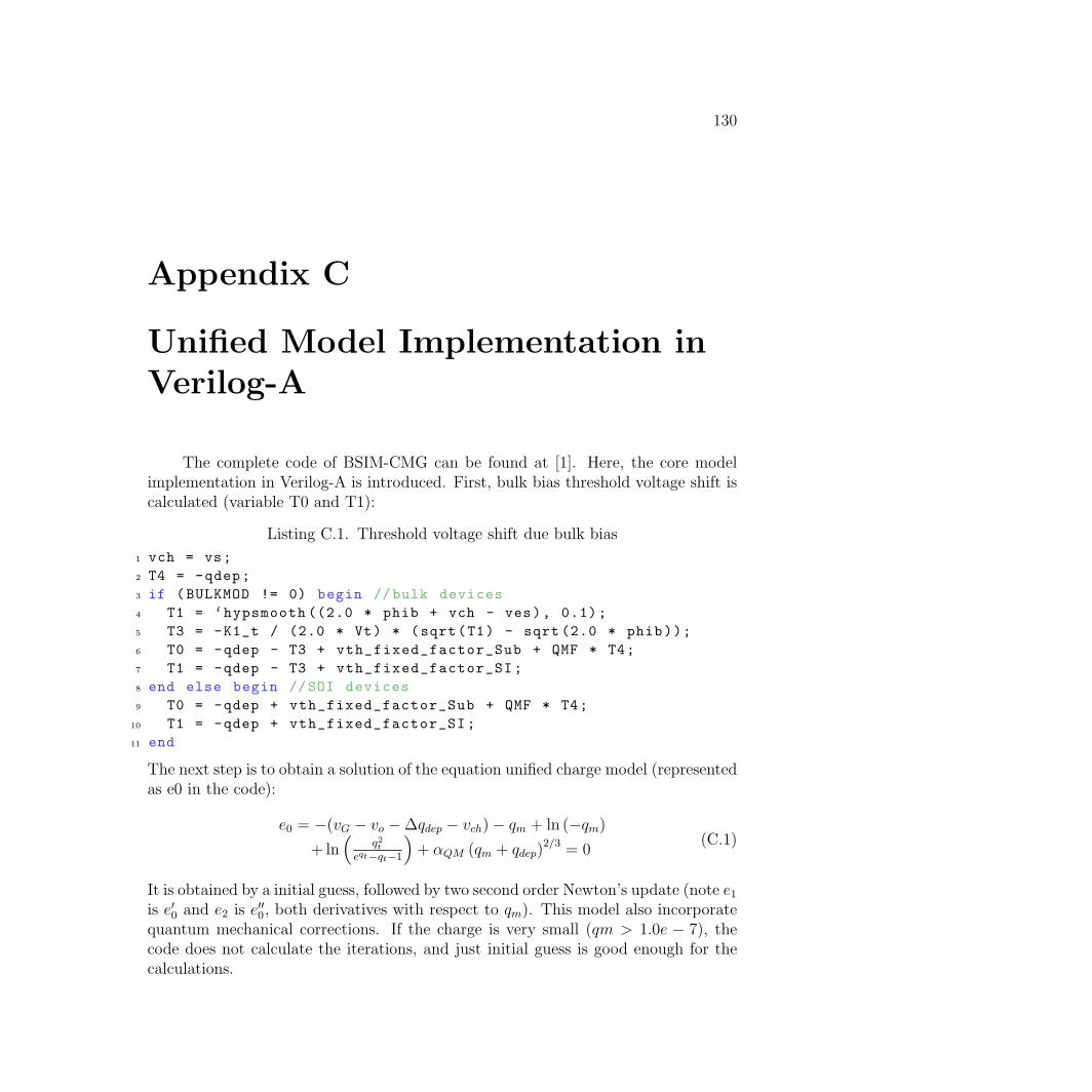
130
Appendix C
Unified Model Implementation inVerilog-A
The complete code of BSIM-CMG can be found at [1]. Here, the core modelimplementation in Verilog-A is introduced. First, bulk bias threshold voltage shift iscalculated (variable T0 and T1):
Listing C.1. Threshold voltage shift due bulk bias
1 vch = vs;
2 T4 = -qdep;
3 if (BULKMOD != 0) begin //bulk devices
4 T1 = ‘hypsmooth ((2.0 * phib + vch - ves), 0.1);
5 T3 = -K1_t / (2.0 * Vt) * (sqrt(T1) - sqrt (2.0 * phib));
6 T0 = -qdep - T3 + vth_fixed_factor_Sub + QMF * T4;
7 T1 = -qdep - T3 + vth_fixed_factor_SI;
8 end else begin //SOI devices
9 T0 = -qdep + vth_fixed_factor_Sub + QMF * T4;
10 T1 = -qdep + vth_fixed_factor_SI;
11 end
The next step is to obtain a solution of the equation unified charge model (representedas e0 in the code):
e0 = −(vG − vo −∆qdep − vch)− qm + ln (−qm)+ ln
(
q2teqt−qt−1
)
+ αQM (qm + qdep)2/3 = 0
(C.1)
It is obtained by a initial guess, followed by two second order Newton’s update (note e1is e′0 and e2 is e′′0, both derivatives with respect to qm). This model also incorporatequantum mechanical corrections. If the charge is very small (qm > 1.0e − 7), thecode does not calculate the iterations, and just initial guess is good enough for thecalculations.
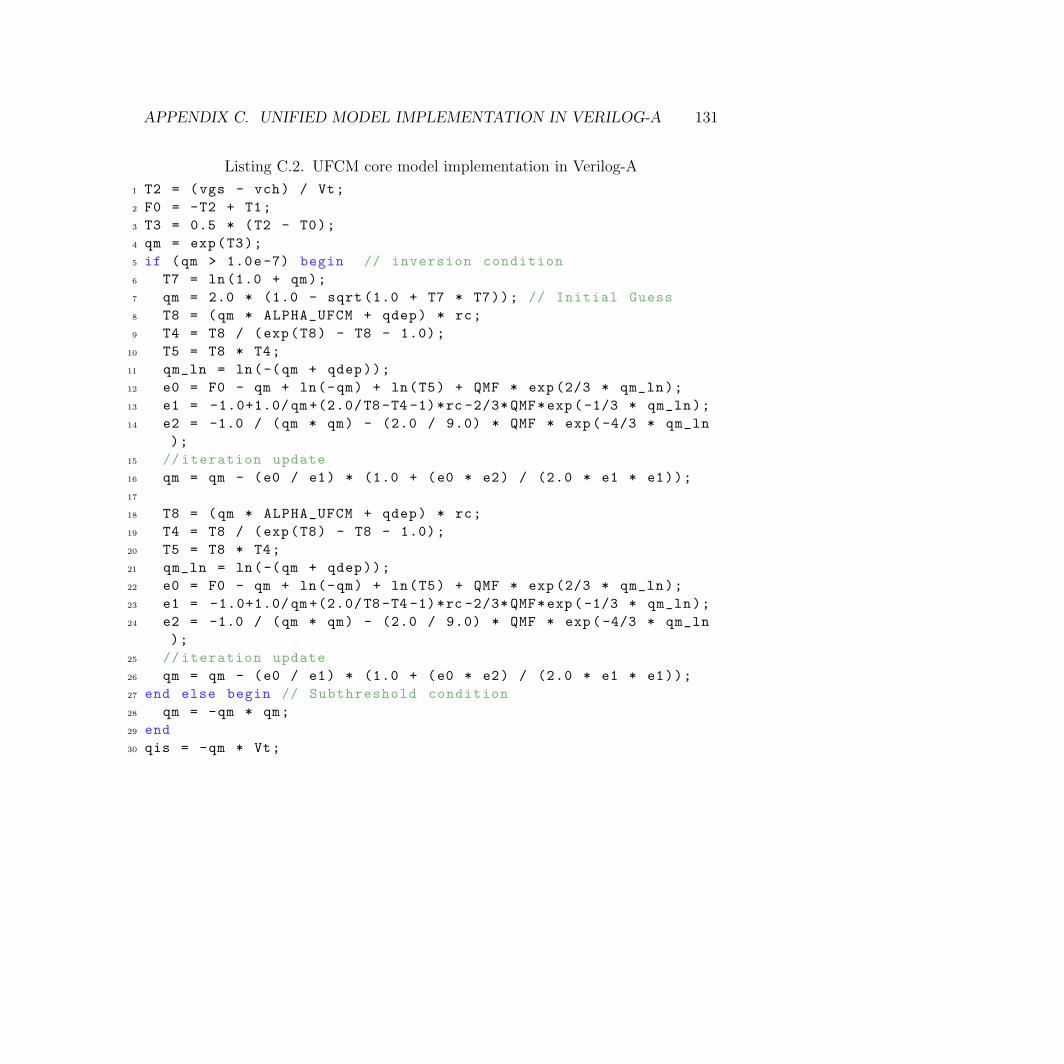
APPENDIX C. UNIFIED MODEL IMPLEMENTATION IN VERILOG-A 131
Listing C.2. UFCM core model implementation in Verilog-A
1 T2 = (vgs - vch) / Vt;
2 F0 = -T2 + T1;
3 T3 = 0.5 * (T2 - T0);
4 qm = exp(T3);
5 if (qm > 1.0e-7) begin // inversion condition
6 T7 = ln(1.0 + qm);
7 qm = 2.0 * (1.0 - sqrt (1.0 + T7 * T7)); // Initial Guess
8 T8 = (qm * ALPHA_UFCM + qdep) * rc;
9 T4 = T8 / (exp(T8) - T8 - 1.0);
10 T5 = T8 * T4;
11 qm_ln = ln(-(qm + qdep));
12 e0 = F0 - qm + ln(-qm) + ln(T5) + QMF * exp (2/3 * qm_ln);
13 e1 = -1.0+1.0/qm +(2.0/T8 -T4 -1)*rc -2/3* QMF*exp(-1/3 * qm_ln);
14 e2 = -1.0 / (qm * qm) - (2.0 / 9.0) * QMF * exp(-4/3 * qm_ln
);
15 // iteration update
16 qm = qm - (e0 / e1) * (1.0 + (e0 * e2) / (2.0 * e1 * e1));
17
18 T8 = (qm * ALPHA_UFCM + qdep) * rc;
19 T4 = T8 / (exp(T8) - T8 - 1.0);
20 T5 = T8 * T4;
21 qm_ln = ln(-(qm + qdep));
22 e0 = F0 - qm + ln(-qm) + ln(T5) + QMF * exp (2/3 * qm_ln);
23 e1 = -1.0+1.0/qm +(2.0/T8 -T4 -1)*rc -2/3* QMF*exp(-1/3 * qm_ln);
24 e2 = -1.0 / (qm * qm) - (2.0 / 9.0) * QMF * exp(-4/3 * qm_ln
);
25 // iteration update
26 qm = qm - (e0 / e1) * (1.0 + (e0 * e2) / (2.0 * e1 * e1));
27 end else begin // Subthreshold condition
28 qm = -qm * qm;
29 end
30 qis = -qm * Vt;
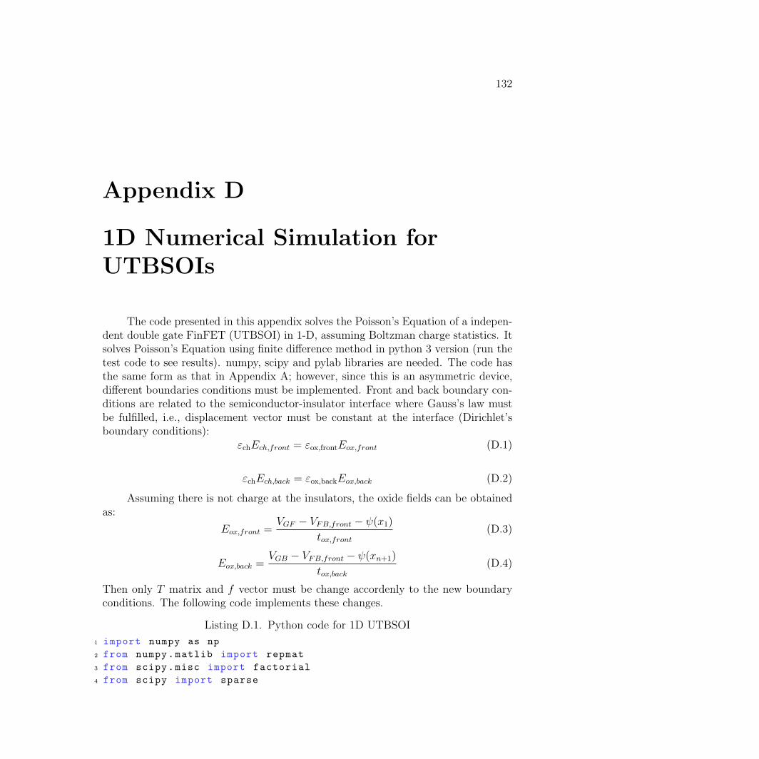
132
Appendix D
1D Numerical Simulation forUTBSOIs
The code presented in this appendix solves the Poisson’s Equation of a indepen-dent double gate FinFET (UTBSOI) in 1-D, assuming Boltzman charge statistics. Itsolves Poisson’s Equation using finite difference method in python 3 version (run thetest code to see results). numpy, scipy and pylab libraries are needed. The code hasthe same form as that in Appendix A; however, since this is an asymmetric device,different boundaries conditions must be implemented. Front and back boundary con-ditions are related to the semiconductor-insulator interface where Gauss’s law mustbe fulfilled, i.e., displacement vector must be constant at the interface (Dirichlet’sboundary conditions):
εchEch,front = εox,frontEox,front (D.1)
εchEch,back = εox,backEox,back (D.2)
Assuming there is not charge at the insulators, the oxide fields can be obtainedas:
Eox,front =VGF − VFB,front − ψ(x1)
tox,front(D.3)
Eox,back =VGB − VFB,front − ψ(xn+1)
tox,back(D.4)
Then only T matrix and f vector must be change accordenly to the new boundaryconditions. The following code implements these changes.
Listing D.1. Python code for 1D UTBSOI
1 import numpy as np
2 from numpy.matlib import repmat
3 from scipy.misc import factorial
4 from scipy import sparse
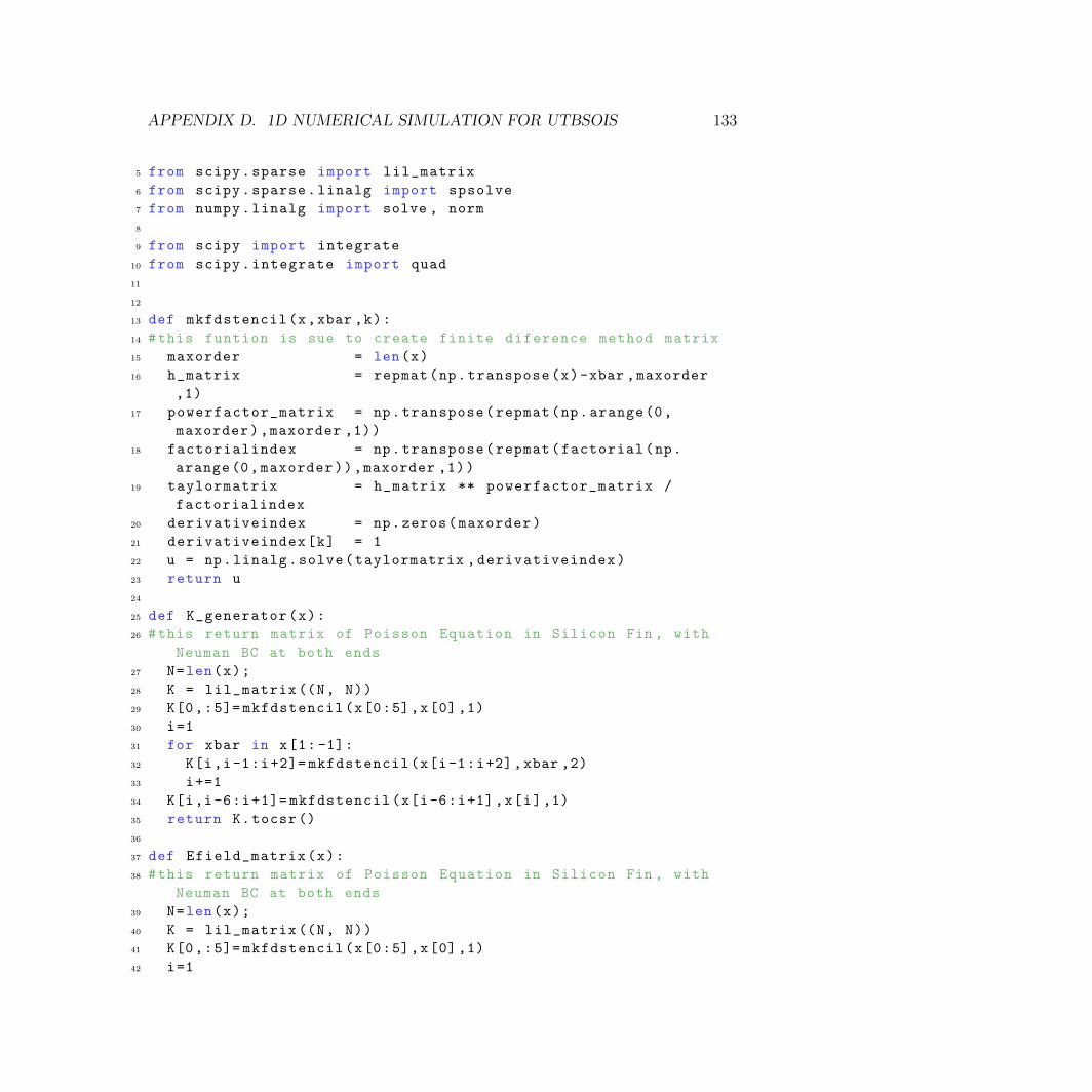
APPENDIX D. 1D NUMERICAL SIMULATION FOR UTBSOIS 133
5 from scipy.sparse import lil_matrix
6 from scipy.sparse.linalg import spsolve
7 from numpy.linalg import solve , norm
8
9 from scipy import integrate
10 from scipy.integrate import quad
11
12
13 def mkfdstencil(x,xbar ,k):
14 #this funtion is sue to create finite diference method matrix
15 maxorder = len(x)
16 h_matrix = repmat(np.transpose(x)-xbar ,maxorder
,1)
17 powerfactor_matrix = np.transpose(repmat(np.arange(0,
maxorder),maxorder ,1))
18 factorialindex = np.transpose(repmat(factorial(np.
arange(0,maxorder)),maxorder ,1))
19 taylormatrix = h_matrix ** powerfactor_matrix /
factorialindex
20 derivativeindex = np.zeros(maxorder)
21 derivativeindex[k] = 1
22 u = np.linalg.solve(taylormatrix ,derivativeindex)
23 return u
24
25 def K_generator(x):
26 #this return matrix of Poisson Equation in Silicon Fin , with
Neuman BC at both ends
27 N=len(x);
28 K = lil_matrix ((N, N))
29 K[0,:5]= mkfdstencil(x[0:5],x[0],1)
30 i=1
31 for xbar in x[1: -1]:
32 K[i,i-1:i+2]= mkfdstencil(x[i-1:i+2],xbar ,2)
33 i+=1
34 K[i,i-6:i+1]= mkfdstencil(x[i-6:i+1],x[i],1)
35 return K.tocsr()
36
37 def Efield_matrix(x):
38 #this return matrix of Poisson Equation in Silicon Fin , with
Neuman BC at both ends
39 N=len(x);
40 K = lil_matrix ((N, N))
41 K[0,:5]= mkfdstencil(x[0:5],x[0],1)
42 i=1
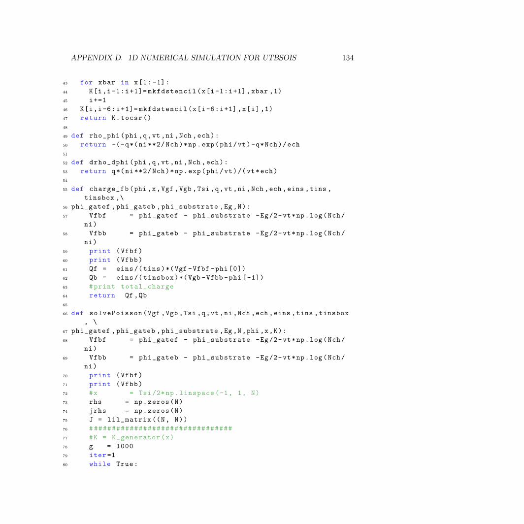
APPENDIX D. 1D NUMERICAL SIMULATION FOR UTBSOIS 134
43 for xbar in x[1: -1]:
44 K[i,i-1:i+1]= mkfdstencil(x[i-1:i+1],xbar ,1)
45 i+=1
46 K[i,i-6:i+1]= mkfdstencil(x[i-6:i+1],x[i],1)
47 return K.tocsr()
48
49 def rho_phi(phi ,q,vt ,ni ,Nch ,ech):
50 return -(-q*(ni**2/ Nch)*np.exp(phi/vt)-q*Nch)/ech
51
52 def drho_dphi(phi ,q,vt ,ni ,Nch ,ech):
53 return q*(ni**2/ Nch)*np.exp(phi/vt)/(vt*ech)
54
55 def charge_fb(phi ,x,Vgf ,Vgb ,Tsi ,q,vt ,ni ,Nch ,ech ,eins ,tins ,
tinsbox ,\
56 phi_gatef ,phi_gateb ,phi_substrate ,Eg ,N):
57 Vfbf = phi_gatef - phi_substrate -Eg/2-vt*np.log(Nch/
ni)
58 Vfbb = phi_gateb - phi_substrate -Eg/2-vt*np.log(Nch/
ni)
59 print (Vfbf)
60 print (Vfbb)
61 Qf = eins/(tins)*(Vgf -Vfbf -phi [0])
62 Qb = eins/( tinsbox)*(Vgb -Vfbb -phi[-1])
63 #print total_charge
64 return Qf ,Qb
65
66 def solvePoisson(Vgf ,Vgb ,Tsi ,q,vt ,ni ,Nch ,ech ,eins ,tins ,tinsbox
, \
67 phi_gatef ,phi_gateb ,phi_substrate ,Eg ,N,phi ,x,K):
68 Vfbf = phi_gatef - phi_substrate -Eg/2-vt*np.log(Nch/
ni)
69 Vfbb = phi_gateb - phi_substrate -Eg/2-vt*np.log(Nch/
ni)
70 print (Vfbf)
71 print (Vfbb)
72 #x = Tsi/2*np.linspace(-1, 1, N)
73 rhs = np.zeros(N)
74 jrhs = np.zeros(N)
75 J = lil_matrix ((N, N))
76 ################################
77 #K = K_generator(x)
78 g = 1000
79 iter=1
80 while True:
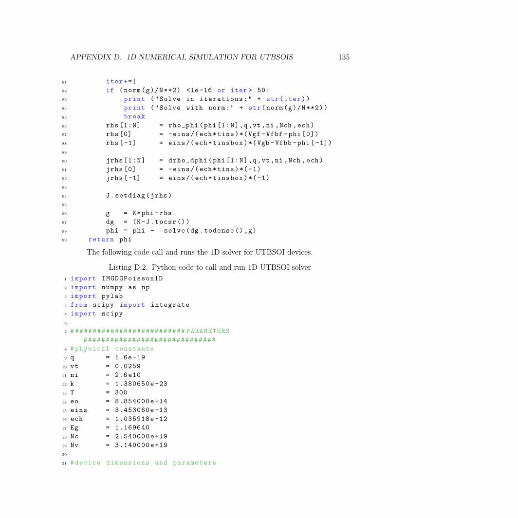
APPENDIX D. 1D NUMERICAL SIMULATION FOR UTBSOIS 135
81 iter +=1
82 if (norm(g)/N**2) <1e-16 or iter > 50:
83 print ("Solve in iterations:" + str(iter))
84 print ("Solve with norm:" + str(norm(g)/N**2))
85 break
86 rhs[1:N] = rho_phi(phi[1:N],q,vt ,ni ,Nch ,ech)
87 rhs [0] = -eins/(ech*tins)*(Vgf -Vfbf -phi [0])
88 rhs[-1] = eins/(ech*tinsbox)*(Vgb -Vfbb -phi[-1])
89
90 jrhs[1:N] = drho_dphi(phi[1:N],q,vt ,ni ,Nch ,ech)
91 jrhs [0] = -eins/(ech*tins)*(-1)
92 jrhs[-1] = eins/(ech*tinsbox)*(-1)
93
94 J.setdiag(jrhs)
95
96 g = K*phi -rhs
97 dg = (K-J.tocsr ())
98 phi = phi - solve(dg.todense (),g)
99 return phi
The following code call and runs the 1D solver for UTBSOI devices.
Listing D.2. Python code to call and run 1D UTBSOI solver
1 import IMGDGPoisson1D
2 import numpy as np
3 import pylab
4 from scipy import integrate
5 import scipy
6
7 ########################## PARAMETERS
##############################
8 #physical constants
9 q = 1.6e-19
10 vt = 0.0259
11 ni = 2.6 e10
12 k = 1.380650e-23
13 T = 300
14 eo = 8.854000e-14
15 eins = 3.453060e-13
16 ech = 1.035918e-12
17 Eg = 1.169640
18 Nc = 2.540000e+19
19 Nv = 3.140000e+19
20
21 #device dimensions and parameters
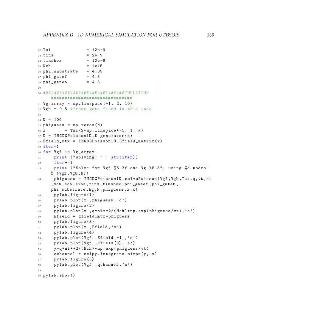
APPENDIX D. 1D NUMERICAL SIMULATION FOR UTBSOIS 136
22 Tsi = 12e-9
23 tins = 2e-9
24 tinsbox = 10e-9
25 Nch = 1e15
26 phi_substrate = 4.05
27 phi_gatef = 4.5
28 phi_gateb = 4.5
29
30 ############################# SIMULATION
##############################
31 Vg_array = np.linspace(-1, 2, 10)
32 Vgb = 0.5 #front gate fixed in this case
33
34 N = 100
35 phiguess = np.zeros(N)
36 x = Tsi/2*np.linspace(-1, 1, N)
37 K = IMGDGPoisson1D.K_generator(x)
38 Efield_mtx = IMGDGPoisson1D.Efield_matrix(x)
39 iter=1
40 for Vgf in Vg_array:
41 print ("solving: " + str(iter))
42 iter +=1
43 print ("Solve for Vgf %5.3f and Vg %5.3f, using %d nodes"
% (Vgf ,Vgb ,N))
44 phiguess = IMGDGPoisson1D.solvePoisson(Vgf ,Vgb ,Tsi ,q,vt,ni
,Nch ,ech ,eins ,tins ,tinsbox ,phi_gatef ,phi_gateb ,
phi_substrate ,Eg ,N,phiguess ,x,K)
45 pylab.figure (1)
46 pylab.plot(x ,phiguess ,’o’)
47 pylab.figure (2)
48 pylab.plot(x ,q*ni **2/( Nch)*np.exp(phiguess/vt),’o’)
49 Efield = Efield_mtx*phiguess
50 pylab.figure (3)
51 pylab.plot(x ,Efield ,’o’)
52 pylab.figure (4)
53 pylab.plot(Vgf ,Efield[-1],’o’)
54 pylab.plot(Vgf ,Efield [0],’s’)
55 y=q*ni **2/( Nch)*np.exp(phiguess/vt)
56 qchannel = scipy.integrate.simps(y, x)
57 pylab.figure (5)
58 pylab.plot(Vgf ,qchannel ,’s’)
59
60 pylab.show()

137
Appendix E
Energy Calculation with Hspice
This appendix explains how to accurately calculate energy using Hspice. Eachcircuit simulation solve self-consistently the voltages and currents for each element.Using these quantities, power can be obtained using V ∗ I. Energy flow is then cal-culated by integrating the power using cumulatively numerical integration, by thecomposite trapezoidal rule. It is important to notice that simulations settings arevery important for accurate energy calculations. Simulations in this work were ob-tained using Hspice simulation engine, with simulations options set to RUNLVL=6,METHOD=GEAR, and MAXORD=3. Fig. E.1 shows energy calculations of a sim-ple RC circuit using default Hspice options and the accurate one used for this work;clearly, the chosen settings are needed for precise calculations.
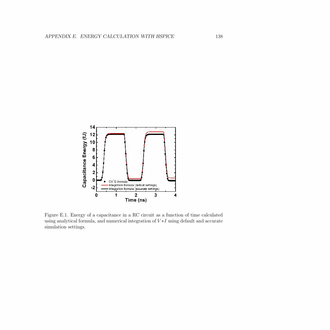
APPENDIX E. ENERGY CALCULATION WITH HSPICE 138
Figure E.1. Energy of a capacitance in a RC circuit as a function of time calculatedusing analytical formula, and numerical integration of V ∗I using default and accuratesimulation settings.


