Embed Size (px)
Citation preview
Freescale SemiconductorData Sheet: Technical Data
Document Number: MCF52223Rev. 3, 3/2011
MCF52223LQFP–6410 mm x 10 mm
MAPBGA–8110 mm x 10 mm
LQFP–10014 mm x 14 mm
MCF52223 ColdFire MicrocontrollerSupports MCF52223 andMCF52221
The MCF52223 microcontroller family is a member of the ColdFire® family of reduced instruction set computing (RISC) microprocessors.This document provides an overview of the 32-bit MCF52223 microcontroller, focusing on its highly integrated and diverse feature set.
This 32-bit device is based on the Version 2 ColdFire core operating at a frequency up to 80 MHz, offering high performance and low power consumption. On-chip memories connected tightly to the processor core include up to 256 Kbytes of flash memory and 32 Kbytes of static random access memory (SRAM). On-chip modules include:• V2 ColdFire core delivering 76 MIPS (Dhrystone 2.1) at
80 MHz running from internal flash memory with Multiply Accumulate (MAC) Unit and hardware divider
• Universal Serial Bus On-The-Go (USBOTG) • USB Transceiver• Three universal asynchronous/synchronous
receiver/transmitters (UARTs)• Inter-integrated circuit (I2C™) bus interface module• Queued serial peripheral interface (QSPI) module• Eight-channel 12-bit fast analog-to-digital converter
(ADC)• Four-channel direct memory access (DMA) controller• Four 32-bit input capture/output compare timers with
DMA support (DTIM)• Four-channel general-purpose timer (GPT) capable of
input capture/output compare, pulse width modulation (PWM), and pulse accumulation
• Eight-channel/Four-channel, 8-bit/16-bit pulse width modulation timer
• Two 16-bit periodic interrupt timers (PITs)• Real-time clock (RTC) module• Programmable software watchdog timer• Interrupt controller capable of handling 57 sources
© Freescale Semiconductor, Inc., 2011. All rights reserved.
Freescale reserves the right to change the detail specifications aimprovements in the design of its products.
• Clock module with 8 MHz on-chip relaxation oscillator and integrated phase-locked loop (PLL)
• Test access/debug port (JTAG, BDM)
s may be required to permit
MCF52223 ColdFire Microcontroller, Rev. 3
Freescale Semiconductor2
Table of Contents1 Family Configurations . . . . . . . . . . . . . . . . . . . . . . . . . . . . . . . .3
1.1 Block Diagram. . . . . . . . . . . . . . . . . . . . . . . . . . . . . . . . .41.2 Features . . . . . . . . . . . . . . . . . . . . . . . . . . . . . . . . . . . . .51.3 Reset Signals . . . . . . . . . . . . . . . . . . . . . . . . . . . . . . . .211.4 PLL and Clock Signals . . . . . . . . . . . . . . . . . . . . . . . . .211.5 Mode Selection . . . . . . . . . . . . . . . . . . . . . . . . . . . . . . .211.6 External Interrupt Signals . . . . . . . . . . . . . . . . . . . . . . .221.7 Queued Serial Peripheral Interface (QSPI). . . . . . . . . .221.8 USB On-the-Go. . . . . . . . . . . . . . . . . . . . . . . . . . . . . . .221.9 I2C I/O Signals . . . . . . . . . . . . . . . . . . . . . . . . . . . . . . .221.10 UART Module Signals. . . . . . . . . . . . . . . . . . . . . . . . . .231.11 DMA Timer Signals . . . . . . . . . . . . . . . . . . . . . . . . . . . .231.12 ADC Signals . . . . . . . . . . . . . . . . . . . . . . . . . . . . . . . . .231.13 General Purpose Timer Signals . . . . . . . . . . . . . . . . . .241.14 Pulse Width Modulator Signals . . . . . . . . . . . . . . . . . . .241.15 Debug Support Signals . . . . . . . . . . . . . . . . . . . . . . . . .241.16 EzPort Signal Descriptions . . . . . . . . . . . . . . . . . . . . . .251.17 Power and Ground Pins . . . . . . . . . . . . . . . . . . . . . . . .26
2 Electrical Characteristics . . . . . . . . . . . . . . . . . . . . . . . . . . . .272.1 Maximum Ratings . . . . . . . . . . . . . . . . . . . . . . . . . . . . .272.2 Current Consumption . . . . . . . . . . . . . . . . . . . . . . . . . .28
2.3 Thermal Characteristics. . . . . . . . . . . . . . . . . . . . . . . . 302.4 Flash Memory Characteristics . . . . . . . . . . . . . . . . . . . 312.5 EzPort Electrical Specifications . . . . . . . . . . . . . . . . . . 322.6 ESD Protection . . . . . . . . . . . . . . . . . . . . . . . . . . . . . . 322.7 DC Electrical Specifications. . . . . . . . . . . . . . . . . . . . . 332.8 Clock Source Electrical Specifications . . . . . . . . . . . . 342.9 General Purpose I/O Timing . . . . . . . . . . . . . . . . . . . . 352.10 Reset Timing . . . . . . . . . . . . . . . . . . . . . . . . . . . . . . . . 352.11 I2C Input/Output Timing Specifications . . . . . . . . . . . . 362.12 Analog-to-Digital Converter (ADC) Parameters. . . . . . 372.13 Equivalent Circuit for ADC Inputs . . . . . . . . . . . . . . . . 382.14 DMA Timers Timing Specifications . . . . . . . . . . . . . . . 392.15 QSPI Electrical Specifications . . . . . . . . . . . . . . . . . . . 392.16 JTAG and Boundary Scan Timing . . . . . . . . . . . . . . . . 402.17 Debug AC Timing Specifications . . . . . . . . . . . . . . . . . 42
3 Mechanical Outline Drawings . . . . . . . . . . . . . . . . . . . . . . . . 433.1 64-pin LQFP Package . . . . . . . . . . . . . . . . . . . . . . . . . 443.2 81 MAPBGA Package . . . . . . . . . . . . . . . . . . . . . . . . . 503.3 100-pin LQFP Package . . . . . . . . . . . . . . . . . . . . . . . . 52
4 Revision History . . . . . . . . . . . . . . . . . . . . . . . . . . . . . . . . . . 54
Family Configurations
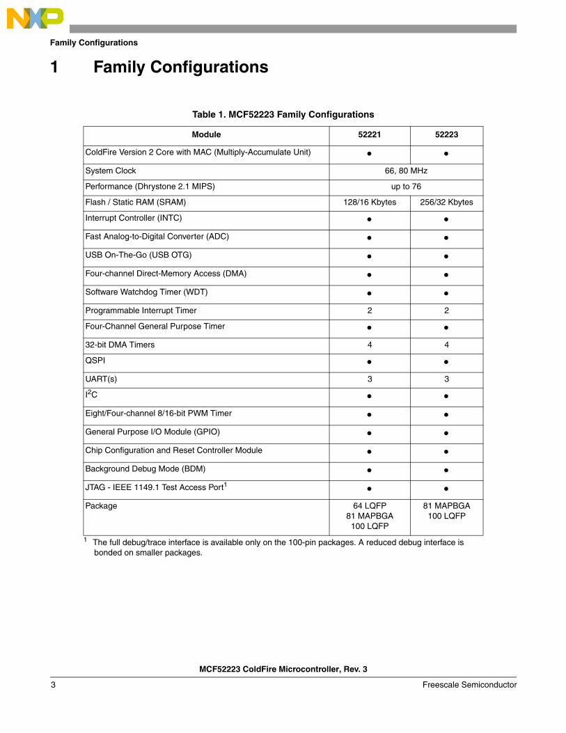
1 Family Configurations
Table 1. MCF52223 Family Configurations
Module 52221 52223
ColdFire Version 2 Core with MAC (Multiply-Accumulate Unit) System Clock 66, 80 MHz
Performance (Dhrystone 2.1 MIPS) up to 76
Flash / Static RAM (SRAM) 128/16 Kbytes 256/32 Kbytes
Interrupt Controller (INTC) Fast Analog-to-Digital Converter (ADC) USB On-The-Go (USB OTG) Four-channel Direct-Memory Access (DMA) Software Watchdog Timer (WDT) Programmable Interrupt Timer 2 2
Four-Channel General Purpose Timer 32-bit DMA Timers 4 4
QSPI UART(s) 3 3
I2C Eight/Four-channel 8/16-bit PWM Timer General Purpose I/O Module (GPIO) Chip Configuration and Reset Controller Module Background Debug Mode (BDM) JTAG - IEEE 1149.1 Test Access Port1
1 The full debug/trace interface is available only on the 100-pin packages. A reduced debug interface is bonded on smaller packages.
Package 64 LQFP
81 MAPBGA100 LQFP
81 MAPBGA 100 LQFP
MCF52223 ColdFire Microcontroller, Rev. 3
Freescale Semiconductor3
Family Configurations
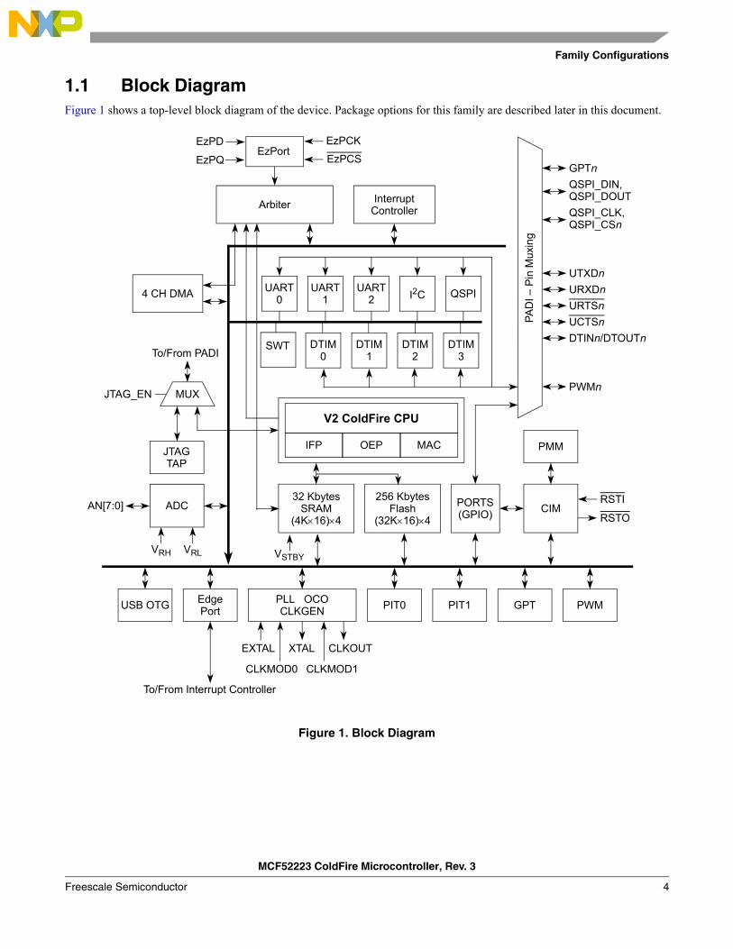
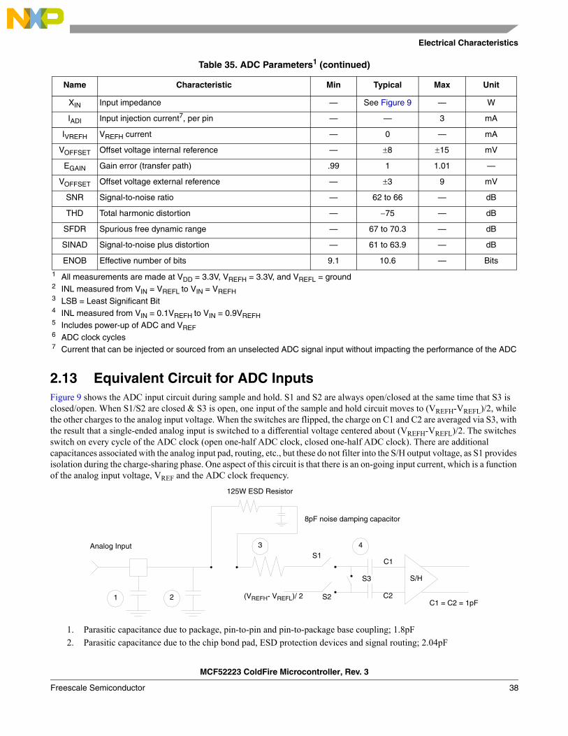
1.1 Block DiagramFigure 1 shows a top-level block diagram of the device. Package options for this family are described later in this document.
Figure 1. Block Diagram
Arbiter InterruptController
UART0
QSPIUART1
UART2 I2C
DTIM0
DTIM1
DTIM2
DTIM3
V2 ColdFire CPU
IFP OEP MAC
4 CH DMA
MUX
JTAGTAP
To/From PADI
32 KbytesSRAM
(4K16)4
256 KbytesFlash
(32K16)4
PORTS(GPIO)
CIMRSTI
RSTO
UTXDn
URXDn
URTSn
DTINn/DTOUTn
JTAG_EN
ADCAN[7:0]
VRH VRL
PLL OCOCLKGEN
EdgePort
USB OTG
EXTAL XTAL CLKOUT
PIT0 PIT1 GPT PWM
To/From Interrupt Controller
UCTSn
PMM
VSTBY
PA
DI –
Pin
Mux
ing
EzPortEzPCS
CLKMOD0 CLKMOD1
QSPI_CLK,QSPI_CSn
PWMn
QSPI_DIN,QSPI_DOUT
GPTn
EzPCKEzPD
EzPQ
SWT
MCF52223 ColdFire Microcontroller, Rev. 3
Freescale Semiconductor 4
Family Configurations
1.2 Features
1.2.1 Feature OverviewThe MCF52223 family includes the following features:
• Version 2 ColdFire variable-length RISC processor core
— Static operation
— 32-bit address and data paths on-chip
— Up to 80 MHz processor core frequency
— Sixteen general-purpose, 32-bit data and address registers
— Implements ColdFire ISA_A with extensions to support the user stack pointer register and four new instructions for improved bit processing (ISA_A+)
— Multiply-Accumulate (MAC) unit with 32-bit accumulator to support 1616 32 or 3232 32 operations
— Illegal instruction decode that allows for 68-Kbyte emulation support
• System debug support
— Real-time trace for determining dynamic execution path
— Background debug mode (BDM) for in-circuit debugging (DEBUG_B+)
— Real-time debug support, with six hardware breakpoints (4 PC, 1 address and 1 data) configurable into a 1- or 2-level trigger
• On-chip memories
— 32-Kbyte dual-ported SRAM on CPU internal bus, supporting core and DMA access with standby power supply support
— 256 Kbytes of interleaved flash memory supporting 2-1-1-1 accesses
• Power management
— Fully static operation with processor sleep and whole chip stop modes
— Rapid response to interrupts from the low-power sleep mode (wake-up feature)
— Clock enable/disable for each peripheral when not used
— Software controlled disable of external clock output for low-power consumption
• Universal Serial Bus On-The-Go (USB OTG) dual-mode host and device controller
— Full-speed / low-speed host controller
— USB 1.1 and 2.0 compliant full-speed / low speed device controller
— 16 bidirectional end points
— DMA or FIFO data stream interfaces
— Low power consumption
— OTG protocol logic
• Three universal asynchronous/synchronous receiver transmitters (UARTs)
— 16-bit divider for clock generation
— Interrupt control logic with maskable interrupts
— DMA support
— Data formats can be 5, 6, 7 or 8 bits with even, odd, or no parity
— Up to two stop bits in 1/16 increments
— Error-detection capabilities
— Modem support includes request-to-send (RTS) and clear-to-send (CTS) lines for two UARTs
— Transmit and receive FIFO buffers
• I2C module
MCF52223 ColdFire Microcontroller, Rev. 3
Freescale Semiconductor5
Family Configurations
— Interchip bus interface for EEPROMs, LCD controllers, A/D converters, and keypads
— Fully compatible with industry-standard I2C bus
— Master and slave modes support multiple masters
— Automatic interrupt generation with programmable level
• Queued serial peripheral interface (QSPI)
— Full-duplex, three-wire synchronous transfers
— Up to four chip selects available
— Master mode operation only
— Programmable bit rates up to half the CPU clock frequency
— Up to 16 pre-programmed transfers
• Fast analog-to-digital converter (ADC)
— Eight analog input channels
— 12-bit resolution
— Minimum 1.125 s conversion time
— Simultaneous sampling of two channels for motor control applications
— Single-scan or continuous operation
— Optional interrupts on conversion complete, zero crossing (sign change), or under/over low/high limit
— Unused analog channels can be used as digital I/O
• Four 32-bit timers with DMA support
— 12.5 ns resolution at 80 MHz
— Programmable sources for clock input, including an external clock option
— Programmable prescaler
— Input capture capability with programmable trigger edge on input pin
— Output compare with programmable mode for the output pin
— Free run and restart modes
— Maskable interrupts on input capture or output compare
— DMA trigger capability on input capture or output compare
• Four-channel general purpose timer
— 16-bit architecture
— Programmable prescaler
— Output pulse-widths variable from microseconds to seconds
— Single 16-bit input pulse accumulator
— Toggle-on-overflow feature for pulse-width modulator (PWM) generation
— One dual-mode pulse accumulation channel
• Pulse-width modulation timer
— Operates as eight channels with 8-bit resolution or four channels with 16-bit resolution
— Programmable period and duty cycle
— Programmable enable/disable for each channel
— Software selectable polarity for each channel
— Period and duty cycle are double buffered. Change takes effect when the end of the current period is reached (PWM counter reaches zero) or when the channel is disabled.
— Programmable center or left aligned outputs on individual channels
— Four clock sources (A, B, SA, and SB) provide for a wide range of frequencies
— Emergency shutdown
• Two periodic interrupt timers (PITs)
MCF52223 ColdFire Microcontroller, Rev. 3
Freescale Semiconductor 6
Family Configurations
— 16-bit counter
— Selectable as free running or count down
• Real-Time Clock (RTC)
— Maintains system time-of-day clock
— Provides stopwatch and alarm interrupt functions
• Software watchdog timer
— 32-bit counter
— Low-power mode support
• Clock generation features
— Crystal, on-chip trimmed relaxation oscillator, or external oscillator reference options
— Trimmed relaxation oscillator
— Pre-divider capable of dividing the clock source frequency into the PLL reference frequency range
— System can be clocked from PLL or directly from crystal oscillator or relaxation oscillator
— Low power modes supported
— 2n (0 n 15) low-power divider for extremely low frequency operation
• Interrupt controller
— Uniquely programmable vectors for all interrupt sources
— Fully programmable level and priority for all peripheral interrupt sources
— Seven external interrupt signals with fixed level and priority
— Unique vector number for each interrupt source
— Ability to mask any individual interrupt source or all interrupt sources (global mask-all)
— Support for hardware and software interrupt acknowledge (IACK) cycles
— Combinatorial path to provide wake-up from low-power modes
• DMA controller
— Four fully programmable channels
— Dual-address transfer support with 8-, 16-, and 32-bit data capability, along with support for 16-byte (432-bit) burst transfers
— Source/destination address pointers that can increment or remain constant
— 24-bit byte transfer counter per channel
— Auto-alignment transfers supported for efficient block movement
— Bursting and cycle-steal support
— Software-programmable DMA requests for the UARTs (3) and 32-bit timers (4)
• Reset
— Separate reset in and reset out signals
— Seven sources of reset:
– Power-on reset (POR)
– External
– Software
– Watchdog
– Loss of clock
– Loss of lock
– Low-voltage detection (LVD)
— Status flag indication of source of last reset
• Chip configuration module (CCM)
— System configuration during reset
MCF52223 ColdFire Microcontroller, Rev. 3
Freescale Semiconductor7
Family Configurations
— Selects one of six clock modes
— Configures output pad drive strength
— Unique part identification number and part revision number
• General purpose I/O interface
— Up to 56 bits of general purpose I/O
— Bit manipulation supported via set/clear functions
— Programmable drive strengths
— Unused peripheral pins may be used as extra GPIO
• JTAG support for system level board testing
1.2.2 V2 Core OverviewThe version 2 ColdFire processor core is comprised of two separate pipelines decoupled by an instruction buffer. The two-stage instruction fetch pipeline (IFP) is responsible for instruction-address generation and instruction fetch. The instruction buffer is a first-in-first-out (FIFO) buffer that holds prefetched instructions awaiting execution in the operand execution pipeline (OEP). The OEP includes two pipeline stages. The first stage decodes instructions and selects operands (DSOC); the second stage (AGEX) performs instruction execution and calculates operand effective addresses, if needed.
The V2 core implements the ColdFire instruction set architecture revision A+ with support for a separate user stack pointer register and four new instructions to assist in bit processing. Additionally, the core includes the multiply-accumulate (MAC) unit for improved signal processing capabilities. The MAC implements a three-stage arithmetic pipeline, optimized for 16x16 bit operations, with support for one 32-bit accumulator. Supported operands include 16- and 32-bit signed and unsigned integers, signed fractional operands, and a complete set of instructions to process these data types. The MAC provides support for execution of DSP operations within the context of a single processor at a minimal hardware cost.
1.2.3 Integrated Debug ModuleThe ColdFire processor core debug interface is provided to support system debugging with low-cost debug and emulator development tools. Through a standard debug interface, access to debug information and real-time tracing capability is provided on 100-lead packages. This allows the processor and system to be debugged at full speed without the need for costly in-circuit emulators.
The on-chip breakpoint resources include a total of nine programmable 32-bit registers: an address and an address mask register, a data and a data mask register, four PC registers, and one PC mask register. These registers can be accessed through the dedicated debug serial communication channel or from the processor’s supervisor mode programming model. The breakpoint registers can be configured to generate triggers by combining the address, data, and PC conditions in a variety of single- or dual-level definitions. The trigger event can be programmed to generate a processor halt or initiate a debug interrupt exception. This device implements revision B+ of the ColdFire Debug Architecture.
The processor’s interrupt servicing options during emulator mode allow real-time critical interrupt service routines to be serviced while processing a debug interrupt event. This ensures the system continues to operate even during debugging.
To support program trace, the V2 debug module provides processor status (PST[3:0]) and debug data (DDATA[3:0]) ports. These buses and the PSTCLK output provide execution status, captured operand data, and branch target addresses defining processor activity at the CPU’s clock rate. The device includes a new debug signal, ALLPST. This signal is the logical AND of the processor status (PST[3:0]) signals and is useful for detecting when the processor is in a halted state (PST[3:0] = 1111).
The full debug/trace interface is available only on the 100-pin packages. However, every product features the dedicated debug serial communication channel (DSI, DSO, DSCLK) and the ALLPST signal.
MCF52223 ColdFire Microcontroller, Rev. 3
Freescale Semiconductor 8
Family Configurations
1.2.4 JTAGThe processor supports circuit board test strategies based on the Test Technology Committee of IEEE and the Joint Test Action Group (JTAG). The test logic includes a test access port (TAP) consisting of a 16-state controller, an instruction register, and three test registers (a 1-bit bypass register, a 112-bit boundary-scan register, and a 32-bit ID register). The boundary scan register links the device’s pins into one shift register. Test logic, implemented using static logic design, is independent of the device system logic.
The device implementation can:
• Perform boundary-scan operations to test circuit board electrical continuity
• Sample system pins during operation and transparently shift out the result in the boundary scan register
• Bypass the device for a given circuit board test by effectively reducing the boundary-scan register to a single bit
• Disable the output drive to pins during circuit-board testing
• Drive output pins to stable levels
1.2.5 On-Chip Memories
1.2.5.1 SRAMThe dual-ported SRAM module provides a general-purpose 32-Kbyte memory block that the ColdFire core can access in a single cycle. The location of the memory block can be set to any 32-Kbyte boundary within the 4-Gbyte address space. This memory is ideal for storing critical code or data structures and for use as the system stack. Because the SRAM module is physically connected to the processor's high-speed local bus, it can quickly service core-initiated accesses or memory-referencing commands from the debug module.
The SRAM module is also accessible by the DMA. The dual-ported nature of the SRAM makes it ideal for implementing applications with double-buffer schemes, where the processor and a DMA device operate in alternate regions of the SRAM to maximize system performance.
1.2.5.2 Flash MemoryThe ColdFire flash module (CFM) is a non-volatile memory (NVM) module that connects to the processor’s high-speed local bus. The CFM is constructed with four banks of 32-Kbyte16-bit flash memory arrays to generate 256 Kbytes of 32-bit flash memory. These electrically erasable and programmable arrays serve as non-volatile program and data memory. The flash memory is ideal for program and data storage for single-chip applications, allowing for field reprogramming without requiring an external high voltage source. The CFM interfaces to the ColdFire core through an optimized read-only memory controller that supports interleaved accesses from the 2-cycle flash memory arrays. A backdoor mapping of the flash memory is used for all program, erase, and verify operations, as well as providing a read datapath for the DMA. Flash memory may also be programmed via the EzPort, which is a serial flash memory programming interface that allows the flash memory to be read, erased and programmed by an external controller in a format compatible with most SPI bus flash memory chips.
1.2.6 Power ManagementThe device incorporates several low-power modes of operation entered under program control and exited by several external trigger events. An integrated power-on reset (POR) circuit monitors the input supply and forces an MCU reset as the supply voltage rises. The low voltage detector (LVD) monitors the supply voltage and is configurable to force a reset or interrupt condition if it falls below the LVD trip point. The RAM standby switch provides power to RAM when the supply voltage to the chip falls below the standby battery voltage.
MCF52223 ColdFire Microcontroller, Rev. 3
Freescale Semiconductor9
Family Configurations
1.2.7 USB On-The-Go ControllerThe device includes a Universal Serial Bus On-The-Go (USB OTG) dual-mode controller. USB is a popular standard for connecting peripherals and portable consumer electronic devices such as digital cameras and handheld computers to host PCs. The OTG supplement to the USB specification extends USB to peer-to-peer application, enabling devices to connect directly to each other without the need for a PC. The dual-mode controller on the device can act as a USB OTG host and as a USB device. It also supports full-speed and low-speed modes.
1.2.8 UARTsThe device has three full-duplex UARTs that function independently. The three UARTs can be clocked by the system bus clock, eliminating the need for an external clock source. On smaller packages, the third UART is multiplexed with other digital I/O functions.
1.2.9 I2C BusThe I2C bus is an industry-standard, two-wire, bidirectional serial bus that provides a simple, efficient method of data exchange and minimizes the interconnection between devices. This bus is suitable for applications requiring occasional communications over a short distance between many devices.
1.2.10 QSPIThe queued serial peripheral interface (QSPI) provides a synchronous serial peripheral interface with queued transfer capability. It allows up to 16 transfers to be queued at once, minimizing the need for CPU intervention between transfers.
1.2.11 Fast ADCThe fast ADC consists of an eight-channel input select multiplexer and two independent sample and hold (S/H) circuits feeding separate 12-bit ADCs. The two separate converters store their results in accessible buffers for further processing.
The ADC can be configured to perform a single scan and halt, a scan when triggered, or a programmed scan sequence repeatedly until manually stopped.
The ADC can be configured for sequential or simultaneous conversion. When configured for sequential conversions, up to eight channels can be sampled and stored in any order specified by the channel list register. Both ADCs may be required during a scan, depending on the inputs to be sampled.
During a simultaneous conversion, both S/H circuits are used to capture two different channels at the same time. This configuration requires that a single channel may not be sampled by both S/H circuits simultaneously.
Optional interrupts can be generated at the end of the scan sequence if a channel is out of range (measures below the low threshold limit or above the high threshold limit set in the limit registers) or at several different zero crossing conditions.
1.2.12 DMA Timers (DTIM0–DTIM3)There are four independent, DMA transfer capable 32-bit timers (DTIM0, DTIM1, DTIM2, and DTIM3) on the device. Each module incorporates a 32-bit timer with a separate register set for configuration and control. The timers can be configured to operate from the system clock or from an external clock source using one of the DTINn signals. If the system clock is selected, it can be divided by 16 or 1. The input clock is further divided by a user-programmable 8-bit prescaler that clocks the actual timer counter register (TCRn). Each of these timers can be configured for input capture or reference (output) compare mode. Timer events may optionally cause interrupt requests or DMA transfers.
MCF52223 ColdFire Microcontroller, Rev. 3
Freescale Semiconductor 10
Family Configurations
1.2.13 General Purpose Timer (GPT)The general purpose timer (GPT) is a four-channel timer module consisting of a 16-bit programmable counter driven by a seven-stage programmable prescaler. Each of the four channels can be configured for input capture or output compare. Additionally, channel three, can be configured as a pulse accumulator.
A timer overflow function allows software to extend the timing capability of the system beyond the 16-bit range of the counter. The input capture and output compare functions allow simultaneous input waveform measurements and output waveform generation. The input capture function can capture the time of a selected transition edge. The output compare function can generate output waveforms and timer software delays. The 16-bit pulse accumulator can operate as a simple event counter or a gated time accumulator.
1.2.14 Periodic Interrupt Timers (PIT0 and PIT1)The two periodic interrupt timers (PIT0 and PIT1) are 16-bit timers that provide interrupts at regular intervals with minimal processor intervention. Each timer can count down from the value written in its PIT modulus register or it can be a free-running down-counter.
1.2.15 Real-Time Clock (RTC)The Real-Time Clock (RTC) module maintains the system (time-of-day) clock and provides stopwatch, alarm, and interrupt functions. It includes full clock features: seconds, minutes, hours, days and supports a host of time-of-day interrupt functions along with an alarm interrupt.
1.2.16 Pulse-Width Modulation (PWM) Timers The device has an 8-channel, 8-bit PWM timer. Each channel has a programmable period and duty cycle as well as a dedicated counter. Each of the modulators can create independent continuous waveforms with software-selectable duty rates from 0% to 100%. The PWM outputs have programmable polarity, and can be programmed as left aligned outputs or center aligned outputs. For higher period and duty cycle resolution, each pair of adjacent channels ([7:6], [5:4], [3:2], and [1:0]) can be concatenated to form a single 16-bit channel. The module can, therefore, be configured to support 8/0, 6/1, 4/2, 2/3, or 0/4 8-/16-bit channels.
1.2.17 Software Watchdog TimerThe watchdog timer is a 32-bit timer that facilitates recovery from runaway code. The watchdog counter is a free-running down-counter that generates a reset on underflow. To prevent a reset, software must periodically restart the countdown.
1.2.18 Phase-Locked Loop (PLL)The clock module contains a crystal oscillator, 8 MHz on-chip relaxation oscillator (OCO), phase-locked loop (PLL), reduced frequency divider (RFD), low-power divider status/control registers, and control logic. To improve noise immunity, the PLL, crystal oscillator, and relaxation oscillator have their own power supply inputs: VDDPLL and VSSPLL. All other circuits are powered by the normal supply pins, VDD and VSS.
1.2.19 Interrupt Controller (INTC)The device has a single interrupt controller that supports up to 63 interrupt sources. There are 56 programmable sources, 49 of which are assigned to unique peripheral interrupt requests. The remaining seven sources are unassigned and may be used for software interrupt requests.
MCF52223 ColdFire Microcontroller, Rev. 3
Freescale Semiconductor11
Family Configurations
1.2.20 DMA ControllerThe direct memory access (DMA) controller provides an efficient way to move blocks of data with minimal processor intervention. It has four channels that allow byte, word, longword, or 16-byte burst line transfers. These transfers are triggered by software explicitly setting a DCRn[START] bit or by the occurrence of certain UART or DMA timer events.
1.2.21 ResetThe reset controller determines the source of reset, asserts the appropriate reset signals to the system, and keeps track of what caused the last reset. There are seven sources of reset:
• External reset input
• Power-on reset (POR)
• Watchdog timer
• Phase locked-loop (PLL) loss of lock
• PLL loss of clock
• Software
• Low-voltage detector (LVD)
Control of the LVD and its associated reset and interrupt are managed by the reset controller. Other registers provide status flags indicating the last source of reset and a control bit for software assertion of the RSTO pin.
1.2.22 GPIONearly all pins on the device have general purpose I/O capability and are grouped into 8-bit ports. Some ports do not use all eight bits. Each port has registers that configure, monitor, and control the port pin.
1.2.23 Part Numbers and PackagingThis product is RoHS-compliant. Refer to the product page at freescale.com or contact your sales office for up-to-date RoHS information.
Table 3. Orderable Part Number Summary
Freescale Part Number
DescriptionSpeed(MHz)
Flash/SRAM(Kbytes)
PackageTemp range
(C)
MCF52221CAE66 MCF52221 Microcontroller 66 128/16 64 LQFP -40 to +85
MCF52221CVM66 MCF52221 Microcontroller 66 128/16 81 MAPBGA -40 to +85
MCF52221CAF66 MCF52221 Microcontroller 66 128/16 100 LQFP -40 to +85
MCF52221CVM80 MCF52221 Microcontroller 80 128/16 81 MAPBGA -40 to +85
MCF52221CAF80 MCF52221 Microcontroller 80 128/16 100 LQFP -40 to +85
MCF52223CVM66 MCF52223 Microcontroller 66 128/16 81 MAPBGA -40 to +85
MCF52223CAF66 MCF52223 Microcontroller 66 128/16 100 LQFP -40 to +85
MCF52223CVM80 MCF52223 Microcontroller 80 128/16 81 MAPBGA -40 to +85
MCF52223CAF80 MCF52223 Microcontroller 80 128/16 100 LQFP -40 to +85
MCF52223 ColdFire Microcontroller, Rev. 3
Freescale Semiconductor 12
Family Configurations
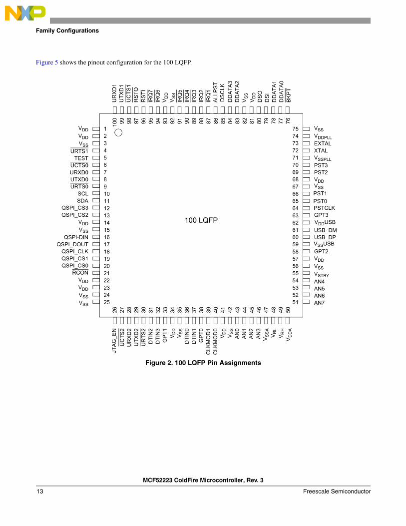
Figure 5 shows the pinout configuration for the 100 LQFP.
Figure 2. 100 LQFP Pin Assignments
AN5
12345678910111213141516171819202122232425
VDD
VDD
VSS
URTS1TEST
UCTS0
UTXD0URTS0
SCLSDA
QSPI_CS3QSPI_CS2
VDD
VSS
QSPI-DINQSPI_DOUT
QSPI_CLKQSPI_CS1QSPI_CS0
RCONVDD
VDD
VSS
100 LQFP
75747372717069686766656463626160595857565554535251
VSS
VDDPLL
EXTALXTALVSSPLL
PST3PST2VDDVSS
PST1
PST0PSTCLKGPT3VDDUSB
USB_DMUSB_DPVSSUSB
GPT2VDD
VSS
VSTBY
AN6AN7
100
99
98
97
96
95
94
93
92
91
90
89
88
87
86
85
84
83
82
81
80
79
78
77
76
UR
XD
1U
TX
D1
UC
TS
1R
ST
OR
ST
IIR
Q7
IRQ
6V
DD
VS
S
IRQ
5IR
Q4
IRQ
3IR
Q2
IRQ
1A
LLP
ST
DD
AT
A3
DD
AT
A2
VS
S
VD
D
DS
OD
SI
DD
AT
A1
DD
AT
A0
BK
PT
26 27 28 29 30 31 32 33 34 35 36 37 38 39 40 41 42 43 44 45 46 47 48 49 50
JTA
G_E
N
UC
TS
2U
RX
D2
UT
XD
2U
RT
S2
DT
IN2
DT
IN3
GP
T1
VD
DV
SS
DT
IN0
DT
IN1
GP
T0
CLK
MO
D1
CLK
MO
D0
VD
DV
SS
AN
0A
N1
AN
2A
N3
VS
SA
VR
L
VR
H
VD
DA
VSS
URXD0
AN4
DS
CLK
MCF52223 ColdFire Microcontroller, Rev. 3
Freescale Semiconductor13
Family Configurations
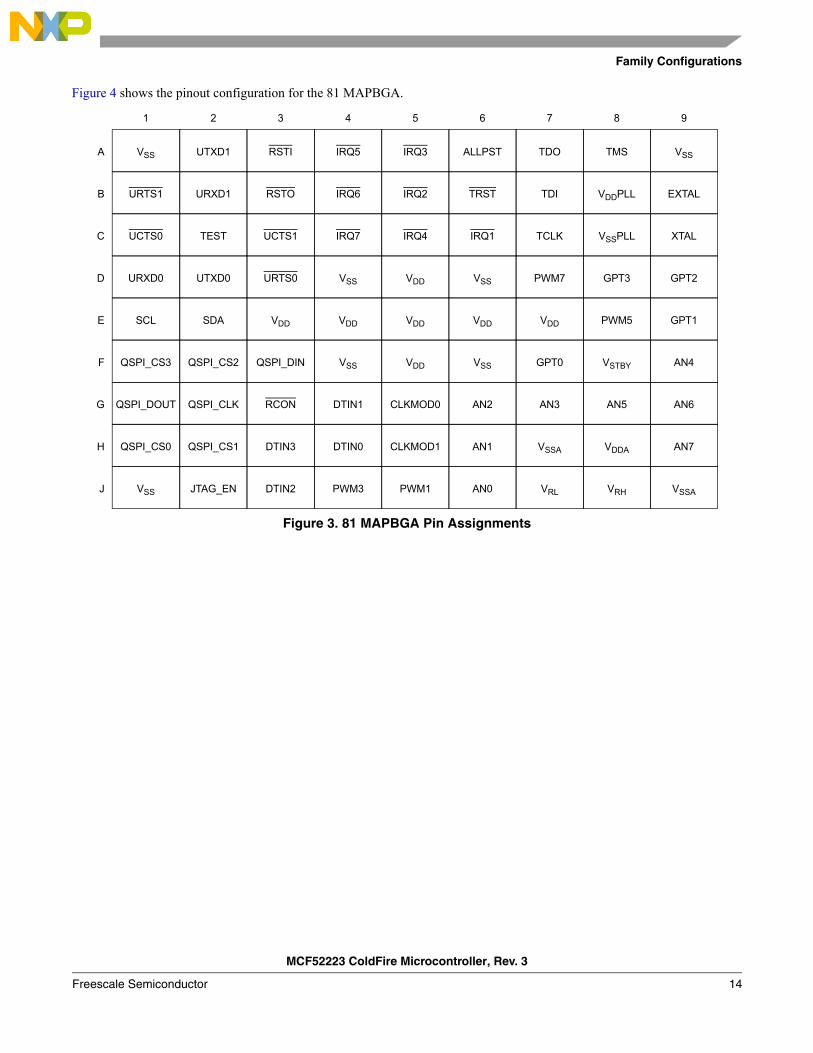
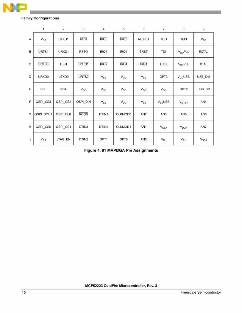
Figure 4 shows the pinout configuration for the 81 MAPBGA.
Figure 3. 81 MAPBGA Pin Assignments
VSS UTXD1 RSTI IRQ5 IRQ3 ALLPST TDO TMS VSSA
1 2 3 4 5 6 7 8 9
URTS1 URXD1 RSTO IRQ6 IRQ2 TRST TDI VDDPLL EXTALB
UCTS0 TEST UCTS1 IRQ7 IRQ4 IRQ1 TCLK VSSPLL XTALC
URXD0 UTXD0 URTS0 VSS VDD VSS PWM7 GPT3 GPT2D
SCL SDA VDD VDD VDD VDD VDD PWM5 GPT1E
QSPI_CS3 QSPI_CS2 QSPI_DIN VSS VDD VSS GPT0 VSTBY AN4F
QSPI_DOUT QSPI_CLK RCON DTIN1 CLKMOD0 AN2 AN3 AN5 AN6G
QSPI_CS0 QSPI_CS1 DTIN3 DTIN0 CLKMOD1 AN1 VSSA VDDA AN7H
VSS JTAG_EN DTIN2 PWM3 PWM1 AN0 VRL VRH VSSAJ
MCF52223 ColdFire Microcontroller, Rev. 3
Freescale Semiconductor 14
Family Configurations
Figure 4. 81 MAPBGA Pin Assignments
VSS UTXD1 RSTI IRQ5 IRQ3 ALLPST TDO TMS VSSA
1 2 3 4 5 6 7 8 9
URTS1 URXD1 RSTO IRQ6 IRQ2 TRST TDI VDDPLL EXTALB
UCTS0 TEST UCTS1 IRQ7 IRQ4 IRQ1 TCLK VSSPLL XTALC
URXD0 UTXD0 URTS0 VSS VDD VSS GPT3 VDDUSB USB_DMD
SCL SDA VDD VDD VDD VDD VDD GPT2 USB_DPE
QSPI_CS3 QSPI_CS2 QSPI_DIN VSS VDD VSS VSSUSB VSTBY AN4F
QSPI_DOUT QSPI_CLK RCON DTIN1 CLKMOD0 AN2 AN3 AN5 AN6G
QSPI_CS0 QSPI_CS1 DTIN3 DTIN0 CLKMOD1 AN1 VSSA VDDA AN7H
VSS JTAG_EN DTIN2 GPT1 GPT0 AN0 VRL VRH VSSAJ
MCF52223 ColdFire Microcontroller, Rev. 3
Freescale Semiconductor15
Fam
ily Co
nfig
uratio
ns
F
Pin on0 LQFP
Pin on 81 MAPBGA
Pin on 64 LQFP
51 H9 33
52 G9 34
53 G8 35
54 F9 36
46 G7 28
45 G6 27
44 H6 26
43 J6 25
— — —
— — —
50 H8 32
47 H7, J9 29
49 J8 31
48 J7 30
73 B9 47
72 C9 46
74 B8 48
71 C8 45
86 A6 55
,83,78,77 — —
,69,66,65 — —
10 E1 8
11 E2 9
MC
F52223 C
old
Fire M
icroco
ntro
ller, Rev. 3
reescale Sem
iconductor16
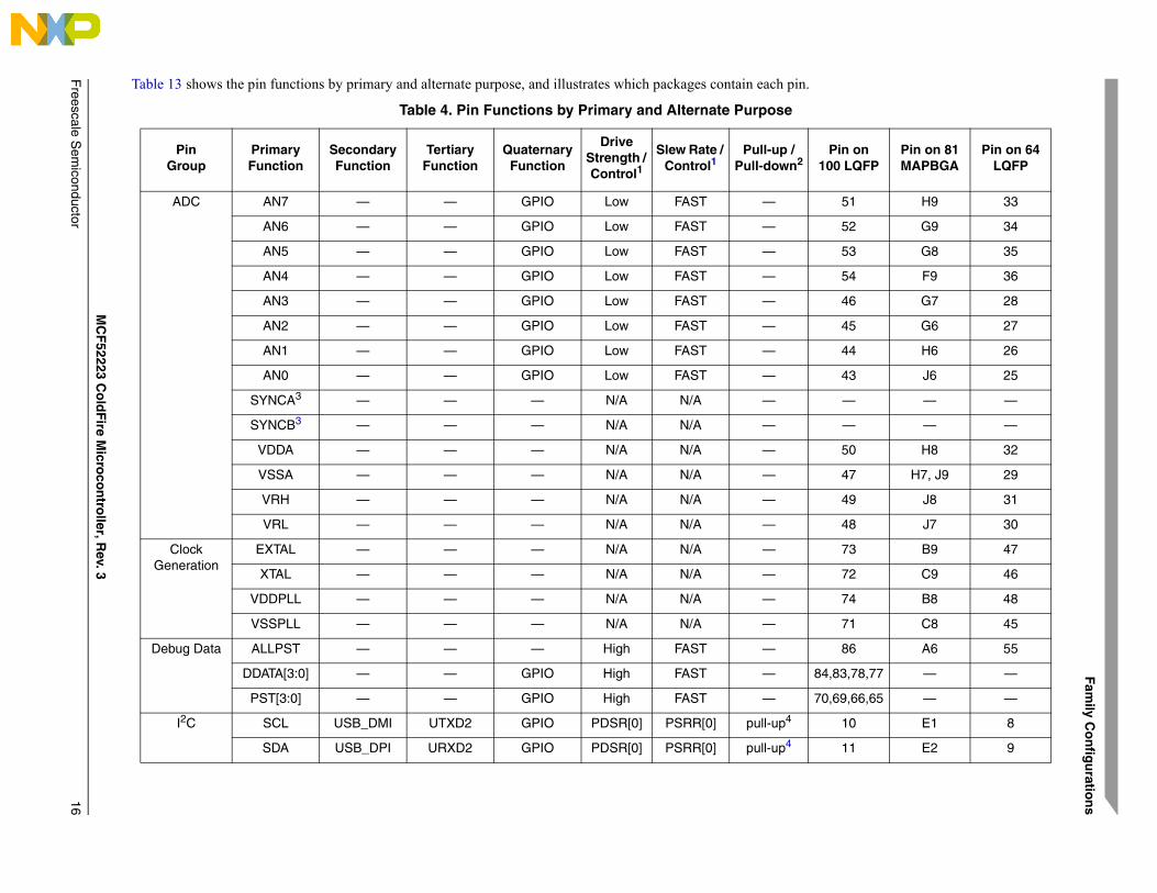
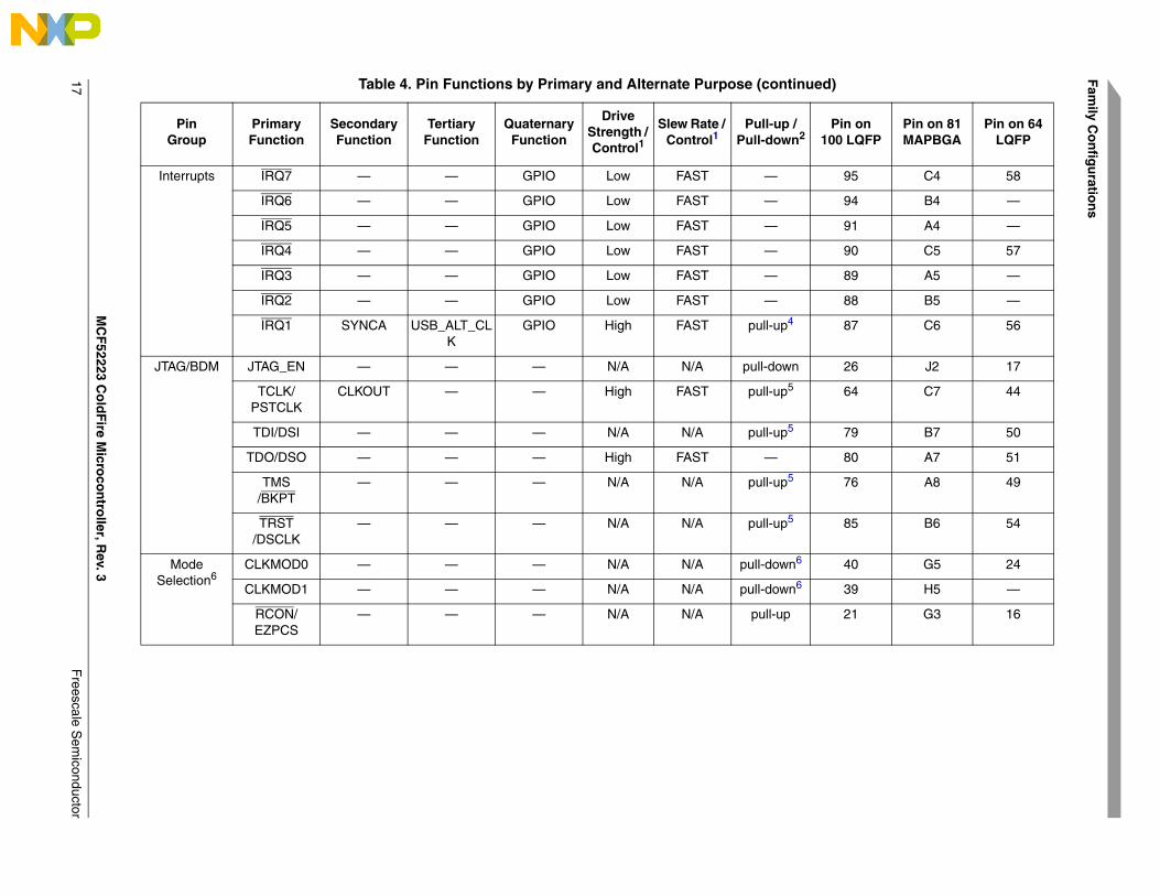
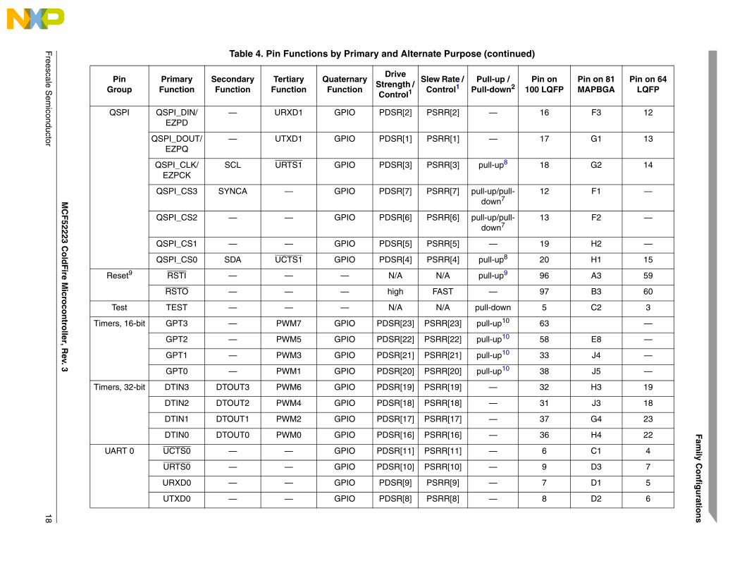
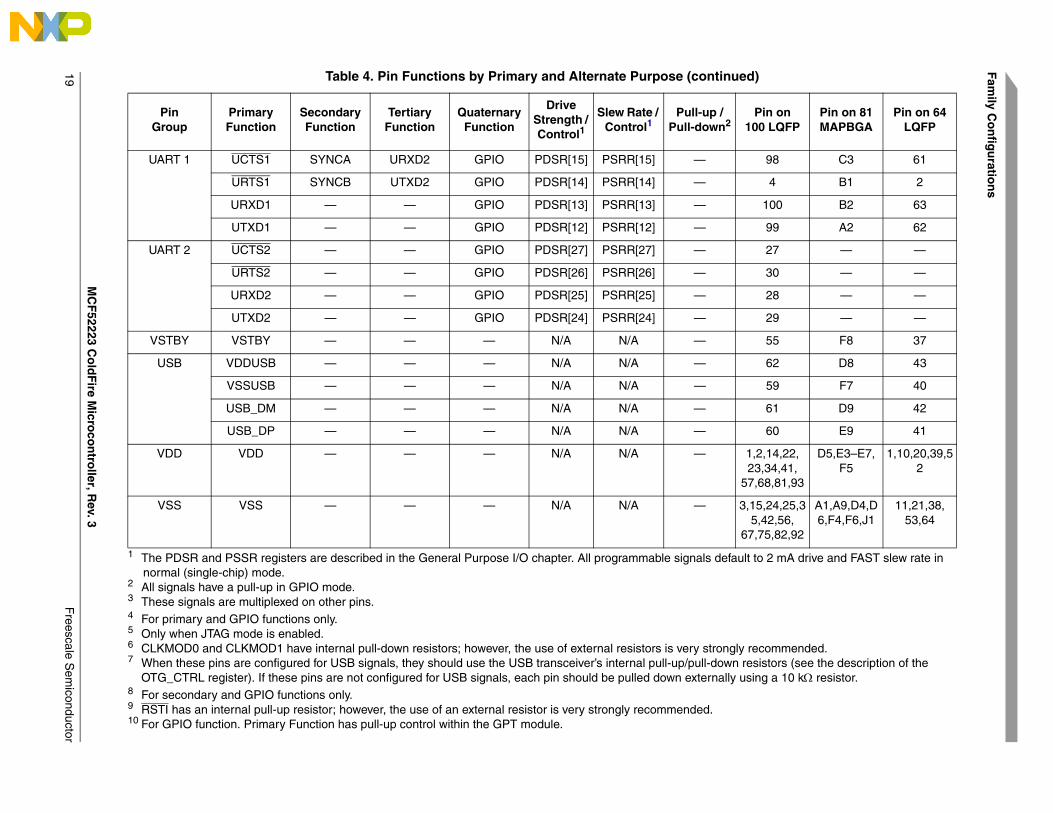
Table 13 shows the pin functions by primary and alternate purpose, and illustrates which packages contain each pin.
Table 4. Pin Functions by Primary and Alternate Purpose
PinGroup
PrimaryFunction
SecondaryFunction
Tertiary Function
QuaternaryFunction
Drive Strength / Control1
Slew Rate / Control1
Pull-up / Pull-down2 10
ADC AN7 — — GPIO Low FAST —
AN6 — — GPIO Low FAST —
AN5 — — GPIO Low FAST —
AN4 — — GPIO Low FAST —
AN3 — — GPIO Low FAST —
AN2 — — GPIO Low FAST —
AN1 — — GPIO Low FAST —
AN0 — — GPIO Low FAST —
SYNCA3 — — — N/A N/A —
SYNCB3 — — — N/A N/A —
VDDA — — — N/A N/A —
VSSA — — — N/A N/A —
VRH — — — N/A N/A —
VRL — — — N/A N/A —
Clock Generation
EXTAL — — — N/A N/A —
XTAL — — — N/A N/A —
VDDPLL — — — N/A N/A —
VSSPLL — — — N/A N/A —
Debug Data ALLPST — — — High FAST —
DDATA[3:0] — — GPIO High FAST — 84
PST[3:0] — — GPIO High FAST — 70
I2C SCL USB_DMI UTXD2 GPIO PDSR[0] PSRR[0] pull-up4
SDA USB_DPI URXD2 GPIO PDSR[0] PSRR[0] pull-up4
1 Fam
ily Co
nfig
uratio
ns
95 C4 58
94 B4 —
91 A4 —
90 C5 57
89 A5 —
88 B5 —
87 C6 56
26 J2 17
64 C7 44
79 B7 50
80 A7 51
76 A8 49
85 B6 54
40 G5 24
39 H5 —
21 G3 16
)
Pin on0 LQFP
Pin on 81 MAPBGA
Pin on 64 LQFP
MC
F52223 C
old
Fire M
icroco
ntro
ller, Rev. 3
Freescale S
emiconductor
7
Interrupts IRQ7 — — GPIO Low FAST —
IRQ6 — — GPIO Low FAST —
IRQ5 — — GPIO Low FAST —
IRQ4 — — GPIO Low FAST —
IRQ3 — — GPIO Low FAST —
IRQ2 — — GPIO Low FAST —
IRQ1 SYNCA USB_ALT_CLK
GPIO High FAST pull-up4
JTAG/BDM JTAG_EN — — — N/A N/A pull-down
TCLK/PSTCLK
CLKOUT — — High FAST pull-up5
TDI/DSI — — — N/A N/A pull-up5
TDO/DSO — — — High FAST —
TMS/BKPT
— — — N/A N/A pull-up5
TRST/DSCLK
— — — N/A N/A pull-up5
Mode Selection6
CLKMOD0 — — — N/A N/A pull-down6
CLKMOD1 — — — N/A N/A pull-down6
RCON/EZPCS
— — — N/A N/A pull-up
Table 4. Pin Functions by Primary and Alternate Purpose (continued
PinGroup
PrimaryFunction
SecondaryFunction
Tertiary Function
QuaternaryFunction
Drive Strength / Control1
Slew Rate / Control1
Pull-up / Pull-down2 10
Fam
ily Co
nfig
uratio
ns
F
16 F3 12
17 G1 13
18 G2 14
12 F1 —
13 F2 —
19 H2 —
20 H1 15
96 A3 59
97 B3 60
5 C2 3
63 —
58 E8 —
33 J4 —
38 J5 —
32 H3 19
31 J3 18
37 G4 23
36 H4 22
6 C1 4
9 D3 7
7 D1 5
8 D2 6
)
Pin on0 LQFP
Pin on 81 MAPBGA
Pin on 64 LQFP
MC
F52223 C
old
Fire M
icroco
ntro
ller, Rev. 3
reescale Sem
iconductor18
QSPI QSPI_DIN/EZPD
— URXD1 GPIO PDSR[2] PSRR[2] —
QSPI_DOUT/EZPQ
— UTXD1 GPIO PDSR[1] PSRR[1] —
QSPI_CLK/EZPCK
SCL URTS1 GPIO PDSR[3] PSRR[3] pull-up8
QSPI_CS3 SYNCA — GPIO PDSR[7] PSRR[7] pull-up/pull-down7
QSPI_CS2 — — GPIO PDSR[6] PSRR[6] pull-up/pull-down7
QSPI_CS1 — — GPIO PDSR[5] PSRR[5] —
QSPI_CS0 SDA UCTS1 GPIO PDSR[4] PSRR[4] pull-up8
Reset9 RSTI — — — N/A N/A pull-up9
RSTO — — — high FAST —
Test TEST — — — N/A N/A pull-down
Timers, 16-bit GPT3 — PWM7 GPIO PDSR[23] PSRR[23] pull-up10
GPT2 — PWM5 GPIO PDSR[22] PSRR[22] pull-up10
GPT1 — PWM3 GPIO PDSR[21] PSRR[21] pull-up10
GPT0 — PWM1 GPIO PDSR[20] PSRR[20] pull-up10
Timers, 32-bit DTIN3 DTOUT3 PWM6 GPIO PDSR[19] PSRR[19] —
DTIN2 DTOUT2 PWM4 GPIO PDSR[18] PSRR[18] —
DTIN1 DTOUT1 PWM2 GPIO PDSR[17] PSRR[17] —
DTIN0 DTOUT0 PWM0 GPIO PDSR[16] PSRR[16] —
UART 0 UCTS0 — — GPIO PDSR[11] PSRR[11] —
URTS0 — — GPIO PDSR[10] PSRR[10] —
URXD0 — — GPIO PDSR[9] PSRR[9] —
UTXD0 — — GPIO PDSR[8] PSRR[8] —
Table 4. Pin Functions by Primary and Alternate Purpose (continued
PinGroup
PrimaryFunction
SecondaryFunction
Tertiary Function
QuaternaryFunction
Drive Strength / Control1
Slew Rate / Control1
Pull-up / Pull-down2 10
1 Fam
ily Co
nfig
uratio
ns
98 C3 61
4 B1 2
100 B2 63
99 A2 62
27 — —
30 — —
28 — —
29 — —
55 F8 37
62 D8 43
59 F7 40
61 D9 42
60 E9 41
2,14,22, 3,34,41,,68,81,93
D5,E3–E7, F5
1,10,20,39,52
5,24,25,3,42,56,,75,82,92
A1,A9,D4,D6,F4,F6,J1
11,21,38,53,64
o 2 mA drive and FAST slew rate in
commended.istors (see the description of the
ng a 10 k resistor.
)
Pin on0 LQFP
Pin on 81 MAPBGA
Pin on 64 LQFP
MC
F52223 C
old
Fire M
icroco
ntro
ller, Rev. 3
Freescale S
emiconductor
9
UART 1 UCTS1 SYNCA URXD2 GPIO PDSR[15] PSRR[15] —
URTS1 SYNCB UTXD2 GPIO PDSR[14] PSRR[14] —
URXD1 — — GPIO PDSR[13] PSRR[13] —
UTXD1 — — GPIO PDSR[12] PSRR[12] —
UART 2 UCTS2 — — GPIO PDSR[27] PSRR[27] —
URTS2 — — GPIO PDSR[26] PSRR[26] —
URXD2 — — GPIO PDSR[25] PSRR[25] —
UTXD2 — — GPIO PDSR[24] PSRR[24] —
VSTBY VSTBY — — — N/A N/A —
USB VDDUSB — — — N/A N/A —
VSSUSB — — — N/A N/A —
USB_DM — — — N/A N/A —
USB_DP — — — N/A N/A —
VDD VDD — — — N/A N/A — 1,2
57
VSS VSS — — — N/A N/A — 3,15
67
1 The PDSR and PSSR registers are described in the General Purpose I/O chapter. All programmable signals default tnormal (single-chip) mode.
2 All signals have a pull-up in GPIO mode.3 These signals are multiplexed on other pins.4 For primary and GPIO functions only. 5 Only when JTAG mode is enabled.6 CLKMOD0 and CLKMOD1 have internal pull-down resistors; however, the use of external resistors is very strongly re7 When these pins are configured for USB signals, they should use the USB transceiver’s internal pull-up/pull-down res
OTG_CTRL register). If these pins are not configured for USB signals, each pin should be pulled down externally usi8 For secondary and GPIO functions only. 9 RSTI has an internal pull-up resistor; however, the use of an external resistor is very strongly recommended.10 For GPIO function. Primary Function has pull-up control within the GPT module.
Table 4. Pin Functions by Primary and Alternate Purpose (continued
PinGroup
PrimaryFunction
SecondaryFunction
Tertiary Function
QuaternaryFunction
Drive Strength / Control1
Slew Rate / Control1
Pull-up / Pull-down2 10

2 Fam
ily Co
nfig
uratio
ns
MC
F52223 C
old
Fire M
icroco
ntro
ller, Rev. 3
Freescale S
emiconductor
0
Family Configurations
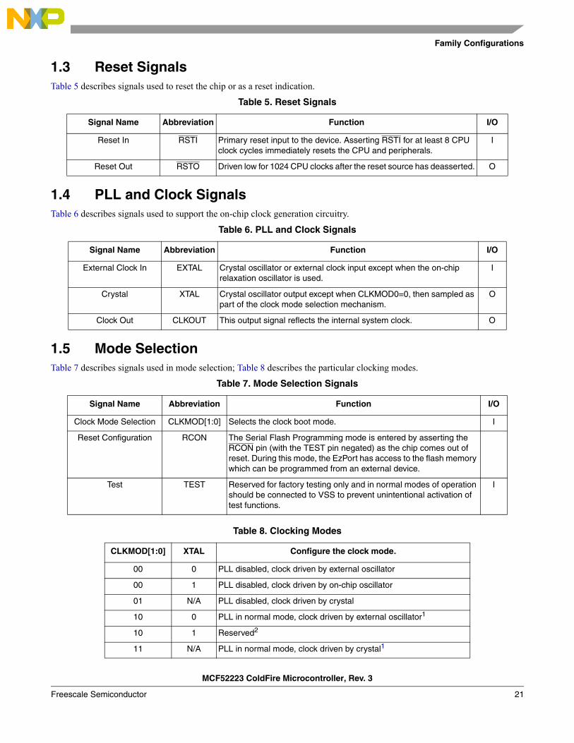
1.3 Reset SignalsTable 5 describes signals used to reset the chip or as a reset indication.
1.4 PLL and Clock SignalsTable 6 describes signals used to support the on-chip clock generation circuitry.
1.5 Mode SelectionTable 7 describes signals used in mode selection; Table 8 describes the particular clocking modes.
Table 5. Reset Signals
Signal Name Abbreviation Function I/O
Reset In RSTI Primary reset input to the device. Asserting RSTI for at least 8 CPU clock cycles immediately resets the CPU and peripherals.
I
Reset Out RSTO Driven low for 1024 CPU clocks after the reset source has deasserted. O
Table 6. PLL and Clock Signals
Signal Name Abbreviation Function I/O
External Clock In EXTAL Crystal oscillator or external clock input except when the on-chip relaxation oscillator is used.
I
Crystal XTAL Crystal oscillator output except when CLKMOD0=0, then sampled as part of the clock mode selection mechanism.
O
Clock Out CLKOUT This output signal reflects the internal system clock. O
Table 7. Mode Selection Signals
Signal Name Abbreviation Function I/O
Clock Mode Selection CLKMOD[1:0] Selects the clock boot mode. I
Reset Configuration RCON The Serial Flash Programming mode is entered by asserting the RCON pin (with the TEST pin negated) as the chip comes out of reset. During this mode, the EzPort has access to the flash memory which can be programmed from an external device.
Test TEST Reserved for factory testing only and in normal modes of operation should be connected to VSS to prevent unintentional activation of test functions.
I
Table 8. Clocking Modes
CLKMOD[1:0] XTAL Configure the clock mode.
00 0 PLL disabled, clock driven by external oscillator
00 1 PLL disabled, clock driven by on-chip oscillator
01 N/A PLL disabled, clock driven by crystal
10 0 PLL in normal mode, clock driven by external oscillator1
10 1 Reserved2
11 N/A PLL in normal mode, clock driven by crystal1
MCF52223 ColdFire Microcontroller, Rev. 3
Freescale Semiconductor 21
Family Configurations
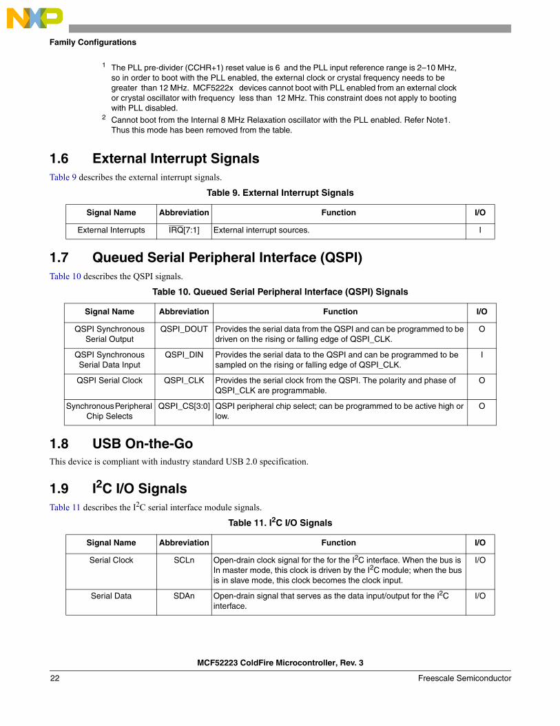
1.6 External Interrupt SignalsTable 9 describes the external interrupt signals.
1.7 Queued Serial Peripheral Interface (QSPI)Table 10 describes the QSPI signals.
1.8 USB On-the-GoThis device is compliant with industry standard USB 2.0 specification.
1.9 I2C I/O SignalsTable 11 describes the I2C serial interface module signals.
1 The PLL pre-divider (CCHR+1) reset value is 6 and the PLL input reference range is 2–10 MHz, so in order to boot with the PLL enabled, the external clock or crystal frequency needs to be greater than 12 MHz. MCF5222x devices cannot boot with PLL enabled from an external clock or crystal oscillator with frequency less than 12 MHz. This constraint does not apply to booting with PLL disabled.
2 Cannot boot from the Internal 8 MHz Relaxation oscillator with the PLL enabled. Refer Note1. Thus this mode has been removed from the table.
Table 9. External Interrupt Signals
Signal Name Abbreviation Function I/O
External Interrupts IRQ[7:1] External interrupt sources. I
Table 10. Queued Serial Peripheral Interface (QSPI) Signals
Signal Name Abbreviation Function I/O
QSPI Synchronous Serial Output
QSPI_DOUT Provides the serial data from the QSPI and can be programmed to be driven on the rising or falling edge of QSPI_CLK.
O
QSPI Synchronous Serial Data Input
QSPI_DIN Provides the serial data to the QSPI and can be programmed to be sampled on the rising or falling edge of QSPI_CLK.
I
QSPI Serial Clock QSPI_CLK Provides the serial clock from the QSPI. The polarity and phase of QSPI_CLK are programmable.
O
Synchronous Peripheral Chip Selects
QSPI_CS[3:0] QSPI peripheral chip select; can be programmed to be active high or low.
O
Table 11. I2C I/O Signals
Signal Name Abbreviation Function I/O
Serial Clock SCLn Open-drain clock signal for the for the I2C interface. When the bus is In master mode, this clock is driven by the I2C module; when the bus is in slave mode, this clock becomes the clock input.
I/O
Serial Data SDAn Open-drain signal that serves as the data input/output for the I2C interface.
I/O
MCF52223 ColdFire Microcontroller, Rev. 3
Freescale Semiconductor22
Family Configurations
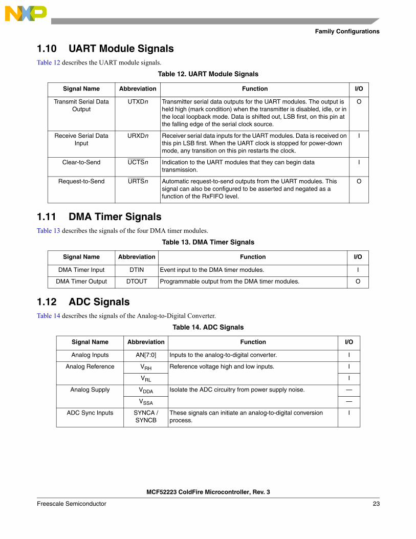
1.10 UART Module SignalsTable 12 describes the UART module signals.
1.11 DMA Timer SignalsTable 13 describes the signals of the four DMA timer modules.
1.12 ADC SignalsTable 14 describes the signals of the Analog-to-Digital Converter.
Table 12. UART Module Signals
Signal Name Abbreviation Function I/O
Transmit Serial Data Output
UTXDn Transmitter serial data outputs for the UART modules. The output is held high (mark condition) when the transmitter is disabled, idle, or in the local loopback mode. Data is shifted out, LSB first, on this pin at the falling edge of the serial clock source.
O
Receive Serial Data Input
URXDn Receiver serial data inputs for the UART modules. Data is received on this pin LSB first. When the UART clock is stopped for power-down mode, any transition on this pin restarts the clock.
I
Clear-to-Send UCTSn Indication to the UART modules that they can begin data transmission.
I
Request-to-Send URTSn Automatic request-to-send outputs from the UART modules. This signal can also be configured to be asserted and negated as a function of the RxFIFO level.
O
Table 13. DMA Timer Signals
Signal Name Abbreviation Function I/O
DMA Timer Input DTIN Event input to the DMA timer modules. I
DMA Timer Output DTOUT Programmable output from the DMA timer modules. O
Table 14. ADC Signals
Signal Name Abbreviation Function I/O
Analog Inputs AN[7:0] Inputs to the analog-to-digital converter. I
Analog Reference VRH Reference voltage high and low inputs. I
VRL I
Analog Supply VDDA Isolate the ADC circuitry from power supply noise. —
VSSA —
ADC Sync Inputs SYNCA / SYNCB
These signals can initiate an analog-to-digital conversion process.
I
MCF52223 ColdFire Microcontroller, Rev. 3
Freescale Semiconductor 23
Family Configurations
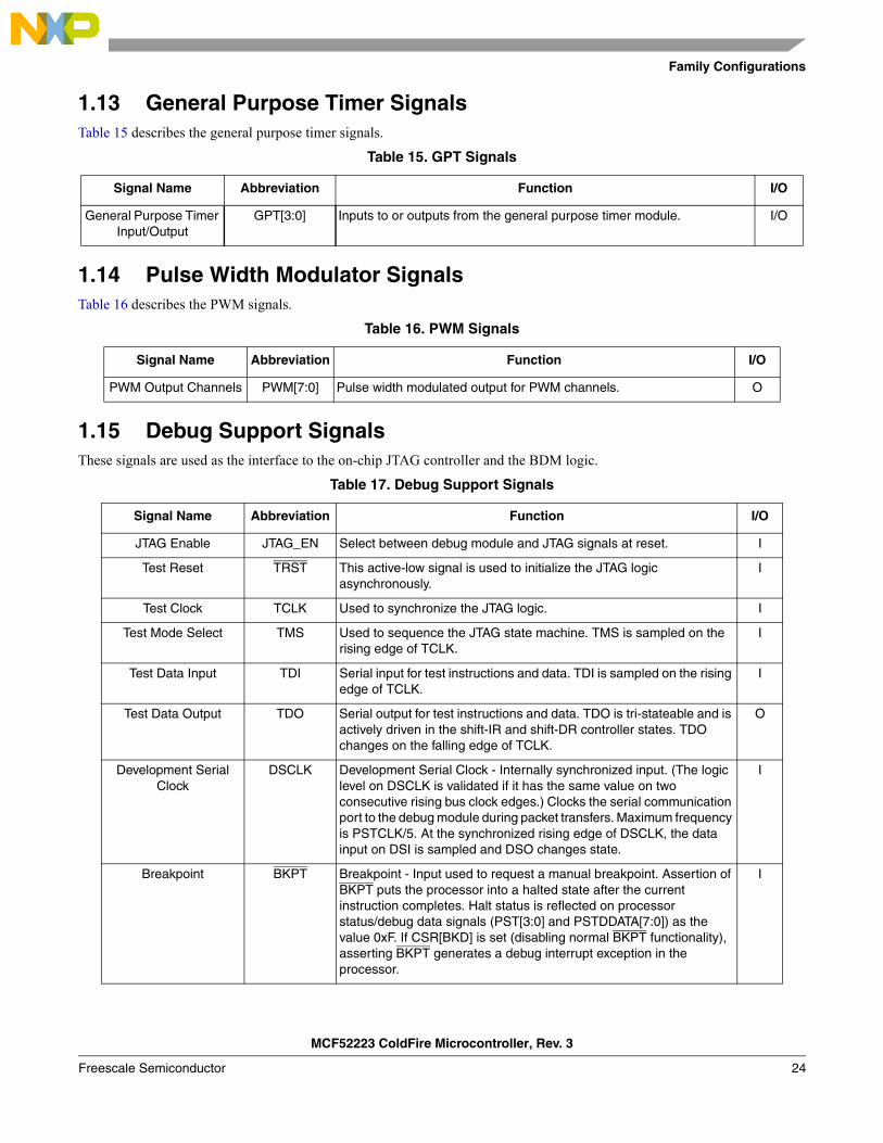
1.13 General Purpose Timer SignalsTable 15 describes the general purpose timer signals.
1.14 Pulse Width Modulator SignalsTable 16 describes the PWM signals.
1.15 Debug Support SignalsThese signals are used as the interface to the on-chip JTAG controller and the BDM logic.
Table 15. GPT Signals
Signal Name Abbreviation Function I/O
General Purpose Timer Input/Output
GPT[3:0] Inputs to or outputs from the general purpose timer module. I/O
Table 16. PWM Signals
Signal Name Abbreviation Function I/O
PWM Output Channels PWM[7:0] Pulse width modulated output for PWM channels. O
Table 17. Debug Support Signals
Signal Name Abbreviation Function I/O
JTAG Enable JTAG_EN Select between debug module and JTAG signals at reset. I
Test Reset TRST This active-low signal is used to initialize the JTAG logic asynchronously.
I
Test Clock TCLK Used to synchronize the JTAG logic. I
Test Mode Select TMS Used to sequence the JTAG state machine. TMS is sampled on the rising edge of TCLK.
I
Test Data Input TDI Serial input for test instructions and data. TDI is sampled on the rising edge of TCLK.
I
Test Data Output TDO Serial output for test instructions and data. TDO is tri-stateable and is actively driven in the shift-IR and shift-DR controller states. TDO changes on the falling edge of TCLK.
O
Development Serial Clock
DSCLK Development Serial Clock - Internally synchronized input. (The logic level on DSCLK is validated if it has the same value on two consecutive rising bus clock edges.) Clocks the serial communication port to the debug module during packet transfers. Maximum frequency is PSTCLK/5. At the synchronized rising edge of DSCLK, the data input on DSI is sampled and DSO changes state.
I
Breakpoint BKPT Breakpoint - Input used to request a manual breakpoint. Assertion of BKPT puts the processor into a halted state after the current instruction completes. Halt status is reflected on processor status/debug data signals (PST[3:0] and PSTDDATA[7:0]) as the value 0xF. If CSR[BKD] is set (disabling normal BKPT functionality), asserting BKPT generates a debug interrupt exception in the processor.
I
MCF52223 ColdFire Microcontroller, Rev. 3
Freescale Semiconductor 24
Family Configurations
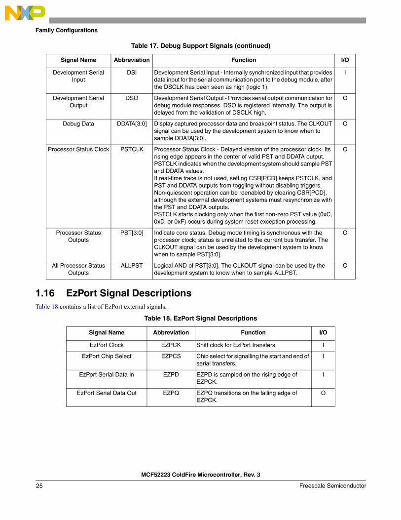
1.16 EzPort Signal DescriptionsTable 18 contains a list of EzPort external signals.
Development Serial Input
DSI Development Serial Input - Internally synchronized input that provides data input for the serial communication port to the debug module, after the DSCLK has been seen as high (logic 1).
I
Development Serial Output
DSO Development Serial Output - Provides serial output communication for debug module responses. DSO is registered internally. The output is delayed from the validation of DSCLK high.
O
Debug Data DDATA[3:0] Display captured processor data and breakpoint status. The CLKOUT signal can be used by the development system to know when to sample DDATA[3:0].
O
Processor Status Clock PSTCLK Processor Status Clock - Delayed version of the processor clock. Its rising edge appears in the center of valid PST and DDATA output. PSTCLK indicates when the development system should sample PST and DDATA values.If real-time trace is not used, setting CSR[PCD] keeps PSTCLK, and PST and DDATA outputs from toggling without disabling triggers. Non-quiescent operation can be reenabled by clearing CSR[PCD], although the external development systems must resynchronize with the PST and DDATA outputs.PSTCLK starts clocking only when the first non-zero PST value (0xC, 0xD, or 0xF) occurs during system reset exception processing.
O
Processor Status Outputs
PST[3:0] Indicate core status. Debug mode timing is synchronous with the processor clock; status is unrelated to the current bus transfer. The CLKOUT signal can be used by the development system to know when to sample PST[3:0].
O
All Processor Status Outputs
ALLPST Logical AND of PST[3:0]. The CLKOUT signal can be used by the development system to know when to sample ALLPST.
O
Table 18. EzPort Signal Descriptions
Signal Name Abbreviation Function I/O
EzPort Clock EZPCK Shift clock for EzPort transfers. I
EzPort Chip Select EZPCS Chip select for signalling the start and end of serial transfers.
I
EzPort Serial Data In EZPD EZPD is sampled on the rising edge of EZPCK.
I
EzPort Serial Data Out EZPQ EZPQ transitions on the falling edge of EZPCK.
O
Table 17. Debug Support Signals (continued)
Signal Name Abbreviation Function I/O
MCF52223 ColdFire Microcontroller, Rev. 3
Freescale Semiconductor25
Family Configurations
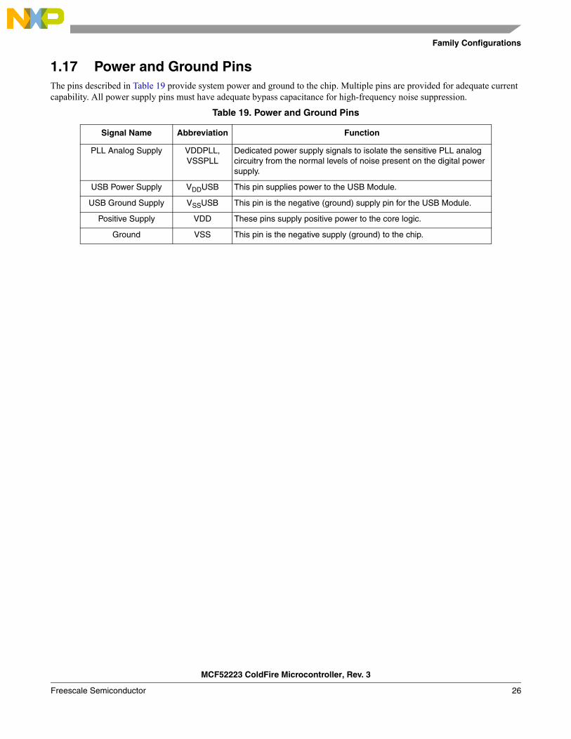
1.17 Power and Ground PinsThe pins described in Table 19 provide system power and ground to the chip. Multiple pins are provided for adequate current capability. All power supply pins must have adequate bypass capacitance for high-frequency noise suppression.
Table 19. Power and Ground Pins
Signal Name Abbreviation Function
PLL Analog Supply VDDPLL, VSSPLL
Dedicated power supply signals to isolate the sensitive PLL analog circuitry from the normal levels of noise present on the digital power supply.
USB Power Supply VDDUSB This pin supplies power to the USB Module.
USB Ground Supply VSSUSB This pin is the negative (ground) supply pin for the USB Module.
Positive Supply VDD These pins supply positive power to the core logic.
Ground VSS This pin is the negative supply (ground) to the chip.
MCF52223 ColdFire Microcontroller, Rev. 3
Freescale Semiconductor 26
Electrical Characteristics
2 Electrical CharacteristicsThis section contains electrical specification tables and reference timing diagrams for the microcontroller unit, including detailed information on power considerations, DC/AC electrical characteristics, and AC timing specifications.
NOTEThe parameters specified in this data sheet supersede any values found in the module specifications.
2.1 Maximum RatingsTable 20. Absolute Maximum Ratings1, 2
1 Functional operating conditions are given in DC Electrical Specifications. Absolute Maximum Ratings are stress ratings only, and functional operation at the maxima is not guaranteed. Stress beyond those listed may affect device reliability or cause permanent damage to the device.
2 This device contains circuitry protecting against damage due to high static voltage or electrical fields; however, it is advised that normal precautions be taken to avoid application of any voltages higher than maximum-rated voltages to this high-impedance circuit. Reliability of operation is enhanced if unused inputs are tied to an appropriate logic voltage level (VSS or VDD).
Rating Symbol Value Unit
Supply voltage VDD –0.3 to 4.0 V
Clock synthesizer supply voltage VDDPLL –0.3 to 4.0 V
RAM standby supply voltage VSTBY –0.3 to 4.0 V
USB standby supply voltage VDDUSB –0.3 to 4.0 V
Digital input voltage 3
3 Input must be current limited to the IDD value specified. To determine the value of the required current-limiting resistor, calculate resistance values for positive and negative clamp voltages, then use the larger of the two values.
VIN –0.3 to 4.0 V
EXTAL pin voltage VEXTAL 0 to 3.3 V
XTAL pin voltage VXTAL 0 to 3.3 V
Instantaneous maximum currentSingle pin limit (applies to all pins)4, 5
4 All functional non-supply pins are internally clamped to VSS and VDD.5 The power supply must maintain regulation within operating VDD range during instantaneous and
operating maximum current conditions. If positive injection current (Vin > VDD) is greater than IDD, the injection current may flow out of VDD and could result in the external power supply going out of regulation. Ensure that the external VDD load shunts current greater than maximum injection current. This is the greatest risk when the MCU is not consuming power (e.g., no clock).
IDD 25 mA
Operating temperature range (packaged) TA(TL - TH)
–40 to 856
6 Depending on the packaging; see the orderable part number summary.
C
Storage temperature range Tstg –65 to 150 C
MCF52223 ColdFire Microcontroller, Rev. 3
Freescale Semiconductor27
Electrical Characteristics
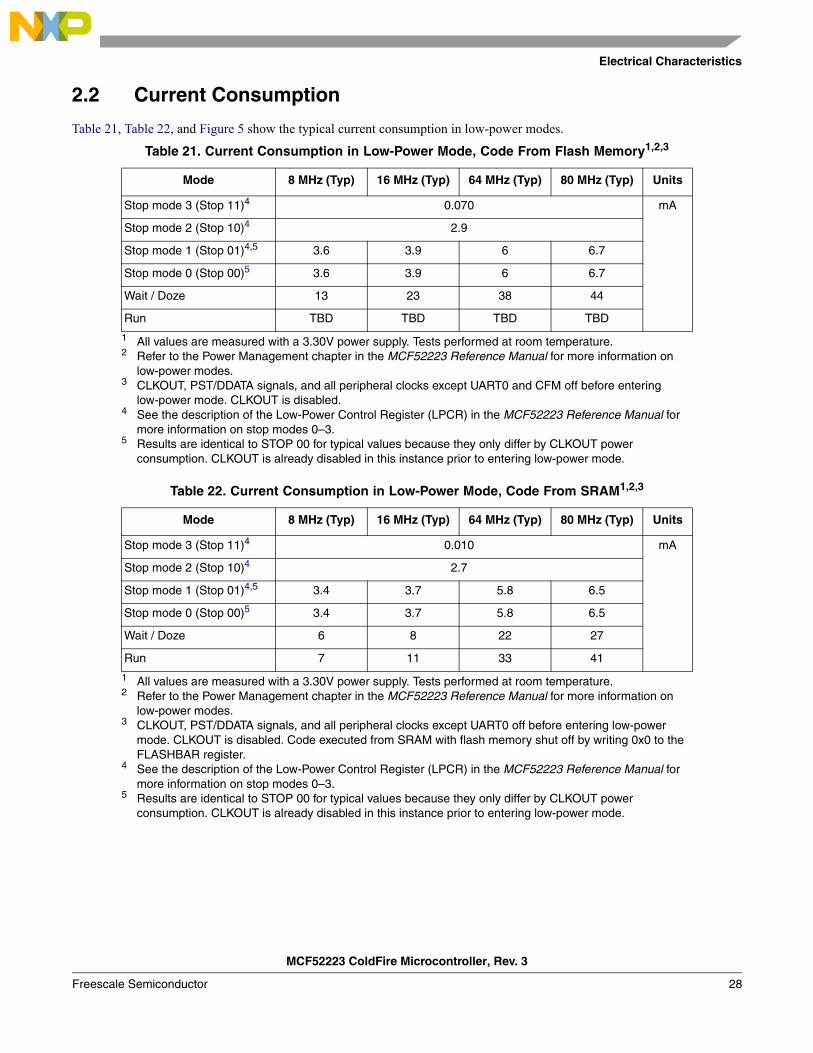
2.2 Current Consumption
Table 21, Table 22, and Figure 5 show the typical current consumption in low-power modes.
Table 21. Current Consumption in Low-Power Mode, Code From Flash Memory1,2,3
1 All values are measured with a 3.30V power supply. Tests performed at room temperature.2 Refer to the Power Management chapter in the MCF52223 Reference Manual for more information on
low-power modes.3 CLKOUT, PST/DDATA signals, and all peripheral clocks except UART0 and CFM off before entering
low-power mode. CLKOUT is disabled.
Mode 8 MHz (Typ) 16 MHz (Typ) 64 MHz (Typ) 80 MHz (Typ) Units
Stop mode 3 (Stop 11)4
4 See the description of the Low-Power Control Register (LPCR) in the MCF52223 Reference Manual for more information on stop modes 0–3.
0.070 mA
Stop mode 2 (Stop 10)4 2.9
Stop mode 1 (Stop 01)4,5
5 Results are identical to STOP 00 for typical values because they only differ by CLKOUT power consumption. CLKOUT is already disabled in this instance prior to entering low-power mode.
3.6 3.9 6 6.7
Stop mode 0 (Stop 00)5 3.6 3.9 6 6.7
Wait / Doze 13 23 38 44
Run TBD TBD TBD TBD
Table 22. Current Consumption in Low-Power Mode, Code From SRAM1,2,3
1 All values are measured with a 3.30V power supply. Tests performed at room temperature.2 Refer to the Power Management chapter in the MCF52223 Reference Manual for more information on
low-power modes.3 CLKOUT, PST/DDATA signals, and all peripheral clocks except UART0 off before entering low-power
mode. CLKOUT is disabled. Code executed from SRAM with flash memory shut off by writing 0x0 to the FLASHBAR register.
Mode 8 MHz (Typ) 16 MHz (Typ) 64 MHz (Typ) 80 MHz (Typ) Units
Stop mode 3 (Stop 11)4
4 See the description of the Low-Power Control Register (LPCR) in the MCF52223 Reference Manual for more information on stop modes 0–3.
0.010 mA
Stop mode 2 (Stop 10)4 2.7
Stop mode 1 (Stop 01)4,5
5 Results are identical to STOP 00 for typical values because they only differ by CLKOUT power consumption. CLKOUT is already disabled in this instance prior to entering low-power mode.
3.4 3.7 5.8 6.5
Stop mode 0 (Stop 00)5 3.4 3.7 5.8 6.5
Wait / Doze 6 8 22 27
Run 7 11 33 41
MCF52223 ColdFire Microcontroller, Rev. 3
Freescale Semiconductor 28
Electrical Characteristics
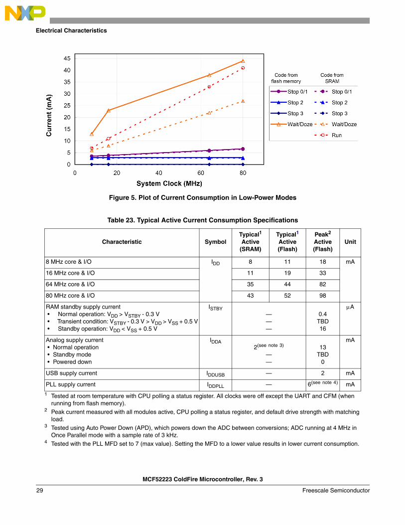
Figure 5. Plot of Current Consumption in Low-Power Modes
Table 23. Typical Active Current Consumption Specifications
Characteristic SymbolTypical1 Active
(SRAM)
1 Tested at room temperature with CPU polling a status register. All clocks were off except the UART and CFM (when running from flash memory).
Typical1
Active (Flash)
Peak2
Active(Flash)
2 Peak current measured with all modules active, CPU polling a status register, and default drive strength with matching load.
Unit
8 MHz core & I/O IDD 8 11 18 mA
16 MHz core & I/O 11 19 33
64 MHz core & I/O 35 44 82
80 MHz core & I/O 43 52 98
RAM standby supply current • Normal operation: VDD > VSTBY - 0.3 V • Transient condition: VSTBY - 0.3 V > VDD > VSS + 0.5 V • Standby operation: VDD < VSS + 0.5 V
ISTBY———
0.4TBD16
A
Analog supply current • Normal operation • Standby mode • Powered down
IDDA2(see note 3)
——
3 Tested using Auto Power Down (APD), which powers down the ADC between conversions; ADC running at 4 MHz in Once Parallel mode with a sample rate of 3 kHz.
13TBD
0
mA
USB supply current IDDUSB — 2 mA
PLL supply current IDDPLL — 6(see note 4)
4 Tested with the PLL MFD set to 7 (max value). Setting the MFD to a lower value results in lower current consumption.
mA
MCF52223 ColdFire Microcontroller, Rev. 3
Freescale Semiconductor29
Electrical Characteristics
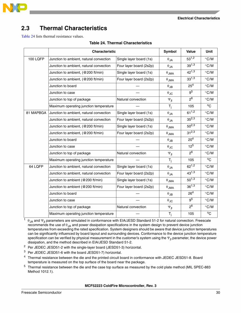
2.3 Thermal CharacteristicsTable 24 lists thermal resistance values.
Table 24. Thermal Characteristics
Characteristic Symbol Value Unit
100 LQFP Junction to ambient, natural convection Single layer board (1s) JA 531,2
1 JA and jt parameters are simulated in conformance with EIA/JESD Standard 51-2 for natural convection. Freescale recommends the use of JA and power dissipation specifications in the system design to prevent device junction temperatures from exceeding the rated specification. System designers should be aware that device junction temperatures can be significantly influenced by board layout and surrounding devices. Conformance to the device junction temperature specification can be verified by physical measurement in the customer’s system using the jt parameter, the device power dissipation, and the method described in EIA/JESD Standard 51-2.
2 Per JEDEC JESD51-2 with the single-layer board (JESD51-3) horizontal.
C / W
Junction to ambient, natural convection Four layer board (2s2p) JA 391,3
3 Per JEDEC JESD51-6 with the board JESD51-7) horizontal.
C / W
Junction to ambient, (@200 ft/min) Single layer board (1s) JMA 421,3 C / W
Junction to ambient, (@200 ft/min) Four layer board (2s2p) JMA 331,3 C / W
Junction to board — JB 254
4 Thermal resistance between the die and the printed circuit board in conformance with JEDEC JESD51-8. Board temperature is measured on the top surface of the board near the package.
C / W
Junction to case — JC 95
5 Thermal resistance between the die and the case top surface as measured by the cold plate method (MIL SPEC-883 Method 1012.1).
C / W
Junction to top of package Natural convection jt 26 C / W
Maximum operating junction temperature — Tj 105 oC
81 MAPBGA Junction to ambient, natural convection Single layer board (1s) JA 611,2 C / W
Junction to ambient, natural convection Four layer board (2s2p) JA 352,3 C / W
Junction to ambient, (@200 ft/min) Single layer board (1s) JMA 502,3 C / W
Junction to ambient, (@200 ft/min) Four layer board (2s2p) JMA 312,3 C / W
Junction to board — JB 204 C / W
Junction to case — JC 125 C / W
Junction to top of package Natural convection jt 26 C / W
Maximum operating junction temperature — Tj 105 oC
64 LQFP Junction to ambient, natural convection Single layer board (1s) JA 621,2 C / W
Junction to ambient, natural convection Four layer board (2s2p) JA 431,3 C / W
Junction to ambient (@200 ft/min) Single layer board (1s) JMA 501,3 C / W
Junction to ambient (@200 ft/min) Four layer board (2s2p) JMA 361,3 C / W
Junction to board — JB 264 C / W
Junction to case — JC 95 C / W
Junction to top of package Natural convection jt 26 C / W
Maximum operating junction temperature — Tj 105 oC
MCF52223 ColdFire Microcontroller, Rev. 3
Freescale Semiconductor 30
Electrical Characteristics
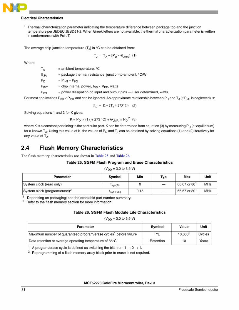
2.4 Flash Memory CharacteristicsThe flash memory characteristics are shown in Table 25 and Table 26.
6 Thermal characterization parameter indicating the temperature difference between package top and the junction temperature per JEDEC JESD51-2. When Greek letters are not available, the thermal characterization parameter is written in conformance with Psi-JT.
The average chip-junction temperature (TJ) in C can be obtained from:
(1)
Where:
TA = ambient temperature, C
JA = package thermal resistance, junction-to-ambient, C/W
PD = PINT PI/O
PINT = chip internal power, IDD VDD, watts
PI/O = power dissipation on input and output pins — user determined, watts
For most applications PI/O PINT and can be ignored. An approximate relationship between PD and TJ (if PI/O is neglected) is:
(2)
Solving equations 1 and 2 for K gives:
K = PD (TA + 273 C) + JMA PD 2 (3)
where K is a constant pertaining to the particular part. K can be determined from equation (3) by measuring PD (at equilibrium) for a known TA. Using this value of K, the values of PD and TJ can be obtained by solving equations (1) and (2) iteratively for any value of TA.
Table 25. SGFM Flash Program and Erase Characteristics
(VDD = 3.0 to 3.6 V)
Parameter Symbol Min Typ Max Unit
System clock (read only) fsys(R) 0 — 66.67 or 801
1 Depending on packaging; see the orderable part number summary.
MHz
System clock (program/erase)2
2 Refer to the flash memory section for more information
fsys(P/E) 0.15 — 66.67 or 801 MHz
Table 26. SGFM Flash Module Life Characteristics
(VDD = 3.0 to 3.6 V)
Parameter Symbol Value Unit
Maximum number of guaranteed program/erase cycles1 before failure
1 A program/erase cycle is defined as switching the bits from 1 0 1.
P/E 10,0002
2 Reprogramming of a flash memory array block prior to erase is not required.
Cycles
Data retention at average operating temperature of 85C Retention 10 Years
TJ TA PD JMA +=
PD K TJ 273C+ =
MCF52223 ColdFire Microcontroller, Rev. 3
Freescale Semiconductor31
Electrical Characteristics
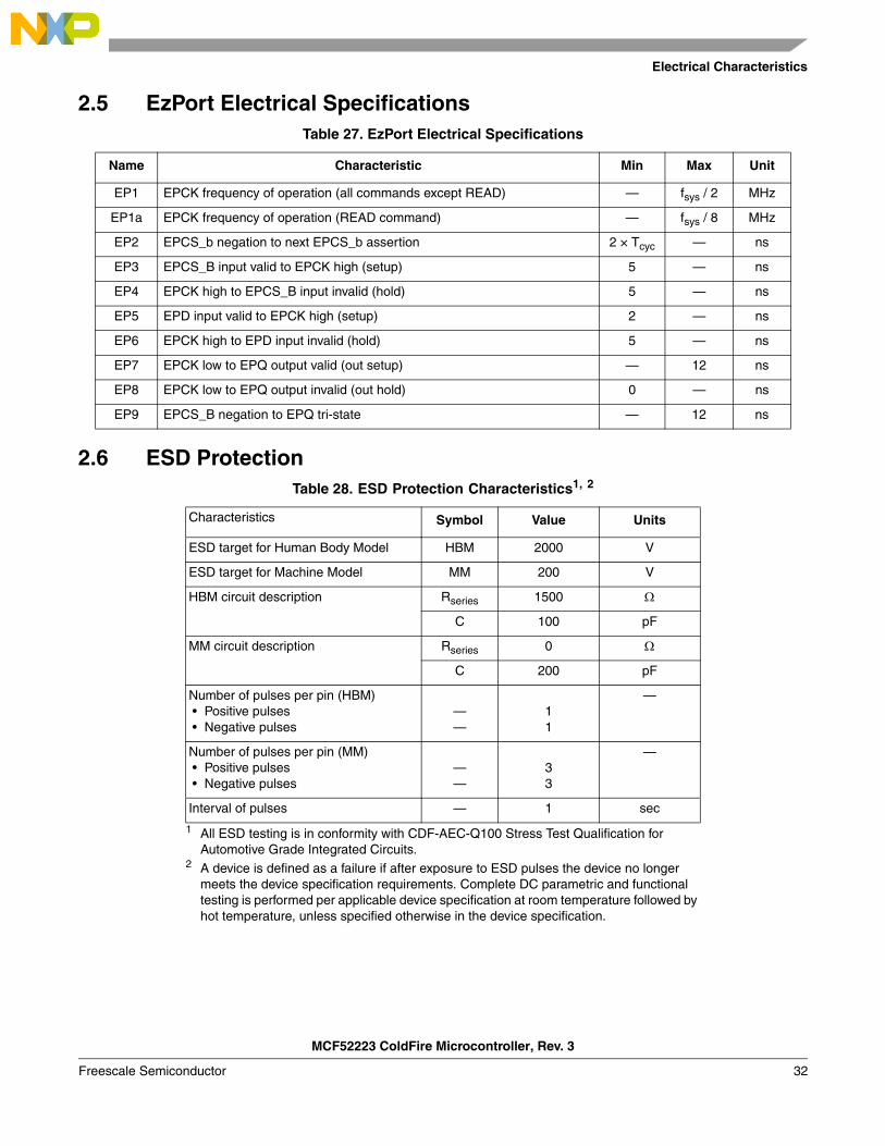
2.5 EzPort Electrical Specifications
2.6 ESD Protection
Table 27. EzPort Electrical Specifications
Name Characteristic Min Max Unit
EP1 EPCK frequency of operation (all commands except READ) — fsys / 2 MHz
EP1a EPCK frequency of operation (READ command) — fsys / 8 MHz
EP2 EPCS_b negation to next EPCS_b assertion 2 × Tcyc — ns
EP3 EPCS_B input valid to EPCK high (setup) 5 — ns
EP4 EPCK high to EPCS_B input invalid (hold) 5 — ns
EP5 EPD input valid to EPCK high (setup) 2 — ns
EP6 EPCK high to EPD input invalid (hold) 5 — ns
EP7 EPCK low to EPQ output valid (out setup) — 12 ns
EP8 EPCK low to EPQ output invalid (out hold) 0 — ns
EP9 EPCS_B negation to EPQ tri-state — 12 ns
Table 28. ESD Protection Characteristics1, 2
1 All ESD testing is in conformity with CDF-AEC-Q100 Stress Test Qualification for Automotive Grade Integrated Circuits.
2 A device is defined as a failure if after exposure to ESD pulses the device no longer meets the device specification requirements. Complete DC parametric and functional testing is performed per applicable device specification at room temperature followed by hot temperature, unless specified otherwise in the device specification.
Characteristics Symbol Value Units
ESD target for Human Body Model HBM 2000 V
ESD target for Machine Model MM 200 V
HBM circuit description Rseries 1500
C 100 pF
MM circuit description Rseries 0
C 200 pF
Number of pulses per pin (HBM) • Positive pulses • Negative pulses
——
11
—
Number of pulses per pin (MM) • Positive pulses • Negative pulses
——
33
—
Interval of pulses — 1 sec
MCF52223 ColdFire Microcontroller, Rev. 3
Freescale Semiconductor 32
Electrical Characteristics
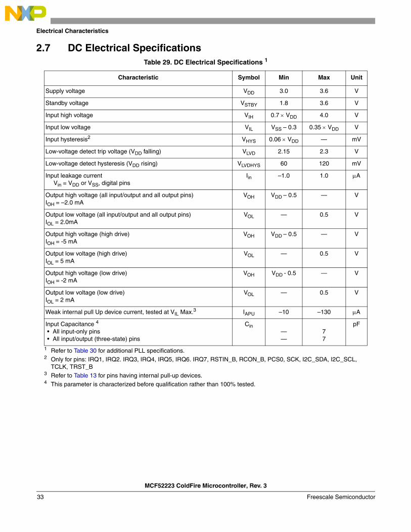
2.7 DC Electrical Specifications
Table 29. DC Electrical Specifications 1
1 Refer to Table 30 for additional PLL specifications.
Characteristic Symbol Min Max Unit
Supply voltage VDD 3.0 3.6 V
Standby voltage VSTBY 1.8 3.6 V
Input high voltage VIH 0.7 VDD 4.0 V
Input low voltage VIL VSS – 0.3 0.35 VDD V
Input hysteresis2
2 Only for pins: IRQ1, IRQ2. IRQ3, IRQ4, IRQ5, IRQ6. IRQ7, RSTIN_B, RCON_B, PCS0, SCK, I2C_SDA, I2C_SCL, TCLK, TRST_B
VHYS 0.06 VDD — mV
Low-voltage detect trip voltage (VDD falling) VLVD 2.15 2.3 V
Low-voltage detect hysteresis (VDD rising) VLVDHYS 60 120 mV
Input leakage currentVin = VDD or VSS, digital pins
Iin –1.0 1.0 A
Output high voltage (all input/output and all output pins)IOH = –2.0 mA
VOH VDD – 0.5 — V
Output low voltage (all input/output and all output pins)IOL = 2.0mA
VOL — 0.5 V
Output high voltage (high drive)IOH = -5 mA
VOH VDD – 0.5 — V
Output low voltage (high drive)IOL = 5 mA
VOL — 0.5 V
Output high voltage (low drive)IOH = -2 mA
VOH VDD - 0.5 — V
Output low voltage (low drive)IOL = 2 mA
VOL — 0.5 V
Weak internal pull Up device current, tested at VIL Max.3
3 Refer to Table 13 for pins having internal pull-up devices.
IAPU –10 –130 A
Input Capacitance 4
• All input-only pins • All input/output (three-state) pins
4 This parameter is characterized before qualification rather than 100% tested.
Cin——
77
pF
MCF52223 ColdFire Microcontroller, Rev. 3
Freescale Semiconductor33
Electrical Characteristics
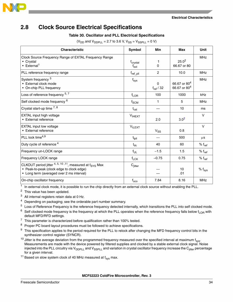
2.8 Clock Source Electrical Specifications
Table 30. Oscillator and PLL Electrical Specifications
(VDD and VDDPLL = 2.7 to 3.6 V, VSS = VSSPLL = 0 V)
Characteristic Symbol Min Max Unit
Clock Source Frequency Range of EXTAL Frequency Range • Crystal • External1
1 In external clock mode, it is possible to run the chip directly from an external clock source without enabling the PLL.
fcrystalfext
10
25.02
66.67 or 80
2 This value has been updated.
MHz
PLL reference frequency range fref_pll 2 10.0 MHz
System frequency 3
• External clock mode • On-chip PLL frequency
3 All internal registers retain data at 0 Hz.
fsys0
fref / 3266.67 or 804
66.67 or 804
4 Depending on packaging; see the orderable part number summary.
MHz
Loss of reference frequency 5, 7
5 Loss of Reference Frequency is the reference frequency detected internally, which transitions the PLL into self clocked mode.
fLOR 100 1000 kHz
Self clocked mode frequency 6
6 Self clocked mode frequency is the frequency at which the PLL operates when the reference frequency falls below fLOR with default MFD/RFD settings.
fSCM 1 5 MHz
Crystal start-up time 7, 8
7 This parameter is characterized before qualification rather than 100% tested.8 Proper PC board layout procedures must be followed to achieve specifications.
tcst — 10 ms
EXTAL input high voltage • External reference
VIHEXT2.0 3.02
V
EXTAL input low voltage • External reference
VILEXTVSS 0.8
V
PLL lock time4,9
9 This specification applies to the period required for the PLL to relock after changing the MFD frequency control bits in the synthesizer control register (SYNCR).
tlpll — 500 s
Duty cycle of reference 4 tdc 40 60 % fref
Frequency un-LOCK range fUL –1.5 1.5 % fref
Frequency LOCK range fLCK –0.75 0.75 % fref
CLKOUT period jitter 4, 5, 10 ,11, measured at fSYS Max • Peak-to-peak (clock edge to clock edge) • Long term (averaged over 2 ms interval)
10 Jitter is the average deviation from the programmed frequency measured over the specified interval at maximum fsys. Measurements are made with the device powered by filtered supplies and clocked by a stable external clock signal. Noise injected into the PLL circuitry via VDDPLL and VSSPLL and variation in crystal oscillator frequency increase the Cjitter percentage for a given interval.
11 Based on slow system clock of 40 MHz measured at fsys max.
Cjitter——
10.01
% fsys
On-chip oscillator frequency foco 7.84 8.16 MHz
MCF52223 ColdFire Microcontroller, Rev. 3
Freescale Semiconductor 34
Electrical Characteristics
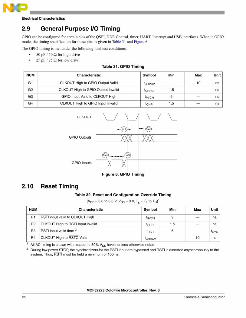
2.9 General Purpose I/O TimingGPIO can be configured for certain pins of the QSPI, DDR Control, timer, UART, Interrupt and USB interfaces. When in GPIO mode, the timing specification for these pins is given in Table 31 and Figure 6.
The GPIO timing is met under the following load test conditions:
• 50 pF / 50 for high drive
• 25 pF / 25 for low drive
Figure 6. GPIO Timing
2.10 Reset Timing
Table 31. GPIO Timing
NUM Characteristic Symbol Min Max Unit
G1 CLKOUT High to GPIO Output Valid tCHPOV — 10 ns
G2 CLKOUT High to GPIO Output Invalid tCHPOI 1.5 — ns
G3 GPIO Input Valid to CLKOUT High tPVCH 9 — ns
G4 CLKOUT High to GPIO Input Invalid tCHPI 1.5 — ns
Table 32. Reset and Configuration Override Timing
(VDD = 3.0 to 3.6 V, VSS = 0 V, TA = TL to TH)1
1 All AC timing is shown with respect to 50% VDD levels unless otherwise noted.
NUM Characteristic Symbol Min Max Unit
R1 RSTI input valid to CLKOUT High tRVCH 9 — ns
R2 CLKOUT High to RSTI Input invalid tCHRI 1.5 — ns
R3 RSTI input valid time 2
2 During low power STOP, the synchronizers for the RSTI input are bypassed and RSTI is asserted asynchronously to the system. Thus, RSTI must be held a minimum of 100 ns.
tRIVT 5 — tCYC
R4 CLKOUT High to RSTO Valid tCHROV — 10 ns
G1
CLKOUT
GPIO Outputs
G2
G3 G4
GPIO Inputs
MCF52223 ColdFire Microcontroller, Rev. 3
Freescale Semiconductor35
Electrical Characteristics
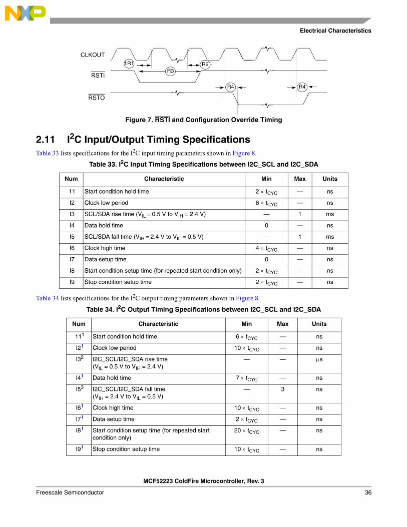
Figure 7. RSTI and Configuration Override Timing
2.11 I2C Input/Output Timing SpecificationsTable 33 lists specifications for the I2C input timing parameters shown in Figure 8.
Table 34 lists specifications for the I2C output timing parameters shown in Figure 8.
Table 33. I2C Input Timing Specifications between I2C_SCL and I2C_SDA
Num Characteristic Min Max Units
11 Start condition hold time 2 tCYC — ns
I2 Clock low period 8 tCYC — ns
I3 SCL/SDA rise time (VIL = 0.5 V to VIH = 2.4 V) — 1 ms
I4 Data hold time 0 — ns
I5 SCL/SDA fall time (VIH = 2.4 V to VIL = 0.5 V) — 1 ms
I6 Clock high time 4 tCYC — ns
I7 Data setup time 0 — ns
I8 Start condition setup time (for repeated start condition only) 2 tCYC — ns
I9 Stop condition setup time 2 tCYC — ns
Table 34. I2C Output Timing Specifications between I2C_SCL and I2C_SDA
Num Characteristic Min Max Units
111 Start condition hold time 6 tCYC — ns
I21 Clock low period 10 tCYC — ns
I32 I2C_SCL/I2C_SDA rise time(VIL = 0.5 V to VIH = 2.4 V)
— — s
I41 Data hold time 7 tCYC — ns
I53 I2C_SCL/I2C_SDA fall time(VIH = 2.4 V to VIL = 0.5 V)
— 3 ns
I61 Clock high time 10 tCYC — ns
I71 Data setup time 2 tCYC — ns
I81 Start condition setup time (for repeated start condition only)
20 tCYC — ns
I91 Stop condition setup time 10 tCYC — ns
1R1 R2
CLKOUT
RSTI
RSTO
R3
R4 R4
MCF52223 ColdFire Microcontroller, Rev. 3
Freescale Semiconductor 36
Electrical Characteristics
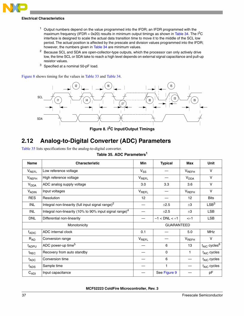
Figure 8 shows timing for the values in Table 33 and Table 34.
Figure 8. I2C Input/Output Timings
2.12 Analog-to-Digital Converter (ADC) ParametersTable 35 lists specifications for the analog-to-digital converter.
1 Output numbers depend on the value programmed into the IFDR; an IFDR programmed with the maximum frequency (IFDR = 0x20) results in minimum output timings as shown in Table 34. The I2C interface is designed to scale the actual data transition time to move it to the middle of the SCL low period. The actual position is affected by the prescale and division values programmed into the IFDR; however, the numbers given in Table 34 are minimum values.
2 Because SCL and SDA are open-collector-type outputs, which the processor can only actively drive low, the time SCL or SDA take to reach a high level depends on external signal capacitance and pull-up resistor values.
3 Specified at a nominal 50-pF load.
Table 35. ADC Parameters1
Name Characteristic Min Typical Max Unit
VREFL Low reference voltage VSS — VREFH V
VREFH High reference voltage VREFL — VDDA V
VDDA ADC analog supply voltage 3.0 3.3 3.6 V
VADIN Input voltages VREFL — VREFH V
RES Resolution 12 — 12 Bits
INL Integral non-linearity (full input signal range)2 — 2.5 3 LSB3
INL Integral non-linearity (10% to 90% input signal range)4 — 2.5 3 LSB
DNL Differential non-linearity — –1 < DNL < 1 <1 LSB
Monotonicity GUARANTEED
fADIC ADC internal clock 0.1 — 5.0 MHz
RAD Conversion range VREFL — VREFH V
tADPU ADC power-up time5 — 6 13 tAIC cycles6
tREC Recovery from auto standby — 0 1 tAIC cycles
tADC Conversion time — 6 — tAIC cycles
tADS Sample time — 1 — tAIC cycles
CADI Input capacitance — See Figure 9 — pF
I2 I6
I1 I4I7
I8 I9
I5
I3SCL
SDA
MCF52223 ColdFire Microcontroller, Rev. 3
Freescale Semiconductor37
Electrical Characteristics
2.13 Equivalent Circuit for ADC Inputs Figure 9 shows the ADC input circuit during sample and hold. S1 and S2 are always open/closed at the same time that S3 is closed/open. When S1/S2 are closed & S3 is open, one input of the sample and hold circuit moves to (VREFH-VREFL)/2, while the other charges to the analog input voltage. When the switches are flipped, the charge on C1 and C2 are averaged via S3, with the result that a single-ended analog input is switched to a differential voltage centered about (VREFH-VREFL)/2. The switches switch on every cycle of the ADC clock (open one-half ADC clock, closed one-half ADC clock). There are additional capacitances associated with the analog input pad, routing, etc., but these do not filter into the S/H output voltage, as S1 provides isolation during the charge-sharing phase. One aspect of this circuit is that there is an on-going input current, which is a function of the analog input voltage, VREF and the ADC clock frequency.
1. Parasitic capacitance due to package, pin-to-pin and pin-to-package base coupling; 1.8pF
2. Parasitic capacitance due to the chip bond pad, ESD protection devices and signal routing; 2.04pF
XIN Input impedance — See Figure 9 — W
IADI Input injection current7, per pin — — 3 mA
IVREFH VREFH current — 0 — mA
VOFFSET Offset voltage internal reference — 8 15 mV
EGAIN Gain error (transfer path) .99 1 1.01 —
VOFFSET Offset voltage external reference — 3 9 mV
SNR Signal-to-noise ratio — 62 to 66 — dB
THD Total harmonic distortion — 75 — dB
SFDR Spurious free dynamic range — 67 to 70.3 — dB
SINAD Signal-to-noise plus distortion — 61 to 63.9 — dB
ENOB Effective number of bits 9.1 10.6 — Bits
1 All measurements are made at VDD = 3.3V, VREFH = 3.3V, and VREFL = ground2 INL measured from VIN = VREFL to VIN = VREFH3 LSB = Least Significant Bit4 INL measured from VIN = 0.1VREFH to VIN = 0.9VREFH5 Includes power-up of ADC and VREF6 ADC clock cycles7 Current that can be injected or sourced from an unselected ADC signal input without impacting the performance of the ADC
Table 35. ADC Parameters1 (continued)
Name Characteristic Min Typical Max Unit
1 2
3Analog Input 4S1
S2
S3
C1
C2
S/H
C1 = C2 = 1pF(VREFH- VREFL)/ 2
125W ESD Resistor
8pF noise damping capacitor
MCF52223 ColdFire Microcontroller, Rev. 3
Freescale Semiconductor 38
Electrical Characteristics
3. Equivalent resistance for the channel select mux; 100 s
4. Sampling capacitor at the sample and hold circuit. Capacitor C1 is normally disconnected from the input and is only connected to it at sampling time; 1.4pF
5. Equivalent input impedance, when the input is selected =
Figure 9. Equivalent Circuit for A/D Loading
2.14 DMA Timers Timing SpecificationsTable 36 lists timer module AC timings.
2.15 QSPI Electrical SpecificationsTable 37 lists QSPI timings.
The values in Table 37 correspond to Figure 10.
Table 36. Timer Module AC Timing Specifications
Name Characteristic1
1 All timing references to CLKOUT are given to its rising edge.
Min Max Unit
T1 DTIN0 / DTIN1 / DTIN2 / DTIN3 cycle time 3 tCYC — ns
T2 DTIN0 / DTIN1 / DTIN2 / DTIN3 pulse width 1 tCYC — ns
Table 37. QSPI Modules AC Timing Specifications
Name Characteristic Min Max Unit
QS1 QSPI_CS[3:0] to QSPI_CLK 1 510 tCYC
QS2 QSPI_CLK high to QSPI_DOUT valid — 10 ns
QS3 QSPI_CLK high to QSPI_DOUT invalid (Output hold) 2 — ns
QS4 QSPI_DIN to QSPI_CLK (Input setup) 9 — ns
QS5 QSPI_DIN to QSPI_CLK (Input hold) 9 — ns
1
(ADC Clock Rate) (1.410-12)
MCF52223 ColdFire Microcontroller, Rev. 3
Freescale Semiconductor39
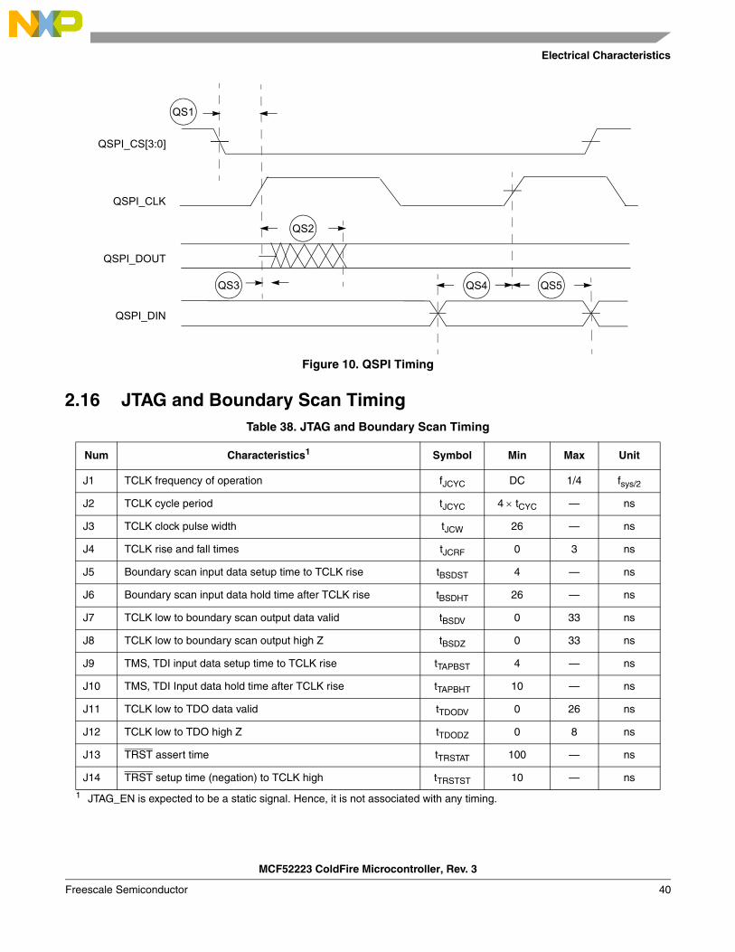
Electrical Characteristics
Figure 10. QSPI Timing
2.16 JTAG and Boundary Scan TimingTable 38. JTAG and Boundary Scan Timing
Num Characteristics1
1 JTAG_EN is expected to be a static signal. Hence, it is not associated with any timing.
Symbol Min Max Unit
J1 TCLK frequency of operation fJCYC DC 1/4 fsys/2
J2 TCLK cycle period tJCYC 4 tCYC — ns
J3 TCLK clock pulse width tJCW 26 — ns
J4 TCLK rise and fall times tJCRF 0 3 ns
J5 Boundary scan input data setup time to TCLK rise tBSDST 4 — ns
J6 Boundary scan input data hold time after TCLK rise tBSDHT 26 — ns
J7 TCLK low to boundary scan output data valid tBSDV 0 33 ns
J8 TCLK low to boundary scan output high Z tBSDZ 0 33 ns
J9 TMS, TDI input data setup time to TCLK rise tTAPBST 4 — ns
J10 TMS, TDI Input data hold time after TCLK rise tTAPBHT 10 — ns
J11 TCLK low to TDO data valid tTDODV 0 26 ns
J12 TCLK low to TDO high Z tTDODZ 0 8 ns
J13 TRST assert time tTRSTAT 100 — ns
J14 TRST setup time (negation) to TCLK high tTRSTST 10 — ns
QSPI_CS[3:0]
QSPI_CLK
QSPI_DOUT
QS5
QS1
QSPI_DIN
QS3 QS4
QS2
MCF52223 ColdFire Microcontroller, Rev. 3
Freescale Semiconductor 40
Electrical Characteristics
Figure 11. Test Clock Input Timing
Figure 12. Boundary Scan (JTAG) Timing
Figure 13. Test Access Port Timing
Figure 14. TRST Timing
TCLKVIL
VIH
J3 J3
J4 J4
J2
(input)
Input Data Valid
Output Data Valid
Output Data Valid
TCLK
Data Inputs
Data Outputs
Data Outputs
Data Outputs
VIL VIH
J5 J6
J7
J8
J7
Input Data Valid
Output Data Valid
Output Data Valid
TCLK
TDI
TDO
TDO
TDO
TMS
VIL VIH
J9 J10
J11
J12
J11
TCLK
TRST
14
13
MCF52223 ColdFire Microcontroller, Rev. 3
Freescale Semiconductor41
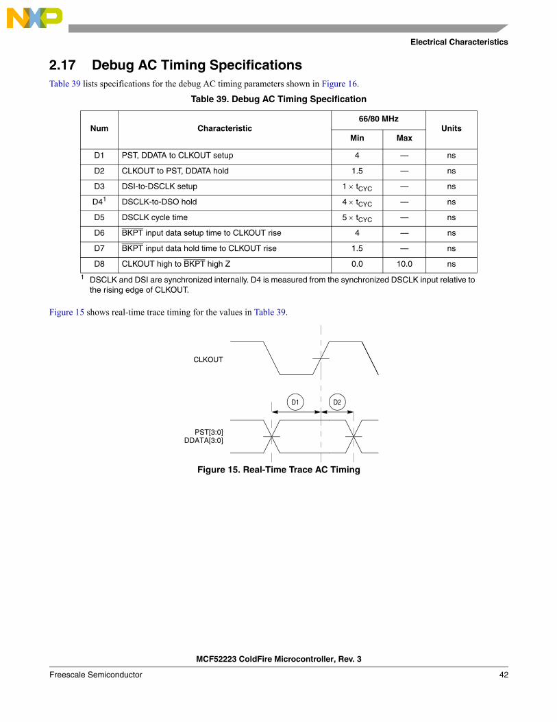
Electrical Characteristics
2.17 Debug AC Timing SpecificationsTable 39 lists specifications for the debug AC timing parameters shown in Figure 16.
Figure 15 shows real-time trace timing for the values in Table 39.
Figure 15. Real-Time Trace AC Timing
Table 39. Debug AC Timing Specification
Num Characteristic66/80 MHz
UnitsMin Max
D1 PST, DDATA to CLKOUT setup 4 — ns
D2 CLKOUT to PST, DDATA hold 1.5 — ns
D3 DSI-to-DSCLK setup 1 tCYC — ns
D41
1 DSCLK and DSI are synchronized internally. D4 is measured from the synchronized DSCLK input relative to the rising edge of CLKOUT.
DSCLK-to-DSO hold 4 tCYC — ns
D5 DSCLK cycle time 5 tCYC — ns
D6 BKPT input data setup time to CLKOUT rise 4 — ns
D7 BKPT input data hold time to CLKOUT rise 1.5 — ns
D8 CLKOUT high to BKPT high Z 0.0 10.0 ns
CLKOUT
PST[3:0]
D2D1
DDATA[3:0]
MCF52223 ColdFire Microcontroller, Rev. 3
Freescale Semiconductor 42
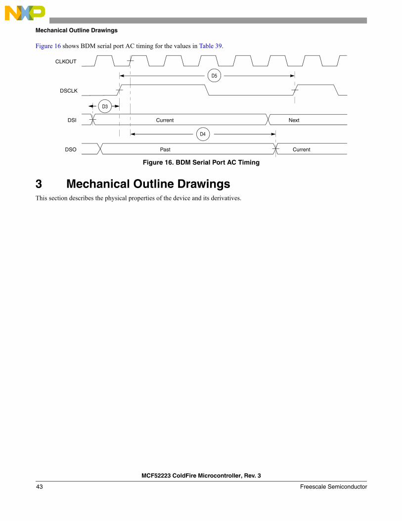
Mechanical Outline Drawings
Figure 16 shows BDM serial port AC timing for the values in Table 39.
Figure 16. BDM Serial Port AC Timing
3 Mechanical Outline DrawingsThis section describes the physical properties of the device and its derivatives.
DSI
DSO
Current Next
CLKOUT
Past Current
DSCLK
D3
D4
D5
MCF52223 ColdFire Microcontroller, Rev. 3
Freescale Semiconductor43
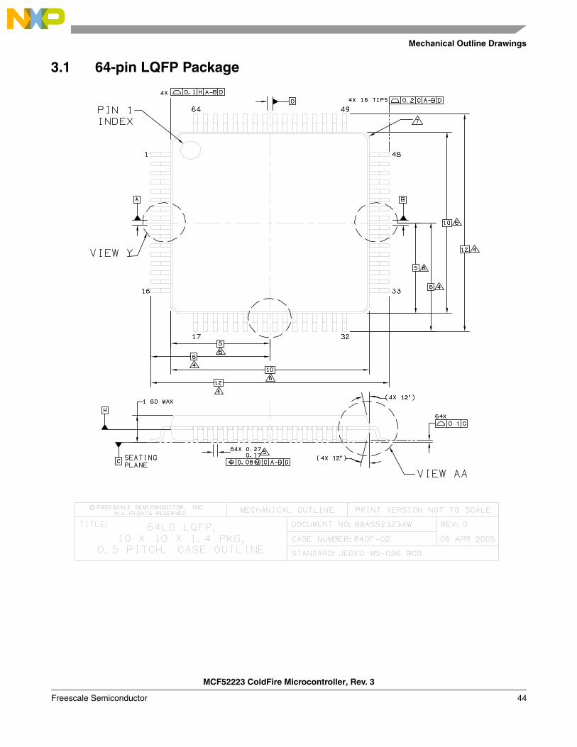
Mechanical Outline Drawings
3.1 64-pin LQFP Package
MCF52223 ColdFire Microcontroller, Rev. 3
Freescale Semiconductor 44
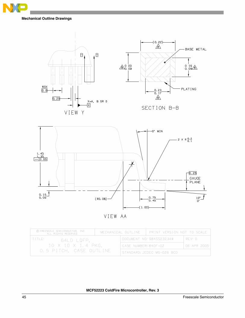
Mechanical Outline Drawings
MCF52223 ColdFire Microcontroller, Rev. 3
Freescale Semiconductor45
Mechanical Outline Drawings
MCF52223 ColdFire Microcontroller, Rev. 3
Freescale Semiconductor 46
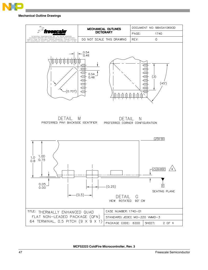
Mechanical Outline Drawings
MCF52223 ColdFire Microcontroller, Rev. 3
Freescale Semiconductor47
Mechanical Outline Drawings
MCF52223 ColdFire Microcontroller, Rev. 3
Freescale Semiconductor 48
Mechanical Outline Drawings
MCF52223 ColdFire Microcontroller, Rev. 3
Freescale Semiconductor49
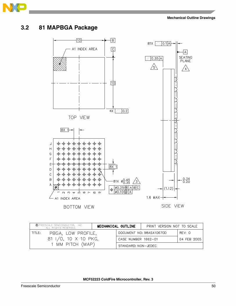
Mechanical Outline Drawings
3.2 81 MAPBGA Package
MCF52223 ColdFire Microcontroller, Rev. 3
Freescale Semiconductor 50
Mechanical Outline Drawings
MCF52223 ColdFire Microcontroller, Rev. 3
Freescale Semiconductor51
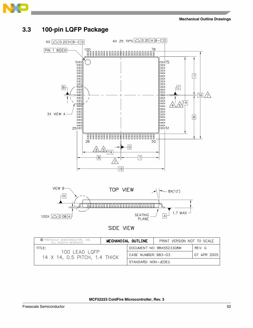
Mechanical Outline Drawings
3.3 100-pin LQFP Package
MCF52223 ColdFire Microcontroller, Rev. 3
Freescale Semiconductor 52
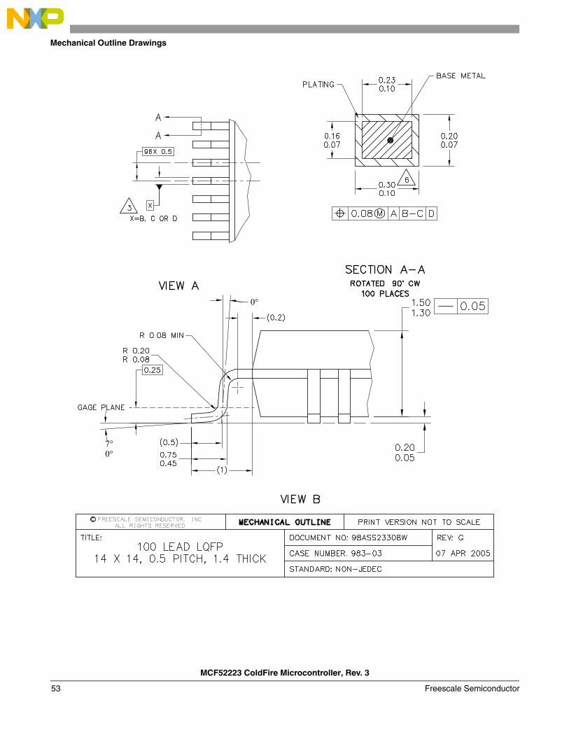
Mechanical Outline Drawings
MCF52223 ColdFire Microcontroller, Rev. 3
Freescale Semiconductor53
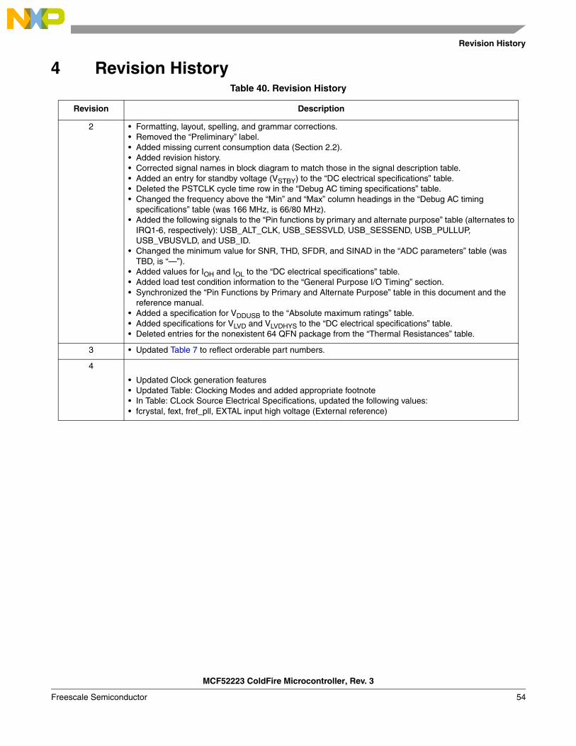
Revision History
4 Revision HistoryTable 40. Revision History
Revision Description
2 • Formatting, layout, spelling, and grammar corrections. • Removed the “Preliminary” label. • Added missing current consumption data (Section 2.2). • Added revision history. • Corrected signal names in block diagram to match those in the signal description table. • Added an entry for standby voltage (VSTBY) to the “DC electrical specifications” table. • Deleted the PSTCLK cycle time row in the “Debug AC timing specifications” table. • Changed the frequency above the “Min” and “Max” column headings in the “Debug AC timing
specifications” table (was 166 MHz, is 66/80 MHz). • Added the following signals to the “Pin functions by primary and alternate purpose” table (alternates to
IRQ1-6, respectively): USB_ALT_CLK, USB_SESSVLD, USB_SESSEND, USB_PULLUP, USB_VBUSVLD, and USB_ID.
• Changed the minimum value for SNR, THD, SFDR, and SINAD in the “ADC parameters” table (was TBD, is “—”).
• Added values for IOH and IOL to the “DC electrical specifications” table. • Added load test condition information to the “General Purpose I/O Timing” section. • Synchronized the “Pin Functions by Primary and Alternate Purpose” table in this document and the
reference manual. • Added a specification for VDDUSB to the “Absolute maximum ratings” table. • Added specifications for VLVD and VLVDHYS to the “DC electrical specifications” table. • Deleted entries for the nonexistent 64 QFN package from the “Thermal Resistances” table.
3 • Updated Table 7 to reflect orderable part numbers.
4
• Updated Clock generation features • Updated Table: Clocking Modes and added appropriate footnote • In Table: CLock Source Electrical Specifications, updated the following values: • fcrystal, fext, fref_pll, EXTAL input high voltage (External reference)
MCF52223 ColdFire Microcontroller, Rev. 3
Freescale Semiconductor 54

Document Number: MCF52223Rev. 33/2011
How to Reach Us:
Home Page:www.freescale.com
Web Support:http://www.freescale.com/support
USA/Europe or Locations Not Listed:Freescale Semiconductor, Inc.Technical Information Center, EL5162100 East Elliot RoadTempe, Arizona 852841-800-521-6274 or +1-480-768-2130www.freescale.com/support
Europe, Middle East, and Africa:Freescale Halbleiter Deutschland GmbHTechnical Information CenterSchatzbogen 781829 Muenchen, Germany+44 1296 380 456 (English)+46 8 52200080 (English)+49 89 92103 559 (German)+33 1 69 35 48 48 (French)www.freescale.com/support
Japan:Freescale Semiconductor Japan Ltd.HeadquartersARCO Tower 15F1-8-1, Shimo-Meguro, Meguro-ku,Tokyo 153-0064Japan0120 191014 or +81 3 5437 [email protected]
Asia/Pacific:Freescale Semiconductor China Ltd.Exchange Building 23FNo. 118 Jianguo RoadChaoyang DistrictBeijing 100022China +86 10 5879 8000 [email protected]
Freescale Semiconductor Literature Distribution Center1-800-441-2447 or +1-303-675-2140Fax: +1-303-675-2150 [email protected]
Information in this document is provided solely to enable system and software implementers to use Freescale Semiconductor products. There are no express or implied copyright licenses granted hereunder to design or fabricate any integrated circuits or integrated circuits based on the information in this document.
Freescale Semiconductor reserves the right to make changes without further notice to any products herein. Freescale Semiconductor makes no warranty, representation or guarantee regarding the suitability of its products for any particular purpose, nor does Freescale Semiconductor assume any liability arising out of the application or use of any product or circuit, and specifically disclaims any and all liability, including without limitation consequential or incidental damages. “Typical” parameters that may be provided in Freescale Semiconductor data sheets and/or specifications can and do vary in different applications and actual performance may vary over time. All operating parameters, including “Typicals”, must be validated for each customer application by customer’s technical experts. Freescale Semiconductor does not convey any license under its patent rights nor the rights of others. Freescale Semiconductor products are not designed, intended, or authorized for use as components in systems intended for surgical implant into the body, or other applications intended to support or sustain life, or for any other application in which the failure of the Freescale Semiconductor product could create a situation where personal injury or death may occur. Should Buyer purchase or use Freescale Semiconductor products for any such unintended or unauthorized application, Buyer shall indemnify and hold Freescale Semiconductor and its officers, employees, subsidiaries, affiliates, and distributors harmless against all claims, costs, damages, and expenses, and reasonable attorney fees arising out of, directly or indirectly, any claim of personal injury or death associated with such unintended or unauthorized use, even if such claim alleges that Freescale Semiconductor was negligent regarding the design or manufacture of the part.
RoHS-compliant and/or Pb-free versions of Freescale products have the functionality and electrical characteristics as their non-RoHS-compliant and/or non-Pb-free counterparts. For further information, see http://www.freescale.com or contact your Freescale sales representative.
For information on Freescale’s Environmental Products program, go to http://www.freescale.com/epp.
Freescale™ and the Freescale logo are trademarks of Freescale Semiconductor, Inc. All other product or service names are the property of their respective owners.© Freescale Semiconductor, Inc. 2011. All rights reserved.


![[BAB I] Microcontroller ATMEGA8535](https://img.pdfslide.net/doc/110x75/635d9893a0f1eac29f0c45be/bab-i-microcontroller-atmega8535.jpg)

