Embed Size (px)
Citation preview
PIC Family Microcontroller
Chapter 13
Lesson 02
Architecture of PIC 16F877

2011 Microcontrollers-... 2nd Ed. Raj Kamal
Pearson Education 3
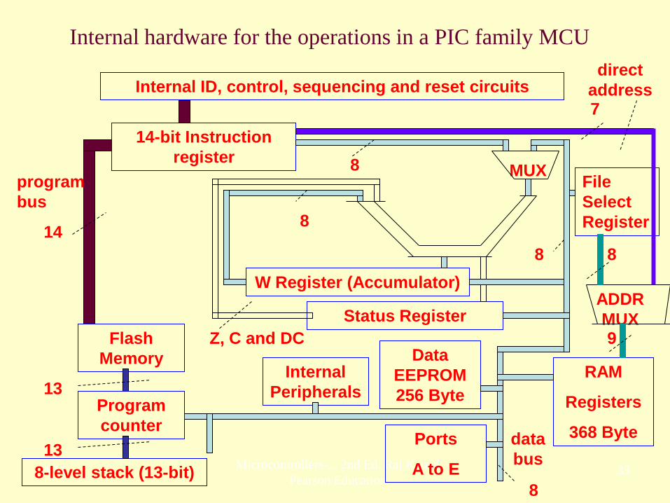
Internal hardware for the operations in a PIC family MCU
Internal ID, control, sequencing and reset circuits
14-bit Instruction
register
W Register (Accumulator)
RAM
Registers
368 Byte
Status Register
MUX File
Select
Register
Z, C and DC
8
8
7
ADDR
MUX
8
9
Ports
A to E
Data
EEPROM
256 Byte
Internal
Peripherals
8
data
bus
8
program
bus
14
Flash
Memory
Program
counter
13
8-level stack (13-bit)
13
direct
address
2011 Microcontrollers-... 2nd Ed. Raj Kamal
Pearson Education 4
ALU Features
• Supports 8-bit operations
• Internal data bus is of 8-bits
2011 Microcontrollers-... 2nd Ed. Raj Kamal
Pearson Education 5
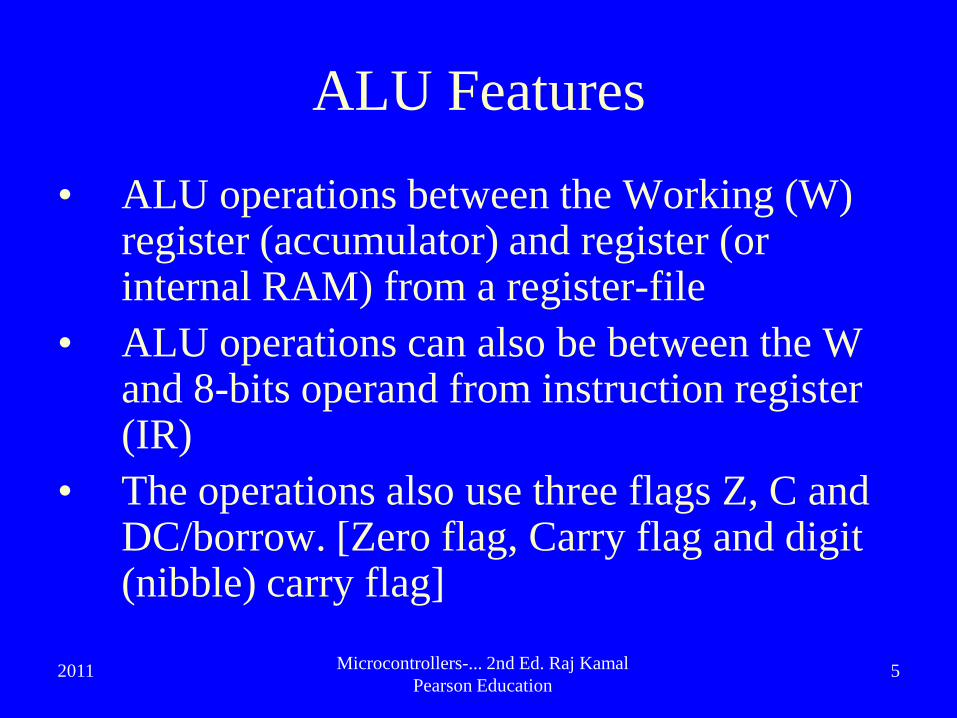
ALU Features
• ALU operations between the Working (W) register (accumulator) and register (or internal RAM) from a register-file
• ALU operations can also be between the W and 8-bits operand from instruction register (IR)
• The operations also use three flags Z, C and DC/borrow. [Zero flag, Carry flag and digit (nibble) carry flag]
2011 Microcontrollers-... 2nd Ed. Raj Kamal
Pearson Education 6
ALU features
• The destination of result from ALU
operations can be either W or register (f) in
file
• The flags save at status register (STATUS)
• PIC CPU is a one-address machine (one
operand specified in the instruction for ALU)
2011 Microcontrollers-... 2nd Ed. Raj Kamal
Pearson Education 7
ALU features
• Two operands are used in an arithmetic or
logic operations
• One is source operand from one a register
file/RAM (or operand from instruction) and
another is W-register
• Advantage—ALU directly operates on a
register or memory similar to 8086 CPU
2011 Microcontrollers-... 2nd Ed. Raj Kamal
Pearson Education 8
Harvard architecture
• Separate address spaces for the program
• Separate address spaces for data
2011 Microcontrollers-... 2nd Ed. Raj Kamal
Pearson Education 9
Data
(i) data memory for special function registers (SFR), registers, internal RAM,
(ii) data memory EEPROM, and
(iii) separate address spaces for program memory, interrupt vectors, constant data and text (flash memory)
2011 Microcontrollers-... 2nd Ed. Raj Kamal
Pearson Education 10
Separate internal buses
• Address of 13-bit A0-A12 for the
program address in 16F877
• Program code-bus of 14-bit
• Data D0-D7 of 8-bit
• Flash memory retention period is more
than 40 years
2011 Microcontrollers-... 2nd Ed. Raj Kamal
Pearson Education 11
Program Memory
• Program memory 8 k × 14. Program address
fetch bus is of 13-bit. There are thus 8192
program instruction addresses.
• Program counter is thus of 13-bit word
pointing to one of the 8 k (8192) addresses in
program memory (flash).
• Total are 8192 addresses (213) in flash in PIC
16F877 as Program counter is of 13 bit)
2011 Microcontrollers-... 2nd Ed. Raj Kamal
Pearson Education 12
Instruction
• Instruction length 14-bit
• Program-code bus 14-bit.
• Flash saves 14-bits at each address
2011 Microcontrollers-... 2nd Ed. Raj Kamal
Pearson Education 13
Program Counter
• Program Counter starts from a value, which is
pre-programmed at the reset vector address
2011 Microcontrollers-... 2nd Ed. Raj Kamal
Pearson Education 14
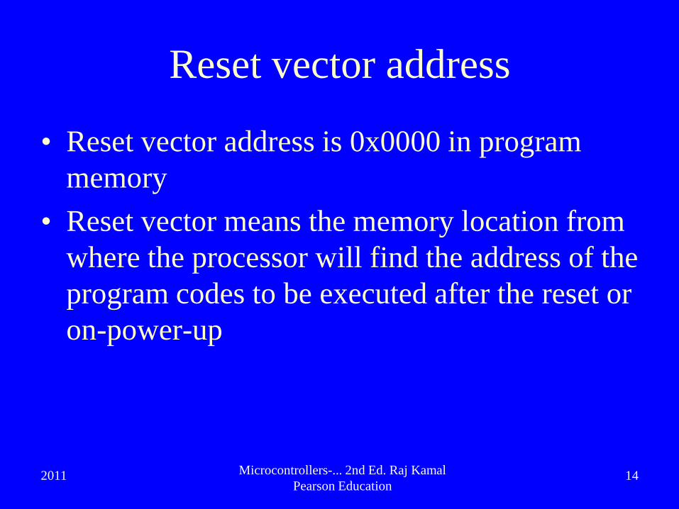
Reset vector address
• Reset vector address is 0x0000 in program
memory
• Reset vector means the memory location from
where the processor will find the address of the
program codes to be executed after the reset or
on-power-up
2011 Microcontrollers-... 2nd Ed. Raj Kamal
Pearson Education 15
Stack
• 8-level stack with 13-bit stacked at an instance
(13-bit Program counter)
2011 Microcontrollers-... 2nd Ed. Raj Kamal
Pearson Education 16
Data bus
• Data bus width 8-bit
• Interconnects the registers
• RAM
• Internal peripherals and ports A to E
2011 Microcontrollers-... 2nd Ed. Raj Kamal
Pearson Education 17
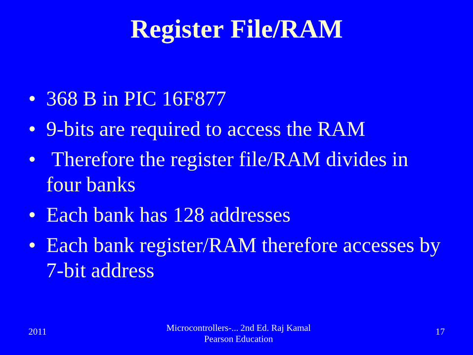
Register File/RAM
• 368 B in PIC 16F877
• 9-bits are required to access the RAM
• Therefore the register file/RAM divides in
four banks
• Each bank has 128 addresses
• Each bank register/RAM therefore accesses by
7-bit address
2011 Microcontrollers-... 2nd Ed. Raj Kamal
Pearson Education 18
RAM/File Register Select Register
FSR
• Register of 8-bits
• Provides the 8-bit address of RAM/register in
register file
• hat address is in which bank-pair, this is as per
IRP bit in the STATUS
• FSR used for indirect addressing in the
instruction
2011 Microcontrollers-... 2nd Ed. Raj Kamal
Pearson Education 19
Status Register
• 8-bits
• Bit 0, 1, 2 — C, DC/borrow and Z
2011 Microcontrollers-... 2nd Ed. Raj Kamal
Pearson Education 20
Multiplexers
• MUX
• ADDRMUX
2011 Microcontrollers-... 2nd Ed. Raj Kamal
Pearson Education 21
Peripherals
• 8-input channel 10-bit ADC
2011 Microcontrollers-... 2nd Ed. Raj Kamal
Pearson Education 22
Peripherals
• The synchronous serial port configured as 3-
wire Serial Peripheral Interface (SPI™)
option 1
• Option 2 is 2-wire Inter-Integrated Circuit
(I²C™) bus and a Universal Asynchronous
Receiver Transmitter. (USART).
2011 Microcontrollers-... 2nd Ed. Raj Kamal
Pearson Education 23
Peripherals
• Two data communication peripherals are 1-
A/E/USART (universal synchronous
asynchronous receiver and transmitter) and
1-MSSP (SPI/I2C). [MSSP (master
synchronous serial port) operate in master
SPI mode or master/slave mode I2 C.
2011 Microcontrollers-... 2nd Ed. Raj Kamal
Pearson Education 24
Timers
• There are two 8-bit timers, TMR0 and TMR2
2 × 8-bit. (Section 13.5)
• There is one 16-bit timer, TMR1 1× 16-bit.
(Section 13.5)
• There is CCP1, 2. CCP1, 2 has two
capture/compare/PWM peripherals for input
capture, out-compare and pulse width
modulation functions].
2011 Microcontrollers-... 2nd Ed. Raj Kamal
Pearson Education 25
Operations
• MCU operates at 2.0 V to 5.5V and has 40-pins.
• The clock circuit (oscillator circuit) and reset
circuits are the internal circuits.
• A XTAL is attached at two pins OSC1 and OSC2.
20 MHz Oscillator. It connects the OSC1 and OSC2
pins. OSC circuit has four options (Table 13.2):
• Reset Circuit, which connects to MCLR pin. MCLR
= 0 for the reset.
2011 Microcontrollers-... 2nd Ed. Raj Kamal
Pearson Education 26
Peripherals
• MCLR pin is also used as Vpp
(Programming voltage). The Vpp is also
applied at this pin when programming the
MCU. [Programming means writing the
program codes to internal flash memory.]
• One external interrupt is provided. It occurs
through PORTB RB0 pin.
2011 Microcontrollers-... 2nd Ed. Raj Kamal
Pearson Education 27
Brown-out Reset
• There are power-up timer, oscillator start-up
timer, power-on reset, brown out reset, in-
circuit debugger and low V programming.
[Brown-out circuit means a circuit, which
detects the voltage VDD falling below a
threshold then it resets the MCU]
Programming means writing the program
codes to internal flash memory/EPROM.
2011 Microcontrollers-... 2nd Ed. Raj Kamal
Pearson Education 28
Watchdog timer
• Can be set to reset the processor after
watched-time for finishing a task is over
2011 Microcontrollers-... 2nd Ed. Raj Kamal
Pearson Education 29
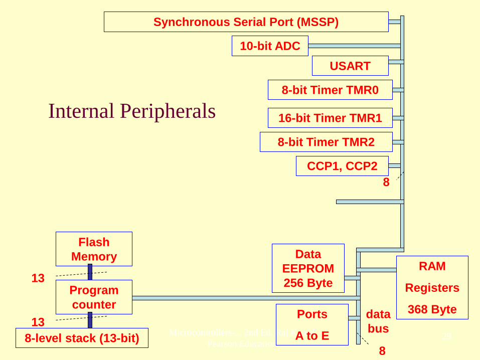
Internal Peripherals
RAM
Registers
368 Byte Ports
A to E
Data
EEPROM
256 Byte
8
data
bus
8
Flash
Memory
Program
counter
13
8-level stack (13-bit)
13
Synchronous Serial Port (MSSP)
USART
10-bit ADC
CCP1, CCP2
8-bit Timer TMR2
8-bit Timer TMR0
16-bit Timer TMR1

Summary
2011 Microcontrollers-... 2nd Ed. Raj Kamal
Pearson Education 31
We learnt
• 13-bit program counter
• 14-bit instructions
• ALU features
• 8-bit Data bus
• 14-bit Program code bus
• 13-bit Address bus
• 8-bit Status Register
2011 Microcontrollers-... 2nd Ed. Raj Kamal
Pearson Education 32
We learnt
• 8-level stack 13-bit
• RAM
• EEPROM
• Flash
• Ports
• Timers
• ADC
• Serial Communication Ports
2011 Microcontrollers-... 2nd Ed. Raj Kamal
Pearson Education 33
Internal hardware for the operations in a PIC family MCU
Internal ID, control, sequencing and reset circuits
14-bit Instruction
register
W Register (Accumulator)
RAM
Registers
368 Byte
Status Register
MUX File
Select
Register
Z, C and DC
8
8
7
ADDR
MUX
8
9
Ports
A to E
Data
EEPROM
256 Byte
Internal
Peripherals
8
data
bus
8
program
bus
14
Flash
Memory
Program
counter
13
8-level stack (13-bit)
13
direct
address
End of Lesson 02 on
Architecture of PIC 16F877


![[BAB I] Microcontroller ATMEGA8535](https://img.pdfslide.net/doc/110x75/635d9893a0f1eac29f0c45be/bab-i-microcontroller-atmega8535.jpg)


