Embed Size (px)
Citation preview

ARTICLE IN PRESS
Journal of Crystal Growth 310 (2008) 5032–5038
Contents lists available at ScienceDirect
Journal of Crystal Growth
0022-02
doi:10.1
� Corr
Institut
Tel.: +1
E-m
journal homepage: www.elsevier.com/locate/jcrysgro
MOVPE growth of transition-metal-doped GaN and ZnO forspintronic applications
S. Gupta a, W.E. Fenwick a, A. Melton a, T. Zaidi a, H. Yu a, V. Rengarajan b, J. Nause b,A. Ougazzaden c, I.T. Ferguson a,d,�
a School of Electrical and Computer Engineering, Georgia Institute of Technology, Atlanta, GA 30332, USAb Cermet Inc., 1019 Collier Road, Atlanta, GA 30318, USAc Georgia Institute of Technology, GTL 2-3 rue Marconi 57070 Metz – UMI 2958 Georgia Tech-CNRS, Franced School of Materials Science and Engineering, Georgia Institute of Technology, 778 Atlantic Drive, Atlanta, GA 30332-0250, USA
a r t i c l e i n f o
Available online 18 July 2008
PACS:
81.05.Ea
81.05.Dz
75.50.Pp
81.15.Gh
Keywords:
A3. Metalorganic vapor phase epitaxy
B1. Nitrides
B1. Oxides
B1. Zinc compounds
B2. Magnetic materials
48/$ - see front matter & 2008 Elsevier B.V. A
016/j.jcrysgro.2008.07.046
esponding author at: School of Materials Scie
e of Technology, 778 Atlantic Drive, Atlanta, G
404 385 2885; fax: +1404 385 2886.
ail address: [email protected] (I.T. Ferguson
a b s t r a c t
This paper presents a comparative study on the effect of transition metal and rare-earth doping on GaN
and ZnO by metal organic vapor phase epitaxy (MOVPE). Bulk ZnO single crystals were also analyzed in
this study. Structural and optical characterization of these materials did not show the presence of any
secondary phases or significant degradation of optical property. Magnetization measurements revealed
different magnetic behavior for ZnO-bulk crystals and thin films that have been doped with the same
transition metal, suggesting that the magnetic properties are dependent on growth conditions. Further,
it was found that with co-doping and annealing the magnetization strength and charge state of
Ga1�xMnxN can be altered. A comparative analysis on the effect of silane doping on Ga1�xMnxN and
Ga1�xFexN revealed that nanoclusters caused by spinodal decomposition are the likely cause of the
observed ferromagnetism. This paper presents the first report on MOVPE-grown Ga1�xGdxN. Room
temperature ferromagnetism is shown for Ga1�xGdxN and its magnetization strength increases with
co-doping. The results obtained in this study are promising, as it has been shown that the magnetization
can be controlled and the transition-metal charge state can be changed by modifying the MOVPE
growth conditions: applying slow growth rates, antisurfactants and employing co-dopants.
& 2008 Elsevier B.V. All rights reserved.
1. Introduction
The field of spintronics exploits both the electron spin and itscharge in order to introduce an additional degree of freedom tothe next generation of electronic devices. Spintronics allows forthe creation of multifunctional devices that enable higherinformation storage densities, higher speeds, and lower powerconsumption than today’s technology allows [1]. There has been atremendous effort to develop dilute magnetic semiconductors(DMS) that exhibit ferromagnetism at room temperature (RT)and can support spin transport and injection. These semiconduc-tors are doped with transition-metals (TM) or rare-earth (RE)elements to introduce magnetic properties into the semiconduc-tor. Most of the initial efforts in DMS were focused on developingGa1�xMnxAs, which had a maximum Curie temperature (TC) of173 K [2]. The growth efforts were then focused on the TM doping
ll rights reserved.
nce and Engineering, Georgia
A 30332-0250, USA.
).
of wide bandgap semiconductors GaN and ZnO, as a theoreticalmodel proposed by Dietl et al. [3] predicted RT ferromagnetismfor Ga1�xMnxN and Zn1�xMnxO. Although tremendous progresshas been made in developing ferromagnetic Ga1�xTM(RE)xN,the mechanism associated with the observed magnetic behaviorremains unclear, and the utility of these materials in spin-baseddevices operating at RT is yet to be demonstrated. Part ofthe confusion regarding the observed ferromagnetism in thismaterial system is due to the different growth techniques used,which result in materials with varying structural and electronicdefects. This research utilizes metal organic vapor phase epitaxy(MOVPE) as it is normally the technique applied to achievehigh-quality GaN and ZnO. Furthermore, this research investi-gates the effect of different TM to study the effect of the TMelectronic configuration and the acceptor level position on theobserved magnetization strength. Moreover, if the magnetizationis solely due to incommensurate impurities in a heterogeneoussystem, then the relative difference in these precipitates with TMdoping should point to their physical nature (e.g. Mn4N isferromagnetic with a TC of 743 K, while Fe3N has a TC of 535 K).RE doping with gadolinium has also been carried out for GaN inthis study.

ARTICLE IN PRESS
Fig. 1. High-resolution X-ray diffraction (2y�o) scans for MOVPE-grown
Ga1�xTMxN layers.
S. Gupta et al. / Journal of Crystal Growth 310 (2008) 5032–5038 5033
2. Experiment
A highly modified commercial rotating disk MOVPE reactorwith a short jar configuration was used to grow Ga1�xTM(RE)xNepitaxial films. This reactor has a specially modified flow flangeinjection system with dual injector blocks to minimize pre-reactions of the gallium and TM precursors in the transport phase.The tool provides the option of running N2 and H2 as carriergases for all metal organic sources. Ammonia, trimethylgallium,bis-cyclopentadienyl (manganese (Mn), iron (Fe), chromium (Cr))(Cp2TM), and Tris(2,2,6,6-tetramethyl-3,5-heptanedionato) gado-linium (III) are the nitrogen, gallium, Mn, Fe, Cr and gadoliniumsources, respectively. Silane and bis-cyclopentadienyl magnesiumare the sources that will be used for the n- and p-dopants,respectively. All these growths were carried out at typical GaNgrowth temperatures on top of GaN buffer layers, which are inturn grown on 200 c-plane sapphire substrates. The Ga1�xTM(RE)xNfilms ranged in thickness from 0.4 to 1mm.
The TM-doped ZnO thin films were grown in a verticalinjection MOVPE system at growth temperatures ranging from450 to 475 1C on c-plane sapphire substrates. ZnO-bulk crystalsdoped with Mn, Co, and Fe were also grown using a modified meltgrowth technique. Induction melting was used to maintain themelt at approximately 1975 1C. Samples were cut from the crystalsperpendicular to the crystallographic c-axis and double-sidepolished.
The crystalline quality and phase purity were determined byhigh-resolution X-ray diffraction (HR-XRD) using a Philips X’PertPro MRD diffractometer. Atomic force microscopy (AFM) wasperformed using a PSIA XE-100. Raman spectroscopy was doneusing a Renishaw micro-Raman system with lexc ¼ 488 nm in thebackscattering configuration. Secondary ion mass spectroscopy(SIMS) depth profiles were performed on the samples using anAtomika Instruments Ionmicroprobe A-DIDA 3000. Magneticproperties were analyzed using a Quantum Design MPMS 5Ssuper conducting quantum interference device (SQUID) attemperatures ranging from 5 to 300 K. Additional RT magneto-metry was performed using a Lakeshore 7404 vibrating samplemagnetometer (VSM). Photoluminescence (PL) data were ob-tained using a HeCd (325 nm) laser as an excitation source. Opticaltransmission experiments were performed using a 75 W XBOlamp. Electrical properties were determined by Hall effectmeasurements (EGK electronics in the van der Pauw configurationwith a 0.51 T magnet).
3. Results and discussion of Ga1�xTMxN
3.1. Structural properties of Ga1�xTMxN
MOVPE growth of Ga1�xMnxN (x: 0–2%), Ga1�xFexN (x: 0–1%)and Ga1�xCrxN (x: 0–1%) has been carried out. It must be notedthat for the Cr samples, the x values are theoretical values and arecalculated using molar flow ratios and may vary from the actualatomic composition. The films grown are specular in nature andthe Mn-doped films are, in general, reddish in color. On the otherhand, the Fe-doped films are colorless, except when co-dopedwith high levels of Si (41019 /cm3), when the color of the Fe-thinfilms turn yellow. This coloring can be attributed to theabsorptions due to the d–d transitions in the substitutionaldivalent transition-metal atoms. The Cr films tend to be milky inappearance when doped 40.002%. In all cases, Hall measure-ments indicate that the as-grown Ga1�xTMxN are semi-insulatingor weakly n-type, even in films which have been co-doped with Sidonors or Mg acceptors. In the HR-XRD scans the only reflectionsthat are visible are the basal plane reflections of the GaN layer and
the sapphire substrate (Fig. 1). No significant deviation or peaksplitting is observed in the GaN (0 0 0 2) reflections, indicatingthat the lattice parameter in the TM-doped layer is close to thatof the GaN template. This is to be expected based on the similarsizes of the Ga and TM ions, and the relatively low alloyingconcentrations. Although no direct evidence of metallic Mn, Fe orCr containing clusters was observed in HR-XRD, the presence ofsmall ferromagnetic clusters or additional phases can not be ruledout. Embedded nanocrystallites or an orientation along non c-axisdirections would not be measurable under the design configura-tion. The experimental findings do not fully preclude the existenceof these second phases below the resolution limit of the XRDinstrument.
Surface morphology studies performed by AFM on Ga1�xTMxNreveal that there is little change in the morphology of the layer atlow doping levels. However, at high-TM concentration, especiallyfor Fe- and Cr-doped GaN, the surface quality deteriorates rapidly.Annealing studies conducted on Ga1�xMnxN show the presence ofprecipitates on the surface for temperatures above 800 1C. XRDscans can attribute this phase to either MnN or Mn3GaN typephases. On the other hand, the annealed samples capped withGaN show no change in surface morphology even at elevatedtemperatures [4]. This suggests that the primary mechanism forthe decay of the thermodynamically unstable Ga1�xMnxN com-pound is through nitrogen desorption and phase rearrangement ofthe surface at the Ga1�xMnxN-to-atmosphere interface in theabsence of a reactive nitrogen environment that is present duringMBE or MOCVD growth. Annealing studies have yet to be carriedout on Ga1�xFexN and Ga1�xCrxN samples.
Raman spectroscopy studies were performed to examine theeffect of TM incorporation on the vibrational modes of the GaNlattice. These studies were recorded at RT in back scatteringgeometry. Fig. 2 shows the Raman spectra between 525 and750 cm�1 for GaN epilayers without TM doping, a Mn concentra-tion of 1.5%, and a Fe concentration of 0.7% as estimated from thegrowth conditions. The most prominent feature in all of thesescans [including for Ga1�xCrxN, where x ¼ 0.0001%, not shownhere. An extremely low Cr doping (calculated by molar flows) isused during growth as the film quality deteriorates significantly athigher concentration.] is the E2(high) and A1(LO) modes at 569

ARTICLE IN PRESS
Fig. 2. Raman spectroscopy measurements of GaN, Ga0.985Mn0.015N and Ga0.993
Fe0.007N thin films taken with a 488 nm excitation wavelength.
Fig. 3. RT PL data for GaN, Ga1�xMnxN (x ¼ 1%), and Ga1�xFexN (x ¼ 0.5%).
S. Gupta et al. / Journal of Crystal Growth 310 (2008) 5032–50385034
and 735 cm�1, respectively. This indicates that there is nosignificant degradation in crystalline quality with TM doping,and the absence of a position shift of these Raman modesindicates there is no significant strain induced.
The A1(LO) mode can be an indicator of free carrier concentra-tion, as it is known to broaden and then wash out at heavy dopinglevels in GaN. Moreover, there are no local phonon–plasmoncoupled modes in the Raman spectra, which also points to a lowcarrier concentration. Mn doping during the MOVPE growth ofGaN caused the appearance of modes at 669 cm�1 and a shoulderat 664 cm�1 which are attributed to nitrogen vacancies [5,6]. Theintensity, but not the linewidth, increases with increasing Mnconcentration. Local vibrational modes (LVMs) of the TM ions onGa sites based on the GaN E2(high) LO mode with respect to thedifference in the reduced masses might be expected around580 cm�1 [6]. However, no such mode was found in theGa1�xTMxN epilayers in this study. The identification of thesemodes may have been prevented by the dominance of the GaN E2
(high) LO mode and a mode near 576 cm�1 that was also seen inthe bare sapphire substrate, as well as the relatively lowconcentrations of TM in the Mn- and Fe-doped alloys. Further-more, for both the Mn and Fe samples there is an additional modeat 710 cm�1 which appears as a shoulder to the A1(LO) mode. Withincreasing doping concentration of either TM, this mode increasesin intensity. This mode has previously been reported in other
Raman studies of TM-doped GaN, and due to its insensitivity tothe nature of the dopant has been best attributed to a structurallyinduced disorder mode [7]. In addition to the allowed c-plane GaNRaman modes, in the Ga1�xFexN scans there appears an additionalA1(TO) mode. The appearance of this mode is likely due to arelaxation of the Raman selection rules about the Fe-induceddefects within the system and is consistent with the observeddegradation in the structural ordering of the system.
3.2. Optical properties of Ga1�xTMxN
Optical studies were conducted by PL measurements in the UVand visible spectral range in order to further understand the stateof the TM in MOVPE-grown Ga1�xTMxN epilayers (PL for Mn- andFe-doped GaN shown in Fig. 3). A typical GaN peak was seenfor all the samples which deteriorated on high-TM doping. InGa1�xMnxN a blue emission band was found to dominate the PLspectrum of films with a Mn concentration 40.5%, resulting intwo distinct peaks at 3.0 and 2.8 eV. Similarly, emission spectra forthe Ga1�xFexN revealed a broad blue band luminescence peakcentered at 2.8 eV. No new blue luminescence peaks were seen forGa1�xCrxN (for x: 0–1%) in the range of 2.7–2.8 eV, as previouslyreported for MBE-grown samples [8]. The blue luminescencefor Ga1�x(Mn/Fe)xN is probably due to a transition from nativedefects (e.g. a nitrogen vacancy) to TM-caused complexes [9]. Incomparison, almost no blue band emission but a pronouncedyellow band attributed to intrinsic gallium defects was observedin the lightly doped Ga1�xMnxN samples (xo0.5%), annealedsamples and the samples co-doped with Si. In the first case, thebehavior is assigned to the lower amount of Mn ion available tosubstitute on lattice sites, reducing the amount of Ga vacancies. Inthe latter two cases, intrinsic and extrinsic shallow donor statesare introduced, leading to a compensation mechanism of the Mn3+
acceptors. In some Fe-doped samples, emission from a yellowband likely due to defect centers in the GaN buffer layer is alsovisible. Also present in the Ga1�x(Mn/Fe)xN-doped samples is afiner structure in the near-band-edge spectra, which is mostprevalent in the Fe-doped samples.
Absorption measurements performed on Ga1�xMnxN show abroad absorption band, a spectrally diffuse line around 1.5 eV
ARTICLE IN PRESS
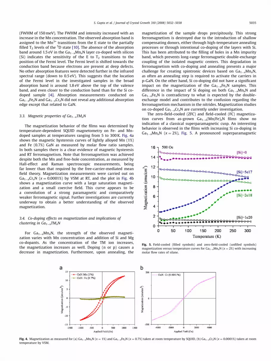
Fig. 5. Field-cooled (filled symbols) and zero-field-cooled (unfilled symbols)
magnetization versus temperature curves for Ga1�xMnxN (x ¼ 2%) with increasing
molar flow rates of silane.
S. Gupta et al. / Journal of Crystal Growth 310 (2008) 5032–5038 5035
(FWHM of 150 meV). The FWHM and intensity increased with anincrease in the Mn concentration. The observed absorption band isassigned to the Mn3+ transitions from the E state to the partiallyfilled T2 levels of the 5D state [10]. The absence of the absorptionband around 1.5 eV in the Ga1�xMnxN layer co-doped with silicon(Si) indicates the sensitivity of the E to T2 transitions to theposition of the Fermi level. The Fermi level is shifted towards theconduction band because electrons are present at deep defects.No other absorption features were detected further in the infraredspectral range (down to 0.5 eV). This suggests that the locationof the Fermi level in the investigated samples in the broadabsorption band is around 1.8 eV above the top of the valenceband, and even closer to the conduction band than for the Si co-doped sample [4]. Absorption measurements conducted onGa1�xFexN and Ga1�xCrxN did not reveal any additional absorptionedge except that related to GaN.
3.3. Magnetic properties of Ga1�xTMxN
The magnetization behavior of the films was determined bytemperature-dependent SQUID magnetometry on Fe- and Mn-doped samples at temperatures ranging from 5 to 300 K. Fig. 4ashows the magnetic hysteresis curves of lightly alloyed Mn (1%)and Fe (0.7%) GaN as measured by molar flow ratio samples.In both samples there is a clear evidence of magnetic hysteresisand RT ferromagnetism. Note that ferromagnetism was achieveddespite both the Mn and free-hole concentration, as measured byHall-effect and Raman spectroscopic measurements, beingfar lower than that required by the free-carrier-mediated meanfield theory. Magnetization measurements were carried out onGa1�xCrxN (x ¼ 0.0001%) by VSM at RT, and the plot in Fig. 4bshows a magnetization curve with a large saturation magneti-zation and a small coercive field. This curve appears to bea convolution of a strong paramagnetic and comparativelyweaker ferromagnetic signal. Further investigations are currentlyunderway to obtain a better understanding of the observedmagnetization.
3.4. Co-doping effects on magnetization and implications of
clustering in Ga1�xTMxN
For Ga1�xMnxN, the strength of the observed magneti-zation varies with Mn concentration and addition of Si and Mgco-dopants. As the concentration of the TM ion increases,the magnetization increases as well. Doping (n or p) causes adecrease in magnetization. Furthermore, upon annealing, the
Fig. 4. Magnetization as measured for (a) Ga1�xMnxN (x ¼ 1%) and Ga1�xFexN (x ¼ 0.7%
temperature by VSM.
magnetization of the sample drops precipitously. This strongferromagnetism is destroyed due to the introduction of shallowcompensating donors, either through high-temperature annealingprocesses or through intentional co-doping of the layers with Si.This has been attributed to the filling of holes in a Mn impurityband, which prevents long-range ferromagnetic double-exchangecoupling of the isolated magnetic centers. This degradation inferromagnetism with co-doping and annealing presents a majorchallenge for creating spintronic devices based on Ga1�xMnxN,as often an annealing step is required to activate the carriers inp-GaN. On the other hand, Si co-doping did not have a significantimpact on the magnetization of the Ga1�xFexN samples. Thisdifference in the impact of Si doping on both Ga1�xMnxN andGa1�xFexN is contradictory to what is expected by the double-exchange model and contributes to the confusion regarding theferromagnetism mechanism in the nitrides. Magnetization studieson co-doped Ga1�xCrxN are currently under investigation.
The zero-field-cooled (ZFC) and field-cooled (FC) magnetiza-tion curves from as-grown Ga1�x(Mn/Fe)xN films show noindication of a classical superparamagnetic cusp. An interestingbehavior is observed in the films with increasing Si co-doping inGa1�xMnxN (x ¼ 2%), Fig. 5. A pronounced superparamagnetic
) taken at room temperature by SQUID, (b) Ga1�xCrxN (x ¼ 0.0001%) taken at room

ARTICLE IN PRESS
Fig. 6. Optical data for Ga1�xGdxN (x ¼ 12%) obtained by PL measurements at
different temperatures.
S. Gupta et al. / Journal of Crystal Growth 310 (2008) 5032–50385036
splitting reminiscent of distributed sizes of magnetic nanoparti-cles can be observed in the ZFC/FC curves with increasing silanemolar flow rate. This observation can be understood by looking atthe role of silane on both the charge state of the Mn ions and theexpected behavior of a group of magnetic nanoparticles ofdistributed size.
Si has two main effects on the growth of films by MOVPE. Oneeffect is the reduction of the Mn valence state, which could resultin an effective decrease in the order parameter and the inhibitionof Mn–Mn interactions, resulting in spinodal decomposition. Thesecond is that Si on the GaN growth surface increases the localsurface energy and acts as a nucleation site for islands. This lowersthe effective diffusion length of these atoms, and hence lowers thenumber of Mn–Mn interactions which are necessary for theformation of the Mn-rich phase. This results in an overall decreasein the volume of the nanoparticles, which in turn leads to agreater fraction of this assembly with lower blocking temperature,and hence a more pronounced splitting in the ZFC/FC magnetiza-tion curves.
Although it might be expected that the Fe co-doped sampleswill also exhibit a similar decrease in the magnetization strengthbased on interaction of charged impurities, it should be noted thatthe absence of such a behavior is not surprising in light of thegrowth processes and relative concentrations of the Mn and Feused. The growth rate for the Mn-doped films in these studies was0.4mm/h, as opposed to 0.9mm/h for the Fe-doped films. Thisallows for shorter diffusion distances and fewer Fe–Fe interac-tions, which in turn results in reduced spinodal decomposition.This is consistent with the Fe films having an increased surfaceroughness. The concurrent observation of the appearance of thesuperparamagnetic phase and the optical observation of theconversion of Mn3+ ions to Mn2+ is consistent with the recentpredictions of charged controlled phase separation in thesesemiconductor alloys [11].
Fig. 7. Room temperature magnetization curves for undoped and co-doped
Ga1�xGdxN (x ¼ 12%).
4. Rare-earth doping of GaN
RE elements have also been used as dopants for spintronicsapplications. Instead of relying on the d-shells of the TM as themagnetic element, the f-electrons from the RE elements are used.There have been several reports of using RE elements foroptoelectronic applications, as it is possible to cover the entirespectrum from the infrared to the visible range due to thedifferent internal f-shell electronic transitions [12]. Despite thepromising results obtained by MBE grown Ga1�xGdxN, whichhave an extremely large magnetic moment of �4000mb/Gd [13],until this report, no MOVPE growth studies have been reportedon this material. This study carried out Gd doping under typicalGaN growth conditions to grow 0.5-mm-thick Ga1�xGdxN,with doping levels ranging from 0.5% to 12% (again, these dopinglevels have been calculated theoretically by using molar flowratios and may differ from the actual atomic concentration).The growth rate was maintained at 0.2mm/h to allow enoughtime for adatom diffusion and to prevent clustering. AlthoughGd is a large atom, HR-XRD measurements did not show anyshift in the GaN peak or the presence of any gross secondaryphase. Co-doping with silane and Mg did not cause any change inthe XRD peaks as well. Hall measurements showed that theGa1�xGdxN have typical n-GaN background carrier concentrationand that this carrier concentration can be increased by silane co-doping (e16 to e18 cm�3). Mg doping of e19 cm�3 results in adecrease in carrier concentration (measured: e15 cm�3) andthereby increases the resistivity, making it hard to get reliableHall measurements. Typical p-GaN activation steps were appliedto p-Ga1�xGdxN.
Furthermore, RT and low-temperature (LT) PL measurementswere performed on the epitaxial Ga1�xGdxN (x ¼ 12%) layers andthe results are shown in Fig. 6. In addition to the GaN emission,both RT and LT PL measurements on Ga1�xGdxN showed thepresence of peaks in the range of 3.1–3.3 eV. These peaks can beattributed to the internal transition associated with Gd3+ as hasbeen suggested in literature [14]. Moreover, a peak is seen at1.74 eV, which could possibly be attributed to Gd3+. PL investiga-tions are underway for co-doped Ga1�xGdxN films.
RT magnetization data for Ga1�xGdxN have been obtained byVSM as shown in Fig. 7. It was observed that as the Gdconcentration is increased, a transition from diamagnetism toferromagnetism occurs; the magnetization strength (for �12% Gdis 20 emu/cm3) is fairly strong as compared to the Ga1�xMnxN and

ARTICLE IN PRESS
S. Gupta et al. / Journal of Crystal Growth 310 (2008) 5032–5038 5037
Ga1�xFexN. Additionally, co-doping with silane and Mg results inan increase in magnetization strength, with the maximummagnetization obtained for the p-type Ga1�xGdxN (�500 emu/cm3
for x ¼ 12%). It is interesting to note that, in contrast with theGa1�xMnxN results, co-doping and p-type activation of Ga1�xGdxNenhanced the magnetic signal. At this time, the origin of themagnetism is not known; it is possible that as this signalincreases with co-doping it could be attributed to carrier-mediated ferromagnetism, but additional studies are needed toverify this.
This is the first MOVPE report on Ga1�xGdxN, and the resultsobtained are promising, as the material and optical propertiesappear to not degrade by the introduction of Gd. Additionally, thepresence of the large RT magnetic signal is promising and couldprove to be a beneficial DMS for spintronic applications.
5. Results and discussion of Zn1�xTMxO
An investigation was also carried out on bulk ZnO crystalsdoped with Mn, and Fe. MOVPE-grown Zn1�xNixO and Zn1�xCoxOwere also analyzed to obtain a more thorough understanding ofthe effects of TM incorporation on ZnO materials properties.
Fig. 8. Raman spectra for un-doped, Co-doped, and Mn-doped ZnO crystals
showing increasing lattice disorder with increasing TM incorporation.
5.1. Structural properties of Zn1�xTMxO
XRD 2y�o scans performed on both undoped and TM-dopedZnO showed that the as-grown material is a single crystal with nosecondary phase peaks visible. Only c-axis (0 0 2) and (0 0 4) peakswere visible in the 2y�o scans at doping levels up to 5% Mn and3% Co. The measured c-axis lattice parameter was 5.207 A in theundoped sample, but increased with Mn incorporation to a valueof 5.211 A at the 5% doping level. Crystal quality was observed todecrease with increasing TM concentration as evidenced by the2y�o linewidths, increasing from 78 arcsec in the undopedsample to 252 arcsec at 5% Mn. Peak asymmetry also increasedon the low angle side with TM doping, indicating the likelyincorporation of Mn/Co interstitial atoms into the crystal latticewith increasing doping concentration.
Raman spectra are shown for varying TM concentrations inZn1�xMnxO and Zn1�xCoxO in Fig. 8. The spectra for the undopedcrystal is shown at the bottom of the graph; the other curves areshifted for clarity. In the undoped sample, the most prevalentfeatures are the lines at 437 cm�1, which corresponds to theE2(high) mode, and at 332 cm�1, which corresponds to a 2-phononline. There is also a shoulder on the E2(high) peak at 407 cm�1,which has been previously indexed as the E1(LO) mode, and asmaller peak at 202 cm�1 corresponding to twice the E2(low)mode [15]. Upon Mn doping, the overall shape of the Ramanspectrum changes, due to the loss of symmetry conservationleading to the appearance of ‘silent’ and mixed Raman modesfrom points off the center of the Brillouin zone [16]. In Zn1�xMnxO,these modes are particularly prevalent at 522 and 580 cm�1. Themajor peaks of the undoped ZnO lattice are still also visible,indicating that the structural quality is only slightly degraded. Inaddition, there is a broad peak centered at 487 cm�1, which maybe the result of some phase segregation as a result of surfacedecomposition in manganese oxide phases. The Zn1�xCoxOshows a similar behavior, though the silent modes are lessenhanced, and there is still a strong contribution from the 437and 332 cm�1 modes of the host lattice. Also, the dominantmode in the disordered region appears to be closer to 550 cm�1
vice 522 or 580 cm�1. These findings are quite similar to reports ofRaman spectra in Zn1�xCoxO, which does exhibit ferromagneticbehavior [15].
5.2. Optical properties of Zn1�xTMxO
Transmission measurements were performed for Zn1�xMnxOand Zn1�xCoxO (Fig. 9). Optical transmission studies forZn1�xMnxO showed an apparent shift in the absorption edge tolower energies with increasing Mn concentration. Note that theapparent shift of the absorption edge to lower energies withincreasing TM concentration is not indicative of a shift in thebandedge. This behavior is due to a separate absorption featurethat is attributed to d–d transitions in the TM dopants. Similarly,transmission measurements for Zn1�xNixO showed absorptionbands between 600 and 700 nm attributed to Ni2+ d–d transitions.
5.3. Magnetic properties of Zn1�xTMxO
Magnetization behavior of these bulk crystals was also studiedusing VSM and SQUID magnetometry. The Zn1�xMnxO crystalsexhibited anti-ferromagnetic behavior, as predicted by Sato andKatayama-Yoshida [17]. Some of the Zn1�xCoxO samples showedferromagnetic behavior; however, XRD results show low-anglepeaks that may be due to grain boundaries in these samples,suggesting that this ferromagnetism may result from somemechanism at the grain boundaries. Fe was also investigated asa TM dopant in bulk ZnO crystals. RT ferromagnetic behavior was

ARTICLE IN PRESS
Fig. 9. Optical absorption spectra for bulk Zn1�xMnxO and Zn1�xCoxO showing d–d
transitions below the bandedge absorption.
S. Gupta et al. / Journal of Crystal Growth 310 (2008) 5032–50385038
observed in the Fe-doped crystal. ZFC–FC measurements per-formed by SQUID showed hysteresis behavior as well as splittingand some irreversibility in the ZFC–FC curves. Additionally, RThysteresis has been observed for Zn1�xNixO. However, the origin ofthis ferromagnetism is unclear at this time and may be related tointerface or grain boundary defects. Magnetization data forZn1�xCoxO showed the Co samples to be anti-ferromagnetic. Morework is needed to ascertain the origin of the ferromagneticbehavior of these materials and to study their usefulness in deviceapplications.
6. Conclusions
In this work, MOVPE has been applied to dope GaN and ZnOwith TM and RE elements. All the Ga1�xTM(RE)xN films growndisplayed good crystalline quality with no significant degradationin optical properties. RT ferromagnetism was shown for theGa1�xTMxN, and comparative silane co-doping studies betweenGa1�xMnxN and Ga1�xFexN suggest that the observed magnetismis due to the presence of magnetic clusters that are formed byspinodal decomposition. This research presents the first report onMOVPE-grown Ga1�xGdxN. Optical measurements show emissionpeaks attributed to Gd at 3.1–3.3 eV and 1.74 eV. Magnetizationstudies reveal RT ferromagnetism for Ga1�xGdxN and its magne-tization strength increases with co-doping, with an extremelyhigh saturation magnetization of �500 emu/cm�3 obtained for
activated p-Ga1�xGdxN epitaxial films. Transition-metal-dopedZnO bulk crystals and thin films were investigated for theirmagnetic, optical, and structural properties. Bulk crystals and thinfilms doped with the same dopant often show different magneticbehavior. This suggests that the ferromagnetism observed in thesematerials is quite sensitive to growth technique and growthconditions. Under growth conditions which lead to interfacesand/or grain boundaries, ferromagnetism is observed. Thissuggests that the ferromagnetic behavior observed in someZnO-based DMS may be due to phase separation at interfacesand grain boundaries. Overall, the results obtained in this studyare promising, as it has been shown that the magnetization can becontrolled and the TM charge state can be changed by modifyingthe MOVPE growth parameters.
Acknowledgements
This work was supported by grants from the Air Force Office ofScientific Research and the National Science Foundation. Theauthors would like to thank Dr. Z. John Zhang in the Departmentof Chemistry & Biochemistry at Georgia Tech for the SQUIDmeasurements.
References
[1] S.A. Wolf, A.Y. Chtchelkanova, D.M. Treger, IBM J. Res. Dev. 50 (2006) 101.[2] H. Ohno, Science 281 (1998) 951.[3] T. Dietl, H. Ohno, F. Matsukura, J. Cibert, D. Ferrand, Science 287 (2000) 1019.[4] M.H. Kane, M. Strassburg, A. Asghar, W.E. Fenwick, J. Senawiratne, Q. Song,
C.J. Summers, Z.J. Zhang, N. Dietz, I.T. Ferguson, Mater. Sci. Eng. B-SolidState Mater. Adv. Technol. 126 (2006) 230.
[5] W. Limmer, W. Ritter, R. Sauer, B. Mensching, C. Liu, R. Rauschenbach, Appl.Phys. Lett. 72 (1998) 2589.
[6] H. Harima, J. Phys.: Condens. Matter 16 (2004) S5653.[7] S. Shanthi, M. Hashimoto, Y.K. Zhou, S. Kimura, M.S. Kim, S. Emura, N. Hasuike,
H. Harima, S. Hasegawa, M. Ishimaru, Y. Hirotsu, H. Asahi, J. Appl. Phys. 98(2005) 013526.
[8] S. Subashchandran, S. Kimura, M.S. Kim, S. Kobayashi, Y.K. Zhou, S. Hasegawa,H. Asahi, Jpn. J. Appl. Phys. 1-Regular Brief Commun. Rev. 45 (2006) 3522.
[9] A.Y. Polyakov, N.B. Smirnov, A.V. Govorkov, N.Y. Pashkova, J. Kim, F. Ren,M.E. Overberg, G.T. Thaler, C.R. Abernathy, S.J. Pearton, R.G. Wilson,J. Appl.Phys. 92 (2002) 3130.
[10] K. Sato, P.H. Dederichs, H. Katayama-Yoshida, J. Kudrnovsky, Physica B340–342 (2003) 863.
[11] T. Dietl, Nat. Mater. 9 (2006) 673.[12] A.J. Steckl, J.C. Heikenfeld, D.S. Lee, M.J. Garter, C.C. Baker, Y.Q. Wang, R. Jones,
IEEE J. Sel. Top. Quantum Electron. 8 (2002) 749.[13] S. Dhar, L. Perez, O. Brandt, A. Trampert, K.H. Ploog, J. Keller, B. Beschoten,
Phys. Rev. B (Condens. Matter Mater. Phys.) 72 (2005) 245203.[14] Z. Lipinska, M. Pawlowski, H. Zolnierowicz, A. Wysmolek, M. Palczewska,
M. Kaminska, A. Twardowski, M. Bockowski, I. Grzegory, Acta Phys. Pol.A 110 (2006) 243.
[15] J.M. Calleja, M. Cardona, Phys. Rev. B 16 (1977) 3753.[16] F.J. Manjon, B. Mari, J. Serrano, A.H. Romero, J. Appl. Phys. 97 (2005) 053516.[17] K. Sato, H. Katayama-Yoshida, Semicond. Sci. Technol. 17 (2002) 367.


