Embed Size (px)
Citation preview
X i l «*.«'» ' N l -1
OFFSET REDUCTION AND THREE-DIMENSIONAL FIELD SENSING WITH MAGNETOTRANSISTORS
1 i « > - i * r' - i h H . - j * «
OFFSET REDUCTION AND THREE-DIMENSIONAL FIELD SENSING WITH MAGNETOTRANSISTORS
Offsetreductie en driedimensionale veldmetin met magnetotransistoren
Proefschrift
ter verkrijging van de graad van doctor aan de Technische Universiteit Delft, op gezag van de Rector Magnificus, prof.dr. J.M. Dirken, in het openbaar te verdedigen ten overstaan van een commissie aangewezen door het College van Dekanen, op donderdag 10 december 1987, te 14.00 uur
door
Srdjan Kordic
elektrotechnisch ingenieur geboren te Belgrado, Joegoslavië T R CÜSS
1593
Dit proefschrift is goedgekeurd door de promotor prof.dr.ir. S. Middelhoek
kW*fK--*-"'wl irSfc-üê

Bismilahir-rahmanir-rahim!
I call as a witness, the inkwell and the quill, and everything they have written; I call as a witness the wavering twilight of the evening, the night and all that it awakens; I call as a witness the moon when it mellows and the dawn when it emerges; I call as a witness Judgement Day, and the soul chastising itself; I call as a witness Time, the beginning and the end of everything;
— that man is always at a loss.
The Koran Adapted by M. Selimovic in "The Dervish and Death"
To Nedja and Mara, for they willed this book, and to Julija, who lived through it.

"r "*■% ■** JÏ * . fr • * ï « H A
When I was seventeen my teachers were so stupid that I could hardly bear them, but by the time I was twenty-four I was amazed to see how much they had learned in seven years.
Mark Twain - adaptation
PREFACE
This book represents the Ph.D. thesis resulting from the research which I have been carrying out during the past four years at the Electrical Engineering Department of the Delft University of Technology. It can roughly be divided in two parts: the first part deals with the causes of offset and its reduction in silicon magnetic-field sensors, while in the second part a family of magnetic-field sensors which are sensitive to all three components of the field vector (3-D sensors) is examined. The work on offset and its reduction has been performed in cooperation with Philips - The Netherlands. 3-D sensors have been developed for Océ - The Netherlands.
In Chapter 1 I have tried to justify the use of silicon as a material for sensors. A review of silicon-based magnetic-field sensors is given in Chapter 2 along with an extensive reference list which, I hope, will spare the reader working on silicon magnetic sensors many tedious visits to the library. The first part of Chapter 3 deals with the causes of offset in magnetotransistors, Hall plates and other magnetic sensors. A definition of offset is given and ways of reducing it are discussed. The second part of Chapter 3 deals with the sensitivity-variation offset-reduction method developed at Delft University, which forms an addition to already existing techniques of offset reduction. In Chapter 4 the influence of high electric fields on the Hall angle is discussed, which is important for the understanding of the magnetotransistor sensitivity characteristics presented
vii
V l l l Preface
in Chapter 3. Finally, in Chapter 5 - the last chapter - a new class of multicollector devices developed at Delft University, which are sensitive to the full magnetic-field vector, is presented.
I have already published many of the aspects of silicon magnetic-field sensors discussed in this thesis, while a few manuscripts are in preparation. These papers are listed at the end of the thesis.
The devices in this thesis were manufactured in the University's IC-Workshop, and I am deeply indebted to its staff members: J. Groeneweg, E. J. G. Goudena, F. J. de Jong, E. J. Linthorst, W. de Koning, Ir. P. K. Nauta, E.Smit, Ir. J. M. G. Teven, W. Verveer and L. Wubben. Without their dedicated work most of this thesis would have been reduced to pure speculation without any experimental proof. I am further indebted to my students: Ir. Y.Xing, Ir. D. W. de Bruin, P. J. A.Munter, Ir. J. M. van den Boom and H. Mol, whose enthusiastic work tied up many loose ends. I am also grateful to Ir. J. H. H. Janssen of Philips and Th. Siebers of Océ for their support of my work and many fruitful discussions. The technical support of F. Schneider and P. C. M. van der Jagt is greatly appreciated. The many excellent drawings have been furnished by W. J. P. van Nimwegen and J. W.Muilman of the Electrical Engineering's Drafting Department. Photographs have been made by W. G. M. M. Straver, J. C. Schipper and J. C. van der Krogt. I am very much indebted to Mrs. S. Massotty, who corrected the manuscript under intense time pressure and never laughed at my sometimes ridiculous spelling, and to Miss. V. Kordié, who reviewed the final version.
The work on this thesis was supported by the Foundation for Technical Sciences (Stichting voor Technische Wetenschappen - STW) under contract DEL 46.0580. The project has also been receiving significant financial support from Philips, Delft University Fund (DHF) and Océ. Royal Dutch Shell has made a contribution to the costs of a trip to Tokyo, where the 4th International Conference on Sol id-State Sensors and Actuators was held.
Finally, I wish to express my gratitude to my thesis advisor, Prof. S. Middelhoek, because his door was always open.
S. Kordic Delft August 1987
CONTENTS
Chapter 1 Introduction 1
1.1 Information-Processing Systems 2 1.2 Silicon Integrated Sensors 3 1.3 Magnetic-Field Sensors and Their Applications 5 1.4 Properties of Magnetic Sensors 9
Chapter 2 Silicon Magnetic-Field Sensors 15
2.1 Introduction 15 2.2 The Basic Physical Principles 17 2.3 Hall Plates and Related Devices 20
2.3.1 Bulk Hall Devices 22 2.3.2 FET Hall Devices 25 2.3.3 Hall Plates Incorporated in an IC 27
2.4 Magnetotransistors 30 2.4.1 Lateral Magnetotransistors 33 2.4.2 Vertical Magnetotransistors 37
2.5 Carrier-Domain Magnetic-Field Sensors 41 2.6 Magnetodiodes 45 2.7 Conclusions 47
Chapter 3 Offset Reduction in Magnetic-Field Sensors 57
3.1 Introduction 57 3.2 Causes of Offset and its Reduction 62
3.2.1 Magnetotransistors 62 3.2.2 Hall Plates 70 3.2.3 Other Magnetic Sensors 84
3.3 Sensitivity-Variation Offset-Reduction Method 85 3.3.1 The Basic Principles 85 3.3.2 The Dual-Col lector Vertical Magnetotransistor 91 3.3.3 Hall Plates 98 3.3.4 Magnetoresistors 122
ix
X Contents
3.4 Electronic Implementation of the Sensitivity-Variation Offset-Reduction Method 124
3.4.1 The Principle of Operation 124 3.4.2 The Electronic Implementation 127 3.4.3 Theory of the Sinusoidal Excitation
of the Sensor 131 3.4.4 Experimental Results 138
3.5 Conclusions 141
Chapter 4 Hall Angle at High Electric Fields 147 4.1 Introduction 147 4.2 The Electric-Field Strength 151
4.2.1 Depletion Layer 151 4.2.2 The Energy Distribution Function 152 4.2.3 The Electron Temperature 153
4.3 The Hall Angle vs. Electron Temperature 154 4.4 The Total Hall Angle 161 4.5 Conclusions 171
Chapter 5 3-D Magnetic-Field Sensors 175 5.1 Introduction 175 5.2 The Elementary 3-D Magnetotransistor 178 5.3 Increasing the Z Sensitivity 192 5.4 Sensor Mounting and Other 3-D Sensitive Structures 202 5.5 Conclusions 213
Summary 219
Samenvatting 223
About the Author 227
List of Publications and Presentations 229
List of Symbols 231
D INFORMATION-PROCESSING SYSTEMS
D SILICON INTEGRATED SENSORS
D MAGNETIC-FIELD SENSORS AND THEIR APPLICATIONS
D PROPERTIES OF MAGNETIC SENSORS
If you must make a mistake, let it be a new one.
1
INTRODUCTION
The past 30 years have been a period of a continuous microelectronic revolution. Since 1959 the integrated-circuit complexity has been doubling every year. At the same time the performance/price ratio has shown a dramatic increase: a factor of 1018 for digital signal processing and 1012 for analog circuits. In comparison, if the aircraft industry had made the same progress today's Boeing 767 would be able to fly around the world in 20 minutes while consuming only 20 liters of fuel; at the same time the aircraft would cost only $ 500 [1.1].
This tremendous improvement in the performance/price ratio has made the proliferation of microelectronics into non-electronic products and industries possible. Today, as a result of the unprecedented, rapid development of microelectronics, electronic watches, games, sewing machines, personal computers, etc. are commonplace. The advent of microelectronics into traditionally non-electronic industries is, however, seriously impeded by the lack of appropriate input transducers (or sensors) having a performance/price ratio comparable to the microelectronic circuits [1.2]. With the exception of military and professional applications where the cost aspect does not seem to be of primary importance, in the vast majority of the consumer goods in which information is processed
1
2 Introduction
electronically the input side of the system is usually formed by very simple sensors such as push buttons. The fact that a large number of products such as mechanical scales, clinical thermometers, rotating vane flow meters, etc. still do not use any form of electronic information processing indicates that there is still a lot of room for innovation and new products. However, the lack of low-cost, dependable and mass-produced sensors, which are at the same time immune to hostile environments and do not exhibit significant drift of the characteristics, is a problem which should be solved before further penetration of electronics into more traditional markets can take place.
RAD —
MECH —
THERM
MAG —
CHEM —
INPUT
TRANSDUCER 1 SENSOR)
EL MODIFIER
EL OUTPUT
TRANSDUCER /ACTUAT0R\ \ DISPLAY J
r— RAD
— MECH
— MAG
— CHEM
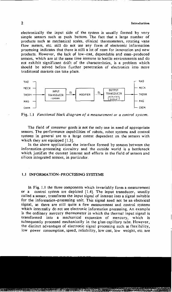
Fig. 1.1 Functional block diagram of a measurement or a control system.
The field of consumer goods is not the only one in need of appropriate sensors. The performance capabilities of robots, robot systems and control systems in general are to a large extent dependent on the sensors with which they are equipped [1.3].
In the above applications the interface formed by sensors between the information-processing circuitry and the outside world is a bottleneck which justifies the current interest and efforts in the field of sensors and silicon integrated sensors, in particular.
1.1 INFORMATION-PROCESSING SYSTEMS
In Fig. 1.1 the three components which invariably form a measurement or a control system are depicted [1.4]. The input transducer, usually called a sensor, transforms the input signal of interest into a signal suitable for the information-processing unit. This signal need not be an electrical signal, as there are still quite a few measurement and control systems which internally do not use electronic information processing. An example is the ordinary mercury thermometer in which the thermal input signal is transformed into a mechanical expansion of mercury, which is subsequently processed mechanically in the glass capillary tube. However, the distinct advantages of electronic signal processing such as flexibility, low power consumption, speed, reliability, low cost, low weight, etc. are
Silicon Integrated Sensors 3
the reasons that this form of information processing has become the most attractive one. As a consequence, sensors which transform the signal of the measurand into an electrical signal suitable for electronic information processing are becoming increasingly important, and we will concentrate on these only.
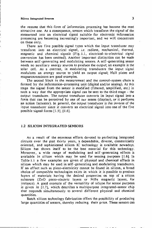
There are five possible signal types which the input transducer may transform into an electrical signal, i.e. radiant, mechanical, thermal, magnetic and chemical signals (Fig. 1.1, electrical-to-electrical signal conversion has been omitted). Another important distinction can be made between self-generating and modulating sensors. A self-generating sensor needs no auxiliary energy sources to produce the output; an example is the solar cell. As a contrast, in modulating transducers the input signal modulates an energy source to yield an output signal; Hall plates and magnetotransistors are good examples.
The second block in the measurement and the control-system chain is formed by the information-processing unit (digital and/or analog). At this stage the signal from the sensor is modified (filtered, amplified, etc.) in such a way that the appropriate signal can be sent to the third stage - the output transducer. The output transducer converts its input signal into a form that can be perceived by one of our senses (display), or it performs an action (actuator). In general, the output transducer is the inverse of the input transducer since it converts an electrical signal into one of the five possible signal forms [1.5], [1.6].
1.2 SILICON INTEGRATED SENSORS
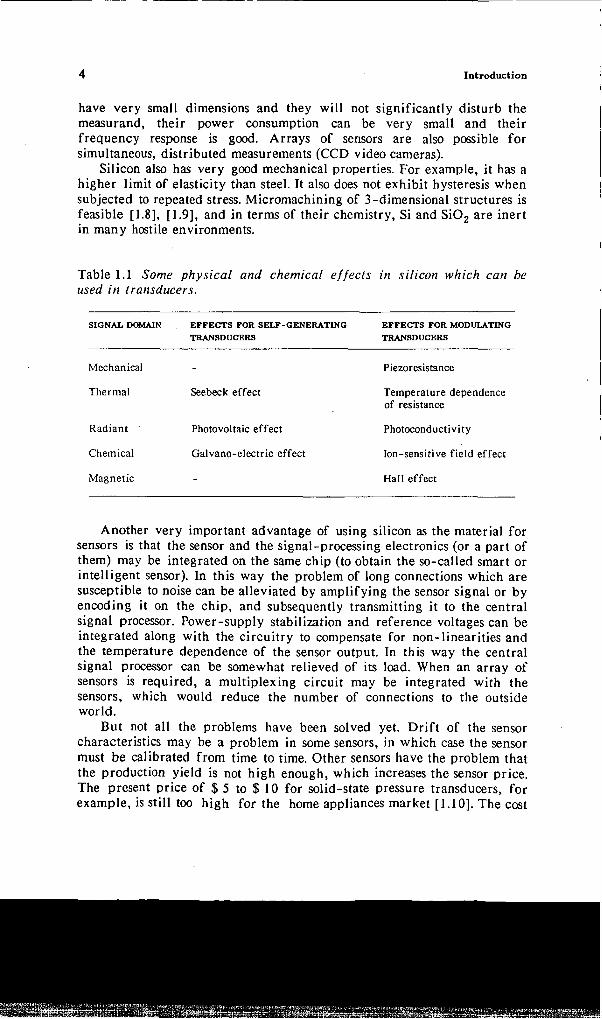
As a result of the enormous efforts devoted to perfecting integrated circuits over the past thirty years, a dependable, diverse, commercially oriented, and sophisticated silicon IC technology is available nowadays. Silicon has shown itself to be the best material for this technology. Moreover, a wide range of modulating and self-generating effects is available in silicon which may be used for sensing purposes [1.6]. In Table 1.1 a few examples are given of physical and chemical effects in silicon which may be used in self-generating and modulating transducers. If an effect such as piezo-electricity cannot be found in silicon, a broad choice of compatible technologies exists in which it is possible to produce layers of materials having the desired properties on top of a silicon substrate (ZnO piezo-electric layers or NiFe magnetic layers, for instance). A good example of the versatility of silicon for sensor purposes is given in [1.7], which describes a multipurpose integrated-sensor chip that responds simultaneously to several different physical and chemical quantities.
Batch silicon technology fabrication offers the possibility of producing large quantities of sensors, thereby reducing their price. These sensors can
4 Introduction
have very small dimensions and they will not significantly disturb the measurand, their power consumption can be very small and their frequency response is good. Arrays of sensors are also possible for simultaneous, distributed measurements (CCD video cameras).
Silicon also has very good mechanical properties. For example, it has a higher limit of elasticity than steel. It also does not exhibit hysteresis when subjected to repeated stress. Micromachining of 3-dimensional structures is feasible [1.8], [1.9], and in terms of their chemistry, Si and Si02 are inert in many hostile environments.
Table 1.1 Some physical and chemical effects in silicon which can be used in transducers.
SIGNAL DOMAIN
Mechanical
Thermal
Radiant
Chemical
Magnetic
EFFECTS FOR SELF-GENERATING TRANSDUCERS
-
Seebeck effect
Photovoltaic effect
Galvano-electric effect
-
EFFECTS FOR MODULATING TRANSDUCERS
Piezoresistance
Temperature dependence of resistance
Photoconductivity
Ion-sensitive field effect
Hall effect
Another very important advantage of using silicon as the material for sensors is that the sensor and the signal-processing electronics (or a part of them) may be integrated on the same chip (to obtain the so-called smart or intelligent sensor). In this way the problem of long connections which are susceptible to noise can be alleviated by amplifying the sensor signal or by encoding it on the chip, and subsequently transmitting it to the central signal processor. Power-supply stabilization and reference voltages can be integrated along with the circuitry to compensate for non-linearities and the temperature dependence of the sensor output. In this way the central signal processor can be somewhat relieved of its load. When an array of sensors is required, a multiplexing circuit may be integrated with the sensors, which would reduce the number of connections to the outside world.
But not all the problems have been solved yet. Drift of the sensor characteristics may be a problem in some sensors, in which case the sensor must be calibrated from time to time. Other sensors have the problem that the production yield is not high enough, which increases the sensor price. The present price of $ 5 to $ 10 for solid-state pressure transducers, for example, is still too high for the home appliances market [1.10]. The cost
Magnetic-Field Sensors and Their Applications 5
of development and processing requires large quantities to be produced and sold. The production yield must be reasonably high to keep the price low. Packaging may present other difficulties. The sensor may have to operate in a hostile environment in which the usual IC encapsulation is inadequate.
In some cases the technological requirements for the sensor may be incompatible with the signal-conditioning circuit technology when a smart sensor is desirable. Where a smart sensor can be realized, unwanted feedback loops may be created (temperature feedback, for example). Silicon can also be used between -50° C and +150 C only, and a smart sensor will always need a power supply.
These problems are the reason why integrated silicon sensors are not yet widely used and why at the present there is intensive research in that field. A comprehensive up-to-date review of solid-state sensors can be found in [1.11].
1.3 MAGNETIC-FIELD SENSORS AND THEIR APPLICATIONS
One of the five possible signal conversions to the electrical domain, as we have seen in the previous section, is the conversion of magnetic signals into electrical signals. A magnetic-field sensor is an input transducer which converts a magnetic signal into a useful electric signal. Magnetic phenomena can be described by a few fundamental quantities: the magnetic-field strength H, the magnetic-flux density B, and the magnetization M. Since this thesis deals with non-magnetic media only (just as the one in [1.12]) where the magnetization is zero, the relationship between the magnetic-flux density and the magnetic-field strength becomes:
B = n0H (1.1)
y,0 is the permeability of vacuum. Because the relationship between these two quantities is so simple, an explicit distinction between the two will be made in this thesis only when it is essential. If it does not make a difference whether we are dealing with the magnetic-flux density B or the magnetic-field strength H, both will be referred to as the magnetic field.
The use of magnetic-field sensors can be classified into direct and indirect applications [1.12]. Direct applications implies that one is interested only in the magnitude and/or the direction of the magnetic-field vector itself. Examples of direct applications are [1.12], [1.13]:
6 Introduction
Field measurements (field mapping) on magnetic materials, devices or apparatus.
Earth magnetic-field measurements for navigational or geological purposes.
Readout of magnetic memories (disk, tape and bubble memories) [1.14].
Recognition of magnetic ink patterns of bank notes and credit cards.
sensor IC
coil spring
Fig. 1.2 A non-contact switch used in solid-state keyboards. A permanent magnet on the plunger operates the switch.
An example of direct field measurements is the characterization of the fringe field generated by magnetic recorder heads [1.15]. The quantities of interest here include the field strength, orientation and its spatial variation. Although on a different scale, the same quantities are also of interest in high-energy and elementary-particle physics. Another illustration of direct field measurement application is the necessary
Magnetic-Field Sensors and Their Applications 7
mapping of the magnetic field generated by magnetic devices in copying machines [1.16]. These devices may be used to apply toner having magnetic properties to the paper [1.17].
Measurement of the earth magnetic field for navigational reasons is very probably the earliest example of an application of a magnetic-field sensor. In the 12th century, mariners in China and Europe independently made the discovery that a piece of lodestone, a naturally occurring strongly magnetic variety of the mineral magnetite, floated on a stick in water, tends to align itself so as to point in the direction of the Pole Star [1.18]. In this case the compass magnetic needle is the sensor which transforms the earth magnetic signal (orientation) into mechanical rotation. Only the measurement of the direction of the magnetic-field vector is desired in this case, while in the case of geological and geophysical applications the measurement of the magnitude of the field vector is needed, too.
In contrast to the direct uses, where the magnetic field itself is the quantity of interest, in the indirect applications a non-magnetic quantity is measured, while the magnetic field serves as an intermediary. The non-magnetic measurand is magnetically encoded, and the magnetic signal becomes the information carrier of the original non-magnetic quantity [1.12]. Some examples are:
Linear displacement or position measurements. Angular displacement or position measurements. Metal detection. Electrical current measurements. Electrical power measurements (watt meters). Analog multiplication. Modulator. Galvanic isolation.
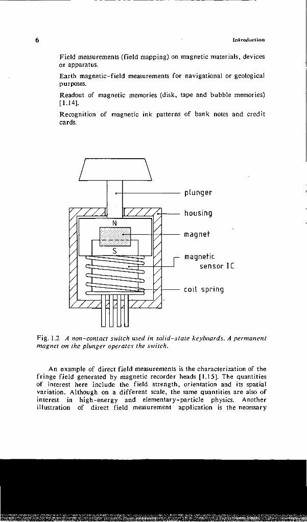
In the first two examples a mechanical quantity is being measured by using a magnetic signal as an information carrier. This transformation may be desirable if mechanical contact is to be avoided. A magnetic signal carrier may also be preferred to other possibilities such as an optical signal carrier, because of its higher resistance to contamination. In the case of the linear and angular position measurements the relative position between the moving parts is determined by attaching a magnetic source (a permanent magnet, for example) on one part, and the magnetic sensor on the other one [1.19], [1.20]. The output signal of the sensor will then depend on the relative position of the sensor and the magnet, which makes position
8 Introduction
sensing possible. An example of linear position sensing is portrayed in Fig. 1.2, which is one key of a solid-state keyboard [1.21], [1.22]. The magnetic sensor IC detects the position of the plunger by means of a permanent magnet that is affixed to the plunger. Compared to mechanical switches, the magnetic switch is less sensitive to contamination and does not wear out as fast.
Fig. 1.3 A Hall plate used to detect the position of a permanent-magnet rotor. The switching of the current in the stator coils is performed electronically, without the commutators.
Another indirect application of magnetic-field sensors can be found in the brushless electromotors depicted in Fig. 1.3, which is an illustration of angular position sensing. In this case the position of the permanent magnet rotor is sensed by means of a magnetic-field sensor and not by commutators [1.23]-[1.25]. The signal from the sensor is subsequently used to time the switching of the current in the stator coils. As no wear-and-tear of the commutators is present, the life span of such a motor is longer, while at the same time better electronic control is possible, and contamination, in contrast to optical sensors, is less important. Brushless electromotors can nowadays be found in such items as video recorder heads and (floppy-) disk drives.
Properties of Magnetic Sensors 9
Similarly, magnetic-field sensors can be used to determine the position of a crankshaft and other moving parts in engines [1.26]-[1.28]. If the position of the shaft is encoded magnetically, non-contact sensing can take place with all the above-mentioned benefits, and the ignition point, for one thing, can be accurately determined. A magnetic encoder used in servo-motor systems is described in [1.29] and [1.30].
In traffic detection it is possible to measure the variation in the earth's magnetic field caused by a passing ferromagnetic vehicle. Another example of metal detection which is often used is the change in the LC product caused by the presence of a metallic body.
A current of 1 A produces a magnetic field of about 100 y.T at the surface of the conductor [1.13]. By measuring this field one can get an idea of the magnitude of the current through the conductor without interrupting the current flow. The field associated with a current in a conductor can also be used for power measurements [1.31].
Figure 1.4 depicts the last three possible applications of the magnetic sensors. The current /M in the coil is proportional to the magnetic-flux density B which is generated by the coil. The output signal of the sensor VH is, in the case of a Hall plate, which is used in the example of Fig. 1.4, proportional to the product of B and the bias current of the sensor /s. Consequently, the output signal is proportional to the /M/8 product - and we have analog multiplication or modulation. At the same time, the two circuits are fully galvanically separated.
1.4 PROPERTIES OF MAGNETIC SENSORS
Each of the applications of magnetic sensors discussed in the preceding section imposes its own demands on the electronic, magnetic and mechanical properties of the transducer. The sensor should be able to cover the entire range of the field magnitudes for that particular application. A large magnitude of the sensor's output signal per unit of the measurand -high sensitivity - is one of the most usual requirements imposed on sensors in general. If the output signal of the sensor is too low to be useful by itself, which is often the case with solid-state sensors, it may be necessary to amplify the signal. A limit to a maximum practical amplification, however, is determined by the signal-to-noise ratio (magnetic resolution) of the sensor. There is not much sense in amplifying a signal (without filtering) which is drowned in noise.
Unlike the non-contact switch used in the solid-state keyboards, where only a two-state (on/off) output is required, most of the linear and angular position sensing applications require a high degree of linearity of the output signal as a function of the measurand. A low offset value is another characteristic which is also often desired.
Because of the inherent advantages the integrated circuits technology
10 Introduction
has to offer, the size and the weight of silicon solid-state magnetic sensors will usually not present a problem, but the mere possibility of realizing small structures, however, seems to lead to even more stringent demands on, for example, the spatial resolution of a magnetic measurement [1.32].
o
. I,
1 )B
Hall plate
X , !
f
i/u
Fig. 1.4 The output signal of the Hall plate Vn is proportional to the /M/s product.
Last but not least, the problem of packaging will be mentioned. Unlike electronic systems and circuits which are usually kept in favorable and friendly environments, a sensor must by its very nature be in "contact" with the measurand. The sensor package, therefore, must satisfy two requirements:
It may not hinder or alter the measurand. The package must shield the sensor from everything that could adversely influence the sensor's performance.
A magnetic-field sensor used, for instance, for crankshaft angle position sensing in combustion engines has to operate in an exceptionally hostile environment. The sensor would be subjected to chemical contamination (humidity, oil, etc.), large temperature swings, and
Properties of Magnetic Sensors 11
mechanical vibrations. Good encapsulation of the sensor is in this case of the utmost importance [1.33].
In the brushless electromotor application the size and the shape of the sensor's package may clash with the small dimensions of contemporary motors [1.34]. The packaging aspect of sensor research in general has not received its due attention, which is evidenced by the practically non-existent literature on this subject.
In the following a list of noteworthy criteria is compiled, which could be used to match an application with a potential sensor:
Magnetic range.
Magnetic sensitivity.
Orientation of the sensitivity with respect to.the plane of the chip.
Magnetic resolution.
Spatial resolution of the measurements.
Capability of measuring more than one component of the magnetic vector.
Linearity.
Frequency response.
Offset.
Temperature dependence of the characteristics.
Temperature range in which the sensor functions.
Drift of the characteristics.
Size of the sensor.
Weight of the sensor and the package.
Power consumption and dissipation.
Reliability.
Lifespan.
Manufacturing and packaging cost.
Packaging - shielding from the environment.
12 Introduction
REFERENCES
1.1] A.Gupta and H.-M. D. Toong, The special issue on personal computers, Proc. IEEE, vol. 72, 1984, pp. 243-245.
1.2] S.Middelhoek, Integrated sensors, Proc. 3rd Sensor Symp., Japan, 1983, pp. 1 -10.
1.3] A. Dumbs and J.Hesse, Sensor problems in robotics, Sensors and Actuators, vol.4, 1983, pp. 629-639.
1.4] S. Middelhoek, S. Kordic and D. W. de Bruin, Silicon: a promising material for sensors, SEV-Bulletin, vol. 5, 1985, pp. 253-257.
1.5] S. Middelhoek and D. J. W. Noorlag, Three-dimensional representation of input and output transducers, Sensors and Actuators, vol. 2, 1981/82, pp. 29-41.
1.6] S. Middelhoek and D. J. W. Noorlag, Silicon micro-transducers, J. Phys. E: Sci. Instrum., vol. 14, 1981, pp. 1343-1352.
1.7] D. L. Polla, R. S. Muller and R. M. White, Integrated multisensor chip, IEEE Electron Device Lett., vol. EDL-7, 1986, pp. 254-256.
1.8] S. Middelhoek, J. B. Angell and D. J. W. Noorlag, Microprocessors get integrated sensors, IEEE Spectrum, vol. 17, 1980, pp. 42-46.
1.9] J. B. Angell, S.C.Terry and P. W. Barth, Silicon micromechanical devices, Scientific American, vol. 248, 1983, pp. 36-47.
1.10] R.Allen, Sensors in silicon, High Technology, vol.4, 1984, pp. 43-50. 1.11] Solid-State Sensors: State-of-the-Art Reviews 1986, Parts I and II,
S. Middelhoek (ed.), Sensors and Actuators, vol. 10, 1986. 1.12] V. Zieren, Integrated silicon multicollector magnetotransistors, Ph.D. thesis,
Delft University of Technology, 1983. 1.13] H. P. Baltes and R.S. Popovic, Integrated semiconductor magnetic field sensors,
Proc. IEEE, vol.74, 1986, pp. 1107-1132. 1.14] A. W. Vinal, Considerations for applying solid state sensors to high density
magnetic disk recording, IEEE Trans. Magn., vol. MAG-20, 1984, pp. 681-686.
1.15] V. Zieren, W. G. M. van den Hoek and J. de Wilde, Submicron magnetoresistive sensors for the measurement of magnetic recording head fields, Proc. Sensors and Actuators Symp., Enschede, The Netherlands, 1984, pp. 61-66.
1.16] S. Kordic, P. J. A. Munter and P.J.French, Simultaneous measurements of 3-D magnetic fields in close proximity to the sample with a single silicon sensor, 4th Int. Conf. on Solid-State Sensors and Actuators, Tokyo, Japan, 1987, Dig. Techn. Papers, pp. 527-531.
1.17] Th. Siebers, Océ - The Netherlands, private communication. 1.18] The New Encyclopaedia Britannica, Encyclopaedia Britannica, Inc., Chicago,
IL, USA, 1985. 1.19] W. D. McCall Jr. and E.J.Rohan, A linear position transducer using a magnet
and Hall effect devices, IEEE Trans. Instrum. Measur., vol. IM-26, 1977, pp. 133-136.
1.20] Y. Netzer, A very linear noncontact displacement measurement with a Hall-element magnetic sensor, Proc. IEEE, vol.69, 1981, pp. 491-492.
1.21] J. T. Maupin and M. L. Geske, The Hall effect in silicon circuits, in C. L. Chien and R. Westgate (eds.), The Hall Effect and its Applications, Proc. of the Commemorative Symp., Baltimore, MD, USA, 1979, Plenum Press, New York, 1980, pp. 421-445.
1.22] J.A.Blackburn and S. Vik, Computer menu tablet employing Hall-effect switches, Rev. Sci. Instrum., vol. 55, 1984, pp. 1358-1359.
1.23] T. Kenjo and S. Nagamori, Permanent-magnet and Brushless DC Motors, Clarendon Press, Oxford, 1985.
References 13
1.24] J.F. Wise Jr. and F. O.Simons Jr., A brushless Hall generator dc servomotor, IEEE Trans. Industrial Elec. Control Instrum., vol. IECI-21, 1974, pp. 75-77.
1.25] Y. Kanda, M. Migitaka, H. Yamamoto, H.Morozumi, T. Okabe and S. Okazaki, Silicon Hall-effect power ICs for brushless motors, IEEE Trans. Electron Devices, vol. ED-29, 1982, pp. 151-154.
1.26] R. W. Holmes, Improved crankshaft sensing techniques, Proc. 2nd Int. Conf. on Automotive Electronics, London, UK, 1979, pp. 155-158.
1.27] L. Halbo and J. Haraldsen, The magnetic field sensitive transistor: a new sensor for crankshaft angle position, Congress and Exposition of the Society of Automotive Engineers, Detroit, MI, USA, 1980.
1.28] J. D. Rickman Jr., Magnetic methods of sensing shielded part motion, Congress and Exposition of the Society of Automotive Engineers, Detroit, MI, USA, 1982, Proc. pp. 1-9.
1.29] S. Kawamata, T. Takahashi, K.Miyashita and K. Tamura, Magnetic rotary encoder with high resolution, Proc. 4th Sensor Symp., Japan, 1984, pp. 277-280.
1.30] T. Takahashi, S. Kawamata, K.Miyashita and H. Kanai, Magnetic rotary encoder with zero reference detection function, Proc. 4th Sensor Symp., Japan, 1984, pp. 281-284.
1.31] K. Matsui, S. Tanaka and T. Kobayashi, GaAs Hall generator application to a current and watt meter, Proc. 1st Sensor Symp., Japan, 1981, pp. 37-40.
1.32] S. Kordic, Sensitivity of the silicon high-resolution 3-dimensional magnetic-field vector sensor, Int. Electron Devices Meet., Los Angeles, CA, USA, 1986, IEDM Techn. Dig., pp. 188-191.
1.33] J. M. Giachino, Ford Motor Co., private communication. 1.34] J. H. H. Janssen, Philips - The Netherlands, private communication.

14
D INTRODUCTION
D THE BASIC PHYSICAL PRINCIPLES
D HALL PLATES AND RELATED DEVICES
D MAGNETOTRANSISTORS
D CARRIER-DOMAIN MAGNETIC-FIELD SENSORS
D MAGNETODIODES
D CONCLUSIONS
There is only one thing in the world worse than being talked about, and that is not being talked about.
Oscar Wilde
2
SILICON MAGNETIC-FIELD SENSORS
2.1 INTRODUCTION
The birth of solid-state magnetic sensors can be traced all the way back to 1879 to the discovery of the Hall effect by E.H. Hall [2.1], [2.2] and the resistance change of a material in a magnetic field discovered in 1856 by W. Thomson. Hall, then a graduate student at Johns Hopkins University in Baltimore, was able to measure a cross-current in a thin gold layer on glass under the influence of a magnetic field. This was the proof that the magnetic field exerts a force on the electric current in a conductor and not on a conductor itself, as was claimed by Maxwell. Since then there was almost no activity in the solid-state magnetic-field sensor field until some 20 to 30 years ago. Silicon became an interesting material for
15
16 Silicon Magnetic-Field Sensors
magnetic sensors somewhat later when silicon-based IC technology became of age. The reason for the increasing importance of silicon as a material for magnetic sensors compared to materials such as GaAs and InSb, which have a much higher Hall mobility, is the ease of integration which makes it possible to not only integrate the sensor but to place signal-conditioning circuitry on the same chip. (This advantage may not be long lived as quite recently there appeared a report on a GaAs Hall sensor integrated on the same chip with an amplifier and other circuitry [2.3].)
e
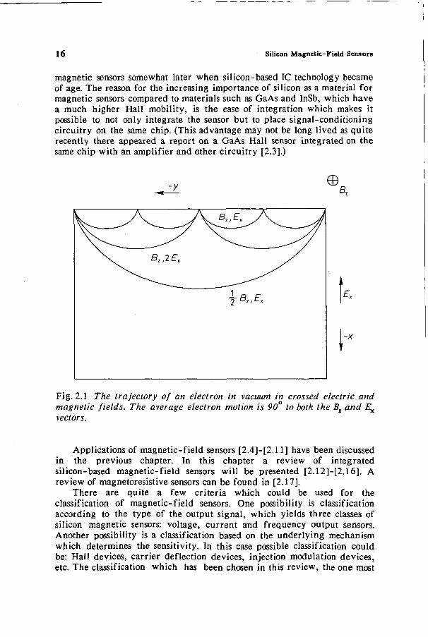
k
r Fig. 2.1 The trajectory of an electron in vacuum in crossed electric and magnetic fields. The average electron motion is 90 to both the Bz and £x vectors.
Applications of magnetic-field sensors [2.4]-[2.11] have been discussed in the previous chapter. In this chapter a review of integrated silicon-based magnetic-field sensors will be presented [2.12]-[2.16]. A review of magnetoresistive sensors can be found in [2.17].
There are quite a few criteria which could be used for the classification of magnetic-field sensors. One possibility is classification according to the type of the output signal, which yields three classes of silicon magnetic sensors: voltage, current and frequency output sensors. Another possibility is a classification based on the underlying mechanism which determines the sensitivity. In this case possible classification could be: Hall devices, carrier deflection devices, injection modulation devices, etc. The classification which has been chosen in this review, the one most
-y
The Basic Physical Principles 17
frequently encountered in the literature, is according to the type of the device which constitutes the sensor. We have bulk Hall plates as a contrast to FET Hall devices, and magnetotransistors have been divided into two classes, lateral and vertical magnetotransistors, while carrier-domain magnetometers are mainly based on npnp structures. There is also a section dealing with magnetodiodes. (There are, as always, exceptions to the rule. JFET magnetic sensors have been mentioned, for example, in the section on FET Hall devices, even though a JFET is a bulk device.)
This review deals only with silicon magnetic sensors because of the importance of the silicon-based IC technology, but a few devices fabricated in other materials have also been mentioned. Sometimes the reasons for this are historical, so that the more recent developments are placed into a better perspective, while some non-silicon examples are included because even though a silicon based device does not yet exist, there is no fundamental reason for not using silicon.
In a review of such broad scope, different problems can only be discussed superficially. Subjects like the numerical simulation of magnetic sensors, for example, have only been broached in passing. To compensate somewhat for the lack of depth, an extensive reference list (with the accent on recent work) has been included, also in the hope that a novice starting in this field will have a useful source of initial information.
2.2 THE BASIC PHYSICAL PRINCIPLES
The magnetic-field sensors presented here are all based on the interaction between the moving charge carriers and the magnetic field. The interaction is described by the well-known Lorentz force:
FL = q(vxB) (2.1)
where FL is the Lorentz force experienced by a charge carrier of charge q when it is moving at velocity v in a magnetic-flux density (magnetic induction) B. If one also takes into account the effect of the electric field, the equation of motion in vacuum becomes
w ^ f = q(E + vxB) (2.2)
where m is the mass of the charge carrier. If we assume that we are dealing with electrons and that all components of E and B fields except £ x and Bz are zero Eq. (2.2) can be reduced to
18 Silicon Magnetic-Field Sensors
j 2
d X At j 2
2
At'
£(** + *>.%) ■■dt
e n dx '""•dt
(2.3)
-y e a
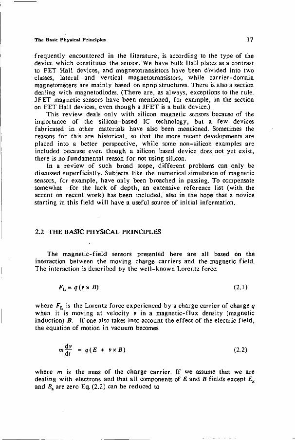
Fig. 2.2 In a solid, collisions will determine the amount of deflection. The Hall angle ©H, which is the angle between the average trajectory of the electron and the applied electric field, is smaller than 90°.
Assuming that the electron is at rest in the origin at / = 0, the solution of the above set of equations becomes [2.18]
% c
Ex 1 y(t) = -£-(öTsinu;c/ - O
D„ C
wc = mBz (2.4)
where wc is the cyclotron frequency. The trajectory of the electron in vacuum is depicted in Fig. 2.1. We can see that the average motion of the electron is perpendicular to both the electric and the magnetic fields, and parallel to the y axis. Therefore, under the influence of the magnetic field the average direction of motion of the electron deviates by 90° from the
The Basic Physical Principles 19
case in which Bt = 0 (electron moves parallel to E). We can introduce a new quantity 6H (Hall angle) defined in Eq. (2.5), which is the angle between the applied electric field E and the average current-density vector J [2.18]. In vacuum 6H becomes 90° for all values of the magnetic field larger than zero.
tan 0 H = -f (2.5) •'x
In a solid (semi-) conductor the electron (hole) cannot move indefinitely and undisturbed in the electric and magnetic fields. After a certain time the electron will collide with a lattice atom, and if the scattering mechanism is isotropic, we can assume that on the average, taken over the whole electron cloud, the electron loses all its energy to the lattice and its velocity just after the collision is zero [2.19]. The acceleration of the particle starts all over again continuing until the next collision. If we assume that all collisions take place after a mean collision-free time <r> the resulting trajectory is the one depicted in Fig. 2.2. The Hall angle can be written as [2.20]
V(<T>) ÖT s i n ( w c< r >) " <T> tan0H = x7 r7) " ~f ( 2 6 )
t£ [ COS (WC<T>) - 1 ]
For small values of 6H and wc<r> the Hall angle becomes proportional to
" c = l * E (2-7) e
H =jn<T>
Finally, with the expression for electron mobility n as a function of the mean collision-free time <r>, the Hall angle becomes
GH a nBz (2.8)
Of course, all electrons do not have the same velocity, nor is the collision-free time <T> a constant. However, if these effects are taken into
2 0 Silicon Magnetic-Field Sensors
account [2.19], only a slightly different result for 6 H is obtained, namely:
6 H - fiHBz (2.9)
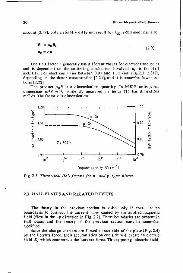
The Hall factor r generally has different values for electrons and holes and is dependent on the scattering mechanism involved. /zH is the Hall mobility. For electrons r lies between 0.97 and 1.15 (see Fig. 2.3 [2.81]), depending on the donor concentration [2.21 ], and it is somewhat lower for holes [2.22].
The product /iH5 is a dimensionless quantity. In M.K.S. units n has dimensions m2V"1s"1 , while B, measured in teslas (T) has dimensions m~2Vs. The factor r is dimensionless.
1.20 0) a.
- 1.10 v.
*- 1.00
0.90
I 1 I 1 1
_
T = 3 0 0 K
, 1 .
1 1 1 1 1 1
^ n - S i
i ' '
i
1.00
0.90
ai a. 4—
I
- 0.80 £
0.70
10u 10" 10° 10" 10" 10"
Dopant density A/(crrT3)
Fig. 2.3 Theoretical Hall factors for n- and p-type silicon.
2.3 HALL PLATES AND RELATED DEVICES
The theory in the previous section is valid only if there are no boundaries to obstruct the current flow caused by the applied magnetic field (flow in the -y direction in Fig. 2.2). These boundaries are present in Hall plates and the theory of the previous section must be somewhat modified.
Since the charge carriers are forced to one side cf the plate (Fig. 2.4) by the Lorentz force, their accumulation on one side will create an electric field Ey which counteracts the Lorentz force. This opposing electric field,
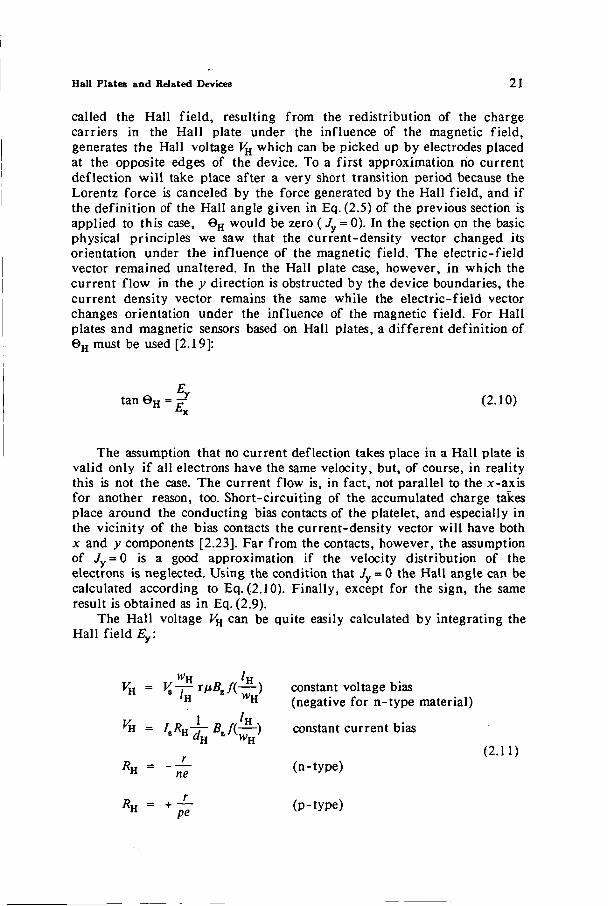
Hall Plates and Related Devices 21
called the Hall field, resulting from the redistribution of the charge carriers in the Hall plate under the influence of the magnetic field, generates the Hall voltage VH which can be picked up by electrodes placed at the opposite edges of the device. To a first approximation no current deflection will take place after a very short transition period because the Lorentz force is canceled by the force generated by the Hall field, and if the definition of the Hall angle given in Eq. (2.5) of the previous section is applied to this case, 6H would be zero ( Jy = 0). In the section on the basic physical principles we saw that the current-density vector changed its orientation under the influence of the magnetic field. The electric-field vector remained unaltered. In the Hall plate case, however, in which the current flow in the y direction is obstructed by the device boundaries, the current density vector remains the same while the electric-field vector changes orientation under the influence of the magnetic field. For Hall plates and magnetic sensors based on Hall plates, a different definition of 0 H must be used [2.19]:
t an6 H = Fy (210)
The assumption that no current deflection takes place in a Hall plate is valid only if all electrons have the same velocity, but, of course, in reality this is not the case. The current flow is, in fact, not parallel to the x-axis for another reason, too. Short-circuiting of the accumulated charge takes place around the conducting bias contacts of the platelet, and especially in the vicinity of the bias contacts the current-density vector will have both x and y components [2.23]. Far from the contacts, however, the assumption of Jy = 0 is a good approximation if the velocity distribution of the electrons is neglected. Using the condition that Jy = 0 the Hall angle can be calculated according to Eq. (2.10). Finally, except for the sign, the same result is obtained as in Eq. (2.9).
The Hall voltage VH can be quite easily calculated by integrating the Hall field Ey:
constant voltage bias (negative for n-type material)
constant current bias (2.11)
(n-type)
(p-type)
= K Tr^/(—) 'H WH
"H WH
R„ = - r ne
H pe
22 Silicon Magnetic-Field Sensors
Here we see the Hall angle (rnBz), the bias voltage VB across the contacts ba and b2, the width-length ratio wH//H, and a correction factor /(/H/wH) which depends on the geometry of the device. The correction factor takes into account the shorting effect of the bias contacts [2.18]. The optimum rectangular IC Hall elements have wH//H ratios slightly less than unity [2.4]. Is is the bias current of the Hall plate, dH is its thickness, and Rn is the Hall coefficient. R^ is a complicated function of the carrier densities and mobilities, but in the case in which one of the carriers predominates it takes the simpler form given in Eq. (2.11).
From Eq. (2.11) we see the importance of the carrier mobility of the material and its influence on the sensitivity of the device. As mentioned earlier, the ease of integration and the possibilities that silicon IC technology has to offer have made this material very interesting for magnetic sensors.
b., o ■•
y\
vv
+ + + + + +
Wu
Is . -»—°b,
■o h?
Fig. 2.4 The presence of boundaries in a Hall plate (p-type in this case) results in the accumulation of charge carriers on one side of the Hall plate (and a depletion on the other side) under the influence of the magnetic field. This manifests itself as a potential difference (Hall voltage Vn) between the Hall contacts hj and h2.
2.3.1 Bulk Hall Devices
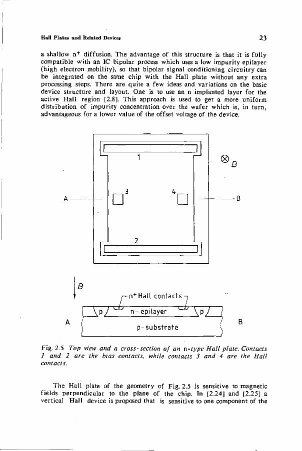
In Fig. 2.5 a top view and a cross-section of a rectangular, n-type silicon Hall plate are depicted. The plate is defined by a deep-p diffusion making an n epilayer island. The Hall and the bias contacts are formed by
Hall Plates and Related Devices 23
a shallow n+ diffusion. The advantage of this structure is that it is fully compatible with an IC bipolar process which uses a low impurity epilayer (high electron mobility), so that bipolar signal conditioning circuitry can be integrated on the same chip with the Hall plate without any extra processing steps. There are quite a few ideas and variations on the basic device structure and layout. One is to use an n implanted layer for the active Hall region [2.8]. This approach is used to get a more uniform distribution of impurity concentration over the wafer which is, in turn, advantageous for a lower value of the offset voltage of the device.
B
B n+ Hall contacts I 5SZ l ïZ n- epilayer
p-substrate
Fig. 2.5 Top view and a cross-section of an n-type Hall plate. Contacts 1 and 2 are the bias contacts, while contacts 3 and 4 are the Hall contacts.
The Hall plate of the geometry of Fig. 2.5 is sensitive to magnetic fields perpendicular to the plane of the chip. In [2.24] and [2.25] a vertical Hall device is proposed that is sensitive to one component of the
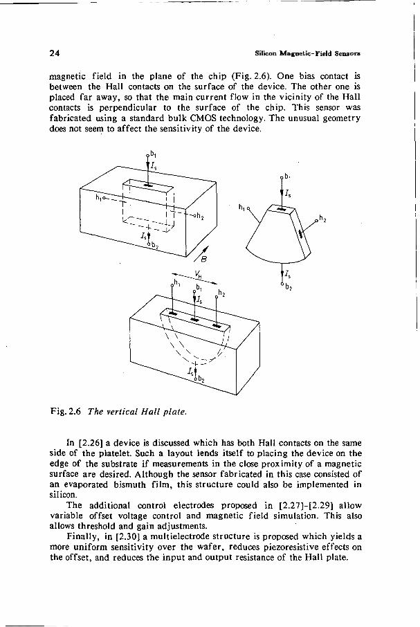
24 Silicon Magnetic-Field Sensors
magnetic field in the plane of the chip (Fig. 2.6). One bias contact is between the Hall contacts on the surface of the device. The other one is placed far away, so that the main current flow in the vicinity of the Hall contacts is perpendicular to the surface of the chip. This sensor was fabricated using a standard bulk CMOS technology. The unusual geometry does not seem to affect the sensitivity of the device.
Fig. 2.6 The vertical Hall plate.
In [2.26] a device is discussed which has both Hall contacts on the same side of the platelet. Such a layout lends itself to placing the device on the edge of the substrate if measurements in the close proximity of a magnetic surface are desired. Although the sensor fabricated in this case consisted of an evaporated bismuth film, this structure could also be implemented in silicon.
The additional control electrodes proposed in [2.27]-[2.29] allow variable offset voltage control and magnetic field simulation. This also allows threshold and gain adjustments.
Finally, in [2.30] a multielectrode structure is proposed which yields a more uniform sensitivity over the wafer, reduces piezoresistive effects on the offset, and reduces the input and output resistance of the Hall plate.
Hall Plates and Related Devices 25
Numerical simulations of Hall and related devices can be found in [2.23] and [2.31 ]-[2.41 ], and the response of Hall devices to non-homogeneous magnetic fields is discussed in [2.42]-[2.49].
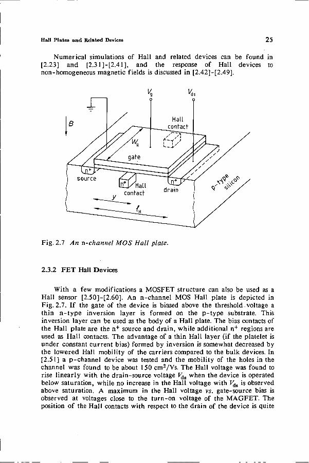
Fig. 2.7 An n-channel MOS Hall plate.
2.3.2 FET Hall Devices
With a few modifications a MOSFET structure can also be used as a Hall sensor [2.50]-[2.60]. An n-channel MOS Hall plate is depicted in Fig. 2.7. If the gate of the device is biased above the threshold voltage a thin n-type inversion layer is formed on the p-type substrate. This inversion layer can be used as the body of a Hall plate. The bias contacts of the Hall plate are the n+ source and drain, while additional n+ regions are used as Hall contacts. The advantage of a thin Hall layer (if the platelet is under constant current bias) formed by inversion is somewhat decreased by the lowered Hall mobility of the carriers compared to the bulk devices. In [2.51] a p-channel device was tested and the mobility of the holes in the channel was found to be about 150 cm2/Vs. The Hall voltage was found to rise linearly with the drain-source voltage Vda when the device is operated below saturation, while no increase in the Hall voltage with Vds is observed above saturation. A maximum in the Hall voltage vs. gate-source bias is observed at voltages close to the turn-on voltage of the MAGFET. The position of the Hall contacts with respect to the drain of the device is quite
26 Silicon Magnetic-Field Sensors
important for the sensitivity of the device to magnetic fields [2.52]. An optimal configuration is the one in which the Hall contacts are close to the drain (ratio y/lH close to 1). Because of the higher mobility of the electrons in the inversion layer, an n-channel device is more sensitive to magnetic fields than its p-channel counterpart [2.51], [2.57]. Moreover, the Hall voltage of a MAGFET does not depend on the geometry of the gate of the device [2.56]. A non-contact keyboard switch based on a MOS Hall device is reported in [2.58]. A low power consumption MOS amplifier was integrated along with the Hall plate to boost the output signal. In [2.60] a lumped element simulation of MOS Hall devices is presented.
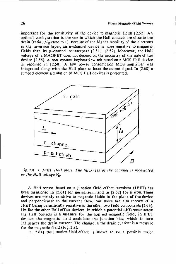
Fig. 2.8 A JFET Hall plate. The thickness of the channel is modulated by the Hall voltage VH.
A Hall sensor based on a junction field effect transistor (JFET) has been mentioned in [2.61] for germanium, and in [2.62] for silicon. These devices are mainly sensitive to magnetic fields in the plane of the device and perpendicular to the current flow, but there are also reports of a JFET being parasitically sensitive to the other two field components [2.63]. Unlike the other Hall effect devices, in which a potential difference across the Hall contacts is a measure for the applied magnetic field, in JFET devices the magnetic field modulates the junction bias, which in turn influences the drain current. The change in the drain current is a measure for the magnetic field (Fig. 2.8).
In [2.64] the junction field effect is shown to be a possible major
Hall Plates and Related Devices 27
source of non-linearity in junction-isolated, integrated Hall devices. This is caused by the modulation of the plate thickness by the Hall voltage.
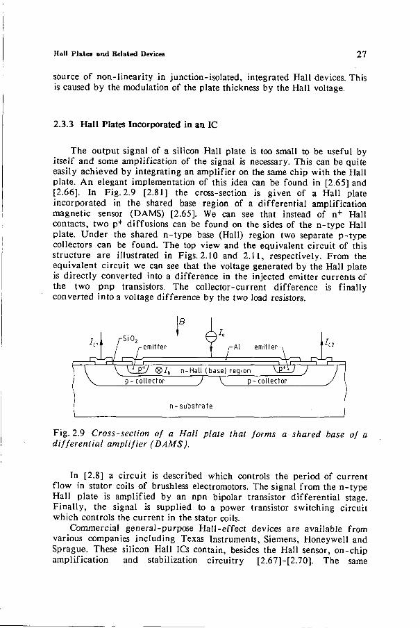
2.3.3 Hall Plates Incorporated in an IC
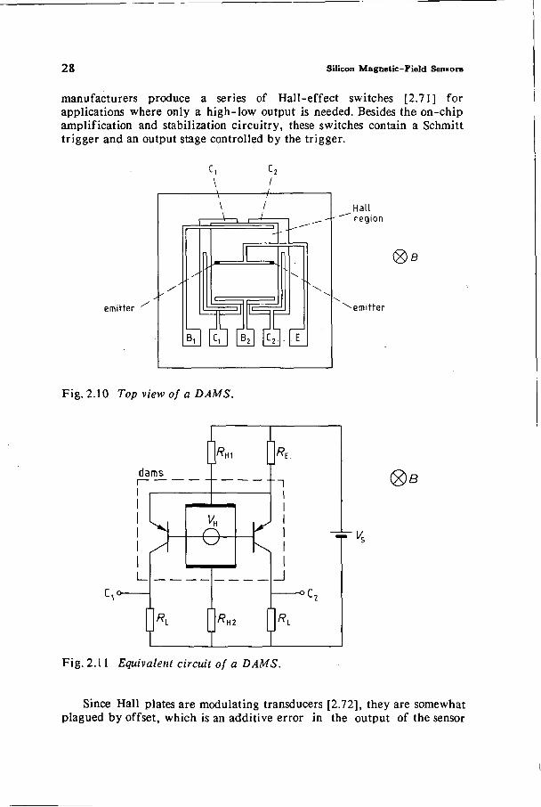
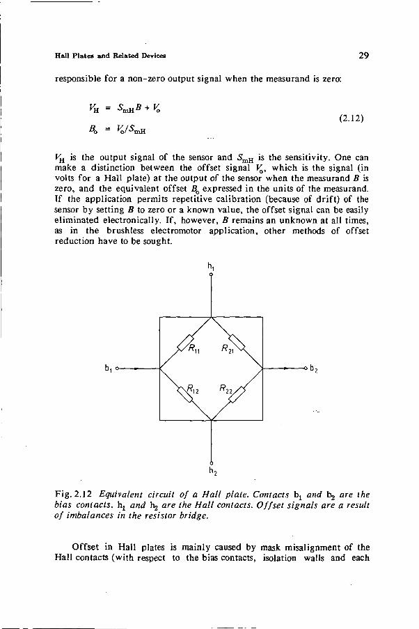
The output signal of a silicon Hall plate is too small to be useful by itself and some amplification of the signal is necessary. This can be quite easily achieved by integrating an amplifier on the same chip with the Hall plate. An elegant implementation of this idea can be found in [2.65] and [2.66]. In Fig. 2.9 [2.81] the cross-section is given of a Hall plate incorporated in the shared base region of a differential amplification magnetic sensor (DAMS) [2.65]. We can see that instead of n+ Hall contacts, two p+ diffusions can be found on the sides of the n-type Hall plate. Under the shared n-type base (Hall) region two separate p-type collectors can be found. The top view and the equivalent circuit of this structure are illustrated in Figs. 2.10 and 2.11, respectively. From the equivalent circuit we can see that the voltage generated by the Hall plate is directly converted into a difference in the injected emitter currents of the two pnp transistors. The collector-current difference is finally converted into a voltage difference by the two load resistors.
emitter
B >'.
4-Al emitter
V \i_E*/ ® J b n-Hall (base) region \$ϱJ J p- collector J \^ p-collector
n- substrate
Fig. 2.9 Cross-section of a Hall plate that forms a shared base of a differential amplifier (DAMS).
In [2.8] a circuit is described which controls the period of current flow in stator coils of brushless electromotors. The signal from the n-type Hall plate is amplified by an npn bipolar transistor differential stage. Finally, the signal is supplied to a power transistor switching circuit which controls the current in the stator coils.
Commercial general-purpose Hall-effect devices are available from various companies including Texas Instruments, Siemens, Honeywell and Sprague. These silicon Hall ICs contain, besides the Hall sensor, on-chip amplification and stabilization circuitry [2.67]-[2.70]. The same
28 Silicon Magnetic-Field Sensors
manufacturers produce a series of Hall-effect switches [2.71] for applications where only a high-low output is needed. Besides the on-chip amplification and stabilization circuitry, these switches contain a Schmitt trigger and an output stage controlled by the trigger.
emitter
Hall region
^emit ter
i f l
Fig. 2.10 Top view of a DAMS.
dams
L C i -
R,
R, H1
■e-
R H2
Ï I
I Rr
_J -°C,
^L
K
Fig. 2.11 Equivalent circuit of a DAMS.
Since Hall plates are modulating transducers [2.72], they are somewhat plagued by offset, which is an additive error in the output of the sensor
Hall Plates and Related Devices 29
responsible for a non-zero output signal when the measurand is zero:
VH = SmHB + V0 (2.12)
VH is the output signal of the sensor and 5mII is the sensitivity. One can make a distinction between the offset signal V0, which is the signal (in volts for a Hall plate) at the output of the sensor when the measurand B is zero, and the equivalent offset B0 expressed in the units of the measurand. If the application permits repetitive calibration (because of drift) of the sensor by setting B to zero or a known value, the offset signal can be easily eliminated electronically. If, however, B remains an unknown at all times, as in the brushless electromotor application, other methods of offset reduction have to be sought.
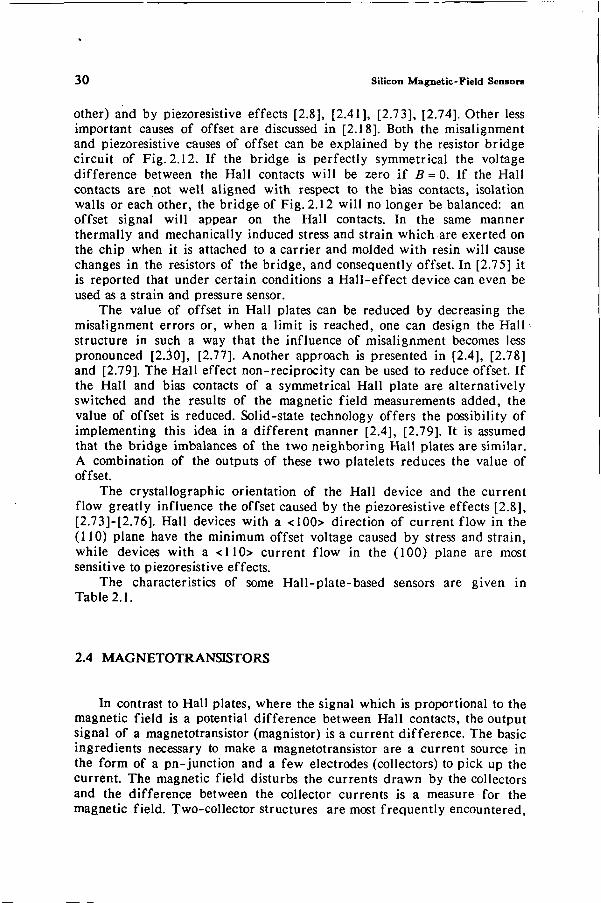
Fig. 2.12 Equivalent circuit of a Hall plate. Contacts bx and bg are the bias contacts. \ and hg are the Hall contacts. Offset signals are a result of imbalances in the resistor bridge.
Offset in Hall plates is mainly caused by mask misalignment of the Hall contacts (with respect to the bias contacts, isolation walls and each
30 Silicon Magnetic-Field Sensors
other) and by piezoresistive effects [2.8], [2.41], [2.73], [2.74]. Other less important causes of offset are discussed in [2.18]. Both the misalignment and piezoresistive causes of offset can be explained by the resistor bridge circuit of Fig. 2.12. If the bridge is perfectly symmetrical the voltage difference between the Hall contacts will be zero if B = 0. If the Hall contacts are not well aligned with respect to the bias contacts, isolation walls or each other, the bridge of Fig. 2.12 will no longer be balanced: an offset signal will appear on the Hall contacts. In the same manner thermally and mechanically induced stress and strain which are exerted on the chip when it is attached to a carrier and molded with resin will cause changes in the resistors of the bridge, and consequently offset. In [2.75] it is reported that under certain conditions a Hall-effect device can even be used as a strain and pressure sensor.
The value of offset in Hall plates can be reduced by decreasing the misalignment errors or, when a limit is reached, one can design the Hall structure in such a way that the influence of misalignment becomes less pronounced [2.30], [2.77]. Another approach is presented in [2.4], [2.78] and [2.79]. The Hall effect non-reciprocity can be used to reduce offset. If the Hall and bias contacts of a symmetrical Hall plate are alternatively switched and the results of the magnetic field measurements added, the value of offset is reduced. Solid-state technology offers the possibility of implementing this idea in a different manner [2.4], [2.79]. It is assumed that the bridge imbalances of the two neighboring Hall plates are similar. A combination of the outputs of these two platelets reduces the value of offset.
The crystallographic orientation of the Hall device and the current flow greatly influence the offset caused by the piezoresistive effects [2.8], [2.73]-[2.76]. Hall devices with a <100> direction of current flow in the (110) plane have the minimum offset voltage caused by stress and strain, while devices with a <110> current flow in the (100) plane are most sensitive to piezoresistive effects.
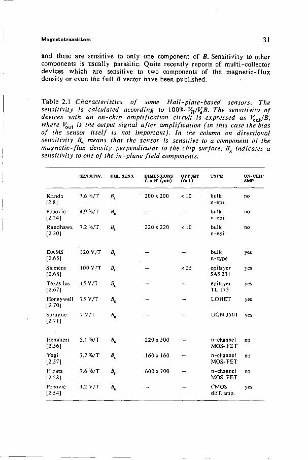
The characteristics of some Hall-plate-based sensors are given in Table 2.1.
2.4 MAGNETOTRANSISTORS
In contrast to Hall plates, where the signal which is proportional to the magnetic field is a potential difference between Hall contacts, the output signal of a magnetotransistor (magnistor) is a current difference. The basic ingredients necessary to make a magnetotransistor are a current source in the form of a pn-junction and a few electrodes (collectors) to pick up the current. The magnetic field disturbs the currents drawn by the collectors and the difference between the collector currents is a measure for the magnetic field. Two-collector structures are most frequently encountered,
Magnetotransistora 31
and these are sensitive to only one component of B. Sensitivity to other components is usually parasitic. Quite recently reports of multi-collector devices which are sensitive to two components of the magnetic-flux density or even the full B vector have been published.
Table 2.1 Characteristics of some Hall-plate-based sensors. The sensitivity is calculated according to 100% VH/VSB. The sensitivity of devices with an on-chip amplification circuit is expressed as Vout/B, where Vout is the output signal after amplification (in this case the bias of the sensor itself is not important). In the column on directional sensitivity Bz means that the sensor is sensitive to a component of the magnetic-flux density perpendicular to the chip surface. Bx indicates a sensitivity to one of the in-plane field components.
Kanda [2.8]
Popov ic [2.24]
Randhawa [2.30]
DAMS [2.65]
Siemens [2.68]
Texas Ins. [2.67]
Honeywell [2.70]
Sprague [2.71]
Hemmert [2.56]
Yagi [2.57]
Hirata [2.58]
Popovic [2.54]
SENSITIV.
7.6 %/T
4.9 %/T
7.2 %/T
120 V/T
100 V/T
15 V/T
75 V/T
7 V/T
3.1 %/T
3.7 %/T
7.6 %/T
1.2 V/T
DDL SENS.
B*
Bx
B*
Bt
B,
Bt
B,
Bt
B,
B*
Bt
B,
DIMENSIONS L x W (/im)
2 0 0 x 2 0 0
—
2 2 0 x 2 2 0
-
—
—
—
2 2 0 x 5 0 0
160x 160
6 0 0 x 7 0 0
-
OFFSET (mT)
< 10
—
< 10
-
<35
—
—
"
-
—
—
-
TYPE
bulk n-epi
bulk n-epi
bulk n-epi
bulk n-type
epilayer SAS 231
epilayer TL 173
LOHET
UGN3501
n-channel MOS-FET
n-channel MOS-FET
n-channel MOS-FET
CMOS dif f. amp.
ON-CHIP AMP.
no
no
no
yes
yes
yes
yes
yes
no
no
no
yes
32 Silicon Magnetic-Field Sensors
As early as 1950, it was noticed that the magnetic field influences the common-base current gain of a germanium bipolar transistor by deflecting the minority carriers in the base [2.80]. One, therefore, does not necessarily need more than one collector for a magnetically sensitive device. Multicollector devices are preferred because of the absence of a very large quiescent signal and the non-linearity. Nor does one need a structure as complicated as a transistor to make a sensor with an electrode current difference as the output signal. A simple resistive slab of silicon with one current source contact and two collector contacts will also yield a collector current difference as a response to an applied magnetic field, but because of concentrated current injection, a comparable magnetotransistor structure has a higher magnetic sensitivity [2.81].
B
B^n+J B2(n+)
Fig. 2.13 Drift-aided lateral magnetic-field sensitive pnp transistor.
Two mechanisms can be responsible for the magnetic sensitivity of the magnetotransitors: carrier deflection as described in the section on the physical principles, and modulation of emitter injection [2.82]-[2.84]. Which mechanism will dominate depends on geometrical factors and operating conditions [2.83], [2.85]. Carrier deflection as described in the section on the Hall angle will dominate in devices in which the Hall field is prevented from building up. The absence of the Hall field will enable the full deflection of the carriers to take place. The deflection will cause a collector current imbalance. If, however, a portion of the transistor base can be regarded as a Hall plate a device reminiscent of DAMS will emerge. Just like DAMS a Hall voltage built up in the base will modulate current injection across the emitter length, which also causes a difference in the collector currents.
One could use the two mechanisms as a basis for a classification of magnetotransistors, but it is more convenient to make a distinction based on the direction of the main current flow with respect to the chip surface. We can distinguish between lateral magnetotransistors: the main current flow is parallel to the chip surface, and the sensor is usually sensitive to fields
Magnetotransistors 33
perpendicular to the surface; and the vertical magnetotransistors: the main current flow is perpendicular to the chip surface, and the sensor is sensitive to fields in the plane of the chip.
2.4.1 Lateral Magnetotransistors
Figure 2.13 depicts the structure of a lateral magnetotransistor which was first reported in [2.86] and [2.87] (a Ge version is presented in [2.88]). This pnp magnistor can be fabricated in standard bipolar technology, where the n-type base region is an epilayer island. If we momentarily disregard the influence of the base bias, we can see that the emitter current (density) / e which is injected into the base will be deflected by the hole Hall angle 0H from its original path, resulting in a collector-current difference A/c. If, in addition, a positive voltage bias is applied between base contacts B1 and B2 the base region will behave as an n-type Hall plate and charge will accumulate on the sides, as indicated in Fig. 2.13; this charge will generate the Hall field. The generated Hall field will, in turn, alter the Je current path by an additional Hall angle 0Hn. The total deflection of the current-density vector Je becomes 0 H + 6H n and the collector current difference A/c = /cl - /c2 is:
Arc = K(nHp + nHn)BIe (2.13)
where K is a constant dependent on the bias conditions, geometry and electrical properties of the device. /xHs are the hole and electron Hall mobilities and /e is the emitter current. No emitter injection modulation has been reported. A pnp magnistor was used in [2.89] to magnetically trigger an on-chip SCR.
A device with only one base contact, which is, therefore, not drift-aided, is presented in [2.90]. In this pnp double-collector transistor only deflection of the holes which are injected into an elongated base plays a role in the magnetic sensitivity.
In [2.91] it was reported that a drift-aided double collector magnistor is sensitive mainly to the magnetic field component perpendicular to the chip surface Bz, as is to be expected. Still, the output signal exhibits some dependence on the magnetic field in the plane of the chip and parallel to the collectors (SJ. Quite contrary to these results, in [2.92] it was experimentally determined that the lateral magnistor in question was 10 times more sensitive to Bx than to Bz. These differences can be explained by the presence of a current injected in the z direction (perpendicular to the surface of the chip). This current is susceptible to deflection by the Bx fields. In [2.92] the authors were dealing with strong vertical injection, while lateral currents contributed only modestly to the total sensitivity.
34 Silicon Magnetic-Field Sensors
Nevertheless, lateral magnetotransistors remain sensitive to both the z and the x component of the magnetic field. This may introduce errors into the measurements. Other reports on the structures similar to the device of Fig. 2.13 are given in [2.93]-[2.100]. In Fig. 2.14 a lateral magnetotransistor is depicted. Deflection in this device takes place in the collector region, and not in the base.
Fig. 2.14 A lateral npn magnetotransistor based on current deflection.
In Fig. 2.15 a structure is presented which resembles the one in Fig. 2.13 except that the dominant mechanism responsible for the magneto-sensitivity is emitter injection modulation [2.82], [2.83], [2.101]. The functioning of this device is very similar to that of DAMS [2.65] described earlier. Due to the lateral base confinement the interaction between the base current and the magnetic field will result in a Hall field across the width of the base region. This will cause the emitter to inject more on one side, while the current injection on the other side is supressed [2.83], causing a collector-current imbalance. The sign of the response depends not only on the field direction but also on the biasing of the base contacts which determines the direction of the Hall field. Which of the two mechanisms, i.e. carrier deflection or injection modulation, dominates depends on the specific structure and operating conditions of the device
Magnetotranaistors 35
[2.83], [2.85]. Other accounts of structures similar to the one in Fig. 2.15 are given in [2.102].
' 'Jci
E
B,
®fi '
- n + ^ .
}ht
P
P
n+
P 1
Fig. 2.15 Lateral magnetotransistor with two base contacts. The base region acts as a Hall plate. The polarity of the response to magnetic fields depends on the biasing of the base.
Fig. 2.16 Lateral magnetotransistor with collectors and base contacts placed on the sides of the emitter.
36 Silicon Magnetic-Field Sensors
In Fig. 2.16 another version of a lateral magnetotransistor is given [2.103]. The magneto-sensitivity of this sensor is claimed to be determined by the deflection of carriers injected by the emitter towards the collectors. The sensor is sensitive to a component of the in-plane magnetic field parallel to the collectors of the device which deflects the vertically injected current. In [2.82] a similar structure is reported in which injection modulation is claimed to be the cause of magneto- sensitivity. The injection modulation mechanism can be enhanced by designing the magnetotransistor so that it has low emitter efficiency, confinement of the base current [2.104], and by appropriately positioning the collectors [2.105]. A one-collector device is presented in [2.85] in which injection modulation plays a major role. The sensitivity of this device is a strong function of the base current. The sensitivity and noise behavior of lateral magnetotransistors fabricated in CMOS technology is presented in [2.106]-[2.109].
p - substrate
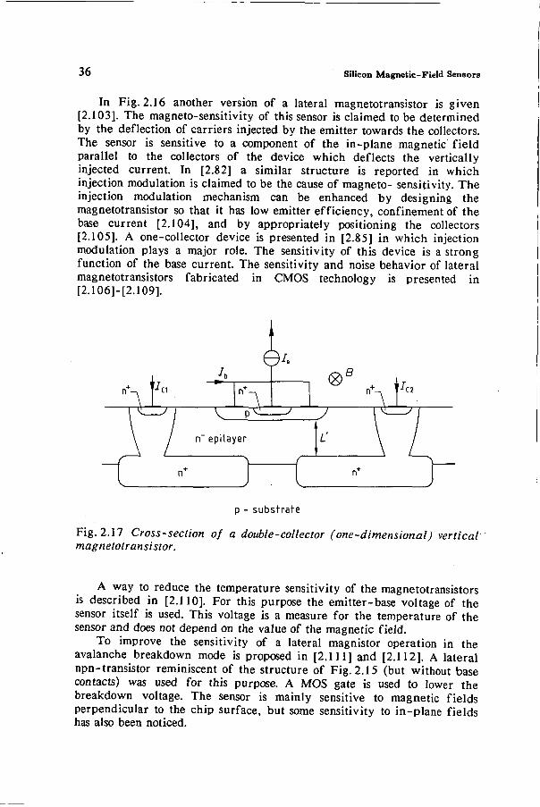
Fig. 2.17 Cross-section of a double-collector (one-dimensional) vertical magnetotransistor.
A way to reduce the temperature sensitivity of the magnetotransistors is described in [2.110]. For this purpose the emitter-base voltage of the sensor itself is used. This voltage is a measure for the temperature of the sensor and does not depend on the value of the magnetic field.
To improve the sensitivity of a lateral magnistor operation in the avalanche breakdown mode is proposed in [2.U1] and [2.112], A lateral npn-transistor reminiscent of the structure of Fig. 2.15 (but without base contacts) was used for this purpose. A MOS gate is used to lower the breakdown voltage. The sensor is mainly sensitive to magnetic fields perpendicular to the chip surface, but some sensitivity to in-plane fields has also been noticed.

Magnetotransistors 37
Fig. 2.18 Top view of a one-dimensional (1-D) vertical magneto-transistor.
A MAGFET can also be used in the mode of current deflection, i.e. current difference is proportional to the magnetic field. In this device the Hall contacts are used as current electrodes (a three-drain MAGFET) or the drain is split in two (a two-drain MAGFET). Just as in a magnetotransistor in which carrier deflection dominates, the applied magnetic field disturbs the current distribution between the drains, which in turn results in a drain current difference. In [2.53] a theoretical discussion of carrier deflection in a MAGFET is presented, while in [2.54] a description of a CMOS magnetic sensor is given, in which the two complementary transistor pairs are each replaced by a single split-drain device.
2.4.2 Vertical Magnetotransistors
The main current flow in these devices is perpendicular to the surface of the chip, which makes them sensitive to magnetic fields in the plane of
38 Silicon Magnetic-Field Sensors
the chip. One of the possible structures of a vertical magnistor is depicted in Fig. 2.17 [2.81]. It is a two-collector npn transistor. Because of the fairly thin base under the emitter (about 0.6 fim) and the large surface of the emitter-base junction, the current is injected mainly down toward the n+ buried layers. The in-plane magnetic field can then deflect the current to one of the collectors, and the collector current difference is proportional to the field strength.
The first vertical magnetotransitor was presented in [2.113] and [2.114]. This device was made on a p-type substrate (no epilayer). Two n-type collectors were made by an n-type diffusion on top of which were diffused a p-type base and an n+- type emitter. The two collectors are separated by the reverse-biased collector-substrate and col lector-base junctions, making the intercollector resistance very high. A disadvantage of this device is that it cannot be made in a standard epitaxial bipolar IC process.
Another version of a vertical magnistor is described in [2.115]. The collectors of this device were placed on the back side of the wafer, and they were separated by an etched groove likewise on the back side of the wafer. The collectors of the sensor were further separated by the depleted substrate collector region. The output signal (collector-current difference A/c) of this and other vertical magnetotransistors was determined to be [2.115], [2.116]:
A/e « 2£6 /*H*a7. (2.14)
where we is the width of the emitter, L' is the effective deflection length (thickness of the n"-epilayer of Fig. 2.17), nHB is the Hall angle, and the product of the common-base current gain a and the emitter current le is the total collector current. L'fiHB/we represents the fraction of the total collector current which is deflected under the influence of the magnetic field towards one of the collectors. The main disadvantage of the structure discussed in [2.115] is that it employs a non-standard manufacturing process.
A vertical magnetotransistor which can be manufactured in a standard bipolar technology is described in [2.81] and [2.116]-[2.122]. The cross-section of this device is depicted in Fig. 2.17. The gap in the buried layer diffusion is necessary to avoid short-circuiting the two collector contacts because, unlike in the devices discussed in [2.113]-[2.115], the two collector contacts of the device of Fig. 2.17 are not isolated by a depletion layer. The gap in the buried layer was determined to have an advantageous effect on the sensitivity of the magnistor compared to devices with a continuous buried layer or without a buried layer [2.118].
The top view of a vertical magnetotransistor capable of measuring one component of the in-plane magnetic-field vector which is parallel to the
Magnetotransistors 39
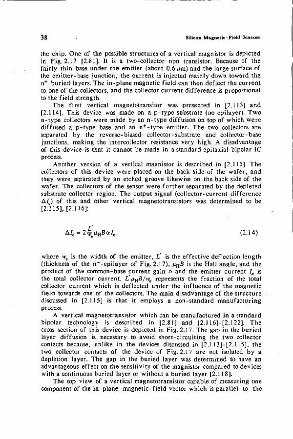
collectors is depicted in Fig. 2.18 (1-D sensor). In Fig. 2.19 a version of the sensor which is capable of measuring the complete in-plane vector is depicted (2-D sensor) [2.121], [2.123], [2.124]. In essence, this sensor is made by merging two 1-D sensors which are at a 90° angle to each other.
Fig. 2.19 Top view of an in-plane vector sensor (2-D magnetic sensor).
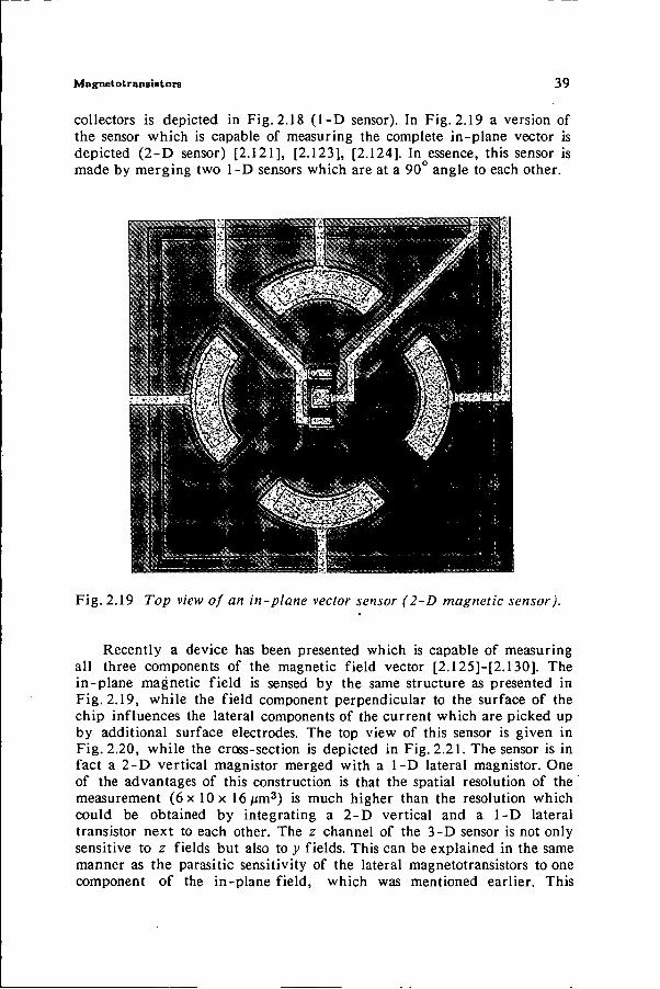
Recently a device has been presented which is capable of measuring all three components of the magnetic field vector [2.125]-[2.130]. The in-plane magnetic field is sensed by the same structure as presented in Fig. 2.19, while the field component perpendicular to the surface of the chip influences the lateral components of the current which are picked up by additional surface electrodes. The top view of this sensor is given in Fig. 2.20, while the cross-section is depicted in Fig. 2.21. The sensor is in fact a 2-D vertical magnistor merged with a 1-D lateral magnistor. One of the advantages of this construction is that the spatial resolution of the measurement (6 x 10 x 16 urn3) is much higher than the resolution which could be obtained by integrating a 2-D vertical and a 1-D lateral transistor next to each other. The z channel of the 3-D sensor is not only sensitive to z fields but also to y fields. This can be explained in the same manner as the parasitic sensitivity of the lateral magnetotransistors to one component of the in-plane field, which was mentioned earlier. This
40 Silicon Magnetic-Field Sensors
so-called cross-sensitivity is caused by current components which contain both the vertical and the lateral component of flow (Fig. 2.21). In the 3-D sensor case, the presence of cross-sensitivity is not troublesome because there are three output channels, so that all three field components can be extracted by inverting the (non-diagonal) sensitivity matrix [2.125]. In [2.131] a 3-D sensor consisting of three Hall plates on one chip is presented.
Fig. 2.20 Top view of an npn magnetotransistor capable of measuring all three components of the magnetic-field vector (3-D magnetic sensor). Collector pairs Cx and Cy are sensitive to the magnetic field in the plane of the chip (Bx and By). The two z-collector pairs are using the lateral components of the collector current to sense Bv
Just like Hall plates, magnetotransistors suffer from the presence of offset. The problem is more serious since more mask levels are needed in the fabrication of magnetotransistors than in the fabrication of a Hall plate. In [2.122] and [2.132] the influence of the misalignment of the emitter diffusion was determined with respect to the buried layer diffusion on the offset of a vertical magnetotransistor. For misalignment shifts which are not too large the influence of the shift on the equivalent

Carrier-Domain Magnetic-Field Sensors 41
offset is approximately linear; it is about 1.5T//im (Tesla per micron misalignment between the two diffusions). The method of offset reduction employed in [2.4] on Hall plates cannot be applied to magnetotransistors. However, recently another of f set-reduction method has been presented which was used on a 1-D vertical magnistor [2.116] and reduced the values of offset by a factor of 10 to 20 [2.20], [2.132]-[2.136]. The method is based on the variation of the sensor's sensitivity using an (electrical) parameter which does not appreciably affect the offset signal. Under these conditions the offset can be reduced while the measurand B remains unknown at all times.
The difference in the magnetic current-deflection properties in the ohmic part of the magnetotransistor (low electric fields) and depletion layer (high electric fields) which reduces sensitivity, is discussed in [2.137].
Numerical simulations of magnetotransistor-related structures are presented in [2.138] and [2.139].
2.5 CARRIER-DOMAIN MAGNETIC-FIELD SENSORS
In contrast to magnetotransistors, in which the current injection takes place over the whole emitter-base junction, the current injection in carrier-domain magnetometers is more or less concentrated at one spot on the junction. One of the possible realizations of a carrier-domain device is given in Fig. 2.22. This particular structure is very similar to the vertical magnetotransistor of Fig. 2.17 except that the substrate now plays an active role. The substrate in this case is an emitter of a pnp transistor, the substrate-epilayer junction being forward-biased. On the top of the structure we can see an npn transistor. The current injected by the n+
emitter of the npn is collected in the base of the pnp, and conversely, the current injected by the p" emitter of the pnp is collected by the base of the npn. Both currents will cause potential drops in the respective bases in such a way that injection is restricted to the center of the junction and a current domain is formed. If a magnetic field is applied the domain will shift and the base currents / p l and /p 2 will no longer be equal (nor will the base currents 7n l and 7n2).
The first report of a carrier-domain magnetic-field sensor (a lateral device) was given in [2.140] and [2.141]. The device is sensitive to fields perpendicular to the surface of the chip, and it was reported that oscillations may occur at some minimum bias current. This device was intended to be a peak-current detector used in transformers [2.142]. The vertical device of Fig. 2.22 was proposed in [2.143]-[2.145]. If the potentials at both edges of the bases are equal (current-mode operation) the expression for the response of the device to a magnetic field becomes [2.144]:
4 2 Silicon Magnetic-Field Sensors
where /t is the sum of the base currents, A/t is the sum of the differences between the currents drawn by the respective base contacts, //Hfl products are the Hall angles, Ls are distances over which deflection takes place and If is a factor (typically between 10 and 100) which depends on the width of the domain. A similar version of a device is presented in [2.146]. The large sensitivity to temperature variations is decreased by integrating a flat metal coil along with the sensor. Alternating current generates in this coil a magnetic field (of a different frequency), which is superimposed on the external magnetic field so that the output signal has a component proportional to the local field. The additional field is subsequently used to control the gain of an amplifier and maintain constant sensitivity.
tËEÈt p - substrate S x
Fig. 2.21 The cross-section of the 3-D magnetic-field sensor. The vertical component (A) of the collector current is sensitive to Bx and B The lateral component (B) of the current is used to sense Bz. The current reaching the z channel is not entirely lateral, but there is also a vertical component (C) that is responsible for the sensitivity of the z channel to By.
Another type of carrier-domain magnetic sensor is presented in Fig. 2.23. The output of this sensor is not a current difference but a stream of current pulses with a frequency which is proportional to the magnetic
Carrier-Domain Magnetic-Field Sensors 43
field. The domain is formed in a manner similar to that described above. If a magnetic field is applied perpendicular to the surface of the chip, the domain begins to rotate and continues to do so, as no balancing, as described in [2.144], occurs. The current pulses are picked up by the subsidiary collectors of the device each time the domain passes them. The concept of this device was first given in [2.147]. In [2.148] and [2.149] it was determined that the frequency response of the device to magnetic fields is described by
ƒ = d»VBz
2*tpR (2.16)
substrate
B
Fig. 2.22 A carrier-domain magnetometer. The domain is formed by, inverse current crowding in the bases of the merged npn and pnp transistors.
fT is the frequency of domain rotation, d is the radial spacing between the npn emitter region and the pnp base region, npBz is the Hall angle, tp is the charging time of the pnp transistor base layer and R is the radius of
44 Silicon Magnetic-Field Sensors
the outer edge of the npn emitter. The operation of this device is seriously hampered by the existence of a threshold level of the magnetic-flux density, below which domain rotation does not take place. The existence of this threshold field is ascribed to the spatial variation of the common-base current gain of the lateral pnp transistor [2.149]. Threshold fields Bt of 100 mT are reported in [2.150], while in [2.151] a large spread in Bt and a high degree of correlation between Bt and the misalignment of the npn emitter diffusion with respect to the npn base diffusion is reported. Other reports on carrier-domain magnetometers can be found in [2.152]-[2.154].
Fig. 2.23 Rotating carrier-domain magnetometer.
Fig, 2.24 Silicon-on-sapphire (SOS) magnetodiode.
Magnet odiodea 45
An account of a carrier-domain magnetometer without a threshold field is reported in [2.155] and [2.156]. It is an npn transistor operating in the collector-emitter breakdown regime. Unlike in the devices reported earlier, where the inversion of the base current is responsible for the domain formation, it is believed that intrinsic thermal effects are responsible for the domain confinement as well as for its spontaneous rotation. The spontaneous rotation (#t = 0) is explained by the domain's tendency to avoid a hot spot that it generates itself.
2.6 MAGNETODIODES
It was observed as early as in 1949 that the conductivity in a semiconductor slab in which holes and electrons are injected changes considerably under the influence of the magnetic field [2.157]. This so-called Suhl or magnetoconcentration effect is based on the difference in recombination velocities between two surfaces or between one surface and the bulk of the device. The magnetic field will concentrate the flow of the injected carriers in a diode structure toward or away from a region with a different recombination velocity, and this will change the current-voltage characteristic of the diode. One of the proposed structures is depicted in Fig. 2.24 [2.81], [2.158]. Electrons and holes are injected from the n+ and the p+ regions into the low doped n region where they drift under the influence of the electric field. The Si-Si02 interface on top of the device has a low recombination velocity s1 compared to the bottom Si-Al203 (sapphire) interface recombination velocity s2. The in-plane magnetic field deflects the carriers to one of the surfaces and a change in the current-voltage characteristic takes place. If the thickness d of the device is smaller than the ambipolar diffusion length Z^, and for fields smaller than 20 mT, it was shown [2.159] that for constant current the voltage U across the diode changes under the influence of the magnetic field as follows:
§U g(Mn + Mp)reff(s2 - h)^ . dB ZkTl ( '
where / is the length of the n region, while the effective carrier lifetime reff is a complicated function of the surface recombination velocities, the thickness of the device and the ambipolar diffusion length [2.160].
The essential requirement of there being a difference in the recombination velocities ij and s2 can also be achieved through creating a difference in mechanical surface roughness by polishing one surface and grinding the other one [2.161]. Both this and the silicon-on-sapphire approach have the disadvantage of poor reproducibility of the high-recombination surface and hence poor reproducibility of the sensor
46 Silicon Magnetic-Field Sensors
Table 2.2 Characteristics of selected magnetotransistors, carrier-domain devices, and magnetodiodes. The sensitivity of magnetotransistors and one carrier-domain device [2.143] is calculated according to 100% AIc/IeB. The sensitivity of carrier-domain devices is expressed as the change in the frequency per Tesla: Af/B, while the sensitivity of magnetodiodes (constant current bias) is expressed as the change in the bias voltage with magnetic field.
SENSITIV.
MAGNETOTRANSISTORS
Nield [2.89]
Halbo [2.95]
Vinal [2.102]
Vikulin [2.91]
Zieren [2.81]
Zieren [2.116]
Kordic [2.125]
0.35 %/T
1.77 %/T
6.7 %/T
2.6 %/T
5 %/T
^ = 5 %/T Sy = 5 %/T
^ = 1.4 %/T £, = 2.2 %/T ■5J = 0.3 %/T
CARRIER-DOMAIN DEVICES
Manley [2.150]
Popovic [2.155]
Goicolea [2.144]
100 kHz/T
250 kHz/T
30 %/T
MAGNETODIODES
Popovic [2.163]
Lutes [2.159]
2 5 V / T
4.9 V/T
DIR. SENS.
BZ
B,
*x
*.
».
By
B* By B*
Bt
Bt
Bx
Bx
Bx
DIMENSIONS (/mi)
-
—
—
—
8 x 2 0 x 1 4 0
8 x 2 0 x 2 0
6 x lOx 16
800 diameter
500 diameter
-
-
OFFSET (mT)
36
45
—
—
50 [2.132]
—
150
-
100 [2.145]
-
-
TYPE
lateral pnp drift-aided
lateral pnp drift-aided
lateral pnp injection mod.
lateral pnp
vertical npn deflection
vertical npn deflection
vertical npn deflection
lateral circular
lateral npn circular
vertical
CMOS
SOS
Conclusions 47
characteristics. Another disadvantage is the high non-linearity of the sensitivity which is also dependent on the direction of the applied magnetic field. An additional problem is the temperature dependence of the recombination process and consequently the temperature dependence of the output signal.
Several devices reported in the literature are, strictly speaking, not diodes, although they do utilize different recombination rates to achieve magnetic sensitivity. One of these is a p-channel MOS transistor with a forward-biased source-substrate junction [2.162]. In this device the hole diffusion current is deflected towards the gate or the substrate back contact. The device operates as a lateral pnp transistor in which the base transport factor is modulated by the magnetic field. In [2.163] a reverse-biased pn junction plays the role of a high recombination region. Again, the magnetic field deflects the current toward or away from that region and changes the diode characteristic. Both of these devices have overcome the problem of irreproducible high-recombination surfaces.
In Table 2.2 characteristics of some selected magnetotransistors, carrier-domain devices, and magnetodiodes are given.
2.7 CONCLUSIONS
We have seen that quite a few types of silicon devices can be designed in such a way that they are sensitive to magnetic fields. Different output signal types are available. Hall-plate-like devices usually have an output signal in the form of a potential difference, while the output signal of a magnetotransistor is a current. Finally, carrier-domain devices can have a frequency output signal.
The size of the sensitive area of silicon magnetic-field sensors can vary from a few hundred microns a side in Hall plates (smaller Hall plates are also available) to a few microns in magnetotransistors. At the same time it is possible to measure all three components of B with a single sensor.
Bias and amplification circuitry can be integrated on the same chip as the sensor. Other signal conditioning circuitry can also be integrated along with the sensor to deal with the inherent problems of silicon magnetic sensors: temperature sensitivity and the offset.
These are, in short, the reasons why there has been a recent increase in the research effort in silicon magnetic-field sensors.
48 Silicon Magnetic-Field Sensors
REFERENCES
[2.1] E. H. Hall, On a new action of the magnet on electric currents, Am. J. Math., vol.2, 1879, pp. 287-292.
[2.2] K.Russell Sopka, The discovery of the Hall effect: Edwin Hall's hitherto unpublished account, in C. L. Chien and C. R. Westgate (eds.), The Hall Effect and its Applications, Proc. of the Commemorative Symp., Baltimore, MD, USA, 1979, Plenum Press, New York, 1980, pp. 523-545.
[2.3] T. R. Lepkowski, G. Shade, S. P. K wok, M. Feng, L. E. Dickens, D. L. Laude and B.Schoendube, A GaAs integrated Hall sensor/amplifier, IEEE Electron Device Lett., vol.EDL-7, 1986, pp. 222-224.
[2.4] J. T. Maupin and M. L. Geske, The Hall effect in silicon circuits, in C. L. Chien and C. R. Westgate (eds.), The Hall Affect and its Applications. Proc. of the Commemorative Symp., Baltimore, MD, USA, 1979, Plenum Press, New York, 1980, pp. 421-445.
[2.5] J. A. Blackburn and S. Vik, Computer menu tablet employing Hall-effect switches, Rev. Sci. lustrum., vol. 55, 1984, pp. 1358-1359.
[2.6] T. Kenjo and S. Nagamori, Permanent-magnet and Brushless DC Motors, Clarendon Press, Oxford, 1985.
[2.7] J. F. Wise Jr. and F. O. Simons Jr., A brushless Hall generator dc servomotor, IEEE Trans. Indust. Elec. Control Instrum., vol.IECI-21, 1974, pp. 75-77.
[2.8] Y. Kanda, M. Migitaka, H. Yamamoto, H. Morozumi, T. Okabe and S. Okazaki, Silicon Hall-effect power ICs for brushless motors, IEEE Trans. Electron Devices, vol. ED-29, 1982, pp. 151-154.
[2.9] R. W. Holmes, Improved crankshaft sensing techniques, Proc. 2nd Int. Conf. on Automotive Electronics, London, UK, 1979, pp. 155-158.
[2.10] W. D. McCall Jr. and E.J.Rohan, A linear position transducer using a magnet and Hall effect devices, IEEE Trans. Instrum. Meas., vol. IM-26, 1977, pp. 133-136.
[2.11] Y. Netzer, A very linear noncontact displacement measurement with a Hall-element magnetic sensor, Proc. IEEE, vol.69, 1981, pp.491-492.
[2.12] S. Kordic, Review of silicon magnetic-field sensors, Internal report, Delft University of Technology, 1982.
[2.13] J. H. Fluitman, A survey of solid-state magnetic-field sensors, in W. Sansen and J. van der Spiegel (eds.), Summer Course 1982: Solid-Stale Sensors and Transducers, vol. II, Katholieke Universiteit Leuven, Belgium, 1982, pp. IX 1-23.
[2.14] H. Mol, Review of literature on silicon magnetically sensitive devices, Internal report, Delft University of Technology, 1986.
[2.15] H. P. Baltes and R. S. Popovic, Integrated semiconductor magnetic field sensors, Proc. IEEE, vol.74, 1986, pp. 1107-1132.
[2.16] S. Kordic, Integrated silicon magnetic-field sensors, Sensors and Actuators, vol. 10, 1986, pp. 347-378.
[2.17] U. Dibbern, Magnetic field sensors using the magnetoresistive effect, Sensors and Actuators, vol. 10, 1986, pp. 127-140.
[2.18] H.Weiss, Structure and Application of Galvanomagnetic Devices, Pergamon Press, Oxford, 1969.
[2.19] R. A. Smith, Semiconductors, Cambridge University Press, Cambridge, 2nd ed., 1978.
[2.20] S. Kordic and P. C. M. van der Jagt, Theory and practice of electronic implementation of the sensitivity-variation offset-reduction method, Sensors and Actuators, vol.8, 1985, pp. 197-217.
[2.21] P.Norton, T. Braggins and H.Levinstein, Impurity and lattice scattering
References 49
parameters as determined from Hall and mobility analysis in n-type silicon, Phys. Rev. B, vol. 8, 1973, pp. 5632-5653.
[2.22] J.F.Lin, S.S.Li, L.C.Linares and K. W. Teng, Theoretical analysis of Hall factor and Hall mobility in p-type silicon, Solid State Electron., vol.24, 1981, pp. 827-833.
[2.23] L. Andor, H.P. Baltes, A.Nathan and H.G.Schmidt-Weinmar, Carrier transport in semiconductor magnetic field sensors, Int. Electron Devices Meet., Washington, DC, USA, 1983, IEDM Techn. Dig., pp. 635-638.
[2.24] R. S. Popovic, The vertical Hall-effect device, IEEE Electron Device Lett., vol. EDL-5, 1984, pp. 357-358.
[2.25] J. L. Berchier and R. S. Popovic, Sensitivity of the vertical Hall-effect device, Nth European Solid-State Device Research Con/. ESSDERC'84, Lille, France, 1984, Europhysics Conf. Abstr., pp. 265-266.
[2.26] J. H. J. Fluitman, Hall-effect device with both voltage leads on one side of the conductor, J. Phys. E: Sci. Instrum., vol. 13, 1980, pp. 783-785.
[2.27] R. J. Braun, Give the Hall transducer flexibility, Electron. Des., vol.22, 1974, pp. 88-92.
[2.28] R. J. Braun, Modular Hall masterslice transducer, IBM J. Res. Dev., vol.19, 1975, pp. 344-352.
[2.29] R.J. Braun, H. D.Chai and W.S. Ebert, FET Hall transducer with control gates, IBM Tech. Disci. Bull., vol. 17, 1974, pp. 1895-1896.
[2.30] G. S. Randhawa, Monolithic integrated Hall devices in silicon circuits, Microelectron. J., vol. 12, 1981, pp. 24-29.
[2.31 ] G. de Mey, Integral equation for the potential distribution in a Hall generator, Electron. Lett., vol.9, 1973, pp. 264-266.
[2.32] G. deMey, Determination of the electric field in a Hall generator under influence of an alternative magnetic field, Solid-State Electron., vol.17, 1974, pp. 977-979.
[2.33] G. deMey, The finite element method for potential calculations in a Hall plate, Radio and Electron. Eng., vol.45, 1975, pp. 472-474.
[2.34] W. Versnel, Analysis of symmetrical Hall plates with finite contacts, J. Appl. Phys., vol.52, 1981, pp. 4659-4666.
[2.35] G. deMey, Potential calculations in Hall plates, Adv. Electron. Electron Phys., vol.61, 1983, pp. 1-62.
[2.36] H. G. Schmidt-Weinmar, L. Andor, H. P. Baltes and A.Nathan, Numerical modeling of silicon magnetic field sensors: magnetoconcentration effects in split-metal-contact devices, IEEE Trans. Magn., vol.MAG-20, 1984, pp. 975-977.
[2.37] H. P. Baltes, L. Andor, A.Nathan and H. G.Schmidt-Weinmar, Two-dimensional numerical analysis of a silicon magnetic field sensor, IEEE Trans. Electron Devices, vol.ED-31, 1984, pp. 996-999.
[2.38] A.M. J. Huiser and H. P. Baltes, Numerical modeling of vertical Hall-effect devices, IEEE Electron Device Lett., vol. EDL-5, 1984, pp. 482-484.
[2.39] A.Nathan, A.M. J. Huiser and H. P. Baltes, Two-dimensonal numerical modeling of magnetic-field sensors in CMOS technology, IEEE Trans. Electron Devices, vol. ED-32, 1985, pp. 1212-1219.
[2.40] L. Andor, H. P. Baltes, A.Nathan and H.G. Schmidt-Weinmar, Numerical modeling of magnetic-field-sensitive semiconductor devices, IEEE Trans. Electron Devices, vol. ED-32, 1985, pp. 1224-1230.
[2.41] J. M. vanden Boom and S. Kordic, Offset reduction in Hall plates - theory and experiments, Submitted to Sensors and Actuators.
[2.42] J. Brunner, Der Halleffekt im inhomogenen Magnetfeld, Solid-State Electron., vol.2, 1960, pp. 172-175.
[2.43] I. Hlasnik and J. Kokavec, Hall generator in inhomogeneous field and dipole
50 Silicon Magnetic-Field Sensors
notion of the Hall effect, Solid-State Electron., vol. 9, 1966, pp. 585-594. G. deMey, Hall effect in a nonhomogeneous magnetic field, Solid-State Electron., vol.20, 1977, pp. 139-142. A. W. Baird, The Hall cross in a perpendicular inhomogeneous magnetic field, IEEE Trans. Magn., vol.MAG-15, 1979, pp. 1138-1141. J. H. J. Fluitman, On the calculation of the response of (planar) Hall-effect devices to inhomogeneous magnetic fields, Sensors and Actuators, vol. 2, 1981/82, pp. 155-170. Y. Sugiyama, Fundamental research on Hall effect in inhomogeneous magnetic fields, Researches of the Electrotechnical Laboratory, Ibaraki, Japan, no. 838, 1983. A. Nathan, W. Allegretto, H. P. Baltes and Y. Sugiyama, Modeling of Hall devices under locally inverted magnetic field, IEEE Electron Device Lett., vol. EDL-8, 1987, pp. 1-3. A.Nathan, W. Allegretto, H. P. Baltes, Y. Sugiyama and M. Tacano, Position sensitive geometric factor for semiconductor Hall devices detecting magnetic domains, 4th Int. Conf. on Solid-State Sensors and Actuators, Tokyo, Japan, 1987, Dig. Techn. Papers, pp. 536-538. A. Waxman, V. E. Henrich, F. V. Shallcross, H. Borkan and P. K. Weimer, Electron mobility studies in surface space-charge layers in vapor deposited CdS films, J.Appl. Phys., vol.36, 1965, pp. 168-175. R.C.Gallagher and W.S.Corak, A metal-oxide-semiconductor (MOS) Hall element, Solid-State Electron., vol.9, 1966, pp. 571-580. P. W. Fry and S. J. Hoey, A silicon MOS magnetic field transducer of high sensitivity, IEEE Trans. Electron Devices, vol. ED-16, 1969, pp. 35-39. W. N. Carr and S. T. Hong, The MAGFET: a new integrated circuit building block, SWIEECO Record of Techn. Papers, 1970, pp. 166-170. R.S. Popovic and H. P.Baltes, A CMOS magnetic field sensor, IEEE J. Solid-State Circuits, vol.SC-18, 1983, pp. 426-428. G. R. Mohan Rao and W. N. Carr, Magnetic sensitivity of a MAGFET of uniform channel current density, Solid-State Electron., vol.14, 1971, pp. 995-1001. R. S. Hemmert, Invariance of the Hall effect MOSFET to gate geometry, Solid-State Electron., vol. 17, 1974, pp. 1039-1043. A. Yagi and S.Sato, Magnetic and electrical properties of n-channel MOS Hall-effect devices, Jpn. J. Appl. Phys., vol. 15, 1976, pp. 655-661. M.Hirata and S.Suzuki, Integrated magnetic sensor, Proc. 1st Sensor Symp., Japan, 1981, pp. 305-310. R.S. Popovic, A MOS Hall device free from short-circuit effects, Sensors and Actuators, vol.5, 1984, pp. 253-262. R. S. Popovic, Numerical analysis of MOS magnetic field sensors, Solid-State Electron., vol.28, 1985, pp. 711-716. G. I. Rekalova, T. V. Persiyanov and G. Shtyubner, Channel method for detection of magnetic field, Sov. Phys.-Semicond., vol. 10, 1976, pp. 213-214. V. V. Alekseev and I. M. Vikulin, Magnetic field sensors using field-effect transistors, Instrum. Exp. Tech., vol.27, 1984, pp. 185-187. N. M. Murthy, P. M. Reddy and S. V. Subrahmanyam, Effect of magnetic field on the drain current of JFET BFW-61, Indian J. Pure Appl. Phys., vol.21, 1983, pp. 363-364. R.S. Popovifi, Nonlinearity in integrated Hall devices and its compensation, 4th Int. Conf. on Solid-State Sensors and Actuators, Tokyo, Japan, 1987, Dig. Techn. Papers, pp. 539-542. S. Takamiya and K. Fujikawa, Differential amplification magnetic sensor, IEEE Trans. Electron Devices, vol. ED-19, 1972, pp. 1085-1090.
References 51
[2.66] R.M.Huang, F.S. Yeh and R.S.Huang, Double-diffusion differential-amplification magnetic sensor, IEEE Trans. Electron Devices, vol. ED-31, 1984, pp. 1001-1004.
[2.67] M. J. Thorn, A monolithic linear Hall effect integrated circuit, Proc. 29th IEEE Vehicular Technology Conf., Arlington Heights, IL, USA, 1979, pp. 226-229.
[2.68] U. Lachman, SAS 231, an integrated Hall effect circuit with analog output, Components Report, vol. 14, 1979, pp. 225-227.
[2.69] J. Haussler, Trends and developments in Hall effect integrated circuits, Electron. Eng., vol.51, 1979, pp.37-46.
[2.70] H. Hencke, Analoge und digitale Hallsensoren, Elektronik, vol.30, 1981, pp. 61-63.
[2.71] J. D. Spencer, Versatile Hall-effect devices handle movement-control tasks, EDN, vol.25, 1980, pp. 151-156.
[2.72] S. Middelhoek and D. J. W. Noorlag, Signal conversion in solid-state transducers, Sensors and Actuators, vol.2, 1982, pp. 211-228.
[2.73] Y. Kanda and M. Migitaka, Effect of mechanical stress on the offset voltages of Hall devices in Si IC, Phys. Status Solidi A, vol. 35, 1976, pp. KI 15-K118.
[2.74] Y. Kanda and M. Migitaka, Design consideration for Hall devices in Si IC, Phys. Status Solidi A, vol. 38, 1976, pp. K41-K44.
[2.75] Y. Kanda and A. Yasukawa, Hall-effect devices as strain and pressure sensors, Sensors and Actuators, vol. 2, 1982, pp. 283-296.
[2.76] Y. Kanda, M. Maki, M. Migitaka and K.Sato, Hall element, US Patent, 4 025 941, 1911.
[2.77] G. Björklund, Improved design of Hall plates for integrated circuits, IEEE Trans. Electron Devices, vol. ED-25, 1978, pp. 541-544.
[2.78] P. Daniil and E.Cohen, Low field Hall effect magnetometry, J. Appl. Phys., vol.53, 1982, pp.8257-8259.
[2.79] - ,Improved Hall devices find new uses, Electron. Week, vol.58, 1985, pp. 59-61.
[2.80] C. Bradner Brown, High-frequency operation of transistors, Electronics, vol.23, 1950, pp. 81-83.
[2.81] V. Zieren, Integrated silicon multicollector magnetotransistors, Ph.D. thesis, Delft University of Technology, 1983.
[2.82] A. W. Vinal and N. A. Masnari, Magnetic transistor behavior explained by modulation of emitter injection, not carrier deflection, IEEE Electron Device Lett., vol. EDL-3, 1982, pp. 203-205.
[2.83] V. Zieren, S. Kordió and S. Middelhoek, Comment on "Magnetic transistor behavior explained by modulation of emitter injection, not carrier deflection", IEEE Electron Device Lett., vol. EDL-3, 1982, pp. 394-395.
[2.84] A. W. Vinal and N. A. Masnari, Response to "Comment on 'Magnetic transistor behavior explained by modulation of emitter injection, not carrier deflection'", IEEE Electron Device Lett., vol. EDL-3, 1982, pp. 396-397.
[2.85] R. S. Popovic and H. P. Baltes, An investigation of the sensitivity of lateral magnetotransistors, IEEE Electron Device Lett., vol. EDL-4, 1983, pp. 51-53.
[2.86] L. W. Davies and M.S. Wells, Magneto-transistor incorporated in a bipolar IC, Proc. ICMCST, Sydney, Australia, 1970, pp. 34-35.
[2.87] L. W. Davies and M.S.Weils, Magneto-transistor incorporated in an integrated circuit, Proc. IREE Australia, 1971, pp. 235-238.
[2.88] I. M. Vikulin, N. A. Kanishcheva and M. A. Glauberman, Influence of the Hall emf on the sensitivity of a two-collector magnetotransistor, Sov. Phys.-Semicond., vol. 11, 1977, p. 340.
[2.89] M. W. Nield and L. W. Davies, Magnetically switched integrated SCR, IEEE J. Solid-State Circ, vol. SC-8, 1973, pp. 175-180.
52 Silicon Magnetic-Field Sensors
[2.90] I. M. Vikulin, M. A. Glauberman, L. F. Vikulina and Yu. A. Zaporozhchenko, Investigation of the characteristics of a two-collector magnetotransistor, Sov. Phys.-Semicond., vol.8, 1974, pp. 369-370.
[2.91] I. M. Vikulin, M. A. Glauberman, G. A. Egiazaryan, N. A. Kanishcheva, Yu. S. Manvelyan and I. P. Shnaider, Experimental estimate of the influence of the diffusion and drift components of the flux of injected carriers on the magnetosensitivity of two-collector planar magnetotransistors, Sov. Phys.-Semicond., vol. 15, 1981, pp. 274-275.
[2.92] D. M. Kozlov, G. I. Rekalova, I. M. Mitnikova, D. A. Tairova and A. A. Shakhov, Nature of the current magnetosensitivity of two-collector planar magnetotransistors, Sov. Phys.-Semicond., vol. 13, 1979, pp. 1263-1265.
[2.93] I. M. Vikulin, N. A. Kanishcheva and M. A. Glauberman, Influence of an electric field in the base on the sensitivity of a two-collector magnetotransistor, Sov. Phys.-Semicond., vol. 10, 1976, pp.467-469.
[2.94] I. M. Vikulin, M. A. Glauberman and N. A. Kanishcheva, A contribution to the problem of distribution of the flux of minority carriers in the base of a two-collector magnetotransistor, Sov. Phys.-Semicond., vol.11, 1977, pp. 377-380.
[2.95] L. Halbo and J. Haraldsen, The magnetic field sensitive transistor: a new sensor for crankshaft angle position, Congress and Exposition of the Society of Automotive Engineers, Detroit, MI, USA, 1980.
[2.96] I. M. Vikulin, M. A. Glauberman, N. A. Kanishcheva, G. A. Egiazaryan and Yu. S. Manvelyan, Influence of interelectrode configurations on electrical parameters of two-collector magnetotransistors, Sov. Phys.-Semicond., vol. 15, 1981, pp.229-231.
[2.97] G. I. Rekalova, D. M. Kozlov and T. V. Persiyanov, Magnetic induction transducers based on silicon planar transistors, IEEE Trans. Magn., vol.MAG-17, 1981, pp. 3373-3375.
[2.98] I. M. Vikulin, M. A. Glauberman and N. A. Kanishcheva, Investigation of the magnetosensitive properties of injection-supplied integrated-circuit elements, Radio Eng. Electron. Phys., vol.27, 1982, pp. 147-151.
[2.99] J.L.Lopez and J. C. Licini, Characterization of magnetic transistors, J. Appl. Phys., vol.53, 1982, pp. 8389-8391.
[2.100] A. Hanneborg and L. Halbo, Using an integrated lateral transistor for sensing lateral magnetic fields, Nordic Semiconductor Conf., Helsingor, Denmark, 1982.
[2.101] A. W. Vinal and N. A. Masnari, Bipolar magnetic sensors, Int. Electron Devices Meet., San Francisco, CA, USA, 1982, IEDM Techn. Dig., pp. 308-311.
[2.102] A. W. Vinal and N. A. Masnari, Operating principles of bipolar transistor magnetic sensors, IEEE Trans. Electron Devices, vol. ED-31, 1984, pp. 1486-1494.
[2.103] I.M.Mitnikova, T. V. Persiyanov, G. I. Rekalova and G.Shtyubner, Investigation of the characteristics of silicon lateral magnetotransistors with two measuring collectors, Sov. Phys.-Semicond., vol. 12, 1978, pp. 26-28.
[2.104] R.S.Popovic and H. P. Baltes, Dual-collector magnetotransistor optimized with respect to injection modulation, Sensors and Actuators, vol.4, 1983, pp. 155-163.
[2.105] C.S. Roumenin and P. T. Kostov, Optimized emitter-injection modulation magnetotransistor, Sensors and Actuators, vol.6, 1984, pp. 19-33.
[2.106] R.S. Popovic and H. P. Baltes, Enhancement of sensitivity of lateral magnetotransistors, Helvetia Phys. Ada, vol. 55, 1982, pp. 599-603.
[2.107] R. S. Popovic and H. P. Baltes, A bipolar magnetotransistor in CMOS technology, 11th Yugoslav Conference on Microelectronics (MIEL-83), 1983, Proc.
References 53
MIEL-83, pp. 299-306. [2.108] R.S. Popovic and R. Widmer, Sensitivity and noise of a lateral bipolar
magnetotransistor in CMOS technology, Int. Electron Devices Meet., San Francisco, CA, USA, 1984, IEDM Techn. Dig., pp. 568-571.
[2.109] R.S. Popovic and R. Widmer, Magneto-transistor in CMOS technology, IEEE Trans. Electron Devices, vol.ED-33, 1986, pp. 1334-1340.
[2.110] C. S. Roumenin and P. T. Kostov, Functional multisensor for magnetic field and temperature measurements, Sensors and Actuators, vol. 8, 1985, pp. 307-318.
[2.111] A. W. Vinal, Differentially modulated avalanche area magnetically sensitive transistor, US Patent, 4 288 708, 1981.
[2.112] A. W. Vinal, A magnetic sensor utilizing an avalanching semiconductor device, IBM J. Res. Develop., vol. 25, 1981, pp. 196-201.
[2.113] E.C.Hudson Jr., Semiconductive magnetic transducer, US Patent, 3 389 230, 1968.
[2.114] R. H. Cushman, Transistor responds to magnetic fields, EDN, Feb. 15, 1969, pp. 73-78.
[2.115] J. B. Flynn, Silicon depletion layer magnetometer, J. Appl. Phys., vol.41, 1970, pp. 2750-2751.
[2.116] V. Zieren and B.P.M.Duyndam, Magnetic-field-sensitive multicollector npn-transistors, IEEE Trans. Electron Devices, vol. ED-29, 1982, pp. 83-90.
[2.117] V. Zieren, A linear magnetic-field-sensitive silicon micro-transducer, 10th European Solid-State Device Research Conf., ESSDERC'80, York, UK, 1980, Europhysics Conf. Abstr., pp. 33-34.
[2.118] V. Zieren, A new silicon micro-transducer for the measurement of the magnitude and direction of a magnetic-field vector, Int. Electron Devices Meet., Washington, DC, USA, 1980, IEDM Techn. Dig., pp. 669-672.
[2.119] V.Zieren and B.P.M.Duyndam, Crowding effects in magnetic-field-sensitive multicollector transistors, 11th European Solid-State Device Research Conf., ESSDERC'81, Toulouse, France, 1981, Europhysics Conf. Abstr., pp. 155-156.
[2.120] V. Zieren and S. Middelhoek, Magnetic-field sensitivity of two-collector transistor structures, Abstr. Annual Meet, of the Materials Research Soc, Boston, USA, 1981, pp. 317.
[2.121] V.Zieren and S.Middelhoek, Magnetic-field vector sensor based on a two-collector transistor structure, Sensors and Actuators, vol.2, 1982, pp. 251-261.
[2.122] V. Zieren, Geometrical analysis of the offset in buried-collector vertical magnetotransistors, Sensors and Actuators, vol. 5, 1984, pp. 199-206.
[2.123] M. Ishida, H. Fujiwara, T. Nakamura, M. Ashiki, Y. Yasuda, A. Yoshida, T.Ohsakama and Y.Kawase, Silicon magnetic vector sensors for integration, Proc. 4th Sensor Symp., Japan, 1984, pp. 79-83.
[2.124] K.Maenaka, H. Fujiwara, T.Ohsakama, M. Ishida, T. Nakamura, A. Yoshida and Y. Yasuda, Integrated magnetic vector sensor, Proc. 5th Sensor Symposium, Japan, 1985, pp. 179-183.
[2.125] S. Kordic, Integrated 3-D magnetic sensor based on an n-p-n transistor, IEEE Electron Device Lett., vol. EDL-7, 1986, pp. 196-198.
[2.126] S. Kordié, The first solid-state three-dimensional magnetic-field sensor-, 14th Yugoslav Conf. on Microelectronics (MIEL-86), 1986, Proc. MIEL-86, pp. 441-447.
[2.127] S. Kordic, A three-dimensional solid-state magnetic-field sensor, 16th European Solid-State Device Research Conf., ESSDERC86, Cambridge, UK, 1986, Europhysics Conf. Abstr., pp. 97-98.
[2.128] S. Kordic, Sensitivity of the silicon high-resolution 3-dimensional magnetic-field vector sensor, Int. Electron Devices Meet., Los Angeles, CA, USA, 1986, IEDM Techn. Dig., pp. 188-191.
54 Silicon Magnetic-Field Sensors
[2.129] S. Kordic, P. J. A. Munter and P.J.French, Simultaneous measurements of 3-D magnetic fields in close proximity to the sample with a single silicon sensor, 4th Int. Conf. on Solid-State Sensors and Actuators, Tokyo, Japan, 1987, Dig. Techn. Papers, pp. 527-531.
[2.130] S. Kordic and P. J. A. Munter, Integrated 3-D magnetic sensors, Submitted to IEEE Trans. Electron Devices.
[2.131] K.Maenaka, T. Ohgusu, M. Ishida and T. Nakamura, Integrated magnetic sensors detecting x, y and z components of the magnetic field, 4th Int. Conf. on Solid-State Sensors and Actuators, Tokyo, Japan, 1987, Dig. Techn. Papers, pp. 523-526.
[2.132] S. Kordic, V.Zieren and S.Middelhoek, A magnetic-field-sensitive multicollector transistor with low offset, Int. Electron Devices Meet., Washington, DC, USA, 1983, IEDM Tech. Dig., pp. 631-634.
[2.133] S. Kordic, V.Zieren and S.Middelhoek, Magneetveldsensor, Dutch patent application, 8 300 557, 1983. Magnetic field sensor, Patent applications: Taiwan, S.Korea, USA, Canada, Singapore, Hong Kong, Italy, England, France, and F. R. Germany.
[2.134] S. Kordic, V.Zieren and S.Middelhoek, A novel method for reducing the offset of magnetic-field sensors, Sensors and Actuators, vol. 4, 1983, pp. 55-61. Also in, 2nd Int. Conf. on Solid-State Sensors and Actuators, Delft, The Netherlands, 1983, Dig. Techn. Papers, pp. 118-119.
[2.135] Yi-Zi Xing, S. Kordic, and S.Middelhoek, A new approach to offset reduction in sensors: the sensitivity variation method, J. Phys. E: Sci. Instrum., vol. 17, 1984, pp. 657-663.
[2.136] S. Kordic and P.CM. van der Jagt, Electronic implementation of the sensitivity-variation offset-reduction method, 3rd Int. Conf. on Solid-State Sensors and Actuators, Philadelphia, PA, USA, 1985, Dig. Techn. Papers, pp. 320-323.
[2.137] P. J. A. Munter and S. Kordic, The decrease in the Hall angle and the sensitivity at high electric fields in silicon magnetic sensors, Eurosensors, Cambridge, UK, 1987, Tech. Dig., pp 200-201.
[2.138] M. G. Guvenc, Finite element analysis of bipolar magnetosensor structures with curved junction boundaries, 4th Int. Conf. on Solid-State Sensors and Actuators, Tokyo, Japan, 1987, Dig. Techn. Papers, pp. 515-518.
[2.139] A. Nathan, W. Allegretto, W.B.Joerg and H.P.Baltes, Numerical modeling of bipolar action in magnetotransistors, 4th Int. Conf. on Solid-Stale Sensors and Actuators, Tokyo, Japan, 1987, Dig. Techn. Papers, pp. 519-522.
[2.140] G. Persky and D. J. Bartelink, Controlled current filaments in pnipn structures with application to magnetic field detection, Bell Syst. Tech. J., vol. 53, 1974, pp. 467-502.
[2.141] D. J. Bartelink and G. Persky, Magnetic sensitivity of a distributed Si planar pnpn structure supporting a controlled current filament, Appl. Phys. Lett., vol.25, 1974, pp. 590-592. .
[2.142] D. J. Bartelink, Private communication. [2.143] J.I.Goicolea, R.S.Muller and J.E.Smith, Highly sensitive integrable silicon
carrier-domain magnetometer, IEEE Solid-State Device Res. Conf., Santa Barbara, CA, USA, 1981, Abstract in: IEEE Trans. Electron Devices, vol.ED-28, 1981, p. 1252.
[2.144] J.I. Goicolea, R.S.Muller and J.E.Smith, Highly sensitive silicon carrier-domain magnetometer, Sensors and Actuators, vol. 5, 1984, pp. 147-167.
[2.145] J.I. Goicolea, Design, theory, and applications of integrable carrier-domain magnetometers, Ph.D. thesis, University of California, Berkeley, 1986.
[2.146] J.I.Goicolea, R.S.Muller and J.E.Smith, An integrable silicon carrier-domain
References 55
magnetometer with temperature compensation, 3rd Int. Conf. on Solid-Stale Sensors and Actuators, Philadelphia, PA, USA, 1985, Dig. Techn. Papers, pp. 300-303.
[2.147] B.Gilbert, Novel magnetic-field sensor using carrier domain rotation: proposed device design, Electron. Lett., vol. 12, 1976, pp. 608-610.
[2.148] M. H.Manley, G. G. Bloodworth and Y. Z. Bahnas, Novel magnetic-field sensor using carrier domain rotation: operating and practical performance, Electron. Lett., vol. 12, 1976, pp. 610-611.
[2.149] M. H.Manley and G. G. Bloodworth,The carrier domain magnetometer: a novel silicon magnetic-field sensor, Solid-Stale and Electron Dev., vol.2, 1978, pp. 176-184.
[2.150] M. H. Manley and G. G. Bloodworth, The design and operation of a second-generation carrier domain magnetometer device, Radio Electron. Eng., vol. 53, 1983, pp. 125-132.
[2.151] D. R. S. Lucas and A. Brunnschweiller, Recent studies of the carrier domain magnetometer, Sensors and Actuators, vol. 4, 1983, pp. 33-43.
[2.152] S. Kirby, Temperature compensation technique for the carrier domain magnetometer, Sensors and Actuators, vol. 3, 1983, pp. 337-384.
[2.153] S. Kirby, The characteristics of the carrier domain magnetometers, Sensors and Actuators, vol.4, 1983, pp. 25-32.
[2.154] G. G. Bloodworth, The carrier domain magnetometer device - a digital silicon transducer, Proc. Transducer Tempcon Conf., Harrogate, UK, 1984, pp. 268-274.
[2.155] R.S. Popovic and H. P. Baltes, A new carrier-domain magnetometer, Sensors and Actuators, vol. 4, 1983, pp. 229-236.
[2.1 56] R. S. Popovic and H. P. Baltes, New oscillation effect in a semiconductor device, in Europhysics Conf. Abstracts, vol. 7b, 1983, p. 223.
[2.157] H.Suhl and W.Shockley, Concentrating holes and electrons by magnetic fields, Phys. Rev., vol.75, 1949, pp. 1617-1618.
[2.158] G. Kamarinos, P. Viktorovitch, S. Christoloveanu, J. Borel and R.Staderini, Silicon on sapphire magnetodiodes of high sensitiveness, Int. Electron Devices Meet., Washington, DC, USA, 1977, IEDM Tech. Dig., pp. 114a-l 14c.
[2.159] O.S. Lutes, P.S. Nussbaum and O.S. Aadland, Sensitivity limits in SOS magnetodiodes, IEEE Trans. Electron Devices, vol. ED-27, 1980, pp.2156-2157.
[2.160] I. Munteanu and C. Constantinescu, Negative magnetoresistance in asymmetric p+-i-n+ structures, Phys. Status Solidi A, vol.25, 1974, pp. 241-249.
[2.161] G. A. Egiazaryan, G. A.Mnatsakanyan, V.I.Murygin and V.I.Stafeev, Silicon magnetodiodes sensitive to magnetic field direction, Sov. Phys.-Semicond., vol.9, 1.975, pp. 829-833.
[2.162] N. D. Smirnov, C. S. Roumenin and I. G. Stoev, Polar MOS - a magnetosensitive element, Sensors and Actuators, vol. 2, 1981/82, pp. 187-193.
[2.163] R.S. Popovic, H. P. Baltes and F.Rudolf, An integrated silicon magnetic field sensor using the magnetodiode principle, IEEE Trans. Electron Devices, vol.ED-31, 1984, pp.286-291.

56
□ INTRODUCTION
□ CAUSES OF OFFSET AND ITS REDUCTION
D SENSITIVITY-VARIATION OFFSET-REDUCTION METHOD
G ELECTRONIC DtfPLEMENTATION OF THE SENSITIVITY-VARIATION OFFSET-REDUCTION METHOD
D CONCLUSIONS
Out, out, damn offset!
Not quite from Shakespeare's "Macbeth".
3
OFFSET REDUCTION IN MAGNETIC-FIELD SENSORS
3.1 INTRODUCTION
All of the magnetic sensors discussed in the previous chapter are of the modulating type [3.1]. These sensors, as mentioned earlier, need an external power supply to function; the energy flow is influenced by the . measurand - it is modulated - which creates a variation in the output signal of the sensor. In the case of the two-collector magnetotransistor, for example, the current which is externally supplied is deflected by the magnetic field, resulting in a current imbalance between the two collectors of the sensor. A problem encountered in all sensors of the modulating type, and certainly in the magnetic-fie Id sensors described in the previous
57
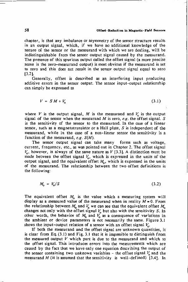
58 Of f set-Reduction in Magnetic-Field Sensors
chapter, is that any imbalance or asymmetry of the sensor structure results in an output signal, which, if we have no additional knowledge of the nature of the sensor or the measurand with which we are dealing, will be indistinguishable from the sensor output signal caused by the measurand. The presence of this spurious output called the offset signal (a more precise name is the zero-measurand output) is most obvious if the measurand is set to zero and this does not result in the sensor output signal equal to zero [3.2].
Generally, offset is described as an interfering input producing additive errors in the sensor output. The sensor input-output relationship can simply be expressed as
V = SM + V0 (3.1)
where V is the output signal, M is the measurand and V0 is the output signal of the sensor when the measurand M is zero, e.g. the offset signal. 5 is the sensitivity of the sensor to the measurand. In the case of a linear sensor, such as a magnetotransistor or a Hall plate, S is independent of the measurand, while in the case of a non-linear sensor the sensitivity is a function of the measurand, e.g. S(M).
The sensor output signal can take many forms such as voltage, current, frequency, etc., as was pointed out in Chapter 2. The offset signal V0, however, is always of the same nature as V [3.3]. A distinction must be made between the offset signal Va, which is expressed in the units of the output signal, and the equivalent offset M0, which is expressed in the units of the measurand. The relationship between the two offset definitions is the following:
K = K/s (3-2)
The equivalent offset M0 is the value which a measuring system will display as a measured value of the measurand when in reality M = 0. From the relationship between A , and V0 we can see that the equivalent offset M0 changes not only with the offset signal VQ but also with the sensitivity 5. In other words, the behavior of A£ and V0 as a consequence of variations in the ambient or device parameters is not necessarily the same. Figure 3.1 shows the input-output relation of a sensor with an offset signal V0.
If both the measurand and the offset signal are unknown quantities, it is clear from Eq. (3.1) and Fig. 3.1 that it is impossible to distinguish from the measured output V which part is due to the measurand and which to the offset signal. This introduces errors into the measurements which are caused by the fact that we have only one equation describing the output of the sensor containing two unknown variables - the offset signal V0 and the measurand M (it is assumed that the sensitivity is well-defined) [3.4]. In
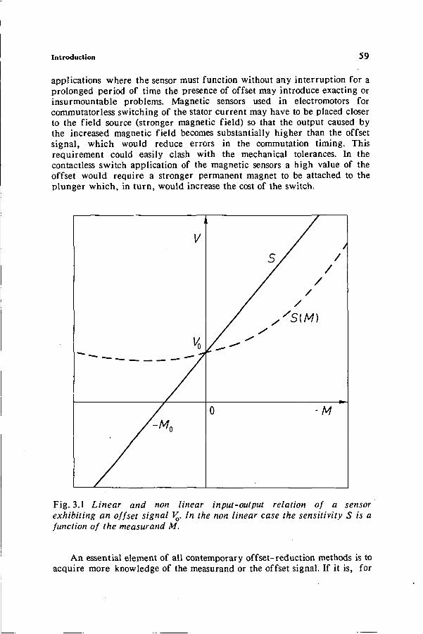
Introduction 59
applications where the sensor must function without any interruption for a prolonged period of time the presence of offset may introduce exacting or insurmountable problems. Magnetic sensors used in electromotors for commutatorless switching of the stator current may have to be placed closer to the field source (stronger magnetic field) so that the output caused by the increased magnetic field becomes substantially higher than the offset signal, which would reduce errors in the commutation timing. This requirement could easily clash with the mechanical tolerances. In the contactless switch application of the magnetic sensors a high value of the offset would require a stronger permanent magnet to be attached to the plunger which, in turn, would increase the cost of the switch.
Fig. 3.1 Linear and non linear input-output relation of a sensor exhibiting an offset signal V0, In the non linear case the sensitivity S is a function of the measurand M.
An essential element of all contemporary offset-reduction methods is to acquire more knowledge of the measurand or the offset signal. If it is, for
60 Offset-Reduction in Magnetic-Field Sensors
example, known that the measurand contains no dc or near-dc frequency components, the offset may be filtered away because it is a dc signal, and no data on the measurand will be lost. (The offset of a rotating carrier-domain magnetometer [3.5] is an exception as it is an alternating signal.) Similarly, if it is known that offset is a well-defined constant, the sensor could be calibrated once and for all. The offset signal, however, usually varies with temperature, strain and stress introduced by packaging, aging and other ambient variations (zero drift) and it may not be regarded as a constant [3.6]-[3.8]. This creates a need for an offset reduction method that can be applied during each measurement.
Several offset-reduction methods are known in the literature. Before we proceed with discussing the causes of offset in various magnetic sensors and the sensitivity-variation offset-reduction method, the most important offset-reduction methods will be briefly reviewed.
Improvement of the Fabrication Process
Most offset problems stem from imperfections in the fabrication process. If we again restrict ourselves to integrated sensors only, then inhomogeneous diffusion, epitaxy, oxidation, etc., and inaccurate mask alignment easily lead to large offset, especially when the sensor is based on diffused Wheatstone-bridge-like structures. In these types of devices a small error in the fabrication process can cause imbalance in the four bridge resistors, which produces offset in the output signal. There are, however, technological and cost limitations to the improvement of the fabrication process.
Better Sensor Structure Design
By a careful choice of geometry ratios, sensors could be designed with undiminished sensitivity and reduced offset. In [3.9] it is shown that the influence of mask rotation errors and etching errors can be reduced by carefully choosing the length/width ratio of Hall sensors. Unfortunately, not all structures are suitable for this method.
Offset Adjustment - Calibration
Before a measurement is started, one can isolate the measuring system from the measurand (or set the measurand to a known value). In doing so one of the two unknown variables has been eliminated. By means of additional adjustable electronic circuitry the output of the sensor can be adjusted to zero. Because of zero drift this adjustment has to be repeated often. A further disadvantage is that in many cases it is rather difficult or at least very inconvenient to set the measurand to zero, and this feature
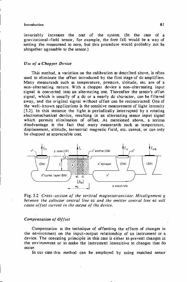
Introduction 61
invariably increases the cost of the system. (In the case of a gravitational-field sensor, for example, the free fall would be a way of setting the measurand to zero, but this procedure would probably not be altogether agreeable to the sensor.)
Use of a Chopper Device
This method, a variation on the calibration as described above, is often used to eliminate the offset introduced by the first stage of dc amplifiers. Many measurands such as temperature, pressure, altitude, etc. are of a non-alternating nature. With a chopper device a non-alternating input signal is converted into an alternating one. Thereafter the sensor's offset signal, which is usually of a dc or a nearly dc character, can be filtered away, and the original signal without offset can be reconstructed. One of the well-known applications is the sensitive measurement of light intensity [3.2]. In this instance the light is periodically interrupted by a rotating electromechanical device, resulting in an alternating sensor input signal which permits elimination of offset. As mentioned above, a serious disadvantage is the fact that many measurands such as temperature, displacement, altitude, terrestrial magnetic field, etc. cannot, or can only be chopped at appreciable cost.
p substrate
Fig. 3.2 Cross-section of the vertical magnetotransistor. Misalignment x between the collector central line cc and the emitter central line ec will cause offset current in the output of the device.
Compensation of Offset
Compensation is the technique of offsetting the effects of changes in the environment on the input-output relationship of an instrument or a device. The operating principle in this case is either to prevent changes in the environment or to make the instrument insensitive to changes that do occur.
In our case this method can be employed by using matched sensor
62 Offset-Reduction in Magnetic-Field Sensors
elements integrated on the same silicon chip. The method is based on the observation that neighboring elements on a silicon wafer often exhibit comparable imperfections, which makes it probable that neighboring sensors will also exhibit nearly the same sensitivity and offset values. One of the sensors can then be used as an offset reference, providing it is well shielded from the measurand.
3.2 CAUSES OF OFFSET AND ITS REDUCTION
3.2.1 Magnetotransistors
Offset in vertical and lateral magnetotransistors which are based on the current deflection principle is mainly caused by the geometrical asymmetries of the sensor structure. These asymmetries are inevitably introduced during the processing steps of the sensor wafer. Their main cause is the presence of alignment errors between masks which define the current source of the sensor (emitter and base diffusions) and the collectors of the device.
In Fig. 3.2 the cross-section of the vertical 1-D magnetotransistor is given. Lines ec and cc represent the middle of the emitter and the middle of the collector region, respectively. If the in-plane magnetic field is zero, the emitter current to the left of the collector center line cc (current in the A and B regions of Fig. 3.2) will be collected in this simplified model by the left collector of the sensor, while the right buried layer and its deep-n (DN) diffusion contact will likewise collect the current which enters the n~ collector region to the right of the collector central line cc (current in the C region). We can readily see that if the two central lines, ec and cc do not coincide, one of the collectors will draw more current than its complement even if B = 0 - and we have offset.
To expose the causes for misalignment between the two central lines of Fig. 3.2 some understanding of bipolar IC processing is essential. The starting material for an npn device is a p-type substrate. The buried layers which enhance the sensitivity of the device are defined by the first diffusion step. Before the growth of the epitaxial layer the pattern of the buried layers is marked by a slight depression, which is the result of the difference in the oxidation rates between the exposed silicon and the regions covered by Si02 [3.10], [3.11]. These depressions, which are 0.2 nm deep [3.11], are subsequently covered by the n-epitaxial layer. It is of primary importance that these depressions be faithfully reproduced on the surface after the epilayer growth, as further visual mask alignment has no other reference but these reliefs on the surface. Next comes the deep-p (DP) isolation diffusion, which is aligned with respect to the relief of the buried layers. This diffusion subsequently serves as the alignment
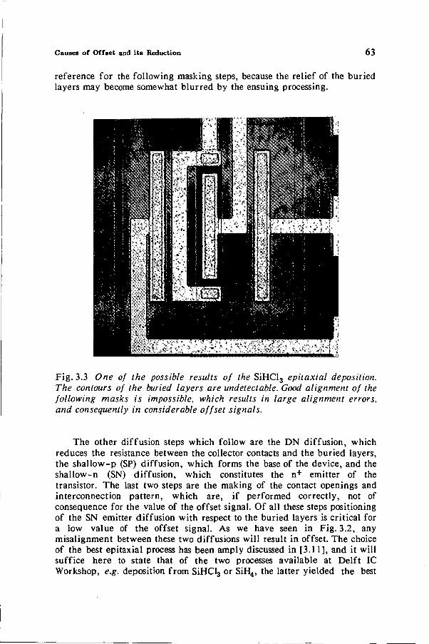
Causes of Offset and its Reduction 63
reference for the following masking steps, because the relief of the buried layers may become somewhat blurred by the ensuing processing.
Fig. 3.3 One of the possible results of the SiHCl3 epitaxial deposition. The contours of the buried layers are undetectable. Good alignment of the following masks is impossible, which results in large alignment errors, and consequently in considerable offset signals.
The other diffusion steps which follow are the DN diffusion, which reduces the resistance between the collector contacts and the buried layers, the shallow-p (SP) diffusion, which forms the base of the device, and the shallow-n (SN) diffusion, which constitutes the n+ emitter of the transistor. The last two steps are the making of the contact openings and interconnection pattern, which are, if performed correctly, not of consequence for the value of the offset signal. Of all these steps positioning of the SN emitter diffusion with respect to the buried layers is critical for a low value of the offset signal. As we have seen in Fig. 3.2, any misalignment between these two diffusions will result in offset. The choice of the best epitaxial process has been amply discussed in [3.11], and it will suffice here to state that of the two processes available at Delft IC Workshop, e.g. deposition from SiHCl3 or SiH4, the latter yielded the best
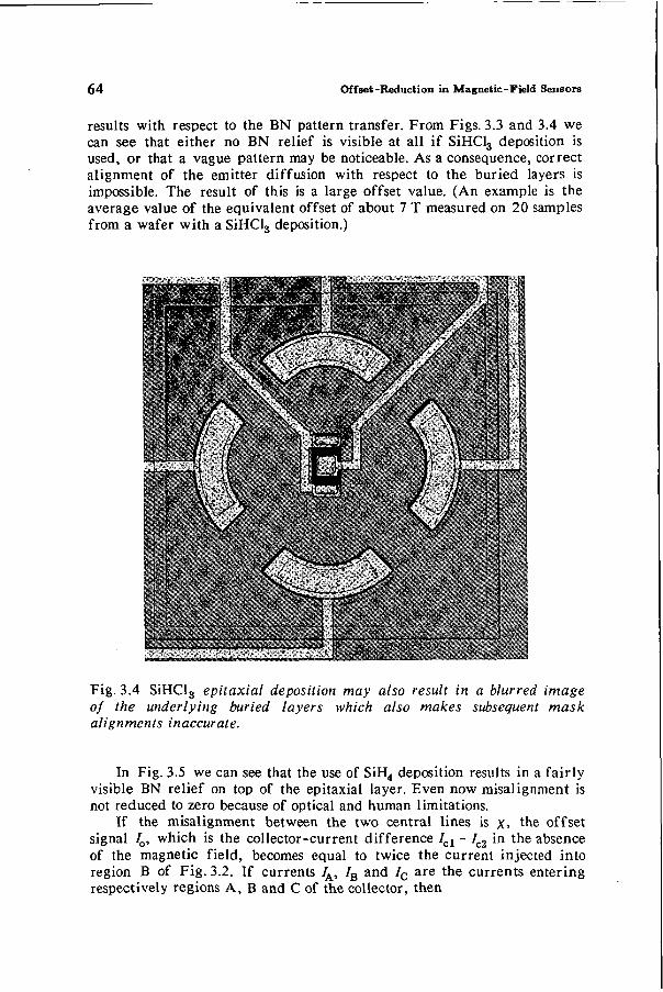
64 Of f set-Reduction in Magnetic-Field Sensors
results with respect to the BN pattern transfer. From Figs. 3.3 and 3.4 we can see that either no BN relief is visible at all if SiHCl3 deposition is used, or that a vague pattern may be noticeable. As a consequence, correct alignment of the emitter diffusion with respect to the buried layers is impossible. The result of this is a large offset value. (An example is the average value of the equivalent offset of about 7 T measured on 20 samples from a wafer with a SiHCl3 deposition.)
Fig. 3.4 SiHCl3 epitaxial deposition may also result in a blurred image of the underlying buried layers which also makes subsequent mask alignments inaccurate.
In Fig. 3.5 we can see that the use of SiH4 deposition results in a fairly visible BN relief on top of the epitaxial layer. Even now misalignment is not reduced to zero because of optical and human limitations.
If the misalignment between the two central lines is x> the offset signal I0, which is the collector-current difference 7cl - /c2 in the absence of the magnetic field, becomes equal to twice the current injected into region B of Fig. 3.2. If currents IA, IB and Ic are the currents entering respectively regions A, B and C of the collector, then
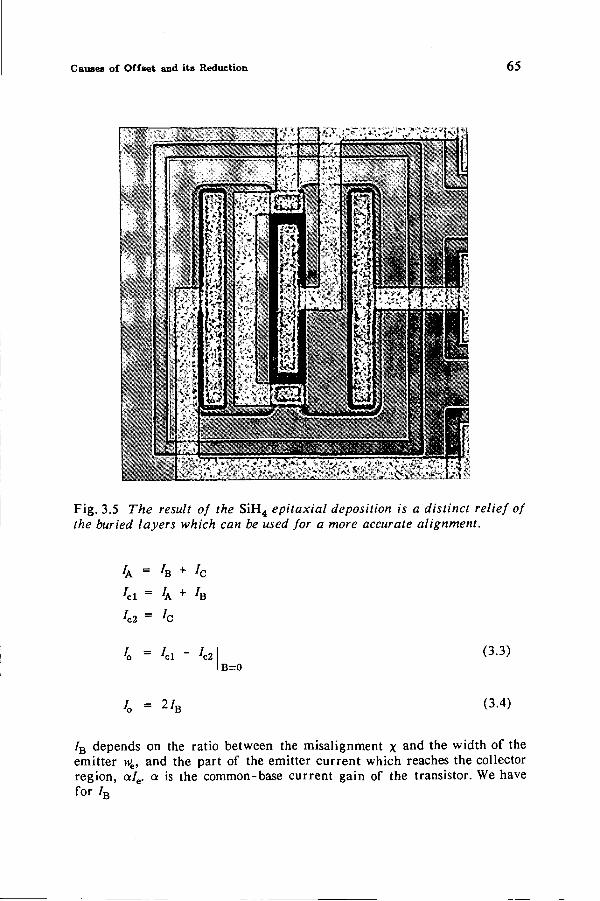
Causes of Offset and its Reduction 65
Fig. 3.5 The result of the SiH4 epitaxial deposition is a distinct relief of the buried layers which can be used for a more accurate alignment.
'A = 'B + ' c
'e l = 7A + 'B
hi = 'c
4 = hi - ' c 2 | (3-3> IB=O
4 = 2 ' B (3-4)
/B depends on the ratio between the misalignment x a n d the width of the emitter we, and the part of the emitter current which reaches the collector region, a/e. a is the common-base current gain of the transistor. We have f o r / B
66 Offset-Reduction in Magnetic-Field Sensors
'B = - < * / . (3-5)
Finally, with Eq. (3.4) the offset signal of the vertical magnetotransistor becomes
4 = 2 ^ a / e (3.6)
The output signal of the magnetotransistor, the collector-current difference A/c, can be written as
A/c = ^B + /0 (3.7)
In Chapter 2 we have seen that the magnetic sensitivity ^ (Eq. (2.14)) of the vertical magnetotransistor can be expressed as
Sm = 2 ^ H a / e (3.8)
The equivalent offset B0 of this sensor is according to Eq. (3.2):
*o = 'oAn (3-9)
and with Eq. (3.6) the equivalent offset becomes
X 4, = 77— (3.10)
The relative offset signal 5, which is the ratio between the offset signal I0 and the total collector current a/e is
If a small equivalent offset is desired, the value of the offset signal I0 should be low, which requires a low value of the misalignment x- The magnetic sensitivity should be as high as possible (both the deflection
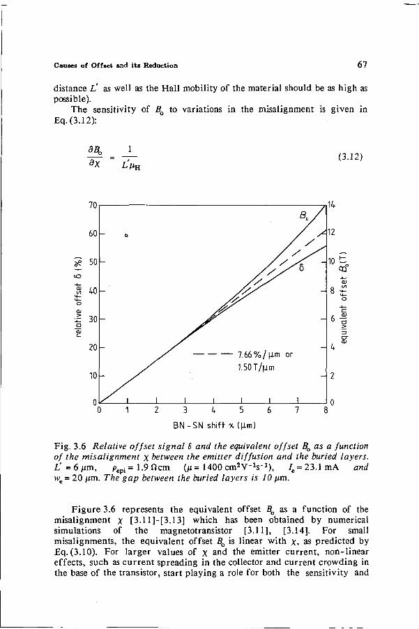
Causes of Offset and its Reduction 67
distance L' as well as the Hall mobility of the material should be as high as possible).
The sensitivity of B0 to variations in the misalignment is given in Eq.(3.12):
3$ , dx
1
L'MH (3.12)
70
60
<o
o
I
50 -
40-
■S 30
20
10-
— o
-
-
-
-
/ I I
B * / / ^
/ / . / / s '
/ / / /Ï/ /IT
/T
/ 7.66%/|im or 1.50 T/^m
I l I l I
14
10 ~ QQ°
<U
c k -2! 6 ^
> cr 01
- 4
3 4 5 BN-SN shift 'x(|im)
Fig. 3.6 Relative offset signal 8 and the equivalent offset B0 as a function of the misalignment x between the emitter diffusion and the buried layers.
6 /xm, pep i= 1.9 «cm (/ i=1400cm2V-1s- a) , w = 20 /xm. The gap between the buried layers is 10 iim.
/e = 23.1 mA and
Figure 3.6 represents the equivalent offset B0 as a function of the misalignment x [3.11]-[3.13] which has been obtained by numerical simulations of the magnetotransistor [3.11], [3.14]. For small misalignments, the equivalent offset BQ is linear with x, as predicted by Eq. (3.10). For larger values of x and the emitter current, non-linear effects, such as current spreading in the collector and current crowding in the base of the transistor, start playing a role for both the sensitivity and
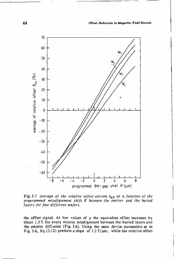
68 Offset-Reduction in Magnetic-Field Sensors
- 4 - 2 0 2 4 6 8 programmed BN-gap shift K (|im)
Fig. 3.7 Average of the relative offset current 5AV as a function of the programmed misalignment shift K between the emitter and the buried layers for four different wafers.
the offset signal. At low values of x the equivalent offset increases by about 1.5 T for every micron misalignment between the buried layers and the emitter diffusion (Fig. 3.6). Using the same device parameters as in Fig. 3.6, Eq. (3.12) predicts a slope of 1.2 T//zm, while the relative offset
Causes of Offset and its Reduction 69
current of Eq. (3.11) increases by 10%//im compared to 7.66 %//«n of Fig. 3.6. Considering the simplicity of the model used in the derivation of Eqs. (3.11) and (3.12), and the fact that a fairly high emitter current was used in Fig. 3.6, Eqs. (3.11) and (3.12) are reasonable approximations of the behavior of the equivalent offset and the relative offset current for small values of x and low values of the emitter current.
Besides the high emitter current the discrepancy between the simple model of Fig. 3.2 and the numerical results presented in Fig. 3.6 stems from the use of we and L' values as they are determined by the dimensions of the sensor and not by the electrical properties of the device. In Fig. 3.2 the current has been represented as if it had only a vertical component, which is the reason that we in Eq. (3.6) is the width of the emitter. In reality, the current will spread laterally, which increases the effective value of V14. To obtain the same value of the relative offset current increase of 7.66 %//tm obtained by numerical simulations, the effective value of we would have to be 26 /mi instead of we = 20 /mi, which is the physical width of the emitter.
The value of L' is also somewhat ambiguous. It is the distance over which charge carriers are deflected by the magnetic field. Ideally L' should be equal to the thickness of the epilayer. However, carrier deflection in the heavily doped emitter, base and buried layer regions of the sensor is much lower than in the low doped epitaxial layer. Also, the effects of current spreading on the sensitivity cannot be taken into account by the same effective value of we found for the offset signal, because the local current density along and in the vicinity of the cc line of Fig. 3.2 plays an important role with respect to the sensitivity. From Eq. (3.12) we can see that an effective L' value of 5 /xm results in the same slope of the B0 vs. x curve as in Fig. 3.6.
In [3.11]-[3.13] the influence of the misalignment on the offset of the vertical magnetotransistor has been experimentally determined. To that end, 17 sensors have been positioned close together on a chip, while each of the devices has been designed with a different "mask-programmed" shift in the buried-layer gap with respect to the emitter. The gap shift £ had a value of n pm with n = -8,...,0,...,+8. The results of offset measurements performed on four different wafers are shown in Fig. 3.7. The data points represent the average of 27 chips. The slope of the curves around K=0 is about 8.25 %/nm, which agrees well with the theoretical predictions. The value of K at 5AV = 0 yields the (negative) intrinsic value of the average misalignment XAV For the f ° u r wafers in question the absolute value of XAV ranges from 0.36/xm to 1.24/jm, which yields values of the equivalent offset as high as 2 T.
The cause of offset in lateral magnetotransistors based on carrier deflection is also the misalignment of the emitter with respect to the collector diffusions. The problem in these devices is far less severe because the emitter and the collectors are made simultaneously by the same mask. This is evidenced by a lower value of the equivalent offset which is below 50 mT, as given by Table 2.2 of the preceding chapter.
7 0 Offset-Reduction in Magnetic-Field Sensors
In injection-modulation devices misalignment of the emitter with respect to the base diffusion plays a more important role. A misalignment of these two diffusions will result in an asymmetrical emitter-base bias along the junction, and consequently offset. The base of these devices is essentially a Hall plate, and all causes of offset in Hall plates will also play a role in injection modulation magnetotransistors.
Finally, the last important cause of offset in magnetotransistors will be mentioned. That is the presence of impedance imbalance in the collector leads of the magnistor, which may be introduced by the imperfections in the electronic circuitry connected to these leads. An impedance imbalance in the collector leads will cause the collector with the smaller impedance to carry more current. The reason for this phenomenon is the fact that the collectors of the magnetotransistor do not behave as perfect current sources. (This is not valid for devices in which the collectors are electrically isolated from each other.) There is a finite intercollector resistance between the collectors which depends on the gap between the collectors, the thickness of the epitaxial layer and its resistivity. More will be said about the influence of the collector impedance imbalance on the offset of the vertical magnetotransistor in one of the following sections.
3.2.2 Hall Plates
Causes of Offset in Hall Plates
The output voltage VH of a Hall plate under a constant current bias (/8) condition can be represented as follows [3.15]:
VH = -W? + *i'. + Vs2 + Vs3 + ijg (3.13)
.S^JJ is the magnetic sensitivity of the Hall plate which has been presented in Chapter 2 (the geometric correction factor is neglected here):
3nH = ^H— current bias
(3.14) c _ wH ■ iH - PH-J—K voltage bias (p-type)
The other terms in Eq. (3.13) are offset errors in the output of the
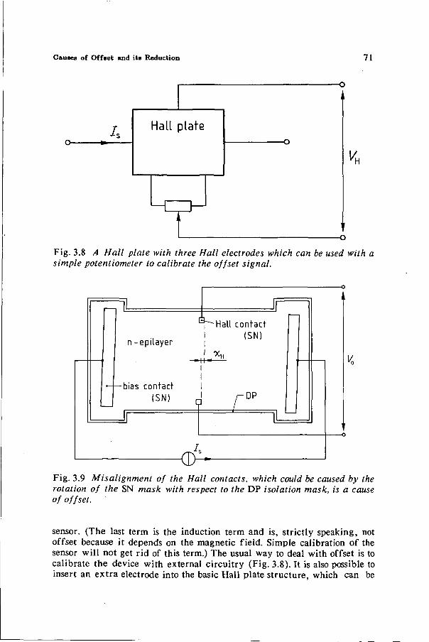
Causes of Offset and its Reduction 71
Is Hall plate
i i
O
Q
O
\/u
Fig. 3.8 A Hall plate with three Hall electrodes which can be used with a simple potentiometer to calibrate the offset signal.
&-.
n-epilayer
bias contact (SN)
Hall contact (SN)
P ruu / .
<I> Fig. 3.9 Misalignment of the Hall contacts, which could be caused by the rotation of the SN mask with respect to the DP isolation mask, is a cause of offset.
sensor. (The last term is the induction term and is, strictly speaking, not offset because it depends on the magnetic field. Simple calibration of the sensor will not get rid of this term.) The usual way to deal with offset is to calibrate the device with external circuitry (Fig. 3.8). It is also possible to insert an extra electrode into the basic Hall plate structure, which can be
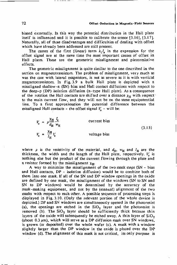
72 Offset-Reduction in Magnetic-Field Sensors
biased externally. In this way the potential distribution in the Hall plate itself is influenced and it is possible to calibrate the sensor [3.16], [3.17]. Naturally, all of those disadvantages and difficulties of dealing with offset which have already been addressed are still present.
The causes of the first (linear) term k±It in the expression for the offset signal are at the same time the most important causes of offset in Hall plates. These are the geometric misalignment and piezoresistive effects.
The geometric misalignment is quite similar to the one described in the section on magnetotransistors. The problem of misalignment, very much as was the case with lateral magnistors, is not as severe as it is with vertical magnetotransistors. In Fig. 3.9 a bulk Hall plate is depicted with a misaligned shallow-n (SN) bias and Hall contact diffusions with respect to the deep-p (DP) isolation diffusion (n-type Hall plate). As a consequence of the rotation the Hall contacts are shifted over a distance XH w^ t n respect to the main current flow, and they will not be on the same equipotential line. To a first approximation the potential difference between the misaligned Hall contacts - the offset signal VQ - will be:
y _ o^S-S. current bias H H (3.15)
V0 = y Vs voltage bias
where p is the resistivity of the material, and dH, vvH and /H are the thickness, the width and the length of the Hall plate, respectively. Va is nothing else but the product of the current flowing through the plate and a resistor formed by the misalignment XH-
A way to minimize the misalignment of the two mask steps (SN - bias and Hall contacts, DP - isolation diffusion) would be to combine both of them into one mask. If all of the SN and DP window openings in the oxide are defined by one mask, the misalignment of the windows (SN to SN and SN to DP windows) would be determined by the accuracy of the mask-making equipment, and not by the (manual) alignment of the two masks with respect to each other. A possible sequence of processing steps is displayed in Fig. 3.10. (Only the relevant portion of the whole device is depicted.) DP and SN windows are simultaneously opened in the photoresist (a), the openings are etched in the Si02 layer and the photoresist is removed (b). The Si02 layer should be sufficiently thick because thin layers of the oxide will subsequently be etched away. A thin layer of Si02 (about 0.3 /an), which will serve as a DP diffusion mask over SN windows, is grown (or deposited) over the whole wafer (c). A mask with a window slightly larger than the DP window in the oxide is placed over the DP window (d). The alignment of this mask is not critical, its only purpose is
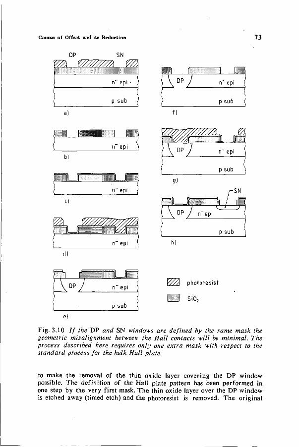
Causes of Offset and its Reduction 73
DP SN
n" epi
p sub
a)
n epi b)
UE 0
d)
K"*-?-!*"! F " ^ LJE DP n epi
p sub
e)
DP n epi
p sub
photoresist
f " ! Si02
Fig. 3.10 If the DP and SN windows are defined by the same mask the geometric misalignment between the Hall contacts will be minimal. The process described here requires only one extra mask with respect to the standard process for the bulk Hall plate.
to make the removal of the thin oxide layer covering the DP window possible. The definition of the Hall plate pattern has been performed in one step by the very first mask. The thin oxide layer over the DP window is etched away (timed etch) and the photoresist is removed. The original
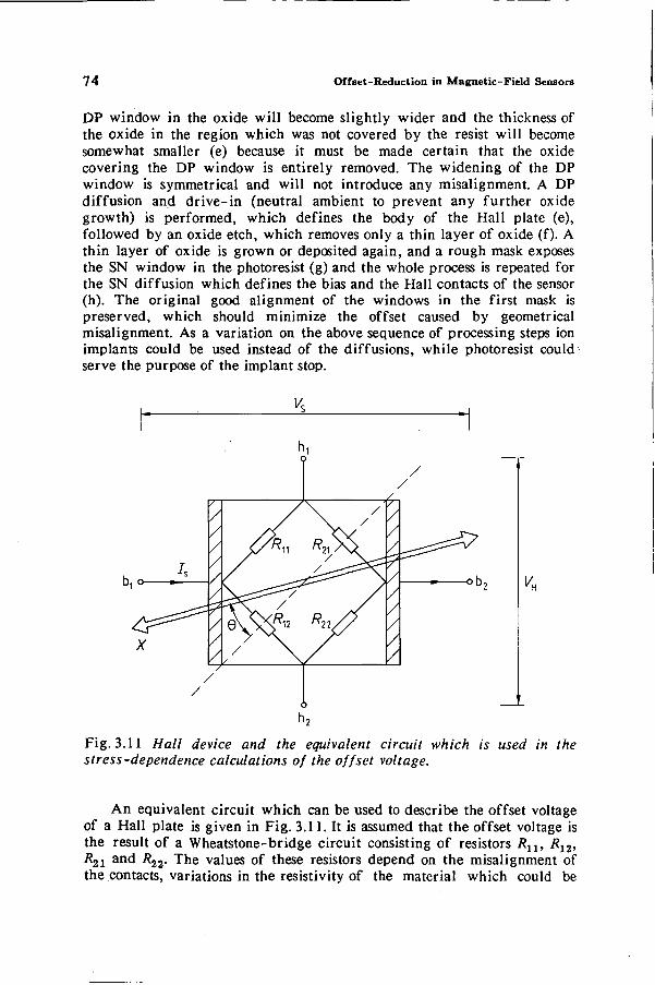
7 4 Offset-Reduction in Magnetic-Field Sensors
DP window in the oxide will become slightly wider and the thickness of the oxide in the region which was not covered by the resist will become somewhat smaller (e) because it must be made certain that the oxide covering the DP window is entirely removed. The widening of the DP window is symmetrical and will not introduce any misalignment. A DP diffusion and drive-in (neutral ambient to prevent any further oxide growth) is performed, which defines the body of the Hall plate (e), followed by an oxide etch, which removes only a thin layer of oxide (f). A thin layer of oxide is grown or deposited again, and a rough mask exposes the SN window in the photoresist (g) and the whole process is repeated for the SN diffusion which defines the bias and the Hall contacts of the sensor (h). The original good alignment of the windows in the first mask is preserved, which should minimize the offset caused by geometrical misalignment. As a variation on the above sequence of processing steps ion implants could be used instead of the diffusions, while photoresist could serve the purpose of the implant stop.
h, o
/ /
/ /
o h2
Fig. 3.11 Hall device and the equivalent circuit which is used in the stress-dependence calculations of the offset voltage.
An equivalent circuit which can be used to describe the offset voltage of a Hall plate is given in Fig. 3.11. It is assumed that the offset voltage is the result of a Wheatstone-bridge circuit consisting of resistors Rlly R12, R21 and R22. The values of these resistors depend on the misalignment of the contacts, variations in the resistivity of the material which could be
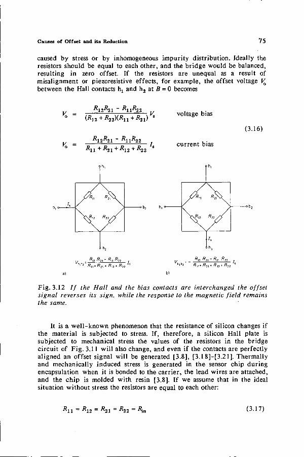
Causes of Offset and its Reduction 75
caused by stress or by inhomogeneous impurity distribution. Ideally the resistors should be equal to each other, and the bridge would be balanced, resulting in zero offset. If the resistors are unequal as a result of misalignment or piezoresistive effects, for example, the offset voltage V0 between the Hall contacts hx and h2 at B = 0 becomes
K =
K =
^ 1 2 ^ 2 1 RnR •22 (R12 + ^ 2 2 X ^ 1 1 + ^21)
^ 1 1 + ^ 2 1 + ^ 1 2 + ^22
voltage bias
current bias
(3.16)
ob; b, o
Ru /?,, - R„ R22 ">*'' R „ . R2t* Ru*R2i
Rn R„ - /?„ R22 ' h . h . n r* r. /-1 JS R,yt R2, ♦ Rn* R22
Fig. 3.12 If the Hall and the bias contacts are interchanged the offset signal reverses its sign, while the response to the magnetic field remains the same.
It is a well-known phenomenon that the resistance of silicon changes if the material is subjected to stress. If, therefore, a silicon Hall plate is subjected to mechanical stress the values of the resistors in the bridge circuit of Fig. 3.11 will also change, and even if the contacts are perfectly aligned an offset signal will be generated [3.8], [3.18]-[3.21]. Thermally and mechanically induced stress is generated in the sensor chip during encapsulation when it is bonded to the carrier, the lead wires are attached, and the chip is molded with resin [3.8]. If we assume that in the ideal situation without stress the resistors are equal to each other:
^ 1 1 _ ^ 1 2 = ^ 2 1 _ ^22 - ^in (3.17)
76 Offset-Reduction in Magnetic-Field Sensors
and if stress X is then applied at an angle 9 to the diagonal of the Hall plate (Fig. 3.11) the resistances can be expressed as [3.21]
* n = *22 = ^ U 1 + (*iCos2e + 7rtsin26)X] (3.18)
Rn = R21 = .Rjjl + 0r1sin2e+-7Ttcos2e)X]
7T[ and 7rt are the longitudinal and transverse piezoresistance constants with respect to the diagonal of the Hall plate. With Eq. (3.16) the expression for the offset signal becomes
(*i - 7rt)(sin2e - cos20)X Vn = V voltage bias
2 + (7r, + 7rt)(sin2e + cos2e)X (3.19)
(TT, - 7rt)(sin2e - cos20)X V. = : /. current bias
The crystallographic orientations of the Hall plate and the current flow are very important for a low value of offset caused by piezoresistive effects. In [3.8], [3.18]-[3.21 ] it was determined that Hall devices with a <100> direction of current flow in the (110) plane have the minimum offset voltage caused by stress and strain, while devices with a <110> current flow in the (100) plane are most sensitive to piezoresistive effects.
Symmetrical Hall plates, devices in which the Hall contacts and the bias contacts are interchangeable, offer a very interesting possibility of reducing offset caused by both the misalignment and the piezoresistance effects [3.22]-[3.24]. This is depicted in Fig. 3.12. In Fig. 3.12a the offset signal is described by Eq. (3.16), and the Hall voltage between contacts hy and h2 is
^H = W * + K (3-20)
If we interchange the bias and the Hall contacts according to Fig. 3.12b the Hall voltage between contacts bx and b2 becomes
VH = - W ? - K (3.21)
We can see that by interchanging the bias and the Hall contacts the sign of the offset signal is reversed, while the sensitivity or the response to
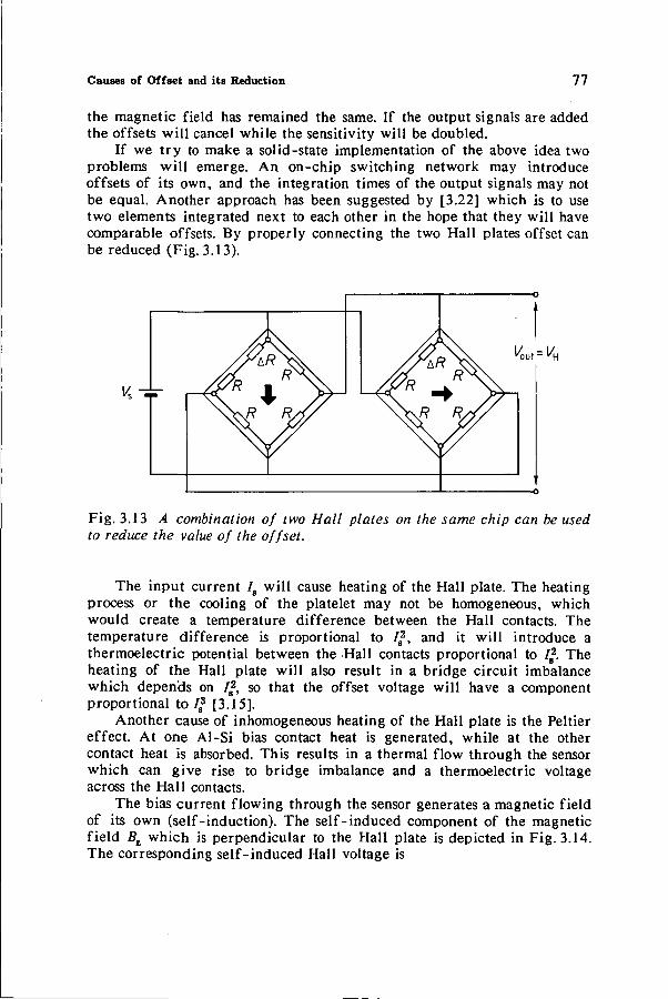
Causes of Offset and its Reduction 77
the magnetic field has remained the same. If the output signals are added the offsets will cancel while the sensitivity will be doubled.
If we try to make a solid-state implementation of the above idea two problems will emerge. An on-chip switching network may introduce offsets of its own, and the integration times of the output signals may not be equal. Another approach has been suggested by [3.22] which is to use two elements integrated next to each other in the hope that they will have comparable offsets. By properly connecting the two Hall plates offset can be reduced (Fig. 3.13).
Fig. 3.13 A combination of two Hall plates on the same chip can be used to reduce the value of the offset.
The input current /8 will cause heating of the Hall plate. The heating process or the cooling of the platelet may not be homogeneous, which would create a temperature difference between the Hall contacts. The temperature difference is proportional to /s
2, and it will introduce a thermoelectric potential between the Hall contacts proportional to 72. The heating of the Hall plate will also result in a bridge circuit imbalance which depends on /2, so that the offset voltage will have a component proportional to/8
3 [3.15]. Another cause of inhomogeneous heating of the Hall plate is the Peltier
effect. At one Al-Si bias contact heat is generated, while at the other contact heat is absorbed. This results in a thermal flow through the sensor which can give rise to bridge imbalance and a thermoelectric voltage across the Hall contacts.
The bias current flowing through the sensor generates a magnetic field of its own (self-induction). The self-induced component of the magnetic field BE which is perpendicular to the Hall plate is depicted in Fig. 3.14. The corresponding self-induced Hall voltage is
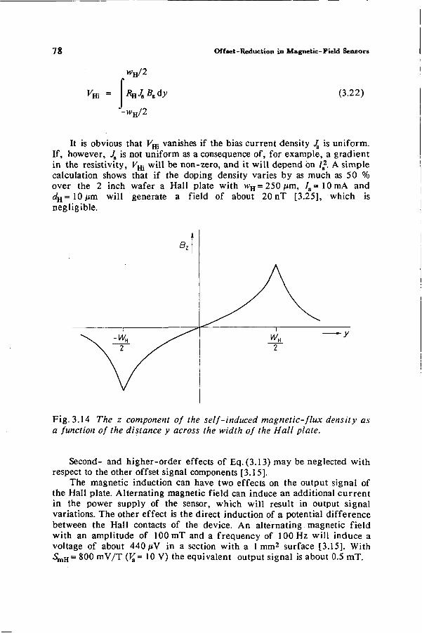
78 Offset-Reduction in Magnetic-Field Sensors
Vm =
wH/2
wu/2
(3.22)
It is obvious that FHi vanishes if the bias current density Js is uniform. If, however, Ja is not uniform as a consequence of, for example, a gradient in the resistivity, Vm will be non-zero, and it will depend on Q. A simple calculation shows that if the doping density varies by as much as 50 % over the 2 inch wafer a Hall plate with wH = 250/im, / s=10mA and t/H=10//m will generate a field of about 20 nT [3.25], which is negligible.
Fig. 3.14 The z component of the self-induced magnetic-flux density as a function of the distance y across the width of the Hall plate.
Second- and higher-order effects of Eq. (3.13) may be neglected with respect to the other offset signal components [3.15].
The magnetic induction can have two effects on the output signal of the Hall plate. Alternating magnetic field can induce an additional current in the power supply of the sensor, which will result in output signal variations. The other effect is the direct induction of a potential difference between the Hall contacts of the device. An alternating magnetic field with an amplitude of 100 mT and a frequency of 100 Hz will induce a voltage of about 440 /iV in a section with a 1 mm2 surface [3.15]. With SmH= 800 mV/T {Vs= 10 V) the equivalent output signal is about 0.5 mT.
Causes of Offset and its Reduction 79
"
' m a x
1
W "max
W6
'd
r ^ -
Fig. 3.15 Insulating dams are applied near the Hall contacts in order to reduce the .equivalent offset caused by the misalignment. ld is the length of the dams, wd is the distance between the dams and dd is their thickness. The length of the Hall plate is /H = wmax which is at the same time the largest value which the thickness of the dams can attain, and the width of the platelet is wH = 2/m a x = wmax/2, where /max is the maximum length of the dams.
Sensitivity and Offset Simulations on Hall Plates
In [3.26] and [3.27] a multi-electrode structure is presented with isolation walls enclosing the contacts which, it is claimed, reduces the effect of offset and also reduces the interaction between the bias and the Hall contacts. To obtain some insight into the effect of insulating dams around the contacts a finite difference numerical simulation has been performed [3.28], [3.29] on a simplified structure of Fig. 3.15, which features a Hall plate with an aspect ratio ln/wH = 2. The Hall contacts are enclosed by the insulating dams (DP diffusion). It is fairly clear from Fig. 3.16, which represents a rough equivalent resistor circuit of the two cases - with and without the insulating dams, that the offset signal is reduced. In Fig. 3.16a an ordinary Hall plate without dams is represented by a number of parallel resistors which are shorted at their base by the bias contacts. The geometric misalignment is represented by three serial resistors on the sides. The value of the offset signal is / j / ^ . In the case with insulating dams (Fig. 3.16b) the resistors are no longer shorted at their base. As a consequence, the path to 1^ has a higher resistance compared to the case of Fig. 3.16a. In other words, I1Rm> V^n> anc* t n e offset signal is reduced. The effect the dams will have on the sensitivity and consequently
80 Of f Bet-Reduction in Magnetic-Field Sensors
'■!
Fig. 3.16 Basic equivalent circuit of a Hall plate, a) No insulating dams. b) Insulating dams decrease the value of the current flowing through the misalignment resistors 1^.
Fig. 3.17 Example of a potential distribution (equipotential lines) for a non-zero magnetic field. The Hall angle is 35°.
on the equivalent offset is not as clear. The simulations have been performed for different values of the
parameters /d, wd and dd, and the results have been compared each time to the Hall plate structure without insulating dams (/d = 0). The effects of the parameter variations on the sensitivity, offset signal and equivalent offset were determined by the numerical simulation of the potential distribution in the Hall plate. The potential distribution in the plane of the device is obtained by solving Laplace's equation. To that end the differential equation was discretized into a system of five-point difference equations. The system was solved iteratively, using the successive over-relaxation
Causes of Offset and its Reduction
Fig. 3.18 Sensitivity vs. the distance between the dams wd, and the length of the dams ld. The sensitivity S^n is normalized to the value of the sensitivity S^n of a Hall plate without dams. ld and wd are normalized to their maximum values /_a, and w> v. Constant-current bias.
method [3.28], [3.29]. A typical solution for a non-zero magnetic field is shown in Fig. 3.17. The simulations were performed for infinitely small Hall contacts and a misalignment of these contacts, which results in a 1 T equivalent offset for the case without dams. The results are presented in Figs. 3.18-3.20.
From Fig. 3.18 we can see that the sensitivity at a constant-current bias increases slightly with the length of the dams /d, and it decreases with the distance between the dams wd. The reason for this is that longer dams and shorter distance between them reduce the shorting effect of the bias contacts and, therefore, increase the output signal of the sensor. The thickness of the dams dd is of almost no consequence under the above conditions.
In the case of a constant-voltage bias, the sensitivity decreases with the
82 Offset-Reduction in Magnetic-Field Sensors
Fig. 3.19 Offset signal V0 (normalized by the value of the offset signal Va of a Hall plate without dams) as a function of wd and ld.
thickness dd of the insulating dams when wd is kept constant. A decrease in the sensitivity is also observed for increasing dam length /d. These are accounted for by the increasing resistance of the platelet, which reduces the current available for deflection (while if a constant current bias is used, this is not the case).
The offset signal becomes smaller if the dams are placed closer together (Fig. 3.19), regardless of the type of supply. The reason for this is the decrease in the current (and the electric field) in the vicinity of the Hall contacts with decreasing wd. At constant-current bias conditions the offset signal does not vary significantly with the thickness of the dams dd. Longer dams decrease the value of the offset signal because this also decreases the local current around the Hall contacts.
Figure 3.20 is the result of Figs. 3.18 and 3.19. We can see that the equivalent offset decreases if the dams are placed close together. The same effect can be observed for increasing dam length /d. In other words, the
Causes of Offset and its Reduction 83
Fig. 3.20 Equivalent offset B0 (normalized by the value of the equivalent offset B° of a Hall plate without dams) as a function of wd and /d.
equivalent offset is reduced when the Hall contacts are properly shielded by the dams.
As a summary we can say that the equivalent offset of a Hall plate can be reduced by insulating dams because they have the ability to reduce the current and the electric field in the vicinity of the Hall contacts, which in turn reduces the offset voltage of the Hall plate. The sensitivity of the platelet, however, is proportional to the total current that flows between the Hall contacts. A large portion of the total current is forced by the dams to flow in the middle of the Hall plate, and far away from the Hall contacts, which does not impair the sensitivity while the offset signal is reduced. In Fig. 3.21 the x component of the current density is depicted along the cross-section through the middle of a typical Hall plate with insulating dams.
8 4 Offset-Reduction in Magnetic-Field Sensors
Fig. 3.21 The x component of the current density Jx along the cross-section through the middle of a typical Hall plate depicted in the inset. The current density is normalized to its maximum value Jx m a x , and B = 0.
3.2.3 Other Magnetic Sensors
In the preceding sections causes of offset in magnetotransistors and bulk Hall plates have been discussed. However, all the other magnetic sensors which were described in Chapter 2 also suffer from the presence of offset. The causes of offset in FET Hall devices are the same as for the bulk Hall devices, except that the gate of a FET Hall plate defines the active region. Variation of the channel resistivity may also be more difficult to control compared to the uniformity of the epitaxial layer of a bulk Hall sensor.
Hall plates incorporated in an integrated circuit will have the same problems with offset as the stand-alone sensors, while additional problems will be created by asymmetries of the amplification circuit itself. Sensors like DAMS and others with on-chip amplifiers may have large sensitivities as a consequence of signal amplification, but the offset signal of the sensor is increased by the same amplification factor, too. The equivalent offset of these circuits, which is a measure of quality of the sensor with respect to offset, will not change with amplification, or it could even become worse because of the possible introduction of extra offset by the electronic
Sensitivity-Variation Offset-Reduction Method 85
circuitry. Carrier-domain devices are also not exempt from offset problems. One
of the causes of offset in vertical carrier-domain devices is the misalignment of the buried layer gap with respect to the base and the emitter of the device [3.30]. Lateral devices suffer from the so-called threshold field below which the device does not function [3.31], The threshold field may be interpreted as a form of offset. In devices which do not have threshold field problems [3.32] the zero output frequency (the frequency is the output signal of this sensor) is also not determined exactly.
Magnetodiodes and magnetoresistors [3.33] have by their very nature a large quiescent signal. The response to the magnetic field is measured with respect to this quiescent signal. If these elements are used in a bridge-like circuit the offset (quiescent) signal is reduced, but asymmetries of the bridge are the new cause of offset.
3.3 SENSITIVITY-VARIATION OFFSET-REDUCTION METHOD
3.3.1 The Basic Principles
From the foregoing analysis of offset it appears that the offset problem is best characterized by the fact that the input-output relation of a sensor is represented by one (linear) equation with two unknowns. In one of the offset-reduction methods described in the previous sections the second equation, which is necessary if the equations are to be solved for the measurand, is obtained by setting the measurand to zero and thereby determining the value of the offset signal. This is sufficient to separate the offset signal from the response to the measurand. In the other offset-reduction method two linear equations with two unknowns are obtained by using two devices with nearly equal offsets [3.22]. In the new method proposed in [3.4], the sensor is activated on two subsequent occasions in such a way that, again, two solvable linear equations are obtained with two unknowns.
If the energy input ports of the modulating transducers are disregarded, sensors are usually looked upon as two-port devices (input and output ports), as shown in Fig. 3.22a. In the new method presented here [3.34], this is not the case. The sensor is considered to be a three-port device (Fig. 3.22b), where the third port is activated in such a way that the behavior of the sensor is influenced. The activation can take the form of an electrical signal although other forms of activation may be required, as will be shown for the case of the magnetoresistors.
There are three possible ways in which the signal U at the third port of the sensor can influence the sensor output signal V [3.3]: (i) The sensor's sensitivity 5 to the measurand Af is a function of the signal at the third
86 Offset-Reduction in Magnetic-Field Sensors
port, while the offset signal V0 is not. (ii) The opposite is the case - the sensitivity is not a function of U while V0 is. (iii) In a practical sensor usually both the sensitivity and the offset signal are U dependent.
1/= S-M ■ ViU) = SiU)M * V„{U)
V[U)
Fig. 3.22 a) Sensor regarded as a two-port device, b) Sensor considered as a three-port device.
(i) In the first case (Fig. 3.23) we obtain two equations for two different values of U, with the same two unknowns M and V^.
V{UX) = SiVx)M + VQ
V(U2) = S(U2)M + V0
U = Uy at time t = tr
U =U2 at time t = t2
(3.23)
These two equations lead to
M =
M =
V{U{) - V(U2) sauj - s(u2)
AS
(3.24)
When the output signals are measured and the dependence of the sensitivity on the signal at the third port is known, the amplitude of the measurand can be detected even though the offset signal V0 might be large, unknown and even not equal to the original offset just after the production of the sensor [3.34]. The measurand is never disturbed, and one is moreover at no time required to know its value. If we keep the time interval tx - t2 short, and if the measurement repetition frequency is high enough, the slow drift of the offset signal V0 is of no consequence. The magnitude of V0 is not important in the sensitivity-variation method, so that whether the sensor exhibits a large spread in the offset signal from
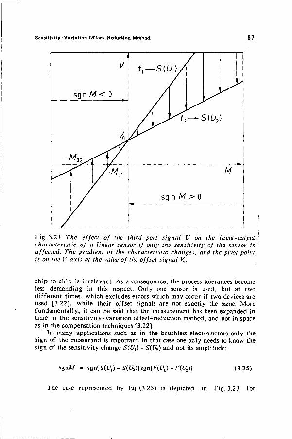
Sensitivity-Variation Offset-Reduction Method 8 7
Fig. 3.23 The effect of the third-port signal U on the input-output characteristic of a linear sensor if only the sensitivity of the sensor is affected. The gradient of the characteristic changes, and the pivot point is on the V axis at the value of the offset signal V0.
chip to chip is irreleyant. As a consequence, the process tolerances become less demanding in this respect. Only one sensor .is used, but at two different times, which excludes errors which may occur if two devices are used [3.22], while their offset signals are not exactly the same. More fundamentally, it can be said that the measurement has been expanded in time in the sensitivity-variation offset-reduction method, and not in space as in the compensation techniques [3.22].
In many applications such as in the brushless electromotors only the sign of the measurand is important. In that case one only needs to know the sign of the sensitivity change SiU^ - S(U2) and not its amplitude:
sgnM = tgnlSiUJ - SUWs&nlViUi) - ViUJ] (3.25)
The case represented by Eq. (3.25) is depicted in Fig. 3.23 for
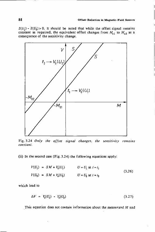
88 Offset-Reduction in Magnetic-Field Sensors
SiUj) - S(U2) > 0. It should be noted that while the offset signal remains constant as required, the equivalent offset changes from Mol to Mo2 as a consequence of the sensitivity change.
1
V
t2 — V0[U2V
/ / ' * * "
s/ / / / 5
M
Fig. 3.24 Only the offset signal changes, the sensitivity remains constant.
(ii) In the second case (Fig. 3.24) the following equations apply:
K(tfa) = SM+ V0(U{)
V(U2) = SM + V0(U2)
U = U1att = tl
U = U2att = t2
(3.26)
which lead to
AK = VJUJ - V0(U2) (3.27)
This equation does not contain information about the measurand M and
Sensitivity-Variation Offset-Reduction Method 89
shows only thé trivial effect that a change in the offset signal results in an equal change in the output of the sensor.
(iii) The situation that will occur in most sensors (Fig. 3.25) is a mixture of the above two extremes. In the new method the output signal is the difference between the output signals V with different activation on the third port (at different times). In the non-ideal but realistic case in which both the sensitivity and the offset signal change with the third port signal, the following equations apply:
TO) = S(Uj)M + TO) U=UX at t = tx
V(U2) = S(U2)M + V0(U2) U=U2 at t = t2
(3.28)
which lead to
TO) - TO) M = 5(4) - 5(4) - M< (3-29)
MT is the residual offset of the sensitivity-variation offset-reduction method [3.12]. Consequently,
M. =
Mr =
TO) - V0(U2) S(Uj) - S(U2)
AS
(3.30)
Application of the new offset-reduction method under non-ideal conditions leads to a residual offset Mt, which is the ratio of the change in the offset signal, and the change in the sensitivity when a signal is applied to the third port.
The differential output of the sensor can now be written as:
(3.31) AV =
AV = AS = AV0 =
ASM
TO) ■ TO) -TO)
yAV0
■ TO) - TO) - TO)
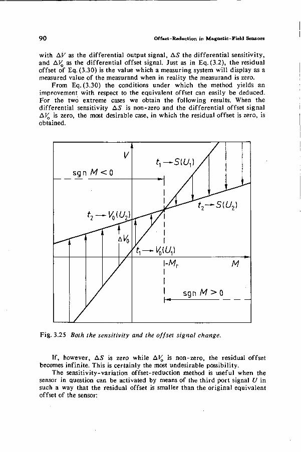
90 Offset-Reduction in Magnetic-Field Sensors
with AV as the differential output signal, AS the differential sensitivity, and AVa as the differential offset signal. Just as in Eq. (3.2), the residual offset of Eq. (3.30) is the value which a measuring system will display as a measured value of the measurand when in reality the measurand is zero.
From Eq. (3.30) the conditions under which the method yields an improvement with respect to the equivalent offset can easily be deduced. For the two extreme cases we obtain the following results. When the differential sensitivity AS is non-zero and the differential offset signal AV0 is zero, the most desirable case, in which the residual offset is zero, is obtained.
Fig. 3.25 Both the sensitivity and the offset signal change.
If, however, AS is zero while AV0 is non-zero, the residual offset becomes infinite. This is certainly the most undesirable possibility.
The sensitivity-variation of fset-reduction method is useful when the sensor in question can be activated by means of the third port signal U in such a way that the residual offset is smaller than the original equivalent offset of the sensor:
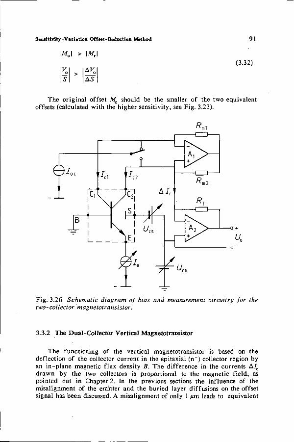
Sensitivity-Variation Of f Bet-Reduction Method 91
MQ\ >
K s >
\Mt\
AS
(3.32)
The original offset M0 should be the smaller of the two equivalent offsets (calculated with the higher sensitivity, see Fig. 3.23).
i;
J« "Ai i7 1
Fig. 3.26 Schematic diagram of bias and measurement circuitry for the two-collector magnetotransistor.
3.3.2 The Dual-Collector Vertical Magnetotransistor
The functioning of the vertical magnetotransistor is based on the deflection of the collector current in the epitaxial (n") collector region by an in-plane magnetic flux density B. The difference in the currents A/c drawn by the two collectors is proportional to the magnetic field, as pointed out in Chapter 2. In the previous sections the influence of the misalignment of the emitter and the buried layer diffusions on the offset signal has been discussed. A misalignment of only 1 /*m leads to equivalent
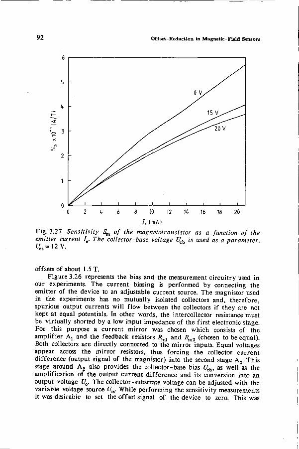
92 Of f Bet-Reduction in Magnetic-Field Sensors
0 2 4 6 8 10 12 14 16 18 20 I, (mA)
Fig. 3.27 Sensitivity 5^ of the magnetotransistor as a function of the emitter current le. The collector-base voltage Uch is used as a parameter.
offsets of about 1.5 T. Figure 3.26 represents the bias and the measurement circuitry used in
our experiments. The current biasing is performed by connecting the emitter of the device to an adjustable current source. The magnistor used in the experiments has no mutually isolated collectors and, therefore, spurious output currents will flow between the collectors if they are not kept at equal potentials. In other words, the intercollector resistance must be virtually shorted by a low input impedance of the first electronic stage. For this purpose a current mirror was chosen which consists of the amplifier Aa and the feedback resistors R^ and / ^ (chosen to be equal). Both collectors are directly connected to the mirror inputs. Equal voltages appear across the mirror resistors, thus forcing the collector current difference (output signal of the magnistor) into the second stage A2. This stage around A2 also provides the collector-base bias Ucb, as well as the amplification of the output current difference and its conversion into an output voltage UQ. The collector-substrate voltage can be adjusted with the variable voltage source £/C8. While performing the sensitivity measurements it was desirable to set the offset signal of the device to zero. This was
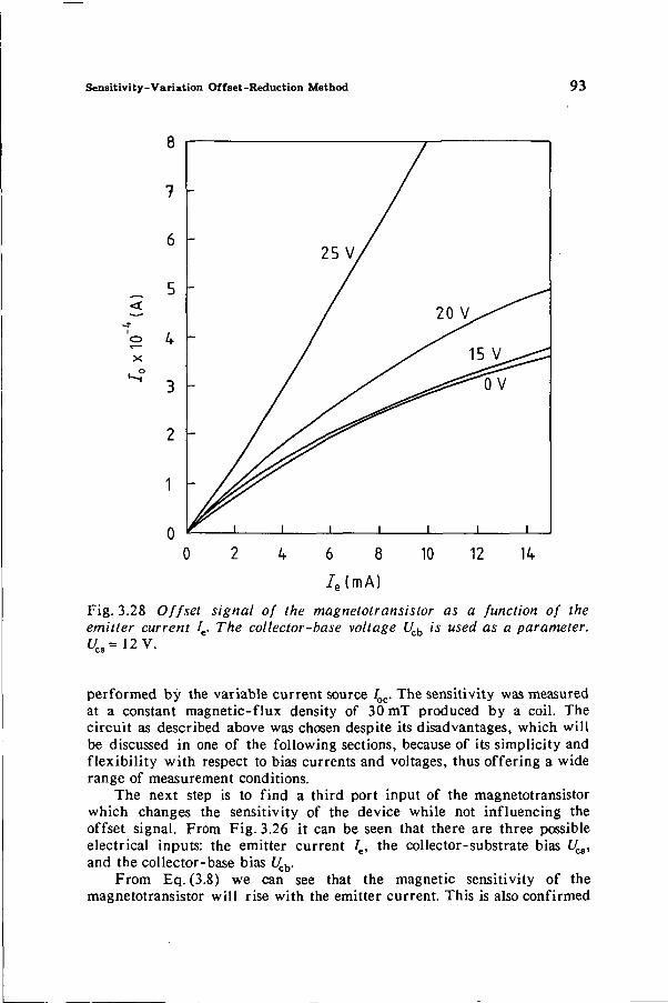
Sensitivity-Variation Offset-Reduction Method 93
0 2 4 6 8 10 12 14
7e(mA)
Fig. 3.28 Offset signal of the magnetotransistor as a function of the emitter current Ie. The col lector-base voltage Uch is used as a parameter.
performed by the variable current source Ioc. The sensitivity was measured at a constant magnetic-flux density of 30 mT produced by a coil. The circuit as described above was chosen despite its disadvantages, which will be discussed in one of the following sections, because of its simplicity and flexibility with respect to bias currents and voltages, thus offering a wide range of measurement conditions.
The next step is to find a third port input of the magnetotransistor which changes the sensitivity of the device while not influencing the offset signal. From Fig. 3.26 it can be seen that there are three possible electrical inputs: the emitter current Ie, the collector-substrate bias Ucs, and the col lector-base bias Ucb.
From Eq. (3.8) we can see that the magnetic sensitivity of the magnetotransistor will rise with the emitter current. This is also confirmed
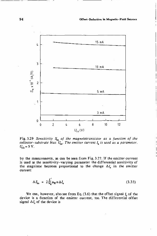
94 Offset-Reduction in Magnetic-Field Sensors
to
2 --
-
15 mA
10 mA
5 mA
3 mA
1 1 1 1 1 1
10 12 Ucs (V)
Fig. 3.29 Sensitivity S^ of the magnetotransistor as a function of the collector-substrate bias UCB. The emitter current Ie is used as a parameter. tcb = 5V.
by the measurements, as can be seen from Fig. 3.27. If the emitter current is used as the sensitivity-varying parameter the differential sensitivity of the magnistor becomes proportional to the change A/e in the emitter current
A$n = 2W^HaMe (3.33)
We can, however, also see from Eq. (3.6) that the offset signal I0 of the device is a function of the emitter current, too. The differential offset signal A/0 of the device is
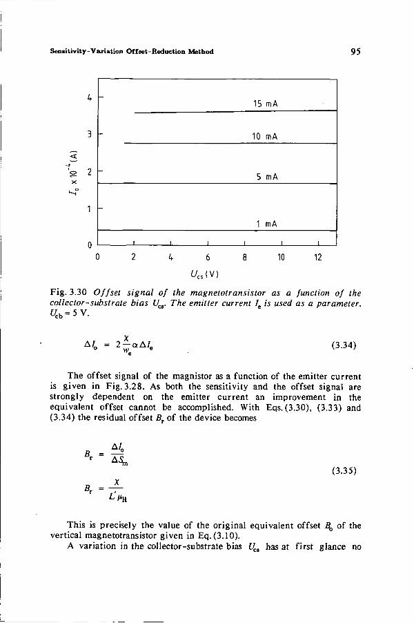
Sensitivity-Variation Offset-Reduction Method 95
•-H
1 -
15 mA
10 mA
5 mA
1 mA
^ c s ( V )
10 12
Fig. 3.30 Offset signal of the magnetotransistor as a function of the collector-substrate bias Ucs. The emitter current Ie is used as a parameter. t/cb = 5V.
A/0 = 2 - a A / e ° vt> e (3.34)
The offset signal of the magnistor as a function of the emitter current is given in Fig. 3.28. As both the sensitivity and the offset signal are strongly dependent on the emitter current an improvement in the equivalent offset cannot be accomplished. With Eqs. (3.30), (3.33) and (3.34) the residual offset BT of the device becomes
B - - ° (3.35)
*r = L'VH
This is precisely the value of the original equivalent offset B^ of the vertical magnetotransistor given in Eq. (3.10).
A variation in the collector-substrate bias Ucs has at first glance no
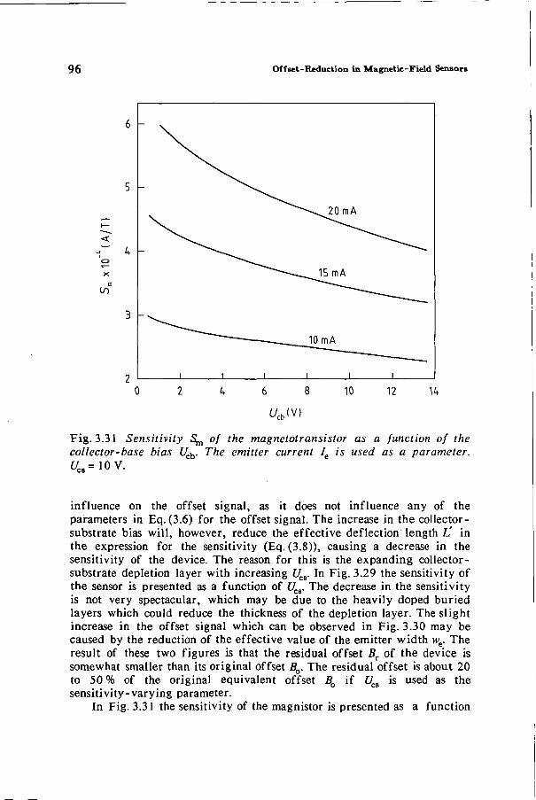
96 Offset-Reduction in Magnetic-Field Sensors
0 2 4 6 8 10 12 14
Fig. 3.31 Sensitivity ^ of the magnetotransistor as a function of the collector-base bias Uch. The emitter current Ie is used as a parameter.
influence on the offset signal, as it does not influence any of the parameters in Eq. (3.6) for the offset signal. The increase in the collector-substrate bias will, however, reduce the effective deflection length L' in the expression for the sensitivity (Eq. (3.8)), causing a decrease in the sensitivity of the device. The reason for this is the expanding collector-substrate depletion layer with increasing Ucs. In Fig. 3.29 the sensitivity of the sensor is presented as a function of UCB. The decrease in the sensitivity is not very spectacular, which may be due to the heavily doped buried layers which could reduce the thickness of the depletion layer. The slight increase in the offset signal which can be observed in Fig. 3.30 may be caused by the reduction of the effective value of the emitter width we. The result of these two figures is that the residual offset BT of the device is somewhat smaller than its original offset B0. The residual offset is about 20 to 50 % of the original equivalent offset B0 if UCB is used as the sensitivity-varying parameter.
In Fig. 3.31 the sensitivity of the magnistor is presented as a function
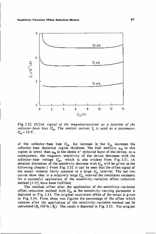
Sensitivity-Variation Of f set-Reduction Method 97
4 <
o X
3
2 0 2 4 6 8 10 12 14
Fig. 3.32 Offset signal of the magnetotransistor as a function of the collector-base bias Uch. The emitter current Ie is used as a parameter.-
of the collector-base bias Uch. An increase in the Ucb increases the col lector-base depletion region thickness. The Hall mobility /iH in this region is lower than /*H in the ohmic n" epitaxial layer of the device. As a consequence, the magnetic sensitivity of the device decreases with the collector-base voltage Ucb, which is also evident from Fig. 3.31. (A detailed discussion of the sensitivity decrease with Ucb will be given in the following chapter.) From Fig. 3.32 it can be seen that the offset signal of the sensor remains fairly constant in a large Uch interval. The last two curves show that in a relatively large Ucb interval the conditions necessary for a successful application of the sensitivity-variation offset-reduction method [3.35] have been fulfilled.
The residual offset after the application of the sensitivity-variation offset-reduction method with Ucb as the sensitivity-varying parameter is depicted in Fig. 3.33. The original equivalent offset of the sensor is given in Fig. 3.34. From these two figures the percentage of the offset which remains after the application of the sensitivity-variation method can be calculated (BT100 % / B0). The result is depicted in Fig. 3.35. The original
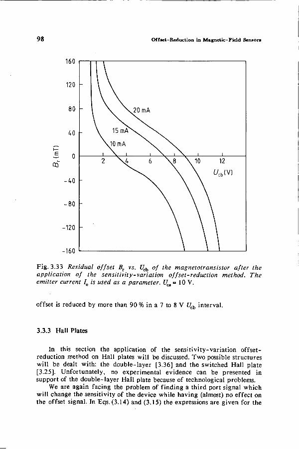
98 Offset-Reduction in Magnetic-Field Sensors
160
120
80
40
S 0 00
-40
-80
-120
-160
Fig. 3.33 Residual offset BT vs. Ucb of the magnetotransistor after the application of the sensitivity-variation offset-reduction method. The emitter current Ie is used as a parameter. UCB= 10 V.
offset is reduced by more than 90 % in a 7 to 8 V U.h interval.
3.3.3 Hall Plates
In this section the application of the sensitivity-variation offset-reduction method on Hall plates will be discussed. Two possible structures will be dealt with: the double-layer [3.36] and the switched Hall plate [3.25]. Unfortunately, no experimental evidence can be presented in support of the double-layer Hall plate because of technological problems.
We are again facing the problem of finding a third port signal which will change the sensitivity of the device while having (almost) no effect on the offset signal. In Eqs. (3.14) and (3.15) the expressions are given for the
-
-
-
-
-
1 \ \ 2 0 m A
\ 15mAS. \ ^
\ l0mA X. 1 \ 1 1 ^ 2 \ 4 6
v. 1 \ \ 8
1
\ 10 1
12
^cb(V)
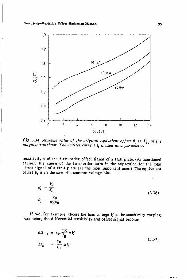
Sensitivity-Variation Offset-Reduction Method 99
03
1.3
1.2
1.1
1.0
0.9
0.8
-
i
10 m A ^ / >/ y
^>^^ 15 mk^^ y /
s>^ . ^ 2 0 mA
i i i i i
6 8 10 12 U
Fig. 3.34 Absolute value of the original equivalent offset B0 vs. Uch of the magnetotransislor. The emitter current 7e is used as a parameter.
sensitivity and the first-order offset signal of a Hall plate. (As mentioned earlier, the causes of the first-order term in the expression for the total offset signal of a Hall plate are the most important ones.) The equivalent offset B0 is in the case of a constant voltage bias
•SmH (3.36)
fl. =
If we, for example, choose the bias voltage Vs as the sensitivity varying parameter, the differential sensitivity and offset signal become
wH
*K (3.37)
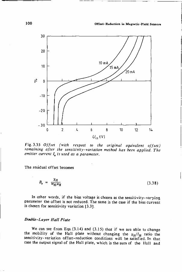
100 Offset-Reduction in Magnetic-Field Sensors
£ 0
Fig. 3.35 Offset (with respect to the original equivalent offset) remaining after the sensitivity-variation method has been applied. The emitter current Ie is used as a parameter.
The residual offset becomes
Br = XH (3.38)
In other words, if the bias voltage is chosen as the sensitivity-varying parameter the offset is not reduced. The same is the case if the bias current is chosen for sensitivity variation [3.3].
Double-Layer Hall Plate
We can see from Eqs. (3.14) and (3.15) that if we are able to change the mobility of the Hall plate without changing the XH/'H r a t i o t n e
sensitivity-variation offset-reduction conditions will be satisfied. In that case the output signal of the Hall plate, which is the sum of the Hall and
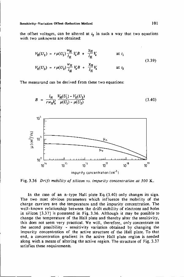
Sensitivity-Variation Offset-Reduction Method 101
the offset voltages, can be altered at t2 in such a way that two equations with two unknowns are obtained:
w„ * H , Vri.Ux) = ri*Ux)-£VtB + -£VB
VdU2) = rKUJjt-V.B + -fve 'H 'H
at t,
at /, (3.39)
The measurand can be derived from these two equations:
B = 'H W I ) " W 2 ) rwnV, n{Ux)-ii{U2)
(3.40)
10"
10 -
10
:"
-
r
-:
-i I i I i
— ^ _ ^ n
^ ~ ^ - - ^ ^ 1 1 i ' i r d i i
, T t 15 ,16 .17 JB 10" 10" 10" 10 10 10
impurity concentration (cm-3)
Fig. 3.36 Drift mobility of silicon vs. impurity concentration at 300 K.
In the case of an n-type Hall plate Eq. (3.40) only changes its sign. The two most obvious parameters which influence the mobility of the charge carriers are the temperature and the impurity concentration. The well-known relationship between the drift mobility of electrons and holes in silicon [3.37] is presented in Fig. 3.36. Although it may be possible to change the temperature of the Hall plate and thereby alter the sensitivity, this does not seem very practical. We will, therefore, only concentrate on the second possibility - sensitivity variation obtained by changing the impurity concentration of the active structure of the Hall plate. To that end, a concentration gradient in the active Hall plate region is needed along with a means of altering the active region. The structure of Fig. 3.37 satisfies these requirements.
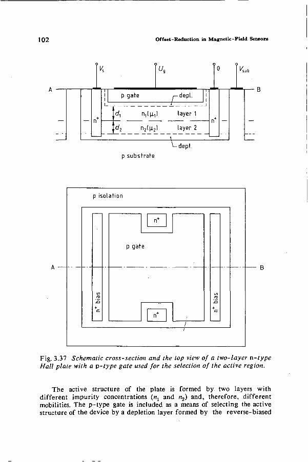
102 Offset-Reduction in Magnetic-Field Sensors
u„ "sub
p gate ■£
depl.
ti :d2
n,(u.,)
n2(u.2)
layer 1
layer 2
i: depl. p substrate
Fig. 3.37 Schematic cross-section and the top view of a two-layer n-type Hall plate with a p-type gate used for the selection of the active region.
The active structure of the plate is formed by two layers with different impurity concentrations («x and n2) and, therefore, different mobilities. The p-type gate is included as a means of selecting the active structure of the device by a depletion layer formed by the reverse-biased
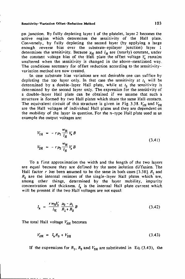
Sensitivity-Variation Offset-Reduction Method 1 0 3
pn junction. By fully depleting layer 1 of the platelet, layer 2 becomes the active region which determines the sensitivity of the Hall plate. Conversely, by fully depleting the second layer (by applying a large enough reverse bias over the substrate-epilayer junction) layer 1 determines the sensitivity. Because XH anc* ^H a r e (nearly) constant, under the constant voltage bias of the Hall plate the offset voltage Va remains unaltered when the sensitivity is changed in the above-mentioned way. The conditions necessary for offset reduction according to the sensitivity-variation method are now created.
In case substrate bias variations are not desirable one can suffice by depleting the top layer only. In that case the sensitivity at t1 will be determined by a double-layer Hall plate, while at t2 the sensitivity is determined by the second layer only. The expression for the sensitivity of a double-layer Hall plate can be obtained if we assume that such a structure is formed by two Hall plates which share the same Hall contacts. The equivalent circuit of this structure is given in Fig. 3.38. Vm and Vm are the Hall voltages of individual Hall plates and they are dependent on the mobility of the layer in question. For the n-type Hall plate used as an example the output voltages are:
(3.41)
2H = -r>h-^v*B
To a first approximation the width and the length of the two layers are equal because they are defined by the same isolation diffusion. The Hall factor r has been assumed to be the same in both cases [3.38]. Ry and R2 are the internal resistors of the single-layer Hall plates which are, among other things, determined by the layer mobility, impurity concentration and thickness. Ik is the internal Hall plate current which will be present if the two Hall voltages are not equal:
I'-iTT^* (342)
The total Hall voltage VdH becomes
>dH = 4*2 + *2H (3-43)
If the expressions for Rlt R2 and V2H are substituted in Eq. (3.43), the
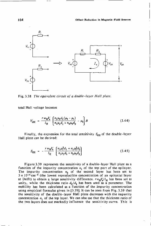
104 Offset-Reduction in Magnetic-Field Sensors
* !
K H O * ! R,
/?, ^O
^ H C )
o o» "2H
o + n
"dH
Fig. 3.38 The equivalent circuit of a double-layer Hall plate.
total Hall voltage becomes
*dH
rwnv* IT, " l M l + "2^2 \h B (3.44)
Finally, the expression for the total sensitivity SdH of the double-layer Hall plate can be derived:
3)H _ rwHVs nx\i\dx + nl\^d2
n^di + n2^d2 (3.45)
Figure 3.39 represents the sensitivity of a double-layer Hall plate as a function of the impurity concentration n1 of the top part of the epilayer. The impurity concentration n2 of the second layer has been set to 5 x 1014cm~3 (the lowest reproducible concentration of an epitaxial layer at Delft) to obtain a large sensitivity difference. rwHl^/lH has been set to unity, while the thickness ratio d2/d1 has been used as a parameter. The mobility has been calculated as a function of the impurity concentration using empirical formulas given in [3.39]. It can be seen from Fig. 3.39 that the sensitivity of the double-layer Hall plate decreases with the impurity concentration nx of the top layer. We can also see that the thickness ratio of the two layers does not markedly influence the sensitivity curve. This is
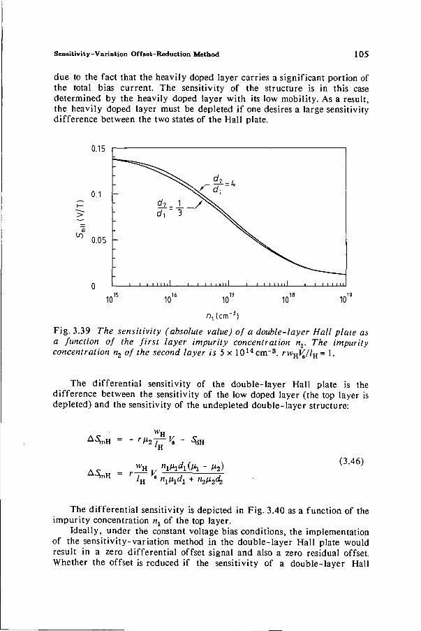
Sensitivity-Variation Offset-Reduction Method 105
due to the fact that the heavily doped layer carries a significant portion of the total bias current. The sensitivity of the structure is in this case determined by the heavily doped layer with its low mobility. As a result, the heavily doped layer must be depleted if one desires a large sensitivity difference between the two states of the Hall plate.
0.15
<o
0.1
0.05 -
i _ ^ _ ^
-
-
1 1
1
C / 2 .
1 1 1 1 1 1 i i
1 3
i
^
i i i i i I 11 I I 1 I i i i i 1 i 1 I I I i i i
10 10 10 10 10
Fig. 3.39 The sensitivity (absolute value) of a double-layer Hall plate as a function of the first layer impurity concentration nv The impurity concentration n2 of the second layer is 5 x 10 1 4 cn r 3 . rw-aVJln= 1.
The differential sensitivity of the double-layer Hall plate is the difference between the sensitivity of the low doped layer (the top layer is depleted) and the sensitivity of the undepleted double-layer structure:
wv A$nH =
A ^ H =
" rii2 -j^-V, - 5dH
(3.46)
The differential sensitivity is depicted in Fig. 3.40 as a function of the impurity concentration nx of the top layer.
Ideally, under the constant voltage bias conditions, the implementation of the sensitivity-variation method in the double-layer Hall plate would result in a zero differential offset signal and also a zero residual offset. Whether the offset is reduced if the sensitivity of a double-layer Hall
106 Offset-Reduction in Magnetic-Field Sensors
0.15
0.1
E
<■ 0.05
-
-
-
d2 1
1 i i 1 i i
10 10 10 10
Fig. 3.40 The differential sensitivity (absolute value) of a double-layer Hall plate as a function of the first layer impurity concentration nv The impurity concentration n2 of the second layer is 5xl01 4cm~3 . rWnVJln-\.
plate is varied under a constant current bias is not as clear. If the bias current is constant the sensitivity and the offset signal become
1 rh mH ndH e
0 nndH ewu "
(3.47)
The equation for the offset signal was obtained from Eq. (3.15) by expressing the resistivity as a function of the mobility and impurity concentration. The offset signal is dependent on n, \i and dn, which will also change as the sensitivity is varied by reverse-biasing the gate. If we, for reasons of simplicity, assume that both layers are alternately depleted so that we are only dealing with single-layer Hall plates of different doping and thickness, the following equations apply:
^1H = " rl.
»l r f l 'B + 1 XH
n1n1d1 ewH at u
Sensitivity-Variation Offset-Reduction Method
15 1 - - ^
v = —-B+ —!— — / 2 H ' n2d2 e + n2\i2d2 ewH
8 at U
107
(3.48)
IXHl l o2l _ rn2wH
Bol and Bo2 are the two possible equivalent offsets. The differential sensitivity and offset signal are
e A^H = - [n\di - „ 2 y
AV = [ l - — 1 — ] ^ ? 0 [ « i M l "2M2J eVVH
(3.49)
The absolute value of the residual offset is
| 5 r | = " l M l ~ "2M2 XH
MlA^Ml " M 2 ) rwH (3.50)
If the method is to be useful the following must be valid (Eq. (3.32)):
| 5 r | < min lxHl IXHI r/i^H rn2wK
(3.51)
The absolute value of the residual offset must be smaller than the smallest of the two possible equivalent offsets |Z?ol| and \Bo2\.
If we assume that ni> n2 (which also means /^ < p2) Eq. (3.51) is reduced to
«iMi^i - n2n2d2
Mi(Mi - n2d2)
/*2
< 1
(3.52)
I M i " «2 TT <21 < I M i - M2I J*i
108 Offset-Reduction in Magnetic-Field Sensors
If it is also assumed that n^y > n2d2, which is a reasonable assumption as «! is an order of magnitude larger than n2, while dx and d2 are comparable to each other, Eq. (3.52) can be reduced to two cases
fi2 fJ-2 M l " n2~ d2 < M l " M 2 i f M l > n2~d2
fh Mi ^2 V-2
n2~ d2 ~ M l < M l ~ n2d2 i f M l < "2~ r f2 Mi th
(3.53)
The first of these two equations leads to the requirement for offset reduction of n2 > y.x, which is always satisfied if nx> n2, as it has been assumed. From the second equation it can be deduced that offset is improved with respect to its original value if
1 «2 «i > y « 2 ^ 1 +
Mi (3.54)
Constant current bias is not desirable because the residual offset is present from the start, which is ideally not the case if a constant voltage bias is used.
p substrate
Fig. 3.41 A sketch of a double-layer Hall device with V-groove isolation, bias and Hall contacts.
The bias contact diffusions in Fig. 3.37 are represented as rectangles and are not realistic. In a real device the curvature of the bias contacts or the slope of the V-grooves (see the following section and Fig. 3.41) will be the cause of some variation in the length /H of the platelet as the epitaxial layers are depleted. The variation of /H will undoubtedly result in the variation of the offset signal and, therefore, residual offset. If A/H is the change in the Hall plate length
Sensitivity-Variation Offset-Reduction Method 109
A ^ H - 2H " 'lH (3.55)
The differential offset signal becomes
AV0 = XH
/ I T X + A / T , '1H (3.56)
We again assume that both layers are alternately depleted so that we are only dealing with single-layer Hall plates of different doping and thickness. The differential sensitivity for an n-type Hall plate is
A $ n H = " ™H T f Mi
H U H ~ H
/ iH+A/u '1H (3.57)
The absolute value of the residual offset can be calculated with the last two equations.
\BT\ = A ' H XH
MlClH + A / H ) " M2>1H rwH (3.58)
When the residual offset is compared to the original equivalent offset the condition for offset improvement becomes Um» A/H)
Mi - H Ml
> A/H
'lH (3.59)
Some Technological Considerations
A sharply defined step in the impurity concentration of the epitaxial layer can be achieved with a two-step epitaxial growth. Care must be taken to ensure that there is a good control of the thickness of the top epitaxial layer during processing. The depletion layer extending from the gate-epi junction should be able to completely deplete the top layer with the larger impurity concentration (thickness d{). The danger exists that the «x epilayer will outdiffuse during subsequent thermal cycles and that it cannot be fully depleted. SUPREM simulations [3.40] have determined that a 5 to 6 hour temperature cycle at 1000°C should not be exceeded to prevent significant outdiffusion. This points to the use of the V-groove
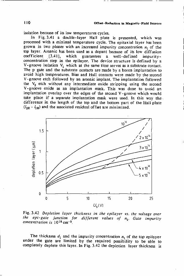
110 Offset-Reduction in Magnetic-Field Sensors
isolation because of its low temperatures cycles. In Fig. 3.41 a double-layer Hall plate is presented, which was
processed with a minimal temperature cycle. The epitaxial layer has been grown in two phases with an increased impurity concentration «x of the top layer. Arsenic has been used as a dopant because of its low diffusion coefficient [3.41], which guarantees a well-defined impurity-concentration step in the epilayer. The device structure is defined by a V-groove isolation Vx which at the same time serves as a substrate contact. The p gate and the substrate contacts are made by a boron implantation to avoid high temperatures. Bias and Hall contacts were made by the second V-groove etch followed by an arsenic implant. The implantation followed the V2 etch without any intermediate oxide stripping using the second V-groove oxide as an implantation mask. This was done to avoid an implantation overlap over the edges of the second V-groove which would take place if a separate implantation mask were used. In this way the difference in the length of the top and the bottom part of the Hall plate (/2H ~ W anc* t n e associated residual offset are minimized.
0 5 10 15 20 25
Fig. 3.42 Depletion layer thickness in the epilayer vs. the voltage over the epi-gate junction for different values of nv Gate impurity concentration is 1018cnr3.
The thickness d1 and the impurity concentration n± of the top epilayer under the gate are limited by the required possibility to be able to completely deplete this layer. In Fig. 3.42 the depletion layer thickness is
Sensitivity-Variation Of f Bet-Reduction Method 111
Q I I 1 I I I ' i l l I 1 1 I 1 1 t I L
0 1 2
10 10 10
A Fig. 3.43 Differential sensitivity (absolute value) as a function of the thickness ratio d2/d1 at two values of nv n2 = 5 x 10 1 4 cnr 3 . rwlll^/lH= 1.
given as a function of the voltage across the epi-gate junction. Impurity concentration nx is used as a parameter. The maximum gate voltage is limited by the breakdown of the junction (dashed line in Fig. 3.42 which is the "worst-case" taken for a spherical junction with a radius of 1 /im [3.37]).
Hall plates have been integrated using the V-groove isolation with dx = 1 urn, d2 = %nm, nx = 2 x 1 0 1 6 c n r 3 and n2 = 5 x 10 1 4 cnr 3 . In this range of impurity concentrations the piezoresistance coefficient is a constant [3.42]. In other words, while switching between the two layers the offset caused by piezoresistive effects will not change. From Fig. 3.43 it can be seen that the expected differential sensitivity is 0.024 V/T ( r w H ^ / / H = 1). In Fig. 3.44 one such device is presented. Unfortunately, all pn junctions were leaking and no measurements could be performed. At first, the cause was thought to be the overlap of the two V-grooves. The etching rate at these places was much higher than for single V-grooves, which resulted in local depressions extending far into the substrate (Fig. 3.45). Together with the remnants of metallization in these depressions (Fig. 3.46) undesired shorts were probably created, which ruined the junction characteristics. Another design has been processed,
112 Offset-Reduction in Magnetic-Field Sensors
MIIIIII ■ fc"r - ir~-
Fig. 3.44 A double-layer V-groove isolation Hall plate. Two gate contacts biased at different potentials can compensate the thickness variation of the depletion layer.
which eliminated V-groove overlap (at the expense of worse structure definition). One device of this type is presented in Fig. 3.47. These devices also had leaking junctions which were probably caused by crystal defects in the epitaxial layer or the substrate-epilayer interface (Fig. 3.48).
Switched Hall plate
The dual-layer Hall plate requires several non-standard processing steps which are crucial for the good performance of the device. In this section a Hall plate structure will be presented which can be implemented in several different standard technologies, without requiring any special processing steps.
The basic principle of the switched Hall plate is illustrated in Figs. 3.49 and 3.50. The structure of Fig. 3.49a consists of two isolated regions which are biased by a common source Vs, while the Hall contacts are placed in the middle of each region. The offset voltage will be
Sensitivity-Variation Offset-Reduction Method 1 1 3
Fig. 3.45 Overlap of the two V-grooves results in deep depressions.
non-zero. The origins of the offset voltage have already been discussed in the previous sections. In Fig. 3.49b an illustration of the equipotential lines is depicted for a non-zero perpendicular magnetic field. If the Hall contacts are close to the center of their respective regions, they will also be on nearly the same equipotential lines. As a consequence, the response of this split structure to the magnetic field will be nearly zero. If the barrier between the two regions is somehow removed so that they can form a single device, the structure of Fig. 3.50 is obtained, which represents a slightly modified Hall plate. The magnetic sensitivity is in this case smaller compared to a platelet with Hall contacts on the sides. Nevertheless, it is significantly larger than the sensitivity of the split Hall plate of Fig. 3.49. The offset signals in the two cases should be almost equal since neither the mechanical stress, geometric misalignment, power consumption nor the current distribution have changed markedly. By switching the sensor between the two states the conditions for offset reduction according to the sensitivity-variation method have been fulfilled.
Ideally we would obtain for the two states
(3.60) >2H = - W ? + K at<2
114 Of f set-Reduction in Magnetic-Field Sensors
Fig. 3.46 Remnants of aluminum in the overlap depressions,
The sensor can be implemented in a variety of different ways, depending on the available technology. The active regions forming the two halves of the Hall plate should have a low doping density to ensure high magnetic sensitivity. A possible structure is depicted in Fig. 3.51. The two halves of the Hall plate are connected or separated by means of a MOS gate switch. An alternative to the MOS switch is the structure depicted in Fig. 3.52. The device is switched by the depletion region of the pn junction. This structure, which can be implemented in a standard bipolar technology, has been used in the experiments.
Ideally the sensitivity will be switched from its maximum value to zero, while the offset signal remains constant. In practical devices several effects will cause a departure from the ideal state: lateral expansion of the depletion layer and alignment of the gate with respect to the isolation diffusion of the device.
If the depletion region of the gate expands laterally, the effective width of the sensor will change, causing the Hall contacts to be off-center (Fig. 3.53). The result is that the magnetic sensitivity in the depleted state is not reduced to zero. The potential difference Vm between the Hall contacts hj and h2 as a response to the magnetic field B becomes
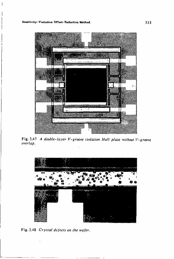
Sensitivity-Variation Offset-Reduction Method 115
Fig. 3.47 A double-layer V-groove isolation Hall plate without V-groove overlap.
Fig. 3.48 Crystal defects on the wafer.
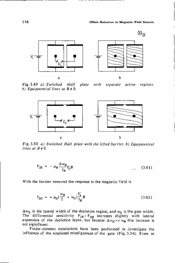
116 Offset-Reduction in Magnetic-Field Sensors
® B
K- l, T
Fig. 3.49 a) Switched Hall plate with separate active regions. b) Equipotential lines at Bi=Q.
Fig. 3.50 a) Switched Hall plate with the lifted barrier, b) Equipotential lines at B ±0.
Vm = /*H-Awv
'KB (3.61)
With the barrier removed the response to the magnetic field is
K2H + M~
H>u
'H (3.62)
AwH is the lateral width of the depletion region, and >vG is the gate width. The differential sensitivity Vm - V2H increases slightly with lateral expansion of the depletion layer, but because A w H « wH this increase is not significant.
Finite-element simulations have been performed to investigate the influence of the rotational misalignment of the gate (Fig. 3.54). Even at
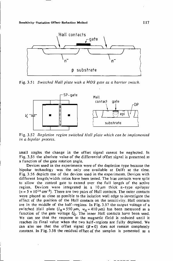
Sensitivity-Variation Offset-Reduction Method 117
Hall contacts
r gate
~\ r \ ^ r v: TV n
7"
p substrate
Fig. 3.51 Switched Hall plate with a MOS gate as a barrier switch.
K"n=-
-SP-gate
Fig. 3.52 Depletion region switched Hall plate which can be implemented in a bipolar process.
small angles the change in the offset signal cannot be neglected. In Fig. 3.55 the absolute value of the differential offset signal is presented as a function of the gate rotation angle.
Devices used in the experiments were of the depletion type because the bipolar technology was the only one available at Delft at the time. Fig. 3.56 depicts one of the devices used in the experiments. Devices with different length/width ratios have been tested. The bias contacts were split to allow the control gate to extend over the full length of the active region. Devices were integrated in a 10 /im thick n-type epilayer (n = 5 x 1014 cm-3). There are two pairs of Hall contacts. The outer contacts were placed as close as possible to the isolation wall edge to investigate the effect of the position of the Hall contacts on the sensitivity. Hall contacts are in the middle of the half-regions. In Fig. 3.57 the output voltage of a switched Hall plate (/H = 550/im, wH = 410Ami) has been measured as a function of the gate voltage ££.. The inner Hall contacts have been used. We can see that the response to the magnetic field is reduced until it reaches its final value when the two half-regions are fully depleted. We can also see that the offset signal (B = 0) does not remain completely constant. In Fig. 3.58 the residual offset of the samples is presented as a
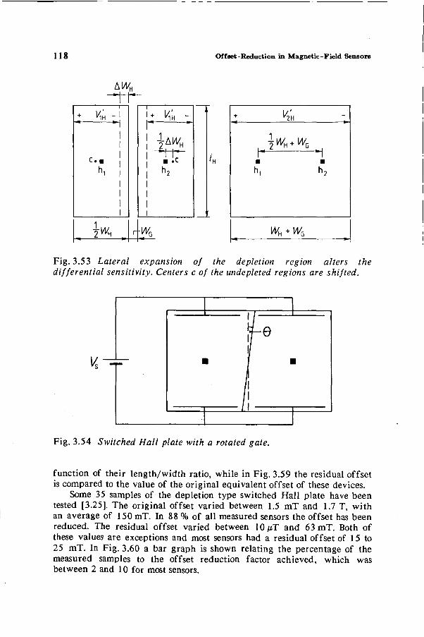
118 Offset-Reduction in Magnetic-Field Sensors
hWti
X K - ]
h1 I
iw» r
1 , , <
i ■ 1 h2
-*—
1
1
Fig. 3.53 Lateral expansion of the depletion region alters the differential sensitivity. Centers c of the undepleted regions are shifted.
Fig. 3.54 Switched Hall plate with a rotated gate.
function of their length/width ratio, while in Fig. 3.59 the residual offset is compared to the value of the original equivalent offset of these devices.
Some 35 samples of the depletion type switched Hall plate have been tested [3.25]. The original offset varied between 1.5 mT and 1.7 T, with an average of 150 mT. In 88 % of all measured sensors the offset has been reduced. The residual offset varied between 10 //T and 63 mT. Both of these values are exceptions and most sensors had a residual offset of 15 to 25 mT. In Fig. 3.60 a bar graph is shown relating the percentage of the measured samples to the offset reduction factor achieved, which was between 2 and 10 for most sensors.
Sensitivity-Variation Offset-Reduction Method 1 1 9
gate rotation angle (degrees)
Fig. 3.55 Calculated absolute value of the differential offset as a function of the gate rotation angle (in degrees). The length/width ratio is a parameter (V&= 1 V).
Fig. 3.56 A switched Hall plate in bipolar technology.
Apart from trying to improve the depletion-type sensor, it would be very interesting to investigate the performance of the MOS-switched sensor. Rotation errors are less important in this type of a structure since
120 Offset-Reduction in Magnetic-Field Sensors
x
Fig. 3.57 Output voltage of a switched Hall plate for 5 = 40mT, B = 0, and B = -40 mT as a function of the gate voltage.
70
60
50
P 40
jtf 30
20
10
0
□ a
o
o □ a
□ g o D ° ° u n □
a □ a
° a a a a
0.25 0.5 0.75
Wu
1.25 1.5
Fig. 3.58 Absolute value of the residual offset of the samples as a function of the Hall plate length/width ratio.
Sensitivity-Variation Offset-Reduction Method 121
XT
O U
200
150
100
50
_ —
G
Q D
I n
D a O D
I a
a a
OD
D
- D
D
0
0
D
D
1
0.25 0.5 0.75 1.25 1.5
Fig. 3.59 Ratio of the residual and original equivalent offset as a function of the length/width ratio.
50.0
37.5
5? 25.0 -
12.5
0.0 < 1 1-2 2 - 4 4-10
offset reduction factor
>10
Fig. 3.60 Bar graph of the of f set-reduction factor and the associated percentage of the measured devices.
1 2 2 Offset-Reduction in Magnetic-Field Sensors
the gate region is determined by the Hall plate halves and not by a separate mask.
Fig. 3.61 The change of the output characteristic of a barber-pole magnetoresistor with the magnetization direction.
3.3.4 Magnetoresistors
As a last example of the application of the sensitivity-variation offset-reduction method a recent development will be discussed which has been presented in [3.33] and [3.43]. It concerns the reduction of offset in
Sensitivity-Variation Offset-Reduction Method 123
magnetic field sensors which are based on the magnetoresistive effect. Magnetoresistive sensors are based on the change in the electrical
resistance of specific ferromagnetic alloys under the influence of an external magnetic field. Compared to Hall-effect devices magnetoresistive sensors can detect much weaker fields, ranging from less than 10~3A/m up to several 104A/m (from 1 nT up to several lOmT in vacuum), but their sensitivity characteristic exhibits saturation at higher field values. The high sensitivity is caused by the ferromagnetic layer with its high internal magnetization, which can easily be rotated by an external field. These solid-state sensors can be realized in thin film technology. If the magnetoresistor is biased with a constant current, the change in the resistance caused by the magnetic field will result in a proportional change of the voltage over the resistor. A review of magnetoresistive sensors is given in [3.34].
The lowest detectable magnetic field is limited, for one by offset. Offset is traditionally cancelled by combining several magnetoresistors in a bridge circuit. The remaining offset signal can be eliminated by laser resistor trimming. A reduction in offset can also be achieved with the sensitivity-variation method [3.33], [3.43].
coil current
h t Q-l--\ i i i i i i ' i I i I
K,t "1R
'2R
r offset
t Fig. 3.62 Switching of the magnetization with coil current pulses varies the output of the sensor between states V1R and V2R. The offset signal remains constant.
The sensitivity-variation offset-reduction method has been applied to a barber-pole structure [3.33] in a four-element bridge circuit [3.43]. The output signal of this sensor structure is very much dependent on the direction of magnetization in the permalloy film which was used as the sensor material in this case. In Fig. 3.61 we can see that the output characteristic of the sensor revolves around the value of the offset signal if the magnetization Mx changes direction, which means that the criteria for offset reduction according to the sensitivity-variation method have been satisfied.
The switching of the magnetization can be achieved by incorporating a small coil with the sensor and driving a current through the coil in the
124 Offset-Reduction in Magnetic-Field Sensors
desired direction. The value of the magnetic-field strength generated by the coil which is necessary to change the magnetization direction of the sensor was 3 x 10³ A/m for the sensor discussed in [3.43]. In vacuum, this corresponds to a magnetic-flux density of about 4 mT. In Fig. 3.62 we can see the effect of coil current pulses which switch the magnetization of the sensor. The differential output signal is the difference between the outputs of the two states V1R - V2R. Since the value of the offset signal is unaffected by the alternating magnetization the differential output signal is nearly free of offset. The reported offset improvement ranges from a factor of 10 to 100 [3.43].
The largest field which can be measured in this way is limited by the fact that the measurand itself can cause the switching of the magnetization. For the sensor used in the experiments [3.43] the maximum value of the measurand is about 250 A/m (0.34 mT in vacuum), while the smallest detectable field was reported to be 0.25 A/m (340 nT).
3.4 ELECTRONIC IMPLEMENTATION OF THE SENSnTvTTY-VARIATION OFFSET-REDUCTION METHOD
In Section 3.3.1 the basic principles of the sensitivity-variation offset-reduction method have been discussed. According to Eqs. (3.23) and (3.24) the reduction of offset can be achieved by varying the sensitivity of the sensor, while at the same time the offset signal of the sensor does not change (appreciably). The salient feature of this offset-reduction method is that the measurand does not have to be set to a known value to calibrate the sensor prior to the measurements. Moreover, slow offset variations and drift caused by temperature and other ambient variations do not influence the measurements. Although the principle of the sensitivity-variation offset-reduction method is described very well by Eqs. (3.23) and (3.24), its methodology does not make for the best electronic implementation. In this section the difference in the response of the sensitivity and the offset to sinusoidal excitation is used to reduce offset in a vertical magnetotransistor [3.44]. The theory and practice of the electronic implementation of the sensitivity-variation offset-reduction method will be discussed [3.45]. The theoretical predictions will be compared with the experimental results and various aspects of the circuit design will be dealt with.
3.4.1 The Principle of Operation
As mentioned earlier, the col lector-base voltage Ucb is the parameter that noticeably influences the sensitivity S^ of the vertical
Electronic Implementation of the SVOR Method 125
Fig. 3.63 Signal Uch (frequency f0) is superimposed on the Uch set point. Because the sensitivity S^ of the magnetotransistor is a monotonically decreasing function of Ucb, the variation of the sensitivity will result in the presence of a magnetic field in an output signal with a prominent frequency f0.
magnetotransistor, while the offset signal I0 is only a weak function of Ucb. Figures 3.31 and 3.32 represent the sensitivity and the offset signal as a function of Ucb. S^ is a decreasing function of Ucb. This is a consequence of the increasing thickness of the depletion layer of the collector-base junction with Uch. Because the deflection by the magnetic field (the Hall angle) of the charge carriers in the depletion layer is lower than in the ohmic part of the device collector [3.45]-[3.47], the sensitivity of the magnetotransistor will decrease with increasing col lector-base bias. More attention will be paid to this effect in the next chapter. The offset signal vs. Ucb curve, however, exhibits nearly independent behavior with respect to Ucb in a fairly large Uch interval.
126 Offset-Reduction in Magnetic-Field Sensors
In Figs. 3.63 and 3.64 the principle of the electronic implementation of the sensitivity-variation offset-reduction method is shown. The sensitivity of the magnetotransistor is varied by superimposing a sinusoidal signal Ucb of frequency fQ on a Ucb set point. Because the sensitivity, of the magnetotransistor is a monotonically decreasing function of Ucb, Ucb will produce an S^B term in the output of the sensor in which the frequency fQ will be strongly represented. The amplitude of this term is dependent £n such things as the magnetic-flux density B and the amplitude of the Ucb signal. Ideally, if the offset signal is completely independent of the sensitivity-varying parameter Uch, the Ucb signal will not result in any signal components caused by I0. Nevertheless, due to parasitic effects the offset signal is slightly dependent on Ucb, resulting in residual offset.
Fig. 3.64 As a consequence of parasitic effect^, the offset signal exhibits a slightly parabolic dependence on Ucb. The Ucb signal will in this case introduce a component with a prominent frequency peak at 2fQ into the output of the sensor.
Electronic Implementation of the SVOR Method 127
K,t
/777 /777 /777
Fig. 3.65 Schematic diagram of the bias and measurement circuit. Signals produced by Uch are subtracted after they are amplified by the transimpedance amplifiers. The modulator extracts signals with frequency f0 (S^B).
The shape of the I0 vs. Ucb is slightly parabolic. This is shown in an exaggerated manner in Fig. 3.64. In this case Uch results in an I0 component of the output signal in which 2f0 frequency components are strongly represented. Because of this difference in the frequency response of the S^B and I0 parts of the output signal, the measurand B can be distinguished from thejrffset signal. Consequently, the offset of the device can be reduced. The /0 signal will also contain frequency components of the fundamental frequency f0. Their amplitude will be dependent on the exact shape of the I0 vs. Ucb curve and the value of the dc Uch bias. These signal components will be interpreted as signals caused^by a magnetic field. In other words, the f0 frequency components of I0 represent the residual offset signal of the measurement.
3.4.2 The Electronic Implementation
Figure 3.26 represents a simple circuit used to make the sensitivity and the offset measurements. This circuit could, in principle, be used for the sinusoidal excitation of the sensor as described in the previous section if it
128 Offset-Reduction in Magnetic-Field Sensors
were not for one major shortcoming. The current mirror, which keeps the two collectors of the device at the same potential, passes the collector current difference to the transimpedance amplifier A2 irrespective of whether the signal is a large dc offset signal or the small S^B ac signal caused by the sinusoidal excitation of the sensor. In this way the amplification range of the A2 amplifier is used only to a small degree. (The compensation current source cannot be used because the value of the offset signal is unknown.) This leads us to the requirement that the large dc offset currents of the sensor must be separated from the small S^B signal before the first amplification stage.
Fig. 3.66 The equivalent circuit of the magnetotransistor that is used in the calculation of the influence of an imbalance in the collector leads of the sensor on the I0 vs. Ucb characteristic.
Figure 3.65 depicts the block diagram of the__electronic circuit that satisfies the above requirement. A sinusoidal signal Ucb of frequency f0 is
Electronic Implementation of the SVOR Method 1 2 9
superimposed on a Uch set point and the composite signal is applied to the base of the magnetotransistor. The bias current is determined by the emitter current source. The two transimpedance amplifiers keep the collectors of the device at the same potential. The two controlled current sources in the collector leads of the magnetotransistor are controlled by the low-frequency signals from the transimpedance amplifiers. This is a result of the low-pass filters in the feedback loops of the controlled current sources. The controlled current sources will form a low impedance for the slow offset signal variations and they will not be passed on to the first amplification stage as they were in the circuit of Fig. 3.26. Conversely, higher frequency signals will be amplified by the transimpedance amplifiers, as the controlled current sources form a high impedance for these signals. A signal proportional to A/c will emerge after the output signalsjjf the transimpedance amplifiers are subtracted from each other. The A/c signal can be further amplified before it is offered to the X input of a modulator. The Y input of the modulator is formed by the Uch signal, which is amplified to the largest permissible level by the amplifier A2 to obtain the highest possible output of the jiodulator. In this way the f0 frequency component that corresponds to S^B can be extracted from the output signal of the sensor A/c. Finally, a dc signal proportional to the amplitude of the signal component of frequency fQ is obtained from the modulator by employing a low-pass filter.
0 0 5 0
10
Fig. 3.67 The influence of the impedance imbalance in the collector leads of the magnetotransistor on its collector-current difference I0 at B = 0. The full curves represent theoretical predictions while dots represent experimental values.
0.3 -
_ 0.1 < % o
X ^= -0.1
-0.3 -
-
- L_
^ J -
~
A
t
. B
B-
i
C
C-
i
i
■
, ■ ■ — ' -
i
A B B-C C-
Afl, t
0 5 0
10 0
10 15 20
130 Offset-Reduction in Magnetic-Field Sensors
It is very important that the input impedance levels of the transimpedance amplifiers in the collector leads of the magnetotransistor be as equal as possible. It is also important that the offset-voltage difference of the transimpedance amplifiers be not too large. Impedance imbalance of only a few ohms adds a significant slope to the I0 vs. Uch characteristic which, as we have seen in the previous section, causes residual offset.
The influence of the impedance imbalance in the collector leads of the magnistor can be determined by considering the equivalent circuit of the sensor (Fig. 3.66). The emitter current /e that reaches the collector region of the magnetotransistor (negligible base current) encounters resistors R1 and R2 (n~ epitaxial layer) on its way to the n+ buried layers. The two buried layers are separated by the intercollector resistance R^. The AR's represent the low resistance of the n+ buried layers, DN diffusions and the external impedances in the collector leads. R1 and R2 are nearly equal (R1 = R2 = R) and the collector-current difference 4 can be written as follows:
2tt op
4 = (ARX - AR2)
2R + R^
2R + R. 2R + (AR1 + AR2)—j^-S
(3.63)
where Uop is the intercollector offset voltage caused by the transimpedance amplifiers. In this equation the 4 dependence on Uch is introduced by the dependence of R and ^. on Uch. R is proportional to the length of the undepleted part of the n" epitaxial collector region, while /?,. is inversely proportional to this length. The depletion layer thickness on the collector side of the col lector-base junction is in turn proportional to the square root of the col lector-base bias Uch, and the Uch dependence of R and R,. can be easily calculated. This simple model does not take into account other effects that influence the 4 behavior with Ucb, such as current crowding, but it is accurate enough to predict the influence of the impedance imbalance on the 4 curve, as can be seen from Fig. 3.67. In this figure the model is compared to the experimental data. A resistance imbalance of only 5 to 10 ohms introduces significant residual offset to the measurements, which is caused by the slope of the 4 vs- UCb curve. An offset voltage between the collector leads of the magnistor has approximately the same effect on the 4 curve, which can be seen from Fig. 3.68.
The impedance imbalance in the collector leads of the magnetotransistors also imposes an upper limit on the frequency of the excitation signal Ucb. This can be explained as follows. The input impedance of the transimpedance amplifier is inversely proportional to the open loop gain of the amplifier. At the same time, the open loop gain of the amplifier is not determined very accurately, but as long as it is large
Electronic Implementation of the SVOR Method 131
4.0
2.4
0.8
0
-0.8
-2.4
-4.0
-
-
-
A
i
B-
B
1
i
z ^ - — - — "
1
1
A B B-C C-
^op(mV)
0 5
-5 10
-10
10 15 20
Fig. 3.68 The influence of the offset-voltage difference of the transimpedance amplifiers on the I0 vs. Uch curve.
enough the difference in the input impedance of the two transimpedance amplifiers will not be significant. At higher frequencies, however, the open loop gain of the amplifier decreases and the differences in the values of the two input impedances become more pronounced.
Calculations and experiments show that undesirable effects of both the impedance imbalance and the offset voltage between the collectors of the magnetotransistor can be reduced by increasing the value of R^.
3.4.3 Theory of the Sinusoidal Excitation of the Sensor
In this section we will formulate the requirements imposed on ^ (C^) and I0(Ucb) that must be met if the offset is to be reduced. The response of .5^ and I0 to the excitation signal will be calculated and certain special cases will be investigated.
The output signal of the magnetotransistor A£ is, among other things, a function of the magnetic-flux density B and the collector-base bias Ucb:
Alc(B,Ucb) = SJiUA)B + 4((/cb) (3.64)
1 3 2 Offset-Reduction in Magnetic-Field Sensors
We can write the sensitivity S^ and the offset signal I0 as a power series around some point U^.
A / e ( W - E (-^^[Bsin\uj ♦ /in\c/m)] (3.65) n=0 n •
From Fig. 3.64 we can see that the I vs. Ucb curve exhibits a minimum at some Ucb value. If we assume that ^ ' (^m) = 0, Eq. (3.65) can be written as
AIc(B,Uch) = SUUJB + UUJ + Bs£\uj(Uch - UJ +
+ E (t/cb:,t/m) rfW + /0(n)(£/m)] (3.66) n=2
As no distinction can be made between the dc signal components SJiU^B and I0(Um), they can in no way contribute to the reduction of offset. (4(f/m)/iJT1(t/m) actually represents the value of the original offset.) The dc components are, therefore, filtered away in the present electronic circuit and they will be neglected in the following discussion.
If a sinusoidal signal is applied to the col lector-base bias of the magnetotransistor of the form
Ucb = Ucbcosu,t + Ücb (3.67)
where Ucb is the amplitude of the signal superimposed on a dc set-point Ücb, Eq. (3.66) becomes (dc terms are neglected again):
(i).,, , ~ , 5 ? (Ucbcoso}t + t7d)° A/C(5,(/Cb) = BS^'(Um)Ucbcosu>t + Z x
n=2 M!
x [Bsin)(UJ + /0(n)(C/m)] (3.68)
where Ud = C/cb - Um. The n-th power can be expanded to a binomial power series.
Equation (3.68) then becomes:
Electronic Implementation of the SVOR Method 133
A/C(5,f/Cb) = Bs£\um)Ucb<xsu,t+ Z £ ±\")x n=2 j=0 " [ / J
x Üiuï-1caJwt[Bs£\um) + £n)(UJ] (3.69)
From Figs. 3.63 and 3.64 we saw that the main signal component, which is proportional to B, is of the same frequency as the excitation signal £4bcosw/. In the circuit of Fig. 3.65 the signal of frequency fQ is extracted from A/c by means of modulation. In the following the amplitude of coswt in A/c will be calculated. Whether the signal of frequency w (w=2irf0) is extracted by means of modulation or by means of simple filtering does not matter very much; there is only a difference of a factor of 2 between the two methods.
Even powers of cosuit in Eq. (3.69) can be expressed in the following way [3.48]: - •
2j . cos u>t = ,2j 'tm cos2(j-k)uit + (3.70)
From this expression we can see that even powers of cosul result only in even multiples of u and a constant term, so that they can be neglected. The odd powers of coswf can be expressed in the following way [3.48]:
cos wt = , j - i
2 jCK|cost/-2*)«/ where j is odd (3.71)
Again, only the signal of frequency w is taken into account (J - 2&= 1). After neglecting the even powers of coswt the component of frequency w in Eq. (3.79) can be written as:
m °° n s\ M AIc(B,Uch) = BSXkujU^ccsut + T, E -^Fl\j\
n = 2 j = 0 « ! 2 1/ J
J
hi
x ^cic/dn"j[S5m
n)(C/m) + /0(n)(t/m)]cosa;/ (3.72)
where
134 Offset-Reduction in Magnetic-Field Sensors
1 if j is even or 0 6, = J 0 if j is odd
Equation (3.72) represents the component of the output signal of the sensor of the same frequency as the^excitation signal £4DCOSÜJ/. This output signal (which will be denoted as A/c) has a part that is proportional to the magnetic-flux density B (which will be denoted as the new sensitivity S^) and a part that is independent of B (the residual offset signal I0).
Arc(B,Uch,UJ = S^Uch,Um)B + I0(Uch,Um) (3.73)
where
s^uch,uj = is£hiuuch + z E —zFi \j\ n=2 j=0 n\2 V )
J
hi
x t^Lf J i n ) (£U}cos«/
and
o(Ucb,Um) = { £ £ —V-, • n=2 j=0 rt!2 1/J
hi Ülur /0(n)(C/m)} cos a;/
The residual offset BT can now be expressed as:
Bt(Ucb,UJ = 4 / 4 , (3.74)
The most desirable case is the one in which IjnXUm) = 0, for n > 1. The residual offset is then zero, independent of the values of Ucb and Um. This means that the offset signal ^ should be independent of Uch. The case that most closely resembles the experiments with the magnetotransistor is the one in which the I0(Ucb) curve exhibits a minimum (fj1)(Um) = 0). In that case the residual offset is small if all derivatives of IQ(Ucb) at Um are small, while the derivatives of "^(^b) a t ^m a r e ^ large as possible. Translated into the shape of the -S /C b) anc* 4(^cb) c u r v e s> this means that the sensitivity curve should be as "steep" as possible, while the offset signal should only be a weak function of Uch. From Eq. (3.73) we can also see that if we start with a linear sensor, as we did in Eq. (3.64), the sinusoidal
Electronic Implementation of the SVOR Method 135
excitation of the sensor does not impair the linearity of the measurement in any way.
The value of the residual offset also depends on the values of the amplitude of the excitation signal Ucb and Ud (deviation from Um). In the case in which Ud = 0, BT becomes:
oo 6
n^2 Yl\2 n- l
Br(Ucb,UJ =
n - l u^kuj (3.75)
oo 5n V n=i « !2
n n - l
2 U*!&n)(UJ
In this case BT is small if odd derivatives of 4(^4b) a t Um a r e small. The
values of even derivatives are not important. This is understandable as Ücb has precisely the value needed for /Q(1)(C4b) = 0. _
In the case where the amplitude of the excitation signal Ucb approaches zero, we obtain the following value for B^
lim Br{Ucb,UJ = lim / 0 / ^ 4b-0 t/cb->0
(3.76)
If we use the rule of 1'Hospital and I&1XUm) = 0, we can see from Eq. (3.73) that the limit B now becomes:
lim BT =
oo a n-1 (")/ Y —-— r Hu )
£^(«-1 ) ! ° (m)
2P UA n-l (3.77)
(•>), £ j ( n - l)!^1 (C/m)
Finally, with
f4 = uA - vm
and
M*) = g ( f ar.1/n)w dx £=i («"»)!
1 3 6 Offset-Reduction in Magnetic-Field Sensors
Eq. (3.77) becomes (Ucb is substituted for the dc setting Üch):
lim Br = tfcb-0
dI0(Uch)/dUcb
d^(t/cb)/d£/cb
lim Br = -77. uch^o
^ d ^
(3.78)
(3.79)
B<0
fl=0
B>0
V, 'cb
Fig. 3.69 The bottom trace is the Ucb signal (5 V/div., /o = 800Hzj . Uch set point is 6 V and Ie= 12 mA.-The top three traces represent the output signal (B = +/- 40 mT and B = 0) of the sensor as measured at the input of amplifier Ax (scale 0.2 V/div.).
As the amplitude of the excitation signal Uchcosu)t approaches zero, the residual offset BT at any Uch value is determined by the quotient of the change in the offset signal d^ (differential offset signal A/0) and the corresponding change in the sensitivity d ^ of the sensor (differential sensitivity A ^ ) . The value of Br is now the same as the one in Section 3.3.1, which means that the residual offset of the sinusoidal-variation method has the same limiting value as the implementation of the sensitivity-variation offset-reduction method as described in Section 3.3.1. This is due to the fact that the contribution to the residual offset of higher
Electronic Implementation of the SVOR Method 137
Fig. 3.70 The spectrum of the output signal of the sensor (linear scale) at B = 0 T with a 2f0 peak at 1600 Hz.
Fig. 3.71 Prominent peak at 800 Hz for B = +/- 40 mT.
138 Offset-Reduction in Magnetic-Field Sensors
0 2 4 6 8 10 12 14
■ Ucb(V)
Fig. 3.72 Experimental data of the differential offset signal IQ vs. Uch. The peak-to-peak amplitude of the excitation signal Uch is used as a parameter. /e= 10 mA.
derivatives becomes negligible as the amplitude Ucb of the excitation signal approaches zero.
3.4.4 Experimental Results
Figure 3.69 represents the output signal of the magnetotransistor measured at the input o£ amplifier A1 (Fig. 3.65). If B = 0 T the sensitivity-varying signal Uchcoswt results in a sensor output signal of twice the fundamental frequency, which is a consequence of the shape of the 4 vs. Uch curve. (In this case Ud has been set to zero.) The presence of a
Electronic Implementation of the SVOR Method 139
24
21 -
18 -
_. 15 -
12 -
JCO 9 -
6 -
10 12 14 ^ c b ( V )
Fig. 3.73 Experimental data of the differential sensitivity S^ vs. Ucb. The peak-to-peak amplitude of the excitation signal Uch is used as a parameter. I = 10 mA.
magnetic field, however, introduces signal components of the fundamental frequency (f0 = 800 Hz in this case) into the output of the sensor, which can be readily extracted by means of modulation. Figures 3.70 and 3.71 represent the spectrum of the output signal of the sensor. In Fig. 3.70 the prominent double frequency peak caused by the offset signal is depicted at B = 0 T . If the magnetic field is not zero we can see from Fig. 3.71 that a prominent peak is introduced at f0.
The above results were obtained close to Ud = 0 because this condition yields the best illustration of the sinusoidal excitation of the sensor, as at this point the residual offset signal is zero. In practice, however, one requires a wide Uch region in which a significant reduction in offset is
140 Offset-Reduction in Magnetic-Field Sensors
obtained. In Fig. 3.72 the value of the differential offset signal I0 (see Eq. (3.73)) is presented as a function of the collector-base bias (the value of the Ucb set point Ücb). The amplitude of the excitation signal is used as a parameter. It can be seen that as we depart from Ud = 0 the amplitude of the differential offset signal becomes non-zero. In Fig. 3.70 this would manifest itself as the appearance of a frequency peak at f0 for B = 0.
s* 0
Fig. 3.74 Remaining offset (with respect to the original offset) after the sinusoidal excitation of the sensor is employed, as a function of Ucb. The peak-to-peak amplitude of the excitation signal Ucb is used as a parameter. Ie = 10 mA.
Because the I0 vs. Ucb curve of our magnetotransistor is fairly flat in a large Uch interval, this also results in a small value of the differential offset signal in the same Ucb region. We can also observe that by
Conclusions 141
increasing the amplitude of the excitation signal Ucb, the C b interval with a small differential _offset signal becomes smaller. This can also be seen from Ecj. (3.73). If Ucb is increased, the value of the differential offset signal IQ can be kept at a constant value by decreasing Ud. In other words, the Ucb interval with I0 below a certain value decrease with increasing Ucb.
Figure 3.73 represents a plot of the differential sensitivity ^ a s a
function of Uch. The amplitude of the excitation^signal Ucb is varied just as in Fig. 3.72. We can see that by increasing Ucb the value of S^ is also increased, which was to be expected from Eq. (3.73). The differential sensitivity curves exhibit a gradual decrease with rising Ucb, which is caused by the decreasing slope of the ^ vs. Ucb curve (Fig. 3.31). In the low-C4b region S^ drops abruptly. The decrease is caused by the forward-biased col lector-base junction, which decreases the collector current and consequently decreases the sensitivity of the device to magnetic fields. The drop in the sensitivity occurs at Ucb values which are higher than zero. The cause of this is the potential drop that the collector current causes in the n~ epitaxial collector region, which advances the conditions necessary for the collector-base junction to become forward biased.
We can combine Figs. 3.72 and 3.73 to obtain the residual offset according to Eq. (3.74). If we compare the residual offset obtained in this way to the original offset of the magnetotransistor (Fig. 3.34), we obtain the offset-reduction curves of Fig. 3.74. It can be observed from Fig. 3.74 that the undesirable reduction of the Ucb intervals hajing a large offset reduction in Fig. 3.74 is not decreased by a large Ucb as much as the differential offset signal intervals in Fig. 3.72.
It is also interesting to observe that the offset reduction obtained for a small Ucb amplitude (1 V peak-to-peak) in Fig. 3.74 corresponds very well with the previous results presented in Fig. 3.35, as was predicted by Eq.(3.79).
3.5 CONCLUSIONS
In this chapter we have been dealing with offset and its reduction in magnetic-field sensors. The causes and remedies of this problem, which have been discussed, are by no means limited to magnetic sensors only.
Offset is important in automatic sensor applications in which a (nearly) dc measurand is to be measured. A definition of an offset signal and equivalent offset has been given. These two quantities usually have different behavior which necessitates discrimination. Several methods of offset reduction have been discussed. These usually require some interference with the measurand. The causes of offset have been discussed for magnetotransistors, Hall plates and other magnetic sensors such as magnetoresistors and magnetodiodes. The main cause of offset in magnetotransistors is usually the misalignment of the current source with
142 Offset-Reduction in Magnetic-Field Sensors
respect to the collectors of the device. Besides the geometric misalignment, an important cause of offset in Hall plates and related devices is the piezoresistance effect, which makes the offset stress dependent. Numerical simulations have been performed to determine the influence of the variation in the geometry on the geometry-caused offset in Hall plates.
Sensitivity-variation offset reduction has been introduced as an additional method to deal with offset. The criteria which must be satisfied if the method is to be applied successfully are that a parameter must be found which changes the sensitivity of the sensor, while the offset signal is not significantly altered. This offset-reduction method uses a single device, but the measurement is expanded in time. The measurand remains an unknown at all times and it is not disrupted in any way if an electrical sensitivity-varying parameter is used. Differential sensitivity and differential offset signal have been introduced. Ideally, the differential offset signal should be zero. When it is non-zero, it causes residual offset. The relation between the sensitivity, offset signal, output signal and the equivalent offset has the same form as the relation between the differential complements of these quantities.
The new method of offset reduction has been tested on a one-dimensional vertical magnetotransistor. The device exhibits a significant change in the sensitivity with collector-base bias variations, while the offset signal remains fairly constant. The original offset of the sensor is reduced by more than 90% in a wide collector-base bias interval. The variation of the collector-base bias is an example of an electrical parameter variation which yields an additional advantage: the sensitivity-variation offset-reduction circuitry can be implemented on the same chip with the sensor.
Two possible implementations of the sensitivity-variation method in Hall plates have been presented: the double-layer and the switched Hall plate. The double-layer Hall plate features an impurity concentration step in the active layer of the device. The sensitivity is altered by means of a depletion layer. No experimental evidence could be presented because of the technological difficulties posed by an unorthodox IC process. The switched Hall plate was manufactured in a standard process. The sensitivity is again varied by means of a depletion layer, but other implementations with a MOS gate, for example, are also feasible. Experiments have shown offset reduction, but still better results should be expected with a MOS gate switch.
The last example of the successful application of the sensitivity-variation offset-reduction method dealt with a magnetoresistor. A non-electrical sensitivity-varying parameter has been used in this case. The sensitivity has been varied by subjecting the sensor to short external magnetic pulses which change the magnetization direction of the sensor and with it the sensitivity.
An electronic implementation of the sensitivity-variation method has been presented using the magnetotransistor as an example. The desired goal of separating the large dc offset signal from the desired differential
Conclusions 143
response before any amplification takes place has been achieved. Both experiments and the presented theory predict that the absence of any significant impedance imbalance in the collector leads of the magnetotransistor (which may originate from the electronic circuit) is essential for the successful implementation of the sensitivity-variation offset-reduction method. The impedance imbalance introduces a gradient to the I0 vs. Ucb curve, which causes the residual offset to increase. A similar problem is posed by the presence of an amplifier offset-voltage difference in the collector leads of the magnetotransistor.
The decrease in the differential sensitivity with the decreasing excitation signal amplitude has been theoretically predicted and experimentally verified. The effect of the decreasing excitation signal amplitude on the differential offset signal, however, is the widening of the collector-base bias interval with a small differential offset signal. This too, was theoretically predicted and verified experimentally. The result of these two effects is that the collector-base bias interval in which the significant offset reduction is obtained decreases slightly with rising excitation frequency amplitude, although not as much as in the case of the differential offset signal.
Finally, both theory and experiments show that when the excitation signal amplitude is small, the offset reduction vs. col lector-base bias curves obtained by sinusoidal excitation of the sensor coincide with the results obtained in a point-by-point measurement.
1 4 4 Offset-Reduction in Magnetic-Field Sensors
REFERENCES
[3.1] S. Middelhoek and D. J. W. Noorlag, Signal conversion in solid-state transducers, Sensors and Actuators, vol.2, 1982, pp. 211-228.
[3.2] H.N.Norton, Sensor and Analyzer Handbook, Prentice-Hall, Englewood Cliffs, 1982.
[3.3] Yi-Zi Xing, S. Kordic and S. Middelhoek, A new approach to offset reduction in sensors: the sensitivity-variation method, J. Phys. E: Sci. lustrum., vol. 17, 1984, pp. 657-663.
[3.4] S. Kordic, V. Zieren and S. Middelhoek, A novel method for reducing the offset of magnetic-field sensors, 2nd Int. Conf. on Solid-State Sensors and Actuators, Delft, The Netherlands, 1983, Dig. Techn. Papers, pp. 118-119.
[3.5] R. S. Popovic and H. P. Baltes, A new carrier-domain magnetometer, Sensors and Actuators, vol.4, 1983, pp. 229-236.
[3.6] F.J.Oliver, Practical Instrumentation Transducers, Heyden, New York, 1971.
[3.7] Samaun, K. D. Wise and J. B. Angell, An IC piezoresistive pressure sensor for biomedical instrumentation, IEEE Trans. Biomedical Eng., vol. BME-20, 1973, pp. 101-109.
[3.8] Y. Kanda, M. Migitaka, H. Yamamoto, H. Morozumi, T. Okabe and S. Okazaki, Silicon Hall-effect power ICs for brushless motors, IEEE Trans. Electron Devices, vol. ED-29, 1982, pp. 151-154.
[3.9] G. Björklund, Improved design of Hall plates for integrated circuits, IEEE Trans. Electron Devices, vol. ED-25, 1978, pp. 541-543.
[3.10] M.L.Hammond, Silicon epitaxy, Solid-State Techn., vol.21, 1978, pp. 68-75. [3.11] V. Zieren, Integrated silicon multicollector magnetotransistors, Ph.D. thesis,
Delft University of Technology, 1983. [3.12] S. Kordic, V. Zieren and S. Middelhoek, A magnetic-field-sensitive
multicollector transistor with low offset, Int. Electron Devices Meet., Washington, DC, USA, 1983, IEDM Techn. Dig., pp. 631-634.
[3.13] V. Zieren, Geometrical analysis of the offset in buried-collector vertical magnetotransistors, Sensors and Actuators, vol. 5, 1984, pp. 199-206.
[3.14] B. P. M. Duijndam, Onderzoek aan en simulatie van een magneetveld-gevoelige transistor, Internal report, Delft University of Technology, 1982.
[3.15] H.Weiss, Structure and Application of Galvanomagnetic Devices, Pergamon Press, Oxford, 1969.
[3.16] R. J.Braun, Give the Hall transducer flexibility, Electronic Design, vol. 11, 1974, pp. 88-92.
[3.17] R. J.Braun, Modular Hall masterslice transducer, IBM J. Res. Dev., vol.19, 1975, pp. 344-352.
[3.18] Y. Kanda and M. Migitaka, Effect of mechanical stress on the offset voltages of Hall devices in Si IC, Phys. Status Solidi A, vol. 35, 1976, pp. KI 15-K118.
[3.19] Y. Kanda and M.Migitaka, Design considerations for Hall devices in Si IC, Phys. Status Solidi A, vol. 38, 1976, pp. K41-K44.
[3.20] Y. Kanda, M. Maki, M. Migitaka and K. Sato, Hall element, US Patent, 4 025 941, 1977.
[3.21] Y. Kanda and A. Yasukawa, Hall-effect devices as strain and pressure sensors, Sensors and Actuators, vol. 2, 1982, pp. 283-296.
[3.22] J. T. Maupin and M. L. Geske, The Hall effect in silicon circuits, in C. L. Chien and C. R. Westgate (eds.), The Hall Effect and its Applications, Proc. of the Commemorative Symp., Baltimore, MD, USA, 1979, Plenum Press, New York, 1980, pp. 421-445.
[3.23] P. Daniil and E.Cohen, Low field Hall effect magnetometry, J. Appl. Phys.,
References 145
vol.53, 1982, pp. 8257-8259. [3.24] -, Improved Hall devices find new uses, Electron. Week, vol.58, 1985,
pp. 59-61. [3.25] D. W. de Bruin, Offset Reduction in Hall plates, Internal report, Delft
University of Technology, 1985. [3.26] G. S. Randhawa, Monolithic integrated Hall devices in silicon circuits,
Microeleclron. J., vol. 12, 1981, pp. 24-29. [3.27] J. H. H. Janssen, Dutch Patent, no. 170069, 1982. [3.28] J. M. v.d. Boom, Hall plate simulations, Internal report, Delft University of
Technology, 1986. [3.29] J. M. v.d. Boom and S. Kordic, Offset reduction in Hall plates - theory and
experiments, Submitted to Sensors and Actuators. [3.30] J. I. Goicolea, Design, Theory and Application of Integrable Carrier-Domain
Magnetometers, Ph.D. thesis, University of California, Berkeley, 1986. [3.31] D. R.S.Lucas and A. Brunnschweiller, Recent studies of the carrier domain
magnetometer, Sensors and Actuators, vol. 4, 1983, pp. 33-43. [3.32] R. S. Popovic and H. P. Baltes, A new carrier-domain magnetometer, Sensors
and Actuators, vol.4, 1983, pp. 229-236. [3.33] U. Dibbern, Magnetic field sensors using the magnetoresistive effect, Sensors
and Actuators, vol. 10, 1986, pp. 127-140. [3.34] S. Kordic, V. Zieren and S. Middelhoek, A novel method for reducing the offset
of magnetic-field sensors, Sensors and Actuators, vol. 4, 1983, pp. 55-61. [3.35] S. Kordió, V. Zieren and S. Middelhoek, Magneetveldsensor, Dutch patent
application, no.8300557, 1983. Magnetic Field Sensor, Patent applications: Taiwan, Korea, USA, Canada, Singapore, Hong Kong and Europe (Italy, England, France and F.R. Germany).
[3.36] S. Kordié, Offset reduction in a Hall plate according to the sensitivity-variation method, Internal report, Delft University of Technology, 1984.
[3.37] S. M. Sze, Physics of Semiconductor Devices, Wiley-Interscience, New York, 1969.
[3.38] A. C. Beer, Hall effect and the beauty and challenges of science, in C. L. Chien and C. R. Westgate (eds.), The Hall Effect and its Applications, Proc. of the Commemorative Symp., Baltimore, MD, USA, 1979, Plenum Press, New York, 1980, pp. 299-338.
[3.39] G. Masetti, M. Severi and S. Solmi, Modeling of carrier mobility against carrier concentration in arsenic-, phosphorus- and boron-doped silicon, IEEE Trans. Electron Devices, vol. ED-30, 1983, pp. 764-769.
[3.40] D. A. Antoniadis, S. E. Hansen and R. W. Dutton, SUPREM II - A Program for IC Process Modeling and Simulation, Stanford University Technical Report, No. 5019-2, 1978.
[3.41] A. B.Glaser and G. E.Subak-Sharpe, Integrated Circuit Engineering, Addison-Wesley, Reading, 1977.
[3.42] Y. Kanda, A graphical representation of the piezoresistance coefficient in silicon, IEEE Trans. Electron Devices, vol. ED-29, 1982, pp. 64-70.
[3.43] A. Petersen, Neues Verfahren für die Messung schwacher Magnetfelder mit magnetoresistiven Sensoren, NTC-Fachberichte, vol.93, 1986, pp. 200-205.
[3.44] S. Kordic and P. C. M. van der Jagt, Electronic implementation of the sensitivity-variation offset-reduction method, 3rd Int. Conf. on Solid-State Sensors and Actuators, Philadelphia, PA, USA, 1985, Dig. Techn. Papers, pp.320-323.
[3.45] S. Kordic and P.C.M. van der Jagt, Theory and practice of the electronic implementation of the sensitivity-variation offset-reduction method, Sensors and Actuators, vol.8, 1985, pp.197-217.
[3.46] P. J. A. Munter, Decrease of sensitivity in the depletion layer of a magnetic-
146 Offset-Reduction in Magnetic-Field Sensors
field sensitive multi-collector transistor, Internal report, Delft University of Technology, 1986.
[3.47] P. J. A. Munter and S. Kordic, The decrease in the Hall angle and the sensitivity at high electric fields in silicon magnetic sensors, Eurosensors, Cambridge, UK, 1987, Tech. Dig., pp. 200-201.
[3.48] I. S. Gradsteyn and I. M. Ryzhik, Table of Integrals, Series and Products, Academic Press, New York, 4th edn., 1980.
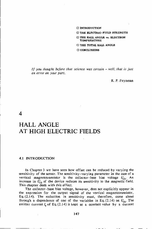
DINTRODUCTION
D THE ELECTRIC-FIELD STRENGTH
D THE HALL ANGLE vs. ELECTRON TEMPERATURE
D THE TOTAL HALL ANGLE
D CONCLUSIONS
If you thought before that science was certain - well, that is just an error on your part.
R. P. Feynman
4
HALL ANGLE AT HIGH ELECTRIC FIELDS
4.1 INTRODUCTION
In Chapter 3 we have seen how offset can be reduced by varying the sensitivity of the sensor. The sensitivity-varying parameter in the case of a vertical magnetotransistor is the col lector-base bias voltage Ucb. An increase in Uch of the device reduces its sensitivity to the magnetic field. This chapter deals with this effect.
The col lector-base bias voltage, however, does not explicitly appear in the expression for the output signal of the vertical magnetotransistor, Eq. (2.14). The reduction in sensitivity must, therefore, come about through a dependence of one of the variables in Eq. (2.14) on Ucb. The emitter current / e of Eq. (2.14) is kept at a constant value by a current
147
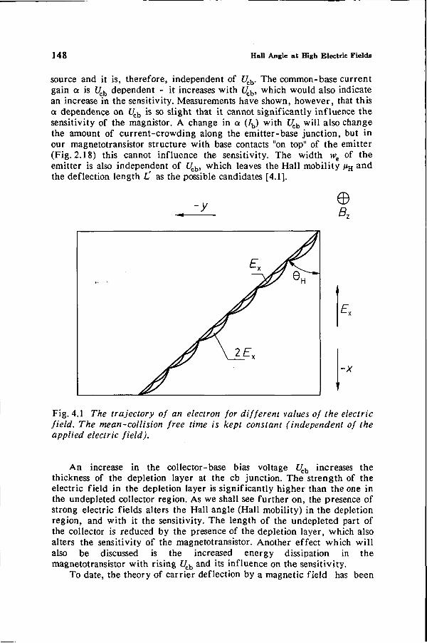
148 Hall Angle at High Electric Fields
source and it is, therefore, independent of Ucb. The common-base current gain a is Ucb dependent - it increases with Ucb, which would also indicate an increase in the sensitivity. Measurements have shown, however, that this a dependence on Ucb is so slight that it cannot significantly influence the sensitivity of the magnistor. A change in a (/b) with Ucb will also change the amount of current-crowding along the emitter-base junction, but in our magnetotransistor structure with base contacts "on top" of the emitter (Fig. 2.18) this cannot influence the sensitivity. The width vve of the emitter is also independent of Ucb, which leaves the Hall mobility % and the deflection length L' as the possible candidates [4.1].
■y 0 a
Fig. 4.1 The trajectory of an electron for different values of the electric field. The mean-collision free time is kept constant (independent of the applied electric field).
An increase in the col lector-base bias voltage Ucb increases the thickness of the depletion layer at the cb junction. The strength of the electric field in the depletion layer is significantly higher than the one in the undepleted collector region. As we shall see further on, the presence of strong electric fields alters the Hall angle (Hall mobility) in the depletion region, and with it the sensitivity. The length of the undepleted part of the collector is reduced by the presence of the depletion layer, which also alters the sensitivity of the magnetotransistor. Another effect which will also be discussed is the increased energy dissipation in the magnetotransistor with rising Ucb and its influence on the sensitivity.
To date, the theory of carrier deflection by a magnetic field has been
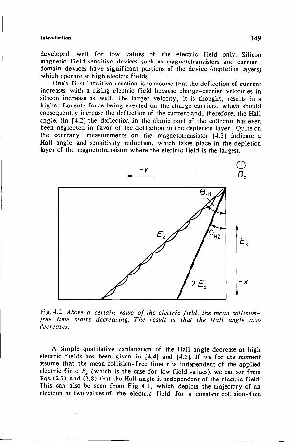
Introduction 149
developed well for low values of the electric field only. Silicon magnetic-field-sensitive devices such as magnetotransistors and carrier-domain devices have significant portions of the device (depletion layers) which operate at high electric fields;
One's first intuitive reaction is to assume that the deflection of current increases with a rising electric field because charge-carrier velocities in silicon increase as well. The larger velocity, it is thought, results in a higher Lorentz force being exerted on the charge carriers, which should consequently increase the deflection of the current and, therefore, the Hall angle. (In [4.2] the deflection in the ohmic part of the collector has even been neglected in favor of the deflection in the depletion layer.) Quite on the contrary, measurements on the magnetotransistor [4.3] indicate a Hall-angle and sensitivity reduction, which takes place in the depletion layer of the magnetotransistor where the electric field is the largest.
-y e
E v
-x
Fig. 4.2 Above a certain value of the electric field, the mean collision-free time starts decreasing. The result is that the Hall angle also decreases.
A simple qualitative explanation of the Hall-angle decrease at high electric fields has been given in [4.4] and [4.5]. If we for the moment assume that the mean collision-free time r is independent of the applied electric field EL^ (which is the case for low field values), we can see from Eqs.(2.7) and (2.8) that the Hall angle is independent of the electric field. This can also be seen from Fig. 4.1, which depicts the trajectory of an electron at two values of the electric field for a constant collision-free
150 Hall Angle at High Electric Fields
time T. In other words, if the mean collision-free time is independent of the electric field, an increase in the col lector-base bias of our magnetotransistor will not change the sensitivity of the device because the Hall angle remains the same. The mean collision-free time is, however, dependent on the carrier energy. From Fig. 4.2 and Eq. (2.7) we can see that the result of a reduced collision-free time r is a reduction in the Hall angle which, in turn, means that above a certain value of the electric field in the depletion layer of the magnetotransistor, the sensitivity of the device to magnetic fields is reduced.
ND (cm"3) 14 15 16 17 18
' CO
'> c
0.14
0.12
0.10
0.08
0.06
0.04
0.02
0 4 5 6 7 8
10 10 10 10 10
Ex(V/m)
Fig. 4.3 The electron drift mobility at room temperature [4.7].
The electron drift mobility depends on the mean collision-free time and the electron's effective mass, Eq. (2.7). The effective mass is only field dependent for a highly parabolically shaped minimum in the conduction band [4.6]. Silicon does not have this property and the field dependence of the electron drift mobility is due to the reduction in the mean collision-free time with a rising electric field. In Fig. 4.3 we can see that for electric field values above 105 V/m the mobility starts to decrease, which indicates a reduction in the mean collision-free time at high electric fields. The mobility characteristic can be divided into three parts. In the ohmic region the carrier mobility is approximately equal to the mobility at a zero field. For fields higher than approximately 105V/m mobility decreases with the rising field. This part of the characteristic is called the warm electron region. In the hot electron region the mobility approaches a minimum value.
The Electric-Field Strength 151
4.2 THE ELECTRIC-FIELD STRENGTH
4.2.1 Depletion Layer
The thickness of the depletion region /d as a function of the reverse bias voltage is given for a step junction by the following well-known expression:
U = (£/bi + Ucb) eNAN» (4.1)
€ is the permitivity of silicon and Ubi is the built-in voltage. With the base impurity concentration A^ of about 1018cm~3 and the epilayer concentration ND of about 6x 1015cm"3 the depletion layer will mainly extend into the epilayer. For a Ucb reverse bias of 10 V, /d is about 1.5 /im. (For iVD = 1015cm~3 /d is about 3.7 /im). The maximum value of the electric field Exm in the depletion layer is given by
'd
At Ucb = 10 V and AD = 6 x 1015 cm"3 Exm becomes 14 x 106 V/m (5.7 x 10⁶ V/m for ND = 1015 cm"3). This value is well above the 105 V/m at which the decrease of the mean collision-free time sets in.
In comparison, the electric-field strength in the ohmic part of the epitaxial layer is much smaller. The resistance R,. of that layer is
* = ' ^ ( 4 - 3 )
where Le is the length of the emitter. With p = 0.8ncm for ND = 6 x 101 5cnr3 , weLe = 26 x 140 nm2 and L' = 5 nm, R,. becomes about 11 fl. (The values of we and L' used here were determined in Section 3.2.1 as the effective deflection length.) If we again assume that the emitter current is 10 mA (the collector current is nearly the same) the electric field in the ohmic part of the collector £XQ becomes
£xfI = -*-r a 2 .2xl0 4V/m (4.4)
1 5 2 Hall Angle at High Electric Fields
From Fig. 4.3 we can see that this value of the electric field has no influence on the electron drift mobility whatsoever, which means that the mean collision-free time in the ohmic collector region is not reduced under the above conditions.
Current deflection in the emitter and base regions can be neglected because of the high impurity concentration in the emitter and the thin base, which means that the ohmic collector region and the collector-base depletion layer determine the sensitivity of our magnetotransistor.
4.2.2 The Energy Distribution Function
Under thermal equilibrium conditions the probability f0 of the occupation of an energy state (energy E) by an electron in the conduction band is given by the Maxwell-Boltzmann energy distribution function
f0 = Qexp(-£Abr) (4.5)
fcb is the Boltzmann's constant, and T the temperature. This function is the high-energy approximation of the Fermi-Dirac distribution function, which is valid only for thermal equilibrium between the electron gas and the lattice. In other words, this relation is only valid in the ohmic collector region of the magnetotransistor.
If an electric field is applied, the electrons gain energy from the field and dissipate it to the lattice. There is now a net energy transfer from the electron system to the lattice, and the temperature Te of the electron cloud is higher then the lattice temperature 7J. For low values of the electric field the difference between Te and 7J is negligible, and Eq. (4.5) still holds [4.6]. For higher electric fields the electron temperature may become much higher than the lattice temperature, the thermal equilibrium is disturbed, and the Maxwell-Boltzmann distribution is no longer valid. A new equilibrium may be established when the difference between the electron and the lattice temperatures is such that the rate of gain of energy of the electrons from the electric field is balanced by the rate of loss of energy to the lattice atoms. If, however, the electron concentration is high enough to dominate the energy relaxation of the hot electrons, their energy distribution still remains Maxwellian, and the following is valid [4.6]:
ƒ(£) = qexp( -£ /Ve) (4-6)
In silicon the number of allowed energy levels per unit of volume in the energy interval between E and E + dE in the conduction band is given as
The Electric-Field Strength 1 5 3
N{E) = C 2 £ 3 / 2 (4.7)
The number of electrons f(E)dE in the conduction band with energies between E and E + d£ is given by the product of Eqs. (4.6) and (4.7):
f(E)dE = C3E3/2exp(-E/kbTe)dE (4.8)
The total number of electrons n in the conduction band per unit of volume is given by
n = C 3 £ 3 / 2 e x p ( - £ A b r e ) d £ (4.9)
4.2.3 The Electron Temperature
The electron temperature is a measure for the average kinetic energy of the electrons. It appears [4.8] that in the warm region (Ex< 1.2 x 10⁶ V/m) the relation between the electron temperature and the electric field is quadratic
T. = Tl + awE* (4.10)
with 0^,= 1.58 x 10"1 0 Km 2 /V 2 as a constant. For higher values of the electric field (15 x 106 < Ex < 40 x 106 V/m) we have [4.9]
Fe = a^El (4.11)
with ah = 8.6 x 10"12 Km 2 /V 2 as a constant. An approximate formula for the electron temperature which is
reasonably accurate for the warm region and the onset of the hot region is given by
Te = Tl + aEx (4.12)
with a = 1.27 x 10" 4Km/V.
154 Hall Angle at High Electric Fields
4.3 THE HALL ANGLE vs. ELECTRON TEMPERATURE
In Chapter 2 the Hall angle has been calculated as a y(<r>)/x(<r>) ratio, which was convenient for the ensuing qualitative discussion. In this section the Hall angle will be calculated according to Eqs. (4.13) and (4.14):
tan6H = H
J = en<v>
(4.13)
(4.14)
where <v> is the average carrier velocity. Starting from the equations of electron motion in crossed electric and
magnetic fields Eq. (2.3), the x and the y components of the electron velocity can be calculated (for the orientation of the fields with respect to each other see Figs. 4.1 and 4.2):
vy(0 = Y (coswcf - i) (4.15)
The probability that an electron will collide in a time interval between / and t + dt is given by [4.10]
f(t)dt = |exp(- t / r )d / (4.16)
If we assume that the average velocity just after the collision is zero, which is the case for a randomizing collision process, we can calculate the average velocity according to the following expressions:
<vx> = J
<v> = «1
(*°° vx(0/(0d/
0
«OO
vy(0 fU)dt 0
(4.17)
The Hall Angle vs. Electron Temperature 155
With Eqs. (4.15) and (4.16) the average velocity components become
<vy> = - ^ c £ x T T ^ - 2 (4.18)
wc = m^z
where m^ is the conductivity effective mass of electrons [4.11]. With mc=2.4x 10"31kg, the average r of about 2x 10"13s [4.12] and Bz of 1 T, we have
r2o;2 = 1.8 xlO"2 (4.19)
For magnetic flux densities of less than 1 T the expressions for the average velocity components reduce to
<vx> = - 4 r £ *
<vy> = -m^riEx
(4.20)
These expressions are also a function of energy, because r is energy dependent. The part of the current density consisting of electrons of energy E can now be written with Eq. (4.14) as
d/x =4«(£)r(£)Ex
(4.21) Uy =^cn(E)r2(E)Ex
n(E) is the number of electrons with energy E, and it is given by Eq. (4.8) (n(E) = f(E)dE). To obtain current density components 7X and Jy we must integrate over all energies:
156 Hall Angle at High Electric Fields
J„ = oo
f(E)T(E)dE
0
Jy = Exr^Uc
.OO (4.22)
f(E)r2(E)dE
These can be written as
J^ = ExF^n<T(E)>
(4.23) Jy = Ex»\.ucn<T2(E)>
with n as the total number of electrons in the conduction band, Eq. (4.9). The energy average of functions T(E) and T2(E) are given by
oo ,3 /2
<r(E)> =
T(E)E ' expi-E/kJJdE
E3/2exp(-E/kJl)dE
„oo
n' ,3 /2 T(E)E-"exp(-E/kJ-e)dE
(4.24)
<r(E)> =
r 2 ( £ ) £ 3 / 2 e x p ( - £ A j ; ) d £
E3/2exp(-E/kJl)dE
The Hall Angle vs. Electron Temperature 157
n' T2(E)E3/2exp(-E/kJ*e)dE
n' = -^
The Hall angle, Eq. (4.13), can now be written as
rsnft _ o 1. <T (E)> tan ö H = a, fa / „ ,
H z n \ <T(E)>
(4.25)
The collision-free time r as a function of electron energy is given by the following expression [4.13]:
,1/2 w.
(£ + fcbe)1/2 + exp(0/7I)(£-A:b0) 1/2
e x p ( 0 / 7 ; ) - l (4.26)
1/2 The E term in this expression is due to the acoustic intravalley
scattering, while the second term is due to the f-type intervalley scattering [4.13], and it can be divided into two parts. The first part (£■+ h^O)1/2 is due to the absorption of energy by the electron from the lattice. The second part (E - A^ö)1/2 describes the transfer of energy from the electrons to the phonons. This transfer can only occur if the electron energy E is higher than ^ , 6 . If this is not the case, the (E - k^Q)1/2 term in Eq. (4.26) is zero [4.13]. Eq. (4.26) can be rewritten so that we obtain
I (exp(G/7I)- l )£ 1 / 2+ w^KE+k^ef^+expiG/TOiE-l^e)^2]
3 /2
exp(6 /7J ) - l
w2fll = 2 f
(4.27)
0 is the characteristic temperature of the phonons (630 K), T0 is a reference temperature which can be chosen to allow for the magnitude of r, while wa relates the strength of coupling of the electrons to acoustic phonons [4.13]. If we substitute Eq. (4.27) in the expressions given in Eq. (4.24) we obtain
158 Hall Angle at High Electric Fields
<r>= 5 [ e x p ( 0 / 7 J ) - l ] x (4.28)
E3/2exp(-E/kbTe)dE
(exp(0/7J)- l)£1 / 2+ w2ai[(E+kb&i/2+ exp(0/7I)(£-^b0)1 / 2]
<r2>= 5 [ e x p ( 0 / 7 ï ) - l ] 2 x (4.29)
E3/2exp(-E/kbTe)dE
[(exp(0/7])-l)£1 / 2+w2 a i[(f+fcb0/ / 2+exp(0/7J)(£-fcb0)1 / 2]]2
These equations cannot be solved analytically, and we are forced to approximate the integrands with simpler expressions:
-,3/2
g(E) = (exp(0/7J)- l )£ 1 / 2+ w2ai[(E+khej/2
+ exp^/T^E-J^ef'2]
(4.30)
The integrand in Eq. (4.28), without the exponent, is given in Eq. (4.30) and the plot of this function is given in Fig. 4.4. The sharp peak in g{E) is caused by the (E - J^©)1/2 term, which becomes non-zero for E > khQ. This function is given for E < 4 kbQ because the maximum electron temperature 7 ,, Eq. (4.12) in the depletion layer of our magnetotransistor will be around 4 0 (7; = 300 K and £ x = 1.7 x 10⁷ V/m). At room temperature (7J = 300 K) g(E) can be approximated by the following function:
g(E) = 0.07 E E < kbQ
g(E) =-0.19 E+ 0.266 kbQ 1^9 < E < \.2kbQ
g(E) = 0.02 E + 0 .0136^0 l.2kbQ<E<oo
(4.31)
With this approximate equation we obtain an approximation for Eq. (4.28) [4.14], [4.15]:
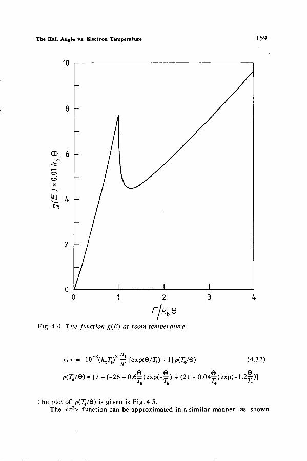
The Hall Angle vs. Electron Temperature 159
IU
8
CD 6 -5c
X
£ 4 Oi
2
n
-
/ i l l 0 1 2
E/kbQ
Fig. 4.4 77ze function g(E) at room temperature.
<T> = Ï O ^ W ^ [«P(©A) - npiTJQ) (4.32)
p(7;/0) = [7 + (-26 + 0.6 |-)exp(- | -) + (21 - 0 .04^ )exp(-1.2|-)]
The plot of piTJQ) is given is Fig. 4.5. The <r2> function can be approximated in a similar manner as shown
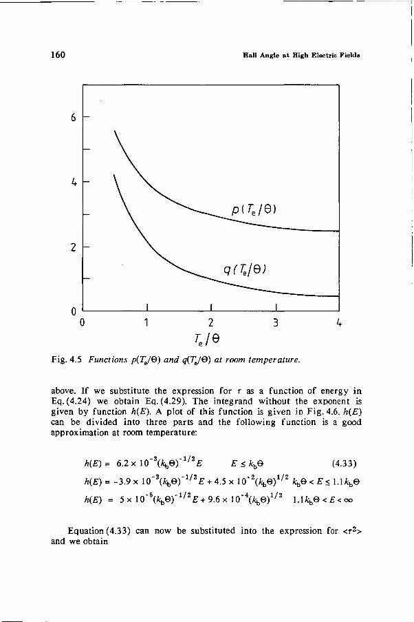
160 Hall Angle at High Electric Fields
Fig. 4.5 Functions p(Te/Q) and qiTJQ) at room temperature.
above. If we substitute the expression for r as a function of energy in Eq. (4.24) we obtain Eq. (4.29). The integrand without the exponent is given by function h(E). A plot of this function is given in Fig. 4.6. h(E) can be divided into three parts and the following function is a good approximation at room temperature:
h(E)- 6.2x l O " 3 ^ © ) " 1 ^ E < khQ (4.33)
h(E)= -3.9 x 10"2(^e)"1 / 2£ + 4.5x 10"2(^e)1 / 2 ^ 6 < E< 1.1^0
h(E) = 5xlO"5(fcbe)"1/2£ + 9.6xlO"4(^0)1 / 2 l.lkb@<E<oo
Equation (4.33) can now be substituted into the expression for <r2> and we obtain
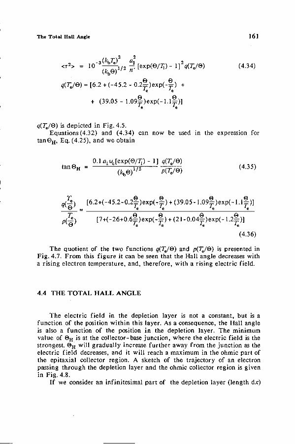
The Total HaU Angle 161
<r2> = i 0 - 3 ^ 1 / 2 ^ [ e x p ( e / 7 ; ) - l ] ^ ( r e / e ) (4.34) (fcb0) "
q{TJ@) = [6.2 + (-45.2 - 0.2p-)exp(-|-) + •"e *e
+ (39.05- 1.09® )exp(-1.1^)]
q(TJQ) is depicted in Fig. 4.5. Equations (4.32) and (4.34) can now be used in the expression for
tan©H, Eq. (4.25), and we obtain
O . l f l ^ f e x r t e / T p - l ] q{TJQ) t a n 0 H = Ï72 1£ itw (4.35)
(fcb0) ' P(Te/e)
q^k) [6.2+(-45.2-0.2®)exp(-®) +(39.05-1.09®)exp(-1.1®)] '<è'
J±) [7+( -26+O.6 | ) exp( - | ) + (21-O.O4|)exp(-1.20T)] 0 xe -*e -"e -"e
(4.36)
The quotient of the two functions q(TJQ) and p(Te/&) is presented in Fig. 4.7. From this figure it can be seen that the Hall angle decreases with a rising electron temperature, and, therefore, with a rising electric field.
4.4 THE TOTAL HALL ANGLE
The electric field in the depletion layer is not a constant, but is a function of the position within this layer. As a consequence, the Hall angle is also a function of the position in the depletion layer. The minimum value of 0 H is at the col lee tor-base junction, where the electric field is the strongest. 0 H will gradually increase further away from the junction as the electric field decreases, and it will reach a maximum in the ohmic part of the epitaxial collector region. A sketch of the trajectory of an electron passing through the depletion layer and the ohmic collector region is given in Fig. 4.8.
If we consider an infinitesimal part of the depletion layer (length dx)
162 Hall Angle at High Electric Fields
6 -
CD -O
n i <=>
X
4 -
2 -
0 0 1 2
EJkhQ Fig. 4.6 The function h(E) at room temperature.
in which the electric field can be assumed to be a constant, the contribution d/d to the collector-current difference of this segment of the depletion layer is
d/d = yjrtan©Ha/edx (4.37)
The total collector-current difference A/d caused by deflection in the depletion layer can be obtained by integrating over the full length of this region:
/•° A/d = ^j-tan6Ha/edx (4.38)
If we assume that A/d is a result of current deflection over a distance
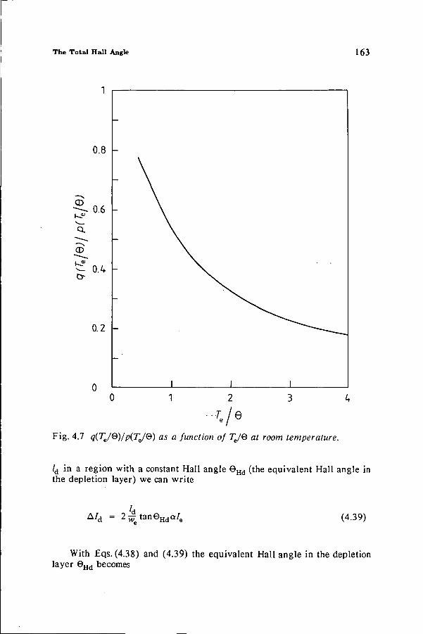
The Total Hall Angle 163
Fig. 4.7 q(Te/Q)/p(Te/Q) as a function of TJQ at room temperature.
ld in a region with a constant Hall angle 0Hd (the equivalent Hall angle in the depletion layer) we can write
A/d = 2 ^ t a n e H d a / ( (4.39)
With Eqs. (4.38) and (4.39) the equivalent Hall angle in the depletion layer 0Hd becomes
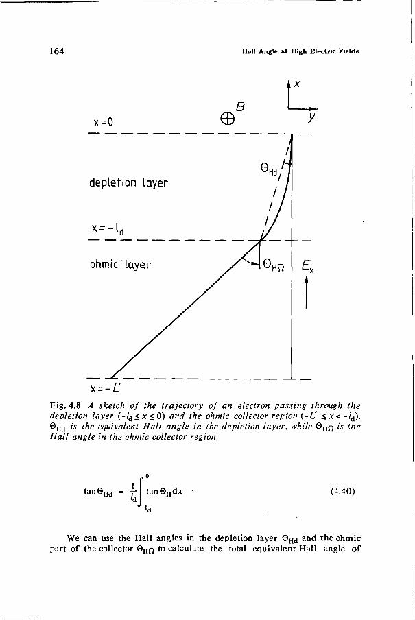
164 Hall Angle at High Electric Fields
t X
x=0 e B
depletion layer
x = -l
ohmic layer
y
x=-L' Fig. 4.8 A sketch of the trajectory of an electron passing through the depletion layer (- /d<x< 0) and the ohmic collector region (-L' <x< -/d). 0H d is the equivalent Hall angle in the depletion layer, while O H Q is the Hall angle in the ohmic collector region.
tan0 Hd = tan0Hdx (4.40)
We can use the Hall angles in the depletion layer 0H d and the ohmic part of the collector 0 H Q to calculate the total equivalent Hall angle of
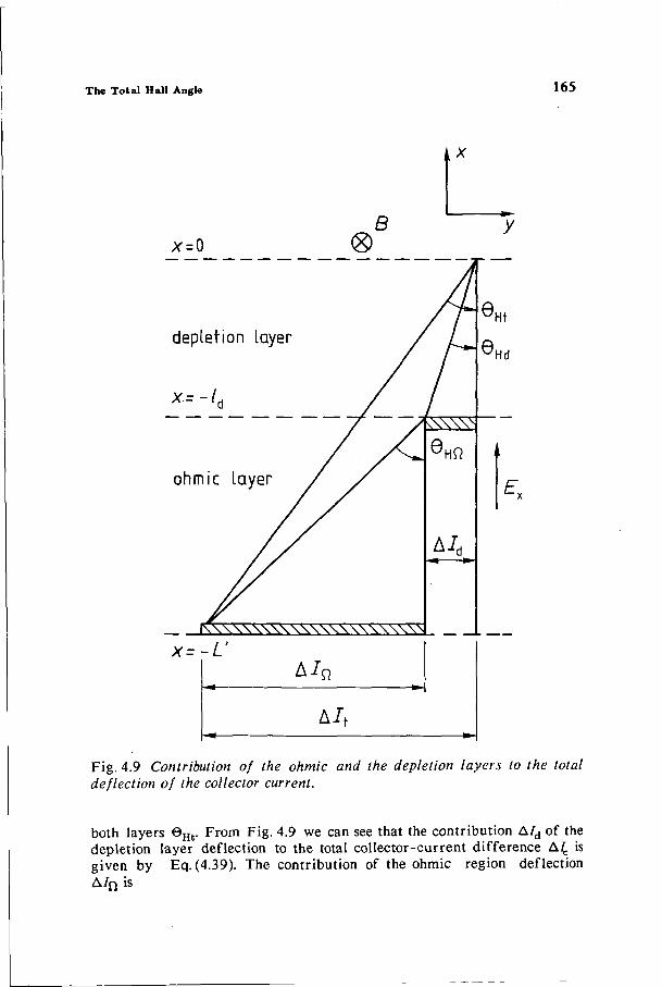
The Total Hall Angle 165
x=-L'
A/t
Fig. 4.9 Contribution of the ohmic and the depletion layers to the total deflection of the collector current.
both layers 6 H t . From Fig. 4.9 we can see that the contribution A/d of the depletion layer deflection to the total collector-current difference A£ is given by Eq. (4.39). The contribution of the ohmic region deflection A / Q is
1 6 6 Hall Angle at High Electric Fields
(4.41)
where L' is the total deflection distance. With Eq. (4.42)
A/n = ^ (L ' - / d ) tan0 H n a / e
A/ c = A/d ■+ A / n (4..42)
we obtain
2 2 WL'taneHta/e = ^a/e[/dtanGHd + (£' - /d)tan0Hn]
(4.43)
This finally leads to
tan6Ht = tan0H n - j> [ tan 0 H n - tan 0H d ] (4.44)
So far the following formulas have been derived:
_ O.lfl1ü;c[exp(0/^)-l] qjTJQ) t a n Ö H = ^0?^ PCV*)
(4.35)
J!±) [6.2+(-45.2-0.2®)exp(-^) + (39.05-1.09® )exp(-1.1®)] k 0 ' =
Jk) [7+(-26+0.6|)exp(-|) + (21-0.04|)exp(-1.2|)] ^e'
wc = mcBz
Z = T, + a£v
(4.36)
(4.18)
(4.12)
/> ° tan© Hd " , tan©Hdx (4.40)
tan©Ht = tan0H n - j , [ tan 0 H n - tan 0H d ] (4.44)
The Total Hall Angle 167
2e(NA + ND)
eNAND (Ubi+Ucb)
1 / 2
(4.1)
^xm ~ (4.2)
Again we have to resort to an approximation because the expression for tan©H of Eqs. (4.35) and (4.36) cannot be analytically integrated in Eq. (4.40). A reasonable approximation of tan0 H is given by
t a n 0 H = A{Tt ■1/2
t a n 0 H = 2 5 . 9 ^ 7 ; "
tan©H = 0 .775^7 ; - 1 / 2
Te<&
0 < 7 i < 2 ©
2 0 < 7 ; (4.45)
A1 = 0.0484 ^ 2 [ e x p ( e / 7 ; ) - l ]
Equation (4.45) has to be integrated according to Eq. (4.40) and for electron temperatures higher than 20 we have the following integral boundaries:
^xi = (0 - Tx)/a = 300/a K for 7; = 0
£ x 2 = (2Q-Tl)/a = 960/a K forTe = 2 0 (4.46)
The relation between the position x in the depletion layer and the electric field (Fig. 4.8) is given by
£x = £xmd + f ) (4.47)
Equation (4.47) yields
dx = F ~ d £ x xm
(4.48)
1 6 8 Hall Angle at High Electric Fields
Equation (4.40) can now be written as
» ^ c l
tanOH d = j T~1/2dEx+ 25.9
-x2
Te *dEx + 0.775 7V1 / 2d^
-■x.2
(4.49)
The boundaries of Eq. (4.49) can be rewritten with Eq. (4.12), and finally we have
t a n e H d = 2£a [ ( 7 [ + a £ x l ) 1 / 2 - 7J1/2] + 12.9 In T\ + aEx2
Ty + aE^
+ 0J7[(Tl+ aExm)1/2 - (Tl + aEx2)1/2] (4.50)
The Hall angle in the ohmic layer can be obtained by setting 7 = 7J in Eq. (4.35) and we obtain
t a n 0 H n = O.l f l lo;c[exp(0/7I)-1] q(J\/@)
(*b©) T7F P(T,/G) (4.51)
The total Hall angle can now be calculated with the above results for the average Hall angles in the depletion and the ohmic layers. If we assume Nu = 6 x 1016 cm"3 in the epitaxial collector region and L'.= 6 nm we obtain for the total Hall angle
tan©Ht(C/cb = 0.6V) = 46.9 A
taneH t(£/c b= 10.6 V) = 41.1/i '
A = 2 aE„
This indicates a 12.4% drop in the sensitivity when Ucb is increased from 0.6 V to 10.6 V. The constant factor A' contains the reference temperature T0 Eq. (4.27), and it can be chosen to fit the measurements. The relative drop in the sensitivity of the magnetotransistor for different values of ND L'and a is given in Table 4.1, while in Fig. 4.10 the decrease
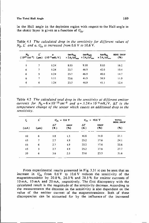
The Total Hall Angle 169
in the Hall angle in the depletion region with respect to the Hall angle in the ohmic layer is given as a function of Ucb.
Table 4.1 The calculated drop in the sensitivity for different values of ND, L' and a. Uch is increased from 0.6 V to 10.6 V.
( 1 0 1 5 c m s )
1
6
6
6
6
L' (ion)
7 7
5 7
6
(10 a
4 mK/V)
1.24
1.24
1.24
1.11 1.24
tan6H d
8.03 23.7
23.7
23.6 23.7
tane H f ,
9.58 46.9
46.9
41.9
46.9
tan6H t x l A J a E ^
8.03
42.0
40.0
36.9 41.1
SENS. DROP
(%)
16.2 10.4
14.7
11.9 12.4
Table 4.2 The calculated total drop in the sensitivity at different emitter currents for ND = 6 x 10"15 cm"3 and a = .1.24 x 10 ' 4 mK/V. AT is the temperature change of the sensor which causes an additional drop in the sensitivity.
'.
(mA)
10
15
15
15
20
L'
( / im)
6 7
6
5
6
u* -A r (K-)
1.8 2.7
2.7
2.7
3.6
= 0.6 V
DROP
(%)
1.3
1.9
1.9
1.9
2.5
u* -Ar (K.)
16.8 25.2
25.2
25.2
33.6
= 10.6 V
DROP
(%)
11.8
17.6
17.6
17.6
23.5
TOTAL SENS. DROP
(%)
21.1
24.1
25.6 27.7
31.6
From experimental results presented in Fig. 3.31 it can be seen that an increase in Ucb from 0.6 V to 10.6 V reduces the sensitivity of the magnetotransistor by 20.8 %, 26.0 % and 28.5 % for emitter currents of 10 mA, 15 mA and 20 mA, respectively. The first discrepancy with the calculated result is the magnitude of the sensitivity decrease. According to the measurements the decrease in the sensitivity is also dependent on the value of the emitter current of the magnetotransistor. Both of these discrepancies can be accounted for by the influence of the increased
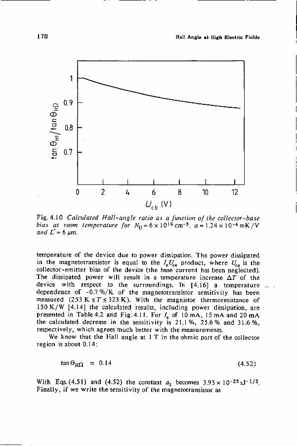
170 Hall Angle at High Electric Fields
Fig. 4.10 Calculated Hall-angle ratio as a function of the collector-base bias at room temperature for ND = 6 x 1015 cm-3, a = 1.24 x 10" 4 mK/V and L' = 6 jjm.
temperature of the device due to power dissipation. The power dissipated in the magnetotransistor is equal to the leUce product, where Uce is the collector-emitter bias of the device (the base current has been neglected). The dissipated power will result in a temperature increase AT of the device with respect to the surroundings. In [4.16] a temperature dependence of -0.7 %/K of the magnetotransistor sensitivity has been measured (253 K < T< 323 K). With the magnistor thermoresistance of 150 K/W [4.14] the calculated results, including power dissipation, are presented in Table 4.2 and Fig. 4.11. For /e of 10 mA, 15 mA and 20 mA the calculated decrease in the sensitivity is 21 .1%, 25.6% and 31.6%, respectively, which agrees much better with the measurements.
We know that the Hall angle at 1 T in the ohmic part of the collector region is about 0.14:
t a n 0 H n ~ 0.14 (4.52)
With Eqs.(4.51) and (4.52) the constant ax becomes 3.95 x l O - ^ s J " 1 / 2 . Finally, if we write the sensitivity of the magnetotransistor as
Conclusions 171
^(/e,f/cb) = IeAGnH(T,Uch) (4.53)
with AQ = 0.182 Vs/m2T as a geometry factor, we can calculate the sensitivity of the magnetotransistor as a function of the emitter current and col lector-base voltage. In Fig. 4.12 the calculated sensitivity curves are compared to the measurements.
1
G 0.9 CD
JLo.8 ■4—
CD o 0.7
0 2 V 6 8 10
Fig. 4.11 Calculated Hall-angle ratio as a function of the collector-base bias for ND = 6xl015 cm-3, a = 1.24 x 10"4 mK/V and L'= 6 urn. Ie is used as a parameter.
4.5 CONCLUSIONS
In this chapter it has been determined that the decrease in the sensitivity of a magnetotransistor is caused by two effects.
1) A significant portion of the device consists of a col lector-base depletion layer in which high electric fields are present. High electric fields in the depletion layer reduce the mean collision-free time, and the Hall angle with it. To calculate this effect the Hall angle has been determined as a
20mA
J I I I
1 7 2 Hall Angle at High Electric Fields
I I I I I I I 0 2 4 6 8 10
U c b(V)
Fig. 4.12 Comparison of the calculated sensitivity to the measurements.
function of the mean col lis ion-free time and the electron temperature. The electric field in the depletion layer is not a constant, but is a function of the position, which makes the Hall angle in the depletion layer position dependent, too. The equivalent Hall angle in the depletion layer has been determined, as well as the total equivalent Hall angle of the device.
2) A decrease in the Hall angle at high electric fields alone was not enough to fully describe the measurements. The temperature of the device
Conclusions 173
rises with Uch and Ie due to power dissipation, which is accompanied by a further drop in the sensitivity of the magnetotransistor.
In spite of the numerous approximations which have been used in the derivation of the Hall angle as a function of the electric field and col lector-base bias, the combined results of the above two effects agree reasonably well with the measurements.
174 Hall Angle at High Electric Fields
REFERENCES
[4.1] P. J. A. Munter and S. Kordic, The decrease in the Hall angle and the sensitivity at high electric fields in silicon magnetic sensors, Eurosensors, Cambridge, UK, 1987, Tech. Dig., pp. 200-201.
[4.2] M. Ishida, H. Fujiwara, T. Nakamura, M. Ashiki, Y. Yasuda, A. Yoshida, T. Ohsakama and Y. Kawase, Silicon magnetic vector sensors for integration, Proc. 4th Sensor Symp., Japan, 1984, pp. 79-83.
[4.3] S. Kordic, V. Zieren and S. Middelhoek, A magnetic-field-sensitive multicollector transistor with low offset, Int. Electron Devices Meet., Washington, DC, USA, 1983, IEDM Techn. Dig., pp. 631-634.
[4.4] S. Kordic and P. C. M. van der Jagt, Electronic implementation of the sensitivity-variation offset-reduction method, 3rd Int. Conf. on Solid-State Sensors and Actuators, Philadelphia, PA, USA, 1985, Dig. Techn. Papers, pp. 320-323.
[4.5] S. Kordic and P. C. M. van der Jagt, Theory and practice of the electronic implementation of the sensitivity-variation offset-reduction method, Sensors and Actuators, vol.8, 1985, pp. 197-217.
[4.6] B. R. Nag, Electron Transport in Compound Semiconductors, Springer-Verlag, Berlin, 1980.
[4.7] V. Zieren, Integrated silicon multicollector magnetotransistors, Ph.D. thesis, Delft University of Technology, 1983.
[4.8] P. K.Basu and B. R. Nag, Room temperature conductivity anisotropy and population redistribution in n-type silicon at high electric fields, Phys. Rev. B, vol. 1, 1970, pp. 627-631.
[4.9] C. Y. Duh and J. L. Moll, Temperature dependence of hot electron drift velocity in silicon at high electric field, Solid-State Elec, vol. 11, 1968, pp. 917-930.
[4.10] H.Weiss, Structure and Application of Galvanomagnetic Devices, Pergamon Press, Oxford, 1969.
[4.11] R. A. Smith, Semiconductors, Cambridge University Press, Cambridge, 2nd ed., 1978.
[4.12] R. A. Smith, Wave Mechanics of Crystalline Solids, Chapman and Hall Ltd., London, 2nd ed., 1969.
[4.13] D. Long, Scattering of conduction electrons by lattice vibrations in silicon, Physical Rev., vol. 120, 1960, pp. 2024-2032.
[4.14] P. J. A. Munter, Decrease of sensitivity in the depletion layer of a magnetic-field sensitive multi-collector transistor, Internal report, Delft University of Technology, 1986.
[4.15] I. S. Gradshteyn and I. M. Ryzhik, Table of Integrals, Series, and Products, Academic Press, New York, 4th ed., 1980.
[4.16] S. Kordic, Current crowding and thermal effects in a magnetic-field sensitive multicollector transistor, Internal report, Delft University of Technology, 1981.
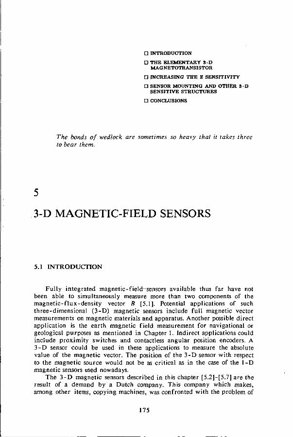
D INTRODUCTION
D THE ELEMENTARY 3-D MAG NETOTRANSISTOR
D INCREASING THE Z SENSITIVITY
D SENSOR MOUNTING AND OTHER 3-D SENSITIVE STRUCTURES
D CONCLUSIONS
The bonds of wedlock are sometimes so heavy that it takes three to bear them.
5
3-D MAGNETIC-FIELD SENSORS
5.1 INTRODUCTION
Fully integrated magnetic-field sensors available thus far have not been able to simultaneously measure more than two components of the magnetic-flux-density vector B [5.1]. Potential applications of such three-dimensional (3-D) magnetic sensors include full magnetic vector measurements on magnetic materials and apparatus. Another possible direct application is the earth magnetic field measurement for navigational or geological purposes as mentioned in Chapter 1. Indirect applications could include proximity switches and contactless angular position encoders. A 3-D sensor could be used in these applications to measure the absolute value of the magnetic vector. The position of the 3-D sensor with respect to the magnetic source would not be as critical as in the case of the 1-D magnetic sensors used nowadays.
The 3-D magnetic sensors described in this chapter [5.2]-[5.7] are the result of a demand by a Dutch company. This company which makes, among other items, copying machines, was confronted with the problem of
175
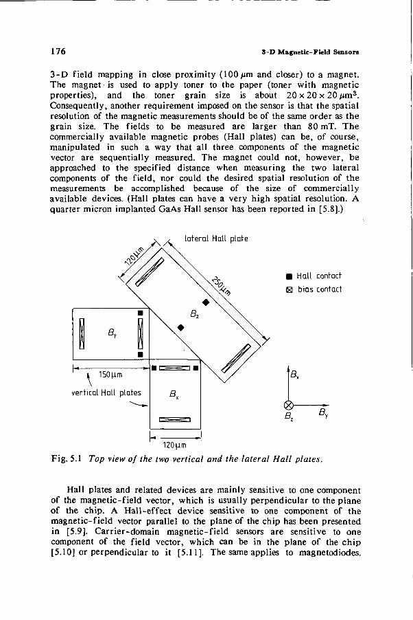
176 3-D Magnetic-Field Sensors
3-D field mapping in close proximity (100/jm and closer) to a magnet. The magnet is used to apply toner to the paper (toner with magnetic properties), and the toner grain size is about 20 x 20 x 20 /im3. Consequently, another requirement imposed on the sensor is that the spatial resolution of the magnetic measurements should be of the same order as the grain size. The fields to be measured are larger than 80 mT. The commercially available magnetic probes (Hall plates) can be, of course, manipulated in such a way that all three components of the magnetic vector are sequentially measured. The magnet could not, however, be approached to the specified distance when measuring the two lateral components of the field, nor could the desired spatial resolution of the measurements be accomplished because of the size of commercially available devices. (Hall plates can have a very high spatial resolution. A quarter micron implanted GaAs Hall sensor has been reported in [5.8].)
lateral Hall plate
a
l 150 Jim
vertical Hall plates
■ Hall contact H bias contact
&
a a 120 im
Fig. 5.1 Top view of the two vertical and the lateral Hall plates.
Hall plates and related devices are mainly sensitive to one component of the magnetic-field vector, which is usually perpendicular to the plane of the chip. A Hall-effect device sensitive to one component of the magnetic-field vector parallel to the plane of the chip has been presented in [5.9]. Carrier-domain magnetic-field sensors are sensitive to one component of the field vector, which can be in the plane of the chip [5.10] or perpendicular to it [5.11]. The same applies to magnetodiodes.
Introduction 177
Measurements of all three components of the magnetic field have so far been performed by successively changing the orientation of the one-dimensional sensor and measuring the field component in question. A simultaneous measurement of all three field components can be achieved by attaching three 1-D sensors to the orthogonal faces of a cube. The spatial resolution of a measurement would not be satisfactory in this case if highly divergent fields were to be measured, nor does it make a sensor integrable. In [5.12] one such Hall plate assembly has been described for measuring the magnitude and direction of a full magnetic-field vector. The sensor was required to study the magnetic field produced by rotating a tube of In cooled to 4 K when a magnetic field in the order of 1 T was applied perpendicular to the axis of the tube. The measurements were performed with three discrete InSb Hall plates mounted at right angles to each other. The dimensions of the plates were 0.9 x 0.25 x 0.15 cm3. Alignment errors between the Hall plates of 2°- 3° are reported, which result in cross-sensitivity, meaning~that one output channel is sensitive to more than one field component.
o ^x A ® - — B,
150 im
A' 120M-m
a ez
M\im
Fig. 5.2 Top view and cross-section of the vertical Hall plate.
Another example of a 3-D magnetic sensor used for measurement of the vector of a cardiac magnetic field at various locations on the thorax is given in [5.13]. The structure for sensing these exceptionally weak fields
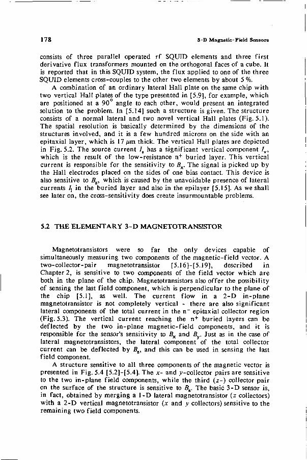
178 3-D Magnetic-Field Sensors
consists of three parallel operated rf SQUID elements and three first derivative flux transformers mounted on the orthogonal faces of a cube. It is reported that in this SQUID system, the flux applied to one of the three SQUID elements cross-couples to the other two elements by about 5 %.
A combination of an ordinary lateral Hall plate on the same chip with two vertical Hall plates of the type presented in [5.9], for example, which are positioned at a 90° angle to each other, would present an integrated solution to the problem. In [5.14] such a structure is given. The structure consists of a normal lateral and two novel vertical Hall plates (Fig. 5.1). The spatial resolution is basically determined by the dimensions of the structures involved, and it is a few hundred microns on the side with an epitaxial layer, which is 17 /mi thick. The vertical Hall plates are depicted in Fig. 5.2. The source current /s has a significant vertical component /v , which is the result of the low-resistance n+ buried layer. This vertical current is responsible for the sensitivity to Bx. The signal is picked up by the Hall electrodes placed on the sides of one bias contact. This device is also sensitive to Bz, which is caused by the unavoidable presence of lateral currents /( in the buried layer and also in the epilayer [5.15]. As we shall see later on, the cross-sensitivity does create insurmountable problems.
5.2 THE ELEMENTARY 3 - D MAGNETOTRANSISTOR
Magnetotransistors were so far the only devices capable of simultaneously measuring two components of the magnetic-field vector. A two-collector-pair magnetotransistor [5.16]-[5.19], described in Chapter 2, is sensitive to two components of the field vector which are both in the plane of the chip. Magnetotransistors also offer the possibility of sensing the last field component, which is perpendicular to the plane of the chip [5.1], as well. The current flow in a 2-D in-plane magnetotransistor is not completely vertical - there are also significant lateral components of the total current in the n~ epitaxial collector region (Fig. 5.3). The vertical current reaching the n+ buried layers can be deflected by the two in-plane magnetic-field components, and it is responsible for the sensor's sensitivity to Bx and B . Just as in the case of lateral magnetotransistors, the lateral component of the total collector current can be deflected by Bt, and this can be used in sensing the last field component.
A structure sensitive to all three components of the magnetic vector is presented in Fig. 5.4 [5.2]-[5.4]. The x- and y-collector pairs are sensitive to the two in-plane field components, while the third (z-) collector pair on the surface of the structure is sensitive to Bz. The basic 3-D sensor is, in fact, obtained by merging a 1-D lateral magnetotransistor (z collectors) with a 2-D vertical magnetotransistor (x and y collectors) sensitive to the remaining two field components.
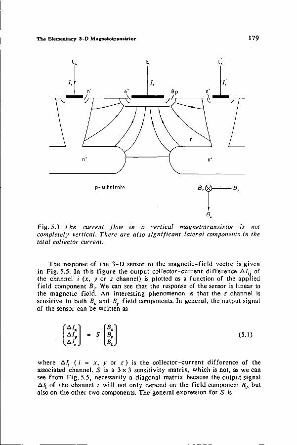
The Elementary 3-D Magnetotransistor 179
p-substrate fix®
B,
Fig. 5.3 The current flow in a vertical magnetotransistor is not completely vertical. There are also significant lateral components in the total collector current.
The response of the 3-D sensor to the magnetic-field vector is given in Fig. 5.5. In this figure the output collector-current difference A/;: of the channel ƒ (x, y or z channel) is plotted as a function of the applied field component B. We can see that the response of the sensor is linear to the magnetic field. An interesting phenomenon is that the z channel is sensitive to both 2?z and B field components. In general, the output signal of the sensor can be written as
fA/*l AT y A/ .
= 5 \BA ffu y
kJ (5.1.)
where A/ ; ( i = x, y or z ) is the collector-current difference of the associated channel. S is a 3 x 3 sensitivity matrix, which is not, as we can see from Fig. 5.5, necessarily a diagonal matrix because the output signal A/j of the channel i will not only depend on the field component B{, but also on the other two components. The general expression for 5 is
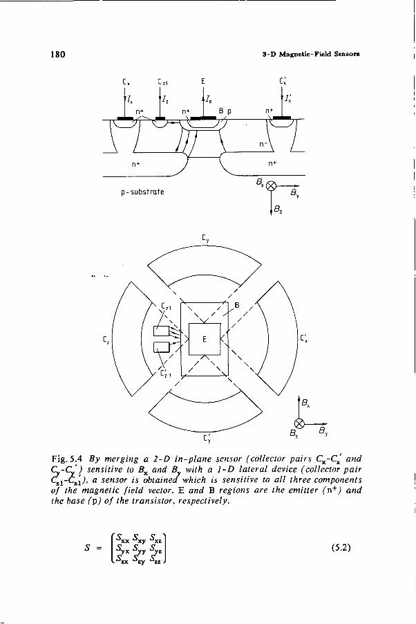
180 3-D Magnetic-Field Sensors
p-substrate
Fig. 5.4 By merging a 2-D in-plane sensor (collector pairs Cx-C^ and C -C') sensitive to Bx and B with a 1-D lateral device (collector pair Czl-Cz'i), a sensor is obtained which is sensitive to all three components of the magnetic field vector. E and B regions are the emitter (n+) and the base (p) of the transistor, respectively.
S = $xx ^xy ^xz C" C C
yx yy yz ^zx Szy Siz
(5.2)
The Elementary 3-D Magnetotransistor 181
Sjj is the sensitivity of the channel i to the field component By If i # j , SVi is the cross-sensitivity. The three components of the magnetic-flux density vector B can now be calculated by inverting the sensitivity matrix and multiplying it by the output signals of the sensor. In other words, the presence of cross-sensitivities does not introduce errors in the measurements.
\BA Bv
U.J =
' e c c 1 " x x "-"xy "-"xz c e e
yx yy y& .^zx ^zy "^zz.
fA/x] A/ y
[A/J (5.3)
The sensitivity matrix of the structure of Fig. 5.4 with one z-collector pair is
5 = ^x> 0
l o
0 syy ^zy
0 0
^ (5.4)
which is evident from the measurements presented in Fig. 5.5. The magnetic sensitivity of a vertical 1-D magnetotransistor can be
easily calculated from Fig. 5.6. The path of the total collector current /c is shifted over a distance Ay under the influence of the lateral magnetic field fix. The shift Ay depends on the Hall angle 0 H ,
t a n 0 H = MHfix (5.5)
and the distance L over which the deflection takes place - the effective thickness of the epitaxial layer. In this case L' is smaller than the thickness of the epitaxial layer because of the presence of the buried layers, emitter and base diffusions, depletion layers, and current spreading. The shift Ay becomes
Ay = L' tan 6 H
Ay = L' nHBx
(5.6)
We will assume that current to the left of the central line between the buried layers is collected by collector Cx, while the current to the right is collected by collector Cx . Because of the shift, currents /x in collector Cx and / ' in collector C x are unequal.
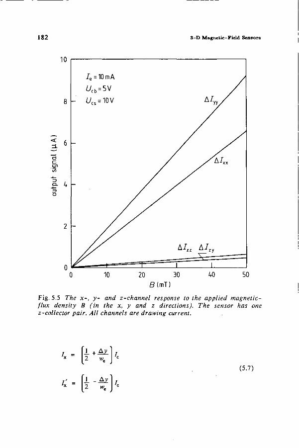
182 3-D Magnetic-Field Sensors
10
8 -
<
o
Z3 O
6 -
4 -
2 -
—
-
ie = 10 m A
^cb = 5V
tycs = iov
A/zz
' i
A / y y /
/ ' A i x x
A/ z y
I 10 20 30
0(mT) 40 50
Fig. 5.5 The x-, y- and z-channel response to the applied magnetic-flux density B (in the x, y and z directions). The sensor has one z-collector pair. All channels are drawing current.
'x =
' , ' =
1 + Az 2 we
V. J
1 - Ay' 2 * .
(5.7)
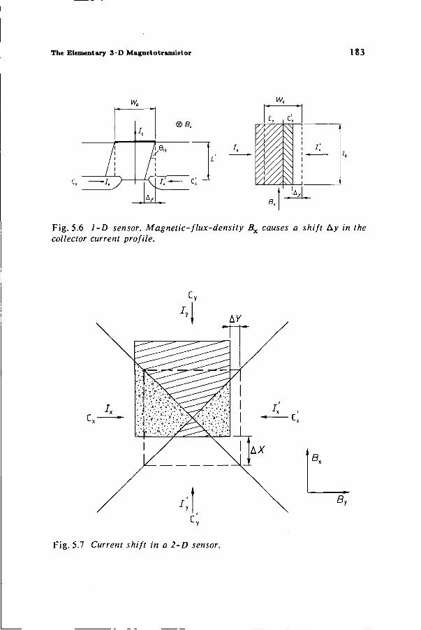
The Elementary 3-D Magnetotrausistor 183
w c« c'„
M / V / / '
\ s
mi A/
Fig. 5.6 1-D sensor. Magnetic-flux-density Bx causes a shift Ay in the collector current profile.
a
a»
Fig. 5.7 Current shift in a 2-D sensor.
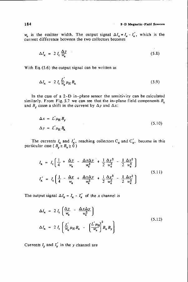
184 3-D Magnetic-Field Sensors
we is the emitter width. The output signal A 7X = 7X - 7X, which is the current difference between the two collectors becomes
A/x = 2 / c ^ (5.8)
With Eq. (5.6) the output signal can be written as
A/x = 2 / c | / z H B x (5.9)
In the case of a 2-D in-plane sensor the sensitivity can be calculated similarly. From Fig. 5.7 we can see that the in-plane field components #x and By cause a shift in the current by Ay and Ax:
Ax = L^iHBy
(5.10) Ay = L V H 3 C
The currents /x and /x', reaching collectors Cx and Cx, become in this particular case ( By > Bx > 0 )
I j f ± + &1 - AxAy + J_Ax2 _ 1 Ax2 1 c [ 4 we we
2 2 w\ 2 wl J
F' = r\± - ±Z + AxAy + 1 Ax2 . 1 Ax2 1 c [ 4 we w? 2 wl 2 w2 J
The output signal A/x = 7X - /x of the x channel is
A/x = 2 / c f ^ - A ^ - }
A / X = 2 / c ^ e M H s x - ( ^ r ] s x .
(5.11)
* y
(5.12)
Currents /y and 7y' in the y channel are

The Elementary 3-D Magnetotransistor 185
/„ = / f i + AX _ Axjn c [ 4 we we
2 J
= 7 f l - Ax + A ^ l c 14 we u>2 J
(5.13)
and the output signal A / = I - i' of the ^-collector pair is y y y
A/„ = A
A/„ = I,
Ax _ Ax2 _ Ay2
H> w *
2 W- % S y
HC
H", MHfly Vt> MH^x
(5.14)
The output signals of the 2-D sensor can be written for \B \ >\Bys\ as
A' x = 2 / c i 7M H 5 x
A/ = 2IcWnHB
wVn\By\
1 -# #
-/'Hi 2We"H\By\ 2we""\By\ "/*HJ
(5.15a)
and for \B \ >\B \ as
A / x = 2 / c | ^
A/y = 2ICWJMHB
" 2we H |Z?X | " 2we
H | £ x l
1 " WMHI^XI
(5.15b)
The difference in the form of these equations is caused by the square shape of the current profile.
We can see from Eq. (5.15) that both output signals are nonlinear, and that they are also dependent on both in-plane field components. In the case
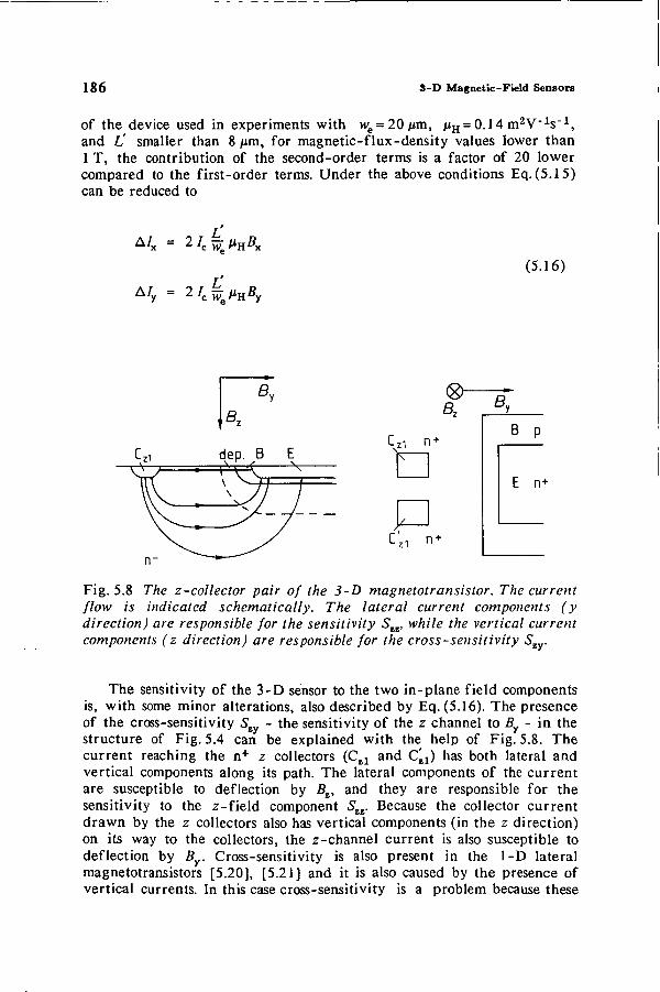
1 8 6 3-D Magnetic-Field Sensors
of the device used in experiments with we=20/im, /*H = 0.14 m2V"1s"1, and L' smaller than 8 /mi, for magnetic-flux-density values lower than 1 T, the contribution of the second-order terms is a factor of 20 lower compared to the first-order terms. Under the above conditions Eq. (5.15) can be reduced to
L' A / x = 2 / c V V e / % B x
(5.16)
My = 2 ' c £ r % * y
3 B p
E n+
Fig. 5.8 The z-collector pair of the 3-D magnetotransistor. The current flow is indicated schematically. The lateral current components (y direction) are responsible for the sensitivity Szz, while the vertical current components (z direction) are responsible for the cross-sensitivity S .
The sensitivity of the 3-D sensor to the two in-plane field components is, with some minor alterations, also described by Eq.(5.16). The presence of the cross-sensitivity S - the sensitivity of the z channel to By - in the structure of Fig. 5.4 can be explained with the help of Fig. 5.8. The current reaching the n+ z collectors (Czl and C^) has both lateral and vertical components along its path. The lateral components of the current are susceptible to deflection by Bz, and they are responsible for the sensitivity to the z-field component Szz. Because the collector current drawn by the z collectors also has vertical components (in the z direction) on its way to the collectors, the z-channel current is also susceptible to deflection by By. Cross-sensitivity is also present in the 1-D lateral magnetotransistors [5.20], [5.21] and it is also caused by the presence of vertical currents. In this case cross-sensitivity is a problem because these
&,
,BZ
dep. B E
P
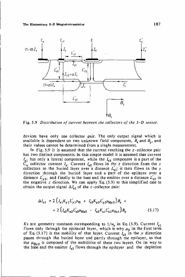
The Elementary 3-D Magnetotranaistor 187
(1-a)Ix
Fig. 5.9 Distribution of current between the collectors of the 3-D sensor.
devices have only one collector pair. The only output signal which is available is dependent on two unknown field components, Bz and By, and their values cannot be determined from a single measurement.
In Fig. 5.9 it is assumed that the current reaching the z-collector pair has two distinct components. In this simple model it is assumed that current / z l has only a lateral component, while the Iz2 component is a part of the Cx collector current 7X. Current Iz2 flows in the z direction from the z collectors to the buried layer over a distance Lzl; it then flows in the y direction through the buried layer and a part of the epilayer over a distance L' 2 , and finally to the base and the emitter over a distance Lz2 in the negative z direction. We can apply Eq. (5.9) to this simplified case to obtain the output signal A/ z l of the z-collector pair:
A / z l ~ 2 Uïl^yl^yl/^H + /z2A:y2Ly2'iHy2JfiE +
+ 2\.Ii2Kz2Li2ilïiz2 - ^^zl^'zl^HzlJ^y (5.17)
Ks are geometry constants corresponding to l/we in Eq. (5.9). Current Izl flows only through the epitaxial layer, which is why /zH in the first term of Eq. (5.17) is the mobility of that layer. Current Iz2 in the y direction passes through the buried layer and partly through the epilayer, so that the juHy2 is composed of the mobilities of these two layers. On its way to the base and the emitter Iz2 flows through the epilayer and the depletion
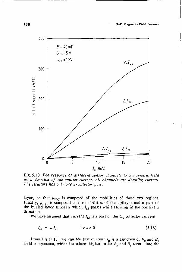
188 3-D Magnetic-Field Sensors
400
300 -
< Zi. a c en " 2 0 0
O-z> o
100 -
£^40mT ^cb = SV
l/cs=10V
-
A/ z y
1— i
A/ y y
A/xx
A/zz
i 10
JJmA) 15 20
Eig. 5.10 The response of different sensor channels to a magnetic field as a function of the emitter current. All channels are drawing current. The structure has only one z-collector pair.
layer, so that /xHz2 is composed of the mobilities of these two regions. Finally, /JH Z 1 is composed of the mobilities of the epilayer and a part of the buried layer through which 7z2 passes while flowing in the positive z direction.
We have assumed that current Il2 is a part of the Cx collector current.
hi = aIx l>a>0 (5.18)
From Eq. (5.11) we can see that current Ix is a function of Bx and B field components, which introduces higher-order fi, and Z?„ terms into the
A y
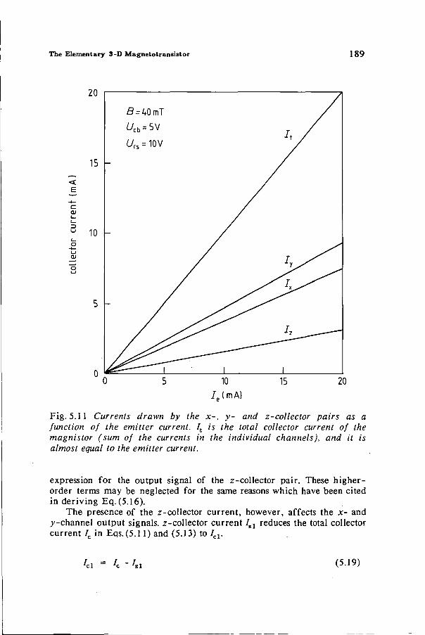
The Elementary 3-D Magnetotransistor 1 8 9
0 5 10 15 20 7e(mA)
Fig. 5.11 Currents drawn by the x-, y- and z-collector pairs as a function of the emitter current. It is the total collector current of the magnistor (sum of the currents in the individual channels), and it is almost equal to the emitter current.
expression for the output signal of the z-collector pair. These higher-order terms may be neglected for the same reasons which have been cited in deriving Eq. (5.16).
The presence of the z-collector current, however, affects the x- and ^-channel output signals, z-collector current I%1 reduces the total collector current /c in Eqs.(5.11) and (5.13) to /cl.
'cl = 'c " / , i (5.19)
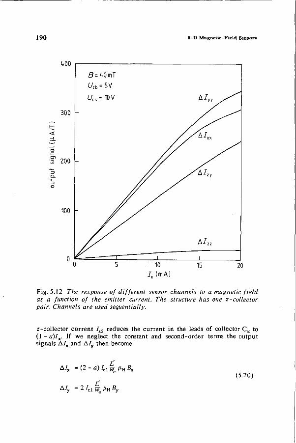
190 3-D Magnetic-Field Sensors
400
300
< =± "a c
•sT 200 3
O
100 -
ö=40mT Ucb = 5V
Ucs= 10 V A / y y ^ ^ ^
/ A n
y^h,
A/zz
I I 10
7e (mA) 15 20
Fig. 5.12 77je response of different sensor channels to a magnetic field as a function of the emitter current. The structure has one z-collector pair. Channels are used sequentially.
z-collector current Iz2 reduces the current in the leads of collector C x to (1 - a) / x . If we neglect the constant and second-order terms the output signals A/x and A/y then become
A/x =(2-a)IclW»HBx (5.20)
A / y = 2IclW»HBy
The Elementary 3-D Magnetotransistor 191
As a consequence of the current drawn by the z-collector pair, A/x and A/ are both reduced (7C> / c l ) . Output signal A/x, however, is further reduced by the (2 - a) term. The sensitivity-matrix elements of the 3-D sensor with one z-collector pair are:
L' Sxx = (2 " a) Iel we^n
Syry = 2 Vcl yf / i H
(5.21)
S™ ~ 2 Uz l^ l^y l^H + /ï2^2ZV2%y2J
Siy = 2 L^Z2^Z2^2MHZ2 " ^^zl^xl^Hïl J
In Fig. 5.10 the response of the 3-D sensor to a magnetic field is given as a function of the emitter current, while Fig. 5.11 represents the collector current picked up by the x-, y- and z-collector pairs as a function of the /e. The response of the x-collector pair is lower than the response of the y channel, which has been predicted by our model. From Fig. 5.11 it can be seen that the current drawn by the x-collector pair is lower than the current drawn by the y collectors. The cause, as pointed out earlier, is the z-collector pair, which draws an extra amount of current which would normally be collected by the x collectors. We can also see from Fig. 5.11 that the current drawn by the z collectors is lower than the other collector currents. This is one of the reasons why the sensitivity of the z channel is lower than the other two in Fig. 5.10.
In Fig. 5.12 the response of the sensor's channels is given under the condition that the channels are biased sequentially (drawing current one at a time). If we compare Figs. 5.10 and 5.12 we can see that both signals A / ^ and A / increase if the channels are biased sequentially. The increase in AIXX is larger than the increase in A/y y , which follows from Eq. 5.20. We can also see that the A/ZE response hardly changes under these different biasing conditions. This is in stark contrast to the results previously presented in [5.5], which were obtained from a different batch of devices. In [5.5] it has been observed that there is a noticeable increase in A/M if the channels were biased sequentially.
The spatial resolution of the measurements is determined by the dimensions of the sensitive part of the magnistor, rather than the overall dimensions of the sensor, which are 350 x 350 pm2 without the interconnection metalization. The spatial resolution of the sensor which has been used in the experiments is about 8 x 10 x 20 jum3 for a structure with only one z-collector pair. It is determined by [5.6]: 8 itm distance between the collectors C z l and C'zl, 10/im thick epilayer in which the device is integrated, and 20 /*m distance between the z-collector pair and the middle of the emitter (Fig. 5.13). The smallest spatial resolution is
192 3-D Magnetic-Field Sensors
determined by the process tolerances. In our case the smallest sensitive volume which has been fabricated was 6x10x16 fim3.
350[im
10[im
20|im
20 / 3 c 8/CgR
V B, 8.|im
-«—»
_n -— i — i _
Bz Fig. 5.13 The sensitive volume of the sensor (8 x 10 x 20 fims) used in the experiments is much smaller than the overall dimensions of the magnetotransistor (350 x 350 nm2).
5.3 INCREASING THE Z SENSITIVITY
The sensitivity Szz of the structure of Fig. 5.4 to the z component of the magnetic field can be increased by introducing an extra pair of z collectors on the opposite side of the emitter [5.2], [5.5]-[5.7]. At the same time, the value of the cross-sensitivity Szy is reduced. This is illustrated in Fig. 5.14. By placing another pair of z collectors on the other side of the emitter, these collectors will intercept a part of the C'x collector current /^. This current is then available for deflection by the Bz and By field components. The current flow from the additional collector pair contains lateral components with a sign opposite to their complements on the other side of the emitter. The response to Bz for the given orientation of the sensor is given in the upper right corner of Fig. 5.14: Czl draws more current than C'zl, while at the same time C'z2 draws more current than Cz2.
Increasing the Z Sensitivity 193
DC»
c;:
c,i a D C Z 2
Fig. 5.14 /l/i additional z-collector pair can increase the z sensitivity Szz, while at the same time suppressing the cross-sensitivity Szy. The collectors are cross-coupled: Czl and Cz2 are shorted as well as collectors Czl and Cz2. The new output signal is the current difference between the collector combination Czl-Cz2 and the combination Cz[-Cz2.
If we short collectors Czl and Cz2, while simultaneously shorting collectors C z l and Cz 2 , the output signal as a response to Bz, which is now the current difference between the collector combination C z l -C z 2 and the combination C z l -C z 2 , increases. The response of the z channel to By is illustrated in the lower right half of Fig. 5.14. The vertical components of the z-collector currents are of the same sign. The response to B is consequently as in Fig. 5.14. If we cross-couple the collectors as explained above, ideally the signals due to B cancel each other, resulting in zero cross-sensitivity Szy. In Fig. 5.15 the structure with two z-collector pairs is depicted.
Unfortunately, the structure with two z-collector pairs is not perfectly symmetrical, so that the cross-sensitivity Szyl of the first z channel (Szy in Eq. (5.21)) is not exactly equal to the cross-sensitivity Szy2 of the second z channel. The same applies to sensitivities Szzl and Szz2:
l^zyll - \Szy2\ (5.22)
A ' z i = SzzlBz + SzylB, *yi y
A / z 2 = " S%z7.Ei + Szy-fiy (5.23)
As a consequence, the cross-sensitivity of the cross-coupled device is reduced, but it is not zero.
194 3-D Magnetic-Field Sensors
Fig. 5.15 The 3-D magnetic-field sensitive npn transistor with two z-collector pairs.
A/z = A/ z l - A/z2
A/z = ( 5 M l + Sll2)Bz + ( 5 , y l - S z y 2)5, (5.24)
The presence of a z-collector pair above collector C x reduces the collector current / x by a factor of (1 - a), just as the presence of the z pair above the Cx collector in Fig. 5.9 reduced the current in that collector to (1 - A)/X. The output signal A/x of the x channel then becomes
A/x = ( l - a ) ( / x - / x ' ) (5.25)
The total current drawn by the x- and y-collector pairs is also reduced to
Increasing the Z Sensitivity 195
U = 4 " 2 / . , (5.26) Jc2 - 'c " •<■ ' z l
The sensitivity matrix components of the cross-coupled structure with two z-collector pairs then become
Sx x = 2(1 -a)/c2H7eMH
Syy = 2 / C 2 K7/J H (5.27)
^ws = ^ z z l + ^zz2
■ zy = ^ z y l " ^zy2
From this equation we can see that the z sensitivity is increased, while the cross-sensitivity Szy is reduced. The x- and y-channel sensitivities have also been reduced with respect to the case of a device with one z-collector pair only (Eq. (5.21)). In Fig. 5.16 the response of the sensor channels as a function of the emitter current is presented, while Fig. 5.17 represents the currents drawn by the channels. From this figure we can see that the value of the total z-collector current has exceeded the x-collector current. The fact that the z sensitivity Szz is still lower than S:xx, as evidenced by Fig. 5.16, indicates that the z-collector current is not used in the most efficient manner. It seems that there is a significant amount of z-collector current spreading which is not favorable for the z sensitivity Szz. Figure 5.18 depicts the response of the sensor to magnetic fields in the x, y and z directions. From these figures we can see that the z sensitivity is increased, while the cross-sensitivity has been reduced. Sensitivity to 5X is also lower, as was expected. In Fig. 5.19 the response of the two z-collector pair sensor is given in the case in which the sensor's channels are used one at a time. The dimensions of the sensitive volume of the transistor are now larger. The spatial resolution is determined by the distance between the two r-collector pairs, which is in this case 40 /zm (Fig. 5.14). The spatial resolution is in this case 8 x 10 x 40 /im3.
We have seen that the addition of an extra z-collector pair to the structure of Fig. 5.4 increases the z sensitivity. The increase of Szl is possible because a part of the current which reaches collector Cx is intercepted by the extra z-collector pair, and it can then contribute to Szz. If the base of the 3-D sensor is somewhat modified [5.6] two extra pairs of z collectors can be placed on the sides of the emitter, as in Figs. 5.20 and 5.21. Just as in the case of Fig. 5.8, which explains the presence of the cross-sensitivity Szy, z-collector pairs 1 and 2 are also sensitive to By, while the two new z collectors 3 and 4 are correspondingly sensitive to 2?x. The sensitivity matrix of this new structure is
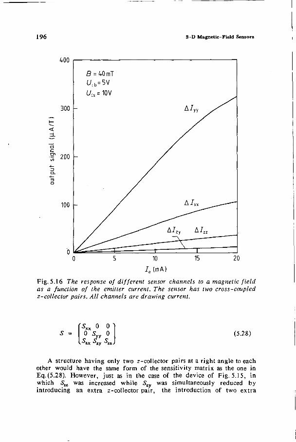
196 3-D Magnetic-Field Sensors
400
300
<
a c en ÏÏ 20° Z>
o
100 -
£ = 40mT Ucb=5V Ua = 10V
r
A/yy S
A/xx _.
A/Zy A/ZZ
-^— I
/ p (
10
mA)
15 20
Fig. 5.16 The response of different sensor channels to a magnetic field as a function of the emitter current. The sensor has two cross-coupled z-collector pairs. All channels are drawing current.
S = rsxx o o 0 Syy 0
"^zx ^zy ^zz
(5.28)
A structure having only two z-collector pairs at a right angle to each other would have the same form of the sensitivity matrix as the one in Eq. (5.28). However, just as in the case of the device of Fig. 5.15, in which Szt was increased while S was simultaneously reduced by introducing an extra z-collector pair, the introduction of two extra
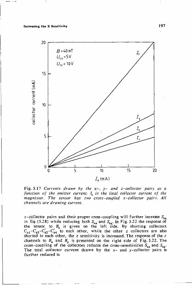
Increasing the Z Sensitivity
0 5 10 15 20
7e(mA)
Fig. 5.17 Currents drawn by the x-,- y- and z-collector pairs as a function of the emitter current. It is the total collector current of the magnistor. The sensor has two cross-coupled z-collector pairs. All channels are drawing current.
z-collector pairs and their proper cross-coupling will further increase Szz in Eq. (5.28) while reducing both Szx and S . In Fig. 5.22 the response of the sensor to Bz is given on the left side. By shorting collectors Czl-CzZ-C'z2-C'z4 to each other, while the other z collectors are also shorted to each other, the z sensitivity is increased. The response of the z channels to Bx and By is presented on the right side of Fig. 5.22. The cross-coupling of the collectors reduces the cross-sensitivities Szx and S . The total collector current drawn by the x- and y-collector pairs is further reduced to
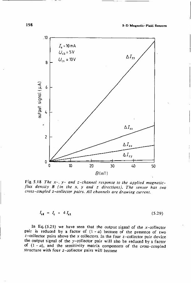
198 3-D Magnetic-Field Sensors
0 10 20 30 40 50
ö(mT)
Fig. 5.18 The x-, y- and z-channel response to the applied magnetic-flux density B (in the x, y and z directions). The sensor has two cross-coupled z-collector pairs. All channels are drawing current.
(5.29)
In Eq. (5.25) we have seen that the output signal of the x-collector pair is reduced by a factor of (1 - a) because of the presence of two z-collector pairs above the x collectors. In the four z-collector pair device the output signal of the y-collector pair will also be reduced by a factor of (1 - a), and the sensitivity matrix components of the cross-coupled structure with four z-collector pairs will become
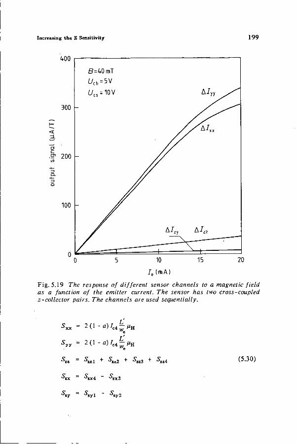
Increasing the Z Sensitivity 199
J e ( m A )
Fig. 5.19 The response of different sensor channels to a magnetic field as a function of the emitter current. The sensor has two cross-coupled z-collector pairs. The channels are used sequentially.
2 0 - Ö K ^ ^ H
Syy = 2 (1 - f l ) / c 4 - M H
S,-r —
^zz l + ^z«2 + ^zz3 + 'S'zz4
■^zx4 " ^zx3
(5.30)
S*y = "^zyl " ^zy2
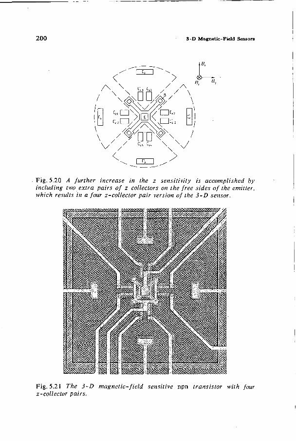
2 0 0 3-D Magnetic-Field Sensors
Fig. 5.20 A further increase in the z sensitivity is accomplished by including two extra pairs of z collectors on the free sides of the emitter, which results in a four z-collector pair version of the 3-D sensor.
Fig. 5.21 The 3-D magnetic-field sensitive npn transistor with four z-collector pairs.
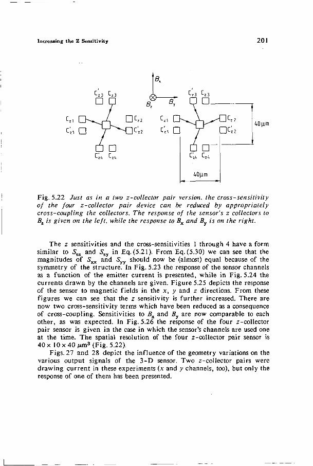
Increasing the Z Sensitivity 201
c'z, D 40u.m
Fig. 5.22 Just as in a two z-collector pair version, the cross-sensitivity of the four z-collector pair device can be reduced by appropriately cross-coupling the collectors. The response of the sensor's z collectors to Bz is given on the left, while the response to 5X and B is on the right.
The z sensitivities and the cross-sensitivities 1 through 4 have a form similar to Szz and Szy in Eq. (5.21). From Eq. (5.30) we can see that the magnitudes of Sxx and Syy should now be (almost) equal because of the symmetry of the structure. In Fig. 5.23 the response of the sensor channels as a function of the emitter current is presented, while in Fig. 5.24 the currents drawn by the channels are given. Figure 5.25 depicts the response of the sensor to magnetic fields in the x, y and z directions. From these figures we can see that the z sensitivity is further increased. There are now two cross-sensitivity terms which have been reduced as a consequence of cross-coupling. Sensitivities to Bx and By are now comparable to each other, as was expected. In Fig. 5.26 the response of the four z-collector pair sensor is given in the case in which the sensor's channels are used one at the time. The spatial resolution of the four z-collector pair sensor is 40 x 10x40 /xm 3 (F ig . 5.22).
Figs. 27 and 28 depict the influence of the geometry variations on the various output signals of the 3-D sensor. Two z-collector pairs were drawing current in these experiments (x and y channels, too), but only the response of one of them has been presented.
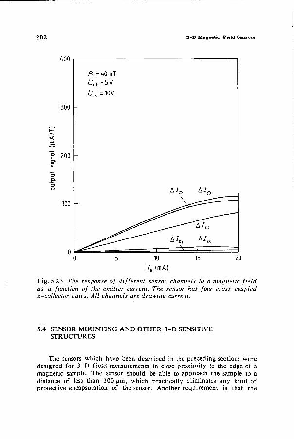
202 3-D Magnetic-Field Sensors
400
300 -
<
a EP
a.
200
100 -
e=40mT ^ c b = 5 V
Ucs = 10V
-
^e^^Z.—t
Aixx
A/2y _ 1 i—
A J y y
'^izT A/zx
—1 10
7 e (mA) 15 20
Fig. 5.23 The response of different sensor channels to a magnetic field as a function of the emitter current. The sensor has four cross-coupled z-collector pairs. All channels are drawing current.
5.4 SENSOR MOUNTING AND OTHER 3-D SENSITIVE STRUCTURES
The sensors which have been described in the preceding sections were designed for 3-D field measurements in close proximity to the edge of a magnetic sample. The sensor should be able to approach the sample to a distance of less than 100/xm, which practically eliminates any kind of protective encapsulation of the sensor. Another requirement is that the
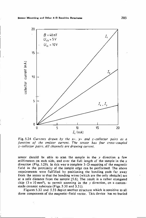
Sensor Mounting and Other 3-D Sensitive Structures 203
0 5 10 15 20 7e (mA)
Fig. 5.24 Currents drawn by the x-, y- and z-collector pairs as a function of the emitter current. The sensor has four cross-coupled z-collector pairs. All channels are drawing current.
sensor should be able to scan the sample in the y direction a few millimeters on each side, and over the full length of the sample in the x direction (Fig. 5.29). In this way a complete 3-D mapping of the magnetic field in the proximity of the sample edge can be performed. The above requirements were fulfilled by positioning the bonding pads far away from the sensor so that the bonding wires (which are the only obstacle) are at a safe distance from the sample [5.6]. The result is a rather elongated chip (3 x 10 mm2), to permit scanning in the y direction, on a custom-made ceramic substrate (Figs. 5.30 and 5.31).
Figures 5.32 and 5.33 depict another structure which is sensitive to all three components of the magnetic-field vector. This device has no buried
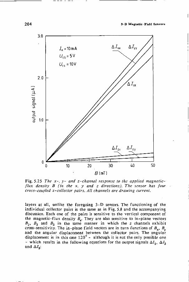
2 0 4 3-D Magnetic-Field Sensors
0 10 20 30 A0 50
fl(mT)
Fig. 5.25 The x-, y- and z-channel response to the applied magnetic-flux density B (in the x, y and z directions). The sensor has four cross-coupled z-collector pairs. All channels are drawing current.
layers at all, unlike the foregoing 3-D sensors. The functioning of the individual collector pairs is the same as in Fig. 5.8 and the accompanying discussion. Each one of the pairs is sensitive to the vertical component of the magnetic-flux density Bz. They are also sensitive to in-plane vectors 5 l 5 B2 and B3 in the same manner in which the z channels exhibit cross-sensitivity. The in-plane field vectors are in turn functions of Bx, B and the angular displacement between the collector pairs. The angular displacement is in this case 120° - although it is not the only possible one - which results in the following equations for the output signals A/1? A/2 and A/3:
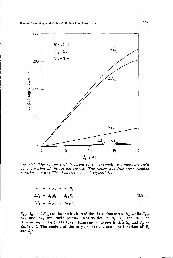
Sensor Mounting and Other 3-D Sensitive Structures 2 0 5
400
300 -
o
3 O
200 -
100 -
-
-
-
£ = 40mT
^cb = 5V
UK = 10V
" - " ^ i
A7yy
//*hx
A/Z2
A/zy A_/Zx
1 .
10
J„(mA)
15 20
Fig. 5.26 77ie response of different sensor channels to a magnetic field as a function of the emitter current. The sensor has four cross-coupled z-collector pairs. The channels are used sequentially.
A/i = SlzBz + £„ /? !
A / 2 = S2tBt + 522^2
A / Q = So.B. + Soofi.
(5.31)
>3zDz 33D3
Slz, S2z and 5"3z are the sensitivities of the three channels to Bz, while S1X, S22 and 5 3 3 are their (cross-) sensitivities to Bu B2 and B3. The sensitivities in Eq. (5.31) have a form similar to sensitivities Szz and S in Eq. (5.21). The moduli of the in-plane field vectors are functions of Bx and B, y
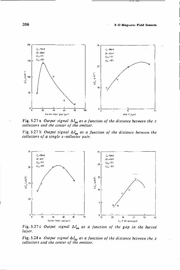
206 3-D Magnetic-Field Sensors
-
-
7e = 10mA
S=W) IT IT
W.b=5V
U „ = 10V
l
\ D
l
D \
1 1 20 40 60
buried-layer gap (|j.m 10
inter-C,lu.m)
Fig. 5.27 a Output signal Afzz as a function of the distance between the z collectors and the center of the emitter.
Fig. 5.27 b Output signal A/M as a function of the distance between the collectors of a single z-collector pair.
F 15
-
-
7e=10mA
S = WmT
ucs = iov
o /
I
o
O /
1
/ o
D
1
O
1
20 40 60
buried-layer gap(}im)
20 30 40 50 60
C,-E distance(p.m)
Fig. 5.27 c Output signal A/zz as a function of the gap in the buried layer.
Fig. 5.28 a Output signal A/zy as a function of the distance between the z collectors and the center of the emitter.
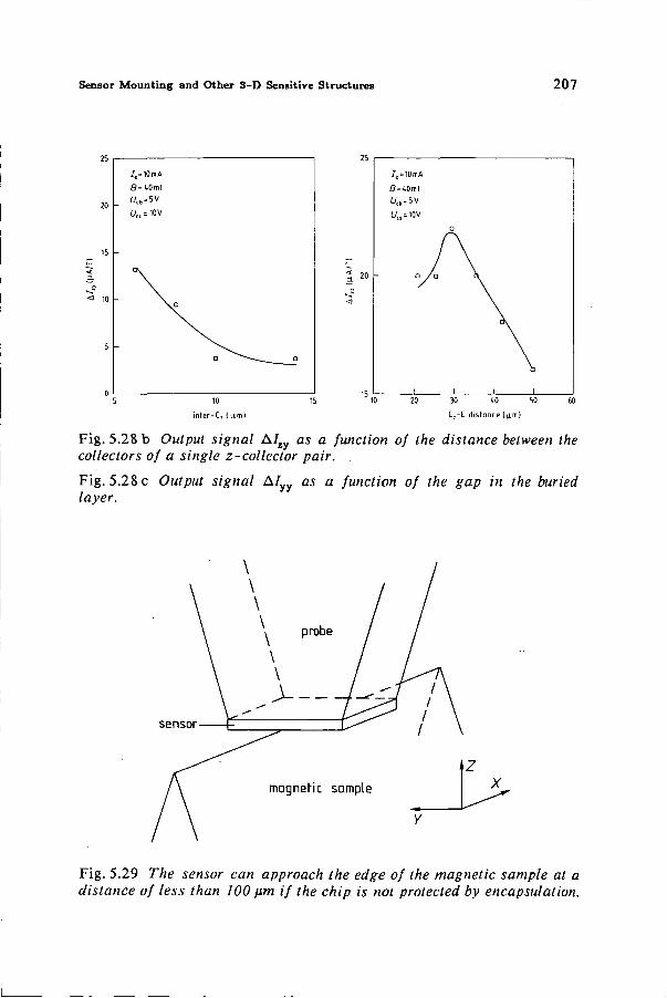
Sensor Mounting and Other 3-D Sensitive Structures 207
-
J, = 10mA S=WmT
U„ = WV
. 0
D ~~ — D
10
inter-Cz (^m)
Je=10mA
B = M)mT
i/..=iov
30 W> 50
Cj-E distance (^m)
Fig. 5.28 b Output signal A/zy as a function of the distance between the collectors of a single z-collector pair. Fig. 5.28 c Output signal A/yy as a function of the gap in the buried layer.
Fig. 5.29 The sensor can approach the edge of the magnetic sample at a distance of less than 100 \an if the chip is not protected by encapsulation.
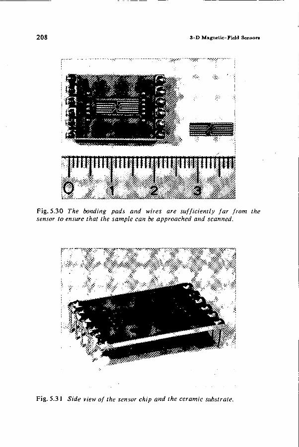
208 3-D Magnetic-Field Sensors
p"—""-<n&&$%^~-~rt"
*
urnim rrnnm TïTïïnn TTTTTTf 0 t
Fig. 5.30 The bonding pads and wires are sufficiently far from the sensor to ensure that the sample can be approached and scanned.
Fig. 5.31 Side view of the sensor chip and the ceramic substrate.
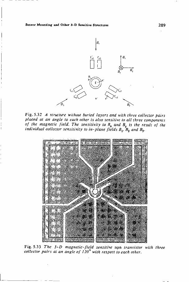
Sensor Mounting and Other 3-D Sensitive Structures 209
s,
l £ > „. fcx C22
Fig. 5.32 A structure without buried layers and with three collector pairs placed at an angle to each other is also sensitive to all three components of the magnetic field. The sensitivity to Bx and By is the result of the individual collector sensitivity to in-plane fields Bv B2 and B3.
I :1
1\
v \ )
t
y
Fig. 5.33 The 3-D magnetic-field sensitive npn transistor with three collector pairs at an angle of 120° with respect to each other.
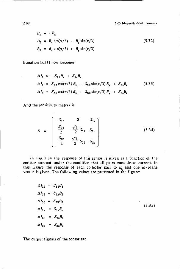
210 3-D Magnetic-Field Sensors
* 1 = " * x
B2 = Bxcos(7r/3) - fiysin(7r/3)
Bz = Bxcos(7r/3) + fiysin(jr/3)
(5.32)
Equation (5.31) now becomes
±h = - ^ i f i x + SuBm
A/2 = S22 cos(7r/3) Bx - S22 sin(ir/3) fly + S2zffz
A/3 = S33cos(7r/3)5x + S33 sin(7r/3) By + S3zBz
(5.33)
And the sensitivity matrix is
S =
Sn ^22 2
■$33 2
0
2 °22
2 ^33
Sl'] s2,
s3l
(5.34)
In Fig. 5.34 the response of this sensor is given as a function of the emitter current under the condition that all pairs must draw current. In this figure the response of each collector pair to Bt and one in-plane vector is given. The following values are presented in the figure:
LA I] i
^ 2 2
A / 3 3
A/i .
A/2 B
A/ 3 e
=
=
=
=
=
=
^ l l ^ l
"$22^2
" S 3 ° 3
SiA ^A S 3 A
(5.35)
The output signals of the sensor are
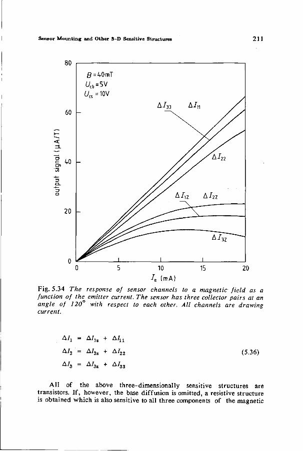
Sensor Mounting and Other 3-D Sensitive Structures 2 1 1
80
60
o
20 -
e = ^0mT
L/C5=10V
7e (mA) Fig. 5.34 The response of sensor channels to a magnetic field as a function of the emitter current. The sensor has three collector pairs at an angle of 120 with respect to each other. All channels are drawing current.
Al, = A / u + A / n
A / 2 = A / 2z + A / 2 2
A / 3 = A / 3z + A ' 3 3
(5.36)
All of the above three-dimensionally sensitive structures are transistors. If, however, the base diffusion is omitted, a resistive structure is obtained which is also sensitive to all three components of the magnetic
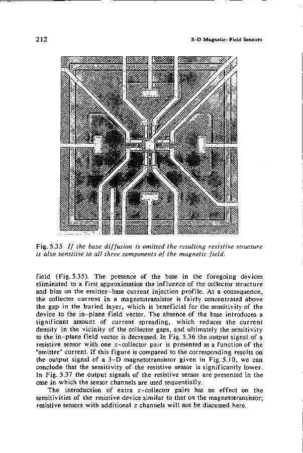
212 3-D Magnetic-Field Sensors
Fig. 5.35 If the base diffusion is omitted the resulting resistive structure is also sensitive to all three components of the magnetic field.
field (Fig. 5.35). The presence of the base in the foregoing devices eliminated to a first approximation the influence of the collector structure and bias on the emitter-base current injection profile. As a consequence, the collector current in a magnetotransistor is fairly concentrated above the gap in the buried layer, which is beneficial for the sensitivity of the device to the in-plane field vector. The absence of the base introduces a significant amount of current spreading, which reduces the current density in the vicinity of the collector gaps, and ultimately the sensitivity to the in-plane field vector is decreased. In Fig. 5.36 the output signal of a resistive sensor with one z-collector pair is presented as a function of the "emitter" current. If this figure is compared to the corresponding results on the output signal of a 3-D magnetotransistor given in Fig. 5.10, we can conclude that the sensitivity of the resistive sensor is significantly lower. In Fig. 5.37 the output signals of the resistive sensor are presented in the case in which the sensor channels are used sequentially.
The introduction of extra z-collector pairs has an effect on the sensitivities of the resistive device similar to that on the magnetotransistor; resistive sensors with additional z channels will not be discussed here.
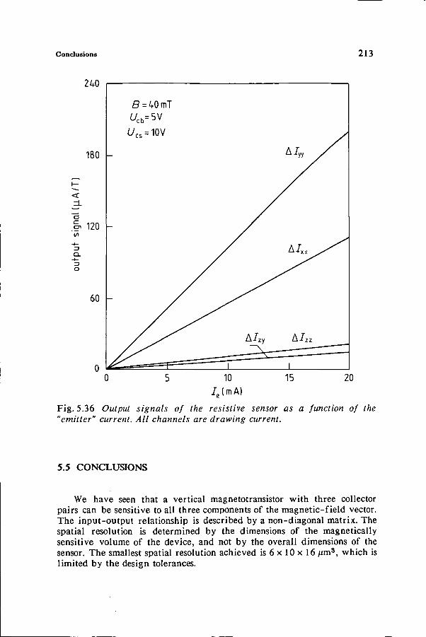
Conclusions 213
240
180 -
<
~a . & 120 </> -*— a. 3 O
60 -
£ = 40mT ^cb=5V t/cs = 10V
-
A/zy
I
A4 /
A / x x ^ ^ ^
A/zz
i 10
J.(mA) 15 20
Fig. 5.36 Output signals of the resistive sensor as a function of the "emitter" current. All channels are drawing current.
5.5 CONCLUSIONS
We have seen that a vertical magnetotransistor with three collector pairs can be sensitive to all three components of the magnetic-field vector. The input-output relationship is described by a non-diagonal matrix. The spatial resolution is determined by the dimensions of the magnetically sensitive volume of the device, and not by the overall dimensions of the sensor. The smallest spatial resolution achieved is 6 x 10 x 16 /xm3, which is limited by the design tolerances.
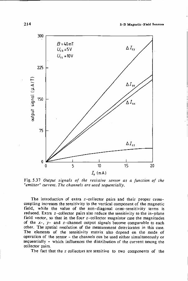
214
O 5 10 15 20
Je (mA)
Fig. 5.37 Output signals of the resistive sensor as a function of the "emitter" current. The channels are used sequentially.
The introduction of extra z-collector pairs and their proper cross-coupling increases the sensitivity to the vertical component of the magnetic field, while the value of the non-diagonal cross-sensitivity terms is reduced. Extra z-collector pairs also reduce the sensitivity to the in-plane field vector, so that in the four z-collector magnistor case the magnitudes of the x-, y- and z-channel output signals become comparable to each other. The spatial resolution of the measurement deteriorates in this case. The elements of the sensitivity matrix also depend on the mode of operation of the sensor - the channels can be used either simultaneously or sequentially - which influences the distribution of the current among the collector pairs.
The fact that the z collectors are sensitive to two components of the
Conclusions 215
magnetic field has been used in a three surface z-collector pair device (without buried layers), which is also sensitive to all three components of the magnetic field. It has been determined that a resistive device also constitutes a 3-D sensor.
To facilitate magnetic field scanning in proximity to the sample, bonding pads had to be placed far away from the sensor. Moreover, the sensor chip has not been encapsulated in any way, which made measurements closer than 100 /im to the sample possible.
216 3-D Magnetic-Field Sensors
REFERENCES
[5.1] S. Kordic, Integrated silicon magnetic-field sensors, Sensors and Actuators, vol.10, 1986, pp. 347-378.
[5.2] S. Kordic, Integrated 3-D magnetic sensor based on an n-p-n transistor, IEEE Electron Devices Lett., vol.EDL-7, 1986, pp. 196-198.
[5.3] S. Kordic, The first three-dimensional magnetic-field sensor, 14th Yugoslav Con}, on Microelectronics (MIEL-86), 1986, Proc. MIEL-86, pp. 441-447.
[5.4] S. Kordic, A three-dimensional solid-state magnetic-field sensor, 16th European Solid-State Device Research Con/., ESSDERC86, Cambridge, UK, 1986, Europhysics Conf. Abstr., pp. 97-98.
[5.5] S. Kordic, Sensitivity of the silicon high-resolution 3-dimensional magnetic-field vector sensor, Int. Electron Devices Meet., Los Angeles, CA, USA, 1986, IEDM Techn. Dig., pp. 188-191.
[5.6] S. Kordic, P. J. A. Munter and P.J.French, Simultaneous measurements of 3-D magnetic fields in close proximity to the sample with a single silicon sensor, 4th Int. Conf. on Solid-State Sensors and Actuators, Tokyo, Japan, 1987, Dig. Techn. Papers, pp. 527-531.
[5.7] S. Kordic and P. J. A. Munter, Integrated silicon 3-D magnetic sensors, Submitted to IEEE Trans. Electron Devices.
[5.8] T. Kanayama, M. Oasa, H.Hiroshima and M. Komuro, A-quarter-micron Hall sensor fabricated with maskless ion implantation, 4th Int. Conf. on Solid-State Sensors and Actuators, Tokyo, Japan, 1987, Dig. Techn. Papers, pp. 532-535.
[5.9] R.S.Popovic, The vertical Hall-effect device, IEEE Electron Device Lett., vol.EDL-5, 1984, pp. 357-358.
[5.10] J. I. Goicolea, R. S. Muller and J. E. Smith, Highly sensitive silicon carrier-domain magnetometer, Sensors and Actuators, vol. 5, 1984, pp. 147-167.
[5.11] S. Kirby, The characteristics of the carrier domain magnetometers, Sensors and Actuators, vol.4, 1983, pp. 25-32.
[5.12] G.N.Harding, W.H.Mitchell and E. H.Putley, A Hall effect device for measuring the magnitude and direction of a magnetic field at 4°K, Solid-State Electron., vol.9, 1966, pp. 465-469.
[5.13] H.Furukawa, K. Kishida and K.Shirae, Vector sensor of weak magnetic field using parallel operated rf SQUID system, Proc. 1st Sensor Symp., Japan, 1981, pp.317-321.
[5.14] K.Maenaka, T. Ohgusu, M. Ishida and T. Nakamura, Integrated magnetic sensors detecting x, y and z components of the magnetic field, 4th Int. Conf. on Solid-State Sensors and Actuators, Tokyo, Japan, 1987, Dig. Techn. Papers, pp. 523-526.
[5.15] K.Maenaka, private communication. [5.16] V. Zieren, A new silicon micro-transducer for the measurement of the
magnitude and direction of a magnetic-field vector, Int. Electron Devices Meet., Washington, DC, USA, 1980, IEDM Techn. Dig., pp. 669-672.
[5.17] V. Zieren, Integrated silicon multicollector magnetotransistors, Ph.D. thesis, Delft University of Technology, 1983.
[5.18] M. Ishida, H. Fujiwara, T. Nakamura, M. Ashiki, Y. Yasuda, A. Yoshida, T. Ohsakama and Y. Kawase, Silicon magnetic vector sensors for integration, Proc. 4th Sensor Symp., Japan, 1984, pp. 79-83.
[5.19] K.Maenaka, H. Fujiwara, T. Ohsakama, M. Ishida, T. Nakamura, A. Yoshida and Y. Yasuda, Integrated magnetic vector sensor, Proc. 5th Sensor Symp., Japan, 1985, pp.179-183.
[5.20] D. M. Kozlov, G. I. Rekalova, I. M. Mitnikova, D. A. Tairova and A. A. Shakhov, Nature of the current magnetosensitivity of two-collector planar
References 217
magnetotransistors, Sov. Phys.-Semicond., vol. 13, 1979, pp. 1263-1265. [5.21] I. M. Vikulin, M. A. Glauberman, G.A. Egiazaryan, N. A. Kanishcheva,
Yu. S. Manvelyan and I. P. Shnaider, Experimental estimate of the influence of the diffusion and drift components of the flux of injected carriers on the magnetosensitivity of two-collector planar magnetotransistors, Sov. Phys.-Semicond., vol. 15, 1981, pp. 274-275.

218
So eine Arbeit wird eigentlich nie fertig, man muss sie für fertig erklaren, wenn man nach Zeit und Umstdnden das Möglichste getan hat.
J. W. Goethe
SUMMARY
This thesis deals with two subjects concerning magnetic-field sensors: offset reduction and three-dimensional field sensing. The main causes of offset have been discussed for magnetotransistors, Hall plates and several other types of devices. The main cause of offset in current-deflection magnetotransistors is the misalignment of the current source with respect to the collectors of the device, which in the case of the vertical npn magnetotransistors used in the experiments, results in offsets as high as 1.5 T per micron misalignment. Besides the geometric misalignment, an important cause of offset in Hall plates and devices in which Hall-plate action plays a significant role in the sensitivity, is the piezoresistance effect, making offset stress-dependent. Finite-difference numerical simulations have been performed to determine the influence of the geometry variations on the geometry-caused offset in Hall plates.
Sensitivity-variation offset-reduction has been introduced as an additional method to deal with offset. The criteria which must be satisfied if the method is to be successfully applied are that a parameter must be found which changes the sensitivity of the sensor, while the offset signal is not significantly altered. This offset-reduction method uses a single device but the measurement is expanded in time. The measurand remains an unknown at all times and it is not disrupted in any way if an electrical sensitivity-varying parameter is used. Differential sensitivity and offset signal have been introduced. Ideally, the differential offset signal should be zero. In case it is non-zero, it causes residual offset. The relation
219
220 Summary
between the sensitivity, offset signal, output signal and the equivalent offset has the same form as the relation between the differential complements of these quantities.
The new method of offset reduction has been tested on a one-dimensional vertical magnetotransistor. The device exhibits a significant change in the sensitivity with col lector-base bias variations, while the offset signal remains fairly constant. The original offset of the sensor, which can be as high as 1 T, is reduced by more than 90 % in a wide collector-base bias interval. The variation of the collector-base bias is an example of an electrical parameter variation, which yields an additional advantage: the sensitivity-variation offset-reduction circuitry can be implemented on the same chip with the sensor.
Two possible implementations of the sensitivity-variation method in Hall plates have been presented: the double-layer and the switched Hall plate. The double-layer Hall plate features a step in the impurity concentration of the active layer of the device. The sensitivity is altered by means of a depletion layer. The switched Hall plate was manufactured with a standard process. The sensitivity is again varied by means of a depletion layer, but other implementations with a MOS gate, for example, are also feasible. Experiments have shown offset reduction, but still better results should be expected with a MOS gate switch.
An electronic implementation of the sensitivity-variation method has been presented using the magnetotransistor as an example.
Offset experiments have determined that the sensitivity of the vertical magnetotransistor is a decreasing function of the col lector-base bias voltage. It has been determined that the cause of this sensitivity decrease is the presence of a strong electric field in the cb-junction depletion layer and the associated decrease in the mean collision-free time. The Hall angle has been calculated as a function of the electric field and the position within the depletion layer. An additional decrease in the sensitivity is caused by the increased power dissipation and the temperature of the device with rising collector-base voltage.
Devices sensitive to all three components of the magnetic field have been presented. The sensitivity to two field components in the plane of the chip is achieved by merging two one-dimensional vertical magnetotransistors positioned at an 90° angle to each other. An additional surface collector pair makes this device also sensitive to the last field component which is perpendicular to the plane of the chip. The sensitivity of the 3-D sensor has been represented by a non-diagonal sensitivity matrix. The smallest achieved sensitive volume was 6 x 1 0 x 1 6 nms, which is limited by the design tolerances.
The introduction of extra z-collector pairs and their proper cross-coupling increases the sensitivity to the vertical component of the magnetic field, while the value of the non-diagonal cross-sensitivity terms is reduced. Extra z-collector pairs also reduce the sensitivity to the in-plane field vector, so that in the four z-collector magnistor case, the magnitudes of the x-, y- and z-channel output signals become comparable to each
Summary 221
other. The spatial resolution of the measurement deteriorates in this case. The elements of the sensitivity matrix also depend on the mode of operation of the sensor - the channels can be used simultaneously, or sequentially - which influences the distribution of the current among the collector pairs.
The fact that the z collectors are sensitive to two components of the magnetic field has been used in a three surface z-collector pair device (without buried layers), which is also sensitive to all three components of the magnetic field. It has been determined that a resistive device also constitutes a 3-D sensor.
To facilitate magnetic field scanning in proximity to the sample bonding pads had to be placed far away from the sensor. Moreover, the sensor chip has not been encapsulated in any way, which made measurements closer than 100 /xm to the sample possible.

222
SAMENVATTING
Dit proefschrift behandelt twee onderwerpen betreffende magneetveld sensoren: reductie van offset en driedimensionale veldmetingen. De hoofdoorzaken van offset zijn behandeld voor magnetotransistoren, Hall platen en een paar andere soorten magneetveldsensoren. De hoofdoorzaken van offset in magnetotransistoren (gebaseerd op het stroomdeflectie principe) zijn de fouten in de plaatsing van de stroombron ten opzichte van de collectoren. Deze resulteren in geval van onze verticale npn magnetotransistor in offsetwaarden van 1.5 T per micron uitrichtfout. Naast geometrische uitrichtfouten zijn de piezoweerstandseffecten belangrijke oorzaken van offset in Hall plaatjes en verwante sensoren. Offset is in dit geval afhankelijk van mechanische spanningen in het materiaal. Eindige-differentie numerieke simulaties werden uitgevoerd om de invloed van geometrievariaties te bepalen op offset veroorzaakt door geometriefouten.
De gevoeligheids-variatie offset-reductie methode is gepresenteerd als een additionele manier om de grootte van offset te reduceren. Het criterium waaraan een sensor moet voldoen, wil deze nieuwe methode met succes toegepast kunnen worden, is dat er een parameter gevonden moet worden die de gevoeligheid van de sensor verandert, terwijl het offsetsignaal niet noemenswaardig verandert. In deze methode wordt één sensor gebruikt, terwijl gedurende een zeker tijdsinterval gemeten wordt. De te meten waarde wordt ook niet verstoord. De begrippen differentiële gevoeligheid en offsetsignaal zijn ingevoerd. Onder ideale omstandigheden zou het differentiële offsetsignaal nul moeten zijn. Differentiële offset die ongelijk aan nul is veroorzaakt een residuele offset. Het verband tussen de gevoeligheid, het offsetsignaal en de equivalente offset heeft eenzelfde vorm als het verband tussen de differentiële complementen van deze grootheden.
De nieuwe methode voor reductie van offset werd toegepast op de één-dimensionale verticale magnetotransistor. Deze sensor vertoont een merkbare gevoeligheidsverandering ten gevolge van variaties in de col lector-basis spanning (Uch), terwijl het offsetsignaal betrekkelijk constant blijft. De oorspronkelijke offset van de sensor (welke in de buurt van 1 T is) is 90 % verkleind over een breed Ucb spanningsinterval.
223
224 Samenvatting
Variatie van Uch is een voorbeeld van elektrische parametervariatie met als bijkomend voordeel dat het offset-reductie circuit samen met de sensor geintegreerd kan worden op één chip.
Twee mogelijke implementaties op Hall plaatjes van de nieuwe offset-reductie methode zijn behandeld: de tweelaags en de geschakelde Hall plaat. Een wezenlijk onderdeel van de tweelaags Hall plaat is de stap in de doteringsconcentratie van de epilaag. De gevoeligheid wordt veranderd door middel van een depletielaag. De geschakelde Hall platen zijn gefabriceerd in een standaard IC-proces. De gevoeligheid wordt weer veranderd met behulp van een depletielaag, maar ook andere implementaties van de grondgedachte, zoals een MOS-gate, zijn mogelijk. Experimenten vertonen een reductie van de offset, hoewel met een MOS schakelaar nog betere resultaten te verwachten zijn.
De elektronische implementatie van de nieuwe offset-reductie methode is behandeld met een magnetotransistor als voorbeeld.
Experimenten met offset hebben aangetoond dat de gevoeligheid van de magnetotransistor een dalende functie is van de eb junctiespanning. De afname van de gevoeligheid met Ucb wordt veroorzaakt door de aanwezigheid van een sterk elektrisch veld in de depletielaag van de cb-junctie, en de daarmee gepaard gaande afname van de gemiddelde botsing-vrije tijd. De Hall hoek is bepaald als functie van het elektrisch veld en de plaats binnen de depletielaag. Een extra afname van de gevoeligheid wordt veroorzaakt door de stijgende temperatuur van de sensor met Ucb (de energie dissipatie).
Sensoren die gevoelig zijn voor alle drie de componenten van de magneetveld vector zijn behandeld. Door het samenvoegen van twee één-dimensionale magnetotransistoren (gepositioneerd 90° ten opzichte van elkaar) tot één sensor worden de twee veldcomponenten in het vlak van de chip gemeten. Door het toevoegen van een extra collectorpaar kan de laatste veldcomponent gemeten worden. De gevoeligheid van de 3-D sensor wordt beschreven door een niet-diagonale matrix. Het kleinste gevoelige volume dat is gemaakt was 6x 10 x 16|im3 en wordt begrensd door de ontwerptoleranties.
Toevoeging van extra z-collector paren en de juiste schakeling daarvan vergroot de gevoeligheid van de sensor voor de loodrechte component van het veld (ten opzichte van het vlak van de chip). Tegelijkertijd worden de kruisgevoeligheidstermen van de gevoeligheidsmatrix kleiner. Extra z-collectorparen verminderen tevens de gevoeligheid van de sensor voor de twee veldkomponenten in het vlak van de chip, zodat in geval van een magnetotransistor met vier z-kanalen de gevoeligheden voor de x, y en z veld componenten vergelijkbaar met elkaar worden. In dit geval verslechtert de ruimtelijke resolutie van de metingen. De elementen van de gevoeligheidsmatrix zijn ook afhankelijk van de manier waarop de sensor wordt gebruikt - of de sensorkanalen tegelijkertijd of apart worden aangesloten. Dit beinvloedt de stroom verdeling tussen de collectoren van de sensor.
Het feit dat de z-collectoren gevoelig zijn voor twee veldcomponenten
Samenvatting 225
is gebruikt bij het ontwerpen van een 3-D sensor met slechts oppervlakte collectoren (er zijn geen begraven lagen). Resistive structuren kunnen ook zodanig ontworpen worden dat zij gevoelig zijn voor alle drie de componenten van de veldvector.
Om metingen in de buurt van een magneet mogelijk te maken zijn de bondflappen ver van de sensor geplaatst. Zonder behuizing is het mogelijk geweest om metingen te verrichten dichter dan 100 firn bij de magneet.

226
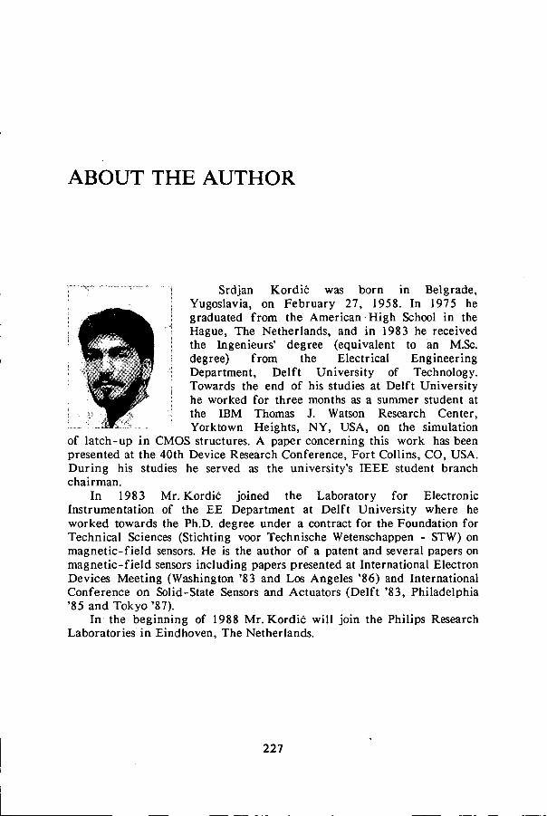
ABOUT THE AUTHOR
1 Srdjan Kordic was born in Belgrade, | Yugoslavia, on February 27, 1958. In 1975 he 1 graduated from the American High School in the
Hague, The Netherlands, and in 1983 he received I the Ingenieurs' degree (equivalent to an M.Sc.
degree) from the Electrical Engineering I Department, Delft University of Technology.
Towards the end of his studies at Delft University he worked for three months as a summer student at the IBM Thomas J. Watson Research Center, Yorktown Heights, NY, USA, on the simulation
of latch-up in CMOS structures. A paper concerning this work has been presented at the 40th Device Research Conference, Fort Collins, CO, USA. During his studies he served as the university's IEEE student branch chairman.
In 1983 Mr. Kordic joined the Laboratory for Electronic Instrumentation of the EE Department at Delft University where he worked towards the Ph.D. degree under a contract for the Foundation for Technical Sciences (Stichting voor Technische Wetenschappen - STW) on magnetic-field sensors. He is the author of a patent and several papers on magnetic-field sensors including papers presented at International Electron Devices Meeting (Washington '83 and Los Angeles '86) and International Conference on Solid-State Sensors and Actuators (Delft '83, Philadelphia '85 and Tokyo '87).
In the beginning of 1988 Mr. Kordic will join the Philips Research Laboratories in Eindhoven, The Netherlands.
227

228
LIST OF PUBLICATIONS AND PRESENTATIONS
PUBLICATIONS
V. Zieren, S. Kordic and S. Middelhoek, Comment on " Magnetic transistor behavior explained by modulation of emitter injection, not carrier deflection", IEEE Electron Device Lett., vol .EDL-3, 1982, pp. 394-395.
S. Kordic, V. Zieren and S. Middelhoek, Magneetveldsensor, Dutch patent application, 8 300 557, 1983. Magnetic field sensor, Patent applications: Taiwan, S. Korea, USA, Canada, Singapore, Hong Kong, Italy, England, France, and F.R. Germany.
S. Kordic, V. Zieren and S. Middelhoek, A novel method for reducing the offset of magnetic-field sensors, Sensors and Actuators, vol.4, 1983, pp. 55 -61 .
Yi-Zi Xing, S. Kordic, and S. Middelhoek, A new approach to offset reduction in sensors: the sensitivity variation method, J. Phys. E: Sci. Instrum., vol. 17, 1984, pp. 657-663.
S. Middelhoek, S. Kordic and D. W. de Bruin, Silicon: a promising material for sensors, SEV-Bulletin, vol .5, 1985, pp. 253-257.
S. Kordic and P. C. M. van der Jagt, Theory and practice of electronic implementation of the sensitivity-variation offset-reduction method, Sensors and Actuators, vol. 8, 1985, pp. 197-217.
S. Kordic, Integrated silicon magnetic-field sensors, Sensors and Actuators, vol. 10, 1986, pp. 347-378.
S. Kordic, Integrated 3-D magnetic sensor based on an n - p - n transistor, IEEE Electron Device Lett., vol .EDL-7, 1986, pp. 196-198.
J. M. van den Boom and S. Kordic, Offset reduction in Hall plates - theory and experiments, Submitted to Sensors and Actuators.
S. Kordió and P. J. A. Munter, Integrated 3-D magnetic sensors, Submitted
229
230 l i s t of Publications and Presentations
to IEEE Trans. Electron Devices. P. J. A. Munter and S. Kordic, The decrease in the Hall angle and the sensitivity at high electric fields in silicon magnetic sensors, Submitted to Sensors and Actuators.
PRESENTATIONS
S. Kordic, V. Zieren and S. Middelhoek, A novel method for reducing the offset of magnetic-field sensors, 2nd Int. Conf. on Solid-State Sensors and Actuators, Delft, The Netherlands, 1983, Dig. Techn. Papers, pp. 118-119. S. Kordic, V.Zieren and SMiddelhoek, A magnetic-field-sensitive multicollector transistor with low offset, Int. Electron Devices Meet., Washington, DC, USA, 1983, IEDM Tech. Dig., pp. 631-634. S. Kordic and P. C. M. van der Jagt, Electronic implementation of the sensitivity-variation offset-reduction method, 3rd Int. Conf. on Solid-State Sensors and Actuators, Philadelphia, PA, USA, 1985, Dig. Techn. Papers, pp. 320-323. S. Kordic, The first solid-state three-dimensional magnetic-field sensor, 14th Yugoslav Conf. on Microelectronics (MIEL-86), 1986, Proc. MIEL-86, pp. 441-447. S. Kordic, A three-dimensional solid-state magnetic-field sensor, 16th European Solid-State Device Research Conf., ESSDERC86, Cambridge, UK, 1986, Europhysics Conf. Abstr., pp. 97-98. S. Kordic, Sensitivity of the silicon high-resolution 3-dimensional magnetic- field vector sensor, Int. Electron Devices Meet., Los Angeles, CA, USA, 1986, IEDM Techn. Dig., pp. 188-191. P. J. A. Munter and S. Kordic, The decrease in the Hall angle and the sensitivity at high electric fields in silicon magnetic sensors, Eurosensors, Cambridge, UK, 1987, Tech. Dig., pp 200-201. P. J. French, W. Lian and S. Kordic, NMOS digital output multisensor chip incorporating flip-flop techniques, 4th Int. Conf. on Solid-State Sensors and Actuators, Tokyo, Japan, 1987, Dig. Techn. Papers, pp. 147-150. S. Kordic, P. J. A. Munter and P.J.French, Simultaneous measurements of 3-D magnetic fields in close proximity to the sample with a single silicon sensor, 4th Int. Conf. on Solid-State Sensors and Actuators, Tokyo, Japan, 1987, Dig. Techn. Papers, pp. 527-531.
LIST OF SYMBOLS
Symbol Name Unit
B B0
e E E H 4, k K I 4 h h j K K
m
M
Mr
P q
magnetic-flux density equivalent offset of a magnetic sensor thickness of a Hall plate electron charge 1.6 x 10~19
energy electric-field strength magnetic-field strength base current collector current emitter current offset signal (current) offset signal (ac) bias (source) current total collector current current density Boltzmann's constant 1.38 x 10"2S
gap shift depletion layer thickness Hall plate length effective deflection length emitter length mass of the charge carrier (9.1 x 10"3 1 for an electron) conductivity effective mass of electrons 2.4 x 10"31
general measurand general equivalent offset general residual offset electron density acceptor impurity concentration donor impurity concentration hole density charge
T T m C J V/m A/m A A A A A A A A/m2
J /K m m m m m kg kg
m - 3
m - 3
m-3
m 3
C
231
232 last of Symbols
r Hall factor % Hall coefficient m 3 / C 5 general sensitivity of a sensor §n sensitivity of the magnistor to the magnetic field A/T S^ sensitivity of the magnistor to the magnetic field (ac) A/T SjnH sensitivity of the Hall plate to the magnetic field V/T t time s T temperature K Te electron temperature K 7J lattice temperature K U sensit ivity-varying parameter Uch col lec tor-base bias V C£s col lector-substrate bias V Uch sinusoidal excitation signal V v velocity m/s V general output signal of a sensor VH Hal l vo l tage V V0 general offset signal of a sensor Ve bias vol tage V we emitter width m wH width of a Hall plate m
a common-base current gain 6 relative offset signal 5AV average relative offset A/c collector-current difference A A/0 differential offset signal of the magnetotransistor A AS general differential sensitivity AS^ differential sensitivity of the magnetotransistor A/T A^H differential sensitivity of the Hall plate V/T AV general differential output signal A^ general differential offset signal 6H Hall angle /i charge carrier mobility m2/Vs HH Hall mobi l i ty m 2 / V s /*0 permeabi l i ty of vacuum H/m p resistivity fi m r collision-free time s X misalignment shift m XAV average misalignment shift m XH misalignment of the Hall contacts m wc cyclotron frequency 1/s

233

234


