Embed Size (px)
Citation preview
Nanoscale Mapping of Electrical Resistivityand Connectivity in Graphene Strips andNetworksPeter N. Nirmalraj,†,§ Tarek Lutz,‡,§ Shishir Kumar,†,§ Georg S. Duesberg,†,§ andJohn J. Boland*,†,§
†School of Chemistry, ‡School of Physics, and §Center for Research on Adaptive Nanostructures and Nanodevices(CRANN), Trinity College Dublin, Dublin 2, Ireland
ABSTRACT In this article we map out the thickness dependence of the resistivity of individual graphene strips, from single layergraphene through to the formation of graphitic structures. We report exceptionally low resistivity values for single strips anddemonstrate that the resistivity distribution for single strips is anomalously narrow when compared to bi- and trilayer graphene,consistent with the unique electronic properties of single graphene layers. In agreement with theoretical predictions, we show thatthe transition to bulklike resistivities occurs at seven to eight layers of graphene. Moreover, we demonstrate that the contact resistancebetween graphene flakes in a graphene network scales with the flake thickness and the implications for transparent conductorapplications are discussed.
KEYWORDS Graphene resistivity, interflake resistance, conductance imaging atomic force microscopy (CI-AFM);
Ever since the pioneering observations of Novoselovet al,1 graphene has continued to attract widespreadresearch interest. As a single layer material, graphene
has interesting electronic properties such as ballistic trans-port,2 a quantum Hall effect at room temperature,3,4 and asize-dependent band gap,5,6 all of which may enable newkinds of nanoscale electronic devices and sensors. Improve-ment in the mechanical7 and solvent-based processing andsynthesis of graphene,8 combined with the ability to transferthese materials from one substrate to another9,10 have nowopened the door to other possible applications. For instance,graphene’s excellent in-plane conductivity and the ability tomake ultrathin materials with limited optical absorption areparticularly suited to transparent and flexible electronicsapplications.11,12 Before these applications can be realized,however, a thorough understanding of transport in graphenefilms is required. Even at this early stage significant experi-mental and theoretical studies have already been conducted,as detailed in the recent review by Castro et al.5 However,most experimental studies performed to date have relied onconventional bulk electrical characterization methods toprobe the electronic behavior of monolayer and bilayergraphene3,6,13-18 which are not amenable to studies oftransport over different length scales or investigations of theroles of intrinsic or patterned defects. Additionally, it is notwell understood how individual monolayer or multilayerflakes interact and make contact with each other within a
graphene film and how to optimize these interactions for anyparticular application. Here we study the nanoscale elec-tronic properties of graphene strips of varying thicknesses.We demonstrate how the resistivity of individual graphenestrips scale as their thickness is increased from a singlemonolayer to larger thicknesses using local nanoscale probemeasurements and how the resistivity values ultimatelyapproach that of bulk graphite. Moreover, we measure theresistance drop between flakes in graphene film networksand show how it scales with the thickness of interconnectingflakes and discuss the implications for the use of graphenefilms in transparent conductor applications.
The graphene films used in this study were synthesizedusing a chemical vapor deposition technique that wasrecently shown as a potential route to large scale graphenefilm growth.12,19 We chose this approach over mechanicalexfoliation1 used previously to investigate few layer graphene(FLG) or liquid phase exfoliation of graphite8 in organicsolvents, which typically leads to smaller sized flakes. Inorder to investigate single graphene flakes we subjected theinitial grown films to a peeling process using Scotch tape thatalso allowed us to investigate films of varying thicknesses.Graphene films were grown in a hot-wall chemical vapordeposition (CVD) furnace on a nickel catalyst surface.19 Afterthe underlying nickel was etched with hydrochloric acid,subsequently the films were transferred onto SiO2 substrates(300 nm of thermally grown oxide). Palladium electrodes (25nm) were sputtered onto the graphene films after electronbeam lithography. The samples were annealed in an atmo-sphere of Ar/H2 for 2 h at 400 °C to remove any photoresistresidues remaining from the lithographic process20 and toensure reliable contacts. All electrical measurements were
*Corresponding author: phone number,+3531896 3140; fax number,+35318963142; e-mail address, [email protected] for review: 04/26/2010Published on Web: 12/03/2010
pubs.acs.org/NanoLett
© 2011 American Chemical Society 16 DOI: 10.1021/nl101469d | Nano Lett. 2011, 11, 16–22
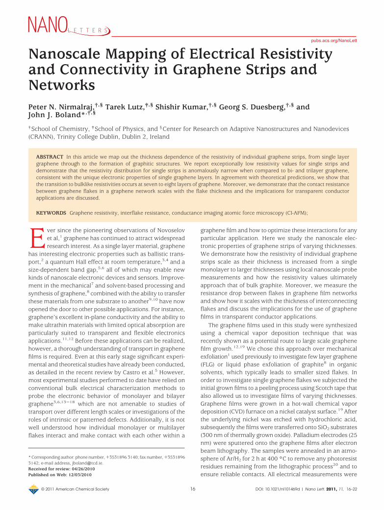
performed using conductance imaging atomic force micros-copy (CI-AFM). This technique has been employed previ-ously to probe the local electronic properties of carbonnanotubes,21-23 to optimize the contact resistance betweencarbon nanotubes and metal electrodes,24 and to measurethe conductivity of DNA molecules.25 The CI-AFM techniquewas implemented using the conducting probe as a mobilecontact which was held at ground potential and made toscan over the material of interest that is electrically con-nected to the biased Pd electrode (see Figure 1a schematic).The probe used in the CI-AFM technique is coated with Pt/Cr conductive coating (Cont E, resonant frequency 13 kHz,force constant 0.2 N/m). All CI-AFM measurements wereperformed under an optimum loading force of ∼1 nN. Thecontact resistance between the metal probe and the metalelectrode was ∼250 Ω in the case of Pd and ∼580 Ω in thecase of Ti/Au, and this was checked repeatedly duringmeasurements to verify the cleanliness and the electricalperformance of the tip. This contact resistance associatedwith the external circuit between the probe and the electrodewas subtracted in all the presented data so that the interceptsand slopes of the data presented correspond to the com-bined electrode-graphene and probe-graphene contactresistance and the linear graphene resistance, respectively(see below).
Figure 1a is a schematic showing the CI-AFM setup.Measurementswereperformedonpristineas-growngraphenefilms transferred to a SiO2 substrate. The thickness distribu-tion of the transferred graphene films was determined usingAFM in tapping mode. The average thicknesses of grapheneflakes found within the as-grown film and a film subjectedto repeated peeling process are 6.5 ( 0.35 and 3.5 ( 0.25nm (see Supporting Information), respectively. The averagethickness of a single graphene flake relative to the SiO2
substrate (300 nm oxide thickness) obtained from ouratomic force microscopy (AFM) analysis is 0.6( 0.2 nm (seeSupporting Information). Previous studies have estimatedthe thickness of a single graphene flake to vary from 0.35
to 1.6 nm.1,13,16,17 In contrast, STM measurements in ultra-high vacuum conditions have reported monolayer graphenethickness of 0.42 nm,20 consistent with 0.34 nm heightwhich is the interlayer spacing in bulk graphite. The largerreported AFM values are due to the presence of adsorbedoxygen during ambient measurements. Figure 1b is a high-resolution TEM image of one of our graphene samples anddemonstrates that the materials used in this study are ofexcellent quality.
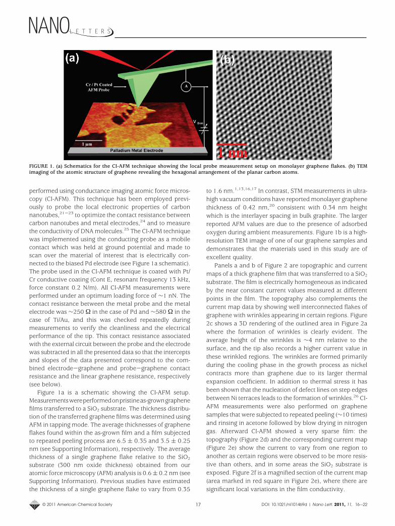
Panels a and b of Figure 2 are topographic and currentmaps of a thick graphene film that was transferred to a SiO2
substrate. The film is electrically homogeneous as indicatedby the near constant current values measured at differentpoints in the film. The topography also complements thecurrent map data by showing well interconnected flakes ofgraphene with wrinkles appearing in certain regions. Figure2c shows a 3D rendering of the outlined area in Figure 2awhere the formation of wrinkles is clearly evident. Theaverage height of the wrinkles is ∼4 nm relative to thesurface, and the tip also records a higher current value inthese wrinkled regions. The wrinkles are formed primarilyduring the cooling phase in the growth process as nickelcontracts more than graphene due to its larger thermalexpansion coefficient. In addition to thermal stress it hasbeen shown that the nucleation of defect lines on step edgesbetween Ni terraces leads to the formation of wrinkles.26 CI-AFM measurements were also performed on graphenesamples that were subjected to repeated peeling (∼10 times)and rinsing in acetone followed by blow drying in nitrogengas. Afterward CI-AFM showed a very sparse film: thetopography (Figure 2d) and the corresponding current map(Figure 2e) show the current to vary from one region toanother as certain regions were observed to be more resis-tive than others, and in some areas the SiO2 substrate isexposed. Figure 2f is a magnified section of the current map(area marked in red square in Figure 2e), where there aresignificant local variations in the film conductivity.
FIGURE 1. (a) Schematics for the CI-AFM technique showing the local probe measurement setup on monolayer graphene flakes. (b) TEMimaging of the atomic structure of graphene revealing the hexagonal arrangement of the planar carbon atoms.
© 2011 American Chemical Society 17 DOI: 10.1021/nl101469d | Nano Lett. 2011, 11, 16-–22
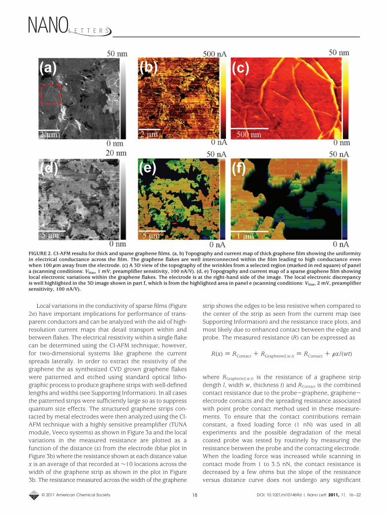
Local variations in the conductivity of sparse films (Figure2e) have important implications for performance of trans-parent conductors and can be analyzed with the aid of high-resolution current maps that detail transport within andbetween flakes. The electrical resistivity within a single flakecan be determined using the CI-AFM technique; however,for two-dimensional systems like graphene the currentspreads laterally. In order to extract the resistivity of thegraphene the as synthesized CVD grown graphene flakeswere patterned and etched using standard optical litho-graphic process to produce graphene strips with well-definedlengths and widths (see Supporting Information). In all casesthe patterned strips were sufficiently large so as to suppressquantum size effects. The structured graphene strips con-tacted by metal electrodes were then analyzed using the CI-AFM technique with a highly sensitive preamplifier (TUNAmodule, Veeco systems) as shown in Figure 3a and the localvariations in the measured resistance are plotted as afunction of the distance (x) from the electrode (blue plot inFigure 3b) where the resistance shown at each distance valuex is an average of that recorded at ∼10 locations across thewidth of the graphene strip as shown in the plot in Figure3b. The resistance measured across the width of the graphene
strip shows the edges to be less resistive when compared tothe center of the strip as seen from the current map (seeSupporting Information) and the resistance trace plots, andmost likely due to enhanced contact between the edge andprobe. The measured resistance (R) can be expressed as
where RGraphene(l,w,t) is the resistance of a graphene strip(length l, width w, thickness t) and RContact is the combinedcontact resistance due to the probe-graphene, graphene-electrode contacts and the spreading resistance associatedwith point probe contact method used in these measure-ments. To ensure that the contact contributions remainconstant, a fixed loading force (1 nN) was used in allexperiments and the possible degradation of the metalcoated probe was tested by routinely by measuring theresistance between the probe and the contacting electrode.When the loading force was increased while scanning incontact mode from 1 to 3.5 nN, the contact resistance isdecreased by a few ohms but the slope of the resistanceversus distance curve does not undergo any significant
FIGURE 2. CI-AFM results for thick and sparse graphene films. (a, b) Topography and current map of thick graphene film showing the uniformityin electrical conductance across the film. The graphene flakes are well interconnected within the film leading to high conductance evenwhen 100 µm away from the electrode. (c) A 3D view of the topography of the wrinkles from a selected region (marked in red square) of panela (scanning conditions: Vbias, 1 mV; preamplifier sensitivity, 100 nA/V). (d, e) Topography and current map of a sparse graphene film showinglocal electronic variations within the graphene flakes. The electrode is at the right-hand side of the image. The local electronic discrepancyis well highlighted in the 3D image shown in part f, which is from the highlighted area in panel e (scanning conditions: Vbias, 2 mV, preamplifiersensitivity, 100 nA/V).
R(x) ) RContact + RGraphene(l,w,t) ) RContact + Fx/(wt)
© 2011 American Chemical Society 18 DOI: 10.1021/nl101469d | Nano Lett. 2011, 11, 16-–22
change (see Supporting Information). The graphene resistiv-ity (F) can be calculated from eq 1 below
Using this equation we can estimate the resistivity of agraphene strip from the slope (blue trace) in Figure 3b andthe known dimensions (thickness, 0.45 nm; width, 4.2 µm;length, 5.8 µm, see Supporting Information) to be ∼0.01 ×10⁻⁶ Ω m. Similar measurments performed on over 20monolayer graphene strips yield a mean single strip resistiv-ity of 0.03 × 10⁻⁶ Ω m. This resistivity value is comparablebut higher than the reported value of 0.01 × 10⁻⁶ Ω m byChen et al27 for monolayer graphene. However, it is impor-tant to note that the resistivity measurements may beinfluenced by the underlying SiO2 substrate which is knownto limit the intrinsic electronic properties of monolayergraphene through the presence of trapped charges,28,29
interfacial phonons,27 substrate induced structural dis-tortions,20,30 or other external impurities as all CI-AFMmeasurements were performed under ambient conditions.31
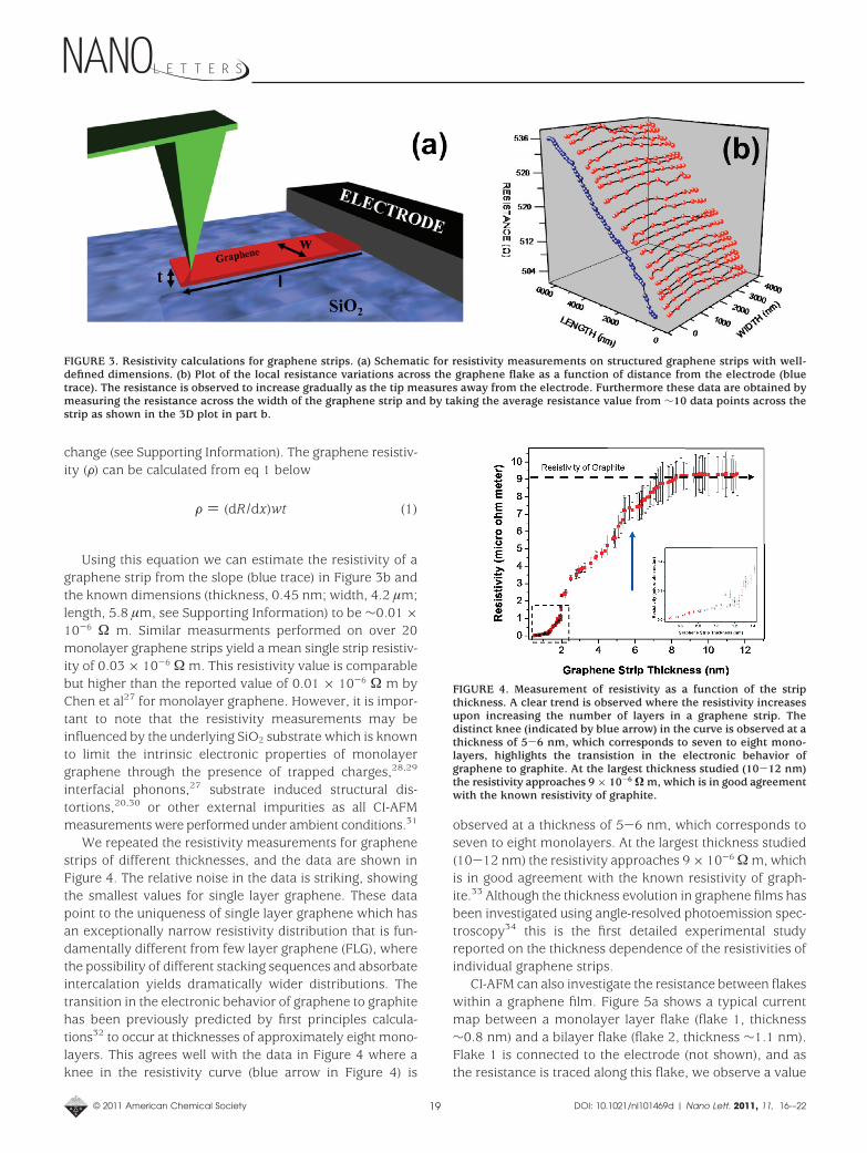
We repeated the resistivity measurements for graphenestrips of different thicknesses, and the data are shown inFigure 4. The relative noise in the data is striking, showingthe smallest values for single layer graphene. These datapoint to the uniqueness of single layer graphene which hasan exceptionally narrow resistivity distribution that is fun-damentally different from few layer graphene (FLG), wherethe possibility of different stacking sequences and absorbateintercalation yields dramatically wider distributions. Thetransition in the electronic behavior of graphene to graphitehas been previously predicted by first principles calcula-tions32 to occur at thicknesses of approximately eight mono-layers. This agrees well with the data in Figure 4 where aknee in the resistivity curve (blue arrow in Figure 4) is
observed at a thickness of 5-6 nm, which corresponds toseven to eight monolayers. At the largest thickness studied(10-12 nm) the resistivity approaches 9 × 10⁻⁶ Ω m, whichis in good agreement with the known resistivity of graph-ite.33 Although the thickness evolution in graphene films hasbeen investigated using angle-resolved photoemission spec-troscopy34 this is the first detailed experimental studyreported on the thickness dependence of the resistivities ofindividual graphene strips.
CI-AFM can also investigate the resistance between flakeswithin a graphene film. Figure 5a shows a typical currentmap between a monolayer layer flake (flake 1, thickness∼0.8 nm) and a bilayer flake (flake 2, thickness ∼1.1 nm).Flake 1 is connected to the electrode (not shown), and asthe resistance is traced along this flake, we observe a value
FIGURE 3. Resistivity calculations for graphene strips. (a) Schematic for resistivity measurements on structured graphene strips with well-defined dimensions. (b) Plot of the local resistance variations across the graphene flake as a function of distance from the electrode (bluetrace). The resistance is observed to increase gradually as the tip measures away from the electrode. Furthermore these data are obtained bymeasuring the resistance across the width of the graphene strip and by taking the average resistance value from ∼10 data points across thestrip as shown in the 3D plot in part b.
F ) (dR/dx)wt (1)
FIGURE 4. Measurement of resistivity as a function of the stripthickness. A clear trend is observed where the resistivity increasesupon increasing the number of layers in a graphene strip. Thedistinct knee (indicated by blue arrow) in the curve is observed at athickness of 5-6 nm, which corresponds to seven to eight mono-layers, highlights the transistion in the electronic behavior ofgraphene to graphite. At the largest thickness studied (10-12 nm)the resistivity approaches 9 × 10⁻⁶ Ω m, which is in good agreementwith the known resistivity of graphite.
© 2011 American Chemical Society 19 DOI: 10.1021/nl101469d | Nano Lett. 2011, 11, 16-–22
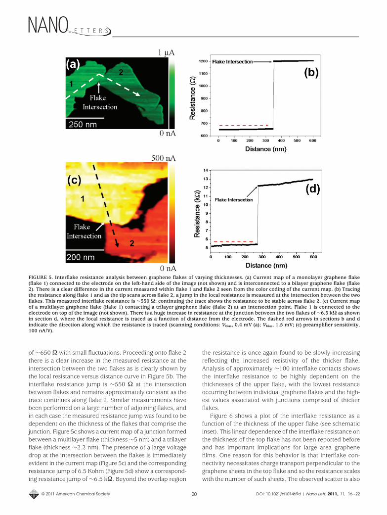
of ∼650 Ω with small fluctuations. Proceeding onto flake 2there is a clear increase in the measured resistance at theintersection between the two flakes as is clearly shown bythe local resistance versus distance curve in Figure 5b. Theinterflake resistance jump is ∼550 Ω at the intersectionbetween flakes and remains approximately constant as thetrace continues along flake 2. Similar measurements havebeen performed on a large number of adjoining flakes, andin each case the measured resistance jump was found to bedependent on the thickness of the flakes that comprise thejunction. Figure 5c shows a current map of a junction formedbetween a multilayer flake (thickness ∼5 nm) and a trilayerflake (thickness ∼2.2 nm). The presence of a large voltagedrop at the intersection between the flakes is immediatelyevident in the current map (Figure 5c) and the correspondingresistance jump of 6.5 Kohm (Figure 5d) show a correspond-ing resistance jump of ∼6.5 kΩ. Beyond the overlap region
the resistance is once again found to be slowly increasingreflecting the increased resistivity of the thicker flake,Analysis of approximately ∼100 interflake contacts showsthe interflake resistance to be highly dependent on thethicknesses of the upper flake, with the lowest resistanceoccurring between individual graphene flakes and the high-est values associated with junctions comprised of thickerflakes.
Figure 6 shows a plot of the interflake resistance as afunction of the thickness of the upper flake (see schematicinset). This linear dependence of the interflake resistance onthe thickness of the top flake has not been reported beforeand has important implications for large area graphenefilms. One reason for this behavior is that interflake con-nectivity necessitates charge transport perpendicular to thegraphene sheets in the top flake and so the resistance scaleswith the number of such sheets. The observed scatter is also
FIGURE 5. Interflake resistance analysis between graphene flakes of varying thicknesses. (a) Current map of a monolayer graphene flake(flake 1) connected to the electrode on the left-hand side of the image (not shown) and is interconnected to a bilayer graphene flake (flake2). There is a clear difference in the current measured within flake 1 and flake 2 seen from the color coding of the current map. (b) Tracingthe resistance along flake 1 and as the tip scans across flake 2, a jump in the local resistance is measured at the intersection between the twoflakes. This measured interflake resistance is ∼550 Ω; continuing the trace shows the resistance to be stable across flake 2. (c) Current mapof a multilayer graphene flake (flake 1) contacting a trilayer graphene flake (flake 2) at an intersection point. Flake 1 is connected to theelectrode on top of the image (not shown). There is a huge increase in resistance at the junction between the two flakes of ∼6.5 kΩ as shownin section d, where the local resistance is traced as a function of distance from the electrode. The dashed red arrows in sections b and dindicate the direction along which the resistance is traced (scanning conditions: Vbias, 0.4 mV (a); Vbias, 1.5 mV; (c) preamplifier sensitivity,100 nA/V).
© 2011 American Chemical Society 20 DOI: 10.1021/nl101469d | Nano Lett. 2011, 11, 16-–22
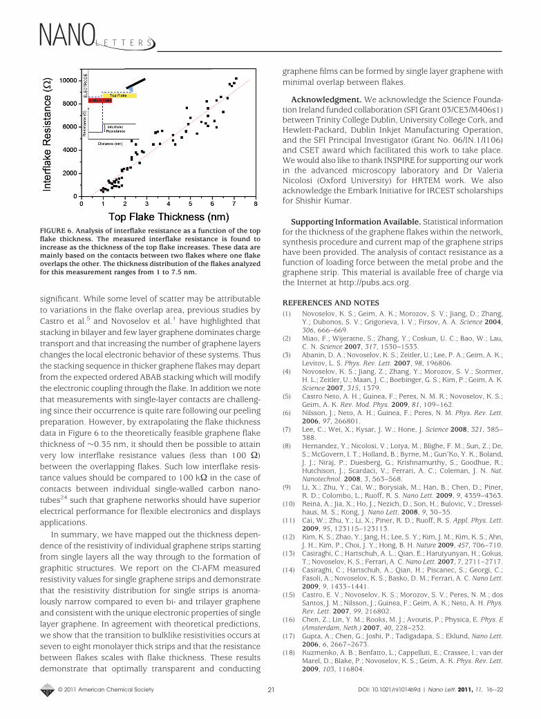
significant. While some level of scatter may be attributableto variations in the flake overlap area, previous studies byCastro et al.5 and Novoselov et al.1 have highlighted thatstacking in bilayer and few layer graphene dominates chargetransport and that increasing the number of graphene layerschanges the local electronic behavior of these systems. Thusthe stacking sequence in thicker graphene flakes may departfrom the expected ordered ABAB stacking which will modifythe electronic coupling through the flake. In addition we notethat measurements with single-layer contacts are challeng-ing since their occurrence is quite rare following our peelingpreparation. However, by extrapolating the flake thicknessdata in Figure 6 to the theoretically feasible graphene flakethickness of ∼0.35 nm, it should then be possible to attainvery low interflake resistance values (less than 100 Ω)between the overlapping flakes. Such low interflake resis-tance values should be compared to 100 kΩ in the case ofcontacts between individual single-walled carbon nano-tubes24 such that graphene networks should have superiorelectrical performance for flexible electronics and displaysapplications.
In summary, we have mapped out the thickness depen-dence of the resistivity of individual graphene strips startingfrom single layers all the way through to the formation ofgraphitic structures. We report on the CI-AFM measuredresistivity values for single graphene strips and demonstratethat the resistivity distribution for single strips is anoma-lously narrow compared to even bi- and trilayer grapheneand consistent with the unique electronic properties of singlelayer graphene. In agreement with theoretical predictions,we show that the transition to bulklike resistivities occurs atseven to eight monolayer thick strips and that the resistancebetween flakes scales with flake thickness. These resultsdemonstrate that optimally transparent and conducting
graphene films can be formed by single layer graphene withminimal overlap between flakes.
Acknowledgment. We acknowledge the Science Founda-tion Ireland funded collaboration (SFI Grant 03/CE3/M406s1)between Trinity College Dublin, University College Cork, andHewlett-Packard, Dublin Inkjet Manufacturing Operation,and the SFI Principal Investigator (Grant No. 06/IN.1/I106)and CSET award which facilitated this work to take place.We would also like to thank INSPIRE for supporting our workin the advanced microscopy laboratory and Dr ValeriaNicolosi (Oxford University) for HRTEM work. We alsoacknowledge the Embark Initiative for IRCEST scholarshipsfor Shishir Kumar.
Supporting Information Available. Statistical informationfor the thickness of the graphene flakes within the network,synthesis procedure and current map of the graphene stripshave been provided. The analysis of contact resistance as afunction of loading force between the metal probe and thegraphene strip. This material is available free of charge viathe Internet at http://pubs.acs.org.
REFERENCES AND NOTES(1) Novoselov, K. S.; Geim, A. K.; Morozov, S. V.; Jiang, D.; Zhang,
Y.; Dubonos, S. V.; Grigorieva, I. V.; Firsov, A. A. Science 2004,306, 666–669.
(2) Miao, F.; Wijeratne, S.; Zhang, Y.; Coskun, U. C.; Bao, W.; Lau,C. N. Science 2007, 317, 1530–1533.
(3) Abanin, D. A.; Novoselov, K. S.; Zeitler, U.; Lee, P. A.; Geim, A. K.;Levitov, L. S. Phys. Rev. Lett. 2007, 98, 196806.
(4) Novoselov, K. S.; Jiang, Z.; Zhang, Y.; Morozov, S. V.; Stormer,H. L.; Zeitler, U.; Maan, J. C.; Boebinger, G. S.; Kim, P.; Geim, A. K.Science 2007, 315, 1379.
(5) Castro Neto, A. H.; Guinea, F.; Peres, N. M. R.; Novoselov, K. S.;Geim, A. K. Rev. Mod. Phys. 2009, 81, 109–162.
(6) Nilsson, J.; Neto, A. H.; Guinea, F.; Peres, N. M. Phys. Rev. Lett.2006, 97, 266801.
(7) Lee, C.; Wei, X.; Kysar, J. W.; Hone, J. Science 2008, 321, 385–388.
(8) Hernandez, Y.; Nicolosi, V.; Lotya, M.; Blighe, F. M.; Sun, Z.; De,S.; McGovern, I. T.; Holland, B.; Byrne, M.; Gun’Ko, Y. K.; Boland,J. J.; Niraj, P.; Duesberg, G.; Krishnamurthy, S.; Goodhue, R.;Hutchison, J.; Scardaci, V.; Ferrari, A. C.; Coleman, J. N. Nat.Nanotechnol. 2008, 3, 563–568.
(9) Li, X.; Zhu, Y.; Cai, W.; Borysiak, M.; Han, B.; Chen, D.; Piner,R. D.; Colombo, L.; Ruoff, R. S. Nano Lett. 2009, 9, 4359–4363.
(10) Reina, A.; Jia, X.; Ho, J.; Nezich, D.; Son, H.; Bulovic, V.; Dressel-haus, M. S.; Kong, J. Nano Lett. 2008, 9, 30–35.
(11) Cai, W.; Zhu, Y.; Li, X.; Piner, R. D.; Ruoff, R. S. Appl. Phys. Lett.2009, 95, 123115–123113.
(12) Kim, K. S.; Zhao, Y.; Jang, H.; Lee, S. Y.; Kim, J. M.; Kim, K. S.; Ahn,J. H.; Kim, P.; Choi, J. Y.; Hong, B. H. Nature 2009, 457, 706–710.
(13) Casiraghi, C.; Hartschuh, A. L.; Qian, E.; Harutyunyan, H.; Gokus,T.; Novoselov, K. S.; Ferrari, A. C. Nano Lett. 2007, 7, 2711–2717.
(14) Casiraghi, C.; Hartschuh, A.; Qian, H.; Piscanec, S.; Georgi, C.;Fasoli, A.; Novoselov, K. S.; Basko, D. M.; Ferrari, A. C. Nano Lett.2009, 9, 1433–1441.
(15) Castro, E. V.; Novoselov, K. S.; Morozov, S. V.; Peres, N. M.; dosSantos, J. M.; Nilsson, J.; Guinea, F.; Geim, A. K.; Neto, A. H. Phys.Rev. Lett. 2007, 99, 216802.
(16) Chen, Z.; Lin, Y. M.; Rooks, M. J.; Avouris, P.; Physica, E. Phys. E(Amsterdam, Neth.) 2007, 40, 228–232.
(17) Gupta, A.; Chen, G.; Joshi, P.; Tadigadapa, S.; Eklund, Nano Lett.2006, 6, 2667–2673.
(18) Kuzmenko, A. B.; Benfatto, L.; Cappelluti, E.; Crassee, I.; van derMarel, D.; Blake, P.; Novoselov, K. S.; Geim, A. K. Phys. Rev. Lett.2009, 103, 116804.
FIGURE 6. Analysis of interflake resistance as a function of the topflake thickness. The measured interflake resistance is found toincrease as the thickness of the top flake increases. These data aremainly based on the contacts between two flakes where one flakeoverlaps the other. The thickness distribution of the flakes analyzedfor this measurement ranges from 1 to 7.5 nm.
© 2011 American Chemical Society 21 DOI: 10.1021/nl101469d | Nano Lett. 2011, 11, 16-–22
(19) Kumar, S.; McEvoy, N.; Lutz, T.; Keeley, G. P.; Nicolosi, V.; Murray,C. P.; Blau, W. J.; Duesberg, G. S. Chem. Commun. (Cambridge,U.K.) , 46, 1422–1424.
(20) Ishigami, M.; Chen, J. H.; Cullen, W. G.; Fuhrer, M. S.; Williams,E. D. Nano Lett. 2007, 7, 1643–1648.
(21) de Pablo, P. J.; Martinez, M. T.; Colchero, J.; Gomez-Herrero, J.;Maser, W. K.; Benito, A. M.; Munoz, E.; Baro, A. M. Adv. Mater.2000, 12, 573–576.
(22) Fujiwara, A.; Iijima, R.; Suematsu, H.; Kataura, H.; Maniwa, Y.; Suzuki,S.; Achiba, Y. Phys. B (Amsterdam, Neth.) 2002, 323, 227–229.
(23) Nirmalraj, P. N.; Lyons, P. E.; De, S.; Coleman, J. N.; Boland, J. J.Nano Lett. 2009, 9, 3890–3895.
(24) Nirmalraj, P. N.; Boland, J. J. ACS Nano 2010, 4, 3801–3806.(25) Heim, T.; Deresmes, D.; Vuillaume, D. J. Appl. Phys. 2004, 96,
2927–2936.(26) Chae, S. J.; et al. In Carbon Nanotubes, Graphene, and Associated
Devices, II.1 ed; SPIE: Bellingham, WA, 2009; 73990W-73911.
(27) Chen, J.-H.; Jang, C.; Xiao, S.; Ishigami, M.; Fuhrer, M. S. Nat.Nanotechnol. 2008, 3, 206–209.
(28) Chen, J. H.; Jang, C.; Adam, S.; Fuhrer, M. S.; Williams, E. D.;Ishigami, M. Nat. Phys. 2008, 4, 377–381.
(29) Nomura, K.; MacDonald, A. H. Q. Phys. Rev. Lett. 2006, 96,256602.
(30) Morozov, S. V.; Novoselov, K. S.; Katsnelson, M. I.; Schedin, F.;Elias, D. C.; Jaszczak, J. A.; Geim, A. K. Phys. Rev. Lett. 2008, 100,No. 016602.
(31) Schedin, F.; Geim, A. K.; Morozov, S. V.; Hill, E. W.; Blake, P.;Katsnelson, M. I.; Novoselov, K. S. Nat. Mater. 2007, 6, 652–655.
(32) AlZahrani, A. Z.; Srivastava, G. P. J. Phys.: Conden. Matter 2009,21, 495503.
(33) Powell, R. L.; Childs, G. E. In American Institute of PhysicsHandbook; AIP: New York, 1972; pp 140-160.
(34) Ohta, T.; Bostwick, A.; McChesney, J. L.; Seyller, T.; Horn, K.;Rotenberg, E. Phys. Rev. Lett. 2007, 98, 206802.
© 2011 American Chemical Society 22 DOI: 10.1021/nl101469d | Nano Lett. 2011, 11, 16-–22


