Embed Size (px)
Citation preview

Aalborg Universitet
Novel Space Vector Pulsewidth Modulation Strategies for Single-Phase Three-LevelNPC Impedance-Source Inverters
Shults, T. E.; Husev, O.; Blaabjerg, F.; Roncero-Clemente, C.; Romero-Cadaval, E.; Vinnikov,D.Published in:IEEE Transactions on Power Electronics
DOI (link to publication from Publisher):10.1109/TPEL.2018.2859194
Publication date:2019
Document VersionAccepted author manuscript, peer reviewed version
Link to publication from Aalborg University
Citation for published version (APA):Shults, T. E., Husev, O., Blaabjerg, F., Roncero-Clemente, C., Romero-Cadaval, E., & Vinnikov, D. (2019).Novel Space Vector Pulsewidth Modulation Strategies for Single-Phase Three-Level NPC Impedance-SourceInverters. IEEE Transactions on Power Electronics, 34(5), 4820-4830. [8418820].https://doi.org/10.1109/TPEL.2018.2859194
General rightsCopyright and moral rights for the publications made accessible in the public portal are retained by the authors and/or other copyright ownersand it is a condition of accessing publications that users recognise and abide by the legal requirements associated with these rights.
? Users may download and print one copy of any publication from the public portal for the purpose of private study or research. ? You may not further distribute the material or use it for any profit-making activity or commercial gain ? You may freely distribute the URL identifying the publication in the public portal ?
Take down policyIf you believe that this document breaches copyright please contact us at [email protected] providing details, and we will remove access tothe work immediately and investigate your claim.

0885-8993 (c) 2018 IEEE. Personal use is permitted, but republication/redistribution requires IEEE permission. See http://www.ieee.org/publications_standards/publications/rights/index.html for more information.
This article has been accepted for publication in a future issue of this journal, but has not been fully edited. Content may change prior to final publication. Citation information: DOI 10.1109/TPEL.2018.2859194, IEEETransactions on Power Electronics
Abstract— This paper presents new Space Vector
Pulse-Width Modulation (SVPWM) strategies for a
single-phase three-level buck-boost Neutral Point
Clamped (NPC) inverter coupled with Impedance-
Source (IS) networks. These strategies can be
implemented for systems with any IS networks with
neutral point. The case study system is based on the
quasi-Z-source inverter with continuous input
current. To demonstrate an improved performance,
the strategies are compared with a traditional pulse-
width modulation strategy. The advantages lie in
reduced switching number, without output voltage
quality distortion. The simulation and experimental
results confirm the theoretical predictions.
I. INTRODUCTION
Present technologies and innovations have led to the
expansion of Photovoltaic (PV) energy generation
systems worldwide [1]-[4]. PV energy sources are
characterized by a wide output voltage and power
variation. The solar irradiation level changes significantly
during the day and gives a variable output power. Also,
the shading or high operating temperature of the PV
module leads to a significant out-voltage drop. Therefore,
the converter for a PV system should have a wide input
voltage and output load regulation range.
To extend the input voltage regulation range, solutions
based on Impedance-Source (IS) networks have been
proposed [5]-[11]. They have a buck mode, a boost mode
and do not suffer from the Shoot-Through (ST) [5] states
compare to the conventional grid-connected inverters.
Manuscript received November 7, 2017; revised February 11, 2018;
accepted July 9, 2018.
Copyright © 2018 IEEE. Personal use of this material is permitted.
However, permission to use this material for any other purposes must be
obtained from the IEEE by sending a request to pubs-
Tatina Shults is with the Power Electronics Institute of Novosibirsk
State Technical University 20, Prospekt K. Marksa, Novosibirsk,
630073, Russia
Oleksandr Husev and Dmitri Vinnikov are with the Department of
Electrical Power Engineering and Mechatronics, Tallinn University of
Technology, Ehitajate str. 5, 19086 Tallinn, Estonia. Oleksandr Husev
is also with the Department of Biomedical Radioelectronics Apparatus
and Systems, Chernihiv National University of Technology,
Shevchenko str. 95, 14027 Chernihiv, Ukraine (e-mail:
Frede Blaabjerg is with the Institute of Energy Technology, Aalborg
University, Pontoppidanstræde, str. 101, 9220 Aalborg, Denmark (e-
mail: [email protected]).
Carlos Roncero-Clemente and Enrique Romero-Cadaval are with the
School of Industrial Engineering, University of Extremadura, Avda.
Elvas s/n, 06006, Badajoz, Spain (e-mail: [email protected],
At the same time, inverters used for PV system
integration to the grid can be based on two-level or
multilevel topologies. Multilevel inverters are preferable
solutions not only for medium-voltage but also for low-
voltage applications. One of the most important benefits
of the multilevel inverter is reduced voltage stress on the
semiconductors. At the same time, the increased number
of the output voltage levels leads to an output voltage
quality improvement. The Three-Level (3L) Neutral Point
Clamped (NPC) inverter is one of the most popular
solutions among the multilevel topologies [12]-[18]. In
case of full-bridge utilization it gives five-level output
voltage.
The latest research [19]-[21] show that any IS networks
are feasible for low power application with a wide range
input voltage regulation. In most applications, low power
facilities are associated with single-phase systems. The
latest research [19]-[21] show that any IS networks are
feasible for low power application with a wide range input
voltage regulation. In most applications, low power
facilities are associated with single-phase systems.
Low power applications make such topologies feasible
by means of a very high switching frequency that, in turn,
reduces the size and weight of the passive components.
Switching losses can be reduced by means of novel wide
bandgap semiconductors and also different modulation
techniques.
There are many well-known Pulse-Width Modulation
(PWM) techniques that can be applied for IS based
converters [22]-[31]. Space Vector PWM (SVPWM) is
mostly applied to three-phase systems [32]-[39]. It can be
applied for IS based converters as well [40]-[43].
At the same time, several papers report that SVPWM is
suitable for conventional single-phase systems [44]-[47].
Additionally, this technique is effective for use with a
voltage unbalancing problem [44]. This technique is
proposed only for conventional single-phase three-level
inverters. Focus in this work is on the development of a
SVPWM for the single-phase 3L NPC buck-boost
inverter coupled with any IS network. SVPWM makes the
neutral point balancing flexible, improves the output
voltage quality, and reduces also the switching losses.
II. EXISTING SVPWM TECHNIQUES FOR SINGLE-
PHASE THREE-LEVEL INVERTER
The 3L NPC buck-boost inverter coupled with IS
(quasi-Z-source) network is shown in Fig. 1, where points
-1, 0, 1, A, and B are denoted. The 3L quasi-Z-Source
NPC inverter is selected as a case study solution [15].
Tatiana Shults, Oleksandr Husev, Member, IEEE, Frede Blaabjerg, Fellow, IEEE, Carlos Roncero-Clemente,
Member, IEEE, Enrique Romero-Cadaval, Senior Member, IEEE, Dmitri Vinnikov, Senior Member, IEEE
Novel Space Vector Pulse Width Modulation
Strategies for Single-Phase Three-Level NPC
Impedance-Source Inverters

0885-8993 (c) 2018 IEEE. Personal use is permitted, but republication/redistribution requires IEEE permission. See http://www.ieee.org/publications_standards/publications/rights/index.html for more information.
This article has been accepted for publication in a future issue of this journal, but has not been fully edited. Content may change prior to final publication. Citation information: DOI 10.1109/TPEL.2018.2859194, IEEETransactions on Power Electronics
Fig. 1. Single-Phase 3L NPC inverter coupled with IS networks.
Nine switching states are possible for a conventional 3L
NPC converter: (-1,-1), (0,0), (1,1), (-1,0), (0,1), (1,-1),
(0,-1), (-1,1), and (1,-1), that are illustrated in Table I.
Where 1 is denoted as conducting switches S1-S8.
TABLE I. SWITCHING STATES FOR A SINGLE-PHASE NPC
Stat
e
S
1
S
2
S
3
S
4
S
5
S
6
S
7
S
8
Voltage
level
VAB
Vectors
(Fig. 2a)
Vectors
(Fig. 2b)
-1,-1 0 0 1 1 0 0 1 1 0
V0 V0 0,0 0 1 1 0 0 1 1 0 0
1,1 1 1 0 0 1 1 0 0 0
1,0 1 1 0 0 0 1 1 0 Vdc/2 V4 V1
0,-1 0 1 1 0 0 0 1 1 Vdc/2 V2
1,-1 1 1 0 0 0 0 1 1 Vdc V3 V2
0,1 0 0 1 1 1 1 0 0 - Vdc/2 V1 V3
-1,0 0 0 1 1 0 1 1 0 - Vdc/2 V5
-1,1 0 0 1 1 1 1 0 0 - Vdc V6 V4
Using these switching states, two space voltage vector
diagrams can be shown [45] for a single-phase 3L NPC
inverter (Fig. 2).
Fig. 2a represents a reference vector V* synthesized by
six non-zero voltage vectors V1-V6 and one zero voltage
vector V0. In each of the six sectors (I-VI) three closer
located vectors are used Vj, Vj+1 and V0, for synthesizing
the reference vector V*, where j is a vector number. In
sector VI, the reference vector V* is synthesized by V1, V6
and V0. The use of V0 is necessary in order to provide the
modulation index in a range of 0≤M≤1. A weighting coefficient τij will be used for the
following analysis, where i is the sector number. The
weighting coefficient τij is the relative duration of the
vector Vj during the switching period in sector i. For any
sector in Fig. 2a, the weighting coefficients τ can be defined from:
600,,1
)sin(3
2
)sin(3
1)cos(
3
)sin(3
1)cos(
31
,
,0)1(,,
)1(,
,
0
T
T
M
M
M
ji
jijiji
ji
ji
, (1)
where Ti,j is the time interval of the space vector
application, T is the switching period.
In the SVPWM shown in Fig. 2b, the reference vector
V* is synthesized by four non-zero voltage vectors V1-V4
and one zero voltage vector V0. In each of the eight
sectors (I-VIII) for synthesizing the reference vector V*,
two closer located vectors are used. For example, V1 and
V0 are used in sector I, and V4 and V3 in sector VII. The
weighting coefficients for this approach are given in
Table II, where phase ϑ is varying in a range 0°<ϑ≤360° and S is the number of the sectors.
I
II
V*
(1,-1)
(-1,1)
V1
V2
V4
V3
III
IV
V
VI VII
VIII
V0
(b)
II
V*
(1,-1)
(0,-1)
(-1,0)
(-1,1)
V2
V3
V6
V5
III
V VI
ϑ
(1,1)(0,0)
(-1,-1)V0
(1,0) V4
(0,1)V1
IIV
V0=0V1=V5=Vdc/2 V2=V4=-Vdc/2 V3=Vdc V6=-Vdc
V1=Vdc/2 V3=-Vdc/2 V2=Vdc V4=-Vdc
V0=0
(a)
ϑ (1,1)(0,0)
(-1,-1)
(0,1)(-1,0)
(1,0)(0,-1)
Fig. 2. Space voltage vector diagrams for a single-phase 3L NPC
inverter derived by different set of vectors (a and b).
TABLE II. WEIGHTING COEFFICIENTS FOR SVPWM IN DIFFERENT
SECTORS (FIG. 2B)
Sector Weighting coefficients (τij)
I, IV
)sin(2
)sin(21
1,41,1
0,40,1
M
M
II, III
1)sin(2
)sin(22
2,32,2
1,31,2
M
M
V, VIII
)sin(2
)sin(21
3,83,5
0,80,5
M
M
VI, VII
)sin(21
)sin(22
4,74,6
3,73,6
M
M
In a general case, the weighting coefficients for any
SVPWM are calculated according to the principle
proposed in [44]. The SVPWM shown in Fig. 2b has
several key advantages over the SVPWM shown in
Fig. 2a. First of all, it has 15% larger fundamental
harmonic component. Also, the calculation of the
weighting coefficients is much easier. Therefore, the
SVPWM is shown in Fig. 2b will be considered like a
basic solution.
III. SVPWM FOR SINGLE-PHASE IS-BASED INVERTER
Fig. 3 shows a proposed space vector diagram for an
IS-based Single-Phase 3L NPC inverter along with an
example of the switching states distribution in each sector.
The main goal of this approach lies in the generation of
the optimal switching sequence in terms of minimum
switching losses providing the output sinusoidal voltage.
At the same time, it should be noted that only equally
distributed ST generation is considered. Maximum boost
control [22] may evoke oscillation in the IS network and
is not feasible for practical implementation. This
phenomenon has been shown and discussed in [48].

0885-8993 (c) 2018 IEEE. Personal use is permitted, but republication/redistribution requires IEEE permission. See http://www.ieee.org/publications_standards/publications/rights/index.html for more information.
This article has been accepted for publication in a future issue of this journal, but has not been fully edited. Content may change prior to final publication. Citation information: DOI 10.1109/TPEL.2018.2859194, IEEETransactions on Power Electronics
I
II
V*
V1
V2
V4
V3
III
IV
V
VI VII
VIII
V1=Vdc/2 V3= –Vdc/2 V2=Vdc V4= –Vdc
V0=0
ϑ
VIVIVIIIIII VIIIVII Sector
V*
t
VST
Vi,j
Vi,j+1
VAB
VST=0
(1,0)(0,-1)
(0,1)(-1,0)
(-1,1)
(1,-1)
V0
V1
V1
V2
V1
V1 V3
V3
V4
V3
V3
V0 V0 V0
V2 V4
VST
VSTV0=
(S,S)
(1,1)(0,0)
(-1,-1)
Fig. 3. Space voltage vector diagram for proposed SVPW for single-
phase 3L NPC IS inverter.
The vector diagram is divided into eight sectors. It is
different by additional ST vector VST, which is in a
response for ST state generation. However, here in each
sector, three weighting coefficients must be defined: two
for general (closer located) vectors and one for the vector
VST. The vector VST is used in each sector in order to
achieve equally distributed ST generation. The weighting
coefficient of VST is equal to ST duty cycle DST,
determined by capacitor voltage regulator. Taking into
account equally distributed ST states (τST=const) the
weighting coefficients are defined as:
1
)1,(
1
1,
)1,(,
*)1(
*)1(
1
1,
jj
jSTji
jj
jSTji
jijiST
STSST
VV
VV
VV
VV
MconstTTD
, (2)
where Vj, Vj+1 are the space vectors used in sector i and
V*=(1–τST)·M·Vdc sin(ϑ) is the reference vector.
For example, in the sector VII, the output voltage is
generated by vectors 2/3 dcj VVV
and
dcj VVV 41
. The weighting coefficients are expressed
from (2) as:
)2
(
sin)1()(1
)(2
sin)1()2
)(1(
3,7,
4,71,
dcdc
dcSTdcSTji
dcdc
dcSTdc
ST
ji
VV
VMV
VV
VMV
, (3)
*
3,7
*4,7
221
21
YST
YST
V
V
, (4)
.sin)1(* MV STY (5)
Here (5) V*Y is y axis projection of V* in relative units. The calculated weighting coefficients for all sectors are
shown in Table III. The vector V* position and sector
boundaries are detected by calculating the rotation angle ϑ
value.
One of the very important issues during generation of
the sequence of the vector is balancing of the energy
utilization from capacitors. It consists in the equal
charging and discharging of the different capacitors of IS
network. Fig. 4 shows two equivalent switching states of
the vector V1 which generates the voltage equal to Vdc/2.
In the first case (Fig. 4a) the charging current of
capacitor C2 (iC2=iIN) is larger than the charging current of
capacitor C3 (iC3=iIN – idc) and vice-versa in the second
case (Fig. 4b). The principle of the balancing consists in
equal utilization of the equivalent circuits shown in Fig. 4
maintaining constant voltage across the capacitors.
Fig. 4.Equivalent circuits of active states of the quasi-Z-Source NPC
inverter.
TABLE III. WEIGHTING COEFFICIENTS OF SVPWM FOR IS INVERTER (FIG. 3) Weighting coefficients (τij) Sector boundaries
*
1,41,1
*,400,1
2
21
Y
YST
V
V
M
I5.0
arcsin0:
M
IV5.0
arcsin:
*
2,32,2
*1,31,2
2)1(
22)1(
YST
YST
V
V
2
5.0arcsin:
M
II
M
III5.0
arcsin2
:
*
3,83,5
*0,80,5
2
21
Y
YST
V
V
M
V5.0
arcsin: 25.0
arcsin2:
M
VIII
*
4,74,6
*3,73,6
2)1(
2)1(2
YST
YST
V
V
2
35.0arcsin:
M
VI
M
VII5.0
arcsin22
3:

0885-8993 (c) 2018 IEEE. Personal use is permitted, but republication/redistribution requires IEEE permission. See http://www.ieee.org/publications_standards/publications/rights/index.html for more information.
This article has been accepted for publication in a future issue of this journal, but has not been fully edited. Content may change prior to final publication. Citation information: DOI 10.1109/TPEL.2018.2859194, IEEETransactions on Power Electronics
Sect.
Vec. VST V1 V0 V1 VST VST V1 V2 V1 VST VST V1 V2 V1 VST VST V1 V0 V1 VST VST V3 V0 V3 VST VST V3 V4 V3 VST VST V3 V4 V3 VST VST V3 V0 V3 VST
SS ST 0,-1 0,0 1,0 ST ST 0,-1 1,-1 1,0 ST ST 1,0 1,-1 0,-1 ST ST 1,0 0,0 0,-1 ST ST 0,1 0,0 -1,0 ST ST 0,1 -1,1 -1,0 ST ST -1,0 1,-1 0,1 ST ST -1,0 0,0 0,1 ST
S1 1 1 1 1 1 1 1 1 1 1 1 1 1 1 1 1 1 1 1 1 1 1
S2 1 1 1 1 1 1 1 1 1 1 1 1 1 1 1 1 1 1 1 1 1 1 1 1 1 1 1 1 1 1 1 1 1 1
S3 1 1 1 1 1 1 1 1 1 1 1 1 1 1 1 1 1 1 1 1 1 1 1 1 1 1 1 1 1 1 1 1 1 1
S4 1 1 1 1 1 1 1 1 1 1 1 1 1 1 1 1 1 1 1 1 1 1
S5 1 1 1 1 1 1 1 1 1 1 1 1 1 1 1 1 1 1 1 1 1 1
S6 1 1 1 1 1 1 1 1 1 1 1 1 1 1 1 1 1 1 1 1 1 1 1 1 1 1 1 1 1 1 1 1 1 1
S7 1 1 1 1 1 1 1 1 1 1 1 1 1 1 1 1 1 1 1 1 1 1 1 1 1 1 1 1 1 1 1 1 1 1
S8 1 1 1 1 1 1 1 1 1 1 1 1 1 1 1 1 1 1 1 1 1 1
VII VIIII II III IV V VI
Fig. 5. Switching states sequences in the proposed SVPWM single-phase IS inverter.
The switching states (SS) distribution is shown in
Fig. 5. It can be noted that a switching state sequence of
sectors III, IV and VII, VIII is the mirror image of sectors
I, II and V, VI, respectively. Grey color means conducting
semiconductor switches of the inverter. One of the direct
criteria of the switching optimization is overall number of
transistor commutation per switching cycle. In this case,
the overall commutation number per switching cycle is
12. It should be noticed, than in case of dropping
modulation index less than 0.5, the sectors II, III, VI and
VII will not be involved in the output voltage vector
generation. It can be seen from Fig. 3. At the same time,
the number of transistor commutation per switching cycle
remains the same. It is explained by fact that all sectors
have equal commutation number per switching cycle
(Fig. 5).
Summarizing above presented approach it includes
calculation of the weighting coefficients of the vectors for
each sector in order to provide sinusoidal waveform of the
output voltage and select a proper switching sequence in
order to provide constant voltage across capacitors along
with minimum number of transistor switching.
IV. MODIFIED SVPWM FOR SINGLE-PHASE IS-
BASED INVERTER
Incomplete ST states are mentioned in several papers
concerning three-phase systems with impedance networks
[29], [30]. The feature of this state consists of
asymmetrical ST application to one out of two networks.
At the same time the voltage applied to the output is not
equal to zero. The equivalent circuit of the additional ST
state (1,S) for 3L NPC quasi-Z-Source inverter is
depicted in Fig. 6. It shows that only the lower part (IS2)
of the quasi-Z-Source network corresponds to the ST
state. Capacitor C3 is discharging and C2 is charging.
D01
D03
D04
1
-1
0A
B
VIN
C2
C3
iC2
iC3
iIN
S8S4
S3
S1
S2 S6
S5
S7
D02
Li
Cf
Lg
VOUT
iOUT
idcC1
C4
L1 L2
L3 L4
D1
D2
IS1
IS2 Fig. 6. Equivalent circuit of additional incomplete ST state (1,S) of the
quasi-Z-Source NPC inverter.
Additional switching states of incomplete ST can be
implemented in order to reduce number of switching. In
total, there are four incomplete ST states: (1,S), (S,-1),
(S,1) and (-1,S). S denotes an incomplete short circuit
when only three switches are opened in the inverter leg.
Because of that switching period, both (1,S) and (S,-1) or
(S,1) and (-1,S) states should be used during the switching
period. Using only one incomplete ST switching state per
switching period leads to a capacitor voltage unbalance.
However, the voltage VAB at an incomplete ST state is
Vdc/2. These additional states give additional flexibility in
the output voltage vector generation. The weighting
coefficients and sector boundaries are shown in Table IV.
Fig. 7a shows a proposed space vector diagram for the
modified SVPWM along with an example of the
switching states distribution in each sector.
Fig. 7. Space voltage vector diagram for proposed modified SVPWM
for single-phase 3L NPC IS inverter (a) along with switching
states sequences (b).
The switching state sequences for the modified
SVPWM are shown in Fig. 7b. Vectors VST1 and V1 are
equal and co-directional, as well as VST3 and V3.

0885-8993 (c) 2018 IEEE. Personal use is permitted, but republication/redistribution requires IEEE permission. See http://www.ieee.org/publications_standards/publications/rights/index.html for more information.
This article has been accepted for publication in a future issue of this journal, but has not been fully edited. Content may change prior to final publication. Citation information: DOI 10.1109/TPEL.2018.2859194, IEEETransactions on Power Electronics
TABLE IV. WEIGHTING COEFFICIENTS OF MODIFIED SVPWM (FIG. 8)
Weighting coefficients (τij) Sector boundaries
*
1,61,1
*0,60,1
2
21
Y
YST
V
V
M
I5.0
arcsin0:
M
VI5.0
arcsin:
STY
Y
V
V
*
1,51,2
*0,50,2
2
21
)1(
5.0arcsin
5.0arcsin:
SDMMII
MDMV
S
5.0arcsin
)1(
5.0arcsin:
*
2,42,3
*1,41,3
21
22
Y
YST
V
V
2)1(
5.0arcsin:
SDMIII
)1(
5.0arcsin
2:
SDMIV
*
3,123,7
*0,120,7
2
21
Y
YST
V
V
M
VII5.0
arcsin: 25.0
arcsin2:
M
XI
STY
Y
V
V
*
3,113,8
*0,110,8
2
21
)1(
5.0arcsin
5.0arcsin:
SDMMVIII
MDMXI
S
5.0arcsin2
)1(
5.0arcsin2:
*
4,104,9
*3,103,9
21
22
Y
YST
V
V
2
3
)1(
5.0arcsin:
SDMIX
)1(
5.0arcsin2
2
3:
SDMX
A switching state sequence of sectors IV-VII and X-XII
is the mirror image of sectors I-III and VII-IX,
respectively. The overall commutation number per
switching period in sectors I, VI, VII, XII is 12. In all
other sectors, the overall commutation number is 8. It can
be seen that the commutation number in the modified
SVPWM (Fig. 7b) is significantly reduced compared with
SVPWM (Fig. 5). It corresponds to the 22% reduction of
overall commutation number in case of M·=1. In advance, the quality of the energy transfer from the
source to the load is also improved.
If modulation index is lower, according to the Fig. 7a, the
involvement of the sectors III, IV, IX and X will be
reduced. The modulation index M·=(1–DST)·0.5 is a
borderline value when these sectors can be used. Since
these sectors have only 8 transistors switching, the overall
commutation number will be increased. At the same time,
it should be mentioned, that in proper designed inverters,
the modulation index lower than 0.5 is not expected. It
corresponds to the poor dc-link voltage utilization.
10.80.60.40.2
τST=DS τij τi(j+1)
10.80.60.40.2
(c)π/4 π/2 3π/4 π 5π/4 3π/2 7π/4 2π 0
π/4 π/2 3π/4 π 5π/4 3π/2 7π/4 2π 0(a)
10.80.60.40.2
(b)π/4 π/2 3π/4 π 5π/4 3π/2 7π/4 2π 0
Fig. 8. Graphical representation of the weighting coefficients of:
(a) both SVPWM, M=1, DST=0; (b) the SVPWM, M=1, DST=0.2;
(c) the modified SVPWM, M=1, DST=0.2.
Finally, in graphical representation of the weighting
coefficients is shown in Fig. 8. Fig. 8b and Fig. 8c
illustrates the weighting coefficients for the case with ST
duty cycle which is equal DST=0.2 and modulation index
М=1 correspondently. From Fig. 3, 7 and Table III, IV it
can be seen that boundaries of the sectors strictly depends
on the amplitude of ST duty cycle. However if M=1 and
DST=0 both SVPWMs have equal weighted coefficients
representation like in Fig. 8a.
V. SIMULATION AND EXPERIMENTAL VERIFICATION
In order to verify the proposed approaches and to
demonstrate the feasibility of the practical
implementation, a comprehensive simulation and
experimental study was performed. The main goal was to
compare the proposed SVPWM for single-phase IS
networks with existing modulation techniques. The value
of components and parameters of the chosen topology are
presented in Table IV [15], [16].
TABLE IV. COMPONENTS AND PARAMETERS OF 3L NPC QUASI-Z-
SOURCE INVERTER USED FOR EXPERIMENTS
Input dc voltage VIN 240-450 V
Output ac RMS voltage VOUT 230 V
Nominal output power 1 kW
Capacitance value of the capacitors C1 and C4 1 mF
Capacitance value of the capacitors C2 and C3 0.4 mF
Inductance value of the inductors L1... L4 240 µH
Inverter side inductor filter LI 0.44 mH
Output side inductor filter Lg 0.2 mH
Capacitor filter Cf 0.47 µF
Switching frequency f 120 - 240kHz
Control Unit (FPGA) Cyclone IV
EP4CE6E22C8
Control Unit (MC) STM32F417ZET
Transistors Driver Chip ACPL-H312
Transistors S1... S8 IPW65R041CFD
quasi-Z-Source and NPC diodes D1... D6 C3D10065A SiC
Shottky
Fig. 9 shows the experimental setup. It consists of the
inverter PCB board, a quasi-Z-Source board with external
quasi-Z-Source inductors and output filters. The values of
the passive components are shown in Table IV. Also, the
control board is shown in Fig. 9. Table IV shows the
values of passive elements along with types of selected
semiconductors. It should be underlined that conventional
Si MOSFET transistors from Infinion are selected. They
belong to the family with very fast body diode and are
adopted for inverter application. At the same time SiC
diodes are selected as clamping diodes and diodes for

0885-8993 (c) 2018 IEEE. Personal use is permitted, but republication/redistribution requires IEEE permission. See http://www.ieee.org/publications_standards/publications/rights/index.html for more information.
This article has been accepted for publication in a future issue of this journal, but has not been fully edited. Content may change prior to final publication. Citation information: DOI 10.1109/TPEL.2018.2859194, IEEETransactions on Power Electronics
quasi-Z-source network. Any other types of diodes are not
suitable for high switching frequency in IS based
converters.
Tektronix
MDO4034B-3
3L NPC
qZSI
Autotransformer
Load
Board with FPGA
Board with DSP
Fig. 9. Photo of the experimental setup along with the control board.
All the measurements were made by the digital
oscilloscope Tektronix MDO4034B-3, current probes
Tektronix TCP0150, and voltage probes Tektronix TPA-
BNC. Fig. 9 shows a zoomed picture of the control board.
It was specially designed for this application. The control
system consists of two boards based on a combination of
the low cost Field-Programmable Gate Array (FPGA) and
Microcontroller (MC) with Floating-point Unit (FPU).
The bottom side board has a low cost FPGA from Altera
Cyclone IV EP4CE6E22C8. The upper side board has
MC STM32F417ZET correspondingly. Each of these
parts can work independently and communicate through
Serial Peripheral Interface (SPI). Such combination
provides an effective performance of any complex
control.
Fig. 10 shows the diagram of the calculation sequence
of the SVPWM techniques. First of all it can be seen that
calculation is distributed between MC and FPGA. The
reference sinusoidal voltage VREF is the input signal for
MC. This signal is derived from another block that is not
topic of discussion of this paper. The ST duty cycle DS is
derived from other control unit as well.
Fig. 10. Diagram of the calculation sequence of the SVPWM.
According to the phase and amplitude of the reference
sinusoidal voltage MC defines the sector number along
with weighting coefficient of the vectors. The FPGA is a
suitable tool to realize a very high PWM switching
frequency. The switching state selection that is realized in
the FPGA requires no powerful computing resources.
FPGA based on received weighting coefficient and sector
number defines the switching states of transistors. It
should be noted that final switching frequency can be
much higher than frequency of data exchange between
MC and FPGA. The switching frequency is defined by
carrier signal in FPGA.
(a) (b)4 ms/div
50 V/divVC2
i out
VC3
2 A/div
THD(iout)=0.5%
THD(VAB)=67%
(c)4 ms/div
50 V/divVC2
i out
VC3
2 A/div
THD(iout)=0.4%
THD(VAB)=43%
4 ms/div
50 V/divVC2
i out
VC3
2 A/div
THD(iout)=0.5%
THD(VAB)=67%
(d) (e) (f)4 ms/div1 A/div
VC2
i in
Vdc
50 V/div
100 V/div
4 ms/div1 A/div
VC2
i in
Vdc
50 V/div
100 V/div
4 ms/div1 A/div
VC2
i in
Vdc
50 V/div
100 V/div
Fig. 11.Simulation results of SPWM (a), (d) proposed SVPWM modulation technique (b), (e) and modified SVPWM (c), (f).
0885-8993 (c) 2018 IEEE. Personal use is permitted, but republication/redistribution requires IEEE permission. See http://www.ieee.org/publications_standards/publications/rights/index.html for more information.
This article has been accepted for publication in a future issue of this journal, but has not been fully edited. Content may change prior to final publication. Citation information: DOI 10.1109/TPEL.2018.2859194, IEEETransactions on Power Electronics
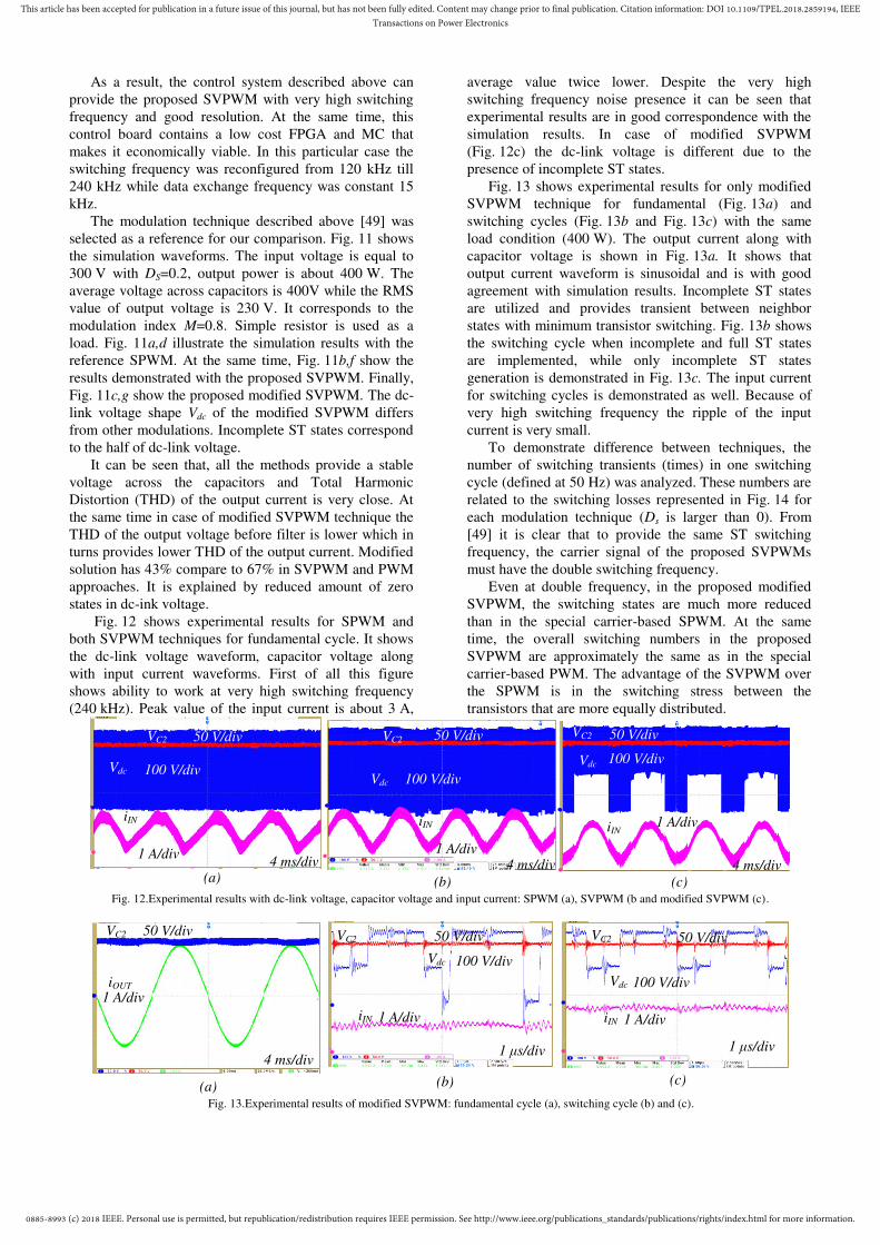
As a result, the control system described above can
provide the proposed SVPWM with very high switching
frequency and good resolution. At the same time, this
control board contains a low cost FPGA and MC that
makes it economically viable. In this particular case the
switching frequency was reconfigured from 120 kHz till
240 kHz while data exchange frequency was constant 15
kHz.
The modulation technique described above [49] was
selected as a reference for our comparison. Fig. 11 shows
the simulation waveforms. The input voltage is equal to
300 V with DS=0.2, output power is about 400 W. The
average voltage across capacitors is 400V while the RMS
value of output voltage is 230 V. It corresponds to the
modulation index M=0.8. Simple resistor is used as a
load. Fig. 11a,d illustrate the simulation results with the
reference SPWM. At the same time, Fig. 11b,f show the
results demonstrated with the proposed SVPWM. Finally,
Fig. 11c,g show the proposed modified SVPWM. The dc-
link voltage shape Vdc of the modified SVPWM differs
from other modulations. Incomplete ST states correspond
to the half of dc-link voltage.
It can be seen that, all the methods provide a stable
voltage across the capacitors and Total Harmonic
Distortion (THD) of the output current is very close. At
the same time in case of modified SVPWM technique the
THD of the output voltage before filter is lower which in
turns provides lower THD of the output current. Modified
solution has 43% compare to 67% in SVPWM and PWM
approaches. It is explained by reduced amount of zero
states in dc-ink voltage.
Fig. 12 shows experimental results for SPWM and
both SVPWM techniques for fundamental cycle. It shows
the dc-link voltage waveform, capacitor voltage along
with input current waveforms. First of all this figure
shows ability to work at very high switching frequency
(240 kHz). Peak value of the input current is about 3 A,
average value twice lower. Despite the very high
switching frequency noise presence it can be seen that
experimental results are in good correspondence with the
simulation results. In case of modified SVPWM
(Fig. 12c) the dc-link voltage is different due to the
presence of incomplete ST states.
Fig. 13 shows experimental results for only modified
SVPWM technique for fundamental (Fig. 13a) and
switching cycles (Fig. 13b and Fig. 13c) with the same
load condition (400 W). The output current along with
capacitor voltage is shown in Fig. 13a. It shows that
output current waveform is sinusoidal and is with good
agreement with simulation results. Incomplete ST states
are utilized and provides transient between neighbor
states with minimum transistor switching. Fig. 13b shows
the switching cycle when incomplete and full ST states
are implemented, while only incomplete ST states
generation is demonstrated in Fig. 13c. The input current
for switching cycles is demonstrated as well. Because of
very high switching frequency the ripple of the input
current is very small.
To demonstrate difference between techniques, the
number of switching transients (times) in one switching
cycle (defined at 50 Hz) was analyzed. These numbers are
related to the switching losses represented in Fig. 14 for
each modulation technique (Ds is larger than 0). From
[49] it is clear that to provide the same ST switching
frequency, the carrier signal of the proposed SVPWMs
must have the double switching frequency.
Even at double frequency, in the proposed modified
SVPWM, the switching states are much more reduced
than in the special carrier-based SPWM. At the same
time, the overall switching numbers in the proposed
SVPWM are approximately the same as in the special
carrier-based PWM. The advantage of the SVPWM over
the SPWM is in the switching stress between the
transistors that are more equally distributed.
iIN
VC2
Vdc
(a) (b) (c)
iIN
VC2
Vdc
50 V/div
1 A/div
100 V/div100 V/div
1 A/div
50 V/div50 V/divVC2
Vdc 100 V/div
iIN
1 A/div4 ms/div 4 ms/div 4 ms/div
Fig. 12.Experimental results with dc-link voltage, capacitor voltage and input current: SPWM (a), SVPWM (b and modified SVPWM (c).
Vdc
VC2VC2
Vdc
(b) (c)(a)
50 V/div
100 V/div
VC2 50 V/div 50 V/div
100 V/div
iOUT
1 A/div
4 ms/div1 μs/div
iIN 1 A/diviIN 1 A/div
1 μs/div
Fig. 13.Experimental results of modified SVPWM: fundamental cycle (a), switching cycle (b) and (c).

0885-8993 (c) 2018 IEEE. Personal use is permitted, but republication/redistribution requires IEEE permission. See http://www.ieee.org/publications_standards/publications/rights/index.html for more information.
This article has been accepted for publication in a future issue of this journal, but has not been fully edited. Content may change prior to final publication. Citation information: DOI 10.1109/TPEL.2018.2859194, IEEETransactions on Power Electronics
Fig. 14. Number of switching transients in one switching cycle. SPWM
modulation technique versus the proposed SVPWM techniques.
In conclusion, it can be predicted that the modified
SVPWM will have lower switching losses. In order to verify
this prediction, several tests with different switching
frequencies and level of power are performed. Fig. 15a shows
the efficiency dependence versus the switching frequency
while Fig. 15b shows the efficiency dependence versus the
output power with the same input voltage (300 V) and constant
ST duty cycle Ds=0.2.
(a)
(b)
Fig. 15.Experimental efficiency versus switching frequency for the different
SVPWM techniques for a single-phase IS inverter (a) and efficiency versus
output power with switching frequency 240 kHz (b).
It can be seen that the efficiency in the case of the SPWM
is significantly reduced by increasing the switching frequency.
A similar effect can be observed for the SVPWM and the
modified SVPWM. At the same time, it can be seen that the
level of incline is different. It means that the level of switching
losses in the case of both SVPWMs is lower, in particular in
the case of the modified solution. Also, it is evident that in the
modified SVPWM, conduction losses are higher. As a result,
the overall efficiency is lower at relatively low switching
frequency, and significantly better at high switching frequency.
Similar effect can be observed with power increasing. There is
some optimal point with the best efficiency, further power
increasing will lead to efficiency decreasing.
VI. CONCLUSIONS
This paper has presented novel SVPWM strategies for the
single-phase 3L buck-boost full-bridge NPC inverter coupled
with IS network. The proposed approach has a minimum
number of switching and, as a result, the improved
performance is demonstrated in terms of switching losses
reduction. The output voltage quality is not worse compared
with the traditional PWM strategies. Finally, the switching
losses are equally distributed among transistors. Also, the
proposed solutions have balanced utilization of all capacitors
of the IS network which remains voltage across capacitors
stable.
It should be noticed, that as any SVM technique, more
complex calculation compare to the PWM is required. The
main drawback of the proposed technique consists in the
increased conduction losses due to the utilizing only single leg
of the full-bridge NPC converter during ST generation. It
belongs mostly to the MOSFET transistors, where losses are
proportional to the drain-source resistance. Because of that,
such approach can be recommended for inverters realized by
MOSFET transistor with very high switching frequency, where
switching losses dominates over conduction losses. Another
application can be based on IGBT transistors, where switching
losses decreasing will allow increasing switching frequency.
Theoretical claims are verified by means of simulation and
experimental study.
ACKNOWLEDGMENT
This research work was finance in part by the Estonian
Centre of Excellence in Zero Energy and Resource Efficient
Smart Buildings and Districts, ZEBE, grant 2014-
2020.4.01.15- 0016 funded by the European Regional
Development Fund and in part by the Estonian Research
Council under Grants PUT1443 and PSG142. Ukrainian
partner research work was supported by the Ukrainian
Ministry of Education and Science under Grant
№0116U006960.
VII. REFERENCES
[1] Representing the global wind energy industry. (2016). [ebook] Global
Wind Energy Council. Available at: http://www.gwec.net/wp-
content/uploads/vip/GWEC-PRstats-2015_LR.pdf [Accessed 10 Apr.
2016].
[2] www.vestas.com, V. (2016). Vestas | Turbines. [online] Vestas.com.
Available at: https://www.vestas.com/en/products/turbines# [Accessed
10 Apr. 2016].
[3] G. K. Dey, K.T. Ahmmed, “Multi-junction solar cells and microwave
power transmission technologies for solar power satellite” In Proc. Informatics, Electronics & Vision (ICIEV), 2014 International Conference on., pp. 1-6, 2014.
[4] G. F. X Strobl, L. Ebel, D. Fuhrmann, W. Guter, R. Kern, V. Khorenko,
M. Meusel, “Development of lightweight space solar cells with 30%
efficiency at end-of-life” In Proc. Photovoltaic Specialist Conference (PVSC), pp. 3595-3600, 2014.

0885-8993 (c) 2018 IEEE. Personal use is permitted, but republication/redistribution requires IEEE permission. See http://www.ieee.org/publications_standards/publications/rights/index.html for more information.
This article has been accepted for publication in a future issue of this journal, but has not been fully edited. Content may change prior to final publication. Citation information: DOI 10.1109/TPEL.2018.2859194, IEEETransactions on Power Electronics
[5] F.Z. Peng, “Z-Source Inverter,” IEEE Trans. Ind. Applicat., vol. 39, no.
2, pp. 504-510, Mar./Apr. 2003.
[6] A. Chub, O. Husev, J. Zakis and J. Rabkowski, “Switched-capacitor
current-fed quasi-Z-source inverter”, In Proc. 14th Biennial Baltic Electronic Conference (BEC), pp. 229-232, Tallinn, 2014.
[7] Y.P. Siwakoti, F. Peng, F. Blaabjerg, P.C. Loh, G.E. Town, "Impedance
Source Networks for Electric Power Conversion Part-I: A Topological
Review," IEEE Trans. Power Electron., vol.30, no. 2, pp. 699-716, Feb.
2015.
[8] O. Husev, L. Liivik, F. Blaabjerg, A. Chub, D. Vinnikov, I. Roasto.
“Galvanically Isolated Quasi-Z-Source DC-DC Converter with a Novel
ZVS and ZCS Technique”, IEEE Trans. Ind. Electron., vol 62, no 12,
pp. 7547-7556, 2015.
[9] A. Chub, D. Vinnikov, F. Blaabjerg, F.Z. Peng “A Review of
Galvanically Isolated Impedance-Source DC–DC Converters” IEEE Trans. Power Electron., vol. 31, no. 4, pp. 2808 - 2828, April 2016.
[10] Y.P. Siwakoti, F. Peng, F. Blaabjerg, P. Loh, G.E. Town, "Impedance
Source Networks for Electric Power Conversion Part-II: Review of
Control Method and Modulation Techniques," IEEE Trans. Power Electron., vol.30, no. 4, pp. 1887 - 1906, April 2015.
[11] T. Shults, O. Husev O. J. Zakis, “Overview of impedance source
networks for voltage source inverters”, In Proc. Micro/Nanotechnologies and Electron Devices (EDM), 2015 16th International Conference of Young Specialists on., pp. 514-520, 2015.
[12] L. G Franquelo, J. Rodriguez, J. I. Leon, S. Kouro, R. Portillo, M. A. M.
Prats, “The age of multilevel converters arrives”, IEEE Ind. Electron. Mag., vol. 2, no. 2, pp. 28–39, Jun. 2008.
[13] J. Rodríguez, J. S. Lai, F. Z. Peng, “Multilevel Inverters: A Survey of
topologies, controls, and applications”, IEEE Trans. Ind. Electron., vol.
49, no. 4, pp.724-738, August 2002.
[14] S. Tenner, S.Tenner, W. Hofmann, "A comparison of Z-Source three-
level NPC inverter versus Z-Source two-level inverter." In Emobility-Electrical Power Train, pp. 1-7. IEEE, 2010.
[15] O. Husev, C. Roncero-Clemente, E. Romero-Cadaval, D. Vinnikov, S.
Stepenko, “Single phase three-level neutral-point-clamped quasi-Z-
source inverter ”, IET Power Electron., vol. 8, no. 1, pp. 1-10, 2015.
[16] Y. Liu, B. Ge, H. Abu-Rub, D. Sun, "Comprehensive modeling of single-
phase quasi-Z-source photovoltaic inverter to investigate low-frequency
voltage and current ripple," IEEE Trans. Ind. Electron., vol. 67, pp.
4194-4202, 2015.
[17] S. Kouro, M. Malinowski, K Gopakumar, J. Pou, L. G Franquelo, B. Wu,
J. Rodriguez, M. A. Perez, J. I. Leon, "Recent advances and industrial
applications of multilevel converters," IEEE Trans. Ind. Electron.,
vol.57, no.8, pp.2553-2580, Aug. 2010.
[18] M. Dybko, S. Brovanov, S. Kharitonov, “Mathematical simulation
technique for power systems based on diode-clamped multilevel VSC”,
in Proc. of EuroCon 2013, Zagreb, pp. 941–947, 1–4 July 2013.
[19] D. Panfilov, O. Husev, F. Blaabjerg, J. Zakis, K. Khandakji,
“Comparison of three-phase three-level voltage source inverter with
intermediate dc–dc boost converter and quasi-Z-source inverter”, IET Power Electron., vol. 9, no. 6, pp. 1238-1248, 2016.
[20] R. Burkart, J. W. Kolar, G. Griepentrog „Comprehensive comparative
evaluation of single- and multi-stage three-phase power converters for
photovoltaic applications,” in Proc. of Intelec, 2012, pp. 1-8.
[21] O. Husev, F. Blaabjerg, C. Roncero-Clemente, E. Romero-Cadaval, D.
Vinnikov, Y. P. Siwakoti, R. Strzelecki, “Comparison of Impedance-
Source Networks for Two and Multilevel Buck-Boost Inverter
Applications”, IEEE Trans. Power Electron., vol. 31, no. 11, pp. 7564-
7579, Nov. 2016.
[22] F. Z. Peng, M. Shen, and Z. Qian, "Maximum boost control of the Z-
source inverter". IEEE Trans. Power Electron, Vol. 20, No. 4, pp. 833–838, July 2005.
[23] P. C. Loh, F. Gao, F. Blaabjerg, S. Yun, C. Feng, K. N. J. Soon "Pulse
width-Modulated Z-Source Neutral-Point-Clamped Inverter". IEEE Trans. Ind. Applicat, vol.43, no.5, pp.1295-1308, Sept.-Oct. 2007.
[24] P. C. Loh, F. Blaabjerg and C. P. Wong, "Comparative Evaluation of
Pulse-width Modulation Strategies for Z-Source Neutral-Point-Clamped
Inverter", IEEE Trans. Power Electron., vol. 22, no. 3, pp. 1005-1013,
May 2007.
[25] P. C. Loh, F. Gao, F. Blaabjerg, "Topological and Modulation Design of
Three-Level Z-Source Inverters". IEEE Trans. Power Electron, vol. 23,
no. 5, pp. 2268-2277, Sep. 2008.
[26] J. H. G. Muniz, E.R.C. da Silva and E.C. dos Santos Jr., “A Hybrid PWM
Strategy for Z-Source Neutral-Point-Clamped inverter”, in Proc. IEEE
APEC 2011, pp. 450-456, Mar. 2011.
[27] O. Husev, C. Roncero-Clemente, E. Romero-Cadaval, D. Vinnikov, T.
Jalakas, “Three-level three-phase quasi-Z-source neutral-point-clamped
inverter with novel modulation technique for photovoltaic application”,
Electric Power Systems Research, vol. 130, no. 1, pp. 10–21, 2016.
[28] Y. Liu, B. Ge, H. Abu-Rub, F. Z. Peng, "Phase-shifted pulse-width-
amplitude modulation for quasi-Z-source cascade multilevel inverter-
based photovoltaic power system," IET Power Electron., vol.7, no. 6,
pp.1444-1456, 2014.
[29] P. C. Loh, F. Gao, F. Blaabjerg and S. W. Lim, "Operational Analysis
and Modulation Control of Three-Level Z-Source Inverters With
Enhanced Output Waveform Quality," IEEE Trans. Power Electron.,
vol. 24, no. 7, pp. 1767-1775, July 2009.
[30] F. Gao, P. C. Loh, F. Blaabjerg and R. Teodorescu, “Modulation
Schemes of Multi-Phase Three Level Z-Source Inverters,” in Proc. of PESC 2007, pp. 1905-1911, June 2007.
[31] O. Ellabban, J. Van Mierlo, P. Lataire, "Comparison between different
PWM control methods for different Z-source inverter topologies", in Proc. of 13th IEE European Conference on Power Electronics and Applications, EPE '09, pp.1-11, 8-10 Sept. 2009.
[32] Y. Liu, B. Ge, F. J. T. E. Ferreiera, A. T. de Almeida and H. Abu-Rub,
“Modelling and SVM Control of quasi Z-Source Inverter”. In Proc. 11th International Conference in Electr. Power Quality Utilization, pp.1-7,
Oct. 2011.
[33] U. S. Ali and V. Kamaraj, "A novel space vector PWM for Z-source
inverter". In Proc. 1st International Conference on Electrical Energy Systems (ICEES), Newport Beach, CA, pp. 82-85. 2011.
[34] Y. Liu, B. Ge, H. Abu-Rub and F. Z. Peng, "Overview of Space Vector
Modulations for Three-Phase Z-Source/Quasi-Z-Source Inverters", IEEE Trans. Power Electron., vol. 29, no. 4, pp. 2098-2108, April 2014.
[35] Y. Liu, B. Ge and H. Abu-Rub, "Theoretical and experimental evaluation
of four space vector modulations applied to quasi-Z-source inverters".
IET Power Electron, vol. 6, no. 7, pp. 1257-1269, August 2013.
[36] Y. P. Siwakoti and G. E. Town, "Three-phase transformerless grid
connected Quasi Z-Source Inverter for solar photovoltaic systems with
minimal leakage current", In Proc. 3rd IEEE International Symposium on Power Electronics for Distributed Generation Systems (PEDG), pp.
368-373. Aalborg, 2012.
[37] F. Bradaschia, M. C. Cavalcanti, P. E. P. Ferraz, F. A. S. Neves, E. C.
dos Santos and J. H. G. M. da Silva, "Modulation for Three-Phase
Transformerless Z-Source Inverter to Reduce Leakage Currents in
Photovoltaic Systems", IEEE Trans. Ind. Electron., vol. 58, no. 12, pp.
5385-5395, Dec. 2011.
[38] P. Majtczak, J. Rabkowski, “Symmetrical Switching Patterns and an
Adaptive Modulator for Three-Phase Quasi-Z-Source Inverters”, 2017
IEEE 26th International Symposium on Industrial Electronics (ISIE), pp.
1676 – 1681.
[39] Y. P. Siwakoti and G. E. Town, "Common-mode voltage reduction
techniques of three-phase Quasi Z-Source Inverter for AC drives", In Proc. Twenty-Eighth Annual IEEE Applied Power Electronics Conference and Exposition (APEC), pp. 2247-2252. Long Beach, CA,
2013.
[40] F.B. Effah, P. Wheeler, J. Clare, A. Watson, "Space-Vector-Modulated
Three-Level Inverters With a Single Z-Source Network". IEEE Trans. Power Electron., vol.28, no.6, pp.2806-2815, June 2013.
[41] Y. Liu, G. Baoming, H. Abu-Rub, F. Z. Peng, “A Modular Multilevel
Space Vector Modulation for Photovoltaic Quasi-Z-Source Cascaded
Multilevel Inverter,”, in Proc. of IEEE APEC 2013, pp. 714-18, Mar.
2013.
[42] X. You, S. Liu, H. Abu-Rub; B. Ge, X. Jiang; F. Z. Peng, “A new space
vector modulation strategy to reduce common-mode voltage for quasi-Z-
source indirect matrix converter”, in Proc. of Energy Conversion
Congress and Exposition (ECCE), 2014 IEEE. – IEEE, 2014. 1064-
1069.
[43] A. A. Abduallah, A. Iqbal, L. Ben-Brahim, “Space vector pulse width
modulation techniques for a five-phase impedance source and quasi
impedance source inverters”, in Proc. IEEE International Conference on Industrial Technology (ICIT), pp. 1173-1178, 2015.
[44] Z. Zhang, Y.X. Xie, W.P. Huang, J.Y. Le, and L. Chen, “A new SVPWM
method for single-phase three-level NPC inverter and the control

0885-8993 (c) 2018 IEEE. Personal use is permitted, but republication/redistribution requires IEEE permission. See http://www.ieee.org/publications_standards/publications/rights/index.html for more information.
This article has been accepted for publication in a future issue of this journal, but has not been fully edited. Content may change prior to final publication. Citation information: DOI 10.1109/TPEL.2018.2859194, IEEETransactions on Power Electronics
method of neutral point voltage balance,” in Proc. of International Conference on Electrical Machines and Systems, 2009. ICEMS 2009,
pp. 1-4. IEEE, 2009.
[45] R.T Shreiner. “Vektornye sistemy shirotno-impul'snoi modulyatsii,”
Matematicheskoe modelirovanie elektroprivodov peremennogo toka s
poluprovodnikovymi preobrazovatelyami chastoty, Ekaterinburg,
Russia: UrO RAN, 2000, pp. 405-420 (in Russian).
[46] S.V. Brovanov, S.A. Kharitonov, M.A. Dybko, E.V. Grishanov, “A new
approach for current calculation in a single-phase three-level NPC
converter with space vector PWM,” in Proc. of IEEE Region 8 International Conference on Computational Technologies in Electrical and Electronics Engineering, SIBIRCON 2010, pp. 639–644.
[47] J. Guzman-Guemez, D.S. Laila, S.M. Sharkh, "State-space approach for
modelling and control of a single-phase three-level NPC inverter with
SVPWM," In Proc. of Power and Energy Society General Meeting (PESGM), 2016, pp. 1-5. IEEE, 2016.
[48] T. Shults, O. Husev, F. Blaabjerg, “Design of Three-Phase Three-Level
CIC T-Source Inverter with Maximum Boost Control in Proc. of IEEE-IECON, 2015, pp. 2408-2413.
[49] C. Roncero-Clemente, O. Husev, T. Jalakas, E. Romero-Cadaval,
J. Zakis, V. Mmiñambres-Marcos, “PWM for Single Phase 3L Z/qZ
Source Inverter with Balanced Power Losses”. Elektronika ir Elektrotechnika, vol. 20, no. 6, pp. 71-76, 2014.
Tatiana E. Shults received the B.Sc., M.Sc.
degrees in industrial electronics and PhD
professional skill “Researcher. Lecture-researcher”
from Novosibirsk State Technical University,
Novosibirsk, Russia in 2012, 2014 and 2018
respectively.
She is engineer of 2nd category of the Power
Electronics Institute of Novosibirsk State
Technical University. In 2015 she had semiannual
internship in the Power Electronics Group,
Department of Electrical Power Engineering and
Mechatronics, Tallinn University of Technology (Estonia).
Her research interests are in power electronics systems: application of
photovoltaic panels as power sources in generation systems; dc-ac multilevel
converters; design of power converters and control systems, impedance source
inverters. She has over 13 publications
Oleksandr Husev (S’10–M’12) received the
B.Sc. and M.Sc. degrees in industrial electronics
from Chernihiv State Technological University,
Chernihiv, Ukraine, in 2007 and 2008 respectively.
He defended PhD thesis in the Institute of
Electrodynamics of the National Academy of
Science of Ukraine in 2012.
He is senior researcher of the Department of
Electrical Power Engineering and Mechatronics,
Tallinn University of Technology and associate
professor of the Department of Biomedical
Radioelectronics Apparatus and Systems, Chernihiv National University of
Technology. He has over 60 publications and is the holder of several patents.
His research interests are in Power Electronics systems. Design of novel
topologies, control systems based on a wide range of algorithms, including
modeling, design, and simulation. Applied design of power converters and
control systems and application, stability investigation.
Frede Blaabjerg (S’86–M’88–SM’97–F’03)
was with ABB-Scandia, Randers, Denmark, from
1987 to 1988. From 1988 to 1992, he got the
PhD degree in Electrical Engineering at Aalborg
University in 1995. He became an Assistant
Professor in 1992, an Associate Professor in
1996, and a Full Professor of power electronics
and drives in 1998. From 2017 he became a
Villum Investigator. He is honoris causa at
University Politehnica Timisoara (UPT),
Romania and Tallinn Technical University
(TTU) in Estonia. His current research interests
include power electronics and its applications such as in wind turbines, PV
systems, reliability, harmonics and adjustable speed drives. He has published
more than 500 journal papers in the fields of power electronics and its
applications. He is the co-author of two monographs and editor of 7 books in
power electronics and its applications.
He has received 26 IEEE Prize Paper Awards, the IEEE PELS
Distinguished Service Award in 2009, the EPE-PEMC Council Award in
2010, the IEEE William E. Newell Power Electronics Award 2014 and the
Villum Kann Rasmussen Research Award 2014. He was the Editor-in-Chief
of the IEEE TRANSACTIONS ON POWER
ELECTRONICS from 2006 to 2012. He has been
Distinguished Lecturer for the IEEE Power
Electronics Society from 2005 to 2007 and for the
IEEE Industry Applications Society from 2010 to
2011 as well as 2017 to 2018. In 2018 he is
President Elect of IEEE Power Electronics Society.
He is nominated in 2014, 2015, 2016 and 2017
by Thomson Reuters to be between the most 250
cited researchers in Engineering in the world.
Carlos Roncero-Clemente (S’11–M’16) was born in Badajoz, Spain, in
1984. He received the B.Sc. degree in electrical engineering with honors, the
M.Sc. degree in industrial engineering with honors, the M.Sc. degree in
engineering and architecture research, and the Ph.D. degree in industrial
engineering from the University of Extremadura, Badajoz, Spain, in 2006,
2008, 2011, and 2016, respectively. During his Ph.D. research, he was a
Visiting Student at Tallinn University of Technology, Tallinn, Estonia, and at
Aalborg University, Aalborg, Denmark. He is currently a Postdoctoral
Researcher with Nova University of Lisbon, Lisbon, Portugal and member of
PE&ES Research Group at University of Extremadura. His research interests
include power electronic interfaces, modulation techniques, modeling and
simulations, renewable energy sources, and smart grids.
Enrique Romero-Cadaval (S’02–M’05–SM’10)
received the M.Sc. degree in industrial electronic
engineering from the Escuela Técnica Superior de
Ingeniería Industrial (ICAI), Universidad Pontificia
de Comillas, Madrid, Spain, in 1992, and the Ph.D.
degree from the Universidad de Extremadura,
Badajoz, Spain, in 2004. In 1995, he joined the
University of Extremadura where he teaches power
electronics and researches within the Power
Electrical and Electronic Systems (PE&ES) R&D Group in the School of
Industrial Engineering. His has participated in several projects dealing with
power electronics applied to power systems, power quality, active power
filters, electric vehicles, smart grids, and renewable energy resources. He is a
Senior Member of the IEEE.
Dmitri Vinnikov (M'07–SM'11) received the
Dipl.Eng., M.Sc., and Dr.Sc.techn. degrees in
electrical engineering from Tallinn University of
Technology, Tallinn, Estonia, in 1999, 2001, and
2005, respectively.
He is currently the Head of the Power Electronics
Group, Department of Electrical Power Engineering
and Mechatronics, Tallinn University of Technology
(Estonia) and a Guest Researcher at the Institute of
Industrial Electronics and Electrical Engineering, Riga Technical University
(Latvia). He is the Head of R&D and co-founder of Ubik Solutions LLC -
Estonian start-up company dedicated to innovative & smart power electronics
for renewable energy systems. Moreover, he is one of the founders and
leading researchers of ZEBE – Estonian Centre of Excellence for zero energy
and resource efficient smart buildings and districts. He has authored or
coauthored two books, five monographs and one book chapter as well as more
than 200 published papers on power converter design and development and is
the holder of numerous patents and utility models in this field. His research
interests include applied design of power electronic converters and control
systems, renewable energy conversion systems (photovoltaic and wind),
impedance-source power converters, and implementation of wide bandgap
power semiconductors.


