Embed Size (px)
Citation preview
R07DS1511EJ0100 Rev.1.00 Page 1 of 7 Jun.02.2022
Datasheet
NP50P06SDG -60V – -50A – P-channel Power MOS FET
Application : Automotive
Description
This product is P-channel MOS Field Effect Transistor designed for high current switching applications.
Features
Super low on-state resistance : RDS(on) = 16.5 m Max. ( VGS = -10 V, ID = -25 A ) RDS(on) = 23.0 m Max. ( VGS = -4.5 V, ID = -25 A )
Low input capacitance : Ciss = 5000 pF Typ. Designed for automotive application and AEC-Q101 qualified. Pb-free (This product does not contain Pb in the external electrode)
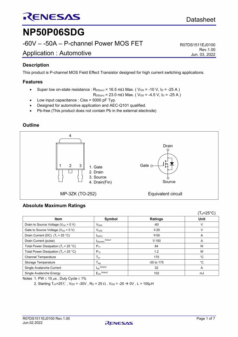
Outline
Absolute Maximum Ratings
(Ta=25°C)
Item Symbol Ratings Unit
Drain to Source Voltage (VGS = 0 V) VDSS -60 V
Gate to Source Voltage (VDS = 0 V) VGSS 20 V
Drain Current (DC) (Tc = 25 °C) ID(DC) 50 A
Drain Current (pulse) ID(pulse) Notes1 150 A
Total Power Dissipation (Tc = 25 °C) PT1 84 W
Total Power Dissipation (Ta = 25 °C) PT2 1.2 W
Channel Temperature Tch 175 °C
Storage Temperature Tstg -55 to 175 °C
Single Avalanche Current IAS Notes2 32 A
Single Avalanche Energy EAS Notes2 102 mJ
Notes 1. PW 10 s , Duty Cycle 1%
2. Starting Tch=25℃ , VDD = -30V , RG = 25 , VGS = -20 0V , L = 100H
Gate
Drain
Source
1. Gate2. Drain3. Source4. Drain(Fin)
Equivalent circuitMP-3ZK (TO-252)
4
1 2 3
R07DS1511EJ0100Rev.1.00
Jun. 03, 2022
NP50P06SDG
R07DS1511EJ0100 Rev.1.00 Page 2 of 7 Jun.02.2022
Thermal Resistance
Channel to Case Thermal Resistance Rth(ch-c) Notes3 1.78 °C/W
Channel to Ambient Thermal Resistance Rth(ch-a) Notes3 125 °C/W
Electrical Characteristics
(Ta=25°C)
Item Symbol Min Typ Max Unit Test Conditions
Zero Gate Voltage Drain Current IDSS — — -10 A VDS = -60 V, VGS = 0 V
Gate Leakage Current IGSS — — 100 nA VGS = 20 V, VDS = 0 V
Gate to Source Threshold Voltage VGS(th) -1.0 -1.6 -2.5 V VDS = VGS, ID = -250μA
Forward Transfer Admittance | yfs | Notes4 15 33 — S VDS = -10 V, ID = -25 A
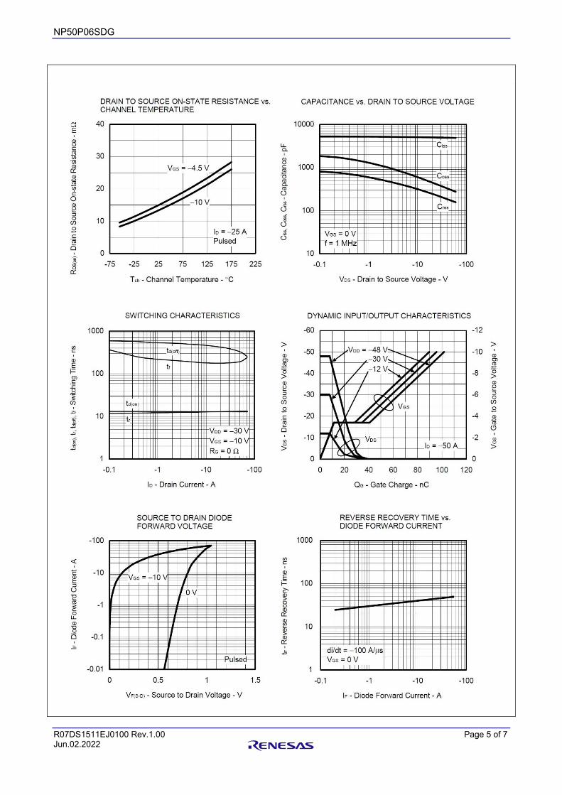
Drain to Source On-state Resistance RDS(on)1 Notes4 — 13.2 16.5 m VGS = -10 V, ID = -25 A
RDS(on)2 Notes4 — 14.9 23.0 m VGS = -4.5 V, ID = -25 A
Input Capacitance Ciss — 5000 — pF VDS = -10 V
VGS = 0 V
f = 1 MHz
Output Capacitance Coss — 600 — pF
Reverse Transfer Capacitance Crss — 300 — pF
Turn-on Delay Time td(on) — 13 — ns VDD = -30 V
ID = -25 A
VGS = -10 V
RG = 0
Rise Time tr — 13 — ns
Turn-off Delay Time td(off) — 405 — ns
Fall Time tf — 180 — ns
Total Gate Charge Qg — 100 — nC VDD = -48 V
VGS = -10 V
ID = -50 A
Gate to Source Charge Qgs — 11 — nC
Gate to Drain Charge Qgd — 30 — nC
Body Diode Forward Voltage VF(S-D) Notes4 — 0.97 1.5 V IF = -50 A, VGS = 0 V
Reverse Recovery Time trr — 50 — ns IF = -50 A, VGS = 0 V
di/dt = -100 A/s Reverse Recovery Charge Qrr — 72 — nC
Notes 3. Designed target value on Renesas measurement condition. Not subject to production test.
4. Pulse test.
NP50P06SDG
R07DS1511EJ0100 Rev.1.00 Page 3 of 7 Jun.02.2022
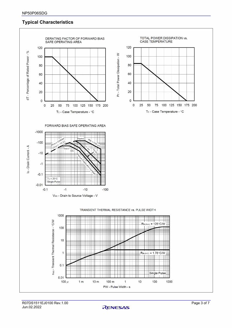
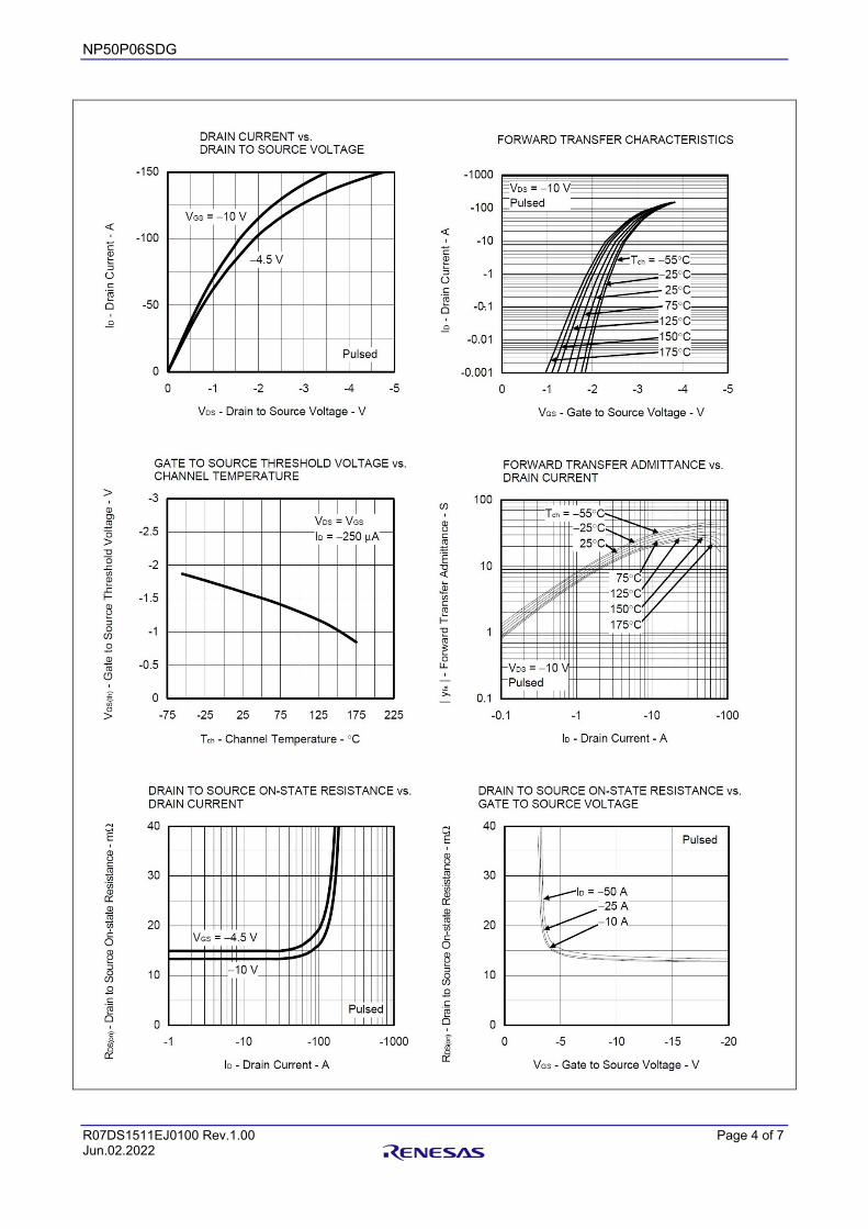
Typical Characteristics
NP50P06SDG
R07DS1511EJ0100 Rev.1.00 Page 4 of 7 Jun.02.2022
NP50P06SDG
R07DS1511EJ0100 Rev.1.00 Page 5 of 7 Jun.02.2022
NP50P06SDG
R07DS1511EJ0100 Rev.1.00 Page 6 of 7 Jun.02.2022
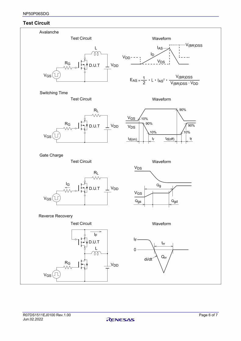
Test Circuit
trtd(on)
90%
90%
10%
td(off)
90%
10%
tf
Waveform
VDS
VGS
VGS
VDD
RL
RG
10%
D.U.T
Test Circuit
Switching Time
Waveform
VDS
VDD
VGS
VDD
L
RG D.U.T
Test Circuit
Avalanche
V(BR)DSS
ID
IAS
EAS =12・L・IAS
2・V(BR)DSS
V(BR)DSS -VDD
Qg
Waveform
VDS
VGS
VGS
VDD
RL
IGD.U.T
Test Circuit
Gate Charge
QgdQgs
Waveform
VGS
VDD
L
RG
Test Circuit
Reverce Recovery
D.U.T
IFIF
0trr
Qrrdi/dt
NP50P06SDG
R07DS1511EJ0100 Rev.1.00 Page 7 of 7 Jun.02.2022
Package Dimensions
Ordering Information
Part No. Quantity Shipping container
NP50P06SDG-E1-AY 2500pcs/reel Taping
Remark Strong electric field, when exposed to this device, can cause destruction of the gate oxide and ultimately degrade the device operation. Steps must be taken to stop generation of static electricity as much as possible, and quickly dissipate it once, when it has occurred.
6.5 ± 0.2
5.1
4.3 Min.4
.0 M
in.
4
1 2 3Pin No.
0.8
10
.4 M
ax.
(9.
8)
6.1
± 0
.21
.0
1.14 Max.
2.3 2.3
0.76 ± 0.12
2.3 ± 0.1
0.5 ± 0.1
0.5
1 M
in.
0 to 0.25
Unit : mm
Mass : 0.3g
0.5 ± 0.1
1.0
© 2021 Renesas Electronics Corporation. All rights reserved.
Notice 1. Descriptions of circuits, software and other related information in this document are provided only to illustrate the operation of semiconductor products
and application examples. You are fully responsible for the incorporation or any other use of the circuits, software, and information in the design of your product or system. Renesas Electronics disclaims any and all liability for any losses and damages incurred by you or third parties arising from the use of these circuits, software, or information.
2. Renesas Electronics hereby expressly disclaims any warranties against and liability for infringement or any other claims involving patents, copyrights, or other intellectual property rights of third parties, by or arising from the use of Renesas Electronics products or technical information described in this document, including but not limited to, the product data, drawings, charts, programs, algorithms, and application examples.
3. No license, express, implied or otherwise, is granted hereby under any patents, copyrights or other intellectual property rights of Renesas Electronics or others.
4. You shall be responsible for determining what licenses are required from any third parties, and obtaining such licenses for the lawful import, export, manufacture, sales, utilization, distribution or other disposal of any products incorporating Renesas Electronics products, if required.
5. You shall not alter, modify, copy, or reverse engineer any Renesas Electronics product, whether in whole or in part. Renesas Electronics disclaims any and all liability for any losses or damages incurred by you or third parties arising from such alteration, modification, copying or reverse engineering.
6. Renesas Electronics products are classified according to the following two quality grades: “Standard” and “High Quality”. The intended applications for each Renesas Electronics product depends on the product’s quality grade, as indicated below. "Standard": Computers; office equipment; communications equipment; test and measurement equipment; audio and visual equipment; home
electronic appliances; machine tools; personal electronic equipment; industrial robots; etc. "High Quality": Transportation equipment (automobiles, trains, ships, etc.); traffic control (traffic lights); large-scale communication equipment; key
financial terminal systems; safety control equipment; etc. Unless expressly designated as a high reliability product or a product for harsh environments in a Renesas Electronics data sheet or other Renesas Electronics document, Renesas Electronics products are not intended or authorized for use in products or systems that may pose a direct threat to human life or bodily injury (artificial life support devices or systems; surgical implantations; etc.), or may cause serious property damage (space system; undersea repeaters; nuclear power control systems; aircraft control systems; key plant systems; military equipment; etc.). Renesas Electronics disclaims any and all liability for any damages or losses incurred by you or any third parties arising from the use of any Renesas Electronics product that is inconsistent with any Renesas Electronics data sheet, user’s manual or other Renesas Electronics document.
7. No semiconductor product is absolutely secure. Notwithstanding any security measures or features that may be implemented in Renesas Electronics hardware or software products, Renesas Electronics shall have absolutely no liability arising out of any vulnerability or security breach, including but not limited to any unauthorized access to or use of a Renesas Electronics product or a system that uses a Renesas Electronics product. RENESAS ELECTRONICS DOES NOT WARRANT OR GUARANTEE THAT RENESAS ELECTRONICS PRODUCTS, OR ANY SYSTEMS CREATED USING RENESAS ELECTRONICS PRODUCTS WILL BE INVULNERABLE OR FREE FROM CORRUPTION, ATTACK, VIRUSES, INTERFERENCE, HACKING, DATA LOSS OR THEFT, OR OTHER SECURITY INTRUSION (“Vulnerability Issues”). RENESAS ELECTRONICS DISCLAIMS ANY AND ALL RESPONSIBILITY OR LIABILITY ARISING FROM OR RELATED TO ANY VULNERABILITY ISSUES. FURTHERMORE, TO THE EXTENT PERMITTED BY APPLICABLE LAW, RENESAS ELECTRONICS DISCLAIMS ANY AND ALL WARRANTIES, EXPRESS OR IMPLIED, WITH RESPECT TO THIS DOCUMENT AND ANY RELATED OR ACCOMPANYING SOFTWARE OR HARDWARE, INCLUDING BUT NOT LIMITED TO THE IMPLIED WARRANTIES OF MERCHANTABILITY, OR FITNESS FOR A PARTICULAR PURPOSE.
8. When using Renesas Electronics products, refer to the latest product information (data sheets, user’s manuals, application notes, “General Notes for Handling and Using Semiconductor Devices” in the reliability handbook, etc.), and ensure that usage conditions are within the ranges specified by Renesas Electronics with respect to maximum ratings, operating power supply voltage range, heat dissipation characteristics, installation, etc. Renesas Electronics disclaims any and all liability for any malfunctions, failure or accident arising out of the use of Renesas Electronics products outside of such specified ranges.
9. Although Renesas Electronics endeavors to improve the quality and reliability of Renesas Electronics products, semiconductor products have specific characteristics, such as the occurrence of failure at a certain rate and malfunctions under certain use conditions. Unless designated as a high reliability product or a product for harsh environments in a Renesas Electronics data sheet or other Renesas Electronics document, Renesas Electronics products are not subject to radiation resistance design. You are responsible for implementing safety measures to guard against the possibility of bodily injury, injury or damage caused by fire, and/or danger to the public in the event of a failure or malfunction of Renesas Electronics products, such as safety design for hardware and software, including but not limited to redundancy, fire control and malfunction prevention, appropriate treatment for aging degradation or any other appropriate measures. Because the evaluation of microcomputer software alone is very difficult and impractical, you are responsible for evaluating the safety of the final products or systems manufactured by you.
10. Please contact a Renesas Electronics sales office for details as to environmental matters such as the environmental compatibility of each Renesas Electronics product. You are responsible for carefully and sufficiently investigating applicable laws and regulations that regulate the inclusion or use of controlled substances, including without limitation, the EU RoHS Directive, and using Renesas Electronics products in compliance with all these applicable laws and regulations. Renesas Electronics disclaims any and all liability for damages or losses occurring as a result of your noncompliance with applicable laws and regulations.
11. Renesas Electronics products and technologies shall not be used for or incorporated into any products or systems whose manufacture, use, or sale is prohibited under any applicable domestic or foreign laws or regulations. You shall comply with any applicable export control laws and regulations promulgated and administered by the governments of any countries asserting jurisdiction over the parties or transactions.
12. It is the responsibility of the buyer or distributor of Renesas Electronics products, or any other party who distributes, disposes of, or otherwise sells or transfers the product to a third party, to notify such third party in advance of the contents and conditions set forth in this document.
13. This document shall not be reprinted, reproduced or duplicated in any form, in whole or in part, without prior written consent of Renesas Electronics. 14. Please contact a Renesas Electronics sales office if you have any questions regarding the information contained in this document or Renesas
Electronics products.
(Note1) “Renesas Electronics” as used in this document means Renesas Electronics Corporation and also includes its directly or indirectly controlled subsidiaries.
(Note2) “Renesas Electronics product(s)” means any product developed or manufactured by or for Renesas Electronics.
(Rev.5.0-1 October 2020)
Corporate Headquarters Contact information TOYOSU FORESIA, 3-2-24 Toyosu,
Koto-ku, Tokyo 135-0061, Japan
www.renesas.com
For further information on a product, technology, the most up-to-date
version of a document, or your nearest sales office, please visit:
www.renesas.com/contact/.
Trademarks Renesas and the Renesas logo are trademarks of Renesas Electronics
Corporation. All trademarks and registered trademarks are the property
of their respective owners.


