Embed Size (px)
Citation preview
To our customers,
Old Company Name in Catalogs and Other Documents
On April 1st, 2010, NEC Electronics Corporation merged with Renesas Technology
Corporation, and Renesas Electronics Corporation took over all the business of both companies. Therefore, although the old company name remains in this document, it is a valid Renesas Electronics document. We appreciate your understanding.
Renesas Electronics website: http://www.renesas.com
April 1st, 2010 Renesas Electronics Corporation
Issued by: Renesas Electronics Corporation (http://www.renesas.com)
Send any inquiries to http://www.renesas.com/inquiry.

Notice 1. All information included in this document is current as of the date this document is issued. Such information, however, is
subject to change without any prior notice. Before purchasing or using any Renesas Electronics products listed herein, please confirm the latest product information with a Renesas Electronics sales office. Also, please pay regular and careful attention to additional and different information to be disclosed by Renesas Electronics such as that disclosed through our website.
2. Renesas Electronics does not assume any liability for infringement of patents, copyrights, or other intellectual property rights of third parties by or arising from the use of Renesas Electronics products or technical information described in this document. No license, express, implied or otherwise, is granted hereby under any patents, copyrights or other intellectual property rights of Renesas Electronics or others.
3. You should not alter, modify, copy, or otherwise misappropriate any Renesas Electronics product, whether in whole or in part. 4. Descriptions of circuits, software and other related information in this document are provided only to illustrate the operation of
semiconductor products and application examples. You are fully responsible for the incorporation of these circuits, software, and information in the design of your equipment. Renesas Electronics assumes no responsibility for any losses incurred by you or third parties arising from the use of these circuits, software, or information.
5. When exporting the products or technology described in this document, you should comply with the applicable export control laws and regulations and follow the procedures required by such laws and regulations. You should not use Renesas Electronics products or the technology described in this document for any purpose relating to military applications or use by the military, including but not limited to the development of weapons of mass destruction. Renesas Electronics products and technology may not be used for or incorporated into any products or systems whose manufacture, use, or sale is prohibited under any applicable domestic or foreign laws or regulations.
6. Renesas Electronics has used reasonable care in preparing the information included in this document, but Renesas Electronics does not warrant that such information is error free. Renesas Electronics assumes no liability whatsoever for any damages incurred by you resulting from errors in or omissions from the information included herein.
7. Renesas Electronics products are classified according to the following three quality grades: “Standard”, “High Quality”, and “Specific”. The recommended applications for each Renesas Electronics product depends on the product’s quality grade, as indicated below. You must check the quality grade of each Renesas Electronics product before using it in a particular application. You may not use any Renesas Electronics product for any application categorized as “Specific” without the prior written consent of Renesas Electronics. Further, you may not use any Renesas Electronics product for any application for which it is not intended without the prior written consent of Renesas Electronics. Renesas Electronics shall not be in any way liable for any damages or losses incurred by you or third parties arising from the use of any Renesas Electronics product for an application categorized as “Specific” or for which the product is not intended where you have failed to obtain the prior written consent of Renesas Electronics. The quality grade of each Renesas Electronics product is “Standard” unless otherwise expressly specified in a Renesas Electronics data sheets or data books, etc.
“Standard”: Computers; office equipment; communications equipment; test and measurement equipment; audio and visual equipment; home electronic appliances; machine tools; personal electronic equipment; and industrial robots.
“High Quality”: Transportation equipment (automobiles, trains, ships, etc.); traffic control systems; anti-disaster systems; anti-crime systems; safety equipment; and medical equipment not specifically designed for life support.
“Specific”: Aircraft; aerospace equipment; submersible repeaters; nuclear reactor control systems; medical equipment or systems for life support (e.g. artificial life support devices or systems), surgical implantations, or healthcare intervention (e.g. excision, etc.), and any other applications or purposes that pose a direct threat to human life.
8. You should use the Renesas Electronics products described in this document within the range specified by Renesas Electronics, especially with respect to the maximum rating, operating supply voltage range, movement power voltage range, heat radiation characteristics, installation and other product characteristics. Renesas Electronics shall have no liability for malfunctions or damages arising out of the use of Renesas Electronics products beyond such specified ranges.
9. Although Renesas Electronics endeavors to improve the quality and reliability of its products, semiconductor products have specific characteristics such as the occurrence of failure at a certain rate and malfunctions under certain use conditions. Further, Renesas Electronics products are not subject to radiation resistance design. Please be sure to implement safety measures to guard them against the possibility of physical injury, and injury or damage caused by fire in the event of the failure of a Renesas Electronics product, such as safety design for hardware and software including but not limited to redundancy, fire control and malfunction prevention, appropriate treatment for aging degradation or any other appropriate measures. Because the evaluation of microcomputer software alone is very difficult, please evaluate the safety of the final products or system manufactured by you.
10. Please contact a Renesas Electronics sales office for details as to environmental matters such as the environmental compatibility of each Renesas Electronics product. Please use Renesas Electronics products in compliance with all applicable laws and regulations that regulate the inclusion or use of controlled substances, including without limitation, the EU RoHS Directive. Renesas Electronics assumes no liability for damages or losses occurring as a result of your noncompliance with applicable laws and regulations.
11. This document may not be reproduced or duplicated, in any form, in whole or in part, without prior written consent of Renesas Electronics.
12. Please contact a Renesas Electronics sales office if you have any questions regarding the information contained in this document or Renesas Electronics products, or if you have any other inquiries.
(Note 1) “Renesas Electronics” as used in this document means Renesas Electronics Corporation and also includes its majority-owned subsidiaries.
(Note 2) “Renesas Electronics product(s)” means any product developed or manufactured by or for Renesas Electronics.
µPD7833416-/8-Bit Single Chip Microcontrollers
µPD78330µPD78334µPD78P334
Document No. U12687EJ7V0UM00 (7th Edition)(O.D. No. IEU-1315C)Date Published January 1998 N CP(K)
1991
User’s Manual
Printed in Japan©

2
[MEMO]
3
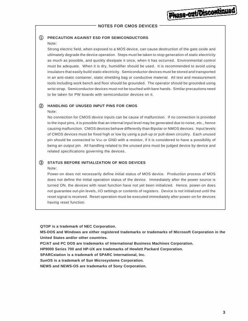
NOTES FOR CMOS DEVICES
1 PRECAUTION AGAINST ESD FOR SEMICONDUCTORS
Note:
Strong electric field, when exposed to a MOS device, can cause destruction of the gate oxide and
ultimately degrade the device operation. Steps must be taken to stop generation of static electricity
as much as possible, and quickly dissipate it once, when it has occurred. Environmental control
must be adequate. When it is dry, humidifier should be used. It is recommended to avoid using
insulators that easily build static electricity. Semiconductor devices must be stored and transported
in an anti-static container, static shielding bag or conductive material. All test and measurement
tools including work bench and floor should be grounded. The operator should be grounded using
wrist strap. Semiconductor devices must not be touched with bare hands. Similar precautions need
to be taken for PW boards with semiconductor devices on it.
2 HANDLING OF UNUSED INPUT PINS FOR CMOS
Note:
No connection for CMOS device inputs can be cause of malfunction. If no connection is provided
to the input pins, it is possible that an internal input level may be generated due to noise, etc., hence
causing malfunction. CMOS devices behave differently than Bipolar or NMOS devices. Input levels
of CMOS devices must be fixed high or low by using a pull-up or pull-down circuitry. Each unused
pin should be connected to VDD or GND with a resistor, if it is considered to have a possibility of
being an output pin. All handling related to the unused pins must be judged device by device and
related specifications governing the devices.
3 STATUS BEFORE INITIALIZATION OF MOS DEVICES
Note:
Power-on does not necessarily define initial status of MOS device. Production process of MOS
does not define the initial operation status of the device. Immediately after the power source is
turned ON, the devices with reset function have not yet been initialized. Hence, power-on does
not guarantee out-pin levels, I/O settings or contents of registers. Device is not initialized until the
reset signal is received. Reset operation must be executed immediately after power-on for devices
having reset function.
QTOP is a trademark of NEC Corporation.
MS-DOS and Windows are either registered trademarks or trademarks of Microsoft Corporation in the
United States and/or other countries.
PC/AT and PC DOS are trademarks of International Business Machines Corporation.
HP9000 Series 700 and HP-UX are trademarks of Hewlett Packard Corporation.
SPARCstation is a trademark of SPARC International, Inc.
SunOS is a trademark of Sun Microsystems Corporation.
NEWS and NEWS-OS are trademarks of Sony Corporation.
4
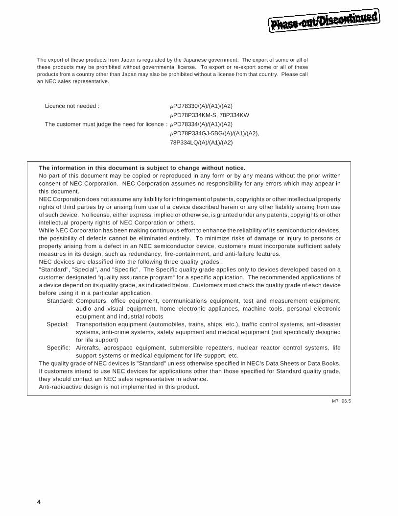
The export of these products from Japan is regulated by the Japanese government. The export of some or all ofthese products may be prohibited without governmental license. To export or re-export some or all of theseproducts from a country other than Japan may also be prohibited without a license from that country. Please callan NEC sales representative.
Licence not needed : µPD78330/(A)/(A1)/(A2)
µPD78P334KM-S, 78P334KW
The customer must judge the need for licence : µPD78334/(A)/(A1)/(A2)
µPD78P334GJ-5BG/(A)/(A1)/(A2),
78P334LQ/(A)/(A1)/(A2)
The information in this document is subject to change without notice.No part of this document may be copied or reproduced in any form or by any means without the prior writtenconsent of NEC Corporation. NEC Corporation assumes no responsibility for any errors which may appear inthis document.NEC Corporation does not assume any liability for infringement of patents, copyrights or other intellectual propertyrights of third parties by or arising from use of a device described herein or any other liability arising from useof such device. No license, either express, implied or otherwise, is granted under any patents, copyrights or otherintellectual property rights of NEC Corporation or others.While NEC Corporation has been making continuous effort to enhance the reliability of its semiconductor devices,the possibility of defects cannot be eliminated entirely. To minimize risks of damage or injury to persons orproperty arising from a defect in an NEC semiconductor device, customers must incorporate sufficient safetymeasures in its design, such as redundancy, fire-containment, and anti-failure features.NEC devices are classified into the following three quality grades:"Standard", "Special", and "Specific". The Specific quality grade applies only to devices developed based on acustomer designated “quality assurance program“ for a specific application. The recommended applications ofa device depend on its quality grade, as indicated below. Customers must check the quality grade of each devicebefore using it in a particular application.
Standard: Computers, office equipment, communications equipment, test and measurement equipment,audio and visual equipment, home electronic appliances, machine tools, personal electronicequipment and industrial robots
Special: Transportation equipment (automobiles, trains, ships, etc.), traffic control systems, anti-disastersystems, anti-crime systems, safety equipment and medical equipment (not specifically designedfor life support)
Specific: Aircrafts, aerospace equipment, submersible repeaters, nuclear reactor control systems, lifesupport systems or medical equipment for life support, etc.
The quality grade of NEC devices is "Standard" unless otherwise specified in NEC's Data Sheets or Data Books.If customers intend to use NEC devices for applications other than those specified for Standard quality grade,they should contact an NEC sales representative in advance.Anti-radioactive design is not implemented in this product.
M7 96.5
5
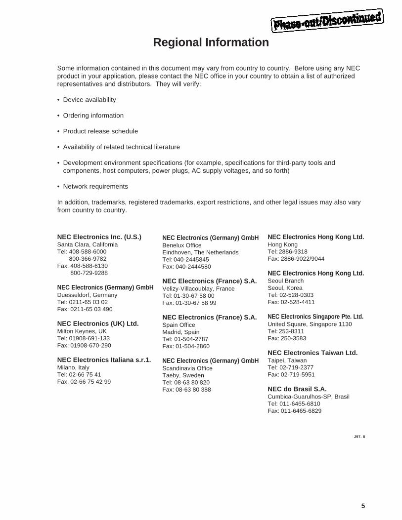
NEC Electronics Inc. (U.S.)Santa Clara, CaliforniaTel: 408-588-6000
800-366-9782Fax: 408-588-6130
800-729-9288
NEC Electronics (Germany) GmbHDuesseldorf, GermanyTel: 0211-65 03 02Fax: 0211-65 03 490
NEC Electronics (UK) Ltd.Milton Keynes, UKTel: 01908-691-133Fax: 01908-670-290
NEC Electronics Italiana s.r.1.Milano, ItalyTel: 02-66 75 41Fax: 02-66 75 42 99
NEC Electronics Hong Kong Ltd.Hong KongTel: 2886-9318Fax: 2886-9022/9044
NEC Electronics Hong Kong Ltd.Seoul BranchSeoul, KoreaTel: 02-528-0303Fax: 02-528-4411
NEC Electronics Singapore Pte. Ltd.United Square, Singapore 1130Tel: 253-8311Fax: 250-3583
NEC Electronics Taiwan Ltd.Taipei, TaiwanTel: 02-719-2377Fax: 02-719-5951
NEC do Brasil S.A.Cumbica-Guarulhos-SP, BrasilTel: 011-6465-6810Fax: 011-6465-6829
NEC Electronics (Germany) GmbHBenelux OfficeEindhoven, The NetherlandsTel: 040-2445845Fax: 040-2444580
NEC Electronics (France) S.A.Velizy-Villacoublay, FranceTel: 01-30-67 58 00Fax: 01-30-67 58 99
NEC Electronics (France) S.A.Spain OfficeMadrid, SpainTel: 01-504-2787Fax: 01-504-2860
NEC Electronics (Germany) GmbHScandinavia OfficeTaeby, SwedenTel: 08-63 80 820Fax: 08-63 80 388
Regional Information
Some information contained in this document may vary from country to country. Before using any NECproduct in your application, please contact the NEC office in your country to obtain a list of authorizedrepresentatives and distributors. They will verify:
• Device availability
• Ordering information
• Product release schedule
• Availability of related technical literature
• Development environment specifications (for example, specifications for third-party tools andcomponents, host computers, power plugs, AC supply voltages, and so forth)
• Network requirements
In addition, trademarks, registered trademarks, export restrictions, and other legal issues may also varyfrom country to country.
J97. 8

6
Major Revisions in This Edition
Page Description
159 CHAPTER 8 A/D CONVERTER
Adds caution
533 Changes APPENDIX B TOOLS
549 Adds APPENDIX E REVISION HISTORY
The mark ★ shows major revised points.
7
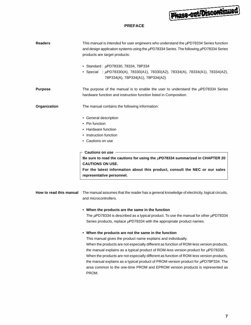
PREFACE
Readers This manual is intended for user engineers who understand the µPD78334 Series function
and design application systems using the µPD78334 Series. The following µPD78334 Series
products are target products:
• Standard : µPD78330, 78334, 78P334
• Special : µPD78330(A), 78330(A1), 78330(A2), 78334(A), 78334(A1), 78334(A2),
78P334(A), 78P334(A1), 78P334(A2)
Purpose The purpose of the manual is to enable the user to understand the µPD78334 Series
hardware function and instruction function listed in Composition.
Organization The manual contains the following information:
• General description
• Pin function
• Hardware function
• Instruction function
• Cautions on use
Cautions on use
Be sure to read the cautions for using the µPD78334 summarized in CHAPTER 20
CAUTIONS ON USE.
For the latest information about this product, consult the NEC or our sales
representative personnel.
How to read this manual The manual assumes that the reader has a general knowledge of electricity, logical circuits,
and microcontrollers.
• When the products are the same in the function
The µPD78334 is described as a typical product. To use the manual for other µPD78334
Series products, replace µPD78334 with the appropriate product names.
• When the products are not the same in the function
This manual gives the product name explains and individually.
When the products are not especially different as function of ROM-less version products,
the manual explains as a typical product of ROM-less version product for µPD78330.
When the products are not especially different as function of ROM-less version products,
the manual explains as a typical product of PROM version product for µPD78P334. The
area common to the one-time PROM and EPROM version products is represented as
PROM.
8
The examples in this manual are described for “standard” quality grade products. To use these examples for the
application required “special” quality grade products, be sure to examine the quality grade of each part and circuit
actually used.
• To look up the instruction function when you know the mnemonic of the instruction.
→ Use APPENDIX D INSTRUCTION INDEX (IN ALPHABETICAL ORDER) .
• To look up instructions when you do not know its mnemonic, but do know the rough
function.
→ Look up the mnemonic of the instruction in 18.1 Operation List , then the instruction
function in 18.6 Explanation of Instructions .
• To understand the µPD78334 Series function in a general way.
→ Read the manual according to the table of contents.
• To know the electric characteristics of µPD78334 Series.
→ Refer to Data Sheet.
• To know application examples of various functions of µPD78334 Series.
→ Refer to Application Note.
Legend Data representation weight : High-order and low-order digits are indicated from left to
right.
Active low representation : ×××× (pin or signal name is overlined)
Memory map address : Upper stage-low order and lower stage-high order
Note : Explanation of (Note) in the text
Caution : Item to which you should pay attention
Remark : Supplementary explanation to the text
Number representation : Binary number ×××× or ××××B
Decimal number ××××Hexadecimal number ××××H
9
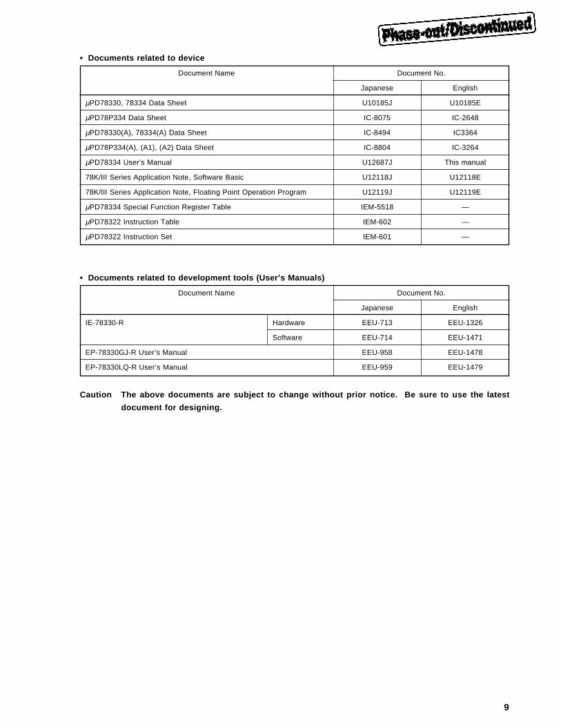
• Documents related to device
Document Name Document No.
Japanese English
µPD78330, 78334 Data Sheet U10185J U10185E
µPD78P334 Data Sheet IC-8075 IC-2648
µPD78330(A), 78334(A) Data Sheet IC-8494 IC3364
µPD78P334(A), (A1), (A2) Data Sheet IC-8804 IC-3264
µPD78334 User’s Manual U12687J This manual
78K/III Series Application Note, Software Basic U12118J U12118E
78K/III Series Application Note, Floating Point Operation Program U12119J U12119E
µPD78334 Special Function Register Table IEM-5518 —
µPD78322 Instruction Table IEM-602 —
µPD78322 Instruction Set IEM-601 —
• Documents related to development tools (User’s Manuals)
Document Name Document No.
Japanese English
IE-78330-R Hardware EEU-713 EEU-1326
Software EEU-714 EEU-1471
EP-78330GJ-R User’s Manual EEU-958 EEU-1478
EP-78330LQ-R User’s Manual EEU-959 EEU-1479
Caution The above documents are subject to change without prior notice. Be sure to use the latest
document for designing.
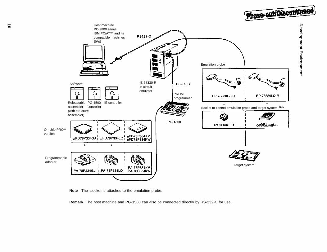
10 Developm
ent Environm
ent
Note The socket is attached to the emulation probe.
Remark The host machine and PG-1500 can also be connected directly by RS-232-C for use.
Host machinePC-9800 seriesIBM PC/AT™ and itscompatible machinesEWS
Relocatableassembler(with structureassembler)
PG-1500controller
IE controller
Software IE-78330-RIn-circuitemulator
PROMprogrammer
Socket to connet emulation probe and target system. Note
Emulation probe
Target system
QFJ socketOn-chip PROMversion
Programmableadapter
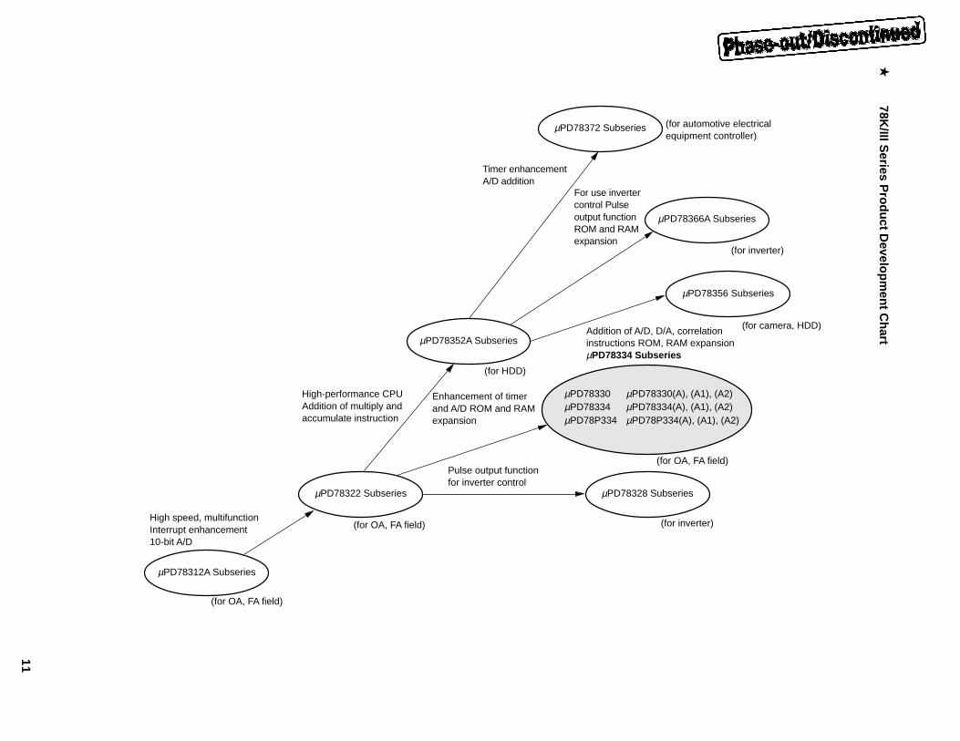
11
78K/III S
eries Product D
evelopment C
hart★
µPD78366A Subseries
µPD78322 Subseries
µPD78312A Subseries
(for automotive electricalequipment controller)
For use invertercontrol Pulseoutput functionROM and RAMexpansion
(for inverter)
(for camera, HDD)Addition of A/D, D/A, correlationinstructions ROM, RAM expansionµPD78334 Subseries
(for OA, FA field)
(for inverter)(for OA, FA field)High speed, multifunctionInterrupt enhancement10-bit A/D
High-performance CPUAddition of multiply andaccumulate instruction
Enhancement of timerand A/D ROM and RAMexpansion
µPD78372 Subseries
µPD78356 Subseries
µPD78352A Subseries
µPD78328 Subseries
µPD78330 µPD78330(A), (A1), (A2)µPD78334 µPD78334(A), (A1), (A2)µPD78P334 µPD78P334(A), (A1), (A2)
(for OA, FA field)
Pulse output functionfor inverter control
Timer enhancementA/D addition
(for HDD)

12
[MEMO]
13
CONTENTS
CHAPTER 1 GENERAL DESCRIPTION............................................................................................... 29
1.1 Features .................................................................................................................... .............. 301.2 Function Outline List ....................................................................................................... ...... 311.3 Ordering Information and Quality Grade ............................................................................. 32
1.3.1 Standard ....................................................................................................................................... 32
1.3.2 Special .......................................................................................................................................... 33
1.4 Pin Configurations (Top View) .............................................................................................. 3 41.4.1 µPD78330, 78334, 78P334 (normal operation mode) ................................................................. 34
1.4.2 µPD78P334 (PROM programming mode: RESET = H and AVDD = L) ......................................... 37
1.5 Block Diagram ............................................................................................................... ......... 391.6 Difference among µPD78334 Series ..................................................................................... 40
1.6.1 Differences between µPD78330, 78334 and 78P334 .................................................................. 40
1.6.2 Differences between µPD78334, 78334(A), 78334(A1) and 78334(A2) ...................................... 41
CHAPTER 2 PIN FUNCTION ................................................................................................................ 43
2.1 Pin Function List ........................................................................................................... ......... 432.1.1 µPD78330, 78334, and 78P334 (normal operation mode) .......................................................... 43
2.1.2 µPD78P334 (PROM programming mode: RESET = H and AVDD = L) ......................................... 46
2.2 Pin Function Description of µPD78330, 78334, and 78P334 (Normal Operation Mode) .. 472.2.1 P00 to P07 (Port 0) … 3-state input/output .................................................................................. 47
2.2.2 P10 to P17 (Port 1) … 3-state input/output .................................................................................. 47
2.2.3 P20 to P27 (Port 2) … input ......................................................................................................... 48
2.2.4 P30 to P37 (Port 3) … 3-state input/output .................................................................................. 48
2.2.5 P40 to P47 (Port 4) … 3-state input/output .................................................................................. 49
2.2.6 P50 to P57 (Port 5) … 3-state input/output .................................................................................. 50
2.2.7 P70 to P77 (Port 7) … input ......................................................................................................... 51
2.2.8 P80 to P87 (Port 8) … input ......................................................................................................... 51
2.2.9 P90 to P95 (Port 9) … 3-state input/output .................................................................................. 51
2.2.10 ASTB … output ............................................................................................................................ 53
2.2.11 EA … input ................................................................................................................................... 53
2.2.12 CLKOUT (Clock Output) … output ............................................................................................... 53
2.2.13 WDTO (Watchdog Timer Output) … output ................................................................................. 53
2.2.14 AVREF (Reference Voltage) … input .............................................................................................. 53
2.2.15 AVDD (Analog VDD) ........................................................................................................................ 53
2.2.16 AVSS (Analog VSS) ........................................................................................................................ 53
2.2.17 RESET (Reset) … input ............................................................................................................... 53
2.2.18 X1 and X2 (Crystal) ...................................................................................................................... 53
2.2.19 VDD ............................................................................................................................................... 53
2.2.20 VSS ................................................................................................................................................ 53
2.2.21 NC ................................................................................................................................................ 53
2.3 Description of the Pin Function of µPD78P334 (PROM Programming Mode) .................. 542.4 Input/Output Circuits and Recommended Connection of Unused Pins ........................... 55
14
CHAPTER 3 CPU ARCHITECTURE ..................................................................................................... . 57
3.1 Memory Space ................................................................................................................ ........ 573.1.1 Vector table area .......................................................................................................................... 59
3.1.2 CALLT instruction table area ........................................................................................................ 60
3.1.3 CALLF instruction entry area ....................................................................................................... 60
3.1.4 Internal RAM area ........................................................................................................................ 60
3.1.5 Special function register area ....................................................................................................... 64
3.1.6 External memory area .................................................................................................................. 64
3.2 Processor Registers ......................................................................................................... ..... 653.2.1 Control registers ........................................................................................................................... 66
3.2.2 General registers .......................................................................................................................... 71
3.2.3 Special function registers (SFR) .................................................................................................. 73
3.3 Data Memory Addressing ...................................................................................................... 783.3.1 General register addressing ......................................................................................................... 79
3.3.2 Short direct addressing ................................................................................................................ 79
3.3.3 Special function register (SFR) addressing .................................................................................. 79
CHAPTER 4 BLOCK FUNCTION OUTLINE......................................................................................... 81
4.1 Execution Unit .............................................................................................................. .......... 814.2 Bus Control Unit ............................................................................................................ ........ 814.3 Program Memory/Data Memory ............................................................................................ 814.4 Ports ....................................................................................................................... ................. 824.5 Real-Time Pulse Unit (RPU) .................................................................................................. 834.6 A/D Converter ............................................................................................................... .......... 834.7 Serial Interface ............................................................................................................ ........... 834.8 Watchdog Timer .............................................................................................................. ....... 834.9 PWM Output Unit ............................................................................................................. ...... 844.10 Interrupt Controller ..................................................................................................... ........... 84
CHAPTER 5 PORT FUNCTION ............................................................................................................ 85
5.1 Hardware Configuration ...................................................................................................... .. 855.2 Port Function ............................................................................................................... ........... 92
5.2.1 Input/output port function and features ........................................................................................ 92
5.2.2 Input/output mode setting ............................................................................................................. 93
5.2.3 Control mode setting .................................................................................................................... 95
CHAPTER 6 CLOCK GENERATOR ..................................................................................................... 101
CHAPTER 7 REAL-TIME PULSE UNIT ................................................................................................ 105
7.1 Configuration ............................................................................................................... .......... 1067.1.1 Timer 0 (TM0) ............................................................................................................................... 110
7.1.2 Timer 1 (TM1) ............................................................................................................................... 111
7.1.3 Timer 2 (TM2) ............................................................................................................................... 111
15
7.1.4 Timer 3 (TM3) ............................................................................................................................... 111
7.1.5 Compare registers ........................................................................................................................ 111
7.1.6 Capture registers .......................................................................................................................... 114
7.1.7 Capture/compare registers ........................................................................................................... 116
7.2 Control Registers ........................................................................................................... ........ 1217.2.1 Timer unit mode registers (TUM0 and TUM1) .............................................................................. 121
7.2.2 Timer control register (TMC0 and TMC1) .................................................................................... 124
7.2.3 Timer output control registers (TOC0 and TOC1) ........................................................................ 126
7.2.4 Programmable pulse output set register (PPOS) ......................................................................... 129
7.2.5 External interrupt mode registers (INTM0 and INTM1) ................................................................ 129
7.3 Operation ................................................................................................................... ............. 1327.3.1 Timer 0 (TM0) ............................................................................................................................... 132
7.3.2 Timer 1 (TM1) ............................................................................................................................... 138
7.3.3 Timer 2 (TM2) ............................................................................................................................... 142
7.3.4 Timer 3 (TM3) ............................................................................................................................... 145
7.4 Timer Output Function ....................................................................................................... ... 1477.5 Real-Time Output Function ................................................................................................... 152
7.5.1 Configuration ................................................................................................................................ 152
7.5.2 Control registers ........................................................................................................................... 154
7.5.3 Operation ...................................................................................................................................... 156
CHAPTER 8 A/D CONVERTER ....................................................................................................... ..... 157
8.1 Configuration ............................................................................................................... .......... 1578.2 A/D Converter Mode Register ............................................................................................... 16 18.3 A/D Conversion Result Register ........................................................................................... 1648.4 Operation ................................................................................................................... ............. 165
8.4.1 Basic operation of A/D converter .................................................................................................. 165
8.4.2 A/D converter operation mode ..................................................................................................... 168
8.5 Use of A/D Converter Characteristic Table ......................................................................... 172
CHAPTER 9 ASYNCHRONOUS SERIAL INTERFACE ....................................................................... 177
9.1 Asynchronous Serial I/O Configuration ............................................................................... 1789.2 Set Serial Communication Pins ............................................................................................ 1809.3 Set Data Format ............................................................................................................. ........ 1829.4 Set Baud Rate ............................................................................................................... .......... 184
9.4.1 Baud rate generator configuration ................................................................................................ 186
9.4.2 Set any desired baud rate ............................................................................................................ 188
9.5 Transmit Data ............................................................................................................... .......... 1909.6 Receive Data ................................................................................................................ ........... 1929.7 When a Reception Error Occurred ....................................................................................... 194
CHAPTER 10 CLOCKED SERIAL INTERFACE .................................................................................. 197
10.1 Clocked Serial Interface Configuration ............................................................................. 19810.2 Set Serial Communication Pins .......................................................................................... 20110.3 Set Baud Rate .............................................................................................................. ........ 203
16
10.3.1 Baud rate generator configuration ........................................................................................... 205
10.3.2 Set any desired baud rate ....................................................................................................... 207
10.4 Two Clocked Synchronous Serial Interface Modes ......................................................... 20810.5 Set 3-Wire Serial I/O Mode ................................................................................................. . 210
10.5.1 Transmit in 3-wire serial I/O mode ........................................................................................... 212
10.5.2 Receive in 3-wire serial I/O mode ........................................................................................... 214
10.5.3 Transfer in 3-wire Serial I/O Mode ........................................................................................... 216
10.5.4 Steps taken when serial clocks and shift operation are placed out of synchronization ........... 219
10.6 Set SBI Mode ............................................................................................................... ......... 22010.6.1 SBI data format ....................................................................................................................... 222
10.6.2 Control and detect serial bus state .......................................................................................... 225
10.6.3 Communication in SBI mode ................................................................................................... 231
10.6.4 Operate only when address is received .................................................................................. 235
CHAPTER 11 WATCHDOG TIMER ..................................................................................................... . 237
11.1 Watchdog Timer Mode Register ......................................................................................... 23811.2 Watchdog Timer Output Pin ............................................................................................... 23911.3 Application Example ........................................................................................................ ... 239
CHAPTER 12 PWM SIGNAL OUTPUT FUNCTION ............................................................................. 241
12.1 Configuration .............................................................................................................. ......... 24212.2 Control Register ........................................................................................................... ........ 243
12.2.1 PWM control register (PWMC) ................................................................................................ 243
12.2.2 PWM buffer registers (PWM0 and PWM1) .............................................................................. 243
12.2.3 Compare registers (CMP0 and CMP1) ................................................................................... 243
12.3 Operation .................................................................................................................. ............ 244
CHAPTER 13 INTERRUPT FUNCTION................................................................................................ 245
13.1 Interrupt Requests ......................................................................................................... ...... 24813.1.1 Non-maskable interrupt requests ............................................................................................ 248
13.1.2 Maskable interrupt requests .................................................................................................... 248
13.1.3 Interrupt requests caused by executing specific instructions .................................................. 248
13.1.4 Exception trap interrupt requests ............................................................................................ 249
13.2 Interrupt Control Registers ................................................................................................ . 25013.2.1 Interrupt request flag register (IF0L, IF0H, IF1L) ..................................................................... 252
13.2.2 Interrupt mask flag register (MK0L, MK0H, MK1L) .................................................................. 253
13.2.3 Processing mode specification flag register (ISM0L, ISM0H, ISM1L) ..................................... 254
13.2.4 Priority level specification buffer register (PB0L, PB0H, PB1L) ............................................... 255
13.2.5 Priority level specification register (PRSL) .............................................................................. 256
13.2.6 In-service priority register (ISPR) ............................................................................................ 257
13.2.7 Context switching enable flag register (CSE0L, CSE0H, CSE1L) .......................................... 258
13.3 Maskable Interrupt Status Flags ........................................................................................ 25913.4 Macro Service Function ..................................................................................................... . 261
13.4.1 Macro service control registers ............................................................................................... 263
13.4.2 Macro service mode ................................................................................................................ 264
17
13.4.3 Macro service operation .......................................................................................................... 264
13.5 Context Switching Function ............................................................................................... 27 713.5.1 Context switching function when an interrupt request occurs ................................................. 277
13.5.2 Context switching function when BRKCS instruction is executed ........................................... 278
13.5.3 Return from address to which branch is taken by context switching function ......................... 279
CHAPTER 14 STANDBY FUNCTION ................................................................................................... 281
14.1 Configuration and Function ................................................................................................ 2 8114.2 Standby Control Register (STBC) ...................................................................................... 28214.3 Operation .................................................................................................................. ............ 284
14.3.1 HALT mode .............................................................................................................................. 284
14.3.2 STOP mode ............................................................................................................................. 286
CHAPTER 15 RESET FUNCTION ........................................................................................................ 291
CHAPTER 16 BUS INTERFACE FUNCTION ....................................................................................... 295
16.1 µPD78334 External Service Expansion Function ............................................................. 29516.2 µPD78330 External Device Access .................................................................................... 29816.3 Control Register ........................................................................................................... ........ 299
16.3.1 Memory expansion mode register ........................................................................................... 299
16.3.2 Programmable wait control register ......................................................................................... 300
16.3.3 Fetch cycle control register ..................................................................................................... 301
CHAPTER 17 µPD78P334 PROGRAMMING ....................................................................................... 303
17.1 Operation Mode ............................................................................................................. ...... 30417.2 PROM Write Procedure ....................................................................................................... 30517.3 PROM Read Procedure ....................................................................................................... 3 0717.4 Erasion Characteristics ( µPD78P334KM, 78P334KW only) ............................................. 30817.5 Window Seal ( µPD78P334KM, 78P334KW only) ............................................................... 30817.6 One-time PROM Product Screening .................................................................................. 308
CHAPTER 18 INSTRUCTION SET ....................................................................................................... 309
18.1 Operation List ............................................................................................................. ......... 30918.1.1 Operand identifiers and description ......................................................................................... 309
18.1.2 Legend on operation explanation ............................................................................................ 312
18.1.3 Explanation of symbols under column of flags ........................................................................ 313
18.1.4 Operation list of basic instruction ............................................................................................ 314
18.2 Operation Codes of Instructions ........................................................................................ 32918.2.1 Symbol explanation of operation codes .................................................................................. 329
18.2.2 Operation codes in memory addressing modes ...................................................................... 331
18.2.3 Operation code list .................................................................................................................. 332
18.3 Instruction Clocks ......................................................................................................... ...... 34818.3.1 Explanation of column of clocks .............................................................................................. 348
18
18.3.2 Clock list .................................................................................................................................. 350
18.4 Instruction Address Addressing ........................................................................................ 37318.4.1 Relative addressing ................................................................................................................. 373
18.4.2 Immediate addressing ............................................................................................................. 374
18.4.3 Table indirect addressing ......................................................................................................... 375
18.4.4 Register addressing ................................................................................................................ 376
18.4.5 Register indirect addressing .................................................................................................... 376
18.5 Operand Address Addressing ............................................................................................ 37718.5.1 Register addressing ................................................................................................................ 377
18.5.2 Immediate addressing ............................................................................................................. 378
18.5.3 Direct addressing .................................................................................................................... 379
18.5.4 Short direct addressing ........................................................................................................... 380
18.5.5 Special function register (SFR) addressing ............................................................................. 382
18.5.6 Short direct memory indirect addressing ................................................................................. 383
18.5.7 Register indirect addressing .................................................................................................... 384
18.5.8 Based addressing .................................................................................................................... 386
18.5.9 Indexed addressing ................................................................................................................. 387
18.5.10 Based indexed addressing ...................................................................................................... 388
18.6 Explanation of Instructions ................................................................................................ 38918.6.1 8-bit data transfer instructions ................................................................................................. 389
18.6.2 16-bit data transfer instructions ............................................................................................... 397
18.6.3 8-bit arithmetic and logical instructions .................................................................................. 402
18.6.4 16-bit arithmetic and logical instructions ................................................................................. 426
18.6.5 Multiplication and division instructions .................................................................................... 433
18.6.6 Signed multiplication instruction .............................................................................................. 434
18.6.7 Increment and decrement instructions .................................................................................... 435
18.6.8 Shift and rotate instructions ..................................................................................................... 438
18.6.9 BCD adjustment instructions ................................................................................................... 443
18.6.10 Data conversion instruction ..................................................................................................... 444
18.6.11 Bit manipulation instructions .................................................................................................... 445
18.6.12 Call and return instructions ...................................................................................................... 461
18.6.13 Stack handling instruction ....................................................................................................... 465
18.6.14 Special instructions ................................................................................................................. 469
18.6.15 Unconditional branch instructions ........................................................................................... 470
18.6.16 Conditional branch instructions ............................................................................................... 472
18.6.17 Context switching instruction ................................................................................................... 490
18.6.18 String instructions .................................................................................................................... 492
18.6.19 CPU control instructions .......................................................................................................... 498
CHAPTER 19 INSTRUCTION EXECUTION SPEED ............................................................................ 501
19.1 Instruction Execution Speed ............................................................................................. 50 119.2 Memory Space and Access Speed ..................................................................................... 501
19.2.1 Main RAM and peripheral RAM ............................................................................................... 501
19.2.2 Memory access ....................................................................................................................... 502
19.3 Interrupt Execution Speed .................................................................................................. 50819.4 Rough Calculation of Number of Execution Clocks ......................................................... 510
19
CHAPTER 20 CAUTIONS ON USE .................................................................................................... .. 515
20.1 Cautions in Chapter 2 ...................................................................................................... .... 51520.2 Cautions in Chapter 3 ...................................................................................................... .... 51620.3 Cautions in Chapter 5 ...................................................................................................... .... 51720.4 Cautions in Chapter 6 ...................................................................................................... .... 51820.5 Cautions in Chapter 7 ...................................................................................................... .... 51820.6 Cautions in Chapter 8 ...................................................................................................... .... 51920.7 Cautions in Chapter 9 ...................................................................................................... .... 52120.8 Cautions in Chapter 10 ..................................................................................................... ... 52120.9 Cautions in Chapter 11 ..................................................................................................... ... 52220.10 Cautions in Chapter 12 .................................................................................................... .... 52220.11 Cautions in Chapter 13 .................................................................................................... .... 52220.12 Cautions in Chapter 14 .................................................................................................... .... 52420.13 Cautions in Chapter 15 .................................................................................................... .... 52520.14 Cautions in Chapter 16 .................................................................................................... .... 52520.15 Cautions in Chapter 18 .................................................................................................... .... 52520.16 Cautions in Chapter 19 .................................................................................................... .... 527
APPENDIX A DIFFERENCES BETWEEN µPD78334 AND µPD78322 ............................................... 529
APPENDIX B TOOLS .............................................................................................................. .............. 533
B.1 Development Tools ........................................................................................................... ..... 533B.2 Evaluation Tools ............................................................................................................ ........ 535B.3 Built-in Software ........................................................................................................... ......... 536
APPENDIX C REGISTER INDEX .......................................................................................................... 539
C. 1 Register Index (In Alphabetical Order) ................................................................................ 539C. 2 Register Index (In Alphabetical Order) ................................................................................ 542
APPENDIX D INSTRUCTION INDEX (IN ALPHABETICAL ORDER).................................................. 545
APPENDIX E REVISION HISTORY ...................................................................................................... 549★
20
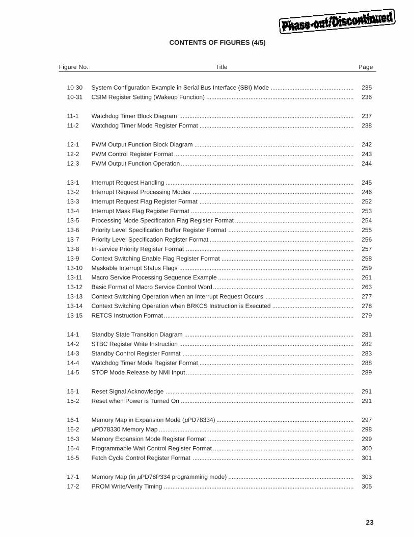
CONTENTS OF FIGURES (1/5)
Figure No. Title Page
2-1 Pin Input/Output Circuits ................................................................................................................... 56
3-1 Memory Map ..................................................................................................................................... 58
3-2 Register Configuration ...................................................................................................................... 65
3-3 PSW Format ..................................................................................................................................... 66
3-4 CCW Format ..................................................................................................................................... 70
3-5 General Register Process Bits .......................................................................................................... 71
3-6 Data Memory Addressing ................................................................................................................. 78
5-1 Port Structure .................................................................................................................................... 85
5-2 Port Specified as Output Port ........................................................................................................... 86
5-3 Port Specified as Input Port .............................................................................................................. 87
5-4 Control Specification ......................................................................................................................... 88
5-5 Port Read Control Register Format .................................................................................................. 89
5-6 Conceptual Diagram of Control (When Port is Specified as Output Port) ........................................ 90
5-7 Port 0 Mode Register Format ........................................................................................................... 93
5-8 Port 1 Mode Register Format ........................................................................................................... 93
5-9 Port 3 Mode Register Format ........................................................................................................... 93
5-10 Port 5 Mode Register Format ........................................................................................................... 94
5-11 Port 9 Mode Register Format ........................................................................................................... 94
5-12 Port 0 Mode Control Register Format ............................................................................................... 96
5-13 Port 1 Mode Control Register Format ............................................................................................... 96
5-14 Port 3 Mode Control Register Format ............................................................................................... 97
5-15 Memory Expansion Mode Register Format ...................................................................................... 98
5-16 PWM Control Register Format .......................................................................................................... 98
5-17 Fetch Cycle Control Register Format ............................................................................................... 99
6-1 Clock Generator Block Diagram ....................................................................................................... 101
6-2 System Clock Oscillator External Circuit .......................................................................................... 102
6-3 Bad Examples of Resonator Connection Circuit ............................................................................... 103
7-1 Real-Time Pulse Unit (RPU) Block Diagram ..................................................................................... 107
7-2 Timer 0 Format ................................................................................................................................. 110
7-3 18/16-bit Compare Register Format (To read) .................................................................................. 113
7-4 18/16-bit Compare Register Format (To write) ................................................................................. 113
7-5 18/16-bit Capture Register Format ................................................................................................... 115
7-6 Capture/Compare Register Format (When read) ............................................................................. 118
7-7 Capture/Compare Register Format (When write) ............................................................................. 118
7-8 Capture Operation ............................................................................................................................ 119
7-9 Compare Operation .......................................................................................................................... 120
7-10 Timer Unit Mode Register 0 Format .................................................................................................. 122
7-11 Timer Unit Mode Register 1 Format .................................................................................................. 123
7-12 Timer Control Register 0 Format ...................................................................................................... 124
21
CONTENTS OF FIGURES (2/5)
Figure No. Title Page
7-13 Timer Control Register 1 Format ...................................................................................................... 125
7-14 Timer Output Control Register 0 Format ........................................................................................... 127
7-15 Timer Output control Register 1 Format ........................................................................................... 128
7-16 Programmable Pulse Output Set Register Format ........................................................................... 129
7-17 External Interrupt Mode Register 0 Format ...................................................................................... 130
7-18 External Interrupt Mode Register 1 Format ...................................................................................... 131
7-19 Basic Operation of Timer 0 (TM0) ..................................................................................................... 132
7-20 Timer 0 Compare Operation Example 1 (pulse output mode 0) ....................................................... 134
7-21 Timer 0 Compare Operation Example 2 (pulse output mode 0) ....................................................... 135
7-22 Timer 0 Compare Operation Example (pulse output mode 1) .......................................................... 136
7-23 Capture Operation Example (TM0) ................................................................................................... 137
7-24 Basic Operation of Timer 1 (TM1) ..................................................................................................... 138
7-25 Compare Operation Example (TM1 in interval timer mode) ............................................................. 140
7-26 Capture Operation Example (TM1) ................................................................................................... 141
7-27 Basic Operation of Timer 2 (TM2) ..................................................................................................... 142
7-28 Compare Operation Example (TM2 in interval timer mode) ............................................................. 144
7-29 Basic Operation of Timer 3 (TM3) ..................................................................................................... 145
7-30 Compare Operation Example (TM3 in interval timer mode) ............................................................. 146
7-31 Pulse Output Mode 0 Block Diagram ................................................................................................ 148
7-32 Pulse Output Mode 1 Block Diagram ................................................................................................ 149
7-33 Timer Output Operation Block Diagram ............................................................................................ 151
7-34 Real-Time Output Port Block Diagram .............................................................................................. 153
7-35 Real-Time Output Port Set Register Format ..................................................................................... 154
7-36 Real-Time Output Port Reset Register Format ................................................................................. 154
7-37 Real-Time Output Port Register Format ........................................................................................... 155
8-1 A/D Converter Block Diagram ........................................................................................................... 158
8-2 Capacitor Connection Example to A/D Converter Pins ..................................................................... 159
8-3 A/D Converter Mode Register Format .............................................................................................. 163
8-4 Word Access to ADCR Register ........................................................................................................ 164
8-5 Byte Access to ADCR Register ......................................................................................................... 164
8-6 Basic Operation of A/D Conversion .................................................................................................. 166
8-7 A/D Conversion Operation Synchronized with the External Signal .................................................. 166
8-8 ADM Rewrite during A/D Conversion Operation ............................................................................... 167
8-9 A/D Conversion Operation in Select Mode (1-buffer mode) ............................................................. 168
8-10 A/D Conversion Operation in Select Mode (4-buffer mode) ............................................................. 169
8-11 A/D Conversion Operation in Scan Mode ......................................................................................... 170
8-12 A/D Conversion Operation in Mix Mode ........................................................................................... 171
8-13 Total Error ......................................................................................................................................... 173
8-14 Quantization Error ............................................................................................................................. 173
8-15 Zero Scale Error ................................................................................................................................ 174
8-16 Full Scale Error ................................................................................................................................. 174
8-17 Non-linear Error ................................................................................................................................ 174
22
CONTENTS OF FIGURES (3/5)
Figure No. Title Page
9-1 Asynchronous Serial interface Block Diagram .................................................................................. 179
9-2 Port 3 Mode Control Register (PMC3) Format ................................................................................. 180
9-3 Port3 Mode Register Format ............................................................................................................ 181
9-4 Send-Receive Data Format on Asynchronous Serial Interface ........................................................ 182
9-5 ASIM Register Setting (Data Format) ............................................................................................... 183
9-6 ASIM Register Setting (Serial Clock) ................................................................................................ 185
9-7 Baud Rate Generator Block Diagram ............................................................................................... 187
9-8 Baud Rate Generator Mode Register Format ................................................................................... 188
9-9 Asynchronous Serial Interface Transmission Completion Interrupt Timing ...................................... 191
9-10 Asynchronous Serial Interface Reception Completion Interrupt Timing ........................................... 192
9-11 ASIM Register Setting (Reception Enable) ....................................................................................... 193
9-12 Reception Error Timing ..................................................................................................................... 195
9-13 Asynchronous Serial Interface Status Register Format .................................................................... 195
10-1 Clocked Serial Interface Block Diagram ........................................................................................... 200
10-2 Port 3 Mode Control Register (PMC3) Format ................................................................................. 201
10-3 Port 3 Mode Register Format ........................................................................................................... 202
10-4 CSIM Register Setting (Serial Clock) ................................................................................................ 204
10-5 Baud Rate Generator Block Diagram ............................................................................................... 206
10-6 Baud Rate Generator Mode Register Format ................................................................................... 207
10-7 System Configuration Example in 3-wire Serial I/O Mode ................................................................ 208
10-8 System Configuration Example in Serial Bus Interface (SBI) Mode ................................................. 209
10-9 3-wire Serial I/O Mode Timing .......................................................................................................... 210
10-10 CSIM Register Setting (3-wire Serial I/O Mode) ............................................................................... 211
10-11 3-wire Serial I/O Mode Timing (Transit) ............................................................................................ 212
10-12 CSIM Register Setting (Transmission Enable) ................................................................................. 213
10-13 3-wire Serial I/O Mode Timing (Reception) ....................................................................................... 214
10-14 CSIM Register Setting (Reception Enable) ...................................................................................... 215
10-15 3-wire Serial I/O Mode Timing (Transfer) .......................................................................................... 217
10-16 CSIM Register Setting (Transfer Enable) ......................................................................................... 218
10-17 System Configuration Example in Serial Bus Interface (SBI) Mode ................................................. 220
10-18 CSIM Register Setting (SBI Mode) ................................................................................................... 221
10-19 Serial Bus interface Control Register Format ................................................................................... 226
10-20 RELT, CMDT, RELD, CMDD Operation ............................................................................................ 227
10-21 ACKT Operation ................................................................................................................................ 227
10-22 ACKE Operation ............................................................................................................................... 228
10-23 ACKD Operation ............................................................................................................................... 229
10-24 BSYE Operation ............................................................................................................................... 230
10-25 CSIM Register Setting (Transfer Enable) ......................................................................................... 232
10-26 Address Transfer Operation from Master Device to Slave Device ................................................... 233
10-27 Command Transfer Operation from Master Device to Slave Device ................................................ 233
10-28 Data Transfer Operation from Master Device to Slave Device ......................................................... 234
10-29 Data Transfer Operation from Slave Device to Master Device ......................................................... 234
23
CONTENTS OF FIGURES (4/5)
Figure No. Title Page
10-30 System Configuration Example in Serial Bus Interface (SBI) Mode ................................................. 235
10-31 CSIM Register Setting (Wakeup Function) ....................................................................................... 236
11-1 Watchdog Timer Block Diagram ....................................................................................................... 237
11-2 Watchdog Timer Mode Register Format ........................................................................................... 238
12-1 PWM Output Function Block Diagram .............................................................................................. 242
12-2 PWM Control Register Format .......................................................................................................... 243
12-3 PWM Output Function Operation ...................................................................................................... 244
13-1 Interrupt Request Handling ............................................................................................................... 245
13-2 Interrupt Request Processing Modes ............................................................................................... 246
13-3 Interrupt Request Flag Register Format ........................................................................................... 252
13-4 Interrupt Mask Flag Register Format ................................................................................................ 253
13-5 Processing Mode Specification Flag Register Format ...................................................................... 254
13-6 Priority Level Specification Buffer Register Format .......................................................................... 255
13-7 Priority Level Specification Register Format ..................................................................................... 256
13-8 In-service Priority Register Format ................................................................................................... 257
13-9 Context Switching Enable Flag Register Format .............................................................................. 258
13-10 Maskable Interrupt Status Flags ....................................................................................................... 259
13-11 Macro Service Processing Sequence Example ................................................................................ 261
13-12 Basic Format of Macro Service Control Word ................................................................................... 263
13-13 Context Switching Operation when an Interrupt Request Occurs .................................................... 277
13-14 Context Switching Operation when BRKCS Instruction is Executed ................................................ 278
13-15 RETCS Instruction Format ................................................................................................................ 279
14-1 Standby State Transition Diagram .................................................................................................... 281
14-2 STBC Register Write Instruction ....................................................................................................... 282
14-3 Standby Control Register Format ..................................................................................................... 283
14-4 Watchdog Timer Mode Register Format ........................................................................................... 288
14-5 STOP Mode Release by NMI Input ................................................................................................... 289
15-1 Reset Signal Acknowledge ............................................................................................................... 291
15-2 Reset when Power is Turned On ...................................................................................................... 291
16-1 Memory Map in Expansion Mode (µPD78334) ................................................................................. 297
16-2 µPD78330 Memory Map ................................................................................................................... 298
16-3 Memory Expansion Mode Register Format ...................................................................................... 299
16-4 Programmable Wait Control Register Format ................................................................................... 300
16-5 Fetch Cycle Control Register Format ............................................................................................... 301
17-1 Memory Map (in µPD78P334 programming mode) .......................................................................... 303
17-2 PROM Write/Verify Timing ................................................................................................................ 305
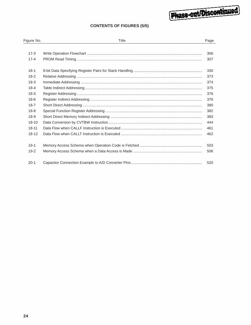
24
CONTENTS OF FIGURES (5/5)
Figure No. Title Page
17-3 Write Operation Flowchart ................................................................................................................ 306
17-4 PROM Read Timing .......................................................................................................................... 307
18-1 8-bit Data Specifying Register Pairs for Stack Handling ................................................................... 330
18-2 Relative Addressing .......................................................................................................................... 373
18-3 Immediate Addressing ...................................................................................................................... 374
18-4 Table Indirect Addressing .................................................................................................................. 375
18-5 Register Addressing .......................................................................................................................... 376
18-6 Register Indirect Addressing ............................................................................................................. 376
18-7 Short Direct Addressing .................................................................................................................... 380
18-8 Special Function Register Addressing .............................................................................................. 382
18-9 Short Direct Memory Indirect Addressing ......................................................................................... 383
18-10 Data Conversion by CVTBW Instruction ........................................................................................... 444
18-11 Data Flow when CALLF Instruction is Executed ............................................................................... 461
18-12 Data Flow when CALLT Instruction is Executed ............................................................................... 462
19-1 Memory Access Schema when Operation Code is Fetched ............................................................. 503
19-2 Memory Access Schema when a Data Access is Made ................................................................... 506
20-1 Capacitor Connection Example to A/D Converter Pins ..................................................................... 520
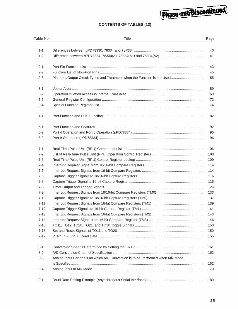
25
1-1 Differences between µPD78330, 78334 and 78P334 ....................................................................... 40
1-2 Difference between µPD78334, 78334(A), 78334(A1) and 78334(A2) ............................................ 41
2-1 Port Pin Function List ........................................................................................................................ 43
2-2 Function List of Non-Port Pins .......................................................................................................... 45
2-3 Pin Input/Output Circuit Types and Treatment when the Function is not Used ................................. 55
3-1 Vector Area ....................................................................................................................................... 59
3-2 Operation in Word Access in Internal RAM Area .............................................................................. 60
3-3 General Register Configuration ........................................................................................................ 72
3-4 Special Function Register List .......................................................................................................... 74
4-1 Port Function and Dual Function ...................................................................................................... 82
5-1 Port Function and Features .............................................................................................................. 92
5-2 Port 4 Operation and Port 5 Operation (µPD78334) ......................................................................... 95
5-3 Port 9 Operation (µPD78334) ........................................................................................................... 96
7-1 Real-Time Pulse Unit (RPU) Component List ................................................................................... 106
7-2 List of Real-Time Pulse Unit (RPU) Operation Control Registers ..................................................... 108
7-3 Real-Time Pulse Unit (RPU) Control Register Lookup ..................................................................... 109
7-4 Interrupt Request Signal from 18/16-bit Compare Registers ............................................................ 114
7-5 Interrupt Request Signals from 16-bit Compare Registers ............................................................... 114
7-6 Capture Trigger Signals to 18/16-bit Capture Registers ................................................................... 116
7-7 Capture Trigger Signal to 16-bit Capture Register ............................................................................ 116
7-8 Timer Output and Trigger Signals ..................................................................................................... 126
7-9 Interrupt Request Signals from 18/16-bit Compare Registers (TM0) ............................................... 133
7-10 Capture Trigger Signals to 18/16-bit Capture Registers (TM0) ........................................................ 137
7-11 Interrupt Request Signals from 16-bit Compare Registers (TM1) .................................................... 139
7-12 Capture Trigger Signals to 16-bit Capture Register (TM1) ............................................................... 141
7-13 Interrupt Request Signals from 16-bit Compare Registers (TM2) .................................................... 143
7-14 Interrupt Request Signal from 16-bit Compare Register (TM3) ........................................................ 146
7-15 TO11, TO12, TO20, TO21, and TO30 Toggle Signals ...................................................................... 150
7-16 Set and Reset Signals of TO11 and TO20 ........................................................................................ 150
7-17 RTPn (n = 0 to 7) Read Data ............................................................................................................ 155
8-1 Conversion Speeds Determined by Setting the FR Bit ..................................................................... 161
8-2 A/D Conversion Channel Specification ............................................................................................. 162
8-3 Analog Input Channels on which A/D Conversion is to be Performed when Mix Mode
is Specified ........................................................................................................................................ 162
8-4 Analog Input in Mix Mode ................................................................................................................. 170
9-1 Baud Rate Setting Example (Asynchronous Serial Interface) .......................................................... 189
CONTENTS OF TABLES (13)
Table No. Title Page
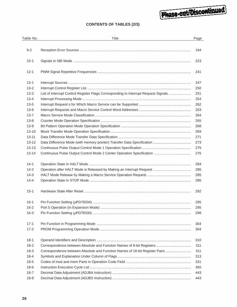
26
CONTENTS OF TABLES (2/3)
Table No. Title Page
9-2 Reception Error Sources .................................................................................................................. 194
10-1 Signals in SBI Mode ......................................................................................................................... 223
12-1 PWM Signal Repetitive Frequencies ................................................................................................ 241
13-1 Interrupt Sources .............................................................................................................................. 247
13-2 Interrupt Control Register List ........................................................................................................... 250
13-3 List of Interrupt Control Register Flags Corresponding to Interrupt Request Signals ....................... 251
13-4 Interrupt Processing Mode ................................................................................................................ 254
13-5 Interrupt Request s for Which Macro Service can be Supported ...................................................... 262
13-6 Interrupt Requests and Macro Service Control Word Addresses ..................................................... 263
13-7 Macro Service Mode Classification ................................................................................................... 264
13-8 Counter Mode Operation Specification ............................................................................................. 265
13-9 Bit Pattern Operation Mode Operation Specification ........................................................................ 268
13-10 Block Transfer Mode Operation Specification ................................................................................... 269
13-11 Data Difference Mode Transfer Data Specification ........................................................................... 271
13-12 Data Difference Mode (with memory pointer) Transfer Data Specification ....................................... 273
13-13 Continuous Pulse Output Control Mode 1 Operation Specification .................................................. 275
13-14 Continuous Pulse Output Control Mode 2 Center Operation Specification ...................................... 276
14-1 Operation State in HALT Mode ......................................................................................................... 284
14-2 Operation after HALT Mode is Released by Making an Interrupt Request ....................................... 285
14-3 HALT Mode Release by Making a Macro Service Operation Request ............................................. 285
14-4 Operation State in STOP Mode ........................................................................................................ 286
15-1 Hardware State After Reset .............................................................................................................. 292
16-1 Pin Function Setting (µPD78334) ..................................................................................................... 295
16-2 Port 5 Operation (In Expansion Mode) ............................................................................................. 295
16-3 Pin Function Setting (µPD78330) ..................................................................................................... 298
17-1 Pin Function in Programming Mode ................................................................................................. 304
17-2 PROM Programming Operation Mode .............................................................................................. 304
18-1 Operand Identifiers and Description ................................................................................................. 310
18-2 Correspondence between Absolute and Function Names of 8-bit Registers ................................... 311
18-3 Correspondence between Absolute and Function Names of 16-bit Register Pairs .......................... 311
18-4 Symbols and Explanation Under Column of Flags ........................................................................... 313
18-5 Codes of mod and mem Parts in Operation Code Field ................................................................... 331
18-6 Instruction Execution Cycle List ........................................................................................................ 365
18-7 Decimal Data Adjustment (ADJBA Instruction) ................................................................................. 443
18-8 Decimal Data Adjustment (ADJBS Instruction) ................................................................................. 443
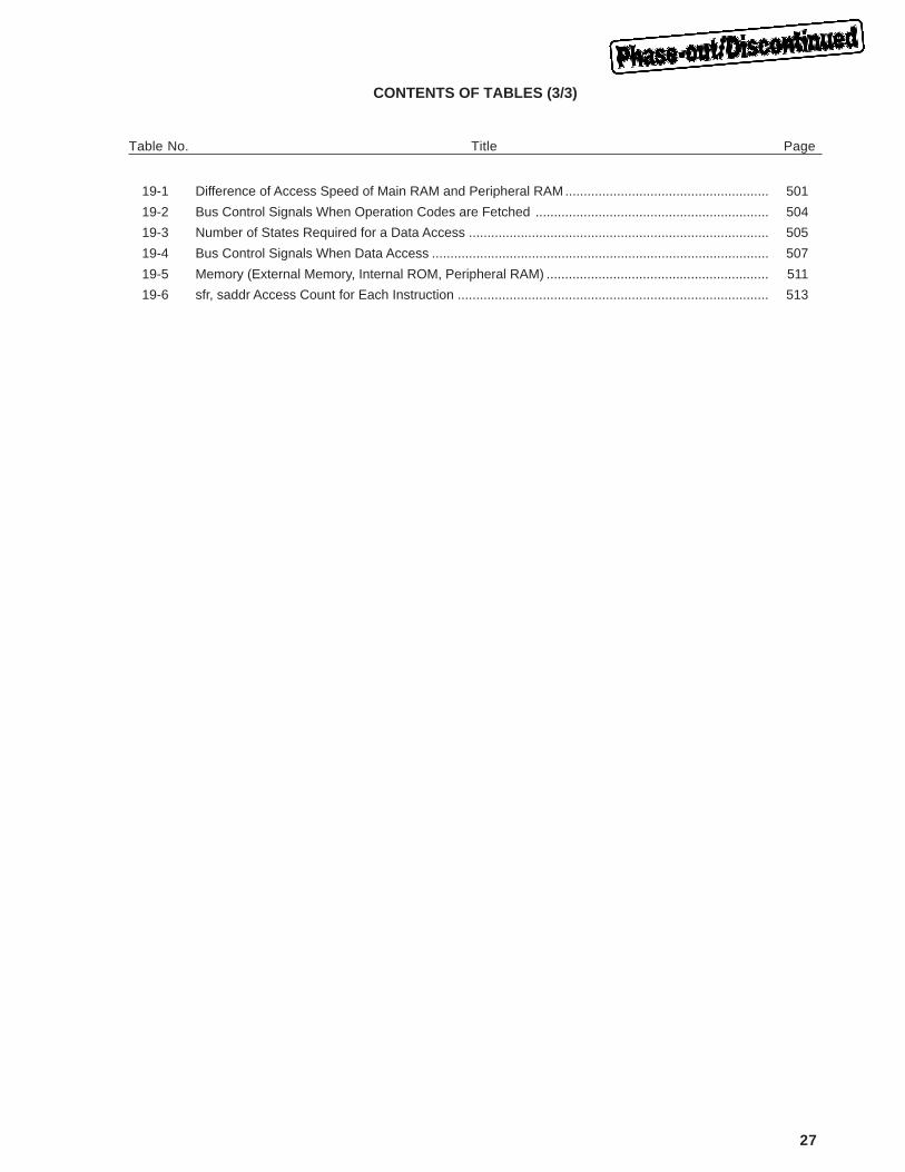
27
CONTENTS OF TABLES (3/3)
Table No. Title Page
19-1 Difference of Access Speed of Main RAM and Peripheral RAM....................................................... 501
19-2 Bus Control Signals When Operation Codes are Fetched ............................................................... 504
19-3 Number of States Required for a Data Access ................................................................................. 505
19-4 Bus Control Signals When Data Access ........................................................................................... 507
19-5 Memory (External Memory, Internal ROM, Peripheral RAM) ............................................................ 511
19-6 sfr, saddr Access Count for Each Instruction .................................................................................... 513

28
[MEMO]
29
CHAPTER 1 GENERAL DESCRIPTION
The µPD78334 Series are 16/8-bit single chip microcontrollers which contain high-performance 16-bit CPUs in
the 78K/III Series.
The µPD78334 Series provides the following 12 product types:
• µPD78334 Series : µPD78330, 78334, 78P334, 78330(A), 78330(A1), 78330(A2), 78334(A), 78334(A1), 78334(A2),
78P334(A), 78P334(A1), 78P334(A2)
The µPD78322 real-time pulse unit function has been enhanced and the internal memory capacity has been
expanded drastically. The products are appropriate for application attaching importance to real-time pulse control
performance, such as motor control or automobile engine control.
The µPD78330 is a ROM-less product of the µPD78334 and external memory of up to 64 Kbytes can be accessed
directly.
The µPD78P334 contains one-time PROM or EPROM in place of µPD78334 on-chip mask ROM. The one-time
PROM version product is programmable only once and is useful for short-run and multiple device production and early
start-up of set. The EPROM version product is erasable and programmable and is appropriate for system evaluation.
The µPD78330(A), 78330(A1), and 78330(A2), 78334(A), 78334(A1), and 78334 (A2), and 78P334 (A), 78P334
(A1) and 78P334 (A2) are special products of the µPD78330, 78334, and 78P334 respectively.
Applications
[Standard]
• Industrial fields such as motor control
[Special]
• Automotive electrical equipment such as engine control and antiskid control
30
CHAPTER 1 GENERAL DESCRIPTION
1.1 Features
• 16-bit internal architecture and 8-bit external data bus
• Pipeline control system and instruction prefetch for high-speed processing
Minimum instruction execution time: 250 ns (8-MHz internal clock, 16-MHz external clock operation)
• Instruction set appropriate for control application (upward compatible with µPD78312 instruction set)
• 16-bit arithmetic instructions.
• Multiplication and division instructions (16 bits × 16 bits and 32 bits ÷ 16 bits)
• Single multiplication instructions
• Bit manipulation instructions
• String instructions
• Powerful real-time pulse unit
• 18/16-bit timer/counter × 1
• 16-bit timer/counter × 3
• High-resolution A/D converter: 10-bit 16-channel input
• Serial interface of two independent channels
• UART
• Clocked synchronous serial interface/SBI
• High-performance interrupt controller
• Three priority levels can be specified by software
• One of three interrupt processing modes can be selected. (Vectored interrupt, macro service, and context
switching)
• High-precision PWM signal output function: 2 channels
• Watchdog timer function to detect program runaway
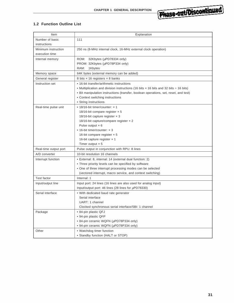
31
CHAPTER 1 GENERAL DESCRIPTION
1.2 Function Outline List
Item Explanation
Number of basic 111
instructions
Minimum instruction 250 ns (8-MHz internal clock, 16-MHz external clock operation)
execution time
Internal memory ROM: 32Kbytes (µPD78334 only)
PROM: 32Kbytes (µPD78P334 only)
RAM: 1Kbytes
Memory space 64K bytes (external memory can be added)
General register 8 bits × 16 registers × 8 banks
Instruction set • 16-bit transfer/arithmetic instructions
• Multiplication and division instructions (16 bits × 16 bits and 32 bits ÷ 16 bits)
• Bit manipulation instructions (transfer, boolean operations, set, reset, and test)
• Context switching instructions
• String instructions
Real-time pulse unit • 18/16-bit timer/counter: × 1
18/16-bit compare register × 5
18/16-bit capture register × 3
18/16-bit capture/compare register × 2
Pulse output × 6
• 16-bit timer/counter: × 3
16-bit compare register × 5
16-bit capture register × 1
Timer output × 5
Real-time output port Pulse output in conjunction with RPU: 8 lines
A/D converter 10-bit resolution 16 channels
Interrupt function • External: 8, internal: 14 (external dual function: 2)
• Three priority levels can be specified by software
• One of three interrupt processing modes can be selected
(vectored interrupt, macro service, and context switching)
Test factor Internal: 1
Input/output line Input port: 24 lines (16 lines are also used for analog input)
Input/output port: 46 lines (28 lines for µPD78330)
Serial interface • With dedicated baud rate generator
Serial interface
UART: 1 channel
Clocked synchronous serial interface/SBI: 1 channel
Package • 84-pin plastic QFJ
• 94-pin plastic QFP
• 84-pin ceramic WQFN (µPD78P334 only)
• 94-pin ceramic WQFN (µPD78P334 only)
Other • Watchdog timer function
• Standby function (HALT or STOP)
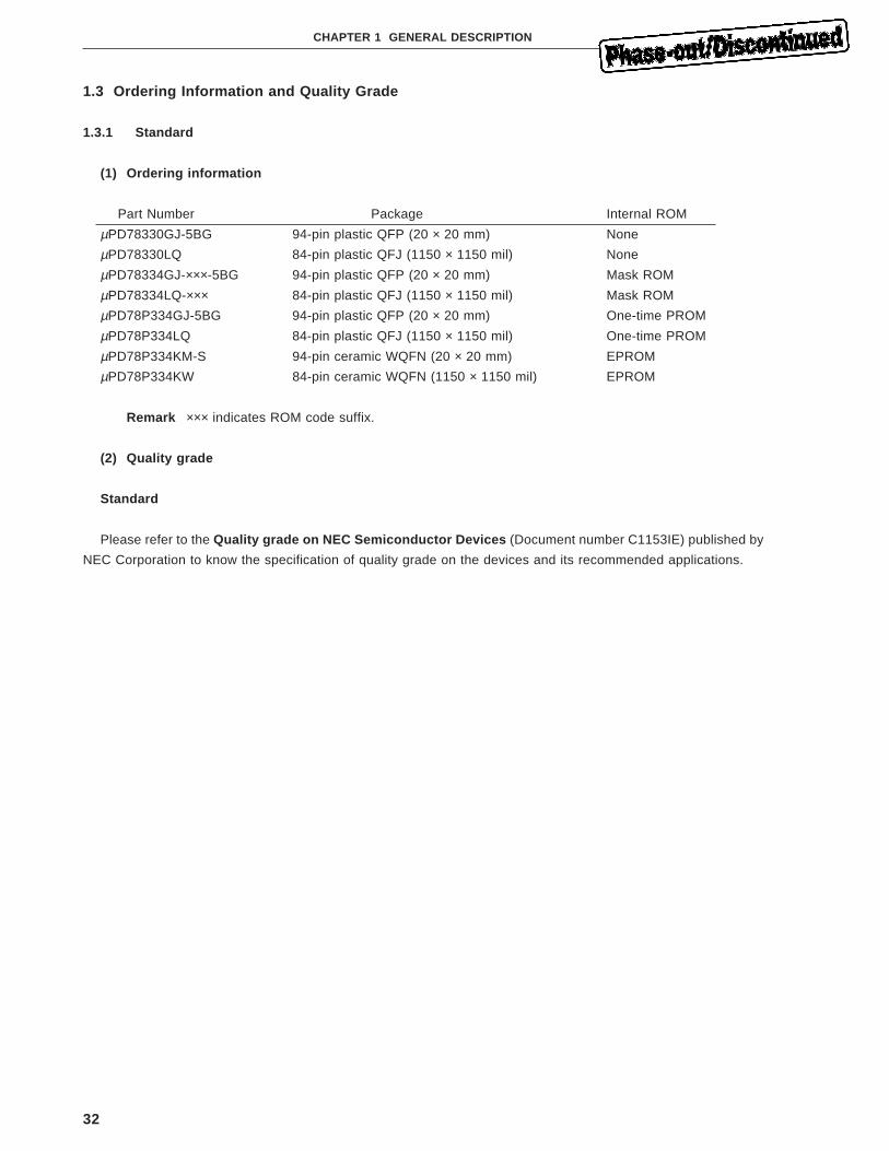
32
CHAPTER 1 GENERAL DESCRIPTION
1.3 Ordering Information and Quality Grade
1.3.1 Standard
(1) Ordering information
Part Number Package Internal ROM
µPD78330GJ-5BG 94-pin plastic QFP (20 × 20 mm) None
µPD78330LQ 84-pin plastic QFJ (1150 × 1150 mil) None
µPD78334GJ-×××-5BG 94-pin plastic QFP (20 × 20 mm) Mask ROM
µPD78334LQ-××× 84-pin plastic QFJ (1150 × 1150 mil) Mask ROM
µPD78P334GJ-5BG 94-pin plastic QFP (20 × 20 mm) One-time PROM
µPD78P334LQ 84-pin plastic QFJ (1150 × 1150 mil) One-time PROM
µPD78P334KM-S 94-pin ceramic WQFN (20 × 20 mm) EPROM
µPD78P334KW 84-pin ceramic WQFN (1150 × 1150 mil) EPROM
Remark ××× indicates ROM code suffix.
(2) Quality grade
Standard
Please refer to the Quality grade on NEC Semiconductor Devices (Document number C1153IE) published by
NEC Corporation to know the specification of quality grade on the devices and its recommended applications.
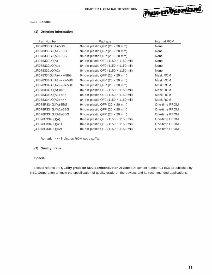
33
CHAPTER 1 GENERAL DESCRIPTION
1.3.2 Special
(1) Ordering information
Part Number Package Internal ROM
µPD78330GJ(A)-5BG 94-pin plastic QFP (20 × 20 mm) None
µPD78330GJ(A1)-5BG 94-pin plastic QFP (20 × 20 mm) None
µPD78330GJ(A2)-5BG 94-pin plastic QFP (20 × 20 mm) None
µPD78330LQ(A) 84-pin plastic QFJ (1150 × 1150 mil) None
µPD78330LQ(A1) 84-pin plastic QFJ (1150 × 1150 mil) None
µPD78330LQ(A2) 84-pin plastic QFJ (1150 × 1150 mil) None
µPD78334GJ(A)-×××-5BG 94-pin plastic QFP (20 × 20 mm) Mask ROM
µPD78334GJ(A1)-×××-5BG 94-pin plastic QFP (20 × 20 mm) Mask ROM
µPD78334GJ(A2)-×××-5BG 94-pin plastic QFP (20 × 20 mm) Mask ROM
µPD78334LQ(A)-××× 84-pin plastic QFJ (1150 × 1150 mil) Mask ROM
µPD78334LQ(A1)-××× 84-pin plastic QFJ (1150 × 1150 mil) Mask ROM
µPD78334LQ(A2)-××× 84-pin plastic QFJ (1150 × 1150 mil) Mask ROM
µPD78P334GJ(A)-5BG 94-pin plastic QFP (20 × 20 mm) One-time PROM
µPD78P334GJ(A1)-5BG 94-pin plastic QFP (20 × 20 mm) One-time PROM
µPD78P334GJ(A2)-5BG 94-pin plastic QFP (20 × 20 mm) One-time PROM
µPD78P334LQ(A) 84-pin plastic QFJ (1150 × 1150 mil) One-time PROM
µPD78P334LQ(A1) 84-pin plastic QFJ (1150 × 1150 mil) One-time PROM
µPD78P334LQ(A2) 84-pin plastic QFJ (1150 × 1150 mil) One-time PROM
Remark ××× indicates ROM code suffix.
(2) Quality grade
Special
Please refer to the Quality grade on NEC Semiconductor Devices (Document number C11531E) published by
NEC Corporation to know the specification of quality grade on the devices and its recommended applications.
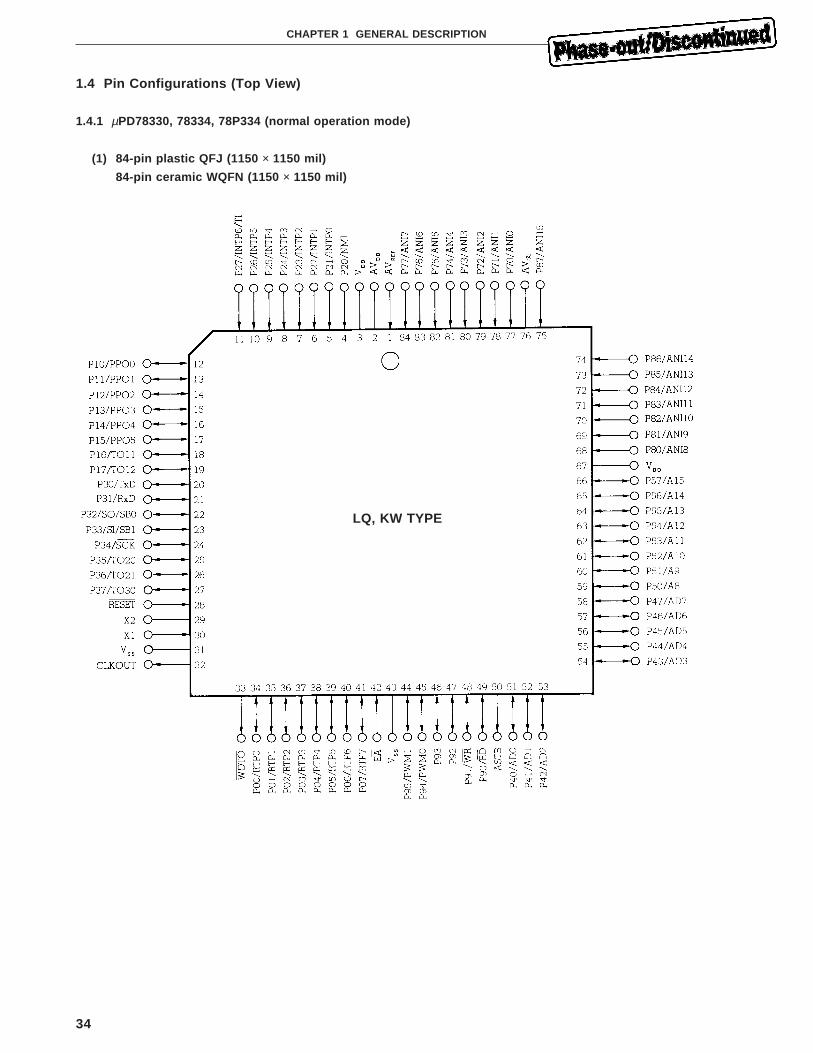
34
CHAPTER 1 GENERAL DESCRIPTION
1.4 Pin Configurations (Top View)
1.4.1 µPD78330, 78334, 78P334 (normal operation mode)
(1) 84-pin plastic QFJ (1150 × 1150 mil)
84-pin ceramic WQFN (1150 × 1150 mil)
LQ, KW TYPE
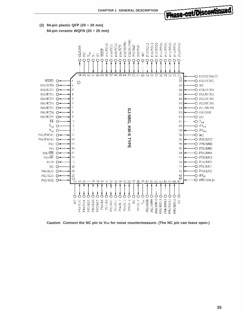
35
CHAPTER 1 GENERAL DESCRIPTION
(2) 94-pin plastic QFP (20 × 20 mm)
94-pin ceramic WQFN (20 × 20 mm)
Caution Connect the NC pin to V SS for noise countermeasure. (The NC pin can leave open.)
GJ-5B
G, K
M-S
TY
PE
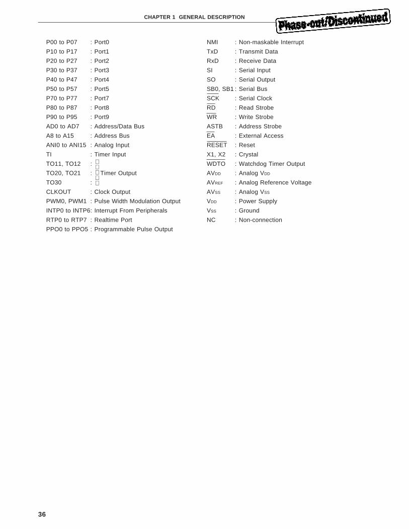
36
CHAPTER 1 GENERAL DESCRIPTION
P00 to P07 : Port0 NMI : Non-maskable Interrupt
P10 to P17 : Port1 TxD : Transmit Data
P20 to P27 : Port2 RxD : Receive Data
P30 to P37 : Port3 SI : Serial Input
P40 to P47 : Port4 SO : Serial Output
P50 to P57 : Port5 SB0, SB1 : Serial Bus
P70 to P77 : Port7 SCK : Serial Clock
P80 to P87 : Port8 RD : Read Strobe
P90 to P95 : Port9 WR : Write Strobe
AD0 to AD7 : Address/Data Bus ASTB : Address Strobe
A8 to A15 : Address Bus EA : External Access
ANI0 to ANI15 : Analog Input RESET : Reset
TI : Timer Input X1, X2 : Crystal
TO11, TO12 : WDTO : Watchdog Timer Output
TO20, TO21 : Timer Output AVDD : Analog VDD
TO30 : AVREF : Analog Reference Voltage
CLKOUT : Clock Output AVSS : Analog VSS
PWM0, PWM1 : Pulse Width Modulation Output VDD : Power Supply
INTP0 to INTP6: Interrupt From Peripherals VSS : Ground
RTP0 to RTP7 : Realtime Port NC : Non-connection
PPO0 to PPO5 : Programmable Pulse Output
37
CHAPTER 1 GENERAL DESCRIPTION
1.4.2 µPD78P334 (PROM programming mode: RESET = H and AV DD = L)
(1) 84-pin plastic QFJ (1150 × 1150 mil)
84-pin ceramic WQFN (1150 × 1150 mil)
Caution The entry enclosed in parentheses indicates treatment of the pins unused in the PROM
programming mode.
L : Connect individually to V SS or V DD via a register.
G : Connect to V SS.
Open : Leave the pins unconnected.
LQ, KW TYPE
38
CHAPTER 1 GENERAL DESCRIPTION
(2) 94-pin plastic QFP (20 × 20 mm)
94-pin ceramic WQFN (20 × 20 mm)
Cautions 1. The entry enclosed in parentheses indicates treatment of the pins unused in the PROM
programming mode.
L : Connect individually to V SS or V DD via a register.
G : Connect to V SS.
Open: Leave the pins unconnected.
2. Connect the NC pin to V SS for noise countermeasure. (The NC pin can leave open.)
A0 to A16 : Address Bus RESET : Programming Mode Set
D0 to D7 : Data Bus AVDD :
CE : Chip Enable VPP : Programming Power Supply
OE : Output Enable NC : Non-connection
PGM : Programming Mode
GJ-5B
G, K
M-S
TY
PE
39
CH
AP
TE
R 1 G
EN
ER
AL D
ES
CR
IPT
ION
1.5 Block D
iagram
PeripheralRAM
768 × 8
Notes 1. The µPD78330 does not contain ROM.
The µPD78P334 contains 32 K-byte PROM.
2. Only the µPD78P334 contains the ECC circuit.
Remark : During programming mode.
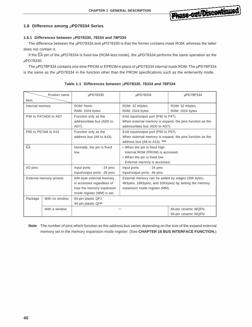
40
CHAPTER 1 GENERAL DESCRIPTION
1.6 Difference among µPD78334 Series
1.6.1 Differences between µPD78330, 78334 and 78P334
The difference between the µPD78334 and µPD78330 is that the former contains mask ROM; whereas the latter
does not contain it.
If the EA pin of the µPD78334 is fixed low (ROM-less mode), the µPD78334 performs the same operation as the
µPD78330.
The µPD78P334 contains one-time PROM or EPROM in place of µPD78334 internal mask ROM. The µPD78P334
is the same as the µPD78334 in the function other than the PROM specifications such as the write/verify mode.
Table 1-1 Differences between µPD78330, 78334 and 78P334
Product name
Item
Internal memory
P40 to P47/AD0 to AD7
P50 to P57/A8 to A15
EA
I/O pins
External memory access
Package With no window
With a window
µPD78330
ROM: None
RAM: 1024 bytes
Function only as the
address/data bus (AD0 to
AD7).
Function only as the
address bus (A8 to A15).
Normally, the pin is fixed
low.
Input ports : 24 pins
Input/output ports : 28 pins
64K-byte external memory
is accessed regardless of
how the memory expansion
mode register (MM) is set.
84-pin plastic QFJ
94-pin plastic QFP
µPD78334 µPD78P334
ROM: 32 Kbytes ROM: 32 Kbytes
RAM: 1024 bytes RAM: 1024 bytes
8-bit input/output port (P40 to P47).
When external memory is expand, the pins function as the
address/data bus (AD0 to AD7).
8-bit input/output port (P50 to P57).
When external memory is expand, the pins function as the
address bus (A8 to A15). Note
• When the pin is fixed high
Internal ROM (PROM) is accessed.
• When the pin is fixed low
External memory is accessed.
Input ports : 24 pins
Input/output ports : 46 pins
External memory can be added by stages (256 bytes,
4Kbytes, 16Kbytes, and 32Kbytes) by setting the memory
expansion mode register (MM).
Note The number of pins which function as the address bus varies depending on the size of the expand external
memory set in the memory expansion mode register. (See CHAPTER 16 BUS INTERFACE FUNCTION. )
84-pin ceramic WQFN
94-pin ceramic WQFN
—
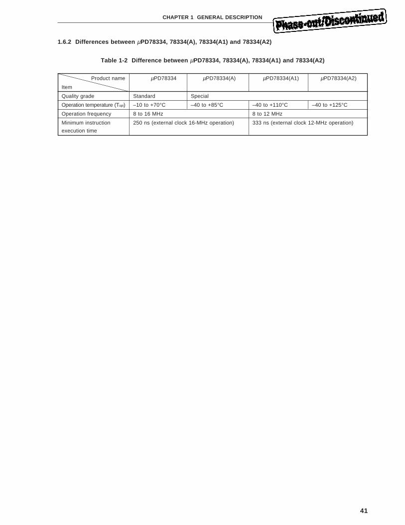
41
CHAPTER 1 GENERAL DESCRIPTION
1.6.2 Differences between µPD78334, 78334(A), 78334(A1) and 78334(A2)
Table 1-2 Difference between µPD78334, 78334(A), 78334(A1) and 78334(A2)
Product name µPD78334 µPD78334(A) µPD78334(A1) µPD78334(A2)
Item
Quality grade Standard Special
Operation temperature (Topt) –10 to +70°C –40 to +85°C –40 to +110°C –40 to +125°C
Operation frequency 8 to 16 MHz 8 to 12 MHz
Minimum instruction 250 ns (external clock 16-MHz operation) 333 ns (external clock 12-MHz operation)
execution time

42
[MEMO]
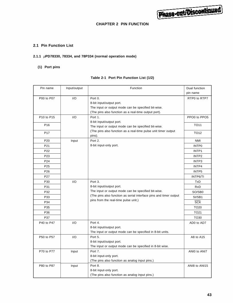
43
CHAPTER 2 PIN FUNCTION
2.1 Pin Function List
2.1.1 µPD78330, 78334, and 78P334 (normal operation mode)
(1) Port pins
Table 2-1 Port Pin Function List (1/2)
Pin name
P00 to P07
P10 to P15
P16
P17
P20
P21
P22
P23
P24
P25
P26
P27
P30
P31
P32
P33
P34
P35
P36
P37
P40 to P47
P50 to P57
P70 to P77
P80 to P87
Input/output
I/O
I/O
Input
I/O
I/O
I/O
Input
Input
Function
Port 0.
8-bit input/output port.
The input or output mode can be specified bit-wise.
(The pins also function as a real-time output port).
Port 1.
8-bit input/output port.
The input or output mode can be specified bit-wise.
(The pins also function as a real-time pulse unit timer output
pins).
Port 2.
8-bit input-only port.
Port 3.
8-bit input/output port.
The input or output mode can be specified bit-wise.
(The pins also function as serial interface pins and timer output
pins from the real-time pulse unit.)
Port 4.
8-bit input/output port.
The input or output mode can be specified in 8-bit units.
Port 5.
8-bit input/output port.
The input or output mode can be specified in 8-bit wise.
Port 7.
8-bit input-only port.
(The pins also function as analog input pins.)
Port 8.
8-bit input-only port.
(The pins also function as analog input pins.)
Dual function
pin name
RTP0 to RTP7
PPO0 to PPO5
TO11
TO12
NMI
INTP0
INTP1
INTP2
INTP3
INTP4
INTP5
INTP6/TI
TxD
RxD
SO/SB0
SI/SB1
SCK
TO20
TO21
TO30
AD0 to AD7
A8 to A15
ANI0 to ANI7
ANI8 to ANI15
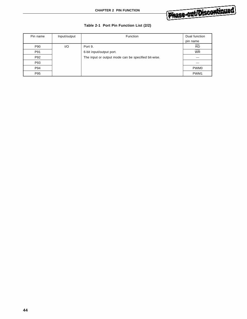
44
CHAPTER 2 PIN FUNCTION
Table 2-1 Port Pin Function List (2/2)
Pin name
P90
P91
P92
P93
P94
P95
Input/output
I/O
Function
Port 9.
6-bit input/output port.
The input or output mode can be specified bit-wise.
Dual function
pin name
RD
WR
—
—
PWM0
PWM1
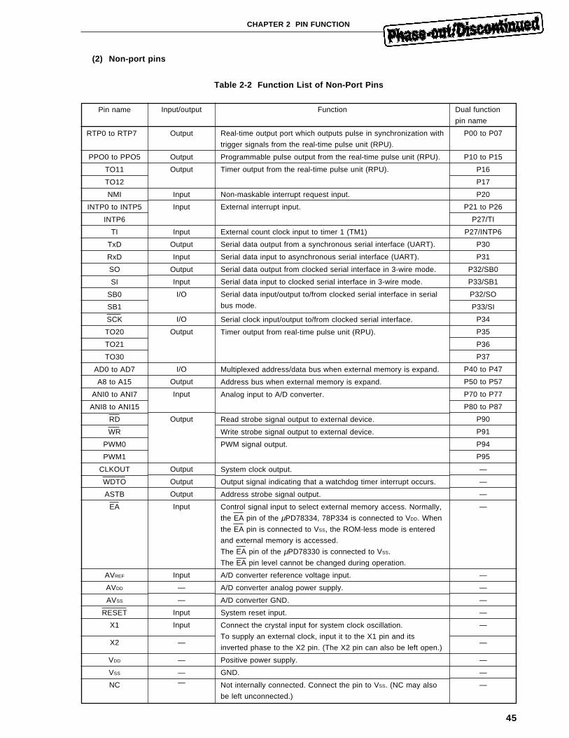
45
CHAPTER 2 PIN FUNCTION
(2) Non-port pins
Table 2-2 Function List of Non-Port Pins
Pin name
RTP0 to RTP7
PPO0 to PPO5
TO11
TO12
NMI
INTP0 to INTP5
INTP6
TI
TxD
RxD
SO
SI
SB0
SB1
SCK
TO20
TO21
TO30
AD0 to AD7
A8 to A15
ANI0 to ANI7
ANI8 to ANI15
RD
WR
PWM0
PWM1
CLKOUT
WDTO
ASTB
EA
AVREF
AVDD
AVSS
RESET
X1
X2
VDD
VSS
NC
Input/output
Output
Output
Output
Input
Input
Input
Output
Input
Output
Input
I/O
I/O
Output
I/O
Output
Input
Output
Output
Output
Output
Input
Input
—
—
Input
Input
—
—
—
Function
Real-time output port which outputs pulse in synchronization with
trigger signals from the real-time pulse unit (RPU).
Programmable pulse output from the real-time pulse unit (RPU).
Timer output from the real-time pulse unit (RPU).
Non-maskable interrupt request input.
External interrupt input.
External count clock input to timer 1 (TM1)
Serial data output from a synchronous serial interface (UART).
Serial data input to asynchronous serial interface (UART).
Serial data output from clocked serial interface in 3-wire mode.
Serial data input to clocked serial interface in 3-wire mode.
Serial data input/output to/from clocked serial interface in serial
bus mode.
Serial clock input/output to/from clocked serial interface.
Timer output from real-time pulse unit (RPU).
Multiplexed address/data bus when external memory is expand.
Address bus when external memory is expand.
Analog input to A/D converter.
Read strobe signal output to external device.
Write strobe signal output to external device.
PWM signal output.
System clock output.
Output signal indicating that a watchdog timer interrupt occurs.
Address strobe signal output.
Control signal input to select external memory access. Normally,
the EA pin of the µPD78334, 78P334 is connected to VDD. When
the EA pin is connected to VSS, the ROM-less mode is entered
and external memory is accessed.
The EA pin of the µPD78330 is connected to VSS.
The EA pin level cannot be changed during operation.
A/D converter reference voltage input.
A/D converter analog power supply.
A/D converter GND.
System reset input.
Connect the crystal input for system clock oscillation.
To supply an external clock, input it to the X1 pin and its
inverted phase to the X2 pin. (The X2 pin can also be left open.)
Positive power supply.
GND.
Not internally connected. Connect the pin to VSS. (NC may also
be left unconnected.)
Dual function
pin name
P00 to P07
P10 to P15
P16
P17
P20
P21 to P26
P27/TI
P27/INTP6
P30
P31
P32/SB0
P33/SB1
P32/SO
P33/SI
P34
P35
P36
P37
P40 to P47
P50 to P57
P70 to P77
P80 to P87
P90
P91
P94
P95
—
—
—
—
—
—
—
—
—
—
—
—
——
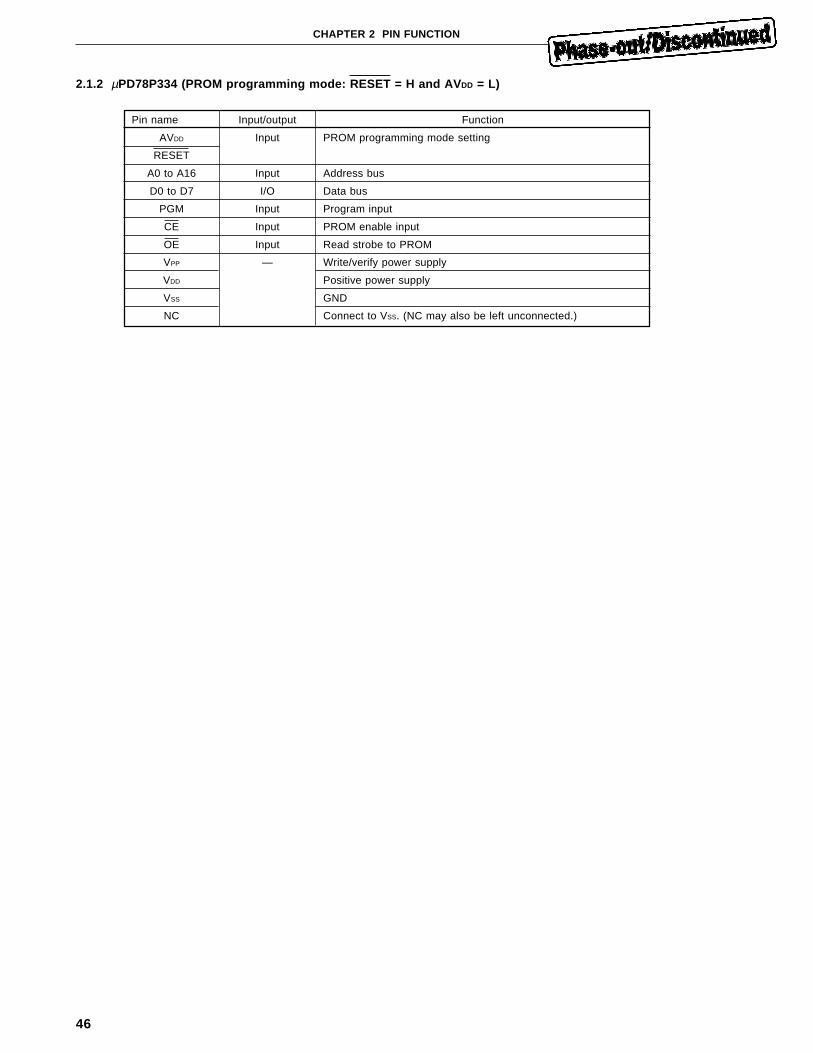
46
CHAPTER 2 PIN FUNCTION
2.1.2 µPD78P334 (PROM programming mode: RESET = H and AV DD = L)
Pin name Input/output Function
AVDD Input PROM programming mode setting
RESET
A0 to A16 Input Address bus
D0 to D7 I/O Data bus
PGM Input Program input
CE Input PROM enable input
OE Input Read strobe to PROM
VPP — Write/verify power supply
VDD Positive power supply
VSS GND
NC Connect to VSS. (NC may also be left unconnected.)
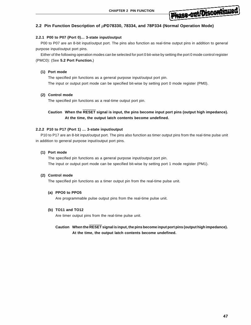
47
CHAPTER 2 PIN FUNCTION
2.2 Pin Function Description of µPD78330, 78334, and 78P334 (Normal Operation Mode)
2.2.1 P00 to P07 (Port 0)… 3-state input/output
P00 to P07 are an 8-bit input/output port. The pins also function as real-time output pins in addition to general
purpose input/output port pins.
Either of the following operation modes can be selected for port 0 bit-wise by setting the port 0 mode control register
(PMC0): (See 5.2 Port Function. )
(1) Port mode
The specified pin functions as a general purpose input/output port pin.
The input or output port mode can be specified bit-wise by setting port 0 mode register (PM0).
(2) Control mode
The specified pin functions as a real-time output port pin.
Caution When the RESET signal is input, the pins become input port pins (output high impedance).
At the time, the output latch contents become undefined.
2.2.2 P10 to P17 (Port 1) … 3-state input/output
P10 to P17 are an 8-bit input/output port. The pins also function as timer output pins from the real-time pulse unit
in addition to general purpose input/output port pins.
(1) Port mode
The specified pin functions as a general purpose input/output port pin.
The input or output port mode can be specified bit-wise by setting port 1 mode register (PM1).
(2) Control mode
The specified pin functions as a timer output pin from the real-time pulse unit.
(a) PPO0 to PPO5
Are programmable pulse output pins from the real-time pulse unit.
(b) TO11 and TO12
Are timer output pins from the real-time pulse unit.
Caution When the RESET signal is input, the pins become input port pins (output high impedance).
At the time, the output latch contents become undefined.
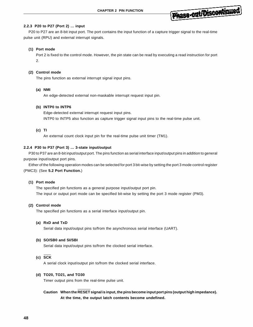
48
CHAPTER 2 PIN FUNCTION
2.2.3 P20 to P27 (Port 2) … input
P20 to P27 are an 8-bit input port. The port contains the input function of a capture trigger signal to the real-time
pulse unit (RPU) and external interrupt signals.
(1) Port mode
Port 2 is fixed to the control mode. However, the pin state can be read by executing a read instruction for port
2.
(2) Control mode
The pins function as external interrupt signal input pins.
(a) NMI
An edge-detected external non-maskable interrupt request input pin.
(b) INTP0 to INTP6
Edge-detected external interrupt request input pins.
INTP0 to INTP5 also function as capture trigger signal input pins to the real-time pulse unit.
(c) TI
An external count clock input pin for the real-time pulse unit timer (TM1).
2.2.4 P30 to P37 (Port 3) … 3-state input/output
P30 to P37 are an 8-bit input/output port. The pins function as serial interface input/output pins in addition to general
purpose input/output port pins.
Either of the following operation modes can be selected for port 3 bit-wise by setting the port 3 mode control register
(PMC3): (See 5.2 Port Function. )
(1) Port mode
The specified pin functions as a general purpose input/output port pin.
The input or output port mode can be specified bit-wise by setting the port 3 mode register (PM3).
(2) Control mode
The specified pin functions as a serial interface input/output pin.
(a) RxD and TxD
Serial data input/output pins to/from the asynchronous serial interface (UART).
(b) SO/SB0 and SI/SBI
Serial data input/output pins to/from the clocked serial interface.
(c) SCK
A serial clock input/output pin to/from the clocked serial interface.
(d) TO20, TO21, and TO30
Timer output pins from the real-time pulse unit.
Caution When the RESET signal is input, the pins become input port pins (output high impedance).
At the time, the output latch contents become undefined.
49
CHAPTER 2 PIN FUNCTION
2.2.5 P40 to P47 (Port 4) … 3-state input/output
The µPD78330, 78334, and 78P334 differ in P40 to P47 function.
(1) µPD78330
Port 4 is fixed to the external memory expansion mode and always functions as the address/data bus (AD0
to AD7). It does not function as a port.
(2) µPD78334 (EA pin is fixed high)
P40 to P47 are an 8-bit input/output port. The pin function as the address/data bus pins in addition to general
purpose input/output port pins.
Either of the following operation modes can be selected for port 4 by setting the memory expansion mode
register (MM): (See CHAPTER 16 BUS INTERFACE FUNCTION. )
(a) Port mode
The pins function as an 8-bit general purpose input/output port.
The input or output port mode can be specified in 8-bit units by setting the memory expansion mode register
(MM).
(b) External memory expansion mode
The pins function as address/data bus pins (AD0 to AD7) to access external memory.
(3) µPD78P334 (no EA pin is fixed high)
P40 to P47 are an 8-bit special input/output port. The pins function as multiplexed address/data bus pins in
addition to general purpose input/output port pins.
In the PROM programming mode, the pins become data input/output pins.
Either of the following operation modes can be selected for port 4 by setting the memory expansion mode
register (MM): (See CHAPTER 16 BUS INTERFACE FUNCTION. )
(a) Port mode
The pins function as an 8-bit general purpose input/output port.
The input or output port mode can be specified in 8-bit units by setting the memory expansion mode register
(MM).
(b) External memory expansion mode
The pins function as address/data bus pins (AD0 to AD7) to access external memory.
In this case, it is not affected by the port 4 register value.
Cautions 1. If the EA pin for µPD78334, 78P334 is fixed low, the pins always function as address/
data bus pins as with the µPD78330; the pins do not function as port pins.
2. When the RESET signal is input, the pins become input port pins (output high
impedance) regardless of the port mode or external memory expansion mode. At the
time, the output latch contents become undefined.
50
CHAPTER 2 PIN FUNCTION
2.2.6 P50 to P57 (Port 5) … 3-state input/output
The µPD78330, 78334, and 78P334 differ in P50 to P57 function.
(1) µPD78330
Port 5 is fixed to the external memory expansion mode and always functions as an 8-bit address bus (A8 to
A15). It does not function as a port.
(2) µPD78334 (EA pin is fixed high)
P50 to P57 are an 8-bit input/output port. The pins function as address bus pins in addition to general purpose
input/output port pins.
Either of the following operation modes can be selected for port 5 by setting the memory expansion mode
register (MM): (See CHAPTER 16 BUS INTERFACE FUNCTION. )
(a) Port mode
The pins function as a 2-, 4-, or 8-bit general purpose input/output port. The input or output port mode
can be specified bit-wise by setting the port 5 mode register (PM5). (See 5.2 Port Function. )
(b) External memory expansion mode
The pins function as a 4-, 6-, or 8-bit address bus to access external memory.
P50 to P57 can be specified as address output by stages according to the size of the external memory
to be expand. (The remaining pins can be used as general purpose input/output port pins.)
(3) µPD78P334 (EA pin is fixed high)
P50 to P57 are an 8-bit special input/output port. In addition to general purpose input/output port pins, the
pins function as address bus pins when external memory and I/O are expand.
(a) Port mode
The pins function as a 2-, 4-, or 8-bit general purpose input/output port.
The input or output port mode can be specified bit-wise by setting the port 5 mode register (PM5). (See
5.2 Port Function. )
(b) External memory expansion mode
The pins function as a 4-, 6-, or 8-bit address bus to access external memory.
P50 to P57 can be specified as address output by stages according to the size of the external memory
to be expand. (The remaining pins can be used as general purpose input/output port pins.)
Cautions 1. If the EA pin for µPD78334, 78P334 is fixed low, the pins always function as address
bus pins as with the µPD78330; the pins do not function as port pins.
2. when the RESET signal is input, the pins become input port pins (output high
impedance)regardless of the port mode or external memory expansion mode. At the
time, the output latch contents become undefined.
51
CHAPTER 2 PIN FUNCTION
2.2.7 P70 to P77 (Port 7) … input
P70 to P77 are an 8-bit input port. The pins function as analog signal input pins to the A/D converter in addition
to general purpose input port pins.
(1) Port mode
Port 7 is fixed to the control mode. However, the pin state can be read by executing a read instruction for port
7.
(2) Control mode
The pins function as analog signal input pins to the A/D converter (ANI0 to ANI7).
2.2.8 P80 to P87 (Port 8) … input
P80 to P87 are an 8-bit input port. The pins function as analog signal input pins to the A/D converter in addition
to general purpose input port pins.
(1) Port mode
Port 8 is fixed to the control mode. However, the pin state can be read by executing a read instruction for port
8.
Example: MOV A, P8; Read the pin state of port 8 into A register.
(2) Control mode
The pins function as analog signal input pins to the A/D converter (ANI8 to ANI15).
2.2.9 P90 to P95 (Port 9) … 3-state input/output
The µPD78330, 78334, 78P334 differ in P90 to P95 function.
(1) µPD78330
The P90 and P91 pins are fixed to external memory control signals and always function as RD and WR
respectively.
Port function is not provided.
(a) Port mode
The pins function as a 4-bit general purpose input/output port.
The input or output port mode can be specified bit-wise by setting the port 9 mode register (PM9).
(b) Control mode
The pins function as a external memory control signal pin and PWM signal output pins (PWM0, PWM1).
52
CHAPTER 2 PIN FUNCTION
(2) µPD78334 (EA pin is fixed high)
P90 to P95 are a 6-bit input/output port. The pins also function as external memory control signal output and
PWM (Pulse Width Modulation) signal output pins in addition to general purpose input/output port pins.
(a) Port mode
The pins function as general purpose input/output port pins.
The input or output port mode can be specified bit-wise by setting the port 9 mode register (PM9).
(b) Control mode
The pins function as external memory control signal output and PWM signal output pins.
(i) RD
Is an external memory read signal output pin.
(ii) WR
Is an external memory write signal output pin.
(iii) PWM0 and PWM1
Are PSW signal output pins.
(3) µPD78P334 (EA pin is fixed high)
P90 to P95 are a 6-bit input/output port. The pins function as external memory control signal output pins in
addition to general purpose input/output port pins.
Either of the following operation modes can be selected for port 9 by setting the port 9 mode register (PM9)
and memory expansion mode register (MM): (See 5.2 Port Function. )
(a) Port mode
The pins function as general purpose input/output port pins.
The input or output port mode can be specified bit-wise by setting port 9 mode register (PM9).
(b) Control mode
The pins function as external memory control signal output and PWM signal output pins.
(i) RD
Is an external memory read signal output pin.
(ii) WR
Is an external memory write signal output pin.
(iii) PWM0 and PWM1
Are PWM signal output pins.
Cautions 1. If the EA pin for µPD78334, 78P334 is fixed low, the P90 and P91 pins always
function as RD and WR pins respectively. The pins do not function as port pins.
2. When the RESET signal is input, the pins become input port pins (output high
impedance). At the time, the output latch contents become undefined.
53
CHAPTER 2 PIN FUNCTION
2.2.10 ASTB … output
ASTB is a timing signal output pin to access external memory expand. It is used to externally latch an address
output from port 4.
2.2.11 EA … input
Normally, the µPD78334 EA pin is fixed to “1” (high). The EA pin level cannot be changed during operation.
(1) When EA is high (connection to V DD pin)
Internal ROM is accessed.
(2) When EA is low (connection to V SS pin)
The ROM-less mode is entered and external memory is accessed.
Fix the µPD78330 EA pin low (connect it to the VSS pin).
2.2.12 CLKOUT (Clock Output) … output
CLKOUT is a system clock output pin.
2.2.13 WDTO (Watchdog Timer Output) … output
WDTO is an output pin of the signal indicating that the watchdog timer causes a non-maskable interrupt to occur.
2.2.14 AVREF (Reference Voltage) … input
AVREF is an A/D converter reference voltage input pin.
2.2.15 AVDD (Analog V DD)
AVDD is an A/D converter power supply pin.
2.2.16 AVSS (Analog V SS)
AVSS is an A/D converter ground pin.
2.2.17 RESET (Reset) … input
RESET is an active low system reset input pin.
2.2.18 X1 and X2 (Crystal)
X1 and X2 are crystal resonator connection pins for system clock generation.
To supply external clock, it is input to the X1 pin and its inverted signal is input to the X2 pin. X2 pin may be left
unconnected.
2.2.19 VDD
VDD is a positive power supply pin.
2.2.20 VSS
VSS is a ground potential pin.
2.2.21 NC
NC is not internally connected pin. Connect the pin to VSS. (NC may also be left unconnected.)
54
CHAPTER 2 PIN FUNCTION
2.3 Description of the Pin Function of µPD78P334 (PROM Programming Mode)
(1) AVDD (Analog V DD)
AVDD is an input pin to set the µPD78P334 to the PROM programming mode.
When the input voltage to the pin is low and RESET input goes high, the µPD78P334 enters the PROM
programming mode.
(2) RESET … input
RESET is an input pin to set the µPD78P334 to the PROM programming mode.
When input to the pin is high and the input voltage to the AVDD pin becomes low, the µD78P334 enters the
PROM programming mode.
(3) A0 to A16 (Address Bus) … input
A0 to A16 are address bus pins.
Internal PROM address (0000H to 7FFFH) is selected.
(4) D0 to D7 (Data Bus) … input/output
D0 to D7 are data bus pins.
Programs are written/read into/from internal PROM via the data bus.
(5) PGM (Programming Mode) … input
PGM is an internal PROM operation mode control signal input pin.
When the signal is active, write into internal PROM is enabled.
When the signal is inactive, read from internal PROM is enabled.
(6) CE (Chip Enable) … input
CE is an internal PROM enable signal input pin.
When the signal is active, program write/read is enabled.
(7) OE (Output Enable) … input
OE is a read strobe signal input pin to internal PROM. If the signal is activated when CE is low, the contents
of PROM selected at A0 to A16 as the 1-byte unit can be read on D0 to D7.
(8) VPP (Programming Power Supply)
VPP is a program write power supply pin.
When VPP is 12.5V and OE is high, if CE is set low, the program on D0 to D7 can be written into the internal
PROM selected at A0 to A16.
(9) VDD
VDD is a positive power supply pin.
(10) VSS
VSS is a GND potential pin.
(11) NC
Connect the IC pin to VSS. (NC may also be left unconnected.)
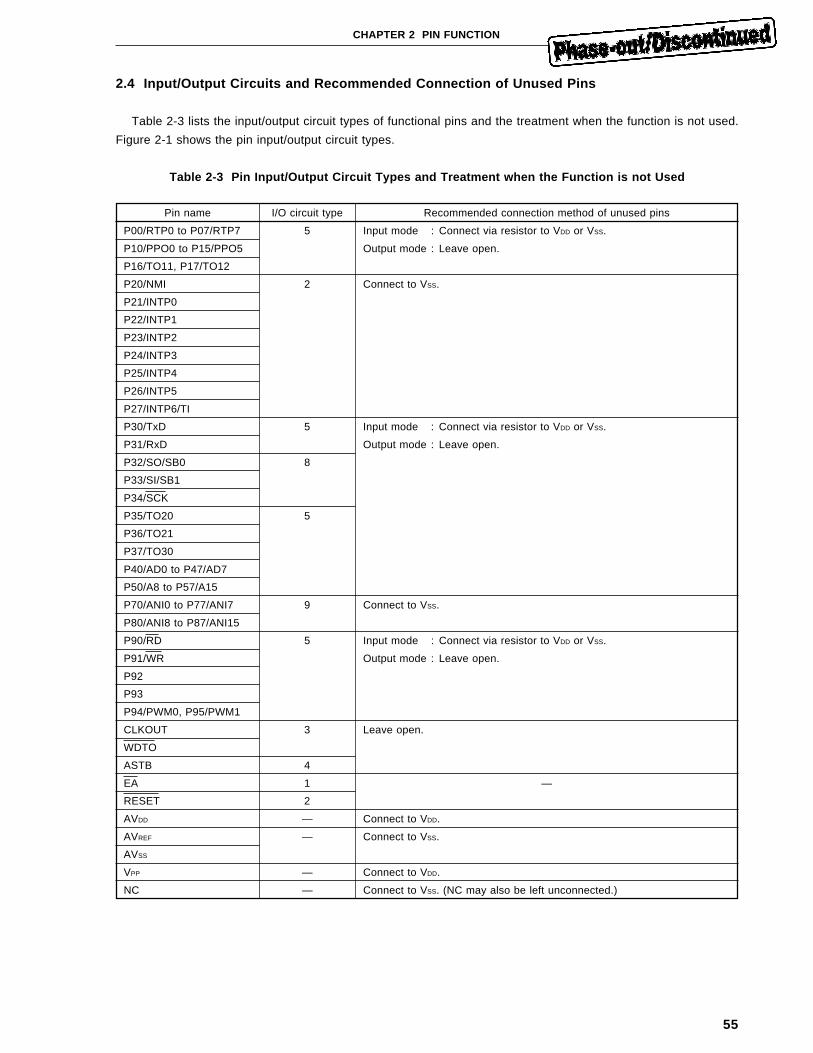
55
CHAPTER 2 PIN FUNCTION
2.4 Input/Output Circuits and Recommended Connection of Unused Pins
Table 2-3 lists the input/output circuit types of functional pins and the treatment when the function is not used.
Figure 2-1 shows the pin input/output circuit types.
Table 2-3 Pin Input/Output Circuit Types and Treatment when the Function is not Used
Pin name I/O circuit type Recommended connection method of unused pins
P00/RTP0 to P07/RTP7 5 Input mode : Connect via resistor to VDD or VSS.
P10/PPO0 to P15/PPO5 Output mode : Leave open.
P16/TO11, P17/TO12
P20/NMI 2 Connect to VSS.
P21/INTP0
P22/INTP1
P23/INTP2
P24/INTP3
P25/INTP4
P26/INTP5
P27/INTP6/TI
P30/TxD 5 Input mode : Connect via resistor to VDD or VSS.
P31/RxD Output mode : Leave open.
P32/SO/SB0 8
P33/SI/SB1
P34/SCK
P35/TO20 5
P36/TO21
P37/TO30
P40/AD0 to P47/AD7
P50/A8 to P57/A15
P70/ANI0 to P77/ANI7 9 Connect to VSS.
P80/ANI8 to P87/ANI15
P90/RD 5 Input mode : Connect via resistor to VDD or VSS.
P91/WR Output mode : Leave open.
P92
P93
P94/PWM0, P95/PWM1
CLKOUT 3 Leave open.
WDTO
ASTB 4
EA 1 —
RESET 2
AVDD — Connect to VDD.
AVREF — Connect to VSS.
AVSS
VPP — Connect to VDD.
NC — Connect to VSS. (NC may also be left unconnected.)
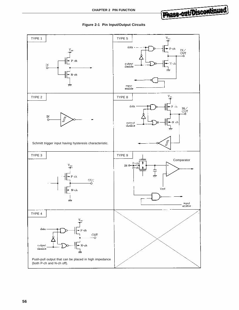
56
CHAPTER 2 PIN FUNCTION
Figure 2-1 Pin Input/Output Circuits
TYPE 1 TYPE 5
TYPE 2 TYPE 8
TYPE 3 TYPE 9
TYPE 4
Schmitt trigger input having hysteresis characteristic.
Push-pull output that can be placed in high impedance(both P-ch and N-ch off).
Comparator
57
CHAPTER 3 CPU ARCHITECTURE
3.1 Memory SpaceThe µPD78334 has address space of a maximum of 64K bytes. (See Figure 3-1 )
Program memory mapping varies depending on the product. Data memory mapping is common to the products.
(1) µPD78330
The program memory is mapped in external memory (64256 bytes: 0000H to FAFFH). This area can also be
used as the data memory.
The data memory is mapped in internal RAM (1024 bytes: FB00H to FEFFH).
(2) µPD78334, 78P334
The program memory is mapped in internal ROM (32768 bytes: 0000H to 7FFFH) and external memory (31488
bytes: 8000H to FAFFH). The external memory is accessed in the external memory expansion mode. The area
mapped in the external memory can also be used as data memory.
The data memory is mapped in internal RAM (1024 bytes: FB00H to FEFFH).
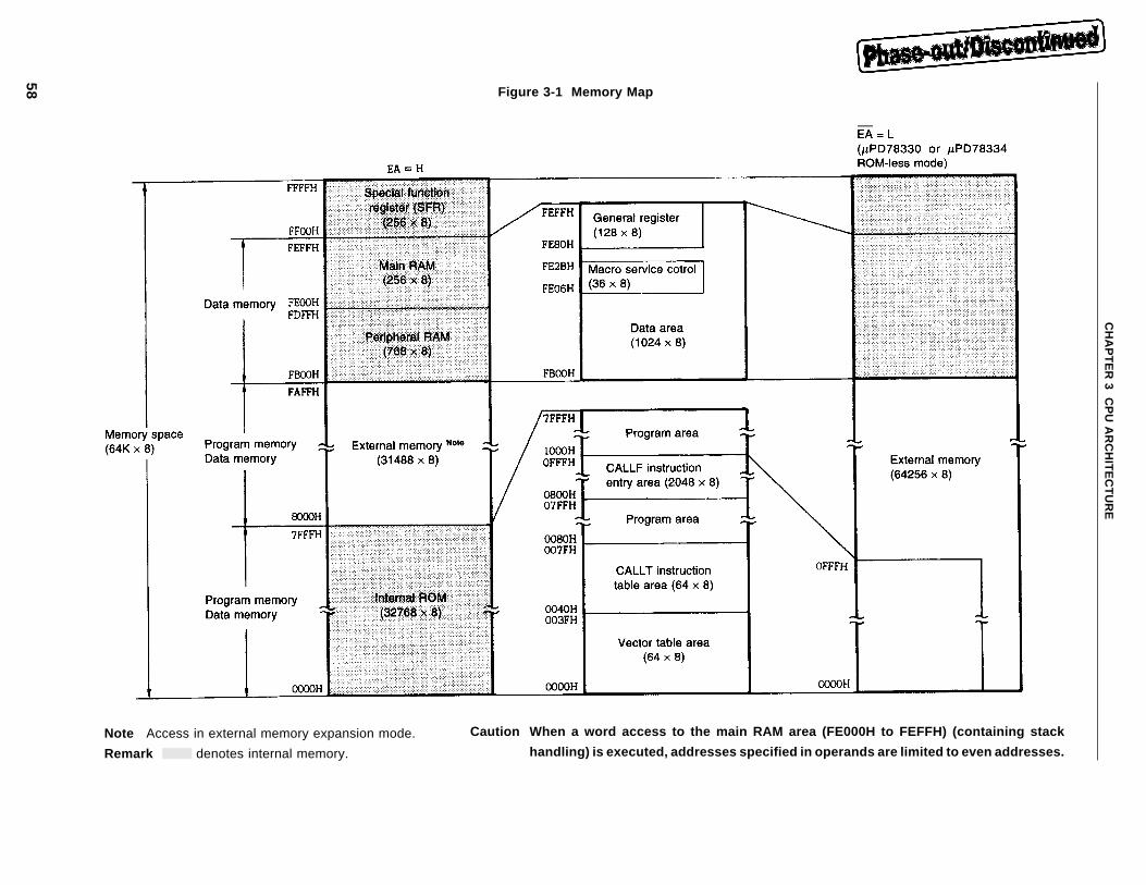
58
CH
AP
TE
R 3 C
PU
AR
CH
ITE
CT
UR
E
Figure 3-1 Memory Map
Note Access in external memory expansion mode.
Remark denotes internal memory.
Caution When a word access to the main RAM area (FE000H to FEFFH) (containing stack
handling) is executed, addresses specified in operands are limited to even addresses.
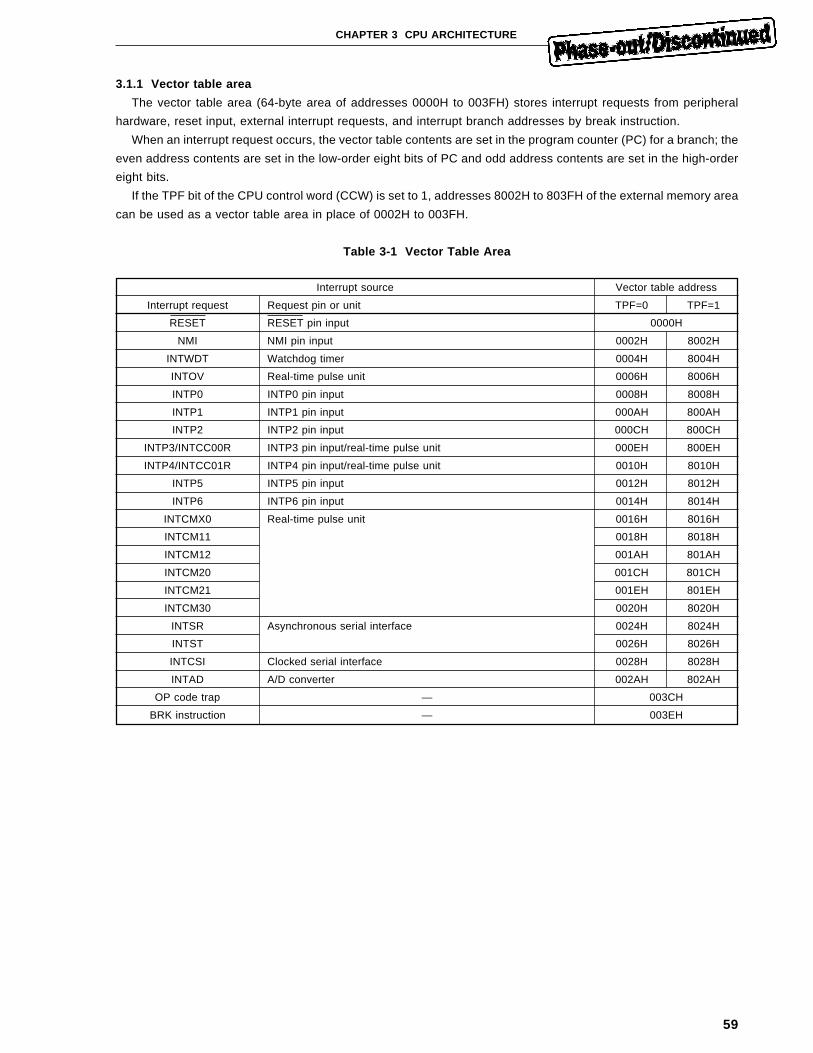
59
CHAPTER 3 CPU ARCHITECTURE
3.1.1 Vector table area
The vector table area (64-byte area of addresses 0000H to 003FH) stores interrupt requests from peripheral
hardware, reset input, external interrupt requests, and interrupt branch addresses by break instruction.
When an interrupt request occurs, the vector table contents are set in the program counter (PC) for a branch; the
even address contents are set in the low-order eight bits of PC and odd address contents are set in the high-order
eight bits.
If the TPF bit of the CPU control word (CCW) is set to 1, addresses 8002H to 803FH of the external memory area
can be used as a vector table area in place of 0002H to 003FH.
Table 3-1 Vector Table Area
Interrupt source Vector table address
Interrupt request Request pin or unit TPF=0 TPF=1
RESET RESET pin input 0000H
NMI NMI pin input 0002H 8002H
INTWDT Watchdog timer 0004H 8004H
INTOV Real-time pulse unit 0006H 8006H
INTP0 INTP0 pin input 0008H 8008H
INTP1 INTP1 pin input 000AH 800AH
INTP2 INTP2 pin input 000CH 800CH
INTP3/INTCC00R INTP3 pin input/real-time pulse unit 000EH 800EH
INTP4/INTCC01R INTP4 pin input/real-time pulse unit 0010H 8010H
INTP5 INTP5 pin input 0012H 8012H
INTP6 INTP6 pin input 0014H 8014H
INTCMX0 Real-time pulse unit 0016H 8016H
INTCM11 0018H 8018H
INTCM12 001AH 801AH
INTCM20 001CH 801CH
INTCM21 001EH 801EH
INTCM30 0020H 8020H
INTSR Asynchronous serial interface 0024H 8024H
INTST 0026H 8026H
INTCSI Clocked serial interface 0028H 8028H
INTAD A/D converter 002AH 802AH
OP code trap — 003CH
BRK instruction — 003EH
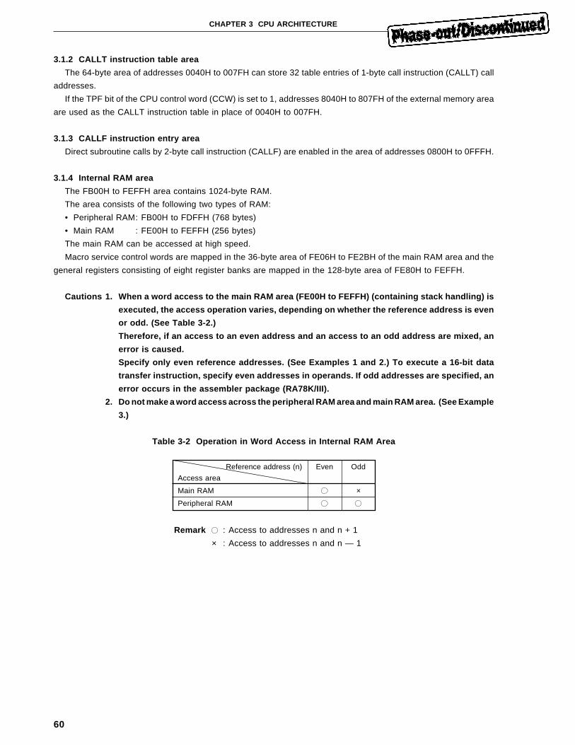
60
CHAPTER 3 CPU ARCHITECTURE
3.1.2 CALLT instruction table area
The 64-byte area of addresses 0040H to 007FH can store 32 table entries of 1-byte call instruction (CALLT) call
addresses.
If the TPF bit of the CPU control word (CCW) is set to 1, addresses 8040H to 807FH of the external memory area
are used as the CALLT instruction table in place of 0040H to 007FH.
3.1.3 CALLF instruction entry area
Direct subroutine calls by 2-byte call instruction (CALLF) are enabled in the area of addresses 0800H to 0FFFH.
3.1.4 Internal RAM area
The FB00H to FEFFH area contains 1024-byte RAM.
The area consists of the following two types of RAM:
• Peripheral RAM: FB00H to FDFFH (768 bytes)
• Main RAM : FE00H to FEFFH (256 bytes)
The main RAM can be accessed at high speed.
Macro service control words are mapped in the 36-byte area of FE06H to FE2BH of the main RAM area and the
general registers consisting of eight register banks are mapped in the 128-byte area of FE80H to FEFFH.
Cautions 1. When a word access to the main RAM area (FE00H to FEFFH) (containing stack handling) is
executed, the access operation varies, depending on whether the reference address is even
or odd. (See Table 3-2.)
Therefore, if an access to an even address and an access to an odd address are mixed, an
error is caused.
Specify only even reference addresses. (See Examples 1 and 2.) To execute a 16-bit data
transfer instruction, specify even addresses in operands. If odd addresses are specified, an
error occurs in the assembler package (RA78K/III).
2. Do not make a word access across the peripheral RAM area and main RAM area. (See Example
3.)
Table 3-2 Operation in Word Access in Internal RAM Area
Reference address (n) Even Odd
Access area
Main RAM ×
Peripheral RAM
Remark : Access to addresses n and n + 1
× : Access to addresses n and n — 1
61
CHAPTER 3 CPU ARCHITECTURE
Examples of word access in the internal RAM area are given in Examples 1 to 5.
Examples 1. To write/read word data into/from an even address (FE20H) in the main RAM area
When word data is written into an even address (address n) in the main RAM area, the low-order
eight bits of the word data are written into the even address (address n) and the high-order eight
bits are written into the odd address (address n + 1).
When word data is read from an even address (address n) in the main RAM area, it is read from
addresses n and n + 1.
MOVW AX, #1234H
MOVW 0FE20H, AX; Write word data into FE20H
MOVW AX, 0FE20H; Read word data from FE20H
n: Reference address
2. To write/read word data into/from an odd address (FE21H) in the main RAM area
When word data is written into an odd address in the main RAM area, the high-order eight bits of
the word data are written into the odd address (address n) and the low-order eight bits are written
into the even address (address n — 1).
When word data is read from an odd address (address n) in the main RAM area, it is read from
addresses n and n — 1.
MOVW AX, #1234H
MOVW DE, #0FE21H
MOVW [DE], AX; Write word data into FE21H
MOVW AX, [DE]; Read word data from FE21H
n: Reference address
62
CHAPTER 3 CPU ARCHITECTURE
3. To write/read word data across the peripheral RAM area and main RAM area
If word data is written across the peripheral RAM area and main RAM area, it is written into the 256-
byte apart address, causing an error to occur.
If word data is read from the end address of the peripheral RAM area (FDFFH), it is read from FEFEH
and FEFFH which are 256 bytes apart from FDFFH.
MOVW AX, #1234H
MOVW DE, #0FDFFH
MOVW [DE], AX; Write word data into peripheral RAM (FDFFH)
·
·
·
MOVW DE, #0FDFFH
MOVW AX, [DE]; Read word data from peripheral RAM (FDFFH)
(Write)
Peripheral RAM
(Read)
Peripheral RAM
Main RAM(256 × 8)
Main RAM(256 × 8)
63
CHAPTER 3 CPU ARCHITECTURE
4. To write/read word data into-from an even address (FD00H) in the peripheral RAM area
When word data is written into an even address in the peripheral RAM area, the low-order eight bits
of the word data are written into the even address (address n) and the high-order eight bits are written
into the odd address (address n+1).
When word data is read from an even address (address n) in the peripheral RAM area, it is read
from addresses n and n + 1.
MOVW AX, #1234H
MOVW DE, #0FD00H
MOVW [DE], AX; Write word data into FD00H
MOVW AX, [DE]; Read word data from FD00H
n: Reference address
5. To write/read word data into/from an odd address (FD01H) in the peripheral RAM area
When word data is written into an odd address in the peripheral RAM area, the low-order eight bits
of the word data are written into the odd address (address n) and the high-order eight bits are written
into the even address (address n+1).
When word data is read from an odd address (address n) in the peripheral RAM area, it is read from
addresses n and n+1.
MOVW AX, #1234H
MOVW DE, #0FD01H
MOVW [DE], AX; Write word data into FD01H
MOVW AX, [DE]; Read word data from FD01H
n: Reference address
64
CHAPTER 3 CPU ARCHITECTURE
3.1.5 Special function register area
The special function registers such as peripheral hardware mode registers and control registers are mapped in
the area of addresses FF00H to FFFFH.
Caution Do not access any addresses in which no special function registers are mapped (except the
external access area).
3.1.6 External memory area
External memory (ROM, RAM) can be expanded to a maximum of 32K bytes (8000H to FFFFH area) by stages
(µPD78334).
External memory (ROM, RAM) can be connected to the 64K-byte area of addresses 0000H to FFFFH (µPD78330).
The external memory is accessed by using P40/AD0 to P47/AD7 (address/data bus), P50/A8 to P57/A15 (address
bus), and RD, WR, and ASTB signals. An external access area is mapped in the 16-byte area of addresses FFD0H
to FFDFH in the special function register (SFR) area. In the FFD0H to FFDFH area, external memory can be accessed
by using SFR addressing.
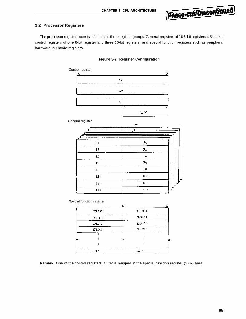
65
CHAPTER 3 CPU ARCHITECTURE
3.2 Processor Registers
The processor registers consist of the main three register groups: General registers of 16 8-bit registers × 8 banks;
control registers of one 8-bit register and three 16-bit registers; and special function registers such as peripheral
hardware I/O mode registers.
Figure 3-2 Register Configuration
Control register
Remark One of the control registers, CCW is mapped in the special function register (SFR) area.
General register
Special function register
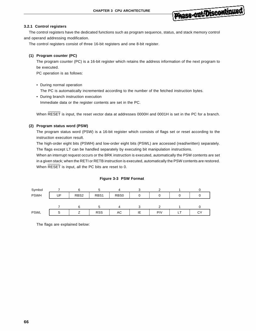
66
CHAPTER 3 CPU ARCHITECTURE
3.2.1 Control registers
The control registers have the dedicated functions such as program sequence, status, and stack memory control
and operand addressing modification.
The control registers consist of three 16-bit registers and one 8-bit register.
(1) Program counter (PC)
The program counter (PC) is a 16-bit register which retains the address information of the next program to
be executed.
PC operation is as follows:
• During normal operation
The PC is automatically incremented according to the number of the fetched instruction bytes.
• During branch instruction execution
Immediate data or the register contents are set in the PC.
When RESET is input, the reset vector data at addresses 0000H and 0001H is set in the PC for a branch.
(2) Program status word (PSW)
The program status word (PSW) is a 16-bit register which consists of flags set or reset according to the
instruction execution result.
The high-order eight bits (PSWH) and low-order eight bits (PSWL) are accessed (read/written) separately.
The flags except LT can be handled separately by executing bit manipulation instructions.
When an interrupt request occurs or the BRK instruction is executed, automatically the PSW contents are set
in a given stack; when the RETI or RETB instruction is executed, automatically the PSW contents are restored.
When RESET is input, all the PC bits are reset to 0.
Figure 3-3 PSW Format
Symbol 7 6 5 4 3 2 1 0
PSWH UF RBS2 RBS1 RBS0 0 0 0 0
7 6 5 4 3 2 1 0
PSWL S Z RSS AC IE P/V LT CY
The flags are explained below:
67
CHAPTER 3 CPU ARCHITECTURE
(a) Interrupt priority level transition flag (LT)
This LT flag is used to control the interrupt priority levels. When the priority level of the current interrupt
request in service changes, the LT is set to 1. See 13.3 Maskable Interrupt Status Flags for details.
Caution Do not handle the LT bit by a program. If it is handled, an error may occur.
(b) Carry flag (CY)
The carry flag (CY) stores an overflow or underflow resulting from arithmetic or logical instruction
execution.
When an arithmetic or logical instruction generates a carry out of bit 7 (overflow) or a borrow into bit 7
(underflow), the CY is set to 1. In word operation, when a carry is generated out of bit 15 (overflow) or
a borrow is generated into bit 15 (underflow), the CY is set to 1. Otherwise, the CY is reset to 0.
The CY can be tested by executing a conditional branch instruction. When a bit manipulation instruction
is executed, the CY serves as a 1-bit accumulator.
(c) Zero flag (Z)
The zero flag (Z) indicates that the operation result is “0”.
When the operation result is “0”, the Z is set to 1; otherwise, the Z is reset to 0.
The flag can be tested by executing a conditional branch instruction.
(d) Sign flag (S)
The sign flag (S) indicates that the most significant bit (MSB) of the operation result is “1”.
When the MSB of the operation result is “1”, the S is set to 1; when the operation result is “0”, the S is
reset to 0.
The flag can be tested by executing a conditional branch instruction.
68
CHAPTER 3 CPU ARCHITECTURE
(e) Parity/overflow flag (P/V)
The parity/overflow flag (P/V) operates in either of the following manners according to logical/arithmetic
instruction execution:
• Parity flag operation
The parity flag is set to 1 when the number of bits set to 1 is even as a result of execution of a logical
operation instruction; reset to 0 when odd. Regardless of 16-bit or 8-bit operations, only the low-order
eight bits of the operation result are effective for the parity flag.
• Overflow flag operation
The overflow flag is set to 1 only when the execution result of an arithmetic operation instruction exceeds
the range of numeric values represented by two’s complement; otherwise, reset to 0.
For example, on 8-bit arithmetic operations, the two’s complement range is from 80H (—128) to 7FH
(+127). When the operation result exceeds the range, the overflow flag is set to 1; when it is within the
range, the flag is reset to 0.
Example Overflow flag operation when an 8-bit addition instruction is executed is shown below:
If 78H (+120) and 69H (+105) are added together, the operation results in E1H (+225) which
exceeds the upper limit of two’s complement, thus the P/V flag is set to 1. E1H becomes -31
in two’s complement representation.
When the following two negative values are added together, the operation result lies within
the two’s complement range, thus the P/V flag is reset to 0.
(f) Auxiliary carry flag (AC)
The auxiliary carry flag (AC) is used for decimal adjustment and stores an underflow into or an overflow
out of bit 3.
When the operation generates a carry out of bit 3 (overflow) or a borrow into bit 3 (underflow), the AC
flag is set to 1; otherwise, the AC is reset to 0.
The flag can be tested by executing a conditional branch instruction.
69
CHAPTER 3 CPU ARCHITECTURE
(g) Register set selection flag (RSS)
This flag is used to specify the general registers which function as X, A, C, and B and the 16-bit general
register pairs which function as AX and BC.
The function names correspond to the absolute names (enclosed in parentheses) by setting the RSS flag
to 1 or 0 as follows: (See Table 3-3. )
• When RSS = 0
X (R0), A (R1), C (R2), B (R3), AX (RP0), BC (RP1)
• When RSS = 1
X (R4), A (R5), C (R6), B (R7), AX (RP2), BC (RP3)
To set or reset the RSS flag, be sure to describe an RSS pseudo instruction immediately preceding (or
immediate following) the RSS flag set or reset instruction. (See the following example.)
<Program example>
• To set RSS = 0
RSS 0 ; RSS pseudo instruction
CLR1 PSWL.5
MOV B, A ; This description is equivalent to “MOV R3, R1”.
• To set RSS = 1
RSS 1 ; RSS pseudo instruction
SET1 PSWL.5
MOV B, A ; This description is equivalent to “MOV R7, R5”.
The same effect as having two register sets is provided by changing the RSS flag value.
The registers and register pairs not specified by the RSS flag can be accessed by describing the absolute
names.
(h) Interrupt request enable flag (IE)
This flag indicates whether interrupt requests are enabled or disabled.
When the EI instruction is executed, the IE flag is set to 1; when the DI instruction is executed, or an
interrupt is acknowledged the IE flag is reset to 0.
(i) Register bank selection flag (RBS0 to RBS2)
These three flag bits select one of eight register banks (register banks 0 to 7).
(j) User flag (UF)
The user flag (UF) can be set or reset by a user program for program control.
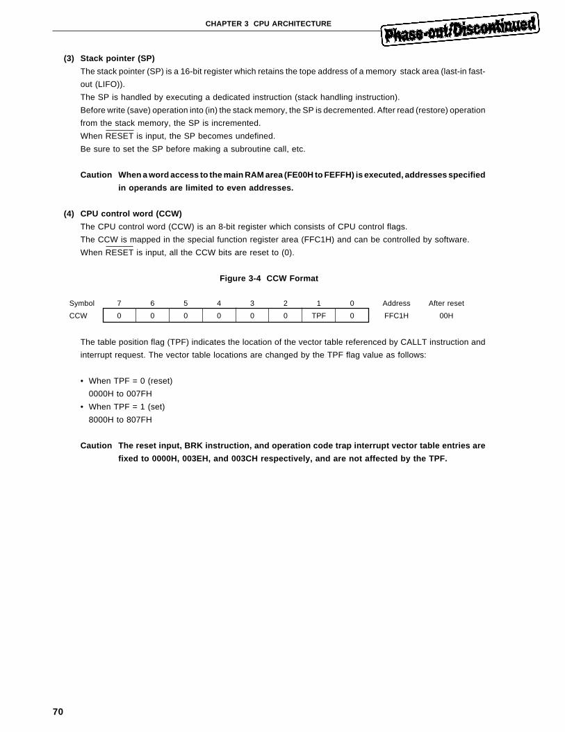
70
CHAPTER 3 CPU ARCHITECTURE
(3) Stack pointer (SP)
The stack pointer (SP) is a 16-bit register which retains the tope address of a memory stack area (last-in fast-
out (LIFO)).
The SP is handled by executing a dedicated instruction (stack handling instruction).
Before write (save) operation into (in) the stack memory, the SP is decremented. After read (restore) operation
from the stack memory, the SP is incremented.
When RESET is input, the SP becomes undefined.
Be sure to set the SP before making a subroutine call, etc.
Caution When a word access to the main RAM area (FE00H to FEFFH) is executed, addresses specified
in operands are limited to even addresses.
(4) CPU control word (CCW)
The CPU control word (CCW) is an 8-bit register which consists of CPU control flags.
The CCW is mapped in the special function register area (FFC1H) and can be controlled by software.
When RESET is input, all the CCW bits are reset to (0).
Figure 3-4 CCW Format
Symbol 7 6 5 4 3 2 1 0 Address After reset
CCW 0 0 0 0 0 0 TPF 0 FFC1H 00H
The table position flag (TPF) indicates the location of the vector table referenced by CALLT instruction and
interrupt request. The vector table locations are changed by the TPF flag value as follows:
• When TPF = 0 (reset)
0000H to 007FH
• When TPF = 1 (set)
8000H to 807FH
Caution The reset input, BRK instruction, and operation code trap interrupt vector table entries are
fixed to 0000H, 003EH, and 003CH respectively, and are not affected by the TPF.
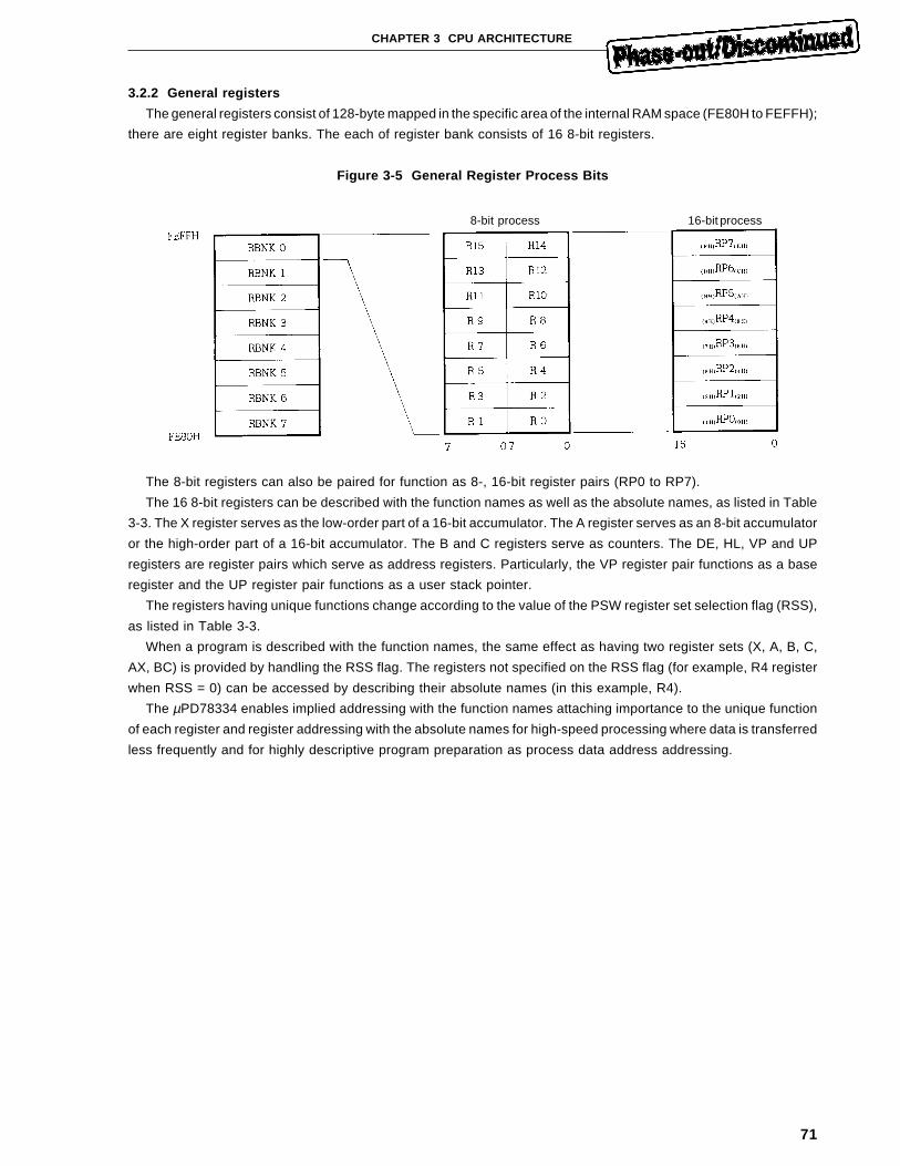
71
CHAPTER 3 CPU ARCHITECTURE
3.2.2 General registers
The general registers consist of 128-byte mapped in the specific area of the internal RAM space (FE80H to FEFFH);
there are eight register banks. The each of register bank consists of 16 8-bit registers.
Figure 3-5 General Register Process Bits
The 8-bit registers can also be paired for function as 8-, 16-bit register pairs (RP0 to RP7).
The 16 8-bit registers can be described with the function names as well as the absolute names, as listed in Table
3-3. The X register serves as the low-order part of a 16-bit accumulator. The A register serves as an 8-bit accumulator
or the high-order part of a 16-bit accumulator. The B and C registers serve as counters. The DE, HL, VP and UP
registers are register pairs which serve as address registers. Particularly, the VP register pair functions as a base
register and the UP register pair functions as a user stack pointer.
The registers having unique functions change according to the value of the PSW register set selection flag (RSS),
as listed in Table 3-3.
When a program is described with the function names, the same effect as having two register sets (X, A, B, C,
AX, BC) is provided by handling the RSS flag. The registers not specified on the RSS flag (for example, R4 register
when RSS = 0) can be accessed by describing their absolute names (in this example, R4).
The µPD78334 enables implied addressing with the function names attaching importance to the unique function
of each register and register addressing with the absolute names for high-speed processing where data is transferred
less frequently and for highly descriptive program preparation as process data address addressing.
8-bit process 16-bit process
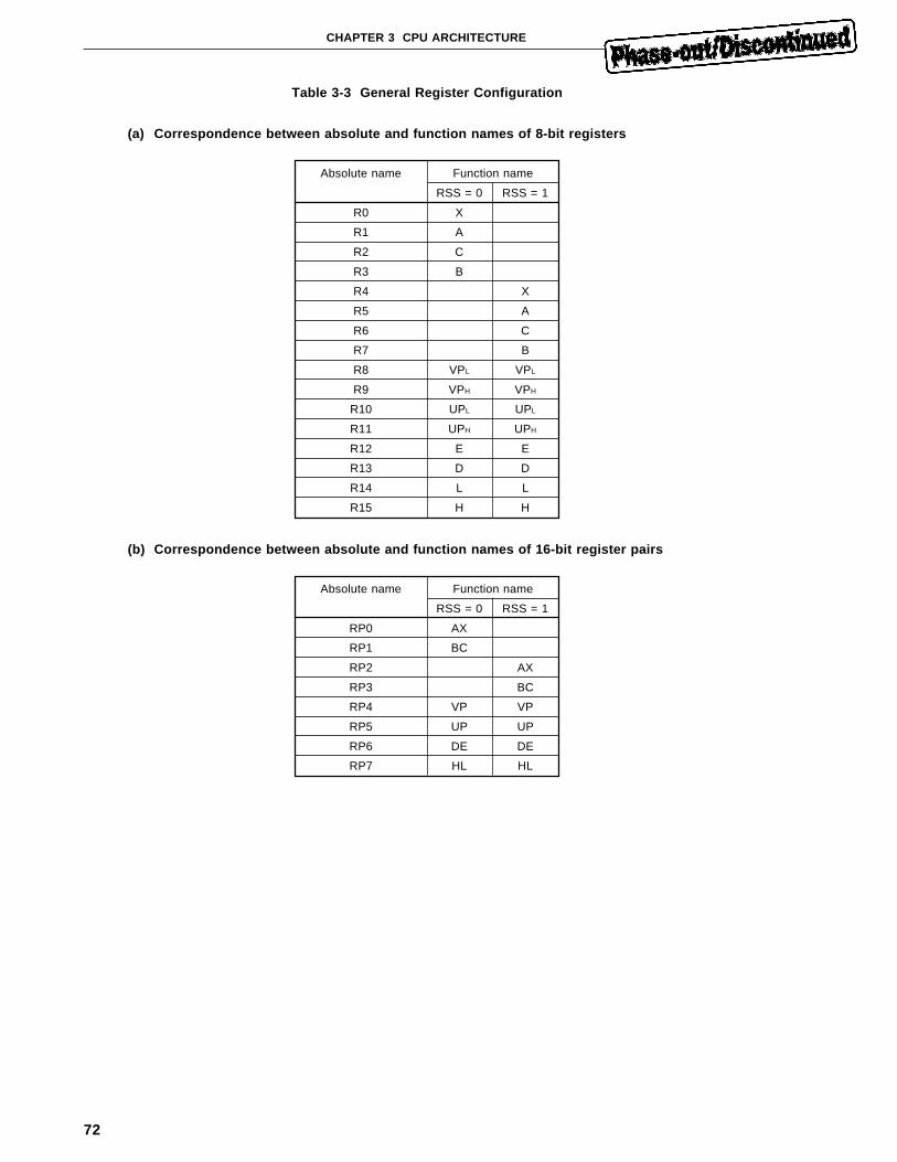
72
CHAPTER 3 CPU ARCHITECTURE
Table 3-3 General Register Configuration
(a) Correspondence between absolute and function names of 8-bit registers
Absolute name Function name
RSS = 0 RSS = 1
R0 X
R1 A
R2 C
R3 B
R4 X
R5 A
R6 C
R7 B
R8 VPL VPL
R9 VPH VPH
R10 UPL UPL
R11 UPH UPH
R12 E E
R13 D D
R14 L L
R15 H H
(b) Correspondence between absolute and function names of 16-bit register pairs
Absolute name Function name
RSS = 0 RSS = 1
RP0 AX
RP1 BC
RP2 AX
RP3 BC
RP4 VP VP
RP5 UP UP
RP6 DE DE
RP7 HL HL
73
CHAPTER 3 CPU ARCHITECTURE
3.2.3 Special function registers (SFR)
Unlike the general registers, the special function registers (SFRs) have their respective special functions. The SFRs
are mapped in the 256-byte memory space of addresses FF00H to FFFFH (special function register area).
Short direct addressing is applicable to the 32-byte area of addresses FF00H to FF1FH. Thus, the SFRs mapped
in the area can be handled with shorter word lengths and fewer number of clocks than other SFRs. The frequently
accessed SFRs such as free-running timers, capture registers, capture/compare registers, and ports are mapped in
the area.
For the 16-byte area of addresses FFD0H to FFDFH, the external is accessed by using SFR addressing. Thus,
external memory access by instruction with short word length, external device bit manipulation, etc., are enabled.
Like the general registers, SFRs can be handled by executing instructions such as arithmetic and logical, transfer,
and bit manipulation instructions. The bit units in which SFRs can be handled (1-, 8-, and 16-bit) vary depending on
the SFR. (See Table 3-4. )
The SFR specification methods for each manipulation bit unit are described below:
• 1-bit manipulation
SFR symbol is described in the bit manipulation instruction operand (sfr. bit). Address can also be described
for specification.
• 8-bit manipulation
SFR symbol is described in the 8-bit manipulation instruction operand (sfr). Address can also be described for
specification.
• 16-bit manipulation
SFR symbol is described in the 16-bit manipulation instruction operand (sfrp). SFR that can be handled in 16-
bit units is mapped in a continuous 2-byte area of even and odd addresses.
To specify the address, describe an even address.
Table 3-4 lists the SFRs. The table columns have the following meanings:
• Symbol : Symbol indicating the on-chip SFR address. It can be described in the instruction operand.
• R/W : Indicates whether the SFR can be read/written.
R/W : Both read and write are enabled.
R : Read only is enabled Note
W : Write only is enabled.
• Bit units in which SFR can be handled:
Indicates the bit units in which SFR can be handled (1-, 8-, and 16-bit). ( ).
The symbol of an SFR that can be handled in 16-bit units can be described in the operand sfrp. To specify the
SFR directly by its address, be sure to describe the even address. The symbol or address of an SFR that can
be handled in 1-bit units can be described in the bit manipulation instruction operand.
• When reset: Indicates the register state when RESET is input.
Note Bit test is enabled in read-only registers.
Cautions 1. To write into an SFR, write “0” and “1” into the bits defined as “0” or “1” respectively.
2. Do not write into any read-only register. If a write is made, an error may occur.
3. Do not access any addresses of the special function register area (FF00H to FFFFH) in which
no SFRs are mapped (except the external access area). If the address is accessed, an error
may occur.
74
CHAPTER 3 CPU ARCHITECTURE
Table 3-4 Special Function Register List (1/4)
Address Special function register (SFR) name Symbol R/W Bit units in which After reset
SFR can be handled
1 bit 8 bits 16 bits
FF00H Port 0 P0 R/W — Undefined
FF01H Port 1 P1 —
FF02H Port 2 P2 R — —
FF03H Port 3 P3 RW —
FF04H Port 4 P4 —
FF05H Port 5 P5 —
FF07H Port 7 P7 R — —
FF08H Port 8 P8 — —
FF09H Port 9 P9 R/W —
FF0AH Timer low access register TLA R/W —
FF0CH Timer register 2 TM2 R — — 0000H
FF0DH
FF10H Capture register 00 CT00 R — — Undefined
FF11H
FF12H Capture register 01 CT01 — —
FF13H
FF14H Capture register 02 CT02 — —
FF15H
FF1CH Capture register 10 CT10 — —
FF1DH
FF20H Port 0 mode register PM0 W — — FFH
FF21H Port 1 mode register PM1 — —
FF23H Port 3 mode register PM3 — —
FF25H Port 5 mode register PM5 — —
FF29H Port 9 mode register PM9 — — ××11 1111B
FF2AH Timer register 0 TM0 R — — 0000H
FF2BH
FF2CH Timer register 1 TM1 — —
FF2DH
FF2EH Timer register 3 TM3 — —
FF2FH
FF40H Port 0 mode control register PMC0 W — — 00H
FF41H Port 1 mode control register PMC1 — —
FF43H Port 3 mode control register PMC3 — —
FF4CH Baud rate generator compare register BRG R/W — — 0000H
FF4DH
FF60H Real-time output port register RTP — Undefined
FF61H Real-time output port reset register RTPR — 00H
FF62H Port read control register PRDC — — 00H
FF63H Real-time output port set register RTPS — 00H
FF64H PWM control register PWMC —
FF66H PWM buffer register 0 PWM0 — — Undefined
FF68H A/D converter mode register ADM — 00H
FF6EH PWM buffer register 1 PWM1 — — Undefined
FF70H Compare register 11 CM11 — —
FF71H
75
CHAPTER 3 CPU ARCHITECTURE
Table 3-4 Special Function Register List (2/4)
Address Special function register (SFR) name Symbol R/W Bit units in which After reset
SFR can be handled
1 bit 8 bits 16 bits
FF72H Compare register 12 CM12 R/W — — Undefined
FF73H
FF74H Compare register 20 CM20 — —
FF75H
FF76H Compare register 21 CM21 — —
FF77H
FF78H Compare register 30 CM30 — —
FF79H
FF80H Clocked serial interface mode register CSIM — 00H
FF82H Serial bus interface control register SBIC —
FF86H Serial I/O shift register SIO — Undefined
FF88H Asynchrounous serial interface mode register ASIM — 80H
FF8AH Asynchronous serial interface status register ASIS R — 00H
FF8CH Serial receive buffer: UART RXB R — — Undefined
FF8EH Serial transmit shift register UART TXS W — —
FF90H Compare register X0 CMX0 R/W — — Undefined
FF91H
FF92H Compare register 01 CM01R — —
FF93H
FF94H Compare register 02 CM02R — —
FF95H
FF96H Compare register 03 CM03R — —
FF97H
FF98H Compare register 04 CM04R — —
FF99H
FF9AH Capture/compare register 00 CC00R — —
FF9BH
FF9CH Capture/compare register 01 CC01R — —
FF9DH
FFA0H A/D conversion result register 0 ADCR0 R — —
(when 16 bits are accessed)
FFA1H A/D conversion result register 0 ADCR0H — —
(when high-order 8 bits are accessed)
FFA2H A/D conversion result register 1 ADCR1 — —
(when 16 bits are accessed)
FFA3H A/D conversion result register 1 ADCR1H — —
(when high-order 8 bits are accessed)
FFA4H A/D conversion result register 2 ADCR2 — —
(when 16 bits are accessed)
FFA5H A/D conversion result register 2 ADCR2H — —
(when high-order 8 bits are accessed)
FFA6H A/D conversion result register 3 ADCR3 — —
(when 16 bits are accessed)
FFA7H A/D conversion result register 3 ADCR3H — —
(when high-order 8 bits are accessed)
FFA8H A/D conversion result register 4 ADCR4 — —
(when 16 bits are accessed)
76
CHAPTER 3 CPU ARCHITECTURE
Table 3-4 Special Function Register List (3/4)
Address Special function register (SFR) name Symbol R/W Bit units in which After reset
SFR can be handled
1 bit 8 bits 16 bits
FFA9H A/D conversion result register 4 ADCR4H R — — Undefined
(when high-order 8 bits are accessed)
FFAAH A/D conversion result register 5 ADCR5 — —
(when 16 bits are accessed)
FFABH A/D conversion result register 5 ADCR5H — —
(when high-order 8 bits are accessed)
FFACH A/D conversion result register 6 ADCR6 — —
(when 16 bits are accessed)
FFADH A/D conversion result register 6 ADCR6H — —
(when high-order 8 bits are accessed)
FFAEH A/D conversion result register 7 ADCR7 — —
(when 16 bits are accessed)
FFAFH A/D conversion result register 7 ADCR7H — —
(when high-order 8 bits are accessed)
FFB0H Timer control register 0 TMC0 R/W — 00H
FFB1H Baud rate generator mode register BRGM — 40H
FFB2H Timer control register 1 TMC1 — 00H
FFB4H Timer unit mode register 0 TUM0 —
FFB5H Timer unit mode register 1 TUM1 —
FFB8H Timer output control register 0 TOC0 —
FFB9H Timer output control register 1 TOC1 —
FFBCH Programmable pulse output set register PPOS —
FFC0H Standby control register STBC Note — 0000×000B
FFC1H CPU control word CCW — 00H
FFC2H Watchdog timer mode register WDM Note —
FFC4H Memory expansion mode register MM —
FFC6H Programmable wait control register PWC — 22H
FFC9H Fetch cycle control register FCC — 00H
FFD0H to External SFR area — Undefined
FFDFH
FFE0H Interrupt request flag register 0L IF0L IF0 00H
FFE1H Interrupt request flag register 0H IF0H
FFE2H Interrupt request flag register 1L IF1L IF1 —
FFE4H Interrupt mask flag register 0L MK0L MK0 FFH
FFE5H Interrupt mask flag register 0H MK0H
FFE6H Interrupt mask flag register 1L MK1L MK1 — ×××× ×111B
FFE8H Priority level specification buffer register 0L PB0L PB0 00H
FFE9H Priority level specification buffer register 0H PB0H
FFEAH Priority level specification buffer register 1L PB1L PB1 —
FFECH Interrupt processing mode specification ISM0L ISM0
register 0L
FFEDH Interrupt processing mode specification ISM0H
register 0H
FFEEH Interrupt processing mode specification ISM1L ISM1 —
register 1L
Note A write can be made into the register by executing a special instruction.
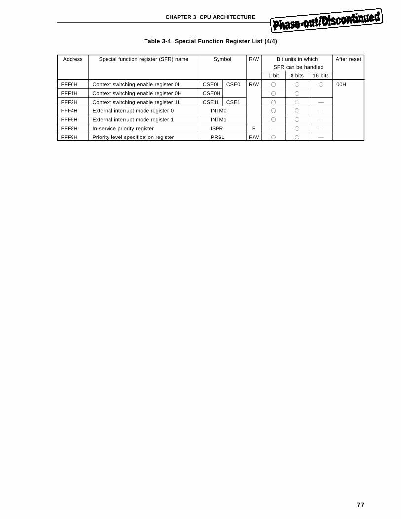
77
CHAPTER 3 CPU ARCHITECTURE
Table 3-4 Special Function Register List (4/4)
Address Special function register (SFR) name Symbol R/W Bit units in which After reset
SFR can be handled
1 bit 8 bits 16 bits
FFF0H Context switching enable register 0L CSE0L CSE0 R/W 00H
FFF1H Context switching enable register 0H CSE0H
FFF2H Context switching enable register 1L CSE1L CSE1 —
FFF4H External interrupt mode register 0 INTM0 —
FFF5H External interrupt mode register 1 INTM1 —
FFF8H In-service priority register ISPR R — —
FFF9H Priority level specification register PRSL R/W —
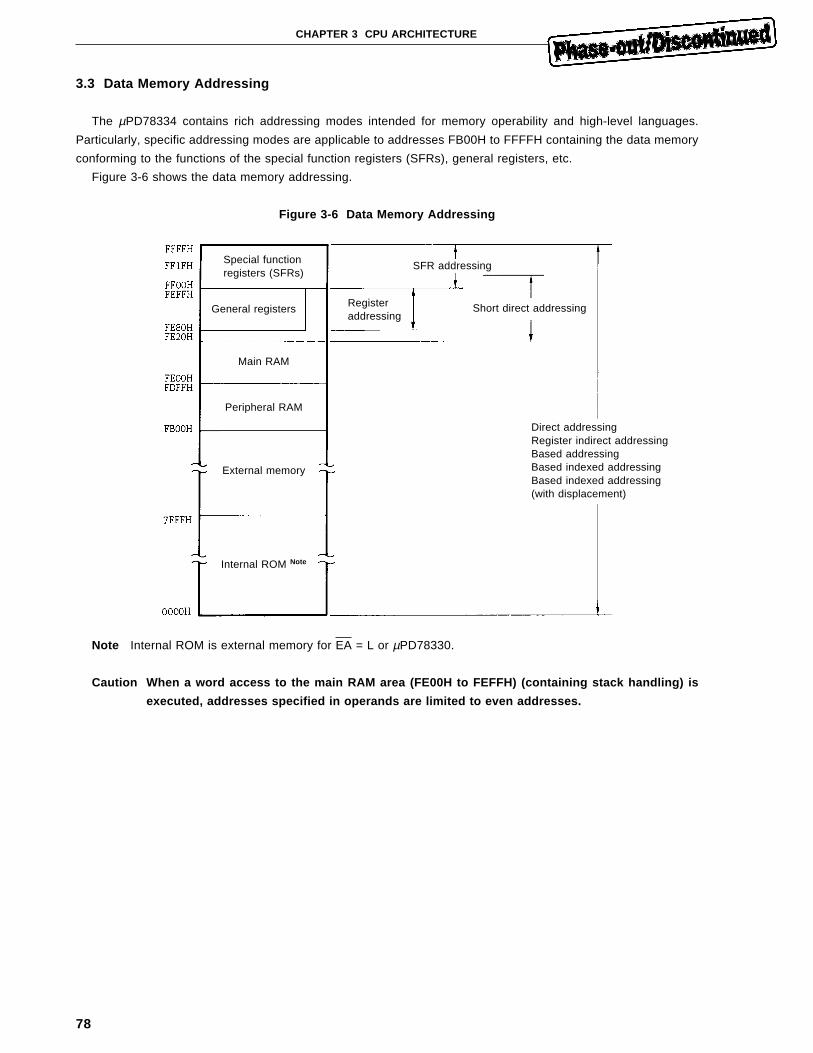
78
CHAPTER 3 CPU ARCHITECTURE
3.3 Data Memory Addressing
The µPD78334 contains rich addressing modes intended for memory operability and high-level languages.
Particularly, specific addressing modes are applicable to addresses FB00H to FFFFH containing the data memory
conforming to the functions of the special function registers (SFRs), general registers, etc.
Figure 3-6 shows the data memory addressing.
Figure 3-6 Data Memory Addressing
Note Internal ROM is external memory for EA = L or µPD78330.
Caution When a word access to the main RAM area (FE00H to FEFFH) (containing stack handling) is
executed, addresses specified in operands are limited to even addresses.
Special functionregisters (SFRs)
General registers Registeraddressing
Short direct addressing
SFR addressing
Main RAM
Peripheral RAM
External memory
Internal ROM Note
Direct addressingRegister indirect addressingBased addressingBased indexed addressingBased indexed addressing(with displacement)
79
CHAPTER 3 CPU ARCHITECTURE
3.3.1 General register addressing
(1) Implied addressing
An accumulator (A or AX) or a register which serves as a loop counter (B or C) in the general register area
is automatically addressed by an instruction.
Description example: MULU r
Assuming that the multiplier is the value stored in the B register in an 8-bit × 8-bit
multiplication instruction, describe the instruction as follows:
MULU B; AX ← A × B
When this instruction is executed, multiplication is performed on the accumulator (A
register) and B register, and the result is stored in the 16-bit accumulator (AX register
pair).
(2) Register addressing
The registers to be used are directly addressed in an instruction.
Description example: ADD r,r
To specify the D and E registers as the regiesters which store the addition instruction
operand values in an 8-bit addition instruction, describe the instruction as follows:
ADD D, E; D ← D + E
3.3.2 Short direct addressing
The short direct addressing is used to access addresses 0FE20H to 0FEFFH of the internal memory space and
addresses 0FF00H to 0FF1FH of the SFR space. The short direct addressing enables the addresses to be accessed
at high speed with a short operation code.
To handle 16-bit data, specify an even address.
Description example: ADD A, saddr
If one addition instruction operand value is stored at internal data memory space address
0FE80H in an 8-bit addition instruction, describe the instruction as follows:
ADD A, 0FE80H; A ← A + (0FE80H)
3.3.3 Special function register (SFR) addressing
The special function register (SFR) addressing is used to handle the special function register (SFRs) mapped in
the SFR area (0FF00H to 0FFFFH).
Description example: MOV A, sfr
To specify the special function register used as source as the serial receive buffer (RXB)
of the SFR area in an 8-bit transfer instruction, describe the following:
MOV A, RXB; A ← RXB

80
[MEMO]
81
CHAPTER 4 BLOCK FUNCTION OUTLINE
4.1 Execution Unit
The execution unit (EXU) executes address calculation, arithmetic and logical operations, data transfer, etc., under
the microprogram control.
The EXU contains 256-byte main RAM. Eight register banks are mapped in the EXU internal main RAM.
4.2 Bus Control Unit
The bus control unit (BCU) starts necessary bus cycles based on the physical address provided by the execution
unit (EXU). When the EXU does not request bus cycle start, the BCU generates an address for prefetch and fetches
a given instruction. The code of the prefetched instruction is read into a 3-byte instruction queue.
4.3 Program Memory/Data Memory
This block consists of 32-Kbyte program memory (ROM) and 768-byte data memory (peripheral RAM). However,
the µPD78330 does not contain the ROM.
If the EA pin of the µPD78334, 78P334 is fixed low, an access to the µPD78334 internal mask ROM, PROM can
be inhibited.
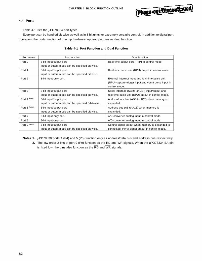
82
CHAPTER 4 BLOCK FUNCTION OUTLINE
4.4 Ports
Table 4-1 lists the µPD78334 port types.
Every port can be handled bit-wise as well as in 8-bit units for extremely versatile control. In addition to digital port
operation, the ports function of on-chip hardware input/output pins as dual function.
Table 4-1 Port Function and Dual Function
Port name
Port 0
Port 1
Port 2
Port 3
Port 4 Note 1
Port 5 Note 1
Port 7
Port 8
Port 9 Note 2
Port function
8-bit input/output port.
Input or output mode can be specified bit-wise.
8-bit input/output port.
Input or output mode can be specified bit-wise.
8-bit input-only port.
8-bit input/output port.
Input or output mode can be specified bit-wise.
8-bit input/output port.
Input or output mode can be specified 8-bit-wise.
8-bit input/output port.
Input or output mode can be specified bit-wise.
8-bit input-only port.
8-bit input-only port.
8-bit input/output port.
Input or output mode can be specified bit-wise.
Dual function
Real-time output port (RTP) in control mode.
Real-time pulse unit (RPU) output in control mode.
External interrupt input and real-time pulse unit
(RPU) capture trigger input and count pulse input in
control mode.
Serial interface (UART or CSI) input/output and
real-time pulse unit (RPU) output in control mode.
Address/data bus (AD0 to AD7) when memory is
expanded.
Address bus (A8 to A15) when memory is
expanded.
A/D converter analog input in control mode.
A/D converter analog input in control mode.
Control signal output when memory is expanded is
connected. PWM signal output in control mode.
Notes 1. µPD78330 ports 4 (P4) and 5 (P5) function only as address/data bus and address bus respectively.
2. The low-order 2 bits of port 9 (P9) function as the RD and WR signals. When the µPD78334 EA pin
is fixed low, the pins also function as the RD and WR signals.
83
CHAPTER 4 BLOCK FUNCTION OUTLINE
4.5 Real-Time Pulse Unit (RPU)
The real-time pulse unit (RPU) consists of the following hardware devices:
• 18/16-bit timer/counter × 1
18/16-bit compare registers × 5
18/16-bit capture registers × 3
18/16-bit capture/compare registers × 2
Pulse output lines × 6
• 16-bit timer/counter × 3
16-bit compare registers × 5
16-bit capture register × 1
Timer output pins × 5
• Real-time output port × 8
The RPU can perform programmable pulse output and pulse interval and frequency measurements.
The greatest feature of the real-time pulse unit lines in rich and multifunctional timer pulse output. A total of six
timer pulse output lines such as toggle output, set output, and reset output can be controlled independently. In addition,
the real time output port output timing can be controlled.
The set and reset timings of real-time output port output are also controlled.
4.6 A/D Converter
High-speeds, high-resolution 10-bit A/D (analog/digital) converter is contained.
16 analog input lines (ANI0 to ANI15) are contained and various functions are provided conforming to application
such as the select mode, scan mode, and mix mode.
4.7 Serial Interface
Two independent serial interface channels of asynchronous serial interface (UART) and clocked serial interface
are provided. Also, a baud rate generator common to both the channels is contained.
On the asynchronous serial interface, data is transferred through the TxD and RxD pins.
The clocked serial interface has the following two operation modes:
• 3-wire serial I/O mode
Data is transferred through the three pins of serial clock (SCK), serial input (SI), and serial output (SO).
• Serial bus interface (SBI) mode
Data is transferred through the two pins of serial clock (SCK) and serial data bus (SB0 or SB1).
4.8 Watchdog Timer
The watchdog timer is a free-running timer which has the non-maskable interrupt function to prevent program
runaway or deadlock. A program error can be known by the fact that a watchdog timer overflow interrupt (INTWDT)
occurs or the watchdog timer output pin (WDTO) goes low. If the output is connected to the RESET pin, a program
error can be prevented from causing an application system error.
84
CHAPTER 4 BLOCK FUNCTION OUTLINE
4.9 PWM Output Unit
Two 8-bit precision PWM signal output are contained. PWM output can be used as digital-analog conversion output
by connecting an external low-pass filter, etc. It is appropriate for actuator control signals of motors, etc.
4.10 Interrupt Controller
The interrupt controller handles various interrupt requests occurring from the peripheral hardware and the external
(NMI and INTP0 to INTP6) in any mode of context switching, vectored interrupt, and macro service. In addition, three
interrupt priority levels are programmable by the software.
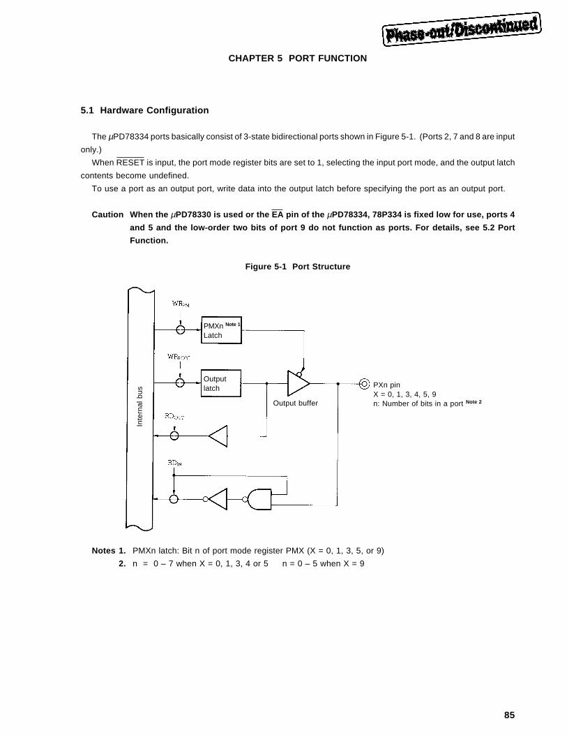
85
CHAPTER 5 PORT FUNCTION
5.1 Hardware Configuration
The µPD78334 ports basically consist of 3-state bidirectional ports shown in Figure 5-1. (Ports 2, 7 and 8 are input
only.)
When RESET is input, the port mode register bits are set to 1, selecting the input port mode, and the output latch
contents become undefined.
To use a port as an output port, write data into the output latch before specifying the port as an output port.
Caution When the µPD78330 is used or the EA pin of the µPD78334, 78P334 is fixed low for use, ports 4
and 5 and the low-order two bits of port 9 do not function as ports. For details, see 5.2 Port
Function.
Figure 5-1 Port Structure
Notes 1. PMXn latch: Bit n of port mode register PMX (X = 0, 1, 3, 5, or 9)
2. n = 0 – 7 when X = 0, 1, 3, 4 or 5 n = 0 – 5 when X = 9
Inte
rnal
bus
PMXn Note 1
Latch
Outputlatch
Output buffer
PXn pinX = 0, 1, 3, 4, 5, 9n: Number of bits in a port Note 2
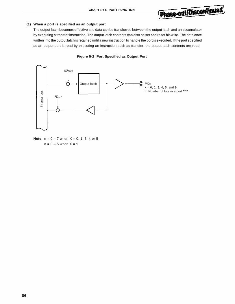
86
CHAPTER 5 PORT FUNCTION
(1) When a port is specified as an output port
The output latch becomes effective and data can be transferred between the output latch and an accumulator
by executing a transfer instruction. The output latch contents can also be set and reset bit-wise. The data once
written into the output latch is retained until a new instruction to handle the port is executed. If the port specified
as an output port is read by executing an instruction such as transfer, the output latch contents are read.
Figure 5-2 Port Specified as Output Port
Note n = 0 – 7 when X = 0, 1, 3, 4 or 5
n = 0 – 5 when X = 9
Inte
rnal
bus
Output latch PXnx = 0, 1, 3, 4, 5, and 9n: Number of bits in a port Note
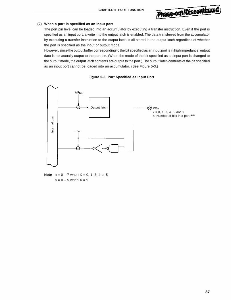
87
CHAPTER 5 PORT FUNCTION
(2) When a port is specified as an input port
The port pin level can be loaded into an accumulator by executing a transfer instruction. Even if the port is
specified as an input port, a write into the output latch is enabled. The data transferred from the accumulator
by executing a transfer instruction to the output latch is all stored in the output latch regardless of whether
the port is specified as the input or output mode.
However, since the output buffer corresponding to the bit specified as an input port is in high impedance, output
data is not actually output to the port pin. (When the mode of the bit specified as an input port is changed to
the output mode, the output latch contents are output to the port.) The output latch contents of the bit specified
as an input port cannot be loaded into an accumulator. (See Figure 5-3.)
Figure 5-3 Port Specified as Input Port
Note n = 0 – 7 when X = 0, 1, 3, 4 or 5
n = 0 – 5 when X = 9
Inte
rnal
bus
Output latch PXnx = 0, 1, 3, 4, 5, and 9n: Number of bits in a port Note
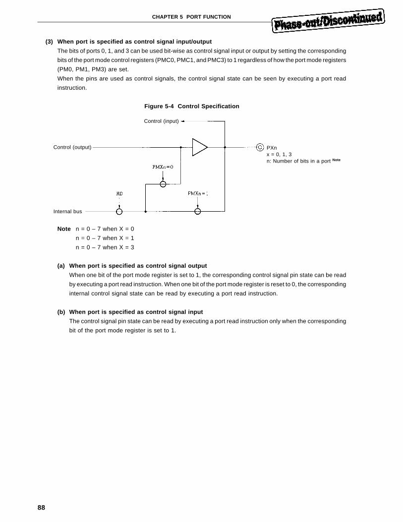
88
CHAPTER 5 PORT FUNCTION
(3) When port is specified as control signal input/output
The bits of ports 0, 1, and 3 can be used bit-wise as control signal input or output by setting the corresponding
bits of the port mode control registers (PMC0, PMC1, and PMC3) to 1 regardless of how the port mode registers
(PM0, PM1, PM3) are set.
When the pins are used as control signals, the control signal state can be seen by executing a port read
instruction.
Figure 5-4 Control Specification
Note n = 0 – 7 when X = 0
n = 0 – 7 when X = 1
n = 0 – 7 when X = 3
(a) When port is specified as control signal output
When one bit of the port mode register is set to 1, the corresponding control signal pin state can be read
by executing a port read instruction. When one bit of the port mode register is reset to 0, the corresponding
internal control signal state can be read by executing a port read instruction.
(b) When port is specified as control signal input
The control signal pin state can be read by executing a port read instruction only when the corresponding
bit of the port mode register is set to 1.
Control (input)
PXnx = 0, 1, 3n: Number of bits in a port Note
Control (output)
Internal bus
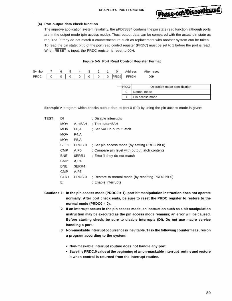
89
CHAPTER 5 PORT FUNCTION
(4) Port output data check function
The improve application system reliability, the µPD78334 contains the pin state read function although ports
are in the output mode (pin access mode). Thus, output data can be compared with the actual pin state as
required. If they do not match a countermeasure such as replacement with another system can be taken.
To read the pin state, bit 0 of the port read control register (PRDC) must be set to 1 before the port is read.
When RESET is input, the PRDC register is reset to 00H.
Figure 5-5 Port Read Control Register Format
Symbol 7 6 5 4 3 2 1 0 Address After reset
PRDC 0 0 0 0 0 0 0 PRDC0 FF62H 00H
PRDC0 Operation mode specification
0 Normal mode
1 Pin access mode
Example A program which checks output data to port 0 (P0) by using the pin access mode is given:
TEST: DI ; Disable interrupts
MOV A, #5AH ; Test data=5AH
MOV P0,A ; Set 5AH in output latch
MOV P4,A
MOV P5,A
SET1 PRDC.0 ; Set pin access mode (by setting PRDC bit 0)
CMP A,P0 ; Compare pin level with output latch contents
BNE $ERR1 ; Error if they do not match
CMP A,P4
BNE $ERR4
CMP A,P5
CLR1 PRDC.0 ; Restore to normal mode (by resetting PRDC bit 0)
EI ; Enable interrupts
Cautions 1. In the pin access mode (PRDC0 = 1), port bit manipulation instruction does not operate
normally. After port check ends, be sure to reset the PRDC register to restore to the
normal mode (PRDC0 = 0).
2. If an interrupt occurs in the pin access mode, an instruction such as a bit manipulation
instruction may be executed as the pin access mode remains; an error will be caused.
Before starting check, be sure to disable interrupts (DI). Do not use macro service
handling a port.
3. Non-maskable interrupt occurrence is inevitable. Task the following countermeasures on
a program according to the system:
• Non-maskable interrupt routine does not handle any port.
• Save the PRDC.0 value at the beginning of a non-maskable interrupt routine and restore
it when control is returned from the interrupt routine.
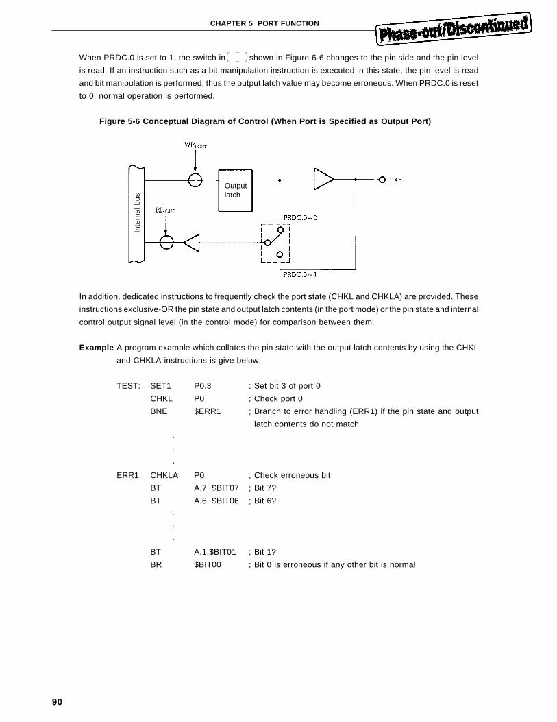
90
CHAPTER 5 PORT FUNCTION
When PRDC.0 is set to 1, the switch in shown in Figure 6-6 changes to the pin side and the pin level
is read. If an instruction such as a bit manipulation instruction is executed in this state, the pin level is read
and bit manipulation is performed, thus the output latch value may become erroneous. When PRDC.0 is reset
to 0, normal operation is performed.
Figure 5-6 Conceptual Diagram of Control (When Port is Specified as Output Port)
In addition, dedicated instructions to frequently check the port state (CHKL and CHKLA) are provided. These
instructions exclusive-OR the pin state and output latch contents (in the port mode) or the pin state and internal
control output signal level (in the control mode) for comparison between them.
Example A program example which collates the pin state with the output latch contents by using the CHKL
and CHKLA instructions is give below:
TEST: SET1 P0.3 ; Set bit 3 of port 0
CHKL P0 ; Check port 0
BNE $ERR1 ; Branch to error handling (ERR1) if the pin state and output
latch contents do not match
·
·
·
ERR1: CHKLA P0 ; Check erroneous bit
BT A.7, $BIT07 ; Bit 7?
BT A.6, $BIT06 ; Bit 6?
·
·
·
BT A.1,$BIT01 ; Bit 1?
BR $BIT00 ; Bit 0 is erroneous if any other bit is normal
Inte
rnal
bus
Outputlatch
91
CHAPTER 5 PORT FUNCTION
Cautions 1. Use the CHKL or CHKLA instructions when the PRDC register PRDC0 bit is “0” (normal
mode).
2. When the ports are set to the input mode, regardless of whether each port pin is specified
as a port or control pin, whenever the CHKL or CHKLA instruction is used to compare
the pin state with the output latch contents (or control output level), they match.
Therefore, even if these instructions are executed for the ports set to the input mode, they
are practically invalid.
3. To use the CHKL or CHKLA instruction to check the input level of a port within which
control output and port output are mixed, set the input/output mode of the control output
pin to the input mode before executing the instructions. (The control output level changes
asynchronously, thus cannot be checked by the CHKL or CHKLA instruction.)
4. Since ports 2, 7, and 8 are input-only ports, whenever the CHKL or CHKLA instruction
is used to compare the pin state with the output latch contents, they match. Therefore,
even if these instructions are executed for ports 2, 7, and 8, they are practically invalid.
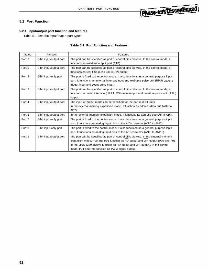
92
CHAPTER 5 PORT FUNCTION
5.2 Port Function
5.2.1 Input/output port function and features
Table 5-1 lists the input/output port types
Table 5-1 Port Function and Features
Name Function Features
Port 0 8-bit input/output port The port can be specified as port or control pins bit-wise. In the control mode, it
functions as real-time output port (RTP).
Port 1 8-bit input/output port The port can be specified as port or control pins bit-wise. In the control mode, it
functions as real-time pulse unit (RTP) output.
Port 2 8-bit input-only port The port is fixed to the control mode. It also functions as a general purpose input
port. It functions as external interrupt input and real-time pulse unit (RPU) capture
trigger input and count pulse input.
Port 3 8-bit input/output port The port can be specified as port or control pins bit-wise. In the control mode, it
functions as serial interface (UART, CSI) input/output and real-time pulse unit (RPU)
output.
Port 4 8-bit input/output port The input or output mode can be specified for the port in 8-bit units.
In the external memory expansion mode, it function as address/data bus (AD0 to
AD7).
Port 5 8-bit input/output port In the external memory expansion mode, it functions as address bus (A8 to A15).
Port 7 8-bit input-only port The port is fixed to the control mode. It also functions as a general purpose input
port. It functions as analog input pins to the A/D converter (ANI0 to ANI7).
Port 8 8-bit input-only port The port is fixed to the control mode. It also functions as a general purpose input
port. It functions as analog input pins to the A/D converter (ANI8 to ANI15).
Port 9 6-bit input/output port The port can be specified as port or control pins bit-wise. In the external memory
expansion mode, P90 and P91 function as RD output and WR output (P90 and P91
of the µPD78330 always function as RD output and WR output). In the control
mode, P94 and P95 function as PWM signal output.
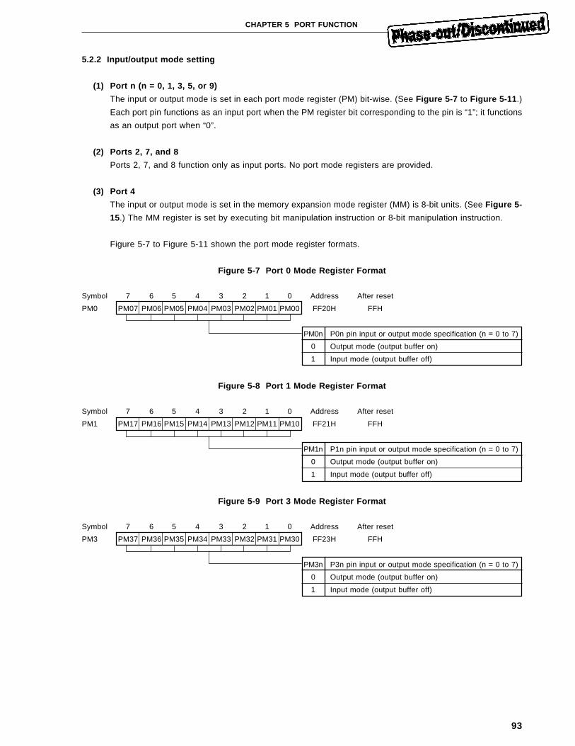
93
CHAPTER 5 PORT FUNCTION
5.2.2 Input/output mode setting
(1) Port n (n = 0, 1, 3, 5, or 9)
The input or output mode is set in each port mode register (PM) bit-wise. (See Figure 5-7 to Figure 5-11 .)
Each port pin functions as an input port when the PM register bit corresponding to the pin is “1”; it functions
as an output port when “0”.
(2) Ports 2, 7, and 8
Ports 2, 7, and 8 function only as input ports. No port mode registers are provided.
(3) Port 4
The input or output mode is set in the memory expansion mode register (MM) is 8-bit units. (See Figure 5-
15.) The MM register is set by executing bit manipulation instruction or 8-bit manipulation instruction.
Figure 5-7 to Figure 5-11 shown the port mode register formats.
Figure 5-7 Port 0 Mode Register Format
Symbol 7 6 5 4 3 2 1 0 Address After reset
PM0 PM07 PM06 PM05 PM04 PM03 PM02 PM01 PM00 FF20H FFH
PM0n P0n pin input or output mode specification (n = 0 to 7)
0 Output mode (output buffer on)
1 Input mode (output buffer off)
Figure 5-8 Port 1 Mode Register Format
Symbol 7 6 5 4 3 2 1 0 Address After reset
PM1 PM17 PM16 PM15 PM14 PM13 PM12 PM11 PM10 FF21H FFH
PM1n P1n pin input or output mode specification (n = 0 to 7)
0 Output mode (output buffer on)
1 Input mode (output buffer off)
Figure 5-9 Port 3 Mode Register Format
Symbol 7 6 5 4 3 2 1 0 Address After reset
PM3 PM37 PM36 PM35 PM34 PM33 PM32 PM31 PM30 FF23H FFH
PM3n P3n pin input or output mode specification (n = 0 to 7)
0 Output mode (output buffer on)
1 Input mode (output buffer off)
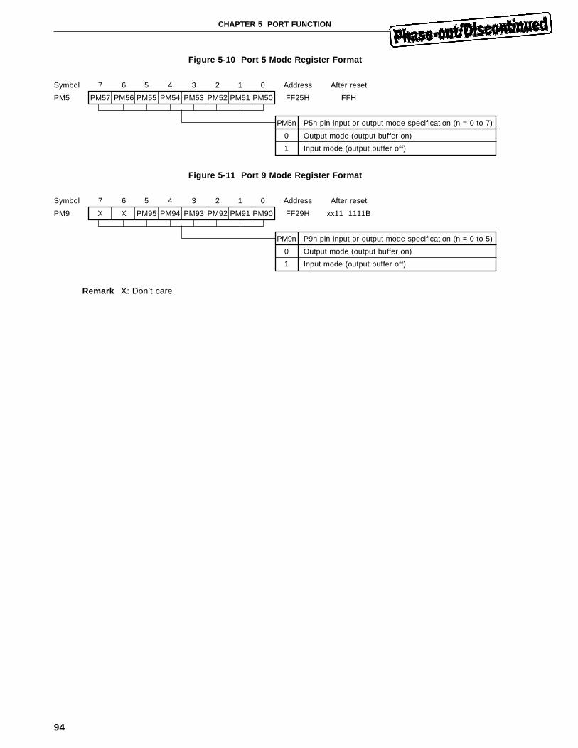
94
CHAPTER 5 PORT FUNCTION
Figure 5-10 Port 5 Mode Register Format
Symbol 7 6 5 4 3 2 1 0 Address After reset
PM5 PM57 PM56 PM55 PM54 PM53 PM52 PM51 PM50 FF25H FFH
PM5n P5n pin input or output mode specification (n = 0 to 7)
0 Output mode (output buffer on)
1 Input mode (output buffer off)
Figure 5-11 Port 9 Mode Register Format
Symbol 7 6 5 4 3 2 1 0 Address After reset
PM9 X X PM95 PM94 PM93 PM92 PM91 PM90 FF29H xx11 1111B
PM9n P9n pin input or output mode specification (n = 0 to 5)
0 Output mode (output buffer on)
1 Input mode (output buffer off)
Remark X: Don’t care
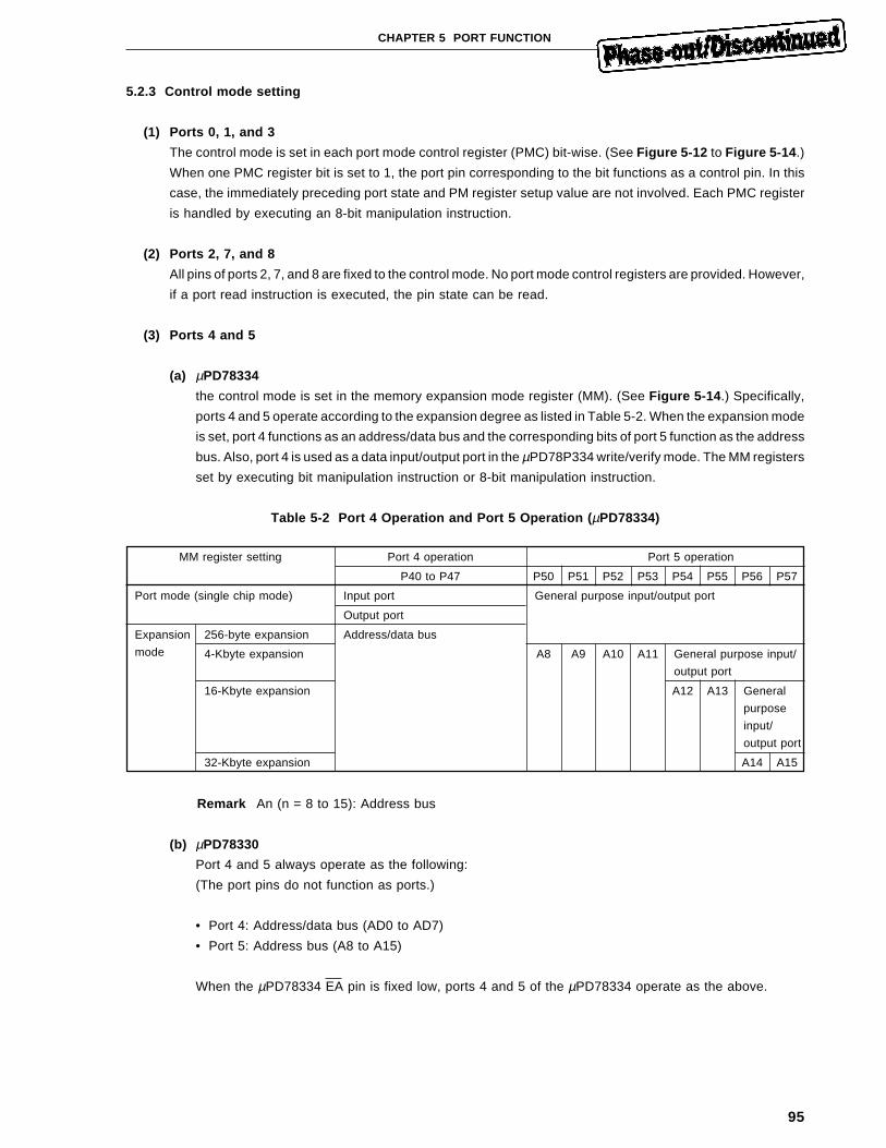
95
CHAPTER 5 PORT FUNCTION
5.2.3 Control mode setting
(1) Ports 0, 1, and 3
The control mode is set in each port mode control register (PMC) bit-wise. (See Figure 5-12 to Figure 5-14 .)
When one PMC register bit is set to 1, the port pin corresponding to the bit functions as a control pin. In this
case, the immediately preceding port state and PM register setup value are not involved. Each PMC register
is handled by executing an 8-bit manipulation instruction.
(2) Ports 2, 7, and 8
All pins of ports 2, 7, and 8 are fixed to the control mode. No port mode control registers are provided. However,
if a port read instruction is executed, the pin state can be read.
(3) Ports 4 and 5
(a) µPD78334
the control mode is set in the memory expansion mode register (MM). (See Figure 5-14 .) Specifically,
ports 4 and 5 operate according to the expansion degree as listed in Table 5-2. When the expansion mode
is set, port 4 functions as an address/data bus and the corresponding bits of port 5 function as the address
bus. Also, port 4 is used as a data input/output port in the µPD78P334 write/verify mode. The MM registers
set by executing bit manipulation instruction or 8-bit manipulation instruction.
Table 5-2 Port 4 Operation and Port 5 Operation ( µPD78334)
MM register setting Port 4 operation Port 5 operation
P40 to P47 P50 P51 P52 P53 P54 P55 P56 P57
Port mode (single chip mode) Input port General purpose input/output port
Output port
Expansion 256-byte expansion Address/data bus
mode 4-Kbyte expansion A8 A9 A10 A11 General purpose input/
output port
16-Kbyte expansion A12 A13 General
purpose
input/
output port
32-Kbyte expansion A14 A15
Remark An (n = 8 to 15): Address bus
(b) µPD78330
Port 4 and 5 always operate as the following:
(The port pins do not function as ports.)
• Port 4: Address/data bus (AD0 to AD7)
• Port 5: Address bus (A8 to A15)
When the µPD78334 EA pin is fixed low, ports 4 and 5 of the µPD78334 operate as the above.
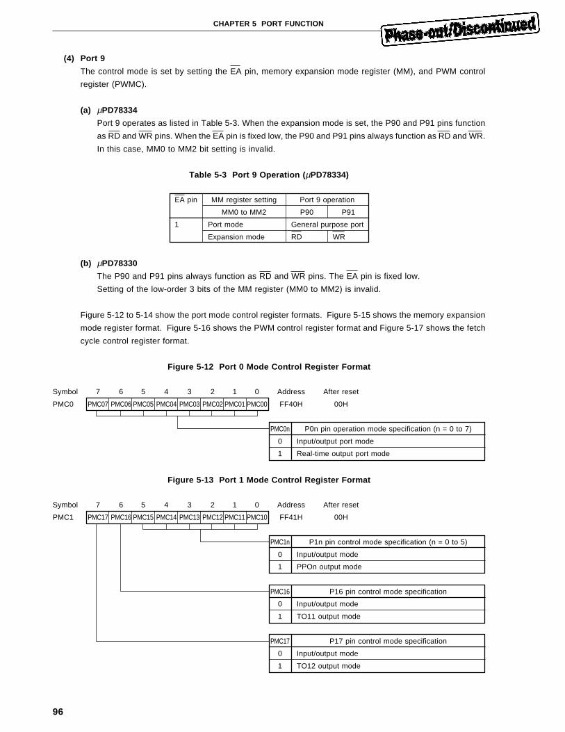
96
CHAPTER 5 PORT FUNCTION
(4) Port 9
The control mode is set by setting the EA pin, memory expansion mode register (MM), and PWM control
register (PWMC).
(a) µPD78334
Port 9 operates as listed in Table 5-3. When the expansion mode is set, the P90 and P91 pins function
as RD and WR pins. When the EA pin is fixed low, the P90 and P91 pins always function as RD and WR.
In this case, MM0 to MM2 bit setting is invalid.
Table 5-3 Port 9 Operation ( µPD78334)
EA pin MM register setting Port 9 operation
MM0 to MM2 P90 P91
1 Port mode General purpose port
Expansion mode RD WR
(b) µPD78330
The P90 and P91 pins always function as RD and WR pins. The EA pin is fixed low.
Setting of the low-order 3 bits of the MM register (MM0 to MM2) is invalid.
Figure 5-12 to 5-14 show the port mode control register formats. Figure 5-15 shows the memory expansion
mode register format. Figure 5-16 shows the PWM control register format and Figure 5-17 shows the fetch
cycle control register format.
Figure 5-12 Port 0 Mode Control Register Format
Symbol 7 6 5 4 3 2 1 0 Address After reset
PMC0 PMC07 PMC06 PMC05 PMC04 PMC03 PMC02 PMC01 PMC00 FF40H 00H
PMC0n P0n pin operation mode specification (n = 0 to 7)
0 Input/output port mode
1 Real-time output port mode
Figure 5-13 Port 1 Mode Control Register Format
Symbol 7 6 5 4 3 2 1 0 Address After reset
PMC1 PMC17 PMC16 PMC15 PMC14 PMC13 PMC12 PMC11 PMC10 FF41H 00H
PMC1n P1n pin control mode specification (n = 0 to 5)
0 Input/output mode
1 PPOn output mode
PMC16 P16 pin control mode specification
0 Input/output mode
1 TO11 output mode
PMC17 P17 pin control mode specification
0 Input/output mode
1 TO12 output mode
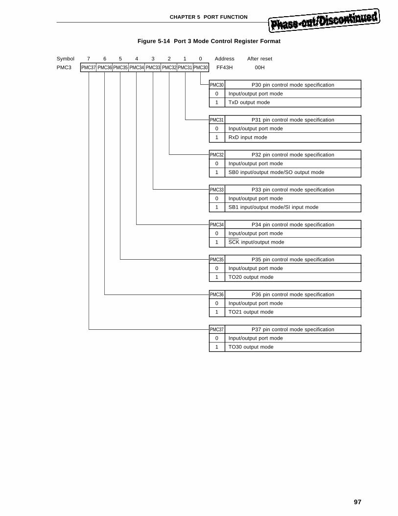
97
CHAPTER 5 PORT FUNCTION
Figure 5-14 Port 3 Mode Control Register Format
Symbol 7 6 5 4 3 2 1 0 Address After reset
PMC3 PMC37 PMC36 PMC35 PMC34 PMC33 PMC32 PMC31 PMC30 FF43H 00H
PMC30 P30 pin control mode specification
0 Input/output port mode
1 TxD output mode
PMC31 P31 pin control mode specification
0 Input/output port mode
1 RxD input mode
PMC32 P32 pin control mode specification
0 Input/output port mode
1 SB0 input/output mode/SO output mode
PMC33 P33 pin control mode specification
0 Input/output port mode
1 SB1 input/output mode/SI input mode
PMC34 P34 pin control mode specification
0 Input/output port mode
1 SCK input/output mode
PMC35 P35 pin control mode specification
0 Input/output port mode
1 TO20 output mode
PMC36 P36 pin control mode specification
0 Input/output port mode
1 TO21 output mode
PMC37 P37 pin control mode specification
0 Input/output port mode
1 TO30 output mode
98
CHAPTER 5 PORT FUNCTION
Figure 5-15 Memory Expansion Mode Register Format
Symbol 7 6 5 4 3 2 1 0 Address After reset
MM 0 0 0 0 0 MM2 MM1 MM0 FFC4H 00H
MM2 MM1 MM0 P40 to P47 and P50 to P57 pin operation
mode specification
0 0 0 Port Single P40 to P47: Input port
mode chip P50 to P57: Port mode
0 0 1 mode P40 to P47: Output port
P50 to P57: Port mode
0 1 0 Undefined
0 1 1 Expan- 256 P40 to P47: Expansion
sion bytes mode
mode P50 to P57: Port mode
1 0 0 4 Kbytes P40 to P47 and P50 to
P53: Expansion mode
P54 to P57: Port mode
1 0 1 16 Kbytes P40 to P47 and P50 to
P55: Expansion mode
P56 to P57: Port mode
1 1 0 Undefined
1 1 1 Expan- 32 Kbytes P40 to P47 and P50 to
sion P57: Expansion mode
mode
Cautions 1. Be sure to set 0 in bits 3 to 7. If 1 is set, normal operation is not performed.
2. Do not write the code combinations indicated by “Undefined”.
Figure 5-16 PWM Control Register Format
Symbol 7 6 5 4 3 2 1 0 Address After reset
PWMC 0 0 0 0 PWME1 PWME0 PRM1 PRM0 FF64H 00H
PRM1 PRM0 Count clock PWM period
0 0 fCLK fCLK/28
0 1 fCLK/26 fCLK/214
1 0 fCLK/29 fCLK/217
1 1 fCLK/210 fCLK/218
PWMEn PWMn signal output operation control (n = 0 or 1)
0 Operation stop (Output contents of output latch)
1 Operation enable
Caution To stop the PWM output function (PWME0 = 0/PWME1 = 0), previously initialize the output
latch to fix the output state at stop.
99
CHAPTER 5 PORT FUNCTION
Figure 5-17 Fetch Cycle Control Register Format
Symbol 7 6 5 4 3 2 1 0 Address After reset
FCC FCC7 FCC6 FCC5 FCC4 FCC3 FCC2 FCC1 FCC0 FCC9H 00H
FCC1 FCC0 Memory space (0000H to 3FFFH) fetch cycle
mode specification
0 0 Normal fetch cycle mode
0 1 Undefined
1 0
1 1 High-speed fetch cycle mode
FCC3 FCC2 Memory space (4000H to 7FFFH) fetch cycle
mode specification
0 0 Normal fetch cycle mode
0 1 Undefined
1 0
1 1 High-speed fetch cycle mode
FCC5 FCC4 Memory space (8000H to BFFFH) fetch cycle
mode specification
0 0 Normal fetch cycle mode
0 1 Undefined
1 0
1 1 High-speed fetch cycle mode
FCC7 FCC6 Memory space (C000H to FFFFH) fetch cycle
mode specification
0 0 Normal fetch cycle mode
0 1 Undefined
1 0
1 1 High-speed fetch cycle mode
Caution Write “00” into the bits corresponding to unaccessed memory areas.

100
[MEMO]
101
CHAPTER 6 CLOCK GENERATOR
To clock generator generates and controls the internal system clock (CLK) supplied to the CPU. Figure 6-1 shows
the clock generator block diagram.
Figure 6-1 Clock Generator Block Diagram
Remarks 1. fXX: Crystal oscillator frequency
2. fX: External clock frequency
3. fCLK: Internal system clock frequency
The system clock oscillator oscillates by a crystal resonator connected to the X1 and X2 pins. When the standby
mode (STOP mode) is set, the system clock oscillator stops oscillation. (see CHAPTER 14 STANDBY FUNCTION )
The external clock can also be input. To input the external clock, input the clock signal to the X1 pin and its inverted
phase to the X2 pin. However, the X2 pin can be open.
The frequency divider divides system clock oscillator output (fXX when crystal oscillation is used or fX when the
external clock is used) by two to generate internal system clock (fCLK).
Caution To use the external clock, do not set the STP bit of the standby control register (STBC) to 1.
Systemclockgenerator
Internal systemclock (CLK)
STOP mode
Divider
fXX or fX
102
CHAPTER 6 CLOCK GENERATOR
Figure 6-2 System Clock Oscillator External Circuit
(a) Crystal Clock
(b) External Clock
(i) To input inverted phase of external clock (ii) To leave X2 is open
to X1 pin to X2 pin
Cautions 1. To use the system clock oscillator, wire the blocked portions in Figure 6-
2 to avoid affection of wiring capacitance, etc.:
• Make wiring as extremely short as possible.
• Do not cross the oscillator and any other signal where high current which
changes flows.
• Be sure to place oscillator capacitor ground point in the same potential as the
VSS pin. Do not connect to any ground pattern where high current flows.
• Do not take out any signal from the oscillator.
2. To input external clock to the X1 pin and leave the X2 pin open, do not connect
load such as wiring capacitance to the X2 pin.
Figure 6-3 shows bad examples of resonator connection circuit.
Externalclock
Open
Externalclock
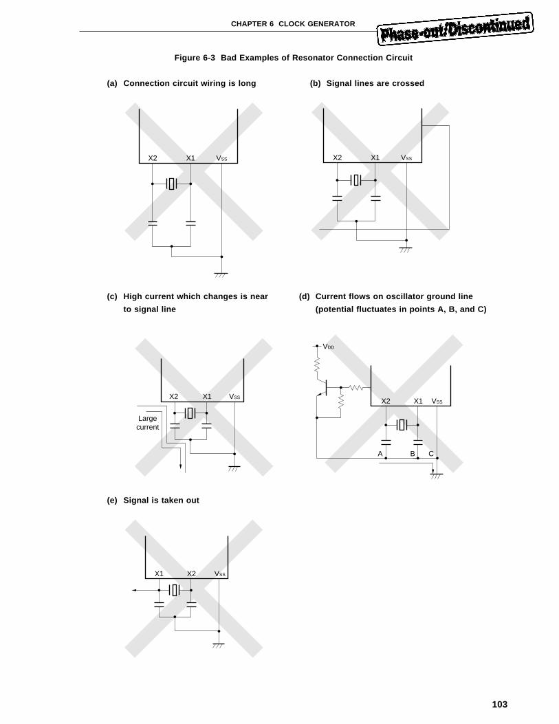
103
CHAPTER 6 CLOCK GENERATOR
Figure 6-3 Bad Examples of Resonator Connection Circuit
(a) Connection circuit wiring is long (b) Signal lines are crossed
X2 X1 VSS X2 X1 VSS
(c) High current which changes is near (d) Current flows on oscillator ground line
to signal line (potential fluctuates in points A, B, and C)
X2 X1 VSS
Largecurrent
X2 X1 VSS
A B C
VDD
(e) Signal is taken out
X1 X2 VSS

104
[MEMO]

105
CHAPTER 7 REAL-TIME PULSE UNIT
The real-time pulse unit (RPU) can perform programmable pulse output and pulse interval and frequency
measurement.
The real-time pulse unit (RPU) consists of the main components of four timers and 16 registers. The functions
and structures of these registers can be programmed to cover various applications flexibility.
The largest feature of the real-time pulse unit (RPU) lies in rich and multifunctional timer pulse output. A total of
six timer pulse output lines such as toggle output, set output, and reset output can be controlled independently. In
addition, the real-time output port output timing can be controlled.
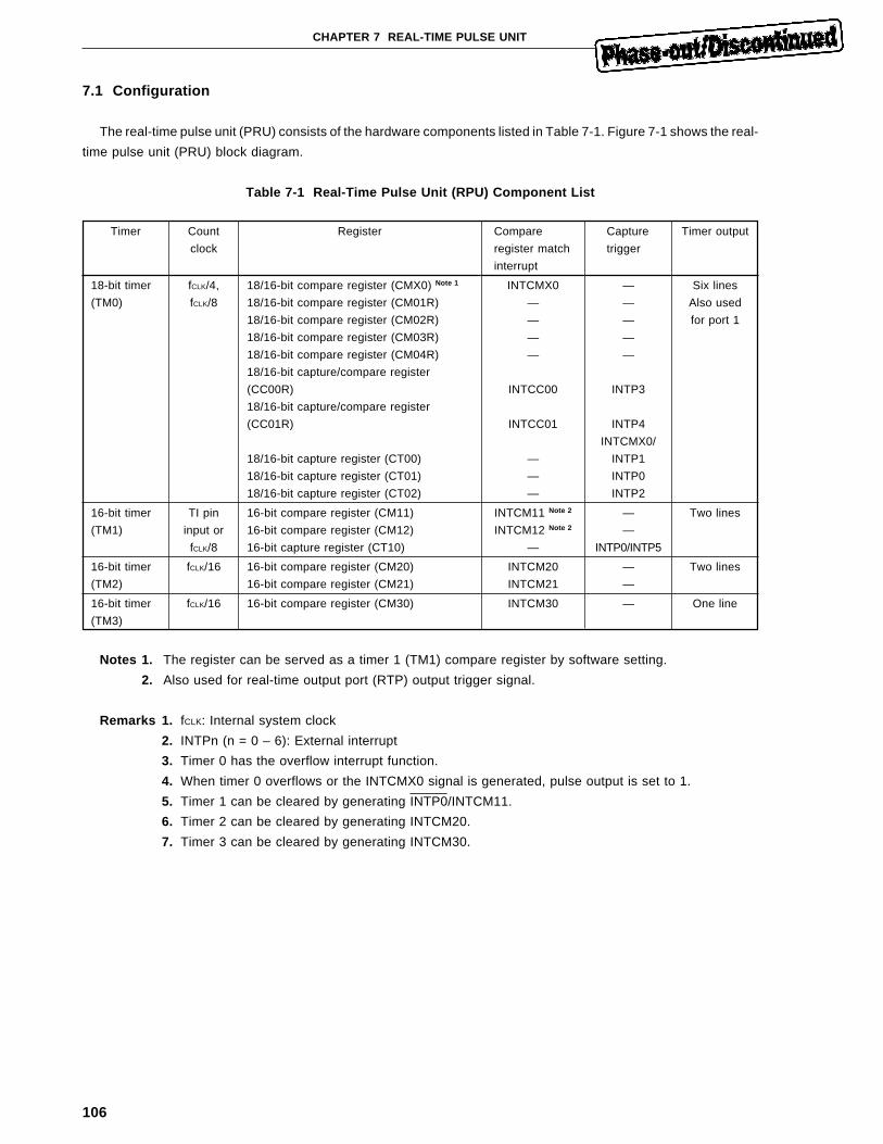
106
CHAPTER 7 REAL-TIME PULSE UNIT
7.1 Configuration
The real-time pulse unit (PRU) consists of the hardware components listed in Table 7-1. Figure 7-1 shows the real-
time pulse unit (PRU) block diagram.
Table 7-1 Real-Time Pulse Unit (RPU) Component List
Timer
18-bit timer
(TM0)
16-bit timer
(TM1)
16-bit timer
(TM2)
16-bit timer
(TM3)
Count
clock
fCLK/4,
fCLK/8
TI pin
input or
fCLK/8
fCLK/16
fCLK/16
Register
18/16-bit compare register (CMX0) Note 1
18/16-bit compare register (CM01R)
18/16-bit compare register (CM02R)
18/16-bit compare register (CM03R)
18/16-bit compare register (CM04R)
18/16-bit capture/compare register
(CC00R)
18/16-bit capture/compare register
(CC01R)
18/16-bit capture register (CT00)
18/16-bit capture register (CT01)
18/16-bit capture register (CT02)
16-bit compare register (CM11)
16-bit compare register (CM12)
16-bit capture register (CT10)
16-bit compare register (CM20)
16-bit compare register (CM21)
16-bit compare register (CM30)
Compare
register match
interrupt
INTCMX0
—
—
—
—
INTCC00
INTCC01
—
—
—
INTCM11 Note 2
INTCM12 Note 2
—
INTCM20
INTCM21
INTCM30
Capture
trigger
—
—
—
—
—
INTP3
INTP4
INTCMX0/
INTP1
INTP0
INTP2
—
—
INTP0/INTP5
—
—
—
Timer output
Six lines
Also used
for port 1
Two lines
Two lines
One line
Notes 1. The register can be served as a timer 1 (TM1) compare register by software setting.
2. Also used for real-time output port (RTP) output trigger signal.
Remarks 1. fCLK: Internal system clock
2. INTPn (n = 0 – 6): External interrupt
3. Timer 0 has the overflow interrupt function.
4. When timer 0 overflows or the INTCMX0 signal is generated, pulse output is set to 1.
5. Timer 1 can be cleared by generating INTP0/INTCM11.
6. Timer 2 can be cleared by generating INTCM20.
7. Timer 3 can be cleared by generating INTCM30.
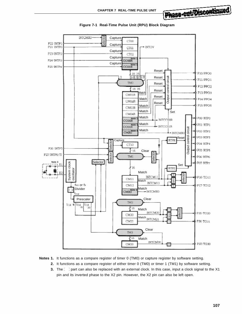
107
CHAPTER 7 REAL-TIME PULSE UNIT
Figure 7-1 Real-Time Pulse Unit (RPU) Block Diagram
Notes 1. It functions as a compare register of timer 0 (TM0) or capture register by software setting.
2. It functions as a compare register of either timer 0 (TM0) or timer 1 (TM1) by software setting.
3. The part can also be replaced with an external clock. In this case, input a clock signal to the X1
pin and its inverted phase to the X2 pin. However, the X2 pin can also be left open.
Sel
ecto
r
Capture
Capture
Capture
Capture
Capture
Reset
Reset
Reset
Reset
Reset
Reset
Match
Match
Match
Match
Match
Match
Match
Set
Reset
Out
put c
ontro
l circ
uit
Sel
ecto
r
Set
Clear
Capture
Sel
ecto
rS
elec
tor
Sys
tem
clo
ckos
cilla
tor
Note 3
fXX or fXDivider
Prescaler
Match
Clear
Match
Match
Clear
Match
Match
Match
Note 2
Sel
ecto
rS
elec
tor
Selector
Out
put c
ontro
l circ
uit
Note 1
Note 1
Note 1
Note 1
Note 2
108
CHAPTER 7 REAL-TIME PULSE UNIT
Table 7-2 lists the control registers of the real time pulse unit. Table 7-3 provides a lookup table of the control
registers for operation specification of the real time pulse unit timers.
Table 7-2 List of Real-Time Pulse Unit (RPU) Operation Control Registers
Address Special function register Symbol Function Reference
(SFR) Name Page
FEB0H Timer control register 0 TMC0 Specification of timer clock to TM0 (PRM00) 124
Specification of bit length of TM0 (PRM01)
Specification of count clock source to TM1 (PRM10)
Control of clear operation by INTP0 input of TM1 (ECLR)
Specification of TM1 (CLR1) operation mode
Control of TM0, TM1 operation (CE0, CE1)
FFB2H Timer control register 1 TMC1 Specification of TM2 (CLR2) operation mode 125
Control of TM2, TM3 (CE2, CE3) operation
FFB4H Timer unit mode register 0 TUM0 Specification of presence of absence of TM0, TM1, TM2 122
overflow (OVF0, OVF1, OVF2)
Specification of TM0 (PRS0, PRS1) INTOV interrupt signal
Specification of PPO0 to PPO5 operation mode (PPOCN)
FFB5H Timer unit mode register 1 TUM1 Specification of CC00R, CC01R register operation mode 123
(CMS0, CMS1)
Specification of CT00, CT10 capture trigger source
(CAPT1, CAPT0)
Specification of PPO3 to PPO5 set signal
(PPOM3 to PPOM5)
Specification of timer connected to CMX0 register (MOD)
FFB8H Timer output control register 0 TOC0 Specification of TO11, TO20 pin output mode 127
(TOM11, TOM20)
Specification of TO11, TO12, TO20 pin active level
(ALV11, ALV12, ALV20)
Specification of TO11, TO12, TO20 operation
(ENTO11, ENTO12, ENTO20)
FFB9H Timer output control register 1 TOC1 Specification of TO21, TO30 pin and PPO0 to PPO5 128
active level (ALV21, ALV30, ALVPPO0, ALVPPO1)
Specification of TO21, TO30 operation (ENTO21, ENTO30)
Control of PPO0 to PPO5 output (ENPPO0, ENPPO1)
FFBCH Programmable pulse output PPOS Control of PPO output by INTCMX0 (PPOS0 to PPOS5) 129
set register
FFF4H External interrupt mode INTM0 Specification of active edge of NMI pin (ESNMI) 130
register 0 Specification of active edge of INTP0 to INTP2 pins
(ES00, ES01, ES10, ES11, ES20, ES21)
FFF5H External interrupt mode INTM1 Specification of active edge of INTP3 to INTP6 pins 131
register 1 (ES30, ES31, ES40, ES41, ES50, ES51, ES60, ES61)
109
CHAPTER 7 REAL-TIME PULSE UNIT
Table 7-3 Real-Time Pulse Unit (RPU) Control Register Lookup Table
Item Control Timer
TM0 TM1 TM2 TM3
Timer operation Count operation enable/disable TMC0 TMC1
Timer operation mode selection Free running TMC0 TMC1 Interval timer
timer
Count bit length selection TMC0 None
Timer clear signal selection None TMC0 None
Overflow bit selection TUM0 None
Count clock Internal or external selection Fixed to internal TMC0 Fixed to internal
Internal frequency dividing selection TMC0 fCLK/8 fCLK/16
External active edge selection None INTM1 None
Timer output Timer output enable/disable None TOC0 TOC0, TOC1 TOC1
Active level selection None TOC0 TOC0, TOC1 TOC1
Output mode (SR/toggle) selection None TOC0 None
Control signal output enable/disable PMC1 PMC3
Programmable Pulse output enable/disable TOC1 None
pulse output Pulse output operating mode selection TUM0 None
Pulse output control selection PPOS None
Set signal selection TUM1 None
Active level selection TOC1 None
Capture/compare Capture/compare function selection TUM1 None
register CMX0 selection TUM1 None
Capture trigger selection TUM1 None
Capture trigger edge selection INTM0, INTM1 None
110
CHAPTER 7 REAL-TIME PULSE UNIT
7.1.1 Timer 0 (TM0)
Timer 0 (TM0) is a 18-bit or 16-bit free-running timer.
The internal clock (fCLK/4 or fCLK/8) is counted. When the timer overflows, an overflow interrupt (INTOV) is generated.
The overflow timer bit can be selected by setting the control register.
To read the timer 0 contents as a 18-bit timer, TM0 of a special function register (SFR) and the timer low access
register (TLA) Note are used. First, execute a TM0 read instruction, and just then execute a TLA register read instruction.
The high-order 16-bit contents of the 18-bit timer are read by reading TM0 and the low-order 2-bit contents are read
by reading the TLA register.
To use timer 0 as the 16-bit timer, use the high-order 16 bits when the 18-bit timer is used. To read the contents
of timer 0, use only TM0 of SFR.
When RESET is input, all bits of TM0 are reset to 0.
Note TLA register: Is an SFR used to access the low-order 2-bit of the 18-bit timer, compare register, capture
register, or capture/compare register.
Caution To read the contents of timer 0 as the 16-bit timer, be sure to continue to execute the TM0 and
TLA register read instructions. If the TLA register read instruction is not executed, the TM0 value
cannot be read correctly.
Figure 7-2 Timer 0 Format
<1> To use 18-bit timer <2> To use 16-bit timer
Timer 0 Timer 0
Read Read
Read
111
CHAPTER 7 REAL-TIME PULSE UNIT
7.1.2 Timer 1 (TM1)
Timer 1 (TM1) is a 16-bit timer/event counter. The internal clock (fCLK/8) selected in the timer control register (TMC0)
or external event input through the TI pin can be counted.
When the timer overflows as a result of counting, the overflow bit (OVF1) is set to 1.
TM1 can be cleared by external interrupt input (inverted edge input of INTP0) or match interrupt signal (INTCM11)
from compare register CM11.
When RESET is input, all the TM1 bits can be reset to 0.
7.1.3 Timer 2 (TM2)
Timer 2 (TM2) is a 16-bit timer/free-running timer. Internal clock (fCLK/16) is counted. When the timer overflows,
the overflow bit (OVF2) is set to 1.
TM2 can be cleared by match interrupt signal (INTCM20) from the compare register CM20.
When RESET is input, all TM2 bits are reset to 0.
7.1.4 Timer 3 (TM3)
Timer 3 (TM3) is a 16-bit interval timer. Internal clock (fCLK/16) is counted. When match interrupt signal (INTCM30)
is generated from the compare register CM30, TM3 is cleared.
When RESET is input, all the TM3 bits are reset to 0.
7.1.5 Compare registers
The contents of each timer are always compared with the data written into the compare register corresponding
to the timer. When they match, a match signal is generated. See Table 7-1 for the configuration of the timers and
compare registers and the correspondence between the compare registers and interrupt sources.
When RESET is input, the compare register contents become undefined.
(1) 18/16-bit compare registers (CMX0 Note 1 and CM0nR (n = 1 – 4))
(a) Function
The 18/16-bit compare registers are connected to timer 0 (TM0) and have the timer output function. When
a match between the CMX0 register and the timer contents is detected, timer output is set to 1 Note 2 . When
a match between the CM0nR register and the timer contents is detected, the timer output is reset to 0.
The 18-bit or 16-bit length is set automatically as the timer 0 length is specified.
Notes 1. The CMX0 register can also be connected to timer 1 (TM1) by software setting.
2. Three of the six timer output lines can also be set to 1 by the timer 0 (TM0) overflow signal
by software setting
112
CHAPTER 7 REAL-TIME PULSE UNIT
(b) Compare register (CMX0, CM0nR) read/write operation
To read the compare register contents as an 18-bit compare register, the 16-bit compare register (CMX0
or CM0nR (n = 1 – 4)) of a special function register (SFR) and the TLA register are used.
<1> To read the 18-bit compare region contents
First, execute a CMX0 (or CM0nR) read instruction, and just then execute a TLA register read
instruction. The high-order 16-bit contents of the 18-bit compare register are read by reading the
CMX0 (or CM0nR) register and the low-order 2-bit contents are read by reading the TLA register.
<2> To write data into 18-bit compare register
First, write data corresponding to the low-order 2-bit of the 18-bit compare register into the TLA
register, and just then write the high-order 16-bit data into the CMX0 (CM0nR) register.
To use as the 16-bit compare register, use the high-order 16 bits (CMX0, CM0nR).
Cautions 1. To read the contents of the 18-bit compare register be sure to continue to execute
the CMX0 (or CM0nR) register and TLA register read instruction is not executed,
the 18-bit compare register value cannot be read correctly.
2. To write data into the 18-bit compare register, be sure to continue to execute write
instruction into the TLA register and CMX0 (or CM0nR) register. If the write
instruction into the CMX0 (or CM0nR) register is not executed, the 18-bit compare
register value is not rewritten.
113
CHAPTER 7 REAL-TIME PULSE UNIT
Figure 7-3 18/16-bit Compare Register Format (To read)
<1> To use 18-bit compare register <2> To use 16-bit compare register
18-bit compare register 16-bit compare register
Remark n = 1 – 4
Figure 7-4 18/16-bit Compare Register Format (To write)
<1> To use 18-bit compare register <2> To use 16-bit compare register
18-bit compare register 16-bit compare register
Remark n = 1 – 4
Read Read
Read
WriteWrite
Write
114
CHAPTER 7 REAL-TIME PULSE UNIT
Table 7-4 Interrupt Request Signal from 18/16-bit Compare Registers
Compare register Interrupt signal
CMX0 INTCMX0
CM01R —
CM02R —
CM03R —
CM04R —
(2) 16-bit compare registers (CM11, CM12, CM20, CM21, and CM30)
The 16-bit compare registers (CM11, CM12, CM20, CM21, and CM30) are connected to timers 1 to 3 as listed
in Table 7-1 and have the timer output function. In synchronization with the interrupt occurrence, the
corresponding timer output is inverted (toggle output operation). CM11, CM12 and CM20, CM21 pairs can
also be used as set reset output (set reset output operation).
Table 7-5 Interrupt Request Signals from 16-bit Compare Registers
Compare register Interrupt signal
CM11 INTCM11
CM12 INTCM12
CM20 INTCM20
CM21 INTCM21
CM30 INTCM30
7.1.6 Capture registers
The capture register captures the timer contents according to the capture trigger signal.
The value once captured is retained until the next capture operation is performed. External interrupts (INTP0 to
INTP2, INTP5) and match detection interrupt (INTCMX0) from compare register CMX0 can be used as capture
triggers. See Table 7-6 for the correspondence between the registers and capture triggers. As the capture trigger
signal is generated, interrupt is also generated.
The pulse width and cycle of each external input pulse can be easily measured by using the capture registers.
When RESET is input, the capture register contents become undefined.
115
CHAPTER 7 REAL-TIME PULSE UNIT
(1) 18/16-bit capture registers (CT00 to CT02)
(a) Function
When a capture trigger occurs, the timer 0 (TM0) contents are captured.
The 18-bit or 16-bit length is set automatically as the timer 0 length is specified.
(b) Capture register (CT00 to CT02) read operation
To read the capture register contents as a 18-bit capture register, the 16-bit capture register (CT00 to
CT02) of a special function register (SFR) and the TLA register are used. First, execute a 16-bit capture
register (CT00 to CT02) read instruction, and just then execute a TLA register read instruction. The high-
order 16-bit contents of the 18-bit capture register are read by reading the 16-bit capture register (CT00
to CT02) and the low-order 2-bit contents are read by reading the TLA register.
To use the capture register as 16-bit capture register, the high-order 16 bits (CT00 to CT02) are used.
Caution To read the contents of the 18-bit capture register, be sure to continue to execute the
16-bit capture register (CT00 to CT02) and TLA register read instructions. If the TLA
register read instruction is not executed, the 18-bit capture register value cannot be read
correctly.
Figure 7-5 18/16-bit Capture Register Format
<1> To use 18-bit capture register <2> To use 16-bit capture register
18-bit capture register 16-bit capture register
Remark n = 0 – 2
Read Read
Read
116
CHAPTER 7 REAL-TIME PULSE UNIT
Table 7-6 Capture Trigger Signals to 18/16-bit Capture Registers
Capture register Capture trigger signal
CT00 INTCMX0 or INTP1
CM01 INTP0
CM02 INTP2
(2) 16-bit capture register (CT10)
When a capture trigger occurs, the timer 1 contents are captured.
Table 7-7 Capture Trigger Signal to 16-bit Capture Register
Capture register Capture trigger signal
CT10 INTP0 or INTP5
7.1.7 Capture/compare registers
The capture/compare registers (CC00R and CC01R) are 18/16-bit registers connected to timer 0 (TM0); each
capture/compare register has both the capture register function and compare register function. The CC00R and
CC01R function are selected by setting the control registers.
When RESET is input, the capture/compare register contents become undefined.
(1) 18/16 bit capture/compare registers (CC00R and CC01R)
(a) Function
The 18-bit or 16-bit length is set automatically as the timer 0 length is specified. When CC00R and CC01R
function as capture registers, external interrupts (INTP3 and INTP4) can be used as capture triggers.
When CC00R and CC01R function as compare registers the timer output function is provided. Timer
output function is provided. Timer output is reset to 0 in synchronization with interrupt occurrence when
the timer value and register value match. The interrupt sources vary depending on the selected register
function. When the capture register function is selected, the external interrupts used as capture triggers
(INTP3 and INTP4) are selected. When the compare register function is selected, the match interrupts
(INTCC00 and INTCC01) are selected. (See Table 7-1 .)
Caution When the compare register function is used, the external interrupts capture triggers
cannot be used for interrupt generation.
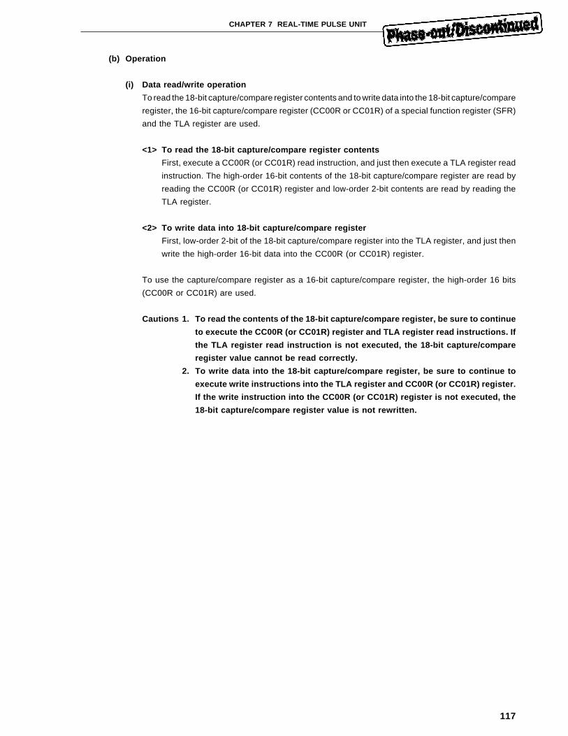
117
CHAPTER 7 REAL-TIME PULSE UNIT
(b) Operation
(i) Data read/write operation
To read the 18-bit capture/compare register contents and to write data into the 18-bit capture/compare
register, the 16-bit capture/compare register (CC00R or CC01R) of a special function register (SFR)
and the TLA register are used.
<1> To read the 18-bit capture/compare register contents
First, execute a CC00R (or CC01R) read instruction, and just then execute a TLA register read
instruction. The high-order 16-bit contents of the 18-bit capture/compare register are read by
reading the CC00R (or CC01R) register and low-order 2-bit contents are read by reading the
TLA register.
<2> To write data into 18-bit capture/compare register
First, low-order 2-bit of the 18-bit capture/compare register into the TLA register, and just then
write the high-order 16-bit data into the CC00R (or CC01R) register.
To use the capture/compare register as a 16-bit capture/compare register, the high-order 16 bits
(CC00R or CC01R) are used.
Cautions 1. To read the contents of the 18-bit capture/compare register, be sure to continue
to execute the CC00R (or CC01R) register and TLA register read instructions. If
the TLA register read instruction is not executed, the 18-bit capture/compare
register value cannot be read correctly.
2. To write data into the 18-bit capture/compare register, be sure to continue to
execute write instructions into the TLA register and CC00R (or CC01R) register.
If the write instruction into the CC00R (or CC01R) register is not executed, the
18-bit capture/compare register value is not rewritten.
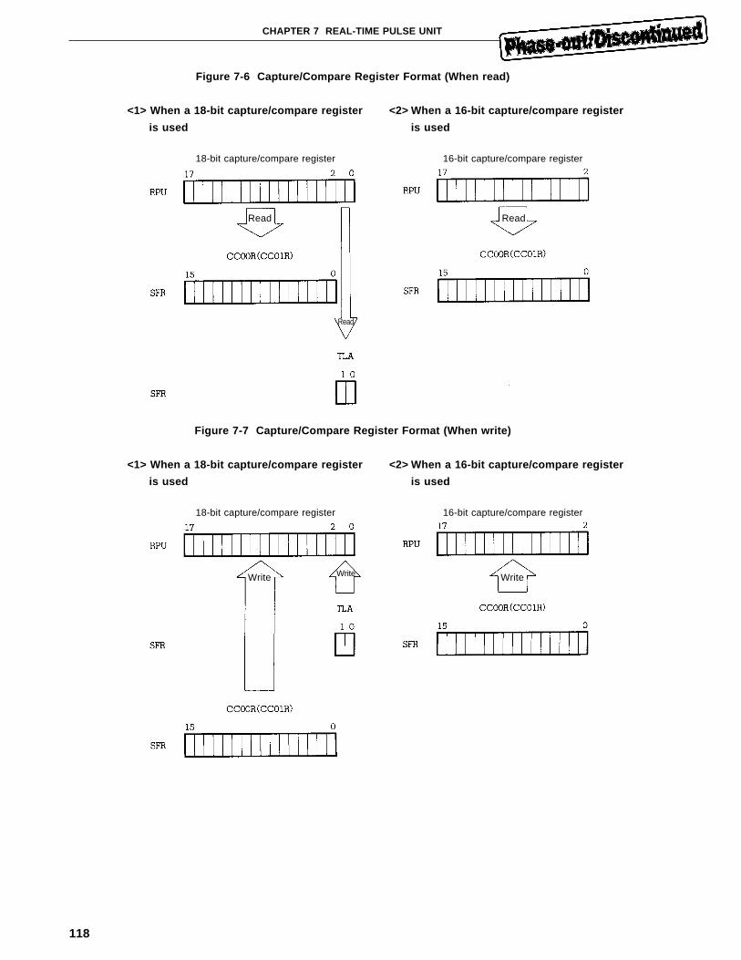
118
CHAPTER 7 REAL-TIME PULSE UNIT
Figure 7-6 Capture/Compare Register Format (When read)
<1> When a 18-bit capture/compare register <2> When a 16-bit capture/compare register
is used is used
18-bit capture/compare register 16-bit capture/compare register
Figure 7-7 Capture/Compare Register Format (When write)
<1> When a 18-bit capture/compare register <2> When a 16-bit capture/compare register
is used is used
18-bit capture/compare register 16-bit capture/compare register
Read Read
Read
Write WriteWrite
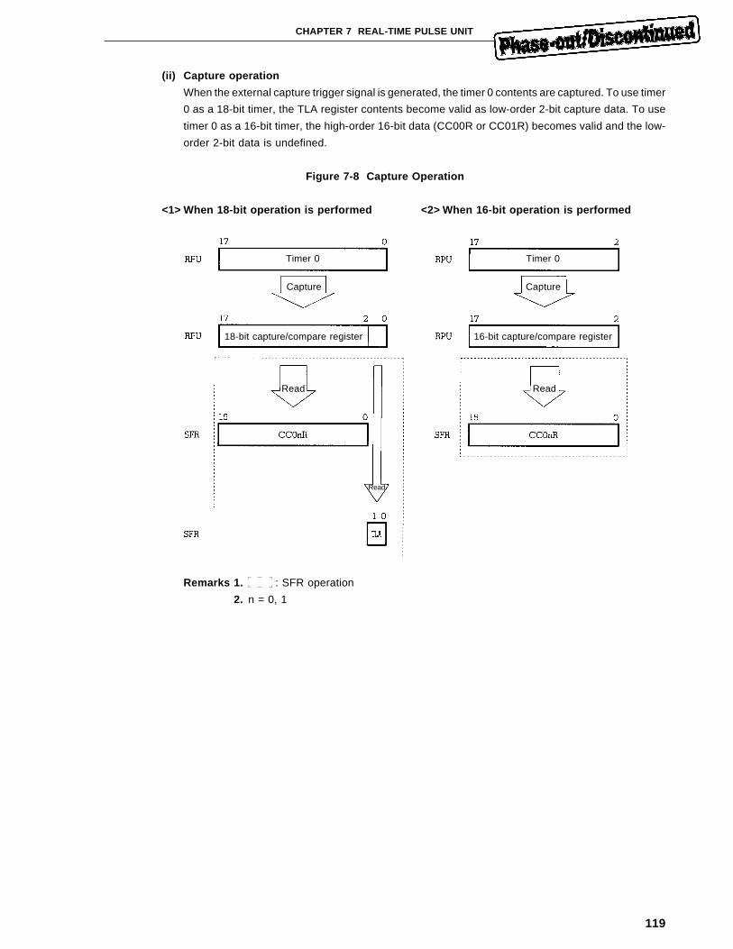
119
CHAPTER 7 REAL-TIME PULSE UNIT
(ii) Capture operation
When the external capture trigger signal is generated, the timer 0 contents are captured. To use timer
0 as a 18-bit timer, the TLA register contents become valid as low-order 2-bit capture data. To use
timer 0 as a 16-bit timer, the high-order 16-bit data (CC00R or CC01R) becomes valid and the low-
order 2-bit data is undefined.
Figure 7-8 Capture Operation
<1> When 18-bit operation is performed <2> When 16-bit operation is performed
Remarks 1. : SFR operation
2. n = 0, 1
Timer 0 Timer 0
Capture Capture
Read Read
Read
18-bit capture/compare register 16-bit capture/compare register
120
CHAPTER 7 REAL-TIME PULSE UNIT
(iii) Compare operation
The register contents are always compared with the timer 0 contents. If a match between them is
detected interrupt signal is generated.
Figure 7-9 Compare Operation
<1> When 18-bit operation is performed
<2> When 16-bit operation is performed
Remarks 1. : SFR operation
2. n = 0, 1
3. m = 0 to 3
Timer 0
18-bit capture/compare register
Match interrupt
16-bit capture/compare register
Timer 0
Match interrupt(INTCC0m)
Write
Write Write
121
CHAPTER 7 REAL-TIME PULSE UNIT
7.2 Control Registers
Real-time pulse unit (RPU) operation is specified by setting the following five types of control registers:
• Timer unit mode registers (TUM0 and TUM1)
• Timer control registers (TMC0 and TMC1)
• Timer output control registers (TOC0 and TOC1)
• Programmable pulse output set register (PPOS)
• External interrupt mode registers (INTM0 and INTM1)
The each of control register are explained below:
7.2.1 Timer unit mode registers (TUM0 and TUM1)
Timer unit mode register 0 (TUM0) is an 8-bit register which stores the timer overflow state and specifies the
overflow interrupt generation signal from timer 0.
Timer unit mode register 1 (TUM1) is an 8-bit register to specify the capture trigger sources and the RPU register
configuration.
Figures 7-10 and 7-11 show the TUM0 and TUM1 register formats.
The registers can be read/written by executing bit or 8-bit manipulation instructions.
When RESET input, the timer unit mode register contents are reset to 00H.
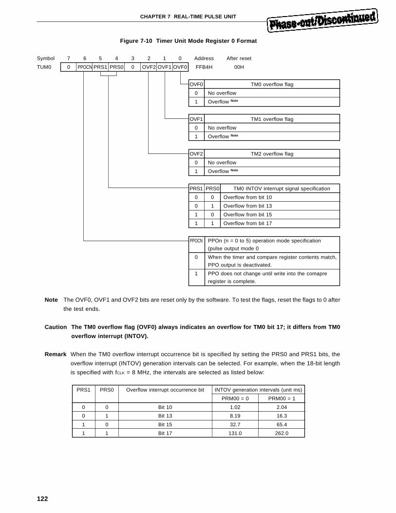
122
CHAPTER 7 REAL-TIME PULSE UNIT
Figure 7-10 Timer Unit Mode Register 0 Format
Symbol 7 6 5 4 3 2 1 0 Address After reset
TUM0 0 PPOCN PRS1 PRS0 0 OVF2 OVF1 OVF0 FFB4H 00H
OVF0 TM0 overflow flag
0 No overflow
1 Overflow Note
OVF1 TM1 overflow flag
0 No overflow
1 Overflow Note
OVF2 TM2 overflow flag
0 No overflow
1 Overflow Note
PRS1 PRS0 TM0 INTOV interrupt signal specification
0 0 Overflow from bit 10
0 1 Overflow from bit 13
1 0 Overflow from bit 15
1 1 Overflow from bit 17
PPOCN PPOn (n = 0 to 5) operation mode specification
(pulse output mode 0
0 When the timer and compare register contents match,
PPO output is deactivated.
1 PPO does not change until write into the comapre
register is complete.
Note The OVF0, OVF1 and OVF2 bits are reset only by the software. To test the flags, reset the flags to 0 after
the test ends.
Caution The TM0 overflow flag (OVF0) always indicates an overflow for TM0 bit 17; it differs from TM0
overflow interrupt (INTOV).
Remark When the TM0 overflow interrupt occurrence bit is specified by setting the PRS0 and PRS1 bits, the
overflow interrupt (INTOV) generation intervals can be selected. For example, when the 18-bit length
is specified with fCLK = 8 MHz, the intervals are selected as listed below:
PRS1 PRS0 Overflow interrupt occurrence bit INTOV generation intervals (unit ms)
PRM00 = 0 PRM00 = 1
0 0 Bit 10 1.02 2.04
0 1 Bit 13 8.19 16.3
1 0 Bit 15 32.7 65.4
1 1 Bit 17 131.0 262.0
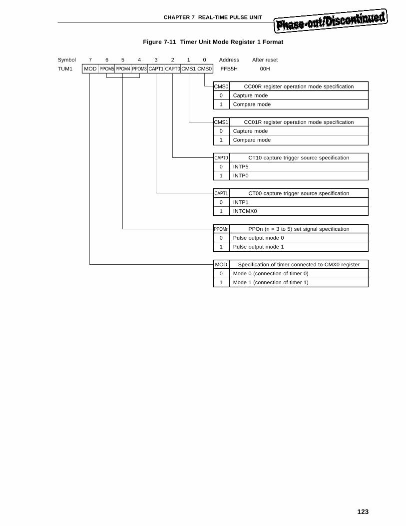
123
CHAPTER 7 REAL-TIME PULSE UNIT
Figure 7-11 Timer Unit Mode Register 1 Format
Symbol 7 6 5 4 3 2 1 0 Address After reset
TUM1 MOD PPOM5 PPOM4 PPOM3 CAPT1 CAPT0 CMS1 CMS0 FFB5H 00H
CMS0 CC00R register operation mode specification
0 Capture mode
1 Compare mode
CMS1 CC01R register operation mode specification
0 Capture mode
1 Compare mode
CAPT0 CT10 capture trigger source specification
0 INTP5
1 INTP0
CAPT1 CT00 capture trigger source specification
0 INTP1
1 INTCMX0
PPOMn PPOn (n = 3 to 5) set signal specification
0 Pulse output mode 0
1 Pulse output mode 1
MOD Specification of timer connected to CMX0 register
0 Mode 0 (connection of timer 0)
1 Mode 1 (connection of timer 1)
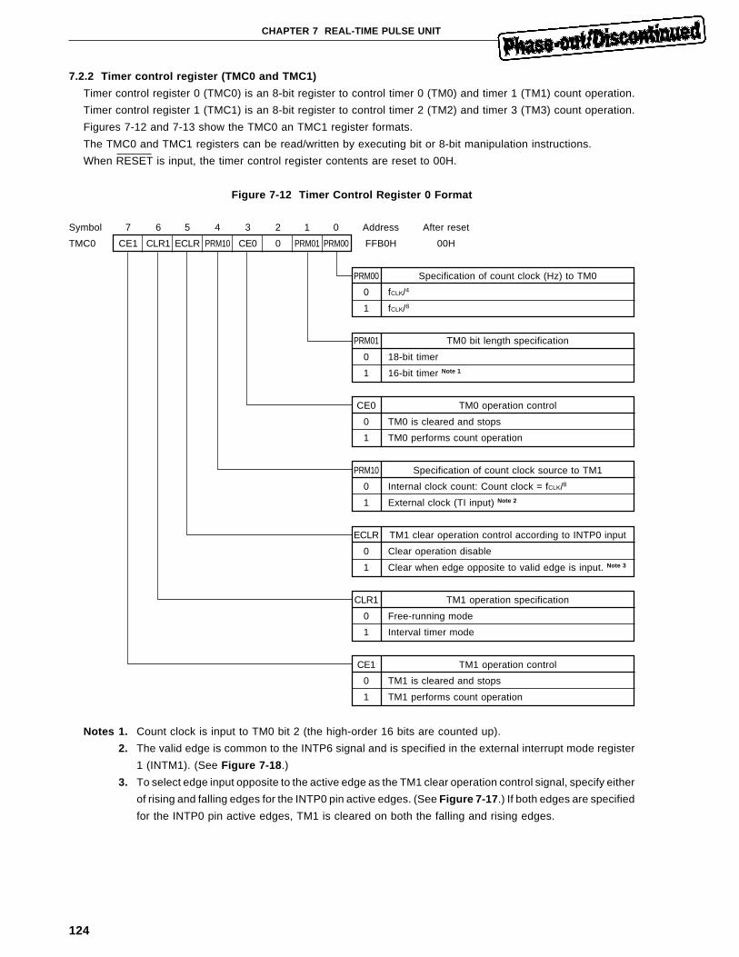
124
CHAPTER 7 REAL-TIME PULSE UNIT
7.2.2 Timer control register (TMC0 and TMC1)
Timer control register 0 (TMC0) is an 8-bit register to control timer 0 (TM0) and timer 1 (TM1) count operation.
Timer control register 1 (TMC1) is an 8-bit register to control timer 2 (TM2) and timer 3 (TM3) count operation.
Figures 7-12 and 7-13 show the TMC0 an TMC1 register formats.
The TMC0 and TMC1 registers can be read/written by executing bit or 8-bit manipulation instructions.
When RESET is input, the timer control register contents are reset to 00H.
Figure 7-12 Timer Control Register 0 Format
Symbol 7 6 5 4 3 2 1 0 Address After reset
TMC0 CE1 CLR1 ECLR PRM10 CE0 0 PRM01 PRM00 FFB0H 00H
PRM00 Specification of count clock (Hz) to TM0
0 fCLK/4
1 fCLK/8
PRM01 TM0 bit length specification
0 18-bit timer
1 16-bit timer Note 1
CE0 TM0 operation control
0 TM0 is cleared and stops
1 TM0 performs count operation
PRM10 Specification of count clock source to TM1
0 Internal clock count: Count clock = fCLK/8
1 External clock (TI input) Note 2
ECLR TM1 clear operation control according to INTP0 input
0 Clear operation disable
1 Clear when edge opposite to valid edge is input. Note 3
CLR1 TM1 operation specification
0 Free-running mode
1 Interval timer mode
CE1 TM1 operation control
0 TM1 is cleared and stops
1 TM1 performs count operation
Notes 1. Count clock is input to TM0 bit 2 (the high-order 16 bits are counted up).
2. The valid edge is common to the INTP6 signal and is specified in the external interrupt mode register
1 (INTM1). (See Figure 7-18 .)
3. To select edge input opposite to the active edge as the TM1 clear operation control signal, specify either
of rising and falling edges for the INTP0 pin active edges. (See Figure 7-17 .) If both edges are specified
for the INTP0 pin active edges, TM1 is cleared on both the falling and rising edges.
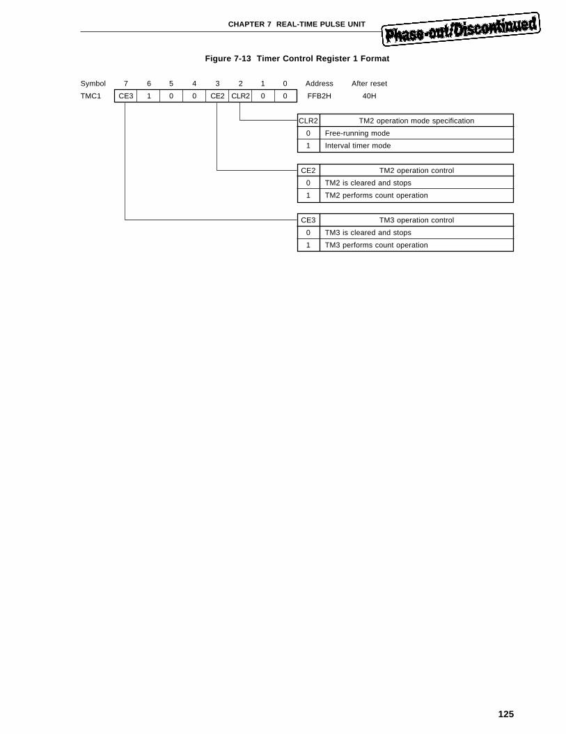
125
CHAPTER 7 REAL-TIME PULSE UNIT
Figure 7-13 Timer Control Register 1 Format
Symbol 7 6 5 4 3 2 1 0 Address After reset
TMC1 CE3 1 0 0 CE2 CLR2 0 0 FFB2H 40H
CLR2 TM2 operation mode specification
0 Free-running mode
1 Interval timer mode
CE2 TM2 operation control
0 TM2 is cleared and stops
1 TM2 performs count operation
CE3 TM3 operation control
0 TM3 is cleared and stops
1 TM3 performs count operation
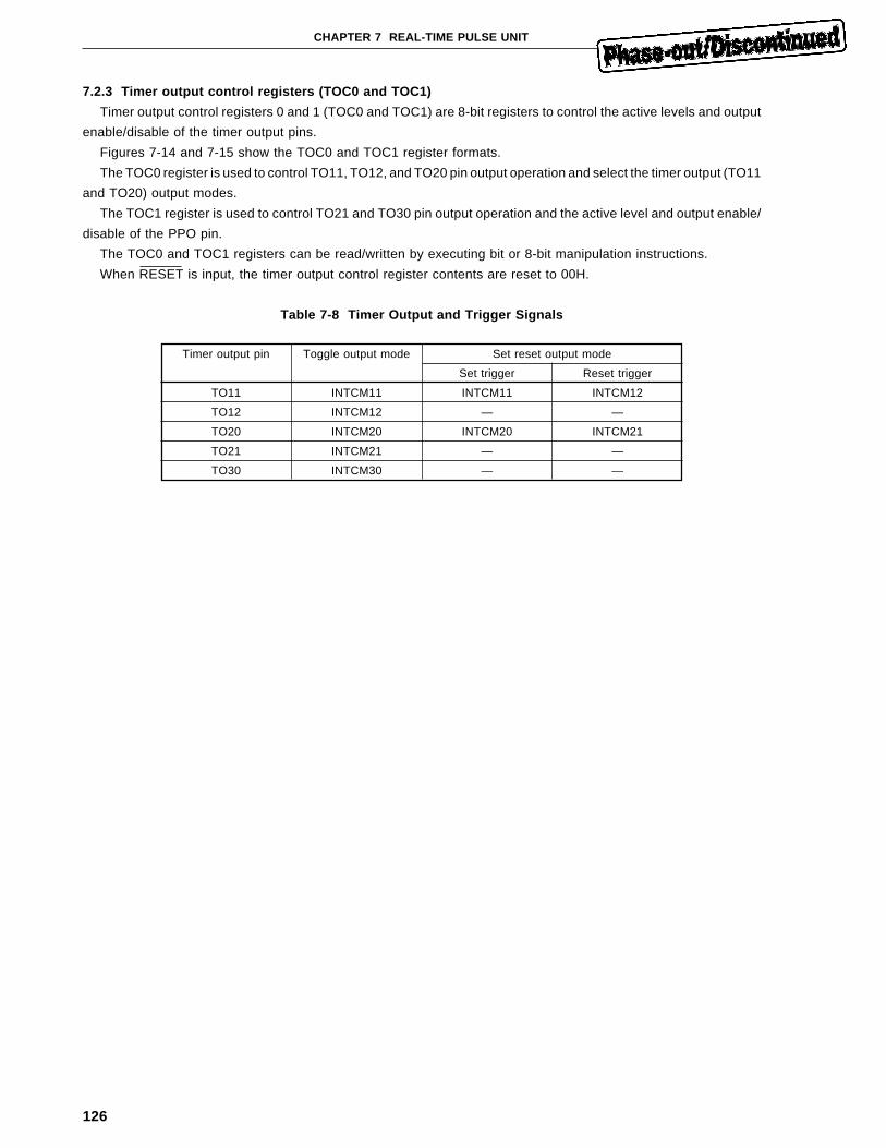
126
CHAPTER 7 REAL-TIME PULSE UNIT
7.2.3 Timer output control registers (TOC0 and TOC1)
Timer output control registers 0 and 1 (TOC0 and TOC1) are 8-bit registers to control the active levels and output
enable/disable of the timer output pins.
Figures 7-14 and 7-15 show the TOC0 and TOC1 register formats.
The TOC0 register is used to control TO11, TO12, and TO20 pin output operation and select the timer output (TO11
and TO20) output modes.
The TOC1 register is used to control TO21 and TO30 pin output operation and the active level and output enable/
disable of the PPO pin.
The TOC0 and TOC1 registers can be read/written by executing bit or 8-bit manipulation instructions.
When RESET is input, the timer output control register contents are reset to 00H.
Table 7-8 Timer Output and Trigger Signals
Timer output pin Toggle output mode Set reset output mode
Set trigger Reset trigger
TO11 INTCM11 INTCM11 INTCM12
TO12 INTCM12 — —
TO20 INTCM20 INTCM20 INTCM21
TO21 INTCM21 — —
TO30 INTCM30 — —
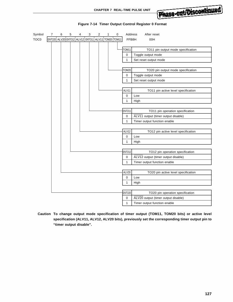
127
CHAPTER 7 REAL-TIME PULSE UNIT
Figure 7-14 Timer Output Control Register 0 Format
Symbol 7 6 5 4 3 2 1 0 Address After reset
TOC0 ENTO20 ALV20 ENTO12 ALV12 ENTO11 ALV11 TOM20 TOM11 FFB8H 00H
TOM11 TO11 pin output mode specification
0 Toggle output mode
1 Set reset output mode
TOM20 TO20 pin output mode specification
0 Toggle output mode
1 Set reset output mode
ALV11 TO11 pin active level specification
0 Low
1 High
ENTO11 TO11 pin operation specification
0 ALV11 output (timer output disable)
1 Timer output function enable
ALV12 TO12 pin active level specification
0 Low
1 High
ENTO12 TO12 pin operation specification
0 ALV12 output (timer output disable)
1 Timer output function enable
ALV20 TO20 pin active level specification
0 Low
1 High
ENTO20 TO20 pin operation specification
0 ALV20 output (timer output disable)
1 Timer output function enable
Caution To change output mode specification of timer output (TOM11, TOM20 bits) or active level
specification (ALV11, ALV12, ALV20 bits), previously set the corresponding timer output pin to
“timer output disable”.
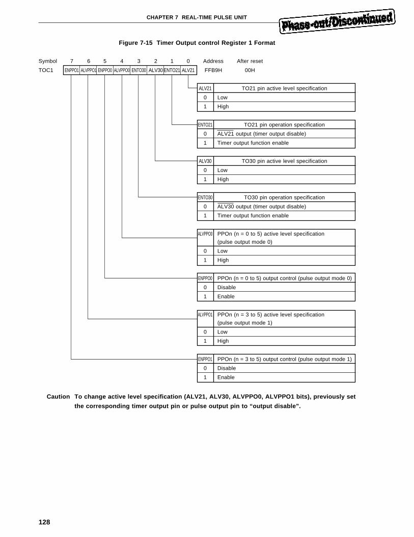
128
CHAPTER 7 REAL-TIME PULSE UNIT
Figure 7-15 Timer Output control Register 1 Format
Symbol 7 6 5 4 3 2 1 0 Address After reset
TOC1 ENPPO1 ALVPPO1 ENPPO0 ALVPPO0 ENTO30 ALV30 ENTO21 ALV21 FFB9H 00H
ALV21 TO21 pin active level specification
0 Low
1 High
ENTO21 TO21 pin operation specification
0 ALV21 output (timer output disable)
1 Timer output function enable
ALV30 TO30 pin active level specification
0 Low
1 High
ENTO30 TO30 pin operation specification
0 ALV30 output (timer output disable)
1 Timer output function enable
ALVPPO0 PPOn (n = 0 to 5) active level specification
(pulse output mode 0)
0 Low
1 High
ENPPO0 PPOn (n = 0 to 5) output control (pulse output mode 0)
0 Disable
1 Enable
ALVPPO1 PPOn (n = 3 to 5) active level specification
(pulse output mode 1)
0 Low
1 High
ENPPO1 PPOn (n = 3 to 5) output control (pulse output mode 1)
0 Disable
1 Enable
Caution To change active level specification (ALV21, ALV30, ALVPPO0, ALVPPO1 bits), previously set
the corresponding timer output pin or pulse output pin to “output disable”.
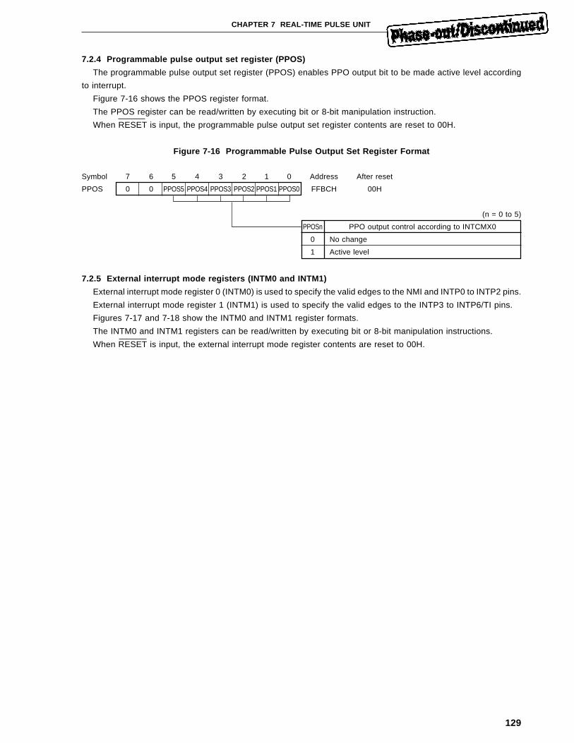
129
CHAPTER 7 REAL-TIME PULSE UNIT
7.2.4 Programmable pulse output set register (PPOS)
The programmable pulse output set register (PPOS) enables PPO output bit to be made active level according
to interrupt.
Figure 7-16 shows the PPOS register format.
The PPOS register can be read/written by executing bit or 8-bit manipulation instruction.
When RESET is input, the programmable pulse output set register contents are reset to 00H.
Figure 7-16 Programmable Pulse Output Set Register Format
Symbol 7 6 5 4 3 2 1 0 Address After reset
PPOS 0 0 PPOS5 PPOS4 PPOS3 PPOS2 PPOS1 PPOS0 FFBCH 00H
(n = 0 to 5)
PPOSn PPO output control according to INTCMX0
0 No change
1 Active level
7.2.5 External interrupt mode registers (INTM0 and INTM1)
External interrupt mode register 0 (INTM0) is used to specify the valid edges to the NMI and INTP0 to INTP2 pins.
External interrupt mode register 1 (INTM1) is used to specify the valid edges to the INTP3 to INTP6/TI pins.
Figures 7-17 and 7-18 show the INTM0 and INTM1 register formats.
The INTM0 and INTM1 registers can be read/written by executing bit or 8-bit manipulation instructions.
When RESET is input, the external interrupt mode register contents are reset to 00H.
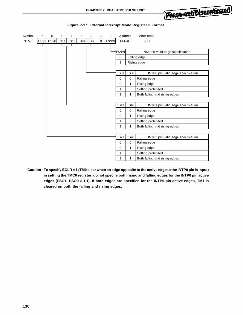
130
CHAPTER 7 REAL-TIME PULSE UNIT
Figure 7-17 External Interrupt Mode Register 0 Format
Symbol 7 6 5 4 3 2 1 0 Address After reset
INTM0 ES21 ES20 ES11 ES10 ES01 ES00 0 ESNMI FFF4H 00H
ESNMI NMI pin valid edge specification
0 Falling edge
1 Rising edge
ES01 ES00 INTP0 pin valid edge specification
0 0 Falling edge
0 1 Rising edge
1 0 Setting prohibited
1 1 Both falling and rising edges
ES11 ES10 INTP1 pin valid edge specification
0 0 Falling edge
0 1 Rising edge
1 0 Setting prohibited
1 1 Both falling and rising edges
ES21 ES20 INTP2 pin valid edge specification
0 0 Falling edge
0 1 Rising edge
1 0 Setting prohibited
1 1 Both falling and rising edges
Caution To specify ECLR = 1 (TM0 clear when an edge opposite to the active edge to the INTP0 pin is input)
in setting the TMC0 register, do not specify both rising and falling edges for the INTP0 pin active
edges (ESO1, ESO0 ≠ 1,1). If both edges are specified for the INTP0 pin active edges, TM1 is
cleared on both the falling and rising edges.
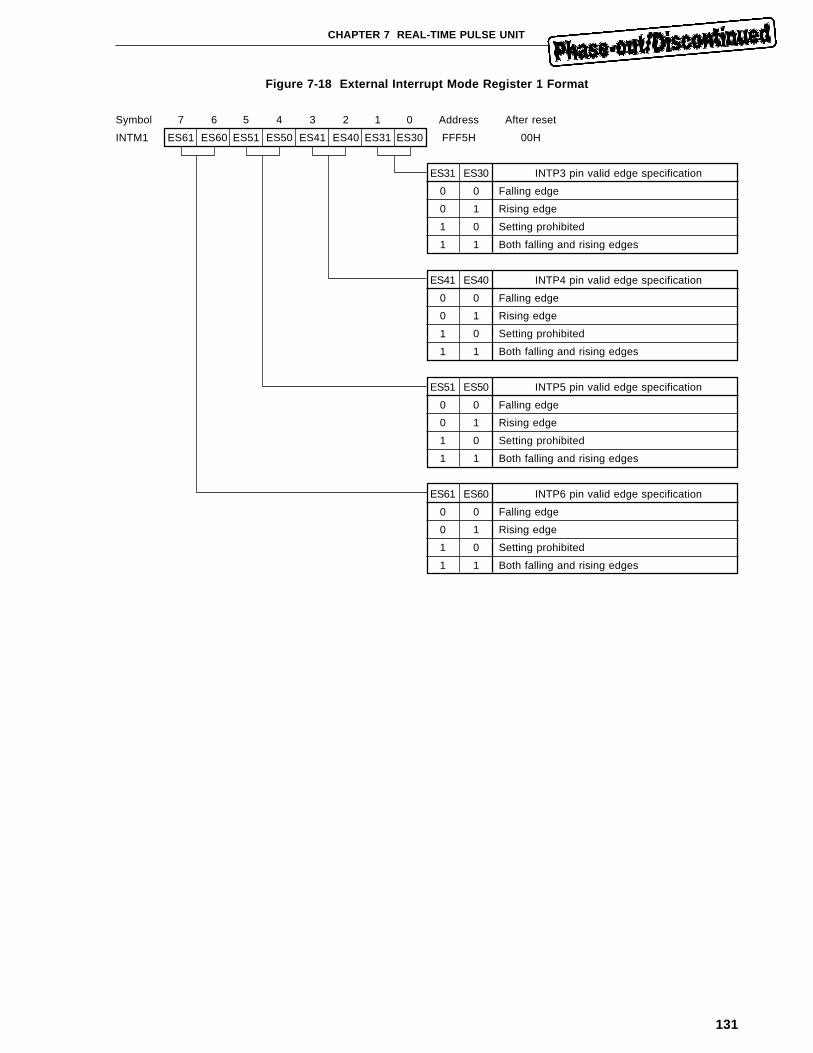
131
CHAPTER 7 REAL-TIME PULSE UNIT
Figure 7-18 External Interrupt Mode Register 1 Format
Symbol 7 6 5 4 3 2 1 0 Address After reset
INTM1 ES61 ES60 ES51 ES50 ES41 ES40 ES31 ES30 FFF5H 00H
ES31 ES30 INTP3 pin valid edge specification
0 0 Falling edge
0 1 Rising edge
1 0 Setting prohibited
1 1 Both falling and rising edges
ES41 ES40 INTP4 pin valid edge specification
0 0 Falling edge
0 1 Rising edge
1 0 Setting prohibited
1 1 Both falling and rising edges
ES51 ES50 INTP5 pin valid edge specification
0 0 Falling edge
0 1 Rising edge
1 0 Setting prohibited
1 1 Both falling and rising edges
ES61 ES60 INTP6 pin valid edge specification
0 0 Falling edge
0 1 Rising edge
1 0 Setting prohibited
1 1 Both falling and rising edges
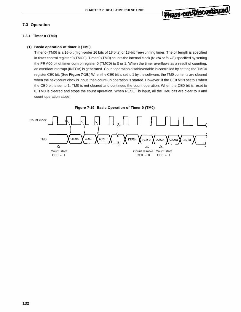
132
CHAPTER 7 REAL-TIME PULSE UNIT
7.3 Operation
7.3.1 Timer 0 (TM0)
(1) Basic operation of timer 0 (TM0)
Timer 0 (TM0) is a 16-bit (high-order 16 bits of 18 bits) or 18-bit free-running timer. The bit length is specified
in timer control register 0 (TMC0). Timer 0 (TM0) counts the internal clock (fCLK/4 or fCLK/8) specified by setting
the PRM00 bit of timer control register 0 (TMC0) to 0 or 1. When the timer overflows as a result of counting,
an overflow interrupt (INTOV) is generated. Count operation disable/enable is controlled by setting the TMC0
register CE0 bit. (See Figure 7-19 .) When the CE0 bit is set to 1 by the software, the TM0 contents are cleared
when the next count clock is input, then count-up operation is started. However, if the CE0 bit is set to 1 when
the CE0 bit is set to 1, TM0 is not cleared and continues the count operation. When the CE0 bit is reset to
0, TM0 is cleared and stops the count operation. When RESET is input, all the TM0 bits are clear to 0 and
count operation stops.
Figure 7-19 Basic Operation of Timer 0 (TM0)
Count clock
TM0
Count startCE0 ← 1
Count disableCE0 ← 0
Count startCE0 ← 1
133
CHAPTER 7 REAL-TIME PULSE UNIT
(2) Compare operation
The value set in the compare register is compared with the timer 0 count value. When the timer 0 (TM0) count
value matches the value preset in the compare register, a match signal is sent to the output control circuit.
The match signal causes the pulse output pin (PPO0 to PPO5) to be changed and generates an interrupt
request signal at the same time (Compare registers CMX0, CC00R, and CC01R only).
Table 7-9 Interrupt Request Signals from 18/16-bit Compare Registers (TM0)
Compare register Interrupt signal
CMX0 INTCMX0
CM01R —
CM02R —
CM03R —
CM04R —
CC00R Note INTCC00
CC01R Note INTCC01
Note CC00R and CC01R are capture/compare registers. The CC00R and CC01R register operation modes
(capture or compare) are specified in timer unit mode register 1 (TUM1).
The six pins of PPO0 to PPO5 are provided for the pulse output pins connected to timer. The pulse output
pin operation modes are determined by setting the TUM1, TOC1, and PPOS registers.
See 7.4 Timer Output Function for details.
134
CHAPTER 7 REAL-TIME PULSE UNIT
Figure 7-20 Timer 0 Compare Operation Example 1 (pulse output mode 0)
When PPOCN = 0
TM0Count value
INTCMX0
PPO0
Count startCE0 ← 1
OVF0 ← 1(Overflow)
OVF0 ← 1(Overflow)
135
CHAPTER 7 REAL-TIME PULSE UNIT
Figure 7-21 Timer 0 Compare Operation Example 2 (pulse output mode 0)
When PPOCN = 1
Notes 1. CM01R register rewrite: B → C
2. CM01R register rewrite: B → C
3. CM01R register rewrite: B → A
4. CM01R register rewrite: B → C
Count value
Count startCE0 ← 1
OVF0 ← 1(Overflow)
OVF0 ← 1(Overflow)
Note 1
Note 2
Note 3
Note 4
136
CHAPTER 7 REAL-TIME PULSE UNIT
Figure 7-22 Timer 0 Compare Operation Example (pulse output mode 1)
TM0Count value
Count startCE0 ← 1
OVF0 ← 1(Overflow)
OVF0 ← 1(Overflow)
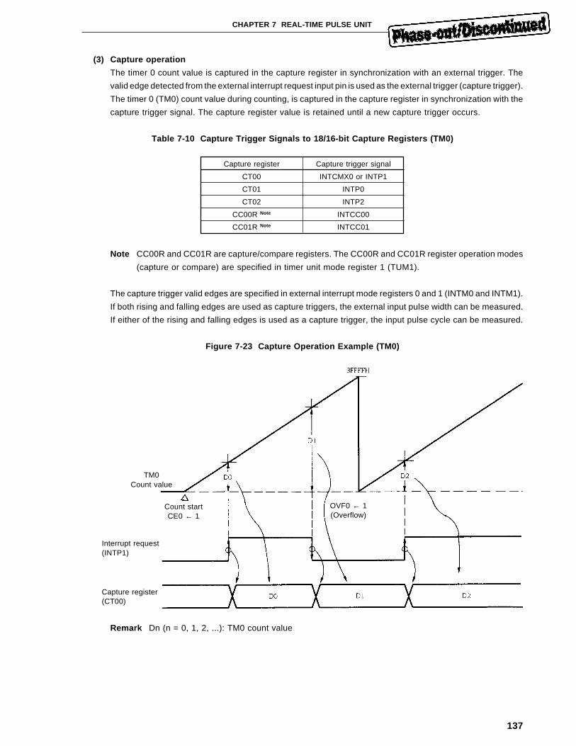
137
CHAPTER 7 REAL-TIME PULSE UNIT
(3) Capture operation
The timer 0 count value is captured in the capture register in synchronization with an external trigger. The
valid edge detected from the external interrupt request input pin is used as the external trigger (capture trigger).
The timer 0 (TM0) count value during counting, is captured in the capture register in synchronization with the
capture trigger signal. The capture register value is retained until a new capture trigger occurs.
Table 7-10 Capture Trigger Signals to 18/16-bit Capture Registers (TM0)
Capture register Capture trigger signal
CT00 INTCMX0 or INTP1
CT01 INTP0
CT02 INTP2
CC00R Note INTCC00
CC01R Note INTCC01
Note CC00R and CC01R are capture/compare registers. The CC00R and CC01R register operation modes
(capture or compare) are specified in timer unit mode register 1 (TUM1).
The capture trigger valid edges are specified in external interrupt mode registers 0 and 1 (INTM0 and INTM1).
If both rising and falling edges are used as capture triggers, the external input pulse width can be measured.
If either of the rising and falling edges is used as a capture trigger, the input pulse cycle can be measured.
Figure 7-23 Capture Operation Example (TM0)
Remark Dn (n = 0, 1, 2, ...): TM0 count value
TM0Count value
Count startCE0 ← 1
OVF0 ← 1(Overflow)
Interrupt request(INTP1)
Capture register(CT00)
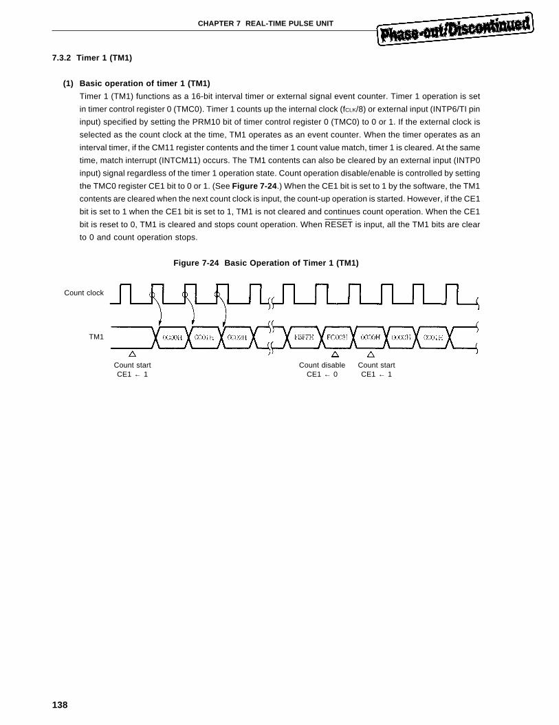
138
CHAPTER 7 REAL-TIME PULSE UNIT
7.3.2 Timer 1 (TM1)
(1) Basic operation of timer 1 (TM1)
Timer 1 (TM1) functions as a 16-bit interval timer or external signal event counter. Timer 1 operation is set
in timer control register 0 (TMC0). Timer 1 counts up the internal clock (fCLK/8) or external input (INTP6/TI pin
input) specified by setting the PRM10 bit of timer control register 0 (TMC0) to 0 or 1. If the external clock is
selected as the count clock at the time, TM1 operates as an event counter. When the timer operates as an
interval timer, if the CM11 register contents and the timer 1 count value match, timer 1 is cleared. At the same
time, match interrupt (INTCM11) occurs. The TM1 contents can also be cleared by an external input (INTP0
input) signal regardless of the timer 1 operation state. Count operation disable/enable is controlled by setting
the TMC0 register CE1 bit to 0 or 1. (See Figure 7-24 .) When the CE1 bit is set to 1 by the software, the TM1
contents are cleared when the next count clock is input, the count-up operation is started. However, if the CE1
bit is set to 1 when the CE1 bit is set to 1, TM1 is not cleared and continues count operation. When the CE1
bit is reset to 0, TM1 is cleared and stops count operation. When RESET is input, all the TM1 bits are clear
to 0 and count operation stops.
Figure 7-24 Basic Operation of Timer 1 (TM1)
Count clock
Count startCE1 ← 1
Count disableCE1 ← 0
TM1
Count startCE1 ← 1
139
CHAPTER 7 REAL-TIME PULSE UNIT
(2) Compare operation
The value set in the compare register is compared with the timer 1 count value. When the timer 1 (TM1) count
value matches the value preset in the compare register, a match signal is sent to the output control circuit.
The match signal causes the pulse output pin (TO11, TO12) to be changed and generates an interrupt request
signal at the same time. When match interrupt (INTCM11) occurs from the compare register CM11, timer 1
is cleared.
Table 7-11 Interrupt Request Signals from 16-bit Compare Registers (TM1)
Compare register Interrupt signal
CM11 INTCM11
CM12 INTCM12
Timer 1 has two timer output pins (TO11 and TO12).
• TO11 pin operation mode
The TO11 pin operation mode is the toggle output mode or set reset output mode. The operation mode is
specified by setting the TOC0 register TOM11 bit.
• TO12 pin operation mode
The toggle output mode only can be used.
See 7.4 Timer Output Function for details.
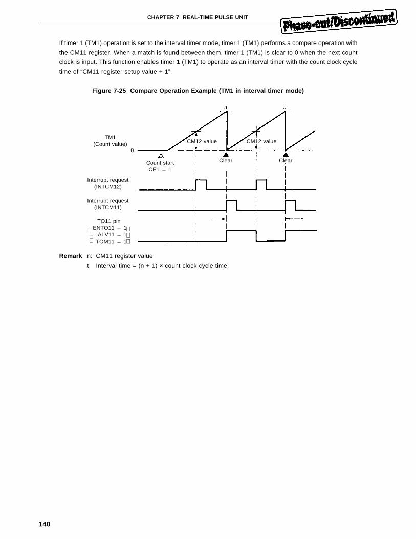
140
CHAPTER 7 REAL-TIME PULSE UNIT
If timer 1 (TM1) operation is set to the interval timer mode, timer 1 (TM1) performs a compare operation with
the CM11 register. When a match is found between them, timer 1 (TM1) is clear to 0 when the next count
clock is input. This function enables timer 1 (TM1) to operate as an interval timer with the count clock cycle
time of “CM11 register setup value + 1”.
Figure 7-25 Compare Operation Example (TM1 in interval timer mode)
Remark n: CM11 register value
t: Interval time = (n + 1) × count clock cycle time
TM1(Count value)
Count startCE1 ← 1
Clear
0
Interrupt request(INTCM12)
Interrupt request(INTCM11)
TO11 pinENTO11 ← 1
ALV11 ← 1TOM11 ← 1
Clear
CM12 value CM12 value
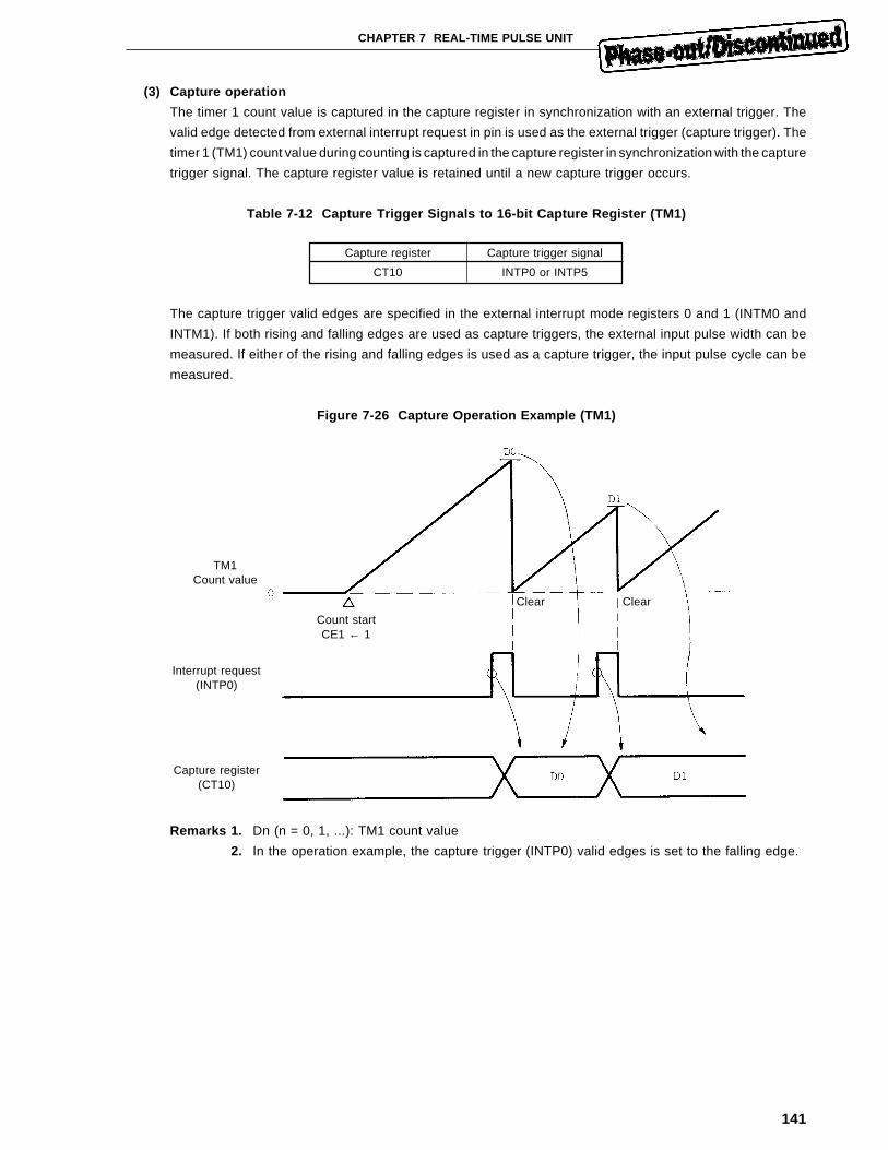
141
CHAPTER 7 REAL-TIME PULSE UNIT
(3) Capture operation
The timer 1 count value is captured in the capture register in synchronization with an external trigger. The
valid edge detected from external interrupt request in pin is used as the external trigger (capture trigger). The
timer 1 (TM1) count value during counting is captured in the capture register in synchronization with the capture
trigger signal. The capture register value is retained until a new capture trigger occurs.
Table 7-12 Capture Trigger Signals to 16-bit Capture Register (TM1)
Capture register Capture trigger signal
CT10 INTP0 or INTP5
The capture trigger valid edges are specified in the external interrupt mode registers 0 and 1 (INTM0 and
INTM1). If both rising and falling edges are used as capture triggers, the external input pulse width can be
measured. If either of the rising and falling edges is used as a capture trigger, the input pulse cycle can be
measured.
Figure 7-26 Capture Operation Example (TM1)
Remarks 1. Dn (n = 0, 1, ...): TM1 count value
2. In the operation example, the capture trigger (INTP0) valid edges is set to the falling edge.
TM1Count value
Count startCE1 ← 1
Clear
Interrupt request(INTP0)
Capture register(CT10)
Clear
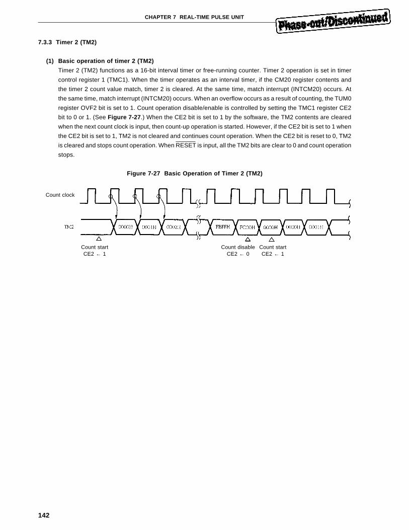
142
CHAPTER 7 REAL-TIME PULSE UNIT
7.3.3 Timer 2 (TM2)
(1) Basic operation of timer 2 (TM2)
Timer 2 (TM2) functions as a 16-bit interval timer or free-running counter. Timer 2 operation is set in timer
control register 1 (TMC1). When the timer operates as an interval timer, if the CM20 register contents and
the timer 2 count value match, timer 2 is cleared. At the same time, match interrupt (INTCM20) occurs. At
the same time, match interrupt (INTCM20) occurs. When an overflow occurs as a result of counting, the TUM0
register OVF2 bit is set to 1. Count operation disable/enable is controlled by setting the TMC1 register CE2
bit to 0 or 1. (See Figure 7-27 .) When the CE2 bit is set to 1 by the software, the TM2 contents are cleared
when the next count clock is input, then count-up operation is started. However, if the CE2 bit is set to 1 when
the CE2 bit is set to 1, TM2 is not cleared and continues count operation. When the CE2 bit is reset to 0, TM2
is cleared and stops count operation. When RESET is input, all the TM2 bits are clear to 0 and count operation
stops.
Figure 7-27 Basic Operation of Timer 2 (TM2)
Count clock
Count startCE2 ← 1
Count disableCE2 ← 0
Count startCE2 ← 1

143
CHAPTER 7 REAL-TIME PULSE UNIT
(2) Compare operation
The value set in the compare register is compared with the timer 2 count value. When the timer 2 (TM2) count
value matches the value preset in the compare register, a match signal is sent to the output control circuit.
The match signal causes the timer output pin (TO20, TO21) to be changed and generates an interrupt request
signal at the same time.
When match interrupt (INTCM20) occurs from compare register CM20, timer 2 is cleared.
Table 7-13 Interrupt Request Signals from 16-bit Compare Registers (TM2)
Compare register Interrupt signal
CM20 INTCM20
CM21 INTCM21
Timer 2 has two timer output pins (TO20 and TO21).
• TO20 pin operation mode
The TO20 pin operation mode is the toggle output mode or set reset output mode. The operation mode is
specified by setting the TOC0 register TOM20 bit.
• TO21 pin operation mode
Only toggle output mode can be used.
See 7.4 Timer Output Function for details.

144
CHAPTER 7 REAL-TIME PULSE UNIT
If timer 2 (TM2) operation is set to the interval timer mode, timer 2 (TM2) performs a compare operation with
the CM20 register. When a match is found between them, timer 2 (TM2) is clear to 0 when the next count
clock is input. This function enables timer 2 (TM2) to operate as an interval timer with the count clock cycle
time of “CM20 register setup value + 1”.
Figure 7-28 Compare Operation Example (TM2 in interval timer mode)
Remark n: CM20 register value
t: Interval time = (n + 1) × count clock cycle time
TM2(Count value)
Count startCE2 ← 1
Clear
Interrupt request(INTCM21)
Interrupt request(INTCM20)
TO20 pinENTO20 ← 1
ALV20 ← 1TOM20 ← 1
Clear
CM12 value CM12 value
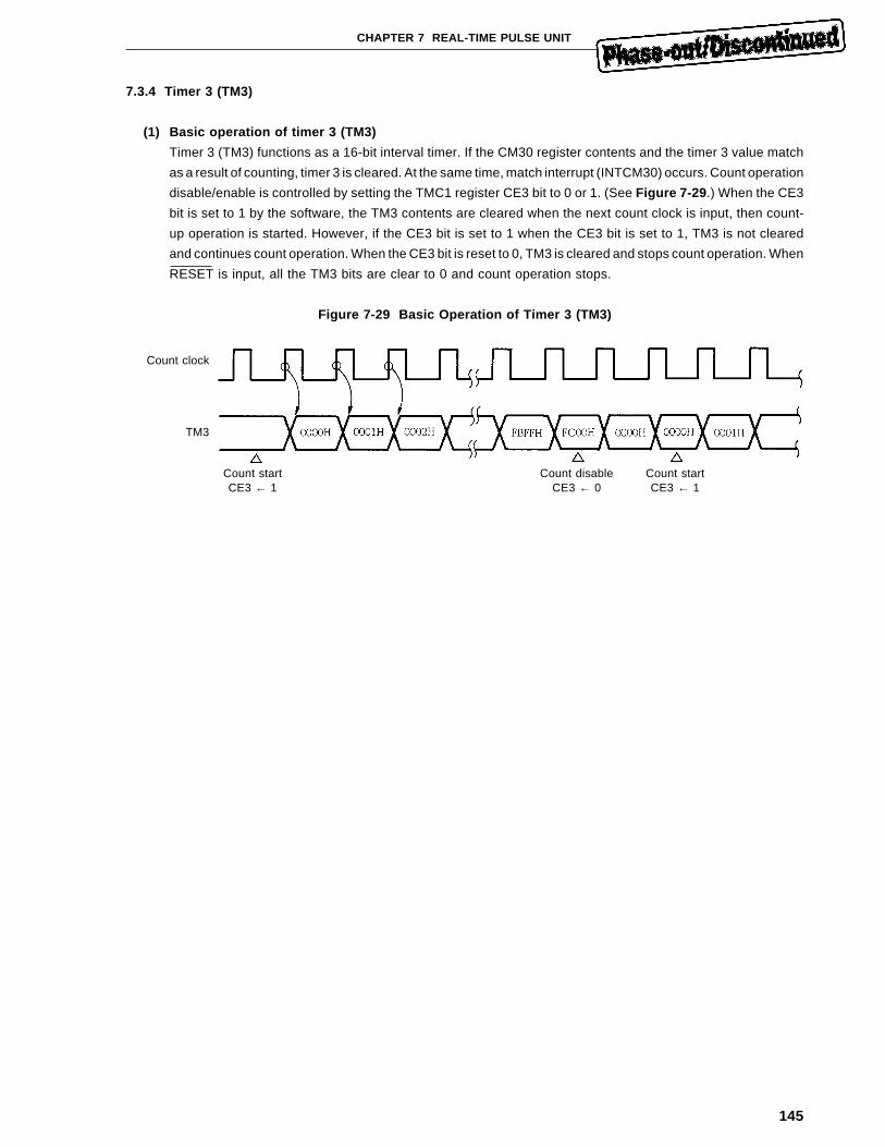
145
CHAPTER 7 REAL-TIME PULSE UNIT
7.3.4 Timer 3 (TM3)
(1) Basic operation of timer 3 (TM3)
Timer 3 (TM3) functions as a 16-bit interval timer. If the CM30 register contents and the timer 3 value match
as a result of counting, timer 3 is cleared. At the same time, match interrupt (INTCM30) occurs. Count operation
disable/enable is controlled by setting the TMC1 register CE3 bit to 0 or 1. (See Figure 7-29 .) When the CE3
bit is set to 1 by the software, the TM3 contents are cleared when the next count clock is input, then count-
up operation is started. However, if the CE3 bit is set to 1 when the CE3 bit is set to 1, TM3 is not cleared
and continues count operation. When the CE3 bit is reset to 0, TM3 is cleared and stops count operation. When
RESET is input, all the TM3 bits are clear to 0 and count operation stops.
Figure 7-29 Basic Operation of Timer 3 (TM3)
Count clock
Count startCE3 ← 1
Count disableCE3 ← 0
Count startCE3 ← 1
TM3
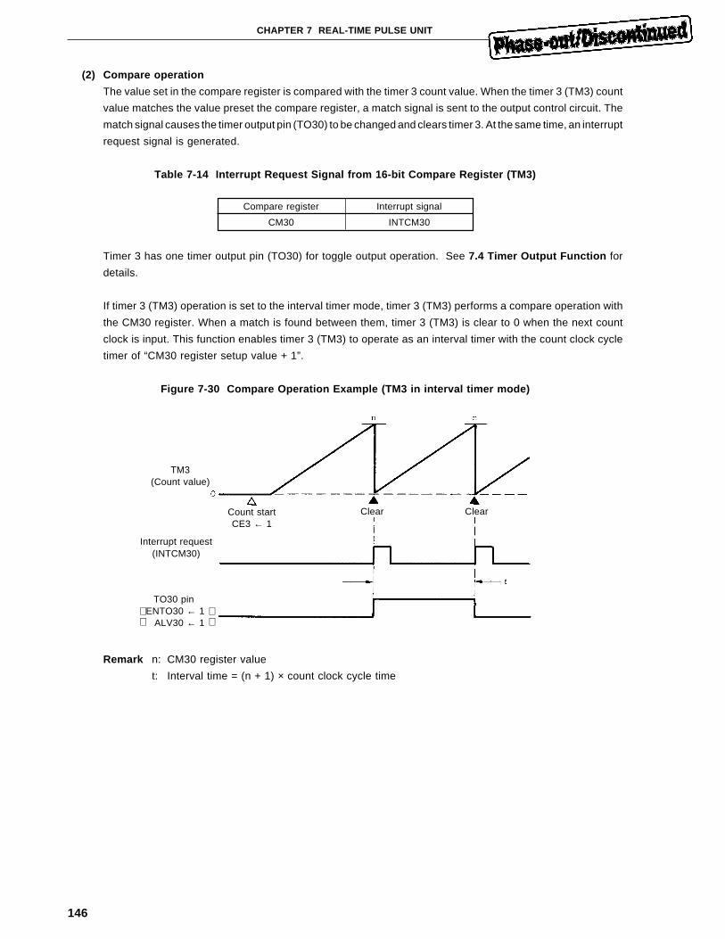
146
CHAPTER 7 REAL-TIME PULSE UNIT
(2) Compare operation
The value set in the compare register is compared with the timer 3 count value. When the timer 3 (TM3) count
value matches the value preset the compare register, a match signal is sent to the output control circuit. The
match signal causes the timer output pin (TO30) to be changed and clears timer 3. At the same time, an interrupt
request signal is generated.
Table 7-14 Interrupt Request Signal from 16-bit Compare Register (TM3)
Compare register Interrupt signal
CM30 INTCM30
Timer 3 has one timer output pin (TO30) for toggle output operation. See 7.4 Timer Output Function for
details.
If timer 3 (TM3) operation is set to the interval timer mode, timer 3 (TM3) performs a compare operation with
the CM30 register. When a match is found between them, timer 3 (TM3) is clear to 0 when the next count
clock is input. This function enables timer 3 (TM3) to operate as an interval timer with the count clock cycle
timer of “CM30 register setup value + 1”.
Figure 7-30 Compare Operation Example (TM3 in interval timer mode)
Remark n: CM30 register value
t: Interval time = (n + 1) × count clock cycle time
TM3(Count value)
Count startCE3 ← 1
Clear
Interrupt request(INTCM30)
TO30 pinENTO30 ← 1
ALV30 ← 1
Clear
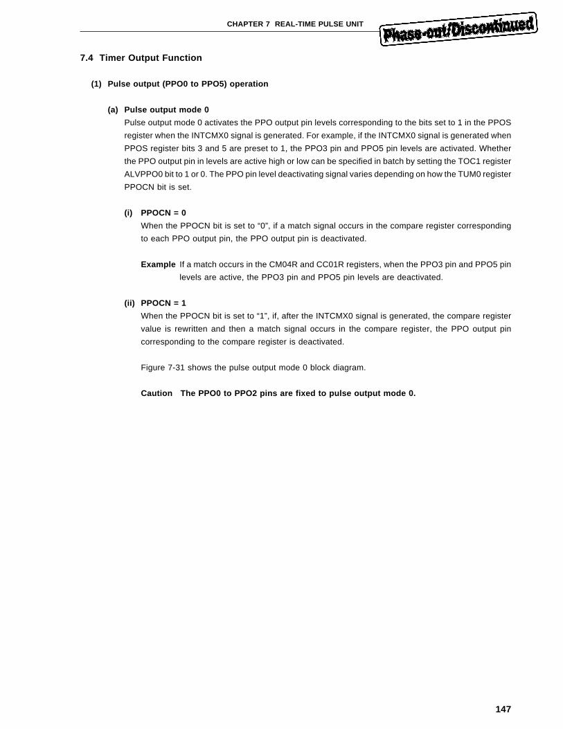
147
CHAPTER 7 REAL-TIME PULSE UNIT
7.4 Timer Output Function
(1) Pulse output (PPO0 to PPO5) operation
(a) Pulse output mode 0
Pulse output mode 0 activates the PPO output pin levels corresponding to the bits set to 1 in the PPOS
register when the INTCMX0 signal is generated. For example, if the INTCMX0 signal is generated when
PPOS register bits 3 and 5 are preset to 1, the PPO3 pin and PPO5 pin levels are activated. Whether
the PPO output pin in levels are active high or low can be specified in batch by setting the TOC1 register
ALVPPO0 bit to 1 or 0. The PPO pin level deactivating signal varies depending on how the TUM0 register
PPOCN bit is set.
(i) PPOCN = 0
When the PPOCN bit is set to “0”, if a match signal occurs in the compare register corresponding
to each PPO output pin, the PPO output pin is deactivated.
Example If a match occurs in the CM04R and CC01R registers, when the PPO3 pin and PPO5 pin
levels are active, the PPO3 pin and PPO5 pin levels are deactivated.
(ii) PPOCN = 1
When the PPOCN bit is set to “1”, if, after the INTCMX0 signal is generated, the compare register
value is rewritten and then a match signal occurs in the compare register, the PPO output pin
corresponding to the compare register is deactivated.
Figure 7-31 shows the pulse output mode 0 block diagram.
Caution The PPO0 to PPO2 pins are fixed to pulse output mode 0.
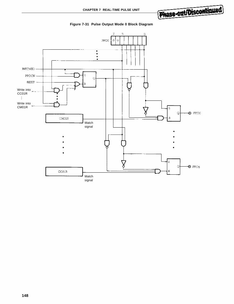
148
CHAPTER 7 REAL-TIME PULSE UNIT
Figure 7-31 Pulse Output Mode 0 Block Diagram
Write intoCC01R
Write intoCM01R
…
Matchsignal
Matchsignal
149
CHAPTER 7 REAL-TIME PULSE UNIT
(b) Pulse output mode 1
Pulse output mode 1 activates the PPO output pin levels when an overflow signal for timer 0 (INTOV)
is generated. Whether the PPO output pin levels are active high or low can be specified in batch by setting
the TOC1 register ALVPPO1 bit to 1 or 0. When a match occurs in the compare register corresponding
to each PPO output pin, the PPO output pin is deactivated. For example, if a match occurs in the CM04R
and CC01R registers when the PPO3 pin and PPO5 pin levels are active, the PPO3 pin and PPO5 pin
levels are deactivated. Figure 7-32 shows the pulse output mode 1 block diagram.
Caution The PPO0 to PPO2 output pins are fixed to pulse output mode 0. Pulse output mode 0
or 1 can be selected for each of the PPO3 to PPO5 output pins by setting the TUM1 register
PPOMn bit (n = 3 to 5) to 0 or 1.
Figure 7-32 Pulse Output Mode 1 Block Diagram
Selector
Match signalCompare register
Timer 0
150
CHAPTER 7 REAL-TIME PULSE UNIT
(2) Timer output (TO11, TO12, TO20, TO21, and TO30) operation
Toggle operation or set reset operation can be selected for timer output TO11 and TO20. TO12, TO21, and
TO30 pin output modes are fixed to toggle operation only. Timer output operation (active level specification,
output disable/enable control, and toggle operation mode or set reset operation mode selection) is set in the
TOC0 and TOC1 registers. Tables 7-15 and 7-16 list the TO pins and their corresponding control signals.
Figure 7-33 shows the timer output operation block diagram.
Table 7-15 TO11, TO12, TO20, TO21, and TO30 Toggle Signals
Timer output Toggle signal
TO11 INTCM11
TO12 INTCM12
TO20 INTCM20
TO21 INTCM21
TO30 INTCM30
Table 7-16 Set and Reset Signals of TO11 and TO20
Timer output Set signal Reset signal
TO11 INTCM11 INTCM12
TO12 INTCM20 INTCM21
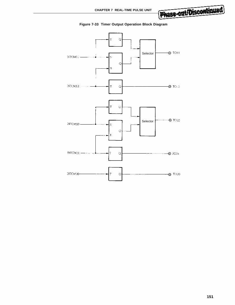
151
CHAPTER 7 REAL-TIME PULSE UNIT
Figure 7-33 Timer Output Operation Block Diagram
Selector
Selector
152
CHAPTER 7 REAL-TIME PULSE UNIT
7.5 Real-Time Output Function
Real-time output port output is set or reset bit-wise in synchronization with a trigger signal from the real-time pulse
unit (RPU).
Synchronous pulse output of multiple channels can be performed easily.
7.5.1 Configuration
The real-time output port is multiplexed to port 0 (P0) as shown in Figure 7-34. The following two registers are
provided to control the output state:
• Real-time output port set register (RTPS)
• Real-time output port reset register (RTPR)
The real-time output change timing is determined by the following two trigger signals output by the real-time pulse
unit (RPU):
• Set output (1) ............. INTCM12 signal
• Reset output (0) ......... INTCM11 signal
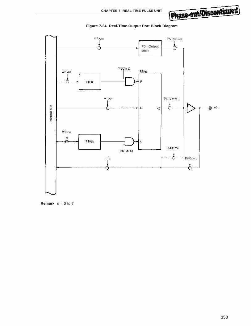
153
CHAPTER 7 REAL-TIME PULSE UNIT
Figure 7-34 Real-Time Output Port Block Diagram
Remark n = 0 to 7
P0n Outputlatch
Inte
rnal
bus
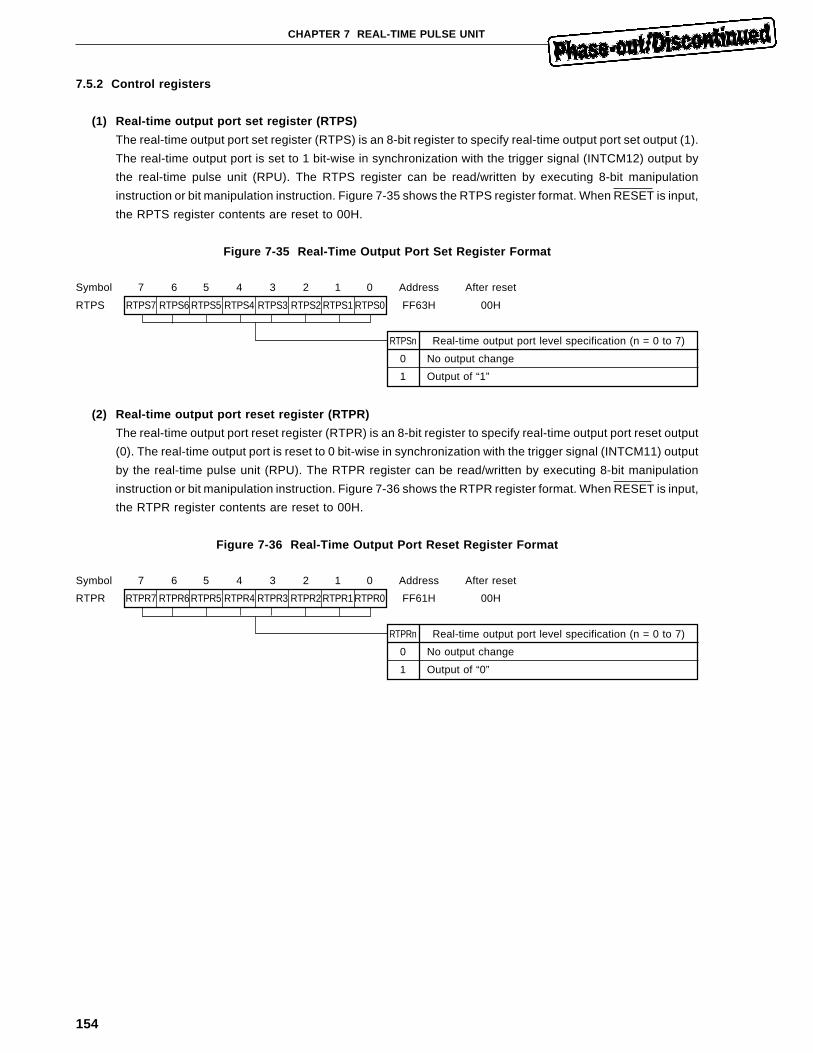
154
CHAPTER 7 REAL-TIME PULSE UNIT
7.5.2 Control registers
(1) Real-time output port set register (RTPS)
The real-time output port set register (RTPS) is an 8-bit register to specify real-time output port set output (1).
The real-time output port is set to 1 bit-wise in synchronization with the trigger signal (INTCM12) output by
the real-time pulse unit (RPU). The RTPS register can be read/written by executing 8-bit manipulation
instruction or bit manipulation instruction. Figure 7-35 shows the RTPS register format. When RESET is input,
the RPTS register contents are reset to 00H.
Figure 7-35 Real-Time Output Port Set Register Format
Symbol 7 6 5 4 3 2 1 0 Address After reset
RTPS RTPS7 RTPS6 RTPS5 RTPS4 RTPS3 RTPS2 RTPS1 RTPS0 FF63H 00H
RTPSn Real-time output port level specification (n = 0 to 7)
0 No output change
1 Output of “1”
(2) Real-time output port reset register (RTPR)
The real-time output port reset register (RTPR) is an 8-bit register to specify real-time output port reset output
(0). The real-time output port is reset to 0 bit-wise in synchronization with the trigger signal (INTCM11) output
by the real-time pulse unit (RPU). The RTPR register can be read/written by executing 8-bit manipulation
instruction or bit manipulation instruction. Figure 7-36 shows the RTPR register format. When RESET is input,
the RTPR register contents are reset to 00H.
Figure 7-36 Real-Time Output Port Reset Register Format
Symbol 7 6 5 4 3 2 1 0 Address After reset
RTPR RTPR7 RTPR6RTPR5 RTPR4 RTPR3 RTPR2RTPR1RTPR0 FF61H 00H
RTPRn Real-time output port level specification (n = 0 to 7)
0 No output change
1 Output of “0”
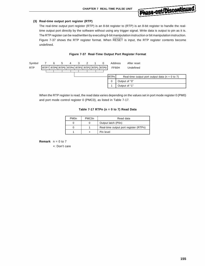
155
CHAPTER 7 REAL-TIME PULSE UNIT
(3) Real-time output port register (RTP)
The real-time output port register (RTP) is an 8-bit register to (RTP) is an 8-bit register to handle the real-
time output port directly by the software without using any trigger signal. Write data is output to pin as it is.
The RTP register can be read/written by executing 8-bit manipulation instruction or bit manipulation instruction.
Figure 7-37 shows the RTP register format. When RESET is input, the RTP register contents become
undefined.
Figure 7-37 Real-Time Output Port Register Format
Symbol 7 6 5 4 3 2 1 0 Address After reset
RTP RTP7 RTP6 RTP5 RTP4 RTP3 RTP2 RTP1 RTP0 FF60H Undefined
RTPn Real-time output port output data (n = 0 to 7)
0 Output of “0”
1 Output of “1”
When the RTP register is read, the read data varies depending on the values set in port mode register 0 (PM0)
and port mode control register 0 (PMC0), as listed in Table 7-17.
Table 7-17 RTPn (n = 0 to 7) Read Data
PM0n PMC0n Read data
0 0 Output latch (P0n)
0 1 Real-time output port register (RTPn)
1 × Pin level
Remark n = 0 to 7
×: Don’t care
156
CHAPTER 7 REAL-TIME PULSE UNIT
7.5.3 Operation
To specify the port 0 (P0) function as a real-time output port, the corresponding bit of port mode control register
0 (PMC0) is set to “1”.
If “1” is set in the real-time output port set register (RTPS), port output is automatically set to “1” in synchronization
with the trigger signal (INTCM12) output by the real-time pulse unit (RPU).
Likewise, if “1” is set in the real-time output port reset register (RTPR), port output is automatically reset to 0 in
synchronization with the trigger signal (INTCM11) output by the real-time pulse unit (RPU).
If set the reset requests occur at the same time, reset operation takes precedence over set operation. The real-
time output port register (RTP) value can also be changed directly by the software using the RTP register. At the time,
even if trigger signal is output by the real-time pulse unit (RPU), the software write takes precedence over the trigger
signal.
157
CHAPTER 8 A/D CONVERTER
The µPD78334 contains high-speed and high-resolution 10-bit analog/digital (A/D) converter. It has 16 analog input
pins (ANI0 to ANI15) to input analog signals and eight 10-bit A/D conversion result registers (ADCR) which retain
the conversion results.
The following three A/D converter conversion operation modes are provided: (The operation mode is specified by
the software in the A/D converter mode register (ADM) and A/D conversion operation can be selected conforming
to the application system.)
• Select mode
Conversion operation of analog input data to one pin is repeated consecutively.
• Scan mode
Conversion operation of analog input data to a number of pins is performed in sequence and this operation is
repeated consecutively.
• Mix mode
Select mode processing and scan mode processing are mixed for conversion operation. When an external trigger
occurs, select mode processing is performed, then scan mode processing is performed.
In each operation mode, whenever A/D conversion terminates, the conversion result is retained in the A/D
conversion result register (ADCR). When A/D conversion terminates, internal interrupt INTAD is generated. This
interrupt can start a macro service which executes automatic transfer of data, etc., by the hardware.
8.1 Configuration
Figure 8-1 shows the µPD78334 A/D converter block diagram.
The high-order 8 channels (ANI8 to ANI15) and low-order 8 channels (ANI0 to ANI7) of analog input to the A/D
converter are changed by software selection.
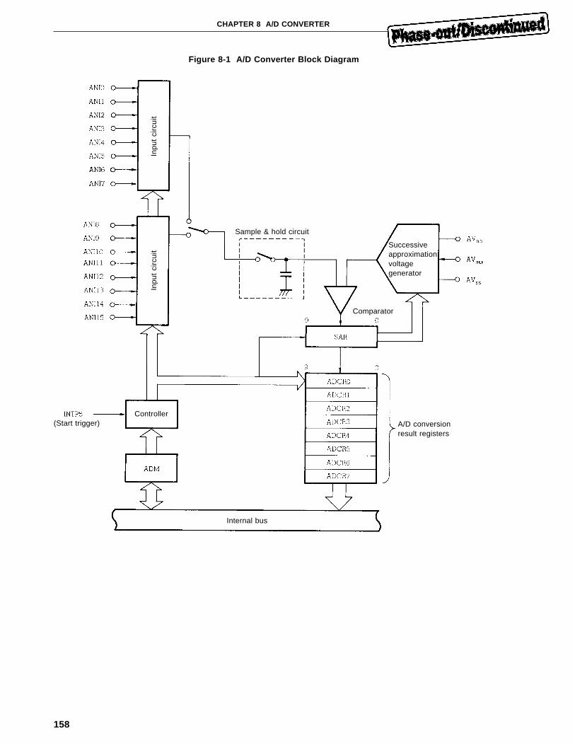
158
CHAPTER 8 A/D CONVERTER
Figure 8-1 A/D Converter Block Diagram
Inpu
t ci
rcui
t
Sample & hold circuit
Inpu
t ci
rcui
t
Controller
Successiveapproximationvoltagegenerator
Comparator
A/D conversionresult registers
Internal bus
(Start trigger)
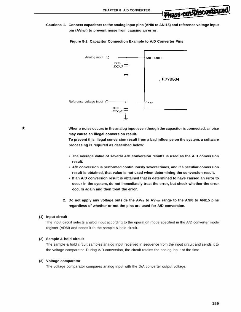
159
CHAPTER 8 A/D CONVERTER
Cautions 1. Connect capacitors to the analog input pins (ANI0 to ANI15) and reference voltage input
pin (AV REF) to prevent noise from causing an error.
Figure 8-2 Capacitor Connection Example to A/D Converter Pins
When a noise occurs in the analog input even though the capacitor is connected, a noise
may cause an illegal conversion result.
To prevent this illegal conversion result from a bad influence on the system, a software
processing is required as described below:
• The average value of several A/D conversion results is used as the A/D conversion
result.
• A/D conversion is performed continuously several times, and if a peculiar conversion
result is obtained, that value is not used when determining the conversion result.
• If an A/D conversion result is obtained that is determined to have caused an error to
occur in the system, do not immediately treat the error, but check whether the error
occurs again and then treat the error.
2. Do not apply any voltage outside the AV SS to AV REF range to the ANI0 to ANI15 pins
regardless of whether or not the pins are used for A/D conversion.
(1) Input circuit
The input circuit selects analog input according to the operation mode specified in the A/D converter mode
register (ADM) and sends it to the sample & hold circuit.
(2) Sample & hold circuit
The sample & hold circuit samples analog input received in sequence from the input circuit and sends it to
the voltage comparator. During A/D conversion, the circuit retains the analog input at the time.
(3) Voltage comparator
The voltage comparator compares analog input with the D/A converter output voltage.
Analog input
Reference voltage input
★
160
CHAPTER 8 A/D CONVERTER
(4) Successive approximation voltage generator
The successive approximation voltage generator generates voltage matching analog input. The successive
approximation voltage generator is connected to the A/D converter reference voltage pin (AVREF) and the A/D
converter ground pin (AVSS). The successive approximation voltage generator output voltage is controlled in SAR.
(5) SAR (Successive Approximation Register)
SAR (successive approximation register) is a 10-bit register in which control data of the D/A converter, output
value one bit at a time from the most significant bit (MSB) to the least significant bit (LSB) is set to compare the
D/A converter output voltage value with the analog input voltage value. When the SAR bits from the MSB to the
LSB are set (A/D conversion termination), the SAR contents (conversion result) are retained in the A/D conversion
result register (ADCR). At the same time, an A/D conversion end interrupt request (INTAD) occurs from the SAR.
(6) Edge detector
The edge detector detects valid edge from input to the interrupt request input pin (INTP5) and generates an
external trigger of A/D conversion operation. The valid edge of INTP5 pin input is set in the external interrupt
mode register 1 (INTM1). (See Figure 7-18 .)
161
CHAPTER 8 A/D CONVERTER
8.2 A/D Converter Mode Register
The A/D converter mode register (ADM) is an 8-bit register to control A/D converter operation.
The ADM register can be read/written by executing bit manipulation instruction or 8-bit manipulation instruction.
However, if a write into the A/D register is performed during ADM conversion operation, the conversion operation
is initialized and again executed from the beginning.
Figure 8-3 shows the ADM register format. The ADM register bits are explained below.
When RESET is input, the ADM register is reset to 00H.
(1) ANIS0, ANIS1, and ANIS2 bits (bits 0 to 2)
The ANIS0, ANIS1, and ANIS2 bits are set for the selection of analog input to be converted into digital form
(ANI0 to ANI7 or ANI8 to ANI15).
(2) PS bit (bit 3)
The PS bit is set for selection of the low-order 8 channels (ANI0 to ANI15) and high-order 8 channels (ANI8
to ANI15) for analog input to be converted into digital form.
• When PS = 0: Low-order 8 channels (ANI0 to ANI7)
• When PS = 1: High-order 8 channels (ANI8 to ANI15)
(3) FR bit (bit 4)
The FR bit is a control bit to switch the A/D conversion time. One conversion speed determined by the internal
system clock (fCLK) and FR bit value is represented by the following expression:
• When FR = 1: Conversion speed = 144/fCLK (µs)
Table 8-1 lists the conversion speeds for each setting.
Caution To set the conversion time, be sure to set the FR bit to 1.
Table 8-1 Conversion Speeds Determined by Setting the FR Bit
Internal system clock (fCLK, MHz) 8 6 4
FR bit 1 1 1
Conversion speed (µs) 18 24 36
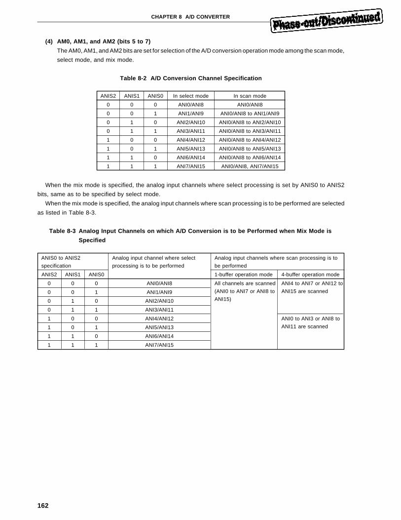
162
CHAPTER 8 A/D CONVERTER
(4) AM0, AM1, and AM2 (bits 5 to 7)
The AM0, AM1, and AM2 bits are set for selection of the A/D conversion operation mode among the scan mode,
select mode, and mix mode.
Table 8-2 A/D Conversion Channel Specification
ANIS2 ANIS1 ANIS0 In select mode In scan mode
0 0 0 ANI0/ANI8 ANI0/ANI8
0 0 1 ANI1/ANI9 ANI0/ANI8 to ANI1/ANI9
0 1 0 ANI2/ANI10 ANI0/ANI8 to ANI2/ANI10
0 1 1 ANI3/ANI11 ANI0/ANI8 to ANI3/ANI11
1 0 0 ANI4/ANI12 ANI0/ANI8 to ANI4/ANI12
1 0 1 ANI5/ANI13 ANI0/ANI8 to ANI5/ANI13
1 1 0 ANI6/ANI14 ANI0/ANI8 to ANI6/ANI14
1 1 1 ANI7/ANI15 ANI0/ANI8, ANI7/ANI15
When the mix mode is specified, the analog input channels where select processing is set by ANIS0 to ANIS2
bits, same as to be specified by select mode.
When the mix mode is specified, the analog input channels where scan processing is to be performed are selected
as listed in Table 8-3.
Table 8-3 Analog Input Channels on which A/D Conversion is to be Performed when Mix Mode is
Specified
ANIS0 to ANIS2 Analog input channel where select Analog input channels where scan processing is to
specification processing is to be performed be performed
ANIS2 ANIS1 ANIS0 1-buffer operation mode 4-buffer operation mode
0 0 0 ANI0/ANI8 All channels are scanned ANI4 to ANI7 or ANI12 to
0 0 1 ANI1/ANI9 (ANI0 to ANI7 or ANI8 to ANI15 are scanned
0 1 0 ANI2/ANI10 ANI15)
0 1 1 ANI3/ANI11
1 0 0 ANI4/ANI12 ANI0 to ANI3 or ANI8 to
1 0 1 ANI5/ANI13 ANI11 are scanned
1 1 0 ANI6/ANI14
1 1 1 ANI7/ANI15
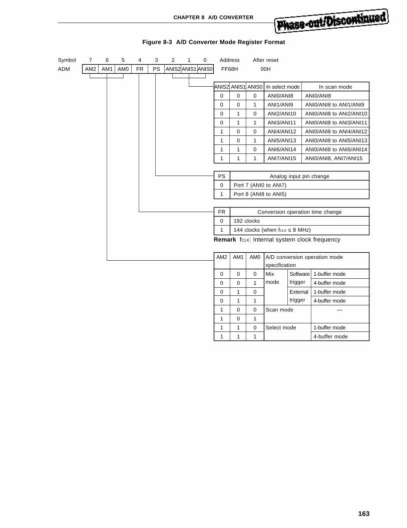
163
CHAPTER 8 A/D CONVERTER
Figure 8-3 A/D Converter Mode Register Format
Symbol 7 6 5 4 3 2 1 0 Address After reset
ADM AM2 AM1 AM0 FR PS ANIS2 ANIS1 ANIS0 FF68H 00H
ANIS2 ANIS1 ANIS0 In select mode In scan mode
0 0 0 ANI0/ANI8 ANI0/ANI8
0 0 1 ANI1/ANI9 ANI0/ANI8 to ANI1/ANI9
0 1 0 ANI2/ANI10 ANI0/ANI8 to ANI2/ANI10
0 1 1 ANI3/ANI11 ANI0/ANI8 to ANI3/ANI11
1 0 0 ANI4/ANI12 ANI0/ANI8 to ANI4/ANI12
1 0 1 ANI5/ANI13 ANI0/ANI8 to ANI5/ANI13
1 1 0 ANI6/ANI14 ANI0/ANI8 to ANI6/ANI14
1 1 1 ANI7/ANI15 ANI0/ANI8, ANI7/ANI15
PS Analog input pin change
0 Port 7 (ANI0 to ANI7)
1 Port 8 (ANI8 to ANI5)
FR Conversion operation time change
0 192 clocks
1 144 clocks (when fCLK ≤ 8 MHz)
Remark fCLK: Internal system clock frequency
AM2 AM1 AM0 A/D conversion operation mode
specification
0 0 0 Mix Software 1-buffer mode
0 0 1 mode trigger 4-buffer mode
0 1 0 External 1-buffer mode
0 1 1 trigger 4-buffer mode
1 0 0 Scan mode —
1 0 1
1 1 0 Select mode 1-buffer mode
1 1 1 4-buffer mode
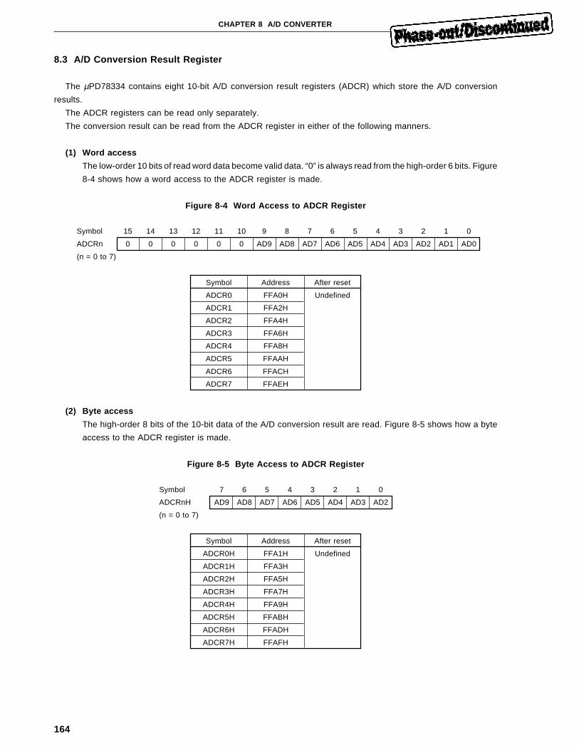
164
CHAPTER 8 A/D CONVERTER
8.3 A/D Conversion Result Register
The µPD78334 contains eight 10-bit A/D conversion result registers (ADCR) which store the A/D conversion
results.
The ADCR registers can be read only separately.
The conversion result can be read from the ADCR register in either of the following manners.
(1) Word access
The low-order 10 bits of read word data become valid data. “0” is always read from the high-order 6 bits. Figure
8-4 shows how a word access to the ADCR register is made.
Figure 8-4 Word Access to ADCR Register
Symbol 15 14 13 12 11 10 9 8 7 6 5 4 3 2 1 0
ADCRn 0 0 0 0 0 0 AD9 AD8 AD7 AD6 AD5 AD4 AD3 AD2 AD1 AD0
(n = 0 to 7)
Symbol Address After reset
ADCR0 FFA0H Undefined
ADCR1 FFA2H
ADCR2 FFA4H
ADCR3 FFA6H
ADCR4 FFA8H
ADCR5 FFAAH
ADCR6 FFACH
ADCR7 FFAEH
(2) Byte access
The high-order 8 bits of the 10-bit data of the A/D conversion result are read. Figure 8-5 shows how a byte
access to the ADCR register is made.
Figure 8-5 Byte Access to ADCR Register
Symbol 7 6 5 4 3 2 1 0
ADCRnH AD9 AD8 AD7 AD6 AD5 AD4 AD3 AD2
(n = 0 to 7)
Symbol Address After reset
ADCR0H FFA1H Undefined
ADCR1H FFA3H
ADCR2H FFA5H
ADCR3H FFA7H
ADCR4H FFA9H
ADCR5H FFABH
ADCR6H FFADH
ADCR7H FFAFH
165
CHAPTER 8 A/D CONVERTER
8.4 Operation
The high-order 8 channels (ANI8 to ANI15) of analog input to the A/D converter have the same function as the
low-order 8 channels (ANI0 to ANI7). Unless otherwise noted, the low-order 8 channels (ANI0 to ANI7) are explained
in the description to follow.
8.4.1 Basic operation of A/D converter
The A/D conversion sequence is as follows:
(1) Analog input selection and operation mode specification are set in the A/D converter mode register (ADM),
and A/D conversion is started.
(2) The voltage generated by the successive approximation voltage generator is compared with the analog input
for each SAR bit.
(3) When the 10-bit comparison terminates, the valid digital result is left in the SAR. The value is transferred to
the ADCR register and is latched. At the same time, an A/D conversion and interrupt request (INTAD) occurs.
Handle the INTAD in the vectored interrupt or macro service mode. (See 13.4 Macro Service Function ). (See
Figure 8-6 ).
Caution Do not apply any voltage outside the AV SS to AV REF range to the ANI0 to ANI7 pins regardless
of whether or not the pins are used for A/D conversion.
A/D conversion operation can be started in synchronization with an external signal. When mix mode external trigger
is specified by the software which sets ADM register bits 5 to 7 (AM0 to AM2), the external trigger signal (INTP5)
wait state is entered. Whenever a valid edge is input to the INT5 pin, A/D conversion operation is initialized and started.
(See Figure 8-7. )
If a write into the ADM register is performed during the A/D conversion operation, the conversion operation is
initialized and again started from the beginning. (See Figure 8-8 ). When RESET is input, the ADCR register becomes
undefined.
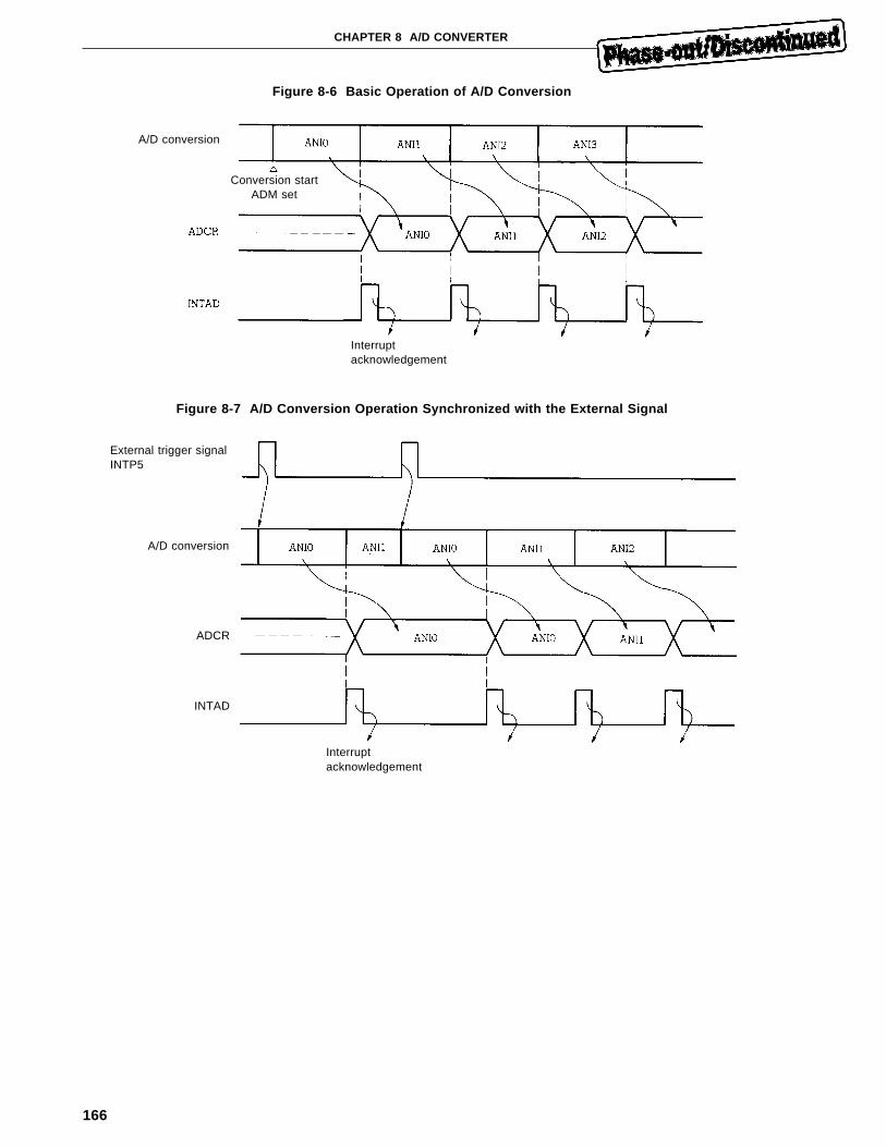
166
CHAPTER 8 A/D CONVERTER
Figure 8-6 Basic Operation of A/D Conversion
Figure 8-7 A/D Conversion Operation Synchronized with the External Signal
Conversion startADM set
A/D conversion
Interruptacknowledgement
External trigger signalINTP5
A/D conversion
ADCR
INTAD
Interruptacknowledgement
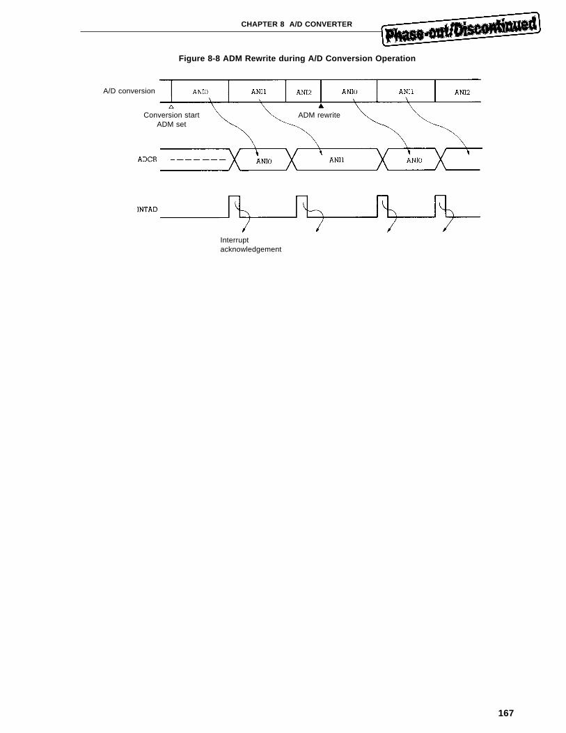
167
CHAPTER 8 A/D CONVERTER
Figure 8-8 ADM Rewrite during A/D Conversion Operation
Conversion startADM set
A/D conversion
Interruptacknowledgement
ADM rewrite
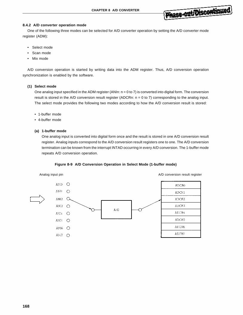
168
CHAPTER 8 A/D CONVERTER
8.4.2 A/D converter operation mode
One of the following three modes can be selected for A/D converter operation by setting the A/D converter mode
register (ADM):
• Select mode
• Scan mode
• Mix mode
A/D conversion operation is started by writing data into the ADM register. Thus, A/D conversion operation
synchronization is enabled by the software.
(1) Select mode
One analog input specified in the ADM register (ANIn: n = 0 to 7) is converted into digital form. The conversion
result is stored in the A/D conversion result register (ADCRn: n = 0 to 7) corresponding to the analog input.
The select mode provides the following two modes according to how the A/D conversion result is stored:
• 1-buffer mode
• 4-buffer mode
(a) 1-buffer mode
One analog input is converted into digital form once and the result is stored in one A/D conversion result
register. Analog inputs correspond to the A/D conversion result registers one to one. The A/D conversion
termination can be known from the interrupt INTAD occurring in every A/D conversion. The 1-buffer mode
repeats A/D conversion operation.
Figure 8-9 A/D Conversion Operation in Select Mode (1-buffer mode)
Analog input pin A/D conversion result register
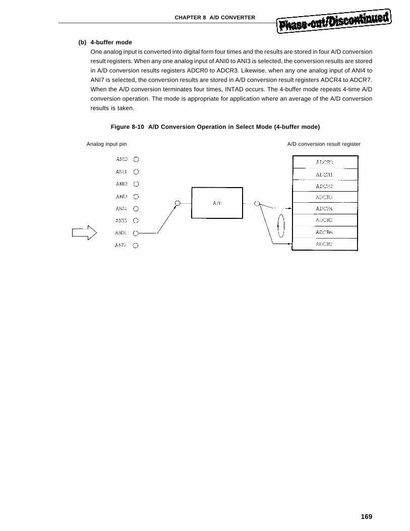
169
CHAPTER 8 A/D CONVERTER
(b) 4-buffer mode
One analog input is converted into digital form four times and the results are stored in four A/D conversion
result registers. When any one analog input of ANI0 to ANI3 is selected, the conversion results are stored
in A/D conversion results registers ADCR0 to ADCR3. Likewise, when any one analog input of ANI4 to
ANI7 is selected, the conversion results are stored in A/D conversion result registers ADCR4 to ADCR7.
When the A/D conversion terminates four times, INTAD occurs. The 4-buffer mode repeats 4-time A/D
conversion operation. The mode is appropriate for application where an average of the A/D conversion
results is taken.
Figure 8-10 A/D Conversion Operation in Select Mode (4-buffer mode)
Analog input pin A/D conversion result register
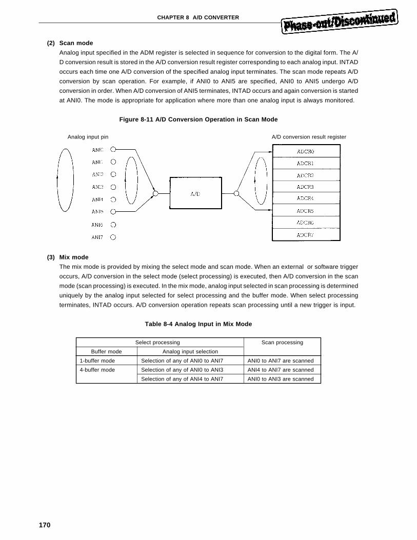
170
CHAPTER 8 A/D CONVERTER
(2) Scan mode
Analog input specified in the ADM register is selected in sequence for conversion to the digital form. The A/
D conversion result is stored in the A/D conversion result register corresponding to each analog input. INTAD
occurs each time one A/D conversion of the specified analog input terminates. The scan mode repeats A/D
conversion by scan operation. For example, if ANI0 to ANI5 are specified, ANI0 to ANI5 undergo A/D
conversion in order. When A/D conversion of ANI5 terminates, INTAD occurs and again conversion is started
at ANI0. The mode is appropriate for application where more than one analog input is always monitored.
Figure 8-11 A/D Conversion Operation in Scan Mode
Analog input pin A/D conversion result register
(3) Mix mode
The mix mode is provided by mixing the select mode and scan mode. When an external or software trigger
occurs, A/D conversion in the select mode (select processing) is executed, then A/D conversion in the scan
mode (scan processing) is executed. In the mix mode, analog input selected in scan processing is determined
uniquely by the analog input selected for select processing and the buffer mode. When select processing
terminates, INTAD occurs. A/D conversion operation repeats scan processing until a new trigger is input.
Table 8-4 Analog Input in Mix Mode
Select processing Scan processing
Buffer mode Analog input selection
1-buffer mode Selection of any of ANI0 to ANI7 ANI0 to ANI7 are scanned
4-buffer mode Selection of any of ANI0 to ANI3 ANI4 to ANI7 are scanned
Selection of any of ANI4 to ANI7 ANI0 to ANI3 are scanned
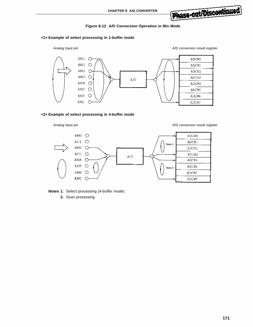
171
CHAPTER 8 A/D CONVERTER
Figure 8-12 A/D Conversion Operation in Mix Mode
<1> Example of select processing in 1-buffer mode
Analog input pin A/D conversion result register
<2> Example of select processing in 4-buffer mode
Analog input pin A/D conversion result register
Notes 1. Select processing (4-buffer mode)
2. Scan processing
Note 1
Note 2
172
CHAPTER 8 A/D CONVERTER
8.5 Use of A/D Converter Characteristic Table
Terms peculiar to the A/D converter are explained:
(1) Resolution
The ratio of minimum analog input voltage that can be identified, that is, analog input voltage per digital output
bit is called 1 LSB (Least Significant Bit). The ratio of 1 LSB to full scale is represented by %FSR (Full Scale
Range).
When the resolution is 10 bits,
1 LSB = 1/210 = 1/1024
= 0.098%FSR
The precision is independent of the resolution and is determined by total error.
(2) Total error
The total error refers to the maximum value of the difference between the measurement value and ideal value.
It represents the total error of zero scale error, full scale error, non-linear error, and error caused by combination
of the errors.
The total error in the characteristic table does not contain any quantization error.
(3) Quantization error
The quantization error is an error of ±1/2 LSB occurring inevitably when an analog value is converted into a
digital value. The A/D converter converts analog input voltage in the range of ±1/2 LSB into the same digital
code, thus a quantization error cannot be avoided.
The quantization error is not contained in the total error, zero scale error, full scale error, or non-linear error
in the characteristic table.
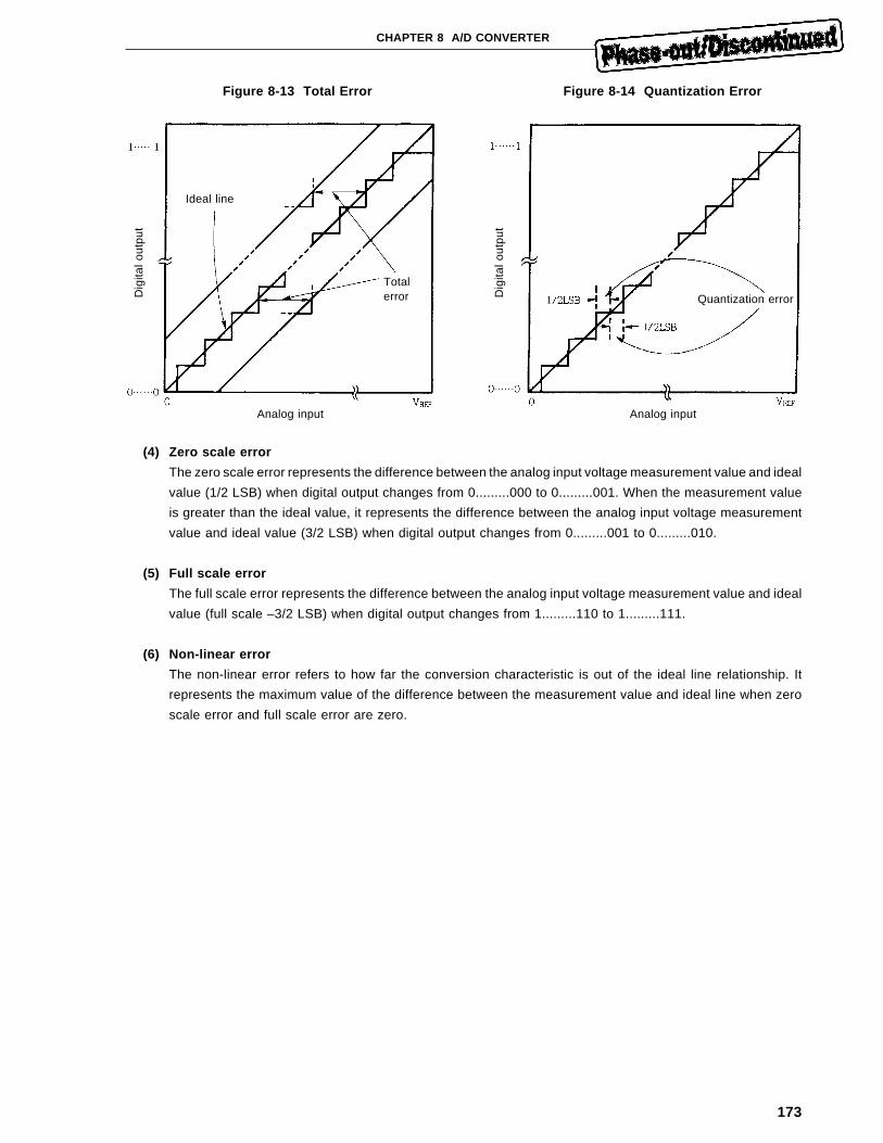
173
CHAPTER 8 A/D CONVERTER
Figure 8-13 Total Error Figure 8-14 Quantization Error
Analog input Analog input
(4) Zero scale error
The zero scale error represents the difference between the analog input voltage measurement value and ideal
value (1/2 LSB) when digital output changes from 0.........000 to 0.........001. When the measurement value
is greater than the ideal value, it represents the difference between the analog input voltage measurement
value and ideal value (3/2 LSB) when digital output changes from 0.........001 to 0.........010.
(5) Full scale error
The full scale error represents the difference between the analog input voltage measurement value and ideal
value (full scale –3/2 LSB) when digital output changes from 1.........110 to 1.........111.
(6) Non-linear error
The non-linear error refers to how far the conversion characteristic is out of the ideal line relationship. It
represents the maximum value of the difference between the measurement value and ideal line when zero
scale error and full scale error are zero.
Dig
ital o
utpu
t
Ideal line
Totalerror Quantization errorD
igita
l out
put
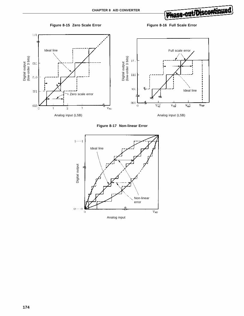
174
CHAPTER 8 A/D CONVERTER
Figure 8-15 Zero Scale Error Figure 8-16 Full Scale Error
Analog input (LSB) Analog input (LSB)
Figure 8-17 Non-linear Error
Analog input
Dig
ital o
utpu
t(l
ow-o
rder
3 b
its)
Ideal line
Zero scale error
Non-linearerror
Ideal line
Ideal line
Dig
ital o
utpu
t(l
ow-o
rder
3 b
its)
Full scale error
Dig
ital o
utpu
t
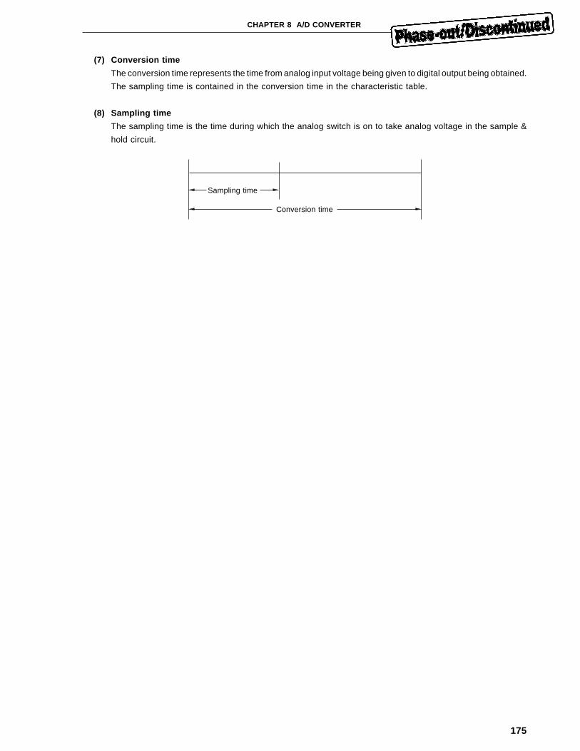
175
CHAPTER 8 A/D CONVERTER
(7) Conversion time
The conversion time represents the time from analog input voltage being given to digital output being obtained.
The sampling time is contained in the conversion time in the characteristic table.
(8) Sampling time
The sampling time is the time during which the analog switch is on to take analog voltage in the sample &
hold circuit.
Sampling time
Conversion time

176
[MEMO]

177
CHAPTER 9 ASYNCHRONOUS SERIAL INTERFACE
The µPD78334 contains UART (Universal Asynchronous Receiver Transmitter) as an asynchronous serial
interface; 1-byte data following a start bit is transferred and full duplex operation can be performed. A baud rate
generator is provided for communication at any baud rate in a wide range.
The asynchronous serial interface operates independently of the clocked serial interface.
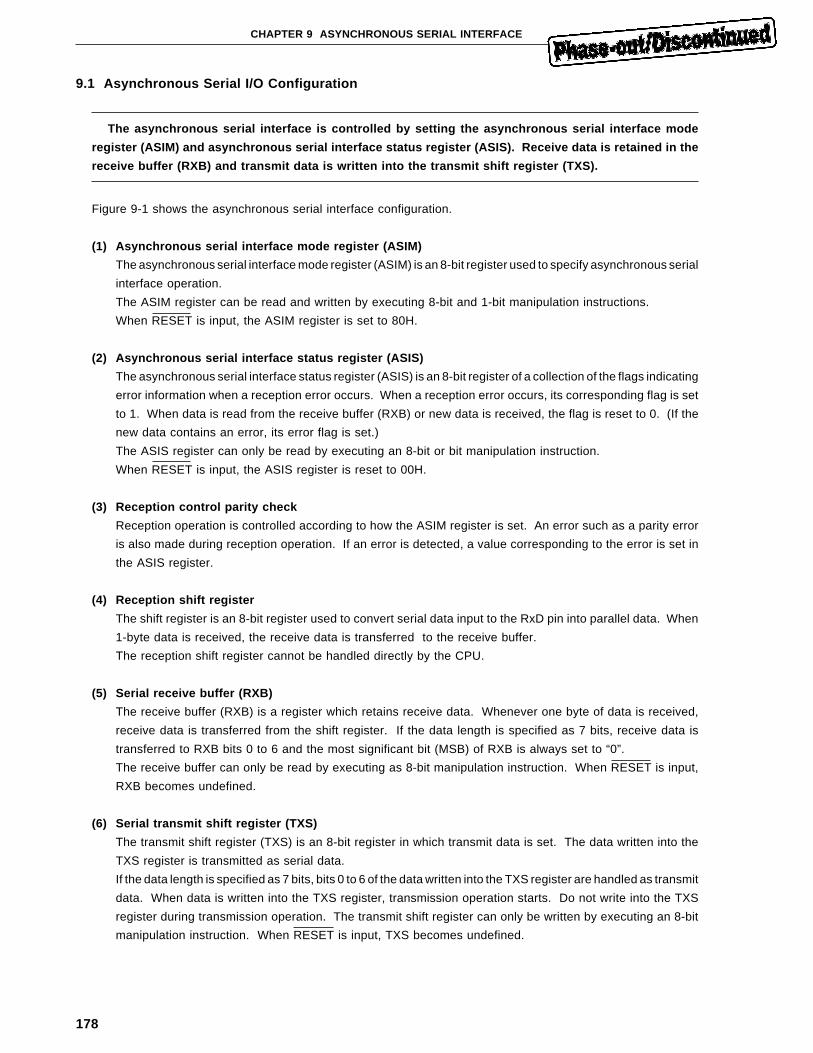
178
CHAPTER 9 ASYNCHRONOUS SERIAL INTERFACE
9.1 Asynchronous Serial I/O Configuration
The asynchronous serial interface is controlled by setting the asynchronous serial interface mode
register (ASIM) and asynchronous serial interface status register (ASIS). Receive data is retained in the
receive buffer (RXB) and transmit data is written into the transmit shift register (TXS).
Figure 9-1 shows the asynchronous serial interface configuration.
(1) Asynchronous serial interface mode register (ASIM)
The asynchronous serial interface mode register (ASIM) is an 8-bit register used to specify asynchronous serial
interface operation.
The ASIM register can be read and written by executing 8-bit and 1-bit manipulation instructions.
When RESET is input, the ASIM register is set to 80H.
(2) Asynchronous serial interface status register (ASIS)
The asynchronous serial interface status register (ASIS) is an 8-bit register of a collection of the flags indicating
error information when a reception error occurs. When a reception error occurs, its corresponding flag is set
to 1. When data is read from the receive buffer (RXB) or new data is received, the flag is reset to 0. (If the
new data contains an error, its error flag is set.)
The ASIS register can only be read by executing an 8-bit or bit manipulation instruction.
When RESET is input, the ASIS register is reset to 00H.
(3) Reception control parity check
Reception operation is controlled according to how the ASIM register is set. An error such as a parity error
is also made during reception operation. If an error is detected, a value corresponding to the error is set in
the ASIS register.
(4) Reception shift register
The shift register is an 8-bit register used to convert serial data input to the RxD pin into parallel data. When
1-byte data is received, the receive data is transferred to the receive buffer.
The reception shift register cannot be handled directly by the CPU.
(5) Serial receive buffer (RXB)
The receive buffer (RXB) is a register which retains receive data. Whenever one byte of data is received,
receive data is transferred from the shift register. If the data length is specified as 7 bits, receive data is
transferred to RXB bits 0 to 6 and the most significant bit (MSB) of RXB is always set to “0”.
The receive buffer can only be read by executing as 8-bit manipulation instruction. When RESET is input,
RXB becomes undefined.
(6) Serial transmit shift register (TXS)
The transmit shift register (TXS) is an 8-bit register in which transmit data is set. The data written into the
TXS register is transmitted as serial data.
If the data length is specified as 7 bits, bits 0 to 6 of the data written into the TXS register are handled as transmit
data. When data is written into the TXS register, transmission operation starts. Do not write into the TXS
register during transmission operation. The transmit shift register can only be written by executing an 8-bit
manipulation instruction. When RESET is input, TXS becomes undefined.
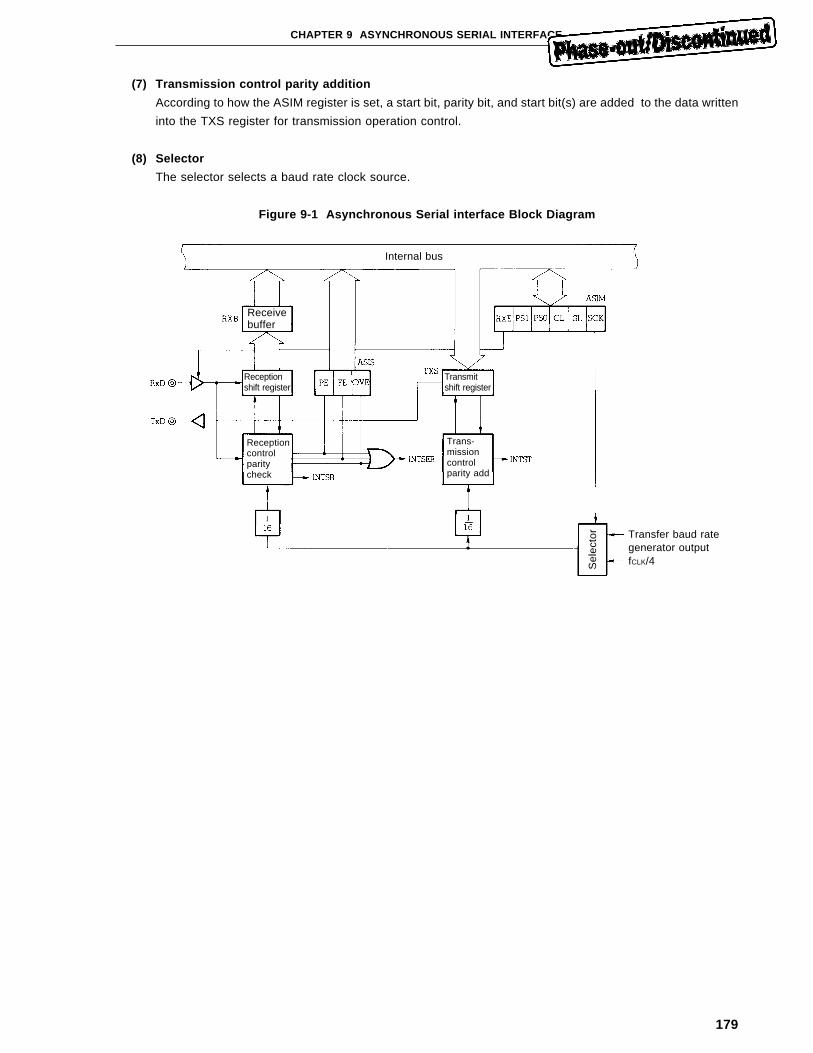
179
CHAPTER 9 ASYNCHRONOUS SERIAL INTERFACE
(7) Transmission control parity addition
According to how the ASIM register is set, a start bit, parity bit, and start bit(s) are added to the data written
into the TXS register for transmission operation control.
(8) Selector
The selector selects a baud rate clock source.
Figure 9-1 Asynchronous Serial interface Block Diagram
Internal bus
Receivebuffer
Receptionshift register
Transmitshift register
Receptioncontrolparitycheck
Trans-missioncontrolparity add
Sel
ecto
r Transfer baud rategenerator outputfCLK/4
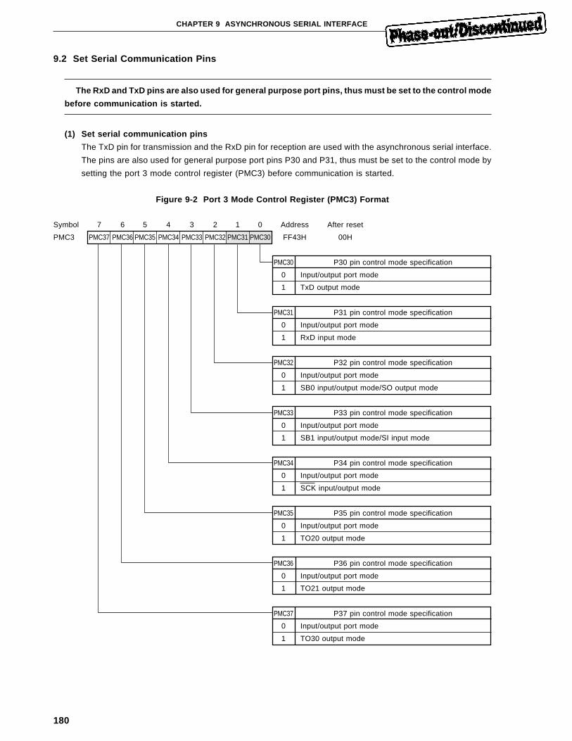
180
CHAPTER 9 ASYNCHRONOUS SERIAL INTERFACE
9.2 Set Serial Communication Pins
The RxD and TxD pins are also used for general purpose port pins, thus must be set to the control mode
before communication is started.
(1) Set serial communication pins
The TxD pin for transmission and the RxD pin for reception are used with the asynchronous serial interface.
The pins are also used for general purpose port pins P30 and P31, thus must be set to the control mode by
setting the port 3 mode control register (PMC3) before communication is started.
Figure 9-2 Port 3 Mode Control Register (PMC3) Format
Symbol 7 6 5 4 3 2 1 0 Address After reset
PMC3 PMC37 PMC36 PMC35 PMC34 PMC33 PMC32 PMC31 PMC30 FF43H 00H
PMC30 P30 pin control mode specification
0 Input/output port mode
1 TxD output mode
PMC31 P31 pin control mode specification
0 Input/output port mode
1 RxD input mode
PMC32 P32 pin control mode specification
0 Input/output port mode
1 SB0 input/output mode/SO output mode
PMC33 P33 pin control mode specification
0 Input/output port mode
1 SB1 input/output mode/SI input mode
PMC34 P34 pin control mode specification
0 Input/output port mode
1 SCK input/output mode
PMC35 P35 pin control mode specification
0 Input/output port mode
1 TO20 output mode
PMC36 P36 pin control mode specification
0 Input/output port mode
1 TO21 output mode
PMC37 P37 pin control mode specification
0 Input/output port mode
1 TO30 output mode
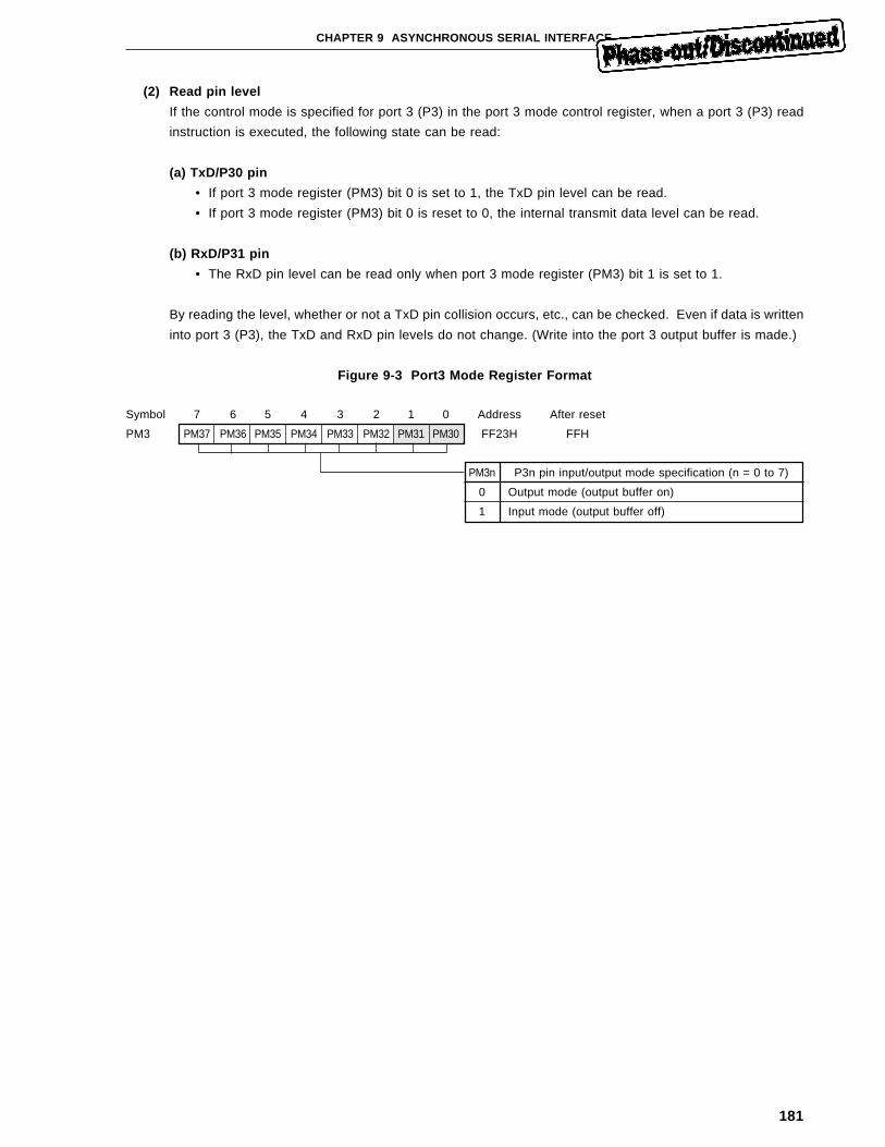
181
CHAPTER 9 ASYNCHRONOUS SERIAL INTERFACE
(2) Read pin level
If the control mode is specified for port 3 (P3) in the port 3 mode control register, when a port 3 (P3) read
instruction is executed, the following state can be read:
(a) TxD/P30 pin
• If port 3 mode register (PM3) bit 0 is set to 1, the TxD pin level can be read.
• If port 3 mode register (PM3) bit 0 is reset to 0, the internal transmit data level can be read.
(b) RxD/P31 pin
• The RxD pin level can be read only when port 3 mode register (PM3) bit 1 is set to 1.
By reading the level, whether or not a TxD pin collision occurs, etc., can be checked. Even if data is written
into port 3 (P3), the TxD and RxD pin levels do not change. (Write into the port 3 output buffer is made.)
Figure 9-3 Port3 Mode Register Format
Symbol 7 6 5 4 3 2 1 0 Address After reset
PM3 PM37 PM36 PM35 PM34 PM33 PM32 PM31 PM30 FF23H FFH
PM3n P3n pin input/output mode specification (n = 0 to 7)
0 Output mode (output buffer on)
1 Input mode (output buffer off)
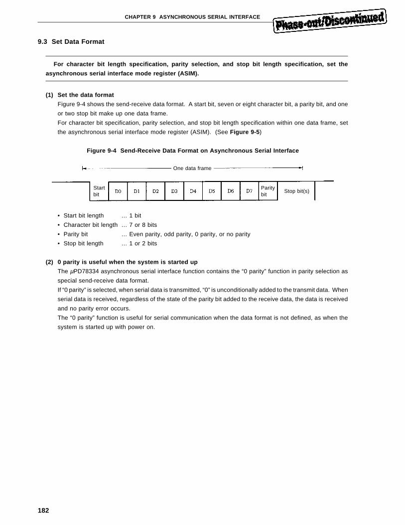
182
CHAPTER 9 ASYNCHRONOUS SERIAL INTERFACE
9.3 Set Data Format
For character bit length specification, parity selection, and stop bit length specification, set the
asynchronous serial interface mode register (ASIM).
(1) Set the data format
Figure 9-4 shows the send-receive data format. A start bit, seven or eight character bit, a parity bit, and one
or two stop bit make up one data frame.
For character bit specification, parity selection, and stop bit length specification within one data frame, set
the asynchronous serial interface mode register (ASIM). (See Figure 9-5 )
Figure 9-4 Send-Receive Data Format on Asynchronous Serial Interface
• Start bit length … 1 bit
• Character bit length … 7 or 8 bits
• Parity bit … Even parity, odd parity, 0 parity, or no parity
• Stop bit length … 1 or 2 bits
(2) 0 parity is useful when the system is started up
The µPD78334 asynchronous serial interface function contains the “0 parity” function in parity selection as
special send-receive data format.
If “0 parity” is selected, when serial data is transmitted, “0” is unconditionally added to the transmit data. When
serial data is received, regardless of the state of the parity bit added to the receive data, the data is received
and no parity error occurs.
The “0 parity” function is useful for serial communication when the data format is not defined, as when the
system is started up with power on.
One data frame
Startbit
Paritybit
Stop bit(s)
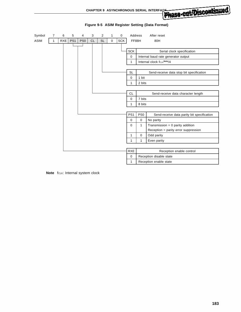
183
CHAPTER 9 ASYNCHRONOUS SERIAL INTERFACE
Figure 9-5 ASIM Register Setting (Data Format)
Symbol 7 6 5 4 3 2 1 0 Address After reset
ASIM 1 RXE PS1 PS0 CL SL 0 SCK FF88H 80H
SCK Serial clock specification
0 Internal baud rate generator output
1 Internal clock fCLKNote/4
SL Send-receive data stop bit specification
0 1 bit
1 2 bits
CL Send-receive data character length
0 7 bits
1 8 bits
PS1 PS0 Send-receive data parity bit specification
0 0 No parity
0 1 Transmission = 0 parity addition
Reception = parity error suppression
1 0 Odd parity
1 1 Even parity
RXE Reception enable control
0 Reception disable state
1 Reception enable state
Note fCLK: Internal system clock
184
CHAPTER 9 ASYNCHRONOUS SERIAL INTERFACE
9.4 Set Baud Rate
Baud rate generator output or internal clock f CLK/4 can be selected as serial clock. If baud rate generator
output is selected, communication can be executed at any desired baud rate, independently of the
operation frequency.
(1) Baud rate = serial clock/16
On the asynchronous serial interface, the RxD pin level is sampled with 1/16 divided clock of the serial clock
specified in the asynchronous serial interface mode register (ASIM).
(2) Select serial clock
Select serial clock by setting bit 0 of the asynchronous serial interface mode register (ASIM). (See Figure
9-6)
If internal system clock fCLK/4 is selected, the baud rate becomes fCLK/64. Thus, when the internal system clock
is 8 MHz, the baud rate becomes 125 Kbps.
Remark The baud rate generator is shared by the clocked serial interface. (See 10.3 Set Baud Rate )
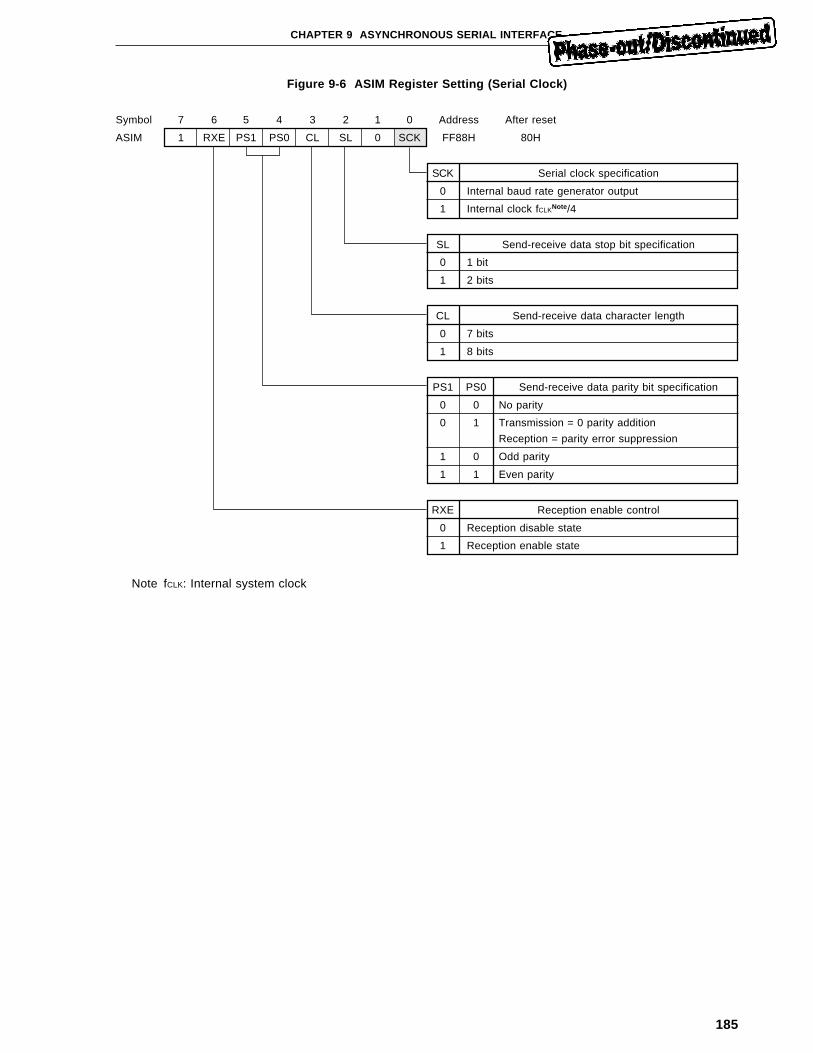
185
CHAPTER 9 ASYNCHRONOUS SERIAL INTERFACE
Figure 9-6 ASIM Register Setting (Serial Clock)
Symbol 7 6 5 4 3 2 1 0 Address After reset
ASIM 1 RXE PS1 PS0 CL SL 0 SCK FF88H 80H
SCK Serial clock specification
0 Internal baud rate generator output
1 Internal clock fCLKNote/4
SL Send-receive data stop bit specification
0 1 bit
1 2 bits
CL Send-receive data character length
0 7 bits
1 8 bits
PS1 PS0 Send-receive data parity bit specification
0 0 No parity
0 1 Transmission = 0 parity addition
Reception = parity error suppression
1 0 Odd parity
1 1 Even parity
RXE Reception enable control
0 Reception disable state
1 Reception enable state
Note fCLK: Internal system clock
186
CHAPTER 9 ASYNCHRONOUS SERIAL INTERFACE
9.4.1 Baud rate generator configuration
The baud rate generator is controlled by setting the baud rate generator mode register (BRGM) and 10-
bit baud rate generator compare register (BRG).
Figure 9-7 shows the baud rate generator block diagram.
(1) Baud rate generator mode register (BRGM)
The baud rate generator mode register (BRGM) is an 8-bit register for 10-bit timer count clock selection and
baud rate generator operation control.
The BRGM register can be read an written by executing 8-bit and 1-bit manipulation instructions.
When RESET is input, the BRGM register is set to 80H.
Figure 9-8 shows the BRGM register format.
(2) Selector
10-bit timer count clock is selected by setting the BRGM register.
(3) 10-bit timer (TMBRG)
The 10-bit timer (TMBRG) counts the count clock selected in the selector.
If 10-bit baud rate generator compare register (BRG) match signal is generated, when the next count clock
is received, the 10-bit timer is cleared to 0.
Count start and count stop are controlled by setting the BRGM register.
The 10-bit timer cannot be handled directly from the CPU.
(4) 10-bit baud rate generator compare register (BRG)
The 10-bit timer contents are always compared with the data written into the 10-bit compare register. When
they match, match signal is generated. The match signal causes the 10-bit timer to be cleared to 0.
The result of dividing the match signal by two is output from the baud rate generator.
The BRG register can be read/written by executing a 16-bit manipulation instruction.
When RESET is input, the BRG register is reset to 0000H.
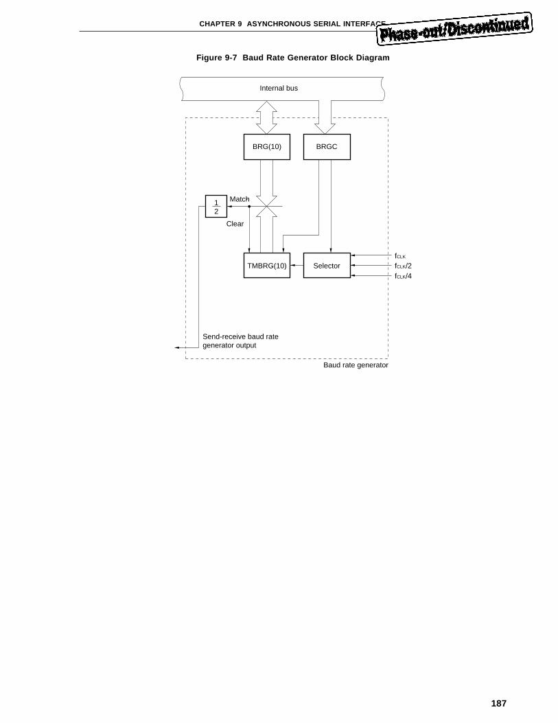
187
CHAPTER 9 ASYNCHRONOUS SERIAL INTERFACE
Figure 9-7 Baud Rate Generator Block Diagram
Internal bus
BRG(10) BRGC
TMBRG(10) Selector fCLK/2fCLK
fCLK/4
Match
Clear
Send-receive baud rate generator output
Baud rate generator
12
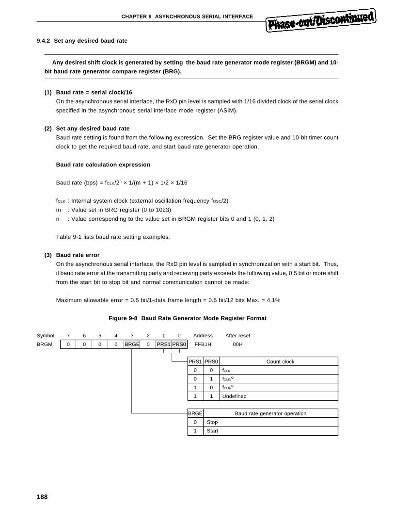
188
CHAPTER 9 ASYNCHRONOUS SERIAL INTERFACE
9.4.2 Set any desired baud rate
Any desired shift clock is generated by setting the baud rate generator mode register (BRGM) and 10-
bit baud rate generator compare register (BRG).
(1) Baud rate = serial clock/16
On the asynchronous serial interface, the RxD pin level is sampled with 1/16 divided clock of the serial clock
specified in the asynchronous serial interface mode register (ASIM).
(2) Set any desired baud rate
Baud rate setting is found from the following expression. Set the BRG register value and 10-bit timer count
clock to get the required baud rate, and start baud rate generator operation.
Baud rate calculation expression
Baud rate (bps) = fCLK/2n × 1/(m + 1) × 1/2 × 1/16
fCLK : Internal system clock (external oscillation frequency fOSC/2)
m : Value set in BRG register (0 to 1023)
n : Value corresponding to the value set in BRGM register bits 0 and 1 (0, 1, 2)
Table 9-1 lists baud rate setting examples.
(3) Baud rate error
On the asynchronous serial interface, the RxD pin level is sampled in synchronization with a start bit. Thus,
if baud rate error at the transmitting party and receiving party exceeds the following value, 0.5 bit or more shift
from the start bit to stop bit and normal communication cannot be made:
Maximum allowable error = 0.5 bit/1-data frame length = 0.5 bit/12 bits Max. = 4.1%
Figure 9-8 Baud Rate Generator Mode Register Format
Symbol 7 6 5 4 3 2 1 0 Address After reset
BRGM 0 0 0 0 BRGE 0 PRS1 PRS0 FFB1H 00H
PRS1 PRS0 Count clock
0 0 fCLK
0 1 fCLK/2
1 0 fCLK/4
1 1 Undefined
BRGE Baud rate generator operation
0 Stop
1 Start
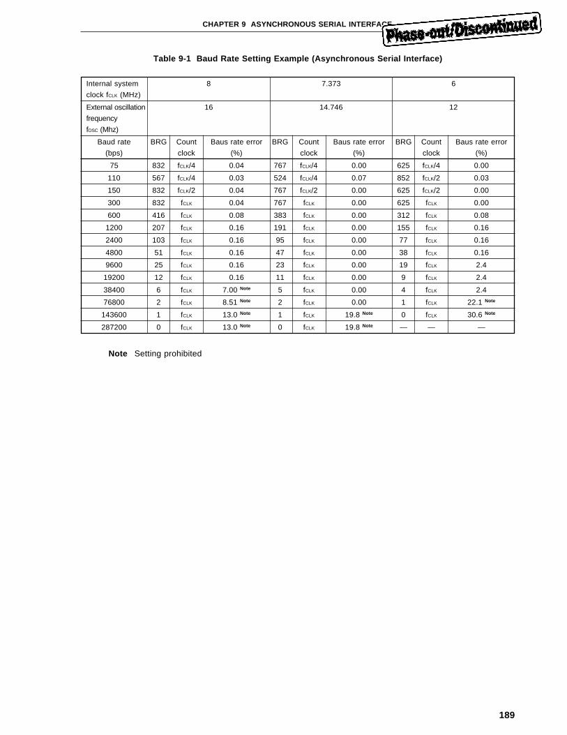
189
CHAPTER 9 ASYNCHRONOUS SERIAL INTERFACE
Table 9-1 Baud Rate Setting Example (Asynchronous Serial Interface)
Internal system 8 7.373 6
clock fCLK (MHz)
External oscillation 16 14.746 12
frequency
fOSC (Mhz)
Baud rate BRG Count Baus rate error BRG Count Baus rate error BRG Count Baus rate error
(bps) clock (%) clock (%) clock (%)
75 832 fCLK/4 0.04 767 fCLK/4 0.00 625 fCLK/4 0.00
110 567 fCLK/4 0.03 524 fCLK/4 0.07 852 fCLK/2 0.03
150 832 fCLK/2 0.04 767 fCLK/2 0.00 625 fCLK/2 0.00
300 832 fCLK 0.04 767 fCLK 0.00 625 fCLK 0.00
600 416 fCLK 0.08 383 fCLK 0.00 312 fCLK 0.08
1200 207 fCLK 0.16 191 fCLK 0.00 155 fCLK 0.16
2400 103 fCLK 0.16 95 fCLK 0.00 77 fCLK 0.16
4800 51 fCLK 0.16 47 fCLK 0.00 38 fCLK 0.16
9600 25 fCLK 0.16 23 fCLK 0.00 19 fCLK 2.4
19200 12 fCLK 0.16 11 fCLK 0.00 9 fCLK 2.4
38400 6 fCLK 7.00 Note 5 fCLK 0.00 4 fCLK 2.4
76800 2 fCLK 8.51 Note 2 fCLK 0.00 1 fCLK 22.1 Note
143600 1 fCLK 13.0 Note 1 fCLK 19.8 Note 0 fCLK 30.6 Note
287200 0 fCLK 13.0 Note 0 fCLK 19.8 Note — — —
Note Setting prohibited
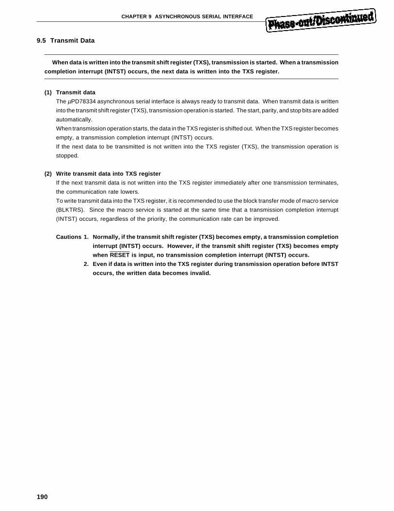
190
CHAPTER 9 ASYNCHRONOUS SERIAL INTERFACE
9.5 Transmit Data
When data is written into the transmit shift register (TXS), transmission is started. When a transmission
completion interrupt (INTST) occurs, the next data is written into the TXS register.
(1) Transmit data
The µPD78334 asynchronous serial interface is always ready to transmit data. When transmit data is written
into the transmit shift register (TXS), transmission operation is started. The start, parity, and stop bits are added
automatically.
When transmission operation starts, the data in the TXS register is shifted out. When the TXS register becomes
empty, a transmission completion interrupt (INTST) occurs.
If the next data to be transmitted is not written into the TXS register (TXS), the transmission operation is
stopped.
(2) Write transmit data into TXS register
If the next transmit data is not written into the TXS register immediately after one transmission terminates,
the communication rate lowers.
To write transmit data into the TXS register, it is recommended to use the block transfer mode of macro service
(BLKTRS). Since the macro service is started at the same time that a transmission completion interrupt
(INTST) occurs, regardless of the priority, the communication rate can be improved.
Cautions 1. Normally, if the transmit shift register (TXS) becomes empty, a transmission completion
interrupt (INTST) occurs. However, if the transmit shift register (TXS) becomes empty
when RESET is input, no transmission completion interrupt (INTST) occurs.
2. Even if data is written into the TXS register during transmission operation before INTST
occurs, the written data becomes invalid.
191
CHAPTER 9 ASYNCHRONOUS SERIAL INTERFACE
Figure 9-9 Asynchronous Serial Interface Transmission Completion Interrupt Timing
(a) Stop bit length: 1
(b) Stop bit length: 2
Remark INTST: Vector table address: 0026H (TPF = 0), 8026H (TPF = 1)
Macro service control word address: FE26H
Caution Normally, if the transmit shift register (TXS) becomes empty, a transmission completion
interrupt (INTST) occurs. However, if the transmit shift register (TXS) becomes empty
when RESET is input, on transmission completion interrupt (INTST) occurs.
TxD (output) Parity
TxD (output) Parity
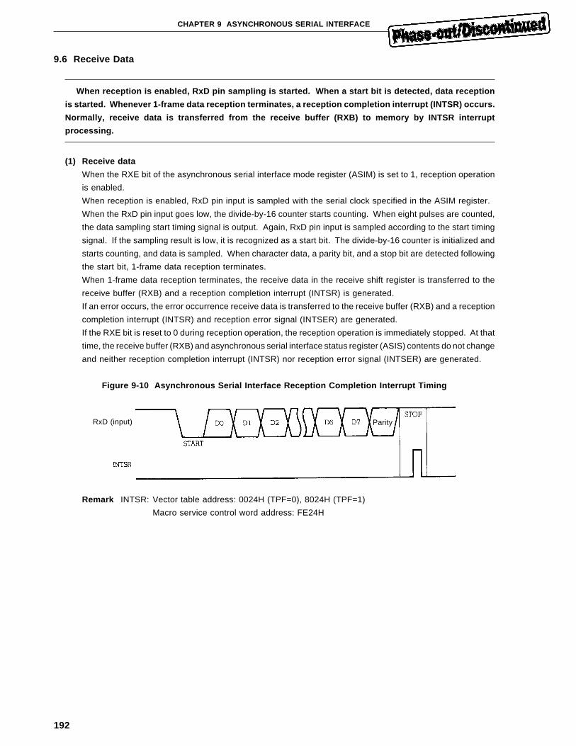
192
CHAPTER 9 ASYNCHRONOUS SERIAL INTERFACE
9.6 Receive Data
When reception is enabled, RxD pin sampling is started. When a start bit is detected, data reception
is started. Whenever 1-frame data reception terminates, a reception completion interrupt (INTSR) occurs.
Normally, receive data is transferred from the receive buffer (RXB) to memory by INTSR interrupt
processing.
(1) Receive data
When the RXE bit of the asynchronous serial interface mode register (ASIM) is set to 1, reception operation
is enabled.
When reception is enabled, RxD pin input is sampled with the serial clock specified in the ASIM register.
When the RxD pin input goes low, the divide-by-16 counter starts counting. When eight pulses are counted,
the data sampling start timing signal is output. Again, RxD pin input is sampled according to the start timing
signal. If the sampling result is low, it is recognized as a start bit. The divide-by-16 counter is initialized and
starts counting, and data is sampled. When character data, a parity bit, and a stop bit are detected following
the start bit, 1-frame data reception terminates.
When 1-frame data reception terminates, the receive data in the receive shift register is transferred to the
receive buffer (RXB) and a reception completion interrupt (INTSR) is generated.
If an error occurs, the error occurrence receive data is transferred to the receive buffer (RXB) and a reception
completion interrupt (INTSR) and reception error signal (INTSER) are generated.
If the RXE bit is reset to 0 during reception operation, the reception operation is immediately stopped. At that
time, the receive buffer (RXB) and asynchronous serial interface status register (ASIS) contents do not change
and neither reception completion interrupt (INTSR) nor reception error signal (INTSER) are generated.
Figure 9-10 Asynchronous Serial Interface Reception Completion Interrupt Timing
Remark INTSR: Vector table address: 0024H (TPF=0), 8024H (TPF=1)
Macro service control word address: FE24H
RxD (input) Parity
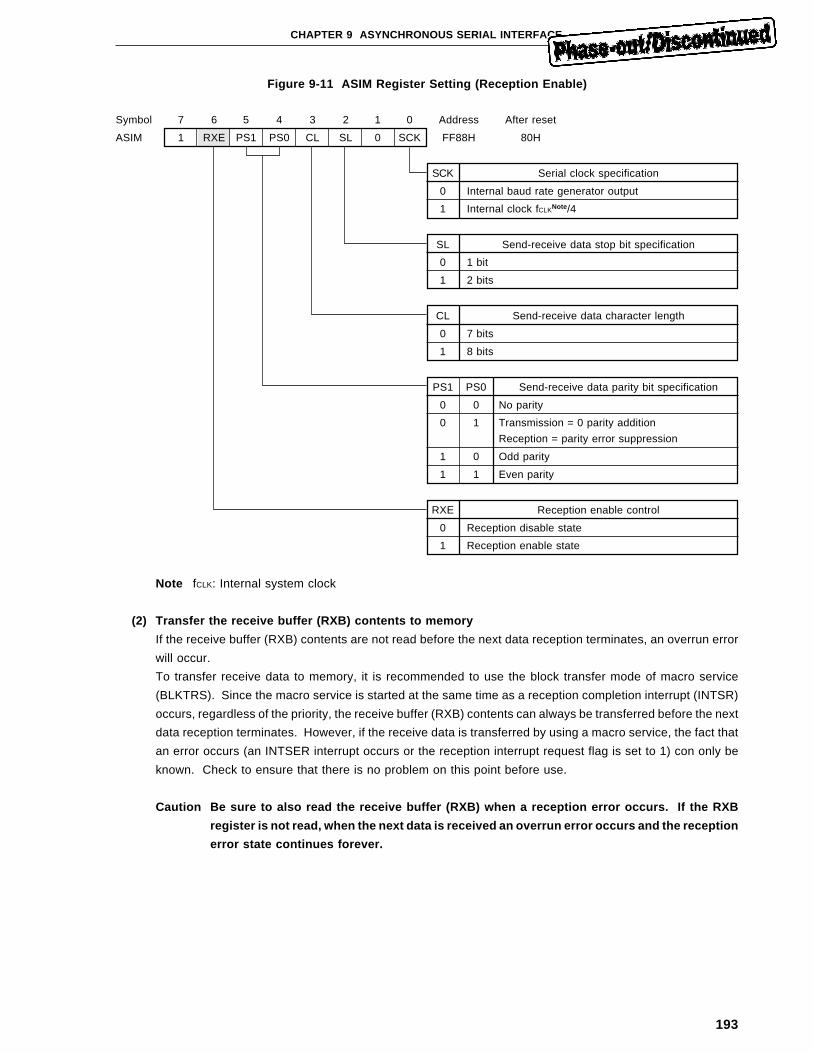
193
CHAPTER 9 ASYNCHRONOUS SERIAL INTERFACE
Figure 9-11 ASIM Register Setting (Reception Enable)
Symbol 7 6 5 4 3 2 1 0 Address After reset
ASIM 1 RXE PS1 PS0 CL SL 0 SCK FF88H 80H
SCK Serial clock specification
0 Internal baud rate generator output
1 Internal clock fCLKNote/4
SL Send-receive data stop bit specification
0 1 bit
1 2 bits
CL Send-receive data character length
0 7 bits
1 8 bits
PS1 PS0 Send-receive data parity bit specification
0 0 No parity
0 1 Transmission = 0 parity addition
Reception = parity error suppression
1 0 Odd parity
1 1 Even parity
RXE Reception enable control
0 Reception disable state
1 Reception enable state
Note fCLK: Internal system clock
(2) Transfer the receive buffer (RXB) contents to memory
If the receive buffer (RXB) contents are not read before the next data reception terminates, an overrun error
will occur.
To transfer receive data to memory, it is recommended to use the block transfer mode of macro service
(BLKTRS). Since the macro service is started at the same time as a reception completion interrupt (INTSR)
occurs, regardless of the priority, the receive buffer (RXB) contents can always be transferred before the next
data reception terminates. However, if the receive data is transferred by using a macro service, the fact that
an error occurs (an INTSER interrupt occurs or the reception interrupt request flag is set to 1) con only be
known. Check to ensure that there is no problem on this point before use.
Caution Be sure to also read the receive buffer (RXB) when a reception error occurs. If the RXB
register is not read, when the next data is received an overrun error occurs and the reception
error state continues forever.
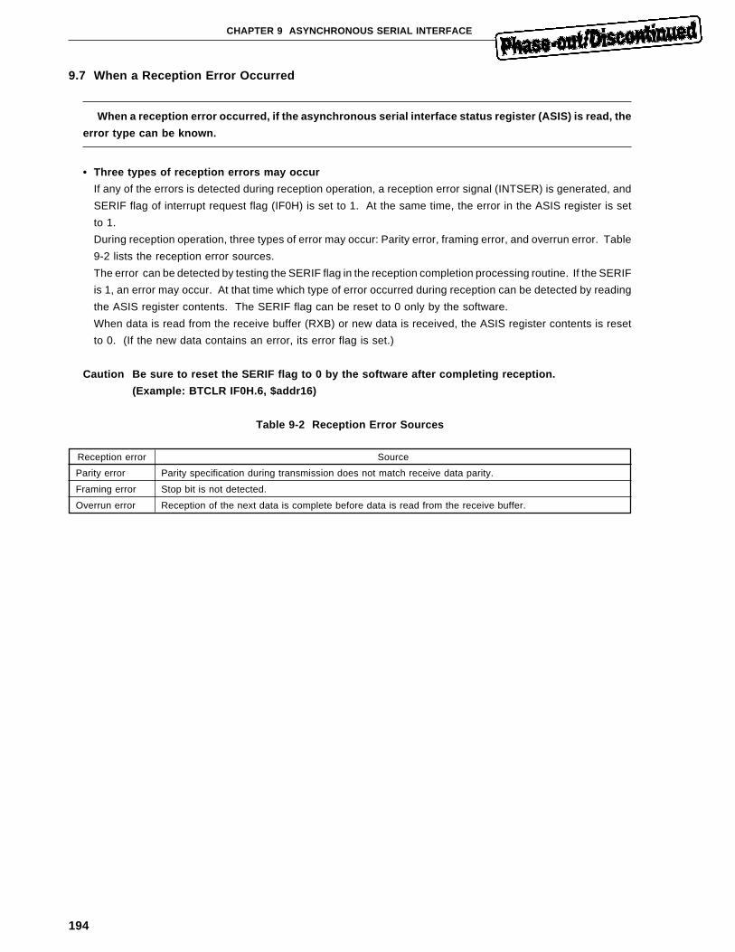
194
CHAPTER 9 ASYNCHRONOUS SERIAL INTERFACE
9.7 When a Reception Error Occurred
When a reception error occurred, if the asynchronous serial interface status register (ASIS) is read, the
error type can be known.
• Three types of reception errors may occur
If any of the errors is detected during reception operation, a reception error signal (INTSER) is generated, and
SERIF flag of interrupt request flag (IF0H) is set to 1. At the same time, the error in the ASIS register is set
to 1.
During reception operation, three types of error may occur: Parity error, framing error, and overrun error. Table
9-2 lists the reception error sources.
The error can be detected by testing the SERIF flag in the reception completion processing routine. If the SERIF
is 1, an error may occur. At that time which type of error occurred during reception can be detected by reading
the ASIS register contents. The SERIF flag can be reset to 0 only by the software.
When data is read from the receive buffer (RXB) or new data is received, the ASIS register contents is reset
to 0. (If the new data contains an error, its error flag is set.)
Caution Be sure to reset the SERIF flag to 0 by the software after completing reception.
(Example: BTCLR IF0H.6, $addr16)
Table 9-2 Reception Error Sources
Reception error Source
Parity error Parity specification during transmission does not match receive data parity.
Framing error Stop bit is not detected.
Overrun error Reception of the next data is complete before data is read from the receive buffer.
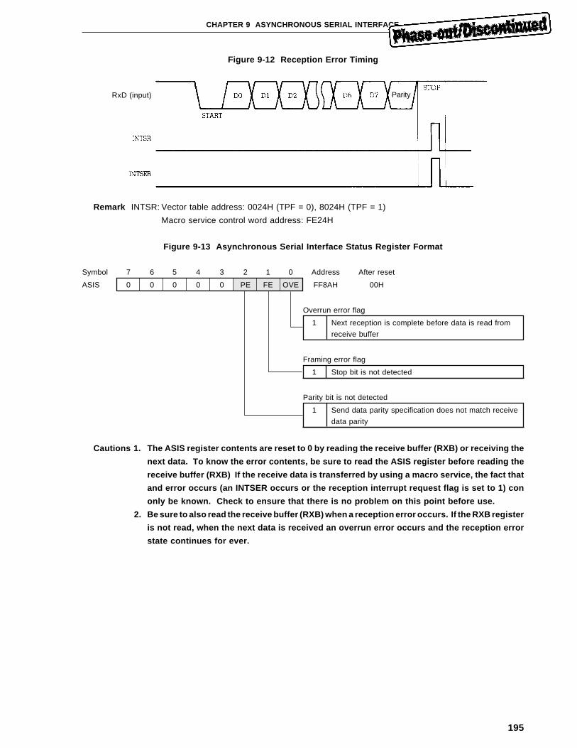
195
CHAPTER 9 ASYNCHRONOUS SERIAL INTERFACE
Figure 9-12 Reception Error Timing
Remark INTSR: Vector table address: 0024H (TPF = 0), 8024H (TPF = 1)
Macro service control word address: FE24H
Figure 9-13 Asynchronous Serial Interface Status Register Format
Symbol 7 6 5 4 3 2 1 0 Address After reset
ASIS 0 0 0 0 0 PE FE OVE FF8AH 00H
Overrun error flag
1 Next reception is complete before data is read from
receive buffer
Framing error flag
1 Stop bit is not detected
Parity bit is not detected
1 Send data parity specification does not match receive
data parity
Cautions 1. The ASIS register contents are reset to 0 by reading the receive buffer (RXB) or receiving the
next data. To know the error contents, be sure to read the ASIS register before reading the
receive buffer (RXB) If the receive data is transferred by using a macro service, the fact that
and error occurs (an INTSER occurs or the reception interrupt request flag is set to 1) con
only be known. Check to ensure that there is no problem on this point before use.
2. Be sure to also read the receive buffer (RXB) when a reception error occurs. If the RXB register
is not read, when the next data is received an overrun error occurs and the reception error
state continues for ever.
ParityRxD (input)

196
[MEMO]

197
CHAPTER 10 CLOCKED SERIAL INTERFACE
The µPD78334 has the two operation modes of the 3-wire serial I/O mode and serial bus interface (SBI) mode
as the clocked serial interface; thus it can cover various applications flexibly.
The clocked serial interface operates independently of the asynchronous serial interface.
198
CHAPTER 10 CLOCKED SERIAL INTERFACE
10.1 Clocked Serial Interface Configuration
The clocked serial interface is controlled by setting the clocked serial interface mode register (CSIM)
and serial bus interface control register (SBIC). Transfer data can be read/written into the SIO register.
(1) Clocked serial interface mode register (CSIM)
The clocked serial interface mode register (CSIM) is an 8-bit register used to specify clocked serial interface
operation.
The CSIM register can be read and written by executing 8-bit and bit manipulation instruction.
When RESET is input, the CSIM register is reset to 00H.
(2) Serial bus interface control register (SBIC)
The serial bus interface control register (SBIC) is an 8-bit register which consists of the serial bus state control
bits and the flags indicating the input data state from the serial bus. The SBIC register can be used only in
the SBI mode and cannot be handled in the 3-wire serial I/O mode.
The SBIC register is handled by executing 8-bit and bit manipulation instructions. Whether read/write is
enabled or disabled varies depending on the bit. If a write-only bit is read, 0 is read.
When RESET is input, the SBIC register is reset to 00H.
The ACKD, CMDD, and RELD detection flags are cleared when transmission or reception operation is disabled
(both CSIM register CTXE and CRXE bits are 0).
(3) Serial I/O shift register (SIO)
The shift register (SIO) is an 8-bit register used to convert serial data and parallel data into serial data. The
SIO register is used for both transmission and reception.
Data is shifted in (received) or out (transmitted) starting at the most significant bit (MSB) or least significant
bit (LSB).
Actual transmission or reception operation is controlled by writing and reading the SIO register.
The SIO register can be read and written by executing 8-bit manipulation instructions.
When RESET is input, the SIO register becomes undefined.
(4) SO latch
The SO latch holds the SO/SB0 pin output level. In the serial bus interface (SBI) mode, the SO latch can also
be controlled directly by the software.
(5) Serial clock selector
The serial clock selector selects the serial clock to be used.
(6) Serial clock control circuit
The serial clock control circuit controls serial clock supply to the shift register. It also controls clock output
to the SCK pin when internal clock is used.
(7) Serial clock counter
The serial clock counter counts serial clocks output or input during transmission or reception operation and
checks that 8-bit data has been transferred.

199
CHAPTER 10 CLOCKED SERIAL INTERFACE
(8) Interrupt signal generation control circuit
The interrupt signal generator controls whether or not an interrupt request is generated when the serial clock
counter counts eight serial clocks. In the 3-wire serial I/O mode, an interrupt request is generated whenever
eight serial clocks are counted. In the SBI mode, an interrupt request is generated when a given condition
becomes true.
(9) Busy/acknowledge output circuit and bus release/command/acknowledge detector
The busy/acknowledge output circuit and bus release/command/acknowledge detector output and detect
control signals in the SBI mode; they do not operate in the 3-wire serial I/O mode.
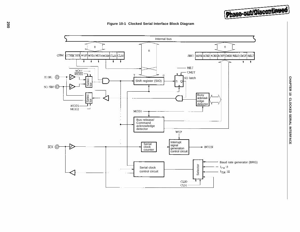
200
CH
AP
TE
R 10 C
LOC
KE
D S
ER
IAL IN
TE
RF
AC
E
Figure 10-1 Clocked Serial Interface Block Diagram
Internal bus
Shift register (SIO)latch
Busyacknowl-edgedetector
Sel
ecto
r
Bus release/Commandacknowledgedetector
Serialclockcounter
Interruptsignalgenerationcontrol circuit
Serial clockcontrol circuit
Sel
ec-
tor
Sel
ec-
tor
Baud rate generator (BRG)
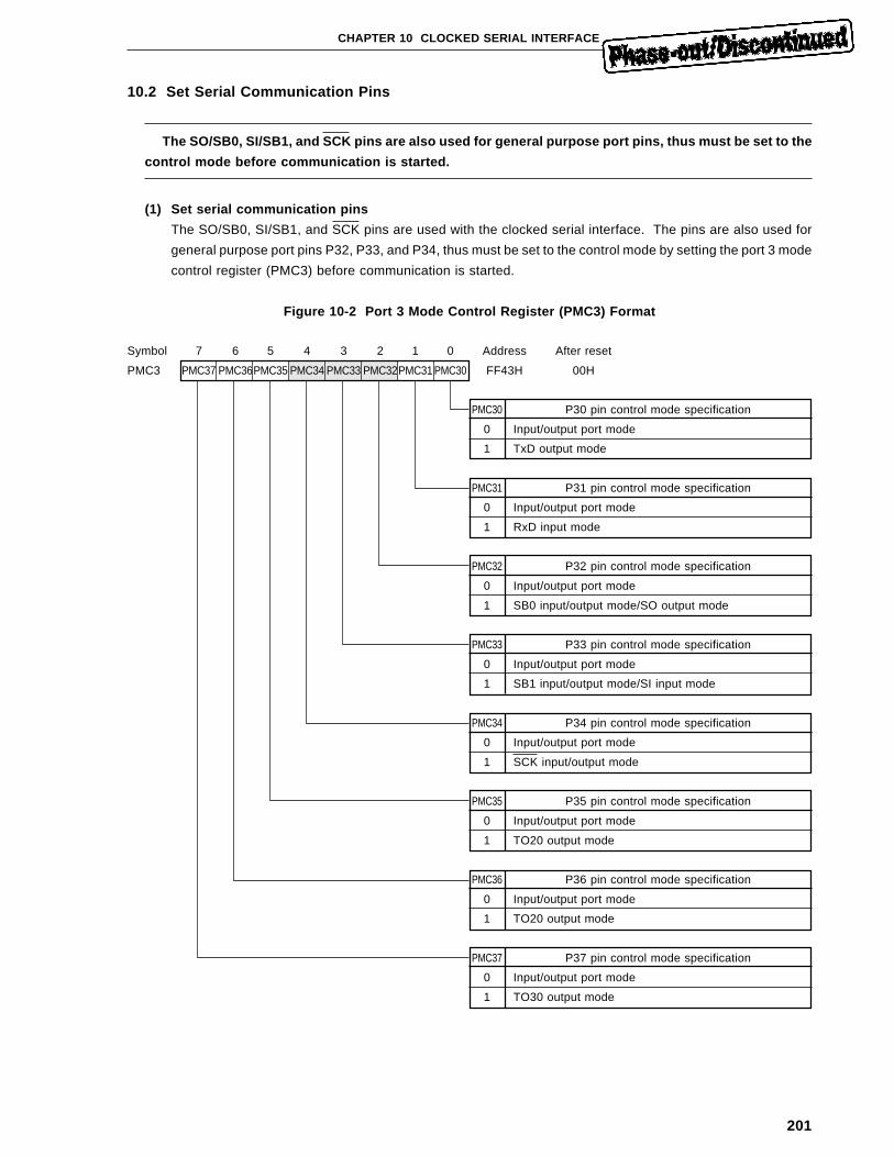
201
CHAPTER 10 CLOCKED SERIAL INTERFACE
10.2 Set Serial Communication Pins
The SO/SB0, SI/SB1, and SCK pins are also used for general purpose port pins, thus must be set to the
control mode before communication is started.
(1) Set serial communication pins
The SO/SB0, SI/SB1, and SCK pins are used with the clocked serial interface. The pins are also used for
general purpose port pins P32, P33, and P34, thus must be set to the control mode by setting the port 3 mode
control register (PMC3) before communication is started.
Figure 10-2 Port 3 Mode Control Register (PMC3) Format
Symbol 7 6 5 4 3 2 1 0 Address After reset
PMC3 PMC37 PMC36PMC35 PMC34 PMC33 PMC32PMC31 PMC30 FF43H 00H
PMC30 P30 pin control mode specification
0 Input/output port mode
1 TxD output mode
PMC31 P31 pin control mode specification
0 Input/output port mode
1 RxD input mode
PMC32 P32 pin control mode specification
0 Input/output port mode
1 SB0 input/output mode/SO output mode
PMC33 P33 pin control mode specification
0 Input/output port mode
1 SB1 input/output mode/SI input mode
PMC34 P34 pin control mode specification
0 Input/output port mode
1 SCK input/output mode
PMC35 P35 pin control mode specification
0 Input/output port mode
1 TO20 output mode
PMC36 P36 pin control mode specification
0 Input/output port mode
1 TO20 output mode
PMC37 P37 pin control mode specification
0 Input/output port mode
1 TO30 output mode
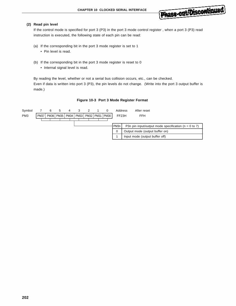
202
CHAPTER 10 CLOCKED SERIAL INTERFACE
(2) Read pin level
If the control mode is specified for port 3 (P3) in the port 3 mode control register , when a port 3 (P3) read
instruction is executed, the following state of each pin can be read:
(a) If the corresponding bit in the port 3 mode register is set to 1
• Pin level is read.
(b) If the corresponding bit in the port 3 mode register is reset to 0
• Internal signal level is read.
By reading the level, whether or not a serial bus collision occurs, etc., can be checked.
Even if data is written into port 3 (P3), the pin levels do not change. (Write into the port 3 output buffer is
made.)
Figure 10-3 Port 3 Mode Register Format
Symbol 7 6 5 4 3 2 1 0 Address After reset
PM3 PM37 PM36 PM35 PM34 PM33 PM32 PM31 PM30 FF23H FFH
PM3n P3n pin input/output mode specification (n = 0 to 7)
0 Output mode (output buffer on)
1 Input mode (output buffer off)

203
CHAPTER 10 CLOCKED SERIAL INTERFACE
10.3 Set Baud Rate
Baud rate generator output, internal clock f CLK/8 or f CLK/32, or external clock can be selected as serial
clock. If baud rate generator output is selected, communication can be executed at any desired baud rate,
independently of the operation frequency.
(1) Baud rate = serial clock
On the clocked serial interface, receive data is sampled on the serial clock rising edge. Thus, the serial clock
becomes the baud rate as it is.
(2) Select serial clock
Select serial clock by setting bits 1and 0 of the clocked serial interface mode register (CSIM).
If external clock is selected, the SCK pin becomes an input pin and serial clock is input from the device with
which the µPD78334 communicates.
If fCLK/8 is selected when internal system clock is 8 MHz, the baud rate becomes 1 Mbps; if fCLK/32 is selected,
250 Kbps.
Remark The baud rate generator is shared by the asynchronous serial interface. (See 9.4 Set Baud Rate )
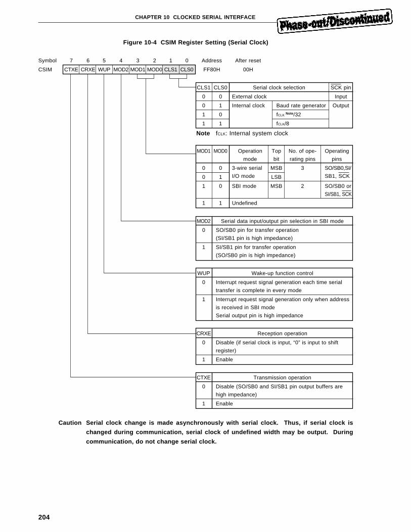
204
CHAPTER 10 CLOCKED SERIAL INTERFACE
Figure 10-4 CSIM Register Setting (Serial Clock)
Symbol 7 6 5 4 3 2 1 0 Address After reset
CSIM CTXE CRXE WUP MOD2 MOD1 MOD0 CLS1 CLS0 FF80H 00H
CLS1 CLS0 Serial clock selection SCK pin
0 0 External clock Input
0 1 Internal clock Baud rate generator Output
1 0 fCLK Note/32
1 1 fCLK/8
Note fCLK: Internal system clock
MOD1 MOD0 Operation Top No. of ope- Operating
mode bit rating pins pins
0 0 3-wire serial MSB 3 SO/SB0,SI/
0 1 I/O mode LSB SB1, SCK
1 0 SBI mode MSB 2 SO/SB0 or
SI/SB1, SCK
1 1 Undefined
MOD2 Serial data input/output pin selection in SBI mode
0 SO/SB0 pin for transfer operation
(SI/SB1 pin is high impedance)
1 SI/SB1 pin for transfer operation
(SO/SB0 pin is high impedance)
WUP Wake-up function control
0 Interrupt request signal generation each time serial
transfer is complete in every mode
1 Interrupt request signal generation only when address
is received in SBI mode
Serial output pin is high impedance
CRXE Reception operation
0 Disable (if serial clock is input, “0” is input to shift
register)
1 Enable
CTXE Transmission operation
0 Disable (SO/SB0 and SI/SB1 pin output buffers are
high impedance)
1 Enable
Caution Serial clock change is made asynchronously with serial clock. Thus, if serial clock is
changed during communication, serial clock of undefined width may be output. During
communication, do not change serial clock.
205
CHAPTER 10 CLOCKED SERIAL INTERFACE
10.3.1 Baud rate generator configuration
The baud rate generator is controlled by setting the baud rate generator mode register (BRGM) and 10-
bit baud rate generator compare register (BRG).
The baud rate generator is configured as shown in Figure 10-5.
(1) Baud rate generator mode register (BRGM)
The baud rate generator mode register (BRGM) is an 8-bit register for 10-bit timer count clock selection and
baud rate generator operation control.
The BRGM register can be read and written by executing 8-bit and 1-bit manipulation instructions.
When RESET is input, the BRGM register is set to 00H.
Figure 10-6 shows the BRGM register format.
(2) Selector
10-bit timer count clock is selected by setting the BRGM register.
(3) 10-bit timer (TMBRG)
The 10-bit timer (TMBRH) counts the count clock selected in the selector.
If 10-bit baud rate generator compare register (BRG) match signal is generated, when the next count clock
is received, the 10-bit timer is cleared to 0.
Count start and count stop are controlled by setting the BRGM register.
The 10-bit timer cannot be handled directly from the CPU.
(4) 10-bit baud rate generator compare register (BRG)
The 10-bit timer contents are always compared with the data written into the 10-bit compare register. When
they match, match signal is generated. The match signal causes the 10-bit timer to be cleared to 0.
The result of dividing the match signal by two is output from the baud rate generator.
The BRG register can be read/written by executing a 16-bit manipulation instruction.
When RESET is input, the BRG register is reset to 0000H.
206
CHAPTER 10 CLOCKED SERIAL INTERFACE
Figure 10-5 Baud Rate Generator Block Diagram
Baud rate generator
Internal bus
Selector
Match
Clear
Transfer baud rategenerator output
207
CHAPTER 10 CLOCKED SERIAL INTERFACE
10.3.2 Set any desired baud rate
Any desired shift clock is generated by setting the baud rate generator mode register (BRGM) and 10-
bit baud rate generator compare register (BRG).
(1) Baud rate = serial clock
On the clocked serial interface, receive data is sampled on the serial clock rising edge. Thus, the serial clock
becomes the baud rate as it is.
(2) Set any desired baud rate
Baud rate setting is found from the following expression. Set the BRG register value and 10-bit timer count
clock to get the required baud rate, and start baud rate generator operation
Baud rate calculation expression
Baud rate (bps) = fCLK/2n × 1/(m +1) × 1/2
fCLK: Internal system clock (external oscillation frequency fOSC/2)
m : Value set in BRG register (0 to 1023)
n : Value corresponding to the value set in BRGM register bits 0 and 1 (0, 1,or 2)
Figure 10-6 Baud Rate Generator Mode Register Format
Symbol 7 6 5 4 3 2 1 0 Address After reset
BRGM 0 0 0 0 BRGE 0 PRS1 PRS0 FFB1H 00H
PRS1 PRS0 Count clock
0 0 fCLK
0 1 fCLK/2
1 0 fCLK/4
1 1 Undefined
BRGE Baud rate generator operation
0 Stop
1 Start
208
CHAPTER 10 CLOCKED SERIAL INTERFACE
10.4 Two Clocked Synchronous Serial Interface Modes
The 3-wire serial I/O mode is useful for communication with devices which contain former clocked serial
interface.
The SBI mode is a communication mode unique to NEC which enables the µPD78334 to communication
with a number of devices on two signal lines.
The µPD78334 clocked serial interface contains the following two operation modes:
(1) 3-wire serial I/O mode
8-bit data is transferred by using the three signal lines of serial clock (SCK), serial input (SI), and Serial output
(SO). The 3-wire serial I/O mode is useful for connection of peripheral I/O display controller, etc., containing
the former clocked serial interface.
Connection of the µPD78334 to a number of devices requires handshaking lines.
Figure 10-7 System Configuration Example in 3-wire Serial I/O Mode
3-wire serial I/O ↔ 3-wire serial I/O
Master CPU Slave CPU
Handshaking lines
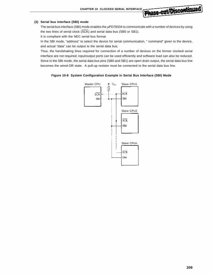
209
CHAPTER 10 CLOCKED SERIAL INTERFACE
(2) Serial bus interface (SBI) mode
The serial bus interface (SBI) mode enables the µPD78334 to communicate with a number of devices by using
the two lines of serial clock (SCK) and serial data bus (SB0 or SB1).
It is compliant with the NEC serial bus format.
In the SBI mode, “address” to select the device for serial communication, “ command” given to the device,
and actual “data” can be output to the serial data bus.
Thus, the handshaking lines required for connection of a number of devices on the former clocked serial
interface are not required; input/output ports can be used efficiently and software load can also be reduced.
Since in the SBI mode, the serial data bus pins (SB0 and SB1) are open drain output, the serial data bus line
becomes the wired-OR state. A pull-up resistor must be connected to the serial data bus line.
Figure 10-8 System Configuration Example in Serial Bus Interface (SBI) Mode
Master CPU Slave CPU1
Slave CPUn
Slave CPU2
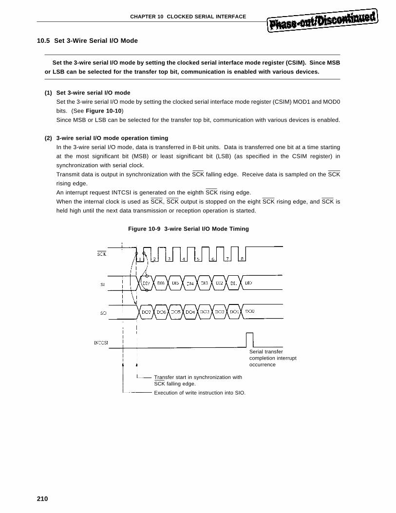
210
CHAPTER 10 CLOCKED SERIAL INTERFACE
10.5 Set 3-Wire Serial I/O Mode
Set the 3-wire serial I/O mode by setting the clocked serial interface mode register (CSIM). Since MSB
or LSB can be selected for the transfer top bit, communication is enabled with various devices.
(1) Set 3-wire serial I/O mode
Set the 3-wire serial I/O mode by setting the clocked serial interface mode register (CSIM) MOD1 and MOD0
bits. (See Figure 10-10 )
Since MSB or LSB can be selected for the transfer top bit, communication with various devices is enabled.
(2) 3-wire serial I/O mode operation timing
In the 3-wire serial I/O mode, data is transferred in 8-bit units. Data is transferred one bit at a time starting
at the most significant bit (MSB) or least significant bit (LSB) (as specified in the CSIM register) in
synchronization with serial clock.
Transmit data is output in synchronization with the SCK falling edge. Receive data is sampled on the SCK
rising edge.
An interrupt request INTCSI is generated on the eighth SCK rising edge.
When the internal clock is used as SCK, SCK output is stopped on the eight SCK rising edge, and SCK is
held high until the next data transmission or reception operation is started.
Figure 10-9 3-wire Serial I/O Mode Timing
Serial transfercompletion interruptoccurrence
Transfer start in synchronization withSCK falling edge.
Execution of write instruction into SIO.
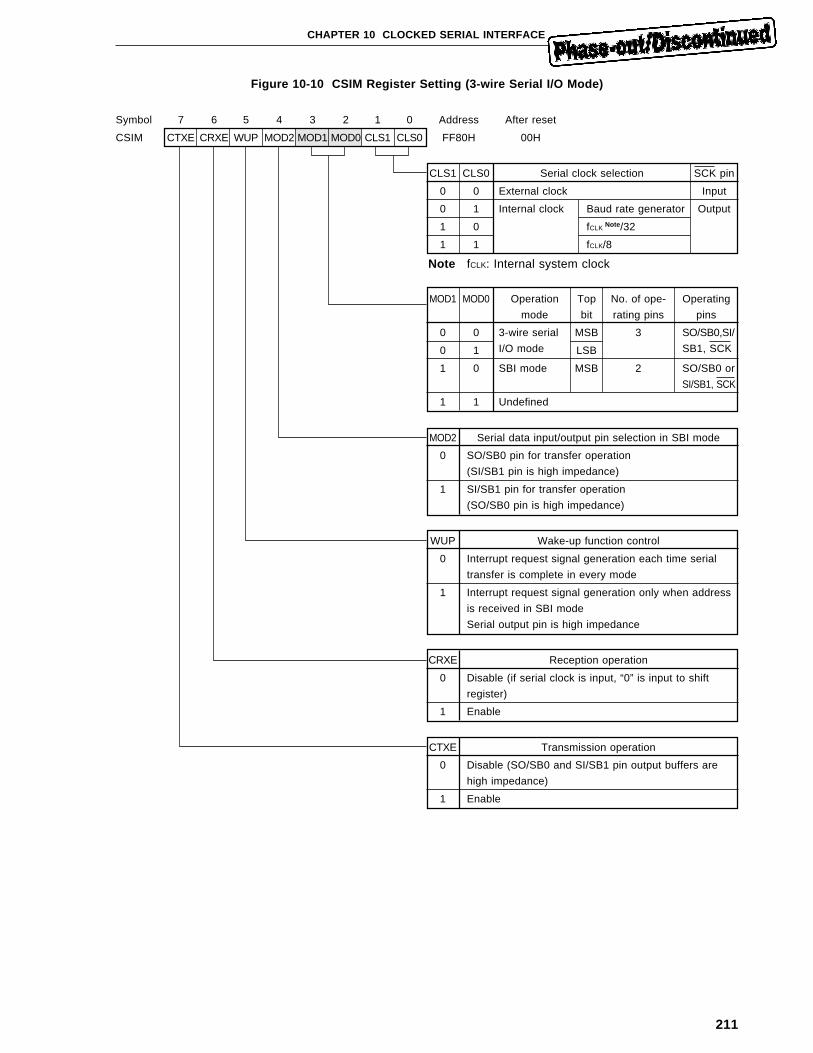
211
CHAPTER 10 CLOCKED SERIAL INTERFACE
Figure 10-10 CSIM Register Setting (3-wire Serial I/O Mode)
Symbol 7 6 5 4 3 2 1 0 Address After reset
CSIM CTXE CRXE WUP MOD2 MOD1 MOD0 CLS1 CLS0 FF80H 00H
CLS1 CLS0 Serial clock selection SCK pin
0 0 External clock Input
0 1 Internal clock Baud rate generator Output
1 0 fCLK Note/32
1 1 fCLK/8
Note fCLK: Internal system clock
MOD1 MOD0 Operation Top No. of ope- Operating
mode bit rating pins pins
0 0 3-wire serial MSB 3 SO/SB0,SI/
0 1 I/O mode LSB SB1, SCK
1 0 SBI mode MSB 2 SO/SB0 or
SI/SB1, SCK
1 1 Undefined
MOD2 Serial data input/output pin selection in SBI mode
0 SO/SB0 pin for transfer operation
(SI/SB1 pin is high impedance)
1 SI/SB1 pin for transfer operation
(SO/SB0 pin is high impedance)
WUP Wake-up function control
0 Interrupt request signal generation each time serial
transfer is complete in every mode
1 Interrupt request signal generation only when address
is received in SBI mode
Serial output pin is high impedance
CRXE Reception operation
0 Disable (if serial clock is input, “0” is input to shift
register)
1 Enable
CTXE Transmission operation
0 Disable (SO/SB0 and SI/SB1 pin output buffers are
high impedance)
1 Enable
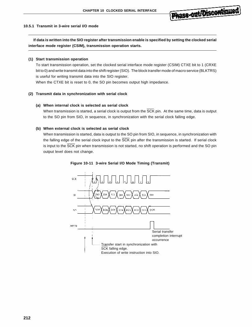
212
CHAPTER 10 CLOCKED SERIAL INTERFACE
10.5.1 Transmit in 3-wire serial I/O mode
If data is written into the SIO register after transmission enable is specified by setting the clocked serial
interface mode register (CSIM), transmission operation starts.
(1) Start transmission operation
To start transmission operation, set the clocked serial interface mode register (CSIM) CTXE bit to 1 (CRXE
bit to 0) and write transmit data into the shift register (SIO). The block transfer mode of macro service (BLKTRS)
is useful for writing transmit data into the SIO register.
When the CTXE bit is reset to 0, the SO pin becomes output high impedance.
(2) Transmit data in synchronization with serial clock
(a) When internal clock is selected as serial clock
When transmission is started, a serial clock is output from the SCK pin. At the same time, data is output
to the SO pin from SIO, in sequence, in synchronization with the serial clock falling edge.
(b) When external clock is selected as serial clock
When transmission is started, data is output to the SO pin from SIO, in sequence, in synchronization with
the falling edge of the serial clock input to the SCK pin after the transmission is started. If serial clock
is input to the SCK pin when transmission is not started, no shift operation is performed and the SO pin
output level does not change.
Figure 10-11 3-wire Serial I/O Mode Timing (Transmit)
Serial transfercompletion interruptoccurrence
Transfer start in synchronization withSCK falling edge.Execution of write instruction into SIO.

213
CHAPTER 10 CLOCKED SERIAL INTERFACE
Figure 10-12 CSIM Register Setting (Transmission Enable)
Symbol 7 6 5 4 3 2 1 0 Address After reset
CSIM CTXE CRXE WUP MOD2 MOD1 MOD0 CLS1 CLS0 FF80H 00H
CLS1 CLS0 Serial clock selection SCK pin
0 0 External clock Input
0 1 Internal clock Baud rate generator Output
1 0 fCLK Note/32
1 1 fCLK/8
Note fCLK: Internal system clock
MOD1 MOD0 Operation Top No. of ope- Operating
mode bit rating pins pins
0 0 3-wire serial MSB 3 SO/SB0,SI/
0 1 I/O mode LSB SB1, SCK
1 0 SBI mode MSB 2 SO/SB0 or
SI/SB1, SCK
1 1 Undefined
MOD2 Serial data input/output pin selection in SBI mode
0 SO/SB0 pin for transfer operation
(SI/SB1 pin is high impedance)
1 SI/SB1 pin for transfer operation
(SO/SB0 pin is high impedance)
WUP Wake-up function control
0 Interrupt request signal generation each time serial
transfer is complete in every mode
1 Interrupt request signal generation only when address
is received in SBI mode
Serial output pin is high impedance
CRXE Reception operation
0 Disable (if serial clock is input, “0” is input to shift
register)
1 Enable
CTXE Transmission operation
0 Disable (SO/SB0 and SI/SB1 pin output buffers are
high impedance)
1 Enable
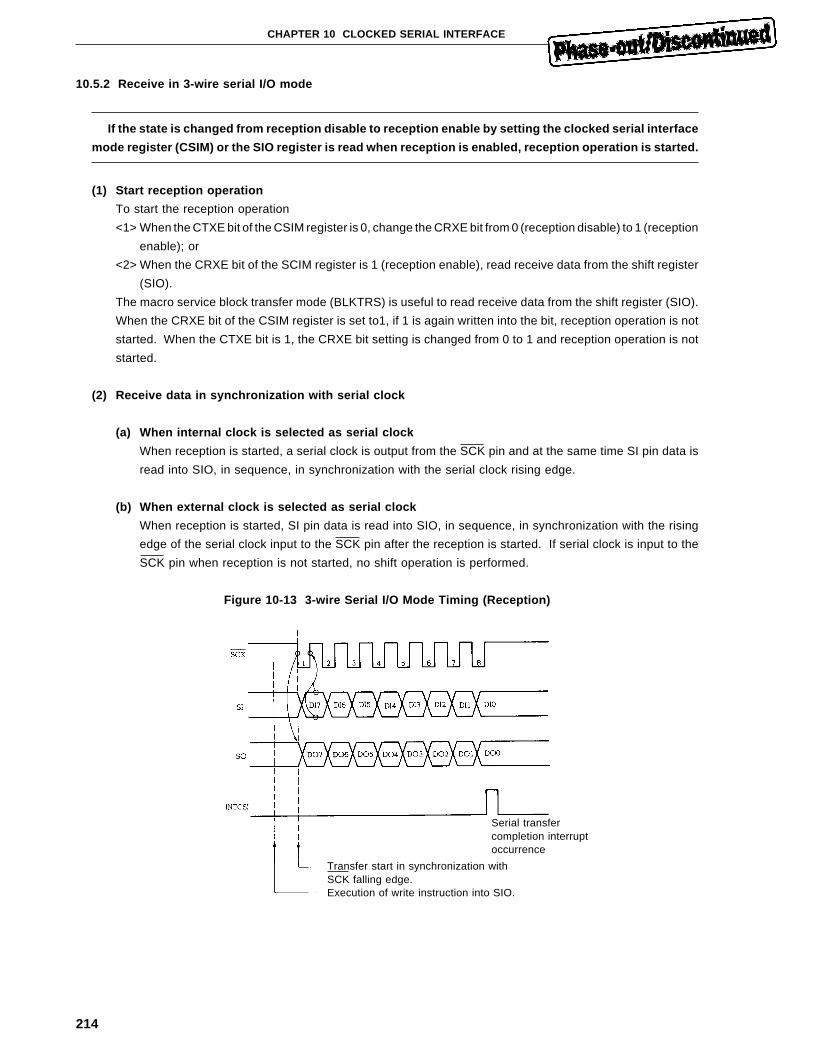
214
CHAPTER 10 CLOCKED SERIAL INTERFACE
10.5.2 Receive in 3-wire serial I/O mode
If the state is changed from reception disable to reception enable by setting the clocked serial interface
mode register (CSIM) or the SIO register is read when reception is enabled, reception operation is started.
(1) Start reception operation
To start the reception operation
<1> When the CTXE bit of the CSIM register is 0, change the CRXE bit from 0 (reception disable) to 1 (reception
enable); or
<2> When the CRXE bit of the SCIM register is 1 (reception enable), read receive data from the shift register
(SIO).
The macro service block transfer mode (BLKTRS) is useful to read receive data from the shift register (SIO).
When the CRXE bit of the CSIM register is set to1, if 1 is again written into the bit, reception operation is not
started. When the CTXE bit is 1, the CRXE bit setting is changed from 0 to 1 and reception operation is not
started.
(2) Receive data in synchronization with serial clock
(a) When internal clock is selected as serial clock
When reception is started, a serial clock is output from the SCK pin and at the same time SI pin data is
read into SIO, in sequence, in synchronization with the serial clock rising edge.
(b) When external clock is selected as serial clock
When reception is started, SI pin data is read into SIO, in sequence, in synchronization with the rising
edge of the serial clock input to the SCK pin after the reception is started. If serial clock is input to the
SCK pin when reception is not started, no shift operation is performed.
Figure 10-13 3-wire Serial I/O Mode Timing (Reception)
Serial transfercompletion interruptoccurrence
Transfer start in synchronization withSCK falling edge.Execution of write instruction into SIO.
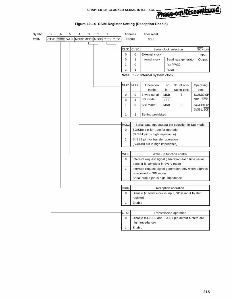
215
CHAPTER 10 CLOCKED SERIAL INTERFACE
Figure 10-14 CSIM Register Setting (Reception Enable)
Symbol 7 6 5 4 3 2 1 0 Address After reset
CSIM CTXE CRXE WUP MOD2 MOD1 MOD0 CLS1 CLS0 FF80H 00H
CLS1 CLS0 Serial clock selection SCK pin
0 0 External clock Input
0 1 Internal clock Baud rate generator Output
1 0 fCLK Note/32
1 1 fCLK/8
Note fCLK: Internal system clock
MOD1 MOD0 Operation Top No. of ope- Operating
mode bit rating pins pins
0 0 3-wire serial MSB 3 SO/SB0,SI/
0 1 I/O mode LSB SB1, SCK
1 0 SBI mode MSB 2 SO/SB0 or
SI/SB1, SCK
1 1 Setting prohibited
MOD2 Serial data input/output pin selection in SBI mode
0 SO/SB0 pin for transfer operation
(SI/SB1 pin is high impedance)
1 SI/SB1 pin for transfer operation
(SO/SB0 pin is high impedance)
WUP Wake-up function control
0 Interrupt request signal generation each time serial
transfer is complete in every mode
1 Interrupt request signal generation only when address
is received in SBI mode
Serial output pin is high impedance
CRXE Reception operation
0 Disable (if serial clock is input, “0” is input to shift
register)
1 Enable
CTXE Transmission operation
0 Disable (SO/SB0 and SI/SB1 pin output buffers are
high impedance)
1 Enable
216
CHAPTER 10 CLOCKED SERIAL INTERFACE
10.5.3 Transfer in 3-wire Serial I/O Mode
If both transmission and reception are enabled by setting the clocked serial interface mode register
(CSIM), transmission operation and reception operation can be performed at the same time.
(1) Start transfer operation
When both the clocked serial interface mode register (CSIM) CTXE and CRXE bits are set to 1, transmission
operation and reception operation can be performed at the same time (transfer operation).
The transfer operation is started by writing transmit data into the shift register (SIO) when both the CTXE and
CRXE bits of the CSIM register are 1 (transfer enable).
When the CSIM register CRXE bit is “1”, if “1” is again written into the bit, transfer operation is not started.
(2) Transfer data in synchronization with serial clock
(a) When internal clock is selected as serial clock
When transfer is started, a serial clock is output from the SCK pin and at the same time data is output
to the SO pin from SIO, in sequence, in synchronization with the serial clock falling edge. SI pin data is
read into SIO in sequence in synchronization with the serial clock rising edge.
(b) When external clock is selected as serial clock
When transfer is started, data is output to the SO pin from SIO, in sequence, in synchronization with the
falling edge of the serial clock input to the SCK pin after the transfer is started, and SI pin data is read
into SIO, in sequence, in synchronization with the serial clock rising edge. If serial clock is input to the
SCK pin when transfer is not started, no shift operation is performed and the SO pin output level does
not change.
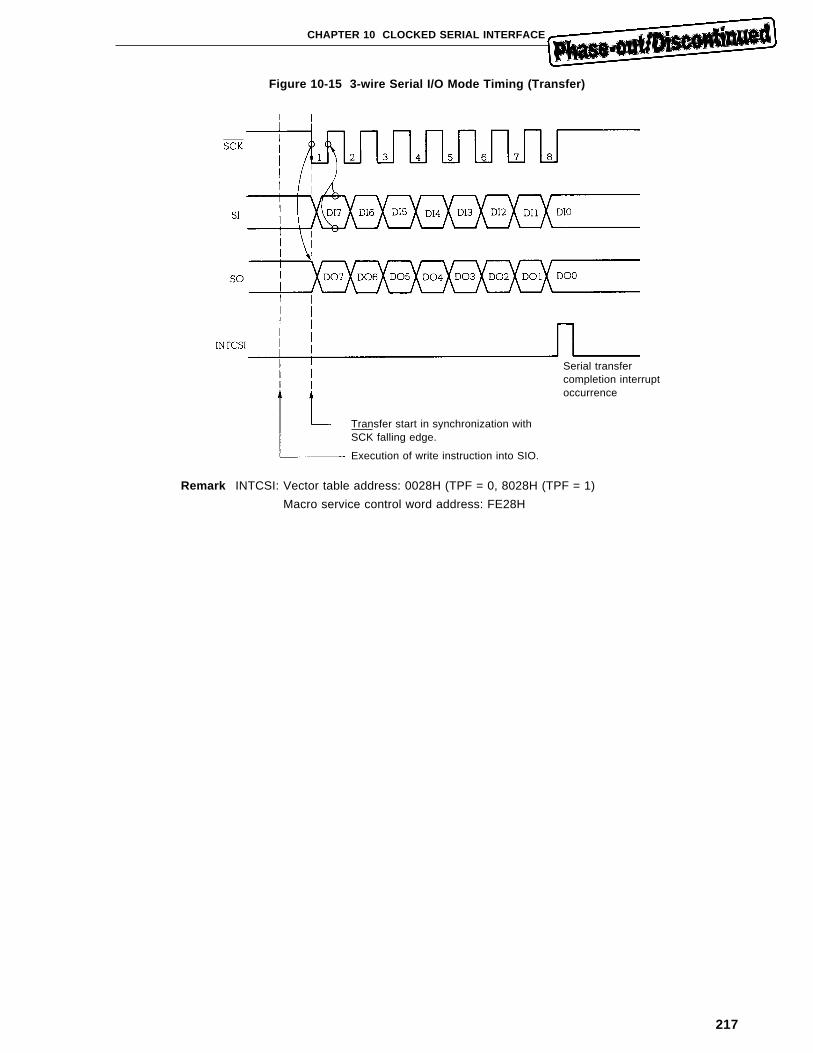
217
CHAPTER 10 CLOCKED SERIAL INTERFACE
Figure 10-15 3-wire Serial I/O Mode Timing (Transfer)
Remark INTCSI: Vector table address: 0028H (TPF = 0, 8028H (TPF = 1)
Macro service control word address: FE28H
Serial transfercompletion interruptoccurrence
Transfer start in synchronization withSCK falling edge.
Execution of write instruction into SIO.
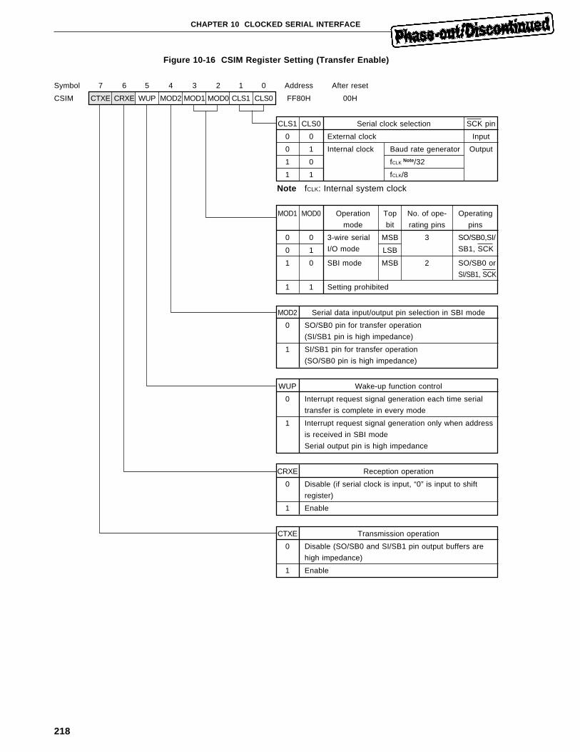
218
CHAPTER 10 CLOCKED SERIAL INTERFACE
Figure 10-16 CSIM Register Setting (Transfer Enable)
Symbol 7 6 5 4 3 2 1 0 Address After reset
CSIM CTXE CRXE WUP MOD2 MOD1 MOD0 CLS1 CLS0 FF80H 00H
CLS1 CLS0 Serial clock selection SCK pin
0 0 External clock Input
0 1 Internal clock Baud rate generator Output
1 0 fCLK Note/32
1 1 fCLK/8
Note fCLK: Internal system clock
MOD1 MOD0 Operation Top No. of ope- Operating
mode bit rating pins pins
0 0 3-wire serial MSB 3 SO/SB0,SI/
0 1 I/O mode LSB SB1, SCK
1 0 SBI mode MSB 2 SO/SB0 or
SI/SB1, SCK
1 1 Setting prohibited
MOD2 Serial data input/output pin selection in SBI mode
0 SO/SB0 pin for transfer operation
(SI/SB1 pin is high impedance)
1 SI/SB1 pin for transfer operation
(SO/SB0 pin is high impedance)
WUP Wake-up function control
0 Interrupt request signal generation each time serial
transfer is complete in every mode
1 Interrupt request signal generation only when address
is received in SBI mode
Serial output pin is high impedance
CRXE Reception operation
0 Disable (if serial clock is input, “0” is input to shift
register)
1 Enable
CTXE Transmission operation
0 Disable (SO/SB0 and SI/SB1 pin output buffers are
high impedance)
1 Enable
219
CHAPTER 10 CLOCKED SERIAL INTERFACE
10.5.4 Steps taken when serial clocks and shift operation are placed out of synchronization
When serial clocks and shift operation are placed out of synchronization, synchronization can be
recovered by disabling both transmission and reception
• Steps taken when serial clocks and shift operation are placed out of synchronization.
When external clock is selected as serial clock, the number of serial clocks and shift operation may be placed
out of synchronization due to noise, etc. In such a case, reset both the CTXE and CRXE bits to 0 to disable
both transmission operation and reception operation. Since the serial clock counter is initialized, synchronization
between shift operation and serial clocks can be recovered by using the first serial clock input after transmission
or reception is enabled as the first clock.
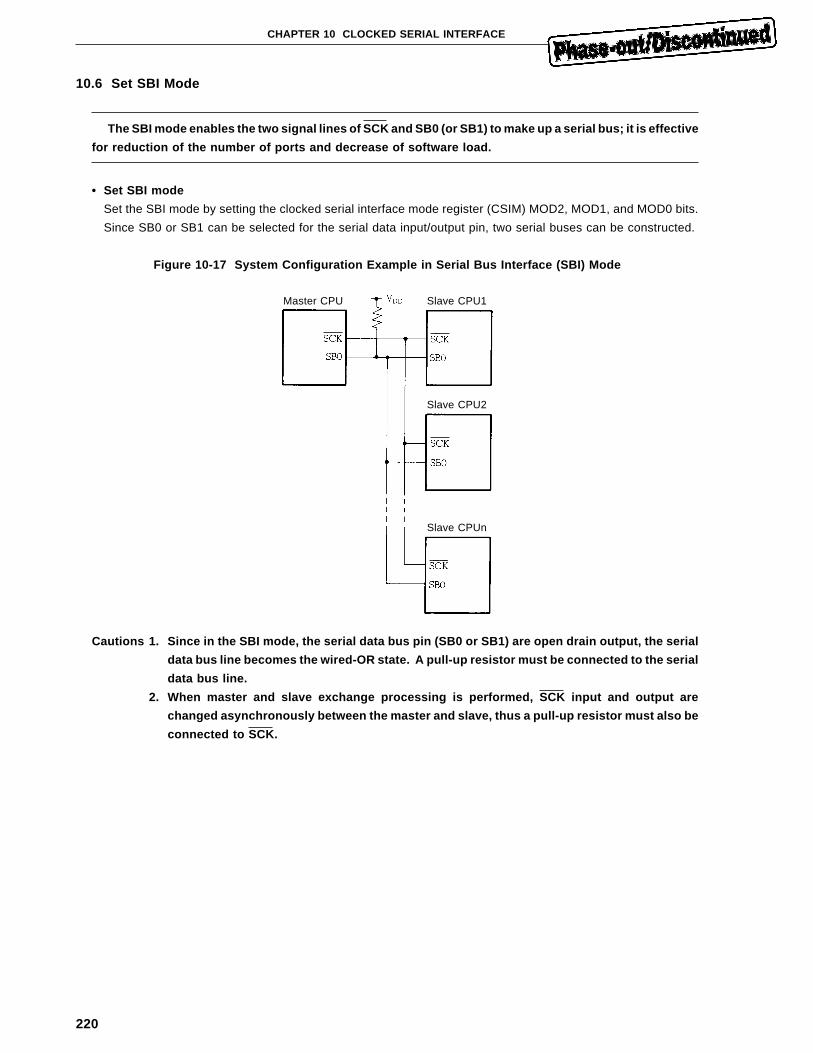
220
CHAPTER 10 CLOCKED SERIAL INTERFACE
10.6 Set SBI Mode
The SBI mode enables the two signal lines of SCK and SB0 (or SB1) to make up a serial bus; it is effective
for reduction of the number of ports and decrease of software load.
• Set SBI mode
Set the SBI mode by setting the clocked serial interface mode register (CSIM) MOD2, MOD1, and MOD0 bits.
Since SB0 or SB1 can be selected for the serial data input/output pin, two serial buses can be constructed.
Figure 10-17 System Configuration Example in Serial Bus Interface (SBI) Mode
Cautions 1. Since in the SBI mode, the serial data bus pin (SB0 or SB1) are open drain output, the serial
data bus line becomes the wired-OR state. A pull-up resistor must be connected to the serial
data bus line.
2. When master and slave exchange processing is performed, SCK input and output are
changed asynchronously between the master and slave, thus a pull-up resistor must also be
connected to SCK.
Master CPU Slave CPU1
Slave CPU2
Slave CPUn
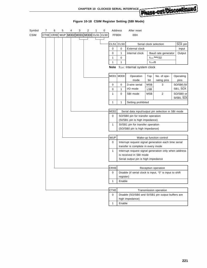
221
CHAPTER 10 CLOCKED SERIAL INTERFACE
Figure 10-18 CSIM Register Setting (SBI Mode)
Symbol 7 6 5 4 3 2 1 0 Address After reset
CSIM CTXE CRXE WUP MOD2 MOD1 MOD0 CLS1 CLS0 FF80H 00H
CLS1 CLS0 Serial clock selection SCK pin
0 0 External clock Input
0 1 Internal clock Baud rate generator Output
1 0 fCLK Note/32
1 1 fCLK/8
Note fCLK: Internal system clock
MOD1 MOD0 Operation Top No. of ope- Operating
mode bit rating pins pins
0 0 3-wire serial MSB 3 SO/SB0,SI/
0 1 I/O mode LSB SB1, SCK
1 0 SBI mode MSB 2 SO/SB0 or
SI/SB1, SCK
1 1 Setting prohibited
MOD2 Serial data input/output pin selection in SBI mode
0 SO/SB0 pin for transfer operation
(SI/SB1 pin is high impedance)
1 SI/SB1 pin for transfer operation
(SO/SB0 pin is high impedance)
WUP Wake-up function control
0 Interrupt request signal generation each time serial
transfer is complete in every mode
1 Interrupt request signal generation only when address
is received in SBI mode
Serial output pin is high impedance
CRXE Reception operation
0 Disable (if serial clock is input, “0” is input to shift
register)
1 Enable
CTXE Transmission operation
0 Disable (SO/SB0 and SI/SB1 pin output buffers are
high impedance)
1 Enable
222
CHAPTER 10 CLOCKED SERIAL INTERFACE
10.6.1 SBI data format
In the SBI mode, various control signals are defined by combining the two signal lines of serial clock
SCK and serial data bus SB0 (or SB1).
(1) Control signals used in SBI mode
In the SBI mode, the following eight types of control signals are defined by combining the two signal lines of
SCK and SB0 (or SBI):
<1> Bus release signal (REL)
The bus release signal indicates that the master is to transmit an address to slaves. It is output by the
master. Each slave contains hardware detecting the bus release signal.
<2> Command signal (CMD)
The bus release signal indicates that the master is to transmit an address or command to slaves. It is
output by the master. Each slave contains hardware detecting the command signal.
<3> Address
The address is 8-bit data following the bus release signal and command signal. It is output by the master
to select slave signal. Each slave compares the received address with its own address by software; if
they match, the slave performs the following communication.
<4> Command
The command is 8-bit data output following the command signal by the master without outputting the bus
release signal. How the command is used can be determined as desired.
<5> Data
The data is 8-bit data output by the master without the bus release signal or command signal.
<6> Acknowledge signal (ACK)
The acknowledge signal (ACK) is used to acknowledge data reception between the transmitting and
receiving parities. The master contains hardware detecting the acknowledge signal. When no acknowledge
signal is returned, it can be decided that normal reception is not performed.
<7> Busy signal (BUSY)
The busy signal (BUSY) indicates that a given slave is preparing for data transfer. While the slave outputs
the busy signal, the master continues to output serial clock and cannot start the next transfer.
<8> Ready signal (READY)
The ready signal (READY) is used to inform the master that a given slave is ready to transfer data.
(2) 1-data frame format in SBI mode
Serial data in the SBI mode makes up one data frame in the following format:
(REL) + (CMD) + 8-bit data + ACK + (BUSY)
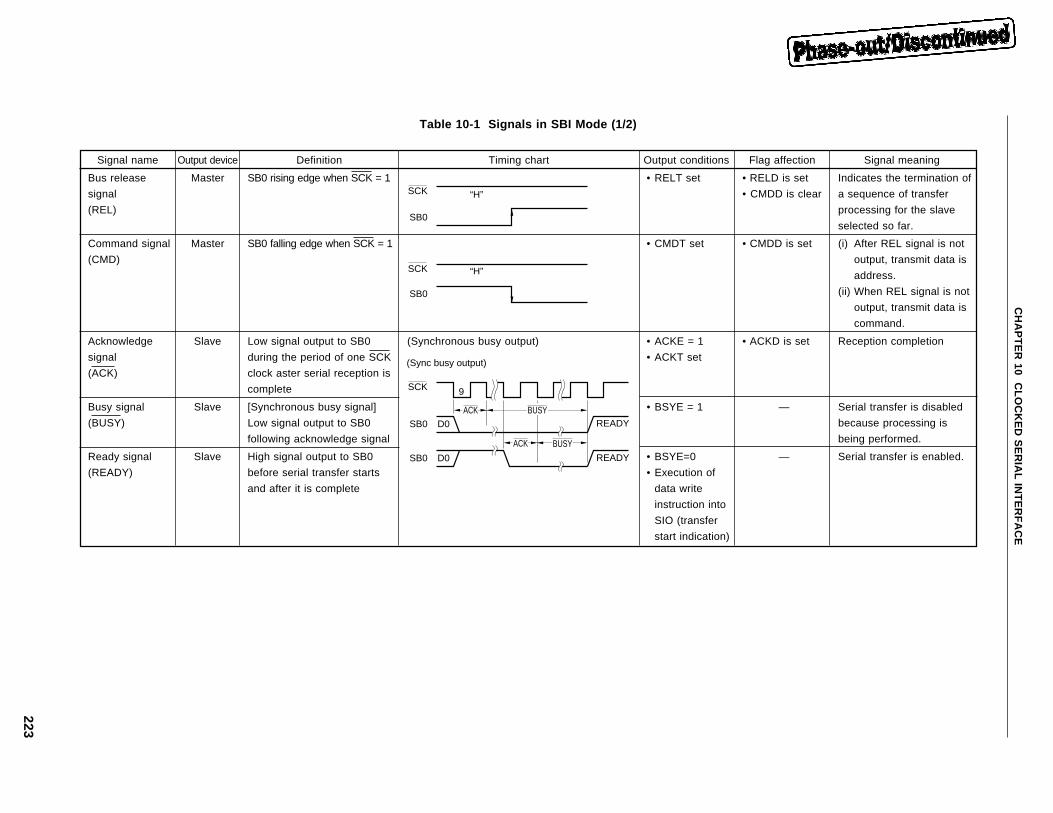
223
CH
AP
TE
R 10 C
LOC
KE
D S
ER
IAL IN
TE
RF
AC
E
SB0
“H”SCK
SB0
“H”SCK
SB0
SCK
SB0
D0
D0
(Sync busy output)
9
ACK BUSY
BUSYACK
READY
READY
Table 10-1 Signals in SBI Mode (1/2)
Signal name Output device Definition Timing chart Output conditions Flag affection Signal meaning
Bus release Master SB0 rising edge when SCK = 1 • RELT set • RELD is set Indicates the termination of
signal • CMDD is clear a sequence of transfer
(REL) processing for the slave
selected so far.
Command signal Master SB0 falling edge when SCK = 1 • CMDT set • CMDD is set (i) After REL signal is not
(CMD) output, transmit data is
address.
(ii) When REL signal is not
output, transmit data is
command.
Acknowledge Slave Low signal output to SB0 (Synchronous busy output) • ACKE = 1 • ACKD is set Reception completion
signal during the period of one SCK • ACKT set
(ACK) clock aster serial reception is
complete
Busy signal Slave [Synchronous busy signal] • BSYE = 1 — Serial transfer is disabled
(BUSY) Low signal output to SB0 because processing is
following acknowledge signal being performed.
Ready signal Slave High signal output to SB0 • BSYE=0 — Serial transfer is enabled.
(READY) before serial transfer starts • Execution of
and after it is complete data write
instruction into
SIO (transfer
start indication)
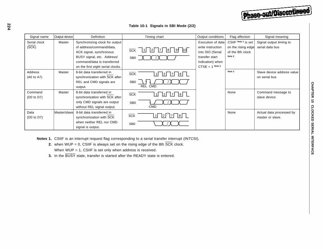
224
CH
AP
TE
R 10 C
LOC
KE
D S
ER
IAL IN
TE
RF
AC
E
SB0
SCK 1 2 7 8 9 10
SB0
SCK 1 2 7 8
REL CMD
SB0
SCK 1 2 7 8
CMD
SB0
SCK 1 2 7 8
Table 10-1 Signals in SBI Mode (2/2)
Signal name Output device Definition Timing chart Output conditions Flag affection Signal meaning
Serial clock Master Synchronizing clock for output Execution of data CSIIF Note 1 is set Signal output timing to
(SCK) of address/command/data, write instruction on the rising edge serial data bus
ACK signal, synchronous into SIO (Serial of the 8th clock
BUSY signal, etc. Address/ transfer start Note 2
command/data is transferred indication) when
on the first eight serial clocks. CTXE = 1 Note 3
Address Master 8-bit data transferred in Note 2 Slave device address value
(A0 to A7) synchronization with SCK after on serial bus
REL and CMD signals are
output.
Command Master 8-bit data transferred in None Command message to
(D0 to D7) synchronization with SCK after slave device
only CMD signals are output
without REL signal output.
Data Master/slave 8-bit data transferred in None Actual data processed by
(D0 to D7) synchronization with SCK master or slave.
when neither REL nor CMD
signal is output.
Notes 1. CSIIF is an interrupt request flag corresponding to a serial transfer interrupt (INTCSI).
2. when WUP = 0, CSIIF is always set on the rising edge of the 8th SCK clock.
When WUP = 1, CSIIF is set only when address is received.
3. In the BUSY state, transfer is started after the READY state is entered.
225
CHAPTER 10 CLOCKED SERIAL INTERFACE
10.6.2 Control and detect serial bus state
The serial bus state can be controlled and detected by setting the serial bus interface control register
(SBIC)
• Control and detect serial bus state
The SBI has the serial bus interface control register (SBIC) to control and detect serial bus state.
The SBIC register is an 8-bit register which consists of the serial bus state control bits and the flags indicating
the input data state from the serial bus.
The SBIC register is handled by executing 8-bit and bit manipulation instructions. However, some are read-
only bits and some are write-only bits. If a write-only bit is read, 0 is read.
When RESET is input, the SBIC register is reset to 00H.
Figure 10-19 shows the SBIC register format.
Figures 10-20 to 10-24 show bit operation.
Here, SB0 is used as the serial data input/output pin for explanation; if SB1 is selected, the same operation is
performed.
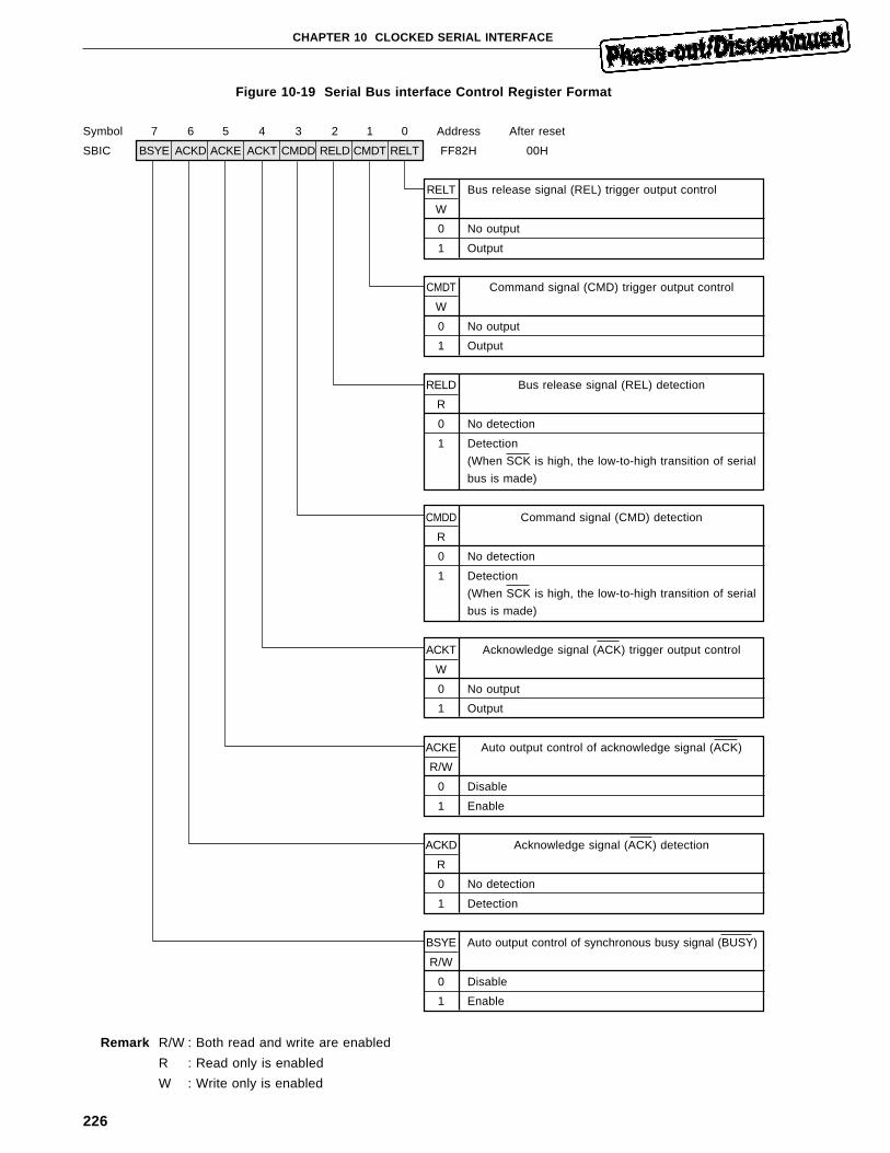
226
CHAPTER 10 CLOCKED SERIAL INTERFACE
Figure 10-19 Serial Bus interface Control Register Format
Symbol 7 6 5 4 3 2 1 0 Address After reset
SBIC BSYE ACKD ACKE ACKT CMDD RELD CMDT RELT FF82H 00H
RELT Bus release signal (REL) trigger output control
W
0 No output
1 Output
CMDT Command signal (CMD) trigger output control
W
0 No output
1 Output
RELD Bus release signal (REL) detection
R
0 No detection
1 Detection
(When SCK is high, the low-to-high transition of serial
bus is made)
CMDD Command signal (CMD) detection
R
0 No detection
1 Detection
(When SCK is high, the low-to-high transition of serial
bus is made)
ACKT Acknowledge signal (ACK) trigger output control
W
0 No output
1 Output
ACKE Auto output control of acknowledge signal (ACK)
R/W
0 Disable
1 Enable
ACKD Acknowledge signal (ACK) detection
R
0 No detection
1 Detection
BSYE Auto output control of synchronous busy signal (BUSY)
R/W
0 Disable
1 Enable
Remark R/W : Both read and write are enabled
R : Read only is enabled
W : Write only is enabled
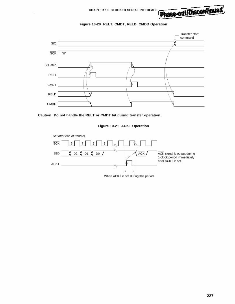
227
CHAPTER 10 CLOCKED SERIAL INTERFACE
Figure 10-20 RELT, CMDT, RELD, CMDD Operation
SIO
SCK “H”
SO latch
RELT
CMDT
RELD
CMDD
Transfer startcommand
Caution Do not handle the RELT or CMDT bit during transfer operation.
Figure 10-21 ACKT Operation
SB0
SCK
ACKT
6 7 8 9
D2 D1 D0 ACK
When ACKT is set during this period.
ACK signal is output during1-clock period immediatelyafter ACKT is set.
Set after end of transfer
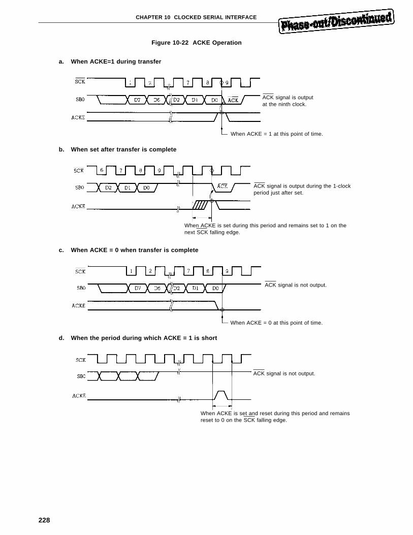
228
CHAPTER 10 CLOCKED SERIAL INTERFACE
Figure 10-22 ACKE Operation
a. When ACKE=1 during transfer
b. When set after transfer is complete
When ACKE is set during this period and remains set to 1 on thenext SCK falling edge.
c. When ACKE = 0 when transfer is complete
d. When the period during which ACKE = 1 is short
When ACKE is set and reset during this period and remainsreset to 0 on the SCK falling edge.
ACK signal is outputat the ninth clock.
When ACKE = 1 at this point of time.
ACK signal is output during the 1-clockperiod just after set.
ACK signal is not output.
When ACKE = 0 at this point of time.
ACK signal is not output.
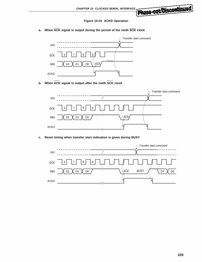
229
CHAPTER 10 CLOCKED SERIAL INTERFACE
Figure 10-23 ACKD Operation
a. When ACK signal is output during the period of the ninth SCK clock
SB0
SCK
ACKD
6
D2 D1 D0 ACK
Transfer start command
7 8 9
SIO
b. When ACK signal is output after the ninth SCK clock
SB0
SCK
ACKD
6
D2 D1 D0 ACK
Transfer start command
7 8 9
SIO
c. Reset timing when transfer start indication is given during BUSY
SB0
SCK
ACKD
6
D2 D1 D0 ACK
Transfer start command
7 8 9
SIO
BUSY D7 D6
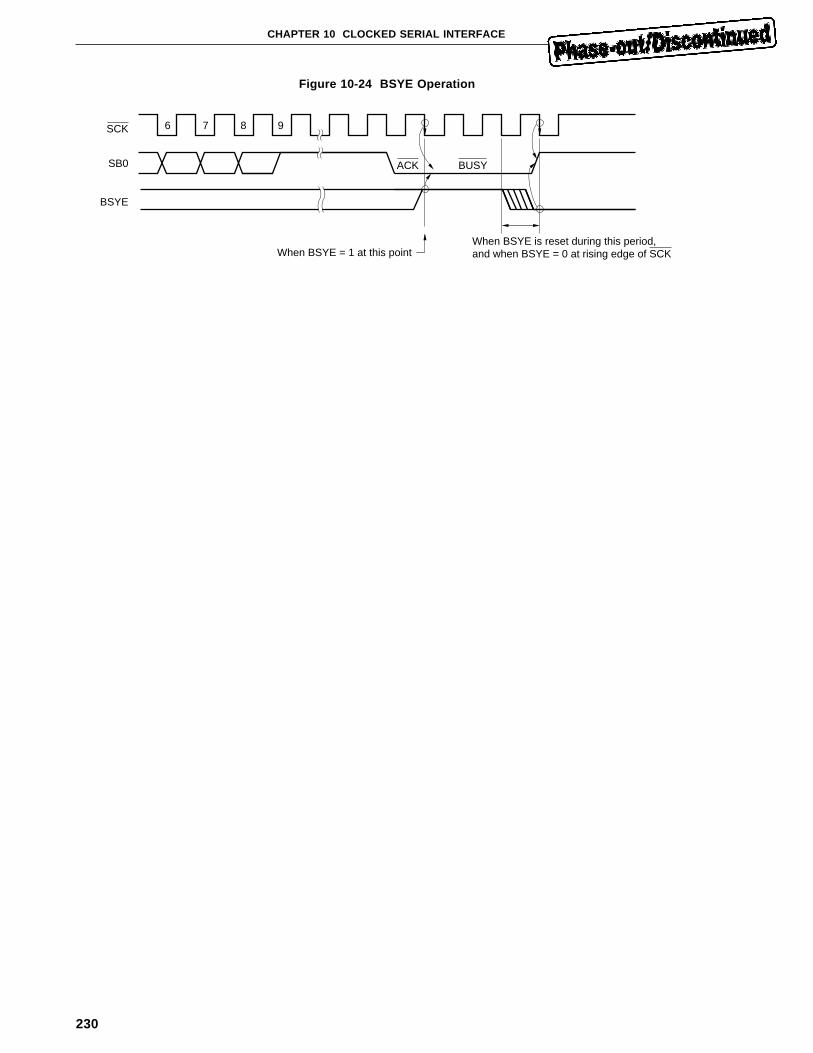
230
CHAPTER 10 CLOCKED SERIAL INTERFACE
Figure 10-24 BSYE Operation
SB0
SCK
BSYE
6
ACK
7 8 9
BUSY
When BSYE = 1 at this pointWhen BSYE is reset during this period,and when BSYE = 0 at rising edge of SCK
231
CHAPTER 10 CLOCKED SERIAL INTERFACE
10.6.3 Communication in SBI mode
After the serial bus is controlled by setting the serial bus interface control register (SBIC), transmit data
is written into the shift register (SIO) to execute transfer.
Here the SB0 pin is used for explanation; if the SBI pin is selected, the same operation is performed.
(1) Start transmission operation
To start transmission operation, set the clocked serial interface mode register (CSIM) CTXE bit to 1 and write
transmit data into the shift register (SIO).
SIO register shift is performed in synchronization with the serial clock (SCK) falling edge, and the data is output
starting at the MSB from the SB0 pin. After the transmission, 0 is written into the SIO register and interrupt
request INTCSI occurs.
(2) Start reception operation
To start reception operation
<1> When the CRXE bit of the CSIM register is 0, change the CRXE bit from 0 (reception disable) to 1 (reception
enable); or
<2> When the CRXE bit of the SCIM register is 1 (reception enable), read receive data from the shift register
(SIO).
When the CRXE bit of the CSIM register is 1, if 1 is written into the bit again, reception is not started. When
the CTXE bit is 1, the CRXE bit setting is changed from 0 to 1 and reception is not started.
The data input to the SB0 pin on the rising edge of the serial clock (SCK) is latched in the SIO register with
the MSB as the top bit. When 8-bit data is latched in the SIO register, interrupt request INTCSI is generated.
(3) Start transfer operation
To start transfer operation, write transmit data into the SIO register when both CSIM register CTXE and CRXE
bits are set to 1.
The data on the serial bus is input to the SIO register as it is. Whether or not a bus collision occurs, etc.,
can be checked by comparing the transmit data written into the SIO register with the data input from the serial
bus.
Remark INTCSI: Vector table address: 0028H (TPF=0), 8028H (TPF=1)
Macro service control word address: FE28H
Caution In the SBI mode, be sure to make pin specification and serial clock specification before
setting the CTXE and CRXE bits.
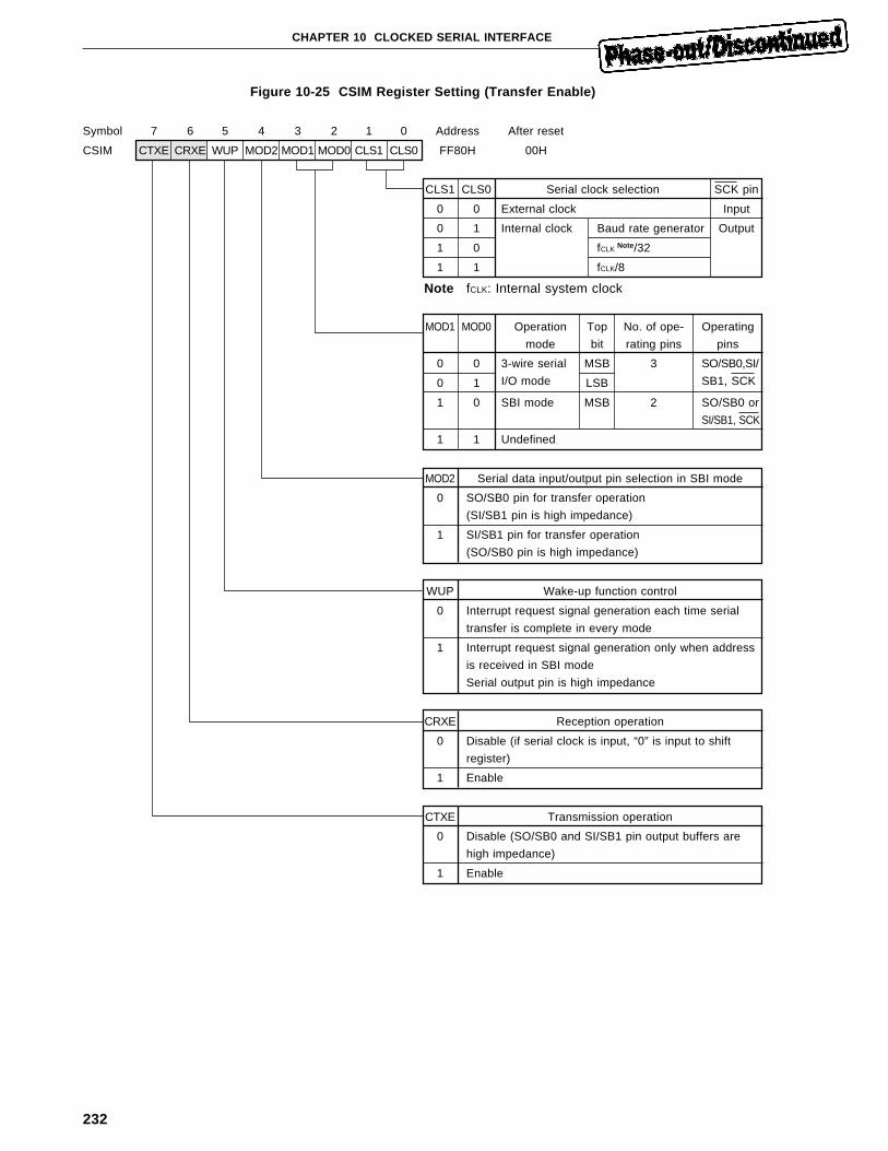
232
CHAPTER 10 CLOCKED SERIAL INTERFACE
Figure 10-25 CSIM Register Setting (Transfer Enable)
Symbol 7 6 5 4 3 2 1 0 Address After reset
CSIM CTXE CRXE WUP MOD2 MOD1 MOD0 CLS1 CLS0 FF80H 00H
CLS1 CLS0 Serial clock selection SCK pin
0 0 External clock Input
0 1 Internal clock Baud rate generator Output
1 0 fCLK Note/32
1 1 fCLK/8
Note fCLK: Internal system clock
MOD1 MOD0 Operation Top No. of ope- Operating
mode bit rating pins pins
0 0 3-wire serial MSB 3 SO/SB0,SI/
0 1 I/O mode LSB SB1, SCK
1 0 SBI mode MSB 2 SO/SB0 or
SI/SB1, SCK
1 1 Undefined
MOD2 Serial data input/output pin selection in SBI mode
0 SO/SB0 pin for transfer operation
(SI/SB1 pin is high impedance)
1 SI/SB1 pin for transfer operation
(SO/SB0 pin is high impedance)
WUP Wake-up function control
0 Interrupt request signal generation each time serial
transfer is complete in every mode
1 Interrupt request signal generation only when address
is received in SBI mode
Serial output pin is high impedance
CRXE Reception operation
0 Disable (if serial clock is input, “0” is input to shift
register)
1 Enable
CTXE Transmission operation
0 Disable (SO/SB0 and SI/SB1 pin output buffers are
high impedance)
1 Enable
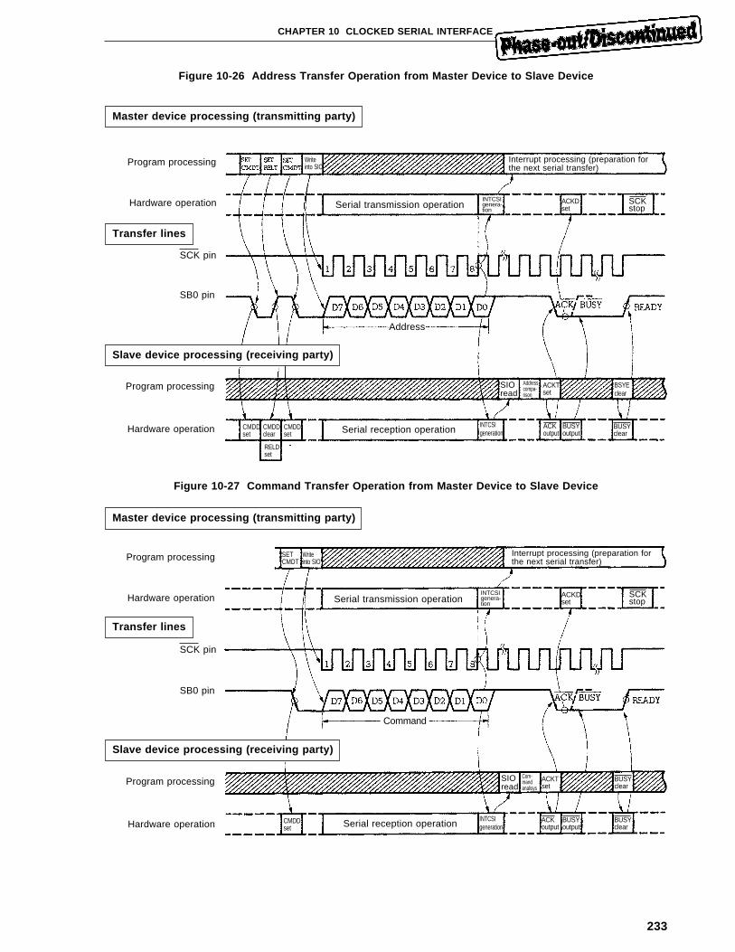
233
CHAPTER 10 CLOCKED SERIAL INTERFACE
Figure 10-26 Address Transfer Operation from Master Device to Slave Device
Figure 10-27 Command Transfer Operation from Master Device to Slave Device
Master device processing (transmitting party)
Transfer lines
Program processing Writeinto SIO
Interrupt processing (preparation forthe next serial transfer)
Hardware operation Serial transmission operationINTCSIgenera-tion
ACKDset
SCKstop
Slave device processing (receiving party)
SCK pin
SB0 pin
Address
Program processing SIOread
ACKTset
Addresscompa-rison
BSYEclear
Hardware operation CMDDset
Com-mandanalisys
Serial reception operationCMDDclear
CMDDset
RELDset
INTCSIgeneration
ACKoutput
BUSYoutput
BUSYclear
Master device processing (transmitting party)
Transfer lines
Program processing Writeinto SIO
Interrupt processing (preparation forthe next serial transfer)
Hardware operation Serial transmission operationINTCSIgenera-tion
ACKDset
SCKstop
Slave device processing (receiving party)
SCK pin
SB0 pin
Program processing SIOread
ACKTset
Hardware operation Serial reception operationCMDDset
INTCSIgeneration
ACKoutput
BUSYoutput
BUSYclear
SETCMDT
BUSYclear
Command
234
CHAPTER 10 CLOCKED SERIAL INTERFACE
Figure 10-28 Data Transfer Operation from Master Device to Slave Device
Figure 10-29 Data Transfer Operation from Slave Device to Master Device
Master device processing (transmitting party)
Transfer lines
Program processing Writeinto SIO
Interrupt processing (preparation forthe next serial transfer)
Hardware operation Serial transmission operation INTCSIgenera-tion
ACKDset
SCKstop
Slave device processing (receiving party)
SCK pin
SB0 pin
Program processing SIOread
Hardware operation Serial reception operation
ACKEset
INTCSIgenera-tion
ACKoutput
BUSYoutput
BUSYreset
Data
BSYEset
Receive dataprocessing
Master device processing (receiving party)
Transfer lines
Program processing SIOread
Receivedataprocessing
Hardware operation Serial reception operationINTCSIgenera-tion
ACKTset
Serial receptionoperation
Slave device processing (transmitting party)
SCK pin
SB0 pin
Program processing
Hardware operation Serial transmitting operationINTCSIgenera-tion
ACKDset
BUSYoutput
BUSYreset
Data
SIOread
ACKoutput
Writeinto SIO
BUSYreset
Data receptionoperation is repeatedby READY signal
SCKstop
235
CHAPTER 10 CLOCKED SERIAL INTERFACE
10.6.4 Operate only when address is received
The wakeup function for operation only when an address is received enables improvement of slave CPU
throughput.
• Slave CPU throughput is improved by the wakeup function
The SBI mode provides the wakeup function which generates an interrupt request signal (INTCSI) only when
an address is received.
When the master CPU (µPD78334) transfers data and commands to and from one slave CPU in the serial
interface system configuration as shown in Figure 10-30, other slave CPUs can operate independently of the
serial communication. If the wakeup function is not provided, whenever data is received, an interrupt is
generated, thus all slave CPUs are affected each time serial communication is made. The wakeup function
enables efficient processing.
In the INTCSI interrupt service routine started when an address is received, the receive address is compared
with its own address, and if they match, the wakeup function is released and the following data is received. If
they do not match, the wakeup state continues.
Remark INTCSI … Vector table address: 0028H (TPF=0), 8028H (TPF=1)
Macro service control word address: FE28H
Figure 10-30 System Configuration Example in Serial Bus Interface (SBI) Mode
Master CPU
Slave CPU2
Slave CPUn
Slave CPU1
236
CHAPTER 10 CLOCKED SERIAL INTERFACE
Figure 10-31 CSIM Register Setting (Wakeup Function)
Symbol 7 6 5 4 3 2 1 0 Address After reset
CSIM CTXE CRXE WUP MOD2 MOD1 MOD0 CLS1 CLS0 FF80H 00H
CLS1 CLS0 Serial clock selection SCK pin
0 0 External clock Input
0 1 Internal clock Baud rate generator Output
1 0 fCLK Note/32
1 1 fCLK/8
Note fCLK: Internal system clock
MOD1 MOD0 Operation Top No. of ope- Operating
mode bit rating pins pins
0 0 3-wire serial MSB 3 SO/SB0,SI/
0 1 I/O mode LSB SB1, SCK
1 0 SBI mode MSB 2 SO/SB0 or
SI/SB1, SCK
1 1 Undefined
MOD2 Serial data input/output pin selection in SBI mode
0 SO/SB0 pin for transfer operation
(SI/SB1 pin is high impedance)
1 SI/SB1 pin for transfer operation
(SO/SB0 pin is high impedance)
WUP Wake-up function control
0 Interrupt request signal generation each time serial
transfer is complete in every mode
1 Interrupt request signal generation only when address
is received in SBI mode
Serial output pin is high impedance
CRXE Reception operation
0 Disable (if serial clock is input, “0” is input to shift
register)
1 Enable
CTXE Transmission operation
0 Disable (SO/SB0 and SI/SB1 pin output buffers are
high impedance)
1 Enable
237
CHAPTER 11 WATCHDOG TIMER
The watchdog timer provides the function for prevention of software upset and deadlock.
A check is made to ensure that a program or system by the fact that no watchdog timer interrupt occurs. For this
purpose, a watchdog timer clear (count start) instruction is entered in each module of the program.
If the watchdog timer clear instruction is not executed within the setup time and the watchdog timer overflows, a
watchdog timer interrupt (INTWDT) is generated and a low level is output to the WDTO pin to signal a program error.
The watchdog timer is also used to provide the oscillation stable time of the oscillator when the STOP mode is
released. (See 14.3.2 STOP mode )
Figure 11-1 shows the watchdog timer configuration.
Figure 11-1 Watchdog Timer Block Diagram
Sel
ecto
r
Watchdog timer(8 bits)
Overflow
Clear
(Reset)
Timer(5 bits)Clear Overflow
Oscillation stabletime control circuit
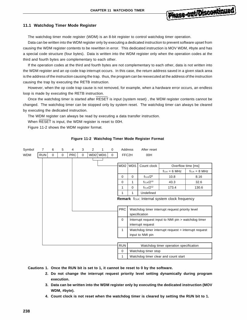
238
CHAPTER 11 WATCHDOG TIMER
11.1 Watchdog Timer Mode Register
The watchdog timer mode register (WDM) is an 8-bit register to control watchdog timer operation.
Data can be written into the WDM register only by executing a dedicated instruction to prevent software upset from
causing the WDM register contents to be rewritten in error. This dedicated instruction is MOV WDM, #byte and has
a special code structure (four bytes). Data is written into the WDM register only when the operation codes at the
third and fourth bytes are complementary to each other.
If the operation codes at the third and fourth bytes are not complementary to each other, data is not written into
the WDM register and an op code trap interrupt occurs. In this case, the return address saved in a given stack area
is the address of the instruction causing the trap. thus, the program can be reexecuted at the address of the instruction
causing the trap by executing the RETB instruction.
However, when the op code trap cause is not removed, for example, when a hardware error occurs, an endless
loop is made by executing the RETB instruction.
Once the watchdog timer is started after RESET is input (system reset) , the WDM register contents cannot be
changed. The watchdog timer can be stopped only by system reset. The watchdog timer can always be cleared
by executing the dedicated instruction.
The WDM register can always be read by executing a data transfer instruction.
When RESET is input, the WDM register is reset to 00H.
Figure 11-2 shows the WDM register format.
Figure 11-2 Watchdog Timer Mode Register Format
Symbol 7 6 5 4 3 2 1 0 Address After reset
WDM RUN 0 0 PRC 0 WDI2 WDI1 0 FFC2H 00H
WDI2 WDI1 Count clock Overflow time [ms]
fCLK = 6 MHz fCLK = 8 MHz
0 0 fCLK/28 10.8 8.16
0 1 fCLK/210 43.3 32.6
1 0 fCLK/212 173.4 130.6
1 1 Undefined
Remark fCLK: Internal system clock frequency
PRC Watchdog timer interrupt request priority level
specification
0 Interrupt request input to NMI pin > watchdog timer
interrupt request
1 Watchdog timer interrupt request > interrupt request
input to NMI pin
RUN Watchdog timer operation specification
0 Watchdog timer stop
1 Watchdog timer clear and count start
Cautions 1. Once the RUN bit is set to 1, it cannot be reset to 0 by the software.
2. Do not change the interrupt request priority level setting dynamically during program
execution.
3. Data can be written into the WDM register only by executing the dedicated instruction (MOV
WDM, #byte).
4. Count clock is not reset when the watchdog timer is cleared by setting the RUN bit to 1.
239
CHAPTER 11 WATCHDOG TIMER
11.2 Watchdog Timer Output Pin
The watchdog timer output pin (WDTO) can signal the external that a system error occurs without software. When
the watchdog timer overflows, watchdog timer output goes and remains low during the period of 32 system clocks.
If the system is reset, the watchdog timer output pin always outputs a low signal of 32-clock width by considering
direct connection to the RESET pin.
Caution Just after the power is turned on, the watchdog timer output pin may go and remain low for a
maximum of 32 clocks.
11.3 Application Example
Design a program without using the watchdog timer at the initial stage of program development. After general
debugging terminates, debug the program containing the watchdog timer.
If the response time from system effort occurrence is important, select the short overflow time mode.
When the watchdog timer output pin is not used as a watchdog timer, it can be used as a non-maskable timer base
interrupt.

240
[MEMO]
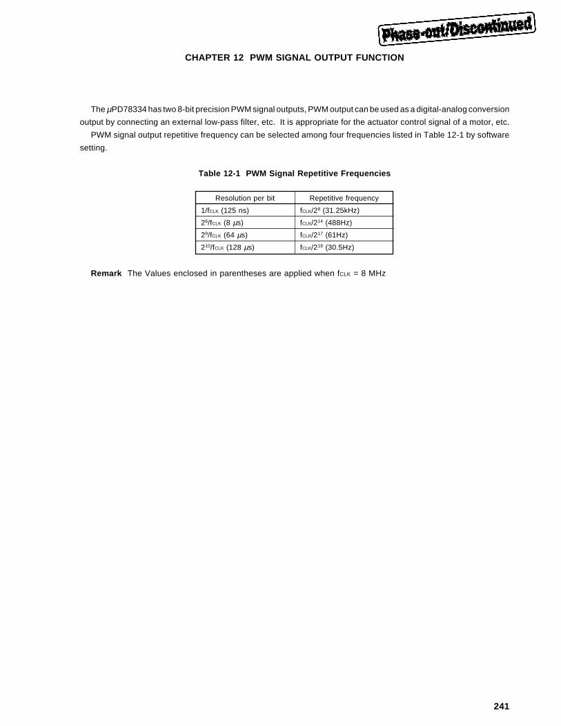
241
CHAPTER 12 PWM SIGNAL OUTPUT FUNCTION
The µPD78334 has two 8-bit precision PWM signal outputs, PWM output can be used as a digital-analog conversion
output by connecting an external low-pass filter, etc. It is appropriate for the actuator control signal of a motor, etc.
PWM signal output repetitive frequency can be selected among four frequencies listed in Table 12-1 by software
setting.
Table 12-1 PWM Signal Repetitive Frequencies
Resolution per bit Repetitive frequency
1/fCLK (125 ns) fCLK/28 (31.25kHz)
26/fCLK (8 µs) fCLK/214 (488Hz)
29/fCLK (64 µs) fCLK/217 (61Hz)
210/fCLK (128 µs) fCLK/218 (30.5Hz)
Remark The Values enclosed in parentheses are applied when fCLK = 8 MHz
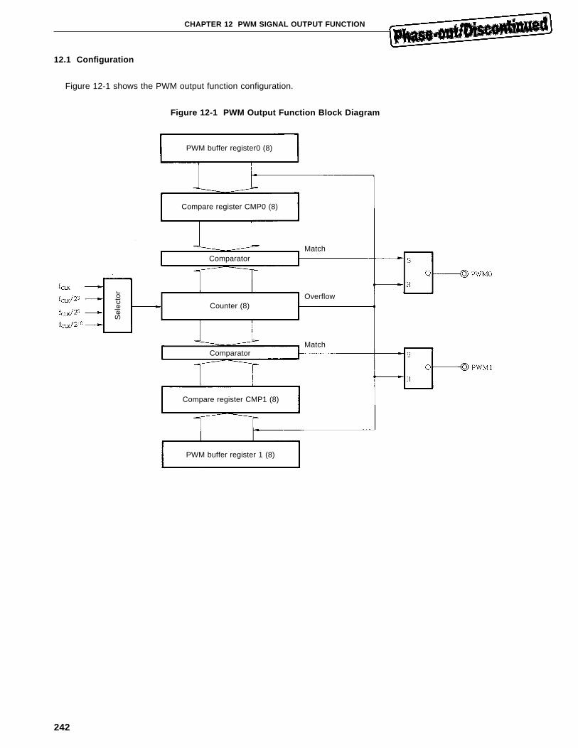
242
CHAPTER 12 PWM SIGNAL OUTPUT FUNCTION
12.1 Configuration
Figure 12-1 shows the PWM output function configuration.
Figure 12-1 PWM Output Function Block Diagram
PWM buffer register0 (8)
Compare register CMP0 (8)
MatchComparator
Counter (8)Overflow
Match
Sel
ecto
r
Comparator
Compare register CMP1 (8)
PWM buffer register 1 (8)
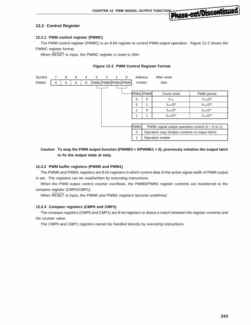
243
CHAPTER 12 PWM SIGNAL OUTPUT FUNCTION
12.2 Control Register
12.2.1 PWM control register (PWMC)
The PWM control register (PWMC) is an 8-bit register to control PWM output operation. Figure 12-2 shows the
PWMC register format.
When RESET is input, the PWMC register is reset to 00H.
Figure 12-2 PWM Control Register Format
Symbol 7 6 5 4 3 2 1 0 Address After reset
PWMC 0 0 0 0 PWME1 PWME0 PRM1 PRM0 FF64H 00H
PRM1 PRM0 Count clock PWM period
0 0 fCLK fCLK/28
0 1 fCLK/26 fCLK/214
1 0 fCLK/29 fCLK/217
1 1 fCLK/210 fCLK/218
PWMEn PWMn signal output operation control (n = 0 or 1)
0 Operation stop (Output contents of output latch)
1 Operation enable
Caution To stop the PWM output function (PWME0 = 0/PWME1 = 0), previously initialize the output latch
to fix the output state at stop.
12.2.2 PWM buffer registers (PWM0 and PWM1)
The PWM0 and PWM1 registers are 8-bit registers in which control data of the active signal width of PWM output
is set. The registers can be read/written by executing instructions.
When the PWM output control counter overflows, the PWM0/PWM1 register contents are transferred to the
compare register (CMP0/CMP1).
When RESET is input, the PWM0 and PWM1 registers become undefined.
12.2.3 Compare registers (CMP0 and CMP1)
The compare registers (CMP0 and CMP1) are 8-bit registers to detect a match between the register contents and
the counter value.
The CMP0 and CMP1 registers cannot be handled directly by executing instructions.
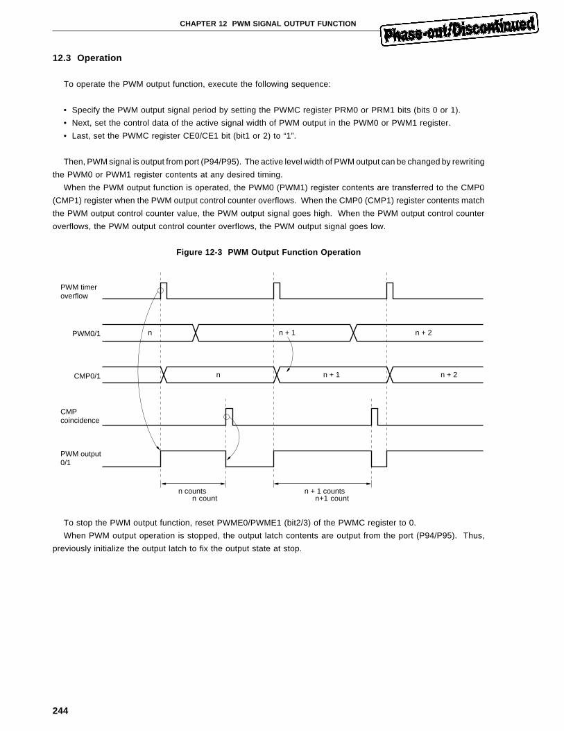
244
CHAPTER 12 PWM SIGNAL OUTPUT FUNCTION
12.3 Operation
To operate the PWM output function, execute the following sequence:
• Specify the PWM output signal period by setting the PWMC register PRM0 or PRM1 bits (bits 0 or 1).
• Next, set the control data of the active signal width of PWM output in the PWM0 or PWM1 register.
• Last, set the PWMC register CE0/CE1 bit (bit1 or 2) to “1”.
Then, PWM signal is output from port (P94/P95). The active level width of PWM output can be changed by rewriting
the PWM0 or PWM1 register contents at any desired timing.
When the PWM output function is operated, the PWM0 (PWM1) register contents are transferred to the CMP0
(CMP1) register when the PWM output control counter overflows. When the CMP0 (CMP1) register contents match
the PWM output control counter value, the PWM output signal goes high. When the PWM output control counter
overflows, the PWM output control counter overflows, the PWM output signal goes low.
Figure 12-3 PWM Output Function Operation
PWM timeroverflow
PWM0/1
CMP0/1
CMPcoincidence
PWM output0/1
n
n
n + 1
n + 1
n + 2
n + 2
n counts n + 1 countsn count n+1 count
To stop the PWM output function, reset PWME0/PWME1 (bit2/3) of the PWMC register to 0.
When PWM output operation is stopped, the output latch contents are output from the port (P94/P95). Thus,
previously initialize the output latch to fix the output state at stop.
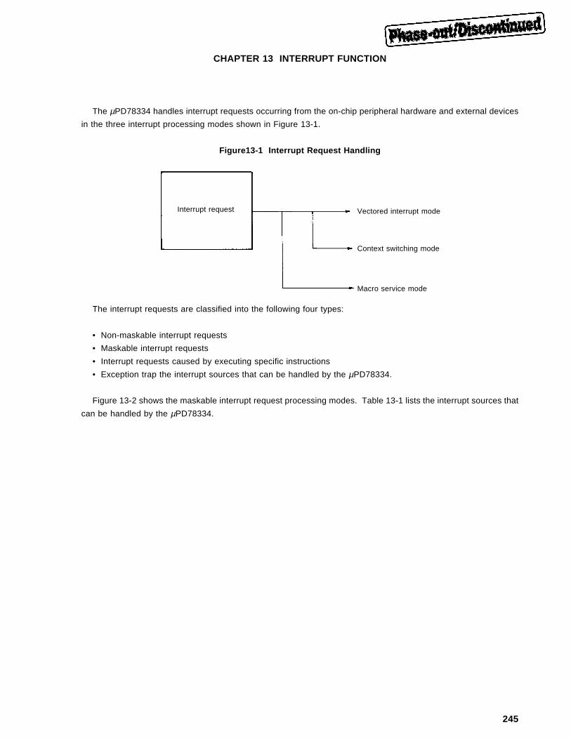
245
CHAPTER 13 INTERRUPT FUNCTION
The µPD78334 handles interrupt requests occurring from the on-chip peripheral hardware and external devices
in the three interrupt processing modes shown in Figure 13-1.
Figure13-1 Interrupt Request Handling
The interrupt requests are classified into the following four types:
• Non-maskable interrupt requests
• Maskable interrupt requests
• Interrupt requests caused by executing specific instructions
• Exception trap the interrupt sources that can be handled by the µPD78334.
Figure 13-2 shows the maskable interrupt request processing modes. Table 13-1 lists the interrupt sources that
can be handled by the µPD78334.
Interrupt request Vectored interrupt mode
Context switching mode
Macro service mode
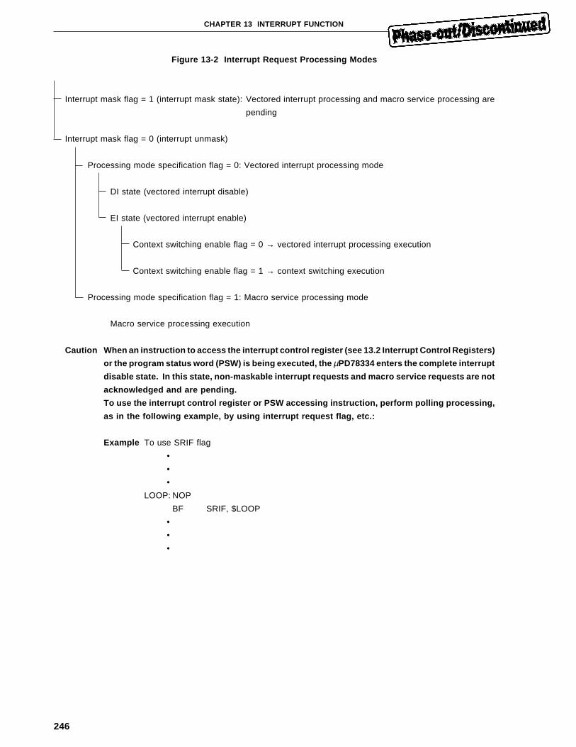
246
CHAPTER 13 INTERRUPT FUNCTION
Figure 13-2 Interrupt Request Processing Modes
Interrupt mask flag = 1 (interrupt mask state): Vectored interrupt processing and macro service processing are
pending
Interrupt mask flag = 0 (interrupt unmask)
Processing mode specification flag = 0: Vectored interrupt processing mode
DI state (vectored interrupt disable)
EI state (vectored interrupt enable)
Context switching enable flag = 0 → vectored interrupt processing execution
Context switching enable flag = 1 → context switching execution
Processing mode specification flag = 1: Macro service processing mode
Macro service processing execution
Caution When an instruction to access the interrupt control register (see 13.2 Interrupt Control Registers)
or the program status word (PSW) is being executed, the µPD78334 enters the complete interrupt
disable state. In this state, non-maskable interrupt requests and macro service requests are not
acknowledged and are pending.
To use the interrupt control register or PSW accessing instruction, perform polling processing,
as in the following example, by using interrupt request flag, etc.:
Example To use SRIF flag
•
•
•
LOOP: NOP
BF SRIF, $LOOP
•
•
•
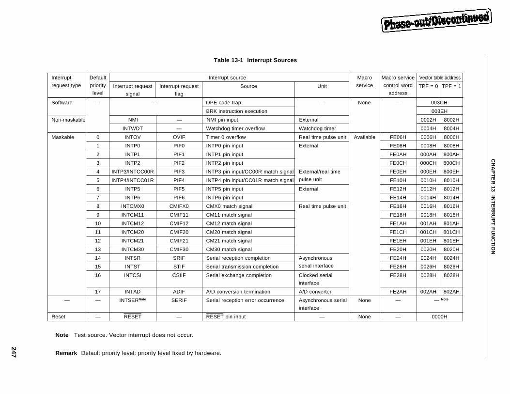
247
CH
AP
TE
R 13 IN
TE
RR
UP
T F
UN
CT
ION
Table 13-1 Interrupt Sources
Interrupt Default Interrupt source Macro Macro service Vector table address
request type priority Interrupt request Interrupt request Source Unit service control word TPF = 0 TPF = 1level signal flag address
Software — — OPE code trap — None — 003CH
BRK instruction execution 003EH
Non-maskable NMI — NMI pin input External 0002H 8002H
INTWDT — Watchdog timer overflow Watchdog timer 0004H 8004H
Maskable 0 INTOV OVIF Timer 0 overflow Real time pulse unit Available FE06H 0006H 8006H
1 INTP0 PIF0 INTP0 pin input External FE08H 0008H 8008H
2 INTP1 PIF1 INTP1 pin input FE0AH 000AH 800AH
3 INTP2 PIF2 INTP2 pin input FE0CH 000CH 800CH
4 INTP3/INTCC00R PIF3 INTP3 pin input/CC00R match signal External/real time FE0EH 000EH 800EH
5 INTP4/INTCC01R PIF4 INTP4 pin input/CC01R match signal pulse unit FE10H 0010H 8010H
6 INTP5 PIF5 INTP5 pin input External FE12H 0012H 8012H
7 INTP6 PIF6 INTP6 pin input FE14H 0014H 8014H
8 INTCMX0 CMIFX0 CMX0 match signal Real time pulse unit FE16H 0016H 8016H
9 INTCM11 CMIF11 CM11 match signal FE18H 0018H 8018H
10 INTCM12 CMIF12 CM12 match signal FE1AH 001AH 801AH
11 INTCM20 CMIF20 CM20 match signal FE1CH 001CH 801CH
12 INTCM21 CMIF21 CM21 match signal FE1EH 001EH 801EH
13 INTCM30 CMIF30 CM30 match signal FE20H 0020H 8020H
14 INTSR SRIF Serial reception completion Asynchronous FE24H 0024H 8024H
15 INTST STIF Serial transmission completion serial interface FE26H 0026H 8026H
16 INTCSI CSIIF Serial exchange completion Clocked serial FE28H 0028H 8028H
interface
17 INTAD ADIF A/D conversion termination A/D converter FE2AH 002AH 802AH
— — INTSERNote SERIF Serial reception error occurrence Asynchronous serial None — — Note
interface
Reset — RESET — RESET pin input — None — 0000H
Note Test source. Vector interrupt does not occur.
Remark Default priority level: priority level fixed by hardware.
248
CHAPTER 13 INTERRUPT FUNCTION
13.1 Interrupt Requests
13.1.1 Non-maskable interrupt requests
Non-maskable interrupt requests are acknowledged unconditionally even if interrupts are disabled (DI state).
Unlike maskable interrupt requests, programmable priority level control is not applied to non-maskable interrupt
requests. However, the priority levels between interrupt requests input to the NMI pin and watchdog timer interrupt
requests can be specified by the watchdog timer mode register (WDM). (See CHAPTER 11 WATCHDOG TIMER )
To return control from the interrupt processing routine, use the RETI instruction.
13.1.2 Maskable interrupt requests
Maskable interrupt requests can be masked by setting the interrupt mask flag register.
Although the default priority levels are given to the maskable interrupt requests, the interrupt priority levels can
be assigned by setting the priority level buffer register and priority level specification register. (Programmable priority
level control)
When an interrupt request is acknowledged, the DI state is entered and the subsequent maskable interrupt requests
are disabled. If the EI instruction is executed by the interrupt service routine, the EI state is entered and interrupt
request having the same or higher priority level than the priority level of the acknowledged interrupt request specified
in the priority level buffer register and priority level specification register is enabled.
However, macro service is acknowledged even in the DI state independently of the priority levels.
The following three interrupt processing modes are provided:
(1) Vectored interrupt processing mode
The program counter (PC) and program status word (PSW) are automatically saved in stack memory and a
branch is taken to a given interrupt processing routine.
To return control from the interrupt processing routine, use the RETI instruction.
(2) Macro service processing mode
The CPU halts program processing and transfers data by the hardware. At the time, the CPU state does not
change. (See 13.4 Macro Service Function )
(3) Context switching function mode
Register banks are switched by the hardware.
The program counter (PC) and program status word (PSW) contents are saved in the new register bank
selected and a branch is taken to the interrupt routine. (See 13.5 Context Switching Function )
13.1.3 Interrupt requests caused by executing specific instructions
Interrupt requests are caused by executing the following two instruction:
• BRK instruction : Vectored interrupt generation (address 003EH)
• BRKCS instruction : Context switching start
If either of these instructions is executed even in the DI state, an interrupt occurs. Interrupt priority level specification
control is not applied.
When the BRK instruction is executed, unconditionally the vector table contents are set in the PC for a branch.
If a new BRK instruction is executed by the BRK instruction interrupt service routine, the routines can also be nested.
249
CHAPTER 13 INTERRUPT FUNCTION
13.1.4 Exception trap interrupt requests
If data cannot be written into the watchdog timer mode register (WDM) or standby control register (STBC), the
µPD78334 generates an exception trap interrupt.
The write instructions into the WDM and STBC registers have special operation code structures. A write is enabled
only when the operation codes at the third and fourth bytes of the instruction are complementary to each other. If
the operation codes at the third and fourth bytes of the instruction are not complementary to each other , an exception
trap interrupt is generated. (See 11.1 Watchdog Timer Mode Register and 14.2 Standby Control Register )
250
CHAPTER 13 INTERRUPT FUNCTION
13.2 Interrupt Control Registers
µPD78334 interrupt processing is controlled for each interrupt request by setting the interrupt control registers to
specify interrupt processing. Table 13-2 shows the following seven interrupt control registers:
Table 13-2 Interrupt Control Register List
Register name Symbol Function
Interrupt request flag register IF0L Stores interrupt request occurrences.
IF0H
IF1L
Interrupt mask flag register MK0L Is used for mask control for maskable interrupt requests.
MK0H
MK1L
Processing mode specification flag register ISM0L Is used to specify vectored interrupt processing or macro service
ISM0H processing.
ISM1L
Priority level specification buffer register PB0L Write buffer register to validate priority levels specified in the priority
PB0H level specification register (PRSL) for maskable interrupt requests.
PB1L
Priority level specification register PRSL Is used to specify priority levels validated in writing into the priority
level specification buffer register for maskable interrupt requests.
In-service priority register ISPR Stores priority levels for the current interrupt request being
acknowledged.
Context switching enable register CSE0L Is used to specify whether the context switching function is
CSE0H enabled or disabled.
CSE1L
Each interrupt source is assigned to each bit of each control register. The register flags are provided to control
the interrupt requests corresponding to the register bit positions of the flags (except for the priority level specification
register or in-service priority register).
Table 13-3 lists the flag names of the priority request flag register, interrupt mask flag register, processing mode
specification buffer register, and context switching enable flag register corresponding to the interrupt request signals.
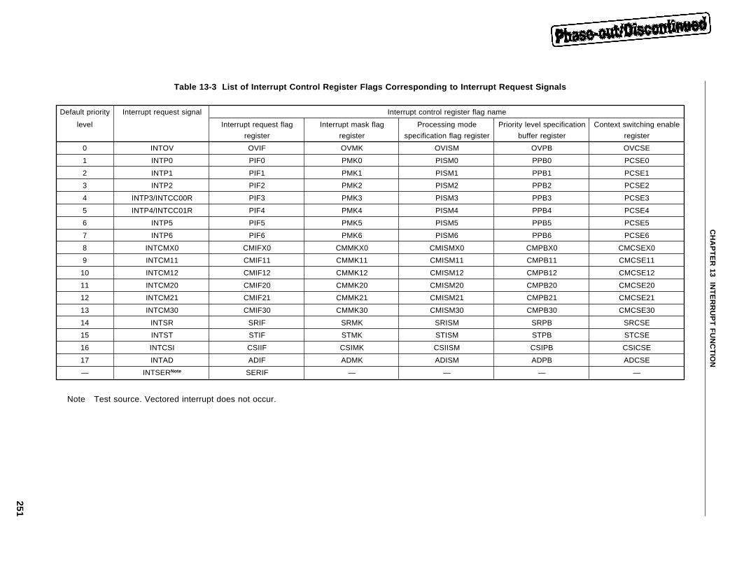
251
CH
AP
TE
R 13 IN
TE
RR
UP
T F
UN
CT
ION
Table 13-3 List of Interrupt Control Register Flags Corresponding to Interrupt Request Signals
Default priority Interrupt request signal Interrupt control register flag name
level Interrupt request flag Interrupt mask flag Processing mode Priority level specification Context switching enable
register register specification flag register buffer register register
0 INTOV OVIF OVMK OVISM OVPB OVCSE
1 INTP0 PIF0 PMK0 PISM0 PPB0 PCSE0
2 INTP1 PIF1 PMK1 PISM1 PPB1 PCSE1
3 INTP2 PIF2 PMK2 PISM2 PPB2 PCSE2
4 INTP3/INTCC00R PIF3 PMK3 PISM3 PPB3 PCSE3
5 INTP4/INTCC01R PIF4 PMK4 PISM4 PPB4 PCSE4
6 INTP5 PIF5 PMK5 PISM5 PPB5 PCSE5
7 INTP6 PIF6 PMK6 PISM6 PPB6 PCSE6
8 INTCMX0 CMIFX0 CMMKX0 CMISMX0 CMPBX0 CMCSEX0
9 INTCM11 CMIF11 CMMK11 CMISM11 CMPB11 CMCSE11
10 INTCM12 CMIF12 CMMK12 CMISM12 CMPB12 CMCSE12
11 INTCM20 CMIF20 CMMK20 CMISM20 CMPB20 CMCSE20
12 INTCM21 CMIF21 CMMK21 CMISM21 CMPB21 CMCSE21
13 INTCM30 CMIF30 CMMK30 CMISM30 CMPB30 CMCSE30
14 INTSR SRIF SRMK SRISM SRPB SRCSE
15 INTST STIF STMK STISM STPB STCSE
16 INTCSI CSIIF CSIMK CSIISM CSIPB CSICSE
17 INTAD ADIF ADMK ADISM ADPB ADCSE
— INTSERNote SERIF — — — —
Note Test source. Vectored interrupt does not occur.
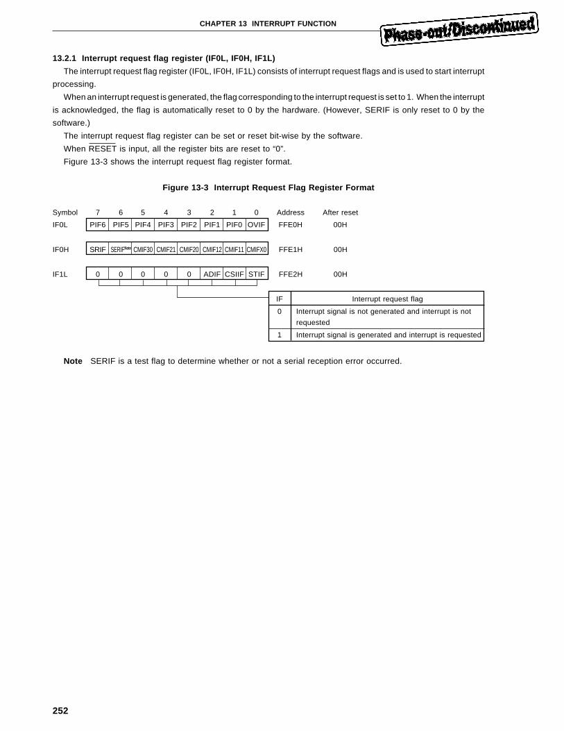
252
CHAPTER 13 INTERRUPT FUNCTION
13.2.1 Interrupt request flag register (IF0L, IF0H, IF1L)
The interrupt request flag register (IF0L, IF0H, IF1L) consists of interrupt request flags and is used to start interrupt
processing.
When an interrupt request is generated, the flag corresponding to the interrupt request is set to 1. When the interrupt
is acknowledged, the flag is automatically reset to 0 by the hardware. (However, SERIF is only reset to 0 by the
software.)
The interrupt request flag register can be set or reset bit-wise by the software.
When RESET is input, all the register bits are reset to “0”.
Figure 13-3 shows the interrupt request flag register format.
Figure 13-3 Interrupt Request Flag Register Format
Symbol 7 6 5 4 3 2 1 0 Address After reset
IF0L PIF6 PIF5 PIF4 PIF3 PIF2 PIF1 PIF0 OVIF FFE0H 00H
IF0H SRIF SERIFNote CMIF30 CMIF21 CMIF20 CMIF12 CMIF11 CMIFX0 FFE1H 00H
IF1L 0 0 0 0 0 ADIF CSIIF STIF FFE2H 00H
IF Interrupt request flag
0 Interrupt signal is not generated and interrupt is not
requested
1 Interrupt signal is generated and interrupt is requested
Note SERIF is a test flag to determine whether or not a serial reception error occurred.
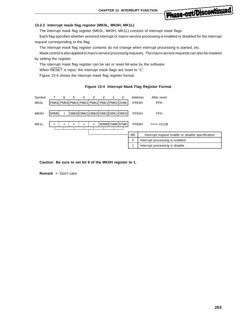
253
CHAPTER 13 INTERRUPT FUNCTION
13.2.2 Interrupt mask flag register (MK0L, MK0H, MK1L)
The interrupt mask flag register (MK0L, MK0H, MK1L) consists of interrupt mask flags.
Each flag specifies whether vectored interrupt or macro service processing is enabled or disabled for the interrupt
request corresponding to the flag.
The interrupt mask flag register contents do not change when interrupt processing is started, etc.
Mask control is also applied to macro service processing requests. The macro service requests can also be masked
by setting the register.
The interrupt mask flag register can be set or reset bit-wise by the software.
When RESET is input, the interrupt mask flags are reset to “1”.
Figure 13-4 shows the interrupt mask flag register format.
Figure 13-4 Interrupt Mask Flag Register Format
Symbol 7 6 5 4 3 2 1 0 Address After reset
MK0L PMK6 PMK5 PMK4 PMK3 PMK2 PMK1 PMK0 OVMK FFE4H FFH
MK0H SRMK 1 CMMK30 CMMK21 CMMK20 CMMK12 CMMK11 CMMKX0 FFE5H FFH
MK1L × × × × × ADMKCSIMK STMK FFE6H ×××× ×111B
MK Interrupt request enable or disable specification
0 Interrupt processing is enabled
1 Interrupt processing is disable
Caution Be sure to set bit 6 of the MK0H register to 1.
Remark ×: Don’t care
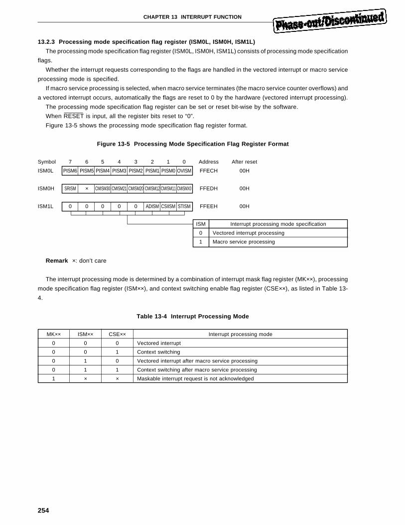
254
CHAPTER 13 INTERRUPT FUNCTION
13.2.3 Processing mode specification flag register (ISM0L, ISM0H, ISM1L)
The processing mode specification flag register (ISM0L, ISM0H, ISM1L) consists of processing mode specification
flags.
Whether the interrupt requests corresponding to the flags are handled in the vectored interrupt or macro service
processing mode is specified.
If macro service processing is selected, when macro service terminates (the macro service counter overflows) and
a vectored interrupt occurs, automatically the flags are reset to 0 by the hardware (vectored interrupt processing).
The processing mode specification flag register can be set or reset bit-wise by the software.
When RESET is input, all the register bits reset to “0”.
Figure 13-5 shows the processing mode specification flag register format.
Figure 13-5 Processing Mode Specification Flag Register Format
Symbol 7 6 5 4 3 2 1 0 Address After reset
ISM0L PISM6 PISM5 PISM4 PISM3 PISM2 PISM1 PISM0 OVISM FFECH 00H
ISM0H SRISM × CMISM30 CMISM21 CMISM20 CMISM12 CMISM11 CMISMX0 FFEDH 00H
ISM1L 0 0 0 0 0 ADISM CSIISM STISM FFEEH 00H
ISM Interrupt processing mode specification
0 Vectored interrupt processing
1 Macro service processing
Remark ×: don’t care
The interrupt processing mode is determined by a combination of interrupt mask flag register (MK××), processing
mode specification flag register (ISM××), and context switching enable flag register (CSE××), as listed in Table 13-
4.
Table 13-4 Interrupt Processing Mode
MK×× ISM×× CSE×× Interrupt processing mode
0 0 0 Vectored interrupt
0 0 1 Context switching
0 1 0 Vectored interrupt after macro service processing
0 1 1 Context switching after macro service processing
1 × × Maskable interrupt request is not acknowledged
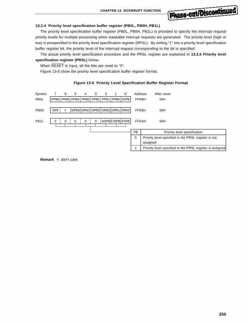
255
CHAPTER 13 INTERRUPT FUNCTION
13.2.4 Priority level specification buffer register (PB0L, PB0H, PB1L)
The priority level specification buffer register (PB0L, PB0H, PB1L) is provided to specify the interrupt request
priority levels for multiple processing when maskable interrupt requests are generated. The priority level (high or
low) is prespecified in the priority level specification register (RPSL). By writing “1” into a priority level specification
buffer register bit, the priority level of the interrupt request corresponding to the bit is specified.
The actual priority level specification procedure and the PRSL register are explained in 13.2.5 Priority level
specification register (PRSL) below.
When RESET is input, all the bits are reset to “0”.
Figure 13-6 show the priority level specification buffer register format.
Figure 13-6 Priority Level Specification Buffer Register Format
Symbol 7 6 5 4 3 2 1 0 Address After reset
PB0L PPB6 PPB5 PPB4 PPB3 PPB2 PPB1 PPB0 OVPB FFE8H 00H
PB0H SRPB × CMPB30 CMPB21 CMPB20 CMPB12 CMPB11 CMPBX0 FFE9H 00H
PB1L 0 0 0 0 0 ADPB CSIPB STPB FFEAH 00H
PB Priority level specification
0 Priority level specified in the PRSL register is not
assigned
1 Priority level specified in the PRSL register is assigned
Remark ×: don’t care
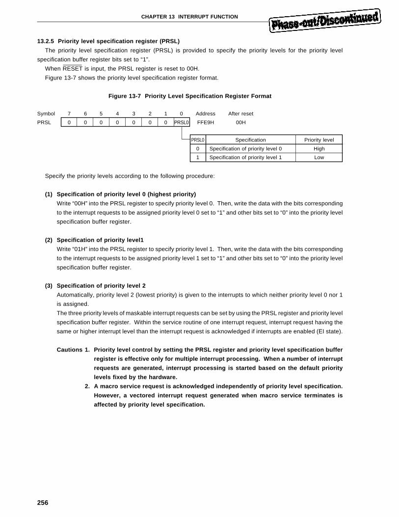
256
CHAPTER 13 INTERRUPT FUNCTION
13.2.5 Priority level specification register (PRSL)
The priority level specification register (PRSL) is provided to specify the priority levels for the priority level
specification buffer register bits set to “1”.
When RESET is input, the PRSL register is reset to 00H.
Figure 13-7 shows the priority level specification register format.
Figure 13-7 Priority Level Specification Register Format
Symbol 7 6 5 4 3 2 1 0 Address After reset
PRSL 0 0 0 0 0 0 0 PRSL0 FFE9H 00H
PRSL0 Specification Priority level
0 Specification of priority level 0 High
1 Specification of priority level 1 Low
Specify the priority levels according to the following procedure:
(1) Specification of priority level 0 (highest priority)
Write “00H” into the PRSL register to specify priority level 0. Then, write the data with the bits corresponding
to the interrupt requests to be assigned priority level 0 set to “1” and other bits set to “0” into the priority level
specification buffer register.
(2) Specification of priority level1
Write “01H” into the PRSL register to specify priority level 1. Then, write the data with the bits corresponding
to the interrupt requests to be assigned priority level 1 set to “1” and other bits set to “0” into the priority level
specification buffer register.
(3) Specification of priority level 2
Automatically, priority level 2 (lowest priority) is given to the interrupts to which neither priority level 0 nor 1
is assigned.
The three priority levels of maskable interrupt requests can be set by using the PRSL register and priority level
specification buffer register. Within the service routine of one interrupt request, interrupt request having the
same or higher interrupt level than the interrupt request is acknowledged if interrupts are enabled (EI state).
Cautions 1. Priority level control by setting the PRSL register and priority level specification buffer
register is effective only for multiple interrupt processing. When a number of interrupt
requests are generated, interrupt processing is started based on the default priority
levels fixed by the hardware.
2. A macro service request is acknowledged independently of priority level specification.
However, a vectored interrupt request generated when macro service terminates is
affected by priority level specification.
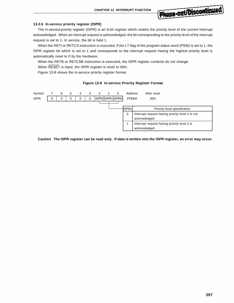
257
CHAPTER 13 INTERRUPT FUNCTION
13.2.6 In-service priority register (ISPR)
The in-service priority register (ISPR) is an 8-bit register which retains the priority level of the current interrupt
acknowledged. When an interrupt request is acknowledged, the bit corresponding to the priority level of the interrupt
request is set to 1. In service, the bit is held 1.
When the RETI or RETCS instruction is executed, if the LT flag of the program status word (PSW) is set to 1, the
ISPR register bit which is set to 1 and coreesponds to the interrupt request having the highest priority level is
automatically reset to 0 by the hardware.
When the RETB or RETCSB instruction is executed, the ISPR register contents do not change.
When RESET is input, the ISPR register is reset to 00H.
Figure 13-8 shows the in-service priority register format.
Figure 13-8 In-service Priority Register Format
Symbol 7 6 5 4 3 2 1 0 Address After reset
ISPR 0 0 0 0 0 ISPR2 ISPR1 ISPR0 FFE8H 00H
ISPRn Priority level specification
0 Interrupt request having priority level n is not
acknowledged
1 Interrupt request having priority level n is
acknowledged
Caution The ISPR register can be read only. If data is written into the ISPR register, an error may occur.
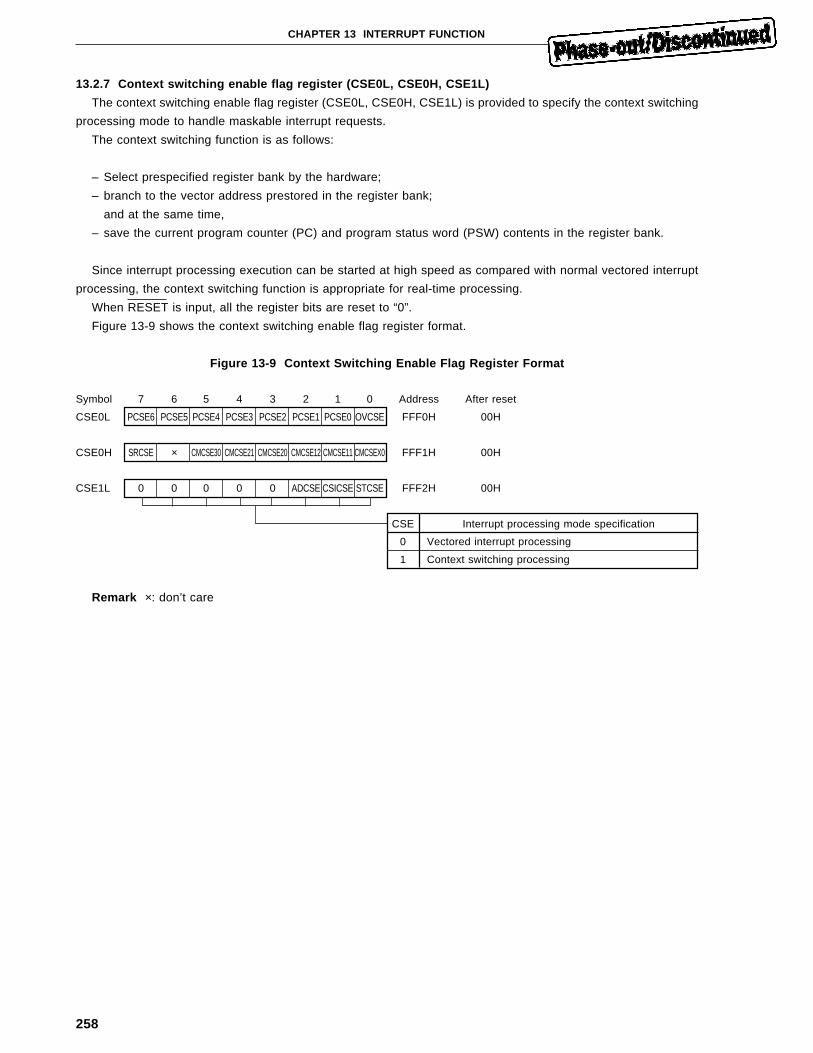
258
CHAPTER 13 INTERRUPT FUNCTION
13.2.7 Context switching enable flag register (CSE0L, CSE0H, CSE1L)
The context switching enable flag register (CSE0L, CSE0H, CSE1L) is provided to specify the context switching
processing mode to handle maskable interrupt requests.
The context switching function is as follows:
– Select prespecified register bank by the hardware;
– branch to the vector address prestored in the register bank;
and at the same time,
– save the current program counter (PC) and program status word (PSW) contents in the register bank.
Since interrupt processing execution can be started at high speed as compared with normal vectored interrupt
processing, the context switching function is appropriate for real-time processing.
When RESET is input, all the register bits are reset to “0”.
Figure 13-9 shows the context switching enable flag register format.
Figure 13-9 Context Switching Enable Flag Register Format
Symbol 7 6 5 4 3 2 1 0 Address After reset
CSE0L PCSE6 PCSE5 PCSE4 PCSE3 PCSE2 PCSE1 PCSE0 OVCSE FFF0H 00H
CSE0H SRCSE × CMCSE30 CMCSE21 CMCSE20 CMCSE12 CMCSE11 CMCSEX0 FFF1H 00H
CSE1L 0 0 0 0 0 ADCSE CSICSE STCSE FFF2H 00H
CSE Interrupt processing mode specification
0 Vectored interrupt processing
1 Context switching processing
Remark ×: don’t care
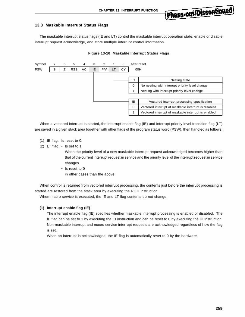
259
CHAPTER 13 INTERRUPT FUNCTION
13.3 Maskable Interrupt Status Flags
The maskable interrupt status flags (IE and LT) control the maskable interrupt operation state, enable or disable
interrupt request acknowledge, and store multiple interrupt control information.
Figure 13-10 Maskable Interrupt Status Flags
Symbol 7 6 5 4 3 2 1 0 After reset
PSW S Z RSS AC IE P/V LT CY 00H
LT Nesting state
0 No nesting with interrupt priority level change
1 Nesting with interrupt priority level change
IE Vectored interrupt processing specification
0 Vectored interrupt of maskable interrupt is disabled
1 Vectored interrupt of maskable interrupt is enabled
When a vectored interrupt is started, the interrupt enable flag (IE) and interrupt priority level transition flag (LT)
are saved in a given stack area together with other flags of the program status word (PSW), then handled as follows:
(1) IE flag: Is reset to 0.
(2) LT flag: • Is set to 1
When the priority level of a new maskable interrupt request acknowledged becomes higher than
that of the current interrupt request in service and the priority level of the interrupt request in service
changes.
• Is reset to 0
in other cases than the above.
When control is returned from vectored interrupt processing, the contents just before the interrupt processing is
started are restored from the stack area by executing the RETI instruction.
When macro service is executed, the IE and LT flag contents do not change.
(1) Interrupt enable flag (IE)
The interrupt enable flag (IE) specifies whether maskable interrupt processing is enabled or disabled. The
IE flag can be set to 1 by executing the EI instruction and can be reset to 0 by executing the DI instruction.
Non-maskable interrupt and macro service interrupt requests are acknowledged regardless of how the flag
is set.
When an interrupt is acknowledged, the IE flag is automatically reset to 0 by the hardware.

260
CHAPTER 13 INTERRUPT FUNCTION
(2) Interrupt priority level transition flag (LT)
When the priority level of a new maskable interrupt request acknowledged becomes higher than that of the
current interrupt request in service and the priority level of the interrupt request in service changes, the interrupt
priority level transition flag (LT) is set to 1. When interrupts are nested within the same priority level, the LT
flag is reset to 0.
The LT flag is used to control ISPR register reset operation when the RETI or RETCS instruction is executed
to return control from interrupt processing.
Caution Do not operate the LT flag by a program. If do so, a malfunction may occur.
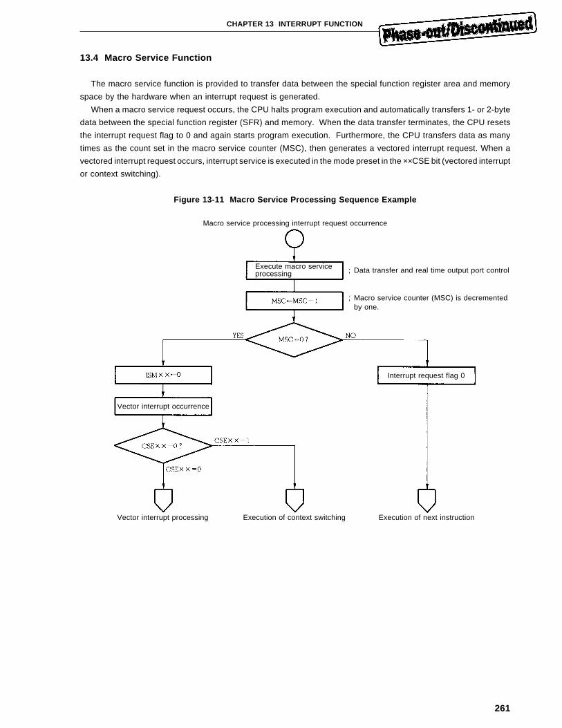
261
CHAPTER 13 INTERRUPT FUNCTION
13.4 Macro Service Function
The macro service function is provided to transfer data between the special function register area and memory
space by the hardware when an interrupt request is generated.
When a macro service request occurs, the CPU halts program execution and automatically transfers 1- or 2-byte
data between the special function register (SFR) and memory. When the data transfer terminates, the CPU resets
the interrupt request flag to 0 and again starts program execution. Furthermore, the CPU transfers data as many
times as the count set in the macro service counter (MSC), then generates a vectored interrupt request. When a
vectored interrupt request occurs, interrupt service is executed in the mode preset in the ××CSE bit (vectored interrupt
or context switching).
Figure 13-11 Macro Service Processing Sequence Example
Macro service processing interrupt request occurrence
Vector interrupt processing Execution of context switching Execution of next instruction
Execute macro serviceprocessing ; Data transfer and real time output port control
; Macro service counter (MSC) is decrementedby one.
Interrupt request flag 0
Vector interrupt occurrence
262
CHAPTER 13 INTERRUPT FUNCTION
Macro service function processing is automatically performed without starting any interrupt service program unlike
other interrupt processing modes, thus a series of steps such as a branch to and return from a given interrupt service
routine and register save and restore are not performed. The macro service function enables improvement of the
CPU service time and reduction of the number of program steps.
When macro service processing is performed, the general purpose registers, instruction queue, etc., in the CPU
retain the state before execution of the macro service processing. The macro service function is useful to execute
simple data transfer such as A/D conversion result store or serial transfer data set by generating an interrupt request.
Macro service processing interrupt requests are not affected by the IE flag state of the program status word (PSW).
If interrupt are disabled or an interrupt service program is being executed, macro service processing can also be
executed. It is disabled only when the interrupt mask flag register (MK0L, MK0H, MK1L) bit corresponding to the
interrupt request is set to 1.
When a number of macro service requests are made, the service order is determined by the default priority levels
of the requests. Instructions are not executed until all the macro service requests have been handled.
The µPD78334 supports macro service for the 18 of 19 maskable interrupt requests, as listed in Table 13-5.
Table 13-5 Interrupt Request s for Which Macro Service can be Supported
Interrupt request Interrupt source
INTOV Timer 0 overflow
INTP0 INTP0 pin input
INTP1 INTP1 pin input
INTP2 INTP2 pin input
INTP3/INTCC00R INTP3 pin input or CC00R match signal
INTP4/INTCC01R INTP4 pin input or CC01R match signal
INTP5 INTP5 pin input
INTP6 INTP6 pin input
INTCMX0 CMX0 match signal
INTCM11 CM11 match signal
INTCM12 CM12 match signal
INTCM20 CM20 match signal
INTCM21 CM21 match signal
INTCM30 CM30 match signal
INTSR UART reception termination
INTST UART transmission termination
INTCSI CSI transfer termination
INTAD A/D conversion termination
Macro service processing involves the following two basic steps:
• Data transfer from memory to special function register (SFR)
• Data transfer from special function register (SFR) to memory
263
CHAPTER 13 INTERRUPT FUNCTION
13.4.1 Macro service control registers
(1) Macro service control words
Each macro service control word consists of a macro service mode register to control the macro service
function and a macro service channel pointer. The control words are mapped in the FE06H to FE2BH address
space of the main RAM area.
Figure 13-12 shows the basic format of the macro service control word.
Figure 13-12 Basic Format of Macro Service Control Word
Address MSB LBS
FE××H Macro service mode register
(FE×× + 1)H Macro service channel pointer
The macro service processing mode is set in the macro service mode register. The macro service channel
address is specified by the macro service channel pointer.
Table 13-6 lists the relationship between the interrupt requests for which macro service can be supported and
the macro service control word addresses.
Table 13-6 Interrupt Requests and Macro Service Control Word Addresses
Interrupt request Address
INTOV FE06H
INTP0 FE08H
INTP1 FE0AH
INTP2 FE0CH
INTP3/INTCC00R FE0EH
INTP4/INTCC01R FE10H
INTP5 FE12H
INTP6 FE14H
INTCMX0 FE16H
INTCM11 FE18H
INTCM12 FE1AH
INTCM20 FE1CH
INTCM21 FE1EH
INTCM30 FE20H
INTSR FE24H
INTST FE26H
INTCSI FE28H
INTAD FE2AH
To execute macro service processing, values must have been set in the macro service mode registers and
channel pointers corresponding to the interrupt requests for which macro service processing can be supported.
(2) Macro service mode registers
Each macro service mode register is an 8-bit register to specify macro service operation. The register is
mapped in the main RAM area as a part of the macro service control word. (See Figure 13-12 .)
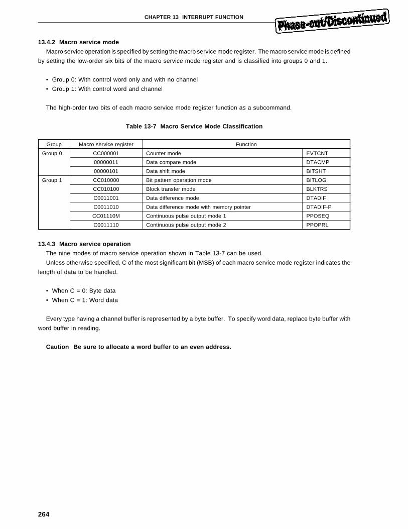
264
CHAPTER 13 INTERRUPT FUNCTION
13.4.2 Macro service mode
Macro service operation is specified by setting the macro service mode register. The macro service mode is defined
by setting the low-order six bits of the macro service mode register and is classified into groups 0 and 1.
• Group 0: With control word only and with no channel
• Group 1: With control word and channel
The high-order two bits of each macro service mode register function as a subcommand.
Table 13-7 Macro Service Mode Classification
Group Macro service register Function
Group 0 CC000001 Counter mode EVTCNT
00000011 Data compare mode DTACMP
00000101 Data shift mode BITSHT
Group 1 CC010000 Bit pattern operation mode BITLOG
CC010100 Block transfer mode BLKTRS
C0011001 Data difference mode DTADIF
C0011010 Data difference mode with memory pointer DTADIF-P
CC01110M Continuous pulse output mode 1 PPOSEQ
C0011110 Continuous pulse output mode 2 PPOPRL
13.4.3 Macro service operation
The nine modes of macro service operation shown in Table 13-7 can be used.
Unless otherwise specified, C of the most significant bit (MSB) of each macro service mode register indicates the
length of data to be handled.
• When C = 0: Byte data
• When C = 1: Word data
Every type having a channel buffer is represented by a byte buffer. To specify word data, replace byte buffer with
word buffer in reading.
Caution Be sure to allocate a word buffer to an even address.
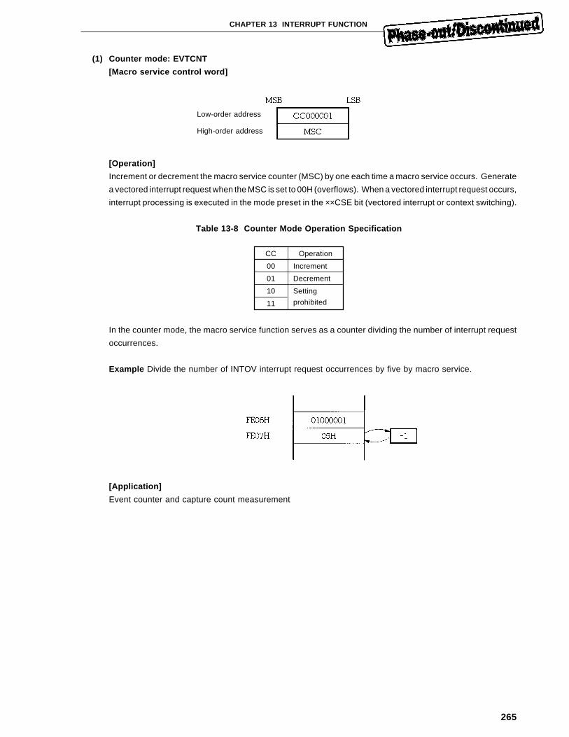
265
CHAPTER 13 INTERRUPT FUNCTION
(1) Counter mode: EVTCNT
[Macro service control word]
[Operation]
Increment or decrement the macro service counter (MSC) by one each time a macro service occurs. Generate
a vectored interrupt request when the MSC is set to 00H (overflows). When a vectored interrupt request occurs,
interrupt processing is executed in the mode preset in the ××CSE bit (vectored interrupt or context switching).
Table 13-8 Counter Mode Operation Specification
CC Operation
00 Increment
01 Decrement
10 Setting
11 prohibited
In the counter mode, the macro service function serves as a counter dividing the number of interrupt request
occurrences.
Example Divide the number of INTOV interrupt request occurrences by five by macro service.
[Application]
Event counter and capture count measurement
Low-order address
High-order address
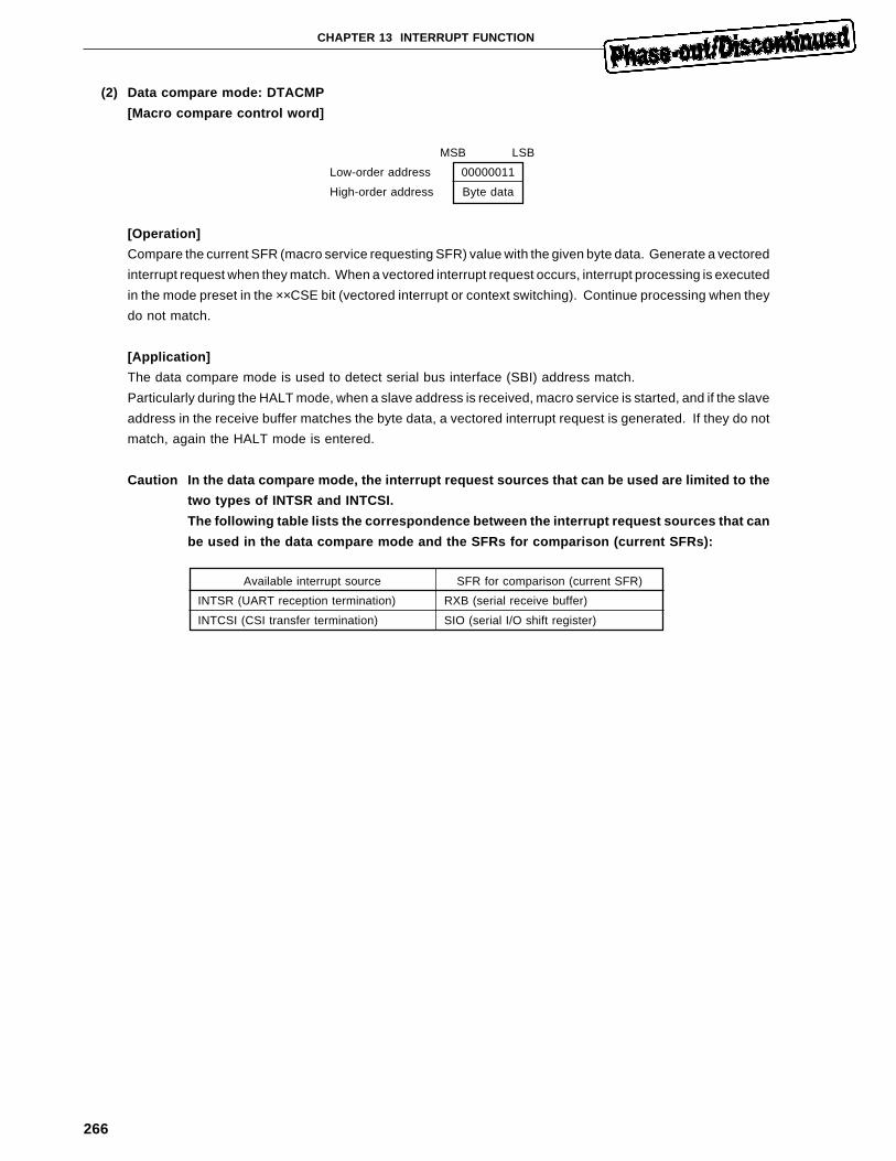
266
CHAPTER 13 INTERRUPT FUNCTION
(2) Data compare mode: DTACMP
[Macro compare control word]
MSB LSB
Low-order address 00000011
High-order address Byte data
[Operation]
Compare the current SFR (macro service requesting SFR) value with the given byte data. Generate a vectored
interrupt request when they match. When a vectored interrupt request occurs, interrupt processing is executed
in the mode preset in the ××CSE bit (vectored interrupt or context switching). Continue processing when they
do not match.
[Application]
The data compare mode is used to detect serial bus interface (SBI) address match.
Particularly during the HALT mode, when a slave address is received, macro service is started, and if the slave
address in the receive buffer matches the byte data, a vectored interrupt request is generated. If they do not
match, again the HALT mode is entered.
Caution In the data compare mode, the interrupt request sources that can be used are limited to the
two types of INTSR and INTCSI.
The following table lists the correspondence between the interrupt request sources that can
be used in the data compare mode and the SFRs for comparison (current SFRs):
Available interrupt source SFR for comparison (current SFR)
INTSR (UART reception termination) RXB (serial receive buffer)
INTCSI (CSI transfer termination) SIO (serial I/O shift register)
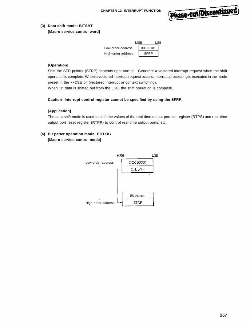
267
CHAPTER 13 INTERRUPT FUNCTION
(3) Data shift mode: BITSHT
[Macro service control word]
MSB LSB
Low-order address 00000101
High-order address SFRP
[Operation]
Shift the SFR pointer (SFRP) contents right one bit. Generate a vectored interrupt request when the shift
operation is complete. When a vectored interrupt request occurs, interrupt processing is executed in the mode
preset in the ××CSE bit (vectored interrupt or context switching).
When “1” data is shifted out from the LSB, the shift operation is complete.
Caution Interrupt control register cannot be specified by using the SFRP.
[Application]
The data shift mode is used to shift the values of the real-time output port set register (RTPS) and real-time
output port reset register (RTPR) to control real-time output ports, etc.
(4) Bit patter operation mode: BITLOG
[Macro service control mode]
Low-order address↑
↓High-order address
Bit pattern
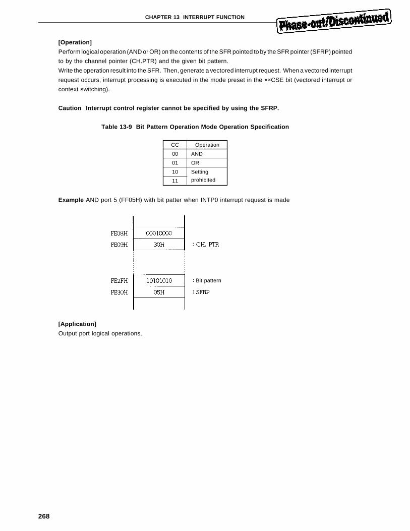
268
CHAPTER 13 INTERRUPT FUNCTION
[Operation]
Perform logical operation (AND or OR) on the contents of the SFR pointed to by the SFR pointer (SFRP) pointed
to by the channel pointer (CH.PTR) and the given bit pattern.
Write the operation result into the SFR. Then, generate a vectored interrupt request. When a vectored interrupt
request occurs, interrupt processing is executed in the mode preset in the ××CSE bit (vectored interrupt or
context switching).
Caution Interrupt control register cannot be specified by using the SFRP.
Table 13-9 Bit Pattern Operation Mode Operation Specification
CC Operation
00 AND
01 OR
10 Setting
11 prohibited
Example AND port 5 (FF05H) with bit patter when INTP0 interrupt request is made
[Application]
Output port logical operations.
Bit pattern
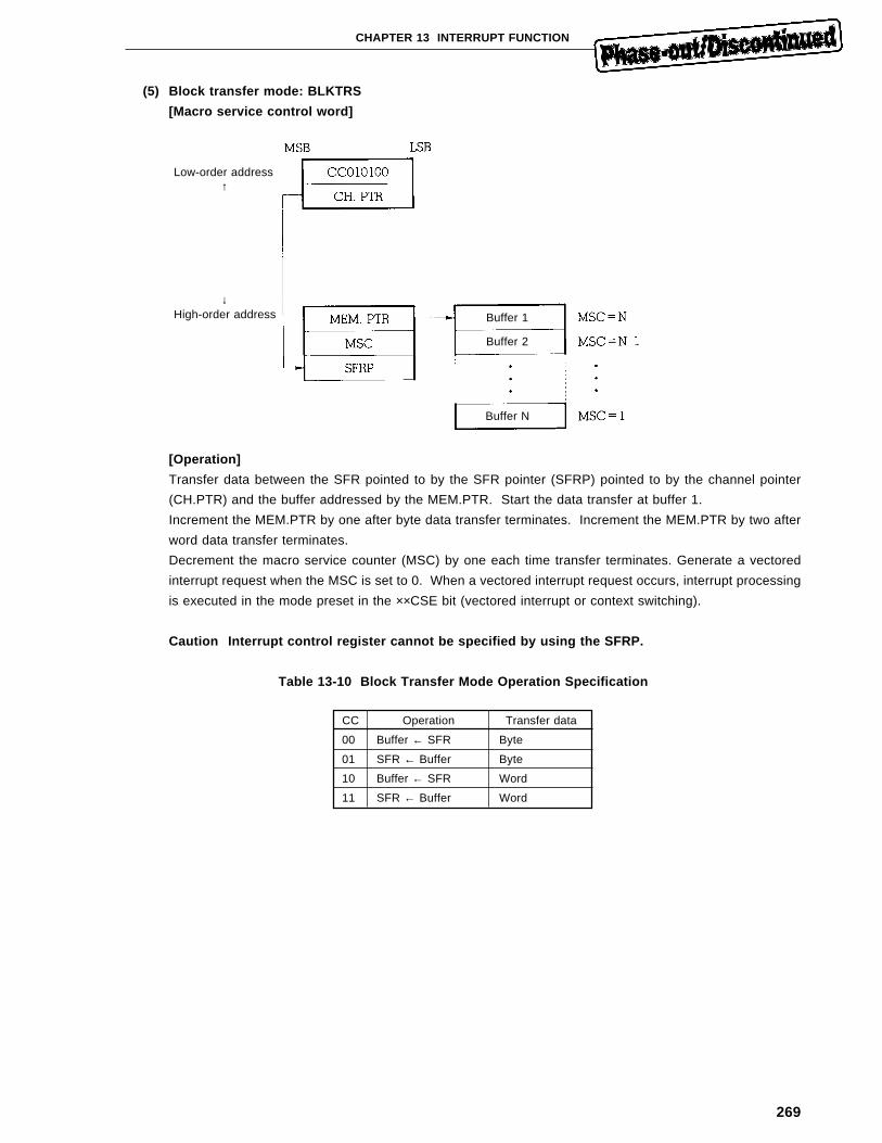
269
CHAPTER 13 INTERRUPT FUNCTION
(5) Block transfer mode: BLKTRS
[Macro service control word]
[Operation]
Transfer data between the SFR pointed to by the SFR pointer (SFRP) pointed to by the channel pointer
(CH.PTR) and the buffer addressed by the MEM.PTR. Start the data transfer at buffer 1.
Increment the MEM.PTR by one after byte data transfer terminates. Increment the MEM.PTR by two after
word data transfer terminates.
Decrement the macro service counter (MSC) by one each time transfer terminates. Generate a vectored
interrupt request when the MSC is set to 0. When a vectored interrupt request occurs, interrupt processing
is executed in the mode preset in the ××CSE bit (vectored interrupt or context switching).
Caution Interrupt control register cannot be specified by using the SFRP.
Table 13-10 Block Transfer Mode Operation Specification
CC Operation Transfer data
00 Buffer ← SFR Byte
01 SFR ← Buffer Byte
10 Buffer ← SFR Word
11 SFR ← Buffer Word
Low-order address↑
↓High-order address Buffer 1
Buffer 2
Buffer N
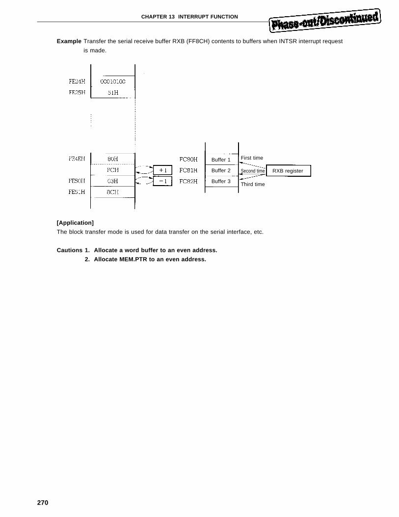
270
CHAPTER 13 INTERRUPT FUNCTION
Example Transfer the serial receive buffer RXB (FF8CH) contents to buffers when INTSR interrupt request
is made.
[Application]
The block transfer mode is used for data transfer on the serial interface, etc.
Cautions 1. Allocate a word buffer to an even address.
2. Allocate MEM.PTR to an even address.
First time
Second time
Buffer 1
Buffer 2
Buffer 3 Third time
RXB register
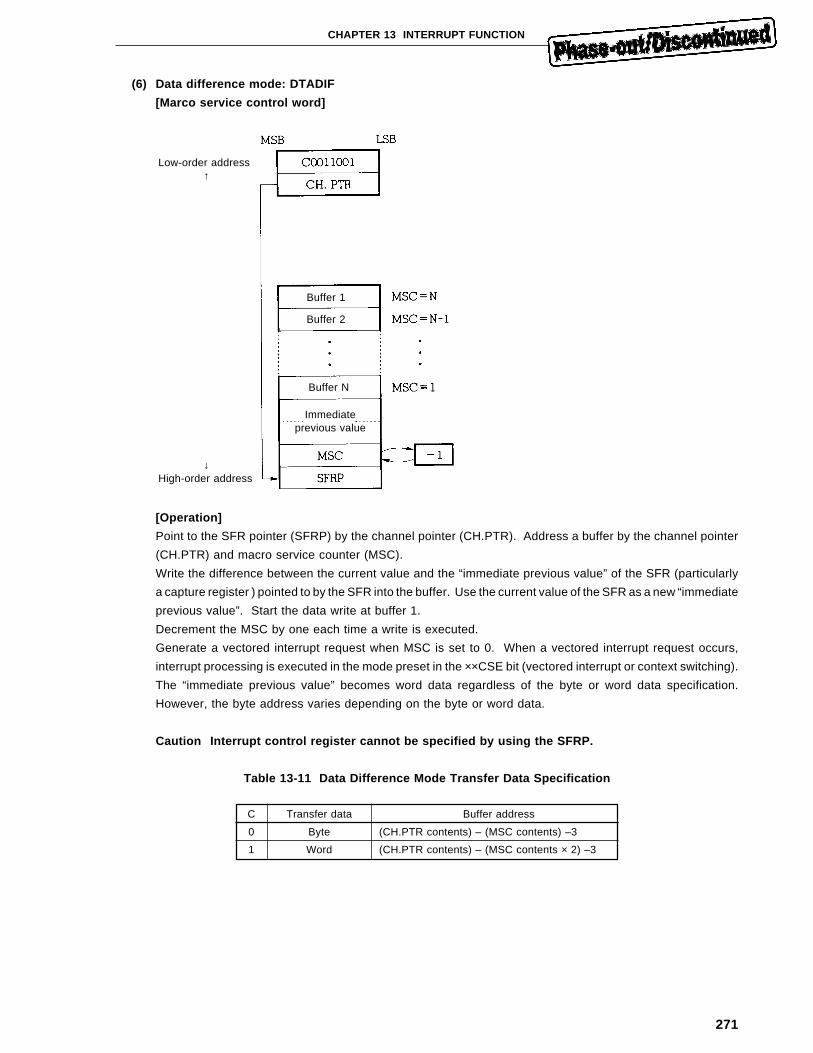
271
CHAPTER 13 INTERRUPT FUNCTION
(6) Data difference mode: DTADIF
[Marco service control word]
[Operation]
Point to the SFR pointer (SFRP) by the channel pointer (CH.PTR). Address a buffer by the channel pointer
(CH.PTR) and macro service counter (MSC).
Write the difference between the current value and the “immediate previous value” of the SFR (particularly
a capture register ) pointed to by the SFR into the buffer. Use the current value of the SFR as a new “immediate
previous value”. Start the data write at buffer 1.
Decrement the MSC by one each time a write is executed.
Generate a vectored interrupt request when MSC is set to 0. When a vectored interrupt request occurs,
interrupt processing is executed in the mode preset in the ××CSE bit (vectored interrupt or context switching).
The “immediate previous value” becomes word data regardless of the byte or word data specification.
However, the byte address varies depending on the byte or word data.
Caution Interrupt control register cannot be specified by using the SFRP.
Table 13-11 Data Difference Mode Transfer Data Specification
C Transfer data Buffer address
0 Byte (CH.PTR contents) – (MSC contents) –3
1 Word (CH.PTR contents) – (MSC contents × 2) –3
Low-order address↑
↓High-order address
Buffer 1
Buffer 2
Buffer N
Immediateprevious value
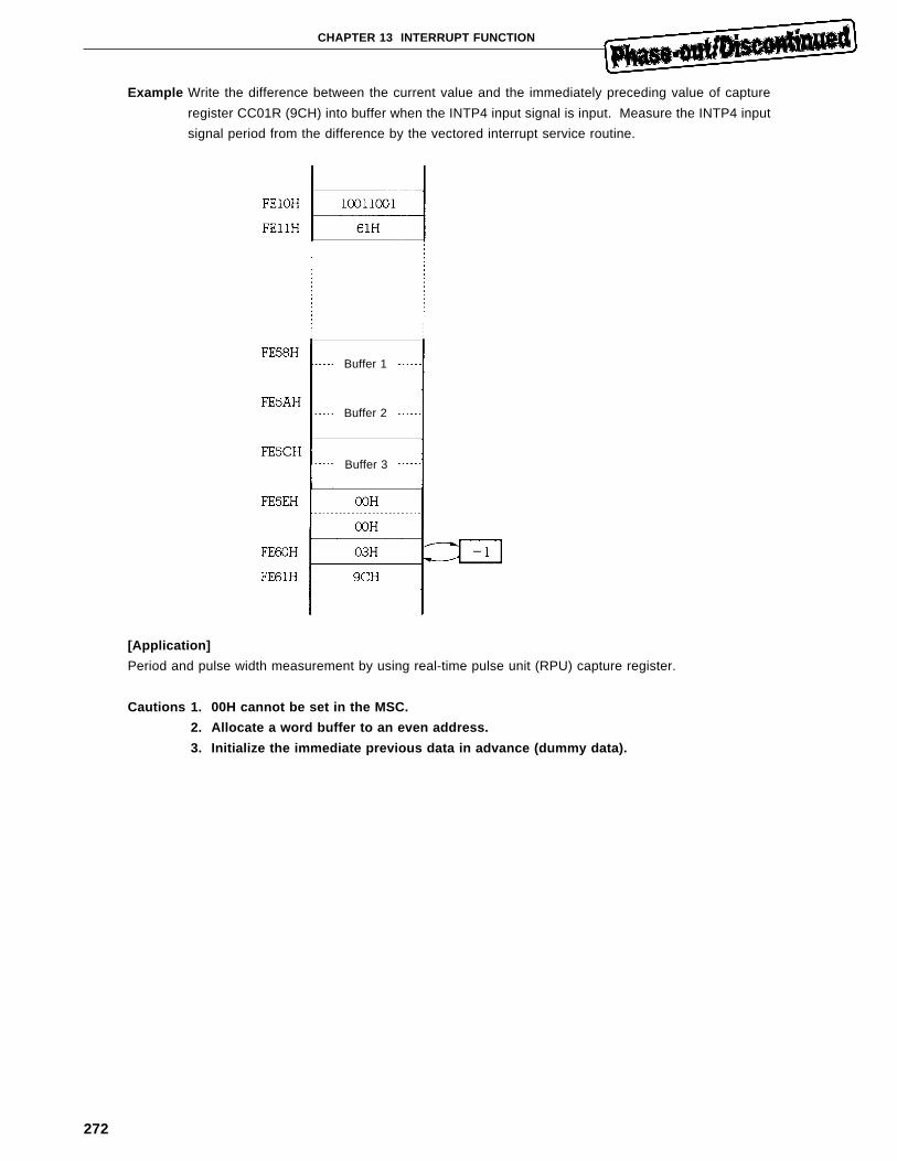
272
CHAPTER 13 INTERRUPT FUNCTION
Example Write the difference between the current value and the immediately preceding value of capture
register CC01R (9CH) into buffer when the INTP4 input signal is input. Measure the INTP4 input
signal period from the difference by the vectored interrupt service routine.
[Application]
Period and pulse width measurement by using real-time pulse unit (RPU) capture register.
Cautions 1. 00H cannot be set in the MSC.
2. Allocate a word buffer to an even address.
3. Initialize the immediate previous data in advance (dummy data).
Buffer 1
Buffer 3
Buffer 2
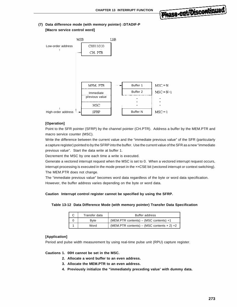
273
CHAPTER 13 INTERRUPT FUNCTION
(7) Data difference mode (with memory pointer) :DTADIF-P
[Macro service control word]
[Operation]
Point to the SFR pointer (SFRP) by the channel pointer (CH.PTR). Address a buffer by the MEM.PTR and
macro service counter (MSC).
Write the difference between the current value and the “immediate previous value” of the SFR (particularly
a capture register) pointed to by the SFRP into the buffer. Use the current value of the SFR as a new “immediate
previous value”. Start the data write at buffer 1.
Decrement the MSC by one each time a write is executed.
Generate a vectored interrupt request when the MSC is set to 0. When a vectored interrupt request occurs,
interrupt processing is executed in the mode preset in the ××CSE bit (vectored interrupt or context switching).
The MEM.PTR does not change.
The “immediate previous value” becomes word data regardless of the byte or word data specification.
However, the buffer address varies depending on the byte or word data.
Caution Interrupt control register cannot be specified by using the SFRP.
Table 13-12 Data Difference Mode (with memory pointer) Transfer Data Specification
C Transfer data Buffer address
0 Byte (MEM.PTR contents) – (MSC contents) +1
1 Word (MEM.PTR contents) – (MSC contents × 2) +2
[Application]
Period and pulse width measurement by using real-time pulse unit (RPU) capture register.
Cautions 1. 00H cannot be set in the MSC.
2. Allocate a word buffer to an even address.
3. Allocate the MEM.PTR to an even address.
4. Previously initialize the “immediately preceding value’ with dummy data.
Low-order address↑
↓High-order address
Buffer 1
Buffer 2Immediateprevious value
Buffer N
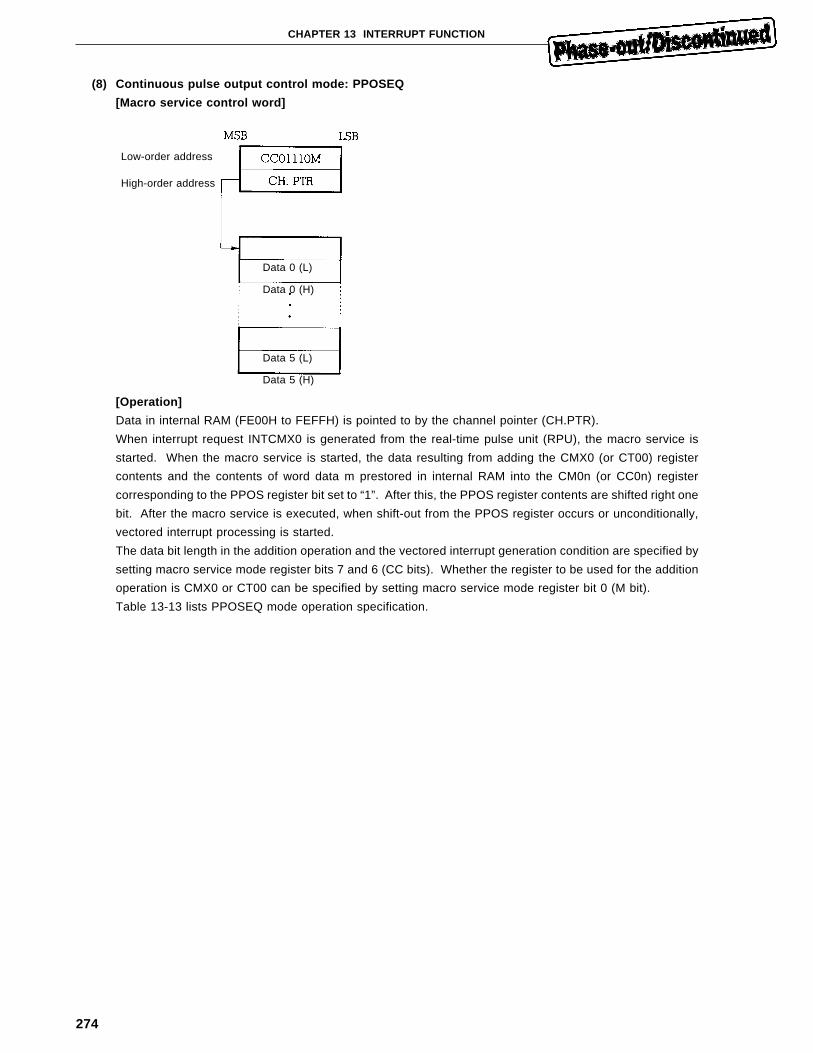
274
CHAPTER 13 INTERRUPT FUNCTION
(8) Continuous pulse output control mode: PPOSEQ
[Macro service control word]
[Operation]
Data in internal RAM (FE00H to FEFFH) is pointed to by the channel pointer (CH.PTR).
When interrupt request INTCMX0 is generated from the real-time pulse unit (RPU), the macro service is
started. When the macro service is started, the data resulting from adding the CMX0 (or CT00) register
contents and the contents of word data m prestored in internal RAM into the CM0n (or CC0n) register
corresponding to the PPOS register bit set to “1”. After this, the PPOS register contents are shifted right one
bit. After the macro service is executed, when shift-out from the PPOS register occurs or unconditionally,
vectored interrupt processing is started.
The data bit length in the addition operation and the vectored interrupt generation condition are specified by
setting macro service mode register bits 7 and 6 (CC bits). Whether the register to be used for the addition
operation is CMX0 or CT00 can be specified by setting macro service mode register bit 0 (M bit).
Table 13-13 lists PPOSEQ mode operation specification.
Low-order address
High-order address
Data 0 (L)
Data 0 (H)
Data 5 (L)
Data 5 (H)
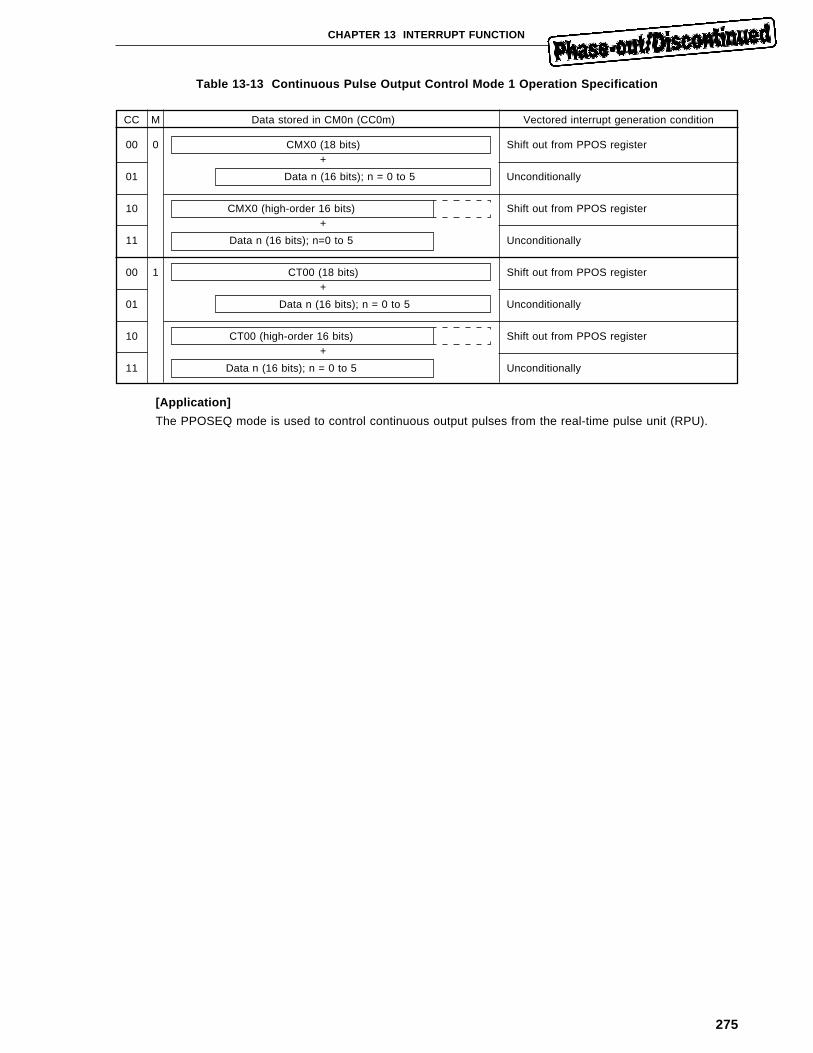
275
CHAPTER 13 INTERRUPT FUNCTION
Table 13-13 Continuous Pulse Output Control Mode 1 Operation Specification
CC M Data stored in CM0n (CC0m) Vectored interrupt generation condition
00 0 CMX0 (18 bits) Shift out from PPOS register+
01 Data n (16 bits); n = 0 to 5 Unconditionally
10 CMX0 (high-order 16 bits) Shift out from PPOS register+
11 Data n (16 bits); n=0 to 5 Unconditionally
00 1 CT00 (18 bits) Shift out from PPOS register+
01 Data n (16 bits); n = 0 to 5 Unconditionally
10 CT00 (high-order 16 bits) Shift out from PPOS register+
11 Data n (16 bits); n = 0 to 5 Unconditionally
[Application]
The PPOSEQ mode is used to control continuous output pulses from the real-time pulse unit (RPU).
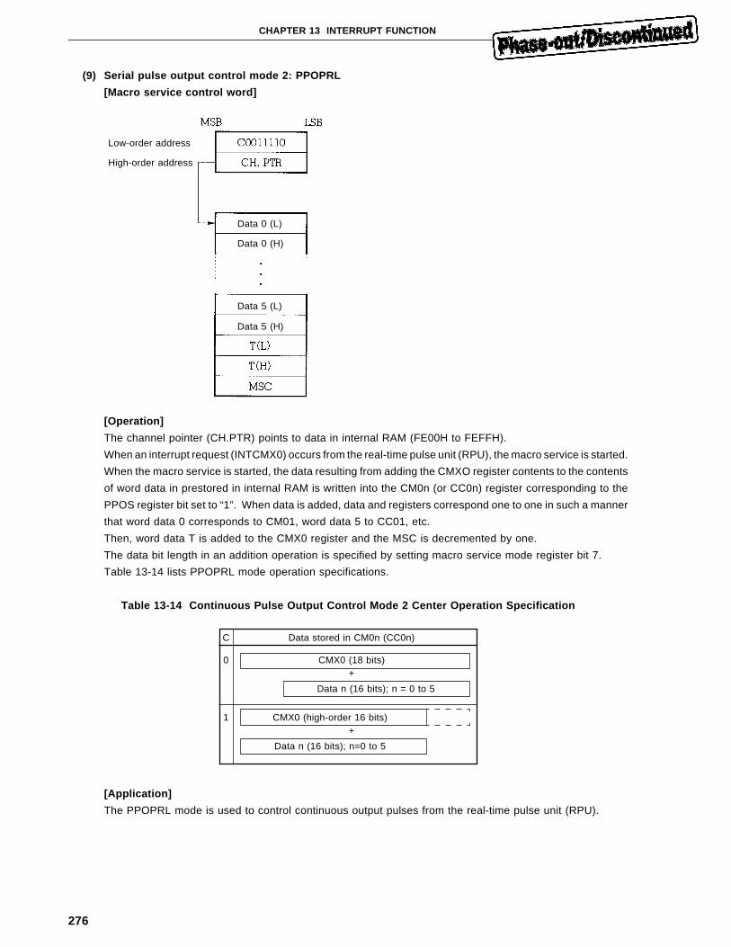
276
CHAPTER 13 INTERRUPT FUNCTION
(9) Serial pulse output control mode 2: PPOPRL
[Macro service control word]
[Operation]
The channel pointer (CH.PTR) points to data in internal RAM (FE00H to FEFFH).
When an interrupt request (INTCMX0) occurs from the real-time pulse unit (RPU), the macro service is started.
When the macro service is started, the data resulting from adding the CMXO register contents to the contents
of word data in prestored in internal RAM is written into the CM0n (or CC0n) register corresponding to the
PPOS register bit set to “1”. When data is added, data and registers correspond one to one in such a manner
that word data 0 corresponds to CM01, word data 5 to CC01, etc.
Then, word data T is added to the CMX0 register and the MSC is decremented by one.
The data bit length in an addition operation is specified by setting macro service mode register bit 7.
Table 13-14 lists PPOPRL mode operation specifications.
Table 13-14 Continuous Pulse Output Control Mode 2 Center Operation Specification
C Data stored in CM0n (CC0n)
0 CMX0 (18 bits)+
Data n (16 bits); n = 0 to 5
1 CMX0 (high-order 16 bits)+
Data n (16 bits); n=0 to 5
[Application]
The PPOPRL mode is used to control continuous output pulses from the real-time pulse unit (RPU).
Low-order address
High-order address
Data 0 (L)
Data 0 (H)
Data 5 (L)
Data 5 (H)
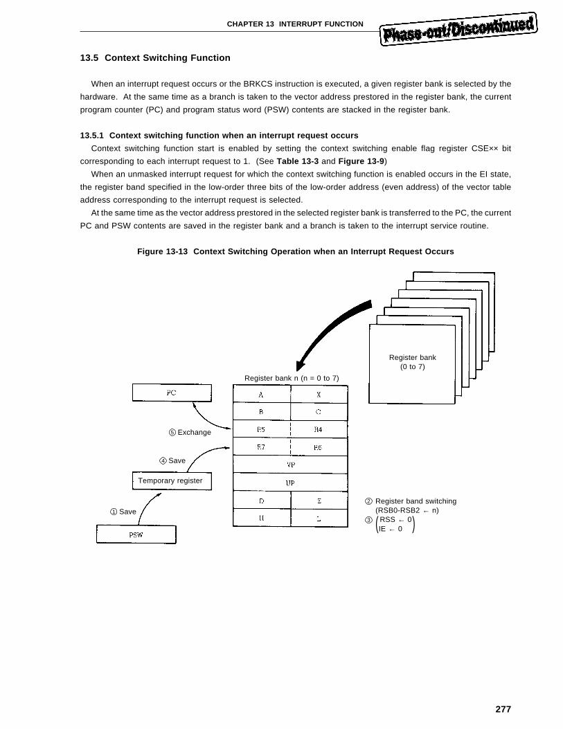
277
CHAPTER 13 INTERRUPT FUNCTION
13.5 Context Switching Function
When an interrupt request occurs or the BRKCS instruction is executed, a given register bank is selected by the
hardware. At the same time as a branch is taken to the vector address prestored in the register bank, the current
program counter (PC) and program status word (PSW) contents are stacked in the register bank.
13.5.1 Context switching function when an interrupt request occurs
Context switching function start is enabled by setting the context switching enable flag register CSE×× bit
corresponding to each interrupt request to 1. (See Table 13-3 and Figure 13-9 )
When an unmasked interrupt request for which the context switching function is enabled occurs in the EI state,
the register band specified in the low-order three bits of the low-order address (even address) of the vector table
address corresponding to the interrupt request is selected.
At the same time as the vector address prestored in the selected register bank is transferred to the PC, the current
PC and PSW contents are saved in the register bank and a branch is taken to the interrupt service routine.
Figure 13-13 Context Switching Operation when an Interrupt Request Occurs
Register bank(0 to 7)
Register bank n (n = 0 to 7)
Exchange5
Save4
Save1
Temporary register
Register band switching(RSB0-RSB2 ← n) RSS ← 0(IE ← 0 )
2
3
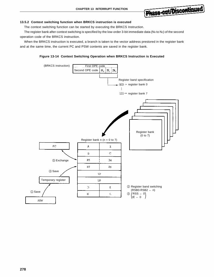
278
CHAPTER 13 INTERRUPT FUNCTION
13.5.2 Context switching function when BRKCS instruction is executed
The context switching function can be started by executing the BRKCS Instruction.
The register bank after context switching is specified by the low-order 3-bit immediate data (N0 to N2) of the second
operation code of the BRKCS instruction.
When the BRKCS instruction is executed, a branch is taken to the vector address prestored in the register bank
and at the same time, the current PC and PSW contents are saved in the register bank.
Figure 13-14 Context Switching Operation when BRKCS Instruction is Executed
(BRKCS instruction) First OPE code
Second OPE code
Register band specification
register bank 0
register bank 7
Register bank(0 to 7)
Register bank n (n = 0 to 7)
Exchange5
Save4
Save1
Temporary register
Register band switching(RSB0-RSB2 ← n) RSS ← 0(IE ← 0 )
2
3
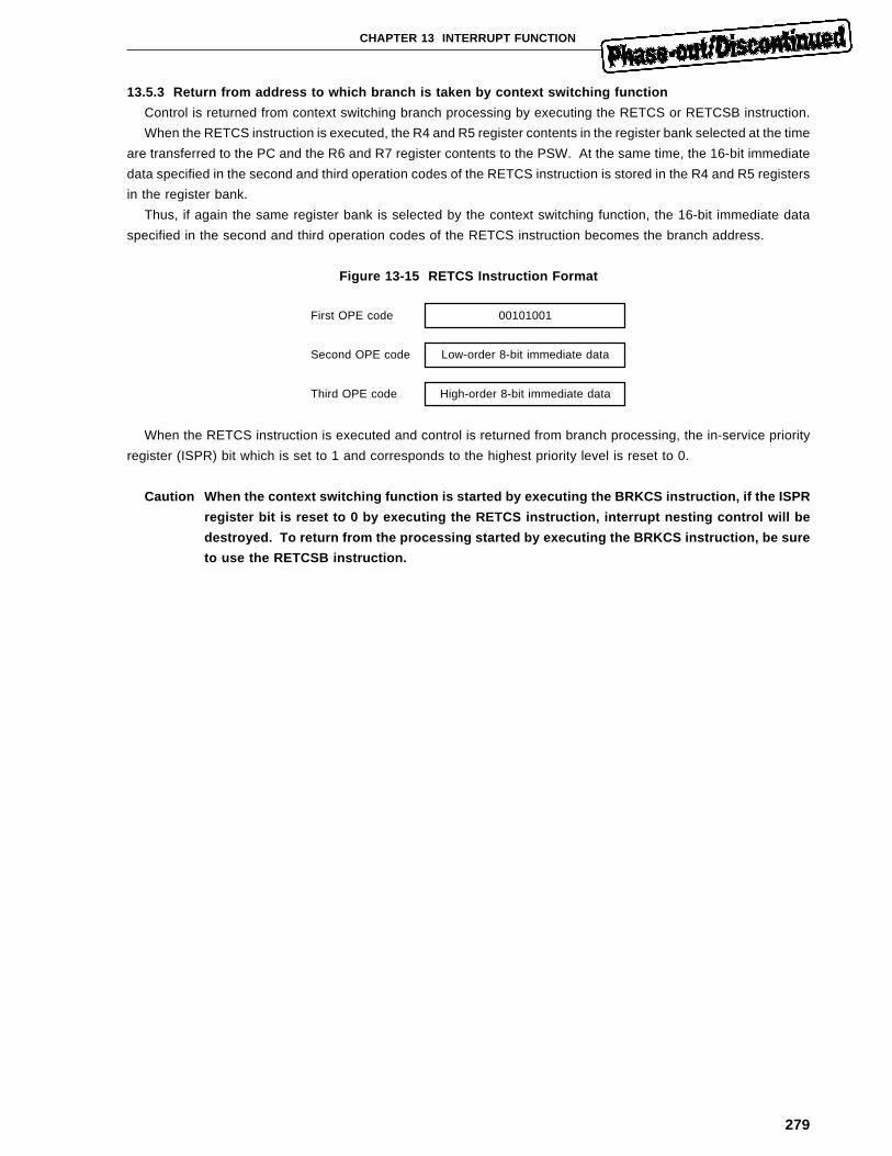
279
CHAPTER 13 INTERRUPT FUNCTION
13.5.3 Return from address to which branch is taken by context switching function
Control is returned from context switching branch processing by executing the RETCS or RETCSB instruction.
When the RETCS instruction is executed, the R4 and R5 register contents in the register bank selected at the time
are transferred to the PC and the R6 and R7 register contents to the PSW. At the same time, the 16-bit immediate
data specified in the second and third operation codes of the RETCS instruction is stored in the R4 and R5 registers
in the register bank.
Thus, if again the same register bank is selected by the context switching function, the 16-bit immediate data
specified in the second and third operation codes of the RETCS instruction becomes the branch address.
Figure 13-15 RETCS Instruction Format
First OPE code 00101001
Second OPE code Low-order 8-bit immediate data
Third OPE code High-order 8-bit immediate data
When the RETCS instruction is executed and control is returned from branch processing, the in-service priority
register (ISPR) bit which is set to 1 and corresponds to the highest priority level is reset to 0.
Caution When the context switching function is started by executing the BRKCS instruction, if the ISPR
register bit is reset to 0 by executing the RETCS instruction, interrupt nesting control will be
destroyed. To return from the processing started by executing the BRKCS instruction, be sure
to use the RETCSB instruction.

280
[MEMO]
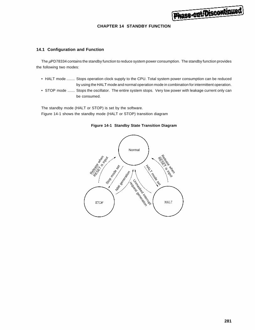
281
CHAPTER 14 STANDBY FUNCTION
14.1 Configuration and Function
The µPD78334 contains the standby function to reduce system power consumption. The standby function provides
the following two modes:
• HALT mode ........ Stops operation clock supply to the CPU. Total system power consumption can be reduced
by using the HALT mode and normal operation mode in combination for intermittent operation.
• STOP mode ....... Stops the oscillator. The entire system stops. Very low power with leakage current only can
be consumed.
The standby mode (HALT or STOP) is set by the software.
Figure 14-1 shows the standby mode (HALT or STOP) transition diagram
Figure 14-1 Standby State Transition Diagram
Rel
ease
whe
n
RES
ET is
inpu
tSt
op m
ode
set
Normal
HALT m
ode setR
elease when
RESET is input
NM
I gen
erat
ion
Unm
asked interrupt
request generation
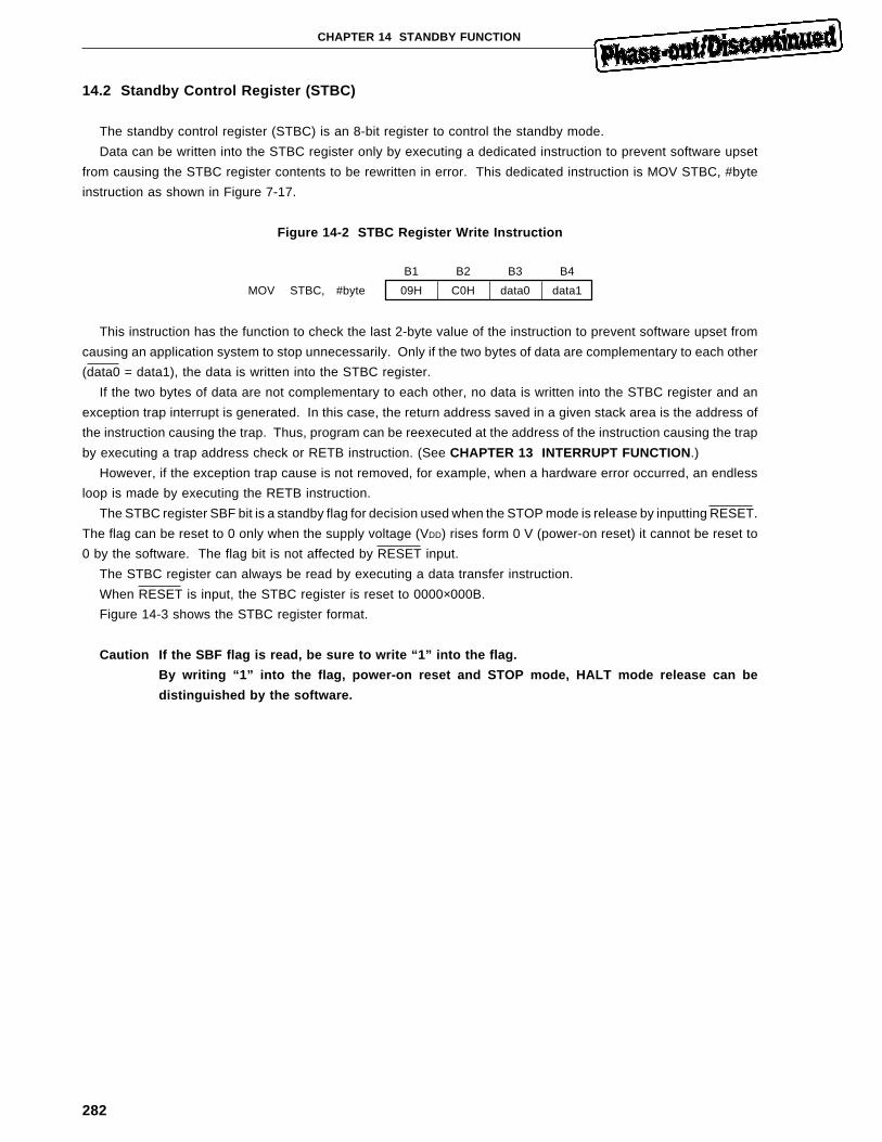
282
CHAPTER 14 STANDBY FUNCTION
14.2 Standby Control Register (STBC)
The standby control register (STBC) is an 8-bit register to control the standby mode.
Data can be written into the STBC register only by executing a dedicated instruction to prevent software upset
from causing the STBC register contents to be rewritten in error. This dedicated instruction is MOV STBC, #byte
instruction as shown in Figure 7-17.
Figure 14-2 STBC Register Write Instruction
B1 B2 B3 B4
MOV STBC, #byte 09H C0H data0 data1
This instruction has the function to check the last 2-byte value of the instruction to prevent software upset from
causing an application system to stop unnecessarily. Only if the two bytes of data are complementary to each other
(data0 = data1), the data is written into the STBC register.
If the two bytes of data are not complementary to each other, no data is written into the STBC register and an
exception trap interrupt is generated. In this case, the return address saved in a given stack area is the address of
the instruction causing the trap. Thus, program can be reexecuted at the address of the instruction causing the trap
by executing a trap address check or RETB instruction. (See CHAPTER 13 INTERRUPT FUNCTION.)
However, if the exception trap cause is not removed, for example, when a hardware error occurred, an endless
loop is made by executing the RETB instruction.
The STBC register SBF bit is a standby flag for decision used when the STOP mode is release by inputting RESET.
The flag can be reset to 0 only when the supply voltage (VDD) rises form 0 V (power-on reset) it cannot be reset to
0 by the software. The flag bit is not affected by RESET input.
The STBC register can always be read by executing a data transfer instruction.
When RESET is input, the STBC register is reset to 0000×000B.
Figure 14-3 shows the STBC register format.
Caution If the SBF flag is read, be sure to write “1” into the flag.
By writing “1” into the flag, power-on reset and STOP mode, HALT mode release can be
distinguished by the software.
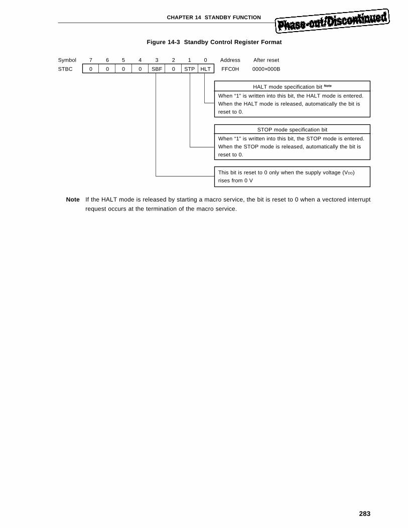
283
CHAPTER 14 STANDBY FUNCTION
Figure 14-3 Standby Control Register Format
Symbol 7 6 5 4 3 2 1 0 Address After reset
STBC 0 0 0 0 SBF 0 STP HLT FFC0H 0000×000B
HALT mode specification bit Note
When “1” is written into this bit, the HALT mode is entered.
When the HALT mode is released, automatically the bit is
reset to 0.
STOP mode specification bit
When “1” is written into this bit, the STOP mode is entered.
When the STOP mode is released, automatically the bit is
reset to 0.
This bit is reset to 0 only when the supply voltage (VDD)
rises from 0 V
Note If the HALT mode is released by starting a macro service, the bit is reset to 0 when a vectored interrupt
request occurs at the termination of the macro service.
284
CHAPTER 14 STANDBY FUNCTION
14.3 Operation
14.3.1 HALT mode
(1) HALT mode set and operation state
The HALT mode stops CPU clock.
The entire system power consumption can be reduced by setting the HALT mode when the CPU is idle.
The HALT mode is entered by setting the STBC register HLT bit to 1.
In the HALT mode, the CPU clock stops and program execution stops, but all the contents of the registers
and internal RAM just before the HALT mode is entered are retained. The on-chip peripheral hardware also
operates. Table 14-1 lists the hardware state in the HALT mode.
Caution If the interrupt request flag (IF ××) is set to 1 and MK ×× is set to 0 (unmask), the HALT mode
is not entered. In macro service processing (ISM ×× = 1), the HALT mode is entered after the
macro service is executed.
Table 14-1 Operation State in HALT Mode
Function Operation state
Clock generator Operation
Internal system clock
CPU Stop
I/O line Retention
On-chip peripheral hardware Operation
Internal data All the internal data such as the CPU status, data, and internal RAM
contents: The state before the HALT mode is set is retained.
In external device expansion AD0 to AD7 High impedance
mode A8 to A15 Retention
ASTB 0
RD 1
WR
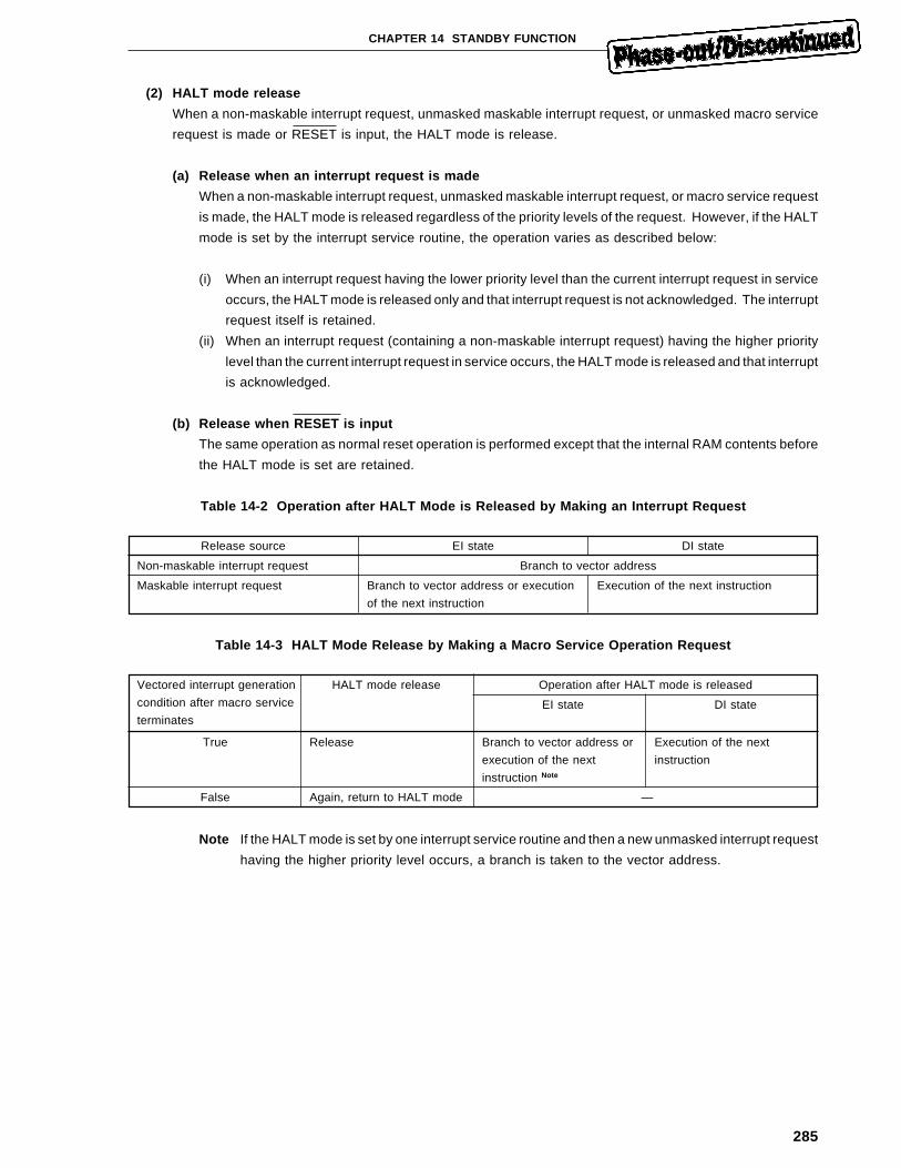
285
CHAPTER 14 STANDBY FUNCTION
(2) HALT mode release
When a non-maskable interrupt request, unmasked maskable interrupt request, or unmasked macro service
request is made or RESET is input, the HALT mode is release.
(a) Release when an interrupt request is made
When a non-maskable interrupt request, unmasked maskable interrupt request, or macro service request
is made, the HALT mode is released regardless of the priority levels of the request. However, if the HALT
mode is set by the interrupt service routine, the operation varies as described below:
(i) When an interrupt request having the lower priority level than the current interrupt request in service
occurs, the HALT mode is released only and that interrupt request is not acknowledged. The interrupt
request itself is retained.
(ii) When an interrupt request (containing a non-maskable interrupt request) having the higher priority
level than the current interrupt request in service occurs, the HALT mode is released and that interrupt
is acknowledged.
(b) Release when RESET is input
The same operation as normal reset operation is performed except that the internal RAM contents before
the HALT mode is set are retained.
Table 14-2 Operation after HALT Mode is Released by Making an Interrupt Request
Release source EI state DI state
Non-maskable interrupt request Branch to vector address
Maskable interrupt request Branch to vector address or execution Execution of the next instruction
of the next instruction
Table 14-3 HALT Mode Release by Making a Macro Service Operation Request
Vectored interrupt generation HALT mode release Operation after HALT mode is released
condition after macro service EI state DI stateterminates
True Release Branch to vector address or Execution of the next
execution of the next instruction
instruction Note
False Again, return to HALT mode —
Note If the HALT mode is set by one interrupt service routine and then a new unmasked interrupt request
having the higher priority level occurs, a branch is taken to the vector address.
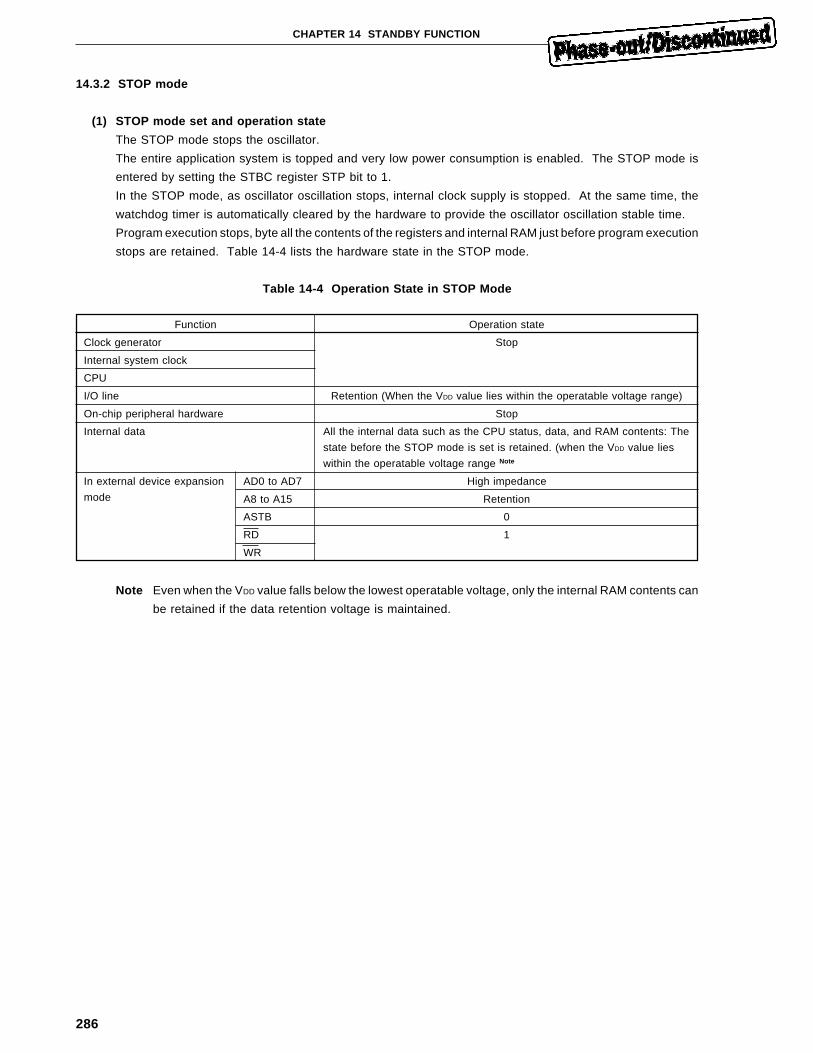
286
CHAPTER 14 STANDBY FUNCTION
14.3.2 STOP mode
(1) STOP mode set and operation state
The STOP mode stops the oscillator.
The entire application system is topped and very low power consumption is enabled. The STOP mode is
entered by setting the STBC register STP bit to 1.
In the STOP mode, as oscillator oscillation stops, internal clock supply is stopped. At the same time, the
watchdog timer is automatically cleared by the hardware to provide the oscillator oscillation stable time.
Program execution stops, byte all the contents of the registers and internal RAM just before program execution
stops are retained. Table 14-4 lists the hardware state in the STOP mode.
Table 14-4 Operation State in STOP Mode
Function Operation state
Clock generator Stop
Internal system clock
CPU
I/O line Retention (When the VDD value lies within the operatable voltage range)
On-chip peripheral hardware Stop
Internal data All the internal data such as the CPU status, data, and RAM contents: The
state before the STOP mode is set is retained. (when the VDD value lies
within the operatable voltage range Note
In external device expansion AD0 to AD7 High impedance
mode A8 to A15 Retention
ASTB 0
RD 1
WR
Note Even when the VDD value falls below the lowest operatable voltage, only the internal RAM contents can
be retained if the data retention voltage is maintained.
287
CHAPTER 14 STANDBY FUNCTION
(2) STOP mode release
When NMI or RESET is input, the STOP mode is release.
(a) Release when NMI is input
When valid edge is input to the NMI pin, the oscillator starts oscillation. After this, when the NMI input
is restored inactive, the watchdog timer starts counting. When the watchdog timer counter overflows,
internal system clock supply is started.
Thus, the µPD78334 waits for the time as long as the oscillation stable time:
(active level width after detection of valid edge input to NMI)
+
(watchdog timer overflow time)
The watchdog timer overflow time is specified by setting the WDM register. (See Figure 14-4 )
The operation after the STOP mode is released varies depending on what state the STOP mode is entered
in.
(i) If the watchdog timer interrupt request priority level is higher than the NMI interrupt request priority
level, when the STOP mode is entered during watchdog timer interrupt service routine execution, the
next instruction is executed after the STOP mode is release.
The NMI interrupt request itself is retained.
After control is returned from the service routine, the NMI interrupt request is acknowledge.
(ii) If the watchdog timer interrupt request priority level is lower than the NMI interrupt request priority
level, when the STOP mode is entered during watchdog timer interrupt routine execution, NMI
interrupt request is acknowledged and a branch is taken to the vector address after the STOP mode
is released.
The NMI and watchdog timer interrupt request priority levels are specified by setting the WDM register. (See
Figure 14-4 )
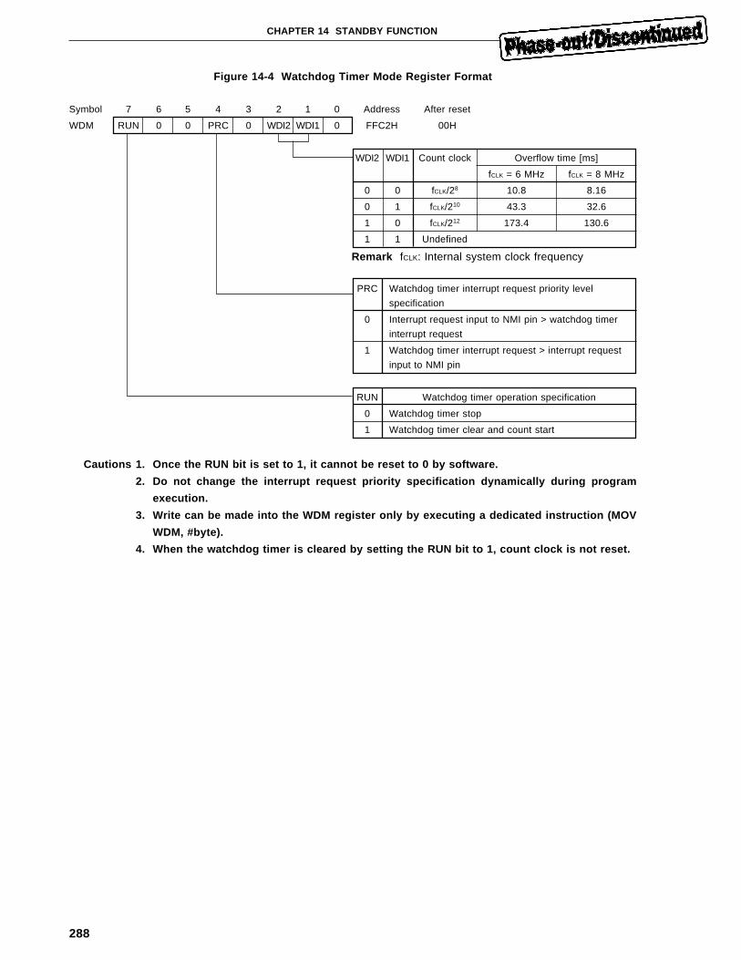
288
CHAPTER 14 STANDBY FUNCTION
Figure 14-4 Watchdog Timer Mode Register Format
Symbol 7 6 5 4 3 2 1 0 Address After reset
WDM RUN 0 0 PRC 0 WDI2 WDI1 0 FFC2H 00H
WDI2 WDI1 Count clock Overflow time [ms]
fCLK = 6 MHz fCLK = 8 MHz
0 0 fCLK/28 10.8 8.16
0 1 fCLK/210 43.3 32.6
1 0 fCLK/212 173.4 130.6
1 1 Undefined
Remark fCLK: Internal system clock frequency
PRC Watchdog timer interrupt request priority level
specification
0 Interrupt request input to NMI pin > watchdog timer
interrupt request
1 Watchdog timer interrupt request > interrupt request
input to NMI pin
RUN Watchdog timer operation specification
0 Watchdog timer stop
1 Watchdog timer clear and count start
Cautions 1. Once the RUN bit is set to 1, it cannot be reset to 0 by software.
2. Do not change the interrupt request priority specification dynamically during program
execution.
3. Write can be made into the WDM register only by executing a dedicated instruction (MOV
WDM, #byte).
4. When the watchdog timer is cleared by setting the RUN bit to 1, count clock is not reset.
289
CHAPTER 14 STANDBY FUNCTION
Figure 14-5 STOP Mode Release by NMI Input
Cautions 1. If the STOP mode is released when NMI is input, a branch to the NMI interrupt service
routine is taken after the one instruction (MOV STBC #byte) is executed. Place an
NOP instruction following the STOP mode setting instruction.
2. If an interrupt request occurs when a STOP mode setting instruction is being
executed, a branch to the NMI interrupt service routine is taken after the processing
of that interrupt is performed after the STOP mode is released. Before executing the
STOP mode setting instruction, mask all maskable interrupts.
If the maskable interrupts are not masked, operation after the STOP mode is released
varies, depending on the processing mode of the interrupt that occurs, as described
below:
(1) If a maskable interrupt request set as vectored interrupt processing occurs, a
branch is taken to the maskable interrupt service routine and one instruction
is executed, then a branch is taken to the NMI interrupt service routine.
(2) If a maskable interrupt request set as macro service processing occurs, the
macro service is executed, then a branch is taken to the NMI interrupt service
routine (NMI processing is pending until the macro service terminates).
3. When a watchdog timer interrupt request of a non-maskable interrupt occurs during
execution of a STOP mode setting instruction, even if the watchdog timer interrupt
request priority, a branch is taken to the NMI interrupt service routine after a branch
is taken to the watchdog timer interrupt service routine and one instruction is
executed. Enter NOP instruction at the top of the watchdog timer interrupt service
routine. Set a stack area considering that two nesting levels are used at the time.
(b) STOP mode release when RESET is input
At the same time as the high-to-low transition of RESET input is made to set the reset state, the oscillator
starts oscillation.
Provide the oscillation stable time during the period of RESET. After this, when the low-to-high transition
of RESET is made, normal operation is started.
Set STOP mode
Oscillator
fCLK
STOP status“Set”
“Release”
System clock“Stop”
“Supply”
NMI input(when rising edgeis specified) Stop oscillator Oscillation stable
timer count time
Normal mode

290
[MEMO]
291
CHAPTER 15 RESET FUNCTION
When a low level is input to the RESET pin, the system is reset and the hardware becomes as listed in Table 15-
1.
When the low-to-high transition of RESET input is made, the reset state is released and program execution is
started. Initialize the register contents by a program as required. Particularly, change the number of cycles in the
programmable wait control register (PWC) and fetch cycle control register (FCC) as required. After reset, these
registers are initialized to the following: Bus cycle = 2 – wait insertion and fetch cycle mode = normal mode.
The RESET pin contains a noise remover using an analog delay to prevent a noise from causing an error to occur.
Cautions 1. While RESET is active, all pins except WDTO, CLKOUT, AV REF, AVDD, AVSS, VDD, VSS, X1, or
X2 become high impedance.
2. When external RAM is added, connect pull-up resistors to the P90/RD and P91/WR pins. When
these pins become high impedance, the external RAM contents may be destroyed. A signal
collision occurs on the address/data bus and the input/output circuit can be destroyed.
Figure 15-1 Reset Signal Acknowledge
In reset operation when the power is turned on, provide the oscillation stable time from power on to reset
acknowledge, as shown in Figure 15-2.
Figure 15-2 Reset when Power is Turned On
RESET input
Analogdelay
Analogdelay
Analogdelay
Removedas noise
Resetacknow-ledgement
Resetrelease
Resetrelease
Analogdelay
Oscillationstable time
292
CHAPTER 15 RESET FUNCTION
Table 15-1 Hardware State After Reset (1/2)
Hardware State after reset
Control registers Program counter (PC) Reset vector table
(0000H and 0001H)
contents are set
Stack pointer (SP) Undefined Note
Program status word (PSW) 0000H
CPU control word (CCW) 00H
Internal RAM Data memory Undefined Note
General registers (R0 to R15)
Ports Output latches (P0, P1, P3 to P5, P9) Undefined
Mode registers (PM0, PM1, PM3, PM5) FFH
(PM9) ××11 1111B
Mode control register (PMC0, PMC1, PMC3) 00H
Port read control register (PRDC)
Real-time output port Real-time output port register (RTP) Undefined
(RTP) Real-time output port set register (RTPS) 00H
Real time output port reset register (RTPR)
Real-time pulse unit Timers (TM0, TM1, TM2, TM3) 0000H
(RTP) Timer low access register (TLA) Undefined
Timer unit mode registers (TUM0, TUM1) 00H
Timer control register (TMC0)
Timer control register (TMC1) 40H
Timer output control registers (TOC0, TOC1) 00H
Programmable pulse output set register (PPOS)
Compare registers (CMX0, CM01R, CM02R, CM03R, CM04R) Undefined
(CM11, CM12, CM20, CM21, CM30)
Capture/compare registers (CC00R, CC01R)
Capture registers (CT00, CT01, CT02, CT10)
PWM output function PWM control register (PWMC) 00H
PWM buffer registers (PWM0, PWM1) Undefined
A/D converter A/D converter mode registers (ADM) 00H
A/D conversion result registers (ADCR0 to ADCR7) Undefined
Serial interface Asynchronous serial interface mode register (ASIM) 80H
Asynchronous serial interface status register (ASIS) 00H
Clocked serial interface mode register (CSIM) 00H
Serial bus interface control register (SBIC)
Serial shift register (SIO) Undefined
Serial receive buffer (RXB)
Serial transmit shift register (TXS)
Baud rate generator compare register (BRG) 0000H
Baud rate generator mode register (BRGM) 00H
External expansion Memory expansion mode register (MM) 00H
function Programmable wait control register (PWC) 22H
Fetch cycle control register (FCC) 00H
Watchdog timer Watchdog timer mode register (WDM) 00H
Note If the STOP mode is released by RESET input, the values before the STOP mode is set are retained.
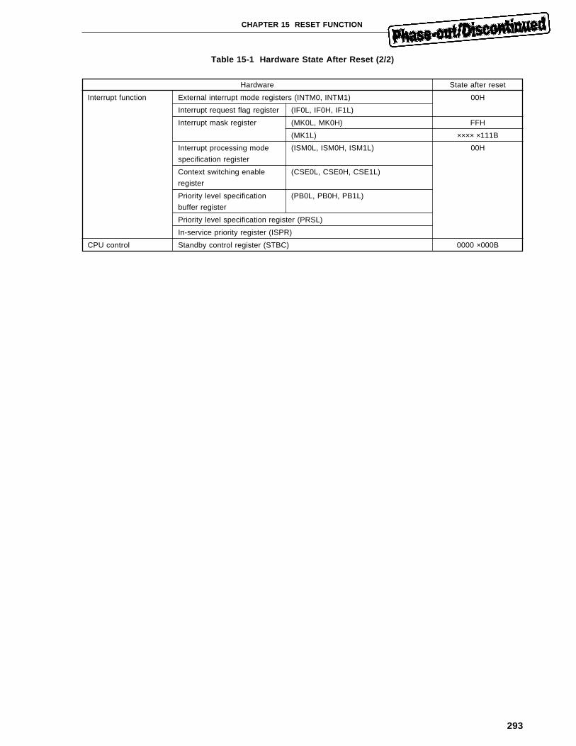
293
CHAPTER 15 RESET FUNCTION
Table 15-1 Hardware State After Reset (2/2)
Hardware State after reset
Interrupt function External interrupt mode registers (INTM0, INTM1) 00H
Interrupt request flag register (IF0L, IF0H, IF1L)
Interrupt mask register (MK0L, MK0H) FFH
(MK1L) ×××× ×111B
Interrupt processing mode (ISM0L, ISM0H, ISM1L) 00H
specification register
Context switching enable (CSE0L, CSE0H, CSE1L)
register
Priority level specification (PB0L, PB0H, PB1L)
buffer register
Priority level specification register (PRSL)
In-service priority register (ISPR)
CPU control Standby control register (STBC) 0000 ×000B

294
[MEMO]
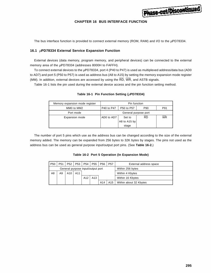
295
CHAPTER 16 BUS INTERFACE FUNCTION
The bus interface function is provided to connect external memory (ROM, RAM) and I/O to the µPD78334.
16.1 µPD78334 External Service Expansion Function
External devices (data memory, program memory, and peripheral devices) can be connected to the external
memory area of the µPD78334 (addresses 8000H to FAFFH).
To connect external devices to the µPD78334, port 4 (P40 to P47) is used as multiplexed address/data bus (AD0
to AD7) and port 5 (P50 to P57) is used as address bus (A8 to A15) by setting the memory expansion mode register
(MM). In addition, external devices are accessed by using the RD, WR, and ASTB signals.
Table 16-1 lists the pin used during the external device access and the pin function setting method.
Table 16-1 Pin Function Setting ( µPD78334)
Memory expansion mode register Pin function
MM0 to MM2 P40 to P47 P50 to P57 P90 P91
Port mode General purpose port
Expansion mode AD0 to AD7 Set to RD WR
A8 to A15 by
stage
The number of port 5 pins which use as the address bus can be changed according to the size of the external
memory added. The memory can be expanded from 256 bytes to 32K bytes by stages. The pins not used as the
address bus can be used as general purpose input/output port pins. (See Table 16-2. )
Table 16-2 Port 5 Operation (In Expansion Mode)
P50 P51 P52 P53 P54 P55 P56 P57 External address space
General purpose input/output port Within 256 bytes
A8 A9 A10 A11 Within 4 Kbytes
A12 A13 Within 16 Kbytes
A14 A15 Within about 32 Kbytes
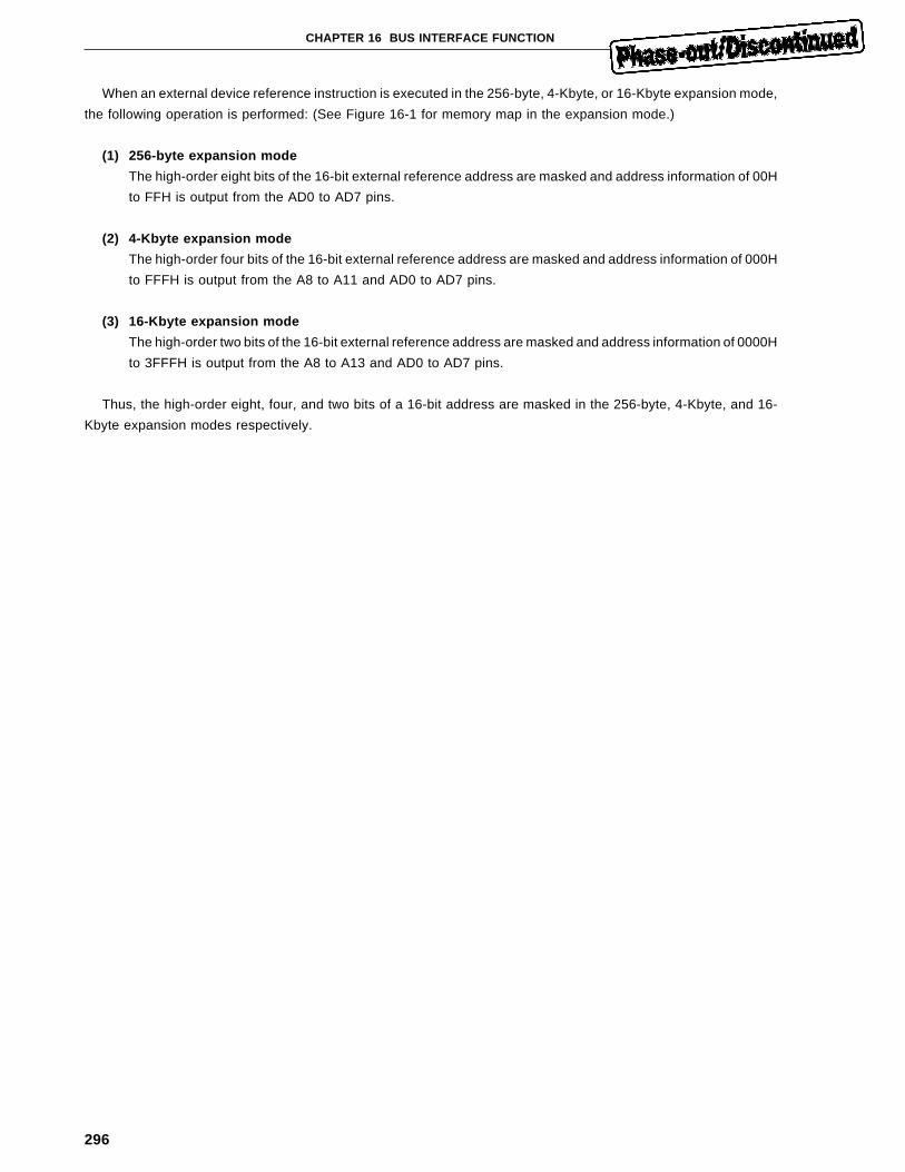
296
CHAPTER 16 BUS INTERFACE FUNCTION
When an external device reference instruction is executed in the 256-byte, 4-Kbyte, or 16-Kbyte expansion mode,
the following operation is performed: (See Figure 16-1 for memory map in the expansion mode.)
(1) 256-byte expansion mode
The high-order eight bits of the 16-bit external reference address are masked and address information of 00H
to FFH is output from the AD0 to AD7 pins.
(2) 4-Kbyte expansion mode
The high-order four bits of the 16-bit external reference address are masked and address information of 000H
to FFFH is output from the A8 to A11 and AD0 to AD7 pins.
(3) 16-Kbyte expansion mode
The high-order two bits of the 16-bit external reference address are masked and address information of 0000H
to 3FFFH is output from the A8 to A13 and AD0 to AD7 pins.
Thus, the high-order eight, four, and two bits of a 16-bit address are masked in the 256-byte, 4-Kbyte, and 16-
Kbyte expansion modes respectively.
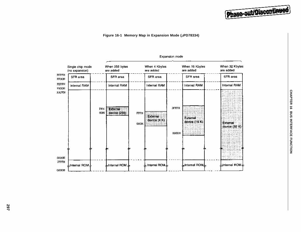
297
CH
AP
TE
R 16 B
US
INT
ER
FA
CE
FU
NC
TIO
N
Figure 16-1 Memory Map in Expansion Mode ( µPD78334)
298
CHAPTER 16 BUS INTERFACE FUNCTION
16.2 µPD78330 External Device Access
Since the µPD78330 does not contain internal ROM, external devices (data memory, program memory and
peripheral devices) can be connected to any area other than internal RAM (addresses 0000H to FAFFH).
When external devices are connected, port 4 (P40 to P47) is used as multiplexed address/data bus (AD0 to AD7)
and port 5 (P50 to P57) is used as address bus (A8 to A15). In addition, external devices are accessed by using the
RD, WR, and ASTB signals. Fix the EA pin low.
On the µPD78330, specification is the memory expansion mode register (MM) MM0 to MM2 bits is insignificant
and ports 4 and 5 always function as the AD0 to AD7 pins and the A8 to A15 pins.
Unlike the µPD78334, the µPD78330 memory size cannot be expanded by stages.
Table 16-3 lists the pins used during external device access and the pin function setting method.
Table 16-3 Pin Function Setting ( µPD78330)
EA pin Pin function
P40 to P47 P50 to P57 P90 P91
0 AD0 to AD7 A8 to A15 RD WR
Figure 16-2 µPD78330 Memory Map
SFR area
Internal RAM
External devices
FFFFH
FF00HFEFFH
FB00HFAFFH
0000H
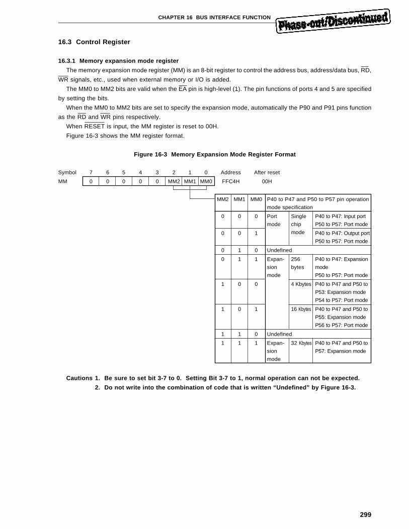
299
CHAPTER 16 BUS INTERFACE FUNCTION
16.3 Control Register
16.3.1 Memory expansion mode register
The memory expansion mode register (MM) is an 8-bit register to control the address bus, address/data bus, RD,
WR signals, etc., used when external memory or I/O is added.
The MM0 to MM2 bits are valid when the EA pin is high-level (1). The pin functions of ports 4 and 5 are specified
by setting the bits.
When the MM0 to MM2 bits are set to specify the expansion mode, automatically the P90 and P91 pins function
as the RD and WR pins respectively.
When RESET is input, the MM register is reset to 00H.
Figure 16-3 shows the MM register format.
Figure 16-3 Memory Expansion Mode Register Format
Symbol 7 6 5 4 3 2 1 0 Address After reset
MM 0 0 0 0 0 MM2 MM1 MM0 FFC4H 00H
MM2 MM1 MM0 P40 to P47 and P50 to P57 pin operation
mode specification
0 0 0 Port Single P40 to P47: Input port
mode chip P50 to P57: Port mode
0 0 1 mode P40 to P47: Output port
P50 to P57: Port mode
0 1 0 Undefined
0 1 1 Expan- 256 P40 to P47: Expansion
sion bytes mode
mode P50 to P57: Port mode
1 0 0 4 Kbytes P40 to P47 and P50 to
P53: Expansion mode
P54 to P57: Port mode
1 0 1 16 Kbytes P40 to P47 and P50 to
P55: Expansion mode
P56 to P57: Port mode
1 1 0 Undefined
1 1 1 Expan- 32 Kbytes P40 to P47 and P50 to
sion P57: Expansion mode
mode
Cautions 1. Be sure to set bit 3-7 to 0. Setting Bit 3-7 to 1, normal operation can not be expected.
2. Do not write into the combination of code that is written “Undefined” by Figure 16-3.
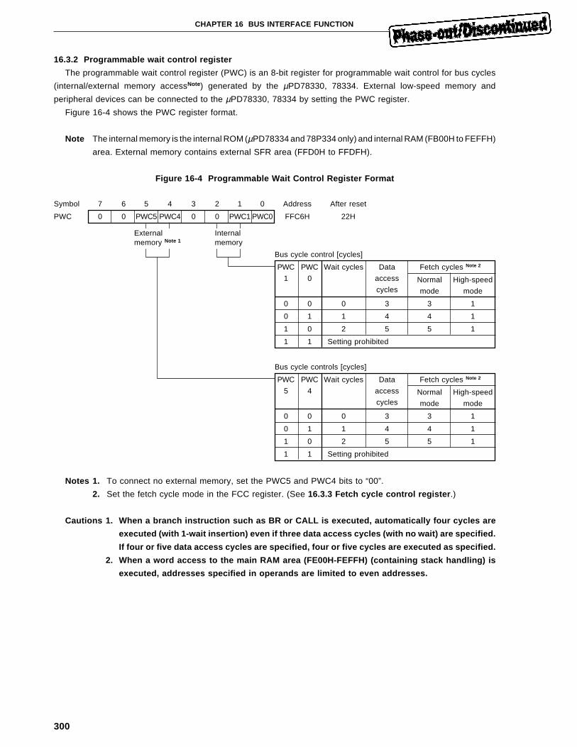
300
CHAPTER 16 BUS INTERFACE FUNCTION
16.3.2 Programmable wait control register
The programmable wait control register (PWC) is an 8-bit register for programmable wait control for bus cycles
(internal/external memory accessNote) generated by the µPD78330, 78334. External low-speed memory and
peripheral devices can be connected to the µPD78330, 78334 by setting the PWC register.
Figure 16-4 shows the PWC register format.
Note The internal memory is the internal ROM (µPD78334 and 78P334 only) and internal RAM (FB00H to FEFFH)
area. External memory contains external SFR area (FFD0H to FFDFH).
Figure 16-4 Programmable Wait Control Register Format
Symbol 7 6 5 4 3 2 1 0 Address After reset
PWC 0 0 PWC5 PWC4 0 0 PWC1 PWC0 FFC6H 22H
Bus cycle control [cycles]
PWC PWC Wait cycles Data Fetch cycles Note 2
1 0 access Normal High-speedcycles mode mode
0 0 0 3 3 1
0 1 1 4 4 1
1 0 2 5 5 1
1 1 Setting prohibited
Bus cycle controls [cycles]
PWC PWC Wait cycles Data Fetch cycles Note 2
5 4 access Normal High-speedcycles mode mode
0 0 0 3 3 1
0 1 1 4 4 1
1 0 2 5 5 1
1 1 Setting prohibited
Notes 1. To connect no external memory, set the PWC5 and PWC4 bits to “00”.
2. Set the fetch cycle mode in the FCC register. (See 16.3.3 Fetch cycle control register .)
Cautions 1. When a branch instruction such as BR or CALL is executed, automatically four cycles are
executed (with 1-wait insertion) even if three data access cycles (with no wait) are specified.
If four or five data access cycles are specified, four or five cycles are executed as specified.
2. When a word access to the main RAM area (FE00H-FEFFH) (containing stack handling) is
executed, addresses specified in operands are limited to even addresses.
Externalmemory Note 1
Internalmemory
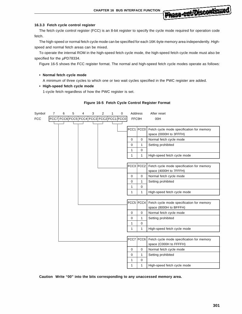
301
CHAPTER 16 BUS INTERFACE FUNCTION
16.3.3 Fetch cycle control register
The fetch cycle control register (FCC) is an 8-bit register to specify the cycle mode required for operation code
fetch.
The high-speed or normal fetch cycle mode can be specified for each 16K-byte memory area independently. High-
speed and normal fetch areas can be mixed.
To operate the internal ROM in the high-speed fetch cycle mode, the high-speed fetch cycle mode must also be
specified for the µPD78334.
Figure 16-5 shows the FCC register format. The normal and high-speed fetch cycle modes operate as follows:
• Normal fetch cycle mode
A minimum of three cycles to which one or two wait cycles specified in the PWC register are added.
• High-speed fetch cycle mode
1-cycle fetch regardless of how the PWC register is set.
Figure 16-5 Fetch Cycle Control Register Format
Symbol 7 6 5 4 3 2 1 0 Address After reset
FCC FCC7 FCC6 FCC5 FCC4 FCC3 FCC2 FCC1 FCC0 FFC9H 00H
FCC1 FCC0 Fetch cycle mode specification for memory
space (0000H to 3FFFH)
0 0 Normal fetch cycle mode
0 1 Setting prohibited
1 0
1 1 High-speed fetch cycle mode
FCC3 FCC2 Fetch cycle mode specification for memory
space (4000H to 7FFFH)
0 0 Normal fetch cycle mode
0 1 Setting prohibited
1 0
1 1 High-speed fetch cycle mode
FCC5 FCC4 Fetch cycle mode specification for memory
space (8000H to BFFFH)
0 0 Normal fetch cycle mode
0 1 Setting prohibited
1 0
1 1 High-speed fetch cycle mode
FCC7 FCC6 Fetch cycle mode specification for memory
space (C000H to FFFFH)
0 0 Normal fetch cycle mode
0 1 Setting prohibited
1 0
1 1 High-speed fetch cycle mode
Caution Write “00” into the bits corresponding to any unaccessed memory area.

302
[MEMO]
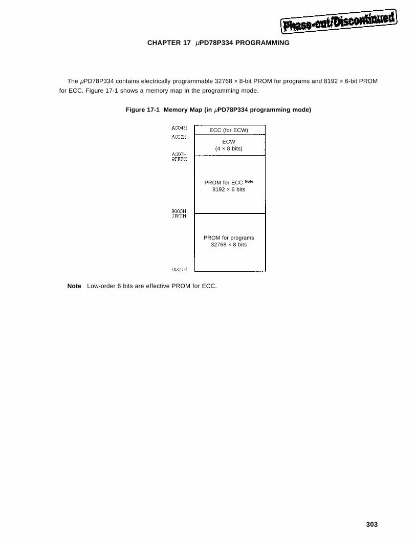
303
CHAPTER 17 µPD78P334 PROGRAMMING
The µPD78P334 contains electrically programmable 32768 × 8-bit PROM for programs and 8192 × 6-bit PROM
for ECC. Figure 17-1 shows a memory map in the programming mode.
Figure 17-1 Memory Map (in µPD78P334 programming mode)
Note Low-order 6 bits are effective PROM for ECC.
ECC (for ECW)
ECW(4 × 8 bits)
PROM for ECC Note
8192 × 6 bits
PROM for programs32768 × 8 bits
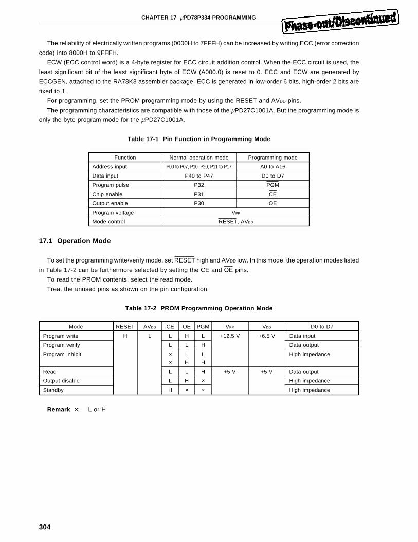
304
CHAPTER 17 µPD78P334 PROGRAMMING
The reliability of electrically written programs (0000H to 7FFFH) can be increased by writing ECC (error correction
code) into 8000H to 9FFFH.
ECW (ECC control word) is a 4-byte register for ECC circuit addition control. When the ECC circuit is used, the
least significant bit of the least significant byte of ECW (A000.0) is reset to 0. ECC and ECW are generated by
ECCGEN, attached to the RA78K3 assembler package. ECC is generated in low-order 6 bits, high-order 2 bits are
fixed to 1.
For programming, set the PROM programming mode by using the RESET and AVDD pins.
The programming characteristics are compatible with those of the µPD27C1001A. But the programming mode is
only the byte program mode for the µPD27C1001A.
Table 17-1 Pin Function in Programming Mode
Function Normal operation mode Programming mode
Address input P00 to P07, P10, P20, P11 to P17 A0 to A16
Data input P40 to P47 D0 to D7
Program pulse P32 PGM
Chip enable P31 CE
Output enable P30 OE
Program voltage VPP
Mode control RESET, AVDD
17.1 Operation Mode
To set the programming write/verify mode, set RESET high and AVDD low. In this mode, the operation modes listed
in Table 17-2 can be furthermore selected by setting the CE and OE pins.
To read the PROM contents, select the read mode.
Treat the unused pins as shown on the pin configuration.
Table 17-2 PROM Programming Operation Mode
Mode RESET AVDD CE OE PGM VPP VDD D0 to D7
Program write H L L H L +12.5 V +6.5 V Data input
Program verify L L H Data output
Program inhibit × L L High impedance
× H H
Read L L H +5 V +5 V Data output
Output disable L H × High impedance
Standby H × × High impedance
Remark ×: L or H
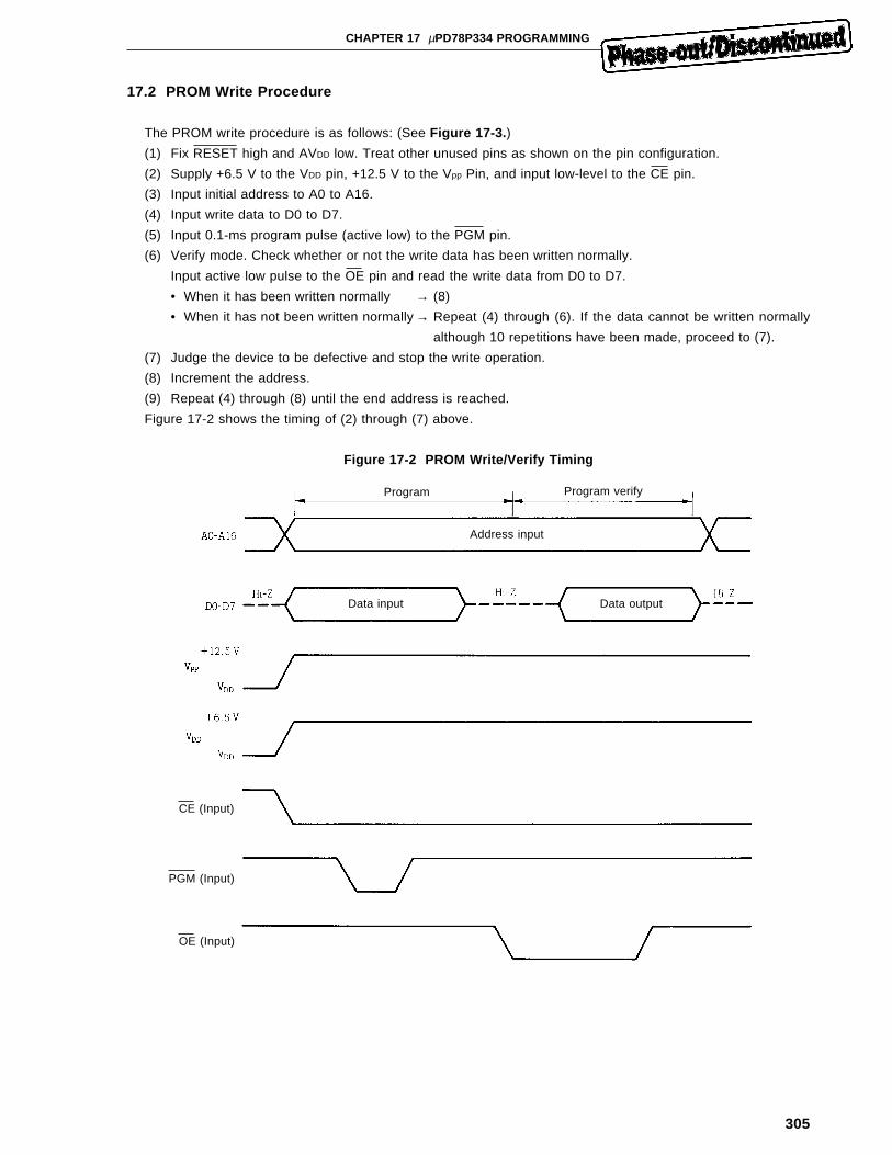
305
CHAPTER 17 µPD78P334 PROGRAMMING
17.2 PROM Write Procedure
The PROM write procedure is as follows: (See Figure 17-3. )
(1) Fix RESET high and AVDD low. Treat other unused pins as shown on the pin configuration.
(2) Supply +6.5 V to the VDD pin, +12.5 V to the Vpp Pin, and input low-level to the CE pin.
(3) Input initial address to A0 to A16.
(4) Input write data to D0 to D7.
(5) Input 0.1-ms program pulse (active low) to the PGM pin.
(6) Verify mode. Check whether or not the write data has been written normally.
Input active low pulse to the OE pin and read the write data from D0 to D7.
• When it has been written normally → (8)
• When it has not been written normally → Repeat (4) through (6). If the data cannot be written normally
although 10 repetitions have been made, proceed to (7).
(7) Judge the device to be defective and stop the write operation.
(8) Increment the address.
(9) Repeat (4) through (8) until the end address is reached.
Figure 17-2 shows the timing of (2) through (7) above.
Figure 17-2 PROM Write/Verify Timing
Program Program verify
Data input Data output
CE (Input)
PGM (Input)
OE (Input)
Address input
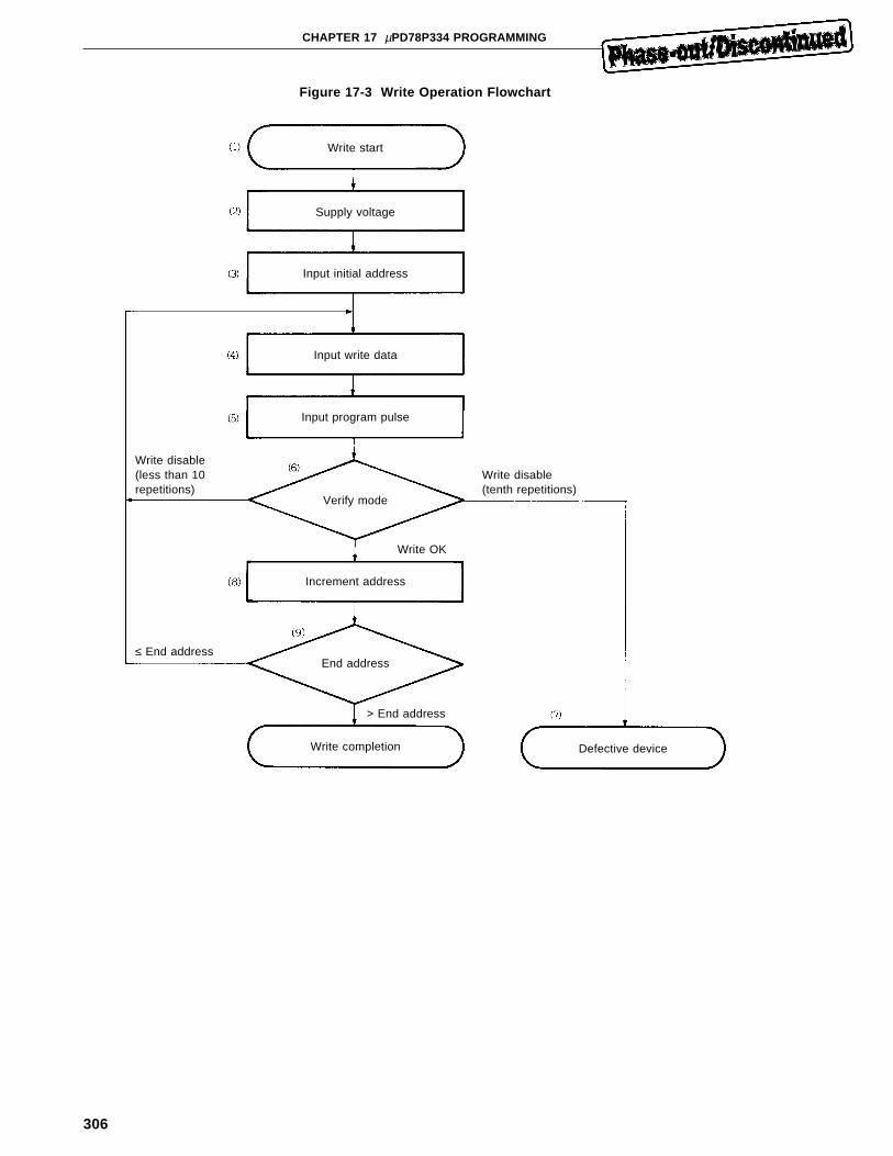
306
CHAPTER 17 µPD78P334 PROGRAMMING
Figure 17-3 Write Operation Flowchart
Write start
Supply voltage
Input initial address
Input write data
Input program pulse
Verify mode
Increment address
End address
Write completion Defective device
> End address
≤ End address
Write disable(less than 10repetitions)
Write disable(tenth repetitions)
Write OK
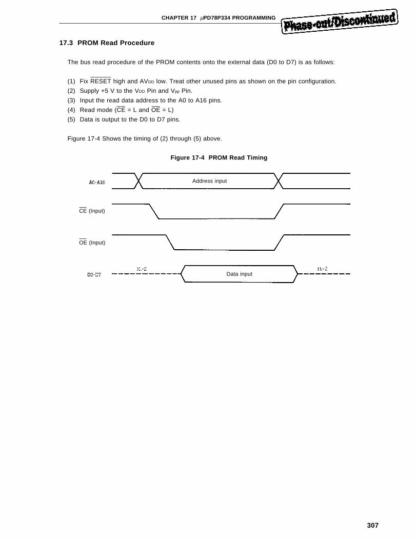
307
CHAPTER 17 µPD78P334 PROGRAMMING
17.3 PROM Read Procedure
The bus read procedure of the PROM contents onto the external data (D0 to D7) is as follows:
(1) Fix RESET high and AVDD low. Treat other unused pins as shown on the pin configuration.
(2) Supply +5 V to the VDD Pin and Vpp Pin.
(3) Input the read data address to the A0 to A16 pins.
(4) Read mode (CE = L and OE = L)
(5) Data is output to the D0 to D7 pins.
Figure 17-4 Shows the timing of (2) through (5) above.
Figure 17-4 PROM Read Timing
Address input
Data input
CE (Input)
OE (Input)
308
CHAPTER 17 µPD78P334 PROGRAMMING
17.4 Erasion Characteristics ( µPD78P334KM, 78P334KW only)
The data contents written into the µPD78P334KM, 78P334KW program memory can be erased (FFH) and new
data can be written into program memory.
To erase the data contents, apply rays having a wave length shorter than about 400 nm to the window. Normally,
apply ultraviolet rays having a 254-nm wave length. The radiation amount required to completely erase the data
contents is as follows:
• Ultraviolet strength × erasion time: 15W • s/cm2 or more
• Erasion time: 15 to 20 minutes (when a 12000 µW/cm2 ultraviolet lamp is used. However, the time may be
prolonged due to ultraviolet lamp performance deterioration, dirty package window, etc.)
For erasion, place an ultraviolet lamp at a position within 2.5 cm from the window. If a filter is attached to the
ultraviolet lamp, remove the filter before erasion.
17.5 Window Seal ( µPD78P334KM, 78P334KW only)
If the µPD78P334KM, 78P334KW is exposed to sunlight or fluorescent lamp light for hours, data in EPROM may
be erased or the internal circuit may malfunction. To prevent such an accident from occurring, put a protective seal
on the window, except when the data contents are erased.
A protective seal whose quality is guaranteed by NEC Corporation, is attached to each EPROM-version package
product with a window for shipment.
17.6 One-time PROM Product Screening
The one-time PROM products (µPD78P334GJ and 78P334LQ) cannot be completely tested by NEC for shipment
because of the structures. For screening, it is recommended to verify PROM after storing the necessary data under
the following conditions:
Storage temperature Storage time
125°C 24 hours
NEC will make service of one-time PROM write to sealing to screening to verification for pay under the name of
QTOP™ MICON. For details, ask the salesperson.
309
CHAPTER 18 INSTRUCTION SET
18.1 Operation List
18.1.1 Operand identifiers and description
In the operand field of each instruction, describe the operands according to the description for the operand
identifiers of the instruction. (For details, see the assembler specifications.)
Select one of the entries under the description, if present. The uppercase alphabetic characters and the +, –, #,
$, !, and [ ] symbols are keywords which should be described exactly as shown.
For immediate data, describe a proper numeric value of label. To describe the immediate data with a label, be
sure to describe the symbols #, $, !, [ ] as well.
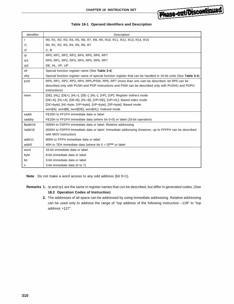
310
CHAPTER 18 INSTRUCTION SET
Table 18-1 Operand Identifiers and Description
Identifier Description
r R0, R1, R2, R3, R4, R5, R6, R7, R8, R9, R10, R11, R12, R13, R14, R15
r1 R0, R1, R2, R3, R4, R5, R6, R7
r2 C, B
rp RP0, RP1, RP2, RP3, RP4, RP5, RP6, RP7
rp1 RP0, RP1, RP2, RP3, RP4, RP5, RP6, RP7
rp2 DE, HL, VP, UP
sfr Special function register name (See Table 3-4 )
sfrp Special function register name of special function register that can be handled in 16-bit units (See Table 3-4 )
post RP0, RP1, RP2, RP3, RP4, RP5,/PSW, RP6, RP7 (more than one cam be described. bit RP5 can be
described only with PUSH and POP instructions and PSW can be described only with PUSHU and POPU
instructions)
mem [DE], [HL], [DE+], [HL+], [DE–], [HL–], [VP], [UP]: Register indirect mode
[DE+A], [HL+A], [DE+B], [HL+B], [VP+DE], [UP+HL]: Based index mode
[DE+byte], [HL+byte, [VP+byte], [UP+byte], [SP+byte]: Based mode
word[A], word[B], word[DE], word[HL]: Indexed mode
saddr FE20H to FF1FH immediate data or label
saddrp FE20H to FF1FH immediate data (where bit 0=0) or label (16-bit operation)
$addr16 0000H to FDFFH immediate data or label: Relative addressing
!addr16 0000H to FDFFH immediate data or label: Immediate addressing (however, up to FFFFH can be described
with MOV instruction)
addr11 800H to FFFH immediate data or label
addr5 40H to 7EH immediate data (where bit 0 = 0)Note or label
word 16-bit immediate data or label
byte 8-bit immediate data or label
bit 3-bit immediate data or label
n 3-bit immediate data (0 to 7)
Note Do not make a word access to any odd address (bit 0=1).
Remarks 1. rp and rp1 are the same in register names that con be described, but differ in generated codes. (See
18.2 Operation Codes of Instruction )
2. The addresses of all space can be addressed by using immediate addressing. Relative addressing
can be used only to address the range of “top address of the following instruction –128” to “top
address +127”.
311
CHAPTER 18 INSTRUCTION SET
The function names as well as the absolute names (R0 to 15 and RP0 to RP7) can be described in 8-bit register
identifiers r and r1 and 16-bit register pair identifiers rp, rp1, and post. Tables 9-2 and 9-3 pair list the correspondence
between the absolute and function names of the registers.
Table 18-2 Correspondence between Absolute and Function Names of 8-bit Registers
Absolute nameFunction name
Absolute nameFunction name
RSS = 0 RSS = 1 RSS = 0 RSS = 1
R0 X R8 VPL VPL
R1 A R9 VPH VPH
R2 C R10 UPL UPL
R3 B R11 UPH UPH
R4 X R12 E E
R5 A R13 D D
R6 C R14 L L
R7 B R15 H H
Table 18-3 Correspondence between Absolute and Function Names of 16-bit Register Pairs
Absolute nameFunction name
RSS = 0 RSS = 1
RP0 AX
RP1 BC
RP2 AX
RP3 BC
RP4 VP VP
RP5 UP UP
RP6 DE DE
RP7 HL HL
The RSS is a register set selection flag (PSW bit 5). The correspondence between the absolute and function names
changed by setting or resetting the flag.
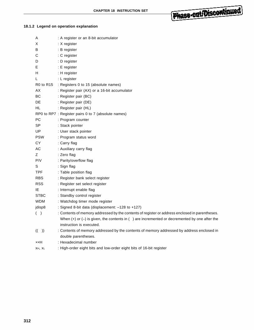
312
CHAPTER 18 INSTRUCTION SET
18.1.2 Legend on operation explanation
A : A register or an 8-bit accumulator
X : X register
B : B register
C : C register
D : D register
E : E register
H : H register
L : L register
R0 to R15 : Registers 0 to 15 (absolute names)
AX : Register pair (AX) or a 16-bit accumulator
BC : Register pair (BC)
DE : Register pair (DE)
HL : Register pair (HL)
RP0 to RP7 : Register pairs 0 to 7 (absolute names)
PC : Program counter
SP : Stack pointer
UP : User stack pointer
PSW : Program status word
CY : Carry flag
AC : Auxiliary carry flag
Z : Zero flag
P/V : Parity/overflow flag
S : Sign flag
TPF : Table position flag
RBS : Register bank select register
RSS : Register set select register
IE : Interrupt enable flag
STBC : Standby control register
WDM : Watchdog timer mode register
jdisp8 : Signed 8-bit data (displacement: –128 to +127)
( ) : Contents of memory addressed by the contents of register or address enclosed in parentheses.
When (+) or (–) is given, the contents in ( ) are incremented or decremented by one after the
instruction is executed.
(( )) : Contents of memory addressed by the contents of memory addressed by address enclosed in
double parentheses.
××H : Hexadecimal number
xH, xL : High-order eight bits and low-order eight bits of 16-bit register
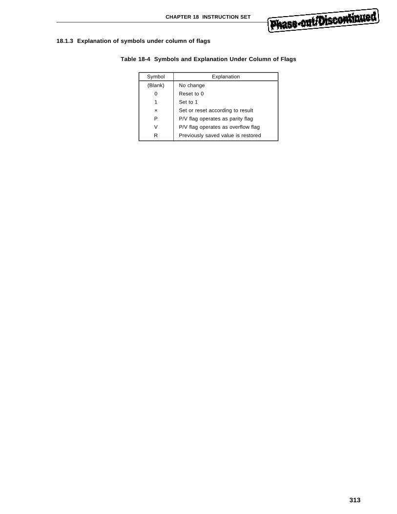
313
CHAPTER 18 INSTRUCTION SET
18.1.3 Explanation of symbols under column of flags
Table 18-4 Symbols and Explanation Under Column of Flags
Symbol Explanation
(Blank) No change
0 Reset to 0
1 Set to 1
× Set or reset according to result
P P/V flag operates as parity flag
V P/V flag operates as overflow flag
R Previously saved value is restored
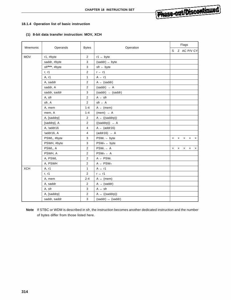
314
CHAPTER 18 INSTRUCTION SET
18.1.4 Operation list of basic instruction
(1) 8-bit data transfer instruction: MOV, XCH
Mnemonic Operands Bytes OperationFlags
S Z AC P/V CY
MOV r1, #byte 2 r1 ← byte
saddr, #byte 3 (saddr) ← byte
sfrNote, #byte 3 sfr ← byte
r, r1 2 r ← r1
A, r1 1 A ← r1
A, saddr 2 A ← (saddr)
saddr, A 2 (saddr) ← A
saddr, saddr 3 (saddr) ← (saddr)
A, sfr 2 A ← sfr
sfr, A 2 sfr ← A
A, mem 1-4 A ← (mem)
mem, A 1-4 (mem) ← A
A, [saddrp] 2 A ← ((saddrp))
[saddrp], A 2 ((saddrp)) ← A
A, !addr16 4 A ← (addr16)
!addr16, A 4 (addr16) ← A
PSWL, #byte 3 PSWL ← byte × × × × ×
PSWH, #byte 3 PSWH ← byte
PSWL, A 2 PSWL ← A × × × × ×
PSWH, A 2 PSWH ← A
A, PSWL 2 A ← PSWL
A, PSWH 2 A ← PSWH
XCH A, r1 1 A ↔ r1
r, r1 2 r ↔ r1
A, mem 2-4 A ↔ (mem)
A, saddr 2 A → (saddr)
A, sfr 3 A ↔ sfr
A, [saddrp] 2 A ↔ ((saddrp))
saddr, saddr 3 (saddr) ↔ (saddr)
Note If STBC or WDM is described in sfr, the instruction becomes another dedicated instruction and the number
of bytes differ from those listed here.
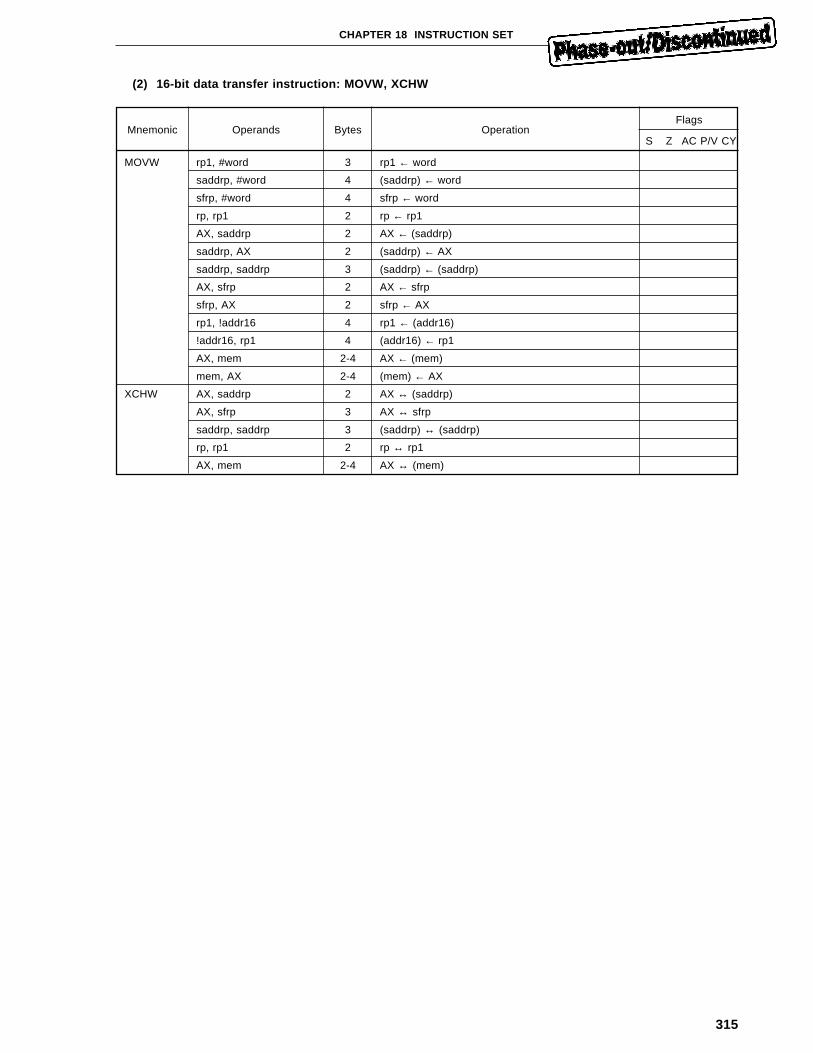
315
CHAPTER 18 INSTRUCTION SET
(2) 16-bit data transfer instruction: MOVW, XCHW
Mnemonic Operands Bytes OperationFlags
S Z AC P/V CY
MOVW rp1, #word 3 rp1 ← word
saddrp, #word 4 (saddrp) ← word
sfrp, #word 4 sfrp ← word
rp, rp1 2 rp ← rp1
AX, saddrp 2 AX ← (saddrp)
saddrp, AX 2 (saddrp) ← AX
saddrp, saddrp 3 (saddrp) ← (saddrp)
AX, sfrp 2 AX ← sfrp
sfrp, AX 2 sfrp ← AX
rp1, !addr16 4 rp1 ← (addr16)
!addr16, rp1 4 (addr16) ← rp1
AX, mem 2-4 AX ← (mem)
mem, AX 2-4 (mem) ← AX
XCHW AX, saddrp 2 AX ↔ (saddrp)
AX, sfrp 3 AX ↔ sfrp
saddrp, saddrp 3 (saddrp) ↔ (saddrp)
rp, rp1 2 rp ↔ rp1
AX, mem 2-4 AX ↔ (mem)
316
CHAPTER 18 INSTRUCTION SET
(3) 8-bit arithmetic and logical instruction: ADD, ADDC, SUB, SUBC, AND, OR, XOR, CMP
(1/2)
Mnemonic Operands Bytes OperationFlags
S Z AC P/V CY
ADD A, #byte 2 A, CY ← A + byte × × × V ×
saddr, #byte 3 (saddr), CY ← (saddr) + byte × × × V ×
sfr, #byte 4 sfr, CY ← sfr + byte × × × V ×
r, r1 2 r, CY ← r + r1 × × × V ×
A, saddr 2 A, CY ← A + (saddr) × × × V ×
A, sfr 3 A, CY ← A + sfr × × × V ×
saddr, saddr 3 (saddr), CY ← (saddr) + (saddr) × × × V ×
A, mem 2-4 A, CY ← A + (mem) × × × V ×
mem, A 2-4 (mem), CY ← (mem) + A × × × V ×
ADDC A, #byte 2 A, CY ← A + byte + CY × × × V ×
saddr, #byte 3 (saddr), CY ← (saddr) + byte + CY × × × V ×
sfr, #byte 4 sfr, CY ← sfr + byte + CY × × × V ×
r, r1 2 r, CY ← r + r1 + CY × × × V ×
A, saddr 2 A, CY ← A + (saddr) + CY × × × V ×
A, sfr 3 A, CY ← A + sfr + CY × × × V ×
saddr, saddr 3 (saddr), CY ← (saddr) + (saddr) + CY × × × V ×
A, mem 2-4 A, CY ← A + (mem) + CY × × × V ×
mem, A 2-4 (mem), CY ← (mem) + A + CY × × × V ×
SUB A, #byte 2 A, CY ← A – byte × × × V ×
saddr, #byte 3 (saddr), CY ← (saddr) – byte × × × V ×
sfr, #byte 4 sfr, CY ← sfr – byte × × × V ×
r, r1 2 r, CY ← r – r1 × × × V ×
A, saddr 2 A, CY ← A – (saddr) × × × V ×
A, sfr 3 A, CY ← A – sfr × × × V ×
saddr, saddr 3 (saddr), CY ← (saddr) – (saddr) × × × V ×
A, mem 2-4 A, CY ← A – (mem) × × × V ×
mem, A 2-4 (mem), CY ← (mem) – A × × × V ×
SUBC A, #byte 2 A, CY ← A – byte – CY × × × V ×
saddr, #byte 3 (saddr), CY ← (saddr) – byte – CY × × × V ×
sfr, #byte 4 sfr, CY ← sfr – byte – CY × × × V ×
r, r1 2 r, CY ← r – r1 – CY × × × V ×
A, saddr 2 A, CY ← A – (saddr) – CY × × × V ×
A, sfr 3 A, CY ← A – sfr – CY × × × V ×
saddr, saddr 3 (saddr), CY ← (saddr) – (saddr) – CY × × × V ×
A, mem 2−4 A, CY ← A – (mem) – CY × × × V ×
mem, A 2-4 (mem), CY ← (mem) – A – CY × × × V ×
317
CHAPTER 18 INSTRUCTION SET
(2/2)
Mnemonic Operands Bytes OperationFlags
S Z AC P/V CY
AND A, #byte 2 A ← A byte × × P
saddr, #byte 3 (saddr) ← (saddr) byte × × P
sfr, #byte 4 sfr ← sfr byte × × P
r, r1 2 r ← r r1 × × P
A, saddr 2 A ← A (saddr) × × P
A, sfr 3 A ← A sfr × × P
saddr, saddr 3 (saddr) ← (saddr) (saddr) × × P
A, mem 2-4 A ← A (mem) × × P
mem, A 2-4 (mem) ← (mem) A × × P
OR A, #byte 2 A ← A byte × × P
saddr, #byte 3 (saddr) ← (saddr) byte × × P
sfr, #byte 4 sfr ← sfr byte × × P
r, r1 2 r ← r r1 × × P
A, saddr 2 A ← A (saddr) × × P
A, sfr 3 A ← A sfr × × P
saddr, saddr 3 (saddr) ← (saddr) (saddr) × × P
A, mem 2-4 A ← A (mem) × × P
mem, A 2-4 (mem) ← (mem) A × × P
XOR A, #byte 2 A ← A byte × × P
saddr, #byte 3 (saddr) ← (saddr) byte × × P
sfr, #byte 4 sfr ← sfr byte × × P
r, r1 2 r ← r r1 × × P
A, saddr 2 A ← A (saddr) × × P
A, sfr 3 A ← A sfr × × P
saddr, saddr 3 (saddr) ← (saddr) (saddr) × × P
A, mem 2-4 A ← A (mem) × × P
mem, A 2-4 (mem) ← (mem) A × × P
CMP A, #byte 2 A – byte × × × V ×
saddr, #byte 3 (saddr) – byte × × × V ×
sfr, #byte 4 sfr – byte × × × V ×
r, r1 2 r – r1 × × × V ×
A, saddr 2 A – (saddr) × × × V ×
A, sfr 3 A – sfr × × × V ×
saddr, saddr 3 (saddr) – (saddr) × × × V ×
A, mem 2-4 A – (mem) × × × V ×
mem, A 2-4 (mem) – A × × × V ×
318
CHAPTER 18 INSTRUCTION SET
(4) 16-bit arithmetic and logical instruction: ADDW, SUBW, CMPW
Mnemonic Operands Bytes OperationFlags
S Z AC P/V CY
ADDW AX, #word 3 AX, CY ← AX + word × × × V ×
saddrp, #word 4 (saddrp), CY ← (saddrp) + word × × × V ×
sfrp, #word 5 sfrp, CY ← sfrp + word × × × V ×
rp, rp1 2 rp, CY ← rp + rp1 × × × V ×
AX, saddrp 2 AX, CY ← AX + (saddrp) × × × V ×
AX, sfrp 3 AX, CY ← A + sfrp × × × V ×
saddrp, saddrp 3 (saddrp), CY ← (saddrp) + (saddrp) × × × V ×
SUBW AX, #word 3 AX, CY ← AX – word × × × V ×
saddrp, #word 4 (saddrp), CY ← (saddrp) – word × × × V ×
sfrp, #word 5 sfrp, CY ← sfrp – word × × × V ×
rp, rp1 2 rp, CY ← rp – rp1 × × × V ×
AX, saddrp 2 AX, CY ← AX – (saddrp) × × × V ×
AX, sfrp 3 AX, CY ← AX – sfrp × × × V ×
saddrp, saddrp 3 (saddrp), CY ← (saddrp) – (saddrp) × × × V ×
CMPW AX, #word 3 AX – word × × × V ×
saddrp, #word 4 (saddrp) – word × × × V ×
sfrp, #word 5 sfrp – word × × × V ×
rp, rp1 2 rp – rp1 × × × V ×
AX, saddrp 2 AX – (saddrp) × × × V ×
AX, sfrp 3 AX – sfrp × × × V ×
saddrp, saddrp 3 (saddrp) – (saddrp) × × × V ×
319
CHAPTER 18 INSTRUCTION SET
(5) Multiplication and division instruction: MULU, DIVUW, MULUW, DIVUX
Mnemonic Operands Bytes OperationFlags
S Z AC P/V CY
MULU r1 2 AX ← A × r1
DIVUW r1 2 AX (quotient), r1 (remainder) ← AX ÷ r1
MULUW rp1 2 AX (high-order 16 bits), rp1 (low-order 16 bits)
← AX × rp1
DIVUX rp1 2 AXDE (quotient), rp1 (remainder) ← AXDE ÷ rp1
(6) Signed multiplication: MULU
Mnemonic Operands Bytes OperationFlags
S Z AC P/V CY
MULW rp1 2 AX (high-order 16 bits), rp1 (low-order 16 bits)
← AX × rp1
(7) Increment and decrement instruction: INC, DEC, INCW, DECW
Mnemonic Operands Bytes OperationFlags
S Z AC P/V CY
INC r1 1 r1 ← r1 + 1 × × × V
saddr 2 (saddr) ← (saddr) + 1 × × × V
DEC r1 1 r1 ← r1 – 1 × × × V
saddr 2 (saddr) ← (saddr) – 1 × × × V
INCW rp2 1 rp2 ← rp2 + 1
saddrp 3 (saddrp) ← (saddrp) + 1
DECW rp2 1 rp2 ← rp2 – 1
saddrp 3 (saddrp) ← (saddrp) – 1
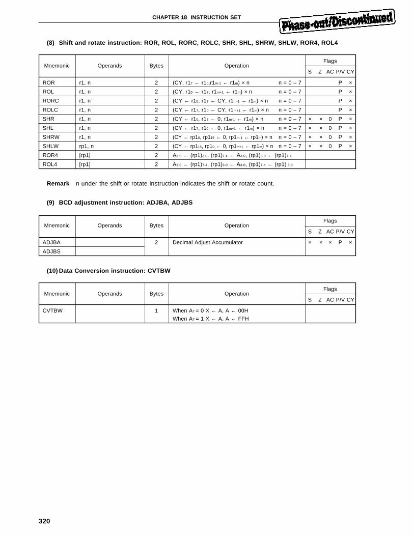
320
CHAPTER 18 INSTRUCTION SET
(8) Shift and rotate instruction: ROR, ROL, RORC, ROLC, SHR, SHL, SHRW, SHLW, ROR4, ROL4
Mnemonic Operands Bytes OperationFlags
S Z AC P/V CY
ROR r1, n 2 (CY, r17 ← r10,r1m-1 ← r1m) × n n = 0 – 7 P ×
ROL r1, n 2 (CY, r10 ← r17, r1m+1 ← r1m) × n n = 0 – 7 P ×
RORC r1, n 2 (CY ← r10, r17 ← CY, r1m-1 ← r1m) × n n = 0 – 7 P ×
ROLC r1, n 2 (CY ← r17, r10 ← CY, r1m+1 ← r1m) × n n = 0 – 7 P ×
SHR r1, n 2 (CY ← r10, r17 ← 0, r1m-1 ← r1m) × n n = 0 – 7 × × 0 P ×
SHL r1, n 2 (CY ← r17, r10 ← 0, r1m+1 ← r1m) × n n = 0 – 7 × × 0 P ×
SHRW r1, n 2 (CY ← rp10, rp115 ← 0, rp1m-1 ← rp1m) × n n = 0 – 7 × × 0 P ×
SHLW rp1, n 2 (CY ← rp115, rp10 ← 0, rp1m+1 ← rp1m) × n n = 0 – 7 × × 0 P ×
ROR4 [rp1] 2 A3-0 ← (rp1)3-0, (rp1)7-4 ← A3-0, (rp1)3-0 ← (rp1)7-4
ROL4 [rp1] 2 A3-0 ← (rp1)7-4, (rp1)3-0 ← A3-0, (rp1)7-4 ← (rp1) 3-0
Remark n under the shift or rotate instruction indicates the shift or rotate count.
(9) BCD adjustment instruction: ADJBA, ADJBS
Mnemonic Operands Bytes OperationFlags
S Z AC P/V CY
ADJBA 2 Decimal Adjust Accumulator × × × P ×
ADJBS
(10) Data Conversion instruction: CVTBW
Mnemonic Operands Bytes OperationFlags
S Z AC P/V CY
CVTBW 1 When A7 = 0 X ← A, A ← 00H
When A7 = 1 X ← A, A ← FFH
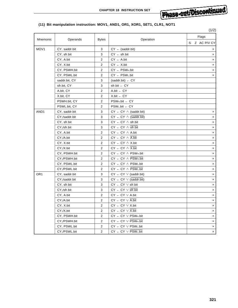
321
CHAPTER 18 INSTRUCTION SET
(11) Bit manipulation instruction: MOV1, AND1, OR1, XOR1, SET1, CLR1, NOT1
(1/2)
Mnemonic Operands Bytes OperationFlags
S Z AC P/V CY
MOV1 CY, saddr.bit 3 CY ← (saddr.bit) ×
CY, sfr.bit 3 CY ← sfr.bit ×
CY, A.bit 2 CY ← A.bit ×
CY, X.bit 2 CY ← X.bit ×
CY, PSWH.bit 2 CY ← PSWH.bit ×
CY, PSWL.bit 2 CY ← PSWL.bit ×
saddr.bit, CY 3 (saddr.bit) ← CY
sfr.bit, CY 3 sfr.bit ← CY
A.bit, CY 2 A.bit ← CY
X.bit, CY 2 X.bit ← CY
PSWH.bit, CY 2 PSWH.bit ← CY
PSWL.bit, CY 2 PSWL.bit ← CY
AND1 CY, saddr.bit 3 CY ← CY (saddr.bit) ×
CY,/saddr.bit 3 CY ← CY (saddr.bit) ×
CY, sfr.bit 3 CY ← CY sfr.bit ×
CY,/sfr.bit 3 CY ← CY sfr.bit ×
CY, A.bit 2 CY ← CY A.bit ×
CY,/A.bit 2 CY ← CY A.bit ×
CY, X.bit 2 CY ← CY X.bit ×
CY,/X.bit 2 CY ← CY X.bit ×
CY, PSWH.bit 2 CY ← CY PSWH.bit ×
CY,/PSWH.bit 2 CY ← CY PSWH.bit ×
CY, PSWL.bit 2 CY ← CY PSWL.bit ×
CY,/PSWL.bit 2 CY ← CY PSWL.bit ×
OR1 CY, saddr.bit 3 CY ← CY (saddr.bit) ×
CY,/saddr.bit 3 CY ← CY (saddr.bit) ×
CY, sfr.bit 3 CY ← CY sfr.bit ×
CY,/sfr.bit 3 CY ← CY sfr.bit ×
CY, A.bit 2 CY ← CY A.bit ×
CY,/A.bit 2 CY ← CY A.bit ×
CY, X.bit 2 CY ← CY X.bit ×
CY,/X.bit 2 CY ← CY X.bit ×
CY, PSWH.bit 2 CY ← CY PSWH.bit ×
CY,/PSWH.bit 2 CY ← CY PSWH.bit ×
CY, PSWL.bit 2 CY ← CY PSWL.bit ×
CY,/PSWL.bit 2 CY ← CY PSWL.bit ×
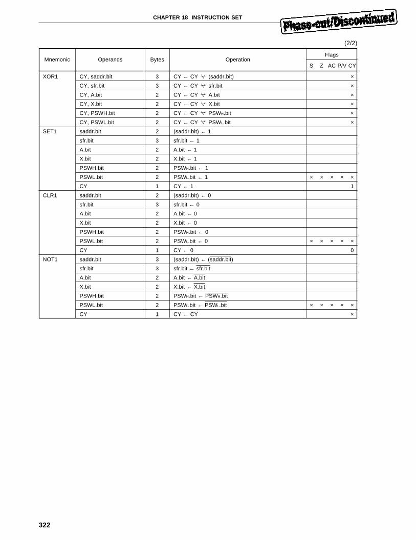
322
CHAPTER 18 INSTRUCTION SET
(2/2)
Mnemonic Operands Bytes OperationFlags
S Z AC P/V CY
XOR1 CY, saddr.bit 3 CY ← CY (saddr.bit) ×
CY, sfr.bit 3 CY ← CY sfr.bit ×
CY, A.bit 2 CY ← CY A.bit ×
CY, X.bit 2 CY ← CY X.bit ×
CY, PSWH.bit 2 CY ← CY PSWH.bit ×
CY, PSWL.bit 2 CY ← CY PSWL.bit ×
SET1 saddr.bit 2 (saddr.bit) ← 1
sfr.bit 3 sfr.bit ← 1
A.bit 2 A.bit ← 1
X.bit 2 X.bit ← 1
PSWH.bit 2 PSWH.bit ← 1
PSWL.bit 2 PSWL.bit ← 1 × × × × ×
CY 1 CY ← 1 1
CLR1 saddr.bit 2 (saddr.bit) ← 0
sfr.bit 3 sfr.bit ← 0
A.bit 2 A.bit ← 0
X.bit 2 X.bit ← 0
PSWH.bit 2 PSWH.bit ← 0
PSWL.bit 2 PSWL.bit ← 0 × × × × ×
CY 1 CY ← 0 0
NOT1 saddr.bit 3 (saddr.bit) ← (saddr.bit)
sfr.bit 3 sfr.bit ← sfr.bit
A.bit 2 A.bit ← A.bit
X.bit 2 X.bit ← X.bit
PSWH.bit 2 PSWH.bit ← PSWH.bit
PSWL.bit 2 PSWL.bit ← PSWL.bit × × × × ×
CY 1 CY ← CY ×
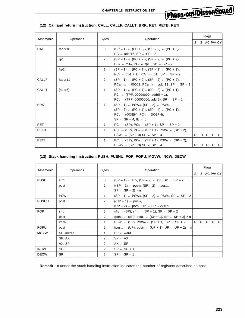
323
CHAPTER 18 INSTRUCTION SET
(12) Call and return instruction: CALL, CALLF, CALLT, BRK, RET, RETB, RETI
Mnemonic Operands Bytes OperationFlags
S Z AC P/V CY
CALL !addr16 3 (SP – 1) ← (PC + 3)H, (SP – 2) ← (PC + 3)L,
PC ← addr16, SP ← SP – 2
rp1 2 (SP – 1) ← (PC + 2)H, (SP – 2) ← (PC + 2)L,
PCH ← rp1H, PCL ← rp1L, SP ← SP – 2
[rp1] 2 (SP – 1) ← (PC + 2)H, (SP – 2) ← (PC + 2)L,
PCH ← (rp1 + 1), PCL ← (rp1), SP ← SP – 2
CALLF !addr11 2 (SP – 1) ← (PC + 2)H, (SP – 2) ← (PC + 2)L,
PC15 – 11 ← 00001, PC10 – 0 ← addr11, SP ← SP – 2
CALLT [addr5] 1 (SP – 1) ← (PC + 1)H, (SP – 2) ← (PC + 1)L,
PCH ← (TPF, 00000000, addr5 + 1),
PCL ← (TPF, 00000000, addr5), SP ← SP – 2
BRK 1 (SP – 1) ← PSWH, (SP – 2) ← PSWL,
(SP – 3) ← (PC + 1)H, (SP – 4) ← (PC + 1)L,
PCL ← (003EH), PCH ← (003FH),
SP ← SP – 4, IE ← 0
RET 1 PCL ← (SP), PCH ← (SP + 1), SP ← SP + 2
RETB 1 PCL ← (SP), PCH ← (SP + 1), PSWL ← (SP + 2),
PSWH ← (SP + 3) SP ← SP + 4 R R R R R
RETI 1 PCL ← (SP), PCH ← (SP + 1), PSWL ← (SP + 2),
PSWH ← (SP + 3) SP ← SP + 4 R R R R R
(13) Stack handling instruction: PUSH, PUSHU, POP, POPU, MOVW, INCW, DECW
Mnemonic Operands Bytes OperationFlags
S Z AC P/V CY
PUSH sfrp 3 (SP – 1) ← sfrH, (SP – 2) ← sfrL, SP ← SP – 2
post 2 {(SP – 1) ← postH, (SP – 2) ← postL,
SP ← SP – 2} × n
PSW 1 (SP – 1) ← PSWH, (SP – 2) ← PSWL, SP ← SP – 2
PUSHU post 2 {(UP – 1) ← postH,
(UP – 2) ← postL, UP ← UP – 2} × n
POP sfrp 3 sfrL ← (SP), sfrH ← (SP + 1), SP ← SP + 2
post 2 {postL ← (SP), postH ← (SP + 1), SP ← SP + 2} × n
PSW 1 PSWL ← (SP), PSWH ← (SP + 1), SP ← SP + 2 R R R R R
POPU post 2 {postL ← (UP), postH ← (UP + 1), UP ← UP + 2) × n
MOVW SP, #word 4 SP ← word
SP, AX 2 SP ← AX
AX, SP 2 AX ← SP
INCW SP 2 SP ← SP + 1
DECW SP 2 SP ← SP – 1
Remark n under the stack handling instruction indicates the number of registers described as post.
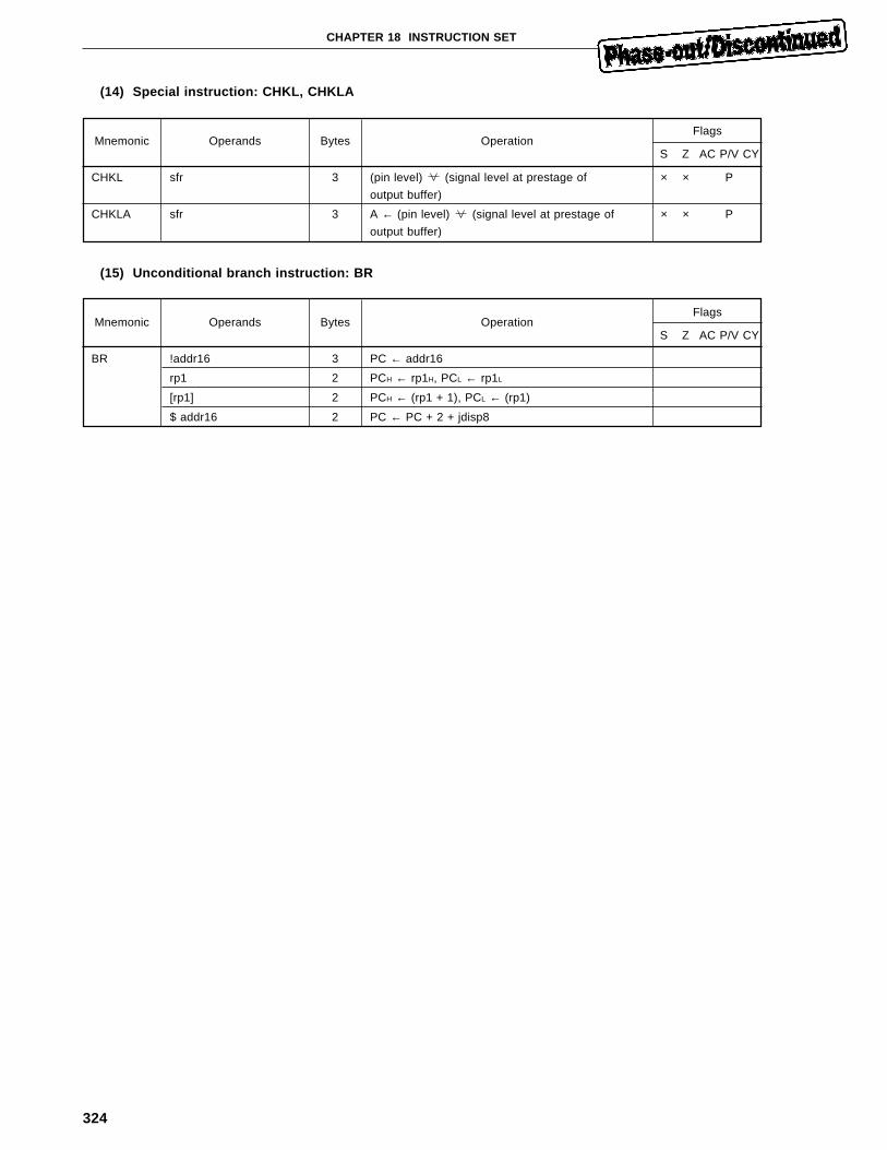
324
CHAPTER 18 INSTRUCTION SET
(14) Special instruction: CHKL, CHKLA
Mnemonic Operands Bytes OperationFlags
S Z AC P/V CY
CHKL sfr 3 (pin level) (signal level at prestage of × × P
output buffer)
CHKLA sfr 3 A ← (pin level) (signal level at prestage of × × P
output buffer)
(15) Unconditional branch instruction: BR
Mnemonic Operands Bytes OperationFlags
S Z AC P/V CY
BR !addr16 3 PC ← addr16
rp1 2 PCH ← rp1H, PCL ← rp1L
[rp1] 2 PCH ← (rp1 + 1), PCL ← (rp1)
$ addr16 2 PC ← PC + 2 + jdisp8
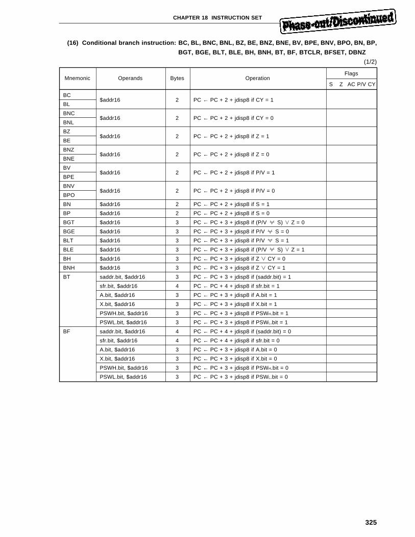
325
CHAPTER 18 INSTRUCTION SET
(16) Conditional branch instruction: BC, BL, BNC, BNL, BZ, BE, BNZ, BNE, BV, BPE, BNV, BPO, BN, BP,
BGT, BGE, BLT, BLE, BH, BNH, BT, BF, BTCLR, BFSET, DBNZ
(1/2)
Mnemonic Operands Bytes OperationFlags
S Z AC P/V CY
BC$addr16 2 PC ← PC + 2 + jdisp8 if CY = 1
BL
BNC$addr16 2 PC ← PC + 2 + jdisp8 if CY = 0
BNL
BZ$addr16 2 PC ← PC + 2 + jdisp8 if Z = 1
BE
BNZ$addr16 2 PC ← PC + 2 + jdisp8 if Z = 0
BNE
BV$addr16 2 PC ← PC + 2 + jdisp8 if P/V = 1
BPE
BNV$addr16 2 PC ← PC + 2 + jdisp8 if P/V = 0
BPO
BN $addr16 2 PC ← PC + 2 + jdisp8 if S = 1
BP $addr16 2 PC ← PC + 2 + jdisp8 if S = 0
BGT $addr16 3 PC ← PC + 3 + jdisp8 if (P/V S) Z = 0
BGE $addr16 3 PC ← PC + 3 + jdisp8 if P/V S = 0
BLT $addr16 3 PC ← PC + 3 + jdisp8 if P/V S = 1
BLE $addr16 3 PC ← PC + 3 + jdisp8 if (P/V S) Z = 1
BH $addr16 3 PC ← PC + 3 + jdisp8 if Z CY = 0
BNH $addr16 3 PC ← PC + 3 + jdisp8 if Z CY = 1
BT saddr.bit, $addr16 3 PC ← PC + 3 + jdisp8 if (saddr.bit) = 1
sfr.bit, $addr16 4 PC ← PC + 4 + jdisp8 if sfr.bit = 1
A.bit, $addr16 3 PC ← PC + 3 + jdisp8 if A.bit = 1
X.bit, $addr16 3 PC ← PC + 3 + jdisp8 if X.bit = 1
PSWH.bit, $addr16 3 PC ← PC + 3 + jdisp8 if PSWH.bit = 1
PSWL.bit, $addr16 3 PC ← PC + 3 + jdisp8 if PSWL.bit = 1
BF saddr.bit, $addr16 4 PC ← PC + 4 + jdisp8 if (saddr.bit) = 0
sfr.bit, $addr16 4 PC ← PC + 4 + jdisp8 if sfr.bit = 0
A.bit, $addr16 3 PC ← PC + 3 + jdisp8 if A.bit = 0
X.bit, $addr16 3 PC ← PC + 3 + jdisp8 if X.bit = 0
PSWH.bit, $addr16 3 PC ← PC + 3 + jdisp8 if PSWH.bit = 0
PSWL.bit, $addr16 3 PC ← PC + 3 + jdisp8 if PSWL.bit = 0
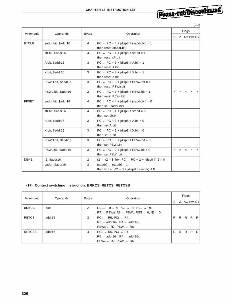
326
CHAPTER 18 INSTRUCTION SET
(2/2)
Mnemonic Operands Bytes OperationFlags
S Z AC P/V CY
BTCLR saddr.bit, $addr16 4 PC ← PC + 4 + jdisp8 if (saddr.bit) = 1
then reset (saddr.bit)
sfr.bit, $addr16 4 PC ← PC + 4 + jdisp8 if sfr.bit = 1
then reset sfr.bit
A.bit, $addr16 3 PC ← PC + 3 + jdisp8 if A.bit = 1
then reset A.bit
X.bit, $addr16 3 PC ← PC + 3 + jdisp8 if X.bit = 1
then reset X.bit
PSWH.bit, $addr16 3 PC ← PC + 3 + jdisp8 if PSWH.bit = 1
then reset PSWH.bit
PSWL.bit, $addr16 3 PC ← PC + 3 + jdisp8 if PSWL.bit = 1 × × × × ×then reset PSWL.bit
BFSET saddr.bit, $addr16 4 PC ← PC + 4 + jdisp8 if (saddr.bit) = 0
then set (saddr.bit)
sfr.bit, $addr16 4 PC ← PC + 4 + jdisp8 if sfr.bit = 0
then set sfr.bit
A.bit, $addr16 3 PC ← PC + 3 + jdisp8 if A.bit = 0
then set A.bit
X.bit, $addr16 3 PC ← PC + 3 + jdisp8 if X.bit = 0
then set X.bit
PSWH.bit, $addr16 3 PC ← PC + 3 + jdisp8 if PSWH.bit = 0
then set PSWH.bit
PSWL.bit, $addr16 3 PC ← PC + 3 + jdisp8 if PSWL.bit = 0 × × × × ×then set PSWL.bit
DBNZ r2, $addr16 2 r2 ← r2 – 1 then PC ← PC + 2 + jdisp8 if r2 ≠ 0
saddr, $addr16 3 (saddr) ← (saddr) – 1,
then PC ← PC + 3 + jdisp8 if (saddr) ≠ 0
(17) Context switching instruction: BRKCS, RETCS, RETCSB
Mnemonic Operands Bytes OperationFlags
S Z AC P/V CY
BRKCS RBn 2 RBS2 – 0 ← n, PCH ↔ R5, PCL ↔ R4,
R7 ← PSWH, R6 ← PSWL, RSS ← 0, IE ← 0
RETCS !addr16 3 PCH ← R5, PCL ← R4, R R R R R
R5 ← addr16H, R4 ← addr16L,
PSWH ← R7, PSWL ← R6
RETCSB !addr16 4 PCH ← R5, PCL ← R4, R R R R R
R5 ← addr16H, R4 ← addr16L,
PSWH ← R7, PSWL ← R6
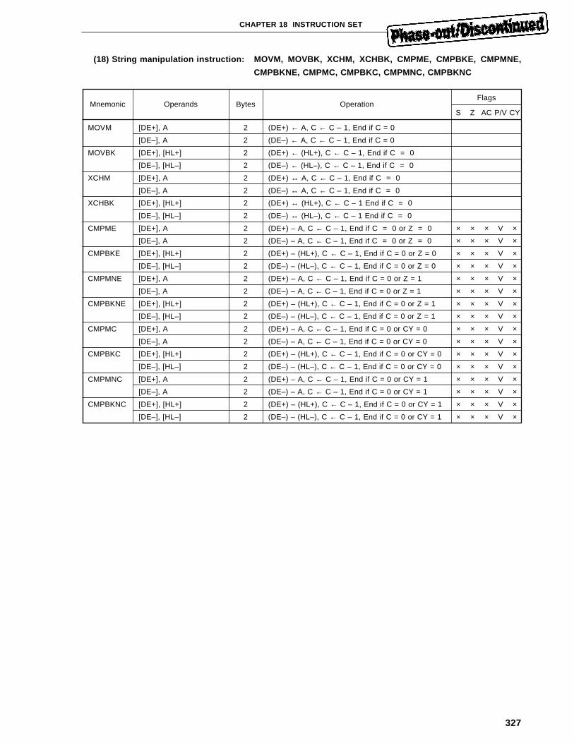
327
CHAPTER 18 INSTRUCTION SET
(18) String manipulation instruction: MOVM, MOVBK, XCHM, XCHBK, CMPME, CMPBKE, CMPMNE,
CMPBKNE, CMPMC, CMPBKC, CMPMNC, CMPBKNC
Mnemonic Operands Bytes OperationFlags
S Z AC P/V CY
MOVM [DE+], A 2 (DE+) ← A, C ← C – 1, End if C = 0
[DE–], A 2 (DE–) ← A, C ← C – 1, End if C = 0
MOVBK [DE+], [HL+] 2 (DE+) ← (HL+), C ← C – 1, End if C = 0
[DE–], [HL–] 2 (DE–) ← (HL–), C ← C – 1, End if C = 0
XCHM [DE+], A 2 (DE+) ↔ A, C ← C – 1, End if C = 0
[DE–], A 2 (DE–) ↔ A, C ← C – 1, End if C = 0
XCHBK [DE+], [HL+] 2 (DE+) ↔ (HL+), C ← C – 1 End if C = 0
[DE–], [HL–] 2 (DE–) ↔ (HL–), C ← C – 1 End if C = 0
CMPME [DE+], A 2 (DE+) – A, C ← C – 1, End if C = 0 or Z = 0 × × × V ×
[DE–], A 2 (DE–) – A, C ← C – 1, End if C = 0 or Z = 0 × × × V ×
CMPBKE [DE+], [HL+] 2 (DE+) – (HL+), C ← C – 1, End if C = 0 or Z = 0 × × × V ×
[DE–], [HL–] 2 (DE–) – (HL–), C ← C – 1, End if C = 0 or Z = 0 × × × V ×
CMPMNE [DE+], A 2 (DE+) – A, C ← C – 1, End if C = 0 or Z = 1 × × × V ×
[DE–], A 2 (DE–) – A, C ← C – 1, End if C = 0 or Z = 1 × × × V ×
CMPBKNE [DE+], [HL+] 2 (DE+) – (HL+), C ← C – 1, End if C = 0 or Z = 1 × × × V ×
[DE–], [HL–] 2 (DE–) – (HL–), C ← C – 1, End if C = 0 or Z = 1 × × × V ×
CMPMC [DE+], A 2 (DE+) – A, C ← C – 1, End if C = 0 or CY = 0 × × × V ×
[DE–], A 2 (DE–) – A, C ← C – 1, End if C = 0 or CY = 0 × × × V ×
CMPBKC [DE+], [HL+] 2 (DE+) – (HL+), C ← C – 1, End if C = 0 or CY = 0 × × × V ×
[DE–], [HL–] 2 (DE–) – (HL–), C ← C – 1, End if C = 0 or CY = 0 × × × V ×
CMPMNC [DE+], A 2 (DE+) – A, C ← C – 1, End if C = 0 or CY = 1 × × × V ×
[DE–], A 2 (DE–) – A, C ← C – 1, End if C = 0 or CY = 1 × × × V ×
CMPBKNC [DE+], [HL+] 2 (DE+) – (HL+), C ← C – 1, End if C = 0 or CY = 1 × × × V ×
[DE–], [HL–] 2 (DE–) – (HL–), C ← C – 1, End if C = 0 or CY = 1 × × × V ×
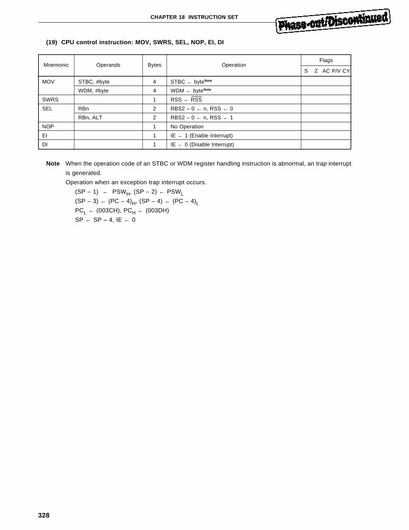
328
CHAPTER 18 INSTRUCTION SET
(19) CPU control instruction: MOV, SWRS, SEL, NOP, EI, DI
Mnemonic Operands Bytes OperationFlags
S Z AC P/V CY
MOV STBC, #byte 4 STBC ← byteNote
WDM, #byte 4 WDM ← byteNote
SWRS 1 RSS ← RSS
SEL RBn 2 RBS2 – 0 ← n, RSS ← 0
RBn, ALT 2 RBS2 – 0 ← n, RSS ← 1
NOP 1 No Operation
EI 1 IE ← 1 (Enable Interrupt)
DI 1 IE ← 0 (Disable Interrupt)
Note When the operation code of an STBC or WDM register handling instruction is abnormal, an trap interrupt
is generated.
Operation when an exception trap interrupt occurs.
(SP – 1) ← PSWH, (SP – 2) ← PSWL
(SP – 3) ← (PC – 4)H, (SP – 4) ← (PC – 4)L
PCL ← (003CH), PCH ← (003DH)
SP ← SP – 4, IE ← 0
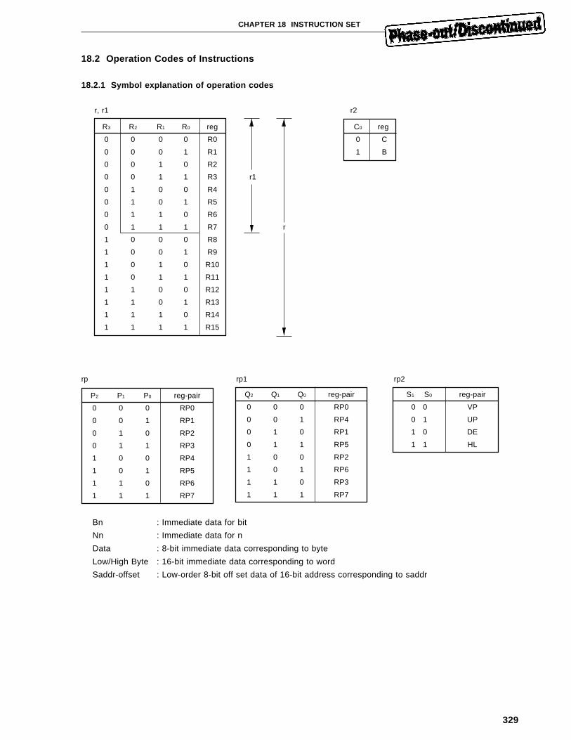
329
CHAPTER 18 INSTRUCTION SET
18.2 Operation Codes of Instructions
18.2.1 Symbol explanation of operation codes
r, r1 r2
R3 R2 R1 R0 reg C0 reg
0 0 0 0 R0 0 C
0 0 0 1 R1 1 B
0 0 1 0 R2
0 0 1 1 R3 r1
0 1 0 0 R4
0 1 0 1 R5
0 1 1 0 R6
0 1 1 1 R7 r
1 0 0 0 R8
1 0 0 1 R9
1 0 1 0 R10
1 0 1 1 R11
1 1 0 0 R12
1 1 0 1 R13
1 1 1 0 R14
1 1 1 1 R15
rp rp1 rp2
P2 P1 P0 reg-pair
0 0 0 RP0
0 0 1 RP1
0 1 0 RP2
0 1 1 RP3
1 0 0 RP4
1 0 1 RP5
1 1 0 RP6
1 1 1 RP7
Bn : Immediate data for bit
Nn : Immediate data for n
Data : 8-bit immediate data corresponding to byte
Low/High Byte : 16-bit immediate data corresponding to word
Saddr-offset : Low-order 8-bit off set data of 16-bit address corresponding to saddr
Q2 Q1 Q0 reg-pair
0 0 0 RP0
0 0 1 RP4
0 1 0 RP1
0 1 1 RP5
1 0 0 RP2
1 0 1 RP6
1 1 0 RP3
1 1 1 RP7
S1 S0 reg-pair
0 0 VP
0 1 UP
1 0 DE
1 1 HL
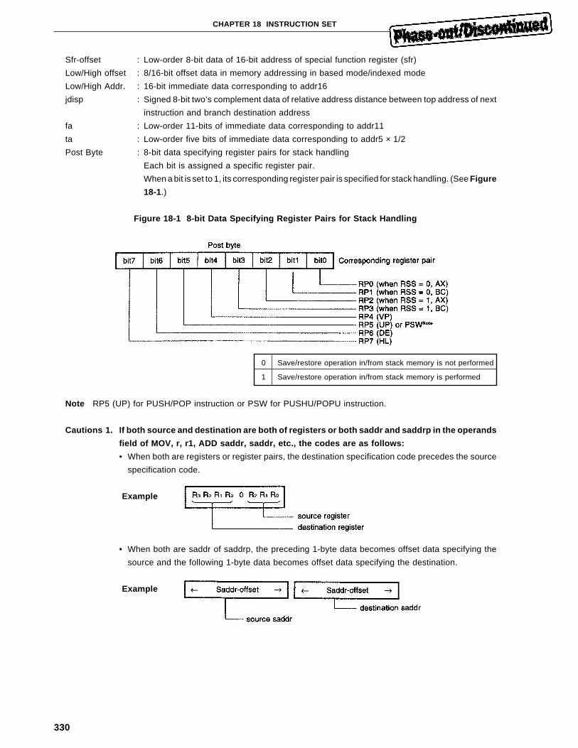
330
CHAPTER 18 INSTRUCTION SET
Sfr-offset : Low-order 8-bit data of 16-bit address of special function register (sfr)
Low/High offset : 8/16-bit offset data in memory addressing in based mode/indexed mode
Low/High Addr. : 16-bit immediate data corresponding to addr16
jdisp : Signed 8-bit two’s complement data of relative address distance between top address of next
instruction and branch destination address
fa : Low-order 11-bits of immediate data corresponding to addr11
ta : Low-order five bits of immediate data corresponding to addr5 × 1/2
Post Byte : 8-bit data specifying register pairs for stack handling
Each bit is assigned a specific register pair.
When a bit is set to 1, its corresponding register pair is specified for stack handling. (See Figure
18-1.)
Figure 18-1 8-bit Data Specifying Register Pairs for Stack Handling
0 Save/restore operation in/from stack memory is not performed
1 Save/restore operation in/from stack memory is performed
Note RP5 (UP) for PUSH/POP instruction or PSW for PUSHU/POPU instruction.
Cautions 1. If both source and destination are both of registers or both saddr and saddrp in the operands
field of MOV, r, r1, ADD saddr, saddr, etc., the codes are as follows:
• When both are registers or register pairs, the destination specification code precedes the source
specification code.
Example
• When both are saddr of saddrp, the preceding 1-byte data becomes offset data specifying the
source and the following 1-byte data becomes offset data specifying the destination.
Example
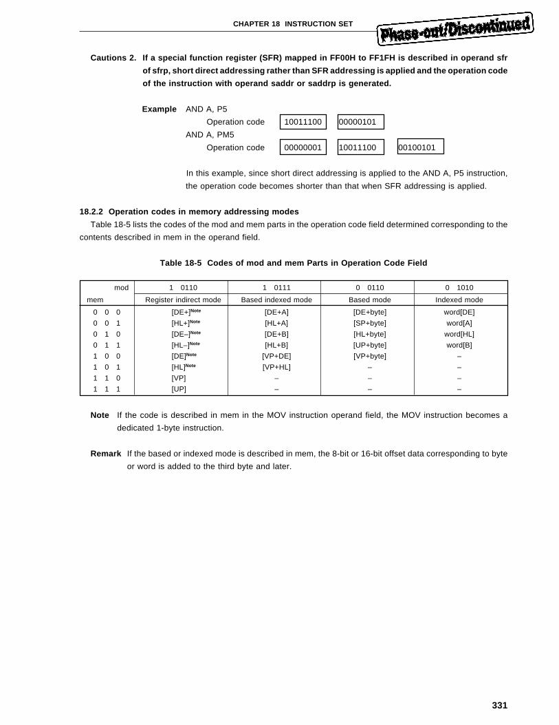
331
CHAPTER 18 INSTRUCTION SET
Cautions 2. If a special function register (SFR) mapped in FF00H to FF1FH is described in operand sfr
of sfrp, short direct addressing rather than SFR addressing is applied and the operation code
of the instruction with operand saddr or saddrp is generated.
Example AND A, P5
Operation code 10011100 00000101
AND A, PM5
Operation code 00000001 10011100 00100101
In this example, since short direct addressing is applied to the AND A, P5 instruction,
the operation code becomes shorter than that when SFR addressing is applied.
18.2.2 Operation codes in memory addressing modes
Table 18-5 lists the codes of the mod and mem parts in the operation code field determined corresponding to the
contents described in mem in the operand field.
Table 18-5 Codes of mod and mem Parts in Operation Code Field
mod 1 0110 1 0111 0 0110 0 1010
mem Register indirect mode Based indexed mode Based mode Indexed mode
0 0 0 [DE+]Note [DE+A] [DE+byte] word[DE]
0 0 1 [HL+]Note [HL+A] [SP+byte] word[A]
0 1 0 [DE–]Note [DE+B] [HL+byte] word[HL]
0 1 1 [HL–]Note [HL+B] [UP+byte] word[B]
1 0 0 [DE]Note [VP+DE] [VP+byte] –
1 0 1 [HL]Note [VP+HL] – –
1 1 0 [VP] – – –
1 1 1 [UP] – – –
Note If the code is described in mem in the MOV instruction operand field, the MOV instruction becomes a
dedicated 1-byte instruction.
Remark If the based or indexed mode is described in mem, the 8-bit or 16-bit offset data corresponding to byte
or word is added to the third byte and later.
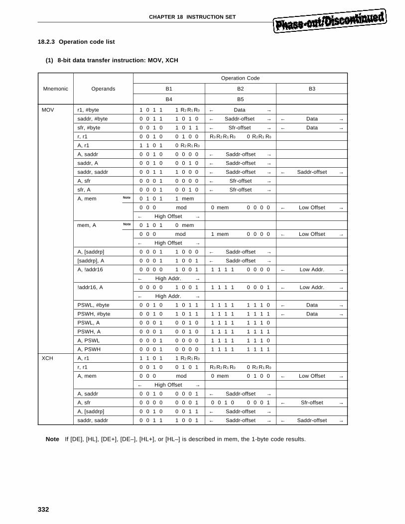
332
CHAPTER 18 INSTRUCTION SET
18.2.3 Operation code list
(1) 8-bit data transfer instruction: MOV, XCH
Operation Code
Mnemonic Operands B1 B2 B3
B4 B5
MOV r1, #byte 1 0 1 1 1 R2 R1 R0 ← Data →
saddr, #byte 0 0 1 1 1 0 1 0 ← Saddr-offset → ← Data →
sfr, #byte 0 0 1 0 1 0 1 1 ← Sfr-offset → ← Data →
r, r1 0 0 1 0 0 1 0 0 R3 R2 R1 R0 0 R2R1 R0
A, r1 1 1 0 1 0 R2 R1 R0
A, saddr 0 0 1 0 0 0 0 0 ← Saddr-offset →
saddr, A 0 0 1 0 0 0 1 0 ← Saddr-offset →
saddr, saddr 0 0 1 1 1 0 0 0 ← Saddr-offset → ← Saddr-offset →
A, sfr 0 0 0 1 0 0 0 0 ← Sfr-offset →
sfr, A 0 0 0 1 0 0 1 0 ← Sfr-offset →
A, mem Note 0 1 0 1 1 mem
0 0 0 mod 0 mem 0 0 0 0 ← Low Offset →
← High Offset →
mem, A Note 0 1 0 1 0 mem
0 0 0 mod 1 mem 0 0 0 0 ← Low Offset →
← High Offset →
A, [saddrp] 0 0 0 1 1 0 0 0 ← Saddr-offset →
[saddrp], A 0 0 0 1 1 0 0 1 ← Saddr-offset →
A, !addr16 0 0 0 0 1 0 0 1 1 1 1 1 0 0 0 0 ← Low Addr. →
← High Addr. →
!addr16, A 0 0 0 0 1 0 0 1 1 1 1 1 0 0 0 1 ← Low Addr. →
← High Addr. →
PSWL, #byte 0 0 1 0 1 0 1 1 1 1 1 1 1 1 1 0 ← Data →
PSWH, #byte 0 0 1 0 1 0 1 1 1 1 1 1 1 1 1 1 ← Data →
PSWL, A 0 0 0 1 0 0 1 0 1 1 1 1 1 1 1 0
PSWH, A 0 0 0 1 0 0 1 0 1 1 1 1 1 1 1 1
A, PSWL 0 0 0 1 0 0 0 0 1 1 1 1 1 1 1 0
A, PSWH 0 0 0 1 0 0 0 0 1 1 1 1 1 1 1 1
XCH A, r1 1 1 0 1 1 R2 R1 R0
r, r1 0 0 1 0 0 1 0 1 R3 R2 R1 R0 0 R2 R1 R0
A, mem 0 0 0 mod 0 mem 0 1 0 0 ← Low Offset →
← High Offset →
A, saddr 0 0 1 0 0 0 0 1 ← Saddr-offset →
A, sfr 0 0 0 0 0 0 0 1 0 0 1 0 0 0 0 1 ← Sfr-offset →
A, [saddrp] 0 0 1 0 0 0 1 1 ← Saddr-offset →
saddr, saddr 0 0 1 1 1 0 0 1 ← Saddr-offset → ← Saddr-offset →
Note If [DE], [HL], [DE+], [DE–], [HL+], or [HL–] is described in mem, the 1-byte code results.
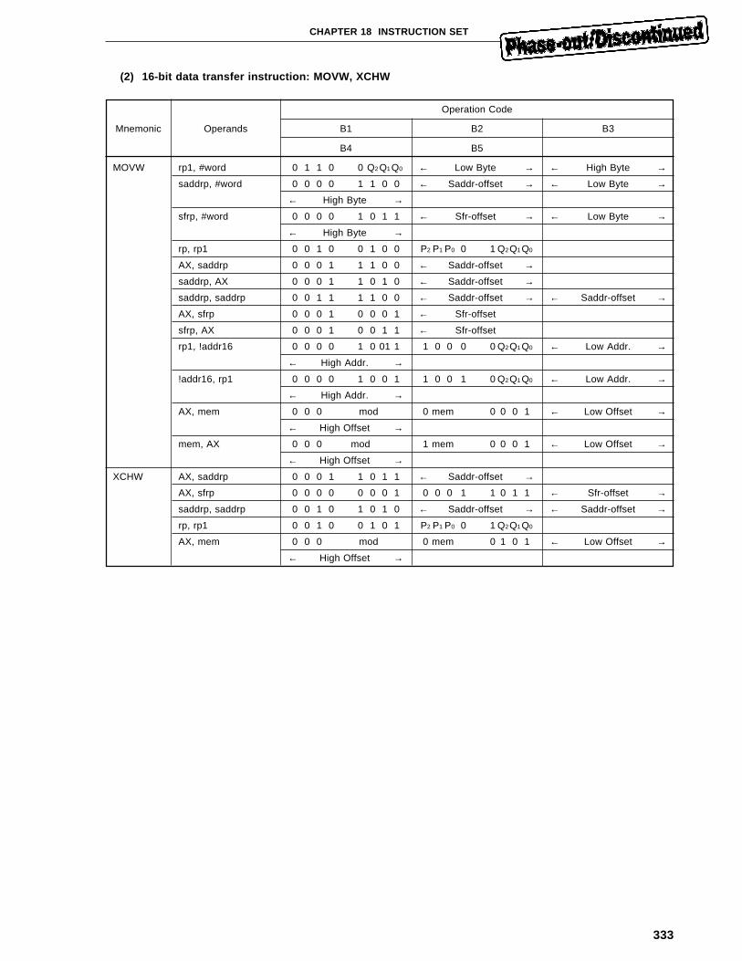
333
CHAPTER 18 INSTRUCTION SET
(2) 16-bit data transfer instruction: MOVW, XCHW
Operation Code
Mnemonic Operands B1 B2 B3
B4 B5
MOVW rp1, #word 0 1 1 0 0 Q2 Q1 Q0 ← Low Byte → ← High Byte →
saddrp, #word 0 0 0 0 1 1 0 0 ← Saddr-offset → ← Low Byte →
← High Byte →
sfrp, #word 0 0 0 0 1 0 1 1 ← Sfr-offset → ← Low Byte →
← High Byte →
rp, rp1 0 0 1 0 0 1 0 0 P2 P1 P0 0 1 Q2Q1 Q0
AX, saddrp 0 0 0 1 1 1 0 0 ← Saddr-offset →
saddrp, AX 0 0 0 1 1 0 1 0 ← Saddr-offset →
saddrp, saddrp 0 0 1 1 1 1 0 0 ← Saddr-offset → ← Saddr-offset →
AX, sfrp 0 0 0 1 0 0 0 1 ← Sfr-offset
sfrp, AX 0 0 0 1 0 0 1 1 ← Sfr-offset
rp1, !addr16 0 0 0 0 1 0 01 1 1 0 0 0 0 Q2Q1 Q0 ← Low Addr. →
← High Addr. →
!addr16, rp1 0 0 0 0 1 0 0 1 1 0 0 1 0 Q2Q1 Q0 ← Low Addr. →
← High Addr. →
AX, mem 0 0 0 mod 0 mem 0 0 0 1 ← Low Offset →
← High Offset →
mem, AX 0 0 0 mod 1 mem 0 0 0 1 ← Low Offset →
← High Offset →
XCHW AX, saddrp 0 0 0 1 1 0 1 1 ← Saddr-offset →
AX, sfrp 0 0 0 0 0 0 0 1 0 0 0 1 1 0 1 1 ← Sfr-offset →
saddrp, saddrp 0 0 1 0 1 0 1 0 ← Saddr-offset → ← Saddr-offset →
rp, rp1 0 0 1 0 0 1 0 1 P2 P1 P0 0 1 Q2Q1 Q0
AX, mem 0 0 0 mod 0 mem 0 1 0 1 ← Low Offset →
← High Offset →
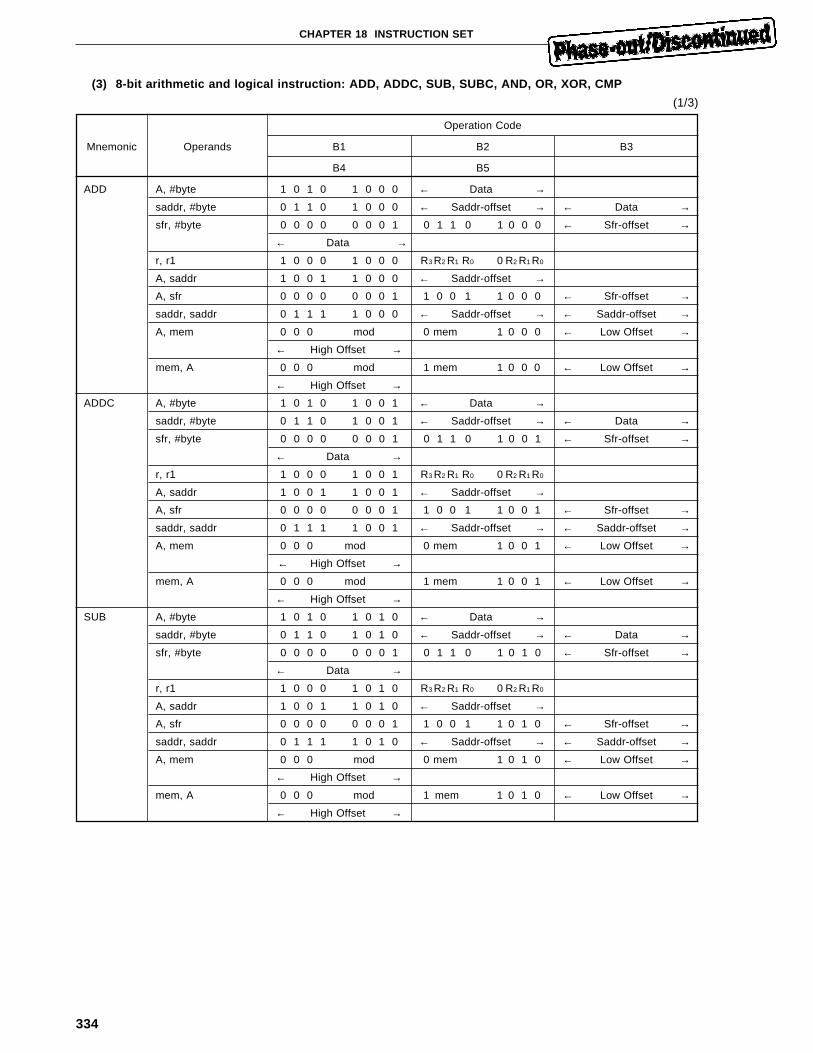
334
CHAPTER 18 INSTRUCTION SET
(3) 8-bit arithmetic and logical instruction: ADD, ADDC, SUB, SUBC, AND, OR, XOR, CMP
(1/3)
Operation Code
Mnemonic Operands B1 B2 B3
B4 B5
ADD A, #byte 1 0 1 0 1 0 0 0 ← Data →
saddr, #byte 0 1 1 0 1 0 0 0 ← Saddr-offset → ← Data →
sfr, #byte 0 0 0 0 0 0 0 1 0 1 1 0 1 0 0 0 ← Sfr-offset →
← Data →
r, r1 1 0 0 0 1 0 0 0 R3 R2 R1 R0 0 R2 R1 R0
A, saddr 1 0 0 1 1 0 0 0 ← Saddr-offset →
A, sfr 0 0 0 0 0 0 0 1 1 0 0 1 1 0 0 0 ← Sfr-offset →
saddr, saddr 0 1 1 1 1 0 0 0 ← Saddr-offset → ← Saddr-offset →
A, mem 0 0 0 mod 0 mem 1 0 0 0 ← Low Offset →
← High Offset →
mem, A 0 0 0 mod 1 mem 1 0 0 0 ← Low Offset →
← High Offset →
ADDC A, #byte 1 0 1 0 1 0 0 1 ← Data →
saddr, #byte 0 1 1 0 1 0 0 1 ← Saddr-offset → ← Data →
sfr, #byte 0 0 0 0 0 0 0 1 0 1 1 0 1 0 0 1 ← Sfr-offset →
← Data →
r, r1 1 0 0 0 1 0 0 1 R3 R2 R1 R0 0 R2 R1 R0
A, saddr 1 0 0 1 1 0 0 1 ← Saddr-offset →
A, sfr 0 0 0 0 0 0 0 1 1 0 0 1 1 0 0 1 ← Sfr-offset →
saddr, saddr 0 1 1 1 1 0 0 1 ← Saddr-offset → ← Saddr-offset →
A, mem 0 0 0 mod 0 mem 1 0 0 1 ← Low Offset →
← High Offset →
mem, A 0 0 0 mod 1 mem 1 0 0 1 ← Low Offset →
← High Offset →
SUB A, #byte 1 0 1 0 1 0 1 0 ← Data →
saddr, #byte 0 1 1 0 1 0 1 0 ← Saddr-offset → ← Data →
sfr, #byte 0 0 0 0 0 0 0 1 0 1 1 0 1 0 1 0 ← Sfr-offset →
← Data →
r, r1 1 0 0 0 1 0 1 0 R3 R2 R1 R0 0 R2 R1 R0
A, saddr 1 0 0 1 1 0 1 0 ← Saddr-offset →
A, sfr 0 0 0 0 0 0 0 1 1 0 0 1 1 0 1 0 ← Sfr-offset →
saddr, saddr 0 1 1 1 1 0 1 0 ← Saddr-offset → ← Saddr-offset →
A, mem 0 0 0 mod 0 mem 1 0 1 0 ← Low Offset →
← High Offset →
mem, A 0 0 0 mod 1 mem 1 0 1 0 ← Low Offset →
← High Offset →
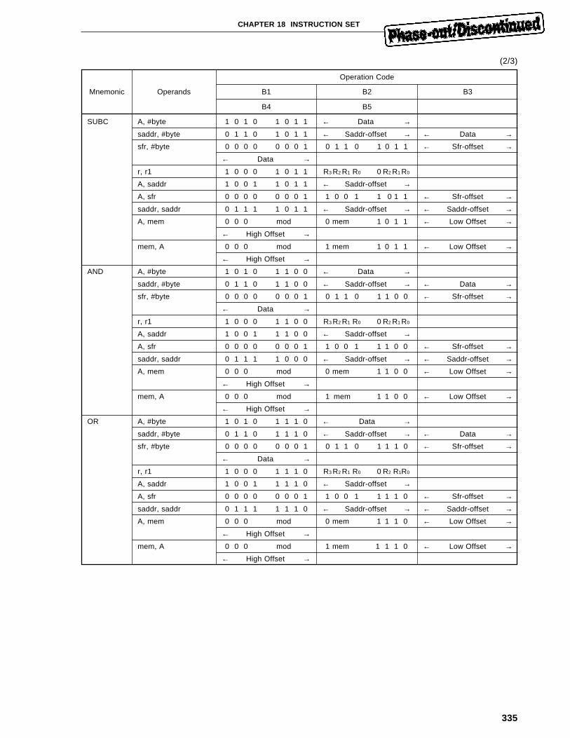
335
CHAPTER 18 INSTRUCTION SET
(2/3)
Operation Code
Mnemonic Operands B1 B2 B3
B4 B5
SUBC A, #byte 1 0 1 0 1 0 1 1 ← Data →
saddr, #byte 0 1 1 0 1 0 1 1 ← Saddr-offset → ← Data →
sfr, #byte 0 0 0 0 0 0 0 1 0 1 1 0 1 0 1 1 ← Sfr-offset →
← Data →
r, r1 1 0 0 0 1 0 1 1 R3 R2 R1 R0 0 R2 R1 R0
A, saddr 1 0 0 1 1 0 1 1 ← Saddr-offset →
A, sfr 0 0 0 0 0 0 0 1 1 0 0 1 1 0 1 1 ← Sfr-offset →
saddr, saddr 0 1 1 1 1 0 1 1 ← Saddr-offset → ← Saddr-offset →
A, mem 0 0 0 mod 0 mem 1 0 1 1 ← Low Offset →
← High Offset →
mem, A 0 0 0 mod 1 mem 1 0 1 1 ← Low Offset →
← High Offset →
AND A, #byte 1 0 1 0 1 1 0 0 ← Data →
saddr, #byte 0 1 1 0 1 1 0 0 ← Saddr-offset → ← Data →
sfr, #byte 0 0 0 0 0 0 0 1 0 1 1 0 1 1 0 0 ← Sfr-offset →
← Data →
r, r1 1 0 0 0 1 1 0 0 R3 R2 R1 R0 0 R2 R1 R0
A, saddr 1 0 0 1 1 1 0 0 ← Saddr-offset →
A, sfr 0 0 0 0 0 0 0 1 1 0 0 1 1 1 0 0 ← Sfr-offset →
saddr, saddr 0 1 1 1 1 0 0 0 ← Saddr-offset → ← Saddr-offset →
A, mem 0 0 0 mod 0 mem 1 1 0 0 ← Low Offset →
← High Offset →
mem, A 0 0 0 mod 1 mem 1 1 0 0 ← Low Offset →
← High Offset →
OR A, #byte 1 0 1 0 1 1 1 0 ← Data →
saddr, #byte 0 1 1 0 1 1 1 0 ← Saddr-offset → ← Data →
sfr, #byte 0 0 0 0 0 0 0 1 0 1 1 0 1 1 1 0 ← Sfr-offset →
← Data →
r, r1 1 0 0 0 1 1 1 0 R3 R2 R1 R0 0 R2 R1R0
A, saddr 1 0 0 1 1 1 1 0 ← Saddr-offset →
A, sfr 0 0 0 0 0 0 0 1 1 0 0 1 1 1 1 0 ← Sfr-offset →
saddr, saddr 0 1 1 1 1 1 1 0 ← Saddr-offset → ← Saddr-offset →
A, mem 0 0 0 mod 0 mem 1 1 1 0 ← Low Offset →
← High Offset →
mem, A 0 0 0 mod 1 mem 1 1 1 0 ← Low Offset →
← High Offset →
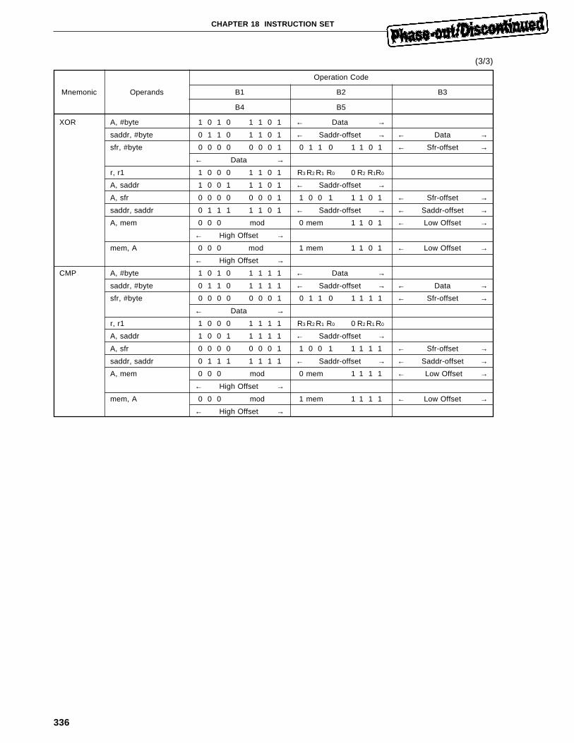
336
CHAPTER 18 INSTRUCTION SET
(3/3)
Operation Code
Mnemonic Operands B1 B2 B3
B4 B5
XOR A, #byte 1 0 1 0 1 1 0 1 ← Data →
saddr, #byte 0 1 1 0 1 1 0 1 ← Saddr-offset → ← Data →
sfr, #byte 0 0 0 0 0 0 0 1 0 1 1 0 1 1 0 1 ← Sfr-offset →
← Data →
r, r1 1 0 0 0 1 1 0 1 R3 R2 R1 R0 0 R2 R1R0
A, saddr 1 0 0 1 1 1 0 1 ← Saddr-offset →
A, sfr 0 0 0 0 0 0 0 1 1 0 0 1 1 1 0 1 ← Sfr-offset →
saddr, saddr 0 1 1 1 1 1 0 1 ← Saddr-offset → ← Saddr-offset →
A, mem 0 0 0 mod 0 mem 1 1 0 1 ← Low Offset →
← High Offset →
mem, A 0 0 0 mod 1 mem 1 1 0 1 ← Low Offset →
← High Offset →
CMP A, #byte 1 0 1 0 1 1 1 1 ← Data →
saddr, #byte 0 1 1 0 1 1 1 1 ← Saddr-offset → ← Data →
sfr, #byte 0 0 0 0 0 0 0 1 0 1 1 0 1 1 1 1 ← Sfr-offset →
← Data →
r, r1 1 0 0 0 1 1 1 1 R3 R2 R1 R0 0 R2 R1 R0
A, saddr 1 0 0 1 1 1 1 1 ← Saddr-offset →
A, sfr 0 0 0 0 0 0 0 1 1 0 0 1 1 1 1 1 ← Sfr-offset →
saddr, saddr 0 1 1 1 1 1 1 1 ← Saddr-offset → ← Saddr-offset →
A, mem 0 0 0 mod 0 mem 1 1 1 1 ← Low Offset →
← High Offset →
mem, A 0 0 0 mod 1 mem 1 1 1 1 ← Low Offset →
← High Offset →
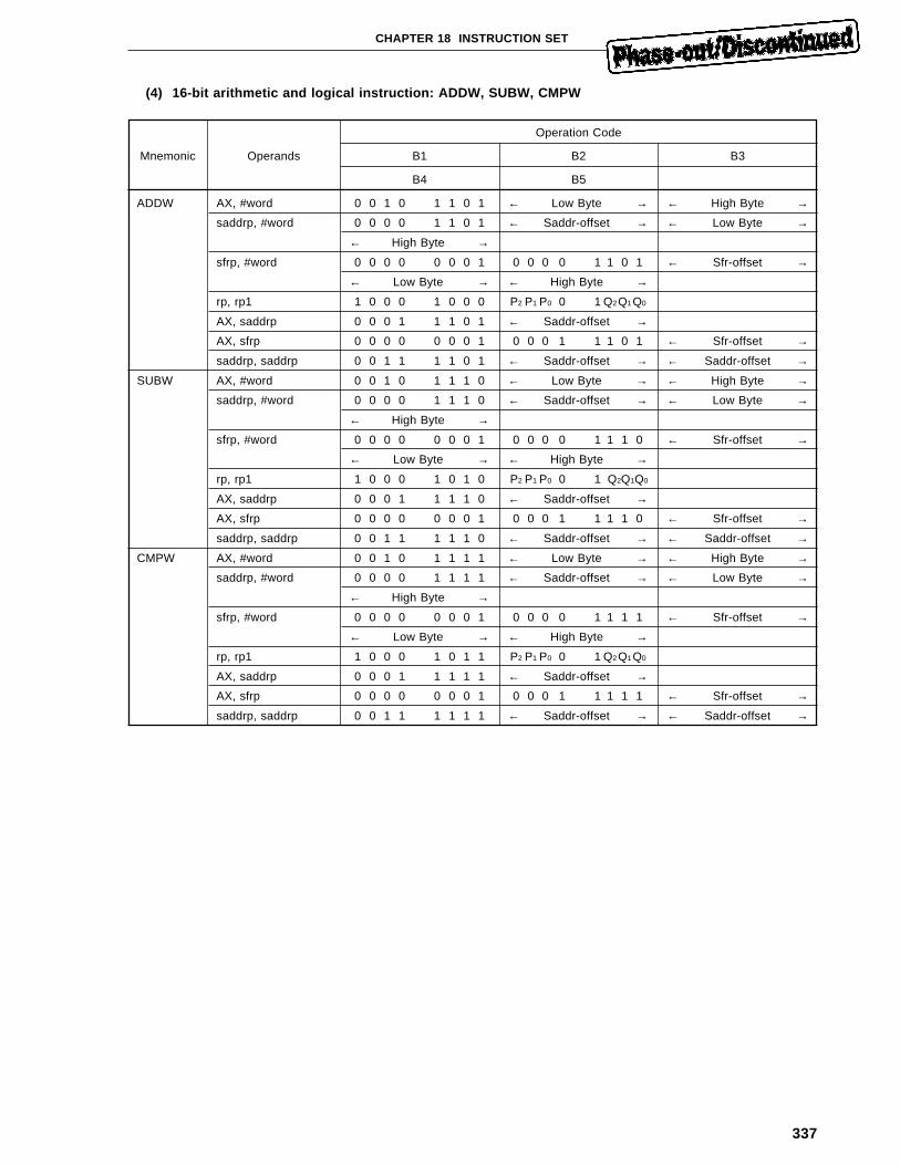
337
CHAPTER 18 INSTRUCTION SET
(4) 16-bit arithmetic and logical instruction: ADDW, SUBW, CMPW
Operation Code
Mnemonic Operands B1 B2 B3
B4 B5
ADDW AX, #word 0 0 1 0 1 1 0 1 ← Low Byte → ← High Byte →
saddrp, #word 0 0 0 0 1 1 0 1 ← Saddr-offset → ← Low Byte →
← High Byte →
sfrp, #word 0 0 0 0 0 0 0 1 0 0 0 0 1 1 0 1 ← Sfr-offset →
← Low Byte → ← High Byte →
rp, rp1 1 0 0 0 1 0 0 0 P2 P1 P0 0 1 Q2Q1 Q0
AX, saddrp 0 0 0 1 1 1 0 1 ← Saddr-offset →
AX, sfrp 0 0 0 0 0 0 0 1 0 0 0 1 1 1 0 1 ← Sfr-offset →
saddrp, saddrp 0 0 1 1 1 1 0 1 ← Saddr-offset → ← Saddr-offset →
SUBW AX, #word 0 0 1 0 1 1 1 0 ← Low Byte → ← High Byte →
saddrp, #word 0 0 0 0 1 1 1 0 ← Saddr-offset → ← Low Byte →
← High Byte →
sfrp, #word 0 0 0 0 0 0 0 1 0 0 0 0 1 1 1 0 ← Sfr-offset →
← Low Byte → ← High Byte →
rp, rp1 1 0 0 0 1 0 1 0 P2 P1 P0 0 1 Q2Q1Q0
AX, saddrp 0 0 0 1 1 1 1 0 ← Saddr-offset →
AX, sfrp 0 0 0 0 0 0 0 1 0 0 0 1 1 1 1 0 ← Sfr-offset →
saddrp, saddrp 0 0 1 1 1 1 1 0 ← Saddr-offset → ← Saddr-offset →
CMPW AX, #word 0 0 1 0 1 1 1 1 ← Low Byte → ← High Byte →
saddrp, #word 0 0 0 0 1 1 1 1 ← Saddr-offset → ← Low Byte →
← High Byte →
sfrp, #word 0 0 0 0 0 0 0 1 0 0 0 0 1 1 1 1 ← Sfr-offset →
← Low Byte → ← High Byte →
rp, rp1 1 0 0 0 1 0 1 1 P2 P1 P0 0 1 Q2Q1 Q0
AX, saddrp 0 0 0 1 1 1 1 1 ← Saddr-offset →
AX, sfrp 0 0 0 0 0 0 0 1 0 0 0 1 1 1 1 1 ← Sfr-offset →
saddrp, saddrp 0 0 1 1 1 1 1 1 ← Saddr-offset → ← Saddr-offset →
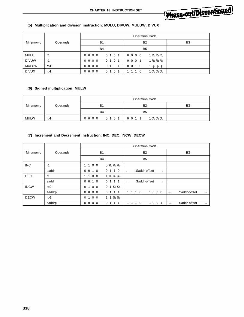
338
CHAPTER 18 INSTRUCTION SET
(5) Multiplication and division instruction: MULU, DIVUW, MULUW, DIVUX
Operation Code
Mnemonic Operands B1 B2 B3
B4 B5
MULU r1 0 0 0 0 0 1 0 1 0 0 0 0 1 R2 R1 R0
DIVUW r1 0 0 0 0 0 1 0 1 0 0 0 1 1 R2 R1 R0
MULUW rp1 0 0 0 0 0 1 0 1 0 0 1 0 1 Q2Q1 Q0
DIVUX rp1 0 0 0 0 0 1 0 1 1 1 1 0 1 Q2Q1 Q0
(6) Signed multiplication: MULW
Operation Code
Mnemonic Operands B1 B2 B3
B4 B5
MULW rp1 0 0 0 0 0 1 0 1 0 0 1 1 1 Q2Q1 Q0
(7) Increment and Decrement instruction: INC, DEC, INCW, DECW
Operation Code
Mnemonic Operands B1 B2 B3
B4 B5
INC r1 1 1 0 0 0 R2 R1 R0
saddr 0 0 1 0 0 1 1 0 ← Saddr-offset →
DEC r1 1 1 0 0 1 R2 R1 R0
saddr 0 0 1 0 0 1 1 1 ← Saddr-offset →
INCW rp2 0 1 0 0 0 1 S1 S0
saddrp 0 0 0 0 0 1 1 1 1 1 1 0 1 0 0 0 ← Saddr-offset →
DECW rp2 0 1 0 0 1 1 S1 S0
saddrp 0 0 0 0 0 1 1 1 1 1 1 0 1 0 0 1 ← Saddr-offset →
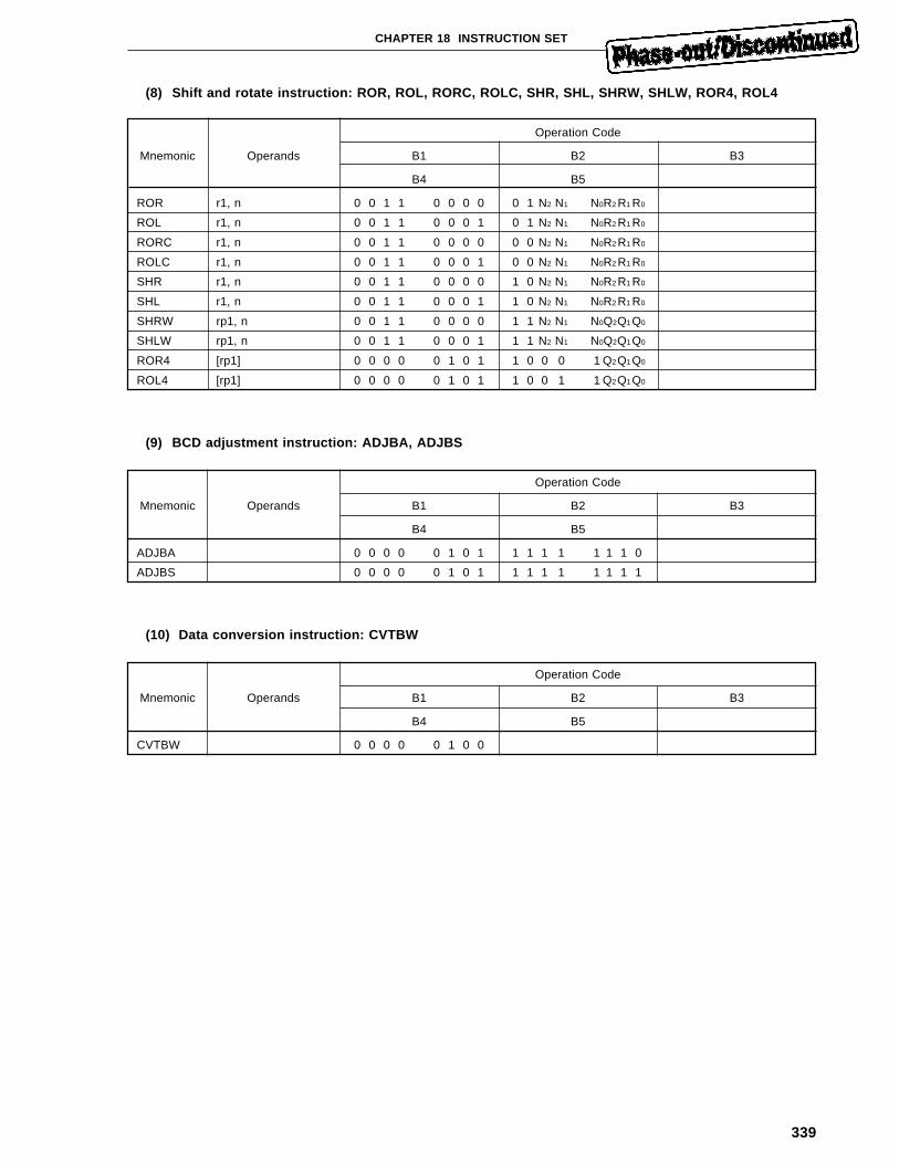
339
CHAPTER 18 INSTRUCTION SET
(8) Shift and rotate instruction: ROR, ROL, RORC, ROLC, SHR, SHL, SHRW, SHLW, ROR4, ROL4
Operation Code
Mnemonic Operands B1 B2 B3
B4 B5
ROR r1, n 0 0 1 1 0 0 0 0 0 1 N2 N1 N0R2 R1 R0
ROL r1, n 0 0 1 1 0 0 0 1 0 1 N2 N1 N0R2 R1 R0
RORC r1, n 0 0 1 1 0 0 0 0 0 0 N2 N1 N0R2 R1 R0
ROLC r1, n 0 0 1 1 0 0 0 1 0 0 N2 N1 N0R2 R1 R0
SHR r1, n 0 0 1 1 0 0 0 0 1 0 N2 N1 N0R2 R1 R0
SHL r1, n 0 0 1 1 0 0 0 1 1 0 N2 N1 N0R2 R1 R0
SHRW rp1, n 0 0 1 1 0 0 0 0 1 1 N2 N1 N0Q2Q1 Q0
SHLW rp1, n 0 0 1 1 0 0 0 1 1 1 N2 N1 N0Q2Q1 Q0
ROR4 [rp1] 0 0 0 0 0 1 0 1 1 0 0 0 1 Q2Q1 Q0
ROL4 [rp1] 0 0 0 0 0 1 0 1 1 0 0 1 1 Q2Q1 Q0
(9) BCD adjustment instruction: ADJBA, ADJBS
Operation Code
Mnemonic Operands B1 B2 B3
B4 B5
ADJBA 0 0 0 0 0 1 0 1 1 1 1 1 1 1 1 0
ADJBS 0 0 0 0 0 1 0 1 1 1 1 1 1 1 1 1
(10) Data conversion instruction: CVTBW
Operation Code
Mnemonic Operands B1 B2 B3
B4 B5
CVTBW 0 0 0 0 0 1 0 0
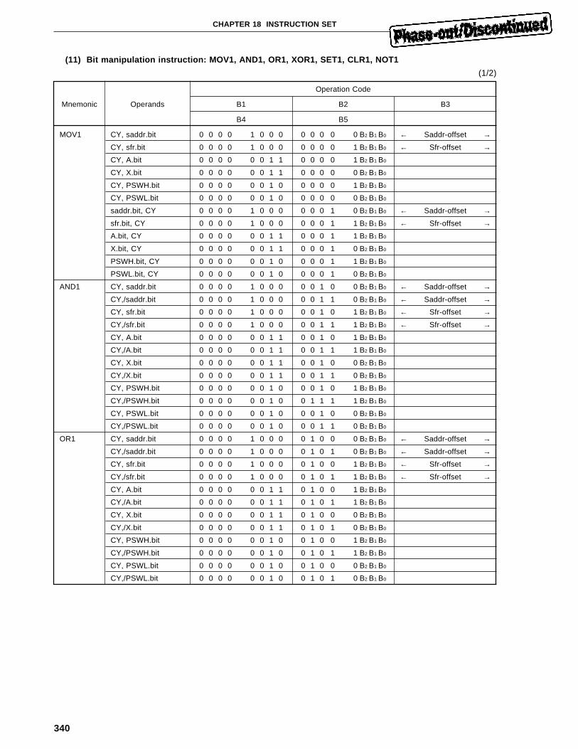
340
CHAPTER 18 INSTRUCTION SET
(11) Bit manipulation instruction: MOV1, AND1, OR1, XOR1, SET1, CLR1, NOT1
(1/2)
Operation Code
Mnemonic Operands B1 B2 B3
B4 B5
MOV1 CY, saddr.bit 0 0 0 0 1 0 0 0 0 0 0 0 0 B2 B1 B0 ← Saddr-offset →
CY, sfr.bit 0 0 0 0 1 0 0 0 0 0 0 0 1 B2 B1 B0 ← Sfr-offset →
CY, A.bit 0 0 0 0 0 0 1 1 0 0 0 0 1 B2 B1 B0
CY, X.bit 0 0 0 0 0 0 1 1 0 0 0 0 0 B2 B1 B0
CY, PSWH.bit 0 0 0 0 0 0 1 0 0 0 0 0 1 B2 B1 B0
CY, PSWL.bit 0 0 0 0 0 0 1 0 0 0 0 0 0 B2 B1 B0
saddr.bit, CY 0 0 0 0 1 0 0 0 0 0 0 1 0 B2 B1 B0 ← Saddr-offset →
sfr.bit, CY 0 0 0 0 1 0 0 0 0 0 0 1 1 B2 B1 B0 ← Sfr-offset →
A.bit, CY 0 0 0 0 0 0 1 1 0 0 0 1 1 B2 B1 B0
X.bit, CY 0 0 0 0 0 0 1 1 0 0 0 1 0 B2 B1 B0
PSWH.bit, CY 0 0 0 0 0 0 1 0 0 0 0 1 1 B2 B1 B0
PSWL.bit, CY 0 0 0 0 0 0 1 0 0 0 0 1 0 B2 B1 B0
AND1 CY, saddr.bit 0 0 0 0 1 0 0 0 0 0 1 0 0 B2 B1 B0 ← Saddr-offset →
CY,/saddr.bit 0 0 0 0 1 0 0 0 0 0 1 1 0 B2 B1 B0 ← Saddr-offset →
CY, sfr.bit 0 0 0 0 1 0 0 0 0 0 1 0 1 B2 B1 B0 ← Sfr-offset →
CY,/sfr.bit 0 0 0 0 1 0 0 0 0 0 1 1 1 B2 B1 B0 ← Sfr-offset →
CY, A.bit 0 0 0 0 0 0 1 1 0 0 1 0 1 B2 B1 B0
CY,/A.bit 0 0 0 0 0 0 1 1 0 0 1 1 1 B2 B1 B0
CY, X.bit 0 0 0 0 0 0 1 1 0 0 1 0 0 B2 B1 B0
CY,/X.bit 0 0 0 0 0 0 1 1 0 0 1 1 0 B2 B1 B0
CY, PSWH.bit 0 0 0 0 0 0 1 0 0 0 1 0 1 B2 B1 B0
CY,/PSWH.bit 0 0 0 0 0 0 1 0 0 1 1 1 1 B2 B1 B0
CY, PSWL.bit 0 0 0 0 0 0 1 0 0 0 1 0 0 B2 B1 B0
CY,/PSWL.bit 0 0 0 0 0 0 1 0 0 0 1 1 0 B2 B1 B0
OR1 CY, saddr.bit 0 0 0 0 1 0 0 0 0 1 0 0 0 B2 B1 B0 ← Saddr-offset →
CY,/saddr.bit 0 0 0 0 1 0 0 0 0 1 0 1 0 B2 B1 B0 ← Saddr-offset →
CY, sfr.bit 0 0 0 0 1 0 0 0 0 1 0 0 1 B2 B1 B0 ← Sfr-offset →
CY,/sfr.bit 0 0 0 0 1 0 0 0 0 1 0 1 1 B2 B1 B0 ← Sfr-offset →
CY, A.bit 0 0 0 0 0 0 1 1 0 1 0 0 1 B2 B1 B0
CY,/A.bit 0 0 0 0 0 0 1 1 0 1 0 1 1 B2 B1 B0
CY, X.bit 0 0 0 0 0 0 1 1 0 1 0 0 0 B2 B1 B0
CY,/X.bit 0 0 0 0 0 0 1 1 0 1 0 1 0 B2 B1 B0
CY, PSWH.bit 0 0 0 0 0 0 1 0 0 1 0 0 1 B2 B1 B0
CY,/PSWH.bit 0 0 0 0 0 0 1 0 0 1 0 1 1 B2 B1 B0
CY, PSWL.bit 0 0 0 0 0 0 1 0 0 1 0 0 0 B2 B1 B0
CY,/PSWL.bit 0 0 0 0 0 0 1 0 0 1 0 1 0 B2 B1 B0
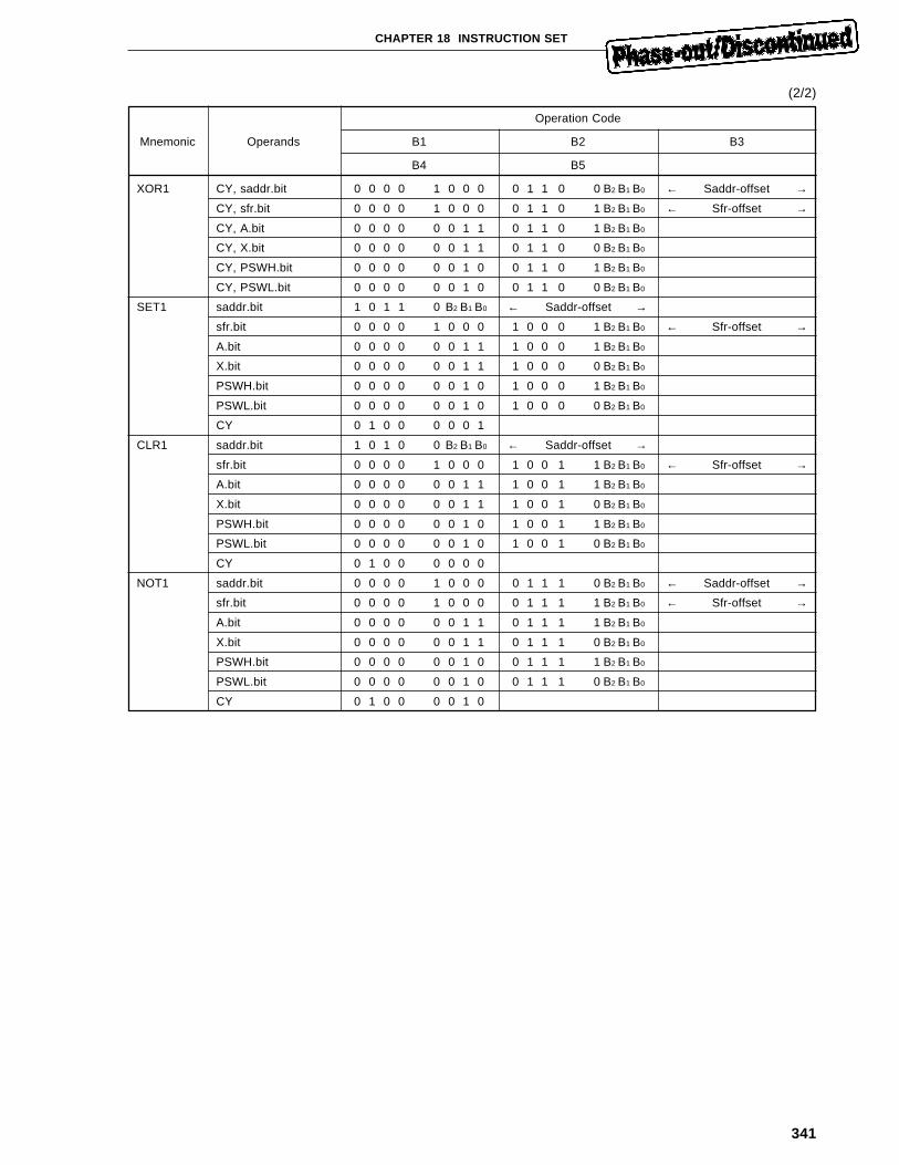
341
CHAPTER 18 INSTRUCTION SET
(2/2)
Operation Code
Mnemonic Operands B1 B2 B3
B4 B5
XOR1 CY, saddr.bit 0 0 0 0 1 0 0 0 0 1 1 0 0 B2 B1 B0 ← Saddr-offset →
CY, sfr.bit 0 0 0 0 1 0 0 0 0 1 1 0 1 B2 B1 B0 ← Sfr-offset →
CY, A.bit 0 0 0 0 0 0 1 1 0 1 1 0 1 B2 B1 B0
CY, X.bit 0 0 0 0 0 0 1 1 0 1 1 0 0 B2 B1 B0
CY, PSWH.bit 0 0 0 0 0 0 1 0 0 1 1 0 1 B2 B1 B0
CY, PSWL.bit 0 0 0 0 0 0 1 0 0 1 1 0 0 B2 B1 B0
SET1 saddr.bit 1 0 1 1 0 B2 B1 B0 ← Saddr-offset →
sfr.bit 0 0 0 0 1 0 0 0 1 0 0 0 1 B2 B1 B0 ← Sfr-offset →
A.bit 0 0 0 0 0 0 1 1 1 0 0 0 1 B2 B1 B0
X.bit 0 0 0 0 0 0 1 1 1 0 0 0 0 B2 B1 B0
PSWH.bit 0 0 0 0 0 0 1 0 1 0 0 0 1 B2 B1 B0
PSWL.bit 0 0 0 0 0 0 1 0 1 0 0 0 0 B2 B1 B0
CY 0 1 0 0 0 0 0 1
CLR1 saddr.bit 1 0 1 0 0 B2 B1 B0 ← Saddr-offset →
sfr.bit 0 0 0 0 1 0 0 0 1 0 0 1 1 B2 B1 B0 ← Sfr-offset →
A.bit 0 0 0 0 0 0 1 1 1 0 0 1 1 B2 B1 B0
X.bit 0 0 0 0 0 0 1 1 1 0 0 1 0 B2 B1 B0
PSWH.bit 0 0 0 0 0 0 1 0 1 0 0 1 1 B2 B1 B0
PSWL.bit 0 0 0 0 0 0 1 0 1 0 0 1 0 B2 B1 B0
CY 0 1 0 0 0 0 0 0
NOT1 saddr.bit 0 0 0 0 1 0 0 0 0 1 1 1 0 B2 B1 B0 ← Saddr-offset →
sfr.bit 0 0 0 0 1 0 0 0 0 1 1 1 1 B2 B1 B0 ← Sfr-offset →
A.bit 0 0 0 0 0 0 1 1 0 1 1 1 1 B2 B1 B0
X.bit 0 0 0 0 0 0 1 1 0 1 1 1 0 B2 B1 B0
PSWH.bit 0 0 0 0 0 0 1 0 0 1 1 1 1 B2 B1 B0
PSWL.bit 0 0 0 0 0 0 1 0 0 1 1 1 0 B2 B1 B0
CY 0 1 0 0 0 0 1 0
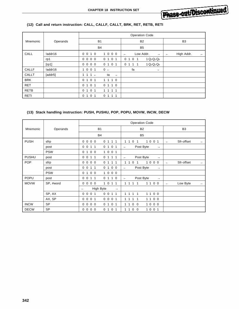
342
CHAPTER 18 INSTRUCTION SET
(12) Call and return instruction: CALL, CALLF, CALLT, BRK, RET, RETB, RETI
Operation Code
Mnemonic Operands B1 B2 B3
B4 B5
CALL !addr16 0 0 1 0 1 0 0 0 ← Low Addr. → ← High Addr. →
rp1 0 0 0 0 0 1 0 1 0 1 0 1 1 Q2Q1 Q0
[rp1] 0 0 0 0 0 1 0 1 0 1 1 1 1 Q2Q1 Q0
CALLF !addr16 1 0 0 1 0 ← fa →
CALLT [addr5] 1 1 1 ← ta →
BRK 0 1 0 1 1 1 1 0
RET 0 1 0 1 0 1 1 0
RETB 0 1 0 1 1 1 1 1
RETI 0 1 0 1 0 1 1 1
(13) Stack handling instruction: PUSH, PUSHU, POP, POPU, MOVW, INCW, DECW
Operation Code
Mnemonic Operands B1 B2 B3
B4 B5
PUSH sfrp 0 0 0 0 0 1 1 1 1 1 0 1 1 0 0 1 ← Sfr-offset →
post 0 0 1 1 0 1 0 1 ← Post Byte →
PSW 0 1 0 0 1 0 0 1
PUSHU post 0 0 1 1 0 1 1 1 ← Post Byte →
POP sfrp 0 0 0 0 0 1 1 1 1 1 0 1 1 0 0 0 ← Sfr-offset →
post 0 0 1 1 0 1 0 0 ← Post Byte →
PSW 0 1 0 0 1 0 0 0
POPU post 0 0 1 1 0 1 1 0 ← Post Byte →
MOVW SP, #word 0 0 0 0 1 0 1 1 1 1 1 1 1 1 0 0 ← Low Byte →
← High Byte →
SP, AX 0 0 0 1 0 0 1 1 1 1 1 1 1 1 0 0
AX, SP 0 0 0 1 0 0 0 1 1 1 1 1 1 1 0 0
INCW SP 0 0 0 0 0 1 0 1 1 1 0 0 1 0 0 0
DECW SP 0 0 0 0 0 1 0 1 1 1 0 0 1 0 0 1
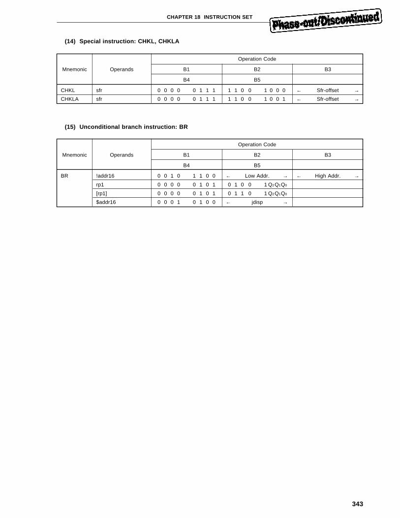
343
CHAPTER 18 INSTRUCTION SET
(14) Special instruction: CHKL, CHKLA
Operation Code
Mnemonic Operands B1 B2 B3
B4 B5
CHKL sfr 0 0 0 0 0 1 1 1 1 1 0 0 1 0 0 0 ← Sfr-offset →
CHKLA sfr 0 0 0 0 0 1 1 1 1 1 0 0 1 0 0 1 ← Sfr-offset →
(15) Unconditional branch instruction: BR
Operation Code
Mnemonic Operands B1 B2 B3
B4 B5
BR !addr16 0 0 1 0 1 1 0 0 ← Low Addr. → ← High Addr. →
rp1 0 0 0 0 0 1 0 1 0 1 0 0 1 Q2Q1Q0
[rp1] 0 0 0 0 0 1 0 1 0 1 1 0 1 Q2Q1Q0
$addr16 0 0 0 1 0 1 0 0 ← jdisp →
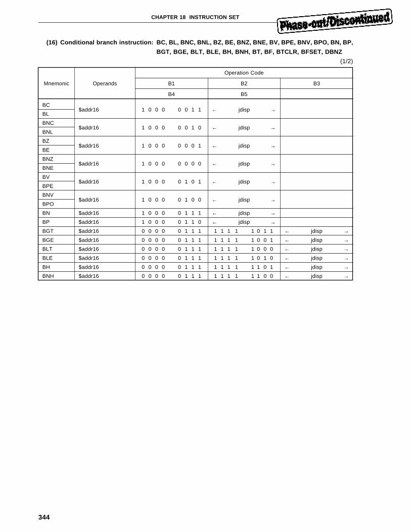
344
CHAPTER 18 INSTRUCTION SET
(16) Conditional branch instruction: BC, BL, BNC, BNL, BZ, BE, BNZ, BNE, BV, BPE, BNV, BPO, BN, BP,
BGT, BGE, BLT, BLE, BH, BNH, BT, BF, BTCLR, BFSET, DBNZ
(1/2)
Operation Code
Mnemonic Operands B1 B2 B3
B4 B5
BC$addr16 1 0 0 0 0 0 1 1 ← jdisp →
BL
BNC$addr16 1 0 0 0 0 0 1 0 ← jdisp →
BNL
BZ$addr16 1 0 0 0 0 0 0 1 ← jdisp →
BE
BNZ$addr16 1 0 0 0 0 0 0 0 ← jdisp →
BNE
BV$addr16 1 0 0 0 0 1 0 1 ← jdisp →
BPE
BNV$addr16 1 0 0 0 0 1 0 0 ← jdisp →
BPO
BN $addr16 1 0 0 0 0 1 1 1 ← jdisp →
BP $addr16 1 0 0 0 0 1 1 0 ← jdisp →
BGT $addr16 0 0 0 0 0 1 1 1 1 1 1 1 1 0 1 1 ← jdisp →
BGE $addr16 0 0 0 0 0 1 1 1 1 1 1 1 1 0 0 1 ← jdisp →
BLT $addr16 0 0 0 0 0 1 1 1 1 1 1 1 1 0 0 0 ← jdisp →
BLE $addr16 0 0 0 0 0 1 1 1 1 1 1 1 1 0 1 0 ← jdisp →
BH $addr16 0 0 0 0 0 1 1 1 1 1 1 1 1 1 0 1 ← jdisp →
BNH $addr16 0 0 0 0 0 1 1 1 1 1 1 1 1 1 0 0 ← jdisp →
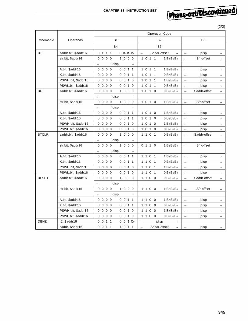
345
CHAPTER 18 INSTRUCTION SET
(2/2)
Operation Code
Mnemonic Operands B1 B2 B3
B4 B5
BT saddr.bit, $addr16 0 1 1 1 0 B2 B1 B0 ← Saddr-offset → ← jdisp →
sfr.bit, $addr16 0 0 0 0 1 0 0 0 1 0 1 1 1 B2 B1 B0 ← Sfr-offset →
← jdisp →
A.bit, $addr16 0 0 0 0 0 0 1 1 1 0 1 1 1 B2 B1 B0 ← jdisp →
X.bit, $addr16 0 0 0 0 0 0 1 1 1 0 1 1 0 B2 B1 B0 ← jdisp →
PSWH.bit, $addr16 0 0 0 0 0 0 1 0 1 0 1 1 1 B2 B1 B0 ← jdisp →
PSWL.bit, $addr16 0 0 0 0 0 0 1 0 1 0 1 1 0 B2 B1 B0 ← jdisp →
BF saddr.bit, $addr16 0 0 0 0 1 0 0 0 1 0 1 0 0 B2 B1 B0 ← Saddr-offset →
← jdisp →
sfr.bit, $addr16 0 0 0 0 1 0 0 0 1 0 1 0 1 B2 B1 B0 ← Sfr-offset →
← jdisp →
A.bit, $addr16 0 0 0 0 0 0 1 1 1 0 1 0 1 B2 B1 B0 ← jdisp →
X.bit, $addr16 0 0 0 0 0 0 1 1 1 0 1 0 0 B2 B1 B0 ← jdisp →
PSWH.bit, $addr16 0 0 0 0 0 0 1 0 1 0 1 0 1 B2 B1 B0 ← jdisp →
PSWL.bit, $addr16 0 0 0 0 0 0 1 0 1 0 1 0 0 B2 B1 B0 ← jdisp →
BTCLR saddr.bit, $addr16 0 0 0 0 1 0 0 0 1 1 0 1 0 B2 B1 B0 ← Saddr-offset →
← jdisp →
sfr.bit, $addr16 0 0 0 0 1 0 0 0 0 1 1 0 1 B2 B1 B0 ← Sfr-offset →
← jdisp →
A.bit, $addr16 0 0 0 0 0 0 1 1 1 1 0 1 1 B2 B1 B0 ← jdisp →
X.bit, $addr16 0 0 0 0 0 0 1 1 1 1 0 1 0 B2 B1 B0 ← jdisp →
PSWH.bit, $addr16 0 0 0 0 0 0 1 0 1 1 0 1 1 B2 B1 B0 ← jdisp →
PSWL.bit, $addr16 0 0 0 0 0 0 1 0 1 1 0 1 0 B2 B1 B0 ← jdisp →
BFSET saddr.bit, $addr16 0 0 0 0 1 0 0 0 1 1 0 0 0 B2 B1 B0 ← Saddr-offset →
← jdisp →
sfr.bit, $addr16 0 0 0 0 1 0 0 0 1 1 0 0 1 B2 B1 B0 ← Sfr-offset →
← jdisp →
A.bit, $addr16 0 0 0 0 0 0 1 1 1 1 0 0 1 B2 B1 B0 ← jdisp →
X.bit, $addr16 0 0 0 0 0 0 1 1 1 1 0 0 0 B2 B1 B0 ← jdisp →
PSWH.bit, $addr16 0 0 0 0 0 0 1 0 1 1 0 0 1 B2 B1 B0 ← jdisp →
PSWL.bit, $addr16 0 0 0 0 0 0 1 0 1 1 0 0 0 B2 B1 B0 ← jdisp →
DBNZ r2, $addr16 0 0 1 1 0 0 1 C0 ← jdisp →
saddr, $addr16 0 0 1 1 1 0 1 1 ← Saddr-offset → ← jdisp →
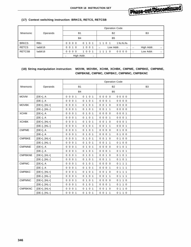
346
CHAPTER 18 INSTRUCTION SET
(17) Context switching instruction: BRKCS, RETCS, RETCSB
Operation Code
Mnemonic Operands B1 B2 B3
B4 B5
BRKCS RBn 0 0 0 0 0 1 0 1 1 1 0 1 1 N2 N1 N0
RETCS !addr16 0 0 1 0 1 0 0 1 ← Low Addr. → ← High Addr. →
RETCSB !addr16 0 0 0 0 1 0 0 1 1 1 1 0 0 0 0 0 ← Low Addr. →
← High Addr. →
(18) String manipulation instruction: MOVM, MOVBK, XCHM, XCHBK, CMPME, CMPBKE, CMPMNE,
CMPBKNE, CMPMC, CMPBKC, CMPMNC, CMPBKNC
Operation Code
Mnemonic Operands B1 B2 B3
B4 B5
MOVM [DE+], A 0 0 0 1 0 1 0 1 0 0 0 0 0 0 0 0
[DE–], A 0 0 0 1 0 1 0 1 0 0 0 1 0 0 0 0
MOVBK [DE+], [HL+] 0 0 0 1 0 1 0 1 0 0 1 0 0 0 0 0
[DE–], [HL–] 0 0 0 1 0 1 0 1 0 0 1 1 0 0 0 0
XCHM [DE+], A 0 0 0 1 0 1 0 1 0 0 0 0 0 0 0 1
[DE–], A 0 0 0 1 0 1 0 1 0 0 0 1 0 0 0 1
XCHBK [DE+], [HL+] 0 0 0 1 0 1 0 1 0 0 1 0 0 0 0 1
[DE–], [HL–] 0 0 0 1 0 1 0 1 0 0 1 1 0 0 0 1
CMPME [DE+], A 0 0 0 1 0 1 0 1 0 0 0 0 0 1 0 0
[DE–], A 0 0 0 1 0 1 0 1 0 0 0 1 0 1 0 0
CMPBKE [DE+], [HL+] 0 0 0 1 0 1 0 1 0 0 1 0 0 1 0 0
[DE–], [HL–] 0 0 0 1 0 1 0 1 0 0 1 1 0 1 0 0
CMPMNE [DE+], A 0 0 0 1 0 1 0 1 0 0 0 0 0 1 0 1
[DE–], A 0 0 0 1 0 1 0 1 0 0 0 1 0 1 0 1
CMPBKNE [DE+], [HL+] 0 0 0 1 0 1 0 1 0 0 1 0 0 1 0 1
[DE–], [HL–] 0 0 0 1 0 1 0 1 0 0 1 1 0 1 0 1
CMPMC [DE+], A 0 0 0 1 0 1 0 1 0 0 0 0 0 1 1 1
[DE–], A 0 0 0 1 0 1 0 1 0 0 0 1 0 1 1 1
CMPBKC [DE+], [HL+] 0 0 0 1 0 1 0 1 0 0 1 0 0 1 1 1
[DE–], [HL–] 0 0 0 1 0 1 0 1 0 0 1 1 0 1 1 1
CMPMNC [DE+], [HL+] 0 0 0 1 0 1 0 1 0 0 0 0 0 1 1 0
[DE–], [HL–] 0 0 0 1 0 1 0 1 0 0 0 1 0 1 1 0
CMPBKNC [DE+], [HL+] 0 0 0 1 0 1 0 1 0 0 1 0 0 1 1 0
[DE–], [HL–] 0 0 0 1 0 1 0 1 0 0 1 1 0 1 1 0
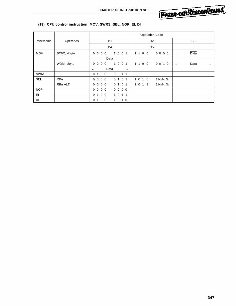
347
CHAPTER 18 INSTRUCTION SET
(19) CPU control instruction: MOV, SWRS, SEL, NOP, EI, DI
Operation Code
Mnemonic Operands B1 B2 B3
B4 B5
MOV STBC, #byte 0 0 0 0 1 0 0 1 1 1 0 0 0 0 0 0 ← Data →
← Data →
WDM, #byte 0 0 0 0 1 0 0 1 1 1 0 0 0 0 1 0 ← Data →
← Data →
SWRS 0 1 0 0 0 0 1 1
SEL RBn 0 0 0 0 0 1 0 1 1 0 1 0 1 N2 N1 N0
RBn ALT 0 0 0 0 0 1 0 1 1 0 1 1 1 N2 N1 N0
NOP 0 0 0 0 0 0 0 0
EI 0 1 0 0 1 0 1 1
DI 0 1 0 0 1 0 1 0
348
CHAPTER 18 INSTRUCTION SET
18.3 Instruction Clocks
18.3.1 Explanation of column of clocks
(1) Conditions to calculate number of execution clocks
The conditions to calculate the number of instruction execution clocks under the column of clocks are as
follows:
(a) Sufficient operation codes are always entered in an instruction queue, and when EXU requires an
operation code, the operation code can be immediately read.
(b) The stack pointer points to main RAM (FE00H to FEFFH).
(c) Addresses indicated by using mem, !addr16, [saddrp], [DE+], [DE–] [HL+], [HL–], and [rp1] point to main
RAM (FE00H to FEFFH).
(d) Only the number of microprogram execution clocks at EXU is counted (the time required from clearing
the instruction queue to reading the operation code at the branch destination when a branch is taken during
execution of an instruction such as BR, CALL, RET, BRK, or RETI or interrupt service is not contained).
The number of instruction execution clocks is a value calculated by assuming these conditions.
Thus, the actual number of clocks when a program is executed may be greater than that listed under the column
of Clocks. The reason why it is greater is described below:
(a) When operation code is read from instruction queue
When EXU reads an operation code, if the instruction queue does not contain any operation code, EXU
waits until an operation code is entered in the instruction queue. Particularly, if branch processing occurs,
the instruction queue becomes empty from once clearing the instruction queue to reading the operation
code at the branch destination, EXU always enters the wait state.
(b) When data in memory other than main RAM is referenced
<1> when data is read
EXU waits from BCU starting a bus cycle to completing data read.
<2> when data is written
If EXU issues a data write request to BCU, it can immediately execute the next instruction.
However, since BCU cannot acknowledge another processing request occurring from EXU during
data write processing execution, EXU enters the wait state (in which it cannot perform memory
reference other than main RAM, SFR reference, or branch processing) until BCU terminates write
processing.
Particularly, when the instruction queue does not contain any, operation code fetch takes precedence
over in write processing into external memory or peripheral RAM, thus when a write bus cycle is to
be started cannot be specified.
Therefore, when EXU enters the wait state cannot be specified due to timing contention with write
processing.
349
CHAPTER 18 INSTRUCTION SET
<3> Contention between memory reference other than main RAM or branch processing and
operation code fetch
When EXU issues a request for memory reference other than main RAM of for branch processing
to BCU, if BCU executes a bus cycle of operation code fetch, the memory reference or branch
processing request is not acknowledged until BCU terminates the operation code fetch bus cycle;
EXU enters the wait state.
(2) Classification of column of clocks
The number of instruction clocks varies depending on the memory area accessed or to which a branch is taken
by the instruction.
• Internal ROM : At internal ROM fetch
• IRAM : When internal dual port RAM (0FE00H to 0FEFFH) is accessed
• PRAM : When internal RAM area other than IRAM is accessed
• SFR : When special function register is accessed
• EMEM : When external memory is accessed
(3) n under column of Clocks
• Shift and rotate instructions : Number of shift bits.
• Stack handling instruction : Number of saved/restored register.
• String manipulation instruction : Number of times a given instruction is executed until the condition is
satisfied and an exit is made from loop.
(4) “/” under column of Clocks
• “/” : a/b means a or b.
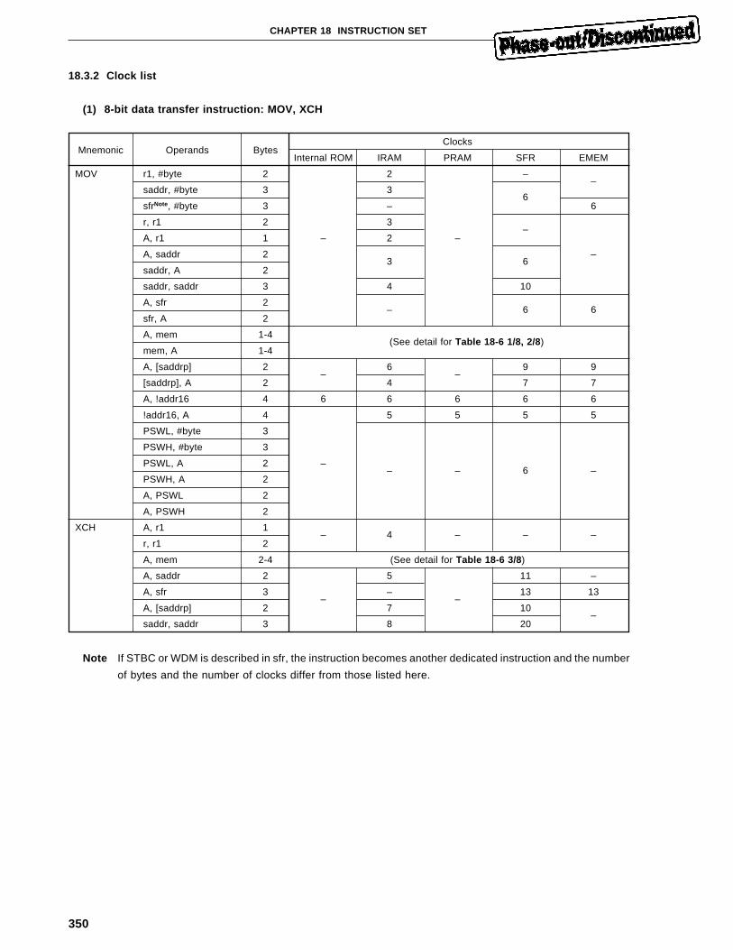
350
CHAPTER 18 INSTRUCTION SET
18.3.2 Clock list
(1) 8-bit data transfer instruction: MOV, XCH
Mnemonic Operands BytesClocks
Internal ROM IRAM PRAM SFR EMEM
MOV r1, #byte 2 2 ––
saddr, #byte 3 36
sfrNote, #byte 3 – 6
r, r1 2 3–
A, r1 1 – 2 –
A, saddr 23 6
–
saddr, A 2
saddr, saddr 3 4 10
A, sfr 2– 6 6
sfr, A 2
A, mem 1-4(See detail for Table 18-6 1/8, 2/8 )
mem, A 1-4
A, [saddrp] 2–
6–
9 9
[saddrp], A 2 4 7 7
A, !addr16 4 6 6 6 6 6
!addr16, A 4 5 5 5 5
PSWL, #byte 3
PSWH, #byte 3
PSWL, A 2 –– – 6 –
PSWH, A 2
A, PSWL 2
A, PSWH 2
XCH A, r1 1– 4 – – –
r, r1 2
A, mem 2-4 (See detail for Table 18-6 3/8 )
A, saddr 2 5 11 –
A, sfr 3–
––
13 13
A, [saddrp] 2 7 10–
saddr, saddr 3 8 20
Note If STBC or WDM is described in sfr, the instruction becomes another dedicated instruction and the number
of bytes and the number of clocks differ from those listed here.
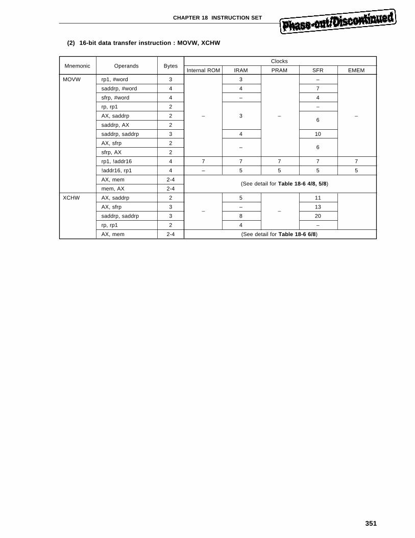
351
CHAPTER 18 INSTRUCTION SET
(2) 16-bit data transfer instruction : MOVW, XCHW
Mnemonic Operands BytesClocks
Internal ROM IRAM PRAM SFR EMEM
MOVW rp1, #word 3 3 –
saddrp, #word 4 4 7
sfrp, #word 4 – 4
rp, rp1 2 –
AX, saddrp 2 – 3 –6
–
saddrp, AX 2
saddrp, saddrp 3 4 10
AX, sfrp 2– 6
sfrp, AX 2
rp1, !addr16 4 7 7 7 7 7
!addr16, rp1 4 – 5 5 5 5
AX, mem 2-4(See detail for Table 18-6 4/8, 5/8 )
mem, AX 2-4
XCHW AX, saddrp 2 5 11
AX, sfrp 3–
––
13
saddrp, saddrp 3 8 20
rp, rp1 2 4 –
AX, mem 2-4 (See detail for Table 18-6 6/8 )
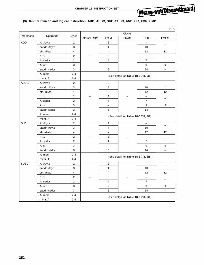
352
CHAPTER 18 INSTRUCTION SET
(3) 8-bit arithmetic and logical instruction: ADD, ADDC, SUB, SUBC, AND, OR, XOR, CMP
(1/2)
Mnemonic Operands BytesClocks
Internal ROM IRAM PRAM SFR EMEM
ADD A, #byte 2 2 ––
saddr, #byte 3 4 10
sfr, #byte 4 – 12 12
r, r1 2 – 3 – ––
A, saddr 2 4 7
A, sfr 3 – 9 9
saddr, saddr 3 5 14 –
A, mem 2-4(See detail for Table 18-6 7/8, 8/8 )
mem, A 2-4
ADDC A, #byte 2 2 ––
saddr, #byte 3 4 10
sfr, #byte 4 – 12 12
r, r1 2 – 3 – ––
A, saddr 2 4 7
A, sfr 3 – 9 9
saddr, saddr 3 5 14 –
A, mem 2-4(See detail for Table 18-6 7/8, 8/8 )
mem, A 2-4
SUB A, #byte 2 2 ––
saddr ,#byte 3 4 10
sfr, #byte 4 – 12 12
r, r1 2 – 3 – ––
A, saddr 2 4 7
A, sfr 3 – 9 9
saddr, saddr 3 5 14 –
A, mem 2-4(See detail for Table 18-6 7/8, 8/8 )
mem, A 2-4
SUBC A, #byte 2 2 ––
saddr, #byte 3 4 10
sfr, #byte 4 – 12 12
r, r1 2 – 3 – ––
A, saddr 2 4 7
A, sfr 3 – 9 9
saddr, saddr 3 5 14 –
A, mem 2-4(See detail for Table 18-6 7/8, 8/8 )
mem, A 2-4
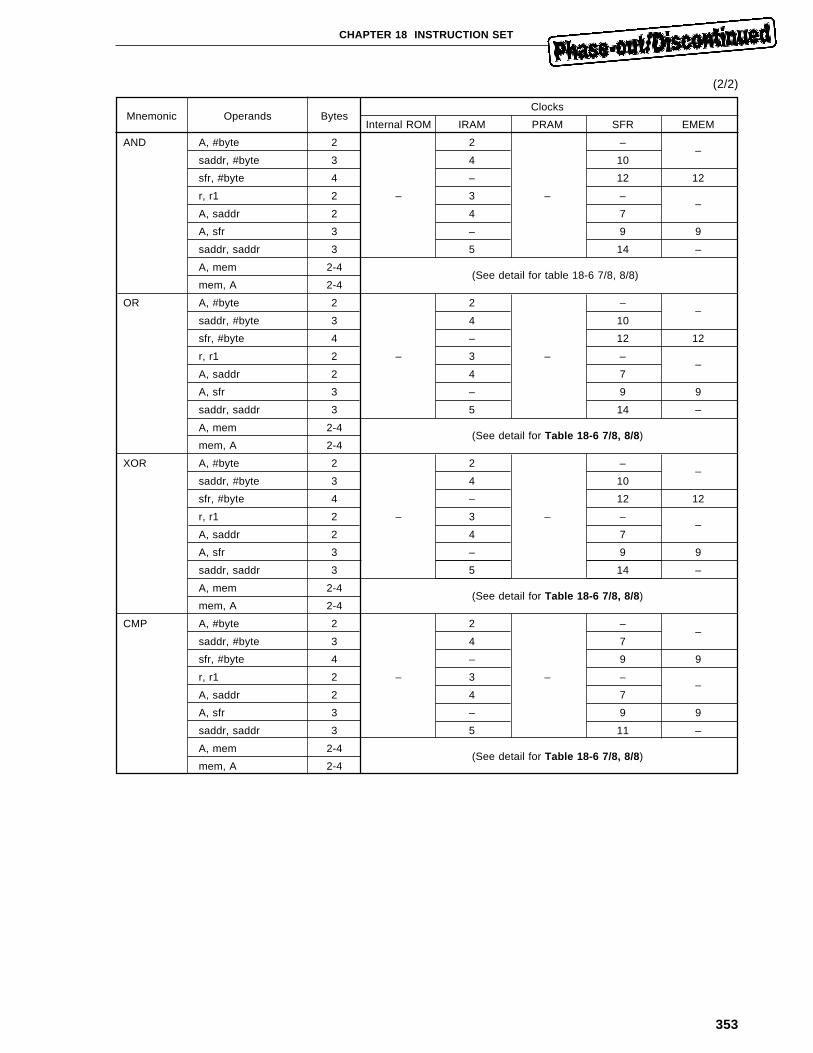
353
CHAPTER 18 INSTRUCTION SET
(2/2)
Mnemonic Operands BytesClocks
Internal ROM IRAM PRAM SFR EMEM
AND A, #byte 2 2 ––
saddr, #byte 3 4 10
sfr, #byte 4 – 12 12
r, r1 2 – 3 – ––
A, saddr 2 4 7
A, sfr 3 – 9 9
saddr, saddr 3 5 14 –
A, mem 2-4(See detail for table 18-6 7/8, 8/8)
mem, A 2-4
OR A, #byte 2 2 ––
saddr, #byte 3 4 10
sfr, #byte 4 – 12 12
r, r1 2 – 3 – ––
A, saddr 2 4 7
A, sfr 3 – 9 9
saddr, saddr 3 5 14 –
A, mem 2-4(See detail for Table 18-6 7/8, 8/8 )
mem, A 2-4
XOR A, #byte 2 2 ––
saddr, #byte 3 4 10
sfr, #byte 4 – 12 12
r, r1 2 – 3 – ––
A, saddr 2 4 7
A, sfr 3 – 9 9
saddr, saddr 3 5 14 –
A, mem 2-4(See detail for Table 18-6 7/8, 8/8 )
mem, A 2-4
CMP A, #byte 2 2 ––
saddr, #byte 3 4 7
sfr, #byte 4 – 9 9
r, r1 2 – 3 – ––
A, saddr 2 4 7
A, sfr 3 – 9 9
saddr, saddr 3 5 11 –
A, mem 2-4(See detail for Table 18-6 7/8, 8/8 )
mem, A 2-4
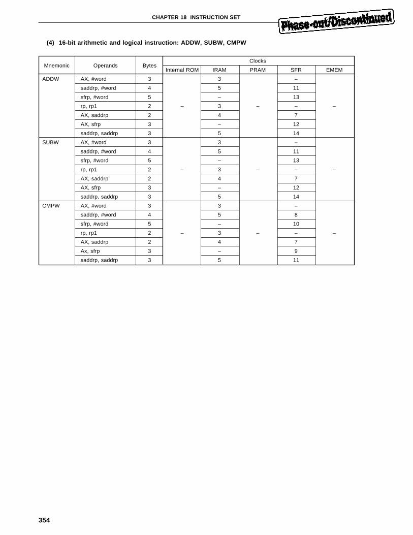
354
CHAPTER 18 INSTRUCTION SET
(4) 16-bit arithmetic and logical instruction: ADDW, SUBW, CMPW
Mnemonic Operands BytesClocks
Internal ROM IRAM PRAM SFR EMEM
ADDW AX, #word 3 3 –
saddrp, #word 4 5 11
sfrp, #word 5 – 13
rp, rp1 2 – 3 – – –
AX, saddrp 2 4 7
AX, sfrp 3 – 12
saddrp, saddrp 3 5 14
SUBW AX, #word 3 3 –
saddrp, #word 4 5 11
sfrp, #word 5 – 13
rp, rp1 2 – 3 – – –
AX, saddrp 2 4 7
AX, sfrp 3 – 12
saddrp, saddrp 3 5 14
CMPW AX, #word 3 3 –
saddrp, #word 4 5 8
sfrp, #word 5 – 10
rp, rp1 2 – 3 – – –
AX, saddrp 2 4 7
Ax, sfrp 3 – 9
saddrp, saddrp 3 5 11
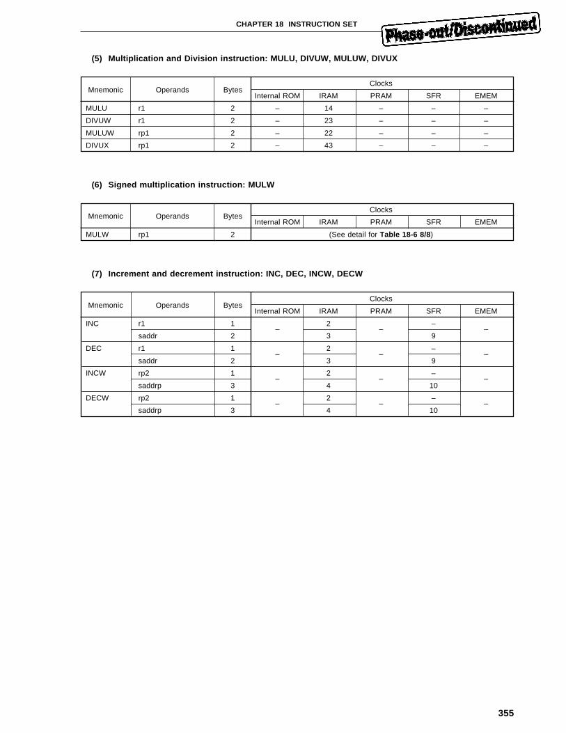
355
CHAPTER 18 INSTRUCTION SET
(5) Multiplication and Division instruction: MULU, DIVUW, MULUW, DIVUX
Mnemonic Operands BytesClocks
Internal ROM IRAM PRAM SFR EMEM
MULU r1 2 – 14 – – –
DIVUW r1 2 – 23 – – –
MULUW rp1 2 – 22 – – –
DIVUX rp1 2 – 43 – – –
(6) Signed multiplication instruction: MULW
Mnemonic Operands BytesClocks
Internal ROM IRAM PRAM SFR EMEM
MULW rp1 2 (See detail for Table 18-6 8/8 )
(7) Increment and decrement instruction: INC, DEC, INCW, DECW
Mnemonic Operands BytesClocks
Internal ROM IRAM PRAM SFR EMEM
INC r1 1–
2–
––
saddr 2 3 9
DEC r1 1–
2–
––
saddr 2 3 9
INCW rp2 1–
2–
––
saddrp 3 4 10
DECW rp2 1–
2–
––
saddrp 3 4 10
356
CHAPTER 18 INSTRUCTION SET
(8) Shift rotate instruction: ROR, ROL, RORC, ROLC, SHR, SHL, SHRW, SHLW, ROR4, ROL4
Mnemonic Operands BytesClocks
Internal ROM IRAM PRAM SFR EMEM
ROR r1, n 2 – 6+n – – –
ROL r1, n 2 – 6+n – – –
RORC r1, n 2 – 6+n – – –
ROLC r1, n 2 – 6+n – – –
SHR r1, n 2 – 6+n – – –
SHL r1, n 2 – 6+n – – –
SHRW rp1, n 2 – 6+n – – –
SHLW rp1, n 2 – 6+n – – –
ROR4 [rp1] 2 – 8 – – –
ROL4 [rp1] 2 – 8 – – –
(9) BCD adjustment instruction: ADJBA, ADJBS
Mnemonic Operands BytesClocks
Internal ROM IRAM PRAM SFR EMEM
ADJBA 2 – 5 – – –
ADJBS 2 – 5 – – –
(10) Data Conversion instruction: CVTBW
Mnemonic Operands BytesClocks
Internal ROM IRAM PRAM SFR EMEM
CVTBW 1 – 3 – – –
357
CHAPTER 18 INSTRUCTION SET
(11) Bit manipulation instruction: MOV1, AND1, OR1, XOR1, SET1, CLR1, NOT1
(1/2)
Mnemonic Operands BytesClocks
Internal ROM IRAM PRAM SFR EMEM
MOV1 Cy, saddr.bit 3 69
–
CY, sfr.bit 3 – 9
CY, A.bit 26 –
CY, X.bit 2
CY, PSWH.bit 2– 6
–
CY, PSWL.bit 2
saddr.bit, CY 3 – 5 – 11
sfr.bit, CY 3 – 8 8
A.bit, CY 27 –
X.bit, CY 2
PSWH.bit, CY 2– 8
–
PSWL.bit, CY 2
AND1 CY, saddr.bit 36 –
CY, /saddr.bit 39
CY, sfr.bit 3– 9
CY, /sfr.bit 3
CY, A.bit 2
CY,/A.bit 2– 6 – –
CY, X.bit 2
CY, /X.bit 2
CY, PSWH.bit 2 –
CY,/PSWH.bit 2– 6
CY, PSWL.bit 2
CY,/PSWL.bit 2
OR1 CY, saddr.bit 3 6–
CY, /saddr.bit 39
CY, sfr.bit 3– 9
CY,/sfr.bit 3
CY, A.bit 2
CY,/A.bit 2– 6 – –
CY, X.bit 2
CY,/X.bit 2
CY, PSWH.bit 2 –
CY,/PSWH.bit 2– 6
CY, PSWL.bit 2
CY,/PSWL.bit 2
358
CHAPTER 18 INSTRUCTION SET
(2/2)
Mnemonic Operands BytesClocks
Internal ROM IRAM PRAM SFR EMEM
XOR1 CY, saddr.bit 3 69
–
CY, sfr.bit 3 – 9
CY, A.bit 2– 6 – –
CY, X.bit 2–
CY, PSWH.bit 2– 6
CY, PSWL.bit 2
SET1 saddr.bit 2 4 10 –
sfr.bit 3 – 11 11
A.bit 26 –
X.bit 2 – –
PSWH.bit 27
–
PSWL.bit 2 –
CY 1 2
CLR1 saddr.bit 2 4 10 –
sfr.bit 3 – 11 11
A.bit 26 –
X.bit 2 – –
PSWH.bit 27
–
PSWL.bit 2 –
CY 1 2
NOT1 saddr.bit 3 511
–
sfr.bit 3 – 11
A.bit 26 –
X.bit 2 – –
PSWH.bit 27
–
PSWL.bit 2 –
CY 1 2
359
CHAPTER 18 INSTRUCTION SET
(12) Call and return instructions: CALL, CALLF, CALLT, BRK, RET, RETB, RETI
Mnemonic Operands Bytes Clocks
CALL !addr16 3 6
rpl 2 7
[rp1] 2 10
CALLF !addr11 2 6
CALLT [addr5] 1 15
BRK 1 17
RET 1 6
RETB 1 10
RETI 1 10
(13) Stack handling instructions: PUSH, PUSHU, POP, POPU, MOVW INCW, DECW
Mnemonic Operands Bytes Clocks
PUSH sfrp 3 10
post 2 3 + 4c1 + 6n
PSW 1 3
PUSHU post 2 4 + 4c1 + 6n
POP sfrp 3 9
post 2 3 + 4c2 + 7n
PSW 1 5
POPU post 2 5 + 4c2 + 7n
MOVW SP, #word 4 5
SP, AX 2 4
AX, SP 2 4
INCW SP 2 4
DECW SP 2 4
Remarks n, c1, and c2 in PUSH, PUSHU, POP, and POPU post instructions denote the following values:
n : Number of registers described as post
c1 : Number of “0” bits to the left of “1” nearest to LSB within post bit pattern
c2 : Number of “0” bits to the right of “1” nearest to MSB within post bit pattern
Example post = 00010100 (specify RP2 and RP4) C1 = 4, C2 = 3, n = 2
post = 00110000 (specify RP4 and RP5) C1 = 2, C 2= 4, n = 2
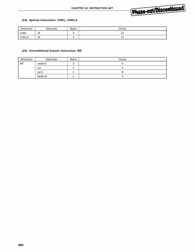
360
CHAPTER 18 INSTRUCTION SET
(14) Special instruction: CHKL, CHKLA
Mnemonic Operands Bytes Clocks
CHKL sfr 3 12
CHKLA sfr 3 12
(15) Unconditional branch instruction: BR
Mnemonic Operands Bytes Clocks
BR !addr16 3 4
rp1 2 4
[rp1] 2 8
$addr16 2 4
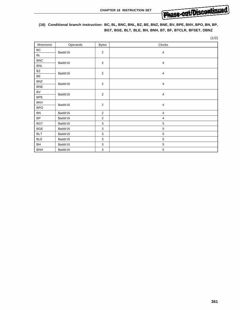
361
CHAPTER 18 INSTRUCTION SET
(16) Conditional branch instruction: BC, BL, BNC, BNL, BZ, BE, BNZ, BNE, BV, BPE, BNV, BPO, BN, BP,
BGT, BGE, BLT, BLE, BH, BNH, BT, BF, BTCLR, BFSET, DBNZ
(1/2)
Mnemonic Operands Bytes Clocks
BC$addr16 2 4
BL
BNC$addr16 2 4
BNL
BZ$addr16 2 4
BE
BNZ$addr16 2 4
BNE
BV$addr16 2 4
BPE
BNV$addr16 2 4
BPO
BN $addr16 2 4
BP $addr16 2 4
BGT $addr16 3 5
BGE $addr16 3 5
BLT $addr16 3 5
BLE $addr16 3 5
BH $addr16 3 5
BNH $addr16 3 5
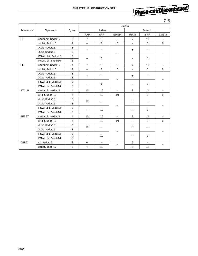
362
CHAPTER 18 INSTRUCTION SET
(2/2)
Clocks
Mnemonic Operands Bytes In-line Branch
IRAM SFR EMEM IRAM SFR EMEM
BT saddr.bit, $addr16 3 7 10 – 7 10 –
sfr.bit, $addr16 4 – 8 8 – 8 8
A.bit, $addr16 38 – 8 –
X.bit, $addr16 3– –
PSWH.bit, $addr16 3– 8 – 8
PSWL.bit, $addr16 3
BF saddr.bit, $addr16 4 7 10 – 7 10 –
sfr.bit, $addr16 4 – 8 8 – 8 8
A.bit, $addr16 38 – 8 –
X.bit, $addr16 3– –
PSWH.bit, $addr16 3– 8 – 8
PSWL.bit, $addr16 3
BTCLR saddr.bit, $addr16 4 10 16 – 8 14 –
sfr.bit, $addr16 4 – 10 10 – 8 8
A.bit, $addr16 310 – 8 –
X.bit, $addr16 3– –
PSWH.bit, $addr16 3– 10 – 8
PSWL.bit, $addr16 3
BFSET saddr.bit, $addr16 4 10 16 – 8 14 –
sfr.bit, $addr16 4 – 10 10 – 8 8
A.bit, $addr16 310 – 8 –
X.bit, $addr16 3– –
PSWH.bit, $addr16 3– 10 – 8
PSWL.bit, $addr16 3
DBNZ r2, $addr16 2 6 ––
5 ––
saddr, $addr16 3 7 13 6 12
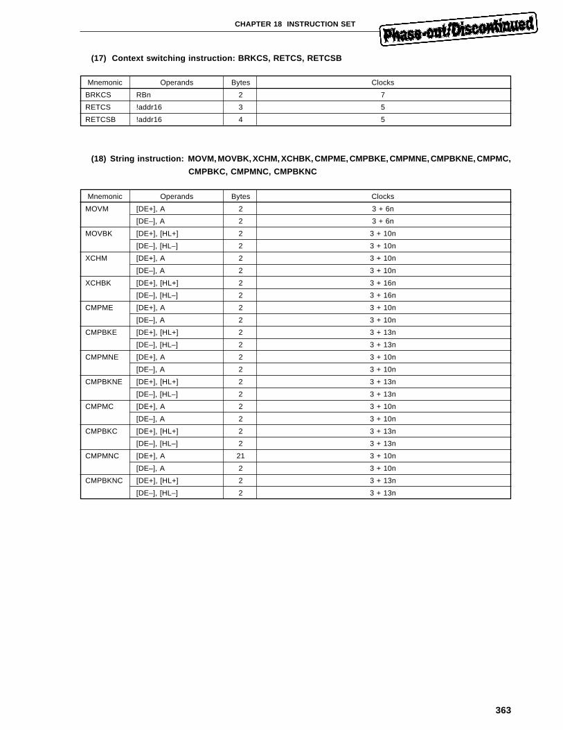
363
CHAPTER 18 INSTRUCTION SET
(17) Context switching instruction: BRKCS, RETCS, RETCSB
Mnemonic Operands Bytes Clocks
BRKCS RBn 2 7
RETCS !addr16 3 5
RETCSB !addr16 4 5
(18) String instruction: MOVM, MOVBK, XCHM, XCHBK, CMPME, CMPBKE, CMPMNE, CMPBKNE, CMPMC,
CMPBKC, CMPMNC, CMPBKNC
Mnemonic Operands Bytes Clocks
MOVM [DE+], A 2 3 + 6n
[DE–], A 2 3 + 6n
MOVBK [DE+], [HL+] 2 3 + 10n
[DE–], [HL–] 2 3 + 10n
XCHM [DE+], A 2 3 + 10n
[DE–], A 2 3 + 10n
XCHBK [DE+], [HL+] 2 3 + 16n
[DE–], [HL–] 2 3 + 16n
CMPME [DE+], A 2 3 + 10n
[DE–], A 2 3 + 10n
CMPBKE [DE+], [HL+] 2 3 + 13n
[DE–], [HL–] 2 3 + 13n
CMPMNE [DE+], A 2 3 + 10n
[DE–], A 2 3 + 10n
CMPBKNE [DE+], [HL+] 2 3 + 13n
[DE–], [HL–] 2 3 + 13n
CMPMC [DE+], A 2 3 + 10n
[DE–], A 2 3 + 10n
CMPBKC [DE+], [HL+] 2 3 + 13n
[DE–], [HL–] 2 3 + 13n
CMPMNC [DE+], A 21 3 + 10n
[DE–], A 2 3 + 10n
CMPBKNC [DE+], [HL+] 2 3 + 13n
[DE–], [HL–] 2 3 + 13n
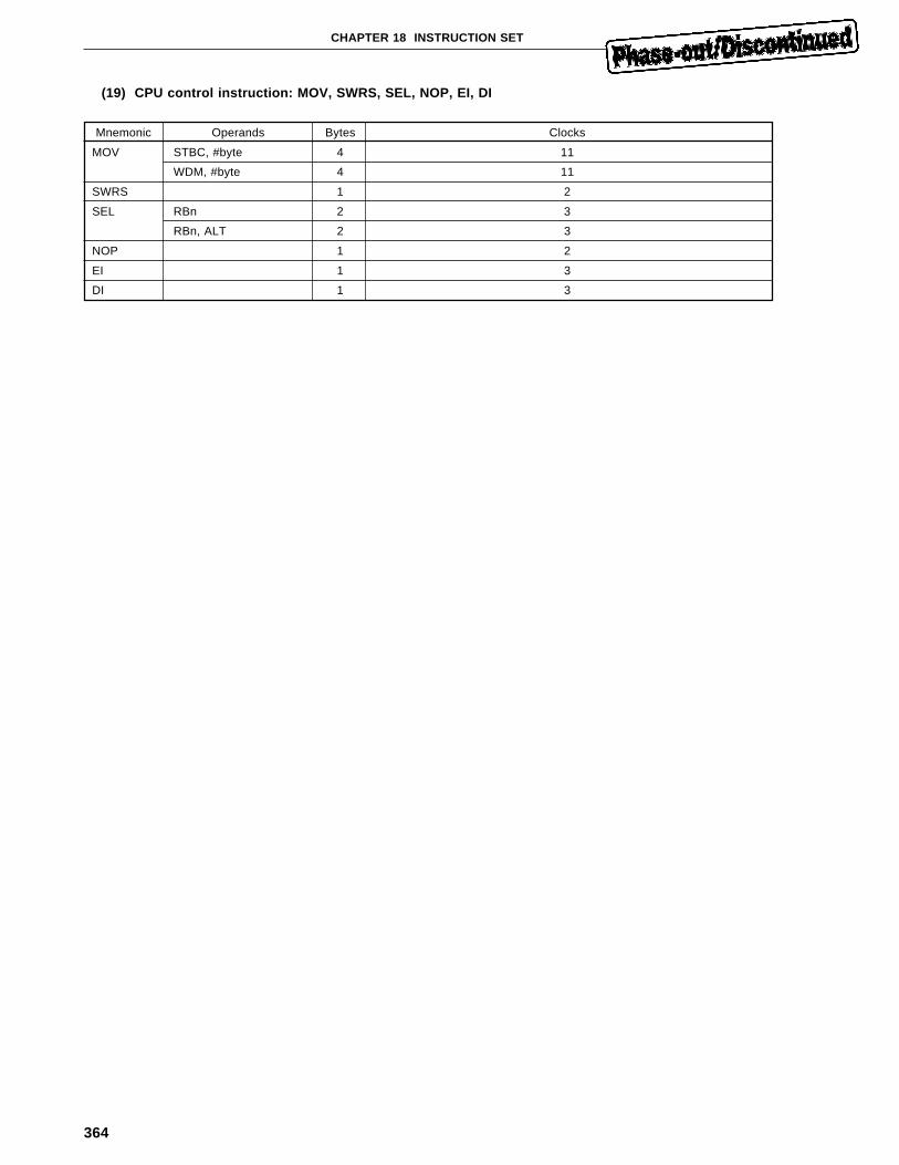
364
CHAPTER 18 INSTRUCTION SET
(19) CPU control instruction: MOV, SWRS, SEL, NOP, EI, DI
Mnemonic Operands Bytes Clocks
MOV STBC, #byte 4 11
WDM, #byte 4 11
SWRS 1 2
SEL RBn 2 3
RBn, ALT 2 3
NOP 1 2
EI 1 3
DI 1 3
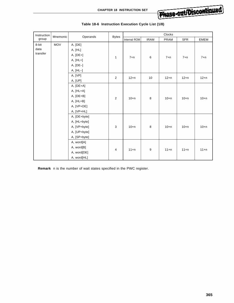
365
CHAPTER 18 INSTRUCTION SET
Table 18-6 Instruction Execution Cycle List (1/8)
Instruction Mnemonic Operands BytesClocks
group Internal ROM IRAM PRAM SFR EMEM
8-bit MOV A, [DE]data A, [HL]transfer A, [DE+]
1 7+n 6 7+n 7+n 7+nA, [HL+]
A, [DE–]
A, [HL–]
A, [VP]2 12+n 10 12+n 12+n 12+n
A, [UP]
A, [DE+A]
A, [HL+A]
A, [DE+B]2 10+n 8 10+n 10+n 10+n
A, [HL+B]
A, [VP+DE]
A, [VP+HL]
A, [DE+byte]
A, [HL+byte]
A, [VP+byte] 3 10+n 8 10+n 10+n 10+n
A, [UP+byte]
A, [SP+byte]
A, word[A]
A, word[B]4 11+n 9 11+n 11+n 11+n
A, word[DE]
A, word[HL]
Remark n is the number of wait states specified in the PWC register.
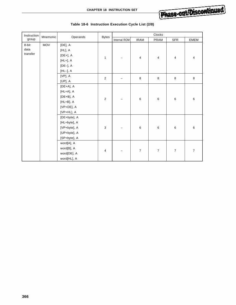
366
CHAPTER 18 INSTRUCTION SET
Table 18-6 Instruction Execution Cycle List (2/8)
Instruction Mnemonic Operands BytesClocks
group Internal ROM IRAM PRAM SFR EMEM
8-bit MOV [DE], Adata [HL], Atransfer [DE+], A
1 – 4 4 4 4[HL+], A
[DE–], A
[HL–], A
[VP], A2 – 8 8 8 8
[UP], A
[DE+A], A
[HL+A], A
[DE+B], A2 – 6 6 6 6
[HL+B], A
[VP+DE], A
[VP+HL], A
[DE+byte], A
[HL+byte], A
[VP+byte], A 3 – 6 6 6 6
[UP+byte], A
[SP+byte], A
word[A], A
word[B], A4 – 7 7 7 7
word[DE], A
word[HL], A

367
CHAPTER 18 INSTRUCTION SET
Table 18-6 Instruction Execution Cycle List (3/8)
Instruction Mnemonic Operands BytesClocks
group Internal ROM IRAM PRAM SFR EMEM
8-bit XCH A, [DE]data A, [HL]trasfer A, [DE+]
A, [HL+]2 – 11 13 + n 13 + n 13 + n
A, [DE–]
A, [HL–]
A, [VP]
A, [UP]
A, [DE+A]
A, [HL+A]
A, [DE+B]2 – 9 11 + n 11 + n 11 + n
A, [HL+B]
A, [VP+DE]
A, [VP+HL]
A, [DE+byte]
A, [HL+byte]
A, [VP+byte] 3 – 9 11 + n 11 + n 11 + n
A, [UP+byte]
A, [SP+byte]
A, word[A]
A, word[B]4 – 10 12 + n 12 + n 12 + n
A, word[DE]
A, word[HL]
Remark n is the number of wait states specified in the PWC register.

368
CHAPTER 18 INSTRUCTION SET
Table 18-6 Instruction Execution Cycle List (4/8)
Instruction Mnemonic Operands BytesClocks
group Internal ROM IRAM PRAM SFR EMEM
16-bit MOVW AX, [DE]data AX, [HL]transfer AX, [DE+]
AX, [HL+]2 15 + 2n 10 15 + 2n 15 + 2n 15 + 2n
AX, [DE–]
AX, [HL–]
AX, [VP]
AX, [UP]
AX, [DE+A]
AX, [HL+A]
AX, [DE+B]2 13 + 2n 8 13 + 2n 13 + 2n 13 + 2n
AX, [HL+B]
AX, [VP+DE]
AX, [VP+HL]
AX, [DE+byte]
AX, [HL+byte]
AX, [VP+byte] 3 13 + 2n 8 13 + 2n 13 + 2n 13 + 2n
AX, [UP+byte]
AX, [SP+byte]
AX, word[A]
AX, word[B]4 14 + 2n 9 14 + 2n 14 + 2n 14 + 2n
AX, word[DE]
AX, word[HL]
Remark n is the number of wait states specified in the PWC register.
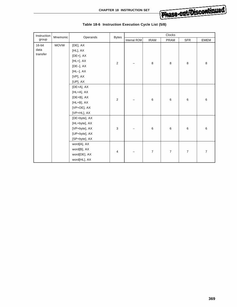
369
CHAPTER 18 INSTRUCTION SET
Table 18-6 Instruction Execution Cycle List (5/8)
Instruction Mnemonic Operands BytesClocks
group Internal ROM IRAM PRAM SFR EMEM
16-bit MOVW [DE], AXdata [HL], AXtransfer [DE+], AX
[HL+], AX2 – 8 8 8 8
[DE–], AX
[HL–], AX
[VP], AX
[UP], AX
[DE+A], AX
[HL+A], AX
[DE+B], AX2 – 6 6 6 6
[HL+B], AX
[VP+DE], AX
[VP+HL], AX
[DE+byte], AX
[HL+byte], AX
[VP+byte], AX 3 – 6 6 6 6
[UP+byte], AX
[SP+byte], AX
word[A], AX
word[B], AX4 – 7 7 7 7
word[DE], AX
word[HL], AX
370
CHAPTER 18 INSTRUCTION SET
Table 18-6 Instruction Execution Cycle List (6/8)
Instruction Mnemonic Operands BytesClocks
group Internal ROM IRAM PRAM SFR EMEM
16-bit XCHW AX, [DE]data AX, [HL]transfer AX, [DE+]
AX, [HL+]2 – 11 16 + 2n 16 + 2n 16 + 2n
AX, [DE–]
AX, [HL–]
AX, [VP]
AX, [UP]
AX, [DE+A]
AX, [HL+A]
AX, [DE+B]2 – 9 14 + 2n 14 + 2n 14 + 2n
AX, [HL+B]
AX, [VP+DE]
AX, [VP+HL]
AX, [DE+byte]
AX, [HL+byte]
AX, [VP+byte] 3 – 9 14 + 2n 14 + 2n 14 + 2n
AX, [UP+byte]
AX, [SP+byte]
AX, word[A]
AX, word[B]4 – 10 15 + 2n 15 + 2n 15 + 2n
AX, word[DE]
AX, word[HL]
Remark n is the number of wait states specified in the PWC register.
371
CHAPTER 18 INSTRUCTION SET
Table 18-6 Instruction Execution Cycle List (7/8)
Instruction Mnemonic Operands BytesClocks
group Internal ROM IRAM PRAM SFR EMEM
8-bit ADD A, [DE]arithmetic ADDC A, [HL]and SUB A, [DE+]logical
SUBC A, [HL+]2 10 + n 8 10 + n 10 + n 10 + n
AND A, [DE–]
OR A, [HL–]
XOR A, [VP]
CMP A, [UP]
A, [DE+A]
A, [HL+A]
A, [DE+B]2 10 + n 8 10 + n 10 + n 10 + n
A, [HL+B]
A, [VP+DE]
A, [VP+HL]
A, [DE+byte]
A, [HL+byte]
A, [VP+byte] 3 10 + n 8 10 + n 10 + n 10 + n
A, [UP+byte]
A, [SP+byte]
A, word[A]
A, word[B]4 11 + n 9 11 + n 11 + n 11 + n
A, word[DE]
A, word[HL]
Remark n is the number of wait states specified in the PWC register.
372
CHAPTER 18 INSTRUCTION SET
Table 18-6 Instruction Execution Cycle List (8/8)
Instruction Mnemonic Operands BytesClocks
group Internal ROM IRAM PRAM SFR EMEM
8-bit ADD [DE], Aarithmetic ADDC [HL], Aand SUB [DE+], Alogical
SUBC [HL+], A2 10+n 8 10+n 10+n 10+n
AND [DE–], A
OR [HL–], A
XOR [VP], A
CMP [UP], A
[DE+A], A
[HL+A], A
[DE+B], A2 10+n 8 10+n 10+n 10+n
[HL+B], A
[VP+DE], A
[VP+HL], A
[DE+byte], A
[HL+byte], A
[VP+byte], A 3 10+n 8 10+n 10+n 10+n
[UP+byte], A
[SP+byte], A
word[A], A
word[B], A4 11+n 9 11+n 11+n 11+n
word[DE], A
word[HL], A
Signed multiplication instruction
Mnemonic Operands Bytes
Clocks
AX(+) AX(–) AX(+) AX(–)
rp1(+) rp1(–) rp1(–) rp1(+)
MULW rp1 2 24 27 28 28
Remark n is the number of wait states specified in the PWC register.
373
CHAPTER 18 INSTRUCTION SET
18.4 Instruction Address Addressing
The instruction address is determined by the program counter (PC) contents. Normally, each time one instruction
is executed, automatically it is incremented by one for one byte according to the number of bytes of the fetched
instruction. When an instruction involving a branch is executed, branch destination address information is set in the
PC for a branch according to the addressing modes described below.
18.4.1 Relative addressing
The value resulting from adding 8-bit immediate data (displacement value: jdisp) of operation code to the top
address of the following instruction is transferred to the program counter (PC) for a branch. The displacement value
is handled as signed two’s complement data (–128 to +127) and bit 7 becomes a sign bit. The relative addressing
is applied when a BR $addr16 instruction or conditional branch instruction is executed.
Figure 18-2 Relative Addressing
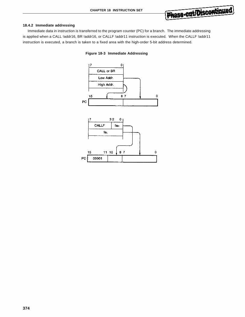
374
CHAPTER 18 INSTRUCTION SET
18.4.2 Immediate addressing
Immediate data in instruction is transferred to the program counter (PC) for a branch. The immediate addressing
is applied when a CALL !addr16, BR !addr16, or CALLF !addr11 instruction is executed. When the CALLF !addr11
instruction is executed, a branch is taken to a fixed area with the high-order 5-bit address determined.
Figure 18-3 Immediate Addressing
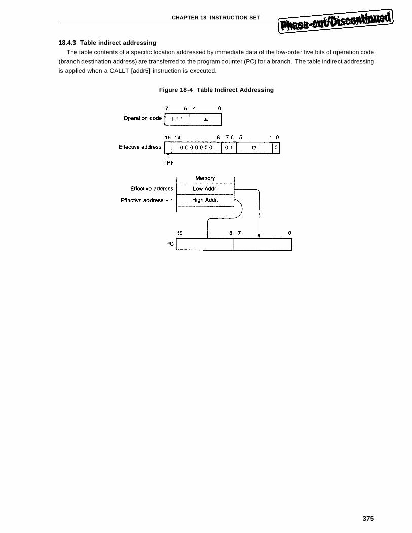
375
CHAPTER 18 INSTRUCTION SET
18.4.3 Table indirect addressing
The table contents of a specific location addressed by immediate data of the low-order five bits of operation code
(branch destination address) are transferred to the program counter (PC) for a branch. The table indirect addressing
is applied when a CALLT [addr5] instruction is executed.
Figure 18-4 Table Indirect Addressing
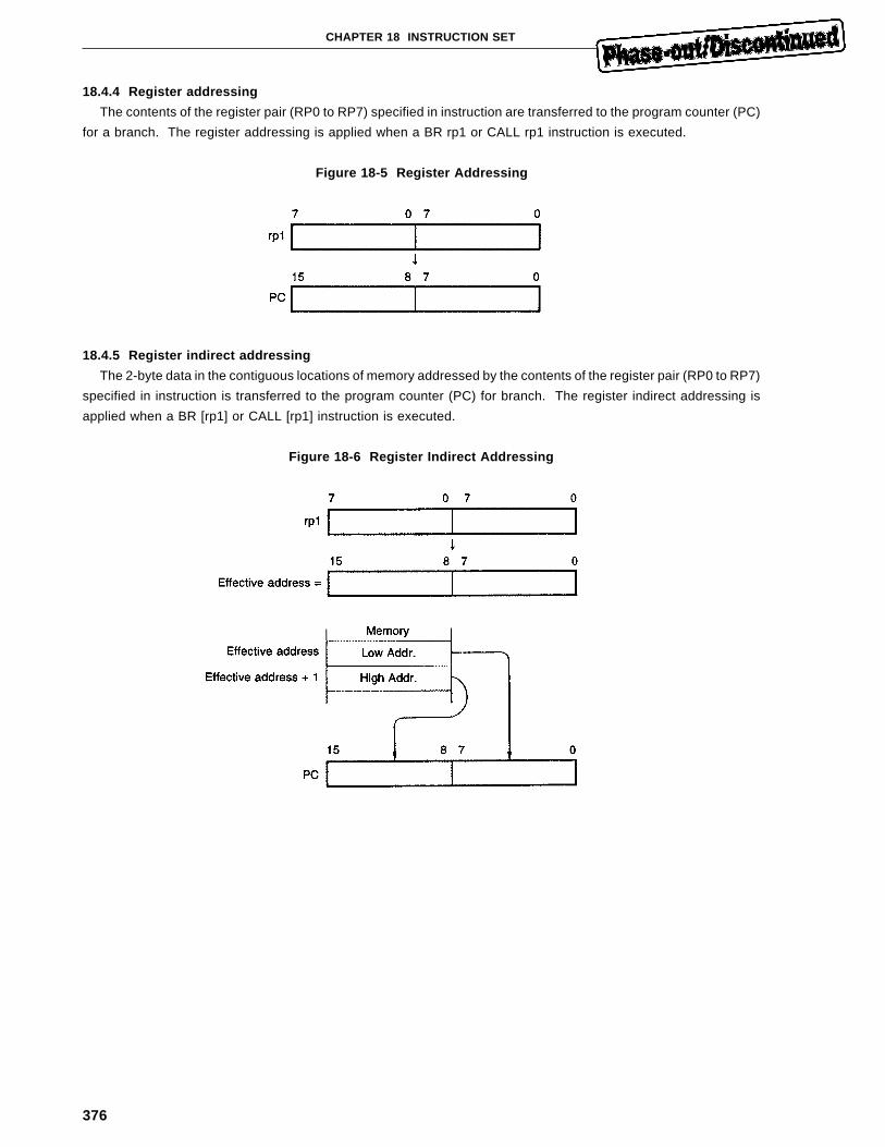
376
CHAPTER 18 INSTRUCTION SET
18.4.4 Register addressing
The contents of the register pair (RP0 to RP7) specified in instruction are transferred to the program counter (PC)
for a branch. The register addressing is applied when a BR rp1 or CALL rp1 instruction is executed.
Figure 18-5 Register Addressing
18.4.5 Register indirect addressing
The 2-byte data in the contiguous locations of memory addressed by the contents of the register pair (RP0 to RP7)
specified in instruction is transferred to the program counter (PC) for branch. The register indirect addressing is
applied when a BR [rp1] or CALL [rp1] instruction is executed.
Figure 18-6 Register Indirect Addressing
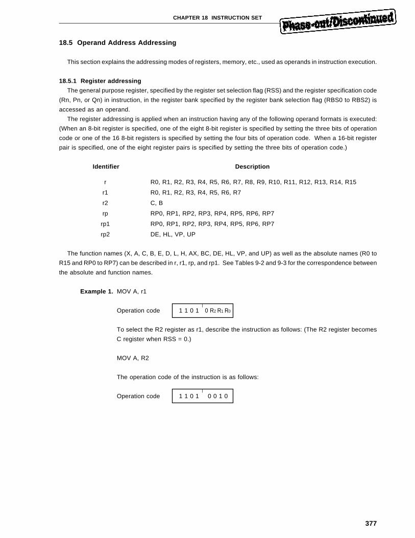
377
CHAPTER 18 INSTRUCTION SET
18.5 Operand Address Addressing
This section explains the addressing modes of registers, memory, etc., used as operands in instruction execution.
18.5.1 Register addressing
The general purpose register, specified by the register set selection flag (RSS) and the register specification code
(Rn, Pn, or Qn) in instruction, in the register bank specified by the register bank selection flag (RBS0 to RBS2) is
accessed as an operand.
The register addressing is applied when an instruction having any of the following operand formats is executed:
(When an 8-bit register is specified, one of the eight 8-bit register is specified by setting the three bits of operation
code or one of the 16 8-bit registers is specified by setting the four bits of operation code. When a 16-bit register
pair is specified, one of the eight register pairs is specified by setting the three bits of operation code.)
Identifier Description
r R0, R1, R2, R3, R4, R5, R6, R7, R8, R9, R10, R11, R12, R13, R14, R15
r1 R0, R1, R2, R3, R4, R5, R6, R7
r2 C, B
rp RP0, RP1, RP2, RP3, RP4, RP5, RP6, RP7
rp1 RP0, RP1, RP2, RP3, RP4, RP5, RP6, RP7
rp2 DE, HL, VP, UP
The function names (X, A, C, B, E, D, L, H, AX, BC, DE, HL, VP, and UP) as well as the absolute names (R0 to
R15 and RP0 to RP7) can be described in r, r1, rp, and rp1. See Tables 9-2 and 9-3 for the correspondence between
the absolute and function names.
Example 1. MOV A, r1
Operation code 1 1 0 1 0 R2 R1 R0
To select the R2 register as r1, describe the instruction as follows: (The R2 register becomes
C register when RSS = 0.)
MOV A, R2
The operation code of the instruction is as follows:
Operation code 1 1 0 1 0 0 1 0
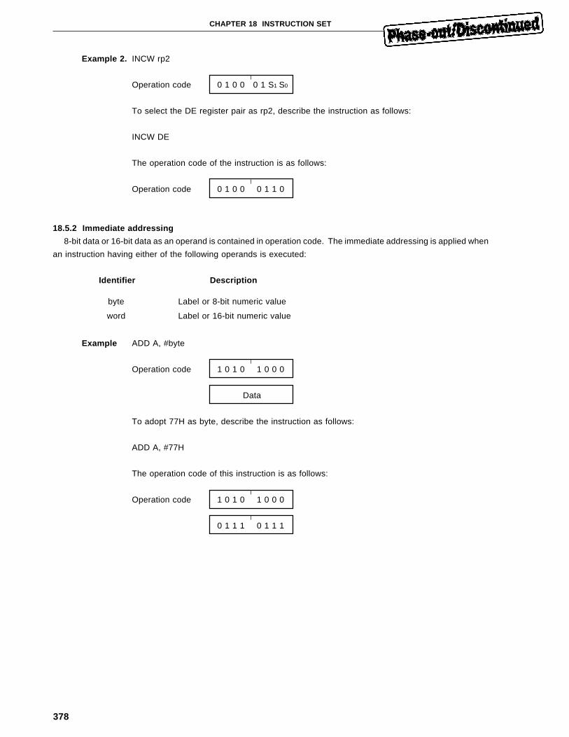
378
CHAPTER 18 INSTRUCTION SET
Example 2. INCW rp2
Operation code 0 1 0 0 0 1 S1 S0
To select the DE register pair as rp2, describe the instruction as follows:
INCW DE
The operation code of the instruction is as follows:
Operation code 0 1 0 0 0 1 1 0
18.5.2 Immediate addressing
8-bit data or 16-bit data as an operand is contained in operation code. The immediate addressing is applied when
an instruction having either of the following operands is executed:
Identifier Description
byte Label or 8-bit numeric value
word Label or 16-bit numeric value
Example ADD A, #byte
Operation code 1 0 1 0 1 0 0 0
Data
To adopt 77H as byte, describe the instruction as follows:
ADD A, #77H
The operation code of this instruction is as follows:
Operation code 1 0 1 0 1 0 0 0
0 1 1 1 0 1 1 1
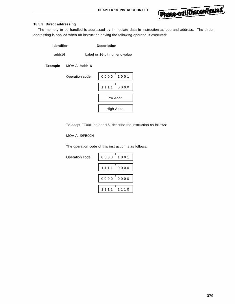
379
CHAPTER 18 INSTRUCTION SET
18.5.3 Direct addressing
The memory to be handled is addressed by immediate data in instruction as operand address. The direct
addressing is applied when an instruction having the following operand is executed:
Identifier Description
addr16 Label or 16-bit numeric value
Example MOV A, !addr16
Operation code 0 0 0 0 1 0 0 1
1 1 1 1 0 0 0 0
Low Addr.
High Addr.
To adopt FE00H as addr16, describe the instruction as follows:
MOV A, !0FE00H
The operation code of this instruction is as follows:
Operation code 0 0 0 0 1 0 0 1
1 1 1 1 0 0 0 0
0 0 0 0 0 0 0 0
1 1 1 1 1 1 1 0
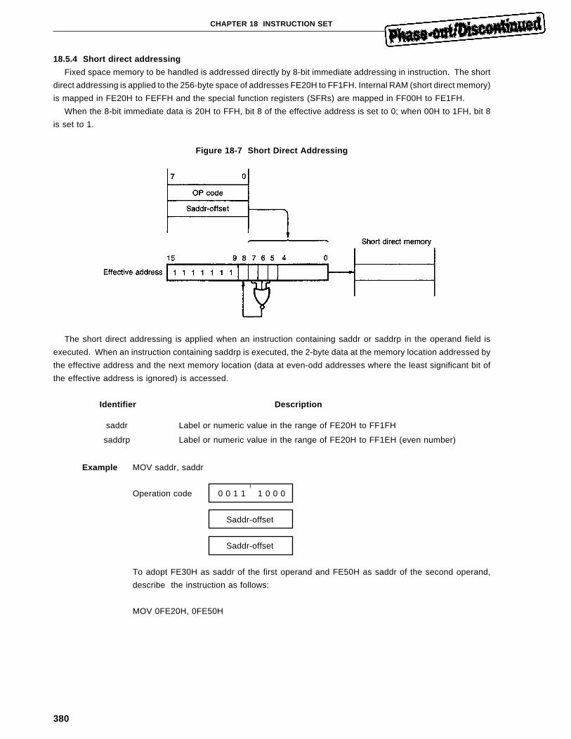
380
CHAPTER 18 INSTRUCTION SET
18.5.4 Short direct addressing
Fixed space memory to be handled is addressed directly by 8-bit immediate addressing in instruction. The short
direct addressing is applied to the 256-byte space of addresses FE20H to FF1FH. Internal RAM (short direct memory)
is mapped in FE20H to FEFFH and the special function registers (SFRs) are mapped in FF00H to FE1FH.
When the 8-bit immediate data is 20H to FFH, bit 8 of the effective address is set to 0; when 00H to 1FH, bit 8
is set to 1.
Figure 18-7 Short Direct Addressing
The short direct addressing is applied when an instruction containing saddr or saddrp in the operand field is
executed. When an instruction containing saddrp is executed, the 2-byte data at the memory location addressed by
the effective address and the next memory location (data at even-odd addresses where the least significant bit of
the effective address is ignored) is accessed.
Identifier Description
saddr Label or numeric value in the range of FE20H to FF1FH
saddrp Label or numeric value in the range of FE20H to FF1EH (even number)
Example MOV saddr, saddr
Operation code 0 0 1 1 1 0 0 0
Saddr-offset
Saddr-offset
To adopt FE30H as saddr of the first operand and FE50H as saddr of the second operand,
describe the instruction as follows:
MOV 0FE20H, 0FE50H

381
CHAPTER 18 INSTRUCTION SET
The operation code of this instruction is as follows:
Operation code 0 0 1 1 1 0 0 0
0 0 1 0 0 0 0 0
0 1 1 0 0 0 0 0
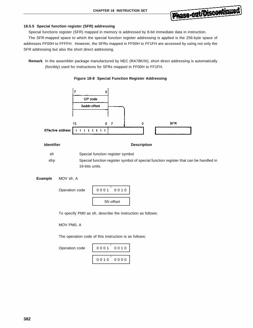
382
CHAPTER 18 INSTRUCTION SET
18.5.5 Special function register (SFR) addressing
Special functions register (SFR) mapped in memory is addressed by 8-bit immediate data in instruction.
The SFR-mapped space to which the special function register addressing is applied is the 256-byte space of
addresses FF00H to FFFFH. However, the SFRs mapped in FF00H to FF1FH are accessed by using not only the
SFR addressing but also the short direct addressing.
Remark In the assembler package manufactured by NEC (RA78K/III), short direct addressing is automatically
(forcibly) used for instructions for SFRs mapped in FF00H to FF1FH.
Figure 18-8 Special Function Register Addressing
Identifier Description
sfr Special function register symbol
sfrp Special function register symbol of special function register that can be handled in
16-bits units.
Example MOV sfr, A
Operation code 0 0 0 1 0 0 1 0
Sfr-offset
To specify PM0 as sfr, describe the instruction as follows:
MOV PM0, A
The operation code of this instruction is as follows:
Operation code 0 0 0 1 0 0 1 0
0 0 1 0 0 0 0 0
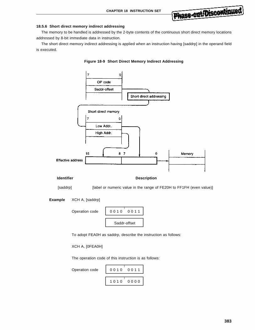
383
CHAPTER 18 INSTRUCTION SET
18.5.6 Short direct memory indirect addressing
The memory to be handled is addressed by the 2-byte contents of the continuous short direct memory locations
addressed by 8-bit immediate data in instruction.
The short direct memory indirect addressing is applied when an instruction having [saddrp] in the operand field
is executed.
Figure 18-9 Short Direct Memory Indirect Addressing
Identifier Description
[saddrp] [label or numeric value in the range of FE20H to FF1FH (even value)]
Example XCH A, [saddrp]
Operation code 0 0 1 0 0 0 1 1
Saddr-offset
To adopt FEA0H as saddrp, describe the instruction as follows:
XCH A, [0FEA0H]
The operation code of this instruction is as follows:
Operation code 0 0 1 0 0 0 1 1
1 0 1 0 0 0 0 0
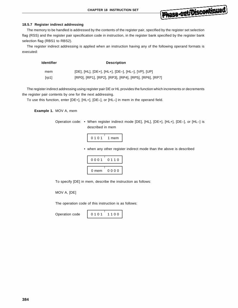
384
CHAPTER 18 INSTRUCTION SET
18.5.7 Register indirect addressing
The memory to be handled is addressed by the contents of the register pair, specified by the register set selection
flag (RSS) and the register pair specification code in instruction, in the register bank specified by the register bank
selection flag (RBS1 to RBS2).
The register indirect addressing is applied when an instruction having any of the following operand formats is
executed:
Identifier Description
mem [DE], [HL], [DE+], [HL+], [DE–], [HL–], [VP], [UP]
[rp1] [RP0], [RP1], [RP2], [RP3], [RP4], [RP5], [RP6], [RP7]
The register indirect addressing using register pair DE or HL provides the function which increments or decrements
the register pair contents by one for the next addressing.
To use this function, enter [DE+], [HL+], [DE–], or [HL–] in mem in the operand field.
Example 1. MOV A, mem
Operation code: • When register indirect mode [DE], [HL], [DE+], [HL+], [DE–], or [HL–] is
described in mem
0 1 0 1 1 mem
• when any other register indirect mode than the above is described
0 0 0 1 0 1 1 0
0 mem 0 0 0 0
To specify [DE] in mem, describe the instruction as follows:
MOV A, [DE]
The operation code of this instruction is as follows:
Operation code 0 1 0 1 1 1 0 0
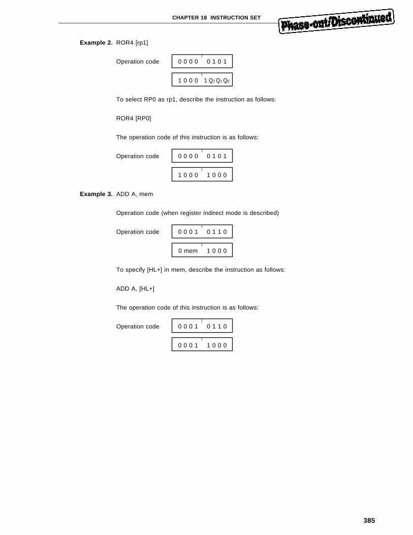
385
CHAPTER 18 INSTRUCTION SET
Example 2. ROR4 [rp1]
Operation code 0 0 0 0 0 1 0 1
1 0 0 0 1 Q2 Q1 Q0
To select RP0 as rp1, describe the instruction as follows:
ROR4 [RP0]
The operation code of this instruction is as follows:
Operation code 0 0 0 0 0 1 0 1
1 0 0 0 1 0 0 0
Example 3. ADD A, mem
Operation code (when register indirect mode is described)
Operation code 0 0 0 1 0 1 1 0
0 mem 1 0 0 0
To specify [HL+] in mem, describe the instruction as follows:
ADD A, [HL+]
The operation code of this instruction is as follows:
Operation code 0 0 0 1 0 1 1 0
0 0 0 1 1 0 0 0
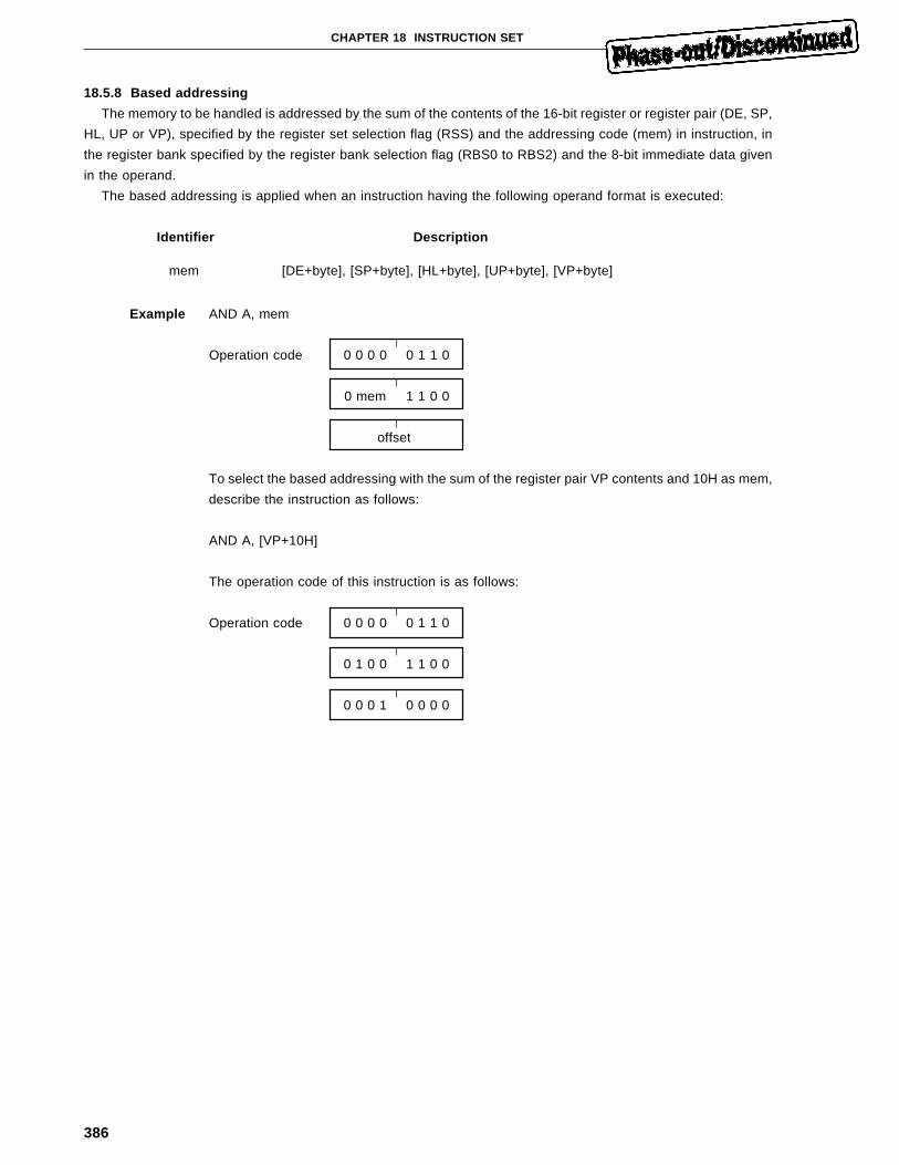
386
CHAPTER 18 INSTRUCTION SET
18.5.8 Based addressing
The memory to be handled is addressed by the sum of the contents of the 16-bit register or register pair (DE, SP,
HL, UP or VP), specified by the register set selection flag (RSS) and the addressing code (mem) in instruction, in
the register bank specified by the register bank selection flag (RBS0 to RBS2) and the 8-bit immediate data given
in the operand.
The based addressing is applied when an instruction having the following operand format is executed:
Identifier Description
mem [DE+byte], [SP+byte], [HL+byte], [UP+byte], [VP+byte]
Example AND A, mem
Operation code 0 0 0 0 0 1 1 0
0 mem 1 1 0 0
offset
To select the based addressing with the sum of the register pair VP contents and 10H as mem,
describe the instruction as follows:
AND A, [VP+10H]
The operation code of this instruction is as follows:
Operation code 0 0 0 0 0 1 1 0
0 1 0 0 1 1 0 0
0 0 0 1 0 0 0 0
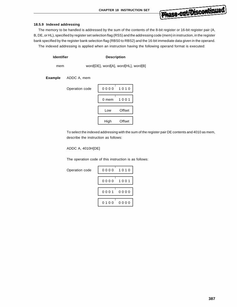
387
CHAPTER 18 INSTRUCTION SET
18.5.9 Indexed addressing
The memory to be handled is addressed by the sum of the contents of the 8-bit register or 16-bit register pair (A,
B, DE, or HL), specified by register set selection flag (RSS) and the addressing code (mem) in instruction, in the register
bank specified by the register bank selection flag (RBS0 to RBS2) and the 16-bit immediate data given in the operand.
The indexed addressing is applied when an instruction having the following operand format is executed:
Identifier Description
mem word[DE], word[A], word[HL], word[B]
Example ADDC A, mem
Operation code 0 0 0 0 1 0 1 0
0 mem 1 0 0 1
Low Offset
High Offset
To select the indexed addressing with the sum of the register pair DE contents and 4010 as mem,
describe the instruction as follows:
ADDC A, 4010H[DE]
The operation code of this instruction is as follows:
Operation code 0 0 0 0 1 0 1 0
0 0 0 0 1 0 0 1
0 0 0 1 0 0 0 0
0 1 0 0 0 0 0 0
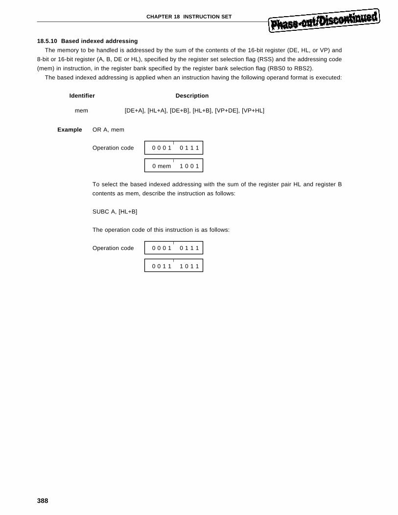
388
CHAPTER 18 INSTRUCTION SET
18.5.10 Based indexed addressing
The memory to be handled is addressed by the sum of the contents of the 16-bit register (DE, HL, or VP) and
8-bit or 16-bit register (A, B, DE or HL), specified by the register set selection flag (RSS) and the addressing code
(mem) in instruction, in the register bank specified by the register bank selection flag (RBS0 to RBS2).
The based indexed addressing is applied when an instruction having the following operand format is executed:
Identifier Description
mem [DE+A], [HL+A], [DE+B], [HL+B], [VP+DE], [VP+HL]
Example OR A, mem
Operation code 0 0 0 1 0 1 1 1
0 mem 1 0 0 1
To select the based indexed addressing with the sum of the register pair HL and register B
contents as mem, describe the instruction as follows:
SUBC A, [HL+B]
The operation code of this instruction is as follows:
Operation code 0 0 0 1 0 1 1 1
0 0 1 1 1 0 1 1
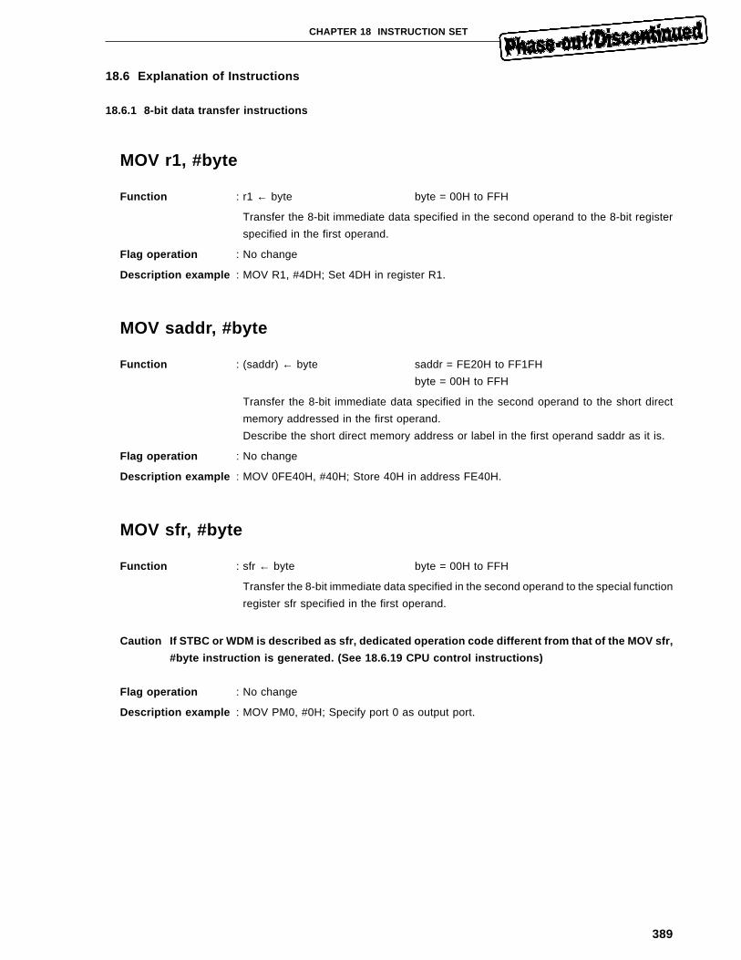
389
CHAPTER 18 INSTRUCTION SET
18.6 Explanation of Instructions
18.6.1 8-bit data transfer instructions
MOV r1, #byte
Function : r1 ← byte byte = 00H to FFH
Transfer the 8-bit immediate data specified in the second operand to the 8-bit register
specified in the first operand.
Flag operation : No change
Description example : MOV R1, #4DH; Set 4DH in register R1.
MOV saddr, #byte
Function : (saddr) ← byte saddr = FE20H to FF1FH
byte = 00H to FFH
Transfer the 8-bit immediate data specified in the second operand to the short direct
memory addressed in the first operand.
Describe the short direct memory address or label in the first operand saddr as it is.
Flag operation : No change
Description example : MOV 0FE40H, #40H; Store 40H in address FE40H.
MOV sfr, #byte
Function : sfr ← byte byte = 00H to FFH
Transfer the 8-bit immediate data specified in the second operand to the special function
register sfr specified in the first operand.
Caution If STBC or WDM is described as sfr, dedicated operation code different from that of the MOV sfr,
#byte instruction is generated. (See 18.6.19 CPU control instructions)
Flag operation : No change
Description example : MOV PM0, #0H; Specify port 0 as output port.
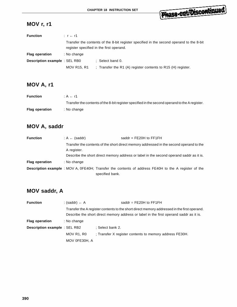
390
CHAPTER 18 INSTRUCTION SET
MOV r, r1
Function : r ← r1
Transfer the contents of the 8-bit register specified in the second operand to the 8-bit
register specified in the first operand.
Flag operation : No change
Description example : SEL RB0 ; Select band 0.
MOV R15, R1 ; Transfer the R1 (A) register contents to R15 (H) register.
MOV A, r1
Function : A ← r1
Transfer the contents of the 8-bit register specified in the second operand to the A register.
Flag operation : No change
MOV A, saddr
Function : A ← (saddr) saddr = FE20H to FF1FH
Transfer the contents of the short direct memory addressed in the second operand to the
A register.
Describe the short direct memory address or label in the second operand saddr as it is.
Flag operation : No change
Description example : MOV A, 0FE40H; Transfer the contents of address FE40H to the A register of the
specified bank.
MOV saddr, A
Function : (saddr) ← A saddr = FE20H to FF1FH
Transfer the A register contents to the short direct memory addressed in the first operand.
Describe the short direct memory address or label in the first operand saddr as it is.
Flag operation : No change
Description example : SEL RB2 ; Select bank 2.
MOV R1, R0 ; Transfer X register contents to memory address FE30H.
MOV 0FE30H, A
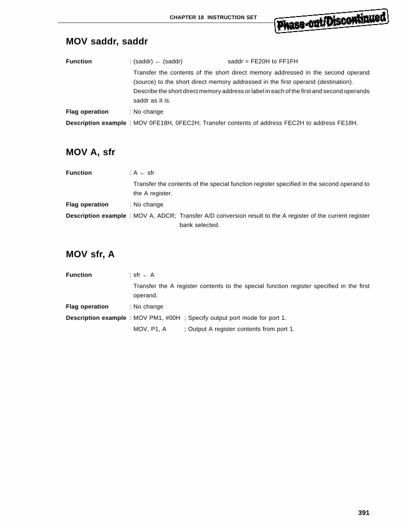
391
CHAPTER 18 INSTRUCTION SET
MOV saddr, saddr
Function : (saddr) ← (saddr) saddr = FE20H to FF1FH
Transfer the contents of the short direct memory addressed in the second operand
(source) to the short direct memory addressed in the first operand (destination).
Describe the short direct memory address or label in each of the first and second operands
saddr as it is.
Flag operation : No change
Description example : MOV 0FE18H, 0FEC2H; Transfer contents of address FEC2H to address FE18H.
MOV A, sfr
Function : A ← sfr
Transfer the contents of the special function register specified in the second operand to
the A register.
Flag operation : No change
Description example : MOV A, ADCR; Transfer A/D conversion result to the A register of the current register
bank selected.
MOV sfr, A
Function : sfr ← A
Transfer the A register contents to the special function register specified in the first
operand.
Flag operation : No change
Description example : MOV PM1, #00H ; Specify output port mode for port 1.
MOV, P1, A ; Output A register contents from port 1.
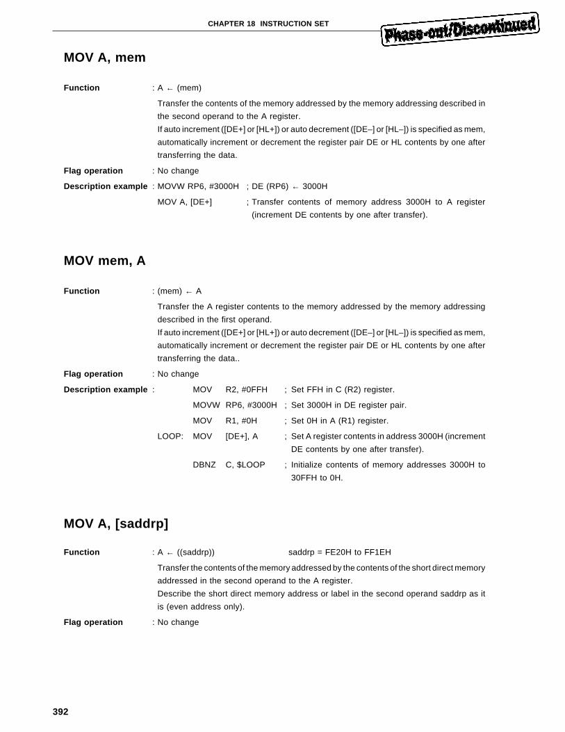
392
CHAPTER 18 INSTRUCTION SET
MOV A, mem
Function : A ← (mem)
Transfer the contents of the memory addressed by the memory addressing described in
the second operand to the A register.
If auto increment ([DE+] or [HL+]) or auto decrement ([DE–] or [HL–]) is specified as mem,
automatically increment or decrement the register pair DE or HL contents by one after
transferring the data.
Flag operation : No change
Description example : MOVW RP6, #3000H ; DE (RP6) ← 3000H
MOV A, [DE+] ; Transfer contents of memory address 3000H to A register
(increment DE contents by one after transfer).
MOV mem, A
Function : (mem) ← A
Transfer the A register contents to the memory addressed by the memory addressing
described in the first operand.
If auto increment ([DE+] or [HL+]) or auto decrement ([DE–] or [HL–]) is specified as mem,
automatically increment or decrement the register pair DE or HL contents by one after
transferring the data..
Flag operation : No change
Description example : MOV R2, #0FFH ; Set FFH in C (R2) register.
MOVW RP6, #3000H ; Set 3000H in DE register pair.
MOV R1, #0H ; Set 0H in A (R1) register.
LOOP: MOV [DE+], A ; Set A register contents in address 3000H (increment
DE contents by one after transfer).
DBNZ C, $LOOP ; Initialize contents of memory addresses 3000H to
30FFH to 0H.
MOV A, [saddrp]
Function : A ← ((saddrp)) saddrp = FE20H to FF1EH
Transfer the contents of the memory addressed by the contents of the short direct memory
addressed in the second operand to the A register.
Describe the short direct memory address or label in the second operand saddrp as it
is (even address only).
Flag operation : No change
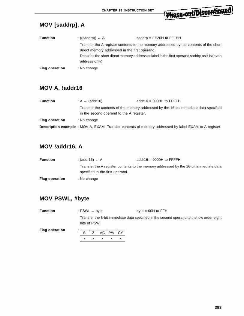
393
CHAPTER 18 INSTRUCTION SET
MOV [saddrp], A
Function : ((saddrp)) ← A saddrp = FE20H to FF1EH
Transfer the A register contents to the memory addressed by the contents of the short
direct memory addressed in the first operand.
Describe the short direct memory address or label in the first operand saddrp as it is (even
address only).
Flag operation : No change
MOV A, !addr16
Function : A ← (addr16) addr16 = 0000H to FFFFH
Transfer the contents of the memory addressed by the 16-bit immediate data specified
in the second operand to the A register.
Flag operation : No change
Description example : MOV A, EXAM; Transfer contents of memory addressed by label EXAM to A register.
MOV !addr16, A
Function : (addr16) ← A addr16 = 0000H to FFFFH
Transfer the A register contents to the memory addressed by the 16-bit immediate data
specified in the first operand.
Flag operation : No change
MOV PSWL, #byte
Function : PSWL ← byte byte = 00H to FFH
Transfer the 8-bit immediate data specified in the second operand to the low order eight
bits of PSW.
Flag operation :S Z AC P/V CY
× × × × ×
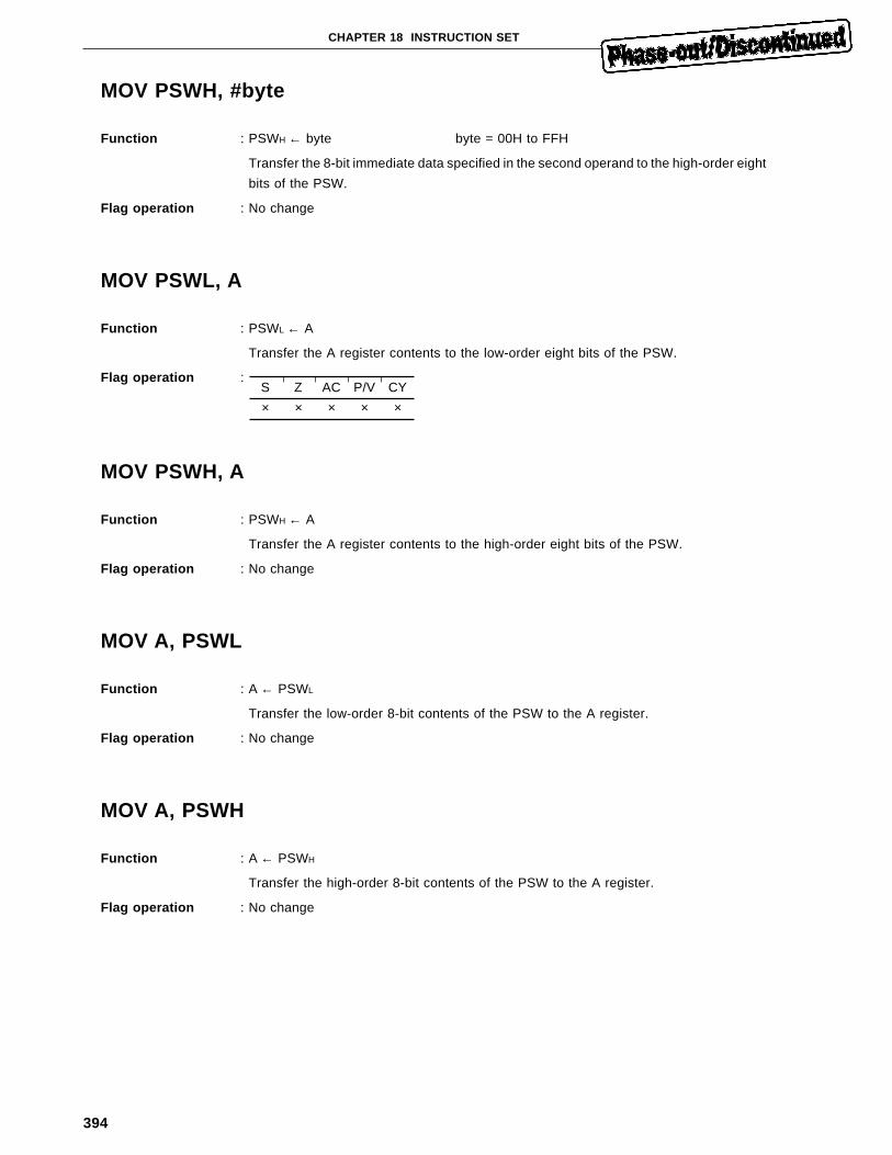
394
CHAPTER 18 INSTRUCTION SET
MOV PSWH, #byte
Function : PSWH ← byte byte = 00H to FFH
Transfer the 8-bit immediate data specified in the second operand to the high-order eight
bits of the PSW.
Flag operation : No change
MOV PSWL, A
Function : PSWL ← A
Transfer the A register contents to the low-order eight bits of the PSW.
Flag operation :
MOV PSWH, A
Function : PSWH ← A
Transfer the A register contents to the high-order eight bits of the PSW.
Flag operation : No change
MOV A, PSWL
Function : A ← PSWL
Transfer the low-order 8-bit contents of the PSW to the A register.
Flag operation : No change
MOV A, PSWH
Function : A ← PSWH
Transfer the high-order 8-bit contents of the PSW to the A register.
Flag operation : No change
S Z AC P/V CY
× × × × ×
395
CHAPTER 18 INSTRUCTION SET
XCH A, r1
Function : A ← r1
Exchange the contents of the A register and the 8-bit register specified in the second
operand.
Flag operation : No change
XCH r, r1
Function : r ↔ r1
Exchange the content of the 8-bit registers specified in the first and second operands.
Flag operation : No change
XCH A, mem
Function : A ↔ (mem)
Exchange the contents of the A register and the memory addressed by the memory
addressing described in the second operand.
If auto increment ([DE+] or [HL+]) or auto decrement ([DE–] or [HL–]) is specified as mem,
automatically increment or decrement the register pair DE or HL contents by one after
exchanging the data.
Flag operation : No change
Description example : MOV R2, #0FH ; C(R2) ← 10H
MOVW RP7, #FE10H ; HL (RP7) ← FE10H
MOV R1, #0H ; A (R1) ← 00H
LOOP: XCH [HL–], A ; Exchange the contents of A register and address
FE10H decrement the HL contents by one after
transfer.
DBNZ C, $LOOP ; Shift the FE01H to FE10H contents forward one
address (address FE10H=00H).
XCH A, saddr
Function : A ↔ (saddr) saddr = FE20H to FF1FH
Exchange the contents of the A register and the short direct memory addressed in the
second operand.
Describe the short direct memory address or label in the second operand saddr as it is.
Flag operation : No change
396
CHAPTER 18 INSTRUCTION SET
XCH A, sfr
Function : A ↔ sfr
Exchange the contents of the A register and the special function register specified in the
second operand.
Flag operation : No change
Description example : XCH A, RXB; Exchange the contents of A register and serial receive buffer.
XCH, A, [saddrp]
Function : A ↔ ((saddrp)) saddrp = FE20H to FF1EH
Exchange the contents of the A register and the memory addressed by the contents of
the short direct memory addressed in the second operand.
Describe the short direct memory address or label in the second operand saddrp as it
is (even address only).
Flag operation : No change
XCH saddr, saddr
Function : (saddr) ↔ (saddr) saddr = FE20H to FF1FH
Exchange the contents of the short direct memory addressed in the first operand and the
short direct memory addressed in the second operand.
Describe the short direct memory address or label in each of the first and second operands
saddr as it is.
Flag operation : No change
397
CHAPTER 18 INSTRUCTION SET
18.6.2 16-bit data transfer instructions
MOVW rp1, #word
Function : rp1 ← word word = 0000H to FFFFH
Transfer the 16-bit immediate data specified in the second operand to the 16-bit register
pair specified in the first operand.
Flag operation : No change
Description example : MOVW RP0, #0AA55H; Transfer AA55H to AX register pair.
MOVW saddrp, #word
Function : (saddrp) ← word saddrp = FE20H to FF1EH
word = 0000H to FFFFH
Transfer the 16-bit immediate data specified in the second operand to the 2-byte area
of the short direct memory addressed in the first operand.
Describe the short direct memory address or label in the first operand saddrp as it is. (even
address only).
Flag operation : No change
MOVW sfrp, #word
Function : sfrp ← word word = 0000H to FFFFH
Transfer the 16-bit immediate data specified in the second operand to the 16-bit special
function register specified in the first operand.
Flag operation : No change
Description example : MOVW PWM0, #0FF00H; Set FF00H in PWM0 register.
MOVW rp, rp1
Function : rp ← rp1
Transfer the contents of the 16-bit register pair specified in the second operand to the
16-bit register pair specified in the first operand.
Flag operation : No change
398
CHAPTER 18 INSTRUCTION SET
MOVW AX, saddrp
Function : AX ← (saddrp) saddrp = FE20H to FF1EH
Transfer the contents of the 2-byte area of the short direct memory addressed in the
second operand to the register pair AX.
Describe the short direct memory address or label in the second operand saddrp as it
is (even address only).
Flag operation : No change
Description example : MOVW AX, 0FE30H; Transfer contents of address FE31H and FE30H to AX register pair.
MOVW saddrp, AX
Function : (saddrp) ← AX saddrp = FE20H to FF1EH
Transfer the register pair AX contents to the 2-byte area of the short direct memory
addressed in the first operand.
Describe the short direct memory address or label in the first operand saddrp as it is (even
address only).
Flag operation : No change
MOVW saddrp, saddrp
Function : (saddrp) ← (saddrp) saddrp = FE20H to FF1EH
Transfer the contents of the 2-byte area of the short direct memory addressed in the
second operand to the 2-byte area of the short direct memory addressed in the first
operand.
Describe the short direct memory address or label in each of the first and second operands
saddrp as it is. (even address only).
Flag operation : No change
MOVW AX, sfrp
Function : AX ← sfrp
Transfer the contents of the 16-bit special function register specified in the second
operand to the register pair AX.
Flag operation : No change
Description example : MOVW AX, CPT0; Transfer CPT0 register contents to AX register pair.
399
CHAPTER 18 INSTRUCTION SET
MOVW sfrp, AX
Function : sfrp ← AX
Transfer the register pair AX contents to the 16-bit special function register specified in
the first operand.
Flag operation : No change
MOVW AX, mem
Function : AX ← (mem) mem = 0000H to FDFFH(any desired address)
mem = FE00H to FFFFH (limited to even address)
Transfer the contents of the memory addressed by the memory addressing described
in the second operand to the register pair AX.
If auto increment ([DE+] or[HL+]) or auto decrement ([DE–] or [HL–]) is specified as mem,
automatically increment or decrement the register pair DE or HL contents by two after
transferring the data.
Flag operation : No change
MOVW mem, AX
Function : (mem) ← AX mem = 0000H to FDFFH (any desired address)
mem = FF00H to FFFFH (limited to even address)
Transfer the register pair AX contents to the memory addressed by the memory
addressing described in the first operand.
If auto increment ([DE+] or [HL+]) or auto decrement ([DE–] or [HL–]) is specified as mem,
automatically increment or decrement the register pair DE or HL contents by two after
transferring the data.
Flag operation : No change
MOVW rp1, !addr16
Function : rp1 ← (addr16) addr16 = 0000H to FDFFH (any desired address)
addr16 = FE00H to FFFFH (limited to even addresses)
Transfer the contents of the 2-byte area of the memory addressed by the 16-bit immediate
data specified in the second operand to the 16-bit register pair specified in the first
operand.
Flag operation : No change
400
CHAPTER 18 INSTRUCTION SET
MOVW !addr16, rp1
Function : (addr16) ← rp1 addr16 = 0000H to FDFFH (any desired addresses)
addr16 = FE00H to FFFFH (limited to even addresses)
Transfer the contents of the 16-bit register pair specified in the second operand to the
2-byte area of memory addressed by the 16-bit immediate data specified in the first
operand.
Flag operation : No change
XCHW AX, saddrp
Function : AX ↔ (saddrp) saddrp = FE20H to FF1EH
Exchange the contents of the register pair AX and the 2-byte area of the short direct
memory addressed in the second operand.
Describe the short direct memory address of label in the second operand saddrp as it
is (even address only).
Flag operation : No change
XCHW AX, sfrp
Function : AX ↔ sfrp
Exchange the contents of the register pair AX and the 16-bit special function register
specified in the second operand.
Flag operation : No change
Description example : Exchange the contents of the register XCHW AX, PWM0L; PWM0 and the register pair
AX.
XCHW saddrp, saddrp
Function : (saddrp) ↔ (saddrp) saddrp = FE20H to FF1EH
Exchange the contents of the 2-byte area of the short direct memory addressed in the
first operand and the 2-byte area of the short direct memory addressed in the second
operand.
Describe the short direct memory address or label in each of the first and second operands
saddrp as it is (even address only).
Flag operation : No change
401
CHAPTER 18 INSTRUCTION SET
XCHW rp, rp1
Function : rp ↔ rp1
Exchange the contents of the 16-bit register pair specified in the first and second
operands.
Flag operation : No change
XCHW AX, mem
Function : AX ↔ (mem) mem = 0000H to FDFFH (any desired addresses)
mem = FE00H to FFFFH (limited to even addresses)
Exchange the contents of the register pair AX and the 2-byte area of the memory
addressed by the memory addressing described in the second operand.
If auto increment ([DE+] or [HL+]) or auto decrement ([DE–] or [HL–]) is specified as mem,
automatically increment or decrement the register pair DE or HL contents by two after
transferring the data.
Flag operation : No change
402
CHAPTER 18 INSTRUCTION SET
18.6.3 8-bit arithmetic and logical instructions
ADD A, #byte
Function : A CY ← A + byte byte = 00H to FFH
Add the 8-bit immediate data specified in the second operand to the A register contents
in binary. Set the carry flag if a carry is generated as a result of the additions. Reset the
carry flag if no carry is generated.
Flag operation :
Description example : ADD A, #40H; ADD 40H to A register contents in binary.
ADD saddr, #byte
Function : (saddrp), CY ← (saddr) + byte saddr = FE20H to FF1FH
byte = 00H to FFH
Add the 8-bit immediate data specified in the second operand to the contents of the short
direct memory addressed in the first operand in binary. Set the carry flag if a carry is
generated as a result of the addition. Reset the carry flag if no carry is generated.
Describe the short direct memory address or label in the first operand saddr as it is.
Flag operation :
ADD sfr, #byte
Function : sfr, CY ← sfr + byte byte = 00H to FFH
Add the 8-bit immediate data specified in the second operand to the contents of the special
function register specified in the first operand in binary. Set the carry flag if a carry is
generated as a result of the addition. Reset the carry flag if no carry is generated.
Flag operation :
Description example : ADD CR00L #1H; Add 1H to the contents of low-order eight bits of CR00 register in
binary and set the result in CR00 register.
S Z AC P/V CY
× × × V ×
S Z AC P/V CY
× × × V ×
S Z AC P/V CY
× × × V ×
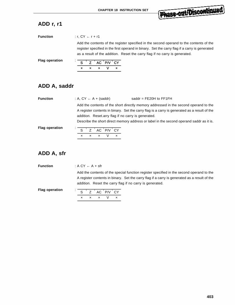
403
CHAPTER 18 INSTRUCTION SET
ADD r, r1
Function : r, CY ← r + r1
Add the contents of the register specified in the second operand to the contents of the
register specified in the first operand in binary. Set the carry flag if a carry is generated
as a result of the addition. Reset the carry flag if no carry is generated.
Flag operation :
ADD A, saddr
Function : A, CY ← A + (saddr) saddr = FE20H to FF1FH
Add the contents of the short directly memory addressed in the second operand to the
A register contents in binary. Set the carry flag is a carry is generated as a result of the
addition. Reset.arry flag if no carry is generated.
Describe the short direct memory address or label in the second operand saddr as it is.
Flag operation :
ADD A, sfr
Function : A CY ← A + sfr
Add the contents of the special function register specified in the second operand to the
A register contents in binary. Set the carry flag if a carry is generated as a result of the
addition. Reset the carry flag if no carry is generated.
Flag operation :
S Z AC P/V CY
× × × V ×
S Z AC P/V CY
× × × V ×
S Z AC P/V CY
× × × V ×
S Z AC P/V CY
× × × V ×
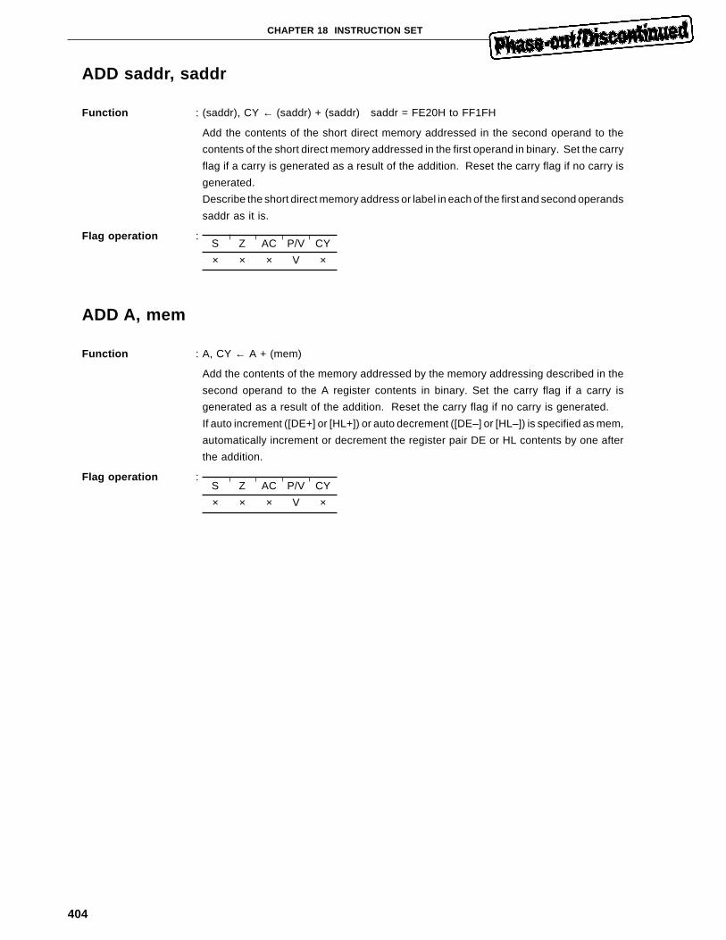
404
CHAPTER 18 INSTRUCTION SET
ADD saddr, saddr
Function : (saddr), CY ← (saddr) + (saddr) saddr = FE20H to FF1FH
Add the contents of the short direct memory addressed in the second operand to the
contents of the short direct memory addressed in the first operand in binary. Set the carry
flag if a carry is generated as a result of the addition. Reset the carry flag if no carry is
generated.
Describe the short direct memory address or label in each of the first and second operands
saddr as it is.
Flag operation :
ADD A, mem
Function : A, CY ← A + (mem)
Add the contents of the memory addressed by the memory addressing described in the
second operand to the A register contents in binary. Set the carry flag if a carry is
generated as a result of the addition. Reset the carry flag if no carry is generated.
If auto increment ([DE+] or [HL+]) or auto decrement ([DE–] or [HL–]) is specified as mem,
automatically increment or decrement the register pair DE or HL contents by one after
the addition.
Flag operation :
S Z AC P/V CY
× × × V ×
S Z AC P/V CY
× × × V ×
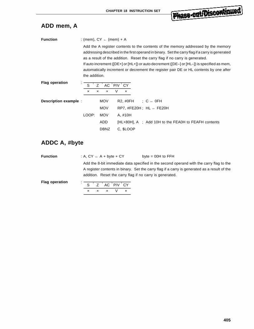
405
CHAPTER 18 INSTRUCTION SET
ADD mem, A
Function : (mem), CY ← (mem) + A
Add the A register contents to the contents of the memory addressed by the memory
addressing described in the first operand in binary. Set the carry flag if a carry is generated
as a result of the addition. Reset the carry flag if no carry is generated.
If auto increment ([DE+] or [HL+]) or auto decrement ([DE–] or [HL–]) is specified as mem,
automatically increment or decrement the register pair DE or HL contents by one after
the addition.
Flag operation :
Description example : MOV R2, #0FH ; C ← 0FH
MOV RP7, #FE20H ; HL ← FE20H
LOOP: MOV A, #10H
ADD [HL+80H], A ; Add 10H to the FEA0H to FEAFH contents
DBNZ C, $LOOP
ADDC A, #byte
Function : A, CY ← A + byte + CY byte = 00H to FFH
Add the 8-bit immediate data specified in the second operand with the carry flag to the
A register contents in binary. Set the carry flag if a carry is generated as a result of the
addition. Reset the carry flag if no carry is generated.
Flag operation :
S Z AC P/V CY
× × × V ×
S Z AC P/V CY
× × × V ×
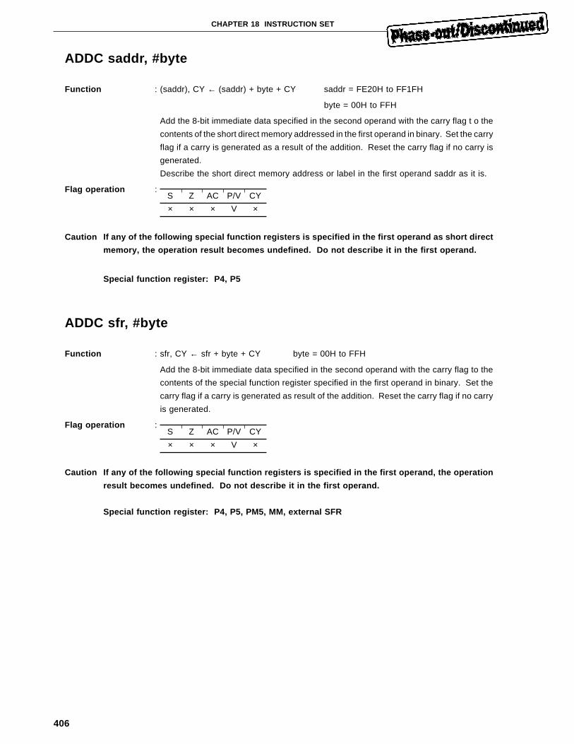
406
CHAPTER 18 INSTRUCTION SET
ADDC saddr, #byte
Function : (saddr), CY ← (saddr) + byte + CY saddr = FE20H to FF1FH
byte = 00H to FFH
Add the 8-bit immediate data specified in the second operand with the carry flag t o the
contents of the short direct memory addressed in the first operand in binary. Set the carry
flag if a carry is generated as a result of the addition. Reset the carry flag if no carry is
generated.
Describe the short direct memory address or label in the first operand saddr as it is.
Flag operation :
Caution If any of the following special function registers is specified in the first operand as short direct
memory, the operation result becomes undefined. Do not describe it in the first operand.
Special function register: P4, P5
ADDC sfr, #byte
Function : sfr, CY ← sfr + byte + CY byte = 00H to FFH
Add the 8-bit immediate data specified in the second operand with the carry flag to the
contents of the special function register specified in the first operand in binary. Set the
carry flag if a carry is generated as result of the addition. Reset the carry flag if no carry
is generated.
Flag operation :
Caution If any of the following special function registers is specified in the first operand, the operation
result becomes undefined. Do not describe it in the first operand.
Special function register: P4, P5, PM5, MM, external SFR
S Z AC P/V CY
× × × V ×
S Z AC P/V CY
× × × V ×
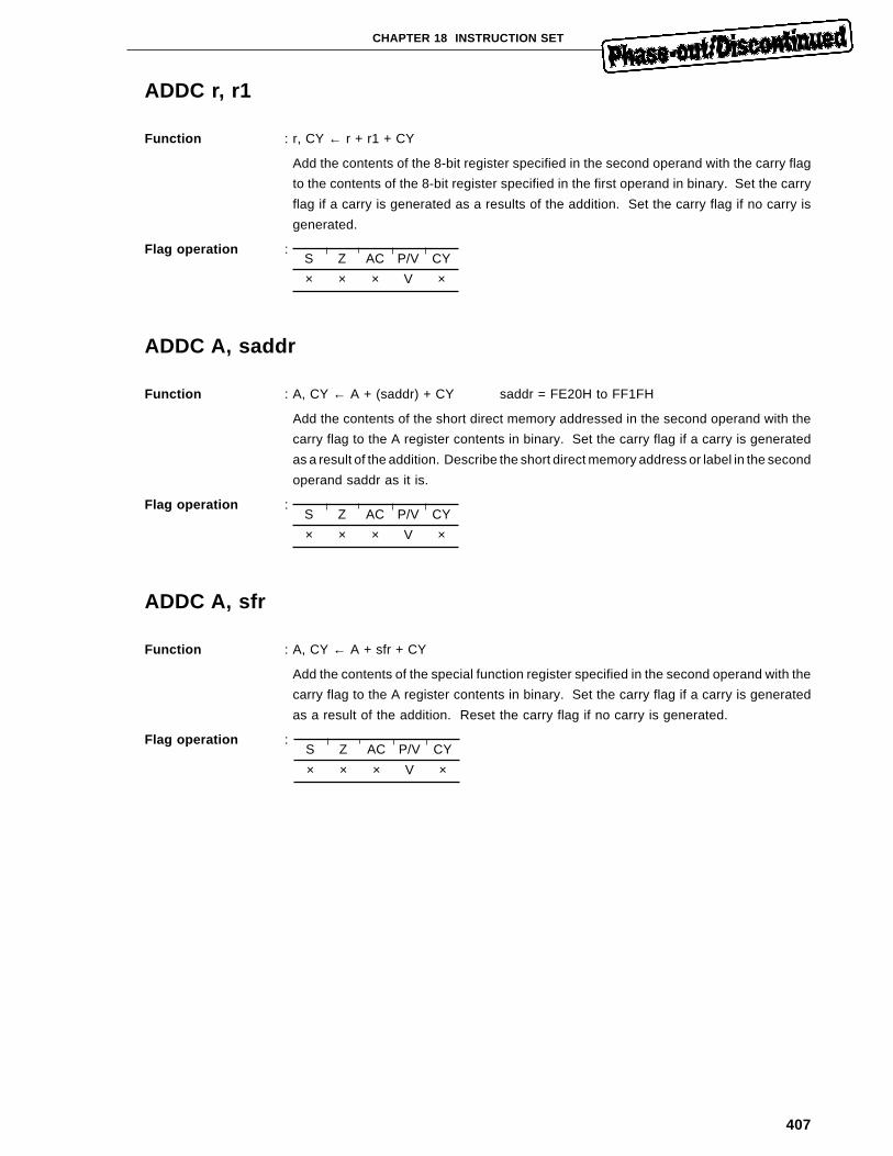
407
CHAPTER 18 INSTRUCTION SET
ADDC r, r1
Function : r, CY ← r + r1 + CY
Add the contents of the 8-bit register specified in the second operand with the carry flag
to the contents of the 8-bit register specified in the first operand in binary. Set the carry
flag if a carry is generated as a results of the addition. Set the carry flag if no carry is
generated.
Flag operation :
ADDC A, saddr
Function : A, CY ← A + (saddr) + CY saddr = FE20H to FF1FH
Add the contents of the short direct memory addressed in the second operand with the
carry flag to the A register contents in binary. Set the carry flag if a carry is generated
as a result of the addition. Describe the short direct memory address or label in the second
operand saddr as it is.
Flag operation :
ADDC A, sfr
Function : A, CY ← A + sfr + CY
Add the contents of the special function register specified in the second operand with the
carry flag to the A register contents in binary. Set the carry flag if a carry is generated
as a result of the addition. Reset the carry flag if no carry is generated.
Flag operation :
S Z AC P/V CY
× × × V ×
S Z AC P/V CY
× × × V ×
S Z AC P/V CY
× × × V ×
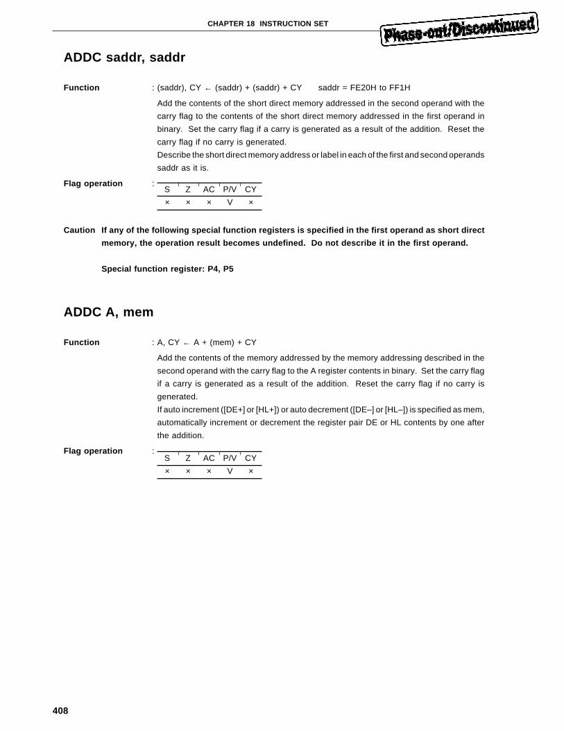
408
CHAPTER 18 INSTRUCTION SET
ADDC saddr, saddr
Function : (saddr), CY ← (saddr) + (saddr) + CY saddr = FE20H to FF1H
Add the contents of the short direct memory addressed in the second operand with the
carry flag to the contents of the short direct memory addressed in the first operand in
binary. Set the carry flag if a carry is generated as a result of the addition. Reset the
carry flag if no carry is generated.
Describe the short direct memory address or label in each of the first and second operands
saddr as it is.
Flag operation :
Caution If any of the following special function registers is specified in the first operand as short direct
memory, the operation result becomes undefined. Do not describe it in the first operand.
Special function register: P4, P5
ADDC A, mem
Function : A, CY ← A + (mem) + CY
Add the contents of the memory addressed by the memory addressing described in the
second operand with the carry flag to the A register contents in binary. Set the carry flag
if a carry is generated as a result of the addition. Reset the carry flag if no carry is
generated.
If auto increment ([DE+] or [HL+]) or auto decrement ([DE–] or [HL–]) is specified as mem,
automatically increment or decrement the register pair DE or HL contents by one after
the addition.
Flag operation :
S Z AC P/V CY
× × × V ×
S Z AC P/V CY
× × × V ×
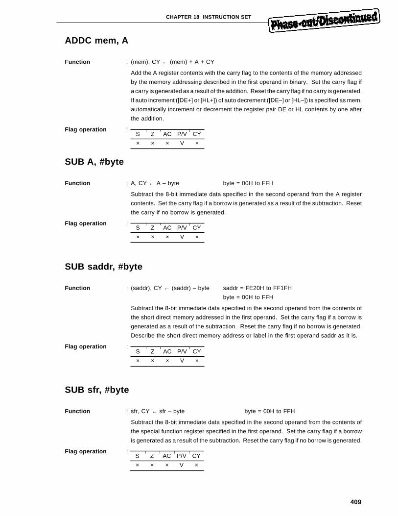
409
CHAPTER 18 INSTRUCTION SET
ADDC mem, A
Function : (mem), CY ← (mem) + A + CY
Add the A register contents with the carry flag to the contents of the memory addressed
by the memory addressing described in the first operand in binary. Set the carry flag if
a carry is generated as a result of the addition. Reset the carry flag if no carry is generated.
If auto increment ([DE+] or [HL+]) of auto decrement ([DE–] or [HL–]) is specified as mem,
automatically increment or decrement the register pair DE or HL contents by one after
the addition.
Flag operation :
SUB A, #byte
Function : A, CY ← A – byte byte = 00H to FFH
Subtract the 8-bit immediate data specified in the second operand from the A register
contents. Set the carry flag if a borrow is generated as a result of the subtraction. Reset
the carry if no borrow is generated.
Flag operation :
SUB saddr, #byte
Function : (saddr), CY ← (saddr) – byte saddr = FE20H to FF1FH
byte = 00H to FFH
Subtract the 8-bit immediate data specified in the second operand from the contents of
the short direct memory addressed in the first operand. Set the carry flag if a borrow is
generated as a result of the subtraction. Reset the carry flag if no borrow is generated.
Describe the short direct memory address or label in the first operand saddr as it is.
Flag operation :
SUB sfr, #byte
Function : sfr, CY ← sfr – byte byte = 00H to FFH
Subtract the 8-bit immediate data specified in the second operand from the contents of
the special function register specified in the first operand. Set the carry flag if a borrow
is generated as a result of the subtraction. Reset the carry flag if no borrow is generated.
Flag operation :
S Z AC P/V CY
× × × V ×
S Z AC P/V CY
× × × V ×
S Z AC P/V CY
× × × V ×
S Z AC P/V CY
× × × V ×
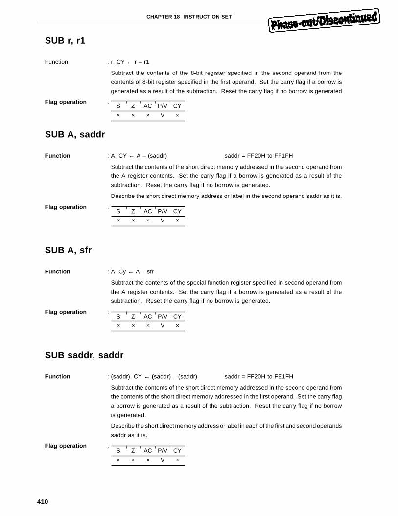
410
CHAPTER 18 INSTRUCTION SET
SUB r, r1
Function : r, CY ← r – r1
Subtract the contents of the 8-bit register specified in the second operand from the
contents of 8-bit register specified in the first operand. Set the carry flag if a borrow is
generated as a result of the subtraction. Reset the carry flag if no borrow is generated
Flag operation :
SUB A, saddr
Function : A, CY ← A – (saddr) saddr = FF20H to FF1FH
Subtract the contents of the short direct memory addressed in the second operand from
the A register contents. Set the carry flag if a borrow is generated as a result of the
subtraction. Reset the carry flag if no borrow is generated.
Describe the short direct memory address or label in the second operand saddr as it is.
Flag operation :
SUB A, sfr
Function : A, Cy ← A – sfr
Subtract the contents of the special function register specified in second operand from
the A register contents. Set the carry flag if a borrow is generated as a result of the
subtraction. Reset the carry flag if no borrow is generated.
Flag operation :
SUB saddr, saddr
Function : (saddr), CY ← (saddr) – (saddr) saddr = FF20H to FE1FH
Subtract the contents of the short direct memory addressed in the second operand from
the contents of the short direct memory addressed in the first operand. Set the carry flag
a borrow is generated as a result of the subtraction. Reset the carry flag if no borrow
is generated.
Describe the short direct memory address or label in each of the first and second operands
saddr as it is.
Flag operation :
S Z AC P/V CY
× × × V ×
S Z AC P/V CY
× × × V ×
S Z AC P/V CY
× × × V ×
S Z AC P/V CY
× × × V ×
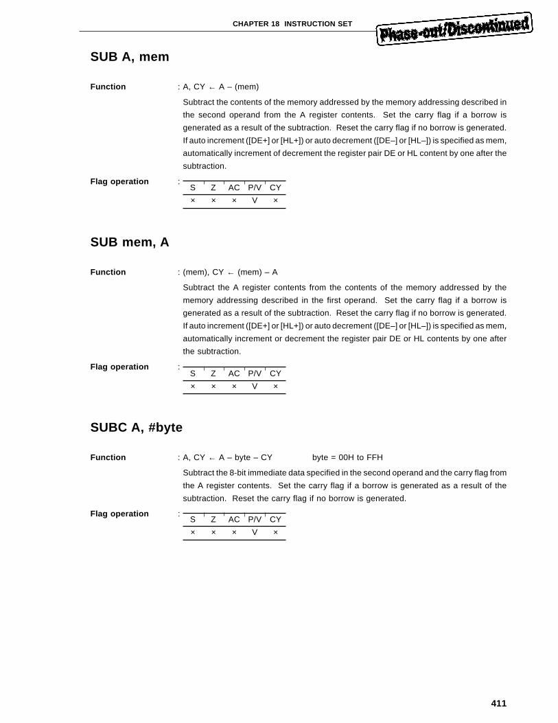
411
CHAPTER 18 INSTRUCTION SET
SUB A, mem
Function : A, CY ← A – (mem)
Subtract the contents of the memory addressed by the memory addressing described in
the second operand from the A register contents. Set the carry flag if a borrow is
generated as a result of the subtraction. Reset the carry flag if no borrow is generated.
If auto increment ([DE+] or [HL+]) or auto decrement ([DE–] or [HL–]) is specified as mem,
automatically increment of decrement the register pair DE or HL content by one after the
subtraction.
Flag operation :
SUB mem, A
Function : (mem), CY ← (mem) – A
Subtract the A register contents from the contents of the memory addressed by the
memory addressing described in the first operand. Set the carry flag if a borrow is
generated as a result of the subtraction. Reset the carry flag if no borrow is generated.
If auto increment ([DE+] or [HL+]) or auto decrement ([DE–] or [HL–]) is specified as mem,
automatically increment or decrement the register pair DE or HL contents by one after
the subtraction.
Flag operation :
SUBC A, #byte
Function : A, CY ← A – byte – CY byte = 00H to FFH
Subtract the 8-bit immediate data specified in the second operand and the carry flag from
the A register contents. Set the carry flag if a borrow is generated as a result of the
subtraction. Reset the carry flag if no borrow is generated.
Flag operation :
S Z AC P/V CY
× × × V ×
S Z AC P/V CY
× × × V ×
S Z AC P/V CY
× × × V ×
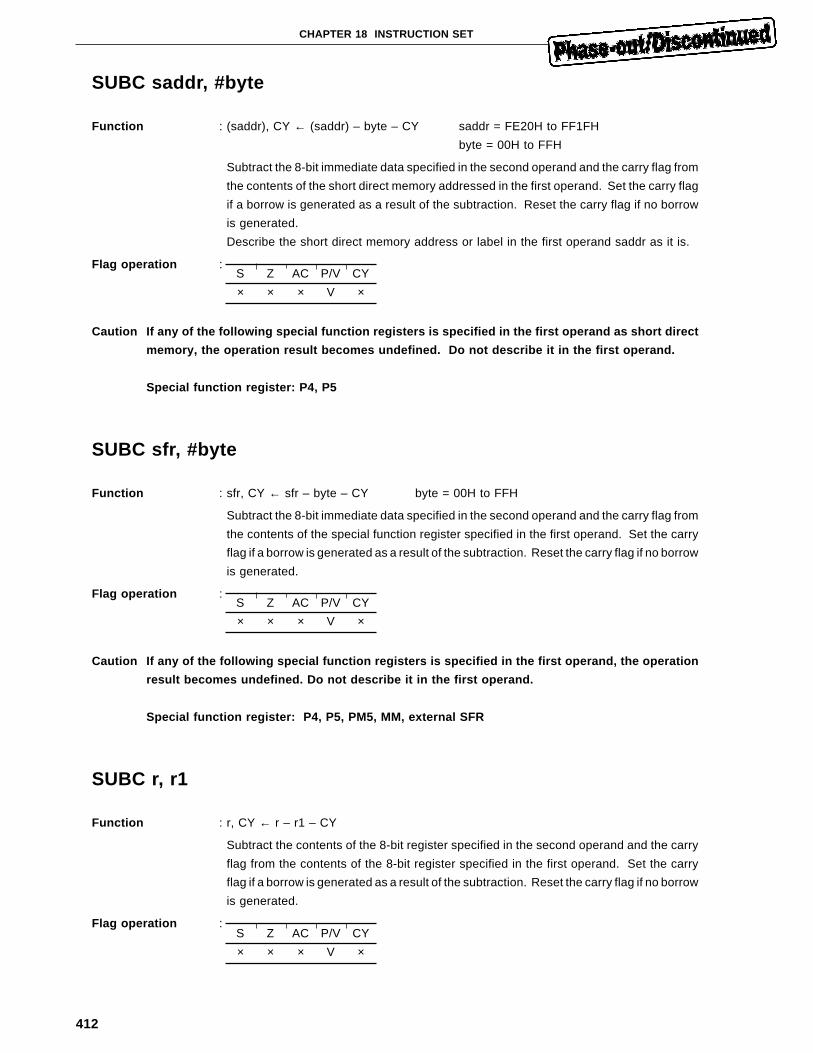
412
CHAPTER 18 INSTRUCTION SET
SUBC saddr, #byte
Function : (saddr), CY ← (saddr) – byte – CY saddr = FE20H to FF1FH
byte = 00H to FFH
Subtract the 8-bit immediate data specified in the second operand and the carry flag from
the contents of the short direct memory addressed in the first operand. Set the carry flag
if a borrow is generated as a result of the subtraction. Reset the carry flag if no borrow
is generated.
Describe the short direct memory address or label in the first operand saddr as it is.
Flag operation :
Caution If any of the following special function registers is specified in the first operand as short direct
memory, the operation result becomes undefined. Do not describe it in the first operand.
Special function register: P4, P5
SUBC sfr, #byte
Function : sfr, CY ← sfr – byte – CY byte = 00H to FFH
Subtract the 8-bit immediate data specified in the second operand and the carry flag from
the contents of the special function register specified in the first operand. Set the carry
flag if a borrow is generated as a result of the subtraction. Reset the carry flag if no borrow
is generated.
Flag operation :
Caution If any of the following special function registers is specified in the first operand, the operation
result becomes undefined. Do not describe it in the first operand.
Special function register: P4, P5, PM5, MM, external SFR
SUBC r, r1
Function : r, CY ← r – r1 – CY
Subtract the contents of the 8-bit register specified in the second operand and the carry
flag from the contents of the 8-bit register specified in the first operand. Set the carry
flag if a borrow is generated as a result of the subtraction. Reset the carry flag if no borrow
is generated.
Flag operation :
S Z AC P/V CY
× × × V ×
S Z AC P/V CY
× × × V ×
S Z AC P/V CY
× × × V ×
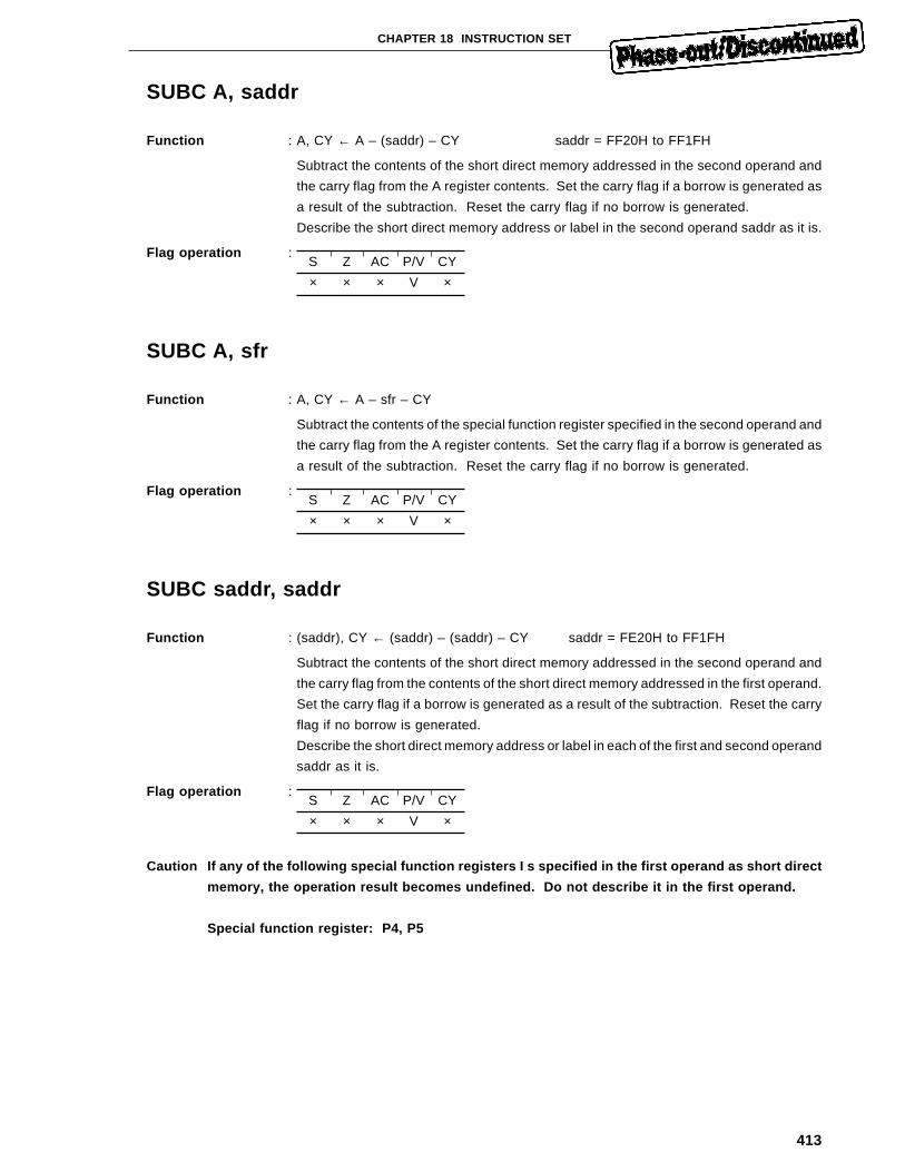
413
CHAPTER 18 INSTRUCTION SET
SUBC A, saddr
Function : A, CY ← A – (saddr) – CY saddr = FF20H to FF1FH
Subtract the contents of the short direct memory addressed in the second operand and
the carry flag from the A register contents. Set the carry flag if a borrow is generated as
a result of the subtraction. Reset the carry flag if no borrow is generated.
Describe the short direct memory address or label in the second operand saddr as it is.
Flag operation :
SUBC A, sfr
Function : A, CY ← A – sfr – CY
Subtract the contents of the special function register specified in the second operand and
the carry flag from the A register contents. Set the carry flag if a borrow is generated as
a result of the subtraction. Reset the carry flag if no borrow is generated.
Flag operation :
SUBC saddr, saddr
Function : (saddr), CY ← (saddr) – (saddr) – CY saddr = FE20H to FF1FH
Subtract the contents of the short direct memory addressed in the second operand and
the carry flag from the contents of the short direct memory addressed in the first operand.
Set the carry flag if a borrow is generated as a result of the subtraction. Reset the carry
flag if no borrow is generated.
Describe the short direct memory address or label in each of the first and second operand
saddr as it is.
Flag operation :
Caution If any of the following special function registers I s specified in the first operand as short direct
memory, the operation result becomes undefined. Do not describe it in the first operand.
Special function register: P4, P5
S Z AC P/V CY
× × × V ×
S Z AC P/V CY
× × × V ×
S Z AC P/V CY
× × × V ×
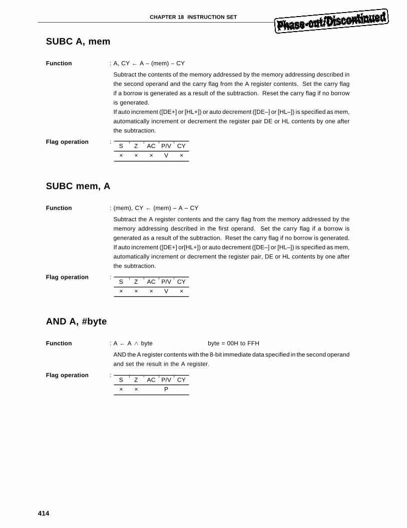
414
CHAPTER 18 INSTRUCTION SET
SUBC A, mem
Function : A, CY ← A – (mem) – CY
Subtract the contents of the memory addressed by the memory addressing described in
the second operand and the carry flag from the A register contents. Set the carry flag
if a borrow is generated as a result of the subtraction. Reset the carry flag if no borrow
is generated.
If auto increment ([DE+] or [HL+]) or auto decrement ([DE–] or [HL–]) is specified as mem,
automatically increment or decrement the register pair DE or HL contents by one after
the subtraction.
Flag operation :
SUBC mem, A
Function : (mem), CY ← (mem) – A – CY
Subtract the A register contents and the carry flag from the memory addressed by the
memory addressing described in the first operand. Set the carry flag if a borrow is
generated as a result of the subtraction. Reset the carry flag if no borrow is generated.
If auto increment ([DE+] or[HL+]) or auto decrement ([DE–] or [HL–]) is specified as mem,
automatically increment or decrement the register pair, DE or HL contents by one after
the subtraction.
Flag operation :
AND A, #byte
Function : A ← A byte byte = 00H to FFH
AND the A register contents with the 8-bit immediate data specified in the second operand
and set the result in the A register.
Flag operation :
S Z AC P/V CY
× × × V ×
S Z AC P/V CY
× × × V ×
S Z AC P/V CY
× × P
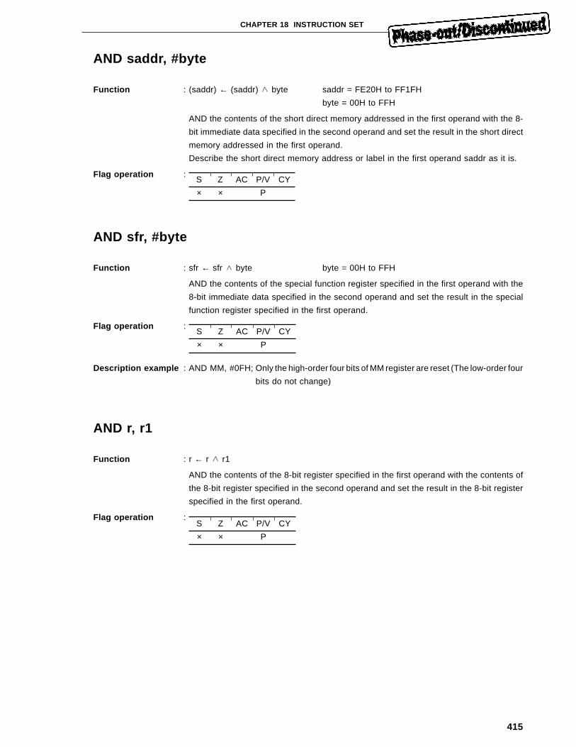
415
CHAPTER 18 INSTRUCTION SET
AND saddr, #byte
Function : (saddr) ← (saddr) byte saddr = FE20H to FF1FH
byte = 00H to FFH
AND the contents of the short direct memory addressed in the first operand with the 8-
bit immediate data specified in the second operand and set the result in the short direct
memory addressed in the first operand.
Describe the short direct memory address or label in the first operand saddr as it is.
Flag operation :
AND sfr, #byte
Function : sfr ← sfr byte byte = 00H to FFH
AND the contents of the special function register specified in the first operand with the
8-bit immediate data specified in the second operand and set the result in the special
function register specified in the first operand.
Flag operation :
Description example : AND MM, #0FH; Only the high-order four bits of MM register are reset (The low-order four
bits do not change)
AND r, r1
Function : r ← r r1
AND the contents of the 8-bit register specified in the first operand with the contents of
the 8-bit register specified in the second operand and set the result in the 8-bit register
specified in the first operand.
Flag operation :
S Z AC P/V CY
× × P
S Z AC P/V CY
× × P
S Z AC P/V CY
× × P
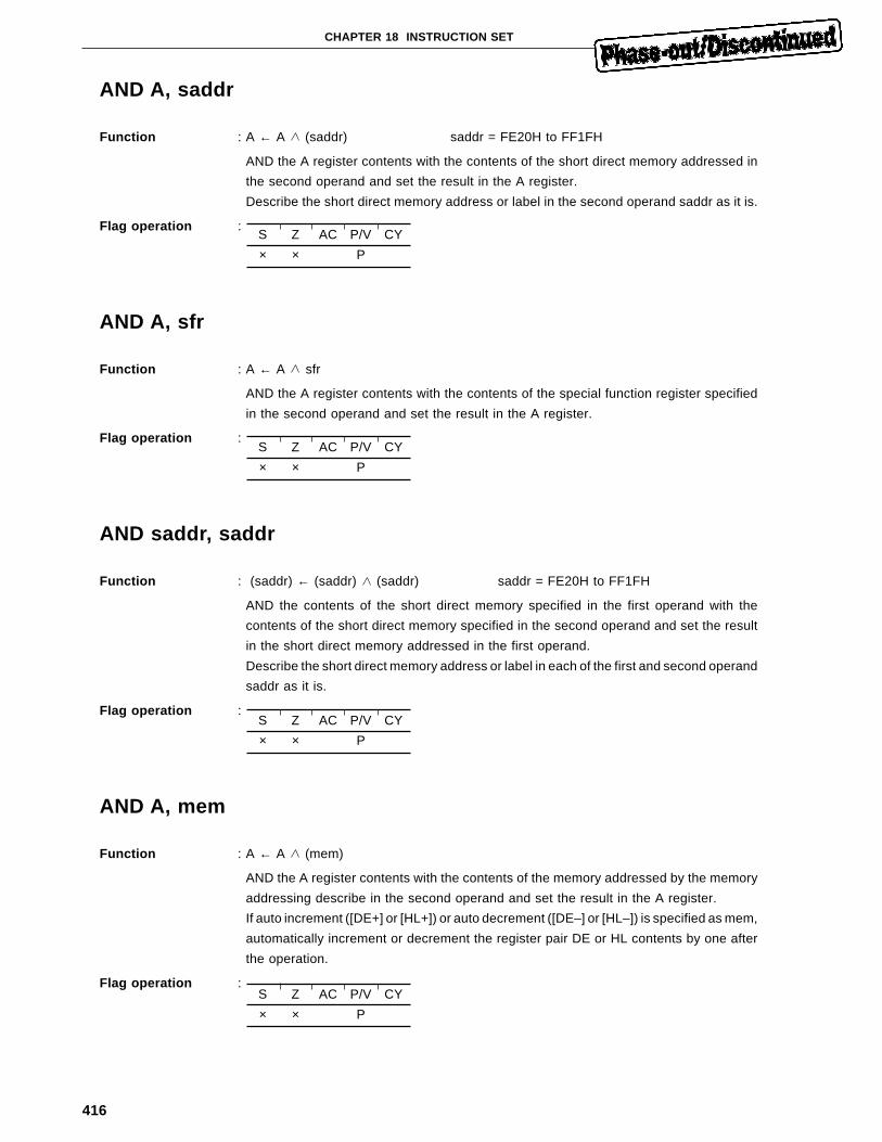
416
CHAPTER 18 INSTRUCTION SET
AND A, saddr
Function : A ← A (saddr) saddr = FE20H to FF1FH
AND the A register contents with the contents of the short direct memory addressed in
the second operand and set the result in the A register.
Describe the short direct memory address or label in the second operand saddr as it is.
Flag operation :
AND A, sfr
Function : A ← A sfr
AND the A register contents with the contents of the special function register specified
in the second operand and set the result in the A register.
Flag operation :
AND saddr, saddr
Function : (saddr) ← (saddr) (saddr) saddr = FE20H to FF1FH
AND the contents of the short direct memory specified in the first operand with the
contents of the short direct memory specified in the second operand and set the result
in the short direct memory addressed in the first operand.
Describe the short direct memory address or label in each of the first and second operand
saddr as it is.
Flag operation :
AND A, mem
Function : A ← A (mem)
AND the A register contents with the contents of the memory addressed by the memory
addressing describe in the second operand and set the result in the A register.
If auto increment ([DE+] or [HL+]) or auto decrement ([DE–] or [HL–]) is specified as mem,
automatically increment or decrement the register pair DE or HL contents by one after
the operation.
Flag operation :
S Z AC P/V CY
× × P
S Z AC P/V CY
× × P
S Z AC P/V CY
× × P
S Z AC P/V CY
× × P
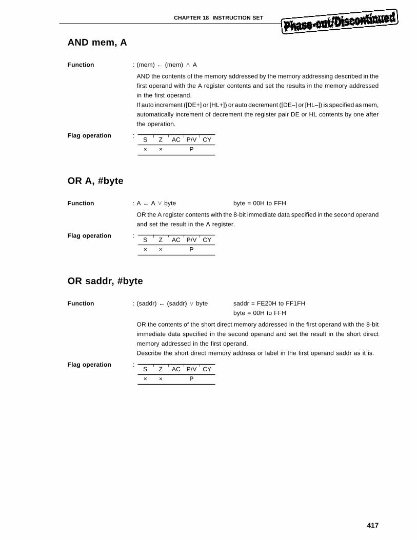
417
CHAPTER 18 INSTRUCTION SET
AND mem, A
Function : (mem) ← (mem) A
AND the contents of the memory addressed by the memory addressing described in the
first operand with the A register contents and set the results in the memory addressed
in the first operand.
If auto increment ([DE+] or [HL+]) or auto decrement ([DE–] or [HL–]) is specified as mem,
automatically increment of decrement the register pair DE or HL contents by one after
the operation.
Flag operation :
OR A, #byte
Function : A ← A byte byte = 00H to FFH
OR the A register contents with the 8-bit immediate data specified in the second operand
and set the result in the A register.
Flag operation :
OR saddr, #byte
Function : (saddr) ← (saddr) byte saddr = FE20H to FF1FH
byte = 00H to FFH
OR the contents of the short direct memory addressed in the first operand with the 8-bit
immediate data specified in the second operand and set the result in the short direct
memory addressed in the first operand.
Describe the short direct memory address or label in the first operand saddr as it is.
Flag operation :
S Z AC P/V CY
× × P
S Z AC P/V CY
× × P
S Z AC P/V CY
× × P
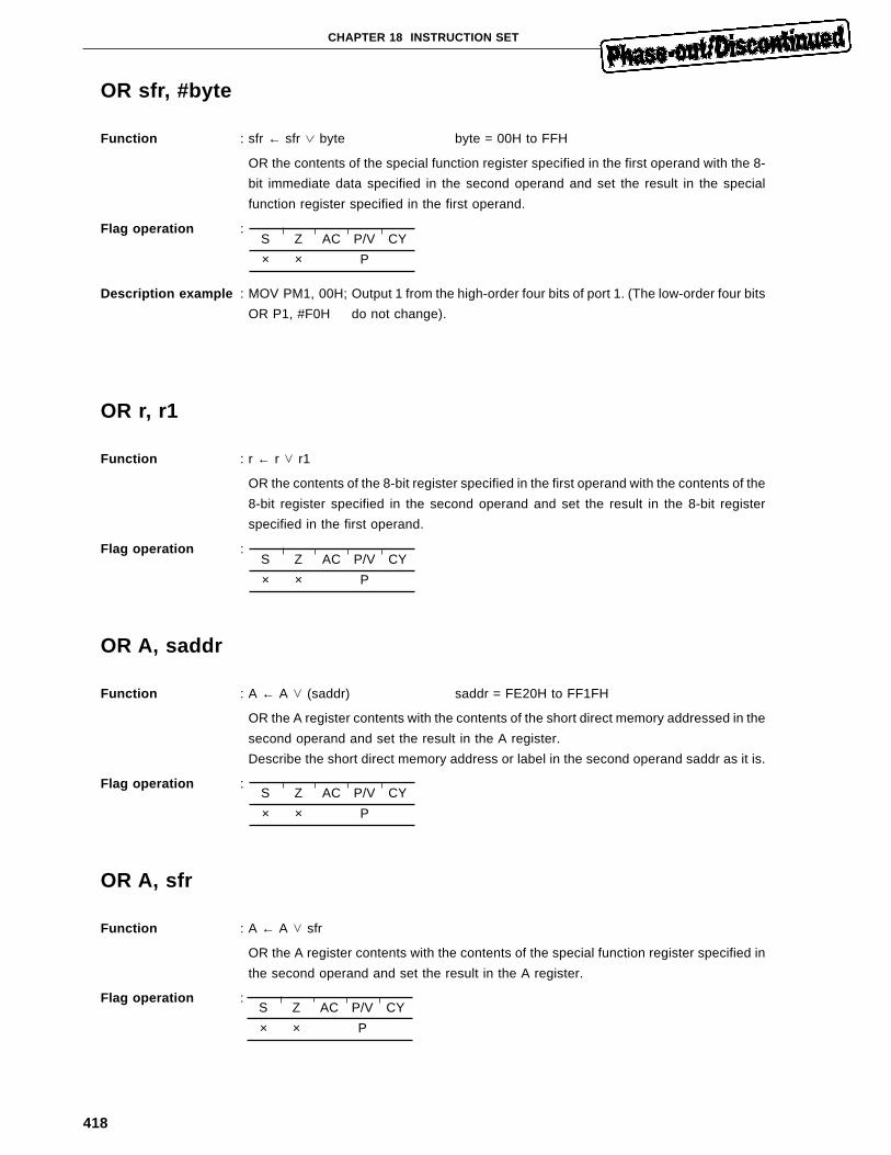
418
CHAPTER 18 INSTRUCTION SET
OR sfr, #byte
Function : sfr ← sfr byte byte = 00H to FFH
OR the contents of the special function register specified in the first operand with the 8-
bit immediate data specified in the second operand and set the result in the special
function register specified in the first operand.
Flag operation :
Description example : MOV PM1, 00H; Output 1 from the high-order four bits of port 1. (The low-order four bits
OR P1, #F0H do not change).
OR r, r1
Function : r ← r r1
OR the contents of the 8-bit register specified in the first operand with the contents of the
8-bit register specified in the second operand and set the result in the 8-bit register
specified in the first operand.
Flag operation :
OR A, saddr
Function : A ← A (saddr) saddr = FE20H to FF1FH
OR the A register contents with the contents of the short direct memory addressed in the
second operand and set the result in the A register.
Describe the short direct memory address or label in the second operand saddr as it is.
Flag operation :
OR A, sfr
Function : A ← A sfr
OR the A register contents with the contents of the special function register specified in
the second operand and set the result in the A register.
Flag operation :
S Z AC P/V CY
× × P
S Z AC P/V CY
× × P
S Z AC P/V CY
× × P
S Z AC P/V CY
× × P
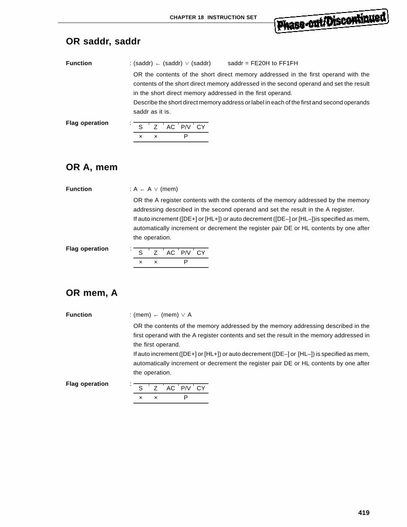
419
CHAPTER 18 INSTRUCTION SET
OR saddr, saddr
Function : (saddr) ← (saddr) (saddr) saddr = FE20H to FF1FH
OR the contents of the short direct memory addressed in the first operand with the
contents of the short direct memory addressed in the second operand and set the result
in the short direct memory addressed in the first operand.
Describe the short direct memory address or label in each of the first and second operands
saddr as it is.
Flag operation :
OR A, mem
Function : A ← A (mem)
OR the A register contents with the contents of the memory addressed by the memory
addressing described in the second operand and set the result in the A register.
If auto increment ([DE+] or [HL+]) or auto decrement ([DE–] or [HL–])is specified as mem,
automatically increment or decrement the register pair DE or HL contents by one after
the operation.
Flag operation :
OR mem, A
Function : (mem) ← (mem) A
OR the contents of the memory addressed by the memory addressing described in the
first operand with the A register contents and set the result in the memory addressed in
the first operand.
If auto increment ([DE+] or [HL+]) or auto decrement ([DE–] or [HL–]) is specified as mem,
automatically increment or decrement the register pair DE or HL contents by one after
the operation.
Flag operation :
S Z AC P/V CY
× × P
S Z AC P/V CY
× × P
S Z AC P/V CY
× × P
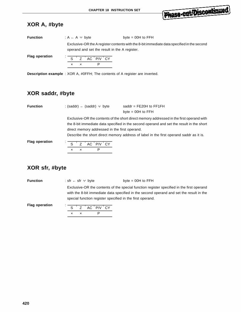
420
CHAPTER 18 INSTRUCTION SET
XOR A, #byte
Function : A ← A byte byte = 00H to FFH
Exclusive-OR the A register contents with the 8-bit immediate data specified in the second
operand and set the result in the A register.
Flag operation :
Description example : XOR A, #0FFH; The contents of A register are inverted.
XOR saddr, #byte
Function : (saddr) ← (saddr) byte saddr = FE20H to FF1FH
byte = 00H to FFH
Exclusive-OR the contents of the short direct memory addressed in the first operand with
the 8-bit immediate data specified in the second operand and set the result in the short
direct memory addressed in the first operand.
Describe the short direct memory address of label in the first operand saddr as it is.
Flag operation :
XOR sfr, #byte
Function : sfr ← sfr byte byte = 00H to FFH
Exclusive-OR the contents of the special function register specified in the first operand
with the 8-bit immediate data specified in the second operand and set the result in the
special function register specified in the first operand.
Flag operation :
S Z AC P/V CY
× × P
S Z AC P/V CY
× × P
S Z AC P/V CY
× × P
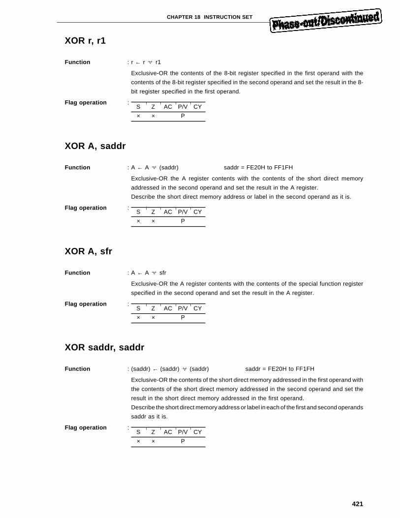
421
CHAPTER 18 INSTRUCTION SET
XOR r, r1
Function : r ← r r1
Exclusive-OR the contents of the 8-bit register specified in the first operand with the
contents of the 8-bit register specified in the second operand and set the result in the 8-
bit register specified in the first operand.
Flag operation :
XOR A, saddr
Function : A ← A (saddr) saddr = FE20H to FF1FH
Exclusive-OR the A register contents with the contents of the short direct memory
addressed in the second operand and set the result in the A register.
Describe the short direct memory address or label in the second operand as it is.
Flag operation :
XOR A, sfr
Function : A ← A sfr
Exclusive-OR the A register contents with the contents of the special function register
specified in the second operand and set the result in the A register.
Flag operation :
XOR saddr, saddr
Function : (saddr) ← (saddr) (saddr) saddr = FE20H to FF1FH
Exclusive-OR the contents of the short direct memory addressed in the first operand with
the contents of the short direct memory addressed in the second operand and set the
result in the short direct memory addressed in the first operand.
Describe the short direct memory address or label in each of the first and second operands
saddr as it is.
Flag operation :
S Z AC P/V CY
× × P
S Z AC P/V CY
× × P
S Z AC P/V CY
× × P
S Z AC P/V CY
× × P
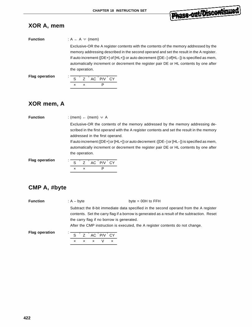
422
CHAPTER 18 INSTRUCTION SET
XOR A, mem
Function : A ← A (mem)
Exclusive-OR the A register contents with the contents of the memory addressed by the
memory addressing described in the second operand and set the result in the A register.
If auto increment ([DE+] of [HL+]) or auto decrement ([DE–] of[HL–]) is specified as mem,
automatically increment or decrement the register pair DE or HL contents by one after
the operation.
Flag operation :
XOR mem, A
Function : (mem) ← (mem) A
Exclusive-OR the contents of the memory addressed by the memory addressing de-
scribed in the first operand with the A register contents and set the result in the memory
addressed in the first operand.
If auto increment ([DE+] or [HL+]) or auto decrement ([DE–] or [HL–]) is specified as mem,
automatically increment or decrement the register pair DE or HL contents by one after
the operation.
Flag operation :
CMP A, #byte
Function : A – byte byte = 00H to FFH
Subtract the 8-bit immediate data specified in the second operand from the A register
contents. Set the carry flag if a borrow is generated as a result of the subtraction. Reset
the carry flag if no borrow is generated.
After the CMP instruction is executed, the A register contents do not change.
Flag operation :
S Z AC P/V CY
× × P
S Z AC P/V CY
× × P
S Z AC P/V CY
× × × V ×
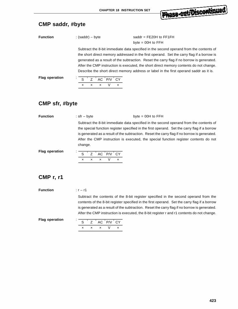
423
CHAPTER 18 INSTRUCTION SET
CMP saddr, #byte
Function : (saddr) – byte saddr = FE20H to FF1FH
byte = 00H to FFH
Subtract the 8-bit immediate data specified in the second operand from the contents of
the short direct memory addressed in the first operand. Set the carry flag if a borrow is
generated as a result of the subtraction. Reset the carry flag if no borrow is generated.
After the CMP instruction is executed, the short direct memory contents do not change.
Describe the short direct memory address or label in the first operand saddr as it is.
Flag operation :
CMP sfr, #byte
Function : sfr – byte byte = 00H to FFH
Subtract the 8-bit immediate data specified in the second operand from the contents of
the special function register specified in the first operand. Set the carry flag if a borrow
is generated as a result of the subtraction. Reset the carry flag if no borrow is generated.
After the CMP instruction is executed, the special function register contents do not
change.
Flag operation :
CMP r, r1
Function : r – r1
Subtract the contents of the 8-bit register specified in the second operand from the
contents of the 8-bit register specified in the first operand. Set the carry flag if a borrow
is generated as a result of the subtraction. Reset the carry flag if no borrow is generated.
After the CMP instruction is executed, the 8-bit register r and r1 contents do not change.
Flag operation :
S Z AC P/V CY
× × × V ×
S Z AC P/V CY
× × × V ×
S Z AC P/V CY
× × × V ×
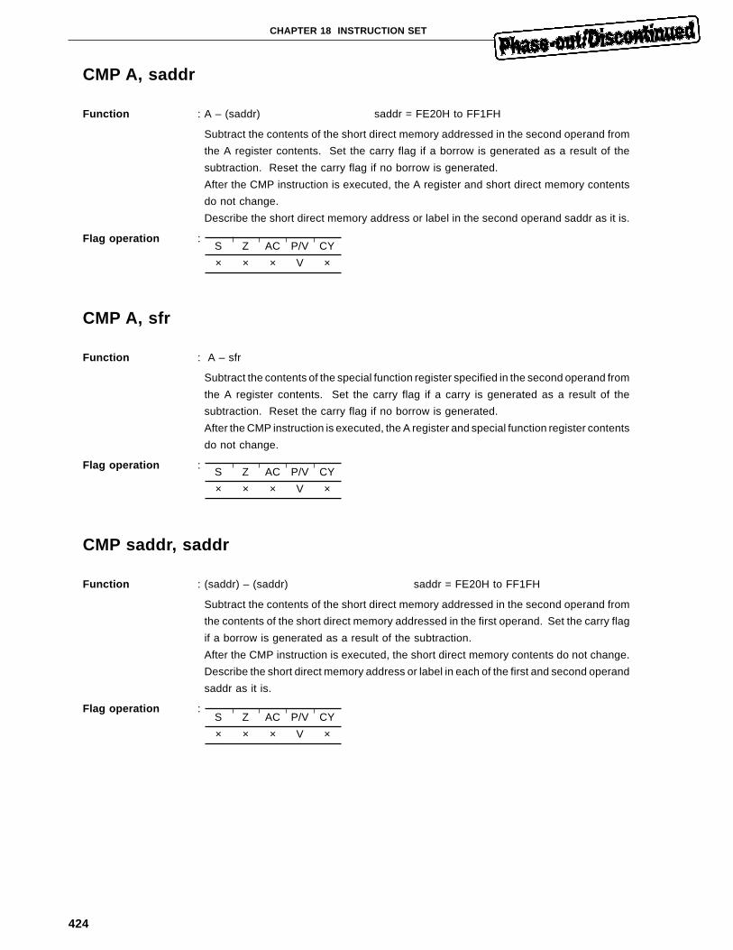
424
CHAPTER 18 INSTRUCTION SET
CMP A, saddr
Function : A – (saddr) saddr = FE20H to FF1FH
Subtract the contents of the short direct memory addressed in the second operand from
the A register contents. Set the carry flag if a borrow is generated as a result of the
subtraction. Reset the carry flag if no borrow is generated.
After the CMP instruction is executed, the A register and short direct memory contents
do not change.
Describe the short direct memory address or label in the second operand saddr as it is.
Flag operation :
CMP A, sfr
Function : A – sfr
Subtract the contents of the special function register specified in the second operand from
the A register contents. Set the carry flag if a carry is generated as a result of the
subtraction. Reset the carry flag if no borrow is generated.
After the CMP instruction is executed, the A register and special function register contents
do not change.
Flag operation :
CMP saddr, saddr
Function : (saddr) – (saddr) saddr = FE20H to FF1FH
Subtract the contents of the short direct memory addressed in the second operand from
the contents of the short direct memory addressed in the first operand. Set the carry flag
if a borrow is generated as a result of the subtraction.
After the CMP instruction is executed, the short direct memory contents do not change.
Describe the short direct memory address or label in each of the first and second operand
saddr as it is.
Flag operation :
S Z AC P/V CY
× × × V ×
S Z AC P/V CY
× × × V ×
S Z AC P/V CY
× × × V ×
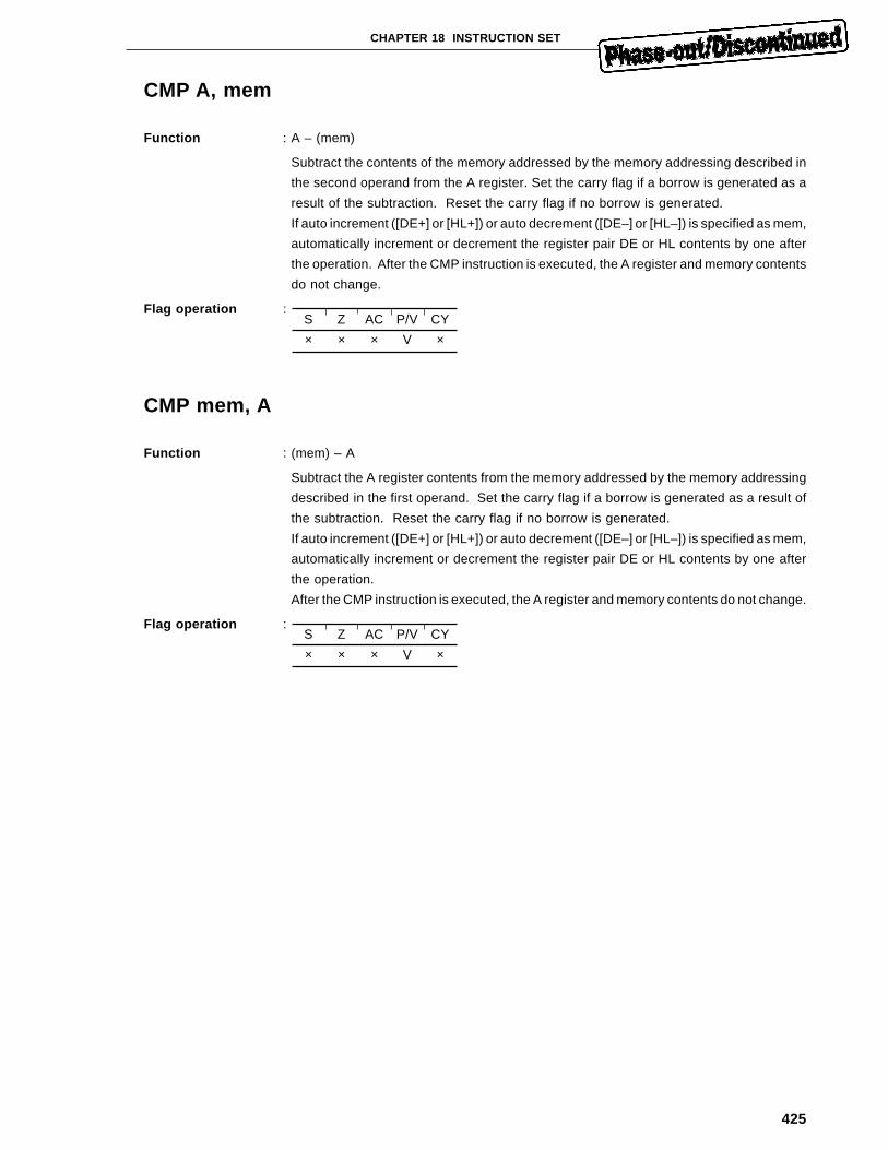
425
CHAPTER 18 INSTRUCTION SET
CMP A, mem
Function : A – (mem)
Subtract the contents of the memory addressed by the memory addressing described in
the second operand from the A register. Set the carry flag if a borrow is generated as a
result of the subtraction. Reset the carry flag if no borrow is generated.
If auto increment ([DE+] or [HL+]) or auto decrement ([DE–] or [HL–]) is specified as mem,
automatically increment or decrement the register pair DE or HL contents by one after
the operation. After the CMP instruction is executed, the A register and memory contents
do not change.
Flag operation :
CMP mem, A
Function : (mem) – A
Subtract the A register contents from the memory addressed by the memory addressing
described in the first operand. Set the carry flag if a borrow is generated as a result of
the subtraction. Reset the carry flag if no borrow is generated.
If auto increment ([DE+] or [HL+]) or auto decrement ([DE–] or [HL–]) is specified as mem,
automatically increment or decrement the register pair DE or HL contents by one after
the operation.
After the CMP instruction is executed, the A register and memory contents do not change.
Flag operation :
S Z AC P/V CY
× × × V ×
S Z AC P/V CY
× × × V ×
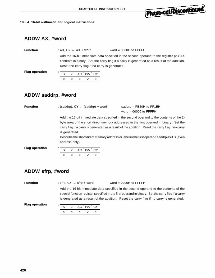
426
CHAPTER 18 INSTRUCTION SET
18.6.4 16-bit arithmetic and logical instructions
ADDW AX, #word
Function : AX, CY ← AX + word word = 0000H to FFFFH
Add the 16-bit immediate data specified in the second operand to the register pair AX
contents in binary. Set the carry flag if a carry is generated as a result of the addition.
Reset the carry flag if no carry is generated.
Flag operation :
ADDW saddrp, #word
Function : (saddrp), CY ← (saddrp) + word saddrp = FE20H to FF1EH
word = 0000J to FFFFH
Add the 16-bit immediate data specified in the second operand to the contents of the 2-
byte area of the short direct memory addressed in the first operand in binary. Set the
carry flag if a carry is generated as a result of the addition. Reset the carry flag if no carry
is generated.
Describe the short direct memory address or label in the first operand saddrp as it is (even
address only).
Flag operation :
ADDW sfrp, #word
Function : sfrp, CY ← sfrp + word word = 0000H to FFFFH
Add the 16-bit immediate data specified in the second operand to the contents of the
special function register specified in the first operand in binary. Set the carry flag if a carry
is generated as a result of the addition. Reset the carry flag if no carry is generated.
Flag operation :
S Z AC P/V CY
× × × V ×
S Z AC P/V CY
× × × V ×
S Z AC P/V CY
× × × V ×

427
CHAPTER 18 INSTRUCTION SET
ADDW rp, rp1
Function : rp, CY ← rp + rp1
Add the contents of the 16-bit register pair specified in the second operand to the contents
of the 16-bit register pair specified in the first operand in binary. Set the carry flag if a
carry is generated as a result of the addition. Reset the carry flag if no carry is generated.
Flag operation :
ADDW AX, saddrp
Function : AX, CY ← AX + (saddrp) saddrp = FE20H to FF1EH
Add the contents of the 2-byte area of the short direct memory addressed in the second
operand to the register pair AX contents in binary. Set the carry flag if a carry is generated
as a result of the addition. Reset the carry flag if no carry is generated.
Describe the short direct memory address or label in the second operand saddrp as it
is (even address only).
Flag operation :
ADDW AX, sfrp
Function : AX, CY ← AX + sfrp
Add the contents of the 16-bit special function register specified in the second operand
to the register pair AX contents in binary. Set the carry flag if a carry is generated as a
result of the addition. Reset the carry flag if no carry is generated.
Flag operation :
S Z AC P/V CY
× × × V ×
S Z AC P/V CY
× × × V ×
S Z AC P/V CY
× × × V ×
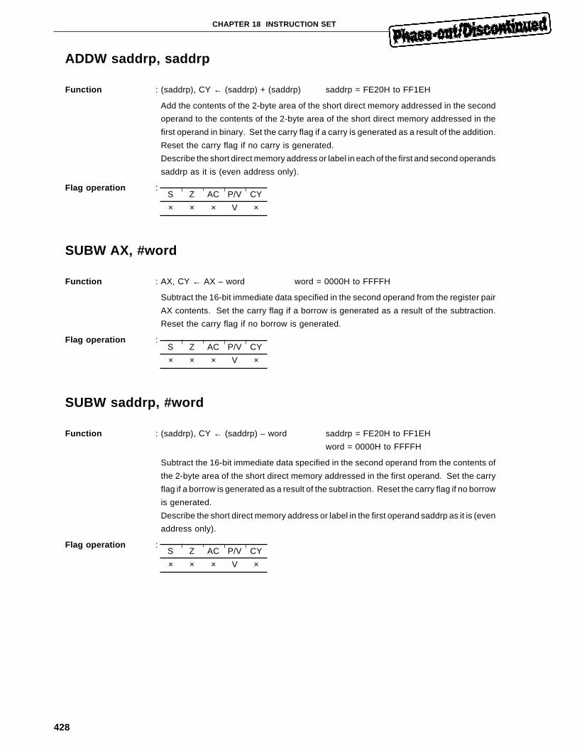
428
CHAPTER 18 INSTRUCTION SET
ADDW saddrp, saddrp
Function : (saddrp), CY ← (saddrp) + (saddrp) saddrp = FE20H to FF1EH
Add the contents of the 2-byte area of the short direct memory addressed in the second
operand to the contents of the 2-byte area of the short direct memory addressed in the
first operand in binary. Set the carry flag if a carry is generated as a result of the addition.
Reset the carry flag if no carry is generated.
Describe the short direct memory address or label in each of the first and second operands
saddrp as it is (even address only).
Flag operation :
SUBW AX, #word
Function : AX, CY ← AX – word word = 0000H to FFFFH
Subtract the 16-bit immediate data specified in the second operand from the register pair
AX contents. Set the carry flag if a borrow is generated as a result of the subtraction.
Reset the carry flag if no borrow is generated.
Flag operation :
SUBW saddrp, #word
Function : (saddrp), CY ← (saddrp) – word saddrp = FE20H to FF1EH
word = 0000H to FFFFH
Subtract the 16-bit immediate data specified in the second operand from the contents of
the 2-byte area of the short direct memory addressed in the first operand. Set the carry
flag if a borrow is generated as a result of the subtraction. Reset the carry flag if no borrow
is generated.
Describe the short direct memory address or label in the first operand saddrp as it is (even
address only).
Flag operation :
S Z AC P/V CY
× × × V ×
S Z AC P/V CY
× × × V ×
S Z AC P/V CY
× × × V ×
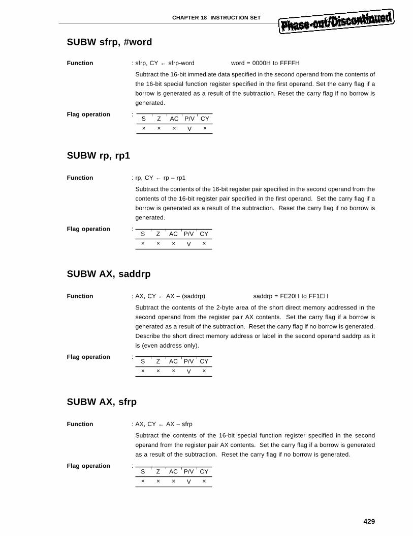
429
CHAPTER 18 INSTRUCTION SET
SUBW sfrp, #word
Function : sfrp, CY ← sfrp-word word = 0000H to FFFFH
Subtract the 16-bit immediate data specified in the second operand from the contents of
the 16-bit special function register specified in the first operand. Set the carry flag if a
borrow is generated as a result of the subtraction. Reset the carry flag if no borrow is
generated.
Flag operation :
SUBW rp, rp1
Function : rp, CY ← rp – rp1
Subtract the contents of the 16-bit register pair specified in the second operand from the
contents of the 16-bit register pair specified in the first operand. Set the carry flag if a
borrow is generated as a result of the subtraction. Reset the carry flag if no borrow is
generated.
Flag operation :
SUBW AX, saddrp
Function : AX, CY ← AX – (saddrp) saddrp = FE20H to FF1EH
Subtract the contents of the 2-byte area of the short direct memory addressed in the
second operand from the register pair AX contents. Set the carry flag if a borrow is
generated as a result of the subtraction. Reset the carry flag if no borrow is generated.
Describe the short direct memory address or label in the second operand saddrp as it
is (even address only).
Flag operation :
SUBW AX, sfrp
Function : AX, CY ← AX – sfrp
Subtract the contents of the 16-bit special function register specified in the second
operand from the register pair AX contents. Set the carry flag if a borrow is generated
as a result of the subtraction. Reset the carry flag if no borrow is generated.
Flag operation :
S Z AC P/V CY
× × × V ×
S Z AC P/V CY
× × × V ×
S Z AC P/V CY
× × × V ×
S Z AC P/V CY
× × × V ×
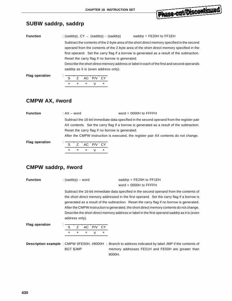
430
CHAPTER 18 INSTRUCTION SET
SUBW saddrp, saddrp
Function : (saddrp), CY ← (saddrp) – (saddrp) saddrp = FE20H to FF1EH
Subtract the contents of the 2-byte area of the short direct memory specified in the second
operand from the contents of the 2-byte area of the short direct memory specified in the
first operand. Set the carry flag if a borrow is generated as a result of the subtraction.
Reset the carry flag if no borrow is generated.
Describe the short direct memory address or label in each of the first and second operands
saddrp as it is (even address only).
Flag operation :
CMPW AX, #word
Function : AX – word word = 0000H to FFFFH
Subtract the 16-bit immediate data specified in the second operand from the register pair
AX contents. Set the carry flag if a borrow is generated as a result of the subtraction.
Reset the carry flag if no borrow is generated.
After the CMPW instruction is executed, the register pair AX contents do not change.
Flag operation :
CMPW saddrp, #word
Function : (saddrp) – word saddrp = FE20H to FF1EH
word = 0000H to FFFFH
Subtract the 16-bit immediate data specified in the second operand from the contents of
the short direct memory addressed in the first operand. Set the carry flag if a borrow is
generated as a result of the subtraction. Reset the carry flag if no borrow is generated.
After the CMPW instruction is generated, the short direct memory contents do not change.
Describe the short direct memory address or label in the first operand saddrp as it is (even
address only).
Flag operation :
Description example : CMPW 0FE50H, #8000H ; Branch to address indicated by label JMP if the contents of
BGT $JMP memory addresses FE51H and FE50H are greater than
8000H.
S Z AC P/V CY
× × × V ×
S Z AC P/V CY
× × × V ×
S Z AC P/V CY
× × × V ×
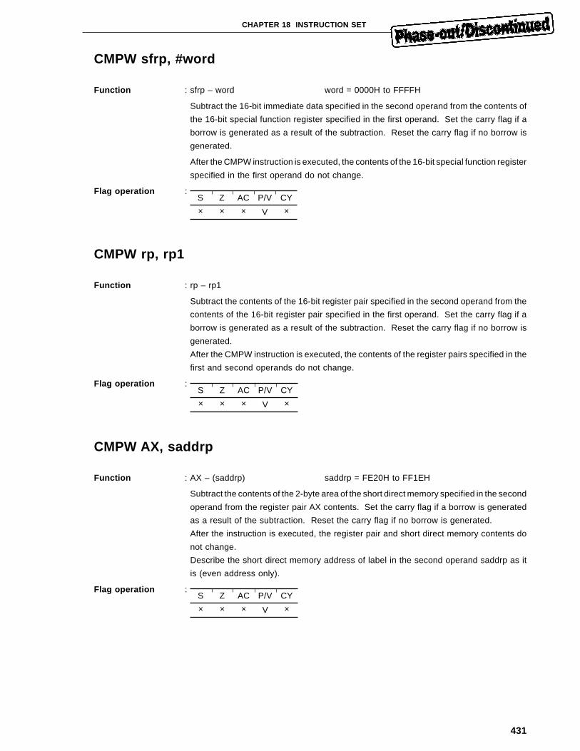
431
CHAPTER 18 INSTRUCTION SET
CMPW sfrp, #word
Function : sfrp – word word = 0000H to FFFFH
Subtract the 16-bit immediate data specified in the second operand from the contents of
the 16-bit special function register specified in the first operand. Set the carry flag if a
borrow is generated as a result of the subtraction. Reset the carry flag if no borrow is
generated.
After the CMPW instruction is executed, the contents of the 16-bit special function register
specified in the first operand do not change.
Flag operation :
CMPW rp, rp1
Function : rp – rp1
Subtract the contents of the 16-bit register pair specified in the second operand from the
contents of the 16-bit register pair specified in the first operand. Set the carry flag if a
borrow is generated as a result of the subtraction. Reset the carry flag if no borrow is
generated.
After the CMPW instruction is executed, the contents of the register pairs specified in the
first and second operands do not change.
Flag operation :
CMPW AX, saddrp
Function : AX – (saddrp) saddrp = FE20H to FF1EH
Subtract the contents of the 2-byte area of the short direct memory specified in the second
operand from the register pair AX contents. Set the carry flag if a borrow is generated
as a result of the subtraction. Reset the carry flag if no borrow is generated.
After the instruction is executed, the register pair and short direct memory contents do
not change.
Describe the short direct memory address of label in the second operand saddrp as it
is (even address only).
Flag operation :
S Z AC P/V CY
× × × V ×
S Z AC P/V CY
× × × V ×
S Z AC P/V CY
× × × V ×
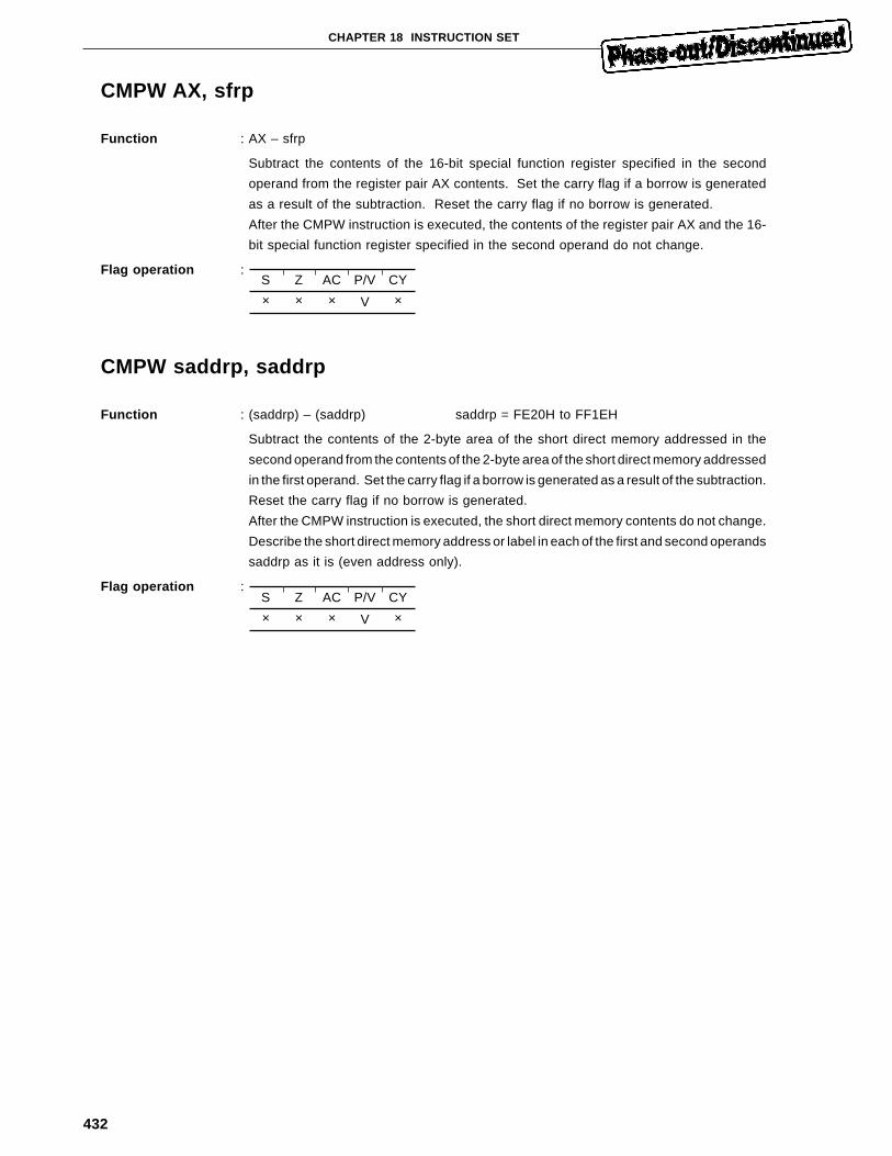
432
CHAPTER 18 INSTRUCTION SET
CMPW AX, sfrp
Function : AX – sfrp
Subtract the contents of the 16-bit special function register specified in the second
operand from the register pair AX contents. Set the carry flag if a borrow is generated
as a result of the subtraction. Reset the carry flag if no borrow is generated.
After the CMPW instruction is executed, the contents of the register pair AX and the 16-
bit special function register specified in the second operand do not change.
Flag operation :
CMPW saddrp, saddrp
Function : (saddrp) – (saddrp) saddrp = FE20H to FF1EH
Subtract the contents of the 2-byte area of the short direct memory addressed in the
second operand from the contents of the 2-byte area of the short direct memory addressed
in the first operand. Set the carry flag if a borrow is generated as a result of the subtraction.
Reset the carry flag if no borrow is generated.
After the CMPW instruction is executed, the short direct memory contents do not change.
Describe the short direct memory address or label in each of the first and second operands
saddrp as it is (even address only).
Flag operation :
S Z AC P/V CY
× × × V ×
S Z AC P/V CY
× × × V ×
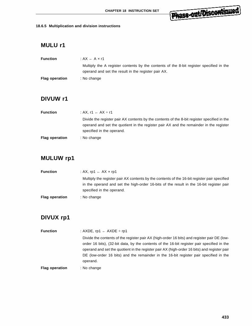
433
CHAPTER 18 INSTRUCTION SET
18.6.5 Multiplication and division instructions
MULU r1
Function : AX ← A × r1
Multiply the A register contents by the contents of the 8-bit register specified in the
operand and set the result in the register pair AX.
Flag operation : No change
DIVUW r1
Function : AX, r1 ← AX ÷ r1
Divide the register pair AX contents by the contents of the 8-bit register specified in the
operand and set the quotient in the register pair AX and the remainder in the register
specified in the operand.
Flag operation : No change
MULUW rp1
Function : AX, rp1 ← AX × rp1
Multiply the register pair AX contents by the contents of the 16-bit register pair specified
in the operand and set the high-order 16-bits of the result in the 16-bit register pair
specified in the operand.
Flag operation : No change
DIVUX rp1
Function : AXDE, rp1 ← AXDE ÷ rp1
Divide the contents of the register pair AX (high-order 16 bits) and register pair DE (low-
order 16 bits), (32-bit data, by the contents of the 16-bit register pair specified in the
operand and set the quotient in the register pair AX (high-order 16 bits) and register pair
DE (low-order 16 bits) and the remainder in the 16-bit register pair specified in the
operand.
Flag operation : No change
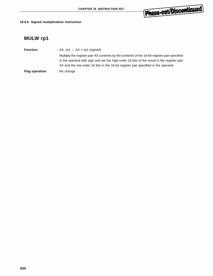
434
CHAPTER 18 INSTRUCTION SET
18.6.6 Signed multiplication instruction
MULW rp1
Function : AX, rp1 ← AX × rp1 (signed)
Multiply the register pair AX contents by the contents of the 16-bit register pair specified
in the operand with sign and set the high-order 16 bits of the result in the register pair
AX and the low-order 16 bits in the 16-bit register pair specified in the operand.
Flag operation : No change.
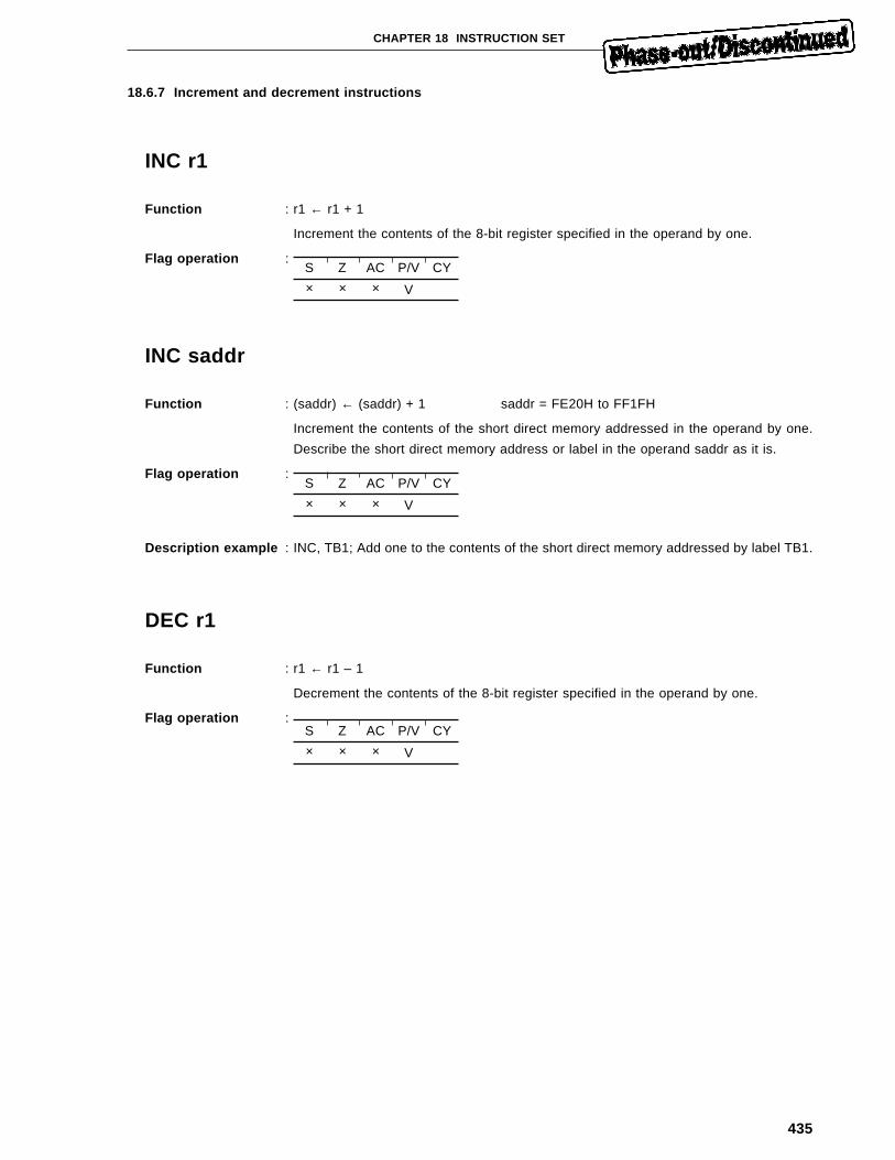
435
CHAPTER 18 INSTRUCTION SET
18.6.7 Increment and decrement instructions
INC r1
Function : r1 ← r1 + 1
Increment the contents of the 8-bit register specified in the operand by one.
Flag operation :
INC saddr
Function : (saddr) ← (saddr) + 1 saddr = FE20H to FF1FH
Increment the contents of the short direct memory addressed in the operand by one.
Describe the short direct memory address or label in the operand saddr as it is.
Flag operation :
Description example : INC, TB1; Add one to the contents of the short direct memory addressed by label TB1.
DEC r1
Function : r1 ← r1 – 1
Decrement the contents of the 8-bit register specified in the operand by one.
Flag operation :
S Z AC P/V CY
× × × V
S Z AC P/V CY
× × × V
S Z AC P/V CY
× × × V
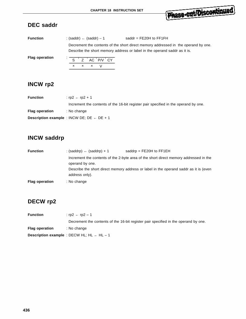
436
CHAPTER 18 INSTRUCTION SET
DEC saddr
Function : (saddr) ← (saddr) – 1 saddr = FE20H to FF1FH
Decrement the contents of the short direct memory addressed in the operand by one.
Describe the short memory address or label in the operand saddr as it is.
Flag operation :
INCW rp2
Function : rp2 ← rp2 + 1
Increment the contents of the 16-bit register pair specified in the operand by one.
Flag operation : No change
Description example : INCW DE; DE ← DE + 1
INCW saddrp
Function : (saddrp) ← (saddrp) + 1 saddrp = FE20H to FF1EH
Increment the contents of the 2-byte area of the short direct memory addressed in the
operand by one.
Describe the short direct memory address or label in the operand saddr as it is (even
address only).
Flag operation : No change
DECW rp2
Function : rp2 ← rp2 – 1
Decrement the contents of the 16-bit register pair specified in the operand by one.
Flag operation : No change
Description example : DECW HL; HL ← HL – 1
S Z AC P/V CY
× × × V

437
CHAPTER 18 INSTRUCTION SET
DECW saddrp
Function : (saddrp) ← (saddrp) – 1 saddrp = FE20H to FF1EH
Decrement the contents of the 2-byte area of the short direct memory addressed in the
operand by one.
Describe the short direct memory address or label in the operand saddrp as it is (even
address only).
Flag operation : No change
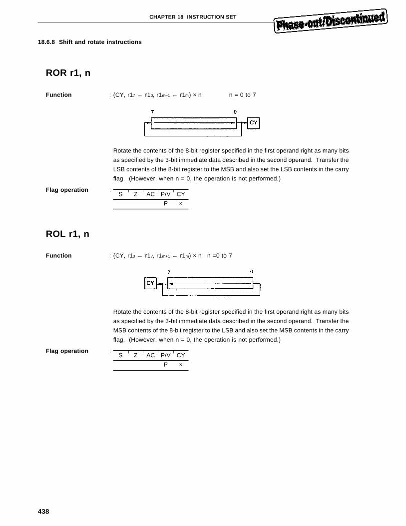
438
CHAPTER 18 INSTRUCTION SET
18.6.8 Shift and rotate instructions
ROR r1, n
Function : (CY, r17 ← r10, r1m–1 ← r1m) × n n = 0 to 7
Rotate the contents of the 8-bit register specified in the first operand right as many bits
as specified by the 3-bit immediate data described in the second operand. Transfer the
LSB contents of the 8-bit register to the MSB and also set the LSB contents in the carry
flag. (However, when n = 0, the operation is not performed.)
Flag operation :
ROL r1, n
Function : (CY, r10 ← r17, r1m+1 ← r1m) × n n =0 to 7
Rotate the contents of the 8-bit register specified in the first operand right as many bits
as specified by the 3-bit immediate data described in the second operand. Transfer the
MSB contents of the 8-bit register to the LSB and also set the MSB contents in the carry
flag. (However, when n = 0, the operation is not performed.)
Flag operation :
S Z AC P/V CY
P ×
S Z AC P/V CY
P ×
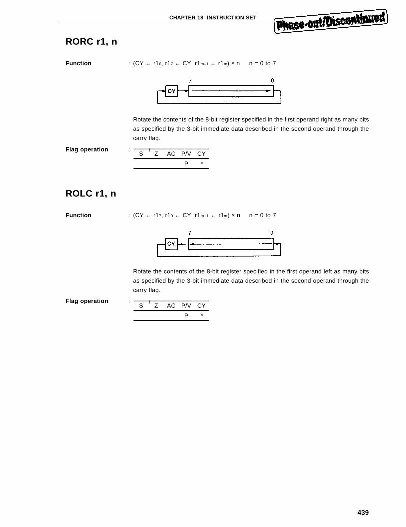
439
CHAPTER 18 INSTRUCTION SET
RORC r1, n
Function : (CY ← r10, r17 ← CY, r1m–1 ← r1m) × n n = 0 to 7
Rotate the contents of the 8-bit register specified in the first operand right as many bits
as specified by the 3-bit immediate data described in the second operand through the
carry flag.
Flag operation :
ROLC r1, n
Function : (CY ← r17, r10 ← CY, r1m+1 ← r1m) × n n = 0 to 7
Rotate the contents of the 8-bit register specified in the first operand left as many bits
as specified by the 3-bit immediate data described in the second operand through the
carry flag.
Flag operation :
S Z AC P/V CY
P ×
S Z AC P/V CY
P ×
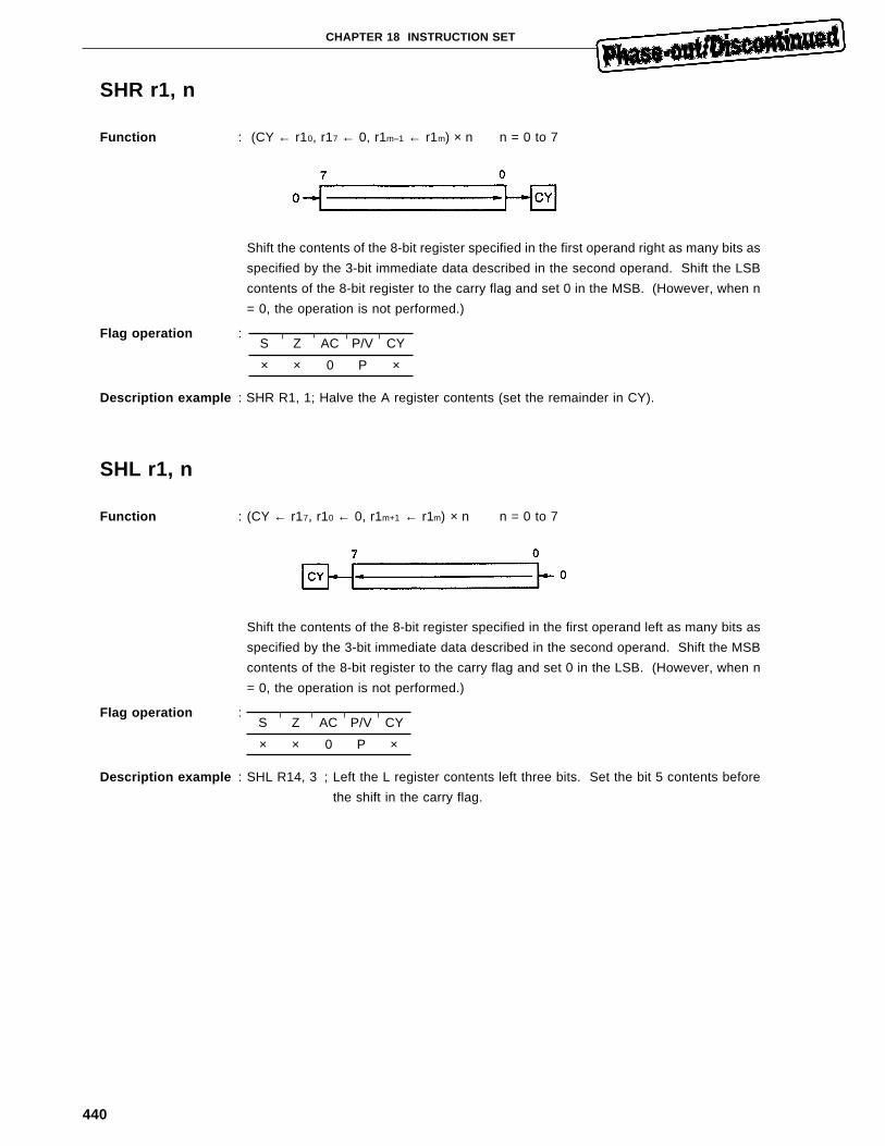
440
CHAPTER 18 INSTRUCTION SET
SHR r1, n
Function : (CY ← r10, r17 ← 0, r1m–1 ← r1m) × n n = 0 to 7
Shift the contents of the 8-bit register specified in the first operand right as many bits as
specified by the 3-bit immediate data described in the second operand. Shift the LSB
contents of the 8-bit register to the carry flag and set 0 in the MSB. (However, when n
= 0, the operation is not performed.)
Flag operation :
Description example : SHR R1, 1; Halve the A register contents (set the remainder in CY).
SHL r1, n
Function : (CY ← r17, r10 ← 0, r1m+1 ← r1m) × n n = 0 to 7
Shift the contents of the 8-bit register specified in the first operand left as many bits as
specified by the 3-bit immediate data described in the second operand. Shift the MSB
contents of the 8-bit register to the carry flag and set 0 in the LSB. (However, when n
= 0, the operation is not performed.)
Flag operation :
Description example : SHL R14, 3 ; Left the L register contents left three bits. Set the bit 5 contents before
the shift in the carry flag.
S Z AC P/V CY
× × 0 P ×
S Z AC P/V CY
× × 0 P ×
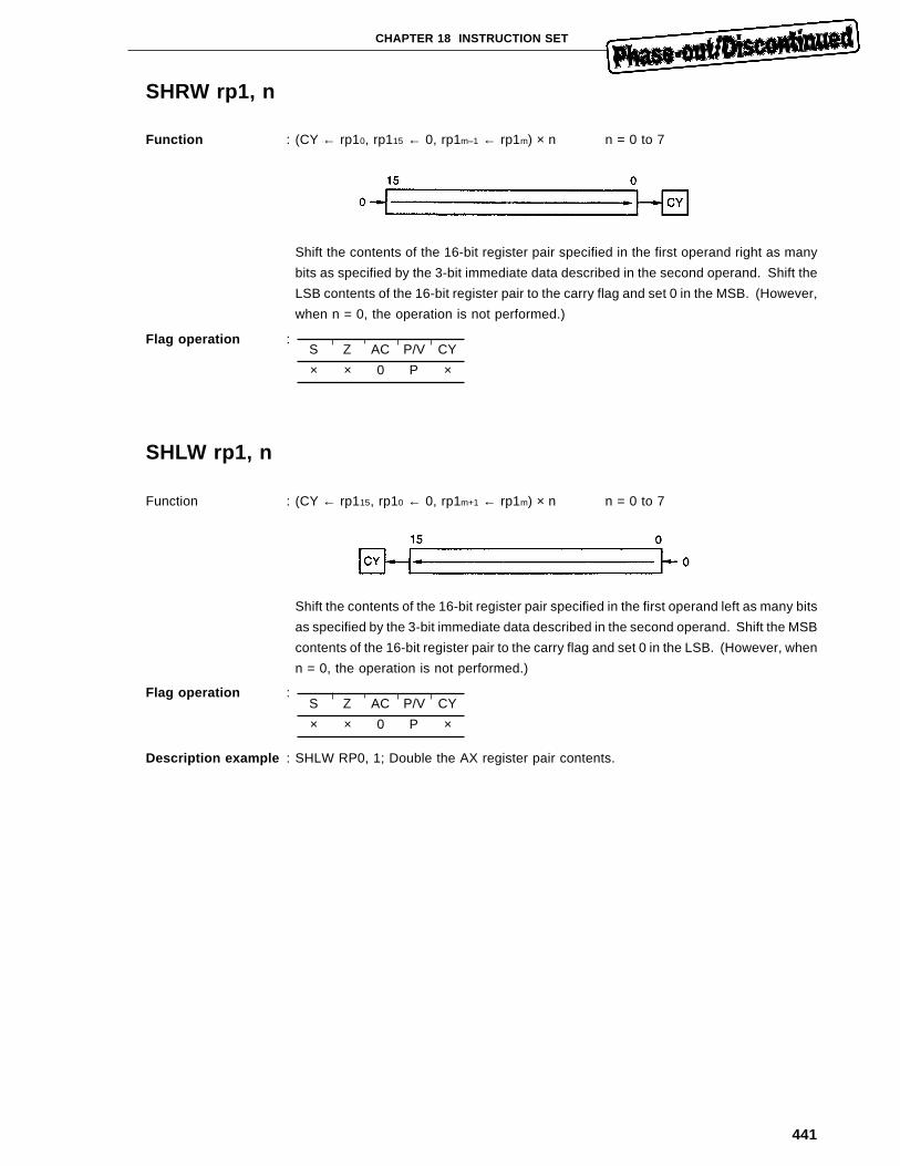
441
CHAPTER 18 INSTRUCTION SET
SHRW rp1, n
Function : (CY ← rp10, rp115 ← 0, rp1m–1 ← rp1m) × n n = 0 to 7
Shift the contents of the 16-bit register pair specified in the first operand right as many
bits as specified by the 3-bit immediate data described in the second operand. Shift the
LSB contents of the 16-bit register pair to the carry flag and set 0 in the MSB. (However,
when n = 0, the operation is not performed.)
Flag operation :
SHLW rp1, n
Function : (CY ← rp115, rp10 ← 0, rp1m+1 ← rp1m) × n n = 0 to 7
Shift the contents of the 16-bit register pair specified in the first operand left as many bits
as specified by the 3-bit immediate data described in the second operand. Shift the MSB
contents of the 16-bit register pair to the carry flag and set 0 in the LSB. (However, when
n = 0, the operation is not performed.)
Flag operation :
Description example : SHLW RP0, 1; Double the AX register pair contents.
S Z AC P/V CY
× × 0 P ×
S Z AC P/V CY
× × 0 P ×
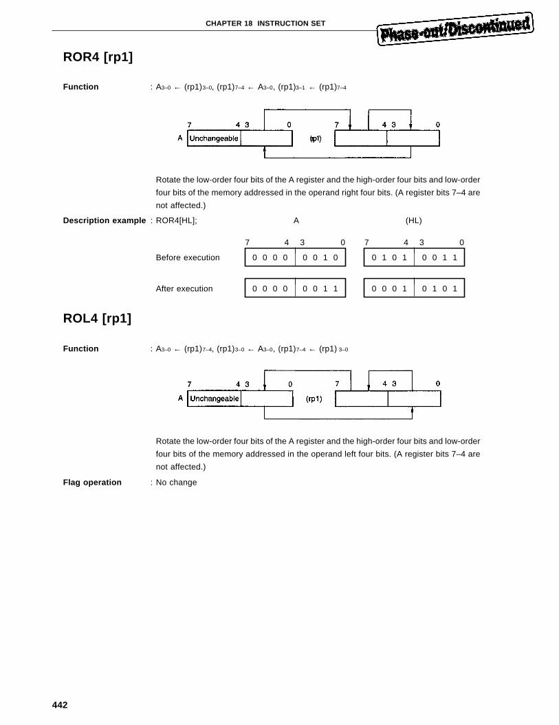
442
CHAPTER 18 INSTRUCTION SET
ROR4 [rp1]
Function : A3–0 ← (rp1)3–0, (rp1)7–4 ← A3–0, (rp1)3–1 ← (rp1)7–4
Rotate the low-order four bits of the A register and the high-order four bits and low-order
four bits of the memory addressed in the operand right four bits. (A register bits 7–4 are
not affected.)
Description example : ROR4[HL]; A (HL)
7 4 3 0 7 4 3 0
Before execution 0 0 0 0 0 0 1 0 0 1 0 1 0 0 1 1
After execution 0 0 0 0 0 0 1 1 0 0 0 1 0 1 0 1
ROL4 [rp1]
Function : A3–0 ← (rp1)7–4, (rp1)3–0 ← A3–0, (rp1)7–4 ← (rp1) 3–0
Rotate the low-order four bits of the A register and the high-order four bits and low-order
four bits of the memory addressed in the operand left four bits. (A register bits 7–4 are
not affected.)
Flag operation : No change
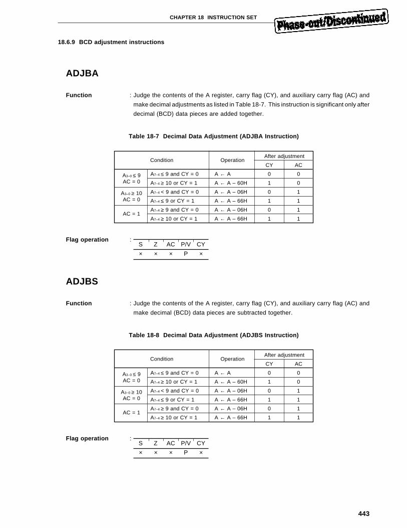
443
CHAPTER 18 INSTRUCTION SET
18.6.9 BCD adjustment instructions
ADJBA
Function : Judge the contents of the A register, carry flag (CY), and auxiliary carry flag (AC) and
make decimal adjustments as listed in Table 18-7. This instruction is significant only after
decimal (BCD) data pieces are added together.
Table 18-7 Decimal Data Adjustment (ADJBA Instruction)
Condition OperationAfter adjustment
CY AC
A3–0 ≤ 9 A7–4 ≤ 9 and CY = 0 A ← A 0 0AC = 0 A7–4 ≥ 10 or CY = 1 A ← A – 60H 1 0
A3–0 ≥ 10 A7–4 < 9 and CY = 0 A ← A – 06H 0 1AC = 0 A7–4 ≤ 9 or CY = 1 A ← A – 66H 1 1
AC = 1A7–4 ≥ 9 and CY = 0 A ← A – 06H 0 1
A7–4 ≥ 10 or CY = 1 A ← A – 66H 1 1
Flag operation :
ADJBS
Function : Judge the contents of the A register, carry flag (CY), and auxiliary carry flag (AC) and
make decimal (BCD) data pieces are subtracted together.
Table 18-8 Decimal Data Adjustment (ADJBS Instruction)
Condition OperationAfter adjustment
CY AC
A3–0 ≤ 9 A7–4 ≤ 9 and CY = 0 A ← A 0 0AC = 0 A7–4 ≥ 10 or CY = 1 A ← A – 60H 1 0
A3–0 ≥ 10 A7–4 < 9 and CY = 0 A ← A – 06H 0 1AC = 0 A7–4 ≤ 9 or CY = 1 A ← A – 66H 1 1
AC = 1A7–4 ≥ 9 and CY = 0 A ← A – 06H 0 1
A7–4 ≥ 10 or CY = 1 A ← A – 66H 1 1
Flag operation :
S Z AC P/V CY
× × × P ×
S Z AC P/V CY
× × × P ×
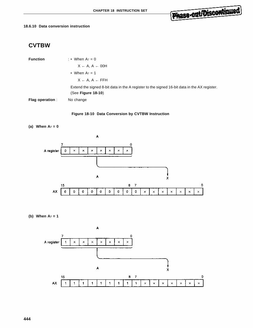
444
CHAPTER 18 INSTRUCTION SET
18.6.10 Data conversion instruction
CVTBW
Function : • When A7 = 0
X ← A, A ← 00H
• When A7 = 1
X ← A, A ← FFH
Extend the signed 8-bit data in the A register to the signed 16-bit data in the AX register.
(See Figure 18-10 )
Flag operation : No change
Figure 18-10 Data Conversion by CVTBW Instruction
(a) When A 7 = 0
(b) When A 7 = 1
445
CHAPTER 18 INSTRUCTION SET
18.6.11 Bit manipulation instructions
MOV1 CY, saddr.bit
Function : CY ← (saddr.bit) saddr = FE20H to FF1FH
bit = 0 to 7
Transfer the contents of the short direct memory bit addressed in the second operand
to the carry flag.
Describe the short direct memory bit address or label in the operand saddr.bit as it is.
Flag operation :
MOV1 CY, sfr.bit
Function : CY ← sfr.bit bit = 0 to 7
Transfer the contents of the bit of the special function register specified in the second
operand, addressed by the 3-bit immediate data to the carry flag.
Flag operation :
MOV1 CY, A.bit
Function : CY ← A.bit bit = 0 to 7
Transfer the contents of the A register bit addressed by the 3-bit immediate data in the
second operand to the carry flag.
Flag operation :
S Z AC P/V CY
×
S Z AC P/V CY
×
S Z AC P/V CY
×
446
CHAPTER 18 INSTRUCTION SET
MOV1 CY, X.bit
Function : CY ← X.bit bit = 0 to 7
Transfer the contents of the X register bit addressed by the 3-bit immediate data in the
second operand to the carry flag.
Flag operation :
MOV1 CY, PSWH.bit
Function : CY ← PSWH.bit bit = 0 to 7
Transfer the contents of the bit of the high-order eight bits of the program status word
(PSW), addressed by the 3-bit immediate data in the second operand to the carry flag.
Flag operation :
MOV1 CY, PSWL.bit
Function : CY ← PSWL.bit bit = 0 to 7
Transfer the contents of the bit of the low-order eight bits of the program status word
(PSW), addressed by the 3-bit immediate data in the second operand to the carry flag.
Flag operation :
MOV1 saddr.bit, CY
Function : (saddr.bit) ← CY saddr = FE20H to FF1FH
bit = 0 to 7
Transfer the carry flag contents to the short direct memory bit addressed in the first
operand.
Describe the short direct memory bit address or label in the operand saddr.bit as it is.
Flag operation : No change
S Z AC P/V CY
×
S Z AC P/V CY
×
S Z AC P/V CY
×
447
CHAPTER 18 INSTRUCTION SET
MOV1 sfr.bit, CY
Function : sfr.bit ← CY bit = 0 to 7
Transfer the carry flag contents to the bit of the special function register specified in the
first operand, addressed by the 3-bit immediate data.
Flag operation : No change
MOV1 A.bit, CY
Function : A.bit ← CY bit = 0 to 7
Transfer the carry flag contents to the A register bit addressed by the 3-bit immediate data
in the first operand.
Flag operation : No change
MOV1 X.bit, CY
Function : X.bit ← CY bit = 0 to 7
Transfer the carry flag contents to the X register bit addressed by the 3-bit immediate data
in the first operand.
Flag operation : No change
MOV1 PSWH.bit, CY
Function : PSWH.bit ← CY bit = 0 to 7
Transfer the carry flag contents of the bit of the high-order eight bits of the program status
word (PSW), addressed by the 3-bit immediate data in the first operand.
Flag operation : No change
MOV1 PSWL.bit, CY
Function : PSWL.bit ← CY bit = 0 to 7
Transfer the carry flag contents to the bit of the low-order eight bits of the program status
word (PSW), addressed by the 3-bit immediate data in the first operand.
Flag operation : No change
448
CHAPTER 18 INSTRUCTION SET
AND1 CY, saddr.bit
Function : CY ← CY (saddr.bit) saddr = FE20H to FF1FH
bit = 0 to 7
AND the carry flag contents with the contents of the short direct memory bit addressed
in the second operand and set the result in the carry flag. Describe the short direct
memory bit address or label in the operand saddr.bit as it is.
Flag operation :
AND1 CY, /saddr.bit
Function : CY ← CY (saddr.bit) saddr = FE20H to FF1FH
bit = 0to7
AND the carry flag contents with the inversion contents of the short direct memory bit
addressed in the second operand and set the result in the carry flag.
Describe the short direct memory bit address or label in the operand saddr.bit as it is.
Flag operation :
AND1 CY, sfr.bit
Function : CY ← CY sfr.bit bit = 0 to 7
AND the carry flag contents with the contents of the bit of the special function register
specified in the second operand, addressed by the 3-bit immediate data in the second
operand and set the result in the carry flag.
Flag operation :
S Z AC P/V CY
×
S Z AC P/V CY
×
S Z AC P/V CY
×
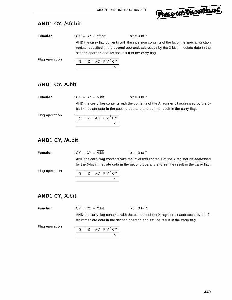
449
CHAPTER 18 INSTRUCTION SET
AND1 CY, /sfr.bit
Function : CY ← CY sfr.bit bit = 0 to 7
AND the carry flag contents with the inversion contents of the bit of the special function
register specified in the second operand, addressed by the 3-bit immediate data in the
second operand and set the result in the carry flag.
Flag operation :
AND1 CY, A.bit
Function : CY ← CY A.bit bit = 0 to 7
AND the carry flag contents with the contents of the A register bit addressed by the 3-
bit immediate data in the second operand and set the result in the carry flag.
Flag operation :
AND1 CY, /A.bit
Function : CY ← CY A.bit bit = 0 to 7
AND the carry flag contents with the inversion contents of the A register bit addressed
by the 3-bit immediate data in the second operand and set the result in the carry flag.
Flag operation :
AND1 CY, X.bit
Function : CY ← CY X.bit bit = 0 to 7
AND the carry flag contents with the contents of the X register bit addressed by the 3-
bit immediate data in the second operand and set the result in the carry flag.
Flag operation :
S Z AC P/V CY
×
S Z AC P/V CY
×
S Z AC P/V CY
×
S Z AC P/V CY
×
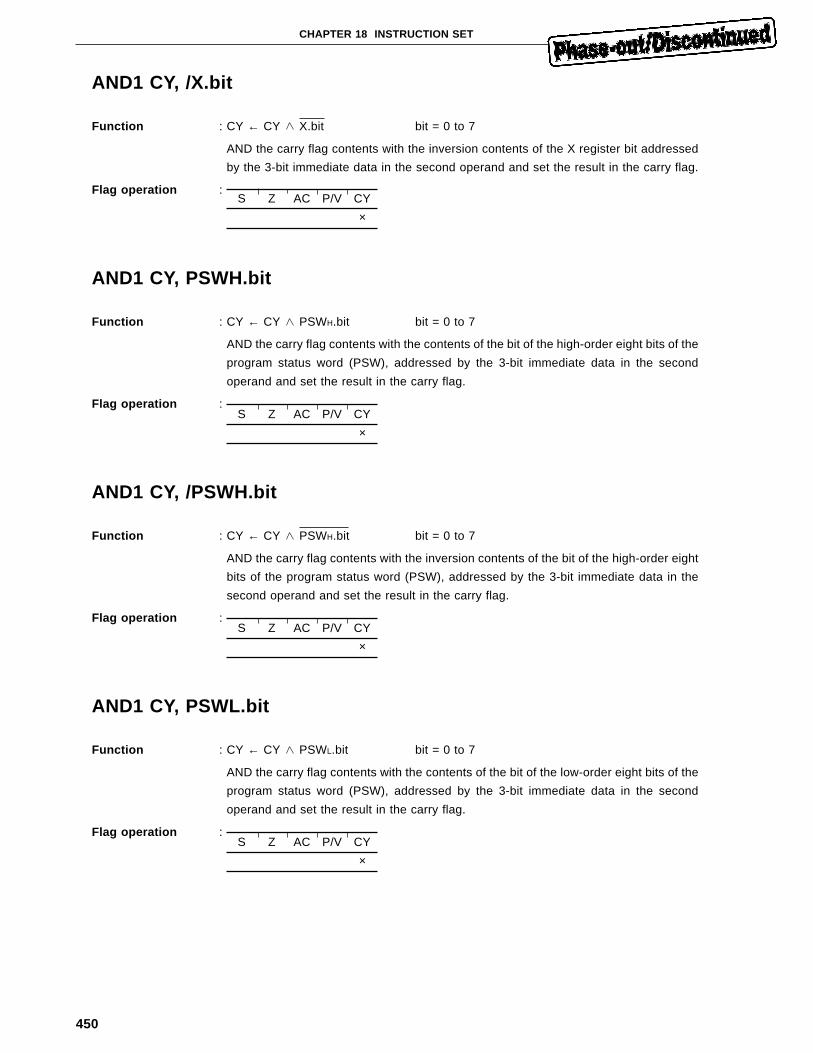
450
CHAPTER 18 INSTRUCTION SET
AND1 CY, /X.bit
Function : CY ← CY X.bit bit = 0 to 7
AND the carry flag contents with the inversion contents of the X register bit addressed
by the 3-bit immediate data in the second operand and set the result in the carry flag.
Flag operation :
AND1 CY, PSWH.bit
Function : CY ← CY PSWH.bit bit = 0 to 7
AND the carry flag contents with the contents of the bit of the high-order eight bits of the
program status word (PSW), addressed by the 3-bit immediate data in the second
operand and set the result in the carry flag.
Flag operation :
AND1 CY, /PSWH.bit
Function : CY ← CY PSWH.bit bit = 0 to 7
AND the carry flag contents with the inversion contents of the bit of the high-order eight
bits of the program status word (PSW), addressed by the 3-bit immediate data in the
second operand and set the result in the carry flag.
Flag operation :
AND1 CY, PSWL.bit
Function : CY ← CY PSWL.bit bit = 0 to 7
AND the carry flag contents with the contents of the bit of the low-order eight bits of the
program status word (PSW), addressed by the 3-bit immediate data in the second
operand and set the result in the carry flag.
Flag operation :
S Z AC P/V CY
×
S Z AC P/V CY
×
S Z AC P/V CY
×
S Z AC P/V CY
×

451
CHAPTER 18 INSTRUCTION SET
AND1 CY, /PSWL.bit
Function : CY ← CY PSWL.bit bit = 0 to 7
AND the carry flag contents with the inversion contents of the bit of the low-order eight
bits of the program status word (PSW), addressed by the 3-bit immediate data in the
second operand and set the result in the carry flag.
Flag operation :
OR1 CY, saddr.bit
Function : CY ← CY (saddr.bit) saddr = FE20H to FF1FH
bit = 0 to 7
OR the carry flag contents with the contents of the short direct memory bit addressed in
the second operand and set the result in the carry flag.
Describe the short direct memory bit address or label in the operand saddr.bit as it is.
Flag operation :
OR1 CY, /saddr.bit
Function : CY ← CY (saddr.bit) saddr = FE20H to FF1FH
bit = 0 to 7
OR the carry flag contents with the inversion contents of the short direct memory bit
addressed by the 3-bit immediate data in the second operand and the result in the carry
flag.
Describe the short direct memory bit address or label in the operand saddr.bit as it is.
Flag operation :
S Z AC P/V CY
×
S Z AC P/V CY
×
S Z AC P/V CY
×
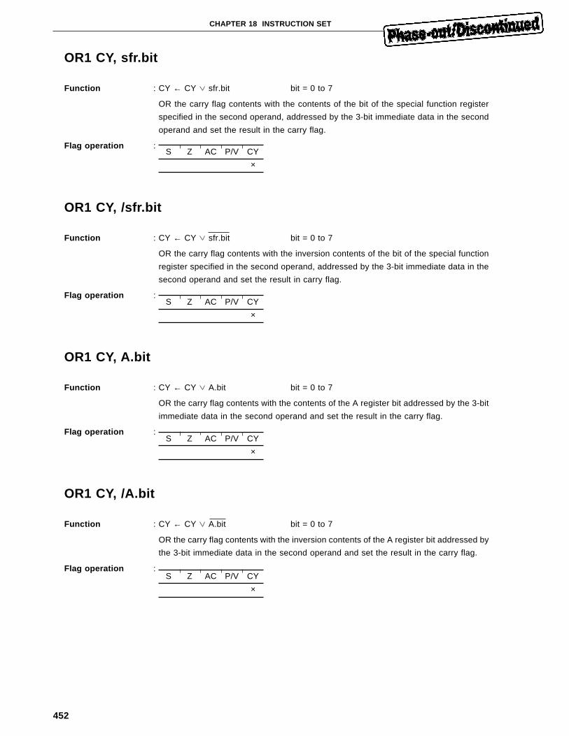
452
CHAPTER 18 INSTRUCTION SET
OR1 CY, sfr.bit
Function : CY ← CY sfr.bit bit = 0 to 7
OR the carry flag contents with the contents of the bit of the special function register
specified in the second operand, addressed by the 3-bit immediate data in the second
operand and set the result in the carry flag.
Flag operation :
OR1 CY, /sfr.bit
Function : CY ← CY sfr.bit bit = 0 to 7
OR the carry flag contents with the inversion contents of the bit of the special function
register specified in the second operand, addressed by the 3-bit immediate data in the
second operand and set the result in carry flag.
Flag operation :
OR1 CY, A.bit
Function : CY ← CY A.bit bit = 0 to 7
OR the carry flag contents with the contents of the A register bit addressed by the 3-bit
immediate data in the second operand and set the result in the carry flag.
Flag operation :
OR1 CY, /A.bit
Function : CY ← CY A.bit bit = 0 to 7
OR the carry flag contents with the inversion contents of the A register bit addressed by
the 3-bit immediate data in the second operand and set the result in the carry flag.
Flag operation :
S Z AC P/V CY
×
S Z AC P/V CY
×
S Z AC P/V CY
×
S Z AC P/V CY
×
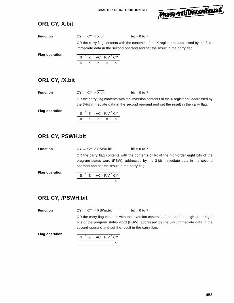
453
CHAPTER 18 INSTRUCTION SET
OR1 CY, X.bit
Function : CY ← CY X.bit bit = 0 to 7
OR the carry flag contents with the contents of the X register bit addressed by the 3-bit
immediate data in the second operand and set the result in the carry flag.
Flag operation :
OR1 CY, /X.bit
Function : CY ← CY X.bit bit = 0 to 7
OR the carry flag contents with the inversion contents of the X register bit addressed by
the 3-bit immediate data in the second operand and set the result in the carry flag.
Flag operation :
OR1 CY, PSWH.bit
Function : CY ← CY PSWH.bit bit = 0 to 7
OR the carry flag contents with the contents of bit of the high-order eight bits of the
program status word (PSW), addressed by the 3-bit immediate data in the second
operand and set the result in the carry flag.
Flag operation :
OR1 CY, /PSWH.bit
Function : CY ← CY PSWH.bit bit = 0 to 7
OR the carry flag contents with the inversion contents of the bit of the high-order eight
bits of the program status word (PSW), addressed by the 3-bit immediate data in the
second operand and set the result in the carry flag.
Flag operation :
S Z AC P/V CY
× × × × ×
S Z AC P/V CY
× × × × ×
S Z AC P/V CY
×
S Z AC P/V CY
×
454
CHAPTER 18 INSTRUCTION SET
OR1 CY, PSWL.bit
Function : CY ← CY PSWL.bit bit = 0 to 7
OR the carry flag contents with the contents of the bit of the low-order eight bits of the
program status word (PSW), addressed by the 3-bit immediate data in the second
operand and set the result in the carry flag.
Flag operation :
OR1 CY, /PSWL.bit
Function : CY ← CY PSWL.bit bit = 0 to 7
OR the carry flag contents with the inversion contents of the bit of the low-order eight bit
of the program status word (PSW), addressed by the 3-bit immediate data in the second
operand and set the result in the carry flag.
Flag operation :
XOR1 CY, saddr.bit
Function : CY ← CY (saddr.bit) saddr = FE20H to FF1FH
bit = 0 to 7
Exclusive-OR the carry flag contents with the contents of the short direct memory bit
addressed in the second operand and set the result in the carry flag.
Describe the short direct memory bit address or label in the operand saddr.bit as it is.
Flag operation :
XOR1 CY, sfr.bit
Function : CY ← CY sfr.bit bit = 0 to 7
Exclusive-OR the carry flag contents with the contents of the bit of the special function
register specified in the second operand, addressed by the 3-bit immediate data in the
second operand and set the result in the carry flag.
Flag operation :
S Z AC P/V CY
×
S Z AC P/V CY
×
S Z AC P/V CY
×
S Z AC P/V CY
×
455
CHAPTER 18 INSTRUCTION SET
XOR1 CY, A.bit
Function : CY ← CY A.bit bit = 0 to 7
Exclusive-OR the carry flag contents with the contents of the A register bit addressed by
the 3-bit immediate data in the second operand and set the result in the carry flag.
Flag operation :
XOR1 CY, X.bit
Function : CY ← CY X.bit bit = 0 to 7
Exclusive-OR the carry flag contents with the contents of the X register bit addressed by
the 3-bit immediate data in the second operand and set the result in the carry flag.
Flag operation :
XOR1 CY, PSWH.bit
Function : CY ← CY PSWH.bit bit = 0 to 7
Exclusive-OR the carry flag contents with the contents of the bit of the high-order eight
bits of the program status word (PSW), addressed by the 3-bit immediate data in the
second operand and set the result in the carry flag.
Flag operation :
XOR1 CY, PSWL.bit
Function : CY ← CY PSWL.bit bit = 0 to 7
Exclusive-OR the carry flag contents with the contents of the bit of the low-order eight
bits of the program status word (PSW), addressed by the 3-bit immediate data in second
operand and set the result in the carry flag.
Flag operation :
S Z AC P/V CY
×
S Z AC P/V CY
×
S Z AC P/V CY
×
S Z AC P/V CY
×
456
CHAPTER 18 INSTRUCTION SET
SET1 saddr.bit
Function : (saddr.bit) ← 1 saddr = FE20H to FF1FH
bit = 0 to 7
Set the short direct memory bit addressed in the operand to 1.
Describe the short direct memory bit address or label in the operand saddr.bit as it is.
Flag operation : No change
SET1 sfr.bit
Function : sfr.bit ← 1 bit= 0 to 7
Set the bit of the special function register specified in the operand, addressed by the 3-
bit immediate data in the operand to 1.
Flag operation : No change
SET1 A.bit
Function : A.bit ← 1 bit= 0 to 7
Set the A register bit addressed by the 3-bit immediate data in the operand to 1.
Flag operation : No change
SET1 X.bit
Function : X.bit ← 1 bit = 0 to 7
Set the X register bit addressed by the 3-bit immediate data in the operand to 1.
Flag operation : No change
457
CHAPTER 18 INSTRUCTION SET
SET1 PSWH.bit
Function : PSWH.bit ← 1 bit = 0 to 7
Set the bit of the high-order bits of the program status word (PSW), addressed by the 3-
bit immediate data in the operand to 1.
Flag operation : No change
SET1 PSWL.bit
Function : PSWL.bit ← 1 bit= 0 to 7
Set the bit of the low-order eight bits of the program status word (PSW), addressed by
the 3-bit immediate data in the operand to 1.
Flag operation : No change
SET1 CY
Function : CY ← 1
Set the carry flag to 1
Flag operation :
CLR1 saddr.bit
Function : (saddr.bit) ← 0 saddr = FE20H to FF1FH
bit = 0 to 7
Reset the short direct memory bit addressed in the operand to 0.
Describe the short direct memory bit address or label in the operand sadddr.bit as it is.
Flag operation : No change
CLR1 sfr.bit
Function : sfr.bit ← 0 bit = 0 to 7
Reset the bit of the special function register specified in the operand, addressed by the
3-bit immediate data in the operand to 0.
Flag operation : No change
S Z AC P/V CY
1
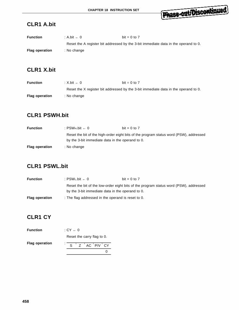
458
CHAPTER 18 INSTRUCTION SET
CLR1 A.bit
Function : A.bit ← 0 bit = 0 to 7
Reset the A register bit addressed by the 3-bit immediate data in the operand to 0.
Flag operation : No change
CLR1 X.bit
Function : X.bit ← 0 bit = 0 to 7
Reset the X register bit addressed by the 3-bit immediate data in the operand to 0.
Flag operation : No change
CLR1 PSWH.bit
Function : PSWH.bit ← 0 bit = 0 to 7
Reset the bit of the high-order eight bits of the program status word (PSW), addressed
by the 3-bit immediate data in the operand to 0.
Flag operation : No change
CLR1 PSWL.bit
Function : PSWL.bit ← 0 bit = 0 to 7
Reset the bit of the low-order eight bits of the program status word (PSW), addressed
by the 3-bit immediate data in the operand to 0.
Flag operation : The flag addressed in the operand is reset to 0.
CLR1 CY
Function : CY ← 0
Reset the carry flag to 0.
Flag operation :S Z AC P/V CY
0
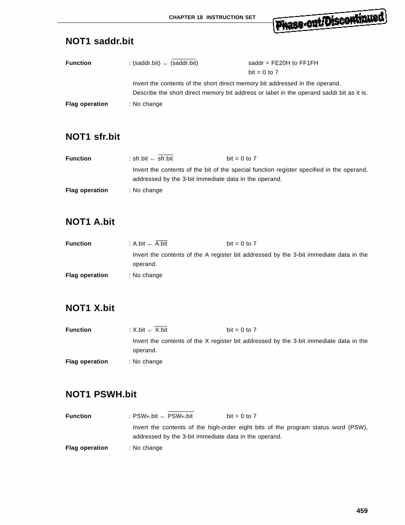
459
CHAPTER 18 INSTRUCTION SET
NOT1 saddr.bit
Function : (saddr.bit) ← (saddr.bit) saddr = FE20H to FF1FH
bit = 0 to 7
Invert the contents of the short direct memory bit addressed in the operand.
Describe the short direct memory bit address or label in the operand saddr.bit as it is.
Flag operation : No change
NOT1 sfr.bit
Function : sfr.bit ← sfr.bit bit = 0 to 7
Invert the contents of the bit of the special function register specified in the operand,
addressed by the 3-bit immediate data in the operand.
Flag operation : No change
NOT1 A.bit
Function : A.bit ← A.bit bit = 0 to 7
Invert the contents of the A register bit addressed by the 3-bit immediate data in the
operand.
Flag operation : No change
NOT1 X.bit
Function : X.bit ← X.bit bit = 0 to 7
Invert the contents of the X register bit addressed by the 3-bit immediate data in the
operand.
Flag operation : No change
NOT1 PSWH.bit
Function : PSWH.bit ← PSWH.bit bit = 0 to 7
Invert the contents of the high-order eight bits of the program status word (PSW),
addressed by the 3-bit immediate data in the operand.
Flag operation : No change
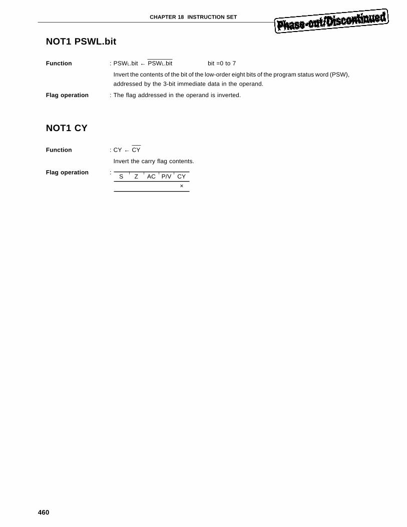
460
CHAPTER 18 INSTRUCTION SET
NOT1 PSWL.bit
Function : PSWL.bit ← PSWL.bit bit =0 to 7
Invert the contents of the bit of the low-order eight bits of the program status word (PSW),
addressed by the 3-bit immediate data in the operand.
Flag operation : The flag addressed in the operand is inverted.
NOT1 CY
Function : CY ← CY
Invert the carry flag contents.
Flag operation :S Z AC P/V CY
×
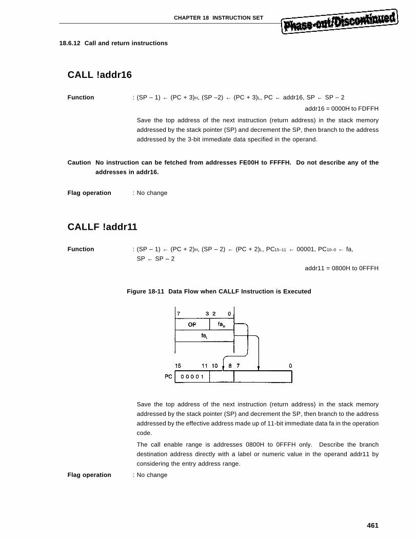
461
CHAPTER 18 INSTRUCTION SET
18.6.12 Call and return instructions
CALL !addr16
Function : (SP – 1) ← (PC + 3)H, (SP –2) ← (PC + 3)L, PC ← addr16, SP ← SP – 2
addr16 = 0000H to FDFFH
Save the top address of the next instruction (return address) in the stack memory
addressed by the stack pointer (SP) and decrement the SP, then branch to the address
addressed by the 3-bit immediate data specified in the operand.
Caution No instruction can be fetched from addresses FE00H to FFFFH. Do not describe any of the
addresses in addr16.
Flag operation : No change
CALLF !addr11
Function : (SP – 1) ← (PC + 2)H, (SP – 2) ← (PC + 2)L, PC15–11 ← 00001, PC10–0 ← fa,
SP ← SP – 2
addr11 = 0800H to 0FFFH
Figure 18-11 Data Flow when CALLF Instruction is Executed
Save the top address of the next instruction (return address) in the stack memory
addressed by the stack pointer (SP) and decrement the SP, then branch to the address
addressed by the effective address made up of 11-bit immediate data fa in the operation
code.
The call enable range is addresses 0800H to 0FFFH only. Describe the branch
destination address directly with a label or numeric value in the operand addr11 by
considering the entry address range.
Flag operation : No change
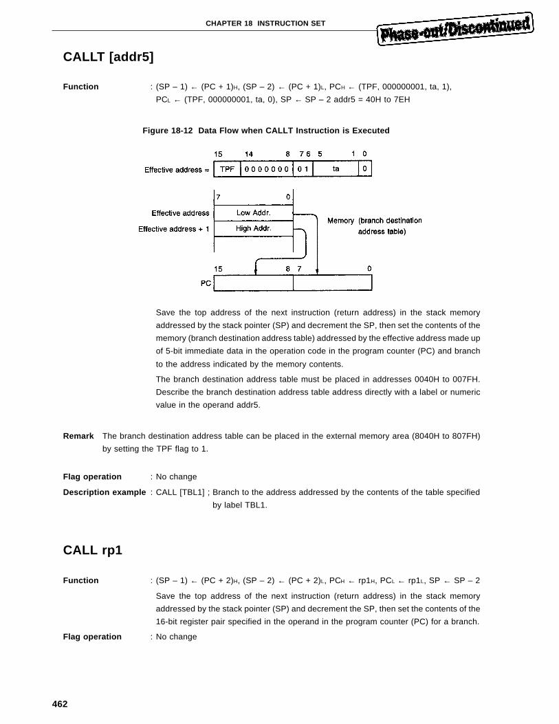
462
CHAPTER 18 INSTRUCTION SET
CALLT [addr5]
Function : (SP – 1) ← (PC + 1)H, (SP – 2) ← (PC + 1)L, PCH ← (TPF, 000000001, ta, 1),
PCL ← (TPF, 000000001, ta, 0), SP ← SP – 2 addr5 = 40H to 7EH
Figure 18-12 Data Flow when CALLT Instruction is Executed
Save the top address of the next instruction (return address) in the stack memory
addressed by the stack pointer (SP) and decrement the SP, then set the contents of the
memory (branch destination address table) addressed by the effective address made up
of 5-bit immediate data in the operation code in the program counter (PC) and branch
to the address indicated by the memory contents.
The branch destination address table must be placed in addresses 0040H to 007FH.
Describe the branch destination address table address directly with a label or numeric
value in the operand addr5.
Remark The branch destination address table can be placed in the external memory area (8040H to 807FH)
by setting the TPF flag to 1.
Flag operation : No change
Description example : CALL [TBL1] ; Branch to the address addressed by the contents of the table specified
by label TBL1.
CALL rp1
Function : (SP – 1) ← (PC + 2)H, (SP – 2) ← (PC + 2)L, PCH ← rp1H, PCL ← rp1L, SP ← SP – 2
Save the top address of the next instruction (return address) in the stack memory
addressed by the stack pointer (SP) and decrement the SP, then set the contents of the
16-bit register pair specified in the operand in the program counter (PC) for a branch.
Flag operation : No change
463
CHAPTER 18 INSTRUCTION SET
CALL [rp1]
Function : (SP – 1) ← (PC + 2)H, (SP – 2) ← (PC + 2)L, PCH ← (rp1 + 1), PCL ← (rp1),
SP ← SP – 2
Save the top address of the next instruction (return address) in the stack memory
addressed by the stack pointer (SP) and decrement the SP, then set the contents of the
2-bit area of the memory addressed by the contents of the 16-bit register pair specified
in the operand in the program counter (PC) for a branch.
Flag operation : No change
BRK
Function : (SP – 1) ← PSWH, (SP – 2) ← PSWL, (SP – 3) ← (PC + 1)H,
(SP – 4) ← (PC + 1)L, PCL ← (003EH), PCH ← (003FH)
SP ← SP – 4, IE ← 0
Save the top address of the next instruction (return address) and the program status word
(PSW) in the stack memory addressed by the stack pointer and decrement the SP, then
set the BRK instruction branch destination address table (003EH and 003FH) contents
in the program counter (PC) for branch. Reset the IE flag to 0 to disable the subsequent
maskable interrupt requests. The BRK instruction is acknowledged even in the DI state
(IE = 0).
Flag operation : No change
RET
Function : PCL ← (SP), PCH ← (SP + 1), SP ← SP + 2
Restore the contents of the stack memory addressed by the stack pointer (SP) to the
program counter, then increment the SP contents.
Flag operation : No change
464
CHAPTER 18 INSTRUCTION SET
RETB
Function : PCL ← (SP), PCH ← (SP + 1), PSWL ← (SP + 2), PSWH ← (SP + 3), SP ← SP + 4
Restore the contents of the stack memory addressed by the stack pointer (SP) to the
program counter (PS) and program status word (PSW), then increment the SP contents.
The RETB instruction is used to return from BRK instruction or operation code trap.
Flag operation :
Caution To return from the interrupt service routine accompanying BRK instruction or operation code
trap, be sure to use the RETB instruction. If the RETI instruction is used, the interrupt control
circuit does not operate normally.
RETI
Function : PCL ← (SP), PCH ← (SP + 1), PSWL ← (SP + 2), PSWH ← (SP + 3), SP ← SP + 4
Restore the contents of the stack memory addressed by the stack pointer (SP) to the
program counter (PC) and program status word (PSW), then increment the SP contents.
The RETI instruction is used to return from interrupt service routine.
Flag operation :
Caution To return from the interrupt service routine accompanying BRK instruction or operation code
trap, do not use the RETI instruction.
S Z AC P/V CY
R R R R R
S Z AC P/V CY
R R R R R
465
CHAPTER 18 INSTRUCTION SET
18.6.13 Stack handling instruction
PUSH sfrp
Function : (SP – 1) ← sfrH, (SP – 2) ← sfrL, SP ← SP – 2
Save the contents of the special function register (register that can be handled in 16-bit
units) in the stack memory addressed by the stack pointer (SP), then decrement the SP.
Flag operation : No change
PUSH post
Function : {(SP – 1) ← postH, (SP – 2) ← postL, SP ← SP – 2} × n
(n is the number of register pairs described as post)
Save the contents of the 16-bit register pair specified in the operand in the stack memory,
then decrement the SP.
More than one register pair name can be described in the operand post.
The save operation is performed starting at the register pair assigned to bit 7 of the 8-
bit immediate data in the second byte (Post Byte). The upper half of the register pair is
saved in the stack addressed by (SP – 2n + 1) and the lower half is saved in the stack
addressed by (SP – 2n).
Flag operation : No change
PUSH PSW
Function : (SP – 1) ← PSWH, (SP – 2) ← PSWL, SP ← SP – 2
Save the program status word (PSW) contents in the stack memory addressed by the
stack pointer (SP) and decrement the SP.
Flag operation : No change
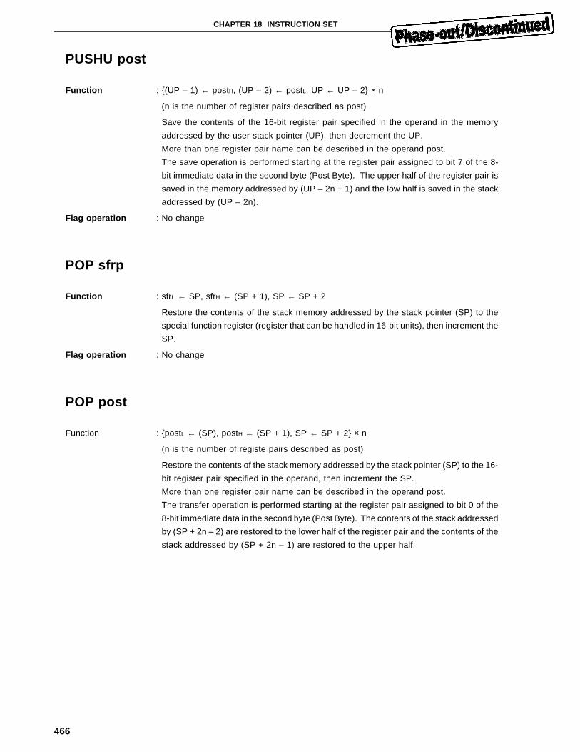
466
CHAPTER 18 INSTRUCTION SET
PUSHU post
Function : {(UP – 1) ← postH, (UP – 2) ← postL, UP ← UP – 2} × n
(n is the number of register pairs described as post)
Save the contents of the 16-bit register pair specified in the operand in the memory
addressed by the user stack pointer (UP), then decrement the UP.
More than one register pair name can be described in the operand post.
The save operation is performed starting at the register pair assigned to bit 7 of the 8-
bit immediate data in the second byte (Post Byte). The upper half of the register pair is
saved in the memory addressed by (UP – 2n + 1) and the low half is saved in the stack
addressed by (UP – 2n).
Flag operation : No change
POP sfrp
Function : sfrL ← SP, sfrH ← (SP + 1), SP ← SP + 2
Restore the contents of the stack memory addressed by the stack pointer (SP) to the
special function register (register that can be handled in 16-bit units), then increment the
SP.
Flag operation : No change
POP post
Function : {postL ← (SP), postH ← (SP + 1), SP ← SP + 2} × n
(n is the number of registe pairs described as post)
Restore the contents of the stack memory addressed by the stack pointer (SP) to the 16-
bit register pair specified in the operand, then increment the SP.
More than one register pair name can be described in the operand post.
The transfer operation is performed starting at the register pair assigned to bit 0 of the
8-bit immediate data in the second byte (Post Byte). The contents of the stack addressed
by (SP + 2n – 2) are restored to the lower half of the register pair and the contents of the
stack addressed by (SP + 2n – 1) are restored to the upper half.
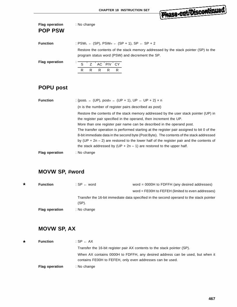
467
CHAPTER 18 INSTRUCTION SET
Flag operation : No change
POP PSW
Function : PSWL ← (SP), PSWH ← (SP + 1), SP ← SP + 2
Restore the contents of the stack memory addressed by the stack pointer (SP) to the
program status word (PSW) and decrement the SP.
Flag operation :
POPU post
Function : {postL ← (UP), postH ← (UP + 1), UP ← UP + 2} × n
(n is the number of register pairs described as post)
Restore the contents of the stack memory addressed by the user stack pointer (UP) in
the register pair specified in the operand, then increment the UP.
More than one register pair name can be described in the operand post.
The transfer operation is performed starting at the register pair assigned to bit 0 of the
8-bit immediate data in the second byte (Post Byte). The contents of the stack addressed
by (UP + 2n – 2) are restored to the lower half of the register pair and the contents of
the stack addressed by (UP + 2n – 1) are restored to the upper half.
Flag operation : No change
MOVW SP, #word
Function : SP ← word word = 0000H to FDFFH (any desired addresses)
word = FE00H to FEFEH (limited to even addresses)
Transfer the 16-bit immediate data specified in the second operand to the stack pointer
(SP).
Flag operation : No change
MOVW SP, AX
Function : SP ← AX
Transfer the 16-bit register pair AX contents to the stack pointer (SP).
When AX contains 0000H to FDFFH, any desired address can be used, but when it
contains FE00H to FEFEH, only even addresses can be used.
Flag operation : No change
S Z AC P/V CY
R R R R R
★
★
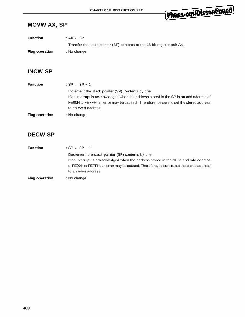
468
CHAPTER 18 INSTRUCTION SET
MOVW AX, SP
Function : AX ← SP
Transfer the stack pointer (SP) contents to the 16-bit register pair AX.
Flag operation : No change
INCW SP
Function : SP ← SP + 1
Increment the stack pointer (SP) Contents by one.
If an interrupt is acknowledged when the address stored in the SP is an odd address of
FE00H to FEFFH, an error may be caused. Therefore, be sure to set the stored address
to an even address.
Flag operation : No change
DECW SP
Function : SP ← SP – 1
Decrement the stack pointer (SP) contents by one.
If an interrupt is acknowledged when the address stored in the SP is and odd address
of FE00H to FEFFH, an error may be caused. Therefore, be sure to set the stored address
to an even address.
Flag operation : No change
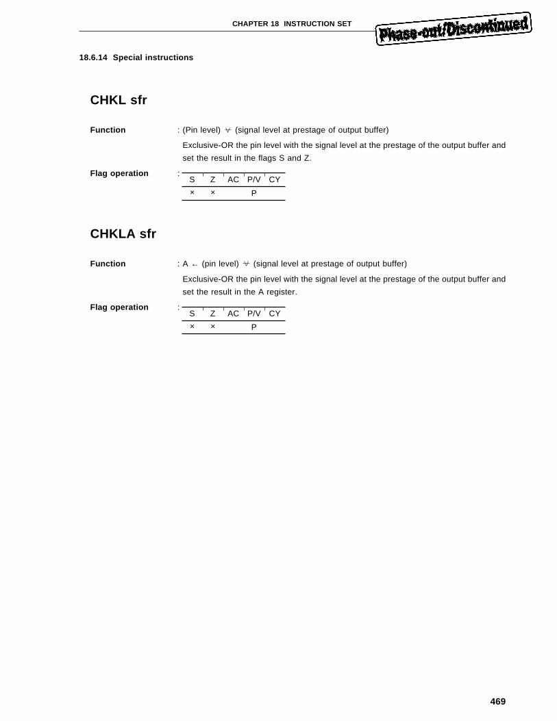
469
CHAPTER 18 INSTRUCTION SET
18.6.14 Special instructions
CHKL sfr
Function : (Pin level) (signal level at prestage of output buffer)
Exclusive-OR the pin level with the signal level at the prestage of the output buffer and
set the result in the flags S and Z.
Flag operation :
CHKLA sfr
Function : A ← (pin level) (signal level at prestage of output buffer)
Exclusive-OR the pin level with the signal level at the prestage of the output buffer and
set the result in the A register.
Flag operation :
S Z AC P/V CY
× × P
S Z AC P/V CY
× × P
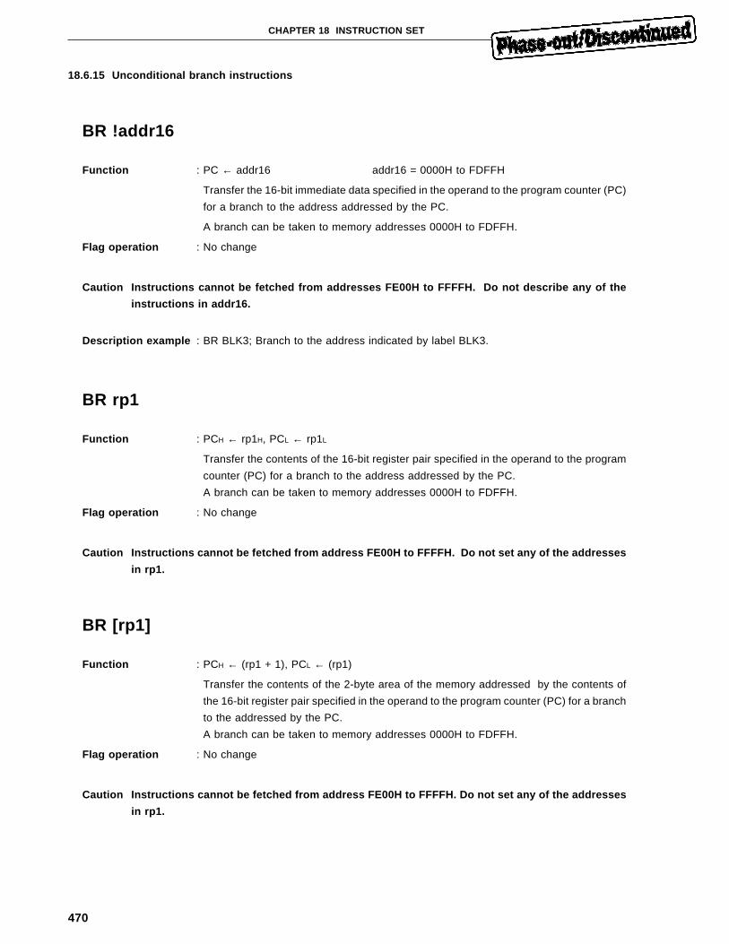
470
CHAPTER 18 INSTRUCTION SET
18.6.15 Unconditional branch instructions
BR !addr16
Function : PC ← addr16 addr16 = 0000H to FDFFH
Transfer the 16-bit immediate data specified in the operand to the program counter (PC)
for a branch to the address addressed by the PC.
A branch can be taken to memory addresses 0000H to FDFFH.
Flag operation : No change
Caution Instructions cannot be fetched from addresses FE00H to FFFFH. Do not describe any of the
instructions in addr16.
Description example : BR BLK3; Branch to the address indicated by label BLK3.
BR rp1
Function : PCH ← rp1H, PCL ← rp1L
Transfer the contents of the 16-bit register pair specified in the operand to the program
counter (PC) for a branch to the address addressed by the PC.
A branch can be taken to memory addresses 0000H to FDFFH.
Flag operation : No change
Caution Instructions cannot be fetched from address FE00H to FFFFH. Do not set any of the addresses
in rp1.
BR [rp1]
Function : PCH ← (rp1 + 1), PCL ← (rp1)
Transfer the contents of the 2-byte area of the memory addressed by the contents of
the 16-bit register pair specified in the operand to the program counter (PC) for a branch
to the addressed by the PC.
A branch can be taken to memory addresses 0000H to FDFFH.
Flag operation : No change
Caution Instructions cannot be fetched from address FE00H to FFFFH. Do not set any of the addresses
in rp1.
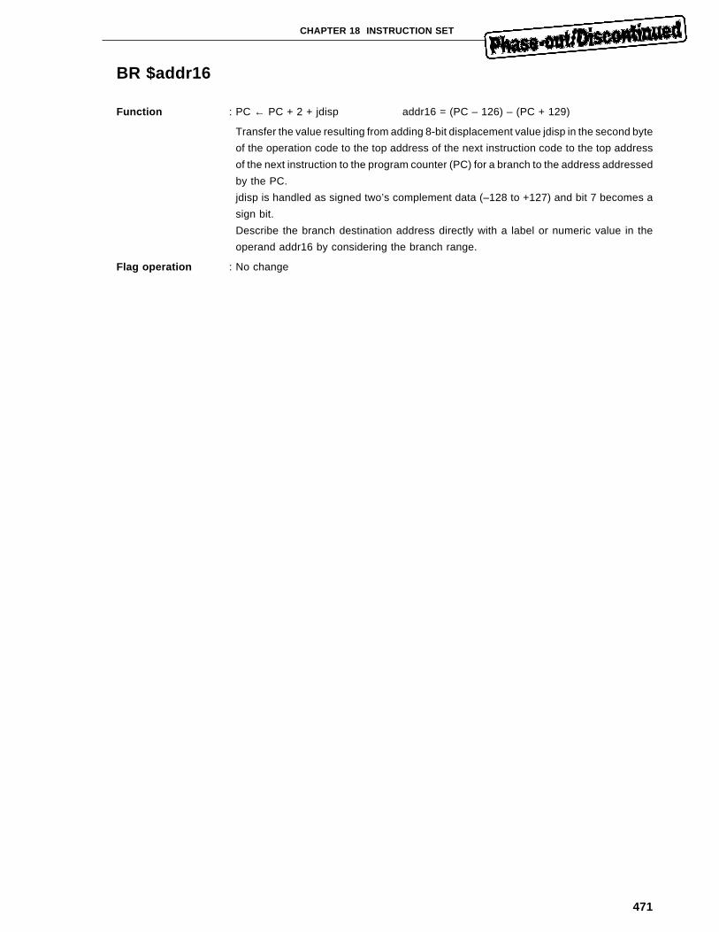
471
CHAPTER 18 INSTRUCTION SET
BR $addr16
Function : PC ← PC + 2 + jdisp addr16 = (PC – 126) – (PC + 129)
Transfer the value resulting from adding 8-bit displacement value jdisp in the second byte
of the operation code to the top address of the next instruction code to the top address
of the next instruction to the program counter (PC) for a branch to the address addressed
by the PC.
jdisp is handled as signed two’s complement data (–128 to +127) and bit 7 becomes a
sign bit.
Describe the branch destination address directly with a label or numeric value in the
operand addr16 by considering the branch range.
Flag operation : No change
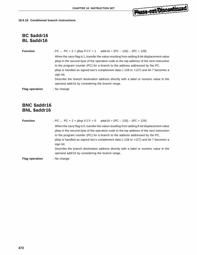
472
CHAPTER 18 INSTRUCTION SET
18.6.16 Conditional branch instructions
BC $addr16BL $addr16
Function : PC ← PC + 2 + jdisp if CY = 1 addr16 = (PC – 126) – (PC + 129)
When the carry flag is 1, transfer the value resulting from adding 8-bit displacement value
jdisp in the second byte of the operation code to the top address of the next instruction
to the program counter (PC) for a branch to the address addressed by the PC.
jdisp is handled as signed two’s complement data (–128 to +127) and bit 7 becomes a
sign bit.
Describe the branch destination address directly with a label or numeric value in the
operand addr16 by considering the branch range.
Flag operation : No change
BNC $addr16BNL $addr16
Function : PC ← PC + 2 + jdisp if CY = 0 addr16 = (PC – 126) – (PC + 129)
When the carry flag is 0, transfer the value resulting from adding 8-bit displacement value
jdisp in the second byte of the operation code to the top address of the next instruction
to the program counter (PC) for a branch to the address addressed by the PC.
jdisp is handled as signed two’s complement data (–128 to +127) and bit 7 becomes a
sign bit.
Describe the branch destination address directly with a label or numeric value in the
operand addr16 by considering the branch range.
Flag operation : No change
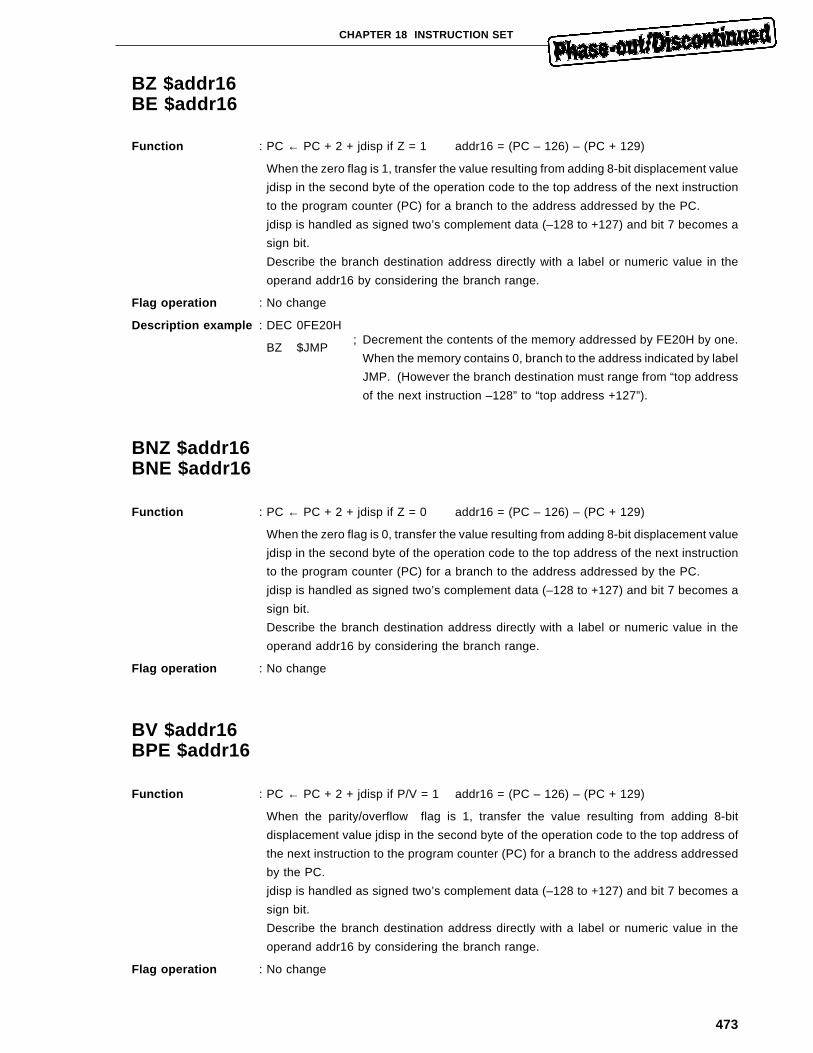
473
CHAPTER 18 INSTRUCTION SET
BZ $addr16BE $addr16
Function : PC ← PC + 2 + jdisp if Z = 1 addr16 = (PC – 126) – (PC + 129)
When the zero flag is 1, transfer the value resulting from adding 8-bit displacement value
jdisp in the second byte of the operation code to the top address of the next instruction
to the program counter (PC) for a branch to the address addressed by the PC.
jdisp is handled as signed two’s complement data (–128 to +127) and bit 7 becomes a
sign bit.
Describe the branch destination address directly with a label or numeric value in the
operand addr16 by considering the branch range.
Flag operation : No change
Description example : DEC 0FE20H
BZ $JMP; Decrement the contents of the memory addressed by FE20H by one.
When the memory contains 0, branch to the address indicated by label
JMP. (However the branch destination must range from “top address
of the next instruction –128” to “top address +127”).
BNZ $addr16BNE $addr16
Function : PC ← PC + 2 + jdisp if Z = 0 addr16 = (PC – 126) – (PC + 129)
When the zero flag is 0, transfer the value resulting from adding 8-bit displacement value
jdisp in the second byte of the operation code to the top address of the next instruction
to the program counter (PC) for a branch to the address addressed by the PC.
jdisp is handled as signed two’s complement data (–128 to +127) and bit 7 becomes a
sign bit.
Describe the branch destination address directly with a label or numeric value in the
operand addr16 by considering the branch range.
Flag operation : No change
BV $addr16BPE $addr16
Function : PC ← PC + 2 + jdisp if P/V = 1 addr16 = (PC – 126) – (PC + 129)
When the parity/overflow flag is 1, transfer the value resulting from adding 8-bit
displacement value jdisp in the second byte of the operation code to the top address of
the next instruction to the program counter (PC) for a branch to the address addressed
by the PC.
jdisp is handled as signed two’s complement data (–128 to +127) and bit 7 becomes a
sign bit.
Describe the branch destination address directly with a label or numeric value in the
operand addr16 by considering the branch range.
Flag operation : No change
474
CHAPTER 18 INSTRUCTION SET
BNV $addr16BPO $addr16
Function : PC ← PC + 2 + jdisp if P/V = 0 addr16 = (PC – 126) – (PC + 129)
When the parity/overflow flag is 0, transfer the value resulting from adding 8-bit displace-
ment value jdisp in the second byte of the operation code to the top address of the next
instruction to the program counter (PC) for a branch to the address addressed by the PC.
jdisp is handled as signed two’s complement data (–128 to +127) and bit 7 becomes a
sign bit.
Describe the branch destination address directly with a label or numeric value in the
operand addr16 by considering the branch range.
Flag operation : No change
BN $addr16
Function : PC ← PC + 2 + jdisp if S = 1 addr16 = (PC – 126) – (PC + 129)
When the sign flag is 1, transfer the value resulting from adding 8-bit displacement value
jdisp in the second byte of the operation code to the top address of the next instruction
to the program counter (PC) for a branch to the address addressed by the PC.
jdisp is handled as signed two’s complement data (–128 to +127) and bit 7 becomes a
sign bit.
Describe the branch destination address directly with a label or numeric value in the
operand addr16 by considering the branch range.
Flag operation : No change
BP $addr16
Function : PC ← PC + 2 + jdisp if S = 0 addr16 = (PC – 126) – (PC + 129)
When the sign flag is 0, transfer the value resulting from adding 8-bit displacement value
jdisp in the second byte of the operation code to the top address of the next instruction
to the program counter (PC) for a branch to the address addressed by the PC.
jdisp is handled as signed two’s complement data (–128 to +127) and bit 7 becomes a
sign bit.
Describe the branch destination address directly with a label or numeric value in the
operand addr16 by considering the branch range.
Flag operation : No change
475
CHAPTER 18 INSTRUCTION SET
BGT $addr16
Function : PC ← PC + 3 + jdisp if (P/V S) Z = 0 addr16 = (PC – 125) – (PC
+ 130)
Exclusive-OR the parity/overflow flag contents with the sign flag contents and OR the
result with the zero flag contents. When the result of ORing is 0, transfer the value
resulting from adding 8-bit displacement value jdisp in the third byte of the operation code
to the top address of the next instruction to the program counter (PC) for a branch to the
address addressed by the PC.
jdisp is handled as signed two’s complement data (–128 to +127) and bit 7 becomes a
sign bit.
Describe the branch destination address directly with a label or numeric value in the
operand addr16 by considering the branch range.
Flag operation : No change
Description example : CMP A, #0FH
BGT $MR2 ; Branch to the address indicated by label MR2 if the two’s complement data
in the A register is greater than FH.
BGE $addr16
Function : PC ← PC + 3 + jdisp if P/V S = 0 addr16 = (PC – 125) – (PC + 130)
Exclusive-OR the parity/overflow flag contents with the sign flag contents. When the
result is 0, transfer the value resulting from adding 8-bit displacement value jdisp in the
third byte of the operation code to the top address of the next instruction to the program
counter (PC) for a branch to the address addressed by the PC.
jdisp is handled as signed two’s complement data (–128 to +127) and bit 7 becomes a
sign bit.
Describe the branch destination address directly with a label or numeric value in the
operand addr16 by considering the branch range.
Flag operation : No change
BLT $addr16
Function : PC ← PC + 3 + jdisp if P/V S = 1 addr16 = (PC – 125) – (PC + 130)
Exclusive-OR the parity/overflow flag contents with the sign flag contents. When the
result is 1, transfer the value resulting from adding 8-bit displacement value jdisp in the
third byte of the operation code to the top address of the next instruction to the program
counter (PC) for a branch to the address addressed by the PC.
jdisp is handled as signed two’s complement data (–128 to +127) and bit 7 becomes a
sign bit.
Describe the branch destination address directly with a label or numeric value in the
operand addr16 by considering the branch range.
Flag operation : No change
476
CHAPTER 18 INSTRUCTION SET
BLE $addr16
Function : PC ← PC + 3 + jdisp if (P/V S) Z = 1 addr16 = (PC – 125) – (PC + 130)
Exclusive-OR the parity/overflow flag contents with the sign flag contents and OR the
result with zero flag contents. When the result of ORing is 1, transfer the value resulting
from adding 8-bit displacement value jdisp in the third byte of the operation code to the
top address of the next instruction to the program counter (PC) for a branch to the address
addressed by the PC.
jdisp is handled as signed two’s complement data (–128 to +127) and bit 7 becomes a
sign bit.
Describe the branch destination address directly with a label or numeric value in the
operand addr16 by considering the branch range.
Flag operation : No change
BH $addr16
Function : PC ← PC + 3 + jdisp if Z CY = 0 addr16 = (PC – 125) – (PC + 130)
OR the zero flag contents with the carry flag contents. When the result is 0, transfer the
value resulting from adding 8-bit displacement value jdisp in the third byte of the operation
code to the top address of the next instruction to the program counter (PC) for a branch
to the address addressed by the PC.
jdisp is handled as signed two’s complement data (–128 to +127) and bit 7 becomes a
sign bit.
Describe the branch destination address directly with a label or numeric value in the
operand addr16 by considering the branch range.
Flag operation : No change
BNH $addr16
Function : PC ← PC + 3 + jdisp if Z CY = 1 addr16 = (PC – 125) – (PC + 130)
OR the zero flag contents with the carry flag contents. When the result is 1, transfer the
value resulting from adding 8-bit displacement value jdisp in the third byte of the operation
code to the top address of the next instruction to the program counter (PC) for a branch
to the address addressed by the PC.
jdisp is handled as signed two’s complement data (–128 to +127) and bit 7 becomes a
sign bit.
Describe the branch destination address directly with a label or numeric value in the
operand addr16 by considering the branch range.
Flag operation : No change

477
CHAPTER 18 INSTRUCTION SET
BT saddr.bit, $addr16
Function : PC ← PC + 3 + jdisp if (saddr.bit) = 1 addr16 = (PC – 125) – (PC + 130)
saddr = FE20H to FF1FH
bit = 0 to 7
When the short direct memory bit addressed in the first operand is set to 1, transfer the
value resulting from adding 8-bit displacement value jdisp in the third byte of the operation
code to the top address of the next instruction to the program counter (PC) for a branch
to the address addressed by the PC.
jdisp is handled as signed two’s complement data (–128 to +127) and bit 7 becomes a
sign bit.
Describe the short direct memory bit address or label in the first operand saddr.bit as it
is and the branch destination address directly with a label or numeric value in the second
operand addr16 by considering the branch range.
Flag operation : No change
BT sfr.bit, $addr16
Function : PC ← PC + 4 + jdisp if sfr.bit = 1 addr16 = (PC – 124) – (PC + 131)
bit = 0 to 7
When the bit of the special function register specified in the first operand, addressed by
the 3-bit immediate data in the first operand is set to 1, transfer the value resulting from
adding 8-bit displacement value jdisp in the third byte of the operation code to the top
address of the next instruction to the program counter (PC) for a branch to the address
addressed by the PC.
jdisp is handled as signed two’s complement data (–128 to +127) and bit 7 becomes a
sign bit.
Describe the branch destination address directly with a label or numeric value in the
second operand addr16 by considering the branch range.
Flag operation : No change
478
CHAPTER 18 INSTRUCTION SET
BT A.bit, $addr16
Function : PC ← PC + 3 + jdisp if A.bit = 1 addr16 = (PC – 125) – (PC + 130)
bit = 0 to 7
When the A register bit addressed by the 3-bit immediate data in the first operand is set
to 1, transfer the value resulting from adding 8-bit displacement value jdisp in the third
byte of the operation code to the top address of the next instruction to the program counter
(PC) for a branch to the address addressed by the PC.
jdisp is handled as signed two’s complement data (–128 to +127) and bit 7 becomes a
sign bit.
Describe the branch destination address directly with a label or numeric value in the
second operand addr16 by considering the branch range.
Flag operation : No change
Description example : BT A.3, $JMP1; Branch to the address indicated by label JMP1 if A register bit 3 is “1”.
BT X.bit, $addr16
Function : PC ← PC + 3 + jdisp if X.bit = 1 addr16 = (PC – 125) – (PC + 130)
bit = 0 to 7
When the X register bit addressed by the 3-bit immediate data in the first operand is set
to 1, transfer the value resulting from adding 8-bit displacement value jdisp in the third
byte of the operation code to the top address of the next instruction to the program counter
(PC) for a branch to the address addressed by the PC.
jdisp is handled as signed two’s complement data (–128 to +127) and bit 7 becomes a
sign bit.
Describe the branch destination address directly with a label or numeric value in the
operand addr16 by considering the branch range.
Flag operation : No change
479
CHAPTER 18 INSTRUCTION SET
BT PSWH.bit, $addr16
Function : PC ← PC + 3 + jdisp if PSWH.bit = 1 addr16 = (PC – 125) – (PC + 130)
bit = 0 to 7
When the bit of the high-order eight bits of the program status word (PSW), addressed
by the 3-bit immediate data in the first operand is set to 1, transfer the value resulting
from adding 8-bit displacement value jdisp in the third byte of the operation code to the
top address of the next instruction to the program counter (PC) for a branch to the address
addressed by the PC.
jdisp is handled as signed two’s complement data (–128 to +127) and bit 7 becomes a
sign bit.
Describe the branch destination address directly with a label or numeric value in the
operand addr16 by considering the branch range.
Flag operation : No change
BT PSWL.bit, $addr16
Function : PC ← PC + 3 + jdisp if PSWL.bit = 1 addr16 = (PC – 125) – (PC + 130)
bit = 0 to 7
When the bit of the low-order eight bits of the program status word (PSW), addressed
by the 3-bit immediate data in the first operand is set to 1, transfer the value resulting
from adding 8-bit displacement value jdisp in the third byte of the operation code to the
top address of the next instruction to the program counter (PC) for a branch to the address
addressed by the PC.
jdisp is handled as signed two’s complement data (–128 to +127) and bit 7 becomes a
sign bit.
Describe the branch destination address directly with a label or numeric value in the
operand addr16 by considering the branch range.
Flag operation : No change
480
CHAPTER 18 INSTRUCTION SET
BF saddr.bit, $addr16
Function : PC ← PC + 4 + jdisp if (saddr.bit) = 0 addr16 = (PC – 124) – (PC + 131)
saddr = FE20H to FF1FH
bit = 0 to 7
When the short direct memory bit addressed in the first operand is set to 0, transfer the
value resulting from adding 8-bit displacement value jdisp in the third byte of the operation
code to the top address of the next instruction to the program counter (PC) for a branch
to the address addressed by the PC.
jdisp is handled as signed two’s complement data (–128 to +127) and bit 7 becomes a
sign bit.
Describe the short direct memory bit address or label in the first operand saddr.bit as it
is and the branch destination address directly with a label or numeric value in the second
operand addr16 by considering the branch range.
Flag operation : No change
BF sfr.bit, $addr16
Function : PC ← PC + 4 + jdisp if sfr.bit = 0 addr16 = (PC – 124) – (PC + 131)
bit = 0 to 7
When the bit of the special function register specified in the first operand, addressed by
the 3-bit immediate data in the first operand is set to 0, transfer the value resulting from
adding 8-bit displacement value jdisp in the third byte of the operation code to the top
address of the next instruction to the program counter (PC) for a branch to the address
addressed by the PC.
jdisp is handled as signed two’s complement data (–128 to +127) and bit 7 becomes a
sign bit.
Describe the branch destination address directly with a label or numeric value in the
operand addr16 by considering the branch range.
Flag operation : No change
481
CHAPTER 18 INSTRUCTION SET
BF A.bit, $addr16
Function : PC ← PC + 3 + jdisp if A.bit = 0 addr16 = (PC – 125) – (PC + 130)
bit = 0 to 7
When the A register bit addressed by the 3-bit immediate data in the first operand is set
to 0, transfer the value resulting from adding 8-bit displacement value jdisp in the third
byte of the operation code to the top address of the next instruction to the program counter
(PC) for a branch to the address addressed by the PC.
jdisp is handled as signed two’s complement data (–128 to +127) and bit 7 becomes a
sign bit.
Describe the branch destination address directly with a label or numeric value in the
operand addr16 by considering the branch range.
Flag operation : No change
BF X.bit, $addr16
Function : PC ← PC + 3 + jdisp if X.bit = 0 addr16 = (PC – 125) – (PC + 130)
bit = 0 to 7
When the X register bit addressed by the 3-bit immediate data in the first operand is set
to 0, transfer the value resulting from adding 8-bit displacement value jdisp in the third
byte of the operation code to the top address of the next instruction to the program counter
(PC) for a branch to the address addressed by the PC.
jdisp is handled as signed two’s complement data (–128 to +127) and bit 7 becomes a
sign bit.
Describe the branch destination address directly with a label or numeric value in the
operand addr16 by considering the branch range.
Flag operation : No change
482
CHAPTER 18 INSTRUCTION SET
BF PSWH.bit, $addr16
Function : PC ← PC + 3 + jdisp if PSWH.bit = 0 addr16 = (PC – 125) – (PC + 130)
bit = 0 to 7
When the bit of the high-order eight bits of the program status word (PSW), addressed
by the 3-bit immediate data in the first operand is set to 0, transfer the value resulting
from adding 8-bit displacement value jdisp in the third byte of the operation code to the
top address of the next instruction to the program counter (PC) for a branch to the address
addressed by the PC.
jdisp is handled as signed two’s complement data (–128 to +127) and bit 7 becomes a
sign bit.
Describe the branch destination address directly with a label or numeric value in the
operand addr16 by considering the branch range.
Flag operation : No change
BF PSWL.bit, $addr16
Function : PC ← PC + 3 + jdisp if PSWL.bit = 0 addr16 = (PC – 125) – (PC + 130)
bit = 0 to 7
When the bit of the low-order eight bits of the program status word (PSW), addressed
by the 3-bit immediate data in the first operand is set to 0, transfer the value resulting
from adding 8-bit displacement value jdisp in the third byte of the operation code to the
top address of the next instruction to the program counter (PC) for a branch to the address
addressed by the PC.
jdisp is handled as signed two’s complement data (–128 to +127) and bit 7 becomes a
sign bit.
Describe the branch destination address directly with a label or numeric value in the
operand addr16 by considering the branch range.
Flag operation : No change
483
CHAPTER 18 INSTRUCTION SET
BTCLR saddr.bit, $addr16
Function : PC ← PC + 4 + jdisp if (saddr.bit) = 1 then clear
addr16 = (PC – 124) – (PC + 131)
saddr = FE20H to FF1FH
bit = 0 to 7
When the short direct memory bit addressed in the first operand is set to 1, transfer the
value resulting from adding 8-bit displacement value jdisp in the third byte of the operation
code to the top address of the next instruction to the program counter (PC) for a branch
to the address addressed by the PC.
jdisp is handled as signed two’s complement data (–128 to +127) and bit 7 becomes a
sign bit.
Describe the short direct memory bit address or label in the first operand saddr.bit as it
is and the branch destination address directly with a label or numeric value in the second
operand addr16 by considering the branch range.
Flag operation : No change
BTCLR sfr.bit, $addr16
Function : PC ← PC + 4 + jdisp if sfr.bit = 1 then clear
addr16 = (PC – 124) – (PC + 131)
bit = 0 to 7
When the bit of the special function register specified in the first operand, addressed by
the 3-bit immediate data in the first operand is set to 1, transfer the value resulting from
adding 8-bit displacement value jdisp in the third byte of the operation code to the top
address of the next instruction to the program counter (PC) for a branch to the address
addressed by the PC.
jdisp is handled as signed two’s complement data (–128 to +127) and bit 7 becomes a
sign bit.
Describe the branch destination address directly with a label or numeric value in the
operand addr16 by considering the branch range.
Flag operation : No change
484
CHAPTER 18 INSTRUCTION SET
BTCLR A.bit, $addr16
Function : PC ← PC + 3 + jdisp if A.bit = 1 then clear
addr16 = (PC – 125) – (PC + 130)
bit = 0 to 7
When the A register bit addressed by the 3-bit immediate data in the first operand is set
to 1, transfer the value resulting from adding 8-bit displacement value jdisp in the third
byte of the operation code to the top address of the next instruction to the program counter
(PC) for a branch to the address addressed by the PC. Then, reset the bit to 0.
jdisp is handled as signed two’s complement data (–128 to +127) and bit 7 becomes a
sign bit.
Describe the branch destination address directly with a label or numeric value in the
operand addr16 by considering the branch range.
Flag operation : No change
BTCLR X.bit, $addr16
Function : PC ← PC + 3 + jdisp if X.bit = 1 then clear
addr16 = (PC – 125) – (PC + 130)
bit = 0 to 7
When the X register bit addressed by the 3-bit immediate data in the first operand is set
to 1, transfer the value resulting from adding 8-bit displacement value jdisp in the third
byte of the operation code to the top address of the next instruction to the program counter
(PC) for a branch to the address addressed by the PC. Then, reset the bit to 0.
jdisp is handled as signed two’s complement data (–128 to +127) and bit 7 becomes a
sign bit.
Describe the branch destination address directly with a label or numeric value in the
operand addr16 by considering the branch range.
Flag operation : No change
485
CHAPTER 18 INSTRUCTION SET
BTCLR PSWH.bit, $addr16
Function : PC ← PC + 3 + jdisp if PSWH.bit = 1 then clear
addr16 = (PC – 125) – (PC + 130)
bit = 0 to 7
When the bit of the high-order eight bit of the program status word (PSW), addressed by
the 3-bit immediate data in the first operand is set to 1, transfer the value resulting from
adding 8-bit displacement value jdisp in the third byte of the operation code to the top
address of the next instruction to the program counter (PC) for a branch to the address
addressed by the PC. Then, reset the bit to 0.
jdisp is handled as signed two’s complement data (–128 to +127) and bit 7 becomes a
sign bit.
Describe the branch destination address directly with a label or numeric value in the
operand addr16 by considering the branch range.
Flag operation : No change
BTCLR PSWL.bit, $addr16
Function : PC ← PC + 3 + jdisp if PSWL.bit = 1 then clear
addr16 = (PC – 125) – (PC + 130)
bit = 0 to 7
When the bit of the low-order eight bit of the program status word (PSW), addressed by
the 3-bit immediate data in the first operand is set to 1, transfer the value resulting from
adding 8-bit displacement value jdisp in the third byte of the operation code to the top
address of the next instruction to the program counter (PC) for a branch to the address
addressed by the PC. Then, reset the bit to 0.
jdisp is handled as signed two’s complement data (–128 to +127) and bit 7 becomes a
sign bit.
Describe the branch destination address directly with a label or numeric value in the
operand addr16 by considering the branch range.
Flag operation : No change
Description example : BTCLR PSWL.3, $0F6EH; Reset UF flag to 0 if the flag is “1” and branch to address F6EH.
486
CHAPTER 18 INSTRUCTION SET
BFSET saddr.bit, $addr16
Function : PC ← PC + 4 + jdisp if (saddr.bit) = 0 then set
addr16 = (PC – 124) – (PC + 131)
saddr = FE20H to FF1FH
bit = 0 to 7
When the short direct memory bit addressed in the first operand is set to 0, transfer the
value resulting from adding 8-bit displacement value jdisp in the fourth byte of the
operation code to the top address of the next instruction to the program counter (PC) for
a branch to the address addressed by the PC. Then, set the addressed bit to 1.
jdisp is handled as signed two’s complement data (–128 to +127) and bit 7 becomes a
sign bit.
Describe the branch destination address directly with a label or numeric value in the
operand addr16 by considering the branch range.
Flag operation : No change
BFSET sfr.bit, $addr16
Function : PC ← PC + 4 + jdisp if sfr.bit = 0 then set
addr16 = (PC – 124) – (PC + 131)
bit = 0 to 7
When the bit of the special function register specified in the first operand, addressed by
the 3-bit immediate data in the first operand is set to 0, transfer the value resulting from
adding 8-bit displacement value jdisp in the fourth byte of the operation code to the top
address of the next instruction to the program counter (PC) for a branch to the address
addressed by the PC. Then, set the addressed bit to 1.
jdisp is handled as signed two’s complement data (–128 to +127) and bit 7 becomes a
sign bit.
Describe the branch destination address directly with a label or numeric value in the
operand addr16 by considering the branch range.
Flag operation : No change
487
CHAPTER 18 INSTRUCTION SET
BFSET A.bit, $addr16
Function : PC ← PC + 3 + jdisp if A.bit = 0 then set
addr16 = (PC – 125) – (PC + 130)
bit = 0 to 7
When the A register bit addressed by the 3-bit immediate data in the first operand is set
to 0, transfer the value resulting from adding 8-bit displacement value jdisp in the third
byte of the operation code to the top address of the next instruction to the program counter
(PC) for a branch to the address addressed by the PC. Then, set the addressed bit to
1.
jdisp is handled as signed two’s complement data (–128 to +127) and bit 7 becomes a
sign bit.
Describe the branch destination address directly with a label or numeric value in the
operand addr16 by considering the branch range.
Flag operation : No change
BFSET X.bit, $addr16
Function : PC ← PC + 3 + jdisp if X.bit = 0 then set
addr16 = (PC – 125) – (PC + 130)
bit = 0 to 7
When the X register bit addressed by the 3-bit immediate data in the first operand is set
to 0, transfer the value resulting from adding 8-bit displacement value jdisp in the third
byte of the operation code to the top address of the next instruction to the program counter
(PC) for a branch to the address addressed by the PC. Then, set the addressed bit to
1.
jdisp is handled as signed two’s complement data (–128 to +127) and bit 7 becomes a
sign bit.
Describe the branch destination address directly with a label or numeric value in the
operand addr16 by considering the branch range.
Flag operation : No change
488
CHAPTER 18 INSTRUCTION SET
BFSET PSWH.bit, $addr16
Function : PC ← PC + 3 + jdisp if PSWH.bit = 0 then set
addr16 = (PC – 125) – (PC + 130)
bit = 0 to 7
When the bit of the high-order eight bits of the program status word (PSW), addressed
by the 3-bit immediate data in the first operand is set to 0, transfer the value resulting
from adding 8-bit displacement value jdisp in the third byte of the operation code to the
top address of the next instruction to the program counter (PC) for a branch to the address
addressed by the PC. Then, set the addressed bit to 1.
jdisp is handled as signed two’s complement data (–128 to +127) and bit 7 becomes a
sign bit.
Describe the branch destination address directly with a label or numeric value in the
operand addr16 by considering the branch range.
Flag operation : No change
BFSET PSWL.bit, $addr16
Function : PC ← PC + 3 + jdisp if PSWL.bit = 0 then set
addr16 = (PC – 125) – (PC + 130)
bit = 0 to 7
When the bit of the low-order eight bits of the program status word (PSW), addressed
by the 3-bit immediate data in the first operand is set to 0, transfer the value resulting
from adding 8-bit displacement value jdisp in the third byte of the operation code to the
top address of the next instruction to the program counter (PC) for a branch to the address
addressed by the PC. Then, set the addressed bit to 1.
jdisp is handled as signed two’s complement data (–128 to +127) and bit 7 becomes a
sign bit.
Describe the branch destination address directly with a label or numeric value in the
operand addr16 by considering the branch range.
Flag operation : If the specified flag is “0”, it is set to 1.
489
CHAPTER 18 INSTRUCTION SET
DBNZ r2, $addr16
Function : r2 ← r2 – 1, then PC ← PC + 2 + jdisp if r2 ≠ 0
addr16 = (PC – 126) – (PC + 129)
Decrement the contents of the 8-bit register specified in the first operand by one. If the
result is not 0, transfer the value resulting from adding 8-bit displacement value jdisp in
the second byte of the operation code to the top address of the next instruction to the
program counter (PC) for a branch to the address addressed by the PC.
jdisp is handled as signed two’s complement data (–128 to +127) and bit 7 becomes a
sign bit.
Describe the branch destination address directly with a label or numeric value in the
operand addr16 by considering the branch range.
Flag operation : No change
DBNZ saddr, $addr16
Function : (saddr) ← (saddr) – 1, then PC ← PC + 3 + jdisp is (saddr) ≠ 0
addr16 = (PC – 125) – (PC + 130)
saddr = FE20H to FF1FH
Decrement the contents of the short direct memory specified in the first operand by one.
If the result is not 0, transfer the value resulting from adding 8-bit displacement value jdisp
in the third byte of the operation code to the top address of the next instruction to the
program counter (PC) for a branch to the address addressed by the PC.
jdisp is handled as signed two’s complement data (– 128 to + 127) and bit 7 becomes
a sign bit.
Describe the branch destination address directly with a label or numeric value in the
operand addr16 by considering the branch range.
Flag operation : No change
490
CHAPTER 18 INSTRUCTION SET
18.6.17 Context switching instruction
BRKCS RBn
Function : RBS2 – 0 ← n, PCH ← R5, PCL ← R4, R7 ← PSWH, R6 ← PSWL, RSS ← 0, IE ← 0
n = 0 to 7
Set 3-bit immediate data N2-0 in the operation code in the register bank selection flag
(RBS2 – 0) to select register bank n described in the operand. Exchange the contents
of the 8-bit registers R5 and R4 of the register bank and the program counter (PC) and
save the program status word (PSW) contents in the 8-bit register R7 and R6 for a branch
to the address set in R5 and R4. Then, reset the RSS and IE flags to 0.
Flag operation : No change
RETCS !addr16
Function : PCH ← R5, PCL ← R4, R5 ← addr16H, R4 ← addr16L, PSWH ← R7, PSWL ← R6
addr16 = 0000H to FDFFH
Transfer the contents of 8-bit register R7 to R4 in the register bank specified during
execution of the RETCS instruction to the program status word (PSW) and program
counter (PC) and return to the address set in R5 and R4. Then, transfer the 16-bit
immediate data specified in the operand to R5 and R4. The RETCS instruction is effective
for context switching when an interrupt request occurs; it is used to return from context
switching branch instruction. addr16 described in the operand becomes branch desti-
nation address when the same register bank is again specified by the context switching
function.
Flag operation :
Cautions 1. Instructions cannot be fetched from address FE00H to FFFFH. Do not describe any of the
addresses in addr16.
2. To return from BRKCS instruction branch processing, do not use the RETCS instruction.
S Z AC P/V CY
R R R R R
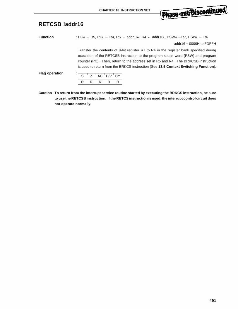
491
CHAPTER 18 INSTRUCTION SET
RETCSB !addr16
Function : PCH ← R5, PCL ← R4, R5 ← addr16H, R4 ← addr16L, PSWH ←R7, PSWL ← R6
addr16 = 0000H to FDFFH
Transfer the contents of 8-bit register R7 to R4 in the register bank specified during
execution of the RETCSB instruction to the program status word (PSW) and program
counter (PC). Then, return to the address set in R5 and R4. The BRKCSB instruction
is used to return from the BRKCS instruction (See 13.5 Context Switching Function ).
Flag operation :
Caution To return from the interrupt service routine started by executing the BRKCS instruction, be sure
to use the RETCSB instruction. If the RETCS instruction is used, the interrupt control circuit does
not operate normally.
S Z AC P/V CY
R R R R R
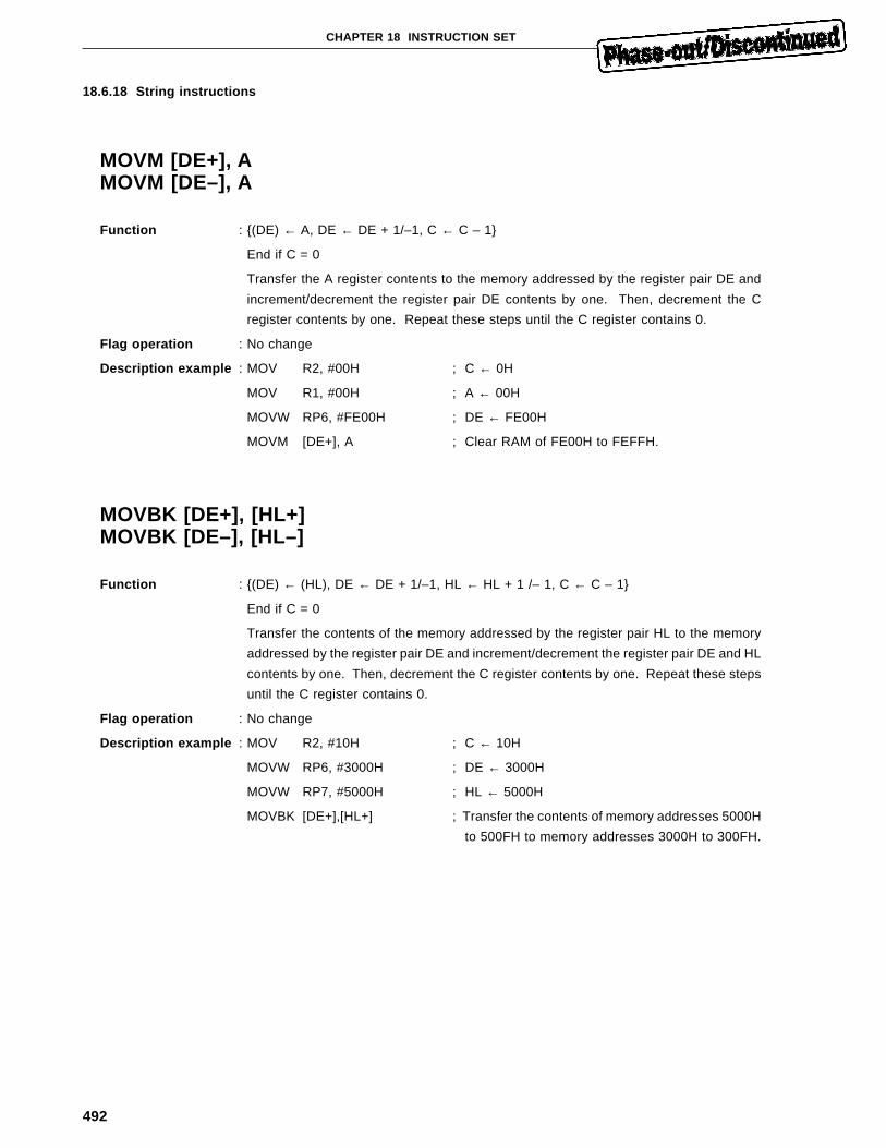
492
CHAPTER 18 INSTRUCTION SET
18.6.18 String instructions
MOVM [DE+], AMOVM [DE–], A
Function : {(DE) ← A, DE ← DE + 1/–1, C ← C – 1}
End if C = 0
Transfer the A register contents to the memory addressed by the register pair DE and
increment/decrement the register pair DE contents by one. Then, decrement the C
register contents by one. Repeat these steps until the C register contains 0.
Flag operation : No change
Description example : MOV R2, #00H ; C ← 0H
MOV R1, #00H ; A ← 00H
MOVW RP6, #FE00H ; DE ← FE00H
MOVM [DE+], A ; Clear RAM of FE00H to FEFFH.
MOVBK [DE+], [HL+]MOVBK [DE–], [HL–]
Function : {(DE) ← (HL), DE ← DE + 1/–1, HL ← HL + 1 /– 1, C ← C – 1}
End if C = 0
Transfer the contents of the memory addressed by the register pair HL to the memory
addressed by the register pair DE and increment/decrement the register pair DE and HL
contents by one. Then, decrement the C register contents by one. Repeat these steps
until the C register contains 0.
Flag operation : No change
Description example : MOV R2, #10H ; C ← 10H
MOVW RP6, #3000H ; DE ← 3000H
MOVW RP7, #5000H ; HL ← 5000H
MOVBK [DE+],[HL+] ; Transfer the contents of memory addresses 5000H
to 500FH to memory addresses 3000H to 300FH.
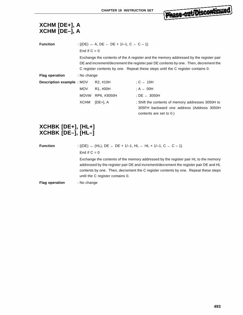
493
CHAPTER 18 INSTRUCTION SET
XCHM [DE+], AXCHM [DE–], A
Function : {(DE) ↔ A, DE ← DE + 1/–1, C ← C – 1}
End if C = 0
Exchange the contents of the A register and the memory addressed by the register pair
DE and increment/decrement the register pair DE contents by one. Then, decrement the
C register contents by one. Repeat these steps until the C register contains 0.
Flag operation : No change
Description example : MOV R2, #10H ; C ← 10H
MOV R1, #00H ; A ← 00H
MOVW RP6, #3050H ; DE ← 3050H
XCHM [DE+], A ; Shift the contents of memory addresses 3050H to
305FH backward one address (Address 3050H
contents are set to 0.)
XCHBK [DE+], [HL+]XCHBK [DE–], [HL–]
Function : {(DE) ↔ (HL), DE ← DE + 1/–1, HL ← HL + 1/–1, C ← C – 1}
End if C = 0
Exchange the contents of the memory addressed by the register pair HL to the memory
addressed by the register pair DE and increment/decrement the register pair DE and HL
contents by one. Then, decrement the C register contents by one. Repeat these steps
until the C register contains 0.
Flag operation : No change
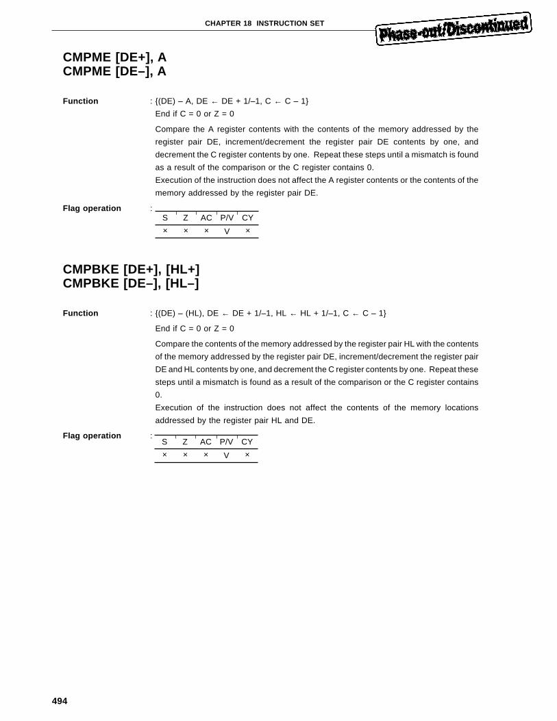
494
CHAPTER 18 INSTRUCTION SET
CMPME [DE+], ACMPME [DE–], A
Function : {(DE) – A, DE ← DE + 1/–1, C ← C – 1}
End if C = 0 or Z = 0
Compare the A register contents with the contents of the memory addressed by the
register pair DE, increment/decrement the register pair DE contents by one, and
decrement the C register contents by one. Repeat these steps until a mismatch is found
as a result of the comparison or the C register contains 0.
Execution of the instruction does not affect the A register contents or the contents of the
memory addressed by the register pair DE.
Flag operation :
CMPBKE [DE+], [HL+]CMPBKE [DE–], [HL–]
Function : {(DE) – (HL), DE ← DE + 1/–1, HL ← HL + 1/–1, C ← C – 1}
End if C = 0 or Z = 0
Compare the contents of the memory addressed by the register pair HL with the contents
of the memory addressed by the register pair DE, increment/decrement the register pair
DE and HL contents by one, and decrement the C register contents by one. Repeat these
steps until a mismatch is found as a result of the comparison or the C register contains
0.
Execution of the instruction does not affect the contents of the memory locations
addressed by the register pair HL and DE.
Flag operation :S Z AC P/V CY
× × × V ×
S Z AC P/V CY
× × × V ×
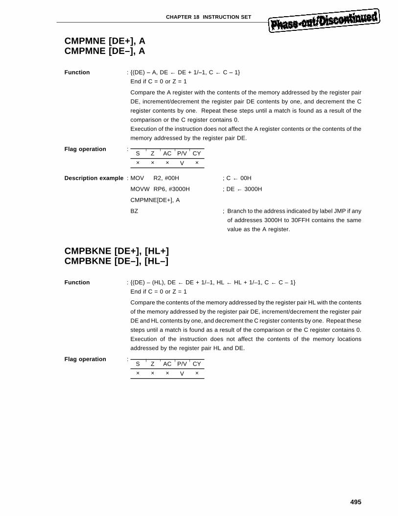
495
CHAPTER 18 INSTRUCTION SET
CMPMNE [DE+], ACMPMNE [DE–], A
Function : {(DE) – A, DE ← DE + 1/–1, C ← C – 1}
End if C = 0 or Z = 1
Compare the A register with the contents of the memory addressed by the register pair
DE, increment/decrement the register pair DE contents by one, and decrement the C
register contents by one. Repeat these steps until a match is found as a result of the
comparison or the C register contains 0.
Execution of the instruction does not affect the A register contents or the contents of the
memory addressed by the register pair DE.
Flag operation :
Description example : MOV R2, #00H ; C ← 00H
MOVW RP6, #3000H ; DE ← 3000H
CMPMNE[DE+], A
BZ ; Branch to the address indicated by label JMP if any
of addresses 3000H to 30FFH contains the same
value as the A register.
CMPBKNE [DE+], [HL+]CMPBKNE [DE–], [HL–]
Function : {(DE) – (HL), DE ← DE + 1/–1, HL ← HL + 1/–1, C ← C – 1}
End if C = 0 or Z = 1
Compare the contents of the memory addressed by the register pair HL with the contents
of the memory addressed by the register pair DE, increment/decrement the register pair
DE and HL contents by one, and decrement the C register contents by one. Repeat these
steps until a match is found as a result of the comparison or the C register contains 0.
Execution of the instruction does not affect the contents of the memory locations
addressed by the register pair HL and DE.
Flag operation :
S Z AC P/V CY
× × × V ×
S Z AC P/V CY
× × × V ×
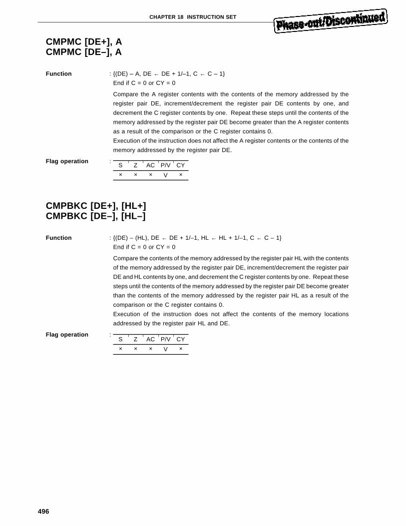
496
CHAPTER 18 INSTRUCTION SET
CMPMC [DE+], ACMPMC [DE–], A
Function : {(DE) – A, DE ← DE + 1/–1, C ← C – 1}
End if C = 0 or CY = 0
Compare the A register contents with the contents of the memory addressed by the
register pair DE, increment/decrement the register pair DE contents by one, and
decrement the C register contents by one. Repeat these steps until the contents of the
memory addressed by the register pair DE become greater than the A register contents
as a result of the comparison or the C register contains 0.
Execution of the instruction does not affect the A register contents or the contents of the
memory addressed by the register pair DE.
Flag operation :
CMPBKC [DE+], [HL+]CMPBKC [DE–], [HL–]
Function : {(DE) – (HL), DE ← DE + 1/–1, HL ← HL + 1/–1, C ← C – 1}
End if C = 0 or CY = 0
Compare the contents of the memory addressed by the register pair HL with the contents
of the memory addressed by the register pair DE, increment/decrement the register pair
DE and HL contents by one, and decrement the C register contents by one. Repeat these
steps until the contents of the memory addressed by the register pair DE become greater
than the contents of the memory addressed by the register pair HL as a result of the
comparison or the C register contains 0.
Execution of the instruction does not affect the contents of the memory locations
addressed by the register pair HL and DE.
Flag operation :
S Z AC P/V CY
× × × V ×
S Z AC P/V CY
× × × V ×
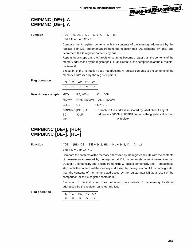
497
CHAPTER 18 INSTRUCTION SET
CMPMNC [DE+], ACMPMNC [DE–], A
Function : {(DE) – A, DE ← DE + 1/–1, C ← C – 1}
End if C = 0 or CY = 1
Compare the A register contents with the contents of the memory addressed by the
register pair DE, increment/decrement the register pair DE contents by one, and
decrement the C register contents by one.
Repeat these steps until the A register contents become greater than the contents of the
memory addressed by the register pair DE as a result of the comparison or the C register
contains 0.
Execution of the instruction does not affect the A register contents or the contents of the
memory addressed by the register pair DE.
Flag operation :
Description example : MOV R2, #00H ; C ← 00H
MOVW RP6, #8000H ; DE ← 8000H
CLR1 CY ; CY ← 0
CMPMNC [DE+], A ; Branch to the address indicated by label JMP if any of
BC $JMP addresses 8000H to 80FFH contains the greater value than
the A register.
CMPBKNC [DE+], [HL+]CMPBKNC [DE–], [HL–]
Function : {(DE) – (HL), DE ← DE + 1/–1, HL ← HL + 1/–1, C ← C – 1}
End if C = 0 or CY = 1
Compare the contents of the memory addressed by the register pair HL with the contents
of the memory addressed by the register pair DE, increment/decrement the register pair
DE and HL contents by one, and decrement the C register contents by one. Repeat these
steps until the contents of the memory addressed by the register pair HL become greater
than the contents of the memory addressed by the register pair DE as a result of the
comparison or the C register contains 0.
Execution of the instruction does not affect the contents of the memory locations
addressed by the register pairs HL and DE.
Flag operation :
S Z AC P/V CY
× × × V ×
S Z AC P/V CY
× × × V ×
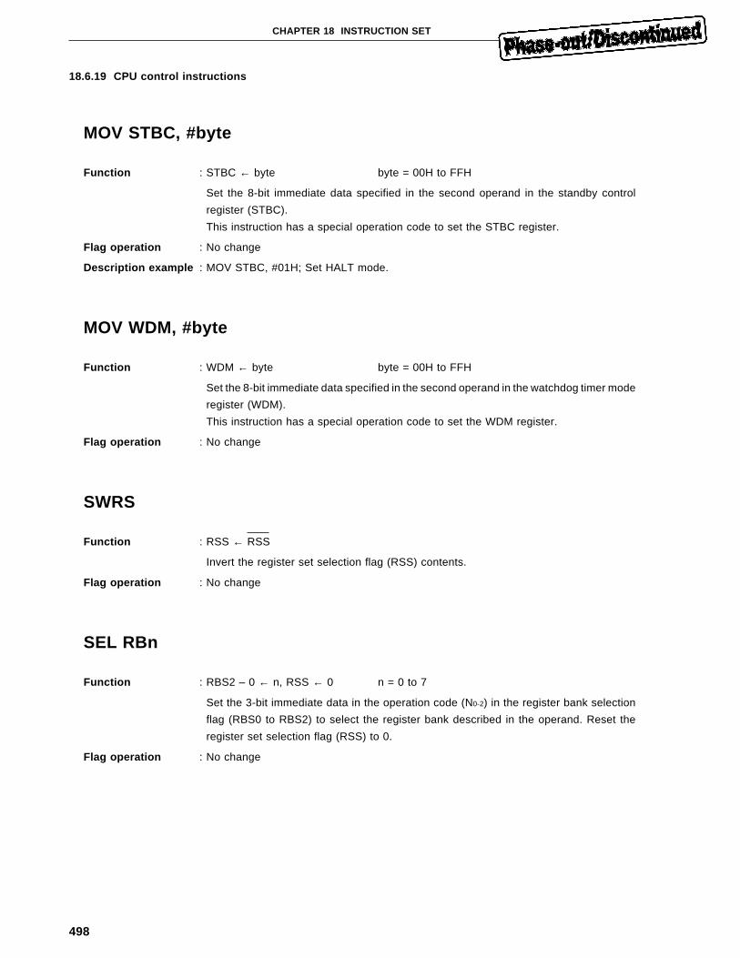
498
CHAPTER 18 INSTRUCTION SET
18.6.19 CPU control instructions
MOV STBC, #byte
Function : STBC ← byte byte = 00H to FFH
Set the 8-bit immediate data specified in the second operand in the standby control
register (STBC).
This instruction has a special operation code to set the STBC register.
Flag operation : No change
Description example : MOV STBC, #01H; Set HALT mode.
MOV WDM, #byte
Function : WDM ← byte byte = 00H to FFH
Set the 8-bit immediate data specified in the second operand in the watchdog timer mode
register (WDM).
This instruction has a special operation code to set the WDM register.
Flag operation : No change
SWRS
Function : RSS ← RSS
Invert the register set selection flag (RSS) contents.
Flag operation : No change
SEL RBn
Function : RBS2 – 0 ← n, RSS ← 0 n = 0 to 7
Set the 3-bit immediate data in the operation code (N0-2) in the register bank selection
flag (RBS0 to RBS2) to select the register bank described in the operand. Reset the
register set selection flag (RSS) to 0.
Flag operation : No change
499
CHAPTER 18 INSTRUCTION SET
SEL RBn, ALT
Function : RBS2 – 0 ← n, RSS ← 0 n = 0 to 7
Set the 3-bit immediate data in the operation code (N0-2) in the register bank selection
flag (RBS0 to RBS2) to select the register bank described in the operand. Set the register
set selection flag (RSS) to 1.
Flag operation : No change
NOP
Function : No Operation
Perform no operation and consume two clocks.
Flag operation : No change.
EI
Function : IE ← 1
Set the interrupt request enable flag (IE) to 1. Whether maskable interrupt acknowledge
is enabled or disabled is controlled by setting the interrupt request control registers.
Flag operation : No change
DI
Function : IE ← 0
Reset the interrupt request enable flag (IE) to 0 to disable acknowledge of every maskable
interrupt.
Flag operation : No change.

500
[MEMO]
501
CHAPTER 19 INSTRUCTION EXECUTION SPEED
19.1 Instruction Execution Speed
The µPD78334 has the following features for instruction execution at a drastically high speed:
(1) Can operate the bus control unit (BCU) completely independent of the execution unit (EXU).
(2) Has a bus independent of an SFR access and can fetch operation code at parallel timing (has no concept
of idle state).
(3) Since the bus control unit has a buffer register, the execution unit can execute the next instruction without
waiting for the bus cycle termination simply by passing address and data to the bus control unit even when
a data access to the external memory is made.
(4) The execution unit can read two general registers simultaneously in one block.
19.2 Memory Space and Access Speed
19.2.1 Main RAM and peripheral RAM
The µPD78334 has internal 1K-byte RAM in the FB00H to FEFFH area which is roughly classified into main RAM
and peripheral RAM because of a difference in the access speed:
Table 19-1 Difference of Access Speed of Main RAM and Peripheral RAM
Address range Access speed
Main RAM FE00H to FEFFH l clock/1 word —
Peripheral RAM FB00H to FDFFH3 + n clocks/l byte
• When normal fetch cycle mode
• When data access
1 clock/l byte • When high speed fetch cycle mode
Remark n is the number of wait states set in the PWC register.
The main RAM which exists in the execution unit (EXU) can be accessed at the highest speed.
Caution When a word access to the main RAM area (FE00H to FEFFH) (containing stack handling) is
executed, addresses specified in operands are limited to even addresses.
Remark In 18.3.2, main RAM is represented as IRAM and peripheral RAM as PRAM.
502
CHAPTER 19 INSTRUCTION EXECUTION SPEED
19.2.2 Memory access
(1) Operation code fetch
(a) Access range
The µPD78330, 78334, 78P334 can fetch operation code from all 64K-byte space. However, operation
code fetch from external memory takes precedence in the address range of FE00H to FFFFH. (See Figure
19-1). Thus, operation codes cannot be described in the main RAM or SFR area.
(b) Number of clocks required for access
The number of clock required for operation code fetch can be specified every 16K-bytes by setting the
FCC register. To fetch an operation code from the area for which the normal fetch cycle mode is specified
in the FCC register, 3+n clocks are required per byte (n is the number of wait states specified in the PWC
register). From the area for which the high-speed fetch cycle mode is specified, one byte of an operation
code can be fetched in one clock. The high-speed fetch cycle mode can be specified only for the internal
memories:
Caution The fetch cycle mode is specified in the FCC register regardless of whether the memory existing
in a specific area is internal or external. After reset, the normal fetch cycle mode is specified for
all the space.
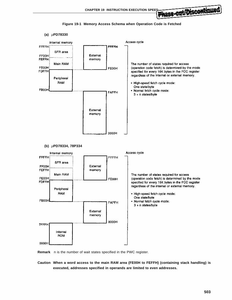
503
CHAPTER 19 INSTRUCTION EXECUTION SPEED
Figure 19-1 Memory Access Schema when Operation Code is Fetched
(a) µPD78330
(b) µPD78334, 78P334
Remark n is the number of wait states specified in the PWC register.
Caution When a word access to the main RAM area (FE00H to FEFFH) (containing stack handling) is
executed, addresses specified in operands are limited to even addresses.
504
CHAPTER 19 INSTRUCTION EXECUTION SPEED
(c) Bus control signals when memory is accessed (ASTB, RD, and WR)
When fetching operation codes, the µPD78334 output bus control signals such as ASTB, RD, and WR.
The output signals vary depending on the area to be accessed. (See Table 19-2 )
Table 19-2 Bus Control Signals When Operation Codes are Fetched
(1) µPD78330
Access area Address ASTB RD WR
External memory FE00H to FFFFH ●● ●● —
Peripheral RAMNormal fetch
FB00H to FDFFH●● — —
High speed fetch —Note — —
External memory 0000H to FAFFH ●● ●● —
Remark ●● : Signal is output
— : Signal is not output (inactive level is output)
Note ASTB signal is output only for BR instruction.
(2) µPD78334, 78P334
Access area Address ASTB RD WR
External memory FE00H to FFFFH ●● ●● —
Peripheral RAMNormal fetch
FB00H to FDFFH●● — —
High speed fetch —Note — —
External memory 8000H to FAFFH ●● ●● —
Internal ROMNormal fetch
0000H to 7FFFH●● — —
High speed fetch —Note — —
Remark ●● : Signal is output
— : Signal is not output (inactive level is output)
Note ASTB signal is output only for BR instruction.
505
CHAPTER 19 INSTRUCTION EXECUTION SPEED
(2) Data Access
When data is read/written from/into memory during execution of an instruction such as MOV A, [HL] or SUB
[DE+], A
(a) Access range
The µPD78330, 78334, 78P334 can access data in all 64K-byte space . However, an access to internal
memory takes precedence in the address range of FE00H to FFFFH. As an exception. external memory
is accessed for the 16-byte external SFR area of addresses FFD0H to FFDFH. (See Figure 19-2 ).
(b) Number of clocks required for access
The number of clocks required for a data access varies depending on the area to be accessed.
Table 19-3 Number of States Required for a Data Access
Access area Address Read access Write access
Main RAM FE00H to FEFFH One clock/word One clock/word
SFR FF00H to FFFFH Four clocks/word Four clocks/word
Internal ROMNote l 0000H to 7FFFH —
Peripheral RAM FB00H to FDFFH3 + n clocks/byte
External SFR FFD0H to FFDFH One clock/wordNote 2
External memory —
Remark n is the number of wait states specified in the PWC register.
Notes 1. The µPD78330 is not applied.
2. A data write access to the peripheral RAM, external SFR, or external memory is complete in one clock
because address and data are only passed to the BCU (bus control unit). However, since the bus is
occupied for the same time as a data read access (3+n clocks/byte), extra clocks may be required if
a data access to the area follows the data write access.
506
CHAPTER 19 INSTRUCTION EXECUTION SPEED
Figure 19-2 Memory Access Schema when a Data Access is Made
(a) µPD78330
(b) µPD78334, 78P334
Remark n is the number of wait states specified in the PWC register
Caution When a word access to the main RAM area (FE00H to FEFFH) (containing stack handling) is
executed, addresses specified in operands are limited to even addresses.
507
CHAPTER 19 INSTRUCTION EXECUTION SPEED
(c) Bus control signals when memory is access (ASTB, RD, and WR)
When fetching operation codes, the µPD78334 output bus control signals such as ASTB, RD, and WR.
The output signals vary depending on the area to be accessed. (See Table 19-4 ).
Table 19-4 Bus Control Signals When Data Access
(1) µPD78330
Access area Address ASTB RD WR
SFRFFE0H to FFFFH
— — —FF00H to FFCFH
External SFR FFD0H to FFDFH ●● ●● ●●
Main RAM FE00H to FEFFH — — —
Peripheral RAM FB00H to FDFFH ●● — —
External memory 0000H to FAFFH ●● ●● ●●
Remarks ●● : Signal is output
— : Signal is not output (inactive level is output)
(2) µPD78334, 78P334
Access area Address ASTB RD WR
SFRFFE0H to FFFFH
— — —FF00H to FFCFH
External SFR FFD0H to FFDFH ●● ●● ●●
Main RAM FE00H to FEFFH — — —
Peripheral RAM FB00H to FDFFH ●● — —
External memory 8000H to FAFFH ●● ●● ●●
Internal ROM 0000H to 7FFFH ●● — —
Remarks ●● : Signal is output
— : Signal is not output (inactive level is output)
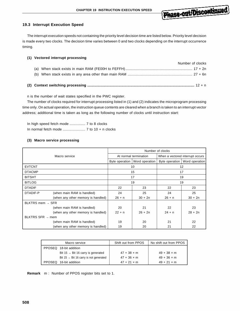
508
CHAPTER 19 INSTRUCTION EXECUTION SPEED
19.3 Interrupt Execution Speed
The interrupt execution speeds not containing the priority level decision time are listed below. Priority level decision
is made every two clocks. The decision time varies between 0 and two clocks depending on the interrupt occurrence
timing.
(1) Vectored interrupt processing
Number of clocks
(a) When stack exists in main RAM (FE00H to FEFFH) .................................................................... 17 + 2n
(b) When stack exists in any area other than main RAM .................................................................. 27 + 6n
(2) Context switching processing ............................................................................................................. 12 + n
n is the number of wait states specified in the PWC register.
The number of clocks required for interrupt processing listed in (1) and (2) indicates the microprogram processing
time only. On actual operation, the instruction queue contents are cleared when a branch is taken to an interrupt vector
address; additional time is taken as long as the following number of clocks until instruction start:
In high speed fetch mode ................ 7 to 8 clocks
In normal fetch mode ....................... 7 to 10 + n clocks
(3) Macro service processing
Number of clocks
Macro service At normal termination When a vectored interrupt occurs
Byte operation Word operation Byte operation Word operation
EVTCNT 10 12
DTACMP 15 17
BITSHT 17 19
BITLOG 19 19
DTADIF 22 23 22 23
DTADIF-P (when main RAM is handled) 24 25 24 25
(when any other memory is handled) 26 + n 30 + 2n 26 + n 30 + 2n
BLKTRS mem → SFR
(when main RAM is handled) 20 21 22 23
(when any other memory is handled) 22 + n 26 + 2n 24 + n 28 + 2n
BLKTRS SFR → mem
(when main RAM is handled) 19 20 21 22
(when any other memory is handled) 19 20 21 22
Macro service Shift out from PPOS No shift out from PPOS
PPOSEQ 18-bit addition
Bit 15 → Bit 16 carry is generated 47 + 38 × m 49 + 38 × m
Bit 15 → Bit 16 carry is not generated 47 + 36 × m 49 + 36 × m
PPOSEQ 16-bit addition 47 + 21 × m 49 + 21 × m
Remark m : Number of PPOS register bits set to 1.
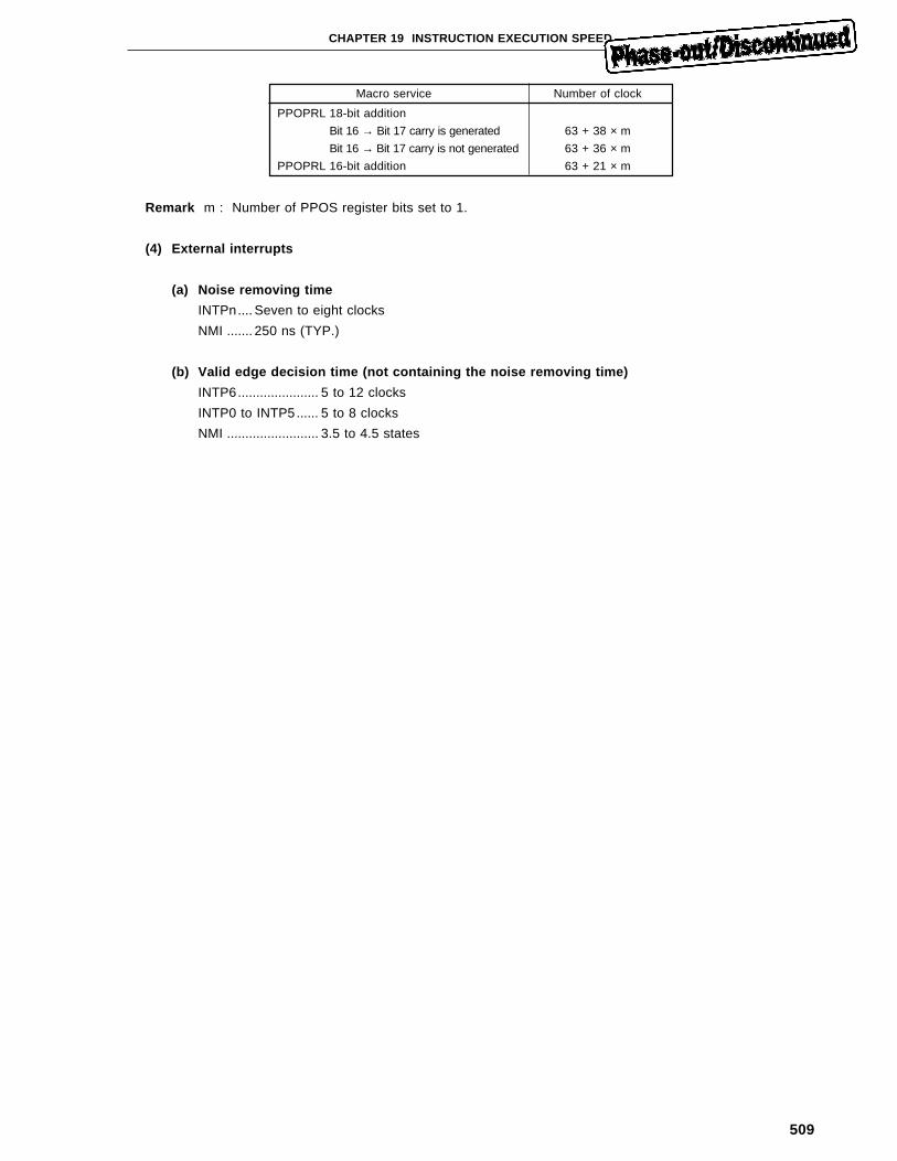
509
CHAPTER 19 INSTRUCTION EXECUTION SPEED
Macro service Number of clock
PPOPRL 18-bit addition
Bit 16 → Bit 17 carry is generated 63 + 38 × m
Bit 16 → Bit 17 carry is not generated 63 + 36 × m
PPOPRL 16-bit addition 63 + 21 × m
Remark m : Number of PPOS register bits set to 1.
(4) External interrupts
(a) Noise removing time
INTPn.... Seven to eight clocks
NMI ....... 250 ns (TYP.)
(b) Valid edge decision time (not containing the noise removing time)
INTP6...................... 5 to 12 clocks
INTP0 to INTP5...... 5 to 8 clocks
NMI ......................... 3.5 to 4.5 states
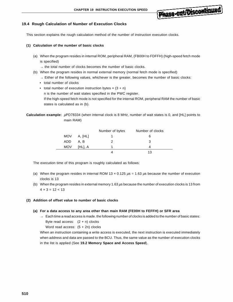
510
CHAPTER 19 INSTRUCTION EXECUTION SPEED
19.4 Rough Calculation of Number of Execution Clocks
This section explains the rough calculation method of the number of instruction execution clocks.
(1) Calculation of the number of basic clocks
(a) When the program resides in internal ROM, peripheral RAM, (FB00H to FDFFH) (high-speed fetch mode
is specified)
→ the total number of clocks becomes the number of basic clocks.
(b) When the program resides in normal external memory (normal fetch mode is specified)
→ Either of the following values, whichever is the greater, becomes the number of basic clocks:
• total number of clocks
• total number of execution instruction bytes × (3 + n)
n is the number of wait states specified in the PWC register.
If the high-speed fetch mode is not specified for the internal ROM, peripheral RAM the number of basic
states is calculated as in (b).
Calculation example: µPD78334 (when internal clock is 8 MHz, number of wait states is 0, and [HL] points to
main RAM)
Number of bytes Number of clocks
MOV A, [HL] 1 6
ADD A, B 2 3
MOV [HL], A 1 4
4 13
The execution time of this program is roughly calculated as follows:
(a) When the program resides in internal ROM 13 × 0.125 µs = 1.63 µs because the number of execution
clocks is 13
(b) When the program resides in external memory 1.63 µs because the number of execution clocks is 13 from
4 × 3 = 12 < 13
(2) Addition of offset value to number of basic clocks
(a) For a data access to any area other than main RAM (FE00H to FEFFH) or SFR area
→ Each time a read access is made. the following number of clocks is added to the number of basic states:
Byte read access: (2 + n) clocks
Word read access: (5 + 2n) clocks
When an instruction containing a write access is executed, the next instruction is executed immediately
when address and data are passed to the BCU. Thus, the same value as the number of execution clocks
in the list is applied (See 19.2 Memory Space and Access Speed ).
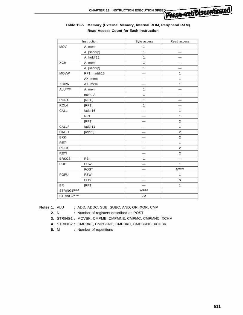
511
CHAPTER 19 INSTRUCTION EXECUTION SPEED
Table 19-5 Memory (External Memory, Internal ROM, Peripheral RAM)
Read Access Count for Each Instruction
Instruction Byte access Read access
MOV A, mem 1 —
A, [saddrp] 1 —
A, !addr16 1 —
XCH A, mem 1 —
A, [saddrp] 1 —
MOVW RP1, ! addr16 — 1
AX, mem — 1
XCHW AX, mem — 1
ALUNote1 A, mem 1 —
mem, A 1 —
ROR4 [RP1.] 1 —
ROL4 [RP1] 1 —
CALL !addr16 — 1
RP1 — 1
[RP1] — 2
CALLF !addr11 — 1
CALLT [addr5] — 2
BRK — 2
RET — 1
RETB — 2
RETI — 2
BRKCS RBn 1 —
POP PSW — 1
POST — NNote2
POPU PSW — 1
POST — N
BR [RP1] — 1
STRING1Note3 MNote5
STRING2Note4 2M
Notes 1. ALU : ADD, ADDC, SUB, SUBC, AND, OR, XOR, CMP
2. N : Number of registers described as POST
3. STRING1 : MOVBK, CMPME, CMPMNE, CMPMC, CMPMNC, XCHM
4. STRING2 : CMPBKE, CMPBKNE, CMPBKC, CMPBKNC, XCHBK
5. M : Number of repetitions
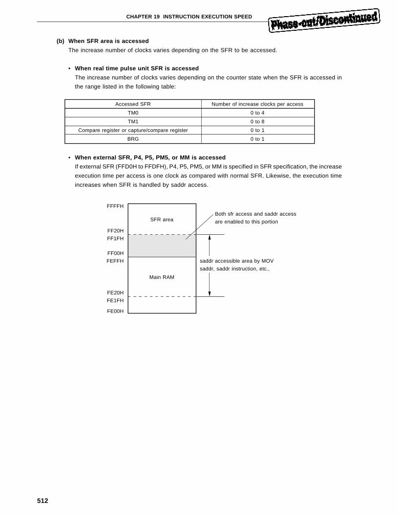
512
CHAPTER 19 INSTRUCTION EXECUTION SPEED
(b) When SFR area is accessed
The increase number of clocks varies depending on the SFR to be accessed.
• When real time pulse unit SFR is accessed
The increase number of clocks varies depending on the counter state when the SFR is accessed in
the range listed in the following table:
Accessed SFR Number of increase clocks per access
TM0 0 to 4
TM1 0 to 8
Compare register or capture/compare register 0 to 1
BRG 0 to 1
• When external SFR, P4, P5, PM5, or MM is accessed
If external SFR (FFD0H to FFDFH), P4, P5, PM5, or MM is specified in SFR specification, the increase
execution time per access is one clock as compared with normal SFR. Likewise, the execution time
increases when SFR is handled by saddr access.
saddr accessible area by MOV
saddr, saddr instruction, etc.,
FFFFH
FF20H
FF1FH
FF00H
FEFFH
FE20H
FE1FH
FE00H
Both sfr access and saddr access
are enabled to this portionSFR area
Main RAM
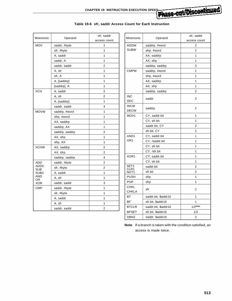
513
CHAPTER 19 INSTRUCTION EXECUTION SPEED
Table 19-6 sfr, saddr Access Count for Each Instruction
Mnemonic Operandsfr, saddr
access count
MOV saddr, #byte 1
sfr, #byte 1
A, saddr 1
saddr, A 1
saddr, saddr 2
A, sfr 1
sfr, A 1
A, [saddrp] 1
[saddrp], A 1
XCH A, saddr 2
A, sfr 2
A, [saddrp] 1
saddr, saddr 4
MOVW saddrp, #word 1
sfrp, #word 1
AX, saddrp 1
saddrp, AX 1
saddrp, saddrp 2
AX, sfrp 1
sfrp, AX 1
XCHW AX, saddrp 2
AX, sfrp 2
saddrp, saddrp 4
saddr, #byte 2
sfr, #byte 2
A, saddr 1
A, sfr 1
saddr, saddr 3
CMP saddr, #byte 1
sfr, #byte 1
A, saddr 1
A, sfr 1
saddr, saddr 2
ADDADDCSUBSUBCANDORXOR
Mnemonic Operandsfr, saddr
access count
ADDW saddrp, #word 2SUBW sfrp, #word 2
AX, saddrp 1
AX, sfrp 1
saddrp, saddrp 3
CMPW saddrp, #word 1
sfrp, #word 1
AX, saddrp 1
AX, sfrp 1
saddrp, saddrp 2
INCsaddr 2
DEC
INCWsaddrp 2
DECW
MOV1 CY, saddr.bit 1
CY, sfr.bit 1
saddr.bit, CY 2
sfr.bit, CY 2
AND1 CY, saddr.bit 1OR1 CY, /saddr.bit 1
CY, sfr.bit 1
CY, /sfr.bit 1
XOR1 CY, saddr.bit 1
CY, sfr.bit 1
saddr.bit 2
sfr.bit 2
PUSH sfrp 1
POP sfrp 1
CHKLsfr 2
CHKLA
BT saddr.bit, $addr16 1
BF sfr.bit, $addr16 1
BTCLR saddr.bit, $addr16 1/2Note
BFSET sfr.bit, $addr16 1/2
DBNZ saddr, $addr16 2
SET1CLR1NOT1
Note If a branch is taken with the condition satisfied, an
access is made twice.
514
CHAPTER 19 INSTRUCTION EXECUTION SPEED
(c) Branch and CALL instruction
When a branch or CALL instruction is executed, the instruction queue is cleared. Thus, as many states
as the following extra number of clocks are required before the instruction immediately following the
branch instruction is executed:
During high-speed fetch mode : 7 to 8 clocks
During normal fetch mode : 7 to 10 + n clocks
The number of clocks added varies in the range listed above depending on the operation code fetch timing,
and is not defined.
515
CHAPTER 20 CAUTIONS ON USE
This chapter collects the cautions in the preceding. Use them when designing application products. The page in
parentheses indicates where the caution is given.
20.1 Cautions in Chapter 2
(1) When the RESET signal is input, the P00 to P07 (Port 0), P10 to P17 (Port 1), and P30 to P37 (Port 3) pins
become input port pins (output high impedance), and the output latch contents become undefined.
(P. 47 to 48)
(2) When the EA pin is fixed low, P40 to P47 (Port 4) of the µPD78334 and 78P334 always function as address/
data bus, like P40 to P47 (Port 4) of the µPD78330. Port function is not provided. (P. 49)
(3) When the RESET signal is input, the P40 to P47 (Port 4) of the µPD78334 and 78P334 become input port
pins in both the port mode and external memory expansion mode (output high impedance), and the output
latch contents become undefined. (P. 49)
(4) When the EA pin is fixed low, P50 to P57 (Port 5) of the µPD78334 and 78P334 always function as address
bus, like P50 to P57 (Port 5) of the µPD78330. Port function is not provided. (P. 50)
(5) When the RESET signal is input, the P50 to P57 (Port 5) pins of the µPD78334 and 78P334 become input
port pins in both the port mode and external memory expansion mode (output high impedance), and the output
latch contents become undefined. (P. 50)
(6) When the EA pin is fixed low, the P90 and P91 pins of the µPD78334 and 78P334 always function as the RD
and WR pins. Port function is not provided. (P. 52)
(7) When the RESET signal is input, the P90 to P95 (Port 9) pins of the µPD78334 and 78P334 become input
port pins (output high impedance), and the output latch contents become undefined. (P. 52)
516
CHAPTER 20 CAUTIONS ON USE
20.2 Cautions in Chapter 3
(1) When a word access to the main RAM area (FE00H to FEFFH) (containing stack handling) is executed,
addresses specified in operands are limited to even addresses. (P. 58, P. 70, P. 78)
(2) When a word access to the main RAM area (FE00H to FEFFH) (containing stack handling) is executed, the
access operation varies, depending on whether the reference address is even or odd. Therefore, if an access
to an even address and an access to an odd address are mixed, an error is caused. Specify only even reference
addresses.
To executed a 16-bit data transfer instruction, specify even addresses in operands. If odd addresses are
specified an error occurs in the assembler package (RA78K/III). (P. 60)
(3) Do not make a word access across the peripheral RAM area and main RAM area. (P. 60)
(4) Do not access any address in which no special function register is mapped (except for the external access
area). (P. 64)
(5) Do not handle the program status word (PSW) LT bit by a program. If the bit is handled by a program, an error
may occur. (P. 67)
(6) The vector table entries of reset input, BRK instruction, and operation code trap interrupt are fixed to 0000H,
003EH, and 003CH, and are not affected by TPF. (P. 70)
(7) To write into a special function register, write 0 or l into the bits defined as 0 or 1. (P. 73)
(8) Do not write into any read-only register. If a write is made into the read-only register, an error may occur. (P. 73)
(9) Do not access the special function register area (FF00H to FFFFH) in which no SFRS are mapped (except
the external access area). If the addresses in which no SFRS are mapped are accessed, an error may occur.
(P. 73)
517
CHAPTER 20 CAUTIONS ON USE
20.3 Cautions in Chapter 5
(1) With the µPD78330 and when the µPD78334, 78P334 EA pin level is fixed low for use, port 4, port 5, and
port 9 (low-order two bits) do not function as port. (P. 85)
(2) In the pin access mode (PRDC0 = 1) specified in the port read control register (PRDC), port bit manipulation
instruction does not operate normally. After port check terminates, be sure to reset and restore to the normal
mode (PRDC0 = 0). (P. 89)
(3) If an interrupt occurs in the pin access mode in the PRDC register, bit manipulation instruction, etc., may be
executed with the mode maintained, causing an error to occur. Before starting check, be sure to disable
interrupt (DI state).
Do not use any macro service handling a port. (P. 89)
(4) In the pin access mode in the PRDC register, non-maskable interrupt occurrence cannot be avoided. Take
the following countermeasures in a program according to the system: (P. 89)
• Non-maskable interrupt routine does not handle any port.
• Save the PRDC.0 level at the beginning of non-maskable interrupt routine, and restore it at return.
(5) Use CHKL and CHKLA instructions when the PRDC register PRDC0 bit is 0 (normal mode). (P. 90)
(6) When the ports are set to the input mode. regardless of whether each port pin is specified as a port or control
pin, whenever the CHKL or CHKLA instruction is used to compare the pin state with the output latch contents
(or control output level), they match. Therefore, even if these instructions are executed for the ports set to
the input model they are practically invalid. (P. 91)
(7) To use the CHKL or CHKLA instruction to check the input level of a port within which control output and port
output are mixed, set the input/output mode of the control output pin to the input mode before executing the
instructions. (The control output level changes asynchronously, thus cannot be checked by the CHKL or
CHKLA instruction.) (P. 91)
(8) Since ports 2, 7, and 8 are input-only ports, whenever the CHKL or CHKLA instruction is used to compare
the pin state with the output latch contents, they match. Therefore, even if these instructions are executed
for ports 2, 7, and 8, they are practically invalid. (P. 91)
(9) Be sure to set 0 in bits 3-7. If I is set, normal operation is not performed. (P. 91)
(10) Do not write the code combinations indicated by “Undefined”. (P. 98)
(11) To stop the PWM output function (PWME0 = 0/PWME1 = 0), previously initialize the output latch to fix the
output state at stop. (P. 98)
(12) Write 00 into the fetch cycle control register (FCC) bits corresponding to an unaccessed memory area.
(P. 99)
518
CHAPTER 20 CAUTIONS ON USE
20.4 Cautions in Chapter 6
(1) To use external clock, do not set the standby control register (STBC) STP bit to 1. (P. 101)
(2) To use the system clock oscillator, wire to avoid wiring capacitance affection, etc., as described below:
(P. 102)
• Make wiring as extremely short as possible.
• Do not cross the oscillator and near other signal line. Do not put the oscillator near any line where high current
which changes flows.
• Be sure to place oscillator capacitor ground point in the same potential as the Vss Pin. Do not connect to
any ground pattern where high current flows.
• Do not take out any signal from the oscillator.
(3) To input external clock to the X1 pin and leave the X2 pin open, do not connect load such as wiring capacitance
to the X2 pin. (P. 102)
20.5 Cautions in Chapter 7
(1) To read the contents of timer 0 as the 16-bit timer, be sure to continue to execute the TM0 and TLA register
read instructions. If the TLA register read instruction is not executed, the TM0 value cannot be read correctly.
(P. 110)
(2) To read the contents of the 18-bit compare register, be sure to continue to execute the CMX0 (or CM0nR)
register and TLA register read instructions. If the TLA register read instruction is not executed, the 18-bit
compare register value cannot be read correctly. (P. 112)
(3) To write data into the 18-bit compare register, be sure to continue to execute write instructions into the TLA
register and CMX0 (or CM0nR) register. If the write instruction into the CMX0 (or CM0nR) register is not
executed, the 18-bit compare register value is not rewritten. (P. 112)
(4) To read the contents of the 18-bit capture register, be sure to continue to execute the 16-bit capture register
(CT00-CT02) and TLA register read instructions. If the TLA register read instruction is not executed, the 18-
bit capture register value cannot be read correctly. (P. 112)
(5) When the capture/compare register (CC00R, CC01R) functions as a compare register, the corresponding
external interrupt (capture trigger signal) cannot cause an interrupt to occur. (P. 116)
(6) To read the contents of the 18-bit capture/compare register, be sure to continue to execute the CC00R (or
CC01R) register and TLA register read instructions. If the TLA register read instruction is not executed. the
18-bit capture/compare register value cannot be read correctly. (P. 117)
(7) To write data into the 18-bit capture/compare register, be sure to continue to execute write instructions into
the TLA register and CC00R (or CC01R) register. If the write instruction into the CC00R (or CC01R) register
is not executed, the 18-bit capture/compare register value is not rewritten. (P. 117)
519
CHAPTER 20 CAUTIONS ON USE
(8) The timer unit mode register 0 (TUM0) OVF0 bit (TM0 overflow flag) always indicates an overflow flag from
timer 0 (TM0) bit 17, and differs from TM0 overflow interrupt (INTOV). (P. 122)
(9) To change output mode specification of timer output (TOM11, TOM20 bit) or active level specification (ALV11,
ALV12, ALV20 bit), previously set the corresponding timer output pin to “timer output disable”. (P. 127)
(10) To change active level specification (ALV21, AVL30, AVLPPO0, ALVPPO1 bit), previously set the correspond-
ing timer output pin or pulse output pin to “output disable”. (P. 128)
(11) To specify ECLR = 1 (TM0 clear when an edge opposite to the active edge to the INTP0 pin is input) in setting
the TMC0 register, do not specify both rising and falling edges for the INTP0 pin active edges (ES01,
ES00 ≠1,1). If both edges are specified for the INTP0 pin active edges, TM1 is cleared on both the falling and
rising edges. (P. 130)
(12) The PPO0 to PPO2 output pins are fixed to pulse output mode 0.
Operation can be selected for the PPO3 to PPO5 output pins by setting the timer unit mode register 1 (TUM1)
PPOMn bit (n = 3 to 5). (P. 149)
20.6 Cautions in Chapter 8
(1) To prevent noise from causing an error to occur, connect a capacitor to each of the analog input pins (ANI0
to ANI15) and the reference voltage input pin (AVREF).
When a noise occurs in the analog input even though the capacitor is connected, a noise may cause an illegal
conversion result.
To prevent this illegal conversion result from a bad influence on a system, a software processing is required
as described below:
• The average value of several A/D conversion results is used as the A/D conversion result.
• A/D conversion is performed continously several times, and if a peculiar conversion result is obtained, that
value is not used when determining the conversion result.
• If the A/D conversion result is obtained that is determined to have caused an error to occur in the system,
do not immediately treat the error, but check whether the error occurs again and then treat the error. (P.
159)
★
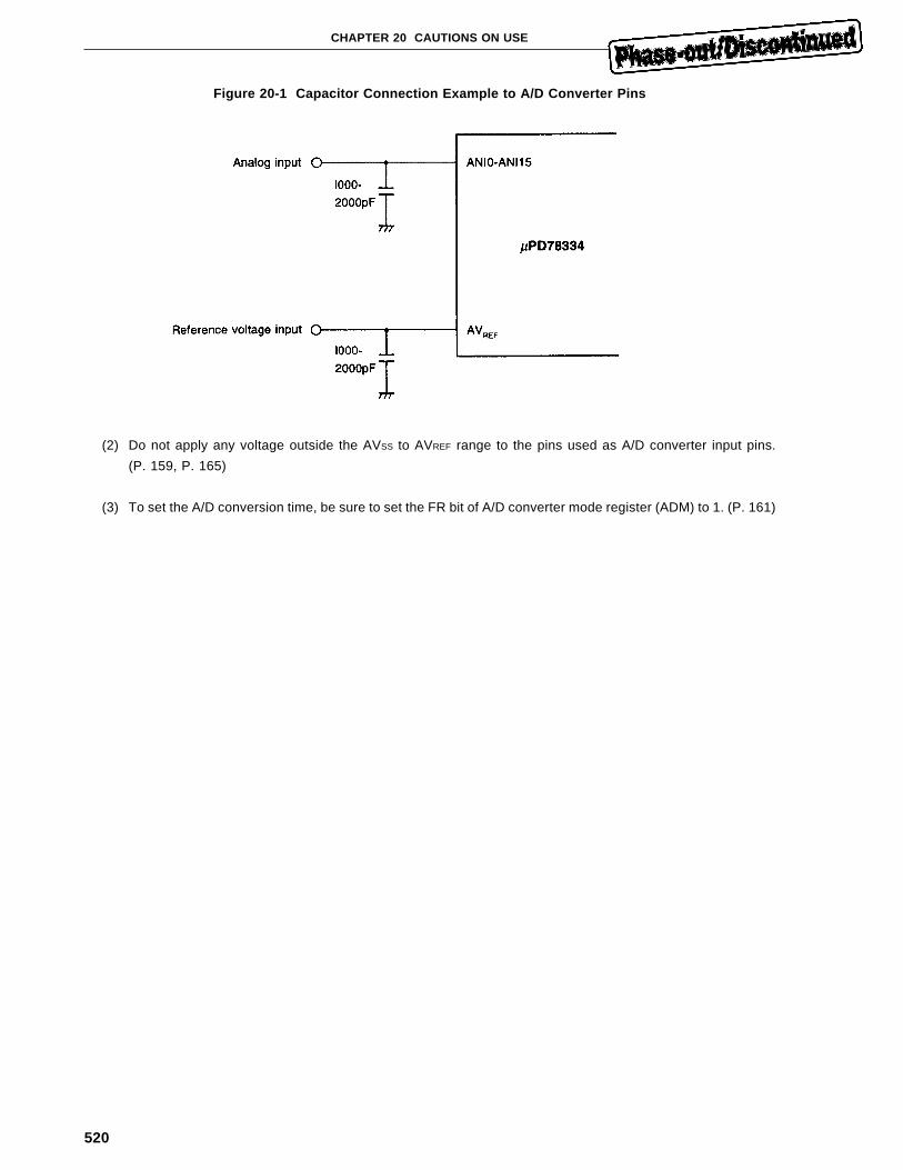
520
CHAPTER 20 CAUTIONS ON USE
Figure 20-1 Capacitor Connection Example to A/D Converter Pins
(2) Do not apply any voltage outside the AVSS to AVREF range to the pins used as A/D converter input pins.
(P. 159, P. 165)
(3) To set the A/D conversion time, be sure to set the FR bit of A/D converter mode register (ADM) to 1. (P. 161)
521
CHAPTER 20 CAUTIONS ON USE
20.7 Cautions in Chapter 9
(1) Normally, if the transmit shift register (TXS) becomes empty, a transmission completion interrupt (INTST)
occurs. However, if the transmit shift register (TXS) becomes empty when RESET is input, no transmission
completion interrupt (INTST) occurs. (P. 190, P. 191)
(2) Even if data is written into the TXS register during transmission operation before INTST occurs, the written
data becomes invalid. (P. 190)
(3) Be sure to also read the receive buffer (RXB) when a reception error occurs. If the RXB register is not read,
when the next data is received an overrun error occurs and the reception error state continues for ever. (P.
193, P. 195)
(4) Be sure to reset the SERIF flag to 0 by the software after completing reception. (Example: BTCLR IF0H.6,
$addr16) (P. 194)
(5) The ASIS register contents are reset to 0 by reading the receive buffer (RXB) or receiving the next data. To
know the error contents, be sure to read the ASIS register before reading the receive buffer (RXB).
If receive data is transferred by using a macro service, the fact that an error occurs (an INTSER interrupt occurs
or the reception interrupt request flag is set to 1) can only be known. Check to ensure that there is no problem
on this point before use. (P. 195)
20.8 Cautions in Chapter 10
(1) Serial clock change is made asynchronously with serial clock. Thus, if serial clock is changed during
communication, serial clock of undefined width may be output. During communication, do not change serial
clock. (P. 204)
(2) Since in the SBI mode, the serial data bus pin (SB0 or SB1) are open drain output, the serial data bus line
becomes the wired OR state. A pull-up resistor must be connected to the serial data bus line. (P. 220)
(3) In the SBI mode, when master and slave exchange processing is performed, SCK input and output are changed
asynchronously between the master and slave, thus a pull-up resistor must also be connected to SCK.
(P. 220)
(4) Do not handle the SBIC register RELT or CMDT bit during transfer operation. (P. 227)
(5) In the SBI mode, be sure to make pin specification and serial clock specification before setting the CTXE and
CRXE bits. (P. 231)
522
CHAPTER 20 CAUTIONS ON USE
20.9 Cautions in Chapter 11
(1) Once the watchdog timer mode register (WDM) RUN bit is set to 1, it cannot be reset to 0 by software.
(P. 238)
(2) Do not change the interrupt request priority specification in the WDM register dynamically during program
execution. (P. 238)
(3) Write can be made into the WDM register only by executing a dedicated instruction (MOV WDM, #byte).
(P. 238)
(4) When the watchdog timer is cleared by setting the WDM register RUN bit to 1, count clock is not reset.
(P. 238)
(5) Just after the power is turned on, the watchdog timer output pin may become low for a maximum of 32 clocks.
(P. 239)
20.10 Cautions in Chapter 12
To stop the PWM output function (PWME0 = 0/PWME1 = 0), previously initialize the output latch to fix the output
state at stop. (P. 243)
20.11 Cautions in Chapter 13
(1) The µPD78334 enters the complete interrupt disable state during execution of instructions accessing the
interrupt control register and the program status word (PSW). In this state, non-maskable interrupt requests
and macro service requests are not acknowledged. To use the interrupt control register or PSW accessing
instruction, perform polling processing, as in the following example, by using interrupt request flag, etc.:
(P. 246)
Example: To use SRIF flag
LOOP: NOP
BF SRIF, $LOOP
(2) Be sure to set bit 6 of interrupt mask flag register (MK0H) to 1. (P. 253)
(3) Priority control by setting the priority specification register (PRSL) and priority specification buffer register is
effective only for multiple interrupt processing. When a number of interrupt requests occur, interrupt processing
is started based on the default priority (fixed by the hardware). (P. 256)
(4) Macro service requests are acknowledged independently of priority specification. However, a vectored
interrupt request occurring at the macro service termination is affected by priority specification. (P. 256)
(5) The in-service priority register (ISPR) can only be read. If write is made into the register, an error may occur.
(P. 257)
……
523
CHAPTER 20 CAUTIONS ON USE
(6) Do not handle the program status word (PSW) LT flag by a program. If the flag is handled by a program, an
error may occur. (P. 259)
(7) In the data compare mode, the interrupt request sources that can be used are limited to the two types of INTSR
and INTCSI.
The correspondence between the interrupt request sources where the data compare mode can be executed
and the SFR to be compared (current SFR) is listed below: (P. 266)
Available interrupt source SFR to be compared (current SFR)
INTSR (UART reception termination) RXB (serial receive buffer)
INTCSI (CSI transfer termination) SIO (serial I/O shift register)
(8) Interrupt control register cannot be specified by using the SFRP. (P. 267, P. 268, P. 271, P. 273)
(9) In the block transfer mode, locate a word buffer at an even address. (P. 270)
(10) In the block transfer mode, locate MEM.PTR at an even address. (P. 270)
(11) In the data differential mode, 00H cannot be set in MSC. (P. 271)
(12) In the data differential mode, locate a word buffer at an even address. (P. 272)
(13) In the data differential mode, previously initialize the “immediately preceding value” (with dummy data).
(P. 272)
(14) In the data differential mode (with a memory pointer), 00H cannot be set in MSC. (P. 273)
(15) In the data differential mode (with a memory pointer), locate a word buffer at an even address. (P. 273)
(16) In the data differential mode (with a memory pointer), locate MEM.PTR at an even address. (P. 274)
(17) In the data differential mode (with a memory pointer), previously initialize the “immediately preceding value”
(with dummy data). (P. 274)
(18) If the context switching function is started by executing a BRKCS instruction when in-service priority register
(ISPR) bit is reset to 0 by executing a RETCS instruction, interrupt nesting control will be destroyed. To return
from processing started by the BRKCS instruction, be sure to use a RETCSB instruction. (P. 279)
524
CHAPTER 20 CAUTIONS ON USE
20.12 Cautions in Chapter 14
(1) If the standby control register (STBC) SBF flag is read, be sure to write 1.
This enables distinction between power on reset and STOP or HALT mode release. (P. 282)
(2) If interrupt request flag (IF××) is set to 1 and no mask is made (MK×× = 0), the HALT mode is not entered.
In macro service processing (ISM×× = 1), the HALT mode is entered after macro service execution. (P. 284)
(3) Once the watchdog timer mode register (WDM) RUN bit is set to 1, it cannot be reset to 0 by software.
(P. 288)
(4) Do not change the interrupt request priority specification in the WDM register dynamically during program
execution. (P. 288)
(5) Write can be made into the WDM register only by executing a dedicated instruction (MOV WDM, #byte).
(P. 288)
(6) When the watchdog timer is cleared by setting the WDM register RUN bit to 1. count clock is not reset.
(P. 288)
(7) If the STOP mode is released when NMI is input, a branch to the NMI interrupt service routine is taken after
the one instruction following the STOP mode setting instruction (MOV STBC #byte) is executed. Place an NOP
instruction following the STOP mode setting instruction. (P. 289)
(8) If an interrupt request occurs when a STOP mode setting instruction is being executed, a branch to the NMI
interrupt service routine is taken after the processing of that interrupt is performed after the STOP mode is
released. Before executing the STOP mode setting instruction, mask all maskable interrupts. (P. 289)
If the maskable interrupts are not masked, operation after the STOP mode is released varies depending on
the processing mode of the interrupt that occurs, as described below:
(a) If a maskable interrupt request set as vectored interrupt processing occurs, a branch is taken to the
maskable interrupt service routine and one instruction is executed, then a branch is taken to the NMI
interrupt service routine.
(b) If a maskable interrupt request set as macro service processing occurs, the macro service is executed,
then a branch is taken to the NMI interrupt service routine (NMI processing is pending until the macro
service terminates).
(9) When a watchdog timer interrupt request of a non-maskable interrupt occurs during execution of a STOP
mode setting instruction, even if the watchdog timer interrupt request priority is lower than the NMI interrupt
request priority, a branch is taken to the NMI interrupt service routine after a branch is taken to the
watchdog timer interrupt service routine and one instruction is executed. Enter NOP instruction at the top
of the watchdog timer interrupt service routine. Set a stack area considering that two nesting levels are
used at the time. (P. 289)
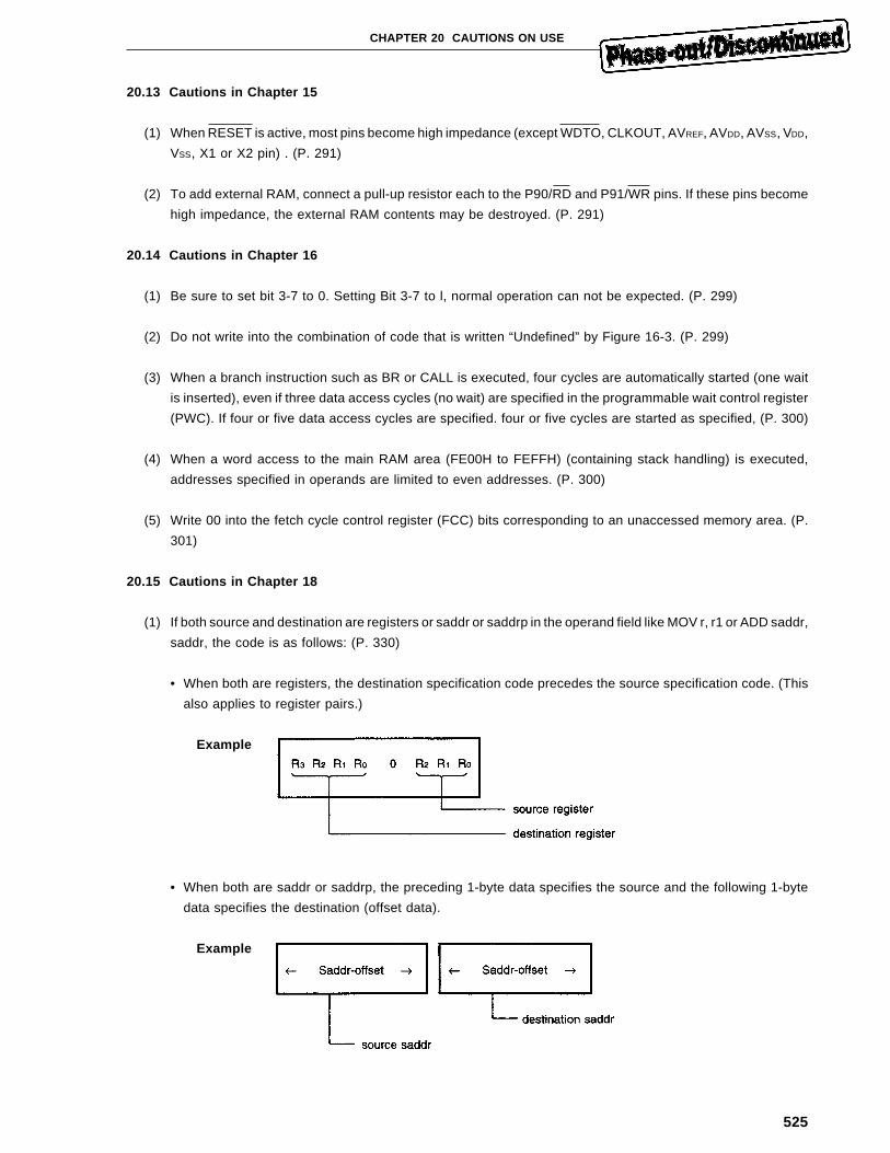
525
CHAPTER 20 CAUTIONS ON USE
20.13 Cautions in Chapter 15
(1) When RESET is active, most pins become high impedance (except WDTO, CLKOUT, AVREF, AVDD, AVSS, VDD,
VSS, X1 or X2 pin) . (P. 291)
(2) To add external RAM, connect a pull-up resistor each to the P90/RD and P91/WR pins. If these pins become
high impedance, the external RAM contents may be destroyed. (P. 291)
20.14 Cautions in Chapter 16
(1) Be sure to set bit 3-7 to 0. Setting Bit 3-7 to l, normal operation can not be expected. (P. 299)
(2) Do not write into the combination of code that is written “Undefined” by Figure 16-3. (P. 299)
(3) When a branch instruction such as BR or CALL is executed, four cycles are automatically started (one wait
is inserted), even if three data access cycles (no wait) are specified in the programmable wait control register
(PWC). If four or five data access cycles are specified. four or five cycles are started as specified, (P. 300)
(4) When a word access to the main RAM area (FE00H to FEFFH) (containing stack handling) is executed,
addresses specified in operands are limited to even addresses. (P. 300)
(5) Write 00 into the fetch cycle control register (FCC) bits corresponding to an unaccessed memory area. (P.
301)
20.15 Cautions in Chapter 18
(1) If both source and destination are registers or saddr or saddrp in the operand field like MOV r, r1 or ADD saddr,
saddr, the code is as follows: (P. 330)
• When both are registers, the destination specification code precedes the source specification code. (This
also applies to register pairs.)
Example
• When both are saddr or saddrp, the preceding 1-byte data specifies the source and the following 1-byte
data specifies the destination (offset data).
Example
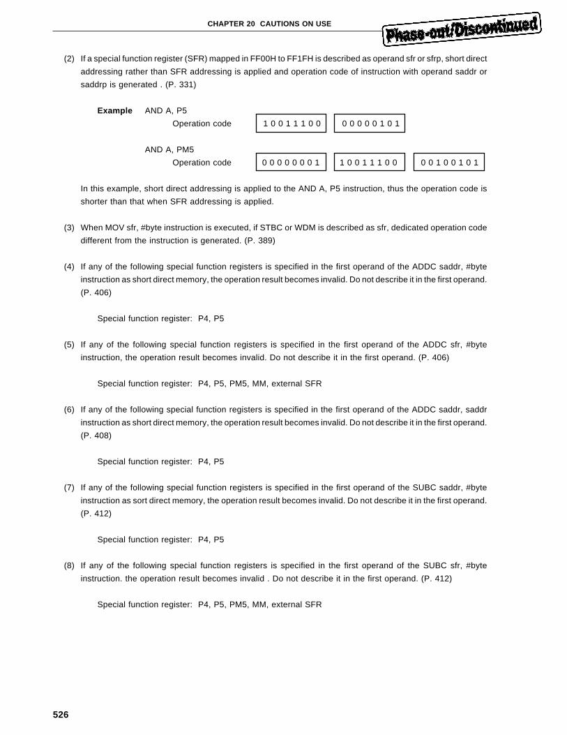
526
CHAPTER 20 CAUTIONS ON USE
(2) If a special function register (SFR) mapped in FF00H to FF1FH is described as operand sfr or sfrp, short direct
addressing rather than SFR addressing is applied and operation code of instruction with operand saddr or
saddrp is generated . (P. 331)
Example AND A, P5
Operation code 1 0 0 1 1 1 0 0 0 0 0 0 0 1 0 1
AND A, PM5
Operation code 0 0 0 0 0 0 0 1 1 0 0 1 1 1 0 0 0 0 1 0 0 1 0 1
In this example, short direct addressing is applied to the AND A, P5 instruction, thus the operation code is
shorter than that when SFR addressing is applied.
(3) When MOV sfr, #byte instruction is executed, if STBC or WDM is described as sfr, dedicated operation code
different from the instruction is generated. (P. 389)
(4) If any of the following special function registers is specified in the first operand of the ADDC saddr, #byte
instruction as short direct memory, the operation result becomes invalid. Do not describe it in the first operand.
(P. 406)
Special function register: P4, P5
(5) If any of the following special function registers is specified in the first operand of the ADDC sfr, #byte
instruction, the operation result becomes invalid. Do not describe it in the first operand. (P. 406)
Special function register: P4, P5, PM5, MM, external SFR
(6) If any of the following special function registers is specified in the first operand of the ADDC saddr, saddr
instruction as short direct memory, the operation result becomes invalid. Do not describe it in the first operand.
(P. 408)
Special function register: P4, P5
(7) If any of the following special function registers is specified in the first operand of the SUBC saddr, #byte
instruction as sort direct memory, the operation result becomes invalid. Do not describe it in the first operand.
(P. 412)
Special function register: P4, P5
(8) If any of the following special function registers is specified in the first operand of the SUBC sfr, #byte
instruction. the operation result becomes invalid . Do not describe it in the first operand. (P. 412)
Special function register: P4, P5, PM5, MM, external SFR
527
CHAPTER 20 CAUTIONS ON USE
(9) If any of the following special function registers is specified in the first operand of the SUBC saddr, saddr
instruction as short direct memory, the operation result becomes invalid. Do not describe it in the first operand.
(P. 413)
Special function register: P4, P5
(10) To return from the interrupt service routine started when a BRK instruction is executed or an operation code
trap occurs, be sure to use a RETB instruction. If a RETI instruction is used, the interrupt control circuit does
not operate normally. (P. 464)
(11) To return from the interrupt service routine started when a BRKCS instruction is executed, be sure to use a
RETCSB instruction. If a RETCS instruction is used, the interrupt control circuit does not operate normally.
(P. 490, P. 491)
20.16 Cautions in Chapter 19
(1) When a word access to the main RAM area (FE00H to FEFFH) (containing stack handling) is executed,
addresses specified in operands are limited to even addresses. (P. 501, P. 503, P. 506)
(2) Mode specification in the FCC register is set regardless of whether the memory existing in the area is internal
or external memory. After reset, all space is specified as the normal fetch cycle mode. (P. 502)

528
[MEMO]

529
APPENDIX A DIFFERENCES BETWEEN µPD78334 AND µPD78322
µPD78334 Series and µPD78322 Series function list are shown the following pages:
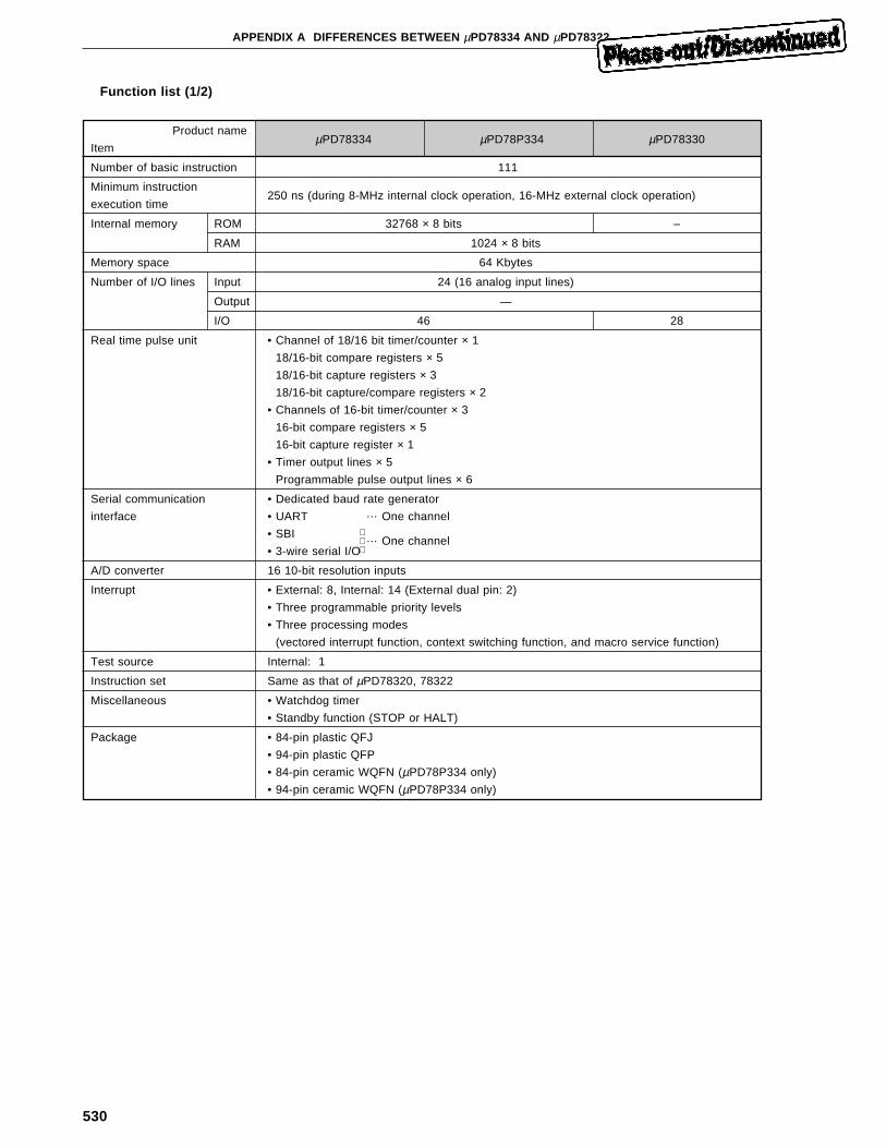
530
APPENDIX A DIFFERENCES BETWEEN µPD78334 AND µPD78322
Function list (1/2)
Product nameµPD78334 µPD78P334 µPD78330
Item
Number of basic instruction 111
Minimum instruction250 ns (during 8-MHz internal clock operation, 16-MHz external clock operation)
execution time
Internal memory ROM 32768 × 8 bits –
RAM 1024 × 8 bits
Memory space 64 Kbytes
Number of I/O lines Input 24 (16 analog input lines)
Output —
I/O 46 28
Real time pulse unit • Channel of 18/16 bit timer/counter × 1
18/16-bit compare registers × 5
18/16-bit capture registers × 3
18/16-bit capture/compare registers × 2
• Channels of 16-bit timer/counter × 3
16-bit compare registers × 5
16-bit capture register × 1
• Timer output lines × 5
Programmable pulse output lines × 6
Serial communication • Dedicated baud rate generator
interface • UART … One channel
• SBI … One channel• 3-wire serial I/O
A/D converter 16 10-bit resolution inputs
Interrupt • External: 8, Internal: 14 (External dual pin: 2)
• Three programmable priority levels
• Three processing modes
(vectored interrupt function, context switching function, and macro service function)
Test source Internal: 1
Instruction set Same as that of µPD78320, 78322
Miscellaneous • Watchdog timer
• Standby function (STOP or HALT)
Package • 84-pin plastic QFJ
• 94-pin plastic QFP
• 84-pin ceramic WQFN (µPD78P334 only)
• 94-pin ceramic WQFN (µPD78P334 only)
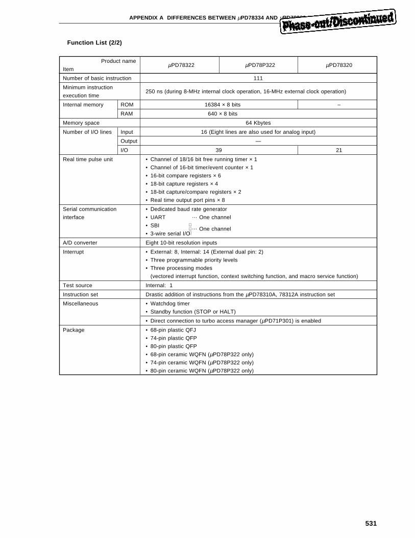
531
APPENDIX A DIFFERENCES BETWEEN µPD78334 AND µPD78322
Function List (2/2)
Product nameµPD78322 µPD78P322 µPD78320
Item
Number of basic instruction 111
Minimum instruction250 ns (during 8-MHz internal clock operation, 16-MHz external clock operation)
execution time
Internal memory ROM 16384 × 8 bits –
RAM 640 × 8 bits
Memory space 64 Kbytes
Number of I/O lines Input 16 (Eight lines are also used for analog input)
Output —
I/O 39 21
Real time pulse unit • Channel of 18/16 bit free running timer × 1
• Channel of 16-bit timer/event counter × 1
• 16-bit compare registers × 6
• 18-bit capture registers × 4
• 18-bit capture/compare registers × 2
• Real time output port pins × 8
Serial communication • Dedicated baud rate generator
interface • UART … One channel
• SBI … One channel• 3-wire serial I/O
A/D converter Eight 10-bit resolution inputs
Interrupt • External: 8, Internal: 14 (External dual pin: 2)
• Three programmable priority levels
• Three processing modes
(vectored interrupt function, context switching function, and macro service function)
Test source Internal: 1
Instruction set Drastic addition of instructions from the µPD78310A, 78312A instruction set
Miscellaneous • Watchdog timer
• Standby function (STOP or HALT)
• Direct connection to turbo access manager (µPD71P301) is enabled
Package • 68-pin plastic QFJ
• 74-pin plastic QFP
• 80-pin plastic QFP
• 68-pin ceramic WQFN (µPD78P322 only)
• 74-pin ceramic WQFN (µPD78P322 only)
• 80-pin ceramic WQFN (µPD78P322 only)

532
[MEMO]
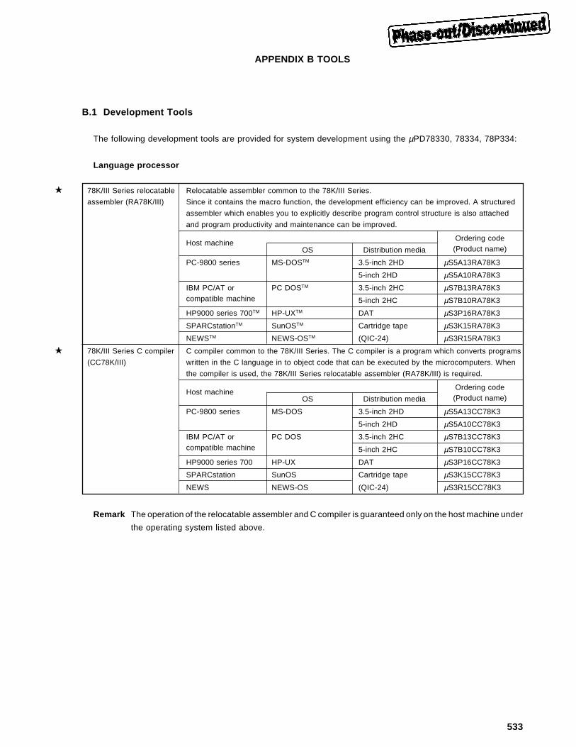
533
APPENDIX B TOOLS
B.1 Development Tools
The following development tools are provided for system development using the µPD78330, 78334, 78P334:
Language processor
78K/III Series relocatable Relocatable assembler common to the 78K/III Series.
assembler (RA78K/III) Since it contains the macro function, the development efficiency can be improved. A structured
assembler which enables you to explicitly describe program control structure is also attached
and program productivity and maintenance can be improved.
Host machineOrdering code
OS Distribution media (Product name)
PC-9800 series MS-DOSTM 3.5-inch 2HD µS5A13RA78K3
5-inch 2HD µS5A10RA78K3
IBM PC/AT or PC DOSTM 3.5-inch 2HC µS7B13RA78K3compatible machine 5-inch 2HC µS7B10RA78K3
HP9000 series 700TM HP-UXTM DAT µS3P16RA78K3
SPARCstationTM SunOSTM Cartridge tape µS3K15RA78K3
NEWSTM NEWS-OSTM (QIC-24) µS3R15RA78K3
78K/III Series C compiler C compiler common to the 78K/III Series. The C compiler is a program which converts programs
(CC78K/III) written in the C language in to object code that can be executed by the microcomputers. When
the compiler is used, the 78K/III Series relocatable assembler (RA78K/III) is required.
Host machineOrdering code
OS Distribution media (Product name)
PC-9800 series MS-DOS 3.5-inch 2HD µS5A13CC78K3
5-inch 2HD µS5A10CC78K3
IBM PC/AT or PC DOS 3.5-inch 2HC µS7B13CC78K3compatible machine 5-inch 2HC µS7B10CC78K3
HP9000 series 700 HP-UX DAT µS3P16CC78K3
SPARCstation SunOS Cartridge tape µS3K15CC78K3
NEWS NEWS-OS (QIC-24) µS3R15CC78K3
Remark The operation of the relocatable assembler and C compiler is guaranteed only on the host machine under
the operating system listed above.
★
★
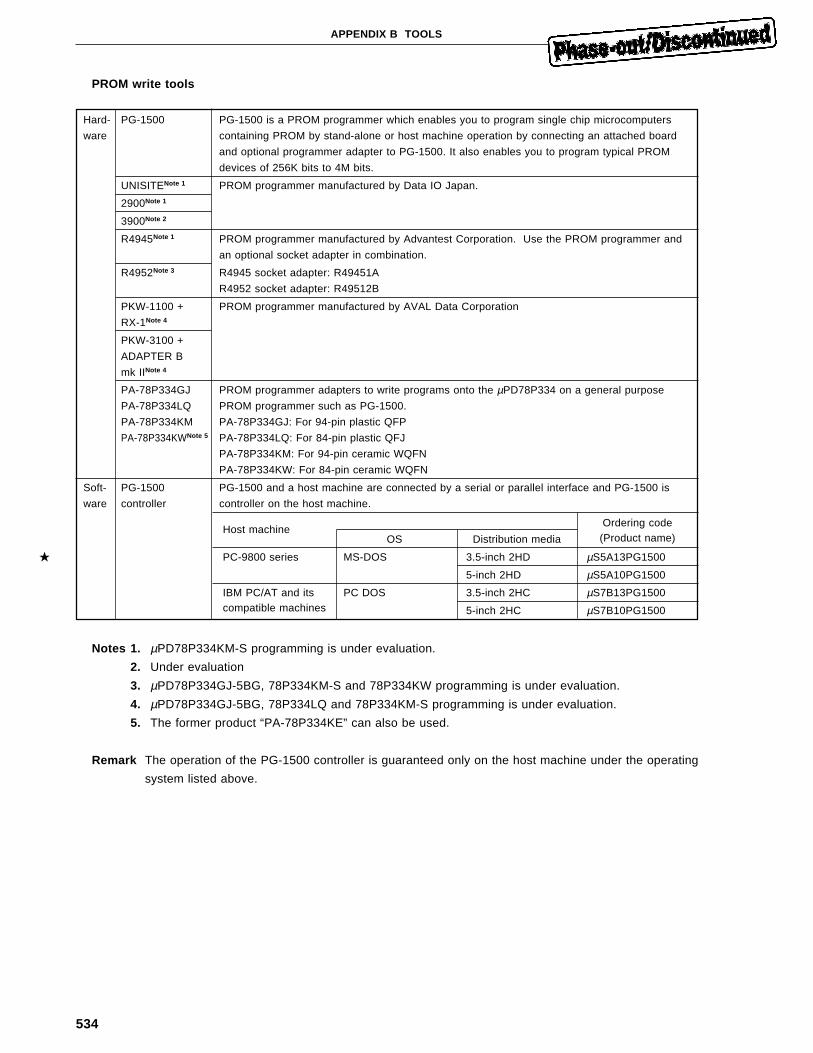
534
APPENDIX B TOOLS
PROM write tools
Hard- PG-1500 PG-1500 is a PROM programmer which enables you to program single chip microcomputers
ware containing PROM by stand-alone or host machine operation by connecting an attached board
and optional programmer adapter to PG-1500. It also enables you to program typical PROM
devices of 256K bits to 4M bits.
UNISITENote 1 PROM programmer manufactured by Data IO Japan.
2900Note 1
3900Note 2
R4945Note 1 PROM programmer manufactured by Advantest Corporation. Use the PROM programmer and
an optional socket adapter in combination.
R4952Note 3 R4945 socket adapter: R49451A
R4952 socket adapter: R49512B
PKW-1100 + PROM programmer manufactured by AVAL Data Corporation
RX-1Note 4
PKW-3100 +
ADAPTER B
mk IINote 4
PA-78P334GJ PROM programmer adapters to write programs onto the µPD78P334 on a general purpose
PA-78P334LQ PROM programmer such as PG-1500.
PA-78P334KM PA-78P334GJ: For 94-pin plastic QFP
PA-78P334KWNote 5 PA-78P334LQ: For 84-pin plastic QFJ
PA-78P334KM: For 94-pin ceramic WQFN
PA-78P334KW: For 84-pin ceramic WQFN
Soft- PG-1500 PG-1500 and a host machine are connected by a serial or parallel interface and PG-1500 is
ware controller controller on the host machine.
Host machineOrdering code
OS Distribution media (Product name)
PC-9800 series MS-DOS 3.5-inch 2HD µS5A13PG1500
5-inch 2HD µS5A10PG1500
IBM PC/AT and its PC DOS 3.5-inch 2HC µS7B13PG1500compatible machines 5-inch 2HC µS7B10PG1500
Notes 1. µPD78P334KM-S programming is under evaluation.
2. Under evaluation
3. µPD78P334GJ-5BG, 78P334KM-S and 78P334KW programming is under evaluation.
4. µPD78P334GJ-5BG, 78P334LQ and 78P334KM-S programming is under evaluation.
5. The former product “PA-78P334KE” can also be used.
Remark The operation of the PG-1500 controller is guaranteed only on the host machine under the operating
system listed above.
★
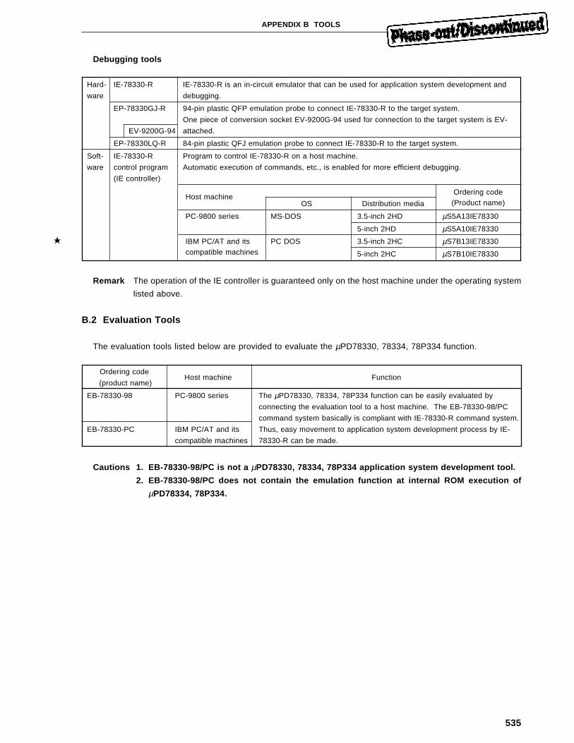
535
APPENDIX B TOOLS
★
Debugging tools
Hard- IE-78330-R IE-78330-R is an in-circuit emulator that can be used for application system development and
ware debugging.
EP-78330GJ-R 94-pin plastic QFP emulation probe to connect IE-78330-R to the target system.
One piece of conversion socket EV-9200G-94 used for connection to the target system is EV-
EV-9200G-94 attached.
EP-78330LQ-R 84-pin plastic QFJ emulation probe to connect IE-78330-R to the target system.
Soft- IE-78330-R Program to control IE-78330-R on a host machine.
ware control program Automatic execution of commands, etc., is enabled for more efficient debugging.
(IE controller)
Host machineOrdering code
OS Distribution media (Product name)
PC-9800 series MS-DOS 3.5-inch 2HD µS5A13IE78330
5-inch 2HD µS5A10IE78330
IBM PC/AT and its PC DOS 3.5-inch 2HC µS7B13IE78330compatible machines 5-inch 2HC µS7B10IE78330
Remark The operation of the IE controller is guaranteed only on the host machine under the operating system
listed above.
B.2 Evaluation Tools
The evaluation tools listed below are provided to evaluate the µPD78330, 78334, 78P334 function.
Ordering codeHost machine Function
(product name)
EB-78330-98 PC-9800 series The µPD78330, 78334, 78P334 function can be easily evaluated by
connecting the evaluation tool to a host machine. The EB-78330-98/PC
command system basically is compliant with IE-78330-R command system.
EB-78330-PC IBM PC/AT and its Thus, easy movement to application system development process by IE-
compatible machines 78330-R can be made.
Cautions 1. EB-78330-98/PC is not a µPD78330, 78334, 78P334 application system development tool.
2. EB-78330-98/PC does not contain the emulation function at internal ROM execution of
µPD78334, 78P334.
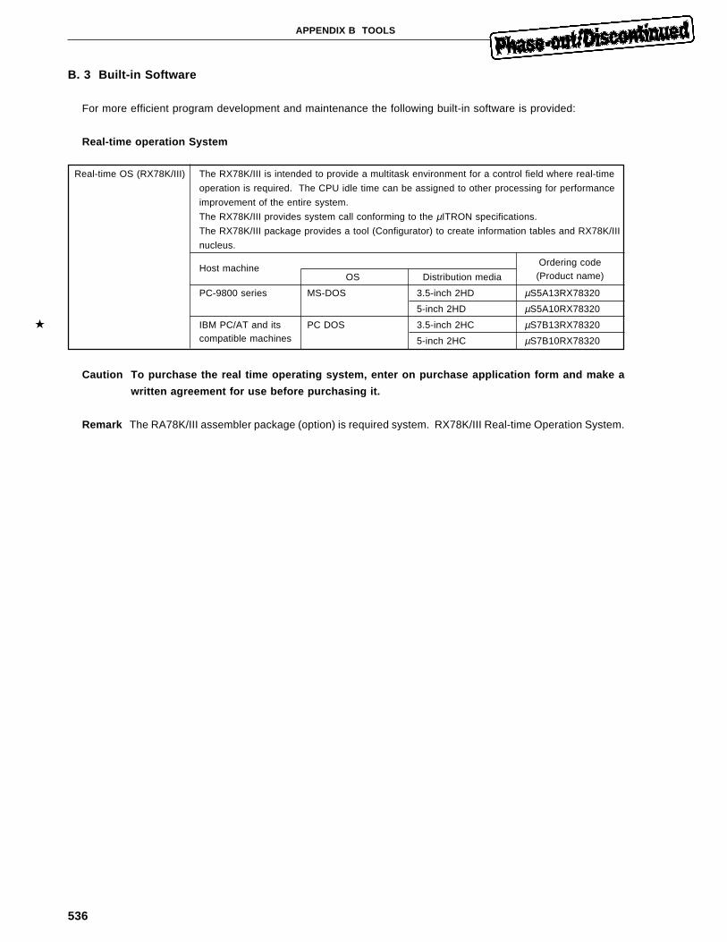
536
APPENDIX B TOOLS
B. 3 Built-in Software
For more efficient program development and maintenance the following built-in software is provided:
Real-time operation System
Real-time OS (RX78K/III) The RX78K/III is intended to provide a multitask environment for a control field where real-time
operation is required. The CPU idle time can be assigned to other processing for performance
improvement of the entire system.
The RX78K/III provides system call conforming to the µITRON specifications.
The RX78K/III package provides a tool (Configurator) to create information tables and RX78K/III
nucleus.
Host machineOrdering code
OS Distribution media (Product name)
PC-9800 series MS-DOS 3.5-inch 2HD µS5A13RX78320
5-inch 2HD µS5A10RX78320
IBM PC/AT and its PC DOS 3.5-inch 2HC µS7B13RX78320compatible machines 5-inch 2HC µS7B10RX78320
Caution To purchase the real time operating system, enter on purchase application form and make a
written agreement for use before purchasing it.
Remark The RA78K/III assembler package (option) is required system. RX78K/III Real-time Operation System.
★
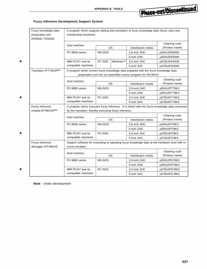
537
APPENDIX B TOOLS
Fuzzy Inference Development Support System
Fuzzy knowledge data A program which supports editing and simulation of fuzzy knowledge data (fuzzy rules and
preparation tool membership functions)
(FE9000, FE9200)
Host machineOrdering code
OS Distribution media (Product name)
PC-9800 series MS-DOS 3.5-inch 2HD µS5A13FE9000
5-inch 2HD µS5A10FE9000
IBM PC/AT and its PC DOS WindowsTM 3.5-inch 2HC µS7B13FE9200compatible machines 5-inch 2HC µS7B10FE9200
Translator (FT78K3)Note A program which convert fuzzy knowledge data prepared with the fuzzy knowledge data
preparation tool into an assembler source program for RA78K/III
Host machineOrdering code
OS Distribution media (Product name)
PC-9800 series MS-DOS 3.5-inch 2HD µS5A13FT78K3
5-inch 2HD µS5A10FT78K3
IBM PC/AT and its PC DOS 3.5-inch 2HC µS7B13FT78K3compatible machines 5-inch 2HC µS7B10FT78K3
Fuzzy inference A program which executes fuzzy inference. It is linked with the fuzzy knowledge data converted
module (FI78K/III)Note by the translator, thereby executing fuzzy inference.
Host machineOrdering code
OS Distribution media (Product name)
PC-9800 series MS-DOS 3.5-inch 2HD µS5A13FI78K3
5-inch 2HD µS5A10FI78K3
IBM PC/AT and its PC DOS 3.5-inch 2HC µS7B13FI78K3compatible machines 5-inch 2HC µS7B10FI78K3
Fuzzy inference Support software for evaluating or adjusting fuzzy knowledge data at the hardware level with in-
debugger (FD78K/III) circuit emulator.
Host machineOrdering code
OS Distribution media (Product name)
PC-9800 series MS-DOS 3.5-inch 2HD µS5A13FD78K3
5-inch 2HD µS5A10FD78K3
IBM PC/AT and its PC DOS 3.5-inch 2HC µS7B13FD78K3compatible machines 5-inch 2HC µS7B10FD78K3
Note Under development
★
★
★
★
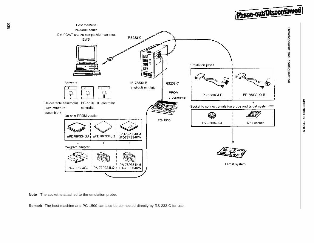
538
AP
PE
ND
IX B
TO
OLS
Developm
ent tool configuration
Note The socket is attached to the emulation probe.
Remark The host machine and PG-1500 can also be connected directly by RS-232-C for use.
539
APPENDIX C REGISTER INDEX
C. 1 Register Index (In Alphabetical Order)
[A]
Asynchronous serial interface mode register (ASIM) ........................................................................................ 178
Asynchronous serial interface status register (ASIS) ........................................................................................ 178
A/D conversion result register 0 (when high-order 8-bit access) (ADCR0H) .................................................. 164
A/D conversion result register 1 (when high-order 8-bit access) (ADCR1H) .................................................. 164
A/D conversion result register 2 (when high-order 8-bit access) (ADCR2H) .................................................. 164
A/D conversion result register 3 (when high-order 8-bit access) (ADCR3H) .................................................. 164
A/D conversion result register 4 (when high-order 8-bit access) (ADCR4H) .................................................. 164
A/D conversion result register 5 (when high-order 8-bit access) (ADCR5H) .................................................. 164
A/D conversion result register 6 (when high-order 8-bit access) (ADCR6H) .................................................. 164
A/D conversion result register 7 (when high-order 8-bit access) (ADCR7H) .................................................. 164
A/D conversion result register 0 (when 16-bit access) (ADCR0) ..................................................................... 164
A/D conversion result register 1 (when 16-bit access) (ADCR1) ..................................................................... 164
A/D conversion result register 2 (when 16-bit access) (ADCR2) ..................................................................... 164
A/D conversion result register 3 (when 16-bit access) (ADCR3) ..................................................................... 164
A/D conversion result register 4 (when 16-bit access) (ADCR4) ..................................................................... 164
A/D conversion result register 5 (when 16-bit access) (ADCR5) ..................................................................... 164
A/D conversion result register 6 (when 16-bit access) (ADCR6) ..................................................................... 164
A/D conversion result register 7 (when 16-bit access) (ADCR7) ..................................................................... 164
A/D converter mode register (ADM) ................................................................................................................... 161
[B]
Baud rate generator compare register (BRG) ...........................................................................................186, 205
Baud rate generator mode register (BRGM) .............................................................................................186, 205
[C]
Capture register 00 (CT00) ................................................................................................................................. 115
Capture register 01 (CT01) ................................................................................................................................. 115
Capture register 02 (CT02) ................................................................................................................................. 115
Capture register 10 (CT10) ................................................................................................................................. 116
Capture/compare register 00 (CC00R) .............................................................................................................. 116
Capture/compare register 01 (CC01R) .............................................................................................................. 116
Clocked serial interface mode register (CSIM) .................................................................................................. 198
Compare register 01 (CM01R) ........................................................................................................................... 111
Compare register 02 (CM02R) ........................................................................................................................... 111
Compare register 03 (CM03R) ........................................................................................................................... 111
Compare register 04 (CM04R) ........................................................................................................................... 111
Compare register 11 (CM11) .............................................................................................................................. 114
Compare register 12 (CM12) .............................................................................................................................. 114
Compare register 20 (CM20) .............................................................................................................................. 114
Compare register 21 (CM21) .............................................................................................................................. 114
Compare register 30 (CM30) .............................................................................................................................. 114
540
APPENDIX C REGISTER INDEX
Compare register X0 (CMX0) ............................................................................................................................. 111
Context switching enable flag register 0H (CSE0H) ......................................................................................... 258
Context switching enable flag register 0L (CSE0L) .......................................................................................... 258
Context switching enable flag register 1L (CSE1L) .......................................................................................... 258
CPU control word (CCW) ...................................................................................................................................... 70
[E]
External interrupt mode register 0 (INTM0) ....................................................................................................... 129
External interrupt mode register 1 (INTM1) ....................................................................................................... 129
[F]
Fetch cycle control register (FCC) ............................................................................................................... 99, 301
[I]
Interrupt mask flag register 0H (MK0H) ............................................................................................................. 253
Interrupt mask flag register 0L (MK0L) .............................................................................................................. 253
Interrupt mask flag register 1L (MK1L) .............................................................................................................. 253
Processing mode specification flag register 0H (ISM0H) ................................................................................. 254
Processing mode specification flag register 0L (ISM0L) ................................................................................... 254
Processing mode specification flag register 1L (ISM1L) ................................................................................... 254
Interrupt request flag register 0H (IF0H) ............................................................................................................ 252
Interrupt request flag register 0L (IF0L) ............................................................................................................. 252
Interrupt request flag register 1L (IF1L) ............................................................................................................. 252
In-service priority register (ISPR) ....................................................................................................................... 257
[M]
Memory expansion mode register (MM) ...................................................................................................... 98, 299
[P]
Port 0 mode control register (PMC0) ................................................................................................................... 96
Port 0 mode register (PM0) .................................................................................................................................. 93
Port 0 (P0) ................................................................................................................................................ 92, 93, 95
Port 1 mode control register (PMC1) ................................................................................................................... 96
port 1 mode register (PM1) .................................................................................................................................. 93
Port 1 (P1) ................................................................................................................................................ 92, 93, 95
Port 2 (P2) ................................................................................................................................................ 92, 93, 95
Port 3 mode control register (PMC3) .................................................................................................. 97, 180, 201
Port 3 mode register (PM3) .................................................................................................................................. 93
Port 3 (P3) ................................................................................................................................................ 92, 93, 95
Port 4 (P4) ................................................................................................................................................ 92, 93, 95
Port 5 mode register (PM5) .................................................................................................................................. 94
Port 5 (P5) ................................................................................................................................................ 92, 93, 95
Port 7 (P7) ................................................................................................................................................ 92, 93, 95
Port 8 (P8) ................................................................................................................................................ 92, 93, 95
Port 9 mode register (PM9) .................................................................................................................................. 94
Port 9 (P9) ................................................................................................................................................ 92, 93, 96
Port read control register (PRDC) ........................................................................................................................ 89
Priority level specification buffer register 0H (PB0H) ........................................................................................ 255
541
APPENDIX C REGISTER INDEX
Priority level specification buffer register 0L (PB0L) ......................................................................................... 255
Priority level specification buffer register 1L (PB1L) ......................................................................................... 255
Priority level specification register (PRSL) ........................................................................................................ 256
Programmable pulse output set register (PPOS) .............................................................................................. 129
Programmable wait control register (PWC) ....................................................................................................... 300
PWM buffer register 0 (PWM0) .......................................................................................................................... 243
PWM buffer register 1 (PWM1) .......................................................................................................................... 243
PWM control register (PWMC) ............................................................................................................................. 98
[R]
Real-time output port register (RTP) .................................................................................................................. 155
Real-time output port reset register (RTPR) ...................................................................................................... 154
Real-time output port set register (RTPS) ......................................................................................................... 154
[S]
Serial bus interface control register (SBIC) ....................................................................................................... 198
Serial I/O shift register (SIO) .............................................................................................................................. 198
Serial receive buffer (RXB) ................................................................................................................................. 178
Serial transmit shift register (TXS) ..................................................................................................................... 178
Standby control register (STBC) ........................................................................................................................ 282
[T]
Timer control register 0 (TMC0) ......................................................................................................................... 124
Timer control register 1 (TMC1) ......................................................................................................................... 124
Timer low access register (TLA) ........................................................................................................................ 110
Timer output control register 0 (TOC0) .............................................................................................................. 126
Timer output control register 1 (TOC1) .............................................................................................................. 126
Timer 0 (TM0) ...................................................................................................................................................... 110
Timer 1 (TM1) ...................................................................................................................................................... 111
Timer 2 (TM2) ...................................................................................................................................................... 111
Timer 3 (TM3) ...................................................................................................................................................... 111
Timer unit mode register 0 (TUM0) .................................................................................................................... 122
Timer unit mode register 1 (TUM1) .................................................................................................................... 123
[W]
Watchdog timer mode register (WDM) ......................................................................................................238, 288
542
APPENDIX C REGISTER INDEX
C. 2 Register Index (In Alphabetical Order)
[A]
ADCR0 .................................................................................................................................................................. 164
ADCR0H ............................................................................................................................................................... 164
ADCR1 .................................................................................................................................................................. 164
ADCR1H ............................................................................................................................................................... 164
ADCR2 .................................................................................................................................................................. 164
ADCR2H ............................................................................................................................................................... 164
ADCR3 .................................................................................................................................................................. 164
ADCR3H ............................................................................................................................................................... 164
ADCR4 .................................................................................................................................................................. 164
ADCR4H ............................................................................................................................................................... 164
ADCR5 .................................................................................................................................................................. 164
ADCR5H ............................................................................................................................................................... 164
ADCR6 .................................................................................................................................................................. 164
ADCR6H ............................................................................................................................................................... 164
ADCR7 .................................................................................................................................................................. 164
ADCR7H ............................................................................................................................................................... 164
ADM ...................................................................................................................................................................... 161
ASIM ..................................................................................................................................................................... 178
ASIS ...................................................................................................................................................................... 178
[B]
BRG ..............................................................................................................................................................186, 205
BRGM ........................................................................................................................................................... 186, 205
[C]
CC00R .................................................................................................................................................................. 116
CC01R .................................................................................................................................................................. 116
CCW ........................................................................................................................................................................ 70
CM01R .................................................................................................................................................................. 111
CM02R .................................................................................................................................................................. 111
CM03R .................................................................................................................................................................. 111
CM04R .................................................................................................................................................................. 111
CM11..................................................................................................................................................................... 114
CM12..................................................................................................................................................................... 114
CM20..................................................................................................................................................................... 114
CM21..................................................................................................................................................................... 114
CM30..................................................................................................................................................................... 114
CMX0 .................................................................................................................................................................... 111
CSE0H .................................................................................................................................................................. 258
CSE0L ................................................................................................................................................................... 258
CSE1L ................................................................................................................................................................... 258
CSIM ..................................................................................................................................................................... 198
CT00 ..................................................................................................................................................................... 115
CT01 ..................................................................................................................................................................... 115
CT02 ..................................................................................................................................................................... 115
543
APPENDIX C REGISTER INDEX
CT10 ..................................................................................................................................................................... 116
[F]
FCC ................................................................................................................................................................. 99, 301
[I]
IF0H ...................................................................................................................................................................... 252
IF0L ....................................................................................................................................................................... 252
IF1L ....................................................................................................................................................................... 252
INTM0 ................................................................................................................................................................... 129
INTM1 ................................................................................................................................................................... 129
ISM0H ................................................................................................................................................................... 254
ISM0L .................................................................................................................................................................... 254
ISM1L .................................................................................................................................................................... 254
ISPR ...................................................................................................................................................................... 257
[M]
MK0H .................................................................................................................................................................... 253
MK0L ..................................................................................................................................................................... 253
MK1L ..................................................................................................................................................................... 253
MM .................................................................................................................................................................. 98, 299
[P]
P0 ............................................................................................................................................................... 92, 93, 95
P1 ............................................................................................................................................................... 92, 93, 95
P2 ............................................................................................................................................................... 92, 93, 95
P3 ............................................................................................................................................................... 92, 93, 95
P4 ............................................................................................................................................................... 92, 93, 95
P5 ............................................................................................................................................................... 92, 93, 95
P7 ............................................................................................................................................................... 92, 93, 95
P8 ............................................................................................................................................................... 92, 93, 95
P9 ............................................................................................................................................................... 92, 93, 96
PB0H ..................................................................................................................................................................... 255
PB0L ..................................................................................................................................................................... 255
PB1L ..................................................................................................................................................................... 255
PM0 ......................................................................................................................................................................... 93
PM1 ......................................................................................................................................................................... 93
PM3 ......................................................................................................................................................................... 93
PM5 ......................................................................................................................................................................... 94
PM9 ......................................................................................................................................................................... 94
PMC0 ...................................................................................................................................................................... 96
PMC1 ...................................................................................................................................................................... 96
PMC3 ..................................................................................................................................................... 97, 180, 201
PPOS .................................................................................................................................................................... 129
PRDC ...................................................................................................................................................................... 89
PRSL ..................................................................................................................................................................... 256
PWC ...................................................................................................................................................................... 300
PWM0 ................................................................................................................................................................... 243
544
APPENDIX C REGISTER INDEX
PWM1 ................................................................................................................................................................... 243
PWMC ..................................................................................................................................................................... 98
[R]
RTP ....................................................................................................................................................................... 155
RTPR .................................................................................................................................................................... 154
RTPS..................................................................................................................................................................... 154
RXB ....................................................................................................................................................................... 178
[S]
SBIC ...................................................................................................................................................................... 198
SIO ........................................................................................................................................................................ 198
STBC..................................................................................................................................................................... 282
[T]
TLA ........................................................................................................................................................................ 110
TM0 ....................................................................................................................................................................... 110
TM1 ....................................................................................................................................................................... 111
TM2 ....................................................................................................................................................................... 111
TM3 ....................................................................................................................................................................... 111
TMC0 .................................................................................................................................................................... 124
TMC1 .................................................................................................................................................................... 124
TOC0..................................................................................................................................................................... 126
TOC1..................................................................................................................................................................... 126
TUM0 .................................................................................................................................................................... 122
TUM1 .................................................................................................................................................................... 123
TXS ....................................................................................................................................................................... 178
[W]
WDM .............................................................................................................................................................238, 288
545
APPENDIX D INSTRUCTION INDEX (IN ALPHABETICAL ORDER)
Instruction Page Instruction Page
ADD A, mem 404 AND1 CY,/saddr.bit 448
ADD A, saddr 403 AND1 CY,/sfr.bit 449
ADD A, sfr 403 AND1 CY,/X.bit 450
ADD A, #byte 402 BC $addr16 472
ADD mem, A 405 BE $addr16 473
ADD saddr, saddr 404 BF A.bit, $addr16 481
ADD saddr, #byte 402 BF PSWH.bit, $addr16 482
ADD sfr, #byte 402 BF PSWL.bit, $addr16 482
ADD r, r1 403 BF saddr.bit, $addr16 480
ADDC A, mem 408 BF sfr.bit, $addr16 480
ADDC A, saddr 407 BF X.bit, $addr16 481
ADDC A, sfr 407 BFSET A.bit, $addr16 487
ADDC A, #byte 405 BFSET PSWH.bit, $addr16 488
ADDC mem, A 409 BFSET PSWL.bit, $addr16 488
ADDC saddr, saddr 408 BFSET saddr.bit, $addr16 486
ADDC saddr, #byte 406 BFSET sfr.bit, $addr16 486
ADDC sfr, #byte 406 BFSET X.bit, $addr16 487
ADDC r, r1 407 BGE $addr16 475
ADDW AX, saddrp 427 BGT $addr16 475
ADDW AX, sfrp 427 BH $addr16 476
ADDW AX, #word 426 BL $addr16 472
ADDW saddrp, saddrp 428 BLE $addr16 476
ADDW saddrp, #word 426 BLT $addr16 475
ADDW sfrp, #word 426 BN $addr16 474
ADDW rp, rp1 427 BNC $addr16 472
ADJBA 443 BNE $addr16 473
ADJBS 443 BNH $addr16 476
AND A, mem 416 BNL $addr16 472
AND A, saddr 416 BNV $addr16 474
AND A, sfr 416 BNZ $addr16 473
AND A, #byte 414 BP $addr16 474
AND mem, A 417 BPE $addr16 473
AND saddr, saddr 416 BPO $addr16 474
AND saddr, #byte 415 BR rp1 470
AND sfr, #byte 415 BR !addr16 470
AND r, r1 415 BR $addr16 471
AND1 CY, A.bit 449 BR [rp1] 470
AND1 CY, PSWH.bit 450 BRK 463
AND1 CY, PSWL.bit 450 BRKCS RBn 490
AND1 CY, saddr.bit 448 BT A.bit, $addr16 478
AND1 CY, sfr.bit 448 BT PSWH.bit, $addr16 479
AND1 CY, X.bit 449 BT PSWL.bit, $addr16 479
AND1 CY,/A.bit 449 BT saddr.bit, $addr16 477
AND1 CY,/PSWH.bit 450 BT sfr.bit, $addr16 477
AND1 CY,/PSWL.bit 451 BT X.bit, $addr16 478
546
APPENDIX D INSTRUCTION INDEX (IN ALPHABETICAL ORDER)
Instruction Page Instruction Page
BTCLR A.bit $addr16 484 CMPMNE [DE+], A 495
BTCLR PSWH. bit, $addr16 485 CMPMNE [DE–], A 495
BTCLR PSWL.bit, $addr16 485 CMPW AX, saddrp 431
BTCLR saddr.bit, $addr16 483 CMPW AX, sfrp 432
BTCLR sfr.bit, $addr16 483 CMPW AX, #word 430
BTCLR X.bit, $addr16 484 CMPW saddrp, saddrp 432
BV $addr16 473 CMPW saddrp, #word 430
BZ $addr16 473 CMPW sfrp, #word 431
CALL rp1 462 CMPW rp, rp1 431
CALL !addr16 461 CVTBW 444
CALL [rp1] 463 DBNZ r2, $addr16 489
CALLF !addr11 461 DBNZ saddr, $addr16 489
CALLT [addr5] 462 DEC r1 435
CHKL sfr 469 DEC saddr 436
CHKLA sfr 469 DECW rp2 436
CLR1 A.bit 458 DECW saddrp 437
CLR1 CY 458 DECW SP 468
CLR1 PSWH.bit 458 DI 499
CLR1 PSWL.bit 458 DIVUW r1 433
CLR1 saddr.bit 457 DIVUX rp1 433
CLR1 sfr.bit 457 EI 499
CLR1 X.bit 458 INC r1 435
CMP A, mem 425 INC saddr 435
CMP A, saddr 424 INCW rp2 436
CMP A, sfr 424 INCW saddrp 436
CMP A, #byte 422 INCW SP 468
CMP mem, A 425 MOV A, !addr16 393
CMP saddr, saddr 424 MOV A, mem 392
CMP saddr, #byte 423 MOV A, PSWH 394
CMP sfr, #byte 423 MOV A, PSWL 394
CMP r, r1 423 MOV A, r1 390
CMPBKC [DE+], [HL+] 496 MOV A, saddr 390
CMPBKC [DE–], [HL–] 496 MOV A, sfr 391
CMPBKE [DE+], [HL+] 494 MOV A, [saddrp] 392
CMPBKE [DE–], [HL–] 494 MOV mem, A 392
CMPBKNC [DE+], [HL+] 497 MOV PSWH, A 394
CMPBKNC [DE–], [HL–] 497 MOV PSWH, #byte 394
CMPBKNE [DE+], [HL+] 495 MOV PSWL, A 394
CMPBKNE [DE–], [HL–] 495 MOV PSWL, #byte 393
CMPMC [DE+], A 496 MOV r1, #byte 389
CMPMC [DE–], A 496 MOV r, r1 390
CMPME [DE+], A 494 MOV saddr, A 390
CMPME [DE–], A 494 MOV saddr, saddr 391
CMPMNC [DE+], A 497 MOV saddr, #byte 389
CMPMNC [DE–], A 497 MOV sfr, A 391
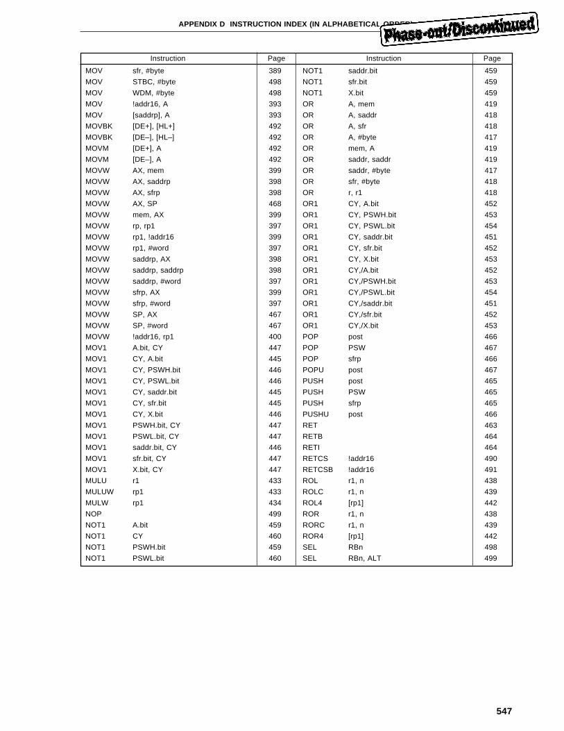
547
APPENDIX D INSTRUCTION INDEX (IN ALPHABETICAL ORDER)
Instruction Page Instruction Page
MOV sfr, #byte 389 NOT1 saddr.bit 459
MOV STBC, #byte 498 NOT1 sfr.bit 459
MOV WDM, #byte 498 NOT1 X.bit 459
MOV !addr16, A 393 OR A, mem 419
MOV [saddrp], A 393 OR A, saddr 418
MOVBK [DE+], [HL+] 492 OR A, sfr 418
MOVBK [DE–], [HL–] 492 OR A, #byte 417
MOVM [DE+], A 492 OR mem, A 419
MOVM [DE–], A 492 OR saddr, saddr 419
MOVW AX, mem 399 OR saddr, #byte 417
MOVW AX, saddrp 398 OR sfr, #byte 418
MOVW AX, sfrp 398 OR r, r1 418
MOVW AX, SP 468 OR1 CY, A.bit 452
MOVW mem, AX 399 OR1 CY, PSWH.bit 453
MOVW rp, rp1 397 OR1 CY, PSWL.bit 454
MOVW rp1, !addr16 399 OR1 CY, saddr.bit 451
MOVW rp1, #word 397 OR1 CY, sfr.bit 452
MOVW saddrp, AX 398 OR1 CY, X.bit 453
MOVW saddrp, saddrp 398 OR1 CY,/A.bit 452
MOVW saddrp, #word 397 OR1 CY,/PSWH.bit 453
MOVW sfrp, AX 399 OR1 CY,/PSWL.bit 454
MOVW sfrp, #word 397 OR1 CY,/saddr.bit 451
MOVW SP, AX 467 OR1 CY,/sfr.bit 452
MOVW SP, #word 467 OR1 CY,/X.bit 453
MOVW !addr16, rp1 400 POP post 466
MOV1 A.bit, CY 447 POP PSW 467
MOV1 CY, A.bit 445 POP sfrp 466
MOV1 CY, PSWH.bit 446 POPU post 467
MOV1 CY, PSWL.bit 446 PUSH post 465
MOV1 CY, saddr.bit 445 PUSH PSW 465
MOV1 CY, sfr.bit 445 PUSH sfrp 465
MOV1 CY, X.bit 446 PUSHU post 466
MOV1 PSWH.bit, CY 447 RET 463
MOV1 PSWL.bit, CY 447 RETB 464
MOV1 saddr.bit, CY 446 RETI 464
MOV1 sfr.bit, CY 447 RETCS !addr16 490
MOV1 X.bit, CY 447 RETCSB !addr16 491
MULU r1 433 ROL r1, n 438
MULUW rp1 433 ROLC r1, n 439
MULW rp1 434 ROL4 [rp1] 442
NOP 499 ROR r1, n 438
NOT1 A.bit 459 RORC r1, n 439
NOT1 CY 460 ROR4 [rp1] 442
NOT1 PSWH.bit 459 SEL RBn 498
NOT1 PSWL.bit 460 SEL RBn, ALT 499
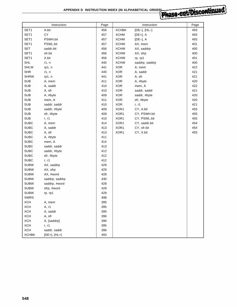
548
APPENDIX D INSTRUCTION INDEX (IN ALPHABETICAL ORDER)
Instruction Page Instruction Page
SET1 A.bit 456 XCHBK [DE–], [HL–] 493
SET1 CY 457 XCHM [DE+], A 493
SET1 PSWH.bit 457 XCHM [DE–], A 493
SET1 PSWL.bit 457 XCHW AX, mem 401
SET saddr.bit 456 XCHW AX, saddrp 400
SET1 sfr.bit 456 XCHW AX, sfrp 400
SET1 X.bit 456 XCHW rp, rp1 401
SHL r1, n 440 XCHW saddrp, saddrp 400
SHLW rp1, n 441 XOR A, mem 422
SHR r1, n 440 XOR A, saddr 421
SHRW rp1, n 441 XOR A, sfr 421
SUB A, mem 411 XOR A, #byte 420
SUB A, saddr 410 XOR mem, A 422
SUB A, sfr 410 XOR saddr, saddr 421
SUB A, #byte 409 XOR saddr, #byte 420
SUB mem, A 411 XOR sfr, #byte 420
SUB saddr, saddr 410 XOR r, r1 421
SUB saddr, #byte 409 XOR1 CY, A.bit 455
SUB sfr, #byte 409 XOR1 CY, PSWH.bit 455
SUB r, r1 410 XOR1 CY, PSWL.bit 455
SUBC A, mem 414 XOR1 CY, saddr.bit 454
SUBC A, saddr 413 XOR1 CY, sfr.bit 454
SUBC A, sfr 413 XOR1 CY, X.bit 455
SUBC A, #byte 411
SUBC mem, A 414
SUBC saddr, saddr 413
SUBC saddr, #byte 412
SUBC sfr, #byte 412
SUBC r, r1 412
SUBW AX, saddrp 429
SUBW AX, sfrp 429
SUBW AX, #word 428
SUBW saddrp, saddrp 430
SUBW saddrp, #word 428
SUBW sfrp, #word 429
SUBW rp, rp1 429
SWRS 498
XCH A, mem 395
XCH A, r1 395
XCH A, saddr 395
XCH A, sfr 396
XCH A, [saddrp] 396
XCH r, r1 395
XCH saddr, saddr 396
XCHBK [DE+], [HL+] 493
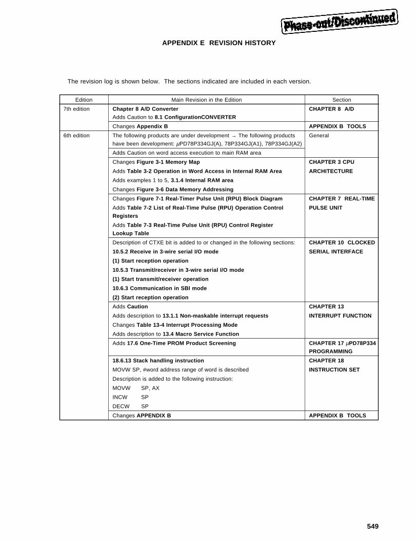
549
APPENDIX E REVISION HISTORY
The revision log is shown below. The sections indicated are included in each version.
Edition Main Revision in the Edition Section
7th edition Chapter 8 A/D Converter CHAPTER 8 A/D
Adds Caution to 8.1 ConfigurationCONVERTER
Changes Appendix B APPENDIX B TOOLS
6th edition The following products are under development → The following products General
have been development: µPD78P334GJ(A), 78P334GJ(A1), 78P334GJ(A2)
Adds Caution on word access execution to main RAM area
Changes Figure 3-1 Memory Map CHAPTER 3 CPU
Adds Table 3-2 Operation in Word Access in Internal RAM Area ARCHITECTURE
Adds examples 1 to 5, 3.1.4 Internal RAM area
Changes Figure 3-6 Data Memory Addressing
Changes Figure 7-1 Real-Timer Pulse Unit (RPU) Block Diagram CHAPTER 7 REAL-TIME
Adds Table 7-2 List of Real-Time Pulse (RPU) Operation Control PULSE UNIT
Registers
Adds Table 7-3 Real-Time Pulse Unit (RPU) Control Register
Lookup Table
Description of CTXE bit is added to or changed in the following sections: CHAPTER 10 CLOCKED
10.5.2 Receive in 3-wire serial I/O mode SERIAL INTERFACE
(1) Start reception operation
10.5.3 Transmit/receiver in 3-wire serial I/O mode
(1) Start transmit/receiver operation
10.6.3 Communication in SBI mode
(2) Start reception operation
Adds Caution CHAPTER 13
Adds description to 13.1.1 Non-maskable interrupt requests INTERRUPT FUNCTION
Changes Table 13-4 Interrupt Processing Mode
Adds description to 13.4 Macro Service Function
Adds 17.6 One-Time PROM Product Screening CHAPTER 17 µPD78P334
PROGRAMMING
18.6.13 Stack handling instruction CHAPTER 18
MOVW SP, #word address range of word is described INSTRUCTION SET
Description is added to the following instruction:
MOVW SP, AX
INCW SP
DECW SP
Changes APPENDIX B APPENDIX B TOOLS

550
[MEMO]

551
Although NEC has taken all possible stepsto ensure that the documentation suppliedto our customers is complete, bug freeand up-to-date, we readily accept thaterrors may occur. Despite all the care andprecautions we've taken, you mayencounter problems in the documentation.Please complete this form wheneveryou'd like to report errors or suggestimprovements to us.
Hong Kong, Philippines, OceaniaNEC Electronics Hong Kong Ltd.Fax: +852-2886-9022/9044
KoreaNEC Electronics Hong Kong Ltd.Seoul BranchFax: 02-528-4411
TaiwanNEC Electronics Taiwan Ltd.Fax: 02-719-5951
Address
North AmericaNEC Electronics Inc.Corporate Communications Dept.Fax: 1-800-729-9288
1-408-588-6130
EuropeNEC Electronics (Europe) GmbHTechnical Documentation Dept.Fax: +49-211-6503-274
South AmericaNEC do Brasil S.A.Fax: +55-11-6465-6829
Asian Nations except PhilippinesNEC Electronics Singapore Pte. Ltd.Fax: +65-250-3583
JapanNEC CorporationSemiconductor Solution Engineering DivisionTechnical Information Support Dept.Fax: 044-548-7900
I would like to report the following error/make the following suggestion:
Document title:
Document number: Page number:
Thank you for your kind support.
If possible, please fax the referenced page or drawing.
Excellent Good Acceptable PoorDocument Rating
Clarity
Technical Accuracy
Organization
CS 97.8
Name
Company
From:
Tel. FAX
Facsimile Message


