Embed Size (px)
Citation preview

Observation of Dirac surface states in the noncentrosymmetric superconductor BiPd
H. M. Benia,1, ∗ E. Rampi,2 C. Trainer,3 C. M. Yim,3 A. Maldonado,3 D. C. Peets,1, 4 A. Stohr,1 U. Starke,1 K.
Kern,1, 5 A. Yaresko,1 G. Levy,2, 6 A. Damascelli,2, 6 C. R. Ast,1 A. P. Schnyder,1 and P. Wahl3, 1, †
1Max-Planck-Institut fur Festkorperforschung, Heisenbergstrasse 1, D-70569 Stuttgart, Germany2Department of Physics & Astronomy, University of British Columbia, Vancouver, British Columbia V6T 1Z1, Canada3SUPA, School of Physics and Astronomy, University of St Andrews, North Haugh, St Andrews, Fife KY16 9SS, UK
4Advanced Materials Laboratory, Fudan University, Shanghai 200438, China5Institut de Physique, Ecole Polytechnique Federale de Lausanne, 1015 Lausanne, Switzerland
6Quantum Matter Institute, University of British Columbia, Vancouver, British Columbia V6T 1Z4, Canada(Dated: August 4, 2016)
Materials with strong spin-orbit coupling (SOC) have in recent years become a subject of intenseresearch due to their potential applications in spintronics and quantum information technology.In particular, in systems which break inversion symmetry, SOC facilitates the Rashba-Dresselhauseffect, leading to a lifting of spin degeneracy in the bulk and intricate spin textures of the Blochwave functions. Here, by combining angular resolved photoemission (ARPES) and low temperaturescanning tunneling microscopy (STM) measurements with relativistic first-principles band structurecalculations, we examine the role of SOC in single crystals of noncentrosymmetric BiPd. We reportthe detection of several Dirac surface states, one of which exhibits an extremely large spin splitting.Unlike the surface states in inversion-symmetric systems, the Dirac surface states of BiPd have com-pletely different properties at opposite faces of the crystal and are not trivially linked by symmetry.The spin-splitting of the surface states exhibits a strong anisotropy by itself, which can be linked tothe low in-plane symmetry of the surface termination.
PACS numbers: 79.60.Bm,73.20.-r,71.70.Ej
The interplay of strong spin-orbit coupling (SOC) withsuperconductivity has become a major focus of researchin recent years, as both are essential ingredients to sta-bilize Majorana bound states. The spin-orbit interactionaffects the electronic states in a material in various waysand in particular can lead to non-trivial topologies of theband structure. In topological insulators SOC separatesthe conduction and valence bands, leading to an insulat-ing state with an inverted band gap [1–3]. The latterleads directly to the presence of Dirac surface states pro-tected by time-reversal symmetry [4–6]. Another conse-quence of SOC is the Rashba effect [7–10], which in theabsence of inversion symmetry lifts the spin degeneracyof the electronic bands, generating intricate spin texturesin the electronic wave functions [11–13]. Commonly ob-served at surfaces or interfaces, in noncentrosymmetricmaterials the Rashba-Dresselhaus effect leads to a liftingof spin-degeneracy of the bulk bands. Combined withsuperconductivity this can lead to mixing of spin-singletand spin-triplet pairing components [14, 15] and, moreinterestingly, to a topologically nontrivial superconduct-ing phase [16–19].
Noncentrosymmetric BiPd [20–24] becomes supercon-ducting below 3.8 K [25–30] and offers a unique opportu-nity to study the interplay between SOC and supercon-ductivity. The large spin-orbit interaction of the heavyelement Bi results in a sizeable spin splitting of the bulkbands of BiPd [29]. This in turn can lead to nontriv-ial wavefunction topologies and unconventional supercon-ducting states [31, 32]. Along with the half-Heusler com-pounds [33–35] and PbTaSe2 [36–38], BiPd constitutes
a rare example of a noncentrosymmetric superconduc-tor which cleaves easily, enabling high-resolution surface-sensitive spectroscopy of its electronic states[29, 39].
In this paper we report the observation of Rashba spin-split Dirac surface states of noncentrosymmetric BiPdby angle-resolved photoemission spectroscopy (ARPES)and low-temperature scanning tunneling microscopy andspectroscopy (STM/STS). Due to the lack of inversionsymmetry, the (010) and (010) surface states can appearat different energies and exhibit different dispersions andspin-polarizations. By combining the experimental re-sults with relativistic first-principles band structure cal-culations we identify the Dirac surface states of both the(010) and (010) surfaces. This observation of distinctDirac surface states originating from the opposing sur-face terminations represents a unique demonstration ofthe impact of the lack of inversion symmetry on the elec-tronic states.
The crystal growth using a modified Bridgman–Stockbarger technique has been described in detail else-where [40]. The crystals were cooled slowly through theα−β phase transition to maximize the domain size of thelow-temperature α phase; resulting in high-quality crys-tals [30]. At low temperature α-BiPd (in the followingreferred to as “BiPd”) forms in the noncentrosymmet-ric space group P21 [21–24]. The structure is character-ized by two double layers stacked along the monoclinicb axis, which are related by a 180◦ screw symmetry [seeFig. 1(a)]. Since the bonding between double layers isweaker than within them, the crystals readily cleave per-pendicular to the monoclinic b axis and, as previously
arX
iv:1
608.
0127
7v1
[co
nd-m
at.m
trl-
sci]
3 A
ug 2
016

2
S 1-S
SS 0+
SS 0-
low
high
FIG. 1. (a) Crystal structure of BiPd, showing the preferred cleaving plane. (b) Schematic representation of the Brillouin zoneof BiPd as well as the surface Brillouin zone of the (010) and (010) surfaces. (c) Surface Brillouin zone with the cuts shown inpanels (d)-(g) in blue. (d) Experimental electronic band structure of a BiPd(010) surface along the S–Γ direction (ν = 21 eV).(e) Electronic structure measured with ν = 29 eV. The photoemission intensities in (d) and (e) and in other photoemissionmaps in this paper are displayed using the colour scale shown in e. (f) and (g) Calculated electronic structure of BiPd in slabgeometry including the cuts shown in (d) and (e). The size of the circles is proportional to the spectral weight of Bi 6p states inthe first (red) and second (blue) layer of the (010) and (010) surfaces. The surface states are labelled SSn+ and SSn-, where +and - denote whether they occur on the (010) or (010) surface, while n numbers the surface states sequentially with increasingbinding energy.
demonstrated [29], are twinned such that both (010) and(010) surfaces can appear on the same side of the crystal(see ref. 41 for details on the cleaving procedure).
ARPES measurements were performed on freshlycleaved surfaces using (i) a Helium source (ν = 21.2 eVand 40.8 eV) with a hemispherical SPECS HSA3500electron analyzer, and (ii) linearly-polarized synchrotronlight from the UE112-PGM undulator beamline atBESSY II with a Scienta R8000 analyzer. The samplewas held at temperatures lower than 100 K during cleav-ing and throughout the measurements.
STM experiments were performed in a home-built low-temperature STM operating at temperatures down to1.5 K in cryogenic vacuum [42]. Samples were preparedby in-situ cleaving at low temperatures. Tips were cutfrom a PtIr wire. Bias voltages were applied to the sam-ple. Differential conductance spectra have been recordedthrough a lock-in amplifier (f = 408 Hz, Vmod = 2 mV).
Figures 1(b) and (c) show schematically the bulk Bril-
louin zone and its surface projection. Figures 1(d) and(e) show the results of ARPES, measured along the Γ–S direction in the Brillouin zone at two different photonenergies. The most prominent feature of the surface elec-tronic structure when measured with a He-I lamp is theappearance of a strong state (labelled SS1+ in Fig. 1(d))at the S-point at 0.7 eV binding energy. In addition, athigher photon energy (Fig. 1(e)), within the same direc-tional band gap at the S-point a surface state SS1– can beidentified, albeit with much weaker intensity. These areidentified as surface states through their lack of disper-sion with varying the incident photon energy and hencekz [41]. To understand the origin and topological natureof these surface states, we have employed fully relativis-tic linear muffin tin orbital calculations [43–45] using arepeated slab system consisting of six BiPd double layersseparated by two empty double layers which representthe vacuum. We find that around the Fermi energy EF,all the bands are mainly of Bi 6p orbital character with

3
subdominant but non-negligible contributions of Pd 4dstates. The strong atomic SOC of Bi induces a spinsplitting of the bands of the order of tens of meV and,moreover, results in a large energy shift of states thathave predominant p1/2 orbital character[46]. The latterleads to formation of a band gap at the Γ point [29, 46].In Figs. 1(f) and (g), we show the calculated dispersionsnear EF of the (010) and (010) surfaces of BiPd, respec-tively, along high symmetry directions of the surface BZ[Fig. 1(b) and (c)]. The momentum-resolved surface den-sities of states at the (010) and (010) sides are indicatedby filled circles. Interestingly, Dirac surface states appearboth at the S and Γ points of the surface BZ. Thus bycomparison with band structure calculations, the featuresSS1+ and SS1- seen in ARPES can be directly associatedwith the surface states of the BiPd surface. The simulta-neous observation of SS1+ and SS1- in the measurementis not reproduced in the calculations: the two states orig-inate from opposite surface terminations, with the one athigher binding energy arising from the (010) terminationand the one closer to the Fermi energy from the (010)termination. Since these two terminations correspond toopposite surfaces of a single crystal, their simultaneousobservation by ARPES indicates twin domains with op-posite direction of the crystallographic b axis within thebeam spot. A structural transition around 200◦C [23, 24]is known to cause twinning, and this type of twin bound-ary has been previously observed by STM [29].
b
21eV
Bin
din
g e
nerg
y (
eV
)
1.5
1.0
0.5
0.0
a G'S
29eV
G'S
0.8 0.4 0.0 -0.4-1
Momentum (Å )
kx
G¢G¢
ky
0.59 eV
-0.8
-0.4
0.0
-1M
om
en
tum
(Å
)
d
0.7
-0.4 -0.2 0.0 0.2 0.4-1
Momentum (Å )-0.4 -0.2 0.0 0.2 0.4
-1Momentum (Å )
-0.4 -0.2 0.0 0.2 0.4-1
Momentum (Å )
Sc
SS 1-
SS 1+
SS 2+
SS 2-
0.8 0.4 0.0 -0.4 0.8 0.4 0.0 -0.4
0.7 eV 0.83 eV
-1Momentum (Å )
-1Momentum (Å )
G'
SS 1+
SS 1-
SS 2
SS 1+
SS 1-
SS 2
FIG. 2. (a) and (b) Intensity maps of the energy and k-resolved surface band structure of BiPd measured along theS − Γ′ direction with ν = 21 eV and ν = 29 eV, respectively.(c) Schematic representation of the surface states. (d) Con-stant energy cuts obtained at 0.59, 0.7, and 0.83 eV, energiesindicated as dashed horizontal lines in (a). Overlaid on theconstant energy cuts is a schematic of the surface Brillouinzone.
In full agreement between experiment and theory, thespin-splitting of the surface state is substantially larger inthe S-Γ′ direction compared to the S-Γ direction. Experi-mental data for the S-Γ′ direction are shown in Figs. 2(a)and (b), taken at the same photon energies ν as Figs. 1(d)and (e), respectively. The two measurements show thestates SS1+ and SS1– with different intensities, but oth-erwise at the same energy and having the same disper-sion, confirming that they are of two-dimensional char-acter. The different intensities are likely due to finalstate effects. There are small differences in binding ener-gies between experiment and calculation on the order of100 meV. One likely source of this discrepancy is surfacerelaxation which is neglected in the calculation. Con-stant energy contours obtained at the energies aroundthe Dirac point, shown in Fig. 2(d) for the energies la-belled in Fig. 2(a), clearly reveal the two band maxima inthe S-Γ′ direction due to the strongly anisotropic Rashbasplitting (see also Ref. 41).
Data and calculations yield a further set of surfacestates at higher binding energies, which we label SS2+and SS2-. As opposed to the hole-like SS1± states, SS2±have an electron-like dispersion. In the experiment, theyare most clearly resolved with ν = 21 eV (Fig. 2(a)).They are located near the bottom of the directional bandgap at the S-point and quickly develop into surface reso-nances when moving away from S.
Besides the surface states found at the S points, thecalculations reveal an additional pair of surfaces statesat the Γ point (labelled by SS0± in Figs. 1(f) and (g)),which are in the unoccupied states and thus inaccessi-ble to ARPES. For one termination, this state has beendetected previously by STS [29]. While the Dirac-conestates at the S point are present even if SOC is neglected,the Dirac state at the Γ point appears within a gapopened up by SOC and arises as a consequence of anSOC-driven band inversion. This scenario is reminiscentof the topological insulator Bi2Se3 [5], indicating a possi-ble topological origin. Here we show the signature of thesurface state at Γ for both terminations from tunnelingspectra, see Fig. 3. The terminations in the STM datahave been identified from the surface corrugation (com-pare fig. 3(a-c)). Spectra of the surface state (fig. 3(d)show only a very small shift of ∼ 6 meV between thetwo terminations, with the surface state showing up atlarger energies on the termination which we identify asthe (010) surface.
We note that the band crossings of the Dirac statesboth at the Γ and S points are protected by time-reversalsymmetry due to Kramers’ theorem. Consistently forall surface states in the occupied states (SS1±, SS2±)those on the (010) surface occur at an energy at least100 meV higher than on (010), whereas the shift is verysmall and in the opposite direction for the surface statein the unoccupied states (SS0±).
We have fitted the standard Rashba-Bychkov
4
10
0Hei
ght (
pm)
2520151050Distance (Å)
010 010
4
3
2
dI/d
V (a
rb. u
nit)
0.50.40.3Sample bias (V)
(010) (010)
(010)(a)
(c)
(b) (d)(010) +6
-6
0
z (pm)
FIG. 3. (a) and (b) Topographies of the (010) and (010) ter-minations respectively, obtained with the same tip. Blue/redspheres represent Bi atoms and green/purple Pd atoms in thetop surface layer, compare fig. 1(a). (c) Linecuts of the twoterminations, showing the different corrugations. Linecutsshifted horizontally for clarity. (d) dI/dV spectra obtained on(010) and (010) terminations. The surface state on the (010)face is at a slightly larger energy than on (010) (Vs = 0.5 V,Is = 2 nA).
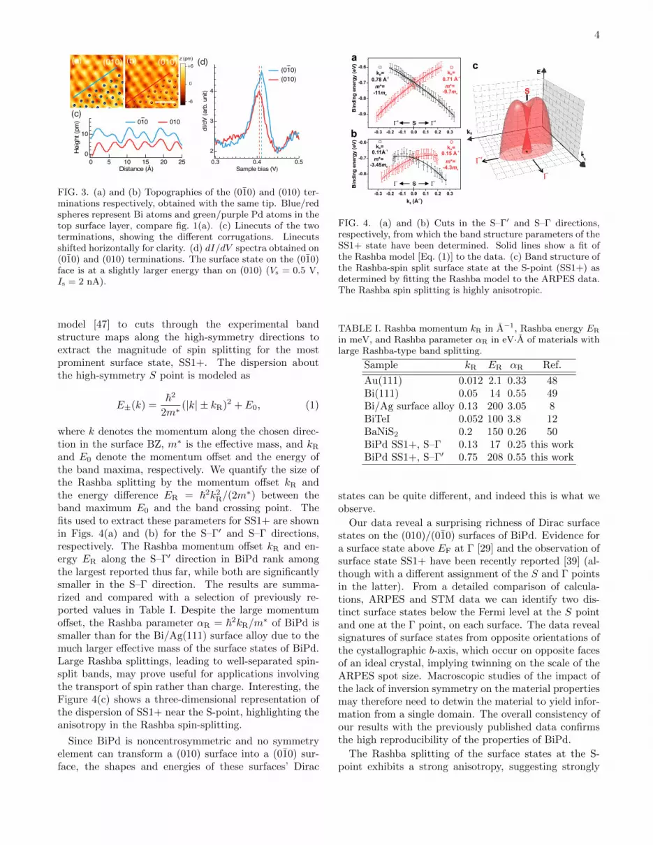
model [47] to cuts through the experimental bandstructure maps along the high-symmetry directions toextract the magnitude of spin splitting for the mostprominent surface state, SS1+. The dispersion aboutthe high-symmetry S point is modeled as
E±(k) =~2
2m∗(|k| ± kR)2 + E0, (1)
where k denotes the momentum along the chosen direc-tion in the surface BZ, m∗ is the effective mass, and kRand E0 denote the momentum offset and the energy ofthe band maxima, respectively. We quantify the size ofthe Rashba splitting by the momentum offset kR andthe energy difference ER = ~2k2R/(2m∗) between theband maximum E0 and the band crossing point. Thefits used to extract these parameters for SS1+ are shownin Figs. 4(a) and (b) for the S–Γ′ and S–Γ directions,respectively. The Rashba momentum offset kR and en-ergy ER along the S–Γ′ direction in BiPd rank amongthe largest reported thus far, while both are significantlysmaller in the S–Γ direction. The results are summa-rized and compared with a selection of previously re-ported values in Table I. Despite the large momentumoffset, the Rashba parameter αR = ~2kR/m∗ of BiPd issmaller than for the Bi/Ag(111) surface alloy due to themuch larger effective mass of the surface states of BiPd.Large Rashba splittings, leading to well-separated spin-split bands, may prove useful for applications involvingthe transport of spin rather than charge. Interesting, theFigure 4(c) shows a three-dimensional representation ofthe dispersion of SS1+ near the S-point, highlighting theanisotropy in the Rashba spin-splitting.
Since BiPd is noncentrosymmetric and no symmetryelement can transform a (010) surface into a (010) sur-face, the shapes and energies of these surfaces’ Dirac
G'
S
E
k II
k II
G
G¢
S
-0.3 -0.2 -0.1 0.0 0.1 0.2 0.3
-0.9
-0.8
-0.7
-0.6
Bin
din
g e
ne
rgy
(e
V)
-1k (Å )II
-0.8
-0.7
-0.6
Bin
din
g e
ne
rgy
(e
V)
-0.3 -0.2 -0.1 0.0 0.1 0.2 0.3
G'S
G G
c
b
a
k = R-10.78 Å
m*= -11me
k = R-10.71 Å
m*= -9.7me
k =R-10.11Å
m*=-3.45me
k = R-1
0.15 Å
m*=-4.3me
FIG. 4. (a) and (b) Cuts in the S–Γ′ and S–Γ directions,respectively, from which the band structure parameters of theSS1+ state have been determined. Solid lines show a fit ofthe Rashba model [Eq. (1)] to the data. (c) Band structure ofthe Rashba-spin split surface state at the S-point (SS1+) asdetermined by fitting the Rashba model to the ARPES data.The Rashba spin splitting is highly anisotropic.
TABLE I. Rashba momentum kR in A−1, Rashba energy ER
in meV, and Rashba parameter αR in eV·A of materials withlarge Rashba-type band splitting.
Sample kR ER αR Ref.
Au(111) 0.012 2.1 0.33 48Bi(111) 0.05 14 0.55 49Bi/Ag surface alloy 0.13 200 3.05 8BiTeI 0.052 100 3.8 12BaNiS2 0.2 150 0.26 50BiPd SS1+, S–Γ 0.13 17 0.25 this workBiPd SS1+, S–Γ′ 0.75 208 0.55 this work
states can be quite different, and indeed this is what weobserve.
Our data reveal a surprising richness of Dirac surfacestates on the (010)/(010) surfaces of BiPd. Evidence fora surface state above EF at Γ [29] and the observation ofsurface state SS1+ have been recently reported [39] (al-though with a different assignment of the S and Γ pointsin the latter). From a detailed comparison of calcula-tions, ARPES and STM data we can identify two dis-tinct surface states below the Fermi level at the S pointand one at the Γ point, on each surface. The data revealsignatures of surface states from opposite orientations ofthe cystallographic b-axis, which occur on opposite facesof an ideal crystal, implying twinning on the scale of theARPES spot size. Macroscopic studies of the impact ofthe lack of inversion symmetry on the material propertiesmay therefore need to detwin the material to yield infor-mation from a single domain. The overall consistency ofour results with the previously published data confirmsthe high reproducibility of the properties of BiPd.
The Rashba splitting of the surface states at the S-point exhibits a strong anisotropy, suggesting strongly

5
directionally-dependent SOC in the surface state. Thisstrong directional dependence can be understood by com-parison with the surface structure of BiPd: the Γ–S di-rection is along rows of Bi (or Pd) atoms, therefore elec-tronic states propagating along this direction are onlymoderately exposed to the surface corrugation. Alongthe Γ–S′ (or equivalently S–Γ′) direction, rows of Bi andPd atoms alternate, and electronic states with wavevec-tors along this direction are exposed much more stronglyto the surface corrugation and hence to the surface elec-tric fields which generate the spin splitting. The con-nection between surface corrugation and the spin-orbitsplitting has been discussed previously in the context ofthe Bi/Ag(111) surface alloy [51, 52]. In BiPd, the corru-gation of the top-most layer is a direct consequence of thecrystal structure of the bulk material, boosting the spinsplitting of the surface states only in specific directionsdue to the anisotropy of the crystal structure.
In summary, through comparison of ARPES and STMexperiments with band structure calculations, we haveconfirmed the presence of unconventional Dirac surfacestates in noncentrosymmetric BiPd. The extremely largeand anisotropic Rashba splitting in this system makesit an excellent candidate for future studies on the intri-cate spin texture of spin-split bands. Our results sug-gest a new way to engineer anisotropic spin textures andRashba splittings of surface states by exploiting the lowsymmetry of the surface termination. The findings pro-vide independent confirmation of the existence of twinboundaries in the material [29], which may prove crucialto understanding its superconducting properties [30, 53].
Acknowledgments.— The authors thank Ed Yellandfor useful discussions. Funding from the MPG-UBCcenter and the Engineering and Physical Sciences Re-search Council (EP/I031014/1 and EP/L505079/1) areacknowledged. This work was supported by the DFGwithin projects STA315/8-1 and BE5190/1-1. We alsothank the staff at Bessy II of the Helmholtz-ZentrumBerlin for their assistance.
∗ [email protected]† [email protected]
[1] M. Z. Hasan and C. L. Kane, Rev. Mod. Phys. 82, 3045(2010).
[2] X.-L. Qi and S.-C. Zhang, Rev. Mod. Phys. 83, 1057(2011).
[3] M. Z. Hasan and J. E. Moore, Ann. Rev. Cond. Matt.Phys. 2, 55 (2011).
[4] D. Hsieh, Y. Xia, L. Wray, D. Qian, A. Pal, J. H. Dil,J. Osterwalder, F. Meier, G. Bihlmayer, C. L. Kane, Y. S.Hor, R. J. Cava, and M. Z. Hasan, Science 323, 919(2009).
[5] Y. Xia, D. Qian, D. Hsieh, L. Wray, A. Pal, H. Lin,A. Bansil, D. Grauer, Y. S. Hor, R. J. Cava, and M. Z.Hasan, Nat Phys 5, 398 (2009).
[6] J. Seo, P. Roushan, H. Beidenkopf, Y. S. Hor, R. J. Cava,and A. Yazdani, Nature 466, 343 (2010).
[7] E. I. Rashba, Sov. Phys. Solid State 2, 1109 (1960).[8] C. R. Ast, J. Henk, A. Ernst, L. Moreschini, M. C. Falub,
D. Pacile, P. Bruno, K. Kern, and M. Grioni, Phys. Rev.Lett. 98, 186807 (2007).
[9] A. Crepaldi, L. Moreschini, G. Autes, C. Tournier-Colletta, S. Moser, N. Virk, H. Berger, P. Bugnon, Y. J.Chang, K. Kern, A. Bostwick, E. Rotenberg, O. V.Yazyev, and M. Grioni, Phys. Rev. Lett. 109, 096803(2012).
[10] M. Bahramy, B.-J. Yang, R. Arita, and N. Nagaosa, Nat.Commun. 3, 679 (2012).
[11] D. Hsieh, Y. Xia, D. Qian, L. Wray, J. H. Dil, F. Meier,J. Osterwalder, L. Patthey, J. G. Checkelsky, N. P. Ong,A. V. Fedorov, H. Lin, A. Bansil, D. Grauer, Y. S. Hor,R. J. Cava, and M. Z. Hasan, Nature 460, 1101 (2009).
[12] K. Ishizaka, M. S. Bahramy, H. Murakawa, M. Sakano,T. Shimojima, T. Sonobe, K. Koizumi, S. Shin,H. Miyahara, A. Kimura, K. Miyamoto, T. Okuda,H. Namatame, M. Taniguchi, R. Arita, N. Nagaosa,K. Kobayashi, Y. Murakami, R. Kumai, Y. Kaneko,Y. Onose, and Y. Tokura, Nat. Mater. 10, 521 (2011).
[13] Y. H. Wang, D. Hsieh, D. Pilon, L. Fu, D. R. Gardner,Y. S. Lee, and N. Gedik, Phys. Rev. Lett. 107, 207602(2011).
[14] E. Bauer and M. Sigrist, Non-Centrosymmetric Super-conductors: Introduction and Overview , Lecture Notesin Physics, Vol. 847 (Springer Berlin, 2012) pp. 1–357.
[15] E. Bauer, G. Hilscher, H. Michor, C. Paul, E. W. Scheidt,A. Gribanov, Y. Seropegin, H. Noel, M. Sigrist, andP. Rogl, Phys. Rev. Lett. 92, 027003 (2004).
[16] A. P. Schnyder, S. Ryu, A. Furusaki, and A. W. W.Ludwig, Phys. Rev. B 78, 195125 (2008).
[17] B. Beri, Phys. Rev. B 81, 134515 (2010).[18] A. P. Schnyder and S. Ryu, Phys. Rev. B 84, 060504
(2011).[19] M. Sato and S. Fujimoto, Phys. Rev. B 79, 094504 (2009).[20] D. M. Kheiker, G. S. Zhdanov, and N. N. Zhuravlev, Zh.
Eksp. Teor. Fiz. 25, 621 (1953).[21] N. Zhuravlev, Zh. Eksp. Teor. Fiz. 5, 1064 (1957).[22] Y. Bhatt and K. Schubert, Journal of the Less Common
Metals 70, P39 (1980).[23] Y. Bhatt and K. Schubert, J. Less-Common Met. 64, P17
(1979).[24] V. M. Ionov, N. A. Tomilin, A. E. Prozorovskii, A. N.
Klimenko, Y. V. Titov, S. G. Zhukov, and G. V. Fetisov,Sov. Phys. Crystallogr. 34, 496 (1989).
[25] N. E. Alekseevskii, Zh. Eksp. Teor. Fiz. 23, 484 (1952).[26] B. Joshi, A. Thamizhavel, and S. Ramakrishnan, Phys.
Rev. B 84, 064518 (2011).[27] M. Mondal, B. Joshi, S. Kumar, A. Kamlapure, S. C.
Ganguli, A. Thamizhavel, S. S. Mandal, S. Ramakrish-nan, and P. Raychaudhuri, Phys. Rev. B 86, 094520(2012).
[28] K. Matano, S. Maeda, H. Sawaoka, Y. Muro, T. Tak-abatake, B. Joshi, S. Ramakrishnan, K. Kawashima,J. Akimitsu, and G.-q. Zheng, J. Phys. Soc. Jpn. 82,084711 (2013).
[29] Z. Sun, M. Enayat, A. Maldonado, C. Lithgow, E. Yel-land, D. C. Peets, A. Yaresko, A. P. Schnyder, andP. Wahl, Nat Commun 6, 6633 (2015).
[30] D. C. Peets, A. Maldonado, M. Enayat, Z. Sun, P. Wahl,and A. P. Schnyder, Phys. Rev. B 93, 174504 (2016).

6
[31] S. Sasaki, M. Kriener, K. Segawa, K. Yada, Y. Tanaka,M. Sato, and Y. Ando, Phys. Rev. Lett. 107, 217001(2011).
[32] N. Levy, T. Zhang, J. Ha, F. Sharifi, A. A. Talin, Y. Kuk,and J. A. Stroscio, Phys. Rev. Lett. 110, 117001 (2013).
[33] C. Liu, Y. Lee, T. Kondo, E. D. Mun, M. Caudle, B. N.Harmon, S. L. Budko, P. C. Canfield, and A. Kaminski,Phys. Rev. B 83, 205133 (2011).
[34] H. Kim, K. Wang, Y. Nakajima, R. Hu, S. Ziemak,P. Syers, L. Wang, H. Hodovanets, J. D. Denlinger,P. M. R. Brydon, D. F. Agterberg, M. A. Tanatar,R. Prozorov, and J. Paglione, “Beyond spin-triplet:Nodal topological superconductivity in a noncentrosym-metric semimetal,” (2016), arXiv:1603.03375 [cond-mat.supr-con].
[35] Y. Nakajima, R. Hu, K. Kirshenbaum, A. Hughes,P. Syers, X. Wang, K. Wang, R. Wang, S. R. Saha,D. Pratt, J. W. Lynn, and J. Paglione, Sci. Adv. 1,e1500242 (2016).
[36] M. N. Ali, Q. D. Gibson, T. Klimczuk, and R. J. Cava,Phys. Rev. B 89, 020505 (2014).
[37] G. Bian, T.-R. Chang, R. Sankar, S.-Y. Xu, H. Zheng,T. Neupert, C.-K. Chiu, S.-M. Huang, G. Chang, I. Be-lopolski, D. S. Sanchez, M. Neupane, N. Alidoust, C. Liu,B. Wang, C.-C. Lee, H.-T. Jeng, C. Zhang, Z. Yuan,S. Jia, A. Bansil, F. Chou, H. Lin, and M. Z. Hasan,Nat. Commun. 7, 10556 (2016).
[38] S.-Y. Guan, P.-J. Chen, M.-W. Chu, R. Sankar,F. Chou, H.-T. Jeng, C.-S. Chang, and T.-M.Chuang, “Superconducting topological surface statesin non-centrosymmetric bulk superconductor PbTaSe2,”(2016), arXiv:1605.00548 [cond-mat.supr-con].
[39] M. Neupane, N. Alidoust, S.-Y. Xu, I. Belopolski, D. S.Sanchez, T.-R. Chang, H.-T. Jeng, H. Lin, A. Bansil,D. Kaczorowski, M. Z. Hasan, and T. Durakiewicz, “Dis-covery of the topological surface state in a noncentrosym-metric superconductor BiPd,” (2015), arXiv:1505.03466[cond-mat.mes-hall].
[40] D. C. Peets, J. Phys.: Conf. Ser. 568, 022037 (2014).[41] See Supplemental Material at http://link.aps.org/
supplemental/10.1103/. . . for additional ARPES mea-surements.
[42] U. Singh, M. Enayat, S. White, and P. Wahl, Rev. Sci.Instr. 84, 013708 (2013).
[43] O. K. Andersen, Phys. Rev. B 12, 3060 (1975).[44] V. Antonov, B. Harmon, and A. Yaresko, Elec-
tronic structure and magneto-optical properties of solids(Kluwer Academic Publishers, Dordrecht, Boston, Lon-don, 2004).
[45] A. Y. Perlov, A. N. Yaresko, and V. N. Antonov, PY-LMTO: A Spin-Polarized Relativistic LMTO Package forElectronic Structure Calculations (unpublished).
[46] A. H. Macdonald, W. E. Pickett, and D. D. Koelling, J.Phys. C 13, 2675 (1980).
[47] Y. A. Bychkov and E. I. Rashba, JETP Lett. 39, 78(1984).
[48] S. LaShell, B. A. McDougall, and E. Jensen, Phys. Rev.Lett. 77, 3419 (1996).
[49] Y. M. Koroteev, G. Bihlmayer, J. E. Gayone, E. V.Chulkov, S. Blugel, P. M. Echenique, and P. Hofmann,Phys. Rev. Lett. 93, 046403 (2004).
[50] D. Santos-Cottin, M. Casula, G. Lantz, Y. Klein,L. Petaccia, P. Le Fevre, F. Bertran, E. Papalazarou,
M. Marsi, and A. Gauzzi, Nat. Commun. 7, 11258(2016).
[51] I. Gierz, B. Stadtmuller, J. Vuorinen, M. Lindroos,F. Meier, J. H. Dil, K. Kern, and C. R. Ast, PhysicalReview B 81, 245430 (2010).
[52] G. Bian, X. Wang, T. Miller, and T.-C. Chiang, PhysicalReview B 88, 085427 (2013).
[53] X. B. Yan, Y. Xu, L. P. He, J. K. Dong, H. B. Cho, D. C.Peets, J.-G. Park, and S. Y. Li, Supercond. Sci. Tech.29, 065001 (2016).

7
Supplementary Information for“Observation of Dirac surface states inthe noncentrosymmetric superconductor
BiPd”
H. M. Benia, E. Rampi, C. Trainer, C. M. Yim,A. Maldonado, D. C. Peets, A. Stohr, U. Starke,
K. Kern, A. Yaresko, G. Levy, A. Damascelli, C. R. Ast,A. P. Schnyder, and P. Wahl
Figures S1 and S2 show supporting ARPES data. InFig. S1 ARPES intensity maps are displayed for threedifferent incident photon energies. These energies probe
different kz, leading to rather different bulk band struc-tures in this relatively three-dimensional material, butthe two-dimensional surface states do not disperse. Thisfigure also includes second-derivative images, showing thesurface states with greater contrast. Figure S2 shows ad-ditional constant-energy cuts for an incident photon en-ergy of 21 eV, fleshing out the dispersion of the surfacestates in greater detail.
Figure S3 shows the cleaving setup that was used toobtain surfaces with opposite surface termination. Sincethe ARPES measurements of the two cleaved surfacesexhibit similar features, we conclude that the BiPd crys-tal consists of twin domains, with the twin domain sizesmaller than the ARPES beam spot.

8
-0.4 0.0 0.2 0.4
SS 3
-1Momentum (Å )-0.4 -0.2 0.0 0.2 0.4
c
-1Momentum (Å )-0.4 -0.2 0.0 0.2 0.4
SS 2
SS 1
41eV29eV 29eV
BS
Bin
din
g e
nerg
y (
eV
)
b
1.5
1.0
0.5
0.0
-1Momentum (Å )-0.4 -0.2 0.0 0.2 0.4
-1Momentum (Å )-0.4 -0.2 0.0 0.2 0.4
-1Momentum (Å )-0.4 -0.2 0.0 0.2 0.4
a
21eV 21eV
Bin
din
g e
nerg
y (
eV
)
1.5
1.0
0.5
0.0
41eV
Bin
din
g e
nerg
y (
eV
)
1.5
1.0
0.5
0.0
G'S G'S G'S G'SG'S G'S
29eV
-1Momentum (Å )-0.2
29eV
FIG. S1. Experimental surface electronic band structure of BiPd(010) along the S–Γ′ direction and second derivative images,measured using different photon energies: (a) 21 eV (He-I), (b) 29 eV (synchrotron light), and (c) 42 eV (He-II). Changing theincident photon energy changes kz, but these bands do not disperse, as would be expected for two-dimensional surface states.
-1.0
-0.6
-0.8
-0.4
-0.2
0.0
0.2
0.8 0.6 0.4 0.2 0.0 -0.2 -0.4 -0.6
E =EB F 0.44 eV 0.59 eV
1.04 eV0.94 eV0.83 eV 1.23 eV
0.69 eV
0.8 0.6 0.4 0.2 0.0 -0.2 -0.4 -0.60.8 0.6 0.4 0.2 0.0 -0.2 -0.4 -0.60.8 0.6 0.4 0.2 0.0 -0.2 -0.4 -0.6
-1.0
-0.6
-0.8
-0.4
-0.2
0.0
0.2
-1Momentum k (Å )x
-1M
om
en
tum
k (
Å)
x
FIG. S2. Additional constant energy cuts at different binding energies EB of the experimental surface electronic band structureof BiPd(010). ARPES measurements have been performed using a He-I light source (21 eV). The dashed line represents theprojected surface Brillouin zone.

9
kyky
-0.4 -0.2 0.0 0.2 0.4-1
Momentum (Å )
G'S
1.5
1.0
0.5
0.0
1.5
1.0
0.5
0.0
-0.4 -0.2 0.0 0.2 0.4-1
Momentum (Å )
G'S
Bin
din
g e
ne
rgy
(e
V)
BiPd
sample holder 2
sample holder 1
Glue
BiPd
sample holder 1
(010)
BiPd
sample holder 2
(010)
BiPd
BiPd surf. 1
BiPd
surf. 1
Cleaving
BiPd surf. 1
BiPd surf. 1
Wobble stick
a b
c
e
d
FIG. S3. (a) Schematic drawing of the experimental design shown in the digital photograph in (b) of a BiPd crystal putinto a sandwich arrangement between two sample holders. (c) Schematic drawing showing an ideal situation, where thenoncentrosymmetric BiPd is a perfect single crystal without twinning. In this case cleaving results in two cleaved surfacescharacterized by a single termination/orientation each. (d) Digital photograph showing the two sample holders with theresulting two BiPd crystals after cleaving in UHV and ARPES measurements. (e) Experimental band structures measuredsuccessively on the two cleaved surfaces at 100 K using a He-I lab source. Since the ARPES data of the two cleaved surfacesexhibit almost identical features, we conclude that the crystals are composed of twin domains, whose size is smaller then theARPES beam spot.


