Embed Size (px)
Citation preview
Phase-Reversal Travelling-Wave Integrated Optical Modulators for Broadband and Bandpass Applications
by
Christopher David Watson
Submitted in accordance with the requirements of the University of London for the degree of Doctor of Philosophy
Department of Electronic and Electrical Engineering University College London
May 1992
1

ProQuest Number: 10609331
All rights reserved
INFORMATION TO ALL USERS The quality of this reproduction is dependent upon the quality of the copy submitted.
In the unlikely event that the author did not send a com p le te manuscript and there are missing pages, these will be noted. Also, if material had to be removed,
a note will indicate the deletion.
uestProQuest 10609331
Published by ProQuest LLC(2017). Copyright of the Dissertation is held by the Author.
All rights reserved.This work is protected against unauthorized copying under Title 17, United States C ode
Microform Edition © ProQuest LLC.
ProQuest LLC.789 East Eisenhower Parkway
P.O. Box 1346 Ann Arbor, Ml 48106- 1346
Abstract
This thesis is concerned with the analysis, fabrication, and characterisation of phase-reversal optical modulators for both broadband and bandpass applications.
The operation of modulation is described together w ith the param eters by which optical modulators are characterised. Direct and indirect modulation are discussed. Particular attention is given to optical m odulators constructed using titanium -indiffused lithium niobate technology. For these devices, the most im portant characteristics determining the frequency response and efficiency are studied.
The technique of phase-reversal is examined as a means of artificial phase-matching. Systematic procedures for the design of phase-reversal electrode patterns are proposed. A novel class of equalising modulator is presented. A simulation of a digital lightwave system based on an equalising phase-reversal device is constructed.
Transmission lines on anisotropic substrates are examined. The lim itations of a quasi-static analysis are highlighted. A full-wave treatm ent utilising the method of lines is presented for the study of electrooptic modulators.
Full-wave analysis is employed to study conventional coplanar waveguide electrooptic modulators. A new modulator structure, based on a fin line, is presented for high frequency operation. A comprehensive analysis of this structure is undertaken, including a modal analysis of a dielectric discontinuity. Designs are developed toward the demonstration of a device operating above 30GHz. A novel phase-matching technique, particularly suited to the fin line configuration, is discussed.
The major processes involved in the fabrication of titanium - indiffused lithium niobate devices are briefly described. The techniques by which high speed modulators are measured are discussed, including a novel method by optical down-conversion. Experimental measurements are presented for devices operating in the frequency range 0 to 40GHz.
The thesis is concluded, with suggestions for future avenues of research.
2

To my parents.
Acknowledgements
I wish to express my gratitude to my supervisor, Professor MGF Wilson for guiding me toward the successful completion of this project. I would like to thank him for his advise, encouragement and sponsorship throughout the duration of my research.
I am indebted to the Electronic & Electrical Engineering Department of UCL for financial support, and for providing part-time employment. In particular I would like to thank Fred Stride, Kevin Lee, Professor Gareth Parry, and Mike Effemey for their goodwill.
My work has benefited from an association with the Marconi Research Centre, Chelmsford with whom I was a CASE student for the first two years of this project. I would like to thank, Alan Donaldson, Chris Rycroft, David Hall, and Nick Parsons for useful discussions.
During the course of this project I was fortunate to obtain a four month visit to the Physical Sciences Centre, Minnesota. This experience was one of the highlights of my PhD, and its success was due in no small part to the friendliness and kindness of all of those I had the pleasure of meeting during my short stay. I would like to thank Anis Husain, Charles Sullivan, Martha and Andy Connors-Roth and in particular Jane Herrmann, for making me feel so welcome.
I am grateful to David Humphreys of the National Physical Laboratory who has devoted a great deal of his time to this project. I would like to thank him for both his collaboration and the many constructive comments that he has made regarding this work.
I would like to thank my friends and colleagues (both past and present) in the Integrated Optics group and E&E department of UCL for providing such a convivial atmosphere in which to conduct research. In particu lar, I would like to thank Mihailo Milovanovic, Duleep Wickramasinghe, Henry Robinson, Didier Erasme and Chen Fushen for their friendship, and many hours of entertainment.
I would like to thank Sian Jaggar for her constant support and encouragment throughout the duration of this project.
I wish to acknowledge financial support from SERC, JOERS, and GEC Marconi.
4

Table of Contents
pageA b s t r a c t ...................................................................................................... 2Acknowledgement........................................................................................ 4Table of Contents.......................................................................................... 5L ist o f figu res an d T ab les..................................................................... 9
C hapter 1: Introduction.......................................................................... 131.1 Introduction.................................................................................... 141.2 Historical Development of the Project......................................... 161.3 Thesis Organisation...................................................................... 16References for chapter 1................................................................... 19
Chapter 2: Basic Theory and Background............................................ 212.1 Introduction ............................................................................. 222.2 Modulation and Optical Modulators........................................ 22
2.2.1 Modulation, response, bandwidth and dynamic range 222.2.2 Optical modulator technologies....................................... 24
2.2.2.1 The laser diode.......................................................... 242.2.2.2 External electroabsorption modulators............... 252.2.2.3 External electrooptic modulators............................ 26
2.3 Electrooptic Modulators on Lithium Niobate.......................... 272.3.1 A bulk phase modulator on lithium niobate.................. 272.3.2 Optical waveguides in lithium niobate.......................... 292.3.3 Crystal orientation, electrode geometry and over-lap . 302.3.4 Integrated optic intensity modulators ......................... 322.3.5 High speed considerations............................................... 35
2.3.5.1 Drive geometries....................................................... 362.3.5.2 The travelling-wave interaction.......................... 36
2.4 State of the Art and Figures of M erit.......................................... 382.4.1 Broadband modulators..................................................... 402.4.2 Narrow band millimetre wave modulators................... 41
2.5 Chapter Summary........................................................................ 41References for chapter 2................................................................... 45
5
Chapter 3: Analysis and Design of Phase-Reversal M odulators 493.1 Introduction.................................................................................... 503.2 The Phase-Reversal Electrode.................................................. 50
3.2.1 Frequency response of a phase-reversal modulator 523.2.2 Pattern selection for phase-reversal modulators 533.2.3 Phase-reversal modulators for broadband
applications....................................................................... 573.3 Equalisation using PRMs......................................................... 61
3.3.1 Time domain analysis of a phase-reversal electrode.... 613.3.2 Time domain pattern selection........................................ 623.3.3 Equalisation of a photodetector........................................ 653.3.4 System equalisation.......................................................... 68
3.3.4.1 System performance criterion................................. 703.3.4.2 Numerical synthesis of eye-diagrams................... 72
3.4 Chapter Summary......................................................................... 74References for chapter 3 ..................................................................... 76
C hapter 4: Electromagnetic Analysis of Modulator Electrodes 794.1 Introduction................................................................................... 804.2 Quasi-Static Analysis ................................................................... 81
4.2.1 Conformal mapping applied to coplanar structures.... 834.2.2 Transmission line equivalent circuits............................ 864.2.3 The limit of the quasi-static approximation.................. 86
4.3 Full-Wave Analysis by the Method of L ines............................... 894.3.1 Hybrid mode analysis and the wave equation............... 894.3.2 Descretisation and solution of the wave equation 914.3.3 Application of the boundary conditions......................... 944.3.4 Calculation of fields, power flow, and impedance 974.3.5 MOL applied to full-wave analysis of EOM.................... 101
4.4 Comparison with Published D a ta ............................................... 1024.5 Deviations from Real Transmission Lines.............................. 107
4.5.1 Dielectric lo ss .................................................................... 1084.5.2 Conductor thickness and loss......................................... 108
4.6 Chapter Summary......................................................................... 110References for chapter 4 ..................................................................... I l l
6
Chapter 5: H igh Speed C oplanar M odulators................................. 1145.1 Introduction.................................................................................... 1155.2 High Speed CPW Modulator......................................................... 115
5.2.1 Convergence of MOL......................................................... 1165.2.2 Confirmation of quasi-static propagation.................... 1185.2.3 Phase matching in CPW.............................................. 1215.2.4 Over-lap estimation for SCPW and CPW modulators... 123
5.2.4.1 Over-lap considerations in the SCPW modulator.. 1255.2.4.2 Low frequency over-lap variations in CPW modulators................................. 128
5.2.5 Thick electrodes and conductor loss............................... 1295.3 A Millimetre Wave Optical Modulator........................................ 130
5.3.1 The dielectric discontinuity......................................... 1325.3.1.1 The modal spectrum of a slab loaded waveguide.. 1325.3.1.2 Modal analysis of the dielectric discontinuity 137
5.3.2 Taper design ..................................................................... 1425.3.3 The interaction region.................................................. 146
5.3.3.1 The phase velocity of the electrical wave............... 1465.3.3.2 Computation of the over-lap efficiency................... 1485.3.3.3 Phase matching by electrical cut-off................... 148
5.4 Chapter Summary......................................................................... 149References for chapter 5................................................................. 152
Chapter 6: Fabrication, Measurements and R esu lts ......................... 1566.1 Introduction.................................................................................... 1576.2 Fabrication..................................................................................... 157
6.2.1 Waveguide fabrication..................................................... 1576.2.2 Electrode fabrication ........................................................ 1596.2.3 Polishing and substrate lapping..................................... 1606.2.4 Modulator pigtailing......................................................... 160
6.3 Measurements Techniques.......................................................... 1616.3.1 Measurement of a phase modulator.............................. 161
6.3.1.1 The scanning Fabry-Perot interferometer 1636.3.1.2 Optical heterodyne detection................................... 164
6.3.2 Measurement of an intensity modulator..................... 1666.3.2.1 Direct detection......................................................... 1686.3.2.2 Swept frequency method.......................................... 1706.3.2.3 Two tone method....................................................... 171
7
6.3.2.4 Optical down-conversion by signal multiplication 1726.4 Results............................................................................................. 174
6.4.1 Broadband phase-reversal modulator............................ 1746.4.1.1 Measurement by direct detection .......................... 1756.4.1.2 Measurement by swept frequency......................... 1806.4.1.3 Modulator modelling................................................ 1836.4.1.4 Discussion.................................................................. 185
6.4.2 Equalising phase-reversal m odulator............................ 1866.4.2.1 Measurement by direct detection............................ 1866.4.2.2 Modulator modelling................................................ 1906.4.2.3.Discussion................................................................ 190
6.4.3 A millimetre wave optical m odulator............................ 1916.4.3.1 Measurement by swept frequency......................... 1916.4.3.2 Measurement optical down-conversion................. 1996.4.3.3 Modulator modelling................................................ 2026.4.3.4 Discussion.................................................................. 203
6.5 Chapter Summary......................................................................... 204References for chapter 6 ..................................................................... 206
Chapter 7: Summary and Future W ork................................................ 2077.1 Summary and Conclusions.......................................................... 2087.2 Directions for Future W ork.......................................................... 212
Appendix 1.......................................................................................... 213Appendix 2............................................................................ 214Appendix 3.......................................................................................... 217
8
List of Figures and Tablespage
Chapter 2:Figure 2.1 A bulk phase modulator on lithium niobate........................ 28Figure 2.2 Alternative electrode and waveguide configurations for
integrated optical modulators on lithium n io b a te 31Figure 2.3 Common optical circuits employed in intensity
modulators ............................................................................ 33Figure 2.4 Some common characteristics of the interferometric
intensity-voltage transfer characteristic............................. 34Figure 2.5 Two common modulator drive configurations................... 37Figure 2.6 The effect of a velocity mismatch in a travelling-wave
in teraction ................................................................... 39Table 2.1 A review of wideband external modulators......................... 42Table 2.2 A review of narrow band millimetre wave modulators.... 43
Chapter 3:Figure 3.1 A schematic diagram of a phase-reversal electrode 51Figure 3.2 A two dimensional error function........................................ 54Figure 3.3 The h it' representation of a phase-reversal electrode 56Figure 3.4 A flow diagram of an iterative optimising algorithm 56Figure 3.5 Frequency response of optimised phase-reversal
p a tte rn s ................................................................................... 58Figure 3.6 Comparison of the efficiency of different m odulators 60Figure 3.7 A phase-reversal electrode and its impulse response... ..... 63Figure 3.8 An externally modulated optical link ................................ 66Figure 3.9 Measured characteristics of a high speed photodetector.. 67Figure 3.10 Theoretical characteristics of equalised photodetector .... 69Figure 3.11 A schematic diagram of the detection process
a t the decision circuit............................................................. 71Figure 3.12 Eye diagrams showing the behaviour of an equalised
and unequalised system........................................................ 73
Chapter 4:Figure 4.1 Typical modulator electrode geometries .......................... 82Figure 4.2 The application of a conformal transformation ................ 84Figure 4.3 The equivalent circuit of a section of transmission line ... 87
9
Figure 4.4 An ideal TEM transmission line incorporating a mixeddielectric.................................................................................. 87
Figure 4.5 Descretisation scheme employed in the method of lines .. 92Figure 4.6 Boundary conditions on T c,h at electric and magnetic
w alls.......................................................................................... 95Figure 4.7 The descretisation of a microstrip containing a single
dielectric interface.................................................................. 95Figure 4.8 Electrode structures examined in this th esis ................... 100Figure 4.9 Calculated variation of impedance with aspect ratio
for a CPW ............................................................................... 103Figure 4.10 The electric field profiles of a CPW as calculated by
MOL and by conformal mapping ........................................ 104Figure 4.11 Dispersion characteristics of a shielded CPW .................. 105Figure 4.12 Dispersion characteristics of the odd and even mode of a
CPW on sapphire .................................................................. 105Figure 4.13 Dispersion characteristics of a fin line fabricated on
different anisotropic substrates.......................................... 106
Chapter 5:Figure 5.1 A CPW and the descretisation system employed in MOL. 117Figure 5.2 The convergence of microwave effective index with
descretisation distance.......................................................... 119Figure 5.3 The convergence of microwave effective index with side
wall position .......................................................................... 119Figure 5.4 Dispersive behaviour of a buffered and unbuffered CPW
on Z cut lithium n iobate....................................................... 120Figure 5.5 The effect of increasing the lateral dimensions of a CPW on
its dispersive properties........................................................ 120Figure 5.6 The variation of microwave effective index and impedance
with buffer layer thickness................................................... 122Figure 5.7 The variation of microwave effective index and impedance
with frequency for a shielded CPW on lithium niobate 122Figure 5.8 Variation of over-lap factor as a function of waveguide
offset for a shielded CPW modulator................................... 126Figure 5.9 Calculated variation of voltage-length product with
optical mode size ................................................................... 126
10

Figure 5.10 Variation of over-lap factor as a function of waveguideoff-set for an X cut shielded CPW modulator.................... 127
Figure 5.11 The variation of over-lap factor as a function of waveguideoffset for X and Z cut CPW modulators above andbelow 100MHz......................................................................... 127
Figure 5.12 The tangential magnetic field at the dielectric interfaceof a CPW electrode fabricated on GaAs................................ 131
Figure 5.13 A schematic diagram of a fin line optical modulator 133Figure 5.14 The cross section of a rectangular waveguide loaded
with a dielectric slab.............................................................. 133Figure 5.15 The dispersion of all the propagating modes of a slab
loaded waveguide................................................................... 136Figure 5.16 The dispersion of all the propagating modes of a slab
loaded waveguide................................................................... 136Figure 5.17 The dispersion of all the propagating modes of a slab
loaded waveguide................................................................... 138Figure 5.18 A longitudinal representation of a discontinuity between an
empty and slab loaded waveguide........................................ 138Figure 5.19 The calculated tangential electric field in the plane
of the discontinuity between an empty and slabloaded waveguide................................................................... 141
Figure 5.20 The measured and calculated return loss of a section of slabloaded waveguide................................................................... 141
Figure 5.21 A fin line and the descretisation system employedin M OL.................................................................................... 144
Figure 5.22 The microwave effective index of a fin line on lithiumniobate as a function of slot width ....................................... 145
Figure 5.23 The power-voltage impedance of a fin line on lithiumniobate as a function of slot width ....................................... 145
Figure 5.24 The microwave effective index and loss coefficient of thefin line modulator as a function of frequency................... 147
Figure 5.25 The variation of maximum phase shift for the fin linemodulator as a function of optical mode size ..................... 147
Figure 5.26 The variation of microwave effective index as a functionof shield heigh t....................................................................... 150
Table 5.1 Calculated and measured voltage-length products of X and Z cut modulators above and below the acoustic resonance.................................................................. 129.
11
Table 5.2 A comparison of different numerical models of a CPW incorporating thick m etalisations.............. 131
Chapter 6:Figure 6.1 The standard procedures involved in the fabrication of a
titanium indiffused lithium niobate integratedoptic device.............................................................................. 158
Figure 6.2 A schematic diagram of an optical phase modulator 162Figure 6.3 The action of a scanning Fabry-Perot interferometer on
a phase modulated optical w ave.......................................... 162Figure 6.4 A schematic diagram of an optical intensity modulator.. 167Figure 6.5 A photograph of device W5/2................................................. 176Figure 6.6 The measured return loss and insertion loss of W5/2 ..... 178Figure 6.7 The direct detection measurement system ........................ 179Figure 6.8 Experimental and theoretical response of W5/2 ............... 181Figure 6.9 The swept frequency measurement system..................... 182Figure 6.10 The equivalent circuit of W5/2 ............................................. 184Figure 6.11 A photograph of device W6/5................................................. 187Figure 6.12 The measured return loss and insertion loss of W6/5 ..... 188Figure 6.13 Experimental and theoretical response of W6/5 ............... 189Figure 6.14 A photograph of device W 10/6.............................................. 192Figure 6.15 The measured return loss and insertion loss of W10/6 .... 193Figure 6.16 The swept frequency measurement system for W 10/6..... 195Figure 6.17 Experimental and theoretical response of W 10/6.............. 197Figure 6.18 The variation of extinction with drive power..................... 198Figure 6.19 The optical down-conversion measurement system ........ 200Figure 6.20 A typical measurement by optical down-conversion 201Table 6.1 Fabrication parameters of W5/2, W6/5 and W10/6............. 177
12

Chapter 1
Introduction
1.1 Introduction
1.2 Historical development of the project
1.3 Thesis organisation
13
1.1 Introduction
As a transmission medium the optical fibre offers a single mode bandwidth and transmission loss far beyond that offered by conventional electrical waveguides. Consequently, considerable effort has been devoted to the development of optoelectronic and integrated optic components to allow communication by fibre optics. In this thesis we are concerned with the analysis, design, and construction of external, integrated optic m odulators in titan ium indiffused technology. E xternal optical modulators of this type with multigigahertz bandwidth or high frequency operation have many applications some of which are described below.
In wideband single channel applications, signal capacity is limited by the bandwidth of the system components. Previously, the speed of the optoelectronic components such as the modulator had exceeded the ability of the electronics to process the signals before modulation and after demodulation. However, in recent years the speed of the electronic processing components has climbed dramatically. Indeed, recently an electronic multiplexer with a data rate of 30Gbit/s has been reported^1 This suggests a new impetus to the design of wideband external modulators.
To increase signal capacity beyond tha t enforced by the processing electronics, multiple data channels may be multiplexed optically and transm itted along the same optical fibre. For short haul communications where fibre dispersion is not too im portant emphasis has been placed upon wave division multiplexing (WDM). In a WDM system each channel consists of a transm itter with a different laser wavelength. At the receiver of the system, demultiplexing is achieved by passing the composite signal through a tunable optical filter. Systems with up to 100, 600MBit channels have been demonstrated with this technique yielding a composite signal capacity of 60Gbit/s^1,2 . In this demonstration directly modulated DFB lasers were employed as the transmitters. However, in principle the same signal capacity could be achieved using fewer channels and wideband external modulators. Moreover, the use of external modulators could allow coherent optical detection enabling closer channel spacing and more sensitive detection^
For long haul communications, in terest has focussed on optical time-division multiplexing (OTDM)f14 . In OTDM systems external optical modulators are used to encode pulse trains generated by mode-
14
locked semiconductor laser diodes. As the pulse width is smaller than the repetition time, higher signal capacity can be achieved by interleaving several low data rate bit streams. In this case, the ultim ate signal capacity is limited by the speed of the optical demultiplexer a t the receiver and by fibre dispersion. Optical demultiplexers can be constructed from external optical modulators operated as switches^1*® or as gates^1-6 but in either case high frequency operation is important. Consequently, narrowband, high speed external modulators are of interest, though in the future these components may be superceded by the development of all-optical dem ultip lexers^1-7 . Most long haul systems employ a transm itting wavelength of 1.55pm in order to minimise optical loss. Unfortunately, in single mode step index optical fibre, dispersion limits the bit rate over a given span^1-8 . Though the effect of dispersion can be reduced by employing dispersion shifted fibre^1-9 , considerable interest has arisen in soliton transm ission schemes^1-10 . Solitons are optical pulses which propagate along 'lossless' optical fibre without dispersion as a result of the variation of fibre index with optical intensity. The loss of the optical fibre in such systems is eliminated by periodic amplification provided by erbium doped fibre amplifiers. As before, there is need for fast optical switching for both demultiplexing and routing control of the solitons. Moreover, external modulators have been used for dynamic soliton reshaping in order to overcome accumulated noise from the optical amplifiers. Using this technique 'error free' transm ission over one million km at a bit rate of lOGbit/s has recently been demonstrated^111 .
Wideband external optical modulators have also found application in instrum entation systems. Indeed, frequency domain test equipment incorporating external modulators is now available commercially for network analysis to frequencies of 20GHz^112 . Furtherm ore, external modulators have also been incorporated in systems for high resolution optical frequency domain reflectometry^113 .
In the following chapters the analysis, design and construction of external electrooptic modulators is considered. Our attention had focused on the design of wideband modulators but, because of the emergence of the other technologies more emphasis was applied to the design of high speed narrow band modulators a t m illimetre wave frequencies. These modulators find application not only as switching elements but also in high frequency analogue links for satellite, radar, and phased array systems. In the following subsection the historical development of this project is outlined.
15
12 Historical development of the project
The project began in 1987 with the principle aim of fabricating both a broadband phase-reversal modulator (2-20GHz), and a bandpass phase- reversal modulator with a centre frequency of 30-35GHz. A previous research program at U C L U . 1 4 ] had investigated the technique of phase- reversal and had concluded tha t improved wideband phase-matching could be achieved. We devised a general strategy of selecting phase- reversal electrode patterns and investigated a number of different arrangements. Subsequently, we designed wideband non-periodic phase- reversal modulators for fabrication on lithium niobate. Considerable difficulty was encountered during the fabrication of these modulators and so construction was not complete until mid 1988. Unfortunately, the optical loss of the resulting devices were too high to allow' accurate calibration. Moreover, the significance of these devices had been eroded by the first experimental demonstration of a broadband non-periodic phase- reversal modulator^115 . At this stage, we directed our attention from the design of broadband phase-reversal modulators owing to the realisation of properly phase-matched modulators in lithium niobate^1,16 and because of the promise of other technologies for broadband a p p l i c a t i o n s ^ 1 1 7 U 1 1 8 ]
Instead, our efforts were directed at the design of an equalising phase- reversal modulator and at the demonstration of millimetre wave device operating above 30GHz. In fact, some effort had already been devoted to the latter class of modulator and it had become apparent during the course of this work that a comprehensive analysis of transmission lines fabricated on anisotropic substrates would be required to appreciate high frequency behaviour. For this purpose a full-wave analysis based upon the method of lines (MOL) was adopted^119!. By the end of 1989 a design of a millimetre wave modulator based upon data from our full-wave model was complete. However, because of fabrication difficulties experimental results were not obtained until December 1990. Investigations continued until June 1991 when experimentation was concluded with the calibration of the millimetre wave modulator by a novel heterodyne detection method.
1.3 Thesis Organisation
This thesis is concerned with the analysis; fabrication and characterisation of phase-reversal optical modulators for both broadband and bandpass applications. This dissertation is composed of seven
16
chapters, the first of which is this introduction.In chapter 2 the operation of modulation is described together with
the param eters by which optical modulators are characterised. Both direct and indirect modulation are discussed. Particular attention is given to external electrooptic modulators fabricated on lithium niobate. For these devices the most important parameters affecting the efficiency and frequency response are described. Subsequently, m erit criteria are developed to facilitate a review of the literature for both broadband and bandpass modulators.
Chapter 3 is concerned with the technique of phase-reversal as a means of artificial velocity matching. A novel procedure for the selection of phase-reversal electrode patterns is described and phase-reversal modulators are examined for broadband applications. The phase-reversal technique is further employed to design a new class of electrooptic modulator not previously reported in the literature. The chapter is concluded with the simulation of a digital optical link to assess the advantage of the novel modulator.
The properties of transmission lines on anisotropic substrates are studied in chapter 4. Electrooptic modulators are commonly studied under the quasi-static approximation. The validity of this approximation is examined through a simplified model and the lim itations of the approximation are highlighted. A more rigorous, numerical treatm ent of planar transm ission lines by the method of lines is presented. Our application of MOL to the study of electrooptic modulators is one of the first ever reported and one of the few to address the full-wave properties and frequency dependent effects in electrooptic modulator structures.
In chapter 5 the full-wave analysis of chapter 4 is employed to examine the quasi-static approximation in conventional coplanar structures; to study shielded transmission lines of the type employed in phase-matched modulators; and to estimate both over-lap factors and electrode loss for different coplanar modulators. In addition, a new modulator structure based on fin line, is presented for high frequency operation. Comprehensive analysis of this structure is undertaken, including a modal analysis of the dielectric interface; over-lap estimation; and the characterisation of higher order modes. A design is developed toward the demonstration of a device operating above 30GHz. The chapter is concluded with a description of a novel phase-matching technique which is particularly suited to the configuration of the fin line millimetre
17
wave modulator.Chapter 6 details the experimental work undertaken during the
course of this research. A brief description of the most significant processes involved in the fabrication of titanium indiffused devices is given. The techniques by which high speed modulators are characterised are reviewed. A novel method of modulator calibration by optical heterodyne detection is presented for measurements to frequencies as high as 60GHz. Experimental measurements are presented for three types of phase-reversal device including: one of the few reported broadband phase-reversal modulators; the first ever equalising phase- reversal modulator; and one of the few reported millimetre wave optical modulators.
The thesis is concluded in chapter 7 with a discussion of the results and suggestions for future avenues of research. In addition, modulator configurations are suggested to increase the modulating frequency beyond 60GHz.
18
References for chapter 1
[1.1] HM Rein, J Hauenschild, M Moller, W McFarland, D Pettengill, and J Doernberg. (Jan. 1992): ”30Gbit/s multiplexer and demultiplexer ICs in silicon bipolar technology", Electron. Lett., 28, pp. 97-99.
[1.2] H. Toba. (March 1990): "100-channel FDM transmission/ distribution at 622Mb/s over 50km utilizing a waveguide frequency selection switch",Electron. Lett., 26, pp. 376-377.
[1.3] RA Linke, and AH Gnauck. (Nov 1988): "High-capacity coherent lightwave systems", IEEE J Lightwave Technol., LT-6, pp. 1750-1769.
[1.4] RS Tucker, G Eisenstein, SK Korotky, U Koren, G Raybon, JJ Veselka,LL Buhl, BL Kasper, and RC Alfemess. (Feb. 1987): "Optical time- division multiplexing in a multigigabit/second fibre transmission system", Electron. Lett., 23, pp. 208-209.
[1.5] SK Korotky, and JJ Veselka. (1990):" Efficient switching in a 72Gbit/s Ti-LiNb03 binary multiplexer/ demultiplexer", in Tech. Dig. OFC'90, paper TUH2.
[1.6] GE Wickens, DM Spirit, and LC Blank. (May 1990): "20Gbit/s, 205km optical time division multiplexed system", Electron. Lett., 27,pp. 973-974.
[1.7] PA Andrekson, NA Olsson, JR Simpson, T Tanbun-Ek, RA Logan, and M Haner. (May 1991): "16Gbit/s all-optical demultiplexing using four- wave mixing", Electron. Lett., 27, pp. 922-924.
[1.8] PS Henry. (Dec. 1985): "Lightwave primer", IEEE J. Quantum.Electron., QE-21, pp. 1862-1879.
[1.9] NS Bergano et al. (Feb. 1991): "Postdeadline Papers", OFC'91, PD-13,San Deigo, CA,. 5Gbit/s 9000km
[1.10] H Kubota, and M Nakazawa. (1990):"Long-distance optical soliton transmission with lumped amplifiers", IEEE J. Quantum Electron.,QE-26, pp. 692-701.
[1.11] M Nakazawa, E Yamada, H Kubota, and K Suzuki. (July 1991): "lOGbit/s soliton data transmission over one million kilometres", Electron. Lett.,27, pp. 1270-1272.
19
[1.12] RL Jungerman, CJ Johnsen, DJ McQuate, KSalomaa, MP Zurakowski, RC Bray, G Conrad, D Cropper, and P Hemday. (Sept. 1990): "High-speed optical modulator for application in instrumentation", IEEE J.Ligthwave Technol., LT-8, pp. 1363-1370.
[1.13] DW Dolfi, and M Nazarathy. (1989): "Optical frequency domain reflectometry with high sensitivity and resolution using optical synchronous detection with coded modulators", Electron. Lett., 25,pp. 160-161.
[1.14] DC Erasme. (June 1987): "High speed integrated optic modulators using phase-reversal travelling wave electrodes", PhD Thesis, University of London.
[1.15] DW Dolfi, M Nazarathy, and RL Jungerman. (April 1988): "40GHz elecro-optic modulator with 7.5V drive voltage", Electron. Lett., 24, pp. 528-529.
[1.16] K Kawano, T Kitoh, H Jumonji, T Nozawa, and M Yanagibashi. (Sept. 1989): "New travelling-wave electrode mach-zehnder optical modulator with 20GHz bandwidth and 4.7V driving voltage at 1.52pm wavelength", Electron. Lett., 25, pp. 1382-1383.
[1.17] R. Walker, I. Bennion, and A. Carter. (1989): "Low voltage, 50Q, GaAs/AlGaAs travelling-wave modulator with bandwidth exceeding 25GHz", Electron. Lett., 25, pp. 1549-1550.
[1.18] I Kotaka, K Wakita, 0 Mitomi, H Asai, and Y Kawamura. (1989): "High speed InGaAlAs/InAlAs multiple quantum well optical modulators with bandwidths in excess of 20Ghz at 1.55pm", IEEE Photonics Technol.Lett., 1, pp. 100-101.
[1.19] BM Sherrill, and NG Alexopoulos. (June 1987): "The method of lines applied to a finline/strip configuration on an anisotropic substrate", IEEE Trans. Microwave Theory Tech., MTT-35, pp. 568-574.
20

Chapter 2
Basic Theory and Background
2.1 Introduction
2.2 Modulation and Optical Modulators
2.3 Electrooptic Modulators on Lithium Niobate
2.4 Figures of Merit and the State of the Art
2.5 Chapter Summary
21
2.1 Introduction
In chapter 1 we have seen that optical modulators with wideband or high frequency operation have a multitude of applications within both telecommunication and instrum entation systems. The purpose of this chapter is to introduce both the technology and terminology of optical modulation. Our ultim ate objective is to introduce lithium niobate electrooptic modulators of the type constructed during our research, and to review the most significant contributions to the literature. In the in terest of brevity only a simplified discussion is given as more detailed analysis is either presented in subsequent chapters or is the subject of review articles.
In section 2.2 both the operation of m odulation and the characterisation of modulators are discussed. Thereafter, a brief review of optical modulator technologies is presented to illustrate the advantages of external electrooptic modulation. In section 2.3 the most im portant param eters affecting the efficiency and frequency response of lithium niobate external electrooptic modulators are described. The objective is to illustrate the difficulties of design and to highlight areas where more sophisticated analysis would be appropriate.
Chapter 2 is concluded in section 2.4 with a review of the literature for both broadband and narrow band millimetre wave optical modulators. This review is facilitated by the definition of various merit criteria.
22 Modulation and Optical Modulators
In this section the operation of modulation is described and definitions are presented for param eters such as, the response, bandwidth, and dynamic range. These parameters are commonly employed to describe optical modulators. A second purpose of this section is to examine the various technologies in which optical modulators can be constructed. For each technology the various merits and demerits are briefly reviewed. Attention is given to external electrooptic modulators in order to emphasise the advantage of these devices in the applications outlined in chapter 1.
2.2.1 M odulation, response, bandwidth and dynam ic rangeThere are three basic means of modulating a monochromatic wave:
22
the signal can be ’carried' by varying either the amplitude, frequency, or phase as described by equations (2.1a) to (2.1c),
Amplitude Mod.: y(t) = y 0(t)expj{co0t + Oc} (2.1a)
Frequency Mod.: y(t) = y oexp j{co(t)t + <I>0} (2.1b)
Phase Mod.: y(t) = y 0exp j{co0t + O(t)} (2.1c)
where y 0, co0, and are the unperturbed amplitude, frequency and phase of the carrier wave, respectively. For optical systems, intensity modulation is also of importance. In an intensity modulated wave the modulated variable is the 'average' intensity which is given by |\}/(t)|2. Note tha t equations (2.1) have been written in complex notation, and where appropriate real variables can be extracted according to the standard conventions.
For convenience we may write the modulated variable in equations (2.1) as a(t). In most applications it is required tha t the action of the modulator is linear so that,
a(t) = k-V(t) (2.2)
where V(t) is the modulating signal which gives rise to a(t), and k is a constant. Little generality is lost by considering the action of the modulator under a harmonic excitation V(t) = V^exp jco t as other excitation functions can be constructed through the Fourier integral. In this case, equation (2.2) implies a harmonic variation of a(t), such tha t a(t) = aw exp jco t, where a^ is a complex constant. Consequently, a complex modulation index can be defined as,
== a (2.3)
Ideally is a constant independent of frequency, so that a(t) is always afaithful reproduction of the excitation signal. Practically however, distortion will occur as will vary with both coR and V . Two types of degradation are apparent for a modulator under a harmonic excitation. These degradations are known as linear and harmonic distortions.
Linear distortions result from the variation in amplitude and phase of the with cor The variation of with co is termed the frequency response of the modulator (m# = ). The frequency response is oftenexpressed in decibels in which case it is common to normalise the response to the value of at dc, such that mdB = 20 LogJm^/m^J. The
23
bandwidth of the modulator refers to frequency range over which or rridB lies within a prescribed range of values.
Harmonic distortion occurs when a harmonic excitation does not lead to harmonic variation of a(t). In this case equation (2.2) cannot be satisfied as the modulator m ust by definition be non-linear. As a consequence additional frequency components are produced at integer multiples of co . The magnitude of these components relative to the fundam ental is determined by the deviation from linear behaviour. Generally, harmonic distortion increases with increasing excitation amplitude and it is the onset of harmonic distortion th a t normally lim its the maximum excitation signal that can be applied to a modulator in linear applications. This restriction is normally expressed in terms of the dynamic range of the modulator. This quantity is specified as the ratio of the maximum to minimum excitation signals tha t can be applied to the modulator; the upper limit being determined by the tolerable level of harmonic distortion and the lower limit being determined by the minimum detectable signal after demodulation. It is im portant to note th a t non-linear systems occupying one octave of bandwidth appear linear under harmonic excitation, but under a general excitation intermodulation products may occur within the passband of the system.
2J2J2 O ptical m odulator technologiesIn the previous section the operation of modulation was described.
From this discussion it is apparent that an ideal optical modulator would exhibit the following characteristics: First, a large modulation factor is desirable (that is m„ ) so tha t maximum excursion of the modulated variable is obtained for a given excitation signal. Second, the ability to attain high bandwidth or high frequency operation. Third, the ability to impart pure and linear modulation of either the amplitude, frequency or phase of an optical wave. Fourth, the bandwidth of the modulated carrier m ust be determined only by the modulation format and information content of the excitation signal. The relative importance of these four attributes will depend on the particular application.
In the following subsection the various technologies in which optical modulators can be constructed are discussed.
2.2.2.1 The laser diodeThus far we have considered both the optical source and the
modulating element as separate entities. With a semiconductor laser
24
diode, however, intensity modulation (or frequency modulation) can be achieved by directly modulating the laser bias current. The major advantage of direct modulation is the sensitivity which results from the gradient of the intensity/ bias current characteristic above threshold^2,1!.
The bandwidth of the laser diode is limited by two factors: the packaging of the laser (typically r=5Q, C=lpF) and the intrinsic resonance of the device^2,2!. Broadband performance can be achieved and recently an InGaAsP laser was demonstrated with a bandwidth of 24GHz^2,3!.
The major disadvantage of direct modulation is that the laser diode is inherently nonlinear. Consequently, direct modulation of the laser diode leads to harmonic and intermodulation distortions. Moreover, the optical spectrum emanating from the laser under high frequency modulation is considerably broader than the information bandwidth of the modulating signal. The broadening of the spectrum results from carrier induced phase changes and is known as frequency chirpt2,4!^2,5!. F u rther broadening of the spectrum may even result from mode hopping in single moded lasers.
For high bit rate systems laser diodes with extended cavities find application as tunable and narrow band CW sources^2-6!. Alternatively, the laser may be mode-locked to produce optical pulses for soliton transmission systems^2,7!.
2.2.2.2 External electro-absorption modulatorsIn semiconductor materials absorption of optical radiation occurs for
photon energies above the interband energy. By application of an electric field, the interband energy may be modified through the Franz-Keldysh effect^2,8!. Consequently, at a fixed wavelength in the vicinity of the band edge, the absorption can be controlled by application of an electric field, thereby, providing a mechanism to produce modulation. A similar effect known as the Quantum Confined Stark effect is especially strong in Multiple Quantum Well m aterials owing to the presence of room temperature exciton resonances^2,9!. The formation of excitons provide an extremely sharp absorption edge whose energy may be adjusted by a process which is akin to the Stark effect is atomic systems. In recent years dramatic performance figures have been produced by MQW waveguide modulators formed from InGaAlAs-InAlAs m aterial. Indeed, a device with a bandwidth of 16GHz and driving voltage of 2V for a 20dB extinction has recently been reported^2,10!. Future improvements are likely as the
25
bandwidth of these devices is only limited by packaging. However, it must be em phasised th a t the operation of MQW modulators is highly wavelength specific, provides gating rather than 1x2 switching, and is accompanied by phase modulation which causes frequency chirp a t high frequencies. In addition, the transmission-voltage characteristic is asymmetric leading to both odd and even harmonic distortions.
2.2.2.3 External electrooptic modulatorsThe dielectric tensor of an electrooptic crystal is modified by the
application of an external electric field. Consequently, the electrooptic effect provides a mechanism to control the characteristics of optical waves th a t are transm itted through the crystal. The electrooptic effect results from the polarisation of the crystal under the influence of electric field and consequently is an extremely fast process. Indeed, with electrooptic modulators the speed of the device is limited only by the efficacy of the drive circuitry carrying the modulating signal.
External electrooptic modulators have recorded the highest speed and broadest band operation (see tables 2.1 and 2.2). However, the greatest advantage of electrooptic devices is their ability to im part pure and perfectly linear phase modulation regardless of the modulating frequency. Furtherm ore, it is important to note tha t electrooptic devices can be configured for switching applications. These advantages are off-set against a low modulation sensitivity, which necessitates both a large device size and a moderate drive power.
Electrooptic materials which have been considered for optoelectronic applications include potassium niobate^211 , GaAs^212 , InP^213 and lithium niobate. Of these technologies lithium niobate is the most mature. Indeed, we have fabricated several devices in this technology during the course of our research. Our choice of this material was dictated by two factors. First, previous research programs using this technology had been conducted at UCL, and so some experience had been amassed. Second, at the beginning of our research, all the most significant advances in electrooptic modulator design had been made in lithium niobate technology.
26
2J3 Electrooptic Modulators on Lithium Niobate
The purpose of this section is to introduce titanium indiffused lithium niobate technology and in particular, the construction of integrated optic modulators. This section is only intended to provided a basic introduction as more detailed information is presented in subsequent chapters. Moreover, a number of excellent reviews of the technology and its application to com m unication system s can be found in the Hterature^2 14 215^ 216].
In the following subsection the linear electrooptic effect is considered in a bulk lithium modulator in order to highlight the advantages of integrated optic technology. Subsequent sections deal with the fabrication of optical waveguides; electrode geometries; and the construction and performance interferom etric in tensity m odulators. Section 2.3 is concluded w ith a discussion of both lumped and travelling-wave electrodes in high speed modulator applications.
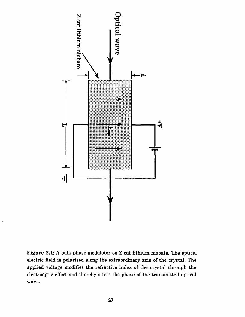
2.3,1 A bulk phase m odulator on lithium niobateFigure 2.1 shows a bulk electrooptic phase modulator constructed
from lithium niobate. A voltage applied between the top and bottom electrodes of the structure acts to modify the refractive index of the lithium niobate through the linear electrooptic effect (see appendix 1). As a consequence, an optical wave passing through the crystal will suffer a perturbation in phase. Provided tha t the perturbation of the index is small, the optical wave will suffer a phase shift given by equation (2.4),
(2.4)K0 d
where next is the unperturbed extraordinary refractive index of the crystal, r33 is the relevant electrooptic coefficient, V is the applied voltage, d is the electrode spacing, L is the total interaction length, and is the free space optical wavelength of the transmitted radiation. Equation (2.4) shows that the induced phase shift of the optical wave is directly proportional to the voltage applied across the electrodes. Consequently, linear phase modulation is readily obtained with the modulator configuration of figure 2.1. Unfortunately however, the electrooptic effect in lithium niobate is extremely weak as may be demonstrated through equation (2.4). To achieve a useful’ phase shift of 2 k radians an electric................................
27
■
H i
F ig u re 2.1: A bulk phase modulator on Z cut lithium niobate. The optical electric field is polarised along the extraordinary axis of the crystal. The applied voltage modifies the refractive index of the crystal through the electrooptic effect and thereby alters the phase of the transm itted optical wave.
28
....field (that is V/d) of almost 106V/m is required, assuming L=lcm, X0=1.3|j,m, next=2.15, and r33 =30.8xl0'12m /V . An electric field of this magnitude can be obtained only if the separation between the electrodes is small as the voltage that can be applied to the electrodes is limited by conventional electronics to a few volts.
Electrodes which are spaced by a few micrometres are readily fabricated in a p lanar geometry by standard photolithographical techniques. However, concentrating the drive field will not prove beneficial unless the optical field is similarly confined to the region of high electric field. Optical confinement can be achieved over long interactions (many wavelengths) through the action of waveguiding. The fabrication and characteristics of waveguides in lithium niobate are briefly discussed in the following subsection.
2.32 O ptical waveguides in lithium niobateWaveguiding is achieved by locally increasing the refractive index of
the lithium niobate substrate through the addition of dopants. The phenomena of waveguiding is well known^217 and a detailed discussion of this subject is not appropriate to this thesis. Instead, we confine our attention to the most basic technological aspects of waveguide fabrication in lithium niobate.
Proton exchange waveguides are formed in lithium niobate by the diffusion of H+ ions from a source such as buffered benzoic acid. Introduction of the H+ ions leads to a very strong and anisotropic change in the refractive index of lithium niobate (Ancxt/next = 07,Anonj/nonl =-.01)^218 in a region close to crystal surface. Though the high index change allows both strong guiding and good confinement, proton exchange waveguides have not been widely utilised in integrated optic applications as the waveguides have until recently suffered from reduced electrooptic activity, instability, and high loss^2-1 .
The most common procedure for the formation of waveguides in lithium niobate is the diffusion of titanium atoms into the crystal from a source which is deposited on the surface of the lithium niobate. The diffusion is accomplished a t an elevated temperature of approximately 1000-1050°C. Typical diffusion times range between 4 and 12hrs. In contrast to proton exchange waveguides, indiffused waveguides exhibit stability, low loss, and an unaltered electrooptic activity. Waveguide losses as low as O.ldb/cm have been reported^2-20!. Moreover, the onset of optical damage in the 1.3-1.5pm region is at relatively high power levels^2-21!.
29
Indeed, commercial devices are routinely subjected to input powers of 20mW^2-22 . In this thesis we have employed titanium indiffusion for waveguide fabrication as UCL has developed expertise in this area.
A consequence of the indiffusion technique is that the intensity profile of the optical radiation confined by the waveguide is spatially non- uniform. Experimentally, the variation of the intensity has been observed as a separable function: the profile having a lateral shape that is gaussian and a vertical profile that is hermite -gaussian. The actual variation of the normalised intensity distribution of a weakly guided TkLiNbOg optical mode together with the parameters by which the mode is described can be found in chapter 5, section 5.2.4. As we shall see, the optical mode profile has an im portant effect on the performance of a device. Consequently, some researchers have devoted considerable effort to relating the optical mode profile to the waveguide fabrication conditions^2*23].
In modulator applications, maximum electrooptic efficiency is assured by a careful choice of the crystal cut, waveguide direction, optical polarisation and the position of the waveguide with respect to the modulator electrodes. These issues are discussed in the following section.
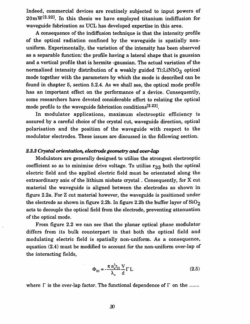
2.3.3 Crystal orientation, electrode geometry and over-lapModulators are generally designed to utilise the strongest electrooptic
coefficient so as to minimise drive voltage. To utilise rgg both the optical electric field and the applied electric field must be orientated along the extraordinary axis of the lithium niobate crystal . Consequently, for X cut material the waveguide is aligned between the electrodes as shown in figure 2.2a. For Z cut material however, the waveguide is positioned under the electrode as shown in figure 2.2b. In figure 2.2b the buffer layer of SiC>2 acts to decouple the optical field from the electrode, preventing attenuation of the optical mode.
From figure 2.2 we can see that the planar optical phase modulator differs from its bulk counterpart in th a t both the optical field and modulating electric field is spatially non-uniform. As a consequence, equation (2.4) must be modified to account for the non-uniform over-lap of the interacting fields,
* .o = J T ‘!kT r L (2.5)K0 d
where T is the over-lap factor. The functional dependence of T on t h e ......
30
electrode
Z (optic)
x 4 X-CUt horizontalLiNb03 - V : .................electric field
TE optical mode
(a)
electrodeSi02 bufferZ (optic)
Z-cutLiNb03 TM optical
mode
vertical electricXfield
(b)
F ig u re 2.2 : Shows the two common electrode/ waveguide configurations designed to maximise electrooptic efficiency. The objective in either case is to utilise the r33 electrooptic coefficient. In (a) the substrate is X cut lithium niobate and so the waveguide is positioned between the electrodes and the optical electric field is TE polarised. In (b) the substrate is Z cut material and the vertical fringing field is employed together with TM polarised light.
31
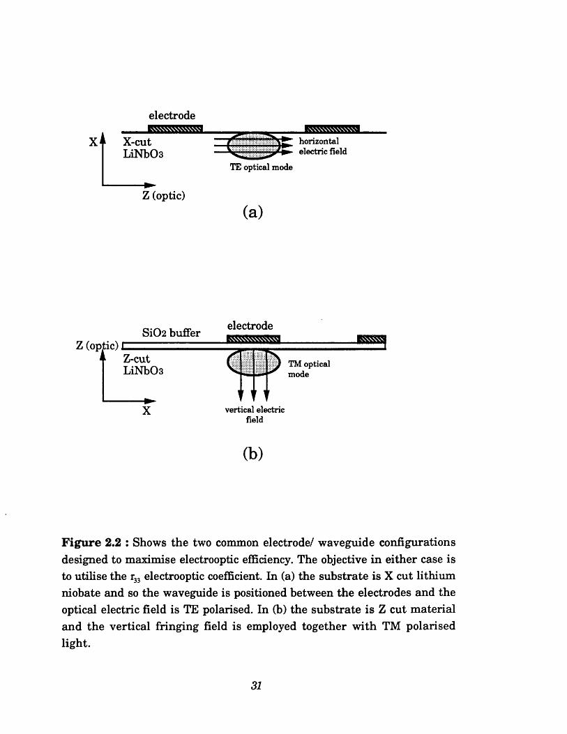
over-lap fields can be found in chapter 5, section 5.2.4, but for typicaldevice geometries r generally lies between 0.2 and 0.5. Clearly, to improve the efficiency of a phase modulator a large over-lap factor is desirable. However, in practice T is often constrained by the need to maintain other im portant and incompatible device characteristics such as optical insertion loss.
We have seen how a planar optical phase modulator may be constructed. However, it is often more convenient to employ intensity modulation.
2.3.4 Integrated optic intensity m odulatorsFigure 2.3 shows two common arrangem ents by which optical
intensity modulation or on-off switching may be achieved. The directional coupler depicted in figure 2.3a operates by electrooptically altering the coupling between two closely spaced waveguides, and thereby modulating the transm itted intensity at the output waveguides. The Mach-Zehnder modulator in figure 2.3b consists of two optical paths whose relative lengths may be adjusted by means of a phase modulator. Consequently, intensity modulation is achieved by interfering the light passing through each arm of the modulator. In this section we are only concerned with the attributes of the Mach-Zehnder interferometer as we have employed this particular optical circuit in the construction of our devices. Moreover, most high speed integrated optic modulators reported in the literature have employed this configuration.
From figure 2.3b we can see th a t the Mach-Zehnder modulator consists of two symmetric Y branch splitter/ combiner, and two phase modulators which are normally operated in antiphase. The average optical intensity, I, at the output of the combiner is given by,
I = I0cos2(4»diff/2) (2.6)
where is the difference in phase between the waves interfering a t the output of the interferometer and I0 is the maximum transm itted optical power. Equation (2.6) shows that when Odiff = tc, the net transmission is zero. In this case the input light is radiated into the substrate through a process of mode conversion and cut-off^2*24!. Thus, for correct operation of an integrated optic interferometer it is im perative th a t the output waveguide is single moded. In figure 2.4 some operational param eters of a Mach-Zehnder modulator are displayed.
32
Directional Coupler Intensity Modulator/Switch
(a)
Mach-Zehnder Intensity Modolator
(b)
F ig u re 2.3 Two common arrangements by which optical in tensity modulation may be achieved. In (a) the coupling between two closely spaced waveguides is altered through the electrooptic effect leading to a variation in the optical intensity at the output ports of the directional coupler. In (b) optical intensity modulation is achieved by interference of two optical waves whose phase difference is controlled through the electrooptic effect. The interferometric arrangem ent depicted in (b) is known as Mach-Zehnder interferometer.
33
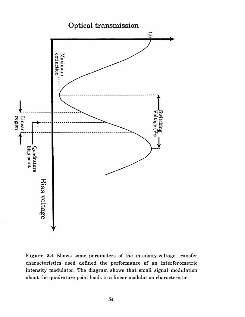
Optical transmissionO
p pCO p
F ig u re 2.4 Shows some param eters of the intensity-voltage transfer characteristics used defined the performance of an interferom etric intensity modulator. The diagram shows th a t small signal modulation about the quadrature point leads to a linear modulation characteristic.
34
The Vjj is the voltage required to switch the modulator from maximum to minimum transm ission and corresponds to a phase difference of k radians between the arms of the interferometer. The extinction, is defined as the ratio of transmitted intensities at the off and on state. This ratio is normally limited by asymmetries in the Y branches and by the alignment of the fibre pigtail to the output waveguide. For typical diffused structures an extinction of -20dB is typical. Another significant param eter is the optical insertion loss: the ratio of maximum transm itted intensity to the input intensity. A major source of optical loss results from inefficient coupling at the fibre to waveguide interface. This loss can be kept below 0.5dB per interface with proper waveguide mode tailoring^2*25 . Though, inevitably such a low loss would lead to an undesirable increase in the VK.
Equations (2.5) and (2.6) show tha t the variation of intensity with applied voltage is non-linear as the transfer characteristic exhibits a cos2 dependence. Consequently, the intensity modulator will suffer from harmonic distortion under harmonic excitation. The magnitude of the distortion depends on both the excitation amplitude and internal bias of the modulator. The distortion can be minimised by biasing the device to quadrature (1/2 maximum transmission). Under these conditions for small excitation signals (with respect to the modulator V*) the modulation characteristic is almost linear^2*26 . In applications of more one octave where high dynamic range is required a further reduction of harmonic distortion can be achieved by using different device configurations^2*27 or by using mixed polarisations^2*28 .
In this thesis, we are concerned only with small signal intensity modulation or large signal phase modulation and so harmonic distortion will not be of significance. However, the frequency spectra of intensity and phase modulated waves are considered in more detail in chapter 6 with regard to modulator calibration.
Thus far, we have considered the application of static voltages to the electrodes of both phase and intensity modulators. In the following section the application of high frequency signals to the modulator electrodes is discussed.
2.3,5 High speed considerationsTwo questions are apparent with regard to the application of high
frequency signals to the modulator electrodes: first, how is the electrode driven from a voltage generator; and second, is the optical transit time through the modulator significant? These questions are considered below.
35
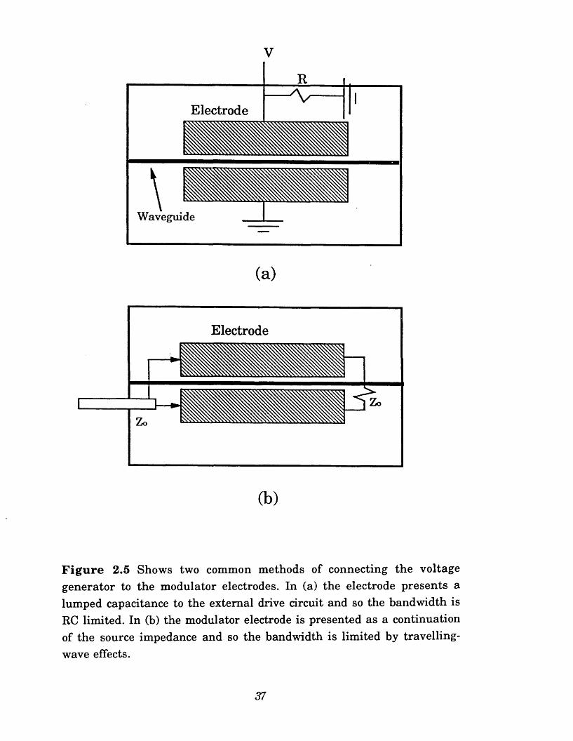
2.3.5.1 Drive geometriesFigure 2.5 shows the two usual methods of connecting the voltage
generator to the modulator electrodes. In figure 2.5a the device presents a lumped capacitive load to the voltage generator. The parallel resistance is often included to improve the matching with the 50£2 source impedance. In this configuration the bandwidth is determined largely by the EC time constant of the device. With a constant source voltage, the field across the modulator will drop by l/V2 of its DC value at a frequency of f3db = 1/tcRC. As the capacitance of the electrode is directly proportional to length, there is an inverse relationship between Vx and the bandwidth of the device. Provided the device length represents a small fraction of the modulating wavelength, and the optical transit time is not too large, the lumped approximation is satisfactory. However, as the frequency increases the electrode will behave as a transmission line and resonant. Consequently, for high-speed and broadband the driving configuration of figure 2.5b is more desirable. In this configuration the modulator electrodes are presented as a continuation of the source transmission line. Ideally, the modulator structure would present an impedance of 500.. But, owing to the large dielectric constant of lithium niobate this condition is difficult to achieve whilst maintaining narrowly spaced electrodes. Generally, designers opt for lower impedance lines and employ impedance tapers or series resistors (less desirable) to reduce mismatch loss. Matters can be improved by careful selection of the dimensions and geometry of the modulator electrode, but subtle trade-offs between bandwidth, Vx, and line impedance will existf2*29^ Though these aspects of design are important, of more interest are the fundamental factors which lim it both the efficiency and the bandwidth of a travelling-wave device. F irst the interaction of the optical and modulating field must be specified.
2.3.5.2 The travelling-wave interactionI t can be shown (see chapter 3, section 3.2.1) th a t the normalised
frequency response of an idealised travelling-wave modulator, constructed from a correctly terminated and lossless transmission line is given by,
Relative phase shift= sin A/A (2.7)
where A = cojn0 -n^| l / 2 c , n0 is the optical refractive index, is the..........
36
V
R
Electrode— 'V ------- 1
\Waveguide
(a)
Electrode
(b)
F ig u re 2.5 Shows two common methods of connecting the voltage generator to the modulator electrodes. In (a) the electrode presents a lumped capacitance to the external drive circuit and so the bandwidth is RC limited. In (b) the modulator electrode is presented as a continuation of the source impedance and so the bandwidth is limited by travelling- wave effects.
37
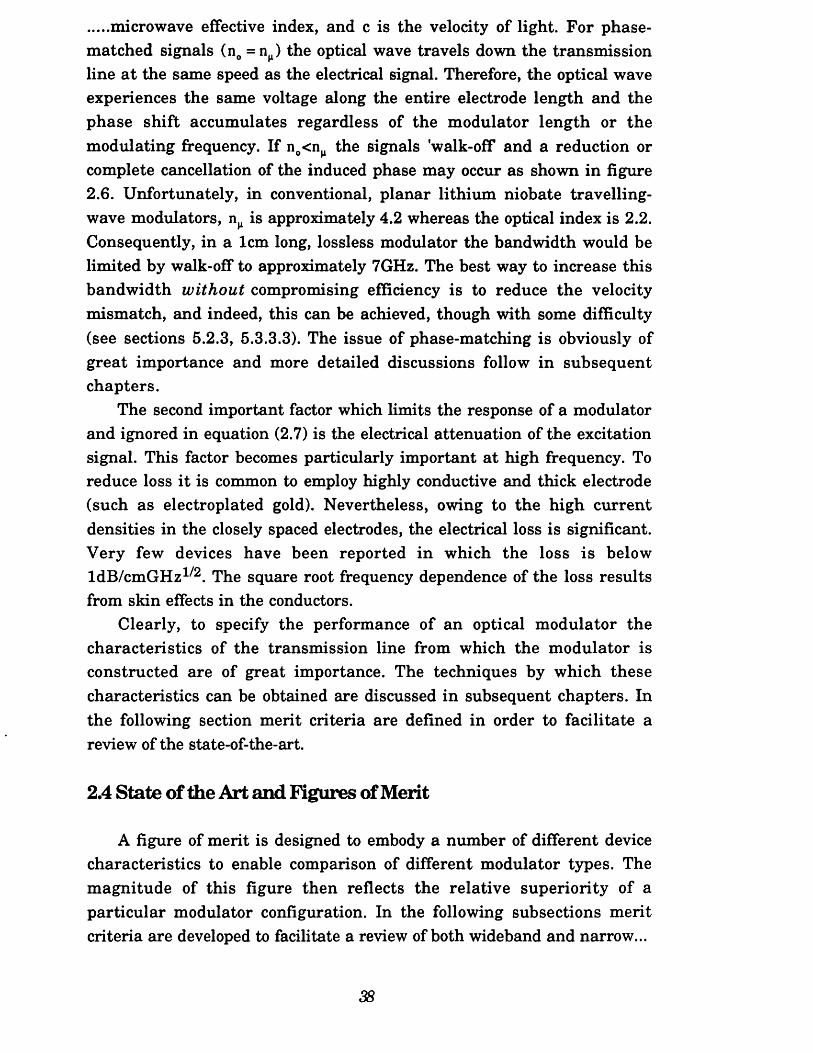
microwave effective index, and c is the velocity of light. For phase-matched signals (n0 = n^) the optical wave travels down the transmission line a t the same speed as the electrical signal. Therefore, the optical wave experiences the same voltage along the entire electrode length and the phase shift accumulates regardless of the modulator length or the modulating frequency. If n0<nJ1 the signals ’walk-off and a reduction or complete cancellation of the induced phase may occur as shown in figure 2.6. Unfortunately, in conventional, planar lithium niobate travelling- wave modulators, is approximately 4.2 whereas the optical index is 2.2. Consequently, in a 1cm long, lossless modulator the bandwidth would be limited by walk-off to approximately 7GHz. The best way to increase this bandwidth w ithout compromising efficiency is to reduce the velocity mismatch, and indeed, this can be achieved, though with some difficulty (see sections 5.2.3, 5.3.3.3). The issue of phase-matching is obviously of great importance and more detailed discussions follow in subsequent chapters.
The second important factor which limits the response of a modulator and ignored in equation (2.7) is the electrical attenuation of the excitation signal. This factor becomes particularly important a t high frequency. To reduce loss it is common to employ highly conductive and thick electrode (such as electroplated gold). Nevertheless, owing to the high current densities in the closely spaced electrodes, the electrical loss is significant. Very few devices have been reported in which the loss is below ldB/cmGHz1/2. The square root frequency dependence of the loss results from skin effects in the conductors.
Clearly, to specify the performance of an optical modulator the characteristics of the transmission line from which the modulator is constructed are of great importance. The techniques by which these characteristics can be obtained are discussed in subsequent chapters. In the following section merit criteria are defined in order to facilitate a review of the state-of-the-art.
2.4 State of the Art and Figures of Merit
A figure of merit is designed to embody a number of different device characteristics to enable comparison of different modulator types. The magnitude of this figure then reflects the relative superiority of a particular modulator configuration. In the following subsections merit criteria are developed to facilitate a review of both wideband and narrow...
38
Optical phase Wavelength of the microwavefront V ^ ^ _ . .Excitation
Time tii
Vo
Time t2-
Time t3-
Time t4-
Vp,
Vo
Vo
Cancellation of induced phase occurs A-------------------
^ propagation direction
Vp j,
Vo
F ig u re 2.6 Shows the effect of a velocity mismatch on the evolution of a travelling-wave interaction. Owing to the higher phase velocity of the optical wave the induced phase shift, which is zero (at tj), is positive (at t2), then negative (at t3) and then zero (at t4). Consequently, over the distance A, the induced phase shift is zero.
39
band millimetre wave modulators. The same merit criteria cannot beemployed in both cases as the different design trade-offs are embodied in the designs of the two types of device.
2.4,1 Broadband modulatorsThe most basic requirements of any broadband modulator are: a large
flat bandwidth; a low drive power from a 50ft source; a linear phase response; low return loss; and low optical insertion loss. Of these attributes, the bandwidth and drive power requirements are generally regarded as being the most important. Consequently, most m erit criteria reflect the trade-offs that are inherent in the selection of these parameters.
A number of related m erit criteria have been described in the lite ra tu re . These param eters include the voltage-length product; bandwidth-length product and bandwidth-Vn ratio. The figure of merit th a t we have employed in our comparisons is defined by equation( 2 . 9 ) [ 2 . 3 ° ] j
2ZC f3JB (GHz-(im/V) (2.9)” 50 + Zc V, ° ^
where Zc is the modulator electrode impedance, f3dB is the electrical bandwidth of the modulator, X0 is the wavelength of the optical radiation, and VK is the switching voltage at DC. The linear wavelength dependence in equation (2.9) is included to compensate for the increased phase efficiency of electrooptic modulators at shorter optical wavelengths. The factor 2Zc/(50 + Zc) is included to express the reduced effectiveness of the drive power for modulators with less than 50ft impedance. And, the fraction f3dB/Vrc encompasses the normal inverse relationship between the bandwidth and drive voltage. In equation (2.9) it is important to define the bandwidth precisely. Here the bandwidth is defined as the electrical 3dB- frequency for which the modulator response (small signal intensity or phase) has fallen to l/V2 of its DC value. This figure must not be confused with the optical bandwidth which corresponds to the frequency at which the modulator response has fallen to 1/2 of its DC value. The electrical bandwidth is more useful as this quantity directly describes the variation of received electrical power in a conventional optical link.
Table 2.1 shows the characteristics of some of the most significant wideband external modulators reported in the literature. The first four entries show th a t in conventional lithium niobate modulators, X cut devices have a higher fm than do Z cut devices owing to a superior over-lap
40
factor; but in either case fm = 2 is not exceeded. The fifth table entry shows an increase in the figure of merit and it is achieved by an artificial reduction in velocity mismatch through the use of a phase-reversal electrode. Entries six and seven show further increases in the figure of m erit which result from further improvements in velocity matching. Nevertheless, it is clear from table 2.1, that the best broadband lithium niobate modulator (reported by Noguchi et al, fm = 5.5) is out-performed by other recently reported devices constructed in different technologies.
2.42 N arrow band m illim etre wave m odulatorsThe figure of m erit defined by equation (2.9) only allows the
comparison of broadband devices as the design of narrow band modulators at millimetre wave frequencies (30GHz and above) do not incorporate the same design trade-offs. The issue of bandwidth is considerably less important than in broadband devices. Most authors only quote the peak phase shift that can be achieved per VWatt of drive power and the modulating frequency at which maximum response occurs. In table 2.2 a selection of the most important results from the literature are reproduced for modulators with responses beyond 30GHz. In case where intensity modulators have been described the phase efficiency is computed from the quoted W% assuming balanced operation. That is, a peak voltage of Vk/2 is assumed to induce a peak phase shift of n/4 in each arm of the interferometer. Where possible, the bandwidth between the electrical 3dB points is quoted.
2.6 Chapter Summary
The objective of this chapter was to introduce the background theory to this thesis. To this end the operation of modulation together with the param eters by which modulators are characterised were described. Subsequently, the various technologies in which optical modulators are constructed were discussed. Particular attention was given to the design of external electrooptic modulators on lithium niobate. For this technology all the most important factors affecting the frequency response and efficiency of travelling-wave m odulators were examined. This examination served to highlight the importance of velocity mismatch, over-lap factor, and electrode loss in modulator design. These parameters depend upon the characteristics of the transmission line from which the travelling-wave electrodes are constructed. Consequently, we highlighted
41
Author Date z(Ohms)
Vic(Volts)
BW(GHz)
31(pm)
Comment fin(GHz/Vpm)
Jungerman et a l [2.22] 1991 22 10.5 12 1.3 Zcut lithium niobate, 5mm
interaction, CPW electrode 0.9
Gee et a l [2.31]
1983 50 7 13 0.83 Zcut lithium niobate, 6mm interaction, ACPS electrode
1.5
Dolfi et al [2.32]
1986 22 3.5 8 1.3 Xcut lithium niobate, 10mm interaction, CPW electrode 1.8
Korotky et al [2.33]
1987 35 26 22.5 1.56 Zcut lithium niobate, 2.5mm interaction, ACPS electrode 1.1
Dolfi et al [2.34] 1988 22 10* 5 to 40 1.3 Zcut lithium niobate, phase
reversal, CPW electrode2.8
Gopalakrishnan et al [2.35] 1992 35-40 5 15 1.3
Zcut lithium niobate, thick CPW electrode 3.5
Noguchi et al [2.36] 1991 43 5.2 20 1.5 Zcut lithium niobate,
shielded, CPW electrode5.7
Walker [2.30] 1991 50 5.7 36 1.3 GaAs, loaded line Push- Pull
8.0
Kotaka et al [2.10]
1991 50 2.0** 16 1.5 InAlGaAs-InAlAs MQW Electro-Absorption 12
Table 2.1 Review of wideband external optical modulators reported in the literature.
* Estimated switching voltage** Switching voltage corresponding to a 20dB extinction
42
Author Date V k(Volts)
Frequency(GHz)
BW(GHz)
X(pm)
Comment Phase Shift (deg.pm/VW)
Korotky et al [2.33] 1987 50* 30 wideband 1.56 Zcut lithium niobate, 2.5mm
interaction, ACPS electrode15
(23)
Itzitsu et al [2.37] 1988 - 35 7
(optical)0.633 Zcut lithium niobate, reson
ant, centre fed, CPW85
(54)
Walker [2.30] 1991 8* 36 wideband 1.3 GaAs, 50il, loaded line Push-Pull
110(145)
Pan [2.38] 1988 4 30 - 1.3 174(227)
Bridges et al [2.39]
1991 - 60 - 0.633 Zcut lithium niobate, wave coupled, resonant electrode
80(51)
T able 2.2 Review of narrow band millimetre wave modulators reported in the literature
* Estimated switching voltage(..) Phase shift normalised to a wave length of X = ljim
43

the importance of deriving the field profiles produced by the modulator electrodes. This chapter concluded with a review of the literature concerning both broadband and millimetre wave external modulators.
44
References for chapter 2
[2.1] J Buus. (1991): "Single frequency semiconductor lasers", Vol TT5, SPIE Optical Engineering Press, Chapter 5.
[2.2] RS Tucker. (1985): " High-speed modulation of semiconductor lasers",J. Lightwave Technol., LT-3, pp. 1180-1192.
[2.3] E Meland, R Holmstrom, J Schlafer, RB Lauer, and W Powazinik. (1990): "Extremely high-frequency (24GHz) InGaAsP diode lasers with excellent modulation efficiency", Electron. Lett., 26, pp. 1827-1829.
[2.4] RA Linke. (1985): "Modulation induced transient chirping in single frequency lasers", IEEE J. Quantum Electron., QE-21, pp. 593-597.
[2.5] S Fujita. (1989): "lOGbit/s, 100km optical fibre transmission experiment using high-speed MQW DFB-LD and back illuminated GalnAs APD", Electron. Lett., 25, pp. 702-703.
[2.6] J Mellis, S Al Chalabi, KH Cameron, R Wyatt, JC Regnault, WJ Devlin, and MC Brain. (1988): "Miniature packaged extemal-cavity semiconductor laser with 50GHz continuous electrical tuning range", Electron. Lett., 24, pp.988-989.
[2.7] M Nakazawa, E Yamada, H Kubota, and K Suzuki. (July 1991): "lOGbit/s soliton data transmission over one million kilometres", Electron. Lett., 27, pp. 1270-1272.
[2.8] TE Van Eck, LM Walpita, WSC Chang, and HH Wieder.(1986): " Franz- Keldysh elelctrorefraction and electroabsorption in bulk InP and GaAs", Appl. Phys. Lett., 48, pp. 451-453.
[2.9] DAB Miller, DS Chemla, TC Damen, AC Gossard, W Wiegmann, TH Wood, and CA Burrus. (1985): "Electric field dependence of optical absorption near the band gap of quantum well structures", Phys. Rev. B, 32, pp. 1043-1060.
[2.10] I Kotaka, K Wakita, K Kawano, M Asai, and M Naganuma. (Nov. 1991): "High speed and low-driving-voltage InGa/InAlAs multiquantum well optical modulators", Electron. Lett., 27, pp. 2162-2163.
[2.11] JC Baument, et al. (1985): "KNb03 electro-optic induced optical waveguide/ cutoff modulator", Appl. Phys. Lett., 46, pp 1018-1020.
45
[2.12] RG Walker. (1987): " High speed electrooptic modulation in GaAs/GaAlAs waveguide devices", J. Lightwave Technol.s LT-5, pp. 1444-1453.
[2.13] JP Donnelly, NL DeMeo, FJ Leonberger, SH Groves, P Vohl and FJ O’Donnell. (1985): "Single-mode optical waveguides and phase modulators in the InP material system", IEEE J. Quantum Electron., QE-21, pp. 1147-1151.
[2.14] RC Alfemess. (1981): "Guided-wave devices for optical communication", IEEE J. Quantum Electron., QE-17, pp. 946-959.
[2.15] Tamir, T, ed. (1990): "Integrated Optics", 3rd ed., Springer-Verlag, New York.
[2.16] E Voges, and A Neyer. (1987): "Integrated-optical devices on LiNb03 or optical communications", J. Lightwave Technol., LT-5, pp. 1229-1238.
[2.17] Tamir, T, ed. (1990): "Integrated Optics", 3rd ed., Springer-Verlag, New York.
[2.18] M DeMicheli, J Botineau, P Sibillot, D Ostrowsky, and M Papuchon. (1982): "Fabrication and characterization of titanium indiffused proton exchanged (TIPE) waveguides in lithium niobate", Opt. Commun., 42, pp. 101-103.
[2.19] M Abouelleil, and FJ Leonberger. (1989): 'Waveguides in lithium niobate", J. Am. Ceram. Soc., 72, pp. 1311-1321.
[2.20] R Reneger, and W Sohler. (1985): "Loss in low-finesse Ti:LiNb03 optical waveguide resonators", Appl. Phys. B, 36, pp. 143-147.
[2.21] GT Harvey, G Astfalk, AY Feldblum, and B Kassahun. (1986): "The photorefractive effect in titanium indiffused lithium niobate optical directional couplers at 1.3pm", IEEE J. Quantum Electron., QE-22, pp. 939-946.
[2.22] RL Jungerman, CJ Johnsen, DJ McQuate, KSalomaa, MP Zurakowski, RC Bray, G Conrad, D Cropper, and P Hemday. (Sept. 1990): "High-speed optical modulator for application in instrumentation", IEEE J.Ligthwave Technol., LT-8, pp. 1363-1370.
[2.23] PG Suchoski, and RV Ramaswamy. (1987): "Minimum-mode size low loss Ti:LiNb03 channel waveguides for efficient modulator operation at 1.3pm", IEEEJ. Quantum Electron., QE-23, pp. 1673-1679.
46
[2.24] M Izutsu, Y Nakai, and T Sueta. (1982): "Operation mechanism of the single mode optical-waveguide Y junction", Opt. Lett., 7, pp. 136-138.
[2.25] K Komatsu, M Kondo, and Y Ohta. (1986): "Titanium/magnesium double diffusion method for efficient fibre-LiNbOg waveguide coupling",Topical Meet. Integrated and Guided Wave Optics, Atlanta, GA, pap. PDP2-1.
[2.26] RL Jungerman, and DW Dolfi. (1991): "Frequency domain optical network analysis using integrated optics", IEEE J. Quantum Electron., QE-27, pp. 580-587.
[2.27] P Liu, BJ Li, and YS Trisno. (1991): "In search of a linear electrooptic amplitude modulator" IEEE Photon. Technol. Lett., 3, pp. 144-146.
[2.28] LM Johnson, and HV Roussell. (1988): " Reduction of intermodulation distortion in interferometric optical modulators", Optic Lett., 13, pp. 928- 930.
[2.29] H Chung, and WSC Chang. (March 1991): "Modeling and optimization of traveling-wave LiNb03 interferometric modulators", IEEE J. Quantum Electron., QE-27, pp. 608-617.
[2.30] RG Walker. (March 1991): "High speed III-V semiconductor intensity modulators", IEEE J. Quantum Electron., QE-27, pp. 654-667.
[2.31] CM Gee, GD Thurmond, and HW Yew. (1983):" 17-GHz bandwidth electro-optic modulator", Appl. Phys. Lett., 43, pp. 998-1000.
[2.32] DW Dolfi. (1986): "Traveling-wave 1.3pm interferometer modulator with high bandwidth, low drive pwer, and low loss", Applied Optics, 25, pp. 2479-2480.
[2.33] SK Korotky, G Eisenstein, RS Tucker, JJ Veselka, and G Raybon. (1987): "Optical intensity modulation to 40GHz using a waveguide elecro-optic switch", Appl. Phys. Lett., 5 0 , pp. 1631-1633.
[2.34] DW Dolfi, M Nazarathy, and RL Jungerman.(1988): "40GHz Electrooptic modulator with 7.5V drive voltage", Electron. Lett., 24, p. 528.
[2.35] GK Gopalakrishnan, CH Bulmer, WK Bums, RW McElhanon, and AS Greenblatt. (April 1992): "40GHz, low half-wave voltage Ti:LiNbOg intensity modulator", Electron. Lett., 28, p. 826-827.
[2.36] K Noguchi, K Kawano, T Nozawa, and T Suzuki. (April 1991): "A Ti:LiNb03 optical intensity modulator with more than 20GHz bandwidth and 5.2V driving voltage", IEEE Photonic Technol. Lett., 3, pp. 333-335.
47

[2.37] M Izutsu, H Murayami, and T Sueta. (1988): "Millimeter-wave light modulator using LiNb03 waveguide with resonant electrode", Tech. Dig. CLEO'88, pp485-486.
[2.38] JJ Pan. (1988): "Microwave and millimetre-wave electrooptic modulators", SPIE, Vol 993, pp. 86-93.
[2.39] WB Bridges, FT Sheehy, and JH Schaffner. (1991): "Wave-coupled LiNbOg electrooptic modulator for microwave and millimeter wave modulation", IEEE Photon. Lett., PTL-3, pp. 133-135.
48
Chapter 3
Analysis and Design of Phase-Reversal Modulators
3.1 Introduction
3.2 The Phase-Reversal Electrode
3.3 Equalisation using PRMs
3.4 Chapter Summary
49
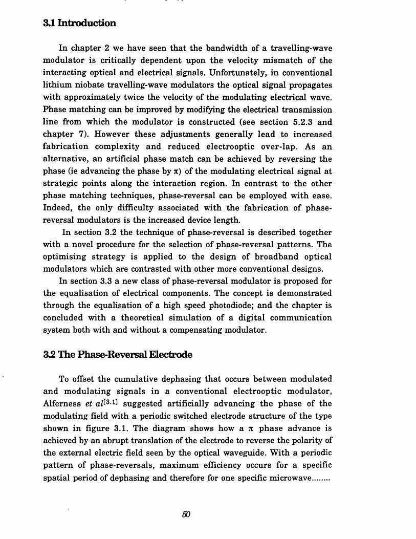
3.1 Introduction
In chapter 2 we have seen that the bandwidth of a travelling-wave modulator is critically dependent upon the velocity mismatch of the interacting optical and electrical signals. Unfortunately, in conventional lithium niobate travelling-wave modulators the optical signal propagates with approximately twice the velocity of the modulating electrical wave. Phase matching can be improved by modifying the electrical transmission line from which the modulator is constructed (see section 5.2.3 and chapter 7). However these adjustments generally lead to increased fabrication complexity and reduced electrooptic over-lap. As an alternative, an artificial phase match can be achieved by reversing the phase (ie advancing the phase by k) of the modulating electrical signal at strategic points along the interaction region. In contrast to the other phase matching techniques, phase-reversal can be employed with ease. Indeed, the only difficulty associated with the fabrication of phase- reversal modulators is the increased device length.
In section 3.2 the technique of phase-reversal is described together with a novel procedure for the selection of phase-reversal patterns. The optimising strategy is applied to the design of broadband optical modulators which are contrasted with other more conventional designs.
In section 3.3 a new class of phase-reversal modulator is proposed for the equalisation of electrical components. The concept is demonstrated through the equalisation of a high speed photodiode; and the chapter is concluded with a theoretical simulation of a digital communication system both with and without a compensating modulator.
3.2 The Phase-Reversal Electrode
To offset the cumulative dephasing that occurs between modulated and modulating signals in a conventional electrooptic modulator, Alferness et alf3-1 suggested artificially advancing the phase of the modulating field with a periodic switched electrode structure of the type shown in figure 3.1. The diagram shows how a % phase advance is achieved by an abrupt translation of the electrode to reverse the polarity of the external electric field seen by the optical waveguide. With a periodic pattern of phase-reversals, maximum efficiency occurs for a specific spatial period of dephasing and therefore for one specific microwave.......
50
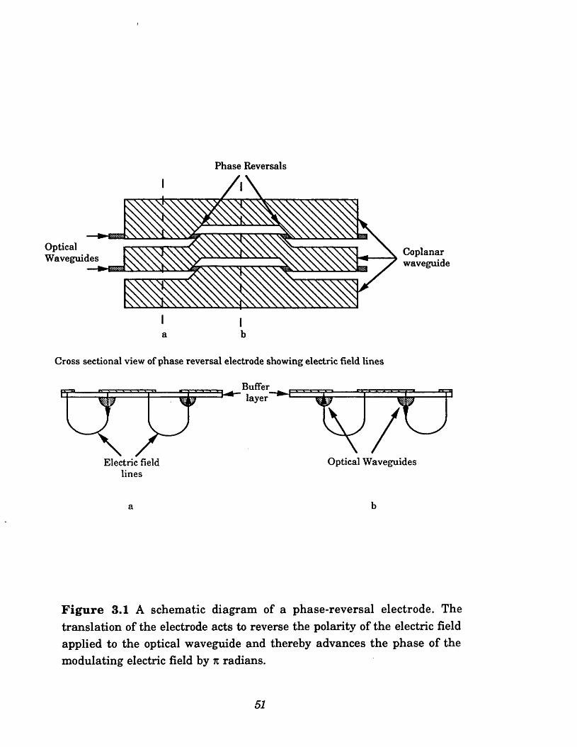
Phase Reversals
OpticalWaveguides Coplanar
waveguide
a b
Cross sectional view of phase reversal electrode showing electric field lines
Buffer _ layer
Optical WaveguidesElectric fieldlines
a b
F ig u re 3.1 A schematic diagram of a phase-reversal electrode. The translation of the electrode acts to reverse the polarity of the electric field applied to the optical waveguide and thereby advances the phase of the modulating electric field by k radians.
51
frequency and so, the resulting device has a bandpass frequencyresponse. A number of periodic phase-reversal modulators have been demonstrated with centre frequencies of 6GHz£3*2l, 12GHzt3-3 , 20GHzt3-4l and most recently at 30GHzt3-5l.
The use of aperiodic patterns of phase-reversals was proposed by Erasme and Wilsont3-6 3-7] to extend the range of frequencies over which efficient modulation could be achieved. Subsequently, a num ber of aperiodic phase-reversal modulators with enhanced figures of m erit were demonstrated by Jungerman et a/t3*8 and by Dolfi et a/t3-9!. The difficulty associated with the design of these devices was the selection of the electrode pattern to achieve a broadband response. To overcome this difficulty both Nazarathy et al&-101 and Erasme et a/t3*n] have suggested systematic design strategies. In this section we describe an alternative and more general optimising strategy for the design of phase-reversal electrode patterns. Before embarking on a description of the technique, the functional dependence of the modulator frequency response on the phase- reversal pattern must be ascertained.
3.2,1 Frequency response o f a phase-reversal m odula tor (after Erasme and Wilsont3-6!)
A CW electrical wave travelling along a correctly terminated electrode will produce voltage distribution within the interaction region of,
V(z,t) = V^exp [j(oy - (3z) - az] (3.1)
where cop, P, and a are angular frequency, propagation constant, and attenuation coefficient of the modulating microwave, respectively. is the peak modulating voltage on the line and is most generally a complex entity. The magnitude of Vtt is determined by the drive power P0, and lineimpedance Zc, as an optical phase fron equations (2.5), (3.1) as,
= ^2 ZCP0. The phase perturbation dd>, induced on over a length dz, of interaction region is given by
7m„r33V„ r r i ,dd> = ---- -----— exp [j(coRt - Pz) - az] dz (3.2)
where r33 the electrooptic coefficient, is the optical wavelength, nc is therefractive index of the optical mode, d is the electrode spacing and T is theelectrooptic over-lap. The time dependence in equation (3.2) can be eliminated by noting that an optical phase front crossing z=0 and at a time
52
tc has a phase velocity of vc = z/(t - 10), that is,
dO = TtSV^expCjoyJ • exp - + j • dz (3.3)
where 3 = n r33r /Xod and A is the effective microwave wavelength as seen from the optical phase front; A is determined from the optical phase velocity v0, and the microwave phase velocity v according to A = 2rc/p(l- v^/vc). The total phase induced on the optical wave by the phase-reversal electrode is determined by integrating (3.3) over the entire interaction region,
) = tc3V^ CXp( to) X (-l)”[exp(-YpZm)-exp(-ypzmtl)] (3.4)i p m « 0
The coefficient -lm reflects the phase-reversal of applied field between phase-reversal sections; zm is the position of the m th phase-reversal and Yp=a + j2rc/A. Equation (3.4) shows tha t O(co ) is a harmonic function whose variation with frequency is determined by the velocity mismatch; microwave attenuation coefficient; and most importantly, the pattern of phase-reversals on the electrode. The frequency response of the modulator is obtained by dividing equation (3.4) by the excitation signal, tha t is, 0(0)^) = 0(coH)/Vffl(iexp(jayo).
Though it is a simple m atter to predict the frequency response of a phase-reversal modulator through equation (3.4), it is the reverse problem of synthesising a phase-reversal pattern to achieve a particular frequency response tha t is problematic. In the following subsection a number of system atic design strategies for selecting phase-reversal electrode patterns are discussed.
3.2.2 Pattern selection for phase-reversal m odulatorsThe problem of optimisation may be formulated as the minimisation
(or maximisation) of a multi-variable scalar function F(i); where F ( i) represents the difference between the performance achieved a t (i) and the desired specification^312]. In general, the domain of F will contain a global minimum where performance is optimal, together with a series of local minima as is shown in figure 3.2. The objective of optimisation is to select the global minimum from all the minima which are present in the domain of F . To optimise a phase-reversal modulator F is defined to reflect all the desired features of the modulator response. A suitable........
53
Contours of constant F
Local Minima
Global Minimum
F ig u re 3.2 A two dimensional error function. The diagram shows that generally there are a number of minima in the domain of F. The objective of optimisation is to select the smallest value of F. This value of F is known as the global minimum.
54
functional for the design of broadband modulators is given byequation (3.5),
where Oc is the modulator response as determined from equation (3.4) with =1; the average response |d>c| is given by |d>c| = J|d>c|df /(f2 -f^; and f j , f2 are the lower and upper modulating frequencies respectively. With fj and f2 fixed, F depends only on the section lengths between phase- reversals. Therefore, to attain optimal performance the phase-reversal selection lengths must be selected to maximise F .
Erasme et a#3-11! defined an error function which is essentially the inverse of equation (3.5). To minimise this functional, Erasme et al employed a gradient method. This technique involved numerically evaluating the vector gradient of the error function, and adjusting the free variables ( that is the positions of the phase-reversals) to follow this vector. However, it is well known that gradient methods always converge to the nearest local minimum, and that this local minimum need not be the smallest value of the error function!3-12]. Indeed, Erasme et al found that their 'optimal' solutions were dependent upon the phase-reversal pattern used to initiate the search.
N azarathy et a/!3-10] has suggested partitioning the interaction into a series of 'bits'; each bit having a polarity o f+1 or -1 as shown in figure 3.3. N azarathy et al observed tha t the time domain impulse response of a lossless modulator is given by a scaled replica of the modulator's electrode pattern!3-7] (see section 3.3.1). Consequently, to obtain patterns exhibiting broadband behaviour, bit patterns were selected from a small class of binary codes (known as Barker codes) which were known to exhibit desirable spectral properties. For more general optimisations, the frequency response corresponding to all the various combinations of bits m ust be examined in turn. Clearly, this direct search strategy becomes unmanageable as the length of the bit pattern increases. Indeed, for aninteraction length of 2cm and a bit width of only .5mm over 1012 patterns exist!
As an alternative to the search strategies described above we developed the simple iterative procedure depicted in figure 3.4!3-13]. The optimising process is initiated from an arbitrary pattern of phase- reversals {zj}. From this pattern, a series of random variations {zj'} (five...
55
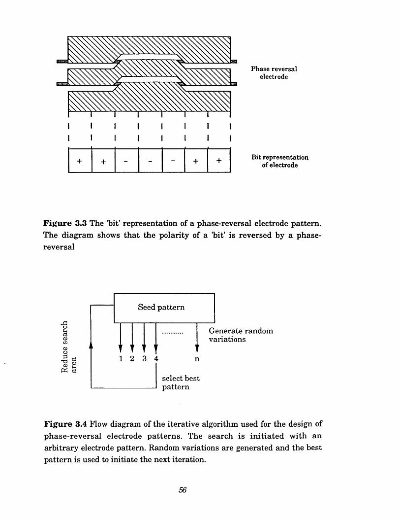
Phase reversal electrode
I I
+ + - - - + + Bit representation of electrode
Figure 3.3 The 'bit' representation of a phase-reversal electrode pattern. The diagram shows tha t the polarity of a ’bit' is reversed by a phase- reversal
o<DCO<1)O3<1>
P h CO
Seed pattern
select best pattern
Generate random variations
Figure 3.4 Flow diagram of the iterative algorithm used for the design of phase-reversal electrode patterns. The search is in itiated with an arbitrary electrode pattern. Random variations are generated and the best pattern is used to initiate the next iteration.
56
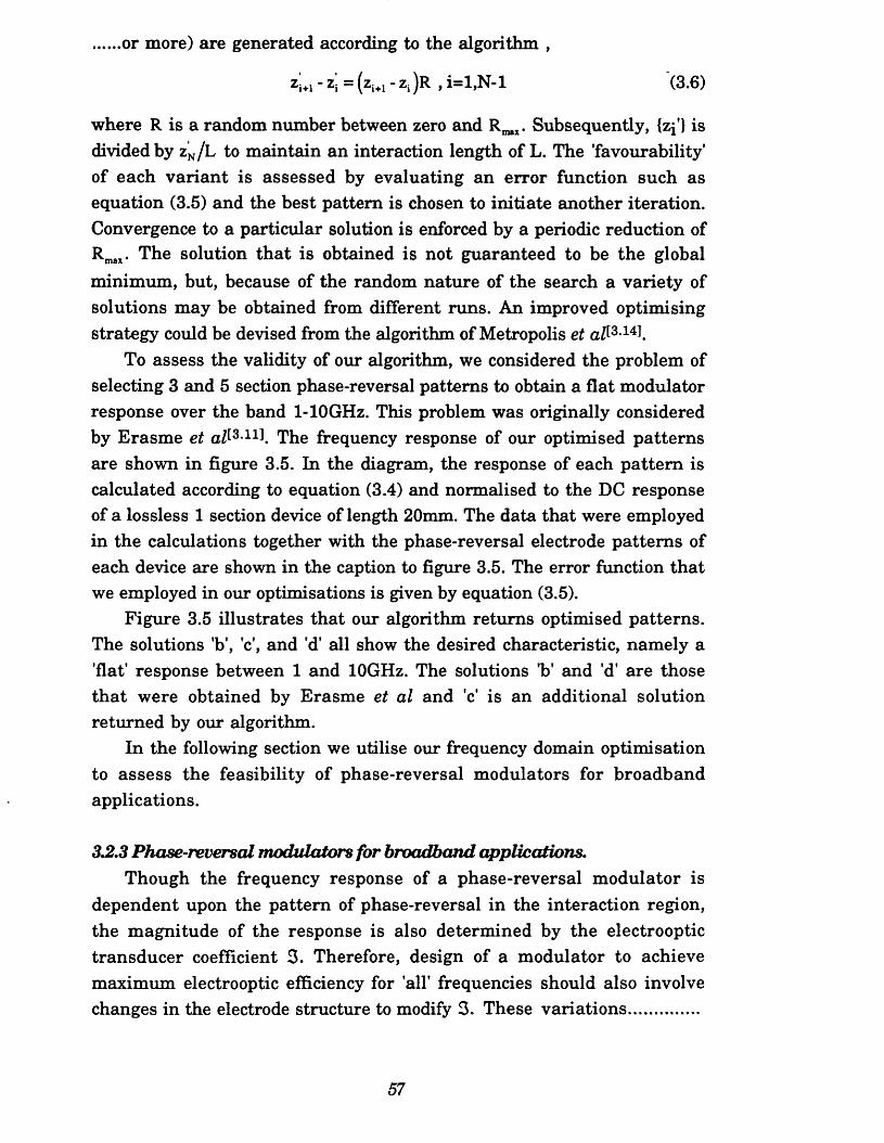
or more) are generated according to the algorithm ,
z'i»i - z| = (z w - Zj )R , i=l,N-l (3.6)
where R is a random number between zero and R ^ . Subsequently, {zj'} is divided by zn / L to maintain an interaction length of L. The 'favourability' of each variant is assessed by evaluating an error function such as equation (3.5) and the best pattern is chosen to initiate another iteration. Convergence to a particular solution is enforced by a periodic reduction of Rmax. The solution tha t is obtained is not guaranteed to be the global minimum, but, because of the random nature of the search a variety of solutions may be obtained from different runs. An improved optimising strategy could be devised from the algorithm of Metropolis et
To assess the validity of our algorithm, we considered the problem of selecting 3 and 5 section phase-reversal patterns to obtain a flat modulator response over the band l-10GHz. This problem was originally considered by Erasme et a ? 3-11!. The frequency response of our optimised patterns are shown in figure 3.5. In the diagram, the response of each pattern is calculated according to equation (3.4) and normalised to the DC response of a lossless 1 section device of length 20mm. The data that were employed in the calculations together with the phase-reversal electrode patterns of each device are shown in the caption to figure 3.5. The error function that we employed in our optimisations is given by equation (3.5).
Figure 3.5 illustrates that our algorithm returns optimised patterns. The solutions 'b', 'c', an d 'd ' all show the desired characteristic, namely a ’flat’ response between 1 and 10GHz. The solutions 'b' and 'df are those tha t were obtained by Erasme et al and 'c' is an additional solution returned by our algorithm.
In the following section we utilise our frequency domain optimisation to assess the feasibility of phase-reversal modulators for broadband applications.
£2.3 Phase-reversal m odulators for broadband applications.Though the frequency response of a phase-reversal modulator is
dependent upon the pattern of phase-reversal in the interaction region, the magnitude of the response is also determined by the electrooptic transducer coefficient 3. Therefore, design of a modulator to achieve maximum electrooptic efficiency for all' frequencies should also involve changes in the electrode structure to modify 3. These variations...............
57
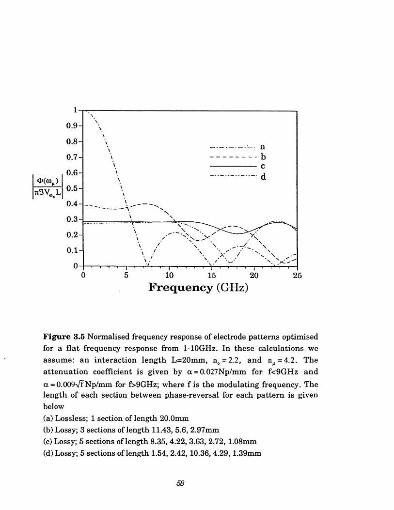
0 . 9 -
0 .8 -
0 . 7 -
0 .6 -
0 . 5 -
0 . 4 -
0 . 3 -
0 . 2 -
0 .1 -
0 5 10 15 20 2 5
Frequency (GHz)
F igu re 3.5 Normalised frequency response of electrode patterns optimised for a flat frequency response from l-10GHz. In these calculations we assume: an interaction length L=20mm, nc =2.2, and n^=4.2. The attenuation coefficient is given by a = 0.027Np/mm for f<9GHz anda = 0.009Vf Np/mm for f>9GHz; where f is the modulating frequency. The length of each section between phase-reversal for each pattern is given below(a) Lossless; 1 section of length 20.0mm(b) Lossy; 3 sections of length 11.43, 5.6, 2.97mm(c) Lossy; 5 sections of length 8.35, 4.22, 3.63, 2.72,1.08mm(d) Lossy; 5 sections of length 1.54, 2.42,10.36, 4.29,1.39mm
58
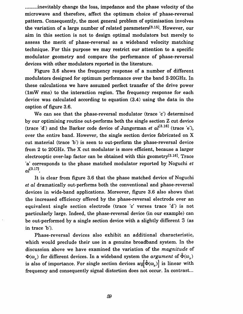
inevitably change the loss, impedance and the phase velocity of themicrowave and therefore, affect the optimum choice of phase-reversal pattern. Consequently, the most general problem of optimisation involves the variation of a large number of related parameters^3 151. However, our aim in this section is not to design optimal modulators but merely to assess the m erit of phase-reversal as a wideband velocity matching technique. For this purpose we may restrict our attention to a specific modulator geometry and compare the performance of phase-reversal devices with other modulators reported in the literature.
Figure 3.6 shows the frequency response of a number of different modulators designed for optimum performance over the band 2-20GHz. In these calculations we have assumed perfect transfer of the drive power (lmW rms) to the interaction region. The frequency response for each device was calculated according to equation (3.4) using the data in the caption of figure 3.6.
We can see that the phase-reversal modulator (trace V) determined by our optimising routine out-performs both the single section Z cut device
r q i g i(trace 'd ') and the Barker code device of Jungerman et al ' (trace V), over the entire band. However, the single section device fabricated on X cut m aterial (trace 'b') is seen to out-perform the phase-reversal device from 2 to 20GHz. The X cut modulator is more efficient, because a larger electrooptic over-lap factor can be obtained with this geometry^3-16!. Trace 'a' corresponds to the phase matched modulator reported by Noguchi et aZ[3'17].
It is clear from figure 3.6 that the phase matched device of Noguchi et al dramatically out-performs both the conventional and phase-reversal devices in wide-band applications. Moreover, figure 3.6 also shows that the increased efficiency offered by the phase-reversal electrode over an equivalent single section electrode (trace V verses trace 'd') is not particularly large. Indeed, the phase-reversal device (in our example) can be out-performed by a single section device with a slightly different 3 (as in trace 'b').
Phase-reversal devices also exhibit an additional characteristic, which would preclude their use in a genuine broadband system. In the discussion above we have examined the variation of the m agnitude of d>(co ) for different devices. In a wideband system the argument of d>(co ) is also of importance. For single section devices arg^co^)] is linear with frequency and consequently signal distortion does not occur. In contrast...
59
2OLog|0((DM)|
-18Drive power is lmW rms
- 21 -
- 2 4 - — a
- 2 7 -
- 3 0 -
-33-
-36-
-392 6 10 221814
Frequency (GHz)
F ig u re 3.6 Shows the peak phase shift of different phase modulators assum ing a drive power of lmW rms. The characteristics of each modulator are given below.(a) a = 0.8dB/ (cmVGHz), nc =2.2, n^=2.2, ZC=44Q, 3 ^OSCcm.V)'1, 1 section of 20mm. (b) a = 1.5dB/ (cmVGHz), n0=2.2, n^=3.5, Zc=22£2, 3 =.14(cm.V)'1, 1 section of 5mm. (c) a = 1.5dB/ (cnWGHz), nc =2.2, =3.5,ZC=22Q, 3=.08(cm.V)1, 5 sections of 6.68, 3.85, 3.60, 3.59, 2.28mm. (d) a = 1.5dB/ (cmVGHz), nc =2.2, n^=3.5, ZC=22Q, 3 =.08(cm.V)1, 1 section of 5mm. (e) a = 1.5dB/(cm-v/GHz), n0=2.2, n^=3.5, ZC=22Q, 3 =.08(cm.V)’1, 3 sections of 5, 2.5, 2.5mm.
60
....non-periodic phase-reversal m odulators exhibit a non-linear argj<i>(co )j[3'3 3'10], which would distort a wideband signal. However, this property need not be a disadvantage. Indeed, the phase-reversal electrode provides a new degree of freedom to predistort a signal so as to equalise other non-ideal components in an optical system. This application of the phase-reversal modulator had received no attention in the literature prior to our publication^313 .
3.3 Equalisation using Phase-Reversal Modulators
An ideal communications system exhibits a constant group delay and well behaved magnitude response. Over a wide bandwidth these characteristics are difficult to achieve because of imperfections in the system components. In externally modulated optical systems distortion may occur from many sources including the modulator, the optical detector, drive and preamplifiers, and the optical fibre. Previously, attention had focused on overcoming the effect of the chromatic dispersion occuring in the optical fibre by equalisation in both the optical^3 181 and electrical domains^3191. Most recently however, Winters has suggested a more general method of equalisation in the electrical domain using a fractionally spaced equalizert3-20!. In this section we demonstrate an alternative method of equalising linear distortions in the optical domain using phase-reversal modulators. The method involves designing the response of the phase-reversal modulator to predistort the system and so correct for the distortion of non-ideal components. First, however, it is important to ascertain the limit of design: it seems unlikely that a phase- reversal device can be constructed to equalise any system response. Moreover, how are both the number of phase-reversals and the length of interaction decided? These questions are difficult to examine from a frequency domain perspective. Some insight can be obtained through a time domain analysis under the assumption of constant loss electrodes.
3,3,1 Time domain analysis o f a phase-reversal electrodeAn optical phase front emerging from the interaction region a t z=L at
a time t, passes the element [z, z + dz] at a time x(t,z) = t-(L -z/v0). The phase shift induced on a phase front is obtained by integrating the microwave voltage V(z,x), which is the voltage at z a t the instan t the optical phase front passes through the element [z, z + dz],
61
+ o©
<I>(t) = 3 tc | V[z,x(t,z)]dz (3.7)
Under the assumption of constant electrical loss, the space-time evolution of an electrical impulse travelling along the interaction region can be described by,
V(z,t) = 8[t - z/v Jexp[-az]g(z) (3.8)
where g{z) is a function which describes the electrode pattern such that g(z) = +l or -1 for (0<z<L) in accordance with the polarity of the phase- reversal sections; and elsewhere g(z)=0. The impulse response is deduced from equations (3.7), (3.8) as,
'im p3 tc t-to" * - 10---- 8 o •exp -a— -q . q . . q .
(3.9)
where q = [l/v^ - l/v0] and t0 = L/v0. The implication of equation (3.9) is that the time domain impulse response is a scaled replica of the electrode pattern delayed by the optical flight time^3101 and modified by an electrode loss envelope. This relationship is emphasised in figure 3.7, which shows a phase-reversal electrode together with its impulse response assuming constant microwave loss.
Equation (3.9) is of significance as this relation gives a d irect relationship between the modulator response and the electrode pattern. Furthermore, the relation suggests that there is no restriction on the frequency response of a constant loss phase-reversal modulator apart from the necessity of a real impulse function. This observation is further discussed below.
3.3-2 Time domain pattern selectionThe electrode function g (z), corresponds to the norm alised
electrooptic over-lap and consequently, commonly assumes a value of +/-1 in accordance with the polarity of the modulator sections. In principle, however, g (z) can take on interm ediate values. In this case a n y predefined real impulse h(t), can be constructed by selecting an electrode..
62
z=0 z=L
Bit representation of electrode
loss envelopea>COcoCucoa>
F ig u re 3.7 A phase-reversal electrode together with its temporal impulse response. The diagram shows that the response is a scaled replica of the electrode pattern.
63
function of,
#[——*■"] = •rec t[-^1 (3.10)L q J lh'(t)L, L qL J
where h'(t) = h(t)exp[a(t-t0)/q)]. The rect function in equation (3.10) imposes the constraint of a finite interaction of length L, and so rect[x] = 1 for 0 < x < 1 and is zero elsewhere. For a constant loss and finite length electrode, the impulse response of a modulator with an electrode pattern given by equation (3.10) can be deduced from equation (3.9) as,
_, v 3 tc h(t) d>(t)lmn = ----- • rectmp q lh‘(t)Lx
t-t.qL .
(3.11)
Consequently, to construct a phase-reversal modulator with an impulse response of h(t) a phase-reversal pattern given by equation (3.10) would be selected such tha t the 'most significant' fraction of h(t) fell within the modulator window. The duration of the modulator window may be increased by increasing the velocity mismatch (ie increasing q) to allow a greater fraction of h(t) to be replicated. However, a secondary effect of increasing q is tha t the efficiency of the modulator is impaired through the 1/q coefficient. Alternatively, for cases in which the velocity mismatch is specified by the modulator construction, the duration of 0 ( 0 ^ can be increased by increasing the electrode length L. However, for lossy electrodes an increased L can lead to a large reduction in the modulator efficiency through the coefficient l/lh 'ft)^ . In practice, formidable difficulties would be encountered in the construction of a modulator with a graded electrode function. However, more practical schemes to approximate h(t) within the modulator window can be developed using both bi and tri level electrode functions^3,211.
The analysis presented above is simplified inasmuch tha t constant loss electrodes are assumed. Nevertheless, the analysis does suggest both the number of phase-reversals and the modulator length that are need to replicate an impulse function h(t). Moreover, it is important to note that the theory suggests that there is no impediment to the replication any real impulse function.
To demonstrate the design of a compensating electrooptic modulator, the equalisation of a fast photodiode is considered below. In this example pattern selection is accomplished in the frequency domain (see section 3.2.2) using the modulator length and number of phase-reversals suggested by a time domain analysis.
Equalisation o f a photodetectorFigure 3.8 shows a simple optical link consisting of an external
phase-reversal intensity modulator and a photodiode. The modulator and detector are linear elements and consequently a harmonic input s^co^ will lead to a harmonic output sout(co ) such that,
= ^(co^DCco^s^Cco^) (3.12)A
where <J>(co ) is the frequency response of the modulator; and DCco ) is the frequency response of the photodetector. In the perfect link, sout(t) would be a scaled replica of (t), but because of linear distortions introduced by the system components this is not case. Figure 3.9a shows the measured^3'223 impulse response of a high speed Plessey Research photodiode[3-23 convolved with a 'top hat' rectangular filter of bandwidth 15GHz. The corresponding frequency response of the photodiode is shown in figure 3.9b. I t is apparent from the asymmetry of figure 3.9a th a t this photodetector introduces signal distortion^3,24, page 69l To eliminate the distortion of s^Ct) the response of the modulator may be designed to
A
predistort the signal such that 0(co^)D(o)>1) = constant. As we have seen, the physical characteristics of the modulator electrode influence the choice of the phase-reversal pattern. In particular, both the phase velocity of the microwave and the loss coefficient of the electrodes as a function of frequency are required. Consequently, Ti:LiNbC>3 technology, together with a modulator package/geometry designed during a previous research program were adopted^3-3}. A detailed description of the modulator electrode can be found in chapter 6. Microwave transmission experiments performed on the modulator electrode led to an estim ate for the microwave attenuation coefficient of,
a = -0091+.0225-Vf(GHz) (Np/mm),f> 2GHz (3.13)
Assuming a microwave effective index of 3.8 and an optical index of 2.2 (values consistent with previous observations^3-3 , a modulator with an interaction length of 2cm may be designed to have a temporal impulse response of up to llOps (co-directional) or of 400ps (counter-directional). A ten section structure for co-directional propagation was designed to equalise the detector response using the algorithm described section 3.2.2.
65
F ig u re 3.8 A simple optical link consisting of an intensity modulator and an optical detector. Ideally, the output from the optical detector is a scaled replica of the electrical signal at the input to the modulator.
66
in
0.8
£ 0.6
0 .4
0.2
- 0.2
-0.40.2 0 .3 0 .4 0 .5 0.6 0 .7 0.8
Time (ns)(a)
5 - i -------- -------------------------- --------
JL J I 1---------------------1---------------------1-------------------- 1----------- 1--------- 1 1
2 4 6 8 10 12 14 16 18 20Frequency (GHz)
(b)
F ig u re 3.9 The measured characteristics of the high speed photodetector chosen for equalisation, (a) shows the temporal impulse response of the diode convolved with a ’top hat' filter of bandwidth 15GHz. (b) shows the frequency response of the photodiode and indicates that the 3dB bandwidth is 14GHz.
67
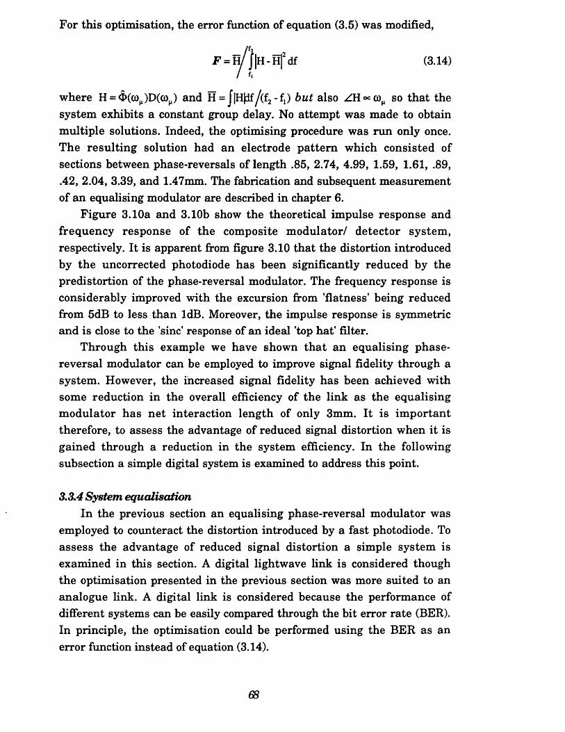
For this optimisation, the error function of equation (3.5) was modified,
where H = 6(coJ1)D(cofI) and H = J|H|df/(f2 -fj) but also so that thesystem exhibits a constant group delay. No attempt was made to obtain multiple solutions. Indeed, the optimising procedure was run only once. The resulting solution had an electrode pattern which consisted of sections between phase-reversals of length .85, 2.74, 4.99, 1.59, 1.61, .89, .42, 2.04, 3.39, and 1.47mm. The fabrication and subsequent measurement of an equalising modulator are described in chapter 6.
Figure 3.10a and 3.10b show the theoretical impulse response and frequency response of the composite modulator/ detector system, respectively. It is apparent from figure 3.10 that the distortion introduced by the uncorrected photodiode has been significantly reduced by the predistortion of the phase-reversal modulator. The frequency response is considerably improved with the excursion from 'flatness' being reduced from 5dB to less than ldB. Moreover, the impulse response is symmetric and is close to the 'sine' response of an ideal 'top hat' filter.
Through this example we have shown tha t an equalising phase- reversal modulator can be employed to improve signal fidelity through a system. However, the increased signal fidelity has been achieved with some reduction in the overall efficiency of the link as the equalising modulator has net interaction length of only 3mm. It is im portant therefore, to assess the advantage of reduced signal distortion when it is gained through a reduction in the system efficiency. In the following subsection a simple digital system is examined to address this point.
3,3.4 System equalisationIn the previous section an equalising phase-reversal modulator was
employed to counteract the distortion introduced by a fast photodiode. To assess the advantage of reduced signal distortion a simple system is examined in this section. A digital lightwave link is considered though the optimisation presented in the previous section was more suited to an analogue link. A digital link is considered because the performance of different systems can be easily compared through the bit error rate (BER). In principle, the optimisation could be performed using the BER as an error function instead of equation (3.14).
68
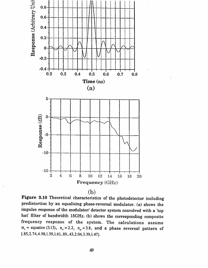
a
au• H
0.6XiQ 0 4og 0.2 o03 0o«
- 0.2
- 0 .40.2 0 .3 0 .4 0 .5 0.6 0 .7 0.8
Time (ns)(a)
pq 0-3<Das -5Q<03©
Pi-10
-15
\
■1 1
2 4 6 8 10 12 14 16 18 20Frequency (GHz)
(b )F igure 3.10 Theoretical characteristics of the photodetector including predistortion by an equalising phase-reversal modulator, (a) shows the impulse response of the modulator/ detector system convolved with a 'top hat filter of bandwidth 15GHz. (b) shows the corresponding composite frequency response of the system. The calculations assum e a c = equation (3.13), n0=2.2, n^=3.8, and a phase reversal pattern of [. 85,2.74,4.98,1.59,1.61,. 89,. 43,2.04,3.39,1.47].
69
3.3.4.1 System performance criterionFigure 3.8 shows a schematic diagram of the externally modulated
optical link. The modulator is biased a t quadrature and so a DC photocurrent of flows from the photodiode. At the input to the decision circuit the photocurrent is given by,
U 0 = bkP(t-kT)+ Z b S (t-n T ) + n(t)+i± (3.15)n « - o o
where k is an integer; T is the bit period; bk is the input unbiased, bi-polar data waveform; n(t) is additive noise; and P(t) is the pulse waveform of the system. P(t) is determined by the excitation pulse together with the frequency response of both the modulator and detector. Ideally, after comparison of a sample idec(kT) with the threshold level i±, the decision circuit will regenerate the data sequence bk. Successful regeneration of bk is limited by two factors: the noise on the transmitted signal n(t), and the inter symbol interference (ISI) represented by the second term of equation (3.15). Figure 3.11 illustrates the detection process occuring a t the decision circuit. The diagram shows that an error occurs if a -1 is sent and /dec exceeds the threshold ^ a t the sampling instant. Conversely, an error occurs if a 1 is sent and idtc falls below iA. To characterise the efficiency of the link an estimate of the probability that a particular symbol will be detected erroneously must be made. The simplest technique of analysis is known as quasi-analytical estimation[3 25l. In this approach, the current waveform is computed in the absence of noise. Subsequently, the noise is added to the waveform at the sampling instant, and the probability of error is estimated by integrating the noise function to determine the fraction of idK on the wrong side' of (see figure 3.11)[3-241. As a result of ISI, the detection probability for a 1 (or a -1) will depend on the pattern of data sent. Consequently, the error rate must be averaged over a random sequence of data whose length is related to the system memory. It is not sufficient to examine specific data sequences such as those studied by Erasme and Wilsonl3-7!.
Noise in optical systems can arise from a variety of sources, but most sensitive reception is achieved when the receiver is operated under shot noise limiting conditions[3-26l. Provided that /dcc(t) does not deviate from significantly, the noise distribution will be constant independent of transm itted symbol. Therefore, any system exhibiting the same contrast between the different symbol levels A/, will exhibit the same BER. Consequently, the performance of different devices in the optical link can..
70
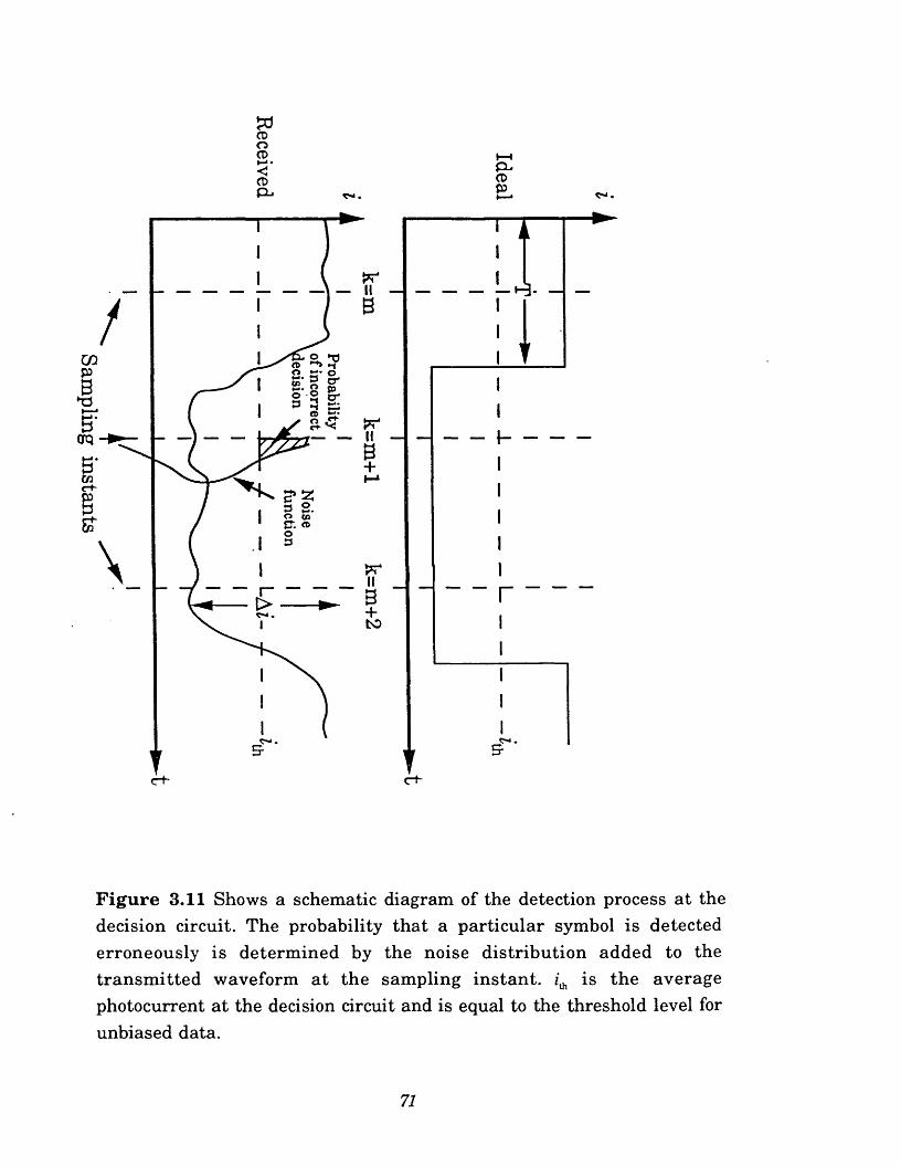
& CD O CD *—1 •<CDP -
Q-CDP
fi o M »S S’ o °>* o STm « 2 CDp 2 cr
CO
to
F ig u re 3.11 Shows a schematic diagram of the detection process a t the decision circuit. The probability that a particular symbol is detected erroneously is determined by the noise distribution added to the transm itted waveform a t the sampling instant. iA is the average photocurrent a t the decision circuit and is equal to the threshold level for unbiased data.
71
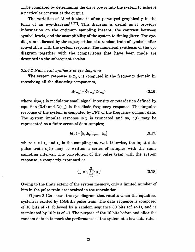
be compared by determining the drive power into the system to achievea particular contrast at the output.
The variation of Ai with time is often portrayed graphically in the form of an eye-diagram[3-27 . This diagram is useful as i t provides information on the optimum sampling instant, the contrast between symbol levels, and the susceptibility of the system to timing jitter. The eye- diagram is formed by the superposition of a random train of symbols after convolution with the system response. The numerical synthesis of the eye diagram together with the comparisons th a t have been made are described in the subsequent section.
3.3A.2 Numerical synthesis o f eye-diagramsThe system response H ( c o h ) , is computed in the frequency domain by
convolving all the distorting components,
H(co,) = d>(co )D(co,) (3.16)
Awhere 0 (0) ) is modulator small signal intensity or retardation defined by equation (3.4) and 0 (0) ) is the diode frequency response. The impulse response of the system is computed by FFT of the frequency domain data. The system impulse response h(t) is truncated and so, h(t) may be represented as a finite series of data samples;
h(tl) = [h„,h1,h2 hN] (3.17)
where tj = i • tA and tA is the sampling interval. Likewise, the input data pulse tra in s^ t) may be written a series of samples with the same sampling interval. The convolution of the pulse train with the system response is compactly expressed as,
sL,=t4i h jS (3.18)j-o
Owing to the finite extent of the system memory, only a limited number of bits in the pulse train are involved in the convolution.
Figure 3.12a shows the eye-diagram that results when the equalised system is excited by 15GBit/s pulse train. The data sequence is composed of 10 bits of -1, followed by a random sequence 30 bits (of +/-1), and is terminated by 10 bits of +1. The purpose of the 10 bits before and after the random data is to mark the performance of the system at a low data rate...
72
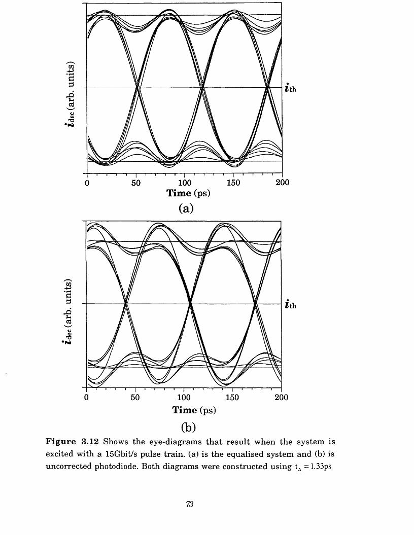
1 1 1 1 1 1 1 1 1 1 1 1 1 1 1 1 1 1 1------
0 50 100 150 200Tim e (ps)
(a)
0 50 100 150 200Time (ps)
(b)F ig u re 3.12 Shows the eye-diagrams tha t result when the system is excited with a 15Gbit/s pulse train, (a) is the equalised system and (b) is uncorrected photodiode. Both diagrams were constructed using tA =1.33ps
73
...(<2Gbits) in order to assess eye-closure a t the higher data rate. In our calculations the pulse shape was rectangular; and the non-zero portion of the equalised system impulse response was assumed to lie between .3 and .7ns (see figure 3.10a). Figure 3.12a shows that an eye-closure of 7% occurs a t the data rate of 15Gbit/s. It is also clear tha t a t the optimum sampling instants the variation of the transmitted waveform is small as consequence of negligible ISI.
Figure 3.12b shows the eye-diagram th a t resu lts when the uncorrected photodiode is excited by the 15GBit/s pulse train. In our calculations we have assumed tha t the non-zero portion of the diode impulse response lies between .35 and .75ns. The distortion of the photodiode causes the asymmetry in figure 3.12b. Moreover, because of ISI at the sampling instant, the variation of the transm itted waveform is much larger than in figure 3.12a. However, it is surprising to note that the eye-closure in figure 3.12b amounts to less than 15%. Consequently, no performance advantage for the equalised system is apparent. Indeed, a system could be constructed using a single section phase matched modulator which would dramatically increase the eye contrast over that th a t could be obtained with the equalising phase-reversal modulator under the same driving conditions. It must be emphasised that the this comparison is not entirely justified as in a digital system symbol recognition is of param ount importance whereas the equalising modulator was designed for optimum signal fidelity. In applications in which signal fidelity was of prime importance the equalising device would be of benefit.
3.4 Chapter Summary
This chapter has concerned the application of the phase-reversal electrode to the design of travelling-wave electrooptic modulators. A major difficulty associated with the design of this type of device is the selection of the phase-reversal electrode pattern to achieve a particular frequency response. For this purpose we devised a novel frequency domain optimising strategy, which we applied to the design of wideband phase- reversal modulators. Subsequently, we found tha t little or no advantage was gained by employing a phase-reversal electrode for wideband phase m atching, especially in comparison to properly phase matched interactions.
In section 3.3 of this chapter we proposed the application of phase-
74
reversal modulators to the equalisation of linear distortions occuring in high speed fibre optic communication systems. Subsequently, we demonstrated this proposal through the equalisation of a high speed photodiode in a simple optical link by including a phase-reversal modulator with a compensating response. We have shown, through an analysis in the time domain, that the compensating procedure is quite general. Indeed, for constant loss electrodes, there is no theoretical impediment to the construction of any real modulator impulse function. To conclude chapter 3 we studied the behaviour of a compensating modulator in a digital optical link. We found that the while some slight advantage accrued, the phase-reversal modulator would be out performed by a conventional a phase matched device. However, it m ust be emphasised that this comparison was not entirely justified as the phase- reversal modulator was designed to maximise signal fidelity through the link and not symbol recognition. Our application of phase-reversal modulators to the equalisation of electronic components in optical fibre systems is the first ever reported. Moreover, this technique represents the only strategy for the compensation of general linear distortions in the optical domain. However, it is important to note th a t predistorting electronic filters such as the fractionally spaced equalisers may be able to achieve the same function.
75
References for chapter 3
[3.1] RC Alfemess, SK Korotky, and EA Marcatili. (1984): "Velocity- matching techniques for integrated optic travelling wave switch/modulators", IEEE J. Quantum Electron., QE-20, pp. 301-309.
[3.2] SC Hiser, WK Bums, CH Bulmer, RD Esman, RP Moeller,A Djupsjobacka, and L Thylen. (1988): "Lithium niobate band pass response microwave modulator with phase-reversal electrodes", Technical Digest of IGWO, paper WD3, pp. 301-304.
[3.3] DC Erasme. (June 1987): "High speed integrated optic modulators using phase-reversal travelling-wave electrodes", PhD Thesis, University of London.
[3.4] GE Betts, CH Cox, and KG Ray. (Dec. 1990): "20GHz optical analog link using an external modulator", IEEE Photon. Technol. Lett., 2,pp. 923-925.
[3.5] CD Watson, and MGF Wilson. (Oct. 1991): "Millimetre wave phase reversal integrated optical modulator in fin line", Electron. Lett., 27, pp. 2059-2061.
[3.6] D Erasme, and MGF Wilson. (1986): "Analysis and optimization of integrated-optic traveling-wave modulators using periodic and nonperiodic phase reversals", Opt. Quantum Electron., 18, pp. 203-211.
[3.7] D Erasme, and MGF Wilson. (1986): "Time-domain analysis of phase- reversal traveling-wave integrated-optic modulators", Electron. Lett. 22, pp. 1024-1026.
[3.8] RL Jungerman, DW Dolfi, CA Johnsen, and M Nazarathy. (1987): "Coded phase reversal LiNb03 modulator with a bandwidth greater than 20GHz", Electron. Lett., 23, pp. 172-174.
[3.9] DW Dolfi, M Nazarathy, and RL Jungerman. (April 1988): "40GHz elecro-optic modulator with 7.5V drive voltage", Electron. Lett., 24, pp. 528-529.
[3.10] M Nazarathy, DW Dolfi, and RL Jungerman. (June 1987): "Velocity mismatch compensation in traveling wave modulators using pseudorandom switched electrode patterns", J. Opt. Soc. Amer., 4,pp. 1071-1079.
76
[3.11] D Erasme, DA Humphreys, AG Roddie, and MGF Wilson. (June 1988): "Design and performance of phase reversal traveling wave modulators", IEEE J. Ligthwave Technol., LT-6, pp. 933-936.
[3.12] KC Gupta et al: "Computer aided design of microwave circuits", Artech Inc House.
[3.13] CD Watson, DA Humphreys, A Roddie, and MGF Wilson. (Oct. 1990): "Equalisation of high bandwidth optical systems by phase reversal modulators", IEE Colloqu. on 'Microwave Optoelectronics', Digest: 1990/139,14/1.
[3.14] N Metropolis, A Rosenbluth, M osenbluth, A Teller, and E Teller. (1953): "Stimulated annealing", J. Chem. Phys., 21, p. 1087.
[3.15] H Chung, and WSC Chang (March 1991): "Modeling and optimization of traveling-wave LiNb03 interferometric modulators", IEEE J. Quantum Electron., QE-27, pp. 608-617.
[3.16] RL Jungerman, CJ Johnsen, DJ McQuate, K Salomaa, MP Zurakowski, RC Bray, G Conrad, D Cropper, and P Hemday. (Sept. 1990): "High-speed optical modulator for application in instrumentation", IEEE J.Ligthwave Technol., LT-8, pp. 1363-1370.
[3.17] K Noguchi, K Kawano, T Nozawa, and T Suzuki. (April 1991): "A Ti:LiNbOg optical intensity modulator with more than 20GHz bandwidth and 5.2V driving voltage", IEEE Photonic Technol. Lett., 33, pp. 333-335.
[3.18] AH Gnauck, U Cimini (Jr.), J Stone, and W Stulz. (August 1990):"Optical equalization of fibre chromatic dispersion in a 5-Gb/s transmission system", IEEE Photonic Technol. Lett., 2, pp. 585-587.
[3.19] JH Winters. (May 1989): "Equalization in coherent lightwave systems using microwave waveguides", IEEE J. Ligthwave Technol., LT-7, pp. 813-815.
[3.20] JH Winters. (Oct. 1990): "Equalization in coherent lightwave systems using a fractionally spaced equalizer", IEEE J. Ligthwave Technol., LT-8, pp. 1487-1491.
[3.21] DA Humphreys, CD Watson, and MGF Wilson. : "Travelling-wave phase reversal modulators for group-delay equalisation of high- bandwidth optical communication systems on transmission", to be published.
77
[3.22] DA Humphreys. (April 1990): "Measurement techniques, numerical methods and photodiode risetime transfer standards for picosecond optoelectronic device metrology at 1-1.6pm", PhD Thesis, University of London.
[3.23] RS Sussman, R Mash, AJ Mosley, and RC Goodfellow. (1982): "Ultra-low- capacitance flip chip bonded GalnAs photodiode", Electron. Lett., 3,pp. 18-20
[3.24] M Schwartz.: "Information,transmission, modulation, and noise", chapter 5, 3rd edition, Mc-Graw-Hill, NY.
[3.25] MC Jeruchim. (Jan. 1984): "Techniques for estimating the bit error rate in the simulation of digital communication systems", IEEE J. Select. Areas Commun., SAC-2, pp. 153-170.
[3.26] A Yariv.: "Introduction to optical electronics", 2nd edition, chapter 11, Holt, Rinehart and Winston, NY.
[3.27] H Nishimoto, T Okiyama, N Kuwata, Y Arai, A Miyauchi, and T Touge. (May 1988): "New method of analyzing eye patterns and its application to high-speed optical transmission systems", IEEE J. Ligthwave Technol., LT-6, pp. 678-685.
78
Chapter 4
Electromagnetic Analysis of Modulator Electrodes
4.1 Introduction
4.2 Quasi-Static Analysis
4.3 Full-Wave Analysis by the Method of Lines
4.4 Comparison with Published Data
4.5 Deviation from Real Transmission Lines
4.6 Chapter Summary
79
4.1 Introduction
The optical response of a travelling-wave modulator is governed by the electrical characteristics of the transmission line guiding the modulating electric field: the temporal evolution of the electrooptic interaction is mediated by the microwave propagation constant, and the efficiency of the interaction is determined by the over-lap of the optical mode and m odulating electric field. Therefore, any accurate design of an electrooptic modulator m ust involve an analysis of the modulator electrode in term s of the electromagnetic modes th a t are supported together with the associated field distributions. The objective of this chapter is to introduce analytical and numerical techniques th a t can be employed for this purpose.
We have seen in chapter 3 th a t integrated optic circuits are constructed in a coplanar geometry. Consequently, the transmission lines tha t are of interest are also coplanar. Generally, the transmission line consists of a layered, anisotropic dielectric medium with coplanar, finite thickness, and finite permittivity metalisations. The boundary conditions on the fields together with the wave equation imply particular field patterns and current distributions for the propagating modes. Solving Maxwell’s equations for the general situation is particularly difficult. Consequently, different levels of approximation have been employed in the analysis of electrooptic modulators (EOMs). The most common analysis is made under the quasi-static approximation, and is discussed in section 4.2. Under this approximation the field distribution is derived under static conditions and is assumed as a solution to Maxwell's equations for time varying systems. As a consequence, quasi-static fields do not contain all field components and do not exhibit frequency dependent characteristics. For certain classes of transmission lines these restrictions are not satisfied.
In section 4.3 a more rigorous solution to Maxwell's equations is presented. The analysis is numerical, and is based upon the Method of Lines. Full-wave solutions containing all six field components can be determined for both dominant and higher modes of the coplanar transm ission line using the technique. In section 4.4 extensive comparisons with the literature are made to confirm the validity of our computer programs.
In our analysis we make the usual assumption of thin and lossless
80
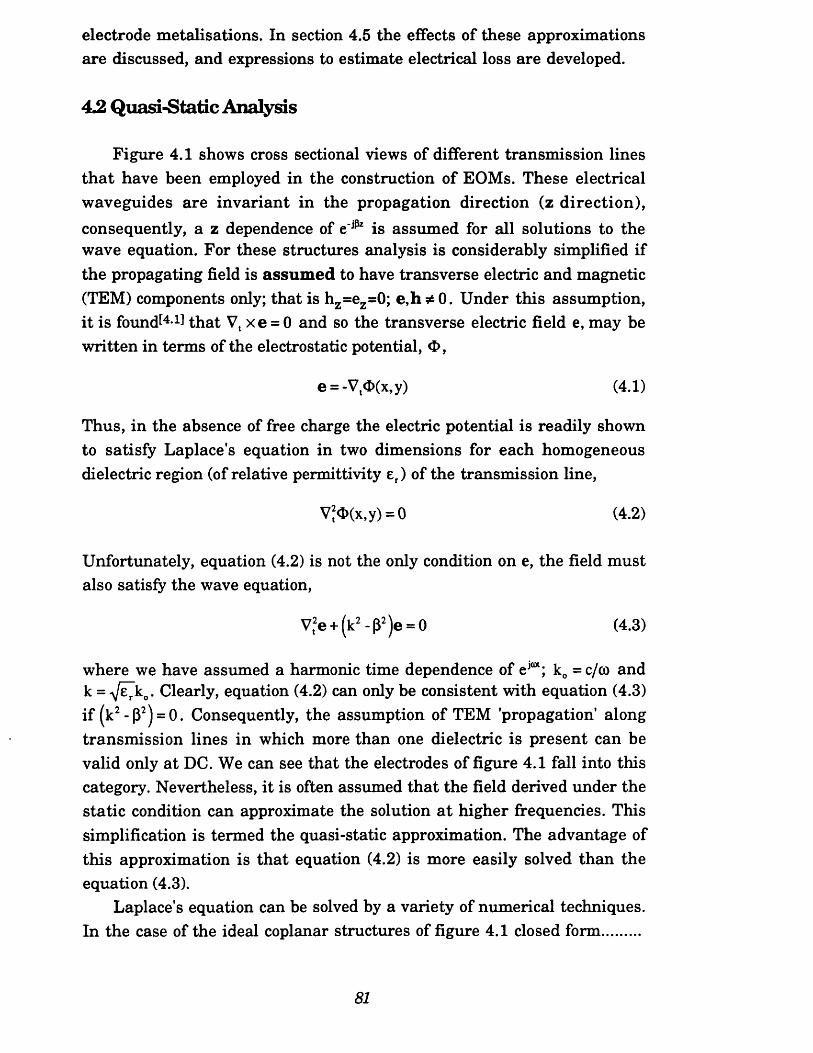
electrode metalisations. In section 4.5 the effects of these approximations are discussed, and expressions to estimate electrical loss are developed.
42 Quasi-Static Analysis
Figure 4.1 shows cross sectional views of different transmission lines th a t have been employed in the construction of EOMs. These electrical waveguides are invariant in the propagation direction (z direction),consequently, a z dependence of e'iPz is assumed for all solutions to the wave equation. For these structures analysis is considerably simplified if the propagating field is assum ed to have transverse electric and magnetic (TEM) components only; that is hz=ez=0; e ,h * 0 . Under this assumption, it is foimd^4 that Vt x e = 0 and so the transverse electric field e, may be written in terms of the electrostatic potential, O,
e = -Vtd>(x,y) (4.1)
Thus, in the absence of free charge the electric potential is readily shown to satisfy Laplace's equation in two dimensions for each homogeneous dielectric region (of relative permittivity er) of the transmission line,
VjO(x,y) = 0 (4.2)
Unfortunately, equation (4.2) is not the only condition on e, the field must also satisfy the wave equation,
Vt2e + (k2 - (32 )e = 0 (4.3)
where we have assumed a harmonic time dependence of ejcot; k0 =c/co and k = V^k0. Clearly, equation (4.2) can only be consistent with equation (4.3) if (k2-p2) = 0. Consequently, the assumption of TEM 'propagation' along transmission lines in which more than one dielectric is present can be valid only at DC. We can see that the electrodes of figure 4.1 fall into this category. Nevertheless, it is often assumed that the field derived under the static condition can approximate the solution a t higher frequencies. This simplification is termed the quasi-static approximation. The advantage of this approximation is that equation (4.2) is more easily solved than the equation (4.3).
Laplace's equation can be solved by a variety of numerical techniques. In the case of the ideal coplanar structures of figure 4.1 closed form........
81
icp w i
:<:S: < : :: :-S:::
' CSL>
(c)
' % €P S >
(b)
a ir
I-V v -.Ca SCp J relativeperm ittivity £ rX
(d)
F igu re 4.1 Typical coplanar electrode geometries that may be employed in the construction of electrooptic modulators. The transmission line metalisations are deposited on the surface of a dielectric and are invariant in the propagation direction, (a) is coplanar waveguide (b) is coplanar strips (c) is coplanar slot line and (d) is asymmetric coplanar waveguide.
82
solutions may be obtained for the electric field through judiciouscoordinate transform s. The transform ation process is known as Conformal mapping.
4.2.1 Conformal mapping applied to coplanar structuresFor problems involving Laplace’s equation a careful choice of the
coordinate system may lead to an advantageous distortion of the problem boundaries. Of particular interest are complex variable substitutions defined as,
W = F( s) = F(x + jy) = u + jv (4.4)
Provided th a t F is analytic and u and v satisfy the Cauchy-Riemann conditions, the transformation is said to be conformal[4-2]. Of consequence, is that u and v must form an orthogonal coordinate system as the Cauchy- Riemann conditions imply that Vtu-Vtv = 0. Moreover, the metrics of the transformed space, and h2, are equal. Hence, Laplace's equation in the uv plane remains unchanged. That is,
d h 2 _ d24> £ ^ = ndu 5u dv hj 9v 5u2 dv2
The advantage of the transformation process is that the boundaries (of constant and known potential) of the problem in the xy plane (s plane) can be mapped to constant coordinate curves in the uv plane (w plane). As Laplace's equation remains unchanged and u and v are orthogonal, the constant coordinate curves in the w plane can be identified with the equipotential lines (or fields) in the s plane. This procedure has been used extensively in electrostatics and has been applied to the characterisation of electrooptic modulators and s w i t c h e s [ 4 -3 U 4 . 4 ] , [ 4 . 5 ] . Useful conformal transforms exist for most classes of coplanar 10 device and within the restrictions of the analysis (infinitely thin and infinitely conducting electrodes) the solutions to Laplace's equation are exact. Consequently, this analysis provides exact data to test against more complex and versatile numerical analyses.
To illustrate the application of conformal mapping we consider the electrode illustrated in figure 4.2. As the substrate upon which the electrode is deposited is lithium niobate Laplace's equation is modified....
83
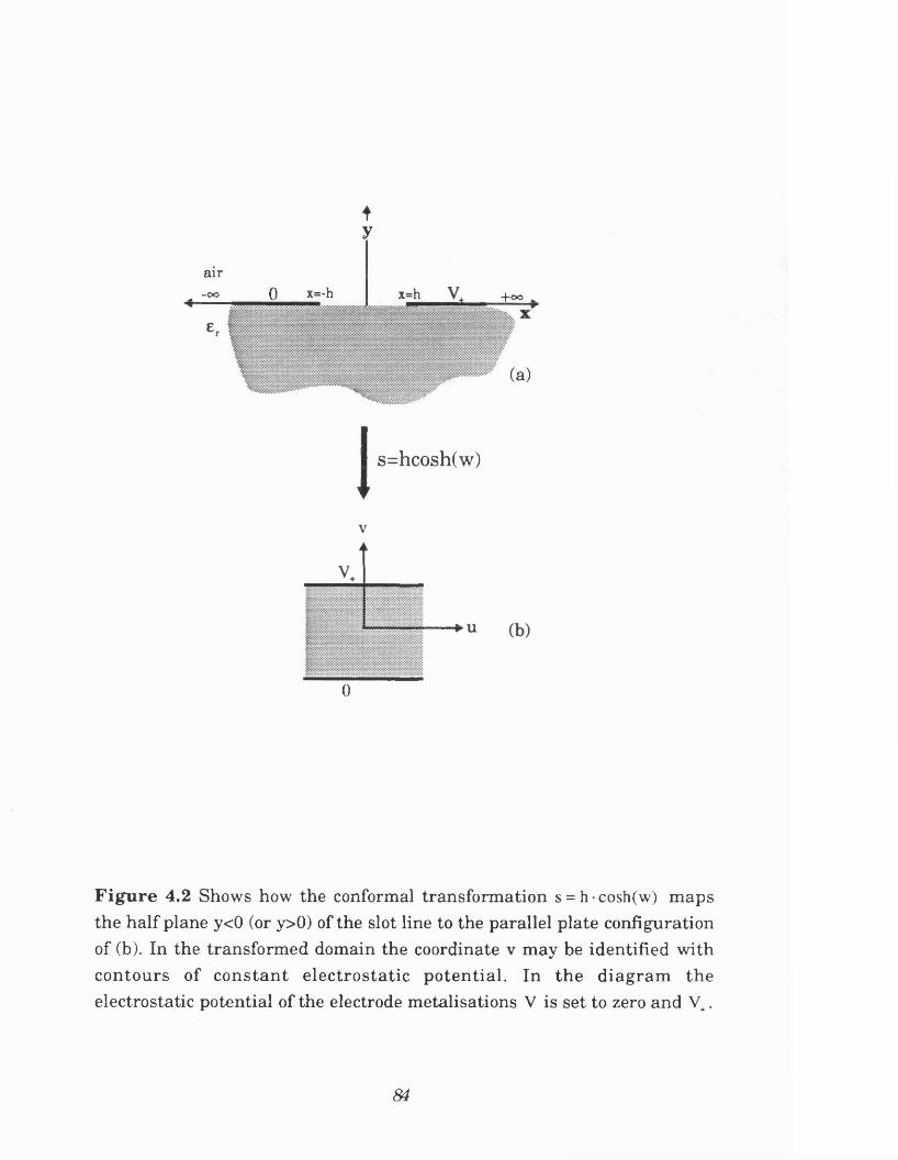
air-oo 0
ty
x=-h x=h +00
(a)
J s=hcosh(w)
v
0
F ig u re 4.2 Shows how the conformal transform ation s = h cosh(w) m aps the h a lf plane y<0 (or y>0) of the slot line to the parallel plate configuration of (b). In the transform ed domain the coordinate v m ay be identified w ith con tours of c o n stan t e lec tro sta tic p o ten tia l. In th e d iag ram the electrostatic potential of the electrode m etalisations V is set to zero and V+.
84
to account for the anisotropy of the substrate,
Vt ' ( e e ) = 0 = ex| 4 + ey | 4 (46)dx2 dy
This relation can be reduced to the form of equation (4.2) by substituting y' = es/eyy. Under the transform ation, s = hcosh(w), the slotline is transformed into a parallel plate as shown in figure 4.2. Consequently, the contours of constant v are identified with the equipotential lines in the z plane. Ultimately, the electric field components may be determined as,
ex = — Im K
_ V .V T■ t 9 , 2nd e — I— Re y .Vs -h J n Vey vVs -h
(4.7a,b)
Equations (4.7a,b) imply a pole of order l/Vr at the electrode edges (r is the distance from s = h). These poles originate from the assumption of infinitely thin and conducting electrodes. On the assumption of finite thickness and finite conductivity electrodes the poles do not occurt4-6L
For TEM waves the propagation constant is computed as the weighted ’average’. Thus, the microwave effective permittivity for the waveguide of figure 4.2 is computed as,
_ Ve ex ye«ff ^ (4.8)
It is interesting to note that an effective permittivity of equation (4.8) leads to satisfaction of equation (4.3) for the waveguide cross section as a whole.
Practical devices are seldom constructed as those in figure 4.1. To prevent excessive optical loss we have seen that a thin buffer layer is often incorporated between the substrate and electrodes in order to decouple the optical field from the conductors. This layer can have a large effect on the magnitude of the electric field in the vicinity of the optical waveguide. For an accurate evaluation of the over-lap factor this structural detail must be incorporated. Buffer layers are not readily accommodated within the framework of conformal analysis, though approximate solutions have been obtained by Sabatier and Caquet[4-7 using the Method of Images together with conformal transforms. For more complex structures, conformal transformations must be abandoned in favour of purely numerical solutions to Laplace's equation.
At this stage, some comment regarding the conversion of an
85
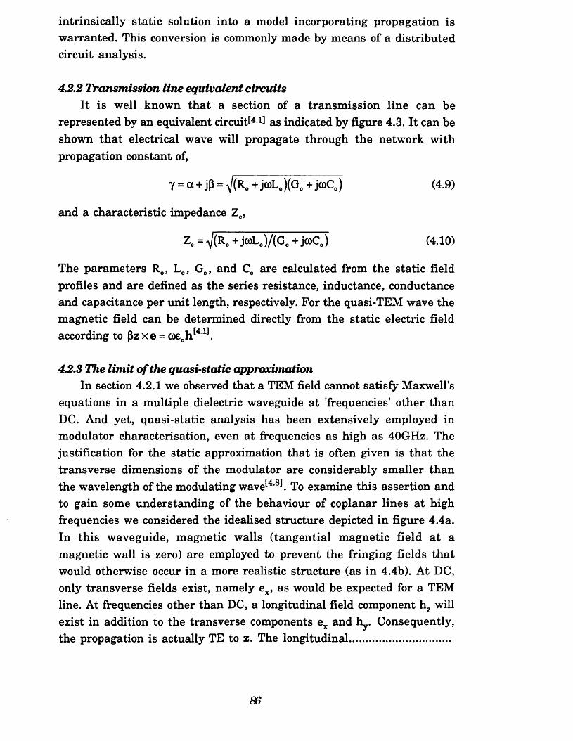
intrinsically static solution into a model incorporating propagation is warranted. This conversion is commonly made by means of a distributed circuit analysis.
4J2.2 Transmission line equivalent circuitsIt is well known th a t a section of a transm ission line can be
represented by an equivalent circuit^411 as indicated by figure 4.3. It can be shown th a t electrical wave will propagate through the network with propagation constant of,
Y = a+ jP = - (R0+jcoL<,)(G0 +ja>C0) (4.9)
and a characteristic impedance Zc,
Ze = V(R„+jwL.)/(G0+jcoC0) (4.10)
The parameters R0, L0, G0, and C0 are calculated from the static field profiles and are defined as the series resistance, inductance, conductance and capacitance per unit length, respectively. For the quasi-TEM wave the magnetic field can be determined directly from the static electric field according to pz x e = coe0h [41].
4J2.3 The lim it o f the quasi-static approximationIn section 4.2.1 we observed that a TEM field cannot satisfy Maxwell's
equations in a multiple dielectric waveguide at 'frequencies' other than DC. And yet, quasi-static analysis has been extensively employed in modulator characterisation, even at frequencies as high as 40GHz. The justification for the static approximation that is often given is tha t the transverse dimensions of the modulator are considerably smaller than the wavelength of the modulating wave*-4,8-*. To examine this assertion and to gain some understanding of the behaviour of coplanar lines at high frequencies we considered the idealised structure depicted in figure 4.4a. In this waveguide, magnetic walls (tangential magnetic field a t a magnetic wall is zero) are employed to prevent the fringing fields that would otherwise occur in a more realistic structure (as in 4.4b). At DC, only transverse fields exist, namely ex, as would be expected for a TEM line. At frequencies other than DC, a longitudinal field component hz will exist in addition to the transverse components ex and hy. Consequently, the propagation is actually TE to z. The longitudinal.................................
86
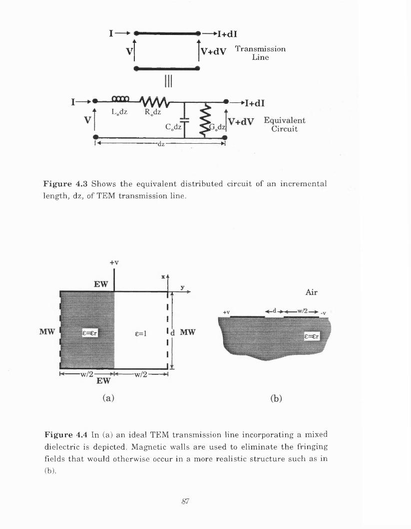
'1
I+ d ly '+dV Transmission
Line
• —
tm uL0dz
-VWv— |Rcdz
----- •▲
1 C0dz
\ < ~ --------dz------ --------H
+I+dI
Circuit
F ig u re 4.3 Shows the equivalent distributed circuit of an incremental length,, dz, of TEM transmission line.
F igu re 4.4 In (a) an ideal TEM transmission line incorporating a mixed dielectric is depicted. Magnetic walls are used to eliminate the fringing fields that would otherwise occur in a more realistic structure such as in (b).
87
magnetic field hz can be shown to satisfy the wave equation in eachhomogeneous dielectric region (relative permittivity e),
(4.11)
where k0 is the wave number of free space. Applying the boundary
between the dielectrics yields a transcendental equation which defines P,
where ka = Vko~P2 ^ kd = Verko-P2*If kaw, kdw « l , equation (4.12) reduces to ka+kd=0 Hence, the
effective dielectric constant can be determined as,
Equation (4.13) is in accord with that that would be predicted under the quasi-static approximation together with a distributed circuit model. Furthermore, it can be shown that hz/hz -»0 as kaw, kdw -» 0 . Thus, this simple example clearly illustrates that a static solution is valid provided the lateral dimensions of the waveguide are smaller than a free space wavelength (ie kaw « l ) . Our example also shows that in a coplanar line, the time averaged power flow through each homogeneous region is equal, regardless of the substrate permittivity.
For optical modulators the feature size is a t least two orders of magnitude smaller than the highest modulating wavelength. Thus, a static approximation is likely to be valid within the interaction region. However, outside of this region in the interface circuit where the electrode dimensions are considerably larger, a more rigorous solution is required to specify the behaviour of the transmission line fields for both the dominant and higher order modes. Moreover, in some waveguides, the dominant mode cannot be quasi-TEM, as the waveguide may have no DC response. To determine the properties of such a waveguide under the quasi-static approximation is clearly impossible. To analyse these waveguides a full-wave analysis determining all 6 field components is required. In the following section a full-wave analysis by the Method of Lines is presented.
conditions on the tangential field at the side walls and at the interface
(4.12)
88
4.3 Full Wave Analysis by the Method of Lines
Of the many numerical methods that could be employed for electrode characterisation^4-9!, we concluded th a t the Method of Lines (MOL) satisfied our requirements most completely. MOL is a semi-analytical procedure which is similar to the finite difference method, but is optimised for the study of planar waveguides. The first application of MOL to the full-wave properties of planar transmission lines was reported by Schulz and Pregla 4 10!. Subsequently, MOL was applied by Sherrill and A lexopoulos 4 n ! to the study of the full-wave properties of planar waveguides incorporating anisotropic dielectrics and by Keen et al in a quasi-static analysis of an EOM on lithium niobatet412!. Extensions to the basic method have been presented by Schmuckle and Pregla to study quasi-planar transmission lines incorporating thick losses^413! and thick lossy[4-14! metalisations. Most recently, Gerdes et afi4-15 have described the application of MOL to the full-wave treatment of lithium niobate EOMs incorporating thick, lossless electrodes. This was the first publication to examine the high frequency properties of EOMs by rigorous solution. An earlier full-wave treatment by Railton and McGeehan 4 151 under the thin electrode approxim ation failed to consider any high frequency phenomena.
In this section we present a full-wave, hybrid mode, treatm ent of anisotropic planar waveguides by MOL. The formulation we have used, is due to Sherrill and Alexopoulos, and is different to tha t employed by Gerdes et al. We have extended the analysis of Sherrill and Alexopoulos to consider four anisotropic dielectric layers. Presently, we are limited to the consideration of thin electrode metalisations. In the forthcoming analysis we adopt the notation of Sherrill^417!.
4.3,1 Hybrid mode analysis and the wave equationSolutions to Maxwell’s equations can be conveniently grouped into
three types; TE (ez=0), TM (hz=0) and TEM. Though satisfactory solutions of these types often occur, most generally, a field will include all six fieldcomponents. This field may be adequately described through thesuperposition of TE and TM fields,
E = €>*+«?* (4.14a)
H = h e +hH (4.14b)
89
Where ee,h e are the TE part of the total field and eH,h H is the TM part. The TE and TM fields are determined from the longitudinal field components e2 and hz. Provided, E,H satisfy all the boundary conditions and tha t ez and hz simultaneously satisfy the wave equation,
a ®
in each separate layer of the waveguide (for y substitute either ez or hz), E,H will be a mode of propagation. Such a solution is known as a hybrid mode.
For m aterials such as lithium niobate the relative permittivity is dependent upon the direction of the field. With a suitable choice of coordinate system the permittivity can be expressed as a diagonal quantity
e = e„e u
(4.16)
This condition conveniently defines the principle axes of the coordinate system for this discourse. For anisotropic substrates, the potentials from which TE and TM like modes are generated, are not the longitudinal fieldcomponents. More suitable generating functions are oriented Hertzpotentials (see section 5.3.1.1),
ft'h= n 'h(x,y,z).y (4.17)
Note that in our notation the superscript (or suffix) ?e,h' denotes either e or h within a particular expression. Therefore, equation (4.17) actually represents two equations which define both ne and n \
It can be shown from Maxwell's equations, that the total hybrid fields,(assuming time-harmonic variation) can be written as 4 111,
E(x, y, z) = V( V • fte) + k2J \e - jcopi0V x fth (4.18a)H(x,y,z) = jcoe0e1V x ft' + V(V • fth) + kj. fih (4.18b)
and th a t the potentials T c,h must satisfy the following scalar wave equations,
^ + n * ^ +(k?-P*)V -0 (4.19a)
90
3 2 « /h ^ 2 m h
1 ? " + i p - + (k'- P 2)'I'h=0 (4‘19b)
where, n ' b =*F' hexp(-jPz), k0 = c o ^ e , , kx = nxk0, k„ = n,k0 and, n n1 = V e7 ,n = n„/n1
To determine the guided modes of the coplanar structures of figure 4.1, equations (4.19a), (4.19b) must be solved for each homogeneous region and the boundary conditions between each region satisfied. From figure4.1 we can see th a t all the coplanar structures exhibit uniformity perpendicular to the plane of metalisation (ie along the y axis). This fact is exploited numerically by MOL: by descretising one variable, the partial differential equations (4.19a), (4.19b) are reduced to set of coupled ordinary differential equations, the free variable being evaluated on a series of lines. These ordinary differential equations can be decoupled by simple linear transformations and solved algebraically. As a consequence, considerable computational efficiency is achieved. MOL also exhibits other significant advantages which have been discussed a t length by Pregla and Pascherf418].
4.33 Descretisation and solution of the wave equation by MOLFigure 4.5 illustrates how descretisation is accomplished for the
planar waveguides analysed in this section. From the diagram it is apparent tha t descretisation along the x axis is desirable as individual layers are homogeneous in the y direction. F ig u r e 4.5 also shows that there are two separate systems of lines, one for each of the two potentials T e and 'F*1. These line systems are shifted so tha t the lateral boundary conditions for each potential may be satisfied more easily. The lateral boundary conditions are dual- if one potential satisfies the Dirichlet condition, (xFc,h = 0) then the other potential satisfies the complementary Neumann condition (vF'h,e=0). The actual condition satisfied by T e,h is determined by the type of 'wall' forming the boundary. The wall may be of an electric or magnetic type. It is important to note tha t the wall type imposes either odd or even symmetry on each of the field components.
The descretised potentials may be written as a column vector. That is,
T c,h (x*’h,y)Vpe.h _ (4.20)
T e,h (x£\y)
91
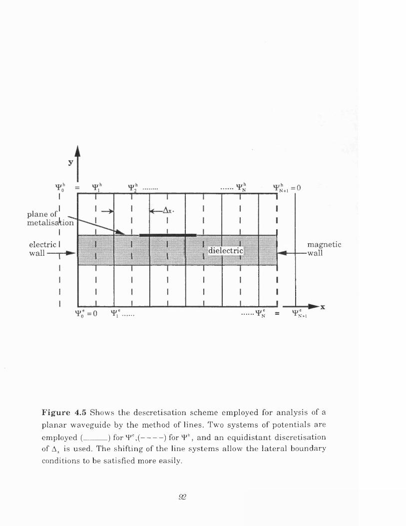
f =0N + l V
plane of _metalisation
electric wall —
magneticwalldielectric
N + l
F ig u re 4.5 Shows the descretisation scheme employed for analysis of a planar waveguide by the method of lines. Two systems of potentials areemployed (_____ ) for T ',(--------) for T h, and an equidistant discretisationof Ax is used. The shifting of the line systems allow the lateral boundary conditions to be satisfied more easily.
92
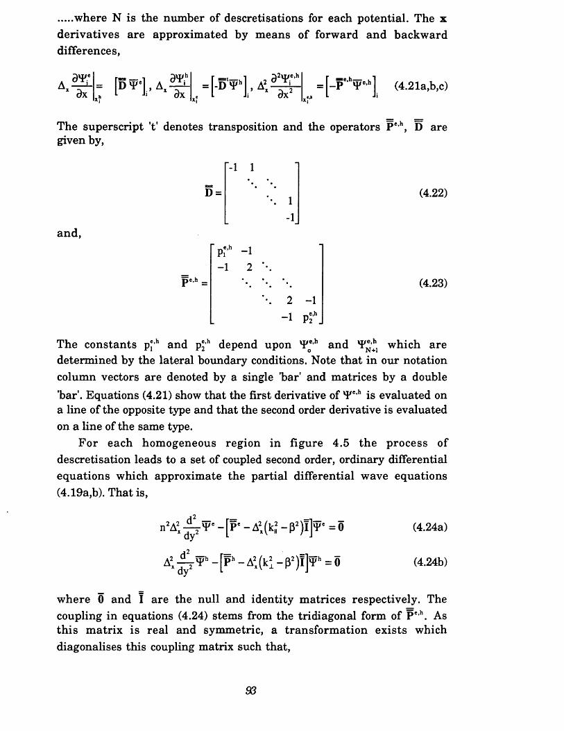
where N is the number of descretisations for each potential. The xderivatives are approximated by means of forward and backward differences,
ay*dx 7 - [ - ^ 1 (4.21a,b,c)
The su p ersc rip t’t' denotes transposition and the operators Pc h, D are given by,
D =
■1 1
1-1
(4.22)
and,
pe.h _-1p r - i
2 - i
1 « ,e >h-i p2
(4.23)
The constants pj,h and p2,h depend upon y*,h and y®** which are determined by the lateral boundary conditions. Note that in our notation column vectors are denoted by a single 'bar' and matrices by a doublebar'. Equations (4.21) show that the first derivative of y c,h is evaluated on a line of the opposite type and that the second order derivative is evaluated on a line of the same type.
For each homogeneous region in figure 4.5 the process of descretisation leads to a set of coupled second order, ordinary differential equations which approximate the partial differential wave equations (4.19a,b). That is,
n2A2 - f j V ' - [p* - A2 (kj - p2) l]y ' = 0dy
A2 [?h ~ A2 (k* - p2 ) IJP = 0
(4.24a)
(4.24b)
where 0 and I are the null and identity matrices respectively. The coupling in equations (4.24) stems from the tridiagonal form of Pc,h. As th is m atrix is real and symmetric, a transform ation exists whichdiagonalises this coupling matrix such that,
93
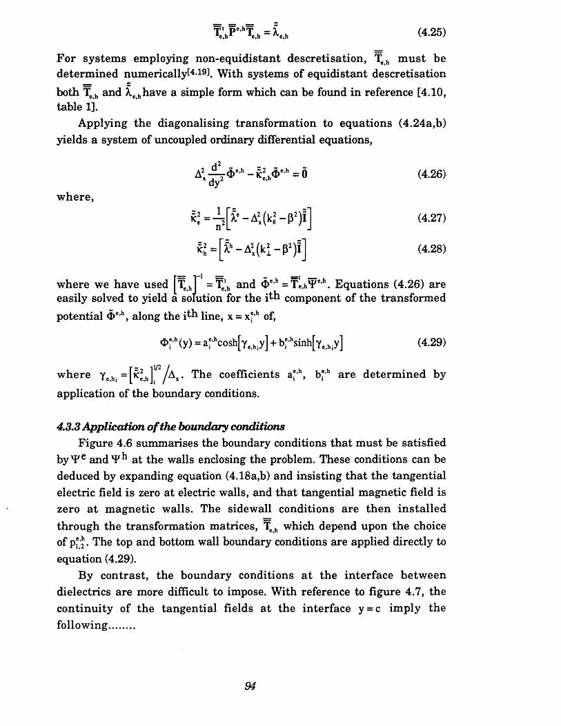
T«;hP ''hT,h= L (4.25)
For systems employing non-equidistant descretisation, T e h m ust be determined numerically^419^ With systems of equidistant descretisationboth T c b and A,c hhave a simple form which can be found in reference [4.10, table lj.
Applying the diagonalising transformation to equations (4.24a,b) yields a system of uncoupled ordinary differential equations,
j 2A\ hd>e,h = 0 (4.26)
dywhere,
*2 = ^ p - A 2(kJ-p2)l] (4.27)
K2 = p h-A 2( k i - P 2)!l (4.28)
where we have used TchJ = T c| h and 4>c,h = T c , h ' F c ,h . Equations (4.26) are easily solved to yield a solution for the i^h component of the transformedpotential 4>c,h, along the i ^ line, x = x*,h of,
3>f,h (y) = af,hcosh[yeh.y] + b‘>hsinh[ye h.y] (4.29)
where yehi =[Kgh]V2/Ax. The coefficients af,h, b*,h are determ ined by application of the boundary conditions.
4.3,3 Application o f the boundary conditionsFigure 4.6 summarises the boundary conditions that must be satisfied
by'F6 a n d T *1 a t the walls enclosing the problem. These conditions can be deduced by expanding equation (4.18a,b) and insisting that the tangential electric field is zero at electric walls, and that tangential magnetic field is zero a t magnetic walls. The sidewall conditions are then installed through the transformation matrices, T c h which depend upon the choice of p* J • The top and bottom wall boundary conditions are applied directly to equation (4.29).
By contrast, the boundary conditions a t the interface between dielectrics are more difficult to impose. With reference to figure 4.7, the continuity of the tangential fields a t the interface y = c imply the following........
94
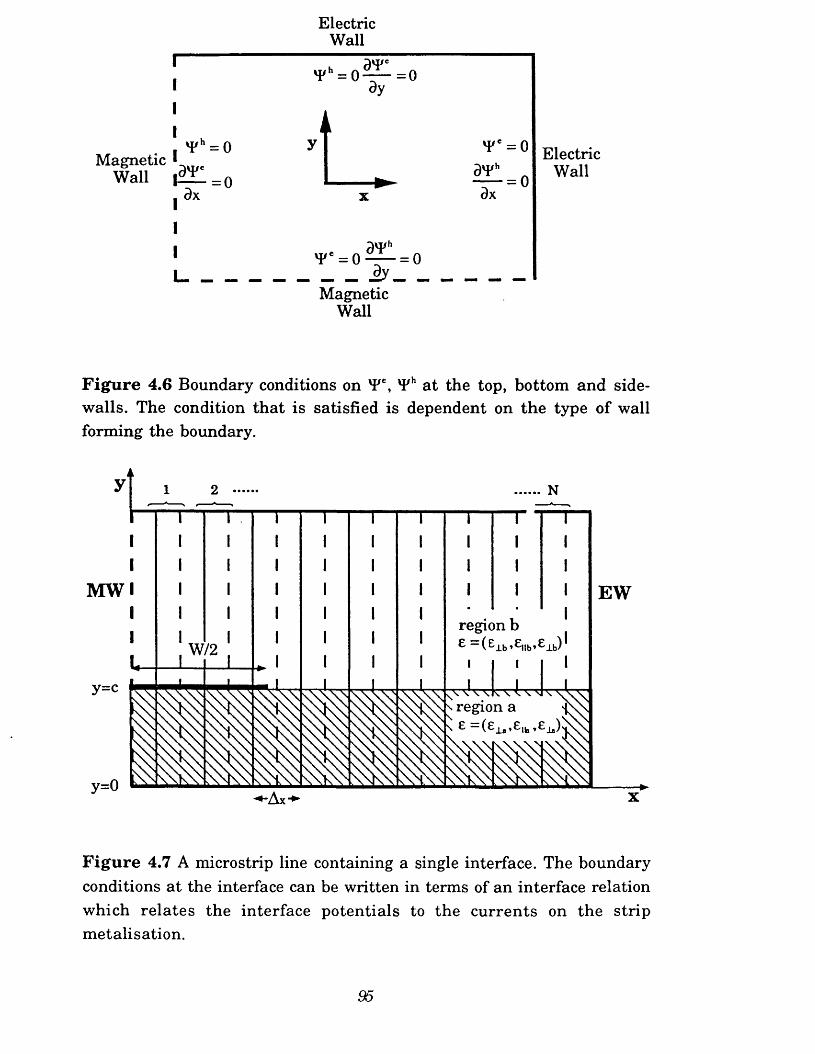
ElectricWall
= 0
ElectricWall
MagneticWall
= 0
MagneticWall
F ig u re 4.6 Boundary conditions on T \ T h at the top, bottom and sidewalls. The condition that is satisfied is dependent on the type of wall forming the boundary.
MW EWregion b = (£±b»*Hlb»£±b)W/2
y=c
F ig u re 4.7 A microstrip line containing a single interface. The boundary conditions at the interface can be written in terms of an interface relation which relates the interface potentials to the currents on the strip metalisation.
95
.conditions on the transformed potentials^411],
d>h = <f>h^ b a
_ do;dy dy
“ E.P^lb^b “ 'Ej.^1) = ^"8d6,hdy dy
+ K,
dy dy+ K,
(4.30a)
(4.30b)
(4.30c)
(4.30d)
where 8 = T^DT,., 8 = 8\ Kx=ThKx, Kz =TeKz and Kz, Kx are thedescretised current densities on the interface metalisation. The matrix 8 is a diagonal quantity when the number of descretisations for eachpotential is equal and quasi-diagonal in the case of unequal numbers ofdescretisationst418].
Combing equations (4.30) with the solutions for the potentials withinthe regions 'a' and V allow the interface potentials a t y=e, to be written interms of the current densities for i^1 pair of lines,
(4.31)
where [r] is a 2X2 matrix known as an interface relation. Using equation (4.18a,b) an expression for tangential electric field in term s of the transformed potentials can be developed,
(4.32)
where [ p ] is a 2X2 matrix. Equation (4.31) together with equation (4.32) allows the transformed tangential electric field a t the interface to be written in terms of the transformed current density,
R■<d ; ( c ) ' K
■ ■i < j> i(c )_ i A .
X (c ) ' = Pi ■ •i _<£,h(c)_
E , ( c ) ' =6
K y 6= P
A ( c ) . ii K . i
i i(4.33)
The final boundary conditions relate to the behaviour of the fields and currents a t the interface in the presence of metalisation. These conditions state that in the spatial domain along the interface the tangential electric field must be zero at conductors and that the current must be zero in the
96
absence of conductors. The tangential electric field along the entire interface in the original domain is determined as,
(4.34)
where G = Tg G t J and the global transformation matrix Tg, is defined as,
Fortunately, equation (4.34) need not be completely evaluated. Only a small number components of Ez(c) and Ex(c) which cross metalisation at the interface are of concerned. Selecting these components from equation(4.34) and imposing the boundary condition of zero tangential electric field a t the interface metalisations yields,
Consequently from equations (4.34) and (4.36) an eigenvalue equation is formed,
Non-trivial solution of equation (4.37) implies th a t ,
The roots of equation (4.38) define P versa co for all modes of propagation. Moreover, from the corresponding eigenvector of each root, the guide fields may be deduced allowing computation of other im portant parameters such as the impedance.
reduced
(4.36)
det[GL = ° (4.38)
4.3.4 Calculation o f fields, power flow and impedanceThe transformed current densities at the interface are determined
from the eigenvector of equation (4.38) as,
where the non-zero elements of are given by K
LKxJred
=R
-i X
A h ( < o . ii
A .
The transformed potentials a t the interface are then determined by inverting equation (4.31) as,
(4.40)
Equation (4.40) illustrates the advantage of calculating the potentials in the transformed domain as 1 has an order of 2 and hence may be inverted algebraically. Once the boundary potentials are known for the dielectric region 'a', d>',hj(y) is automatically specified everywhere on a line within the region through equation (4.29). Expressions for the transformed fields can be developed in terms of d>e,h(y) by descretisation and transformation of equations (4.18/417 ,
Ev(y) = T c E (y) =
J -S jL $ ' (y) + con |3<i>h(y) A, dy
(4.41a)
-X-K2 + k2I A2 i>'(y) (4.41b)
-jp-^-4>'(y) + (y) dy A,
(4.41c)
-w e^Pd^y)-A, dy
(4.41d)
-4-kJ + id iA2„ X
d>h(y) (4.41e)
J ^ i | d > ‘(y)-jpA ® h( y)A, dy
(4.41f)
It is important to note that each field component is associated with a particular line type. The association is enforced by the requirement of the field to satisfy the boundary conditions at the side-wall. For example, at an electric side-wall we have seen from figure 4.6 that ¥ c(y) = 0, therefore we would expect both ez and ey to be associated with electric lines as these field components exhibit the same symmetry as T e(y).
In order to calculate parameters such as impedance an expression for the power flow through the waveguide must be determined. The power flow is given by the integral of the Poynting vector over the waveguide
98
cross section. For z propagation, the power flow P is given by,
P = T Re JJ(e«hy 'eyh>)dxdy (4.42)x section
For a particular layer of the planar waveguide an estimate for the x integration can be made with the descretised fields together with a trapezoidal integration,
P = R e j(E ;H ;-E ;H ;)dy (4.43)
Instead of evaluating equation (4.43) with the field components in the spatial domain, the field components in the transformed domain can be used with considerable advantage as, for example,
E t f j * _ l ? t 'T ’ t T ' i t * _ r l u *x y ” *^x h h y " ^ x “ y (4.44)
Not only is the x integral reduced to a sum of dimension N, but the variation of Ex,Hy are known as explicit functions of y through equations (4.41). Consequently, an expressions for P can be developed in terms of the fields at the boundary of a dielectric region 417],[4.18]
1 NP=oReI
1 A‘\sinh2( ,h) _
1 A,wsinh2( ^ L 2
1[ A>2
sinh2(£*). 4 ic *.
1 Axw_ sinh2(4*) 2
A w
A,2 —*— s 2Khi
A»w2
-c o s h ^ -^ s m h fc )
[£„ (y, )fi; (y,) + (y 2 )H; (y 2)]
[e« (yi )H ; (y 2) + E* (y2 )H ; (y ,)]
[£^(y.)H^(y,)+£^(y2)H^(ya)]
(y, ) h ; (y 2) + % (y 2 (y,)]
(4.45)
where =[yc>h w and w = y2 - yj.For non-TEM waveguides a definition of impedance is not unique.
For the waveguides examined in this thesis we have utilised the power- voltage impedance which is defined as,
z = y ic 2P
(4.46)
where V refers to the slot voltage for a CPW lines or fin line.
99
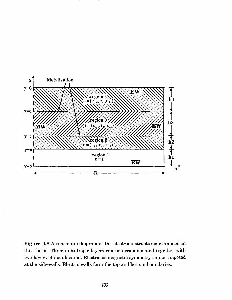
y=
y=
y=
Metalisation
region 4 x
^region 3£ “ (E 3,£|3
W ////MsS^region 2\^
region 1 e = 1
y=c
y=ej
- U
F ig u re 4.8 A schematic diagram of the electrode structures examined in this thesis. Three anisotropic layers can be accommodated together with two layers of metalisation. Electric or magnetic symmetry can be imposed at the side-walls. Electric walls form the top and bottom boundaries.
100
4.3.5 MOL applied to full-uxwe analysis ofEOMFigure 4.8 shows the general form of the problems th a t may be
analysed with the computer programs that we have developed during the course of our research. The structure may contain three anisotropic layers (regions 4,3,2) and two layers of metalisation a t positions c and d. Our intention was to incorporate a single layer of thick metalisation14 131. However, presently we are limited to the consideration of thin electrodes. The boundaries of the enclosure are electric a t the top and bottom walls, and either electric or magnetic at the side walls.
An important stage in the application of MOL relates to the definition of the interface relations for the problem. As two layers of metalisation are now accommodated, the interface relations are 4X4 matrices instead of the 2X2 matrices used in section 4.3.3. For i ^ pair of lines we adopted the following convention for the interface relation,
X '•
a
•XX K *
X . i H a. 1 __
where the first suffix to <!>c’h refers to the region number, and the second suffix indicates the y coordinate. The interface relation may defined by imposing the boundary conditions on the solutions to the wave equation as described in section 4.3.3. The problem is rather involve algebraically and its exposition is left to Appendix 2. Using the interface relation an expression can be developed which relates the transformed current densities to the transformed tangential electric fields. Before embedding these relations into the global matrix and transforming the reduced matrix to the original domain, it is sometimes advantageous to rearrange the equations in order to lim it the size of the reduced matrix. For example, an interface containing mostly metalisation will lead to a reduced matrix of large order if the final boundary condition imposed is zero tangential electric field. An equivalent boundary condition that could be applied would be zero current density in the absence of metalisation. This boundary condition would lead to a reduced matrix of considerably smaller order. Appendix 3 gives a listing of the MOL computer program that we have developed.
101
4.4 Comparison with published data
Before em barking on any quantita tive analysis of unknown microwave structures it is important to validate the MOL computer programs. In this section extensive comparisons are made with the literature to confirm the accuracy of our numerical analysis.
Figure 4.9 shows the variation of impedance verses aspect ratio for a CPW on a semi-infinite isotropic dielectric of relative permittivity 35.5 as determined by the MOL. For comparison, the impedance calculated by conformal mapping^4*20] is also shown.
Figure 4.10 shows the lateral variation of ex at 1pm, 4pm and 7pm into the substrate of a CPW fabricated on Z cut lithium niobate. The structure that has been analysed is defined by the inset to figure 4.10 together with figure 4.8. The data employed in the MOL computations is given in the caption. The dimension of the CPW is typical of an electrooptic modulator; and a voltage of +1V is applied to the centre conductor. Note tha t in this example only half the cross-section of the CPW is shown as a magnetic wall has been inserted into the plane of symmetry for our analysis. The field determined by MOL is seen to be in excellent agreement with that determined by conformal mapping. However, it is important to note that the slot voltage V, was determined in our MOL analysis by integrating ex between the conductors in the plane of the dielectric interface,
v = A ,X[Ex] (4.48)slot i
Equation (4.48) ignores the singular behaviour of the field at the electrode edges and is only exact in the limit as Ax—>0. Consequently, an underestimate of the slot-voltage might be expected for finite Ax. However, we have confirmed the validity of equation (4.48) by integrating the electric field along a different path, between the electrodes, to avoid the field singularities.
Figure 4.11 shows the dispersion characteristics of the dominant and two higher order modes of a shielded CPW line. This data may be compared with that generated by Fujiki et afi4-21\ The data defining the structure we have analysed is given in the figure caption.
Figure 4.12 shows the variation of microwave effective permittivity verses frequency for both the odd and even mode of a CPW on a sapphire substrate as determined by MOL. The odd mode (odd in ex) is determined with magnetic wall symmetry and the even mode is determined from......
102
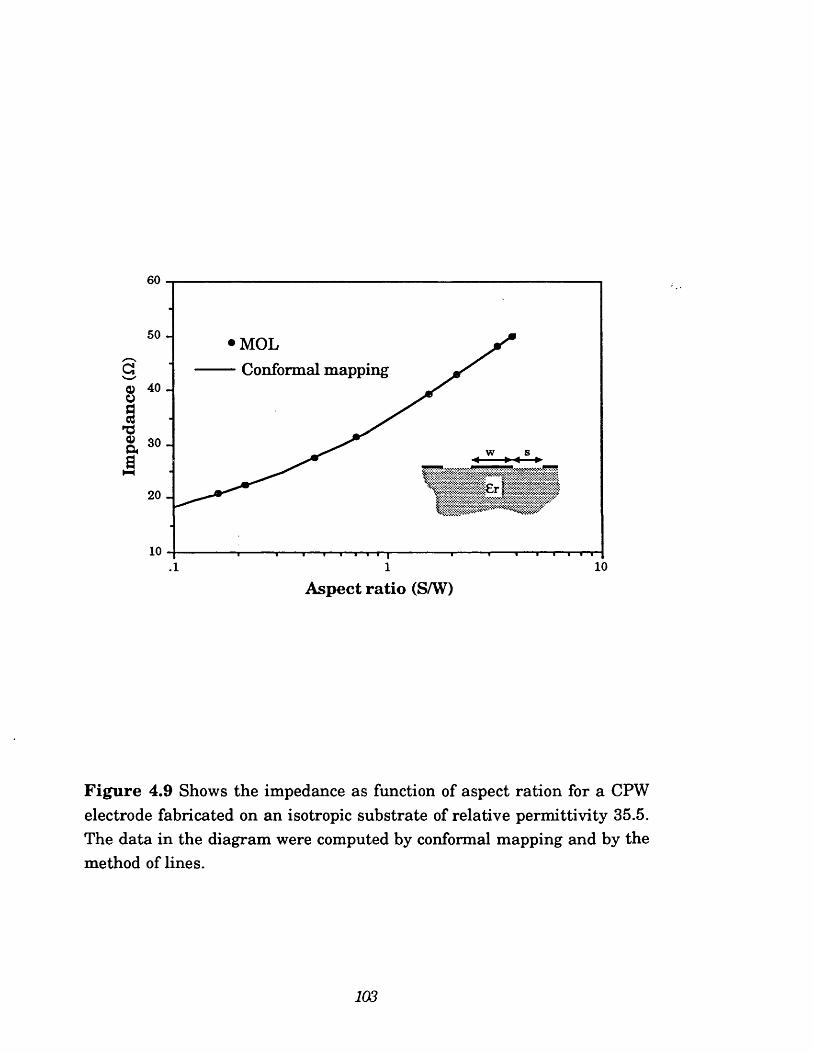
60
50 •MOL- Conformal mappinga
W
10.1 lA spect ra tio (S/W)
F ig u re 4.9 Shows the impedance as function of aspect ration for a CPW electrode fabricated on an isotropic substrate of relative permittivity 35.5. The data in the diagram were computed by conformal mapping and by the method of lines.
103
ex (kV/m)
80-
70-w/2 h4
60- T\/TW ' / / / / s s S s / s s / s / / M W V Z cut lithium niobate V
50- hl
(prn^40-
30- MOLConformalmapping
20 -
10 -
40 50x (pm)
F ig u re 4.10 Shows the lateral variation ofex a t 1pm, 4pm and 7pm into the substrate of a CPW fabricated on Z cut lithium niobate. Note that only half the cross-section of the CPW is shown. The data employed in the MOL computations were as follows:hl=2.112m m , h2=lm m , h3=.2pm, h4=4mm, e2 = [44,28,44],e3 =[44,28,44], e4 = 1, s=10pm, w=23.95pm, Ax = 0.465pm, f=lGHz, ecff =18.05, B=180pm.(a) 1pm into the substrate ie y=4.001mm(b) 4pm into the substrate ie y=4.004mm(c) 7pm into the substrate ie y=4.007mm
104
10
MOL[4.21]
h48 MW
0cS
2
04020 30100
F requency (GHz)
F ig u re 4.11 Shows the dispersion characteristics of a shielded CPW for the dominant, first and second higher order modes. hl=3.0mm, h2=.95mm, h3=.05mm, h4=3mm, e ,= l, e2 =[9.6,9.6,9.6], e3 =[9.6,9.6,9.6], e4= l, s=lmm, w=2mm, Ax = 1053mm, B=7.474mm.
3.0
MOL[4.22]12 2 .5 -
►H odd mode
2 . 0 -
even modeh4MW
orEW
1.00 5 10 15 20 25 30
Frequency (GHz)
F ig u re 4.12 Shows the dispersion characteristics of the odd and even mode of a CPW fabricated on a sapphire substrate. h l= 10mm, h2=.95mm, h3=.05mm, h4=10mm, = 1, e2 =[9.4,11.6,9.4], e3 =[9.4,11.6,9.4], e4=l,s=lmm, w=.5mm, Ax = 143mm, B=8.58mm.
105
3.2
MOL•[4.23]
2 .8 .Sapphire
2 .4 .
8 w 2.0.Boron Nitride
— CD 1-6 -s O'■gO 1.2.
h4
0.8 . EW
0 .4 -
0.00 10 20 30 40 50 60 70 80
Frequency (GHz)
F ig u re 4.13 Shows the variation of microwave effective permittivity verses frequency for fin lines fabricated on different anisotropic substrates. hl=3.4935m m , h2=.12mm, h3=.005mm, h4=3.4935mm, B=1.797, Ax = 037mm, s = 356jim. For boron n itride e ^ l , e2 = [5.12,3.4,5.12], e3 =[5.12,3.4,5.12], e4= l, and for sapphire e ^ l , e2 =[9.4,11.6,9.4],e3 =[9.4,11.6,9.4], e4 = l.
106
an analysis with electric wall symmetry. The data is compared withthat of Kitazawa and Hayashit4*22 The parameters defining the structure under investigation are defined in the figure caption.
Figure 4.13 shows the dispersive characteristics of various fin lines fabricated on different anisotropic substrates. The inset to figure 4.13 shows tha t the dominant mode of the fin line has electric symmetry about the centre of the waveguide. Moreover, because the waveguide consists of only one conducting surface the waveguide has no DC response.
The comparisons th a t we have made all show good agreement between our MOL analysis and the literature confirming the validity of our programs.
In the calculations presented above, we have neglected to indicate how the descretisation distance was selected. In the limit in which Ax is made very small the solution obtained by MOL is exact[4<18 . For finite Ax the solutions are approximate. The variation of the solution w ith the descretisation distance is known as convergence. It is a characteristic of MOL tha t the convergence properties are excellent and accurate results can be achieved even with a large Ax. Pregla and Pascher[418> ps 3981 have shown th a t optimum convergence occurs when electric descretisations are placed Ax/4 from electrode edges. However, convergence still occurs with decreasing Ax even with a non-optimal placement of descretisation lines. To ensure accurate calculation in section 4.4, the computations were repeated until satisfactory convergence was achieved.
In previous sections we have described how the full-wave properties of coplanar transmission lines can be obtained. The analysis th a t was presented was approximate inasmuch that the dielectrics were assumed lossless and the electrodes were assumed to be both lossless and infinitely thin. In the next section we consider the effect of the approximation and how the loss coefficient for a real' transmission lines may be determined from the approximate analysis.
4.5 Deviations from Real Transmission Lines
Attenuation of an electromagnetic wave propagating along a real transmission line results from a number of effects including dielectric loss, conductor loss and the excitation of higher order modes (radiation losses). The latter source of loss should negligible for transmission lines with small lateral dimensions and hence is not considered here[4-24J.
107
4.5.1 Dielectric lossThe normal procedure for calculating dielectric loss is to assume that
the loss does not significantly perturbed the lossless field distribution. Under this assumption the loss coefficient a d, is given by equation (4.49)£4.6];
G)estan 8 J|E|2ds
where es is the substrate permittivity and tan 5 is the loss tangent of the substrate. For a quasi-TEM line an equivalent expression for a d may be developed in terms of the line impedance^4-20!,
a j (dB/m) = 27.3 ' 1V 3"8 (4.50)
where c is the velocity of light, tan 5 is the loss tangent, and f is the modulating frequency. The accepted values of perm ittivity and loss tan g en t for lith ium niobate are e = [44,28,44] and tan 5 =.001 respectively^4'251. Using this data together with equation (4.50) a d may be computed a t a frequency of 40GHz for a typical CPW line on lithium niobate as .l(dB/cm). This figure is considerably sm aller than the attenuation that results from electrode loss. Consequently, dielectric loss is not significant for the modulator transmission lines considered in this thesis.
4.5.2 Conductor thickness and lossThe conventional formula for the calculation of the conductor loss of a
transmission line with high conductivity metalisations is given byt4-6!,
R ,J |H j2dl«c =-----%-------— (4.51)
2ReJ E x H dss
where Rs = /cop0/2o is the surface resistance of the conductors, c is the conductivity of the metalisations, p0 is the permeability of free space, co is the angular frequency, and Htan is the tangential magnetic field round the periphery of the conductors for the lossless case. The tangential field may be approximated by the field determined from an analysis based on infinitely thin electrodes, provided the electrode thickness is considerably
108
smaller any other transverse dimension. Under this assumption the evaluation of the integral poses no problem as far as |hz|2 is concerned, inasmuch that this field has a regular behavior at the electrode edge[4-261. Difficulty arises with the transverse field component hx, which exhibits apole of the order r'1 exactly of the same form as the poles in equations (4.7a,b). Direct integration of equation (4.51) is therefore impossible as the integral exhibits a logarithmic divergence^4'27]. Rossi et aZt4*281 haveargued th a t the pole is weakened to r*V3 for finite thickness electrodes provide the electrode has a rectangular cross-section. Under this assumption equation (4.51) can be approximated by integrating the discretised fields using a trapezoidal rule together with a direct integration of the pole from the last intersecting line to the electrode edge. If the direct integration of the pole is neglected, a c is determined from the descretised fields as,
• H,\ + H;. • H I + h ; • h;. + h : • h;.] (4.52)
where Hx+.,Hz+_ are the descretised magnetic fields in the spatial domain just above and below the areas o f metalisation.
For an EOM the metalisation thickness may be an appreciable fraction of the transverse dimensions (typically 10-20%). Consequently, the perturbational approach described above for the estimation of a c is not valid for electrooptic modulators. Indeed estimates of a c made with equation (4.52) tend to be smaller than would be predicted by a more rigorous theory (see section 5.2.5).
It is well known that when the electrode thickness represents an appreciable fraction of the transverse dimensions of a waveguide the phase velocity is increased from that that would be predicted under a thin electrode analysis14 291. Indeed, a number of authors have observed this effect in studies of EOMs under the quasi-static approximation. However, these analyses neglect the finite conductivity of the electrode which is important as the skin depth is also of the same order as the transverse dimensions of the transmission line. The penetration of the magnetic field into the metalisations tends to decrease the phase velocity of the electrical wave. As 'a rule of thumb' for EOM in which the electrode thickness represents less than 20% of the slot width, a thin electrode model may provide an accurate estimate of the electrical phase velocity (see section 5.2.5). For devices satisfying this requirement researchers have found good agreement between experiment and thin electrode theoriest4'301,[4*311.
109
4.6 Chapter Summary
We have seen tha t the behaviour of a travelling-wave electrooptic m odulator is largely determ ined by the characteristics of the transmission line forming the modulator electrodes. The objective of this chapter was to introduce analytical and numerical techniques to ascerta in the field profiles and propagation constants of the electromagnetic modes supported by the modulator electrodes. For this purpose we studied the quasi-static approximation that is often employed in modulator analysis. In particular, the application of conformal transform to the derivation of the static field profiles was discussed. To examine the validity of the quasi-static approximation we constructed a simple model which showed the dependence of hybrid effects on the lateral dimensions of the electrodes. Subsequently, we emphasised the limitations of the static approximation and presented a more rigorous full-wave solution by the method of lines. Our application of the method of lines to the full-wave analysis of electrooptic modulators is one of the first ever reported. To confirm the validity of our model extensive comparisons were made with the literature and excellent agreement was apparent in all cases. Finally, the approximations inherent to our full-wave analysis were discussed and expressions were developed to determine important transmission line characteristics.
110
References for chapter 4
[4.1] RE Collin. (1966): "Foundations for microwave engineering", McGraw- Hill, New York.
[4.2] EG Phillips (1955): "Functions of a complex variable", Oliver and Boyde, Edinburgh,
[4.3] OG Ramer. (March 1982): "Integrated optics electrooptic modulator electrode analysis", IEEE J. Quantum Electron., QE-18, pp. 386-392.
[4.4] D Marcuse. (March 1982): "Optimal electrode design for integrated optics modulators", IEEE J. Quantum Electron., QE-18, pp. 393-398
[4.5] CM Kim, and RV Ramaswamy. (July 1989): "Overlap factors in integrated optic modulators and switches", IEEE J. Ligthwave Technol., LT-7, pp. 1063-1070
[4.6] D Mirshekar-Syahkal, and JB Davies. (Feb. 1981): "Accurate analysis of tapered planar transmission lines for microwave integrated circuits", IEEE Trans. Microwave Theory Tech., MTT-29, pp. 123-128.
[4.7] CS Sabatier, and E Caquot. (Jan. 1986): "Influence of a dielectric buffer layer on the filed distribution in an electrooptic guided wave device", IEEE J. Quantum Electron., QE-22, pp. 32-36.
[4.8] NJ Parsons, AC O'Donnell and KK Wong. (1986): "Design of efficient and wideband travelling-wave modulators", SPIE, Vol. 651,paper 651-24.
[4.9] T Itoh. (Feb. 1989): "Overview of quasi-planar transmission lines",IEEE Trans. Microwave Theory Tech., MTT-37, pp. 275-280.
[4.10] U Schulz, and R Pregla. (1981): "A new technique for the analysis of the dispersion characteristics of planar waveguides and its application to microstrips with tuning septums", Radio Sci., 16, pp. 1173-1178.
[4.11] BM Sherrill, and NG Alexopoulos. (June 1987): "The method of lines applied to a finline/strip configuration on an anisotropic substrate",IEEE Trans. Microwave Theory Tech., MTT-35, pp. 568-574.
[4.12] AG Keen, MJ Whale, MI Sohby, and AJ Holden. (1987): "Analysis of electro-optic modulators by the method of lines", Proc. European Microwave Conf. (Rome), pp. 917-922.
I ll
[4.13] FJ Schmuckle, and R Pregla. (Jan. 1991): "The method of lines for the analysis of planar waveguides with finite metallization thickness", IEEE Trans. Microwave Theory Tech., MTT-39, pp. 107-111.
[4.14] FJ Schmuckle, and R Pregla. (Oct. 1990): "The method of lines for the analysis of loss planar waveguides", IEEE Trans. Microwave Theory Tech., MTT-38, pp. 1473-1479.
[4.15] J Gerdes, KH Helf and R Pregla. (April 1991): "Full-wave analysis of traveling-wave electrodes with finite thickness for electro-optic modulators by the method of lines", IEEE J. Ligthwave Technol., LT-9, pp. 461-467.
[4.16] CJ Rail ton, and JP McGeehan. (July 1989): "A rigorous and computationally efficient analysis of microstrip for use as an electrooptic modulator", IEEE Trans. Microwave Theory Tech., MTT-37,pp. 1099-1104.
[4.17] BM Sherrill. (1986): "The method of lines applied to a fin-line with an anisotropic substrate", M.S.E.E. thesis, Univ. of California, Los Angeles.
[4.18] R Pregla, W Pascher. (1989): "The method of lines", Chapter 6,Numerical techniques for Microwave and Millimeter-Wave Passive Structures, Ed. T Itoh, J Wiley & Sons, New York.
[4.19] H Diestel, and SB Worm. (1984): "Analysis of hybrid field problems by the method of lines with nonequidistant discretization", IEEE Trans. Microwave Theory Tech., MTT-32, pp. 633-638.
[4.20] K Gupta, R Garg, and I Bahl. (1979): "Microstrip lines and slotlines", Artech House, Dedham, MA.
[4.21] Y Fujiki, M Suzuki, T Kitazawa, and Y Hayashi. (1975): "Higher-order modes in coplanar-type transmission lines", Electronics and Communications in Japan, 58-B, pp. 74-81.
[4.22] T Kitazawa, and Y Hayashi. (Oct. 1981): "Coupled slots on an anisotropic sapphire substrate", IEEE Trans. Microwave Theory Tech., MTT-29, pp. 1035-1040.
[4.23] ATK Shalaby, and A Kumar. (April 1987): "Dispersion in unilateral finlines on anisotropic substrates", IEEE Trans. Microwave Theory Tech., MTT-35, pp. 448-450.
112
[4.24] M Riaziat, R Majidi-ahy, and I Feng. (March 1990): "Propagation modes and dispersion characteristics of coplanar waveguides", IEEE Trans. Microwave Theory Tech., MTT-38, pp. 245-251.
[4.25] RS Weis, and TK Gaylord. (Feb. 1985): "Lithium niobate: summary of physical properties and crystal structure", App. Phys.,A37, pp. 191-203.
[4.26] J Meixner. (July 1972): "The behavior of electromagnetic fields at edges", IEEE Trans, on Antennas and Propagation, AP-20, pp. 442-4546.
[4.27] R Pregla. (April 1980): "Determination of conductor losses in planar waveguide structures (a comment to some published results for microstrips and microslots)", IEEE Trans. Microwave Theory Tech., MTT-28, pp. 433-434.
[4.28] T Rozzi, F Moglie, A Morini, E Marchionna, and M Politi. (Aug. 1990): "Hybrid modes, substrate leakage, and losses of slotline at millimeter- wave frequencies", IEEE Trans. Microwave Theory Tech., MTT-38, pp. 1069-1078.
[4.29] T Kitazawa, Y Fujiki, Y Hayashi, and M Suzuki. (Sept 1973): "Slot line with thick metal coating", IEEE Trans. Microwave Theory Tech., MTT-21, pp. 580-582.
[4.30] K Kawano, T Kitoh, H Jumonji, T Nozawa, and M Yanagibashi, and T Suzuki. (Sept. 1991): "Spectral-domain analysis of coplanar waveguide traveling-wave electrodes and their applications to Ti:LiNbOg mach- zehnder optical modulators", IEEE Trans. Microwave Theory Tech., MTT-39, pp. 1595-1601.
[4.31] DC Erasme. (June 1987): "High speed integrated optic modulators using phase-reversal travelling-wave electrodes", PhD Thesis, University of London.
113
Chapter 5
High Speed Coplanar Modulators
5.1 Introduction
5.2 High Speed CPW Modulator
5.3 A Millimetre Wave Optical Modulator
5.4 Chapter Summary
114
5.1 Introduction
In the previous chapter, a full-wave trea tm en t of coplanar transmission lines by the method of lines (MOL) was presented. In this chapter extensive use of this analysis is made to study electrooptic m odulators (EOMs) designed for both broadband and bandpass applications.
Section 5.2 is concerned with the properties of the CPW line. This electrode geometry has been extensively employed in the construction of broadband devices because of its easy application to push-pull intensity modulators fabricated on both X and Z cut materials. Indeed, during the course of this project we have utilised the CPW geometry to construct phase-reversal modulators with broadband frequency responses. In addition, to examining the quasi-TEM approximation often employed in the study of CPW structures, phase matching, over-lap variations with frequency, and electrode loss are also examined.
Section 5.3 is devoted to a description of a new millimetre wave optical modulator which is the subject of our publication^5-1!. The design of this device has drawn heavily upon the full-wave analysis of chapter 4 as the transmission line from which the modulator is constructed exhibits non- TEM propagation. A design is presented for application from 26GHz to 40GHz, though the geometry can be modified for operation at up to 60GHz. It is shown that the device also offers the potential for a phase matched interaction.
5.2 High Speed CPW Modulators
In the last decade there have been many approaches to analysing CPW integrated optic modulators. Owing to the small lateral dimensions of the electrodes most analyses have been based upon the quasi-static approximation (see section 4.2). Under this approximation modulators have been analysed with thin electrodes^5-2’5-5!; thin electrodes with buffer layers^5-6’5-9!; and thick electrodes with buffer layers^510*511!. More recently, full-wave formulations have been reported by both Railton and McGeehan^5-12! and by Gerdes et aZ[5-13!. In the case of reference [5.12], only low frequency phenomena were examined and the finite extent of electrode metalisations were ignored. The analysis of Gerdes et al was based upon the method of lines, though with a different formulation to
115
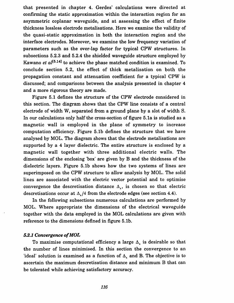
th a t presented in chapter 4. Gerdes' calculations were directed at confirming the static approximation within the interaction region for an asymmetric coplanar waveguide, and a t assessing the effect of finite thickness lossless electrode metalisations. Here we examine the validity of the quasi-static approximation in both the interaction region and the interface electrodes. Moreover, we examine the low frequency variation of param eters such as the over-lap factor for typical CPW structures. In subsections 5.2.3 and 5.2.4 the shielded waveguide structure employed by Kawano et a/t5141 to achieve the phase matched condition is examined. To conclude section 5.2, the effect of thick m etalisation on both the propagation constant and attenuation coefficient for a typical CPW is discussed; and comparisons between the analysis presented in chapter 4 and a more rigorous theory are made.
Figure 5.1 defines the structure of the CPW electrode considered in this section. The diagram shows that the CPW line consists of a central electrode of width W, separated from a ground plane by a slot of width S. In our calculations only half the cross-section of figure 5.1a is studied as a magnetic wall is employed in the plane of symmetry to increase computation efficiency. Figure 5.1b defines the structure tha t we have analysed by MOL. The diagram shows that the electrode metalisations are supported by a 4 layer dielectric. The entire structure is enclosed by a magnetic wall together with three additional electric walls. The dimensions of the enclosing 'box' are given by B and the thickness of the dielectric layers. Figure 5.1b shows how the two systems of lines are superimposed on the CPW structure to allow analysis by MOL. The solid lines are associated with the electric vector potential and to optimise convergence the descretisation distance Ax, is chosen so th a t electric descretisations occur at Ax/4 from the electrode edges (see section 4.4).
In the following subsections numerous calculations are performed by MOL. Where appropriate the dimensions of the electrical waveguide together with the data employed in the MOL calculations are given with reference to the dimensions defined in figure 5.1b.
5~2.1 Convergence o f MOLTo maximise computational efficiency a large Ax is desirable so that
the number of lines minimised. In this section the convergence to an 'ideal' solution is examined as a function of Ax and B. The objective is to ascertain the maximum descretisation distance and minimum B that can be tolerated while achieving satisfactory accuracy.
116
Magneticwall
I
S—H
Conductingenclosure
h4
103I W/21 I S I 1
h3T h2
h i
(b)
Figure 5.1 (a) shows the structure of the CPW under investigation. W is the centre conductor width and S is the slot width, (b) defines the structure analysed by MOL. To improve computational efficiency only half the cross-section is considered. is the relative permittivity of the iLn region. Ax is the descretisation distance. B, h i, h2, h3, and h4 define the dimensions of the enclosing box.
117
Figure 5.2 shows the variation of mode effective index as a function of descretisation distance Ax for a typical CPW modulator electrode. The diagram shows that even with only 5 lines (electric and magnetic) in the slot, the relative error is below 1%. However, with the number of lines fixed w ithin the slot, the total number of descretisations will be determined by the size of the enclosure confining the CPW (ie by B): there is no restriction in the y direction as the solution is ’analytic' along this axis. Along the x direction, however, the position of the side-wall is governed by the number of descretisations. Figure 5.3 shows the convergence of MOL as a function side-wall position for the structure examined figure 5.2. It can be seen that the position of the side-wall does not significantly influence the CPW provided th a t the side-wall is positioned greater than 10 slot widths distant from the central electrode (that is, B should be no smaller than lOOjim for this particular structure).
In the calculations described in later subsections of this thesis, Ax and B have been selected to achieve a higher accuracy than would result with the ’rule of thumb' recommendations described above. To assure good accuracy calculations were often repeated with different Ax and B in order to assess the convergence for individual problems.
5J2J2 Confirmation o f quasirstatic propagationFigure 5.4 shows the dispersive character of a typical CPW modulator
electrode from 0-40GHz with and without a buffer layer. Figure 5.4 shows tha t there is negligible dispersion for both the buffered (h3=.2pm) and unbuffered case (h3=0). The calculated effective index for the unbuffered electrode is 4.2485, which is equal to tha t derived under the static approximation. The microwave effective index of the buffered electrode is somewhat reduced from this value, because of the finite energy flow within the buffer layer. These results are similar to those found by Gerdes etafi6is\
In the example above, quasi-TEM propagation is observed because of the small lateral dimensions of the electrode. However, in a practical device, the active region must be interfaced to an external microwave circuit. The connection is commonly made through a coaxial connector. At the interface, the electrode dimension must be comparable to that of the connector. Consequently, within this interface region the modulator electrodes may exhibit hybrid effects. Figure 5.5 shows the effect of increasing the dimensions of the electrode while maintaining the same aspect ratio (S/W is constant). Clearly, as the electrode slot width....
118
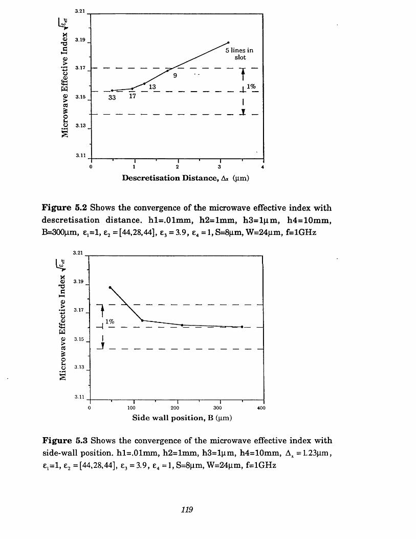
3.21
I4xG> 3.19
g0)>
3.17O,CD
tawC? 3.15 > cd£oJhO 3.13
5 lines in slot
-I -
3.11
0 1 2 3 4
D e s c r e t i s a t io n D is ta n c e , Ax (jim)
F ig u re 5.2 Shows the convergence of the microwave effective index with descretisation distance. hl=.01mm, h2=lmm, h3=l|j.m, h4=10mm, B=300(j.m, ej=l, e2 = [44,28,44], e3 = 3.9, e4 = 1, S=8fim, W=24jim, f=lGHz
3.21
14xQ) 3.19
Gt—i^ 3.17o
Wo>cd*oo
1%3.15
3.13
3.11
0 100 200 300 400
S id e w all p o sitio n , B (p.m)
F ig u re 5.3 Shows the convergence of the microwave effective index with side-wall position. hl=.01mm, h2=lmm, h3=l|im, h4=10mm, Ax = 1.23pm, eL=l, e2 =[44,28,44], e3 =3.9, e4 = 1, S=8jim, W=24pm, f=lGHz
119
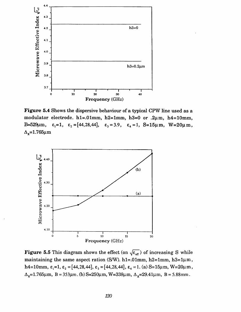
4.4
4.3XCUG»—i h3=0
3.8
3.7
0 10 20 30 40
F r e q u e n c y (GHz)
F ig u re 5.4 Shows the dispersive behaviour of a typical CPW line used as a modulator electrode. hl=.01mm, h2=lmm, h3=0 or .2pm, h4=10mm, B=529pm, E jsl, e2 =[44,28,44], e3 = 3.9, e4 = 1, S=15pm, W =20pm, Ax=l.765pm
4.40
4.30
CC 4.20
4.10
0 5 10 15 20
F r e q u e n c y (GHz)
F ig u re 5.5 This diagram shows the effect (on ^/e^) of increasing S while maintaining the same aspect ration (S/W). hl=.01mm, h2=lmm, h3=lpm , h4=10mm, e ^ l , e2 =[44,28,44], e3 =[44,28,44], e4 = 1. (a) S=15pm, W=20pm, Ax=l.765pm, B = 353pm. (b) S=250pm, W=338pm, Ax=29.41pm, B = 5.88mm.
120
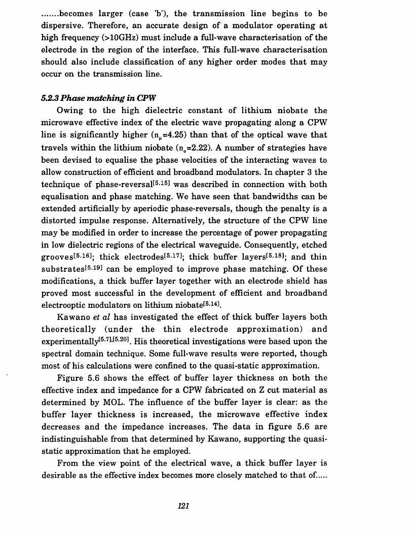
becomes larger (case ’b'), the transm ission line begins to bedispersive. Therefore, an accurate design of a modulator operating a t high frequency (>10GHz) must include a full-wave characterisation of the electrode in the region of the interface. This full-wave characterisation should also include classification of any higher order modes th a t may occur on the transmission line.
5.2.3 Phase m atching in CPWOwing to the high dielectric constant of lithium niobate the
microwave effective index of the electric wave propagating along a CPW line is significantly higher (n^=4.25) than tha t of the optical wave tha t travels within the lithium niobate (n0=2.22). A number of strategies have been devised to equalise the phase velocities of the interacting waves to allow construction of efficient and broadband modulators. In chapter 3 the technique of phase-reversaK5-15] was described in connection with both equalisation and phase matching. We have seen that bandwidths can be extended artificially by aperiodic phase-reversals, though the penalty is a distorted impulse response. Alternatively, the structure of the CPW line may be modified in order to increase the percentage of power propagating in low dielectric regions of the electrical waveguide. Consequently, etched grooves^5'16]; thick electrodes^5-17]; thick buffer layers^5-18]; and thin substrates^5-19] can be employed to improve phase matching. Of these modifications, a thick buffer layer together with an electrode shield has proved most successful in the development of efficient and broadband electrooptic modulators on lithium niobate^514].
Kawano et al has investigated the effect of thick buffer layers both theore tica lly (under the th in electrode approxim ation) and experimentally15'7 5'20]. His theoretical investigations were based upon the spectral domain technique. Some full-wave results were reported, though most of his calculations were confined to the quasi-static approximation.
Figure 5.6 shows the effect of buffer layer thickness on both the effective index and impedance for a CPW fabricated on Z cut material as determined by MOL. The influence of the buffer layer is clear: as the buffer layer thickness is increased, the microwave effective index decreases and the impedance increases. The data in figure 5.6 are indistinguishable from that determined by Kawano, supporting the quasistatic approximation that he employed.
From the view point of the electrical wave, a thick buffer layer is desirable as the effective index becomes more closely matched to that of.....
121
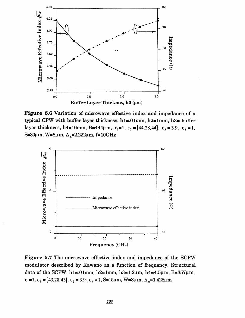
4.50 80
4 4.25Xo73A 70
4.00
<X>>><m*42 3.75O£W 3.50Q>rt£ 3.25OUo
3.00
50
• 4s
402.75
1.00.0
B uffer L ay er T h ick n es, h3 (pm)
F ig u re 5.6 Variation of microwave effective index and impedance of a typical CPW with buffer layer thickness. hl=.01mm, h2=lmm, h3= buffer layer thickness, h4=10mm, B=444pm, £j=l, e2 =[44,28,44], e3 = 3.9, e4 =1, S=30pm, W=8|im, Ax=2.222pm, f=10GHz
14x0)co > • fHofcW0>>03*OS-io
50
40
Impedance
Microwave effective index
B73a*0PO
5
30
10 20 30 40
F req u e n c y (GHz)
F ig u re 5.7 The microwave effective index and impedance of the SCPW modulator described by Kawano as a function of frequency. S tructural data of the SCPW: hl=.01mm, h2=lmm, h3=1.2pm, h4=4.5pm, B=357|im, £j=l, e2 = [43,28,43], e3 = 3.9, £4 = 1, S=15pm, W=8jim, Ax=1.428jim
122
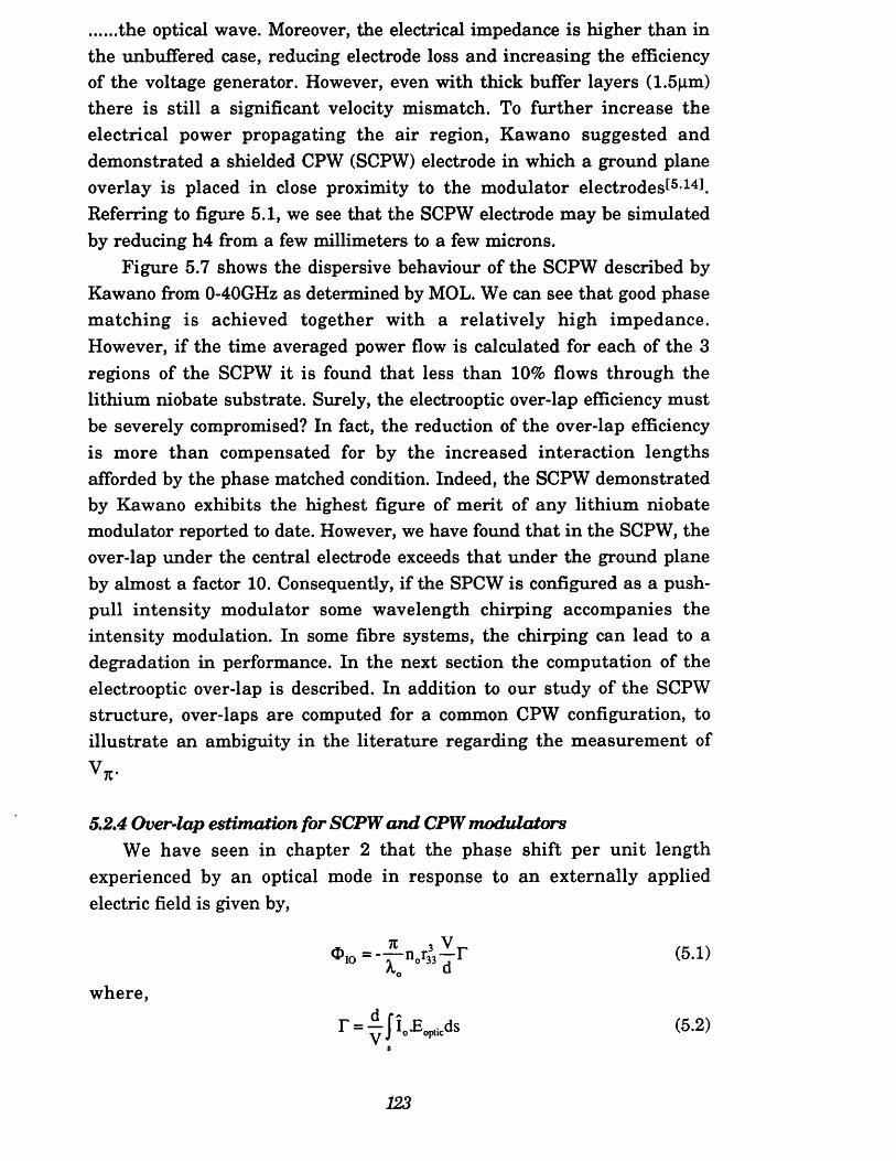
the optical wave. Moreover, the electrical impedance is higher than inthe unbuffered case, reducing electrode loss and increasing the efficiency of the voltage generator. However, even with thick buffer layers (1.5|im) there is still a significant velocity mismatch. To further increase the electrical power propagating the air region, Kawano suggested and demonstrated a shielded CPW (SCPW) electrode in which a ground plane overlay is placed in close proximity to the modulator electrodes^5 14]. Referring to figure 5.1, we see that the SCPW electrode may be simulated by reducing h4 from a few millimeters to a few microns.
Figure 5.7 shows the dispersive behaviour of the SCPW described by Kawano from 0-40GHz as determined by MOL. We can see that good phase m atching is achieved together with a relatively high impedance. However, if the time averaged power flow is calculated for each of the 3 regions of the SCPW it is found that less than 10% flows through the lithium niobate substrate. Surely, the electrooptic over-lap efficiency must be severely compromised? In fact, the reduction of the over-lap efficiency is more than compensated for by the increased interaction lengths afforded by the phase matched condition. Indeed, the SCPW demonstrated by Kawano exhibits the highest figure of merit of any lithium niobate modulator reported to date. However, we have found that in the SCPW, the over-lap under the central electrode exceeds that under the ground plane by almost a factor 10. Consequently, if the SPCW is configured as a push- pull intensity modulator some wavelength chirping accompanies the intensity modulation. In some fibre systems, the chirping can lead to a degradation in performance. In the next section the computation of the electrooptic over-lap is described. In addition to our study of the SCPW structure, over-laps are computed for a common CPW configuration, to illustrate an ambiguity in the literature regarding the measurement of
V *.
5,2.4 Over-lap estimation for SCPW and CPW modulatorsWe have seen in chapter 2 that the phase shift per unit length
experienced by an optical mode in response to an externally applied electric field is given by,
(5.1)
where,
(5.2)
123
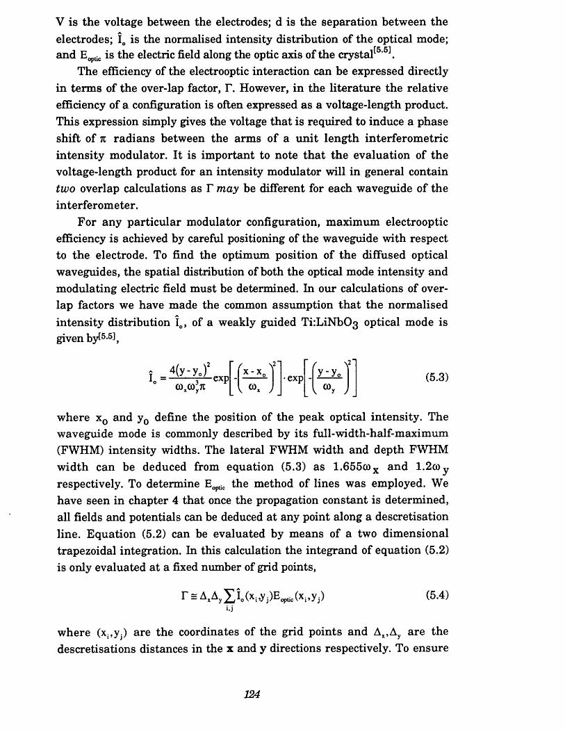
V is the voltage between the electrodes; d is the separation between the electrodes; Ic is the normalised intensity distribution of the optical mode; and E^j,. is the electric field along the optic axis of the crystal[55].
The efficiency of the electrooptic interaction can be expressed directly in terms of the over-lap factor, T. However, in the literature the relative efficiency of a configuration is often expressed as a voltage-length product. This expression simply gives the voltage that is required to induce a phase shift of n radians between the arms of a unit length interferometric intensity modulator. It is important to note tha t the evaluation of the voltage-length product for an intensity modulator will in general contain two overlap calculations as T may be different for each waveguide of the interferometer.
For any particular modulator configuration, maximum electrooptic efficiency is achieved by careful positioning of the waveguide with respect to the electrode. To find the optimum position of the diffused optical waveguides, the spatial distribution of both the optical mode intensity and modulating electric field must be determined. In our calculations of overlap factors we have made the common assumption tha t the normalised intensity distribution I0, of a weakly guided Ti:LiNb03 optical mode is given byt5*5],
j 4(y-y.fe x p
- f \ 2 1 r \
I—
X 1 X o • e x p
o>>i
. CO
i
CO- V X / - _ \ y ) _
(5.3)
where x0 and y0 define the position of the peak optical intensity. The waveguide mode is commonly described by its full-width-half-maximum (FWHM) intensity widths. The lateral FWHM width and depth FWHM width can be deduced from equation (5.3) as 1.655cox and 1.2c0y respectively. To determine Eoptic the method of lines was employed. We have seen in chapter 4 that once the propagation constant is determined, all fields and potentials can be deduced at any point along a descretisation line. Equation (5.2) can be evaluated by means of a two dimensional trapezoidal integration. In this calculation the integrand of equation (5.2) is only evaluated at a fixed number of grid points,
r £AA X U xi^i)Ei*fc(xi>yj) (5.4)».J
where (x^yp are the coordinates of the grid points and Ax,Ay are the descretisations distances in the x and y directions respectively. To ensure
124
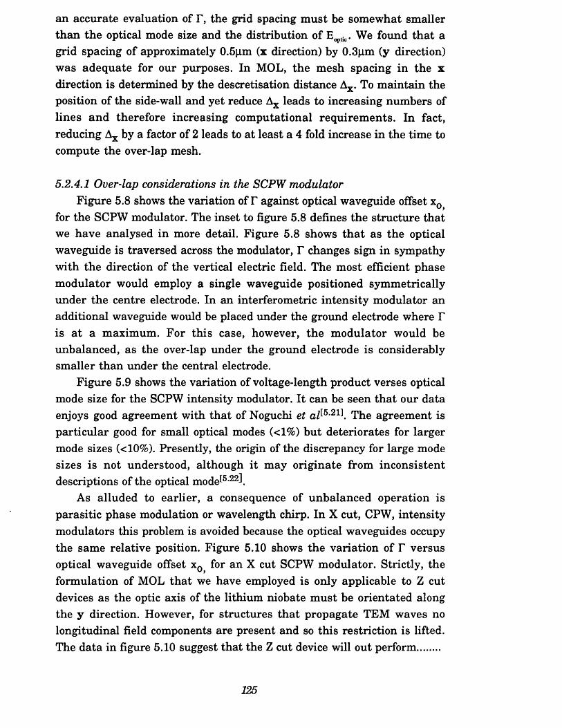
an accurate evaluation of r , the grid spacing must be somewhat smaller than the optical mode size and the distribution of E ^ . We found tha t a grid spacing of approximately 0.5pm (x direction) by 0.3pm (y direction) was adequate for our purposes. In MOL, the mesh spacing in the x direction is determined by the descretisation distance Ax. To maintain the position of the side-wall and yet reduce Ax leads to increasing numbers of lines and therefore increasing computational requirements. In fact, reducing Ax by a factor of 2 leads to at least a 4 fold increase in the time to compute the over-lap mesh.
5.2.4.1 Over-lap considerations in the SCPW modulatorFigure 5.8 shows the variation of T against optical waveguide offset x0>
for the SCPW modulator. The inset to figure 5.8 defines the structure that we have analysed in more detail. Figure 5.8 shows th a t as the optical waveguide is traversed across the modulator, T changes sign in sympathy with the direction of the vertical electric field. The most efficient phase modulator would employ a single waveguide positioned symmetrically under the centre electrode. In an interferometric intensity modulator an additional waveguide would be placed under the ground electrode where T is a t a maximum. For this case, however, the modulator would be imbalanced, as the over-lap under the ground electrode is considerably smaller than under the central electrode.
Figure 5.9 shows the variation of voltage-length product verses optical mode size for the SCPW intensity modulator. It can be seen that our data enjoys good agreement with that of Noguchi et a^5,21 The agreement is particular good for small optical modes (<1%) but deteriorates for larger mode sizes (<10%). Presently, the origin of the discrepancy for large mode sizes is not understood, although it may originate from inconsistent descriptions of the optical mode^5,22].
As alluded to earlier, a consequence of unbalanced operation is parasitic phase modulation or wavelength chirp. In X cut, CPW, intensity modulators this problem is avoided because the optical waveguides occupy the same relative position. Figure 5.10 shows the variation of T versus optical waveguide offset xQ> for an X cut SCPW modulator. Strictly, the formulation of MOL that we have employed is only applicable to Z cut devices as the optic axis of the lithium niobate must be orientated along the y direction. However, for structures that propagate TEM waves no longitudinal field components are present and so this restriction is lifted. The data in figure 5.10 suggest that the Z cut device will out perform.......
125
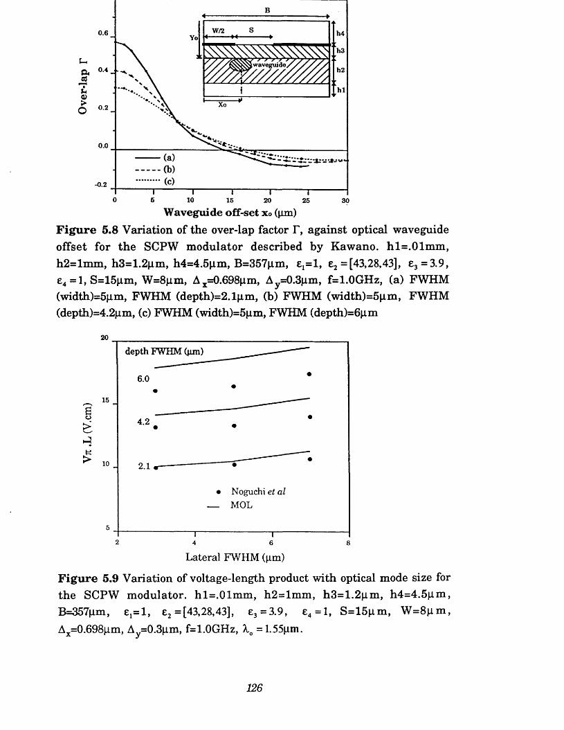
W/2 S
v//^^^waveguide//V//y
0.6 h4Yo
h3
h2
h i
Xo
0.0
- 0.2
0 6 10 15 20 25 30
W a v e g u id e o f f -s e t xo (pm)
F ig u re 5.8 Variation of the over-lap factor T, against optical waveguide offset for the SCPW modulator described by Kawano. hl=.01m m , h2=lmm, h3=1.2|im, h4=4.5|im, B=357|im, e ^ l , e2 =[43,28,43], e3=3.9, e4 = 1, S=15jim, W=8jim, Ax=0.698pm, Ay=0.3|im, f=1.0GHz, (a) FWHM (width)=5|im, FWHM (depth)=2.1pm, (b) FWHM (width)=5pm, FWHM (depth)=4.2pm, (c) FWHM (width)=5pm, FWHM (depth)=6pm
depth FWHM (pm)
6.0
15
4.2
10 2.1
• Noguchi et al - MOL
5
2 4 6 8Lateral FWHM (|im)
F ig u re 5.9 Variation of voltage-length product with optical mode size for the SCPW modulator. hl=.01m m, h2=lmm, h3=1.2pm, h4=4.5jim, B=357pm, e1=l , e2 =[43,28,43], e3=3.9, e4= l, S=15pm, W =8pm ,Ax=0.698|im, Ay=0.3|im, f=1.0GHz, A.0 = 1.55pm.
126
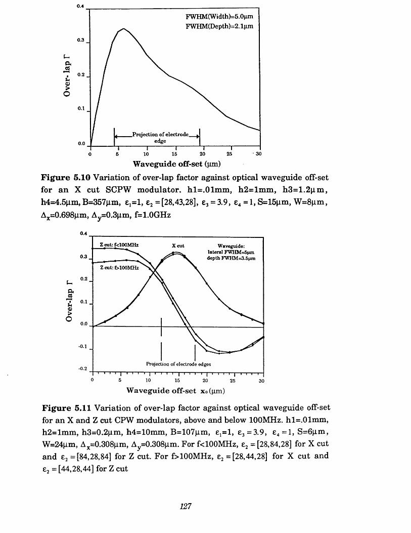
0.4
FWHM(Width)=5.0jim FWHM(Depth)=2. lpm
0.3
Ucu«uG)>
O
0.2
0.1
.Projection of electrode, edge0.0
• 3015 20 255 100W a v e g u id e o ff-se t (pm)
F ig u re 5.10 Variation of over-lap factor against optical waveguide off-set for an X cut SCPW modulator. hl=.01mm, h2=lm m , h3=1.2pm , h4=4.5jim, B=357pm, £j=l, e2 =[28,43,28], e3 = 3.9, e4 = 1, S=15pm, W=8(im, Ax=0.698pm, Ay=0.3pm, f=1.0GHz
0.4
Z cu t: f<100M Hz X cut W aveguide: la te ra l FW HM =5pm d ep th FW HM =3.5pm
Z cut: £>100 M H z
u 02 a.S3
7 01<x>>° 0.0
- 0.1
Projection of electrode edges- 0.2
0 5 10 15 20 25 30
W a v e g u id e o ff -s e t xo(pm)
F ig u re 5.11 Variation of over-lap factor against optical waveguide off-set for an X and Z cut CPW modulators, above and below 100MHz. hl=.01mm, h2=lmm, h3=0.2|im, h4=10mm, B=107pm, ^=1, e3 = 3.9, e4= l, S=6jim, W=24|im, Ax=0.308|im, Ay=0.308pm. For fdOOMHz, e2 =[28,84,28] for X cut and e2 =[84,28,84] for Z cut. For f>100MHz, e2 =[28,44,28] for X cut and e2 = [44,28,44] for Z cut
127
the X cut device when configured as a phase modulator as the overlap is almost 60% larger in the former case. For intensity modulators however, the performance is almost identical. Consequently, for applications in which pure intensity modulation is required, a SCPW modulator fabricated on X cut material would be desirable.
5.2.4.2 Low frequency over-lap variation in CPW modulatorsIn section 5.2.2 we have seen tha t a CPW electrode with lateral
dimensions of a few microns will propagate a quasi-TEM mode from DC to a t least 40GHz. W ithin this frequency range, field dependent param eters such as the mode effective index, impedance and T are constant owing to the invariance of the transverse fields. These predictions assume invariance in the dielectric properties of lithium niobate, and over the range 100MHz to 40GHz few variations in the characteristics of lithium niobate are apparent. However, at a frequency between 30-100MHz (the acoustic resonance) lithium niobate exhibits a transition between its unclamped' and 'clamped' states^5-23]. Around this transition frequency, the performance of lithium niobate modulators is affected by the excitation of acoustic waves[5-24 5-25!. More significantly however, Jungerman et a/t5.26] found that the switching voltages of Z cut devices measured below 30MHz were 20% lo w e r than the switching voltages measured above 50MHz, whereas comparable X cut devices were unaffected.
In the literature, it is common to refer to the DC of a modulator and to use this figure to predict the behaviour of the modulator a t higher frequencies. Clearly, in the case of Jungerm an's Z cut device this procedure would lead to an over optimistic prediction of the modulator's performance. Indeed, in a conventional IM/DD link the received electrical power would only be 60% of predicted value. Can these discrepancies result from differing over-lap efficiencies when the lithium niobate substrate is in its clamped or unclamped state? To assess this question T m ust be evaluated for both X and Z cut modulators. The electrode geometry of Jungerman's X and Z cut devices have been described in some detail[5'26]’[5,27l, and the structural dimensions of the modulators are given in the caption of figure 5.11. Figure 5.11 shows the variation of T verses waveguide off-set for both X and Z cut devices above and below the acoustic resonance. The over-lap efficiencies were calculated using the procedure described in section 5.2.4. Throughout these calculations, the waveguide mode intensity was assumed to have a FWHM(depth) of 3.5|im
128
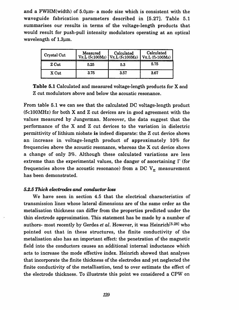
and a FWHM(width) of 5.0pm- a mode size which is consistent with the waveguide fabrication param eters described in [5.27]. Table 5.1 summarises our results in terms of the voltage-length products tha t would result for push-pull intensity modulators operating a t an optical wavelength of 1.3pm.
Crystal Cut Measured Vtc.L (fclOOMz)
Calculated Vtc.L (fclOOMz)
Calculated Vtc.L (f>100Mz)
Z Cut 5.25 5.3 5.75
X Cut 3.75 3.57 3.67
Table 5.1 Calculated and measured voltage-length products for X and Z cut modulators above and below the acoustic resonance.
From table 5.1 we can see that the calculated DC voltage-length product (fclOOMHz) for both X and Z cut devices are in good agreement with the values measured by Jungerman. Moreover, the data suggest th a t the performance of the X and Z cut devices to the variation in dielectric permittivity of lithium niobate is indeed disparate: the Z cut device shows an increase in voltage-length product of approxim ately 10% for frequencies above the acoustic resonance, whereas the X cut device shows a change of only 3%. Although these calculated variations are less extreme than the experimental values, the danger of ascertaining T (for frequencies above the acoustic resonance) from a DC measurement has been demonstrated.
5.2.5 Thick electrodes and conductor lossWe have seen in section 4.5 tha t the electrical characteristics of
transmission lines whose lateral dimensions are of the same order as the metalisation thickness can differ from the properties predicted under the thin electrode approximation. This statement has be made by a number of authors- most recently by Gerdes et al. However, it was Heinrich^5-28] who pointed out th a t in these structures, the finite conductivity of the metalisation also has an important effect: the penetration of the magnetic field into the conductors causes an additional internal inductance which acts to increase the mode effective index. Heinrich showed that analyses that incorporate the finite thickness of the electrodes and yet neglected the finite conductivity of the metallisation, tend to over estimate the effect of the electrode thickness. To illustrate this point we considered a CPW on
129
GaAs analysed by Heinrich, and compared it with both MOL under the th in electrode approximation, and data from a full-wave method incorporating thick lossless electrodes. Both the mode effective index and loss were computed. The inset to figure 5.12 defines the structure tha t we have analysed. Figure 5.12 shows the calculated tangential magnetic field a t the surface (ie 0.1pm from the interface) of the electrode metalisations when the power flow is lW att. Note tha t because of the quasi-TEM propagation the tangential field contains only one component as hz is zero. An additional, consequence of the TEM propagation is that |hx| is equal on both the air and GaAs sides of the metalisation. The diagram shows that the the sign of hx is reversed on either side of the slot, suggesting a current flow down the center electrode and return current up the ground plane as would be expected. The electrode loss was computed from the tangential magnetic according to equation (4.52). In these calculations the conducting enclosure was assumed to have zero resistance. Table 5.2 summarises the results of our comparisons. In table 5.2 the 'correct' values of the transmission line parameters are those produced by the most sophisticated analysis, namely the analysis incorporating the thick and lossy metalisations.
The data of table 5.2 show the danger of including the finite extent of the electrode metalisations while neglecting their conductivity. In our example it is apparent from table 5.2 that a thin electrode analysis such as MOL, provides a more accurate determination of eefr than does an analysis incorporating thick, lossless m etalisations. More general statements cannot be made, as all the results in table 5.2 apply only to the waveguide of figure 5.12.
Unfortunatley, it is also apparent from table 5.2, the attenuation coefficient determined by MOL is inaccurate, and for this reason we have relied upon experimental data to provide estimates of the electrode loss coefficient for our modulator configurations.
5.3 A Millimetre Wave Optical Modulator
Considerable effort has been devoted to the construction of optical modulators operating beyond 26GHz. In addition to the problems of electrode loss and velocity mismatch, coupling of the electrical drive.........
130
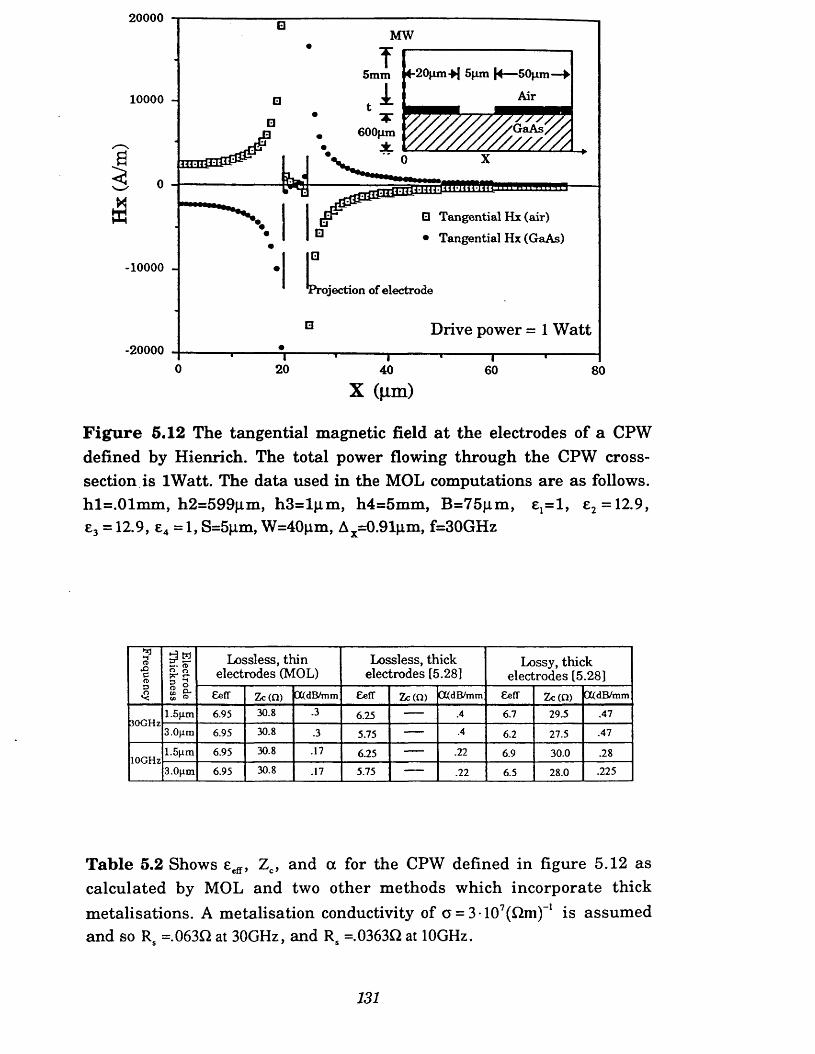
20000MW
4-20|xm +| 5}im |<— 50jxm—►
Air5mm
10000 -
600fim
□ Tangential Hx (air)• Tangential Hx (GaAs)
-10000 -•ojection of electrode
Drive power = 1 W att-20000
o 20 40 60 80
X (jim)
F ig u re 5.12 The tangential magnetic field a t the electrodes of a CPW defined by Hienrich. The total power flowing through the CPW cross- section is lW att. The data used in the MOL computations are as follows. hl=.01mm, h2=599jim, h3=lpm , h4=5mm, B=75fim, ^=1, e2 = 12.9, e3 = 12.9, e4 = 1, S=5pm, W=40jim, Ax=0.91pm, f=30GHz
Frequency
Electrode
Thickness
Lossless, thin electrodes (MOL)
Lossless, thick electrodes [5.28]
Lossy, thick electrodes [5.28]
£e(T Zc (£1) 0C(dB/mm £e(T Zc(Q) 0C(dB/mm eeff Zc(G) 0C(dB/mm
30GHz1.5jim 6.95 30.8 .3 6.25 ------ .4 6.7 29.5 .47
3.0^m 6.95 30.8 .3 5.75 ------ .4 6.2 27.5 .47
10GHz1.5|im 6.95 30.8 .17 6.25 ------ .22 6.9 30.0 .28
3.0fim 6.95 30.8 .17 5.75 ------ .22 6.5 28.0 .225
T able 5.2 Shows eeff, Zc, and a for the CPW defined in figure 5.12 as calculated by MOL and two other methods which incorporate thick metalisations. A metalisation conductivity of o = 3*107(Gm)-1 is assumed and so Rs =.063D at 30GHz, and Rs =.03630 at 10GHz.
131
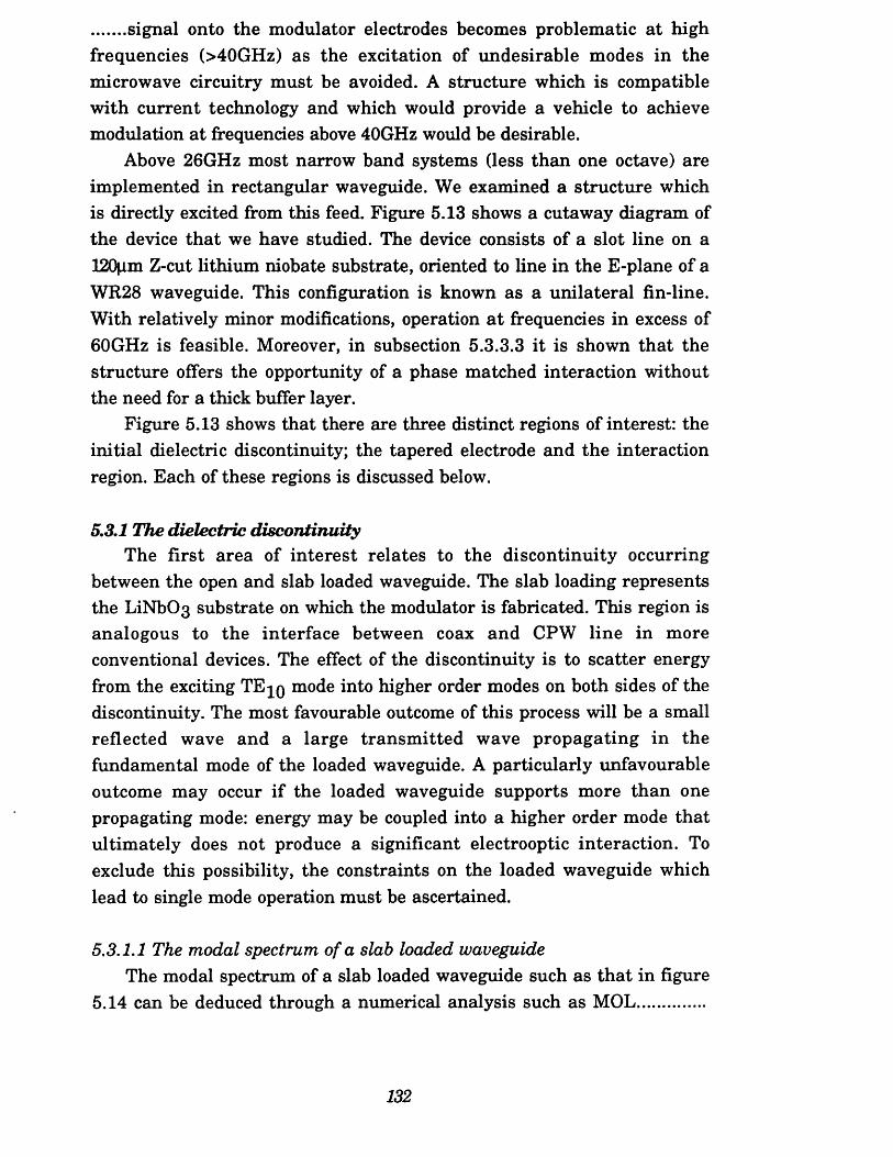
signal onto the modulator electrodes becomes problematic at highfrequencies (>40GHz) as the excitation of undesirable modes in the microwave circuitry must be avoided. A structure which is compatible with current technology and which would provide a vehicle to achieve modulation at frequencies above 40GHz would be desirable.
Above 26GHz most narrow band systems (less than one octave) are implemented in rectangular waveguide. We examined a structure which is directly excited from this feed. Figure 5.13 shows a cutaway diagram of the device tha t we have studied. The device consists of a slot line on a 120|im Z-cut lithium niobate substrate, oriented to line in the E-plane of a WR28 waveguide. This configuration is known as a unilateral fin-line. With relatively minor modifications, operation a t frequencies in excess of 60GHz is feasible. Moreover, in subsection 5.3.3.3 it is shown that the structure offers the opportunity of a phase matched interaction without the need for a thick buffer layer.
Figure 5.13 shows that there are three distinct regions of interest: the initial dielectric discontinuity; the tapered electrode and the interaction region. Each of these regions is discussed below.
5.3.1 The dielectric discontinuityThe first area of in terest relates to the discontinuity occurring
between the open and slab loaded waveguide. The slab loading represents the LiNb03 substrate on which the modulator is fabricated. This region is analogous to the interface between coax and CPW line in more conventional devices. The effect of the discontinuity is to scatter energy from the exciting TE^q mode into higher order modes on both sides of the discontinuity. The most favourable outcome of this process will be a small reflected wave and a large transm itted wave propagating in the fundamental mode of the loaded waveguide. A particularly unfavourable outcome may occur if the loaded waveguide supports more than one propagating mode: energy may be coupled into a higher order mode that ultimately does not produce a significant electrooptic interaction. To exclude this possibility, the constraints on the loaded waveguide which lead to single mode operation must be ascertained.
5.3.1.1 The modal spectrum of a slab loaded waveguideThe modal spectrum of a slab loaded waveguide such as tha t in figure
5.14 can be deduced through a numerical analysis such as MOL..............
132
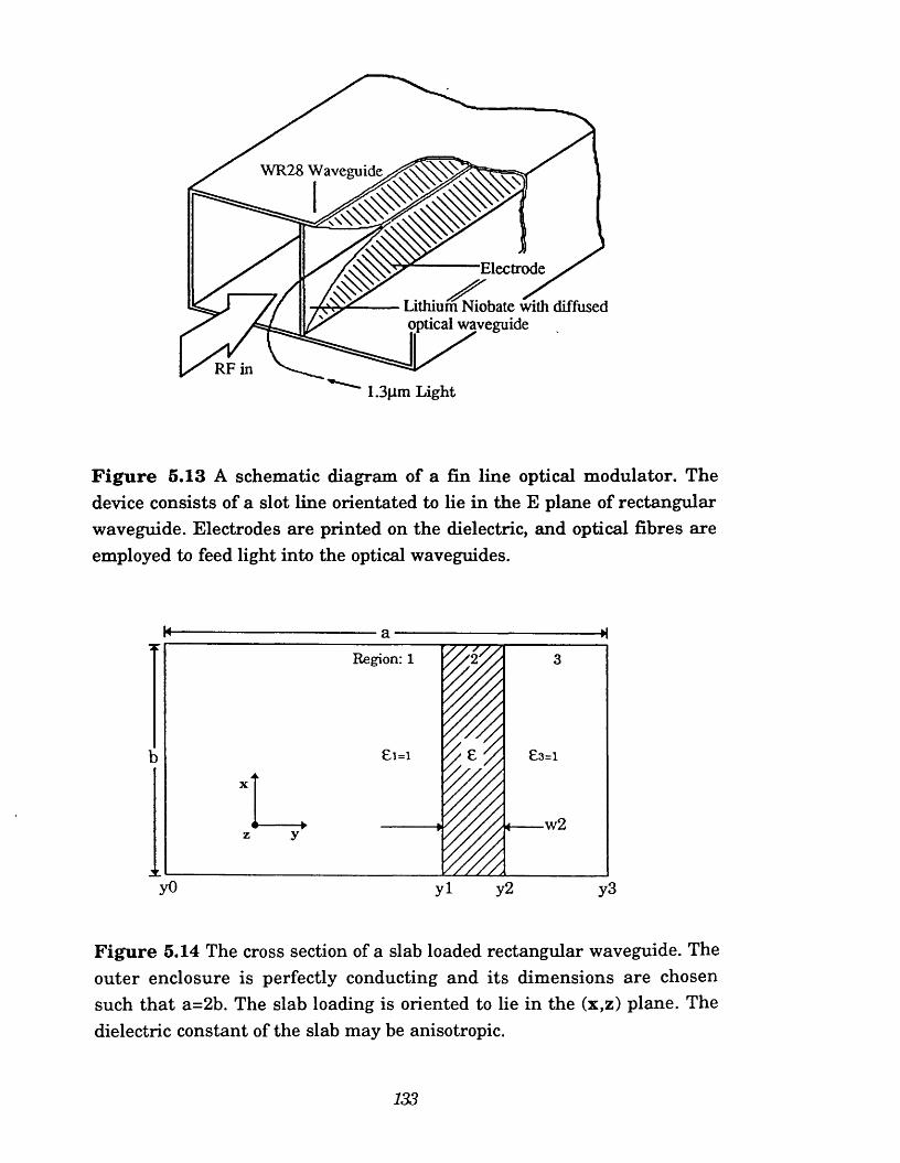
W a v e g u id c ^ ^ ^ ^ ^WR28
Electrode
Lithium Niobate with diffused optical waveguide
F ig u re 5.13 A schematic diagram of a fin line optical modulator. The device consists of a slot line orientated to lie in the E plane of rectangular waveguide. Electrodes are printed on the dielectric, and optical fibres are employed to feed light into the optical waveguides.
Region: 1
w2
yO y l y2 y3
F ig u re 5.14 The cross section of a slab loaded rectangular waveguide. The outer enclosure is perfectly conducting and its dimensions are chosen such tha t a=2b. The slab loading is oriented to lie in the (x,z) plane. The dielectric constant of the slab may be anisotropic.
133
However, for simple slab loadings numerical analyses are not required as solutions may be deduced algebraically. Indeed, solutions for waveguides with isotropic slab loadings were determined by Collin^5-29] over 20 years ago. Collin employed a method based upon transverse resonance and found tha t the modes of the slab loaded waveguide could be divided into two classes: the longitudinal section electric modes (LSE) for which ey=0; and the longitudinal section magnetic modes (LSM) for which hy=0. Wehave seen in chapter 4 that the oriented Hertz potentials ftc,h, exhibit just these characteristics. Therefore, we may regard 'F* as the generating function for LSM modes and T h as the generating function of LSE modes. Moreover, by using the equations in chapter 4 we may solve for problems in which the slab loading is anisotropic (ie e = [e1,e„,e1]). From chapter 4 (section 4.3.1) we recall that the oriented hertz potentials must satisfy the following equations in each homogeneous region of figure 5.14,
| ^ 'F e+n2^ 'F '+ ( k J - p 2 )¥ '= () (5.5a)
+ z fr 'i’h + (k^ - P2) 'fh = 0 (5.5b)dx dy
where k0 = co^p080 , kx = nxk0, k„ =n„k0 and, nH =-y/I , n1 =^JT[> n = nH/nx. Owing to the uncomplicated waveguide geometry these equations may be solved individually using separated variables. Thus, the potential in each section of figure 5.14 is written,
T s = f£(y) i (5.6)
as T c = 0; 3'Fh/3x = 0 at both x=0 and x=b. Substituting (5.6) in both (5.5a) and (5.5b), results in a solution for f * (y) in the i ^ region of the slab loaded waveguide of,
f; (y) = a ; sin[k? (y - yM)] + B,5 cos[k? (y - yM)] (5.7)
To determine the unknown coefficients A? and Bf, the boundary conditions between the dielectric layers must be resolved. The continuity of the tangential field at an interface in the y=y^ plane, between two regions i and i-1 may be written as,
y x [E 'h (x,yi<ZX -E*'h(x,yi,z)l.] = 0 (5.8a)
134
y x [ H 'h(x,y„Z)l,-H 'h(x,yi,Z)l] = 0 (5.8b)
where the suffix V represents evaluation in the region i, and the suffix represents evaluation in region i-1. Expanding (5.8a) and (5.8b) according to equations (4.18a,b) results in the following conditions on f h(y) and dfh(y)/dy at the dielectric interface;
f+h(yi) = fh(yi)
eiaf:(yi) = exbfc(yi)
df e,h
dydfe,h
dy
(5.9a)
(5.9b)
(5.9c)
Applying these boundary conditions to the solutions of the wave equation results in two transcendental equations defining the dispersion relations for both the LSE and LSM modes of the waveguide. For the waveguide of figure 5.14 in which a single anisotropic region is present, the LSE modes are defined by equation (5.10),
cos(paw3)
sin(p,w3)
cos(pdW2)sin(p,w1) | cos(paw1)sin(p;w2) P . P S
P a
PdSin(Pdw2)sin(p,w1)P .
+ cos(paw1)cos(pdw2) = 0(5.10)
w here Wj = yO-yl; w2 = yl - y2; W; = y2 - y3, p2 = k2 - p2 - (nrn/b)2,(Pd) = ■ P2 ■ (nm/b)2, m is an integer; and the LSM modes are defined byequation (5.11),
cos(paw3)
-P asin(paw 3)
P d S i n ( P d W 2 ) C 0 S ( P a W 1)
cos(pSw2)cos(paw1)
+ pasin(paw1)cos(p>2)
e1pasin(paw1)sin(pdw2)h
P d
= 0(5.11)
where (pj)2 =[ kj -p2 -(m7t/b)2jy n2. It can be shown that for a centered, and isotropic slab loading, equations (5.10) and (5.11) reduce to those of Collin.
Figure 5.15 shows the dispersion of all the propagating modes supported by a WR28 with a 120pm lithium niobate slab loading, offset to lie against a side wall. The data th a t we have employed in our calculations can be found in the caption to figure 5.15. Figure 5.15 shows that only a single mode is supported by the waveguide. In fact, the LSE 10..
135
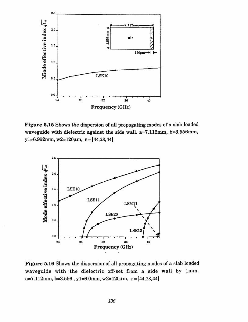
2.6
Is?X 2.0 _ O 'd.9> 1-5 _
■7.112mm-
air
120nm—M H-
LSE10
o.o24 28 32 36 40
Frequency (GHz)
F ig u re 5.15 Shows the dispersion of all propagating modes of a slab loaded waveguide with dielectric against the side wall. a=7.112mm, b=3.556mm, yl=6.992mm, w2=120pm, e = [44,28,44]
2.5
2.0 .
LSE 10© 1 .5 .>■+*o
0
1
LSE 11LSM111.0 .
LSE200 .5 .
LSE 12o.o
32 4024 28 36
Frequency (GHz)
F ig u re 5.16 Shows the dispersion of all propagating modes of a slab loaded waveguide w ith the dielectric off-set from a side wall by 1mm. a=7.112mm, b=3.556 , yl=6.0mm, w2=120}im, e = [44,28,44]
136
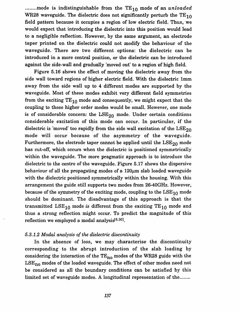
mode is indistinguishable from the TE^q mode of an unloadedWR28 waveguide. The dielectric does not significantly perturb the TE jq field pattern because it occupies a region of low electric field. Thus, we would expect that introducing the dielectric into this position would lead to a negligible reflection. However, by the same argument, an electrode taper printed on the dielectric could not modify the behaviour of the waveguide. There are two different options: the dielectric can be introduced in a more central position, or the dielectric can be introduced against the side-wall and gradually 'moved out' to a region of high field.
Figure 5.16 shows the effect of moving the dielectric away from the side wall toward regions of higher electric field. With the dielectric 1mm away from the side wall up to 4 different modes are supported by the waveguide. Most of these modes exhibit very different field symmetries from the exciting TEjq mode and consequently, we might expect that the coupling to these higher order modes would be small. However, one mode is of considerable concern: the LSE20 mode. Under certain conditions considerable excitation of this mode can occur. In particular, if the dielectric is 'moved' too rapidly from the side wall excitation of the LSE2Q mode will occur because of the asym metry of the waveguide. Furthermore, the electrode taper cannot be applied until the LSE20 mode has cut-off, which occurs when the dielectric is positioned symmetrically within the waveguide. The more pragmatic approach is to introduce the dielectric to the centre of the waveguide. Figure 5.17 shows the dispersive behaviour of all the propagating modes of a 120pm slab loaded waveguide with the dielectric positioned symmetrically within the housing. With this arrangement the guide still supports two modes from 26-40GHz. However, because of the symmetry of the exciting mode, coupling to the LSE^q mode should be dominant. The disadvantage of this approach is th a t the transm itted LSEjq mode is different from the exciting TEjq mode and thus a strong reflection might occur. To predict the magnitude of this reflection we employed a modal analysis^5-30!.
5.3.1.2 Modal analysis of the dielectric discontinuityIn the absence of loss, we may characterise the discontinuity
corresponding to the abrupt introduction of the slab loading by considering the interaction of the TEno modes of the WR28 guide with the LSEno modes of the loaded waveguide. The effect of other modes need not be considered as all the boundary conditions can be satisfied by this limited set of waveguide modes. A longitudinal representation of the.......
137
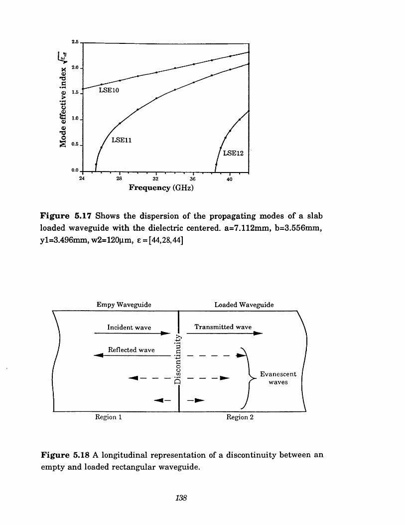
2 .0 .
LSE10Q) 1.5. >
I % 10 -0
1 «•»- LSE11
LSE 12
o.o24 28 32 36 40
Frequency (GHz)
F ig u re 5.17 Shows the dispersion of the propagating modes of a slab loaded waveguide with the dielectric centered. a=7.112mm, b=3.556mm, yl=3.496mm, w2=120|im, e = [44,28,44]
Empy Waveguide Loaded Waveguide
Transmitted waveIncident wave
Reflected wave
Evanescentwaves
Region 1 Region 2
F ig u re 5.18 A longitudinal representation of a discontinuity between an empty and loaded rectangular waveguide.
138
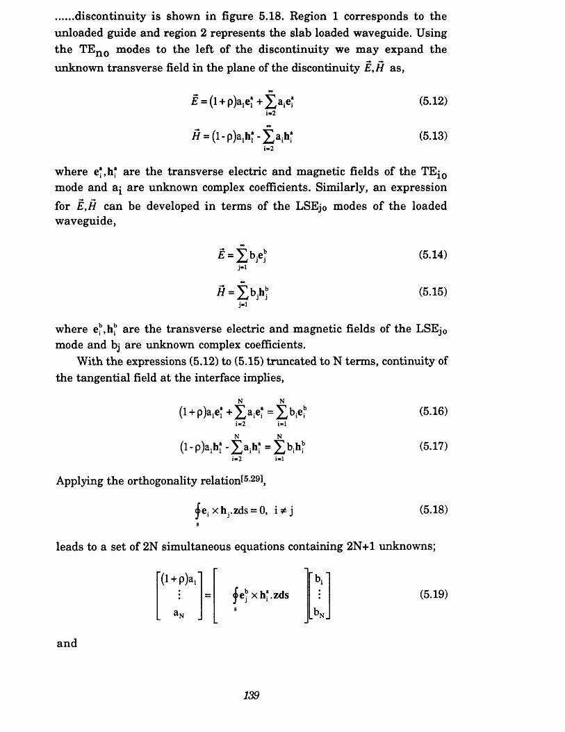
discontinuity is shown in figure 5.18. Region 1 corresponds to theunloaded guide and region 2 represents the slab loaded waveguide. Using the TEno modes to the left of the discontinuity we may expand the unknown transverse field in the plane of the discontinuity E,H as,
£ = (l + p)a1e ; + X a ie*i-2
" = ( l-p )a ,h ;-2 > ,h -i - 2
where e‘,h‘ are the transverse electric and magnetic fields of the TEj0 mode and aj are unknown complex coefficients. Similarly, an expressionfor E,H can be developed in terms of the LSEjo modes of the loaded waveguide,
£ = X bje‘
j-1
where e|\hf are the transverse electric and magnetic fields of the LSEj0 mode and bj are unknown complex coefficients.
With the expressions (5.12) to (5.15) truncated to N terms, continuity of the tangential field at the interface implies,
( i+ p )aie*+ X a.ei = X b.eii - 2 i-1
( l - p K b l - X a t f - X b t fi-2 i-1
Applying the orthogonality relation^5-29!,
^ejXhr zds = 0, i * j (5.18)s
leads to a set of 2N simultaneous equations containing 2N+1 unknowns;
(5.16)
(5.17)
(5.14)
(5.15)
(5.12)
(5.13)
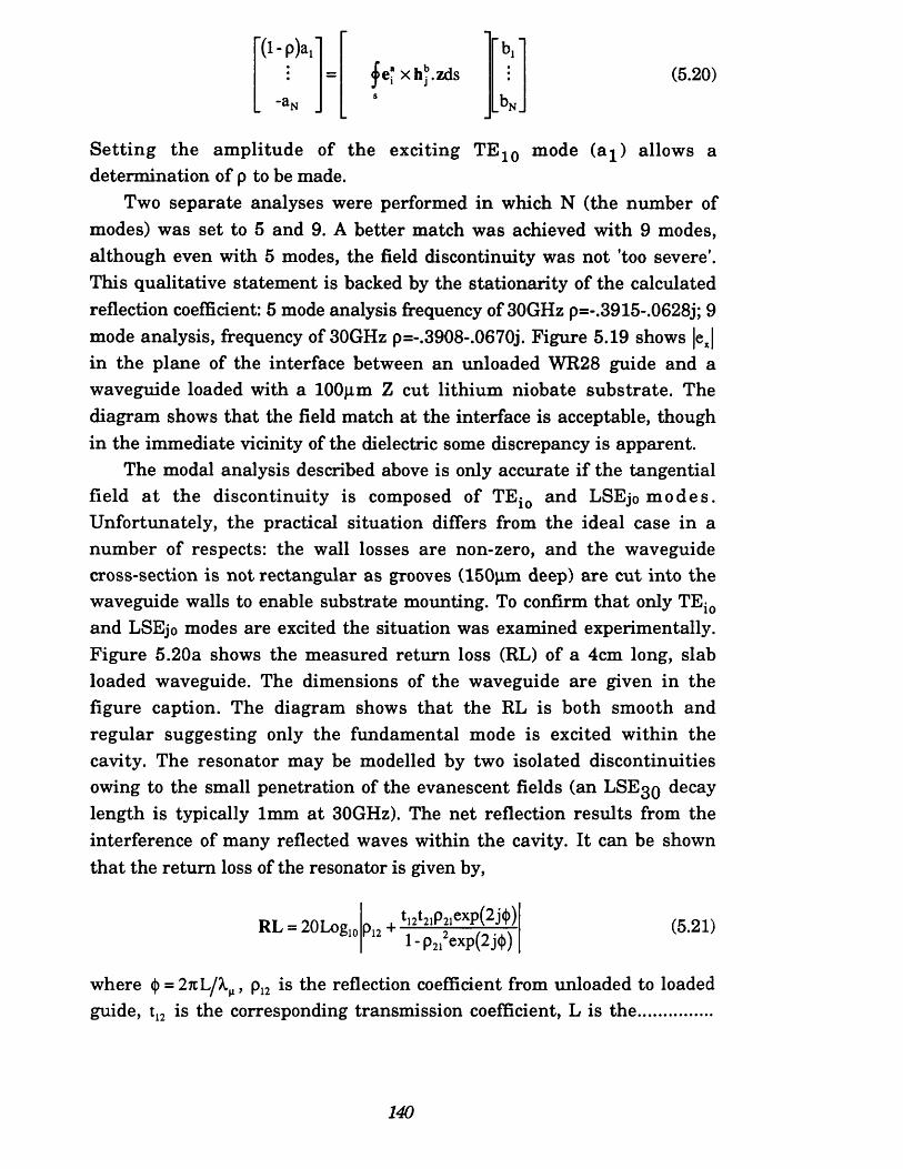
(l-p)a,"e* xhj’.zds
V
“ a Ns
. V
(5.20)
Setting the am plitude of the exciting TE10 mode (a j ) allows a determination of p to be made.
Two separate analyses were performed in which N (the number of modes) was set to 5 and 9. A better match was achieved with 9 modes, although even with 5 modes, the field discontinuity was not 'too severe'. This qualitative statement is backed by the stationarity of the calculated reflection coefficient: 5 mode analysis frequency of 30GHz p=-.3915-.0628j; 9 mode analysis, frequency of 30GHz p=-.3908-.0670j. Figure 5.19 shows |ex| in the plane of the interface between an unloaded WR28 guide and a waveguide loaded with a 100pm Z cut lithium niobate substrate. The diagram shows that the field match at the interface is acceptable, though in the immediate vicinity of the dielectric some discrepancy is apparent.
The modal analysis described above is only accurate if the tangential field a t the discontinuity is composed of TEio and LSEjo modes . Unfortunately, the practical situation differs from the ideal case in a number of respects: the wall losses are non-zero, and the waveguide cross-section is not rectangular as grooves (150pm deep) are cut into the waveguide walls to enable substrate mounting. To confirm that only TEio and LSEjo modes are excited the situation was examined experimentally. Figure 5.20a shows the measured return loss (RL) of a 4cm long, slab loaded waveguide. The dimensions of the waveguide are given in the figure caption. The diagram shows tha t the RL is both smooth and regular suggesting only the fundamental mode is excited within the cavity. The resonator may be modelled by two isolated discontinuities owing to the small penetration of the evanescent fields (an LSEgo decay length is typically 1mm at 30GHz). The net reflection results from the interference of many reflected waves within the cavity. It can be shown that the return loss of the resonator is given by,
RL = 20 Log10 P12 + 12 2lP2ieXp(^J(l))l-p 2i2exp(2j<(>)
(5.21)
where <|> = 2rcL/?i , p12 is the reflection coefficient from unloaded to loaded guide, t12 is the corresponding transmission coefficient, L is the...............
140
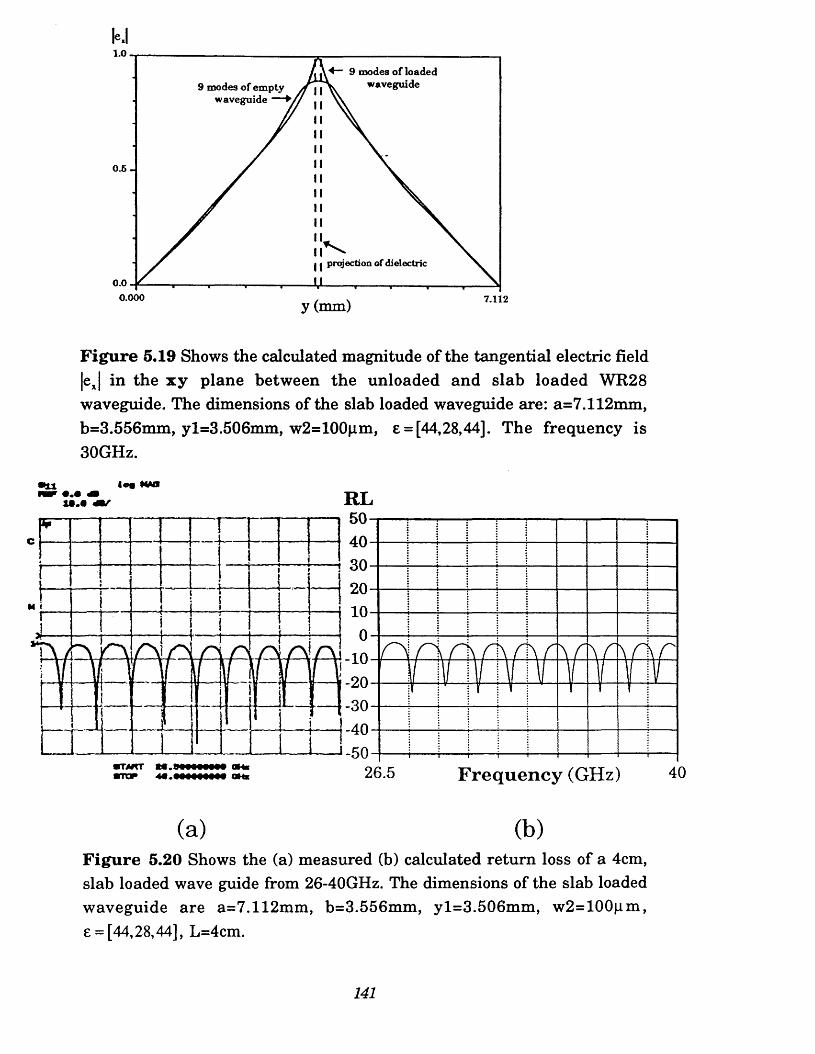
1.0
^ — 9 m o d es o f lo a d e d C w a v e g u id e9 m o d es o f e m p ty
w a v e g u id e
0.6 -
projectioD of dielectric
0.0-jd 0.000 7.112y (mm)
F ig u re 5.19 Shows the calculated magnitude of the tangential electric field |e j in the x y plane between the unloaded and slab loaded WR28 waveguide. The dimensions of the slab loaded waveguide are: a=7.112mm, b=3.556mm, yl=3.506mm, w2=100jim, e = [44,28,44]. The frequency is 30GHz.
mxx l«a MM~ r S W RL
5040
¥
| -30 j -40 J-50
_____
26.5 40Frequency (GHz)
(a) (b)F ig u re 5.20 Shows the (a) measured (b) calculated return loss of a 4cm, slab loaded wave guide from 26-40GHz. The dimensions of the slab loaded waveguide are a=7.112mm, b=3.556mm, yl=3.506mm, w2=100jim, e = [44,28,44], L=4cm.
141
resonator, and is the electrical wavelength. A 5 mode analysiswas made of the discontinuity to determine p12, p21, t12, t21 a t 2GHz intervals from 26 to 40GHz. was determined for the LSEjo mode according to equation (5.10). Figure 5.20b shows the calculated RL for a 4cm lossless resonator whose cross-sectional dimensions correspond to the experimental situation. Note that in figure 5.20b the minimum RL is set a t -25dB, but as the simulation is lossless, the minimum RL is actually unbounded. It is apparent that the agreement between experiment and theory is acceptable as both the shape and spacing of the resonances have been reproduced. Consequently, the assertion that the discontinuity field can be decomposed into TEio and LSEj0 modes is justified.
5.3J2 Taper designFigure 5.13 shows th a t beyond the dielectric discontinuity the
microwave field is subjected to a tapered coplanar electrode. The taper is electrically connected to the waveguide housing and its purpose is twofold: first, to cut off all but the fundamental mode of the waveguide; andsecond, to maximise RF power transfer from the slab loaded waveguide tothe interaction region. The analysis of impedance tapers in TEM structures is well known^5-32]; and in the absence of impedance discontinuities, the input reflection coefficient x is given by;
L
x = - J p(z)exp{-2jPz}dz (5.22)o
where,
P(z) = ~ [ l O g e(Zc)] (5.23)
Zc(z) is the impedance along the tapered line; (5 is the propagation constant of the electrical wave, and L is the total length of the taper. For structures in which P is also a function of z, the expression for x must be modified^6-32],
x = - J p(z)exp j-2 j | p(£)d^jdz (5.24)
where p(z) is given by equation (5.23).The design of the electrode taper involves choosing Zc(z) to minimise
the reflection coefficient. However, this process is complicated by the need to control the taper length, so that the electrical loss through the taper is minimised. An impedance profile th a t has been shown to offer a
142
reasonable trade off between length and reflection is the exponential taper. This taper is designed to exhibit an exponential variation of impedance and is defined[5,32] as,
(5.25)
where Zc(0) and ZC(L) are the impedance at beginning and end of the taper, respectively. To determine the contour (ie the variation of slot width with position along the taper) of the electrode th a t gives rise to an impedance profile given by equation (5.25), and to deduce the performance of the taper verses length, both the propagation constant and impedance must be ascertained as a function of both slot width and frequency. For this purpose a full-wave analysis is imperative as the fundamental mode of a fin line cannot be characterised with a static model.
Figure 5.21 shows the geometry of the fin line th a t we have investigated. As before only half of the cross section is analysed in order to maximise computational efficiency. The fin line structure shown in figure 5.21b differs from the CPW shown figure 5.1b in two respects: first, the magnetic wall has been replaced by an electric wall, and second, the centre conductor has been removed.
Figures 5.22 and 5.23 show the calculated power-voltage impedance and the effective index as a function of frequency, for fin lines of various slot widths. According to this data, we selected an 8mm taper terminating in a 10|im slot and having a contour described by equation (5.26),
in mm. Unfortunately, the contour described by equation (5.26) leads to an
However, from equations (5.24),(5.26) and the data in figures 5.22 and 5.23 the RL of the taper was estimated to be less than -16dB from 26-40GHz. This reflection is negligible in comparison to tha t associated with the abrupt introduction of the dielectric.
In our calculation of the taper impedance, the power-voltage definition of Zc was utilised as this quantity does not diverge for large slot widths. However, the definition of impedance for non-TEM lines is contentious within the literature. Mirshekar-Syahkal and Davies[5-33]......
S = 3506.5 exp(-0.73307z) (5.26)
where S is the slot width in microns, and z is the distance along the taper
impedance variation which departs from the desired exponential profile.
143
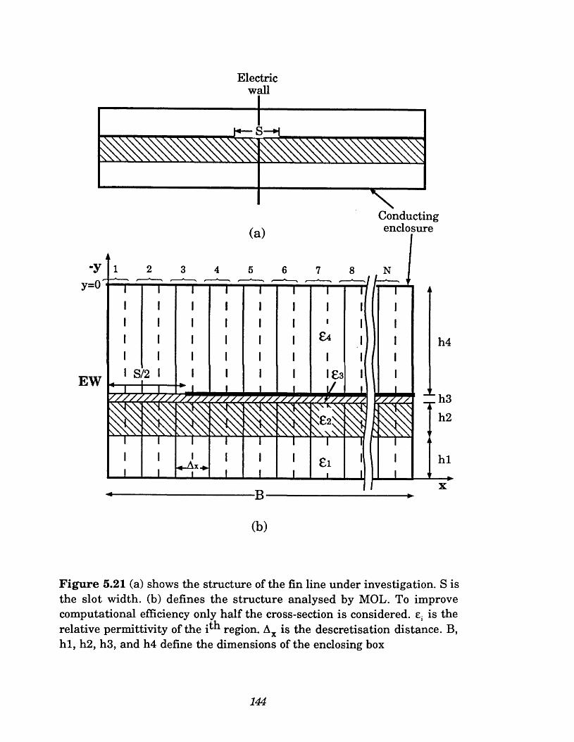
Electricwall
S—H
Conductingenclosure
h4
ZIh3 h2
(b)
F igu re 5.21 (a) shows the structure of the fin line under investigation. S is the slot width, (b) defines the structure analysed by MOL. To improve computational efficiency only half the cross-section is considered. ei is the relative permittivity of the i^ 1 region. Ax is the descretisation distance. B, h i, h2, h3, and h4 define the dimensions of the enclosing box
144
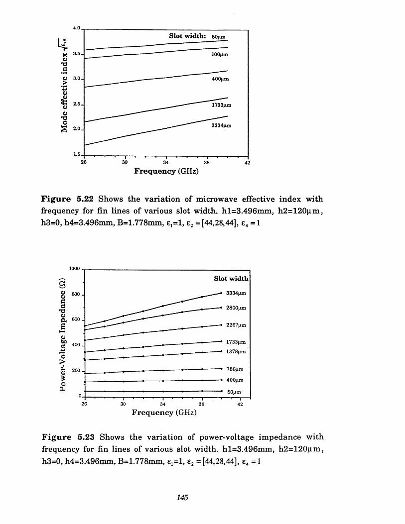
4.0
Slot width: 50fim
lOOfim
Q 3 .0 - > 400nm
15g 2-6.oo2 2 .0 .
3 3 3 4 ^ m
1.5
26 30 34 38 42
Frequency (GHz)
F ig u re 5.22 Shows the variation of microwave effective index with frequency for fin lines of various slot width. hl=3.496mm, h2=120pm, h3=0, h4=3.496mm, B=l.778mm, £j=l, e2 =[44,28,44], e4 = 1
1000
ag 800
cdo>
600
Bt—(o
og 200* o (X
026 30 34 38 42
Frequency (GHz)
F ig u re 5.23 Shows the variation of power-voltage impedance with frequency for fin lines of various slot width. hl=3.496mm, h2=120|im, h3=0, h4=3.496mm, B=l.778mm, e ^ l , e2 =[44,28,44], e4 = 1
Slot width
3 3 3 4 (Am
50 jira
145
have suggested how non-uniform, non-TEM lines may be analysed inorder to avoid this area of contention.
An accurate estimate of the electrical loss of the taper has not been made. However, preliminary calculations have suggested tha t the overall loss should be below ldB at 30GHz.
5.3.3 The interaction regionPreviously we have seen tha t the most im portant factors which
determine the magnitude of the electrooptic interaction are the phase mismatch between the interacting electrical and optical signals; the electrode loss; and the over-lap of the electrical and optical fields. In this section theoretical estimates of these parameters are made using MOL for the device depicted in figure 5.13. Ultimately, this data is employed to predict the optical frequency response and efficiency of a fin line modulator whose construction and structural dimensions are described in chapter 6.
5.3.3.1 The phase velocity of the electrical waveFigure 5.24 shows the variation of both the effective index and
attenuation coefficient of the electrical wave within the interaction region as a function of frequency. The data employed in the computations is shown in the figure caption. The attenuation coefficient was computed according to equation (4.52) assuming a metalisation conductivity of a = 3x 10⁷(Qm)_1. Note that the structure under study incorporates a 0.2pm buffer layer of silicon dioxide to prevent excessive attenuation of the optical mode. The variation of the effective index n^, can be conveniently expressed as,
=3.36 +0.01 F(GHz) 2 6 <F <4 0 (5.27)
It is apparent from equation (5.27) that a significant velocity mismatch occurs between the optical wave and the modulating microwave. In order to overcome this velocity mismatch, a periodic phase-reversal electrode was employed. We have seen in chapter 3 this type of electrode exhibits a bandpass optical response, the centre frequency of which is determined by both the velocity mismatch and the length of interaction between phase- reversals. To centre the pass band at 30GHz, we computed that 6 sections were required assuming n0 = 2.2 and given by equation (5.27) for a total interaction length of 2cm. For this case the phase shift for a given drive....
146
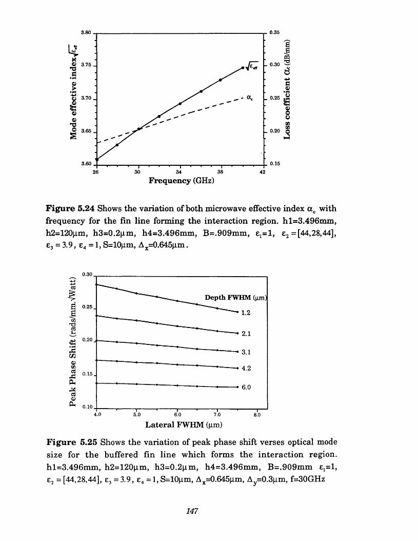
3.80 0.35
u?a>
£ • »H
'T3_ 0.30 ^3 .75 _
g 3.70 _taqj
0 3
© 3 . 6 5 .s
_ 0.25
_ 0.20
0.153.60
3826 30 34 42
Frequency (GHz)
F ig u re 5.24 Shows the variation of both microwave effective index a c with frequency for the fin line forming the interaction region. hl=3.496mm, h2=120|im, h3=0.2jim, h4=3.496mm, B=.909mm, ^=1, e2 = [44,28,44], e3 = 3.9, e4 = 1, S=10|im, Ax=0.645|im.
0.30
cCDepth FWHM (jim)
S 0.25aCO03 V
0.20
1.2
2.1
ACO0)CO“ 0 .1 5 .
CLh03O)
^ 0 .10 .
3.1
4.2
6.0
4.0 6.05.0 7.0 8.0
Lateral FWHM (jim)
F ig u re 5.25 Shows the variation of peak phase shift verses optical mode size for the buffered fin line which forms the interaction region. hl=3.496mm, h2=120jim, h3=0.2jim, h4=3.496mm, B=.909mm e ^ l , e2 =[44,28,44], e3 =3.9, e4 = 1,S=10jim, Ax=0.645jim, Ay=0.3jim, f=30GHz
147
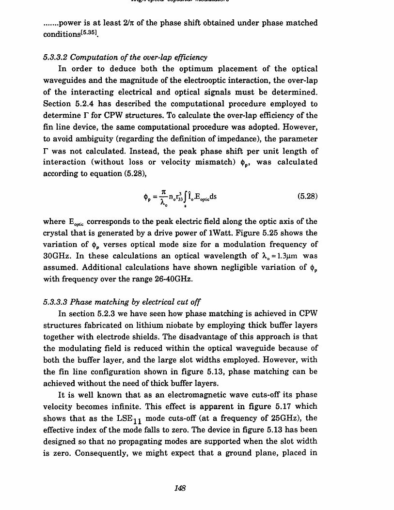
power is a t least 2/rc of the phase shift obtained under phase matchedconditions^5*351.
5.3.3.2 Computation of the overlap efficiencyIn order to deduce both the optimum placement of the optical
waveguides and the magnitude of the electrooptic interaction, the over-lap of the interacting electrical and optical signals m ust be determined. Section 5.2.4 has described the computational procedure employed to determine T for CPW structures. To calculate the over-lap efficiency of the fin line device, the same computational procedure was adopted. However, to avoid ambiguity (regarding the definition of impedance), the parameter r was not calculated. Instead, the peak phase shift per unit length of interaction (without loss or velocity mismatch) <j)p, was calculated according to equation (5.28),
♦ , = - f n.,» J i- Ew b (5-28)
where Eoptic corresponds to the peak electric field along the optic axis of the crystal that is generated by a drive power of lWatt. Figure 5.25 shows the variation of <j)p verses optical mode size for a modulation frequency of 30GHz. In these calculations an optical wavelength of A.0 = 1.3|im was assumed. Additional calculations have shown negligible variation of <|)p with frequency over the range 26-40GHz.
5.3.3.3 Phase matching by electrical cut offIn section 5.2.3 we have seen how phase matching is achieved in CPW
structures fabricated on lithium niobate by employing thick buffer layers together with electrode shields. The disadvantage of this approach is that the modulating field is reduced within the optical waveguide because of both the buffer layer, and the large slot widths employed. However, with the fin line configuration shown in figure 5.13, phase matching can be achieved without the need of thick buffer layers.
I t is well known that as an electromagnetic wave cuts-off its phase velocity becomes infinite. This effect is apparent in figure 5.17 which shows th a t as the LSE-^ mode cuts-off (at a frequency of 25GHz), the effective index of the mode falls to zero. The device in figure 5.13 has been designed so tha t no propagating modes are supported when the slot width is zero. Consequently, we might expect that a ground plane, placed in
148
close proximity to the electrode slot, would act to force the electrical waveguide toward cut-off and hence increase the phase velocity of the electrical wave within the interaction region. Indeed, recently Yoneyama et aZ[5-361 dem onstrated this type of phase matching in an optical modulator operating at a frequency of 12GHz. In addition, Yoneyama measured the phase velocity of electrical waves (using an electrical probe) in different shielded slot lines at frequencies up to 50GHz. Unfortunately no theoretical verification of his experimental measurements was offered.
In figure 5.26 a comparison between the experimental data of Yoneyama and theoretical estimates made by MOL, is presented. The structure we have analysed is defined in the caption of figure 5.26. Strictly, our analysis is not applicable, as Yoneyama's structure was fabricated on Y cut lithium niobate. Nevertheless, from figure 5.26 we can see tha t the agreement between Yoneyama's experimental data and our theoretical predictions is excellent.
The major advantage of phase matching by electrical cut off is that an unbuffered X cut substrate can be utilised allowing an improvement in electrooptic over-lap. Consequently, greater efficiency is achieved provided that no additional electrical loss is incurred.
It is important to note that while a demultiplexer could be constructed using this type of phase matching, the technique must be approached with some caution with regard to the transmission of finite bandwidth signals.
5.4 Chapter Summary
In this chapter the full-wave analysis presented in chapter 4 has been employed to study different coplanar electrodes. The CPW electrode, has been studied in some detail. For this configuration we confirmed quasistatic propagation in CPWs of small lateral dimensions and highlighted the importance of a full-wave analysis in the region of the interface electrodes. The shielded CPW electrode was studied with regard to phase matching, and for this structure we confirmed the validity of quasi-static approximation to a frequency of 40GHz. Over-lap factors were computed for both shield CPW and conventional CPW electrodes. We found that shield CPW intensity modulators fabricated on Z cut m aterial are unbalanced. Moreover, we confirmed theoretically the variation of overlap a t the acoustic resonance frequency for Z cut devices. Further calculations showed the importance of including finite conductivity..........
149
4.5
4 -
3 -
A - M O Lfl) 2.5-S*h
2 -
1.5-
1-
0.540 60 oo
h4 (jim)
F ig u re 5.26 Shows how phase matching can be achieved by electrical cut off. Experimental data is compared with theoretical estimates made by MOL. hl=10mm, h2=199(im, h3=lpm , B=1.29mm, Ax=1.29jim, S=20pm, £,=1, e2 =[28,44,28], e3 =[28,44,28], e4 = 1, f=50GHz
150
m etalisations in models of transm ission lines whose la tera ldimensions are comparable to a skin depth.
A second purpose of this chapter has been to study a new millimetre wave modulator constructed in fin line. Analytic expressions were developed to ascertain the modal spectrum of the modulator a t the interface with the electrical source. Subsequently, a modal analysis was performed to determine the return loss of modulator. The method of lines was employed to computed the power-voltage impedance and effective index of fin lines as a function of frequency and slot width. This data was used to design an electode taper to the interaction region. Further calculations were performed to estimate the phase velocity of the modulating electric field within interaction region and to determine the electrooptic over-lap. Chapter 5 was concluded with a discussion of a novel phase matching technique which is particularly suited to the fin line optical modulator.
151
References for chapter 5
[5.1] CD Watson, and MGF Wilson. (Oct. 1991): "Millimetre wave phase reversal integrated optical modulator in fin line", Electron. Lett., 27, pp. 2059-2061.
[5.2] P Vandenbulcke, and PE Lagasse. (1976): "Static field analysis of thin film electrooptic light modulators and switches", Wave Electron.,1, pp. 295-308.
[5.3] OG Ramer. (March 1982): "Integrated optics electrooptic modulator electrode analysis", IEEE J. Quantum Electron., QE-18, pp. 386-392.
[5.4] D Marcuse. (March 1982): "Optimal electrode design for integrated optics modulators", IEEE J. Quantum Electron., QE-18, pp. 393-398
[5.5] CM Kim, and RV Ramaswamy. (July 1989): "Overlap factors in integrated optic modulators and switches", IEEE J. Ligthwave Technol., LT-7, pp. 1063-1070.
[5.6] CS Sabatier, and E Caquot. (Jan. 1986):" Influence of a dielectric buffer layer on the filed distribution in an electrooptic guided wave device", IEEE J. Quantum Electron., QE-22, pp. 32-36.
[5.7] K Kawano, T Kitoh, O Mitomi, T Nozawa, and H Jumonji. (Feb. 1989): "A wide-band and low-driving -power phase modulator employing Ti:LiNbOg optical waveguide at 1.5pm wavelength", IEEE Photonic Technol. Lett., 1, pp. 33-34.
[5.8] D Marcuse. (May 1989): "Electrostatic field of coplanar lines computed with the point matching method", IEEE J. Quantum Electron., QE-25, pp. 939-947.
[5.9] AC Keen, MJ Wale, MI Sobhy, and AJ Holden. (Jan 1990): "Quasi-static analysis of electrooptic modulators by the method of lines", IEEE J. Ligthwave Technol., LT-8, pp.42-50.
[5.10] H Jin, M Belanger, and Z Jakubczyk. (Feb 1991): "General analysis of electrodes in integrated-optics electrooptic devices", IEEE J. Quantum Electron., QE-27, pp.243-251.
[5.11] JC Yi, SH Kim, and SS Choi. (June 1990): "Finite-element method for the impedance analysis of traveling-wave modulators", IEEE J. Ligthwave Technol., LT-8, pp. 817-822.
152

[5.12] CJ Railton, and JP McGeehan. (July 1989):" A rigorous and computationally efficient analysis of microstrip for use as an electrooptic modulator", IEEE Trans. Microwave Theory Tech., MTT-37,pp.1099-1104.
[5.13] J Gerdes, KH Helf and R Pregla. (April 1991): "Full-wave analysis of traveling-wave electrodes with finite thickness for electro-optic modulators by the method of lines", IEEE J. Ligthwave Technol., LT-9, pp. 461-467.
[5.14] K Kawano, T Kitoh, H Jumonji, T Nozawa, and M Yanagibashi.(Sept. 1989): "New travelling-wave electrode mach-zehnder optical modulator with 20GHz bandwidth and 4.7V driving voltage at 1.52|im wavelength", Electron. Lett., 2 5 , pp. 1382-1383.
[5.15] RC Alfemess, SK Korotky, and EA Marcatili. (1984): "Velocity- matching techniques for integrated optic travelling wave switch/modulators", IEEE J. Quantum, Electron., Q E - 2 0 , pp. 301-309.
[5.16] H Haga, M Izutsu, and T Sueta. (June 1986): "LiNbOg traveling-wave light modulator/ switch with an etched groove", IEEE J. Quantum Electron., QE-22, pp. 902-906.
[5.17] M Seino, N Mekada, N Namiki, T Yamane, and H Nakajima.(Oct. 1988): "12GHz- bandwidth Ti:LiNbOg mach-zehnder modulator", presented at Second Optoelectron. Conf., paper PD-1.
[5.18] NJ Parsons, AC O'Donnell, and KK Wong. (1986): "Design of efficient and wideband traveling-wave modulators", SPIE, 651 ,Integ. Opt. Cir. ENG III, (Insbtruck), paper 24.
[5.19] K Atsuki, and E Yamashita. (March 1987): "Transmission line aspects of the design of broadband electrooptic traveling-wave modulators", IEEEJ. Ligthwave Technol., LT-3, pp. 316-319.
[5.20] K Kawano, T Kitoh, H Jumonji, T Nozawa, and M Yanagibashi, and T Suzuki. (Sept. 1991): "Spectral-domain analysis of coplanar waveguide traveling-wave electrodes and their applications to Ti:LiNbOg mach- zehnder optical modulators", IEEE Trans. Microwave Theory Tech., MTT-39, pp. 1595-1601.
[5.21] K Noguchi, K Kawano, T Nozawa, and T Suzuki. (April 1991): "A Ti:LiNbOg optical intensity modulator with more than 20GHz bandwidth and 5.2V driving voltage", IEEE Photonic Technol. Lett., 33, pp. 333-335.
153
[5.22] K Kawano, T Nozawa, M Yanagibashi, and H Jumonji. (1989): "Broadband and low-driving-power LiNbOg external optical modulators", NTT Rev., 4, p. 103.
[5.23] RS Weis, and TK Gaylord. (Feb. 1985): "Lithium niobate: summary of physical properties and crystal structure", App. Phys., A37, pp. 191-203.
[5.24] JL Nightingale, RA Becker, PC Willis, and JS Vrhel. (Sept. 1987): "Characterization of frequency dispersion in Ti-indiffused lithium niobate optical devices", Appl. Phys. Lett., 51, pp. 716-718.
[5.25] RL Jungerman, and CA Flory. (Oct. 1988): "Low-frequency acoustic anomalies in lithium niobate mach-zehnder inteferometers", Appl.Phys. Lett., 53, pp. 1477-1479.
[5.26] RL Jungerman, CJ Johnsen, DJ McQuate, KSalomaa, MP Zurakowski, RC Bray, G Conrad, D Cropper, and P Hemday. (Sept. 1990): "High-speed optical modulator for application in instrumentation", IEEE J.Ligthwave Technol., LT-8, pp. 1363-1370.
[5.27] DW Dolfi. (Aug. 1986): "Traveling-wave interferometer modulator with high bandwidth, low drive power, and low loss", Appl. Opt., 25,pp. 2479-2480.
[5.28] W Heinrich. (Oct. 1990): "Full-wave anlaysis of conductor losses on MMIC transmission lines", IEEE Trans. Microwave Theory Tech., MTT-38, pp. 1468-1472.
[5.29] RE Collin. (1960): "Field theory of guided waves", McGraw-Hill,New York.
[5.30] A Wexler. (Sept. 1967): "Solution of waveguide discontinuities by modal analysis", IEEE Trans. Microwave Theory Tech., MTT-15, pp. 508-517.
[5.31] RE Collin. (1966): "Foundations for microwave engineering", McGraw- Hill, New York.
[5.32] Bhat, and Bharathi. (1988): "Analysis, design and applications of fin lines", Artech House, Norwood.
[5.33] D Mirshekar-Syahkal, and JB Davies. (Feb. 1981): "Accurate analysis oftapered planar transmission lines for microwave integrated circuits", , IEEE Trans. Microwave Theory Tech., MTT-29, pp. 123-128.
[5.34] SB Cohn. (Oct. 1969): "Slot line on a dielectric substrate", IEEE Trans. Microwave Theory Tech., MTT-17, pp. 768-779.
154

[5.35] D Erasme, and MGF Wilson. (1986): "Analysis and optimisation of integrated-optic travelling-wave modulators using periodic and nonperiodic phase reversals", Opt. & Quant. Electr., 18, pp. 203-211.
[5.36] T Yoneyama, K Niinuma, and S Kanno. (April 1991): "Velocity-matched LiNbOg modulator using an inverted slot line", IEEE Microwave and Guided Wave Lett., 1, pp. 192-194.
155

Chapter 6
Fabrication, Measurements and Results
6.1 Introduction
6.2 Fabrication
6.3 Principles of Modulator Characterisation
6.4 Experimental Results
6.5 Chapter Summary
156
6.1 Introduction
This chapter is devoted to a description of the experimental work undertaken during the course of this project. In section 6.2 the most basic techniques of fabrication are described. This description includes details of the fabrication parameters of the diffused optical waveguides tha t we have employed, and the methods by which travelling-wave electrodes are formed.
One of the major difficulties associated with the experimental stage of this project was the accurate measurement of optical modulation. Section 6.3 describes the techniques that can be employed for this purpose. Particular attention is given to measurement at very high frequencies, and a technique not previously reported is described for characterisation a t frequencies in excess of 40GHz.
Section 6.4 is split into three separate subsections. Each of these subsections describes the results for a particular type of modulator constructed during the course of this project: a broadband phase-reversal modulator is described in section 6.4.1; an equalising phase-reversal modulator is described in section 6.4.2; and finally, section 6.4.3 describes a millimetre wave fin-line optical modulator of the type examined in chapter 5.
6.2 Fabrication
Figure 6.1 provides an overview of the major stages involved in the fabrication of a titanium indiffused modulator on Z cut lithium niobate. More detailed descriptions of the procedures are given below, though the most basic detail is omitted.
6,2.1 Waveguide fabricationFabrication is accomplished on a 3 inch optical grade Z cut lithium
niobate wafer obtained from Crystal Technology. The wafer is too large to fit in a standard 6cm diffusion tube and so small sections are cut away to reduce the wafer width to 5.8cm. The wafer cuts are made parallel to the Y axis of the crystal and the cuts are subsequently used as reference lines to locate metalisation layers on the wafer surface. A standard solvent and acid cleaning procedure is used to prepare the wafers prior to the fabrication of the waveguides. After cleaning, a positive photoresist..........
157
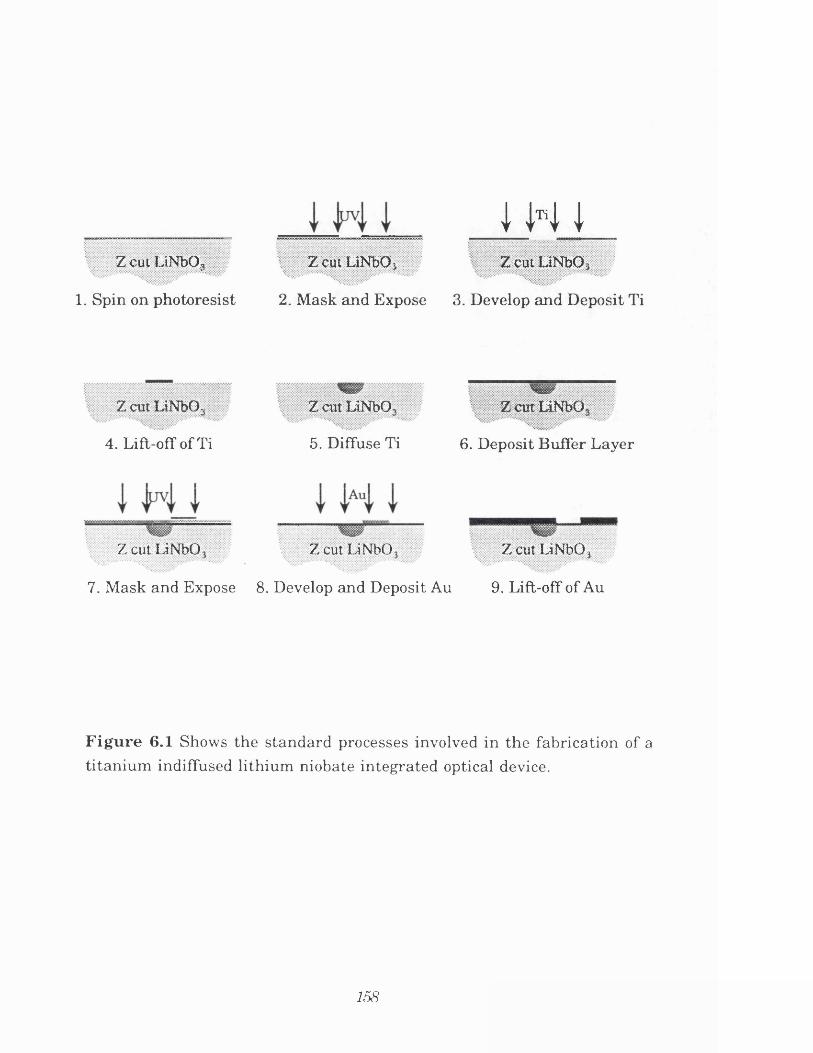
I H I
Z cut LiNb03
1. Spin on photoresist
ZcutLiNbO^ Z cut LiNbQ,
2. Mask and Expose 3. Develop and Deposit Ti
Z cut LiNbG- Z cut LiNbO. ZcutliNbO.
4. Lift-off of Ti
ZcutUNbO
5. Diffuse Ti
Zcut LiNbO
6. Deposit Buffer Layer
7. Mask and Expose 8. Develop and Deposit Au
Zcut LiNbO3
9. Lift-off of Au
F igu re 6.1 Shows the standard processes involved in the fabrication of a titanium indiffused lithium niobate integrated optical device.
158
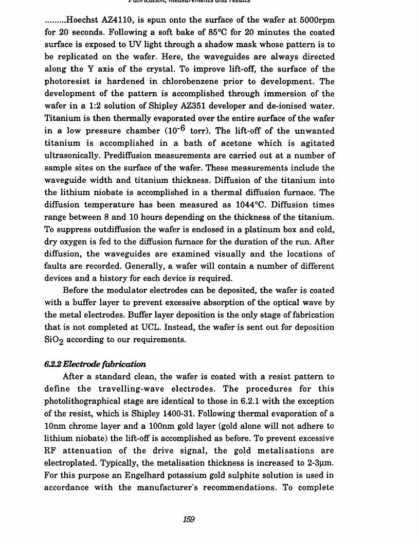
ir w uf iitv iia u f vriuziw o u r u t s edc*t&d
Hoechst AZ4110, is spun onto the surface of the wafer a t 5000rpmfor 20 seconds. Following a soft bake of 85°C for 20 minutes the coated surface is exposed to UV light through a shadow mask whose pattern is to be replicated on the wafer. Here, the waveguides are always directed along the Y axis of the crystal. To improve lift-off, the surface of the photoresist is hardened in chlorobenzene prior to development. The development of the pattern is accomplished through immersion of the wafer in a 1:2 solution of Shipley AZ351 developer and de-ionised water. Titanium is then thermally evaporated over the entire surface of the wafer in a low pressure chamber (10'® torr). The lift-off of the unwanted titan ium is accomplished in a bath of acetone which is agitated ultrasonically. Prediflfusion measurements are carried out at a number of sample sites on the surface of the wafer. These measurements include the waveguide width and titanium thickness. Diffusion of the titanium into the lithium niobate is accomplished in a thermal diffusion furnace. The diffusion tem perature has been measured as 1044°C. Diffusion times range between 8 and 10 hours depending on the thickness of the titanium. To suppress outdiffusion the wafer is enclosed in a platinum box and cold, dry oxygen is fed to the diffusion furnace for the duration of the run. After diffusion, the waveguides are examined visually and the locations of faults are recorded. Generally, a wafer will contain a number of different devices and a history for each device is required.
Before the modulator electrodes can be deposited, the wafer is coated with a buffer layer to prevent excessive absorption of the optical wave by the metal electrodes. Buffer layer deposition is the only stage of fabrication that is not completed at UCL. Instead, the wafer is sent out for deposition SiC>2 according to our requirements.
6,2,2 Electrode fabricationAfter a standard clean, the wafer is coated with a resist pattern to
define the travelling-wave electrodes. The procedures for th is photolithographical stage are identical to those in 6.2.1 with the exception of the resist, which is Shipley 1400-31. Following thermal evaporation of a lOnm chrome layer and a lOOnm gold layer (gold alone will not adhere to lithium niobate) the lift-off is accomplished as before. To prevent excessive RF attenuation of the drive signal, the gold m etalisations are electroplated. Typically, the metalisation thickness is increased to 2-3|im. For this purpose an Engelhard potassium gold sulphite solution is used in accordance with the manufacturer's recommendations. To complete
159
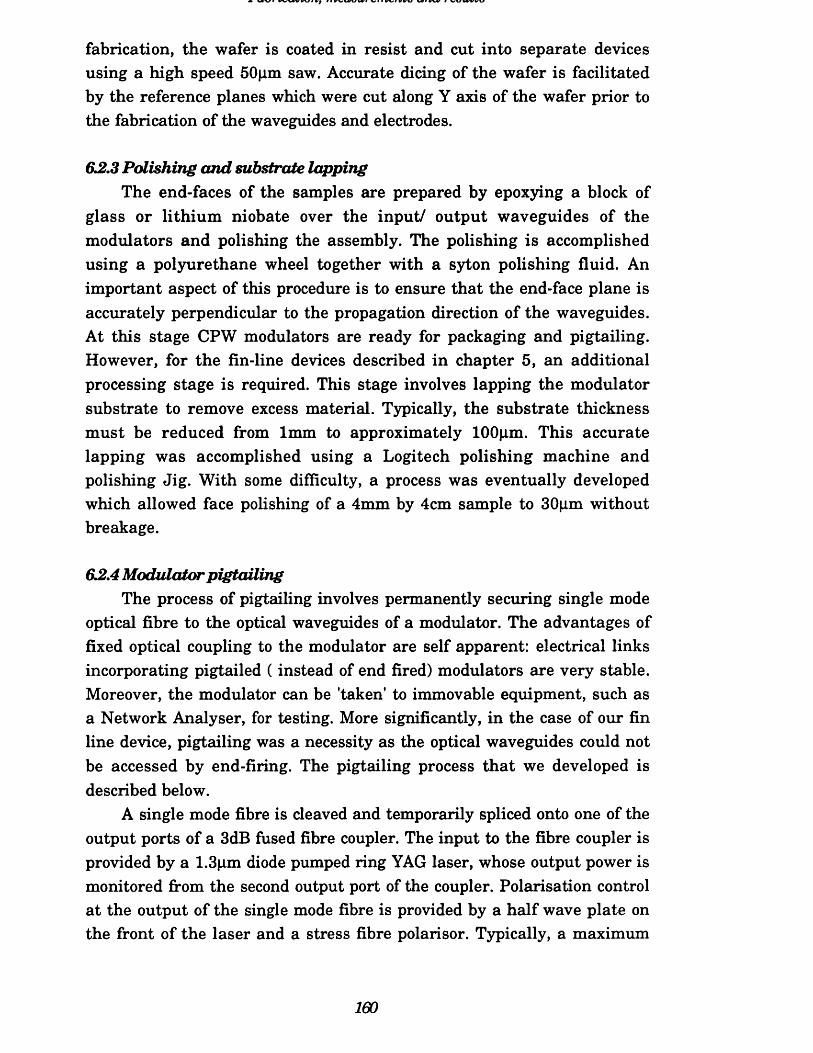
fabrication, the wafer is coated in resist and cut into separate devices using a high speed 50pm saw. Accurate dicing of the wafer is facilitated by the reference planes which were cut along Y axis of the wafer prior to the fabrication of the waveguides and electrodes.
6L2.3 Polishing and substrate lappingThe end-faces of the samples are prepared by epoxying a block of
glass or lithium niobate over the input/ output waveguides of the modulators and polishing the assembly. The polishing is accomplished using a polyurethane wheel together with a syton polishing fluid. An important aspect of this procedure is to ensure that the end-face plane is accurately perpendicular to the propagation direction of the waveguides. At this stage CPW modulators are ready for packaging and pigtailing. However, for the fin-line devices described in chapter 5, an additional processing stage is required. This stage involves lapping the modulator substrate to remove excess material. Typically, the substrate thickness m ust be reduced from 1mm to approximately 100pm. This accurate lapping was accomplished using a Logitech polishing machine and polishing Jig. With some difficulty, a process was eventually developed which allowed face polishing of a 4mm by 4cm sample to 30pm without breakage.
6L2.4 Modulator pigtailingThe process of pigtailing involves permanently securing single mode
optical fibre to the optical waveguides of a modulator. The advantages of fixed optical coupling to the modulator are self apparent: electrical links incorporating pigtailed ( instead of end fired) modulators are very stable. Moreover, the modulator can be 'taken' to immovable equipment, such as a Network Analyser, for testing. More significantly, in the case of our fin line device, pigtailing was a necessity as the optical waveguides could not be accessed by end-firing. The pigtailing process th a t we developed is described below.
A single mode fibre is cleaved and temporarily spliced onto one of the output ports of a 3dB fused fibre coupler. The input to the fibre coupler is provided by a 1.3pm diode pumped ring YAG laser, whose output power is monitored from the second output port of the coupler. Polarisation control at the output of the single mode fibre is provided by a half wave plate on the front of the laser and a stress fibre polarisor. Typically, a maximum
optical power of 250pW is obtained at the output of the single mode fibre which is butted against the input waveguide of the modulator. A second fibre is butted against the output waveguide and the input polarisation is adjusted to minimise the modulator drive voltage. Once TM polarisation has been attained the input and output fibres are m anipulated to maximise the transmitted optical signal. A small quantity of UV curing adhesive is then applied to both fibre/ waveguide joints and the optical through-put is reoptimised. After curing, the fibres are secured to the modulator package with an epoxy. We have found th a t the resulting pigtails are quite stable for the CPW devices but less so for the fin line devices.
6.3 Measurements Techniques
In previous sections of this thesis we have seen how high speed optical modulators are designed; analysed; and fabricated. Thus far however, we have neglected the issues involved in the calibration of the resulting devices. Clearly, the issue of calibration is of great importance as w ithout an accurate measurement of a modulator's response we cannot hope to assess the quality of its design.
It is well known that the effect of modulating a monochromatic wave is to produce additional frequency components or side-bands. Characterisation of a modulator involves determining the amplitude and phase of the resulting side bands as a function of modulating frequency. Previously, we have seen that the simplest form of modulator tha t can be constructed with an electrooptic crystal is a phase modulator. In the next section the characterisation of a phase modulator is considered.
6,3.1 Measurement o f a phase modulatorConsider the optical phase modulator depicted in figure 6.2. The
excitation signal V(t) acts to modulate phase of the optical wave passing through the device. We recall from chapter 2, that the phase modulated optical field y(t), emerging from the output waveguide can be written as,
\|/(t) = \|/0exp j{(0ot + O(t)} (6.1)
where y 0 is a real optical amplitude. Equation (6.1) could include a term to account for the finite optical loss of the waveguide. Little generality is lost by assuming harmonic time variations as other temporal functions can be constructed through the Fourier integral. A cw excitation.............
161
OpticalWave
'F0expj{co0t}Phase Modulator
Phase Modulated Optical Wave
T0exp j{co01 + Ojcosfoy + Z<&) }
ModulatingSignal
V, cos c y
F ig u re 6.2 Shows a schematic diagram of an optical phase modulator. The excitation field acts to modulate the phase of the optical wave producing side bands at harmonics of the modulating frequency.
Carrier and Harmonics
wo-0),
co. +co,
Fabry-Perot
FilteredWave
ram p applied to plate spacing
x
time
A(0 + (0O W)i
time
F ig u re 6.3 Shows the action of a scanning Fabry-Perot interferometer on the spectrum of a phase modulated wave. Each harmonic passes through the filter a t a different time during the scan.
162
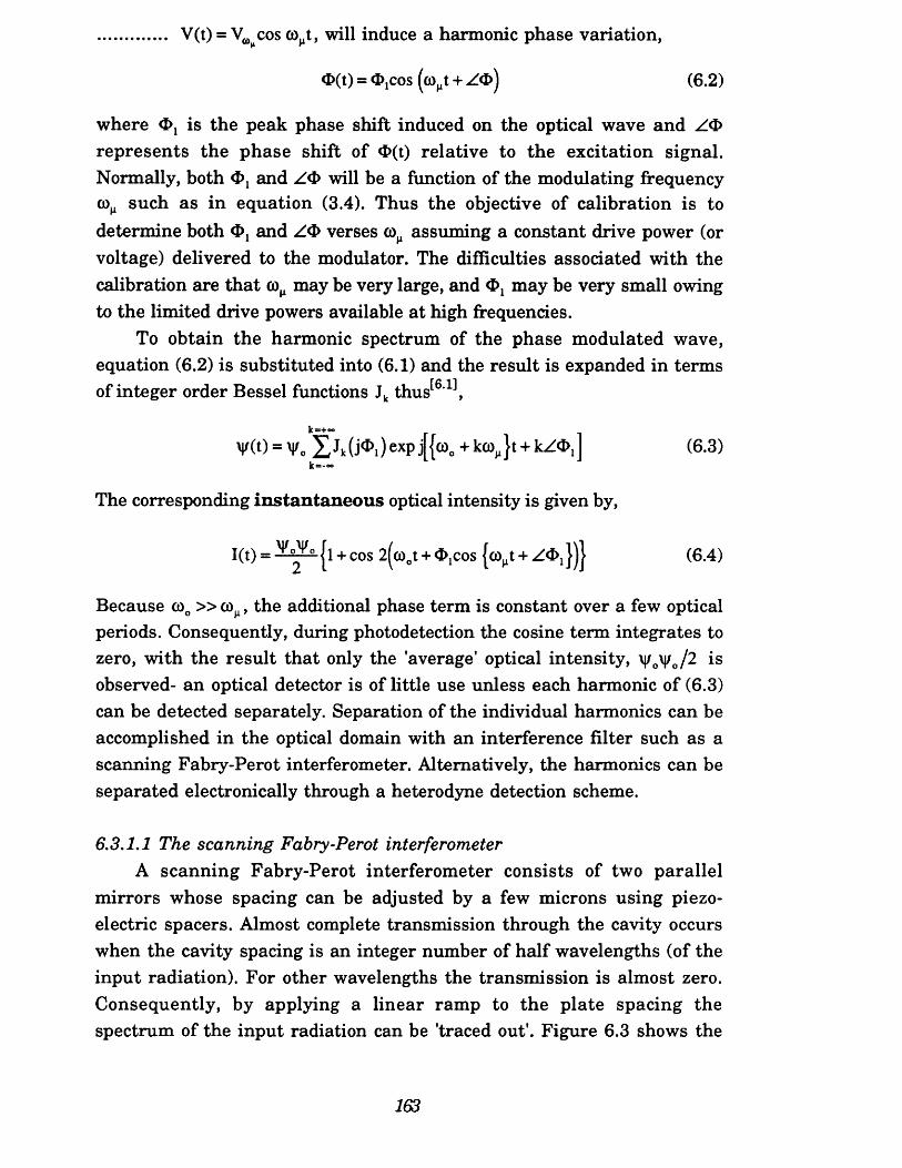
V(t) = cos o y , will induce a harmonic phase variation,
d>(t) = Ojcos (co t + Zd>) (6.2)
where d>j is the peak phase shift induced on the optical wave and Zd> represents the phase shift of d>(t) relative to the excitation signal. Normally, both d>j and will be a function of the modulating frequency ci such as in equation (3.4). Thus the objective of calibration is to determine both and Zd> verses co assuming a constant drive power (or voltage) delivered to the modulator. The difficulties associated with the calibration are that coR may be very large, and may be very small owing to the limited drive powers available at high frequencies.
To obtain the harmonic spectrum of the phase modulated wave, equation (6.2) is substituted into (6.1) and the result is expanded in terms of integer order Bessel functions Jk thus[61 ,
Because coo » co , the additional phase term is constant over a few optical periods. Consequently, during photodetection the cosine term integrates to zero, with the result that only the 'average' optical intensity, y oy o/2 is observed- an optical detector is of little use unless each harmonic of (6.3) can be detected separately. Separation of the individual harmonics can be accomplished in the optical domain with an interference filter such as a scanning Fabry-Perot interferometer. Alternatively, the harmonics can be separated electronically through a heterodyne detection scheme.
6.3.1.1 The scanning Fabry-Perot interferometerA scanning Fabry-Perot interferometer consists of two parallel
mirrors whose spacing can be adjusted by a few microns using piezoelectric spacers. Almost complete transmission through the cavity occurs when the cavity spacing is an integer number of half wavelengths (of the input radiation). For other wavelengths the transmission is almost zero. Consequently, by applying a linear ramp to the plate spacing the spectrum of the input radiation can be 'traced out'. Figure 6.3 shows the
(6.3)
The corresponding in stan taneous optical intensity is given by,
1(0 = ~ ~ ~ 2"{l + cos 2(co0t + Ojcos { o y + (6.4)
163
action of the interferometer on the phase modulated spectrum of equation(6.3). Each harmonic passes through the interferometer a t a different time during the scan. The intensity of each harmonic Ik, can be deduced from (6.3) as,
(6.5)
By comparing the magnitude of these side bands an absolute measure of the depth of phase modulation can be obtained. And, as both the scanning range and free spectral range are adjustable, measurements can be made for any modulation frequency. However, it is apparent from equation (6.5) that the calibration by the Fabry-Perot interferometer will not include a determination of the argument of response.
The dynamic range of the measurement system is dependent upon the finesse of the cavity F, that is l ^ / l ^ =4(F/rc)2. With mirrors of 95% reflectivity (finesse=60), minimum transmission is a t best 31dB down on the peak transmission. This places a lower limit on the peak phase shift d>, tha t can be resolved of approximately 3°. At this modulation depth the intensity a t the side-band frequency is only double that of the background. In our experiments we have seldom obtained a finesse in excess of 30, and the minimum detectable in this case is greater than 6°. It is apparent this measurement system is not suited to the measurement of small signal phase modulation as an interferometer of high finesse is required in order to resolve the side-bands from the carrier. However, a significant improvement in sensitivity can be achieved by converting the phase modulation to intensity modulation and measuring the spectrum at extinction. In this case the carrier and first side-band are of the same magnitude (see section 6.3.2).
Some of the short comings of the scanning Fabry-Perot can be overcome by employing a optical heterodyne detection scheme.
6.3.1.2 Optical heterodyne detectionA coherent optical heterodyne detection scheme is based upon the
mixing of two lasers closely spaced in frequency to produce down- converted components at microwave frequencies. Such a system has been employed by Tim et to down-convert the harmonics of the phasemodulated spectrum given by equation (6.3). In the system the local oscillator laser has an amplitude of,
164
Vu, =V,expj{co,t + A(p(t)} (6.6)
The term Acp(t) represents the phase instability of the local oscillator. A second laser is directed though the phase modulator under test. The amplitude of the second laser at the detector is therefore,
Vm = V.exp j{<o0t + <J>,cos (oy + <J>,) + Acp(t)} (6.7)
The local oscillator and the modulated signal mix on the photodetector to produce a photocurrent of,
i = f(v„+Vio)(Vm+Vlo) (6.8)
Expanding (6.8) according to (6.3) yields,
~ = vf + Vo + 2v ,v0[j.(<l>1)cos(co1 - co0)t
+ j,(01)cos(co1-co0+£o)1)t
-J ,(0 1)cos(co1-to0-co(l)t
+J2(0,)cos(co1 - co0 + 2co(1)t+.... ] (6 9)
where R is the responsivity of the detector in A/W.By careful tuning of the local oscillator, the side bands can be down
converted to a fixed IF frequency (100MHz in the case of Tun et al) and detected. As detection is performed in the electrical domain a single frequency, narrow band receiver can be employed and so the dynamic range of the measurement can be very large. Moreover, as the amplitude of the IF component is proportional to the amplitude of the local oscillator, the IF can be amplified simply by increasing the local oscillator power until shot noise limited performance is achieved. By comparing the magnitude of the side bands a determination of <J>j can be made. In principle, the measurement is absolute as the sensitivity of the detector can be calibrated at the IF frequency for various signal levels by beating the two lasers and passing the resultant though an optical attenuator (for further discussion see section 6.3.2.4).
The technique described above is applicable to very high frequencies as the local laser can be tuned by over 100GHz. The disadvantage of heterodyne detection system relates to its complexity and the stringent requirements which are placed upon the optical sources. In particular,
165
laser frequency jitter must be ’absent’ and the laser polarization must be continuously adjustable so as to avoid polarization fading in the beat signal. In practice, Acp(t) is sufficiently large to destroy any measurement of Zd>.
An alternative measurement strategy is to convert the phase modulator into an intensity modulator by mixing the phase modulated wave with a reference beam taken from the same optical source. The interferometer can be implemented in an integrated or bulk form. The only constraint on the interferometer is that any path imbalance must less than the coherence length of the source. In the next section the calibration of an intensity modulator is considered. This section is particularly relevant to this thesis as all the devices th a t have been constructed during the course of this project are intensity modulators.
6.3.2 Measurement o f an intensity modulatorThe optical field at the output of a modulator such as that depicted in
figure 6.4 is given by the sum of the fields emerging from the two paths of the interferometer, that is,
V(t) = V.exp j{w„t+<!>.} + y bexp j{co„t+ <!>„} (6.10)
Rearranging equation (6.10) shows that generally the optical field is both phase and amplitude modulated,
V(t) = Vo exp j|(D„t + * c>b j.cosj0 , 2 | (6.11)
where, Vo= ¥ a = ¥b> f°r a symmetric Y branch interferometer. Both exponential and cosine terms of (6.11) may be expanded in terms of Bessel functions. The overall expression is complicated except in the case of balanced operation (that is, d>#= -O b) when the residual phase modulation is zero. The instantaneous intensity at the output of the interferometer can be deduced from (6.11) as,
I(t) = p - j l + cos 2 co0t + ***■ 2^ ]|-cos2 j ^* j (6.12)
Under cw modulation and after averaging, the output intensity attains a familiar form,
1(0 = y ( i + COS + <I>dacos[oy + Z<1> ]}) (6.13)
166
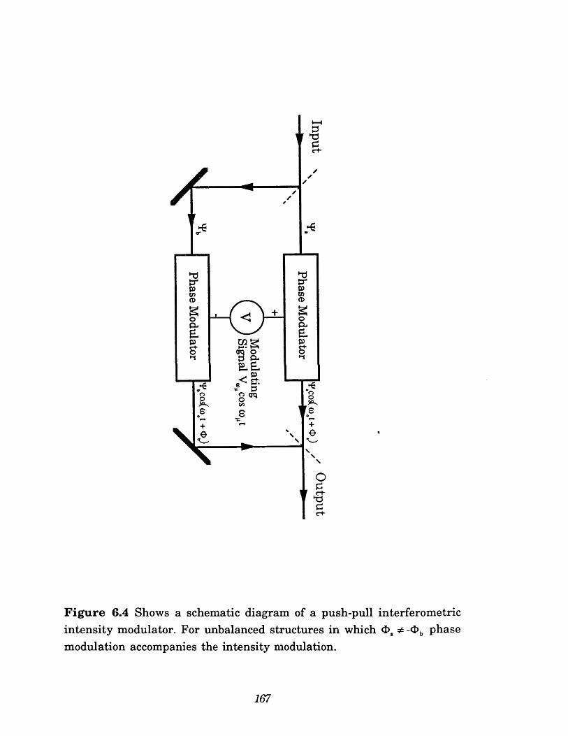
a sorq o £ P-E-E-
. Pf tio orq o
F ig u re 6.4 Shows a schematic diagram of a push-pull interferometric intensity modulator. For imbalanced structures in which <I>a * -d>b phase modulation accompanies the intensity modulation.
167
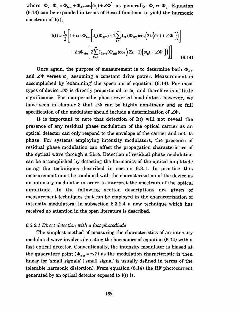
where 0>, - Ob = ObiM + O^cosfco^t + Z<I>] as generally Oa oc-<j>b. Equation (6.13) can be expanded in terms of Bessel functions to yield the harmonic spectrum of I(t),
KO-i- l + cosfc^
+sin<I>bI„
(« „)+ 2 2 ;jrlk(®„)cos(2k{cDMt + Z * })k=l
2 1 2k+l ( diff )cos((2k + ljlco^t + Z4> })(6.14)
Once again, the purpose of measurement is to determine both d>diff and Zd> verses co assuming a constant drive power. M easurement is accomplished by 'examining' the spectrum of equation (6.14). For most types of device Z4> is directly proportional to co and therefore is of little significance. For non-periodic phase-reversal modulators however, we have seen in chapter 3 that ZO can be highly non-linear and so full specification of the modulator should include a determination of ZO.
It is im portant to note that detection of I(t) will not reveal the presence of any residual phase modulation of the optical carrier as an optical detector can only respond to the envelope of the carrier and not its phase. For systems employing intensity modulators, the presence of residual phase modulation can affect the propagation characteristics of the optical wave through a fibre. Detection of residual phase modulation can be accomplished by detecting the harmonics of the optical amplitude using the techniques described in section 6.3.1. In practice this measurement must be combined with the characterisation of the device as an intensity modulator in order to interpret the spectrum of the optical am plitude. In the following section descriptions are given of measurement techniques that can be employed in the characterisation of intensity modulators. In subsection 6.3.2.4 a new technique which has received no attention in the open literature is described.
6.3.2.1 Direct detection with a fast photodiodeThe simplest method of measuring the characteristics of an intensity
modulated wave involves detecting the harmonics of equation (6.14) with a fast optical detector. Conventionally, the intensity modulator is biased at the quadrature point ( >bias = tc/2 ) as the modulation characteristic is then linear for 'small signals' ('small signal' is usually defined in terms of the tolerable harmonic distortion). From equation (6.14) the RF photocurrent generated by an optical detector exposed to I(t) is,
168
i = y R(w„)-[l + 2-J, (<*>„„ )cos(oy + Z3>)] (6.15)
where R(co ) is the responsivity of the photodetector in A/W. The corresponding RF signal generated by the photodetector can be observed with a spectrum analyser (measures only) or RF vector network analyser (measures both d>diff and Zd>). The rms RF power Psig, measured by an instrument of input impedance Zb when timed to co is,
P.ig = !,(<!>,« )]2.S(co,,i) (6.16)
where S(co ,i) describes the variation in the sensitivity of the electrical receiver with both frequency and signal level. Ideally S(co ,i) is equal to unity, but for very low signal level (-50dBm and below) this not the case. Clearly, to obtain an absolute measure of the response of both the photodetector and electrical receiver m ust be elim inated from the measurements. Unfortunately, to calibrate (that is, to determine the correction) the response of the optical receiver, the system must be excited with intensity modulated signal of known amplitude for all frequencies and signal levels of interest. Obtaining a suitable optical calibration signal is rather problematic. However, if the responsivity of the photodiode is known, then the sensitivity of the electrical receiver can be calibrated against a chain of precision electrical attenuators a t power levels consistent with those provided by the optical link. In this thesis we have employed direct detection together with the latter method of calibration. In these measurements our aim was to determine only the variation of d>diff with (o and not the absolute magnitude of d ^ .
Measurement by direct detection is often hampered by the low signal levels generated by the photodetector. For example, with = ji/20 , a peak optical through-put of 200|iW and a detector responsivity of .5A/W only -58dBm of signal is delivered to the receiver. This signal power can be amplified by increasing I0, though this process is limited by the DC photocurrent which accompanies the RF signal. Consequently, a stage of electrical amplification is often employed.
At frequencies in excess of 20GHz the signal may be further attenuated if an additional stage of down-conversion is required before the electronic receiver. This conversion loss is typically -20dB (HP harmonic mixer). Consequently, above 20GHz direct detection becomes very difficult because of the limited availability of high quality electronic equipment and
169
photodetectors. Fortunately, alternative measurement strategies can be devised which do not require high frequency components.
6.3.2.2 Swept frequency method6®Equation (6.14) shows that when an intensity modulator is biased
away from quadrature the DC term of I(t) becomes a function of ,
lDc=Y[l+cos(<Kbi>t).J0(<I><tff)] (6.17)
By biasing the modulator toward minimum (or maximum) transmission, the modulation response becomes non-linear and 'rectification' of the optical modulation occurs. By setting <£bias = n and m easuring the difference in 1^ with and without modulation allows a determination of <I>diff to made,
max
where Ai^ is the difference between DC photocurrent at extinction with and without modulation; is the photocurrent tha t is generated with maximum optical throughput (that is with =0); and we have used J0(<D*ff) = l-<D^/4 for small signal modulation.
To ensure that Ai^ is an accurate measure of Odiff it is important that the bias point does not drift from the minimum optical transmission. Humphreys^6'4] has suggested that the bias point can be stabilised by adding a low-level (<I>eiTOr « Odiff), low frequency modulation coerror to the bias voltage. In this case the optical output will contain a component a t cocrror given by,
I(o>en. r) = I0sin(OttJ J 0(cDem)r) (6.19)
By detecting this component an error signal can be generated and fed back to the bias voltage. In principle an accurate determination of d>diff can be made w ith the above m easurem ent system, especially if lock-in techniques are applied to the m easurem ent of Ai^. Moreover, measurements can be made irrespective of the modulating frequency without the need for sophisticated equipment. However, it m ust be emphasised that this measurement system does measure a harmonic of the intensity modulated spectrum. Therefore, measurement by swept frequency technique cannot be regarded as irrefutable evidence of
170
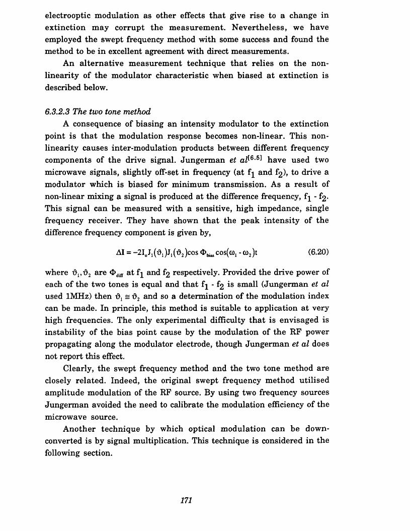
electrooptic modulation as other effects th a t give rise to a change in extinction may corrupt the measurement. Nevertheless, we have employed the swept frequency method with some success and found the method to be in excellent agreement with direct measurements.
An alternative measurement technique th a t relies on the non- linearity of the modulator characteristic when biased a t extinction is described below.
6.3.2.3 The two tone methodA consequence of biasing an intensity modulator to the extinction
point is th a t the modulation response becomes non-linear. This non- linearity causes inter-modulation products between different frequency components of the drive signal. Jungerm an et have used twomicrowave signals, slightly off-set in frequency (at f^ and f2), to drive a modulator which is biased for minimum transmission. As a result of non-linear mixing a signal is produced at the difference frequency, f j - f2- This signal can be measured with a sensitive, high impedance, single frequency receiver. They have shown th a t the peak intensity of the difference frequency component is given by,
AI = - 2 1 ,1 ^ ) 1 ^ ) 0 0 8 f c ^ c o s to - a 2)t (6.20)
where 'd1,‘d2 are diff 1 an^ 2 respectively. Provided the drive power of each of the two tones is equal and that f j - f2 is small (Jungerman et al used 1MHz) then = $2 and so a determination of the modulation index can be made. In principle, this method is suitable to application a t very high frequencies. The only experimental difficulty tha t is envisaged is instability of the bias point cause by the modulation of the RF power propagating along the modulator electrode, though Jungerman et al does not report this effect.
Clearly, the swept frequency method and the two tone method are closely related. Indeed, the original swept frequency method utilised amplitude modulation of the RF source. By using two frequency sources Jungerman avoided the need to calibrate the modulation efficiency of the microwave source.
Another technique by which optical modulation can be down- converted is by signal multiplication. This technique is considered in the following section.
171
6.3.2.4 Optical down-conversion by signal multiplicationFrom equation (6.14) it is apparent tha t under small signal CW
modulation an intensity modulator biased at quadrature will produce an intensity variation of the form,
I(t) = i-[l + 2J, (<!>,,„ )cos(oy)] (6.21)
If the optical source at the input to the intensity modulator is itself modulated by the factor [l + mcos(coLOt)] then I(t) will contain a down- converted component at the difference frequency co - 0)^ , that is,
I(t) = M l + mcos^Lot)+21,(0^ )cos(a> t)
+Ji(4>d„)mcos(to(1-o )LO)t + Jl(<D,iff)mcos(o)LO >} ( 6 . 2 2 )
Provided m and I0 are known the down-converted signal can be detected with a calibrated optical receiver and a determination of d>difr made. This technique provides a general strategy for measuring components lying beyond frequencies normally accessible by direct detection. Moreover, observation of the down-converted component may provide irrefutable evidence of electrooptic activity. It is clear however, that the provision of a calibrated optical receiver (see section 6.3.2.1) or suitable modulated optical source is a basic requirement for this measurement system. As optical receivers are calibrated with known optical signals a calibrated modulated optical source would be of more benefit. Unfortunately, many of these sources require specialised laser systems which are not readily available. However, one modulated optical source that can be constructed with relative ease has been described by Humphreys^6-4]. The modulated source consists of a CW laser modulated a t cos by an external intensity m odulator. The in tensity modulator is biased a t extinction and consequently, the output contains only even harmonics of the drive signal. Under small signal modulation equation (6.14) shows tha t the DC and second harmonic signals are given by,
I(t)= I DC + iLoCOS Lot) (6.23)
where 1^ = I0 (Os) and co^ = 2cos and we note that forsmall signal modulation that IDC = Ilo. The output intensity of the source is entirely defined by d>s (with the input intensity I0fixed) which can be deduced simply by measuring 1^. The DC component may be used to
172
'level' the optical source by adjusting the RF drive to the modulator to compensate for variations in the modulator response regardless of the modulating frequency. If the modulated source is applied to the input of a second modulator whose linear response is to be measured, then the output from the second modulator is deduced from equation (6.22) as,
I(t) = “ [ioc + iLoCOs(cOix)t) + 2 . I j x ;* Ji ( ^ d i f f ) C O s ( c D ^ t )
+lLO*Jl(( >diff)C0S(®LO + (6.24)
where A represent the total optical insertion loss of the second modulator. If I(t) is detected by a fast photodiode of responsivity R AAV we recall from equation (6.16) tha t the RF power measured by a spectrum analyser of input impedance Zm timed to a frequency co8ide is,
P , d . = ^ l j R K d.)2 S(coride>i) (6.25)
where Ip is the peak optical intensity of the frequency component. With a perfect optical receiver in which R2S = 1, it is a simple matter to determine
P^ ' Bi‘ (6.26)
where PfflLo is generated by the 2n^ term of equation (6.24) and P,^-^ is generated by the 4 ^ term. Unfortunately, the optical receiver will have a sensitivity that varies with both frequency and signal level. Consequently, equation (6.26) will not generally provide and accurate determination of JiC diff)* or(ier to determine the absolute modulation depth a calibration procedure is performed by replacing the modulator under test by an optical attenuator. With the leveled modulated source tuned to co^ an optical attenuation a ^ , is applied to reproduce the RF signal level detected at cOlq to P . The peak optical intensity lp incident on the optical receiver is then obtained from the accompanying DC photocurrent iDC(clo) as>
j _ 1dc(^lq) (6 27)P Rdc
where we have used the fact that 1^ =1^ for C>s <.4. Similarly, the peak intensity of the down-converted signal a t the spectrum analyser can be deduced by retuning the modulated source to co^ - co and applying
173
attenuation a ^ , to reproduce P ^ .^ - Ultimately, an expression for can be developed from equations (6.25)-(6.27) as,
*.(»») = 1Pc(°*",) (6-28)1Dc(a Lo)
An erroneous value of Jj (Odi#r) will be obtained if either the modulated source is not stable during the calibration procedure or if the photodetector measuring is non linear. Both of these parameters are easily monitored during the calibration procedure. With standard microwave equipment a measurement system operating to frequencies as high as 60GHz is feasible though in this thesis m easurements are restricted by the modulated optical source to 40GHz.
The measurement system described above has not previously been applied to the calibration of optical modulators; although optical up- conversion and optical down-conversion by signal multiplication has been reported in connection with both fast pulse generation^6*6] and optical frequency domain reflectrometeryt6*7].
6.4 Results
During the course of this project a number of different phase-reversal modulators were constructed. In this section these devices are described together with the measurements of the ir characteristics. Where appropriate these experimental results are compared with theory. Section6.4 is split into 3 separate subsections each of which describes a particular type of device.
6.4.1 A broadband phase-reversal modulator: device W5/2We have seen in chapter 3 that phase-reversal electrodes may be
employed to improve phase matching in conventional CPW modulators. The difficulty associated with the design of a broadband device is the selection of the phase-reversal pattern which leads to the desired response. At an early stage of this project (May 1987) the methodology of pattern selection described in chapter 3 was developed and applied to the design a broadband device exhibiting a flat response from DC to 20GHz. Owing to difficulties experienced during fabrication, a device was not competed until December 1990. During the intervening period, the significance of this broadband design was eroded owing to the advent of
174
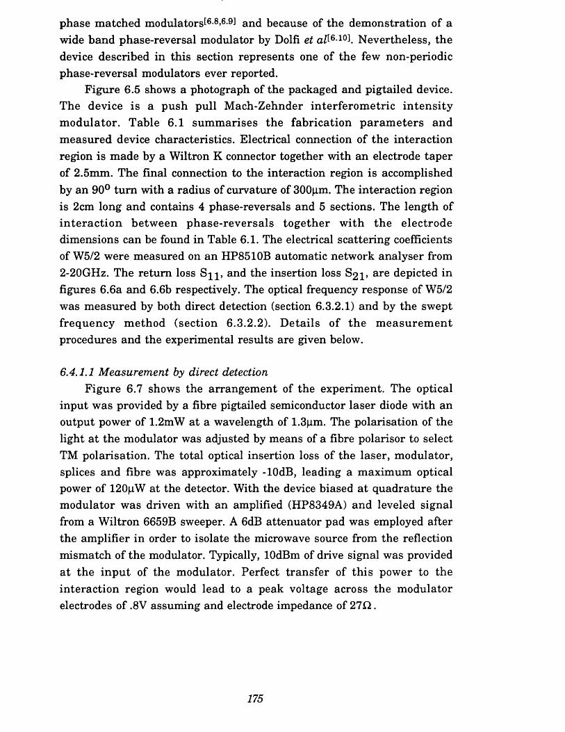
phase matched modulators^6'8’6'9] and because of the demonstration of a wide band phase-reversal modulator by Dolfi et afi6-10\ Nevertheless, the device described in this section represents one of the few non-periodic phase-reversal modulators ever reported.
Figure 6.5 shows a photograph of the packaged and pigtailed device. The device is a push pull Mach-Zehnder interferom etric in tensity modulator. Table 6.1 summarises the fabrication param eters and measured device characteristics. Electrical connection of the interaction region is made by a Wiltron K connector together with an electrode taper of 2.5mm. The final connection to the interaction region is accomplished by an 90° turn with a radius of curvature of 300pm. The interaction region is 2cm long and contains 4 phase-reversals and 5 sections. The length of in teraction between phase-reversals together with the electrode dimensions can be found in Table 6.1. The electrical scattering coefficients of W5/2 were measured on an HP8510B automatic network analyser from 2-20GHz. The return loss and the insertion loss S21, are depicted in figures 6.6a and 6.6b respectively. The optical frequency response of W5/2 was measured by both direct detection (section 6.3.2.1) and by the swept frequency method (section 6.3.2.2). Details of the m easurem ent procedures and the experimental results are given below.
6.4.1.1 Measurement by direct detectionFigure 6.7 shows the arrangement of the experiment. The optical
input was provided by a fibre pigtailed semiconductor laser diode with an output power of 1.2mW at a wavelength of 1.3pm. The polarisation of the light a t the modulator was adjusted by means of a fibre polarisor to select TM polarisation. The total optical insertion loss of the laser, modulator, splices and fibre was approximately -lOdB, leading a maximum optical power of 120pW at the detector. With the device biased at quadrature the modulator was driven with an amplified (HP8349A) and leveled signal from a Wiltron 6659B sweeper. A 6dB attenuator pad was employed after the amplifier in order to isolate the microwave source from the reflection mismatch of the modulator. Typically, lOdBm of drive signal was provided at the input of the modulator. Perfect transfer of this power to the interaction region would lead to a peak voltage across the modulator electrodes of .8V assuming and electrode impedance of 210..
175
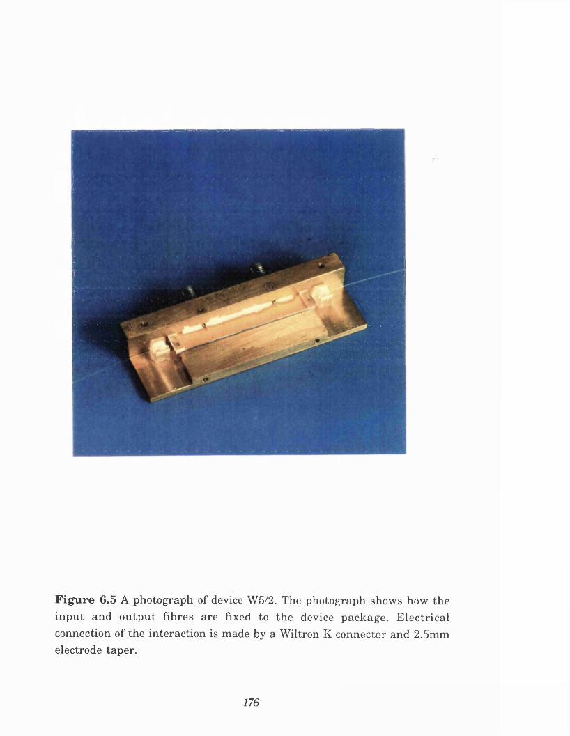
F igu re 6.5 A photograph of device W5/2. The photograph shows how the in p u t and o u tp u t fibres are fixed to the device package. E lectrical connection of the interaction is made by a W iltron K connector and 2.5mm electrode taper.
176
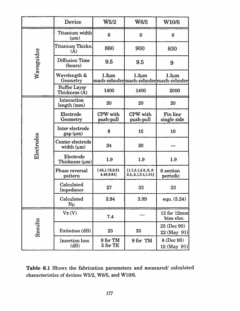
Device W5/2 W6/5 W10/6
Titanium width (pm) 6 6 6
<DTitanium Thickno
(A) 880 900 830• pH
aQ>
Diffusion Time (hours)
9.5 9.5 9
£ Wavelength & Geometry
1.3pmmach-zehnder
1.3|immach-zehnder
1.3pmmach-zehnder
Buffer Layer Thickness (A) 1400 1400 2000
Interaction length (mm) 20 20 20
ElectrodeGeometry
CPW with push-pull
CPW with push-pull
Fin line single side
ma>n3OuCJ
Inter electrode gap (pm) 8 15 10
Center electrode width (pm) 24 20 —
<Ds Electrode
Thickness (pm) 1.9 1.9 1.9
Phase reversal pattern
[.56,1.73,3.314.49,9.91]
[1.7,3.1,5.9,.9,.8 2.5,.5,1,2.4,1.01]
6 section periodic
CalculatedImpedance 27 33 33
CalculatedNp
3.94 3.99 eqn. (5.24)
U1
Vtc(V) 7.4 — 13 for 12mm bias elec.
2Ul<D
P hExtintion (dB) 25 25
25 (Dec 90) 22 (May 91)
Insertion loss (dB)
9 for TM 5 for TE
9 for TM 8 (Dec 90) 15 (May 91)
T able 6.1 Shows the fabrication param eters and measured/ calculated characteristics of devices W5/2, W6/5, and W10/6.
177
S n I og MAGREF 0 . 0 dB
5 . 0 d B /
—!
1 —
START 2 . 0 0 0 0 0 0 0 0 0 GHz STOP 2 0 . 0 0 0 0 0 0 0 0 0 GHz
S2 1 l o g MAGREF - 1 0 . 0 dB
2 . 0 d B /
I—1___1 ____1
START 2.000000000 GHz STOP 20.000000000 GHz
F ig u re 6.6 (a) shows the measured return loss of W5/2. Note tha t the enhanced transmission a t 9GHz is due to the electrode taper which acts as a quarter wave transformer, (b) shows the measured insertion loss. The measurements were made on an HP8510B network analyser.
178
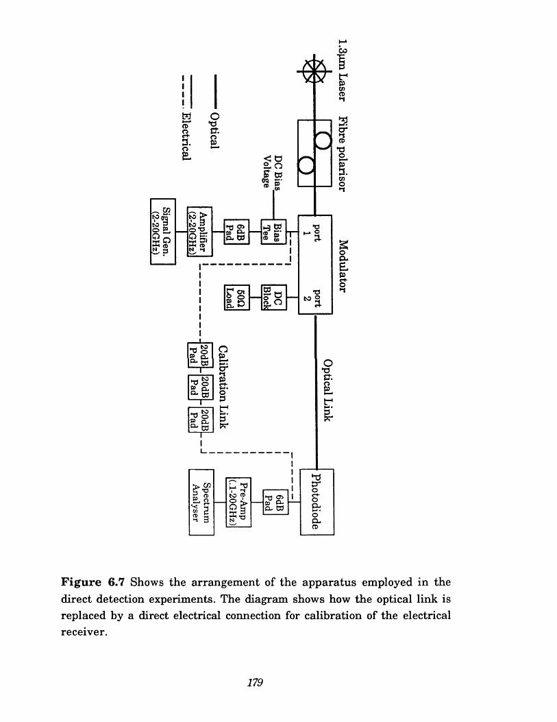
CO
CO
£- O£ to
— 10 2o , O
u ^I -Ito 9
F ig u re 6.7 Shows the arrangement of the apparatus employed in the direct detection experiments. The diagram shows how the optical link is replaced by a direct electrical connection for calibration of the electrical receiver.
179
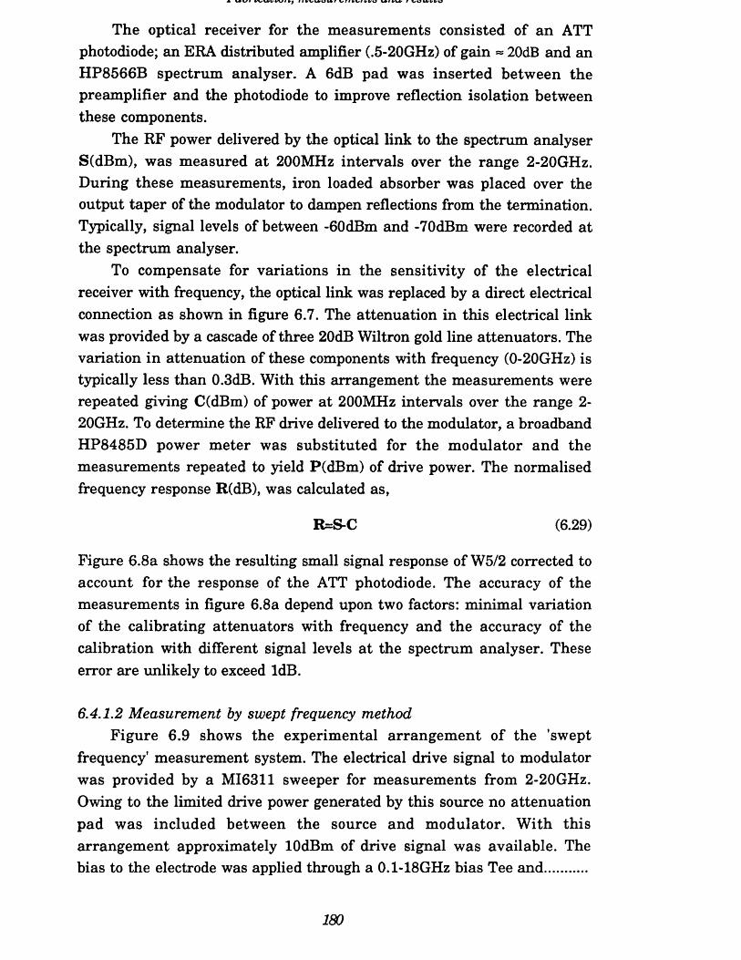
A \M rSS! IVUt'IA/f Vy I U /»U ' I VU U'l'I'O
The optical receiver for the measurements consisted of an ATT photodiode; an ERA distributed amplifier (.5-20GHz) of gain * 20dB and an HP8566B spectrum analyser. A 6dB pad was inserted between the preamplifier and the photodiode to improve reflection isolation between these components.
The RF power delivered by the optical link to the spectrum analyser S(dBm), was measured a t 200MHz intervals over the range 2-20GHz. During these measurements, iron loaded absorber was placed over the output taper of the modulator to dampen reflections from the termination. Typically, signal levels of between -60dBm and -70dBm were recorded at the spectrum analyser.
To compensate for variations in the sensitivity of the electrical receiver with frequency, the optical link was replaced by a direct electrical connection as shown in figure 6.7. The attenuation in this electrical link was provided by a cascade of three 20dB Wiltron gold line attenuators. The variation in attenuation of these components with frequency (0-20GHz) is typically less than 0.3dB. With this arrangement the measurements were repeated giving C(dBm) of power at 200MHz intervals over the range 2- 20GHz. To determine the RF drive delivered to the modulator, a broadband HP8485D power meter was substituted for the modulator and the measurements repeated to yield P(dBm) of drive power. The normalised frequency response R(dB), was calculated as,
R=S-C (6.29)
Figure 6.8a shows the resulting small signal response of W5/2 corrected to account for the response of the ATT photodiode. The accuracy of the measurements in figure 6.8a depend upon two factors: minimal variation of the calibrating attenuators with frequency and the accuracy of the calibration with different signal levels at the spectrum analyser. These error are unlikely to exceed ldB.
6.4.1.2 Measurement by swept frequency methodFigure 6.9 shows the experimental arrangem ent of the ’swept
frequency’ measurement system. The electrical drive signal to modulator was provided by a MI6311 sweeper for measurements from 2-20GHz. Owing to the limited drive power generated by this source no attenuation pad was included between the source and modulator. With this arrangem ent approximately lOdBm of drive signal was available. The bias to the electrode was applied through a 0.1-18GHz bias Tee and..........
180
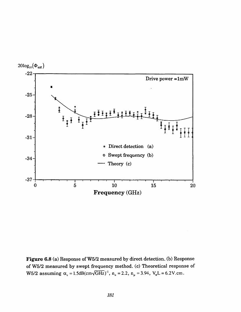
20iog10(a>difr)
-22Drive power =lmW
-25-
-28-
-31-
* Direct detection (a)
o Swept frequency (b)
_ Theory (c)-34-
-370 5 10 15 20
Frequency (GHz)
Figure 6.8 (a) Response of W5/2 measured by direct detection, (b) Response of W5/2 measured by swept frequency method, (c) Theoretical response of W5/2 assuming a c = 1.5dB(cmVGHz)'\ nc =2.2, nM =3.94, VKL = 6.2V.cm.
181
SO Q
.-g W
toa O
SOEpC-*“O►1
F ig u re 6.9 A schematic diagram of the swept frequency system used to measure the response of W5/2.
182
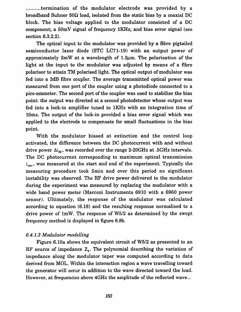
term ination of the modulator electrode was provided by abroadband Suhner 50ft load, isolated from the static bias by a coaxial DC block. The bias voltage applied to the modulator consisted of a DC component; a 50mV signal of frequency lKHz; and bias error signal (see section 6.3.2.2).
The optical input to the modulator was provided by a fibre pigtailed semiconductor laser diode (STC LC71-19) with an output power of approximately 2mW at a wavelength of 1.3pm. The polarisation of the light a t the input to the modulator was adjusted by means of a fibre polarisor to attain TM polarised light. The optical output of modulator was fed into a 3dB fibre coupler. The average transmitted optical power was measured from one port of the coupler using a photodiode connected to a pico-ammeter. The second port of the coupler was used to stabilise the bias point: the output was directed at a second photodetector whose output was fed into a lock-in amplifier tuned to lKHz with an integration time of 10ms. The output of the lock-in provided a bias error signal which was applied to the electrode to compensate for small fluctuations in the bias point.
With the modulator biased a t extinction and the control loop activated, the difference between the DC photocurrent with and without drive power Ai^, was recorded over the range 2-20GHz at .5GHz intervals. The DC photocurrent corresponding to maximum optical transmission imax> was measured at the start and end of the experiment. Typically the measuring procedure took 5min and over this period no significant instability was observed. The RF drive power delivered to the modulator during the experiment was measured by replacing the modulator with a wide band power meter (Marconi Instruments 6910 with a 6960 power sensor). Ultimately, the response of the modulator was calculated according to equation (6.18) and the resulting response normalised to a drive power of lmW. The response of W5/2 as determined by the swept frequency method is displayed in figure 6.8b.
6.4.1.3 Modulator modellingFigure 6.10a shows the equivalent circuit of W5/2 as presented to an
RF source of impedance Zs. The polynomial describing the variation of impedance along the modulator taper was computed according to data derived from MOL. Within the interaction region a wave travelling toward the generator will occur in addition to the wave directed toward the load. However, a t frequencies above 4GHz the amplitude of the reflected wave...
183
4IQ Zc = 41.1-2.9x +4.7x2-2.3x3
Z„ = 21.20.
Interaction Length 2cm
ElectrodeTaper2.5mm
(a)
Z„ = 2120.
# Signifies boundaries of modulator electrode
Xa Interaction Length 2cm ^|4
(b)
F igu re 6.10 (a) shows the equivalent circuit of W5/2. The impedance of the transmission line was calculated by MOL. Note tha t 0<x<2.5mm in the polynomial describing the taper impedance, (b) shows how (a) can be simplified because of the modulator insertion loss and low termination m ism atch.
184
* i » v r u i • ' i * i
(generator bound) is negligible (ie 20dB down on tha t transmitted intothe interaction region) as a consequence of the electrode insertion loss and the small return loss of the electrode termination. Consequently, above 4GHz we may assume that the electrode is correctly terminated with a load impedance of Zc. Furthermore, if the effect of the taper is also ignored, at worst only a .5dB error in the transmitted electrical power is incurred. Therefore, the equivalent circuit of figure 6.10a may be simplified to that of figure 6.10b. In this case, the peak amplitude of the voltage wave V *, transmitted into the interaction region is simply,
< 6 ' 3 0 >
Provided that both the propagation constant of the electrical wave and the electrooptic transducer coefficient are known, it is a simple m atter to calculate according to equations (6.30) and (3.4). The microwave effective index and impedance within the interaction region were computed by MOL as 3.94 and 27.20, respectively. The electrooptic overlap factor was computed for frequencies above and below the acoustic resonance assuming an optical mode profile of 4pm (FWHM depth) by 5pm (FWHM width). The computations lead to estimates of the V^.L product for W5/2 of 5.8V.cm and 6.2V.cm- the higher value referring to frequencies above the acoustic resonance. These values are consistent with the measured DC of W5/2. From the experimental measurement of S21 (figure 6.6b) a frequency dependent loss coefficient of a c = 1.5dB(cm.VGHz)1 was derived. Using this data Odiff was calculated against frequency assuming a drive power of lmW (that is Es = 0.63Vwith Zs = 50Q). The theoretical value of d>diff is plotted in figure 6.8c.
6.4.1.4 DiscussionFigure 6.8 shows that the experimental data is in good agreement
with theory with only slight deviations apparent below 4GHz and above 15GHz. Both the absolute value Odiff and its variation with frequency have been successfully modelled. Moreover, it is apparen t th a t our experimental measurements are consistent as both the direct detection and the swept frequency measurements are in excellent agreement.
At 20GHz the RF power required for complete on-off switching of W5/2 is approximately 33dBm. This figure compares unfavourably with conventional CPW modulators on X cut material. These devices typically require 30dBm of drive signal. However, the phase-reversal pattern of
185
W5/2 was selected under the assumption of a loss coefficient given by a c =0.7dB(cm.VGHz) . Consequently, W5/2 does not represent an optimal design as the m easurem ent of S21 suggests a loss coefficient of a c = 1.5dB(cm.VGHz) . We have redesigned electrode patterns assuming the experimental loss coefficient. These calculations suggest tha t a device exhibiting a flat frequency response (+/-ldB) from 2-20GHz with a switching power of approximately 30dBm at 20GHz is readily attainable. However, th is performance must be contrasted with th a t of phase matched devices which typically require 22dBm of drive power for on-off switching at 20GHz!
6,4.2 An equalising phase-reversal modulator: device W6/5In chapter 3 of this thesis the equalisation of a fast photodiode by a
predistorting phase-reversal modulator was considered. In this section the construction and experimental characterisation of an equalising device is presented.
Figure 6.11 shows a photograph of the packaged and pigtailed device. The device is a push-pull Mach Zehnder interferom etric intensity modulator. Table 6.1 summarises the fabrication param eters and measured device characteristics. Electrical connection is made by an SMA connector together with a constant impedance, 1cm electrode taper and bend. The interaction region is 2cm long and contains 9 phase- reversals and 10 section lengths. The electrical scattering parameters were measured on a HP8510B network analyser from 2-20GHz. The return loss S ^ , an( insertion loss S21, are shown in figures 6.12a and 6.12b respectively. The package and electrode geometry (but not the phase- reversal pattern) of W6/5 were designed during in a previous research program by DC Erasme[6,11l We adopted this design so that experimental m easurements of a c and could be incorporated into the design procedure described in chapter 3.
The m agnitude of the small signal optical frequency response of W6/5 was measured by direct detection, and the experimental results are described below.
6.4.2.1 Measurement by direct detectionThe experimental procedure employed in these measurements was
the same as that described in section 6.4.1.1. During the measurements iron loaded absorber was placed over the output taper of the modulator to dampen reflections from the termination. Figure 6.13a shows the............
186
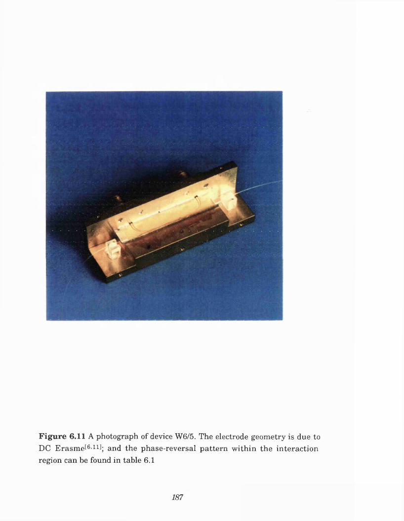
F i g u r e 6 .1 1 A photograph of device W6/5. The electrode geometry is due to DC E rasm el611 ; and the phase-reversal p a tte rn w ith in th e in te rac tion region can be found in table 6.1
187
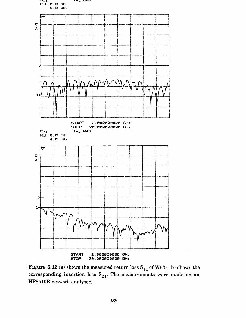
^11REF 0 . 0 dB
5 . 0 d B /
i p g
IV | !
!
1 ! T ---1ii __"1"'1)i _
T 'i
~ T ~ '
i 1
i
11i J !
. . L !ii |
i11i1iii11
I! *1
ii i
. 1 1i i! !-
i ^ Ia r\ L aW\ I \ l\ A / \. A / V. (\
I i n i
1---------Ir H-
S 2 1REF 0 . 0 dB
4 . 0 d B /
START 2 . 0 0 0 0 0 0 0 0 0 GHz STOP 2 0 . 0 0 0 0 0 0 0 0 0 GHz
l o g MAG
START 2 . 0 0 0 0 0 0 0 0 0 GHz STOP 2 0 . 0 0 0 0 0 0 0 0 0 GHz
F ig u re 6.12 (a) shows the measured return loss S-q of W6/5. (b) shows the corresponding insertion loss S2i- The measurements were made on an HP8510B network analyser.
188
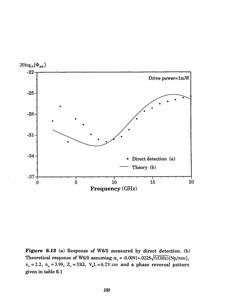
201og10(<I>diff)-22
Drive power=lmW
-25-
-28-
-31-
-34- * Direct detection (a)
“ Theory (b)
-3720151050
Frequency (GHz)
F ig u re 6.13 (a) Response of W6/5 measured by direct detection, (b) Theoretical response of W6/5 assuming a c = -0.0091+.0 2 2 5 (GHz) (Np/mm), n0=2.2, n = 3.99, Zc=33Q, V1tL = 6.2V.cm and a phase reversal pattern given in table 6.1
189
resulting small signal response of W6/5 corrected to account forthe response of the ATT photodiode. By replacing the electrical receiver and modulator drive in figure 6.7 with ports 1 and 2 of a network analyser the phase response of the modulator ZO could be determined (after deconvolution of the photodiode response).
6.4.2.2 Modulator modellingAs in section 6.4.1.3 the modulator was assum ed correctly
terminated. Consequently, the equivalent circuit of W6/5 is given by figure 6.10b. Using MOL the effective index and electrode impedance within the interaction region of W6/5 were calculated as 3.99 and 330 respectively. The electrode taper was judged to have negligible effect as the calculated impedance was constant along its length and equal to 310. From figure 6.12b it is apparent that the electrode loss coefficient is consistent with a c = -0.0091+.0225^f(GHz)(Np/mm), which was used in the design procedure. No estimate of the over-lap parameter was made for W6/5 as only the variation of <I>diff with frequency was sought. The theoretical response of the modulator was calculated according to equation (3.4) and is displayed in figure 6.13b.
6.4.2.3 DiscussionFigure 6.13 shows th a t the agreem ent between theory and
experiment is acceptable from approximately 7GHz. Below 7GHz the measured optical response exhibits large resonances owing to reflections within the package. These resonances are quite pronounced and both Sn and S2i are also seen to exhibit the same feature. The resonances seem to originate at the CPW to Coax interface. It is possible that the hole through which the coax pin protrudes into the package is too small leading to a section of very low impedance line which affects the CPW launch.
Presently, we have not measured the phase response of W6/5. However, equation (3.4) shows that the variation with frequency of both Odiffand Zd> depend upon the same parameters: the velocity mismatch, electrical attenuation coefficient, and the pattern of phase-reversals in the in teraction region. Consequently, it would be expected th a t a measurement of ZO would also follow theory provided that no significant phase distortion is introduced by the taper.
It is important to note that under ideal circumstances (ie a good package) W6/5 would not equalise the diode described in section 3.3.4 as
190
W6/5 was mistakenly designed to equalise the complex conjugate of the diode response! Nevertheless, W6/5 still represents the first example of an 10 modulator whose complex response has been designed for the purpose of equalisation.
6.4.3 A m illim etre wave optical modulator: device W10I6Device W10/6 is an example of the fin line structure th a t was
described in section 5.3. Figure 6.14 shows a photograph of the split block in which the modulator is housed. Unfortunately, we could not photograph the lithium niobate substrate inside the housing, without destroying the device. However, internally the substrate is arranged as depicted in figure 5.13.
Device W10/6 is a one sided Mach-Zehnder interferometric intensity modulator. Table 6.1 summarises the fabrication param eters and measured device characteristics. Electrical connection of the interaction region is made by an earthed, 8mm fin line taper whose contour is given by equation (5.26). The interaction region is 2cm long and contains 5 periodic phase-reversals and six section lengths. An external bias electrode of 12mm is applied to one arm of the Mach Zehnder. The bias electrode is separated from the interaction region by 112pm. The substrate thickness is 120pm and is secured in the center of the housing (ie 3.496mm from a narrow wall) by an acetone soluble resin. The only significant difference between the structure described in chapter 5 and W10/6 is that glass blocks (.5 by 2 by 2mm) are expoxied to the substrate for pigtail stabilisation. The electrical scattering parameters S ^ ; S21; and S22 were measured on an HP8510B network analyser and are displayed in figure 6.15. The return loss from both ports 1 and 2 should be equal as the modulator electrode is symmetric. However, because of some missing metalisation on port 2 of W10/6, S j j and S22 are considerably different. As a result, S21 is distorted, though the electrode loss may still be estimated as port 1 is effectively isolated from the mismatch a t port 2 owing to the large electrical loss of the interaction region.
The optical response of W10/6 was measured by both the swept frequency technique and by the optical heterodyne detection scheme described in 6.3.2.4. Details of the measurement procedures and the experimental results are given below.
6.4.3.1 Measurement by swept frequency methodFigure 6.16 shows the experimental arrangement of the.................
191
F i g u r e 6 .1 4 Shows a photograph of the split block housing in which W10/6 is contained.
192
REF 0.0 dB 1 5 . 0 d B /V - 5 . 9 9 7 8 dB
START 2 6 . 0 0 0 0 0 0 0 0 0 GHz STOP 4 0 . 0 0 0 0 0 0 0 0 0 GHz
S2 1 log MAGREF 0 . 0 dB
5 . 0 d B / - 1 6 . 9 3 4 dB
START 26.000000000 GHz STOP 40.000000000 GHz
F igure 6.15 (a) shows the measured return loss of from port 1 of W10/6. (b) shows the corresponding insertion loss S21 from port 1 to port 2. The measurements were made on an HP8510B network analyser
193
2 r
> n
*
REF 0 . 0 dB5.0 dB/
-16.789 dBV
START 26.000000000 GHz STOP 40.000000000 GHz
F ig u re 6.15c Shows the measured return loss from port 2 of W10/6. The measurements were made on an HP8510B network analyser.
194
tn r-H fJL,®3 3
T T
to W0 5 *X)CT W i 0 5
© OlQ W 10db couplers
cn
toOu
£ O S O
CO
tr103COCD•-1
*1M*crCD*13ooT3.03O►1
oCLE-0)o►1
F ig u re 6.16 Shows a schematic diagram of the swept frequency system used to measure the response of W10/6
195
measurement system. This arrangement differs from figure 6.9 inthat the bias is applied directly to the bias electrode of W10/6 and that the electrical drive power is conducted along rectangular waveguide. The electrical drive to modulator was provided by an HP3675B backward wave oscillator for measurements from 26.5-40GHz. This source was isolated from the modulator by a Hughes 45111F-2000 (ser. 309) isolator. M easurements of both reflected and incident microwave power were made using two Flann 22131-10 lOdB couplers together with an Marconi Instrum ents 6500 scalar analyser with 6514 power sensors in the arrangem ent shown in figure 6.16. To determine the actual power delivered to the modulator, the response of the couplers were measured on an HP8510B network analyser. The correction factor which was applied to the power measured at port 3 to determine the power delivered to port 2 (port 1 to port 2 is 'thru' and port 4 is terminated) was 9.2dB+.18(F-26.5)dB; where F is in GHz. Typically, less than 7dbm of drive signal was available.
The optical input to the modulator was provided by a fibre pigtailed semiconductor laser diode (STC LC71-19) with an output power of approximately 2mW at a wavelength of 1.3pm. The polarisation of the light a t the input to the modulator was adjusted by means of a fibre polarisor to attain minimum drive voltage. The optical output of the modulator was fed into a 3dB fibre coupler. The insertion loss of the system through to one port of the output coupler was approximately -12dB. The average transmitted optical power was measured from one port of the coupler using photodiode connected to a pico-ammeter. The second port of the coupler was used to stabilise the bias point as described in section 6.4.1.2.
With the modulator biased a t extinction and the control loop activated, AIrf, was recorded together with the incident electrical drive power over the range 26.5-40GHz at .5GHz intervals. The DC photocurrent corresponding to maximum optical transmission i ^ , was measured at both the start and end of the experiment to assess stability. Ultimately, the response of the modulator was calculated according to equation (6.18) and the results normalised to a drive power of lmW. Figure 6.17a shows d>diff as determined by the swept frequency technique. Figure 6.18 shows the variation of Ai^ with electrical drive signal. The la tter measurements were performed at a frequency of 30GHz and the data show that Ai^ is proportional to drive power as would be expected from equation (6.18).
196
201og10(C>dlf()
-27Drive power=lmW
-30-
-33-
-36-
-39-
-42-
-45-Swept frequency (a)Optical down-conversion (b) Theory (c)
-48-
-51-
-54-
-5726 28 30 32 34 36 38 40
Frequency (GHz)
F ig u re 6.17 (a) Response of W10/6 as determined by swept frequency, (b) Response of W10/6 as determined by optical down-conversion (c) Theoretical respnse of W10/6 assuming a c = LbdBCcmVGHz)'1, n0=2.2 n0 =3.36 + O.Olf(GHz) <t>p = 0.17(rad/ mmVWatt).
197
Ai^Arb. U)0.7
0.6
0.5
0.4
0.3
0.2
0.1
00 1 2 3 4 5
Drive power (mW)
im«=880max // '
f = 30GHz // s
y/
/Ay
Figure 6.18 Shows the variation of Ai^ verses drive power a t a frequency of 30GHz. The response is linear as would be expected from equation (6.18).
198
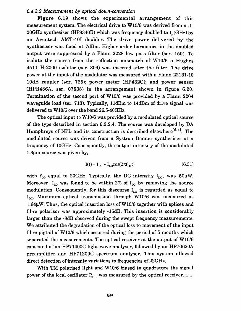
6.4.3.2 Measurement by optical down-conversionFigure 6.19 shows the experim ental a rrangem ent of th is
measurement system. The electrical drive to W10/6 was derived from a .1- 20GHz synthesiser (HP8340B) which was frequency doubled to f^(GHz) by an Aventech AMT-40I doubler. The drive power delivered by the synthesiser was fixed at 7dBm. Higher order harmonics in the doubled output were suppressed by a Flann 2228 low pass filter (ser. 150). To isolate the source from the reflection mismatch of W10/6 a Hughes 45111H-2000 isolator (ser. 309) was inserted after the filter. The drive power at the input of the modulator was measured with a Flann 22131-10 lOdB coupler (ser. 725); power meter (HP432C); and power sensor (HPR486A, ser. 07538) in the arrangem ent shown in figure 6.20. Termination of the second port of W10/6 was provided by a Flann 2204 waveguide load (ser. 713). Typically, lldB m to 14dBm of drive signal was delivered to W10/6 over the band 26.5-40GHz.
The optical input to W10/6 was provided by a modulated optical source of the type described in section 6.3.2.4. The source was developed by DA Humphreys of NPL and its construction is described elsewhere[64 . The modulated source was driven from a Systron Donner synthesiser at a frequency of 10GHz. Consequently, the output intensity of the modulated 1.3pm source was given by,
I(t) = Idc + ILOc°s(27cfLOt) (6.31)
with equal to 20GHz. Typically, the DC intensity 1^, was 50pW. Moreover, 1^ was found to be within 2% of 1^ by removing the source modulation. Consequently, for this discourse 1^ is regarded as equal to IDC. Maximum optical transmission through W10/6 was measured as 1.64pW. Thus, the optical insertion loss of W10/6 together with splices and fibre polarisor was approximately -15dB. This insertion is considerably larger than the -8dB observed during the swept frequency measurements. We attributed the degradation of the optical loss to movement of the input fibre pigtail of W10/6 which occurred during the period of 5 months which separated the measurements. The optical receiver a t the output of W10/6 consisted of an HP71400C light wave analyser, followed by an HP70620A preamplifier and HP71200C spectrum analyser. This system allowed direct detection of intensity variations to frequencies of 22GHz.
With TM polarised light and W10/6 biased to quadrature the signal power of the local oscillator Pffl was measured by the optical receiver......
199
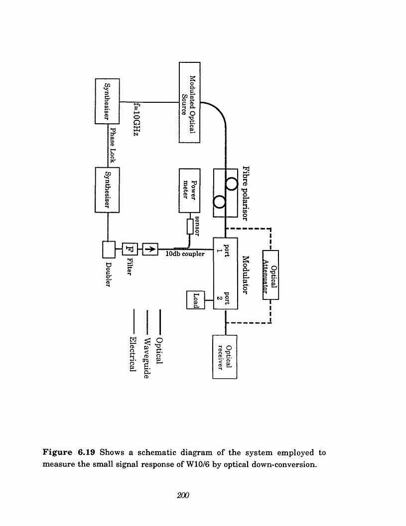
lOdb coupler
<D oO xo<<6
oso
•-1
F ig u re 6.19 Shows a schematic diagram of the system employed to measure the small signal response of W10/6 by optical down-conversion.
200
1 6 : 3 6 : 4 3 1 6 . 0 0 . 1 9 9 1! RL - 9 5 . 0 0 dBm MKR # 1 a FRQ 0 Hz*RTTE
5 . 0 01 0 0 d E
d B / D IIBU a L [GHTWf
- 2 9 . G I UE Or
5 dB Ti CRL
RUGHARK
>UR H: r a
. 5 6 n u SRMP LE
0 Hz - 2 9 . 55 dB1
P5 0
\f A
: C E N T E R 6 . 5 0 0 0 0 i i RB 2 1 5 Hz
0 0 0 GHz SPAN 2 0 . 0 0 UB 3 0 0 Hz ST 1 . 4 1 9
kHzs e c
F ig u re 6.20 Shows a typical measurement by optical down-conversion. With a modulation frequency of 26.5GHz and the local oscillator set at 20GHz a down-converted component occurs at 6.5GHz (trace V). Trace 'b' shows the effect of biasing W10/6 away from quadratu re toward maximum transmission.
201
Typically, -61dBm of power was obtained at the local oscillatorfrequency of 20GHz. Subsequently, f was adjusted from 26.5-39.99GHz at .5GHz intervals. At each frequency, the signal power of the down converted component Pf fli) was measured together with the electrical drive signal applied to W10/6. Figure 6.20 shows a typical measurement. In this example the is 26.5GHz and the local oscillator frequency is 20GHz. Consequently, a down converted signal is observed a t the difference frequency of 6.5GHz. The signal power of this down converted component P65GHz is -85dBm. The second trace of figure 6.20 (trace 'b') shows P65GHz with the bias of W10/6 adjusted away from quadrature towards maximum transmission. With this bias, W10/6 produces only even harmonic of and therefore only a small signal is observed at 6.5GHz. Clearly, the observation of the down converted component and its behaviour with bias provides direct confirmation of electrooptic activity in W1Q/6. The example shows that even with the high optical loss of W10/6 almost 30dB of dynamic range is available for measurement a t 26.5GHz. This dynamic range could be considerably improved by amplification of the output of the modulated optical source.
As described in section 6.3.2.4, the optical receiver must be calibrated to account for variations in the sensitivity of the receiver with frequency and signal power. To calibrate the optical receiver, an optical attenuator (HP8157A) was substituted for W10/6 as shown in figure 6.19. The local oscillator was tuned to each down converted frequency and the optical attenuation a down, required to reproduce both Pf fw recorded together with the corresponding DC optical intensity lockdown)- Typically, lockdown) was in the range 10-30nw. The error on these measurements was fixed at +/- 0.5nW (manufacturer's specification). Subsequently, the modulation depth Odiff was computed according to equation (6.28). Figure 6.17b shows the resulting variation of Odiff with assuming a constant drive power of lmW. Note that as only one arm of W10/6 is active, <X>diff corresponds to d>r
6.4.3.3 Modulator modellingThe return loss of W10/6 originates from both the electrode taper and
the dielectric discontinuity corresponding to the abrupt introduction of the substrate within the rectangular housing. In section 5.3 the reflection of the electrode taper was shown to be negligible in comparison to that generated by the dielectric discontinuity. The la tter source of reflection was estimated at -lOdB. The measured return loss S ^ , seems broadly in agreement with this estimate, being less than -lOdB across the band.
202
However, it is important to note tha t our estimate does not include the effect of the glass block epoxied to the substrate at the dielectric interface. Moreover, the measurement of S22 reveals a considerably different response than would be predicted from theory. The discrepancy between
and S22 may occur as a result of defects in the taper metalisation at port 2.
From the experimental measurements of S ^ ; Sg2 and an estimate of the attenuation coefficient was made as a c = 1.6dB(cm.VGHz) \ This estimate was made on the assumption of negligible loss occuring in the electrode taper. The propagation constant of the electrical wave within the interaction was estimated numerically through MOL and is given by equation (5.27). The electrooptic over-lap was estimated for a variety of waveguide mode sizes and the results are depicted in figure 5.25. Here, we assume a mode size of 4pm (FWHM depth) by 5pm (FWHM width). This mode size is consistent with both the fabrication parameters and previous experimental results. Using this data together with equation (3.4), <E>diff was computed for W10/6 assuming a drive power of lmW. The resulting response is shown in figure 6.17c.
6.4.3.4 DiscussionFigure 6.17 shows th a t the theoretical variation of Odiff with
modulating frequency is consistent with experimental observations: the peak response occurs a t approximately 30GHz and rolls off rapidly thereafter. The data from the swept frequency method is in good agreement with both the shape and magnitude of the theoretical response. Deviation from theory is only apparent above 39GHz where the experimental errors in the measurements are large. The swept frequency data show a maximum phase efficiency of 60°(Vw) occuring a t a frequency 29GHz.
It is also clear from figure 6.17 th a t the optical heterodyne measurements are in poor agreement with both theory and the swept frequency data. Though the heterodyne measurement replicates the shape of the theoretical curve, the peak phase efficiency is only 30° (Vw) . This discrepancy can in no way be explained by experimental error. Moreover, if the observed electrical loss is 'split' between the taper and interaction region, no better agreement results. Indeed, the theoretical response still agrees with the swept frequency data.
Previously, we have seen tha t the swept frequency method has produced measurements tha t are consistent with other experimental
203
methods. We have also seen in figure 6.18 th a t the swept frequency measurements are internally consistent, inasmuch tha t the variation of Ai^ is directly proportional to drive power. Moreover, i t m ust be emphasised tha t the heterodyne experiment described above has never been reported. Therefore, measurement of a known modulator response is required to support the experimental procedure tha t we have adopted. Furthermore, the measurements described in section 6.4.3.2 were made on a single day and under unique conditions. Additional experimentation under different conditions would therefore be highly desirable. Consequently, we believe that the swept frequency data provide a more reliable measure of the response of W10/6 than do the heterodyne data. However, the heterodyne experiments do provide irrefutable evidence of electrooptic activity in W10/6.
One possible explanation for the discrepancy between our data sets is that the polarisation of the input light to W10/6 may not have been TM during the heterodyne experiments. At UCL the bias to W10/6 was modulated with a large AC signal and the output intensity monitored with a photodiode and oscilloscope. To select TM polarisation the fibre polarisor was adjusted to achieve minimum drive voltage. At NPL we optimised the extinction of W10/6 on the basis that the insertion loss of TM exceeded tha t of TE and that we had observed a better extinction with TM polarised light at UCL. However, this procedure did not take account of the change in optical coupling which occurred betw een the measurements a t UCL and NPL.
6.5 Chapter Summary
This chapter has been concerned with a description of the experimental work undertake during the period of our research. We have been concerned with the fabrication and m easurem ent of titanium indiffused lithium niobate intensity modulators. For this type of device we described the most important techniques of fabrication.
In section 6.3 we examined the most common methods of modulator calibration. In particular, we studied those techniques th a t are particularly suited to very high frequency modulators (30GHz and above). To this end we developed expressions to describe the action of both phase and intensity modulators under harmonic excitation in term s of the spectrum of sidebands that they generate. We considered direct detection
204
with a fast photodiode, the swept frequency method, and novel method of calibration by optical down-conversion. This la tte r method of measurement has received no attention in the literature.
Section 6.4 described the experimental m easurem ent of three different phase-reversal modulators which we constructed. The first device considered was a five section non-periodic phase-reversal modulator. The electrode on this device was designed, using the techniques described in chapter 3 to exhibit an efficient response from 2- 20GHz. The modulation response of the device was measured by both direct detection and the swept frequency method. Excellent agreement was obtained between the experimental data and a theoretical model which incorporated data computed using the full-wave analysis described in chapter 4. Unfortunately, the device did not exhibit a particularly efficient response owing to inaccuracies in the data employed during the selection of the electrode pattern. Nevertheless the device is still one of the few non-periodic phase-reversal modulators ever reported.
A second type of non-periodic phase-reversal m odulator was described in section 6.4.2. This device was designed to equalise a high speed photodiode. The modulation response of the device was measured by direct detection and found to be in good agreement with theory. However, full characterisation of the optical link incorporating both the equalising modulator and photodiode was not completed owing to resonance in the modulator packaging. The equalising phase-reversal modulator described in this chapter is the first of its type ever reported.
The final device described in this chapter was a millimetre wave modulator constructed from fin line. Measurements of the modulation response were made to frequencies as high as 40GHz by both swept frequency and by optical down-conversion. Agreement with theory was excellent in the case of swept frequency and a peak phase shift of 60° (Vw) 1 at a frequency of 29GHz was obtained. Unfortunately, the measurements by optical down-conversion differed from both theory and the swept frequency data. Though the modulation response had the correct shape, the peak phase shift was estimated at only 30°(Vw) . The discrepancy between the two measurements can not be explained by experimental error. We concluded tha t further experimentation was required as the optical down-conversion m easurem ents, though confirming electrooptic activity, were unsubstantiated and preliminary. The fin line modulator described above is the first of its type ever reported.
205
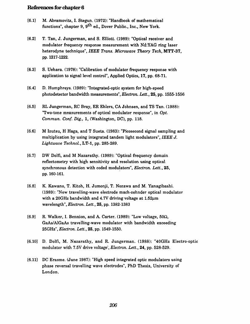
References for chapter 6
[6.1] M. Abramovitz, I. Stegun. (1972): "Handbook of mathematical functions", chapter 9, 9 ^ ed.f Dover Public., Inc., New York.
[6.2] T. Tan, J. Jungerman, and S. Elliott. (1989): "Optical receiver and modulator frequency response measurement with Nd:YAG ring laser heterodyne technique", IEEE Trans. Microwave Theory Tech, MTT-37, pp. 1217-1222.
[6.3] S. Uehara. (1978): "Calibration of modulator frequency response with application to signal level control", Applied Optics, 17, pp. 68-71.
[6.4] D. Humphreys. (1989): "Integrated-optic system for high-speed photodetector bandwidth measurements", Electron. Lett., 25, pp. 1555-1556
[6.5] RL Jungerman, RC Bray, ER Ehlers, CA Johnsen, and TS Tan. (1988): "Two-tone measurements of optical modulator response", in Opt.Commun. Conf. Dig., 1, (Washington, DC), pp. 118.
[6.6] M Izutsu, H Haga, and T Sueta. (1983): "Picosecond signal sampling and multiplication by using integrated tandem light modulators", IEEE J.Lightwave Technol., LT-1, pp. 285-289.
[6.7] DW Dolfi, and M Nazarathy. (1989): "Optical frequency domain reflectometry with high sensitivity and resolution using optical synchronous detection with coded modulators", Electron. Lett., 25,pp. 160-161.
[6.8] K. Kawano, T. Kitoh, H. Jumonji, T. Nozawa and M. Yanagibashi.(1989): "New travelling-wave electrode mach-zehnder optical modulator with a 20GHz bandwidth and 4.7V driving voltage at 1.52pm wavelength", Electron. Lett., 25, pp. 1382-1383
[6.9] R. Walker, I. Bennion, and A. Carter. (1989): "Low voltage, 50f2,GaAs/AlGaAs travelling-wave modulator with bandwidth exceeding 25GHz", Electron. Lett., 25, pp. 1549-1550.
[6.10] D. Dolfi, M. Nazarathy, and R. Jungerman. (1988): "40GHz Electro-optic modulator with 7.5V drive voltage', Electron. Lett., 24, pp. 528-529.
[6.11] DC Erasme. (June 1987): "High speed integrated optic modulators using phase reversal travelling wave electrodes", PhD Thesis, University of London.
206

Chapter 7
Summary and Future Work
7.1 Summary and Conclusions
7.2 Directions for Future Work
207
7.1 Summary and Conclusions
This thesis has been concerned with the analysis; fabrication and characterisation of titan ium indiffused lith ium niobate optical modulators for both broadband and bandpass applications. The objectives of this research were the demonstration of both a broadband modulator with a bandwidth 0-20GHz and a millimetre wave optical modulator operating above 30GHz. In the following section a brief summary of this thesis is presented. More detailed summaries of our work can be found at the end of each chapter.
One of the difficulties associated with the design of broadband modulators in conventional structures is the velocity mismatch that occurs between the interacting waves. Various methods of phase- matching have been proposed in the literature. Many of these techniques rely on the modification of the electrical transmission line to increase the percentage of power propagating in the air regions. As an alternative, and as a continuation of a previous research program, we investigated an artificial form of velocity matching using phase-reversal electrodes. In particular:
• we devised a frequency domain optimising strategy for the selection of phase-reversal electrode patterns.
• we examined various non-periodic phase-reversal p a ttern s and concluded that phase-reversal modulators offer little or no advantage over properly phase matched interactions in efficient wideband systems.
• we proposed the application of phase-reversal modulators for the equalisation of linear distortions occuring in high-speed fibre optic communication systems.
• we concluded th a t in the case of constant loss electrodes the equalisation procedure is quite general with no theoretical impediment to the design of a modulator with any real impulse response- though the efficiency of the resulting device might be low.
• we demonstrated theoretically, the equalisation of a high speed photodiode in a simple optical link by inclusion of a phase-reversal
208
modulator with a compensating response.
The application of phase-reversal modulators to the equalisation of linear distortions in fibre systems had received no attention prior to our work. It is im portant to note however, th a t predistorting electronic filters combined with conventional modulators may be able to achieve the same function and with greater efficiency.
The behaviour of a travelling-wave electrooptic modulator is largely determined by the characteristics of the transmission line forming the modulator electrode. Consequently, an important stage in the analysis or design of a modulator is the derivation of both the field profiles and propagation constants of all the electromagnetic modes that are supported by the modulator electrodes. For this purpose:
• we studied the quasi-static approximation and the application of conformal transforms to the derivation of the electrostatic field profiles.
• we examined the validity of the quasi-static approximation and developed a simple model to show the dependence of hybrid effects on the lateral dimensions of the electrodes.
• we emphasised the lim itations of the static approximation and described a more rigorous full-wave, hybrid mode analysis by the method of lines.
• we developed a model to allow analysis of planar waveguide structures incorporating 3 uniaxial, anisotopic dielectric layers and one isotropic layer; with 2 layers of thin metalisations. The model allowed the determination of all fields and propagation constants for all propagating modes.
• we confirmed the validity of our model though extensive comparisons with the literature.
• we discussed the approximations inherent to the full-wave analysis, and expressions were developed to determine important transmission line characteristics such as the loss coefficient.
An electrode geometry tha t is often employed in the design of
209
wideband modulators is the CPW. This electrode is commonly analysed under the static approximation to frequencies as high as 40GHz. We applied our full-wave model to the study of the CPW- although our purpose was not necessarily to uncover hybrid effects. In particular:
• we confirmed the validity of the quasi-static approximation in CPWs of small la teral dimension and highlighted the importance full-wave analysis in the region of the interface electrodes.
• we studied phase-matching in shielded CPW electrodes with thick buffer layers and showed by evaluating over-lap factors tha t Z cut devices are particularly unbalanced.
• we examined the variation of over-lap a t the acoustic resonance frequency of lithium niobate for a common CPW configuration and illustrated an ambiguity in the literature regarding the measurement ofV,.
• we emphasised the importance of including finite conductivity metalisations in models of transmission lines whose lateral dimensions are comparable to a skin depth.
An important objective of our research was the demonstration of an optical modulator operating above 30GHz. To this end we analysed a structure based upon a fin line which prior to our work had not been reported. Extensive modelling of the structure was undertaken, and in particular:
• we developed analytic expressions to ascertain the modal spectrum of a rectangular waveguide loaded with a uniaxial anisotropic dielectric.
• we performed a modal analysis of a discontinuity to determine the return loss of our modulator.
• we utilised the method of lines to characterise fin lines of various slot widths on an anisotropic substrate at frequencies between 26-40GHz.
• we estimated the phase velocity of the modulating electric field within the interaction region and calculated the electrooptic over-lap as a
210
function of waveguide mode size.
• we discussed a novel phase-matching technique which is particularly suited to the fin line optical modulator.
Our research has culminated in the fabrication and measurement of a number of high speed optical modulators. Specifically, during the experimental phase of our research:
• we examined different techniques of modulator calibration, including a novel method previously unreported. The technique employed optical down-conversion and is particularly suited to very high frequency measurements (30GHz and above).
• we fabricated and m easured two non-periodic phase-reversal modulators. The results agreed well with theory though neither device was particularly efficient.
• we fabricated a millimetre wave optical modulator constructed in a fin line geometry. Measurements of the modulation response were made to frequencies as high as 40GHz by both swept frequency and by optical down-conversion. Agreement with theory was acceptable in the case of the swept frequency measurements, and a peak phase shift of 60°±5°(Vw) was obtained a t frequency of 29GHz. This performance is comparable to that of other designs reported in the literature.
The performance of our millimetre wave modulator could be improved through a reduction in both the electrode loss and the optical mode size. Indeed, with a loss coefficient of a c = ldB(cm.VGHz) and an optical mode size of 2.1|imx5.0|im the phase efficiency could be improved from 60° (Vw) to approximately 100°(Vw) . Further, increases in efficiency could be obtained by inducing electrical resonance in the electrode. It must be emphasised however, that similar results could be obtained by using other electrode geometries in the interaction region (such as a CPW) and in this respect our device is no better than a more conventional design. The advantages of the fin line device are two fold. F irst the structure may be used with only minor modifications at frequencies in excess of 40GHz; and second; the fin line may be modified to allow a phase
211
matched interaction without the disadvantage of reduced electrooptic efficiency.
7.2 Directions for Future Work
Following this work a short term development would be the demonstration of a fin line device a t 60GHz. The device could be constructed simply by reducing the dimensions of housing to 3.6 x 1.8mm and increasing the number of phase-reversals in the interaction region. Assuming a loss coefficient of a c = ldB(cm.VGHz)1 and an optical mode size of 2.1pmx5.0|im a peak phase shift of approximately 80° (Vw) could be obtained.
An alternative design could be developed in which the electrical wave is phase matched by means of an electrode shield. We showed how this could achieved by at 50GHz in section 5.3.3.3. The advantage of this configuration is that an unbuffered X cut substrate can be used so as to increase electrooptic efficiency. The degree to which the performance could be improved would depend strongly on the electrical loss. I t is envisaged that a number of calculations would have to be accomplished in order to ascertain the optimum electrode spacing and shield height.
The most im portant issue involved in the design of high speed electrooptic modulators is that of electrode loss. Owing to the weakness of the electrooptic effect in lithium niobate closely spaced electrodes are required in order to enhance the electric field. An unfortunate consequence is that the electrode current densities are simultaneously enhanced leading to large ohmic loss. As a result the net interaction length tha t can be obtained is small, regardless of phase mismatch. Though alternative m aterials may be sought which have larger electrooptic coefficients (so that weaker electric fields may be tolerated) a systematic approach to reducing electrode loss would be of significant interest. In this respect the approaches described by Walker et aZ[6 ^ and
fO QQ1by Bridges et al ’ require further investigation.
212
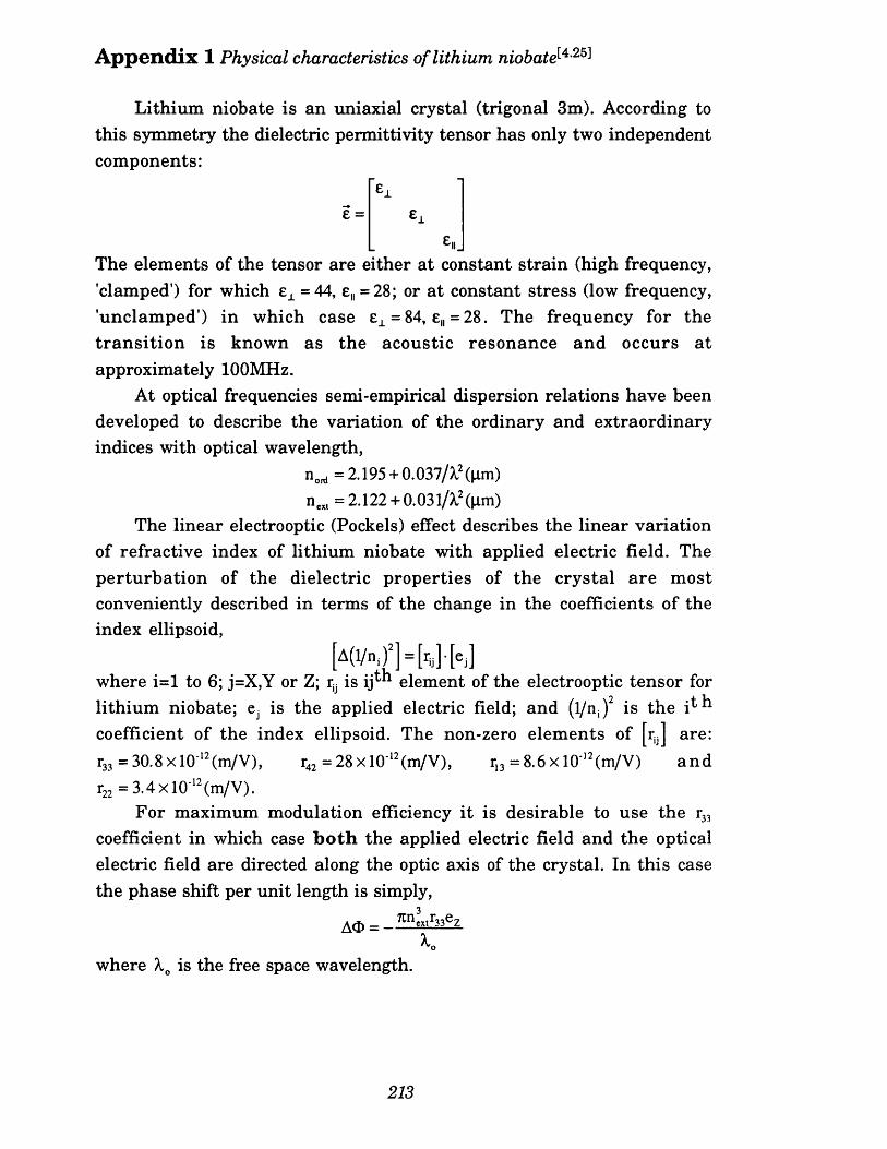
A p p e n d ix 1 Physical characteristics of lithium niohate 4,25]
Lithium niobate is an uniaxial crystal (trigonal 3m). According to this symmetry the dielectric permittivity tensor has only two independent components:
"e±
e = ex^ii
The elements of the tensor are either at constant strain (high frequency, clamped') for which e± = 44, e„ = 28; or at constant stress (low frequency, 'unclamped') in which case e± = 84, eB = 28. The frequency for the tran sitio n is known as the acoustic resonance and occurs at approximately 100MHz.
At optical frequencies semi-empirical dispersion relations have been developed to describe the variation of the ordinary and extraordinary indices with optical wavelength,
nonl =2.195 + 0.037/A2 (pm) next =2.122 + 0.03 l/X2 (pm)
The linear electrooptic (Pockels) effect describes the linear variation of refractive index of lithium niobate with applied electric field. The perturbation of the dielectric properties of the crystal are most conveniently described in terms of the change in the coefficients of the index ellipsoid,
[A(l/n,)2] = [r,J] [ e J]where i= l to 6; j=X,Y or Z; is y™1 element of the electrooptic tensor for lithium niobate; ej is the applied electric field; and (l/nj )2 is the i^*1 coefficient of the index ellipsoid. The non-zero elements of [r ] are: r33 = 30.8 x 10'12(m/V), r42 = 28 x 10'12(m/V), r13 = 8.6 x 10'12(m/V) an dr22 = 3 .4 x l0 12(m/V).
For maximum modulation efficiency it is desirable to use the r33 coefficient in which case b o th the applied electric field and the optical electric field are directed along the optic axis of the crystal. In this case the phase shift per unit length is simply,
AO = - ^ ^ zK
where is the free space wavelength.
213
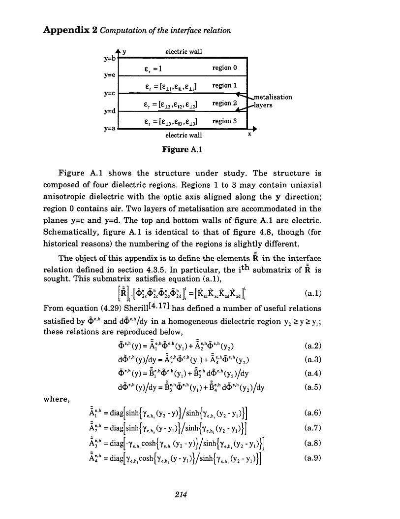
A p p e n d ix 2 Computation of the interface relation
electric wally=b
region 0
region 1y=c ^ -^jnetalisation
region 2 f la y e rsy=d
region 3 ■—y=a
electric wall x
Figure A.1
Figure A .l shows the structure under study. The structure is composed of four dielectric regions. Regions 1 to 3 may contain uniaxial anisotropic dielectric with the optic axis aligned along the y direction; region 0 contains air. Two layers of metalisation are accommodated in the planes y=c and y=d. The top and bottom walls of figure A.l are electric. Schematically, figure A.l is identical to tha t of figure 4.8, though (for historical reasons) the numbering of the regions is slightly different.
The object of this appendix is to define the elements R in the interfacerelation defined in section 4.3.5. In particular, the i *1 submatrix of R is sought. This submatrix satisfies equation (a.l),
R I = [K zcK xcK 2dK xd ] (a .l)
From equation (4.29) S h e r i l l ^ - 1 7 ] has defined a number of useful relationssatisfied by 4>e,h and dd>e,h/dy in a homogeneous dielectric region y2 > y > yj; these relations are reproduced below,
(a.2) (a.3) (a.4)
(a.5)where,
Arh = diag[sinh{ye hj (y2 - y)}/sinh{yc hj (y2 - yi)}
A'>h =diag[sinh{ye>hj(y-y1)}/sinh{yc>h (y2 - yi)}
A f = diag[-ye h.cosh{yc h. (y2 - y)}/sinh{yc hj (y2 - yi)}]
A^h =diag[ye h cosh{ye hj(y -y1)}/sinh{ye hj(y2 -y,)}]
(a.6)
(a.7)
(a.8)
(a.9)
214
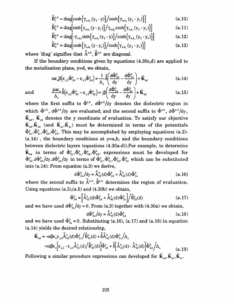
I f = diag[cosh{yt h| (y2 - y)}/cosh{yell| (y2 - y,)}] (a.10)
§2h = diag sinh|Ye h. (y - Yi)}/Yt,h,cosh{ye h| (y2 - y,)}] (a .ll)
I f =diag-ye„isinh{yel,i(y2-y)}/cosh{yCtlli(y2-y1)}] (a.12)
I f =diag[cosh{y.h (y-y1)}/cosh{y<,h (y2-y1)}] (a.13)
where ’diag' signifies that Ac,h, Be,h are diagonal.If the boundary conditions given by equations (4.30c,d) are applied to
the metalisation plane, y=d, we obtain,
“ e.P(ei2^2d-ei3®L) = 7 -8 d O 3d d^2d'dy dy
+ Kzd
and ( 12 2d £13 >3d ) ” jPdd>2d
dy dy+ Kxd
(a. 14)
(a.15)
where the first suffix to d>ch, dOe,h/dy denotes the dielectric region in which <f>c h , d<f>c,h/d y are evaluated; and the second suffix to d>e,h, dd>e h/dy, Kzd, Kxd denotes the y coordinate of evaluation. To satisfy our objective Kzd,Kxd (and KZC,KXC) must be determined in terms of the potentials ^ 2c > ^ c ^ 2dA hd- This may be accomplished by employing equations (a.2)- (a.14) , the boundary conditions at y=a,b, and the boundary conditions between dielectric layers (equations (4.30a-d)).For example, to determine Kzd in term s of expressions m ust be developed for* ,M.d*‘,/dy.d*L/dy in terms of which can be substitutedinto (a. 14): From equation (a.3) we derive,
d65d/dy = A*2(d)®h2d + AJ2(d)®$c (a. 16)where the second suffix to Ae h, Be,h determines the region of evaluation. Using equations (a.3),(a.5) and (4.30b) we obtain,
<i>5d =[A'2( d ) < + A:2(djd.5c] / I '5(d) (a. 17)
and we have used dd>3a/dy = 0. From (a.3) together with (4.30a) we obtain,d ^ d/dy = A;3(d )^ d (a. 18)
and we have used d>Ja =0. Substituting (a.16), (a.17) and (a.18) in equation (a. 14) yields the desired relationship,
= -o)pe0e13A:2(d)d>'c/I '3(d) + SAJfd^./A,
+cope„ 12 “ ei3A32(d)/§33(d) O' +5 A;2(d)-A^3(d) /A. (a. 19)Following a similar procedure expressions can developed for Kxd,Kzc,K,
215

These expressions are,
Kld = -jcoe0le i3Ad2 (d)4>'t /A ,^ ,(d) - jpAJ2 (d)O
+jcoe05 6 'd
k . =
'12 -e 1 i(d )/frSJ(d)]/A,+jp® A«(d)-A52(d)
^1 1 ^ 4 2 Cc)/b 52 (c) - £12 j + 8 d>2c[A5, (c) - A42 ( c ) ] /a ,
+coe^ .d^A '* (c)/1;, (c) - §d>S„ / a,
K« = jcoe0S ^ 'c[e11A:2(c)/§ '1(c)-e12]/AI + jp*
+jcoe0le110 'dAe32(c)/AII ' 1 (c) - jPAj;2(c)d>h2d
A52(c)-A5,(c)
where,
A;, ( c ) = (AS, (c)/A i (c) - § S , (c ) /ij , (c)A;o(e)j / (l/ AJ, ( c ) - 1/ Is, (c) AJ, <e>)
and ,
h (C) = ( ( c ) / A :i ( c ) - 1;, ( c ) / i C3 0 (e)!;, (c)e±1) j( l/A i (c) - 1/Ij , (e)!;, (c)exl
(a.20)
(a.21)
(a.22)
216

A ppendix 3 Listing of the F77 program used for the analysis of planar waveguides by MOL.
A listing of the F77 program used for the analysis of p lanar waveguides is shown over-leaf. Note th a t the program is not well commented and some routines are redundant. The code is not particularly efficient and could be more compact.
The program is specifically for the analysis of fin lines of small lateral dimensions. Modelling of other structures would involve the modification of subroutines: GETRE, SPEF, EMBED. Moreover, the variables IEB, MB and IWALL would be adjusted according to the lateral wall boundaries. Prior to using the code the program must be edit so that ’bigar' is set to the total number of magnetic lines in the problem and noi' is set to the dimension of the reduced matrix.
Program FINMOL.f utilises a number of NAG routines. These routines are F04ADF, F03ADF, F01AMF, F02ANF, X02AAF, F02BLF, and F01ANF. Documentation for these routines may be obtained from NAG.
217
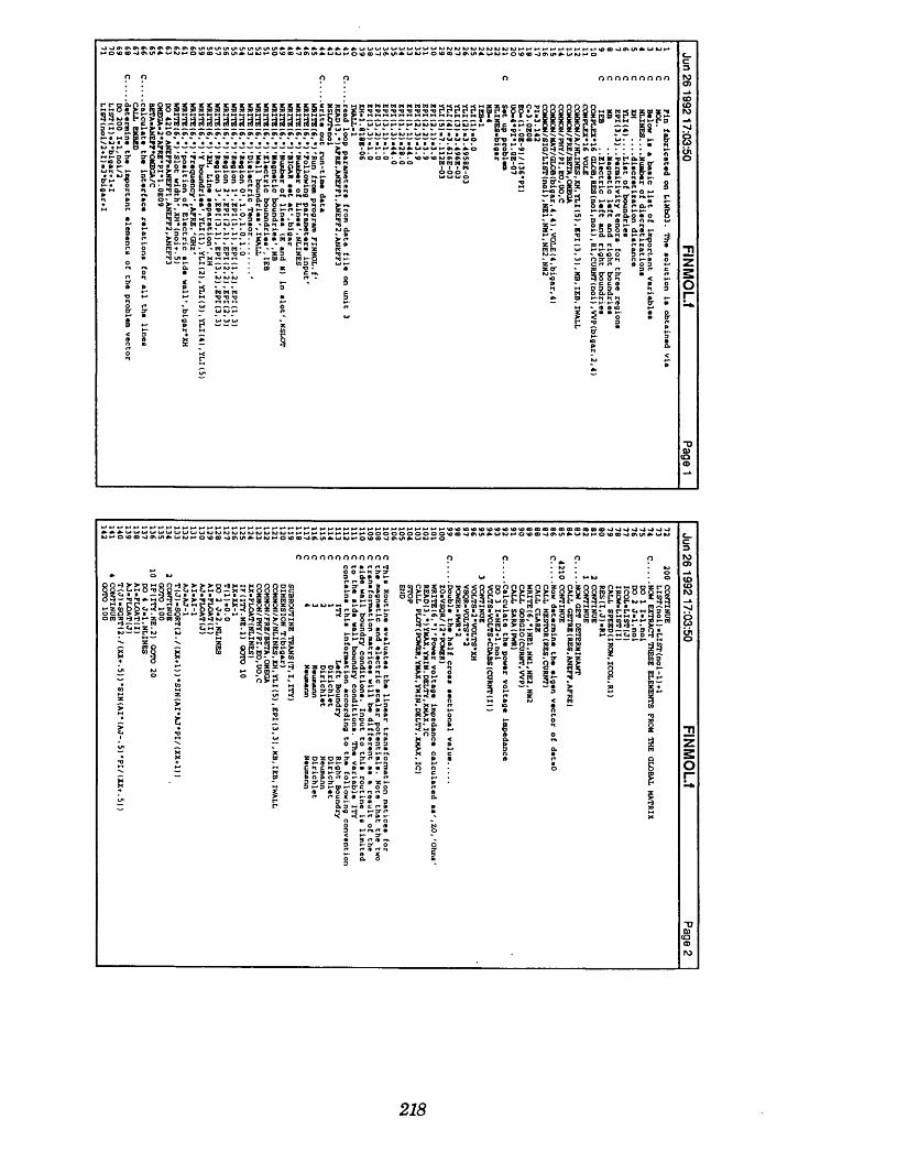
HHHHHHHHHHHHHHHMHMUt3i3i3i3t3cic3(3(3t3!3c3c3i3i3t3i3ei
assixotNlztiz'taS2222:TS.5r2iK§2.§!?
??
nr- x §
*TJ82co
rotocoN>
"O
218
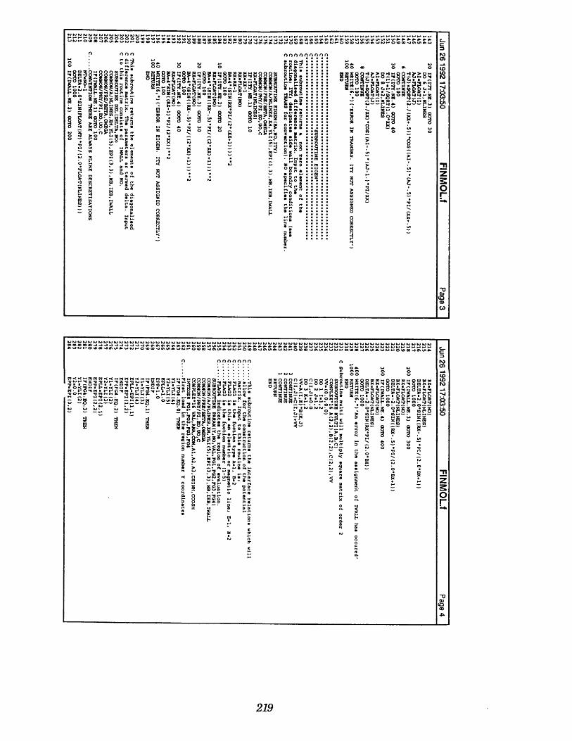
g •%£
i M l J l l i f rH°g ^ i p gg?S 3 * ^riiPs^So 3 SoS-’- dShc§ | sigSPg^ag I l g ' n e ? g ° p
y SMIi. r*— an 0
;s ?lip ; ;t ?!
n
§s s g 8B5
H im
l!p|P!Ip!PPipil!i Bl nil%°!Egsosgsos5sos"2Ma53|5s a& i::::? SSi i*k iSs s I l r |S ::: |i n u u i
iiS 3 S 2 S ^
- gZ Z Mi I i
■S3 ililiii!° "e2§ 11g" : : ! :
=3 I
mr "O j f C ' . >H
[ I PP s§ 2.:I r! ?l
?! IIS ?
g £ .
i l p i? h m r
' " " " IIp rg
§
i ?(0X V»to —
3 !§ ^s 5* g
« Ii>
£SSS83S3S3isSsgSSSSS££'SSSS3SSS”S"SS“ ™ ^
rvj
n
r~
219
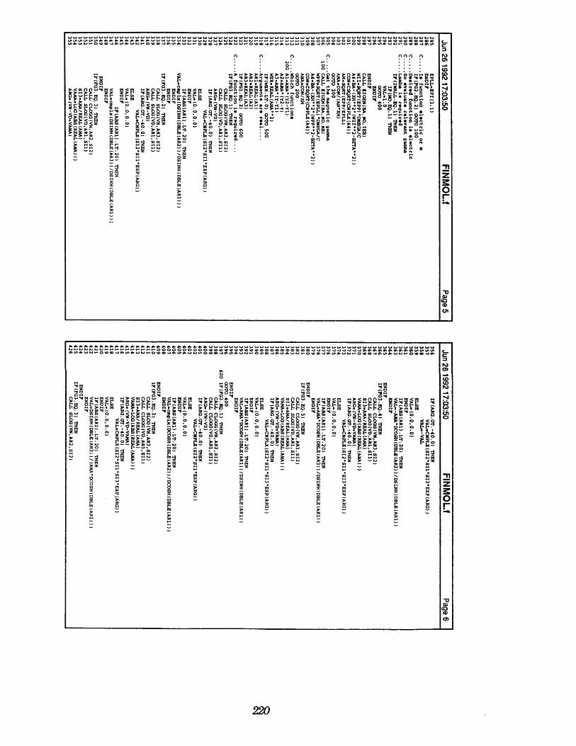
SS = S = SSSSSS£SSSSSSSSKS=““~X“S~“£~““S5"^
If
.E S IIIIsss lss i lssssssssssssssssssgssaaaS aS S gssss^
n ' m mh §i I ==
"Tl
D
o>
220
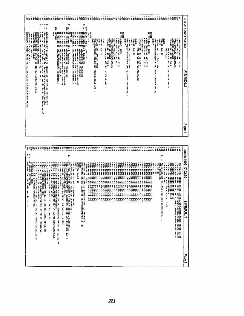
illgglutKgiis^s?
KaSESSZ S
& i i l s l r
I H l i ip r g E f £S 6 ^
B t°AffSEi sfs-s-H'ff mzzz
I s^55555s|55555s5
f l l p l l l i ■ffpfi i i i p B r i f p i i p r i p i h i p h i Hflii ti I Mnt *s: mS?
s = M msa ? 2-»
Vl^WWPr Vli'UMMft M
fffff- f« H :iI P i i i | | i | p s M u l M u lSgEjjg
P i5 11
III
I s
IIIII
psP
SS 5£‘
?1 552 — H*5
!1 •: ?gN||si" ' M S *p
u
i n I I i i I i
S **I lE51 I sr I =
ol~
TJOJ
2S£S£ee£sxssss2ssss“ E£"££"“sS=s“ks““xSSsk
S"2
°5«oH???piBooo(5>-yocMu o 25 —1——51—5i 5ir r r r i C l S ^ Q ? 5 p d g g g R R R g g g R R R g g g R R R g g g R R R R S R R S R5 S a ^ d 2 2 w n S . ^ ^ M‘" 2 2 “ t s r r " ° ° " O g 6 6 o r i o r t o o o i i o o o 5 o n n o 5 5 o n o o o t i o o « n!.P^g2s|Sg?^ 2 Qjs|j=| 2 ggs|S5SSSSSS|iS8S555S5S5S5SSS5SS5SS•gi25oo?258S22^5S0.?=
f lip iillilllrl5T S2So “ z no, n z 3 5&JL5
ii IU ill ? h§HI g 2 B hS'h 2 “2l“s - = s ”1 S 5i su i H h r *' i ' i 11 I!
>s gggggggggggggggggggggggggggggg5~ S S S n n n S S o n n n S S S n n n S S o n n n n n n n B O
:2c"oi 5 s ;: n g g g s2 >b o o n o o o
* I l l l l l l— O ^WW»(,JW*WW*IJU*UU*WU*UU*UU»UUI»UUI
iimS2 S s & 11
og ”n rK> £ 2
:s
M ."Rfi r s g g g g!T i o o o o n
i iggg5 5 5
gggK> K> NJo o ogggp p p
O D O
221
roo>88
n
o>
88
■n
r-
222
fOZ H H C|aS=gg ro
■n
o>88
CO
223
non o n n o
noon n n n n
224
"n
£cEss83ssi88si3HssSS§§§8K8»HH§SS§§S§§Siss§S
*n
225
ro
ro
U
W> — U* — Ul ■ —. — UMH^U
TJ
ro
pessser r k> m r r r* r ■ ■ r r5 5 O 5 5 5§ § 2 S n §
226
CT>U>S’PPi’SSSSSSSSSBS !35,RR A22 t*r- ““
jSjjaarrrrfiB.?? C R g g B R g g g 3 5 3 *
y ^ p p ^ L L C ^ y yR S jjG S u jO " " ^?-*ii^i|pggpgu nu wk k • "g83S8S33*M??^• •*•»-« • VMM- * • • »0SSuwSSum --in
oSllliaeREaassT^TTpS4 wn53»o n x h —MK K> KJ—' —’8088PPZ O Z Z >>. "n.§5oo£?— O-'' 2is§p. k
ro
COroppoooMraw>Mt»w| I MHM1) Z | ■ f* | ■OOI•1• • O O O 50 h o tifls •— m M M m ra ** • x n — ~ • > * * c ©Sc co *—■WOO —H*b - • MXsc > to • — © * z x• Om>o« • KJ X *paasas ss sp
SBSSSSaaBSiSgSSBR
CO
53
r~
227
3§ 8Sb B £5§ SS55555|8S372P? 77£222?SfrprrPrrrxjFCrrSRSBSRS!si °is » sli 3aaaaa-S52sftS5 smft»Bs*S«««BafcBBA&i,s,J.?5i- -b| 5? se| s5535H|s^"'b3 8 fissesciw^M^osfi.i rvll i l l BEPBiPSIil iiv-SPi :S I Si i?l U I p l l p p p i ll 1” \ „ \ J ^ i i S sssi#i e i s^ sh s? '? i|i?«i;il|i??ss its -P2 P25 g gig b8 s c c p s* ♦ s: -8s= q §3 ,iv«
J r ? £ s o g * s - > --------- ^ ^ “ * “ - g* i * = 3 S o ” - 7738*J*i SS-mf ' i i j I g If ii 1 g 6 ss: B i 5=:SSBBSS?S BIS?l I 1 5 * i S 5 S i^ s s p p i i v»H « wH"— ♦
£ R 3 £ 5 s | ® £ g SjS 2 P 3 a 5 3*5 S ~ B
3 P— X
i ib b p s b : :*- W w- k> —' «-MK)
i i | o
r> f n n
TJ09(O
rs>
a
■n
r~
228
• H M H H M M M H O O O O O O O O O O V W W ) W 4 ) * O * 0 ( D O ( D t t ( D ( D Q D < 0 ( D ( D « J « J « J < 4 « J ' « ) < ^ « J ' J « J 9 t 9 t 9 t O « C
Sl|l|l|855H5SpHp|i?Bp5®lsP?lsPS5Sdr*dnd* t3t3t3y «r' — *? 9* f *r*i —tjgg t ■ Hriiwr1. ■ y issgssassssggsa• - - “ o H M r h i k>
5 « 0 l l l < l O Z H Z l 1 1 | I N ■ M M 50 i I~ 0 M O H O X H* H *0 *0 *- . . W TJ *0 *0 T? O O >-
M 9% m + I • K - 50 H H O O G > > > > m ‘ «
c ^ a i o o H H B C<- I •■ ■ <0 QfnH z w » «
juWHMM^Sc555S3PS-' ro p O © j . J " > M M M M <0 O O * O
iiiisssr £z as as z x o y * *■*o o o o g C f e j -gggg°P3§ ^3 S 3 w 3 ^ ® w ® -*’O ~ O ~X O X Ofgfg
♦ o—.0 ►t h
S S I ? 8 m mB•O *0
1 i ix r rw n
3 « M
H g g» t* r
s * MI ggx r rw n
M M
ggr r
Pop*w
OK X X X'
kJWHH
o 3 A0 w •h O W
iE p lip ?j x — K»y y w x jn'osfcsttl*:>kk5 : gVM«Pt5 #- - r*~.**22*^S
3 S ~
75S8*0 *0 O O
( Oc oro
8
zO
n x wgg
229


