Embed Size (px)
Citation preview

1
Photolithography-Free Ge-Se Based Memristive Arrays; Materials Characterization and
Device Testing
M. R. Latif1, I. Csarnovics1,2, S. Kökényesi2, A. Csik3, M. Mitkova1
1. Department of Electrical and Computer Engineering, Boise State University, Boise ID – USA
2. Department of Experimental Physics, University of Debrecen, Debrecen – Hungary
3. Institute of Nuclear Research, Hungarian Academy of Sciences, Debrecen- Hungary
Abstract
The focus of this work is on formation of lithography free redox conductive bridge memristor
arrays comprised of different compositions of GexSe1-x chalcogenide glasses with the aim of
selecting the insulating material with the best performance. The memristive arrays were
fabricated on a metal/chalcogenide/metal stack. This structure offers high device density with the
simplest of configuration and allows access to each nano redox conductive bridge device. It was
found that the device stability and threshold voltage were a function of the chalcogenide glass
composition, with the Ge rich film contributing to the best performance, which is attributed to
the formation of rigid structure and of Ge-Ge bonds. Additionally, these parameters were
dependent on the thickness of the chalcogenide glass and its surface roughness. Application of
non-lithography method for fabricating the array structure offered excellent yield, stable
ON/OFF states and good uniformity. This demonstration, along with success already achieved at
the single cell level, suggests that the redox conductive bridge memristor is well positioned for
ultra-high performance memory and logic applications.
Keywords: Lithography, redox conductive bridge memristor, chalcogenide glass.

2
1. Introduction
Resistive Random Access Memory (RRAM) technologies are of wide interest because of
their potential to replace flash memory as the next-generation nonvolatile memory [1-3]. Among
different emerging RRAM technologies, the nanoionic based electrochemical systems,
commonly known as Redox Conductive Bridge Memory (RCBM), has attracted significant
interest as a promising candidate for future high density, high performance memory and logic
applications [4-6]. These devices exhibit low power consumption together with high
programming speed [7, 8] and offer excellent scaling potential as their simple structure requires
only one dimension to be critically controlled [9].
RCBM devices consist of two terminals: A thin film of solid electrolyte is sandwiched
between an electrochemically active electrode and an electrochemically inert counter electrode
as shown in Figure 1. The RCBM working principle is based on field driven generation of
metallic ions at the active electrode and their reduction and deposition at the counter electrode
after ions migration through solid electrolyte. Applying a positive voltage to the
electrochemically active electrode (SET operation), leads to formation of a nano-sized filament
bridging the two electrodes together and thus defines the low resistance state (ON State) of the
RCBM cell. The filament can be dissolved by applying a voltage of opposite polarity (RESET
operation), which returns the cell to high resistive state (OFF State). Such polarity dependent
switching is attainable in nanoseconds regime with a voltage of few hundred mV and currents in
the nA range [10].

3
Memristive array posses significant advantages for memory, including massive storage
capacity with high storage density, precision and access speed [11]. Also the array structure
provides powerful capability in information processing [12], arithmetic computation [13], pattern
comparison [14] and reconfigurable FPGA [15]. An array of RCBM devices can be formed by
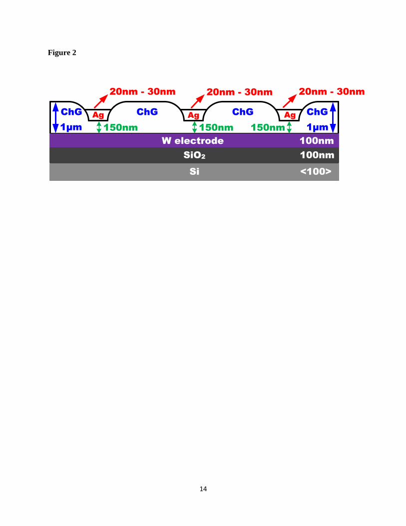
laying a nano-wire over the inert electrode with chalcogenide glass (ChG) film as a dielectric
medium between the two electrodes, as presented in Figure 2. In this study we demonstrate a
RCBM memory array on a thin films metal/ChG/metal stack with no lithography step for device
fabrication and show that the array structure offers excellent yield and repeatability. The vias
were formed by bombardment of Ar+ ions using a shadow mask. To analyze the influence of the
ion bombardment on surface topography and composition of the materials in the device active
area; Atomic Force Microscopy (AFM) and Energy Dispersive X-Ray Spectroscopy (EDS)
studies were performed. Specific attention was paid to the surface roughness in the device vias
region as it plays an important role in the growth of the conductive molecular bridge. The
devices were electrically tested to show the usability of the process for fabrication of the
RCBRM array.
2. Experimental Details
The RCBM devices were fabricated on a stack of GexSe1-x/W/SiO2/Si (where x=0.2, 0.3 and
0.4). The thickness of the films comprising the devices was as follows: Si <100> substrate
covered with 200nm thermally grown SiO2; followed by 100nm of sputtered W (Tungsten) and
1µm thermally evaporated GeSe films. The films were evaporated using a crucible resembling a
semi-Knudsen cell, thus equilibrating the vapor pressure of the gaseous products in it. The films
thicknesses were verified by ellipsometry (Model No.: L115 C-8). An INA-X type (SPECS,
Berlin) Secondary Neutral Mass Spectrometer (SNMS) was used for sputtering samples with Ar+

4
ions through a copper TEM-grid with mesh size of 40µm×40μm which was placed in close
contact with the sample surface. The surface bombardment was made at low pressure by
Electron Cyclotron Wave Resonance (ECWR) argon. A 350 V sputtering potential at 100 kHz
frequency with 80% duty cycle was applied on the sample. 20nm silver (Ag) layer was deposited
by DC magnetron sputtering with deposition pressure of 5x10⁻³mbar. The sputtering rate was
calibrated by Ambios XP-1 profilometer. The same sample holder and copper grid was used for
Ar+ ion beam and silver sputtering.
EDS results were acquired by averaging data over five points on each sample within the film
using a Hitachi S-3400N EDS system. The average compositional error of the films was found to
be less than 2%. The Ge-Se film surface characterization and stress analysis were studied by
using a Veeco Dimensions 3100 AFM system. Electrical testing on the devices were performed
with Agilent 4155B Semiconductors Parameter Analyzer equipped with triax cables to avoid
residual charge build up. W and Ag pads were probed with correct biasing for SET and RESET
conditions. Various cells in the array were tested in dual sweep mode with a voltage step size of
2mV and compliance current set to 50nA. Data were analyzed and recorded by Easy Expert
Software provided by Agilent. The testing equipment (sample stage holder, triax cables and
probes) was placed inside a Faraday cage sharing a common ground to avoid static charge build
up. All measurements were carried out at room temperature.
3. Results
The top view of the fabricated 40x40 array is presented in Figure 3. Vias filled with Ag
served as the top electrode of the array cell with W as the bottom electrode. GexSe1-x (where x =
0.2, 0.3 & 0.4) layer was used to isolate individual cells. The surface topography within the cell

5
vias of the GexSe1-x layer were studied by AFM and the results are presented in Figure 4. AFM
scans were performed on cell 1, cell 10 and cell 20 in the 20th row of the array structure on a
25µm2 area within the device vias. There is a clear tendency for improvement of the surface
smoothness of the films with increasing Ge concentration.
Figure 5 shows the IV sweeps of the electrical measurements conducted on the fabricated
array with different compositions of GexSe1-x for cell # 20. Each cycle starts at -0.1V. Then the
voltage sweeps to +1.5V and sweeps back to -0.1V. At first the current is very low (cell
resistance: high) until a threshold voltage of approximately 0.6 V is exceeded. At that moment a
conductive connection is formed between the top and bottom electrodes causing a steep increase
in the current until it reaches the compliance current which was limited to 50nA (cell resistance:
low).
4. Discussion
The most important result of this study is to establish the GexSe1-x composition suitable for
reliable array performance. The electrical tests were performed on all three compositions, which
resulted in several thousand switching cycles. The memory window of threshold voltage (Vth) for
high resistive state (HRS) to threshold voltage of low resistive state (LRS) is considered as a
figure of merit for RRAM technologies [16, 17]. A higher difference in the Vth window of the
two states will result in better memory performance since a small ratio will lead to more read
errors. In the studied compositions, Ge30Se70 and Ge40Se60 showed better ratio of threshold
voltage for HRS to LRS.
Ion bombardment in thin films may cause a surface roughness resulting in difference in
film strength and can influence hillock formation and electron migration and, thus, negatively

6
affect the device reliability[18, 19]. A good surface condition is of extreme importance in
providing location for nucleation and growth for the conductive molecular bridge, especially
taking into account the high electric field of 107-108Vm-1 [20] occurring at the switching events.
The main reason for this is the statistical nature of the nucleation process, which is determined
not by free available adsorption sites at the electrode surface, but by the closest distance between
the electrode and a hillock in the active layer. This may result in incorrect nucleation with a false
switching. Thus, to have a reliable device, a smooth surface within the device via is essential.
The surface roughness RMS value and peak hillock in the 25µm2 area in the device vias is
presented in Figure 6.
There could be several reasons for the tendency in surface smoothness improvement with
increasing Ge concentration. First, the hillocks formation and surface roughness in the Ge-Se
system could be related to the packing fraction of these glasses. The larger free volume will
correspond to lower packing fraction [21]. According to the data for this system, the packing
fraction of Ge20Se80 is the least for the composition studied in this work [22]. This means that
there is more open space for the Ar+ ions to penetrate and affect the shape of the device vias, as
well as to form pockets in which later the traversing ions can be captured. Thus, Ar+ ions
bombardment for via formation causes more surface roughness and film damage in Ge20Se80 as
compared to the other two compositions and hence results in degradation of the cells Vth
performance for the two states. If we regard the structure of the studied films, the decrease of the
structure fraction is related to increased dominance of the tetrahedral structures in the films.
While in the Ge20Se80 films Se-Se bonds are available, with increased Ge concentration they
disappear and the structure is formed only by tetrahedrally coordinated Ge, surrounded by Se
atoms and some ethane-like structural units [23]. Interestingly the results show, that the optimal
7
coordination of 2.4 according to the Constrain Counting Theory [24], characteristic for the
Ge20Se80 films, is not the leading factor for the strength of the structure. It is the higher
coordination of 2.6 and especially 2.8 which results in more stable reaction of the films to the
mechanical stress. Indeed, in the studied case the stability of the network is related to how
amendable it is to continuous deformation. The covalent forces that also involve the bond length,
bond angles and the increased rigidity are important factors, which in fact keep the structure
intact [25]. The floppy modes related to the Se-Se bonding within the system require much lower
energy to be destroyed and they quantify the instability of the films in the studied case.
The resistance and Vth plots in various cells in all three compositions are in good agreement
with AFM results and are presented in Figure 7. All cells show six orders of magnitude
difference between the ON and OFF state of the device. The resistance of the device varies from
tens of giga ohms in the OFF state to a few kilo ohms in the ON state, ensuring good memory
retention of the devices [26]. However, the Vth of Ge20Se80 illustrates variations within the cells
and also in different cells of the array structure. On the other hand, Ge30Se70 and Ge40Se60 offer
excellent repeatability within a cell and the array. Hence, an increase in Ge concentration results
in an improvement of device performance due to formation of specific structures.
5. Conclusion
An array of RCBM devices with no lithography step is successfully demonstrated. The
fabricated array structure allowed individual cell addressing. The individual cells built by thin
Ge-Se films showed excellent yield with good endurance at over 103 cycles. The devices built by
Ge40Se60 film, that offered the least surface roughness in the vias region, resulted in excellent

8
device performance. An improvement in the cells performance can be achieved by formation of
smoother layers within the vias and filling them homogeneously with Ag.
Acknowledgments
This work was supported by IMI-NFG under NSF Grant # DMR 0844014 and TÁMOP-
4.2.2/B-10/1-2010-0024 and TÁMOP-4.2.2.A-11/2/KONV-2012-0032, which are co-financed
by the European Union and European Social Fund. The financial support of the Czech Science
Foundation (under the project No. P106/11/0506) is also acknowledged. The authors would also
like to acknowledge the Surface Science Lab at Boise State University for AFM use and Dr. Paul
Davis for assistance in performing AFM.

9
References
[1] D. Ielmini, A. Spinelli, and A. Lacaita, "Recent developments on Flash memory
reliability," Microelectronic engineering, vol. 80, pp. 321-328, 2005.
[2] M. Kund, G. Beitel, C.-U. Pinnow, T. Rohr, J. Schumann, R. Symanczyk, et al.,
"Conductive bridging RAM (CBRAM): An emerging non-volatile memory technology
scalable to sub 20nm," in Electron Devices Meeting, 2005. IEDM Technical Digest. IEEE
International, 2005, pp. 754-757.
[3] M. N. Kozicki, M. Park, and M. Mitkova, "Nanoscale memory elements based on solid-
state electrolytes," Nanotechnology, IEEE Transactions on, vol. 4, pp. 331-338, 2005.
[4] L. Chua, "Memristor-the missing circuit element," Circuit Theory, IEEE Transactions on,
vol. 18, pp. 507-519, 1971.
[5] J. R. Heath, P. J. Kuekes, G. S. Snider, and R. S. Williams, "A defect-tolerant computer
architecture: Opportunities for nanotechnology," Science, vol. 280, pp. 1716-1721, 1998.
[6] H. Mizuta and S. Oda, "Bottom-up approach to silicon nanoelectronics,"
Microelectronics Journal, vol. 39, pp. 171-176, 2008.
[7] E. Vianello, C. Cagli, G. Molas, E. Souchier, P. Blaise, C. Carabasse, et al., "On the
impact of Ag doping on performance and reliability of GeS2 - based Conductive Bridge
Memories," in Solid-State Device Research Conference (ESSDERC), 2012 Proceedings
of the European, 2012, pp. 278-281.
[8] I. Valov, E. Linn, S. Tappertzhofen, S. Schmelzer, J. van den Hurk, F. Lentz, et al.,
"Nanobatteries in redox-based resistive switches require extension of memristor theory,"
Nature communications, vol. 4, p. 1771, 2013.
10
[9] S. H. Jo, K.-H. Kim, and W. Lu, "High-density crossbar arrays based on a Si memristive
system," Nano letters, vol. 9, pp. 870-874, 2009.
[10] I. Valov, R. Waser, J. R. Jameson, and M. N. Kozicki, "Electrochemical metallization
memories—fundamentals, applications, prospects," Nanotechnology, vol. 22, p. 254003,
2011.
[11] K.-H. Kim, S. Gaba, D. Wheeler, J. M. Cruz-Albrecht, T. Hussain, N. Srinivasa, et al.,
"A functional hybrid memristor crossbar-array/CMOS system for data storage and
neuromorphic applications," Nano letters, vol. 12, pp. 389-395, 2011.
[12] X. Hu, S. Duan, L. Wang, and X. Liao, "Memristive crossbar array with applications in
image processing," Science China Information Sciences, vol. 55, pp. 461-472, 2012.
[13] K. Bickerstaff and E. Swartzlander, "Memristor-based arithmetic," in Conference Record
of the Forty Fourth Asilomar Conference on Signals, Systems and Computers
(ASILOMAR), 2010, pp. 1173-1177.
[14] B. Mouttet, "Proposal for memristor crossbar design and applications," in Memristors
and Memristive Systems Symposium, UC Berkeley, 2008.
[15] J. Cong and B. Xiao, "mrFPGA: A novel FPGA architecture with memristor-based
reconfiguration," in IEEE/ACM International Symposium on Nanoscale Architectures
(NANOARCH), pp. 1-8, 2011.
[16] B. Jacob, S. Ng, and D. Wang, Memory systems: cache, DRAM, disk: Morgan Kaufmann,
2010.
[17] H. Yang, C. T. Chong, R. Zhao, H. K. Lee, J. Li, K. G. Lim, et al., "GeTe/Sb7Te3
superlatticelike structure for lateral phase change memory," Applied Physics Letters, vol.
94, pp. 203110-3, 05/18/ 2009.

11
[18] H. Ji, G. S. Was, J. W. Jones, and N. R. Moody, "Effect of ion bombardment on in-plane
texture, surface morphology, and microstructure of vapor deposited Nb thin films,"
Journal of applied physics, vol. 81, pp. 6754-6761, 1997.
[19] R. P. Vinci and J. J. Vlassak, "Mechanical behavior of thin films," Annual Review of
Materials Science, vol. 26, pp. 431-462, 1996.
[20] I. Valov and G. Staikov, "Nucleation and growth phenomena in nanosized
electrochemical systems for resistive switching memories," Journal of Solid State
Electrochemistry, vol. 17, pp. 365-371, 2013.
[21] P. Chen, M. Mitkova, D. A. Tenne, K. Wolf, V. Georgieva, and L. Vergov, "Study of the
Sorption Properties of Ge20Se80 thin Films for NO2 Gas Sensing," Thin Solid Films, 2012.
[22] A. Feltz, Amorphous inorganic materials and glasses: VCH Weinheim, 1993.
[23] X. Feng, W. Bresser, and P. Boolchand, "Direct evidence for stiffness threshold in
Chalcogenide glasses," Physical review letters, vol. 78, p. 4422, 1997.
[24] M. Thorpe and M. Chubynsky, "Rigidity and self-organization of network glasses and the
intermediate phase," in Properties and Applications of Amorphous Materials, ed:
Springer, pp. 61-96, 2001.
[25] D. J. Jacobs and M. F. Thorpe, "Generic rigidity percolation: the pebble game," Physical
review letters, vol. 75, p. 4051, 1995.
[26] C. Kügeler, R. Rosezin, E. Linn, R. Bruchhaus, and R. Waser, "Materials, technologies,
and circuit concepts for nanocrossbar-based bipolar RRAM," Applied Physics A, vol.
102, pp. 791-809, 2011.

12
List of figures and captions
Figure 1. RCBM memory structure with cell in (a) Low Resistive State (LRS) (b) High Resistive
State (HRS)
Figure 2. Schematic for RCBM array
Figure 3. SEM Image of the fabricated RCBM Array
Figure 4. a (i) Formation of via in Ge20Se80 by Ar+ ion bombardment. 25µm area scan in the via
of (ii) 1st Cell (iii) 10th Cell (iv) 20th Cell of the array. 4-b (i) Formation of via in Ge30Se70 by Ar+
ion bombardment. 25µm area scan in the via of (ii) 1st Cell (iii) 10th Cell (iv) 20th Cell of the
array. 4-c (i) Formation of via in Ge40Se60 by Ar+ ion bombardment. 25µm area scan in the via of
(ii) 1st Cell (iii) 10th Cell (iv) 20th Cell of the array.
Figure 5. IV Curves with 100 sweeps in cell no. 20 in the RCBM array
Figure 6. Surface roughness RMS and peak hillocks in the vias of the cell
Figure 7. Resistance and Threshold plot of (a) Ge20Se80 (b) Ge30Se70 and (c) Ge40Se60

13
Figure 1
14
Figure 2
ChG ChG Ag ChG ChG Ag
1µm 150nm 150nm
20nm - 30nm 20nm - 30nm 20nm - 30nm
Ag
W electrode 100nm
1µm150nm
Si <100>
SiO2 100nm

15
Figure 3
ChG
Vias filled
with Ag
ChG
Ag
ChG

16
Figure 4
a)
Via in
Ge30Se70 film
a)
ii)b)
iv)
iii)
i)
b) Ge30Se70 Film/Device
Via in
Ge40Se60
film
ii)iii)
iv)
c) Ge40Se60 Film/Device
i)
Via in
Ge20Se80
film
i)
ii) iii)
iv)
a) Ge20Se80 Film/Device
Ge20Se80 Layer
Ge30Se70 Layer
Ge40Se60 L
ayer

17
Figure 5
0.0 0.2 0.4 0.6 0.8 1.0 1.2 1.4-10n
0
10n
20n
30n
40n
50n
60n
Cu
rre
nt
(A)
Voltage (V)
Cell 20 100 Cycles
0.0 0.2 0.4 0.6 0.8 1.0 1.2 1.4-10n
0
10n
20n
30n
40n
50n
60n
Cu
rre
nt
(A)
Voltage (V)
Cell 20 100 Cycles
0.0 0.2 0.4 0.6 0.8 1.0 1.2 1.4-10n
0
10n
20n
30n
40n
50n
60n
Cu
rre
nt
(A)
Voltage (V)
100 CyclesCell 20
a) Ge20Se80 Device
b) Ge30Se70 Device
c) Ge40Se60 Device

18
Figure 6
Cell No.1
Cell No.10
Cell No.20
Cell No.1
Cell No.10
Cell No.20
Cell No.1
Cell No.10
Cell No.20
0
4
8
12
16
20
24
28
32
Ge40Se60Ge30Se70
H
eig
ht
(nm
)
Average Surface Roughness
Hillock Height
Ge20Se80

19
Figure 7
0.0
0.2
0.4
0.6
0.8
1.0
1.2
1.4
Vth
HRS
LRS
100 Cycles/Cell
Th
res
ho
ld V
olt
ag
e (
V)
10k
100k
1M
10M
100M
1G
10G
100G
1T
Re
sis
tan
ce
(
)
Cell 1 Cell 8 Cell 16 Cell 20
0.2
0.4
0.6
0.8
1.0
1.2
Vth
HRS
LRS
100 Cycles/Cell
Th
resh
old
Vo
ltag
e (
V)
Cell 1 Cell 4 Cell 8 Cell 12 Cell 16 Cell 2010k
100k
1M
10M
100M
1G
10G
100G
1T
Re
sis
tan
ce
()
-0.2
0.0
0.2
0.4
0.6
0.8
1.0
Cell 20Cell 16Cell 12Cell 8Cell 4Cell 1
Vth
HRS
LRS
100 Cycles/Cell
Th
res
ho
ld V
olt
ag
e (
V)
1k
10k
100k
1M
10M
100M
1G
10G
100G
Re
sis
tan
ce
()
0
a) Ge20Se80 Device
b) Ge30Se70 Device
c) Ge40Se60 Device


