Embed Size (px)
Citation preview

ApplicationBook
1996 8-Bit Microcontroller Family

Printed in U.S.A., February 1996 SPNA017
1996Application
Book
TMS370 Microcontroller FamilyApplication Book
Microcontroller Products—Semiconductor Group
SPNA017February 1996

IMPORTANT NOTICE
Texas Instruments (TI) reserves the right to make changes to its products or to discontinue any semiconductorproduct or service without notice, and advises its customers to obtain the latest version of relevant informationto verify, before placing orders, that the information being relied on is current.
TI warrants performance of its semiconductor products and related software to the specifications applicable atthe time of sale in accordance with TI’s standard warranty. Testing and other quality control techniques areutilized to the extent TI deems necessary to support this warranty. Specific testing of all parameters of eachdevice is not necessarily performed, except those mandated by government requirements.
Certain applications using semiconductor products may involve potential risks of death, personal injury, orsevere property or environmental damage (“Critical Applications”).
TI SEMICONDUCTOR PRODUCTS ARE NOT DESIGNED, INTENDED, AUTHORIZED, OR WARRANTEDTO BE SUITABLE FOR USE IN LIFE-SUPPORT APPLICATIONS, DEVICES OR SYSTEMS OR OTHERCRITICAL APPLICATIONS.
Inclusion of TI products in such applications is understood to be fully at the risk of the customer. Use of TIproducts in such applications requires the written approval of an appropriate TI officer. Questions concerningpotential risk applications should be directed to TI through a local SC sales office.
In order to minimize risks associated with the customer’s applications, adequate design and operatingsafeguards should be provided by the customer to minimize inherent or procedural hazards.
TI assumes no liability for applications assistance, customer product design, software performance, orinfringement of patents or services described herein. Nor does TI warrant or represent that any license, eitherexpress or implied, is granted under any patent right, copyright, mask work right, or other intellectual propertyright of TI covering or relating to any combination, machine, or process in which such semiconductor productsor services might be or are used.
Copyright 1996, Texas Instruments Incorporated
iii
Contents
Part I: IntroductionIntroduction 5. . . . . . . . . . . . . . . . . . . . . . . . . . . . . . . . . . . . . . . . . . . . . . . . . . . . . . . . . . . . . . . . . . . . Overview 5. . . . . . . . . . . . . . . . . . . . . . . . . . . . . . . . . . . . . . . . . . . . . . . . . . . . . . . . . . . . . . . . . . . . . . . . . Typical Applications 5. . . . . . . . . . . . . . . . . . . . . . . . . . . . . . . . . . . . . . . . . . . . . . . . . . . . . . . . . . . . . . . .
Part II: Software RoutinesArithmetic
16×16 (32-Bit) Multiplication 9. . . . . . . . . . . . . . . . . . . . . . . . . . . . . . . . . . . . . . . . . . . . . . . . . . .
Binary Division With the TMS370 13. . . . . . . . . . . . . . . . . . . . . . . . . . . . . . . . . . . . . . . . . . . . .
. . . . . . . . . . . . . . . . . . . . . . . . . . . . . . . . . . . . . . . . . . . . . .
16. . . . . . . . . . . . . . . . . . . . . . . . . . . . . . . . . . . . . . . . . . . . .
BCD-to-Binary Conversion on the TMS370 17. . . . . . . . . . . . . . . . . . . . . . . . . . . . . . . . . . .
Binary-to-BCD Conversion on the TMS370 21. . . . . . . . . . . . . . . . . . . . . . . . . . . . . . . . . . .
BCD String Addition With the TMS370 25. . . . . . . . . . . . . . . . . . . . . . . . . . . . . . . . . . . . . . .
TMS370 Floating Point Package 29. . . . . . . . . . . . . . . . . . . . . . . . . . . . . . . . . . . . . . . . . . . . . . . Introduction 31. . . . . . . . . . . . . . . . . . . . . . . . . . . . . . . . . . . . . . . . . . . . . . . . . . . . . . . . . . . . . . . . . . . . . . Floating Point Format 32. . . . . . . . . . . . . . . . . . . . . . . . . . . . . . . . . . . . . . . . . . . . . . . . . . . . . . . . . . . . . . Floating Point Routines 33. . . . . . . . . . . . . . . . . . . . . . . . . . . . . . . . . . . . . . . . . . . . . . . . . . . . . . . . . . . . .
Floating Point Addition/Subtraction 33. . . . . . . . . . . . . . . . . . . . . . . . . . . . . . . . . . . . . . . . . . . . . . Floating Point Number Comparison 37. . . . . . . . . . . . . . . . . . . . . . . . . . . . . . . . . . . . . . . . . . . . . . Floating Point Division 39. . . . . . . . . . . . . . . . . . . . . . . . . . . . . . . . . . . . . . . . . . . . . . . . . . . . . . . . Floating Point Multiplication 43. . . . . . . . . . . . . . . . . . . . . . . . . . . . . . . . . . . . . . . . . . . . . . . . . . . . Floating Point Increment / Decrement 46. . . . . . . . . . . . . . . . . . . . . . . . . . . . . . . . . . . . . . . . . . . . . Floating Point Number Test 49. . . . . . . . . . . . . . . . . . . . . . . . . . . . . . . . . . . . . . . . . . . . . . . . . . . . . Floating Point Number Negation 50. . . . . . . . . . . . . . . . . . . . . . . . . . . . . . . . . . . . . . . . . . . . . . . . . Floating Point To Signed 8-Bit Integer Conversion 51. . . . . . . . . . . . . . . . . . . . . . . . . . . . . . . . . . . Floating Point To Signed Long (16-Bit) Integer Conversion 53. . . . . . . . . . . . . . . . . . . . . . . . . . . . Floating Point To Unsigned 8-Bit Integer Conversion 55. . . . . . . . . . . . . . . . . . . . . . . . . . . . . . . . . Floating Point To Unsigned Long (16-Bit) Integer Conversion 56. . . . . . . . . . . . . . . . . . . . . . . . . Signed 8-Bit Integer To Floating Point Conversion 57. . . . . . . . . . . . . . . . . . . . . . . . . . . . . . . . . . . Signed Long (16-Bit) Integer To Floating Point Conversion Comparison 58. . . . . . . . . . . . . . . . . Unsigned Long (16-bit) Integer To Floating Point Conversion 59. . . . . . . . . . . . . . . . . . . . . . . . . . Unsigned 8-Bit Integer To Floating Point Conversion 60. . . . . . . . . . . . . . . . . . . . . . . . . . . . . . . . .
Memory OperationsClear RAM Routine 63. . . . . . . . . . . . . . . . . . . . . . . . . . . . . . . . . . . . . . . . . . . . . . . . . . . . . . . . . . .
RAM Self-Test Routine 67. . . . . . . . . . . . . . . . . . . . . . . . . . . . . . . . . . . . . . . . . . . . . . . . . . . . . . . .
ROM Checksum on the TMS370 71. . . . . . . . . . . . . . . . . . . . . . . . . . . . . . . . . . . . . . . . . . . . . .
iv
Table Search With the TMS370 75. . . . . . . . . . . . . . . . . . . . . . . . . . . . . . . . . . . . . . . . . . . . . . . .
Bubble Sort With the TMS370 79. . . . . . . . . . . . . . . . . . . . . . . . . . . . . . . . . . . . . . . . . . . . . . . . .
Specific FunctionalityRoutine to Read a 16-Key Keyboard 85. . . . . . . . . . . . . . . . . . . . . . . . . . . . . . . . . . . . . . . . . . .
DTMF Generation With the TMS370 89. . . . . . . . . . . . . . . . . . . . . . . . . . . . . . . . . . . . . . . . . .
System Integrity Check for the TMS370 95. . . . . . . . . . . . . . . . . . . . . . . . . . . . . . . . . . . . . . .
Part III: Module Specific Application Design Aids
RESET OperationsReset: Explanation of Operation and Suggested Designs 101. . . . . . . . . . . . . . . . . . . . . .
COLD START 103. . . . . . . . . . . . . . . . . . . . . . . . . . . . . . . . . . . . . . . . . . . . . . . . . . . . . . . . . . . . . . OSC FLT FLAG 103. . . . . . . . . . . . . . . . . . . . . . . . . . . . . . . . . . . . . . . . . . . . . . . . . . . . . . . . . . . . . WD OVRFL INT FLAG 103. . . . . . . . . . . . . . . . . . . . . . . . . . . . . . . . . . . . . . . . . . . . . . . . . . . . . . General Operation 103. . . . . . . . . . . . . . . . . . . . . . . . . . . . . . . . . . . . . . . . . . . . . . . . . . . . . . . . . . .
SPI and SCI ModulesUsing the TMS370 SPI and SCI Modules 107. . . . . . . . . . . . . . . . . . . . . . . . . . . . . . . . . . . . . Introduction 109. . . . . . . . . . . . . . . . . . . . . . . . . . . . . . . . . . . . . . . . . . . . . . . . . . . . . . . . . . . . . . . . . . . . . Module Description: Serial Peripheral Interface (SPI) 110. . . . . . . . . . . . . . . . . . . . . . . . . . . . . . . . . . . .
The SPI – How It Works 110. . . . . . . . . . . . . . . . . . . . . . . . . . . . . . . . . . . . . . . . . . . . . . . . . . . . . . SPI Operating Modes 111. . . . . . . . . . . . . . . . . . . . . . . . . . . . . . . . . . . . . . . . . . . . . . . . . . . . . . . . .
$%# ! . . . . . . . . . . . . . . . . . . . . . . . . . . . . . . . . . . . . . . . . . . . . . . . . . . . . . . ' !
Configuring the SPI 112. . . . . . . . . . . . . . . . . . . . . . . . . . . . . . . . . . . . . . . . . . . . . . . . . . . . . . . . . . % !#% # $%% ' % # $# %
Controlling the SPI through Interrupts and Flag Checking 114. . . . . . . . . . . . . . . . . . . . . . . . . . . . The TALK Bit and Multiprocessor Communications 115. . . . . . . . . . . . . . . . . . . . . . . . . . . . . . . . Considerations When Using the SPI 115. . . . . . . . . . . . . . . . . . . . . . . . . . . . . . . . . . . . . . . . . . . . . Data Integrity and the SPI 116. . . . . . . . . . . . . . . . . . . . . . . . . . . . . . . . . . . . . . . . . . . . . . . . . . . . .
SPI Module Software Examples 117. . . . . . . . . . . . . . . . . . . . . . . . . . . . . . . . . . . . . . . . . . . . . . . . . . . . . Common Equates 117. . . . . . . . . . . . . . . . . . . . . . . . . . . . . . . . . . . . . . . . . . . . . . . . . . . . . . . . . . . . Master SPI Configuration 118. . . . . . . . . . . . . . . . . . . . . . . . . . . . . . . . . . . . . . . . . . . . . . . . . . . . . . Slave SPI Configuration 119. . . . . . . . . . . . . . . . . . . . . . . . . . . . . . . . . . . . . . . . . . . . . . . . . . . . . . . Dynamic Bit Justification 120. . . . . . . . . . . . . . . . . . . . . . . . . . . . . . . . . . . . . . . . . . . . . . . . . . . . . . Address Recognition by SPI 121. . . . . . . . . . . . . . . . . . . . . . . . . . . . . . . . . . . . . . . . . . . . . . . . . . .
!&% SPI Module Specific Applications 122. . . . . . . . . . . . . . . . . . . . . . . . . . . . . . . . . . . . . . . . . . . . . . . . . . . .
Vacuum Fluorescent Display Driver 122. . . . . . . . . . . . . . . . . . . . . . . . . . . . . . . . . . . . . . . . . . . . . $ %! # $% % %! # % $%#
Bootstrap Loader 131. . . . . . . . . . . . . . . . . . . . . . . . . . . . . . . . . . . . . . . . . . . . . . . . . . . . . . . . . . . . "#!# % !# #!#!#( %#!& !#%
DSP Controller 132. . . . . . . . . . . . . . . . . . . . . . . . . . . . . . . . . . . . . . . . . . . . . . . . . . . . . . . . . . . . . . %# %!
SCI Module Description 140. . . . . . . . . . . . . . . . . . . . . . . . . . . . . . . . . . . . . . . . . . . . . . . . . . . . . . . . . . .
v
The SCI – How It Works 140. . . . . . . . . . . . . . . . . . . . . . . . . . . . . . . . . . . . . . . . . . . . . . . . . . . . . . Choosing SCI Protocols and Formats 141. . . . . . . . . . . . . . . . . . . . . . . . . . . . . . . . . . . . . . . . . . . . . . . . .
The SCI SW RESET Bit 142. . . . . . . . . . . . . . . . . . . . . . . . . . . . . . . . . . . . . . . . . . . . . . . . . . . . . . Operating Modes of the SCI 143. . . . . . . . . . . . . . . . . . . . . . . . . . . . . . . . . . . . . . . . . . . . . . . . . . . . Setting the SCICLK Pins and Baud Rate 144. . . . . . . . . . . . . . . . . . . . . . . . . . . . . . . . . . . . . . . . . . SCI Receiver Operation 145. . . . . . . . . . . . . . . . . . . . . . . . . . . . . . . . . . . . . . . . . . . . . . . . . . . . . . . SCI Transmitter Operation 147. . . . . . . . . . . . . . . . . . . . . . . . . . . . . . . . . . . . . . . . . . . . . . . . . . . . . SCI Interrupts and Flags 149. . . . . . . . . . . . . . . . . . . . . . . . . . . . . . . . . . . . . . . . . . . . . . . . . . . . . . . Multiprocessor Communications 150. . . . . . . . . . . . . . . . . . . . . . . . . . . . . . . . . . . . . . . . . . . . . . . .
0(,& 1'$ (1 0(,& 1'$ (1 (0 !*(,& 1'$ / ,0+(11$/ '--0(,& 1'$ (&'1 /-1-"-*
Timing the Flow of Data 152. . . . . . . . . . . . . . . . . . . . . . . . . . . . . . . . . . . . . . . . . . . . . . . . . . . . . . / ,0+(11(,& $"$(3(,&
Detecting Transmission Errors 152. . . . . . . . . . . . . . . . . . . . . . . . . . . . . . . . . . . . . . . . . . . . . . . . . . What to Do With Transmission Errors 153. . . . . . . . . . . . . . . . . . . . . . . . . . . . . . . . . . . . . . . . . . . .
SCI Module Software Examples 154. . . . . . . . . . . . . . . . . . . . . . . . . . . . . . . . . . . . . . . . . . . . . . . . . . . . . Common Equates 154. . . . . . . . . . . . . . . . . . . . . . . . . . . . . . . . . . . . . . . . . . . . . . . . . . . . . . . . . . . . SLEEP Bit – Multiprocessing Control 155. . . . . . . . . . . . . . . . . . . . . . . . . . . . . . . . . . . . . . . . . . . .
-21(,$ System Controller Configuration 156. . . . . . . . . . . . . . . . . . . . . . . . . . . . . . . . . . . . . . . . . . . . . . . .
-21(,$ Nine-Bit Data Protocol 157. . . . . . . . . . . . . . . . . . . . . . . . . . . . . . . . . . . . . . . . . . . . . . . . . . . . . . . .
-21(,$ HALT Mode Wakeup Using the SCI Receiver 158. . . . . . . . . . . . . . . . . . . . . . . . . . . . . . . . . . . . .
-21(,$ SCI Module Specific Applications 159. . . . . . . . . . . . . . . . . . . . . . . . . . . . . . . . . . . . . . . . . . . . . . . . . . .
RS-232-C Interface 159. . . . . . . . . . . . . . . . . . . . . . . . . . . . . . . . . . . . . . . . . . . . . . . . . . . . . . . . . . ,1$/% "$ 1- 55 -,,$"1(-,
SCI Module Specific Applications 160. . . . . . . . . . . . . . . . . . . . . . . . . . . . . . . . . . . . . . . . . . . . . . . . . . . -21(,$
Dumb-Terminal Driver 164. . . . . . . . . . . . . . . . . . . . . . . . . . . . . . . . . . . . . . . . . . . . . . . . . . . . . . . . 0$ 1- ,1$/% "$ 1- 2+!5$/+(, * -21(,$
Low Power Remote Data Acquisition 172. . . . . . . . . . . . . . . . . . . . . . . . . . . . . . . . . . . . . . . . . . . . 0$ (, -#$ 4(1' )$5. /-"$#2/$
Appendix A: SPI Control Registers 178. . . . . . . . . . . . . . . . . . . . . . . . . . . . . . . . . . . . . . . . . . . . . . . . . . . Appendix B: SCI Control Registers 179. . . . . . . . . . . . . . . . . . . . . . . . . . . . . . . . . . . . . . . . . . . . . . . . . . . Appendix C 180. . . . . . . . . . . . . . . . . . . . . . . . . . . . . . . . . . . . . . . . . . . . . . . . . . . . . . . . . . . . . . . . . . . . .
TMS0170 Specifications 180. . . . . . . . . . . . . . . . . . . . . . . . . . . . . . . . . . . . . . . . . . . . . . . . . . . . . . Key Features 180. . . . . . . . . . . . . . . . . . . . . . . . . . . . . . . . . . . . . . . . . . . . . . . . . . . . . . . . . . . . . . . . Functional Description 181. . . . . . . . . . . . . . . . . . . . . . . . . . . . . . . . . . . . . . . . . . . . . . . . . . . . . . . .
/"'(1$"12/$ '(%1 $&(01$/
Interface 182. . . . . . . . . . . . . . . . . . . . . . . . . . . . . . . . . . . . . . . . . . . . . . . . . . . . . . . . . . . . . . . . . . . Electrical Specifications 184. . . . . . . . . . . . . . . . . . . . . . . . . . . . . . . . . . . . . . . . . . . . . . . . . . . . . . .
Glossary 185. . . . . . . . . . . . . . . . . . . . . . . . . . . . . . . . . . . . . . . . . . . . . . . . . . . . . . . . . . . . . . . . . . . . . . . . References 187. . . . . . . . . . . . . . . . . . . . . . . . . . . . . . . . . . . . . . . . . . . . . . . . . . . . . . . . . . . . . . . . . . . . . .
vi
Fast Method to Determine Parity 189. . . . . . . . . . . . . . . . . . . . . . . . . . . . . . . . . . . . . . . . . . . . .
Automatic Baud Rate Calculation 193. . . . . . . . . . . . . . . . . . . . . . . . . . . . . . . . . . . . . . . . . . . . SPI Port Interfacing 195. . . . . . . . . . . . . . . . . . . . . . . . . . . . . . . . . . . . . . . . . . . . . . . . . . . . . . . . . . . . . . . SCI Control Registers 196. . . . . . . . . . . . . . . . . . . . . . . . . . . . . . . . . . . . . . . . . . . . . . . . . . . . . . . . . . . . . Automatic Baud Rate Calculation 196. . . . . . . . . . . . . . . . . . . . . . . . . . . . . . . . . . . . . . . . . . . . . . . . . . . .
Automatic Baud Rate Routine 196. . . . . . . . . . . . . . . . . . . . . . . . . . . . . . . . . . . . . . . . . . . . . . . . . . Possible Improvements 198. . . . . . . . . . . . . . . . . . . . . . . . . . . . . . . . . . . . . . . . . . . . . . . . . . . . . . .
Timer and Watchdog ModulesUsing the TMS370 Timer Modules 201. . . . . . . . . . . . . . . . . . . . . . . . . . . . . . . . . . . . . . . . . . . Introduction 203. . . . . . . . . . . . . . . . . . . . . . . . . . . . . . . . . . . . . . . . . . . . . . . . . . . . . . . . . . . . . . . . . . . . . Module Description 204. . . . . . . . . . . . . . . . . . . . . . . . . . . . . . . . . . . . . . . . . . . . . . . . . . . . . . . . . . . . . . .
Timer 1 (T1) 204. . . . . . . . . . . . . . . . . . . . . . . . . . . . . . . . . . . . . . . . . . . . . . . . . . . . . . . . . . . . . . . . -". ("-(+ ' +0- " +0*/"- / %!+$ */"--0,/. &*. ,"-/&+*( +!".
T2 212. . . . . . . . . . . . . . . . . . . . . . . . . . . . . . . . . . . . . . . . . . . . . . . . . . . . . . . . . . . . . . . . . . . . . . . . +0*/"- */"--0,/. &*. ,"-/&+*( +!".
Timer Formulas 216. . . . . . . . . . . . . . . . . . . . . . . . . . . . . . . . . . . . . . . . . . . . . . . . . . . . . . . . . . . . . &)"- *! +0*/"- 1"-#(+2 +),-" "$&./"- +-)0( &)"- +0*/"- 1"-#(+2 &)"- +),-" "$&./"- +-)0(
Timer Application Software Routine Examples 220. . . . . . . . . . . . . . . . . . . . . . . . . . . . . . . . . . . . . . . . . Real-Time System Control: Periodic Interrupt of T1 221. . . . . . . . . . . . . . . . . . . . . . . . . . . . . . . . . Output Pulse Width Generation: 1-kHz Square Wave 223. . . . . . . . . . . . . . . . . . . . . . . . . . . . . . . . Pulse Width Modulation #1 225. . . . . . . . . . . . . . . . . . . . . . . . . . . . . . . . . . . . . . . . . . . . . . . . . . . . Pulse Width Modulation #2 227. . . . . . . . . . . . . . . . . . . . . . . . . . . . . . . . . . . . . . . . . . . . . . . . . . . . Pulse Position Modulation (PPM) 229. . . . . . . . . . . . . . . . . . . . . . . . . . . . . . . . . . . . . . . . . . . . . . . Pulse Width Measurement Using Pulse Accumulation Clock Source 231. . . . . . . . . . . . . . . . . . . . Counting External Pulses Relative to an External Signal 233. . . . . . . . . . . . . . . . . . . . . . . . . . . . . Output Pulse Drive Referenced to Input Signal: TRIAC Controller or One Shot 235. . . . . . . . . . . Pulse Width Measurement: Time Between Edges 236. . . . . . . . . . . . . . . . . . . . . . . . . . . . . . . . . . . Output Pulse Generation (Delayed) Referenced to Input Signal 238. . . . . . . . . . . . . . . . . . . . . . . .
Watchdog Operation and Initialization 240. . . . . . . . . . . . . . . . . . . . . . . . . . . . . . . . . . . . . . . . . . . . . . . . Watchdog Initialization Example 240. . . . . . . . . . . . . . . . . . . . . . . . . . . . . . . . . . . . . . . . . . . . . . . . WD Reset Enable Initialization #1 243. . . . . . . . . . . . . . . . . . . . . . . . . . . . . . . . . . . . . . . . . . . . . . .
/ %!+$ "."/ *(" *&/&(&4/&+* WD Initialization When System Reset is Not Desired 246. . . . . . . . . . . . . . . . . . . . . . . . . . . . . . .
Specific Applications 247. . . . . . . . . . . . . . . . . . . . . . . . . . . . . . . . . . . . . . . . . . . . . . . . . . . . . . . . . . . . . . Stepper Motor Control 247. . . . . . . . . . . . . . . . . . . . . . . . . . . . . . . . . . . . . . . . . . . . . . . . . . . . . . . . Time-of-Day Clock Application Routine 254. . . . . . . . . . . . . . . . . . . . . . . . . . . . . . . . . . . . . . . . . .
,/&+*( ("*!- 0* /&+*. #+- /%" &)"5+#53 (+ ' Frequency Counter Application 260. . . . . . . . . . . . . . . . . . . . . . . . . . . . . . . . . . . . . . . . . . . . . . . . .
vii
Display Dimming Application Routine 263. . . . . . . . . . . . . . . . . . . . . . . . . . . . . . . . . . . . . . . . . . . Speedometer and Tachometer Display Application 270. . . . . . . . . . . . . . . . . . . . . . . . . . . . . . . . . .
! !"!! " ! !$ % Conclusion 283. . . . . . . . . . . . . . . . . . . . . . . . . . . . . . . . . . . . . . . . . . . . . . . . . . . . . . . . . . . . . . . . . . . . . . Appendix A: Timer 1 (T1) Control Registers 284. . . . . . . . . . . . . . . . . . . . . . . . . . . . . . . . . . . . . . . . . . . Appendix B: Timer 2 (T2) Control Registers 287. . . . . . . . . . . . . . . . . . . . . . . . . . . . . . . . . . . . . . . . . . . References 291. . . . . . . . . . . . . . . . . . . . . . . . . . . . . . . . . . . . . . . . . . . . . . . . . . . . . . . . . . . . . . . . . . . . . . Glossary 292. . . . . . . . . . . . . . . . . . . . . . . . . . . . . . . . . . . . . . . . . . . . . . . . . . . . . . . . . . . . . . . . . . . . . . . .
Using Input Capture Pins as External Interrupts 295. . . . . . . . . . . . . . . . . . . . . . . . . . . . . Introduction 297. . . . . . . . . . . . . . . . . . . . . . . . . . . . . . . . . . . . . . . . . . . . . . . . . . . . . . . . . . . . . . . . . . . . . Timer 1 297. . . . . . . . . . . . . . . . . . . . . . . . . . . . . . . . . . . . . . . . . . . . . . . . . . . . . . . . . . . . . . . . . . . . . . . . . Timer 2A 297. . . . . . . . . . . . . . . . . . . . . . . . . . . . . . . . . . . . . . . . . . . . . . . . . . . . . . . . . . . . . . . . . . . . . . . Timer 2B 298. . . . . . . . . . . . . . . . . . . . . . . . . . . . . . . . . . . . . . . . . . . . . . . . . . . . . . . . . . . . . . . . . . . . . . .
Watchdog Design Considerations and Mask Options 299. . . . . . . . . . . . . . . . . . . . . . . . . Introduction 301. . . . . . . . . . . . . . . . . . . . . . . . . . . . . . . . . . . . . . . . . . . . . . . . . . . . . . . . . . . . . . . . . . . . . Standard Watchdog 301. . . . . . . . . . . . . . . . . . . . . . . . . . . . . . . . . . . . . . . . . . . . . . . . . . . . . . . . . . . . . . . Hard Watchdog Mask Option 301. . . . . . . . . . . . . . . . . . . . . . . . . . . . . . . . . . . . . . . . . . . . . . . . . . . . . . . Simple Counter 302. . . . . . . . . . . . . . . . . . . . . . . . . . . . . . . . . . . . . . . . . . . . . . . . . . . . . . . . . . . . . . . . . .
T1PWM Set-Up Routines 305. . . . . . . . . . . . . . . . . . . . . . . . . . . . . . . . . . . . . . . . . . . . . . . . . . . . .
Analog-to-Digital ModuleUsing the TMS370 ADC1 Module 311. . . . . . . . . . . . . . . . . . . . . . . . . . . . . . . . . . . . . . . . . . . . Introduction 313. . . . . . . . . . . . . . . . . . . . . . . . . . . . . . . . . . . . . . . . . . . . . . . . . . . . . . . . . . . . . . . . . . . . . Module Description 313. . . . . . . . . . . . . . . . . . . . . . . . . . . . . . . . . . . . . . . . . . . . . . . . . . . . . . . . . . . . . . .
Principles of Operation 315. . . . . . . . . . . . . . . . . . . . . . . . . . . . . . . . . . . . . . . . . . . . . . . . . . . . . . . . Functional Description 316. . . . . . . . . . . . . . . . . . . . . . . . . . . . . . . . . . . . . . . . . . . . . . . . . . . . . . . .
Design Considerations 316. . . . . . . . . . . . . . . . . . . . . . . . . . . . . . . . . . . . . . . . . . . . . . . . . . . . . . . . . . . . . A/D Input Pin Model 316. . . . . . . . . . . . . . . . . . . . . . . . . . . . . . . . . . . . . . . . . . . . . . . . . . . . . . . . . Analog Input Pin Connection 317. . . . . . . . . . . . . . . . . . . . . . . . . . . . . . . . . . . . . . . . . . . . . . . . . . . Analog Input Conditioning 319. . . . . . . . . . . . . . . . . . . . . . . . . . . . . . . . . . . . . . . . . . . . . . . . . . . . . Resolution 322. . . . . . . . . . . . . . . . . . . . . . . . . . . . . . . . . . . . . . . . . . . . . . . . . . . . . . . . . . . . . . . . . . Ratiometric Conversion 324. . . . . . . . . . . . . . . . . . . . . . . . . . . . . . . . . . . . . . . . . . . . . . . . . . . . . . . Sampling Frequency 324. . . . . . . . . . . . . . . . . . . . . . . . . . . . . . . . . . . . . . . . . . . . . . . . . . . . . . . . . . Analog Reference and Layout Considerations 325. . . . . . . . . . . . . . . . . . . . . . . . . . . . . . . . . . . . . .
Software Routines 328. . . . . . . . . . . . . . . . . . . . . . . . . . . . . . . . . . . . . . . . . . . . . . . . . . . . . . . . . . . . . . . . Common Equates 328. . . . . . . . . . . . . . . . . . . . . . . . . . . . . . . . . . . . . . . . . . . . . . . . . . . . . . . . . . . . Single Channel Continuous Conversion 328. . . . . . . . . . . . . . . . . . . . . . . . . . . . . . . . . . . . . . . . . . Multiple Channel Conversions 331. . . . . . . . . . . . . . . . . . . . . . . . . . . . . . . . . . . . . . . . . . . . . . . . . .
Application Examples 334. . . . . . . . . . . . . . . . . . . . . . . . . . . . . . . . . . . . . . . . . . . . . . . . . . . . . . . . . . . . . Data Translation 335. . . . . . . . . . . . . . . . . . . . . . . . . . . . . . . . . . . . . . . . . . . . . . . . . . . . . . . . . . . . . Temperature Sensor Interface 337. . . . . . . . . . . . . . . . . . . . . . . . . . . . . . . . . . . . . . . . . . . . . . . . . . . Automatic Ranging Interface 338. . . . . . . . . . . . . . . . . . . . . . . . . . . . . . . . . . . . . . . . . . . . . . . . . . . Interfacing a Serial A/D Converter with TMS370 Family Microcontrollers 343. . . . . . . . . . . . . .
' !$ ! ! ! #!
Conclusions 355. . . . . . . . . . . . . . . . . . . . . . . . . . . . . . . . . . . . . . . . . . . . . . . . . . . . . . . . . . . . . . . . . . . . . Appendix A: ADC1 Control Registers 356. . . . . . . . . . . . . . . . . . . . . . . . . . . . . . . . . . . . . . . . . . . . . . . .
viii
Appendix B: A/D Errors 357. . . . . . . . . . . . . . . . . . . . . . . . . . . . . . . . . . . . . . . . . . . . . . . . . . . . . . . . . . . Appendix C: External A/D Converters 358. . . . . . . . . . . . . . . . . . . . . . . . . . . . . . . . . . . . . . . . . . . . . . . . Appendix D: A /D Testing 362. . . . . . . . . . . . . . . . . . . . . . . . . . . . . . . . . . . . . . . . . . . . . . . . . . . . . . . . . . Glossary 366. . . . . . . . . . . . . . . . . . . . . . . . . . . . . . . . . . . . . . . . . . . . . . . . . . . . . . . . . . . . . . . . . . . . . . . . References 367. . . . . . . . . . . . . . . . . . . . . . . . . . . . . . . . . . . . . . . . . . . . . . . . . . . . . . . . . . . . . . . . . . . . . .
Analog-to-Digital (A/D) Helpful Hints 369. . . . . . . . . . . . . . . . . . . . . . . . . . . . . . . . . . . . . . . . Analog-to-Digital VCC and VSS Pins: 371. . . . . . . . . . . . . . . . . . . . . . . . . . . . . . . . . . . . . . . . . . . . . . . . Power Down Operation 371. . . . . . . . . . . . . . . . . . . . . . . . . . . . . . . . . . . . . . . . . . . . . . . . . . . . . . . . . . . . A/D Reference Options 371. . . . . . . . . . . . . . . . . . . . . . . . . . . . . . . . . . . . . . . . . . . . . . . . . . . . . . . . . . . . A/D Source Impedence 371. . . . . . . . . . . . . . . . . . . . . . . . . . . . . . . . . . . . . . . . . . . . . . . . . . . . . . . . . . . .
Example : Typical A/D Input Selection and Conversion Process 372. . . . . . . . . . . . . . . . . . . . . . .
PACT ModulePACT Command Macros 377. . . . . . . . . . . . . . . . . . . . . . . . . . . . . . . . . . . . . . . . . . . . . . . . . . . . . PACT Command Macros 379. . . . . . . . . . . . . . . . . . . . . . . . . . . . . . . . . . . . . . . . . . . . . . . . . . . . . . . . . . .
Macro Definitions 379. . . . . . . . . . . . . . . . . . . . . . . . . . . . . . . . . . . . . . . . . . . . . . . . . . . . . . . . . . .
PACT Module Sample Routines 385. . . . . . . . . . . . . . . . . . . . . . . . . . . . . . . . . . . . . . . . . . . . . . Introduction 387. . . . . . . . . . . . . . . . . . . . . . . . . . . . . . . . . . . . . . . . . . . . . . . . . . . . . . . . . . . . . . . . . . . . .
Register Equates 387. . . . . . . . . . . . . . . . . . . . . . . . . . . . . . . . . . . . . . . . . . . . . . . . . . . . . . . . . . . . . Using The Hardware Default Timer 388. . . . . . . . . . . . . . . . . . . . . . . . . . . . . . . . . . . . . . . . . . . . . . . . . .
Square Wave PWM On OP1 388. . . . . . . . . . . . . . . . . . . . . . . . . . . . . . . . . . . . . . . . . . . . . . . . . . . *-"!* ,)1)!*)5!1)-, . . . . . . . . . . . . . . . . . . . . . . . . . . . . . . . . . . . . . . . . . . . . . . -++!,$%&),)1)-, ,)1)!*)5!1)-,
PWM With Period and Duty Cycle Change 391. . . . . . . . . . . . . . . . . . . . . . . . . . . . . . . . . . . . . . . . . . . . PACT Peripheral Initialization 391. . . . . . . . . . . . . . . . . . . . . . . . . . . . . . . . . . . . . . . . . . . . . . . . . . PACT Command /Definition Initialization 391. . . . . . . . . . . . . . . . . . . . . . . . . . . . . . . . . . . . . . . . Virtual Timer PWM 394. . . . . . . . . . . . . . . . . . . . . . . . . . . . . . . . . . . . . . . . . . . . . . . . . . . . . . . . . .
2*0% )$1( -$2*!1)-, 4!+.*% 2*0% )$1( -$2*!1)-, 4!+.*%
Synchronized Pulses On External Event 403 %,%/!1)-, , !#( 3%,1 %,%/!1)-, , %*%#1%$ 3%,1
Pulse Width Measurement (PWM) 413. . . . . . . . . . . . . . . . . . . . . . . . . . . . . . . . . . . . . . . . . . . . . . 0),' %$)#!1%$ 7)1 !.12/% %')01%/0 0),' (% )/#2*!/ 2&&%/ %')01%/0
Using PACT Step Mode 422. . . . . . . . . . . . . . . . . . . . . . . . . . . . . . . . . . . . . . . . . . . . . . . . . . . . . . . /-'/!++),' (%
PACT Command/Definition Initialization: 426. . . . . . . . . . . . . . . . . . . . . . . . . . . . . . . . . . . . . . . . Appendix 429. . . . . . . . . . . . . . . . . . . . . . . . . . . . . . . . . . . . . . . . . . . . . . . . . . . . . . . . . . . . . . . . . . . . . . .
PACT Input Capture Structure 430. . . . . . . . . . . . . . . . . . . . . . . . . . . . . . . . . . . . . . . . . . . . . . . . . Command And Definition Area 431. . . . . . . . . . . . . . . . . . . . . . . . . . . . . . . . . . . . . . . . . . . . . . . . .
)/12!* )+%/ %&),)1)-, !2$ !1% )+%/ %&),)1)-,
Offset Timer Definition - Time From Last Event 433. . . . . . . . . . . . . . . . . . . . . . . . . . . . . . . . . . . 1!,$!/$ -+.!/% -++!,$ -,$)1)-,!* -+.!/% -++!,$ -2"*% 3%,1 -+.!/% -++!,$
PACT Control Registers 437. . . . . . . . . . . . . . . . . . . . . . . . . . . . . . . . . . . . . . . . . . . . . . . . . . . . . . Interrupt Vector Sources 438. . . . . . . . . . . . . . . . . . . . . . . . . . . . . . . . . . . . . . . . . . . . . . . . . . . . . .
ix
I/O PinsProper Termination of Unused I/O Pins 441. . . . . . . . . . . . . . . . . . . . . . . . . . . . . . . . . . . . . . Introduction 443. . . . . . . . . . . . . . . . . . . . . . . . . . . . . . . . . . . . . . . . . . . . . . . . . . . . . . . . . . . . . . . . . . . . . What to Do: Best Solution 443. . . . . . . . . . . . . . . . . . . . . . . . . . . . . . . . . . . . . . . . . . . . . . . . . . . . . . . . . . What to Do: Alternative Solutions 445. . . . . . . . . . . . . . . . . . . . . . . . . . . . . . . . . . . . . . . . . . . . . . . . . . . Summary 447. . . . . . . . . . . . . . . . . . . . . . . . . . . . . . . . . . . . . . . . . . . . . . . . . . . . . . . . . . . . . . . . . . . . . . .
Part IV: EEPROM ProgrammingEEPROM Self Programming
EEPROM Self Programming With the TMS370 Family 451. . . . . . . . . . . . . . . . . . . . . Programming With the TMS370 Family 453. . . . . . . . . . . . . . . . . . . . . . . . . . . . . . . . . . . . . . . . . . . . . . .
Write Data EEPROM Routine 453. . . . . . . . . . . . . . . . . . . . . . . . . . . . . . . . . . . . . . . . . . . . . . . . . . PROGRAM Routine 453. . . . . . . . . . . . . . . . . . . . . . . . . . . . . . . . . . . . . . . . . . . . . . . . . . . . . . . . . EEPROG Routine 454. . . . . . . . . . . . . . . . . . . . . . . . . . . . . . . . . . . . . . . . . . . . . . . . . . . . . . . . . . . . PROGRAM Routine (provides actual values at each step) 454. . . . . . . . . . . . . . . . . . . . . . . . . . . .
Bootstrap ProgramsBootstrap Program for the TMS370 459. . . . . . . . . . . . . . . . . . . . . . . . . . . . . . . . . . . . . . . . .
Bootstrap Program for the SPI in Slave Mode 463. . . . . . . . . . . . . . . . . . . . . . . . . . . . . . .
Bootstrap Program for the TMS370 in Master 467. . . . . . . . . . . . . . . . . . . . . . . . . . . . . . .
Part V: External Memory Expansion ExamplesUsing Memory Expansion in Microcomputer Mode WithInternal Memory Disabled 475. . . . . . . . . . . . . . . . . . . . . . . . . . . . . . . . . . . . . . . . . . . . . . . . . . . Introduction 477. . . . . . . . . . . . . . . . . . . . . . . . . . . . . . . . . . . . . . . . . . . . . . . . . . . . . . . . . . . . . . . . . . . . . Special Features 477. . . . . . . . . . . . . . . . . . . . . . . . . . . . . . . . . . . . . . . . . . . . . . . . . . . . . . . . . . . . . . . . . .
Interfacing and Accessing External Memory 479. . . . . . . . . . . . . . . . . . . . . . . . . . . . . . . . . Microcomputer Interface Example 481. . . . . . . . . . . . . . . . . . . . . . . . . . . . . . . . . . . . . . . . . . . . . . . . . . .
Read Cycle Timing 484. . . . . . . . . . . . . . . . . . . . . . . . . . . . . . . . . . . . . . . . . . . . . . . . . . . . . . . . . . . )'" ""/#0071,7 1 # " '*# #.2'/#*#+1 &'-7#)#!1 ,471,7 1 # " #.2'/#*#+10 &'-7#)#!1 '%&71,7#51 1 20 /'3# #.2'/#*#+10 # " 1 ,)" $1#/ &'- #)#!1 '%& #.2'/#*#+10
Write Cycle Timing 488. . . . . . . . . . . . . . . . . . . . . . . . . . . . . . . . . . . . . . . . . . . . . . . . . . . . . . . . . . /'1# 1 #17- '*# #.2'/#*#+10 1 ,)" $1#/ &'-7#)#!1 '%&
Design Options 489. . . . . . . . . . . . . . . . . . . . . . . . . . . . . . . . . . . . . . . . . . . . . . . . . . . . . . . . . . . . . . ,4#/ ,01 01#/ -##"
Bank Switching Examples 490. . . . . . . . . . . . . . . . . . . . . . . . . . . . . . . . . . . . . . . . . . . . . . . . . . . . . . . . . . Equates for Examples 491. . . . . . . . . . . . . . . . . . . . . . . . . . . . . . . . . . . . . . . . . . . . . . . . . . . . . . . . . Coding 492. . . . . . . . . . . . . . . . . . . . . . . . . . . . . . . . . . . . . . . . . . . . . . . . . . . . . . . . . . . . . . . . . . . .
+'1' )'6'+% 1, +( & +%'+% 1, +( & +%'+% 1, +( +" +( & +%'+% +(0
x
Read/Write Serial EEPROM Data on the TMS370 495. . . . . . . . . . . . . . . . . . . . . . . . . . .
Part VI: Specific System Application Design Aids
EMI ReductionPCB Design Guidelines for Reduced EMI 505. . . . . . . . . . . . . . . . . . . . . . . . . . . . . . . . . . . . Overview 507. . . . . . . . . . . . . . . . . . . . . . . . . . . . . . . . . . . . . . . . . . . . . . . . . . . . . . . . . . . . . . . . . . . . . . . Background and Theory 507. . . . . . . . . . . . . . . . . . . . . . . . . . . . . . . . . . . . . . . . . . . . . . . . . . . . . . . . . . . .
EMI Sources, Paths, and Receivers 507. . . . . . . . . . . . . . . . . . . . . . . . . . . . . . . . . . . . . . . . . . . . . . Loops and Antennas 508. . . . . . . . . . . . . . . . . . . . . . . . . . . . . . . . . . . . . . . . . . . . . . . . . . . . . . . . . .
,,- /# 0 &# ,,- 2//#+1 ),3 1&
Differential Mode and Common Mode Radiation 510. . . . . . . . . . . . . . . . . . . . . . . . . . . . . . . . . . . '$$#/#+1' )6*,"# ,'0# ,**,+6*,"# ,'0#
Coupling 511. . . . . . . . . . . . . . . . . . . . . . . . . . . . . . . . . . . . . . . . . . . . . . . . . . . . . . . . . . . . . . . . . . . High-frequency Characteristics of Passive Devices 512. . . . . . . . . . . . . . . . . . . . . . . . . . . . . . . . . . Reciprocity of Emissions and Susceptibility 512. . . . . . . . . . . . . . . . . . . . . . . . . . . . . . . . . . . . . . .
PCB Design Implementation 513. . . . . . . . . . . . . . . . . . . . . . . . . . . . . . . . . . . . . . . . . . . . . . . . . . . . . . . . Floor-Plan PCB First 513. . . . . . . . . . . . . . . . . . . . . . . . . . . . . . . . . . . . . . . . . . . . . . . . . . . . . . . . .
, /" ,+'+% - !# $,/ /,2+" 1/2!12/#0 '+'*'5# ,21'+% '01 +!#0 &,/1 ,21#0 $,/ '%&6$/#.2#+!4 '%+ )0
Grounding 514. . . . . . . . . . . . . . . . . . . . . . . . . . . . . . . . . . . . . . . . . . . . . . . . . . . . . . . . . . . . . . . . . . '%'1 ) /'" 1&# /,2+" + ),% /,2+" ,'04 /,2+" ,3 *-#" +!# /,2+" ,"# /,2+" '"1& ,++#!1,/ /,2+"0 ,3#/ ,21'+% ),!( '+#0 2)1'6) 4#/ , /"0
Bypassing 522. . . . . . . . . . . . . . . . . . . . . . . . . . . . . . . . . . . . . . . . . . . . . . . . . . . . . . . . . . . . . . . . . . ,3#/ 4- 00'+% '%+ ) 4- 00'+% ,++#!1,/ 4- 00'+%
Summary 523. . . . . . . . . . . . . . . . . . . . . . . . . . . . . . . . . . . . . . . . . . . . . . . . . . . . . . . . . . . . . . . . . . . . . . . Priority of Guidelines 523. . . . . . . . . . . . . . . . . . . . . . . . . . . . . . . . . . . . . . . . . . . . . . . . . . . . . . . . .
References 523. . . . . . . . . . . . . . . . . . . . . . . . . . . . . . . . . . . . . . . . . . . . . . . . . . . . . . . . . . . . . . . . . . . . . .
Cost Effective Input Protection Circuitry for the Texas InstrumentsTMS370 Family of Microcontrollers
Cost Effective Input Protection Circuitry for the Texas InstrumentsTMS370 Family of Microcontrollers 527. . . . . . . . . . . . . . . . . . . . . . . . . . . . . . . . . . . . . . . . . Introduction 529. . . . . . . . . . . . . . . . . . . . . . . . . . . . . . . . . . . . . . . . . . . . . . . . . . . . . . . . . . . . . . . . . . . . . Advantages of TTL Specified Input Pins 529. . . . . . . . . . . . . . . . . . . . . . . . . . . . . . . . . . . . . . . . . . . . . . Designing With Competitors CMOS Specified Level Inputs 532. . . . . . . . . . . . . . . . . . . . . . . . . . . . . . . Designing With TI’s TTL Level CMOS Inputs 534. . . . . . . . . . . . . . . . . . . . . . . . . . . . . . . . . . . . . . . . . .

xi
Advantages of Internal Diode Protection Circuitry 535. . . . . . . . . . . . . . . . . . . . . . . . . . . . . . . . . . . . . . . Designing Input Protection Circuitry for TMS370 Microcontrollers 537. . . . . . . . . . . . . . . . . . . . . . . . .
Calculation of External Current Limiting Resistor Value Example 539. . . . . . . . . . . . . . . . . . . . . . Cost Analysis 542. . . . . . . . . . . . . . . . . . . . . . . . . . . . . . . . . . . . . . . . . . . . . . . . . . . . . . . . . . . . . . . . . . . . Conclusion 545. . . . . . . . . . . . . . . . . . . . . . . . . . . . . . . . . . . . . . . . . . . . . . . . . . . . . . . . . . . . . . . . . . . . . . References 546. . . . . . . . . . . . . . . . . . . . . . . . . . . . . . . . . . . . . . . . . . . . . . . . . . . . . . . . . . . . . . . . . . . . . .
xii
List of Illustrations
Binary Division With the TMS370 13. . . . . . . . . . . . . . . . . . . . . . . . . . . . . . . . . . . . . . . . . . . . . '(03' #/& (5'3 ')+45'3 !#-6'4 (03 +7+&'
'(03' #/& (5'3 ')+45'3 !#-6'4 (03 +7+&'
Routine to Read a 16-Key Keyboard 85. . . . . . . . . . . . . . . . . . . . . . . . . . . . . . . . . . . . . . . . . . . ':$0#3& %#/ 0//'%5+0/4 50 035
Reset: Explanation of Operation and Suggested Designs 101. . . . . . . . . . . . . . . . . . . . . . :1+%#- '4'5 +3%6+5
Using the TMS370 SPI and SCI Modules 107. . . . . . . . . . . . . . . . . . . . . . . . . . . . . . . . . . . . . -0%, +#)3#.
#45'3 -#7' 0//'%5+0/
!#%66. -03'4%'/5 /5'3(#%'
-08%*#35 0( 005453#1 0#&'3 /5'33615 '37+%' 065+/'
/5'3(#%'
0/5+/6064 0&' 0 3#.' :/%*30/+;#5+0/ 6-4' -0%, +#)3#.
#5# 3#.' 03.#54
4:/%*30/064 0..6/+%#5+0/ 03.#5
-404:/%*30/064 0..6/+%#5+0/ 03.#5
'%'+7'3 1'3#5+0/ -08%*#35
3#/4.+55'3 1'3#5+0/ -08%*#35
== /5'3(#%'
'3.+/#- /5'3(#%' 9#.1-'
'.05' #5# %26+4+5+0/ 9#.1-'
-0%, +#)3#.
+/ 65
Automatic Baud Rate Calculation 193. . . . . . . . . . . . . . . . . . . . . . . . . . . . . . . . . . . . . . . . . . . . /5'3(#%' 9#.1-'
650$#6& "#7'(03.
Using the TMS370 Timer Modules 201. . . . . . . . . . . . . . . . . . . . . . . . . . . . . . . . . . . . . . . . . . . +.'3 -0%, +#)3#.
3'4%#-'3 -0%, 063%'
=+5 30)3#..#$-' '/'3#-=63104'
"#5%*&0) 06/5'3
':$0#3& %#/ 4+/) #4 #/ 95'3/#- /5'33615
6#- 0.1#3' 0&' (03
#1563'0.1#3' 0&' (03
=+5 30)3#..#$-' '/'3#-=63104'
6#- 0.1#3' 0&' (03
6#- #1563' 0&' (03
:1+%#- 08'3= 108/ +3%6+5
80=0+/5 065+/' 1'3#5+0/
/'=0+/5 #+/ 065+/' -64 /5'33615 1'3#5+0/
5'11'3 0503 3+7' 11-+%#5+0/ %*'.#5+%
5'11'3 0503 0/530- 11-+%#5+0/ -08%*#35
xiii
-08$)"35 '03 *.&<0'<": -0$, 11-*$"5*0/ *41-": *..*/( 11-*$"5*0/ *41-": *..*/( ! *(/"-
*41-": *..*/( -08$)"35 *(*5"- /4536.&/5"5*0/ -645&3 11-*$"5*0/ /4536.&/5"5*0/ -08$)"35 *.&3 6"- 0.1"3& 0%&
*.&3 "1563&0.1"3& 0%& *.&3 6"- "1563& 0%& *.&3 6"- 0.1"3& 0%&
Using the TMS370 ADC1 Module 311. . . . . . . . . . . . . . . . . . . . . . . . . . . . . . . . . . . . . . . . . . . . 0/7&35&3 -0$, *"(3".
*.1-*'*&% 0%&- 0' 5)& 6$$&44*7& 11309*."5*0/ 0/7&35&3 /165 */ 0%&- 1&3"5*0/"- .1-*'*&3 0/*/7&35*/( 6''&3 '03 /"-0( /165 */
/7&35*/( 6''&3 '03 /"-0( /165 */ "/(& ''4&55*/( "/% $"-*/( 3*%(& .1-*'*&3 9".1-& 0' /5&3'"$& *3$6*5 50 /$3&"4& &40-65*0/ 50 */& *54
3"/4'&3 )"3"$5&3*45*$4 0' 5)& /5&3'"$& *3$6*5 /+&$5*/( 0*4& */50 5)& /165 *(/"- -0$, *"(3". 0' 80 5&1 6#3"/(*/( 0/7&34*0/ -*"4*/( *(/"- "64&% #: /"%&26"5& ".1-*/( "5&
*3$6*5 8*5) 0..0/ .1&%"/$& "35) "5) *3$6*5 !*5) 0 0..0/ .1&%"/$& "35) "5) &'&3&/$& 0-5"(& 063$& .1&%"/$& 0*/5&3
0/7&34*0/ 03.6-" &.1&3"563& &/403 /5&3'"$& 6503"/(*/( *3$6*5 *"(3". /5&3'"$*/( *3$6*5 4*/(
/5&3'"$*/( *3$6*5 4*/( 0'58"3& 065*/& 0/530- &(*45&3 &.03: "1 3"/4'&3 )"3"$5&3*45*$4 6/$5*0/"- -0$, *"(3". 0' /5&3'"$& !*5)
0/7&34*0/ *.*/( *"(3". 6/$5*0/"- -0$, *"(3". 4*/( 0/7&35&3 "4 6/$5*0/"- -0$, *"(3". 4*/( 0/7&35&3 "4 -0$, *"(3". 0' &45 &5<1 0%& !*%5) &"463&.&/5
0%&4 "7*/( "9*.6. *''&3&/5*"- */&"3*5: 3303 *''&3&/5*"- */&"3*5: 3303
PACT Module Sample Routines 385. . . . . . . . . . . . . . . . . . . . . . . . . . . . . . . . . . . . . . . . . . . . . . 26"3& !"7&
!!*5) &3*0% "/% 65: :$-& )"/(& 9".1-& !
xiv
-0-1+ -&+4&0 # :&03/) #&8) -0-1+ -&+4&0 :6)41&/ 8)16 8)16 )/&; &1( ;1' 7/5)5 -0-1+ -&+4&0 :6)41&/ 8)16 &1( # -0-1+ -&+4&05 &1( 8)165 # 6)3 2() # -0-1+ -&+4&0 -0-1+ -&+4&0 7&/ 246 &0&33-1+ 4+&1-<&6-21 2* 6,) &3674) )+-56)45 &1( 6,)
-4'7/&4 7**)4 -1 7&/ 246
Proper Termination of Unused I/O Pins 441. . . . . . . . . . . . . . . . . . . . . . . . . . . . . . . . . . . . . . )56 2/76-21 *24 )40-1&6-1+ !175)( -15
7// 29 ,427+, & )5-5624 )'200)1()( )40-1&6-21 *24 6,) $ -1
#,)1 !5)( -1 6,) :6)41&/ 4-8)1 /2'. 2() /6)41&6) 2/76-21 *24 )40-1&6-1+ !175)( -15 3)1 -4'7-6 /6)41&6) 2/76-21 *24 )40-1&6-1+ !175)( -15
,&4)( 7//=291 )5-5624
Interfacing and Accessing External Memory 479. . . . . . . . . . . . . . . . . . . . . . . . . . . . . . . . . -'42'20376)4 16)4*&') :&03/) "&/-( ((4)55=62=&6& )&( -0-1+ ,-3=)/)'6 29=62=&6& )&( -0-1+ ,-3=)/)'6 -+,=62=):6 &6& 75 4-8) -0-1+ )&( &6& 2/( *6)4 ,-3=)/)'6 -+, -0-1+ #4-6) &6& )6=!3 -0-1+ #4-6) &6& 2/( *6)4 ,-3=)/)'6 -+, )4-3,)4&/ -/) 4&0) -+-6&/ 246 21642/ )+-56)45
PCB Design Guidelines for Reduced EMI 505. . . . . . . . . . . . . . . . . . . . . . . . . . . . . . . . . . . . 274')5 &6,5 &1( )')-8)45 &6,5 2* )&56 03)(&1') 85 &6,5 2* )&56 )5-56&1') -**)4)16-&/=2() &(-&6-21 20021=2() &(-&6-21 5'-//&624 273/-1+ 162 -+1&/ -(()1 ',)0&6-' **)'65 2* 20021 &55-8)
-4'7-6 /)0)165 %21-1+ 4271( 4-( -'42=4271( )4-)5 &1( &4&//)/ 4271( 211)'6-21 ',)0)5 π=-/6)4 21*-+74&6-21 /26 -1 & +4271( 3/&1)
Cost Effective Input Protection Circuitry for the Texas Instruments TMS370 Family of Microcontrollers 527. . . . . . . . . . . . . . . . . . . . . . . . . . . . . . . . . . . . .
xv
.%&4&2-*."4& ".(& '/2 ".% .054 )2&3)/,%3 $$
7*4$)*.( 4/ &)*$,& "44&29 #"4 7*4$)*.( 4/ &)*$,& 2/5.% *$2/$/.42/,,&2 5''&2 *2$5*429 !*4) 84&2.",
/,4"(& *6*%&2 *2$5*429 .054 &6&,3 6&2 "2*"4*/.3 *. #"4 .054 &6&,3 6&2 "2*"4*/.3 *. /2-", #"4 84&2.", ,&$42*$", /*3& 5002&33*/. *2$5*429 "3&% 84&2.", /*3& 5002&33*/. *2$5*429 *-0,*'*&% *$2/. ".% *$2/. *,*$/. 5''&2 *2$5*429 84&2.", &3*34".$& ",5&3 '/2 "2*/53 84&2.",
2".3*&.4 /,4"(& /.%*4*/.3 8"-0,&3 /' 84&2.", 2/4&$4*/. *2$5*429
List of Tables
Introduction 5. . . . . . . . . . . . . . . . . . . . . . . . . . . . . . . . . . . . . . . . . . . . . . . . . . . . . . . . . . . . . . . . . . . . 90*$", 00,*$"4*/.3 '/2 "-*,9 *$2/$/.42/,,&2 &6*$&3
Binary-to-BCD Conversion on the TMS370 21. . . . . . . . . . . . . . . . . . . . . . . . . . . . . . . . . . . &(*34&2 ",5&3
BCD String Addition With the TMS370 25. . . . . . . . . . . . . . . . . . . . . . . . . . . . . . . . . . . . . . . &(*34&2 ",5&3 ".% 5.$4*/.3
RAM Self-Test Routine 67. . . . . . . . . . . . . . . . . . . . . . . . . . . . . . . . . . . . . . . . . . . . . . . . . . . . . . . . &(*34&2 ",5&3
ROM Checksum on the TMS370 71. . . . . . . . . . . . . . . . . . . . . . . . . . . . . . . . . . . . . . . . . . . . . . &(*34&2 ".% 5.$4*/. ",5&3
Table Search With the TMS370 75. . . . . . . . . . . . . . . . . . . . . . . . . . . . . . . . . . . . . . . . . . . . . . . . &(*34&2 ".% 802&33*/. 5.$4*/.3
Bubble Sort With the TMS370 79. . . . . . . . . . . . . . . . . . . . . . . . . . . . . . . . . . . . . . . . . . . . . . . . . &(*34&2 5.$4*/.3
Routine to Read a 16-Key Keyboard 85. . . . . . . . . . . . . . . . . . . . . . . . . . . . . . . . . . . . . . . . . . . &(*34&2 2/0&24*&3
Using the TMS370 SPI and SCI Modules 107. . . . . . . . . . . . . . . . . . . . . . . . . . . . . . . . . . . . . )"2"$4&2 *4 &.(4) ,/$+ 2&15&.$9 "5% "4&3 '/2 *4 "4& ",5&3 2".3-*44&2 )"2"$4&2 *4 &.(4) 39.$)2/./53 "5% "4& &(*34&2 ",5&3 '/2 /--/.
"5% "4&3 /.42/, &(*34&23 /.42/, &(*34&23 &$/--&.%&% 0&2"4*.( /.%*4*/.3 ,&$42*$", )"2"$4&2*34*$3 6&2 0&2"4*.( 2&& *2 &-0&2"452& ".(&
xvi
Fast Method to Determine Parity 189. . . . . . . . . . . . . . . . . . . . . . . . . . . . . . . . . . . . . . . . . . . . . +-/89+7 $'1:+8 '3* :3)9/438
Automatic Baud Rate Calculation 193. . . . . . . . . . . . . . . . . . . . . . . . . . . . . . . . . . . . . . . . . . . . 472'9 '7'2+9+78 ! 439741 +-/89+78
Using the TMS370 Timer Modules 201. . . . . . . . . . . . . . . . . . . . . . . . . . . . . . . . . . . . . . . . . . . "! '2/1> "/2+7 4*:1+ '5'(/1/9/+8 " 4*:1+ 4:39+7 ;+7,14< '9+8 " 425'7+ +-/89+7 $'1:+8 !&! ? " 4*:1+ 4:39+7 ;+7,14< '9+8 " 425'7+ +-/89+7 $'1:+8 !&! ? 42243 +-/89+7 6:'9+ "'(1+ "/2+7 4*:1+ +-/89+7 +247> '5 "/2+7 4*:1+ +-/89+7 +247> '5
Using the TMS370 ADC1 Module 311. . . . . . . . . . . . . . . . . . . . . . . . . . . . . . . . . . . . . . . . . . . . +> 5@25 '7'2+9+78 3'14- 35:9 "'(1+ 251/,/+7 '/3 ')947 "+89 43*/9/438
Using Memory Expansion in Microcomputer Mode With Internal Memory Disabled 475. . . . . . . . . . . . . . . . . . . . . . . . . . . . . . . . . . . . . . . . . . . . . . . . +'* '3* %7/9+ :3)9/438 %'/9@!9'9+ 439741 /98 +247> 39+7,')+ "/2/3- 479 43,/-:7'9/43 +-/89+78 !+9@#5
Cost Effective Input Protection Circuitry for the Texas Instruments TMS370 Family of Microcontrollers 527. . . . . . . . . . . . . . . . . . . . . . . . . . . . . . . . . . . . . . 3*:897> !9'3*'7* /)74)4397411+7 35:9 ".7+8.41*8 ">5/)'1 ! '7'2+9+78 '3* !>89+2 43*/9/438 ">5/)'1 "" '7'2+9+78 '3* !>89+2 43*/9/438 "! /)74)4397411+7 /3 :,,+7 ">5+8 ">5/)'1 $'1:+8 4, +6:/7+* ,47 '3* /)743 !/1/)43
88:2/3- '3 =9+73'1 $ !5/0+ 489 425'7/843

1
Part IIntroduction

2

3
Introduction
Microcontroller Products—Semiconductor GroupTexas Instruments

4

5
Overview
The TMS370 family consists of VLSI, 8-bit, CMOS microcontrollers with on-chip EEPROM storage andperipheral support functions. These devices offer superior performance in complex, real-time controlapplications in demanding environments. They are available with mask-programmable ROM andEPROM.
Robust features in the TMS370 family of devices enhance performance and enable new applicationtechnologies. These features include watchdog modes and low-power modes for mask-OM devices. Allfamily members share software compatibility, so you can run many existing applications on differentdevices without having to modify the software.
This application book contains software routines, helpful hints, and other resources that will help youtake advantage of the many uses of the TMS370 family of microcontrollers. The software routines in thisbook are available on the TI TMS370 Microcontroller BBS. The parameters are: 8 data, no parity, and1 stop bit. If you have questions concerning the TMS370 family, please contact us at the followingnumbers:
• Technical Hotline: (713) 274-2370
• Bulletin Board: (713) 274-3700
• Fax: (713) 274–4203
Other info, including routines, will also be available on TI’s world wide web site:
Typical Applications
In expanding its powerful TMS370 family of microcontrollers, TI offers many configurable devices forspecific applications. As microcontrollers have evolved, TI has added multiple peripheral functions tochips that originally had only a CPU, memory, and I/O blocks. Now, with the high-performance,software-compatible TMS370 microcontrollers, you can choose from over 78 standard products.Alternatively, you can use as many as 16 function modules to configure your new device quickly, easily,and cost effectively for your application.
The TMS370 family of devices is the ideal choice for (but not limited to) the applications shown inTable 1.
Table 1. Typical Applications for TMS370 Family Microcontroller Devices
Application Area Applications
Automotive
Climate control systemsCruise controlEntertainment systemsInstrumentation
Navigational systemsEngine controlAntilock braking
ComputerKeyboardsPeripheral interface control
Disk controllersTerminals
IndustrialMotor controlTemperature controllersProcess control
Meter controlMedical instrumentationSecurity systems
TelecommunicationsModemsIntelligent phonesIntelligent line card control
TelecopiersDebit cards

6
7
Part IISoftware Routines
Part II contains three sections:
Arithmetic 7. . . . . . . . . . . . . . . . . . . . . . . . . . .
Memory Operations 61. . . . . . . . . . . . . . . . . .
Specific Functionality 83. . . . . . . . . . . . . . . .

8
9
16×16 (32-Bit) MultiplicationWith the TMS370
Microcontroller Products—Semiconductor GroupTexas Instruments

10
11
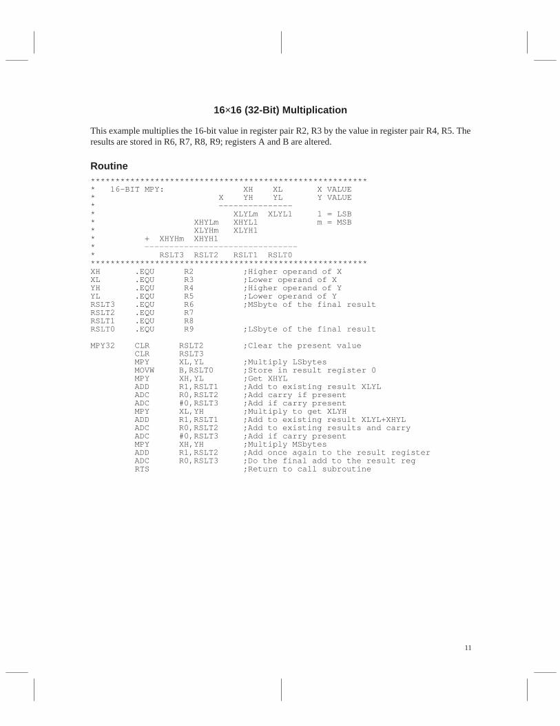
16×16 (32-Bit) Multiplication
This example multiplies the 16-bit value in register pair R2, R3 by the value in register pair R4, R5. Theresults are stored in R6, R7, R8, R9; registers A and B are altered.
Routine********************************************************* 16-BIT MPY: XH XL X VALUE* X YH YL Y VALUE* –––––––––––––––* XLYLm XLYL1 1 = LSB* XHYLm XHYL1 m = MSB* XLYHm XLYH1* + XHYHm XHYH1* –––––––––––––––––––––––––––––––* RSLT3 RSLT2 RSLT1 RSLT0********************************************************XH .EQU R2 ;Higher operand of XXL .EQU R3 ;Lower operand of XYH .EQU R4 ;Higher operand of YYL .EQU R5 ;Lower operand of YRSLT3 .EQU R6 ;MSbyte of the final resultRSLT2 .EQU R7RSLT1 .EQU R8RSLT0 .EQU R9 ;LSbyte of the final result
MPY32 CLR RSLT2 ;Clear the present value CLR RSLT3 MPY XL,YL ;Multiply LSbytes MOVW B,RSLT0 ;Store in result register 0 MPY XH,YL ;Get XHYL ADD R1,RSLT1 ;Add to existing result XLYL ADC R0,RSLT2 ;Add carry if present ADC #0,RSLT3 ;Add if carry present MPY XL,YH ;Multiply to get XLYH ADD R1,RSLT1 ;Add to existing result XLYL+XHYL ADC R0,RSLT2 ;Add to existing results and carry ADC #0,RSLT3 ;Add if carry present MPY XH,YH ;Multiply MSbytes ADD R1,RSLT2 ;Add once again to the result register ADC R0,RSLT3 ;Do the final add to the result reg RTS ;Return to call subroutine

12
13
Binary DivisionWith the TMS370
Microcontroller Products—Semiconductor GroupTexas Instruments

14
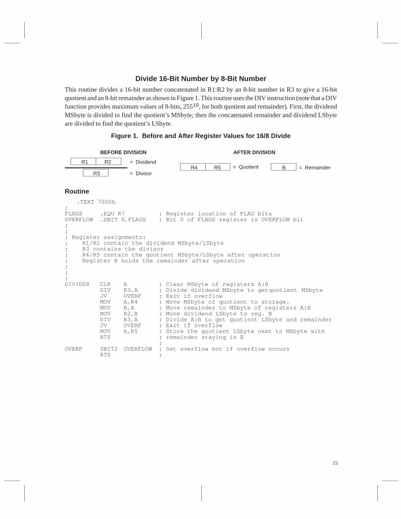
15
Divide 16-Bit Number by 8-Bit NumberThis routine divides a 16-bit number concatenated in R1:R2 by an 8-bit number in R3 to give a 16-bitquotient and an 8-bit remainder as shown in Figure 1. This routine uses the DIV instruction (note that a DIVfunction provides maximum values of 8-bits, 25510, for both quotient and remainder). First, the dividendMSbyte is divided to find the quotient’s MSbyte; then the concatenated remainder and dividend LSbyteare divided to find the quotient’s LSbyte.
Figure 1. Before and After Register Values for 16/8 Divide
R1
R3
BEFORE DIVISION AFTER DIVISION
R4 R5 = Quotient B = Remainder= Dividend
= Divisor
R2
Routine
.TEXT 7000h;FLAGS .EQU R7 ; Register location of FLAG bitsOVERFLOW .DBIT 0,FLAGS ; Bit 0 of FLAGS register is OVERFLOW bit ;;; Register assignments:; R1/R2 contain the dividend MSbyte/LSbyte; R3 contains the divisor; R4/R5 contain the quotient MSbyte/LSbyte after operation; Register B holds the remainder after operation;;;DIVIDE8 CLR A ; Clear MSbyte of registers A:B
DIV R3,A ; Divide dividend MSbyte to getquotient MSbyteJV OVERF ; Exit if overflowMOV A,R4 ; Move MSbyte of quotient to storage.MOV B,A ; Move remainder to MSbyte of registers A:BMOV R2,B ; Move dividend LSbyte to reg. BDIV R3,A ; Divide A:B to get quotient LSbyte and remainderJV OVERF ; Exit if overflowMOV A,R5 ; Store the quotient LSbyte next to MSbyte withRTS ; remainder staying in B
;OVERF SBIT2 OVERFLOW ; Set overflow bot if overflow occurs
RTS ;
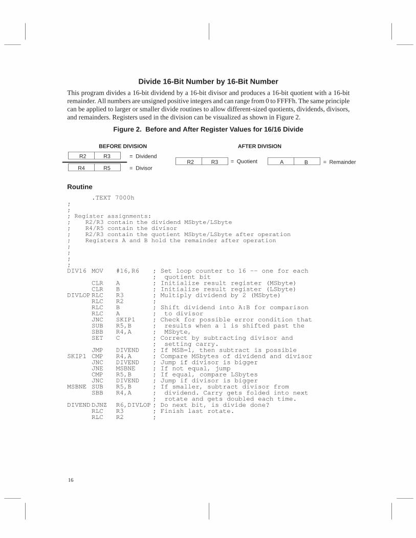
16
Divide 16-Bit Number by 16-Bit NumberThis program divides a 16-bit dividend by a 16-bit divisor and produces a 16-bit quotient with a 16-bitremainder. All numbers are unsigned positive integers and can range from 0 to FFFFh. The same principlecan be applied to larger or smaller divide routines to allow different-sized quotients, dividends, divisors,and remainders. Registers used in the division can be visualized as shown in Figure 2.
Figure 2. Before and After Register Values for 16/16 Divide
R2 R3
R4 R5
BEFORE DIVISION AFTER DIVISION
R2 R3 = Quotient A B = Remainder= Dividend
= Divisor
Routine
.TEXT 7000h;;; Register assignments:; R2/R3 contain the dividend MSbyte/LSbyte; R4/R5 contain the divisor; R2/R3 contain the quotient MSbyte/LSbyte after operation; Registers A and B hold the remainder after operation;;;;DIV16 MOV #16,R6 ; Set loop counter to 16 –– one for each
; quotient bitCLR A ; Initialize result register (MSbyte)CLR B ; Initialize result register (LSbyte)
DIVLOP RLC R3 ; Multiply dividend by 2 (MSbyte)RLC R2 ; RLC B ; Shift dividend into A:B for comparison RLC A ; to divisorJNC SKIP1 ; Check for possible error condition that SUB R5,B ; results when a 1 is shifted past the SBB R4,A ; MSbyte,SET C ; Correct by subtracting divisor and
; setting carry.JMP DIVEND ; If MSB=1, then subtract is possible
SKIP1 CMP R4,A ; Compare MSbytes of dividend and divisorJNC DIVEND ; Jump if divisor is biggerJNE MSBNE ; If not equal, jumpCMP R5,B ; If equal, compare LSbytesJNC DIVEND ; Jump if divisor is bigger
MSBNE SUB R5,B ; If smaller, subtract divisor fromSBB R4,A ; dividend. Carry gets folded into next
; rotate and gets doubled each time.DIVEND DJNZ R6,DIVLOP ; Do next bit, is divide done?
RLC R3 ; Finish last rotate.RLC R2 ;
17
BCD-to-Binary Conversionon the TMS370
Microcontroller Products—Semiconductor GroupTexas Instruments

18
19
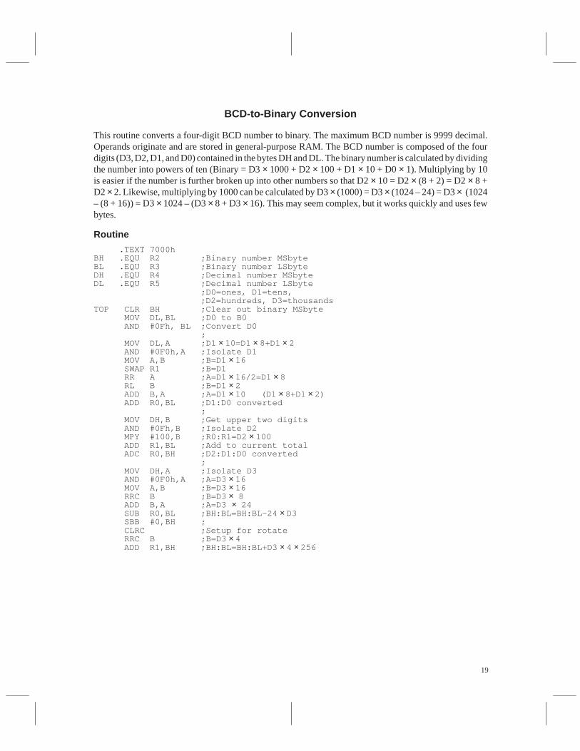
BCD-to-Binary Conversion
This routine converts a four-digit BCD number to binary. The maximum BCD number is 9999 decimal.Operands originate and are stored in general-purpose RAM. The BCD number is composed of the fourdigits (D3, D2, D1, and D0) contained in the bytes DH and DL. The binary number is calculated by dividingthe number into powers of ten (Binary = D3 × 1000 + D2× 100 + D1× 10 + D0× 1). Multiplying by 10is easier if the number is further broken up into other numbers so that D2× 10 = D2× (8 + 2) = D2× 8 +D2× 2. Likewise, multiplying by 1000 can be calculated by D3× (1000) = D3× (1024 – 24) = D3× (1024– (8 + 16)) = D3× 1024 – (D3× 8 + D3× 16). This may seem complex, but it works quickly and uses fewbytes.
Routine
.TEXT 7000hBH .EQU R2 ;Binary number MSbyteBL .EQU R3 ;Binary number LSbyteDH .EQU R4 ;Decimal number MSbyteDL .EQU R5 ;Decimal number LSbyte ;D0=ones, D1=tens, ;D2=hundreds, D3=thousandsTOP CLR BH ;Clear out binary MSbyte MOV DL,BL ;D0 to B0 AND #0Fh, BL ;Convert D0 ; MOV DL,A ;D1 × 10=D1 × 8+D1 × 2 AND #0F0h,A ;Isolate D1 MOV A,B ;B=D1 × 16 SWAP R1 ;B=D1 RR A ;A=D1 × 16/2=D1 × 8 RL B ;B=D1 × 2 ADD B,A ;A=D1 × 10 (D1 × 8+D1 × 2) ADD R0,BL ;D1:D0 converted ; MOV DH,B ;Get upper two digits AND #0Fh,B ;Isolate D2 MPY #100,B ;R0:R1=D2 × 100 ADD R1,BL ;Add to current total ADC R0,BH ;D2:D1:D0 converted ; MOV DH,A ;Isolate D3 AND #0F0h,A ;A=D3 × 16 MOV A,B ;B=D3 × 16 RRC B ;B=D3 × 8 ADD B,A ;A=D3 × 24 SUB R0,BL ;BH:BL=BH:BL–24 × D3 SBB #0,BH ; CLRC ;Setup for rotate RRC B ;B=D3 × 4 ADD R1,BH ;BH:BL=BH:BL+D3 × 4 × 256

20
21
Binary-to-BCD Conversionon the TMS370
Microcontroller Products—Semiconductor GroupTexas Instruments

22
23
Binary-to-BCD Conversion
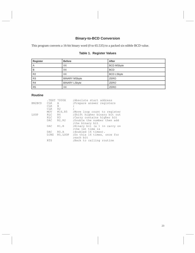
This program converts a 16-bit binary word (0 to 65.535) to a packed six-nibble BCD value.
Table 1. Register Values
Register Before After
A XX BCD MSbyte
B XX BCD
R2 XX BCD LSbyte
R3 BINARY MSbyte ZERO
R4 BINARY LSbyte ZERO
R5 XX ZERO
Routine
.TEXT 7000H ;Absolute start addressBN2BCD CLR A ;Prepare answer registers CLR B ; CLR R2 ; MOV #16,R5 ;Move loop count to registerLOOP RLC R4 ;Shift higher binary bit out RLC R3 ;Carry contains higher bit DAC R2,R2 ;Double the number then add ;the binary bit DAC R1,B ;Binary bit (a 1 in carry on ;the 1st time is DAC R0,A ;doubled 16 times). DJNZ R5,LOOP ;Do this 16 times, once for ;each bit RTS ;Back to calling routine

24
25
BCD String AdditionWith the TMS370
Microcontroller Products—Semiconductor GroupTexas Instruments

26
27
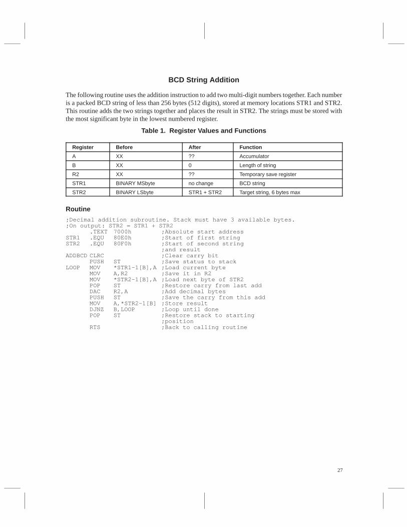
BCD String Addition
The following routine uses the addition instruction to add two multi-digit numbers together. Each numberis a packed BCD string of less than 256 bytes (512 digits), stored at memory locations STR1 and STR2.This routine adds the two strings together and places the result in STR2. The strings must be stored withthe most significant byte in the lowest numbered register.
Table 1. Register Values and Functions
Register Before After Function
A XX ?? Accumulator
B XX 0 Length of string
R2 XX ?? Temporary save register
STR1 BINARY MSbyte no change BCD string
STR2 BINARY LSbyte STR1 + STR2 Target string, 6 bytes max
Routine
;Decimal addition subroutine. Stack must have 3 available bytes.;On output: STR2 = STR1 + STR2
.TEXT 7000h ;Absolute start addressSTR1 .EQU 80E0h ;Start of first stringSTR2 .EQU 80F0h ;Start of second string
;and resultADDBCD CLRC ;Clear carry bit
PUSH ST ;Save status to stackLOOP MOV *STR1–1[B],A ;Load current byte
MOV A,R2 ;Save it in R2MOV *STR2–1[B],A ;Load next byte of STR2POP ST ;Restore carry from last addDAC R2,A ;Add decimal bytesPUSH ST ;Save the carry from this addMOV A,*STR2–1[B] ;Store resultDJNZ B,LOOP ;Loop until donePOP ST ;Restore stack to starting
;positionRTS ;Back to calling routine

28

29
TMS370 Floating Point Package
Microcontroller Products—Semiconductor GroupTexas Instruments

30

31
Introduction
This report describes assembly language floating point math routines for the TMS370 family ofmicrocontrollers. Floating point operations allow binary processors to carry out decimal, signed arithmetic.This package includes most of the common arithmetic and conversion routines used in floating pointoperations. The routines included are:
• Floating point addition/subtraction
• Floating point number comparison
• Floating point division
• Floating point multiplication
• Floating point increment/decrement
• Floating point number test
• Floating point negation
• Floating point to signed 8-bit integer conversion
• Floating point to signed long (16-bit) integer conversion
• Floating point to unsigned 8-bit integer conversion
• Floating point to unsigned long (16-bit) integer conversion
• Signed 8-bit integer to floating point conversion
• Signed long (16-bit) integer to floating point conversion
• Unsigned long (16-bit) integer to floating point conversion
• Unsigned 8-bit integer to floating point conversion

32
Floating Point Format
Each number in this floating point format is 24 bits long. This includes eight bits for the exponent, fifteenfor the mantissa, and the remaining bits for the sign.
The format is as follows:E E E E E E E E S M M M M M M M M M M M M M M M
The first byte is devoted to the exponent. The most significant bit of the second byte is the sign bit and theremaining bits are the mantissa. This format has been chosen so that arithmetic on the objects are restrictedto normal 8-bit operation or a 16-bit operations.
With this format, a routine that operates on one of these floating point values can check the sign bit andthen set that bit as implied. A 16-bit operation can then be used to modify the value.
The exponent’s bias is 128: subtract 128 from the unsigned value of the eight exponential bits to find theactual value of the exponent.
Example: exp = 00h -> real exp = 00h – 128 = –128
exp = FFh -> real exp = FFh – 128 = 127
exp = 80h -> real exp = 80h – 128 = 0
The mantissa contains 15 bits plus an implied bit. The layout is:
(m0) m1 m2 ... m15
The m0 bit is implied and is always 1. The value of each mi is the reciprocal of 2 to the ith power.
So the layout in terms of values is:
(1) 1/2 1/4 1/8 1/16 1/32 1/64 1/128 1/256 1/512 1/1024 1/2048 . . .
Given the above format, some special floating point values are:ZERO – 000000h = 2-128 = approx 2.94E-39MAX_POS – FF7FFFh = 2128 - 2112 = approx 3.4E38MIN_POS – 000001h = 2-128 + 2-143 = approx 2.94E-39MAX_NEG – FFFFFFh = 2112 - 2128 = approx -3.4E38MIN_NEG – 008000h = -(2-128) = approx -2.94E-39EPSILON – 710000h = 2-15 = approx 3E-5
MAX_POS is the largest positive number the format can represent. MIN_POS is the smallest positivenumber that can be represented. ZERO is a special case which is treated as true 0. EPSILON is the smallestnumber which can be added to 1.0 and result in a sum which is not 1.0.
The actual value of a floating point number can be expressed as : s × M × 2e-128, where s is the sign of thenumber –1 or 1, M is the value of the mantissa, and e is the bit value of the exponent.
A few more examples:
11 = 833000h –31.25 = 84FA00h
1 = 800000h –1 = 808000h
33
Floating Point Routines
Floating Point Addition/Subtraction
;Rev.1.0
;Function name - $fp_add,$fp_sub
;
;Purpose - 1) Perform the addition of two floating point numbers.
;
; OP1 + OP2
;
; 2) Perform the subtraction of two floating point
; numbers.
;
; OP1 - OP2
;
;
;Registers used - Register Before After
; -------------------------------------------------------
; Status | XX | Modified
;
; R14 | OP1 exponent | Modified
; R15 | OP1 mantissa MSB | Modified
; R16 | OP1 mantissa LSB | Modified
;
; R17 | OP2 exponent | Result exponent
; R18 | OP2 mantissa MSB | Result mantissa MSB
; R19 | OP2 mantissa LSB | Result mantissa LSB
;
;Size 200 Bytes
;
;Stack space 4 Bytes
;;Notes - 1) Some special considerations for floating point; operations are:;; ZERO + OP2 = OP2; OP1 + ZERO = OP1;; ZERO - OP2 = -OP2; OP1 - ZERO = OP1;
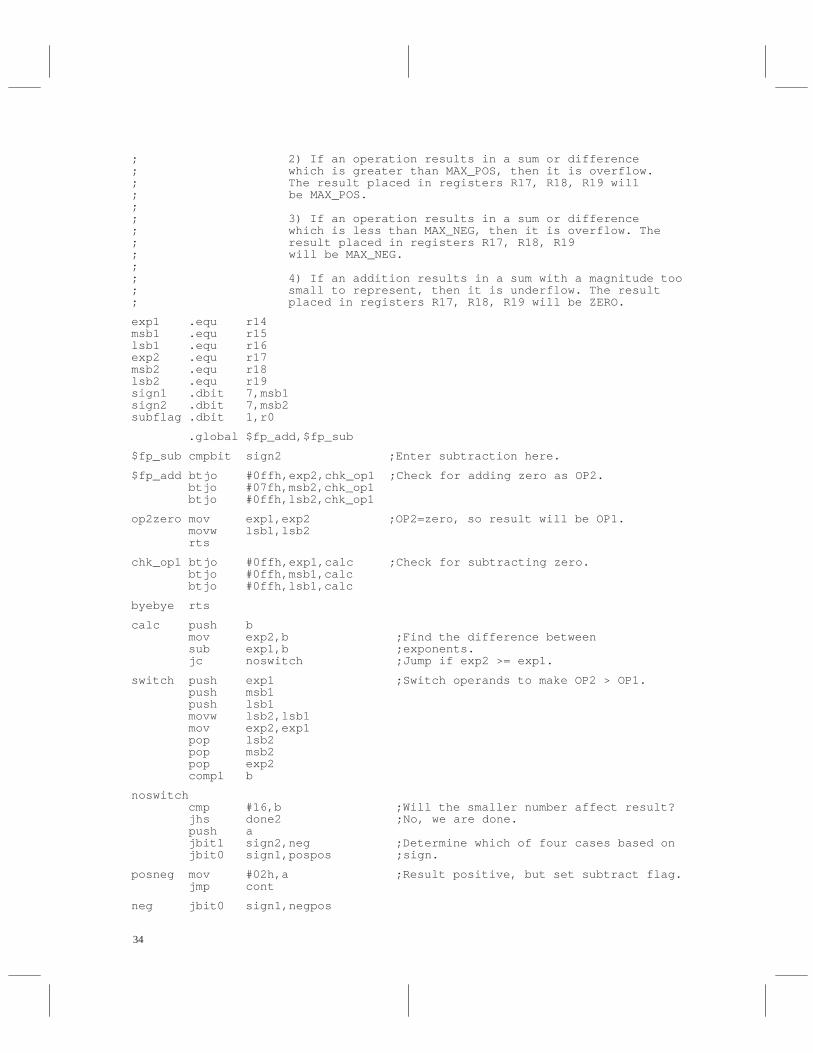
34
; 2) If an operation results in a sum or difference; which is greater than MAX_POS, then it is overflow.; The result placed in registers R17, R18, R19 will ; be MAX_POS.;; 3) If an operation results in a sum or difference; which is less than MAX_NEG, then it is overflow. The; result placed in registers R17, R18, R19; will be MAX_NEG.;; 4) If an addition results in a sum with a magnitude too; small to represent, then it is underflow. The result; placed in registers R17, R18, R19 will be ZERO.
exp1 .equ r14msb1 .equ r15lsb1 .equ r16exp2 .equ r17msb2 .equ r18lsb2 .equ r19sign1 .dbit 7,msb1sign2 .dbit 7,msb2subflag .dbit 1,r0
.global $fp_add,$fp_sub
$fp_sub cmpbit sign2 ;Enter subtraction here.
$fp_add btjo #0ffh,exp2,chk_op1 ;Check for adding zero as OP2. btjo #07fh,msb2,chk_op1 btjo #0ffh,lsb2,chk_op1
op2zero mov exp1,exp2 ;OP2=zero, so result will be OP1. movw lsb1,lsb2 rts
chk_op1 btjo #0ffh,exp1,calc ;Check for subtracting zero. btjo #0ffh,msb1,calc btjo #0ffh,lsb1,calc
byebye rts
calc push b mov exp2,b ;Find the difference between sub exp1,b ;exponents. jc noswitch ;Jump if exp2 >= exp1.
switch push exp1 ;Switch operands to make OP2 > OP1. push msb1 push lsb1 movw lsb2,lsb1 mov exp2,exp1 pop lsb2 pop msb2 pop exp2 compl b
noswitch cmp #16,b ;Will the smaller number affect result? jhs done2 ;No, we are done. push a jbit1 sign2,neg ;Determine which of four cases based on jbit0 sign1,pospos ;sign.
posneg mov #02h,a ;Result positive, but set subtract flag. jmp cont
neg jbit0 sign1,negpos
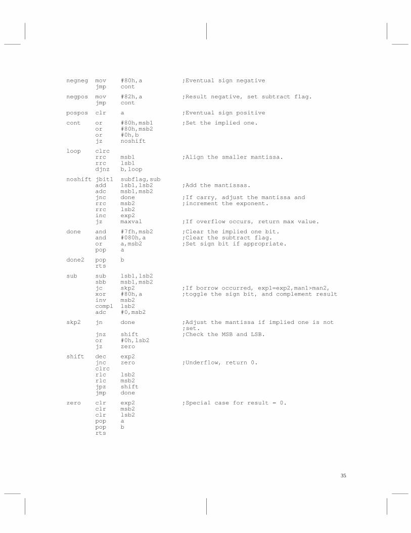
35
negneg mov #80h,a ;Eventual sign negative jmp cont
negpos mov #82h,a ;Result negative, set subtract flag. jmp cont
pospos clr a ;Eventual sign positive
cont or #80h,msb1 ;Set the implied one. or #80h,msb2 or #0h,b jz noshift
loop clrc rrc msb1 ;Align the smaller mantissa. rrc lsb1 djnz b,loop
noshift jbit1 subflag,sub add lsb1,lsb2 ;Add the mantissas. adc msb1,msb2 jnc done ;If carry, adjust the mantissa and rrc msb2 ;increment the exponent. rrc lsb2 inc exp2 jz maxval ;If overflow occurs, return max value.
done and #7fh,msb2 ;Clear the implied one bit. and #080h,a ;Clear the subtract flag. or a,msb2 ;Set sign bit if appropriate. pop a
done2 pop b rts
sub sub lsb1,lsb2 sbb msb1,msb2 jc skp2 ;If borrow occurred, exp1=exp2,man1>man2, xor #80h,a ;toggle the sign bit, and complement result inv msb2 compl lsb2 adc #0,msb2
skp2 jn done ;Adjust the mantissa if implied one is not ;set. jnz shift ;Check the MSB and LSB. or #0h,lsb2 jz zero
shift dec exp2 jnc zero ;Underflow, return 0. clrc rlc lsb2 rlc msb2 jpz shift jmp done
zero clr exp2 ;Special case for result = 0. clr msb2 clr lsb2 pop a pop b rts

36
maxval mov #0ffh,exp2 ;Create maximum value. movw #07fffh,lsb2 or a,msb2 ;Set sign bit as appropriate. pop a pop b rts
37
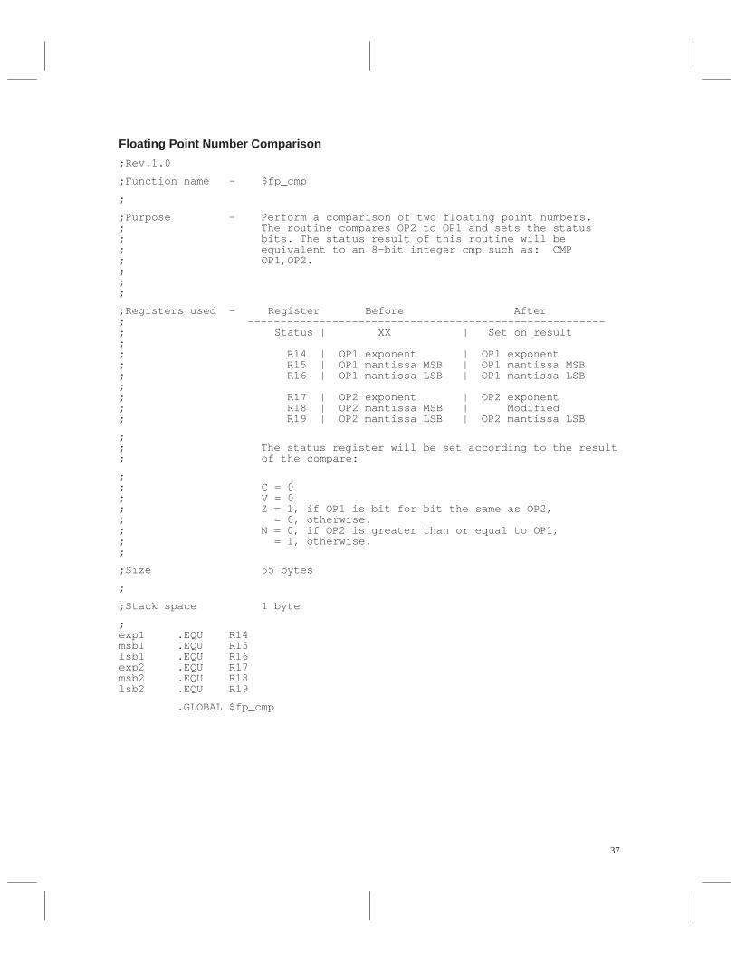
Floating Point Number Comparison
;Rev.1.0
;Function name - $fp_cmp
;
;Purpose - Perform a comparison of two floating point numbers.; The routine compares OP2 to OP1 and sets the status; bits. The status result of this routine will be; equivalent to an 8-bit integer cmp such as: CMP; OP1,OP2.;;;
;Registers used - Register Before After; -------------------------------------------------------; Status | XX | Set on result;; R14 | OP1 exponent | OP1 exponent; R15 | OP1 mantissa MSB | OP1 mantissa MSB; R16 | OP1 mantissa LSB | OP1 mantissa LSB;; R17 | OP2 exponent | OP2 exponent; R18 | OP2 mantissa MSB | Modified; R19 | OP2 mantissa LSB | OP2 mantissa LSB
;; The status register will be set according to the result; of the compare:
;; C = 0; V = 0; Z = 1, if OP1 is bit for bit the same as OP2,; = 0, otherwise.; N = 0, if OP2 is greater than or equal to OP1,; = 1, otherwise.;
;Size 55 bytes
;
;Stack space 1 byte
;exp1 .EQU R14msb1 .EQU R15lsb1 .EQU R16exp2 .EQU R17msb2 .EQU R18lsb2 .EQU R19
.GLOBAL $fp_cmp
38
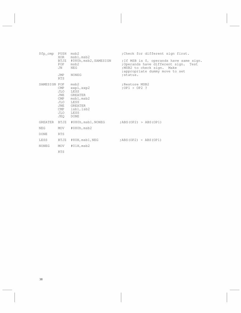
$fp_cmp PUSH msb2 ;Check for different sign first. XOR msb1,msb2 BTJZ #080h,msb2,SAMESIGN ;If MSB is 0, operands have same sign. POP msb2 ;Operands have different sign. Test JN NEG ;MSB2 to check sign. Make ;appropriate dummy move to set JMP NONEG ;status. RTS
SAMESIGN POP msb2 ;Restore MSB2 CMP exp1,exp2 ;OP1 > OP2 ? JLO LESS JNE GREATER CMP msb1,msb2 JLO LESS JNE GREATER CMP lsb1,lsb2 JLO LESS JEQ DONE
GREATER BTJZ #080h,msb1,NONEG ;ABS(OP2) > ABS(OP1)
NEG MOV #080h,msb2
DONE RTS
LESS BTJZ #80H,msb1,NEG ;ABS(OP2) < ABS(OP1)
NONEG MOV #01H,msb2
RTS
39
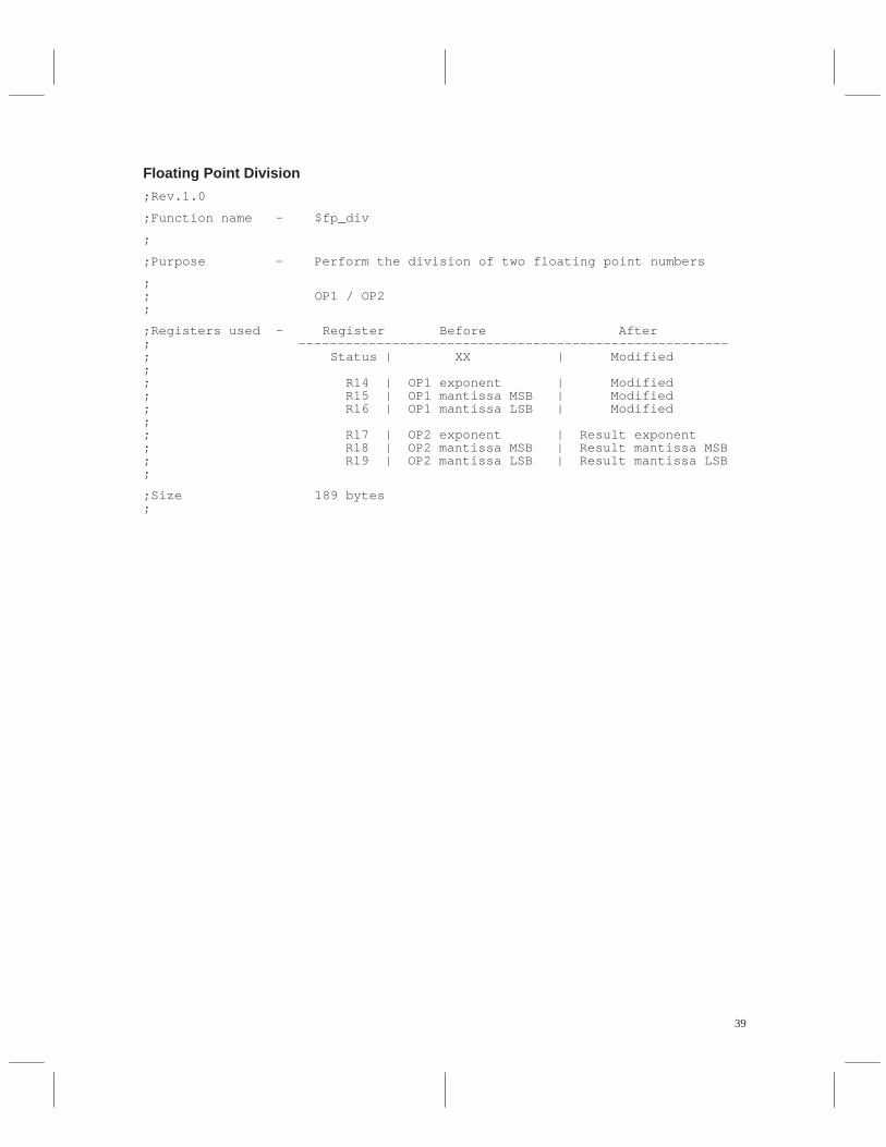
Floating Point Division
;Rev.1.0
;Function name - $fp_div
;
;Purpose - Perform the division of two floating point numbers
;; OP1 / OP2;
;Registers used - Register Before After; -------------------------------------------------------; Status | XX | Modified;; R14 | OP1 exponent | Modified; R15 | OP1 mantissa MSB | Modified; R16 | OP1 mantissa LSB | Modified;; R17 | OP2 exponent | Result exponent; R18 | OP2 mantissa MSB | Result mantissa MSB; R19 | OP2 mantissa LSB | Result mantissa LSB;
;Size 189 bytes;
40
;Stack space 4 bytes;
;;Notes - 1) Some special considerations for floating point; divide are:
;; ZERO / OP2 = ZERO; OP1 / ZERO = MAX_POS (if OP1 >= 0); MAX_NEG (if OP1 < 0);; 2) If a division results in a quotient which is; greater than MAX_POS, then it is overflow. The; result placed in registers R17, R18, R19 will be; MAX_POS.;; 3) If a division results in a quotient which is; less than MAX_NEG, then it is overflow. The result; placed in registers R17, R18, R19 will be MAX_NEG.;; 4) If a division results in a quotient with a; magnitude too small to represent, then it is underflow.; The result placed in registers R17, R18, R19; will be ZERO.
EXP1 .equ R14MAN1MSB .equ R15MAN1LSB .equ R16EXP2 .equ R17MAN2MSB .equ R18MAN2LSB .equ R19COUNTER .equ R20FLAGS .equ R23
OVFL .dbit 0,FLAGSSIGN_OP1 .dbit 7,MAN1MSB .global $fp_div
$fp_div PUSH A ;Save registers
CHK_OP1 ;Check for OP1=ZERO. MOV MAN1MSB,A ;Use FLAGS here as dummy register OR EXP1,A ;OR all parts operand together. OR MAN1LSB,A ;If ZERO, no bits will be ones. JNZ CHK_OP2 CLR MAN2LSB ;OP1 is ZERO, so clear OP2 as answer. CLR MAN2MSB ;Store results in OP2 registers. CLR EXP2 POP A ;Restore registers to original ;values. RTS ;Exit fp_div.
CHK_OP2 ;Check for OP2=ZERO. MOV MAN2MSB,A ;Use FLAGS here as dummy register OR EXP2,A ;OR all parts operand together. OR MAN2LSB,A ;If ZERO, no bits will be ones. JNZ FINDSIGN MOV #0FFh,EXP2 ;Set result to MAX_POS or MAX_NEG MOVW #07FFFh,MAN2LSB ;depending on the sign bit. OR MAN1LSB,MAN2LSB POP A ;Restore registers to original ;values. RTS ;Exit fp_div.
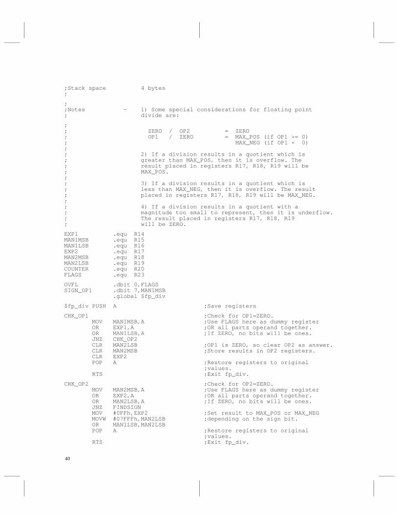
41
FINDSIGN PUSH B ;Save registers. PUSH COUNTER PUSH FLAGS MOV MAN1MSB,FLAGS ;Find sign of quotient. XOR MAN2MSB,FLAGS ;If sign flags differ, FLAGS 7=1. AND #080h,FLAGS ;Clear other bits in FLAGS. OR #080h,MAN1MSB ;Set implied 1 in sign bit position. OR #080h,MAN2MSB ;
SUBEXP CLR B ;Clear B for result of exponent math. SUB EXP2,EXP1 ;Subtract exponents. ADC #0h,B ;Save status of carry bit from SUB. MOV EXP1,EXP2 ;Move result of SUB to EXP2. ADD #080h,EXP2 ;Correct for +128 offset. ADC #0FFh,B ;Save status of carry bit and JZ SETUP ;subtract 1 from SUB. Jump on result JP CHK_OVER ;of exponent math: ; 01 = possible overflow ; 00 = ok ; FF = definite underflow
UNDERFLOW ;Result of division is underflow. CLR MAN2LSB ;Store results in OP2 registers. CLR MAN2MSB CLR EXP2 POP FLAGS ;Restore registers to original ;values. POP COUNTER POP B POP A RTS ;Exit fp_div.
CHK_OVER ;Subtraction of exponents may have BTJO #0FFh,EXP2,OVERFLOW ;overflowed. If exponent is not 00, SBIT1 OVFL ;then result has definitely ;overflowed. ;If result may be ok, set flag.
SETUP MOV #16,COUNTER ;Set loop counter to 16, one for each CLR A ;quotient bit, and initalize result ;registers (reg B was cleared above).
SKIP1 CMP MAN2MSB,MAN1MSB ;Compare MSBs of dividend and ;divisor. JLO DIVEND ;Jump if divisor is bigger. JNE MSBNE ;If equal, compare LSBs. CMP MAN2LSB,MAN1LSB ;Compare LSBs. JLO DIVEND ;Jump if divisor is bigger.
MSBNE SUB MAN2LSB,MAN1LSB ;If smaller, subtract divisor from SBB MAN2MSB,MAN1MSB ;dividend. Carry is folded into ;next rotate and doubled each time.
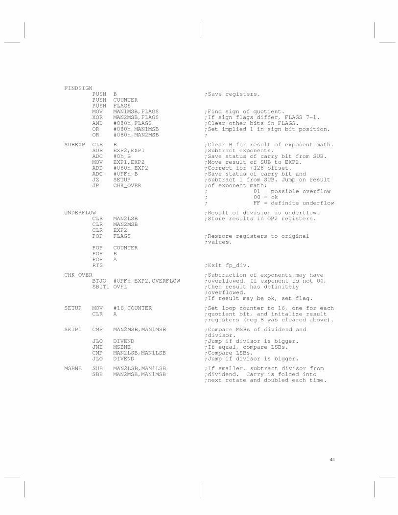
42
DIVEND DJNZ COUNTER,DIVIDE ;Next bit. Is divide done? RLC B ;Finish last rotate. RLC A JN DONE ;If MSB is not one, decrement EXP2 SUB #01h,EXP2 ;and go back up and shift one more ;time. JNC UNDERFLOW ;If EXP2 was zero, decrement has ;caused an underflow. SBIT0 OVFL ;Clear flag to show possible overflow ;condition has been corrected. INC COUNTER ;Reset counter for 1 last loop ;through. JMP LAST1
OVERFLOW ;Result of divide is overflow. MOVW #07FFFh,MAN2LSB ;Store results in OP2 registers. MOV #0FFh,EXP2 OR FLAGS,MAN2MSB ;Set sign bit of result. POP FLAGS ;Restore registers to original ;values. POP COUNTER POP B POP A RTS ;Exit fp_div.
DIVIDE ;16 x 16 division routine. RLC B ;Multiply divend by 2. RLC A ;
LAST1 RLC MAN1LSB ;Shift dividend into MAN1MSB:MAN1LSB RLC MAN1MSB ;for comparison to divisor. JNC SKIP1 ;Check for possible error condition SUB MAN2LSB,MAN1LSB ;that results when a 1 is shifted ;past the MSB. SBB MAN2MSB,MAN1MSB ;Correct by subtracting SETC ;divisor and setting carry. JMP DIVEND
DONE BTJO #01h,FLAGS,OVERFLOW ;Make sure that divide sequence fixed ;previous exponent overflow. OR #07Fh,FLAGS ;Set FLAGS bits except for sign bit. AND FLAGS,A ;Set sign bit. MOVW B,MAN2LSB ;Put answer in result register. POP FLAGS ;Restore registers to original ;values. POP COUNTER POP B POP A RTS ;Exit fp_div.
43
Floating Point Multiplication;Rev.1.0
;Function name - $fp_mul
;
;Purpose - Perform the multiplication of two floating point; numbers.;; OP1 * OP2;
;Registers used - Register Before After; -------------------------------------------------------; Status | XX | Modified;; R14 | OP1 exponent | Modified; R15 | OP1 mantissa MSB | Modified; R16 | OP1 mantissa LSB | Modified;; R17 | OP2 exponent | Result exponent; R18 | OP2 mantissa MSB | Result mantissa MSB; R19 | OP2 mantissa LSB | Result mantissa LSB;
;Size 189 Bytes
;
;Stack space 4 Bytes
;
;Notes - 1) Some special considerations for floating point; multiplication are:;; ZERO * OP2 = ZERO; OP1 * ZERO = ZERO;; 2) If a multiplication results in a product which is; greater than MAX_POS, then it is overflow. The result; placed in registers R17, R18, R19 will be MAX_POS.;; 3) If a multiplication results in a product which is; less than MAX_NEG, then it is overflow. The result; placed in registers R17, R18, R19 will be MAX_NEG.;; 4) If a multiplication results in a product with a; magnitude too small to represent, then it is underflow.; The result placed in registers R17, R18, R19; will be ZERO.
EXP1 .equ R14MAN1MSB .equ R15MAN1LSB .equ R16EXP2 .equ R17MAN2MSB .equ R18MAN2LSB .equ R19FLAGS .equ R20RSLT1 .equ R21
SIGNBIT .dbit 7,FLAGSUNDER_BIT .dbit 0,FLAGSIMPLIED_ONE .dbit 7,MAN1LSB
44
.global $fp_mul
$fp_mul ;Check for OP1=ZERO. BTJO #0FFh,EXP2,CHK_OP2 BTJO #0FFh,MAN1LSB,CHK_OP2 BTJO #0FFh,MAN1MSB,CHK_OP2 CLR MAN2LSB ;OP1 is ZERO, so clear OP2 as answer. CLR MAN2MSB CLR EXP2 RTS ;Exit fp_mul
CHK_OP2 ;Check for OP2=ZERO BTJO #0FFh,EXP2,FINDSIGN BTJO #0FFh,MAN2LSB,FINDSIGN BTJO #0FFh,MAN2MSB,FINDSIGN RTS ;OP2 is ZERO, so done. Exit fp_mul.
FINDSIGN PUSH R0 ;Save values of registers used. PUSH RSLT1 PUSH FLAGS MOV MAN1MSB,FLAGS ;Find sign of product. XOR MAN2MSB,FLAGS ;If sign flags differ, FLAGS 7=1. AND #080h,FLAGS ;Clear other bits in FLAGS. OR #080h,MAN1MSB ;Set implied 1 in sign bit position. OR #080h,MAN2MSB
ADDEXP CLR R0 ;Clear A for result of exponent math. ADD EXP1,EXP2 ;Add exponents. ADC #0h,A ;Save status of carry bit from ADD. SUB #080h,EXP2 ;Correct for +128 offset. ADC #0FFh,A ;Save status of carry bit and ;subtract 1 from SUB. JZ MULTIPLY ;Jump according to ;result of exponent math: JN CHK_UNDER ; FF = underflow ; 00 = ok ; 01 = definite overflow
OVERFLOW ;Result of multiplication is ;overflow. MOVW #07FFFh,MAN2LSB ;Store results in OP2 registers. MOV #0FFh,EXP2 OR FLAGS,MAN2MSB ;Set sign bit of result. POP FLAGS ;Restore registers to original ;values. POP RSLT1 POP R0 RTS ;Exit fp_mul
UNDERFLOW ;Result of multiplication is ;underflow. CLR MAN2LSB ;Store results in OP2 registers. CLR MAN2MSB CLR EXP2 POP FLAGS ;Restore registers to original ;values. POP RSLT1 POP R0 RTS ;Exit fp_mul
45
CHK_UNDER ;Addition of exponents has ;underflowed.
BTJZ #0FFh,EXP2,UNDERFLOW ;If exponent is not FF, then the ;exponent has definitely ;underflowed.
SBIT1 UNDER_BIT ;Set bit to indicate that an ;underflow is possible if not ;corrected at end of multiplication ;routine.
MULTIPLY PUSH R1 ;Save value of B register. MPY MAN1LSB,MAN2LSB ;Start multiplying. MOV A,RSLT1 MPY MAN1MSB,MAN2LSB CLR MAN2LSB ;MAN2LSB = LSB of mantissa product. ADD R1,RSLT1 ADC R0,MAN2LSB MPY MAN1LSB,MAN2MSB CLR MAN1LSB ;Since MAN1LSB is not needed anymore, ;use it as temporary storage during ;the multiplication process. ADD R1,RSLT1 ADC R0,MAN2LSB ADC #0,MAN1LSB MPY MAN1MSB,MAN2MSB ADD R1,MAN2LSB ADC R0,MAN1LSB POP R1 ;Restore value of B register.
DONE_MULT JBIT0 IMPLIED_ONE,JUSTIFY ;If result has no implied one, need ;to justify result. BTJZ #0FFh,EXP2,INCEXP ;If exponent is not FFh, then ;increment will not cause JMP OVERFLOW ;overflow.
JUSTIFY JBIT1 UNDER_BIT,UNDERFLOW ;Previous underflow will not be ;corrected, so result is underflow. RL RSLT1 ;Justify result to add implied one. RLC MAN2LSB RLC MAN1LSB DEC EXP2 ;Value of exponent does not need to ;be changed, so decrement here to ;make up for next INC instruction.
INCEXP INC EXP2
SET_RESULTS ;Result of multiplication is in ;range. MOV MAN1LSB,MAN2MSB ;Store results in OP2 registers. OR #07Fh,FLAGS ;Set FLAGS bits except for sign bit. AND FLAGS,MAN2MSB ;Set sign bit. LSB is in correct ;place from multiply routine. POP FLAGS ;Restore registers to original ;values. POP RSLT1 POP R0 RTS ;Exit fp_mul
46
Floating Point Increment / Decrement
;Rev.1.0
;Function name - $fp_inc,$fp_dec
;;Purpose - 1) Increment a floating point number,; i.e. add a 1.0 to it.;; OP1 + 1.0;; 2) Decrement a floating point number,; i.e. subtract 1.0 from it.;; OP1 - 1.0;
;Registers used - Register Before After; -------------------------------------------------------; Status | XX | Modified;; R17 | OP1 exponent | Result exponent; R18 | OP1 mantissa MSB | Result mantissa MSB; R19 | OP1 mantissa LSB | Result mantissa LSB;
;Size 180 Bytes;
;Stack space 4 Bytes;
;Notes - 1) Incrementing or decrementing a number with an; exponent greater than or equal to 90 will have no; effect.;; 2) Incrementing or decrementing a number with an; exponent less than or equal to 71 will have no; effect.
;msb2 .equ r15lsb2 .equ r16exp1 .equ r17msb1 .equ r18lsb1 .equ r19sign .dbit 7,r0 ;Flag to indicate whether to add or ;subtract numbers as a result of ;math.
decflag .dbit 0,r0 ;1=increment, 0=decrement. .global $fp_inc .global $fp_dec
$fp_dec .text 7000h ;Entry point for decrement. push a ;Save A register. mov #80h,a ;Complement the sign bit and set all xor msb1,a ;other bits of msb1=1. or #07fh,a ; sbit0 decflag ;Set flag to indicate decrement op. jmp $1
47
$fp_inc ;Entry point for increment. push a ;Save A register. mov msb1,a ;Move msb1 to A register and set every or #07fh,a ;bit except sign bit.
$1 cmp #90h,exp1 ;Check to see if 1.0 is insignificant jhs done ;compared with size of OP1. Exit if ;OP1 will not change. cmp #71h,exp1 ;Check to see if OP1 is insignificant jhs size_ok ;compared with 1.0. mov #80h,exp1 ;If so, result=1.0 or -1.0. clr lsb1 jbit0 decflag,$5 ;Is it a decrement operation? clr msb1 ;No, set result to 1.0. jmp done ;
$5 mov #080h,msb1 ;Yes, set result to -1.0.
done pop a rts
size_ok push b ;Save registers that will be modified. push msb2 push lsb2 or #80h,msb1 ;Set the implied one. mov exp1,b ;Calculate number of spaces needed to sub #80h,b ;shift number to align mantissas. jc greater ;If exp1>#80h then OP1>1.0: adjust ;OP2. compl b ;Take absolute value of exponent diff. mov #80h,exp1 ;Set the exponent.
loop clrc rrc msb1 ;Adjust OP1 so that it has the same rrc lsb1 ;exponent as OP2. This is necessary djnz b,loop ;for the two numbers to be added. btjo #80h,a,subt ;Choose whether you need to add or ;subtract numbers based on sign of ;numbers and whether you are ;incrementing or decrementing. add #80h,msb1 ;Need to add numbers. Add one to OP1.
done2 jbit1 decflag,$4 ;If a decrement is in progress, xor #80h,a ;flip the sign of the result. sbit1 decflag
$4 and a,msb1 ;Set the sign bit according to the ;result.
done3 pop lsb2 ;Restore registers and exit. pop msb2 pop a pop b rts
subt sbit0 sign ;The result is positive. (OP1 is less sub #80h,msb1 ;than 1.0) The operands have already inv msb1 ;been aligned to have the same compl lsb1 ;exponent. Subtract 1 from OP1 and adc #0,msb1 ;invert the MSB and complement the LSB ;to get the absolute value.
48
adjust dec exp1 ;Shift the mantissa and adjust the clrc ;exponent until an implied one is set. rlc lsb1 rlc msb1 jpz adjust jmp done2
greater clr lsb2 ;OP1 is greater than 1. Shift 1 so it clr msb2 ;has the same exponent as OP1. If the cmp #07h,b ;exponents differ by < 7, then only ;MSB is affected. Otherwise, implied jle msb_only ;one will roll on into LSB. sub #07h,b ;Calculate number of shifts needed. setc ;Since implied 1 will roll all the$2 rrc lsb2 ;way through the MSB, go ahead and djnz b,$2 ;subtract 7 from number of shifts jmp calc ;needed and start with LSB.
msb_only inc b ;Adjust to 1 needs less than 7 shifts, setc ;so only the MSB will be affected.
$3 rrc msb2 djnz b,$3
calc btjo #80h,a,subtr ;If the sign flag is negative,operands ;actually need to be subtracted. add lsb2,lsb1 ;Sign flag is positive, so add ;OP1+1.0. adc msb2,msb1
chkadj jnc done2 ;If carry occurs, need to roll back rrc msb1 ;mantissa and increment exponent. rrc lsb1 inc exp1 jmp done2
subtr sub lsb2,lsb1 ;Subtract mantissa2 - mantissa1. sbb msb2,msb1 jn done2 ;Implied 1 is present. Do not adjust. jnz adjust ;If MSBs are not equal, adjust. or #0h,lsb1 ;MSBs are equal, check to see if jnz adjust ;LSBs are equal. If not, adjust. clr exp1 ;Mantissas are zero, so it is a jmp done3 ;floating point zero.
49
Floating Point Number Test
;Rev.1.0;Function name - $fp_tst;
;Purpose - Perform a test of the floating point number, similar; to the hardware TST instruction for the A and B; registers.;;Registers used - Register Before After; -------------------------------------------------------; Status | XX | Set on result;; R17 | OP1 exponent | OP1 exponent; R18 | OP1 mantissa MSB | Modified; R19 | OP1 mantissa LSB | OP1 mantissa LSB;
;Size 22 bytes;
;Stack space None;
;Notes - 1) The output will be the new contents of the status; bits C, N, Z, and V.;; C = 0.; V = 0.; N = sign bit of the floating point number.; Z = 1, if the floating point number is ZERO.; = 0, otherwise.;; 2) This routine is the same as a call to $fp_cmp,; with OP1 = ZERO and OP2 = the number to test.exp1 .equ r17msb1 .equ r18lsb1 .equ r19
.global $fp_tst
$fp_tst mov msb1,msb1 ;Test the MSB. If negative, return jn done ;and status register will be set ;correctly. btjo #0ffh,exp1,$1 ;Check for zero. btjo #0ffh,lsb1,$1 btjo #0ffh,msb1,$1
done rts ;Result is zero. Status reg is ;correct.
$1 mov #01h,msb1 ;Number is not negative and not zero, rts ;so it must be positive. Do a dummy ;move to set status flags correctly.
50
Floating Point Number Negation
;Rev.1.0;Function name - $fp_neg;;Purpose - Perform the sign negation of a floating point number;; -OP1;
;Registers used - Register Before After; -------------------------------------------------------; Status | XX | Set on result MSB;; R17 | OP1 exponent | Result exponent; R18 | OP1 mantissa MSB | Result mantissa MSB; R19 | OP1 mantissa LSB | Result mantissa LSB;
;Size 17 Bytes;
;Stack space None;
;Notes - Some special considerations for floating point; negation are:;; -ZERO = ZEROexp .equ r17msb .equ r18lsb .equ r19
.global $fp_neg
$fp_neg .text 7000h btjo #0ffh,exp,negate ;Check for zero. btjo #0ffh,msb,negate btjo #0ffh,lsb,negate
zero rts ;Number was zero, return.
negate xor #80h,msb ;Toggle sign bit if not zero. rts
51
Floating Point To Signed 8-Bit Integer Conversion
;Rev.1.0
;Function name - $fp_ftoi;
;Purpose - Convert a 24-bit signed floating representation; of a number to an equivalent 8-bit signed integer; representation.;
;Registers used - Register Before After; -------------------------------------------------------; Status | XX | Modified; A | XX | Result;; R17 | OP2 exponent | OP2 exponent; R18 | OP2 mantissa MSB | OP2 mantissa MSB; R19 | OP2 mantissa LSB | OP2 mantissa LSB;
;Size 45 bytes;
;Stack space 1 byte;
;Notes - 1) The fractional part of the float is discarded.;; 2) If the value of the integral part of the float cannot; be represented by the signed int, the behavior is; undefined.;; 3) A float value of ZERO will be converted to 0.expon .equ r17fsign .dbit 7,r18
.global $fp_ftoi .text 7000h
$fp_ftoi ;Floating point to integer conversion. btjo #80h,expon,$1 ;If exponent < 1, then number is too small. clr a ;Set result = 0 and return. rts
$1 cmp #87h,expon ;Check for too big (>127). jhs big mov r18,a ;Put MSB into A reg to be adjusted. or #80h,a ;Set the implied one. push expon ;Save true value of exponent. sub #87h,expon ;Exponent – 87h = # of shifts needed to compl expon ;represent number as 7 binary digit number.
loop clrc rrc a ;Rotate A as needed. Loop until implied 1 is djnz expon,loop ;in position. jbit0 fsign,pos ;Check for minus sign. compl a ;Take the 2’s complement of integer to set ;sign.
pos pop expon ;Restore the original exponent. rts
big jbit1 fsign,bigminus ;Number is too big to be represented as a mov #7fh,a ;signed integer. Set result to max positive ;value. rts

52
bigminus ;Number is too small to be represented as a mov #80h,a ;signed integer. Set result to max negative rts ;value.
53
Floating Point To Signed Long (16-Bit) Integer Conversion;Rev.1.0
;Function name - $fp_ftol;
;Purpose - Convert a 24-bit signed floating representation; of a number to an equivalent 16-bit signed integer; representation.;
;Registers used - Register Before After; -------------------------------------------------------; Status | XX | Modified; A | XX | Signed integer MSB; B | XX | Signed integer LSB;; R17 | OP1 exponent | OP1 exponent; R18 | OP1 mantissa MSB | OP1 mantissa MSB; R19 | OP1 mantissa LSB | OP1 mantissa LSB;
;Size 56 bytes;
;Stack space 1 byte;
;Notes - 1) The fractional part of the float is discarded.;; 2) If the value of the integral part of the float cannot; be represented by the signed long int, the behavior is; undefined.;; 3) A float value of ZERO will be converted to 0.
expon .equ r17fsign .dbit 7,r18
.global $fp_ftol .text 7000h
$fp_ftol ;Floating point to long integer conversion. btjo #80h,expon,$1 ;If exponent < 1, then number is too small. clr a ;Set result = 0 and return. clr b rts
$1 cmp #8fh,expon ;Check for too big (>32767) jhs big mov r19,b mov r18,a or #80h,a ;Set the implied one push expon ;Save true value of exponent. sub #8fh,expon ;Exponent – 8Fh = # of shifts needed to ;represent compl expon ;number as binary 15 digit number.
loop clrc rrc a ;Rotate A and B as needed. Loop until implied 1 rrc b ;is in position. djnz expon,loop jbit0 fsign,pos ;Check for minus sign. inv a ;Take the 2’s complement of integer to set ;sign. compl b adc #0,a
54
pos pop expon rts
big jbit1 fsign,bigminus mov #0ffh,b ;Number is too big to be represented as a ;signed integer. mov #7fh,a ;Set result to max positive value. rts
bigminus mov #0,b ;Number is too small to be represented as a mov #80h,a ;signed integer. Set result to max negative rts ;value.
55
Floating Point To Unsigned 8-Bit Integer Conversion
;Rev.1.0
;Function name - $fp_ftou;
;Purpose - Convert a 24-bit signed floating representation; of a number to an equivalent 8-bit unsigned integer; representation.;
;Registers used - Register Before After; -------------------------------------------------------; Status | XX | Modified; A | XX | Result;; R17 | OP1 exponent | OP1 exponent; R18 | OP1 mantissa MSB | OP1 mantissa MSB; R19 | OP1 mantissa LSB | OP1 mantissa LSB;
;Size 35 Bytes;
;Stack space 1 Byte;
;Notes - 1) The fractional part of the float is discarded.;; 2) If the value of the integral part of the float cannot; be represented by the unsigned int, the behavior is; undefined.;; 3) A float value of ZERO will be converted to 0.expon .equ r17fsign .dbit 7,r18
.global $fp_ftou .text 7000h
$fp_ftou ;Floating point to unsigned integer conversion. btjo #80h,expon,$1;If exponent<1, then number is too small. clr a ;Set result = 0 and return. rts
$1 cmp #88h,expon ;Check for too big (>255). jhs big mov r18,a or #80h,a ;Set the implied one. push expon ;Save true value of exponent. sub #87h,expon ;Exponent-87h = # of shifts needed to represent compl expon ;number as 7 binary digit number. jz done
loop clrc rrc a ;Rotate A as needed. Loop until implied 1 is djnz expon,loop ;in position.
done pop expon rts
big mov #0ffh,a ;Number is too big to be represented as a signed rts ;integer. Set result to max positive value.
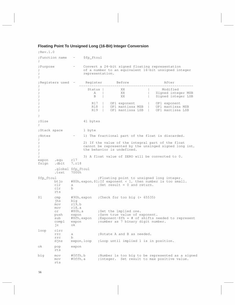
56
Floating Point To Unsigned Long (16-Bit) Integer Conversion;Rev.1.0
;Function name - $fp_ftoul;
;Purpose - Convert a 24-bit signed floating representation; of a number to an equivalent 16-bit unsigned integer; representation.;
;Registers used - Register Before After; -------------------------------------------------------; Status | XX | Modified; A | XX | Signed integer MSB; B | XX | Signed integer LSB;; R17 | OP1 exponent | OP1 exponent; R18 | OP1 mantissa MSB | OP1 mantissa MSB; R19 | OP1 mantissa LSB | OP1 mantissa LSB
;
;Size 41 bytes;
;Stack space 1 byte
;Notes - 1) The fractional part of the float is discarded.;; 2) If the value of the integral part of the float; cannot be represented by the unsinged signed long int,; the behavior is undefined.;; 3) A float value of ZERO will be converted to 0.expon .equ r17fsign .dbit 7,r18
.global $fp_ftoul .text 7000h
$fp_ftoul ;Floating point to unsigned long integer. btjo #80h,expon,$1;If exponent < 1, then number is too small. clr a ;Set result = 0 and return. clr b rts
$1 cmp #90h,expon ;Check for too big (> 65535) jhs big mov r19,b mov r18,a or #80h,a ;Set the implied one. push expon ;Save true value of exponent. sub #8fh,expon ;Exponent-8fh = # of shifts needed to represent compl expon ;number as 7 binary digit number. jz ok
loop clrc rrc a ;Rotate A and B as needed. rrc b djnz expon,loop ;Loop until implied 1 is in position.
ok pop expon rts
big mov #0ffh,b ;Number is too big to be represented as a signed mov #0ffh,a ;integer. Set result to max positive value. rts
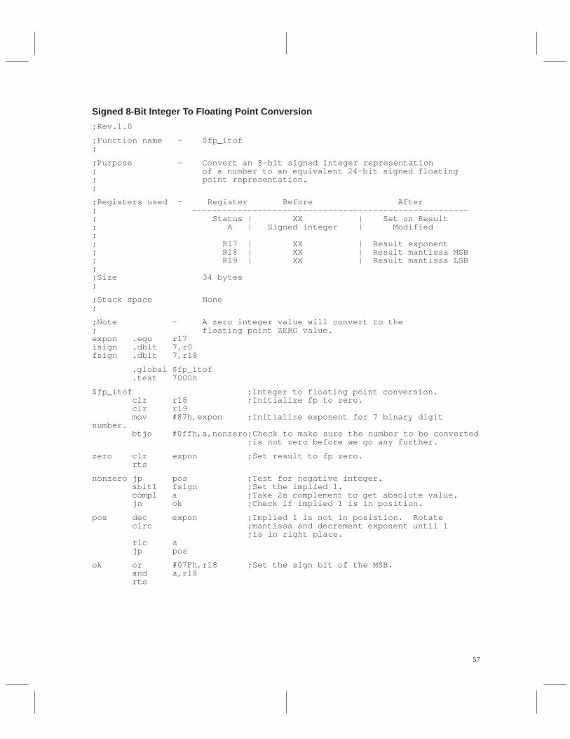
57
Signed 8-Bit Integer To Floating Point Conversion
;Rev.1.0
;Function name - $fp_itof;
;Purpose - Convert an 8-bit signed integer representation; of a number to an equivalent 24-bit signed floating; point representation.;
;Registers used - Register Before After; -------------------------------------------------------; Status | XX | Set on Result; A | Signed integer | Modified;; R17 | XX | Result exponent; R18 | XX | Result mantissa MSB; R19 | XX | Result mantissa LSB;;Size 34 bytes;
;Stack space None;
;Note - A zero integer value will convert to the; floating point ZERO value.expon .equ r17isign .dbit 7,r0fsign .dbit 7,r18
.global $fp_itof .text 7000h
$fp_itof ;Integer to floating point conversion. clr r18 ;Initialize fp to zero. clr r19 mov #87h,expon ;Initialize exponent for 7 binary digitnumber. btjo #0ffh,a,nonzero;Check to make sure the number to be converted ;is not zero before we go any further.
zero clr expon ;Set result to fp zero. rts
nonzero jp pos ;Test for negative integer. sbit1 fsign ;Set the implied 1. compl a ;Take 2s complement to get absolute value. jn ok ;Check if implied 1 is in position.
pos dec expon ;Implied 1 is not in posistion. Rotate clrc ;mantissa and decrement exponent until 1 ;is in right place. rlc a jp pos
ok or #07Fh,r18 ;Set the sign bit of the MSB. and a,r18 rts
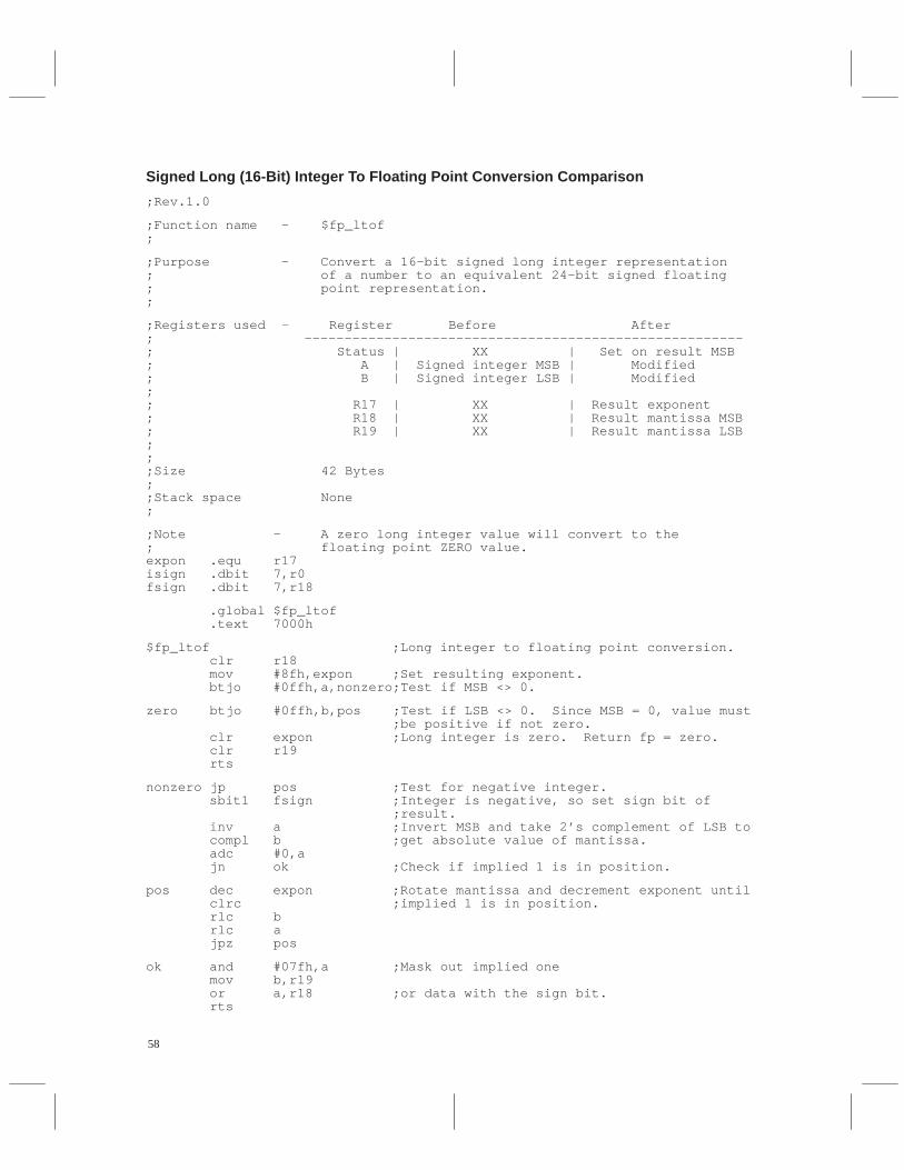
58
Signed Long (16-Bit) Integer To Floating Point Conversion Comparison
;Rev.1.0
;Function name - $fp_ltof;
;Purpose - Convert a 16-bit signed long integer representation; of a number to an equivalent 24-bit signed floating; point representation.;
;Registers used - Register Before After; -------------------------------------------------------; Status | XX | Set on result MSB; A | Signed integer MSB | Modified; B | Signed integer LSB | Modified;; R17 | XX | Result exponent; R18 | XX | Result mantissa MSB; R19 | XX | Result mantissa LSB;;;Size 42 Bytes;;Stack space None;
;Note - A zero long integer value will convert to the; floating point ZERO value.expon .equ r17isign .dbit 7,r0fsign .dbit 7,r18
.global $fp_ltof .text 7000h
$fp_ltof ;Long integer to floating point conversion. clr r18 mov #8fh,expon ;Set resulting exponent. btjo #0ffh,a,nonzero;Test if MSB <> 0.
zero btjo #0ffh,b,pos ;Test if LSB <> 0. Since MSB = 0, value must ;be positive if not zero. clr expon ;Long integer is zero. Return fp = zero. clr r19 rts
nonzero jp pos ;Test for negative integer. sbit1 fsign ;Integer is negative, so set sign bit of ;result. inv a ;Invert MSB and take 2’s complement of LSB to compl b ;get absolute value of mantissa. adc #0,a jn ok ;Check if implied 1 is in position.
pos dec expon ;Rotate mantissa and decrement exponent until clrc ;implied 1 is in position. rlc b rlc a jpz pos
ok and #07fh,a ;Mask out implied one mov b,r19 or a,r18 ;or data with the sign bit. rts
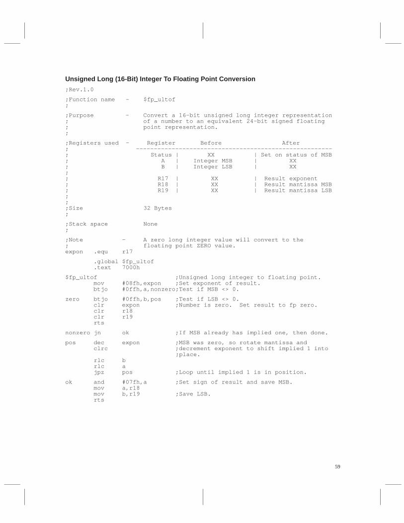
59
Unsigned Long (16-Bit) Integer To Floating Point Conversion
;Rev.1.0
;Function name - $fp_ultof;
;Purpose - Convert a 16-bit unsigned long integer representation; of a number to an equivalent 24-bit signed floating; point representation.;
;Registers used - Register Before After; -------------------------------------------------------; Status | XX | Set on status of MSB; A | Integer MSB | XX; B | Integer LSB | XX;; R17 | XX | Result exponent; R18 | XX | Result mantissa MSB; R19 | XX | Result mantissa LSB;;;Size 32 Bytes;
;Stack space None;
;Note - A zero long integer value will convert to the; floating point ZERO value.expon .equ r17
.global $fp_ultof .text 7000h
$fp_ultof ;Unsigned long integer to floating point. mov #08fh,expon ;Set exponent of result. btjo #0ffh,a,nonzero;Test if MSB <> 0.
zero btjo #0ffh,b,pos ;Test if LSB <> 0. clr expon ;Number is zero. Set result to fp zero. clr r18 clr r19 rts
nonzero jn ok ;If MSB already has implied one, then done.
pos dec expon ;MSB was zero, so rotate mantissa and clrc ;decrement exponent to shift implied 1 into ;place. rlc b rlc a jpz pos ;Loop until implied 1 is in position.
ok and #07fh,a ;Set sign of result and save MSB. mov a,r18 mov b,r19 ;Save LSB. rts
60
Unsigned 8-Bit Integer To Floating Point Conversion
;Rev.1.0
;Function name - $fp_utof;
;Purpose - Convert an 8-bit unsigned integer representation; of a number to an equivalent 24-bit signed floating; point representation.;
;Registers used - Register Before After; -------------------------------------------------------; Status | XX | Set on status of MSB; A | Integer MSB | Modified; B | Integer LSB | Integer LSB;; R17 | XX | Result exponent; R18 | XX | Result mantissa MSB; R19 | XX | Result mantissa LSB;
;Size 26 Bytes;
;Stack space None;
;Note - A zero integer value will convert to the; floating point ZERO value.expon .equ r17
.global $fp_utof .text 7000h
$fp_utof ;Unsigned integer to floating point ;conversion. clr r19 ;Initialize MSB. mov #87h,expon ;Initialize the exponent. btjo #0ffh,a,nonzero;Test to see if integer is zero.
zero clr r18 ;Integer is zero, result will be fp zero. clr expon rts
nonzero jn ok ;Check if implied 1 is in position.
pos dec expon ;Implied 1 is not in position, rotate and clrc ;decrement until implied one is in position. rlc a ; jp pos ;
ok and #07fh,a ;Set sign of result. mov a,r18 rts
61
Part IISoftware Routines
Part II contains three sections:
Arithmetic 7. . . . . . . . . . . . . . . . . . . . . . . . . . .
Memory Operations 61. . . . . . . . . . . . . . . . . .
Specific Functionality 83. . . . . . . . . . . . . . . .

62

63
Clear RAM
Microcontroller Products—Semiconductor GroupTexas Instruments

64
65
Clear RAM
This routine clears all of the internal RAM registers. It can be used at the beginning of a program toinitialize the first 256 bytes of RAM to a known value. Registers A and B have the following functionsin this routine:
• Register A holds the initialization value.
• Register B serves as the index into the RAM.
Routine
.TEXT 7000h ;Absolute start address
CLEAR MOV #254,B ;Number of registers to clear less 2CLR A ;Load the initialization
;value of zero
LOOP MOV A,1[B] ;Clear the location indexed;by B+1
DJNZ B,LOOP ;Loop until all RAM is
;cleared;A and B end up as zeros.

66

67
RAM Self-Test on the TMS370
Microcontroller Products—Semiconductor GroupTexas Instruments

68
69
RAM Self-Test
This routine performs a simple alternating 0/1 test on RAM locations R3–R255 by writing an AA,55 patternto this RAM space and then checking the RAM for this pattern. The inverted pattern is then written to RAMand rechecked. Finally, the entire RAM is cleared. If an error is found, a bit is set in the flag register. Theerror flag bit should be cleared before the routine is started.
Table 1. Register Values
Register Before After: No Error After: Error
A XX 0 ?
B XX 0 ?
FLAG XX 0 Bit 0 = 1
NOTE:
• Passing data: none
• Registers affected: all
• Ending data: all registers = 0; bit 0 in FLAG = 1 if error was found
Routine
.TEXT 7000H ;Absolute start addressFLAG .EQU R2 ;Error register MOV #55h,A ;Start RAM fill with 55hFILLR MOV #0FDh,B ;Set RAM start address – 3 ;(don’t change registers A, B, or R2)FILL1 MOV A,*2[B] ;Fill RAM with AA to 55 pattern RR A ;Change to beginning number DJNZ B,FILL1 ;Fill entire RAM with pattern RR A ;Change to beginning number MOV #0FDh,B ;Refresh indexCOMPAR CMP *2[B],A ;Check for errors JNE ERROR ;Exit if values don’t match RR A ;Change from 55 to AA to 55 DJNZ B,COMPAR ;Check the entire RAM CLRC ;Is reg A now 55, AA or 00? JN FILLR ;=AA, change to opposite pattern JZ EXIT ;=00,FILL0 CLR A ;=55,clear the ram now JMP FILLR ;Repeat the fill and check routineERROR OR #1,FLAG ;Set bit zero in the flag ;registerEXIT .EQU $ ;Continue program here

70

71
ROM Checksum on the TMS370
Microcontroller Products—Semiconductor GroupTexas Instruments

72

73
ROM Checksum
This routine checks the integrity of a 4K-byte ROM by performing a checksum on the entire ROM. AllROM bytes from 7002h to 7FDFh are added together in a 16-bit word. The sum is checked against the valueat the beginning of the ROM (7000h, 7001h). If the values don’t match, then an error has occurred, and abit is set in a register. The error flag bit should be cleared before the start of the routine. This routine caneasily be modified for other ROM sizes.
NOTE:Addresses 7FE0h through 7FEBh are reserved for TI use only and should notbe used in a checksum calculation.
Table 1. Register and Function Values
Register Before After: No Error After: Error
A XX X X
B XX X X
R2 XX CHKSUM MSbyte CHKSUM MSbyte
R3 XX CHKSUM LSbyte CHKSUM LSbyte
R4 XX 70h 70h
R5 XX 01h 01h
R6 XX FFh FFh
R7 XX FFh FFh
FLAG XX Bit 1 = 0 Bit 1 = 1
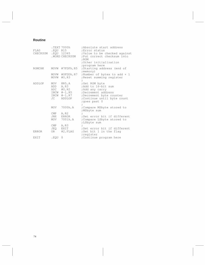
74
Routine
.TEXT 7000h ;Absolute start addressFLAG .EQU R15 ;Error statusCHECKSUM .EQU 12345 ;Value to be checked against
.WORD CHECKSUM ;Put correct checksum into;ROM;Other initialization;program here
ROMCHK MOVW #7FDFh,R5 ;Starting address (end of;memory)
MOVW #0FDDh,R7 ;Number of bytes to add + 1MOVW #0,R3 ;Reset summing register
;ADDLOP MOV @R5,A ;Get ROM byte
ADD A,R3 ;Add to 16-bit sumADC #0,R2 ;Add any carryINCW #–1,R5 ;Decrement addressINCW #–1,R7 ;Decrement byte counterJC ADDLOP ;Continue until byte count
;goes past 0;
MOV 7000h,A ;Compare MSbyte stored to;MSbyte sum
CMP A,R2 ;JNE ERROR ;Set error bit if differentMOV 7001h,A ;Compare LSbyte stored to
;LSbyte sumCMP A,R3 ;JEQ EXIT ;Set error bit if different
ERROR OR #2,FLAG ;Set bit 1 in the flag;register
EXIT .EQU $ ;Continue program here

75
Table Search With the TMS370
Microcontroller Products—Semiconductor GroupTexas Instruments

76
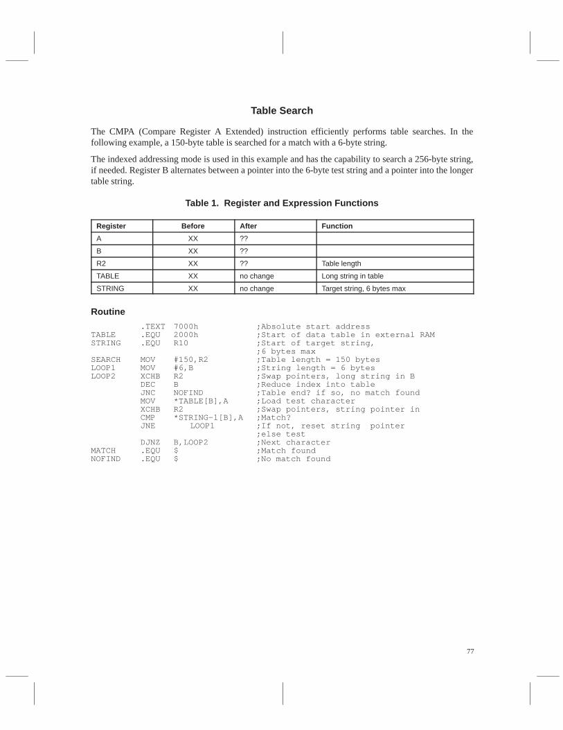
77
Table Search
The CMPA (Compare Register A Extended) instruction efficiently performs table searches. In thefollowing example, a 150-byte table is searched for a match with a 6-byte string.
The indexed addressing mode is used in this example and has the capability to search a 256-byte string,if needed. Register B alternates between a pointer into the 6-byte test string and a pointer into the longertable string.
Table 1. Register and Expression Functions
Register Before After Function
A XX ??
B XX ??
R2 XX ?? Table length
TABLE XX no change Long string in table
STRING XX no change Target string, 6 bytes max
Routine
.TEXT 7000h ;Absolute start addressTABLE .EQU 2000h ;Start of data table in external RAMSTRING .EQU R10 ;Start of target string,
;6 bytes maxSEARCH MOV #150,R2 ;Table length = 150 bytesLOOP1 MOV #6,B ;String length = 6 bytesLOOP2 XCHB R2 ;Swap pointers, long string in B
DEC B ;Reduce index into tableJNC NOFIND ;Table end? if so, no match foundMOV *TABLE[B],A ;Load test characterXCHB R2 ;Swap pointers, string pointer inCMP *STRING–1[B],A ;Match?JNE LOOP1 ;If not, reset string pointer
;else testDJNZ B,LOOP2 ;Next character
MATCH .EQU $ ;Match foundNOFIND .EQU $ ;No match found

78

79
Bubble Sort With the TMS370
Microcontroller Products—Semiconductor GroupTexas Instruments

80
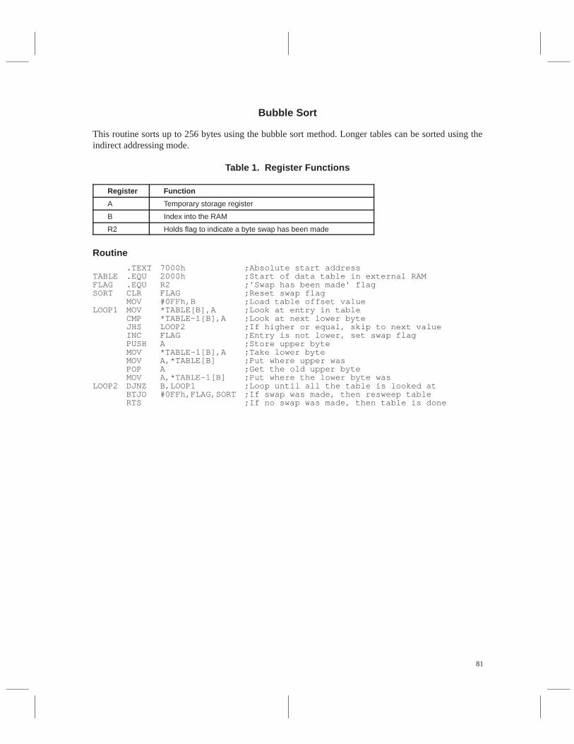
81
Bubble Sort
This routine sorts up to 256 bytes using the bubble sort method. Longer tables can be sorted using theindirect addressing mode.
Table 1. Register Functions
Register Function
A Temporary storage register
B Index into the RAM
R2 Holds flag to indicate a byte swap has been made
Routine
.TEXT 7000h ;Absolute start addressTABLE .EQU 2000h ;Start of data table in external RAMFLAG .EQU R2 ;’Swap has been made’ flagSORT CLR FLAG ;Reset swap flag
MOV #0FFh,B ;Load table offset valueLOOP1 MOV *TABLE[B],A ;Look at entry in table
CMP *TABLE–1[B],A ;Look at next lower byteJHS LOOP2 ;If higher or equal, skip to next valueINC FLAG ;Entry is not lower, set swap flagPUSH A ;Store upper byteMOV *TABLE-1[B],A ;Take lower byteMOV A,*TABLE[B] ;Put where upper wasPOP A ;Get the old upper byteMOV A,*TABLE-1[B] ;Put where the lower byte was
LOOP2 DJNZ B,LOOP1 ;Loop until all the table is looked atBTJO #0FFh,FLAG,SORT ;If swap was made, then resweep tableRTS ;If no swap was made, then table is done

82
83
Part IISoftware Routines
Part II contains three sections:
Arithmetic 7. . . . . . . . . . . . . . . . . . . . . . . . . . . .
Memory Operations 61. . . . . . . . . . . . . . . . . .
Specific Functionality 83. . . . . . . . . . . . . . . . .

84

85
Routine to Read a 16-Key Keyboard
Microcontroller Products—Semiconductor GroupTexas Instruments

86
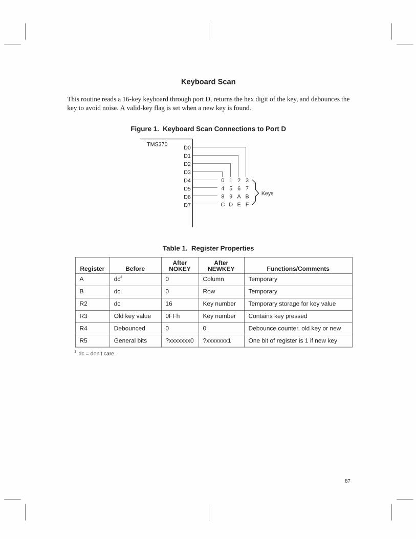
87
Keyboard Scan
This routine reads a 16-key keyboard through port D, returns the hex digit of the key, and debounces thekey to avoid noise. A valid-key flag is set when a new key is found.
Figure 1. Keyboard Scan Connections to Port D
D0
D1
D2
D3
D4
D5
D6
D7
TMS370
0
4
8
C
1
5
9
D
2
6
A
E
3
7
B
F
Keys
Table 1. Register Properties
After After/CRegister Before NOKEY NEWKEY Functions/Comments
A dc† 0 Column Temporary
B dc 0 Row Temporary
R2 dc 16 Key number Temporary storage for key value
R3 Old key value 0FFh Key number Contains key pressed
R4 Debounced 0 0 Debounce counter, old key or new
R5 General bits ?xxxxxxx0 ?xxxxxxx1 One bit of register is 1 if new key
† dc = don’t care.
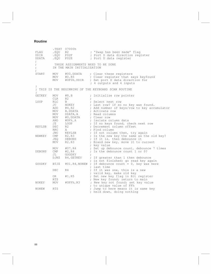
88
Routine
.TEXT 07000h FLAG .EQU R2 ; ”Swap has been made” flagDDIR .EQU P02F ; Port D data direction registerDDATA .EQU P02E ; Port D data register;; THESE ASSIGNMENTS NEED TO BE DONE ; IN THE MAIN INITIALIZATION; START MOV #00,DDATA ; Clear these registers
MOV #0,R5 ; Clear register that says keyfoundMOV #0F0h,DDIR ; Set port D data direction for
; 4 outputs and 4 inputs; ; THIS IS THE BEGINNING OF THE KEYBOARD SCAN ROUTINE;GETKEY MOV #8,B ; Initialize row pointer
CLR R2 ;LOOP RLC B ; Select next row
JC NOKEY ; Last row? if so no key was found.ADD #4,R2 ; Add number of keys/row to key accumulatorMOV B,DDATA ; Activate rowMOV DDATA,A ; Read columnsMOV #0,DDATA ; Clear rowAND #0Fh,A ; Isolate column dataJZ LOOP ; If no keys found, check next row
KEYLSB DEC R2 ; Decrement column offsetRRC A ; Find columnJNC KEYLSB ; If not column then, try again
NEWKEY CMP R2,R3 ; Is the new key the same as the old key?JEQ DEBONS ; If it is, then debounce itMOV R2,R3 ; Brand new key, move it to current
; key valueMOV #07,R4 ; Set up debounce count, debounce 7 times
DEBONS CMP #2,R4 ; Is the debounce count 1 or 0? JL GOODKY ;
DJNZ R4,GETKEY ; If greater than 1 then debounce ; is not finished; go read key again
GOODKY BTJZ #01,R4,NONEW ; If debounce count = 0, key was here ; last time
DEC R4 ; If it was one, this is a new ; valid key, make old key
OR #1,R5 ; Set new key flag in Bit registerRTS ; New key found; return to main
NOKEY MOV #0FFh,R3 ; New key not found; set key value ; to unique value of FFh
NONEW RTS ; Jump to here means it is same key; held down, doing nothing

89
DTMF Generation With the TMS370
Microcontroller Products—Semiconductor GroupTexas Instruments

90
91
DTMF Generator
The TMS370 can be used to generate DTMF dialing. The following routine can be used to generate all 16DTMF digits.
Routine;***************************************************************************;
.TITLE ”DTMF GENERATOR”;***************************************************************************;; *** DTMF GENERATOR ***; GENERATES ALL 16 DTMF DIGITS;; CRYSTAL: 7.158MHZ (2X COLOR BURST);; OUTPUT: 4 BIT DATA TO THE LOW NIBBLE OF B–PORT; UPPER NIBBLE OF B–PORT IS LEFT UNMODIFIED;; B0 LSB; B1; B2; B3 MSB;;;ENTRY POINTS:’CALLSETMID’; SET D/A OUTPUT TO THE MIDPOINT VOLTAGE; (DONE AUTOMATICALLY AFTER ’CALL DTMF’);; ’CALLDTMF’; GENERATE DTMF DIGIT IN TONE(0–3); GENERATE TONE FOR DURATION IN TIMER/TIMER+1; START AT D/A MIDPOINT; ON EXIT–SET D/A TO MIDPOINT;; TONE(0–3)DTMF(HZ); –––––––––––––––––; 0 941/1336; 1 697/1209; 2 697/1336; 3 697/1477; 4 770/1209; 5 770/1336; 6 770/1477; 7 852/1209; 8 852/1336; 9 852/1477; A 697/1633; B 770/1633; C 852/1633; D 941/1633; E 941/1209; F 941/1477;;***************************************************************************;TONE .EQU R020 ;BCD DTMF DIGIT IN BITS 0–3;PRT1 .EQU R021 ;R22 R23 POINTER FOR FREQUENCY 1PRT2 .EQU R024 ;R25 R26 POINTER FOR FREQUENCY 2CNT1 .EQU R027 ;FREQUENCY 1 COUNTADJ1 .EQU R028 ;FREQUENCY 1 ADJUST
92
CNT2 .EQU R029 ;FREQUENCY 2 COUNTADJ2 .EQU R02A ;FREQUENCY 2 ADJUSTTIMER .EQU R02B ;R32DIGIT DURATION: 1 = 100 µS;BPORT .EQU P026 ;I/O PORTBDR .EQU P027 ;DATA DIRECTION REGISTER;;***************************************************************************;; CALCULATIONS:;; FREQ. = [(CNT,ADJ)/(# SAMPLES)] / 100.02794US;; CNT = INTEGER PART OF UPDATE RATE; ADJ = FRACTION PART OF UPDATE RATE (NORMALIZED TO 256);; # SAMPLES: 64;; CRYSTAL = 7.158 MHZ / 4; 179 MACHINE CYCLES = 100.02794 µS;; DTMF FREQUENCY TIME CONSTANTS – CNT,ADJ;L1 .EQU 00476h ;697 HZL2 .EQU 004EEh ;770 HZL3 .EQU 00574h ;852 HZL4 .EQU 00606h ;941 HZ;H1 .EQU 007BDh ;1209 HZH2 .EQU 0088Eh ;1336 HZH3 .EQU 00975h ;1477 HZH4 .EQU 00A74h ;1633 HZ;
.SECT “S1”,0F806h;DTMF .EQU $
MOV #00Fh,BDR ;LOWER NIBBLE OF BPORT IS OUTPUT;; INITIALIZE DTMF POINTERS;
MOV TONE,B ;LOAD DIGIT INTOAND #00Fh,B ;LOWER 4 BITS OF BRL B ;MAKERL B ;ADDRESSMOV *DIGIT[B],A ;LOADMOV A,CNT1 ;COUNT1MOV *DIGIT+1[B],A ;LOADMOV A,ADJ1 ;ADJUST1MOV *DIGIT+2[B],A ;LOADMOV A,CNT2 ;COUNT2MOV *DIGIT+3[B],A ;LOADMOV A,ADJ2 ;ADJUST2
;MOVW #TABLE,PRT1+1 ;POINT TOMOVW #TABLE,PRT2+1 ;TABLE START
;MOV BPORT,B ;SET OUTPUTAND #0F0h,BOR #008h,B ;TO D/A MIDPOINTMOV B,BPORT
;;***************************************************************************;
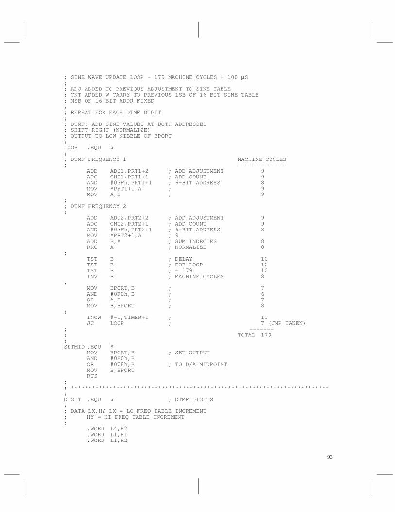
93
; SINE WAVE UPDATE LOOP – 179 MACHINE CYCLES = 100 µS;; ADJ ADDED TO PREVIOUS ADJUSTMENT TO SINE TABLE; CNT ADDED W CARRY TO PREVIOUS LSB OF 16 BIT SINE TABLE; MSB OF 16 BIT ADDR FIXED;; REPEAT FOR EACH DTMF DIGIT;; DTMF: ADD SINE VALUES AT BOTH ADDRESSES; SHIFT RIGHT (NORMALIZE); OUTPUT TO LOW NIBBLE OF BPORT;LOOP .EQU $;; DTMF FREQUENCY 1 MACHINE CYCLES; ––––––––––––––
ADD ADJ1,PRT1+2 ; ADD ADJUSTMENT 9ADC CNT1,PRT1+1 ; ADD COUNT 9AND #03Fh,PRT1+1 ; 6-BIT ADDRESS 8MOV *PRT1+1,A ; 9MOV A,B ; 9
;; DTMF FREQUENCY 2;
ADD ADJ2,PRT2+2 ; ADD ADJUSTMENT 9ADC CNT2,PRT2+1 ; ADD COUNT 9AND #03Fh,PRT2+1 ; 6-BIT ADDRESS 8MOV *PRT2+1,A ; 9ADD B,A ; SUM INDECIES 8RRC A ; NORMALIZE 8
;TST B ; DELAY 10TST B ; FOR LOOP 10TST B ; = 179 10INV B ; MACHINE CYCLES 8
;MOV BPORT,B ; 7AND #0F0h,B ; 6OR A,B ; 7MOV B,BPORT ; 8
;INCW #–1,TIMER+1 ; 11JC LOOP ; 7 (JMP TAKEN)
; –––––––; TOTAL 179;SETMID .EQU $
MOV BPORT,B ; SET OUTPUTAND #0F0h,BOR #008h,B ; TO D/A MIDPOINTMOV B,BPORTRTS
;;***************************************************************************;DIGIT .EQU $ ; DTMF DIGITS;; DATA LX,HY LX = LO FREQ TABLE INCREMENT; HY = HI FREQ TABLE INCREMENT;
.WORD L4,H2
.WORD L1,H1
.WORD L1,H2
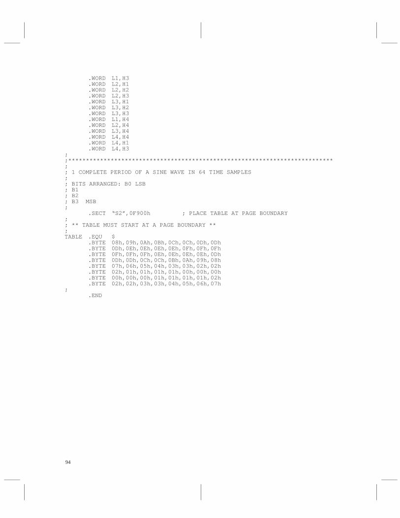
94
.WORD L1,H3
.WORD L2,H1
.WORD L2,H2
.WORD L2,H3
.WORD L3,H1
.WORD L3,H2
.WORD L3,H3
.WORD L1,H4
.WORD L2,H4
.WORD L3,H4
.WORD L4,H4
.WORD L4,H1
.WORD L4,H3;;***************************************************************************;; 1 COMPLETE PERIOD OF A SINE WAVE IN 64 TIME SAMPLES;; BITS ARRANGED: B0 LSB; B1; B2; B3 MSB;
.SECT “S2”,0F900h ; PLACE TABLE AT PAGE BOUNDARY;; ** TABLE MUST START AT A PAGE BOUNDARY **;TABLE .EQU $
.BYTE 08h,09h,0Ah,0Bh,0Ch,0Ch,0Dh,0Dh
.BYTE 0Dh,0Eh,0Eh,0Eh,0Eh,0Fh,0Fh,0Fh
.BYTE 0Fh,0Fh,0Fh,0Eh,0Eh,0Eh,0Eh,0Dh
.BYTE 0Dh,0Dh,0Ch,0Ch,0Bh,0Ah,09h,08h
.BYTE 07h,06h,05h,04h,03h,03h,02h,02h
.BYTE 02h,01h,01h,01h,01h,00h,00h,00h
.BYTE 00h,00h,00h,01h,01h,01h,01h,02h
.BYTE 02h,02h,03h,03h,04h,05h,06h,07h;
.END

95
System Integrity Check for theTMS370
Microcontroller Products—Semiconductor GroupTexas Instruments

96
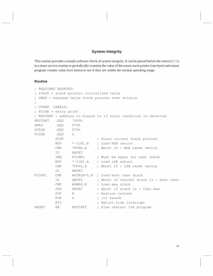
97
System Integrity
This routine provides a simple software check of system integrity. It can be placed before the return (RTS)in a timer service routine to periodically examine the value of the return stack pointer (one byte) and returnprogram counter value (two bytes) to see if they are within the normal operating range.
Routine
; REQUIRED EQUATES: ; STACK = stack pointer initialized value; SMAX = maximum value stack pointer ever attains;; OTHER LABELS: ; PCCHK = entry point; RESTART = address to branch to if error condition is detectedRESTART .EQU 7000hSMAX .EQU 07fhSTACK .EQU 07fhPCCHK .EQU $
STSP ; Store current stack pointer MOV *–3[B],A ; Load MSB return CMP 7FFEh,A ; Abort if < MSB reset vector JL ABORT JNE PCCHK1 ; Must be equal for next check MOV *–2[B],A ; Load LSB return CMP 7FFFh,A ; Abort if < LSB reset vector JL ABORT
PCCHK1 CMP #STACK+5,B ; Load best case stack JL ABORT ; Abort if current stack is < best case CMP #SMAX,B ; Load max stack JHS ABORT ; Abort if stack is > than max POP B ; Restore context POP A ; (if saved) RTI ; Return from interrupt
ABORT BR RESTART ; Else restart the program

98
99
Part IIIModule Specific
Application Design Aids
Part III contains six sections:
RESET Operations 99. . . . . . . . . . . . . . . . . . .
SPI and SCI Modules 105. . . . . . . . . . . . . . . .
Timer and Watchdog Modules 199. . . . . . . .
Analog to Digital Modules 309. . . . . . . . . . .
PACT Module 375. . . . . . . . . . . . . . . . . . . . . .
I/O Pins 439. . . . . . . . . . . . . . . . . . . . . . . . . . .

100
101
Reset: Explanation of Operation andSuggested Designs
Michael S. StewartMicrocontroller Products—Semiconductor Group
Texas Instruments

102
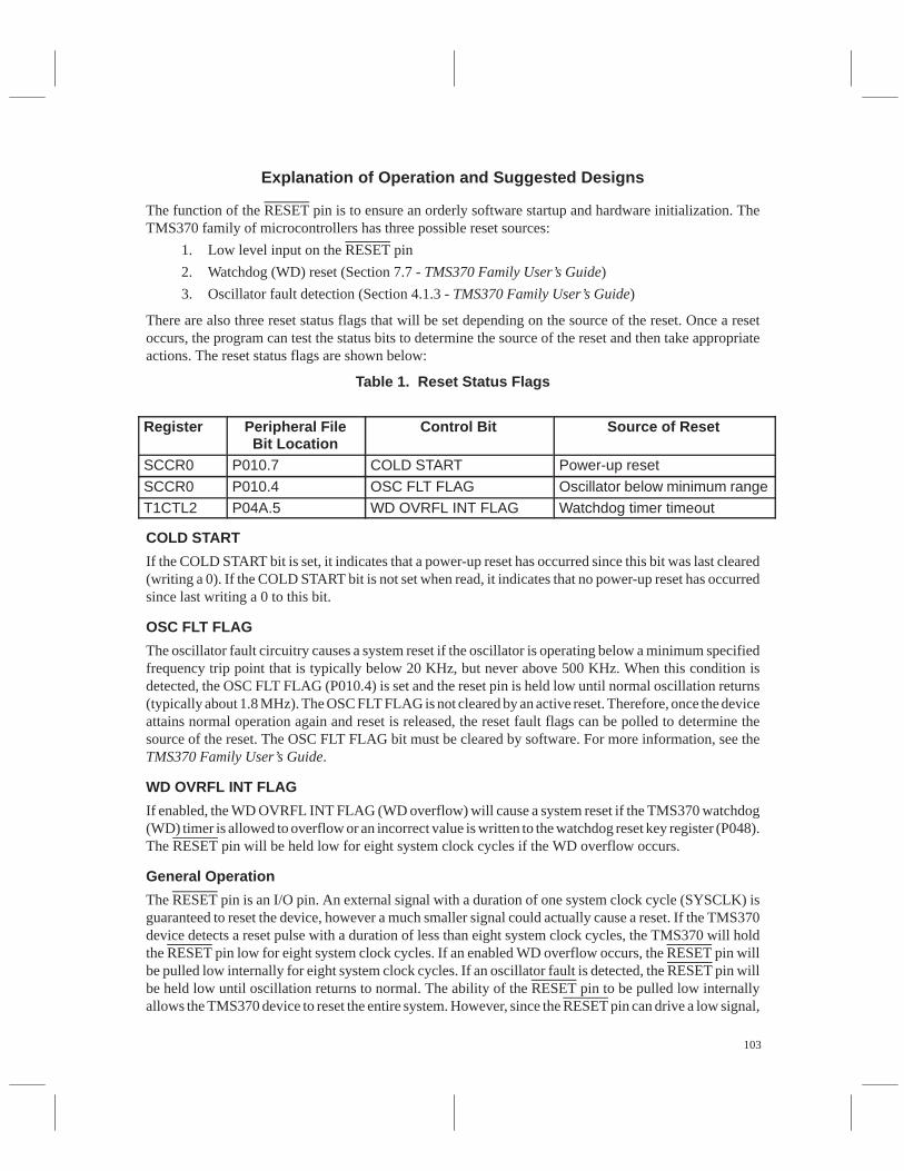
103
Explanation of Operation and Suggested Designs
The function of the RESET pin is to ensure an orderly software startup and hardware initialization. TheTMS370 family of microcontrollers has three possible reset sources:
1. Low level input on the RESET pin
2. Watchdog (WD) reset (Section 7.7 - TMS370 Family User’s Guide)
3. Oscillator fault detection (Section 4.1.3 - TMS370 Family User’s Guide)
There are also three reset status flags that will be set depending on the source of the reset. Once a resetoccurs, the program can test the status bits to determine the source of the reset and then take appropriateactions. The reset status flags are shown below:
Table 1. Reset Status Flags
ÁÁÁÁÁÁÁÁÁÁÁÁ
RegisterÁÁÁÁÁÁÁÁÁÁÁÁÁÁÁÁÁÁÁÁÁÁÁÁ
Peripheral FileBit Location
ÁÁÁÁÁÁÁÁÁÁÁÁÁÁÁÁÁÁÁÁÁÁÁÁÁÁÁ
Control Bit ÁÁÁÁÁÁÁÁÁÁÁÁÁÁÁÁÁÁÁÁÁÁÁÁÁÁÁÁÁÁÁÁÁ
Source of Reset
ÁÁÁÁSCCR0 ÁÁÁÁÁÁÁÁP010.7 ÁÁÁÁÁÁÁÁÁCOLD START ÁÁÁÁÁÁÁÁÁÁÁPower-up resetÁÁÁÁÁÁÁÁSCCR0
ÁÁÁÁÁÁÁÁÁÁÁÁÁÁÁÁP010.4
ÁÁÁÁÁÁÁÁÁÁÁÁÁÁÁÁÁÁOSC FLT FLAG
ÁÁÁÁÁÁÁÁÁÁÁÁÁÁÁÁÁÁÁÁÁÁOscillator below minimum rangeÁÁÁÁ
ÁÁÁÁT1CTL2ÁÁÁÁÁÁÁÁÁÁÁÁÁÁÁÁP04A.5
ÁÁÁÁÁÁÁÁÁÁÁÁÁÁÁÁÁÁWD OVRFL INT FLAG
ÁÁÁÁÁÁÁÁÁÁÁÁÁÁÁÁÁÁÁÁÁÁWatchdog timer timeout
COLD START
If the COLD START bit is set, it indicates that a power-up reset has occurred since this bit was last cleared(writing a 0). If the COLD START bit is not set when read, it indicates that no power-up reset has occurredsince last writing a 0 to this bit.
OSC FLT FLAG
The oscillator fault circuitry causes a system reset if the oscillator is operating below a minimum specifiedfrequency trip point that is typically below 20 KHz, but never above 500 KHz. When this condition isdetected, the OSC FLT FLAG (P010.4) is set and the reset pin is held low until normal oscillation returns(typically about 1.8 MHz). The OSC FLT FLAG is not cleared by an active reset. Therefore, once the deviceattains normal operation again and reset is released, the reset fault flags can be polled to determine thesource of the reset. The OSC FLT FLAG bit must be cleared by software. For more information, see theTMS370 Family User’s Guide.
WD OVRFL INT FLAG
If enabled, the WD OVRFL INT FLAG (WD overflow) will cause a system reset if the TMS370 watchdog(WD) timer is allowed to overflow or an incorrect value is written to the watchdog reset key register (P048).The RESET pin will be held low for eight system clock cycles if the WD overflow occurs.
General Operation
The RESET pin is an I/O pin. An external signal with a duration of one system clock cycle (SYSCLK) isguaranteed to reset the device, however a much smaller signal could actually cause a reset. If the TMS370device detects a reset pulse with a duration of less than eight system clock cycles, the TMS370 will holdthe RESET pin low for eight system clock cycles. If an enabled WD overflow occurs, the RESET pin willbe pulled low internally for eight system clock cycles. If an oscillator fault is detected, the RESET pin willbe held low until oscillation returns to normal. The ability of the RESET pin to be pulled low internallyallows the TMS370 device to reset the entire system. However, since the RESET pin can drive a low signal,
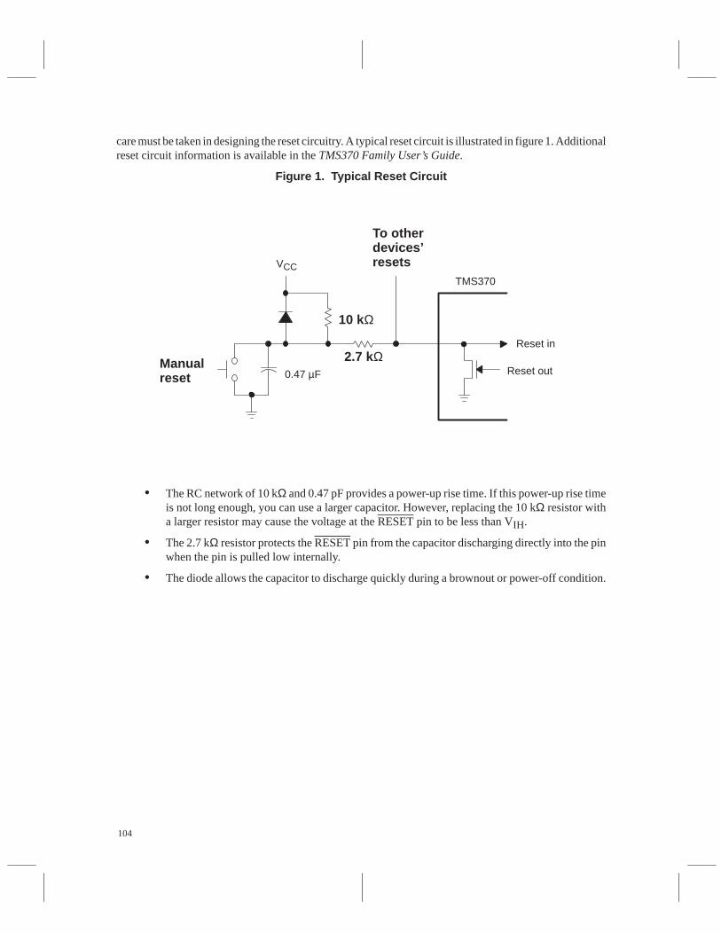
104
care must be taken in designing the reset circuitry. A typical reset circuit is illustrated in figure 1. Additionalreset circuit information is available in the TMS370 Family User’s Guide.
Figure 1. Typical Reset Circuit
10 kΩ
VCC
2.7 kΩ
To other devices’resets
0.47 µFManualreset
Reset in
Reset out
TMS370
• The RC network of 10 kΩ and 0.47 pF provides a power-up rise time. If this power-up rise timeis not long enough, you can use a larger capacitor. However, replacing the 10 kΩ resistor witha larger resistor may cause the voltage at the RESET pin to be less than VIH.
• The 2.7 kΩ resistor protects the RESET pin from the capacitor discharging directly into the pinwhen the pin is pulled low internally.
• The diode allows the capacitor to discharge quickly during a brownout or power-off condition.
105
Part IIIModule Specific
Application Design Aids
Part III contains six sections:
RESET Operations 99. . . . . . . . . . . . . . . . . . .
SPI and SCI Modules 105. . . . . . . . . . . . . . . .
Timer and Watchdog Modules 199. . . . . . . .
Analog to Digital Modules 309. . . . . . . . . . .
PACT Module 375. . . . . . . . . . . . . . . . . . . . . .
I/O Pins 439. . . . . . . . . . . . . . . . . . . . . . . . . . .

106
107
Using the TMS370 SPI and SCI Modules
Kevin L. SelfMicrocontroller Products—Semiconductor Group
Texas Instruments
Contributions by Paul Krause, Mark Palmer, and Al Lovrich

108

109
Introduction
The TMS370 family of 8-bit microcontrollers has been designed with two serial communications modules:the serial peripheral interface (SPI) and the serial communications interface (SCI). These two modulesgreatly enhance the ability of the microcontroller to interface to other serial devices and common interfacessuch as the industry standard RS-232. External hardware and software overhead are reduced by theflexibility and programmability of the interfaces.
This application report provides examples of hardware interfaces and software routines to illustrate theversatility of the SPI and SCI modules. Common applications of these modules will be discussed, whichmay be modified to suit the engineer’s specific needs. Additional information on the serial interfaces maybe found in the TMS370 Family User’s Guide.
NOTE:The SCI module is available in the three pin (SCI1) and two pin (SCI2)versions.
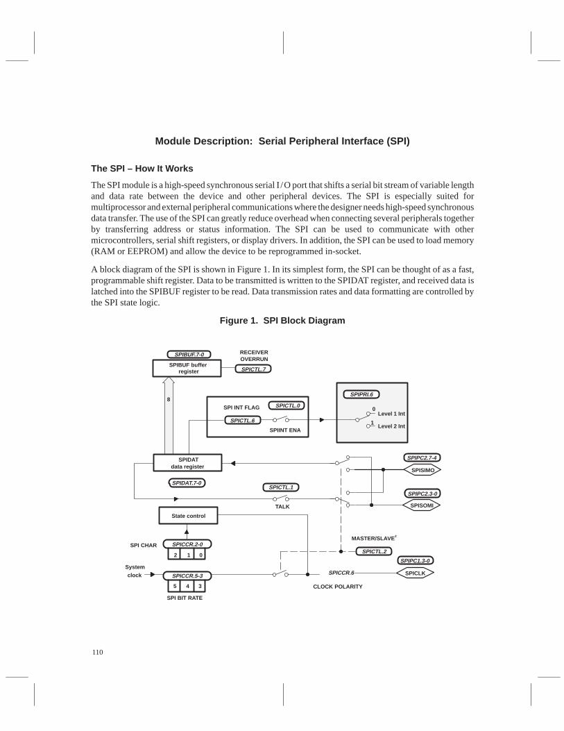
110
Module Description: Serial Peripheral Interface (SPI)
The SPI – How It Works
The SPI module is a high-speed synchronous serial I /O port that shifts a serial bit stream of variable lengthand data rate between the device and other peripheral devices. The SPI is especially suited formultiprocessor and external peripheral communications where the designer needs high-speed synchronousdata transfer. The use of the SPI can greatly reduce overhead when connecting several peripherals togetherby transferring address or status information. The SPI can be used to communicate with othermicrocontrollers, serial shift registers, or display drivers. In addition, the SPI can be used to load memory(RAM or EEPROM) and allow the device to be reprogrammed in-socket.
A block diagram of the SPI is shown in Figure 1. In its simplest form, the SPI can be thought of as a fast,programmable shift register. Data to be transmitted is written to the SPIDAT register, and received data islatched into the SPIBUF register to be read. Data transmission rates and data formatting are controlled bythe SPI state logic.
Figure 1. SPI Block Diagram
SPIBUF bufferregister
SPIDATdata register
SPIBUF.7-0
State control
SPI CHAR
SPI BIT RATE
CLOCK POLARITY
SPI INT FLAG
SPICTL.6
SPIINT ENA
SPICTL.0
RECEIVEROVERRUN
8
SPIDAT.7-0SPICTL.1
TALK
2 01
345
SPICCR.2-0
SPICCR.5-3
Systemclock SPICCR.6 SPICLK
MASTER/SLAVE †
SPICTL.7
Level 2 Int
SPIPRI.6
1
SPIPC2.7-4
SPISIMO
SPICTL.2
SPIPC1.3-0
SPISOMI
SPIPC2.3-0
Level 1 Int0

111
SPI Operating Modes
The Master Mode
The SPI operates in one of two modes. The master mode is used when the SPI controls the data transfer.The master SPI initiates and controls the data transfer by issuing the SPICLK signal. Writing data to theSPIDAT buffer starts the transfer by starting SPICLK and shifting the data out of the SPIDAT shift registeronto the SPISIMO pin. New data is simultaneously gated in on the SPISOMI pin into the SPIDAT buffer.
Since the master device controls the data transfer by issuing the SPICLK, the other devices must wait forthe master to start the transmission. Even if the master is only interested in receiving data, it is still necessaryto write dummy data to the SPIDAT register to initiate the transfer from the slave or external source.
Because of the way data is shifted through the SPIDAT register, any data value in SPIDAT is alwaysmodified after a transmission, even if no new data value has been received into the register. The SPIDATregister will contain indeterminate data because no new data has been received.
The Slave Mode
The slave mode is used when the SPI is controlled by another serial device. In the slave mode, the SPI isdependent on an external clock source from a master configured device to control the data transfer. Anelement of data resident in the SPIDAT buffer is shifted out upon receipt of a clock signal on the SPICLKpin, which in slave mode becomes an input pin. Simultaneously, any data present on the SPISIMO pin isshifted into the SPIDAT register. The data transmission of a slave can be disabled by clearing the TALKbit. This allows many devices to be tied to the same serial network, but it eliminates the possibility of writeconflicts. Figure 2 illustrates two TMS370 devices in a master/slave connection.
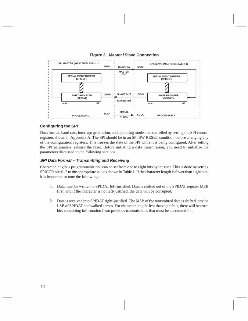
112
Figure 2. Master / Slave Connection
ÉÉÉÉ
SPI MASTER (MASTER/SLAVE = 1)SIMO SLAVE IN/
MASTEROUT
SERIAL INPUT BUFFER(SPIBUF)
SHIFT REGISTER(SPIDAT)
msb lsb
SOMI SLAVE OUT
MASTER IN
PROCESSOR 1SCLK
SERIAL
CLOCK
SPI SLAVE (MASTER/SLAVE = 0)SIMO
SERIAL INPUT BUFFER(SPIBUF)
SHIFT REGISTER(SPIDAT)
msb lsb
SOMI
SCLK PROCESSOR 2
ÉÉÉÉ
Configuring the SPI
Data format, baud rate, interrupt generation, and operating mode are controlled by setting the SPI controlregisters shown in Appendix A. The SPI should be in an SPI SW RESET condition before changing anyof the configuration registers. This freezes the state of the SPI while it is being configured. After settingthe SPI parameters, release the reset. Before initiating a data transmission, you need to initialize theparameters discussed in the following sections.
SPI Data Format – Transmitting and Receiving
Character length is programmable and can be set from one to eight bits by the user. This is done by settingSPICCR bits 0–2 to the appropriate values shown in Table 1. If the character length is fewer than eight bits,it is important to note the following:
1. Data must be written to SPIDAT left-justified. Data is shifted out of the SPIDAT register MSBfirst, and if the character is not left-justified, the data will be corrupted.
2. Data is received into SPIDAT right-justified. The MSB of the transmitted data is shifted into theLSB of SPIDAT and walked across. For character lengths less than eight bits, there will be extrabits containing information from previous transmissions that must be accounted for.
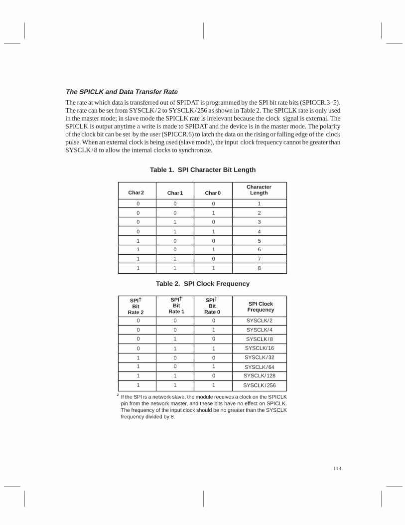
113
The SPICLK and Data Transfer Rate
The rate at which data is transferred out of SPIDAT is programmed by the SPI bit rate bits (SPICCR.3–5).The rate can be set from SYSCLK/2 to SYSCLK/256 as shown in Table 2. The SPICLK rate is only usedin the master mode; in slave mode the SPICLK rate is irrelevant because the clock signal is external. TheSPICLK is output anytime a write is made to SPIDAT and the device is in the master mode. The polarityof the clock bit can be set by the user (SPICCR.6) to latch the data on the rising or falling edge of the clockpulse. When an external clock is being used (slave mode), the input clock frequency cannot be greater thanSYSCLK/8 to allow the internal clocks to synchronize.
Table 1. SPI Character Bit Length
Char2 Char1 Char0Character
Length
0 0 0 1
0 0 1 2
0 1 0 3
0 1 1 4
1 0 0 5
1 0 1 6
1 1 0 7
1 1 1 8
Table 2. SPI Clock Frequency
SPIBit
Rate 2
SPI ClockFrequency
0 0 0 SYSCLK/2
0 0 1
0 1 0
0 1 1
1 0 0
1 0 1
1 1 0
1 1 1
SPIBit
Rate 1
SPI Bit
Rate 0
SYSCLK/4
SYSCLK/8
SYSCLK/16
SYSCLK/32
SYSCLK/64
SYSCLK/128
SYSCLK/256
† If the SPI is a network slave, the module receives a clock on the SPICLKpin from the network master, and these bits have no effect on SPICLK.The frequency of the input clock should be no greater than the SYSCLKfrequency divided by 8.
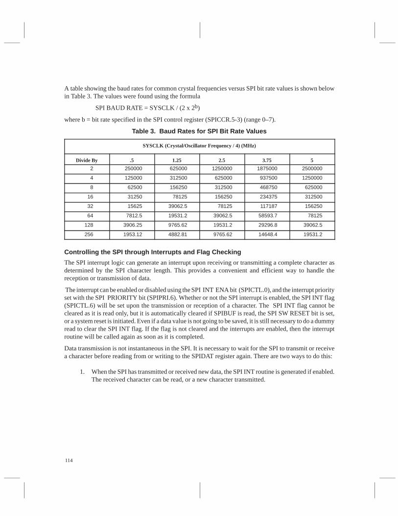
114
A table showing the baud rates for common crystal frequencies versus SPI bit rate values is shown belowin Table 3. The values were found using the formula
SPI BAUD RATE = SYSCLK / (2 x 2b)
where b = bit rate specified in the SPI control register (SPICCR.5-3) (range 0–7).
Table 3. Baud Rates for SPI Bit Rate Values
SYSCLK (Crystal/Oscillator Frequency / 4) (MHz)
Divide By .5 1.25 2.5 3.75 5
2 250000 625000 1250000 1875000 2500000
4 125000 312500 625000 937500 1250000
8 62500 156250 312500 468750 625000
16 31250 78125 156250 234375 312500
32 15625 39062.5 78125 117187 156250
64 7812.5 19531.2 39062.5 58593.7 78125
128 3906.25 9765.62 19531.2 29296.8 39062.5
256 1953.12 4882.81 9765.62 14648.4 19531.2
Controlling the SPI through Interrupts and Flag Checking
The SPI interrupt logic can generate an interrupt upon receiving or transmitting a complete character asdetermined by the SPI character length. This provides a convenient and efficient way to handle thereception or transmission of data.
The interrupt can be enabled or disabled using the SPI INT ENA bit (SPICTL.0), and the interrupt priorityset with the SPI PRIORITY bit (SPIPRI.6). Whether or not the SPI interrupt is enabled, the SPI INT flag(SPICTL.6) will be set upon the transmission or reception of a character. The SPI INT flag cannot becleared as it is read only, but it is automatically cleared if SPIBUF is read, the SPI SW RESET bit is set,or a system reset is initiated. Even if a data value is not going to be saved, it is still necessary to do a dummyread to clear the SPI INT flag. If the flag is not cleared and the interrupts are enabled, then the interruptroutine will be called again as soon as it is completed.
Data transmission is not instantaneous in the SPI. It is necessary to wait for the SPI to transmit or receivea character before reading from or writing to the SPIDAT register again. There are two ways to do this:
1. When the SPI has transmitted or received new data, the SPI INT routine is generated if enabled.The received character can be read, or a new character transmitted.
115
2. If the program cannot do anything until the new data value is received or transmitted, the SPIINT flag can be continuously polled until it goes high. At that time, the character can be reador a new one transmitted.
It is important to use one of the above methods to wait for the data before reading or writing again. Also,if the exact number of cycles is known, the transmission can be timed that way. When doing fast datatransfers where the possibility of a data collision exists, polling the RECEIVER OVERRUN flag(SPICTL.7) will indicate if you have lost any data.
The TALK Bit and Multiprocessor Communications
If more than two processors are going to be connected to the same SPI data lines (SPISIMO/SPISOMI),it will be necessary to limit the conversation to just two processors at a time. This is done through softwareusing the TALK bit (SPICTL.1). When the TALK bit is 0, data transmission is disabled but receptioncontinues. One device, usually (but not necessarily) the master, sends out an address to other devices in thenetwork that have their TALK bits set to 0. Since reception is not affected, all devices receive thetransmitted address and compare it to their own addresses. If a device matches, it sets its TALK bit andbegins transmitting data. When it finishes, the receiving device clears its TALK bit and the network waitsfor another address. Another scheme for using the TALK bit is to transmit groups of characters (10 or so)in a block with the address as the first character. This way the address occurs at regular intervals and reducesthe need for address checking.
Considerations When Using the SPI
The most important thing to remember when writing SPI service routines is to keep your code short.Received data should be quickly removed from the SPIBUF register to prevent it from being overwritten.If you have to manipulate the data, wait until all the data has been received. This becomes more importantas the SPI baud rate increases. If your code involves long SPI routines, new data may be received beforethe previous data value has been read from the SPI buffer register.

116
Data Integrity and the SPI
The SPI was designed as a fast, simple interface to serial logic. As a result, it has no direct way to checkfor transmission errors. There are a number of software methods that can be used to check the integrity ofthe transmission. Parity checking is one of the most common, and it can be easily implemented in softwarefor the SPI. Parity checking involves reserving one bit of the character to be used in setting the total numberof 1s in a character as odd or even.
If you are going to be sending large blocks of data, there are coding methods that allow faster data transferbut still ensure data integrity. Block checksums and other encoding methods can be found in most bookson digital communications. These methods allow some degree of data integrity without significantlyslowing the data transfer rate.
117
SPI Module Software Examples
The following are examples of the various modes of operation and common software routines used inoperating the SPI. The register equate for the following examples shown below.
Common Equates
SPICCR .equ P030 ;SPI Configuration Control Register
SPICTL .equ P031 ;SPI Operation Control Register
SPIBUF .equ P037 ;Serial Input Buffer
SPIDAT .equ P039 ;Serial Data Register
SPIPC1 .equ P03D ;SPI Port Control Register 1
SPIPC2 .equ P03E ;SPI Port Control Register 2
SPIPRI .equ P03F ;SPI Priority Control Register
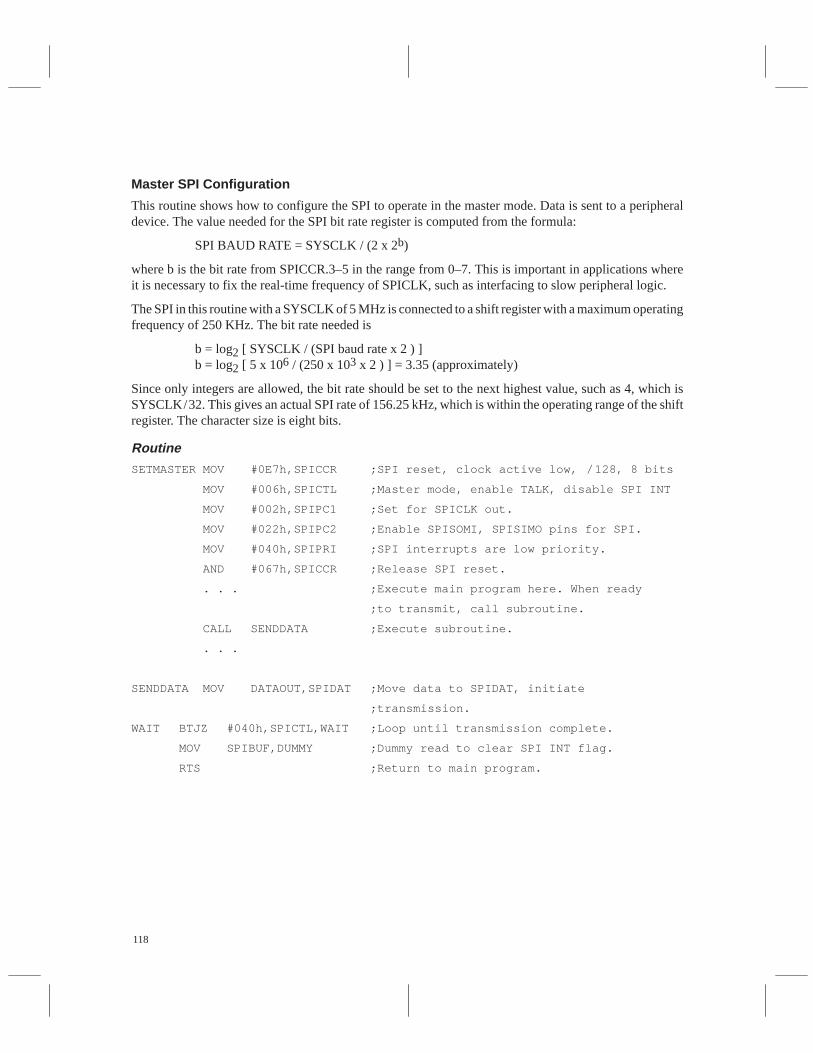
118
Master SPI Configuration
This routine shows how to configure the SPI to operate in the master mode. Data is sent to a peripheraldevice. The value needed for the SPI bit rate register is computed from the formula:
SPI BAUD RATE = SYSCLK / (2 x 2b)
where b is the bit rate from SPICCR.3–5 in the range from 0–7. This is important in applications whereit is necessary to fix the real-time frequency of SPICLK, such as interfacing to slow peripheral logic.
The SPI in this routine with a SYSCLK of 5 MHz is connected to a shift register with a maximum operatingfrequency of 250 KHz. The bit rate needed is
b = log2 [ SYSCLK / (SPI baud rate x 2 ) ]b = log2 [ 5 x 10⁶ / (250 x 103 x 2 ) ] = 3.35 (approximately)
Since only integers are allowed, the bit rate should be set to the next highest value, such as 4, which isSYSCLK/32. This gives an actual SPI rate of 156.25 kHz, which is within the operating range of the shiftregister. The character size is eight bits.
RoutineSETMASTER MOV #0E7h,SPICCR ;SPI reset, clock active low, /128, 8 bits
MOV #006h,SPICTL ;Master mode, enable TALK, disable SPI INT
MOV #002h,SPIPC1 ;Set for SPICLK out.
MOV #022h,SPIPC2 ;Enable SPISOMI, SPISIMO pins for SPI.
MOV #040h,SPIPRI ;SPI interrupts are low priority.
AND #067h,SPICCR ;Release SPI reset.
. . . ;Execute main program here. When ready
;to transmit, call subroutine.
CALL SENDDATA ;Execute subroutine.
. . .
SENDDATA MOV DATAOUT,SPIDAT ;Move data to SPIDAT, initiate
;transmission.
WAIT BTJZ #040h,SPICTL,WAIT ;Loop until transmission complete.
MOV SPIBUF,DUMMY ;Dummy read to clear SPI INT flag.
RTS ;Return to main program.
119
Slave SPI Configuration
This routine shows how to use the SPI interrupt to interrupt a program and load two 8-bit characters fromthe SPI. The program will call the SPI interrupt upon receipt of an 8-bit character, save it, and wait for onemore character. It will then save the values and return to the main program. The characters will be savedin DATAMSB and DATALSB.
RoutineSETSLAVE DINT ;Disable global interrupts.
MOV #0E7h,SPICCR ;SPI reset, clock active low, /32, 8 bits
MOV #001h,SPICTL ;Slave mode, TALK disable, SPI INT enable
MOV #002h,SPIPC1 ;Set SPICLK.
MOV #022h,SPIPC2 ;Enable SPISOMI, SPISIMO pins for SPI.
MOV #040h,SPIPRI ;SPI interrupts are low priority.
MOV #067h,SPICCR ;Release SPI RESET.
EINT ;Enable global interrupts.
. . . ;Insert main part of program here. SPI
;INT will fetch characters when first
;is detected.
SPIINTR MOV SPIBUF,DATAMSB ;Save first character already in buffer.
WAIT BTJZ #040h,SPICTL,WAIT;Wait until second character is received.
MOV SPIBUF,DATALSB ;Save second character.
RTI ;Return to main program.
120
Dynamic Bit Justification
On occasion it may be necessary to transmit characters of length less than eight bits. As stated previously,the data needs to be left-justified for transmitting from SPIDAT and right-justified when read fromSPIBUF. If the SPI is accessing several peripherals with different character lengths, it may be more efficientto have one subroutine justify all the transmitted data.
This routine reads the value of the character length stored in SPICCR.0–2 and left-justifies the data to betransmitted as needed. If the character length is less than five bits, the routine swaps nibbles to save time.The value to be transmitted is stored in the register DATA.
RoutineLJUSTIFY MOV SPICCR,NUMBITS ;Save character length in temp register.
XOR #0FFh,NUMBITS ;8 numbits = number of shifts
AND #007h,NUMBITS ;Clear all bits except character length.
BTJZ #004h,NUMBITS,ROLL ;If < 4 shifts needed, go to roll
;routine.
SWAP DATA ;More than 4 shifts, swap is faster.
SUB #004h,NUMBITS ;Since we swapped, 4 rolls are complete.
JZ DONE ;If only 4 rolls needed, we are done.
ROLL RL DATA ;Rotate one bit left.
DJNZ NUMBITS,ROLL ;If not done rotating, continue.
DONE MOV DATA,SPIDAT ;Data is now left justified, transmit.
121
Address Recognition by SPI
In multiprocessor systems using the SPI for communication, it is necessary to keep conversations limitedto two microprocessors at a time. The TALK bit is used to disable the transmit ability of a TMS370 in slavemode until it sees its address, MYADDRESS, at which time it will transmit a byte of data. This exampleshows the SPI interrupt routine, which is called when a character is received. If it is the correct address,the TALK bit is set, SPIDAT is loaded, and the TALK bit is cleared once again.
RoutineSPIINTR MOV SPIBUF,ADDRESS ;Store received address.
CMP #MYADDRESS,ADDRESS ;Is it my address?
JNZ DONE ;If not, ignore transmission.
OR #002h,SPICTL ;Set TALK bit.
MOV DATA,SPIDAT ;Load transmit buffer, wait for clock
;from master.
WAIT BTJZ #040h,SPICTL,WAIT ;Wait until character is sent.
MOV SPIBUF,DUMMY ;Dummy read to clear SPI INT flag.
DONE AND #0FDh,SPICTL ;Clear TALK bit.
RTI ;Return from interrupt.

122
SPI Module Specific Applications
Vacuum Fluorescent Display Driver
Use SPI to Transmit Data to Serial Shift Register
One common and very practical use of an SPI is sending serial data to a display. The use of simple softwareroutines can simplify your design and eliminate expensive external hardware such as decoders. Thisexample interfaces a TMS370C010 microcontroller to a vacuum fluorescent display. The only externallogic necessary is one TMS0170 VF Display Driver. This device is a 33-bit shift register /display driverand is especially suited for serial display applications. The design uses only SPI and Timer 1 (T1) pins, sothe designer does not need to dedicate any more I /O pins to the design. The schematic shown is for a genericserial display application, and it can be easily modified to work with an LED or LCD display.
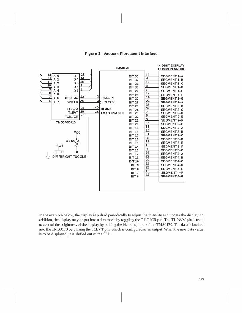
123
Figure 3. Vacuum Florescent Interface
TMS0170
14131110
9873
28241512
2324
212022
23
4038
TMS370C010
VCC
4.7 kΩSW1
DIM/BRIGHT TOGGLE
DATA INCLOCK
BLANKLOAD ENABLE
4 DIGIT DISPLAYCOMMON ANODE
13419824171823353476536332031301110932292227261615
BIT 6BIT 7BIT 8BIT 9
BIT 10BIT 11BIT 12BIT 13BIT 14BIT 15BIT 16BIT 17BIT 18BIT 19BIT 20BIT 21BIT 22BIT 23BIT 24BIT 25BIT 26BIT 27BIT 28BIT 29BIT 30BIT 31BIT 32BIT 33 SEGMENT 1–A
SEGMENT 1–BSEGMENT 1–CSEGMENT 1–DSEGMENT 1–ESEGMENT 1–FSEGMENT 1–GSEGMENT 2–ASEGMENT 2–BSEGMENT 2–CSEGMENT 2–DSEGMENT 2–ESEGMENT 2–FSEGMENT 2–GSEGMENT 3–ASEGMENT 3–BSEGMENT 3–CSEGMENT 3–DSEGMENT 3–ESEGMENT 3–FSEGMENT 3–GSEGMENT 4–ASEGMENT 4–BSEGMENT 4–CSEGMENT 4–DSEGMENT 4–ESEGMENT 4–FSEGMENT 4–G
A 0A 1A 2A 3A 4A 5A 6A 7
D 3D 4D 5D 6D 7
SPISIMOSPICLK
T1PWMT1EVT
T1IC/CR
In the example below, the display is pulsed periodically to adjust the intensity and update the display. Inaddition, the display may be put into a dim mode by toggling the T1IC/CR pin. The T1 PWM pin is usedto control the brightness of the display by pulsing the blanking input of the TMS0170. The data is latchedinto the TMS0170 by pulsing the T1EVT pin, which is configured as an output. When the new data valueis to be displayed, it is shifted out of the SPI.

124
This display update routine is controlled by T1 interrupts. The compare 1 and compare 2 registers are setto control the refresh rate and intensity, respectively. Because the display is pulsed more frequently thannew values are calculated, an interval counter is used to specify when it is time to update the display value.In this example, the following parameters are used:
Refreshes /s = 100 (eliminates flicker in display)Display updates/s = 2SYSCLK freq. = 5 MHzPrescale divide = 16Normal display intensity = 90%Dim display intensity = 40%
The T1 compare register values are found from the formulas:
Compare 1 value =
Compare 1 value =5,000,000
100 x 16
SYSCLK Frequency
refreshes/s x prescale divide
Compare 2 value = intensity x compare 1 value
Compare 2 value (bright) = 0.9 x 3125 = 2812 or 0AFCh
Compare 2 value (dim) = 0.4 x 3125 = 1250 or 04E2h
By XORing the bright and dim values together, we get the logical difference between the two values.XORing the difference with either the bright or dim values will give the other. This is an easy and quickway to toggle the brightness.
DIFFMSB = compare 2 value (dim) MSB XOR compare 2 value (bright) MSBDIFFLSB = compare 2 value (dim) LSB XOR compare 2 value (bright) LSB
The interval counter value is found from the following formula:
Interval = 100/2 = 50 or 32h
refreshes /sInterval = updates/s
125
Routine
The source code for this application is as follows:
.title “Display Driver”
; This routine uses the SPI and T1 modules to output values
; to a serial display. The display is updated every 0.5 seconds.
; Display intensity is changed by toggling TlIC/CR pin.
SPICCR .equ P030 ;SPI register assignments.
SPICTL .equ P031
SPIDAT .equ P039
SPIBUF .equ P037
SPIPC1 .equ P03D
SPIPC2 .equ P03E
T1CNTRMSB equ P040 ;T1 register assignments.
T1CMSBLSB .equ P041
T1CMSB .equ P042
T1CLSB .equ P043
T1CCMSB .equ P044
T1CCLSB .equ P045
T1CTL1 .equ P049
T1CTL2 .equ P04A
T1CTL3 .equ P04B
T1CTL4 .equ P04C
T1PC1 .equ P04D
T1PC2 .equ P04E
T1PRI .equ P04F
; Allocate register space for the registers used in the application
; routine.
DISPMSB .equ R5 ;High byte of display value.
DISPLSB .equ R6 ;Low byte of display value.
ICOUNT .equ R7 ;Time between display refreshes.
DCOUNT .equ R8
DIGIT0 .equ R10 ;BCD values of display digits
126
DIGIT1 .equ R11 ; ”
DIGIT2 .equ R12 ; ”
DIGIT3 .equ R13 ; ”
TEMPMSB .equ R14
TEMPLSB .equ R15
DUMMY .equ R16
; Assign values for display intensity, and refresh period.
TIMER .equ 3125 ;100 interrupts/sec @ 5 MHz
BRIGHT .equ TIMER*9/10 ;Max intensity = 90
DIFF .equ BRIGHT^(TIMER*4/10) ;Min intensity = 40
INTERVAL .equ 50
.text 07000h
START DINT ;Disable all interrupts.
; SPI Initialization
MOV #OE6h,SPICCR ;Reset SPI, data out on falling
;SPICLK,
;7-bit characters.
MOV #006h,SPICTL ;Master,enable TALK, disable SPI INT.
MOV #002h,SPIPC1 ;Enable SPICLK out.
MOV #020h,SPIPC2 ;Set SPISIMO out.
; Set delays for brightness, and value updates
MOV #HI(TIMER),T1CMSB ;Load compare 1 register with delay.
MOV #HI(TIMER),T1CLSB ;Time between refreshes (10 mS)
MOV #HI(BRIGHT),T1CCMSB ;Set display to bright intensity.
MOV #LO(BRIGHT),T1CCLSB ; ”
MOV #INTERVAL,ICOUNT ;Temp register for interval counter
; Timer 1 Initialization
MOV #001h,T1PC1 ;Set T1EVT as general I /O.
MOV #062h,T1PC2 ;Set T1IC/CR to input.
MOV #040h,T1PRI ;Set T1 interrupts to low priority.
MOV #071h,T1CTL4 ;Dual-compare,disable interrupts.
MOV #005h,T1CTL1 ;System clock / 16
MOV #000h,T1CTL3 ;Disable T1 interrupts, clear flags.
MOV #001h,T1CTL2 ;Disable overflow interrupts,reset
127
;T1.
; Enable Timer1 & SPI
MOV #005h,T1CTL3 ;Enable T1EDGE INT, enable T1C1 INT.
MOV #066h,SPICCR ;Release SPI.
MOV #0F0h,B ;Move stack pointer value to B.
LDSP ;Set stack pointer.
EINT ;Global interrupt enable
MAIN ;Main loop
; Place major portion of code here. This part of the program should
; calculate the value to be displayed, scale it from 0 to 9999, and
; store the result in DISPMSB and DISPLSB. When T1 counts down,
; the interrupt will be called and the program will jump to DISPLAY.
...
MOV #??,DISPMSB ;Move sample value into memory.
MOV #??,DISPLSB ;
...
JMP MAIN
; T1 Interrupt Routine.
; This routine pulls the value to be displayed from DISPMSB and
; DISPLSB, converts it to a packed 4 nibble BCD number, and shifts
; the result out through the SPI. The routine checks to see whether
; the routine was called by the timer or the T1C1 pin and clears
; the appropriate flag. DISPMSB and DISPLSB are temporary registers
; and will not contain their original values upon completion of the
; interrupt routine.
DISPLAY
BTJZ #080h,T1CTL3,TIMERINT ;Was interrupt from T1IC/CR pin?
; T1IC/CR pin called interrupt, toggle the intensity bright/dim.
MOV #003h,T1CTL1 ;Stop timer.
MOV #001h,T1CTL2 ;Reset timer (T1 SW RESET).
MOV #050h,T1PC2 ;Set PWM as general purpose I /O.
MOV #050h,T1PC2 ;Set T1PWM = 1 (command must be
;repeated).
128
MOV #060h,T1PC2 ;Reenable T1PWM.
MOV T1CCLSB,TEMPLSB ;Get current display intensity.
MOV T1CCMSB,TEMPMSB ;
XOR #LO(DIFF),TEMPLSB ;Toggle display intensity.
XOR #HI(DIFF),TEMPMSB ;
MOV TEMPMSB,T1CCMSB ;Update display intensity
MOV TEMPLSB,T1CCLSB ;
MOV #005h,T1CTL1 ;Restart timer.
AND #07Fh,T1CTL3 ;Clear T1IC/CR interrupt flag.
JMP DONE ;End of display toggle: wait for
;update.
TIMERINT DJNZ ICOUNT,NOTNOW ;Is it time for new value be
;displayed?
;If it is not, do not calc new value.
MOV #INTERVAL,ICOUNT ;Restore interval counter.
; Hex to BCD Conversion Routine.
CLR DIGIT2 ;Clear result registers.
CLR DIGIT0 ;”
MOV #16,R3 ;Set loop count.
LOOP RLC DISPLSB ;Shift high bit out.
RLC DISPMSB ;Carry contains the high bit.
DAC DIGIT0,DIGIT0 ;Double the number then add high bit.
DAC DIGIT2,DIGIT2 ;”
DJNZ R3,LOOP ;Loop until multiplied 16 times.
MOV DIGIT0,DIGIT1 ;Save second digit.
MOV DIGIT2,DIGIT3 ;Save third digit.
SWAP DIGIT1 ;Swap BCD nibbles.
SWAP DIGIT3 ;Swap BCD nibbles.
AND #0Fh,DIGIT0 ;Clear high nibble.
AND #0Fh,DIGIT1 ;Clear high nibble.
AND #0Fh,DIGIT2 ;Clear high nibble.
AND #0Fh,DIGIT3 ;Clear high nibble.
; Output display values.
; This part actually outputs the BCD values to the display through the
; SPI. Note that in this example the display is limited to 4
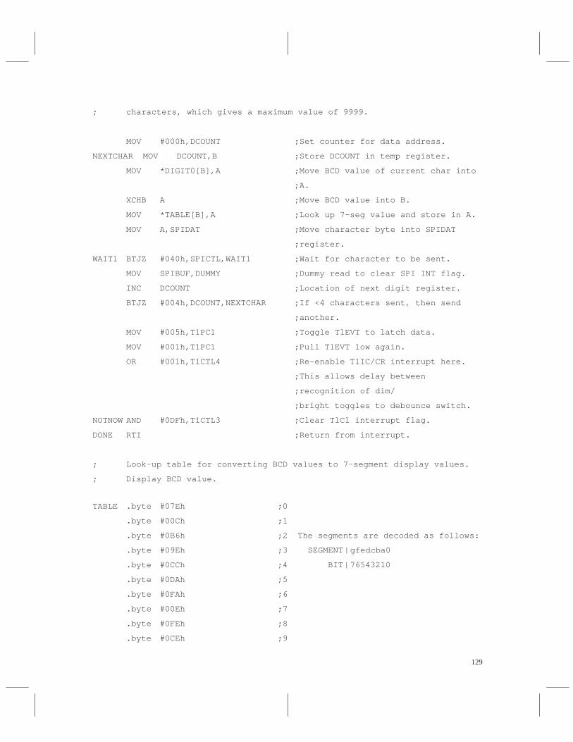
129
; characters, which gives a maximum value of 9999.
MOV #000h,DCOUNT ;Set counter for data address.
NEXTCHAR MOV DCOUNT,B ;Store DCOUNT in temp register.
MOV *DIGIT0[B],A ;Move BCD value of current char into
;A.
XCHB A ;Move BCD value into B.
MOV *TABLE[B],A ;Look up 7-seg value and store in A.
MOV A,SPIDAT ;Move character byte into SPIDAT
;register.
WAIT1 BTJZ #040h,SPICTL,WAIT1 ;Wait for character to be sent.
MOV SPIBUF,DUMMY ;Dummy read to clear SPI INT flag.
INC DCOUNT ;Location of next digit register.
BTJZ #004h,DCOUNT,NEXTCHAR ;If <4 characters sent, then send
;another.
MOV #005h,T1PC1 ;Toggle TlEVT to latch data.
MOV #001h,T1PC1 ;Pull TlEVT low again.
OR #001h,T1CTL4 ;Re-enable T1IC/CR interrupt here.
;This allows delay between
;recognition of dim/
;bright toggles to debounce switch.
NOTNOW AND #0DFh,T1CTL3 ;Clear TlCl interrupt flag.
DONE RTI ;Return from interrupt.
; Look–up table for converting BCD values to 7–segment display values.
; Display BCD value.
TABLE .byte #07Eh ;0
.byte #00Ch ;1
.byte #0B6h ;2 The segments are decoded as follows:
.byte #09Eh ;3 SEGMENT|gfedcba0
.byte #0CCh ;4 BIT |76543210
.byte #0DAh ;5
.byte #0FAh ;6
.byte #00Eh ;7
.byte #0FEh ;8
.byte #0CEh ;9
130
; Set up interrupt vector addresses
.sect “Vectors”,07FF4h
.word DISPLAY ;T1 interrupt
.word START ;All other vectors go to ’START’.
.word START
.word START
.word START
.word START
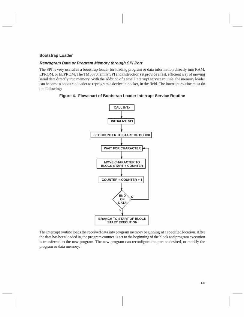
131
Bootstrap Loader
Reprogram Data or Program Memory through SPI Port
The SPI is very useful as a bootstrap loader for loading program or data information directly into RAM,EPROM, or EEPROM. The TMS370 family SPI and instruction set provide a fast, efficient way of movingserial data directly into memory. With the addition of a small interrupt service routine, the memory loadercan become a bootstrap loader to reprogram a device in-socket, in the field. The interrupt routine must dothe following:
Figure 4. Flowchart of Bootstrap Loader Interrupt Service Routine
CALL INTx
INITIALIZE SPI
SET COUNTER TO START OF BLOCK
WAIT FOR CHARACTER
MOVE CHARACTER TOBLOCK START + COUNTER
COUNTER = COUNTER + 1
ENDOF
DATA
N
Y
BRANCH TO START OF BLOCKSTART EXECUTION
The interrupt routine loads the received data into program memory beginning at a specified location. Afterthe data has been loaded in, the program counter is set to the beginning of the block and program executionis transferred to the new program. The new program can reconfigure the part as desired, or modify theprogram or data memory.
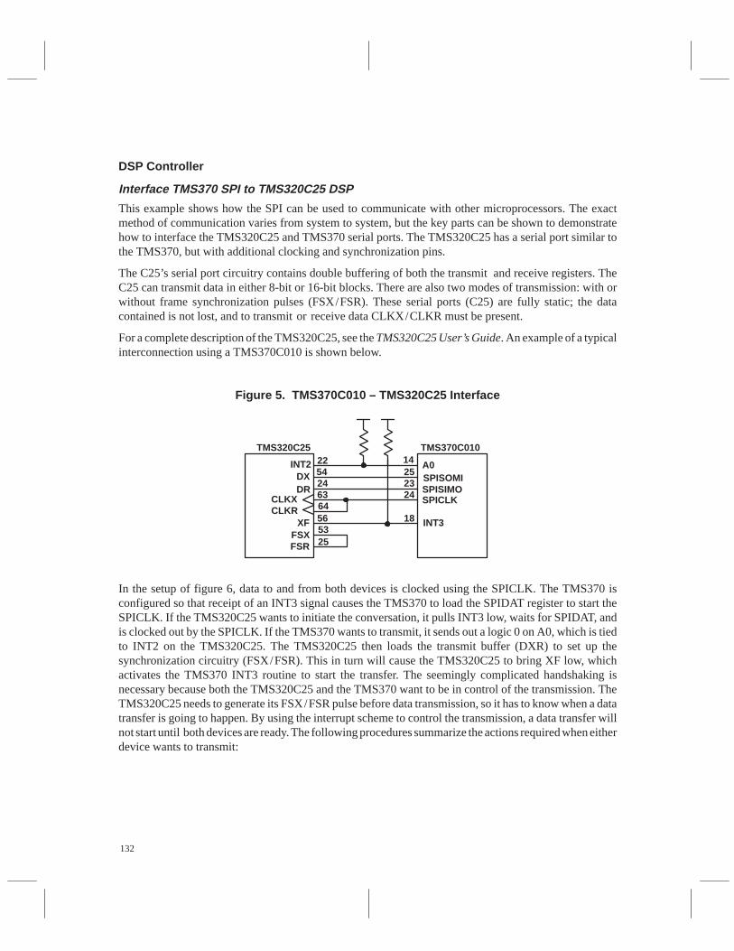
132
DSP Controller
Interface TMS370 SPI to TMS320C25 DSP
This example shows how the SPI can be used to communicate with other microprocessors. The exactmethod of communication varies from system to system, but the key parts can be shown to demonstratehow to interface the TMS320C25 and TMS370 serial ports. The TMS320C25 has a serial port similar tothe TMS370, but with additional clocking and synchronization pins.
The C25’s serial port circuitry contains double buffering of both the transmit and receive registers. TheC25 can transmit data in either 8-bit or 16-bit blocks. There are also two modes of transmission: with orwithout frame synchronization pulses (FSX/FSR). These serial ports (C25) are fully static; the datacontained is not lost, and to transmit or receive data CLKX/CLKR must be present.
For a complete description of the TMS320C25, see the TMS320C25 User’s Guide. An example of a typicalinterconnection using a TMS370C010 is shown below.
Figure 5. TMS370C010 – TMS320C25 Interface
TMS320C25 TMS370C010
INT2DXDR
CLKXCLKR
XFFSXFSR
A0SPISOMISPISIMOSPICLK
INT3
2254246364565325
14252324
18
In the setup of figure 6, data to and from both devices is clocked using the SPICLK. The TMS370 isconfigured so that receipt of an INT3 signal causes the TMS370 to load the SPIDAT register to start theSPICLK. If the TMS320C25 wants to initiate the conversation, it pulls INT3 low, waits for SPIDAT, andis clocked out by the SPICLK. If the TMS370 wants to transmit, it sends out a logic 0 on A0, which is tiedto INT2 on the TMS320C25. The TMS320C25 then loads the transmit buffer (DXR) to set up thesynchronization circuitry (FSX/FSR). This in turn will cause the TMS320C25 to bring XF low, whichactivates the TMS370 INT3 routine to start the transfer. The seemingly complicated handshaking isnecessary because both the TMS320C25 and the TMS370 want to be in control of the transmission. TheTMS320C25 needs to generate its FSX/FSR pulse before data transmission, so it has to know when a datatransfer is going to happen. By using the interrupt scheme to control the transmission, a data transfer willnot start until both devices are ready. The following procedures summarize the actions required when eitherdevice wants to transmit:
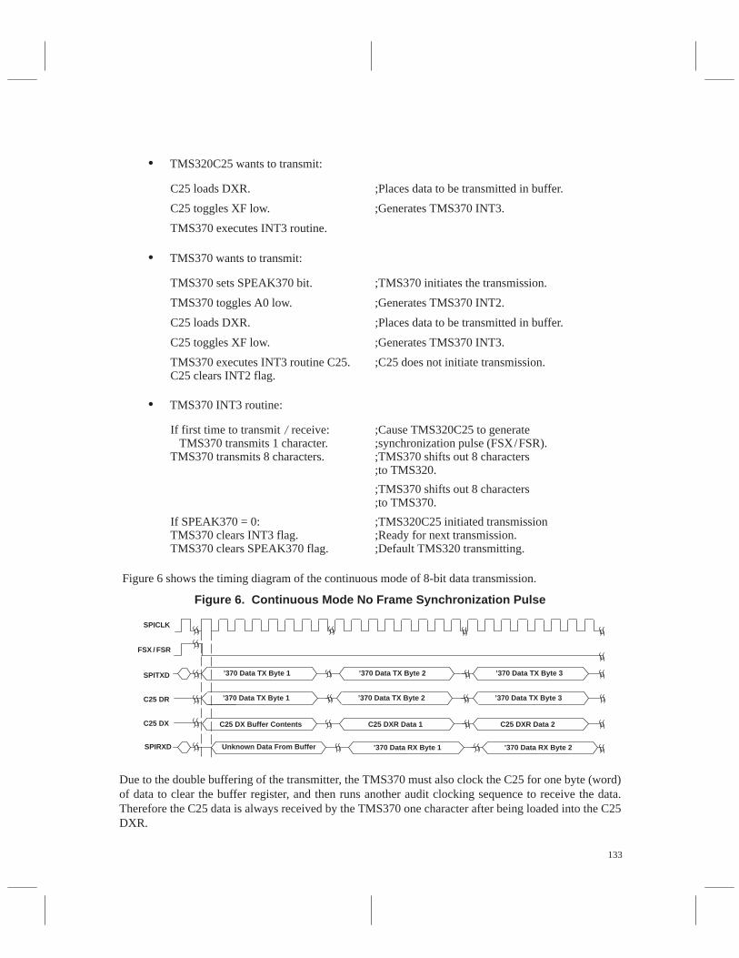
133
• TMS320C25 wants to transmit:
C25 loads DXR. ;Places data to be transmitted in buffer.
C25 toggles XF low. ;Generates TMS370 INT3.
TMS370 executes INT3 routine.
• TMS370 wants to transmit:
TMS370 sets SPEAK370 bit. ;TMS370 initiates the transmission.
TMS370 toggles A0 low. ;Generates TMS370 INT2.
C25 loads DXR. ;Places data to be transmitted in buffer.
C25 toggles XF low. ;Generates TMS370 INT3.
TMS370 executes INT3 routine C25. C25 clears INT2 flag.
;C25 does not initiate transmission.
• TMS370 INT3 routine:
If first time to transmit/ receive: TMS370 transmits 1 character. TMS370 transmits 8 characters.
;Cause TMS320C25 to generate;synchronization pulse (FSX/FSR).;TMS370 shifts out 8 characters;to TMS320.
;TMS370 shifts out 8 characters;to TMS370.
If SPEAK370 = 0: TMS370 clears INT3 flag. TMS370 clears SPEAK370 flag.
;TMS320C25 initiated transmission;Ready for next transmission.;Default TMS320 transmitting.
Figure 6 shows the timing diagram of the continuous mode of 8-bit data transmission.
Figure 6. Continuous Mode No Frame Synchronization Pulse
SPICLK
FSX / FSR
SPITXD
C25 DR
C25 DX
SPIRXD
’370 Data TX Byte 1
’370 Data TX Byte 1
’370 Data TX Byte 2
’370 Data TX Byte 2
’370 Data TX Byte 3
’370 Data TX Byte 3
’370 Data RX Byte 1
C25 DX Buffer Contents C25 DXR Data 1 C25 DXR Data 2
’370 Data RX Byte 2Unknown Data From Buffer
Due to the double buffering of the transmitter, the TMS370 must also clock the C25 for one byte (word)of data to clear the buffer register, and then runs another audit clocking sequence to receive the data.Therefore the C25 data is always received by the TMS370 one character after being loaded into the C25DXR.
134
Different protocols have different benefits, and the protocol used depends on the requirements of thesystem. If the system requires continual transmission of data from the C25, then the no framesynchronization mode (no FSX/FSR pulse) allows greater throughput and less system overhead on theTMS370 processor.
If the system only has periodic data transmission of data between the two processors, and the data needsto be transmitted immediately, then the TMS370 needs to allow 16 SPICLK cycles for the data from C25to be received by the TMS370 with added speed. The first byte from the C25 is dummy data. This procedureis not as efficient as the method of Figure 6, but for single bytes transmitted between long intervals, the datatransfer is quicker. This is due to the TMS370’s not having to wait for the C25 to load the next byte oftransmit data into the buffer for transmission.
Both processors’ flexible modes of transmission (such as C25’s ability to transmit in either 8-bit or 16-bitmode) allows customization to the parameters of the desired system. The routines shown do not incorporateany checks if both the C25 routine and TMS370 routine try to communicate at the same time. When thissituation occurs, both processors will think that they initiated the communication and ignore the receiveddata. If asynchronous communications can occur at the same time in your system, then you need to definea proper protocol.
Routine.title “TMS370-TMS320C25 Interface Continuous Mode”
; This is the framework of source code for an interface between a
; TMS370 microcontroller and a TMS320C25 DSP. The external
; interrupts on both devices are used to synchronize the data
; transfer.
; Set up equate table for peripheral file registers used in the
; routine.
SPICCR .equ P030 ;SPI register assignments.
SPICTL .equ P031
SPIBUF .equ P037
SPIDAT .equ P039
SPIPC1 .equ P03D
SPIPC2 .equ P03E
SPIPRI .equ P03F
ADATA .equ P022
ADIR .equ P023
INT1 .equ P017
INT2 .equ P018
INT3 .equ P019
; Allocate register space for communications flags and data registers.
135
COM370 .equ R4 ;Status register for TMS320–TMS370 comm
SPEAK370 .dbit 0,COM370 ;=1 if TMS370 is transmitting
FIRSTX .dbit 7,COM370 ;=1 C25 in continuous mode, need to
;generate first sync pulse
DATAIN .equ R5 ;Received data
DATAOUT .equ R6 ;Data to be transmitted
.text 07000H
START DINT ;Disable all interrupts.
MOV #100,B ;Set stack pointer to r100.
LDSP
Initialize SPI, APORT, and communication status flag.
MOV #087h,SPICCR ;Reset SPI, data out on rising SPICLK,
;8-bit characters
MOV #006h,SPICTL ;Master, enable TALK, disable SPI INT.
MOV #002h,SPIPC1 ;Enable SPICLK out.
MOV #022h,SPIPC2 ;Set SPISIMO & SPISOMI out.
MOV #020h,SPIPRI ;Enable emulator suspend.
MOV #007h,SPICCR ;Reset SPI, data out on rising SPICLK,
;8-bit characters
MOV #001h,ADIR ;Set A0 as output.
MOV #001h,ADATA ;Set A0 high.
MOV #01H,INT1 ;Initialize interrupt 1.
MOV #01H,INT2 ;Initialize interrupt 2.
MOV #01H,INT3 ;Initialize interrupt 3.
SBIT0 SPEAK370 ;Default is TMS370 not speaking.
SBIT1 FIRSTX ;Initialize as first Transmission.
MOV #00H,DATAOUT ;Initialize the data out register.
EINT ;Enable interrupts.
; Place main program here. When TMS370 is ready to transmit, it will
; call subroutine TRANSMIT. This will cause an interrupt in the TMS320
; which will in turn activate INT1 in the TMS370. When the TMS320 wants
; to initiate a transfer it will generate an INT1 interrupt, causing the
136
; part to execute the INT1 service routine, which will prepare it to
; initiate a transfer. Since both transmissions by the TMS320 and
; TMS370 involve calling the TMS370 INT1 routine, the SPEAK370 bit is
; set by the TMS370 when it initiates a transfer. The data to be
; transmitted is stored in DATA OUT and received data, if it is valid,
; will be stored in DATA IN.
MAIN ...
;
; TMS370 initiates the data transfer to the C25; set appropriate
; flags.
;
TRANSMIT SBIT1 SPEAK370 ;TMS370 is initiating transfer.
AND #0FEh,ADATA ;Write 0 to A0, trigger INT1 in TMS320.
OR #001h,ADATA ;Release TMS320 INT1.
RTS ;Return from subroutine (after INT1
;call).
; Interrupt 3 service routine. This routine is called when the
; TMS370 is going to transmit or receive data.
; Do frame sync once (FIRSTX).
INTR3 JBIT0,FIRSTX,DATA ;If NOT the first transmission gotoDATA.
SBIT0,FIRSTX ;Clear FLAG FIRSTX, this is first time
MOV #080h,SPICCR ;Set character size=1 bit.
MOV #000h,SPICCR ;Reset SPI, data out on rising SPICLK,
MOV #000h,SPIDAT ;Transmit dummy pulse to make TMS320
;generate FSX/FSR sync pulse.
WAIT1 BTJZ #0040h,SPICTL,WAIT1 ;Wait until character has been sent.
MOV SPIBUF,DATAIN ;Clear SPI flag.
MOV #087h,SPICCR ;RESET SPI, character size=8 bit.
MOV #007h,SPICCR ;Enable SPI, character size=8 bit.
DATA MOV DATAOUT,SPIDAT ;Transmit data to TMS320. If SPEAK370=0,
;this may be dummy data.
WAIT2 BTJZ #040h,SPICTL,WAIT2 ;Wait until character has been sent.
JBIT1 SPEAK370,DONE ;If TMS370 is talking, do not save data.
MOV SPIBUF,DATAIN ;Save received data, clear SPI flag.
DONE AND #07Fh,INT3 ;Clear INT1 flag.
137
SBIT0 SPEAK370 ;Clear TMS370 transmission flag.
RTI ;End of INT3 routine.
INTR2 ... ;Interrupt 2 routine
MOV #01H,INT2 ;Clear and enable interrupt 2 flag.
RTI
INTR1 ... ;Interrupt 1 routine
MOV #01H,INT1 ;Clear and enable interrupt 1 flag.
RTI
Set up interrupt vector addresses.
.sect “Vectors”,07FF4H
.word START ;Vector goes to ’START’.
.word START ;Vector goes to ’START’.
.word INTR3 ;INT3 vector
.word INTR2 ;INT2 vector
.word INTR1 ;INT1 vector
.word START ;Reset vector.
The source code for the TMS370C25 in this application is as follows:
*
* sample program for interfacing the TMS370C10 and
* the TMS320C25 serial ports.
*
*
DRR: .equ 0 ;Serial port receive register
DXR: .equ 1 ;Serial port transmit register
IMR: .equ 4 ;Interrupt mask register
DATA: .equ 96 ;General purpose register
*
.sect “AORGO”
B START ;Power–up reset
.sect “AORG1”
B INT2 ;Interrupt 2 service routine
.sect “AORG2”
B RXINT ;Serial port receiver interrupt
*
.sect “AORG3”
138
START .equ $
DINT ;Disable interrupts.
LDPK 0 ;Point to page 0.
FORT 1 ;Set serial port to 8-bit mode.
LALK 0ffc4h ;Enable interrupt 2.
SACL IMR ;
STXM ;FSX is output.
RFSM ;Continuos mode
ZAC ;Zero the accumulator.
SACL DRR ;Initialize receiver register.
SACL DXR ;Initialize transmit register.
EINT
*
*
* Main body of program goes here. To initiate data transfer to the TMS370
* CALL subroutine XMIT. Doing this tells the TMS370 to start clocking, and
* the 320 knows not to save the received data. When subroutine INT2 is
* entered, the 320 again tells the 370 to start clocking the serial port
* and the 320 knows that it needs to save the data it receives. RXISR
* lets the processor know when the data has been received.
*
XMIT LAC DXR ;Load data for transmission.
CALL XMTISR ;Initiate data transfer to 370.
EINT ;Enable interrupts.
IDLE ;Wait for received data, do not save
RET ;received data.
INT2: .equ $
RPTK 40 ;Give 370 enough time to detect
NOP ;the XF generated interrupt. Then
CALL XMTISR ;initiate data transfer to 370.
LALK Offd4h ;
SACL IMR ;Enable int2, rxint.
EINT ;Enable interrupts.
IDLE ;Wait for received data.
LAC DRR ;Load accumulator with data receive
;register.
ANDK Offh ;Save only lower 8 bits.
139
SACL DATA ;Store received data.
RET
*
RXISR: .equ $ ;Serial receive interrupt
EINT ;Enable interrupts.
RET
*
XMTISR:.equ $ ;Initiate data transfer to 370 routine.
RXF ;Toggle XF flag low, causes 370
;interrupt
NOP ;
NOP ;
NOP ;
SXF ;and then high, to clear only, want 370
;INT3
RET ;routine to execute once.
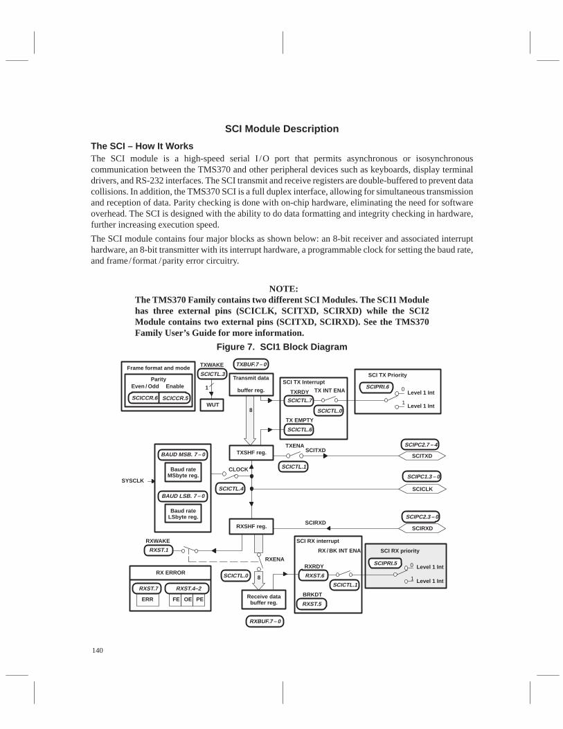
140
SCI Module Description
The SCI – How It WorksThe SCI module is a high-speed serial I /O port that permits asynchronous or isosynchronouscommunication between the TMS370 and other peripheral devices such as keyboards, display terminaldrivers, and RS-232 interfaces. The SCI transmit and receive registers are double-buffered to prevent datacollisions. In addition, the TMS370 SCI is a full duplex interface, allowing for simultaneous transmissionand reception of data. Parity checking is done with on-chip hardware, eliminating the need for softwareoverhead. The SCI is designed with the ability to do data formatting and integrity checking in hardware,further increasing execution speed.
The SCI module contains four major blocks as shown below: an 8-bit receiver and associated interrupthardware, an 8-bit transmitter with its interrupt hardware, a programmable clock for setting the baud rate,and frame/format /parity error circuitry.
NOTE:The TMS370 Family contains two different SCI Modules. The SCI1 Modulehas three external pins (SCICLK, SCITXD, SCIRXD) while the SCI2Module contains two external pins (SCITXD, SCIRXD). See the TMS370Family User’s Guide for more information.
Figure 7. SCI1 Block Diagram
RXST.4–2
FE OE PE
RX ERROR
SCICTL.3
TXWAKE
SCICCR.6 SCICCR.5
Even / Odd EnableParity
Frame format and mode
WUT
TXBUF.7 – 0
Transmit data
buffer reg.
TXSHF reg.
SCICTL.7
SCICTL.6
TXRDY
TX EMPTY
SCI TX Interrupt
SCICTL.0
TXENA
8
SCICTL.4
BAUD MSB. 7 – 0
Baud rateMSbyte reg.
BAUD LSB. 7 – 0
Baud rateLSbyte reg.
SYSCLK
SCICTL.1
SCITXD
TX INT ENA
RXST.7
ERR
RXSHF reg.
RXST.1
8
Receive databuffer reg.
RXBUF.7 – 0
RXENA
RXST.6
RXST.5
RXRDY
BRKDT
SCI RX interrupt
SCICTL.1
RX / BK INT ENA
ÎÎÎÎÎÎ
SCIPRI.5
Level 1 Int
Level 1 Int
Level 1 Int
Level 1 Int
SCI TX Priority
SCI RX priority
SCITXD
SCIPC2.7 – 4
SCIRXDSCIRXD
SCIPC2.3 – 0
SCICTL.0
RXWAKE
1 ÎÎÎSCIPRI.6 0
1
0
1
SCICLK
SCIPC1.3 – 0CLOCK
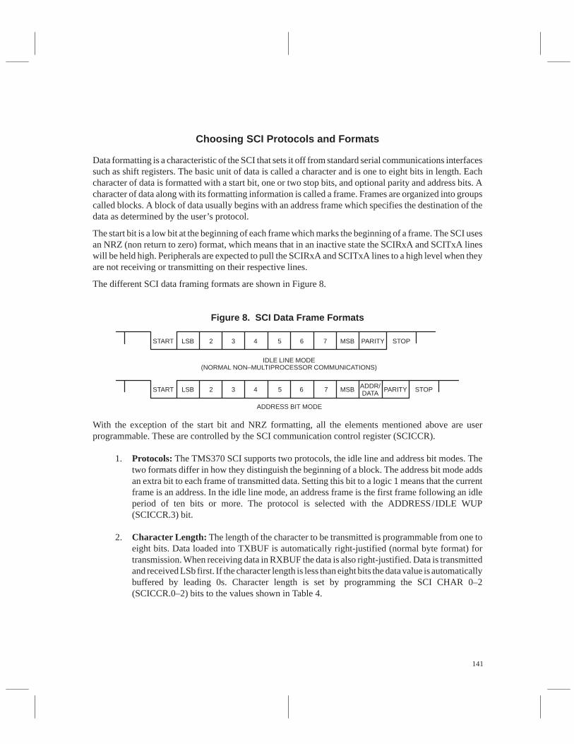
141
Choosing SCI Protocols and Formats
Data formatting is a characteristic of the SCI that sets it off from standard serial communications interfacessuch as shift registers. The basic unit of data is called a character and is one to eight bits in length. Eachcharacter of data is formatted with a start bit, one or two stop bits, and optional parity and address bits. Acharacter of data along with its formatting information is called a frame. Frames are organized into groupscalled blocks. A block of data usually begins with an address frame which specifies the destination of thedata as determined by the user’s protocol.
The start bit is a low bit at the beginning of each frame which marks the beginning of a frame. The SCI usesan NRZ (non return to zero) format, which means that in an inactive state the SCIRxA and SCITxA lineswill be held high. Peripherals are expected to pull the SCIRxA and SCITxA lines to a high level when theyare not receiving or transmitting on their respective lines.
The different SCI data framing formats are shown in Figure 8.
Figure 8. SCI Data Frame Formats
ADDRESS BIT MODE
IDLE LINE MODE(NORMAL NON–MULTIPROCESSOR COMMUNICATIONS)
START LSB 2 3 4 5 6 7 MSB PARITY STOPADDR/DATA
START LSB 2 3 4 5 6 7 MSB PARITY STOP
With the exception of the start bit and NRZ formatting, all the elements mentioned above are userprogrammable. These are controlled by the SCI communication control register (SCICCR).
1. Protocols: The TMS370 SCI supports two protocols, the idle line and address bit modes. Thetwo formats differ in how they distinguish the beginning of a block. The address bit mode addsan extra bit to each frame of transmitted data. Setting this bit to a logic 1 means that the currentframe is an address. In the idle line mode, an address frame is the first frame following an idleperiod of ten bits or more. The protocol is selected with the ADDRESS/IDLE WUP(SCICCR.3) bit.
2. Character Length: The length of the character to be transmitted is programmable from one toeight bits. Data loaded into TXBUF is automatically right-justified (normal byte format) fortransmission. When receiving data in RXBUF the data is also right-justified. Data is transmittedand received LSb first. If the character length is less than eight bits the data value is automaticallybuffered by leading 0s. Character length is set by programming the SCI CHAR 0–2(SCICCR.0–2) bits to the values shown in Table 4.
142
Table 4. Transmitter Character Bit Length
SCIChar2
SCIChar1
SCIChar0
CharacterLength
0 0 0 1
0 0 1 2
0 1 0 3
0 1 1 4
1 0 0 5
1 0 1 6
1 1 0 7
1 1 1 8
3. Parity : Parity is a method of checking the integrity of a transmitted/received character. It sendsan extra bit with the character to make sure that the sum of 1s in the character is an odd or evennumber. Parity checking and generation is done on-chip in hardware. It may be enabled ordisabled, and if used it can be set odd or even. Bits 5 and 6 of the SCICCR register control theparity checking.
4. Stop bits: A stop bit is a high bit of data transmitted at the end of a frame. The number of stopbits can be one or two, depending on your application. In general, data integrity is more secureif two bits are used because the SCI is more likely to catch a framing (SCI synchronization) error.Adding the extra bit increases the number of bits transmitted per character, however, and slowsthe throughput of the serial port.
The SCI SW RESET Bit
The SCI SW RESET bit (SCICTL.5) is used to reset the condition of the SCI state machine and operatingflags. Writing a 0 to this bit sets the operating flags to their reset state and halts the operation of the SCI.This must be done before using the SCI for the first time or after a system RESET to assure the state of theSCI. Writing a 1 to the bit releases the SCI state machine and allows the SCI to resume operation.
It is good practice to reset the SCI by writing a 0 to the SCI SW RESET bit before setting up the controlregisters. The registers are then set to the desired value and a 1 is written to the SCI SW RESET bit to releasethe SCI. This stops the operation of the SCI while it is being configured initially. The SCICTL controlregister values can be set in the same instruction that sets the SCI SW RESET bit to 1.
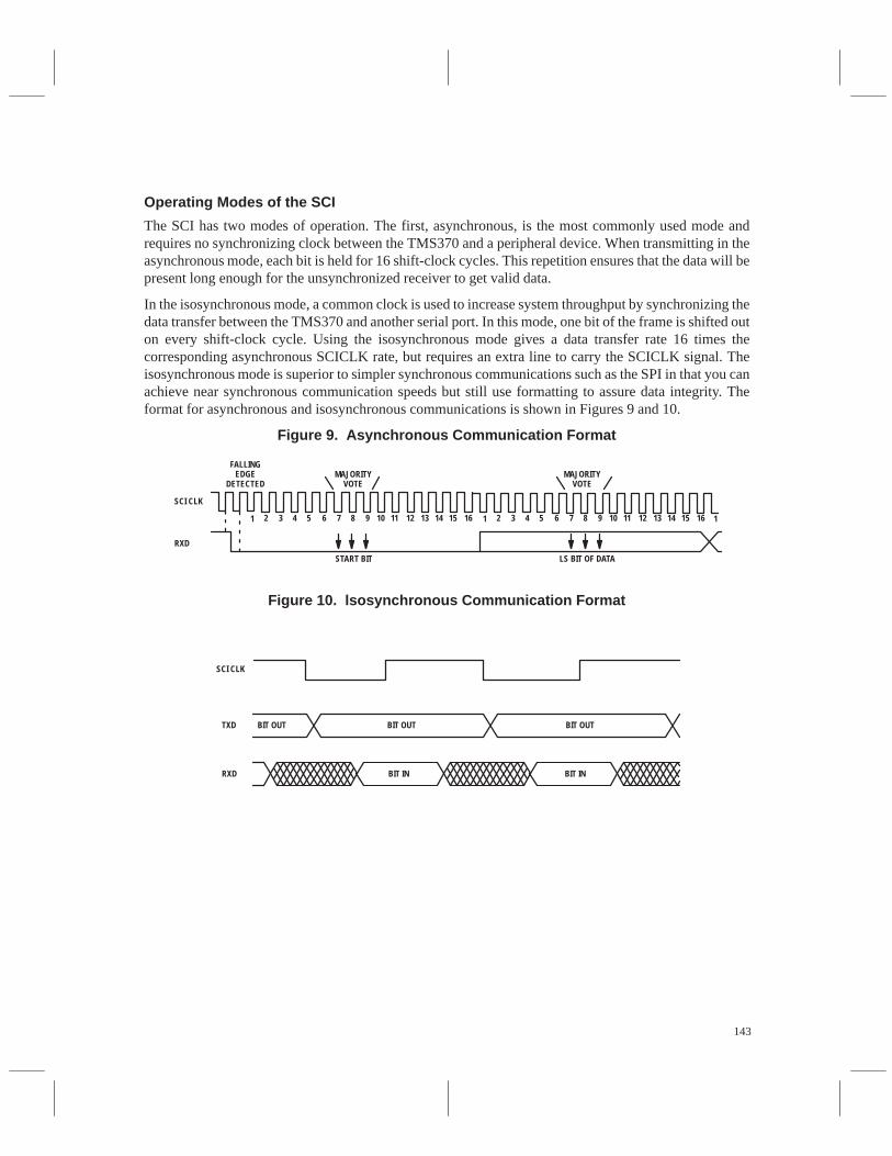
143
Operating Modes of the SCI
The SCI has two modes of operation. The first, asynchronous, is the most commonly used mode andrequires no synchronizing clock between the TMS370 and a peripheral device. When transmitting in theasynchronous mode, each bit is held for 16 shift-clock cycles. This repetition ensures that the data will bepresent long enough for the unsynchronized receiver to get valid data.
In the isosynchronous mode, a common clock is used to increase system throughput by synchronizing thedata transfer between the TMS370 and another serial port. In this mode, one bit of the frame is shifted outon every shift-clock cycle. Using the isosynchronous mode gives a data transfer rate 16 times thecorresponding asynchronous SCICLK rate, but requires an extra line to carry the SCICLK signal. Theisosynchronous mode is superior to simpler synchronous communications such as the SPI in that you canachieve near synchronous communication speeds but still use formatting to assure data integrity. Theformat for asynchronous and isosynchronous communications is shown in Figures 9 and 10.
Figure 9. Asynchronous Communication Format
1 2 3 4 5 6 7 8 9 10 11 12 13 14 1615 1 2 3 4 5 6 7 8 9 10 11 12 13 14 1615 1
FALLINGEDGE
DETECTEDMAJORITY
VOTEMAJORITY
VOTE
SCI CLK
RXD
START BIT LS BIT OF DATA
Figure 10. lsosynchronous Communication Format
SCI CLK
TXD
RXD
BIT OUT BIT OUT BIT OUT
BIT IN BIT IN
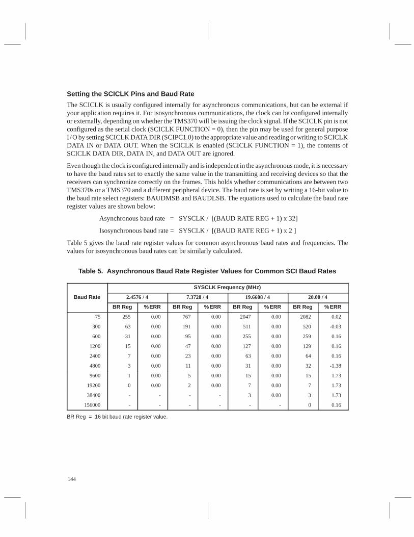
144
Setting the SCICLK Pins and Baud Rate
The SCICLK is usually configured internally for asynchronous communications, but can be external ifyour application requires it. For isosynchronous communications, the clock can be configured internallyor externally, depending on whether the TMS370 will be issuing the clock signal. If the SCICLK pin is notconfigured as the serial clock (SCICLK FUNCTION = 0), then the pin may be used for general purposeI /O by setting SCICLK DATA DIR (SCIPC1.0) to the appropriate value and reading or writing to SCICLKDATA IN or DATA OUT. When the SCICLK is enabled (SCICLK FUNCTION = 1), the contents ofSCICLK DATA DIR, DATA IN, and DATA OUT are ignored.
Even though the clock is configured internally and is independent in the asynchronous mode, it is necessaryto have the baud rates set to exactly the same value in the transmitting and receiving devices so that thereceivers can synchronize correctly on the frames. This holds whether communications are between twoTMS370s or a TMS370 and a different peripheral device. The baud rate is set by writing a 16-bit value tothe baud rate select registers: BAUDMSB and BAUDLSB. The equations used to calculate the baud rateregister values are shown below:
Asynchronous baud rate = SYSCLK / [(BAUD RATE REG + 1) x 32]
Isosynchronous baud rate = SYSCLK / [(BAUD RATE REG + 1) x 2 ]
Table 5 gives the baud rate register values for common asynchronous baud rates and frequencies. Thevalues for isosynchronous baud rates can be similarly calculated.
Table 5. Asynchronous Baud Rate Register Values for Common SCI Baud Rates
SYSCLK Frequency (MHz)
Baud Rate 2.4576 / 4 7.3728 / 4 19.6608 / 4 20.00 / 4
BR Reg %ERR BR Reg %ERR BR Reg %ERR BR Reg %ERR
75 255 0.00 767 0.00 2047 0.00 2082 0.02
300 63 0.00 191 0.00 511 0.00 520 -0.03
600 31 0.00 95 0.00 255 0.00 259 0.16
1200 15 0.00 47 0.00 127 0.00 129 0.16
2400 7 0.00 23 0.00 63 0.00 64 0.16
4800 3 0.00 11 0.00 31 0.00 32 -1.38
9600 1 0.00 5 0.00 15 0.00 15 1.73
19200 0 0.00 2 0.00 7 0.00 7 1.73
38400 - - - - 3 0.00 3 1.73
156000 - - - - - - 0 0.16
BR Reg = 16 bit baud rate register value.

145
NOTE:When using an externally generated SCICLK in isosynchronous mode, themaximum speed at which the SCICLK can run is limited to SYSCLK/10.This is necessary so that the internal clocks of the SCI have time tosynchronize with the external clock. For this reason, use the TMS370 to drivethe master serial clock in a system where maximum throughput is a majorconcern.
SCI Receiver Operation
A flowchart showing the operation of the receiver is shown in Figure 11. When the SCI senses a fallingedge on SCIRXD, the flow shown in the figure begins. Depending on the protocol and format, the receiverchecks for transmission errors and loads the data into RXSHF, the receiver shift register. When the numberof bits specified by the SCI character length control bit have been read in, the contents of RXSHF aretransferred to the receiver data buffer, RXBUF, and the RXRDY flag is set to show that the data value isready to be read. An SCI receiver interrupt is generated if the SCI receiver interrupt is enabled.
If errors are detected, the RXERROR and specific error (parity, framing, overrun, and break) flags are setby the hardware and operation continues. Error control is done in software. If multiprocessorcommunications are being used, frames received are checked to see if they are address frames and theappropriate bits are set.
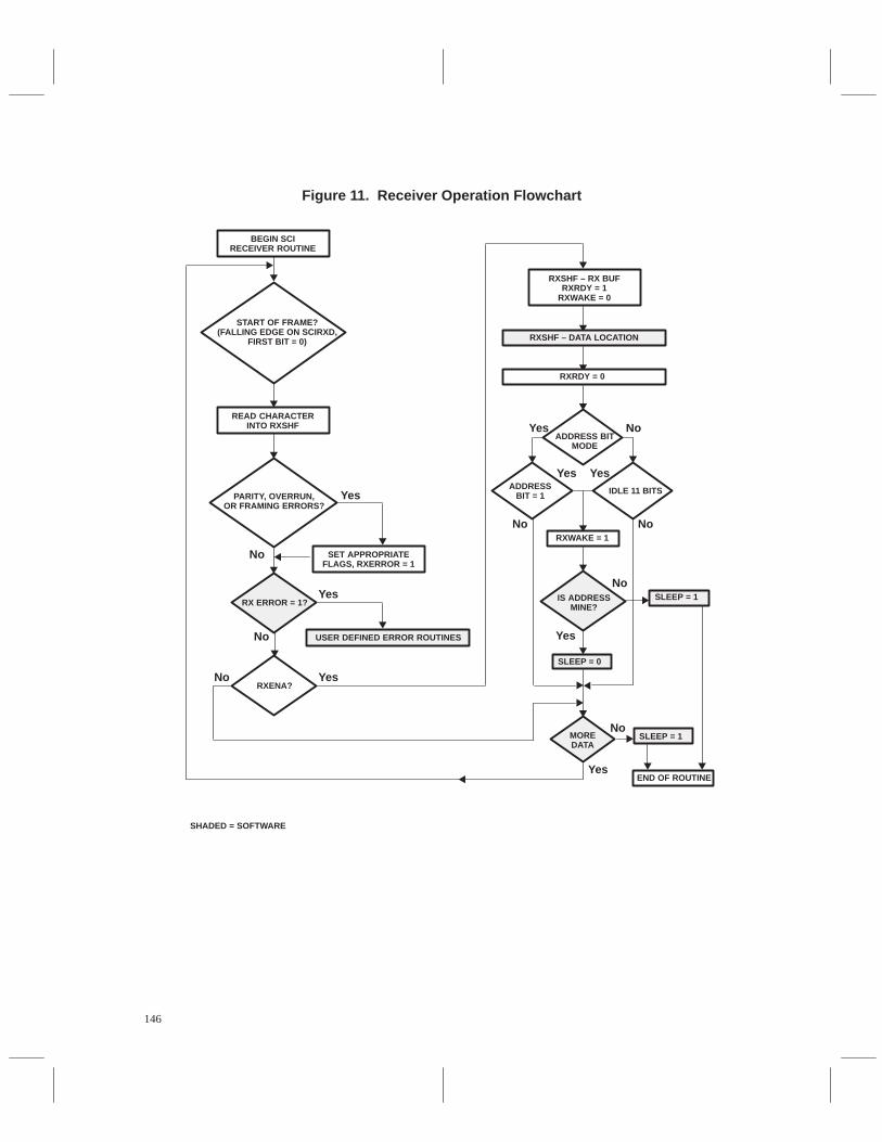
146
Figure 11. Receiver Operation Flowchart
Yes
No
BEGIN SCIRECEIVER ROUTINE
START OF FRAME?(FALLING EDGE ON SCIRXD,
FIRST BIT = 0)
READ CHARACTERINTO RXSHF
PARITY, OVERRUN,OR FRAMING ERRORS?
SET APPROPRIATEFLAGS, RXERROR = 1
RX ERROR = 1?
USER DEFINED ERROR ROUTINES
RXENA?
Yes
Yes
No
No
RXSHF – RX BUFRXRDY = 1
RXWAKE = 0
RXSHF – DATA LOCATION
RXRDY = 0
ADDRESS BITMODE
IDLE 11 BITSADDRESSBIT = 1
RXWAKE = 1
IS ADDRESSMINE?
SLEEP = 0
SLEEP = 1
MOREDATA
SLEEP = 1
END OF ROUTINEYes
No
Yes
No
YesYes
No
No
Yes
SHADED = SOFTWARE
No

147
SCI Transmitter Operation
A flowchart of the operation of the SCI transmitter is shown in Figure 12. The SCI transmitter is activatedby loading the transmitter buffer, TXBUF, which clears the TXRDY flag. When TXSHF, the transmittershift register, is empty the contents of TXBUF are latched into TXSHF and the TXRDY flag is set toindicate the transmitter is ready for a new character. Depending on the protocol and format, the transmitterformats the data as needed to signal the beginning and end of frames of data.
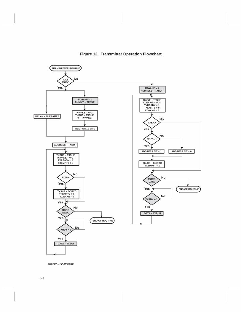
148
Figure 12. Transmitter Operation Flowchart
Yes
No
TRANSMITTER ROUTINE
IDLEMODE
TXWAKE = 1ADDRESS – TXBUF
TXWAKE = 1DUMMY – TXBUF
TXWAKE – WUTTXBUF – TXSHF
0 – TXWAKE
IDLE FOR 10 BITS
DELAY > 10 FRAMES
ADDRESS – TXBUF
TXBUF – TXSHFTXWAKE – WUT
TXREADY = 1TXEMPTY = 0
TXENA
TXSHF – SCITXDTXEMPTY = 1TXWAKE = 0
MOREDATA
TXRDY = 1
DATA – TXBUF
END OF ROUTINE
TXBUF – TXSHFTXWAKE – WUT
TXREADY = 1TXEMPTY = 0TXWAKE = 0
NoTXENA
NoWUT = 1
ADDRESS BIT = 1 ADDRESS BIT = 0
TXSHF – SCITXDTXEMPTY = 1
MOREDATA
TXRDY = 1
DATA – TXBUF
END OF ROUTINE
Yes
No
No
Yes
Yes
No
Yes
Yes
Yes
Yes
Yes
No
No
SHADED = SOFTWARE

149
Data transmission is initiated by moving data into TXBUF. The status of the TXWAKE flag, set prior towriting to TXBUF, determines whether or not the current character is an address or data. The contents ofTXWAKE and TXBUF are transferred to WUT (wake up temporary) and TXSHF, respectively, to beshifted out as soon as the current transmission is complete. WUT and TXSHF are the actual transmissionbuffers and cannot be written to directly, only through TXWAKE and TXBUF. This double buffering ofthe transmission registers allows you to begin setting up for the transmission of a new character before theprevious character has been shifted out of TXSHF, speeding up data transfer. Data is shifted out of TXSHF,LSb first.
It should be noted that there are two ways to initiate a block signal when using the idle line protocol. Thefirst is to write a 1 to the TXWAKE bit and then write dummy data to the TXBUF register. The transmitterwill idle for 10 bits, signalling a block start. The other method is to simply wait for a period of time greaterthan the transmitter takes to transmit 10 bits (this is determined from the SCICLK frequency) and writethe address to TXBUF.
SCI Interrupts and Flags
The SCI interrupt logic generates interrupt flags when it receives or transmits a complete character asdetermined by the SCI character length. This provides a convenient and efficient way of timing andcontrolling the operation of the SCI transmitter and receiver. The interrupt flags for the transmitter andreceiver are TXRDY (TXCTL.7) and RXRDY (RXCTL.7), respectively. The TXRDY flag is set when acharacter is transferred to TXSHF and TXBUF is ready to receive a new character. In addition, when boththe TXBUF and TXSHF registers are empty, the TX EMPTY flag (TXCTL.6) is set. The TXRDY flagsignals that you can write another character to TXBUF, and the TXEMPTY flag is set when no new datavalue has been written to TXBUF and the SCI has finished transmitting.
When a new character has been received and shifted into RXBUF, the RXRDY flag is set. The status ofdata transfers can be checked by polling the flags. In this way, the risk of a receiver overrun or transmittercorruption can be avoided.
The interrupts associated with the receiver and transmitter can be enabled or disabled using the SCI RXINT ENA (RXCTL.0) and SCI TX INT ENA (TXTCL.0) bits, respectively. When the interrupts areenabled and the flag is set, that particular interrupt is asserted. The priority of the SCI RX and TX interruptscan be set independently using the SCI TX and RX priority bits (SCIPRI.5-6). Note that unless the RXENAbit (SCICTL.0) is set, the received data will not be shifted into RXBUF and no interrupt will be generated.Data loaded into TXBUF will not be shifted out unless the TXENA bit is set.

150
Multiprocessor Communications
Using the SLEEP Bit
Quite often several serial ports will be tied to a common line, and a method is needed to restrict theconversation between two devices to avoid a communications conflict. The SLEEP flag can be used todisable an SCI until the start of a new block, at which time an address check can be made to see if thatparticular receiver is being addressed. The SLEEP bit is used in both idle and address bit modes.
For the single microcontroller system, SLEEP is initialized to 0. In a multiprocessor environment, the SCIuses the SLEEP (SCICTL.2) flag to control when a specific receiver is addressed. In a multiprocessorsystem, the SLEEP flag is initialized to a 1. Until a sleeping receiver receives a block start signal, thefollowing happens:
1. SCIRX continues to load RXSHF.
2. No format errors are recognized, but BRKDT is.
3. Data is shifted into RXBUF, but RXRDY is not set.
4. RXINT is disabled.
A block start signal acts like an alarm clock for the sleeping SCI receiver. A block start signal signifies thatthe current signal is an address. In the address bit mode, this is signalled by address bit = 1. In the idle mode,a block starts when a low bit is detected after an idle period of 10 bits or more. When a block start signalis received, the data received (an address) is loaded normally, including the RXWAKE flag. At this point,the receiver interrupt will be called if enabled and the address byte received is checked with softwareagainst the key for that particular processor. If it matches, the software needs to clear the SLEEP bit andreturn to the main loop to read the rest of the block; if not, put the part back to bed (SLEEP = 1), returnto the program, and wait until another block start is detected. Clearing the SLEEP bit informs themicrocontroller that the following frames are data and not addresses.

151
Using the TXWAKE Bit
The TXWAKE bit is used by the transmitter to format the data going out as an address frame or a data frame.If a data character is being transmitted, the TXWAKE flag is left at 0. If an address needs to be sent,TXWAKE is set to 1 before the address byte is loaded into TXBUF. The TXWAKE flag is automaticallycleared when the byte is shifted from TXBUF to TXSHF.
Depending on which protocol you are using (address bit or idle), setting the TXWAKE bit has differenteffects. If the address bit mode is being used, the address bit will be set for that frame as it is transmittedout. If the idle bit mode is being used, the transmitter goes idle (transmits a logic high) for a period of 10bits when TXBUF is loaded. This is, in effect, a dummy write; the next data written to TXBUF will be theaddress and will be transmitted out as the address frame. Depending on your application, it may not benecessary to use the TXWAKE bit. If your design has only one peripheral or device tied to the SCI, thenaddress bytes are not needed. TXWAKE can be left at 0 for the duration of the transmission and no addressbits will be sent.
Disabling the SCI Transmitter
Because the SCI uses the NRZ format, the transmitter is actually outputting a logic 1 when data is not beingtransmitted. If the SCITXD line is going to be tied to a bus, it will be necessary to put the line in a three-statecondition so that the line is not constantly being driven high. This is done by reconfiguring the SCITX pinas general I /O after transmission. Setting the SCITXD FUNCTION bit = 0 and the SCITXD DATA DIR = 0 will put the pin into an input configuration that will prevent bus conflicts fromoccurring.
Choosing the Right Protocol
Because no idle period is needed between blocks, the address mode is more efficient when sending smallblocks of data, typically fewer than 10 frames. When sending larger blocks, however, it is usually moreefficient to use the idle line mode because the extra bit per frame used in address bit mode becomes moresignificant. If the receiver does not change very often, the idle line mode is probably the best choice becauseaddress bytes are not sent that often. For single-processor applications, the idle line mode is usually used.The address bit mode, because it is formatted to accommodate addressing easily, is frequently used formultiprocessor designs.
An important consideration to take into account when using the idle line mode is the amount of time it takesfor software overhead. If the transmitter must service a lot of code between transmissions, then there is apossibility that the transmitter will inadvertently remain idle for ten bits or more, accidentally sending ablock start signal. This becomes more and more likely as the transmitter service routines become moreinvolved and the baud rate increases. If you are going to be using complicated transmitter routines, it maybe a good idea to use the address bit protocol, even though the extra bit may seem unnecessary in the shortrun.
The TMS370 SCI was designed for maximum compatibility with existing microcontroller protocols. Forthe purposes of interfacing to other microcontrollers, the address-bit mode is compatible with the I8051protocol. The idle line mode is in accordance with the MC6801 protocol.
152
Timing the Flow of Data
TransmittingA few items need to be taken into consideration when using the SCI transmitter. It is important not to writedata to the TXBUF register before it has shifted its data to the TXSHF register. This becomes more likelyas the SCI baud rate decreases and it takes longer to shift out the data. Unlike the SCI receiver, there is notransmitter overrun flag.
There are two ways to make sure that characters do not get overwritten in TXBUF. The first is to usetransmitter interrupts to control the loading of TXBUF. By setting TX INT ENA (TXCTL.0), the TXinterrupt will be called when TXRDY is set. Because TXRDY is only set (and the TX interrupt called) whenTXBUF is ready to receive a new character, there is no possibility of an overwrite if the instruction is placedin the interrupt routine. Also, in a large program that transmits from many locations in its code,interrupt-driven transmit routines are more memory efficient than other methods.
The second way to prevent transmitter overruns is to poll the TXRDY flag (TXCTL.6). If usinginterrupt-driven routines is not practical in your application, or the program can do nothing until the datais transmitted, it may be more practical to load TXBUF and simply loop until the TXRDY flag is set. Usethe BTJZ instruction to loop on itself until the flag is set. Several of the application examples shown lateruse this technique.
ReceivingBy far the most important thing to remember when receiving data is to keep your receiver routine short.If a large amount of data is being received, store it in a table and manipulate it later. As soon as the receiverinterrupt is called, move the data out of RXBUF and store it in another register. This will prevent new datafrom overwriting data that is already in RXBUF and causing a receiver overrun.
Detecting Transmission Errors
The advantage of formatting data is the ability to detect communication errors when they occur. The SCIhas hardware designed features that make it easy to detect such errors. The SCI receiver has flags to detectthe following errors:
1. Parity: The parity error bit, PE (RXCTL.2), is set when the number of 1s plus the parity bit addsup incorrectly, depending on whether the parity is odd or even according to the EVEN/ODDPARITY bit (SCICCR.6). Parity checking can be disabled with the PARITY ENABLE bit(SCICCR.5).
2. Receiver Overrun: If data is not read from RXBUF before new data is received, the overrun errorbit, OE (RXCTL.3), will be set. This signifies that data received was lost before it could be read.
3. Framing: A framing error occurs when the receiver loses synchronization with the transmitter.The framing error bit, FE (RXCTL.4), is set when the receiver does not detect a stop bit (or bits)as expected at the end of a frame.
4. Break Detect: The break detect flag, BRKDT (RXCTL.6), is set when the receiver detects 11continuous low bits after the FE flag is set. Because of the NRZ communications format, thissignifies a serious error in either the transmitter or the transmission line. This will cause aninterrupt if enabled.
5. RX ERROR: Any time any of the above flags are set, the RX ERROR flag is set. The RX ERRORflag provides an easy and quick way to see if an error has occurred without polling each bit.

153
All of the above flags are cleared by reading RXBUF, executing an SCI SW RESET, or executing a systemreset.
Of course, if data integrity is not an issue, you can ignore checking for errors. Disabling parity checkingdecreases the number of bits sent per frame so, in effect, a faster transmission rate is achieved. In most cases,however, you will want to make sure your data has been transmitted correctly and leave parity checkingenabled.
In addition to on-chip error checking, there are a number of coding methods that allow faster data transferbut still ensure data integrity. Encoding the data before it is sent can speed up the transfer without sacrificingquality. Encoding methods such as cyclic redundancy checking (CRC) or block encoding can be found inmost good books on digital communications. The checksum method of error checking involves checkingparity on a block of data as well as the individual characters.
What to Do With Transmission Errors
Once you get an error, what do you do? Unfortunately, with digital communications there is no easy wayto correct bad data, and then it can only be done if complicated encoding schemes are used. The simplestway to correct the data is to have the transmitter retransmit the data. This is usually done by reserving aspecial NAK (negative acknowledge) character in the data to signal when an error has been detected bythe receiver. When the receiver detects an error, it transmits the NAK character to the other device,signaling it to retransmit the data.
154
SCI Module Software Examples
The following are examples of the various modes of operation and common software routines used in theimplementation of the SCI. The register equates are shown below.
Common Equates
SCICCR .equ P050 ;SCI communication control register
SCICTL .equ P051 ;SCI operation control register
BAUDMSB .equ P052 ;Baud rate select XSB register
BAUDLSB .equ P053 ;Baud rate select LSS register
TXCTL .equ P054 ;Transmitter interrupt control and status register
RXCTL .equ P055 ;Receiver interrupt control and status register
RXBUF .equ P057 ;Receiver data buffer register
TXBUF .equ P059 ;Transmit data buffer register
SCIPC1 .equ P05D ;SCI port control register 1
SCIPC2 .equ P05E ;SCI port control register 2
SCIPRI .equ P05F ;SCI priority control register
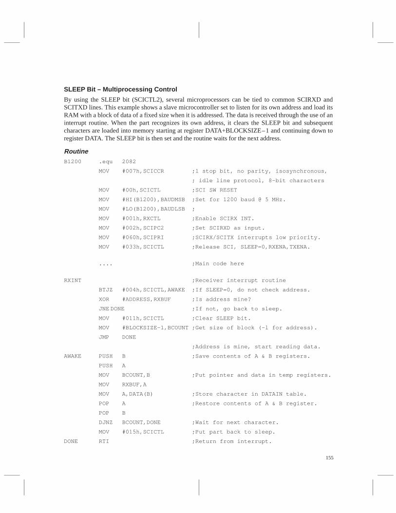
155
SLEEP Bit – Multiprocessing Control
By using the SLEEP bit (SCICTL2), several microprocessors can be tied to common SCIRXD andSCITXD lines. This example shows a slave microcontroller set to listen for its own address and load itsRAM with a block of data of a fixed size when it is addressed. The data is received through the use of aninterrupt routine. When the part recognizes its own address, it clears the SLEEP bit and subsequentcharacters are loaded into memory starting at register DATA+BLOCKSIZE–1 and continuing down toregister DATA. The SLEEP bit is then set and the routine waits for the next address.
RoutineB1200 .equ 2082
MOV #007h,SCICCR ;l stop bit, no parity, isosynchronous,
; idle line protocol, 8–bit characters
MOV #00h,SCICTL ;SCI SW RESET
MOV #HI(B1200),BAUDMSB ;Set for 1200 baud @ 5 MHz.
MOV #LO(B1200),BAUDLSB ;
MOV #001h,RXCTL ;Enable SCIRX INT.
MOV #002h,SCIPC2 ;Set SCIRXD as input.
MOV #060h,SCIPRI ;SCIRX/SCITX interrupts low priority.
MOV #033h,SCICTL ;Release SCI, SLEEP=0,RXENA,TXENA.
.... ;Main code here
RXINT ;Receiver interrupt routine
BTJZ #004h,SCICTL,AWAKE ;If SLEEP=0, do not check address.
XOR #ADDRESS,RXBUF ;Is address mine?
JNE DONE ;If not, go back to sleep.
MOV #011h,SCICTL ;Clear SLEEP bit.
MOV #BLOCKSIZE–1,BCOUNT ;Get size of block (-l for address).
JMP DONE
;Address is mine, start reading data.
AWAKE PUSH B ;Save contents of A & B registers.
PUSH A
MOV BCOUNT,B ;Put pointer and data in temp registers.
MOV RXBUF,A
MOV A,DATA(B) ;Store character in DATAIN table.
POP A ;Restore contents of A & B register.
POP B
DJNZ BCOUNT,DONE ;Wait for next character.
MOV #015h,SCICTL ;Put part back to sleep.
DONE RTI ;Return from interrupt.
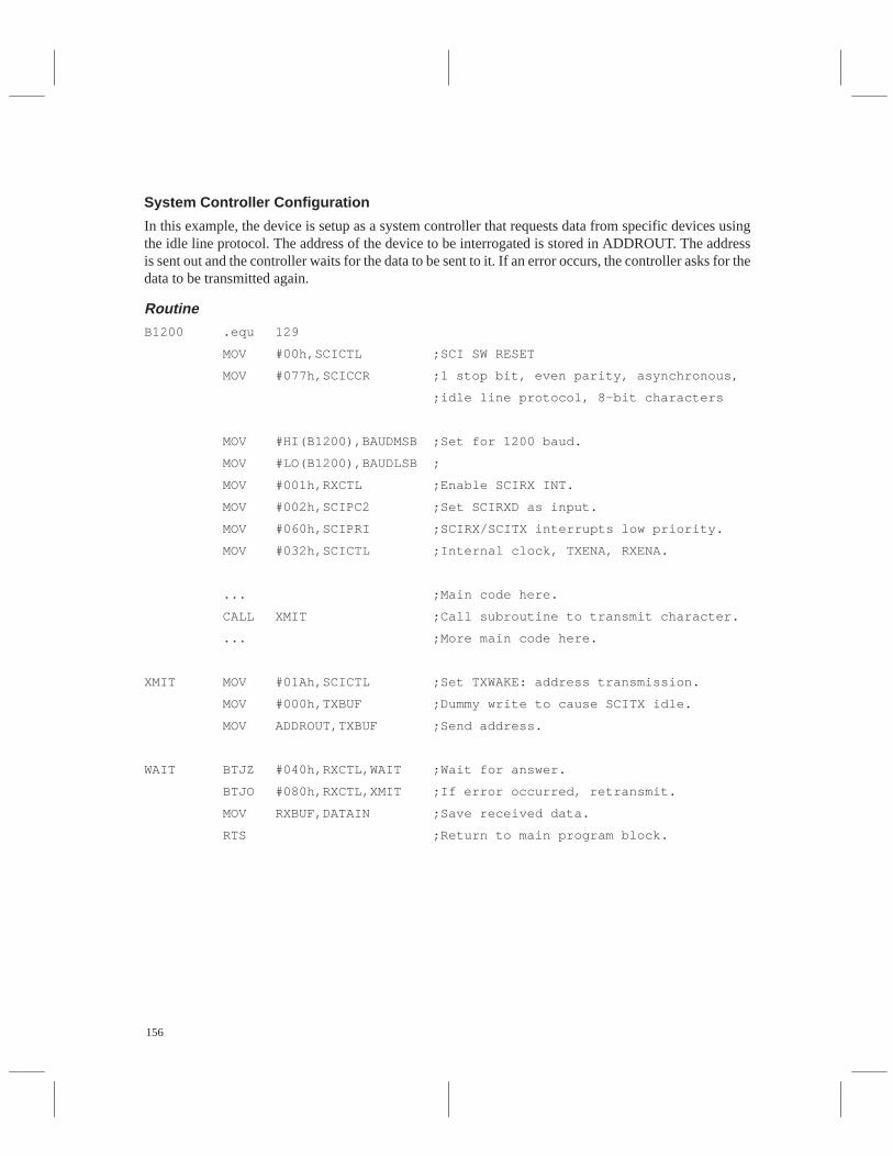
156
System Controller Configuration
In this example, the device is setup as a system controller that requests data from specific devices usingthe idle line protocol. The address of the device to be interrogated is stored in ADDROUT. The addressis sent out and the controller waits for the data to be sent to it. If an error occurs, the controller asks for thedata to be transmitted again.
RoutineB1200 .equ 129
MOV #00h,SCICTL ;SCI SW RESET
MOV #077h,SCICCR ;1 stop bit, even parity, asynchronous,
;idle line protocol, 8–bit characters
MOV #HI(B1200),BAUDMSB ;Set for 1200 baud.
MOV #LO(B1200),BAUDLSB ;
MOV #001h,RXCTL ;Enable SCIRX INT.
MOV #002h,SCIPC2 ;Set SCIRXD as input.
MOV #060h,SCIPRI ;SCIRX/SCITX interrupts low priority.
MOV #032h,SCICTL ;Internal clock, TXENA, RXENA.
... ;Main code here.
CALL XMIT ;Call subroutine to transmit character.
... ;More main code here.
XMIT MOV #01Ah,SCICTL ;Set TXWAKE: address transmission.
MOV #000h,TXBUF ;Dummy write to cause SCITX idle.
MOV ADDROUT,TXBUF ;Send address.
WAIT BTJZ #040h,RXCTL,WAIT ;Wait for answer.
BTJO #080h,RXCTL,XMIT ;If error occurred, retransmit.
MOV RXBUF,DATAIN ;Save received data.
RTS ;Return to main program block.
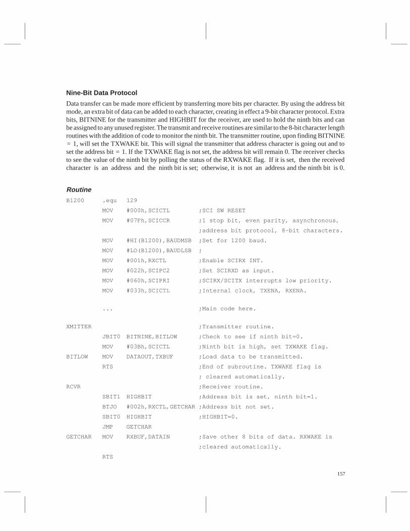
157
Nine-Bit Data Protocol
Data transfer can be made more efficient by transferring more bits per character. By using the address bitmode, an extra bit of data can be added to each character, creating in effect a 9-bit character protocol. Extrabits, BITNINE for the transmitter and HIGHBIT for the receiver, are used to hold the ninth bits and canbe assigned to any unused register. The transmit and receive routines are similar to the 8-bit character lengthroutines with the addition of code to monitor the ninth bit. The transmitter routine, upon finding BITNINE= 1, will set the TXWAKE bit. This will signal the transmitter that address character is going out and toset the address bit = 1. If the TXWAKE flag is not set, the address bit will remain 0. The receiver checksto see the value of the ninth bit by polling the status of the RXWAKE flag. If it is set, then the receivedcharacter is an address and the ninth bit is set; otherwise, it is not an address and the ninth bit is 0.
RoutineB1200 .equ 129
MOV #000h,SCICTL ;SCI SW RESET
MOV #07Fh,SCICCR ;1 stop bit, even parity, asynchronous,
;address bit protocol, 8–bit characters.
MOV #HI(B1200),BAUDMSB ;Set for 1200 baud.
MOV #LO(B1200),BAUDLSB ;
MOV #001h,RXCTL ;Enable SCIRX INT.
MOV #022h,SCIPC2 ;Set SCIRXD as input.
MOV #060h,SCIPRI ;SCIRX/SCITX interrupts low priority.
MOV #033h,SCICTL ;Internal clock, TXENA, RXENA.
... ;Main code here.
XMITTER ;Transmitter routine.
JBIT0 BITNINE,BITLOW ;Check to see if ninth bit=0.
MOV #03Bh,SCICTL ;Ninth bit is high, set TXWAKE flag.
BITLOW MOV DATAOUT,TXBUF ;Load data to be transmitted.
RTS ;End of subroutine. TXWAKE flag is
; cleared automatically.
RCVR ;Receiver routine.
SBIT1 HIGHBIT ;Address bit is set, ninth bit=1.
BTJO #002h,RXCTL,GETCHAR ;Address bit not set.
SBIT0 HIGHBIT ;HIGHBIT=0.
JMP GETCHAR
GETCHAR MOV RXBUF,DATAIN ;Save other 8 bits of data. RXWAKE is
;cleared automatically.
RTS
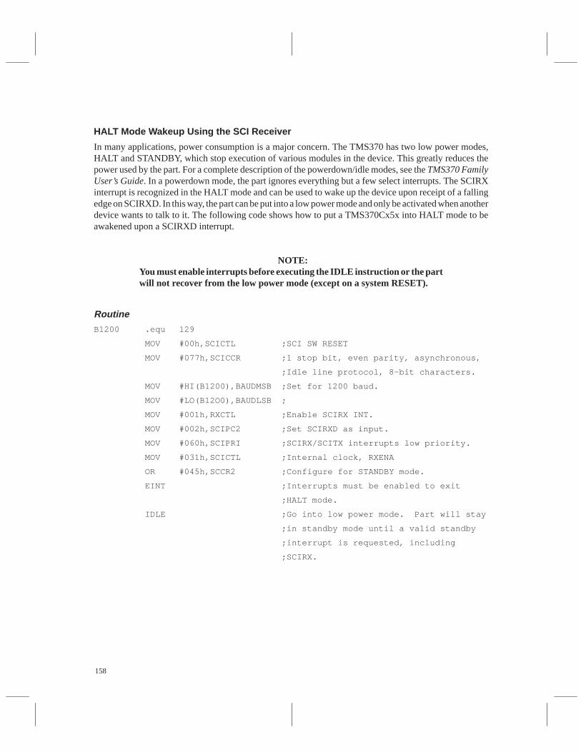
158
HALT Mode Wakeup Using the SCI Receiver
In many applications, power consumption is a major concern. The TMS370 has two low power modes,HALT and STANDBY, which stop execution of various modules in the device. This greatly reduces thepower used by the part. For a complete description of the powerdown/idle modes, see the TMS370 FamilyUser’s Guide. In a powerdown mode, the part ignores everything but a few select interrupts. The SCIRXinterrupt is recognized in the HALT mode and can be used to wake up the device upon receipt of a fallingedge on SCIRXD. In this way, the part can be put into a low power mode and only be activated when anotherdevice wants to talk to it. The following code shows how to put a TMS370Cx5x into HALT mode to beawakened upon a SCIRXD interrupt.
NOTE:You must enable interrupts before executing the IDLE instruction or the partwill not recover from the low power mode (except on a system RESET).
RoutineB1200 .equ 129
MOV #00h,SCICTL ;SCI SW RESET
MOV #077h,SCICCR ;1 stop bit, even parity, asynchronous,
;Idle line protocol, 8-bit characters.
MOV #HI(B1200),BAUDMSB ;Set for 1200 baud.
MOV #LO(B12O0),BAUDLSB ;
MOV #001h,RXCTL ;Enable SCIRX INT.
MOV #002h,SCIPC2 ;Set SCIRXD as input.
MOV #060h,SCIPRI ;SCIRX/SCITX interrupts low priority.
MOV #031h,SCICTL ;Internal clock, RXENA
OR #045h,SCCR2 ;Configure for STANDBY mode.
EINT ;Interrupts must be enabled to exit
;HALT mode.
IDLE ;Go into low power mode. Part will stay
;in standby mode until a valid standby
;interrupt is requested, including
;SCIRX.
159
SCI Module Specific Applications
RS-232-C Interface
Interface TMS370C050 to RS-232-C Connection
The most common of the myriad of serial interfaces is the RS-232-C. Over time it has become an industrystandard for digital communications, used for everything from PCs to telecommunication. This examplewill show the software and hardware necessary to connect a TMS370C050 to an RS-232-C interface.External hardware is needed because RS-232-C specifications call for non-TTL compatible voltage levels.This example uses the Maxim MAX232 RS-232 line driver/ receiver to buffer the TTL levels to the–12 V to 12 V levels needed for RS-232 communications. The TMS370C050 will be used as the DCE (datacommunications equipment) end of the communications link, that is, as a slave to another controller. Formore information about the RS-232-C interface, consult the References Section for books on digitalcommunications.
RS-232-C specifications are vague about the exact uses and protocols associated with the pins. Thisexample shows a common format, using the CTS (clear to send) and DTR (data terminal ready) lines forhandshaking. The transmitted data and received data lines are used for the actual data transmission. In thisexample, as in most RS-232-C communications, the transmission are asynchronous and need nosynchronizing clocks. When the DTR line is pulled high, the controller is ready to receive data. Otherwise,the TMS370C050 stops data transmission until the controller pulls the line high again. The TMS370C050can also halt data transmission from the controller by pulling the CTS line low. The SCICLK and sevenanalog input pins are configured as general I /O pins for the CTS and DTR signals, respectively. The basicconfiguration for an RS-232-C connection is shown in Figure 13.
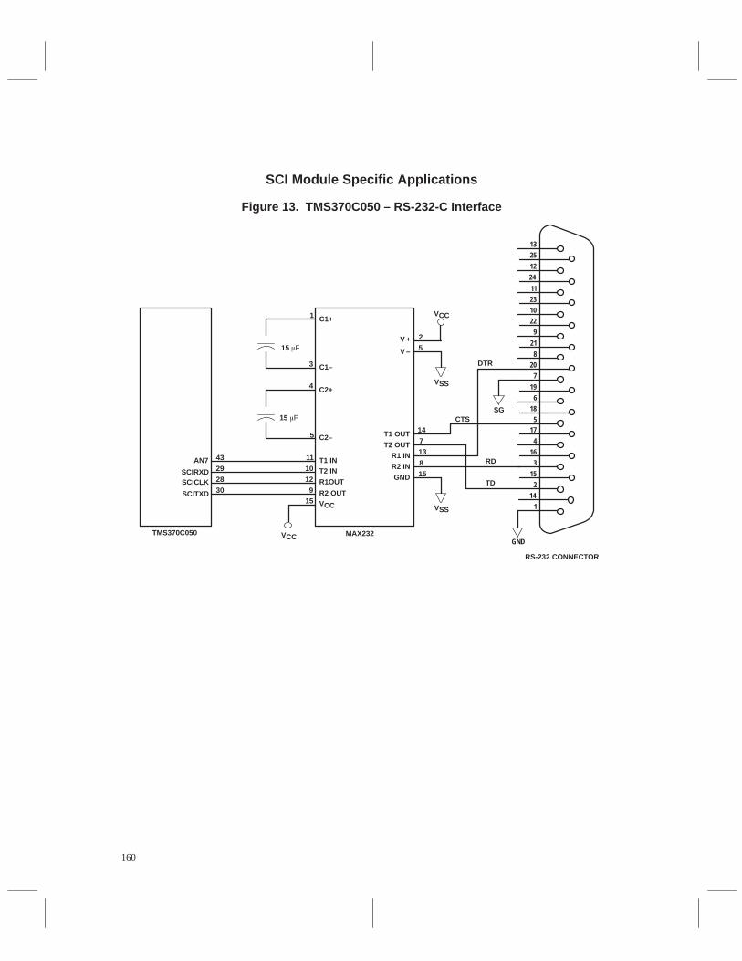
160
SCI Module Specific Applications
Figure 13. TMS370C050 – RS-232-C Interface
1
2
3
4
5
6
7
8
9
10
11
12
13
14
15
16
17
18
19
20
21
22
23
24
25
2
5
14
7
13
8
15
1
11
10
12
9
3
4
5
15
43
29
28
30
15 F
15 F
AN7
SCIRXDSCICLK
SCITXD
TMS370C050 MAX232
RS-232 CONNECTOR
GND
C1+
C1–
C2+
C2–
T1 INT2 IN
R1OUT
R2 OUTVCC
T1 OUT
T2 OUTR1 IN
R2 IN
GND
V +
V –
VCC
VSS
VSS
VCC
DTR
SGCTS
RD
TD
161
The framework of a program for controlling communications between the TMS370C050 and a DTE (dataterminal equipment) configured device is shown below.
Routine.title “RS-232-C Interface”
; This example shows the skeleton of a program for implementing an
; RS-232-C interface in hardware and software.
; Set up EQUATE table for peripheral file registers used in the
; program.
SCICCR .equ P050 ;SCI configuration control register
SCICTL .equ P051 ;SCI operation control register
BAUDMSB .equ P052 ;Baud rate select MSB register
BAUDLSB .equ P053 ;Baud rate select LSB register
TXCTL .equ P054 ;Transmitter int. control /status
;register
RXCTL .equ P055 ;Receiver int. control /status register
RXBUF .equ P057 ;Receiver data buffer register
TXBUF .equ P059 ;Transmit data buffer register
SCIPC1 .equ P05D ;SCI port control register 1
SCIPC2 .equ P05E ;SCI port control register 2
; Define registers & constants used in program
DATAIN .equ R2 ;Temporary register for received data
DATAOUT .equ R3 ;Temporary register for transmitted data
B9600 .equ 15 ;Baud rate register value for 9600 baud.
.text 07000h
START DINT
; SCI Initialization
MOV #000h,SCICTL ;SCI SW RESET
MOV #077h,SCICCR ;stop bit, even parity, asynchronous,
162
;Idle line protocol, 8-bit charactersMOV #HI(B9600),BAUDMSB ;Set for 9600 baud (@ 4.9152MHz)
MOV #LO(B9600),BAUDLSB ;
MOV #002h,SCIPC1 ;Set SCICLK as function pin.
MOV #022h,SCIPC2 ;Set SCIRXD,SCITXD as input.
MOV #060h,SCIPRI ;SCIRX interrupt low priority
MOV #033h,SCICTL ;Release SCI, set internal clock,
;Sleep=0,RXENA,TXENA
MOV #200,B ;Start stack pointer at R200.
LDSP
EINT ;Enable interrupts
; Main part of program manages and stores the data. When the program is
; ready to receive new data it calls subroutine RXCHAR. When the
; program is ready to transmit, it loads register DATA OUT and calls
; subroutine TXCHAR.
MAIN
...
RECEIVE CALL RXCHAR ;Get next character.
MOV A,DATAIN
...
XMIT MOV DATAOUT,A
CALL TXCHAR ;Transmit character.
...
JMP MAIN
; SCI receiver subroutine.
; The subroutine brings CTS high to signal that the TMS370 is ready to
; receive data, then it waits until a character is received. After a
; character has been received, CTS is pulled low again to stop
; transmission by the other device, and the character is saved in
; register A.
RXCHAR MOV #005h,SCIPC1 ;Set CTS high. (TMS370 ready to receive)
RXWAIT BTJZ #040h,RXCTL,RXWAIT ;Loop until character received.
MOV #001h,SCIPC1 ;Set CTS low to stop transmission.
163
MOV RXBUF,A ;Save received character.
RTS
; SCI transmitter subroutine.
; The subroutine waits for the other device to bring the DTR line high
; before transmitting. The character is then sent and the TXCTL
; register is polled to make sure the character has been transmitted
; before continuing.
TXCHAR BTJZ #080h,ADIN,TXCHAR ;Wait for DTR to go high.
TXWAIT BTJZ #080h,TXCTL,TXWAIT ;Wait until previous characters are
;transmitted out.
MOV A,TXBUF ;Send out the character.
RTS
; Set up interrupt vector addresses.
.sect “VECTORS”,07FF2h
.word START ;No interrupts are used:
.word START ;All vectors will jump to ’START’.
.word START
.word START
.word START
.word START
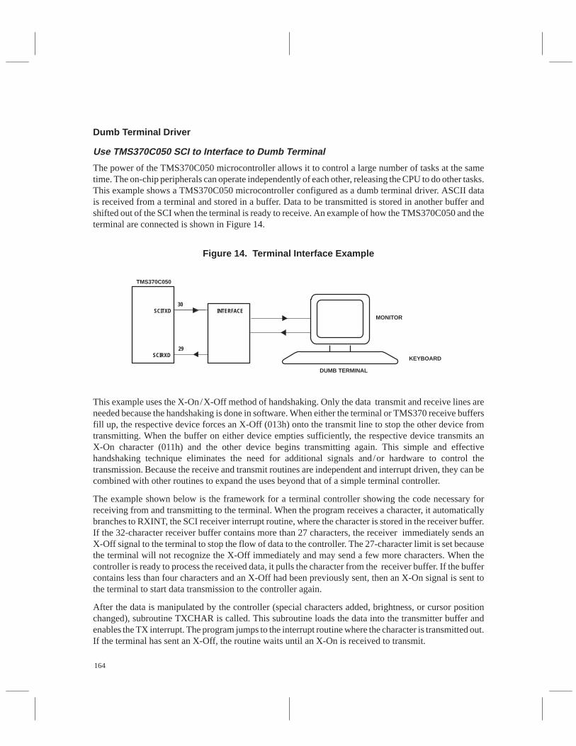
164
Dumb Terminal Driver
Use TMS370C050 SCI to Interface to Dumb Terminal
The power of the TMS370C050 microcontroller allows it to control a large number of tasks at the sametime. The on-chip peripherals can operate independently of each other, releasing the CPU to do other tasks.This example shows a TMS370C050 microcontroller configured as a dumb terminal driver. ASCII datais received from a terminal and stored in a buffer. Data to be transmitted is stored in another buffer andshifted out of the SCI when the terminal is ready to receive. An example of how the TMS370C050 and theterminal are connected is shown in Figure 14.
Figure 14. Terminal Interface Example
SCITXD30
INTERFACE
SCIRXD29
DUMB TERMINAL
KEYBOARD
MONITOR
TMS370C050
This example uses the X-On/X-Off method of handshaking. Only the data transmit and receive lines areneeded because the handshaking is done in software. When either the terminal or TMS370 receive buffersfill up, the respective device forces an X-Off (013h) onto the transmit line to stop the other device fromtransmitting. When the buffer on either device empties sufficiently, the respective device transmits anX-On character (011h) and the other device begins transmitting again. This simple and effectivehandshaking technique eliminates the need for additional signals and/or hardware to control thetransmission. Because the receive and transmit routines are independent and interrupt driven, they can becombined with other routines to expand the uses beyond that of a simple terminal controller.
The example shown below is the framework for a terminal controller showing the code necessary forreceiving from and transmitting to the terminal. When the program receives a character, it automaticallybranches to RXINT, the SCI receiver interrupt routine, where the character is stored in the receiver buffer.If the 32-character receiver buffer contains more than 27 characters, the receiver immediately sends anX-Off signal to the terminal to stop the flow of data to the controller. The 27-character limit is set becausethe terminal will not recognize the X-Off immediately and may send a few more characters. When thecontroller is ready to process the received data, it pulls the character from the receiver buffer. If the buffercontains less than four characters and an X-Off had been previously sent, then an X-On signal is sent tothe terminal to start data transmission to the controller again.
After the data is manipulated by the controller (special characters added, brightness, or cursor positionchanged), subroutine TXCHAR is called. This subroutine loads the data into the transmitter buffer andenables the TX interrupt. The program jumps to the interrupt routine where the character is transmitted out.If the terminal has sent an X-Off, the routine waits until an X-On is received to transmit.
165
Routine.title “SCI Terminal Driver”
; Set up equate table for peripheral registers used in program.
SCCR0 .equ P010 ;System configuration register
;assignments.
SCCR1 .equ P011
SCCR2 .equ P012
SCICCR .equ P050 ;SCI configuration control register
SCICTL .equ P051 ;SCI operation control register
BAUDMSB .equ P052 ;Baud rate select MSB register
BAUDLSB .equ P053 ;Baud rate select LSB register
TXCTL .equ P054 ;Transmitter int. control /status register
RXCTL .equ P055 ;Receiver int. control /status register
RXBUF .equ P057 ;Receiver data buffer register
TXBUF .equ P059 ;Transmit data buffer register
SCIPC1 .equ P05D ;SCI port control register 1
SCIPC2 .equ P05E ;SCI port control register 2
SCIPRI .equ P05F ;SCI priority control register
; Allocate register space for registers used in program. Also mark
; beginning of spaces to be used by 32-byte data transfer buffers.
COMSTAT .equ R2 ;Communications status register
LOCSTAT .dbit 0,COMSTAT ;X-Status from local TKS370 (1=Xoff)
REMSTAT .dbit 1,COMSTAT ;X-Status from remote terminal (1=Xoff)
RXPTR .equ R3 ;Location of last received data in BUFFER.
RXPTRI .equ R4 ;Interrupt routine data pointer.
RXDIFF .equ R5 ;Number of characters in RXBUFFER
TXPTR .equ R6 ;Next location to be transmitted in BUFFER
TXPTRI .equ R7 ;Interrupt routine data pointer
TXDIFF .equ R8 ;Number of characters in TXBUFFER
RXBUFFER .equ R9 ;Beginning of 32-byte receiver data buffer
TXBUFFER .equ R41 ;Beginning of 32-byte transmit data buffer
; Define constants used in program.
TXLIMIT .equ 27 ;Maximum # of characters in buffers before
166
RXLIMIT .equ 27 ;XOFF or XON is sent
RXLIMIT2 .equ 4
XON .equ 011h ;Control-Q character
XOFF .equ 013h ;Control-S character
.text 07000h
START DINT
; Initialize SCI.
MOV #077h,SCICCR ;1 stop bit, even parity, asynchronous,
;Idle line protocol, 8-bit characters
MOV #000h,SCICTL ;SCI SW RESET.
MOV #000h,BAUDMSB ;Set for 9600 (@ 5MHz)
MOV #00Fh,BAUDLSB ;
MOV #001h,RXCTL ;Enable SCIRX INT
MOV #001h,TXCTL ;Enable SCITX INT
MOV #002h,SCIPC1 ;Set SCICLK as function pin.
MOV #022h,SCIPC2 ;Set SCIRXD,SCITXD as input.
MOV #050h,SCIPRI ;SCIRX INT — high priority
;SCITX INT — low priority
MOV #033h,SCICTL ;Release SCI, internal clock,
;sleep=0,RXENA,TXENA
; Clear data registers.
CLR COMSTAT ;Set status flags to XON.
CLR RXPTR ;Clear data pointer registers.
CLR RXPTRI
CLR RXDIFF
CLR TXPTR
CLR TXPTRI
CLR TXDIFF
Mov #200,B ;Set stack pointer below BUFFER table.
LDSP
EINT ;Global interrupt enable
;
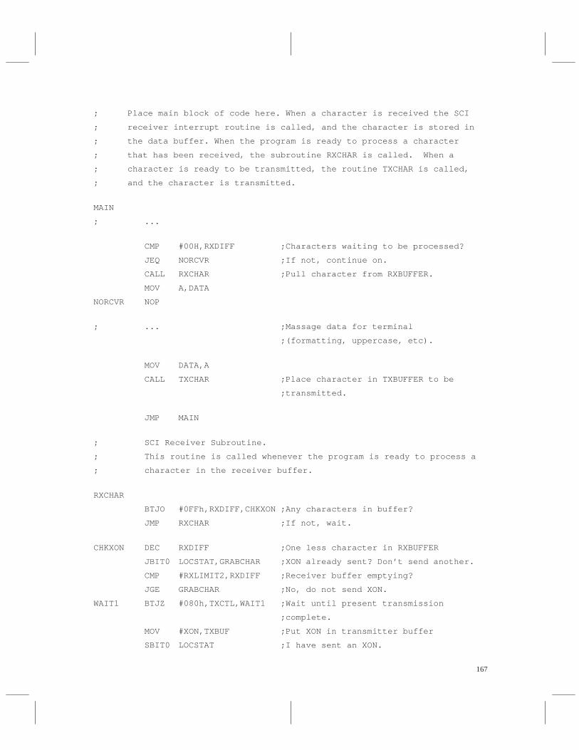
167
; Place main block of code here. When a character is received the SCI
; receiver interrupt routine is called, and the character is stored in
; the data buffer. When the program is ready to process a character
; that has been received, the subroutine RXCHAR is called. When a
; character is ready to be transmitted, the routine TXCHAR is called,
; and the character is transmitted.
MAIN
; ...
CMP #00H,RXDIFF ;Characters waiting to be processed?
JEQ NORCVR ;If not, continue on.
CALL RXCHAR ;Pull character from RXBUFFER.
MOV A,DATA
NORCVR NOP
; ... ;Massage data for terminal
;(formatting, uppercase, etc).
MOV DATA,A
CALL TXCHAR ;Place character in TXBUFFER to be
;transmitted.
JMP MAIN
; SCI Receiver Subroutine.
; This routine is called whenever the program is ready to process a
; character in the receiver buffer.
RXCHAR
BTJO #0FFh,RXDIFF,CHKXON ;Any characters in buffer?
JMP RXCHAR ;If not, wait.
CHKXON DEC RXDIFF ;One less character in RXBUFFER
JBIT0 LOCSTAT,GRABCHAR ;XON already sent? Don’t send another.
CMP #RXLIMIT2,RXDIFF ;Receiver buffer emptying?
JGE GRABCHAR ;No, do not send XON.
WAIT1 BTJZ #080h,TXCTL,WAIT1 ;Wait until present transmission
;complete.
MOV #XON,TXBUF ;Put XON in transmitter buffer
SBIT0 LOCSTAT ;I have sent an XON.
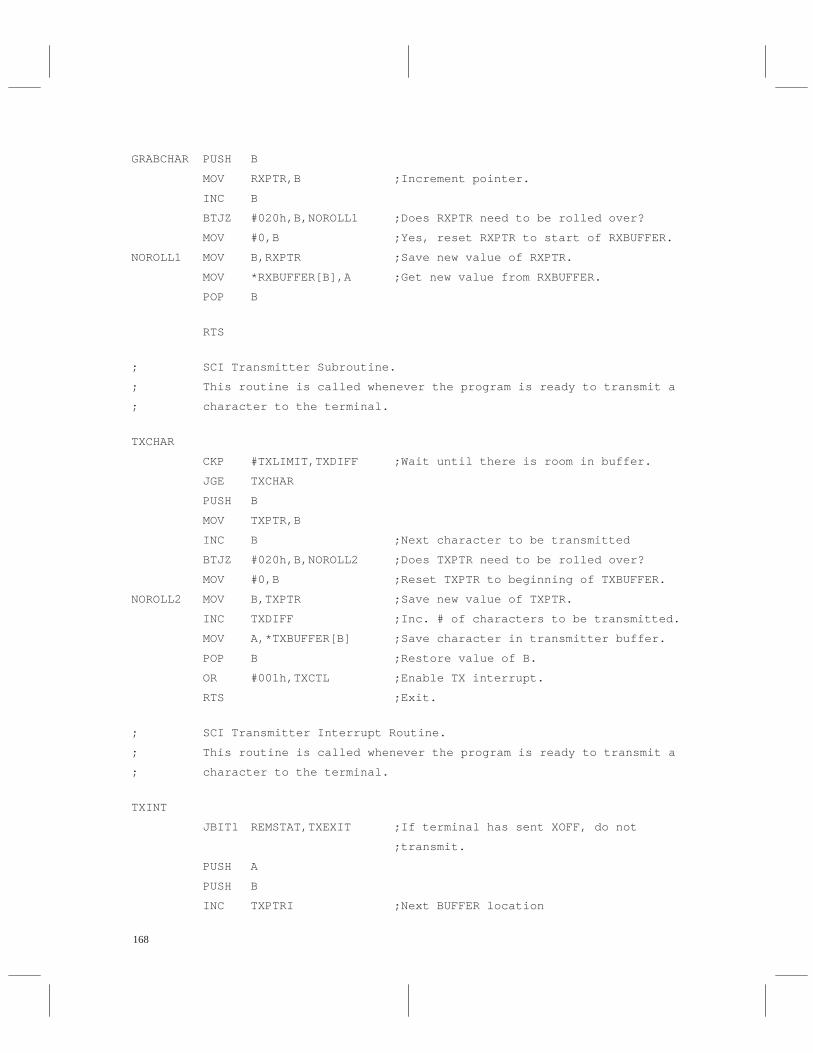
168
GRABCHAR PUSH B
MOV RXPTR,B ;Increment pointer.
INC B
BTJZ #020h,B,NOROLL1 ;Does RXPTR need to be rolled over?
MOV #0,B ;Yes, reset RXPTR to start of RXBUFFER.
NOROLL1 MOV B,RXPTR ;Save new value of RXPTR.
MOV *RXBUFFER[B],A ;Get new value from RXBUFFER.
POP B
RTS
; SCI Transmitter Subroutine.
; This routine is called whenever the program is ready to transmit a
; character to the terminal.
TXCHAR
CKP #TXLIMIT,TXDIFF ;Wait until there is room in buffer.
JGE TXCHAR
PUSH B
MOV TXPTR,B
INC B ;Next character to be transmitted
BTJZ #020h,B,NOROLL2 ;Does TXPTR need to be rolled over?
MOV #0,B ;Reset TXPTR to beginning of TXBUFFER.
NOROLL2 MOV B,TXPTR ;Save new value of TXPTR.
INC TXDIFF ;Inc. # of characters to be transmitted.
MOV A,*TXBUFFER[B] ;Save character in transmitter buffer.
POP B ;Restore value of B.
OR #001h,TXCTL ;Enable TX interrupt.
RTS ;Exit.
; SCI Transmitter Interrupt Routine.
; This routine is called whenever the program is ready to transmit a
; character to the terminal.
TXINT
JBIT1 REMSTAT,TXEXIT ;If terminal has sent XOFF, do not
;transmit.
PUSH A
PUSH B
INC TXPTRI ;Next BUFFER location
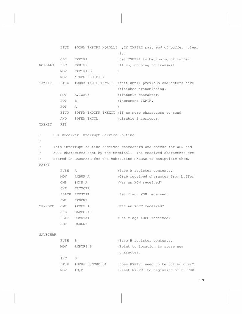
169
BTJZ #020h,TXPTRI,NOROLL3 ;If TXPTRI past end of buffer, clear
;it.
CLR TXPTRI ;Set TXPTRI to beginning of buffer.
NOROLL3 DEC TXDIFF ;If so, nothing to transmit.
MOV TXPTRI,B ;
MOV *TXBUFFER[B],A
TXWAIT1 BTJZ #080h,TXCTL,TXWAIT1 ;Wait until previous characters have
;finished transmitting.
MOV A,TXBUF ;Transmit character.
POP B ;Increment TXPTR.
POP A ;
BTJO #0FFh,TXDIFF,TXEXIT ;If no more characters to send,
AND #0FEh,TXCTL ;disable interrupts.
TXEXIT RTI
; SCI Receiver Interrupt Service Routine
;
; This interrupt routine receives characters and checks for XON and
; XOFF characters sent by the terminal. The received characters are
; stored in RXBUFFER for the subroutine RXCHAR to manipulate them.
RXINT
PUSH A ;Save A register contents.
MOV RXBUF,A ;Grab received character from buffer.
CMP #XON,A ;Was an XON received?
JNE TRYXOFF
SBIT0 REMSTAT ;Set flag: XON received.
JMP RXDONE
TRYXOFF CMP #XOFF,A ;Was an XOFF received?
JNE SAVECHAR
SBIT1 REMSTAT ;Set flag: XOFF received.
JMP RXDONE
SAVECHAR
PUSH B ;Save B register contents.
MOV RXPTRI,B ;Point to location to store new
;character.
INC B
BTJZ #020h,B,NOROLL4 ;Does RXPTR1 need to be rolled over?
MOV #O,B ;Reset RXPTRI to beginning of BUFFER.
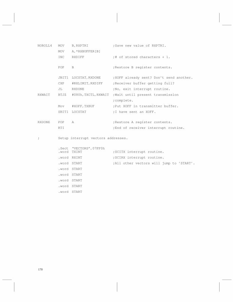
170
NOROLL4 MOV B,RXPTRI ;Save new value of RXPTRI.
MOV A,*RXBUFFER[B]
INC RXDIFF ;# of stored characters + 1.
POP B ;Restore B register contents.
JBIT1 LOCSTAT,RXDONE ;XOFF already sent? Don’t send another.
CXP #RXLIMIT,RXDIFF ;Receiver buffer getting full?
JL RXDONE ;No, exit interrupt routine.
RXWAIT BTJZ #080h,TXCTL,RXWAIT ;Wait until present transmission
;complete.
Mov #XOFF,TXBUF ;Put XOFF in transmitter buffer.
SBIT1 LOCSTAT ;I have sent an XOFF.
RXDONE POP A ;Restore A register contents.
RTI ;End of receiver interrupt routine.
; Setup interrupt vectors addresses.
.Sect “VECTORS”,07FF0h
.word TXINT ;SCITX interrupt routine.
.word RXINT ;SCIRX interrupt routine.
.word START ;All other vectors will jump to ’START’.
.word START
.word START
.word START
.word START
.word START

171
There are a few things that should be noted about any terminal controller code. The most important is towatch the timing of the transmission of X-Off and X-On characters from the receiver routines. It isimportant that as soon as the receiver buffer passes its limit (in this case 27 characters) that an X-Off betransmitted to make sure that the buffer does not overflow. A problem arises in that the routine to transmitthe X-Off character should be placed inside the RXINT routine so that it can be called immediately.Unfortunately, you have to wait to make sure that the current transmission is finished before starting theX-Off transmission. With all this waiting and transmitting inside the RXINT routine, it is possible at highSCI speeds that the routine will not be able to finish the current receiver interrupt and get the next characterout of RXBUF before it is overwritten.
There is no simple way around this problem. One suggestion is to find the maximum time it takes for theinterrupt routine with the X-Off transmission and tailor your SCI speed accordingly. If the receiver buffersize is greatly increased, it may be possible to wait for the next transmitter interrupt to send the X-Off. Youmay also want to poll the receiver overrun flag and transmit a special NAK (negative acknowledge)character to the terminal to have it retransmit the data. The exact solution for your particular case dependson your application.
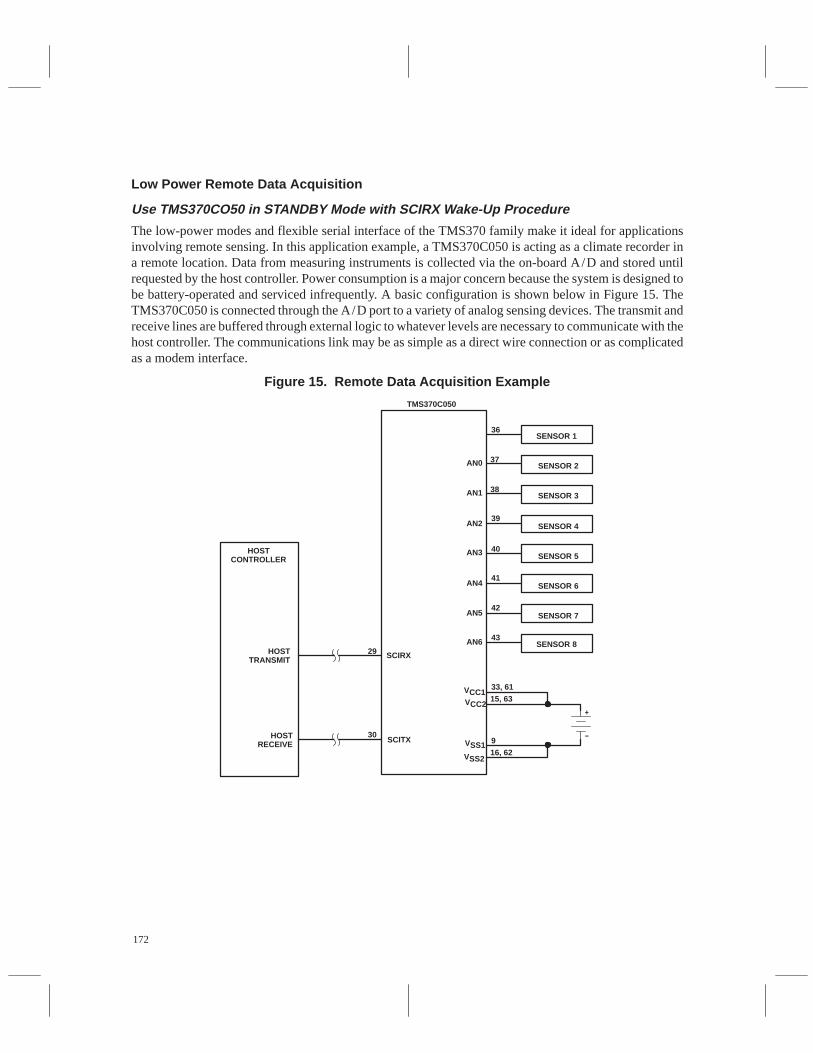
172
Low Power Remote Data Acquisition
Use TMS370CO50 in STANDBY Mode with SCIRX Wake-Up Procedure
The low-power modes and flexible serial interface of the TMS370 family make it ideal for applicationsinvolving remote sensing. In this application example, a TMS370C050 is acting as a climate recorder ina remote location. Data from measuring instruments is collected via the on-board A/D and stored untilrequested by the host controller. Power consumption is a major concern because the system is designed tobe battery-operated and serviced infrequently. A basic configuration is shown below in Figure 15. TheTMS370C050 is connected through the A/D port to a variety of analog sensing devices. The transmit andreceive lines are buffered through external logic to whatever levels are necessary to communicate with thehost controller. The communications link may be as simple as a direct wire connection or as complicatedas a modem interface.
Figure 15. Remote Data Acquisition Example
+
–
HOSTCONTROLLER
TMS370C050
HOSTTRANSMIT
HOSTRECEIVE
29
30
SCIRX
SCITX
36
37
38
39
40
41
42
43
33, 61
15, 63
9
16, 62
SENSOR 1
SENSOR 2
SENSOR 3
SENSOR 4
SENSOR 5
SENSOR 6
SENSOR 7
AN0
AN1
AN2
AN3
AN4
AN5
AN6
VCC1VCC2
VSS1VSS2
SENSOR 8
173
The program uses T1 to periodically read the A/D values and store them in ATABLE. T1 can also bringthe device out of STANDBY mode through the T1 interrupt. In this way, the device will draw less thanone-quarter its normal operating current most of the time. The A/D conversion routine is not shown here,but examples can be found in the TMS370 Family User’s Guide and related application notes. In particular,the A/D routine is similar to the one shown in the Design Aids section of the TMS370 Family User’s Guide.The data can be stored in RAM, or if power loss is a consideration, EEPROM memory may be used.
Because of the minimum speed of the part and the size of the timer registers, the longest timer period wecan have is 33.6 seconds. For this example, the time between updates is 10 minutes. To allow for the extratime, a counter is included in the timer interrupt routine. If a full 10 minutes have not passed, the part goesback into STANDBY mode to wait for the next interrupt. The equation used to calculate the timer andcounter values is:
Time between updates =
10 min = 600 sec =256
0.5 MHz
PRESCALE
SYSCLKx T1 value x interval counter
For this example:
x 65104 x 18
The device will periodically update ATABLE, where the data is stored. Upon receipt of information fromthe host (SCIRXD goes low), the remote THS037C050 will come out of STANDBY mode. If the receiveddata does not match the internal address, the part goes back into STANDBY mode. If the address matches,the remote will first send one byte of information with the number of bytes of data to be sent, followed bythe data itself. After the device sends all the data, it will put itself back into STANDBY mode to wait foranother inquiry or data acquisition.
Routine
.title “Remote Data Acquisition program”
; This routine uses T1 and SCI receiver interrupts to bring a
; THS0370C050 out of STANDBY mode. The T1 interrupt is used to
; collect data from the A/D converter.
; Set up EQUATE table for peripheral file registers used in the
; program.
SCCR2 .equ P012 ;System configuration register
;assignments.
SCICCR .equ P050 ;SCI configuration control register
SCICTL .equ P051 ;SCI operation control register
BAUDMSB .equ P052 ;Baud rate select MSB register
BAUDLSB .equ P053 ;Baud rate select LSB register
174
TXCTL .equ P054 ;Transmitter int. control/status
;register
RXCTL .equ P055 ;Receiver int. control/status register
RXBUF .equ P057 ;Receiver data buffer register
TXBUF .equ P059 ;Transmit data buffer register
SCIPC1 .equ P05D ;SCI port control register 1
SCIPC2 .equ P05E ;SCI port control register 2
SCIPRI .equ P05F ;SCI priority control register
T1CNTRMSB .equ P040 ;T1 register assignments
T1CXSBLSB .equ P041
T1CMSB .equ P042
T1CLSB .equ P043
T1CCMSB .equ P044
T1CCLSB .equ P045
T1CTL1 .equ P049
T1CTL2 .equ P04A
T1CTL3 .equ P04B
T1CTL4 .equ P04C
T1PC1 .equ P04D
T1PC2 .equ P04E
T1PRI .equ P04E
; Allocate register space for variables and data table used in the
; routine.
ADDRESS .equ R2 ;Temp register for received value.
ICOUNT .equ R3 ;Counter for number of T1 interrupts
;before data is sampled for table.
ATABLE .equ R4 ;Table where A/D data is stored before
;being transmitted.
; Define constants used in program.
TIMEMSB .equ 0FEh ;Interrupt timing
TIMELSB .equ 050h
INTERVAL .equ 18 ;Number of timer interrupts before data
;is stored
MYADDRESS .equ 0FFh ;Personal address of this device
.text 07000h
175
START DINT ;Disable interrupts while initializing.
; System Initialization
MOV #041h,SCCR2 ;STANDBY mode, no priv mode, no osc
;fault reset
; SCI Initialization
MOV #000h,SCICTL ;SCI SW RESET
MOV #077h,SCICCR ;1 stop bit, even parity, asynchronous,
;idle line protocol, 8-bit characters
MOV #000h,BAUDMSB ;Set for 9600 baud @ 5 MHz.
MOV #00Fh,BAUDLSB ;
MOV #001h,RXCTL ;Enable SCIRX INT.
MOV #022h,SCIPC2 ;Set SCIRXD, SCITXD function.
MOV #070h,SCIPRI ;SCIRX interrupt low priority
MOV #033h,SCICTL ;Release SCI SW RESET.
;Internal clock, TXENA, RXENA
; T1 Initialization
MOV #TIMEMSB,TlCMSB ;Set timer values.
MOV #TIMELSB,TlCLSB
MOV #040h,T1PRI ;Set T1 interrupts to low priority.
MOV #010h,T1CTL4 ;Dual compare, disable interrupts.
MOV #007h,T1CTL1 ;System clock / 256
MOV #001h,T1CTL3 ;Disable T1 interrupts, clear flags.
MOV #001h,T1CTL2 ;Disable overflow interrupts,reset Tl.
MOV #INTERVAL,ICOUNT ;Initialize counter.
Mov #200,B ;Initalize the stack pointer to start at
LDSP ;register 200 (away from ATABLE).
MOV #000h,B ;Reset ATABLE pointer.
EINT ;Interrupts must be enabled to exit
;STANDBY mode.
; Main part of program actually does nothing but wait for interrupts.
; The T1 and SCIRX interrupt service routines actually do the work.
MAIN IDLE ;Go into low-power mode.
176
JMP MAIN ;Main loop
; Tl Interrupt Routine
; When the interrupt routine is called, the part will come out of
; STANDBY mode. The routine will collect information from the A/D
; and store it in register A. The data is then loaded into ATABLE so
; it can be easily transmitted out. The number of bytes of stored
; data is in B. At the end of the routine, the part will return to
; the main program where it will go into STANDBY mode again.
TIMERINT AND #00Fh,T1CTL3 ;Clear interrupt flags.
DJNZ ICOUNT,DONE ;Time to get new A/D value? If not,
;skip.
... ;A/D data gathering & formatting. Value
;is stored in register A.
INC B ;Increment data counter /pointer.
MOV A,*ATABLE–1[B] ;Store data in ATABLE.
MOV #INTERVAL,ICOUNT ;Restore counter.
DONE RTI ;End of service routine
; SCI Receiver Interrupt Routine
; This routine is called when the part receives a low pulse on the
; SCIRX pin. The received datum is compared against an internal
; address to see if the device was addressed. If so, the routine
; transmits one character indicting the number of bytes to be
; transmitted. The routine then transmits all the data stored in
; ATABLE, LIFO.
RXINT MOV RXBUF,ADDRESS ;Read received address.
BTJ0 #080h,RXCTL,RXDONE ;If there was an error, wait for another
;transmission.
CMP #MYADDRESS,ADDRESS ;If address not mine, ignore wake-up
;call.
JNE RXDONE ;
MOV B,TXBUF ;# of characters to be transmitted
CMP #00,B ;If no data stored yet, ignore.
JEQ WAIT
LOOP BTJZ #080h,TXCTL,LOOP ;Wait until character sent.
MOV *ATABLE[B]–1,A ;Transmit character.
177
MOV A,TXBUF ;
DJNZ B,LOOP ;If not done, send next character.
WAIT BTJZ #040h,TXCTL,WAIT ;Wait for last character to be sent.
RXDONE RTI ;Exit interrupt routine and go back into
;STANDBY mode.
; Set up interrupt vectors.
.sect “VECTORS”,07FF2h
.word RXINT ;SCIRX interrupt routine.
.word TIMERINT ;T1 interrupt routine.
.word START ;All other vectors will jump to ‘START’.
.word START
.word START
.word START
.word START

178
Appendix A: SPI Control Registers
The SPI is controlled and accessed through registers in the peripheral file. These registers are listed in Table6 and described in the TMS370 Family User’s Guide. The bits shown in shaded boxes in Table 6 areprivilege mode bits; that is, they can only be written to in the privilege mode.
Table 6. SPI Control Registers
Designa-tion
ADDR PF Bit 7 Bit 6 Bit 5 Bit 4 Bit 3 Bit 2 Bit 1 Bit 0
SPICCR 1030h P030 SPI SWRESET
CLOCKPOLARITY
SPI BITRATE2
SPI BITRATE1
SPI BITRATE0
SPICHAR2
SPICHAR1
SPICHAR0
SPICTL 1031h P031 RECEIVEROVERRUN
SPI INTFLAG — — — MASTER/
SLAVE TALK SPI INTENA
1032h P032
to to Reserved
1036h P036
SPIBUF 1037h P037 RCVD7 RCVD6 RCVD5 RCVD4 RCVD3 RCVD2 RCVD1 RCVD0
1038h P038 Reserved
SPIDAT 1039h P039 SDAT7 SDAT6 SDAT5 SDAT4 SDAT3 SDAT2 SDAT1 SDAT0
103Ah P03A
to to Reserved
103Ch P03C
SPIPC1 103Dh P03D — — — — SPICLKDATA IN
SPICLKDATA OUT
SPICLKFUNCTION
SPICLKDATA DIR
SPIPC2 103Eh P03E SPISIMODATA IN
SPISIMODATA OUT
SPISIMOFUNCTION
SPISIMODATA DIR
SPISOMIDATA IN
SPISOMIDATA OUT
SPISOMIFUNCTION
SPISOMIDATA DIR
SPIPRI 103Fh P03F SPISTEST
SPIPRIORITY
SPIESPEN — — — — —

179
Appendix B: SCI Control Registers
The SCI is controlled and accessed through registers in the peripheral file. These registers are listed in Table7 and described in the TMS370 Family User’s Guide. The bits shown in shaded boxes in Table 7 areprivilege mode bits; that is, they can only be written to in the privilege mode.
Table 7. SCI1 and SCI2 Control Registers
SCI1Designa-
tionADDR PF Bit 7 Bit 6 Bit 5 Bit 4 Bit 3 Bit 2 Bit 1 Bit 0
SCICCR 1050h P050 STOPBITS
EVEN/ODDPARITY
PARITYENABLE
ASYNC/ISOSYNC
ADDRESS/IDLE WUP
SCICHAR2
SCICHAR1
SCICHAR0
SCICTL 1051h P051 — — SCI SWRESET CLOCK TXWAKE SLEEP TXENA RXENA
BAUDMSB
1052h P052 BAUDF(MSB) BAUDE BAUDD BAUDC BAUDB BAUDA BAUD9 BAUD8
BAUD LSB 1053h P053 BAUD7 BAUD6 BAUD5 BAUD4 BAUD3 BAUD2 BAUD1 BAUD0(LSB)
TXCTL 1054h P054 TXRDY TXEMPTY — — — — — SCI TX
INT ENA
RXCTL 1055h P055 RXERROR RXRDY BRKDT FE OE PE RXWAKE SCI RX
INT ENA
1056h P056 Reserved
RXBUF 1057h P057 RXDT7 RXDT6 RXDT5 RXDT4 RXDT3 RXDT2 RXDT1 RXDT0
1058h P058 Reserved
TXBUF 1059h P059 TXDT7 TXDT6 TXDT5 TXDT4 TXDT3 TXDT2 TXDT1 TXDT0
105Ah
P05A
105Bh
P05B Reserved
105Ch
P05C
SCIPC1 105Dh
P05D — — — — SCICLKDATA IN
SCICLKDATA OUT
SCICLKFUNCTION
SCICLKDATA DIR
SCIPC2 105Eh
P05E SCITXDDATA IN
SCITXDDATA OUT
SCITXDFUNCTION
SCITXDDATA DIR
SCIRXDDATA IN
SCIRXDDATA OUT
SCIRXDFUNCTION
SCIRXDDATA DIR
SCIPRI 105Fh P05F SCISTEST
SCITXPRIORITY
SCIRXPRIORITY
SCIESPEN — — — —
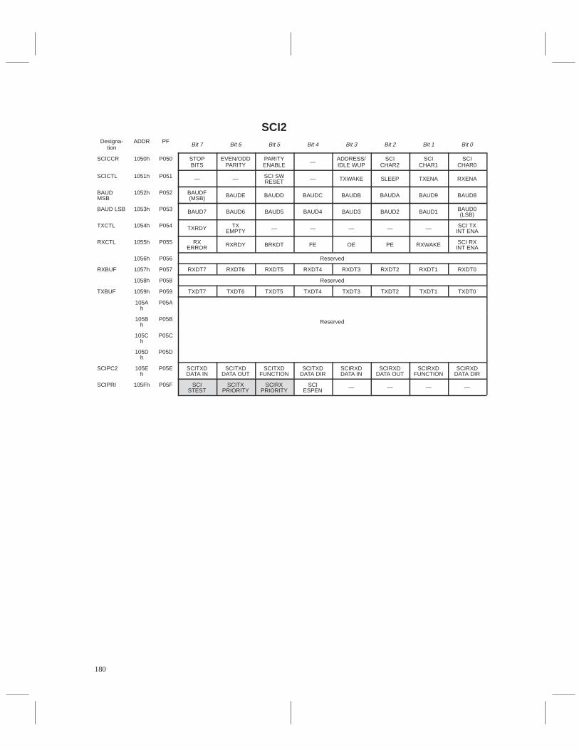
180
SCI2Designa-
tionADDR PF Bit 7 Bit 6 Bit 5 Bit 4 Bit 3 Bit 2 Bit 1 Bit 0
SCICCR 1050h P050 STOPBITS
EVEN/ODDPARITY
PARITYENABLE — ADDRESS/
IDLE WUPSCI
CHAR2SCI
CHAR1SCI
CHAR0
SCICTL 1051h P051 — — SCI SWRESET — TXWAKE SLEEP TXENA RXENA
BAUDMSB
1052h P052 BAUDF(MSB) BAUDE BAUDD BAUDC BAUDB BAUDA BAUD9 BAUD8
BAUD LSB 1053h P053 BAUD7 BAUD6 BAUD5 BAUD4 BAUD3 BAUD2 BAUD1 BAUD0(LSB)
TXCTL 1054h P054 TXRDY TXEMPTY — — — — — SCI TX
INT ENA
RXCTL 1055h P055 RXERROR RXRDY BRKDT FE OE PE RXWAKE SCI RX
INT ENA
1056h P056 Reserved
RXBUF 1057h P057 RXDT7 RXDT6 RXDT5 RXDT4 RXDT3 RXDT2 RXDT1 RXDT0
1058h P058 Reserved
TXBUF 1059h P059 TXDT7 TXDT6 TXDT5 TXDT4 TXDT3 TXDT2 TXDT1 TXDT0
105Ah
P05A
105Bh
P05B Reserved
105Ch
P05C
105Dh
P05D
SCIPC2 105Eh
P05E SCITXDDATA IN
SCITXDDATA OUT
SCITXDFUNCTION
SCITXDDATA DIR
SCIRXDDATA IN
SCIRXDDATA OUT
SCIRXDFUNCTION
SCIRXDDATA DIR
SCIPRI 105Fh P05F SCISTEST
SCITXPRIORITY
SCIRXPRIORITY
SCIESPEN — — — —
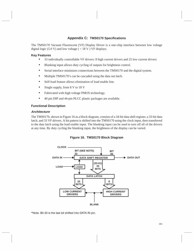
181
Appendix C: TMS0170 Specifications
The TMS0170 Vacuum Fluorescent (VF) Display Driver is a one-chip interface between low voltagedigital logic (5.0 V) and low voltage ( < 18 V ) VF displays.
Key Features• 33 individually controllable VF drivers: 8 high current drivers and 25 low current drivers
• Blanking input allows duty cycling of outputs for brightness control.
• Serial interface minimizes connections between the TMS0170 and the digital system.
• Multiple TMS0170’s can be cascaded using the data out latch.
• Self-load feature allows elimination of load enable line.
• Single supply, from 8 V to 18 V
• Fabricated with high voltage PMOS technology.
• 40 pin DIP and 44-pin PLCC plastic packages are available.
Functional Description
Architecture
The TMS0170, shown in Figure 16 as a block diagram, consists of a 34-bit data shift register, a 33-bit datalatch, and 33 VF drivers. A bit pattern is shifted into the TMS0170 using the clock input, then transferredto the data latch using the load enable input. The blanking input can be used to turn off all of the driversat any time. By duty cycling the blanking input, the brightness of the display can be varied.
Figure 16. TMS0170 Block Diagram
DATA SHIFT REGISTER
LOAD
DATA LATCH
(33-01)33
BITS
DATA IN
CLOCK
33BIT (SEE NOTE) BIT
00DATA OUT
25BITS
8BITS
LOW CURRENTDRIVERS
HIGH CURRENTDRIVERS
BLANK
LOAD

182
Shift Register
The 34-bit shift register consists of 34 D-type flip-flops. The bits are numbered from 33 down to 00. Eachdata bit is clocked in on the rising edge of the clock pin, and enters the shift register in flip-flop #33. Uponeach successive clock rising edge, the bit is shifted sequentially through the shift register, from flip-flop#33 to flip-flop #00. The data in the first 33 flip-flops (from #33 down to #01) is transferred into the datalatch on the rising edge of load enable. Flip-flop #00 is not connected to the data latch, but instead, isconnected to the Data Out output pin. This output can be used for cascading several TMS0170s togetheror for self loading. All of the flip-flops in the shift register are cleared by the rising edge of load enable.
Interface
The interface between the TMS0170 and the digital logic consists of four lines; a clock in line, a data inline, and a load enable line, and a Blank input.
• Data Input: Determines what data value is loaded into the data shift register. This data can thenbe latched to the output drivers upon a valid load enable input. A latched high level will turn theoutput driver on. A latched low level will turn the output driver off.
• Clock: The rising edge of the clock input will latch the current value of the data input into thedata shift register and cause the shift register to shift by one.
• Load Enable: The rising edge of the load enable input transfers the data from the data shiftregister into the data latches and sets the data shift register to zero.
• Blank: This input is used to disable all the drivers. A low level on this pin will force all driveroutputs to a low level. A high level will enable the drivers to output whatever data has beenloaded into their respective latches. This pin has an internal pull-up resistor.
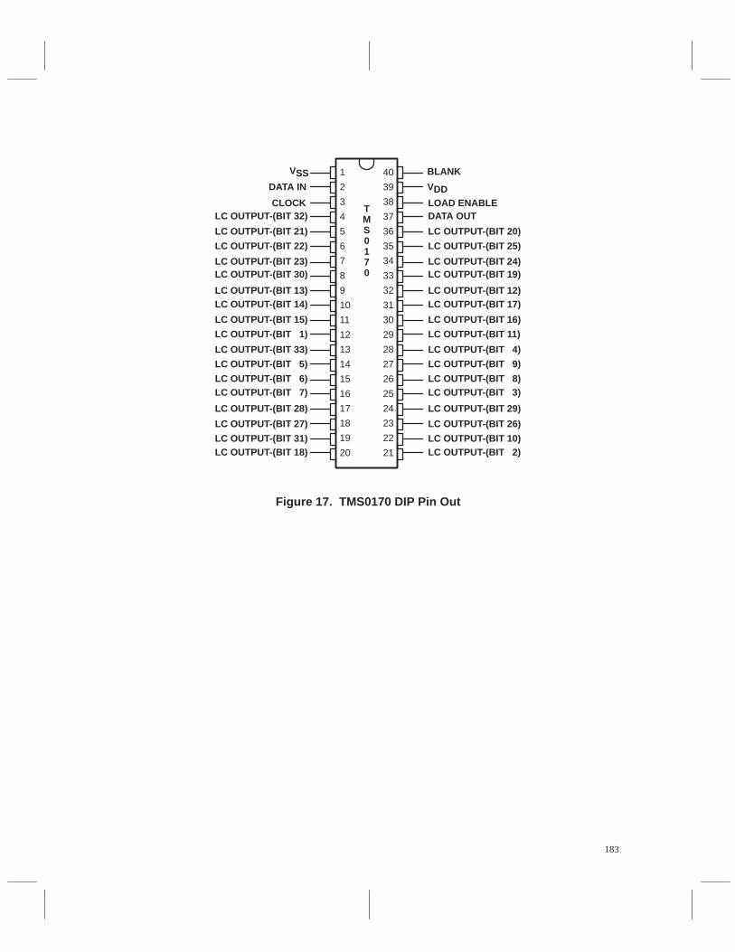
183
1
2
3
4
5
6
7
8
9
10
11
12
13
14
15
16
17
18
19
20
40
39
38
37
36
35
34
33
32
31
30
29
28
27
26
25
24
23
22
21
VSSDATA IN
CLOCK
LC OUTPUT-(BIT 21)
LC OUTPUT-(BIT 22)
LC OUTPUT-(BIT 23)LC OUTPUT-(BIT 30)
LC OUTPUT-(BIT 13)LC OUTPUT-(BIT 14)
LC OUTPUT-(BIT 15)
LC OUTPUT-(BIT 1)
LC OUTPUT-(BIT 33)
LC OUTPUT-(BIT 5)
LC OUTPUT-(BIT 6)LC OUTPUT-(BIT 7)
LC OUTPUT-(BIT 28)
LC OUTPUT-(BIT 27)
LC OUTPUT-(BIT 31)LC OUTPUT-(BIT 18)
LC OUTPUT-(BIT 32)
VDD
BLANK
LOAD ENABLE
LC OUTPUT-(BIT 20)
LC OUTPUT-(BIT 25)
LC OUTPUT-(BIT 24)LC OUTPUT-(BIT 19)
LC OUTPUT-(BIT 12)LC OUTPUT-(BIT 17)
LC OUTPUT-(BIT 16)
LC OUTPUT-(BIT 11)
LC OUTPUT-(BIT 4)
LC OUTPUT-(BIT 9)
LC OUTPUT-(BIT 8)LC OUTPUT-(BIT 3)
LC OUTPUT-(BIT 29)
LC OUTPUT-(BIT 26)
LC OUTPUT-(BIT 10)LC OUTPUT-(BIT 2)
DATA OUTTMS0170
Figure 17. TMS0170 DIP Pin Out
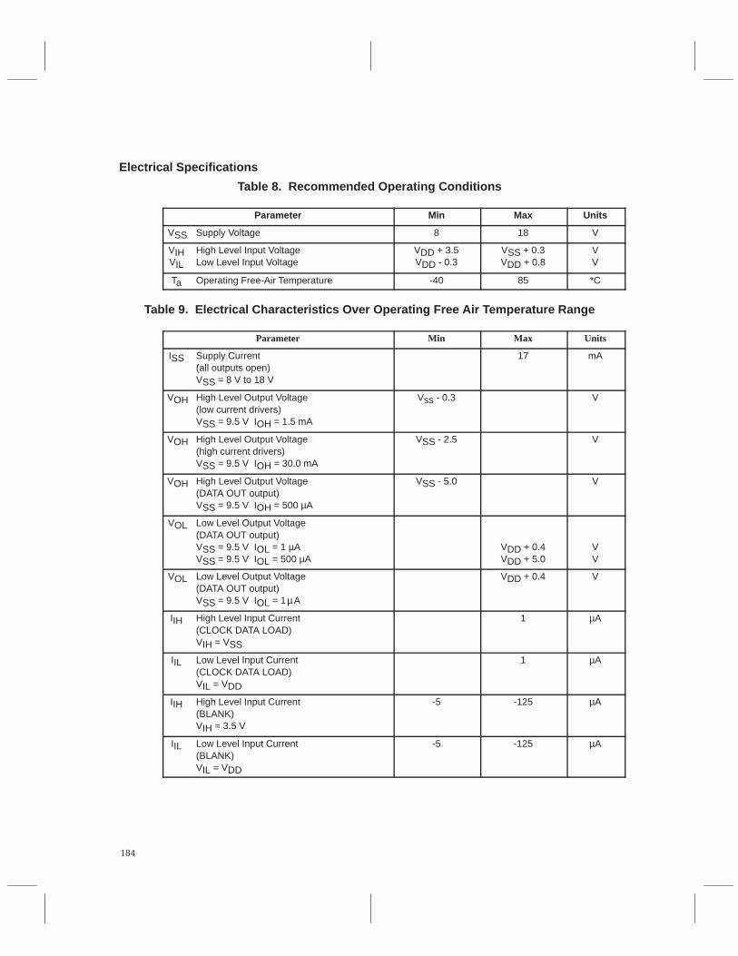
184
Electrical Specifications
Table 8. Recommended Operating Conditions
Parameter Min Max Units
VSS Supply Voltage 8 18 V
VIHVIL
High Level Input VoltageLow Level Input Voltage
VDD + 3.5VDD - 0.3
VSS + 0.3VDD + 0.8
VV
Ta Operating Free-Air Temperature -40 85 *C
Table 9. Electrical Characteristics Over Operating Free Air Temperature Range
Parameter Min Max Units
ISS Supply Current(all outputs open)VSS = 8 V to 18 V
17 mA
VOH High Level Output Voltage(low current drivers)VSS = 9.5 V IOH = 1.5 mA
Vss - 0.3 V
VOH High Level Output Voltage(high current drivers)VSS = 9.5 V IOH = 30.0 mA
VSS - 2.5 V
VOH High Level Output Voltage(DATA OUT output)VSS = 9.5 V IOH = 500 µA
VSS - 5.0 V
VOL Low Level Output Voltage(DATA OUT output)VSS = 9.5 V IOL = 1 µAVSS = 9.5 V IOL = 500 µA
VDD + 0.4VDD + 5.0
VV
VOL Low Level Output Voltage(DATA OUT output)VSS = 9.5 V IOL = 1µA
VDD + 0.4 V
IIH High Level Input Current(CLOCK DATA LOAD)VIH = VSS
1 µA
IIL Low Level Input Current(CLOCK DATA LOAD)VIL = VDD
1 µA
IIH High Level Input Current(BLANK)VIH = 3.5 V
-5 -125 µA
IIL Low Level Input Current(BLANK)VIL = VDD
-5 -125 µA

185
Glossary
address bit mode: An SCI mode of communication incorporating an extra bit into each frame todistinguish address frames from data frames. Setting the address bit to a logic 1 signifies a frame beginninga new block.
asynchronous mode: A communication format in which no synchronizing clocks are used. The data beingtransmitted is repeated several times and a majority vote is taken of selected bits to determine thetransmitted value. This format is commonly used in RS-232-C and systems communications.
block: A collection of one or more frames, the first of which is an address frame.
baud rate: The communication rate for digital transfers, measured in line changes per second. For serialcommunications, this equals one bit per second.
character: A group of bits, from one to eight bits in length, that makes up one unit of data.
DCE (data communications equipment): The hardware responsible for controlling digitalcommunications.
DTE (data terminal equipment): Equipment which receives or originates data transfer in a communicationsnetwork.
double-buffered: Using a temporary storage register to hold data between register reads or writes. In theSCI, the temporary registers are TXBUF and RXBUF. They are used to hold data while transmitting orreceiving and TXSHF or RXSHF are being used, speeding up data transfer and reducing the possibility oftransmitter or receiver overruns.
frame: The basic packet of serial communication. It typically contains one start bit, one to eight bits of data,and one or two stop bits. It may also contain a parity bit and an address designator bit depending on theprotocol.
full-duplex: A mode of communication in which transmission and reception of signals happenssimultaneously.
idle line mode: A serial communications protocol in which the beginning of a new block (an address frame)is identified as being the first frame after an idle period.
idle period: A period of ten bits or longer in which no data is received.
isosynchronous mode: A communication format in which synchronizing clocks are used. This is typicallyfaster than asynchronous communications because one bit of data is transmitted on each shift-clock cycle.
LSb: Least significant bit.
LSB: Least significant byte.
master: In its most general meaning, a mode of operation in which a microcontroller controls anothermicrocontroller or peripheral and issues timing signals to it. It also refers to a specific mode of operationof the SPI.
MSb: Most significant bit.
MSB: Most significant byte.

186
NRZ (non return to zero) format: A communication format in which the inactive state is a logic one.
RS-232-C: An industry standard serial communications interface. The most commonly used serialinterface for personal computers.
parity: An error checking protocol based on the assumption that the number of 1s in a character of datais odd or even. Usually one bit is reserved in each frame to make sure that it plus the number of bits in theactual data is an odd or even number, depending on whether odd or even parity is used.
protocol: The rules of communication and data format in a communications link between two devices.
shift-clock cycle: One cycle of the SCI clock that gates one bit of data. For isosynchronouscommunications, one shift-clock cycle gates one bit of data or format information. In the asynchronousmode, 16 shift-clock cycles are needed per bit of information.
slave: A mode of operation in which a microcontroller is controlled by and receives synchronizing signalsfrom another microprocessor.
UART: Universal Asynchronous Receiver/Transmitter; an interface designed to receive and transmitasynchronous signals for a serial device.

187
References
Friend, G. E., Fike, J. L., Baker, H. C., Bellamy, J.C., Understanding Data Communications, TexasInstruments Information Publishing Center, 1984.
Schwartz, Mischa. Information, Transmission, Modulation, and Noise. McGraw-Hill Book Company,1980.
T. I. Microcontroller Applications Group. TMS370 Family User’s Guide, Texas Instruments TechnicalPublishing. 1996.
T. I. Digital Signal Processing Applications Group. TMS320C25 User’s Guide, Texas InstrumentsTechnical Publishing, 1986.

188

189
Fast Method to Determine ParityWith the TMS370
Microcontroller Products — Semiconductor GroupTexas Instruments

190
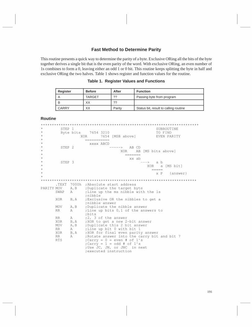
191
Fast Method to Determine Parity
This routine presents a quick way to determine the parity of a byte. Exclusive ORing all the bits of the bytetogether derives a single bit that is the even parity of the word. With exclusive ORing, an even number of1s combines to form a 0, leaving either an odd 1 or 0 bit. This routine keeps splitting the byte in half andexclusive ORing the two halves. Table 1 shows register and function values for the routine.
Table 1. Register Values and Functions
Register Before After Function
A TARGET ?? Passing byte from program
B XX ??
CARRY XX Parity Status bit, result to calling routine
Routine
************************************************************************ STEP 1 SUBROUTINE* Byte bits 7654 3210 TO FIND* XOR 7654 [MSB above] EVEN PARITY* ===========* xxxx ABCD* STEP 2 –––––> AB CD* XOR AB [MS bits above]* =======* xx ab* STEP 3 –––> a b* XOR a [MS bit]* =====* x P answer***********************************************************************
.TEXT 7000h ;Absolute start addressPARITY MOV A,B ;Duplicate the target byte
SWAP A ;Line up the ms nibble with the ls;nibble
XOR B,A ;Exclusive OR the nibbles to get a;nibble answer
MOV A,B ;Duplicate the nibble answerRR A ;Line up bits 0,1 of the answers to
;bitsRR A ;2, 3 of the answerXOR B,A ;XOR to get a new 2-bit answerMOV A,B ;Duplicate this 2 bit answerRR A ;Line up bit 0 with bit 1XOR B,A ;XOR for final even parity answerRR A ;Rotate answer into the carry bit and bit 7RTS ;Carry = 0 = even # of 1’s
;Carry = 1 = odd # of 1’s;Use JC, JN, or JNC in next;executed instruction

192
193
Automatic Baud Rate CalculationWith the TMS370
Microcontroller Products—Semiconductor GroupTexas Instruments

194
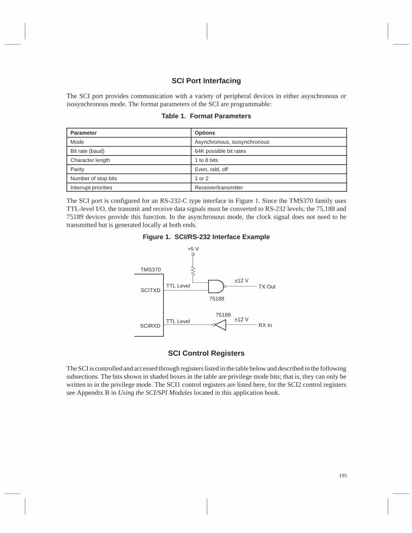
195
SCI Port Interfacing
The SCI port provides communication with a variety of peripheral devices in either asynchronous orisosynchronous mode. The format parameters of the SCI are programmable:
Table 1. Format Parameters
Parameter Options
Mode Asynchronous, isosynchronous
Bit rate (baud) 64K possible bit rates
Character length 1 to 8 bits
Parity Even, odd, off
Number of stop bits 1 or 2
Interrupt priorities Receiver/transmitter
The SCI port is configured for an RS-232-C type interface in Figure 1. Since the TMS370 family usesTTL-level I/O, the transmit and receive data signals must be converted to RS-232 levels; the 75,188 and75189 devices provide this function. In the asynchronous mode, the clock signal does not need to betransmitted but is generated locally at both ends.
Figure 1. SCI/RS-232 Interface Example
TMS370
TTL LevelSCITXD
SCIRXD
75189
+5 V
75188
TX Out
RX InTTL Level
±12 V
±12 V
SCI Control Registers
The SCI is controlled and accessed through registers listed in the table below and described in the followingsubsections. The bits shown in shaded boxes in the table are privilege mode bits; that is, they can only bewritten to in the privilege mode. The SCI1 control registers are listed here, for the SCI2 control registerssee Appendix B in Using the SCI/SPI Modules located in this application book.
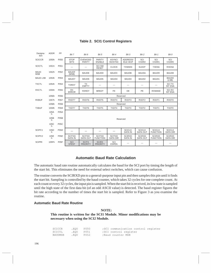
196
Table 2. SCI1 Control Registers
Designa-tion
ADDR PF Bit 7 Bit 6 Bit 5 Bit 4 Bit 3 Bit 2 Bit 1 Bit 0
SCICCR 1050h P050 STOPBITS
EVEN/ODDPARITY
PARITYENABLE
ASYNC/ISOSYNC
ADDRESS/IDLE WUP
SCICHAR2
SCICHAR1
SCICHAR0
SCICTL 1051h P051 — — SCI SWRESET CLOCK TXWAKE SLEEP TXENA RXENA
BAUDMSB
1052h P052 BAUDF(MSB) BAUDE BAUDD BAUDC BAUDB BAUDA BAUD9 BAUD8
BAUD LSB 1053h P053 BAUD7 BAUD6 BAUD5 BAUD4 BAUD3 BAUD2 BAUD1 BAUD0(LSB)
TXCTL 1054h P054 TXRDY TXEMPTY — — — — — SCI TX
INT ENA
RXCTL 1055h P055 RXERROR RXRDY BRKDT FE OE PE RXWAKE SCI RX
INT ENA
1056h P056 Reserved
RXBUF 1057h P057 RXDT7 RXDT6 RXDT5 RXDT4 RXDT3 RXDT2 RXDT1 RXDT0
1058h P058 Reserved
TXBUF 1059h P059 TXDT7 TXDT6 TXDT5 TXDT4 TXDT3 TXDT2 TXDT1 TXDT0
105Ah
P05A
105Bh
P05B Reserved
105Ch
P05C
SCIPC1 105Dh
P05D — — — — SCICLKDATA IN
SCICLKDATA OUT
SCICLKFUNCTION
SCICLKDATA DIR
SCIPC2 105Eh
P05E SCITXDDATA IN
SCITXDDATA OUT
SCITXDFUNCTION
SCITXDDATA DIR
SCIRXDDATA IN
SCIRXDDATA OUT
SCIRXDFUNCTION
SCIRXDDATA DIR
SCIPRI 105Fh P05F SCISTEST
SCITXPRIORITY
SCIRXPRIORITY
SCIESPEN — — — —
Automatic Baud Rate Calculation
The automatic baud rate routine automatically calculates the baud for the SCI port by timing the length ofthe start bit. This eliminates the need for external select switches, which can cause confusion.
The routine converts the SCIRXD pin to a general-purpose input pin and then samples this pin until it findsthe start bit. Sampling is controlled by the baud counter, which takes 32 cycles for one complete count. Ateach count or every 32 cycles, the input pin is sampled. When the start bit is received, its low state is sampleduntil the high state of the first data bit (of an odd ASCII value) is detected. The baud register figures thebit rate according to the number of times the start bit is sampled. Refer to Figure 3 as you examine theroutine.
Automatic Baud Rate Routine
NOTE:This routine is written for the SCI1 Module. Minor modifications may benecessary when using the SCI2 Module.
SCICCR .EQU P050 ;SCI communication control registerSCICTL .EQU P051 ;SCI control registerBAUDMSB .EQU P052 ;Baud counter MSB
197
BAUDLSB .EQU P053 ;Baud counter LSBTXCTL .EQU P054 ;Transmitter controlRXCTL .EQU P055 ;Receiver controlRXBUF .EQU P057 ;Receiver bufferTXBUF .EQU P059 ;Transmitter bufferSCIPC1 .EQU P05D ;Port control 1 (SCLK)SCIPC2 .EQU P05E ;Port control 2 (TXD,RXD)SCIPRI .EQU P05F ;Priority registerCOUNT .EQU R04 ;Temporary counting register.TEXT 07000h ;Initialize SCI port with a;<CR> (return)
;Baud automatically set on odd;ASCII character
AUTOBAUD CLR COUNT ;Clear count registerCLR COUNT-1 ;COUNT–1MOV #0,SCIPC2 ;Set RXD to general-purpose input pin
WAITSTRT BTJO #8,SCIPC2,WAITSTRT ;Wait for a start bit to go lowWAITBIT INC A ;Dummy, gives 32 clock states
;(1 min baud)INCW #1, COUNT ;Increment counterBTJZ #8,SCIPC2,WAITBIT ;Wait until start bit ends
;(ASCII char=odd)SETUP INCW #–1,COUNT ;One less than count into baud reg
MOV COUNT,BAUDLSB ;since the SCI starts from count 0MOV COUNT–1,BAUDMSB ;Initialize baud registersMOV #22h,SCIPC2 ;Enable RX and TX pinsMOV #2,SCIPC1 ;Enable SCLK pin (if needed)MOV #01110111b,SCICCR ;8-bit length, even parity, 1 stop bit
;only even, odd, or no parity;determined by SCICCR value
MOV #00110011b,SCICTL ;Enable TX, RX, SCLK = internal;program after input character finishes
MOV #1,TXCTL ;Enable TX interrupts MOV #1,RXCTL ;Enable RX interruptsMOV TXBUF,A ;Clear out garbage from SCI (Place in
;program after input character finishes)EINT
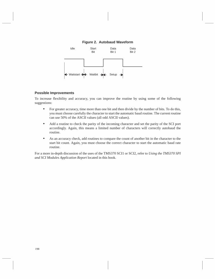
198
Figure 2. Autobaud Waveform
Idle StartBit
DataBit 1
DataBit 2
Waitstart Waitbit Setup
Possible Improvements
To increase flexibility and accuracy, you can improve the routine by using some of the followingsuggestions:
• For greater accuracy, time more than one bit and then divide by the number of bits. To do this,you must choose carefully the character to start the automatic baud routine. The current routinecan use 50% of the ASCII values (all odd ASCII values).
• Add a routine to check the parity of the incoming character and set the parity of the SCI portaccordingly. Again, this means a limited number of characters will correctly autobaud theroutine.
• As an accuracy check, add routines to compare the count of another bit in the character to thestart bit count. Again, you must choose the correct character to start the automatic baud rateroutine.
For a more in-depth discussion of the uses of the TMS370 SCI1 or SCI2, refer to Using the TMS370 SPIand SCI Modules Application Report located in this book.
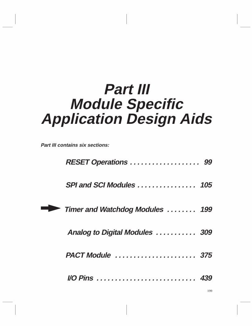
199
Part IIIModule Specific
Application Design Aids
Part III contains six sections:
RESET Operations 99. . . . . . . . . . . . . . . . . . .
SPI and SCI Modules 105. . . . . . . . . . . . . . . .
Timer and Watchdog Modules 199. . . . . . . .
Analog to Digital Modules 309. . . . . . . . . . .
PACT Module 375. . . . . . . . . . . . . . . . . . . . . .
I/O Pins 439. . . . . . . . . . . . . . . . . . . . . . . . . . .

200

201
Using the TMS370 Timer Modules
Microcontroller Products—Semiconductor GroupTexas Instruments

202

203
Introduction
The TMS370 family of 8-bit microcontrollers presently provides up to three timer modules designed tomeet user demands for timer applications.
This application report provides examples of software routines and hardware interface circuits designedto illustrate how the features of the timer modules may be used to solve a variety of system timerrequirements. These concepts may be adapted and applied to fit the specific needs of your individualproject. Additional information for T1 and T2n may be found in the TMS370 Family User’s Guide, Sections7 and 8.
Table 1. TMS370 Family Timer Module Capabilities
System Requirements Timer Resources
Real-Time System Control Interval Timers with Interrupts
Input Pulse Width Measurement Pulse Accumulate or Input Capture Functions
External Event Synchronization Event Count Function
Timer Output Control Compare Function
Pulse-Width Modulated Output Control PWM Output Function
System Integrity Watchdog (WD) Function
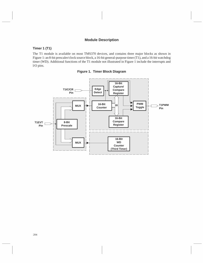
204
Module Description
Timer 1 (T1)
The T1 module is available on most TMS370 devices, and contains three major blocks as shown inFigure 1: an 8-bit prescaler/clock source block, a 16-bit general-purpose timer (T1), and a 16-bit watchdogtimer (WD). Additional functions of the T1 module not illustrated in Figure 1 include the interrupts andl/O pins.
Figure 1. Timer Block Diagram
ÁÁÁÁÁÁÁÁÁÁÁÁÁÁÁÁÁÁÁÁÁÁÁÁÁÁÁÁÁÁÁÁÁÁÁÁ
8-BitPrescale
MUX
MUX
ÁÁÁÁÁÁÁÁÁÁÁÁÁÁÁ
EdgeDetect
16-BitCapture/CompareRegister
16-BitCounter
16 PWMToggle
16-BitCompareRegister
16-BitWD
Counter(Third Timer)
T1IC/CRPin
T1EVTPin
T1PWMPin
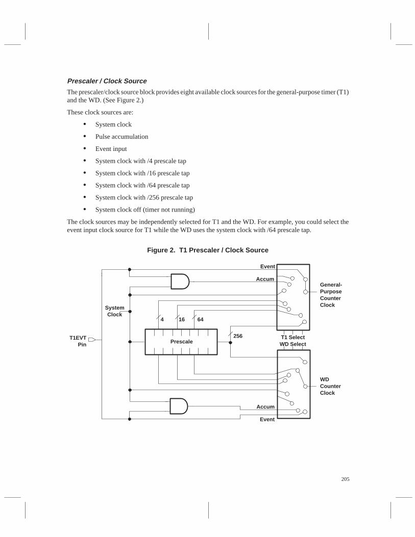
205
Prescaler / Clock Source
The prescaler/clock source block provides eight available clock sources for the general-purpose timer (T1)and the WD. (See Figure 2.)
These clock sources are:
• System clock
• Pulse accumulation
• Event input
• System clock with /4 prescale tap
• System clock with /16 prescale tap
• System clock with /64 prescale tap
• System clock with /256 prescale tap
• System clock off (timer not running)
The clock sources may be independently selected for T1 and the WD. For example, you could select theevent input clock source for T1 while the WD uses the system clock with /64 prescale tap.
Figure 2. T1 Prescaler / Clock Source
PrescaleT1EVT
Pin
SystemClock
4 16 64
256 T1 SelectWD Select
General-PurposeCounterClock
WDCounterClock
Event
Accum
Accum
Event
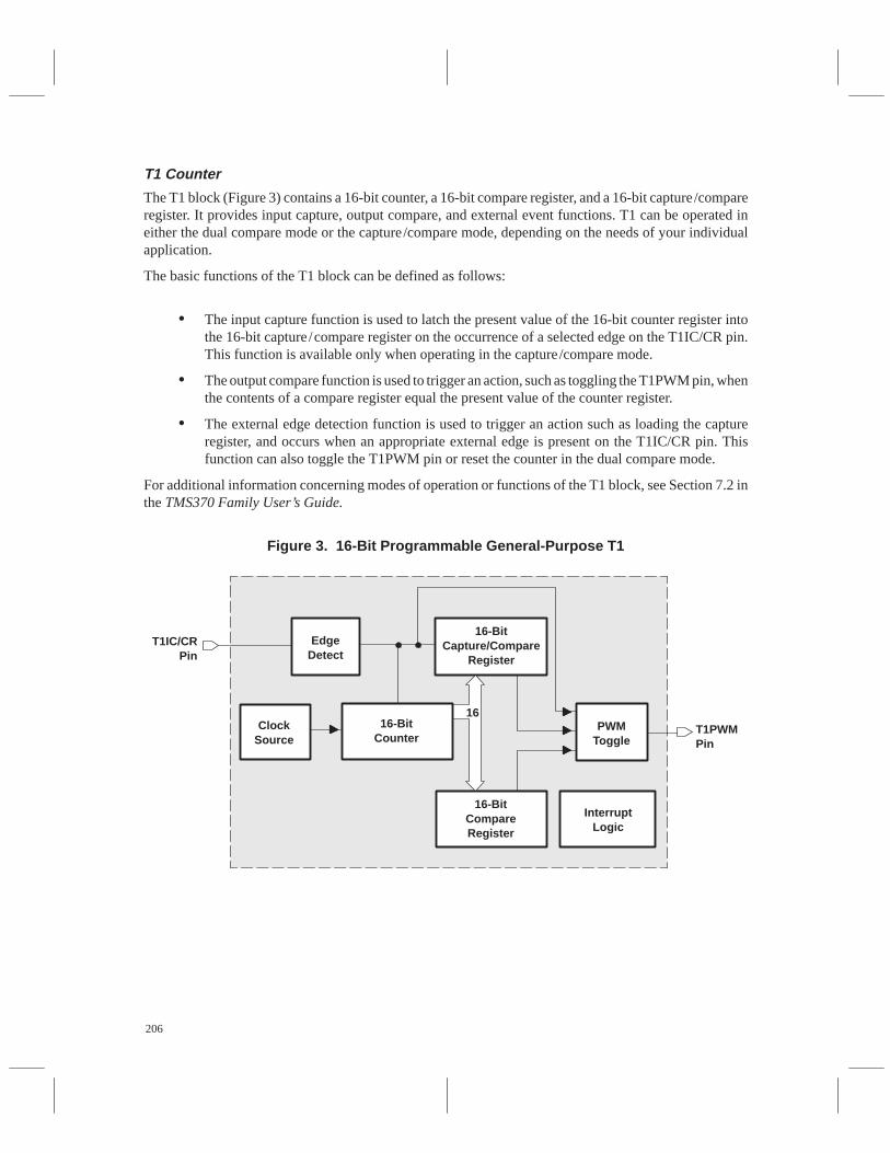
206
T1 Counter
The T1 block (Figure 3) contains a 16-bit counter, a 16-bit compare register, and a 16-bit capture/compareregister. It provides input capture, output compare, and external event functions. T1 can be operated ineither the dual compare mode or the capture/compare mode, depending on the needs of your individualapplication.
The basic functions of the T1 block can be defined as follows:
• The input capture function is used to latch the present value of the 16-bit counter register intothe 16-bit capture/compare register on the occurrence of a selected edge on the T1IC/CR pin.This function is available only when operating in the capture/compare mode.
• The output compare function is used to trigger an action, such as toggling the T1PWM pin, whenthe contents of a compare register equal the present value of the counter register.
• The external edge detection function is used to trigger an action such as loading the captureregister, and occurs when an appropriate external edge is present on the T1IC/CR pin. Thisfunction can also toggle the T1PWM pin or reset the counter in the dual compare mode.
For additional information concerning modes of operation or functions of the T1 block, see Section 7.2 inthe TMS370 Family User’s Guide.
Figure 3. 16-Bit Programmable General-Purpose T1
ÁÁÁÁÁÁÁÁÁÁÁÁ
16Clock
Source
EdgeDetect
16-BitCapture/Compare
Register
PWMToggle
16-BitCompareRegister
InterruptLogic
T1IC/CRPin
T1PWMPin
16-BitCounter
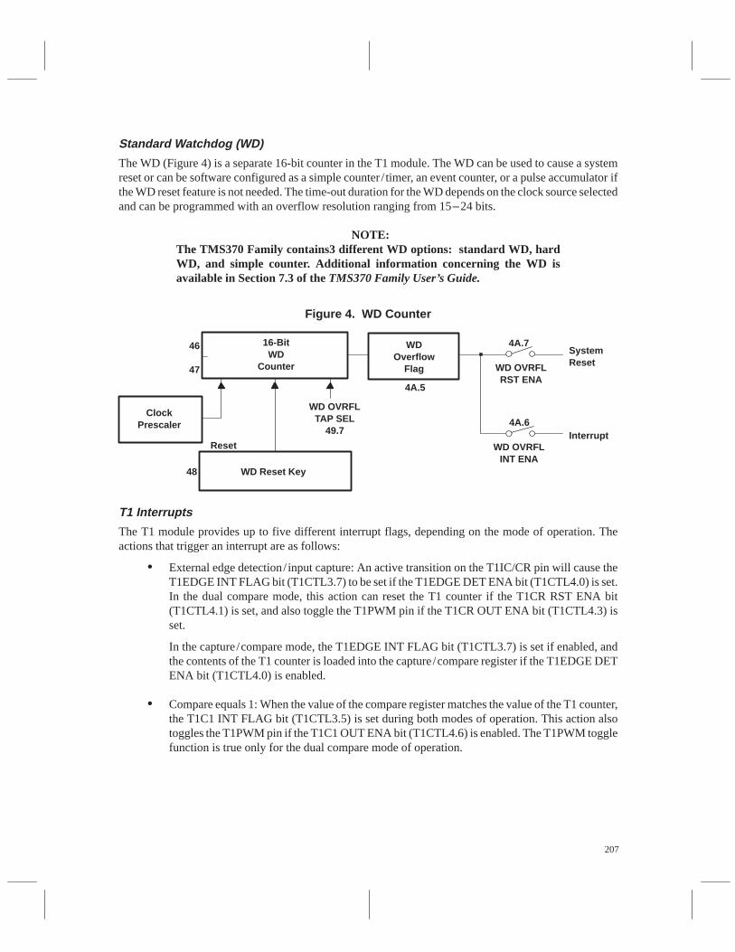
207
Standard Watchdog (WD)
The WD (Figure 4) is a separate 16-bit counter in the T1 module. The WD can be used to cause a systemreset or can be software configured as a simple counter/ timer, an event counter, or a pulse accumulator ifthe WD reset feature is not needed. The time-out duration for the WD depends on the clock source selectedand can be programmed with an overflow resolution ranging from 15–24 bits.
NOTE:The TMS370 Family contains3 different WD options: standard WD, hardWD, and simple counter. Additional information concerning the WD isavailable in Section 7.3 of the TMS370 Family User’s Guide.
Figure 4. WD Counter
16-BitWD
Counter
WDOverflow
Flag
4A.7
WD OVRFLRST ENA
WD OVRFLINT ENA
4A.5
WD OVRFLTAP SEL
49.7
WD Reset Key
ClockPrescaler
Reset
48
46
47
SystemReset
Interrupt4A.6
T1 Interrupts
The T1 module provides up to five different interrupt flags, depending on the mode of operation. Theactions that trigger an interrupt are as follows:
• External edge detection/ input capture: An active transition on the T1IC/CR pin will cause theT1EDGE INT FLAG bit (T1CTL3.7) to be set if the T1EDGE DET ENA bit (T1CTL4.0) is set.In the dual compare mode, this action can reset the T1 counter if the T1CR RST ENA bit(T1CTL4.1) is set, and also toggle the T1PWM pin if the T1CR OUT ENA bit (T1CTL4.3) isset.
In the capture/compare mode, the T1EDGE INT FLAG bit (T1CTL3.7) is set if enabled, andthe contents of the T1 counter is loaded into the capture/compare register if the T1EDGE DETENA bit (T1CTL4.0) is enabled.
• Compare equals 1: When the value of the compare register matches the value of the T1 counter,the T1C1 INT FLAG bit (T1CTL3.5) is set during both modes of operation. This action alsotoggles the T1PWM pin if the T1C1 OUT ENA bit (T1CTL4.6) is enabled. The T1PWM togglefunction is true only for the dual compare mode of operation.
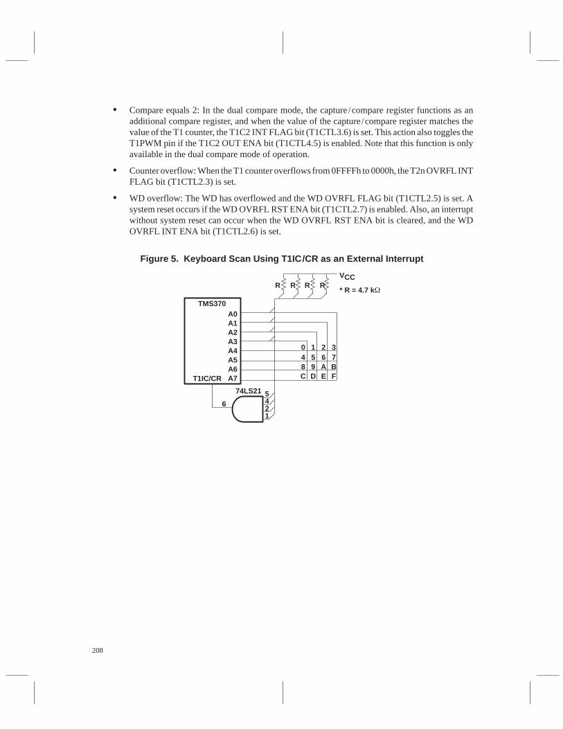
208
• Compare equals 2: In the dual compare mode, the capture/compare register functions as anadditional compare register, and when the value of the capture/compare register matches thevalue of the T1 counter, the T1C2 INT FLAG bit (T1CTL3.6) is set. This action also toggles theT1PWM pin if the T1C2 OUT ENA bit (T1CTL4.5) is enabled. Note that this function is onlyavailable in the dual compare mode of operation.
• Counter overflow: When the T1 counter overflows from 0FFFFh to 0000h, the T2n OVRFL INTFLAG bit (T1CTL2.3) is set.
• WD overflow: The WD has overflowed and the WD OVRFL FLAG bit (T1CTL2.5) is set. Asystem reset occurs if the WD OVRFL RST ENA bit (T1CTL2.7) is enabled. Also, an interruptwithout system reset can occur when the WD OVRFL RST ENA bit is cleared, and the WDOVRFL INT ENA bit (T1CTL2.6) is set.
Figure 5. Keyboard Scan Using T1IC/CR as an External Interrupt
TMS370
T1IC/CR
A0A1A2A3A4A5A6A7
R R R RVCC
* R = 4.7 k
0 1 2 34 5 6 78 9 A BC D E F
5421
6
74LS21

209
T1 I/O Pins
The T1 module includes three I/O pins which can be dedicated for timer functions or as general-purposeI/O pins. The configuration for these pins is controlled through the timer port control registers T1PC1 andT1PC2. Their names and T1 functions are as follows:
• T1EVT: This pin may be used as an external clock input to the prescaler /clock source block.Input frequency may not exceed SYSCLK/2.
• T1IC/CR: Depending on the mode of operation, this pin may be used to input an external signalto trigger loading of the capture register, toggle the T1PWM output pin, reset the counter, orgenerate an interrupt.
• T1PWM: The T1 function of this pin is to output a pulse width modulated (PWM) signal fromthe module.
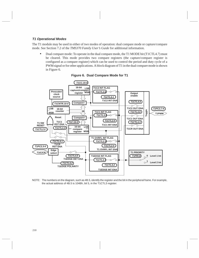
210
T1 Operational Modes
The T1 module may be used in either of two modes of operation: dual compare mode or capture/comparemode. See Section 7.2 of the TMS370 Family User’s Guide for additional information.
• Dual compare mode: To operate in the dual compare mode, the T1 MODE bit (T1CTL4.7) mustbe cleared. This mode provides two compare registers (the capture/compare register isconfigured as a compare register) which can be used to control the period and duty cycle of aPWM signal or for other applications. A block diagram of T1 in the dual compare mode is shownin Figure 6.
Figure 6. Dual Compare Mode for T1
T1CTL4.1
T1CTL4.4
Prescaler/clock
source
16-bitcounter
16-bit
16
Compare=
Compare=Reset
T1C1RST ENAT1 SW
RESET
Edgeselect
T1EDGE DET ENA
Outputenable
capture/compareregister MSB
LSB
MSB
LSB
T1CR OUT ENA
T1IC/CR
T1EDGE POLARITY
Togg
le
16-bitcompare
MSB
LSB
register
T1CC.15-0
T1C1 INT FLAG
T1CTL3.0
T1CTL3.5
T1C1 INT ENA
T1C2 INT FLAG
T1CTL3.1
T1CTL3.6
T1C2 INT ENA
T1 OVRFL INT FLAG
T1CTL2.4
T1CTL2.3
T1 OVRFL INT ENA
T1EDGE INT FLAG
T1CTL3.2
T1CTL3.7
T1EDGE INT ENA
T1 PRIORITY
T1C2 OUT ENA
T1C1 OUT ENA
T1CTL4.3
T1CTL4.6
T1CTL4.5
T1PWM
T1PC2.7-4
T1PRI.6
T1C.15-0
T1CNTR.15-0
T1CTL2.0
T1CRRST ENAT1PC2.3-0
T1CTL4.0
T1CTL4.2
Level 1 Int
Level 2 Int
0
1
NOTE: The numbers on the diagram, such as 4B.5, identify the register and the bit in the peripheral frame. For example,the actual address of 4B.5 is 104Bh, bit 5, in the T1CTL3 register.
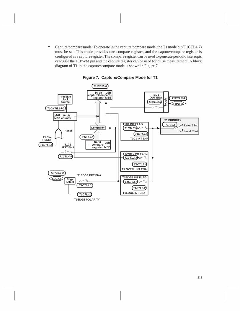
211
• Capture/compare mode: To operate in the capture/compare mode, the T1 mode bit (T1CTL4.7)must be set. This mode provides one compare register, and the capture/compare register isconfigured as a capture register. The compare register can be used to generate periodic interruptsor toggle the T1PWM pin and the capture register can be used for pulse measurement. A blockdiagram of T1 in the capture/compare mode is shown in Figure 7.
Figure 7. Capture/Compare Mode for T1
T1CTL4.2
16
Compare=
Edgeselect
T1IC/CR
T1EDGE POLARITY
T1EDGE DET ENA
Prescaleclock
source
16-bitcounterMSB
LSB
T1CNTR.15-0
Reset
T1C1RST ENA
T1 SWRESET
T1CTL2.0
T1CTL4.4
T1PC2.3-0
T1CTL4.0
T1EDGE INT FLAG
T1EDGE INT ENA
T1CTL3.7
T1CTL3.2
T1 OVRFL INT FLAG
T1 OVRFL INT ENA
T1CTL2.3
T1CTL2.4
T1C1 INT FLAG
T1C1 INT ENA
T1CTL3.5
T1CTL3.0
T1C1OUT ENA
T1PWMT1CTL4.6
Togg
le T1PC2.7-4
16-bitcapture/compare
MSB
LSB
register
T1CC.15-0
T1C.15-0
16-bitcompare
MSB
LSB
register
T1 PRIORITY
ÏÏÏT1PRI.6 Level 1 Int
Level 2 Int
0
1
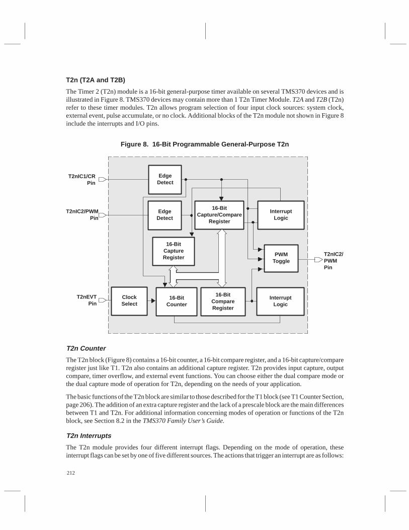
212
T2n (T2A and T2B)
The Timer 2 (T2n) module is a 16-bit general-purpose timer available on several TMS370 devices and isillustrated in Figure 8. TMS370 devices may contain more than 1 T2n Timer Module. T2A and T2B (T2n)refer to these timer modules. T2n allows program selection of four input clock sources: system clock,external event, pulse accumulate, or no clock. Additional blocks of the T2n module not shown in Figure 8include the interrupts and I/O pins.
Figure 8. 16-Bit Programmable General-Purpose T2n
InterruptLogic
16-BitCapture/Compare
Register
EdgeDetect
EdgeDetect
16-BitCaptureRegister
16-BitCounter
16-BitCompareRegister
InterruptLogic
PWMToggle
ClockSelect
T2nEVTPin
T2nIC2/PWMPin
T2nIC1/CRPin
T2nIC2/PWMPin
T2n Counter
The T2n block (Figure 8) contains a 16-bit counter, a 16-bit compare register, and a 16-bit capture/compareregister just like T1. T2n also contains an additional capture register. T2n provides input capture, outputcompare, timer overflow, and external event functions. You can choose either the dual compare mode orthe dual capture mode of operation for T2n, depending on the needs of your application.
The basic functions of the T2n block are similar to those described for the T1 block (see T1 Counter Section,page 206). The addition of an extra capture register and the lack of a prescale block are the main differencesbetween T1 and T2n. For additional information concerning modes of operation or functions of the T2nblock, see Section 8.2 in the TMS370 Family User’s Guide.
T2n Interrupts
The T2n module provides four different interrupt flags. Depending on the mode of operation, theseinterrupt flags can be set by one of five different sources. The actions that trigger an interrupt are as follows:

213
• Input capture 1/external edge detection 1: When an active transition occurs on the T2nIC1/CRpin, the T2nEDGE1 INT FLAG bit (T2nCTL2.7) is set. If the T2nEDGE1 DET bit(T2nCTL3.0) is enabled, then this action also loads the contents of the T2n counter into thecapture/compare register. Please note, you must be in the dual capture mode of operation forthe capture function.
• Input capture 2/external edge detection 2: When an active transition occurs on theT2nIC2/PWM pin, the T2nEDGE2 INT FLAG bit (T2nCTL2.6) is set. If the T2nEDGE2 DETbit (T2nCTL3.1) is enabled, then this action also loads the contents of the T2n counter into thecapture register. Please note, you must be in the dual capture mode of operation for these actionsto occur.
• Compare equals 1: When the value of the compare register matches the value of the T2n counter,the T2nC1 INT FLAG bit (T2nCTL2.5) is set. This is true for both modes of operation.
• Compare equals 2: When the value of the capture/compare register matches the value of the T2ncounter, the T2nC2 INT FLAG bit (T2nCTL2.6) is set. This is true for the dual compare modeof operation only.
• Counter overflow: When the T2n counter overflows from 0FFFFh to 0000h; the T2n OVRFLINT FLAG bit (T2nCTL1.3) is set.
T2n I/O Pins
The T2n module includes three I/O pins which can be dedicated for timer functions or as general-purposeI/O pins. Their names and T2n functions are as follows:
• T2nEVT: This pin may be used as an external clock input or pulse accumulation signal to theT2n module. Input frequency may not exceed SYSCLK/2.
• T2nIC1/CR: Depending on the mode of operation, this pin may be used to input an externalsignal to trigger loading of the capture/compare register or to toggle the T2nPWM output pin.A signal on this pin may also reset the counter.
• T2nIC2/PWM: In the dual compare mode, the function of this pin is to output a PWM signalfrom the module. In the dual capture mode, this pin is used to input an external signal to triggerloading the capture register with the contents of the T2n counter.
The configuration for these pins is controlled through the timer port control registers T2nPC1 and T2nPC2.
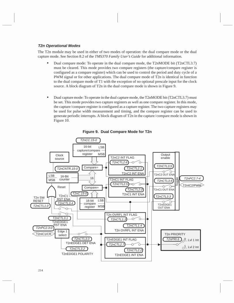
214
T2n Operational Modes
The T2n module may be used in either of two modes of operation: the dual compare mode or the dualcapture mode. See Section 8.2 of the TMS370 Family User’s Guide for additional information.
• Dual compare mode: To operate in the dual compare mode, the T2nMODE bit (T2nCTL3.7)must be cleared. This mode provides two compare registers (the capture/compare register isconfigured as a compare register) which can be used to control the period and duty cycle of aPWM signal or for other applications. The dual compare mode of T2n is identical in functionto the dual compare mode of T1 with the exception of no optional prescale input for the clocksource. A block diagram of T2n in the dual compare mode is shown in Figure 9.
• Dual capture mode: To operate in the dual capture mode, the T2nMODE bit (T2nCTL3.7) mustbe set. This mode provides two capture registers as well as one compare register. In this mode,the capture/compare register is configured as a capture register. The two capture registers maybe used for pulse width measurement and timing, and the compare register can be used togenerate periodic interrupts. A block diagram of T2n in the capture/compare mode is shown inFigure 10.
Figure 9. Dual Compare Mode for T2n
16
T2nC.15-0
T2nCTL2.1
T2nCTL3.2
T2nCTL3.1
T2nCTL3.5
T2nCTL3.3
Clocksource
16-Bitcounter
16-bit
Compare=
Compare=Reset
T2nC1RST ENAT2n SW
RESET
Edge 1select
T2nEDGE1 DET ENA
Outputenable
capture/compareregister MSB
LSB
MSBLSB
T2nEDGE1OUT ENA
T2nIC1/CR
T2nEDGE1 POLARITY
Togg
le
16-bitcompare
MSB
LSB
register
T2nCC.15-0
T2nC1 INT FLAG
T2nCTL2.0
T2nCTL2.5
T2nC1 INT ENA
T2nC2 INT FLAG
T2nCTL2.6
T2nC2 INT ENA
T2n OVRFL INT FLAG
T2nCTL1.4
T2nCTL1.3
T2n OVRFL INT ENA
T2nEDGE1 INT FLAG
T2nCTL2.2
T2nCTL2.7
T2nEDGE1 INT ENA
T2n PRIORITY
T2nC2 OUT ENA
T2nC1 OUT ENA
T2nCTL3.6
T2nIC2/PWM
T2nPC2.7-4
T2nPRI.6
T2nCNTR.15-0
T2nCTL1.0T2nCTL3.4
T2nEDGE1RST ENA
T2nPC2.3-0
T2nCTL3.0 Lvl 1 Int
Lvl 2 Int
0
1
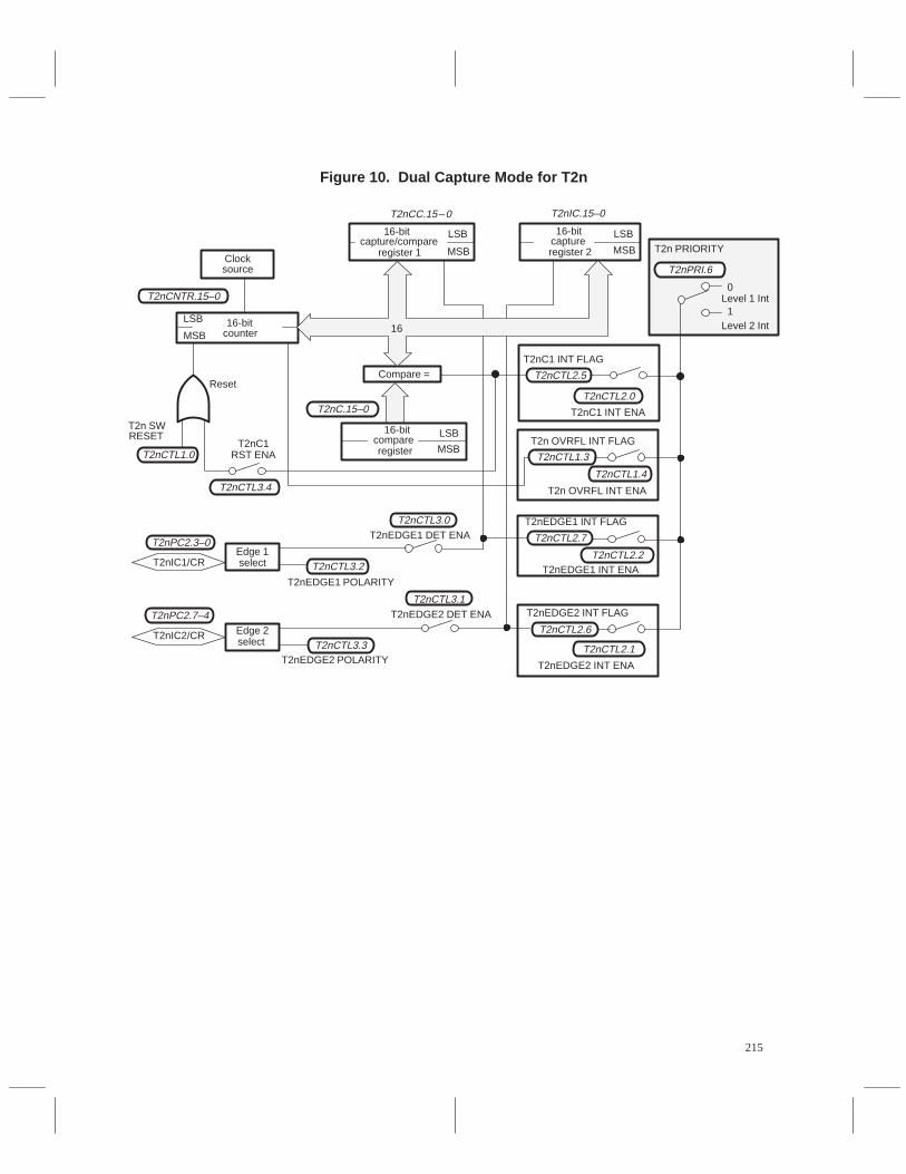
215
Figure 10. Dual Capture Mode for T2n
T2nCTL2.5
T2nCTL3.3
0
capture/compare
T2nPC2.3–0
Compare =
Clocksource
16-bitcounterMSB
LSB
T2nCNTR.15–0
Reset
T2nC1RST ENA
T2n SWRESET
T2nCTL1.0
T2nCTL3.4
T2nCTL2.6
T2nCTL2.1
T2nCTL2.7
T2nCTL2.2
T2nCTL2.0
16-bit
MSB
LSB
register 1
T2nC.15–0
16-bitcompare
MSB
LSB
register
T2n PRIORITY
Level 1 Int
Level 2 Int1
T2nCTL1.3
T2nCTL1.4
16-bitcapture
MSB
LSB
register 2
T2nIC.15–0
Edge 2select
T2nIC2/CR
T2nPC2.7–4
T2nCTL3.1
Edge 1selectT2nIC1/CR T2nCTL3.2
T2nCTL3.0
16
T2nEDGE1 POLARITY
T2nEDGE1 DET ENA
T2nEDGE2 DET ENA
T2nEDGE2 POLARITY
T2nC1 INT FLAG
T2nC1 INT ENA
T2n OVRFL INT FLAG
T2n OVRFL INT ENA
T2nEDGE1 INT FLAG
T2nEDGE1 INT ENA
T2nEDGE2 INT ENA
T2nEDGE2 INT FLAG
T2nPRI.6
T2nCC.15– 0
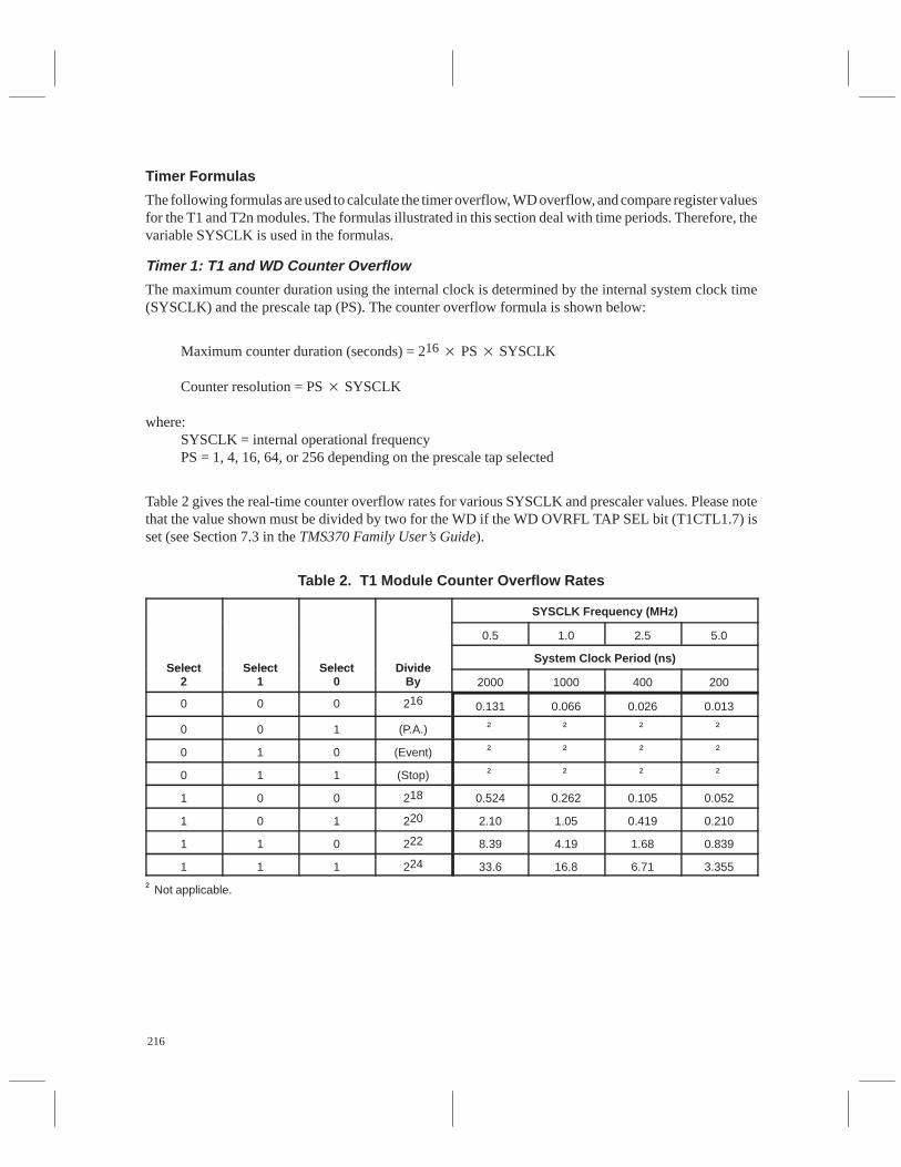
216
Timer Formulas
The following formulas are used to calculate the timer overflow, WD overflow, and compare register valuesfor the T1 and T2n modules. The formulas illustrated in this section deal with time periods. Therefore, thevariable SYSCLK is used in the formulas.
Timer 1: T1 and WD Counter Overflow
The maximum counter duration using the internal clock is determined by the internal system clock time(SYSCLK) and the prescale tap (PS). The counter overflow formula is shown below:
Maximum counter duration (seconds) = 216 PS SYSCLK
Counter resolution = PS SYSCLK
where: SYSCLK = internal operational frequencyPS = 1, 4, 16, 64, or 256 depending on the prescale tap selected
Table 2 gives the real-time counter overflow rates for various SYSCLK and prescaler values. Please notethat the value shown must be divided by two for the WD if the WD OVRFL TAP SEL bit (T1CTL1.7) isset (see Section 7.3 in the TMS370 Family User’s Guide).
Table 2. T1 Module Counter Overflow Rates
SYSCLK Frequency (MHz)
0.5 1.0 2.5 5.0
Select Select Select DivideSystem Clock Period (ns)
Select2
Select1
Select0
DivideBy 2000 1000 400 200
0 0 0 216 0.131 0.066 0.026 0.013
0 0 1 (P.A.) † † † †
0 1 0 (Event) † † † †
0 1 1 (Stop) † † † †
1 0 0 218 0.524 0.262 0.105 0.052
1 0 1 220 2.10 1.05 0.419 0.210
1 1 0 222 8.39 4.19 1.68 0.839
1 1 1 224 33.6 16.8 6.71 3.355
† Not applicable.
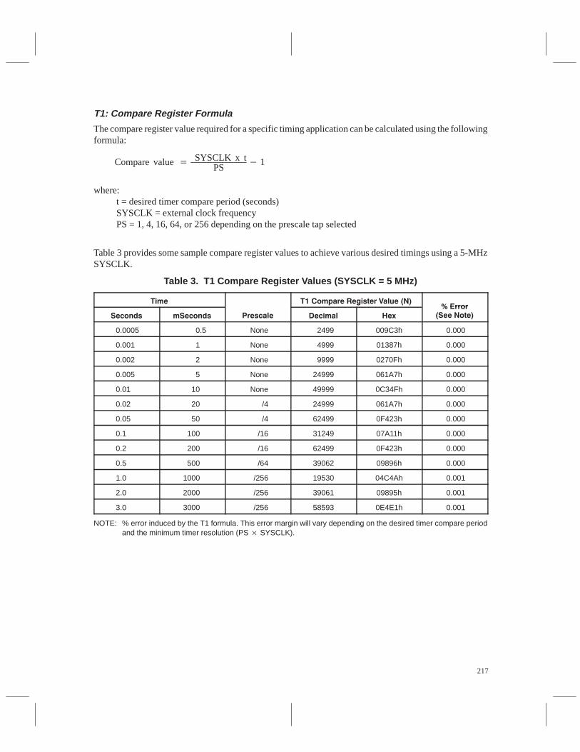
217
T1: Compare Register Formula
The compare register value required for a specific timing application can be calculated using the followingformula:
Compare value SYSCLK x tPS
1
where:t = desired timer compare period (seconds)SYSCLK = external clock frequencyPS = 1, 4, 16, 64, or 256 depending on the prescale tap selected
Table 3 provides some sample compare register values to achieve various desired timings using a 5-MHzSYSCLK.
Table 3. T1 Compare Register Values (SYSCLK = 5 MHz)
0.0005 0.5 None 2499 009C3h 0.000
0.001 1 None 4999 01387h 0.000
0.002 2 None 9999 0270Fh 0.000
0.005 5 None 24999 061A7h 0.000
0.01 10 None 49999 0C34Fh 0.000
0.02 20 /4 24999 061A7h 0.000
0.05 50 /4 62499 0F423h 0.000
0.1 100 /16 31249 07A11h 0.000
0.2 200 /16 62499 0F423h 0.000
0.5 500 /64 39062 09896h 0.000
1.0 1000 /256 19530 04C4Ah 0.001
2.0 2000 /256 39061 09895h 0.001
3.0 3000 /256 58593 0E4E1h 0.001
NOTE: % error induced by the T1 formula. This error margin will vary depending on the desired timer compare periodand the minimum timer resolution (PS SYSCLK).
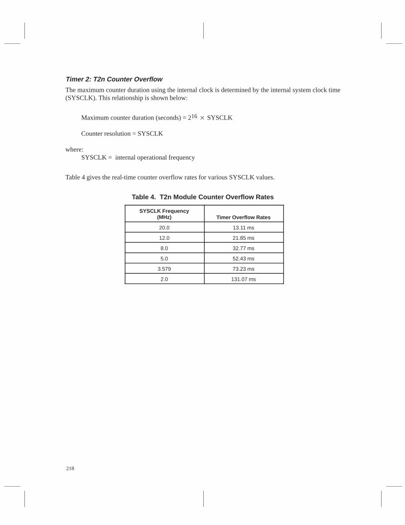
218
Timer 2: T2n Counter Overflow
The maximum counter duration using the internal clock is determined by the internal system clock time(SYSCLK). This relationship is shown below:
Maximum counter duration (seconds) = 216 SYSCLK
Counter resolution = SYSCLK
where:SYSCLK = internal operational frequency
Table 4 gives the real-time counter overflow rates for various SYSCLK values.
Table 4. T2n Module Counter Overflow Rates
SYSCLK Frequency(MHz) Timer Overflow Rates
20.0 13.11 ms
12.0 21.85 ms
8.0 32.77 ms
5.0 52.43 ms
3.579 73.23 ms
2.0 131.07 ms

219
Timer 2: Compare Register Formula
The compare register value required for a specific timing application can be calculated using the followingformula:
Compare value (SYSCLK x t) 1
where:t = desired timer compare period (seconds)SYSCLK = internal operational frequency
Table 5 provides some sample compare register values to achieve various desired timings.
Table 5. T2n Compare Register Values (SYSCLK = 5 MHz)
Time T2n Compare Register Value (N)
Seconds mSeconds Decimal Hex % Error (See Note)
0.0005 0.5 2499 009C3h 0.000
0.001 1 4999 01387h 0.000
0.002 2 9999 0270Fh 0.000
0.005 5 24999 061A7h 0.000
0.010 10 49999 0C34Fh 0.000
0.013 13 64999 0FDE7h 0.000
NOTE: % error induced by the T2n formula. This error margin will vary depending on the desired timer compare periodand the minimum timer resolution (SYSCLK).
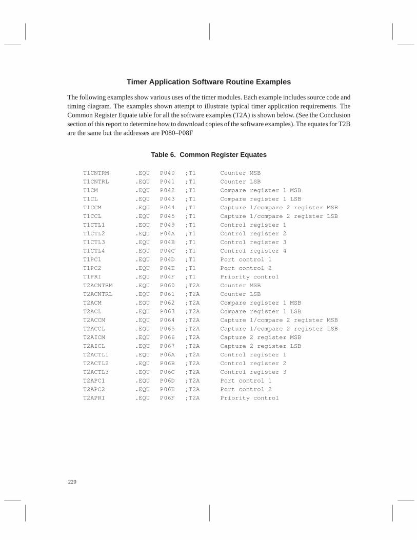
220
Timer Application Software Routine Examples
The following examples show various uses of the timer modules. Each example includes source code andtiming diagram. The examples shown attempt to illustrate typical timer application requirements. TheCommon Register Equate table for all the software examples (T2A) is shown below. (See the Conclusionsection of this report to determine how to download copies of the software examples). The equates for T2Bare the same but the addresses are P080–P08F
Table 6. Common Register Equates
T1CNTRM .EQU P040 ;T1 Counter MSB
T1CNTRL .EQU P041 ;T1 Counter LSB
T1CM .EQU P042 ;T1 Compare register 1 MSB
T1CL .EQU P043 ;T1 Compare register 1 LSB
T1CCM .EQU P044 ;T1 Capture 1/compare 2 register MSB
T1CCL .EQU P045 ;T1 Capture 1/compare 2 register LSB
T1CTL1 .EQU P049 ;T1 Control register 1
T1CTL2 .EQU P04A ;T1 Control register 2
T1CTL3 .EQU P04B ;T1 Control register 3
T1CTL4 .EQU P04C ;T1 Control register 4
T1PC1 .EQU P04D ;T1 Port control 1
T1PC2 .EQU P04E ;T1 Port control 2
T1PRI .EQU P04F ;T1 Priority control
T2ACNTRM .EQU P060 ;T2A Counter MSB
T2ACNTRL .EQU P061 ;T2A Counter LSB
T2ACM .EQU P062 ;T2A Compare register 1 MSB
T2ACL .EQU P063 ;T2A Compare register 1 LSB
T2ACCM .EQU P064 ;T2A Capture 1/compare 2 register MSB
T2ACCL .EQU P065 ;T2A Capture 1/compare 2 register LSB
T2AICM .EQU P066 ;T2A Capture 2 register MSB
T2AICL .EQU P067 ;T2A Capture 2 register LSB
T2ACTL1 .EQU P06A ;T2A Control register 1
T2ACTL2 .EQU P06B ;T2A Control register 2
T2ACTL3 .EQU P06C ;T2A Control register 3
T2APC1 .EQU P06D ;T2A Port control 1
T2APC2 .EQU P06E ;T2A Port control 2
T2APRI .EQU P06F ;T2A Priority control
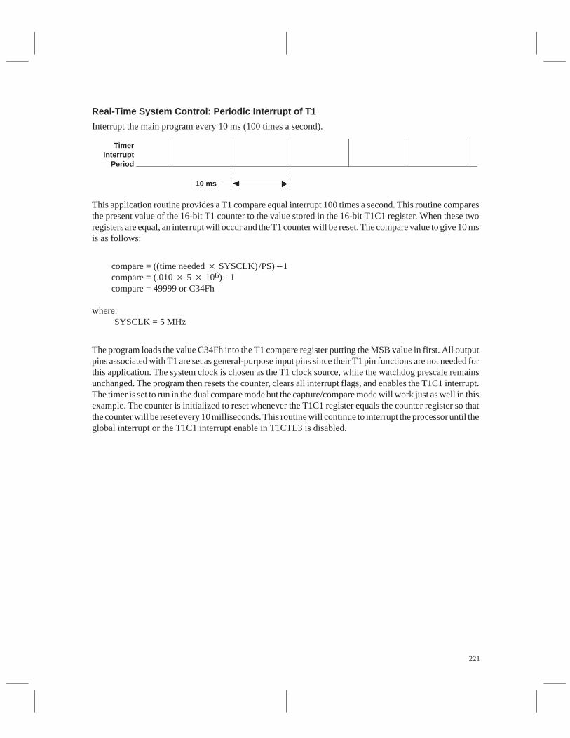
221
Real-Time System Control: Periodic Interrupt of T1
Interrupt the main program every 10 ms (100 times a second).
TimerInterrupt
Period
10 ms
This application routine provides a T1 compare equal interrupt 100 times a second. This routine comparesthe present value of the 16-bit T1 counter to the value stored in the 16-bit T1C1 register. When these tworegisters are equal, an interrupt will occur and the T1 counter will be reset. The compare value to give 10 msis as follows:
compare = ((time needed SYSCLK)/PS) –1 compare = (.010 5 106) –1 compare = 49999 or C34Fh
where:SYSCLK = 5 MHz
The program loads the value C34Fh into the T1 compare register putting the MSB value in first. All outputpins associated with T1 are set as general-purpose input pins since their T1 pin functions are not needed forthis application. The system clock is chosen as the T1 clock source, while the watchdog prescale remainsunchanged. The program then resets the counter, clears all interrupt flags, and enables the T1C1 interrupt.The timer is set to run in the dual compare mode but the capture/compare mode will work just as well in thisexample. The counter is initialized to reset whenever the T1C1 register equals the counter register so thatthe counter will be reset every 10 milliseconds. This routine will continue to interrupt the processor until theglobal interrupt or the T1C1 interrupt enable in T1CTL3 is disabled.
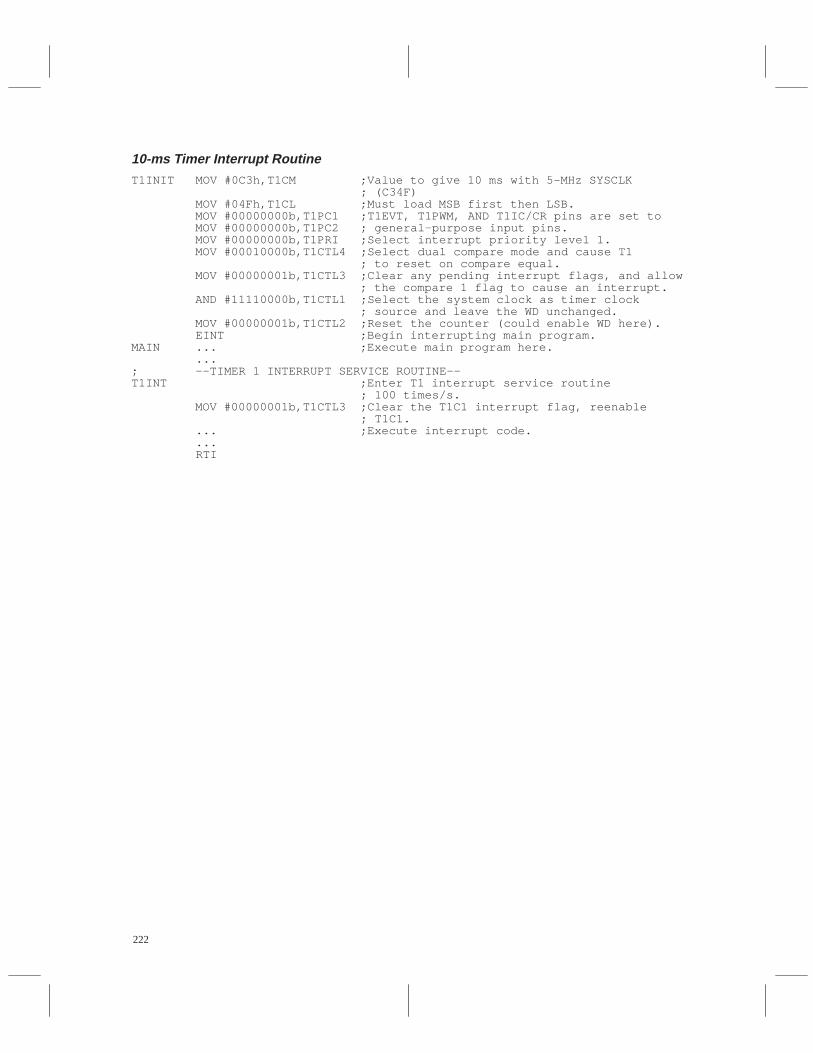
222
10-ms Timer Interrupt RoutineT1INIT MOV #0C3h,T1CM ;Value to give 10 ms with 5-MHz SYSCLK ; (C34F) MOV #04Fh,T1CL ;Must load MSB first then LSB. MOV #00000000b,T1PC1 ;T1EVT, T1PWM, AND T1IC/CR pins are set to MOV #00000000b,T1PC2 ; general-purpose input pins. MOV #00000000b,T1PRI ;Select interrupt priority level 1. MOV #00010000b,T1CTL4 ;Select dual compare mode and cause T1 ; to reset on compare equal. MOV #00000001b,T1CTL3 ;Clear any pending interrupt flags, and allow ; the compare 1 flag to cause an interrupt. AND #11110000b,T1CTL1 ;Select the system clock as timer clock ; source and leave the WD unchanged. MOV #00000001b,T1CTL2 ;Reset the counter (could enable WD here). EINT ;Begin interrupting main program.MAIN ... ;Execute main program here. ...; ––TIMER 1 INTERRUPT SERVICE ROUTINE––T1INT ;Enter T1 interrupt service routine ; 100 times/s. MOV #00000001b,T1CTL3 ;Clear the T1C1 interrupt flag, reenable ; T1C1. ... ;Execute interrupt code. ... RTI

223
Output Pulse Width Generation: 1-kHz Square Wave
Output a 1-kHz square wave (50% duty cycle).
T1PWMPin
This application routine generates a 1-kHz square wave output signal by using the 16-bit T1 compare regis-ter to toggle the T1PWM output pin. Since the timer needs to toggle the output pin twice to produce onesquare wave pulse, the timer needs to toggle at a 2-kHz rate, or every 0.5 ms. The compare value to give 0.5ms is:
compare = ((time needed SYSCLK)/PS) –1 compare = (0.0005 5 106) –1 compare = 2499 or 09C3h
where:SYSCLK = 5 MHz
The program loads the value 09C3h into the T1 compare register, putting the MSB value in first. TheT1PWM pin is set to the PWM output function and the other T1 pins are set to general-purpose input pinssince their T1 pin functions are not needed for this application. The system clock is chosen as the T1 clocksource, while the WD prescale remains unchanged. The program then resets the counter, clears all interruptflags, and disables all T1 interrupts. The timer is set to run in dual compare mode, but the capture/comparemode works just as well in this example. The counter resets whenever the T1C1 register equals the counterregister, so that the counter resets every 0.5 ms. Once the T1 module is initialized, a 1-kHz square wavesignal is output continuously on the T1PWM pin without further program intervention.
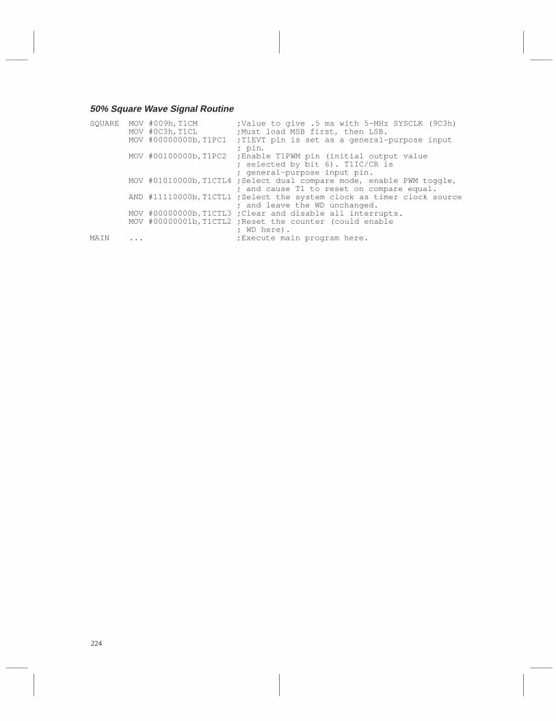
224
50% Square Wave Signal RoutineSQUARE MOV #009h,T1CM ;Value to give .5 ms with 5-MHz SYSCLK (9C3h) MOV #0C3h,T1CL ;Must load MSB first, then LSB. MOV #00000000b,T1PC1 ;T1EVT pin is set as a general-purpose input ; pin . MOV #00100000b,T1PC2 ;Enable T1PWM pin (initial output value ; selected by bit 6). T1IC/CR is ; general-purpose input pin. MOV #01010000b,T1CTL4 ;Select dual compare mode, enable PWM toggle, ; and cause T1 to reset on compare equal. AND #11110000b,T1CTL1 ;Select the system clock as timer clock source ; and leave the WD unchanged. MOV #00000000b,T1CTL3 ;Clear and disable all interrupts. MOV #00000001b,T1CTL2 ;Reset the counter (could enable ; WD here).MAIN ... ;Execute main program here.
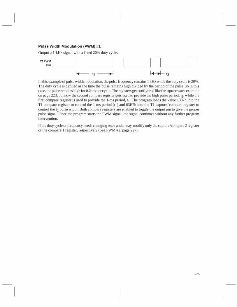
225
Pulse Width Modulation (PWM) #1
Output a 1-kHz signal with a fixed 20% duty cycle.
T1PWMPin
t1 t2
In this example of pulse width modulation, the pulse frequency remains 1 kHz while the duty cycle is 20%.The duty cycle is defined as the time the pulse remains high divided by the period of the pulse, so in thiscase, the pulse remains high for 0.2 ms per cycle. The registers get configured like the square wave exampleon page 223, but now the second compare register gets used to provide the high pulse period, t2, while thefirst compare register is used to provide the 1-ms period, t1. The program loads the value 1387h into theT1 compare register to control the 1-ms period (t1) and 03E7h into the T1 capture/compare register tocontrol the t2 pulse width. Both compare registers are enabled to toggle the output pin to give the properpulse signal. Once the program starts the PWM signal, the signal continues without any further programintervention.
If the duty cycle or frequency needs changing once under way, modify only the capture/compare 2 registeror the compare 1 register, respectively (See PWM #2, page 227).
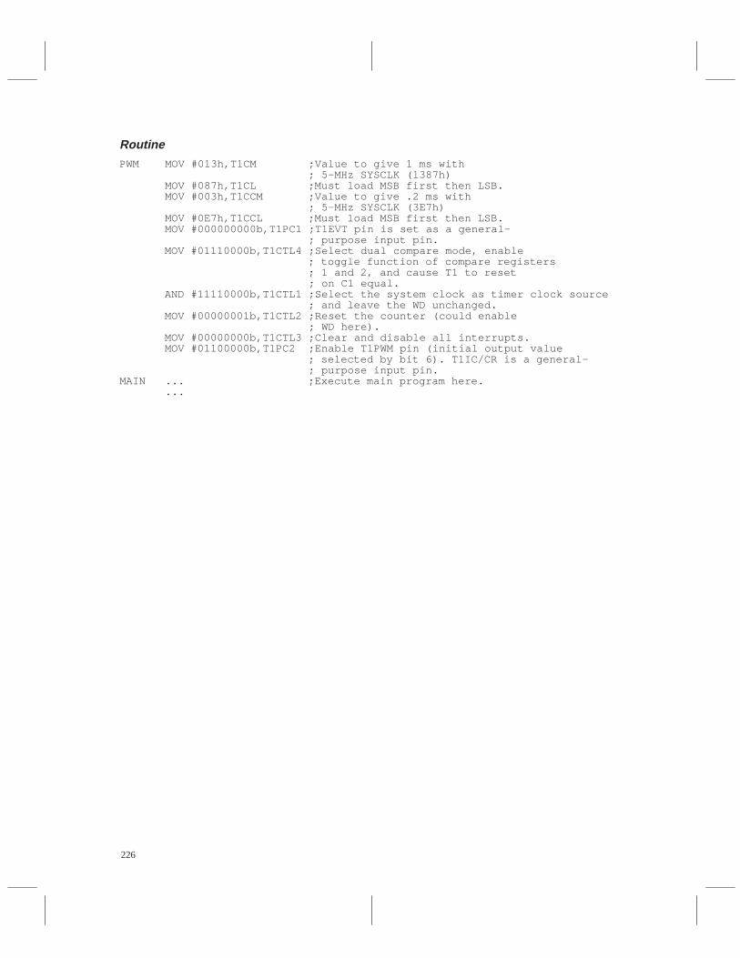
226
RoutinePWM MOV #013h,T1CM ;Value to give 1 ms with ; 5-MHz SYSCLK (1387h) MOV #087h,T1CL ;Must load MSB first then LSB. MOV #003h,T1CCM ;Value to give .2 ms with ; 5-MHz SYSCLK (3E7h) MOV #0E7h,T1CCL ;Must load MSB first then LSB. MOV #000000000b,T1PC1 ;T1EVT pin is set as a general- ; purpose input pin. MOV #01110000b,T1CTL4 ;Select dual compare mode, enable ; toggle function of compare registers ; 1 and 2, and cause T1 to reset ; on C1 equal. AND #11110000b,T1CTL1 ;Select the system clock as timer clock source ; and leave the WD unchanged. MOV #00000001b,T1CTL2 ;Reset the counter (could enable ; WD here). MOV #00000000b,T1CTL3 ;Clear and disable all interrupts. MOV #01100000b,T1PC2 ;Enable T1PWM pin (initial output value ; selected by bit 6). T1IC/CR is a general- ; purpose input pin.MAIN ... ;Execute main program here. ...
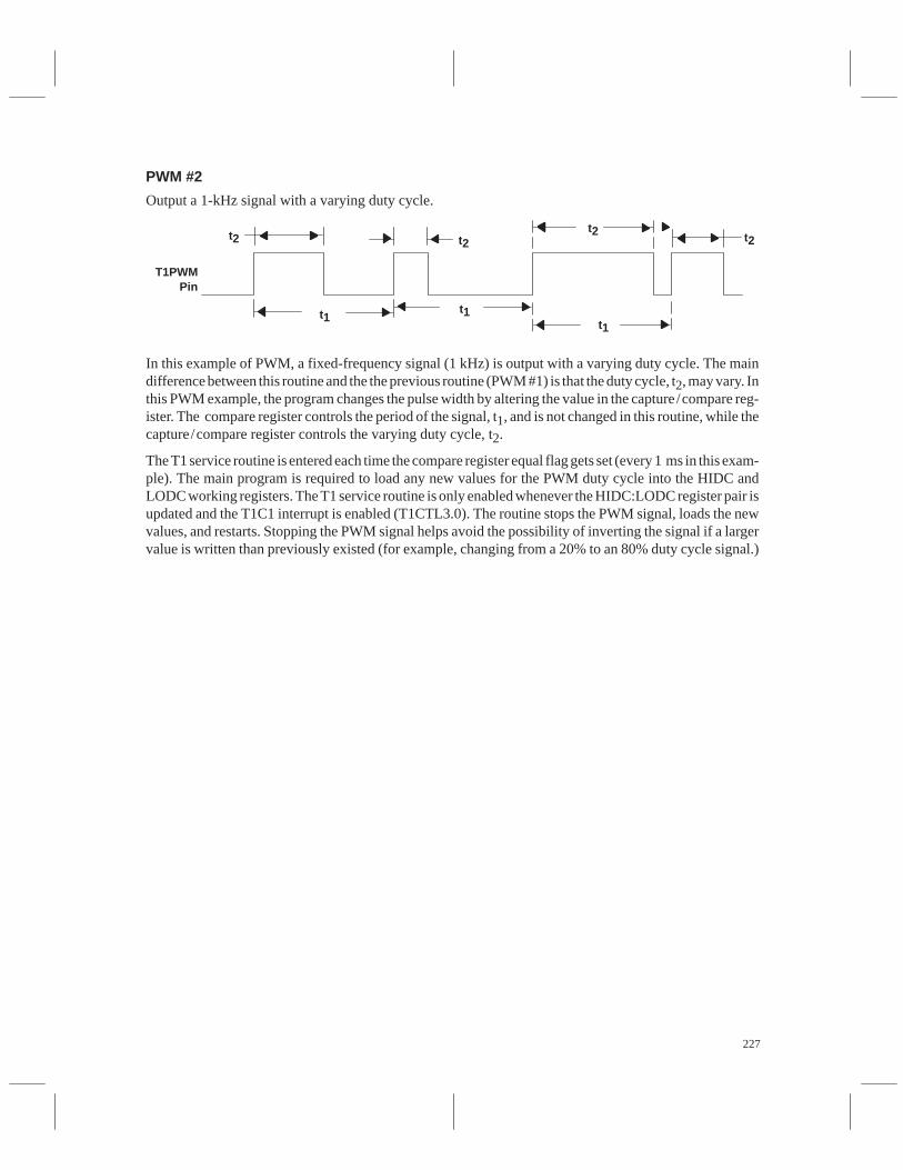
227
PWM #2
Output a 1-kHz signal with a varying duty cycle.
T1PWMPin
t1
t2 t2
t1
t2
t1
t2
In this example of PWM, a fixed-frequency signal (1 kHz) is output with a varying duty cycle. The maindifference between this routine and the the previous routine (PWM #1) is that the duty cycle, t2, may vary. Inthis PWM example, the program changes the pulse width by altering the value in the capture/compare reg-ister. The compare register controls the period of the signal, t1, and is not changed in this routine, while thecapture/compare register controls the varying duty cycle, t2.
The T1 service routine is entered each time the compare register equal flag gets set (every 1 ms in this exam-ple). The main program is required to load any new values for the PWM duty cycle into the HIDC andLODC working registers. The T1 service routine is only enabled whenever the HIDC:LODC register pair isupdated and the T1C1 interrupt is enabled (T1CTL3.0). The routine stops the PWM signal, loads the newvalues, and restarts. Stopping the PWM signal helps avoid the possibility of inverting the signal if a largervalue is written than previously existed (for example, changing from a 20% to an 80% duty cycle signal.)
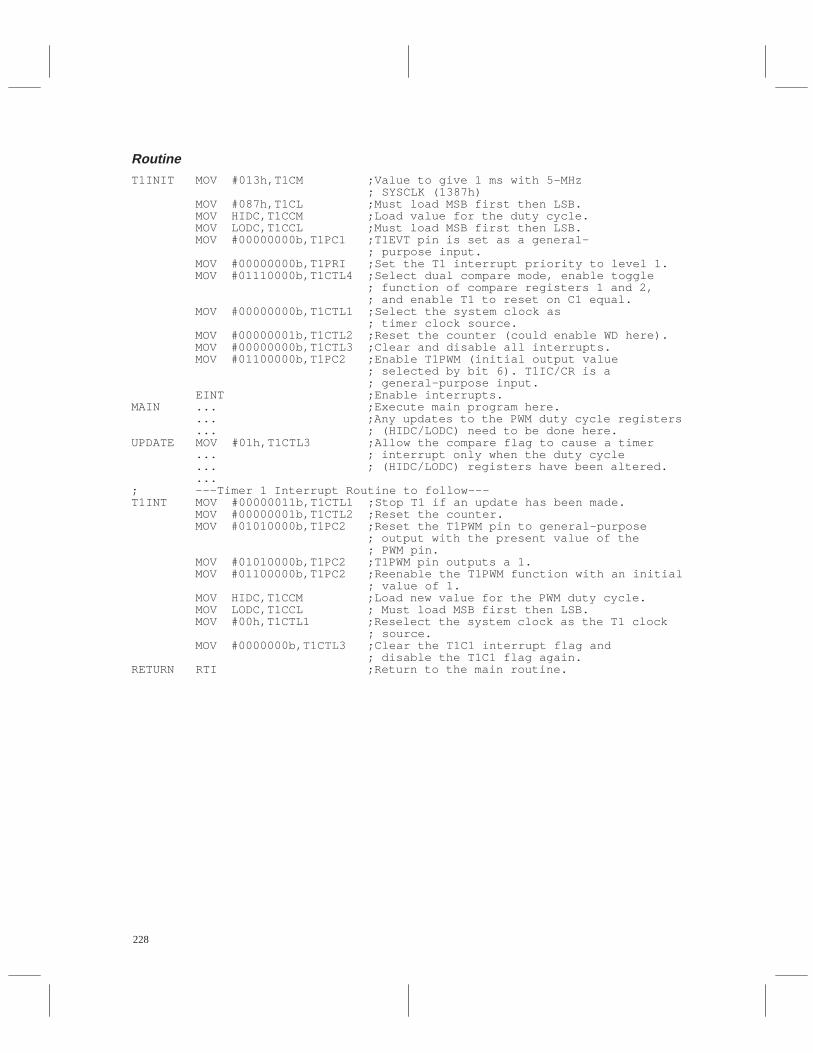
228
RoutineT1INIT MOV #013h,T1CM ;Value to give 1 ms with 5-MHz ; SYSCLK (1387h) MOV #087h,T1CL ;Must load MSB first then LSB. MOV HIDC,T1CCM ;Load value for the duty cycle. MOV LODC,T1CCL ;Must load MSB first then LSB. MOV #00000000b,T1PC1 ;T1EVT pin is set as a general- ; purpose input. MOV #00000000b,T1PRI ;Set the T1 interrupt priority to level 1. MOV #01110000b,T1CTL4 ;Select dual compare mode, enable toggle ; function of compare registers 1 and 2, ; and enable T1 to reset on C1 equal. MOV #00000000b,T1CTL1 ;Select the system clock as ; timer clock source. MOV #00000001b,T1CTL2 ;Reset the counter (could enable WD here). MOV #00000000b,T1CTL3 ;Clear and disable all interrupts. MOV #01100000b,T1PC2 ;Enable T1PWM (initial output value ; selected by bit 6). T1IC/CR is a ; general-purpose input. EINT ;Enable interrupts.MAIN ... ;Execute main program here. ... ;Any updates to the PWM duty cycle registers ... ; (HIDC/LODC) need to be done here.UPDATE MOV #01h,T1CTL3 ;Allow the compare flag to cause a timer ... ; interrupt only when the duty cycle ... ; (HIDC/LODC) registers have been altered. ...; –––Timer 1 Interrupt Routine to follow–––T1INT MOV #00000011b,T1CTL1 ;Stop T1 if an update has been made. MOV #00000001b,T1CTL2 ;Reset the counter. MOV #01010000b,T1PC2 ;Reset the T1PWM pin to general-purpose ; output with the present value of the ; PWM pin. MOV #01010000b,T1PC2 ;T1PWM pin outputs a 1. MOV #01100000b,T1PC2 ;Reenable the T1PWM function with an initial ; value of 1. MOV HIDC,T1CCM ;Load new value for the PWM duty cycle. MOV LODC,T1CCL ; Must load MSB first then LSB. MOV #00h,T1CTL1 ;Reselect the system clock as the T1 clock ; source. MOV #0000000b,T1CTL3 ;Clear the T1C1 interrupt flag and ; disable the T1C1 flag again.RETURN RTI ;Return to the main routine.
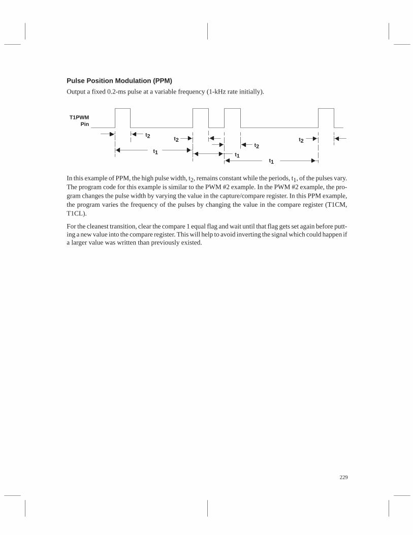
229
Pulse Position Modulation (PPM)
Output a fixed 0.2-ms pulse at a variable frequency (1-kHz rate initially).
T1PWMPin
t2 t2
t1 t1
t2t2
t1
In this example of PPM, the high pulse width, t2, remains constant while the periods, t1, of the pulses vary.The program code for this example is similar to the PWM #2 example. In the PWM #2 example, the pro-gram changes the pulse width by varying the value in the capture/compare register. In this PPM example,the program varies the frequency of the pulses by changing the value in the compare register (T1CM,T1CL).
For the cleanest transition, clear the compare 1 equal flag and wait until that flag gets set again before putt-ing a new value into the compare register. This will help to avoid inverting the signal which could happen ifa larger value was written than previously existed.
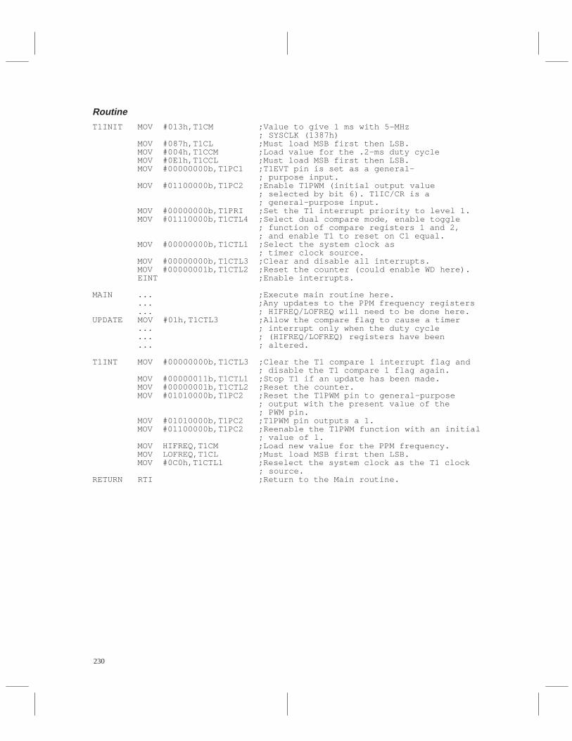
230
RoutineT1INIT MOV #013h,T1CM ;Value to give 1 ms with 5-MHz ; SYSCLK (1387h) MOV #087h,T1CL ;Must load MSB first then LSB. MOV #004h,T1CCM ;Load value for the .2-ms duty cycle MOV #0E1h,T1CCL ;Must load MSB first then LSB. MOV #00000000b,T1PC1 ;T1EVT pin is set as a general- ; purpose input. MOV #01100000b,T1PC2 ;Enable T1PWM (initial output value ; selected by bit 6). T1IC/CR is a ; general-purpose input. MOV #00000000b,T1PRI ;Set the T1 interrupt priority to level 1. MOV #01110000b,T1CTL4 ;Select dual compare mode, enable toggle ; function of compare registers 1 and 2, ; and enable T1 to reset on C1 equal. MOV #00000000b,T1CTL1 ;Select the system clock as ; timer clock source. MOV #00000000b,T1CTL3 ;Clear and disable all interrupts. MOV #00000001b,T1CTL2 ;Reset the counter (could enable WD here). EINT ;Enable interrupts.
MAIN ... ;Execute main routine here. ... ;Any updates to the PPM frequency registers ... ; HIFREQ/LOFREQ will need to be done here.UPDATE MOV #01h,T1CTL3 ;Allow the compare flag to cause a timer ... ; interrupt only when the duty cycle ... ; (HIFREQ/LOFREQ) registers have been ... ; altered.
T1INT MOV #00000000b,T1CTL3 ;Clear the T1 compare 1 interrupt flag and ; disable the T1 compare 1 flag again. MOV #00000011b,T1CTL1 ;Stop T1 if an update has been made. MOV #00000001b,T1CTL2 ;Reset the counter. MOV #01010000b,T1PC2 ;Reset the T1PWM pin to general-purpose ; output with the present value of the ; PWM pin. MOV #01010000b,T1PC2 ;T1PWM pin outputs a 1. MOV #01100000b,T1PC2 ;Reenable the T1PWM function with an initial ; value of l. MOV HIFREQ,T1CM ;Load new value for the PPM frequency. MOV LOFREQ,T1CL ;Must load MSB first then LSB. MOV #0C0h,T1CTL1 ;Reselect the system clock as the T1 clock ; source.RETURN RTI ;Return to the Main routine.
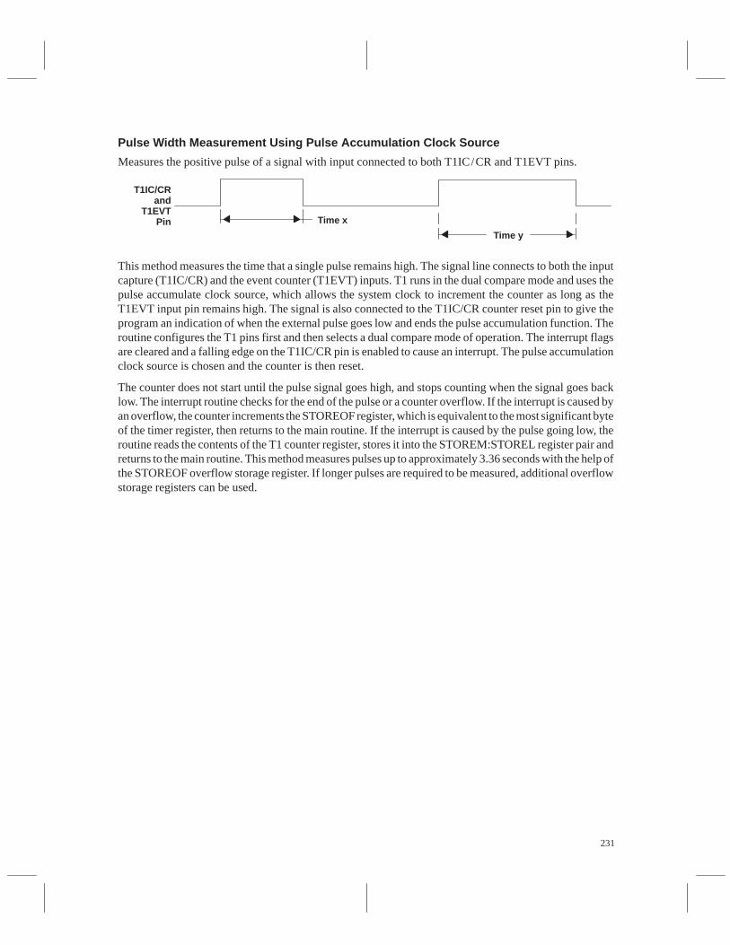
231
Pulse Width Measurement Using Pulse Accumulation Clock Source
Measures the positive pulse of a signal with input connected to both T1IC/CR and T1EVT pins.
T1IC/CRand
T1EVTPin Time x
Time y
This method measures the time that a single pulse remains high. The signal line connects to both the inputcapture (T1IC/CR) and the event counter (T1EVT) inputs. T1 runs in the dual compare mode and uses thepulse accumulate clock source, which allows the system clock to increment the counter as long as theT1EVT input pin remains high. The signal is also connected to the T1IC/CR counter reset pin to give theprogram an indication of when the external pulse goes low and ends the pulse accumulation function. Theroutine configures the T1 pins first and then selects a dual compare mode of operation. The interrupt flagsare cleared and a falling edge on the T1IC/CR pin is enabled to cause an interrupt. The pulse accumulationclock source is chosen and the counter is then reset.
The counter does not start until the pulse signal goes high, and stops counting when the signal goes backlow. The interrupt routine checks for the end of the pulse or a counter overflow. If the interrupt is caused byan overflow, the counter increments the STOREOF register, which is equivalent to the most significant byteof the timer register, then returns to the main routine. If the interrupt is caused by the pulse going low, theroutine reads the contents of the T1 counter register, stores it into the STOREM:STOREL register pair andreturns to the main routine. This method measures pulses up to approximately 3.36 seconds with the help ofthe STOREOF overflow storage register. If longer pulses are required to be measured, additional overflowstorage registers can be used.
232
Pulse Accumulation Measurement PWM Routine .REG STOREOF ;Registers used in this routine .REG STOREM .REG STOREL .REG BITS
CLR STOREOF ;Initialize the registers that will be used CLR STOREM ; in this routine. CLR STOREL CLR BITS
TIMEPULSMOV #00000010b,T1PC1 ;T1EVT and T1IC/CR pins enabled; T1PWM pin MOV #00000010b,T1PC2 ; is set up as general-purpose input pin. MOV #00,T1PRI ;Select level 1 interrupts for T1. MOV #00000001b,T1CTL4 ;Select dual compare mode and watch for ; a falling edge on the T1IC/CR pin. MOV #00000001b,T1CTL1 ;Select the pulse accumulate clock source. MOV #00000100b,T1CTL3 ;Clear interrupt flags, enable falling ; edge on the T1IC/CR pin to cause ; an interrupt. MOV #00010001b,T1CTL2 ;Reset the counter, clear and enable the ; the overflow interrupt. (Could enable WD ; here.) EINT ;Enable interrupts. ...MAIN ... ;Main routine here. ...; –– T1 interrupt routine to follow ––T1INT BTJO #08h,T1CTL2,OVERFLW ;Was this interrupt caused by overflow? AND #0F7h,T1CTL2 ; Yes, jump to OVERFLW. MOV T1CNTRL,STOREL ; No, load the value in the T1CNTRL MOV T1CNTRM,STOREM ; registers (LSB first) into the STORE ; registers. MOV #00000100b,T1CTL3 ;Clear the T1IC/CR flag. MOV #00000001b,T1CTL4 ;Reenable the T1IC/CR falling edge detect. OR #00000001b,BITS ;Signal to main routine that pulse was read. ; BITS register may be used by main routine. MOV #00000001b,T1CTL2 ;Reset the counter. RTI ;Return from interrupt.OVERFLW AND #11110111b,T1CTL2 ;Clear the overflow flag, then increment # INC STOREOF ; of overflows (equivalent timer bits ; 16–23). RTI ;Return from interrupt.

233
Counting External Pulses Relative to an External Signal
Determines the number of external clock pulses per measure signal with the measure signal attached to theT1IC/CR pin and the clock signal attached to the T1EVT pin.
T1IC/CR
T1EVT
Measure Signal
Clock Signal
In this example, two signals are input to the processor, a measure signal and a clock signal. The goal is todetermine how many clock signals happen during one high pulse of the measure signal. The clock signalconnects to the T1EVT pin and the measure signal connects to the T1IC/CR pin. The clock signal will nowincrement the counter instead of the system clock as in the previous example. Because clock continues torun after measure goes low, the timer module will run in the capture/compare mode and use the 16-bit cap-ture/compare register to store the value of the counter the instant that measure goes low.
One condition can occur when a counter overflow happens at almost exactly the same time the measuresignal goes low, so that both interrupt flags are set. The problem is then whether or not to increment theMSB counter register (STOREOF). If the capture register reads FFxxh, then the counter overflowed justafter the measure signal went low. If the register reads 00xxh, the counter overflowed just before the mea-sure pulse went low, so the MSB counter register (STOREOF) should be incremented.
234
External Pulse Counting Routine .REG STOREOF ;Registers used in this routine .REG STOREM .REG STOREL .REG BITS
CLR STOREOF ;Clear registers used to store the sum of CLR STOREM ; the T1EVT pulses. CLR STORELT1INIT MOV #02h,T1PC1 ;T1EVT and T1IC/CR pins enabled, T1PWM pin MOV #02h,T1PC2 ; set to general-purpose input pin. MOV #40h,T1PRI ;Select interrupt priority level 2 for T1. MOV #81h,T1CTL4 ;Select capture/compare mode, enable the ; T1IC/CR pin to load the capture register ; on a falling pulse. MOV #04h,T1CTL3 ;Clear the interrupt flags and enable the ; T1IC/CR pin to cause an interrupt. MOV #02h,T1CTL1 ;Choose event input as clock source. MOV #11h,T1CTL2 ;Reset the counter, clear and enable the ; overflow interrupt (WD can enable here). EINT ...; –– Interrupt routine to follow. –– T1INT ;Interrupt routine BTJZ #08h,T1CTL2,PULSELO ;Was interrupt caused by a low pulse? AND #0F7h,T1CTL2 ;No, clear overflow flag, then increment INC STOREOF ; the overflow register (STOREOF). RTIPULSELO MOV T1CCL,STOREL ;YES, load the value in the capture ; register LSB first into the STORE MOV T1CCM,STOREM ; registers. BTJZ #08h,T1CTL2,NOOVER ;Was there an overflow just now? AND #0F7h,T1CTL2 ;Yes, clear the overflow flag. CMP #0FFh,STOREM ;If overflow and pulse low, which came ; first? JEQ NOOVER ;If FFxxh, overflow happened after pulse ; low INC STOREOF ;if 00xxh, overflow happened first, ; increment register.NOOVER MOV #01h,T1CTL2 ;No, reset the counter. MOV #04h,T1CTL3 ;Clear the interrupt flag, reenable edge ; interrupt. MOV #81h,T1CTL4 ;Reenable the T1IC/CR edge detect. OR #1,BITS ;Signal to the main routine that pulse was ; read. RTI ;Return from interrupt.
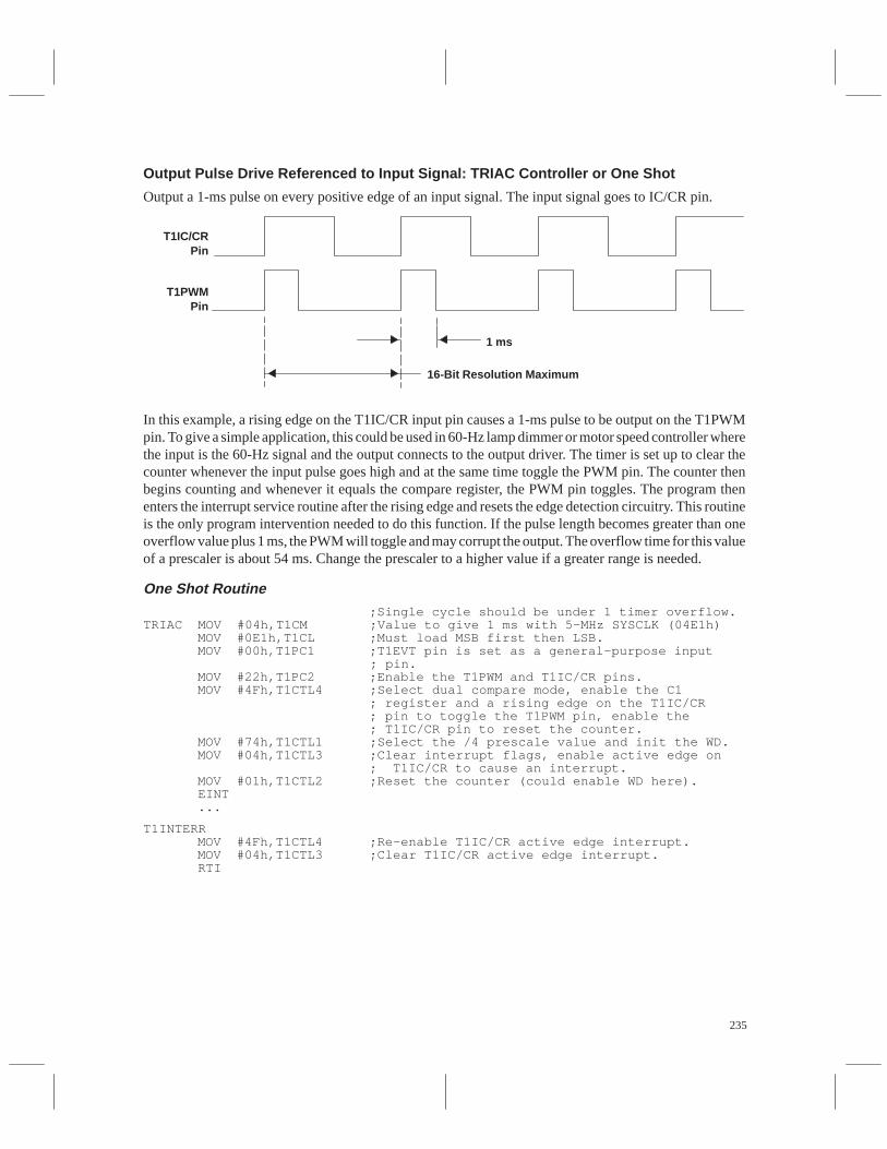
235
Output Pulse Drive Referenced to Input Signal: TRIAC Controller or One Shot
Output a 1-ms pulse on every positive edge of an input signal. The input signal goes to IC/CR pin.
T1IC/CRPin
T1PWMPin
16-Bit Resolution Maximum
1 ms
In this example, a rising edge on the T1IC/CR input pin causes a 1-ms pulse to be output on the T1PWMpin. To give a simple application, this could be used in 60-Hz lamp dimmer or motor speed controller wherethe input is the 60-Hz signal and the output connects to the output driver. The timer is set up to clear thecounter whenever the input pulse goes high and at the same time toggle the PWM pin. The counter thenbegins counting and whenever it equals the compare register, the PWM pin toggles. The program thenenters the interrupt service routine after the rising edge and resets the edge detection circuitry. This routineis the only program intervention needed to do this function. If the pulse length becomes greater than oneoverflow value plus 1 ms, the PWM will toggle and may corrupt the output. The overflow time for this valueof a prescaler is about 54 ms. Change the prescaler to a higher value if a greater range is needed.
One Shot Routine ;Single cycle should be under 1 timer overflow.TRIAC MOV #04h,T1CM ;Value to give 1 ms with 5-MHz SYSCLK (04E1h) MOV #0E1h,T1CL ;Must load MSB first then LSB. MOV #00h,T1PC1 ;T1EVT pin is set as a general-purpose input ; pin. MOV #22h,T1PC2 ;Enable the T1PWM and T1IC/CR pins. MOV #4Fh,T1CTL4 ;Select dual compare mode, enable the C1 ; register and a rising edge on the T1IC/CR ; pin to toggle the T1PWM pin, enable the ; T1IC/CR pin to reset the counter. MOV #74h,T1CTL1 ;Select the /4 prescale value and init the WD. MOV #04h,T1CTL3 ;Clear interrupt flags, enable active edge on ; T1IC/CR to cause an interrupt. MOV #01h,T1CTL2 ;Reset the counter (could enable WD here). EINT ...
T1INTERR MOV #4Fh,T1CTL4 ;Re-enable T1IC/CR active edge interrupt. MOV #04h,T1CTL3 ;Clear T1IC/CR active edge interrupt. RTI
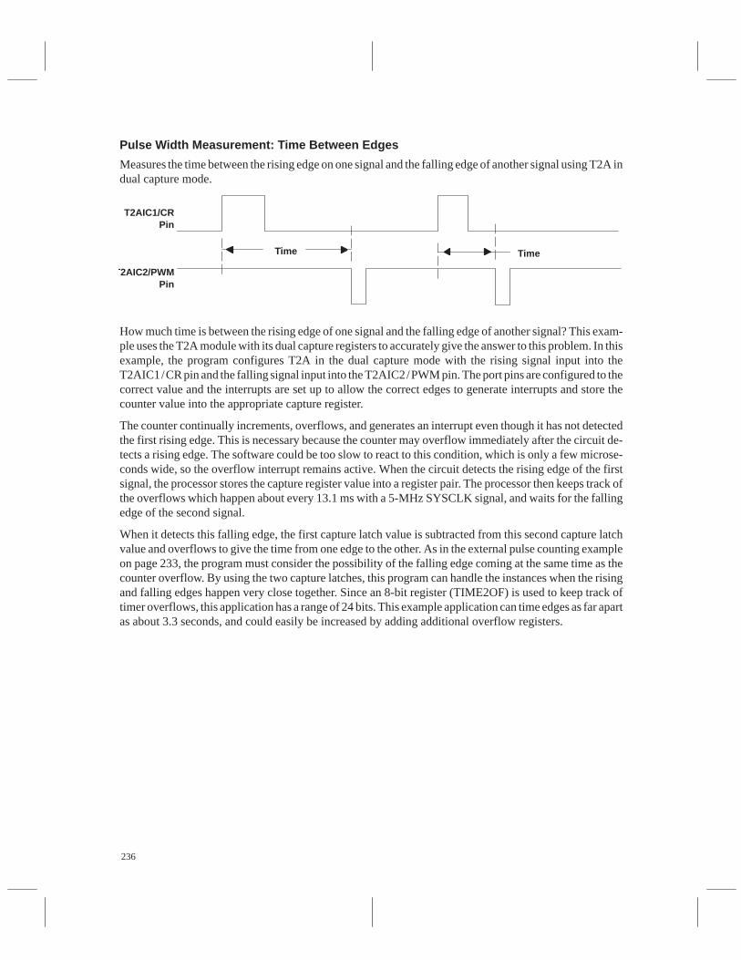
236
Pulse Width Measurement: Time Between Edges
Measures the time between the rising edge on one signal and the falling edge of another signal using T2A indual capture mode.
Time
T2AIC1/CRPin
T2AIC2/PWMPin
Time
How much time is between the rising edge of one signal and the falling edge of another signal? This exam-ple uses the T2A module with its dual capture registers to accurately give the answer to this problem. In thisexample, the program configures T2A in the dual capture mode with the rising signal input into theT2AIC1/CR pin and the falling signal input into the T2AIC2/PWM pin. The port pins are configured to thecorrect value and the interrupts are set up to allow the correct edges to generate interrupts and store thecounter value into the appropriate capture register.
The counter continually increments, overflows, and generates an interrupt even though it has not detectedthe first rising edge. This is necessary because the counter may overflow immediately after the circuit de-tects a rising edge. The software could be too slow to react to this condition, which is only a few microse-conds wide, so the overflow interrupt remains active. When the circuit detects the rising edge of the firstsignal, the processor stores the capture register value into a register pair. The processor then keeps track ofthe overflows which happen about every 13.1 ms with a 5-MHz SYSCLK signal, and waits for the fallingedge of the second signal.
When it detects this falling edge, the first capture latch value is subtracted from this second capture latchvalue and overflows to give the time from one edge to the other. As in the external pulse counting exampleon page 233, the program must consider the possibility of the falling edge coming at the same time as thecounter overflow. By using the two capture latches, this program can handle the instances when the risingand falling edges happen very close together. Since an 8-bit register (TIME2OF) is used to keep track oftimer overflows, this application has a range of 24 bits. This example application can time edges as far apartas about 3.3 seconds, and could easily be increased by adding additional overflow registers.
237
Edge Measurement RoutineEDGES MOV #02h,T2APC1 ;Set up T2AEVT pin as general-purpose input ; pin MOV #22h,T2APC2 ;Enable T2AIC1/CR and T2AIC2/PWM pins. MOV #8Bh,T2ACTL3 ;Select dual capture mode, enable rising ; edge of T2AIC1/CR and falling edge of ; T2AIC2/PWM to load the capture registers. MOV #11h,T2ACTL1 ;Reset counter, enable T2A overflow ; interrupt. MOV #06h,T2ACTL2 ;Clear flags, enable T2AIC1/CR and ;T2AIC2/PWM edges to cause interrupts. EINT ... ;T2A interrupt routine to follow.T2AINTERR BTJO #80h,T2ACTL2,EDGE1 ;Jump on T2AIC1/CR rising edge? BTJO #40h,T2ACTL2,EDGE2 ;Jump on T2AIC2/PWM falling edge?OVERFLOW INC TIME2OF ;Neither? Increment the TIME2OF overflow ; storage register (Timer bits 16–23). AND #F6h,T2ACTL1 ;Clear overflow interrupt. RTIEDGE2 MOV T2AICL,TIME2L ;Get 2nd capture latch value LSB and store ; it. MOV T2AICM,TIME2M ;Get 2nd capture latch value MSB and store ; it. BTJZ #08h,T2ACTL1,NOOVER;Was there an overflow just now? CMP #0FFh,TIME2M ;If overflow and pulse low, which came ; first? JEQ NOOVER ;If FFxxh, overflow happened after pulse ; low. INC TIME20F ;If 00xxh, overflow happened first, ; increment register. AND #0F6h,T2ACTL1 ;Clear overflow interrupts.NOOVER MOV #06h,T2ACTL2 ;Clear edge 2 interrupts and enable edge ; 1,2 interrupts. SUB TIME1L,TIME2L ;Get the difference between the two times. SBB TIME1M,TIME2M ;Store the difference in TIME2. SBB #0,TIME2OF ;Subtract any borrows from the overflows. RTIEDGE1 AND #62,T2ACTL2 ;Disable T2AIC1/CR interrupt untilT2AIC2/PWM ; edge occurs. CLR TIME2OF ;Reinitialize the TIME2OF overflow ; register. MOV T2ACCL,TIME1L ;Get 1st capture latch value LSB and store ; it. MOV T2ACCM,TIME1M ;Get 1st capture latch value MSB. RTI
NOTE: This code can work for T2A as well as T2B Timer Modules.
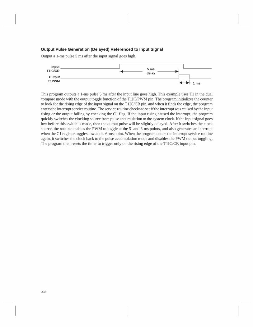
238
Output Pulse Generation (Delayed) Referenced to Input Signal
Output a 1-ms pulse 5 ms after the input signal goes high.
1 ms
InputT1IC/CR
OutputT1PWM
5 msdelay
This program outputs a 1-ms pulse 5 ms after the input line goes high. This example uses T1 in the dualcompare mode with the output toggle function of the T1IC/PWM pin. The program initializes the counterto look for the rising edge of the input signal on the T1IC/CR pin, and when it finds the edge, the programenters the interrupt service routine. The service routine checks to see if the interrupt was caused by the inputrising or the output falling by checking the C1 flag. If the input rising caused the interrupt, the programquickly switches the clocking source from pulse accumulation to the system clock. If the input signal goeslow before this switch is made, then the output pulse will be slightly delayed. After it switches the clocksource, the routine enables the PWM to toggle at the 5- and 6-ms points, and also generates an interruptwhen the C1 register toggles low at the 6-ms point. When the program enters the interrupt service routineagain, it switches the clock back to the pulse accumulation mode and disables the PWM output toggling.The program then resets the timer to trigger only on the rising edge of the T1IC/CR input pin.
239
Delayed Output Pulse Generation Routine ;Put 6 ms into C1 and 5 ms into C2. ;Input pulse must remain high at least 9 s. ;Input = T1IC/CR output = T1PWM.DELAY MOV #18h,T1CCM ;Value to give 5 ms with 5-MHz SYSCLK ; (1869h) MOV #69h,T1CCL ;Must load MSB first then LSB. MOV #1Dh,T1CM ;Value to give 6 ms with 20-MHz crystal ; (1D45h) MOV #45h,T1CL ;Must load MSB first then LSB. MOV #00h,T1PC1 ;T1EVT pin is set up as general-purpose ; input. MOV #22h,T1PC2 ;Enable the T1IC/CR and T1IC/PWM pins, and ; initialize the T1IC/PWM pin to 0. MOV #07h,T1CTL4 ;Select dual compare mode, look for rising ; edge on T1IC/CR pin, and enable edge ; detection. MOV #04h,T1CTL3 ;Clear interrupts, and enable T1IC/CR edge ; interrupts. MOV #71h,T1CTL1 ;Setup WD, clock source=pulse ; accumulator. MOV #01h,T1CTL2 ;Reset the counter (could enable WD here). EINT ...MAIN ... ;Main routine goes here. ...T1INTERR ;T1 interrupt routine to follow. BTJO #20h,T1CTL3,ENDPUL ;Jump if at end of pulse (C1 flag=1). MOV #70h,T1CTL1 ;Counter now clocked by system clock. MOV #64h,T1CTL4 ;Enable PWM outputs, disable edge detect. MOV #01h,T1CTL3 ;Clear flag, enable C1 to trigger at end. RTIENDPUL MOV #71h,T1CTL1 ;Counter now clocked by pulse accumulations. MOV #07h,T1CTL4 ;Re-enable edge interrupt, disable PWM ; output. MOV #04h,T1CTL3 ;Clear flag, enable C1 to trigger at end. RTI

240
Watchdog (WD) Operation and Initialization
A WD timer operates as a sentry to guard against improper program flow. Any time the WD is enabled tocause a system reset and then overflows without being reset by a proper value being written to the WDRSTregister, a system reset will occur. In other words, the program must write the proper values to the WDRSTkey register before the WD has a chance to time-out or the WD causes a system reset. This interaction be-tween the program and the WD helps ensure program integrity. After the WD is enabled to reset the device,it can only be disabled by removing power from the part.
WD Initialization Example
To initialize the WD to generate a system reset, do the following:
1. Select the appropriate clock source and WD overflow tap select bits (T1CTL1.4, 5, 6, and 7).
2. Clear the WD OVRFL INT FLAG bit (T1CTL2.5). This bit must be cleared in order to receiveWD-generated resets.
3. Set the WD OVRFL RST ENA bit (T1CTL2.7). Once this bit is set, only a power-up reset canclear it. For this condition to occur, VCC must fall to somewhere around 1 V. The actual trip pointdepends on variables such as processing and temperature. The device stops working before theWD OVRFL RST ENA bit gets cleared. Also, once this bit is set, the following WD bits can notbe altered until after a power-up reset:
a. WD OVRFL INT ENA (T1CTL2.6)
b. WD OVRFL INT FLAG (T1CTL2.5)
c. WD OVRFL TAP SEL (T1CTL1.7)
d. WD INPUT SELECT0–2 (T1CTL1.4–6)
e. Write 55h to the WD RESET key register (WDRST) to enable a proper reset sequence.

241
There are conditions where the program will fail to work properly due to low VCC levels and the WD willnot catch the failure. Your system should incorporate circuitry to cause a RESET when VCC is out of spec.(See Figure 11.)
If a reset occurs, the RESET subroutine needs to determine if the reset was caused by the WD or not bychecking the WD OVRFL INT FLAG (T1CTL2.5). If the reset was caused by the WD, the WD OVRFLINT FLAG bit (T1CTL2.5) must be cleared in order to receive additional WD resets.
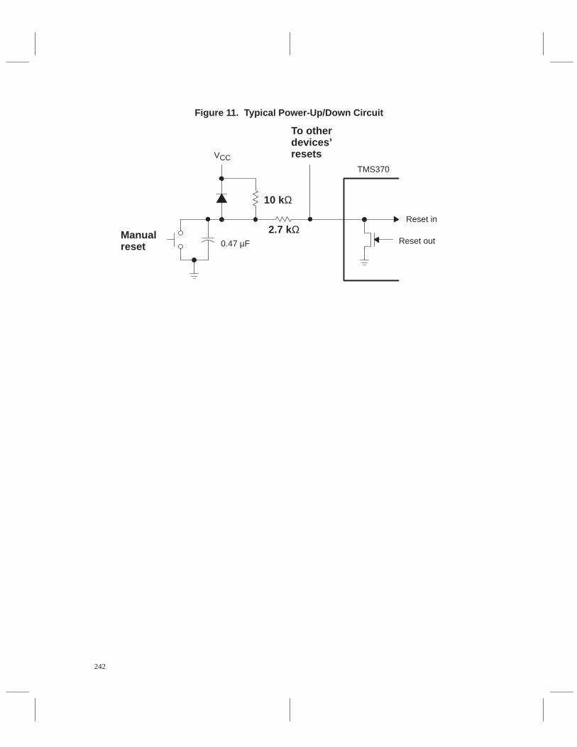
242
Figure 11. Typical Power-Up/Down Circuit
10 kΩ
VCC
2.7 kΩ
To other devices’resets
0.47 µFManualreset
Reset in
Reset out
TMS370
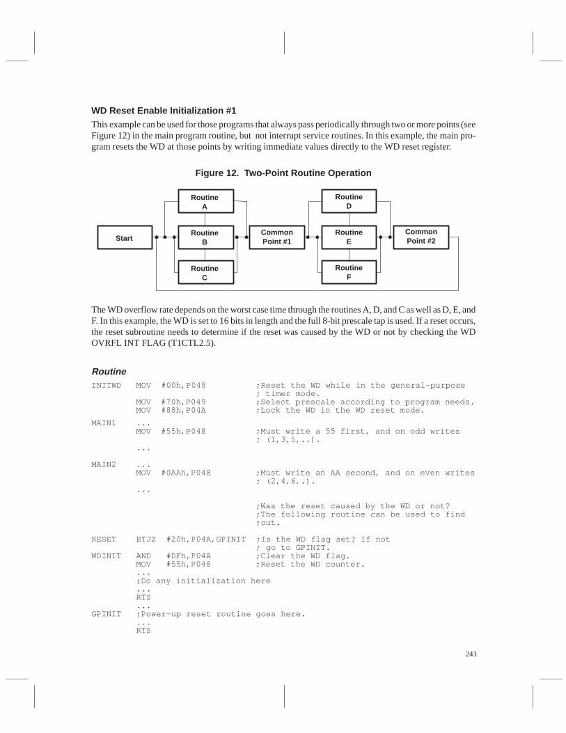
243
WD Reset Enable Initialization #1This example can be used for those programs that always pass periodically through two or more points (seeFigure 12) in the main program routine, but not interrupt service routines. In this example, the main pro-gram resets the WD at those points by writing immediate values directly to the WD reset register.
Figure 12. Two-Point Routine Operation
Start
RoutineA
RoutineB
RoutineC
CommonPoint #1
RoutineD
RoutineE
RoutineF
CommonPoint #2
The WD overflow rate depends on the worst case time through the routines A, D, and C as well as D, E, andF. In this example, the WD is set to 16 bits in length and the full 8-bit prescale tap is used. If a reset occurs,the reset subroutine needs to determine if the reset was caused by the WD or not by checking the WDOVRFL INT FLAG (T1CTL2.5).
RoutineINITWD MOV #00h,P048 ;Reset the WD while in the general-purpose ; timer mode. MOV #70h,P049 ;Select prescale according to program needs. MOV #88h,P04A ;Lock the WD in the WD reset mode.
MAIN1 ... MOV #55h,P048 ;Must write a 55 first, and on odd writes ; (1,3,5,..). ...
MAIN2 ... MOV #0AAh,P048 ;Must write an AA second, and on even writes ; (2,4,6,.). ...
;Was the reset caused by the WD or not? ;The following routine can be used to find ;out.
RESET BTJZ #20h,P04A,GPINIT ;Is the WD flag set? If not ; go to GPINIT.WDINIT AND #DFh,P04A ;Clear the WD flag. MOV #55h,P048 ;Reset the WD counter. ... ;Do any initialization here ... RTS ...GPINIT ;Power-up reset routine goes here. ... RTS
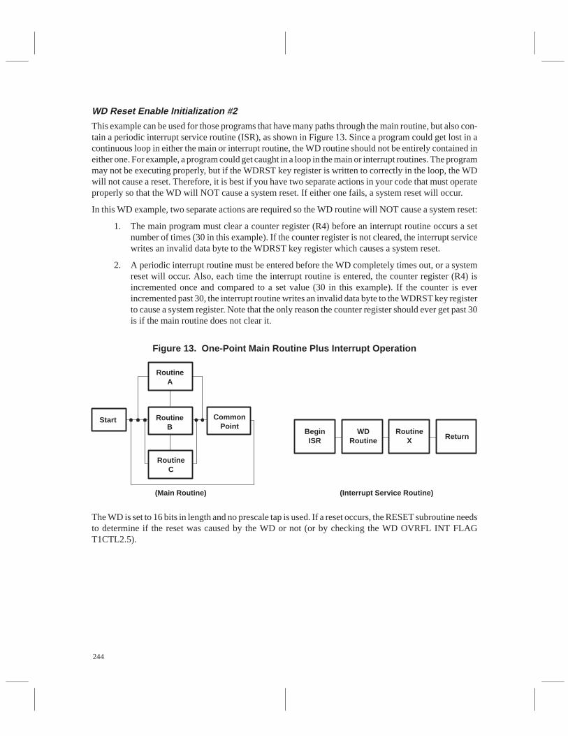
244
WD Reset Enable Initialization #2
This example can be used for those programs that have many paths through the main routine, but also con-tain a periodic interrupt service routine (ISR), as shown in Figure 13. Since a program could get lost in acontinuous loop in either the main or interrupt routine, the WD routine should not be entirely contained ineither one. For example, a program could get caught in a loop in the main or interrupt routines. The programmay not be executing properly, but if the WDRST key register is written to correctly in the loop, the WDwill not cause a reset. Therefore, it is best if you have two separate actions in your code that must operateproperly so that the WD will NOT cause a system reset. If either one fails, a system reset will occur.
In this WD example, two separate actions are required so the WD routine will NOT cause a system reset:
1. The main program must clear a counter register (R4) before an interrupt routine occurs a setnumber of times (30 in this example). If the counter register is not cleared, the interrupt servicewrites an invalid data byte to the WDRST key register which causes a system reset.
2. A periodic interrupt routine must be entered before the WD completely times out, or a systemreset will occur. Also, each time the interrupt routine is entered, the counter register (R4) isincremented once and compared to a set value (30 in this example). If the counter is everincremented past 30, the interrupt routine writes an invalid data byte to the WDRST key registerto cause a system register. Note that the only reason the counter register should ever get past 30is if the main routine does not clear it.
Figure 13. One-Point Main Routine Plus Interrupt Operation
Start
RoutineA
RoutineB
RoutineC
CommonPoint
BeginISR
WDRoutine
RoutineX Return
(Main Routine) (Interrupt Service Routine)
The WD is set to 16 bits in length and no prescale tap is used. If a reset occurs, the RESET subroutine needsto determine if the reset was caused by the WD or not (or by checking the WD OVRFL INT FLAGT1CTL2.5).
245
RoutineWDCOUNT .EQU R4WDSTORE .EQU R5
; The following routine detects whether the reset was caused by the ; WD or not.
RESET BTJZ #20h,P04A,GPINIT ;Is the WD flag set? If NOT go to GPINIT.WDINIT AND #0DFh,P04A ;Clear the WD flag. ...
;Do any initialization here you desire specific to the WD. ...
GPINIT ;Power-up reset routine goes here.
MOV #00h,P048 ;Reset the WD while in the general-purpose ; timer mode. MOV #00h,P049 ;Select prescale according to program needs. MOV #80h,P04A ;Lock the WD in the WD reset mode. ;Set up the register values used in the ; following routine. R4 used as a counter, CLR WDCOUNT ; R5 used as the storage register for the next MOV #0AAh,WDSTORE ; write to WDRST.
MAIN ... CLR WDCOUNT ;Clear the register before interrupt routine ... ; increments it past the value 30. The ; register can be cleared at several points in ; a program if necessary.
INTERR ;Interrupt routine. INC WDCOUNT ;Increment the counter register each interrupt ; routine. CMP #30,WDCOUNT ;Has the counter register been incremented to ; 30? JL PETDOG ;No, jump to PETDOG. Yes, write an invalid MOV #00,P048 ; value to WDRST. This will cause a system ; reset.
PETDOG INV WDSTORE ;Everything OK, invert old value (AA to 55, or MOV WDSTORE,P048 ; 55 to AA) then pet the watchdog to keep it ; happy. ... RTI

246
WD Initialization When System Reset is Not Desired
If a program does not use the WD reset circuit, any erroneously enabled WD can generate a reset. If theprogram also clears the WD overflow interrupt flag, then the WD reset can continue to occur until a power-down.
If a program does not use the WD circuit, then take the following actions to avoid the continuous resetcondition.
1. Assure the RESET pin is low during power up and oscillator start up.
2. Write x011xxxxb to T1CTL1 (P049) to halt clocking to the WD circuit.
3. Do not clear or write a zero to the WD overflow interrupt flag (P04A.5). Consider theread-modify-write actions of the AND and XOR instructions and use them with care at thisaddress.

247
Specific Applications
This section describes sample routines for specific applications using the timer modules.
Stepper Motor Control
This application routine uses the T1 compare register to generate an interrupt which drives a stepper motorthrough the following series of activities:
1. Start stepping the motor at a desired minimum speed of approximately 92 rpm.
2. Accelerate the motor to a desired maximum speed of approximately 1378 rpm.
3. Decelerate the motor back to the minimum speed.
4. Change the motor rotation direction and repeat from step one.
Acceleration, deceleration, and change of direction are controlled by checking bits in the flag register. Bit 7of flag is checked to determine the desired direction of rotation, while bit 0 is tested to see if the speed ofrotation should be accelerated or decelerated. If bit 0 is a 1, then the speed needs to be decreased, and con-versely if bit 0 is a 0, the speed needs to be increased.
The change of speed is accomplished by altering the value of the MSCOMP and LSCOMP workingregisters. Since the MSCOMP:LSCOMP register pair is continually loaded into the T1 compare registerduring the algorithm, any changes to the these registers between writes to the compare register will causethe compare equal interrupt period to change. If the value of the MSCOMP:LSCOMP register pairdecreases, the T1 interrupt period decreases and the motor steps faster. If the value of theMSCOMP:LSCOMP register pair increases, the T1 interrupt period increases and the motor steps slower.Change of direction is accomplished at the minimum desired speed, and is completed by altering bit 7 inthe flag register.
The hardware circuitry required for this application includes any TMS370 microcontroller with the T1module, two SN75603 chips and two SN75604 driver chips, and the stepper motor. The SN75603/4 driverchips are power peripherals with three-state outputs having the capability to sink or source currents up to2 A. Other driver chips may be used in this application. The stepper motor used in this application isconfigured with four stator poles and 25 permanent magnet rotor poles. One hundred steps are required tocomplete one revolution of the rotor, each step being 3.6 degrees. VCC for the driver chips depends on thestepper motor which is rated at 1 A at 20 V.
The schematic for the application is shown in Figure 14.
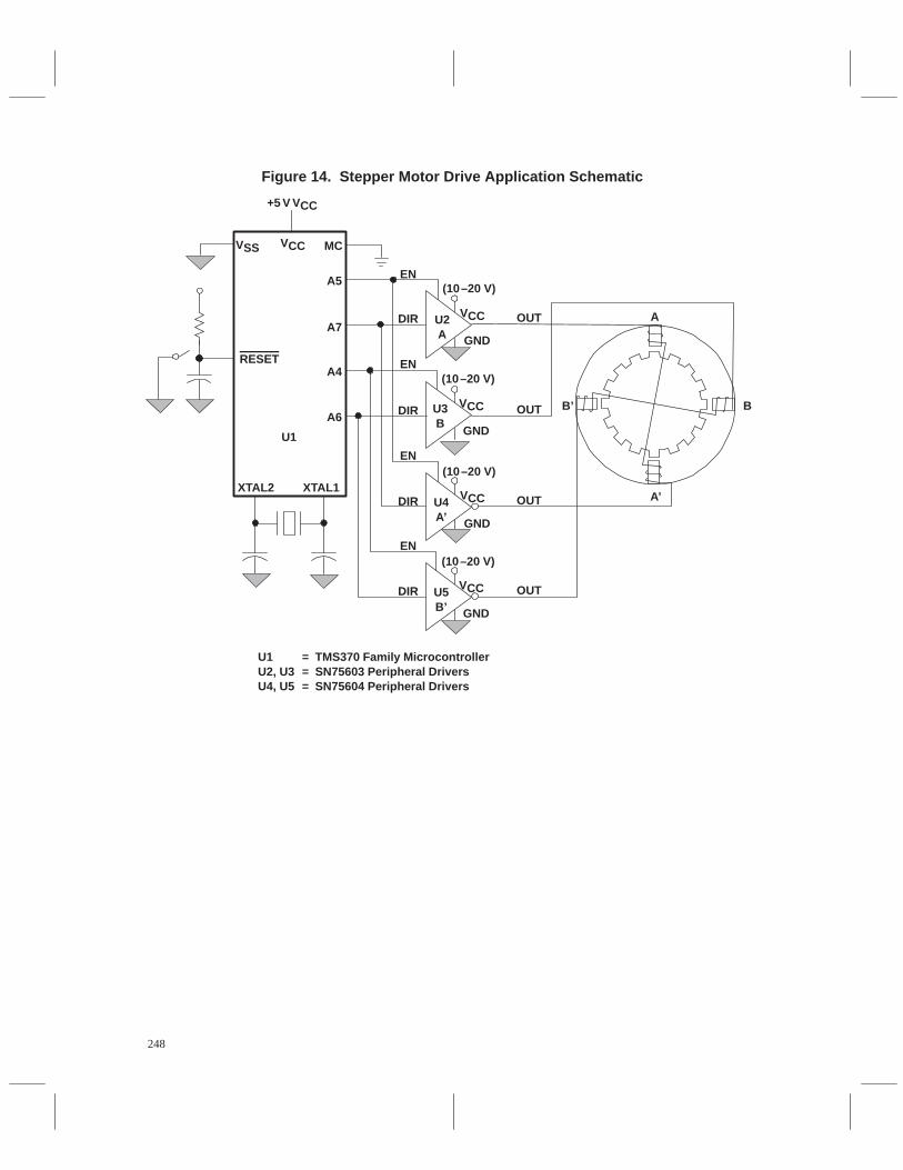
248
Figure 14. Stepper Motor Drive Application Schematic
+5 V VCC
RESET
VCCVSS MC
A5
A7
A4
A6
U1
EN
DIR
EN
DIR
EN
DIR
EN
DIR U5B’
U4A’
U3B
U2A
(10–20 V)
VCC
GND
(10–20 V)
VCC
GND
(10–20 V)
VCC
GND
(10–20 V)
VCC
GND
XTAL2 XTAL1
OUT
OUT
OUT
OUT A
A’
B’ B
U1 = TMS370 Family MicrocontrollerU2, U3 = SN75603 Peripheral DriversU4, U5 = SN75604 Peripheral Drivers
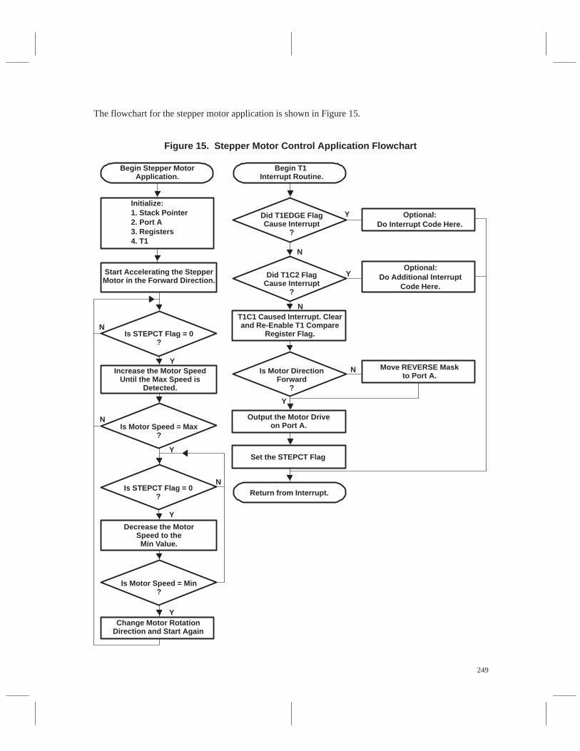
249
The flowchart for the stepper motor application is shown in Figure 15.
Figure 15. Stepper Motor Control Application Flowchart
Begin Stepper MotorApplication.
Initialize:1. Stack Pointer2. Port A3. Registers4. T1
Start Accelerating the StepperMotor in the Forward Direction.
Is STEPCT Flag = 0?
Increase the Motor SpeedUntil the Max Speed is
Detected.
Is Motor Speed = Max?
Is STEPCT Flag = 0?
Is Motor Speed = Min?
Decrease the MotorSpeed to theMin Value.
Change Motor RotationDirection and Start Again
Y
Y
Y
N
N
N
Begin T1 Interrupt Routine.
Did T1EDGE FlagCause Interrupt
?
Did T1C2 FlagCause Interrupt
?
T1C1 Caused Interrupt. Clearand Re-Enable T1 Compare
Register Flag.
Is Motor DirectionForward
?
Output the Motor Driveon Port A.
Set the STEPCT Flag
Return from Interrupt.
Y
Y
N
Y
Optional:Do Interrupt Code Here.
Optional:Do Additional Interrupt
Code Here.
Move REVERSE Maskto Port A.
N
N
Y
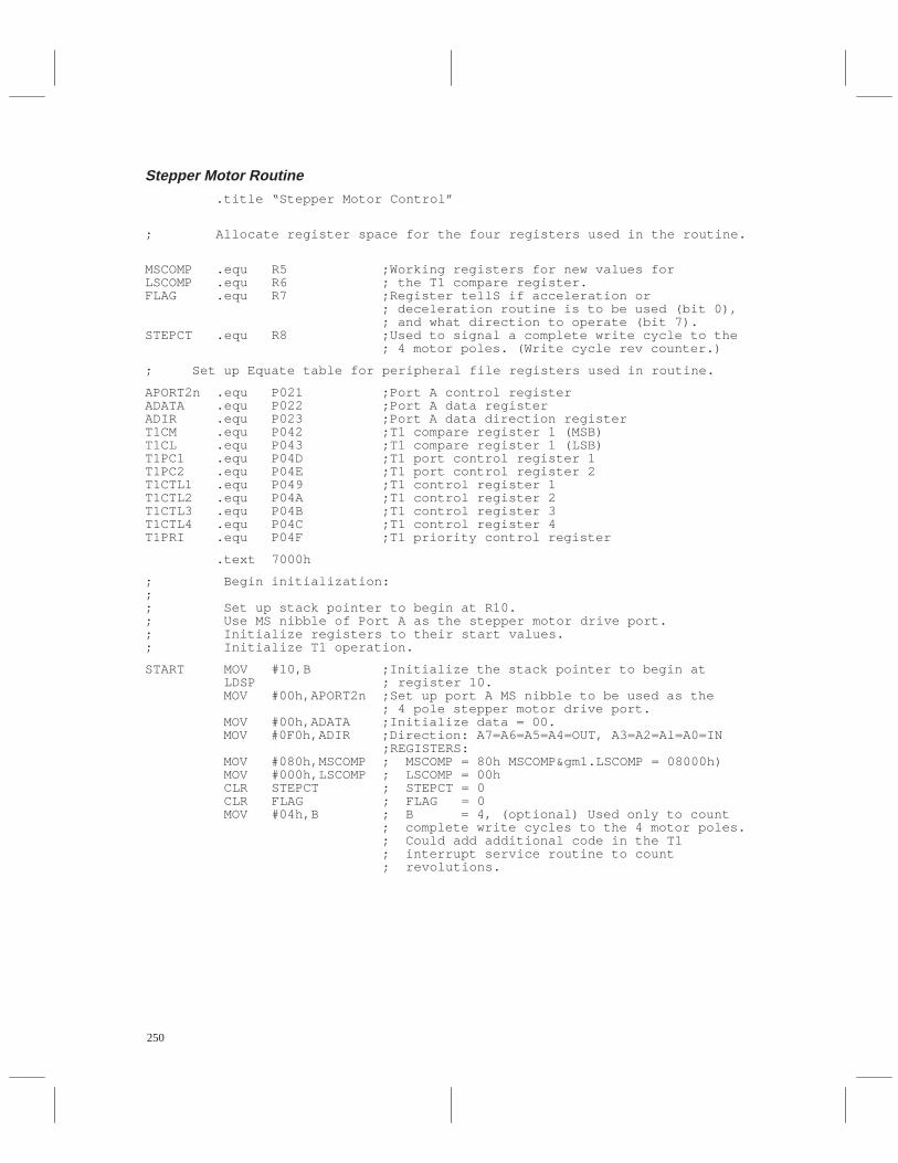
250
Stepper Motor Routine .title “Stepper Motor Control”
; Allocate register space for the four registers used in the routine.
MSCOMP .equ R5 ;Working registers for new values for LSCOMP .equ R6 ; the T1 compare register.FLAG .equ R7 ;Register tellS if acceleration or ; deceleration routine is to be used (bit 0), ; and what direction to operate (bit 7).STEPCT .equ R8 ;Used to signal a complete write cycle to the ; 4 motor poles. (Write cycle rev counter.)
; Set up Equate table for peripheral file registers used in routine.
APORT2n .equ P021 ;Port A control registerADATA .equ P022 ;Port A data registerADIR .equ P023 ;Port A data direction registerT1CM .equ P042 ;T1 compare register 1 (MSB)T1CL .equ P043 ;T1 compare register 1 (LSB)T1PC1 .equ P04D ;T1 port control register 1T1PC2 .equ P04E ;T1 port control register 2T1CTL1 .equ P049 ;T1 control register 1T1CTL2 .equ P04A ;T1 control register 2T1CTL3 .equ P04B ;T1 control register 3T1CTL4 .equ P04C ;T1 control register 4T1PRI .equ P04F ;T1 priority control register
.text 7000h
; Begin initialization:; ; Set up stack pointer to begin at R10.; Use MS nibble of Port A as the stepper motor drive port.; Initialize registers to their start values.; Initialize T1 operation.
START MOV #10,B ;Initialize the stack pointer to begin at LDSP ; register 10. MOV #00h,APORT2n ;Set up port A MS nibble to be used as the ; 4 pole stepper motor drive port. MOV #00h,ADATA ;Initialize data = 00. MOV #0F0h,ADIR ;Direction: A7=A6=A5=A4=OUT, A3=A2=Al=A0=IN ;REGISTERS: MOV #080h,MSCOMP ; MSCOMP = 80h MSCOMP&gm1.LSCOMP = 08000h) MOV #000h,LSCOMP ; LSCOMP = 00h CLR STEPCT ; STEPCT = 0 CLR FLAG ; FLAG = 0 MOV #04h,B ; B = 4, (optional) Used only to count ; complete write cycles to the 4 motor poles. ; Could add additional code in the T1 ; interrupt service routine to count ; revolutions.
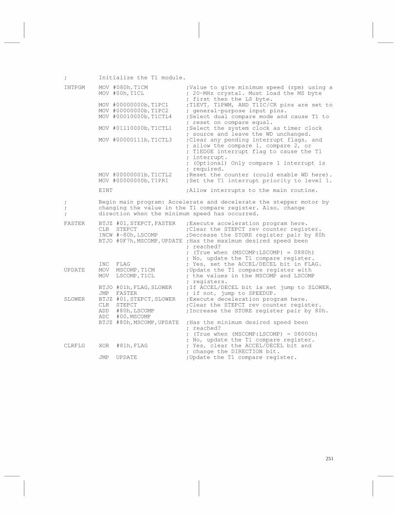
251
; Initialize the T1 module.
INTPGM MOV #080h,T1CM ;Value to give minimum speed (rpm) using a MOV #00h,T1CL ; 20-MHz crystal. Must load the MS byte ; first then the LS byte. MOV #00000000b,T1PC1 ;T1EVT, T1PWM, AND T1IC/CR pins are set to MOV #00000000b,T1PC2 ; general-purpose input pins. MOV #00010000b,T1CTL4 ;Select dual compare mode and cause T1 to ; reset on compare equal. MOV #01110000b,T1CTL1 ;Select the system clock as timer clock ; source and leave the WD unchanged. MOV #00000111b,T1CTL3 ;Clear any pending interrupt flags, and ; allow the compare 1, compare 2, or ; T1EDGE interrupt flag to cause the T1 ; interrupt. ; (Optional) Only compare 1 interrupt is ; required. MOV #00000001b,T1CTL2 ;Reset the counter (could enable WD here). MOV #00000000b,T1PRI ;Set the T1 interrupt priority to level 1.
EINT ;Allow interrupts to the main routine.
; Begin main program: Accelerate and decelerate the stepper motor by; changing the value in the T1 compare register. Also, change; direction when the minimum speed has occurred.
FASTER BTJZ #01,STEPCT,FASTER ;Execute acceleration program here. CLR STEPCT ;Clear the STEPCT rev counter register. INCW #–80h,LSCOMP ;Decrease the STORE register pair by 80h BTJO #0F7h,MSCOMP,UPDATE ;Has the maximum desired speed been ; reached? ; (True when (MSCOMP:LSCOMP) = 0880h) ; No, update the T1 compare register. INC FLAG ; Yes, set the ACCEL/DECEL bit in FLAG.UPDATE MOV MSCOMP,T1CM ;Update the T1 compare register with MOV LSCOMP,T1CL ; the values in the MSCOMP and LSCOMP ; registers. BTJO #01h,FLAG,SLOWER ;If ACCEL/DECEL bit is set jump to SLOWER, JMP FASTER ; if not, jump to SPEEDUP.SLOWER BTJZ #01,STEPCT,SLOWER ;Execute deceleration program here. CLR STEPCT ;Clear the STEPCT rev counter register. ADD #80h,LSCOMP ;Increase the STORE register pair by 80h. ADC #00,MSCOMP BTJZ #80h,MSCOMP,UPDATE ;Has the minimum desired speed been ; reached? ; (True when (MSCOMP:LSCOMP) = 08000h) ; No, update the T1 compare register.CLRFLG XOR #81h,FLAG ; Yes, clear the ACCEL/DECEL bit and ; change the DIRECTION bit. JMP UPDATE ;Update the T1 compare register.
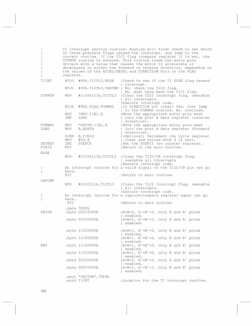
252
; T1 interrupt service routine: Routine will first check to see which; of three possible flags caused the interrupt, and jump to the; correct routine. If the T1C1 flag (compare register 1) is set, the; STPMTR routine is entered. This routine loads the motor pole ; drivers with a value that causes the motor to accelerate or ; decelerate in either the forward or reverse direction, depending on; the values of the ACCEL/DECEL and DIRECTION bits in the FLAG; register.
T1INT BTJO #80h,T1CTL3,EDGE ;Check to see if the T1 EDGE flag caused ; interrupt. BTJO #40h,T1CTL3,CAPCMP ; No, check the T1C2 flag. ; No, must have been the T1C1 flag.STPMTR MOV #11000111b,T1CTL3 ;Clear the T1C1 interrupt flag, reenable ; all interrupts. ;Execute interrupt code. BTJZ #80h,FLAG,FORWRD ;Is DIRECTION bit clear? Yes, then jump ; to the FORWRD routine. No, continue. MOV *REV–1[B],A ;Move the appropriate motor pole mask JMP LOAD ; into the port A data register (reverse ; direction).FORWRD MOV *DRIVE–1[B],A ;Move the appropriate motor pole mask LOAD MOV A,ADATA ; into the port A data register (forward ; direction). DJNZ B,FINIS ;(Optional) Decrement the cycle register MOV #04,B ; count and reload with 4 if zero.SETREV INC STEPCT ;Set the STEPCT rev counter register.FINIS RTI ;Return to the main routine.
EDGE MOV #01100111b,T1CTL3 ;Clear the T1IC/CR interrupt flag, ; reenable all interrupts ;Execute interrupt code.; An interrupt routine for a valid signal on the T1IC/CR pin can go; here. RTI ;Return to main routine.
CAPCMP MOV #0100111b,T1CTL3 ;Clear the T1C2 interrupt flag, reenable ; all interrupts. ;Execute interrupt code.; An interrupt routine for a capture/compare register equal can go; here. RTI ;Return to main routine.
.data 7E00hDRIVE .byte 00010000b ;A=B=0, A’=B’=1, only B and B’ poles ; enabled. .byte 00100000b ;A=B=0, A’=B’=1, only A and A’ poles ; enabled.
.byte 11010000b ;A=B=1, A’=B’=0, only B and B’ poles ; enabled. .byte 11100000b ;A=B=1, A’=B’=0, only B and B’ poles ; enabled.REV .byte 11100000b ;A=B=1, A’=B’=0, only B and B’ poles ; enabled. .byte 11010000b ;A=B=1, A’=B’=0, only B and B’ poles ; enabled. .byte 00100000b ;A=B=0, A’=B’=1, only A and A’ poles ; enabled. .byte 00010000b ;A=B=0, A’=B’=1, only B and B’ poles ; enabled.
.sect ”VECTOR”,7FF4h .word T1INT ;Location for the T1 interrupt routine.

253
.word START ; All other interrupt vectors point to .word START ; the reset vector. .word START .word START .word START .end

254
Time-of-Day Clock Application Routine
This application routine uses the T1 compare register to generate an interrupt service routine every 1/10second (100 ms), which will be used to update a time-of-day clock. The value required by the compareregister to generate a 100-ms interrupt period with a 5-MHz SYSCLK is 07A11h . See page 217 for formulaand look-up table.
The application software uses five registers to keep track of hours, minutes, seconds, tenths of seconds, andan AM/PM mode flag. Additional code and circuitry may be added for external time setting control andcalendar application requirements. See page 258.
The flowchart for the application is shown in Figure 16.
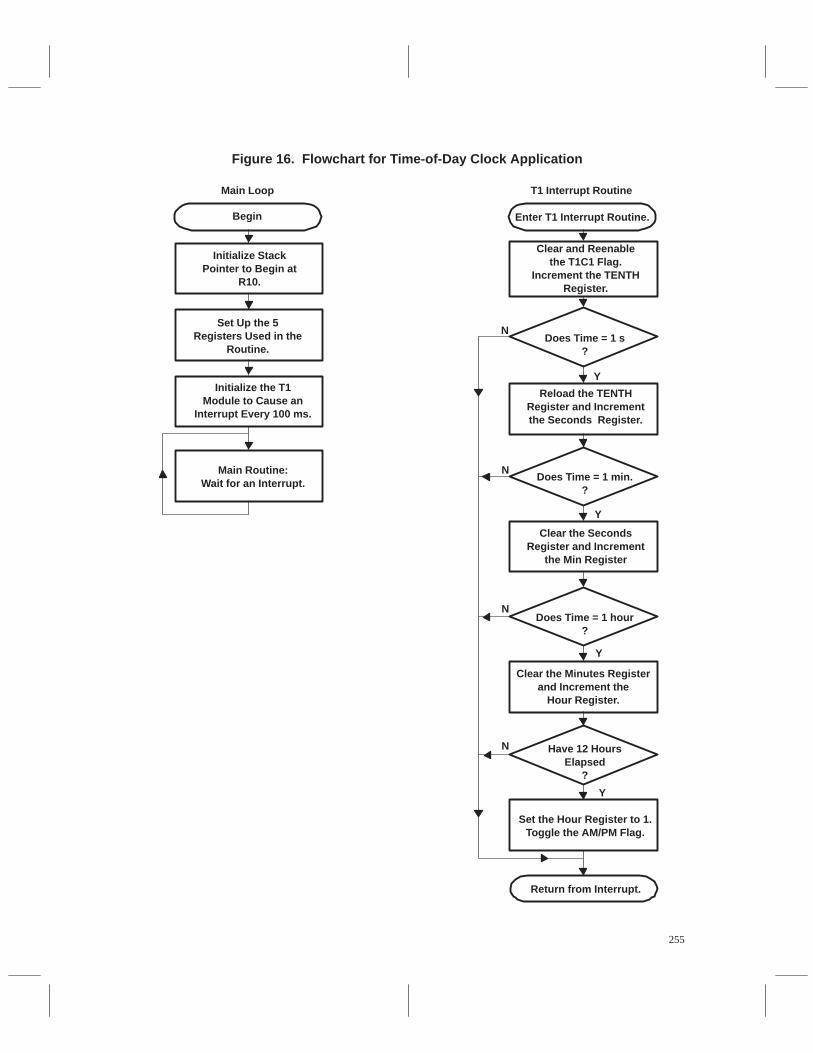
255
Figure 16. Flowchart for Time-of-Day Clock Application
Main Loop T1 Interrupt Routine
Begin
Initialize StackPointer to Begin at
R10.
Set Up the 5Registers Used in the
Routine.
Initialize the T1Module to Cause an
Interrupt Every 100 ms.
Main Routine:Wait for an Interrupt.
Enter T1 Interrupt Routine.
Clear and Reenablethe T1C1 Flag.
Increment the TENTHRegister.
Does Time = 1 s?
Does Time = 1 min.?
Reload the TENTHRegister and Incrementthe Seconds Register.
Clear the SecondsRegister and Increment
the Min Register
Does Time = 1 hour?
Clear the Minutes Registerand Increment the
Hour Register.
Have 12 HoursElapsed
?
Set the Hour Register to 1.Toggle the AM/PM Flag.
Return from Interrupt.
N
Y
Y
Y
Y
N
N
N
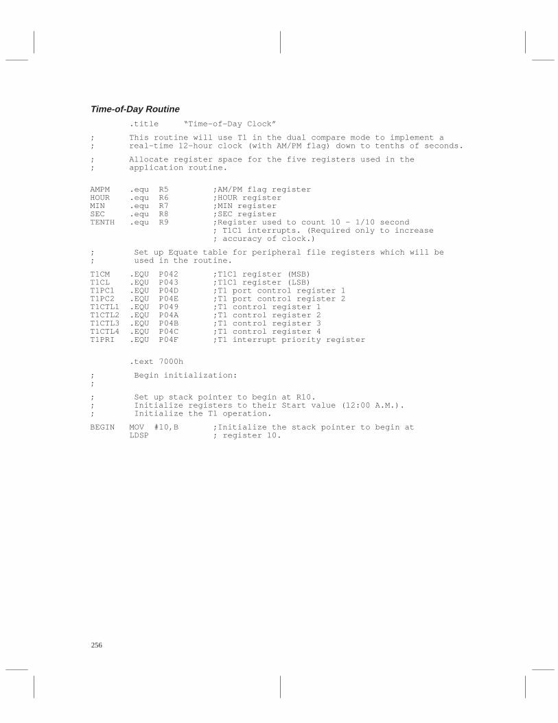
256
Time-of-Day Routine .title “Time-of-Day Clock”
; This routine will use T1 in the dual compare mode to implement a; real-time 12-hour clock (with AM/PM flag) down to tenths of seconds.
; Allocate register space for the five registers used in the; application routine.
AMPM .equ R5 ;AM/PM flag registerHOUR .equ R6 ;HOUR registerMIN .equ R7 ;MIN registerSEC .equ R8 ;SEC registerTENTH .equ R9 ;Register used to count 10 – 1/10 second ; T1C1 interrupts. (Required only to increase ; accuracy of clock.)
; Set up Equate table for peripheral file registers which will be; used in the routine.
T1CM .EQU P042 ;T1C1 register (MSB)T1CL .EQU P043 ;T1C1 register (LSB)T1PC1 .EQU P04D ;T1 port control register 1T1PC2 .EQU P04E ;T1 port control register 2T1CTL1 .EQU P049 ;T1 control register 1T1CTL2 .EQU P04A ;T1 control register 2T1CTL3 .EQU P04B ;T1 control register 3T1CTL4 .EQU P04C ;T1 control register 4T1PRI .EQU P04F ;T1 interrupt priority register
.text 7000h
; Begin initialization:;
; Set up stack pointer to begin at R10.; Initialize registers to their Start value (12:00 A.M.).; Initialize the T1 operation.
BEGIN MOV #10,B ;Initialize the stack pointer to begin at LDSP ; register 10.
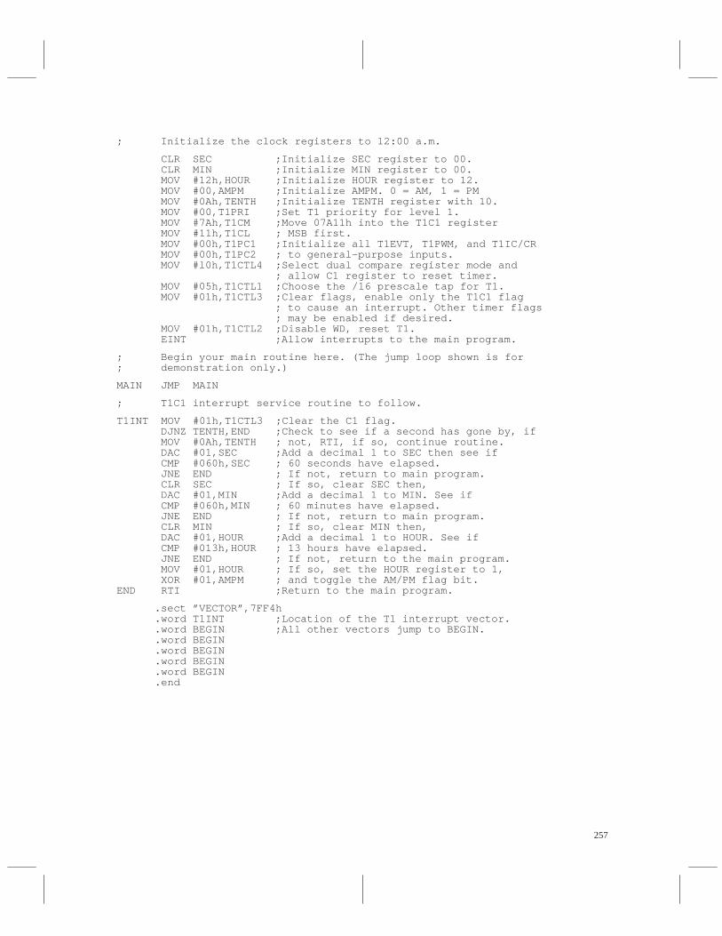
257
; Initialize the clock registers to 12:00 a.m.
CLR SEC ;Initialize SEC register to 00. CLR MIN ;Initialize MIN register to 00. MOV #12h,HOUR ;Initialize HOUR register to 12. MOV #00,AMPM ;Initialize AMPM. 0 = AM, 1 = PM MOV #0Ah,TENTH ;Initialize TENTH register with 10. MOV #00,T1PRI ;Set T1 priority for level 1. MOV #7Ah,T1CM ;Move 07A11h into the T1C1 register MOV #11h,T1CL ; MSB first. MOV #00h,T1PC1 ;Initialize all T1EVT, T1PWM, and T1IC/CR MOV #00h,T1PC2 ; to general-purpose inputs. MOV #l0h,T1CTL4 ;Select dual compare register mode and ; allow C1 register to reset timer. MOV #05h,T1CTL1 ;Choose the /16 prescale tap for T1. MOV #01h,T1CTL3 ;Clear flags, enable only the T1C1 flag ; to cause an interrupt. Other timer flags ; may be enabled if desired. MOV #01h,T1CTL2 ;Disable WD, reset T1. EINT ;Allow interrupts to the main program.
; Begin your main routine here. (The jump loop shown is for; demonstration only.)
MAIN JMP MAIN
; T1C1 interrupt service routine to follow.
T1INT MOV #01h,T1CTL3 ;Clear the C1 flag. DJNZ TENTH,END ;Check to see if a second has gone by, if MOV #0Ah,TENTH ; not, RTI, if so, continue routine. DAC #01,SEC ;Add a decimal 1 to SEC then see if CMP #060h,SEC ; 60 seconds have elapsed. JNE END ; If not, return to main program. CLR SEC ; If so, clear SEC then, DAC #01,MIN ;Add a decimal 1 to MIN. See if CMP #060h,MIN ; 60 minutes have elapsed. JNE END ; If not, return to main program. CLR MIN ; If so, clear MIN then, DAC #01,HOUR ;Add a decimal 1 to HOUR. See if CMP #013h,HOUR ; 13 hours have elapsed. JNE END ; If not, return to the main program. MOV #01,HOUR ; If so, set the HOUR register to 1, XOR #01,AMPM ; and toggle the AM/PM flag bit.END RTI ;Return to the main program.
.sect ”VECTOR”,7FF4h .word T1INT ;Location of the T1 interrupt vector. .word BEGIN ;All other vectors jump to BEGIN. .word BEGIN .word BEGIN .word BEGIN .word BEGIN .end
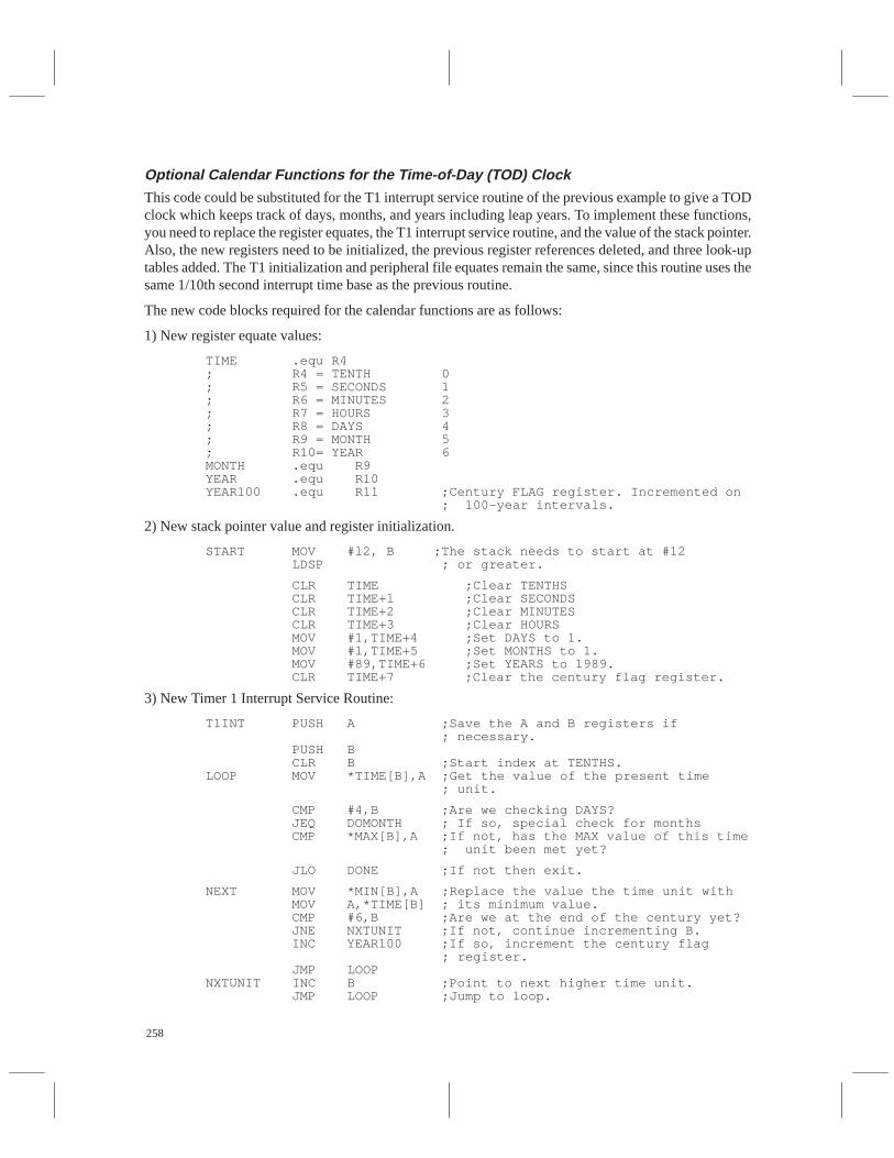
258
Optional Calendar Functions for the Time-of-Day (TOD) Clock
This code could be substituted for the T1 interrupt service routine of the previous example to give a TODclock which keeps track of days, months, and years including leap years. To implement these functions,you need to replace the register equates, the T1 interrupt service routine, and the value of the stack pointer.Also, the new registers need to be initialized, the previous register references deleted, and three look-uptables added. The T1 initialization and peripheral file equates remain the same, since this routine uses thesame 1/10th second interrupt time base as the previous routine.
The new code blocks required for the calendar functions are as follows:
1) New register equate values:
TIME .equ R4; R4 = TENTH 0; R5 = SECONDS 1; R6 = MINUTES 2; R7 = HOURS 3; R8 = DAYS 4; R9 = MONTH 5; R10= YEAR 6MONTH .equ R9YEAR .equ R10YEAR100 .equ R11 ;Century FLAG register. Incremented on ; 100-year intervals.
2) New stack pointer value and register initialization.
START MOV #l2, B ;The stack needs to start at #12 LDSP ; or greater.
CLR TIME ;Clear TENTHS CLR TIME+l ;Clear SECONDS CLR TIME+2 ;Clear MINUTES CLR TIME+3 ;Clear HOURS MOV #1,TIME+4 ;Set DAYS to 1. MOV #l,TIME+5 ;Set MONTHS to 1. MOV #89,TIME+6 ;Set YEARS to 1989. CLR TIME+7 ;Clear the century flag register.
3) New Timer 1 Interrupt Service Routine:
T1INT PUSH A ;Save the A and B registers if ; necessary. PUSH B CLR B ;Start index at TENTHS.LOOP MOV *TIME[B],A ;Get the value of the present time ; unit.
CMP #4,B ;Are we checking DAYS? JEQ DOMONTH ; If so, special check for months CMP *MAX[B],A ;If not, has the MAX value of this time ; unit been met yet?
JLO DONE ;If not then exit.
NEXT MOV *MIN[B],A ;Replace the value the time unit with MOV A,*TIME[B] ; its minimum value. CMP #6,B ;Are we at the end of the century yet? JNE NXTUNIT ;If not, continue incrementing B. INC YEAR100 ;If so, increment the century flag ; register. JMP LOOPNXTUNIT INC B ;Point to next higher time unit. JMP LOOP ;Jump to loop.
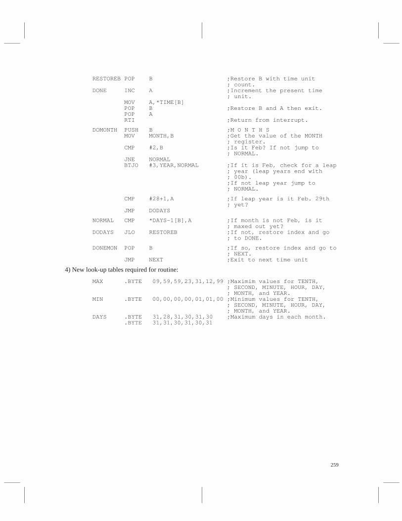
259
RESTOREB POP B ;Restore B with time unit ; count.DONE INC A ;Increment the present time ; unit. MOV A,*TIME[B] POP B ;Restore B and A then exit. POP A RTI ;Return from interrupt.
DOMONTH PUSH B ;M O N T H S MOV MONTH,B ;Get the value of the MONTH ; register. CMP #2,B ;Is it Feb? If not jump to ; NORMAL. JNE NORMAL BTJO #3,YEAR,NORMAL ;If it is Feb, check for a leap ; year (leap years end with ; 00b). ;If not leap year jump to ; NORMAL.
CMP #28+1,A ;If leap year is it Feb. 29th ; yet? JMP DODAYS
NORMAL CMP *DAYS–1[B],A ;If month is not Feb, is it ; maxed out yet?DODAYS JLO RESTOREB ;If not, restore index and go ; to DONE.
DONEMON POP B ;If so, restore index and go to ; NEXT. JMP NEXT ;Exit to next time unit
4) New look-up tables required for routine:
MAX .BYTE 09,59,59,23,31,12,99 ;Maximim values for TENTH, ; SECOND, MINUTE, HOUR, DAY, ; MONTH, and YEAR.MIN .BYTE 00,00,00,00,01,01,00 ;Minimum values for TENTH, ; SECOND, MINUTE, HOUR, DAY, ; MONTH, and YEAR.DAYS .BYTE 31,28,31,30,31,30 ;Maximum days in each month. .BYTE 31,31,30,31,30,31

260
Frequency Counter Application
This routine uses the T1 module in a frequency counter application. The frequency is calculated by keepingtrack of the number of pulses for one second. The pulse count is input on the T1IC/CR pin, and the T1compare register is set up to give a one-second interrupt. The value required by the compare register togenerate a one-second interrupt period with a 5-MHz SYSCLK is 04C4Ah with a /256 prescale. See page217 for formula and look-up table. This counter application is designed to measure an input signal from1 Hz to approximately 60 kHz.
A series of three registers keeps a decimal count of the number of pulses seen on the T1IC/CR pin untilthe compare equal interrupt is detected. After each T1 compare equal interrupt, the values in the COUNTXregisters are loaded into the STOREX registers for use by your program. The COUNTX registers are thencleared and ready to keep count of any pulses during the next second.
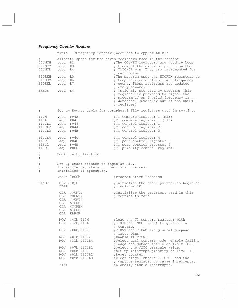
261
Frequency Counter Routine
.title “Frequency Counter”;accurate to approx 60 kHz
; Allocate space for the seven registers used in the routine.COUNTH .equ R2 ;The COUNTX registers are used to keep COUNTM .equ R3 ; track of the external pulses on the COUNTL .equ R4 ; T1IC/CR pin. They are incremented for ; each pulse.STOREH .equ R5 ;The program uses the STOREX registers toSTOREM .equ R6 ; keep, a record of the last frequency STOREL .equ R7 ; count. These registers are updated ; every second.ERROR .equ R8 ;(Optional, not used by program) This ; register is provided to signal the ; program if an invalid frequency is ; detected. (Overflow out of the COUNTH ; register)
; Set up Equate table for peripheral file registers used in routine.
T1CM .equ P042 ;T1 compare register 1 (MSB)T1CL .equ P043 ;T1 compare register 1 (LSB)T1CTL1 .equ P049 ;T1 control register 1T1CTL2 .equ P04A ;T1 control register 2T1CTL3 .equ P04B ;T1 control register 3
T1CTL4 .equ P04C ;T1 control register 4T1PC1 .equ P04D ;T1 port control register 1T1PC2 .equ P04E ;T1 port control register 2T1PRI .equ P00F ;T1 priority control register
; Begin initialization:;
; Set up stack pointer to begin at R10.; Initialize registers to their start values.; Initialize T1 operation.
.text 7000h ;Program start location
START MOV #10,B ;Initialize the stack pointer to begin at LDSP ; register 10.
CLR COUNTL ;Initialize the registers used in this CLR COUNTM ; routine to zero. CLR COUNTH CLR STOREL CLR STOREM CLR STOREH CLR ERROR
MOV #4Ch,T1CM ;Load the T1 compare register with MOV #4Ah,T1CL ; #04C4Ah (MSB first) to give a 1 s ; compare. MOV #00h,T1PC1 ;T1EVT and T1PWM are general-purpose ; input pins MOV #02h,T1PC2 ;Enable T1IC/CR. MOV #11h,T1CTL4 ;Select dual compare mode, enable falling ; edge and detect enable of T2nIC1/CR. MOV #07h,T1CTL1 ;Select the /256 prescale value. MOV #00h,T1PRI ;Set up interrupt priority as level 1. MOV #01h,T1CTL2 ;Reset counter. MOV #05h,T1CTL3 ;Clear flags, enable T1IC/CR and the ; capture register to cause interrupts. EINT ;Globally enable interrupts.
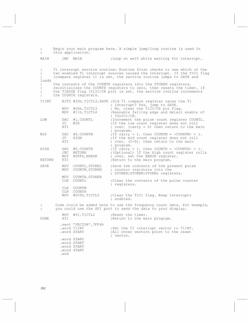
262
; Begin your main program here. A simple jump/loop routine is used in; this application.
MAIN JWP MAIN ;Loop on self while waiting for interrupt.
; T1 interrupt service routine: Routine first checks to see which of the; two enabled T1 interrupt sources caused the interrupt. If the T1C1 flag; (compare register 1) is set, the service routine jumps to SAVE andloads; the contents of the COUNTX registers into the STOREX registers, ; reinitializes the COUNTX registers to zero, then resets the timer. If ; the T1EDGE flag (T1IC/CR pin) is set, the service routine increments; the COUNTX registers.
T1INT BJTO #20h,T1CTL3,SAVE ;Did T1 compare register cause the T1 ; interrupt? Yes, jump to SAVE. MOV #65h,T1CTL3 ; No, clear the T1IC/CR pin flag. MOV #11h,T1CTL4 ;Reenable falling edge and detect enable of ; T2nIC1/CR.LOW DAC #l,COUNTL ;Increment the pulse count register COUNTL. JC MID ;If the low count register does not roll RTI ; over, (carry = 0) then return to the main ; program.MID DAC #0,COUNTM ;If carry = 1, then COUNTM = <COUNTM> + 1. JC HIGH ;If the mid count register does not roll RTI ; over, (C=0), then return to the main ; program.HIGH DAC #0,COUNTH ;If carry = 1, then COUNTH = <COUNTH> + 1. JNC RETURN ;(Optional) If the high count register rolls MOV #0FFh,ERROR ; over, set the ERROR register.RETURN RTI ;Return to the main program.
SAVE MOV COUNTL,STOREL ;Save the contents of the present pulse MOV COUNTM,STOREM ; counter registers into the ; STOREH:STOREM:STOREL registers. MOV COUNTH,STOREH CLR COUNTL ;Clear the contents of the pulse counter ; registers. CLR COUNTM CLR COUNTH MOV #0C5h,T1CTL3 ;Clear the T1C1 flag. Keep interrupts ; enabled.
; Code could be added here to use the frequency count data. For example,; you could use the SPI port to send the data to your display.
MOV #01,T1CTL2 ;Reset the timer.DONE RTI ;Return to the main program.
.sect ”VECTOR”,7FF4h .word T1INT ;Set the T1 interrupt vector to T1INT. .word START ;All other vectors point to the reset ; vector. .word START .word START .word START .word START .end
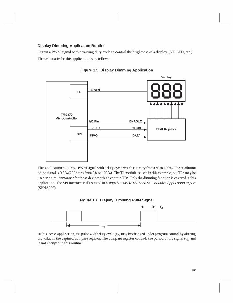
263
Display Dimming Application Routine
Output a PWM signal with a varying duty cycle to control the brightness of a display. (VF, LED, etc.)
The schematic for this application is as follows:
Figure 17. Display Dimming Application
T1
SPI
TMS370Microcontroller
T1PWM
I/O Pin
SPICLK
SIMO
ENABLE
CLKIN
DATA
Shift Register
Display
This application requires a PWM signal with a duty cycle which can vary from 0% to 100%. The resolutionof the signal is 0.5% (200 steps from 0% to 100%). The T1 module is used in this example, but T2n may beused in a similar manner for those devices which contain T2n. Only the dimming function is covered in thisapplication. The SPI interface is illustrated in Using the TMS370 SPI and SCI Modules Application Report(SPNA006).
Figure 18. Display Dimming PWM Signal
t1
t2
In this PWM application, the pulse width duty cycle (t2) may be changed under program control by alteringthe value in the capture/compare register. The compare register controls the period of the signal (t1) andis not changed in this routine.

264
The main program loads any new values for the PWM duty cycle into the MS/LSDATA working registers.These values are checked against the latest values in the HI/LODUTY registers. If they are different, theHI/LODUTY registers are updated, and the MAIN loop compares to see if the new value is 0% or 100%.If so, the PWM pin is set either LO or HIGH. If the new value is not 0% or 100%, the T1 interrupt serviceroutine is enabled, and on the next interrupt, the PWM duty cycle changes.
When the T1 service routine is entered, the routine stops the PWM signal, loads the new values, and restarts.Stopping the PWM signal helps avoid the possibility of inverting the signal if the new value is larger thanthe old; for example, when changing from a 20% to a 30% duty cycle signal.
The program flowchart diagram for this routine is illustrated in Figure 19.
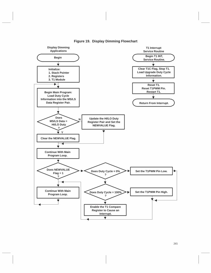
265
Figure 19. Display Dimming Flowchart
Begin
Initialize:1. Stack Pointer2. Registers3. T1 Module
Begin Main Program:Load Duty Cycle
Information into the MS/LSData Register Pair.
Display DimmingApplications
DoesMS/LS Data =
HI/LO Duty?
Clear the NEWVALUE Flag.
Continue With MainProgram Loop.
Does Duty Cycle = 0%?
Set the T1PWM Pin Low.
Update the HI/LO DutyRegister Pair and Set the
NEWVALUE Flag.
Continue With MainProgram Loop.
Does Duty Cycle = 100%?
Enable the T1 CompareRegister to Cause an
Interrupt.
Set the T1PWM Pin High.
T1 InterruptService Routine
Begin T1 INT,Service Routine.
Clear T1C Flag, Stop T1.Load Upgrade Duty Cycle
Information.
Reset T1.Reset T1PWM Pin.
Restart T1.
Return From Interrupt.
N
Y
Does NEWVALUEFlag = 1
?
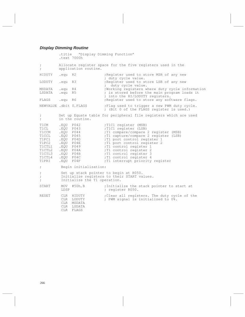
266
Display Dimming Routine .title “Display Dimming Function” .text 7000h ; Allocate register space for the five registers used in the ; application routine.
HIDUTY .equ R2 ;Register used to store MSB of any new ; duty cycle value.LODUTY .equ R3 ;Register used to store LSB of any new ; duty cycle value.MSDATA .equ R4 ;Working registers where duty cycle informationLSDATA .equ R5 ; is stored before the main program loads it ; into the HI/LODUTY registers.FLAGS .equ R6 ;Register used to store any software flags.
NEWVALUE .dbit 0,FLAGS ;Flag used to trigger a new PWM duty cycle. ; (Bit 0 of the FLAGS register is used.)
; Set up Equate table for peripheral file registers which are used; in the routine.
T1CM .EQU P042 ;T1C1 register (MSB)T1CL .EQU P043 ;T1C1 register (LSB)T1CCM .EQU P044 ;T1 compare/compare 2 register (MSB)T1CCL .EQU P045 ;T1 capture/compare 2 register (LSB)T1PC1 .EQU P04D ;T1 port control register 1T1PC2 .EQU P04E ;T1 port control register 2T1CTL1 .EQU P049 ;T1 control register 1T1CTL2 .EQU P04A ;T1 control register 2T1CTL3 .EQU P04B ;T1 control register 3T1CTL4 .EQU P04C ;T1 control register 4T1PRI .EQU P04F ;T1 interrupt priority register
; Begin initialization:
; Set up stack pointer to begin at R050.; Initialize registers to their START values.; Initialize the T1 operation.
START MOV #50h,B ;Initialize the stack pointer to start at LDSP ; register R050.
RESET CLR HIDUTY ;Clear all registers. The duty cycle of the CLR LODUTY ; PWM signal is initialized to 0%. CLR MSDATA CLR LSDATA CLR FLAGS
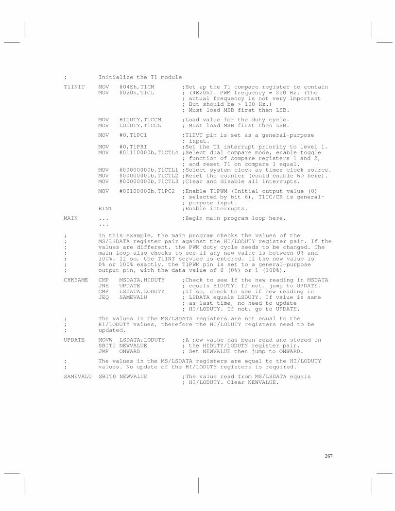
267
; Initialize the T1 module
T1INIT MOV #04Eh,T1CM ;Set up the T1 compare register to contain MOV #020h,T1CL ; (4E20h). PWM frequency = 250 Hz. (The ; actual frequency is not very important ; But should be > 100 Hz.) ; Must load MSB first then LSB.
MOV HIDUTY,T1CCM ;Load value for the duty cycle. MOV LODUTY,T1CCL ; Must load MSB first then LSB.
MOV #0,T1PC1 ;T1EVT pin is set as a general-purpose ; input. MOV #0,T1PRI ;Set the T1 interrupt priority to level 1. MOV #01110000b,T1CTL4 ;Select dual compare mode, enable toggle ; function of compare registers 1 and 2, ; and reset T1 on compare 1 equal. MOV #00000000b,T1CTL1 ;Select system clock as timer clock source. MOV #00000001b,T1CTL2 ;Reset the counter (could enable WD here). MOV #00000000b,T1CTL3 ;Clear and disable all interrupts.
MOV #00100000b,T1PC2 ;Enable T1PWM (Initial output value (0) ; selected by bit 6), T1IC/CR is general– ; purpose input. EINT ;Enable interrupts.
MAIN ... ;Begin main program loop here. ...
; In this example, the main program checks the values of the ; MS/LSDATA register pair against the HI/LODUTY register pair. If the; values are different, the PWM duty cycle needs to be changed. The; main loop also checks to see if any new value is between 0% and; 100%. If so, the T1INT service is entered. If the new value is; 0% or 100% exactly, the T1PWM pin is set to a general-purpose; output pin, with the data value of 0 (0%) or 1 (100%).
CHKSAME CMP MSDATA,HIDUTY ;Check to see if the new reading in MSDATA JNE UPDATE ; equals HIDUTY. If not, jump to UPDATE. CMP LSDATA,LODUTY ;If so, check to see if new reading in JEQ SAMEVALU ; LSDATA equals LSDUTY. If value is same ; as last time, no need to update ; HI/LODUTY. If not, go to UPDATE.
; The values in the MS/LSDATA registers are not equal to the ; HI/LODUTY values, therefore the HI/LODUTY registers need to be; updated.
UPDATE MOVW LSDATA,LODUTY ;A new value has been read and stored in SBIT1 NEWVALUE ; the HIDUTY/LODUTY register pair. JMP ONWARD ; Set NEWVALUE then jump to ONWARD.
; The values in the MS/LSDATA registers are equal to the HI/LODUTY; values. No update of the HI/LODUTY registers is required.
SAMEVALU SBIT0 NEWVALUE ;The value read from MS/LSDATA equals ; HI/LODUTY. Clear NEWVALUE.
268
; Continue on with the main loop.
ONWARD ;(NEXT INSTRUCTION) ... ...
JBIT1 NEWVALUE,CHK0 ;Check to see if a new value has been ; stored into the HI/LODUTY regs. ; If so check for 0% or 100%. BR ONWARD1 ; If not, branch to ONWARD1. ; Check to see if the NEW duty cycle is either 0% or 100%. If so,; set the T1PWM pin accordingly.
CHK0 CMP #0,LODUTY ;Is LODUTY = 0? No, check to see = 100%. JNE CHK100 ; Yes, check the HIDUTY register. CMP #0,HIDUTY ;Is HIDUTY also = 0? JEQ SETLOW ; Yes, set T1PWM line low. ; No, check if 100%.CHK100 CMP #20h,LODUTY ;Is LODUTY = 20h? JNE T1ENABLE ; No, jump to T1ENABLE. CMP #4Eh,HIDUTY ; If so, is HIDUTY = 4Eh? JEQ SETHIGH ; Yes, set T1PWM line high.
; If there has been a new value detected for the PWM duty cycle, and; that new value is not 0 (0%) or 4E20h (100%), then clear the; NEWVALUE flag and enable T1INT.
T1ENABLE SBIT0 NEWVALUE ;Clear the NEWVALUE flag. MOV #01h,T1CTL3 ;Allow the compare flag to cause a timer ; interrupt only when the PWM duty cycle ; needs to be altered.
... ;Continue main routine. ... BR MAIN
; This next section of code is only executed if the desired duty ; cycle is either 0% or 100% exactly.
SETLOW MOV #00010000b,T1PC2 ;Make the T1PWM pin an output pin with the ; present data output. MOV #0001000b,T1PC2 ;Output a low value on the T1PWM pin. JMP ONWARD1
SETHIGH CLR MSDATA CLR LSDATA MOV #01010000b,T1PC2 ;Make the T1PWM pin an output pin with the ; present data output. MOV #01010000b,T1PC2 ;Output a high value on the T1PWM pin.ONWARD1 ... ;Continue with the main routine. ... ...GOBACK BR MAIN
269
; The T1 interrupt service routine follows. This routine is only ; entered if a different duty cycle value is detected, and that new; duty cycle value is: 0 < value < 4E20h. (Between 0% and 100%.)
T1INT MOV #00000011b,T1CTL1 ;Stop T1 since an update has been read. MOV HIDUTY,T1CCM ;Load new value for the PWM duty cycle. MOV LODUTY,T1CCL ; Must load MSB first then LSB. MOV #00000001b,T1CTL2 ;Reset the counter. MOV #01010000b,T1PC2 ;Reset the T1PWM pin to general-purpose ; output with the present value of the PWM ; pin. MOV #01010000b T1PC2 ;T1PWM pin will output a 1. MOV #01100000b T1PC2 ;Reenable the T1PWM function with an ; initial value of 1. MOV #01110000b,T1CTL4 ;Reenable the PWM toggling (T1C and T1CC). MOV #00h,T1CTL1 ;Reselect the system clock as the T1 clock ; source. ;The PWM signal now runs with the new ; duty cycle until the next change. MOV #00000000b,T1CTL3 ;Clear the T1 compare 1 interrupt flag and ; disable the T1 compare 1 flag again.
RETURN RTI ;Return to the main routine.
; Set up the interrupt vectors. Only T1INT is used in this example,; but the rest of the vectors have been loaded with the reset vector; in case of an extraneous pulse.
.sect ”VECTORS”,7FF4h ;Location of the vector table. .word T1INT ;T1 interrupt vector. .word START ;Points to reset vector. .word STMT ; ” .word START ; ” .word START ; ” .word START ;Reset vector. .end
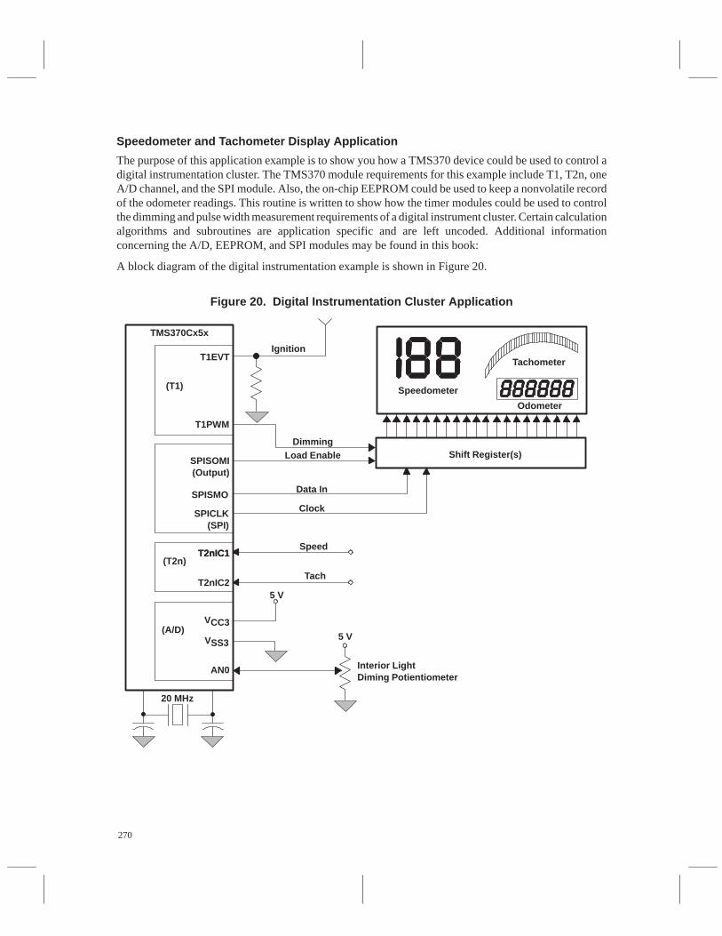
270
Speedometer and Tachometer Display Application
The purpose of this application example is to show you how a TMS370 device could be used to control adigital instrumentation cluster. The TMS370 module requirements for this example include T1, T2n, oneA/D channel, and the SPI module. Also, the on-chip EEPROM could be used to keep a nonvolatile recordof the odometer readings. This routine is written to show how the timer modules could be used to controlthe dimming and pulse width measurement requirements of a digital instrument cluster. Certain calculationalgorithms and subroutines are application specific and are left uncoded. Additional informationconcerning the A/D, EEPROM, and SPI modules may be found in this book:
A block diagram of the digital instrumentation example is shown in Figure 20.
Figure 20. Digital Instrumentation Cluster Application
TMS370Cx5x
IgnitionT1EVT
T1PWM
DimmingLoad Enable
Data In
Clock
Speed
Tach
(T1)
SPISOMI(Output)
SPISMO
SPICLK(SPI)
5 V
(T2n)T2nIC1T2nIC1
T2nIC2
VCC3
VSS3(A/D)
AN0
5 V
Interior LightDiming Potientiometer
20 MHz
Speedometer
Odometer
Tachometer
Shift Register(s)

271
Application Overview and Theory of Operation
The basic functions of this application example include input signal measurement, display dimming, serialcommunication, and conversion of one A/D channel. The speed and tach readings are measured using thetwo input capture registers of T2n. The dimming of the display is controlled by reading an A/D channelwhich is connected to a potentiometer. This A/D information is used to determine the duty cycle of a PWMsignal output from T1. The information sent to the display is controlled using the SPI module. The mainroutine in this example checks to see that the ignition switch is on. Once the ignition switch is on, the displaybegins to be updated, and a series of flags is checked to determine any needed operation.
The flowchart for this route is shown in Figure 21.
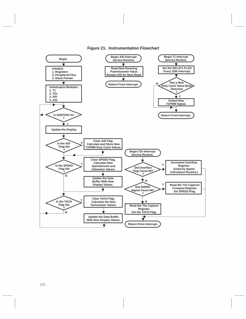
272
Figure 21. Instrumentation Flowchart
Begin
Initialize1. Registers2. Peripheral Files3. Stack Pointer
Initialization Modules:1. T12. T2n3. SPI4. A/D
Is IGNITION On?
Update the Display
Is the A/D Flag Set
?
Is the SPEEDFlag Set
?
Is the TACHFlag Set
?
Clear A/D Flag.Calculate and Store New
T1PWM Duty Cycle Values.
Clear SPEED Flag. Calculate New
Speedometer andOdometer Values.
Update the DataBuffer With NewDisplay Values.
Begin A/D InterruptService Routine.
Read New DimmingPotentiometer Value.
Restart A/D for Next Read.
Return From Interrupt.
Begin T2n InterruptService Routine.
Did OverflowFlag Cause INT
?
Clear TACH Flag.Calculate the New
Tachometer Values.
Update the Data BufferWith New Display Values.
Begin T1 InterruptService Routine.
Set the DELAY1 FLAGEvery 10th Interrupt.
Has a NewDuty Cycle Value Been
Detected?
Output NewT1PWM Signal.
Return From Interrupt.
Did SPEEDSignal Cause INT
?
Read the T2n CaptureRegister.
Set the TACH Flag.
Return From Interrupt.
Increment OverflowRegister.
(Used by SpeedCalculation Routine.)
Read the T2n Capture/Compare Register.Set SPEED Flag.
Y
Y
Y
N
N
N
N
Y
Y
Y
N
Y

273
T1 Module Operation
The T1 module is used to output a PWM signal to control the brightness of the display. T1 operates in thedual compare mode. The period of the PWM signal is controlled by the T1 compare 1 register, and the pulsewidth is controlled by the T1 capture/compare register. The pulse width duty cycle may be changed underprogram control by altering the value in the T1 capture/compare register.
The main routine checks to see if the newest reading from the A/D has changed since it was last read. Ifthe values are different, the NEWVALUE flag is set. If the values are the same, the NEWVALUE flag iscleared. The T1 service routine checks this flag. If the NEWVALUE flag is cleared, the present PWM dutycycle continues. If the NEWVALUE flag is set, the interrupt routine stops the PWM signal, loads the newduty cycle values (HI/LODUTY) into the T1CC registers, and restarts the PWM signal. Stopping the PWMsignal helps avoid the possibility of inverting the signal if the new value is larger than the old; for example,when changing from a 20% to a 30% duty cycle signal.
T2n Module Operation
The T2n module is used to measure the speed and tach input signals. The module is set up for the dual cap-ture mode to enable both 16-bit capture registers. The T2nIC1 pin, the T2n capture/compare register, andany T2n counter overflows are used to determine the speed function, while the T2nIC2 pin, the T2n captureregister, and any T2n counter overflows are used for the tach function.
When a valid signal occurs on either T2n input capture pin, the associated capture register is loaded withthe value of the T2n counter. The T2n service routine then reads the contents of the capture register andany T2n overflows that may have occurred. This information can be used to determine the speed and tachreadings by keeping track of how long it has been since the last pulse occurred. The actual conversionroutines used to determine the speedometer, odometer, and tachometer display information is applicationdependent, and is not coded in this example.
SPI Module Operation
The SPI module is used to send the display information to the instrument cluster. The main routineconstantly updates the display with any new tach information every 1/20 second, and updates the completedisplay every 1/2 second. The actual number of bytes to be sent, the data format, and how often the displayneeds to be updated are all application specific variables that you may alter for your needs.
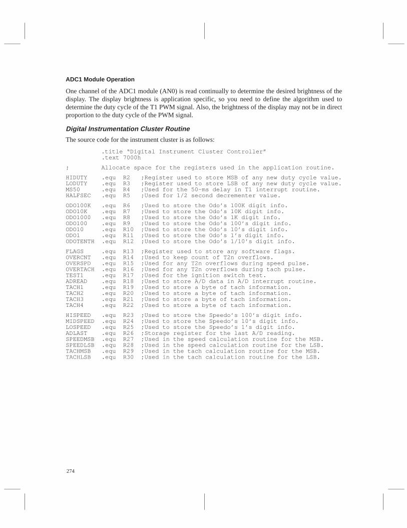
274
ADC1 Module Operation
One channel of the ADC1 module (AN0) is read continually to determine the desired brightness of thedisplay. The display brightness is application specific, so you need to define the algorithm used todetermine the duty cycle of the T1 PWM signal. Also, the brightness of the display may not be in directproportion to the duty cycle of the PWM signal.
Digital Instrumentation Cluster Routine
The source code for the instrument cluster is as follows:
.title “Digital Instrument Cluster Controller” .text 7000h
; Allocate space for the registers used in the application routine.
HIDUTY .equ R2 ;Register used to store MSB of any new duty cycle value.LODUTY .equ R3 ;Register used to store LSB of any new duty cycle value.MS50 .equ R4 ;Used for the 50-ms delay in T1 interrupt routine.HALFSEC .equ R5 ;Used for 1/2 second decrementer value.
ODO100K .equ R6 ;Used to store the Odo’s 100K digit info.ODO10K .equ R7 ;Used to store the Odo’s 10K digit info.ODO1000 .equ R8 ;Used to store the Odo’s 1K digit info.ODO100 .equ R9 ;Used to store the Odo’s 100’s digit info.ODO10 .equ R10 ;Used to store the Odo’s 10’s digit info.ODO1 .equ R11 ;Used to store the Odo’s 1’s digit info.ODOTENTH .equ R12 ;Used to store the Odo’s 1/10’s digit info.
FLAGS .equ R13 ;Register used to store any software flags.OVERCNT .equ R14 ;Used to keep count of T2n overflows.OVERSPD .equ R15 ;Used for any T2n overflows during speed pulse.OVERTACH .equ R16 ;Used for any T2n overflows during tach pulse.TEST1 .equ R17 ;Used for the ignition switch test.ADREAD .equ R18 ;Used to store A/D data in A/D interrupt routine.TACH1 .equ R19 ;Used to store a byte of tach information.TACH2 .equ R20 ;Used to store a byte of tach information.TACH3 .equ R21 ;Used to store a byte of tach information.TACH4 .equ R22 ;Used to store a byte of tach information.
HISPEED .equ R23 ;Used to store the Speedo’s 100’s digit info.MIDSPEED .equ R24 ;Used to store the Speedo’s 10’s digit info.LOSPEED .equ R25 ;Used to store the Speedo’s 1’s digit info.ADLAST .equ R26 ;Storage register for the last A/D reading.SPEEDMSB .equ R27 ;Used in the speed calculation routine for the MSB.SPEEDLSB .equ R28 ;Used in the speed calculation routine for the LSB.TACHMSB .equ R29 ;Used in the tach calculation routine for the MSB.TACHLSB .equ R30 ;Used in the tach calculation routine for the LSB.
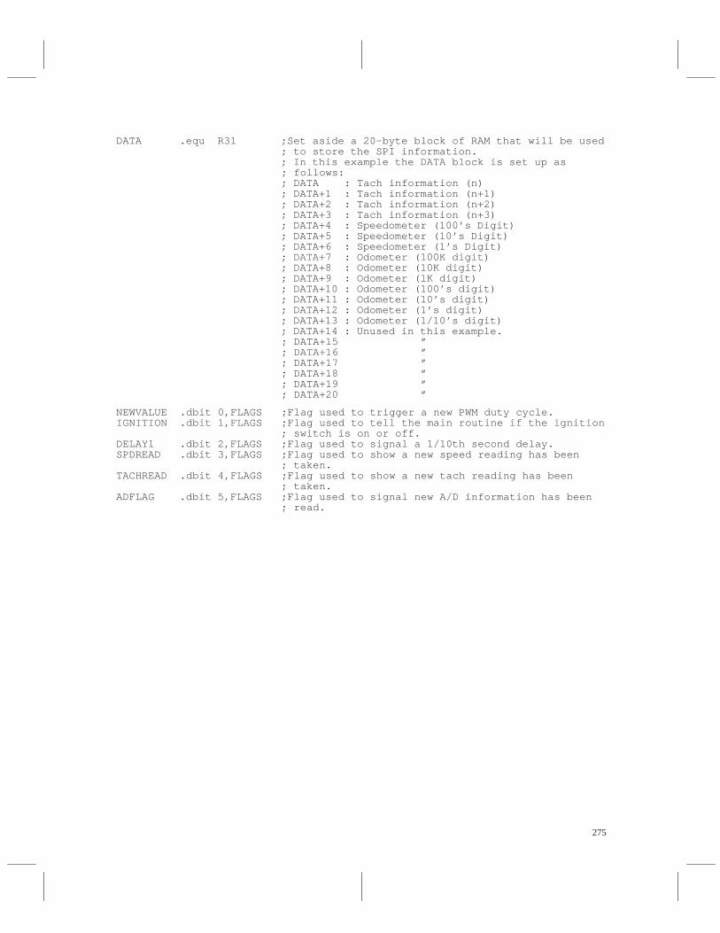
275
DATA .equ R31 ;Set aside a 20-byte block of RAM that will be used ; to store the SPI information. ; In this example the DATA block is set up as ; follows: ; DATA : Tach information (n) ; DATA+1 : Tach information (n+1) ; DATA+2 : Tach information (n+2) ; DATA+3 : Tach information (n+3) ; DATA+4 : Speedometer (100’s Digit) ; DATA+5 : Speedometer (10’s Digit) ; DATA+6 : Speedometer (1’s Digit) ; DATA+7 : Odometer (100K digit) ; DATA+8 : Odometer (10K digit) ; DATA+9 : Odometer (lK digit) ; DATA+10 : Odometer (100’s digit) ; DATA+11 : Odometer (10’s digit) ; DATA+12 : Odometer (1’s digit) ; DATA+13 : Odometer (1/10’s digit) ; DATA+14 : Unused in this example. ; DATA+15 ” ; DATA+16 ” ; DATA+17 ” ; DATA+18 ” ; DATA+19 ” ; DATA+20 ”
NEWVALUE .dbit 0,FLAGS ;Flag used to trigger a new PWM duty cycle.IGNITION .dbit 1,FLAGS ;Flag used to tell the main routine if the ignition ; switch is on or off.DELAY1 .dbit 2,FLAGS ;Flag used to signal a 1/10th second delay.SPDREAD .dbit 3,FLAGS ;Flag used to show a new speed reading has been ; taken.TACHREAD .dbit 4,FLAGS ;Flag used to show a new tach reading has been ; taken.ADFLAG .dbit 5,FLAGS ;Flag used to signal new A/D information has been ; read.
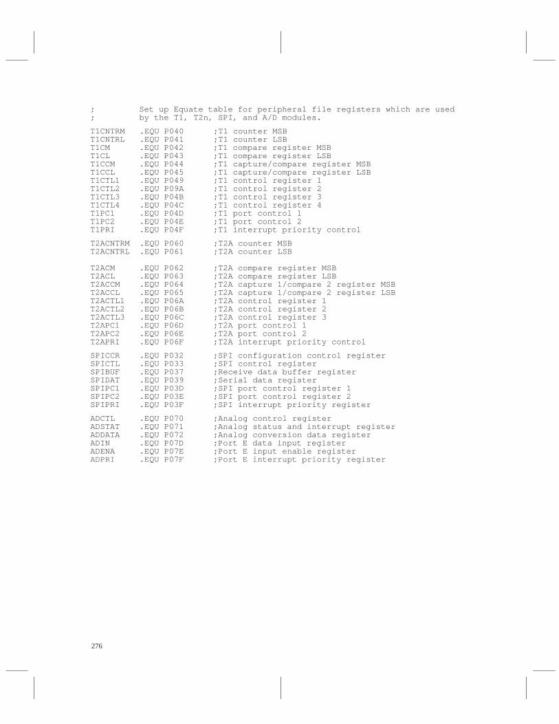
276
; Set up Equate table for peripheral file registers which are used; by the T1, T2n, SPI, and A/D modules.
T1CNTRM .EQU P040 ;T1 counter MSBT1CNTRL .EQU P041 ;T1 counter LSBT1CM .EQU P042 ;T1 compare register MSBT1CL .EQU P043 ;T1 compare register LSBT1CCM .EQU P044 ;T1 capture/compare register MSBT1CCL .EQU P045 ;T1 capture/compare register LSBT1CTL1 .EQU P049 ;T1 control register 1T1CTL2 .EQU P09A ;T1 control register 2T1CTL3 .EQU P04B ;T1 control register 3T1CTL4 .EQU P04C ;T1 control register 4T1PC1 .EQU P04D ;T1 port control 1T1PC2 .EQU P04E ;T1 port control 2T1PRI .EQU P04F ;T1 interrupt priority control
T2ACNTRM .EQU P060 ;T2A counter MSBT2ACNTRL .EQU P061 ;T2A counter LSB
T2ACM .EQU P062 ;T2A compare register MSBT2ACL .EQU P063 ;T2A compare register LSBT2ACCM .EQU P064 ;T2A capture 1/compare 2 register MSBT2ACCL .EQU P065 ;T2A capture 1/compare 2 register LSBT2ACTL1 .EQU P06A ;T2A control register 1T2ACTL2 .EQU P06B ;T2A control register 2T2ACTL3 .EQU P06C ;T2A control register 3T2APC1 .EQU P06D ;T2A port control 1T2APC2 .EQU P06E ;T2A port control 2T2APRI .EQU P06F ;T2A interrupt priority control
SPICCR .EQU P032 ;SPI configuration control registerSPICTL .EQU P033 ;SPI control registerSPIBUF .EQU P037 ;Receive data buffer registerSPIDAT .EQU P039 ;Serial data registerSPIPC1 .EQU P03D ;SPI port control register 1SPIPC2 .EQU P03E ;SPI port control register 2SPIPRI .EQU P03F ;SPI interrupt priority register
ADCTL .EQU P070 ;Analog control registerADSTAT .EQU P071 ;Analog status and interrupt registerADDATA .EQU P072 ;Analog conversion data registerADIN .EQU P07D ;Port E data input registerADENA .EQU P07E ;Port E input enable registerADPRI .EQU P07F ;Port E interrupt priority register
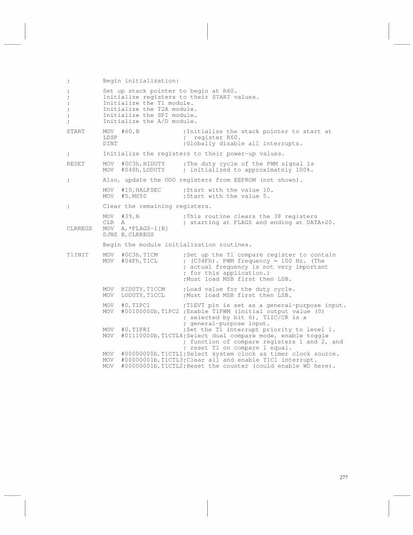
277
; Begin initialization:
; Set up stack pointer to begin at R60.; Initialize registers to their START values.; Initialize the T1 module.; Initialize the T2A module.; Initialize the SPI module.; Initialize the A/D module.
START MOV #60,B ;Initialize the stack pointer to start at LDSP ; register R60. DINT ;Globally disable all interrupts.
; Initialize the registers to their power-up values.
RESET MOV #0C3h,HIDUTY ;The duty cycle of the PWM signal is MOV #048h,LODUTY ; initialized to approximately 100%.
; Also, update the ODO registers from EEPROM (not shown).
MOV #10,HALFSEC ;Start with the value 10. MOV #5,MS50 ;Start with the value 5.
; Clear the remaining registers.
MOV #39,B ;This routine clears the 38 registers CLR A ; starting at FLAGS and ending at DATA+20.CLRREGS MOV A,*FLAGS–1[B] DJNZ B,CLRREGS
Begin the module initialization routines.
T1INIT MOV #0C3h,T1CM ;Set up the Tl compare register to contain MOV #04Fh,T1CL ; (C34Fh). PWM frequency = 100 Hz. (The ; actual frequency is not very important ; for this application.) ;Must load MSB first then LSB.
MOV HIDUTY,T1CCM ;Load value for the duty cycle. MOV LODUTY,T1CCL ;Must load MSB first then LSB.
MOV #0,T1PC1 ;T1EVT pin is set as a general-purpose input. MOV #00100000b,T1PC2 ;Enable T1PWM (initial output value (0) ; selected by bit 6), T1IC/CR is a ; general-purpose input. MOV #0,T1PRI ;Set the T1 interrupt priority to level 1. MOV #01110000b,T1CTL4;Select dual compare mode, enable toggle ; function of compare registers 1 and 2, and ; reset T1 on compare 1 equal. MOV #00000000b,T1CTL1;Select system clock as timer clock source. MOV #00000001b,T1CTL3;Clear all and enable T1C1 interrupt. MOV #00000001b,T1CTL2;Reset the counter (could enable WD here).
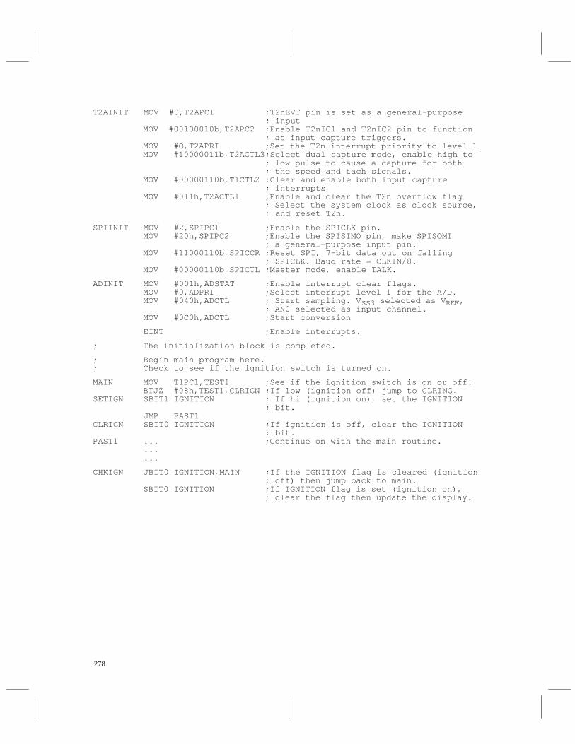
278
T2AINIT MOV #0,T2APC1 ;T2nEVT pin is set as a general-purpose ; input MOV #00100010b,T2APC2 ;Enable T2nIC1 and T2nIC2 pin to function ; as input capture triggers. MOV #O,T2APRI ;Set the T2n interrupt priority to level 1. MOV #10000011b,T2ACTL3;Select dual capture mode, enable high to ; low pulse to cause a capture for both ; the speed and tach signals. MOV #00000110b,T1CTL2 ;Clear and enable both input capture ; interrupts MOV #011h,T2ACTL1 ;Enable and clear the T2n overflow flag ; Select the system clock as clock source, ; and reset T2n.
SPIINIT MOV #2,SPIPC1 ;Enable the SPICLK pin. MOV #20h,SPIPC2 ;Enable the SPISIMO pin, make SPISOMI ; a general-purpose input pin. MOV #11000110b,SPICCR ;Reset SPI, 7-bit data out on falling ; SPICLK. Baud rate = CLKIN/8. MOV #00000110b,SPICTL ;Master mode, enable TALK.
ADINIT MOV #001h,ADSTAT ;Enable interrupt clear flags. MOV #0,ADPRI ;Select interrupt level 1 for the A/D. MOV #040h,ADCTL ; Start sampling. V SS3 selected as V REF, ; AN0 selected as input channel. MOV #0C0h,ADCTL ;Start conversion
EINT ;Enable interrupts.
; The initialization block is completed.
; Begin main program here.; Check to see if the ignition switch is turned on.
MAIN MOV T1PC1,TEST1 ;See if the ignition switch is on or off. BTJZ #08h,TEST1,CLRIGN ;If low (ignition off) jump to CLRING.SETIGN SBIT1 IGNITION ; If hi (ignition on), set the IGNITION ; bit. JMP PAST1CLRIGN SBIT0 IGNITION ;If ignition is off, clear the IGNITION ; bit.PAST1 ... ;Continue on with the main routine. ... ...
CHKIGN JBIT0 IGNITION,MAIN ;If the IGNITION flag is cleared (ignition ; off) then jump back to main. SBIT0 IGNITION ;If IGNITION flag is set (ignition on), ; clear the flag then update the display.
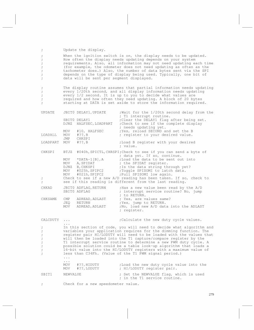
279
; Update the display.
; When the ignition switch is on, the display needs to be updated. ; How often the display needs updating depends on your system; requirements. Also, all information may not need updating each time; (for example, the odometer does not need updating as often as the; tachometer does.) Also, the number of data bytes sent via the SPI; depends on the type of display being used. Typically, one bit of ; data will be sent per segment displayed.
; The display routine assumes that partial information needs updating; every 1/20th second, and all display information needs updating; every 1/2 second. It is up to you to decide what values are; required and how often they need updating. A block of 20 bytes; starting at DATA is set aside to store the information required.
UPDATE JBIT0 DELAY1,UPDATE ;Wait for the 1/20th second delay from the ; T1 interrupt routine. SBIT0 DELAY1 ;Clear the DELAY1 flag after being set. DJNZ HALFSEC,LOADPART ;Check to see if the complete display ; needs updating yet. MOV #10, HALFSEC ;Yes, reload SECOND and set the BLOADALL MOV #??,B ; register to your desired value. JMP CHKSPILOADPART MOV #??,B ;Load B register with your desired ; value.
CHKSPI BTJZ #040h,SPICTL,CHRSPI;Check to see if you can send a byte of ; data yet. If so, continue. MOV *DATA–1[B],A ;Load the data to be sent out into MOV A,SPIDAT ; the SPIDAT register. DJNZ B,CHKSPI ;Is the data string through yet? MOV #025h,SPIPC2 ;Toggle SPISOMI to latch data. MOV #021h,SPIPC2 ;Pull SPISOMI low again.; Check to see if a new A/D reading has been taken. If so, check to; see if this reading is different from the last reading.
CHKAD JBIT0 ADFLAG,RETURN ;Has a new value been read by the A/D SBIT0 ADFLAG ; interrupt service routine? No, jump ; to RETURN.CHKSAME CMP ADREAD,ADLAST ; Yes, are values same? JEQ RETURN ;Yes, jump to RETURN. MOV ADREAD,ADLAST ;No, load new A/D data into the ADLAST ; register.
CALCDUTY ... ;Calculate the new duty cycle values. ...; In this section of code, you will need to decide what algorithm and; variables your application requires for the dimming function. The; register pair HI/LODUTY will need to be loaded with the values that; will then be loaded into the T1 capture/compare register by the; T1 interrupt service routine to determine a new PWM duty cycle. A; possible solution could be a table look-up algorithm that loads a; 16-bit value into the HI/LODUTY registers with a maximum value of; less than C34Fh. (Value of the T1 PWM signal period.) ... ... MOV #??,HIDUTY ;Load the new duty cycle value into the MOV #??,LODUTY ; HI/LODUTY register pair.
SBIT1 NEWVALUE ; Set the NEWVALUE flag, which is used ; in the T1 service routine.
; Check for a new speedometer value.
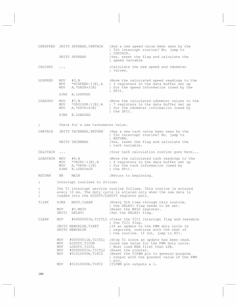
280
CHKSPEED JBIT0 SPDREAD,CHKTACH ;Has a new speed value been seen by the ; T2n interrupt routine? No, jump to ; CHKTACH. SBIT0 SPDREAD ;Yes, reset the flag and calculate the ; speed variable
CALCSPD ... ;Calculate the new speed and odometer ; values.
LDSPEED MOV #3,B ;Move the calculated speed readings to the MOV *HISPEED–1[B],A ; 3 registers in the data buffer set up MOV A,*DATA+3[B] ; for the speed information (used by the ; SPI). DJNZ B,LDSPEED
LOADODO MOV #7,B ;Move the calculated odometer values to the MOV *ODO100K–1[B],A ; 7 registers in the data buffer set up MOV A,*DATA+6[B] ; for the odometer information (used by ; the SPI). DJNZ B,LOADODO
; Check for a new tachometer value.
CHKTACH JBIT0 TACHREAD,RETURN ;Has a new tach value been seen by the ; T2n interrupt routine? No, jump to ; RETURN. SBIT0 TACHREAD ;Yes, reset the flag and calculate the ; tach variable.
CALCTACH ... ;Your tach calculation routine goes here...
LOADTACH MOV #4,B ;Move the calculated tach readings to the MOV *TACH1–1[B],A ; 4 registers in the data buffer set up MOV A,*DATA–1[B] ; for the tach information (used by DJNZ B,LOADTACH ; the SPI).
RETURN BR MAIN ;Return to beginning.
; Interrupt routines to follow:
; The T1 interrupt service routine follows. This routine is entered; every 10 ms. The duty cycle is altered only when the new data is; loaded into the HIDUTY/LODUTY register pair.
T1INT DJNZ MS50,CLEAR ;Every 5th time through this routine, ; the DELAY1 flag needs to be set. MOV #5,MS50 ;Reset the MS50 register. SBIT1 DELAY1 ;Set the DELAY1 flag.
CLEAR MOV #00000001b,T1CTL3 ;Clear the T1C1 interrupt flag and reenable ; the T1C1 flag. JBIT0 NEWVALUE,T1RET ;If an update to the PWM duty cycle is SBIT0 NEWVALUE ; required, continue with the rest of ; the routine. If not, jump to RTI.
MOV #00000011b,T1CTL1 ;Stop T1 since an update has been read. MOV HIDUTY,T1CCM ;Load new value for the PWM duty cycle. MOV LODUTY,T1CCL ; Must load MSB first then LSB. MOV #00000001b,T1CTL2 ;Reset the counter. MOV #01010000b,T1PC2 ;Reset the T1PWM pin to general-purpose ; output with the present value of the PWM ; pin. MOV #01010000b,T1PC2 ;T1PWM pin outputs a 1.
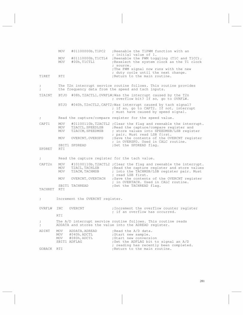
281
MOV #01100000b,T1PC2 ;Reenable the T1PWM function with an ; initial value of 1. MOV #01110000b,T1CTL4 ;Reenable the PWM toggling (T1C and T1CC). MOV #00h,T1CTL1 ;Reselect the system clock as the T1 clock ; source. ;The PWM signal now runs with the new ; duty cycle until the next change.T1RET RTI ;Return to the main routine.
; The T2n interrupt service routine follows. This routine provides; the frequency data from the speed and tach inputs.
T2AINT BTJO #08h,T2ACTL1,OVRFLW;Was the interrupt caused by the T2n ; overflow bit? If so, go to OVRFLW.
BTJO #040h,T2nCTL2,CAPT2;Was interrupt caused by tach signal? ; if so, go to CAPT2. If not, interrupt ; must have caused by speed signal.
; Read the capture/compare register for the speed value.
CAPT1 MOV #01100110b,T2ACTL2 ;Clear the flag and reenable the interrupt. MOV T2ACCL,SPEEDLSB ;Read the capture/compare register and MOV T2ACCM,SPEEDMSB ; store values into SPEEDMSB/LSB register ; pair. Must read LSB first. MOV OVERCNT,OVERSPD ;Save the contents of the OVERCNT register ; in OVERSPD. Used in CALC routine. SBIT1 SPDREAD ;Set the SPDREAD flag.SPDRET RTI
; Read the capture register for the tach value.
CAPT2n MOV #10100110b,T2ACTL2 ;Clear the flag and reenable the interrupt. MOV T2ACL,TACHLSB ;Read the capture register and store values MOV T2ACM,TACHMSB ; into the TACHMSB/LSB register pair. Must ; read LSB first. MOV OVERCNT,OVERTACH ;Save the contents of the OVERCNT register ; in OVERTACH. Used in CALC routine. SBIT1 TACHREAD ;Set the TACHREAD flag.TACHRET RTI
; Increment the OVERCNT register.
OVRFLW INC OVERCNT ;Increment the overflow counter register ; if an overflow has occurred. RTI
; The A/D interrupt service routine follows. This routine reads; ADDATA and stores the value into the ADREAD register.
ADINT MOV ADDATA,ADREAD ;Read the A/D data. MOV #040h,ADCTL ;Start new sample. MOV #080h,ADCTL ;Start new conversion SBIT1 ADFLAG ;Set the ADFLAG bit to signal an A/D ; reading has recently been completed.GOBACK RTI ;Return to the main routine.

282
.sect ”VECTORS”,7FFCh ;Interrupt vectors: .word ADINT ; A/D vector .word T2AINT ; T2A vector .word GOBACK ; SCI TX vector (not used) .word GOBACK ; SCI RX vector (not used) .word T1INT ; Timer 1 vector .word GOBACK ; SPI vector (not used) .word GOBACK ; INT 3 vector (not used) .word GOBACK ; INT 2 vector (not used) .word GOBACK ; INT 1 vector (not used) .word START ; RESET vector .end

283
Conclusion
The timer modules of the TMS370 8-bit microcontroller family are designed to provide the flexibility tomeet a broad range of timer and counter applications. The software and interface examples illustrate howthe basic functions of the timer modules, along with other modules of the TMS370 family, can be used toprovide cost-effective system solutions. This application report has been designed to be used in conjunctionwith the TMS370 Family User’s Guide. The manual is a valuable reference and provides many answers toquestions not addressed in this report.
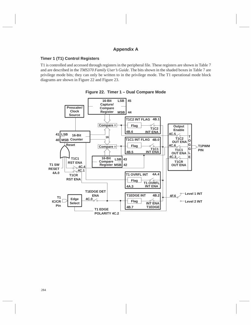
284
Appendix A
Timer 1 (T1) Control Registers
T1 is controlled and accessed through registers in the peripheral file. These registers are shown in Table 7and are described in the TMS370 Family User’s Guide. The bits shown in the shaded boxes in Table 7 areprivilege mode bits; they can only be written to in the privilege mode. The T1 operational mode blockdiagrams are shown in Figure 22 and Figure 23.
Figure 22. Timer 1 – Dual Compare Mode
T1C1RST ENA
4C.44C.1
16-BitCounter
LSB
MSB
41
40
16-BitCompareRegister
LSB
MSB
43
42
Prescaler/Clock
Source
16-BitCapture/CompareRegister
LSB
MSB
45
44
T1C2 INT FLAG
Flag
4B.1
INT ENA
Compare =
4B.6T1C2
T1C1 INT FLAG
Flag
4B.0
INT ENA4B.5T1C1
Compare =Reset
T1 OVRFL INT
Flag
4A.4
T1 OVRFLINT ENA4A.3
T1CRRST ENA
T1 SWRESET
4A.0
T1IC/CR
Pin
EdgeSelect
T1EDGE DETENA
4C.0
T1 EDGEPOLARITY 4C.2
T1EDGE INT
Flag
4B.2
INT ENA4B.7
Level 1 INT4F.6
Level 2 INT
OutputEnable
4C.5
4C.6
4C.3
T1C2OUT ENA
T1C1OUT ENA
T1CROUT ENA
TOGGLE
T1PWMPIN
16
T1EDGE
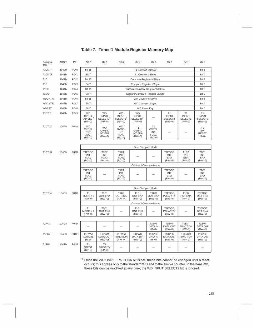
285
Table 7. Timer 1 Module Register Memory Map
Designa-tion
ADDR PF Bit 7 Bit 6 Bit 5 Bit 4 Bit 3 Bit 2 Bit 1 Bit 0
T1CNTR 1040h P040 Bit 15 T1 Counter MSbyte Bit 8
T1CNTR 1041h P041 Bit 7 T1 Counter LSbyte Bit 0
T1C 1042h P042 Bit 15 Compare Register MSbyte Bit 8
T1C 1043h P043 Bit 7 Compare Register LSbyte Bit 0
T1CC 1044h P044 Bit 15 Capture/Compare Register MSbyte Bit 8
T1CC 1045h P045 Bit 7 Capture/Compare Register LSbyte Bit 0
WDCNTR 1046h P046 Bit 15 WD Counter MSbyte Bit 8
WDCNTR 1047h P047 Bit 7 WD Counter LSbyte Bit 0
WDRST 1048h P048 Bit 7 WD Reset Key Bit 0
T1CTL1 1049h P049ÎÎÎÎÎÎÎÎÎÎÎÎ
WDOVRFL
TAP SEL †(RP–0)
ÎÎÎÎÎÎÎÎÎ
WDINPUT
SELECT2†(RP–0)
ÎÎÎÎÎÎÎÎÎÎÎÎ
WDINPUT
SELECT1†(RP–0)
ÎÎÎÎÎÎÎÎÎ
WDINPUT
SELECT0†(RP–0)
—
T1 INPUT
SELECT2(RW–0)
T1INPUT
SELECT1(RW–0)
T1INPUT
SELECT0(RW–0)
T1CTL2 104Ah P04AÎÎÎÎÎÎÎÎÎÎÎÎ
WDOVRFL
RSTENA †(RS–0)
WDOVRFL
INT ENA(RW–0)
WDOVRFL
INT FLAG(RC–*)
T1OVRFL
INT ENA(RW–0)
T1OVRFL
INTFLAG
(RC–0)
— —
T1SW
RESET(S–0)
Dual Compare Mode
T1CTL3 104Bh P04B T1EDGEINT
FLAG(RC–0)
T1C2INT
FLAG(RC–0)
T1C1INT
FLAG(RC–0)
— —
T1EDGEINTENA
(RW–0)
T1C2INTENA
(RW–0)
T1C1INTENA
(RW–0)
Capture / Compare Mode
T1EDGEINT
FLAG(RC–0)
—
T1C1INT
FLAG(RC–0)
— —
T1EDGEINTENA
(RW–0)
—
T1C1INTENA
(RW–0)
Dual Compare Mode
T1CTL4 104Ch P04C T1 MODE = 0
(RW–0)
T1C1OUT ENA(RW–0)
T1C2OUT ENA(RW–0)
T1C1RST ENA(RW–0)
T1CROUT ENA(RW–0)
T1EDGEPOLARITY
(RW–0)
T1CRRST ENA(RW–0)
T1EDGEDET ENA(RW–0)
Capture / Compare Mode
T1MODE = 1
(RW–0)
T1C1OUT ENA(RW–0)
—T1C1
RST ENA(RW–0)
—T1EDGE
POLARITY(RW–0)
—T1EDGEDET ENA(RW–0)
T1PC1 104Dh P04D— — — —
T1EVTDATA IN
(R–0)
T1EVTDATA OUT
(RW–0)
T1EVTFUNCTION
(RW–0)
T1EVTDATA DIR
(RW–0)
T1PC2 104Eh P04E T1PWMDATA IN
(R–0)
T1PWMDATA OUT
(RW–0)
T1PWMFUNCTION
(RW–0)
T1PWMDATA DIR
(RW–0)
T1IC/CRDATA IN
(R–0)
T1IC/CRDATA OUT
(RW–0)
T1IC/CRFUNCTION
(RW–0)
T1IC/CRDATA DIR
(RW–0)
T1PRI 104Fh P04F T1STEST(RP–0)
T1PRIORITY
(RP–0)— — — — — —
† Once the WD OVRFL RST ENA bit is set, these bits cannot be changed until a resetoccurs; this applies only to the standard WD and to the simple counter. In the hard WD,these bits can be modified at any time; the WD INPUT SELECT2 bit is ignored.
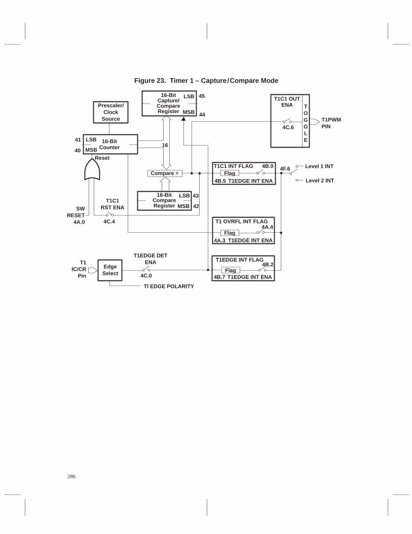
286
Figure 23. Timer 1 – Capture/Compare Mode
16-BitCounter
LSB
MSB
41
40
Prescaler/Clock
Source
16-BitCapture/CompareRegister
LSB
MSB
45
44
T1C1 INT FLAG 4B.0
4B.5 T1EDGE INT ENACompare =
T1 OVRFL INT FLAG4A.4
4A.3 T1EDGE INT ENA
T1EDGE INT FLAG4B.2
4B.7 T1EDGE INT ENA
16-BitCompareRegister
LSB
MSB
43
42
EdgeSelect
SWRESET
4A.0
T1IC/CR
Pin
T1EDGE DETENA
4C.0
TI EDGE POLARITY
Reset
T1C1RST ENA
4C.4
T1C1 OUTENA
4C.6
TOGGLE
T1PWMPIN
Level 1 INT4F.6
Level 2 INTFlag
Flag
Flag
16

287
Appendix B
Timer 2 (T2A) Control Registers
T2A is controlled and accessed through registers in the peripheral file. These registers are shown in Table 8and are described in the TMS370 Family User’s Guide. The bits shown in the shaded boxes in Table 8 areprivilege mode bits; they can only be written to in the privilege mode. Figure 24 and Figure 25 illustratethe T2A operational mode block diagrams.
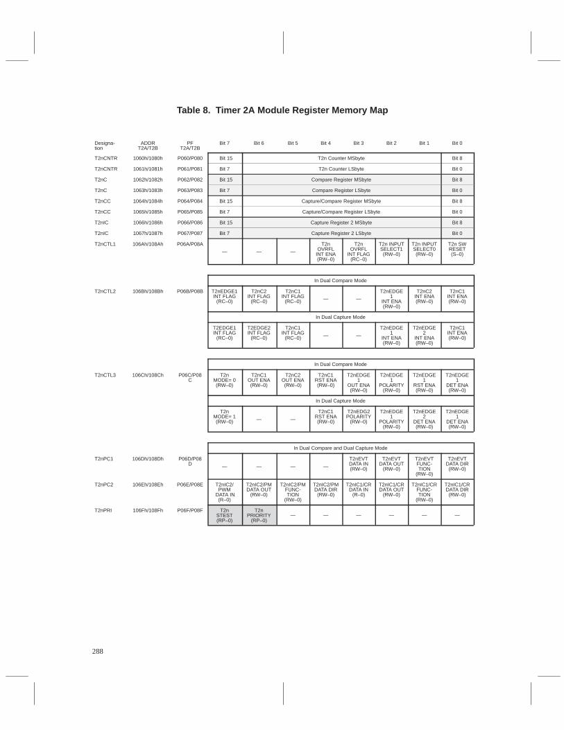
288
Table 8. Timer 2A Module Register Memory Map
Designa-tion
ADDRT2A/T2B
PFT2A/T2B
Bit 7 Bit 6 Bit 5 Bit 4 Bit 3 Bit 2 Bit 1 Bit 0
T2nCNTR 1060h/1080h P060/P080 Bit 15 T2n Counter MSbyte Bit 8
T2nCNTR 1061h/1081h P061/P081 Bit 7 T2n Counter LSbyte Bit 0
T2nC 1062h/1082h P062/P082 Bit 15 Compare Register MSbyte Bit 8
T2nC 1063h/1083h P063/P083 Bit 7 Compare Register LSbyte Bit 0
T2nCC 1064h/1084h P064/P084 Bit 15 Capture/Compare Register MSbyte Bit 8
T2nCC 1065h/1085h P065/P085 Bit 7 Capture/Compare Register LSbyte Bit 0
T2nIC 1066h/1086h P066/P086 Bit 15 Capture Register 2 MSbyte Bit 8
T2nIC 1067h/1087h P067/P087 Bit 7 Capture Register 2 LSbyte Bit 0
T2nCTL1 106Ah/108Ah P06A/P08A
— — —
T2nOVRFL
INT ENA(RW–0)
T2nOVRFL
INT FLAG(RC–0)
T2n INPUTSELECT1(RW–0)
T2n INPUTSELECT0(RW–0)
T2n SWRESET(S–0)
In Dual Compare Mode
T2nCTL2 106Bh/108Bh P06B/P08B T2nEDGE1INT FLAG
(RC–0)
T2nC2INT FLAG
(RC–0)
T2nC1INT FLAG
(RC–0) — —
T2nEDGE1
INT ENA(RW–0)
T2nC2INT ENA(RW–0)
T2nC1INT ENA(RW–0)
In Dual Capture Mode
T2EDGE1INT FLAG
(RC–0)
T2EDGE2INT FLAG
(RC–0)
T2nC1INT FLAG
(RC–0) — —
T2nEDGE1
INT ENA(RW–0)
T2nEDGE2
INT ENA(RW–0)
T2nC1INT ENA(RW–0)
In Dual Compare Mode
T2nCTL3 106Ch/108Ch P06C/P08C
T2nMODE= 0(RW–0)
T2nC1OUT ENA(RW–0)
T2nC2OUT ENA(RW–0)
T2nC1RST ENA(RW–0)
T2nEDGE1
OUT ENA(RW–0)
T2nEDGE1
POLARITY(RW–0)
T2nEDGE1
RST ENA(RW–0)
T2nEDGE1
DET ENA(RW–0)
In Dual Capture Mode
T2nMODE= 1(RW–0) — —
T2nC1RST ENA(RW–0)
T2nEDG2POLARITY
(RW–0)
T2nEDGE1
POLARITY(RW–0)
T2nEDGE2
DET ENA(RW–0)
T2nEDGE1
DET ENA(RW–0)
In Dual Compare and Dual Capture Mode
T2nPC1 106Dh/108Dh P06D/P08D — — — —
T2nEVTDATA IN(RW–0)
T2nEVTDATA OUT
(RW–0)
T2nEVTFUNC-TION
(RW–0)
T2nEVTDATA DIR
(RW–0)
T2nPC2 106Eh/108Eh P06E/P08E T2nIC2/PWM
DATA IN(R–0)
T2nIC2/PMDATA OUT
(RW–0)
T2nIC2/PMFUNC-TION
(RW–0)
T2nIC2/PMDATA DIR
(RW–0)
T2nIC1/CRDATA IN
(R–0)
T2nIC1/CRDATA OUT
(RW–0)
T2nIC1/CRFUNC-TION
(RW–0)
T2nIC1/CRDATA DIR
(RW–0)
T2nPRI 106Fh/108Fh P06F/P08F T2nSTEST(RP–0)
T2nPRIORITY
(RP–0)— — — — — —
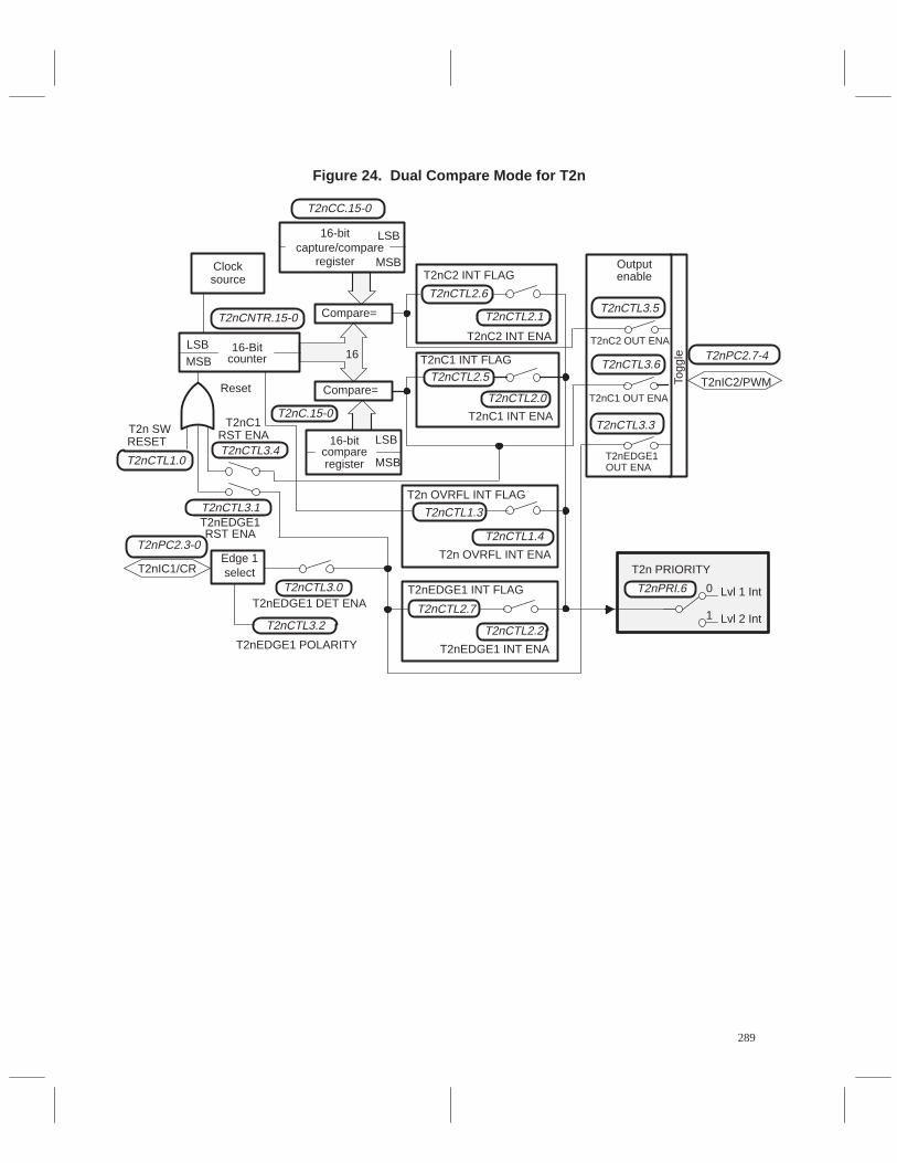
289
Figure 24. Dual Compare Mode for T2n
16
T2nC.15-0
T2nCTL2.1
T2nCTL3.2
T2nCTL3.1
T2nCTL3.5
T2nCTL3.3
Clocksource
16-Bitcounter
16-bit
Compare=
Compare=Reset
T2nC1RST ENAT2n SW
RESET
Edge 1select
T2nEDGE1 DET ENA
Outputenable
capture/compareregister MSB
LSB
MSBLSB
T2nEDGE1OUT ENA
T2nIC1/CR
T2nEDGE1 POLARITY
Togg
le
16-bitcompare
MSB
LSB
register
T2nCC.15-0
T2nC1 INT FLAG
T2nCTL2.0
T2nCTL2.5
T2nC1 INT ENA
T2nC2 INT FLAG
T2nCTL2.6
T2nC2 INT ENA
T2n OVRFL INT FLAG
T2nCTL1.4
T2nCTL1.3
T2n OVRFL INT ENA
T2nEDGE1 INT FLAG
T2nCTL2.2
T2nCTL2.7
T2nEDGE1 INT ENA
T2n PRIORITY
T2nC2 OUT ENA
T2nC1 OUT ENA
T2nCTL3.6
T2nIC2/PWM
T2nPC2.7-4
T2nPRI.6
T2nCNTR.15-0
T2nCTL1.0T2nCTL3.4
T2nEDGE1RST ENA
T2nPC2.3-0
T2nCTL3.0 Lvl 1 Int
Lvl 2 Int
0
1
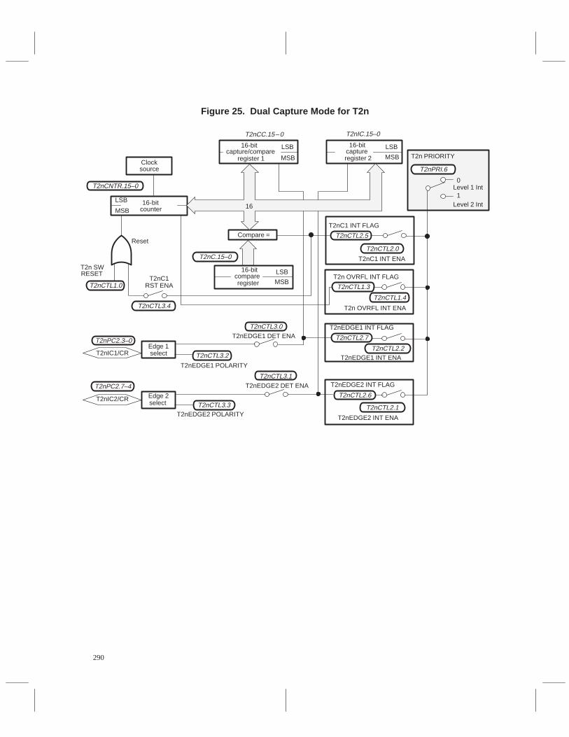
290
Figure 25. Dual Capture Mode for T2n
T2nCTL2.5
T2nCTL3.3
0
capture/compare
T2nPC2.3–0
Compare =
Clocksource
16-bitcounterMSB
LSB
T2nCNTR.15–0
Reset
T2nC1RST ENA
T2n SWRESET
T2nCTL1.0
T2nCTL3.4
T2nCTL2.6
T2nCTL2.1
T2nCTL2.7
T2nCTL2.2
T2nCTL2.0
16-bit
MSB
LSB
register 1
T2nC.15–0
16-bitcompare
MSB
LSB
register
T2n PRIORITY
Level 1 Int
Level 2 Int1
T2nCTL1.3
T2nCTL1.4
16-bitcapture
MSB
LSB
register 2
T2nIC.15–0
Edge 2select
T2nIC2/CR
T2nPC2.7–4
T2nCTL3.1
Edge 1selectT2nIC1/CR T2nCTL3.2
T2nCTL3.0
16
T2nEDGE1 POLARITY
T2nEDGE1 DET ENA
T2nEDGE2 DET ENA
T2nEDGE2 POLARITY
T2nC1 INT FLAG
T2nC1 INT ENA
T2n OVRFL INT FLAG
T2n OVRFL INT ENA
T2nEDGE1 INT FLAG
T2nEDGE1 INT ENA
T2nEDGE2 INT ENA
T2nEDGE2 INT FLAG
T2nPRI.6
T2nCC.15– 0

291
References
Linear and Interface Circuits Applications, SLYA003, Texas Instruments Incorporated, 1987.
TMS370 Family User’s Guide, SPNU127, Texas Instruments Incorporated, 1996.
292
Glossary
C
capture register: A T1 or T2n register that is loaded with the 16-bit counter value when an external inputtransition occurs. Either edge of the external input can be configured to trigger the capture.
CLKIN: The external oscillator frequency (20 MHz maximum)
compare register: The compare register, in the T1 or T2n module, contains a value that is compared tothe counter value. The compare function triggers when the counter matches the contents of the compareregister.
E
edge detection: Edge detection circuitry senses an active pulse transition on a given timer input andprovides appropriate output transitions to the rest of the module. The active transition can be configuredto be low to high or high to low.
event count: A T1 or T2n clock source option where the timer is clocked from the rising edge of a signalon an external pin (T1EVT or T2nEVT).
EEPROM: Electrically erasable programmable read-only memory; has the capability to be programmedand erased under direct program control.
I
interrupt: A signal input to the CPU to stop the flow of a program and force the CPU to execute instructionsat an address corresponding to the source of the interrupt. When the interrupt is finished, the CPU resumesexecution at the point where the input occurred.
P
PPM: Pulse position modulation; a serial signal in which the information is contained in the frequency ofa signal with a constant pulse width. A TMS370 device can output a PPM signal with a constant duty cyclewithout any program intervention using the T1 or T2n compare registers.
prescale: Circuitry in the T1 module that effectively divides the SYSCLK by a set value. For example, /64prescale divides the SYSCLK signal by 64.
pulse accumulation: A T1 mode which keeps a cumulative count of SYSCLK pulses as long as the T1EVTpin is high.
PWM: Pulse width modulation; a serial signal in which the information is contained in the width of a pulseof a constant frequency signal. A TMS370 device can output a PWM signal with a constant duty cyclewithout any program intervention using the T1 or T2n compare features.

293
S
SPI module: Serial peripheral interface module; used to send serial data in a simple bit format to devicessuch as shift registers.
SYSCLK: The internal system clock period.
W
Watchdog timer: A free-running counter in the T1 module which must be cleared by the program at a setinterval. If the program is not working properly, the counter will overflow, causing a system reset.

294
295
Using Input Capture Pins asExternal Interrupts
Michael S. StewartMicrocontroller Products — Semiconductor Group
Texas Instruments

296

297
Introduction
The TMS370 family of microcontrollers are typically available with three external interrupt pins.
• INT1: Maskable or non maskable interrupt of general purpose input only pin
• INT2: Maskable interrupt or general purpose bidirectional I/O pin
• INT3: Maskable interrupt or general purpose bidirectional I/O pin
For applications that require more than three individual external interrupts, the timer input capture pins canbe used to cause interrupts.
Timer 1 (T1)
The T1IC/CR pin may be configured to operate as an external interrupt. To initialize this pin as an externalinterrupt, do the following:
1. Select the mode of operation for T1. The T1 MODE (T1CTL4.7) bit can be selected for eitherdual compare mode or capture/compare mode. The T1IC/CR pin can operate as an externalinterrupt in either mode.
2. Select the rising edge or falling edge polarity of the interrupt by writing to the T1EDGEPOLARITY (T1CTL4.2) bit.
3. Enable the selected edge to set the T1EDGE INT flag by setting the T1EDGE DETECT(T1CTL4.0) bit.
4. Enable the active T1EDGE INT flag to request an interrupt by setting the T1EDGE INT ENA(T1CTL3.2) bit.
Timer 2A (T2A)
The pins T2AIC1/CR and T2AIC2/PWM may be configured to operate as external interrupts. To initializethe T2AIC1/CR pin to cause an external interrupt, do the following:
1. Select the mode of operation for T2A. The T2A MODE (T2ACTL3.7) bit can be selected foreither dual compare mode or dual capture mode. The T2AIC1/CR pin can operate as an externalinterrupt in either mode.
2. Select the rising edge or falling edge polarity of the interrupt by writing to the T2AEDGE1POLARITY (T2ACTL4.2) bit.
3. Enable the selected edge to set the T2AEDGE1 INT flag by setting the T2AEDGE1 DETECT(T2ACTL4.0) bit.
4. Enable the active T2AEDGE1 INT flag to request an interrupt by setting the T2AEDGE1 INTENA (T2ACTL3.2) bit.
To initialize the T2AIC2/PWM pin to cause an external interrupt, do the following:
1. Select the dual capture mode of operation for T2A. The T2A MODE (T2ACTL3.7) bit mustbe set. The T2AIC2/PWM pin can operate as an external interrupt in the dual capture mode only.In the dual compare mode this pin operates as a pulse width modulation (PWM) output pin.
2. Select the rising edge or falling edge polarity of the interrupt by writing to the T2AEDGE2POLARITY (T2ACTL4.3) bit.

298
3. Enable the selected edge to set the T2AEDGE2 INT flag by setting the T2AEDGE2 DETECT(T2ACTL4.1) bit.
4. Enable the active T2AEDGE2 INT flag to request an interrupt by setting the T2AEDGE2 INTENA (T2ACTL3.1) bit.
Timer 2B (T2B)
The T2B pins T2BIC1/CR and T2BIC2/PWM may be configured to operate as external interrupts. Toinitialize the T2BIC1/CR pin to cause an external interrupt, do the following:
1. Select the mode of operation for T2B. The T2B MODE (T2BCTL3.7) bit can be selected foreither dual compare mode or dual capture mode. The T2BIC1/CR pin can operate as an externalinterrupt in either mode.
2. Select the rising edge or falling edge polarity of the interrupt by writing to the T2BEDGE1POLARITY (T2BCTL4.2) bit.
3. Enable the selected edge to set the T2BEDGE1 INT flag by setting the T2BEDGE1 DETECT(T2BCTL4.0) bit.
4. Enable the active T2BEDGE1 INT flag to request an interrupt by setting the T2BEDGE1 INTENA (T2BCTL3.2) bit.
To initialize the T2BIC2/PWM pin to cause an external interrupt, do the following:
1. Select the dual capture mode of operation for T2B. The T2B MODE (T2BCTL3.7) bit must beset. The T2BIC2/PWM pin can operate as an external interrupt in the dual capture mode only.In the dual compare mode this pin operates as a PWM output pin.
2. Select the rising edge or falling edge polarity of the interrupt by writing to the T2BEDGE2POLARITY (T2BCTL4.3) bit.
3. Enable the selected edge to set the T2BEDGE2 INT flag by setting the T2BEDGE2 DETECT(T2ACTL4.1) bit.
4. Enable the active T2BEDGE2 INT flag to request an interrupt by setting the T2BEDGE2 INTENA (T2BCTL3.1) bit.
NOTE:Remember that T1, T2A, and T2B all have multiple sources thatmay cause an interrupt. If multiple sources are enabled to causean interrupt, the interrupt service routine must poll theindividual flag bits to determine the source(s) of an interrupt.

299
Watchdog Design Considerationsand Mask Options
Michael S. StewartMicrocontroller Products — Semiconductor Group
Texas Instruments

300
301
Introduction
Many applications require the presence of a watchdog (WD) timer to increase system integrity. TheTMS370 family of microcontrollers provides three different mask options for WD timer functionality.
1. A standard watchdog for ROM-less, EPROM, and mask-ROM devices.
2. A hard watchdog for mask-ROM devices
3. A simple counter for mask-ROM devices
Standard WD
The standard WD counter option on the TMS370 has been designed to be as flexible as possible for a widerange of system designers. The TMS370 WD counter was designed to add a greater level of system integrityto the software operation. External conditions that cause the TMS370 to operate outside the specifiedranges may cause the WD counter to lose functionality. It may be used as a WD counter with variabletimeout ranges, as an event counter, or as a simple overflow timer. The standard WD timer is designed aspart of the Timer 1 (T1) module, and consists of the following functional blocks:
• 16–bit, WD/event counter which provides up to 224 clock cycles between counter resets. TheWD counter can be read by the program at locations P046 (MSB) and P047 (LSB).
• Prescaled clock input selection or external clock may be options for clocking the WD counter.
• WD Reset key, which provides protection against illegal counter resets.
• An overflow flag which the program may read following reset to determine if the WD causedthe reset.
• Programmable interrupt and system reset.
The standard WD counter option is available on all ROM-less, mask ROM, and some EPROM devices.Mask ROM devices may be selected with the standard WD mask option by selecting the appropriate boxin the device New Code Release Form (NCRF). EPROM devices that are represented with the ‘A’ versiondesignator (TMS370C756A for example) are designed with the standard WD counter. All ROM-lessdevices are available only with the standard WD counter mask option. See the TMS370 Family User’sGuide for additional WD operational information.
The flexible design of the TMS370 standard WD counter allows the counter to be used in a wide range ofsystem applications. This flexibility also brings with it certain limitations.
• The WD counter is not enabled on power–up to cause a system reset. However, the firstinstruction executed can enable the WD counter and select the WD clock source.
• The WD overflow flag must be cleared once set to enable any further WD resets. This meansthat if the WD counter overflows and causes a reset, the WD OVRFL INT FLAG must be writtenwith a ’0’ to clear the flag, or the WD counter will not cause any additional resets. This wouldeffectively disable the WD counter from causing any additional resets.
• The WD counter is not free standing. In other words, internal circuitry can override the WD resetability. This was required for testing purposes of the TMS370.
Hard Watchdog Mask Option
The hard WD counter mask option on the TMS370 has been designed to eliminate any features from thestandard WD option that could cause the WD to not cause a system reset. The hard WD counter is enabled

302
on reset and cannot be disabled. The hard WD design provides a WD counter that will always cause asystem reset if the WDRST key register is not properly written. It may be used as a WD counter withvariable timeout ranges based on one of four prescale clock options and the tap select. The hard WD timeris designed as part of the T1 module, and consists of the following functional blocks:
• 16–bit, WD which provides up to 224 clock cycles between counter resets. The WD counter canbe read by the program at locations P046 (MSB) and P047 (LSB).
• Prescaled clock input selection for clocking the WD counter.
• WD reset key which provides protection against illegal counter resets.
• An overflow flag which the program may read following reset to determine if the WD causedthe reset.
• System reset enabled at all times. No programmable interrupt or system reset enable capability.
NOTE:Selecting the hard WD mask option enables the externalinterrupt 1 (INT1) as a non-maskable interrupt (NMI) duringa low-power mode. Since the hard WD option is disabled in alow-power mode, any active edge on the external interrupt INT1will wake-up the microcontroller regardless of the state of theINT1 individual interrupt enable and the global interruptenable bits.
The hard WD counter option is available on all mask ROM, and some EPROM devices. Mask ROMdevices may be selected with the hard WD mask option by selecting the appropriate box in the deviceNCRF. EPROM devices represented with the ‘B’ version designator (for example TMS370C576B) aredesigned with the standard WD counter. See section 7.7.2 of the TMS370 Family Data Manual foradditional hard WD operational information.
The design of the TMS370 hard WD counter allows the counter to be used only to generate a system reset.Therefore, writes to the WDRST key must occur before the WD can overflow assuming the fastestoverflow rate.
Simple Counter
The simple counter option on the TMS370 provides an additional timebase for applications that to notrequire or desire a WD counter. It may be used as an event counter, or as a simple overflow timer. The simplecounter is part of the T1 module, and consists of the following functional blocks:
• A 16-bit counter, which provides up to 224 clock cycles between counter resets. The counter canbe read by the program at locations P046 (MSB) and P047 (LSB).
• A prescaled clock input selection or external clock, which are options for clocking the counter.
• An overflow flag, which the program may read following reset to determine if the counter causedthe interrupt.

303
• A programmable overflow interrupt.
The simple counter option is available only on mask ROM devices by selecting the simple counter maskoption box in the device NCRF. See the TMS370 Family User’s Guide for additional WD operationalinformation.
The limited design of the TMS370 simple counter allows the counter to be used as an counter overflowinterrupt. The actual timebase of the overflow is dependent on SYSCLK speed, tap select, and clockprescale select. This design does not allow a compare feature and limits the counter functionality.

304

305
T1PWM Set-Up Routines
Microcontroller Products—Semiconductor GroupTexas Instruments

306
307
T1PWM Pin Set-Up
This application note provides three T1PWM pin set-up routines:
Routine 1
This routine starts and stops the PWM function with a certain value on the PWM pin. Starting theT1PWM pin with a specific value can be done with one instruction as shown below. The value of the dataout bit will become the initial value of the PWM pin.
MOV #60h,P04E ;Start with PWM pin high
MOV #20h,P04E ;Start with PWM pin low
Routine 2
This routine shows the two instructions needed to change the T1PWM pin from a PWM pin to ageneral-purpose output pin with a specific value. The first instruction changes the pin to ageneral-purpose output pin with the same value as the current PWM pin. The second instruction changesthe pin to a particular value.
MOV #50h,P04E ;Stop with PWM pin high.MOV #50h,P04E ;
MOV #10h,P04E ;Stop with PWM pin low.MOV #10h,P04E ;
Routine 3
This routine starts and stops the PWM function with the current value on the pin. Starting the functionrequires four instructions, while stopping the function takes only one.
MOV #20h,A ;Start with PWM pin same asBTJZ #80h,P04E,SKIP ;current state.MOV #60h,A ;
SKIP MOV A,P04E ;
MOV #10h,P04E ;Stop with PWM pin same as;current state.

308
309
Part IIIModule Specific
Application Design Aids
Part III contains six sections:
RESET Operations 99. . . . . . . . . . . . . . . . . . .
SPI and SCI Modules 105. . . . . . . . . . . . . . . .
Timer and Watchdog Modules 199. . . . . . . .
Analog to Digital Modules 309. . . . . . . . . . . .
PACT Module 375. . . . . . . . . . . . . . . . . . . . . .
I/O Pins 439. . . . . . . . . . . . . . . . . . . . . . . . . . .

310
311
Using the TMS370ADC1 Module
Henry KwanMicrocontroller Products—Semiconductor Group
Texas Instruments

312
313
Introduction
To provide advanced performance and cost effective system solutions for complex control applications,the TMS370 family combines an 8-bit CPU containing powerful peripherals such as an Analog to Digitalconverters, timers, serial peripheral interface, and serial communication interface with on-chip memory:RAM, ROM, EEPROM, and EPROM. Many applications involve the determination of the values ofphysical parameters, such as temperature, position, and pressure, which must be transformed into electricalanalog signals and then converted to digital codes for the controller. With the on-chip ADC1, the TMS370microcontrollers greatly simplify interactions between the analog world and a digital system. Thisapplication report illustrates the operation of the ADC1 on-chip A/D converter and provides someapplication examples for ADC1 conversions with the TMS370 family microcontrollers.
Many applications involve the determination of the values of physical parameters, such as temperature,position, and pressure, that must be transformed into electrical analog signals and then converted to digitalcodes for the controller. With the on-chip ADC1, the TMS370 microcontrollers greatly simplifyinteractions between the analog world and a digital system. This application report illustrates the operationof the ADC1 on-chip A/D converter and provides some application examples for ADC1 conversions withthe TMS370 family microcontrollers.
NOTE:This application report was written for the ADC1 Module. Minormodifications will need to be implemented for ADC2 and ADC3 Modules.
Module Description
The ADC1 converter module is an 8-bit successive approximation converter with internal sample-and-holdcircuitry. The module has eight multiplexed analog input channels which allow the processor to convertthe voltage levels of up to eight different sources. The ADC1 converter contains three major blocks: ananalog (input and reference) multiplexer, successive approximation A/D converter with internalsample-and-hold circuitry, and interrupt logic.
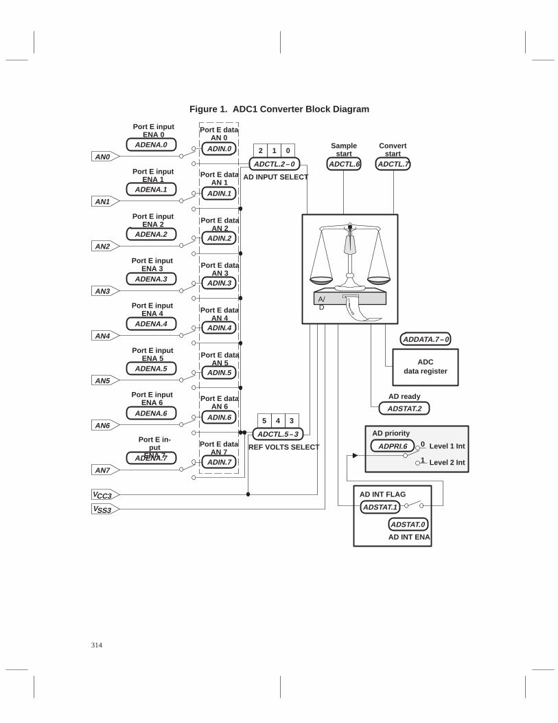
314
Figure 1. ADC1 Converter Block Diagram
ADCTL.5–3
5 4 3
ADENA.0
REF VOLTS SELECT
ADCTL.2–0
2 1 0
AD INPUT SELECT
ADIN.0
Port E inputENA 0
Port E dataAN 0
AN0
ADENA.1 ADIN.1
Port E inputENA 1
Port E dataAN 1
AN1
ADENA.2 ADIN.2
Port E inputENA 2 Port E data
AN 2
AN2
ADENA.3 ADIN.3
Port E inputENA 3 Port E data
AN 3
AN3
ADENA.4 ADIN.4
Port E inputENA 4 Port E data
AN 4
AN4
ADENA.5 ADIN.5
Port E inputENA 5 Port E data
AN 5
AN5
ADENA.6 ADIN.6
Port E inputENA 6 Port E data
AN 6
AN6
ADENA.7 ADIN.7
Port E in-put
ENA 7
Port E dataAN 7
AN7
VCC3
VSS3
ADCTL.6
Samplestart
ADCTL.7
Convertstart
ADDATA.7–0
ADCdata register
ADSTAT.2
AD ready
AD priority
ADPRI.6 0
1
Level 1 Int
Level 2 Int
AD INT FLAG
ADSTAT.1
AD INT ENA
ADSTAT.0
A/D
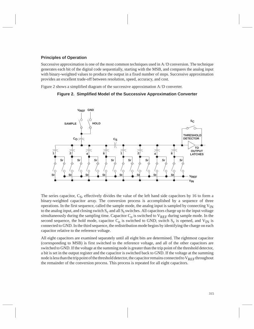
315
Principles of Operation
Successive approximation is one of the most common techniques used in A/D conversion. The techniquegenerates each bit of the digital code sequentially, starting with the MSB, and compares the analog inputwith binary-weighted values to produce the output in a fixed number of steps. Successive approximationprovides an excellent trade-off between resolution, speed, accuracy, and cost.
Figure 2 shows a simplified diagram of the successive approximation A/D converter.
Figure 2. Simplified Model of the Successive Approximation Converter
VREF GND
HOLDSAMPLE
CO CS
1 2 4 8 1 2 4 8
SC
THRESHOLDDETECTOR
TOOUTPUTLATCHES
VREFVIN
Sr
St
Sr
St
Sr
St
Sr
St
Sr
St
Sr
St
Sr
St
Sr
St
The series capacitor, CS, effectively divides the value of the left hand side capacitors by 16 to form abinary-weighted capacitor array. The conversion process is accomplished by a sequence of threeoperations. In the first sequence, called the sample mode, the analog input is sampled by connecting VINto the analog input, and closing switch Sc and all St switches. All capacitors charge up to the input voltagesimultaneously during the sampling time. Capacitor Co is switched to VREF during sample mode. In thesecond sequence, the hold mode, capacitor Co is switched to GND; switch Sc is opened, and VIN isconnected to GND. In the third sequence, the redistribution mode begins by identifying the charge on eachcapacitor relative to the reference voltage.
All eight capacitors are examined separately until all eight bits are determined. The rightmost capacitor(corresponding to MSB) is first switched to the reference voltage, and all of the other capacitors areswitched to GND. If the voltage at the summing node is greater than the trip point of the threshold detector,a bit is set in the output register and the capacitor is switched back to GND. If the voltage at the summingnode is less than the trip point of the threshold detector, the capacitor remains connected to VREF throughoutthe remainder of the conversion process. This process is repeated for all eight capacitors.

316
Functional Description
The ADC1 module has ten input pins. Two pins are used for analog voltage supply: VCC3 and VSS3. Thisisolates the ADC1 module from digital switching noise. The other eight pins (AN0–AN7) are used foranalog input channels and can be configured as general purpose input pins if not needed. The analogreference can be either VCC3 or one of the analog input channels, AN1 to AN7. This allows for ratiomeasurement of one analog signal to another.
The internal sample-and-hold circuitry is used to maintain the analog input during conversion. Thisminimizes inaccuracies in the converted value of an analog signal due to changes in the signal’s valueduring the conversion process. The input sampling begins when the SAMPLE START bit (bit 6 of theADCTL) is set. The application program should allow 1 µs for each kilohm of source output impedanceor a minimum of 1 µs for the low-impedance source to sample the analog signal. This allows time to chargethe internal capacitor array. When the sampling time is completed, the SAMPLE START and theCONVERT START bit (bit 7 of the ADCTL) are set. The analog signal’s value will be held by the ADC1module for 18 cycles after the CONVERT START bit is set. By that time, the ADC1 module has clearedboth the SAMPLE START and CONVERT START bit to signify the end of the internal sampling phase.
After the internal sampling phase, the program can change the input channel without affecting theconversion. The reference voltage should remain constant throughout the conversion. The conversionprocess takes 164 system clock cycles after the CONVERT START bit is set. Upon completion, the ADINT FLAG will be set. If the AD INT ENA bit is set, the module will generate an interrupt request.
Design Considerations
The following section provides a starting point for the digital designer by offering some hints for the analoginterface. For a more thorough discussion of additional analog devices (such as op-amp and filter circuits),refer to additional analog applications literature mentioned in the References section at the end of thisreport.
ADC1 Input Pin Model
The model of the ADC1 input pin shown in Figure 3 is intended to facilitate your understanding of theeffects of interface circuitry on A/D conversion.
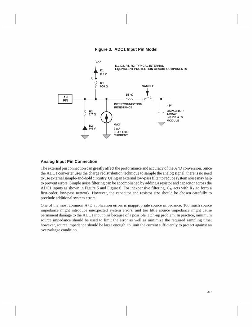
317
Figure 3. ADC1 Input Pin Model
D1, D2, R1, R2, TYPICAL INTERNALEQUIVALENT PROTECTION CIRCUIT COMPONENTS
VCC
D10.7 V
A
R1900 Ω
ANPIN
R22.7 Ω
D20.6 V
INTERCONNECTIONRESISTANCE
MAX2 µ ALEAKAGECURRENT
2 pF
CAPACITORARRAYINSIDE A / DMODULE
SAMPLE
15 kΩ
Analog Input Pin Connection
The external pin connection can greatly affect the performance and accuracy of the A/D conversion. Sincethe ADC1 converter uses the charge redistribution technique to sample the analog signal, there is no needto use external sample-and-hold circuitry. Using an external low-pass filter to reduce system noise may helpto prevent errors. Simple noise filtering can be accomplished by adding a resistor and capacitor across theADC1 inputs as shown in Figure 5 and Figure 6. For inexpensive filtering, CX acts with RX to form afirst-order, low-pass network. However, the capacitor and resistor size should be chosen carefully topreclude additional system errors.
One of the most common A/D application errors is inappropriate source impedance. Too much sourceimpedance might introduce unexpected system errors, and too little source impedance might causepermanent damage to the ADC1 input pins because of a possible latch-up problem. In practice, minimumsource impedance should be used to limit the error as well as minimize the required sampling time;however, source impedance should be large enough to limit the current sufficiently to protect against anovervoltage condition.
318
When the reference voltage, Vref, is at 5.1 V, one LSB corresponds to 20 mV. From the input pin model,the maximum leakage current is 2 µA (see note). That is, for the worst case of 2-µA leakage, current flowthrough a 1kΩ external resistor will result in a 2-mV voltage drop or induce 0.1 LSB error. If the sourceimpedance induces an error higher than can be tolerated by the system, a buffering device, such as an(op-amps), might be considered.
Latch-up poses a different problem for the input pin connection. Latch-up is the uncontrolled flow ofcurrent through the parasitic silicon controlled rectifier (SCR) inherent in all CMOS devices. This SCRmight be triggered into a low-impedance state, resulting in excessive supply current. Once the SCR istriggered, the current flow is limited only by the impedance of the power supply and the forward resistanceof the SCR. An external resistance should be used to limit the current flow through the ADC1 pin so thatthe current is never high enough to cause CMOS latch-up. The source resistance will depend on the totalsystem.
The absolute maximum rating of the analog pin should not exceed the values specified in the electricalspecification. The input voltage range should be within –0.3 to 7 V, and the input current should be within10 µA.
Suppose, for example, the analog input signal is shorted to 12V, the worst case for an application. Anexternal resistor would be required to limit the input voltage below 7 V to protect the input pin fromdamage. Also, the internal diode to VCC (5 V) would clamp the voltage at node A (see Figure 3 ) at 5.7 V.Let X be the resistance of the external resistor. Therefore,
12 – 7 12 – 5.7=
X 900 + X
or X = 3.46 k
It is suggested that the designer add in some guard band for tolerance of the internal resistance andfluctuations of the external power supplies. The designer may also consider using external clamping diodesto limit the analog voltage range between VSS3 and 7 V. However, if clamping diodes are used, the leakagecurrent induced by the diodes should be kept as low as possible.
If an external capacitor is added to form a low-pass filter, the capacitance value should be chosen carefully.The capacitor size mainly depends on the frequency of the analog input signal and the sampling timeallowed. Obviously, the RC time constant needs to be large enough to filter any undesirable noise signal,but it must be expected that the external filter also introduces a delay between the analog source and theADC1 input pin. It is important to make sure that the RC time constant is much smaller (for example, 10times smaller) than the sample time to allow the internal capacitor array to become fully charged withinthe sampling window. Adding an external capacitor can also increase protection in case an overvoltagecondition occurs. In combination with the external resistor, the external capacitor limits the rise time oflarge spikes so that the diode can clip them before they do any damage.
NOTE: Absolute resolution = 20 mV. At Vref = 5 V, this is one LSB. As Vref decreases, LSB size decreases; therefore,the absolute accuracy and differential/integral linearity errors in terms of LSBs increase.
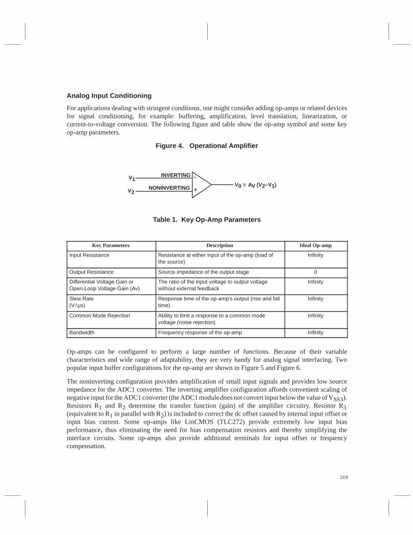
319
Analog Input Conditioning
For applications dealing with stringent conditions, one might consider adding op-amps or related devicesfor signal conditioning, for example: buffering, amplification, level translation, linearization, orcurrent-to-voltage conversion. The following figure and table show the op-amp symbol and some keyop-amp parameters.
Figure 4. Operational Amplifier
INVERTING
NONINVERTING
–
+
V1
V2V0 = AV (V2–V1)
Table 1. Key Op-Amp Parameters
Key Parameters Description Ideal Op-amp
Input Resistance Resistance at either input of the op-amp (load ofthe source)
Infinity
Output Resistance Source impedance of the output stage 0
Differential Voltage Gain orOpen-Loop Voltage Gain (Av)
The ratio of the input voltage to output voltagewithout external feedback
Infinity
Slew Rate(V /µs)
Response time of the op-amp’s output (rise and falltime)
Infinity
Common Mode Rejection Ability to limit a response to a common modevoltage (noise rejection)
Infinity
Bandwidth Frequency response of the op-amp Infinity
Op-amps can be configured to perform a large number of functions. Because of their variablecharacteristics and wide range of adaptability, they are very handy for analog signal interfacing. Twopopular input buffer configurations for the op-amp are shown in Figure 5 and Figure 6.
The noninverting configuration provides amplification of small input signals and provides low sourceimpedance for the ADC1 converter. The inverting amplifier configuration affords convenient scaling ofnegative input for the ADC1 converter (the ADC1 module does not convert input below the value of VSS3).Resistors R1 and R2 determine the transfer function (gain) of the amplifier circuitry. Resistor R3(equivalent to R1 in parallel with R2) is included to correct the dc offset caused by internal input offset orinput bias current. Some op-amps like LinCMOS (TLC272) provide extremely low input biasperformance, thus eliminating the need for bias compensation resistors and thereby simplifying theinterface circuits. Some op-amps also provide additional terminals for input offset or frequencycompensation.
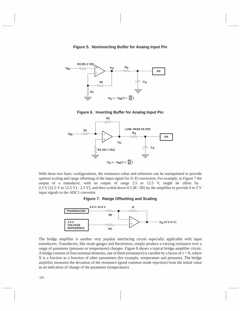
320
Figure 5. Noninverting Buffer for Analog Input Pin
+
–AN
VIN
R3 (R1 // R2)
R2
R1
VO RX
CX
VO = – VINR2R11 + )(
Figure 6. Inverting Buffer for Analog Input Pin
+
–AN
VIN
R1
R2
VO
RX
CX
VO = – VINR2R11 + )(
R3 ( R1 / / R2 )
LOW- PASS FILTER
With these two basic configurations, the resistance value and reference can be manipulated to provideoptimal scaling and range offsetting of the input signal for A/D conversion. For example, in Figure 7 theoutput of a transducer, with an output of range 2.5 to 12.5 V, might be offset by 2.5 V [ (2.5 V to 12.5 V) - 2.5 V], and then scaled down 0.5 (R / 2R) by the amplifier to provide 0 to 5 Vinput signals to the ADC1 converter.
Figure 7. Range Offsetting and Scaling
2.5 VVOLTAGEREFERENCE
2R
+
–VO ( 0 V–5 V )
RTRANSDUCER
R2
2.5 V–12.5 V
The bridge amplifier is another very popular interfacing circuit especially applicable with inputtransducers. Transducers, like strain gauges and thermistors, simply produce a varying resistance over arange of parameter (pressure or temperature) changes. Figure 8 shows a typical bridge amplifier circuit.A bridge consists of four terminal elements, one of them (resistance) is variable by a factor of 1 + X, whereX is a fraction as a function of other parameters (for example, temperature and pressure). The bridgeamplifier measures the deviation of the resistance (good common mode rejection) from the initial valueas an indication of change of the parameter (temperature).
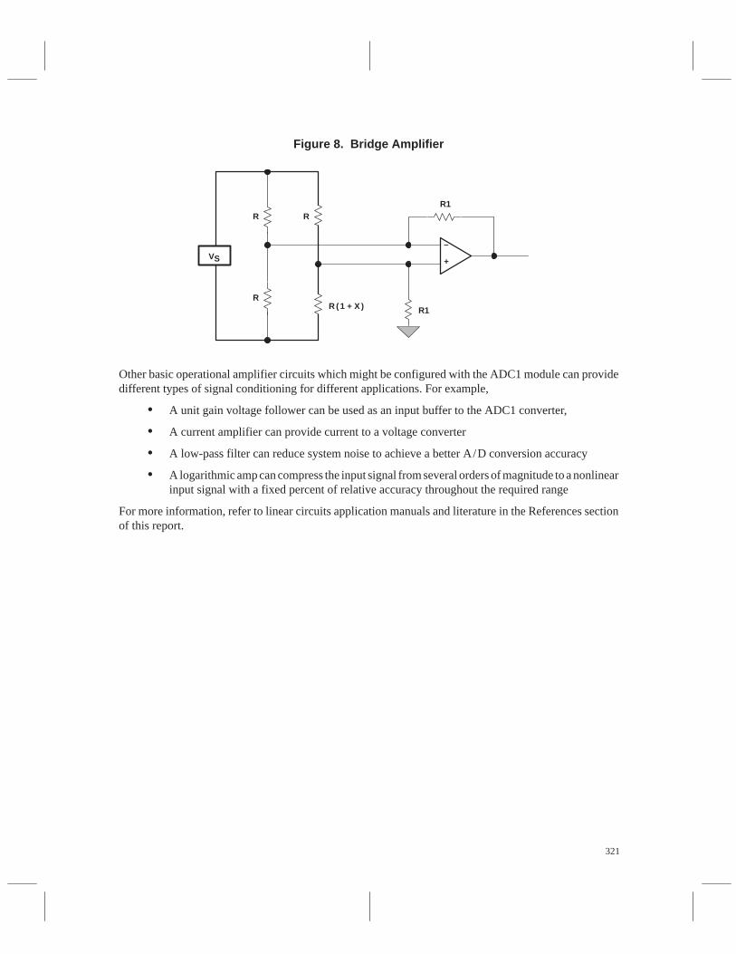
321
Figure 8. Bridge Amplifier
VS
R1
+
–
R1
R R
RR ( 1 + X )
Other basic operational amplifier circuits which might be configured with the ADC1 module can providedifferent types of signal conditioning for different applications. For example,
• A unit gain voltage follower can be used as an input buffer to the ADC1 converter,
• A current amplifier can provide current to a voltage converter
• A low-pass filter can reduce system noise to achieve a better A/D conversion accuracy
• A logarithmic amp can compress the input signal from several orders of magnitude to a nonlinearinput signal with a fixed percent of relative accuracy throughout the required range
For more information, refer to linear circuits application manuals and literature in the References sectionof this report.
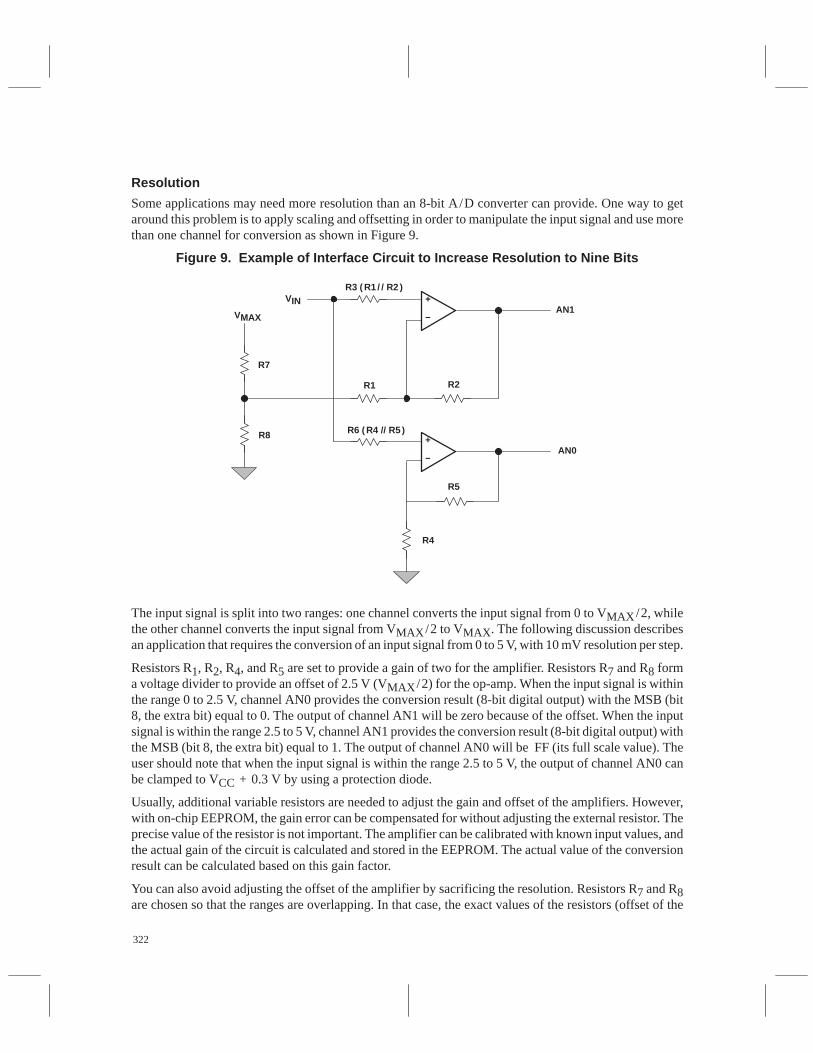
322
Resolution
Some applications may need more resolution than an 8-bit A/D converter can provide. One way to getaround this problem is to apply scaling and offsetting in order to manipulate the input signal and use morethan one channel for conversion as shown in Figure 9.
Figure 9. Example of Interface Circuit to Increase Resolution to Nine Bits
R1
+
–
+
–
R7
R8
R2
R5
R4
AN0
AN1
R3 ( R1 / / R2 )VIN
VMAX
R6 ( R4 // R5 )
The input signal is split into two ranges: one channel converts the input signal from 0 to VMAX /2, whilethe other channel converts the input signal from VMAX /2 to VMAX . The following discussion describesan application that requires the conversion of an input signal from 0 to 5 V, with 10 mV resolution per step.
Resistors R1, R2, R4, and R5 are set to provide a gain of two for the amplifier. Resistors R7 and R8 forma voltage divider to provide an offset of 2.5 V (VMAX /2) for the op-amp. When the input signal is withinthe range 0 to 2.5 V, channel AN0 provides the conversion result (8-bit digital output) with the MSB (bit8, the extra bit) equal to 0. The output of channel AN1 will be zero because of the offset. When the inputsignal is within the range 2.5 to 5 V, channel AN1 provides the conversion result (8-bit digital output) withthe MSB (bit 8, the extra bit) equal to 1. The output of channel AN0 will be FF (its full scale value). Theuser should note that when the input signal is within the range 2.5 to 5 V, the output of channel AN0 canbe clamped to VCC + 0.3 V by using a protection diode.
Usually, additional variable resistors are needed to adjust the gain and offset of the amplifiers. However,with on-chip EEPROM, the gain error can be compensated for without adjusting the external resistor. Theprecise value of the resistor is not important. The amplifier can be calibrated with known input values, andthe actual gain of the circuit is calculated and stored in the EEPROM. The actual value of the conversionresult can be calculated based on this gain factor.
You can also avoid adjusting the offset of the amplifier by sacrificing the resolution. Resistors R7 and R8are chosen so that the ranges are overlapping. In that case, the exact values of the resistors (offset of the
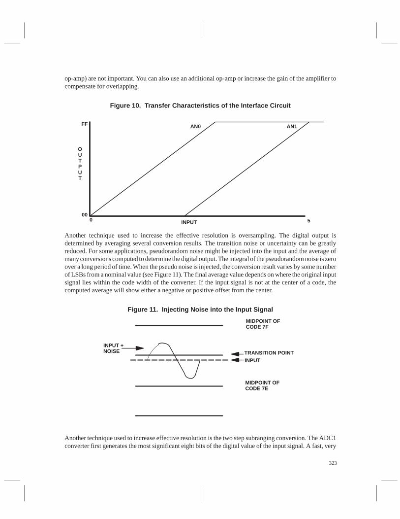
323
op-amp) are not important. You can also use an additional op-amp or increase the gain of the amplifier tocompensate for overlapping.
Figure 10. Transfer Characteristics of the Interface Circuit
FF AN0 AN1
INPUT 5000
OUTPUT
Another technique used to increase the effective resolution is oversampling. The digital output isdetermined by averaging several conversion results. The transition noise or uncertainty can be greatlyreduced. For some applications, pseudorandom noise might be injected into the input and the average ofmany conversions computed to determine the digital output. The integral of the pseudorandom noise is zeroover a long period of time. When the pseudo noise is injected, the conversion result varies by some numberof LSBs from a nominal value (see Figure 11). The final average value depends on where the original inputsignal lies within the code width of the converter. If the input signal is not at the center of a code, thecomputed average will show either a negative or positive offset from the center.
Figure 11. Injecting Noise into the Input Signal
INPUT +NOISE
MIDPOINT OFCODE 7F
TRANSITION POINTINPUT
MIDPOINT OFCODE 7E
Another technique used to increase effective resolution is the two step subranging conversion. The ADC1converter first generates the most significant eight bits of the digital value of the input signal. A fast, very
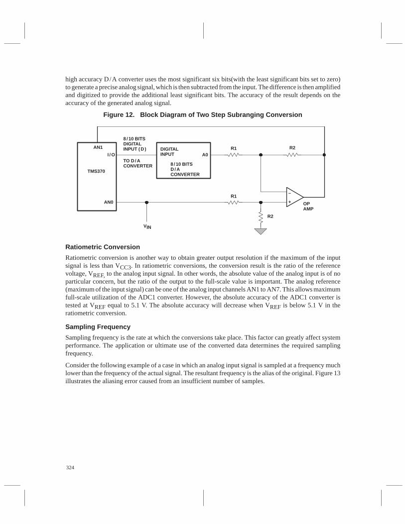
324
high accuracy D/A converter uses the most significant six bits(with the least significant bits set to zero)to generate a precise analog signal, which is then subtracted from the input. The difference is then amplifiedand digitized to provide the additional least significant bits. The accuracy of the result depends on theaccuracy of the generated analog signal.
Figure 12. Block Diagram of Two Step Subranging Conversion
+
–
AN1
I / O
AN0
TMS370
8 / 10 BITSDIGITALINPUT ( D )
TO D / ACONVERTER
DIGITALINPUT A0
8 / 10 BITSD / ACONVERTER
R1
R1
R2
R2
OPAMP
VIN
Ratiometric Conversion
Ratiometric conversion is another way to obtain greater output resolution if the maximum of the inputsignal is less than VCC3. In ratiometric conversions, the conversion result is the ratio of the referencevoltage, VREF, to the analog input signal. In other words, the absolute value of the analog input is of noparticular concern, but the ratio of the output to the full-scale value is important. The analog reference(maximum of the input signal) can be one of the analog input channels AN1 to AN7. This allows maximumfull-scale utilization of the ADC1 converter. However, the absolute accuracy of the ADC1 converter istested at VREF equal to 5.1 V. The absolute accuracy will decrease when VREF is below 5.1 V in theratiometric conversion.
Sampling Frequency
Sampling frequency is the rate at which the conversions take place. This factor can greatly affect systemperformance. The application or ultimate use of the converted data determines the required samplingfrequency.
Consider the following example of a case in which an analog input signal is sampled at a frequency muchlower than the frequency of the actual signal. The resultant frequency is the alias of the original. Figure 13illustrates the aliasing error caused from an insufficient number of samples.
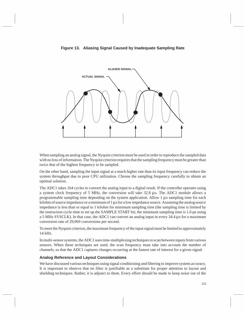
325
Figure 13. Aliasing Signal Caused by Inadequate Sampling Rate
ALIASED SIGNAL
ACTUAL SIGNAL
When sampling an analog signal, the Nyquist criterion must be used in order to reproduce the sampled datawith no loss of information. The Nyquist criterion requires that the sampling frequency must be greater thantwice that of the highest frequency to be sampled.
On the other hand, sampling the input signal at a much higher rate than its input frequency can reduce thesystem throughput due to poor CPU utilization. Choose the sampling frequency carefully to obtain anoptimal solution.
The ADC1 takes 164 cycles to convert the analog input to a digital result. If the controller operates usinga system clock frequency of 5 MHz, the conversion will take 32.8 µs. The ADC1 module allows aprogrammable sampling time depending on the system application. Allow 1 µs sampling time for eachkilohm of source impedance or a minimum of 1 µs for a low impedance source. Assuming the analog sourceimpedance is less than or equal to 1 kilohm for minimum sampling time (the sampling time is limited bythe instruction cycle time to set up the SAMPLE START bit; the minimum sampling time is 1.6 µs usinga 5 MHz SYSCLK). In that case, the ADC1 can convert an analog input in every 34.4 µs for a maximumconversion rate of 29,069 conversions per second.
To meet the Nyquist criterion, the maximum frequency of the input signal must be limited to approximately14 kHz.
In multi-sensor systems, the ADC1 uses time-multiplexing techniques to scan between inputs from varioussensors. When these techniques are used, the scan frequency must take into account the number ofchannels, so that the ADC1 captures changes occurring at the fastest rate of interest for a given signal.
Analog Reference and Layout Considerations
We have discussed various techniques using signal conditioning and filtering to improve system accuracy.It is important to observe that no filter is justifiable as a substitute for proper attention to layout andshielding techniques. Rather, it is adjunct to them. Every effort should be made to keep noise out of the
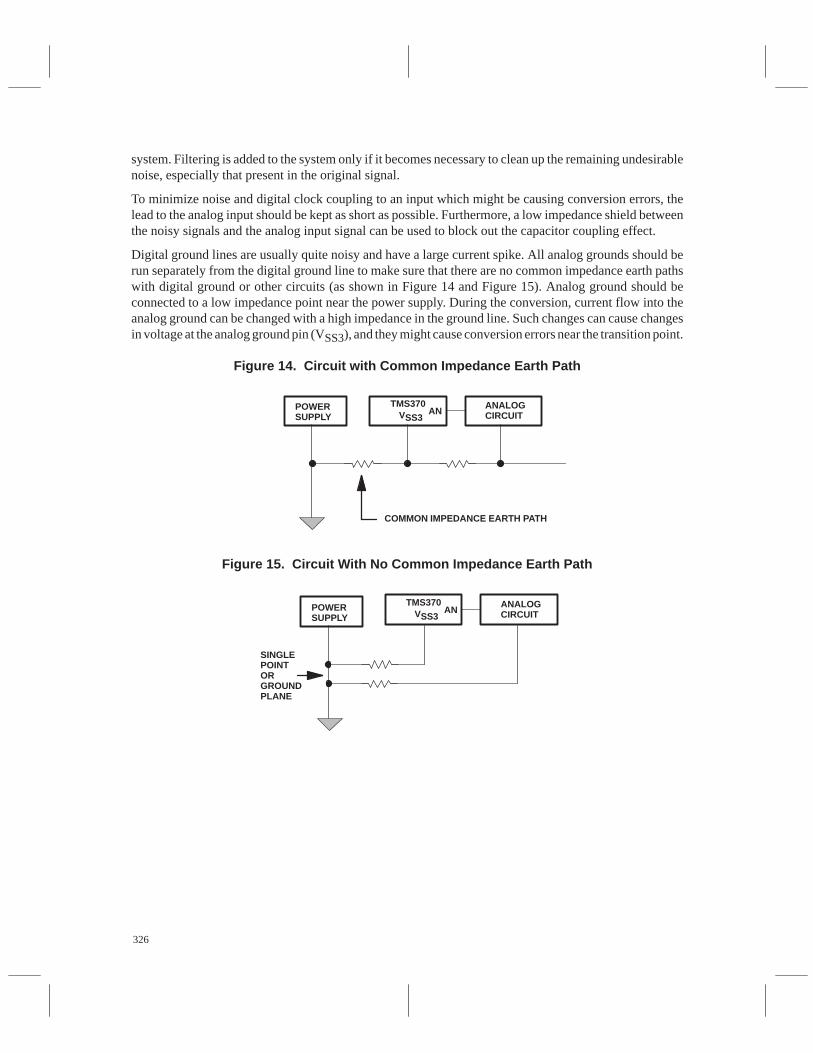
326
system. Filtering is added to the system only if it becomes necessary to clean up the remaining undesirablenoise, especially that present in the original signal.
To minimize noise and digital clock coupling to an input which might be causing conversion errors, thelead to the analog input should be kept as short as possible. Furthermore, a low impedance shield betweenthe noisy signals and the analog input signal can be used to block out the capacitor coupling effect.
Digital ground lines are usually quite noisy and have a large current spike. All analog grounds should berun separately from the digital ground line to make sure that there are no common impedance earth pathswith digital ground or other circuits (as shown in Figure 14 and Figure 15). Analog ground should beconnected to a low impedance point near the power supply. During the conversion, current flow into theanalog ground can be changed with a high impedance in the ground line. Such changes can cause changesin voltage at the analog ground pin (VSS3), and they might cause conversion errors near the transition point.
Figure 14. Circuit with Common Impedance Earth Path
POWERSUPPLY
TMS370 ANALOGCIRCUITVSS3
AN
COMMON IMPEDANCE EARTH PATH
Figure 15. Circuit With No Common Impedance Earth Path
POWERSUPPLY
SINGLEPOINTORGROUNDPLANE
TMS370 ANALOGCIRCUITVSS3
AN
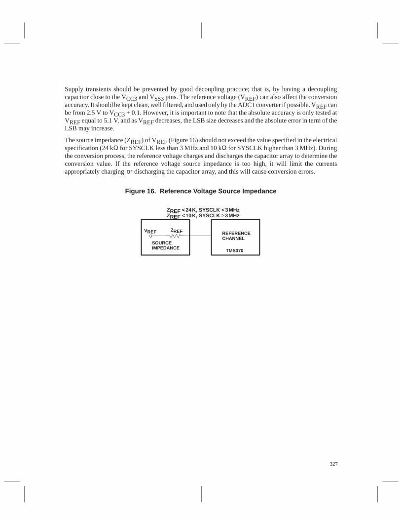
327
Supply transients should be prevented by good decoupling practice; that is, by having a decouplingcapacitor close to the VCC3 and VSS3 pins. The reference voltage (VREF) can also affect the conversionaccuracy. It should be kept clean, well filtered, and used only by the ADC1 converter if possible. VREF canbe from 2.5 V to VCC3 + 0.1. However, it is important to note that the absolute accuracy is only tested atVREF equal to 5.1 V, and as VREF decreases, the LSB size decreases and the absolute error in term of theLSB may increase.
The source impedance (ZREF) of VREF (Figure 16) should not exceed the value specified in the electricalspecification (24 kΩ for SYSCLK less than 3 MHz and 10 kΩ for SYSCLK higher than 3 MHz). Duringthe conversion process, the reference voltage charges and discharges the capacitor array to determine theconversion value. If the reference voltage source impedance is too high, it will limit the currentsappropriately charging or discharging the capacitor array, and this will cause conversion errors.
Figure 16. Reference Voltage Source Impedance
VREF
TMS370
ZREF
SOURCEIMPEDANCE
REFERENCECHANNEL
ZREF <24K, SYSCLK <3MHzZREF <10K, SYSCLK ≥3MHz
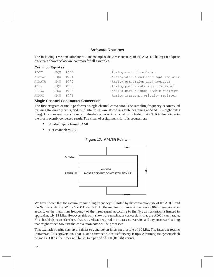
328
Software Routines
The following TMS370 software routine examples show various uses of the ADC1. The register equatedirectives shown below are common for all examples.
Common EquatesADCTL .EQU P070 ;Analog control register
ADSTAT .EQU P071 ;Analog status and interrupt register
ADDATA .EQU P072 ;Anolog conversion data register
ADIN .EQU P07D ;Analog port E data input register
ADENA .EQU P07E ;Analog port E input enable register
ADPRI .EQU P07F ;Analog itnerrupt priority register
Single Channel Continuous ConversionThe first program example performs a single channel conversion. The sampling frequency is controlledby using the on-chip timer, and the digital results are stored in a table beginning at ATABLE (eight byteslong). The conversions continue with the data updated in a round robin fashion. APNTR is the pointer tothe most recently converted result. The channel assignments for this program are:
• Analog input channel: AN0
• Ref channel: VCC3
Figure 17. APNTR Pointer
ATABLE
APNTR
OLDEST
MOST RECENTLY CONVERTED RESULT
We have shown that the maximum sampling frequency is limited by the conversion rate of the ADC1 andthe Nyquist criterion. With a SYSCLK of 5 MHz, the maximum conversion rate is 29,069 conversions persecond, or the maximum frequency of the input signal according to the Nyquist criterion is limited toapproximately 14 kHz. However, this only shows the maximum conversions that the ADC1 can handle.You should also consider the software overhead required to initiate a conversion and any processor loadingthat might affect how fast the conversion data will be processed.
This example routine sets up the timer to generate an interrupt at a rate of 10 kHz. The interrupt routineinitiates an A/D conversion. That is, one conversion occurs for every 100µs. Assuming the system clockperiod is 200 ns, the timer will be set to a period of 500 (01F4h) counts.
329
The following section sets up the table (ATABLE) and the control registers for the ADC1.
.REG ATABLE,8 ;8 BYTE TABLE THAT STORES CONVERTED DATA
.REG APNTR ;POINTER TO MOST RECENTLY CONVERTED DATA
T1C .EQU P043 ;LSB TIMER COMPARE REGISTER
T1CTL1 .EQU P049 ;TIMER COUNTER CONTROL REG 1
T1CTL2 .EQU P04A ;TIMER COUNTER CONTROL REG 2
T1CTL3 .EQU P04B ;TIMER INTERRUPT CONTROL REG
T1CTL4 .EQU P04C ;TIMER COUNTER CONTROL REG 4
;
INIT MOV #0FEH,ADENA ;ENABLE AN0 AS ANALOG CHANNEL
MOV #01H,ADSTAT ;SET THE INTERRUPT ENABLE AND
;CLEAR FLAG
MOV #0A0H,B
LDSP ;INITIALIZE STACK POINTER TO 0A0H
;CLEAR THE TABLE BEFORE CONVERSION
MOV #08H,B
MOV B,APNTR ;SET POINTER TO FIRST BYTE
CLR A
INIT0 MOV A,*ATABLE–1[B] ;CLEAR ALL EIGHT BYTES
DJNZ B,#INIT0
The following section sets up the on-chip timer to control the sampling frequency. The conversion periodis loaded into the timer compare register (T1C). When the counter (T1CNTR) matches the T1C, aninterrupt request will be generated. The timer interrupt service routine will initiate an A/D conversion andset up the time for the next conversion in the compare register. For more detailed information about theT1C, see the TMS370 Family User’s Guide.
;
; SET UP THE TIMER COMPARE FUNCTION TO CONTROL THE SAMPLING FREQ
;
MOV #00H,T1CTL1 ;SET TIMER CLOCK TO SYSTEM CLOCK
MOV #090H,T1CTL4 ;SET TIMER TO CAPTURE/COMPARE MODE
;SET COMPARE RESET ENABLE
MOV #HI(500-1),T1C–1 ;SETUP THE SAMPLING TIME IN COMPARE
;REGISTER
MOV #LO(500-1),T1C
MOV #01,T1CTL2 ;RESET TIMER TO ZERO
MOV #01,T1CTL3 ;ENABLE COMPARE 1 INTERRUPT
;
; MAIN PROGRAM
;

330
; THE ANALOG INPUT SIGNAL IS SAMPLED AND CONVERTED
; CONTINUOUSLY AT A RATE OF 10 KHZ
;
;
The following section is the timer interrupt routine. It sets up the time for the next conversion in the compareregister and initiates the A/D conversion. The address of the label T1SERV must be placed in the interruptvector table located at 7FF4h and 7FF5h.
;
; INTERRUPT ROUTINE FOR TIMER COMPARE
;
T1CINT .DBIT 5,T1CTL3 ;NAMED T1 COMPARE INTERRUPT FLAG
T1SERV SBITO T1CINT ;CLEAR INTERRUPT FLAG
SAMPLE MOV #040H,ADCTL ;START SAMPLING (APPROX. 2uS DELAY
;FOR CLOCKIN = 20 MHZ)
MOV #0C0H,ADCTL ;START CONVERSION
RTI
The following section is the ADC1 interrupt routine. It saves the conversion results in the ATABLE andsets the pointer to the next available location. The address of the label ATOD must be placed in the interruptvector table located at 7FECh and 7FEDh.
;
; INTERRUPT ROUTINE FOR ADC1
;
ADFLAG .DBIT 1,ADSTAT ;NAMED THE INTERRUPT FLAG AS ADFLAG
ATOD PUSH A ;SAVE THE REGISTERS
PUSH B
SBIT0 ADFLAG ;CLEAR THE INTERRUPT FLAG
MOV APNTR,B ;GET THE CURRENT POINTER
MOV ADDATA,A ;GET THE CONVERSION RESULTS
MOV A,*ATABLE–1[B] ;SAVE THE RESULT IN THE TABLE
DJNZ APNTR,EXITAD ;CHECK FOR WRAP AROUND
MOV #08H,APNTR ;START FROM LOCATION ATABLE(7)
EXITAD POP B ;RESTORE REGISTER
POP A
RTI
;
; INIT INTERRUPT VECTORS
.SECT ”vect”,7FECH
.WORD ATOD,0,0,0,T1SERV,0,0,0,0,INIT
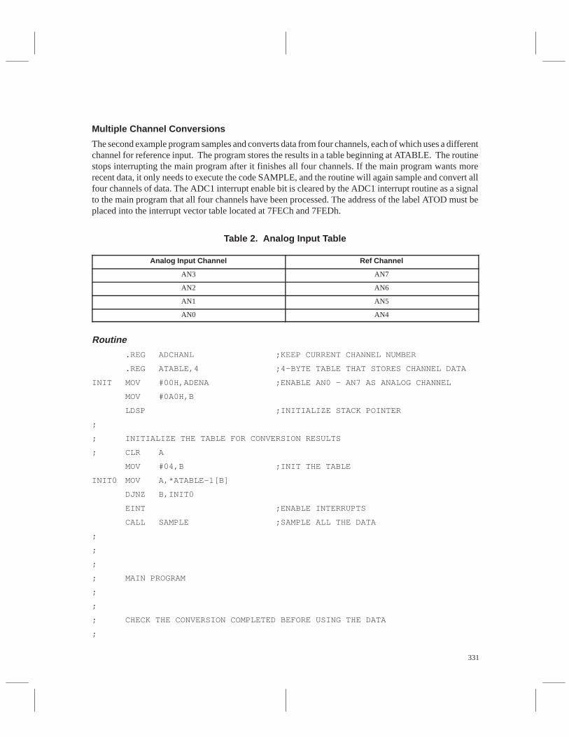
331
Multiple Channel Conversions
The second example program samples and converts data from four channels, each of which uses a differentchannel for reference input. The program stores the results in a table beginning at ATABLE. The routinestops interrupting the main program after it finishes all four channels. If the main program wants morerecent data, it only needs to execute the code SAMPLE, and the routine will again sample and convert allfour channels of data. The ADC1 interrupt enable bit is cleared by the ADC1 interrupt routine as a signalto the main program that all four channels have been processed. The address of the label ATOD must beplaced into the interrupt vector table located at 7FECh and 7FEDh.
Table 2. Analog Input Table
Analog Input Channel Ref Channel
AN3 AN7
AN2 AN6
AN1 AN5
AN0 AN4
Routine
.REG ADCHANL ;KEEP CURRENT CHANNEL NUMBER
.REG ATABLE,4 ;4-BYTE TABLE THAT STORES CHANNEL DATA
INIT MOV #00H,ADENA ;ENABLE AN0 - AN7 AS ANALOG CHANNEL
MOV #0A0H,B
LDSP ;INITIALIZE STACK POINTER
;
; INITIALIZE THE TABLE FOR CONVERSION RESULTS
; CLR A
MOV #04,B ;INIT THE TABLE
INIT0 MOV A,*ATABLE–1[B]
DJNZ B,INIT0
EINT ;ENABLE INTERRUPTS
CALL SAMPLE ;SAMPLE ALL THE DATA
;
;
;
; MAIN PROGRAM
;
;
; CHECK THE CONVERSION COMPLETED BEFORE USING THE DATA
;
332
WAITC BTJO #01H,ADSTAT,WAITC
;
; ALL CONVERSIONS HAVE BEEN DONE, RESULTS ARE READY
; READ DATA HERE
;
;
CALL SAMPLE ;SAMPLE ANOTHER SET OF DATA
;
;
The following section is the subroutine to initiate the first A/D conversion. When the conversion iscompleted, an interrupt request will be generated. Subsequent conversions will be driven by the interruptroutine.
;
; SUBROUTINE SECTION
;
SAMPLE MOV #3BH,ADCHANL ;RESET THE CHANNEL SELECTION FOR
;NEW SET OF CONVERSION
MOV #01H,ADSTAT ;ENABLE THE INTERRUPT AND CLEAR
;ANY FLAGS
MOV #07BH,ADCTL ;START SAMPLING (APPROX. 2uS DELAY
;FOR CLOCKIN – 20 MHZ)
MOV #0FBH,ADCTL ;START CONVERSION
RTS
The following section is the ADC1 interrupt routine. It saves the conversion result in the ATABLE andinitiates another conversion. If it does not, all four channels have already been processed.
;
; INTERRUPT ROUTINE FOR ADC1
;
ATOD PUSH A ;SAVE THE REGISTERS
PUSH B
MOV #01,ADSTAT ;CLEAR THE INTERRUPT FLAG
MOV ADCHANL,B ;GET THE CURRENT CHANNEL NUMBER
AND #07H,B ;GET ANALOG INPUT CHANNEL ONLY
INC B
MOV ADDATA,A ;GET THE CONVERSION RESULTS
MOV A,*ATABLE–1[B] ;SAVE THE RESULT IN THE TABLE
DJNZ B,NEXTCON ;GO TO NEXT CONVERT

333
ENDCON AND #0FEH,ADSTAT ;CLEAR THE INTERRUPT ENABLE
;TO SIGNAL THE END OF 4 CONVERSIONS
JMP EXITAD
NEXTCON SUB #09H,ADCHANL ;SET THE NEXT REFERENCE CHANNEL AND
;ANALOG INPUT CHANNEL
MOV ADCHANL,ADCTL ;SET UP INPUT AND REF CHANNEL
OR #40H,ADCTL ;START SAMPLE DATA
OR #0E0H,ADCTL ;START CONVERSION
EXITAD POP B ;RESTORE REGISTER
POP A
RTI
;
; INIT INTERRUPT VECTORS
.SECT ”vect”,7FECH
.WORD ATOD,0,0,0,0,0,0,0,0,INIT
The above examples illustrate two basic operations of analog to digital conversion. The first uses theTMS370 timer to control the sampling frequency of conversions, and the second example illustratesmultiple channel conversion; that is, using multiple input and reference sources.
The routines can be easily extended to multiple channel conversions with the on-chip timer controlling thesampling frequency. In some cases, the user may even want different sampling frequencies for differentchannels to account for any disparity in the frequencies of the input signals.
One way to achieve this is to set the time base (output compare function) to the period of the fastestsampling frequency. The sampling frequency of slower input signals will be a multiple of this time base.Additional registers may be allocated to indicate the number of timer interrupts that might have occurredsince the last conversion of a particular signal (slow input signal). The interrupt routine will determinewhether single or multiple conversions will be initiated.
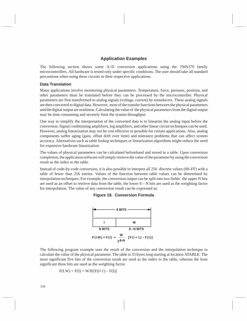
334
Application Examples
The following section shows some A/D conversion applications using the TMS370 familymicrocontrollers. All hardware is tested only under specific conditions. The user should take all standardprecautions when using these circuits in their respective applications.
Data TranslationMany applications involve monitoring physical parameters. Temperature, force, pressure, position, andother parameters must be translated before they can be processed by the microcontroller. Physicalparameters are first transformed to analog signals (voltage, current) by transducers. These analog signalsare then converted to digital data. However, most of the transfer functions between the physical parametersand the digital output are nonlinear. Calculating the value of the physical parameters from the digital outputmay be time consuming and severely limit the system throughput.
One way to simplify the interpretation of the converted data is to linearize the analog input before theconversion. Signal conditioning amplifiers, log amplifiers, and other linear circuit techniques can be used.However, analog linearization may not be cost effective or possible for certain applications. Also, analogcomponents suffer aging (gain, offset drift over time) and tolerance problems that can affect systemaccuracy. Alternatives such as table lookup techniques or linearization algorithms might reduce the needfor expensive hardware linearization.
The values of physical parameters can be calculated beforehand and stored in a table. Upon conversioncompletion, the application software will simply retrieve the value of the parameter by using the conversionresult as the index to the table.
Instead of code-by-code conversion, it is also possible to interpret all 256 discrete values (00–FF) with atable of fewer than 256 entries. Values of the function between table values can be determined byinterpolation techniques. For example, the conversion output can be split into two fields: the upper N bitsare used as an offset to retrieve data from the table, the lower 8 – N bits are used as the weighting factorfor interpolation. The value of any conversion result can be expressed as:
Figure 18. Conversion Formula
8 BITS
I W
N BITS 8–N BITS
F( I.W) = F ( I ) +W
28-N[F( I + 1 ) – F ( I ) ]
The following program example uses the result of the conversion and the interpolation technique tocalculate the value of the physical parameter. The table is 33 bytes long starting at location ATABLE. Themost significant five bits of the conversion result are used as the index to the table, whereas the leastsignificant three bits are used as the weighting factor.
F(I.W) = F(I) + W/B[F(I+1) – F(I)]
335
Assuming the conversion result is 01100010 (98), the value of the physical parameter can be calculatedby the following equation:
F(01100.010) = F(01100) + 2/8[F(01101) – F(01100)]
.REG ATABLE,33 ;33-BYTE TABLE
.REG RESULT ;REGISTER FOR FINAL RESULT
.REG ATPNT ;TEMPORARY REGISTER
;
;
BEGIN PUSH A ;SAVE REG A
PUSH B ;SAVE REG B
MOV ADDATA,ATPNT ;SAVE THE CONVERSION RESULT
MOV ATPNT,B
SWAP B ;GET THE INDEX FIELD
RL B
AND #1FH,B
;
; GET THE VALUE FROM THE TABLE
;
MOV *ATABLE[B],A ;GET F(I)
MOV A,RESULT
;
; CHECK IF INTERPOLATION NECESSARY
; IF THE MOST LEAST SIGNIFICANT THREE BITS ARE ZERO, NO
; INTERPOLATION IS NECESSARY
BTJO #07H,ATPNT,INTERP
JMP FINISH ;
INTERP INC B ;SET INDEX POINT TO NEXT ENTRY
MOV *ATABLE[B],A ;GET F(I+1)
SUB RESULT,A ;CALCULATE THE DIFFERENCE;F(I+1) – F(I)
AND #07H,ATPNT ;GET THE WEIGHTING FACTOR
MPY ATPNT,A ;W * [F(I+1) – F(I)]
;RESULT STORE IN A:B
MOV #08,ATPNT
DIV ATPNT,A ;DIVIDE A:B BY 8
ADD A,RESULT ;F(I) + INTERPOLATION VALUE
336
FINISH POP B ;RESTORE REGISTERS A AND B
POP A
RTS
TMS370 microcontrollers contain on-chip data EEPROM, which provides an excellent area to implementthe translation table. With the on-chip EEPROM capability, the translation table can be adjusted forcorrection as environmental conditions change. Also, the write protection feature of the data EEPROM canbe used to protect the translation table from inadvertent overwriting by the application software. For moredetailed information about the on-chip data EEPROM, refer to the TMS370 Family User’s Guide.
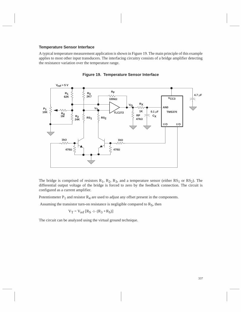
337
Temperature Sensor Interface
A typical temperature measurement application is shown in Figure 19. The main principle of this exampleapplies to most other input transducers. The interfacing circuitry consists of a bridge amplifier detectingthe resistance variation over the temperature range.
Figure 19. Temperature Sensor Interface
R1
Vref = 5 V
62K
R41M
P110K
R224K
RS1
R32K7
RF
100k
RS2
VT
470 470
1k
TLC272
VORX
RP47k
0.1 µFCX
VCC3
AN0
TMS370
I / O I / O
4.7 µF
1K
1k
The bridge is comprised of resistors R1, R2, R3, and a temperature sensor (either RS1 or RS2). Thedifferential output voltage of the bridge is forced to zero by the feedback connection. The circuit isconfigured as a current amplifier.
Potentiometer P1 and resistor R4 are used to adjust any offset present in the components.
Assuming the transistor turn-on resistance is negligible compared to RS, then
VT = Vref [RS (R3 +RS)]
The circuit can be analyzed using the virtual ground technique.
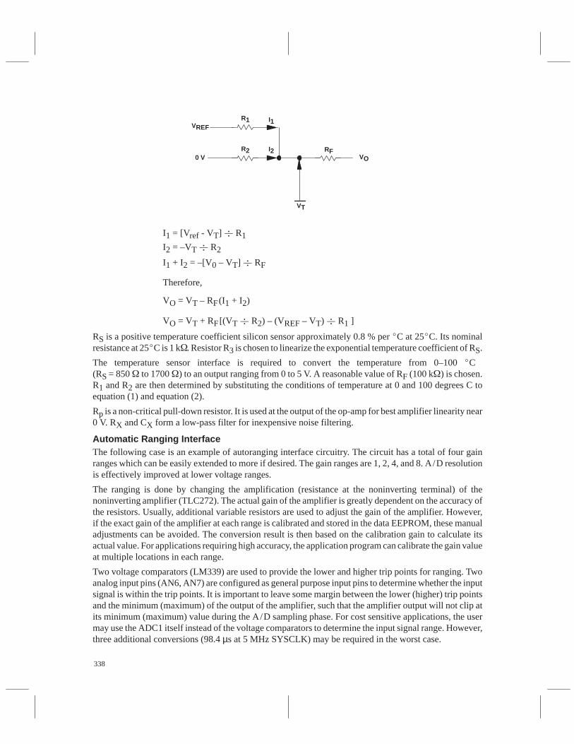
338
R1
R2
VT
VREF
0 V
I1
I2 RFVO
I1 = [Vref - VT] R1I2 = –VT R2
Therefore,
VO = VT – RF(I1 + I2)
VO = VT + RF[(VT R2) – (VREF – VT) R1 ]
I1 + I2 = –[V0 – VT] RF
RS is a positive temperature coefficient silicon sensor approximately 0.8 % perC at 25C. Its nominalresistance at 25C is 1 k. Resistor R3 is chosen to linearize the exponential temperature coefficient of RS.
The temperature sensor interface is required to convert the temperature from 0–100 C (RS = 850 to 1700 ) to an output ranging from 0 to 5 V. A reasonable value of RF (100 k) is chosen.R1 and R2 are then determined by substituting the conditions of temperature at 0 and 100 degrees C toequation (1) and equation (2).
Rp is a non-critical pull-down resistor. It is used at the output of the op-amp for best amplifier linearity near0 V. RX and CX form a low-pass filter for inexpensive noise filtering.
Automatic Ranging InterfaceThe following case is an example of autoranging interface circuitry. The circuit has a total of four gainranges which can be easily extended to more if desired. The gain ranges are 1, 2, 4, and 8. A/D resolutionis effectively improved at lower voltage ranges.
The ranging is done by changing the amplification (resistance at the noninverting terminal) of thenoninverting amplifier (TLC272). The actual gain of the amplifier is greatly dependent on the accuracy ofthe resistors. Usually, additional variable resistors are used to adjust the gain of the amplifier. However,if the exact gain of the amplifier at each range is calibrated and stored in the data EEPROM, these manualadjustments can be avoided. The conversion result is then based on the calibration gain to calculate itsactual value. For applications requiring high accuracy, the application program can calibrate the gain valueat multiple locations in each range.
Two voltage comparators (LM339) are used to provide the lower and higher trip points for ranging. Twoanalog input pins (AN6, AN7) are configured as general purpose input pins to determine whether the inputsignal is within the trip points. It is important to leave some margin between the lower (higher) trip pointsand the minimum (maximum) of the output of the amplifier, such that the amplifier output will not clip atits minimum (maximum) value during the A/D sampling phase. For cost sensitive applications, the usermay use the ADC1 itself instead of the voltage comparators to determine the input signal range. However,three additional conversions (98.4 µs at 5 MHz SYSCLK) may be required in the worst case.
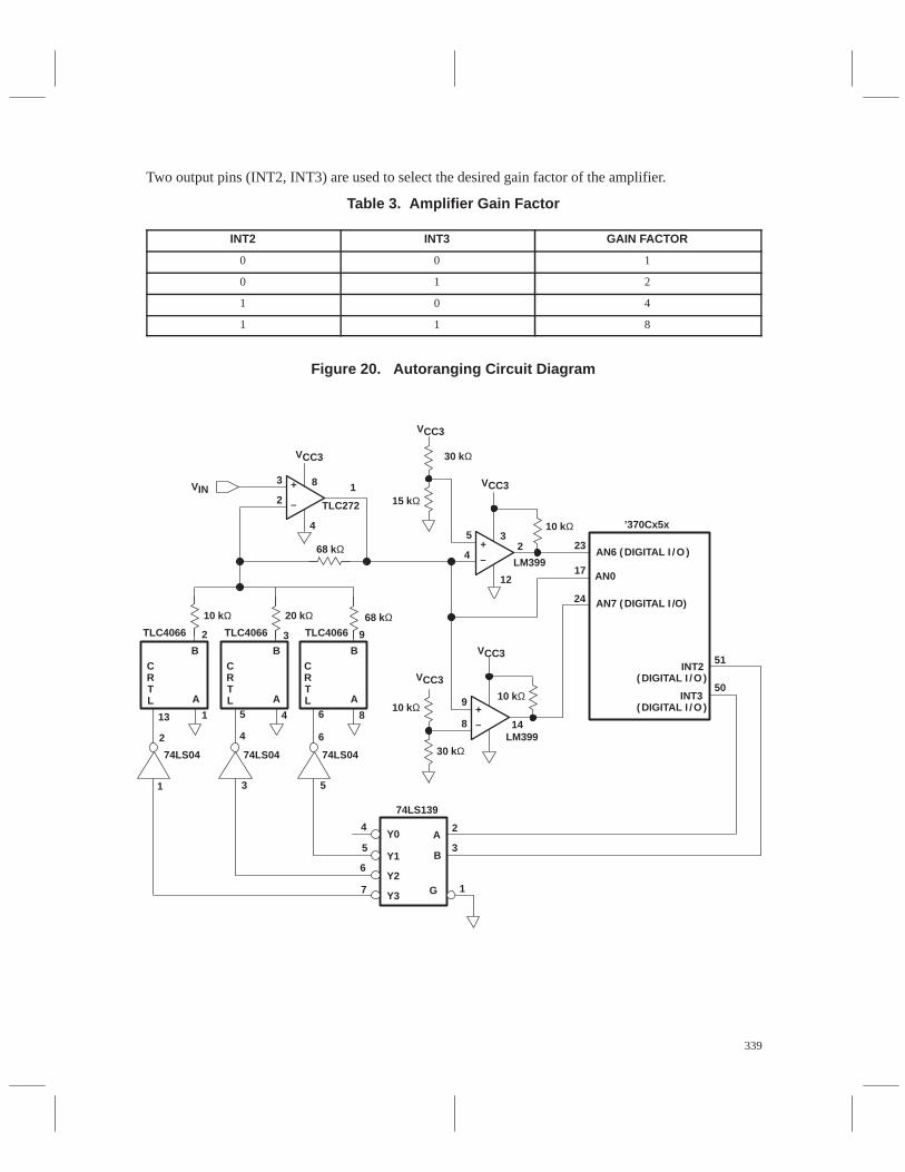
339
Two output pins (INT2, INT3) are used to select the desired gain factor of the amplifier.
Table 3. Amplifier Gain Factor
INT2 INT3 GAIN FACTOR
0 0 1
0 1 2
1 0 4
1 1 8
Figure 20. Autoranging Circuit Diagram
+
–
+–
+–
VIN3
2
VCC3
8
1
4
TLC272
68 kΩ
VCC3
30 kΩ
15 kΩ
VCC3
10 kΩ
23
LM399
LM399
10 kΩ
VCC3
17
24
5
4
32
12
’370Cx5x
AN6 ( DIGITAL I / O )
AN0
AN7 ( DIGITAL I /O)
51
50
INT2
INT3
( DIGITAL I / O )
( DIGITAL I / O )9
8 14
30 kΩ
10 kΩ
VCC3
10 kΩ 20 kΩ 68 kΩTLC4066 TLC4066 TLC40662 3 9
B B BCRTL
CRTL
CRTLA A A
13 5
42
6
6
6
4 8
4
5
7
1 3 5
74LS04 74LS04 74LS04
74LS139
1
3
2Y0
Y1
Y2
Y3
A
B
G
1
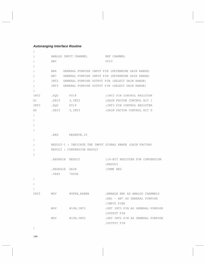
340
Autoranging Interface Routine;
; ANALOG INPUT CHANNEL REF CHANNEL
; ANC VCC3
;
; AN6 GENERAL PURPOSE INPUT PIN (DETERMINE GAIN RANGE)
; AN7 GENERAL PURPOSE INPUT PIN (DETERMINE GAIN RANGE)
; INT2 GENERAL PURPOSE OUTPUT PIN (SELECT GAIN RANGE)
; INT3 GENERAL PURPOSE OUTPUT PIN (SELECT GAIN RANGE)
;
INT2 .EQU P018 ;INT2 PIN CONTROL REGISTER
G1 .DBIT 3,INT2 ;GAIN FACTOR CONTROL BIT 1
INT3 .EQU P019 ;INT3 PIN CONTROL REGISTER
G0 .DBIT 3,INT3 ;GAIN FACTOR CONTROL BIT 0
;
;
;
;
.REG RESERVE,10
;
; RESULT-1 : INDICATE THE INPUT SIGNAL RANGE (GAIN FACTOR)
; RESULT : CONVERSION RESULT
;
.REGPAIR RESULT ;16-BIT REGISTER FOR CONVERSION
;RESULT
.REGPAIR GAIN ;TEMP REG
.TEXT 7000H
;
;
;
INIT MOV #0FEH,ADENA ;ENABLE ANO AS ANALOG CHANNELS
;AN1 — AN7 AS GENERAL PURPOSE
;INPUT PINS
MOV #10H,INT3 ;SET INT3 PIN AS GENERAL PURPOSE
;OUTPUT PIN
MOV #10H,INT2 ;SET INT2 PIN AS GENERAL PURPOSE
;OUTPUT PIN
;
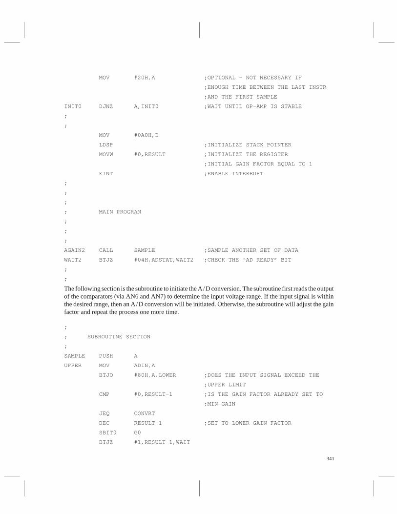
341
MOV #20H,A ;OPTIONAL — NOT NECESSARY IF
;ENOUGH TIME BETWEEN THE LAST INSTR
;AND THE FIRST SAMPLE
INIT0 DJNZ A,INIT0 ;WAIT UNTIL OP-AMP IS STABLE
;
;
MOV #0A0H,B
LDSP ;INITIALIZE STACK POINTER
MOVW #0,RESULT ;INITIALIZE THE REGISTER
;INITIAL GAIN FACTOR EQUAL TO 1
EINT ;ENABLE INTERRUPT
;
;
;
; MAIN PROGRAM
;
;
;
AGAIN2 CALL SAMPLE ;SAMPLE ANOTHER SET OF DATA
WAIT2 BTJZ #04H,ADSTAT,WAIT2 ;CHECK THE “AD READY” BIT
;
;
The following section is the subroutine to initiate the A/D conversion. The subroutine first reads the outputof the comparators (via AN6 and AN7) to determine the input voltage range. If the input signal is withinthe desired range, then an A/D conversion will be initiated. Otherwise, the subroutine will adjust the gainfactor and repeat the process one more time.
;
; SUBROUTINE SECTION
;
SAMPLE PUSH A
UPPER MOV ADIN,A
BTJO #80H,A,LOWER ;DOES THE INPUT SIGNAL EXCEED THE
;UPPER LIMIT
CMP #0,RESULT-1 ;IS THE GAIN FACTOR ALREADY SET TO
;MIN GAIN
JEQ CONVRT
DEC RESULT-1 ;SET TO LOWER GAIN FACTOR
SBIT0 G0
BTJZ #1,RESULT-1,WAIT
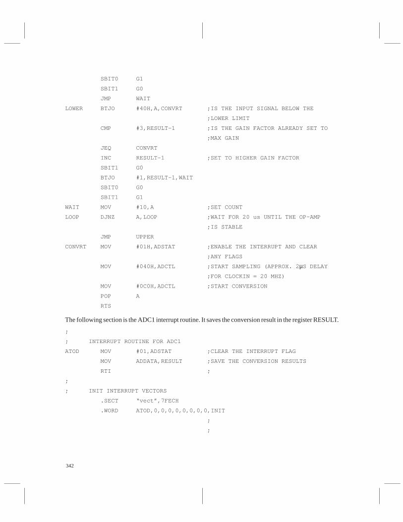
342
SBIT0 G1
SBIT1 G0
JMP WAIT
LOWER BTJO #40H,A,CONVRT ;IS THE INPUT SIGNAL BELOW THE
;LOWER LIMIT
CMP #3,RESULT-1 ;IS THE GAIN FACTOR ALREADY SET TO
;MAX GAIN
JEQ CONVRT
INC RESULT-1 ;SET TO HIGHER GAIN FACTOR
SBIT1 G0
BTJO #1,RESULT-1,WAIT
SBIT0 G0
SBIT1 G1
WAIT MOV #10,A ;SET COUNT
LOOP DJNZ A,LOOP ;WAIT FOR 20 us UNTIL THE OP-AMP
;IS STABLE
JMP UPPER
CONVRT MOV #01H,ADSTAT ;ENABLE THE INTERRUPT AND CLEAR
;ANY FLAGS
MOV #040H,ADCTL ;START SAMPLING (APPROX. 2 µS DELAY
;FOR CLOCKIN = 20 MHZ)
MOV #0C0H,ADCTL ;START CONVERSION
POP A
RTS
The following section is the ADC1 interrupt routine. It saves the conversion result in the register RESULT.
;
; INTERRUPT ROUTINE FOR ADC1
ATOD MOV #01,ADSTAT ;CLEAR THE INTERRUPT FLAG
MOV ADDATA,RESULT ;SAVE THE CONVERSION RESULTS
RTI ;
;
; INIT INTERRUPT VECTORS
.SECT “vect”,7FECH
.WORD ATOD,0,0,0,0,0,0,0,0,INIT
;
;

343
Interfacing a Serial A/D Converter with TMS370 Family Microcontrollers
The following demonstrates the interface between a 10-bit serial A/D converter (TLC1 540/1) andTMS370. This will be useful for those who want to use the TMS370 devices that do not possess on–chipADC functions but still need A/D conversion, or those systems that require high accuracy (down to 5 mVresolution) and better isolation of the analog system from the relatively noisy digital controller.
The TLC1540 and TLC1541 are both 10-bit, 11 channel serial A/D converters with sample-and-holdcircuitry. TLC1540 has ±0.5 LSB error, whereas TLC1541 has ±1 LSB error. The serial A/D converterhas four control inputs: chip select (CS), address input, I /O clock, and system clock. The first example usesthe on-chip serial peripheral interface (SPI) to interface with the serial A/D, whereas the second exampleuses software routines to interface with the serial A/D.
Using On-Chip SPI
Figure 21 shows the circuit diagram of the interface between TLC1540/1 and TMS370. This sectiondescribes the interface of a 10-bit serial A/D converter through the SPI. The system clock of theTLC1540/1 is provided by the CLKOUT pin of the TMS370. Note that the maximum TLC1540/1 systemclock frequency is only 2.1 MHz; an additional frequency divider/counter may required if the SYSCLKfrequency is higher than 2.1 MHz.
The serial A/D receives the I/O clock 500 ns after (delay by the dual D flip-flops as shift register) theSPICLK is active; this ensures enough set up time for the channel address. The conversion cycle takes 44TLC1540/1 system clock cycles and is initiated on the tenth falling edge of the I /O clock.
The following example program converts data from all 11 channels consecutively. It assumes a TMS370using an 8.4 MHz crystal; for example, 2.1 MHz for CLKOUT. If the application program requires differentsystem clock rates or I /O transmission clock rates, you must ensure that the time between executing theinstruction at label TRAN8 for initiating the conversion and TRAN2 for transmitting the next channeladdress is greater than the time transmitting 8-bit data plus 44 TLC1540/1 system clock cycles.
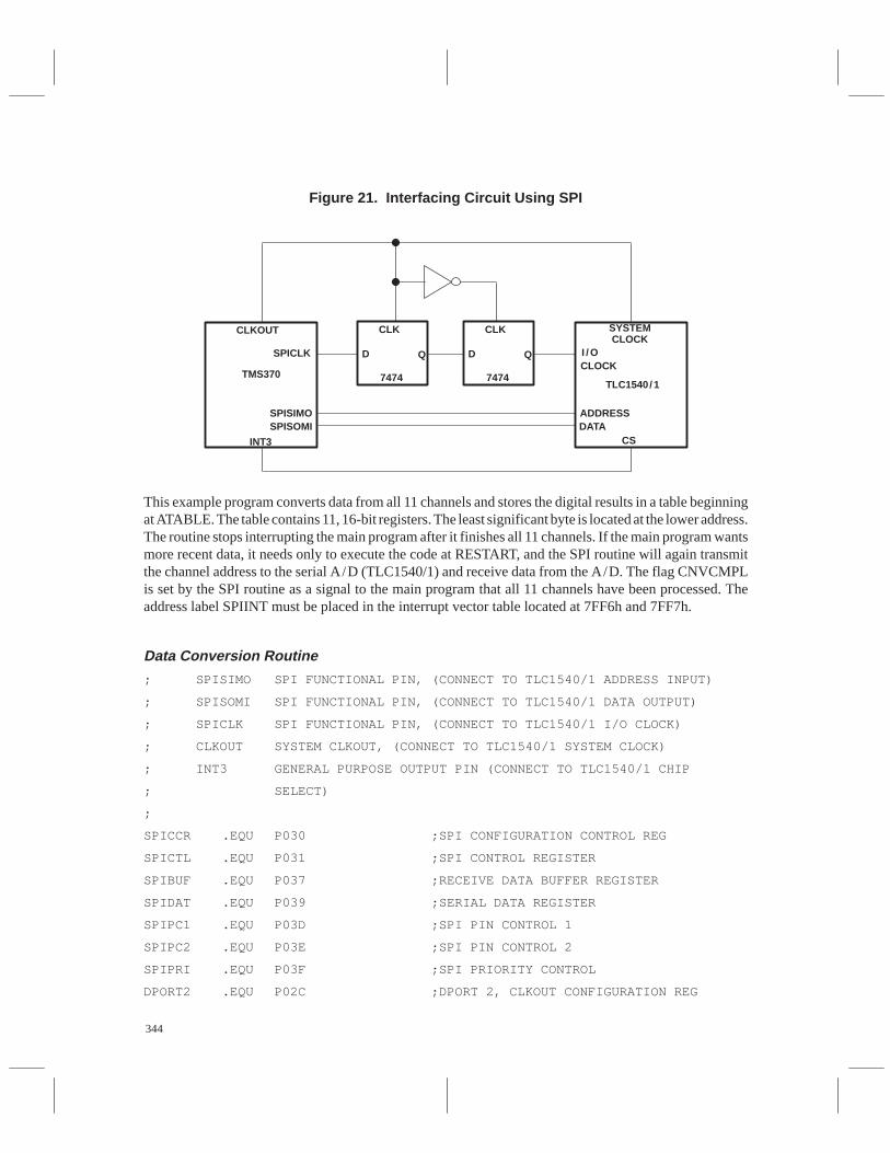
344
Figure 21. Interfacing Circuit Using SPI
CLKOUT
SPICLK
TMS370
SPISIMOSPISOMI
INT3
CLK
D Q
7474
CLK
D Q
7474
SYSTEMCLOCK
I / O
TLC1540/ 1
ADDRESSDATA
CS
CLOCK
This example program converts data from all 11 channels and stores the digital results in a table beginningat ATABLE. The table contains 11, 16-bit registers. The least significant byte is located at the lower address.The routine stops interrupting the main program after it finishes all 11 channels. If the main program wantsmore recent data, it needs only to execute the code at RESTART, and the SPI routine will again transmitthe channel address to the serial A/D (TLC1540/1) and receive data from the A/D. The flag CNVCMPLis set by the SPI routine as a signal to the main program that all 11 channels have been processed. Theaddress label SPIINT must be placed in the interrupt vector table located at 7FF6h and 7FF7h.
Data Conversion Routine
; SPISIMO SPI FUNCTIONAL PIN, (CONNECT TO TLC1540/1 ADDRESS INPUT)
; SPISOMI SPI FUNCTIONAL PIN, (CONNECT TO TLC1540/1 DATA OUTPUT)
; SPICLK SPI FUNCTIONAL PIN, (CONNECT TO TLC1540/1 I/O CLOCK)
; CLKOUT SYSTEM CLKOUT, (CONNECT TO TLC1540/1 SYSTEM CLOCK)
; INT3 GENERAL PURPOSE OUTPUT PIN (CONNECT TO TLC1540/1 CHIP
; SELECT)
;
SPICCR .EQU P030 ;SPI CONFIGURATION CONTROL REG
SPICTL .EQU P031 ;SPI CONTROL REGISTER
SPIBUF .EQU P037 ;RECEIVE DATA BUFFER REGISTER
SPIDAT .EQU P039 ;SERIAL DATA REGISTER
SPIPC1 .EQU P03D ;SPI PIN CONTROL 1
SPIPC2 .EQU P03E ;SPI PIN CONTROL 2
SPIPRI .EQU P03F ;SPI PRIORITY CONTROL
DPORT2 .EQU P02C ;DPORT 2, CLKOUT CONFIGURATION REG
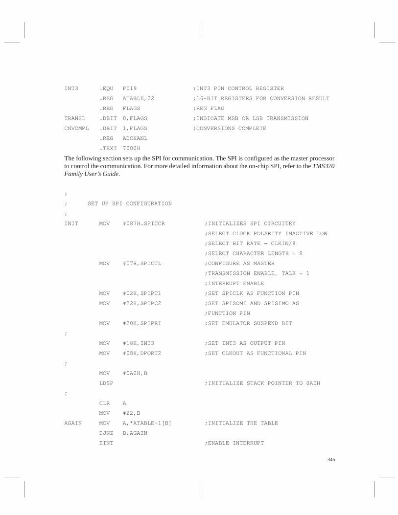
345
INT3 .EQU P019 ;INT3 PIN CONTROL REGISTER
.REG ATABLE,22 ;16-BIT REGISTERS FOR CONVERSION RESULT
.REG FLAGS ;REG FLAG
TRANSL .DBIT 0,FLAGS ;INDICATE MSB OR LSB TRANSMISSION
CNVCMPL .DBIT 1,FLAGS ;CONVERSIONS COMPLETE
.REG ADCHANL
.TEXT 7000H
The following section sets up the SPI for communication. The SPI is configured as the master processorto control the communication. For more detailed information about the on-chip SPI, refer to the TMS370Family User’s Guide.
;
; SET UP SPI CONFIGURATION
;
INIT MOV #087H.SPICCR ;INITIALIZES SPI CIRCUITRY
;SELECT CLOCK POLARITY INACTIVE LOW
;SELECT BIT RATE = CLKIN/8
;SELECT CHARACTER LENGTH = 8
MOV #07H,SPICTL ;CONFIGURE AS MASTER
;TRANSMISSION ENABLE, TALK = 1
;INTERRUPT ENABLE
MOV #02H,SPIPC1 ;SET SPICLK AS FUNCTION PIN
MOV #22H,SPIPC2 ;SET SPISOMI AND SPISIMO AS
;FUNCTION PIN
MOV #20H,SPIPRI ;SET EMULATOR SUSPEND BIT
;
MOV #18H,INT3 ;SET INT3 AS OUTPUT PIN
MOV #08H,DPORT2 ;SET CLKOUT AS FUNCTIONAL PIN
;
MOV #0A0H,B
LDSP ;INITIALIZE STACK POINTER TO 0A0H
;
CLR A
MOV #22,B
AGAIN MOV A,*ATABLE–1[B] ;INITIALIZE THE TABLE
DJNZ B,AGAIN
EINT ;ENABLE INTERRUPT
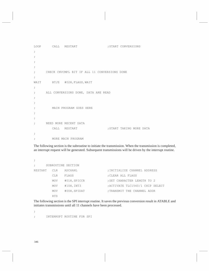
346
LOOP CALL RESTART ;START CONVERSIONS
;
;
;
;
; CHECK CNVCMPL BIT IF ALL 11 CONVERSIONS DONE
;
WAIT BTJZ #02H,FLAGS,WAIT
;
; ALL CONVERSIONS DONE, DATA ARE READ
;
;
; MAIN PROGRAM GOES HERE
;
;
; NEED MORE RECENT DATA
CALL RESTART ;START TAKING MORE DATA
;
; MORE MAIN PROGRAM
The following section is the subroutine to initiate the transmission. When the transmission is completed,an interrupt request will be generated. Subsequent transmissions will be driven by the interrupt routine.
;
; SUBROUTINE SECTION
RESTART CLR ADCHANL ;INITIALIZE CHANNEL ADDRESS
CLR FLAGS ;CLEAR ALL FLAGS
MOV #01H,SPICCR ;SET CHARACTER LENGTH TO 2
MOV #10H,INT3 ;ACTIVATE TLC1540/1 CHIP SELECT
MOV #00H,SPIDAT ;TRANSMIT THE CHANNEL ADDR
RTS
The following section is the SPI interrupt routine. It saves the previous conversion result in ATABLE andinitiates transmissions until all 11 channels have been processed.
;
; INTERRUPT ROUTINE FOR SPI
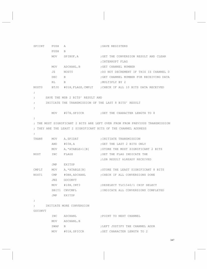
347
SPIINT PUSH A ;SAVE REGISTERS
PUSH B
MOV SPIBUF,A ;GET THE CONVERSION RESULT AND CLEAR
;INTERRUPT FLAG
MOV ADCHANL,B ;GET CHANNEL NUMBER
JZ NOST0 ;DO NOT DECREMENT IF THIS IS CHANNEL 0
DEC B ;GET CHANNEL NUMBER FOR RECEIVING DATA
RL B ;MULTIPLY BY 2
NOST0 BTJO #01H,FLAGS,CMPLT ;CHECK IF ALL 10 BITS DATA RECEIVED
;
; SAVE THE MSB 2 BITS’ RESULT AND
; INITIATE THE TRANSMISSION OF THE LAST 8 BITS’ RESULT
;
MOV #07H,SPICCR ;SET THE CHARACTER LENGTH TO 8
;
; THE MOST SIGNIFICANT 2 BITS ARE LEFT OVER FROM FROM PREVIOUS TRANSMISSION
; THEY ARE THE LEAST 2 SIGNIFICANT BITS OF THE CHANNEL ADDRESS
;
TRAN8 MOV A,SPIDAT ;INITIATE TRANSMISSION
AND #03H,A ;GET THE LAST 2 BITS ONLY
MOV A,*ATABLE+1[B] ;STORE THE MOST SIGNIFICANT 2 BITS
NOST INC FLAGS ;SET THE FLAG INDICATE THE
;LSB RESULT ALREADY RECEIVED
JMP EXITSP
CMPLT MOV A,*ATABLE[B] ;STORE THE LEAST SIGNIFICANT 8 BITS
NOST1 CMP #0BH,ADCHANL ;CHECK IF ALL CONVERSIONS DONE
JNZ GOCONVT
MOV #18H,INT3 ;DESELECT TLC1540/1 CHIP SELECT
SBIT1 CNVCMPL ;INDICATE ALL CONVERSIONS COMPLETED
JMP EXITSP
;
; INITIATE MORE CONVERSION
GOCONVT
INC ADCHANL ;POINT TO NEXT CHANNEL
MOV ADCHANL,B
SWAP B ;LEFT JUSTIFY THE CHANNEL ADDR
MOV #01H,SPICCR ;SET CHARACTER LENGTH TO 2
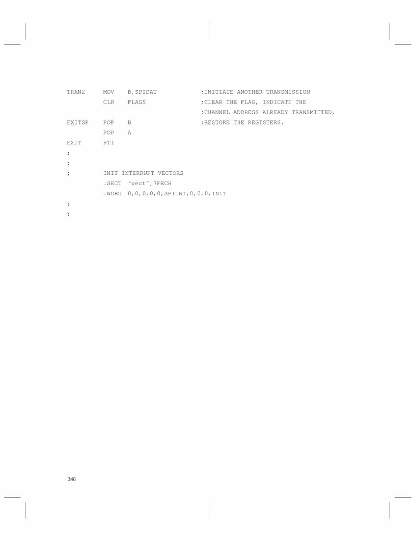
348
TRAN2 MOV B,SPIDAT ;INITIATE ANOTHER TRANSMISSION
CLR FLAGS ;CLEAR THE FLAG, INDICATE THE
;CHANNEL ADDRESS ALREADY TRANSMITTED,
EXITSP POP B ;RESTORE THE REGISTERS.
POP A
EXIT RTI
;
;
; INIT INTERRUPT VECTORS
.SECT “vect”,7FECH
.WORD 0,0,0,0,0,SPIINT,0,0,0,INIT
;
;
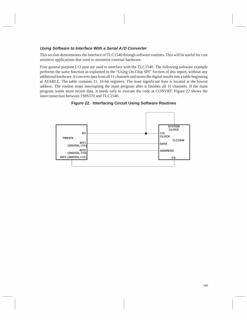
349
Using Software to Interface With a Serial A/D Converter
This section demonstrates the interface of TLC1540 through software routines. This will be useful for costsensitive applications that need to minimize external hardware.
Four general purpose I /O pins are used to interface with the TLC1540. The following software exampleperforms the same function as explained in the “Using On-Chip SPI” Section of this report, without anyadditional hardware. It converts data from all 11 channels and stores the digital results into a table beginningat ATABLE. The table contains 11, 16-bit registers. The least significant byte is located at the lowestaddress. The routine stops interrupting the main program after it finishes all 11 channels. If the mainprogram wants more recent data, it needs only to execute the code at CONVRT. Figure 22 shows theinterconnection between TMS370 and TLC1540.
Figure 22. Interfacing Circuit Using Software Routines
D3
TMS370
INT3
SYSTEMCLOCK
I / OCLOCK
TLC1540
ADDRESS
DATA
CS
INT1
INT2
( DIGITAL I / O )
( DIGITAL I / O)
( DIGITAL I / O )
350
Interfacing Software Routines;
;
; D3/CLKOUT GENERAL PURPOSE OUTPUT PIN, (CONNECT TO TLC1540/1
; I/O CLOCK AND TLC1540/1 SYSTEM CLOCK)
; INT1 GENERAL PURPOSE INPUT PIN (CONNECT TO TLC1540/1
; DATA OUTPUT)
; INT2 GENERAL PURPOSE OUTPUT PIN (CONNECT TO TLC1540/1
; ADDRESS INPUT)
; INT3 GENERAL PURPOSE OUTPUT PIN (CONNECT TO TLC1540/1
; CHIP SELECT)
DPORT1 .EQU P02C ;DPORT 1, CLKOUT CONFIGURATION REG
DPORT2 .EQU P02D ;DPORT 2, CLKOUT CONFIGURATION REG
DDATA .EQU P02E ;DPORT DATA REG
DDIR .EQU P02F ;DPORT DATA DIR REG
INT1 .EQU P017 ;INT1 PIN CONTROL REGISTER
INT2 .EQU P018 ;INT2 PIN CONTROL REGISTER
INT3 .EQU P019 ;INT3 PIN CONTROL REGISTER
.REG RESERVE,10
.REG ATABLE,22 ;16-BIT REGISTERS FOR CONVERSION RESULT
.REGPAIR RESULT,2 ;TEMPORARY RESULT REGISTER
.REG FLAG ;REG FLAG
.REG ADCHANL
.REG BITCNT
.REG CHNLCNT
IOCLK .DBIT 3,DDATA ;TLC1540 SYSTEM CLOCK
;AND I/O CLOCK FOR TRANSMISSION
CS .DBIT 3,INT3 ;TLC1540 CHIP SELECT
ADADDR .DBIT 3,INT2 ;TLC1540 ADDRESS INPUT
DATAOUT .DBIT 6,INT1 ;TLC1540 DATA OUTPUT
;
;
.TEXT 7000H
;
;

351
BEGIN MOV #18H,INT3 ;SET INT3 AS OUTPUT PIN
MOV #18H,INT2 ;SET INT2 AS OUTPUT PIN
MOV #00H,DPORT1 ;SET CLKOUT AS GENERAL PURPOSE I/O
MOV #00H,DPORT2
MOV #08H,DDIR
;
MOV #0A0H,B
LDSP ;INITIALIZE STACK POINTER TO 0A0H
;
CLR A
MOV #22,B
AGAIN MOV A,*ATABLE–1[B] ;INITIALIZE THE TABLE
DJNZ B,AGAIN
EINT ;ENABLE INTERRUPT
LOOP CALL CONVRT ;START CONVERSIONS
;
;
;
;
;
; MAIN PROGRAM GOES HERE
;
;
;
;
; NEED MORE RECENT DATA
NOP
CALL CONVRT ;START TAKING MORE DATA
NOP
;
; MORE MAIN PROGRAM
;
352
The following section is the subroutine CONVRT that initiates the A/D conversion. It sets up the channeladdress and invokes subroutine ADTRAN for serial transmission. When the transmission finishes, it savesthe previous conversion result in ATABLE and generates 44 I /O clocks for current A/D conversion.
;
; SUBROUTINE SECTION
;
;
; SUBROUNTINE CONVRT
;
; ENTER : NO PARAMETERS
; EXIT : ATABLE - FILL 22 ENTRIES STARTING FROM ATABLE
CONVRT PUSH A
PUSH B
CLR ADCHANL ;INITIALIZE CHANNEL ADDRESS
;THE UPPER 4 BITS INDICATE THE CHANNEL
;ADDRESS
CLR FLAG ;CLEAR ALL FLAGS
MOV #12,CHNLCNT ;SET COUNT TO NUMBER OF CHANNELS + 1
;ONE MORE TRANSMISSION TO READ BACK
;THE CONVERSION RESULT
NEXT MOV ADCHANL,B ;
SWAP B ;PASS THE CHANNEL ADDRESS TO
;SUBROUTINE THROUGH REGISTER B,
;THE UPPER 4 BITS IS THE CHANNEL ADDRESS
CLR RESULT ;CLEAR THE TEMPORARY REGISTER
CLR RESULT–1
CALL ADTRAN ;TRANSMIT ADDRESS AND RECEIVE DATA
MOV ADCHANL,B ;IS THE CHANNEL ADDRESS 0?
JZ SKSAVE ;SKIP THE FIRST ONE
RLC B ;MULTIPLY BY TWO
MOV RESULT–1,A ;SAVE THE RESULT
MOV A,*ATABLE–2[B]
MOV RESULT,A
MOV A,*ATABLE–1[B]
SKSAVE INC ADCHANL ;NEXT CHANNEL
;
MOV #44,B
353
REPEAT SBIT1 IOCLK ;44 SYSTEM CLOCKS FOR CONVERSION
SBIT0 IOCLK
DJNZ B,REPEAT
;
DJNZ CHNLCNT,NEXT
POP B
POP A
RTS
The following section is subroutine ADTRAN that handles the communication between TMS370 andTLC1540/1.
;
; SUBROUTINE ADTRAN
;
; BIT BANGING ROUTINE
; TRANSMITTING AND RECEIVING DATA TO/FROM TLC1540
;
; ENTER : B - AD CHANNEL ADDRESS (UPPER 4 BITS)
; EXIT : RESULT - 10-BIT RESULT
;
ADTRAN SBIT0 CS ;CHIP SELECT ACTIVE
SBIT1 IOCLK ;SEND TWO CLOCK PULSES TO TLC1540
SBIT0 IOCLK
SBIT1 IOCLK
SBIT0 IOCLK
MOV #8,BITCNT ;SET UP COUNTER
ADRTRA SBIT1 ADADDR ;TRANSMIT THE ADDRESS
RL B
JC BIT1 ;IS ADDRESS EQUAL TO 1
SBIT0 ADADDR ;NO, SET IT BACK TO 0
BIT1 SBIT1 IOCLK
RLC RESULT ;GET THE CONVERTED RESULT
RLC RESULT-1 ;THE BIT IS EQUAL TO 1
JBIT0 DATAOUT,BIT0 ;IS THE DATA BIT EQUAL TO 0
OR #1,RESULT ;NO, SET IT BACK TO 1
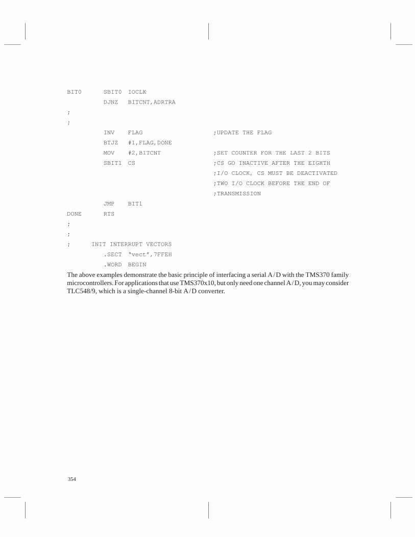
354
BIT0 SBIT0 IOCLK
DJNZ BITCNT,ADRTRA
;
;
INV FLAG ;UPDATE THE FLAG
BTJZ #1,FLAG,DONE
MOV #2,BITCNT ;SET COUNTER FOR THE LAST 2 BITS
SBIT1 CS ;CS GO INACTIVE AFTER THE EIGHTH
;I/O CLOCK, CS MUST BE DEACTIVATED
;TWO I/O CLOCK BEFORE THE END OF
;TRANSMISSION
JMP BIT1
DONE RTS
;
;
; INIT INTERRUPT VECTORS
.SECT “vect”,7FFEH
.WORD BEGIN
The above examples demonstrate the basic principle of interfacing a serial A/D with the TMS370 familymicrocontrollers. For applications that use TMS370x10, but only need one channel A/D, you may considerTLC548/9, which is a single-channel 8-bit A/D converter.

355
Conclusions
This application report provides information on using the ADC1 converter module with the TMS370family microcontrollers to a provide cost-effective system solution. Examples have been given todemonstrate the operation of the ADC1, typical methods of interfacing to the external circuits, andinteractions with other modules. The TMS370 on-chip timer provides a handy method to control thesampling frequency of conversions. Calibration data of analog components can be stored in the dataEEPROM module. This data can be used to adjust the conversion result to achieve high system accuracywhile using inexpensive analog components.
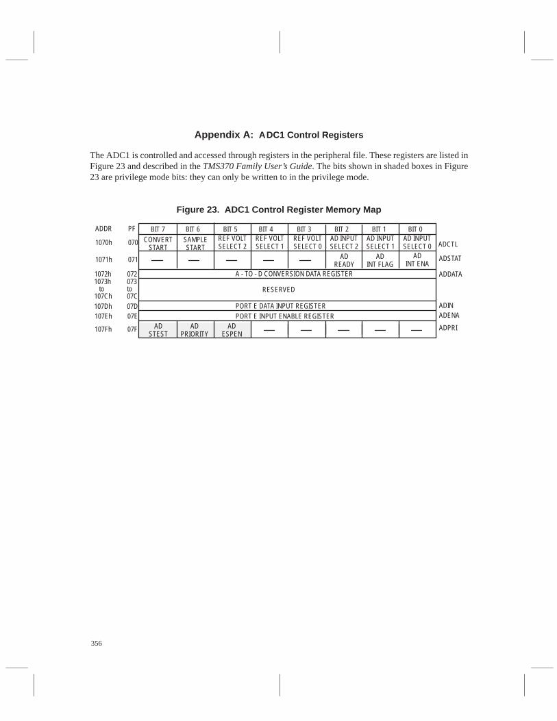
356
Appendix A: ADC1 Control Registers
The ADC1 is controlled and accessed through registers in the peripheral file. These registers are listed inFigure 23 and described in the TMS370 Family User’s Guide. The bits shown in shaded boxes in Figure23 are privilege mode bits: they can only be written to in the privilege mode.
Figure 23. ADC1 Control Register Memory Map
BIT 7 BIT 6 BIT 5 BIT 4 BIT 3 BIT 2 BIT 1 BIT 0CONVERT
STARTSAMPLESTART
REF VOLTSELECT 2
ADINT ENA
RESERVED
PORT E DATA INPUT REGISTER
ADSTEST
ADPRIORITY
ADESPEN
ADDR PF
1070h 070
1071h 071
1073h 073 to to107Ch 07C107Dh 07D107Eh 07E
ADSTAT
1072h 072 A - TO - D CONVERSION DATA REGISTER
PORT E INPUT ENABLE REGISTER
107Fh 07F
ADCTL
ADDATA
ADINADENA
ADPRI
REF VOLTSELECT 1
REF VOLTSELECT 0
AD INPUTSELECT 0
AD INPUTSELECT 1
AD INPUTSELECT 2
ADINT FLAG
ADREADY
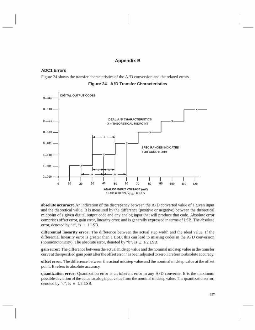
357
Appendix B
ADC1 Errors
Figure 24 shows the transfer characteristics of the A/D conversion and the related errors.
Figure 24. A/D Transfer Characteristics
X
X
X
X
X
X
a
b
a
cc
X
DIGITAL OUTPUT CODES
IDEAL A / D CHARACTERISTICSX = THEORETICAL MIDPOINT
SPEC RANGES INDICATED
FOR CODE 0...010
ANALOG INPUT VOLTAGE (mV)1 LSB = 20 mV, V REF = 5.1 V
0...000
0...001
0...010
0...011
0...100
0...101
0...110
0...111
0 10 20 30 40 50 60 70 80 90 100 110 120
absolute accuracy: An indication of the discrepancy between the A/D converted value of a given inputand the theoretical value. It is measured by the difference (positive or negative) between the theoreticalmidpoint of a given digital output code and any analog input that will produce that code. Absolute errorcomprises offset error, gain error, linearity error, and is generally expressed in terms of LSB. The absoluteerror, denoted by “a”, is 1 LSB.
differential linearity error: The difference between the actual step width and the ideal value. If thedifferential linearity error is greater than 1 LSB, this can lead to missing codes in the A/D conversion(nonmonotonicity). The absolute error, denoted by “b”, is 1/2 LSB.
gain error: The difference between the actual midstep value and the nominal midstep value in the transfercurve at the specified gain point after the offset error has been adjusted to zero. It refers to absolute accuracy.
offset error: The difference between the actual midstep value and the nominal midstep value at the offsetpoint. It refers to absolute accuracy.
quantization error: Quantization error is an inherent error in any A/D converter. It is the maximumpossible deviation of the actual analog input value from the nominal midstep value. The quantization error,denoted by “c”, is 1/2 LSB.
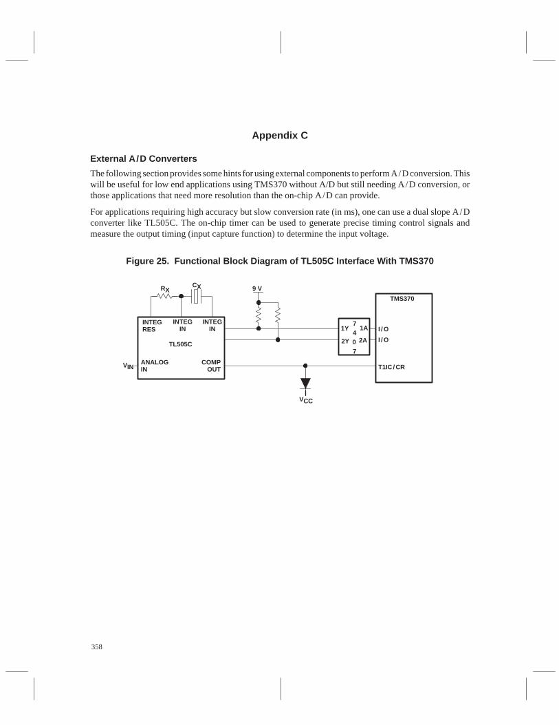
358
Appendix C
External A/D Converters
The following section provides some hints for using external components to perform A/D conversion. Thiswill be useful for low end applications using TMS370 without A/D but still needing A/D conversion, orthose applications that need more resolution than the on-chip A/D can provide.
For applications requiring high accuracy but slow conversion rate (in ms), one can use a dual slope A/Dconverter like TL505C. The on-chip timer can be used to generate precise timing control signals andmeasure the output timing (input capture function) to determine the input voltage.
Figure 25. Functional Block Diagram of TL505C Interface With TMS370
INTEGRES
INTEGIN
INTEGIN
TL505C
ANALOGIN
COMPOUT
VIN
VCC
T1IC / CR
I / O
I / O
TMS370
9 VCXRX
1Y7407
2Y
1A
2A
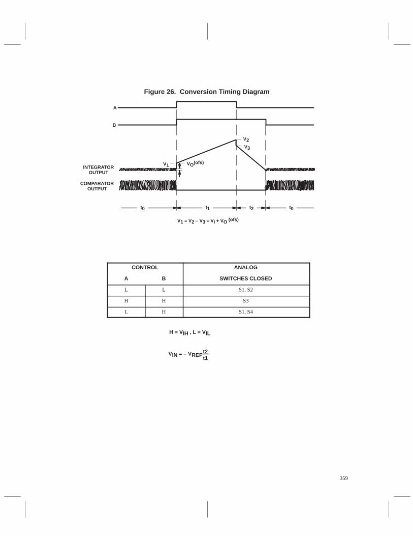
359
Figure 26. Conversion Timing Diagram
VO(ofs)V1
V2V3
A
B
INTEGRATOROUTPUT
COMPARATOROUTPUT
t0 t1 t2 t0
V1 = V2 – V3 = VI + VO (ofs)
CONTROL ANALOG
A B SWITCHES CLOSED
L L S1, S2
H H S3
L H S1, S4
VIN = – VREFt2t1
H = VIH , L = VIL
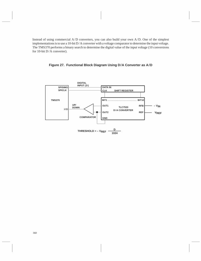
360
Instead of using commercial A/D converters, you can also build your own A/D. One of the simplestimplementations is to use a 10-bit D/A converter with a voltage comparator to determine the input voltage.The TMS370 performs a binary search to determine the digital value of the input voltage (10 conversionsfor 10-bit D/A converter).
Figure 27. Functional Block Diagram Using D/A Converter as A/D
UP/DOWN
OUT1
OUT2
GND
BIT1 BIT10. . . . . . . . . . . . . . . . . . . . . . . . .
TLC7533D / A CONVERTER
RFB
REF
DATA INCLK SHIFT REGISTER
COMPARATOR
DIGITALINPUT ( D )
THRESHOLD = – VREFD
1024
– VIN
VREF
SPISIMOSPICLK
TMS370
I / O
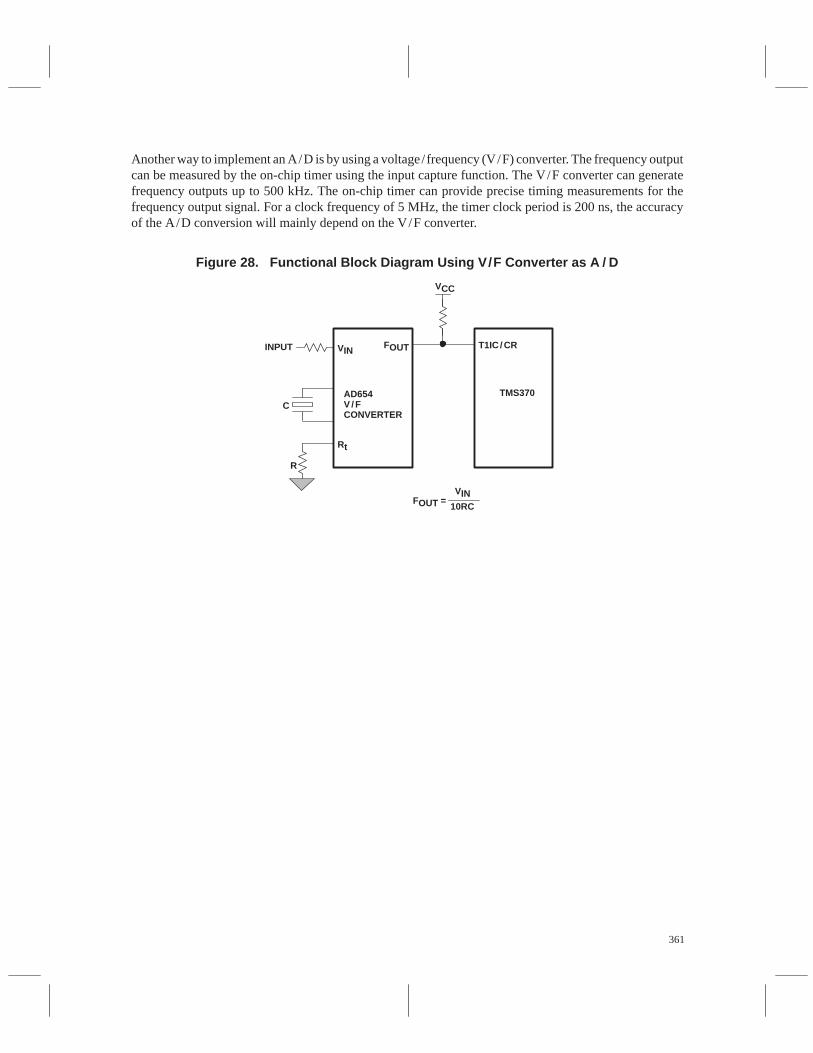
361
Another way to implement an A/D is by using a voltage/frequency (V/F) converter. The frequency outputcan be measured by the on-chip timer using the input capture function. The V/F converter can generatefrequency outputs up to 500 kHz. The on-chip timer can provide precise timing measurements for thefrequency output signal. For a clock frequency of 5 MHz, the timer clock period is 200 ns, the accuracyof the A/D conversion will mainly depend on the V/F converter.
Figure 28. Functional Block Diagram Using V/F Converter as A / D
AD654V / FCONVERTER
T1IC / CRFOUT
Rt
TMS370
VCC
R
C
INPUT VIN
FOUT =VIN
10RC

362
Appendix D: A /D Testing
The following section provides information about testing two A / D converter parameters, absoluteaccuracy and differential linearity error.
Table 4. Test Conditions
SYSCLK 0.5 MHz and 5 MHz
VCC3 5.5 V
Vref 5.1 V
Sampling time 2 µs (SYSCLK = 5 MHz)20 µs (SYSCLK = 0.5 MHz)
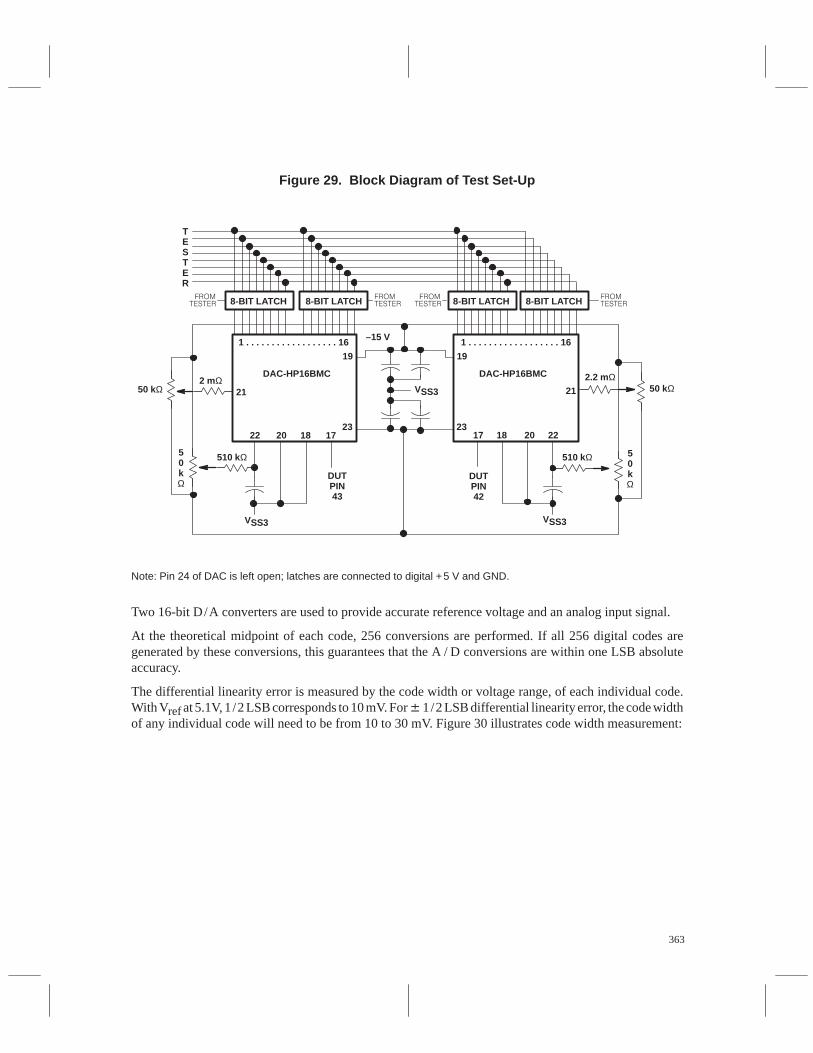
363
Figure 29. Block Diagram of Test Set-Up
8-BIT LATCH 8-BIT LATCH 8-BIT LATCH 8-BIT LATCH
TESTER
50 kΩ2 mΩ
510 kΩ50kΩ
VSS3 VSS3
50 kΩ
50kΩ
510 kΩ
2.2 mΩ
DUTPIN43
DUTPIN42
VSS3
–15 V1 . . . . . . . . . . . . . . . . . . 16
19
21
22 20 18 1723
DAC-HP16BMC
1 . . . . . . . . . . . . . . . . . . 16
19
23
21
22201817
DAC-HP16BMC
Note: Pin 24 of DAC is left open; latches are connected to digital +5 V and GND.
Two 16-bit D/A converters are used to provide accurate reference voltage and an analog input signal.
At the theoretical midpoint of each code, 256 conversions are performed. If all 256 digital codes aregenerated by these conversions, this guarantees that the A / D conversions are within one LSB absoluteaccuracy.
The differential linearity error is measured by the code width or voltage range, of each individual code.With Vref at 5.1V, 1/2 LSB corresponds to 10 mV. For 1/2 LSB differential linearity error, the code widthof any individual code will need to be from 10 to 30 mV. Figure 30 illustrates code width measurement:
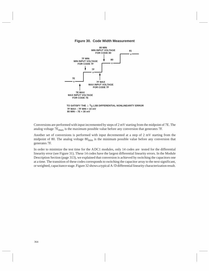
364
Figure 30. Code Width Measurement
x
x
x
x
80 MINMIN INPUT VOLTAGE
FOR CODE 80
7F MINMIN INPUT VOLTAGE
FOR CODE 7F
7E MAXMAX INPUT VOLTAGE
FOR CODE 7E
7F MAXMAX INPUT VOLTAGE
FOR CODE 7F
7E
7F
80
81
TO SATISFY THE 1⁄2 LSB DIFFERENTIAL NONLINEARITY ERROR7F MAX – 7F MIN > 10 mV80 MIN – 7E < 30 mV
Conversions are performed with input incremented by steps of 2 mV starting from the midpoint of 7E. Theanalog voltage 7Emax is the maximum possible value before any conversion that generates 7F.
Another set of conversions is performed with input decremented at a step of 2 mV starting from themidpoint of 80. The analog voltage 80min is the minimum possible value before any conversion thatgenerates 7F.
In order to minimize the test time for the ADC1 modules, only 14 codes are tested for the differentiallinearity error (see Figure 31). These 14 codes have the largest differential linearity errors. In the ModuleDescription Section (page 313), we explained that conversion is achieved by switching the capacitors oneat a time. The transition of these codes corresponds to switching the capacitor array to the next significant,or weighted, capacitance stage. Figure 32 shows a typical A/D differential linearity characterization result.
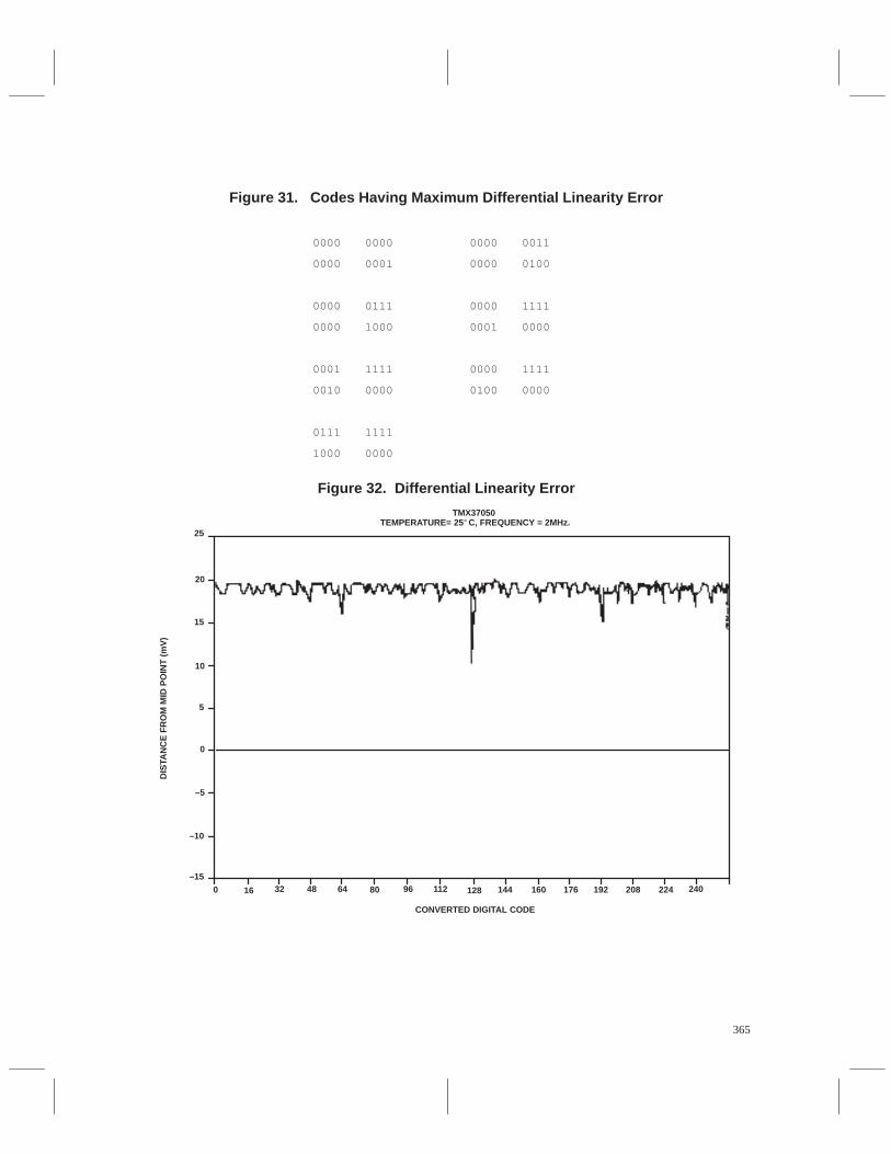
365
Figure 31. Codes Having Maximum Differential Linearity Error
0000 0000 0000 0011
0000 0001 0000 0100
0000 0111 0000 1111
0000 1000 0001 0000
0001 1111 0000 1111
0010 0000 0100 0000
0111 1111
1000 0000
Figure 32. Differential Linearity Error
CONVERTED DIGITAL CODE
TMX37050 TEMPERATURE= 25° C, FREQUENCY = 2MHz.
DIS
TAN
CE
FR
OM
MID
PO
INT
(m
V)
25
20
15
10
5
0
–5
–10
–15
0 16 32 48 64 80 96 112 128 144 160 176 192 208 224 240

366
Glossary
aliasing signal: The false lower frequency signal reconstructed from an analog input because ofinsufficient sampling rate (see Nyquist Criterion).
conversion speed: Provides an indication of system sampling rate. It is usually expressed in conversionsper second.
code width or step width: The voltage corresponding to the difference between two adjacent codetransitions.
input leakage: Leakage current of an analog input pin.
monotonicity: The state of having at least one analog input voltage for every possible digital output code(that is, no missing code) occurring in ascending or descending order.
Nyquist criterion: A criterion that requires using a sampling frequency which is greater than twice thatof the highest frequency to be sampled to recover the original signal without distortion.
ratiometric conversion: The output of an A/D conversion which is a digital number proportional to theratio of the input to a fixed or variable reference. In some applications where the measurement is affectedby the slow, varying changes of the reference voltage comparable to the conversion time, it is advantageousto use that same reference as the reference for the conversion to eliminate the effect of variation.
resolution: The ability of the converter to distinguish between adjacent analog input levels. An 8-bitconverter is capable of distinguishing between input levels that differ by 1/256 of the full scale range.
sample-and-hold circuit: A circuit that accurately acquires and stores an analog voltage on a capacitorfor a certain period of time.
transducer: A device that converts input energy of one form into output energy of another, such as anelectrical signal.

367
References
Linear Applications Group, Linear Circuits Applications, LinCMOS Products: Op-Amps, Comparatorsand Timers, Texas Instruments Technical Publishing, Dallas, Texas, 1987.
Linear Applications Handbook, Linear Technology Corporation, Milpitas, California, 1987.
Linear Products, TLC1540 LinCMOS 10-Bit Analog-to-Digital Converter, Texas Instruments TechnicalPublishing, Dallas, Texas, 1986.
McCreary, James L, “All-MOS Charge Redistribution Analog-to-Digital Conversion Technique.” IEEEJournal of Solid-State Circuits, 1975.
Pippenger, D.E., and Tobaben, E. J. Linear and Interface Circuits Applications, Texas InstrumentsTechnical Publishing, Dallas, Texas, 1986.
Sheingold, Daniel H, Transducer Interface Handbook, Analog Devices, Inc, Massachusetts, 1981.
The Handbook of Linear IC Applications, Burr-Brown Corporation, Tucson, Arizona, 1987.
T. I. Microcontroller Applications Group, TMS370 Family User’s Guide, Texas Instruments TechnicalPublishing, Dallas, Texas, 1996.
T. I. Microcontroller Group, TMS370 Family Assembly Language Tools User’s Guide, Texas InstrumentsTechnical Publishing, Dallas, Texas, 1996.
T. I. Microcontroller Group, TMS370Cx5x 8-Bit Microcontrollers, Texas Instruments TechnicalPublishing, Dallas, Texas, 1995.

368

369
Analog-to-Digital (A/D) Helpful Hints
Michael S. StewartMicrocontroller Products — Semiconductor Group
Texas Instruments

370
371
Analog-to-Digital V cc and Vss Pins
The A/D module has been designed with separate power (VCC3) and ground (VSS3) reference pins. Thiswas done to allow a greater level of noise immunity for the A/D conversion requirements. When using theA/D module, the VCC3 and VSS3 pins must be connected to an appropriate power source and current returnpath. This must be done when using the XDS development system or an actual device. If these pins are notconnected and an A/D conversion is attempted, the results will vary and could include an invalid conversionor A/D completion flag not being set.
Power Down Operation
It is recommended to complete any A/D conversion before entering a power down mode. If you are in themiddle of an A/D conversion and then enter a power down mode, the conversion will be completed afterthe power down mode is exited, but the results of the conversion will be indeterminate. Also, it is notnecessary to disconnect the VCC3 and VSS3 pins when entering a power down mode.
A/D Reference Options
You may use up to one of eight A/D pins as the voltage reference (Vref) for the TMS370 A/D conversion.These eight references include AN1 – AN7, and VCC3. There are three bits (REF VOLT SELECT0–2) inthe ADCTL register (P070.5–3) that control the A/D voltage reference selection. The design flexibility ofthe TMS370 A/D module voltage reference selection allows various voltages or input signals to be usedas reference voltages for other analog input signals. See Chapter 11 of the TMS370 Family User’s Guidefor additional information.
A/D Source Impedence
The TMS370 A/D module incorporates a successive approximation design for the conversion circuitry. Toguarantee the internal circuitry is allowed to charge sufficiently, the specification tw(s) must be met. Thisspecification requires a minimum delay time from when the SAMPLE START (P070.6) bit is set until priorto setting the CONVERSION START (P070.7) bit. The tw(s) specification requires 1 µS delay per kΩ ofsource impedance of the analog input channel used in the conversion. This delay is needed to allow theinternal circuitry to charge sufficiently during the sample time before the conversion actually starts. Delaytimes of less than those specified may result in inaccurate conversion results.
For example, if you had a signal connected to the AN0 pin that had a source impedance of 5 kΩ, you wouldneed to delay 5 µs between setting the SAMPLE START bit and setting the CONVERSION START BIT.Assuming an internal system clock (SYSCLK) frequency of 5 MHz, (200 ns period) the tw(s) delay timewould be equivalent to 25 SYSCLK cycles. The formula required to determine the number of SYSCLKcycles required for delay is:
SYSCLK Cycles = [Source impedance (kΩ) × 1 µs / kΩ] / SYSCLK period
Substituting for the above example we would get:
SYSCLK cycles = [5 kΩ × 1 µs / kΩ] /200 ns
= 5 µs / 200 ns
= 25
372
NOTE:The TMS370 devices require the SAMPLE bit be set before theCONVERSION bit. This requirement means that separate instructions arerequired to set these two bits. The maximum SYSCLK frequency for theTMS370 family is 5 MHz. The MOV #iop,Pd instruction format requires 10SYSCLK cycles to complete. At 5 MHz SYSCLK these 10 cycles will take 2µS to complete. Therefore if the source impedance of the A/D input pinselected for conversion is 2 kΩ or less, then no additional delay.
Example : Typical A/D Input Selection and Conversion Process
The following code example will provide a template for initializing an A/D conversion. The followingconversion variables are initialized:
• Input channel used for conversion – AN5
• Voltage reference (Vref) – VCC3
• Source impedance of AN5 = 5 kΩ
• The result of the conversion will be polled (interrupt driven routines are similar)
• SYSCLK = 5 MHz
CodeADCTL .EQU P070 ;A/D equates
ADSTAT .EQU P071
ADDATA .EQU P072
ADIN .EQU P07D
ADENA .EQU P07E
ADPRI .EQU P07F
AD_READY .DBIT 2,ADSTAT ;Bit definitions
AD_FLAG .DBIT 1,ADSTAT
.REG BUFFER ;Define a register
START MOV #0DFh,ADENA ;Make sure AN5 can be selected an analog;input. All others may be digital inputs.
MOV #000h,ADSTAT ;Clear the AD INT FLAG and ENA bits.
MOV #000h,ADPRI ;Optional – Select level 1 ints (not used).
READY JBIT0 AD_READY,READY ;Wait until the converter is ready before;starting the sample process.
MOV #10000101b,ADCTL ;Start sample, select V CC3 as VREF, and AN5;as input channel.
;This instruction takes 10 SYSCLK cycles (2 µs). We still need to delay 3 µS;more.
DELAY INV A ;Dummy write takes 8 SYSCLK cycles (1.6 µs)
INV A ;Dummy write takes 8 SYSCLK cycles (1.6 µs)
OR #040h,ADCTL ;Set CONVERSION START bit and keep ;SAMPLE BIT and previous init the same.

373
WAIT JBIT0 AD_FLAG,WAIT ;Wait on the AD INT FLAG bit to be set.
MOV ADDATA,A ;Read conversion data, store in BUFFER.
MOV A,BUFFER

374
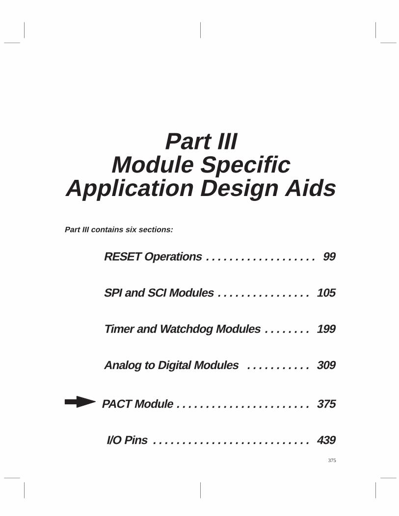
375
Part IIIModule Specific
Application Design Aids
Part III contains six sections:
RESET Operations 99. . . . . . . . . . . . . . . . . . .
SPI and SCI Modules 105. . . . . . . . . . . . . . . .
Timer and Watchdog Modules 199. . . . . . . .
Analog to Digital Modules 309. . . . . . . . . . .
PACT Module 375. . . . . . . . . . . . . . . . . . . . . . .
I/O Pins 439. . . . . . . . . . . . . . . . . . . . . . . . . . .

376

377
PACT Command Macros
Microcontroller Products—Semiconductor GroupTexas Instruments

378
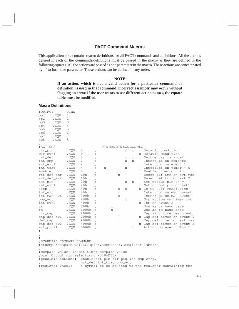
379
PACT Command Macros
This application note contains macro definitions for all PACT commands and definitions. All the actionsdesired in each of the commands/definitions must be passed in the macro as they are defined in thefollowing equates. All the actions are passed as one parameter in the macro. These actions are concatenatedby ’|’ to form one parameter. These actions can be defined in any order.
NOTE:If an action, which is not a valid action for a particular command ordefinition, is used in that command, incorrect assembly may occur withoutflagging an error. If the user wants to use different action names, the equatetable must be modified.
Macro Definitions
;OUTPUT PINSop1 .EQU 1op2 .EQU 2op3 .EQU 3op4 .EQU 4op5 .EQU 5op6 .EQU 6op7 .EQU 7op8 .EQU 8;;ACTIONS VTD BRD OTD SCC CCC DECclr_pin .EQU 0 ; x x Default conditionclr_evt1 .EQU 0 ; x Default conditionnxt_def .EQU 1 ; x x x Next entry is a defint_cmp .EQU 2 ; x x Interrupt on compareint_evt1 .EQU 2 ; x Interrupt on event 1int_trst .EQU 4 ; x x Interrupt on timer = 0enable .EQU 8 ; x x x x Enable timer or pinrst_def_tmr .EQU 10h ; x Reset def tmr on evt maxrst_def_ev2 .EQU 10h ; x Reset def tmr on evt 2set_pin .EQU 20h ; x x Set output pin on =set_evt1 .EQU 20h ; x Set output pin on evt1step .EQU 40h ; x x x Go to half resolutionint_evt .EQU 80h ; x Interrupt on each eventint_max_evt .EQU 100h ; x Interrupt on max eventopp_act .EQU 200h ; x x Opp action on timer rstint_evt2 .EQU 400h ; x Int on event 2tx .EQU 800h ; x Use as tx baud raterx .EQU 1000h ; x Use as rx baud ratevir_cap .EQU 2000h ; x Cap virt timer each evtcap_def_ev1 .EQU 2000h ; x Cap def timer on event 1def_cap .EQU 4000h ; x Cap def timer on evt maxcap_def_ev2 .EQU 4000h ; x Cap def timer on event 2evt_plus1 .EQU 8000h ; x Action on event plus 1;;;;STANDARD COMPARE COMMAND;stdcmp <compare value>,<pin>,<actions>,<register label>;;compare value: 16-bit timer compare value;pin: Output pin selection. (D18–D20);possible actions: enable,set_pin,clr_pin,int_cmp,step,; nxt_def,int_trst,opp_act;register label: a symbol to be equated to the register containing the
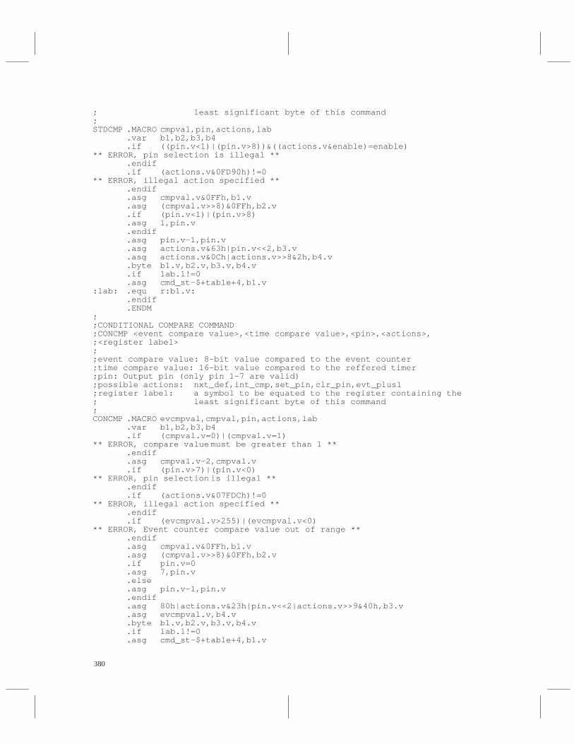
380
; least significant byte of this command;STDCMP .MACRO cmpval,pin,actions,lab
.var b1,b2,b3,b4
.if ((pin.v<1)|(pin.v>8))&((actions.v&enable)=enable)** ERROR, pin selection is illegal **
.endif
.if (actions.v&0FD90h)!=0** ERROR, illegal action specified **
.endif
.asg cmpval.v&0FFh,b1.v
.asg (cmpval.v>>8)&0FFh,b2.v
.if (pin.v<1)|(pin.v>8)
.asg 1,pin.v
.endif
.asg pin.v–1,pin.v
.asg actions.v&63h|pin.v<<2,b3.v
.asg actions.v&0Ch|actions.v>>8&2h,b4.v
.byte b1.v,b2.v,b3.v,b4.v
.if lab.l!=0
.asg cmd_st–$+table+4,b1.v:lab: .equ r:b1.v:
.endif
.ENDM;;CONDITIONAL COMPARE COMMAND;CONCMP <event compare value>,<time compare value>,<pin>,<actions>,;<register label>;;event compare value: 8-bit value compared to the event counter;time compare value: 16-bit value compared to the reffered timer;pin: Output pin (only pin 1–7 are valid);possible actions: nxt_def,int_cmp,set_pin,clr_pin,evt_plus1;register label: a symbol to be equated to the register containing the; least significant byte of this command;CONCMP .MACRO evcmpval,cmpval,pin,actions,lab
.var b1,b2,b3,b4
.if (cmpval.v=0)|(cmpval.v=1)** ERROR, compare value must be greater than 1 **
.endif
.asg cmpval.v–2,cmpval.v
.if (pin.v>7)|(pin.v<0)** ERROR, pin selection is illegal **
.endif
.if (actions.v&07FDCh)!=0** ERROR, illegal action specified **
.endif
.if (evcmpval.v>255)|(evcmpval.v<0)** ERROR, Event counter compare value out of range **
.endif
.asg cmpval.v&0FFh,b1.v
.asg (cmpval.v>>8)&0FFh,b2.v
.if pin.v=0
.asg 7,pin.v
.else
.asg pin.v–1,pin.v
.endif
.asg 80h|actions.v&23h|pin.v<<2|actions.v>>9&40h,b3.v
.asg evcmpval.v,b4.v
.byte b1.v,b2.v,b3.v,b4.v
.if lab.l!=0
.asg cmd_st–$+table+4,b1.v
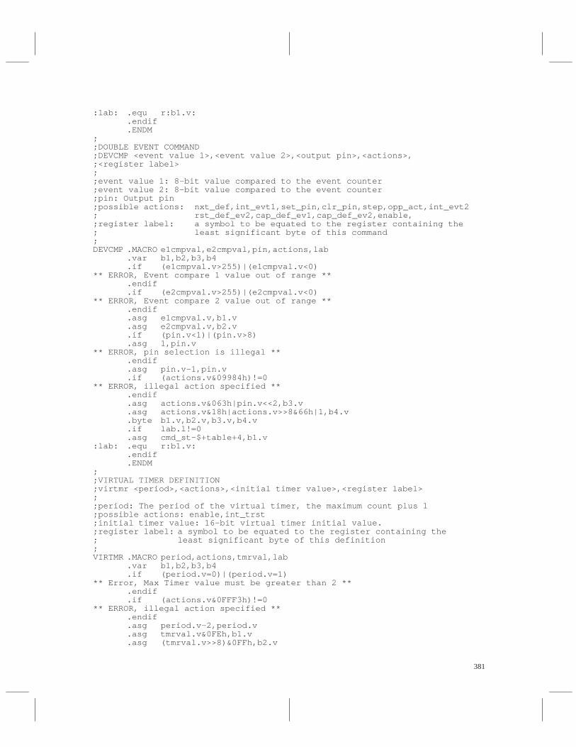
381
:lab: .equ r:b1.v:.endif.ENDM
;;DOUBLE EVENT COMMAND;DEVCMP <event value 1>,<event value 2>,<output pin>,<actions>,;<register label>;;event value 1: 8-bit value compared to the event counter;event value 2: 8-bit value compared to the event counter;pin: Output pin;possible actions: nxt_def,int_evt1,set_pin,clr_pin,step,opp_act,int_evt2; rst_def_ev2,cap_def_ev1,cap_def_ev2,enable,;register label: a symbol to be equated to the register containing the; least significant byte of this command;DEVCMP .MACRO e1cmpval,e2cmpval,pin,actions,lab
.var b1,b2,b3,b4
.if (e1cmpval.v>255)|(e1cmpval.v<0)** ERROR, Event compare 1 value out of range **
.endif
.if (e2cmpval.v>255)|(e2cmpval.v<0)** ERROR, Event compare 2 value out of range **
.endif
.asg e1cmpval.v,b1.v
.asg e2cmpval.v,b2.v
.if (pin.v<1)|(pin.v>8)
.asg 1,pin.v** ERROR, pin selection is illegal **
.endif
.asg pin.v–1,pin.v
.if (actions.v&09984h)!=0** ERROR, illegal action specified **
.endif
.asg actions.v&063h|pin.v<<2,b3.v
.asg actions.v&18h|actions.v>>8&66h|1,b4.v
.byte b1.v,b2.v,b3.v,b4.v
.if lab.l!=0
.asg cmd_st–$+table+4,b1.v:lab: .equ r:b1.v:
.endif
.ENDM;;VIRTUAL TIMER DEFINITION;virtmr <period>,<actions>,<initial timer value>,<register label>;;period: The period of the virtual timer, the maximum count plus 1;possible actions: enable,int_trst;initial timer value: 16-bit virtual timer initial value.;register label: a symbol to be equated to the register containing the; least significant byte of this definition;VIRTMR .MACRO period,actions,tmrval,lab
.var b1,b2,b3,b4
.if (period.v=0)|(period.v=1)** Error, Max Timer value must be greater than 2 **
.endif
.if (actions.v&0FFF3h)!=0** ERROR, illegal action specified **
.endif
.asg period.v–2,period.v
.asg tmrval.v&0FEh,b1.v
.asg (tmrval.v>>8)&0FFh,b2.v
382
.if ((period.v>>8)&0FFh) > 1Fh
.asg (period.v>>9)&70h|(period.v<<3)&80h|08h,b3.v
.if (period.v&0Fh)!=0** ERROR, Max. Timer value truncated in last 4 bits **
.endif
.else
.asg (period.v<<3)&0F0h|(actions.v&0Ch)>>1,b3.v
.if period.v&01h!=0** ERROR, Max. Timer value truncated in last bit **
.endif
.endif
.if tmrval.v&01h!=0** ERROR, Timer value truncated in last bit **
.endif
.asg b3.v|actions.v&0Ch>>1,b3.v
.asg (period.v>>5)&0FFh,b4.v
.byte b1.v,b2.v,b3.v,b4.v
.if lab.l!=0
.asg cmd_st–$+table+4,b1.v:lab: .equ r:b1.v:
.endif
.ENDM;;BAUD RATE TIMER DEFINITION;BRTMR <maximum count>,<actions>,<initial timer value>,<register label>;;maximum count: number that determines the baud rate;initial timer value: 16-bit virtual timer initial value;possible actions: rx,tx;register label: a symbol to be equated to the register containing the; least significant byte of this definition;BRTMR .MACRO maxcount,actions,tmrval,lab
.var b1,b2,b3,b4
.if ((actions.v&0E7FFh)!=0)** ERROR, illegal action specified **
.endif
.asg tmrval.v&0FEh,b1.v
.asg (tmrval.v>>8)&0FFh,b2.v
.if ((maxcount.v>>8)&0FFh) > 1Fh
.asg (maxcount.v>>9)&70h|(maxcount.v<<3)&80h|08h,b3.v
.if maxcount.v&0Fh!=0** ERROR, Max. Timer value truncated in last 4 bits **
.endif
.else
.asg (maxcount.v<<3)&0F0h,b3.v
.if maxcount.v&01h!=0** ERROR, Max. Timer value truncated in last bit **
.endif
.endif
.if tmrval.v&01h!=0** ERROR, Timer value truncated in last bit **
.endif
.asg (maxcount.v>>5)&0FFh,b4.v
.asg b3.v|((actions.v&1800h)>>10)|1,b3.v
.byte b1.v,b2.v,b3.v,b4.v
.if lab.l!=0
.asg cmd_st–$+table+4,b1.v:lab: .equ r:b1.v:
.endif
.ENDM;;OFFSET TIMER DEFINITION
383
;OFSTMR <max event count>,<actions>,<inital value>,<register label>;;max event count: The maximum value the event counter may reach before;being reset.;possible actions: step,int_max_evt,enable,rst_def_tmr,; vir_cap,def_cap,int_evt;initial value: 16-bit initial timer value;register label: a symbol to be equated to the register containing the; least significant byte of this definition;OFSTMR .MACRO maxcount,actions,tmrval,lab
.var b1,b2,b3,b4
.if (maxcount.v>255)|(maxcount.v<0)** ERROR, Maximum event value out of range **
.endif
.if ((actions.v&09E27h)!=0)** ERROR, illegal action specified **
.endif
.asg (tmrval.v&0FFh|1),b1.v
.asg (tmrval.v>>8)&0FFh,b2.v
.asg (actions.v&090h)|((actions.v&8)>>1)|(actions.v&40h)>>6,b3.v
.asg b3.v|((actions.v&100h)>>7)|((actions.v>>8)&60h),b3.v
.asg maxcount.v&0FFh,b4.v
.byte b1.v,b2.v,b3.v,b4.v
.if lab.l!=0
.asg cmd_st–$+table+4,b1.v:lab: .equ r:b1.v:
.endif
.ENDM

384
385
PACT Module Sample Routines
J. L. PettegolaMicrocontroller Products—Semiconductor Group
Texas Instruments

386
387
Introduction
This report provides software routines to illustrate the basic functions and characteristics of PACT8 modulein the TMS370Cx36 8-bit microcontroller. Each example includes the source code and related timingdiagrams. All routines are based on a system clock of 200 ns.
For a complete description of the PACT8 module, refer to the TMS370Cx36 8-Bit Microcontroller datasheet, literature number SPNS039, or the TMS370 Family User’s Guide, literature number SPNU127.
Register Equates
The following are register equates that are used for routines throughout this report:
PACTSCR EQU P040 ;setup control register
CDSTART EQU P041 ;CMD/DEF area start register
CDEND EQU P042 ;CMD/DEF area end register
BUFPTR EQU P043 ;buffer pointer register
DUMMY EQU P044 ;unused register
SCICTLP EQU P045 ;PACT SCI control register
RXBUFP EQU P046 ;PACT SCI receive data register
TXBUFP EQU P047 ;PACT SCI transmit data register
OPSTATE EQU P048 ;output pin 1 to 8 state register
CDFLAGS EQU P049 ;CMD/DEF entry flags register
CPCTL1 EQU P04A ;setup CP1,CP2 control register
CPCTL2 EQU P04B ;setup CP3,CP4 control register
CPCTL3 EQU P04C ;setup CP5,CP6 control register
CPPRE EQU P04D ;CP input control register
WDRST EQU P04E ;watchdog reset key control register
PACTPR EQU P04F ;global function control register

388
Using The Hardware Default Timer
Square Wave PWM On OP1
This routine shows how to generate a simple square wave on pulse width modulator (PWM) output OP1.
Figure 1. Square Wave
OP1 ...
T=26.5ms
PACT Global Initialization• Set the watchdog (WD) time out in the global function control register (or disable it if no
watchdog is required).
• Define the number command and definitions required to generate the PWM as well as the relatednumber of time slots. Then the minimum divide rate for the prescaled clock can be derived.
• Set and reset the PWM output. No timer definition is required for the default timer, so only twostandard compares will be needed.
• Since there are no captures, no capture register or circular buffer is required.
• Define the size of the command and definition area and set the start and end address in the dualport RAM.
1 TS NEEDED, FREQUENCY MAX => SYSCLK / 2 (2 TS AVAILABLE)
PRESCALER VALUE = 00H, FAST MODE
BUFFER NOT USED (MIN), NO CAPTURE => MODE A
START ADDRESS = 01EFH
2 CMD / DEF NEEDED (2 STD COMPARE) => END ADDRESS = 01E8H
PACT RESOLUTION = SYSCLK x 2 = 400nS
OP1 OUTPUT PERIOD = COMPARE VALUE x 2 x RESOLUTION = 26.2 mS
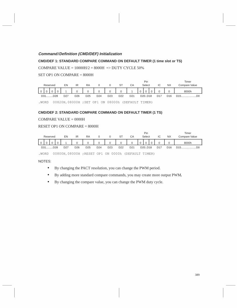
389
Command/Definition (CMD/DEF) Initialization
CMD/DEF 1: STANDARD COMPARE COMMAND ON DEFAULT TIMER (1 time slot or TS)
COMPARE VALUE = 10000H/2 = 8000H => DUTY CYCLE 50%
SET OP1 ON COMPARE = 8000H
ÁÁÁÁÁÁÁÁÁÁ
ReservedÁÁÁÁÁÁ
ENÁÁÁÁ
IRÁÁÁÁÁÁ
RAÁÁÁÁÁÁ
0ÁÁÁÁÁÁ
0ÁÁÁÁÁÁ
STÁÁÁÁÁÁ
CAÁÁÁÁÁÁ
PinSelectÁÁÁÁÁÁ
ICÁÁÁÁÁÁ
NXÁÁÁÁÁÁÁÁÁÁ
TimerCompare Value
ÁÁÁÁ
0ÁÁÁÁ
0ÁÁÁÁ
0ÁÁÁÁ
0ÁÁÁÁÁÁ
1ÁÁÁÁ
0ÁÁÁÁÁÁ
0ÁÁÁÁÁÁ
0ÁÁÁÁÁÁ
0ÁÁÁÁÁÁ
0ÁÁÁÁÁÁ
1ÁÁÁÁ
0ÁÁ
0ÁÁÁÁ
0ÁÁÁÁÁÁ
0ÁÁÁÁÁÁ
0ÁÁÁÁÁÁÁÁÁÁ
8000hÁÁÁÁÁÁÁÁÁÁ
D31.........D28 ÁÁÁÁÁÁ
D27 ÁÁÁÁ
D26ÁÁÁÁÁÁ
D25ÁÁÁÁÁÁ
D24ÁÁÁÁÁÁ
D23ÁÁÁÁÁÁ
D22ÁÁÁÁÁÁ
D21 ÁÁÁÁÁÁ
D20..D18ÁÁÁÁÁÁ
D17ÁÁÁÁÁÁ
D16ÁÁÁÁÁÁÁÁÁÁ
D15....................D0
.WORD 00820H,08000H ;SET OP1 ON 08000h (DEFAULT TIMER)
CMD/DEF 2: STANDARD COMPARE COMMAND ON DEFAULT TIMER (1 TS)
COMPARE VALUE = 0000H
RESET OP1 ON COMPARE = 8000HÁÁÁÁÁÁÁÁÁÁÁÁÁÁÁ
Reserved
ÁÁÁÁÁÁÁÁÁ
EN
ÁÁÁÁÁÁ
IR
ÁÁÁÁÁÁÁÁÁ
RA
ÁÁÁÁÁÁÁÁÁ
0
ÁÁÁÁÁÁÁÁÁ
0
ÁÁÁÁÁÁÁÁÁ
ST
ÁÁÁÁÁÁÁÁÁ
CA
ÁÁÁÁÁÁÁÁÁ
PinSelect
ÁÁÁÁÁÁÁÁÁ
IC
ÁÁÁÁÁÁÁÁÁ
NX
ÁÁÁÁÁÁÁÁÁÁÁÁÁÁÁ
TimerCompare Value
ÁÁÁÁ
0ÁÁÁÁ
0ÁÁÁÁ
0ÁÁÁÁ
0ÁÁÁÁÁÁ
1 ÁÁÁÁ
0ÁÁÁÁÁÁ
0ÁÁÁÁÁÁ
0ÁÁÁÁÁÁ
0 ÁÁÁÁÁÁ
0 ÁÁÁÁÁÁ
0 ÁÁÁÁ
0 ÁÁ
0ÁÁÁÁ
0ÁÁÁÁÁÁ
0ÁÁÁÁÁÁ
0 ÁÁÁÁÁÁÁÁÁÁ
8000h
ÁÁÁÁÁÁÁÁÁÁ
D31.........D28 ÁÁÁÁÁÁ
D27 ÁÁÁÁ
D26ÁÁÁÁÁÁ
D25ÁÁÁÁÁÁ
D24ÁÁÁÁÁÁ
D23ÁÁÁÁÁÁ
D22ÁÁÁÁÁÁ
D21 ÁÁÁÁÁÁ
D20..D18ÁÁÁÁÁÁ
D17ÁÁÁÁÁÁ
D16ÁÁÁÁÁÁÁÁÁÁ
D15....................D0
.WORD 00800H,08000H ;RESET OP1 ON 0000h (DEFAULT TIMER)
NOTES:
• By changing the PACT resolution, you can change the PWM period.
• By adding more standard compare commands, you may create more output PWM.
• By changing the compare value, you can change the PWM duty cycle.
390
Square Wave PWM Routine .TEXT 7000H
.global deb
;**********************************************************
; START END ADDRESS DEFINITION
;**********************************************************
STARTAD .EQU 01EFH
PACTPRI .EQU p04F ; Global function control register
CDSTART .EQU p041 ; Command/definition area start register
CDEND .EQU p042 ; Command/definition area end register
PACTSCR .EQU p040 ; Setup control register
ENDAD .EQU 01E8H
;**********************************************************
; INIT PACT PERIPHERAL FRAME
;**********************************************************
OR #003H,PACTPRI ;DISABLE WATCHDOG, MODE A
MOV #(STARTAD-0100H-080H),CDSTART ;START AD, CMD/DEF INT DIS
MOV #(ENDAD-0100H),CDEND ;END AD
MOV #010H,PACTSCR ;SYSCLK DIVIDED BY 2 => RESOL=400NS AT ;20MHZ
;...
;**********************************************************
; MAIN PGM
;**********************************************************
MAIN
OR #020H,PACTSCR ;ENABLE PACT CMD/DEF AREA
JMP $ ;LOOP MAIN PGM
;**********************************************************
; INIT PACT CMD/DEF AREA
;**********************************************************
.sect “CMDEF”,(ENDAD) ;CMD/DEF SECTION PROGRAM
.WORD 0800H,0000H ;RESET OP1 ON 0000h (DEFAULT TIMER) ERO
.WORD 0820H,8000H ;SET OP1 ON 08000h (DEFAULT TIMER) ERO
;...
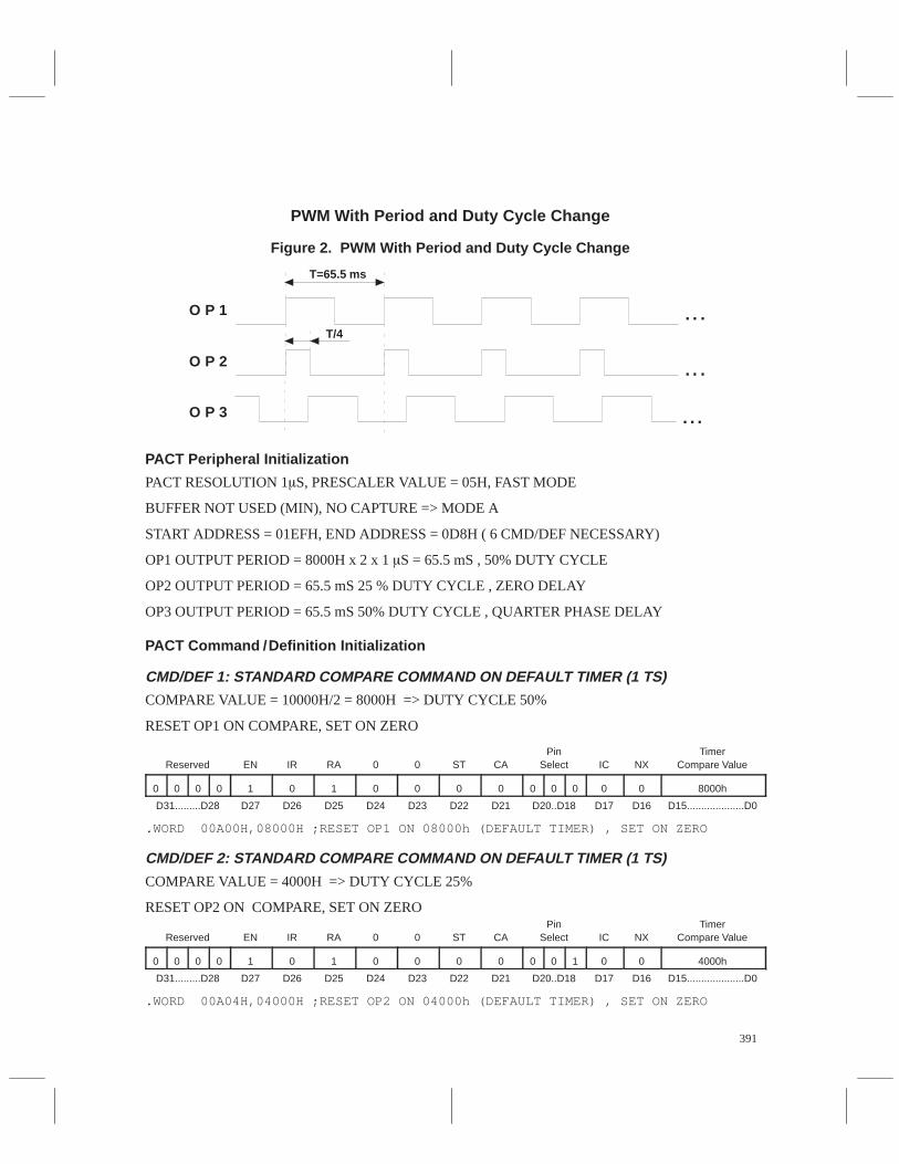
391
PWM With Period and Duty Cycle Change
Figure 2. PWM With Period and Duty Cycle Change
O P 1
O P 2
O P 3
...
...
...
T=65.5 ms
T/4
PACT Peripheral Initialization
PACT RESOLUTION 1S, PRESCALER VALUE = 05H, FAST MODE
BUFFER NOT USED (MIN), NO CAPTURE => MODE A
START ADDRESS = 01EFH, END ADDRESS = 0D8H ( 6 CMD/DEF NECESSARY)
OP1 OUTPUT PERIOD = 8000H x 2 x 1 S = 65.5 mS , 50% DUTY CYCLE
OP2 OUTPUT PERIOD = 65.5 mS 25 % DUTY CYCLE , ZERO DELAY
OP3 OUTPUT PERIOD = 65.5 mS 50% DUTY CYCLE , QUARTER PHASE DELAY
PACT Command /Definition Initialization
CMD/DEF 1: STANDARD COMPARE COMMAND ON DEFAULT TIMER (1 TS)
COMPARE VALUE = 10000H/2 = 8000H => DUTY CYCLE 50%
RESET OP1 ON COMPARE, SET ON ZEROÁÁÁÁÁÁÁÁÁÁÁÁÁÁÁ
Reserved
ÁÁÁÁÁÁÁÁÁ
EN
ÁÁÁÁÁÁ
IR
ÁÁÁÁÁÁÁÁÁ
RA
ÁÁÁÁÁÁÁÁÁ
0
ÁÁÁÁÁÁÁÁÁ
0
ÁÁÁÁÁÁÁÁÁ
ST
ÁÁÁÁÁÁÁÁÁ
CA
ÁÁÁÁÁÁÁÁÁ
PinSelect
ÁÁÁÁÁÁÁÁÁ
IC
ÁÁÁÁÁÁÁÁÁ
NX
ÁÁÁÁÁÁÁÁÁÁÁÁÁÁÁ
TimerCompare Value
ÁÁÁÁ
0ÁÁÁÁ
0ÁÁÁÁ
0ÁÁÁÁ
0ÁÁÁÁÁÁ
1 ÁÁÁÁ
0ÁÁÁÁÁÁ
1ÁÁÁÁÁÁ
0ÁÁÁÁÁÁ
0 ÁÁÁÁÁÁ
0 ÁÁÁÁÁÁ
0 ÁÁÁÁ
0 ÁÁ
0ÁÁÁÁ
0ÁÁÁÁÁÁ
0ÁÁÁÁÁÁ
0 ÁÁÁÁÁÁÁÁÁÁ
8000h
ÁÁÁÁÁÁÁÁÁÁ
D31.........D28 ÁÁÁÁÁÁ
D27 ÁÁÁÁ
D26ÁÁÁÁÁÁ
D25ÁÁÁÁÁÁ
D24ÁÁÁÁÁÁ
D23ÁÁÁÁÁÁ
D22ÁÁÁÁÁÁ
D21 ÁÁÁÁÁÁ
D20..D18ÁÁÁÁÁÁ
D17ÁÁÁÁÁÁ
D16ÁÁÁÁÁÁÁÁÁÁ
D15....................D0
.WORD 00A00H,08000H ;RESET OP1 ON 08000h (DEFAULT TIMER) , SET ON ZERO
CMD/DEF 2: STANDARD COMPARE COMMAND ON DEFAULT TIMER (1 TS)
COMPARE VALUE = 4000H => DUTY CYCLE 25%
RESET OP2 ON COMPARE, SET ON ZEROÁÁÁÁÁÁÁÁÁÁReserved
ÁÁÁÁÁÁEN
ÁÁÁÁIRÁÁÁÁÁÁRA
ÁÁÁÁÁÁ0
ÁÁÁÁÁÁ0
ÁÁÁÁÁÁST
ÁÁÁÁÁÁCA
ÁÁÁÁÁÁ
PinSelect
ÁÁÁÁÁÁIC
ÁÁÁÁÁÁNX
ÁÁÁÁÁÁÁÁÁÁ
TimerCompare ValueÁÁ
ÁÁ0ÁÁÁÁ0ÁÁÁÁ0ÁÁÁÁ0
ÁÁÁÁÁÁ1
ÁÁÁÁ0ÁÁÁÁÁÁ1ÁÁÁÁÁÁ0
ÁÁÁÁÁÁ0
ÁÁÁÁÁÁ0
ÁÁÁÁÁÁ0
ÁÁÁÁ0
ÁÁ0ÁÁÁÁ1ÁÁÁÁÁÁ0ÁÁÁÁÁÁ0
ÁÁÁÁÁÁÁÁÁÁ4000hÁÁÁÁÁ
ÁÁÁÁÁD31.........D28ÁÁÁÁÁÁD27ÁÁÁÁD26ÁÁÁÁÁÁD25ÁÁÁÁÁÁD24ÁÁÁÁÁÁD23ÁÁÁÁÁÁD22ÁÁÁÁÁÁD21ÁÁÁÁÁÁD20..D18ÁÁÁÁÁÁD17ÁÁÁÁÁÁD16ÁÁÁÁÁÁÁÁÁÁD15....................D0
.WORD 00A04H,04000H ;RESET OP2 ON 04000h (DEFAULT TIMER) , SET ON ZERO
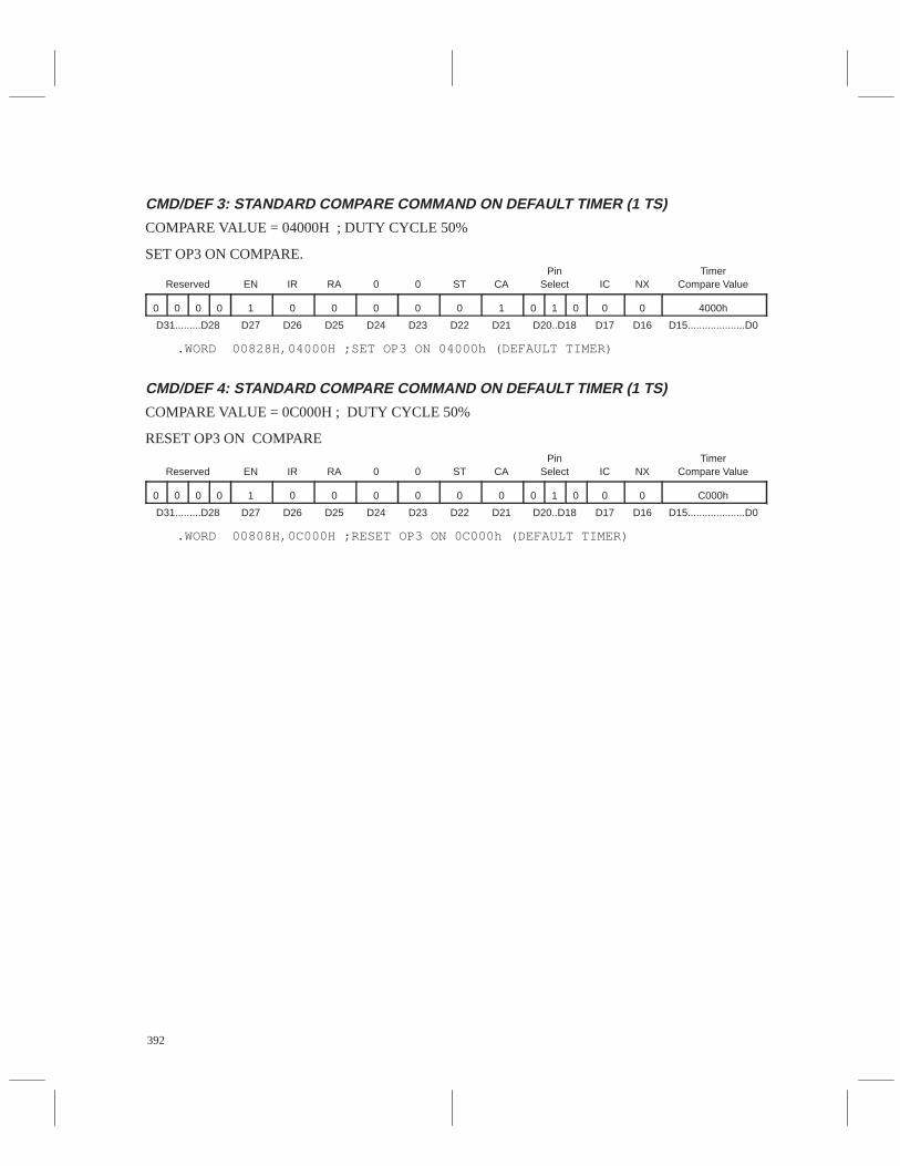
392
CMD/DEF 3: STANDARD COMPARE COMMAND ON DEFAULT TIMER (1 TS)
COMPARE VALUE = 04000H ; DUTY CYCLE 50%
SET OP3 ON COMPARE.ÁÁÁÁÁÁÁÁÁÁÁÁÁÁÁ
Reserved
ÁÁÁÁÁÁÁÁÁ
EN
ÁÁÁÁÁÁ
IR
ÁÁÁÁÁÁÁÁÁ
RA
ÁÁÁÁÁÁÁÁÁ
0
ÁÁÁÁÁÁÁÁÁ
0
ÁÁÁÁÁÁÁÁÁ
ST
ÁÁÁÁÁÁÁÁÁ
CA
ÁÁÁÁÁÁÁÁÁ
PinSelect
ÁÁÁÁÁÁÁÁÁ
IC
ÁÁÁÁÁÁÁÁÁ
NX
ÁÁÁÁÁÁÁÁÁÁÁÁÁÁÁ
TimerCompare Value
ÁÁÁÁ
0ÁÁÁÁ
0ÁÁÁÁ
0ÁÁÁÁ
0ÁÁÁÁÁÁ
1 ÁÁÁÁ
0ÁÁÁÁÁÁ
0ÁÁÁÁÁÁ
0ÁÁÁÁÁÁ
0 ÁÁÁÁÁÁ
0 ÁÁÁÁÁÁ
1 ÁÁÁÁ
0 ÁÁ
1ÁÁÁÁ
0ÁÁÁÁÁÁ
0ÁÁÁÁÁÁ
0 ÁÁÁÁÁÁÁÁÁÁ
4000h
ÁÁÁÁÁD31.........D28 ÁÁÁD27 ÁÁD26ÁÁÁD25ÁÁÁD24ÁÁÁD23ÁÁÁD22ÁÁÁD21 ÁÁÁD20..D18ÁÁÁD17ÁÁÁD16ÁÁÁÁÁD15....................D0
.WORD 00828H,04000H ;SET OP3 ON 04000h (DEFAULT TIMER)
CMD/DEF 4: STANDARD COMPARE COMMAND ON DEFAULT TIMER (1 TS)
COMPARE VALUE = 0C000H ; DUTY CYCLE 50%
RESET OP3 ON COMPARE
ÁÁÁÁÁÁÁÁÁÁ
Reserved ÁÁÁÁÁÁ
EN ÁÁÁÁ
IRÁÁÁÁÁÁ
RAÁÁÁÁÁÁ
0ÁÁÁÁÁÁ
0 ÁÁÁÁÁÁ
ST ÁÁÁÁÁÁ
CA ÁÁÁÁÁÁ
PinSelectÁÁÁÁÁÁ
ICÁÁÁÁÁÁ
NX ÁÁÁÁÁÁÁÁÁÁ
TimerCompare Value
ÁÁÁÁ
0ÁÁÁÁ
0ÁÁÁÁ
0ÁÁÁÁ
0ÁÁÁÁÁÁ
1 ÁÁÁÁ
0ÁÁÁÁÁÁ
0ÁÁÁÁÁÁ
0ÁÁÁÁÁÁ
0 ÁÁÁÁÁÁ
0 ÁÁÁÁÁÁ
0 ÁÁÁÁ
0 ÁÁ
1ÁÁÁÁ
0ÁÁÁÁÁÁ
0ÁÁÁÁÁÁ
0 ÁÁÁÁÁÁÁÁÁÁ
C000h
ÁÁÁÁÁÁÁÁÁÁ
D31.........D28 ÁÁÁÁÁÁ
D27 ÁÁÁÁ
D26ÁÁÁÁÁÁ
D25ÁÁÁÁÁÁ
D24ÁÁÁÁÁÁ
D23ÁÁÁÁÁÁ
D22ÁÁÁÁÁÁ
D21 ÁÁÁÁÁÁ
D20..D18ÁÁÁÁÁÁ
D17ÁÁÁÁÁÁ
D16ÁÁÁÁÁÁÁÁÁÁ
D15....................D0
.WORD 00808H,0C000H ;RESET OP3 ON 0C000h (DEFAULT TIMER)
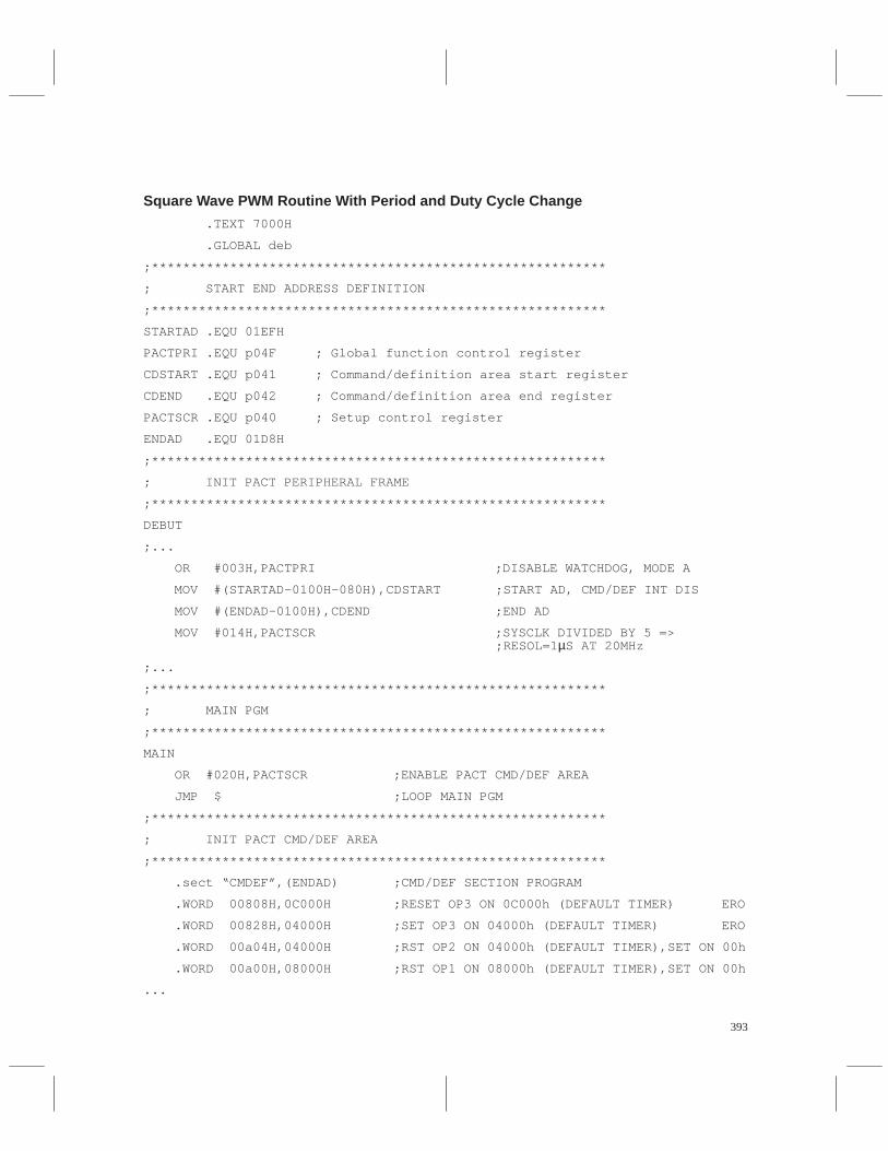
393
Square Wave PWM Routine With Period and Duty Cycle Change
.TEXT 7000H
.GLOBAL deb
;**********************************************************
; START END ADDRESS DEFINITION
;**********************************************************
STARTAD .EQU 01EFH
PACTPRI .EQU p04F ; Global function control register
CDSTART .EQU p041 ; Command/definition area start register
CDEND .EQU p042 ; Command/definition area end register
PACTSCR .EQU p040 ; Setup control register
ENDAD .EQU 01D8H
;**********************************************************
; INIT PACT PERIPHERAL FRAME
;**********************************************************
DEBUT
;...
OR #003H,PACTPRI ;DISABLE WATCHDOG, MODE A
MOV #(STARTAD-0100H-080H),CDSTART ;START AD, CMD/DEF INT DIS
MOV #(ENDAD-0100H),CDEND ;END AD
MOV #014H,PACTSCR ;SYSCLK DIVIDED BY 5 => ;RESOL=1 µS AT 20MHz
;...
;**********************************************************
; MAIN PGM
;**********************************************************
MAIN
OR #020H,PACTSCR ;ENABLE PACT CMD/DEF AREA
JMP $ ;LOOP MAIN PGM
;**********************************************************
; INIT PACT CMD/DEF AREA
;**********************************************************
.sect “CMDEF”,(ENDAD) ;CMD/DEF SECTION PROGRAM
.WORD 00808H,0C000H ;RESET OP3 ON 0C000h (DEFAULT TIMER) ERO
.WORD 00828H,04000H ;SET OP3 ON 04000h (DEFAULT TIMER) ERO
.WORD 00a04H,04000H ;RST OP2 ON 04000h (DEFAULT TIMER),SET ON 00h
.WORD 00a00H,08000H ;RST OP1 ON 08000h (DEFAULT TIMER),SET ON 00h
...
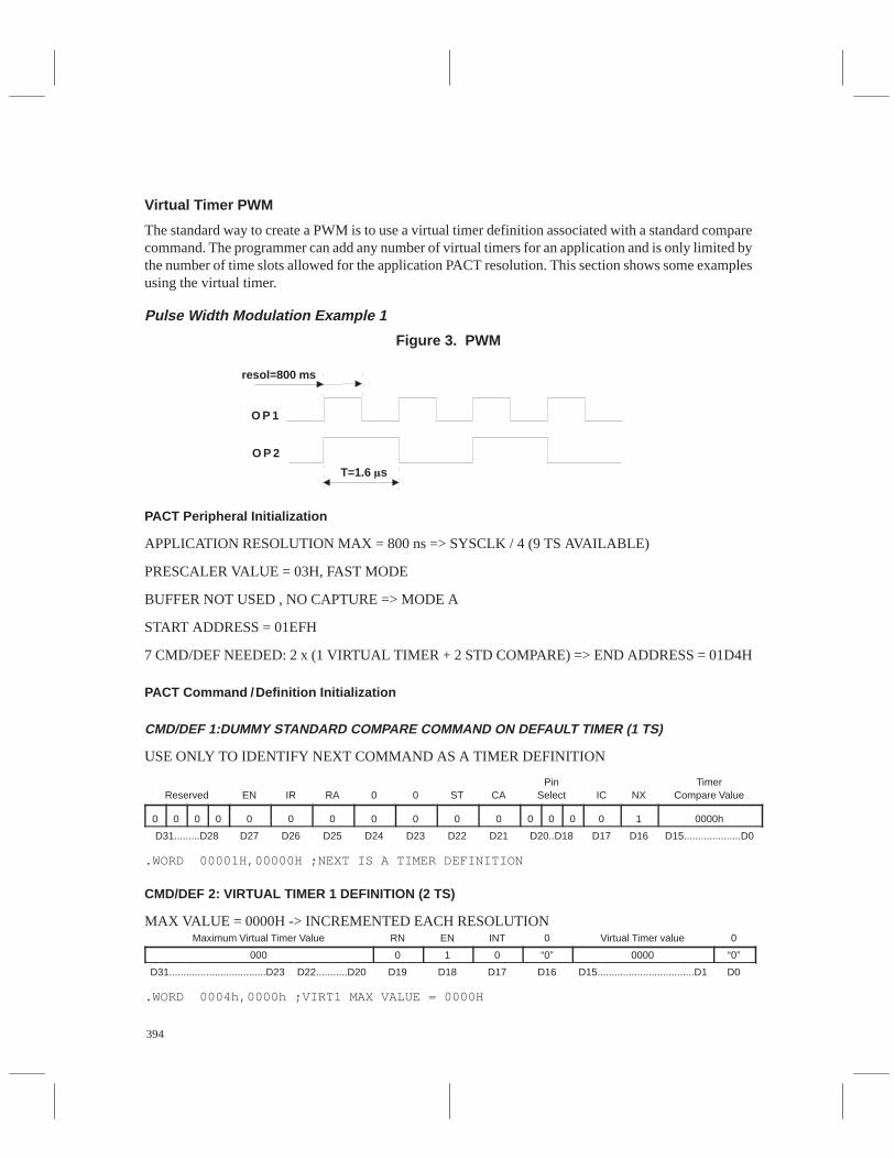
394
Virtual Timer PWM
The standard way to create a PWM is to use a virtual timer definition associated with a standard comparecommand. The programmer can add any number of virtual timers for an application and is only limited bythe number of time slots allowed for the application PACT resolution. This section shows some examplesusing the virtual timer.
Pulse Width Modulation Example 1
Figure 3. PWM
O P 1
O P 2
resol=800 ms
T=1.6 s
PACT Peripheral Initialization
APPLICATION RESOLUTION MAX = 800 ns => SYSCLK / 4 (9 TS AVAILABLE)
PRESCALER VALUE = 03H, FAST MODE
BUFFER NOT USED , NO CAPTURE => MODE A
START ADDRESS = 01EFH
7 CMD/DEF NEEDED: 2 x (1 VIRTUAL TIMER + 2 STD COMPARE) => END ADDRESS = 01D4H
PACT Command /Definition Initialization
CMD/DEF 1:DUMMY STANDARD COMPARE COMMAND ON DEFAULT TIMER (1 TS)
USE ONLY TO IDENTIFY NEXT COMMAND AS A TIMER DEFINITION
ÁÁÁÁÁÁÁÁÁÁReserved
ÁÁÁÁÁÁENÁÁÁÁIRÁÁÁÁÁÁRAÁÁÁÁÁÁ0ÁÁÁÁÁÁ0ÁÁÁÁÁÁSTÁÁÁÁÁÁCAÁÁÁÁÁÁ
PinSelectÁÁÁÁÁÁICÁÁÁÁÁÁNXÁÁÁÁÁÁÁÁÁÁ
TimerCompare ValueÁÁ
ÁÁ0ÁÁÁÁ0ÁÁÁÁ0ÁÁÁÁ0ÁÁÁÁÁÁ0ÁÁÁÁ0ÁÁÁÁÁÁ0ÁÁÁÁÁÁ0ÁÁÁÁÁÁ0ÁÁÁÁÁÁ0ÁÁÁÁÁÁ0ÁÁÁÁ0ÁÁ0ÁÁÁÁ0ÁÁÁÁÁÁ0ÁÁÁÁÁÁ1ÁÁÁÁÁÁÁÁÁÁ0000hÁÁÁÁÁ
ÁÁÁÁÁD31.........D28
ÁÁÁÁÁÁ
D27ÁÁÁÁ
D26ÁÁÁÁÁÁ
D25ÁÁÁÁÁÁ
D24ÁÁÁÁÁÁ
D23ÁÁÁÁÁÁ
D22ÁÁÁÁÁÁ
D21ÁÁÁÁÁÁ
D20..D18ÁÁÁÁÁÁ
D17ÁÁÁÁÁÁ
D16ÁÁÁÁÁÁÁÁÁÁ
D15....................D0
.WORD 00001H,00000H ;NEXT IS A TIMER DEFINITION
CMD/DEF 2: VIRTUAL TIMER 1 DEFINITION (2 TS)
MAX VALUE = 0000H -> INCREMENTED EACH RESOLUTIONÁÁÁÁÁÁÁÁÁÁÁÁÁÁÁÁÁÁÁÁÁÁ
Maximum Virtual Timer Value ÁÁÁÁÁÁ
RNÁÁÁÁÁÁÁÁ
EN ÁÁÁÁÁÁ
INT ÁÁÁÁÁÁ
0 ÁÁÁÁÁÁÁÁÁÁÁÁÁÁ
Virtual Timer value ÁÁÁÁÁÁ
0
ÁÁÁÁÁÁÁÁÁÁÁ000 ÁÁÁ0ÁÁÁÁ1 ÁÁÁ0 ÁÁÁ“0” ÁÁÁÁÁÁÁ0000 ÁÁÁ“0”ÁÁÁÁÁÁÁÁÁÁÁÁÁÁ
D31..................................D23ÁÁÁÁÁÁÁÁÁÁ
D22...........D20ÁÁÁÁÁÁ
D19ÁÁÁÁÁÁÁÁ
D18ÁÁÁÁÁÁ
D17ÁÁÁÁÁÁ
D16ÁÁÁÁÁÁÁÁÁÁÁÁÁÁ
D15..................................D1ÁÁÁÁÁÁ
D0
.WORD 0004h,0000h ;VIRT1 MAX VALUE = 0000H
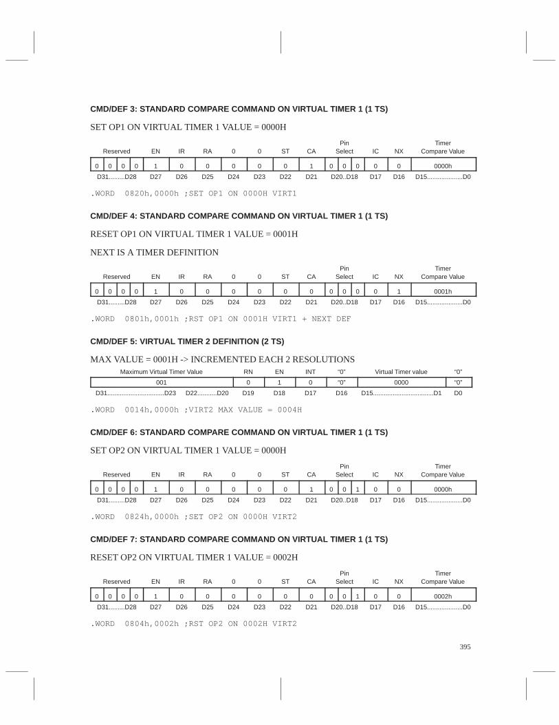
395
CMD/DEF 3: STANDARD COMPARE COMMAND ON VIRTUAL TIMER 1 (1 TS)
SET OP1 ON VIRTUAL TIMER 1 VALUE = 0000HÁÁÁÁÁÁÁÁÁÁÁÁÁÁÁ
Reserved
ÁÁÁÁÁÁÁÁÁ
EN
ÁÁÁÁÁÁ
IR
ÁÁÁÁÁÁÁÁÁ
RA
ÁÁÁÁÁÁÁÁÁ
0
ÁÁÁÁÁÁÁÁÁ
0
ÁÁÁÁÁÁÁÁÁ
ST
ÁÁÁÁÁÁÁÁÁ
CA
ÁÁÁÁÁÁÁÁÁ
PinSelect
ÁÁÁÁÁÁÁÁÁ
IC
ÁÁÁÁÁÁÁÁÁ
NX
ÁÁÁÁÁÁÁÁÁÁÁÁÁÁÁ
TimerCompare Value
ÁÁÁÁ
0ÁÁÁÁ
0ÁÁÁÁ
0ÁÁÁÁ
0ÁÁÁÁÁÁ
1 ÁÁÁÁ
0ÁÁÁÁÁÁ
0ÁÁÁÁÁÁ
0ÁÁÁÁÁÁ
0 ÁÁÁÁÁÁ
0 ÁÁÁÁÁÁ
1 ÁÁÁÁ
0 ÁÁ
0ÁÁÁÁ
0ÁÁÁÁÁÁ
0ÁÁÁÁÁÁ
0 ÁÁÁÁÁÁÁÁÁÁ
0000h
ÁÁÁÁÁD31.........D28 ÁÁÁD27 ÁÁD26ÁÁÁD25ÁÁÁD24ÁÁÁD23ÁÁÁD22ÁÁÁD21 ÁÁÁD20..D18ÁÁÁD17ÁÁÁD16ÁÁÁÁÁD15....................D0
.WORD 0820h,0000h ;SET OP1 ON 0000H VIRT1
CMD/DEF 4: STANDARD COMPARE COMMAND ON VIRTUAL TIMER 1 (1 TS)
RESET OP1 ON VIRTUAL TIMER 1 VALUE = 0001H
NEXT IS A TIMER DEFINITIONÁÁÁÁÁÁÁÁÁÁÁÁÁÁÁ
Reserved
ÁÁÁÁÁÁÁÁÁ
EN
ÁÁÁÁÁÁ
IR
ÁÁÁÁÁÁÁÁÁ
RA
ÁÁÁÁÁÁÁÁÁ
0
ÁÁÁÁÁÁÁÁÁ
0
ÁÁÁÁÁÁÁÁÁ
ST
ÁÁÁÁÁÁÁÁÁ
CA
ÁÁÁÁÁÁÁÁÁ
PinSelect
ÁÁÁÁÁÁÁÁÁ
IC
ÁÁÁÁÁÁÁÁÁ
NX
ÁÁÁÁÁÁÁÁÁÁÁÁÁÁÁ
TimerCompare Value
ÁÁÁÁ
0ÁÁÁÁ
0ÁÁÁÁ
0ÁÁÁÁ
0ÁÁÁÁÁÁ
1 ÁÁÁÁ
0ÁÁÁÁÁÁ
0ÁÁÁÁÁÁ
0ÁÁÁÁÁÁ
0 ÁÁÁÁÁÁ
0 ÁÁÁÁÁÁ
0 ÁÁÁÁ
0 ÁÁ
0ÁÁÁÁ
0ÁÁÁÁÁÁ
0ÁÁÁÁÁÁ
1 ÁÁÁÁÁÁÁÁÁÁ
0001h
ÁÁÁÁÁD31.........D28 ÁÁÁD27 ÁÁD26ÁÁÁD25ÁÁÁD24ÁÁÁD23ÁÁÁD22ÁÁÁD21 ÁÁÁD20..D18ÁÁÁD17ÁÁÁD16ÁÁÁÁÁD15....................D0
.WORD 0801h,0001h ;RST OP1 ON 0001H VIRT1 + NEXT DEF
CMD/DEF 5: VIRTUAL TIMER 2 DEFINITION (2 TS)
MAX VALUE = 0001H -> INCREMENTED EACH 2 RESOLUTIONS
ÁÁÁÁÁÁÁÁÁÁÁMaximum Virtual Timer Value ÁÁÁRNÁÁÁÁEN ÁÁÁINT ÁÁÁ“0” ÁÁÁÁÁÁÁVirtual Timer value ÁÁÁ“0”ÁÁÁÁÁÁÁÁÁÁÁÁÁÁÁÁÁÁÁÁÁÁ
001ÁÁÁÁÁÁ
0ÁÁÁÁÁÁÁÁ
1ÁÁÁÁÁÁ
0ÁÁÁÁÁÁ
“0”ÁÁÁÁÁÁÁÁÁÁÁÁÁÁ
0000ÁÁÁÁÁÁ
“0”ÁÁÁÁÁÁÁÁÁÁÁÁÁÁ
D31................................D23ÁÁÁÁÁÁÁÁÁÁ
D22...........D20ÁÁÁÁÁÁ
D19ÁÁÁÁÁÁÁÁ
D18 ÁÁÁÁÁÁ
D17 ÁÁÁÁÁÁ
D16ÁÁÁÁÁÁÁÁÁÁÁÁÁÁ
D15..................................D1ÁÁÁÁÁÁ
D0
.WORD 0014h,0000h ;VIRT2 MAX VALUE = 0004H
CMD/DEF 6: STANDARD COMPARE COMMAND ON VIRTUAL TIMER 1 (1 TS)
SET OP2 ON VIRTUAL TIMER 1 VALUE = 0000HÁÁÁÁÁÁÁÁÁÁÁÁÁÁÁ
Reserved
ÁÁÁÁÁÁÁÁÁ
EN
ÁÁÁÁÁÁ
IR
ÁÁÁÁÁÁÁÁÁ
RA
ÁÁÁÁÁÁÁÁÁ
0
ÁÁÁÁÁÁÁÁÁ
0
ÁÁÁÁÁÁÁÁÁ
ST
ÁÁÁÁÁÁÁÁÁ
CA
ÁÁÁÁÁÁÁÁÁ
PinSelect
ÁÁÁÁÁÁÁÁÁ
IC
ÁÁÁÁÁÁÁÁÁ
NX
ÁÁÁÁÁÁÁÁÁÁÁÁÁÁÁ
TimerCompare Value
ÁÁÁÁ
0ÁÁÁÁ
0ÁÁÁÁ
0ÁÁÁÁ
0ÁÁÁÁÁÁ
1 ÁÁÁÁ
0ÁÁÁÁÁÁ
0ÁÁÁÁÁÁ
0ÁÁÁÁÁÁ
0 ÁÁÁÁÁÁ
0 ÁÁÁÁÁÁ
1 ÁÁÁÁ
0 ÁÁ
0ÁÁÁÁ
1ÁÁÁÁÁÁ
0ÁÁÁÁÁÁ
0 ÁÁÁÁÁÁÁÁÁÁ
0000h
ÁÁÁÁÁD31.........D28 ÁÁÁD27 ÁÁD26ÁÁÁD25ÁÁÁD24ÁÁÁD23ÁÁÁD22ÁÁÁD21 ÁÁÁD20..D18ÁÁÁD17ÁÁÁD16ÁÁÁÁÁD15....................D0
.WORD 0824h,0000h ;SET OP2 ON 0000H VIRT2
CMD/DEF 7: STANDARD COMPARE COMMAND ON VIRTUAL TIMER 1 (1 TS)
RESET OP2 ON VIRTUAL TIMER 1 VALUE = 0002H
ÁÁÁÁÁÁÁÁÁÁReserved
ÁÁÁÁÁÁENÁÁÁÁIRÁÁÁÁÁÁRAÁÁÁÁÁÁ0ÁÁÁÁÁÁ0ÁÁÁÁÁÁSTÁÁÁÁÁÁCAÁÁÁÁÁÁ
PinSelectÁÁÁÁÁÁICÁÁÁÁÁÁNXÁÁÁÁÁÁÁÁÁÁ
TimerCompare ValueÁÁ
ÁÁ0ÁÁÁÁ0ÁÁÁÁ0ÁÁÁÁ0ÁÁÁÁÁÁ1ÁÁÁÁ0ÁÁÁÁÁÁ0ÁÁÁÁÁÁ0ÁÁÁÁÁÁ0ÁÁÁÁÁÁ0ÁÁÁÁÁÁ0ÁÁÁÁ0ÁÁ0ÁÁÁÁ1ÁÁÁÁÁÁ0ÁÁÁÁÁÁ0ÁÁÁÁÁÁÁÁÁÁ0002hÁÁÁÁÁ
ÁÁÁÁÁD31.........D28
ÁÁÁÁÁÁ
D27ÁÁÁÁ
D26ÁÁÁÁÁÁ
D25ÁÁÁÁÁÁ
D24ÁÁÁÁÁÁ
D23ÁÁÁÁÁÁ
D22ÁÁÁÁÁÁ
D21ÁÁÁÁÁÁ
D20..D18ÁÁÁÁÁÁ
D17ÁÁÁÁÁÁ
D16ÁÁÁÁÁÁÁÁÁÁ
D15....................D0
.WORD 0804h,0002h ;RST OP2 ON 0002H VIRT2
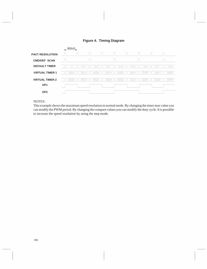
396
Figure 4. Timing Diagram
PACT RESOLUTION
CMD/DEF SCAN
DEFAULT TIMER
VIRTUAL TIMER 1
OP2
OP1
VIRTUAL TIMER 2
800nS
NOTES:This example shows the maximum speed resolution in normal mode. By changing the timer max value youcan modify the PWM period. By changing the compare values you can modify the duty cycle. It is possibleto increase the speed resolution by using the step mode.
397
Virtual Timer PWM Routine .TEXT 7000H
.GLOBAL deb
;**********************************************************
; START END ADDRESS DEFINITION
;**********************************************************
STARTAD .EQU 01EFH
PACTPRI .EQU p04F ; Global function control register
CDSTART .EQU p041 ; Command/definition area start register
CDEND .EQU p042 ; Command/definition area end register
PACTSCR .EQU p040 ; Setup control register
ENDAD .EQU 01D4H
;**********************************************************
; INIT PACT PERIPHERAL FRAME
;**********************************************************
DEBUT
OR #003H,PACTPRI ;DISABLE WATCHDOG, MODE A
MOV #(STARTAD-0100H-080H),CDSTART ;START AD, CMD/DEF INT DIS
MOV #(ENDAD-0100H),CDEND ;END AD
MOV #013H,PACTSCR ;SYSCLK DIVIDED BY 4 => ;RESOL=800nS AT 20MHz;**********************************************************
; MAIN PGM
;**********************************************************
MAIN
OR #020H,PACTSCR ;ENABLE PACT CMD/DEF AREA
JMP $ ;LOOP MAIN PGM
;**********************************************************
; INIT PACT CMD/DEF AREA
;**********************************************************
.sect “CMDEF”,(ENDAD) ;CMD/DEF SECTION PROGRAM
.WORD 0804h,0002h ;RST OP2 ON 0002H VIRT2
.WORD 0824h,0000h ;SET OP2 ON 0000H VIRT2
.WORD 0014h,0000h ;VIRT2 MAX VALUE = 0004H
.WORD 0801h,0001h ;RST OP1 ON 0001H VIRT1 + NEXT DEF
.WORD 0820h,0000h ;SET OP1 ON 0000H VIRT1
.WORD 0004h,0000h ;VIRT1 MAX VALUE = 0002H
.WORD 0001h,0000h ;NEXT IS A DEF
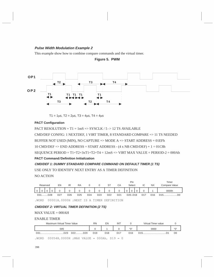
398
Pulse Width Modulation Example 2This example show how to combine compare commands and the virtual timer.
Figure 5. PWM
T1
T2
T1 T1 T1
T3
T3 T4
T2
T1
T4
OP1
O P 2
T1 = 1s, T2 = 2s, T3 = 4s, T4 = 4s
PACT Configuration
PACT RESOLUTION = T1 = 1mS => SYSCLK / 5 -> 12 TS AVAILABLE
CMD/DEF CONFIG: 1 NEXTDEF, 1 VIRT TIMER, 8 STANDARD COMPARE => 11 TS NEEDED
BUFFER NOT USED (MIN), NO CAPTURE => MODE A => START ADDRESS = 01EFh
10 CMD/DEF => END ADDRESS = START ADDRESS - (4 x NB CMD/DEF) + 1 = 01C8h
SEQUENCE PERIOD = T1+T2+3xT1+T2+T4 = 12mS => VIRT MAX VALUE = PERIOD-2 = 000Ah
PACT Command/Definition Initialization
CMD/DEF 1: DUMMY STANDARD COMPARE COMMAND ON DEFAULT TIMER (1 TS)
USE ONLY TO IDENTIFY NEXT ENTRY AS A TIMER DEFINITION
NO ACTION
ÁÁÁÁÁÁÁÁÁÁReserved
ÁÁÁÁÁÁENÁÁÁÁIRÁÁÁÁÁÁRAÁÁÁÁÁÁ0ÁÁÁÁÁÁ0ÁÁÁÁÁÁSTÁÁÁÁÁÁCAÁÁÁÁÁÁ
PinSelectÁÁÁÁÁÁICÁÁÁÁÁÁNXÁÁÁÁÁÁÁÁÁÁ
TimerCompare ValueÁÁ
ÁÁ0ÁÁÁÁ0ÁÁÁÁ0ÁÁÁÁ0
ÁÁÁÁÁÁ0
ÁÁÁÁ0ÁÁÁÁÁÁ0ÁÁÁÁÁÁ0
ÁÁÁÁÁÁ0
ÁÁÁÁÁÁ0
ÁÁÁÁÁÁ0
ÁÁÁÁ0
ÁÁ0ÁÁÁÁ0ÁÁÁÁÁÁ0ÁÁÁÁÁÁ1
ÁÁÁÁÁÁÁÁÁÁ0000hÁÁÁÁÁ
ÁÁÁÁÁD31.........D28
ÁÁÁÁÁÁ
D27ÁÁÁÁ
D26ÁÁÁÁÁÁ
D25ÁÁÁÁÁÁ
D24ÁÁÁÁÁÁ
D23ÁÁÁÁÁÁ
D22ÁÁÁÁÁÁ
D21ÁÁÁÁÁÁ
D20..D18ÁÁÁÁÁÁ
D17ÁÁÁÁÁÁ
D16ÁÁÁÁÁÁÁÁÁÁ
D15....................D0
.WORD 00001H,0000H ;NEXT IS A TIMER DEFINITION
CMD/DEF 2: VIRTUAL TIMER DEFINITION (2 TS)
MAX VALUE = 000AH
ENABLE TIMER
ÁÁÁÁÁÁÁÁÁÁÁMaximum Virtual Timer Value ÁÁÁRNÁÁÁÁEN ÁÁÁINT ÁÁÁ0 ÁÁÁÁÁÁÁVirtual Timer value ÁÁÁ0ÁÁÁÁÁÁÁÁÁÁÁÁÁÁÁÁÁÁÁÁÁÁÁÁÁÁÁÁÁÁÁÁÁ
005
ÁÁÁÁÁÁÁÁÁ
0
ÁÁÁÁÁÁÁÁÁÁÁÁ
1
ÁÁÁÁÁÁÁÁÁ
0
ÁÁÁÁÁÁÁÁÁ
“0”
ÁÁÁÁÁÁÁÁÁÁÁÁÁÁÁÁÁÁÁÁÁ
0000
ÁÁÁÁÁÁÁÁÁ
“0”
ÁÁÁÁÁÁÁD31..................................D23ÁÁÁÁÁD22...........D20ÁÁÁD19ÁÁÁÁD18 ÁÁÁD17 ÁÁÁD16ÁÁÁÁÁÁÁD15..................................D1ÁÁÁD0
.WORD 00054H,0000H ;MAX VALUE = 000Ah, D19 = 0
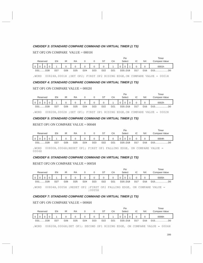
399
CMD/DEF 3: STANDARD COMPARE COMMAND ON VIRTUAL TIMER (1 TS)
SET OP2 ON COMPARE VALUE = 0001HÁÁÁÁÁÁÁÁÁÁÁÁÁÁÁ
Reserved
ÁÁÁÁÁÁÁÁÁ
EN
ÁÁÁÁÁÁ
IR
ÁÁÁÁÁÁÁÁÁ
RA
ÁÁÁÁÁÁÁÁÁ
0
ÁÁÁÁÁÁÁÁÁ
0
ÁÁÁÁÁÁÁÁÁ
ST
ÁÁÁÁÁÁÁÁÁ
CA
ÁÁÁÁÁÁÁÁÁ
PinSelect
ÁÁÁÁÁÁÁÁÁ
IC
ÁÁÁÁÁÁÁÁÁ
NX
ÁÁÁÁÁÁÁÁÁÁÁÁÁÁÁ
TimerCompare Value
ÁÁÁÁ
0ÁÁÁÁ
0ÁÁÁÁ
0ÁÁÁÁ
0ÁÁÁÁÁÁ
1 ÁÁÁÁ
0ÁÁÁÁÁÁ
0ÁÁÁÁÁÁ
0ÁÁÁÁÁÁ
0 ÁÁÁÁÁÁ
0 ÁÁÁÁÁÁ
1 ÁÁÁÁ
0 ÁÁ
0ÁÁÁÁ
1ÁÁÁÁÁÁ
0ÁÁÁÁÁÁ
0 ÁÁÁÁÁÁÁÁÁÁ
0001h
ÁÁÁÁÁÁÁÁÁÁ
D31.........D28 ÁÁÁÁÁÁ
D27 ÁÁÁÁ
D26ÁÁÁÁÁÁ
D25ÁÁÁÁÁÁ
D24ÁÁÁÁÁÁ
D23ÁÁÁÁÁÁ
D22ÁÁÁÁÁÁ
D21 ÁÁÁÁÁÁ
D20..D18ÁÁÁÁÁÁ
D17ÁÁÁÁÁÁ
D16ÁÁÁÁÁÁÁÁÁÁ
D15....................D0
.WORD 00824H,0001H ;SET OP2; FIRST OP2 RISING EDGE,ON COMPARE VALUE = 0001H
CMD/DEF 4: STANDARD COMPARE COMMAND ON VIRTUAL TIMER (1 TS)
SET OP1 ON COMPARE VALUE = 0002HÁÁÁÁÁÁÁÁÁÁÁÁÁÁÁ
Reserved
ÁÁÁÁÁÁÁÁÁ
EN
ÁÁÁÁÁÁ
IR
ÁÁÁÁÁÁÁÁÁ
RA
ÁÁÁÁÁÁÁÁÁ
0
ÁÁÁÁÁÁÁÁÁ
0
ÁÁÁÁÁÁÁÁÁ
ST
ÁÁÁÁÁÁÁÁÁ
CA
ÁÁÁÁÁÁÁÁÁ
PinSelect
ÁÁÁÁÁÁÁÁÁ
IC
ÁÁÁÁÁÁÁÁÁ
NX
ÁÁÁÁÁÁÁÁÁÁÁÁÁÁÁ
TimerCompare Value
ÁÁÁÁ
0ÁÁÁÁ
0ÁÁÁÁ
0ÁÁÁÁ
0ÁÁÁÁÁÁ
1ÁÁÁÁ
0ÁÁÁÁÁÁ
0ÁÁÁÁÁÁ
0ÁÁÁÁÁÁ
0ÁÁÁÁÁÁ
0ÁÁÁÁÁÁ
1ÁÁÁÁ
0ÁÁ
0ÁÁÁÁ
0ÁÁÁÁÁÁ
0ÁÁÁÁÁÁ
0ÁÁÁÁÁÁÁÁÁÁ
0002h
ÁÁÁÁÁÁÁÁÁÁ
D31.........D28 ÁÁÁÁÁÁ
D27 ÁÁÁÁ
D26ÁÁÁÁÁÁ
D25ÁÁÁÁÁÁ
D24ÁÁÁÁÁÁ
D23ÁÁÁÁÁÁ
D22ÁÁÁÁÁÁ
D21 ÁÁÁÁÁÁ
D20..D18ÁÁÁÁÁÁ
D17ÁÁÁÁÁÁ
D16ÁÁÁÁÁÁÁÁÁÁ
D15....................D0
.WORD 00820H,0002H ;SET OP1; FIRST OP1 RISING EDGE,ON COMPARE VALUE = 0002H
CMD/DEF 5: STANDARD COMPARE COMMAND ON VIRTUAL TIMER (1 TS)
RESET OP1 ON COMPARE VALUE = 0004HÁÁÁÁÁÁÁÁÁÁÁÁÁÁÁ
Reserved
ÁÁÁÁÁÁÁÁÁ
EN
ÁÁÁÁÁÁ
IR
ÁÁÁÁÁÁÁÁÁ
RA
ÁÁÁÁÁÁÁÁÁ
0
ÁÁÁÁÁÁÁÁÁ
0
ÁÁÁÁÁÁÁÁÁ
ST
ÁÁÁÁÁÁÁÁÁ
CA
ÁÁÁÁÁÁÁÁÁ
PinSelect
ÁÁÁÁÁÁÁÁÁ
IC
ÁÁÁÁÁÁÁÁÁ
NX
ÁÁÁÁÁÁÁÁÁÁÁÁÁÁÁ
TimerCompare Value
ÁÁÁÁ
0ÁÁÁÁ
0ÁÁÁÁ
0ÁÁÁÁ
0ÁÁÁÁÁÁ
1ÁÁÁÁ
0ÁÁÁÁÁÁ
0ÁÁÁÁÁÁ
0ÁÁÁÁÁÁ
0ÁÁÁÁÁÁ
0ÁÁÁÁÁÁ
0ÁÁÁÁ
0ÁÁ
0ÁÁÁÁ
0ÁÁÁÁÁÁ
0ÁÁÁÁÁÁ
0ÁÁÁÁÁÁÁÁÁÁ
0004hÁÁÁÁÁÁÁÁÁÁ
D31.........D28 ÁÁÁÁÁÁ
D27 ÁÁÁÁ
D26ÁÁÁÁÁÁ
D25ÁÁÁÁÁÁ
D24ÁÁÁÁÁÁ
D23ÁÁÁÁÁÁ
D22ÁÁÁÁÁÁ
D21 ÁÁÁÁÁÁ
D20..D18ÁÁÁÁÁÁ
D17ÁÁÁÁÁÁ
D16ÁÁÁÁÁÁÁÁÁÁ
D15....................D0
.WORD 00800H,0004H;RESET OP1; FIRST OP1 FALLING EDGE, ON COMPARE VALUE =0004H
CMD/DEF 6: STANDARD COMPARE COMMAND ON VIRTUAL TIMER (1 TS)
RESET OP2 ON COMPARE VALUE = 0005HÁÁÁÁÁÁÁÁÁÁÁÁÁÁÁ
Reserved
ÁÁÁÁÁÁÁÁÁ
EN
ÁÁÁÁÁÁ
IR
ÁÁÁÁÁÁÁÁÁ
RA
ÁÁÁÁÁÁÁÁÁ
0
ÁÁÁÁÁÁÁÁÁ
0
ÁÁÁÁÁÁÁÁÁ
ST
ÁÁÁÁÁÁÁÁÁ
CA
ÁÁÁÁÁÁÁÁÁ
PinSelect
ÁÁÁÁÁÁÁÁÁ
IC
ÁÁÁÁÁÁÁÁÁ
NX
ÁÁÁÁÁÁÁÁÁÁÁÁÁÁÁ
TimerCompare Value
ÁÁÁÁ
0ÁÁÁÁ
0ÁÁÁÁ
0ÁÁÁÁ
0ÁÁÁÁÁÁ
1 ÁÁÁÁ
0ÁÁÁÁÁÁ
0ÁÁÁÁÁÁ
0ÁÁÁÁÁÁ
0 ÁÁÁÁÁÁ
0 ÁÁÁÁÁÁ
0 ÁÁÁÁ
0 ÁÁ
0ÁÁÁÁ
1ÁÁÁÁÁÁ
0ÁÁÁÁÁÁ
0 ÁÁÁÁÁÁÁÁÁÁ
0005h
ÁÁÁÁÁÁÁÁÁÁ
D31.........D28 ÁÁÁÁÁÁ
D27 ÁÁÁÁ
D26ÁÁÁÁÁÁ
D25ÁÁÁÁÁÁ
D24ÁÁÁÁÁÁ
D23ÁÁÁÁÁÁ
D22ÁÁÁÁÁÁ
D21 ÁÁÁÁÁÁ
D20..D18ÁÁÁÁÁÁ
D17ÁÁÁÁÁÁ
D16ÁÁÁÁÁÁÁÁÁÁ
D15....................D0
.WORD 00804H,0005H ;RESET OP2 ;FIRST OP2 FALLING EDGE, ON COMPARE VALUE = ;0005H
CMD/DEF 7: STANDARD COMPARE COMMAND ON VIRTUAL TIMER (1 TS)
SET OP1 ON COMPARE VALUE = 0006H
ÁÁÁÁÁÁÁÁÁÁReserved
ÁÁÁÁÁÁENÁÁÁÁIRÁÁÁÁÁÁRAÁÁÁÁÁÁ0ÁÁÁÁÁÁ0ÁÁÁÁÁÁSTÁÁÁÁÁÁCAÁÁÁÁÁÁ
PinSelectÁÁÁÁÁÁICÁÁÁÁÁÁNXÁÁÁÁÁÁÁÁÁÁ
TimerCompare ValueÁÁ
ÁÁ0ÁÁÁÁ0ÁÁÁÁ0ÁÁÁÁ0
ÁÁÁÁÁÁ1
ÁÁÁÁ0ÁÁÁÁÁÁ0ÁÁÁÁÁÁ0
ÁÁÁÁÁÁ0
ÁÁÁÁÁÁ0
ÁÁÁÁÁÁ1
ÁÁÁÁ0
ÁÁ0ÁÁÁÁ0ÁÁÁÁÁÁ0ÁÁÁÁÁÁ0
ÁÁÁÁÁÁÁÁÁÁ0006hÁÁÁÁÁ
ÁÁÁÁÁD31.........D28
ÁÁÁÁÁÁ
D27ÁÁÁÁ
D26ÁÁÁÁÁÁ
D25ÁÁÁÁÁÁ
D24ÁÁÁÁÁÁ
D23ÁÁÁÁÁÁ
D22ÁÁÁÁÁÁ
D21ÁÁÁÁÁÁ
D20..D18ÁÁÁÁÁÁ
D17ÁÁÁÁÁÁ
D16ÁÁÁÁÁÁÁÁÁÁ
D15....................D0
.WORD 00820H,0006H;SET OP1; SECOND OP1 RISING EDGE, ON COMPARE VALUE = 0006H
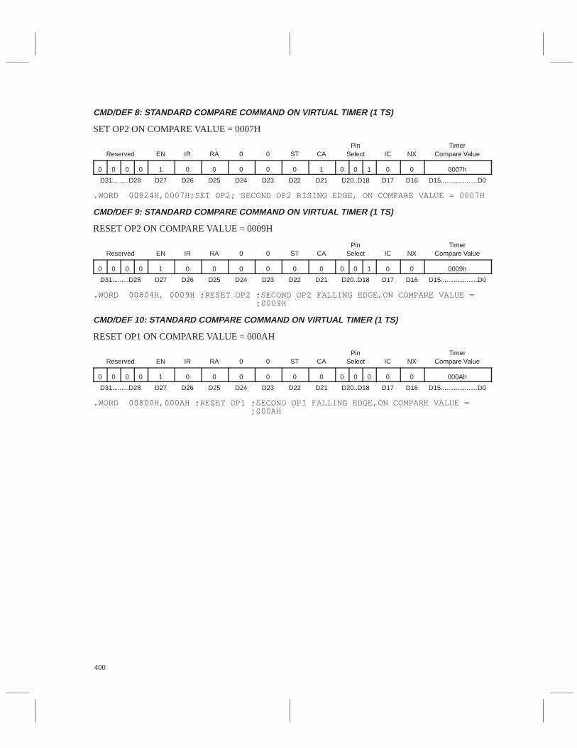
400
CMD/DEF 8: STANDARD COMPARE COMMAND ON VIRTUAL TIMER (1 TS)
SET OP2 ON COMPARE VALUE = 0007HÁÁÁÁÁÁÁÁÁÁÁÁÁÁÁ
Reserved
ÁÁÁÁÁÁÁÁÁ
EN
ÁÁÁÁÁÁ
IR
ÁÁÁÁÁÁÁÁÁ
RA
ÁÁÁÁÁÁÁÁÁ
0
ÁÁÁÁÁÁÁÁÁ
0
ÁÁÁÁÁÁÁÁÁ
ST
ÁÁÁÁÁÁÁÁÁ
CA
ÁÁÁÁÁÁÁÁÁ
PinSelect
ÁÁÁÁÁÁÁÁÁ
IC
ÁÁÁÁÁÁÁÁÁ
NX
ÁÁÁÁÁÁÁÁÁÁÁÁÁÁÁ
TimerCompare Value
ÁÁÁÁ
0ÁÁÁÁ
0ÁÁÁÁ
0ÁÁÁÁ
0ÁÁÁÁÁÁ
1 ÁÁÁÁ
0ÁÁÁÁÁÁ
0ÁÁÁÁÁÁ
0ÁÁÁÁÁÁ
0 ÁÁÁÁÁÁ
0 ÁÁÁÁÁÁ
1 ÁÁÁÁ
0 ÁÁ
0ÁÁÁÁ
1ÁÁÁÁÁÁ
0ÁÁÁÁÁÁ
0 ÁÁÁÁÁÁÁÁÁÁ
0007h
ÁÁÁÁÁD31.........D28 ÁÁÁD27 ÁÁD26ÁÁÁD25ÁÁÁD24ÁÁÁD23ÁÁÁD22ÁÁÁD21 ÁÁÁD20..D18ÁÁÁD17ÁÁÁD16ÁÁÁÁÁD15....................D0
.WORD 00824H,0007H;SET OP2; SECOND OP2 RISING EDGE, ON COMPARE VALUE = 0007H
CMD/DEF 9: STANDARD COMPARE COMMAND ON VIRTUAL TIMER (1 TS)
RESET OP2 ON COMPARE VALUE = 0009H
ÁÁÁÁÁÁÁÁÁÁReserved
ÁÁÁÁÁÁEN
ÁÁÁÁIRÁÁÁÁÁÁRA
ÁÁÁÁÁÁ0
ÁÁÁÁÁÁ0
ÁÁÁÁÁÁST
ÁÁÁÁÁÁCA
ÁÁÁÁÁÁ
PinSelect
ÁÁÁÁÁÁIC
ÁÁÁÁÁÁNX
ÁÁÁÁÁÁÁÁÁÁ
TimerCompare ValueÁÁ
ÁÁ0ÁÁÁÁ0ÁÁÁÁ0ÁÁÁÁ0
ÁÁÁÁÁÁ1
ÁÁÁÁ0ÁÁÁÁÁÁ0ÁÁÁÁÁÁ0
ÁÁÁÁÁÁ0
ÁÁÁÁÁÁ0
ÁÁÁÁÁÁ0
ÁÁÁÁ0
ÁÁ0ÁÁÁÁ1ÁÁÁÁÁÁ0ÁÁÁÁÁÁ0
ÁÁÁÁÁÁÁÁÁÁ0009hÁÁÁÁÁ
ÁÁÁÁÁD31.........D28
ÁÁÁÁÁÁ
D27ÁÁÁÁ
D26ÁÁÁÁÁÁ
D25ÁÁÁÁÁÁ
D24ÁÁÁÁÁÁ
D23ÁÁÁÁÁÁ
D22ÁÁÁÁÁÁ
D21ÁÁÁÁÁÁ
D20..D18ÁÁÁÁÁÁ
D17ÁÁÁÁÁÁ
D16ÁÁÁÁÁÁÁÁÁÁ
D15....................D0
.WORD 00804H, 0009H ;RESET OP2 ;SECOND OP2 FALLING EDGE,ON COMPARE VALUE = ;0009H
CMD/DEF 10: STANDARD COMPARE COMMAND ON VIRTUAL TIMER (1 TS)
RESET OP1 ON COMPARE VALUE = 000AHÁÁÁÁÁÁÁÁÁÁÁÁÁÁÁ
Reserved
ÁÁÁÁÁÁÁÁÁ
EN
ÁÁÁÁÁÁ
IR
ÁÁÁÁÁÁÁÁÁ
RA
ÁÁÁÁÁÁÁÁÁ
0
ÁÁÁÁÁÁÁÁÁ
0
ÁÁÁÁÁÁÁÁÁ
ST
ÁÁÁÁÁÁÁÁÁ
CA
ÁÁÁÁÁÁÁÁÁ
PinSelect
ÁÁÁÁÁÁÁÁÁ
IC
ÁÁÁÁÁÁÁÁÁ
NX
ÁÁÁÁÁÁÁÁÁÁÁÁÁÁÁ
TimerCompare Value
ÁÁÁÁ
0ÁÁÁÁ
0ÁÁÁÁ
0ÁÁÁÁ
0ÁÁÁÁÁÁ
1 ÁÁÁÁ
0ÁÁÁÁÁÁ
0ÁÁÁÁÁÁ
0ÁÁÁÁÁÁ
0 ÁÁÁÁÁÁ
0 ÁÁÁÁÁÁ
0 ÁÁÁÁ
0 ÁÁ
0ÁÁÁÁ
0ÁÁÁÁÁÁ
0ÁÁÁÁÁÁ
0 ÁÁÁÁÁÁÁÁÁÁ
000Ah
ÁÁÁÁÁÁÁÁÁÁ
D31.........D28 ÁÁÁÁÁÁ
D27 ÁÁÁÁ
D26ÁÁÁÁÁÁ
D25ÁÁÁÁÁÁ
D24ÁÁÁÁÁÁ
D23ÁÁÁÁÁÁ
D22ÁÁÁÁÁÁ
D21 ÁÁÁÁÁÁ
D20..D18ÁÁÁÁÁÁ
D17ÁÁÁÁÁÁ
D16ÁÁÁÁÁÁÁÁÁÁ
D15....................D0
.WORD 00800H,000AH ;RESET OP1 ;SECOND OP1 FALLING EDGE,ON COMPARE VALUE = ;000AH
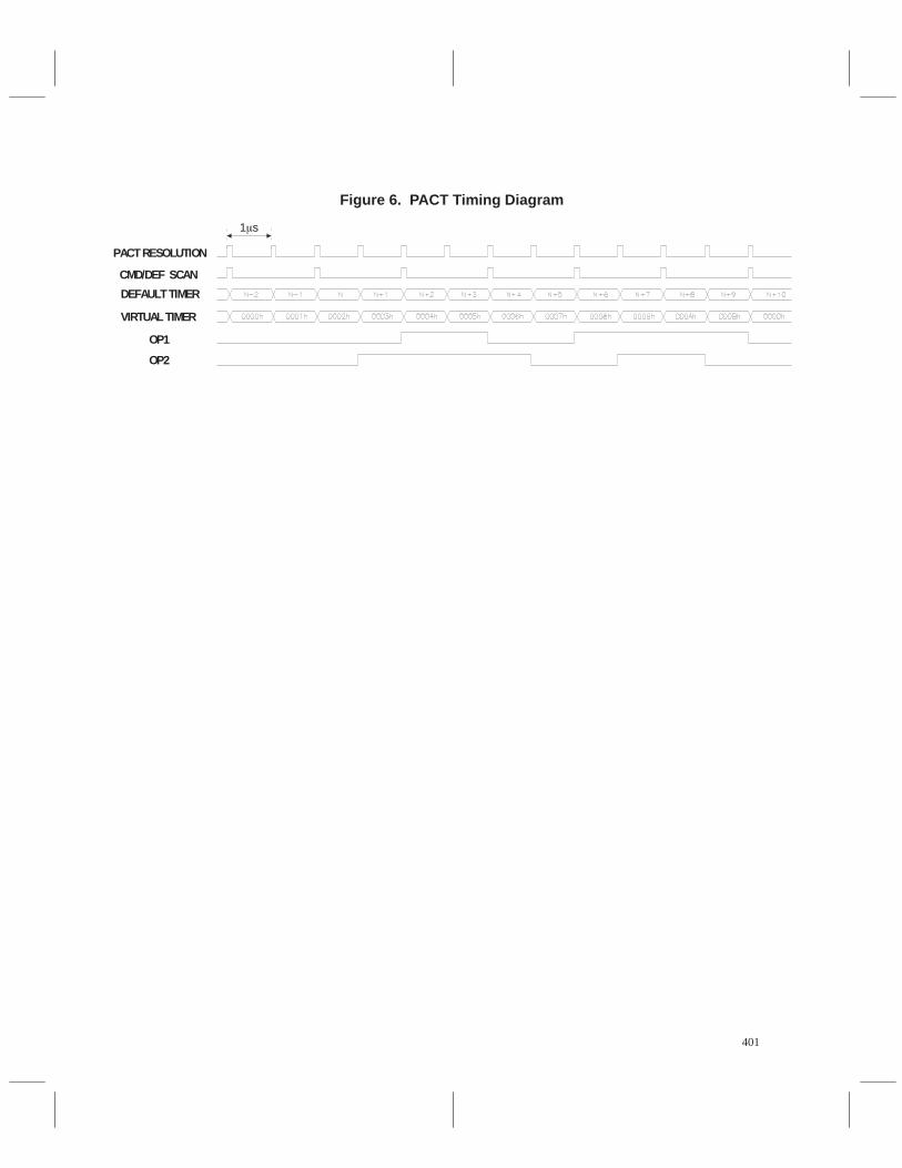
401
Figure 6. PACT Timing Diagram
PACT RESOLUTION
CMD/DEF SCAN
DEFAULT TIMER
VIRTUAL TIMER
OP1
OP2
1s
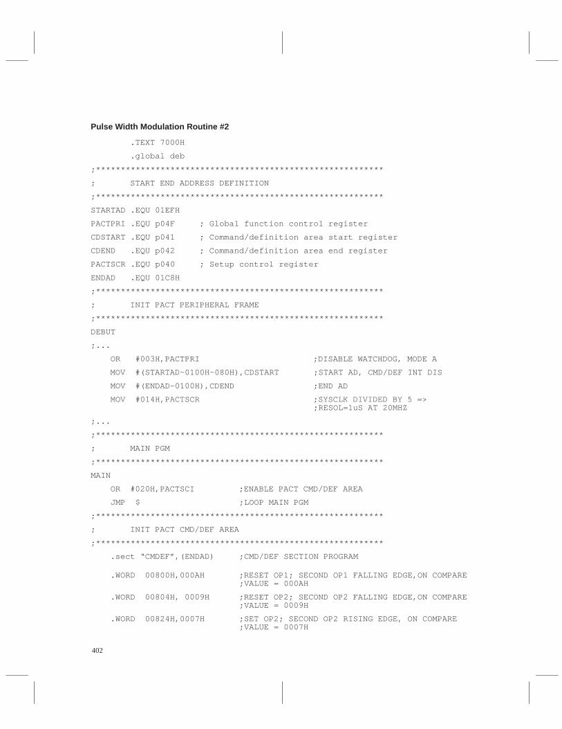
402
Pulse Width Modulation Routine #2
.TEXT 7000H
.global deb
;**********************************************************
; START END ADDRESS DEFINITION
;**********************************************************
STARTAD .EQU 01EFH
PACTPRI .EQU p04F ; Global function control register
CDSTART .EQU p041 ; Command/definition area start register
CDEND .EQU p042 ; Command/definition area end register
PACTSCR .EQU p040 ; Setup control register
ENDAD .EQU 01C8H
;**********************************************************
; INIT PACT PERIPHERAL FRAME
;**********************************************************
DEBUT
;...
OR #003H,PACTPRI ;DISABLE WATCHDOG, MODE A
MOV #(STARTAD-0100H-080H),CDSTART ;START AD, CMD/DEF INT DIS
MOV #(ENDAD-0100H),CDEND ;END AD
MOV #014H,PACTSCR ;SYSCLK DIVIDED BY 5 => ;RESOL=1uS AT 20MHZ
;...
;**********************************************************
; MAIN PGM
;**********************************************************
MAIN
OR #020H,PACTSCI ;ENABLE PACT CMD/DEF AREA
JMP $ ;LOOP MAIN PGM
;**********************************************************
; INIT PACT CMD/DEF AREA
;**********************************************************
.sect “CMDEF”,(ENDAD) ;CMD/DEF SECTION PROGRAM
.WORD 00800H,000AH ;RESET OP1; SECOND OP1 FALLING EDGE,ON COMPARE ;VALUE = 000AH
.WORD 00804H, 0009H ;RESET OP2; SECOND OP2 FALLING EDGE,ON COMPARE ;VALUE = 0009H
.WORD 00824H,0007H ;SET OP2; SECOND OP2 RISING EDGE, ON COMPARE ;VALUE = 0007H
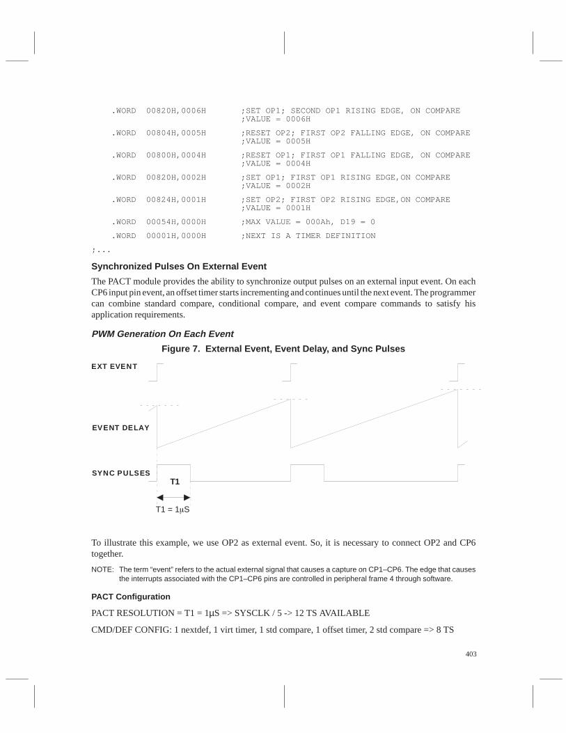
403
.WORD 00820H,0006H ;SET OP1; SECOND OP1 RISING EDGE, ON COMPARE ;VALUE = 0006H
.WORD 00804H,0005H ;RESET OP2; FIRST OP2 FALLING EDGE, ON COMPARE ;VALUE = 0005H
.WORD 00800H,0004H ;RESET OP1; FIRST OP1 FALLING EDGE, ON COMPARE ;VALUE = 0004H
.WORD 00820H,0002H ;SET OP1; FIRST OP1 RISING EDGE,ON COMPARE ;VALUE = 0002H
.WORD 00824H,0001H ;SET OP2; FIRST OP2 RISING EDGE,ON COMPARE ;VALUE = 0001H
.WORD 00054H,0000H ;MAX VALUE = 000Ah, D19 = 0
.WORD 00001H,0000H ;NEXT IS A TIMER DEFINITION
;...
Synchronized Pulses On External Event
The PACT module provides the ability to synchronize output pulses on an external input event. On eachCP6 input pin event, an offset timer starts incrementing and continues until the next event. The programmercan combine standard compare, conditional compare, and event compare commands to satisfy hisapplication requirements.
PWM Generation On Each Event
Figure 7. External Event, Event Delay, and Sync Pulses
T1
EXT EVENT
EVENT DELAY
SYNC PULSES
T1 = 1S
To illustrate this example, we use OP2 as external event. So, it is necessary to connect OP2 and CP6together.
NOTE: The term “event” refers to the actual external signal that causes a capture on CP1–CP6. The edge that causesthe interrupts associated with the CP1–CP6 pins are controlled in peripheral frame 4 through software.
PACT Configuration
PACT RESOLUTION = T1 = 1µS => SYSCLK / 5 -> 12 TS AVAILABLE
CMD/DEF CONFIG: 1 nextdef, 1 virt timer, 1 std compare, 1 offset timer, 2 std compare => 8 TS
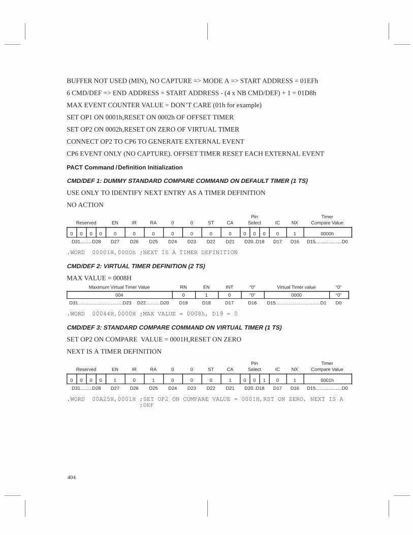
404
BUFFER NOT USED (MIN), NO CAPTURE => MODE A => START ADDRESS = 01EFh
6 CMD/DEF => END ADDRESS = START ADDRESS - (4 x NB CMD/DEF) + 1 = 01D8h
MAX EVENT COUNTER VALUE = DON’T CARE (01h for example)
SET OP1 ON 0001h,RESET ON 0002h OF OFFSET TIMER
SET OP2 ON 0002h,RESET ON ZERO OF VIRTUAL TIMER
CONNECT OP2 TO CP6 TO GENERATE EXTERNAL EVENT
CP6 EVENT ONLY (NO CAPTURE). OFFSET TIMER RESET EACH EXTERNAL EVENT
PACT Command /Definition Initialization
CMD/DEF 1: DUMMY STANDARD COMPARE COMMAND ON DEFAULT TIMER (1 TS)
USE ONLY TO IDENTIFY NEXT ENTRY AS A TIMER DEFINITION
NO ACTION
ÁÁÁÁÁÁÁÁÁÁReserved
ÁÁÁÁÁÁENÁÁÁÁIRÁÁÁÁÁÁRAÁÁÁÁÁÁ0ÁÁÁÁÁÁ0ÁÁÁÁÁÁSTÁÁÁÁÁÁCAÁÁÁÁÁÁ
PinSelectÁÁÁÁÁÁICÁÁÁÁÁÁNXÁÁÁÁÁÁÁÁÁÁ
TimerCompare ValueÁÁ
ÁÁ0ÁÁÁÁ0ÁÁÁÁ0ÁÁÁÁ0
ÁÁÁÁÁÁ0
ÁÁÁÁ0ÁÁÁÁÁÁ0ÁÁÁÁÁÁ0
ÁÁÁÁÁÁ0
ÁÁÁÁÁÁ0
ÁÁÁÁÁÁ0
ÁÁÁÁ0
ÁÁ0ÁÁÁÁ0ÁÁÁÁÁÁ0ÁÁÁÁÁÁ1
ÁÁÁÁÁÁÁÁÁÁ0000hÁÁÁÁÁ
ÁÁÁÁÁD31.........D28
ÁÁÁÁÁÁ
D27ÁÁÁÁ
D26ÁÁÁÁÁÁ
D25ÁÁÁÁÁÁ
D24ÁÁÁÁÁÁ
D23ÁÁÁÁÁÁ
D22ÁÁÁÁÁÁ
D21ÁÁÁÁÁÁ
D20..D18ÁÁÁÁÁÁ
D17ÁÁÁÁÁÁ
D16ÁÁÁÁÁÁÁÁÁÁ
D15....................D0
.WORD 00001H,0000h ;NEXT IS A TIMER DEFINITION
CMD/DEF 2: VIRTUAL TIMER DEFINITION (2 TS)
MAX VALUE = 0008H
ÁÁÁÁÁÁÁÁÁÁÁÁÁÁÁÁÁÁÁÁÁÁ
Maximum Virtual Timer Value ÁÁÁÁÁÁ
RNÁÁÁÁÁÁÁÁ
EN ÁÁÁÁÁÁ
INT ÁÁÁÁÁÁ
“0” ÁÁÁÁÁÁÁÁÁÁÁÁÁÁ
Virtual Timer value ÁÁÁÁÁÁ
“0”
ÁÁÁÁÁÁÁÁÁÁÁ004 ÁÁÁ0ÁÁÁÁ1 ÁÁÁ0 ÁÁÁ“0” ÁÁÁÁÁÁÁ0000 ÁÁÁ“0”ÁÁÁÁÁÁÁÁÁÁÁÁÁÁ
D31..................................D23ÁÁÁÁÁÁÁÁÁÁ
D22...........D20ÁÁÁÁÁÁ
D19ÁÁÁÁÁÁÁÁ
D18ÁÁÁÁÁÁ
D17ÁÁÁÁÁÁ
D16ÁÁÁÁÁÁÁÁÁÁÁÁÁÁ
D15..................................D1ÁÁÁÁÁÁ
D0
.WORD 00044H,0000H ;MAX VALUE = 0008h, D19 = 0
CMD/DEF 3: STANDARD COMPARE COMMAND ON VIRTUAL TIMER (1 TS)
SET OP2 ON COMPARE VALUE = 0001H,RESET ON ZERO
NEXT IS A TIMER DEFINITIONÁÁÁÁÁÁÁÁÁÁÁÁÁÁÁ
Reserved
ÁÁÁÁÁÁÁÁÁ
EN
ÁÁÁÁÁÁ
IR
ÁÁÁÁÁÁÁÁÁ
RA
ÁÁÁÁÁÁÁÁÁ
0
ÁÁÁÁÁÁÁÁÁ
0
ÁÁÁÁÁÁÁÁÁ
ST
ÁÁÁÁÁÁÁÁÁ
CA
ÁÁÁÁÁÁÁÁÁ
PinSelect
ÁÁÁÁÁÁÁÁÁ
IC
ÁÁÁÁÁÁÁÁÁ
NX
ÁÁÁÁÁÁÁÁÁÁÁÁÁÁÁ
TimerCompare Value
ÁÁÁÁ
0ÁÁÁÁ
0ÁÁÁÁ
0ÁÁÁÁ
0ÁÁÁÁÁÁ
1 ÁÁÁÁ
0ÁÁÁÁÁÁ
1ÁÁÁÁÁÁ
0ÁÁÁÁÁÁ
0 ÁÁÁÁÁÁ
0 ÁÁÁÁÁÁ
1 ÁÁÁÁ
0 ÁÁ
0ÁÁÁÁ
1ÁÁÁÁÁÁ
0ÁÁÁÁÁÁ
1 ÁÁÁÁÁÁÁÁÁÁ
0001h
ÁÁÁÁÁD31.........D28 ÁÁÁD27 ÁÁD26ÁÁÁD25ÁÁÁD24ÁÁÁD23ÁÁÁD22ÁÁÁD21 ÁÁÁD20..D18ÁÁÁD17ÁÁÁD16ÁÁÁÁÁD15....................D0
.WORD 00A25H,0001H ;SET OP2 ON COMPARE VALUE = 0001H,RST ON ZERO, NEXT IS A ;DEF
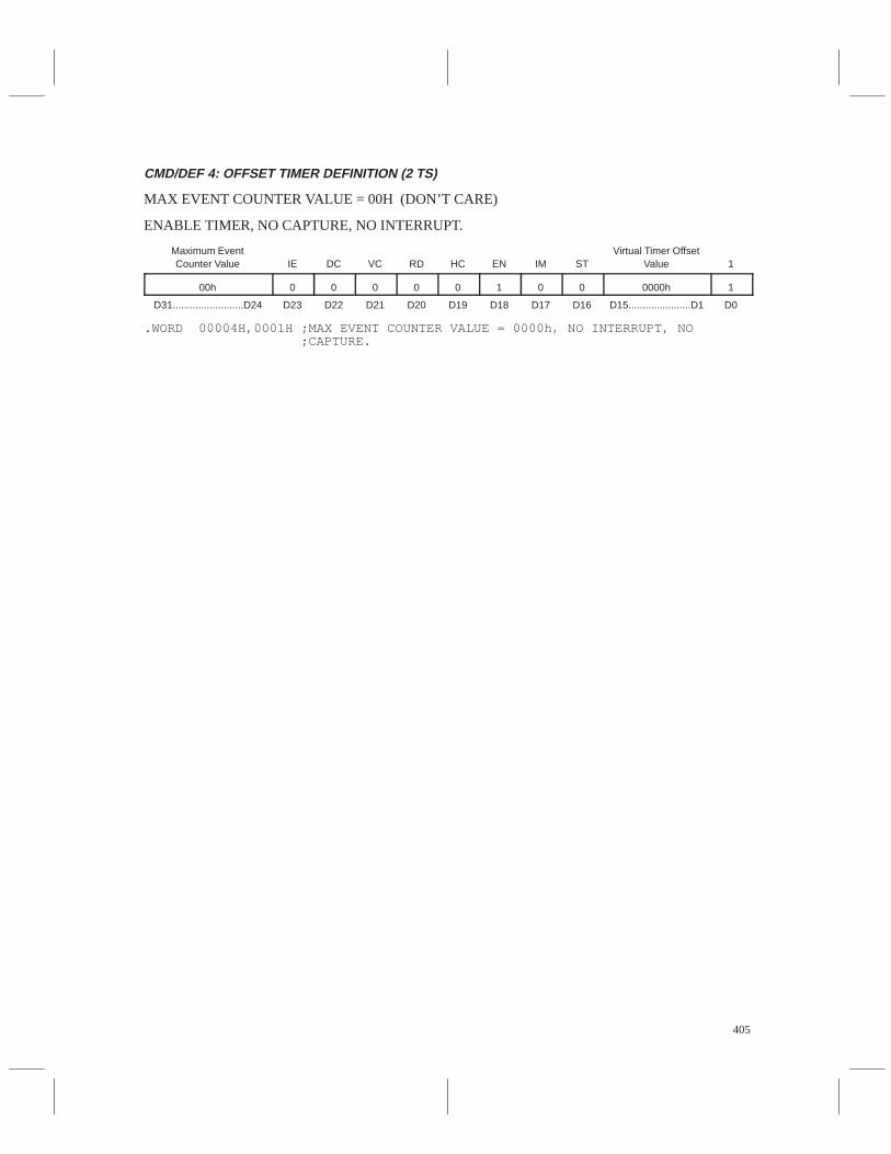
405
CMD/DEF 4: OFFSET TIMER DEFINITION (2 TS)
MAX EVENT COUNTER VALUE = 00H (DON’T CARE)
ENABLE TIMER, NO CAPTURE, NO INTERRUPT.ÁÁÁÁÁÁÁÁÁÁÁÁÁÁÁÁÁÁÁÁÁ
Maximum EventCounter Value
ÁÁÁÁÁÁÁÁÁ
IE
ÁÁÁÁÁÁÁÁÁ
DC
ÁÁÁÁÁÁÁÁÁ
VC
ÁÁÁÁÁÁÁÁÁ
RD
ÁÁÁÁÁÁÁÁÁ
HC
ÁÁÁÁÁÁÁÁÁ
EN
ÁÁÁÁÁÁÁÁÁ
IM
ÁÁÁÁÁÁ
ST
ÁÁÁÁÁÁÁÁÁÁÁÁÁÁÁÁÁÁ
Virtual Timer OffsetValue
ÁÁÁÁÁÁÁÁÁ
1
ÁÁÁÁÁÁÁÁÁÁÁÁÁÁ
00h ÁÁÁÁÁÁ
0ÁÁÁÁÁÁ
0ÁÁÁÁÁÁ
0ÁÁÁÁÁÁ
0ÁÁÁÁÁÁ
0 ÁÁÁÁÁÁ
1 ÁÁÁÁÁÁ
0 ÁÁÁÁ
0ÁÁÁÁÁÁÁÁÁÁÁÁ
0000h ÁÁÁÁÁÁ
1
ÁÁÁÁÁÁÁÁÁÁÁÁÁÁ
D31.........................D24 ÁÁÁÁÁÁ
D23ÁÁÁÁÁÁ
D22ÁÁÁÁÁÁ
D21ÁÁÁÁÁÁ
D20ÁÁÁÁÁÁ
D19ÁÁÁÁÁÁ
D18 ÁÁÁÁÁÁ
D17 ÁÁÁÁ
D16ÁÁÁÁÁÁÁÁÁÁÁÁ
D15......................D1ÁÁÁÁÁÁ
D0
.WORD 00004H,0001H ;MAX EVENT COUNTER VALUE = 0000h, NO INTERRUPT, NO ;CAPTURE.
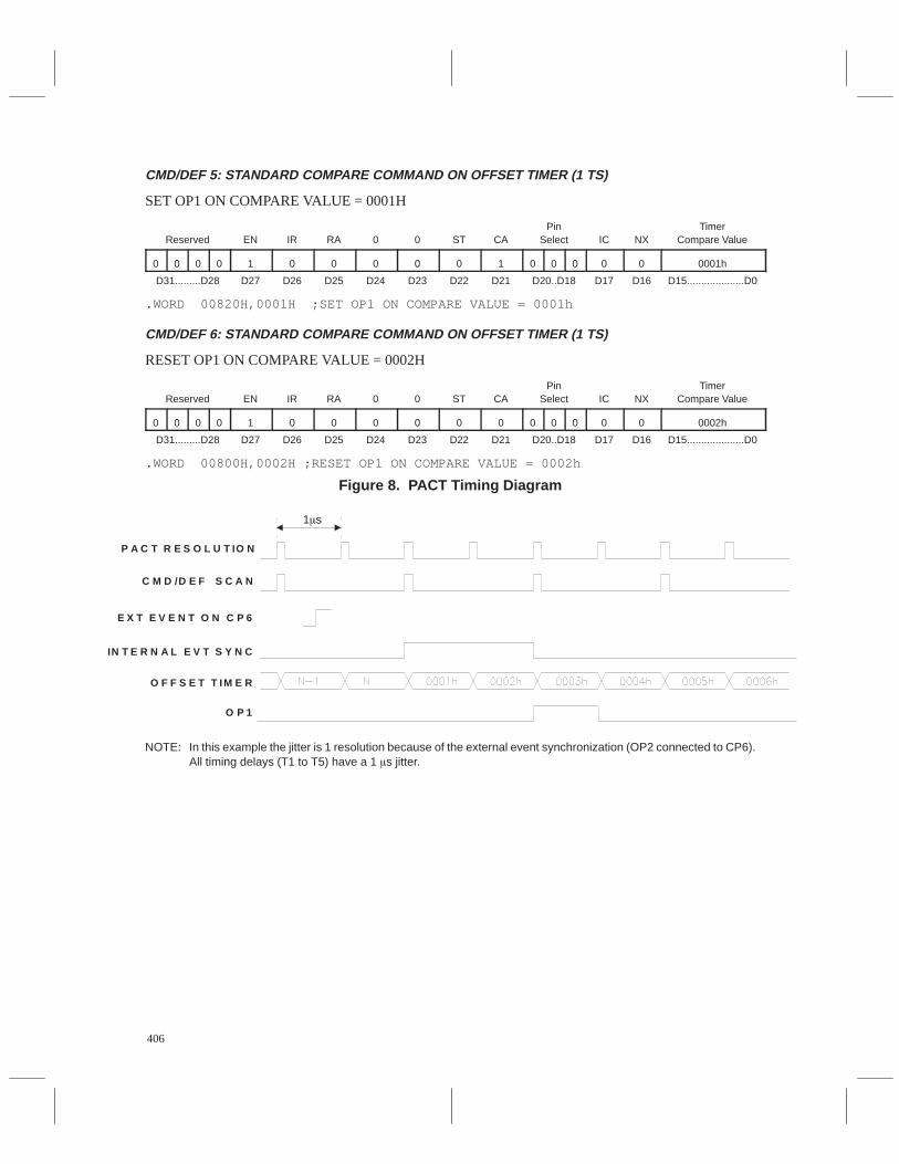
406
CMD/DEF 5: STANDARD COMPARE COMMAND ON OFFSET TIMER (1 TS)
SET OP1 ON COMPARE VALUE = 0001HÁÁÁÁÁÁÁÁÁÁÁÁÁÁÁ
Reserved
ÁÁÁÁÁÁÁÁÁ
EN
ÁÁÁÁÁÁ
IR
ÁÁÁÁÁÁÁÁÁ
RA
ÁÁÁÁÁÁÁÁÁ
0
ÁÁÁÁÁÁÁÁÁ
0
ÁÁÁÁÁÁÁÁÁ
ST
ÁÁÁÁÁÁÁÁÁ
CA
ÁÁÁÁÁÁÁÁÁ
PinSelect
ÁÁÁÁÁÁÁÁÁ
IC
ÁÁÁÁÁÁÁÁÁ
NX
ÁÁÁÁÁÁÁÁÁÁÁÁÁÁÁ
TimerCompare Value
ÁÁÁÁ
0ÁÁÁÁ
0ÁÁÁÁ
0ÁÁÁÁ
0ÁÁÁÁÁÁ
1 ÁÁÁÁ
0ÁÁÁÁÁÁ
0ÁÁÁÁÁÁ
0ÁÁÁÁÁÁ
0 ÁÁÁÁÁÁ
0 ÁÁÁÁÁÁ
1 ÁÁÁÁ
0 ÁÁ
0ÁÁÁÁ
0ÁÁÁÁÁÁ
0ÁÁÁÁÁÁ
0 ÁÁÁÁÁÁÁÁÁÁ
0001h
ÁÁÁÁÁD31.........D28 ÁÁÁD27 ÁÁD26ÁÁÁD25ÁÁÁD24ÁÁÁD23ÁÁÁD22ÁÁÁD21 ÁÁÁD20..D18ÁÁÁD17ÁÁÁD16ÁÁÁÁÁD15....................D0
.WORD 00820H,0001H ;SET OP1 ON COMPARE VALUE = 0001h
CMD/DEF 6: STANDARD COMPARE COMMAND ON OFFSET TIMER (1 TS)
RESET OP1 ON COMPARE VALUE = 0002HÁÁÁÁÁÁÁÁÁÁÁÁÁÁÁ
Reserved
ÁÁÁÁÁÁÁÁÁ
EN
ÁÁÁÁÁÁ
IR
ÁÁÁÁÁÁÁÁÁ
RA
ÁÁÁÁÁÁÁÁÁ
0
ÁÁÁÁÁÁÁÁÁ
0
ÁÁÁÁÁÁÁÁÁ
ST
ÁÁÁÁÁÁÁÁÁ
CA
ÁÁÁÁÁÁÁÁÁ
PinSelect
ÁÁÁÁÁÁÁÁÁ
IC
ÁÁÁÁÁÁÁÁÁ
NX
ÁÁÁÁÁÁÁÁÁÁÁÁÁÁÁ
TimerCompare Value
ÁÁÁÁ
0ÁÁÁÁ
0ÁÁÁÁ
0ÁÁÁÁ
0ÁÁÁÁÁÁ
1 ÁÁÁÁ
0ÁÁÁÁÁÁ
0ÁÁÁÁÁÁ
0ÁÁÁÁÁÁ
0 ÁÁÁÁÁÁ
0 ÁÁÁÁÁÁ
0 ÁÁÁÁ
0 ÁÁ
0ÁÁÁÁ
0ÁÁÁÁÁÁ
0ÁÁÁÁÁÁ
0 ÁÁÁÁÁÁÁÁÁÁ
0002h
ÁÁÁÁÁD31.........D28 ÁÁÁD27 ÁÁD26ÁÁÁD25ÁÁÁD24ÁÁÁD23ÁÁÁD22ÁÁÁD21 ÁÁÁD20..D18ÁÁÁD17ÁÁÁD16ÁÁÁÁÁD15....................D0
.WORD 00800H,0002H ;RESET OP1 ON COMPARE VALUE = 0002h
Figure 8. PACT Timing Diagram
P A C T R E S O L U T IO N
C M D /D E F S C A N
O F F S E T T IM E R
O P 1
IN T E R N A L E V T S Y N C
E X T E V E N T O N C P 6
1s
NOTE: In this example the jitter is 1 resolution because of the external event synchronization (OP2 connected to CP6).All timing delays (T1 to T5) have a 1 s jitter.
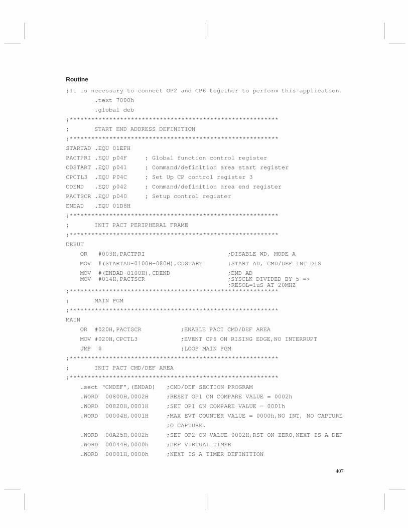
407
Routine
;It is necessary to connect OP2 and CP6 together to perform this application.
.text 7000h
.global deb
;**********************************************************
; START END ADDRESS DEFINITION
;**********************************************************
STARTAD .EQU 01EFH
PACTPRI .EQU p04F ; Global function control register
CDSTART .EQU p041 ; Command/definition area start register
CPCTL3 .EQU P04C ; Set Up CP control register 3
CDEND .EQU p042 ; Command/definition area end register
PACTSCR .EQU p040 ; Setup control register
ENDAD .EQU 01D8H
;**********************************************************
; INIT PACT PERIPHERAL FRAME
;**********************************************************
DEBUT
OR #003H,PACTPRI ;DISABLE WD, MODE A
MOV #(STARTAD-0100H-080H),CDSTART ;START AD, CMD/DEF INT DIS
MOV #(ENDAD-0100H),CDEND ;END AD MOV #014H,PACTSCR ;SYSCLK DIVIDED BY 5 => ;RESOL=1uS AT 20MHZ;**********************************************************
; MAIN PGM
;**********************************************************
MAIN
OR #020H,PACTSCR ;ENABLE PACT CMD/DEF AREA
MOV #020H,CPCTL3 ;EVENT CP6 ON RISING EDGE,NO INTERRUPT
JMP $ ;LOOP MAIN PGM
;**********************************************************
; INIT PACT CMD/DEF AREA
;**********************************************************
.sect “CMDEF”,(ENDAD) ;CMD/DEF SECTION PROGRAM
.WORD 00800H,0002H ;RESET OP1 ON COMPARE VALUE = 0002h
.WORD 00820H,0001H ;SET OP1 ON COMPARE VALUE = 0001h
.WORD 00004H,0001H ;MAX EVT COUNTER VALUE = 0000h,NO INT, NO CAPTURE
;O CAPTURE.
.WORD 00A25H,0002h ;SET OP2 ON VALUE 0002H,RST ON ZERO,NEXT IS A DEF
.WORD 00044H,0000h ;DEF VIRTUAL TIMER
.WORD 00001H,0000h ;NEXT IS A TIMER DEFINITION
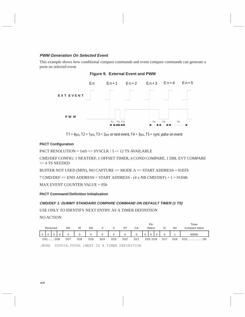
408
PWM Generation On Selected Event
This example shows how conditional compare commands and event compare commands can generate apwm on selected event.
Figure 9. External Event and PWM
E X T E V E N T
En En+1 En+2 En+3 En+4 En+5
T1 T2 T4T3
P W M
T5 T6
T1 = 4s, T2 = 1s, T3 = 2s or next event, T4 = 3s, T5 = sync pulse on event
PACT Configuration
PACT RESOLUTION = 1mS => SYSCLK / 5 -> 12 TS AVAILABLE
CMD/DEF CONFIG: 1 NEXTDEF, 1 OFFSET TIMER, 4 COND COMPARE, 1 DBL EVT COMPARE=> 4 TS NEEDED
BUFFER NOT USED (MIN), NO CAPTURE => MODE A => START ADDRESS = 01EFh
7 CMD/DEF => END ADDRESS = START ADDRESS - (4 x NB CMD/DEF) + 1 = 01D4h
MAX EVENT COUNTER VALUE = 05h
PACT Command/Definition Initialization
CMD/DEF 1: DUMMY STANDARD COMPARE COMMAND ON DEFAULT TIMER (1 TS)
USE ONLY TO IDENTIFY NEXT ENTRY AS A TIMER DEFINITION
NO ACTIONÁÁÁÁÁÁÁÁÁÁÁÁÁÁÁ
Reserved
ÁÁÁÁÁÁÁÁÁ
EN
ÁÁÁÁÁÁ
IR
ÁÁÁÁÁÁÁÁÁ
RA
ÁÁÁÁÁÁÁÁÁ
0
ÁÁÁÁÁÁÁÁÁ
0
ÁÁÁÁÁÁÁÁÁ
ST
ÁÁÁÁÁÁÁÁÁ
CA
ÁÁÁÁÁÁÁÁÁ
PinSelect
ÁÁÁÁÁÁÁÁÁ
IC
ÁÁÁÁÁÁÁÁÁ
NX
ÁÁÁÁÁÁÁÁÁÁÁÁÁÁÁ
TimerCompare Value
ÁÁÁÁ
0ÁÁÁÁ
0ÁÁÁÁ
0ÁÁÁÁ
0ÁÁÁÁÁÁ
0ÁÁÁÁ
0ÁÁÁÁÁÁ
0ÁÁÁÁÁÁ
0ÁÁÁÁÁÁ
0ÁÁÁÁÁÁ
0ÁÁÁÁÁÁ
0ÁÁÁÁ
0ÁÁ
0ÁÁÁÁ
0ÁÁÁÁÁÁ
0ÁÁÁÁÁÁ
1ÁÁÁÁÁÁÁÁÁÁ
0000h
ÁÁÁÁÁÁÁÁÁÁ
D31.........D28 ÁÁÁÁÁÁ
D27 ÁÁÁÁ
D26ÁÁÁÁÁÁ
D25ÁÁÁÁÁÁ
D24ÁÁÁÁÁÁ
D23ÁÁÁÁÁÁ
D22ÁÁÁÁÁÁ
D21 ÁÁÁÁÁÁ
D20..D18ÁÁÁÁÁÁ
D17ÁÁÁÁÁÁ
D16ÁÁÁÁÁÁÁÁÁÁ
D15....................D0
.WORD 00001H,0000h ;NEXT IS A TIMER DEFINITION
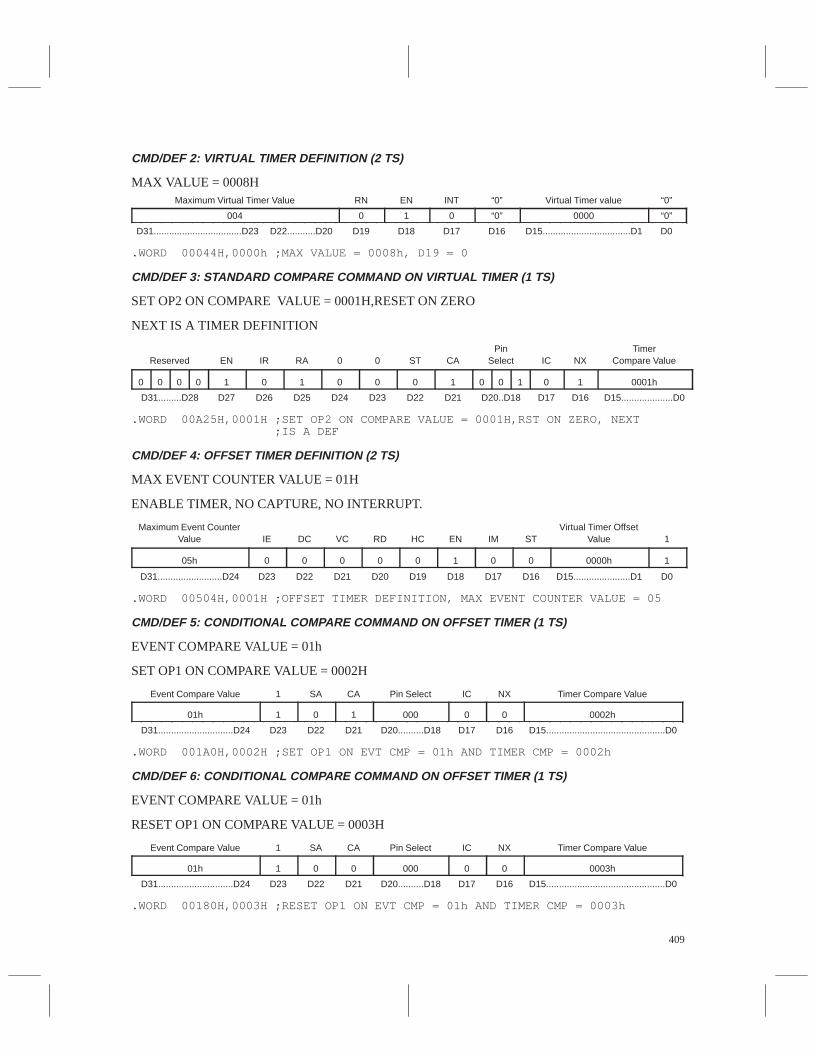
409
CMD/DEF 2: VIRTUAL TIMER DEFINITION (2 TS)
MAX VALUE = 0008HÁÁÁÁÁÁÁÁÁÁÁÁÁÁÁÁÁÁÁÁÁÁ
Maximum Virtual Timer Value ÁÁÁÁÁÁ
RNÁÁÁÁÁÁÁÁ
EN ÁÁÁÁÁÁ
INT ÁÁÁÁÁÁ
“0” ÁÁÁÁÁÁÁÁÁÁÁÁÁÁ
Virtual Timer value ÁÁÁÁÁÁ
“0”
ÁÁÁÁÁÁÁÁÁÁÁ004 ÁÁÁ0ÁÁÁÁ1 ÁÁÁ0 ÁÁÁ“0” ÁÁÁÁÁÁÁ0000 ÁÁÁ“0”ÁÁÁÁÁÁÁÁÁÁÁÁÁÁD31..................................D23
ÁÁÁÁÁÁÁÁÁÁD22...........D20
ÁÁÁÁÁÁD19ÁÁÁÁÁÁÁÁD18
ÁÁÁÁÁÁD17ÁÁÁÁÁÁD16ÁÁÁÁÁÁÁÁÁÁÁÁÁÁD15..................................D1
ÁÁÁÁÁÁD0
.WORD 00044H,0000h ;MAX VALUE = 0008h, D19 = 0
CMD/DEF 3: STANDARD COMPARE COMMAND ON VIRTUAL TIMER (1 TS)
SET OP2 ON COMPARE VALUE = 0001H,RESET ON ZERO
NEXT IS A TIMER DEFINITIONÁÁÁÁÁÁÁÁÁÁÁÁÁÁÁ
Reserved
ÁÁÁÁÁÁÁÁÁ
EN
ÁÁÁÁÁÁ
IR
ÁÁÁÁÁÁÁÁÁ
RA
ÁÁÁÁÁÁÁÁÁ
0
ÁÁÁÁÁÁÁÁÁ
0
ÁÁÁÁÁÁÁÁÁ
ST
ÁÁÁÁÁÁÁÁÁ
CA
ÁÁÁÁÁÁÁÁÁ
PinSelect
ÁÁÁÁÁÁÁÁÁ
IC
ÁÁÁÁÁÁÁÁÁ
NX
ÁÁÁÁÁÁÁÁÁÁÁÁÁÁÁ
TimerCompare Value
ÁÁÁÁ
0ÁÁÁÁ
0ÁÁÁÁ
0ÁÁÁÁ
0ÁÁÁÁÁÁ
1 ÁÁÁÁ
0ÁÁÁÁÁÁ
1ÁÁÁÁÁÁ
0ÁÁÁÁÁÁ
0 ÁÁÁÁÁÁ
0 ÁÁÁÁÁÁ
1 ÁÁÁÁ
0 ÁÁ
0ÁÁÁÁ
1ÁÁÁÁÁÁ
0ÁÁÁÁÁÁ
1 ÁÁÁÁÁÁÁÁÁÁ
0001h
ÁÁÁÁÁD31.........D28 ÁÁÁD27 ÁÁD26ÁÁÁD25ÁÁÁD24ÁÁÁD23ÁÁÁD22ÁÁÁD21 ÁÁÁD20..D18ÁÁÁD17ÁÁÁD16ÁÁÁÁÁD15....................D0
.WORD 00A25H,0001H ;SET OP2 ON COMPARE VALUE = 0001H,RST ON ZERO, NEXT ;IS A DEF
CMD/DEF 4: OFFSET TIMER DEFINITION (2 TS)
MAX EVENT COUNTER VALUE = 01H
ENABLE TIMER, NO CAPTURE, NO INTERRUPT.
ÁÁÁÁÁÁÁÁÁÁÁÁÁÁ
Maximum Event CounterValue
ÁÁÁÁÁÁIEÁÁÁÁÁÁDCÁÁÁÁÁÁVCÁÁÁÁÁÁRDÁÁÁÁÁÁHCÁÁÁÁÁÁENÁÁÁÁÁÁIMÁÁÁÁSTÁÁÁÁÁÁÁÁÁÁÁÁ
Virtual Timer OffsetValue
ÁÁÁÁÁÁ1ÁÁÁÁÁÁÁ
ÁÁÁÁÁÁÁ05hÁÁÁÁÁÁ0ÁÁÁÁÁÁ0ÁÁÁÁÁÁ0ÁÁÁÁÁÁ0ÁÁÁÁÁÁ0ÁÁÁÁÁÁ1ÁÁÁÁÁÁ0ÁÁÁÁ0ÁÁÁÁÁÁÁÁÁÁÁÁ0000h
ÁÁÁÁÁÁ1ÁÁÁÁÁÁÁ
ÁÁÁÁÁÁÁD31.........................D24
ÁÁÁÁÁÁ
D23ÁÁÁÁÁÁ
D22ÁÁÁÁÁÁ
D21ÁÁÁÁÁÁ
D20ÁÁÁÁÁÁ
D19ÁÁÁÁÁÁ
D18ÁÁÁÁÁÁ
D17ÁÁÁÁ
D16ÁÁÁÁÁÁÁÁÁÁÁÁ
D15......................D1ÁÁÁÁÁÁ
D0
.WORD 00504H,0001H ;OFFSET TIMER DEFINITION, MAX EVENT COUNTER VALUE = 05
CMD/DEF 5: CONDITIONAL COMPARE COMMAND ON OFFSET TIMER (1 TS)
EVENT COMPARE VALUE = 01h
SET OP1 ON COMPARE VALUE = 0002H
ÁÁÁÁÁÁÁÁÁÁÁÁÁÁ
Event Compare ValueÁÁÁÁÁÁ
1ÁÁÁÁÁÁ
SAÁÁÁÁÁÁ
CA ÁÁÁÁÁÁÁÁ
Pin SelectÁÁÁÁÁÁ
ICÁÁÁÁÁÁ
NXÁÁÁÁÁÁÁÁÁÁÁÁÁÁÁÁÁÁ
Timer Compare Value
ÁÁÁÁÁÁÁÁÁÁÁÁÁÁ
01h ÁÁÁÁÁÁ
1ÁÁÁÁÁÁ
0 ÁÁÁÁÁÁ
1 ÁÁÁÁÁÁÁÁ
000 ÁÁÁÁÁÁ
0ÁÁÁÁÁÁ
0ÁÁÁÁÁÁÁÁÁÁÁÁÁÁÁÁÁÁ
0002h
ÁÁÁÁÁÁÁÁÁÁÁÁÁÁ
D31.............................D24ÁÁÁÁÁÁ
D23ÁÁÁÁÁÁ
D22ÁÁÁÁÁÁ
D21ÁÁÁÁÁÁÁÁ
D20..........D18ÁÁÁÁÁÁ
D17ÁÁÁÁÁÁ
D16ÁÁÁÁÁÁÁÁÁÁÁÁÁÁÁÁÁÁ
D15..............................................D0
.WORD 001A0H,0002H ;SET OP1 ON EVT CMP = 01h AND TIMER CMP = 0002h
CMD/DEF 6: CONDITIONAL COMPARE COMMAND ON OFFSET TIMER (1 TS)
EVENT COMPARE VALUE = 01h
RESET OP1 ON COMPARE VALUE = 0003HÁÁÁÁÁÁÁÁÁÁÁÁÁÁEvent Compare Value
ÁÁÁÁÁÁ1
ÁÁÁÁÁÁSA
ÁÁÁÁÁÁCA
ÁÁÁÁÁÁÁÁPin Select
ÁÁÁÁÁÁICÁÁÁÁÁÁNX
ÁÁÁÁÁÁÁÁÁÁÁÁÁÁÁÁÁÁTimer Compare ValueÁÁÁÁÁÁÁ
ÁÁÁÁÁÁÁ01h
ÁÁÁÁÁÁ1
ÁÁÁÁÁÁ0
ÁÁÁÁÁÁ0
ÁÁÁÁÁÁÁÁ000
ÁÁÁÁÁÁ0ÁÁÁÁÁÁ0
ÁÁÁÁÁÁÁÁÁÁÁÁÁÁÁÁÁÁ0003hÁÁÁÁÁÁÁ
ÁÁÁÁÁÁÁD31.............................D24
ÁÁÁÁÁÁ
D23ÁÁÁÁÁÁ
D22ÁÁÁÁÁÁ
D21ÁÁÁÁÁÁÁÁ
D20..........D18ÁÁÁÁÁÁ
D17ÁÁÁÁÁÁ
D16ÁÁÁÁÁÁÁÁÁÁÁÁÁÁÁÁÁÁ
D15..............................................D0
.WORD 00180H,0003H ;RESET OP1 ON EVT CMP = 01h AND TIMER CMP = 0003h
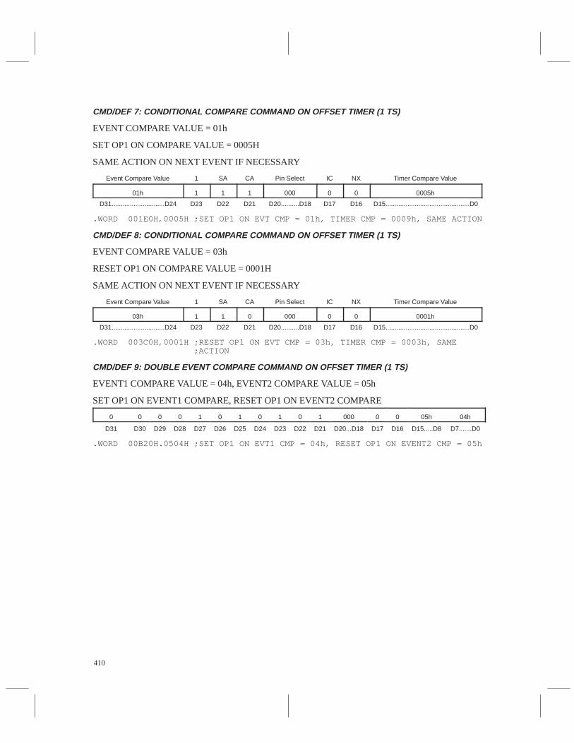
410
CMD/DEF 7: CONDITIONAL COMPARE COMMAND ON OFFSET TIMER (1 TS)
EVENT COMPARE VALUE = 01h
SET OP1 ON COMPARE VALUE = 0005H
SAME ACTION ON NEXT EVENT IF NECESSARYÁÁÁÁÁÁÁÁÁÁÁÁÁÁEvent Compare Value
ÁÁÁÁÁÁ1ÁÁÁÁÁÁSAÁÁÁÁÁÁCAÁÁÁÁÁÁÁÁPin Select
ÁÁÁÁÁÁICÁÁÁÁÁÁNXÁÁÁÁÁÁÁÁÁÁÁÁÁÁÁÁÁÁTimer Compare ValueÁÁÁÁÁÁÁ
ÁÁÁÁÁÁÁ01hÁÁÁÁÁÁ1ÁÁÁÁÁÁ1ÁÁÁÁÁÁ1ÁÁÁÁÁÁÁÁ000
ÁÁÁÁÁÁ0ÁÁÁÁÁÁ0ÁÁÁÁÁÁÁÁÁÁÁÁÁÁÁÁÁÁ0005hÁÁÁÁÁÁÁ
ÁÁÁÁÁÁÁD31.............................D24
ÁÁÁÁÁÁ
D23ÁÁÁÁÁÁ
D22ÁÁÁÁÁÁ
D21ÁÁÁÁÁÁÁÁ
D20..........D18ÁÁÁÁÁÁ
D17ÁÁÁÁÁÁ
D16ÁÁÁÁÁÁÁÁÁÁÁÁÁÁÁÁÁÁ
D15..............................................D0
.WORD 001E0H,0005H ;SET OP1 ON EVT CMP = 01h, TIMER CMP = 0009h, SAME ACTION
CMD/DEF 8: CONDITIONAL COMPARE COMMAND ON OFFSET TIMER (1 TS)
EVENT COMPARE VALUE = 03h
RESET OP1 ON COMPARE VALUE = 0001H
SAME ACTION ON NEXT EVENT IF NECESSARY
ÁÁÁÁÁÁÁÁÁÁÁÁÁÁ
Event Compare ValueÁÁÁÁÁÁ
1ÁÁÁÁÁÁ
SAÁÁÁÁÁÁ
CA ÁÁÁÁÁÁÁÁ
Pin SelectÁÁÁÁÁÁ
ICÁÁÁÁÁÁ
NXÁÁÁÁÁÁÁÁÁÁÁÁÁÁÁÁÁÁ
Timer Compare Value
ÁÁÁÁÁÁÁÁÁÁÁÁÁÁ
03h ÁÁÁÁÁÁ
1ÁÁÁÁÁÁ
1 ÁÁÁÁÁÁ
0 ÁÁÁÁÁÁÁÁ
000 ÁÁÁÁÁÁ
0ÁÁÁÁÁÁ
0ÁÁÁÁÁÁÁÁÁÁÁÁÁÁÁÁÁÁ
0001h
ÁÁÁÁÁÁÁÁÁÁÁÁÁÁ
D31.............................D24ÁÁÁÁÁÁ
D23ÁÁÁÁÁÁ
D22ÁÁÁÁÁÁ
D21ÁÁÁÁÁÁÁÁ
D20..........D18ÁÁÁÁÁÁ
D17ÁÁÁÁÁÁ
D16ÁÁÁÁÁÁÁÁÁÁÁÁÁÁÁÁÁÁ
D15..............................................D0
.WORD 003C0H,0001H ;RESET OP1 ON EVT CMP = 03h, TIMER CMP = 0003h, SAME ;ACTION
CMD/DEF 9: DOUBLE EVENT COMPARE COMMAND ON OFFSET TIMER (1 TS)
EVENT1 COMPARE VALUE = 04h, EVENT2 COMPARE VALUE = 05h
SET OP1 ON EVENT1 COMPARE, RESET OP1 ON EVENT2 COMPARE
ÁÁÁÁÁÁÁÁ
0 ÁÁÁÁ
0ÁÁÁÁ
0ÁÁÁÁÁÁ
0 ÁÁÁÁ
1ÁÁÁÁ
0ÁÁÁÁÁÁ
1ÁÁÁÁ
0ÁÁÁÁÁÁ
1 ÁÁÁÁ
0ÁÁÁÁ
1ÁÁÁÁÁÁÁÁ
000 ÁÁÁÁ
0ÁÁÁÁÁÁ
0 ÁÁÁÁÁÁ
05hÁÁÁÁÁÁÁÁ
04h
ÁÁÁÁÁÁÁÁ
D31 ÁÁÁÁ
D30ÁÁÁÁ
D29ÁÁÁÁÁÁ
D28ÁÁÁÁ
D27ÁÁÁÁ
D26ÁÁÁÁÁÁ
D25ÁÁÁÁ
D24ÁÁÁÁÁÁ
D23ÁÁÁÁ
D22ÁÁÁÁ
D21ÁÁÁÁÁÁÁÁ
D20...D18ÁÁÁÁ
D17ÁÁÁÁÁÁ
D16ÁÁÁÁÁÁ
D15.....D8ÁÁÁÁÁÁÁÁ
D7.......D0
.WORD 00B20H.0504H ;SET OP1 ON EVT1 CMP = 04h, RESET OP1 ON EVENT2 CMP = 05h
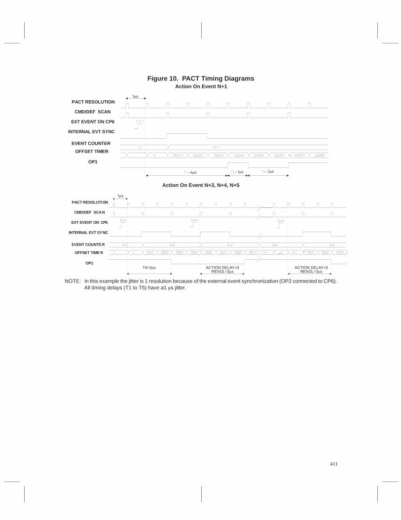
411
Figure 10. PACT Timing DiagramsAction On Event N+1
PACT RESOLUTION
CMD/DEF SCAN
OFFSET TIMER
OP1
INTERNAL EVT SYNC
EXT EVENT ON CP6
..
EVENT COUNTER
1s
s 1s s
Action On Event N+3, N+4, N+5
PACT RESOLUTION
CMD/DEF SCAN
OFFSET TIME R
OP1
INTERNAL EVT SYNC
EXT EVENT ON CP6
..EVENT COUNTE R
T4=3s ACTION DELAY=3RESOL=3s
ACTION DELAY=3RESOL=3s
...
1s
NOTE: In this example the jitter is 1 resolution because of the external event synchronization (OP2 connected to CP6).All timing delays (T1 to T5) have a1 s jitter.
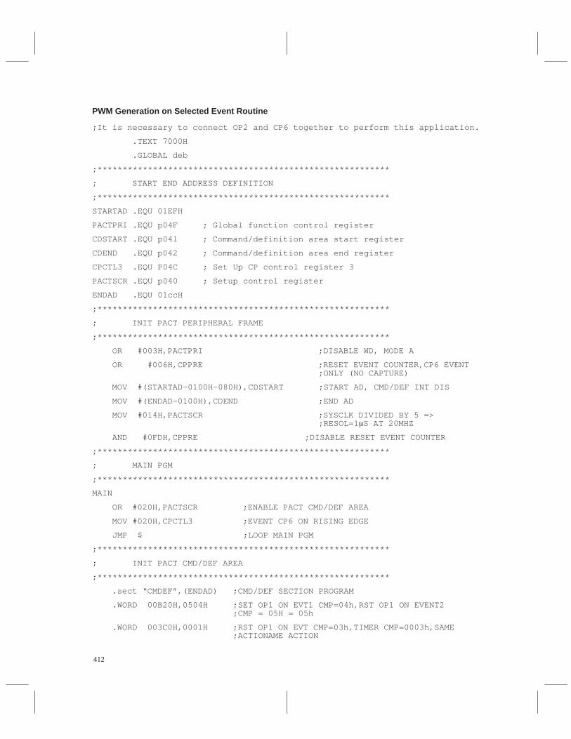
412
PWM Generation on Selected Event Routine
;It is necessary to connect OP2 and CP6 together to perform this application.
.TEXT 7000H
.GLOBAL deb
;**********************************************************
; START END ADDRESS DEFINITION
;**********************************************************
STARTAD .EQU 01EFH
PACTPRI .EQU p04F ; Global function control register
CDSTART .EQU p041 ; Command/definition area start register
CDEND .EQU p042 ; Command/definition area end register
CPCTL3 .EQU P04C ; Set Up CP control register 3
PACTSCR .EQU p040 ; Setup control register
ENDAD .EQU 01ccH
;**********************************************************
; INIT PACT PERIPHERAL FRAME
;**********************************************************
OR #003H,PACTPRI ;DISABLE WD, MODE A
OR #006H,CPPRE ;RESET EVENT COUNTER,CP6 EVENT ;ONLY (NO CAPTURE)
MOV #(STARTAD-0100H-080H),CDSTART ;START AD, CMD/DEF INT DIS
MOV #(ENDAD-0100H),CDEND ;END AD
MOV #014H,PACTSCR ;SYSCLK DIVIDED BY 5 => ;RESOL=1 S AT 20MHZ
AND #0FDH,CPPRE ;DISABLE RESET EVENT COUNTER
;**********************************************************
; MAIN PGM
;**********************************************************
MAIN
OR #020H,PACTSCR ;ENABLE PACT CMD/DEF AREA
MOV #020H,CPCTL3 ;EVENT CP6 ON RISING EDGE
JMP $ ;LOOP MAIN PGM
;**********************************************************
; INIT PACT CMD/DEF AREA
;**********************************************************
.sect “CMDEF”,(ENDAD) ;CMD/DEF SECTION PROGRAM
.WORD 00B20H,0504H ;SET OP1 ON EVT1 CMP=04h,RST OP1 ON EVENT2 ;CMP = 05H = 05h
.WORD 003C0H,0001H ;RST OP1 ON EVT CMP=03h,TIMER CMP=0003h,SAME ;ACTIONAME ACTION
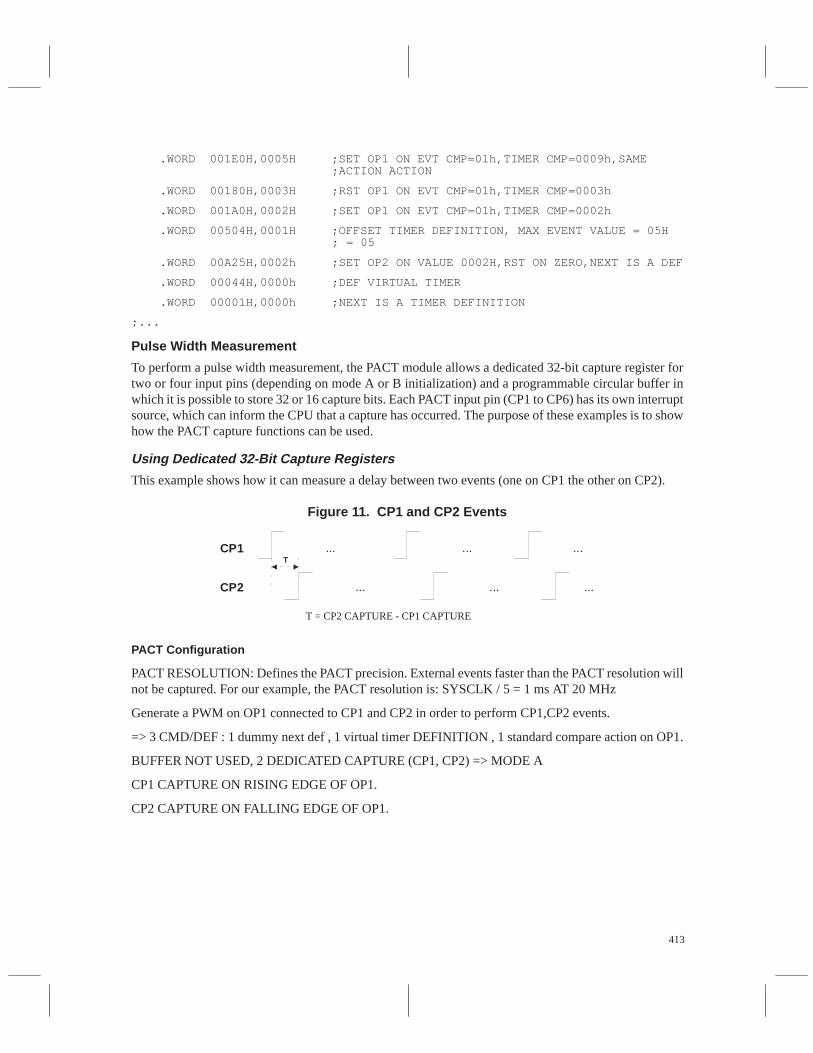
413
.WORD 001E0H,0005H ;SET OP1 ON EVT CMP=01h,TIMER CMP=0009h,SAME ;ACTION ACTION
.WORD 00180H,0003H ;RST OP1 ON EVT CMP=01h,TIMER CMP=0003h
.WORD 001A0H,0002H ;SET OP1 ON EVT CMP=01h,TIMER CMP=0002h
.WORD 00504H,0001H ;OFFSET TIMER DEFINITION, MAX EVENT VALUE = 05H ; = 05
.WORD 00A25H,0002h ;SET OP2 ON VALUE 0002H,RST ON ZERO,NEXT IS A DEF
.WORD 00044H,0000h ;DEF VIRTUAL TIMER
.WORD 00001H,0000h ;NEXT IS A TIMER DEFINITION
;...
Pulse Width Measurement
To perform a pulse width measurement, the PACT module allows a dedicated 32-bit capture register fortwo or four input pins (depending on mode A or B initialization) and a programmable circular buffer inwhich it is possible to store 32 or 16 capture bits. Each PACT input pin (CP1 to CP6) has its own interruptsource, which can inform the CPU that a capture has occurred. The purpose of these examples is to showhow the PACT capture functions can be used.
Using Dedicated 32-Bit Capture Registers
This example shows how it can measure a delay between two events (one on CP1 the other on CP2).
Figure 11. CP1 and CP2 Events
...
...
...
...
...
...
TCP1
CP2
T = CP2 CAPTURE - CP1 CAPTURE
PACT Configuration
PACT RESOLUTION: Defines the PACT precision. External events faster than the PACT resolution willnot be captured. For our example, the PACT resolution is: SYSCLK / 5 = 1 ms AT 20 MHz
Generate a PWM on OP1 connected to CP1 and CP2 in order to perform CP1,CP2 events.
=> 3 CMD/DEF : 1 dummy next def , 1 virtual timer DEFINITION , 1 standard compare action on OP1.
BUFFER NOT USED, 2 DEDICATED CAPTURE (CP1, CP2) => MODE A
CP1 CAPTURE ON RISING EDGE OF OP1.
CP2 CAPTURE ON FALLING EDGE OF OP1.
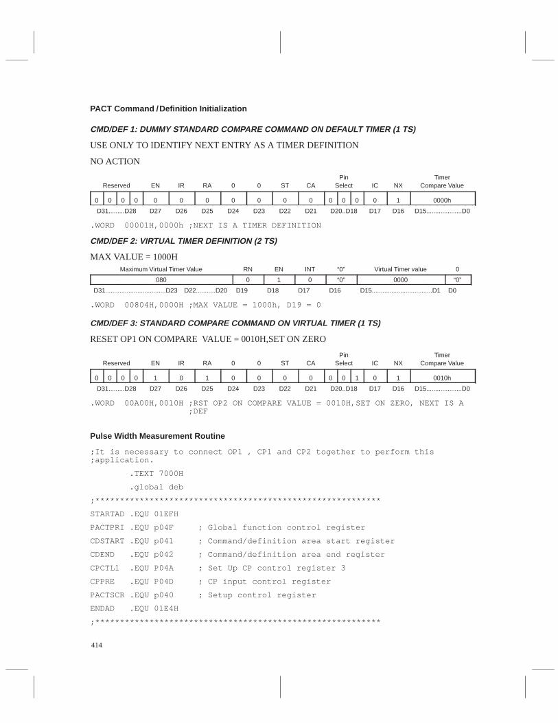
414
PACT Command /Definition Initialization
CMD/DEF 1: DUMMY STANDARD COMPARE COMMAND ON DEFAULT TIMER (1 TS)
USE ONLY TO IDENTIFY NEXT ENTRY AS A TIMER DEFINITION
NO ACTION
ÁÁÁÁÁÁÁÁÁÁ
ReservedÁÁÁÁÁÁ
ENÁÁÁÁ
IRÁÁÁÁÁÁ
RAÁÁÁÁÁÁ
0ÁÁÁÁÁÁ
0ÁÁÁÁÁÁ
STÁÁÁÁÁÁ
CAÁÁÁÁÁÁ
PinSelectÁÁÁÁÁÁ
ICÁÁÁÁÁÁ
NXÁÁÁÁÁÁÁÁÁÁ
TimerCompare Value
ÁÁÁÁ
0ÁÁÁÁ
0ÁÁÁÁ
0ÁÁÁÁ
0ÁÁÁÁÁÁ
0ÁÁÁÁ
0ÁÁÁÁÁÁ
0ÁÁÁÁÁÁ
0ÁÁÁÁÁÁ
0ÁÁÁÁÁÁ
0ÁÁÁÁÁÁ
0ÁÁÁÁ
0ÁÁ
0ÁÁÁÁ
0ÁÁÁÁÁÁ
0ÁÁÁÁÁÁ
1ÁÁÁÁÁÁÁÁÁÁ
0000hÁÁÁÁÁÁÁÁÁÁ
D31.........D28 ÁÁÁÁÁÁ
D27 ÁÁÁÁ
D26ÁÁÁÁÁÁ
D25ÁÁÁÁÁÁ
D24ÁÁÁÁÁÁ
D23ÁÁÁÁÁÁ
D22ÁÁÁÁÁÁ
D21 ÁÁÁÁÁÁ
D20..D18ÁÁÁÁÁÁ
D17ÁÁÁÁÁÁ
D16ÁÁÁÁÁÁÁÁÁÁ
D15....................D0
.WORD 00001H,0000h ;NEXT IS A TIMER DEFINITION
CMD/DEF 2: VIRTUAL TIMER DEFINITION (2 TS)
MAX VALUE = 1000HÁÁÁÁÁÁÁÁÁÁÁÁÁÁÁÁÁÁÁÁÁÁ
Maximum Virtual Timer ValueÁÁÁÁÁÁ
RNÁÁÁÁÁÁÁÁ
ENÁÁÁÁÁÁ
INTÁÁÁÁÁÁ
“0”ÁÁÁÁÁÁÁÁÁÁÁÁÁÁ
Virtual Timer valueÁÁÁÁÁÁ
0ÁÁÁÁÁÁÁÁÁÁÁÁÁÁÁÁÁÁÁÁÁÁ
080 ÁÁÁÁÁÁ
0ÁÁÁÁÁÁÁÁ
1 ÁÁÁÁÁÁ
0 ÁÁÁÁÁÁ
“0” ÁÁÁÁÁÁÁÁÁÁÁÁÁÁ
0000 ÁÁÁÁÁÁ
“0”
ÁÁÁÁÁÁÁÁÁÁÁÁÁÁ
D31..................................D23ÁÁÁÁÁÁÁÁÁÁ
D22...........D20ÁÁÁÁÁÁ
D19 ÁÁÁÁÁÁÁÁ
D18 ÁÁÁÁÁÁ
D17 ÁÁÁÁÁÁ
D16 ÁÁÁÁÁÁÁÁÁÁÁÁÁÁ
D15..................................D1ÁÁÁÁÁÁ
D0
.WORD 00804H,0000H ;MAX VALUE = 1000h, D19 = 0
CMD/DEF 3: STANDARD COMPARE COMMAND ON VIRTUAL TIMER (1 TS)
RESET OP1 ON COMPARE VALUE = 0010H,SET ON ZEROÁÁÁÁÁÁÁÁÁÁÁÁÁÁÁ
Reserved
ÁÁÁÁÁÁÁÁÁ
EN
ÁÁÁÁÁÁ
IR
ÁÁÁÁÁÁÁÁÁ
RA
ÁÁÁÁÁÁÁÁÁ
0
ÁÁÁÁÁÁÁÁÁ
0
ÁÁÁÁÁÁÁÁÁ
ST
ÁÁÁÁÁÁÁÁÁ
CA
ÁÁÁÁÁÁÁÁÁ
PinSelect
ÁÁÁÁÁÁÁÁÁ
IC
ÁÁÁÁÁÁÁÁÁ
NX
ÁÁÁÁÁÁÁÁÁÁÁÁÁÁÁ
TimerCompare Value
ÁÁÁÁ
0ÁÁÁÁ
0ÁÁÁÁ
0ÁÁÁÁ
0ÁÁÁÁÁÁ
1 ÁÁÁÁ
0ÁÁÁÁÁÁ
1ÁÁÁÁÁÁ
0ÁÁÁÁÁÁ
0 ÁÁÁÁÁÁ
0 ÁÁÁÁÁÁ
0 ÁÁÁÁ
0 ÁÁ
0ÁÁÁÁ
1ÁÁÁÁÁÁ
0ÁÁÁÁÁÁ
1 ÁÁÁÁÁÁÁÁÁÁ
0010h
ÁÁÁÁÁÁÁÁÁÁ
D31.........D28 ÁÁÁÁÁÁ
D27 ÁÁÁÁ
D26ÁÁÁÁÁÁ
D25ÁÁÁÁÁÁ
D24ÁÁÁÁÁÁ
D23ÁÁÁÁÁÁ
D22ÁÁÁÁÁÁ
D21 ÁÁÁÁÁÁ
D20..D18ÁÁÁÁÁÁ
D17ÁÁÁÁÁÁ
D16ÁÁÁÁÁÁÁÁÁÁ
D15....................D0
.WORD 00A00H,0010H ;RST OP2 ON COMPARE VALUE = 0010H,SET ON ZERO, NEXT IS A ;DEF
Pulse Width Measurement Routine
;It is necessary to connect OP1 , CP1 and CP2 together to perform this;application.
.TEXT 7000H
.global deb
;**********************************************************
STARTAD .EQU 01EFH
PACTPRI .EQU p04F ; Global function control register
CDSTART .EQU p041 ; Command/definition area start register
CDEND .EQU p042 ; Command/definition area end register
CPCTL1 .EQU P04A ; Set Up CP control register 3
CPPRE .EQU P04D ; CP input control register
PACTSCR .EQU p040 ; Setup control register
ENDAD .EQU 01E4H
;**********************************************************

415
; INIT PACT PERIPHERAL FRAME
;**********************************************************
OR #003H,PACTPRI ;DISABLE WATCHDOG, MODE A
MOV #010H,B
LDSP
MOV #000H,CPPRE ;INPUT CAPTURE PRESCALER DIVIDE ;BY 1
MOV #(STARTAD-0100H-080H),CDSTART ;START AD, CMD/DEF INT DIS
MOV #(ENDAD-0100H),CDEND ;END AD
MOV #013H,PACTSCR ;SYSCLK DIVIDED BY 4 => ;RESOL=800uS AT 20MHZ
;**********************************************************
; MAIN PGM
;**********************************************************
MAIN
OR #020H,PACTSCR ;ENABLE PACT CMD/DEF AREA
EINT ;ENABLE INTERRUPT
MN MOV #092H,CPCTL1 ;CAPTURE ON CP1 RISE AND CP2 FALL,INT CP2 ENABLE BLE
JMP MN ;LOOP MAIN PGM
;**********************************************************
; INTERRUPT CAPTURE CP2
;**********************************************************
ITCP2
MOV #000H,CPCTL1 ;DISABLE CP1/CP2 CAPTURE AND CLEAR ITCP2 FLAG
; STORE CP1 CAPTURE IN REGISTERS R0F9, R0FA, R0FB
MOV &01F9H,A
MOV A,R0F9
MOV &01FAH,A
MOV A,R0FA
MOV &01FBH,A
MOV A,R0FB
; STORE CP2 CAPTURE IN REGISTERS R0F5, R0F6, R0F7
MOV &01F5H,A
MOV A,R0F5
MOV &01F6H,A
MOV A,R0F6
MOV &01F7H,A
MOV A,R0F7
;CP2 PERIOD MEASUREMENT (T2)
SUB R0FB,R0F7
416
SBB R0FA,R0F6
SBB R0F9,R0F5
; RESULT STORED IN REGISTERS R0E5, R0E6, R0E7
MOV R0F7,R0E7
MOV R0F6,R0E6
MOV R0F5,R0E5
;RETURN TO MAIN PGM
RTI
;**********************************************************
; CP2 INTERRUPT VECTORS
;**********************************************************
.sect “VECT”,07FBAH ;PACT INTERRUPT VECTOR
.WORD ITCP2 ;CP2 IT VECTOR
;**********************************************************
; INIT PACT CMD/DEF AREA
;**********************************************************
.sect “CMDEF”,(ENDAD) ;CMD/DEF SECTION PROGRAM
.WORD 0A00h,0010h ;RST OP1 ON 0010H VIRT1,SET ON ZERO
.WORD 8004h,0000h ;VIRT1 MAX VALUE = 8000H
.WORD 0001h,0000h ;NEXT IS A DEF
NOTES:
• In this example, the jitter is 1 resolution because of the external event synchronization (OP1connected to CP1 and CP2). All timing delays (T1 to T5) have 1 ms jitter. The jitter average is1/2 resolution in case of asynchronous external events.
• The measurement value is stored in registers R0E5,R0E6,R0E7 (LSB). It is always equal to theCMD/DEF 3 compare value ( if OP1 connected to CP1 and CP2).
• By changing CMD/DEF 3 compare value, you change the OP1 falling edge and so increase ordecrease CP1/CP2 delay.
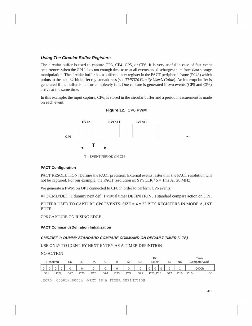
417
Using The Circular Buffer Registers
The circular buffer is used to capture CP3, CP4, CP5, or CP6. It is very useful in case of fast eventoccurrences when the CPU does not enough time to treat all events and discharges them from data storagemanipulation. The circular buffer has a buffer pointer register in the PACT peripheral frame (P043) whichpoints to the next 32-bit buffer register address (see TMS370 Family User’s Guide). An interrupt buffer isgenerated if the buffer is half or completely full. One capture is generated if two events (CP5 and CP6)arrive at the same time.
In this example, the input capture, CP6, is stored in the circular buffer and a period measurement is madeon each event.
Figure 12. CP6 PWM
CP6
T
EVTn EVTn+1 EVTn+2
...
T = EVENT PERIOD ON CP6
PACT Configuration
PACT RESOLUTION: Defines the PACT precision. External events faster than the PACT resolution willnot be captured. For our example, the PACT resolution is: SYSCLK / 5 = 1ms AT 20 MHz
We generate a PWM on OP1 connected to CP6 in order to perform CP6 events.
=> 3 CMD/DEF : 1 dummy next def , 1 virtual timer DEFINITION , 1 standard compare action on OP1.
BUFFER USED TO CAPTURE CP6 EVENTS. SIZE = 4 x 32 BITS REGISTERS IN MODE A, INTBUFF
CP6 CAPTURE ON RISING EDGE.
PACT Command/Definition Initialization
CMD/DEF 1: DUMMY STANDARD COMPARE COMMAND ON DEFAULT TIMER (1 TS)
USE ONLY TO IDENTIFY NEXT ENTRY AS A TIMER DEFINITION
NO ACTIONÁÁÁÁÁÁÁÁÁÁReserved
ÁÁÁÁÁÁENÁÁÁÁIRÁÁÁÁÁÁRAÁÁÁÁÁÁ0ÁÁÁÁÁÁ0ÁÁÁÁÁÁSTÁÁÁÁÁÁCAÁÁÁÁÁÁ
PinSelectÁÁÁÁÁÁICÁÁÁÁÁÁNXÁÁÁÁÁÁÁÁÁÁ
TimerCompare ValueÁÁ
ÁÁ0ÁÁÁÁ0ÁÁÁÁ0ÁÁÁÁ0ÁÁÁÁÁÁ0ÁÁÁÁ0ÁÁÁÁÁÁ0ÁÁÁÁÁÁ0ÁÁÁÁÁÁ0ÁÁÁÁÁÁ0ÁÁÁÁÁÁ0ÁÁÁÁ0ÁÁ0ÁÁÁÁ0ÁÁÁÁÁÁ0ÁÁÁÁÁÁ1ÁÁÁÁÁÁÁÁÁÁ0000hÁÁÁÁÁ
ÁÁÁÁÁD31.........D28
ÁÁÁÁÁÁ
D27ÁÁÁÁ
D26ÁÁÁÁÁÁ
D25ÁÁÁÁÁÁ
D24ÁÁÁÁÁÁ
D23ÁÁÁÁÁÁ
D22ÁÁÁÁÁÁ
D21ÁÁÁÁÁÁ
D20..D18ÁÁÁÁÁÁ
D17ÁÁÁÁÁÁ
D16ÁÁÁÁÁÁÁÁÁÁ
D15....................D0
.WORD 00001H,0000h ;NEXT IS A TIMER DEFINITION
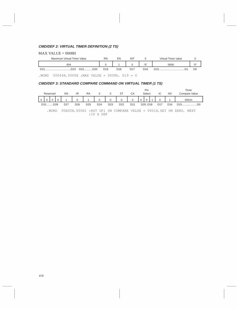
418
CMD/DEF 2: VIRTUAL TIMER DEFINITION (2 TS)
MAX VALUE = 0008HÁÁÁÁÁÁÁÁÁÁÁÁÁÁÁÁÁÁÁÁÁÁ
Maximum Virtual Timer Value ÁÁÁÁÁÁ
RNÁÁÁÁÁÁÁÁ
EN ÁÁÁÁÁÁ
INT ÁÁÁÁÁÁ
0 ÁÁÁÁÁÁÁÁÁÁÁÁÁÁ
Virtual Timer value ÁÁÁÁÁÁ
0
ÁÁÁÁÁÁÁÁÁÁÁÁÁÁÁÁÁÁÁÁÁÁ
004 ÁÁÁÁÁÁ
0ÁÁÁÁÁÁÁÁ
1 ÁÁÁÁÁÁ
0 ÁÁÁÁÁÁ
“0” ÁÁÁÁÁÁÁÁÁÁÁÁÁÁ
0000 ÁÁÁÁÁÁ
“0”
ÁÁÁÁÁÁÁD31..................................D23ÁÁÁÁÁD22...........D20ÁÁÁD19ÁÁÁÁD18 ÁÁÁD17 ÁÁÁD16ÁÁÁÁÁÁÁD15..................................D1ÁÁÁD0
.WORD 00044H,0000H ;MAX VALUE = 0008h, D19 = 0
CMD/DEF 3: STANDARD COMPARE COMMAND ON VIRTUAL TIMER (1 TS)ÁÁÁÁÁÁÁÁÁÁÁÁÁÁÁ
Reserved
ÁÁÁÁÁÁÁÁÁ
EN
ÁÁÁÁÁÁ
IR
ÁÁÁÁÁÁÁÁÁ
RA
ÁÁÁÁÁÁÁÁÁ
0
ÁÁÁÁÁÁÁÁÁ
0
ÁÁÁÁÁÁÁÁÁ
ST
ÁÁÁÁÁÁÁÁÁ
CA
ÁÁÁÁÁÁÁÁÁ
PinSelect
ÁÁÁÁÁÁÁÁÁ
IC
ÁÁÁÁÁÁÁÁÁ
NX
ÁÁÁÁÁÁÁÁÁÁÁÁÁÁÁ
TimerCompare Value
ÁÁÁÁ
0ÁÁÁÁ
0ÁÁÁÁ
0ÁÁÁÁ
0ÁÁÁÁÁÁ
1 ÁÁÁÁ
0ÁÁÁÁÁÁ
1ÁÁÁÁÁÁ
0ÁÁÁÁÁÁ
0 ÁÁÁÁÁÁ
0 ÁÁÁÁÁÁ
0 ÁÁÁÁ
0 ÁÁ
0ÁÁÁÁ
1ÁÁÁÁÁÁ
0ÁÁÁÁÁÁ
1 ÁÁÁÁÁÁÁÁÁÁ
0001h
ÁÁÁÁÁD31.........D28 ÁÁÁD27 ÁÁD26ÁÁÁD25ÁÁÁD24ÁÁÁD23ÁÁÁD22ÁÁÁD21 ÁÁÁD20..D18ÁÁÁD17ÁÁÁD16ÁÁÁÁÁD15....................D0
.WORD 00A00H,000H1 ;RST OP1 ON COMPARE VALUE = 0001H,SET ON ZERO, NEXT ;IS A DEF
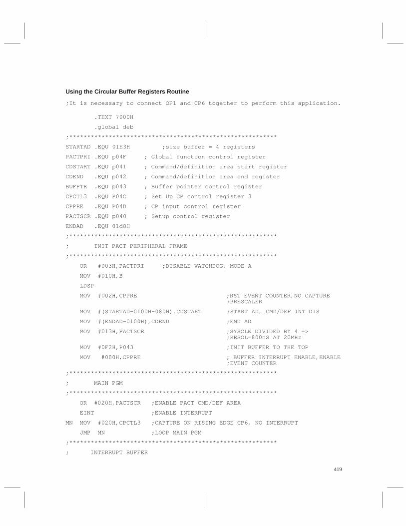
419
Using the Circular Buffer Registers Routine
;It is necessary to connect OP1 and CP6 together to perform this application.
.TEXT 7000H
.global deb
;**********************************************************
STARTAD .EQU 01E3H ;size buffer = 4 registers
PACTPRI .EQU p04F ; Global function control register
CDSTART .EQU p041 ; Command/definition area start register
CDEND .EQU p042 ; Command/definition area end register
BUFPTR .EQU p043 ; Buffer pointer control register
CPCTL3 .EQU P04C ; Set Up CP control register 3
CPPRE .EQU P04D ; CP input control register
PACTSCR .EQU p040 ; Setup control register
ENDAD .EQU 01d8H
;**********************************************************
; INIT PACT PERIPHERAL FRAME
;**********************************************************
OR #003H,PACTPRI ;DISABLE WATCHDOG, MODE A
MOV #010H,B
LDSP
MOV #002H,CPPRE ;RST EVENT COUNTER,NO CAPTURE ;PRESCALER
MOV #(STARTAD-0100H-080H),CDSTART ;START AD, CMD/DEF INT DIS
MOV #(ENDAD-0100H),CDEND ;END AD
MOV #013H,PACTSCR ;SYSCLK DIVIDED BY 4 => ;RESOL=800nS AT 20MHz
MOV #0F2H,P043 ;INIT BUFFER TO THE TOP
MOV #080H,CPPRE ; BUFFER INTERRUPT ENABLE,ENABLE ;EVENT COUNTER
;**********************************************************
; MAIN PGM
;**********************************************************
OR #020H,PACTSCR ;ENABLE PACT CMD/DEF AREA
EINT ;ENABLE INTERRUPT
MN MOV #020H,CPCTL3 ;CAPTURE ON RISING EDGE CP6, NO INTERRUPT
JMP MN ;LOOP MAIN PGM
;**********************************************************
; INTERRUPT BUFFER

420
;**********************************************************
ITBUFF
MOV #000H,CPCTL3 ;DISABLE BUFFER CAPTURE AND CLEAR ITBUFF FLAG
AND #0BFH,CPPRE ;CLEAR ITBUF FLAG
MOV BUFPTR,A ;TEST IF BUFFER FULL
CMP #0F2H,A
JZ BFULL
BHALF
MOV #0F3H,B ;B = STORAGE POINTER
CALL STORE
;CP6 PERIOD MEASUREMENT
SUB R0F3,R0EF
SBB R0F2,R0EE
SBB R0F1,R0ED
;RESULT STORED IN REGISTER R0ED, R0EE, R0EF
;RETURN TO MAIN PGM
RTI
BFULL
MOV #0EBH,B ;B = STORAGE POINTER
CALL STORE
;CP6 PERIOD MEASUREMENT
SUB R0EB,R0E7
SBB R0EA,R0E6
SBB R0E9,R0E5
;RESULT STORED IN REGISTER R0E5, R0E6, R0E7
;RETURN TO MAIN PGM
RTI
;**********************************************************
; SUBROUTINE STORE
;**********************************************************
STORE
; STORE BUFFER CAPTURE 1 IN REGISTERS R0F0,R0F1, R0F2, R0F3
MOV B,R090 ;R090 = END STORAGE POINTER
SUB #009H,R090
LOOP
MOV *0100H[B],A
MOV A,*0[B]
DEC B
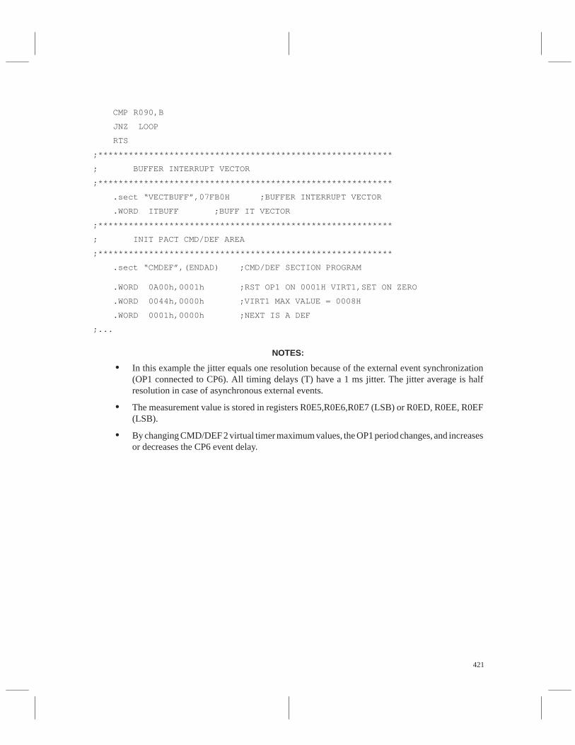
421
CMP R090,B
JNZ LOOP
RTS
;**********************************************************
; BUFFER INTERRUPT VECTOR
;**********************************************************
.sect “VECTBUFF”,07FB0H ;BUFFER INTERRUPT VECTOR
.WORD ITBUFF ;BUFF IT VECTOR
;**********************************************************
; INIT PACT CMD/DEF AREA
;**********************************************************
.sect “CMDEF”,(ENDAD) ;CMD/DEF SECTION PROGRAM
.WORD 0A00h,0001h ;RST OP1 ON 0001H VIRT1,SET ON ZERO
.WORD 0044h,0000h ;VIRT1 MAX VALUE = 0008H
.WORD 0001h,0000h ;NEXT IS A DEF
;...
NOTES:
• In this example the jitter equals one resolution because of the external event synchronization(OP1 connected to CP6). All timing delays (T) have a 1 ms jitter. The jitter average is halfresolution in case of asynchronous external events.
• The measurement value is stored in registers R0E5,R0E6,R0E7 (LSB) or R0ED, R0EE, R0EF(LSB).
• By changing CMD/DEF 2 virtual timer maximum values, the OP1 period changes, and increasesor decreases the CP6 event delay.
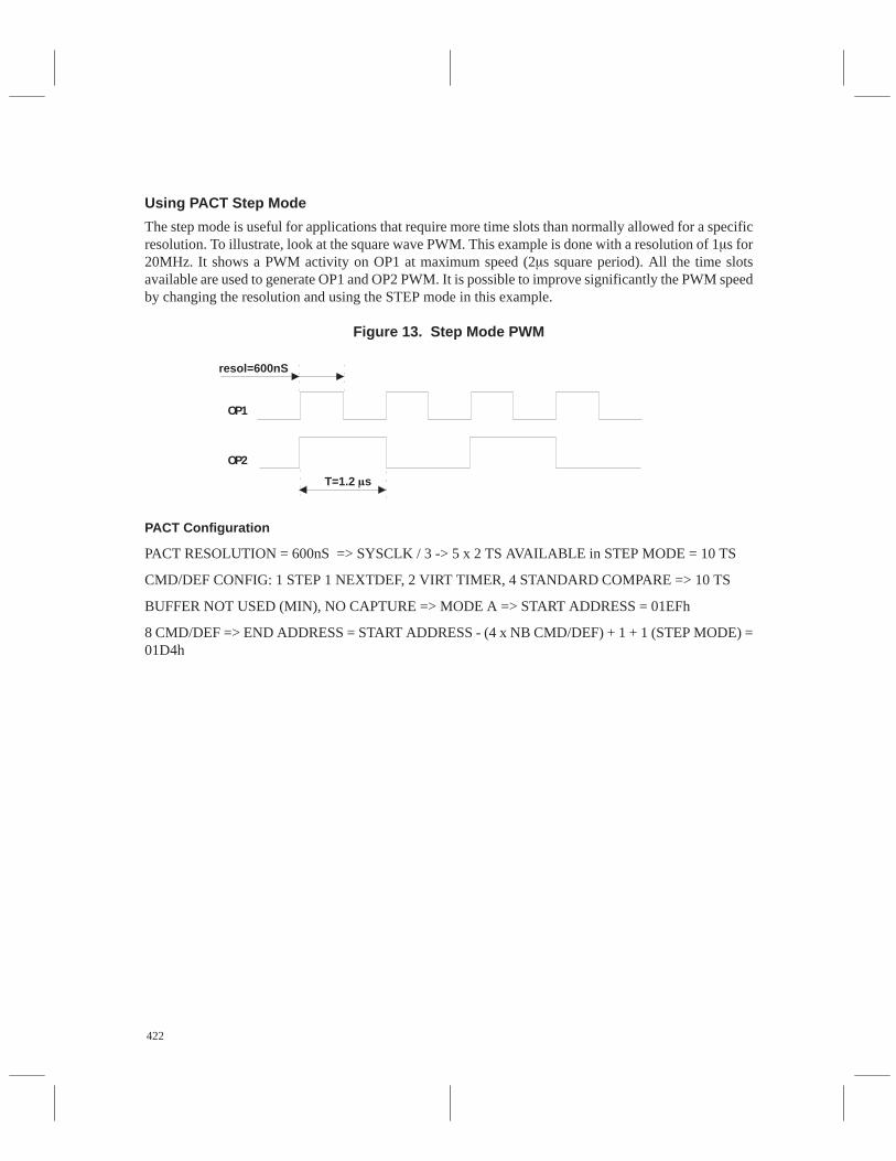
422
Using PACT Step Mode
The step mode is useful for applications that require more time slots than normally allowed for a specificresolution. To illustrate, look at the square wave PWM. This example is done with a resolution of 1s for20MHz. It shows a PWM activity on OP1 at maximum speed (2s square period). All the time slotsavailable are used to generate OP1 and OP2 PWM. It is possible to improve significantly the PWM speedby changing the resolution and using the STEP mode in this example.
Figure 13. Step Mode PWM
OP1
OP2
resol=600nS
T=1.2 s
PACT Configuration
PACT RESOLUTION = 600nS => SYSCLK / 3 -> 5 x 2 TS AVAILABLE in STEP MODE = 10 TS
CMD/DEF CONFIG: 1 STEP 1 NEXTDEF, 2 VIRT TIMER, 4 STANDARD COMPARE => 10 TS
BUFFER NOT USED (MIN), NO CAPTURE => MODE A => START ADDRESS = 01EFh
8 CMD/DEF => END ADDRESS = START ADDRESS - (4 x NB CMD/DEF) + 1 + 1 (STEP MODE) =01D4h
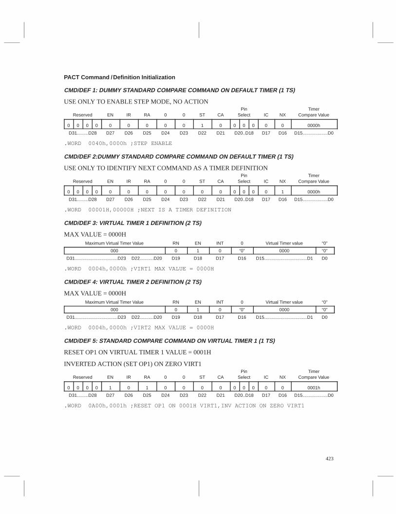
423
PACT Command /Definition Initialization
CMD/DEF 1: DUMMY STANDARD COMPARE COMMAND ON DEFAULT TIMER (1 TS)
USE ONLY TO ENABLE STEP MODE, NO ACTIONÁÁÁÁÁÁÁÁÁÁReserved
ÁÁÁÁÁÁEN
ÁÁÁÁIRÁÁÁÁÁÁRA
ÁÁÁÁÁÁ0
ÁÁÁÁÁÁ0
ÁÁÁÁÁÁST
ÁÁÁÁÁÁCA
ÁÁÁÁÁÁ
PinSelect
ÁÁÁÁÁÁIC
ÁÁÁÁÁÁNX
ÁÁÁÁÁÁÁÁÁÁ
TimerCompare ValueÁÁ
ÁÁÁÁ
0
ÁÁÁÁÁÁ
0
ÁÁÁÁÁÁ
0
ÁÁÁÁÁÁ
0
ÁÁÁÁÁÁÁÁÁ
0
ÁÁÁÁÁÁ
0
ÁÁÁÁÁÁÁÁÁ
0
ÁÁÁÁÁÁÁÁÁ
0
ÁÁÁÁÁÁÁÁÁ
0
ÁÁÁÁÁÁÁÁÁ
1
ÁÁÁÁÁÁÁÁÁ
0
ÁÁÁÁÁÁ
0
ÁÁÁ
0
ÁÁÁÁÁÁ
0
ÁÁÁÁÁÁÁÁÁ
0
ÁÁÁÁÁÁÁÁÁ
0
ÁÁÁÁÁÁÁÁÁÁÁÁÁÁÁ
0000hÁÁÁÁÁÁÁÁÁÁD31.........D28
ÁÁÁÁÁÁD27ÁÁÁÁD26ÁÁÁÁÁÁD25ÁÁÁÁÁÁD24ÁÁÁÁÁÁD23ÁÁÁÁÁÁD22ÁÁÁÁÁÁD21ÁÁÁÁÁÁD20..D18ÁÁÁÁÁÁD17ÁÁÁÁÁÁD16ÁÁÁÁÁÁÁÁÁÁD15....................D0
.WORD 0040h,0000h ;STEP ENABLE
CMD/DEF 2:DUMMY STANDARD COMPARE COMMAND ON DEFAULT TIMER (1 TS)
USE ONLY TO IDENTIFY NEXT COMMAND AS A TIMER DEFINITIONÁÁÁÁÁÁÁÁÁÁ
ReservedÁÁÁÁÁÁ
ENÁÁÁÁ
IRÁÁÁÁÁÁ
RAÁÁÁÁÁÁ
0ÁÁÁÁÁÁ
0ÁÁÁÁÁÁ
STÁÁÁÁÁÁ
CAÁÁÁÁÁÁ
PinSelectÁÁÁÁÁÁ
ICÁÁÁÁÁÁ
NXÁÁÁÁÁÁÁÁÁÁ
TimerCompare Value
ÁÁÁÁ
0ÁÁÁÁ
0ÁÁÁÁ
0ÁÁÁÁ
0ÁÁÁÁÁÁ
0ÁÁÁÁ
0ÁÁÁÁÁÁ
0ÁÁÁÁÁÁ
0ÁÁÁÁÁÁ
0ÁÁÁÁÁÁ
0ÁÁÁÁÁÁ
0ÁÁÁÁ
0ÁÁ
0ÁÁÁÁ
0ÁÁÁÁÁÁ
0ÁÁÁÁÁÁ
1ÁÁÁÁÁÁÁÁÁÁ
0000hÁÁÁÁÁÁÁÁÁÁ
D31.........D28 ÁÁÁÁÁÁ
D27 ÁÁÁÁ
D26ÁÁÁÁÁÁ
D25ÁÁÁÁÁÁ
D24ÁÁÁÁÁÁ
D23ÁÁÁÁÁÁ
D22ÁÁÁÁÁÁ
D21 ÁÁÁÁÁÁ
D20..D18ÁÁÁÁÁÁ
D17ÁÁÁÁÁÁ
D16ÁÁÁÁÁÁÁÁÁÁ
D15....................D0
.WORD 00001H,00000H ;NEXT IS A TIMER DEFINITION
CMD/DEF 3: VIRTUAL TIMER 1 DEFINITION (2 TS)
MAX VALUE = 0000H
ÁÁÁÁÁÁÁÁÁÁÁMaximum Virtual Timer Value ÁÁÁRNÁÁÁÁEN ÁÁÁINT ÁÁÁ0 ÁÁÁÁÁÁÁVirtual Timer value ÁÁÁ“0”ÁÁÁÁÁÁÁÁÁÁÁÁÁÁÁÁÁÁÁÁÁÁ
000ÁÁÁÁÁÁ
0ÁÁÁÁÁÁÁÁ
1ÁÁÁÁÁÁ
0ÁÁÁÁÁÁ
“0”ÁÁÁÁÁÁÁÁÁÁÁÁÁÁ
0000ÁÁÁÁÁÁ
“0”
ÁÁÁÁÁÁÁÁÁÁÁÁÁÁ
D31..................................D23ÁÁÁÁÁÁÁÁÁÁ
D22...........D20ÁÁÁÁÁÁ
D19ÁÁÁÁÁÁÁÁ
D18 ÁÁÁÁÁÁ
D17 ÁÁÁÁÁÁ
D16ÁÁÁÁÁÁÁÁÁÁÁÁÁÁ
D15..................................D1ÁÁÁÁÁÁ
D0
.WORD 0004h,0000h ;VIRT1 MAX VALUE = 0000H
CMD/DEF 4: VIRTUAL TIMER 2 DEFINITION (2 TS)
MAX VALUE = 0000HÁÁÁÁÁÁÁÁÁÁÁÁÁÁÁÁÁÁÁÁÁÁ
Maximum Virtual Timer ValueÁÁÁÁÁÁ
RNÁÁÁÁÁÁÁÁ
ENÁÁÁÁÁÁ
INTÁÁÁÁÁÁ
0ÁÁÁÁÁÁÁÁÁÁÁÁÁÁ
Virtual Timer valueÁÁÁÁÁÁ
“0”ÁÁÁÁÁÁÁÁÁÁÁÁÁÁÁÁÁÁÁÁÁÁ
000 ÁÁÁÁÁÁ
0ÁÁÁÁÁÁÁÁ
1 ÁÁÁÁÁÁ
0 ÁÁÁÁÁÁ
“0” ÁÁÁÁÁÁÁÁÁÁÁÁÁÁ
0000 ÁÁÁÁÁÁ
“0”
ÁÁÁÁÁÁÁÁÁÁÁÁÁÁ
D31..................................D23ÁÁÁÁÁÁÁÁÁÁ
D22...........D20ÁÁÁÁÁÁ
D19ÁÁÁÁÁÁÁÁ
D18 ÁÁÁÁÁÁ
D17 ÁÁÁÁÁÁ
D16ÁÁÁÁÁÁÁÁÁÁÁÁÁÁ
D15..................................D1ÁÁÁÁÁÁ
D0
.WORD 0004h,0000h ;VIRT2 MAX VALUE = 0000H
CMD/DEF 5: STANDARD COMPARE COMMAND ON VIRTUAL TIMER 1 (1 TS)
RESET OP1 ON VIRTUAL TIMER 1 VALUE = 0001H
INVERTED ACTION (SET OP1) ON ZERO VIRT1
ÁÁÁÁÁÁÁÁÁÁ
Reserved ÁÁÁÁÁÁ
EN ÁÁÁÁ
IRÁÁÁÁÁÁ
RAÁÁÁÁÁÁ
0ÁÁÁÁÁÁ
0 ÁÁÁÁÁÁ
ST ÁÁÁÁÁÁ
CA ÁÁÁÁÁÁ
PinSelectÁÁÁÁÁÁ
ICÁÁÁÁÁÁ
NX ÁÁÁÁÁÁÁÁÁÁ
TimerCompare Value
ÁÁÁÁ
0ÁÁÁÁ
0ÁÁÁÁ
0ÁÁÁÁ
0ÁÁÁÁÁÁ
1 ÁÁÁÁ
0ÁÁÁÁÁÁ
1ÁÁÁÁÁÁ
0ÁÁÁÁÁÁ
0 ÁÁÁÁÁÁ
0 ÁÁÁÁÁÁ
0 ÁÁÁÁ
0 ÁÁ
0ÁÁÁÁ
0ÁÁÁÁÁÁ
0ÁÁÁÁÁÁ
0 ÁÁÁÁÁÁÁÁÁÁ
0001h
ÁÁÁÁÁÁÁÁÁÁ
D31.........D28 ÁÁÁÁÁÁ
D27 ÁÁÁÁ
D26ÁÁÁÁÁÁ
D25ÁÁÁÁÁÁ
D24ÁÁÁÁÁÁ
D23ÁÁÁÁÁÁ
D22ÁÁÁÁÁÁ
D21 ÁÁÁÁÁÁ
D20..D18ÁÁÁÁÁÁ
D17ÁÁÁÁÁÁ
D16ÁÁÁÁÁÁÁÁÁÁ
D15....................D0
.WORD 0A00h,0001h ;RESET OP1 ON 0001H VIRT1,INV ACTION ON ZERO VIRT1
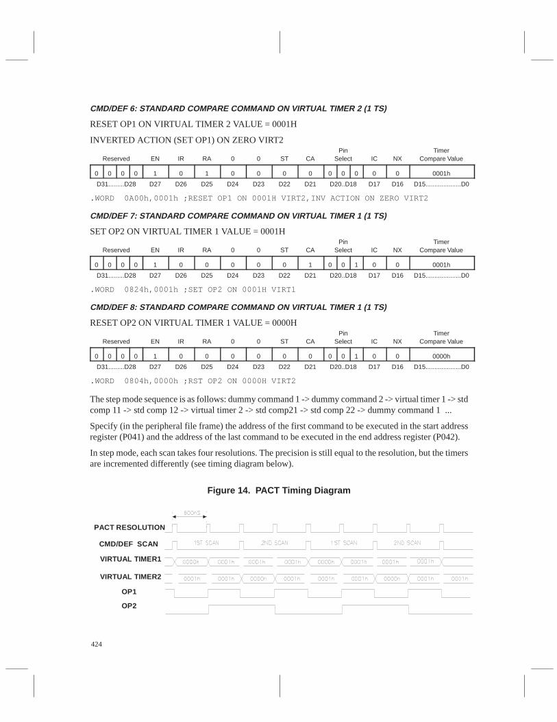
424
CMD/DEF 6: STANDARD COMPARE COMMAND ON VIRTUAL TIMER 2 (1 TS)
RESET OP1 ON VIRTUAL TIMER 2 VALUE = 0001H
INVERTED ACTION (SET OP1) ON ZERO VIRT2ÁÁÁÁÁÁÁÁÁÁReserved
ÁÁÁÁÁÁENÁÁÁÁIRÁÁÁÁÁÁRAÁÁÁÁÁÁ0ÁÁÁÁÁÁ0ÁÁÁÁÁÁSTÁÁÁÁÁÁCAÁÁÁÁÁÁ
PinSelectÁÁÁÁÁÁICÁÁÁÁÁÁNXÁÁÁÁÁÁÁÁÁÁ
TimerCompare ValueÁÁ
ÁÁ0ÁÁÁÁ0ÁÁÁÁ0ÁÁÁÁ0ÁÁÁÁÁÁ1ÁÁÁÁ0ÁÁÁÁÁÁ1ÁÁÁÁÁÁ0ÁÁÁÁÁÁ0ÁÁÁÁÁÁ0ÁÁÁÁÁÁ0ÁÁÁÁ0ÁÁ0ÁÁÁÁ0ÁÁÁÁÁÁ0ÁÁÁÁÁÁ0ÁÁÁÁÁÁÁÁÁÁ0001hÁÁÁÁÁ
ÁÁÁÁÁD31.........D28
ÁÁÁÁÁÁ
D27ÁÁÁÁ
D26ÁÁÁÁÁÁ
D25ÁÁÁÁÁÁ
D24ÁÁÁÁÁÁ
D23ÁÁÁÁÁÁ
D22ÁÁÁÁÁÁ
D21ÁÁÁÁÁÁ
D20..D18ÁÁÁÁÁÁ
D17ÁÁÁÁÁÁ
D16ÁÁÁÁÁÁÁÁÁÁ
D15....................D0
.WORD 0A00h,0001h ;RESET OP1 ON 0001H VIRT2,INV ACTION ON ZERO VIRT2
CMD/DEF 7: STANDARD COMPARE COMMAND ON VIRTUAL TIMER 1 (1 TS)
SET OP2 ON VIRTUAL TIMER 1 VALUE = 0001H
ÁÁÁÁÁÁÁÁÁÁ
Reserved ÁÁÁÁÁÁ
EN ÁÁÁÁ
IRÁÁÁÁÁÁ
RAÁÁÁÁÁÁ
0ÁÁÁÁÁÁ
0 ÁÁÁÁÁÁ
ST ÁÁÁÁÁÁ
CA ÁÁÁÁÁÁ
PinSelectÁÁÁÁÁÁ
ICÁÁÁÁÁÁ
NX ÁÁÁÁÁÁÁÁÁÁ
TimerCompare Value
ÁÁÁÁ
0ÁÁÁÁ
0ÁÁÁÁ
0ÁÁÁÁ
0ÁÁÁÁÁÁ
1 ÁÁÁÁ
0ÁÁÁÁÁÁ
0ÁÁÁÁÁÁ
0ÁÁÁÁÁÁ
0 ÁÁÁÁÁÁ
0 ÁÁÁÁÁÁ
1 ÁÁÁÁ
0 ÁÁ
0ÁÁÁÁ
1ÁÁÁÁÁÁ
0ÁÁÁÁÁÁ
0 ÁÁÁÁÁÁÁÁÁÁ
0001h
ÁÁÁÁÁÁÁÁÁÁ
D31.........D28 ÁÁÁÁÁÁ
D27 ÁÁÁÁ
D26ÁÁÁÁÁÁ
D25ÁÁÁÁÁÁ
D24ÁÁÁÁÁÁ
D23ÁÁÁÁÁÁ
D22ÁÁÁÁÁÁ
D21 ÁÁÁÁÁÁ
D20..D18ÁÁÁÁÁÁ
D17ÁÁÁÁÁÁ
D16ÁÁÁÁÁÁÁÁÁÁ
D15....................D0
.WORD 0824h,0001h ;SET OP2 ON 0001H VIRT1
CMD/DEF 8: STANDARD COMPARE COMMAND ON VIRTUAL TIMER 1 (1 TS)
RESET OP2 ON VIRTUAL TIMER 1 VALUE = 0000HÁÁÁÁÁÁÁÁÁÁReserved
ÁÁÁÁÁÁENÁÁÁÁIRÁÁÁÁÁÁRAÁÁÁÁÁÁ0ÁÁÁÁÁÁ0ÁÁÁÁÁÁSTÁÁÁÁÁÁCAÁÁÁÁÁÁ
PinSelectÁÁÁÁÁÁICÁÁÁÁÁÁNXÁÁÁÁÁÁÁÁÁÁ
TimerCompare ValueÁÁ
ÁÁ0ÁÁÁÁ0ÁÁÁÁ0ÁÁÁÁ0ÁÁÁÁÁÁ1ÁÁÁÁ0ÁÁÁÁÁÁ0ÁÁÁÁÁÁ0ÁÁÁÁÁÁ0ÁÁÁÁÁÁ0ÁÁÁÁÁÁ0ÁÁÁÁ0ÁÁ0ÁÁÁÁ1ÁÁÁÁÁÁ0ÁÁÁÁÁÁ0ÁÁÁÁÁÁÁÁÁÁ0000hÁÁÁÁÁ
ÁÁÁÁÁD31.........D28
ÁÁÁÁÁÁ
D27ÁÁÁÁ
D26ÁÁÁÁÁÁ
D25ÁÁÁÁÁÁ
D24ÁÁÁÁÁÁ
D23ÁÁÁÁÁÁ
D22ÁÁÁÁÁÁ
D21ÁÁÁÁÁÁ
D20..D18ÁÁÁÁÁÁ
D17ÁÁÁÁÁÁ
D16ÁÁÁÁÁÁÁÁÁÁ
D15....................D0
.WORD 0804h,0000h ;RST OP2 ON 0000H VIRT2
The step mode sequence is as follows: dummy command 1 -> dummy command 2 -> virtual timer 1 -> stdcomp 11 -> std comp 12 -> virtual timer 2 -> std comp21 -> std comp 22 -> dummy command 1 ...
Specify (in the peripheral file frame) the address of the first command to be executed in the start addressregister (P041) and the address of the last command to be executed in the end address register (P042).
In step mode, each scan takes four resolutions. The precision is still equal to the resolution, but the timersare incremented differently (see timing diagram below).
Figure 14. PACT Timing Diagram
PACT RESOLUTION
CMD/DEF SCAN
VIRTUAL TIMER1
VIRTUAL TIMER2
OP1
OP2
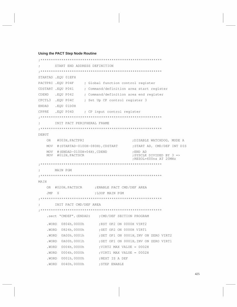
425
Using the PACT Step Node Routine
;**********************************************************
; START END ADDRESS DEFINITION
;**********************************************************
STARTAD .EQU 01EFH
PACTPRI .EQU P04F ; Global function control register
CDSTART .EQU P041 ; Command/definition area start register
CDEND .EQU P042 ; Command/definition area end register
CPCTL3 .EQU P04C ; Set Up CP control register 3
ENDAD .EQU 01D0H
CPPRE .EQU P04D ; CP input control register
;**********************************************************
; INIT PACT PERIPHERAL FRAME
;**********************************************************
DEBUT
OR #003H,PACTPRI ;DISABLE WATCHDOG, MODE A
MOV #(STARTAD-0100H-080H),CDSTART ;START AD, CMD/DEF INT DIS
MOV #(ENDAD-0100H+04H),CDEND ;END AD MOV #012H,PACTSCR ;SYSCLK DIVIDED BY 3 => ;RESOL=600ns AT 20MHz
;**********************************************************
; MAIN PGM
;**********************************************************
MAIN
OR #020H,PACTSCR ;ENABLE PACT CMD/DEF AREA
JMP $ ;LOOP MAIN PGM
;**********************************************************
; INIT PACT CMD/DEF AREA
;**********************************************************
.sect “CMDEF”,(ENDAD) ;CMD/DEF SECTION PROGRAM
.WORD 0804h,0000h ;RST OP2 ON 0000H VIRT2
.WORD 0824h,0000h ;SET OP2 ON 0000H VIRT1
.WORD 0A00h,0001h ;SET OP1 ON 0001H,INV ON ZERO VIRT2
.WORD 0A00h,0001h ;SET OP1 ON 0001H,INV ON ZERO VIRT1
.WORD 0004h,0000h ;VIRT2 MAX VALUE = 0002H
.WORD 0004h,0000h ;VIRT1 MAX VALUE = 0002H
.WORD 0001h,0000h ;NEXT IS A DEF
.WORD 0040h,0000h ;STEP ENABLE
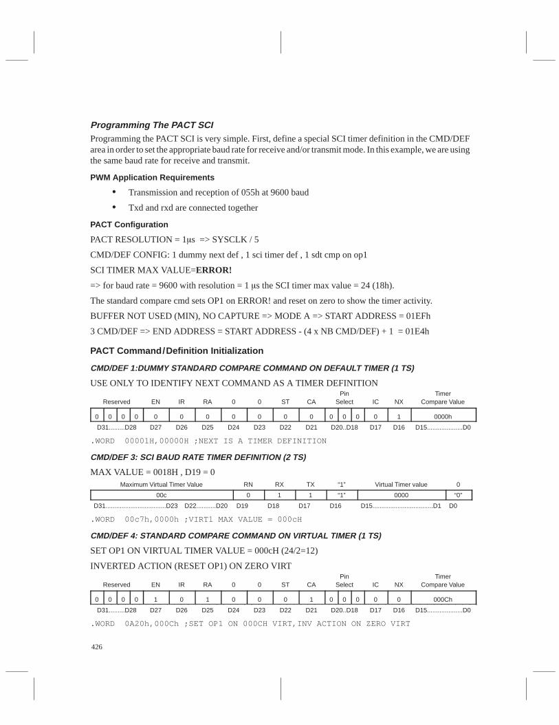
426
Programming The PACT SCIProgramming the PACT SCI is very simple. First, define a special SCI timer definition in the CMD/DEFarea in order to set the appropriate baud rate for receive and/or transmit mode. In this example, we are usingthe same baud rate for receive and transmit.
PWM Application Requirements
• Transmission and reception of 055h at 9600 baud
• Txd and rxd are connected together
PACT Configuration
PACT RESOLUTION = 1s => SYSCLK / 5
CMD/DEF CONFIG: 1 dummy next def , 1 sci timer def , 1 sdt cmp on op1
SCI TIMER MAX VALUE=ERROR!
=> for baud rate = 9600 with resolution = 1 s the SCI timer max value = 24 (18h).
The standard compare cmd sets OP1 on ERROR! and reset on zero to show the timer activity.
BUFFER NOT USED (MIN), NO CAPTURE => MODE A => START ADDRESS = 01EFh
3 CMD/DEF => END ADDRESS = START ADDRESS - (4 x NB CMD/DEF) + 1 = 01E4h
PACT Command/Definition Initialization
CMD/DEF 1:DUMMY STANDARD COMPARE COMMAND ON DEFAULT TIMER (1 TS)
USE ONLY TO IDENTIFY NEXT COMMAND AS A TIMER DEFINITIONÁÁÁÁÁÁÁÁÁÁÁÁÁÁÁ
Reserved
ÁÁÁÁÁÁÁÁÁ
EN
ÁÁÁÁÁÁ
IR
ÁÁÁÁÁÁÁÁÁ
RA
ÁÁÁÁÁÁÁÁÁ
0
ÁÁÁÁÁÁÁÁÁ
0
ÁÁÁÁÁÁÁÁÁ
ST
ÁÁÁÁÁÁÁÁÁ
CA
ÁÁÁÁÁÁÁÁÁ
PinSelect
ÁÁÁÁÁÁÁÁÁ
IC
ÁÁÁÁÁÁÁÁÁ
NX
ÁÁÁÁÁÁÁÁÁÁÁÁÁÁÁ
TimerCompare Value
ÁÁÁÁ
0ÁÁÁÁ
0ÁÁÁÁ
0ÁÁÁÁ
0ÁÁÁÁÁÁ
0 ÁÁÁÁ
0ÁÁÁÁÁÁ
0ÁÁÁÁÁÁ
0ÁÁÁÁÁÁ
0 ÁÁÁÁÁÁ
0 ÁÁÁÁÁÁ
0 ÁÁÁÁ
0 ÁÁ
0ÁÁÁÁ
0ÁÁÁÁÁÁ
0ÁÁÁÁÁÁ
1 ÁÁÁÁÁÁÁÁÁÁ
0000h
ÁÁÁÁÁD31.........D28 ÁÁÁD27 ÁÁD26ÁÁÁD25ÁÁÁD24ÁÁÁD23ÁÁÁD22ÁÁÁD21 ÁÁÁD20..D18ÁÁÁD17ÁÁÁD16ÁÁÁÁÁD15....................D0
.WORD 00001H,00000H ;NEXT IS A TIMER DEFINITION
CMD/DEF 3: SCI BAUD RATE TIMER DEFINITION (2 TS)
MAX VALUE = 0018H , D19 = 0
ÁÁÁÁÁÁÁÁÁÁÁMaximum Virtual Timer Value ÁÁÁRNÁÁÁÁRX ÁÁÁTX ÁÁÁ“1” ÁÁÁÁÁÁÁVirtual Timer value ÁÁÁ0ÁÁÁÁÁÁÁÁÁÁÁÁÁÁÁÁÁÁÁÁÁÁ
00cÁÁÁÁÁÁ
0ÁÁÁÁÁÁÁÁ
1ÁÁÁÁÁÁ
1ÁÁÁÁÁÁ
“1”ÁÁÁÁÁÁÁÁÁÁÁÁÁÁ
0000ÁÁÁÁÁÁ
“0”ÁÁÁÁÁÁÁÁÁÁÁÁÁÁ
D31..................................D23ÁÁÁÁÁÁÁÁÁÁ
D22...........D20ÁÁÁÁÁÁ
D19 ÁÁÁÁÁÁÁÁ
D18 ÁÁÁÁÁÁ
D17 ÁÁÁÁÁÁ
D16 ÁÁÁÁÁÁÁÁÁÁÁÁÁÁ
D15..................................D1ÁÁÁÁÁÁ
D0
.WORD 00c7h,0000h ;VIRT1 MAX VALUE = 000cH
CMD/DEF 4: STANDARD COMPARE COMMAND ON VIRTUAL TIMER (1 TS)
SET OP1 ON VIRTUAL TIMER VALUE = 000cH (24/2=12)
INVERTED ACTION (RESET OP1) ON ZERO VIRTÁÁÁÁÁÁÁÁÁÁÁÁÁÁÁ
Reserved
ÁÁÁÁÁÁÁÁÁ
EN
ÁÁÁÁÁÁ
IR
ÁÁÁÁÁÁÁÁÁ
RA
ÁÁÁÁÁÁÁÁÁ
0
ÁÁÁÁÁÁÁÁÁ
0
ÁÁÁÁÁÁÁÁÁ
ST
ÁÁÁÁÁÁÁÁÁ
CA
ÁÁÁÁÁÁÁÁÁ
PinSelect
ÁÁÁÁÁÁÁÁÁ
IC
ÁÁÁÁÁÁÁÁÁ
NX
ÁÁÁÁÁÁÁÁÁÁÁÁÁÁÁ
TimerCompare Value
ÁÁÁÁ
0ÁÁÁÁ
0ÁÁÁÁ
0ÁÁÁÁ
0ÁÁÁÁÁÁ
1 ÁÁÁÁ
0ÁÁÁÁÁÁ
1ÁÁÁÁÁÁ
0ÁÁÁÁÁÁ
0 ÁÁÁÁÁÁ
0 ÁÁÁÁÁÁ
1 ÁÁÁÁ
0 ÁÁ
0ÁÁÁÁ
0ÁÁÁÁÁÁ
0ÁÁÁÁÁÁ
0 ÁÁÁÁÁÁÁÁÁÁ
000Ch
ÁÁÁÁÁD31.........D28 ÁÁÁD27 ÁÁD26ÁÁÁD25ÁÁÁD24ÁÁÁD23ÁÁÁD22ÁÁÁD21 ÁÁÁD20..D18ÁÁÁD17ÁÁÁD16ÁÁÁÁÁD15....................D0
.WORD 0A20h,000Ch ;SET OP1 ON 000CH VIRT,INV ACTION ON ZERO VIRT
427
Programming the PACT SCI Routine
;It is necessary to connect TXD and RXD together to perform this application.
.TEXT 7000H
.global deb
;**********************************************************
; START END ADDRESS DEFINITION
;**********************************************************
STARTAD .EQU 01EFH
PACTPRI .EQU P04F ; Global function control register
CDSTART .EQU P041 ; Command/definition area start register
CDEND .EQU P042 ; Command/definition area end register
PACTSCR .EQU P040 ; Setup control register
ENDAD .EQU 01E4H
SCICTLP .EQU P045 ; PACT/SCI control register
RXBUFP .EQU P046 ; PACT/SCI RX data register
TXBUFP .EQU P047 ; PACT/SCI TX data register
;**********************************************************
; INIT PACT PERIPHERAL FRAME
;**********************************************************
DEBUT
;...
OR #003H,PACTPRI ;DISABLE WATCHDOG, MODE A
MOV #010H,B ;INIT STACK POINTER
LDSP
MOV #(STARTAD-0100H-080H),CDSTART ;START AD, CMD/DEF INT DIS
MOV #(ENDAD-0100H),CDEND ;END AD
MOV #014H,PACTSCR ;SYSCLK DIVIDED BY 5 => ;RESOL=1us AT 20MHz
MOV #00CH,SCICTLP ;ENABLE SCI RECEIVE AND TRANSMIT ;INT T
;...
;**********************************************************
; MAIN PGM
;**********************************************************
MAIN
OR #020H,PACTSCR ;ENABLE PACT CMD/DEF AREA
EINT ;ENABLE INTERRUPT TO START SCI TRANSMISSION
;ON
428
JMP $ ;LOOP MAIN PGM
;**********************************************************
; INTERRUPT SCI TRANSIT
;**********************************************************
ITTXD
MOV #055H,TXBUFP ;LOAD DATA TRANSMIT = 055H IN TRANSMIT BUFFER
RTI
;**********************************************************
; INTERRUPT SCI RECEIVE
;**********************************************************
ITRXD
MOV RXBUFP,A ;READ SCI RECEIVE BUFFER
CMP #055H,A ;TEST IF RECEPTION OK
JNZ ERROR
RTI
ERROR
DINT ;DISABLE INT TO STOP TRANSMISSION IN CASE OF ERROR.
JMP $
;**********************************************************
; SCI INTERRUPT VECTOR
;**********************************************************
.sect “VECTSC8I”,07F9CH ;SCI INTERRUPT VECTORS
.WORD ITTXD ;SCI TRANSMIT VECTOR
.WORD ITRXD ;SCI RECEIVE VECTOR
;**********************************************************
; INIT PACT CMD/DEF AREA
;**********************************************************
.sect “CMDEF”,(ENDAD) ;CMD/DEF SECTION PROGRAM
.WORD 0A20h,000Ch ;SET OP1 ON 000CH VIRT,INV ACTION ON ZERO VIRT
.WORD 00C7h,0000h ;VIRT1 MAX VALUE = 000cH
.WORD 0001h,0000h ;NEXT IS A DEF
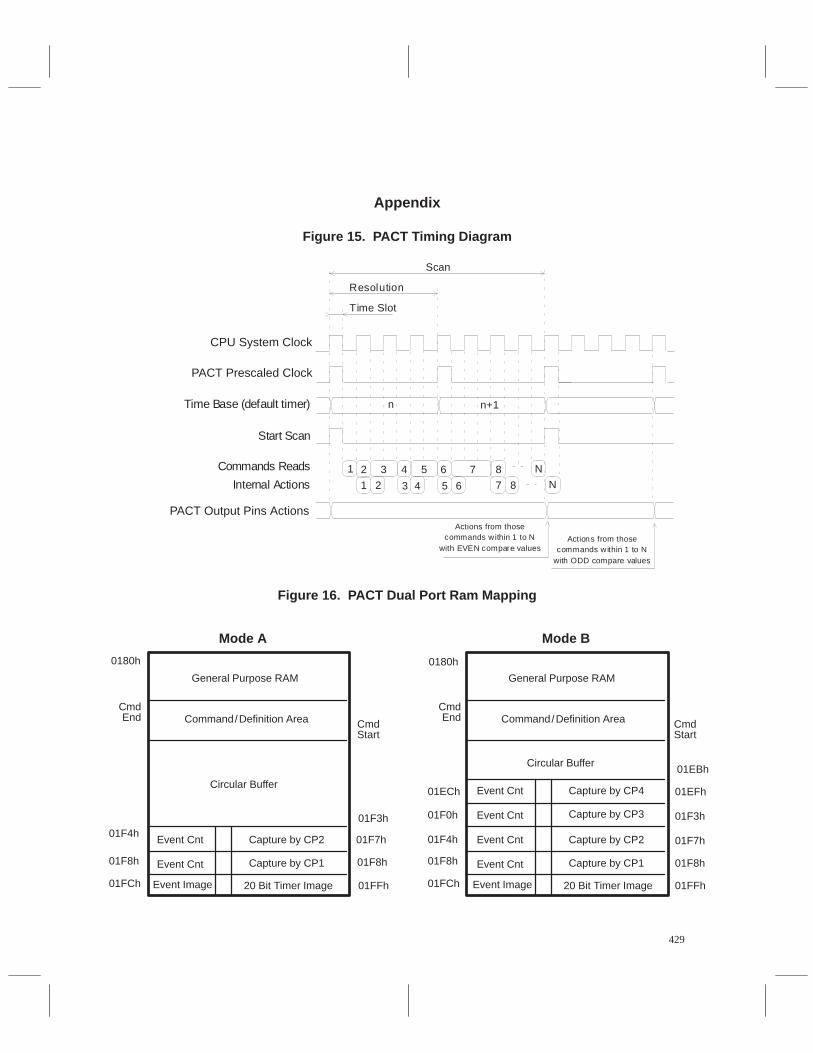
429
Appendix
Figure 15. PACT Timing Diagram
Time Slot
Resolution
1 2 4 6 N3 5 7
Actions from those commands within 1 to N
with EVEN compare values
Start Scan
Scan
8
1 2 3 4 5 6 7 8 N
Time Base (default timer)
Commands Reads
Internal Actions
n n+1
Actions from
those
commands within 1 to Nwith ODD compare values
PACT Prescaled Clock
CPU System Clock
PACT Output Pins Actions
Figure 16. PACT Dual Port Ram Mapping
Mode A Mode B
0180h
CmdEnd
01F4h
01F8h
01FCh
General Purpose RAM
Command/Definition Area
Circular Buffer
Event Cnt
Event Cnt
Event Image
Capture by CP2
Capture by CP1
20 Bit Timer Image
01F3h
01F7h
01F8h
01FFh
CmdStart
0180h
CmdEnd
General Purpose RAM
Command/Definition Area
Circular Buffer
CmdStart
Event Cnt
Event Cnt
Event Image
Capture by CP2
Capture by CP1
20 Bit Timer Image
Event Cnt
Event Cnt
Capture by CP4
Capture by CP3
01F4h
01F8h
01FCh
01F3h
01F7h
01F8h
01FFh
01ECh
01F0h
01EBh
01EFh
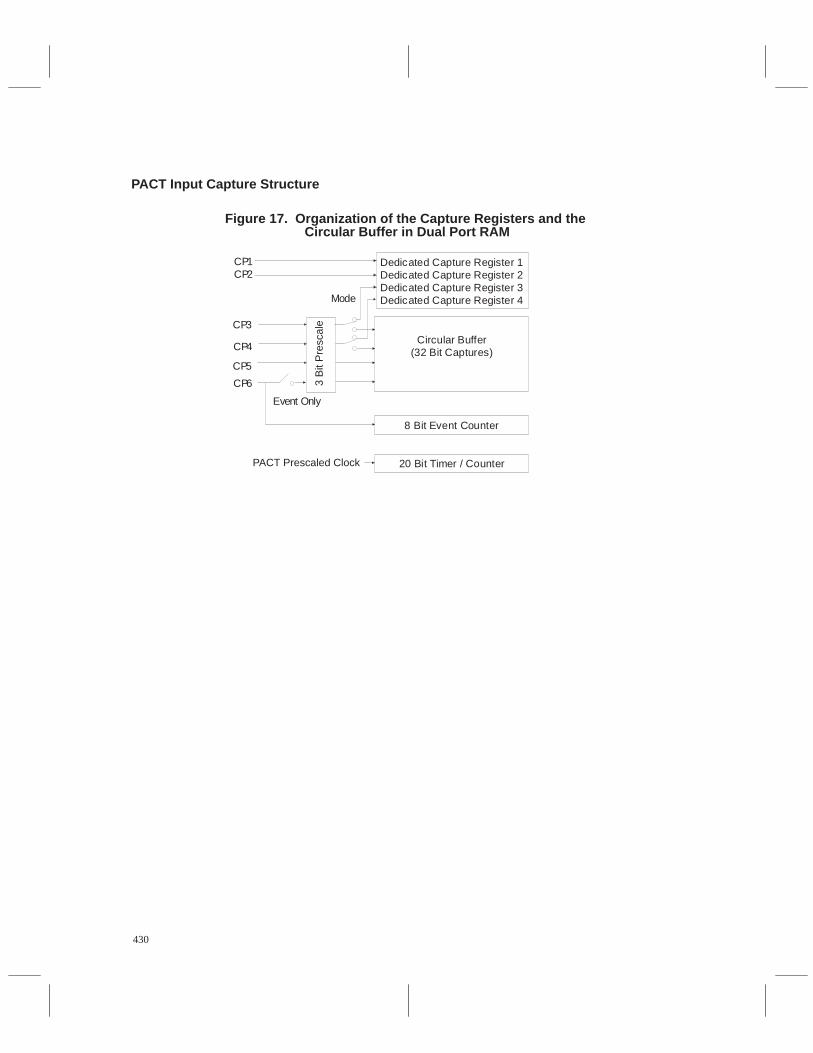
430
PACT Input Capture Structure
Figure 17. Organization of the Capture Registers and the Circular Buffer in Dual Port RAM
Dedicated Capture Register 1Dedicated Capture Register 2Dedicated Capture Register 3Dedicated Capture Register 4
Circular Buffer(32 Bit Captures)
8 Bit Event Counter
20 Bit Timer / Counter
CP1CP2
CP3
CP4
CP5
CP6
Mode
Event Only
3 B
it P
resc
ale
PACT Prescaled Clock
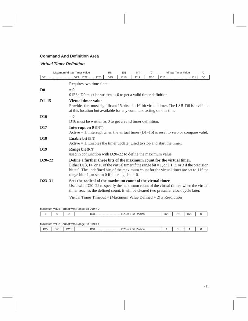
431
Command And Definition Area
Virtual Timer Definition
ÁÁÁÁÁÁÁÁÁÁÁÁÁÁÁÁÁÁÁÁÁÁ
Maximum Virtual Timer Value ÁÁÁÁÁÁ
RNÁÁÁÁÁÁÁÁ
EN ÁÁÁÁÁÁ
INT ÁÁÁÁÁÁ
“0” ÁÁÁÁÁÁÁÁÁÁÁÁÁÁ
Virtual Timer Value ÁÁÁÁÁÁ
“0”
ÁÁÁÁÁÁÁD31..................................D23ÁÁÁÁÁD22...........D20ÁÁÁD19ÁÁÁÁD18 ÁÁÁD17 ÁÁÁD16ÁÁÁÁÁÁÁD15..................................D1ÁÁÁD0
Requires two time slots.
D0 = 001F3h D0 must be written as 0 to get a valid timer definition.
D1–15 Virtual timer valueProvides the most significant 15 bits of a 16-bit virtual timer. The LSB D0 is invisibleat this location but available for any command acting on this timer.
D16 = 0D16 must be written as 0 to get a valid timer definition.
D17 Interrupt on 0 (INT) Active = 1. Interrupt when the virtual timer (D1–15) is reset to zero or compare valid.
D18 Enable bit (EN)Active = 1. Enables the timer update. Used to stop and start the timer.
D19 Range bit (RN)used in conjunction with D20–22 to define the maximum value.
D20–22 Define a further three bits of the maximum count for the virtual timer.Either D13, 14, or 15 of the virtual timer if the range bit = 1, or D1, 2, or 3 if the precisionbit = 0. The undefined bits of the maximum count for the virtual timer are set to 1 if therange bit =1, or set to 0 if the range bit = 0.
D23–31 Sets the radical of the maximum count of the virtual timer.Used with D20–22 to specify the maximum count of the virtual timer: when the virtualtimer reaches the defined count, it will be cleared two prescaler clock cycle later.
Virtual Timer Timeout = (Maximum Value Defined + 2) x Resolution
Maximum Value Format with Range Bit D19 = 0
ÁÁÁ0 ÁÁÁ0 ÁÁ0ÁÁÁÁÁÁÁÁÁÁÁÁÁÁÁD31.................................D23 = 9 Bit Radical ÁÁÁD22ÁÁÁD21ÁÁÁD20ÁÁÁ0
Maximum Value Format with Range Bit D19 = 1
ÁÁÁÁÁÁ
D22ÁÁÁÁÁÁ
D21 ÁÁÁÁ
D20ÁÁÁÁÁÁÁÁÁÁÁÁÁÁÁÁÁÁÁÁÁÁÁÁÁÁÁÁÁÁ
D31.................................D23 = 9 Bit Radical ÁÁÁÁÁÁ
1ÁÁÁÁÁÁ
1 ÁÁÁÁÁÁ
1 ÁÁÁÁÁÁ
0
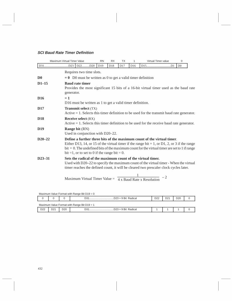
432
SCI Baud Rate Timer Definition
ÁÁÁÁÁÁÁÁÁÁÁMaximum Virtual Timer Value ÁÁÁRNÁÁÁRX ÁÁÁTX ÁÁ1ÁÁÁÁÁÁÁÁVirtual Timer value ÁÁÁ0ÁÁÁÁÁÁÁÁÁÁÁÁÁÁ
D31................................D23ÁÁÁÁÁÁÁÁÁÁ
D22..........D20ÁÁÁÁÁÁ
D19ÁÁÁÁÁÁ
D18ÁÁÁÁÁÁ
D17ÁÁÁÁ
D16ÁÁÁÁÁÁÁÁÁÁÁÁÁÁÁÁ
D15................................D1ÁÁÁÁÁÁ
D0
Requires two time slots.
D0 = 0 D0 must be written as 0 to get a valid timer definition
D1–15 Baud rate timerProvides the most significant 15 bits of a 16-bit virtual timer used as the baud rategenerator.
D16 = 1D16 must be written as 1 to get a valid timer definition.
D17 Transmit select (TX)Active = 1. Selects this timer definition to be used for the transmit baud rate generator.
D18 Receive select (RX)Active = 1. Selects this timer definition to be used for the receive baud rate generator.
D19 Range bit (RN)Used in conjunction with D20–22.
D20–22 Define a further three bits of the maximum count of the virtual timer.Either D13, 14, or 15 of the virtual timer if the range bit = 1, or D1, 2, or 3 if the rangebit = 0. The undefined bits of the maximum count for the virtual timer are set to 1 if rangebit =1, or to set to 0 if the range bit = 0.
D23–31 Sets the radical of the maximum count of the virtual timer.Used with D20–22 to specify the maximum count of the virtual timer - When the virtualtimer reaches the defined count, it will be cleared two prescaler clock cycles later.
Maximum Virtual Timer Value = 1
4 x Baud Rate x Resolution– 2
ÁÁÁÁÁÁÁÁÁÁÁÁÁÁÁÁÁÁÁÁÁÁÁÁÁÁÁÁÁÁÁÁÁÁÁÁÁÁÁÁÁÁÁÁÁÁÁÁÁÁÁÁÁÁÁÁÁÁÁÁÁÁÁÁÁÁÁÁÁÁÁÁÁÁÁÁÁÁÁÁÁÁÁÁ
Maximum Value Format with Range Bit D19 = 0ÁÁÁÁÁÁ
0 ÁÁÁÁÁÁ
0 ÁÁÁÁ
0ÁÁÁÁÁÁÁÁÁÁÁÁÁÁÁÁÁÁÁÁÁÁÁÁÁÁÁÁÁÁ
D31.................................D23 = 9 Bit Radical ÁÁÁÁ
D22ÁÁÁÁÁÁ
D21ÁÁÁÁÁÁ
D20ÁÁÁÁÁÁ
0
ÁÁÁÁÁÁÁÁÁÁÁÁÁÁÁÁÁÁÁÁÁÁÁÁÁÁÁÁÁÁÁÁÁÁÁÁÁÁÁÁÁÁÁÁÁÁÁÁÁÁÁÁÁÁÁÁ
Maximum Value Format with Range Bit D19 = 1
ÁÁÁÁÁÁ
D22ÁÁÁÁÁÁ
D21 ÁÁÁÁ
D20ÁÁÁÁÁÁÁÁÁÁÁÁÁÁÁÁÁÁÁÁÁÁÁÁÁÁÁÁÁÁ
D31.................................D23 = 9 Bit Radical ÁÁÁÁ
1ÁÁÁÁÁÁ
1ÁÁÁÁÁÁ
1ÁÁÁÁÁÁ
0
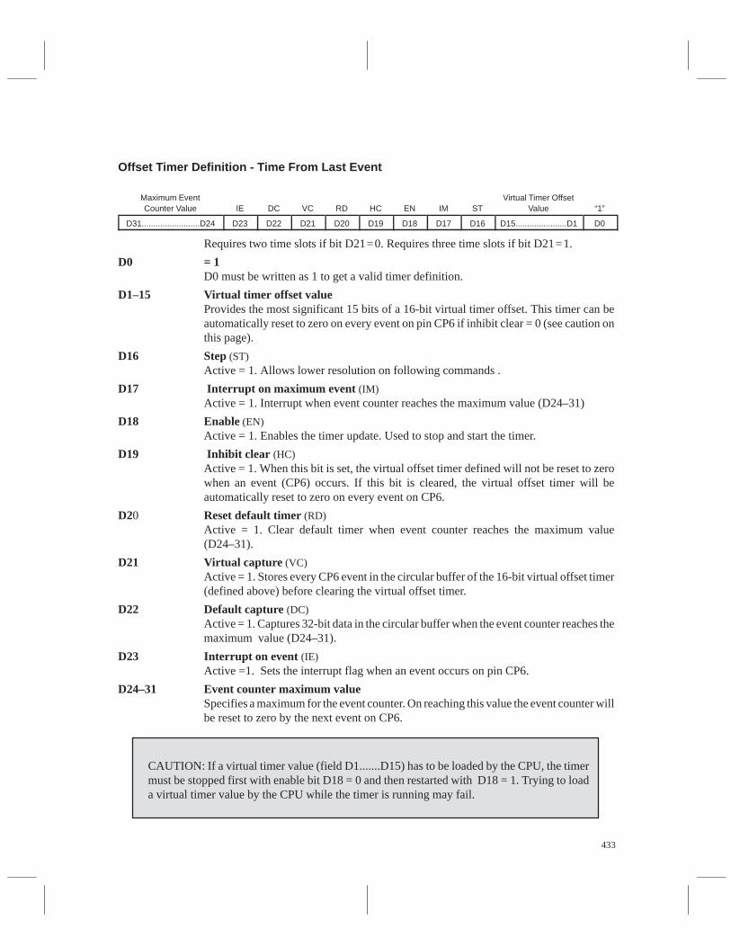
433
Offset Timer Definition - Time From Last Event
ÁÁÁÁÁÁÁÁÁÁÁÁÁÁ
Maximum EventCounter Value
ÁÁÁÁÁÁIEÁÁÁÁÁÁDCÁÁÁÁÁÁVCÁÁÁÁÁÁRDÁÁÁÁÁÁHCÁÁÁÁÁÁENÁÁÁÁÁÁIMÁÁÁÁSTÁÁÁÁÁÁÁÁÁÁÁÁ
Virtual Timer OffsetValue
ÁÁÁÁÁÁ“1”ÁÁÁÁÁÁÁ
ÁÁÁÁÁÁÁD31.........................D24
ÁÁÁÁÁÁ
D23ÁÁÁÁÁÁ
D22ÁÁÁÁÁÁ
D21ÁÁÁÁÁÁ
D20ÁÁÁÁÁÁ
D19ÁÁÁÁÁÁ
D18ÁÁÁÁÁÁ
D17ÁÁÁÁ
D16ÁÁÁÁÁÁÁÁÁÁÁÁ
D15......................D1ÁÁÁÁÁÁ
D0
Requires two time slots if bit D21=0. Requires three time slots if bit D21=1.
D0 = 1D0 must be written as 1 to get a valid timer definition.
D1–15 Virtual timer offset valueProvides the most significant 15 bits of a 16-bit virtual timer offset. This timer can beautomatically reset to zero on every event on pin CP6 if inhibit clear = 0 (see caution onthis page).
D16 Step (ST)Active = 1. Allows lower resolution on following commands .
D17 Interrupt on maximum event (IM)Active = 1. Interrupt when event counter reaches the maximum value (D24–31)
D18 Enable (EN)Active = 1. Enables the timer update. Used to stop and start the timer.
D19 Inhibit clear (HC)Active = 1. When this bit is set, the virtual offset timer defined will not be reset to zerowhen an event (CP6) occurs. If this bit is cleared, the virtual offset timer will beautomatically reset to zero on every event on CP6.
D20 Reset default timer (RD)Active = 1. Clear default timer when event counter reaches the maximum value(D24–31).
D21 Virtual capture (VC)Active = 1. Stores every CP6 event in the circular buffer of the 16-bit virtual offset timer(defined above) before clearing the virtual offset timer.
D22 Default capture (DC)Active = 1. Captures 32-bit data in the circular buffer when the event counter reaches themaximum value (D24–31).
D23 Interrupt on event (IE)Active =1. Sets the interrupt flag when an event occurs on pin CP6.
D24–31 Event counter maximum valueSpecifies a maximum for the event counter. On reaching this value the event counter willbe reset to zero by the next event on CP6.
CAUTION: If a virtual timer value (field D1.......D15) has to be loaded by the CPU, the timermust be stopped first with enable bit D18 = 0 and then restarted with D18 = 1. Trying to loada virtual timer value by the CPU while the timer is running may fail.
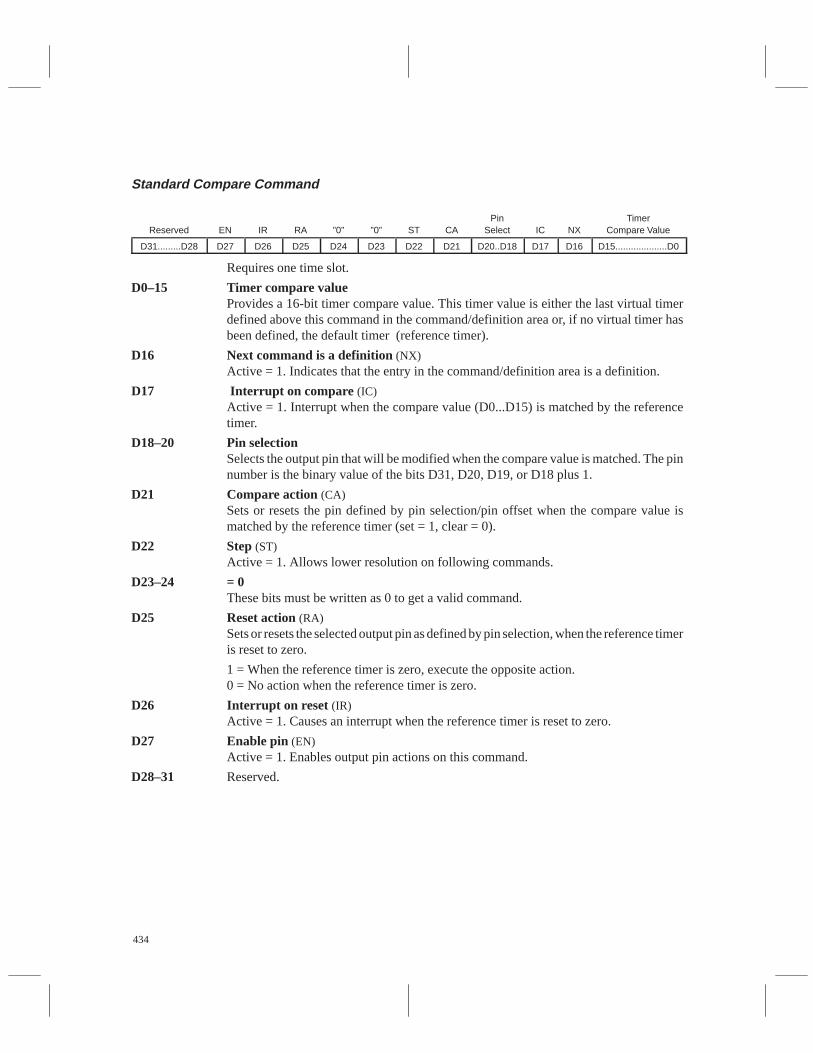
434
Standard Compare Command
ÁÁÁÁÁÁÁÁÁÁ
ReservedÁÁÁÁ
ENÁÁÁÁÁÁ
IRÁÁÁÁÁÁ
RAÁÁÁÁÁÁ
”0”ÁÁÁÁÁÁ
”0”ÁÁÁÁÁÁ
STÁÁÁÁÁÁ
CAÁÁÁÁÁÁ
PinSelectÁÁÁÁÁÁ
ICÁÁÁÁ
NXÁÁÁÁÁÁÁÁÁÁÁÁ
TimerCompare Value
ÁÁÁÁÁÁÁÁÁÁ
D31.........D28 ÁÁÁÁ
D27ÁÁÁÁÁÁ
D26ÁÁÁÁÁÁ
D25ÁÁÁÁÁÁ
D24ÁÁÁÁÁÁ
D23ÁÁÁÁÁÁ
D22 ÁÁÁÁÁÁ
D21 ÁÁÁÁÁÁ
D20..D18ÁÁÁÁÁÁ
D17ÁÁÁÁ
D16ÁÁÁÁÁÁÁÁÁÁÁÁ
D15....................D0
Requires one time slot.
D0–15 Timer compare valueProvides a 16-bit timer compare value. This timer value is either the last virtual timerdefined above this command in the command/definition area or, if no virtual timer hasbeen defined, the default timer (reference timer).
D16 Next command is a definition (NX)Active = 1. Indicates that the entry in the command/definition area is a definition.
D17 Interrupt on compare (IC)Active = 1. Interrupt when the compare value (D0...D15) is matched by the referencetimer.
D18–20 Pin selectionSelects the output pin that will be modified when the compare value is matched. The pinnumber is the binary value of the bits D31, D20, D19, or D18 plus 1.
D21 Compare action (CA)Sets or resets the pin defined by pin selection/pin offset when the compare value ismatched by the reference timer (set = 1, clear = 0).
D22 Step (ST)Active = 1. Allows lower resolution on following commands.
D23–24 = 0These bits must be written as 0 to get a valid command.
D25 Reset action (RA)Sets or resets the selected output pin as defined by pin selection, when the reference timeris reset to zero.
1 = When the reference timer is zero, execute the opposite action.0 = No action when the reference timer is zero.
D26 Interrupt on reset (IR)Active = 1. Causes an interrupt when the reference timer is reset to zero.
D27 Enable pin (EN)Active = 1. Enables output pin actions on this command.
D28–31 Reserved.
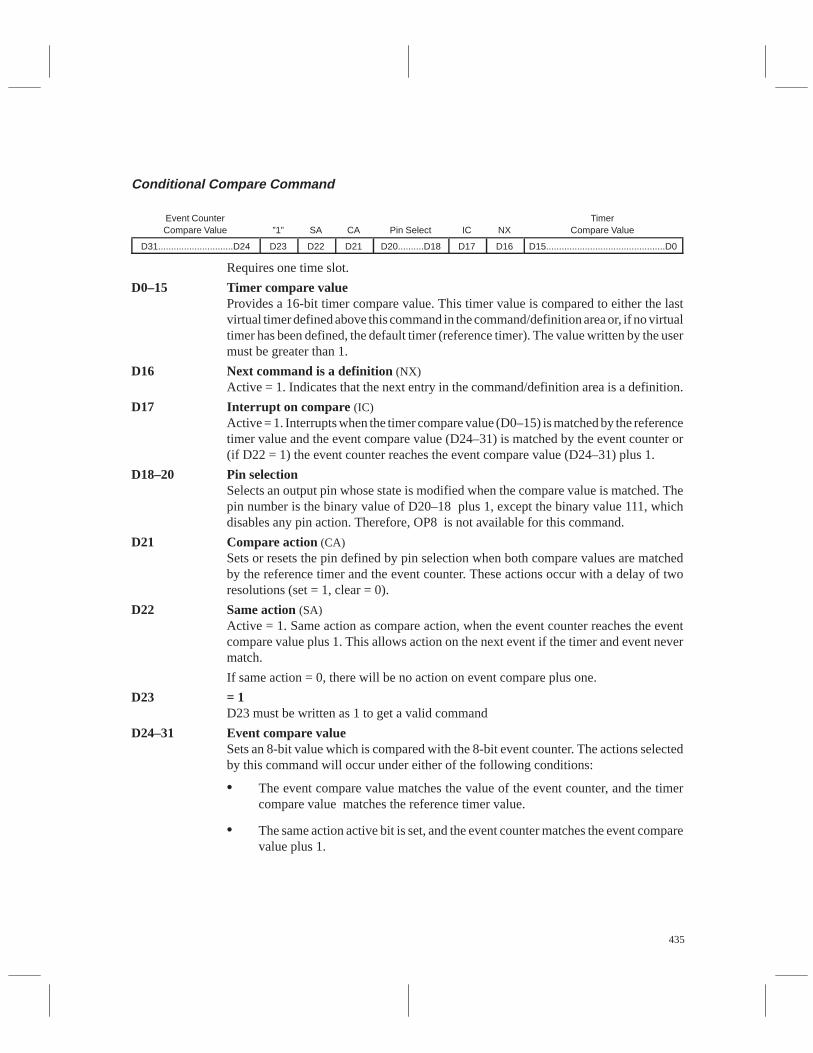
435
Conditional Compare Command
ÁÁÁÁÁÁÁÁÁÁÁÁÁÁ
Event CounterCompare Value
ÁÁÁÁÁÁ
”1”ÁÁÁÁÁÁ
SAÁÁÁÁÁÁ
CAÁÁÁÁÁÁÁÁ
Pin SelectÁÁÁÁÁÁ
ICÁÁÁÁÁÁ
NXÁÁÁÁÁÁÁÁÁÁÁÁÁÁÁÁÁÁ
TimerCompare Value
ÁÁÁÁÁÁÁÁÁÁÁÁÁÁ
D31.............................D24ÁÁÁÁÁÁ
D23ÁÁÁÁÁÁ
D22ÁÁÁÁÁÁ
D21ÁÁÁÁÁÁÁÁ
D20..........D18ÁÁÁÁÁÁ
D17ÁÁÁÁÁÁ
D16ÁÁÁÁÁÁÁÁÁÁÁÁÁÁÁÁÁÁ
D15..............................................D0
Requires one time slot.
D0–15 Timer compare valueProvides a 16-bit timer compare value. This timer value is compared to either the lastvirtual timer defined above this command in the command/definition area or, if no virtualtimer has been defined, the default timer (reference timer). The value written by the usermust be greater than 1.
D16 Next command is a definition (NX)Active = 1. Indicates that the next entry in the command/definition area is a definition.
D17 Interrupt on compare (IC)Active = 1. Interrupts when the timer compare value (D0–15) is matched by the referencetimer value and the event compare value (D24–31) is matched by the event counter or(if D22 = 1) the event counter reaches the event compare value (D24–31) plus 1.
D18–20 Pin selectionSelects an output pin whose state is modified when the compare value is matched. Thepin number is the binary value of D20–18 plus 1, except the binary value 111, whichdisables any pin action. Therefore, OP8 is not available for this command.
D21 Compare action (CA)Sets or resets the pin defined by pin selection when both compare values are matchedby the reference timer and the event counter. These actions occur with a delay of tworesolutions (set = 1, clear = 0).
D22 Same action (SA)Active = 1. Same action as compare action, when the event counter reaches the eventcompare value plus 1. This allows action on the next event if the timer and event nevermatch.
If same action = 0, there will be no action on event compare plus one.
D23 = 1D23 must be written as 1 to get a valid command
D24–31 Event compare valueSets an 8-bit value which is compared with the 8-bit event counter. The actions selectedby this command will occur under either of the following conditions:
• The event compare value matches the value of the event counter, and the timercompare value matches the reference timer value.
• The same action active bit is set, and the event counter matches the event comparevalue plus 1.

436
Double Event Compare CommandÁÁÁÁÁÁÁÁÁÁÁÁ
Reserved
ÁÁÁÁÁÁ
2C
ÁÁÁÁÁÁ
1C
ÁÁÁÁÁÁÁÁÁ
2R
ÁÁÁÁÁÁ
EP
ÁÁÁÁÁÁ
I2
ÁÁÁÁÁÁÁÁÁ
A2
ÁÁÁÁÁÁ
”0”
ÁÁÁÁÁÁÁÁÁ
”1”
ÁÁÁÁÁÁ
ST
ÁÁÁÁÁÁ
A1
ÁÁÁÁÁÁÁÁÁÁÁÁ
PinSelect
ÁÁÁÁÁÁ
I1
ÁÁÁÁÁÁÁÁÁ
NX
ÁÁÁÁÁÁÁÁÁ
Event 2Comp.Value
ÁÁÁÁÁÁÁÁÁÁÁÁ
Event 1Comp.Value
ÁÁÁÁÁÁÁÁ
D31 ÁÁÁÁ
D30ÁÁÁÁ
D29ÁÁÁÁÁÁ
D28ÁÁÁÁ
D27ÁÁÁÁ
D26ÁÁÁÁÁÁ
D25ÁÁÁÁ
D24ÁÁÁÁÁÁ
D23ÁÁÁÁ
D22ÁÁÁÁ
D21ÁÁÁÁÁÁÁÁ
D20...D18ÁÁÁÁ
D17ÁÁÁÁÁÁ
D16ÁÁÁÁÁÁ
D15.....D8ÁÁÁÁÁÁÁÁ
D7.......D0
Requires one time slot.D0–D7 Event 1
Sets an 8-bit value which, when matched by the 8-bit event counter, causes the actiondefined by D17, D21, and D29.
D8–15 Event 2Sets an 8-bit value which, when matched by the 8-bit event counter, causes the associatedaction defined by D25, D26, D28 and D30.
D16 Next command is a definition (NX)Active = 1. Indicates that the next entry in the command/definition area will be adefinition.
D17 Interrupt on compare 1 (I1)Active = 1. Interrupt when the event 1 compare value is matched by the event counter.
D18–20 Pin selectionSelects the output pin where state will be modified when the compare value is matched.The pin number is the binary value of the bits D20 to 18 + 1 (20 = LSB, 18 = MSB)
D21 Compare action 1 (A1)Sets or resets the output pin defined by pin selection/pin offset when the event 1 comparevalue (D0–D7) is matched by the event counter. These actions occur with a delay of threeresolutions (set = 1, clear = 0).
D22 Step (ST)Active = 1 Allows lower resolution on the following commands:
D23 = 0D23 must be written as 0 to get a valid command.
D24 = 1D24 must be written as 1 to get a valid command.
D25 Compare action 2 (A2)No action = 0. Inverted action = 1. Sets or resets the pin defined by pin selection/pinoffset when the event 2 compare value (D8–D15) is matched by the event counter.
D26 Interrupt on compare 2 (I2)Active = 1. Causes an interrupt when event 2 occurs.
D27 Enable pin (EP)Active = 1. Enables output pin actions for this command.
D28 Event 2 default timer reset (2R)Active = 1. Resets the default timer when event 2 occurs.
D29 Event 1 default timer capture (1C)Active = 1. Stores 32-bit data in the circular buffer when event 1 occurs.
D30 Event 2 default timer capture (2C)Active = 1. Stores 32-bit data in the circular buffer when event 2 occurs.
D31 Reserved.

437
PACT Control RegistersÁÁÁÁÁÁÁÁ
ÁÁÁÁÁÁÁÁBit 7
ÁÁÁÁÁÁÁÁBit 6
ÁÁÁÁÁÁÁÁBit 5
ÁÁÁÁÁÁÁÁBit 4
ÁÁÁÁÁÁÁÁBit 3
ÁÁÁÁÁÁÁÁBit 2
ÁÁÁÁÁÁÁÁBit 1
ÁÁÁÁÁÁÁÁÁÁBit 0
ÁÁÁÁÁÁ
ÁÁÁÁÁÁÁÁ
PACTSCRP040
ÁÁÁÁÁÁÁÁÁÁÁÁ
DEFTIMOVRFL
INT ENA
ÁÁÁÁÁÁÁÁÁÁÁÁ
DEFTIMOVRFL
INT FLAG
ÁÁÁÁÁÁÁÁÁÁÁÁ
CMD/DEFAREAENA
ÁÁÁÁÁÁÁÁÁÁÁÁ
FASTMODE
SELECT
ÁÁÁÁÁÁÁÁÁÁÁÁ
PACT PRESCALESELECT3
ÁÁÁÁÁÁÁÁÁÁÁÁ
PACT PRESCALESELECT2
ÁÁÁÁÁÁÁÁÁÁÁÁ
PACT PRESCALESELECT1
ÁÁÁÁÁÁÁÁÁÁÁÁÁÁÁ
PACT PRESCALESELECT0
ÁÁÁÁÁÁÁ
ÁÁÁÁÁÁÁÁÁÁÁÁ
CDSTARTP041
ÁÁÁÁÁÁÁÁÁÁÁÁÁÁÁÁ
CMD/DEFAREA
INT ENA
ÁÁÁÁÁÁÁÁÁÁÁÁÁÁÁÁ
-
ÁÁÁÁÁÁÁÁÁÁÁÁÁÁÁÁ
CMD/DEFAREASTARTBIT 5
ÁÁÁÁÁÁÁÁÁÁÁÁÁÁÁÁ
CMD/DEFAREASTARTBIT 4
ÁÁÁÁÁÁÁÁÁÁÁÁÁÁÁÁ
CMD/DEFAREASTARTBIT 3
ÁÁÁÁÁÁÁÁÁÁÁÁÁÁÁÁ
CMD/DEFAREASTARTBIT 2
ÁÁÁÁÁÁÁÁÁÁÁÁÁÁÁÁ
-
ÁÁÁÁÁÁÁÁÁÁÁÁÁÁÁÁÁÁÁÁ
-
ÁÁÁÁÁÁÁÁ
ÁÁÁÁÁÁÁÁÁÁÁÁ
CDENDP042
ÁÁÁÁÁÁÁÁÁÁÁÁÁÁÁÁ
-ÁÁÁÁÁÁÁÁÁÁÁÁÁÁÁÁ
CMD/DEFAREAENDBIT 6
ÁÁÁÁÁÁÁÁÁÁÁÁÁÁÁÁ
CMD/DEFAREAENDBIT 5
ÁÁÁÁÁÁÁÁÁÁÁÁÁÁÁÁ
CMD/DEFAREAENDBIT 4
ÁÁÁÁÁÁÁÁÁÁÁÁÁÁÁÁ
CMD/DEFAREAENDBIT 3
ÁÁÁÁÁÁÁÁÁÁÁÁÁÁÁÁ
CMD/DEFAREAENDBIT 2
ÁÁÁÁÁÁÁÁÁÁÁÁÁÁÁÁ
-ÁÁÁÁÁÁÁÁÁÁÁÁÁÁÁÁÁÁÁÁ
-ÁÁÁÁÁÁÁÁ
ÁÁÁÁÁÁÁÁ
BUFPTRP043 ÁÁÁÁÁÁÁÁÁÁÁÁ
1 ÁÁÁÁÁÁÁÁÁÁÁÁ
1 ÁÁÁÁÁÁÁÁÁÁÁÁ
BUFFERPOINTER
BIT 5
ÁÁÁÁÁÁÁÁÁÁÁÁ
BUFFERPOINTER
BIT 4
ÁÁÁÁÁÁÁÁÁÁÁÁ
BUFFERPOINTER
BIT 3
ÁÁÁÁÁÁÁÁÁÁÁÁ
BUFFERPOINTER
BIT 2
ÁÁÁÁÁÁÁÁÁÁÁÁ
BUFFERPOINTER
BIT 1
ÁÁÁÁÁÁÁÁÁÁÁÁÁÁÁ
- ÁÁÁÁÁÁÁ
ÁÁÁÁÁÁÁÁ
SCICTLPP045ÁÁÁÁÁÁÁÁÁÁÁÁ
PACTSCI
RXRDY
ÁÁÁÁÁÁÁÁÁÁÁÁ
PACTSCI
TXRDY
ÁÁÁÁÁÁÁÁÁÁÁÁ
PACTSCI
PARITY
ÁÁÁÁÁÁÁÁÁÁÁÁ
PACTSCIFE
ÁÁÁÁÁÁÁÁÁÁÁÁ
PACTSCI RX INT ENA
ÁÁÁÁÁÁÁÁÁÁÁÁ
PACTSCI TX
INT ENA
ÁÁÁÁÁÁÁÁÁÁÁÁ
- ÁÁÁÁÁÁÁÁÁÁÁÁÁÁÁ
PACTSCI SWRESET
ÁÁÁÁÁÁÁ
ÁÁÁÁÁÁÁÁ
RXBUFPP046ÁÁÁÁÁÁÁÁÁÁÁÁ
PACTSCI
RXDT7
ÁÁÁÁÁÁÁÁÁÁÁÁ
PACTSCI
RXDT6
ÁÁÁÁÁÁÁÁÁÁÁÁ
PACTSCI
RXDT5
ÁÁÁÁÁÁÁÁÁÁÁÁ
PACTSCI
RXDT4
ÁÁÁÁÁÁÁÁÁÁÁÁ
PACTSCI
RXDT3
ÁÁÁÁÁÁÁÁÁÁÁÁ
PACTSCI
RXDT2
ÁÁÁÁÁÁÁÁÁÁÁÁ
PACTSCI
RXDT1
ÁÁÁÁÁÁÁÁÁÁÁÁÁÁÁ
PACTSCI
RXDT0
ÁÁÁÁÁÁÁ
ÁÁÁÁÁÁÁÁ
TXBUFPP047ÁÁÁÁÁÁÁÁÁÁÁÁ
PACTSCI
TXDT7
ÁÁÁÁÁÁÁÁÁÁÁÁ
PACTSCI
TXDT6
ÁÁÁÁÁÁÁÁÁÁÁÁ
PACTSCI
TXDT5
ÁÁÁÁÁÁÁÁÁÁÁÁ
PACTSCI
TXDT4
ÁÁÁÁÁÁÁÁÁÁÁÁ
PACTSCI
TXDT3
ÁÁÁÁÁÁÁÁÁÁÁÁ
PACTSCI
TXDT2
ÁÁÁÁÁÁÁÁÁÁÁÁ
PACTSCI
TXDT1
ÁÁÁÁÁÁÁÁÁÁÁÁÁÁÁ
PACTSCI
TXDT0
ÁÁÁÁÁÁÁ
ÁÁÁÁÁÁÁÁ
OPSTATEP048ÁÁÁÁÁÁÁÁÁÁÁÁ
PACTOP8
STATE
ÁÁÁÁÁÁÁÁÁÁÁÁ
PACTOP7
STATE
ÁÁÁÁÁÁÁÁÁÁÁÁ
PACTOP6
STATE
ÁÁÁÁÁÁÁÁÁÁÁÁ
PACTOP5
STATE
ÁÁÁÁÁÁÁÁÁÁÁÁ
PACTOP4
STATE
ÁÁÁÁÁÁÁÁÁÁÁÁ
PACTOP3
STATE
ÁÁÁÁÁÁÁÁÁÁÁÁ
PACTOP2
STATE
ÁÁÁÁÁÁÁÁÁÁÁÁÁÁÁ
PACTOP1
STATE
ÁÁÁÁÁÁÁ
ÁÁÁÁÁÁÁÁ
CDFLAGSP049ÁÁÁÁÁÁÁÁÁÁÁÁ
CMD/DEFINT 7FLAG
ÁÁÁÁÁÁÁÁÁÁÁÁ
CMD/DEFINT 6FLAG
ÁÁÁÁÁÁÁÁÁÁÁÁ
CMD/DEFINT 5FLAG
ÁÁÁÁÁÁÁÁÁÁÁÁ
CMD/DEFINT 4FLAG
ÁÁÁÁÁÁÁÁÁÁÁÁ
CMD/DEFINT 3FLAG
ÁÁÁÁÁÁÁÁÁÁÁÁ
CMD/DEFINT 2FLAG
ÁÁÁÁÁÁÁÁÁÁÁÁ
CMD/DEFINT 1FLAG
ÁÁÁÁÁÁÁÁÁÁÁÁÁÁÁ
CMD/DEFINT 0FLAG
ÁÁÁÁÁÁÁ
ÁÁÁÁÁÁÁÁ
CPCTL1P04A
ÁÁÁÁÁÁÁÁÁÁÁÁ
CP2INT ENA
ÁÁÁÁÁÁÁÁÁÁÁÁ
CP2INT FLAG
ÁÁÁÁÁÁÁÁÁÁÁÁ
CP2CAPT
RISINGEDGE
ÁÁÁÁÁÁÁÁÁÁÁÁ
CP2CAPT
FALLINGEDGE
ÁÁÁÁÁÁÁÁÁÁÁÁ
CP1INT ENA
ÁÁÁÁÁÁÁÁÁÁÁÁ
CP1INT FLAG
ÁÁÁÁÁÁÁÁÁÁÁÁ
CP1CAPT
RISINGEDGE
ÁÁÁÁÁÁÁÁÁÁÁÁÁÁÁ
CP1CAPT
FALLINGEDGE
ÁÁÁÁÁÁÁ
ÁÁÁÁÁÁÁÁÁÁÁÁ
CPCTL2P04B
ÁÁÁÁÁÁÁÁÁÁÁÁÁÁÁÁ
CP4INT ENA
ÁÁÁÁÁÁÁÁÁÁÁÁÁÁÁÁ
CP4INT FLAG
ÁÁÁÁÁÁÁÁÁÁÁÁÁÁÁÁ
CP4CAPT
RISINGEDGE
ÁÁÁÁÁÁÁÁÁÁÁÁÁÁÁÁ
CP4CAPT
FALLINGEDGE
ÁÁÁÁÁÁÁÁÁÁÁÁÁÁÁÁ
CP3INT ENA
ÁÁÁÁÁÁÁÁÁÁÁÁÁÁÁÁ
CP3INT FLAG
ÁÁÁÁÁÁÁÁÁÁÁÁÁÁÁÁ
CP3CAPT
RISINGEDGE
ÁÁÁÁÁÁÁÁÁÁÁÁÁÁÁÁÁÁÁÁ
CP3CAPT
FALLINGEDGE
ÁÁÁÁÁÁÁÁ
ÁÁÁÁÁÁÁÁÁÁÁÁ
CPCTL3P04C
ÁÁÁÁÁÁÁÁÁÁÁÁÁÁÁÁ
CP6INT ENA
ÁÁÁÁÁÁÁÁÁÁÁÁÁÁÁÁ
CP6INT FLAG
ÁÁÁÁÁÁÁÁÁÁÁÁÁÁÁÁ
CP6CAPT
RISINGEDGE
ÁÁÁÁÁÁÁÁÁÁÁÁÁÁÁÁ
CP6CAPT
FALLINGEDGE
ÁÁÁÁÁÁÁÁÁÁÁÁÁÁÁÁ
CP5INT ENA
ÁÁÁÁÁÁÁÁÁÁÁÁÁÁÁÁ
CP5INT FLAG
ÁÁÁÁÁÁÁÁÁÁÁÁÁÁÁÁ
CP5CAPT
RISINGEDGE
ÁÁÁÁÁÁÁÁÁÁÁÁÁÁÁÁÁÁÁÁ
CP5CAPT
FALLINGEDGE
ÁÁÁÁÁÁÁÁ
ÁÁÁÁÁÁÁÁ
CPPREP04D
ÁÁÁÁÁÁÁÁÁÁÁÁ
BUFFERHALF/FULL
INT ENA
ÁÁÁÁÁÁÁÁÁÁÁÁ
BUFFERHALF/FULL
INT FLAG
ÁÁÁÁÁÁÁÁÁÁÁÁ
INPUTCAPT
PRESCALESELECT 3
ÁÁÁÁÁÁÁÁÁÁÁÁ
INPUTCAPT
PRESCALESELECT 2
ÁÁÁÁÁÁÁÁÁÁÁÁ
INPUTCAPT
PRESCALESELECT 1
ÁÁÁÁÁÁÁÁÁÁÁÁ
CP6EVENTONLY
ÁÁÁÁÁÁÁÁÁÁÁÁ
EVENTCOUNTER
SWRESET
ÁÁÁÁÁÁÁÁÁÁÁÁÁÁÁ
OP/SET/CLRSELECT
ÁÁÁÁÁÁÁ
ÁÁÁÁÁÁÁÁ
WDRSTP04E
ÁÁÁÁÁÁÁÁÁÁÁÁ
PACTWD KEY
BIT 7
ÁÁÁÁÁÁÁÁÁÁÁÁ
PACTWD KEY
BIT 7
ÁÁÁÁÁÁÁÁÁÁÁÁ
PACTWD KEY
BIT 7
ÁÁÁÁÁÁÁÁÁÁÁÁ
PACTWD KEY
BIT 7
ÁÁÁÁÁÁÁÁÁÁÁÁ
PACTWD KEY
BIT 7
ÁÁÁÁÁÁÁÁÁÁÁÁ
PACTWD KEY
BIT 7
ÁÁÁÁÁÁÁÁÁÁÁÁ
PACTWD KEY
BIT 7
ÁÁÁÁÁÁÁÁÁÁÁÁÁÁÁ
PACTWD KEY
BIT 7
ÁÁÁÁÁÁÁ
ÁÁÁÁÁÁÁÁ
PACTPRIP04F
PACTSTEST
ÁÁÁÁÁÁÁÁÁÁÁÁ
PACTSUSPEND
PACTGROUP 1PRIORITY
PACTGROUP 2PRIORITY
PACTGROUP 3PRIORITY
PACTMODE
SELECT
PACT WDPRESCALESELECT 1
PACT WDPRESCALESELECT 0
ÁÁÁÁÁÁÁ
ÁÁÁÁÁÁÁÁÁÁÁÁ
ÁÁÁÁÁÁÁÁ
ÁÁÁÁÁÁÁÁ
ÁÁÁÁÁÁÁÁ
ÁÁÁÁÁÁÁÁ
ÁÁÁÁÁÁÁÁ
ÁÁÁÁÁÁÁÁ
ÁÁÁÁÁÁÁÁÁÁ
ÁÁ

438
Interrupt Vector Sources
ÁÁÁÁÁÁÁÁ
MODULEÁÁÁÁÁÁÁÁÁÁ
VECTORADDRESS
ÁÁÁÁÁÁÁÁÁÁÁÁÁÁ
INTERRUPTSOURCE
ÁÁÁÁÁÁÁÁÁÁÁÁ
INTERRUPTFLAG
ÁÁÁÁÁÁÁÁÁÁ
SYSTEMINTERRUPT
ÁÁÁÁÁÁÁÁ
PRIORITYIN GROUPÁÁÁÁ
ÁÁÁÁPACTÁÁÁÁÁÁÁÁÁÁ
7FB0h,7FB1hÁÁÁÁÁÁÁÁÁÁÁÁÁÁ
PACT Circular BufferÁÁÁÁÁÁÁÁÁÁÁÁ
BUFF INT FLAGÁÁÁÁÁÁÁÁÁÁ
BUFINTÁÁÁÁÁÁÁÁ
1ÁÁÁÁÁÁÁÁ
(Group 1)ÁÁÁÁÁÁÁÁÁÁ
7FB2h,7FB3hÁÁÁÁÁÁÁÁÁÁÁÁÁÁ
PACT CP6 EdgeÁÁÁÁÁÁÁÁÁÁÁÁ
CP6 INT FLAGÁÁÁÁÁÁÁÁÁÁ
CP6INTÁÁÁÁÁÁÁÁ
2ÁÁÁÁÁÁÁÁ
ÁÁÁÁÁÁÁÁÁÁ
7FB4h,7FB5hÁÁÁÁÁÁÁÁÁÁÁÁÁÁ
PACT CP5 Edge ÁÁÁÁÁÁÁÁÁÁÁÁ
CP5 INT FLAGÁÁÁÁÁÁÁÁÁÁ
CP5INT ÁÁÁÁÁÁÁÁ
3
ÁÁÁÁÁÁÁÁ
ÁÁÁÁÁÁÁÁÁÁ
7FB6h,7FB7hÁÁÁÁÁÁÁÁÁÁÁÁÁÁ
PACT CP4 Edge ÁÁÁÁÁÁÁÁÁÁÁÁ
CP4 INT FLAGÁÁÁÁÁÁÁÁÁÁ
CP4INT ÁÁÁÁÁÁÁÁ
4
ÁÁÁÁÁÁÁÁ
ÁÁÁÁÁÁÁÁÁÁ
7FB8h,7FB9hÁÁÁÁÁÁÁÁÁÁÁÁÁÁ
PACT CP3 Edge ÁÁÁÁÁÁÁÁÁÁÁÁ
CP3 INT FLAGÁÁÁÁÁÁÁÁÁÁ
CP3INT ÁÁÁÁÁÁÁÁ
5
ÁÁÁÁÁÁÁÁ
ÁÁÁÁÁÁÁÁÁÁ
7FBAh,7FBBhÁÁÁÁÁÁÁÁÁÁÁÁÁÁ
PACT CP2 Edge ÁÁÁÁÁÁÁÁÁÁÁÁ
CP2 INT FLAGÁÁÁÁÁÁÁÁÁÁ
CP2INT ÁÁÁÁÁÁÁÁ
6
ÁÁÁÁÁÁÁÁÁ7FBCh,7FBDhÁÁÁÁÁÁÁPACT CP1 Edge ÁÁÁÁÁÁCP1 INT FLAGÁÁÁÁÁCP1INT ÁÁÁÁ7ÁÁÁÁÁÁÁÁÁÁÁÁ
ÁÁÁÁÁÁÁÁÁÁÁÁÁÁÁ
7FBEh,7FBFhÁÁÁÁÁÁÁÁÁÁÁÁÁÁÁÁÁÁÁÁÁ
Default TimerOverflow
ÁÁÁÁÁÁÁÁÁÁÁÁÁÁÁÁÁÁ
DEFTIM OVRFLINT FLAG
ÁÁÁÁÁÁÁÁÁÁÁÁÁÁÁ
POVRFLINT
ÁÁÁÁÁÁÁÁÁÁÁÁ
8
ÁÁÁÁÁÁÁÁ
PACT ÁÁÁÁÁÁÁÁÁÁ
7F9Ch,7F9DhÁÁÁÁÁÁÁÁÁÁÁÁÁÁ
PACT SCI TX INTÁÁÁÁÁÁÁÁÁÁÁÁ
PACT TX RDYÁÁÁÁÁÁÁÁÁÁ
PTXINT ÁÁÁÁÁÁÁÁ
2
ÁÁÁÁÁÁÁÁ
(Group 2)ÁÁÁÁÁÁÁÁÁÁ
7F9Eh,7F9FhÁÁÁÁÁÁÁÁÁÁÁÁÁÁ
PACT SCI RX INTÁÁÁÁÁÁÁÁÁÁÁÁ
PACT RXRDYÁÁÁÁÁÁÁÁÁÁ
PRXINT ÁÁÁÁÁÁÁÁ
1
ÁÁÁÁÁÁÁÁ
PACT(Group 3)
ÁÁÁÁÁÁÁÁÁÁ
7FA0h,7FA1hÁÁÁÁÁÁÁÁÁÁÁÁÁÁ
PACT CMD/DEFEntry 0
ÁÁÁÁÁÁÁÁÁÁÁÁ
CMD/DEF INT 0FLAG
ÁÁÁÁÁÁÁÁÁÁ
CDINT 0 ÁÁÁÁÁÁÁÁ
1
ÁÁÁÁÁÁÁÁÁÁÁÁ
ÁÁÁÁÁÁÁÁÁÁÁÁÁÁÁ
7FA2h,7FA3hÁÁÁÁÁÁÁÁÁÁÁÁÁÁÁÁÁÁÁÁÁ
PACT CMD/DEFEntry 1
ÁÁÁÁÁÁÁÁÁÁÁÁÁÁÁÁÁÁ
CMD/DEF INT 1FLAG
ÁÁÁÁÁÁÁÁÁÁÁÁÁÁÁ
CDINT 1ÁÁÁÁÁÁÁÁÁÁÁÁ
2
ÁÁÁÁÁÁÁÁÁÁÁÁ
ÁÁÁÁÁÁÁÁÁÁÁÁÁÁÁ
7FA4h,7FA5hÁÁÁÁÁÁÁÁÁÁÁÁÁÁÁÁÁÁÁÁÁ
PACT CMD/DEFEntry 2
ÁÁÁÁÁÁÁÁÁÁÁÁÁÁÁÁÁÁ
CMD/DEF INT 2FLAG
ÁÁÁÁÁÁÁÁÁÁÁÁÁÁÁ
CDINT 2 ÁÁÁÁÁÁÁÁÁÁÁÁ
3
ÁÁÁÁÁÁÁÁ
ÁÁÁÁÁÁÁÁÁÁ
7FA6h,7FA7hÁÁÁÁÁÁÁÁÁÁÁÁÁÁ
PACT CMD/DEFEntry 3
ÁÁÁÁÁÁÁÁÁÁÁÁ
CMD/DEF INT 3FLAG
ÁÁÁÁÁÁÁÁÁÁ
CDINT 3 ÁÁÁÁÁÁÁÁ
4
ÁÁÁÁÁÁÁÁÁÁÁÁ
ÁÁÁÁÁÁÁÁÁÁÁÁÁÁÁ
7FA8h,7FA9hÁÁÁÁÁÁÁÁÁÁÁÁÁÁÁÁÁÁÁÁÁ
PACT CMD/DEFEntry 4
ÁÁÁÁÁÁÁÁÁÁÁÁÁÁÁÁÁÁ
CMD/DEF INT 4FLAG
ÁÁÁÁÁÁÁÁÁÁÁÁÁÁÁ
CDINT 4 ÁÁÁÁÁÁÁÁÁÁÁÁ
5
ÁÁÁÁÁÁÁÁ
ÁÁÁÁÁÁÁÁÁÁ
7FAAh,7FABhÁÁÁÁÁÁÁÁÁÁÁÁÁÁ
PACT CMD/DEFEntry 5
ÁÁÁÁÁÁÁÁÁÁÁÁ
CMD/DEF INT 5FLAG
ÁÁÁÁÁÁÁÁÁÁ
CDINT 5 ÁÁÁÁÁÁÁÁ
6
ÁÁÁÁÁÁÁÁÁÁÁÁ
ÁÁÁÁÁÁÁÁÁÁÁÁÁÁÁ
7FACh,7FADhÁÁÁÁÁÁÁÁÁÁÁÁÁÁÁÁÁÁÁÁÁ
PACT CMD/DEFEntry 6
ÁÁÁÁÁÁÁÁÁÁÁÁÁÁÁÁÁÁ
CMD/DEF INT 6FLAG
ÁÁÁÁÁÁÁÁÁÁÁÁÁÁÁ
CDINT 6ÁÁÁÁÁÁÁÁÁÁÁÁ
7
ÁÁÁÁÁÁÁÁ
ÁÁÁÁÁÁÁÁÁÁ
7FAEh,7FAFhÁÁÁÁÁÁÁÁÁÁÁÁÁÁ
PACT CMD/DEFEntry 7
ÁÁÁÁÁÁÁÁÁÁÁÁ
CMD/DEF INT 7FLAG 7
ÁÁÁÁÁÁÁÁÁÁ
CDINT 7 ÁÁÁÁÁÁÁÁ
8
439
Part IIIModule Specific
Application Design Aids
Part III contains six sections:
RESET Operations 99. . . . . . . . . . . . . . . . . . .
SPI and SCI Modules 105. . . . . . . . . . . . . . . .
Timer and Watchdog Modules 199. . . . . . . .
Analog to Digital Modules 309. . . . . . . . . . .
PACT Module 375. . . . . . . . . . . . . . . . . . . . . . .
I/O Pins 439. . . . . . . . . . . . . . . . . . . . . . . . . . . .

440
441
Proper Termination of Unused I/OPins
Michael S. StewartMicrocontroller Products — Semiconductor Group
Texas Instruments

442

443
Introduction
Occasionally, embedded microcontroller systems applications do not require the use of all the I/O pinsavailable on the chosen microcontroller. In this case, the design engineer must properly terminate allunused I/O pins to ensure proper device operation. The main area of concern regarding proper pintermination is power consumption in low-power modes (standby or halt). However, proper terminationtechniques should be followed for applications that do not use low-power modes.
When a CMOS microcontroller enters a low-power mode, the internal nodes connected to the external pinsneed to be biased in the logical high (VIH) or logical low (VIL) condition. When the internal nodes are biasedidentically, there is little to no internal stray power consumption. An obvious solution to this requirementis to configure the unused bidirectional I/O pins as outputs driving either a high (VOH) or low (VOL) value.In this situation, no external circuitry is necessary.
However, if the external pins are not bidirectional but input only, they must be pulled high or low externally.If any input pin is not externally biased but allowed to float, the internal nodes connected to this pin circuitrywill then be self-biased to either a logical high or low state. In this condition, current paths will be generatedallowing unwanted power consumption. This condition is normally called the ’floating nodes’ problem,and the symptom that is most commonly seen when the device does not have any unused input pinsconnected to VCC or VSS is that the low-power current will initially fall to the specified range but willslowly climb into the multiple mA range. This condition is not destructive, but in a battery operated systemthat is assuming a halt mode current drain of 30 µA or less, a multiple mA current consumption coulddischarge the battery much sooner than expected.
NOTE:When terminating unused I/O pins, good layout practices must beimplemented to reduce EMI emissions. Loop areas must be kept to aminimum. Any components used for terminations must be kept as close to thedevice as possible.
What to Do: Best Solution
The TMS370 family of microcontrollers have various types of pins. Some are input only some aregeneral-purpose bidirectional, and others are multiplexed module function and I/O pins. Without going intoa great degree of detail, the best overall solution for terminating unused I/O pins (bidirectional) is toindividually pull each pin low through a resistor (typically 10 kΩ or greater) as shown in Figure 1.
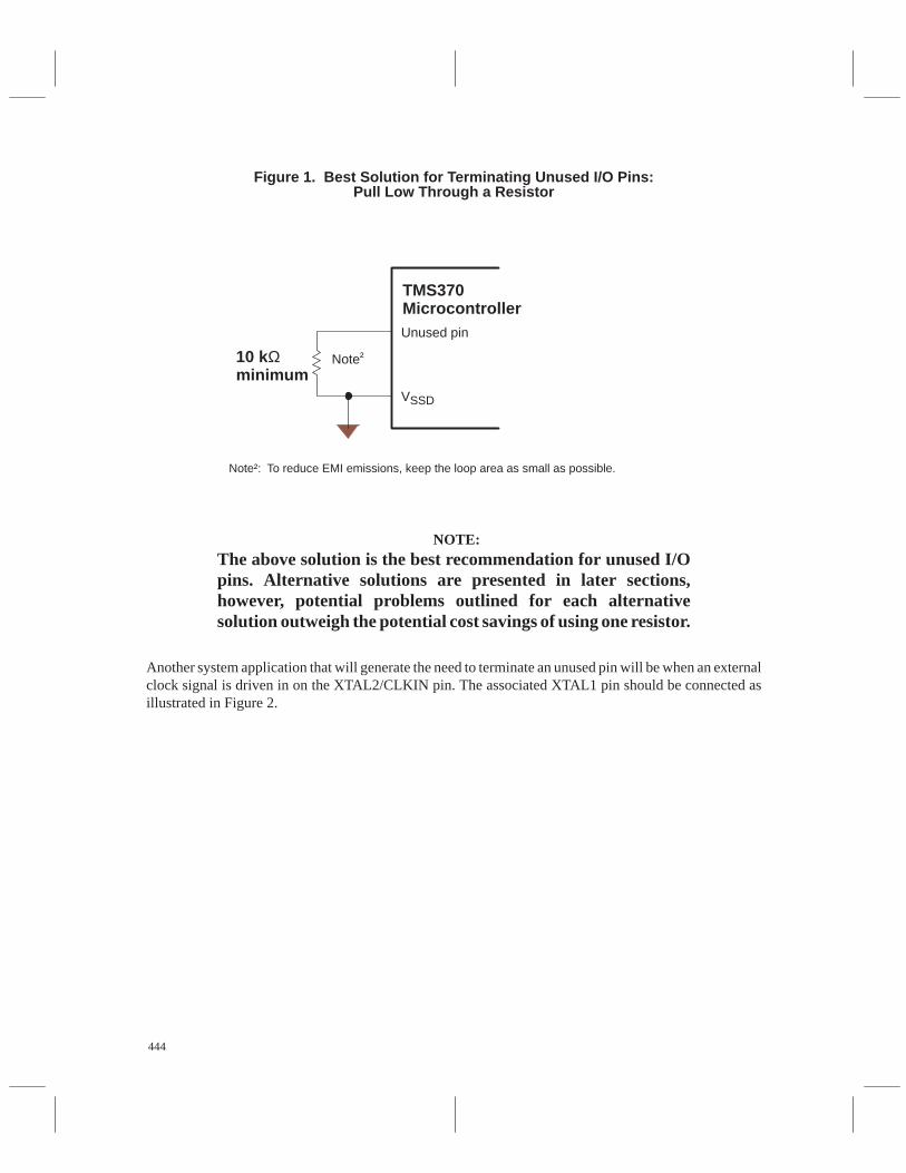
444
Figure 1. Best Solution for Terminating Unused I/O Pins:Pull Low Through a Resistor
TMS370MicrocontrollerUnused pin
Note†
VSSD
10 kΩminimum
Note†: To reduce EMI emissions, keep the loop area as small as possible.
NOTE:The above solution is the best recommendation for unused I/Opins. Alternative solutions are presented in later sections,however, potential problems outlined for each alternativesolution outweigh the potential cost savings of using one resistor.
Another system application that will generate the need to terminate an unused pin will be when an externalclock signal is driven in on the XTAL2/CLKIN pin. The associated XTAL1 pin should be connected asillustrated in Figure 2.
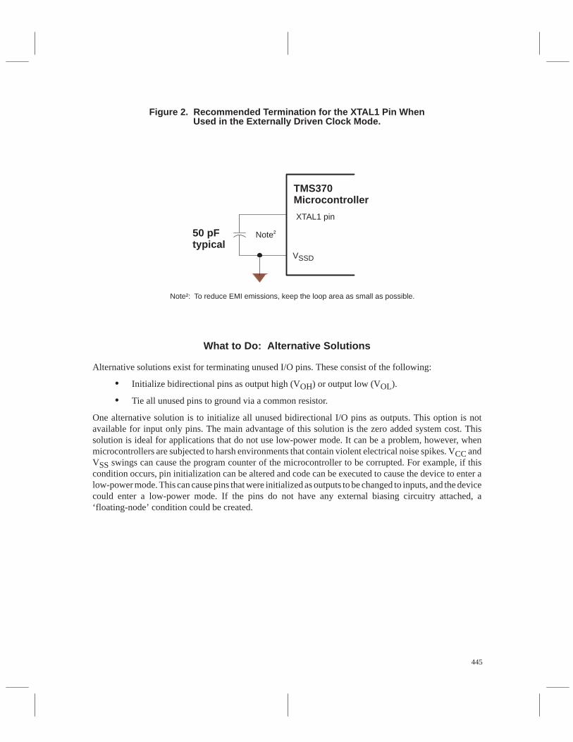
445
Figure 2. Recommended Termination for the XTAL1 Pin WhenUsed in the Externally Driven Clock Mode.
TMS370Microcontroller
XTAL1 pin
VSSD
50 pFtypical
Note†
Note†: To reduce EMI emissions, keep the loop area as small as possible.
What to Do: Alternative Solutions
Alternative solutions exist for terminating unused I/O pins. These consist of the following:
• Initialize bidirectional pins as output high (VOH) or output low (VOL).
• Tie all unused pins to ground via a common resistor.
One alternative solution is to initialize all unused bidirectional I/O pins as outputs. This option is notavailable for input only pins. The main advantage of this solution is the zero added system cost. Thissolution is ideal for applications that do not use low-power mode. It can be a problem, however, whenmicrocontrollers are subjected to harsh environments that contain violent electrical noise spikes. VCC andVSS swings can cause the program counter of the microcontroller to be corrupted. For example, if thiscondition occurs, pin initialization can be altered and code can be executed to cause the device to enter alow-power mode. This can cause pins that were initialized as outputs to be changed to inputs, and the devicecould enter a low-power mode. If the pins do not have any external biasing circuitry attached, a‘floating-node’ condition could be created.
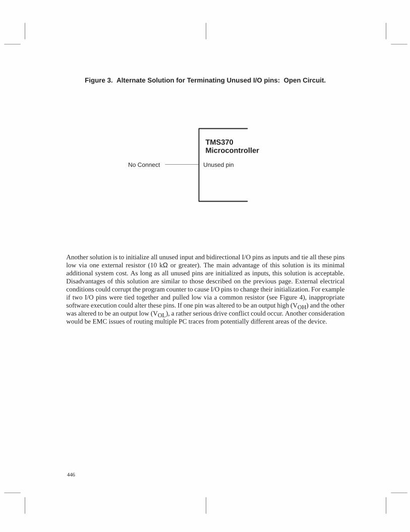
446
Figure 3. Alternate Solution for Terminating Unused I/O pins: Open Circuit.
TMS370Microcontroller
Unused pinNo Connect
Another solution is to initialize all unused input and bidirectional I/O pins as inputs and tie all these pinslow via one external resistor (10 kΩ or greater). The main advantage of this solution is its minimaladditional system cost. As long as all unused pins are initialized as inputs, this solution is acceptable.Disadvantages of this solution are similar to those described on the previous page. External electricalconditions could corrupt the program counter to cause I/O pins to change their initialization. For exampleif two I/O pins were tied together and pulled low via a common resistor (see Figure 4), inappropriatesoftware execution could alter these pins. If one pin was altered to be an output high (VOH) and the otherwas altered to be an output low (VOL), a rather serious drive conflict could occur. Another considerationwould be EMC issues of routing multiple PC traces from potentially different areas of the device.
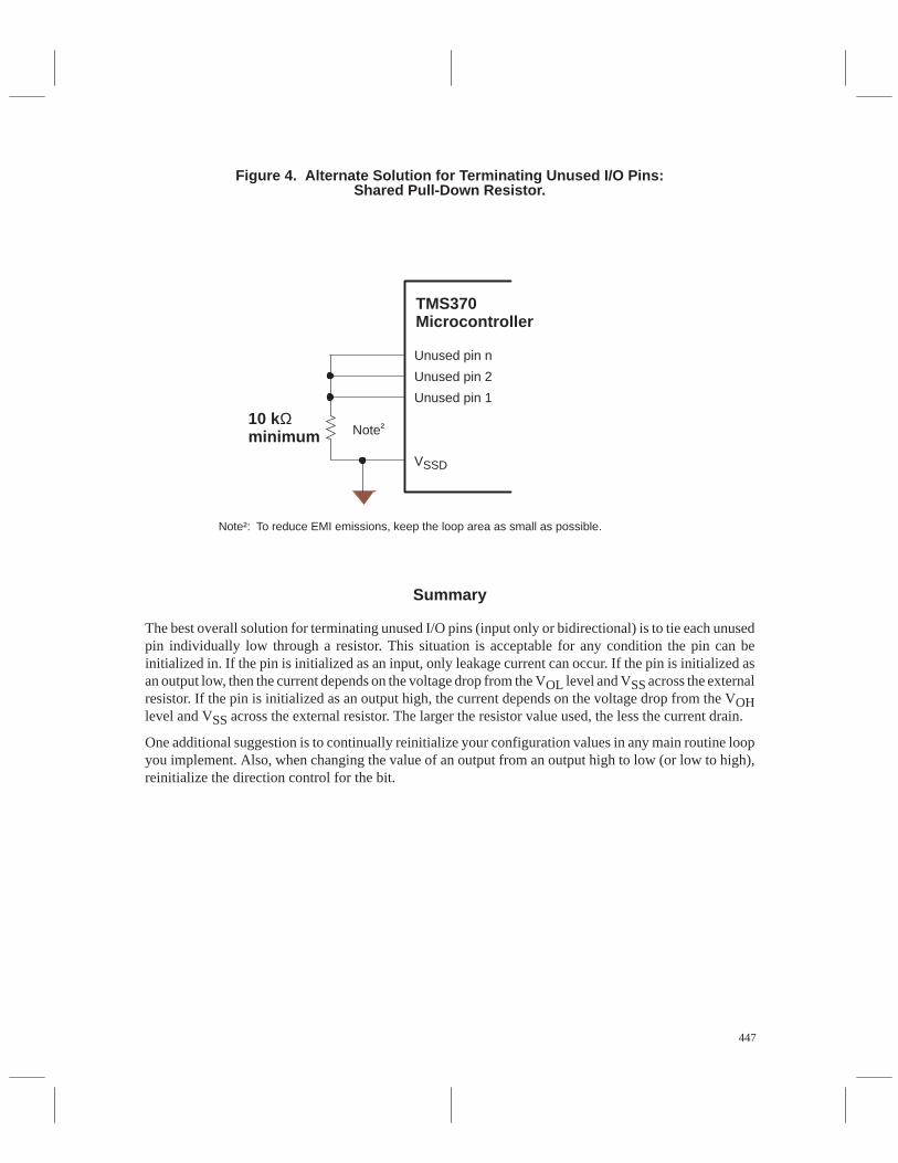
447
Figure 4. Alternate Solution for Terminating Unused I/O Pins:Shared Pull-Down Resistor.
TMS370Microcontroller
Unused pin 1
VSSD
10 kΩminimum
Unused pin 2
Unused pin n
Note†
Note†: To reduce EMI emissions, keep the loop area as small as possible.
Summary
The best overall solution for terminating unused I/O pins (input only or bidirectional) is to tie each unusedpin individually low through a resistor. This situation is acceptable for any condition the pin can beinitialized in. If the pin is initialized as an input, only leakage current can occur. If the pin is initialized asan output low, then the current depends on the voltage drop from the VOL level and VSS across the externalresistor. If the pin is initialized as an output high, the current depends on the voltage drop from the VOHlevel and VSS across the external resistor. The larger the resistor value used, the less the current drain.
One additional suggestion is to continually reinitialize your configuration values in any main routine loopyou implement. Also, when changing the value of an output from an output high to low (or low to high),reinitialize the direction control for the bit.

448

449
Part IVEEPROM Programming
Part IV contains two sections:
EEPROM Self Programming 449. . . . . . . . . .
Bootstrap Programs 457. . . . . . . . . . . . . . . .

450

451
EEPROM Self ProgrammingWith the TMS370
Microcontroller Products—Semiconductor GroupTexas Instruments

452
453
Programming With the TMS370 Family
The following example demonstrates the self-programming ability of the TMS370 family. This feature canprogram any byte of the onboard data EEPROM by passing the appropriate data and address to this routine.
The program consists of two major sections: the procedure that determines the bits that need to be changed(PROGRAM), and the procedure that changes these bits (EEPROG).
• PROGRAM attempts to save programming time by checking which portions of the two-stepprogramming procedure must occur. If the data already in the array is the same as the new data,then no programming is necessary. By omitting a write ones or a write zeros operation, 10 msis removed from the total 20-ms programming time; every programming step that this routineomits saves 10 ms.
The address and data to program are passed to this routine in the register pair ADDR1–1:ADDR1and in register A, respectively.
• EEPROG is the routine that initiates, times, and then stops the actual EEPROM programming.During this section of code, disable the interrupts to prevent data corruption. Corruption canoccur when an interrupt routine accesses any EEPROM location, interrupting the EEPROGroutine between writing to the EEPROM location and setting the EXE bit (DEECTL.0).
You can program unprotected data EEPROM using only the VCC power supply. Enter the write protectionoverride (WPO) mode by placing 12 V on the MC pin when programming protected data EEPROM.
The following program is used to write to any location in the data EEPROM.
Parameters used:
ADDR1–1:ADDR1 = EEPROM address to program A = data to write to EEPROM address
Write Data EEPROM RoutineTEMP1 .EQU R3 ;General-purpose temporary registerTEMP2 .EQU R4 ;General-purpose temporary registerADDR1 .EQU R6 ;Contains address for program
;operation.ECOM .EQU R7 ;Command for DEECTLDEECTL .EQU P01A ;Address for data EEPROM control reg.;
PROGRAM RoutinePROGRAM MOV A,TEMP2 ;Save data.
MOV @ADDR1,A ;Read current data.XOR TEMP2,A ;Different bits = 1JZ EXITW ;If byte is already equal then exit.INV A ;Different bits = 0OR TEMP2,A ;Bits that change from 1 to 0 = 0BTJZ #0FFh,A,WRITE0 ;Program 0s if any 0sJMP ONES ;If all 1s then go to WRITE1 part.
WRITE0 MOV #1,ECOM ;Program to write 0s (DEECTL = 1).MOV TEMP2,ACALL EEPROG ;Programming EEPROM
ONES MOV @ADDR1,A ;Get the current data.XOR TEMP2,A ;Bits that change = 1AND TEMP2,A ;Bits that change from 0 to 1 = 1
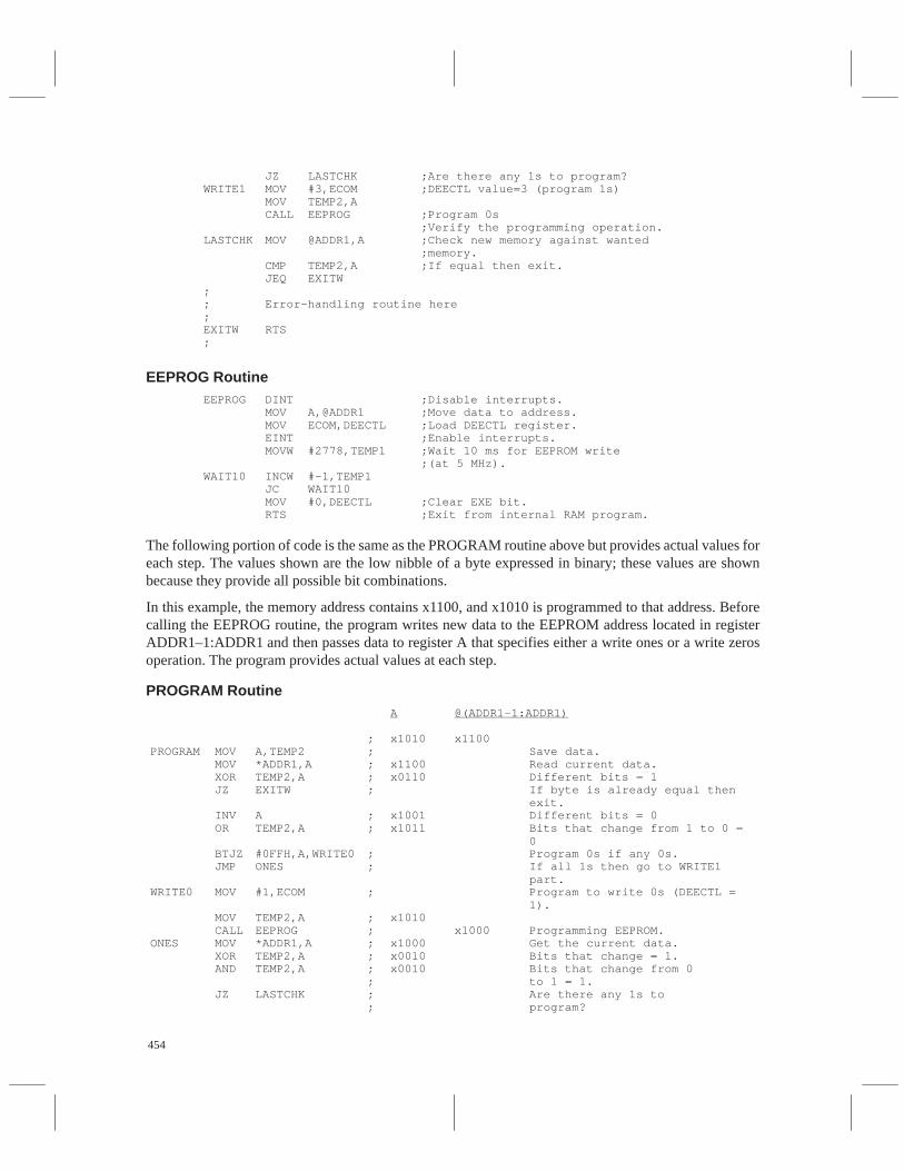
454
JZ LASTCHK ;Are there any 1s to program?WRITE1 MOV #3,ECOM ;DEECTL value=3 (program 1s)
MOV TEMP2,ACALL EEPROG ;Program 0s
;Verify the programming operation.LASTCHK MOV @ADDR1,A ;Check new memory against wanted
;memory.CMP TEMP2,A ;If equal then exit.JEQ EXITW
;; Error–handling routine here;EXITW RTS;
EEPROG RoutineEEPROG DINT ;Disable interrupts.
MOV A,@ADDR1 ;Move data to address.MOV ECOM,DEECTL ;Load DEECTL register.EINT ;Enable interrupts.MOVW #2778,TEMP1 ;Wait 10 ms for EEPROM write
;(at 5 MHz).WAIT10 INCW #–1,TEMP1
JC WAIT10MOV #0,DEECTL ;Clear EXE bit.RTS ;Exit from internal RAM program.
The following portion of code is the same as the PROGRAM routine above but provides actual values foreach step. The values shown are the low nibble of a byte expressed in binary; these values are shownbecause they provide all possible bit combinations.
In this example, the memory address contains x1100, and x1010 is programmed to that address. Beforecalling the EEPROG routine, the program writes new data to the EEPROM address located in registerADDR1–1:ADDR1 and then passes data to register A that specifies either a write ones or a write zerosoperation. The program provides actual values at each step.
PROGRAM RoutineA @(ADDR1–1:ADDR1)
; x1010 x1100PROGRAM MOV A,TEMP2 ; Save data.
MOV *ADDR1,A ; x1100 Read current data.XOR TEMP2,A ; x0110 Different bits = 1JZ EXITW ; If byte is already equal then
exit.INV A ; x1001 Different bits = 0OR TEMP2,A ; x1011 Bits that change from 1 to 0 =
0BTJZ #0FFH,A,WRITE0 ; Program 0s if any 0s.JMP ONES ; If all 1s then go to WRITE1
part.WRITE0 MOV #1,ECOM ; Program to write 0s (DEECTL =
1).MOV TEMP2,A ; x1010CALL EEPROG ; x1000 Programming EEPROM.
ONES MOV *ADDR1,A ; x1000 Get the current data.XOR TEMP2,A ; x0010 Bits that change = 1.AND TEMP2,A ; x0010 Bits that change from 0
; to 1 = 1.JZ LASTCHK ; Are there any 1s to
; program?
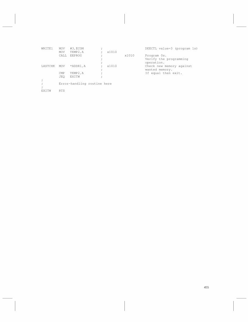
455
WRITE1 MOV #3,ECOM ; DEECTL value=3 (program 1s)MOV TEMP2,A ; x1010CALL EEPROG ; x1010 Program 0s.
; Verify the programming; operation.
LASTCHK MOV *ADDR1,A ; x1010 Check new memory against; wanted memory.
CMP TEMP2,A ; If equal then exit.JEQ EXITW ;
;; Error–handling routine here;EXITW RTS

456

457
Part IVEEPROM Programming
Part IV contains two sections:
EEPROM Self Programming 449. . . . . . . . .
Bootstrap Programs 457. . . . . . . . . . . . . . . . .

458

459
Bootstrap Program for the TMS370
Microcontroller Products—Semiconductor GroupTexas Instruments

460
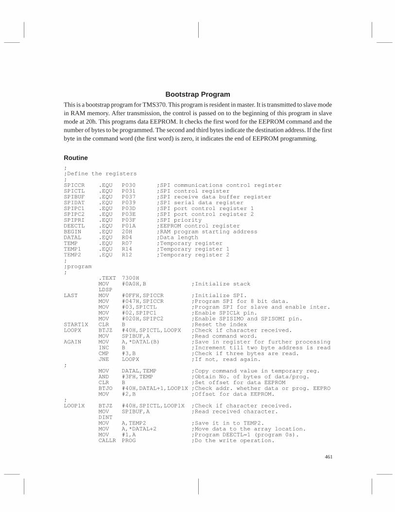
461
Bootstrap ProgramThis is a bootstrap program for TMS370. This program is resident in master. It is transmitted to slave modein RAM memory. After transmission, the control is passed on to the beginning of this program in slavemode at 20h. This programs data EEPROM. It checks the first word for the EEPROM command and thenumber of bytes to be programmed. The second and third bytes indicate the destination address. If the firstbyte in the command word (the first word) is zero, it indicates the end of EEPROM programming.
Routine;;Define the registers;SPICCR .EQU P030 ;SPI communications control registerSPICTL .EQU P031 ;SPI control registerSPIBUF .EQU P037 ;SPI receive data buffer registerSPIDAT .EQU P039 ;SPI serial data registerSPIPC1 .EQU P03D ;SPI port control register 1SPIPC2 .EQU P03E ;SPI port control register 2SPIPRI .EQU P03F ;SPI priorityDEECTL .EQU P01A ;EEPROM control registerBEGIN .EQU 20H ;RAM program starting addressDATAL .EQU R04 ;Data lengthTEMP .EQU R07 ;Temporary registerTEMP1 .EQU R14 ;Temporary register 1TEMP2 .EQU R12 ;Temporary register 2;;program;
.TEXT 7300HMOV #0A0H,B ;Initialize stackLDSP
LAST MOV #0FFH,SPICCR ;Initialize SPI.MOV #047H,SPICCR ;Program SPI for 8 bit data.MOV #03,SPICTL ;Program SPI for slave and enable inter.MOV #02,SPIPC1 ;Enable SPICLk pin.MOV #020H,SPIPC2 ;Enable SPISIMO and SPISOMI pin.
START1X CLR B ;Reset the indexLOOPX BTJZ #40H,SPICTL,LOOPX ;Check if character received.
MOV SPIBUF,A ;Read command word.AGAIN MOV A,*DATAL(B) ;Save in register for further processing
INC B ;Increment till two byte address is readCMP #3,B ;Check if three bytes are read.JNE LOOPX ;If not, read again.
;MOV DATAL,TEMP ;Copy command value in temporary reg.AND #3FH,TEMP ;Obtain No. of bytes of data/prog.CLR B ;Set offset for data EEPROMBTJO #40H,DATAL+1,LOOP1X ;Check addr. whether data or prog. EEPROMOV #2,B ;Offset for data EEPROM.
;LOOP1X BTJZ #40H,SPICTL,LOOP1X ;Check if character received.
MOV SPIBUF,A ;Read received character.DINTMOV A,TEMP2 ;Save it in to TEMP2.MOV A,*DATAL+2 ;Move data to the array location.MOV #1,A ;Program DEECTL=1 (program 0s).CALLR PROG ;Do the write operation.
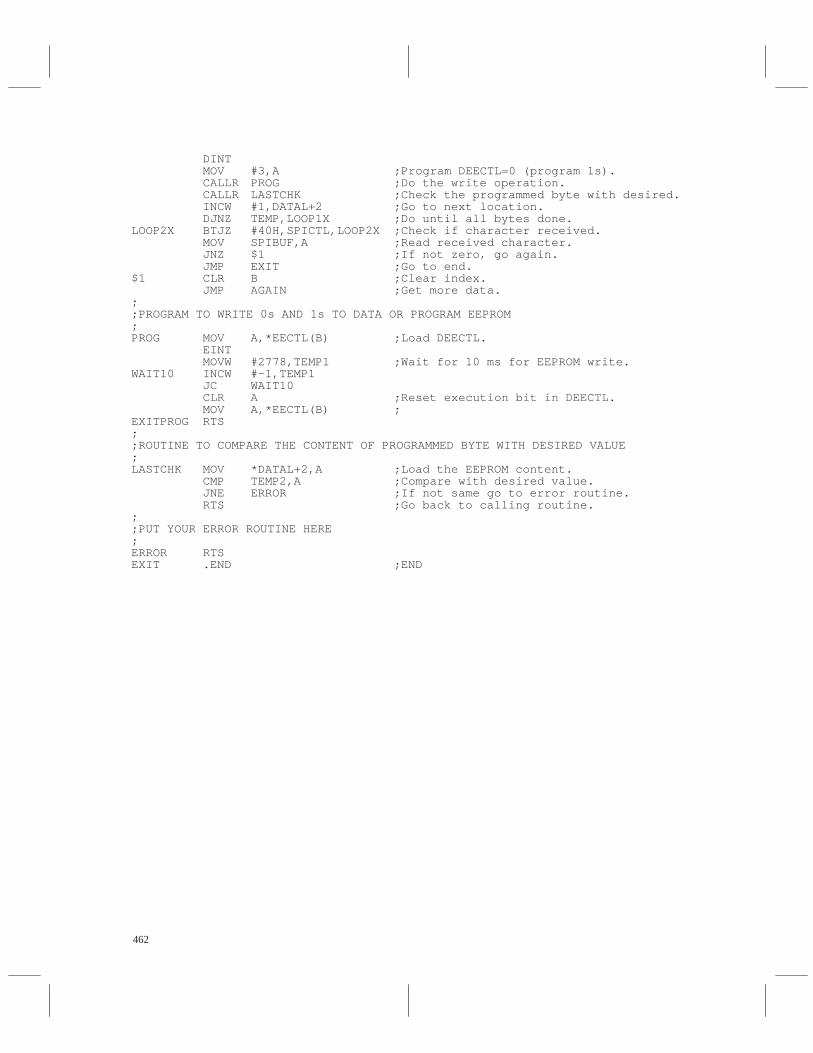
462
DINTMOV #3,A ;Program DEECTL=0 (program 1s).CALLR PROG ;Do the write operation.CALLR LASTCHK ;Check the programmed byte with desired.INCW #1,DATAL+2 ;Go to next location.DJNZ TEMP,LOOP1X ;Do until all bytes done.
LOOP2X BTJZ #40H,SPICTL,LOOP2X ;Check if character received.MOV SPIBUF,A ;Read received character.JNZ $1 ;If not zero, go again.JMP EXIT ;Go to end.
$1 CLR B ;Clear index.JMP AGAIN ;Get more data.
;;PROGRAM TO WRITE 0s AND 1s TO DATA OR PROGRAM EEPROM;PROG MOV A,*EECTL(B) ;Load DEECTL.
EINTMOVW #2778,TEMP1 ;Wait for 10 ms for EEPROM write.
WAIT10 INCW #–1,TEMP1JC WAIT10CLR A ;Reset execution bit in DEECTL.MOV A,*EECTL(B) ;
EXITPROG RTS;;ROUTINE TO COMPARE THE CONTENT OF PROGRAMMED BYTE WITH DESIRED VALUE;LASTCHK MOV *DATAL+2,A ;Load the EEPROM content.
CMP TEMP2,A ;Compare with desired value.JNE ERROR ;If not same go to error routine.RTS ;Go back to calling routine.
;;PUT YOUR ERROR ROUTINE HERE;ERROR RTSEXIT .END ;END

463
Bootstrap Program for the SPI in Slave Mode
Microcontroller Products—Semiconductor GroupTexas Instruments

464
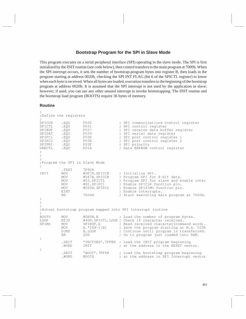
465
Bootstrap Program for the SPI in Slave Mode
This program executes on a serial peripheral interface (SPI) operating in the slave mode. The SPI is firstinitialized by the INIT routine (see code below), then control transfers to the main program at 7000h. Whenthe SPI interrupt occurs, it sets the number of bootstrap-program bytes into register B, then loads in theprogram starting at address 0020h, checking the SPI INT FLAG (bit 6 of the SPICTL register) to knowwhen each byte is received. When all bytes are loaded, execution transfers to the beginning of the bootstrapprogram at address 0020h. It is assumed that the SPI interrupt is not used by the application in slave;however, if used, you can use any other unused interrupt to invoke bootstrapping. The INIT routine andthe bootstrap load program (BOOTS) require 36 bytes of memory.
Routine
;;Define the registers;SPICCR .EQU P030 ; SPI communications control registerSPICTL .EQU P031 ; SPI control registerSPIBUF .EQU P037 ; SPI receive data buffer registerSPIDAT .EQU P039 ; SPI serial data registerSPIPC1 .EQU P03D ; SPI port control register 1SPIPC2 .EQU P03E ; SPI port control register 2SPIPRI .EQU P03F ; SPI priorityDEECTL .EQU P01A ; Data EEPROM control register;;;;Program the SPI in Slave Mode;
.TEXT 7F9CHINIT MOV #0F7H,SPICCR ; Initialize SPI.
MOV #047H,SPICCR ; Program SPI for 8-bit data.MOV #03,SPICTL ; Program SPI for slave and enable interMOV #02,SPIPC1 ; Enable SPICLK function pin.MOV #020H,SPIPC2 ; Enable SPISIMO function pin.EINT ; Enable interrupts.BR 7000H ; Start executing main program at 7000H.
;;;;Actual bootstrap program mapped into SPI interrupt routine;BOOTS MOV #0E0H,B ; Load the number of program bytes.LOOP BTJZ #40H,SPICTL,LOOP ; Check if character received.SPIRD MOV SPIBUF,A ; Read received character(command word).
MOV A,*20H–1[B] ; Save the program starting at M.A. 020hDJNZ B,LOOP ; Continue until program is transferred.BR 20H ; Go to program just loaded into RAM.
;.SECT ”VECTORS”,7FFEH ; Load the INIT program beginning.WORD INIT ; at the address in the RESET vector.
;.SECT ”BOOT”,7FF6H ; Load the bootstrap program beginning.WORD BOOTS ; at the address in SPI Interrupt vector

466

467
Bootstrap Program for the TMS370in Master
Microcontroller Products—Semiconductor GroupTexas Instruments

468
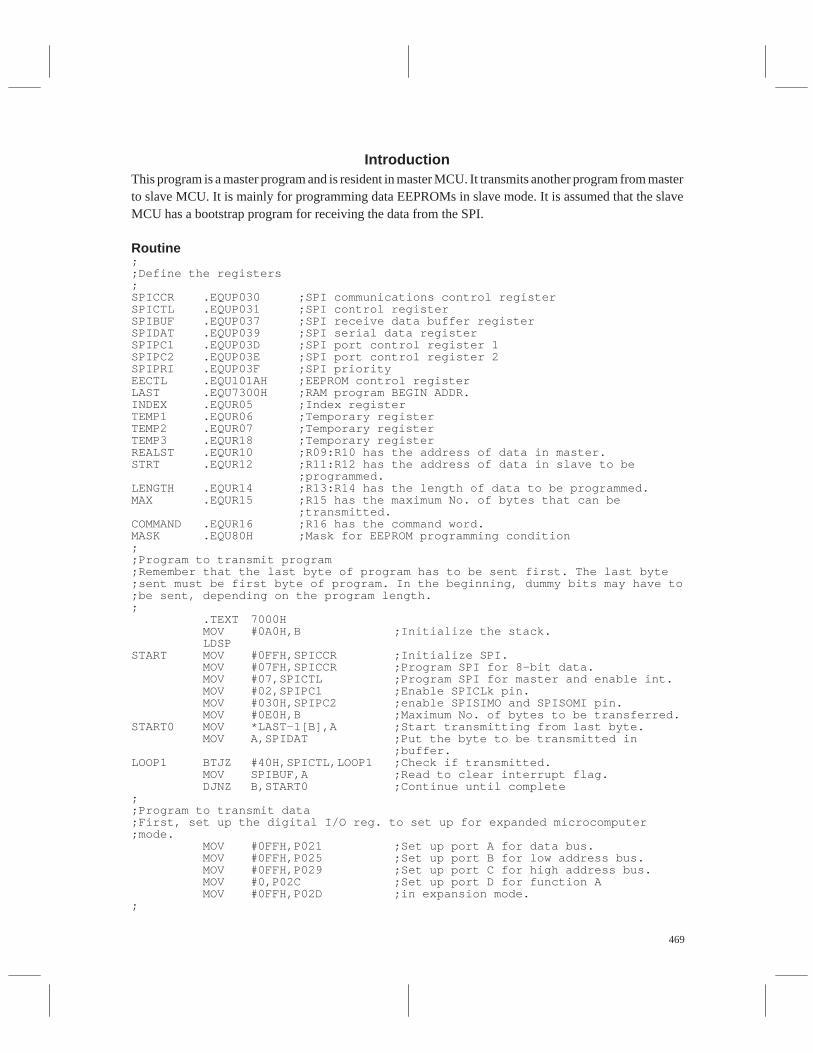
469
IntroductionThis program is a master program and is resident in master MCU. It transmits another program from masterto slave MCU. It is mainly for programming data EEPROMs in slave mode. It is assumed that the slaveMCU has a bootstrap program for receiving the data from the SPI.
Routine;;Define the registers;SPICCR .EQUP030 ;SPI communications control registerSPICTL .EQUP031 ;SPI control registerSPIBUF .EQUP037 ;SPI receive data buffer registerSPIDAT .EQUP039 ;SPI serial data registerSPIPC1 .EQUP03D ;SPI port control register 1SPIPC2 .EQUP03E ;SPI port control register 2SPIPRI .EQUP03F ;SPI priorityEECTL .EQU101AH ;EEPROM control registerLAST .EQU7300H ;RAM program BEGIN ADDR.INDEX .EQUR05 ;Index registerTEMP1 .EQUR06 ;Temporary registerTEMP2 .EQUR07 ;Temporary registerTEMP3 .EQUR18 ;Temporary registerREALST .EQUR10 ;R09:R10 has the address of data in master.STRT .EQUR12 ;R11:R12 has the address of data in slave to be
;programmed.LENGTH .EQUR14 ;R13:R14 has the length of data to be programmed.MAX .EQUR15 ;R15 has the maximum No. of bytes that can be
;transmitted.COMMAND .EQUR16 ;R16 has the command word.MASK .EQU80H ;Mask for EEPROM programming condition;;Program to transmit program;Remember that the last byte of program has to be sent first. The last byte;sent must be first byte of program. In the beginning, dummy bits may have to;be sent, depending on the program length.;
.TEXT 7000HMOV #0A0H,B ;Initialize the stack.LDSP
START MOV #0FFH,SPICCR ;Initialize SPI.MOV #07FH,SPICCR ;Program SPI for 8-bit data.MOV #07,SPICTL ;Program SPI for master and enable int.MOV #02,SPIPC1 ;Enable SPICLk pin.MOV #030H,SPIPC2 ;enable SPISIMO and SPISOMI pin.MOV #0E0H,B ;Maximum No. of bytes to be transferred.
START0 MOV *LAST–1[B],A ;Start transmitting from last byte.MOV A,SPIDAT ;Put the byte to be transmitted in
;buffer.LOOP1 BTJZ #40H,SPICTL,LOOP1 ;Check if transmitted.
MOV SPIBUF,A ;Read to clear interrupt flag.DJNZ B,START0 ;Continue until complete
;;Program to transmit data;First, set up the digital I/O reg. to set up for expanded microcomputer;mode.
MOV #0FFH,P021 ;Set up port A for data bus.MOV #0FFH,P025 ;Set up port B for low address bus.MOV #0FFH,P029 ;Set up port C for high address bus.MOV #0,P02C ;Set up port D for function AMOV #0FFH,P02D ;in expansion mode.
;
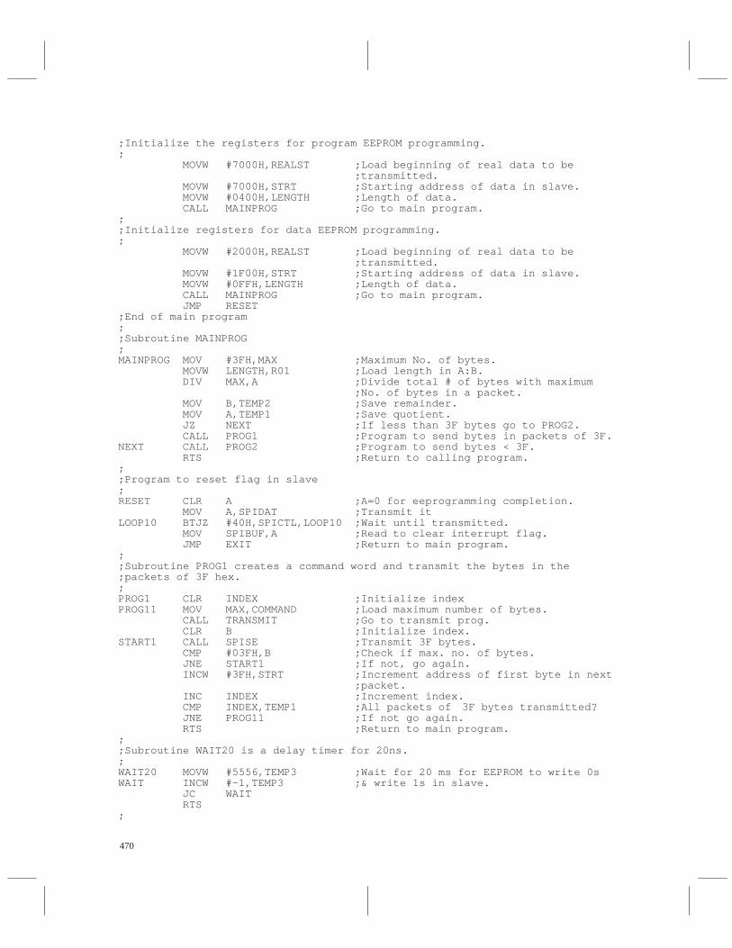
470
;Initialize the registers for program EEPROM programming.;
MOVW #7000H,REALST ;Load beginning of real data to be;transmitted.
MOVW #7000H,STRT ;Starting address of data in slave.MOVW #0400H,LENGTH ;Length of data.CALL MAINPROG ;Go to main program.
;;Initialize registers for data EEPROM programming.;
MOVW #2000H,REALST ;Load beginning of real data to be;transmitted.
MOVW #1F00H,STRT ;Starting address of data in slave.MOVW #0FFH,LENGTH ;Length of data.CALL MAINPROG ;Go to main program.JMP RESET
;End of main program;;Subroutine MAINPROG;MAINPROG MOV #3FH,MAX ;Maximum No. of bytes.
MOVW LENGTH,R01 ;Load length in A:B.DIV MAX,A ;Divide total # of bytes with maximum
;No. of bytes in a packet.MOV B,TEMP2 ;Save remainder.MOV A,TEMP1 ;Save quotient.JZ NEXT ;If less than 3F bytes go to PROG2.CALL PROG1 ;Program to send bytes in packets of 3F.
NEXT CALL PROG2 ;Program to send bytes < 3F.RTS ;Return to calling program.
;;Program to reset flag in slave;RESET CLR A ;A=0 for eeprogramming completion.
MOV A,SPIDAT ;Transmit itLOOP10 BTJZ #40H,SPICTL,LOOP10 ;Wait until transmitted.
MOV SPIBUF,A ;Read to clear interrupt flag.JMP EXIT ;Return to main program.
;;Subroutine PROG1 creates a command word and transmit the bytes in the;packets of 3F hex.;PROG1 CLR INDEX ;Initialize indexPROG11 MOV MAX,COMMAND ;Load maximum number of bytes.
CALL TRANSMIT ;Go to transmit prog.CLR B ;Initialize index.
START1 CALL SPISE ;Transmit 3F bytes.CMP #03FH,B ;Check if max. no. of bytes.JNE START1 ;If not, go again.INCW #3FH,STRT ;Increment address of first byte in next
;packet.INC INDEX ;Increment index.CMP INDEX,TEMP1 ;All packets of 3F bytes transmitted?JNE PROG11 ;If not go again.RTS ;Return to main program.
;;Subroutine WAIT20 is a delay timer for 20ns.;WAIT20 MOVW #5556,TEMP3 ;Wait for 20 ms for EEPROM to write 0sWAIT INCW #–1,TEMP3 ;& write 1s in slave.
JC WAITRTS
;
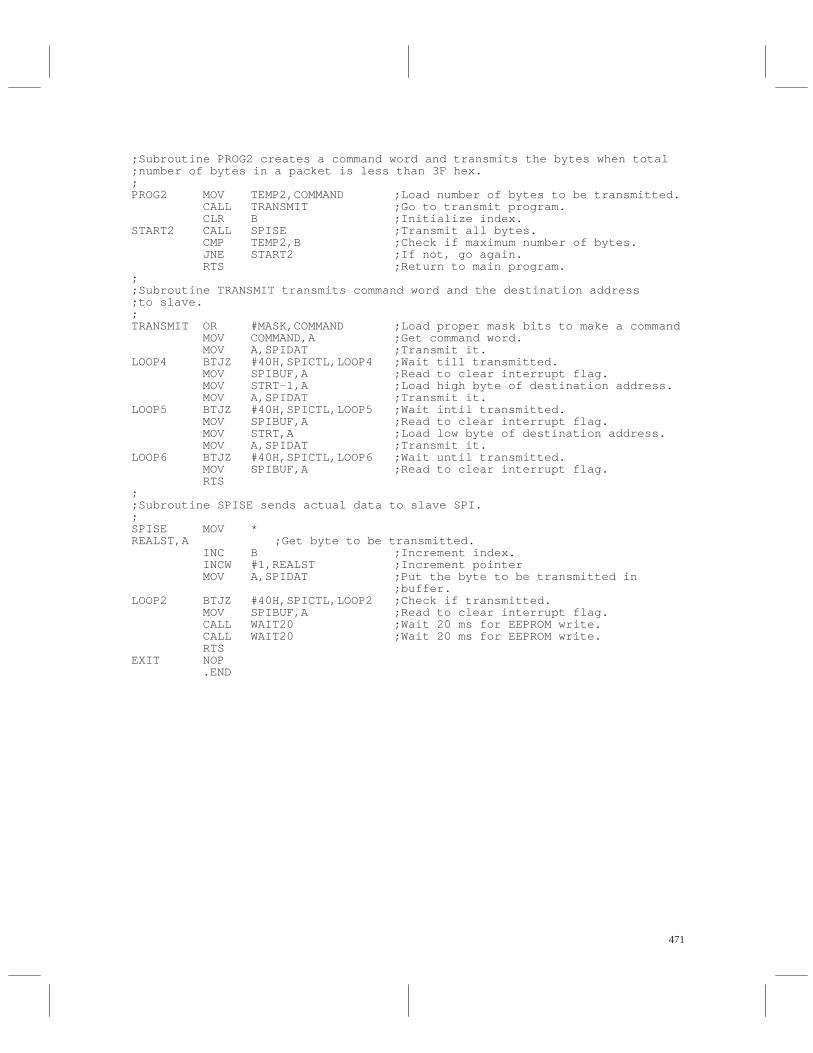
471
;Subroutine PROG2 creates a command word and transmits the bytes when total;number of bytes in a packet is less than 3F hex.;PROG2 MOV TEMP2,COMMAND ;Load number of bytes to be transmitted.
CALL TRANSMIT ;Go to transmit program.CLR B ;Initialize index.
START2 CALL SPISE ;Transmit all bytes.CMP TEMP2,B ;Check if maximum number of bytes.JNE START2 ;If not, go again.RTS ;Return to main program.
;;Subroutine TRANSMIT transmits command word and the destination address;to slave.;TRANSMIT OR #MASK,COMMAND ;Load proper mask bits to make a command
MOV COMMAND,A ;Get command word.MOV A,SPIDAT ;Transmit it.
LOOP4 BTJZ #40H,SPICTL,LOOP4 ;Wait till transmitted.MOV SPIBUF,A ;Read to clear interrupt flag.MOV STRT–1,A ;Load high byte of destination address.MOV A,SPIDAT ;Transmit it.
LOOP5 BTJZ #40H,SPICTL,LOOP5 ;Wait intil transmitted.MOV SPIBUF,A ;Read to clear interrupt flag.MOV STRT,A ;Load low byte of destination address.MOV A,SPIDAT ;Transmit it.
LOOP6 BTJZ #40H,SPICTL,LOOP6 ;Wait until transmitted.MOV SPIBUF,A ;Read to clear interrupt flag.RTS
;;Subroutine SPISE sends actual data to slave SPI.;SPISE MOV *REALST,A ;Get byte to be transmitted.
INC B ;Increment index.INCW #1,REALST ;Increment pointerMOV A,SPIDAT ;Put the byte to be transmitted in
;buffer.LOOP2 BTJZ #40H,SPICTL,LOOP2 ;Check if transmitted.
MOV SPIBUF,A ;Read to clear interrupt flag.CALL WAIT20 ;Wait 20 ms for EEPROM write.CALL WAIT20 ;Wait 20 ms for EEPROM write.RTS
EXIT NOP.END

472
473
Part VExternal Memory
Expansion Examples

474

475
Using Memory Expansion inMicrocomputer Mode With Internal
Memory Disabled
Microcontroller Products—Semiconductor GroupTexas Instruments

476

477
Introduction
This report describes special features of the digital I/O port control registers (address range 1020h to102Fh), not fully documented in the TMS370 Family User’s Guide.
These features should be taken into account when memory expansion is used in microcomputer mode toprevent any uncontrolled effect.
Special Features
In microcomputer mode, with bus expansion (function A or B) and internal program memory disabled,the internal program memory locations and 1020h to 102Fh are decoded as external addresses.
Memory accesses to the locations 1020h to 102Fh have following effect:
• Writes are executed externally as expected, but also internally (not expected). In other words,the internal I/O configuration register using the same address is also modified. This may corruptthe port pins initially set as alternate function A or B, if port control registers (XPORT2 and/orDPORT1) have changed. It may also affect those port pins which were originally configured asgeneral purpose I/Os.
• Reads are only performed from the external data bus as expected.
To prevent corrupting the bus expansion mode:
• The addresses of XPORT2 and DPORT1 should not be used as external.
• Addresses used to control general purpose I/Os should not be used as external addresses.
• Use of read-modify instructions at 102Xh locations is not available since it would read externaldata and write or modify the internal I/O configuration registers located at the same addresses.
The table below summarizes read and write functions at the locations 1020h to 102Fh in all the operatingmodes.
Table 1. Read and Write Functions
ÁÁÁÁÁÁÁÁÁÁÁÁÁÁÁÁÁÁÁÁÁ
ÁÁÁÁÁÁÁÁÁÁÁÁÁÁÁÁÁÁÁÁÁÁÁÁÁÁÁÁÁÁÁÁÁ
MicrocomputerMode
ÁÁÁÁÁÁÁÁÁÁÁÁÁÁÁÁÁÁÁÁÁÁÁÁÁÁÁÁÁÁÁÁÁ
MicroprocessorMode
ÁÁÁÁÁÁÁÁÁÁ
ÁÁÁÁÁÁÁInternal Memory
EnabledÁÁÁÁÁÁÁÁÁÁÁÁÁÁÁÁÁÁÁÁÁÁ
Internal Write & Read ÁÁÁÁÁÁÁÁÁÁÁÁÁÁÁÁÁÁÁÁÁÁ
Internal Write & Read(Internal Write has no effect on I/O’s)
ÁÁÁÁÁÁÁÁÁ
ÁÁÁÁÁÁÁÁÁÁÁÁÁÁÁÁÁÁÁÁÁ
Internal MemoryDisabled
ÁÁÁÁÁÁÁÁÁÁÁÁÁÁÁÁÁÁÁÁÁÁÁÁÁÁÁÁÁÁÁÁÁÁÁÁÁÁÁÁÁÁÁÁ
External Write & Read
Internal Write (Internal write may affect I/O’s)
ÁÁÁÁÁÁÁÁÁÁÁÁÁÁÁÁÁÁÁÁÁÁÁÁÁÁÁÁÁÁÁÁÁÁÁÁÁÁÁÁÁÁÁÁ
External Write & Read
Internal Write (Internal write has no effect on I/O’s)
ÁÁÁÁÁÁÁÁÁÁÁ
ÁÁÁÁÁÁÁÁÁÁÁÁÁÁÁÁÁÁÁÁÁÁÁÁÁÁÁÁÁ
ÁÁÁÁÁÁÁÁÁÁÁÁÁÁÁÁÁÁÁÁÁÁ
ÁÁ

478

479
Interfacing and AccessingExternal Memory
Microcontroller Products—Semiconductor GroupTexas Instruments

480

481
Microcomputer Interface Example
The following exercise is one method of interfacing the TMS370 family with common memory. The goalsof this example include the following:
• Interfacing with the maximum amount of memory
• Using the least expensive logic elements
• Using a minimum amount of parts
• Maintaining sufficient system speed
The example shown in Figure 1 illustrates a balance of these goals. In this case, the TMS370C050 is usedwith the following:
• Three TMS27C256s, each providing 32K bytes of EPROM (ROM1, ROM2, and ROM3 at U2to U4) for a total of 96K bytes
• Two HM626LP-15s, each providing 8K bytes of RAM (RAM1 and RAM2 at U6 and U7) fora total of 16K bytes
• A peripheral device (U5) needing up to 64 bytes of memory address space that interfaces to thememory-select process
This uses a total memory of 116K bytes: 112K bytes of external memory and 4K bytes of memory internalto the microcomputer. The current timings for the EPROM and RAM memory devices are given. Sincespecifications change from time to time, always check the latest data sheets for the devices used.
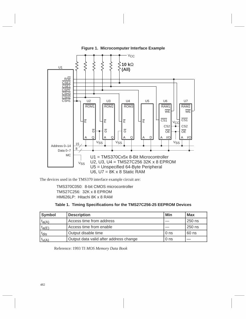
482
Figure 1. Microcomputer Interface Example
VCC
Address 0–14
Data 0–7MC
158
VSS
U1
E
VSS
G
A Q
U2
A Q
U3
E
G
VSS
A Q
U4
E
G
A D
U5
E
A I/O
U6
CS1
VSS
A I/O
U7
CS1
WE WE
OE OE
CS2 CS2VCC
10 kΩ(All)
U1 = TMS370Cx5x 8-Bit MicrocontrollerU2, U3, U4 = TMS27C256 32K x 8 EPROMU5 = Unspecified 64-Byte PeripheralU6, U7 = 8K x 8 Static RAM
R/WCSE2CSE1CSPFCSH3CSH2CSH1
ROM1 ROM2 ROM3 RAM1 RAM2
The devices used in the TMS370 interface example circuit are:
TMS370C050: 8-bit CMOS microcontrollerTMS27C256: 32K x 8 EPROMHM626LP: Hitachi 8K x 8 RAM
Table 1. Timing Specifications for the TMS27C256-25 EEPROM Devices
Symbol Description Min Max
ta(A) Access time from address — 250 ns
ta(E) Access time from enable — 250 ns
tdis Output disable time 0 ns 60 ns
tv(A) Output data valid after address change 0 ns —
Reference: 1993 TI MOS Memory Data Book
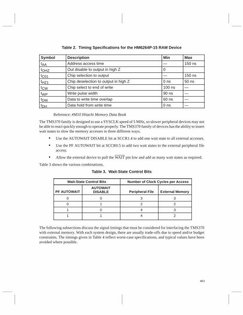
483
Table 2. Timing Specifications for the HM6264P-15 RAM Device
Symbol Description Min Max
tAA Address access time — 150 ns
tOHZ Out disable to output in high Z 0
tC01 Chip selection to output — 150 ns
tHZ1 Chip deselection to output in high Z 0 ns 50 ns
tCW Chip select to end of write 100 ns —
tWP Write pulse width 90 ns —
tDW Data to write time overlap 60 ns —
tDH Data hold from write time 0 ns —
Reference: #M10 Hitachi Memory Data Book
The TMS370 family is designed to use a SYSCLK speed of 5 MHz, so slower peripheral devices may notbe able to react quickly enough to operate properly. The TMS370 family of devices has the ability to insertwait states to slow the memory accesses in three different ways.
• Use the AUTOWAIT DISABLE bit at SCCR1.4 to add one wait state to all external accesses.
• Use the PF AUTOWAIT bit at SCCR0.5 to add two wait states to the external peripheral fileaccess.
• Allow the external device to pull the WAIT pin low and add as many wait states as required.
Table 3 shows the various combinations.
Table 3. Wait-State Control Bits
Wait-State Control Bits Number of Clock Cycles per Access
PF AUTOWAITAUTOWAITDISABLE Peripheral File External Memory
0 0 3 3
0 1 2 2
1 0 4 3
1 1 4 2
The following subsections discuss the signal timings that must be considered for interfacing the TMS370with external memory. With each system design, there are usually trade-offs due to speed and/or budgetconstraints. The timings given in Table 4 reflect worst-case specifications, and typical values have beenavoided where possible.
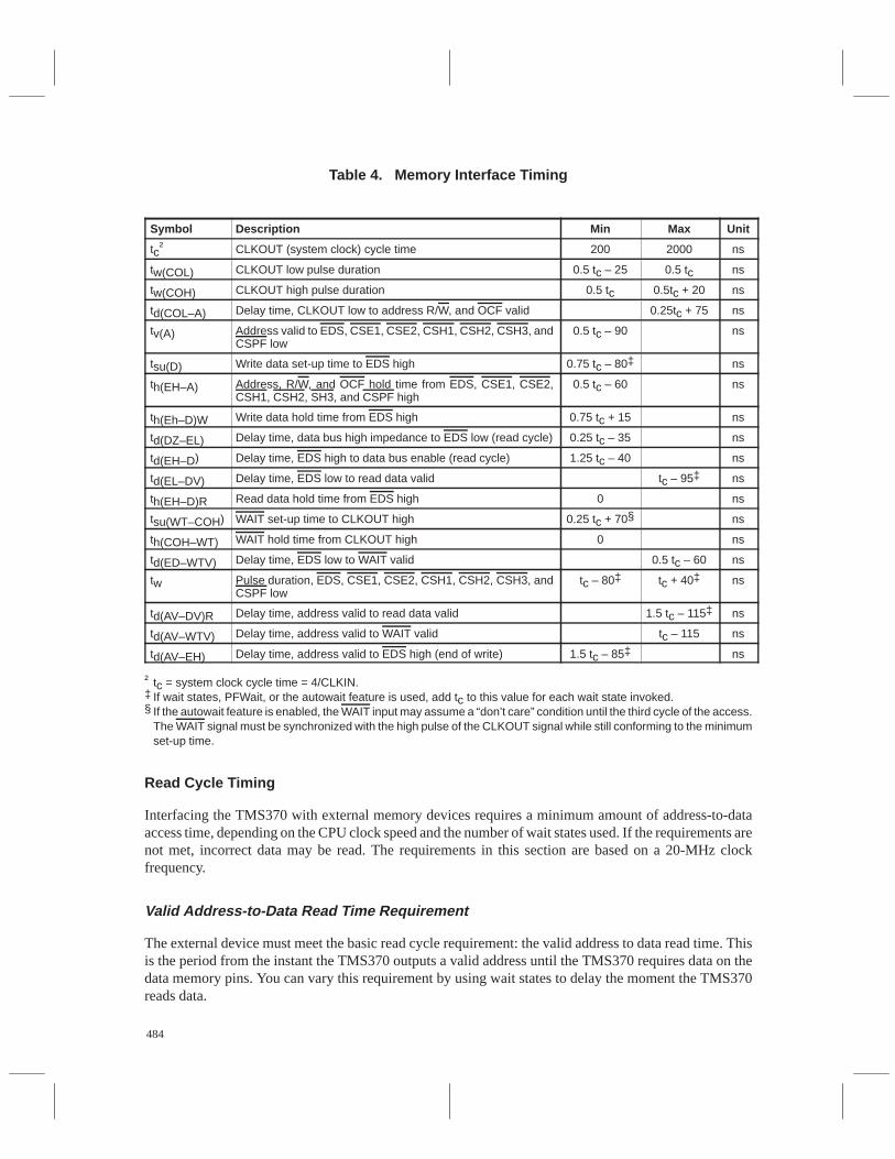
484
Table 4. Memory Interface Timing
Symbol Description Min Max Unit
tc† CLKOUT (system clock) cycle time 200 2000 ns
tw(COL) CLKOUT low pulse duration 0.5 tc – 25 0.5 tc ns
tw(COH) CLKOUT high pulse duration 0.5 tc 0.5tc + 20 ns
td(COL–A) Delay time, CLKOUT low to address R/W, and OCF valid 0.25tc + 75 ns
tv(A) Address valid to EDS, CSE1, CSE2, CSH1, CSH2, CSH3, andCSPF low
0.5 tc – 90 ns
tsu(D) Write data set-up time to EDS high 0.75 tc – 80‡ ns
th(EH–A) Address, R/W, and OCF hold time from EDS, CSE1, CSE2,CSH1, CSH2, SH3, and CSPF high
0.5 tc – 60 ns
th(Eh–D)W Write data hold time from EDS high 0.75 tc + 15 ns
td(DZ–EL) Delay time, data bus high impedance to EDS low (read cycle) 0.25 tc – 35 ns
td(EH–D) Delay time, EDS high to data bus enable (read cycle) 1.25 tc – 40 ns
td(EL–DV) Delay time, EDS low to read data valid tc – 95‡ ns
th(EH–D)R Read data hold time from EDS high 0 ns
tsu(WT–COH) WAIT set-up time to CLKOUT high 0.25 tc + 70§ ns
th(COH–WT) WAIT hold time from CLKOUT high 0 ns
td(ED–WTV) Delay time, EDS low to WAIT valid 0.5 tc – 60 ns
tw Pulse duration, EDS, CSE1, CSE2, CSH1, CSH2, CSH3, andCSPF low
tc – 80‡ tc + 40‡ ns
td(AV–DV)R Delay time, address valid to read data valid 1.5 tc – 115‡ ns
td(AV–WTV) Delay time, address valid to WAIT valid tc – 115 ns
td(AV–EH) Delay time, address valid to EDS high (end of write) 1.5 tc – 85‡ ns
† tc = system clock cycle time = 4/CLKIN.‡ If wait states, PFWait, or the autowait feature is used, add tc to this value for each wait state invoked.§ If the autowait feature is enabled, the WAIT input may assume a “don’t care” condition until the third cycle of the access.
The WAIT signal must be synchronized with the high pulse of the CLKOUT signal while still conforming to the minimumset-up time.
Read Cycle Timing
Interfacing the TMS370 with external memory devices requires a minimum amount of address-to-dataaccess time, depending on the CPU clock speed and the number of wait states used. If the requirements arenot met, incorrect data may be read. The requirements in this section are based on a 20-MHz clockfrequency.
Valid Address-to-Data Read Time Requirement
The external device must meet the basic read cycle requirement: the valid address to data read time. Thisis the period from the instant the TMS370 outputs a valid address until the TMS370 requires data on thedata memory pins. You can vary this requirement by using wait states to delay the moment the TMS370reads data.
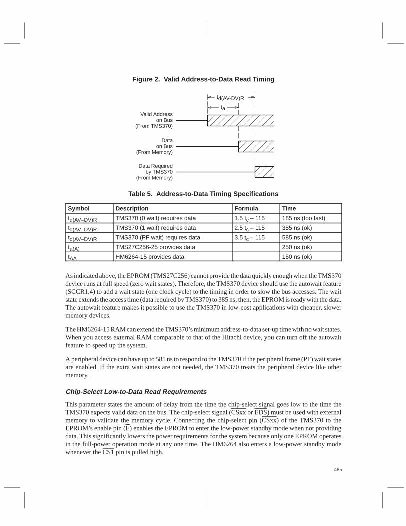
485
Figure 2. Valid Address-to-Data Read Timing
td(AV-DV)R
taValid Address
on Bus(From TMS370)
Dataon Bus
(From Memory)
Data Requiredby TMS370
(From Memory)
Table 5. Address-to-Data Timing Specifications
Symbol Description Formula Time
td(AV–DV)R TMS370 (0 wait) requires data 1.5 tc – 115 185 ns (too fast)
td(AV–DV)R TMS370 (1 wait) requires data 2.5 tc – 115 385 ns (ok)
td(AV–DV)R TMS370 (PF wait) requires data 3.5 tc – 115 585 ns (ok)
ta(A) TMS27C256-25 provides data 250 ns (ok)
tAA HM6264-15 provides data 150 ns (ok)
As indicated above, the EPROM (TMS27C256) cannot provide the data quickly enough when the TMS370device runs at full speed (zero wait states). Therefore, the TMS370 device should use the autowait feature(SCCR1.4) to add a wait state (one clock cycle) to the timing in order to slow the bus accesses. The waitstate extends the access time (data required by TMS370) to 385 ns; then, the EPROM is ready with the data.The autowait feature makes it possible to use the TMS370 in low-cost applications with cheaper, slowermemory devices.
The HM6264-15 RAM can extend the TMS370’s minimum address-to-data set-up time with no wait states.When you access external RAM comparable to that of the Hitachi device, you can turn off the autowaitfeature to speed up the system.
A peripheral device can have up to 585 ns to respond to the TMS370 if the peripheral frame (PF) wait statesare enabled. If the extra wait states are not needed, the TMS370 treats the peripheral device like othermemory.
Chip-Select Low-to-Data Read Requirements
This parameter states the amount of delay from the time the chip-select signal goes low to the time theTMS370 expects valid data on the bus. The chip-select signal (CSxx or EDS) must be used with externalmemory to validate the memory cycle. Connecting the chip-select pin (CSxx) of the TMS370 to theEPROM’s enable pin (E) enables the EPROM to enter the low-power standby mode when not providingdata. This significantly lowers the power requirements for the system because only one EPROM operatesin the full-power operation mode at any one time. The HM6264 also enters a low-power standby modewhenever the CS1 pin is pulled high.
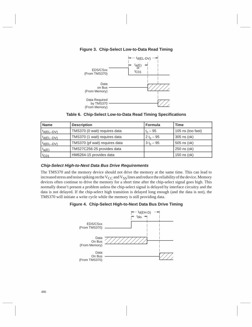
486
Figure 3. Chip-Select Low-to-Data Read Timing
td(EL-DV)
ta(E)or
tC01EDS/CSxx
(From TMS370)
Dataon Bus
(From Memory)
Data Requiredby TMS370
(From Memory)
Table 6. Chip-Select Low-to-Data Read Timing Specifications
Name Description Formula Time
td(EL–DV) TMS370 (0 wait) requires data tc – 95 105 ns (too fast)
td(EL–DV) TMS370 (1 wait) requires data 2 tc – 95 305 ns (ok)
td(EL–DV) TMS370 (pf wait) requires data 3 tc – 95 505 ns (ok)
ta(E) TMS27C256-25 provides data 250 ns (ok)
tC01 HM6264-15 provides data 150 ns (ok)
Chip-Select High-to-Next Data Bus Drive Requirements
The TMS370 and the memory device should not drive the memory at the same time. This can lead toincreased stress and noise spiking on the VCC and VSS lines and reduce the reliability of the device. Memorydevices often continue to drive the memory for a short time after the chip-select signal goes high. Thisnormally doesn’t present a problem unless the chip-select signal is delayed by interface circuitry and thedata is not delayed. If the chip-select high transition is delayed long enough (and the data is not), theTMS370 will initiate a write cycle while the memory is still providing data.
Figure 4. Chip-Select High-to-Next Data Bus Drive Timing
td(EH-D)tdis
EDS/CSxx(From TMS370)
DataOn Bus
(From Memory)
DataOn Bus
(From TMS370)
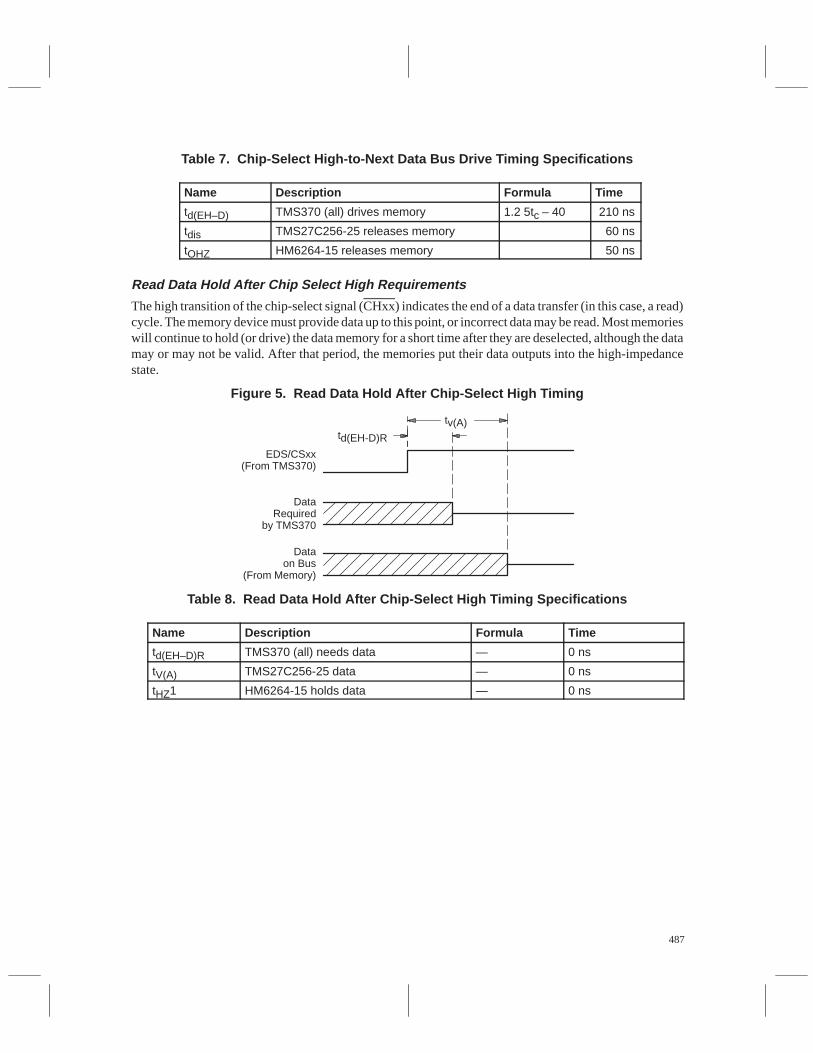
487
Table 7. Chip-Select High-to-Next Data Bus Drive Timing Specifications
Name Description Formula Time
td(EH–D) TMS370 (all) drives memory 1.2 5tc – 40 210 ns
tdis TMS27C256-25 releases memory 60 ns
tOHZ HM6264-15 releases memory 50 ns
Read Data Hold After Chip Select High Requirements
The high transition of the chip-select signal (CHxx) indicates the end of a data transfer (in this case, a read)cycle. The memory device must provide data up to this point, or incorrect data may be read. Most memorieswill continue to hold (or drive) the data memory for a short time after they are deselected, although the datamay or may not be valid. After that period, the memories put their data outputs into the high-impedancestate.
Figure 5. Read Data Hold After Chip-Select High Timing
tv(A)td(EH-D)R
EDS/CSxx(From TMS370)
DataRequired
by TMS370
Dataon Bus
(From Memory)
Table 8. Read Data Hold After Chip-Select High Timing Specifications
Name Description Formula Time
td(EH–D)R TMS370 (all) needs data — 0 ns
tV(A) TMS27C256-25 data — 0 ns
tHZ1 HM6264-15 holds data — 0 ns
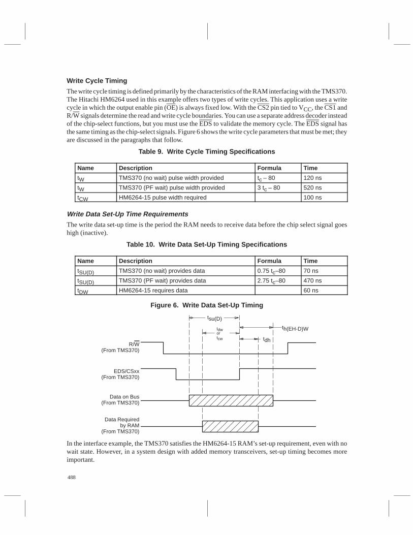
488
Write Cycle Timing
The write cycle timing is defined primarily by the characteristics of the RAM interfacing with the TMS370.The Hitachi HM6264 used in this example offers two types of write cycles. This application uses a writecycle in which the output enable pin (OE) is always fixed low. With the CS2 pin tied to VCC, the CS1 andR/W signals determine the read and write cycle boundaries. You can use a separate address decoder insteadof the chip-select functions, but you must use the EDS to validate the memory cycle. The EDS signal hasthe same timing as the chip-select signals. Figure 6 shows the write cycle parameters that must be met; theyare discussed in the paragraphs that follow.
Table 9. Write Cycle Timing Specifications
Name Description Formula Time
tW TMS370 (no wait) pulse width provided tc – 80 120 ns
tW TMS370 (PF wait) pulse width provided 3 tc – 80 520 ns
tCW HM6264-15 pulse width required 100 ns
Write Data Set-Up Time Requirements
The write data set-up time is the period the RAM needs to receive data before the chip select signal goeshigh (inactive).
Table 10. Write Data Set-Up Timing Specifications
Name Description Formula Time
tSU(D) TMS370 (no wait) provides data 0.75 tc–80 70 ns
tSU(D) TMS370 (PF wait) provides data 2.75 tc–80 470 ns
tDW HM6264-15 requires data 60 ns
Figure 6. Write Data Set-Up Timing
tsu(D)
th(EH-D)W
tdh
tdwortcw
R/W(From TMS370)
EDS/CSxx(From TMS370)
Data Requiredby RAM
(From TMS370)
Data on Bus(From TMS370)
In the interface example, the TMS370 satisfies the HM6264-15 RAM’s set-up requirement, even with nowait state. However, in a system design with added memory transceivers, set-up timing becomes moreimportant.
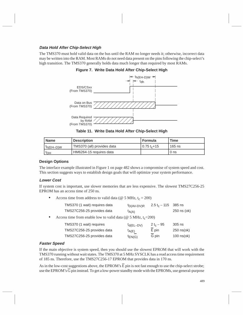
489
Data Hold After Chip-Select HighThe TMS370 must hold valid data on the bus until the RAM no longer needs it; otherwise, incorrect datamay be written into the RAM. Most RAMs do not need data present on the pins following the chip-select’shigh transition. The TMS370 generally holds data much longer than required by most RAMs.
Figure 7. Write Data Hold After Chip-Select High
th(EH-D)Wtdh
EDS/CSxx(From TMS370)
Data Requiredby RAM
(From TMS370)
Data on Bus(From TMS370)
Table 11. Write Data Hold After Chip-Select High
Name Description Formula Time
th(EH–D)W TMS370 (all) provides data 0.75 tc+15 165 ns
tDH HM6264-15 requires data 0 ns
Design Options
The interface example illustrated in Figure 1 on page 482 shows a compromise of system speed and cost.This section suggests ways to establish design goals that will optimize your system performance.
Lower CostIf system cost is important, use slower memories that are less expensive. The slowest TMS27C256-25EPROM has an access time of 250 ns.
• Access time from address to valid data (@ 5 MHz, tc = 200)
TMS370 (1 wait) requires data tD(AV-DV)R 2.5 tc – 115 385 ns
TMS27C256-25 provides data tA(A) 250 ns (ok)
• Access time from enable low to valid data (@ 5 MHz, tc=200)
TMS370 (1 wait) requires td(EL–DV) 2 tc – 95 305 ns
TMS27C256-25 provides data tA(E) E pin 250 ns(ok)
TMS27C256-25 provides data tEN(G) G pin 100 ns(ok)
Faster SpeedIf the main objective is system speed, then you should use the slowest EPROM that will work with theTMS370 running without wait states. The TMS370 at 5 MHz SYSCLK has a read access time requirementof 185 ns. Therefore, use the TMS27C256-17 EPROM that provides data in 170 ns.
As in the low-cost suggestions above, the EPROM’s E pin is not fast enough to use the chip-select strobe;use the EPROM’s G pin instead. To get a low-power standby mode with the EPROMs, use general-purpose
490
output lines from the TMS370 to the EPROM’s E pin. The pins should be software enabled before theEPROM’s program is entered.
• Access time from address to valid data:
TMS370 (no wait) requires data tD(AV–DV)R 1.5 tc – 115 185 ns
TMS27C256-17 provides data tA(A) 170 ns (ok)
• Access time from enable low to valid data:
TMS370 (no wait) requires tD(EL–DV) tc – 95 105 ns
TMS27C256-17 provides data tA(E) E pin 170 ns (not ok)
TMS27C256-17 provides data tEN(G) G pin 75 ns (ok)
Bank Switching Examples
The programs in this section show how memory bank switching can be used by the circuit in Figure 1 (page482). Memory bank switching allows two or more memory devices to share the same addresses. Theprogrammable chip-select signals (CSHx, CSEx, and CSPF) enable the memory devices or banks one ata time during a read or write cycle. Figure 8 and Table 12 define the registers and their addresses used inthese examples.
In the interface example in Figure 1 (page 482), the three EPROM devices (ROM1 – ROM3) each useaddresses 8000h though FFFFh. Only one EPROM device (or bank), selected by CSH1, CSH2, or CSH3,can be allowed to read data at a single time. The two RAM devices are each mapped at addresses 2000hthrough 3FFFh. The write and read cycles affect one RAM device at a time, as determined by the chip-selectsignals CSE1 and CSE2. The CSPF signal controls the peripheral memory device, which, in our example,is unspecified but defined to contain 64 bytes of memory. This device is mapped at addresses 10C0hthrough 10FFh.
To use external memory, devices with memory expansion must be configured for the microcomputer modeso that the chip-select signals are available. The external memory devices must have 3-state outputsbecause these devices share the data bus.
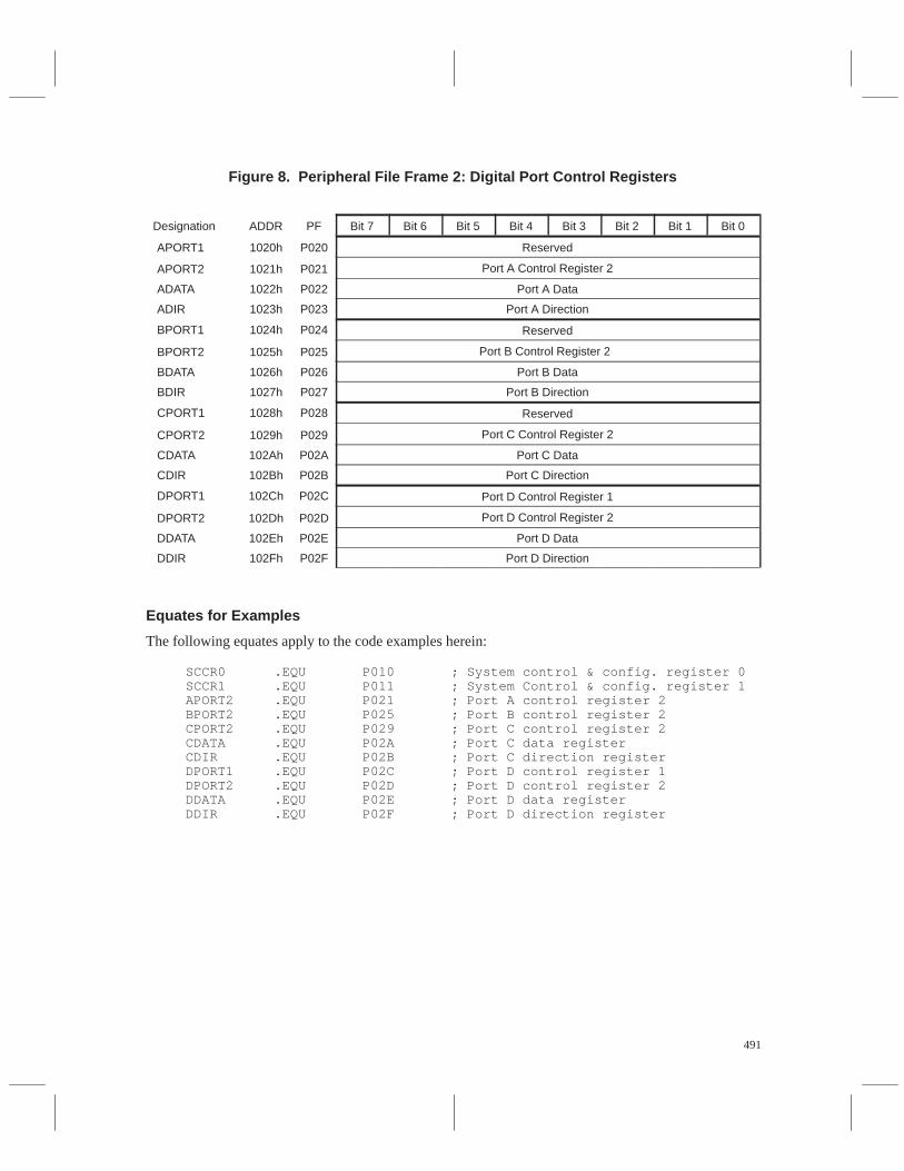
491
Figure 8. Peripheral File Frame 2: Digital Port Control Registers
Designation ADDR PF Bit 7 Bit 6 Bit 5 Bit 4 Bit 3 Bit 2 Bit 1 Bit 0
APORT1 1020h P020 Reserved
APORT2 1021h P021 Port A Control Register 2
ADATA 1022h P022 Port A Data
ADIR 1023h P023 Port A Direction
BPORT1 1024h P024 Reserved
BPORT2 1025h P025 Port B Control Register 2
BDATA 1026h P026 Port B Data
BDIR 1027h P027 Port B Direction
CPORT1 1028h P028 Reserved
CPORT2 1029h P029 Port C Control Register 2
CDATA 102Ah P02A Port C Data
CDIR 102Bh P02B Port C Direction
DPORT1 102Ch P02C Port D Control Register 1
DPORT2 102Dh P02D Port D Control Register 2
DDATA 102Eh P02E Port D Data
DDIR 102Fh P02F Port D Direction
Equates for Examples
The following equates apply to the code examples herein:
SCCR0 .EQU P010 ; System control & config. register 0SCCR1 .EQU P011 ; System Control & config. register 1APORT2 .EQU P021 ; Port A control register 2BPORT2 .EQU P025 ; Port B control register 2CPORT2 .EQU P029 ; Port C control register 2CDATA .EQU P02A ; Port C data registerCDIR .EQU P02B ; Port C direction registerDPORT1 .EQU P02C ; Port D control register 1DPORT2 .EQU P02D ; Port D control register 2DDATA .EQU P02E ; Port D data registerDDIR .EQU P02F ; Port D direction register
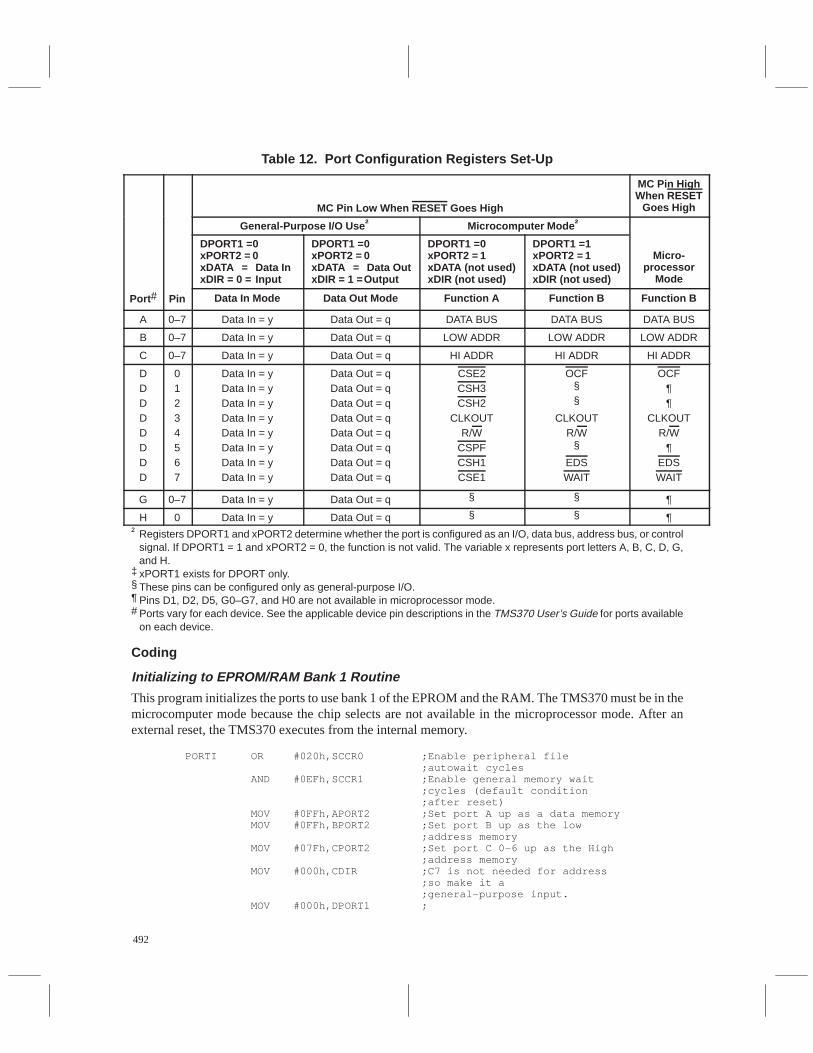
492
Table 12. Port Configuration Registers Set-Up
MC Pin Low When RESET Goes High
MC Pin HighWhen RESET
Goes High
#
General-Purpose I/O Use † Microcomputer Mode †
#
DPORT1 =0xPORT2 = 0xDATA = Data InxDIR = 0 = Input
DPORT1 =0xPORT2 = 0xDATA = Data OutxDIR = 1 =Output
DPORT1 =0xPORT2 = 1xDATA (not used)xDIR (not used)
DPORT1 =1xPORT2 = 1xDATA (not used)xDIR (not used)
Micro-processor
Mode
Port # Pin Data In Mode Data Out Mode Function A Function B Function B
A 0–7 Data In = y Data Out = q DATA BUS DATA BUS DATA BUS
B 0–7 Data In = y Data Out = q LOW ADDR LOW ADDR LOW ADDR
C 0–7 Data In = y Data Out = q HI ADDR HI ADDR HI ADDR
DDDDDDDD
01234567
Data In = yData In = yData In = yData In = yData In = yData In = yData In = yData In = y
Data Out = qData Out = qData Out = qData Out = qData Out = qData Out = qData Out = qData Out = q
CSE2CSH3CSH2
CLKOUTR/W
CSPFCSH1CSE1
OCF§§
CLKOUTR/W
§
EDSWAIT
OCF¶¶
CLKOUTR/W
¶EDSWAIT
G 0–7 Data In = y Data Out = q § § ¶
H 0 Data In = y Data Out = q § § ¶† Registers DPORT1 and xPORT2 determine whether the port is configured as an I/O, data bus, address bus, or control
signal. If DPORT1 = 1 and xPORT2 = 0, the function is not valid. The variable x represents port letters A, B, C, D, G,and H.
‡ xPORT1 exists for DPORT only.§ These pins can be configured only as general-purpose I/O.¶ Pins D1, D2, D5, G0–G7, and H0 are not available in microprocessor mode.# Ports vary for each device. See the applicable device pin descriptions in the TMS370 User’s Guide for ports available
on each device.
Coding
Initializing to EPROM/RAM Bank 1 Routine
This program initializes the ports to use bank 1 of the EPROM and the RAM. The TMS370 must be in themicrocomputer mode because the chip selects are not available in the microprocessor mode. After anexternal reset, the TMS370 executes from the internal memory.
PORTI OR #020h,SCCR0 ;Enable peripheral file;autowait cycles
AND #0EFh,SCCR1 ;Enable general memory wait;cycles (default condition;after reset)
MOV #0FFh,APORT2 ;Set port A up as a data memoryMOV #0FFh,BPORT2 ;Set port B up as the low
;address memoryMOV #07Fh,CPORT2 ;Set port C 0–6 up as the High
;address memoryMOV #000h,CDIR ;C7 is not needed for address
;so make it a;general-purpose input.
MOV #000h,DPORT1 ;
493
MOV #0E7h,P02E ;Set all CSxx to 1 when CSxx;are outputs
MOV #0D0h,DPORT2 ;Enable CSH1, CSE1, and;R/W functions.
MOV #0E7h,P02F ;Turn all chip selects to outputs.;Pull-up resistors are important;for power-up since CSxx are high-;impedance floating inputs.
Changing to EPROM Bank 2 Routine
This program illustrates how to change the EPROM bank without affecting the RAM banks. In thisexample, the program runs out of internal memory, disables all EPROM banks, and then enables EPROMbank 2. For this reason, the program must not reside in an EPROM. In order to verify that EPROM bank2 exists within the system, the program could test various EPROM bank 2 memory locations beforeexecuting the branch instruction.
AND #0B9h,DPORT2 ;Disable all EPROM banks (cannot;be done while executing from EPROMbanks.)
OR #004h,DPORT2 ;Enable EPROM bank 2. When turned off,;pin outputs a 1 because of the
BR ROM2 ;initial set–up above, could be done;in 1 instruction if conditions of;other chip selects were known.
Changing to EPROM Bank 3 and RAM Bank 2 Routine
This routine provides switching from one EPROM bank to another while operating from an EPROM bank.Only one instruction in EPROM bank 2 is needed. The code within the EPROM banks must besynchronized, and the instruction at the address after the move instruction must be a valid instruction withinthe new EPROM bank.
GOROM3 MOV #003h,DPORT2 ;Enable ROM bank 3 and RAM bank 2.ROM3 ;This address must be the same
;as the beginning routine address;in bank 3 if executing from EPROM.
Changing RAM Banks Routine
This method demonstrates how to change RAM banks without affecting the execution from the currentEPROM bank. The RAM banks are selected and deselected in the same manner as the EPROM banks.When you change RAM or EPROM banks, the software must ensure that only one bank is selected at a time.This example disables the CSE1 and CSE2 signals and enables the CSE2 signal.
AND #07Eh,DPORT2 ;Turn off all RAM banks (execute;from EPROM or on chip)
OR #001h,DPORT2 ;Turn on RAM bank 2. When turned off,;pin outputs a 1 because of the;initial set-up above.

494
495
Read/Write Serial EEPROM Data onthe TMS370
Microcontroller Products—Semiconductor GroupTexas Instruments

496

497
Introduction
This routine reads and writes to the EEPROM, computes the checksum on the first seven bytes of data andplaces the checksum in the eighth byte. These are conditions for the read/write serial EEPROM dataroutine:
1. The delay timing is based on a 5 MHz SYSCLK.
2. This routine works with National or XICOR 64 × 4 devices.
3. Data is arranged as seven 8-bit bytes, plus an 8-bit checksum (last byte).
4. The last byte contains the checksum.
5. I/O port assignments:
• D0 is the clock output
• D1 is the select output
• D2 is the read data input
• D3 is the write data output
498
Read/Write Serial EEPROM Data Routine;REGISTER FILE EQUATES;EEPROM .EQU R010 ;8 BYTES OF EEPROM DATAEEPFLG .EQU R018 ;EEPROM FLAGS;; PERIPHERAL FILE EQUATES;DPORT .EQU P02E ;I/O PORTDDR .EQU P02F ;DATA DIRECTION REGISTER;––––––––––––––––––––––––––––––––––––––––––––––––––––––––––––––––––––––––;READ EEPROM;RDEEP CALL SELEEP ;STROBE OUT 0s TO EEPROM
MOV #64,B ;64 MORE THAN ENOUGHRDEEP5 CALL CLKZRO
DJNZ B,RDEEP5CALL DESEEPMOV #10001010b,A ;STROBE OUT A COMBINATION.CALL NATINS ;XICOR RECALL, NATIONAL READ COMMANDCLR EEPFLGBTJZ #00000100b,DPORT,RDEEP1 ;BRANCH IF NATIONAL PART.OR #00000001b,EEPFLG ;XICOR PARTCALL DESEEP ;DESELECT EEPROM.MOV #10000110b,A ;READ RAM 0.CALL RDXICMOV #10001110b,A ;READ RAM 1.CALL RDXICMOV #10010110b,A ;READ RAM 2.CALL RDXICMOV #10011110b,A ;READ RAM 3.CALL RDXICMOV #10000010b,A ;ENTER SLEEP MODE.CALL XICINSCALL DESEEP ;DESELECT EEPROM.JMP RDEEP2 ;DO COMMON EEPROM PROCESSING.
RDEEP1 CALL DESEEPMOV #10000000b,A ;READ RAM 0.CALL RDNATMOV #10000001b,A ;READ RAM 1.CALL RDNATMOV #10000010b,A ;READ RAM 2.CALL RDNATMOV #10000011b,A ;READ RAM 3.CALL RDNAT
RDEEP2 CALL CMPCHK ;COMPUTE CHECKSUM.CMP EEPROM+7,A ;= EEPROM CHECKSUM?JNZ RDEEP3 ;NOOR #00000010b,EEPFLG ;YES, SET EEPROM VALID FLAG.RTS
RDEEP3 AND #11111101b,EEPFLG ;CLEAR EEPROM VALID FLAG.RTS
;;CLOCK NATIONAL READ INSTUCTION, THEN READ IN DATA;RDNAT CALL NATINS
CALL CLKZROJMP RDDAT
;;CLOCK XICOR READ INSTRUCTION, THEN READ IN DATA;;READ 16 BITS;
499
RDXIC CALL XICINSRDDAT MOV #16,BRDDAT1 BTJZ #00000100b,DPORT,RDDAT2
SETCRDDAT2 CALL SHFTNV
CALL CLKZRODJNZ B,RDDAT1BR DESEEP ;DESELECT EEPROM & RETURN.
;;WRITE EEPROM;;THIS ROUTINE COMPUTES THE CHECKSUM ON THE FIRST 7 BYTES OF;EEPROM AND PLACES THAT IN THE 8TH BYTE. THE 8 BYTES ARE THEN;WRITTEN TO EEPROM LOCATIONS 0–3.;WTEEP CALL CMPCHK ;COMPUTE THE CHECKSUM.
MOV A,EEPROM+7 ;PLACE IN EEPROM.BTJZ #00000001b,EEPFLG,WTEEP1 ;BRANCH IF NATIONAL.MOV #10000101b,A ;XICOR, RECALL.CALL XICINSCALL DESEEPMOV #10000100b,A ;SET WRITE ENABLE LATCH.CALL XICINSCALL DESEEPMOV #10000011b,A ;WRITE RAM 0.CALL WTXICMOV #10001011b,A ;WRITE RAM 1.CALL WTXICMOV #10010011b,A ;WRITE RAM 2.CALL WTXICMOV #10011011b,A ;WRITE RAM 3.CALL WTXICMOV #10000001b,A ;STORE RAM DATA INTO E2PROM.CALL XICINSCALL DL10MS ;WAIT 10 MILLISECONDS.JMP WTEEP2
WTEEP1 MOV #00110000b,A ;ERASE/WRITE ENABLE.CALL NATINSCALL DESEEPMOV #00100000b,A ;ERASE E2PROM.CALL NATINSCALL DESEEPCALL DL30MS ;DESELECT FOR 30 MILLISECONDS.MOV #01000000b,A ;WRITE RAM 0.CALL WTNATMOV #01000001b,A ;WRITE RAM 1.CALL WTNATMOV #01000010b,A ;WRITE RAM 2.CALL WTNATMOV #01000011b,A ;WRITE RAM 3.CALL WTNATMOV #00000000b,A ;ERASE/WRITE DISABLE.CALL NATINS
WTEEP2 JMP DESEEP;;COMPUTE CHECKSUM ON FIRST 7 BYTES OF EEPROM;CMPCHK MOV EEPROM,A ;COMPUTE EEPROM CHKSUM.
ADD EEPROM+1,AADD EEPROM+2,AADD EEPROM+3,AADD EEPROM+4,AADD EEPROM+5,A
500
ADD EEPROM+6,ARTS
;;WRITE INSTUCTION TO NATIONAL PART, THEN SEND DATA, DELAY;WTNAT CALL NATINS
CALL WTDATCALL DESEEPCALL DL30MS ;DESELECT FOR 30 MILLISECONDS.CALL SELEEPJMP DESEEP
;DL30MS CALL DL10MS ;30 MILLISECOND DELAY
CALL DL10MSDL10MS MOV #2,A ;10 MILLISECOND DELAY
CLR BDL10M1 DJNZ B,DL10M1
DJNZ A,DL10M1RTS
;;WRITE INSTRUCTION TO XICOR PART, THEN SEND DATA;WTXIC CALL XICINS
CALL WTDATJMP DESEEP
;;SEND 16 BITS OF DATA TO EEPROM;WTDAT MOV #16,BWTDAT1 CALL SHFTNV
JC WTDAT2CALL CLKZROJMP WTDAT3
;WTDAT2 CALL CLKONEWTDAT3 DJNZ B,WTDAT1
JMP DESEEP;;SEND INSTRUCTION TO EEPROM FROM ’A’;;NATINS FOR NATIONAL, XICINS FOR XICOR;NATINS CALL SELEEP
CALL CLKONEJMP INS1
;XICINS CALL SELEEPINS1 MOV #8,BINS2 RLC A
JC INS3CALL CLKZROJMP INS4
;INS3 CALL CLKONEINS4 DJNZ B,INS2 ;NEXT BIT OF INSTRUCTION
RTS;;CLOCK A ONE BIT TO EEPROM;CLKONE OR #00000001b,DPORT
JMP CLKEEP;;SELECT EEPROM
501
;SELEEP OR #00000010b,DPORT
JMP CLKZRO;;DESELECT EEPROM;DESEEP AND #11111101b,DPORT;;CLOCK A ZERO BIT TO EEPROM;CLKZRO AND #11111110b,DPORTCLKEEP OR #00001000b,DPORT
AND #11110111b,DPORTRTS
;;SHIFT EEPROM DATA LEFT 1 BIT;;LEAVES BIT SHIFTED OUT IN CARRY, SHIFTS CARRY VALUE ON CALL INTO;LAST BIT OF EEPROM;SHFTNV .EQU $
RLC EEPROM+7RLC EEPROM+6RLC EEPROM+5RLC EEPROM+4RLC EEPROM+3RLC EEPROM+2RLC EEPROM+1RLC EEPROMRTS.END

502

503
Part VISpecific System
Application Design AidsPart VI contains two sections:
EMI Reduction 503. . . . . . . . . . . . . . . . . . . . . .
Cost Effective Input Protection Circuitry for the Texas Instruments TMS370 Family of Microcontrollers 525. . . . . .

504
505
PCB Design Guidelines forReduced EMI
Robert DeMoorMicrocontroller Products—Semiconductor Group
Texas Instruments

506

507
Overview
Electromagnetic interference (EMI) often seems like a mysterious phenomenon. EMI can be difficult tocontrol, and even the results of EMI testing can vary from day to day and from test facility to test facility.The act of controlling EMI has been called black magic or voodoo. However, EMI has been researched formany years, and guidelines have been established that can improve the electromagnetic compatibility(EMC) of systems to which they are applied.
Designing for low EMI from the start of a project results in much easier and less expensive solutions thanattempting to fix EMI problems after a design has reached the testing phase of development. Consequently,following a few guidelines for printed circuit board (PCB) design at the beginning of a project can help tominimize the system’s EMI while adding little or no cost to the system.
Background and Theory
Knowledge and understanding of a few fundamental concepts can be exercised toward the design of anelectronic system in order to improve electromagnetic compatibility (EMC) performance.
EMI Sources, Paths, and Receivers
EMI requires a source, a path, and a receiver. In today’s electronics, clocked CMOS integrated circuits oftensupply the source. The printed circuit board (PCB) and its associated cabling and wire harness, acts as theconductive and radiating part of the path, otherwise called the antenna.
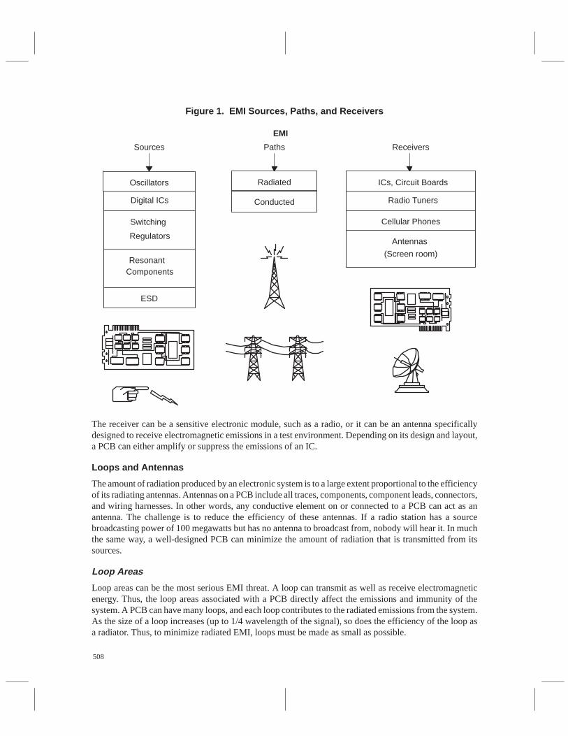
508
Figure 1. EMI Sources, Paths, and Receivers
EMI
Oscillators
Switching
Resonant
ESD
Radiated
Conducted
Cellular Phones
Antennas
(Screen room)
Sources Paths Receivers
ICs, Circuit Boards
Radio Tuners
Components
Regulators
Digital ICs
The receiver can be a sensitive electronic module, such as a radio, or it can be an antenna specificallydesigned to receive electromagnetic emissions in a test environment. Depending on its design and layout,a PCB can either amplify or suppress the emissions of an IC.
Loops and Antennas
The amount of radiation produced by an electronic system is to a large extent proportional to the efficiencyof its radiating antennas. Antennas on a PCB include all traces, components, component leads, connectors,and wiring harnesses. In other words, any conductive element on or connected to a PCB can act as anantenna. The challenge is to reduce the efficiency of these antennas. If a radio station has a sourcebroadcasting power of 100 megawatts but has no antenna to broadcast from, nobody will hear it. In muchthe same way, a well-designed PCB can minimize the amount of radiation that is transmitted from itssources.
Loop Areas
Loop areas can be the most serious EMI threat. A loop can transmit as well as receive electromagneticenergy. Thus, the loop areas associated with a PCB directly affect the emissions and immunity of thesystem. A PCB can have many loops, and each loop contributes to the radiated emissions from the system.As the size of a loop increases (up to 1/4 wavelength of the signal), so does the efficiency of the loop asa radiator. Thus, to minimize radiated EMI, loops must be made as small as possible.
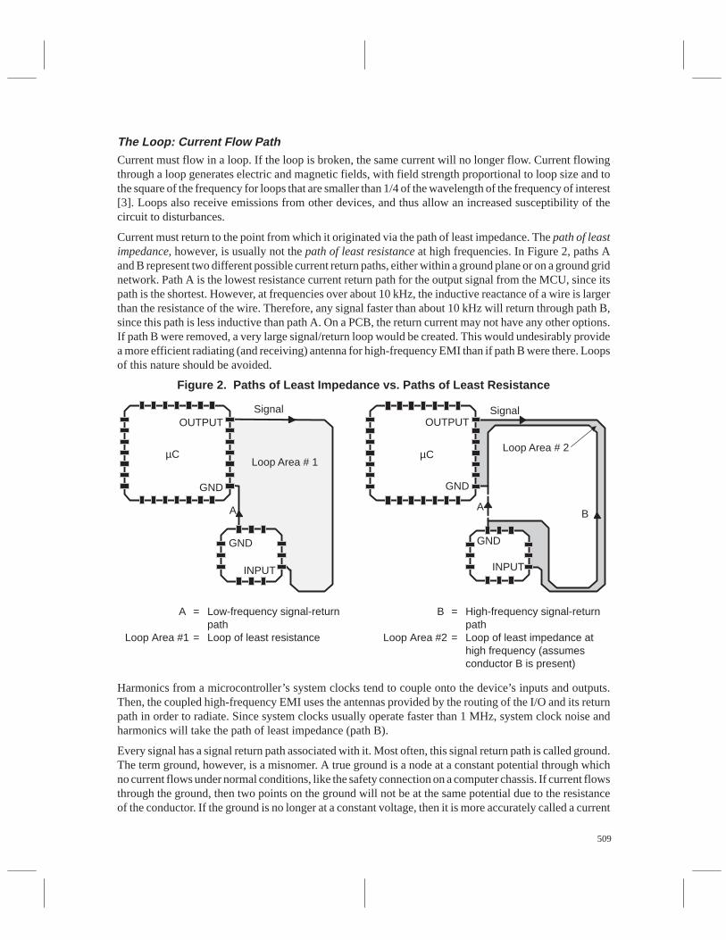
509
The Loop: Current Flow PathCurrent must flow in a loop. If the loop is broken, the same current will no longer flow. Current flowingthrough a loop generates electric and magnetic fields, with field strength proportional to loop size and tothe square of the frequency for loops that are smaller than 1/4 of the wavelength of the frequency of interest[3]. Loops also receive emissions from other devices, and thus allow an increased susceptibility of thecircuit to disturbances.
Current must return to the point from which it originated via the path of least impedance. The path of leastimpedance, however, is usually not the path of least resistance at high frequencies. In Figure 2, paths Aand B represent two different possible current return paths, either within a ground plane or on a ground gridnetwork. Path A is the lowest resistance current return path for the output signal from the MCU, since itspath is the shortest. However, at frequencies over about 10 kHz, the inductive reactance of a wire is largerthan the resistance of the wire. Therefore, any signal faster than about 10 kHz will return through path B,since this path is less inductive than path A. On a PCB, the return current may not have any other options.If path B were removed, a very large signal/return loop would be created. This would undesirably providea more efficient radiating (and receiving) antenna for high-frequency EMI than if path B were there. Loopsof this nature should be avoided.
Figure 2. Paths of Least Impedance vs. Paths of Least Resistance
GND
OUTPUT
GND
INPUT
A
Loop Area # 1
GND
OUTPUT
GND
INPUT
B
Loop Area # 2
A
Signal Signal
µC µC
A = Low-frequency signal-returnpath
Loop Area #1 = Loop of least resistance
B = High-frequency signal-returnpath
Loop Area #2 = Loop of least impedance athigh frequency (assumesconductor B is present)
Harmonics from a microcontroller’s system clocks tend to couple onto the device’s inputs and outputs.Then, the coupled high-frequency EMI uses the antennas provided by the routing of the I/O and its returnpath in order to radiate. Since system clocks usually operate faster than 1 MHz, system clock noise andharmonics will take the path of least impedance (path B).
Every signal has a signal return path associated with it. Most often, this signal return path is called ground.The term ground, however, is a misnomer. A true ground is a node at a constant potential through whichno current flows under normal conditions, like the safety connection on a computer chassis. If current flowsthrough the ground, then two points on the ground will not be at the same potential due to the resistanceof the conductor. If the ground is no longer at a constant voltage, then it is more accurately called a current
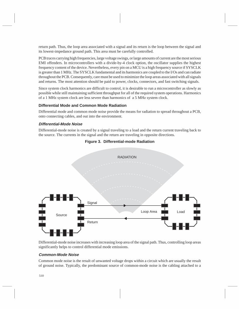
510
return path. Thus, the loop area associated with a signal and its return is the loop between the signal andits lowest-impedance ground path. This area must be carefully controlled.
PCB traces carrying high frequencies, large voltage swings, or large amounts of current are the most seriousEMI offenders. In microcontrollers with a divide-by-4 clock option, the oscillator supplies the highestfrequency content of the device. Nevertheless, every pin on a MCU is a high frequency source if SYSCLKis greater than 1 MHz. The SYSCLK fundamental and its harmonics are coupled to the I/Os and can radiatethroughout the PCB. Consequently, care must be used to minimize the loop areas associated with all signalsand returns. The most attention should be paid to power, clocks, connectors, and fast switching signals.
Since system clock harmonics are difficult to control, it is desirable to run a microcontroller as slowly aspossible while still maintaining sufficient throughput for all of the required system operations. Harmonicsof a 1 MHz system clock are less severe than harmonics of a 5 MHz system clock.
Differential Mode and Common Mode Radiation
Differential mode and common mode noise provide the means for radiation to spread throughout a PCB,onto connecting cables, and out into the environment.
Differential-Mode Noise
Differential-mode noise is created by a signal traveling to a load and the return current traveling back tothe source. The currents in the signal and the return are traveling in opposite directions.
Figure 3. Differential-mode Radiation
Signal
Return
SourceLoad
RADIATION
Loop Area
Differential-mode noise increases with increasing loop area of the signal path. Thus, controlling loop areassignificantly helps to control differential mode emissions.
Common-Mode Noise
Common mode noise is the result of unwanted voltage drops within a circuit which are usually the resultof ground noise. Typically, the predominant source of common-mode noise is the cabling attached to a
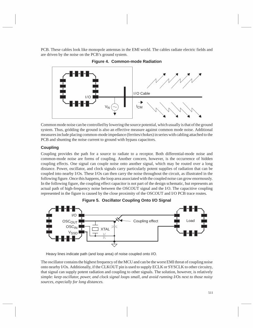
511
PCB. These cables look like monopole antennas in the EMI world. The cables radiate electric fields andare driven by the noise on the PCB’s ground system.
Figure 4. Common-mode Radiation
I /O
VN
I /O Cable
ICM
Common mode noise can be controlled by lowering the source potential, which usually is that of the groundsystem. Thus, gridding the ground is also an effective measure against common mode noise. Additionalmeasures include placing common-mode impedance (ferrites/chokes) in series with cabling attached to thePCB and shunting the noise current to ground with bypass capacitors.
Coupling
Coupling provides the path for a source to radiate to a receptor. Both differential-mode noise andcommon-mode noise are forms of coupling. Another concern, however, is the occurrence of hiddencoupling effects. One signal can couple noise onto another signal, which may be routed over a longdistance. Power, oscillator, and clock signals carry particularly potent supplies of radiation that can becoupled into nearby I/Os. These I/Os can then carry the noise throughout the circuit, as illustrated in thefollowing figure. Once this happens, the loop area associated with the coupled noise can grow enormously.In the following figure, the coupling effect capacitor is not part of the design schematic, but represents anactual path of high-frequency noise between the OSCOUT signal and the I/O. The capacitive couplingrepresented in the figure is caused by the close proximity of the OSCOUT and I/O PCB trace routes.
Figure 5. Oscillator Coupling Onto I/O Signal
Load
XTAL
I/O
Heavy lines indicate path (and loop area) of noise coupled onto I/O.
Coupling effect
VSSD
OSCOUTOSCIN
The oscillator contains the highest frequency of the MCU and can be the worst EMI threat of coupling noiseonto nearby I/Os. Additionally, if the CLKOUT pin is used to supply ECLK or SYSCLK to other circuitry,that signal can supply potent radiation and coupling to other signals. The solution, however, is relativelysimple: keep oscillator, power, and clock signal loops small, and avoid running I/Os next to those noisysources, especially for long distances.
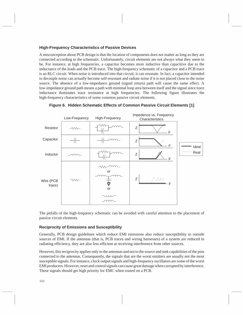
512
High-Frequency Characteristics of Passive Devices
A misconception about PCB design is that the location of components does not matter as long as they areconnected according to the schematic. Unfortunately, circuit elements are not always what they seem tobe. For instance, at high frequencies, a capacitor becomes more inductive than capacitive due to theinductance of the leads and the PCB trace. The high-frequency schematic of a capacitor and a PCB traceis an RLC circuit. When noise is introduced into that circuit, it can resonate. In fact, a capacitor intendedto decouple noise can actually become self-resonant and radiate noise if it is not placed close to the noisesource. The absence of a low-impedance ground (signal return) path will cause the same effect. Alow-impedance ground path means a path with minimal loop area between itself and the signal since traceinductance dominates trace resistance at high frequencies. The following figure illustrates thehigh-frequency characteristics of some common passive circuit elements.
Figure 6. Hidden Schematic Effects of Common Passive Circuit Elements [1]
Resistor
Capacitor
Inductor
Wire (PCBtrace)
ZF
ZF
ZF
ZF
Characteristics
Ideal
Real
or
or
Low-Frequency High-FrequencyImpedence vs. Frequency
The pitfalls of the high-frequency schematic can be avoided with careful attention to the placement ofpassive circuit elements.
Reciprocity of Emissions and Susceptibility
Generally, PCB design guidelines which reduce EMI emissions also reduce susceptibility to outsidesources of EMI. If the antennas (that is, PCB traces and wiring harnesses) of a system are reduced inradiating efficiency, they are also less efficient at receiving interference from other sources.
However, this reciprocity applies only to the antennas and not to the source and sink capabilities of the pinsconnected to the antennas. Consequently, the signals that are the worst emitters are usually not the mostsusceptible signals. For instance, clock output signals and high-frequency oscillators are some of the worstEMI producers. However, reset and control signals can cause great damage when corrupted by interference.These signals should get high priority for EMC when routed on a PCB.

513
PCB Design Implementation
The implementation of PCB design guidelines to circuit board layout is critical for achievingelectromagnetic compatibility (EMC). Furthermore, it is most cost-effective to design a PCB for EMC atthe beginning of the design cycle since later changes to improve EMC become more difficult and costly.However, there is little or no cost involved with implementing PCB design guidelines for reduced EMI atthe beginning of the design cycle.
The three most important aspects of PCB design are floor-planning, grounding, and bypassing, as will bediscussed in the following sections.
Floor-Plan PCB First
Floor-planning a PCB is the first step toward designing for EMC. Floor-planning consists of creating zoneson the PCB for analog, digital, and noisy components and providing proper space for grounding. Also,devices should be arranged to minimize routing distances of EMI-critical signals, such as clocks, power,cabling, and control signals.
Board Zoning
Board zoning allows the grounding structures to be optimized for different types of circuitry. For instance,digital circuits should be grouped together, and analog circuits should be grouped in another location. Thisconfiguration will reduce coupling of digital noise onto sensitive analog circuitry. Noisy components, likerelays, motors, and high-current-consumption devices, should be separated from both digital and analogcircuitry.
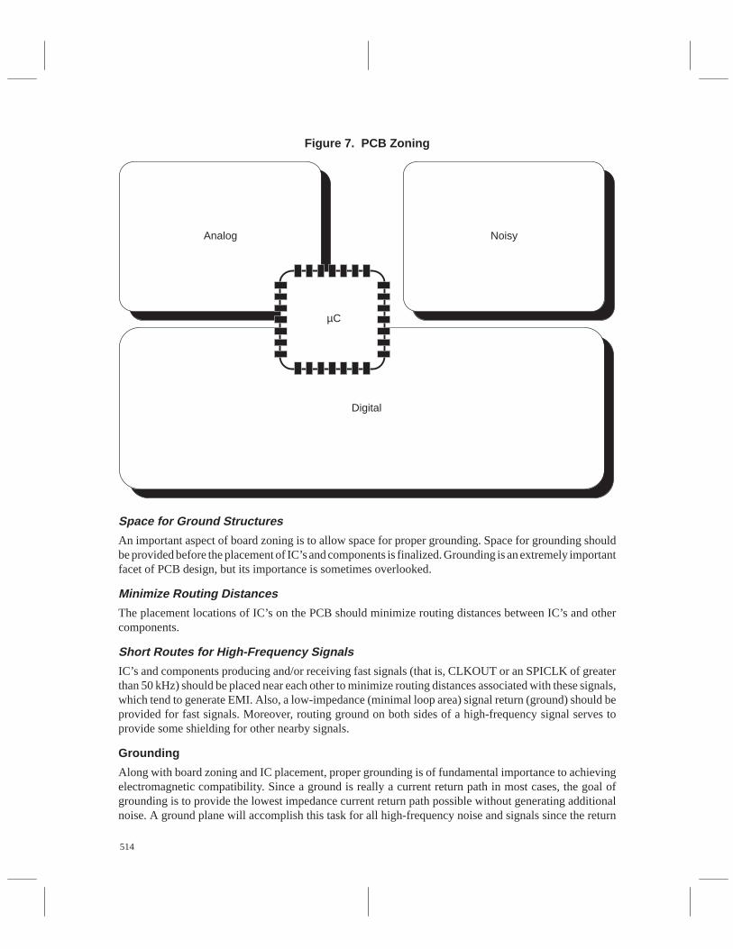
514
Figure 7. PCB Zoning
Analog Noisy
Digital
µC
Space for Ground Structures
An important aspect of board zoning is to allow space for proper grounding. Space for grounding shouldbe provided before the placement of IC’s and components is finalized. Grounding is an extremely importantfacet of PCB design, but its importance is sometimes overlooked.
Minimize Routing Distances
The placement locations of IC’s on the PCB should minimize routing distances between IC’s and othercomponents.
Short Routes for High-Frequency Signals
IC’s and components producing and/or receiving fast signals (that is, CLKOUT or an SPICLK of greaterthan 50 kHz) should be placed near each other to minimize routing distances associated with these signals,which tend to generate EMI. Also, a low-impedance (minimal loop area) signal return (ground) should beprovided for fast signals. Moreover, routing ground on both sides of a high-frequency signal serves toprovide some shielding for other nearby signals.
Grounding
Along with board zoning and IC placement, proper grounding is of fundamental importance to achievingelectromagnetic compatibility. Since a ground is really a current return path in most cases, the goal ofgrounding is to provide the lowest impedance current return path possible without generating additionalnoise. A ground plane will accomplish this task for all high-frequency noise and signals since the return

515
current for the high frequencies will follow a path directly under the signal and back to the source. Whilea ground plane is ideal for minimizing loop area and impedance, it will not always solve capacitive orinductive coupling problems.
A ground grid for digital circuitry can provide low-impedance signal return paths for high-frequency noiseon a two-layer board and does not require the additional cost of a ground plane, which usually requires atleast a four-layer PCB. For analog circuitry, a single-point grounding scheme is often better in order toavoid the presence of ground loops. Single-point grounding is also preferred for noisy or high-powercircuitry.
To protect sensitive analog circuitry from digital noise and to protect both analog and digital circuitry fromeven noisier components such as relays and motors, the analog, digital, and noisy parts of a system shouldbe separated from each other and connected only at a low-impedance ground node.
In a mixed-signal environment, the divisions between analog and digital ground may seem unclear.However, the analog sections of a mixed-signal IC (that is, ADC) should be provided with an analoggrounding scheme, and digital sections of the same IC (that is, CMOS digital I/O), including its signals androuting, should be provided with a digital grounding scheme.
Digital: Grid the Ground
Ideally, each signal should be routed next to a ground (signal return). Since this is not usually possible ona two-layer board, gridding the ground is the next best alternative. A four-layer PCB often includes aground plane which provides a low-impedance signal return path for each signal. On a two-layer board,a ground grid provides a low-impedance signal return path that resembles that of a four-layer board. Thus,digital ground should be in the form of a grid on a two layer board in order to keep loop areas small andthus to minimize the impedance of the ground structure. Following is an example of what a ground gridon a two-layer PCB can look like.
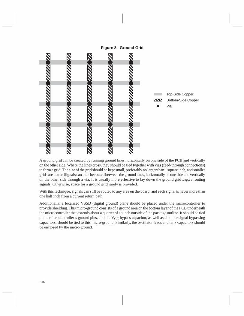
516
Figure 8. Ground GridÎÎÎÎÎÎÎÎÎÎÎÎÎÎÎÎÎÎÎÎÎÎÎÎÎÎÎÎÎÎÎÎÎÎÎÎ
ÎÎÎÎÎÎÎÎÎÎÎÎÎÎÎÎÎÎÎÎÎÎÎÎÎÎÎÎÎÎÎÎÎÎÎÎ
ÎÎÎÎÎÎÎÎÎÎÎÎÎÎÎÎÎÎ
ÎÎÎÎÎÎÎÎÎÎÎÎÎÎÎÎÎÎÎÎÎÎÎÎÎÎÎÎÎÎÎÎÎÎÎÎ
ÎÎÎÎÎÎÎÎÎÎÎÎÎÎÎÎÎÎ
ÎÎ
Top-Side Copper
Bottom-Side Copper
Via
A ground grid can be created by running ground lines horizontally on one side of the PCB and verticallyon the other side. Where the lines cross, they should be tied together with vias (feed-through connections)to form a grid. The size of the grid should be kept small, preferably no larger than 1 square inch, and smallergrids are better. Signals can then be routed between the ground lines, horizontally on one side and verticallyon the other side through a via. It is usually more effective to lay down the ground grid before routingsignals. Otherwise, space for a ground grid rarely is provided.
With this technique, signals can still be routed to any area on the board, and each signal is never more thanone half inch from a current return path.
Additionally, a localized VSSD (digital ground) plane should be placed under the microcontroller toprovide shielding. This micro-ground consists of a ground area on the bottom layer of the PCB underneaththe microcontroller that extends about a quarter of an inch outside of the package outline. It should be tiedto the microcontroller’s ground pins, and the VCC bypass capacitor, as well as all other signal bypassingcapacitors, should be tied to this micro-ground. Similarly, the oscillator leads and tank capacitors shouldbe enclosed by the micro-ground.
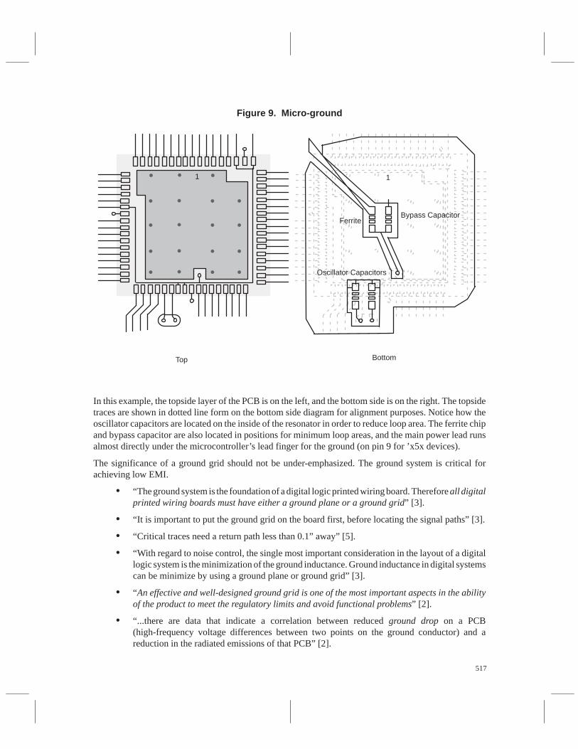
517
Figure 9. Micro-ground
FerriteBypass Capacitor
11
BottomTop
Oscillator Capacitors
In this example, the topside layer of the PCB is on the left, and the bottom side is on the right. The topsidetraces are shown in dotted line form on the bottom side diagram for alignment purposes. Notice how theoscillator capacitors are located on the inside of the resonator in order to reduce loop area. The ferrite chipand bypass capacitor are also located in positions for minimum loop areas, and the main power lead runsalmost directly under the microcontroller’s lead finger for the ground (on pin 9 for ’x5x devices).
The significance of a ground grid should not be under-emphasized. The ground system is critical forachieving low EMI.
• “The ground system is the foundation of a digital logic printed wiring board. Therefore all digitalprinted wiring boards must have either a ground plane or a ground grid” [3].
• “It is important to put the ground grid on the board first, before locating the signal paths” [3].
• “Critical traces need a return path less than 0.1” away” [5].
• “With regard to noise control, the single most important consideration in the layout of a digitallogic system is the minimization of the ground inductance. Ground inductance in digital systemscan be minimize by using a ground plane or ground grid” [3].
• “An effective and well-designed ground grid is one of the most important aspects in the abilityof the product to meet the regulatory limits and avoid functional problems” [2].
• “...there are data that indicate a correlation between reduced ground drop on a PCB(high-frequency voltage differences between two points on the ground conductor) and areduction in the radiated emissions of that PCB” [2].
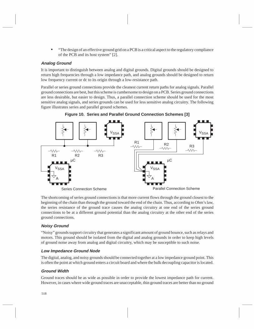
518
• “The design of an effective ground grid on a PCB is a critical aspect to the regulatory complianceof the PCB and its host system” [2].
Analog Ground
It is important to distinguish between analog and digital grounds. Digital grounds should be designed toreturn high frequencies through a low impedance path, and analog grounds should be designed to returnlow frequency current or dc to its origin through a low-resistance path.
Parallel or series ground connections provide the cleanest current return paths for analog signals. Parallelground connections are best, but this scheme is cumbersome to design on a PCB. Series ground connectionsare less desirable, but easier to design. Thus, a parallel connection scheme should be used for the mostsensitive analog signals, and series grounds can be used for less sensitive analog circuitry. The followingfigure illustrates series and parallel ground schemes.
Figure 10. Series and Parallel Ground Connection Schemes [3]
Series Connection Scheme Parallel Connection Scheme
R1 R2 R3
R1 R2 R3
A A
VSSA
µC µC
VSSA
VSSA VSSA
The shortcoming of series ground connections is that more current flows through the ground closest to thebeginning of the chain than through the ground toward the end of the chain. Thus, according to Ohm’s law,the series resistance of the ground trace causes the analog circuitry at one end of the series groundconnections to be at a different ground potential than the analog circuitry at the other end of the seriesground connections.
Noisy Ground
“Noisy” grounds support circuitry that generates a significant amount of ground bounce, such as relays andmotors. This ground should be isolated from the digital and analog grounds in order to keep high levelsof ground noise away from analog and digital circuitry, which may be susceptible to such noise.
Low Impedance Ground Node
The digital, analog, and noisy grounds should be connected together at a low impedance ground point. Thisis often the point at which ground enters a circuit board and where the bulk decoupling capacitor is located.
Ground Width
Ground traces should be as wide as possible in order to provide the lowest impedance path for current.However, in cases where wide ground traces are unacceptable, thin ground traces are better than no ground
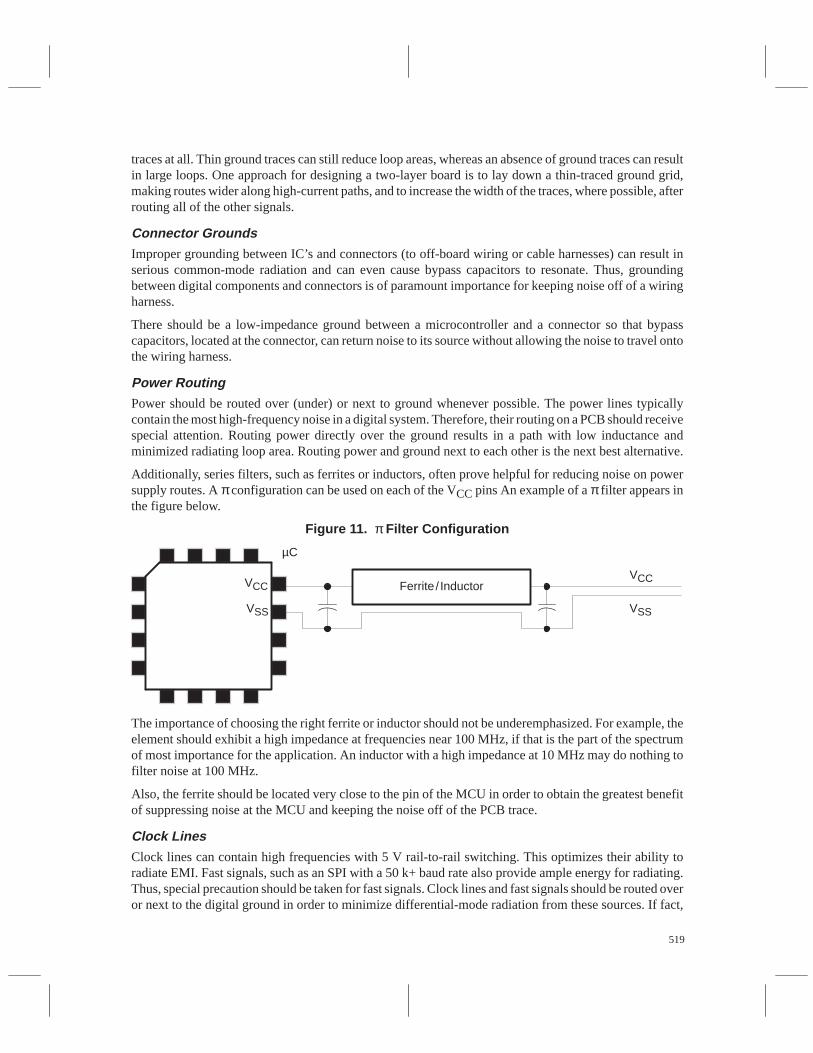
519
traces at all. Thin ground traces can still reduce loop areas, whereas an absence of ground traces can resultin large loops. One approach for designing a two-layer board is to lay down a thin-traced ground grid,making routes wider along high-current paths, and to increase the width of the traces, where possible, afterrouting all of the other signals.
Connector Grounds
Improper grounding between IC’s and connectors (to off-board wiring or cable harnesses) can result inserious common-mode radiation and can even cause bypass capacitors to resonate. Thus, groundingbetween digital components and connectors is of paramount importance for keeping noise off of a wiringharness.
There should be a low-impedance ground between a microcontroller and a connector so that bypasscapacitors, located at the connector, can return noise to its source without allowing the noise to travel ontothe wiring harness.
Power Routing
Power should be routed over (under) or next to ground whenever possible. The power lines typicallycontain the most high-frequency noise in a digital system. Therefore, their routing on a PCB should receivespecial attention. Routing power directly over the ground results in a path with low inductance andminimized radiating loop area. Routing power and ground next to each other is the next best alternative.
Additionally, series filters, such as ferrites or inductors, often prove helpful for reducing noise on powersupply routes. A π configuration can be used on each of the VCC pins An example of a π filter appears inthe figure below.
Figure 11. π Filter Configuration
µC
Ferrite / Inductor
VSS
VCC
VSS
VCC
The importance of choosing the right ferrite or inductor should not be underemphasized. For example, theelement should exhibit a high impedance at frequencies near 100 MHz, if that is the part of the spectrumof most importance for the application. An inductor with a high impedance at 10 MHz may do nothing tofilter noise at 100 MHz.
Also, the ferrite should be located very close to the pin of the MCU in order to obtain the greatest benefitof suppressing noise at the MCU and keeping the noise off of the PCB trace.
Clock Lines
Clock lines can contain high frequencies with 5 V rail-to-rail switching. This optimizes their ability toradiate EMI. Fast signals, such as an SPI with a 50 k+ baud rate also provide ample energy for radiating.Thus, special precaution should be taken for fast signals. Clock lines and fast signals should be routed overor next to the digital ground in order to minimize differential-mode radiation from these sources. If fact,

520
routing a ground on each side of these fast signals provides a good signal return while also providing someshielding for the nearby signals. Additionally, routing fast signals to connectors (and wiring harnesses), orroutine adjacent to other signals that are routed to connectors should be avoided. The fast signal lines shouldalso be properly bypassed, as discussed later.
Multi-Layer BoardsMulti-layer boards can provide many EMC benefits over two-layer boards. Sometimes, providing adequategrounding for EMC on a two-layer board is extremely difficult due to space, routing, and componentplacement constraints. If this is the case, then a multi-layer board can improve the system EMCperformance with less time required for finding EMC fixes.
Multi-layer boards can provide several weapons against radiated EMI. First, multi-layer boards providelow-impedance return paths for all signals. Since the high-frequency component of every signal will returnto its source via the path of least impedance, every signal will be returned on the ground plane directly underthe path of the signal. For this reason, the ground plane is sometimes called an image plane. Consequently,the loop area associated with each signal corresponds to the length of the trace and the thickness of the PCBbetween the signal layer and the ground layer. On a board without a ground plane, the loop area correspondsto the area between the signal and the return trace (usually ground), and this can be quite large.
Multi-layer boards can take advantage of the shielding capabilities of a ground plane if the plane is on theoutside of the board. In fact, imbedding the signal layers in the center of the board, with ground planes onthe outsides of the board, provides shielding for much of the system. This configuration is very good forEMC; however, it may add difficulty for circuit debug since all of the signals will be covered over.Nevertheless, a generous number of test points and vias as well as a copy of the board layout should providean engineer with the necessary tools for circuit debug for a board with buried signals.
Sometimes only one layer of ground plane is available. If that is the case, it usually should be on the outsideof the board (on the side with the fewest components) in order to provide the best shielding effectiveness.If the ground plane is buried between two signal layers, its potential shielding effectiveness is reduced. Ifthe only ground plane is located on the side of the board with the most components, the space required forthe components (especially surface mount) tends to create many holes or gaps in the ground plane, thusreducing its shielding effectiveness and its image plane effect. Therefore, if locating a ground plane on theouter layer of a multilayer PCB results in a chopped up ground plane, it should probably be implementedon an inner layer instead. Regardless of where the ground plane is located, the image plane effect usuallyprovides a reduction of common-mode and differential-mode emissions.
Even when designing a PCB with a ground plane, good two-layer board design practices should still befollowed. Ground planes do not cure EMI, they just help to reduce it. Following are a few points that areoften overlooked when designing multi-layer PCBs:
• Avoid routing clock lines or other high-speed signals near connectors or wiring harnesses. Alsoavoid routing these high-speed signals near other signals that are routed to connectors or wiringharnesses. Noise may couple from one signal to another which may be routed to a connector andwiring harness, providing several feet of antenna for the radiated noise to propagate from.
• If clocks or high-frequency signals are exposed on the outer layer of the PCB, GND should berouted on each side of the signal to couple noise back to the source and to provide some shieldingfor other nearby signals.
• Components, such as resistors and small capacitors, which filter emissions from the IC shouldbe kept as near to the pins as possible in order to suppress the noise within a minimal area. Thesecomponents should not be confused with circuitry designed to keep voltage spikes from entering
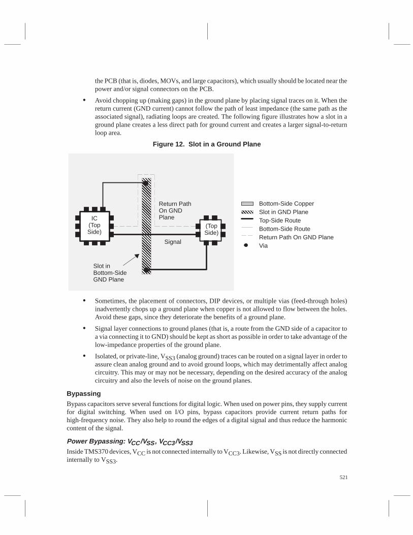
521
the PCB (that is, diodes, MOVs, and large capacitors), which usually should be located near thepower and/or signal connectors on the PCB.
• Avoid chopping up (making gaps) in the ground plane by placing signal traces on it. When thereturn current (GND current) cannot follow the path of least impedance (the same path as theassociated signal), radiating loops are created. The following figure illustrates how a slot in aground plane creates a less direct path for ground current and creates a larger signal-to-returnloop area.
Figure 12. Slot in a Ground Plane
ÎÎ
ÎÎÎÎÎÎÎÎÎÎÎÎÎÎÎÎÎÎÎÎ
Bottom-Side CopperSlot in GND PlaneTop-Side RouteBottom-Side RouteReturn Path On GND PlaneVia
Slot inBottom-SideGND Plane
Return PathOn GNDPlane
Signal
IC(TopSide)
(TopSide)
• Sometimes, the placement of connectors, DIP devices, or multiple vias (feed-through holes)inadvertently chops up a ground plane when copper is not allowed to flow between the holes.Avoid these gaps, since they deteriorate the benefits of a ground plane.
• Signal layer connections to ground planes (that is, a route from the GND side of a capacitor toa via connecting it to GND) should be kept as short as possible in order to take advantage of thelow-impedance properties of the ground plane.
• Isolated, or private-line, VSS3 (analog ground) traces can be routed on a signal layer in order toassure clean analog ground and to avoid ground loops, which may detrimentally affect analogcircuitry. This may or may not be necessary, depending on the desired accuracy of the analogcircuitry and also the levels of noise on the ground planes.
Bypassing
Bypass capacitors serve several functions for digital logic. When used on power pins, they supply currentfor digital switching. When used on I/O pins, bypass capacitors provide current return paths forhigh-frequency noise. They also help to round the edges of a digital signal and thus reduce the harmoniccontent of the signal.
Power Bypassing: V CC/VSS, VCC3/VSS3Inside TMS370 devices, VCC is not connected internally to VCC3. Likewise, VSS is not directly connectedinternally to VSS3.

522
VCC should be bypassed to VSS. Similarly, the analog supply (VCC3) should be bypassed only to analogground (VSS3).
Since VCC and VSS supply the current to the digital logic, they contain the most high-frequency elec-tromagnetic energy of any pins on a device. Thus, the loops created by VCC and VSS should receive themost attention with regard to placement of the capacitors and the loops created by their connections.Therefore, the VCC bypass capacitor (0.1 µF) should always be attached as close as possible to the de-vice’s VCC and VSS pins, and should provide minimal loop areas for the high-frequency currents.
The locations and routing of the bypass and load capacitors for the analog circuitry (VCCA/VSSA)(VCC3/VSS3) should take next priority after the digital supply capacitors.
Signal Bypassing
Ideally, every I/O on the device should have an RC filter attached close to the pin. This provides bothwave-shaping for the signal and smaller return paths for high-frequency noise. However, this is usuallynot necessary or practical.
On the other hand, some pins that have high-frequency signals should have at least a small bypass ca-pacitor connected to the digital ground. SPI pins with greater than 50 k baud rates and the CLKOUTpin, if SYSCLK is active on the pin, are good candidates for bypass capacitors of 50 pF or less to VSSand series resistors. The value of the series resistor depends on the loading and current drive capabilityof the output; however, 100 Ω is a good value to start with.
Any filter components attached to a device pin should be located as close as possible in order to keep anynoise close to the microcontoller and off of the rest of the circuit board. Moreover, a proper return path fora bypass capacitor, from the capacitor’s ground to the microcontroller’s ground, is essential for returninghigh-frequency noise to its source while providing minimal radiating loop area.
Connector Bypassing
Signals which are routed to a connector should also be bypassed at the connector with a small capacitor.This helps to keep high frequencies off of the cables and/or wiring harness by providing a high-frequencypath for any noise to get back to its source before entering the wiring harness. Proper grounding must besupplied between the microcontroller and the connector in order to keep the bypass capacitors fromradiating rather than filtering noise.

523
Summary
By understanding and applying a few fundamental PCB design guidelines, a designer can reduce theradiated EMI of a system inexpensively at the beginning of the design cycle. Following is a summary ofPCB design guidelines for reduced EMI:
1. Floor-plan the PCB first.a. Analog, digital, and noisy components should be located on the PCB by category.b. Allow space for grounding.c. Minimize routing distances.d. ICs that have high-frequency signals (that is CLKOUT or SPICLK of greater than 50 kHz)
should be placed near each other to minimize routing distances for clocks and fast signals.2. Grounding
a. Digital: Grid the ground.b. Analog: Use a parallel grounding scheme for sensitive analog circuitry, and use series
grounding scheme for less sensitive analog circuitry.c. Noisy: Isolate from analog and digital grounds.d. Low impedance ground node: Connect digital, analog, and noisy grounds together at the
lowest impedance ground node on the PCB.e. Connectors: Provide a low-impedance ground between IC’s and connectors.f. Fast signals: Run a digital ground next to fast signals (or over if possible).
3. Bypassinga. Power: Capacitors should be located as near as possible to VCC and VSS pins.b. Signal: Capacitors should be located as near as possible to the associated pins.c. Connector: Proper grounding between the microcontroller and a connector is necessary for
the bypass capacitors at the connector to keep noise off of the wiring harness.
Priority of Guidelines
1. Locate devices on the PCB for EMC optimization of: 1) grounds, 2) power, and 3) routing(especially clocks and high-speed signals).
2. Provide a ground grid for a two-layer board or a ground plane(s) for a multi-layer board.3. Route the power and place the filter components.4. Route the clocks and high-speed signals and place the filter components.5. Route other noise-making or noise-susceptible signals. Also give attention to the reset and
control signals.6. Route all other circuitry.

524
References
1. Gerke, Daryl and Bill Kimmel, EDN: The Designer’s Guide to Electromagnetic Compatibility,Cahners Publishing Company, 1994.
2. Paul, Clayton R., Introduction to Electromagnetic Compatibility, John Wiley & Sons, Inc., 1992.
3. Ott, Henry W., Noise Reduction Techniques In Electronic Systems, second edition, John Wiley& Sons, New York, 1988.
4. Schneider, John, Automotove PCB Design Guidelines for Reduced EMI, Texas Instruments,1992
5. Van Doren, Tom, Grounding and Shielding Electronic Systems, T. Van Doren, 1993.

525
Part VISpecific System
Application Design AidsPart VI contains two sections:
EMI Reduction 503. . . . . . . . . . . . . . . . . . . . .
Cost Effective Input Protection Circuitry for the Texas Instruments TMS370 Family of Microcontrollers 525. . . . . .

526

527
Cost Effective Input ProtectionCircuitry for the Texas InstrumentsTMS370 Family of Microcontrollers
David T. MaplesMichael S. Stewart
Microcontroller Products—Semiconductor GroupTexas Instruments

528
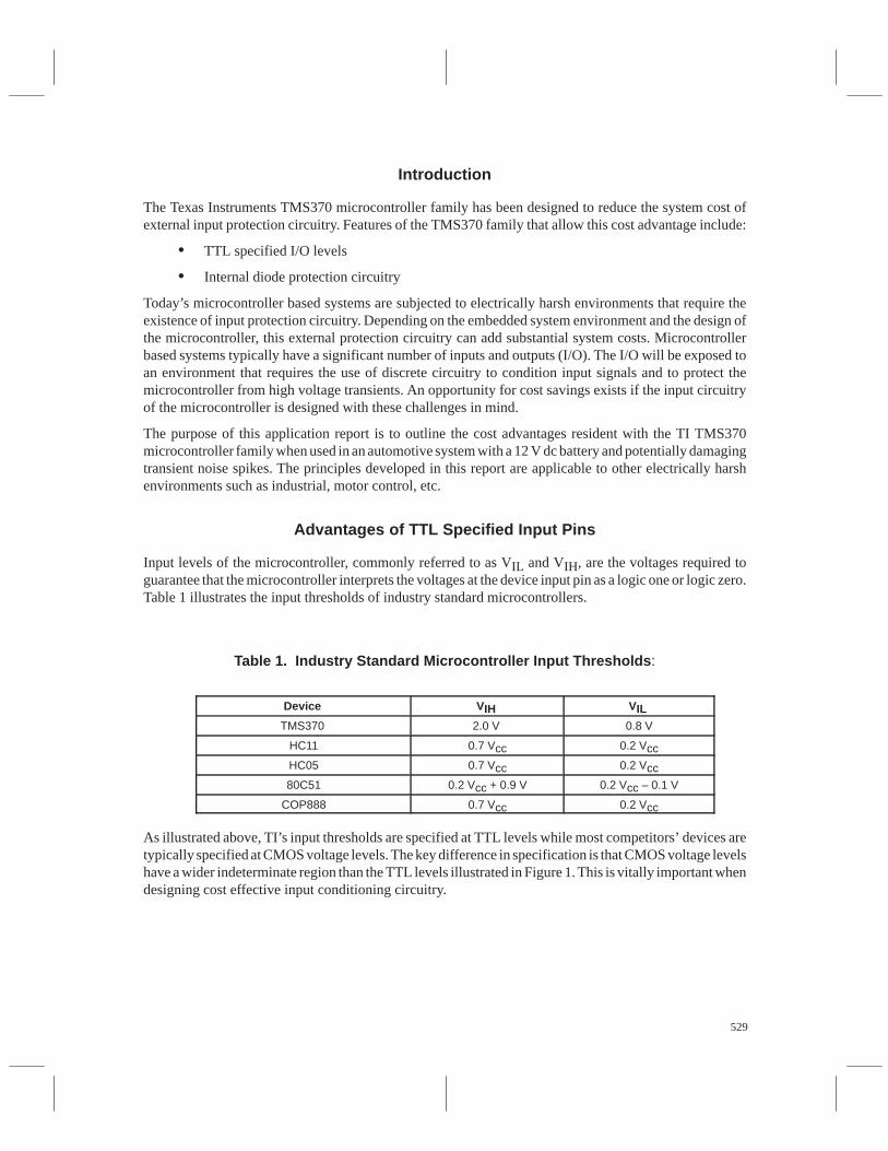
529
Introduction
The Texas Instruments TMS370 microcontroller family has been designed to reduce the system cost ofexternal input protection circuitry. Features of the TMS370 family that allow this cost advantage include:
• TTL specified I/O levels
• Internal diode protection circuitry
Today’s microcontroller based systems are subjected to electrically harsh environments that require theexistence of input protection circuitry. Depending on the embedded system environment and the design ofthe microcontroller, this external protection circuitry can add substantial system costs. Microcontrollerbased systems typically have a significant number of inputs and outputs (I/O). The I/O will be exposed toan environment that requires the use of discrete circuitry to condition input signals and to protect themicrocontroller from high voltage transients. An opportunity for cost savings exists if the input circuitryof the microcontroller is designed with these challenges in mind.
The purpose of this application report is to outline the cost advantages resident with the TI TMS370microcontroller family when used in an automotive system with a 12 V dc battery and potentially damagingtransient noise spikes. The principles developed in this report are applicable to other electrically harshenvironments such as industrial, motor control, etc.
Advantages of TTL Specified Input Pins
Input levels of the microcontroller, commonly referred to as VIL and VIH, are the voltages required toguarantee that the microcontroller interprets the voltages at the device input pin as a logic one or logic zero.Table 1 illustrates the input thresholds of industry standard microcontrollers.
Table 1. Industry Standard Microcontroller Input Thresholds :
ÁÁÁÁÁÁÁÁÁÁÁÁÁÁÁÁÁÁÁÁÁÁ
Device ÁÁÁÁÁÁÁÁÁÁÁÁÁÁÁÁ
VIH ÁÁÁÁÁÁÁÁÁÁÁÁÁÁ
VIL
ÁÁÁÁÁÁÁÁÁÁÁTMS370 ÁÁÁÁÁÁÁÁ2.0 V ÁÁÁÁÁÁÁ0.8 VÁÁÁÁÁÁÁÁÁÁÁÁÁÁÁÁÁÁÁÁÁÁHC11
ÁÁÁÁÁÁÁÁÁÁÁÁÁÁÁÁ0.7 Vcc
ÁÁÁÁÁÁÁÁÁÁÁÁÁÁ0.2 VccÁÁÁÁÁÁÁÁÁÁÁ
ÁÁÁÁÁÁÁÁÁÁÁHC05
ÁÁÁÁÁÁÁÁÁÁÁÁÁÁÁÁ
0.7 VccÁÁÁÁÁÁÁÁÁÁÁÁÁÁ
0.2 VccÁÁÁÁÁÁÁÁÁÁÁÁÁÁÁÁÁÁÁÁÁÁ
80C51ÁÁÁÁÁÁÁÁÁÁÁÁÁÁÁÁ
0.2 Vcc + 0.9 VÁÁÁÁÁÁÁÁÁÁÁÁÁÁ
0.2 Vcc – 0.1 VÁÁÁÁÁÁÁÁÁÁÁÁÁÁÁÁÁÁÁÁÁÁ
COP888 ÁÁÁÁÁÁÁÁÁÁÁÁÁÁÁÁ
0.7 VccÁÁÁÁÁÁÁÁÁÁÁÁÁÁ
0.2 Vcc
As illustrated above, TI’s input thresholds are specified at TTL levels while most competitors’ devices aretypically specified at CMOS voltage levels. The key difference in specification is that CMOS voltage levelshave a wider indeterminate region than the TTL levels illustrated in Figure 1. This is vitally important whendesigning cost effective input conditioning circuitry.
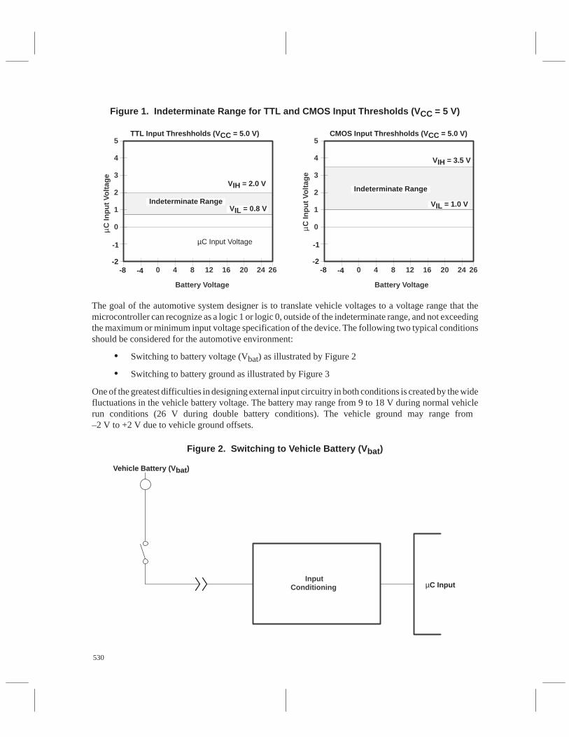
530
Figure 1. Indeterminate Range for TTL and CMOS Input Thresholds (V CC = 5 V)
0
1
2
3
4
5
0 4 8 12 16 20 24 26
0
1
2
3
5
4
0 4 8 12 16 20 24 26
Battery Voltage Battery Voltage
-1
-2-8 -4
-1
-2-8 -4
Indeterminate Range
Indeterminate Range
TTL Input Threshholds (V CC = 5.0 V) CMOS Input Threshholds (V CC = 5.0 V)
C In
put V
olta
ge
µC Input Voltage
µC In
put V
olta
geµ
VIH = 2.0 V
VIH = 3.5 V
VIL = 0.8 VVIL = 1.0 V
The goal of the automotive system designer is to translate vehicle voltages to a voltage range that themicrocontroller can recognize as a logic 1 or logic 0, outside of the indeterminate range, and not exceedingthe maximum or minimum input voltage specification of the device. The following two typical conditionsshould be considered for the automotive environment:
• Switching to battery voltage (Vbat) as illustrated by Figure 2
• Switching to battery ground as illustrated by Figure 3
One of the greatest difficulties in designing external input circuitry in both conditions is created by the widefluctuations in the vehicle battery voltage. The battery may range from 9 to 18 V during normal vehiclerun conditions (26 V during double battery conditions). The vehicle ground may range from –2 V to +2 V due to vehicle ground offsets.
Figure 2. Switching to Vehicle Battery (V bat)
InputConditioning
Vehicle Battery (V bat)
µC Input
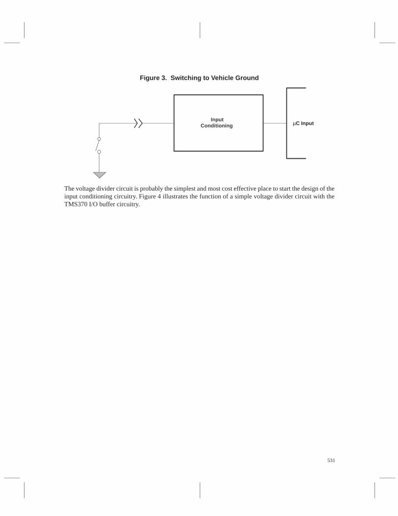
531
Figure 3. Switching to Vehicle Ground
InputConditioning µC Input
The voltage divider circuit is probably the simplest and most cost effective place to start the design of theinput conditioning circuitry. Figure 4 illustrates the function of a simple voltage divider circuit with theTMS370 I/O buffer circuitry.
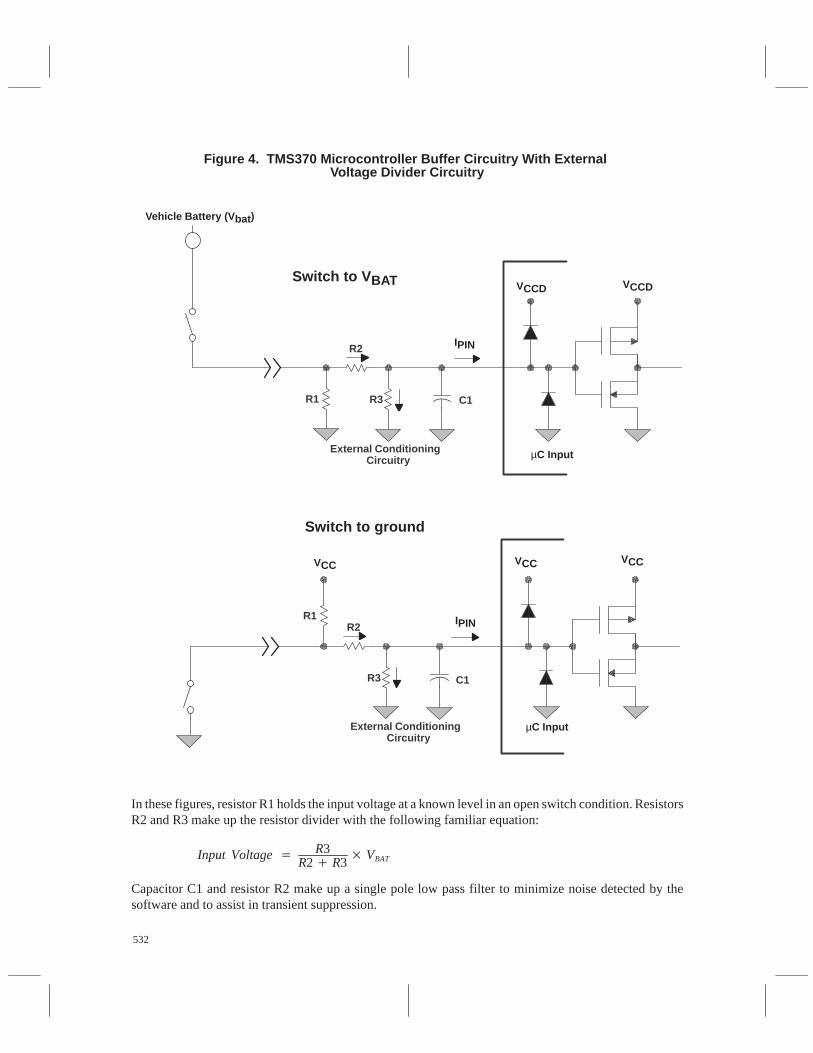
532
Figure 4. TMS370 Microcontroller Buffer Circuitry With External Voltage Divider Circuitry
R2
R1 R3 C1
External ConditioningCircuitry
R2R1
R3 C1
External ConditioningCircuitry
Vehicle Battery (V bat)
VCCD VCCD
IPIN
µC Input
VCC VCCVCC
µC Input
IPIN
Switch to V BAT
Switch to ground
In these figures, resistor R1 holds the input voltage at a known level in an open switch condition. ResistorsR2 and R3 make up the resistor divider with the following familiar equation:
Input Voltage R3R2 R3
VBAT
Capacitor C1 and resistor R2 make up a single pole low pass filter to minimize noise detected by thesoftware and to assist in transient suppression.
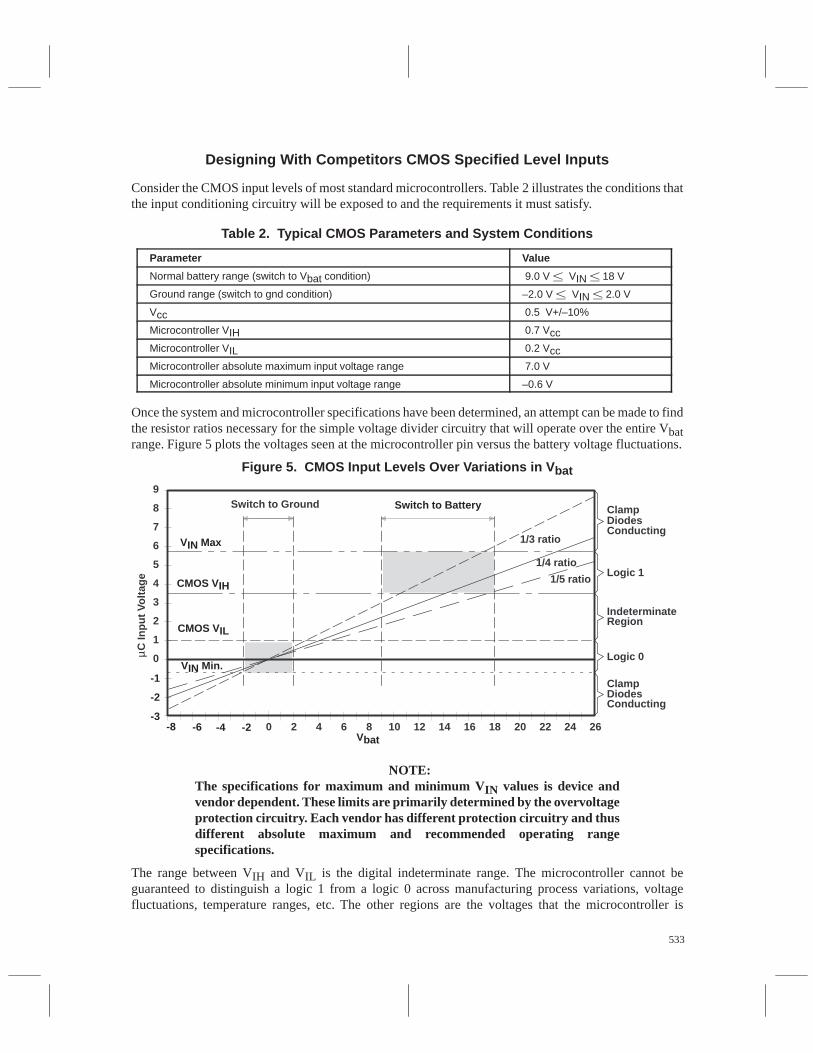
533
Designing With Competitors CMOS Specified Level Inputs
Consider the CMOS input levels of most standard microcontrollers. Table 2 illustrates the conditions thatthe input conditioning circuitry will be exposed to and the requirements it must satisfy.
Table 2. Typical CMOS Parameters and System Conditions
ÁÁÁÁÁÁÁÁÁÁÁÁÁÁÁÁÁÁÁÁÁÁÁÁÁÁÁÁÁÁÁÁÁÁÁÁÁÁ
Parameter ÁÁÁÁÁÁÁÁÁÁÁÁÁÁÁÁÁÁ
Value
ÁÁÁÁÁÁÁÁÁÁÁÁÁÁÁÁÁÁÁNormal battery range (switch to Vbat condition) ÁÁÁÁÁÁÁÁÁ 9.0 V VIN 18 VÁÁÁÁÁÁÁÁÁÁÁÁÁÁÁÁÁÁÁÁÁÁÁÁÁÁÁÁÁÁÁÁÁÁÁÁÁÁGround range (switch to gnd condition)
ÁÁÁÁÁÁÁÁÁÁÁÁÁÁÁÁÁÁ–2.0 V VIN 2.0 VÁÁÁÁÁÁÁÁÁÁÁÁÁÁÁÁÁÁÁ
ÁÁÁÁÁÁÁÁÁÁÁÁÁÁÁÁÁÁÁVcc
ÁÁÁÁÁÁÁÁÁÁÁÁÁÁÁÁÁÁ
0.5 V+/–10%ÁÁÁÁÁÁÁÁÁÁÁÁÁÁÁÁÁÁÁÁÁÁÁÁÁÁÁÁÁÁÁÁÁÁÁÁÁÁ
Microcontroller VIHÁÁÁÁÁÁÁÁÁÁÁÁÁÁÁÁÁÁ
0.7 VccÁÁÁÁÁÁÁÁÁÁÁÁÁÁÁÁÁÁÁÁÁÁÁÁÁÁÁÁÁÁÁÁÁÁÁÁÁÁ
Microcontroller VILÁÁÁÁÁÁÁÁÁÁÁÁÁÁÁÁÁÁ
0.2 VccÁÁÁÁÁÁÁÁÁÁÁÁÁÁÁÁÁÁÁÁÁÁÁÁÁÁÁÁÁÁÁÁÁÁÁÁÁÁ
Microcontroller absolute maximum input voltage range ÁÁÁÁÁÁÁÁÁÁÁÁÁÁÁÁÁÁ
7.0 V
ÁÁÁÁÁÁÁÁÁÁÁÁÁÁÁÁÁÁÁÁÁÁÁÁÁÁÁÁÁÁÁÁÁÁÁÁÁÁ
Microcontroller absolute minimum input voltage range ÁÁÁÁÁÁÁÁÁÁÁÁÁÁÁÁÁÁ
–0.6 V
Once the system and microcontroller specifications have been determined, an attempt can be made to findthe resistor ratios necessary for the simple voltage divider circuitry that will operate over the entire Vbatrange. Figure 5 plots the voltages seen at the microcontroller pin versus the battery voltage fluctuations.
Figure 5. CMOS Input Levels Over Variations in V bat
9
8
7
6
5
4
3
2
1
0
0 2 4 6 8 10 12 14 16 18 20 22 24 26
1/3 ratio
1/4 ratio
1/5 ratio
ClampDiodesConducting
Logic 1
IndeterminateRegion
Logic 0
ClampDiodesConducting
Switch to Ground
-1
-2
-3-8 -6 -4 -2
Switch to Battery
VIN Max
CMOS VIH
CMOS VIL
VIN Min.
Vbat
C In
put V
olta
geµ
NOTE:The specifications for maximum and minimum VIN values is device andvendor dependent. These limits are primarily determined by the overvoltageprotection circuitry. Each vendor has different protection circuitry and thusdifferent absolute maximum and recommended operating rangespecifications.
The range between VIH and VIL is the digital indeterminate range. The microcontroller cannot beguaranteed to distinguish a logic 1 from a logic 0 across manufacturing process variations, voltagefluctuations, temperature ranges, etc. The other regions are the voltages that the microcontroller is
534
guaranteed to recognize as a logic 1 or logic 0. Therefore, for all valid voltages that the input conditioningis exposed to (such as 9 V to 18 V for an automotive switch to battery condition), the resistor curves mustfall within the logic 1 or logic 0 range to satisfy the design constraints.
A review of Figure 5 shows that all the design considerations cannot be met for CMOS inputs with a simpleresistor divider. The switch to battery condition is shown between the two arrows on the right of the figure.Take the 1/4 ratio as an example. Battery voltages between 9 and 14 V violate VIH. The 1/3 ratio has betterperformance with respect to VIH but battery voltages greater than 17 V and less than 10.5 V still do not meetthe required VIH specification. Some type of active circuitry must be designed to satisfy all the designconstraints, adding to the total system cost. The switch to ground condition is shown between the twoarrows on the left hand side of the figure. The design conditions can be met for a switch to ground withCMOS input levels for all three resistor ratios since VIN falls within VIL and the minimum input voltageof the device.
Designing With TI’s TTL Level CMOS Inputs
The advantages of designing with TI’s TTL level CMOS inputs are considered next. Table 3 shows theconditions that the input conditioning circuitry are exposed to and the requirements it must satisfy. Thedesign requirements are identical to the previous example, except for the change in VIH and VIL.
Table 3. Typical TTL Parameters and System Conditions
ÁÁÁÁÁÁÁÁÁÁÁÁÁÁÁÁÁÁÁÁÁÁÁÁÁÁÁÁÁÁÁÁÁÁÁÁÁÁ
Parameter ÁÁÁÁÁÁÁÁÁÁÁÁÁÁ
Value
ÁÁÁÁÁÁÁÁÁÁÁÁÁÁÁÁÁÁÁÁÁÁÁÁÁÁÁÁÁÁÁÁÁÁÁÁÁÁ
Battery Range (switch to Vbat condition) ÁÁÁÁÁÁÁÁÁÁÁÁÁÁ
9.0 V ≤ VIN ≤ 18 V
ÁÁÁÁÁÁÁÁÁÁÁÁÁÁÁÁÁÁÁÁÁÁÁÁÁÁÁÁÁÁÁÁÁÁÁÁÁÁ
Ground Range (switch to ground condition) ÁÁÁÁÁÁÁÁÁÁÁÁÁÁ
–2.0 V ≤ VIN ≤ 2.0 V
ÁÁÁÁÁÁÁÁÁÁÁÁÁÁÁÁÁÁÁÁÁÁÁÁÁÁÁÁÁÁÁÁÁÁÁÁÁÁ
Vcc ÁÁÁÁÁÁÁÁÁÁÁÁÁÁ
5.0 V ±10%
ÁÁÁÁÁÁÁÁÁÁÁÁÁÁÁÁÁÁÁÁÁÁÁÁÁÁÁÁÁÁÁÁÁÁÁÁÁÁ
Microcontroller VIH ÁÁÁÁÁÁÁÁÁÁÁÁÁÁ
2.0 V
ÁÁÁÁÁÁÁÁÁÁÁÁÁÁÁÁÁÁÁÁÁÁÁÁÁÁÁÁÁÁÁÁÁÁÁÁÁÁ
Microcontroller VIL ÁÁÁÁÁÁÁÁÁÁÁÁÁÁ
0.8 V
ÁÁÁÁÁÁÁÁÁÁÁÁÁÁÁÁÁÁÁMicrocontroller absolute maximum input voltage range ÁÁÁÁÁÁÁ7.0 VÁÁÁÁÁÁÁÁÁÁÁÁÁÁÁÁÁÁÁÁÁÁÁÁÁÁÁÁÁÁÁÁÁÁÁÁÁÁMicrocontroller absolute minimum input voltage range
ÁÁÁÁÁÁÁÁÁÁÁÁÁÁ–0.6 V
Figure 6 plots the voltages seen at the microcontroller versus the battery voltage fluctuations with TTLvoltage levels. Again, several resistor ratios are plotted and the input voltage ranges of interest are notedto the right of the plot. A review of the figure shows that all the design considerations can be met with a1/4 ratio for TTL input levels and a simple resistor divider. The switch to battery condition is shownbetween the two arrows on the right hand side of the figure. The microcontroller input voltage is alwaysgreater than VIH and less than the maximum input voltage specification for normal battery voltagesbetween 9 and 18 V.
The switch to ground condition is shown between the two arrows on the left of the figure. Again, the designconditions can be met for a switch to ground with TTL input levels. The microcontroller input voltage forall three resistor ratios fall with in VIL and the minimum input voltage of the device. A component reductionis recognized over the CMOS voltage levels by using a simple resistor divider instead of active circuitry.
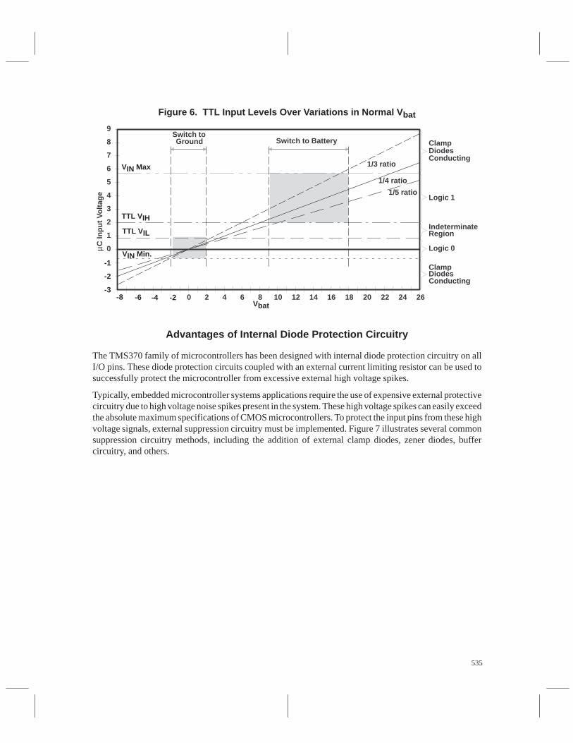
535
Figure 6. TTL Input Levels Over Variations in Normal V bat
9
8
7
6
5
4
3
2
1
0
0 2 4 6 8 10 12 14 16 18 20 22 24 26
Switch toGround Switch to Battery
1/3 ratio
1/4 ratio
1/5 ratio
ClampDiodesConducting
Logic 1
IndeterminateRegion
Logic 0
ClampDiodesConducting
-1
-2
-3-8 -6 -4 -2
VIN Max
TTL VIH
VIN Min.
TTL VIL
C In
put V
olta
geµ
Vbat
Advantages of Internal Diode Protection Circuitry
The TMS370 family of microcontrollers has been designed with internal diode protection circuitry on allI/O pins. These diode protection circuits coupled with an external current limiting resistor can be used tosuccessfully protect the microcontroller from excessive external high voltage spikes.
Typically, embedded microcontroller systems applications require the use of expensive external protectivecircuitry due to high voltage noise spikes present in the system. These high voltage spikes can easily exceedthe absolute maximum specifications of CMOS microcontrollers. To protect the input pins from these highvoltage signals, external suppression circuitry must be implemented. Figure 7 illustrates several commonsuppression circuitry methods, including the addition of external clamp diodes, zener diodes, buffercircuitry, and others.
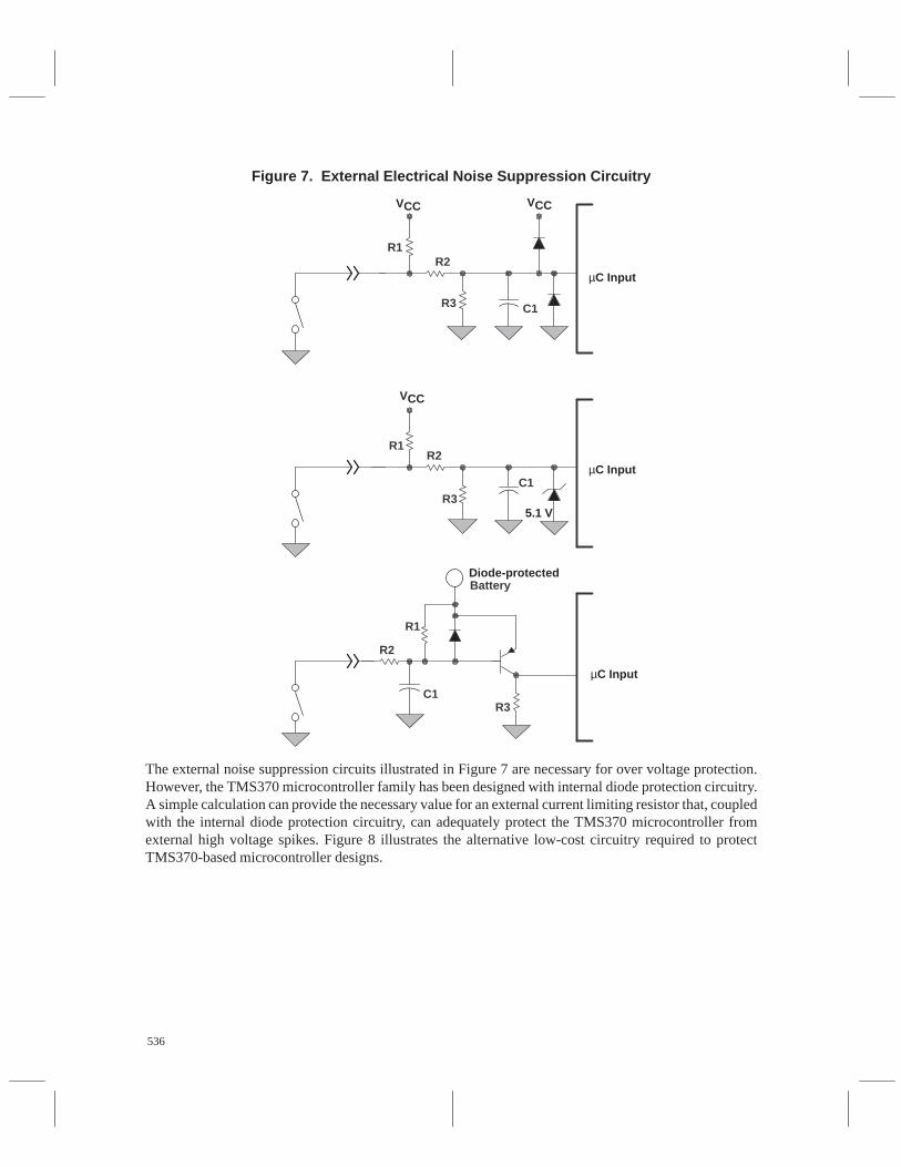
536
Figure 7. External Electrical Noise Suppression Circuitry
R2R1
R3 C1
R2R1
R3C1
R2
R1
R3C1
Battery
5.1 V
µC Input
µC Input
µC Input
Diode-protected
VCC VCC
VCC
The external noise suppression circuits illustrated in Figure 7 are necessary for over voltage protection.However, the TMS370 microcontroller family has been designed with internal diode protection circuitry.A simple calculation can provide the necessary value for an external current limiting resistor that, coupledwith the internal diode protection circuitry, can adequately protect the TMS370 microcontroller fromexternal high voltage spikes. Figure 8 illustrates the alternative low-cost circuitry required to protectTMS370-based microcontroller designs.
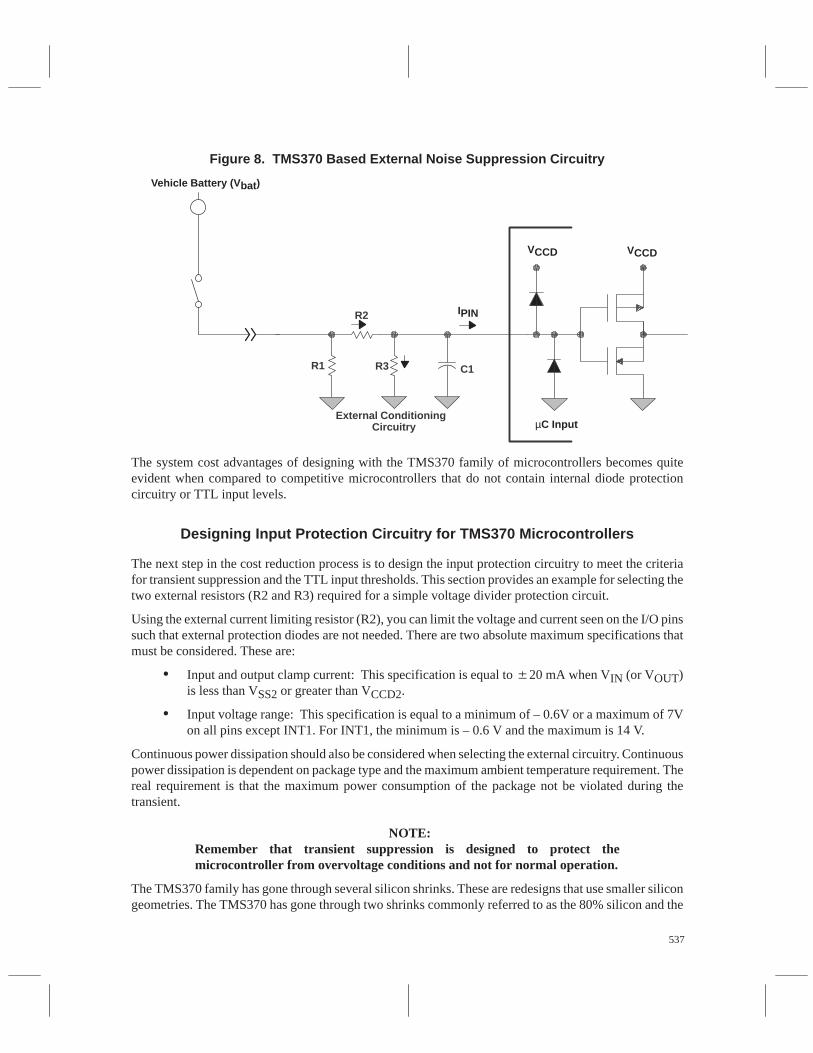
537
Figure 8. TMS370 Based External Noise Suppression Circuitry
R2
R1 R3 C1
External ConditioningCircuitry
Vehicle Battery (V bat)
µC Input
VCCD VCCD
IPIN
The system cost advantages of designing with the TMS370 family of microcontrollers becomes quiteevident when compared to competitive microcontrollers that do not contain internal diode protectioncircuitry or TTL input levels.
Designing Input Protection Circuitry for TMS370 Microcontrollers
The next step in the cost reduction process is to design the input protection circuitry to meet the criteriafor transient suppression and the TTL input thresholds. This section provides an example for selecting thetwo external resistors (R2 and R3) required for a simple voltage divider protection circuit.
Using the external current limiting resistor (R2), you can limit the voltage and current seen on the I/O pinssuch that external protection diodes are not needed. There are two absolute maximum specifications thatmust be considered. These are:
• Input and output clamp current: This specification is equal to 20 mA when VIN (or VOUT)is less than VSS2 or greater than VCCD2.
• Input voltage range: This specification is equal to a minimum of – 0.6V or a maximum of 7Von all pins except INT1. For INT1, the minimum is – 0.6 V and the maximum is 14 V.
Continuous power dissipation should also be considered when selecting the external circuitry. Continuouspower dissipation is dependent on package type and the maximum ambient temperature requirement. Thereal requirement is that the maximum power consumption of the package not be violated during thetransient.
NOTE:Remember that transient suppression is designed to protect themicrocontroller from overvoltage conditions and not for normal operation.
The TMS370 family has gone through several silicon shrinks. These are redesigns that use smaller silicongeometries. The TMS370 has gone through two shrinks commonly referred to as the 80% silicon and the
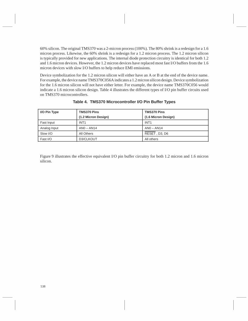
538
60% silicon. The original TMS370 was a 2-micron process (100%). The 80% shrink is a redesign for a 1.6micron process. Likewise, the 60% shrink is a redesign for a 1.2 micron process. The 1.2 micron siliconis typically provided for new applications. The internal diode protection circuitry is identical for both 1.2and 1.6 micron devices. However, the 1.2 micron devices have replaced most fast I/O buffers from the 1.6micron devices with slow I/O buffers to help reduce EMI emissions.
Device symbolization for the 1.2 micron silicon will either have an A or B at the end of the device name.For example, the device name TMS370C056A indicates a 1.2 micron silicon design. Device symbolizationfor the 1.6 micron silicon will not have either letter. For example, the device name TMS370C056 wouldindicate a 1.6 micron silicon design. Table 4 illustrates the different types of I/O pin buffer circuits usedon TMS370 microcontrollers.
Table 4. TMS370 Microcontroller I/O Pin Buffer Types
ÁÁÁÁÁÁÁÁÁÁÁÁÁÁÁÁÁÁÁÁÁ
I/O Pin Type ÁÁÁÁÁÁÁÁÁÁÁÁÁÁÁÁÁÁÁÁÁÁÁÁÁÁÁÁÁÁÁÁÁ
TMS370 Pins
(1.2 Micron Design)
ÁÁÁÁÁÁÁÁÁÁÁÁÁÁÁÁÁÁÁÁÁÁÁÁÁÁÁÁÁÁÁÁÁÁÁÁ
TMS370 Pins
(1.6 Micron Design)
ÁÁÁÁÁÁÁÁÁÁÁÁÁÁ
Fast Input ÁÁÁÁÁÁÁÁÁÁÁÁÁÁÁÁÁÁÁÁÁÁ
INT1 ÁÁÁÁÁÁÁÁÁÁÁÁÁÁÁÁÁÁÁÁÁÁÁÁ
INT1
ÁÁÁÁÁÁÁÁÁÁÁÁÁÁ
Analog Input ÁÁÁÁÁÁÁÁÁÁÁÁÁÁÁÁÁÁÁÁÁÁ
AN0 – AN14 ÁÁÁÁÁÁÁÁÁÁÁÁÁÁÁÁÁÁÁÁÁÁÁÁ
AN0 – AN14
ÁÁÁÁÁÁÁSlow I/O ÁÁÁÁÁÁÁÁÁÁÁAll Others ÁÁÁÁÁÁÁÁÁÁÁÁRESET , D3, D6ÁÁÁÁÁÁÁÁÁÁÁÁÁÁFast I/O
ÁÁÁÁÁÁÁÁÁÁÁÁÁÁÁÁÁÁÁÁÁÁD3/CLKOUT
ÁÁÁÁÁÁÁÁÁÁÁÁÁÁÁÁÁÁÁÁÁÁÁÁAll others
Figure 9 illustrates the effective equivalent I/O pin buffer circuitry for both 1.2 micron and 1.6 micronsilicon.
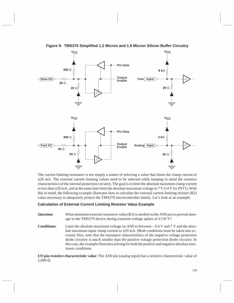
539
Figure 9. TMS370 Simplified 1.2 Micron and 1.6 Micron Silicon Buffer Circuitry
Slow I/O
Pin Data
OutputEnable InputFast
Pin Data
OutputEnableFast I/O Analog Input
300 Ω
30 Ω
20 Ω
400 Ω
30 Ω
20 Ω
8 kΩ
20 Ω
2 kΩ
20 Ω
VCCVCC
VCC VCC
The current limiting resistance is not simply a matter of selecting a value that limits the clamp current to±20 mA. The external current limiting values need to be selected while keeping in mind the resistivecharacteristics of the internal protection circuitry. The goal is to limit the absolute maximum clamp currentto less than ±20 mA, and at the same time limit the absolute maximum voltage to 7 V (14 V for INT1). Withthis in mind, the following example illustrates how to calculate the external current limiting resistor (R2)value necessary to adequately protect the TMS370 microcontroller family. Let’s look at an example.
Calculation of External Current Limiting Resistor Value Example
Question: What minimum external resistance value (R2) is needed on the AN0 pin to prevent dam-age to the TMS370 device during transient voltage spikes of ±150 V?
Conditions: Limit the absolute maximum voltage on AN0 to between – 0.6 V and 7 V and the abso-lute maximum input clamp current to ±20 mA. (Both conditions must be taken into ac-count) Also, note that the resistance characteristics of the negative voltage protectiondiode circuitry is much smaller than the positive voltage protection diode circuitry. Inthis case, the example illustrates solving for both the positive and negative absolute max-imum conditions.
I/O pin resistive characteristic value: The AN0 pin (analog input) has a resistive characteristic value of2,000 Ω.
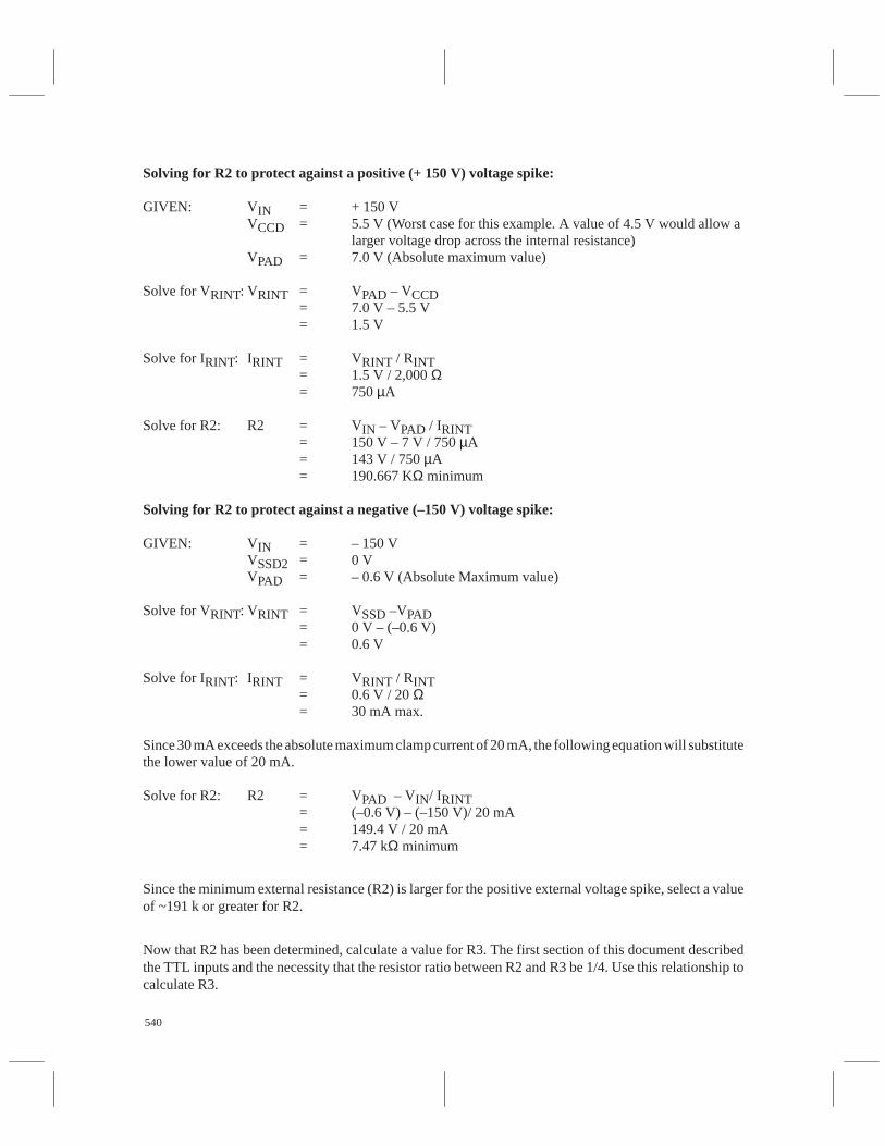
540
Solving for R2 to protect against a positive (+ 150 V) voltage spike:
GIVEN: VIN = + 150 VVCCD = 5.5 V (Worst case for this example. A value of 4.5 V would allow a
larger voltage drop across the internal resistance)VPAD = 7.0 V (Absolute maximum value)
Solve for VRINT: VRINT = VPAD – VCCD= 7.0 V – 5.5 V= 1.5 V
Solve for IRINT: IRINT = VRINT / RINT= 1.5 V / 2,000 Ω= 750 µA
Solve for R2: R2 = VIN – VPAD / IRINT= 150 V – 7 V / 750 µA= 143 V / 750 µA= 190.667 KΩ minimum
Solving for R2 to protect against a negative (–150 V) voltage spike:
GIVEN: VIN = – 150 VVSSD2 = 0 V VPAD = – 0.6 V (Absolute Maximum value)
Solve for VRINT: VRINT = VSSD –VPAD= 0 V – (–0.6 V)= 0.6 V
Solve for IRINT: IRINT = VRINT / RINT= 0.6 V / 20 Ω= 30 mA max.
Since 30 mA exceeds the absolute maximum clamp current of 20 mA, the following equation will substitutethe lower value of 20 mA.
Solve for R2: R2 = VPAD – VIN/ IRINT= (–0.6 V) – (–150 V)/ 20 mA= 149.4 V / 20 mA= 7.47 kΩ minimum
Since the minimum external resistance (R2) is larger for the positive external voltage spike, select a valueof ~191 k or greater for R2.
Now that R2 has been determined, calculate a value for R3. The first section of this document describedthe TTL inputs and the necessity that the resistor ratio between R2 and R3 be 1/4. Use this relationship tocalculate R3.
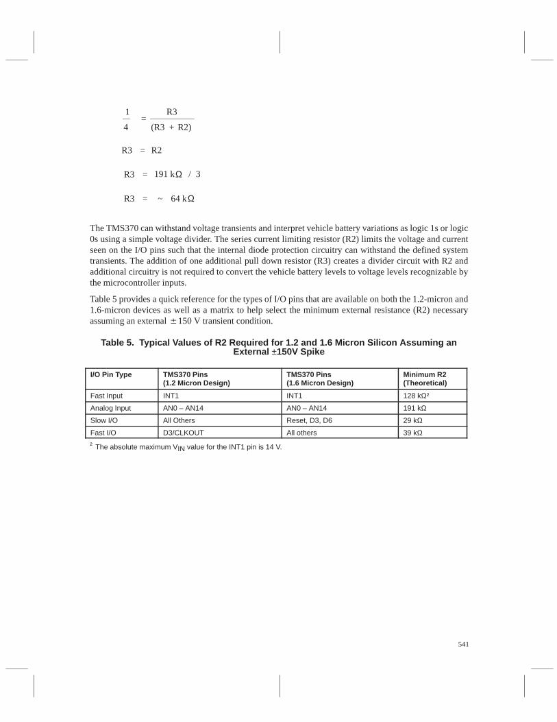
541
1
4=
R3
(R3 + R2)
R3 =
3
R2
R3 =
R3 = ~
Ω
Ω
/
64 k
191 k
The TMS370 can withstand voltage transients and interpret vehicle battery variations as logic 1s or logic0s using a simple voltage divider. The series current limiting resistor (R2) limits the voltage and currentseen on the I/O pins such that the internal diode protection circuitry can withstand the defined systemtransients. The addition of one additional pull down resistor (R3) creates a divider circuit with R2 andadditional circuitry is not required to convert the vehicle battery levels to voltage levels recognizable bythe microcontroller inputs.
Table 5 provides a quick reference for the types of I/O pins that are available on both the 1.2-micron and1.6-micron devices as well as a matrix to help select the minimum external resistance (R2) necessaryassuming an external 150 V transient condition.
Table 5. Typical Values of R2 Required for 1.2 and 1.6 Micron Silicon Assuming anExternal ±150V Spike
ÁÁÁÁÁÁÁÁÁÁÁÁ
I/O Pin Type ÁÁÁÁÁÁÁÁÁÁÁÁÁÁÁÁÁÁÁÁ
TMS370 Pins(1.2 Micron Design)
ÁÁÁÁÁÁÁÁÁÁÁÁÁÁÁÁÁÁ
TMS370 Pins(1.6 Micron Design)
ÁÁÁÁÁÁÁÁÁÁÁÁ
Minimum R2(Theoretical)ÁÁÁÁÁÁ
ÁÁÁÁÁÁFast Input
ÁÁÁÁÁÁÁÁÁÁÁÁÁÁÁÁÁÁÁÁ
INT1ÁÁÁÁÁÁÁÁÁÁÁÁÁÁÁÁÁÁ
INT1ÁÁÁÁÁÁÁÁÁÁÁÁ
128 kΩ†ÁÁÁÁÁÁÁÁÁÁÁÁ
Analog InputÁÁÁÁÁÁÁÁÁÁÁÁÁÁÁÁÁÁÁÁ
AN0 – AN14ÁÁÁÁÁÁÁÁÁÁÁÁÁÁÁÁÁÁ
AN0 – AN14ÁÁÁÁÁÁÁÁÁÁÁÁ
191 kΩÁÁÁÁÁÁÁÁÁÁÁÁ
Slow I/O ÁÁÁÁÁÁÁÁÁÁÁÁÁÁÁÁÁÁÁÁ
All Others ÁÁÁÁÁÁÁÁÁÁÁÁÁÁÁÁÁÁ
Reset, D3, D6 ÁÁÁÁÁÁÁÁÁÁÁÁ
29 kΩÁÁÁÁÁÁÁÁÁÁÁÁ
Fast I/O ÁÁÁÁÁÁÁÁÁÁÁÁÁÁÁÁÁÁÁÁ
D3/CLKOUT ÁÁÁÁÁÁÁÁÁÁÁÁÁÁÁÁÁÁ
All others ÁÁÁÁÁÁÁÁÁÁÁÁ
39 kΩ
† The absolute maximum VIN value for the INT1 pin is 14 V.
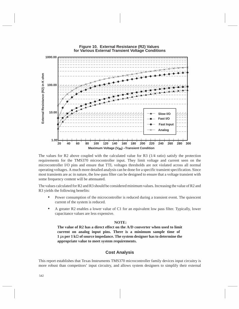
542
Figure 10. External Resistance (R2) Values for Various External Transient Voltage Conditions
Ext
erna
l Res
ista
nce
(R2)
in K
ohm
1000.00
100.00
10.00
1.0020 40 60 80 100 120 140 160 180 200 240 260 280 300220
Maximum Voltage (V IN) –Transient Condition
Fast Input
Fast I/O
Slow I/O
Analog
The values for R2 above coupled with the calculated value for R3 (1/4 ratio) satisfy the protectionrequirements for the TMS370 microcontroller input. They limit voltage and current seen on themicrocontroller I/O pins and ensure that TTL voltages thresholds are not violated across all normaloperating voltages. A much more detailed analysis can be done for a specific transient specification. Sincemost transients are ac in nature, the low-pass filter can be designed to ensure that a voltage transient withsome frequency content will be attenuated.
The values calculated for R2 and R3 should be considered minimum values. Increasing the value of R2 andR3 yields the following benefits:
• Power consumption of the microcontroller is reduced during a transient event. The quiescentcurrent of the system is reduced.
• A greater R2 enables a lower value of C1 for an equivalent low pass filter. Typically, lowercapacitance values are less expensive.
NOTE:The value of R2 has a direct effect on the A/D converter when used to limitcurrent on analog input pins. There is a minimum sample time of 1 µs per 1 kΩ of source impedance. The system designer has to determine theappropriate value to meet system requirements.
Cost Analysis
This report establishes that Texas Instruments TMS370 microcontroller family devices input circuitry ismore robust than competitors’ input circuitry, and allows system designers to simplify their external

543
conditioning circuitry. The ultimate goal and the reason for this analysis is to minimize cost at the systemlevel. The following section establishes the substantial system level cost savings associated with robustinput circuitry.
Several typical input conditioning circuits are shown in Figure 11. This is by no means an exhaustive list,but it provides a basis for cost comparison between different types of input circuits. Figure 11 illustratesthe simple resistor divider input conditioning circuit for Texas Instruments TMS370 family TTL inputs,as well as other external protection circuits such as external diodes, external zener, transistor level shifter,and a buffered hex-inverter used as a level shifter.
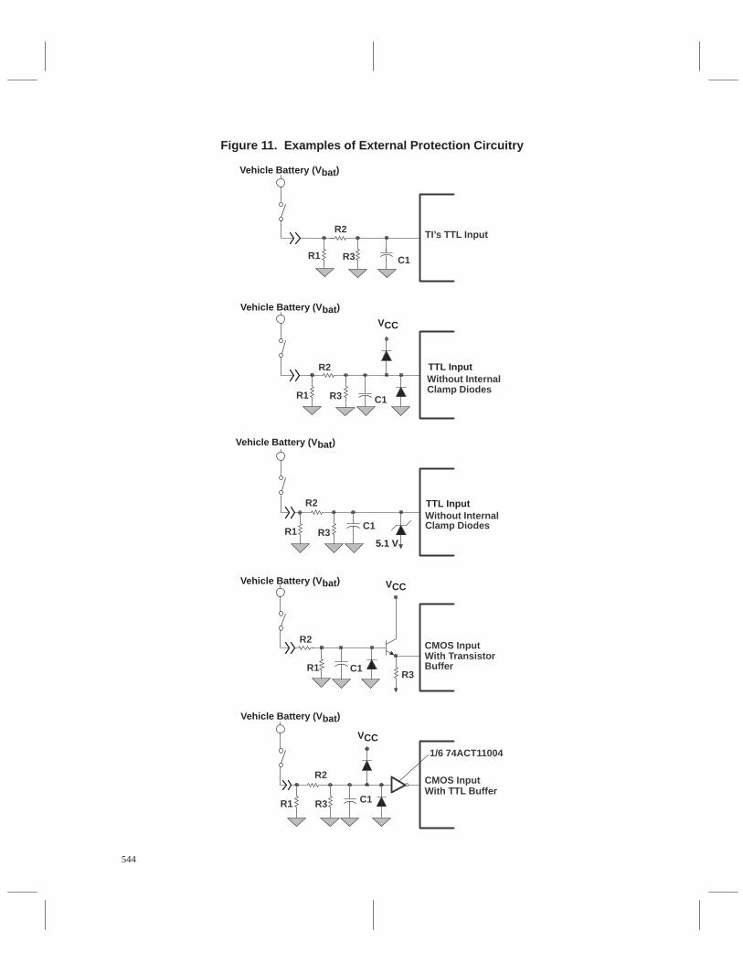
544
Figure 11. Examples of External Protection Circuitry
R2
R1 R3 C1
TI’s TTL Input
R1 R3
R2
C1
R1 R3
R2
C1
Without InternalClamp Diodes
Without InternalClamp Diodes
R1R3
R2
C1
CMOS InputWith TransistorBuffer
R1 R3
R2
With TTL BufferC1
CMOS Input
1/6 74ACT11004
Vehicle Battery (V bat)
Vehicle Battery (V bat)
Vehicle Battery (V bat)
Vehicle Battery (V bat)
Vehicle Battery (V bat)
5.1 V
TTL Input
TTL Input
VCC
VCC
VCC

545
Table 6 is a cost comparison among the five implementations shown in figure 11. The following componentcost assumptions in the table below are used for comparison purposes only.
• Resistor $.01
• Capacitor $.02
• Signal diode $.04(assume dual SOT23)
• Zener diode $.05
• Small signal transistor $.05
• Hex inverter (74ACT11004) $.05(assume 1/6 total cost of device and decoupling caps)
Table 6. Cost Comparison
ÁÁÁÁÁÁÁÁÁÁÁÁÁÁÁÁÁÁÁÁÁ
Component ÁÁÁÁÁÁÁÁÁÁÁÁÁÁÁ
TI’sTTL input
ÁÁÁÁÁÁÁÁÁÁÁÁÁÁÁÁÁÁ
TTL InputDiode
Protection
ÁÁÁÁÁÁÁÁÁÁÁÁÁÁÁÁÁÁ
TTL InputZener Protection
ÁÁÁÁÁÁÁÁÁÁÁÁÁÁÁÁÁÁ
CMOSTransistor
Buffer
ÁÁÁÁÁÁÁÁÁÁÁÁÁÁÁ
CMOSTTL Buffer
ÁÁÁÁÁÁÁÁÁÁÁÁÁÁ
R1 ÁÁÁÁÁÁÁÁÁÁ
.01 ÁÁÁÁÁÁÁÁÁÁÁÁ
.01 ÁÁÁÁÁÁÁÁÁÁÁÁ
.01 ÁÁÁÁÁÁÁÁÁÁÁÁ
.01 ÁÁÁÁÁÁÁÁÁÁ
.01
ÁÁÁÁÁÁÁÁÁÁÁÁÁÁ
R2 ÁÁÁÁÁÁÁÁÁÁ
.01 ÁÁÁÁÁÁÁÁÁÁÁÁ
.01 ÁÁÁÁÁÁÁÁÁÁÁÁ
.01 ÁÁÁÁÁÁÁÁÁÁÁÁ
.01 ÁÁÁÁÁÁÁÁÁÁ
.01
ÁÁÁÁÁÁÁR3 ÁÁÁÁÁ.01 ÁÁÁÁÁÁ.01 ÁÁÁÁÁÁ.01 ÁÁÁÁÁÁ.01 ÁÁÁÁÁ.01ÁÁÁÁÁÁÁÁÁÁÁÁÁÁC1
ÁÁÁÁÁÁÁÁÁÁ.03
ÁÁÁÁÁÁÁÁÁÁÁÁ.03
ÁÁÁÁÁÁÁÁÁÁÁÁ.03
ÁÁÁÁÁÁÁÁÁÁÁÁ.03
ÁÁÁÁÁÁÁÁÁÁ.03ÁÁÁÁÁÁÁ
ÁÁÁÁÁÁÁD1ÁÁÁÁÁÁÁÁÁÁN/A
ÁÁÁÁÁÁÁÁÁÁÁÁ.04
ÁÁÁÁÁÁÁÁÁÁÁÁN/A
ÁÁÁÁÁÁÁÁÁÁÁÁ.04
ÁÁÁÁÁÁÁÁÁÁ.04ÁÁÁÁÁÁÁ
ÁÁÁÁÁÁÁZener
ÁÁÁÁÁÁÁÁÁÁ
N/AÁÁÁÁÁÁÁÁÁÁÁÁ
N/AÁÁÁÁÁÁÁÁÁÁÁÁ
.05ÁÁÁÁÁÁÁÁÁÁÁÁ
N/AÁÁÁÁÁÁÁÁÁÁ
N/AÁÁÁÁÁÁÁÁÁÁÁÁÁÁ
Q1 ÁÁÁÁÁÁÁÁÁÁ
N/A ÁÁÁÁÁÁÁÁÁÁÁÁ
N/A ÁÁÁÁÁÁÁÁÁÁÁÁ
N/A ÁÁÁÁÁÁÁÁÁÁÁÁ
.05 ÁÁÁÁÁÁÁÁÁÁ
N/AÁÁÁÁÁÁÁÁÁÁÁÁÁÁ
1/6 74ACT11004 ÁÁÁÁÁÁÁÁÁÁ
N/A ÁÁÁÁÁÁÁÁÁÁÁÁ
N/A ÁÁÁÁÁÁÁÁÁÁÁÁ
N/A ÁÁÁÁÁÁÁÁÁÁÁÁ
N/A ÁÁÁÁÁÁÁÁÁÁ
.05
ÁÁÁÁÁÁÁÁÁÁÁÁÁÁ
Totals ÁÁÁÁÁÁÁÁÁÁ
$.06 ÁÁÁÁÁÁÁÁÁÁÁÁ
$.10 ÁÁÁÁÁÁÁÁÁÁÁÁ
$.11 ÁÁÁÁÁÁÁÁÁÁÁÁ
$.15 ÁÁÁÁÁÁÁÁÁÁ
$.15
The totals shown at the bottom of Table 6 indicate that the simple resistor divider circuit used to conditionTexas Instruments TTL inputs is the least expensive. Texas Instruments input only requires fourcomponents while the other conditioning circuitry requires between five and six components. There areextra costs with more components, such as manufacturing cost (costs to insert extra parts), inventory costs,board space, test time, etc. These costs are not reflected in the example above.
Conclusion
TTL input thresholds simplify the external circuitry required to ensure that the microcontroller recognizeslogic 1 and 0 input voltages across all valid vehicle voltages. There is a cost savings over the CMOS voltagelevels by using a simple resistor divider instead of active circuitry. Likewise, Texas Instruments TMS370family of microcontrollers allows system designers to use the internal diode protection circuits to withstandvoltage transients with a simple resistor divider. The ability to use the internal diode protection circuitsinstead of active components automatically reduces part count, perhaps board layout, complexity, andultimately, cost.

546
References
1. Texas Instruments,TMS370 Family Data Manual, pg. 16–18, 1993
2. Motorola Corp., MC68HC11E9 Data Sheet, Appendix A, pg. 2, April 1992
3. Motorola Corp., 80C51 Data Sheet, pg. 13–3, March 1992
4. Phillips Semiconductor Corp., 80C51 Data Sheet, pg. 142, Jan 26, 1993
5. National Semiconductor Corp., COP888CF Data Manual, pg. 7, May, 1992
6. TI, Advanced CMOS Logic, 1988
7. TI, High Speed CMOS Logic, 1989


![[BAB I] Microcontroller ATMEGA8535](https://img.pdfslide.net/doc/110x75/635d9893a0f1eac29f0c45be/bab-i-microcontroller-atmega8535.jpg)


