Embed Size (px)
Citation preview
18Plasma-assisted techniques for
growing hard nanostructured
coatings: an overviewR.S. Pessoa*,†, M.A. Fraga†,‡, L.V. Santos*,†, N.K.A.M. Galvao†,
H.S. Maciel*,†, and M. Massi**�IP&D, University of Paraiba Valley (UniVap), Sao Jose dos Campos/SP, Brazil;†Technological Institute of Aeronautics (ITA-DCTA), Sao Jose dos Campos/SP, Brazil;‡Faculty of Technology of Sao Paulo, Sao Paulo/SP, Brazil; ��Federal University ofSao Paulo-ICT, Sao Jose dos Campos/SP, Brazil
18.1 Introduction
Nanostructured materials are a new class of materials that are distinguished from
conventional materials by their extremely fine grain size from 100 nm down to a just
few nm. This is due to the small grain and the significant contribution of the grain
boundary regions causing the “nanoscale effect,” in which the properties are opti-
mized or exhibit completely new and/or different behavior compared to conventional
materials (Baer et al., 2003; Musil, 2012). Several papers refer to the properties of
nanostructured materials as “unique properties,” for example, superior hardness,
toughness, chemical stability, low friction and wear-resistance, and these unique
properties allow then to be applied in various technological sectors (Lukaszkowicz,
2011; Baer et al., 2003; Lu et al., 2006; Pogrebnjak and Beresnev, 2012). Table 18.1
presents some nanostructured materials and respective technological applications.
The thin (nanometer-sized) coating of a bulk material is a crescent category in the
field of nanostructured materials. The highly sophisticated surface-related properties
of nanocoatings, such as super-plasticity, and optical, magnetic, electronic and cata-
lytic properties, make them attractive for industrial applications in high-speed
machining, tooling, biomedical, automotive, optical applications and magnetic stor-
age devices (Musil, 2012; Baer et al., 2003).
There are many types of design models for nanostructured coatings, such as
nanocomposite coatings (Pogrebnjak and Beresnev, 2012), nanoscale multilayer
coatings (Hovsepian and Munz, 2003), superlattice coatings (Hovsepian and Munz,
2003; Munz et al., 2001), and nanocrystalline coatings (Malshe et al., 2002;
Hernandez-Torres et al., 2012). Moreover, there are different combinations for
nanocoating formation, namely metal�metal, metal�ceramic, ceramic�ceramic,
and solid�lubricant. Thus, by engineering these composite materials at the nanome-
ter scale, it is possible to enhance the materials properties such as hardness, making
it possible to obtain hard (with hardness above 20 GPa), super-hard (hardness above
Anti-Abrasive Nanocoatings.
© 2015 Elsevier Ltd. All rights reserved.

40 GPa), or even ultra-hard (80 GPa) materials, that rival diamond performance
(Zhang et al., 2003). As is known, diamond demonstrates both high thermal conduc-
tivity and electrically insulating properties and much attention has been put into
finding practical applications for this material. However, diamond has several lim-
itations for mass industrial applications, including its high cost and oxidation at
temperatures above 800�C (John et al., 2002). Therefore, recent research into super-
and ultra-hard materials has focused on compounds that would be thermally and
chemically more stable than pure diamond. Some examples of super-hard materials
are cubic boron nitride (c-BN), carbon nitrides, silicon carbide (SiC), and ternary
compounds such as boron-carbon-nitride (B-N-C). Sapphire and zirconia are exam-
ples of ultra-hard materials.
Table 18.1 Nanostructured materials and respective technologicalapplications in different fields of science and industry
Nanostructured
materials
Some technological applications in
different fields
References
Al-N based
coatings
Optical protective coatings Li et al. (2005)
Optoelectronic (field emission devices, flat
panel displays), heterostructure diodes
for UV light emitters and homojunction
light emitting diodes (LED)
Kasu and Kobayashi
(2000), Miskys
et al. (2003)
Protective layers against corrosion Miao et al. (1997)
Electromechanical/microelectromechanical
systems (MEMS) (piezoelectric sensing
layers)
Perooly et al. (2005)
B-N based
coatings
Field passivation and capping layers for
thermal annealing
Bathe et al. (2001)
Protective layers for metallic filaments Bathe et al. (2001),
Rudolph (1993)
Electrical insulation Rudolph (1993)
Si-C based
coatings
Optical coatings Fraga et al. (2012)
Optoelectronic (LED and heterojunction
diodes)
Kortright and Windt
(1988)
Piezoresistive sensing layers Fraga et al. (2011)
Si-N based
coatings
Microelectronics (sacrificial layers) Williams et al. (2003)
Electronic passivation of silicon surfaces
and antireflection coating on silicon
solar cells
Nagel et al. (1999)
Ti-C based
coatings
Industrial (high-speed machining, tooling,
and wear)
Steinmann and
Hintermann (2009)
Hard disk drives Sangkla et al. (2011),
Vitu et al. (2008)
Biocompatible implants Vitu et al. (2008)
Carbon based
coatings
Biomedical Takeno et al. (2010)
Tribological Bull (1995)
456 Anti-Abrasive Nanocoatings

All these designs and manipulations of materials with unique properties that are
often unachievable in bulk materials are now possible due to recent advances in tech-
niques for deposition and processing of thin films. Additionally, the design of hard
nanostructured coatings needs many factors to be taken into consideration, for exam-
ple, the interface volume, grain size, single layer thickness, surface and interfacial
energy, texture, epitaxial stress and strain, all of which depend significantly on mate-
rials selection, deposition methods, and processing parameters (Baer et al., 2003;
Malshe et al., 2002).
Physical vapor deposition (PVD), chemical vapor deposition (CVD), ion implan-
tation, and laser beam treatments are the most widely applied procedures for modify-
ing the chemical composition and/or atomic structure of solid surfaces on a
nanometer scale. In this chapter an overview is presented of the hard nanocoatings and
the main plasma-assisted techniques for their synthesis. Among these techniques,
plasma enhanced chemical vapor deposition (PECVD), magnetron sputtering, and
atomic layer deposition (ALD) are highlighted. Characteristics of some hard coatings
such as DLC, SiC, c-BN, and aluminum oxide (Al2O3) as well as heterostructures
obtained by these techniques are presented.
18.2 Hard nanocoatings: from history to designsand properties
The concepts that seeded nanotechnology were first discussed in 1959 by renowned
physicist Richard Feynman in his talk “There’s Plenty of Room at the Bottom,” in
which he described the possibility of synthesis via direct manipulation of atoms
(Drexler, 1992). Only in 1974 was the term “nanotechnology” defined by Tokyo
Science University Professor Norio Taniguchi: “Nanotechnology mainly consists of
the processing of, separation, consolidation, and deformation of materials by one
atom or by one molecule” (Sandhu, 2006). The ideas contained in this definition
were further explored and developed by K. Eric Drexler in the late 1970s and
1980s, culminating in the release of his book Engines of Creation: The Coming Era
of Nanotechnology in 1986, which is considered the first book on the topic of nano-
technology (Drexler, 1986). Hence, emergence of nanotechnology as a field in the
1980s occurred through convergence of Drexler’s theoretical and public work,
which developed and popularized a conceptual framework for nanotechnology, and
high-visibility experimental advances that drew additional wide-scale attention to
the prospects of atomic control of matter.
At the same time, the German physicist Herbert Gleiter contributed significantly
and at various levels, to the development of nanostructured materials (Nordmann,
2009). Several papers cite H. Gleiter as the first to introduce the field of nano-
structured materials with his proposal to synthesize a new solid state structure � an
interfacial material � which differs from the crystalline and amorphous counter-
parts of the same chemical composition (Nordmann, 2009; Gleiter, 2000; Meyers
et al., 2006; Langdon, 2010). Gleiter’s proposal to achieve such a new structure by
457Plasma-assisted techniques for growing hard nanostructured coatings: an overview

introducing very large volume fractions of grain boundary or interface atoms by
crystal size reduction was based on the understanding of grain boundary structure.
Thus, by controlling the type and/or volume fraction of grain boundaries of conven-
tional engineering materials, unique material performance characteristics in bulk
materials as well as films and coatings can be achieved (Gleiter, 2000). After this
work, the interest in nanostructured materials greatly increased alongside the devel-
opment of techniques for engineering of these materials.
As mentioned in the Section 18.1, there are different design models for nanos-
tructured coatings where the main classes are: nanoscale multilayer coatings
and nanocomposite coatings (Musil, 2000; Lukaszkowicz, 2011; Pogrebnjak et al.,
2013). The multilayer coatings exhibit composition and phase modulation in one
direction of space (the growth direction), whereas the nanocomposite coatings are
modulated in all three directions of space. Due to the size effect, these new classes
of materials exhibit improved mechanical, electronic, magnetic and optical proper-
ties, and, of all the exotic properties, hardness is one of the most important for
applications in manufacturing industry (Pogrebnjak and Beresnev, 2012). For exam-
ple, nanocomposite coatings can present hardness two times greater than that of its
harder component (Pogrebnjak and Beresnev, 2012; Musil et al., 2001). From
knowledge of nanostructured materials emerged the following hardness classifica-
tion: materials with hardness greater than 20 GPa and less than 40 GPa are called
hard materials, super-hard materials and the ultra-hard materials refer to materials
with hardness $40 GPa and $80 GPa respectively (Zhang et al., 2002).
The hardness of nanostructured coatings as well as conventional bulk materials
is related to the material grain size (Lukaszkowicz, 2011; Zhang et al., 2003). The
relationship of the hardness and the grain size is illustrated in Figure 18.1; from this
Amorphous
Microcrystalline phase
Nanocrystalline
Har
dnes
s
100 101 102 104 106
Grain size, d (nm)
dc
Figure 18.1 Behavior of the hardness of materials as a function of grain size.
Source: Adapted from Lukaszkowicz, 2011; Pogrebnjak and Beresnev, 2012; Zhang et al., 2003.
458 Anti-Abrasive Nanocoatings

it can be seen that there is a critical value of the grain size dc� 10 nm at which a
maximum value of hardness, Hmax, of the coating is achieved.
When the grain size is decreased to about 10 nm, the mobility of dislocations is
restricted. This occurs because the refined grain and the boundary regions suppress
the dislocation, causing the onset of incoherent deformations and increasing the
hardness of the material accord with the “Hall-Petch” relationship (Musil, 2012;
Zhang et al., 2003; Schiotz, 2001; Holleck, 1999):
HðdÞ5H0 1KUd21=2 (18.1)
where, H is the material hardness, K is strengthening coefficient and d is the grain
size. This effect is especially prominent for grain size down to tens of nanometers
(Lukaszkowicz, 2011; Zhang et al., 2003). In grain size of approximately 10 nm
there is a critical value where the maximal hardness is achieved. For grain size less
than dc, due to the increase in grain boundary a new deformation mechanism (i.e. the
Hall-Petch relation is inverted), called grain boundary sliding, replaces the disloca-
tion activity that dominates deformation process in conventional materials, thus
decreasing the hardness (Pogrebnjak and Beresnev, 2012; Zhang et al., 2003).
Softening caused by grain boundary sliding is mainly attributed to the large amount
of defects in the grain boundaries, which allows fast diffusion of atoms and vacan-
cies with the applying of stress. A further increase in the strength and hardness with
decreasing crystallite size can be achieved only if grain boundary sliding is blocked
by appropriate coating design and materials selection.
18.2.1 Classifications of hard nanocoatings
There are many design ideas for nanocomposite coatings, and embedding nano-
crystalline phases in the amorphous phase matrix is quite often applied which can
be fulfilled easily by PVD and CVD methods (Zhang et al., 2002). According to
Musil there are at least four types of nanostructures (Figure 18.2) that result in the
enhanced hardness of nanocomposite coatings: (1) bilayers with nanosize period λ;(2) the columnar nanostructure; (3) nanograins surrounded by a very thin tissue
phase, w (B1 to 2 monolayers); and (4) the mixture of nanograins with different
crystallographic orientations and/or different phases; here λ5 h11 h2, h1 and h2are the thickness of first and second layer of the bilayer, respectively (Musil,
2012).
Individual nanostructures are formed under different conditions using either a
sequential deposition of individual layers in the nanosize bilayers or in transition
regions where the coating structure changes from crystalline through nanocrystal-
line to amorphous. There are three transition regions: (1) the transition from the
crystalline to the amorphous material; (2) the transition between two crystalline
phases of different materials; and (3) the transition between two crystallographic
orientations of grains of the same material (Pogrebnjak and Beresnev, 2012).
459Plasma-assisted techniques for growing hard nanostructured coatings: an overview

Additionally, in 1999, Holleck et al. proposed a classification of hard coatings in
three groups according to their bonds (see Figure 18.3): (1) covalent hard materials;
(2) metallic hard materials; and (3) ionic hard materials (Zhang et al., 2003; Holleck,
1999; Zhang et al., 2005; Stuber et al., 2011).
(a) Nanosized bilayer
Layer 1
Layer 2
Layer 1
Layer 2
(b) Nanocolumn
(c) Nanograins surroundedby a tissue phase
(d) Nanograins with differentcrystallographic orientation
λ
Nanograin
w
Nanograin 1 Nanograin 2Tissue phase3D
sys
tem
s2D
sys
tem
sFigure 18.2 Schematic illustration of four nanostructures of the nanocomposite coating with
enhanced hardness: (a) nanosize bilayers, (b) columnar nanostructure, (c) nanograins
surrounded by a tissue phase, and (d) mixture of nanograins with different crystallographic
orientation (adapted from Musil, 2012; Pogrebnjak and Beresnev, 2012). Where w is the
tissue phase thickness.
Covalent bond
Hardness
Ionic bond
Stability, inertness
Metallic bond
Adhesion, toughness
Metallic hard materialsCovalent hard materials
Ionic hard materials
Titanium based
TiCTiBCN
TiN
TiSiCTiA1CN
Ti2N
VCWCCrN
Others
Diamond likeC
Others
SiCCN BN
A12O3ZrO2
A1N
Figure 18.3. Classification of some hard coatings with relation to their bond nature.
Source: Adapted from Zhang et al., 2003; Holleck, 1999; Zhang et al., 2005.
460 Anti-Abrasive Nanocoatings

The specific properties of each hard material group are related to the bond type
between the elements. For example, covalent coatings such as diamond and boron
nitride are the hardest materials and have a high temperature strength, whereas the
ionic (ceramic) coatings exhibit the best chemical inertness and higher brittleness.
Metallic coatings have a good adhesion and toughness.
From Figure 18.3, S. Zhang et al. (2003) conclude that the best to design a nano-
composite coating with both high hardness and high toughness is probably to use
ternary, quaternary or even more complex systems (for example, multilayer struc-
ture Zhang et al., 2005), with a high-strength amorphous phase as matrix (such as
a-SiNx, a-BN, a-C) and hard transition metal-nitride nanocrystals (such as TiN, BN)
as the nanocrystalline phase to increase grain boundary complexity and strength.
These nanocrystalline phases should be refractory and immiscible with each other,
and could result in compositional modulation, segregation, and high thermal stabil-
ity of the nanostructure. The aim is to maximize interfaces and form well-defined
spinodal structure at interfaces.
18.2.2 Hardness mechanisms of crystallinenanostructured materials
There are few intrinsic super-hard materials highlighting diamond, c-BN and
some binary and ternary B-C-N compounds. Studies show that the high intrinsic
hardness of these materials is related to the following characteristics: a short inter-
atomic distance, a high binding energy, and a high degree of covalent bonding
(Gao et al., 2003).
On the other hand, there is a group of hard materials that have what is called
extrinsic hardness. These crystalline materials have the hardness determined by
their microstructure, that is, it is possible obtain hard and super-hard nanocoatings
from these materials only by hindering or retarding the deformation generated by
dislocation movements (Arzt, 1998).
The four main mechanisms that can modify the hardness of crystalline materials
are illustrated in Figure 18.4.
It is known that high hardness is achieved for maximal concentration of introduced
distortions. Grain boundary is an example of a lattice distortion. This mechanism
has been observed especially in nanocrystalline ceramics (Szlufarska et al., 2005),
Hardnessmechanisms
Grain boundary Solid solution Precipitation Energetic ionbombardment
Figure 18.4. Different mechanisms that can influence the hardness of crystalline materials.
461Plasma-assisted techniques for growing hard nanostructured coatings: an overview

nanocrystalline metals (Van Swygenhoven, 2002), and multilayer nanostructures
(Mayrhofer et al., 2005).
Solid solution mechanisms are characterized by lattice distortion due to the
insertion of atoms of the solute (also called alloy element) either in interstitial or
substitutional lattice positions. These mechanisms are limited by the solubility limit
of the solute. It has been observed that PVD processes at low substrate temperature
increase the solubility limit (Holleck, 1988). Examples of hard coatings that can be
obtained from the solid solution mechanism are Ti-C-N, Ti-Al-N, and Cr-Al-N
(Zhang et al., 2007).
Precipitation or dispersion strengthening is the process characterized by the pre-
cipitation of a second phase from a supersaturated metastable phase. Generally, this
mechanism is accelerated and controlled by a post-deposition annealing (Arzt,
1998). The literature reports the precipitation mechanism for nanocrystalline thin
films such as Ti-Al-N (Mayrhofer et al., 2003), Ti-B-N (Mayrhofer et al., 2006),
and Zr-Al-N (Sanjines et al., 2006).
Energetic ion bombardment is another mechanism used to obtain hard coatings
during film growth. It has been employed to modify the morphology of the films.
The ion bombardment creates interstitials and vacancies that can lead to the forma-
tion of dimensional defects (Mattox, 1989). These defects are associated with the
existence of internal stress in the films, which result in hardness increase. It has
been reported for different PVD coatings (Mayrhofer et al., 2006).
18.3 Main plasma-based techniques for synthesisof hard nanocoatings
A variety of modern coating techniques have been employed to realize hard nanos-
tructured coatings. Among these technologies are plasma-assisted PVD, CVD, and
PECVD processes, which make it possible to grow materials with extremely high
indentation hardness (40�80 GPa) (Veprek and Veprek-Heijman, 2007; Veprek
et al., 2000; Zou et al., 2010).
Table 18.2 provides a listing of hard thin film materials and compares the micro-
hardness of PECVD and PVD deposited thin films (note that nanocrystalline films
have the highest hardness) (Martinu et al., 2009). Several types of films deposited
by PECVD have microhardness in the super-hard range while the number is limited
for PVD deposited films. Hardness is generally improved by increasing the energy
of deposited atoms using high substrate temperatures, substrate bias, plasma bom-
bardment (ion assist), or a combination of all four.
Moreover, as can be seen in Table 18.2 the most widely used hard and super-
hard coatings are binary and ternary alloys of titanium, boron, chromium, tungsten,
silicon, and allotropes of carbon.
The sections that follow describe plasma-assisted techniques for growing hard
nanostructured coatings as well as discussing materials synthesis and its resulting
properties.
462 Anti-Abrasive Nanocoatings

18.3.1 Physical vapor deposition
The PVD process comprises physical and reactive sputtering techniques. Basically,
these techniques differ when a neutral gas (physical sputtering) is added together
with a reactive gas (reactive sputtering). In physical sputtering, ions impinging on
Table 18.2 Microhardness of PECVD and PVD films
Note: a � amorphous, c � crystalline, pc � polycrystalline, and nc � nanocrystalline.Source: Adapted from Zhang et al., 2005.
463Plasma-assisted techniques for growing hard nanostructured coatings: an overview

the plasma bombard the target and release atoms (or molecules) of the target mate-
rial. Argon ions at 500�1000 V are usually used. The sputtered atoms diffuse
through the plasma and arrive at the substrate, where they can be deposited
(Bogaerts et al., 2003). In reactive sputtering, a molecular gas (for example, N2
and/or O2) is used together or without a neutral gas. Besides the positive ions from
the plasma that sputter bombard the target, the dissociation products from the reac-
tive gas also react with the target. Hence, the film deposited at the substrate will be
a combination of sputtered target material and the reactive gas (Bogaerts et al.,
2003; Lieberman and Lichtenberg, 2007; Berg and Nyberg, 2005; Pessoa et al.).
The sputter deposition process is schematically presented in Figure 18.5.
The steps of sputtering process are as follows:
1. The neutral gas is ionized by an external power supply (direct current, radio-frequency,
etc.), producing a glow discharge or plasma.
2. The source (the cathode, also called the target) is bombarded in a high vacuum by plasma
ions due to the potential acceleration drop in the cathode sheath.
3. Atoms from the target are ejected by momentum transfer and diffuse through the vacuum
chamber.
4. Atoms are deposited on the substrate to be coated and form a thin film.
Because sputter yields are of the order of unity for almost all target materials, a
very wide variety of pure metals, alloys and insulators can be deposited. Physical
sputtering, especially of elemental targets, is a well understood process enabling sput-
tering systems for various applications to be relatively easily designed. Reasonable
deposition rates with excellent film uniformity, good surface smoothness and adhe-
sion can be achieved over large areas (Lieberman and Lichtenberg, 2007).
Figure 18.5 Schematics of the sputtering process.
464 Anti-Abrasive Nanocoatings

Typically, the sputtering process can be accomplished using a planar configura-
tion of electrodes and a direct current (DC) power supply, where one electrode is
biased negatively (cathode) and suffers the sputtering process. However, the sput-
tering yield is directly dependent on the gas pressure (the best sputtering rates are
in the range of mTorr), which compromises the efficiency of planar geometry for
this application: it is ideal for pressures above 100 mTorr. To solve this problem,
a magnetron discharge where the plasma is magnetically enhanced by placing
magnets behind the cathode target was developed, that is, a crossed electric and
magnetic field configuration is created. Figure 18.6 shows a schematic drawing of a
conventional DC magnetron sputtering discharge. The trapping of the secondary
electrons results in higher probability of electron impact ionization and hence high-
er plasma density, increasing the sputtering flux and allowing operation at lower
pressures, below 10 mTorr. Furthermore, the discharge voltage can be lowered into
the range of 300�700 V. The main problem with the magnetron sputtering configu-
ration is that the sputtering is confined to a small area of the target cathode gov-
erned by the magnetic field. The discharge appears in the form of a high-density
annulus of width w and radius R, as seen in Figure 18.6. Sputtering occurs in the
corresponding track of the target. This area, known as race track, is created by the
uneven ion density.
According to the Hall-Petch equation, the strength properties of the material rise
along with the reduction of the grain size. In case of coatings deposited by the PVD
processes, the structures obtained, with grain size B10 nm result in the maximum
mechanical properties. Coatings of this structure present very high hardness
(.40 GPa), ductility, stability at high temperatures, and so on (Lukaszkowicz,
2011). According to Musil, the addition of one or more selected elements into a
base material, for example, the addition of Si in the nitride transition metal (TM), is
a very effective way to produce hard nanocomposite coatings with enhanced hard-
ness, here TM5Ti, Zr, Hf, V, Nb, Ta, and so on (Musil, 2012). Moreover, it is
highlighted that the energy delivered to the growing film also has a crucial effect
on its structure, elemental and phase composition, and physical properties
Figure 18.6 Schematic drawing of a conventional dc magnetron sputtering discharge.
Source: Adapted from Bogaerts et al., 2003.
465Plasma-assisted techniques for growing hard nanostructured coatings: an overview

(Musil, 2012). This energy is delivered from the plasma environment and is com-
posed of (1) heating processes; and (2) conversion of the kinetic energy of bom-
barding ions and fast neutrals incident on the surface of growing film.
Recently, amorphous coatings with hardness ranging from B20 � B40 GPa
were reactively sputtered using an unbalanced magnetron deposition technique
(Musil, 2012):
1. a-(Si3N4/MeNx) composite coatings with high ($50 vol.%) content of a-Si3N4 phase; here
Me5Ta, Zr, Ti, Al, Mo, W, and so on.
2. a-(Si�B�C�N) coatings with strong covalent bonds. Magnetron sputtered films were
deposited co-sputtered using high purity graphite and boron targets in 50/50 Ar1N2 mix-
tures with formation of hybridized B-C-N bonds (Kim et al., 2004).
Also, super-hard amorphous SiC coatings are deposited by our group using co-
sputtering of silicon and carbon targets. Here the SiC coatings were obtained with
hardness of up to 50 GPa only modifying the negative bias applied at the substrate
holder (Medeiros, 2012).
Relative to the deposition of boron nitride films in cubic form (c-BN), it is reported
that the lower adhesion and extreme compressive stresses of these films are the main
problems in PVD techniques, which limits film thickness of c-BN up to 1 μm.
However, many researchers have reported adherent and thick multilayered films
recently (Cesur et al., 2008). Boron carbon nitride (BxCyN), also known as “heterodia-
mond” is essentially c-BN that contains between 5 at% and 30 at% C and is generally
deposited by PVD and CVD processes (Yamamoto et al., 2000). Magnetron sputtered
films were deposited co-sputtered using high purity graphite and boron targets in
50/50 Ar1N2 mixtures with formation of hybridized B-C-N bonds. Table 18.3
summarizes hardness values for the B-C-N family (Ulrich et al., 2009).
18.3.2 Chemical vapor deposition
In the field of chemical-based deposition techniques of hard coating thin films liq-
uid phase epitaxy (LPE), CVD techniques and their derivatives, such as PECVD
and atomic layer deposition (ALD), can be mentioned, among others. A very desir-
able feature of CVD-based techniques is that they can be carried out with well con-
trolled atmospheres and at lower temperatures (lower than 1500�C) in comparison
with other related techniques.
Currently, the most popular low-pressure thin film deposition techniques are
those based on chemical deposition processes such as hot filament chemical vapor
Table 18.3 Summary of hardness values for the B-C-N family(Solozhenko et al., 2009)
Material Diamond c-BC2N c-BC5 c-BN B4C ReB2
Vickers Hardness (GPa) 115 76 71 62 38 22
466 Anti-Abrasive Nanocoatings

deposition (HFCVD) and PECVD (Veprek et al., 2000; Zou et al., 2010; Bogaerts
et al., 2003; Lieberman and Lichtenberg, 2007).
Thermal CVD is the process of gas phase heating (by a hot filament or hot wall,
for example (Berg and Nyberg, 2005)) in order to cause the decomposition of the
gas, generating radical species that, by diffusion, can reach and be deposited on a
suitably placed substrate. It differs from PVD, which relies on material transfer
from a condensed-phase evaporant or sputter target sources. A reaction chamber is
used for this process, into which the reactant gases are introduced to decompose
and react with the substrate to form the film. Figure 18.7(a) illustrates a schematic
of the reactor and its main components. Basically, a typical thermal CVD system
(HFCVD) consists of the following parts:
1. sources and feed lines of gases;
2. mass flow controllers for metering the gas inlet;
Figure 18.7 Schematic diagram of (a) HFCVD and (b) PECVD systems.
467Plasma-assisted techniques for growing hard nanostructured coatings: an overview

3. a reaction chamber for decomposition of precursor gases;
4. a system for heating up (hot filament or hot wall) the gas phase and wafer on which the
film is to be deposited; and
5. temperature sensors.
As a modification to the CVD system, PECVD arose when plasma was used to
perform the decomposition of the reactive gas source. By chemical reactions in
the plasma (mainly electron impact ionization and dissociation), different kinds of
ions and radicals are formed which diffuse toward the substrate where chemical
surface reactions are promoted, leading to film growth. The major advantage com-
pared to simple CVD is that PECVD can operate at much lower temperatures.
Indeed, the electron temperature of 2�5 eV in PECVD is sufficient for dissocia-
tion, whereas in CVD the gas and surface reactions occur by thermal activation.
Hence, some coatings, which are difficult to form by CVD due to melting pro-
blems, can be deposited more easily with PECVD (Lieberman and Lichtenberg,
2007; Peng et al., 2011). Among the kinds of plasma sources that have been used
for this application radiofrequency (RF) discharges (Lieberman and Lichtenberg,
2007), pulsed discharges (Peng et al., 2011), and microwave discharges (Berg and
Nyberg, 2005) stand.
Basically, in PECVD the substrate is mounted on one of the electrodes in the
same reactor where the species are created, as illustrated in Figure 18.7(b). Here,
we focused the RF discharge because it is the configuration more used in research
and industry. The RF PECVD reactor essentially consists of two electrodes of dif-
ferent areas, where the substrate is placed on the smaller electrode, to which the
power is capacitively coupled. The RF power creates a plasma between the electro-
des. Due to the electrons having higher mobility than the ions, a sheath is created
next to the electrodes containing an excess of ions. Hence, the sheath has a positive
space charge, and the plasma creates a positive voltage with respect to the electro-
des. The electrodes therefore acquire a DC self-bias equal to their peak RF voltage
(self-bias electrode). The ratio of the DC self-bias voltages is inversely proportional
to the ratio of the squared electrode areas, that is, V1/V25 (A1/A2)2 (Lieberman
and Lichtenberg, 2007).
Therefore, the smaller electrode acquires a larger bias voltage and becomes neg-
ative with respect to the larger electrode. The negative sheath voltage accelerates
the positive ions towards the substrate which is mounted on this smaller electrode,
allowing the substrate to be bombarded by energetic ions facilitating reactions with
the substrate surface.
In order to maximize the ion-to-neutral ratio of the plasma, the plasma must be
operated at the lowest possible pressure. Nevertheless, the ions are only about 10%
of the film-forming flux even at pressures as low as 50 mTorr. Lower pressures
cannot be used, as the plasma will no longer strike. A second disadvantage of this
source is the energy spread in the ion energy distribution, prohibiting a controlled
deposition. This energy spread is due to inelastic collisions as the ions are acceler-
ated towards the substrate. The effect of this energy spread is to lower the mean ion
energy to about 0.4 of the sheath voltage. Another disadvantage of the RF PECVD
source is that it is not possible to have independent control over the ion energy and
468 Anti-Abrasive Nanocoatings

the ion current, as they both vary with the RF power. On the other hand, PECVD
allows the deposition of uniform films over large areas, and PECVD systems can be
easily scaled up (Zhao et al., 2010).
Figure 18.8 illustrates the deposition mechanism of the CVD technique (Zou
et al., 2010). The mechanism occurs as a result of the following steps:
1. A predefined mix of reactant gases and diluents inert gases are introduced at a specified
flow rate into the reaction chamber.
2. A heat source is applied in order to dissociate the reactant gases.
3. The resulting radical species diffuse to the substrate.
4. The reactants get adsorbed on the surface of the substrate.
5. The reactants undergo chemical reactions with the substrate to form the film.
6. The gaseous by-products of the reactions are desorbed.
7. The gaseous by-products of the reactions are evacuated from the reaction chamber.
In general, SiC PECVD is performed in conventional PECVD reactors with
heated substrate holders (Neyts, 2006). Methane and silane are commonly used pre-
cursors (Sarro et al., 1998; Pelegrini et al., 2010). It is also possible to use a single
precursor such as 1,3-disilabutane DSB or methylsilane. The film properties
strongly depend on the process parameters including deposition temperature, pres-
sure, plasma power, and gas phase composition. In general, PECVD SiC films
exhibit amorphous form and compressive stress, but process conditions can be opti-
mized to tailor the stress levels to desired values. Typically, low plasma power and
high temperature conditions yield low stress films. Sometimes post-deposition
annealing at temperatures of order of 1000�C may still be required to crystallize the
films. Typical values of hydrogenated SiC films deposited by PECVD ranging from
10 to 30 GPa (El Khakania et al., 1994; Kim et al., 2008).
1. Introduction of precursor gases
2. Transport of reactivespecies to the substrate
6. Transportation of reaction products
5. Desorption of reaction products
4. Migration of chemical species on the surface and film formation
3. Adsorption of reactive speciesonto the substrate surface
7. Removal of reaction products
Substrate
Figure 18.8 Chemical vapor deposition mechanism.
Source: Adapted from Zou et al., 2010.
469Plasma-assisted techniques for growing hard nanostructured coatings: an overview
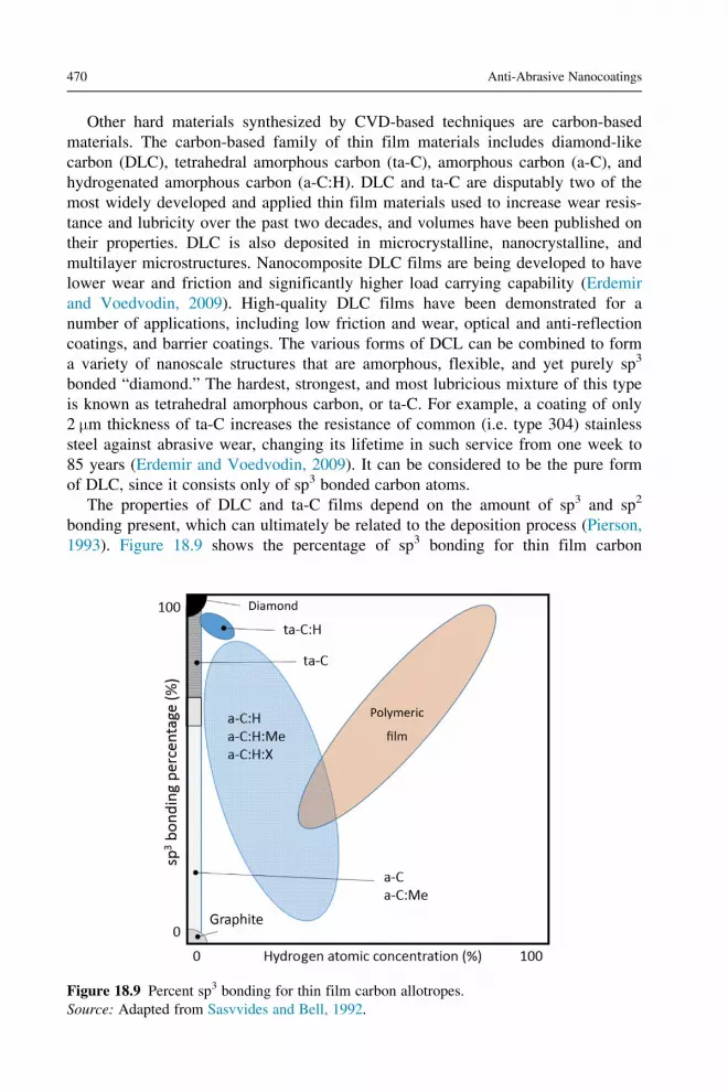
Other hard materials synthesized by CVD-based techniques are carbon-based
materials. The carbon-based family of thin film materials includes diamond-like
carbon (DLC), tetrahedral amorphous carbon (ta-C), amorphous carbon (a-C), and
hydrogenated amorphous carbon (a-C:H). DLC and ta-C are disputably two of the
most widely developed and applied thin film materials used to increase wear resis-
tance and lubricity over the past two decades, and volumes have been published on
their properties. DLC is also deposited in microcrystalline, nanocrystalline, and
multilayer microstructures. Nanocomposite DLC films are being developed to have
lower wear and friction and significantly higher load carrying capability (Erdemir
and Voedvodin, 2009). High-quality DLC films have been demonstrated for a
number of applications, including low friction and wear, optical and anti-reflection
coatings, and barrier coatings. The various forms of DCL can be combined to form
a variety of nanoscale structures that are amorphous, flexible, and yet purely sp3
bonded “diamond.” The hardest, strongest, and most lubricious mixture of this type
is known as tetrahedral amorphous carbon, or ta-C. For example, a coating of only
2 μm thickness of ta-C increases the resistance of common (i.e. type 304) stainless
steel against abrasive wear, changing its lifetime in such service from one week to
85 years (Erdemir and Voedvodin, 2009). It can be considered to be the pure form
of DLC, since it consists only of sp3 bonded carbon atoms.
The properties of DLC and ta-C films depend on the amount of sp3 and sp2
bonding present, which can ultimately be related to the deposition process (Pierson,
1993). Figure 18.9 shows the percentage of sp3 bonding for thin film carbon
Figure 18.9 Percent sp3 bonding for thin film carbon allotropes.
Source: Adapted from Sasvvides and Bell, 1992.
470 Anti-Abrasive Nanocoatings

allotropes (Sasvvides and Bell, 1992). It shows the two extremes, diamond and
graphite, and every combination of bonding in between. Note also that bonding
configuration is related to hydrogen content, and eventually back to the deposition
process. Microstructures range from purely amorphous to nanocrystalline. Hardness
definitely increases with an increase of sp3 percentage. CVD techniques allow con-
trolling sp3 percentage only modifying process parameters such as gas flow, sub-
strate bias, discharge power, etc.
Finally, we present some of the main advantages and disadvantages of CVD-
based techniques:
18.3.2.1 Advantages
� excellent interface and surface morphology;� growth of complex heterostructures with many different layers;� growth on patterned substrates;� multiple wafer scale-up;� high purity of the layers.
18.3.2.2 Disadvantages
� large quantities of serious toxic or flammable gases (AsH3, SiH4, etc.);� almost no possibility of in situ monitoring;� not the best technique for some specific material (lack of adequate precursors or of not
suited growth conditions).
18.3.3 Atomic layer deposition
18.3.3.1 Deposition technique
ALD is a nanocoating process based on the self-limiting gas�solid reaction where
it is possible to produce thin films of high quality (Violet et al., 2009; Marin et al.,
2012; Liang et al., 2008). This process is similar to CVD but in the ALD method
the reactions are divided into two separated processes (Marin et al., 2012). Thus,
ALD is a variant of the CVD process (Marin et al., 2009).
In the ALD method it is possible to control the film thickness at the atomic level
(Marin et al., 2009; Hoivik et al., 2003) over the deposition process. This control is
possible because unlike CVD, where the reactants are presented simultaneously dur-
ing the process, in ALD the precursor gases pulses are separated by purge steps of
an inert gas to remove the unreacted precursor and gases by products (Miikkulainen
et al., 2013; Wikimedia Commons; Leskela and Ritala, 2002; Puurunen, 2005). In
this process, the film thickness increases in each deposition cycle (Leskela and
Ritala, 2002). The cycle of the ALD reaction is showed in Figure 18.10.
When the alternating is realized with the ALD steps replaced by a pulsed CVD
step, the process is known as partial ALD (Granneman et al., 2007). Figure 18.11
shows a schematic model of ALD and partial ALD processes.
471Plasma-assisted techniques for growing hard nanostructured coatings: an overview

Precursor chemistry plays a very important role in the ALD process (Kim, 2011;
Kim, 2003). There are many requirements for the precursor used in the ALD pro-
cess, such as (Miikkulainen et al., 2013):
� it must be gaseous or vaporizable at a temperature lower than the ALD reaction
temperature;� it must react, preferably fast and aggressively, in a saturating, irreversible manner with
sites on the surface of the growth substrate;� the by-products formed should be inert not interfere with the ALD grown;
Figure 18.10 Schematic diagram of the ALD reaction cycle (adapted from Miikkulainen
et al. and Wikimedia Commons (Miikkulainen et al., 2013; Wikimedia Commons)): (1)
adsorbed reagent A molecule; (2) non-adsorbed reagent A molecule; (3) surface without �H
or �OH ligant; (4) unreacted site; (5) adsorbed reagent B molecule; (6) reagent A
contamination. Depending on temperature of the ALD process the as-deposited film can
contain reagent A contaminant.
Figure 18.11 Schematic model of: (a) ALD and (b) partial ALD process.
(Adapted from Granneman et al., 2007).
472 Anti-Abrasive Nanocoatings

� its reactants should not dissolve in the film and they must not decompose thermally during
storage, vaporization or ALD growth;� for some applications, high purity is required; and� it should present safe and easy handling, preferably not toxic or corrosive, thus ensuring
the integrity of the reactor and the user. And like any industrial process, low cost will
make it attractive to industries.
For reaction between the precursor and substrate surface an activation energy is
required. The activation energy is provided by the heating of the substrate and/or
the system (reactor chamber). In this case the process is known as “thermal ALD”
(Kim, 2011; Kim, 2003). Sometimes, precursors (molecular elements precursors)
are not sufficiently reactive, and thus they require more energy than provided in the
thermal ALD process. In order to reach the required energy, alternative methods
that complement the ALD process are used, for example plasma enhanced ALD
(PEALD). The difference between these two processes is that in PEALD the plasma
is activated during the step of exposure of the precursor (Kim, 2011; Kim, 2003)
and the film growth occurs at a lower temperature than in thermal ALD (Kim,
2011). Moreover, the reactant molecules of the precursor become more reactive and
the films deposited by PEALD have better properties, such as improved hardness
(Kim, 2011; Profijt et al., 2011).
Finally, the advantages of use the ALD technique include (Violet et al., 2009;
Marin et al., 2012; Leskela and Ritala, 2002; Granneman et al., 2007; Kim, 2003):
� deposition of several types of thin films (oxides, nitrides, sulfides and metals);� possibility of depositing films on various substrates, such as wafers, steel, 3D substrates,
micro- and nanoparticles, and others;� accurate thickness;� control of film thickness;� deposition of multilayers of different structures;� low deposition temperature.
18.3.3.2 Applications of ALD hard coatings
Although the main application of the ALD process is the deposition of ultra-thin
films, the hard coatings application is more geared towards the field of microelec-
tronics, more specifically in MEMS. MEMS comprise a variety of functional
mechanical devices fabricated on length scales from fractions of a micrometer to
millimeters. These devices are finding application in a wide variety of technologies,
including motion sensing, optical switching and other photonic applications, RF
switches and filters, mechanical actuators, chemical sensors, and others. As the size
of these devices shrinks, surface-to-volume ratio increases, and at dimensions
typical of MEMS devices, inertial forces become insignificant compared to sur-
face forces acting on these mechanisms. Then interfacial phenomena such as adhe-
sion, friction and wear can dominate the performance and reliability of MEMS
devices. The most sophisticated MEMS devices now in development employ sliding
contacts in rotary- or linear-motion structures, where friction and wear are a major
concern (Sniegowski and de Boer, 2000).
473Plasma-assisted techniques for growing hard nanostructured coatings: an overview

To mitigate these problems, the surfaces of MEMS devices can be modified
with coatings to prevent adhesion, and reduce friction and wear. Some of the most
commonly used/studied materials are the Al2O3, ZnO, WS2, W, and W/A12O3
nanolaminates. WS2 is a superior solid phase lubricant, W is a hard metallic,
wear-resistant material, and W/Al2O3 laminate films are potential super-hard coat-
ings with properties determined by the nanometer length scales of the laminate
layers.
Al2O3 is an advantageous material to use over various forms of silicon nitride, for
micro- and nanoelectromechanical systems, due in part to the low deposition temper-
ature that allows for integration with Complementary metal�oxide�semiconductor)
CMOS processing. Also, Al2O3, unlike silicon nitride, has a high chemical resistance
to dry-chemistry Si etchants (Tripp et al., 2006; Bull, 2012). Tripp et al. observed
that the hardness of ALD AL2O3 (order of 12 GPa) is comparable with the films pro-
duced by other deposition techniques (Tripp et al., 2006).
18.4 Conclusion
Engineered nanostructured thin films and low-dimensional structures are present on
thin film technology. New advanced deposition processes, such as ALD, are now
being developed and used to deposit advanced thin film materials and structures not
possible with conventional techniques. As a result, the hardness of thin films has
been steadily increasing, due primarily to new materials, improved deposition pro-
cesses and use of nanostructures and nanocomposites.
Plasma-assisted processes have contributed significantly to this development,
especially due to the ease automation of these processes allowing fine control of
the properties of matter. An example is the ALD process that has been well suited
to deposition of friction and wear-reducing films on MEMS structures. Sequential
reactant exposure and self-limiting surface chemistry result in exquisite control of
deposition rate and film thickness, and extremely conformal coating of high-aspect
ratio structures. However, the challenge remains to examine the mechanical and tri-
bological properties of thin and ultra-thin ALD films, and their suitability for appli-
cation in functional MEMS devices. Processes for preparation of a wide range of
materials, which are potential hard and/or lubricious coatings, have been demon-
strated by ALD (Ritala et al., 2002). The ease of fabrication of alloys and nanolami-
nates of ALD materials adds extra dimensions to the possibilities for tailoring the
properties of materials for tribological applications.
Acknowledgments
This work was supported by FAPESP-MCT/CNPq-PRONEX (process no. 2011/50773-0) and
PNPD-CAPES (process no. 02765/09-8).
474 Anti-Abrasive Nanocoatings

References
Arzt, E., 1998. Size effects in materials due to microstructural and dimensional constraints: a
comparative review. Acta Mater. 46, 5611�5626.
Baer, D.R., Burrows, P.E., El-Azab, A.A., 2003. Enhancing coating functionality using
nanoscience and nanotechnology. Prog. Org. Coat. 47, 342�356.
Bathe, R., Vispute, R.D., Habersat, D., Takeuchi, I., Sharma, R.P., et al., 2001. BN protective
coating for high temperature applications. MRS Proc. 697, P3.3. http://dx.doi.org/
10.1557/PROC-697-P3.3.
Berg, S., Nyberg, T., 2005. Fundamental understanding and modeling of reactive sputtering
processes. Thin Solid Films. 476, 215�230.
Bogaerts, A., Neyts, E., Gijbels, R., van der Mullen, J., 2003. Gas discharge plasmas and
their applications. Spectrochim. Acta Part B. 57, 609�658.
Bull, S.J., 1995. Tribology of carbon coatings: DLC, diamond and beyond. Diamond Related
Materials. 4, 827�836.
Bull, S.J., 2012. Mechanical response of atomic layer deposition alumina coatings on stiff
and compliant substrates. J. Vac. Sci. Technol. A. 30, 01A160.
Cesur, H., Kaftanoglu, B., Kalkanli, A., Oral, B., 2008. Deposition of boron nitride coatings
on steel substrates by rf magnetron sputtering, In: Proceedings of the 7th International
Conference Coatings in Manufacturing Engineering, Greece, pp. 409�416.
Drexler, K.E., 1986. Engines of Creation: The Coming Era of Nanotechnology. Doubleday,
New York.
Drexler, K.E., 1992. Nanosystems: Molecular Machinery, Manufacturing, and Computation.
John Wiley & Sons, New York.
El Khakania, M.A., Chakera, M., Jeana, A., Boilya, S., Kieffera, J.C., et al., 1994. Hardness
and Young’s modulus of amorphous a-SiC thin films determined by nanoindentation
and bulge tests. J. Mater. Res. 9, 96�103.
Erdemir, A., Voedvodin, A.A., 2009. Nanocomposite coatings for severe applications.
In: Martin, P.M. (Ed.), Handbook of Deposition Technologies for Films and Coatings,
third ed. Elsevier, Amsterdam, pp. 679�715.
Fraga, M.A., Pessoa, R.S., Maciel, H.S., Massi, M., 2011. Recent developments on silicon carbide
thin films for piezoresistive sensors applications. In: Mukherjee, M. (Ed.), Silicon Carbide �Materials, Processing and Applications in Electronic Devices. InTech, Croatia, http://dx.doi.
org/10.5772/20332. Available from: ,http://www.intechopen.com/books/silicon-carbide-
materials-processing-and-applications-in-electronic-devices/recent-developments-on-
silicon-carbide-thin-films-for-piezoresistive-sensors-applications. (accessed 28.06.13.).
Fraga, M.A., Pessoa, R.S., Massi, M., Maciel, H.S., 2012. Applications of SiC-based thin films
in electronic and MEMS devices. In: Hijikata, Y. (Ed.), Physics and Technology of Silicon
Carbide Devices. InTech, Croatia, http://dx.doi.org/10.5772/50998. Available from:
,http://www.intechopen.com/books/physics-and-technology-of-silicon-carbide-devices/
applications-of-sic-based-thin-films-in-lectronic-and-mems-devices. (accessed 05.08.13.).
Gao, F., He, J., Wu, E., Liu, S., Yu, D., et al., 2003. Hardness of covalent crystals. Phys.
Rev. Lett. 91, 015502.
Gleiter, H., 2000. Nanostructured materials: basic concepts and microstructure. Acta Mater.
48, 1�29.
Granneman, E., Fischer, P., Pierreux, D., Terhorst, H., Zagwijn, P., 2007. Batch ALD: char-
acteristics, comparison with single wafer ALD, and examples. Surf. Coat. Technol. 201,
8899�8907.
475Plasma-assisted techniques for growing hard nanostructured coatings: an overview

Hernandez-Torres, J., Garcıa-Gonzalez, L., Zamora-Peredo, L., Hernandez-Quiroz, T.,
Sauceda-Carvajal, A., et al., 2012. Analysis of hardness of nanocrystalline coatings of
aluminum-rich Ti1-xAlxN. Bull. Mater. Sci. 35 (5), 733�738.
Hoivik, N.D., Elam, J.W., Linderman, R.J., Bright, V.M., George, S.M., et al., 2003. Atomic
layer deposited protective coatings for micro-electromechanical systems. Sens.
Actuators A. 103, 100�108.
Holleck, H., 1988. Metastable coatings � prediction of composition and structure. Surf.
Coat. Technol. 36, 151�159.
Holleck, H., 1999. Design of nanostructured thin films for tribological applications.
In: Kumar, A., Chung, Y.W., Moore, J.J., Smugeresky, J.E. (Eds.), Surface Engineering:
Science and Technology I. The Minerals, Metals and Materials Society, Pennsylvania,
pp. 207�218.
Hovsepian, P.E., Munz, W.-D., 2003. Recent progress in large-scale production of nanoscale
multilayer/superlattice hard coatings. Vacuum. 69, 27�36.
John, P., Polwart, N., Troupe, C.E., Wilson, J.I.B., 2002. The oxidation of (100) textured dia-
mond. Diamond Related Materials. 11 (3�6), 861�866.
Kasu, M., Kobayashi, N., 2000. Large and stable field-emission current from heavily Si-doped
AlN grown by metalorganic vapor phase epitaxy. Appl. Phys. Lett. 76 (20), 2910�2912.
Kim, H., 2003. Atomic layer deposition of metal and nitride thin films: current research
efforts and applications for semiconductor device processing. J. Vac. Sci. Technol. B.
21, 2231�2261.
Kim, H., 2011. Characteristics and applications of plasma enhanced-atomic layer deposition.
Thin Solid Films. 519, 6639�6644.
Kim, D.H., Byon, E., Lee, S., Kim, J.-K., Ruh, H., 2004. Characterization of ternary boron
carbon nitride films synthesized by RF magnetron sputtering. Thin Solid Films.
447�448, 192�196.
Kim, J.H., Lee, H.K., Park, J.-Y., Kim, W.-J., Kim, D.K., 2008. Mechanical properties of
chemical-vapor-deposited silicon carbide using a nanoindentation technique. J. Korean
Ceram. Soc. 45, 518�523.
Kortright, J.B., Windt, D.L., 1988. Amorphous silicon carbide coatings for extreme ultravio-
let optics. Appl. Opt. 27, 2841�2846.
Langdon, T.G., 2010. The impact of bulk nanostructured materials in modern research. Rev.
Adv. Mater. Sci. 25, 11�15.
Leskela, M., Ritala, M., 2002. Atomic layer deposition (ALD): from precursors to thin film
structures. Thin Solid Films. 409, 138�146.
Li, M.K., Li, C.B., Liu, C.S., Fan, X.J., 2005. Preparation of AlN Films and nc-AlN/a-SiNx
nanocomposite films by medium frequency magnetron sputtering. J. Korean Phys. Soc.
46, S83�S87.
Liang, X., Zhan, G.-D., King, D.M., McCormick, J.A., Zhang, J., et al., 2008. Alumina
atomic layer deposition nanocoatings on primary diamond particles using a fluidized
bed reactor. Diamond Related Materials. 17, 185�189.
Lieberman, M.A., Lichtenberg, A.J., 2007. Principles of Plasma Discharges and Materials
Processing. second ed. Wiley, New York.
Lu, C., Mai, Y.-W., Shen, Y.-G., 2006. Recent advances on understanding the origin of
superhardness in nanocomposite coatings: a critical review. J. Mater. Sci. 41, 937�950.
Lukaszkowicz, K., 2011. Review of nanocomposite thin films and coatings deposited by PVD
and CVD technology. In: Rahman, M. (Ed.), Nanomaterials. InTech, Croatia. Available
from: ,http://www.intechopen.com/books/nanomaterials/review-of-nanocomposite-thin-
films-andcoatings-deposited-by-pvd-and-cvd-technology. (accessed 20.08.13.).
476 Anti-Abrasive Nanocoatings
Malshe, A.P., Jiang, W., Dhamdhere, A.R., 2002. Nanostructured coatings for machining and
wear-resistant applications. JOM. 54 (9), 28�30.
Marin, E., Guzman, L., Lanzutti, A., Fedrizzi, L., Saikkonen, M., 2009. Chemical and elec-
trochemical characterization of hybrid PVD1ALD hard coatings on tool steel.
Electrochem. Commun. 11, 2060�2063.
Marin, E., Lanzutti, A., Lekka, M., Guzman, L., Ensinger, W., et al., 2012. Chemical and
mechanical characterization of TiO2/Al2O3 atomic layer depositions on AISI 316 L
stainless steel. Surf. Coat. Technol. 211, 84�88.
Martinu, L., Zabeida, O., Klemberg-Sapieha, J.E., 2009. Plasma-enhanced chemical vapor
deposition of functional coatings. In: Martin, P.M. (Ed.), Handbook of Deposition
Technologies for Films and Coatings, third ed. Elsevier, Amsterdam, pp. 392�465.
Mattox, D.M., 1989. Particle bombardment effects on thin-film deposition: a review. J. Vac.
Sci. Technol. A. 7, 1105�1114.
Mayrhofer, P.H., Horling, A., Karlsson, L., Sjolen, J., Larsson, T., et al., 2003. Self-
organized nanostructures in the Ti-Al-N system. Appl. Phys. Lett. 83, 2049�2051.
Mayrhofer, P.H., Mitterer, C., Hultman, L., Clemens, H., 2006. Microstructural design of
hard coatings. Prog. Mater. Sci. 51, 1032�1114.
Mayrhofer, P.H., Mitterer, C., Wen, J.G., Greene, J.E., Petrov, I., 2005. Self-organized nano-
columnar structure in superhard TiB2 thin films. Appl. Phys. Lett. 86, 131909.
Mayrhofer, P.H., Mitterer, C., Wen, J.G., Petrov, I., Greene, J.E., 2006. Thermally induced
self-hardening of nanocrystalline Ti-B-N thin films. J. Appl. Phys. 100, 044301.
Medeiros, H.S., 2012. Obtencao de filmes de SiC, SiCN e AlN por Magnetron Sputtering
para aplicacao em Microsensores, Master’s Thesis, Technological Institute of
Aeronautics, Brazil.
Meyers, M.A., Mishra, A., Benson, D.J., 2006. Mechanical properties of nanocrystalline
materials. Prog. Mater. Sci. 51, 427�556.
Miao, X.S., Chan, Y.C., Lee, Z.Y., 1997. Optical properties and reactive sputtering condi-
tions of ain and alsin thin films for magneto-optical applications. J. Electron. Mater. 26
(1), 21�24.
Miikkulainen, V., Leskela, M., Ritala, M., Puurunen, R.L., 2013. Crystallinity of inorganic
films grown by atomic layer deposition: overview and general trends. J. Appl. Phys.
113, 021301.
Miskys, C.R., Garrido, J.A., Nebel, C.E., Hermann, M., Ambacher, O., et al., 2003. AlN/dia-
mond heterojunction diodes. Appl. Phys. Lett. 82, 290�292.
Munz, W.-D., Lewis, D.B., Hovsepian, P.E., Schonjahn, C., Ehiasarian, A., et al., 2001.
Industrial scale manufactured superlattice hard PVD coatings. Surf. Eng. 17 (1), 15�27.
Musil, J., 2000. Hard and superhard nanocomposite coatings. Surf. Coat. Technol. 125,
322�330.
Musil, J., 2012. Hard nanocomposite coatings: thermal stability, oxidation resistance and
toughness. Surf. Coat. Technol. 207, 50�65.
Musil, J., Karvankova, P., Kasl, J., 2001. Hard and superhard Zr�Ni�N nanocomposite
films. Surf. Coat. Technol. 139, 101�109.
Nagel, H., Aberle, A.G., Hezel, R., 1999. Optimised antireflection coatings for planar silicon
solar cells using remote PECVD silicon nitride and porous silicon dioxide. Prog.
Photovoltaics Res. Appl. 7, 245�260.
Neyts, E., 2006. Mathematical Simulation of the Deposition of Diamond-like carbon (DLC)
Films, PhD thesis, Universiteit Antwerpen.
Nordmann, A., 2009. Invisible origins of nanotechnology: Herbert Gleiter, materials science,
and questions of prestige. Perspect. Sci. 17 (2), 123�143.
477Plasma-assisted techniques for growing hard nanostructured coatings: an overview

Pelegrini, M.V., Rehder, G.P., Pereyra, L., 2010. a-SiC:H films deposited by PECVD for
MEMS applications. Physica Status Solidi C. 7, 786�789.
Peng, X., Matthews, A., Xue, S., 2011. Plasma-based processes and thin film equipment for
nano-scale device fabrication. J. Mater. Sci. 46, 1�37.
Perooly, S.S., Garg, V., Rahman, M.H., Rosenberger, L.W., Shreve, G.S., et al., 2005.
Determination of elastic modulus of piezoelectric aluminum nitride coating. MRS Proc.
888, 0888-V03-12. http://dx.doi.org/10.1557/PROC-0888-V03-12.
Pessoa, R.S., Medeiros, H.S., Fraga, M.A., Galvao, N.K.A.M., Sagas, J.C., et al., 2013.
Low pressure deposition techniques of silicon carbide thin films: an overview. In: Withers,
M.C. (Ed.), Advances in Materials Science Research, vol. 16. Nova Science Publishers,
New York, pp. 1�21.
Pierson, H.O., 1993. Handbook of Carbon, Graphite, Diamond and Fullerines. Noyes
Publications, USA, pp. 249�266.
Pogrebnjak, A.D., Beresnev, V.M., 2012. Hard nanocomposite coatings, their structure and prop-
erties. In: Ebrahami, F. (Ed.), Nanocomposites � New Trends and Developments. InTech,
Croatia, http://dx.doi.org/10.5772/50567. Available from: ,http://www.intechopen.com/
books/nanocomposites-new-trends-and-developments/hard-nanocomposite-coatings-
their-structure-and-properties. (accessed 20.08.13.).
Pogrebnjak, A., Baidak, V., Beresnev, V., Turbin, P., Makhmudov, N., et al., 2013. Physical-
mechanical properties of superhard nanocomposite coatings on base Zr-Ti-Si-N.
Medziagotyra. 19, 140�143.
Profijt, H.B., Potts, S.E., van de Sanden, M.C.M., Kessels, W.M.M., 2011. Plasma-assisted
atomic layer deposition: basics, opportunities and challenges. J. Vac. Sci. Technol. A.
29 (5), 050801.
Puurunen, R.L., 2005. Surface chemistry of atomic layer deposition: a case study for the tri-
methylaluminum/water process. J. Appl. Phys. 97, 121301.
Ritala, M., Leskela, M., Nalwa, H.S., 2002. Atomic layer deposition. In: Nalwa, H.S. (Ed.),
Handbook of Thin Film Materials, vol. 1. Academic Press, San Diego, pp. 103�159.
Rudolph, S., 1993. Composition and application of coatings based on Boron nitride.
Interceram. 42, 302�305.
Sandhu, A., 2006. Who invented nano? Nat. Nanotechnol. 1, 87.
Sangkla, T., Bland, S.,. Tuchinda, K., 2011. Feasibility study of using TiCN and CrN thin
film coatings to enhance lifetime of grippers used in hard disk drive assembly line, In:
Proceedings of the World Congress on Engineering 2011, Vol. 3. WCE 2011, July 6�8,
London, UK, pp. 1987�1992.
Sanjines, R., Sandu, C.S., Lamni, R., Levy, F., 2006. Thermal decomposition of Zr12 xAlxN
thin films deposited by magnetron sputtering. Surf. Coat. Technol. 200, 6308�6312.
Sarro, P.M., deBoer, C.R., Korkmaz, E., Laros, J.M.W., 1998. Low-stress PECVD SiC thin
films for IC-compatible microstructures. Sens. Actuators A. 67, 175�180.
Sasvvides, N., Bell, T.J., 1992. Microhardness and Young’s modulus of diamond and dia-
mondlike carbon films. J. Appl. Phys. 72, 2791�2796.
Schiotz, J., 2001. Simulations of nanocrystalline metals at the atomic scale. What can we do?
What can we trust? In: Dinesen, A.R. (Ed.), Science of Metastable and Nanocrystalline
Alloys: Structure, Properties and Modelling; Proceedings of the 22nd International
Symposium on Materials Science 3�7 September 2001. Risø National Laboratory,
Roskilde, Denmark, pp. 127�139.
Sniegowski, J.J., de Boer, M.P., 2000. IC-compatible polysilicon surface micromachining.
Annu. Rev. Mater. Sci. 30, 297.
478 Anti-Abrasive Nanocoatings

Solozhenko, V.L., Kurakevych, O.O., Andrault, D., Godec, Y.L., Mezouar, M., 2009.
Ultimate metastable solubility of boron in diamond: synthesis of superhard diamondlike
BC5. Phys. Rev. Lett. 102, 015506.
Steinmann, P.A., Hintermann, H.E., 2009. Adhesion of TiC and Ti(C,N) coatings on steel.
J. Vac. Sci. Technol. A. 3, 2394�2400.
Stuber, M., Ulrich, S., Leiste, H., Holleck, H., 2011. Magnetron sputtered nanocrystalline
metastable (V,Al)(C,N) hard coatings. Surf. Coat. Technol. 206, 610�616.
Szlufarska, I., Nakano, A., Vashishta, P., 2005. A crossover in the mechanical response of
nanocrystalline ceramics. Science. 309, 911�914.
Takeno, T., Shiota, H., Miki, H., Takagi, T., Luo, Y., 2010. Carbon-based nanostructured
coatings on NiTi shape memory alloy for biomedical applications. Intell. Rob. Appl.
Lect. Notes Comput. Sci. 6425, 742�753.
Tripp, M.K., Stampfer, C., Miller, D.C., Helbling, T., Herrmann, C.F., et al., 2006. The
mechanical properties of atomic layer deposited alumina for use in micro- and nano-
electromechanical systems. Sens. Actuators A. 130�131, 419�429.
Ulrich, S., Ye, J., Stuber, M., Ziebert, C., 2009. Cubic boron nitride based metastable coatings
and nanocomposites. Thin Solid Films. 518, 1443�1450.
Van Swygenhoven, H., 2002. Grain boundaries and dislocations. Science. 296, 66�67.
Veprek, S., Veprek-Heijman, M.G.J., 2007. The formation and role of interfaces in superhard
nc-MenN/a-Si3N4 nanocomposites. Surf. Coat. Technol. 201, 6064�6070.
Veprek, S., Niederhofer, A., Moto, K., Bolom, T., Mannling, H.D., et al., 2000. Composition,
nanostructure and origin of the ultrahardness in nc-TiN/a-Si3N4/a- and nc-TiSi2 nano-
composites with HV5 80 to $ 105 GPa. Surf. Coat. Technol. 133�134, 152�159.
Violet, P., Blanquet, E., Monnier, D., Nuta, I., Chatillon, C., 2009. Experimental thermody-
namics for the evaluation of ALD growth processes. Surf. Coat. Technol. 204,
882�886.
Vitu, T., Polcar, T., Cvrcek, L., Novak, R., Macak, J., et al., 2008. Structure and tribology of
biocompatible Ti�C:H coatings. Surf. Coat. Technol. 202, 5790�5793.
Wikimedia Commons (n.d). Atomic layer deposition-schematic cycle DE.svg. Available from:
,http://commons.wikimedia.org/wiki/File:Atomic_layer_deposition_-_schematic_cycle
_DE.svg. (accessed 29.01.14.).
Williams, K.R., Gupta, K., Wasilik, M., 2003. Etch rates for micromachining processing �Part II. J. Microelectromech. Syst. 12, 761�778.
Yamamoto, K., Keunecke, M., Bewilogua, K., 2000. Deposition of well adhering cBN films
up to 2 μm thickness by B�C�N gradient layer system. Thin Solid Films. 377�378,
331�339.
Zhang, S., Fu, Y., Du, H., Zeng, X.T., Liu, Y.C., 2002. Magnetron sputtering of nanocompo-
site (Ti,Cr)CN/DLC coatings. Surf. Coat. Technol. 162, 42�48.
Zhang, S., Sun, D., Fu, Y., Du, H., 2003. Recent advances of superhard nanocomposite coat-
ings: a review. Surf. Coat. Technol. 167, 113�119.
Zhang, S., Sun, D., Fu, Y., Du, H., 2005. Toughening of hard nanostructural thin films: a crit-
ical review. Surf. Coat. Technol. 198, 2�8.
Zhang, S., Wang, H.L., Ong, S.E., Sun, D., Bui, X.L., 2007. Hard yet tough nanocomposite
coatings � Present status and future trends. Plasma Process Polym. 4, 219�228.
Zhao, D., Mourey, D.A., Jackson, T.N., 2010. Low-temperature pulsed-PECVD ZnO thin-
film transistors. J. Electron. Mater. 39 (5), 554�558.
Zou, C.W., Wang, H.J., Li, M., Yu, J.F., Liu, C.S., et al., 2010. Characterization and proper-
ties of TiN-containing amorphous Ti�Si�N nanocomposite coatings prepared by arc
assisted middle frequency magnetron sputtering. Vacuum. 84, 817�822.
479Plasma-assisted techniques for growing hard nanostructured coatings: an overview