Embed Size (px)
Citation preview
Poseidon User ManualEPIC format VIA CPU Board with Integrated Data Acquisition
User Manual v1.00
© Copyright 2006Diamond Systems Corporation
1255 Terra Bella Ave.Mountain View, CA 94043
Tel (650) 810-2500Fax (650) 810-2525
www.diamondsystems.com
Table of Contents
Introduction......................................................................................................................8Description and Features...........................................................................................8
Processor Section..................................................................................................8I/O Section.............................................................................................................8Analog Input...........................................................................................................8Analog Output........................................................................................................9Digital I/O...............................................................................................................9Counter/Timers......................................................................................................9System Features....................................................................................................9
Block Diagram..........................................................................................................10Functional Overview................................................................................................11
Processor.............................................................................................................11North Bridge and South Bridge............................................................................11Memory................................................................................................................11Video Features....................................................................................................11Audio....................................................................................................................11Ethernet...............................................................................................................11Data Acquisition...................................................................................................11Standard Peripherals...........................................................................................12Bus Interfaces......................................................................................................12Power Supply.......................................................................................................12Battery Backup....................................................................................................12Watchdog Timer..................................................................................................13
Board Description.....................................................................................................14Board Layout.......................................................................................................14
Connector Summary................................................................................................15Jumper Summary.....................................................................................................15
Connectors.....................................................................................................................16PC/104 ISA Bus.......................................................................................................16PC/104-Plus PCI Bus...............................................................................................17PS2 Mouse and Keyboard connector......................................................................17Utility Connector.......................................................................................................18Data Acquisition (Digital I/O) Connector..................................................................20Data Acquisition (Analog I/O) Connector.................................................................21Ethernet Connector..................................................................................................22Audio I/O Connector................................................................................................22Speaker Connector..................................................................................................23External Auxiliary Power Connector (Output)..........................................................24IDE Connector..........................................................................................................25Serial Port I/O Connector.........................................................................................26
RS-232 Pin Assignment......................................................................................26RS-485 Pin Assignment......................................................................................27RS-422 Pin Assignment......................................................................................28
Diamond Systems Corporation Poseidon User Manual Page 2
External Battery Connector......................................................................................28LCD Panel (LVDS Interface) Connector..................................................................29VGA Connector........................................................................................................30LCD Backlight Connector.........................................................................................31Power Input Connector............................................................................................31USB 2.0 Connectors................................................................................................32Serial ATA Connector..............................................................................................33I/O Panel Power.......................................................................................................34
Board Configuration......................................................................................................35PCI VI/O Voltage Setting (JP1)................................................................................35DAQ Configuration (JP2).........................................................................................37
Base Address Selection......................................................................................37DMA Level Selection...........................................................................................37Data Bus Width Selection....................................................................................38
COM3/COM4/ADC IRQ Configuration (JP3)...........................................................38Analog I/O Single-ended/Differential Configuration (JP4).......................................39DAC Configuration (JP5).........................................................................................40Battery Connection (JP6).........................................................................................42ATX Power Control (JP7).........................................................................................43DIO Pull-up/Pull-down Configuration (JP8).............................................................43RS-422/RS-485 Termination Configuration (JP9)...................................................44
System Features............................................................................................................45System Resources...................................................................................................45COM Port / FPGA Control Registers.......................................................................45Console Redirection to a Serial Port........................................................................46Watchdog Timer.......................................................................................................47Flash Memory..........................................................................................................47Backup Battery.........................................................................................................47System Reset...........................................................................................................48On-Board Video.......................................................................................................48
System I/O......................................................................................................................49Ethernet....................................................................................................................49Serial Ports...............................................................................................................49
RS-232 Mode.......................................................................................................49RS-485 Mode.......................................................................................................49RS-422 Mode.......................................................................................................50
PS/2 Ports................................................................................................................50USB Ports................................................................................................................50
Data Acquisition Circuit................................................................................................52Data Acquisition Circuitry I/O Map...........................................................................53
I/O Memory Space...............................................................................................53I/O Register Map Bit Assignments...........................................................................55
Page 0 Write........................................................................................................55
Diamond Systems Corporation Poseidon User Manual Page 3
Page 0 Read........................................................................................................56Page 1 Write........................................................................................................56Page 1 Read........................................................................................................57Page 2 Write........................................................................................................57Page 2 Read........................................................................................................57
I/O Register Definitions............................................................................................58Page 0 Register Definitions.................................................................................58Page 1 Register Definitions.................................................................................70Page 2 Register Definitions.................................................................................74Page 3 Register Definitions.................................................................................76
Data Acquisition Circuit Configuration.......................................................................77Single-ended/Differential Inputs...............................................................................77Unipolar/Bipolar Inputs.............................................................................................77Analog Output Configuration....................................................................................77
Analog-to-Digital Input Ranges and Resolution.........................................................78Overview..................................................................................................................78Input Range Selection..............................................................................................78Input Range Table....................................................................................................78Performing an A/D Conversion................................................................................79Select the Input Channel..........................................................................................79Select the Input Range............................................................................................79Wait for Analog Input Circuit to Settle......................................................................79Perform an A/D Conversion on the Current Channel..............................................80Wait for the Conversion to Finish.............................................................................80Read the Data from the Board.................................................................................80Convert the numerical data to a meaningful value..................................................81
Conversion Formula for Bipolar Input Ranges....................................................81Conversion Formula for Unipolar Input Ranges..................................................82
A/D Scan, Interrupt, and FIFO Operation................................................................82Poseidon A/D Operating Modes..............................................................................83
Digital-to-Analog Output Ranges and Resolution......................................................85Description...............................................................................................................85Resolution................................................................................................................85Output Range Selection...........................................................................................85D/A Conversion Formulas and Tables.....................................................................85
D/A Conversion Formulas for Unipolar Output Ranges......................................86D/A Conversion Formulas for Bipolar Output Ranges........................................ 86
Generating an Analog Output..................................................................................87Compute the D/A Code for the Desired Output Voltage..................................... 87Write the Value to the Selected Output Channel Registers................................87Set Registers for Channel...................................................................................88Wait for the D/A to Update...................................................................................89
Analog Circuit Calibration Resources......................................................................89Analog Circuit Calibration Procedures.....................................................................90Using EEPROM.......................................................................................................91
Diamond Systems Corporation Poseidon User Manual Page 4
Reading Value from EEPROM.................................................................................91Writing Value to EEPROM.......................................................................................91Digital I/O Operation................................................................................................92
Bit-Mode Operation..............................................................................................92Byte-Mode Operation..........................................................................................92
DIO Handshaking Operation....................................................................................93DIO Pull-up/Down Settings......................................................................................93
Counter/Timer Operation..............................................................................................95Counter 0 – A/D Sample Control.............................................................................95Counter 1 – Counting/Totalizing Functions..............................................................95Command Sequences.............................................................................................96
To Make a Counter Run (Load and Enable a Counter)...................................... 96To Read a Counter..............................................................................................96Loading and Enabling a Counter.........................................................................96Reading a Counter...............................................................................................97Enabling the Counter Gate..................................................................................97Disabling the Counter Gate.................................................................................97Clearing a Counter...............................................................................................98
Watchdog Timer Programming....................................................................................99Example: Watchdog Timer With Software Trigger................................................. 99Example: Watchdog Timer With Hardware Trigger................................................99
Data Acquisition Specifications (Data Acquisition units only)...............................100Analog Inputs.........................................................................................................100Analog Outputs......................................................................................................100Digital I/O...............................................................................................................100Counter/Timers......................................................................................................100General..................................................................................................................100
FlashDisk Module........................................................................................................101Installing the FlashDisk Module.............................................................................101Using the FlashDisk with Another IDE Drive.........................................................102Power Supply.........................................................................................................102
FlashDisk Programmer Board....................................................................................103
I/O Cables.....................................................................................................................104
Mounting PC/104-Plus Cards onto a Poseidon Baseboard.................................... 105
Customization Options...............................................................................................106
Specifications...............................................................................................................107CPU........................................................................................................................107
Diamond Systems Corporation Poseidon User Manual Page 5
Data Acquisition Circuitry.......................................................................................107Power Supply.........................................................................................................108General..................................................................................................................108
Additional Information................................................................................................109
Technical Support........................................................................................................110
FiguresFigure 1: Poseidon Functional Block Diagram................................................................10
Figure 2: Poseidon Board Layout....................................................................................14
Figure 3: J1 and J2 Connectors.......................................................................................16
Figure 4: CN3 Connector.................................................................................................17
Figure 5: CN10 Connector...............................................................................................24
Figure 6: CN8 Connector.................................................................................................28
Figure 7: LCD Panel Connector.......................................................................................29
Figure 8: CN4 Connector.................................................................................................31
Figure 9: CN9 Connector.................................................................................................31
Figure 10: Serial ATA Connector.....................................................................................33
Figure 11: Jumper Block JP1...........................................................................................35
Figure 12: JP1 Settings...................................................................................................36
Figure 13: Base Address Configuration Example........................................................... 37
Figure 14: DMA Channel Selection.................................................................................37
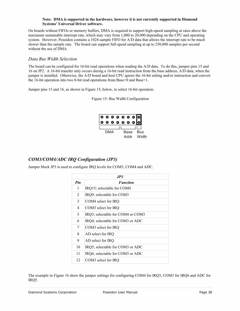
Figure 15: Bus Width Configuration.................................................................................38
Figure 16: IRQ Selection Example..................................................................................39
Figure 17: Analog I/O Single-ended/Differential Configuration Example........................40
Figure 18: JP5 Jumper Block...........................................................................................41
Figure 19: D/A Configuration for ±5V Output Range Example........................................41
Figure 20: D/A Configuration to Reset to Zero Scale Example.......................................42
Diamond Systems Corporation Poseidon User Manual Page 6
Figure 21: JP6 Jumper....................................................................................................42
Figure 22: ATX Configuration Using JP7.........................................................................43
Figure 23: DIO Pull-up/Pull-down Configuration............................................................. 44
Figure 24: RS-422/RS-485 Termination Configuration Options......................................44
Figure 25: Watchdog Timer Block Diagram.....................................................................47
Figure 26: Data Acquisition Block Diagram.....................................................................52
Figure 27: DIOLATCH/ACK Handshaking Sequence..................................................... 93
Figure 28: FlashDisk Module.........................................................................................101
Figure 29: FlashDisk Programmer Board Layout..........................................................103
Diamond Systems Corporation Poseidon User Manual Page 7
Introduction
Poseidon is an embedded CPU board in an EPIC form factor that integrates CPU and data acquisition circuitry into a single board.
Poseidon conforms to the EPIC standard with expansion support via PC/104-Plus, an embedded standard that is based on the ISA and PCI buses and provides a compact, rugged mechanical design for embedded systems. PC/104 modules feature a pin and socket connection system in place of card edge connectors, as well as mounting holes for stand-offs in each corner. The result is an extremely rugged computer system fit for mobile and miniature applications. PC/104 modules stack together with 0.6” spacing between boards (0.662” pitch including the thickness of the PCB).
Poseidon uses the PCI bus internally to connect the Ethernet circuit to the processor. It uses the ISA bus internally to connect serial ports 3 and 4, as well as the data acquisition circuit, to the processor. Both the ISA and PCI buses are brought out to expansion connectors for the connection of add-on boards. Diamond Systems manufactures a wide variety of compatible PC/104 add-on boards for analog I/O, digital I/O, counter/timer functions, serial ports, and power supplies.
Description and FeaturesThe Poseidon board is an all-in-one embedded CPU with the following key system and data acquisition features.
Processor Section• Low-power, fanless 1.0GHz VIA Eden ULV CPU or high-performance 2.0GHz VIA C7 CPU.• 256MB or 512MB 533MHz DDR2 RAM soldered, on-board, system memory.• 400MHz front side bus.• 2MB 16-bit wide integrated flash memory for BIOS and user programs.• Advanced 2D/3D graphics engine with integral MPEG-2 hardware acceleration.• 33MHz PCI Bus.
I/O Section• 4 serial ports, 115.2kbaud max.
• 2 ports 16550-compatible• 2 ports 16850-compatible with 128-byte FIFOs and RS-232, RS-422 and RS-485 capability, with RS-
422/485 termination.• 4 USB 2.0 ports.• Accepts solid-state IDE FlashDisk modules directly on board.• 10-/100-/1000BaseT Gigabit Ethernet.• CRT and 24-bit dual channel LVDS flat panel support.• Dual Independent Display.• PS/2 keyboard and mouse ports.• S-ATA and UDMA-100 IDE interfaces.• Interface for amplified audio.
Analog Input• 32 single-ended/16 differential inputs, 16-bit resolution.• 250KHz maximum aggregate A/D sampling rate.• Bipolar input ranges: ±10V, ±5V, ±2.5V, ±1.25V, ±0.625V.• Unipolar input ranges: 0-10V, 0-5V, 0-2.5V, 0-1.25V, 0-.625V.• 5 ppm/°C drift accuracy.• Internal and external A/D triggering.• 1024-sample FIFO for reliable high-speed sampling and scan operation.
Diamond Systems Corporation Poseidon User Manual Page 8
Analog Output• 4 analog outputs, 12-bit resolution.• ±5V, ±10V, 0-5V, 0-10V output ranges available.• Simultaneous update.• Adjustable output range (optional).
Digital I/O• 24 programmable digital I/O lines, 3.3V and 5V logic compatible.• Enhanced output current capability: -8/+12mA max.• Selectable pull-up/down resistors on board.
Counter/Timers• 1 24-bit counter/timer for A/D sampling rate control.• 1 16-bit counter/timer for user counting and timing functions.• Programmable gate and count enable.• Internal and external clocking capability.
System Features• Plug and play BIOS with IDE auto detection, 32-bit IDE access, and LBA support.• One CompactFlash socket.• User-selectable COM1 or COM2 terminal mode.• On-board lithium backup battery for real-time-clock and CMOS RAM.• ATX power switching capability.• Programmable watchdog timer.• I/O panel board that connects to on-board I/O brought to pin headers, to provide PC-style connectors.• Power supply: 5VDC operation from the PC-104 bus.• Extended temperature range operation: -40 to +85°C (VIA Eden ULV) or -20 to +70ºC (VIA C7).
Diamond Systems Corporation Poseidon User Manual Page 9
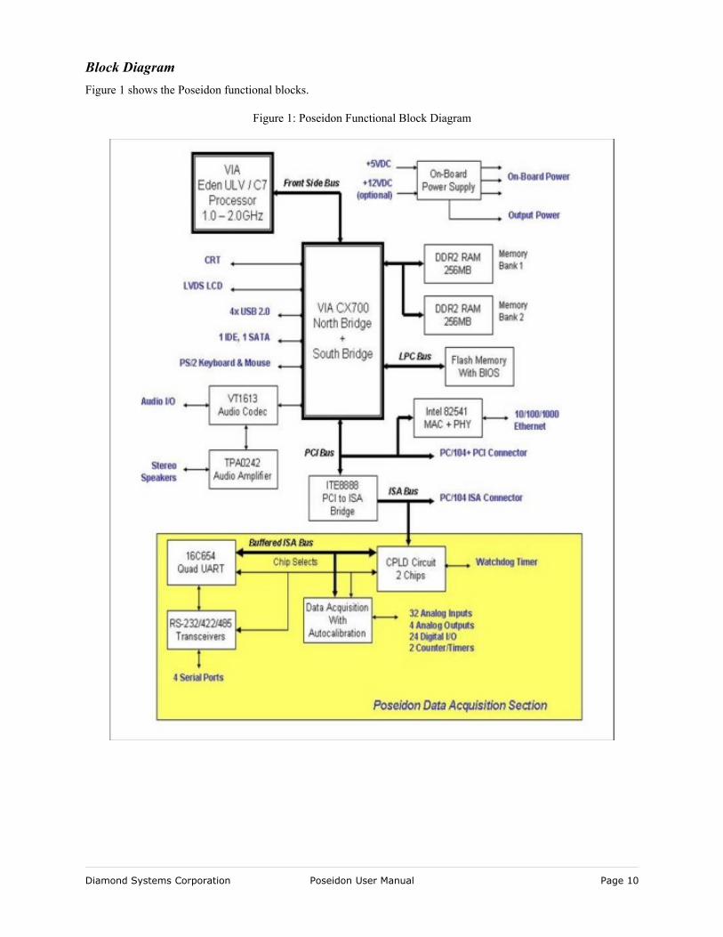
Block DiagramFigure 1 shows the Poseidon functional blocks.
Diamond Systems Corporation Poseidon User Manual Page 10
Figure 1: Poseidon Functional Block Diagram
Functional OverviewThis section describes the major Poseidon subsystems.
ProcessorTwo processor options are available for the Poseidon board.
• Low-power, fanless 1.0GHz VIA Eden ULV CPU• High-performance 2.0GHz VIA C7 CPU
North Bridge and South BridgeThe North and South bridge are integrated in the on-board VIA CX700 chip.
MemoryThe board accommodates 512MB of SDRAM system memory soldered on the board. No expansion connector is provided for additional memory.
The board also includes flash memory for storage of BIOS and user programs. Flash memory is accessible via the on-board ISA bus.
Video FeaturesVideo circuitry is provided by the VIA CX700 chipset and includes,
• Dual 200MHz 2D/3D graphics engines featuring dedicated 128-bit data paths for pixel data flow and texture/command access.
• An integrated MPEG-2 decoder.• Dual independent display with separate frame buffers for CRT and flat panel displays.
AudioThe design provides AC97 audio support derived from the South Bridge chip. The Via VT1612A CODEC provides audio processing. Give special attention to design and routing to minimize noise on the audio I/O lines.
Audio I/O includes,
• Stereo line in.• Stereo line out.• Mono mic in.• Stereo internal line in.
The board includes audio power amplifier circuitry for stereo speaker output. The amplifier circuit is powered by +5VDC from the board. User DC control of volume is also provided, which overrides the software settings.
EthernetThe board supports 10-/100-/1000BaseT (Gigabit) Ethernet. Magnetics are included on the board so that a complete circuit is provided.
Data AcquisitionThe board provides the following data acquisition capabilities.
Diamond Systems Corporation Poseidon User Manual Page 11
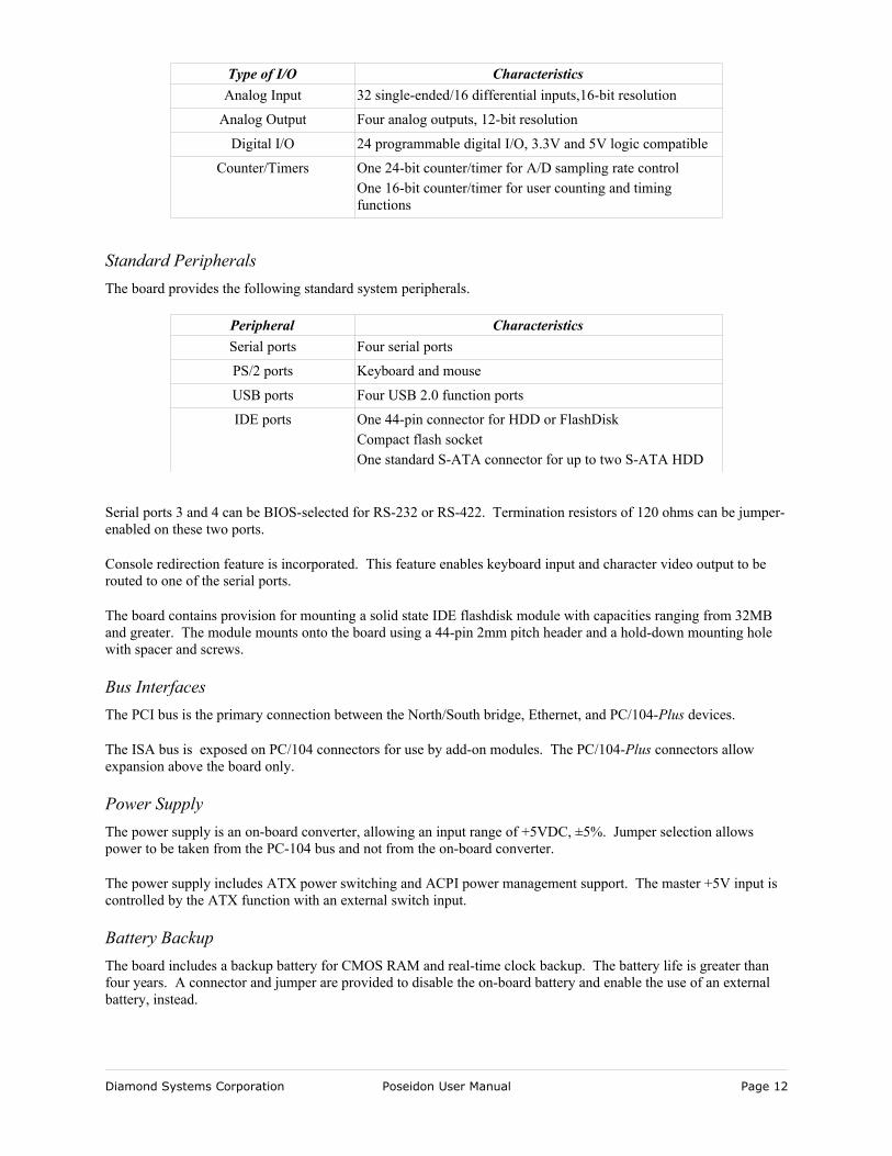
Type of I/O CharacteristicsAnalog Input 32 single-ended/16 differential inputs,16-bit resolution
Analog Output Four analog outputs, 12-bit resolution
Digital I/O 24 programmable digital I/O, 3.3V and 5V logic compatible
Counter/Timers One 24-bit counter/timer for A/D sampling rate controlOne 16-bit counter/timer for user counting and timing functions
Standard PeripheralsThe board provides the following standard system peripherals.
Peripheral CharacteristicsSerial ports Four serial ports
PS/2 ports Keyboard and mouse
USB ports Four USB 2.0 function ports
IDE ports One 44-pin connector for HDD or FlashDiskCompact flash socketOne standard S-ATA connector for up to two S-ATA HDD
Serial ports 3 and 4 can be BIOS-selected for RS-232 or RS-422. Termination resistors of 120 ohms can be jumper-enabled on these two ports.
Console redirection feature is incorporated. This feature enables keyboard input and character video output to be routed to one of the serial ports.
The board contains provision for mounting a solid state IDE flashdisk module with capacities ranging from 32MB and greater. The module mounts onto the board using a 44-pin 2mm pitch header and a hold-down mounting hole with spacer and screws.
Bus InterfacesThe PCI bus is the primary connection between the North/South bridge, Ethernet, and PC/104-Plus devices.
The ISA bus is exposed on PC/104 connectors for use by add-on modules. The PC/104-Plus connectors allow expansion above the board only.
Power SupplyThe power supply is an on-board converter, allowing an input range of +5VDC, ±5%. Jumper selection allows power to be taken from the PC-104 bus and not from the on-board converter.
The power supply includes ATX power switching and ACPI power management support. The master +5V input is controlled by the ATX function with an external switch input.
Battery BackupThe board includes a backup battery for CMOS RAM and real-time clock backup. The battery life is greater than four years. A connector and jumper are provided to disable the on-board battery and enable the use of an external battery, instead.
Diamond Systems Corporation Poseidon User Manual Page 12

Watchdog TimerA watchdog timer (WDT) circuit consists of two cascaded programmable timers, which may be triggered in hardware or software.
Diamond Systems Corporation Poseidon User Manual Page 13
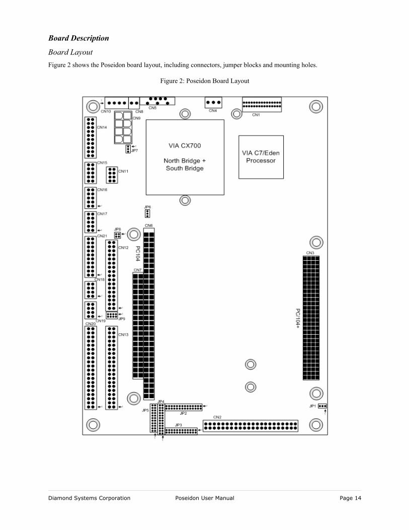
Board Description
Board LayoutFigure 2 shows the Poseidon board layout, including connectors, jumper blocks and mounting holes.
Diamond Systems Corporation Poseidon User Manual Page 14
Figure 2: Poseidon Board Layout
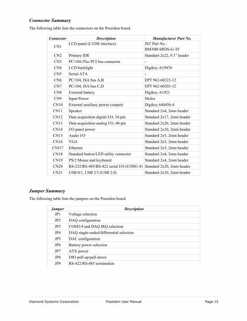
Connector SummaryThe following table lists the connectors on the Poseidon board.
Connector Description Manufacturer Part No.
CN1LCD panel (LVDS interface) JST Part No.:
BM30B-SRDS-G-TFCN2 Primary IDE Standard 2x22, 0.1” headerCN3 PC/104-Plus PCI bus connector -CN4 LCD backlight Digikey A19470CN5 Serial ATA -CN6 PC/104, ISA bus A,B EPT 962-60323-12CN7 PC/104, ISA bus C,D EPT 962-60203-12CN8 External battery Digikey A1921CN9 Input Power MolexCN10 External auxiliary power (output) Digikey 640456-4CN11 Speaker Standard 2x4, 2mm headerCN12 Data acquisition digital I/O, 34-pin Standard 2x17, 2mm headerCN13 Data acquisition analog I/O, 40-pin Standard 2x20, 2mm headerCN14 I/O panel power Standard 2x10, 2mm headerCN15 Audio I/O Standard 2x5, 2mm headerCN16 VGA Standard 2x5, 2mm headerCNJ17 Ethernet Standard 2x5, 2mm headerCN18 Standard button/LED utility connector Standard 2x4, 2mm headerCN19 PS/2 Mouse and keyboard Standard 2x4, 2mm headerCN20 RS-232/RS-485/RS-422 serial I/O (COM1-4) Standard 2x20, 2mm headerCN21 USB 0/1, USB 2/3 (USB 2.0) Standard 2x10, 2mm header
Jumper SummaryThe following table lists the jumpers on the Poseidon board.
Jumper DescriptionJP1 Voltage selectionJP2 DAQ configurationJP3 COM3/4 and DAQ IRQ selectionJP4 DAQ single-ended/differential selectionJP5 DAC configurationJP6 Battery power selectionJP7 ATX powerJP8 DIO pull-up/pull-downJP9 RS-422/RS-485 termination
Diamond Systems Corporation Poseidon User Manual Page 15
Connectors
This section describes the onboard Poseidon connectors.
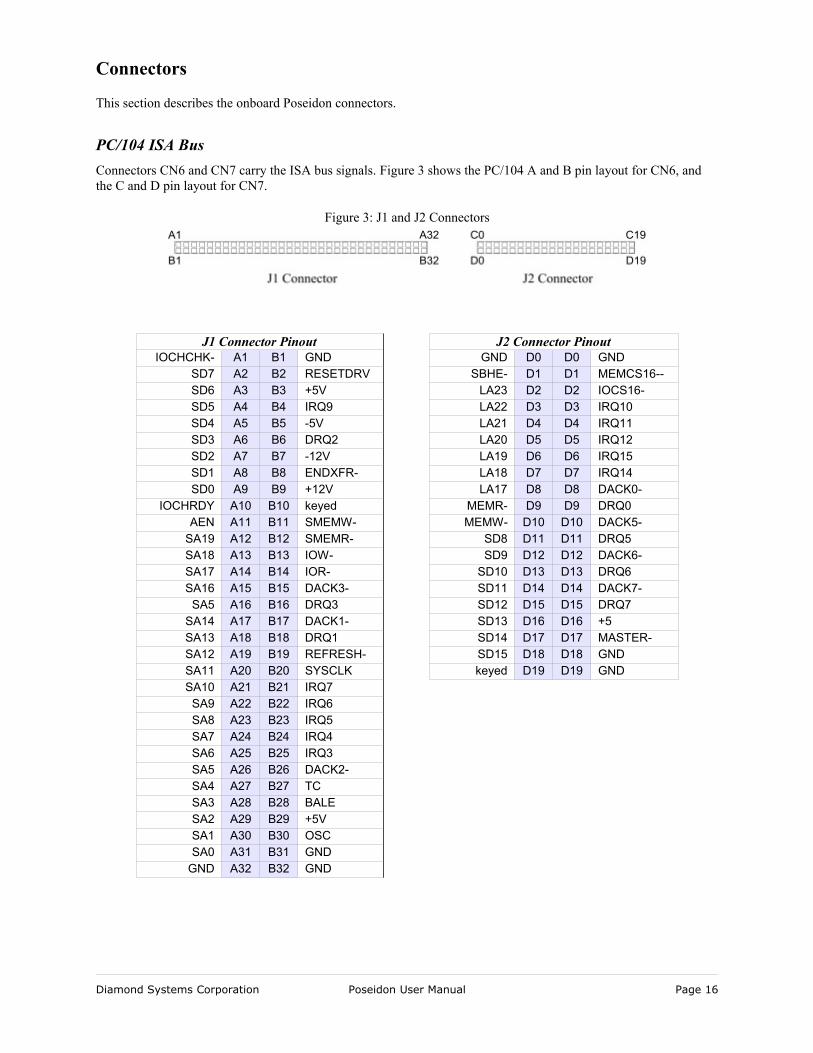
PC/104 ISA BusConnectors CN6 and CN7 carry the ISA bus signals. Figure 3 shows the PC/104 A and B pin layout for CN6, and the C and D pin layout for CN7.
J1 Connector Pinout J2 Connector PinoutIOCHCHK- A1 B1 GND GND D0 D0 GND
SD7 A2 B2 RESETDRV SBHE- D1 D1 MEMCS16--SD6 A3 B3 +5V LA23 D2 D2 IOCS16-SD5 A4 B4 IRQ9 LA22 D3 D3 IRQ10SD4 A5 B5 -5V LA21 D4 D4 IRQ11SD3 A6 B6 DRQ2 LA20 D5 D5 IRQ12SD2 A7 B7 -12V LA19 D6 D6 IRQ15SD1 A8 B8 ENDXFR- LA18 D7 D7 IRQ14SD0 A9 B9 +12V LA17 D8 D8 DACK0-
IOCHRDY A10 B10 keyed MEMR- D9 D9 DRQ0AEN A11 B11 SMEMW- MEMW- D10 D10 DACK5-
SA19 A12 B12 SMEMR- SD8 D11 D11 DRQ5SA18 A13 B13 IOW- SD9 D12 D12 DACK6-SA17 A14 B14 IOR- SD10 D13 D13 DRQ6SA16 A15 B15 DACK3- SD11 D14 D14 DACK7-
SA5 A16 B16 DRQ3 SD12 D15 D15 DRQ7SA14 A17 B17 DACK1- SD13 D16 D16 +5SA13 A18 B18 DRQ1 SD14 D17 D17 MASTER-SA12 A19 B19 REFRESH- SD15 D18 D18 GNDSA11 A20 B20 SYSCLK keyed D19 D19 GNDSA10 A21 B21 IRQ7
SA9 A22 B22 IRQ6SA8 A23 B23 IRQ5SA7 A24 B24 IRQ4SA6 A25 B25 IRQ3SA5 A26 B26 DACK2-SA4 A27 B27 TCSA3 A28 B28 BALESA2 A29 B29 +5VSA1 A30 B30 OSCSA0 A31 B31 GND
GND A32 B32 GND
Diamond Systems Corporation Poseidon User Manual Page 16
Figure 3: J1 and J2 Connectors
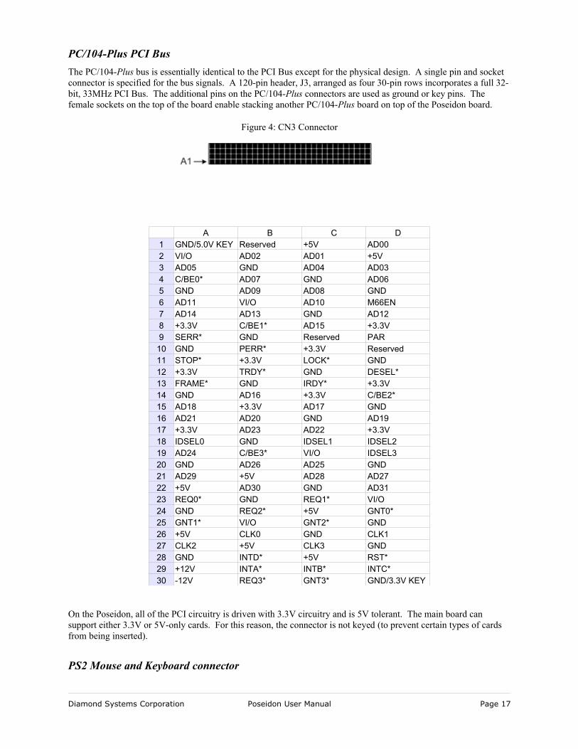
PC/104-Plus PCI BusThe PC/104-Plus bus is essentially identical to the PCI Bus except for the physical design. A single pin and socket connector is specified for the bus signals. A 120-pin header, J3, arranged as four 30-pin rows incorporates a full 32-bit, 33MHz PCI Bus. The additional pins on the PC/104-Plus connectors are used as ground or key pins. The female sockets on the top of the board enable stacking another PC/104-Plus board on top of the Poseidon board.
A B C D1 GND/5.0V KEY Reserved +5V AD002 VI/O AD02 AD01 +5V3 AD05 GND AD04 AD034 C/BE0* AD07 GND AD065 GND AD09 AD08 GND6 AD11 VI/O AD10 M66EN7 AD14 AD13 GND AD128 +3.3V C/BE1* AD15 +3.3V9 SERR* GND Reserved PAR
10 GND PERR* +3.3V Reserved11 STOP* +3.3V LOCK* GND12 +3.3V TRDY* GND DESEL*13 FRAME* GND IRDY* +3.3V14 GND AD16 +3.3V C/BE2*15 AD18 +3.3V AD17 GND16 AD21 AD20 GND AD1917 +3.3V AD23 AD22 +3.3V18 IDSEL0 GND IDSEL1 IDSEL219 AD24 C/BE3* VI/O IDSEL320 GND AD26 AD25 GND21 AD29 +5V AD28 AD2722 +5V AD30 GND AD3123 REQ0* GND REQ1* VI/O24 GND REQ2* +5V GNT0*25 GNT1* VI/O GNT2* GND26 +5V CLK0 GND CLK127 CLK2 +5V CLK3 GND28 GND INTD* +5V RST*29 +12V INTA* INTB* INTC*30 -12V REQ3* GNT3* GND/3.3V KEY
On the Poseidon, all of the PCI circuitry is driven with 3.3V circuitry and is 5V tolerant. The main board can support either 3.3V or 5V-only cards. For this reason, the connector is not keyed (to prevent certain types of cards from being inserted).
PS2 Mouse and Keyboard connector
Diamond Systems Corporation Poseidon User Manual Page 17
Figure 4: CN3 Connector
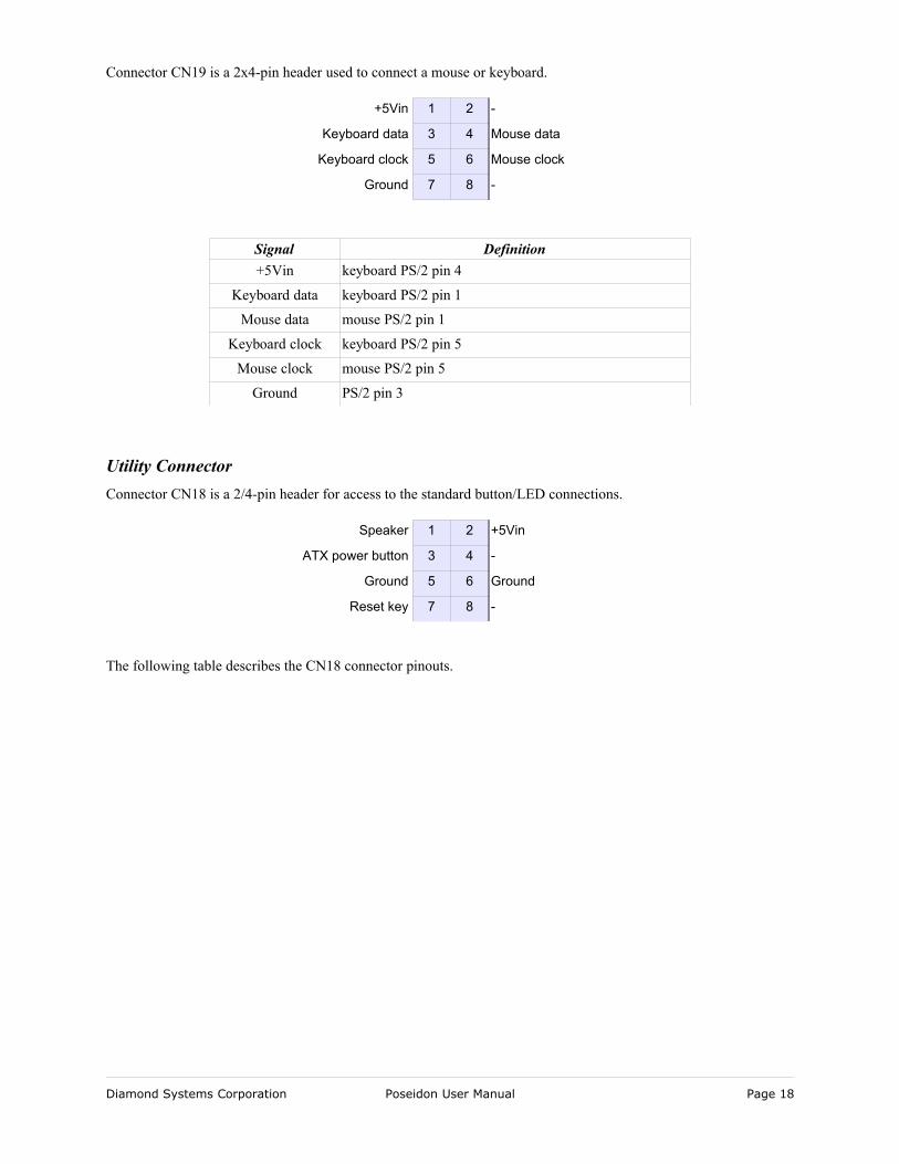
Connector CN19 is a 2x4-pin header used to connect a mouse or keyboard.
+5Vin 1 2 -
Keyboard data 3 4 Mouse data
Keyboard clock 5 6 Mouse clock
Ground 7 8 -
Signal Definition+5Vin keyboard PS/2 pin 4
Keyboard data keyboard PS/2 pin 1
Mouse data mouse PS/2 pin 1
Keyboard clock keyboard PS/2 pin 5
Mouse clock mouse PS/2 pin 5
Ground PS/2 pin 3
Utility ConnectorConnector CN18 is a 2/4-pin header for access to the standard button/LED connections.
Speaker 1 2 +5Vin
ATX power button 3 4 -
Ground 5 6 Ground
Reset key 7 8 -
The following table describes the CN18 connector pinouts.
Diamond Systems Corporation Poseidon User Manual Page 18
Signal DefinitionSpeaker The signal on the Speaker pin is referenced to +5V out. Connect a speaker between this pin
and +5V out.
+5Vin The +5v pin is a switched power pin that is turned on and off with either the ATX power switch or the +5v input.
ATX power button The ATX power button should be tied to ground whenever the “Power Button” is used. The “Power Button” has different functionality, depending on the current system mode and software operation. In general, the following guidelines apply.• If the board is powered down, toggling (i.e., tie to ground briefly, then release) this
button turns the system on, causing all non-standby voltages to become active.
NOTE: depending on the default configuration, the system usually powers-up immediately as power is applied.
• If the system is currently powered up and active, toggling (i.e., tie to ground briefly, then release) this button causes a system power-down event to be initiated. Typically, this powers-down the monitor, hard drive, and any other non-essential functions. The system must be operating and the software executing normally for this function. Under Windows and some other OSs, this power-down event may cause the system to shut down. Typically, this is software-configurable via an option setting for the given OS.
• If the system is currently powered-up and active, holding this button for four seconds causes a forced system shutdown. This is a hardware power-down, which can be detrimental to many OSs due to the fact that they are not given adequate time to initiate shut-down sequencing. This operation should only be used in critical circumstances, such as when the system itself is locked due to system instability or a software crash. After powering the system down in this manner, the system remains powered down until the power button is toggled (tied to ground again and released).
When ATX is enabled, a momentary contact between this pin and Ground causes the CPU to turn on and a contact of four seconds or longer generates a power shutdown.ATX power control is enabled using a jumper on jumper block JP7.
Ground Ground
Reset key Connection between Reset key and ground generate a reset condition. The board remains in a reset state (with non-standby power rails disabled) until Reset key is removed from ground.
Diamond Systems Corporation Poseidon User Manual Page 19
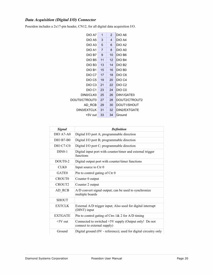
Data Acquisition (Digital I/O) ConnectorPoseidon includes a 2x17-pin header, CN12, for all digital data acquisition I/O.
DIO A7 1 2 DIO A6DIO A5 3 4 DIO A4DIO A3 5 6 DIO A2DIO A1 7 8 DIO A0DIO B7 9 10 DIO B6DIO B5 11 12 DIO B4DIO B3 13 14 DIO B2DIO B1 15 16 DIO B0DIO C7 17 18 DIO C6DIO C5 19 20 DIO C4DIO C3 21 22 DIO C2DIO C1 23 24 DIO C0
DIN0/CLK0 25 26 DIN1/GATE0DOUT0/CTROUT0 27 28 DOUT2/CTROUT2
AD_RCB 29 30 DOUT1/SHOUTDIN3/EXTCLK 31 32 DIN2/EXTGATE
+5V out 33 34 Ground
Signal DefinitionDIO A7-A0 Digital I/O port A; programmable direction
DIO B7-B0 Digital I/O port B; programmable direction
DIO C7-C0 Digital I/O port C; programmable direction
DIN0-1 Digital input port with counter/timer and external trigger functions
DOUT0-2 Digital output port with counter/timer functions
CLK0 Input source to Ctr 0
GATE0 Pin to control gating of Ctr 0
CROUT0 Counter 0 output
CROUT2 Counter 2 output
AD_RCB A/D convert signal output; can be used to synchronize multiple boards
SHOUT
EXTCLK External A/D trigger input; Also used for digital interrupt (DINT) input
EXTGATE Pin to control gating of Ctrs 1& 2 for A/D timing
+5V out Connected to switched +5V supply (Output only! Do not connect to external supply)
Ground Digital ground (0V - reference); used for digital circuitry only
Diamond Systems Corporation Poseidon User Manual Page 20
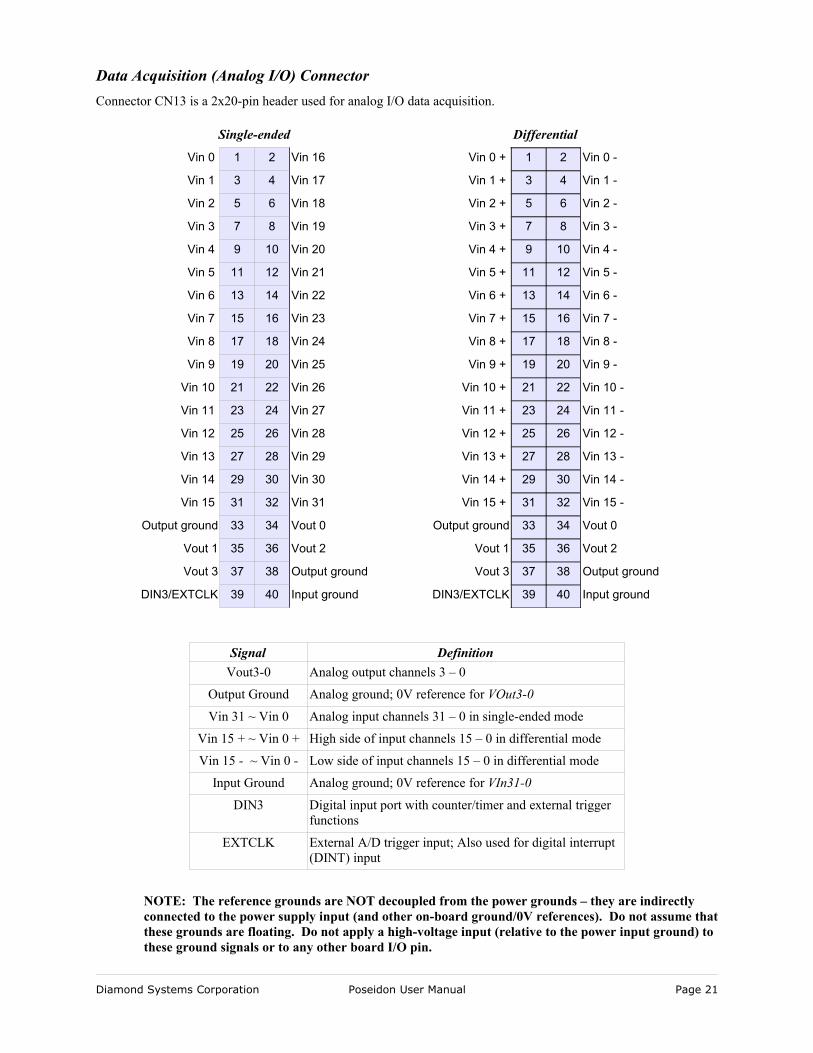
Data Acquisition (Analog I/O) ConnectorConnector CN13 is a 2x20-pin header used for analog I/O data acquisition.
Single-ended Differential
Vin 0 1 2 Vin 16 Vin 0 + 1 2 Vin 0 -
Vin 1 3 4 Vin 17 Vin 1 + 3 4 Vin 1 -
Vin 2 5 6 Vin 18 Vin 2 + 5 6 Vin 2 -
Vin 3 7 8 Vin 19 Vin 3 + 7 8 Vin 3 -
Vin 4 9 10 Vin 20 Vin 4 + 9 10 Vin 4 -
Vin 5 11 12 Vin 21 Vin 5 + 11 12 Vin 5 -
Vin 6 13 14 Vin 22 Vin 6 + 13 14 Vin 6 -
Vin 7 15 16 Vin 23 Vin 7 + 15 16 Vin 7 -
Vin 8 17 18 Vin 24 Vin 8 + 17 18 Vin 8 -
Vin 9 19 20 Vin 25 Vin 9 + 19 20 Vin 9 -
Vin 10 21 22 Vin 26 Vin 10 + 21 22 Vin 10 -
Vin 11 23 24 Vin 27 Vin 11 + 23 24 Vin 11 -
Vin 12 25 26 Vin 28 Vin 12 + 25 26 Vin 12 -
Vin 13 27 28 Vin 29 Vin 13 + 27 28 Vin 13 -
Vin 14 29 30 Vin 30 Vin 14 + 29 30 Vin 14 -
Vin 15 31 32 Vin 31 Vin 15 + 31 32 Vin 15 -
Output ground 33 34 Vout 0 Output ground 33 34 Vout 0
Vout 1 35 36 Vout 2 Vout 1 35 36 Vout 2
Vout 3 37 38 Output ground Vout 3 37 38 Output ground
DIN3/EXTCLK 39 40 Input ground DIN3/EXTCLK 39 40 Input ground
Signal DefinitionVout3-0 Analog output channels 3 – 0
Output Ground Analog ground; 0V reference for VOut3-0
Vin 31 ~ Vin 0 Analog input channels 31 – 0 in single-ended mode
Vin 15 + ~ Vin 0 + High side of input channels 15 – 0 in differential mode
Vin 15 - ~ Vin 0 - Low side of input channels 15 – 0 in differential mode
Input Ground Analog ground; 0V reference for VIn31-0
DIN3 Digital input port with counter/timer and external trigger functions
EXTCLK External A/D trigger input; Also used for digital interrupt (DINT) input
NOTE: The reference grounds are NOT decoupled from the power grounds – they are indirectly connected to the power supply input (and other on-board ground/0V references). Do not assume that these grounds are floating. Do not apply a high-voltage input (relative to the power input ground) to these ground signals or to any other board I/O pin.
Diamond Systems Corporation Poseidon User Manual Page 21
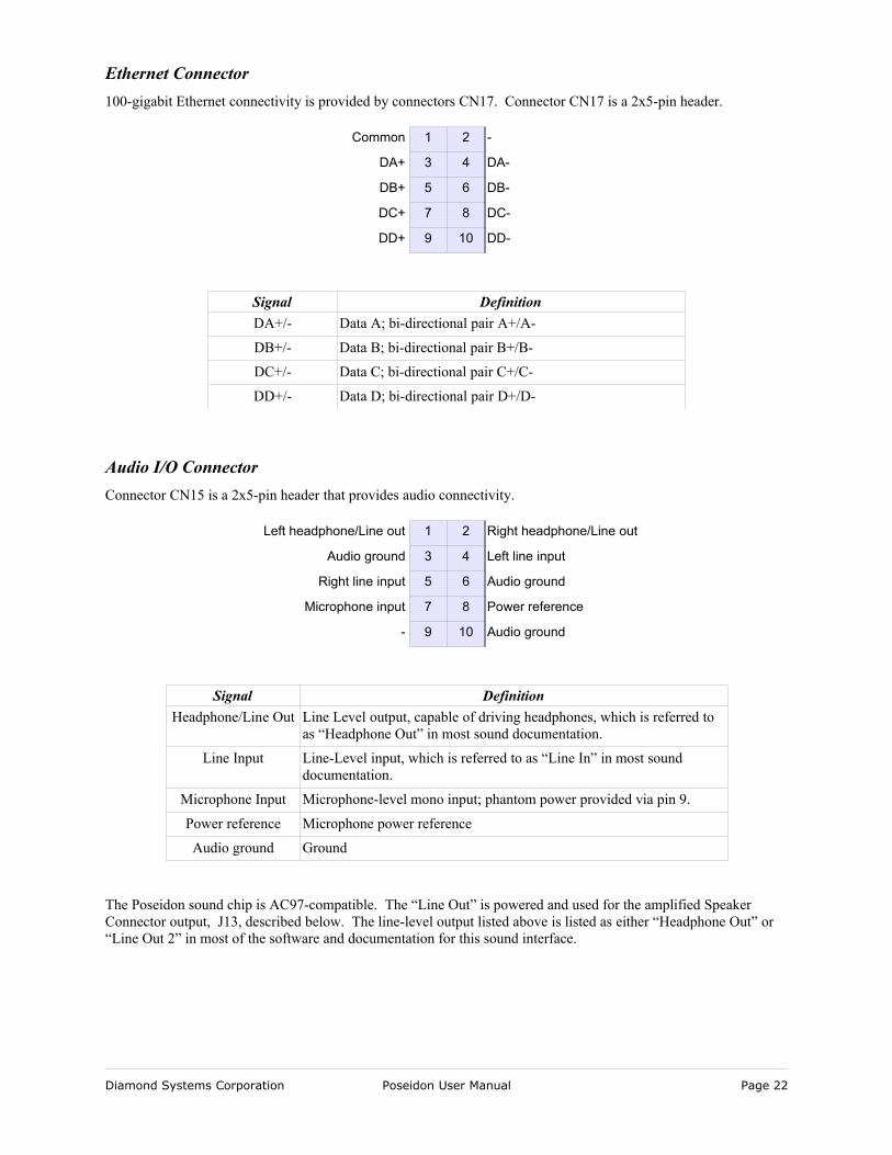
Ethernet Connector100-gigabit Ethernet connectivity is provided by connectors CN17. Connector CN17 is a 2x5-pin header.
Common 1 2 -
DA+ 3 4 DA-
DB+ 5 6 DB-
DC+ 7 8 DC-
DD+ 9 10 DD-
Signal DefinitionDA+/- Data A; bi-directional pair A+/A-
DB+/- Data B; bi-directional pair B+/B-
DC+/- Data C; bi-directional pair C+/C-
DD+/- Data D; bi-directional pair D+/D-
Audio I/O ConnectorConnector CN15 is a 2x5-pin header that provides audio connectivity.
Left headphone/Line out 1 2 Right headphone/Line out
Audio ground 3 4 Left line input
Right line input 5 6 Audio ground
Microphone input 7 8 Power reference
- 9 10 Audio ground
Signal DefinitionHeadphone/Line Out Line Level output, capable of driving headphones, which is referred to
as “Headphone Out” in most sound documentation.
Line Input Line-Level input, which is referred to as “Line In” in most sound documentation.
Microphone Input Microphone-level mono input; phantom power provided via pin 9.
Power reference Microphone power reference
Audio ground Ground
The Poseidon sound chip is AC97-compatible. The “Line Out” is powered and used for the amplified Speaker Connector output, J13, described below. The line-level output listed above is listed as either “Headphone Out” or “Line Out 2” in most of the software and documentation for this sound interface.
Diamond Systems Corporation Poseidon User Manual Page 22
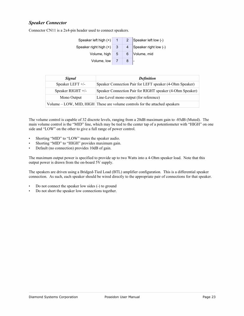
Speaker ConnectorConnector CN11 is a 2x4-pin header used to connect speakers.
Speaker left high (+) 1 2 Speaker left low (-)
Speaker right high (+) 3 4 Speaker right low (-)
Volume, high 5 6 Volume, mid
Volume, low 7 8 -
Signal DefinitionSpeaker LEFT +/- Speaker Connection Pair for LEFT speaker (4-Ohm Speaker)
Speaker RIGHT +/- Speaker Connection Pair for RIGHT speaker (4-Ohm Speaker)
Mono Output Line-Level mono output (for reference)
Volume – LOW, MID, HIGH These are volume controls for the attached speakers
The volume control is capable of 32 discrete levels, ranging from a 20dB maximum gain to -85dB (Muted). The main volume control is the “MID” line, which may be tied to the center tap of a potentiometer with “HIGH” on one side and “LOW” on the other to give a full range of power control.
• Shorting “MID” to “LOW” mutes the speaker audio.• Shorting “MID” to “HIGH” provides maximum gain.• Default (no connection) provides 10dB of gain.
The maximum output power is specified to provide up to two Watts into a 4-Ohm speaker load. Note that this output power is drawn from the on-board 5V supply.
The speakers are driven using a Bridged-Tied Load (BTL) amplifier configuration. This is a differential speaker connection. As such, each speaker should be wired directly to the appropriate pair of connections for that speaker.
• Do not connect the speaker low sides (-) to ground• Do not short the speaker low connections together.
Diamond Systems Corporation Poseidon User Manual Page 23
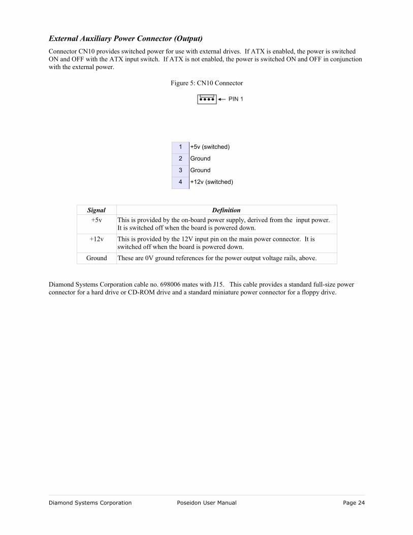
External Auxiliary Power Connector (Output)Connector CN10 provides switched power for use with external drives. If ATX is enabled, the power is switched ON and OFF with the ATX input switch. If ATX is not enabled, the power is switched ON and OFF in conjunction with the external power.
1 +5v (switched)
2 Ground
3 Ground
4 +12v (switched)
Signal Definition+5v This is provided by the on-board power supply, derived from the input power.
It is switched off when the board is powered down.
+12v This is provided by the 12V input pin on the main power connector. It is switched off when the board is powered down.
Ground These are 0V ground references for the power output voltage rails, above.
Diamond Systems Corporation cable no. 698006 mates with J15. This cable provides a standard full-size power connector for a hard drive or CD-ROM drive and a standard miniature power connector for a floppy drive.
Diamond Systems Corporation Poseidon User Manual Page 24
Figure 5: CN10 Connector
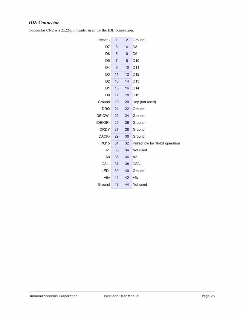
IDE ConnectorConnector CN2 is a 2x22-pin header used for the IDE connection.
Reset - 1 2 Ground
D7 3 4 D8
D6 5 6 D9
D5 7 8 D10
D4 9 10 D11
D3 11 12 D12
D2 13 14 D13
D1 15 16 D14
D0 17 18 D15
Ground 19 20 Key (not used)
DRQ 21 22 Ground
IDEIOW- 23 24 Ground
IDEIOR- 25 26 Ground
IORDY 27 28 Ground
DACK- 29 30 Ground
IRQ15 31 32 Pulled low for 16-bit operation
A1 33 34 Not used
A0 35 36 A2
CS1- 37 38 CS3-
LED- 39 40 Ground
+5v 41 42 +5v
Ground 43 44 Not used
Diamond Systems Corporation Poseidon User Manual Page 25
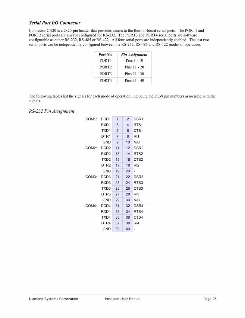
Serial Port I/O ConnectorConnector CN20 is a 2x20-pin header that provides access to the four on-board serial ports. The PORT1 and PORT2 serial ports are always configured for RS-232. The PORT3 and PORT4 serial ports are software configurable as either RS-232, RS-485 or RS-422. All four serial ports are independently enabled. The last two serial ports can be independently configured between the RS-232, RS-485 and RS-422 modes of operation.
Port No. Pin AssignmentPORT1 Pins 1 - 10
PORT2 Pins 11 - 20
PORT3 Pins 21 - 30
PORT4 Pins 31 - 40
The following tables list the signals for each mode of operation, including the DE-9 pin numbers associated with the signals.
RS-232 Pin AssignmentCOM1: DCD1 1 2 DSR1
RXD1 3 4 RTS1TXD1 5 6 CTS1DTR1 7 8 RI1GND 9 10 N/C
COM2: DCD2 11 12 DSR2RXD2 13 14 RTS2TXD2 15 16 CTS2DTR2 17 18 RI2GND 19 20 -
COM3: DCD3 21 22 DSR3RXD3 23 24 RTS3TXD3 25 26 CTS3DTR3 27 28 RI3GND 29 30 N/C
COM4: DCD4 31 32 DSR4RXD4 33 34 RTS4TXD4 35 36 CTS4DTR4 37 38 RI4GND 39 40 -
Diamond Systems Corporation Poseidon User Manual Page 26
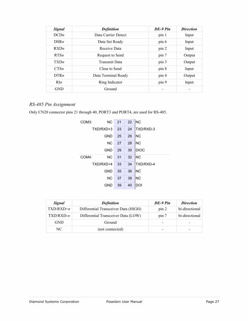
Signal Definition DE-9 Pin DirectionDCDn Data Carrier Detect pin 1 Input
DSRn Data Set Ready pin 6 Input
RXDn Receive Data pin 2 Input
RTSn Request to Send pin 7 Output
TXDn Transmit Data pin 3 Output
CTSn Clear to Send pin 8 Input
DTRn Data Terminal Ready pin 4 Output
RIn Ring Indicator pin 9 Input
GND Ground - -
RS-485 Pin AssignmentOnly CN20 connector pins 21 through 40, PORT3 and PORT4, are used for RS-485.
COM3: NC 21 22 NC
TXD/RXD+3 23 24 TXD/RXD-3
GND 25 26 NC
NC 27 28 NC
GND 29 30 DIOC
COM4: NC 31 32 NC
TXD/RXD+4 33 34 TXD/RXD-4
GND 35 36 NC
NC 37 38 NC
GND 39 40 DOI
Signal Definition DE-9 Pin DirectionTXD/RXD+n Differential Transceiver Data (HIGH) pin 2 bi-directional
TXD/RXD-n Differential Transceiver Data (LOW) pin 7 bi-directional
GND Ground - -
NC (not connected) - -
Diamond Systems Corporation Poseidon User Manual Page 27
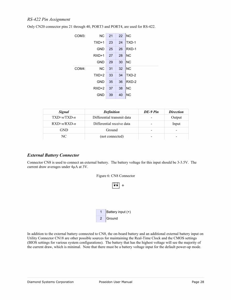
RS-422 Pin AssignmentOnly CN20 connector pins 21 through 40, PORT3 and PORT4, are used for RS-422.
COM3: NC 21 22 NC
TXD+1 23 24 TXD-1
GND 25 26 RXD-1
RXD+1 27 28 NC
GND 29 30 NC
COM4: NC 31 32 NC
TXD+2 33 34 TXD-2
GND 35 36 RXD-2
RXD+2 37 38 NC
GND 39 40 NC
Signal Definition DE-9 Pin DirectionTXD+n/TXD-n Differential transmit data - Output
RXD+n/RXD-n Differential receive data - Input
GND Ground - -
NC (not connected) - -
External Battery ConnectorConnector CN8 is used to connect an external battery. The battery voltage for this input should be 3-3.5V. The current draw averages under 4µA at 3V.
1 Battery input (+)
2 Ground
In addition to the external battery connected to CN8, the on-board battery and an additional external battery input on Utility Connector CN18 are other possible sources for maintaining the Real-Time Clock and the CMOS settings (BIOS settings for various system configurations). The battery that has the highest voltage will see the majority of the current draw, which is minimal. Note that there must be a battery voltage input for the default power-up mode.
Diamond Systems Corporation Poseidon User Manual Page 28
Figure 6: CN8 Connector
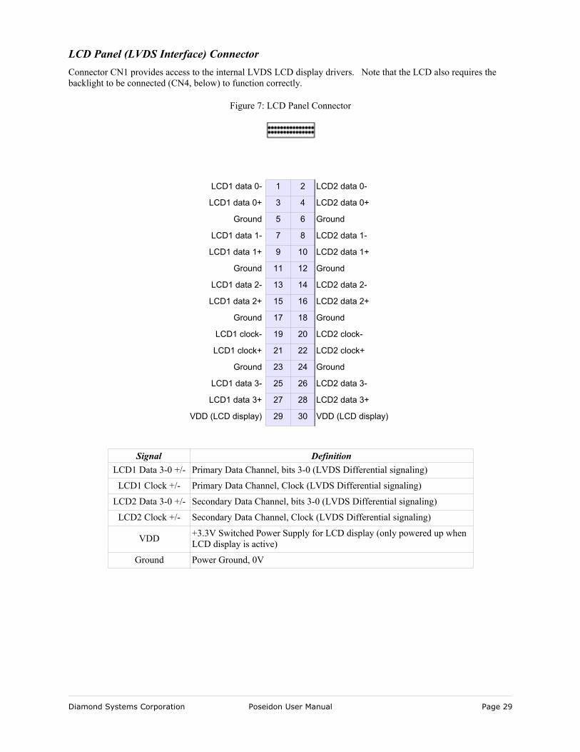
LCD Panel (LVDS Interface) ConnectorConnector CN1 provides access to the internal LVDS LCD display drivers. Note that the LCD also requires the backlight to be connected (CN4, below) to function correctly.
LCD1 data 0- 1 2 LCD2 data 0-
LCD1 data 0+ 3 4 LCD2 data 0+
Ground 5 6 Ground
LCD1 data 1- 7 8 LCD2 data 1-
LCD1 data 1+ 9 10 LCD2 data 1+
Ground 11 12 Ground
LCD1 data 2- 13 14 LCD2 data 2-
LCD1 data 2+ 15 16 LCD2 data 2+
Ground 17 18 Ground
LCD1 clock- 19 20 LCD2 clock-
LCD1 clock+ 21 22 LCD2 clock+
Ground 23 24 Ground
LCD1 data 3- 25 26 LCD2 data 3-
LCD1 data 3+ 27 28 LCD2 data 3+
VDD (LCD display) 29 30 VDD (LCD display)
Signal DefinitionLCD1 Data 3-0 +/- Primary Data Channel, bits 3-0 (LVDS Differential signaling)
LCD1 Clock +/- Primary Data Channel, Clock (LVDS Differential signaling)
LCD2 Data 3-0 +/- Secondary Data Channel, bits 3-0 (LVDS Differential signaling)
LCD2 Clock +/- Secondary Data Channel, Clock (LVDS Differential signaling)
VDD +3.3V Switched Power Supply for LCD display (only powered up when LCD display is active)
Ground Power Ground, 0V
Diamond Systems Corporation Poseidon User Manual Page 29
Figure 7: LCD Panel Connector

VGA ConnectorConnector CN16 is a 2x5-pin header for connecting a VGA monitor.
Red 1 2 Ground
Green 3 4 -
Blue 5 6 Ground
HSYNC 7 8 DDC data
VSYNC 9 10 DDC clock
Signal DefinitionRed RED signal (positive, 0.7Vpp into 75 Ohm load)
R-Ground Ground return for RED signal
Green GREEN signal (positive, 0.7Vpp into 75 Ohm load)
G-Ground Ground return for GREEN signal
Blue BLUE signal (positive, 0.7Vpp into 75 Ohm load)
B-Ground Ground return for BLUE signal
DDCclock/data Digital serial I/O signals used for monitor detection (DDC1 specification)
HSYNC Horizontal sync
VSYNC Vertical sync
Note: While the DDC serial detection pins are present, a 5V power supply is not provided (the old “Monitor ID” pins are also not used).
Diamond Systems Corporation Poseidon User Manual Page 30
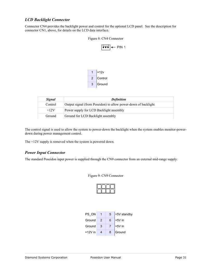
LCD Backlight ConnectorConnector CN4 provides the backlight power and control for the optional LCD panel. See the description for connector CN1, above, for details on the LCD data interface.
1 +12v
2 Control
3 Ground
Signal DefinitionControl Output signal (from Poseidon) to allow power-down of backlight
+12V Power supply for LCD Backlight assembly
Ground Ground for LCD Backlight assembly
The control signal is used to allow the system to power-down the backlight when the system enables monitor-power-down during power management control.
The +12V supply is removed when the system is powered down.
Power Input ConnectorThe standard Poseidon input power is supplied through the CN9 connector from an external mid-range supply.
PS_ON 1 5 +5V standby
Ground 2 6 +5V in
Ground 3 7 +5V in
+12V in 4 8 Ground
Diamond Systems Corporation Poseidon User Manual Page 31
Figure 8: CN4 Connector
Figure 9: CN9 Connector
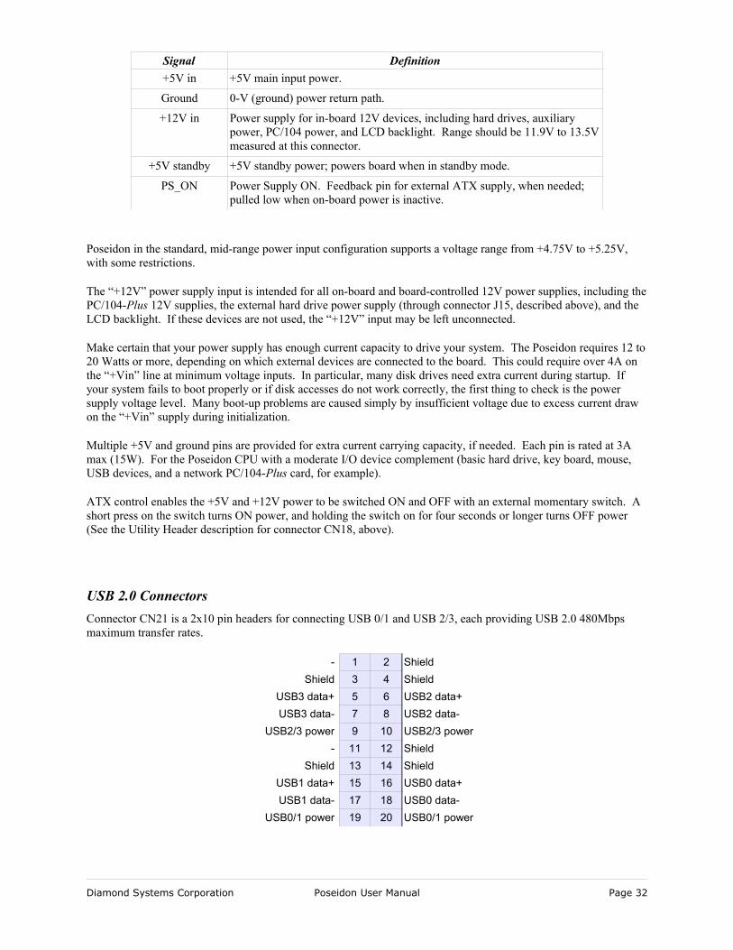
Signal Definition+5V in +5V main input power.
Ground 0-V (ground) power return path.
+12V in Power supply for in-board 12V devices, including hard drives, auxiliary power, PC/104 power, and LCD backlight. Range should be 11.9V to 13.5V measured at this connector.
+5V standby +5V standby power; powers board when in standby mode.
PS_ON Power Supply ON. Feedback pin for external ATX supply, when needed; pulled low when on-board power is inactive.
Poseidon in the standard, mid-range power input configuration supports a voltage range from +4.75V to +5.25V, with some restrictions.
The “+12V” power supply input is intended for all on-board and board-controlled 12V power supplies, including the PC/104-Plus 12V supplies, the external hard drive power supply (through connector J15, described above), and the LCD backlight. If these devices are not used, the “+12V” input may be left unconnected.
Make certain that your power supply has enough current capacity to drive your system. The Poseidon requires 12 to 20 Watts or more, depending on which external devices are connected to the board. This could require over 4A on the “+Vin” line at minimum voltage inputs. In particular, many disk drives need extra current during startup. If your system fails to boot properly or if disk accesses do not work correctly, the first thing to check is the power supply voltage level. Many boot-up problems are caused simply by insufficient voltage due to excess current draw on the “+Vin” supply during initialization.
Multiple +5V and ground pins are provided for extra current carrying capacity, if needed. Each pin is rated at 3A max (15W). For the Poseidon CPU with a moderate I/O device complement (basic hard drive, key board, mouse, USB devices, and a network PC/104-Plus card, for example).
ATX control enables the +5V and +12V power to be switched ON and OFF with an external momentary switch. A short press on the switch turns ON power, and holding the switch on for four seconds or longer turns OFF power (See the Utility Header description for connector CN18, above).
USB 2.0 ConnectorsConnector CN21 is a 2x10 pin headers for connecting USB 0/1 and USB 2/3, each providing USB 2.0 480Mbps maximum transfer rates.
- 1 2 ShieldShield 3 4 Shield
USB3 data+ 5 6 USB2 data+USB3 data- 7 8 USB2 data-
USB2/3 power 9 10 USB2/3 power- 11 12 Shield
Shield 13 14 ShieldUSB1 data+ 15 16 USB0 data+USB1 data- 17 18 USB0 data-
USB0/1 power 19 20 USB0/1 power
Diamond Systems Corporation Poseidon User Manual Page 32
Signal DefinitionShield ground
USB0-3 power- +5V power for USB ports 0-3
USB0-3 data+ data + for USB ports 0-3
USB0-3 data- data - for USB ports 0-3
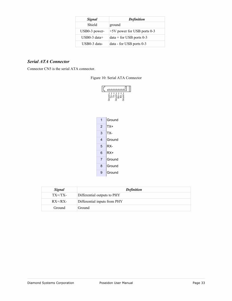
Serial ATA ConnectorConnector CN5 is the serial ATA connector.
1 Ground
2 TX+
3 TX-
4 Ground
5 RX-
6 RX+
7 Ground
8 Ground
9 Ground
Signal DefinitionTX+/TX- Differential outputs to PHY
RX+/RX- Differential inputs from PHY
Ground Ground
Diamond Systems Corporation Poseidon User Manual Page 33
Figure 10: Serial ATA Connector
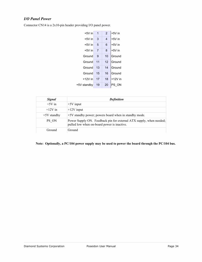
I/O Panel PowerConnector CN14 is a 2x10-pin header providing I/O panel power.
+5V in 1 2 +5V in
+5V in 3 4 +5V in
+5V in 5 6 +5V in
+5V in 7 8 +5V in
Ground 9 10 Ground
Ground 11 12 Ground
Ground 13 14 Ground
Ground 15 16 Ground
+12V in 17 18 +12V in
+5V standby 19 20 PS_ON
Signal Definition+5V in +5V input
+12V in +12V input
+5V standby +5V standby power; powers board when in standby mode.
PS_ON Power Supply ON. Feedback pin for external ATX supply, when needed; pulled low when on-board power is inactive.
Ground Ground
Note: Optionally, a PC/104 power supply may be used to power the board through the PC/104 bus.
Diamond Systems Corporation Poseidon User Manual Page 34
Board Configuration
The Poseidon board has the following jumper-selectable configuration options.
Jumper Block Configuration FunctionsJP1 PCI VI/O voltage setting
JP2 DAQ configuration:DMA levelBase address16/8-bit bus
JP3 COM3/COM4/ADC IRQ configuration
JP4 Analog I/O single-ended/differential configuration
JP5 DAC configuration
JP6 Battery connection (CMOS RAM erase)
JP7 ATX power
JP8 DIO pull-up/pull-down
JP9 RS-422/RS-485 termination
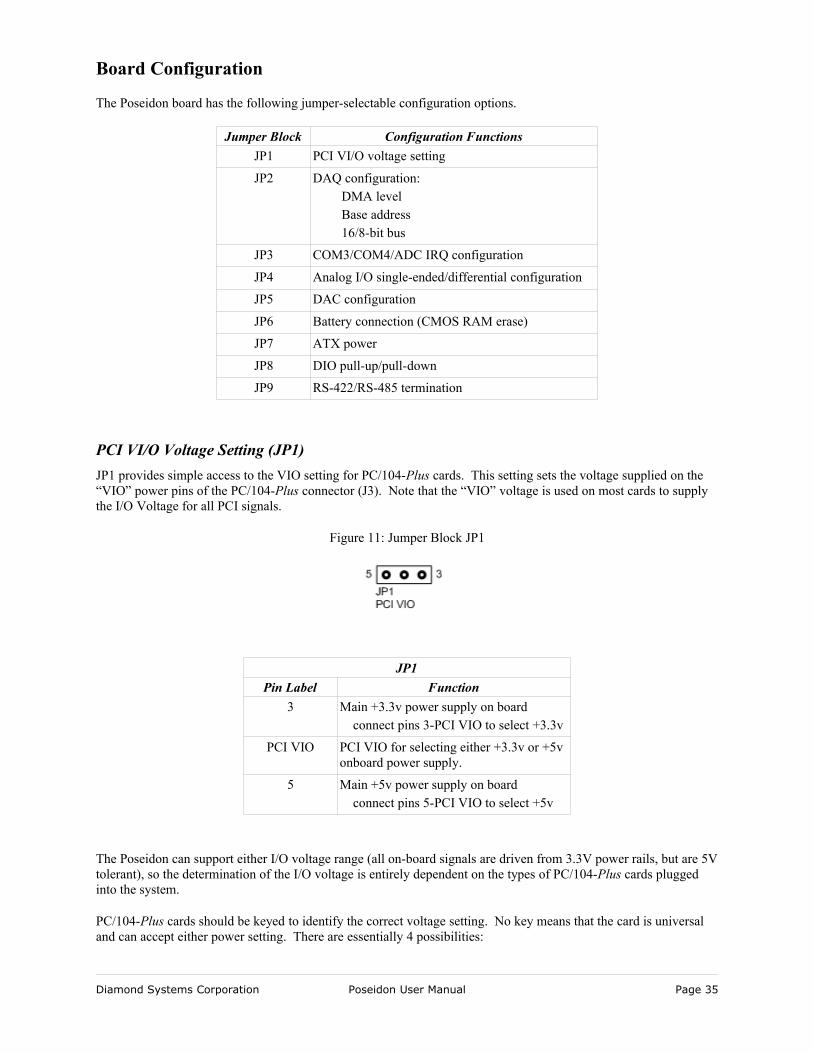
PCI VI/O Voltage Setting (JP1)JP1 provides simple access to the VIO setting for PC/104-Plus cards. This setting sets the voltage supplied on the “VIO” power pins of the PC/104-Plus connector (J3). Note that the “VIO” voltage is used on most cards to supply the I/O Voltage for all PCI signals.
JP1Pin Label Function
3 Main +3.3v power supply on board connect pins 3-PCI VIO to select +3.3v
PCI VIO PCI VIO for selecting either +3.3v or +5v onboard power supply.
5 Main +5v power supply on board connect pins 5-PCI VIO to select +5v
The Poseidon can support either I/O voltage range (all on-board signals are driven from 3.3V power rails, but are 5V tolerant), so the determination of the I/O voltage is entirely dependent on the types of PC/104-Plus cards plugged into the system.
PC/104-Plus cards should be keyed to identify the correct voltage setting. No key means that the card is universal and can accept either power setting. There are essentially 4 possibilities:
Diamond Systems Corporation Poseidon User Manual Page 35
Figure 11: Jumper Block JP1
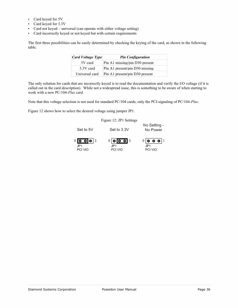
• Card keyed for 5V• Card keyed for 3.3V• Card not keyed – universal (can operate with either voltage setting)• Card incorrectly keyed or not keyed but with certain requirements
The first three possibilities can be easily determined by checking the keying of the card, as shown in the following table.
Card Voltage Type Pin Configuration5V card Pin A1 missing/pin D30 present
3.3V card Pin A1 present/pin D30 missingUniversal card Pin A1 present/pin D30 present
The only solution for cards that are incorrectly keyed is to read the documentation and verify the I/O voltage (if it is called out in the card description). While not a widespread issue, this is something to be aware of when starting to work with a new PC/104-Plus card.
Note that this voltage selection is not used for standard PC/104 cards; only the PCI-signaling of PC/104-Plus.
Figure 12 shows how to select the desired voltage using jumper JP1.
Diamond Systems Corporation Poseidon User Manual Page 36
Figure 12: JP1 Settings
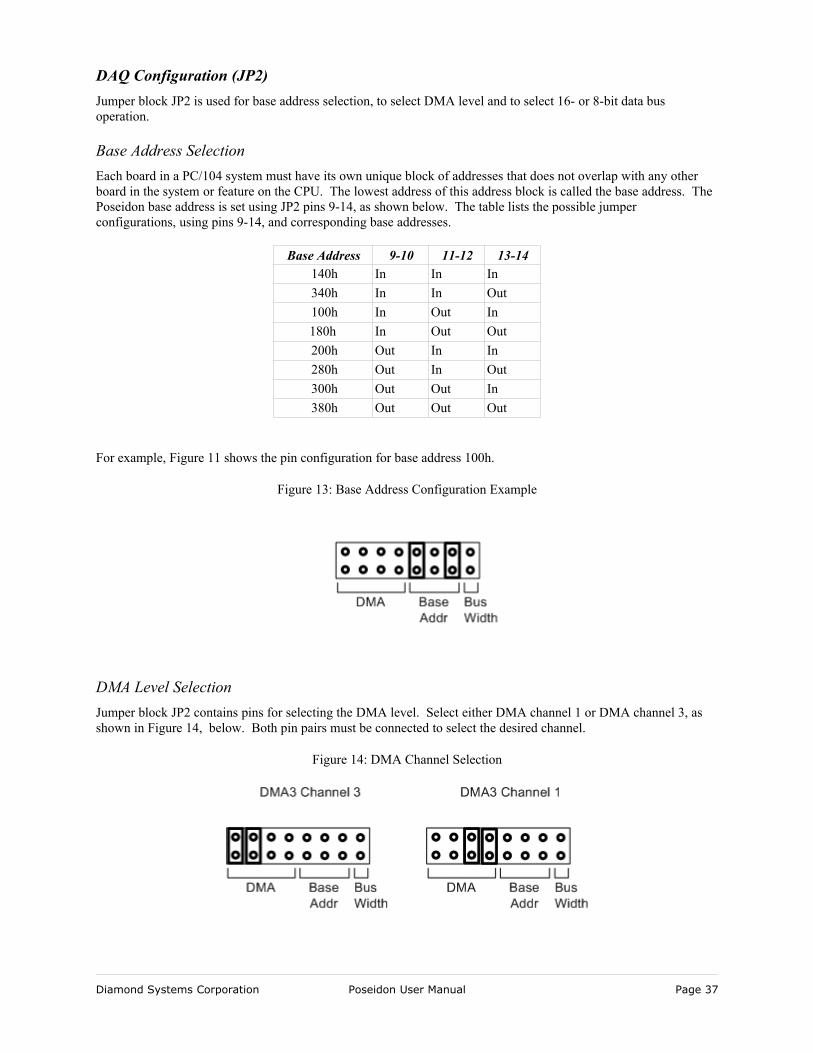
DAQ Configuration (JP2)Jumper block JP2 is used for base address selection, to select DMA level and to select 16- or 8-bit data bus operation.
Base Address SelectionEach board in a PC/104 system must have its own unique block of addresses that does not overlap with any other board in the system or feature on the CPU. The lowest address of this address block is called the base address. The Poseidon base address is set using JP2 pins 9-14, as shown below. The table lists the possible jumper configurations, using pins 9-14, and corresponding base addresses.
Base Address 9-10 11-12 13-14140h In In In340h In In Out100h In Out In180h In Out Out200h Out In In280h Out In Out300h Out Out In380h Out Out Out
For example, Figure 11 shows the pin configuration for base address 100h.
DMA Level SelectionJumper block JP2 contains pins for selecting the DMA level. Select either DMA channel 1 or DMA channel 3, as shown in Figure 14, below. Both pin pairs must be connected to select the desired channel.
Diamond Systems Corporation Poseidon User Manual Page 37
Figure 13: Base Address Configuration Example
Figure 14: DMA Channel Selection
Note: DMA is supported in the hardware, however it is not currently supported in Diamond Systems’ Universal Driver software.
On boards without FIFOs or memory buffers, DMA is required to support high-speed sampling at rates above the maximum sustainable interrupt rate, which may vary from 1,000 to 20,000 depending on the CPU and operating system. However, Poseidon contains a 1024-sample FIFO for A/D data that allows the interrupt rate to be much slower than the sample rate. The board can support full-speed sampling at up to 250,000 samples per second without the use of DMA.
Data Bus Width SelectionThe board can be configured for 16-bit read operations when reading the A/D data. To do this, jumper pins 15 and 16 on JP2. A 16-bit transfer only occurs during a 16-bit read instruction from the base address, A/D data, when the jumper is installed. Otherwise, the A/D board and host CPU ignore the 16-bit setting and/or instruction and convert the 16-bit operation into two 8-bit read operations from Base+0 and Base+1.
Jumper pins 15 and 16, as shown in Figure 15, below, to select 16-bit operation.
COM3/COM4/ADC IRQ Configuration (JP3)Jumper block JP3 is used to configure IRQ levels for COM3, COM4 and ADC.
JP3Pin Function
1 IRQ15; selectable for COM4
2 IRQ9; selectable for COM3
3 COM4 select for IRQ
4 COM3 select for IRQ
5 IRQ3; selectable for COM4 or COM3
6 IRQ4; selectable for COM3 or ADC
7 COM3 select for IRQ
8 AD select for IRQ
9 AD select for IRQ
10 IRQ5; selectable for COM3 or ADC
11 IRQ6; selectable for COM3 or ADC
12 COM3 select for IRQ
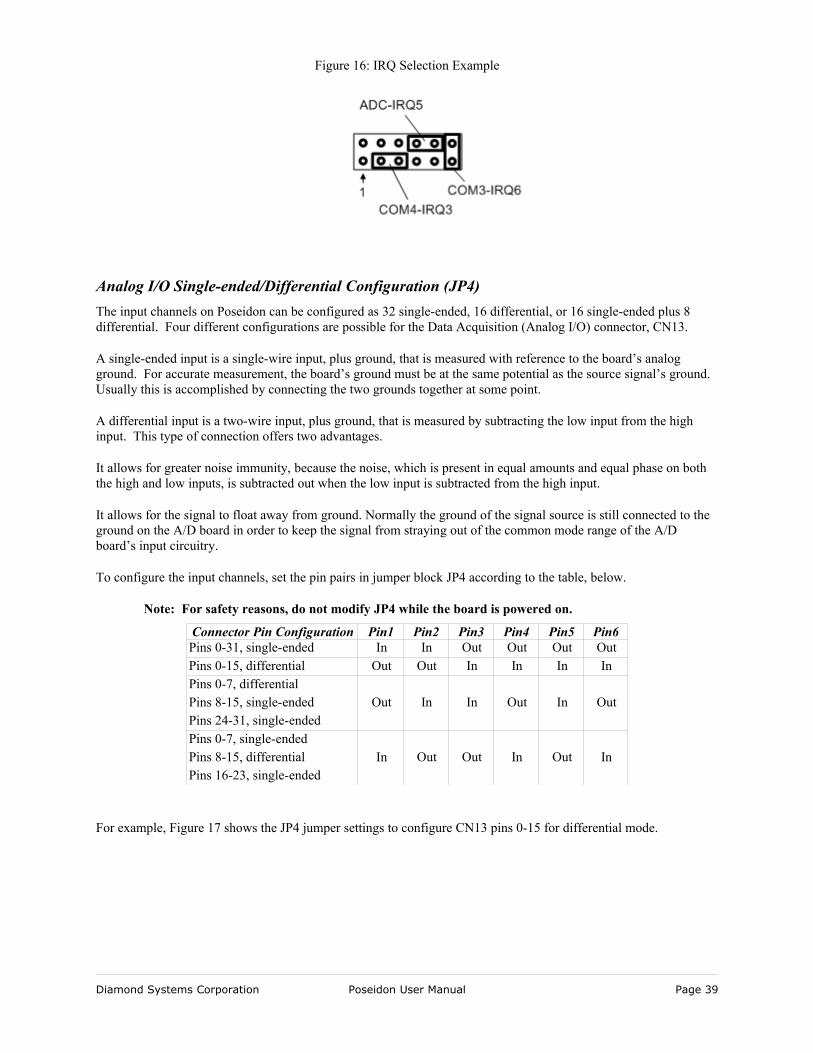
The example in Figure 16 show the jumper settings for configuring COM4 for IRQ3, COM3 for IRQ6 and ADC for IRQ5.
Diamond Systems Corporation Poseidon User Manual Page 38
Figure 15: Bus Width Configuration
Analog I/O Single-ended/Differential Configuration (JP4)The input channels on Poseidon can be configured as 32 single-ended, 16 differential, or 16 single-ended plus 8 differential. Four different configurations are possible for the Data Acquisition (Analog I/O) connector, CN13.
A single-ended input is a single-wire input, plus ground, that is measured with reference to the board’s analog ground. For accurate measurement, the board’s ground must be at the same potential as the source signal’s ground. Usually this is accomplished by connecting the two grounds together at some point.
A differential input is a two-wire input, plus ground, that is measured by subtracting the low input from the high input. This type of connection offers two advantages.
It allows for greater noise immunity, because the noise, which is present in equal amounts and equal phase on both the high and low inputs, is subtracted out when the low input is subtracted from the high input.
It allows for the signal to float away from ground. Normally the ground of the signal source is still connected to the ground on the A/D board in order to keep the signal from straying out of the common mode range of the A/D board’s input circuitry.
To configure the input channels, set the pin pairs in jumper block JP4 according to the table, below.
Note: For safety reasons, do not modify JP4 while the board is powered on.
Connector Pin Configuration Pin1 Pin2 Pin3 Pin4 Pin5 Pin6Pins 0-31, single-ended In In Out Out Out OutPins 0-15, differential Out Out In In In InPins 0-7, differentialPins 8-15, single-endedPins 24-31, single-ended
Out In In Out In Out
Pins 0-7, single-endedPins 8-15, differentialPins 16-23, single-ended
In Out Out In Out In
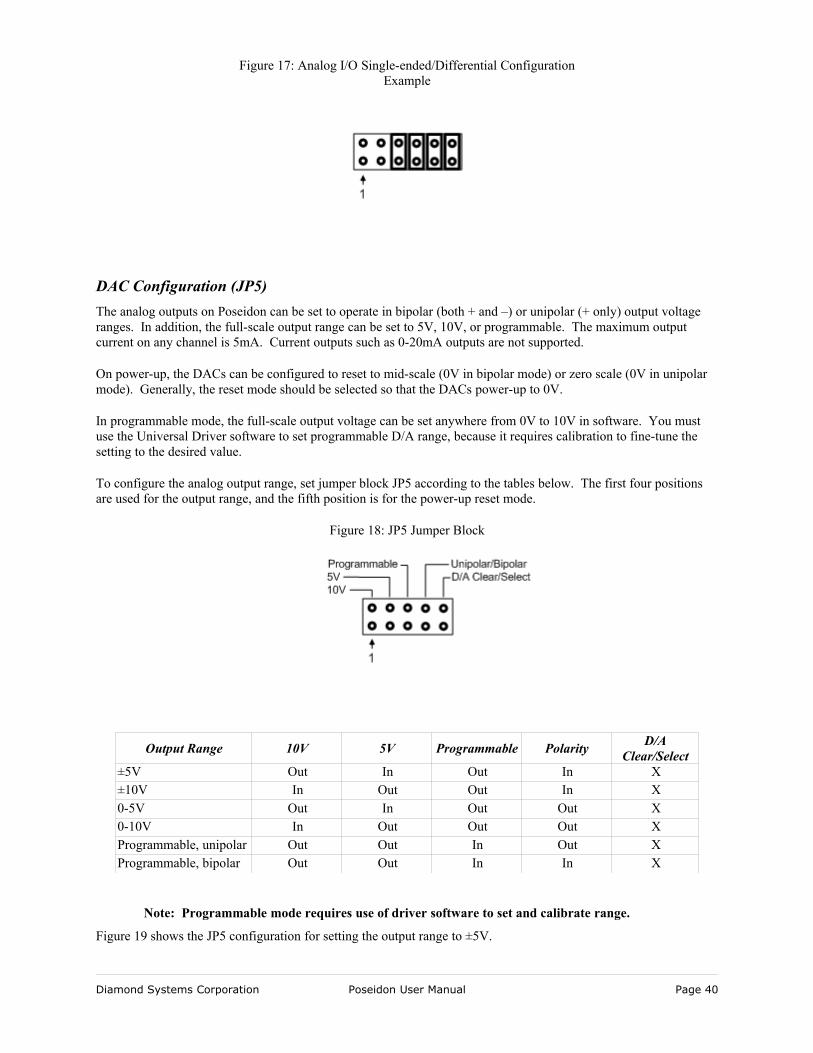
For example, Figure 17 shows the JP4 jumper settings to configure CN13 pins 0-15 for differential mode.
Diamond Systems Corporation Poseidon User Manual Page 39
Figure 16: IRQ Selection Example
DAC Configuration (JP5)The analog outputs on Poseidon can be set to operate in bipolar (both + and –) or unipolar (+ only) output voltage ranges. In addition, the full-scale output range can be set to 5V, 10V, or programmable. The maximum output current on any channel is 5mA. Current outputs such as 0-20mA outputs are not supported.
On power-up, the DACs can be configured to reset to mid-scale (0V in bipolar mode) or zero scale (0V in unipolar mode). Generally, the reset mode should be selected so that the DACs power-up to 0V.
In programmable mode, the full-scale output voltage can be set anywhere from 0V to 10V in software. You must use the Universal Driver software to set programmable D/A range, because it requires calibration to fine-tune the setting to the desired value.
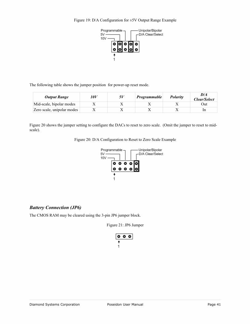
To configure the analog output range, set jumper block JP5 according to the tables below. The first four positions are used for the output range, and the fifth position is for the power-up reset mode.
Output Range 10V 5V Programmable Polarity D/A Clear/Select
±5V Out In Out In X±10V In Out Out In X0-5V Out In Out Out X0-10V In Out Out Out XProgrammable, unipolar Out Out In Out XProgrammable, bipolar Out Out In In X
Note: Programmable mode requires use of driver software to set and calibrate range.
Figure 19 shows the JP5 configuration for setting the output range to ±5V.
Diamond Systems Corporation Poseidon User Manual Page 40
Figure 17: Analog I/O Single-ended/Differential Configuration Example
Figure 18: JP5 Jumper Block
The following table shows the jumper position for power-up reset mode.
Output Range 10V 5V Programmable Polarity D/A Clear/Select
Mid-scale, bipolar modes X X X X OutZero scale, unipolar modes X X X X In
Figure 20 shows the jumper setting to configure the DACs to reset to zero scale. (Omit the jumper to reset to mid-scale).
Battery Connection (JP6)The CMOS RAM may be cleared using the 3-pin JP6 jumper block.
Diamond Systems Corporation Poseidon User Manual Page 41
Figure 19: D/A Configuration for ±5V Output Range Example
Figure 20: D/A Configuration to Reset to Zero Scale Example
Figure 21: JP6 Jumper
With the jumper in position 1-2, the CPU powers up with the default BIOS settings. Follow these steps to clear the CMOS RAM.
1. Power-down the CPU.2. Remove the jumper from position 1-2.3. Insert the jumper in position 2-3.4. Wait a few seconds.5. Insert the jumper in position 1-2.6. Power-up the CPU.
Note: Before erasing CMOS RAM, write down any custom BIOS settings.
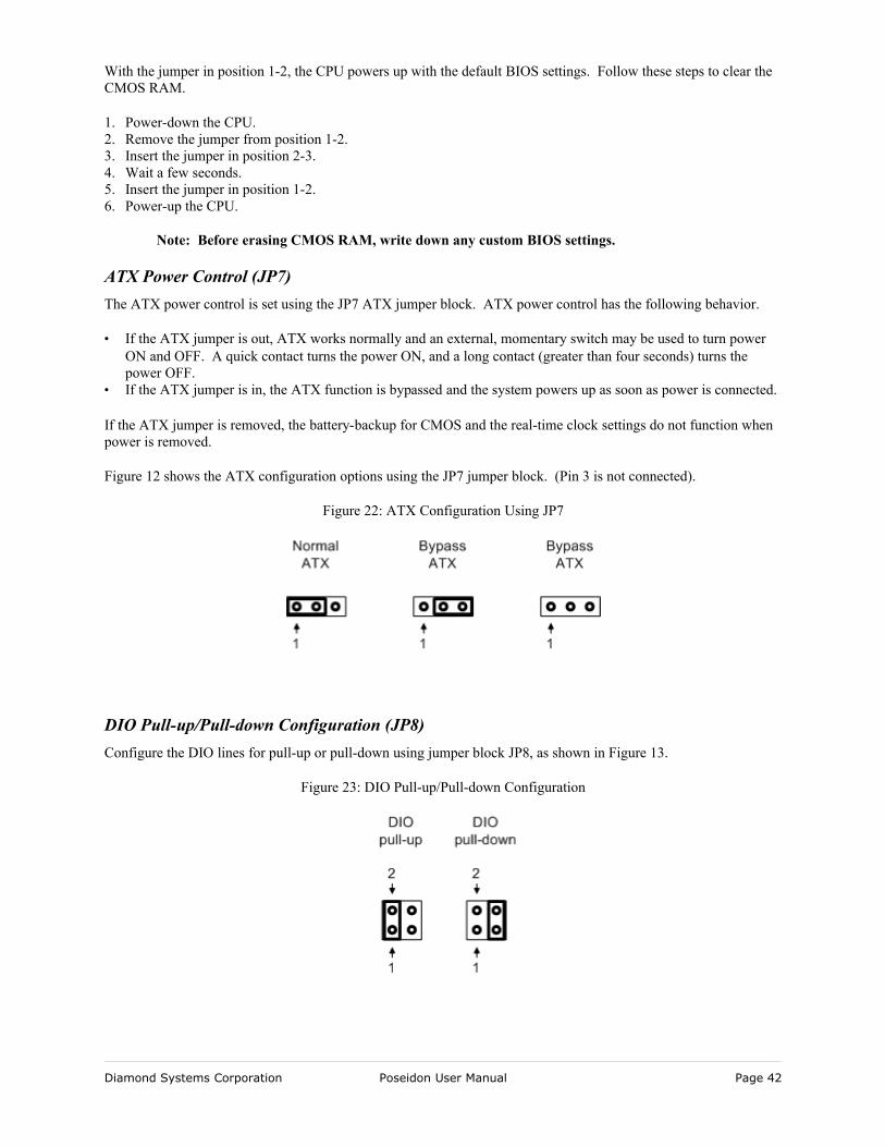
ATX Power Control (JP7)The ATX power control is set using the JP7 ATX jumper block. ATX power control has the following behavior.
• If the ATX jumper is out, ATX works normally and an external, momentary switch may be used to turn power ON and OFF. A quick contact turns the power ON, and a long contact (greater than four seconds) turns the power OFF.
• If the ATX jumper is in, the ATX function is bypassed and the system powers up as soon as power is connected.
If the ATX jumper is removed, the battery-backup for CMOS and the real-time clock settings do not function when power is removed.
Figure 12 shows the ATX configuration options using the JP7 jumper block. (Pin 3 is not connected).
DIO Pull-up/Pull-down Configuration (JP8)Configure the DIO lines for pull-up or pull-down using jumper block JP8, as shown in Figure 13.
Diamond Systems Corporation Poseidon User Manual Page 42
Figure 22: ATX Configuration Using JP7
Figure 23: DIO Pull-up/Pull-down Configuration
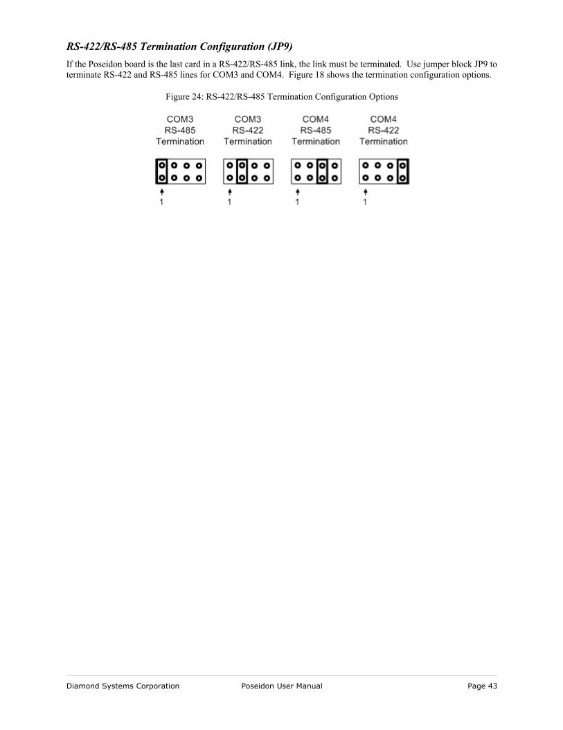
RS-422/RS-485 Termination Configuration (JP9)If the Poseidon board is the last card in a RS-422/RS-485 link, the link must be terminated. Use jumper block JP9 to terminate RS-422 and RS-485 lines for COM3 and COM4. Figure 18 shows the termination configuration options.
Diamond Systems Corporation Poseidon User Manual Page 43
Figure 24: RS-422/RS-485 Termination Configuration Options
System Features
System ResourcesThe table below lists the default system resources utilized by the circuits on Poseidon.
Device Address ISA IRQ ISA DMASerial Port COM1 I/O 0x3F8 – 0x3FF 4 –
Serial Port COM2 I/O 0x2F8 – 0x2FF 3 –
Serial Port COM3 I/O 0x3E8 – 0x3EF 9 –
Serial Port COM4 I/O 0x2E8 – 0x2EF 7 –
IDE Controller I/O 0x1F0 – 0x1F7 14 –
A/D Circuit (when applicable) I/O 0x240 – 0x25F 5 –
Serial Port / FPGA Control I/O 0xA50-0xA5F – –
Ethernet OS-dependent OS-dependent –
USB OS-dependent OS-dependent –
Sound OS-dependent OS-dependent –
Video OS-dependent OS-dependent –
Most of these resources are configurable and, in many cases, the Operating System alters these settings. The main devices that are subject to this dynamic configuration are on-board Ethernet, sound, video, USB, and any PC/104-Plus cards that are in the system. These settings may also vary depending on what other devices are present in the system. For example, adding a PC/104-Plus card may change the on-board Ethernet resources.
The serial port settings for COM3 and COM4 are jumper selectable, whereas the settings for COM1 and COM2 are entirely software-configured in the BIOS.
COM Port / FPGA Control RegistersA set of registers is located at addresses 0xA50-0xA5F for controlling the enhanced serial port features and for some FPGA control capability. Only two registers from this range should be accessed by the user, as shown in the following table.
Address Bit Read/Write Functional Description0xA50 0 read-only COM3 Address
1 read-only COM4 Address
2-7 read-only (unused)
0xA51 0 read/write COM3 0 = Disable, 1 = Enable
1 read/write COM3 : 0 = RS-232, 1 = RS-485
2 read/write COM4 0 = Disable, 1 = Enable
3 read/write COM4 : 0 = RS-232, 1 = RS-485
4-7 read/write (unused, set to 0)
0xA52-0xA5F 0-7 – (reserved – do not access)
Diamond Systems Corporation Poseidon User Manual Page 44
Console Redirection to a Serial PortIn many applications without a local display and keyboard, it may be necessary to obtain keyboard and monitor access to the CPU for configuration, file transfer, or other operations. Poseidon supports this operation by enabling keyboard input and character output onto a serial port, referred to as console redirection. A serial port on another PC can be connected to the serial port on Poseidon with a null modem cable, and a terminal emulation program, such as HyperTerminal, can be used to establish the connection. The terminal program must be capable of transmitting special characters including F2 (some programs or configurations trap special characters).
The default Poseidon BIOS setting enables console redirection onto COM2 during power-on self-test (POST). Communication parameters are 115.2Kbaud, N, 8, 1. When the CPU is powered up, the BIOS outputs POST information to COM2 and monitors the port it for any keyboard activity. You can enter the BIOS by pressing F2 during this time interval. In the default configuration, console redirection is disabled after POST is finished and the CPU boots.
There are three possible configurations for console redirection:
• POST-only (default)• Always On• Disabled
To modify the console redirection settings,
1. Enter the BIOS
2. Select the Advanced menu
3. Select Console Redirection.
4. In Com Port Address, select Disabled to disable the function, On-board COM A for COM1, or On-board COM B for COM2 (default).
If you select Disabled, you will not be able to enter BIOS again during power-up through the serial port.
To reenter BIOS when console redirection is disabled, you must either install a PC/104 video board and use a keyboard and terminal or erase the CMOS RAM, which will return the BIOS to its default settings. CMOS RAM may be erased by removing the jumper on the JP6 jumper block.
Note: Before erasing CMOS RAM, write down any custom BIOS settings you have made.
If you erase the CMOS RAM, the next time the CPU powers up COM2 returns to the default settings of 115.2Kbaud, N, 8, 1 and operates only during POST.
If you selected COMA or COMB, continue with the configuration, as follows.
1. For Console Type, select PC ANSI.
2. You can modify the baud rate and flow control here if desired.
3. At the bottom, for Continue C.R. after POST, select Off (default) to turn off after POST or select On to remain on always.
4. Exit the BIOS and save your settings.
Diamond Systems Corporation Poseidon User Manual Page 45
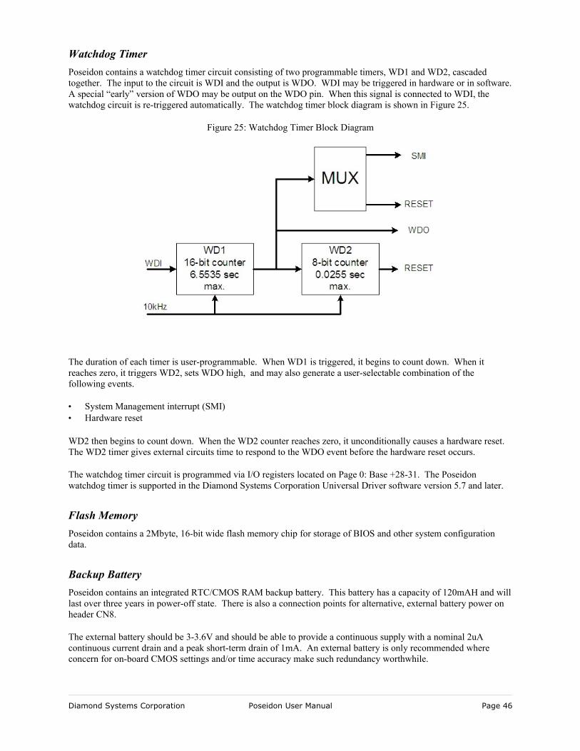
Watchdog TimerPoseidon contains a watchdog timer circuit consisting of two programmable timers, WD1 and WD2, cascaded together. The input to the circuit is WDI and the output is WDO. WDI may be triggered in hardware or in software. A special “early” version of WDO may be output on the WDO pin. When this signal is connected to WDI, the watchdog circuit is re-triggered automatically. The watchdog timer block diagram is shown in Figure 25.
The duration of each timer is user-programmable. When WD1 is triggered, it begins to count down. When it reaches zero, it triggers WD2, sets WDO high, and may also generate a user-selectable combination of the following events.
• System Management interrupt (SMI)• Hardware reset
WD2 then begins to count down. When the WD2 counter reaches zero, it unconditionally causes a hardware reset. The WD2 timer gives external circuits time to respond to the WDO event before the hardware reset occurs.
The watchdog timer circuit is programmed via I/O registers located on Page 0: Base +28-31. The Poseidon watchdog timer is supported in the Diamond Systems Corporation Universal Driver software version 5.7 and later.
Flash MemoryPoseidon contains a 2Mbyte, 16-bit wide flash memory chip for storage of BIOS and other system configuration data.
Backup BatteryPoseidon contains an integrated RTC/CMOS RAM backup battery. This battery has a capacity of 120mAH and will last over three years in power-off state. There is also a connection points for alternative, external battery power on header CN8.
The external battery should be 3-3.6V and should be able to provide a continuous supply with a nominal 2uA continuous current drain and a peak short-term drain of 1mA. An external battery is only recommended where concern for on-board CMOS settings and/or time accuracy make such redundancy worthwhile.
Diamond Systems Corporation Poseidon User Manual Page 46
Figure 25: Watchdog Timer Block Diagram
The on-board battery is activated for the first time during initial factory configuration and test.
System ResetPoseidon contains a chip to control system reset operation. Reset occurs under the following conditions.
• User causes reset with a ground contact on the Reset input.• Input voltage drops below 4.75V.• Over-current condition on output power line .
The ISA Reset signal is an active high pulse with a 200ms duration. The PCI Reset is active low, with a typical pulse width duration of 200 msec.
On-Board VideoUsing the the on-board VIA CX700 processor, Poseidon integrates all of the support needed for modern media. Refer to the VIA Technologies, Inc. documentation for CX700-series processors, listed in the Additional Information section of this document.
Diamond Systems Corporation Poseidon User Manual Page 47
System I/O
EthernetPoseidon includes a 10/100/1000 BaseT (Gigabit) Ethernet connectivity, using an Intel 82541 Gigabit Ethernet controller. The signals are provided on two connectors on the right edge of the board:
Jumper Block Connector TypeJ10 RJ45J11 6-pin header
Serial PortsPoseidon contains four serial ports. Each port is capable of transmitting at speeds up to 115.2Kbaud. Ports COM1 and COM2 are built into the standard chipset., which are standard 16550 UARTs with 16-byte FIFOs.
Ports COM3 and COM4 are derived from an Exar 16C2850 dual UART chip and include 128-byte FIFOs. These ports may be operated at speeds to 1.5Mbaud with installation of high-speed drivers, as a custom option.
The serial ports use the following default system resources.
Port I/O Address Range IRQCOM1 0x3F8 - 0x3FF 4COM2 0x2F8 - 0x2FF 3COM3 0x3E8 - 0x3EF 4COM4 0x2E8 - 0x2EF 3
The COM1 and COM2 settings may be changed in the system BIOS. Select the Advanced menu, followed by I/O Device Configuration, to modify the base address and interrupt level.
The settings of COM3 and COM4 I/O addresses may be changed using jumpers J5. The jumper settings are auto-detected by the BIOS.
Note: The IRQ settings for COM3 and COM4 are selected using jumper J4. COM3 may use IRQ4 or IRQ9. COM4 may use IRQ3, IRQ7 or IRQ15. Once these jumper selections are made, you must update the serial port IRQ settings to match these selections; the IRQ settings are NOT auto-detected in the way that the address settings are detected.
RS-232 ModeRS-232 mode is the standard mode for most PC applications. COM1 and COM2 are always RS-232-only. COM3 and COM4 are RS-232 by default and the settings are managed in the BIOS using the I/O Device Configuration menu.
RS-232 mode for all four ports provides complete signaling support, including all handshaking signals and the Ring Indicate (RI) signal.
RS-485 ModeCOM3 and COM4 are independently selectable between RS-232 mode (default) and RS-485 mode. If RS-485 mode is selected, special consideration is required to implement RS-485 mode in both hardware and software.
In hardware, the critical issues for RS-485 mode are:
Diamond Systems Corporation Poseidon User Manual Page 48
• Receive and transmit only. No handshaking lines are supported.• Differential signaling; two wires each, high and low, for receive and transmit.• Signal definitions for connector J18 change depending on the mode for each serial port.
In software, control of the RS-485 transmit line is handled using the serial port RTS signal. Defined as a handshaking signal for RS-232, it is used as a write-control signal for RS-485 operation.
The RS-485 implementation for COM3/4 always receives the data sent. For example, when data is transmitted from COM3, the same data is locally echoed back into the receive buffer of COM3. This allows for data verification to identify RS-485 network collisions; i.e., if another device sends data onto the RS-485 lines at the same time, the data coming into the receive buffer does not match and is not received.
To transmit data for one of these RS-485 ports, the RTS signal must be driven active. The transmitter for that RS-485 port is then active and remains active until the RTS signal is returned to its default, no-transmit, state.
The typical sequence to transmit data on a shared RS-485 cable as follows.
1. Set RTS high to enable transmit.2. Send data, which is echoed to the receive buffer of the same port.3. Set RTS low to disable transmit.4. Verify that data is received and that it matches the transmit data. If the data does not match, re-transmit the data.
RS-422 ModeCOM3 and COM4 are independently selectable to operate in RS-422 mode, instead of RS-232 mode (default) or RS-485 mode. Jumper the J4 connector RS-422 pins to override the BIOS RS-232/RS-485 selection. To operate COM3 in RS-422 mode, jumper J4 pins labeled C3 422. To operate COM4 in RS-422 mode, jumper J4 pins labeled C4 422.
If RS-422 mode is selected, special hardware and software consideration is required to implement RS-422.
PS/2 PortsPoseidon supports two PS/2 ports.
• Keyboard• Mouse
The PS/2 ports are accessible using a cable assembly (DSC#698022) attached to connector J6. Support for these ports is independent of, and in addition to, mouse and keyboard support using the USB ports.
USB PortsFour USB 2.0 ports, USB0 through USB3, are accessible using cable assemblies attached to connector CN21.
USB support is intended primarily for the following devices (although any USB-standard device should function).
• Keyboard• Mouse• USB Floppy Drive (This is required for Crisis Recovery of boot ROM)• USB flash disk
The BIOS supports the USB keyboard during BIOS initialization screens and legacy emulation for DOS-based applications.
Diamond Systems Corporation Poseidon User Manual Page 49

The USB ports can be used for keyboard and mouse at the same time that the PS/2 keyboard and mouse are connected.
Diamond Systems Corporation Poseidon User Manual Page 50
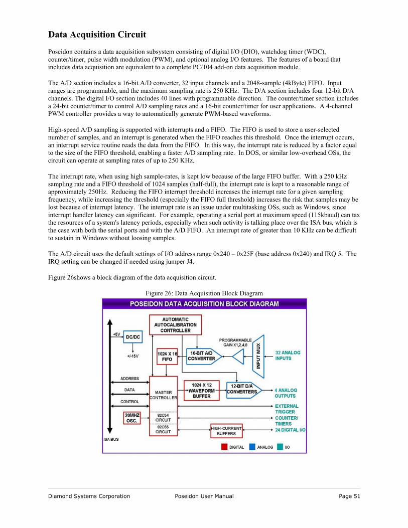
Data Acquisition Circuit
Poseidon contains a data acquisition subsystem consisting of digital I/O (DIO), watchdog timer (WDC), counter/timer, pulse width modulation (PWM), and optional analog I/O features. The features of a board that includes data acquisition are equivalent to a complete PC/104 add-on data acquisition module.
The A/D section includes a 16-bit A/D converter, 32 input channels and a 2048-sample (4kByte) FIFO. Input ranges are programmable, and the maximum sampling rate is 250 KHz. The D/A section includes four 12-bit D/A channels. The digital I/O section includes 40 lines with programmable direction. The counter/timer section includes a 24-bit counter/timer to control A/D sampling rates and a 16-bit counter/timer for user applications. A 4-channel PWM controller provides a way to automatically generate PWM-based waveforms.
High-speed A/D sampling is supported with interrupts and a FIFO. The FIFO is used to store a user-selected number of samples, and an interrupt is generated when the FIFO reaches this threshold. Once the interrupt occurs, an interrupt service routine reads the data from the FIFO. In this way, the interrupt rate is reduced by a factor equal to the size of the FIFO threshold, enabling a faster A/D sampling rate. In DOS, or similar low-overhead OSs, the circuit can operate at sampling rates of up to 250 KHz.
The interrupt rate, when using high sample-rates, is kept low because of the large FIFO buffer. With a 250 kHz sampling rate and a FIFO threshold of 1024 samples (half-full), the interrupt rate is kept to a reasonable range of approximately 250Hz. Reducing the FIFO interrupt threshold increases the interrupt rate for a given sampling frequency, while increasing the threshold (especially the FIFO full threshold) increases the risk that samples may be lost because of interrupt latency. The interrupt rate is an issue under multitasking OSs, such as Windows, since interrupt handler latency can significant. For example, operating a serial port at maximum speed (115kbaud) can tax the resources of a system's latency periods, especially when such activity is talking place over the ISA bus, which is the case with both the serial ports and with the A/D FIFO. An interrupt rate of greater than 10 KHz can be difficult to sustain in Windows without loosing samples.
The A/D circuit uses the default settings of I/O address range 0x240 – 0x25F (base address 0x240) and IRQ 5. The IRQ setting can be changed if needed using jumper J4.
Figure 26shows a block diagram of the data acquisition circuit.
Diamond Systems Corporation Poseidon User Manual Page 51
Figure 26: Data Acquisition Block Diagram
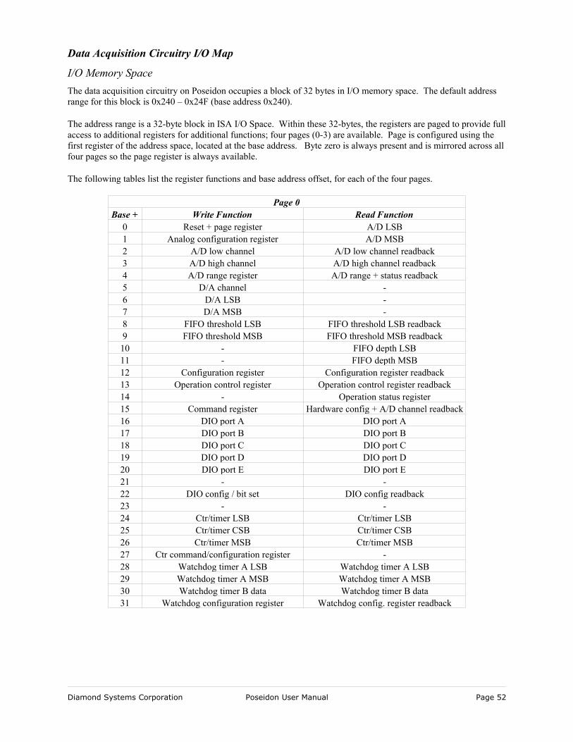
Data Acquisition Circuitry I/O Map
I/O Memory SpaceThe data acquisition circuitry on Poseidon occupies a block of 32 bytes in I/O memory space. The default address range for this block is 0x240 – 0x24F (base address 0x240).
The address range is a 32-byte block in ISA I/O Space. Within these 32-bytes, the registers are paged to provide full access to additional registers for additional functions; four pages (0-3) are available. Page is configured using the first register of the address space, located at the base address. Byte zero is always present and is mirrored across all four pages so the page register is always available.
The following tables list the register functions and base address offset, for each of the four pages.
Page 0Base + Write Function Read Function
0 Reset + page register A/D LSB1 Analog configuration register A/D MSB2 A/D low channel A/D low channel readback3 A/D high channel A/D high channel readback4 A/D range register A/D range + status readback5 D/A channel -6 D/A LSB -7 D/A MSB -8 FIFO threshold LSB FIFO threshold LSB readback9 FIFO threshold MSB FIFO threshold MSB readback10 - FIFO depth LSB11 - FIFO depth MSB12 Configuration register Configuration register readback13 Operation control register Operation control register readback14 - Operation status register15 Command register Hardware config + A/D channel readback16 DIO port A DIO port A17 DIO port B DIO port B18 DIO port C DIO port C19 DIO port D DIO port D20 DIO port E DIO port E21 - -22 DIO config / bit set DIO config readback23 - -24 Ctr/timer LSB Ctr/timer LSB25 Ctr/timer CSB Ctr/timer CSB26 Ctr/timer MSB Ctr/timer MSB27 Ctr command/configuration register -28 Watchdog timer A LSB Watchdog timer A LSB29 Watchdog timer A MSB Watchdog timer A MSB30 Watchdog timer B data Watchdog timer B data31 Watchdog configuration register Watchdog config. register readback
Diamond Systems Corporation Poseidon User Manual Page 52
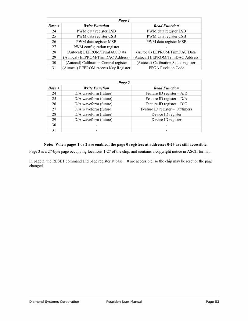
Page 1Base + Write Function Read Function
24 PWM data register LSB PWM data register LSB25 PWM data register CSB PWM data register CSB26 PWM data register MSB PWM data register MSB27 PWM configuration register -28 (Autocal) EEPROM/TrimDAC Data (Autocal) EEPROM/TrimDAC Data 29 (Autocal) EEPROM/TrimDAC Address) (Autocal) EEPROM/TrimDAC Address 30 (Autocal) Calibration Control register (Autocal) Calibration Status register 31 (Autocal) EEPROM Access Key Register FPGA Revision Code
Page 2Base + Write Function Read Function
24 D/A waveform (future) Feature ID register – A/D25 D/A waveform (future) Feature ID register – D/A26 D/A waveform (future) Feature ID register – DIO27 D/A waveform (future) Feature ID register – Ctr/timers28 D/A waveform (future) Device ID register29 D/A waveform (future) Device ID register30 - -31 - -
Note: When pages 1 or 2 are enabled, the page 0 registers at addresses 0-23 are still accessible.
Page 3 is a 27-byte page occupying locations 1-27 of the chip, and contains a copyright notice in ASCII format.
In page 3, the RESET command and page register at base + 0 are accessible, so the chip may be reset or the page changed.
Diamond Systems Corporation Poseidon User Manual Page 53
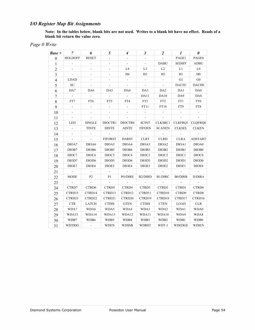
I/O Register Map Bit AssignmentsNote: In the tables below, blank bits are not used. Writes to a blank bit have no effect. Reads of a blank bit return the value zero.
Page 0 WriteBase + 7 6 5 4 3 2 1 0
0 HOLDOFF RESET - - - - PAGE1 PAGE0
1 - - - - - DABU SEDIFF ADBU
2 - - - L4 L3 L2 L1 L0
3 - - - H4 H3 H2 H1 H0
4 LDAD - - - - - G1 G0
5 SU - - - - - DACH1 DACH0
6 DA7 DA6 DA5 DA4 DA3 DA2 DA1 DA0
7 - - - - DA11 DA10 DA9 DA8
8 FT7 FT6 FT5 FT4 FT3 FT2 FT1 FT0
9 - - - - FT11 FT10 FT9 FT8
10 - - - - - - - -
11 - - - - - - - -
12 LED SINGLE DIOCTR1 DIOCTR0 SCINT CLKSRC1 CLKFRQ1 CLQFRQ0
13 - TINTE DINTE AINTE FIFOEN SCANEN CLKSEL CLKEN
14 - - - - - - - -
15 - - FIFORST DARST CLRT CLRD CLRA ADSTART
16 DIOA7 DIOA6 DIOA5 DIOA4 DIOA3 DIOA2 DIOA1 DIOA0
17 DIOB7 DIOB6 DIOB5 DIOB4 DIOB3 DIOB2 DIOB1 DIOB0
18 DIOC7 DIOC6 DIOC5 DIOC4 DIOC3 DIOC2 DIOC1 DIOC0
19 DIOD7 DIOD6 DIOD5 DIOD4 DIOD3 DIOD2 DIOD1 DIOD0
20 DIOE7 DIOE6 DIOE5 DIOE4 DIOE3 DIOE2 DIOE1 DIOE0
21 - - - - - - - -
22 MODE P2 P1 PO/DIRE B2/DIRD B1/DIRC B0/DIRB D/DIRA
23 - - - - - - - -
24 CTRD7 CTRD6 CTRD5 CTRD4 CTRD3 CTRD2 CTRD1 CTRD0
25 CTRD15 CTRD14 CTRD13 CTRD12 CTRD11 CTRD10 CTRD9 CTRD8
26 CTRD23 CTRD22 CTRD21 CTRD20 CTRD19 CTRD18 CTRD17 CTRD16
27 CTR LATCH CTDIS GTEN CTDIS CTEN LOAD CLR
28 WDA7 WDA6 WDA5 WDA4 WDA3 WDA2 WDA1 WDA0
29 WDA15 WDA14 WDA13 WDA12 WDA11 WDA10 WDA9 WDA8
30 WDB7 WDB6 WDB5 WDB4 WDB3 WDB2 WDB1 WDB0
31 WDTRIG - WDEN WDSMI WDRST WDT-1 WDEDGE WDIEN
Diamond Systems Corporation Poseidon User Manual Page 54
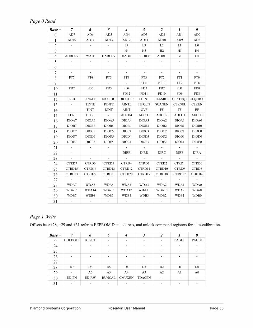
Page 0 Read
Base + 7 6 5 4 3 2 1 00 AD7 AD6 AD5 AD4 AD3 AD2 AD1 AD0
1 AD15 AD14 AD13 AD12 AD11 AD10 AD9 AD8
2 - - - L4 L3 L2 L1 L0
3 - - - H4 H3 H2 H1 H0
4 ADBUSY WAIT DABUSY DABU SEDIFF ADBU G1 G0
5 - - - - - - - -
6 - - - - - - - -
7 - - - - - - - -
8 FT7 FT6 FT5 FT4 FT3 FT2 FT1 FT0
9 - - - - FT11 FT10 FT9 FT8
10 FD7 FD6 FD5 FD4 FD3 FD2 FD1 FD0
11 - - - FD12 FD11 FD10 FD9 FD8
12 LED SINGLE DIOCTR1 DIOCTR0 SCINT CLKSRC1 CLKFRQ1 CLQFRQ0
13 - TINTE DINTE AINTE FIFOEN SCANEN CLKSEL CLKEN
14 - TINT DINT AINT OVF FF TF EF
15 CFG1 CFG0 - ADCH4 ADCH3 ADCH2 ADCH1 ADCH0
16 DIOA7 DIOA6 DIOA5 DIOA4 DIOA3 DIOA2 DIOA1 DIOA0
17 DIOB7 DIOB6 DIOB5 DIOB4 DIOB3 DIOB2 DIOB1 DIOB0
18 DIOC7 DIOC6 DIOC5 DIOC4 DIOC3 DIOC2 DIOC1 DIOC0
19 DIOD7 DIOD6 DIOD5 DIOD4 DIOD3 DIOD2 DIOD1 DIOD0
20 DIOE7 DIOE6 DIOE5 DIOE4 DIOE3 DIOE2 DIOE1 DIOE0
21 - - - - - - - -
22 - - - DIRE DIRD DIRC DIRB DIRA
23 - - - - - - - -
24 CTRD7 CTRD6 CTRD5 CTRD4 CTRD3 CTRD2 CTRD1 CTRD0
25 CTRD15 CTRD14 CTRD13 CTRD12 CTRD11 CTRD10 CTRD9 CTRD8
26 CTRD23 CTRD22 CTRD21 CTRD20 CTRD19 CTRD18 CTRD17 CTRD16
27 - - - - - - - -
28 WDA7 WDA6 WDA5 WDA4 WDA3 WDA2 WDA1 WDA0
29 WDA15 WDA14 WDA13 WDA12 WDA11 WDA10 WDA9 WDA8
30 WDB7 WDB6 WDB5 WDB4 WDB3 WDB2 WDB1 WDB0
31 - - - - - - - -
Page 1 WriteOffsets base+28, +29 and +31 refer to EEPROM Data, address, and unlock command registers for auto-calibration.
Base + 7 6 5 4 3 2 1 00 HOLDOFF RESET - - - - PAGE1 PAGE0
24 - - - - - - - -
25 - - - - - - - -
26 - - - - - - - -
27 - - - - - - - -
28 D7 D6 D5 D4 D3 D2 D1 D0
29 - A6 A5 A4 A3 A2 A1 A0
30 EE_EN EE_RW RUNCAL CMUXEN TDACEN - - -
31 - - - - - - - -
Diamond Systems Corporation Poseidon User Manual Page 55
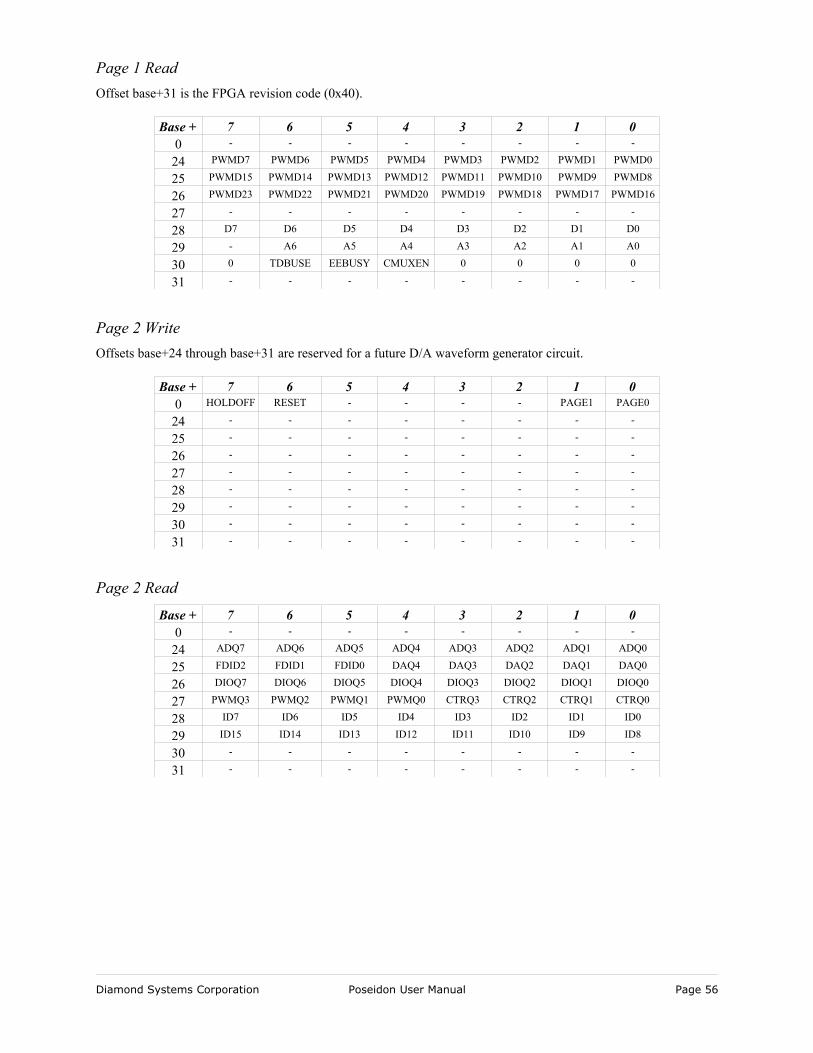
Page 1 ReadOffset base+31 is the FPGA revision code (0x40).
Base + 7 6 5 4 3 2 1 00 - - - - - - - -
24 PWMD7 PWMD6 PWMD5 PWMD4 PWMD3 PWMD2 PWMD1 PWMD0
25 PWMD15 PWMD14 PWMD13 PWMD12 PWMD11 PWMD10 PWMD9 PWMD8
26 PWMD23 PWMD22 PWMD21 PWMD20 PWMD19 PWMD18 PWMD17 PWMD16
27 - - - - - - - -
28 D7 D6 D5 D4 D3 D2 D1 D0
29 - A6 A5 A4 A3 A2 A1 A0
30 0 TDBUSE EEBUSY CMUXEN 0 0 0 0
31 - - - - - - - -
Page 2 WriteOffsets base+24 through base+31 are reserved for a future D/A waveform generator circuit.
Base + 7 6 5 4 3 2 1 00 HOLDOFF RESET - - - - PAGE1 PAGE0
24 - - - - - - - -
25 - - - - - - - -
26 - - - - - - - -
27 - - - - - - - -
28 - - - - - - - -
29 - - - - - - - -
30 - - - - - - - -
31 - - - - - - - -
Page 2 Read
Base + 7 6 5 4 3 2 1 00 - - - - - - - -
24 ADQ7 ADQ6 ADQ5 ADQ4 ADQ3 ADQ2 ADQ1 ADQ0
25 FDID2 FDID1 FDID0 DAQ4 DAQ3 DAQ2 DAQ1 DAQ0
26 DIOQ7 DIOQ6 DIOQ5 DIOQ4 DIOQ3 DIOQ2 DIOQ1 DIOQ0
27 PWMQ3 PWMQ2 PWMQ1 PWMQ0 CTRQ3 CTRQ2 CTRQ1 CTRQ0
28 ID7 ID6 ID5 ID4 ID3 ID2 ID1 ID0
29 ID15 ID14 ID13 ID12 ID11 ID10 ID9 ID8
30 - - - - - - - -
31 - - - - - - - -
Diamond Systems Corporation Poseidon User Manual Page 56
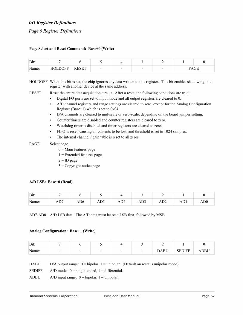
I/O Register Definitions
Page 0 Register Definitions
Page Select and Reset Command: Base+0 (Write)
Bit: 7 6 5 4 3 2 1 0
Name: HOLDOFF RESET - - - - PAGE
HOLDOFF When this bit is set, the chip ignores any data written to this register. This bit enables shadowing this register with another device at the same address.
RESET Reset the entire data acquisition circuit. After a reset, the following conditions are true:• Digital I/O ports are set to input mode and all output registers are cleared to 0.• A/D channel registers and range settings are cleared to zero, except for the Analog Configuration
Register (Base+1) which is set to 0x04.• D/A channels are cleared to mid-scale or zero-scale, depending on the board jumper setting.• Counter/timers are disabled and counter registers are cleared to zero.• Watchdog timer is disabled and timer registers are cleared to zero.• FIFO is reset, causing all contents to be lost, and threshold is set to 1024 samples.• The internal channel / gain table is reset to all zeros.
PAGE Select page.0 = Main features page1 = Extended features page2 = ID page3 = Copyright notice page
A/D LSB: Base+0 (Read)
Bit: 7 6 5 4 3 2 1 0
Name: AD7 AD6 AD5 AD4 AD3 AD2 AD1 AD0
AD7-AD0 A/D LSB data. The A/D data must be read LSB first, followed by MSB.
Analog Configuration: Base+1 (Write)
Bit: 7 6 5 4 3 2 1 0
Name: - - - - - DABU SEDIFF ADBU
DABU D/A output range: 0 = bipolar, 1 = unipolar. (Default on reset is unipolar mode).
SEDIFF A/D mode: 0 = single-ended, 1 = differential.
ADBU A/D input range: 0 = bipolar, 1 = unipolar.
Diamond Systems Corporation Poseidon User Manual Page 57
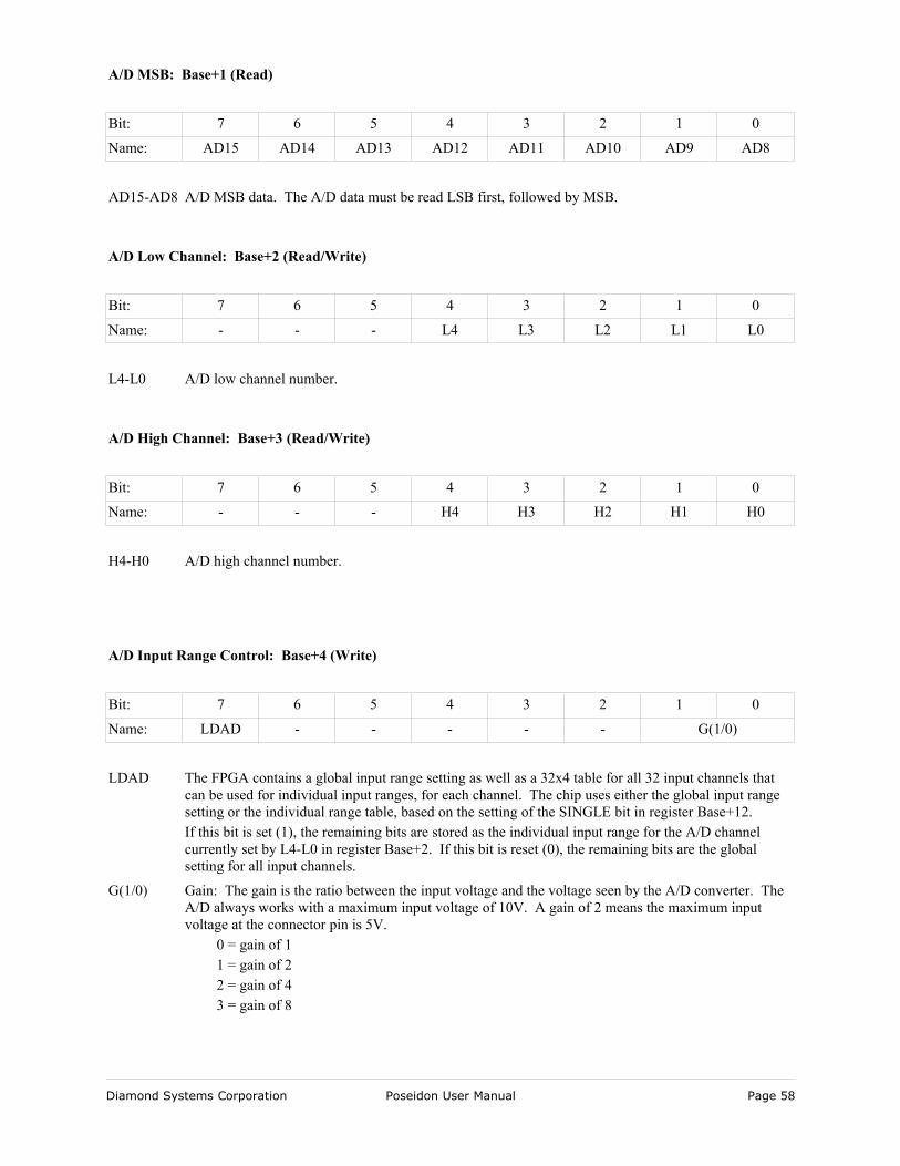
A/D MSB: Base+1 (Read)
Bit: 7 6 5 4 3 2 1 0
Name: AD15 AD14 AD13 AD12 AD11 AD10 AD9 AD8
AD15-AD8 A/D MSB data. The A/D data must be read LSB first, followed by MSB.
A/D Low Channel: Base+2 (Read/Write)
Bit: 7 6 5 4 3 2 1 0
Name: - - - L4 L3 L2 L1 L0
L4-L0 A/D low channel number.
A/D High Channel: Base+3 (Read/Write)
Bit: 7 6 5 4 3 2 1 0
Name: - - - H4 H3 H2 H1 H0
H4-H0 A/D high channel number.
A/D Input Range Control: Base+4 (Write)
Bit: 7 6 5 4 3 2 1 0
Name: LDAD - - - - - G(1/0)
LDAD The FPGA contains a global input range setting as well as a 32x4 table for all 32 input channels that can be used for individual input ranges, for each channel. The chip uses either the global input range setting or the individual range table, based on the setting of the SINGLE bit in register Base+12.If this bit is set (1), the remaining bits are stored as the individual input range for the A/D channel currently set by L4-L0 in register Base+2. If this bit is reset (0), the remaining bits are the global setting for all input channels.
G(1/0) Gain: The gain is the ratio between the input voltage and the voltage seen by the A/D converter. The A/D always works with a maximum input voltage of 10V. A gain of 2 means the maximum input voltage at the connector pin is 5V.
0 = gain of 11 = gain of 22 = gain of 43 = gain of 8
Diamond Systems Corporation Poseidon User Manual Page 58
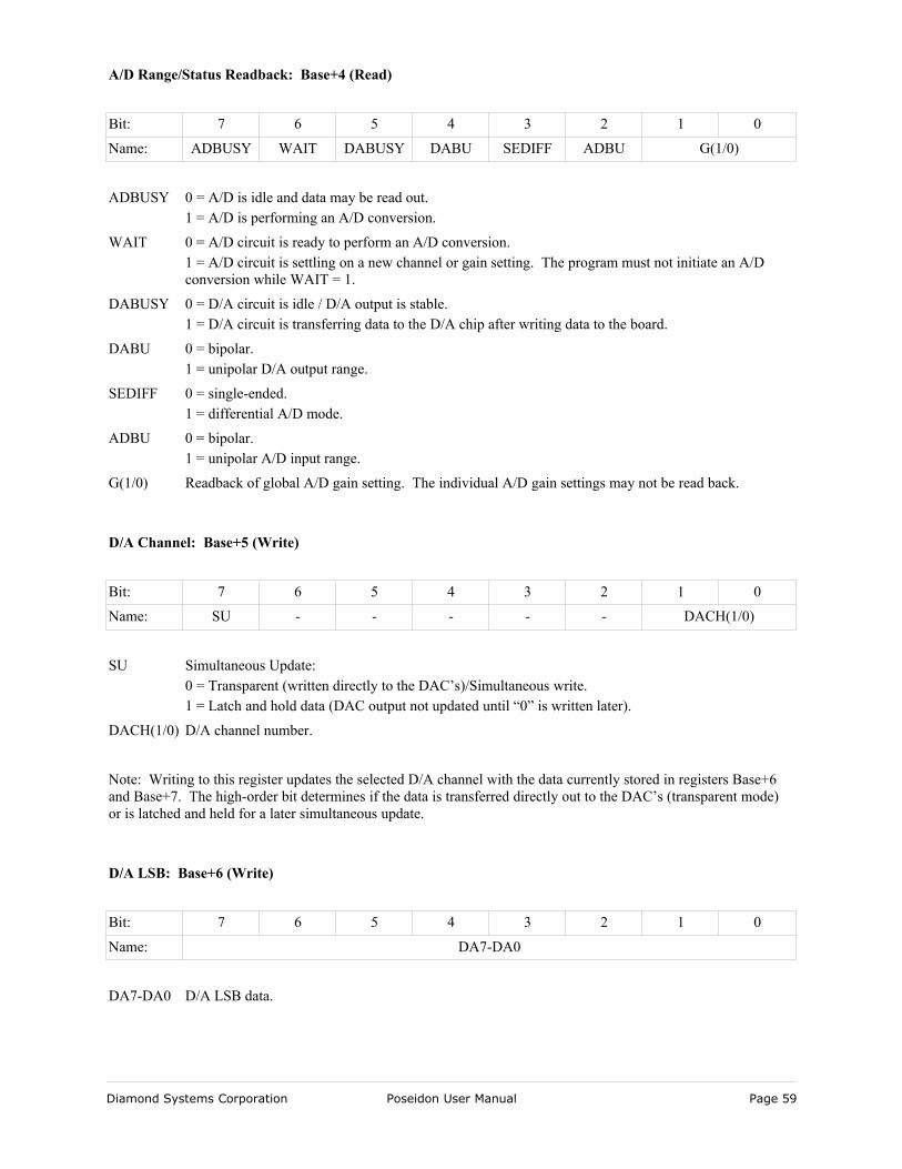
A/D Range/Status Readback: Base+4 (Read)
Bit: 7 6 5 4 3 2 1 0
Name: ADBUSY WAIT DABUSY DABU SEDIFF ADBU G(1/0)
ADBUSY 0 = A/D is idle and data may be read out.1 = A/D is performing an A/D conversion.
WAIT 0 = A/D circuit is ready to perform an A/D conversion.1 = A/D circuit is settling on a new channel or gain setting. The program must not initiate an A/D conversion while WAIT = 1.
DABUSY 0 = D/A circuit is idle / D/A output is stable.1 = D/A circuit is transferring data to the D/A chip after writing data to the board.
DABU 0 = bipolar.1 = unipolar D/A output range.
SEDIFF 0 = single-ended.1 = differential A/D mode.
ADBU 0 = bipolar.1 = unipolar A/D input range.
G(1/0) Readback of global A/D gain setting. The individual A/D gain settings may not be read back.
D/A Channel: Base+5 (Write)
Bit: 7 6 5 4 3 2 1 0
Name: SU - - - - - DACH(1/0)
SU Simultaneous Update:0 = Transparent (written directly to the DAC’s)/Simultaneous write.1 = Latch and hold data (DAC output not updated until “0” is written later).
DACH(1/0) D/A channel number.
Note: Writing to this register updates the selected D/A channel with the data currently stored in registers Base+6 and Base+7. The high-order bit determines if the data is transferred directly out to the DAC’s (transparent mode) or is latched and held for a later simultaneous update.
D/A LSB: Base+6 (Write)
Bit: 7 6 5 4 3 2 1 0
Name: DA7-DA0
DA7-DA0 D/A LSB data.
Diamond Systems Corporation Poseidon User Manual Page 59
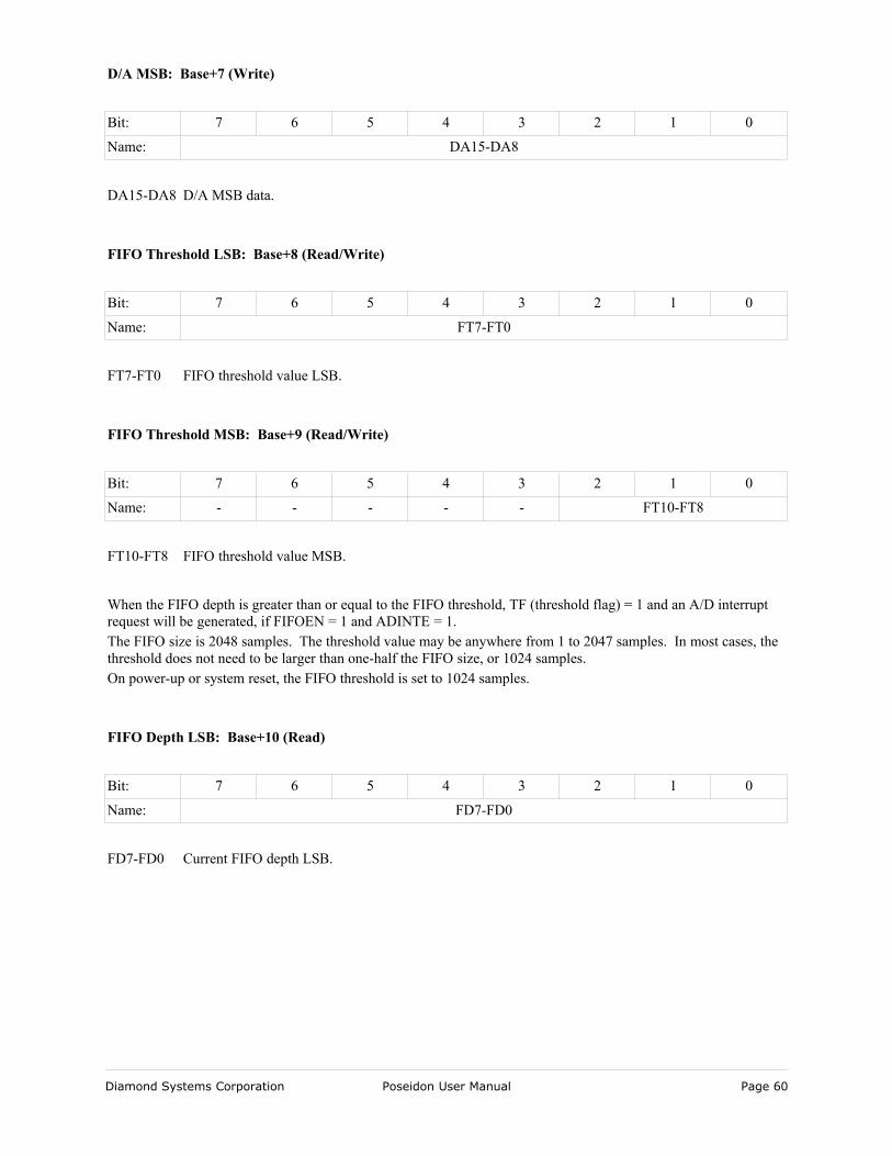
D/A MSB: Base+7 (Write)
Bit: 7 6 5 4 3 2 1 0
Name: DA15-DA8
DA15-DA8 D/A MSB data.
FIFO Threshold LSB: Base+8 (Read/Write)
Bit: 7 6 5 4 3 2 1 0
Name: FT7-FT0
FT7-FT0 FIFO threshold value LSB.
FIFO Threshold MSB: Base+9 (Read/Write)
Bit: 7 6 5 4 3 2 1 0
Name: - - - - - FT10-FT8
FT10-FT8 FIFO threshold value MSB.
When the FIFO depth is greater than or equal to the FIFO threshold, TF (threshold flag) = 1 and an A/D interrupt request will be generated, if FIFOEN = 1 and ADINTE = 1. The FIFO size is 2048 samples. The threshold value may be anywhere from 1 to 2047 samples. In most cases, the threshold does not need to be larger than one-half the FIFO size, or 1024 samples.On power-up or system reset, the FIFO threshold is set to 1024 samples.
FIFO Depth LSB: Base+10 (Read)
Bit: 7 6 5 4 3 2 1 0
Name: FD7-FD0
FD7-FD0 Current FIFO depth LSB.
Diamond Systems Corporation Poseidon User Manual Page 60
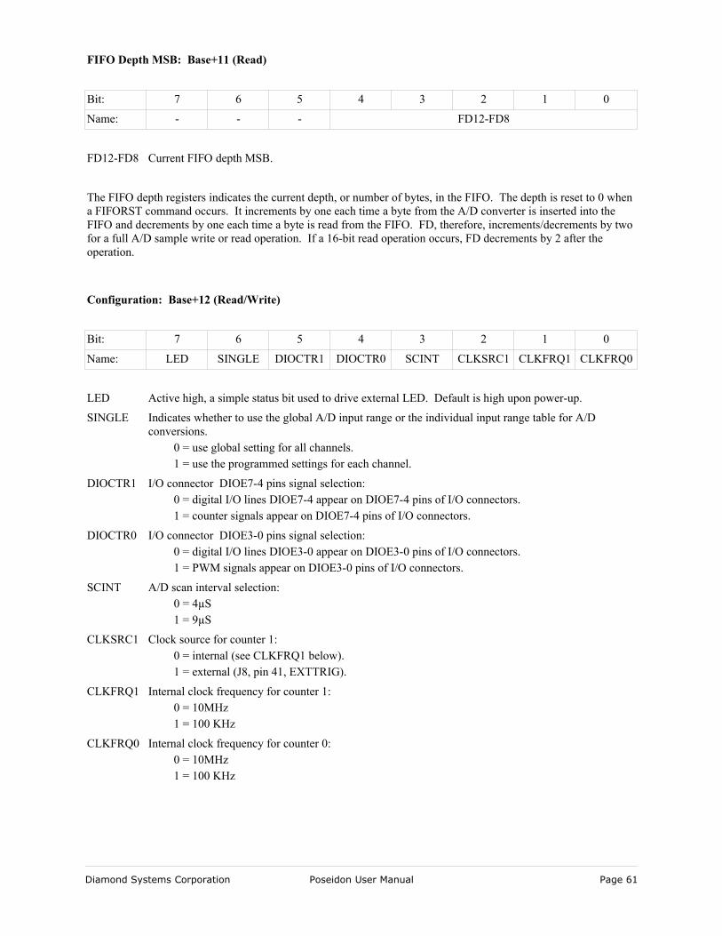
FIFO Depth MSB: Base+11 (Read)
Bit: 7 6 5 4 3 2 1 0
Name: - - - FD12-FD8
FD12-FD8 Current FIFO depth MSB.
The FIFO depth registers indicates the current depth, or number of bytes, in the FIFO. The depth is reset to 0 when a FIFORST command occurs. It increments by one each time a byte from the A/D converter is inserted into the FIFO and decrements by one each time a byte is read from the FIFO. FD, therefore, increments/decrements by two for a full A/D sample write or read operation. If a 16-bit read operation occurs, FD decrements by 2 after the operation.
Configuration: Base+12 (Read/Write)
Bit: 7 6 5 4 3 2 1 0
Name: LED SINGLE DIOCTR1 DIOCTR0 SCINT CLKSRC1 CLKFRQ1 CLKFRQ0
LED Active high, a simple status bit used to drive external LED. Default is high upon power-up.
SINGLE Indicates whether to use the global A/D input range or the individual input range table for A/D conversions.
0 = use global setting for all channels.1 = use the programmed settings for each channel.
DIOCTR1 I/O connector DIOE7-4 pins signal selection:0 = digital I/O lines DIOE7-4 appear on DIOE7-4 pins of I/O connectors.1 = counter signals appear on DIOE7-4 pins of I/O connectors.
DIOCTR0 I/O connector DIOE3-0 pins signal selection:0 = digital I/O lines DIOE3-0 appear on DIOE3-0 pins of I/O connectors.1 = PWM signals appear on DIOE3-0 pins of I/O connectors.
SCINT A/D scan interval selection:0 = 4µS1 = 9µS
CLKSRC1 Clock source for counter 1: 0 = internal (see CLKFRQ1 below).1 = external (J8, pin 41, EXTTRIG).
CLKFRQ1 Internal clock frequency for counter 1:0 = 10MHz1 = 100 KHz
CLKFRQ0 Internal clock frequency for counter 0:0 = 10MHz1 = 100 KHz
Diamond Systems Corporation Poseidon User Manual Page 61
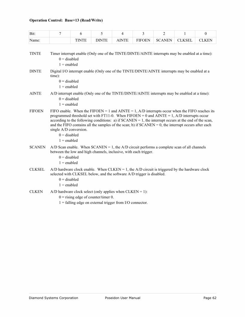
Operation Control: Base+13 (Read/Write)
Bit: 7 6 5 4 3 2 1 0
Name: TINTE DINTE AINTE FIFOEN SCANEN CLKSEL CLKEN
TINTE Timer interrupt enable (Only one of the TINTE/DINTE/AINTE interrupts may be enabled at a time):0 = disabled1 = enabled
DINTE Digital I/O interrupt enable (Only one of the TINTE/DINTE/AINTE interrupts may be enabled at a time):
0 = disabled1 = enabled
AINTE A/D interrupt enable (Only one of the TINTE/DINTE/AINTE interrupts may be enabled at a time):0 = disabled1 = enabled
FIFOEN FIFO enable. When the FIFOEN = 1 and AINTE = 1, A/D interrupts occur when the FIFO reaches its programmed threshold set with FT11-0. When FIFOEN = 0 and AINTE = 1, A/D interrupts occur according to the following conditions: a) if SCANEN = 1, the interrupt occurs at the end of the scan, and the FIFO contains all the samples of the scan; b) if SCANEN = 0, the interrupt occurs after each single A/D conversion.
0 = disabled1 = enabled
SCANEN A/D Scan enable. When SCANEN = 1, the A/D circuit performs a complete scan of all channels between the low and high channels, inclusive, with each trigger.
0 = disabled1 = enabled
CLKSEL A/D hardware clock enable. When CLKEN = 1, the A/D circuit is triggered by the hardware clock selected with CLKSEL below, and the software A/D trigger is disabled.
0 = disabled1 = enabled
CLKEN A/D hardware clock select (only applies when CLKEN = 1):0 = rising edge of counter/timer 0.1 = falling edge on external trigger from I/O connector.
Diamond Systems Corporation Poseidon User Manual Page 62
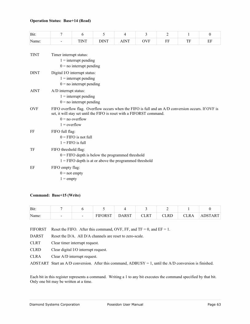
Operation Status: Base+14 (Read)
Bit: 7 6 5 4 3 2 1 0
Name: - TINT DINT AINT OVF FF TF EF
TINT Timer interrupt status:1 = interrupt pending0 = no interrupt pending
DINT Digital I/O interrupt status:1 = interrupt pending0 = no interrupt pending
AINT A/D interrupt status:1 = interrupt pending0 = no interrupt pending
OVF FIFO overflow flag. Overflow occurs when the FIFO is full and an A/D conversion occurs. If OVF is set, it will stay set until the FIFO is reset with a FIFORST command.
0 = no overflow1 = overflow
FF FIFO full flag:0 = FIFO is not full1 = FIFO is full
TF FIFO threshold flag:0 = FIFO depth is below the programmed threshold1 = FIFO depth is at or above the programmed threshold
EF FIFO empty flag:0 = not empty1 = empty
Command: Base+15 (Write)
Bit: 7 6 5 4 3 2 1 0
Name: - - FIFORST DARST CLRT CLRD CLRA ADSTART
FIFORST Reset the FIFO. After this command, OVF, FF, and TF = 0, and EF = 1.
DARST Reset the D/A. All D/A channels are reset to zero-scale.
CLRT Clear timer interrupt request.
CLRD Clear digital I/O interrupt request.
CLRA Clear A/D interrupt request.
ADSTART Start an A/D conversion. After this command, ADBUSY = 1, until the A/D conversion is finished.
Each bit in this register represents a command. Writing a 1 to any bit executes the command specified by that bit. Only one bit may be written at a time.
Diamond Systems Corporation Poseidon User Manual Page 63
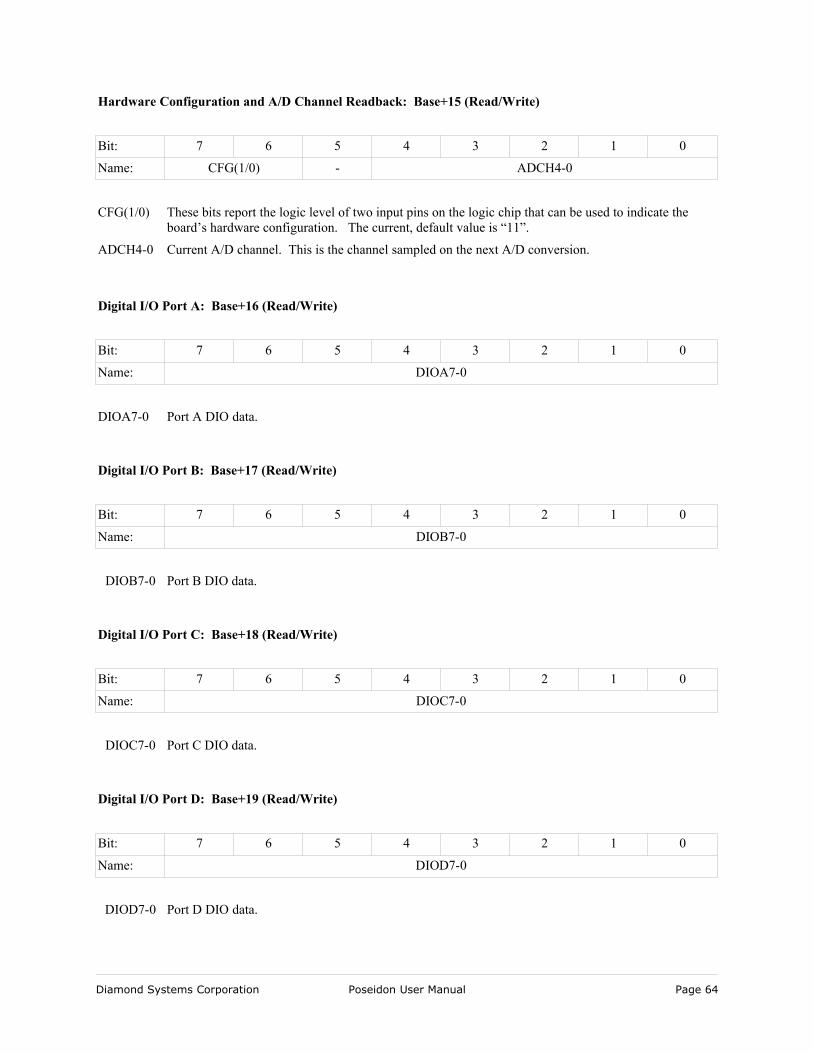
Hardware Configuration and A/D Channel Readback: Base+15 (Read/Write)
Bit: 7 6 5 4 3 2 1 0
Name: CFG(1/0) - ADCH4-0
CFG(1/0) These bits report the logic level of two input pins on the logic chip that can be used to indicate the board’s hardware configuration. The current, default value is “11”.
ADCH4-0 Current A/D channel. This is the channel sampled on the next A/D conversion.
Digital I/O Port A: Base+16 (Read/Write)
Bit: 7 6 5 4 3 2 1 0
Name: DIOA7-0
DIOA7-0 Port A DIO data.
Digital I/O Port B: Base+17 (Read/Write)
Bit: 7 6 5 4 3 2 1 0
Name: DIOB7-0
DIOB7-0 Port B DIO data.
Digital I/O Port C: Base+18 (Read/Write)
Bit: 7 6 5 4 3 2 1 0
Name: DIOC7-0
DIOC7-0 Port C DIO data.
Digital I/O Port D: Base+19 (Read/Write)
Bit: 7 6 5 4 3 2 1 0
Name: DIOD7-0
DIOD7-0 Port D DIO data.
Diamond Systems Corporation Poseidon User Manual Page 64
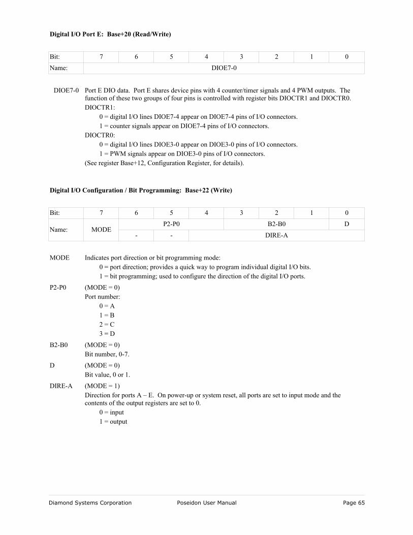
Digital I/O Port E: Base+20 (Read/Write)
Bit: 7 6 5 4 3 2 1 0
Name: DIOE7-0
DIOE7-0 Port E DIO data. Port E shares device pins with 4 counter/timer signals and 4 PWM outputs. The function of these two groups of four pins is controlled with register bits DIOCTR1 and DIOCTR0.DIOCTR1:
0 = digital I/O lines DIOE7-4 appear on DIOE7-4 pins of I/O connectors.1 = counter signals appear on DIOE7-4 pins of I/O connectors.
DIOCTR0:0 = digital I/O lines DIOE3-0 appear on DIOE3-0 pins of I/O connectors.1 = PWM signals appear on DIOE3-0 pins of I/O connectors.
(See register Base+12, Configuration Register, for details).
Digital I/O Configuration / Bit Programming: Base+22 (Write)
Bit: 7 6 5 4 3 2 1 0
Name: MODEP2-P0 B2-B0 D
- - DIRE-A
MODE Indicates port direction or bit programming mode:0 = port direction; provides a quick way to program individual digital I/O bits.1 = bit programming; used to configure the direction of the digital I/O ports.
P2-P0 (MODE = 0)Port number:
0 = A1 = B2 = C3 = D
B2-B0 (MODE = 0)Bit number, 0-7.
D (MODE = 0)Bit value, 0 or 1.
DIRE-A (MODE = 1)Direction for ports A – E. On power-up or system reset, all ports are set to input mode and the contents of the output registers are set to 0.
0 = input1 = output
Diamond Systems Corporation Poseidon User Manual Page 65
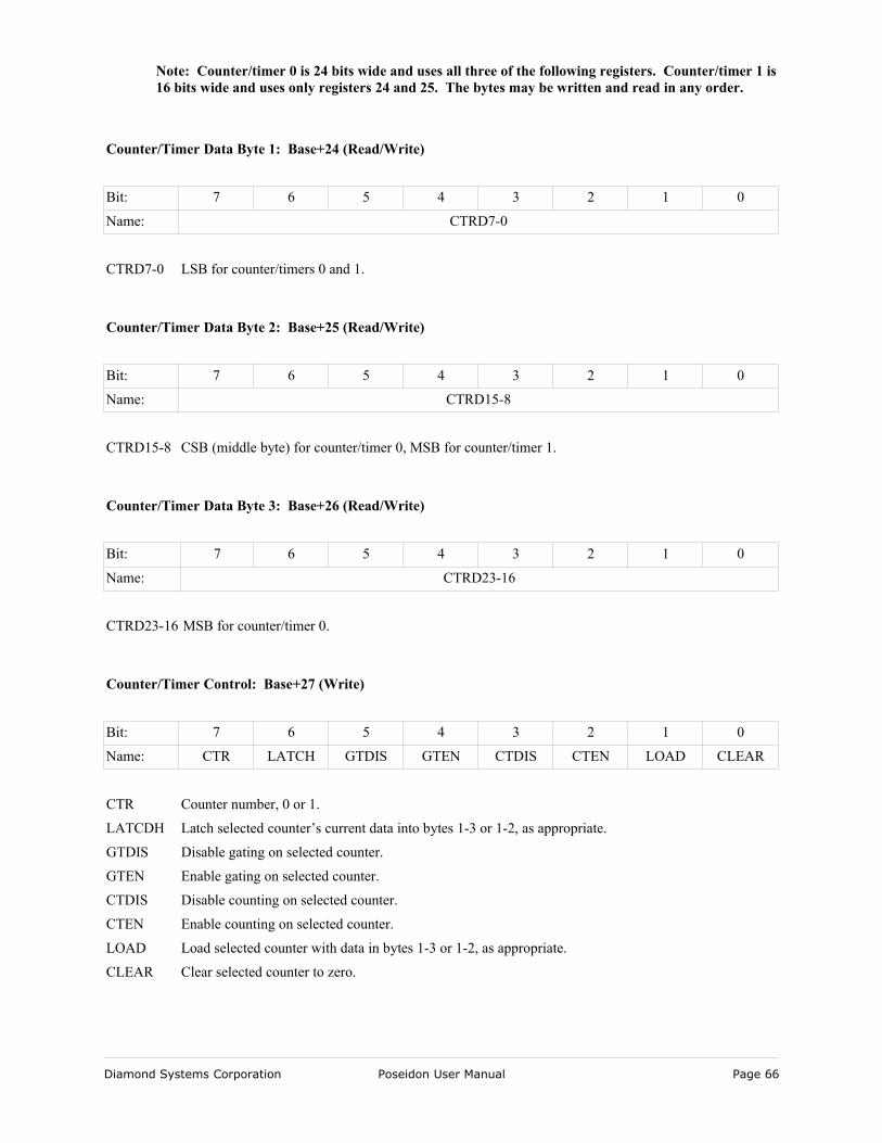
Note: Counter/timer 0 is 24 bits wide and uses all three of the following registers. Counter/timer 1 is 16 bits wide and uses only registers 24 and 25. The bytes may be written and read in any order.
Counter/Timer Data Byte 1: Base+24 (Read/Write)
Bit: 7 6 5 4 3 2 1 0
Name: CTRD7-0
CTRD7-0 LSB for counter/timers 0 and 1.
Counter/Timer Data Byte 2: Base+25 (Read/Write)
Bit: 7 6 5 4 3 2 1 0
Name: CTRD15-8
CTRD15-8 CSB (middle byte) for counter/timer 0, MSB for counter/timer 1.
Counter/Timer Data Byte 3: Base+26 (Read/Write)
Bit: 7 6 5 4 3 2 1 0
Name: CTRD23-16
CTRD23-16 MSB for counter/timer 0.
Counter/Timer Control: Base+27 (Write)
Bit: 7 6 5 4 3 2 1 0
Name: CTR LATCH GTDIS GTEN CTDIS CTEN LOAD CLEAR
CTR Counter number, 0 or 1.
LATCDH Latch selected counter’s current data into bytes 1-3 or 1-2, as appropriate.
GTDIS Disable gating on selected counter.
GTEN Enable gating on selected counter.
CTDIS Disable counting on selected counter.
CTEN Enable counting on selected counter.
LOAD Load selected counter with data in bytes 1-3 or 1-2, as appropriate.
CLEAR Clear selected counter to zero.
Diamond Systems Corporation Poseidon User Manual Page 66
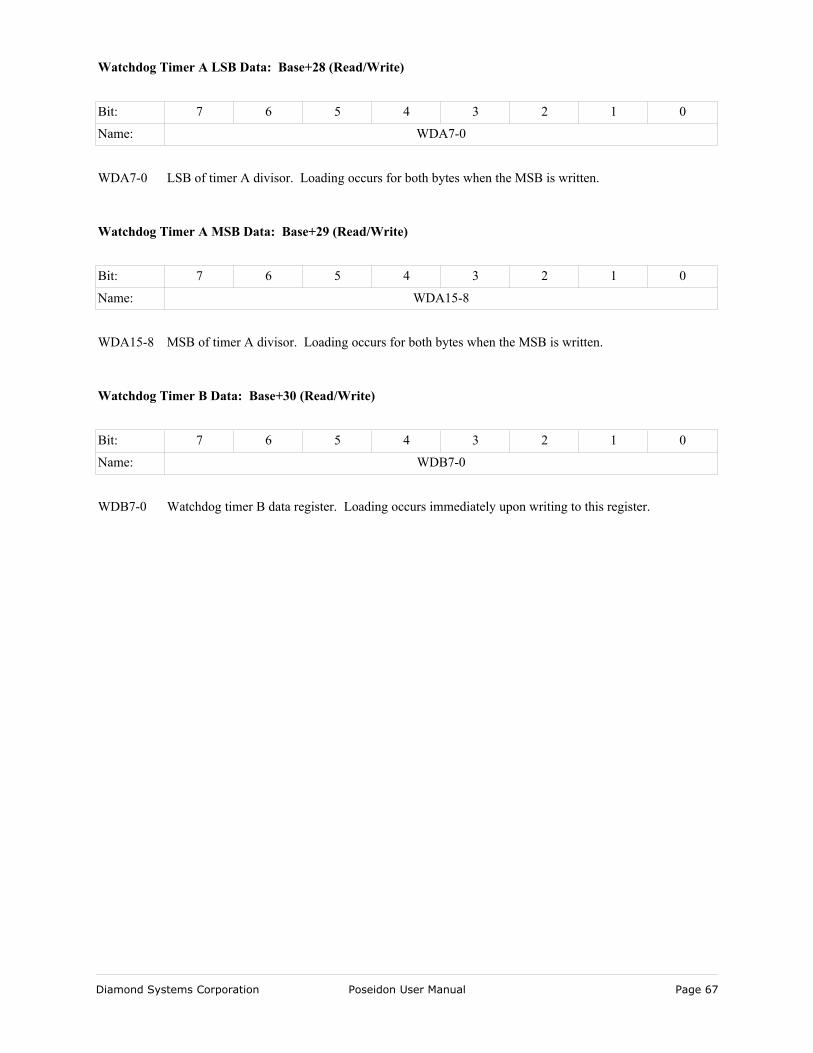
Watchdog Timer A LSB Data: Base+28 (Read/Write)
Bit: 7 6 5 4 3 2 1 0
Name: WDA7-0
WDA7-0 LSB of timer A divisor. Loading occurs for both bytes when the MSB is written.
Watchdog Timer A MSB Data: Base+29 (Read/Write)
Bit: 7 6 5 4 3 2 1 0
Name: WDA15-8
WDA15-8 MSB of timer A divisor. Loading occurs for both bytes when the MSB is written.
Watchdog Timer B Data: Base+30 (Read/Write)
Bit: 7 6 5 4 3 2 1 0
Name: WDB7-0
WDB7-0 Watchdog timer B data register. Loading occurs immediately upon writing to this register.
Diamond Systems Corporation Poseidon User Manual Page 67
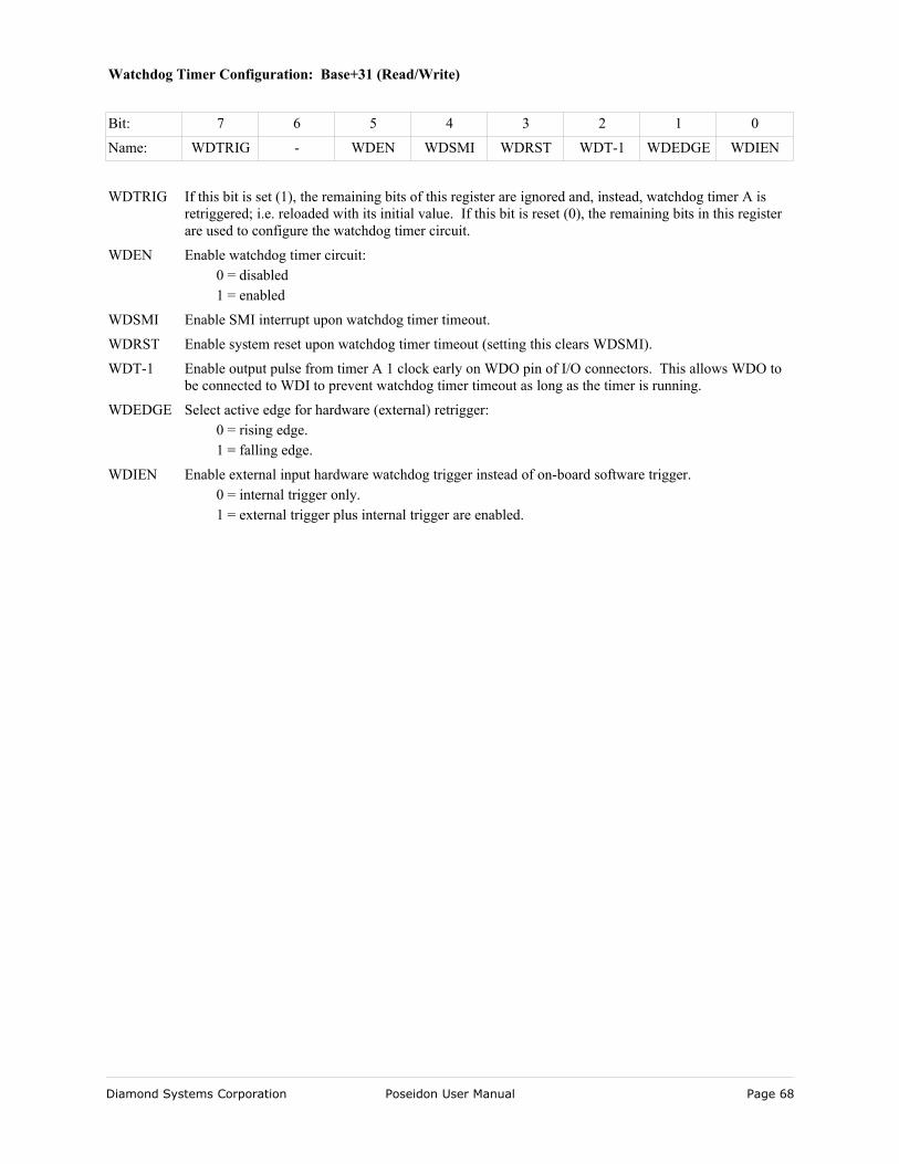
Watchdog Timer Configuration: Base+31 (Read/Write)
Bit: 7 6 5 4 3 2 1 0
Name: WDTRIG - WDEN WDSMI WDRST WDT-1 WDEDGE WDIEN
WDTRIG If this bit is set (1), the remaining bits of this register are ignored and, instead, watchdog timer A is retriggered; i.e. reloaded with its initial value. If this bit is reset (0), the remaining bits in this register are used to configure the watchdog timer circuit.
WDEN Enable watchdog timer circuit:0 = disabled1 = enabled
WDSMI Enable SMI interrupt upon watchdog timer timeout.
WDRST Enable system reset upon watchdog timer timeout (setting this clears WDSMI).
WDT-1 Enable output pulse from timer A 1 clock early on WDO pin of I/O connectors. This allows WDO to be connected to WDI to prevent watchdog timer timeout as long as the timer is running.
WDEDGE Select active edge for hardware (external) retrigger:0 = rising edge.1 = falling edge.
WDIEN Enable external input hardware watchdog trigger instead of on-board software trigger.0 = internal trigger only.1 = external trigger plus internal trigger are enabled.
Diamond Systems Corporation Poseidon User Manual Page 68
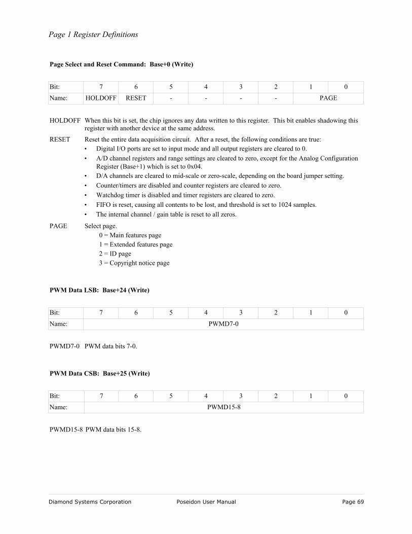
Page 1 Register Definitions
Page Select and Reset Command: Base+0 (Write)
Bit: 7 6 5 4 3 2 1 0
Name: HOLDOFF RESET - - - - PAGE
HOLDOFF When this bit is set, the chip ignores any data written to this register. This bit enables shadowing this register with another device at the same address.
RESET Reset the entire data acquisition circuit. After a reset, the following conditions are true:• Digital I/O ports are set to input mode and all output registers are cleared to 0.• A/D channel registers and range settings are cleared to zero, except for the Analog Configuration
Register (Base+1) which is set to 0x04.• D/A channels are cleared to mid-scale or zero-scale, depending on the board jumper setting.• Counter/timers are disabled and counter registers are cleared to zero.• Watchdog timer is disabled and timer registers are cleared to zero.• FIFO is reset, causing all contents to be lost, and threshold is set to 1024 samples.• The internal channel / gain table is reset to all zeros.
PAGE Select page.0 = Main features page1 = Extended features page2 = ID page3 = Copyright notice page
PWM Data LSB: Base+24 (Write)
Bit: 7 6 5 4 3 2 1 0
Name: PWMD7-0
PWMD7-0 PWM data bits 7-0.
PWM Data CSB: Base+25 (Write)
Bit: 7 6 5 4 3 2 1 0
Name: PWMD15-8
PWMD15-8 PWM data bits 15-8.
Diamond Systems Corporation Poseidon User Manual Page 69
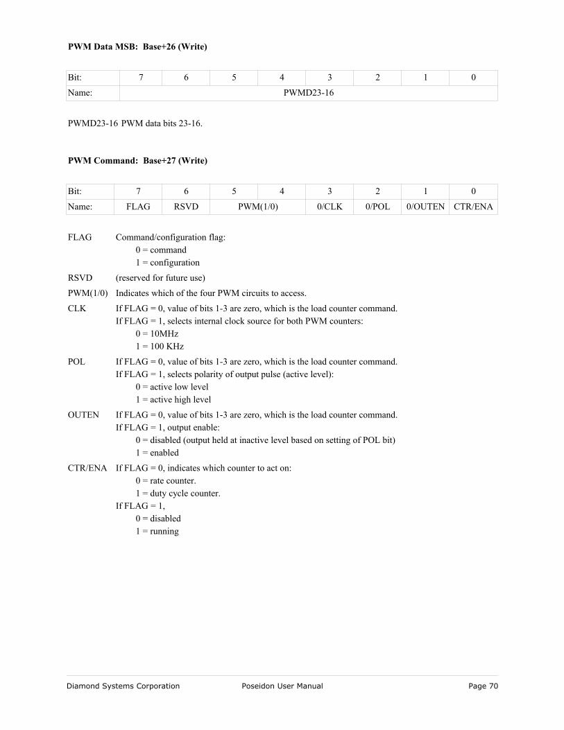
PWM Data MSB: Base+26 (Write)
Bit: 7 6 5 4 3 2 1 0
Name: PWMD23-16
PWMD23-16 PWM data bits 23-16.
PWM Command: Base+27 (Write)
Bit: 7 6 5 4 3 2 1 0
Name: FLAG RSVD PWM(1/0) 0/CLK 0/POL 0/OUTEN CTR/ENA
FLAG Command/configuration flag:0 = command1 = configuration
RSVD (reserved for future use)
PWM(1/0) Indicates which of the four PWM circuits to access.
CLK If FLAG = 0, value of bits 1-3 are zero, which is the load counter command.If FLAG = 1, selects internal clock source for both PWM counters:
0 = 10MHz1 = 100 KHz
POL If FLAG = 0, value of bits 1-3 are zero, which is the load counter command.If FLAG = 1, selects polarity of output pulse (active level):
0 = active low level1 = active high level
OUTEN If FLAG = 0, value of bits 1-3 are zero, which is the load counter command.If FLAG = 1, output enable:
0 = disabled (output held at inactive level based on setting of POL bit)1 = enabled
CTR/ENA If FLAG = 0, indicates which counter to act on:0 = rate counter.1 = duty cycle counter.
If FLAG = 1, 0 = disabled1 = running
Diamond Systems Corporation Poseidon User Manual Page 70
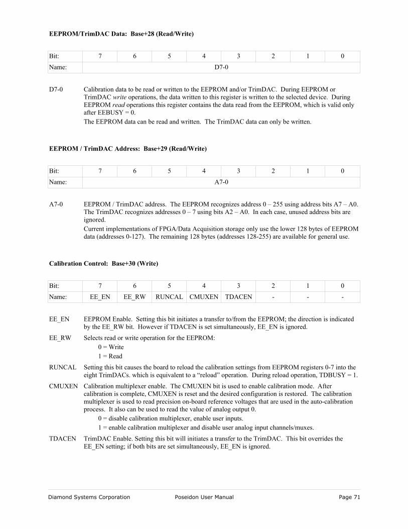
EEPROM/TrimDAC Data: Base+28 (Read/Write)
Bit: 7 6 5 4 3 2 1 0
Name: D7-0
D7-0 Calibration data to be read or written to the EEPROM and/or TrimDAC. During EEPROM or TrimDAC write operations, the data written to this register is written to the selected device. During EEPROM read operations this register contains the data read from the EEPROM, which is valid only after EEBUSY = 0.The EEPROM data can be read and written. The TrimDAC data can only be written.
EEPROM / TrimDAC Address: Base+29 (Read/Write)
Bit: 7 6 5 4 3 2 1 0
Name: A7-0
A7-0 EEPROM / TrimDAC address. The EEPROM recognizes address 0 – 255 using address bits A7 – A0. The TrimDAC recognizes addresses 0 – 7 using bits A2 – A0. In each case, unused address bits are ignored. Current implementations of FPGA/Data Acquisition storage only use the lower 128 bytes of EEPROM data (addresses 0-127). The remaining 128 bytes (addresses 128-255) are available for general use.
Calibration Control: Base+30 (Write)
Bit: 7 6 5 4 3 2 1 0
Name: EE_EN EE_RW RUNCAL CMUXEN TDACEN - - -
EE_EN EEPROM Enable. Setting this bit initiates a transfer to/from the EEPROM; the direction is indicated by the EE_RW bit. However if TDACEN is set simultaneously, EE_EN is ignored.
EE_RW Selects read or write operation for the EEPROM:0 = Write1 = Read
RUNCAL Setting this bit causes the board to reload the calibration settings from EEPROM registers 0-7 into the eight TrimDACs. which is equivalent to a “reload” operation. During reload operation, TDBUSY = 1.
CMUXEN Calibration multiplexer enable. The CMUXEN bit is used to enable calibration mode. After calibration is complete, CMUXEN is reset and the desired configuration is restored. The calibration multiplexer is used to read precision on-board reference voltages that are used in the auto-calibration process. It also can be used to read the value of analog output 0.
0 = disable calibration multiplexer, enable user inputs.1 = enable calibration multiplexer and disable user analog input channels/muxes.
TDACEN TrimDAC Enable. Setting this bit will initiates a transfer to the TrimDAC. This bit overrides the EE_EN setting; if both bits are set simultaneously, EE_EN is ignored.
Diamond Systems Corporation Poseidon User Manual Page 71
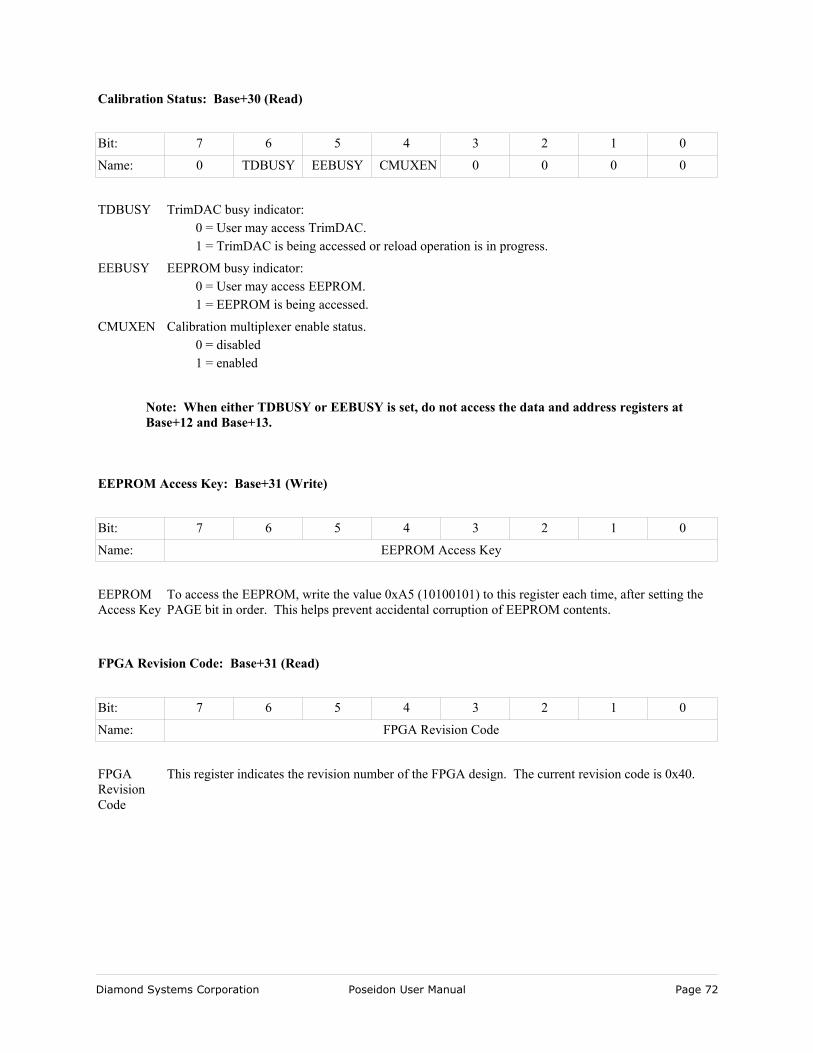
Calibration Status: Base+30 (Read)
Bit: 7 6 5 4 3 2 1 0
Name: 0 TDBUSY EEBUSY CMUXEN 0 0 0 0
TDBUSY TrimDAC busy indicator:0 = User may access TrimDAC.1 = TrimDAC is being accessed or reload operation is in progress.
EEBUSY EEPROM busy indicator:0 = User may access EEPROM.1 = EEPROM is being accessed.
CMUXEN Calibration multiplexer enable status. 0 = disabled1 = enabled
Note: When either TDBUSY or EEBUSY is set, do not access the data and address registers at Base+12 and Base+13.
EEPROM Access Key: Base+31 (Write)
Bit: 7 6 5 4 3 2 1 0
Name: EEPROM Access Key
EEPROM Access Key
To access the EEPROM, write the value 0xA5 (10100101) to this register each time, after setting the PAGE bit in order. This helps prevent accidental corruption of EEPROM contents.
FPGA Revision Code: Base+31 (Read)
Bit: 7 6 5 4 3 2 1 0
Name: FPGA Revision Code
FPGA Revision Code
This register indicates the revision number of the FPGA design. The current revision code is 0x40.
Diamond Systems Corporation Poseidon User Manual Page 72
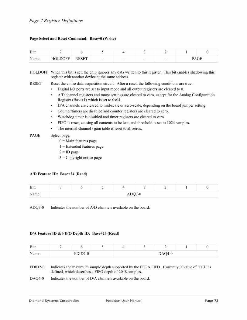
Page 2 Register Definitions
Page Select and Reset Command: Base+0 (Write)
Bit: 7 6 5 4 3 2 1 0
Name: HOLDOFF RESET - - - - PAGE
HOLDOFF When this bit is set, the chip ignores any data written to this register. This bit enables shadowing this register with another device at the same address.
RESET Reset the entire data acquisition circuit. After a reset, the following conditions are true:• Digital I/O ports are set to input mode and all output registers are cleared to 0.• A/D channel registers and range settings are cleared to zero, except for the Analog Configuration
Register (Base+1) which is set to 0x04.• D/A channels are cleared to mid-scale or zero-scale, depending on the board jumper setting.• Counter/timers are disabled and counter registers are cleared to zero.• Watchdog timer is disabled and timer registers are cleared to zero.• FIFO is reset, causing all contents to be lost, and threshold is set to 1024 samples.• The internal channel / gain table is reset to all zeros.
PAGE Select page.0 = Main features page1 = Extended features page2 = ID page3 = Copyright notice page
A/D Feature ID: Base+24 (Read)
Bit: 7 6 5 4 3 2 1 0
Name: ADQ7-0
ADQ7-0 Indicates the number of A/D channels available on the board.
D/A Feature ID & FIFO Depth ID: Base+25 (Read)
Bit: 7 6 5 4 3 2 1 0
Name: FDID2-0 DAQ4-0
FDID2-0 Indicates the maximum sample depth supported by the FPGA FIFO. Currently, a value of “001” is defined, which describes a FIFO depth of 2048 samples.
DAQ4-0 Indicates the number of D/A channels available on the board.
Diamond Systems Corporation Poseidon User Manual Page 73
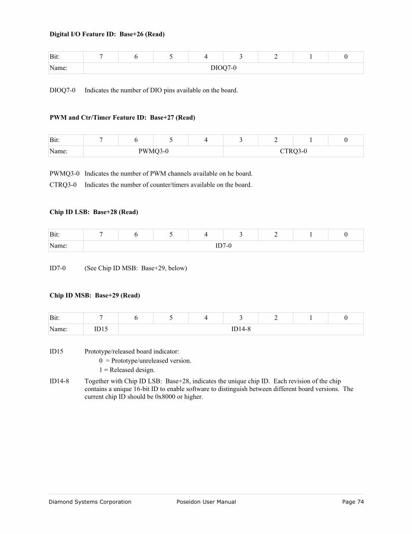
Digital I/O Feature ID: Base+26 (Read)
Bit: 7 6 5 4 3 2 1 0
Name: DIOQ7-0
DIOQ7-0 Indicates the number of DIO pins available on the board.
PWM and Ctr/Timer Feature ID: Base+27 (Read)
Bit: 7 6 5 4 3 2 1 0
Name: PWMQ3-0 CTRQ3-0
PWMQ3-0 Indicates the number of PWM channels available on he board.
CTRQ3-0 Indicates the number of counter/timers available on the board.
Chip ID LSB: Base+28 (Read)
Bit: 7 6 5 4 3 2 1 0
Name: ID7-0
ID7-0 (See Chip ID MSB: Base+29, below)
Chip ID MSB: Base+29 (Read)
Bit: 7 6 5 4 3 2 1 0
Name: ID15 ID14-8
ID15 Prototype/released board indicator:0 = Prototype/unreleased version.1 = Released design.
ID14-8 Together with Chip ID LSB: Base+28, indicates the unique chip ID. Each revision of the chip contains a unique 16-bit ID to enable software to distinguish between different board versions. The current chip ID should be 0x8000 or higher.
Diamond Systems Corporation Poseidon User Manual Page 74
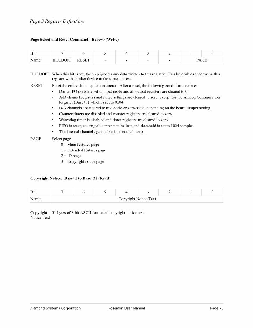
Page 3 Register Definitions
Page Select and Reset Command: Base+0 (Write)
Bit: 7 6 5 4 3 2 1 0
Name: HOLDOFF RESET - - - - PAGE
HOLDOFF When this bit is set, the chip ignores any data written to this register. This bit enables shadowing this register with another device at the same address.
RESET Reset the entire data acquisition circuit. After a reset, the following conditions are true:• Digital I/O ports are set to input mode and all output registers are cleared to 0.• A/D channel registers and range settings are cleared to zero, except for the Analog Configuration
Register (Base+1) which is set to 0x04.• D/A channels are cleared to mid-scale or zero-scale, depending on the board jumper setting.• Counter/timers are disabled and counter registers are cleared to zero.• Watchdog timer is disabled and timer registers are cleared to zero.• FIFO is reset, causing all contents to be lost, and threshold is set to 1024 samples.• The internal channel / gain table is reset to all zeros.
PAGE Select page.0 = Main features page1 = Extended features page2 = ID page3 = Copyright notice page
Copyright Notice: Base+1 to Base+31 (Read)
Bit: 7 6 5 4 3 2 1 0
Name: Copyright Notice Text
Copyright Notice Text
31 bytes of 8-bit ASCII-formatted copyright notice text.
Diamond Systems Corporation Poseidon User Manual Page 75
Data Acquisition Circuit Configuration
There are three primary configuration options for the data acquisition circuitry on the Poseidon board.
• Single-ended versus differential (A/D)• Unipolar or bipolar (A/D)• Unipolar or bipolar (D/A)
These settings are configured in software, using the PAGE 0 register, Analog Configuration: Base+1. No jumper configuration is needed.
Single-ended/Differential InputsPoseidon accepts both single-ended and differential inputs. A single-ended input uses 2 wires: input and ground. The measured input voltage is the difference between the two wires. A differential input uses 3 wires: input (+), input (-), and ground. The measured input voltage is the difference between the (+) and (-) inputs.
Differential inputs are frequently used when the grounds of the input device and the measurement device (Poseidon) are at different voltages, or when a low-level signal is measured that has its own ground wire. A differential input also has higher noise immunity than a single-ended input, since most noise affects both (+) and (–) input wires equally, cancelling out in the noise in the measurement. The disadvantage of differential inputs is that only half as many are available, since two input pins are required to produce a single differential input. Poseidon can be configured for either 32 single-ended inputs or 16 differential inputs.
If you have a combination of single-ended and differential input signals, select differential mode. Then, to measure the single-ended signals, connect the signal to the (+) input and connect analog ground to the (-) input.
The maximum measurable rail voltage is +/- 10V for differential inputs. Any voltage outside of this range is measured as at the maximum rail. As an example, if VIN0+ = +15V and VIN0-=+10V the differential voltage is measured as 0V, since both voltages are outside of the maximum measurable range).
WARNING: The maximum range of voltages that can be applied to an analog input on Poseidon without damage is ±35V. If you connect the analog inputs to a circuit whose ground potential plus maximum signal voltage exceeds ±35V, the analog input circuit may be damaged. Check the ground difference between the input source and the Poseidon board before connecting analog input signals.
Unipolar/Bipolar InputsThe analog inputs can be configured for unipolar (positive input voltages only) or bipolar (both negative and positive input voltages).
Analog Output ConfigurationThe four analog outputs can also be configured for unipolar (positive voltages only) or bipolar (both negative and positive output voltages). In unipolar mode, the outputs range between 0-10V. In bipolar mode, the outputs range between ±10V.
When the board powers up or is reset, the analog outputs are also reset. The D/A powers up in unipolar mode with zero-scale output (0V default).
Diamond Systems Corporation Poseidon User Manual Page 76
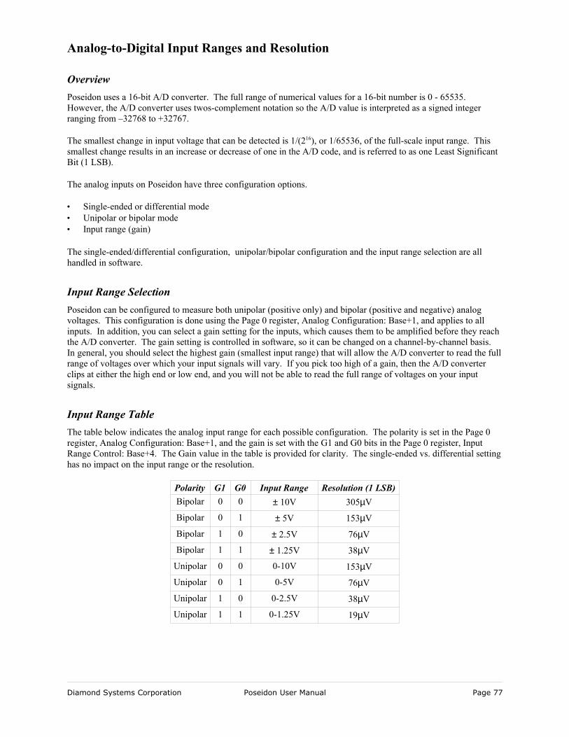
Analog-to-Digital Input Ranges and Resolution
OverviewPoseidon uses a 16-bit A/D converter. The full range of numerical values for a 16-bit number is 0 - 65535. However, the A/D converter uses twos-complement notation so the A/D value is interpreted as a signed integer ranging from –32768 to +32767.
The smallest change in input voltage that can be detected is 1/(216), or 1/65536, of the full-scale input range. This smallest change results in an increase or decrease of one in the A/D code, and is referred to as one Least Significant Bit (1 LSB).
The analog inputs on Poseidon have three configuration options.
• Single-ended or differential mode • Unipolar or bipolar mode • Input range (gain)
The single-ended/differential configuration, unipolar/bipolar configuration and the input range selection are all handled in software.
Input Range SelectionPoseidon can be configured to measure both unipolar (positive only) and bipolar (positive and negative) analog voltages. This configuration is done using the Page 0 register, Analog Configuration: Base+1, and applies to all inputs. In addition, you can select a gain setting for the inputs, which causes them to be amplified before they reach the A/D converter. The gain setting is controlled in software, so it can be changed on a channel-by-channel basis. In general, you should select the highest gain (smallest input range) that will allow the A/D converter to read the full range of voltages over which your input signals will vary. If you pick too high of a gain, then the A/D converter clips at either the high end or low end, and you will not be able to read the full range of voltages on your input signals.
Input Range TableThe table below indicates the analog input range for each possible configuration. The polarity is set in the Page 0 register, Analog Configuration: Base+1, and the gain is set with the G1 and G0 bits in the Page 0 register, Input Range Control: Base+4. The Gain value in the table is provided for clarity. The single-ended vs. differential setting has no impact on the input range or the resolution.
Polarity G1 G0 Input Range Resolution (1 LSB)Bipolar 0 0 ± 10V 305µV
Bipolar 0 1 ± 5V 153µV
Bipolar 1 0 ± 2.5V 76µV
Bipolar 1 1 ± 1.25V 38µV
Unipolar 0 0 0-10V 153µV
Unipolar 0 1 0-5V 76µV
Unipolar 1 0 0-2.5V 38µV
Unipolar 1 1 0-1.25V 19µV
Diamond Systems Corporation Poseidon User Manual Page 77
Performing an A/D ConversionThis chapter describes the steps involved in performing an A/D conversion on a selected input channel using direct programming (without the driver software). Performing an A/D conversion according to the following steps. Each step is discussed in detail, below.
1. Select the input channel.
2. Select the input range.
3. Wait for analog input circuit to settle.
4. Initiate an A/D conversion.
5. Wait for the conversion to finish.
6. Read the data from the board.
7. Convert the numerical data to a meaningful value.
Select the Input ChannelTo select the input channel to read, write a low-channel/high-channel pair to the Page 0 register pair, A/D Low Channel: Base+2 and A/D High Channel : Base+3. For the Poseidon, only 5 bits are supported for each setting, for 32 potential input source channels. When you write any value to these registers, the current A/D channel is set to the low channel.
For example, to set the board to channel 4 only, write 0x04 to Base+2 (low channel) and 0x04 to Base+3 (high channel). To set the board to read channels 0 through 15, write 0x00 to Base+2 (low channel) and 0x0F to Base+3 (high channel).
When you perform an A/D conversion, the current channel is automatically incremented to the next channel in the selected range. Therefore, to perform A/D conversions on a group of consecutively-numbered channels, you do not need to write the input channel prior to each conversion. For example, to read from channels 0 - 2, write 0x00 to base+2 and 0x02 to base+3. The first conversion is on channel 0, the second is on channel 1 and the third is on channel 2. The channel counter then wraps around to the beginning so the fourth conversion is on channel 0, and so on.
If you are sampling the same channel repeatedly, set both high and low to the same value as in the first example, above. On subsequent conversions you do not need to set the channel again.
Select the Input RangeSelect the input range from among the available ranges. If the range is the same as for the previous A/D conversion it does not need to be set again. Write this value to the Page 0 register, A/D Input Range Control: Base+4.
For example, for a global (affects all channels) ±5V range (gain of 2), write 0x01 to Base+4.
Wait for Analog Input Circuit to SettleAfter writing to either the channel registers (Base+2, Base+3) or the input range register (Base+4), you must allow time for the analog input circuit to settle before starting an A/D conversion. The board has a built-in 10µS timer to assist with the wait period. Monitor the WAIT bit at register Base+4, bit 6. When the bit is 1, the circuit is actively settling on the input signal. When the bit is 0, the board is ready to perform A/D conversions.
Diamond Systems Corporation Poseidon User Manual Page 78
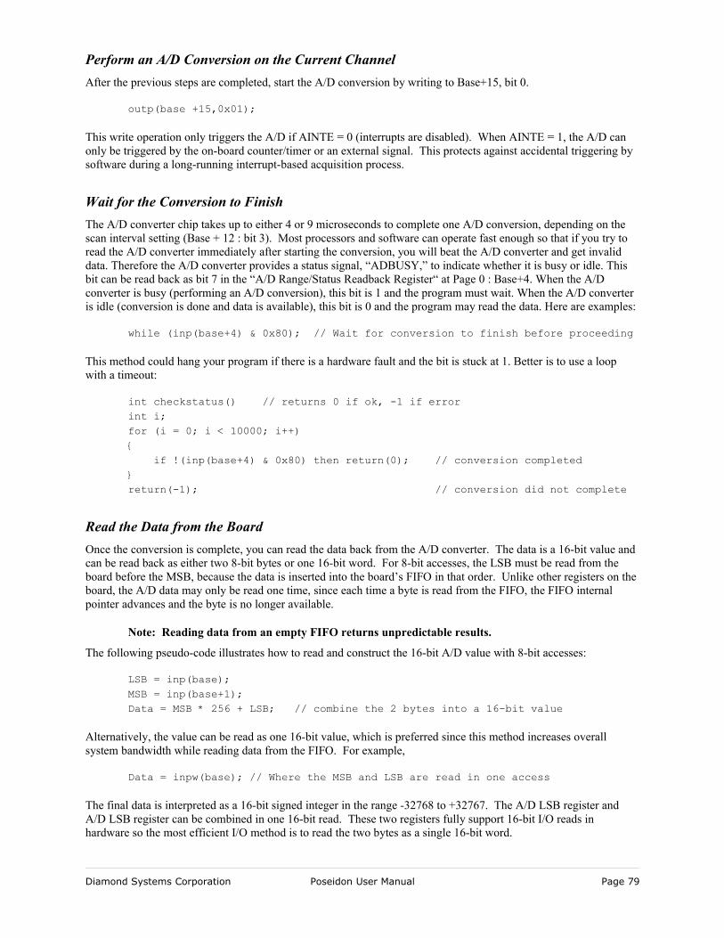
Perform an A/D Conversion on the Current ChannelAfter the previous steps are completed, start the A/D conversion by writing to Base+15, bit 0.
outp(base +15,0x01);
This write operation only triggers the A/D if AINTE = 0 (interrupts are disabled). When AINTE = 1, the A/D can only be triggered by the on-board counter/timer or an external signal. This protects against accidental triggering by software during a long-running interrupt-based acquisition process.
Wait for the Conversion to FinishThe A/D converter chip takes up to either 4 or 9 microseconds to complete one A/D conversion, depending on the scan interval setting (Base + 12 : bit 3). Most processors and software can operate fast enough so that if you try to read the A/D converter immediately after starting the conversion, you will beat the A/D converter and get invalid data. Therefore the A/D converter provides a status signal, “ADBUSY,” to indicate whether it is busy or idle. This bit can be read back as bit 7 in the “A/D Range/Status Readback Register“ at Page 0 : Base+4. When the A/D converter is busy (performing an A/D conversion), this bit is 1 and the program must wait. When the A/D converter is idle (conversion is done and data is available), this bit is 0 and the program may read the data. Here are examples:
while (inp(base+4) & 0x80); // Wait for conversion to finish before proceeding
This method could hang your program if there is a hardware fault and the bit is stuck at 1. Better is to use a loop with a timeout:
int checkstatus() // returns 0 if ok, -1 if errorint i;for (i = 0; i < 10000; i++){
if !(inp(base+4) & 0x80) then return(0); // conversion completed}return(-1); // conversion did not complete
Read the Data from the BoardOnce the conversion is complete, you can read the data back from the A/D converter. The data is a 16-bit value and can be read back as either two 8-bit bytes or one 16-bit word. For 8-bit accesses, the LSB must be read from the board before the MSB, because the data is inserted into the board’s FIFO in that order. Unlike other registers on the board, the A/D data may only be read one time, since each time a byte is read from the FIFO, the FIFO internal pointer advances and the byte is no longer available.
Note: Reading data from an empty FIFO returns unpredictable results.
The following pseudo-code illustrates how to read and construct the 16-bit A/D value with 8-bit accesses:
LSB = inp(base);MSB = inp(base+1);Data = MSB * 256 + LSB; // combine the 2 bytes into a 16-bit value
Alternatively, the value can be read as one 16-bit value, which is preferred since this method increases overall system bandwidth while reading data from the FIFO. For example,
Data = inpw(base); // Where the MSB and LSB are read in one access
The final data is interpreted as a 16-bit signed integer in the range -32768 to +32767. The A/D LSB register and A/D LSB register can be combined in one 16-bit read. These two registers fully support 16-bit I/O reads in hardware so the most efficient I/O method is to read the two bytes as a single 16-bit word.
Diamond Systems Corporation Poseidon User Manual Page 79
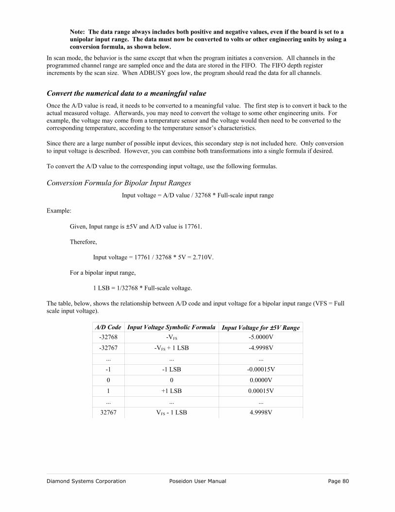
Note: The data range always includes both positive and negative values, even if the board is set to a unipolar input range. The data must now be converted to volts or other engineering units by using a conversion formula, as shown below.
In scan mode, the behavior is the same except that when the program initiates a conversion. All channels in the programmed channel range are sampled once and the data are stored in the FIFO. The FIFO depth register increments by the scan size. When ADBUSY goes low, the program should read the data for all channels.
Convert the numerical data to a meaningful valueOnce the A/D value is read, it needs to be converted to a meaningful value. The first step is to convert it back to the actual measured voltage. Afterwards, you may need to convert the voltage to some other engineering units. For example, the voltage may come from a temperature sensor and the voltage would then need to be converted to the corresponding temperature, according to the temperature sensor’s characteristics.
Since there are a large number of possible input devices, this secondary step is not included here. Only conversion to input voltage is described. However, you can combine both transformations into a single formula if desired.
To convert the A/D value to the corresponding input voltage, use the following formulas.
Conversion Formula for Bipolar Input RangesInput voltage = A/D value / 32768 * Full-scale input range
Example:
Given, Input range is ±5V and A/D value is 17761.
Therefore,
Input voltage = 17761 / 32768 * 5V = 2.710V.
For a bipolar input range,
1 LSB = 1/32768 * Full-scale voltage.
The table, below, shows the relationship between A/D code and input voltage for a bipolar input range (VFS = Full scale input voltage).
A/D Code Input Voltage Symbolic Formula Input Voltage for ±5V Range-32768 -VFS -5.0000V
-32767 -VFS + 1 LSB -4.9998V
... ... ...
-1 -1 LSB -0.00015V
0 0 0.0000V
1 +1 LSB 0.00015V
... ... ...
32767 VFS - 1 LSB 4.9998V
Diamond Systems Corporation Poseidon User Manual Page 80
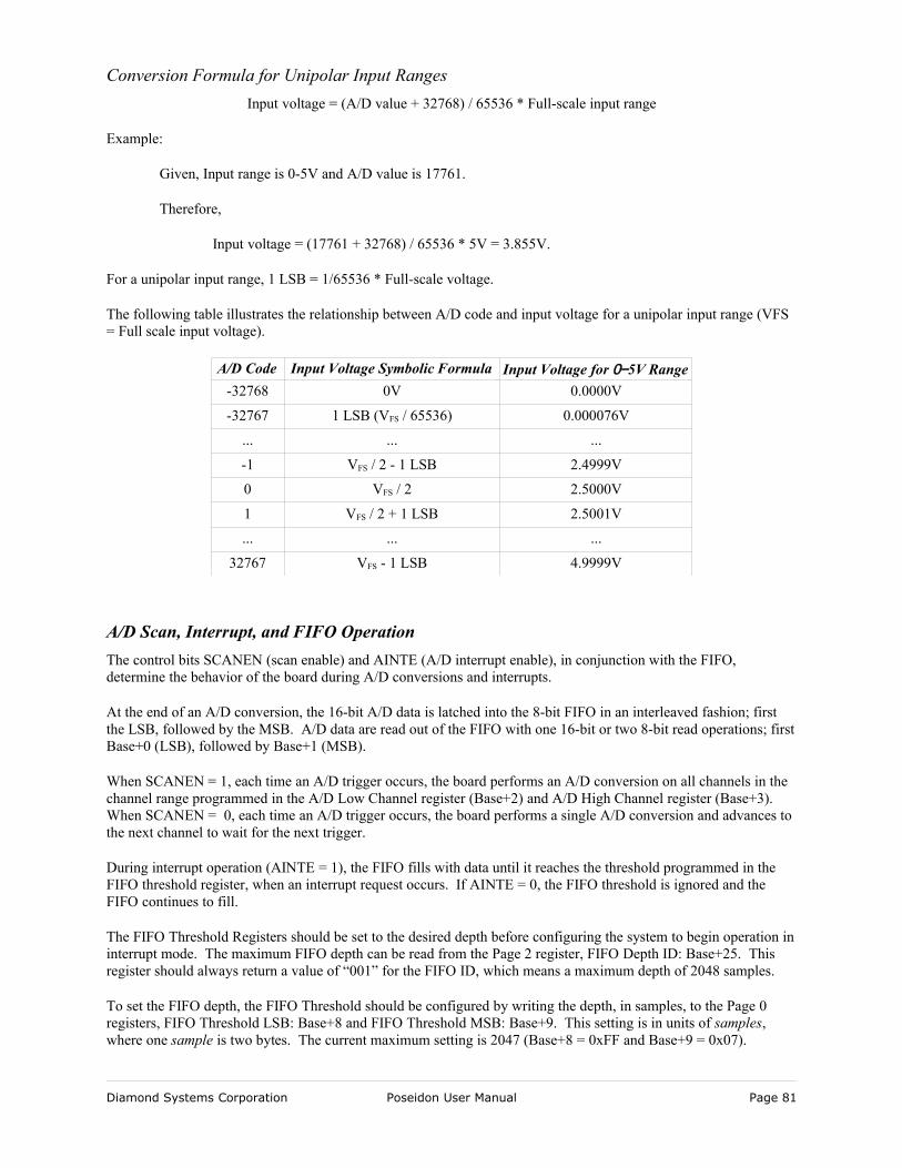
Conversion Formula for Unipolar Input RangesInput voltage = (A/D value + 32768) / 65536 * Full-scale input range
Example:
Given, Input range is 0-5V and A/D value is 17761.
Therefore,
Input voltage = (17761 + 32768) / 65536 * 5V = 3.855V.
For a unipolar input range, 1 LSB = 1/65536 * Full-scale voltage.
The following table illustrates the relationship between A/D code and input voltage for a unipolar input range (VFS = Full scale input voltage).
A/D Code Input Voltage Symbolic Formula Input Voltage for 0−5V Range-32768 0V 0.0000V
-32767 1 LSB (VFS / 65536) 0.000076V
... ... ...
-1 VFS / 2 - 1 LSB 2.4999V
0 VFS / 2 2.5000V
1 VFS / 2 + 1 LSB 2.5001V
... ... ...
32767 VFS - 1 LSB 4.9999V
A/D Scan, Interrupt, and FIFO OperationThe control bits SCANEN (scan enable) and AINTE (A/D interrupt enable), in conjunction with the FIFO, determine the behavior of the board during A/D conversions and interrupts.
At the end of an A/D conversion, the 16-bit A/D data is latched into the 8-bit FIFO in an interleaved fashion; first the LSB, followed by the MSB. A/D data are read out of the FIFO with one 16-bit or two 8-bit read operations; first Base+0 (LSB), followed by Base+1 (MSB).
When SCANEN = 1, each time an A/D trigger occurs, the board performs an A/D conversion on all channels in the channel range programmed in the A/D Low Channel register (Base+2) and A/D High Channel register (Base+3). When SCANEN = 0, each time an A/D trigger occurs, the board performs a single A/D conversion and advances to the next channel to wait for the next trigger.
During interrupt operation (AINTE = 1), the FIFO fills with data until it reaches the threshold programmed in the FIFO threshold register, when an interrupt request occurs. If AINTE = 0, the FIFO threshold is ignored and the FIFO continues to fill.
The FIFO Threshold Registers should be set to the desired depth before configuring the system to begin operation in interrupt mode. The maximum FIFO depth can be read from the Page 2 register, FIFO Depth ID: Base+25. This register should always return a value of “001” for the FIFO ID, which means a maximum depth of 2048 samples.
To set the FIFO depth, the FIFO Threshold should be configured by writing the depth, in samples, to the Page 0 registers, FIFO Threshold LSB: Base+8 and FIFO Threshold MSB: Base+9. This setting is in units of samples, where one sample is two bytes. The current maximum setting is 2047 (Base+8 = 0xFF and Base+9 = 0x07).
Diamond Systems Corporation Poseidon User Manual Page 81
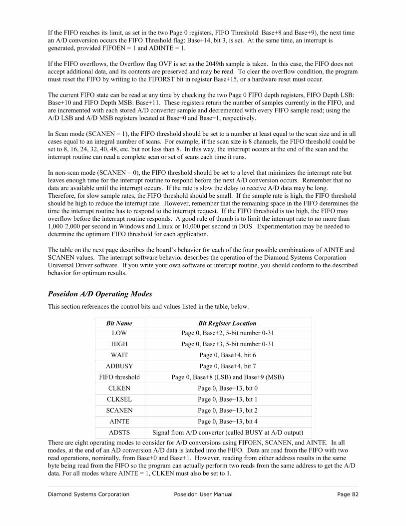
If the FIFO reaches its limit, as set in the two Page 0 registers, FIFO Threshold: Base+8 and Base+9), the next time an A/D conversion occurs the FIFO Threshold flag: Base+14, bit 3, is set. At the same time, an interrupt is generated, provided FIFOEN = 1 and ADINTE = 1.
If the FIFO overflows, the Overflow flag OVF is set as the 2049th sample is taken. In this case, the FIFO does not accept additional data, and its contents are preserved and may be read. To clear the overflow condition, the program must reset the FIFO by writing to the FIFORST bit in register Base+15, or a hardware reset must occur.
The current FIFO state can be read at any time by checking the two Page 0 FIFO depth registers, FIFO Depth LSB: Base+10 and FIFO Depth MSB: Base+11. These registers return the number of samples currently in the FIFO, and are incremented with each stored A/D converter sample and decremented with every FIFO sample read; using the A/D LSB and A/D MSB registers located at Base+0 and Base+1, respectively.
In Scan mode (SCANEN = 1), the FIFO threshold should be set to a number at least equal to the scan size and in all cases equal to an integral number of scans. For example, if the scan size is 8 channels, the FIFO threshold could be set to 8, 16, 24, 32, 40, 48, etc. but not less than 8. In this way, the interrupt occurs at the end of the scan and the interrupt routine can read a complete scan or set of scans each time it runs.
In non-scan mode (SCANEN = 0), the FIFO threshold should be set to a level that minimizes the interrupt rate but leaves enough time for the interrupt routine to respond before the next A/D conversion occurs. Remember that no data are available until the interrupt occurs. If the rate is slow the delay to receive A/D data may be long. Therefore, for slow sample rates, the FIFO threshold should be small. If the sample rate is high, the FIFO threshold should be high to reduce the interrupt rate. However, remember that the remaining space in the FIFO determines the time the interrupt routine has to respond to the interrupt request. If the FIFO threshold is too high, the FIFO may overflow before the interrupt routine responds. A good rule of thumb is to limit the interrupt rate to no more than 1,000-2,000 per second in Windows and Linux or 10,000 per second in DOS. Experimentation may be needed to determine the optimum FIFO threshold for each application.
The table on the next page describes the board’s behavior for each of the four possible combinations of AINTE and SCANEN values. The interrupt software behavior describes the operation of the Diamond Systems Corporation Universal Driver software. If you write your own software or interrupt routine, you should conform to the described behavior for optimum results.
Poseidon A/D Operating ModesThis section references the control bits and values listed in the table, below.
Bit Name Bit Register LocationLOW Page 0, Base+2, 5-bit number 0-31
HIGH Page 0, Base+3, 5-bit number 0-31
WAIT Page 0, Base+4, bit 6
ADBUSY Page 0, Base+4, bit 7
FIFO threshold Page 0, Base+8 (LSB) and Base+9 (MSB)
CLKEN Page 0, Base+13, bit 0
CLKSEL Page 0, Base+13, bit 1
SCANEN Page 0, Base+13, bit 2
AINTE Page 0, Base+13, bit 4
ADSTS Signal from A/D converter (called BUSY at A/D output)There are eight operating modes to consider for A/D conversions using FIFOEN, SCANEN, and AINTE. In all modes, at the end of an AD conversion A/D data is latched into the FIFO. Data are read from the FIFO with two read operations, nominally, from Base+0 and Base+1. However, reading from either address results in the same byte being read from the FIFO so the program can actually perform two reads from the same address to get the A/D data. For all modes where AINTE = 1, CLKEN must also be set to 1.
Diamond Systems Corporation Poseidon User Manual Page 82
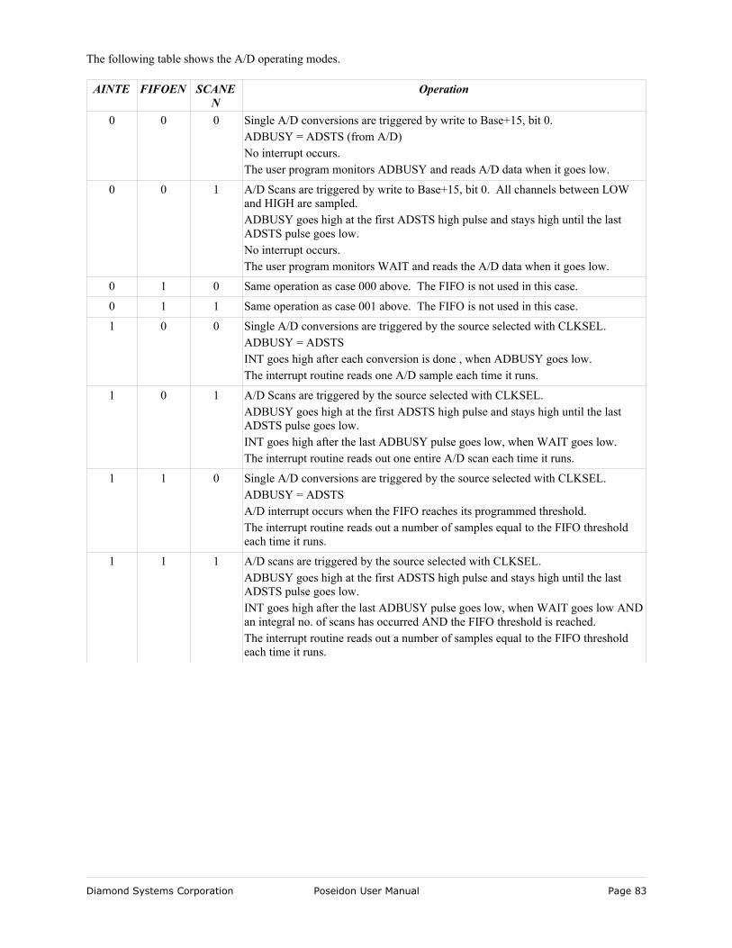
The following table shows the A/D operating modes.
AINTE FIFOEN SCANEN
Operation
0 0 0 Single A/D conversions are triggered by write to Base+15, bit 0.ADBUSY = ADSTS (from A/D)No interrupt occurs.The user program monitors ADBUSY and reads A/D data when it goes low.
0 0 1 A/D Scans are triggered by write to Base+15, bit 0. All channels between LOW and HIGH are sampled.ADBUSY goes high at the first ADSTS high pulse and stays high until the last ADSTS pulse goes low.No interrupt occurs.The user program monitors WAIT and reads the A/D data when it goes low.
0 1 0 Same operation as case 000 above. The FIFO is not used in this case.
0 1 1 Same operation as case 001 above. The FIFO is not used in this case.
1 0 0 Single A/D conversions are triggered by the source selected with CLKSEL.ADBUSY = ADSTSINT goes high after each conversion is done , when ADBUSY goes low.The interrupt routine reads one A/D sample each time it runs.
1 0 1 A/D Scans are triggered by the source selected with CLKSEL.ADBUSY goes high at the first ADSTS high pulse and stays high until the last ADSTS pulse goes low.INT goes high after the last ADBUSY pulse goes low, when WAIT goes low.The interrupt routine reads out one entire A/D scan each time it runs.
1 1 0 Single A/D conversions are triggered by the source selected with CLKSEL.ADBUSY = ADSTSA/D interrupt occurs when the FIFO reaches its programmed threshold.The interrupt routine reads out a number of samples equal to the FIFO threshold each time it runs.
1 1 1 A/D scans are triggered by the source selected with CLKSEL.ADBUSY goes high at the first ADSTS high pulse and stays high until the last ADSTS pulse goes low.INT goes high after the last ADBUSY pulse goes low, when WAIT goes low AND an integral no. of scans has occurred AND the FIFO threshold is reached.The interrupt routine reads out a number of samples equal to the FIFO threshold each time it runs.
Diamond Systems Corporation Poseidon User Manual Page 83
Digital-to-Analog Output Ranges and Resolution
DescriptionPoseidon uses a 4-channel 12-bit D/A converter (DAC) to provide four analog outputs. A 12-bit DAC can generate output voltages with the precision of a 12-bit binary number. The maximum value of a 12-bit binary number is 212 - 1, or 4095, so the full range of numerical values that the DACs support is 0 - 4095. The value 0 always corresponds to the lowest voltage in the output range, and the value 4095 always corresponds to the highest voltage minus 1 LSB. The theoretical top end of the range corresponds to an output code of 4096 which is impossible to achieve.
Note: In this manual, the terms analog output, D/A, and DAC are all used interchangeably to mean the conversion of digital data originating from the Poseidon computer hardware to an analog signal terminating at an external source.
ResolutionThe resolution is the smallest possible change in output voltage. For a 12-bit DAC the resolution is 1/(212), or 1/4096, of the full-scale output range. This smallest change results from an increase or decrease of 1 in the D/A code, so this change is referred to as 1 least significant bit (1 LSB ). The value of this LSB is calculated as follows.
1 LSB = Output voltage range / 4096
Example:
For, Output range = 0-10V,
Output voltage range = 10V – 0V = 10V
Therefore,
1 LSB = 10V / 4096 = 2.44mV
Example:
For, Output range = ±10V;
Output voltage range = 10V – (-10V) = 20V
Therefore,
1 LSB = 20V / 4096 = 4.88mV
Output Range SelectionThe Page 0 register, Analog Configuration: Base+1 is used to select the DAC output range. The DACs can be configured for 0-10V or ±10V.
D/A Conversion Formulas and TablesThe formulas below explain how to convert between D/A codes and output voltages.
Diamond Systems Corporation Poseidon User Manual Page 84
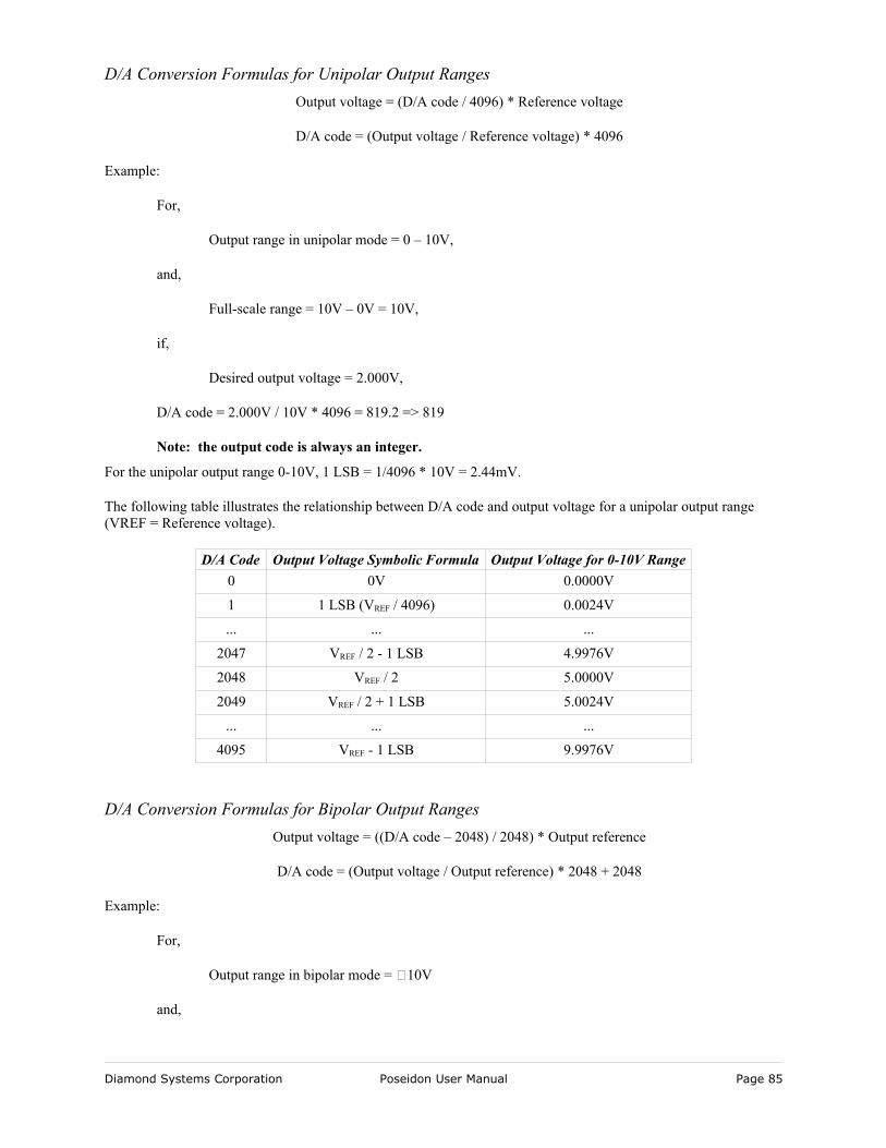
D/A Conversion Formulas for Unipolar Output RangesOutput voltage = (D/A code / 4096) * Reference voltage
D/A code = (Output voltage / Reference voltage) * 4096
Example:
For,
Output range in unipolar mode = 0 – 10V,
and,
Full-scale range = 10V – 0V = 10V,
if,
Desired output voltage = 2.000V,
D/A code = 2.000V / 10V * 4096 = 819.2 => 819
Note: the output code is always an integer.
For the unipolar output range 0-10V, 1 LSB = 1/4096 * 10V = 2.44mV.
The following table illustrates the relationship between D/A code and output voltage for a unipolar output range (VREF = Reference voltage).
D/A Code Output Voltage Symbolic Formula Output Voltage for 0-10V Range0 0V 0.0000V
1 1 LSB (VREF / 4096) 0.0024V
... ... ...
2047 VREF / 2 - 1 LSB 4.9976V
2048 VREF / 2 5.0000V
2049 VREF / 2 + 1 LSB 5.0024V
... ... ...
4095 VREF - 1 LSB 9.9976V
D/A Conversion Formulas for Bipolar Output RangesOutput voltage = ((D/A code – 2048) / 2048) * Output reference
D/A code = (Output voltage / Output reference) * 2048 + 2048
Example:
For,
Output range in bipolar mode = 10V
and,
Diamond Systems Corporation Poseidon User Manual Page 85
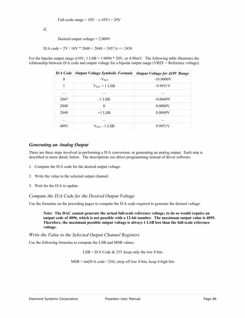
Full-scale range = 10V – (-10V) = 20V
if,
Desired output voltage = 2.000V
D/A code = 2V / 10V * 2048 + 2048 = 2457.6 => 2458
For the bipolar output range ±10V, 1 LSB = 1/4096 * 20V, or 4.88mV. The following table illustrates the relationship between D/A code and output voltage for a bipolar output range (VREF = Reference voltage).
D/A Code Output Voltage Symbolic Formula Output Voltage for ±10V Range0 -VREF -10.0000V
1 VREF + 1 LSB -9.9951V
... ... ...
2047 -1 LSB -0.0049V
2048 0 0.0000V
2049 +1 LSB 0.0049V
... ... ...
4095 VREF - 1 LSB 9.9951V
Generating an Analog OutputThere are three steps involved in performing a D/A conversion, or generating an analog output. Each step is described in more detail, below. The descriptions use direct programming instead of driver software.
1. Compute the D/A code for the desired output voltage.
2. Write the value to the selected output channel.
3. Wait for the D/A to update.
Compute the D/A Code for the Desired Output VoltageUse the formulas on the preceding pages to compute the D/A code required to generate the desired voltage.
Note: The DAC cannot generate the actual full-scale reference voltage; to do so would require an output code of 4096, which is not possible with a 12-bit number. The maximum output value is 4095. Therefore, the maximum possible output voltage is always 1 LSB less than the full-scale reference voltage.
Write the Value to the Selected Output Channel RegistersUse the following formulas to compute the LSB and MSB values.
LSB = D/A Code & 255 ;keep only the low 8 bits
MSB = int(D/A code / 256) ;strip off low 8 bits, keep 4 high bits
Diamond Systems Corporation Poseidon User Manual Page 86
Example:
For,
Output code = 1776
Compute,
LSB = 1776 & 255 = 240 (0xF0)
and
MSB = int(1776 / 256) = int(6.9375) = 6
The LSB is an 8-bit number in the range 0-255. The MSB is a 4-bit number in the range 0-15.
The MSB is always rounded down. The truncated portion is accounted for by the LSB.
Write the computed values to the output registers. The LSB is written to Page 0 register Base+6. The MSB is written to Page 0 register Base+7.
outp(Base + 6, LSB);outp(Base + 7, MSB);
Set Registers for ChannelAfter the value for the given channel is set, make the channel selection to latch the data to the D/A. Decide whether or not to pass the data to the D/A immediately, transparent pass-through mode, or to latch and hold the data until all of the D/A channels are set, simultaneous update mode.
Transparent pass-through mode sends the data, written in the previous step, to the D/A beginning immediately after the channel selection is made. The D/A output is updated as soon as the data is transferred with a worst-case settling time of ~10µsec, as described in the DAC7715 specification.
Simultaneous update mode latches the data into an internal buffer for that channel, but will not update the A/D until instructed to do so. In this way, several, or all four, of the A/D channels can be configured and updated, simultaneously. This allows for a uniform transition time for all A/D outputs.
To send the data to the D/A immediately, write the channel number to Page 0 register Base+5, bits 1-0. For transparent pass-through mode, bit 8 should be reset to zero, as shown,
outp(Base + 5, ChannelNumber);
where ChannelNumber is 0-3.
To latch the data in preparation for more updates, not sending the data to the D/A until channel data updates are completed, write the channel number to Page 0 register Base+5, bits 1-0, also setting bit 8 to 1, as shown,
outp(Base + 5, 0x80 + ChannelNumber);
where ChannelNumber is 0-3.
The D/A data is held until a zero is written to the simultaneous update bit, at which time all of the latched data is updated at the same time. If data was previously latched with the simultaneous update bit set to one and the data for the last channel involved in the simultaneous update was written to Base+6 and Base+7, the final channel selection operates the same as a transparent mode write,
Diamond Systems Corporation Poseidon User Manual Page 87
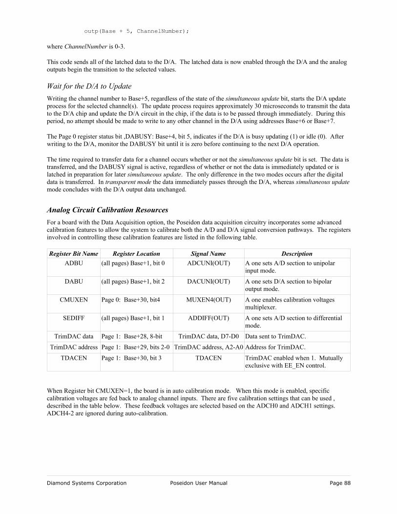
outp(Base + 5, ChannelNumber);
where ChannelNumber is 0-3.
This code sends all of the latched data to the D/A. The latched data is now enabled through the D/A and the analog outputs begin the transition to the selected values.
Wait for the D/A to UpdateWriting the channel number to Base+5, regardless of the state of the simultaneous update bit, starts the D/A update process for the selected channel(s). The update process requires approximately 30 microseconds to transmit the data to the D/A chip and update the D/A circuit in the chip, if the data is to be passed through immediately. During this period, no attempt should be made to write to any other channel in the D/A using addresses Base+6 or Base+7.
The Page 0 register status bit ,DABUSY: Base+4, bit 5, indicates if the D/A is busy updating (1) or idle (0). After writing to the D/A, monitor the DABUSY bit until it is zero before continuing to the next D/A operation.
The time required to transfer data for a channel occurs whether or not the simultaneous update bit is set. The data is transferred, and the DABUSY signal is active, regardless of whether or not the data is immediately updated or is latched in preparation for later simultaneous update. The only difference in the two modes occurs after the digital data is transferred. In transparent mode the data immediately passes through the D/A, whereas simultaneous update mode concludes with the D/A output data unchanged.
Analog Circuit Calibration ResourcesFor a board with the Data Acquisition option, the Poseidon data acquisition circuitry incorporates some advanced calibration features to allow the system to calibrate both the A/D and D/A signal conversion pathways. The registers involved in controlling these calibration features are listed in the following table.
Register Bit Name Register Location Signal Name DescriptionADBU (all pages) Base+1, bit 0 ADCUNI(OUT) A one sets A/D section to unipolar
input mode.
DABU (all pages) Base+1, bit 2 DACUNI(OUT) A one sets D/A section to bipolar output mode.
CMUXEN Page 0: Base+30, bit4 MUXEN4(OUT) A one enables calibration voltages multiplexer.
SEDIFF (all pages) Base+1, bit 1 ADDIFF(OUT) A one sets A/D section to differential mode.
TrimDAC data Page 1: Base+28, 8-bit TrimDAC data, D7-D0 Data sent to TrimDAC.
TrimDAC address Page 1: Base+29, bits 2-0 TrimDAC address, A2-A0 Address for TrimDAC.
TDACEN Page 1: Base+30, bit 3 TDACEN TrimDAC enabled when 1. Mutually exclusive with EE_EN control.
When Register bit CMUXEN=1, the board is in auto calibration mode. When this mode is enabled, specific calibration voltages are fed back to analog channel inputs. There are five calibration settings that can be used , described in the table below. These feedback voltages are selected based on the ADCH0 and ADCH1 settings. ADCH4-2 are ignored during auto-calibration.
Diamond Systems Corporation Poseidon User Manual Page 88
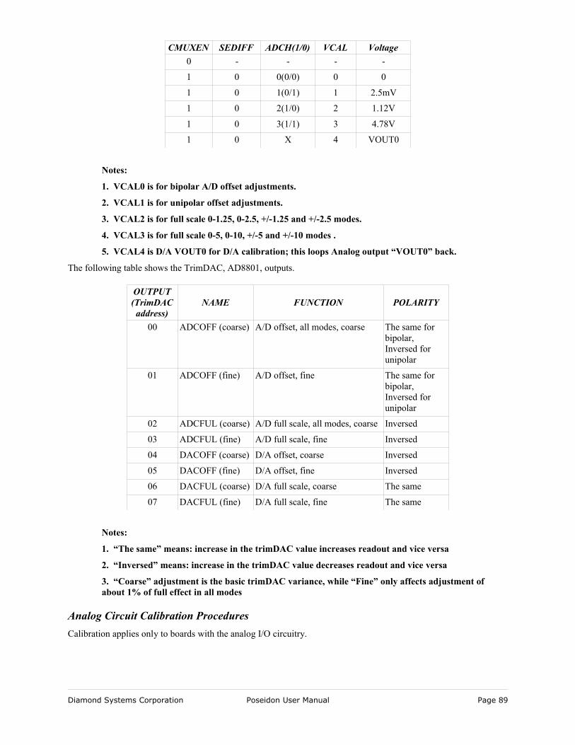
CMUXEN SEDIFF ADCH(1/0) VCAL Voltage0 - - - -
1 0 0(0/0) 0 0
1 0 1(0/1) 1 2.5mV
1 0 2(1/0) 2 1.12V
1 0 3(1/1) 3 4.78V
1 0 X 4 VOUT0
Notes:
1. VCAL0 is for bipolar A/D offset adjustments.
2. VCAL1 is for unipolar offset adjustments.
3. VCAL2 is for full scale 0-1.25, 0-2.5, +/-1.25 and +/-2.5 modes.
4. VCAL3 is for full scale 0-5, 0-10, +/-5 and +/-10 modes .
5. VCAL4 is D/A VOUT0 for D/A calibration; this loops Analog output “VOUT0” back.
The following table shows the TrimDAC, AD8801, outputs.
OUTPUT (TrimDAC address)
NAME FUNCTION POLARITY
00 ADCOFF (coarse) A/D offset, all modes, coarse The same for bipolar, Inversed for unipolar
01 ADCOFF (fine) A/D offset, fine The same for bipolar, Inversed for unipolar
02 ADCFUL (coarse) A/D full scale, all modes, coarse Inversed
03 ADCFUL (fine) A/D full scale, fine Inversed
04 DACOFF (coarse) D/A offset, coarse Inversed
05 DACOFF (fine) D/A offset, fine Inversed
06 DACFUL (coarse) D/A full scale, coarse The same
07 DACFUL (fine) D/A full scale, fine The same
Notes:
1. “The same” means: increase in the trimDAC value increases readout and vice versa
2. “Inversed” means: increase in the trimDAC value decreases readout and vice versa
3. “Coarse” adjustment is the basic trimDAC variance, while “Fine” only affects adjustment of about 1% of full effect in all modes
Analog Circuit Calibration ProceduresCalibration applies only to boards with the analog I/O circuitry.
Diamond Systems Corporation Poseidon User Manual Page 89
The analog I/O circuit is calibrated during production test prior to shipment. Over time the circuit may drift slightly. If calibration is desired, internal auto-calibration can be performed using the software routines provided with the Diamond Systems Corporation driver libraries, which are included with the Poseidon development kit.
Six adjustments are possible:
• A/D bipolar offset.• A/D unipolar offset.• A/D full-scale.• D/A bipolar offset.• D/A unipolar offset.• D/A full-scale.
The specific algorithms required to perform auto-calibration can be involved, and are too detailed to be presented in this document. The detailed procedures are provided in the included drivers and additional auto-calibration information can be provided as needed.
The auto-calibration settings are stored in nonvolatile memory in the calibration EEPROM and are reloaded each time the on-board FPGA, or system, is reset.
Using EEPROMAn EEPROM is used to store all TrimDAC adjustment values. These values are loaded on reset or power-up, and it is critical that these values are correct to maintain accurate A/D measurements. These settings are configured to defaults during manufacturing test. Do not change these settings without a complete understanding the impact of the change.
The EEPROM provides 256 bytes of non-volatile storage. The first 128 bytes, addresses 0x00-0x7F, are reserved for auto-calibration settings and should not be overwritten. The last 128 bytes are available for user-accessible nonvolatile storage.
Access to EEPROM data can be handled through the DSCUD software utilities.
Note: Remember that bytes 0-127 are reserved for system use (TrimDAC autocal values). Altering those values adversely affects system calibration.
Reading Value from EEPROMExample: Read one byte from EEPROM location 128.
outp(base+0, 0x01); // set page to page 1outp(base+15, 0xA5); // unlock EEPROMoutp(base+29,0x80); // set address location to 128 (0x80)outp(base+30, 0xC0); // Initiate transfer, set to readwhile(inp(base+30) & 0x20); // Wait for EEPROM load to completedata = inpb(base+28); // data returned from EEPROM access outp(base+0, 0x00); // select page 0 (re-enables lock on EEPROM/TrimDAC)
Writing Value to EEPROMExample. Write the byte value 0xAA to EEPROM location 254, then verify the data.
outp(base+0, 0x01); // set page to page 1outp(base+15, 0xA5); // unlock EEPROMoutp(base+29,0xFE); // set address location to 254 (0xFE)outp(base+28, 0xAA); // Set data to write to EEPROM
Diamond Systems Corporation Poseidon User Manual Page 90
outp(base+30, 0x80); // Initiate transfer, set to writewhile (inp(base+30) & 0x20); // Wait for EEPROM write to completeoutp(base+15, 0xA5); // unlock EEPROMoutp(base +29,0xFE); // set address location to 254 (0xFE)outp(base+30, 0xC0); // Initiate transfer, set to readwhile (inp(base+30) & 0x20); // Wait for EEPROM load to completeData = inpb(base+28); // data returned from EEPROM access; data should be 0xAAoutp(base+0, 0x00); // select page 0 (re-enables lock on EEPROM/TrimDAC)
Digital I/O OperationPoseidon contains 40 digital I/O lines organized as four 8-bit I/O ports: A, B, C, D and E. The direction for each port is independently programmable. The ports are accessed at registers Base+16 through Base+20, respectively, and the direction register is at Base+22. Port and direction registers are located at Page 0.
The digital I/O lines are located at pins 1 through 40 on connector CN12. The lines are 3.3V and 5V logic compatible. Each output is capable of supplying –8mA in logic 1 state and +12mA in logic 0 state.
Register Base+22 bits DIRA, DIRB, DIRC, DIRD and DIRE control the direction of ports A, B, C, D and E, respectively. A zero indicates output and a one indicates input. All ports power up to input mode and the output registers are cleared to zero. When a port direction is changed to output mode, its output register is cleared to zero. When a port is in output mode, its value can be read.
There are two methods of programming the Digital I/O ports.
• As individual bits (useful for output only).• As bytes (for either input or output).
Accessing a digital output port can be handled as bit- or byte-level accesses, interchangeably. The two methods are provided to allow maximum flexibility for output operations.
Bit-Mode OperationTo program a specific output bit, bit-mode operation can be used. This mode is selected by writing a one to the MODE bit of the register Base=22: Digital I/O Configuration/Bit Programming located. When setting bit mode, bits 6-4 select the DIO port (A-E, values 0-4), bits 3-1 select the bit within the port (bit selection 0-7), and bit 0 selects the value for the bit in question.
In bit-mode, an individual output bit for one of the 40 available DIO bits can be individually assigned a value. For example, the following code segment sets bit 4 of DIO port B to zero and sets DIO port B to an output, with all other ports set to input.
outp(base+22, 0x98); // Selects: Bit Mode (bit 7=1), // Port B (bits 6-4 = 001),// bit 4 (bits 3-1 = 100),// value = 0 (bit 0=0)
outp(base+22, 0x02); // Selects: DIO direction Mode (bit 7=0) and// Port B is output; Ports A,C,D,E are inputs
Byte-Mode OperationFor byte-mode operation, the data for a given byte is read or written to the appropriate DIO byte register. DIO ports A-E are located at Base+16 to Base+20, respectively. For example, the following code segment illustrates setting port A to output , with B-E as input, writing a value of 0xAA to port A, and reading data from port C.
outp(base+22, 0x01); // Selects: DIO direction Mode (bit 7=0) and// Port A is output; Ports B,C,D,E are inputs
Diamond Systems Corporation Poseidon User Manual Page 91
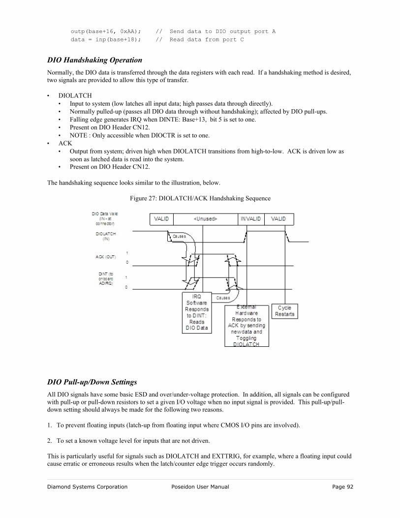
outp(base+16, 0xAA); // Send data to DIO output port Adata = inp(base+18); // Read data from port C
DIO Handshaking OperationNormally, the DIO data is transferred through the data registers with each read. If a handshaking method is desired, two signals are provided to allow this type of transfer.
• DIOLATCH • Input to system (low latches all input data; high passes data through directly).• Normally pulled-up (passes all DIO data through without handshaking); affected by DIO pull-ups.• Falling edge generates IRQ when DINTE: Base+13, bit 5 is set to one.• Present on DIO Header CN12.• NOTE : Only accessible when DIOCTR is set to one.
• ACK• Output from system; driven high when DIOLATCH transitions from high-to-low. ACK is driven low as
soon as latched data is read into the system.• Present on DIO Header CN12.
The handshaking sequence looks similar to the illustration, below.
DIO Pull-up/Down SettingsAll DIO signals have some basic ESD and over/under-voltage protection. In addition, all signals can be configured with pull-up or pull-down resistors to set a given I/O voltage when no input signal is provided. This pull-up/pull-down setting should always be made for the following two reasons.
1. To prevent floating inputs (latch-up from floating input where CMOS I/O pins are involved).
2. To set a known voltage level for inputs that are not driven.
This is particularly useful for signals such as DIOLATCH and EXTTRIG, for example, where a floating input could cause erratic or erroneous results when the latch/counter edge trigger occurs randomly.
Diamond Systems Corporation Poseidon User Manual Page 92
Figure 27: DIOLATCH/ACK Handshaking Sequence
To set DIO signal pull-ups or pull-downs, a jumper must be added across signals on connector JP8
Notes:
1. “Pull-up” means that a weak (47kOhm) pull-up resistor will be connected between the DIO signal and +3.3V. This sets the DIO signal to a “1” value when there is no external source driving the signal.
2. “Pull-down” means that a weak (47kOhm) pull-down resistor will be connected between the DIO signal and ground. . This sets the DIO signal to a “0” value when there is no external source driving the signal.
3. FPGA programming / updates: These Pull-up/down resistors also affect signal outputs during the period when the FPGA is being loaded or re-loaded. During an FPGA update, the FPGA will briefly tri-state all signals – during this period, the pull-up/down resistors will be the only current source coming from the board through the DIO signals.
As an example, to set all standard DIO signals to zero by default and to allow DIO handshaking to be configured such that the DIOLATCH signal is pulled high, for normal handshaking operation default follow these steps.
Diamond Systems Corporation Poseidon User Manual Page 93
Counter/Timer Operation
Poseidon contains two counter/timers that provide various timing functions on the board for A/D timing and user functions. These counters are controlled with registers in the on-board data acquisition controller FPGA.
Counter 0 – A/D Sample ControlThe first counter, Counter 0, is a 24-bit divide-by-n counter used for controlling A/D sampling. The counter has an internal clock input, an external gate input (Gate 0, alternate function for DIO Channel E bit 4), and a dedicated output (TOUT 0). The input is a 10MHz or 100 kHz clock provided on the board and selected with bit CKFRQ0 in Page 0 Base+12, bit zero. The gate is an optional signal that can be input on I/O header, CN12, when Page 0 register DIOCTR1: Base+12, bit 5 is one. If this signal is not used, the counter runs freely. The TOUT 0 signal output is a positive pulse whose frequency is equal to the input clock divided by the 24-bit divisor programmed into the counter.
The counter operates by counting down from the programmed divisor value. When it reaches zero, it outputs a positive-going pulse equal to one input clock period of 100ns or 10µs, depending on the input clock selected by CKFRQ0. It then reloads to the initial load value and repeats the process indefinitely.
The output frequency can range from 5MHz (10MHz clock, divisor = 2) down to 0.006Hz (100 kHz clock divided by 16,777,215, or 224-1). The output is fed into the A/D timing circuit and can be selected to trigger A/D conversions when AINTE is one and CLKSEL is zero in Base+13, bit 1. Using the control Page 0 registers at Base+13 and Base+27, the counter can be loaded, cleared, enabled and disabled. The optional gate can be enabled and disabled, and the counter value can be latched for reading.
Counter 1 – Counting/Totalizing FunctionsThe second counter, Counter 1, is similar to Counter 0 except it is a 16-bit counter. It also has an internal clock input, as well as an external input (EXTTRIG), an external gate (GATE 1), and an output (TOUT1). The gate and output signals are present on the I/O header only when DIOCTR is zero. The input may come from either the external trigger signal or the on-board clock generator. When the on-board clock generator is used, the clock frequency is either 10MHz or 100 KHz as determined by Page 0 register control bit CKFRQ1 located at Base+12, bit 1.
The output (TOUT1) is a positive-going pulse that appears on I/O header, CN12, when DIOCTR1 is one. The output pulse occurs when the counter reaches zero. When the counter reaches zero it reloads and starts over on the next clock pulse. The output stays high the entire time the counter is at zero; i.e., the interval from the input pulse that causes the counter to reach zero until the input pulse that causes the counter to reload.
When CLKSRC1 is one (external source), Counter 1 counts positive edges of the signal on pin 41 (EXTTRIG) on the I/O header. The counter can either be free running or gated, as determined by the Page 0 register Gate Enable control bit, GTEN: Base +27, bit 4.
The gate signal is provided on pin 37 when DIOCTR1 is one, enabling counter functions on I/O header, and GTEN is one, enabling gating for this counter. If the gate signal is high then the counter counts, and if it is low the counter holds its value and ignore input pulses. This pin can have a pull-up so the counter can operate without any external gate signal.
When DIOCTR1 is zero, Counter 1 takes its input from the on-board clock generator based on the value of the Page 0 register bit, CKFRQ1, located at Base+12. There is no gating and the counter runs continuously.
Counter 1 may be used as either a pulse generator or a totalizer/counter. In pulse generator mode the output signal on pin 26 is of interest. In totalizer/counter mode the counter value is of interest and may be read by first latching the value and then reading it.
Diamond Systems Corporation Poseidon User Manual Page 94
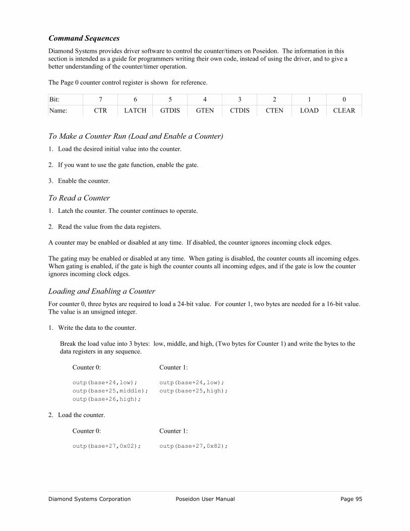
Command SequencesDiamond Systems provides driver software to control the counter/timers on Poseidon. The information in this section is intended as a guide for programmers writing their own code, instead of using the driver, and to give a better understanding of the counter/timer operation.
The Page 0 counter control register is shown for reference.
Bit: 7 6 5 4 3 2 1 0
Name: CTR LATCH GTDIS GTEN CTDIS CTEN LOAD CLEAR
To Make a Counter Run (Load and Enable a Counter)1. Load the desired initial value into the counter.
2. If you want to use the gate function, enable the gate.
3. Enable the counter.
To Read a Counter1. Latch the counter. The counter continues to operate.
2. Read the value from the data registers.
A counter may be enabled or disabled at any time. If disabled, the counter ignores incoming clock edges.
The gating may be enabled or disabled at any time. When gating is disabled, the counter counts all incoming edges. When gating is enabled, if the gate is high the counter counts all incoming edges, and if the gate is low the counter ignores incoming clock edges.
Loading and Enabling a CounterFor counter 0, three bytes are required to load a 24-bit value. For counter 1, two bytes are needed for a 16-bit value. The value is an unsigned integer.
1. Write the data to the counter.
Break the load value into 3 bytes: low, middle, and high, (Two bytes for Counter 1) and write the bytes to the data registers in any sequence.
Counter 0: Counter 1:
outp(base+24,low); outp(base+24,low);outp(base+25,middle); outp(base+25,high);outp(base+26,high);
2. Load the counter.
Counter 0: Counter 1:
outp(base+27,0x02); outp(base+27,0x82);
Diamond Systems Corporation Poseidon User Manual Page 95
3. Enable the gate if desired.
Counter 0: Counter 1:
outp(base+27,0x10); outp(base+27,0x90);
4. Enable the counter.
Counter 0: Counter 1:
outp(base+27,0x04); outp(base+27,0x84);
Reading a Counter1. Latch the counter.
Counter 0: Counter 1:
outp(base+27,0x40); outp(base+27,0xC0);
2. Read the data.
The value is returned in 3 bytes, low, middle, and high (2 bytes for counter 1).
Counter 0: Counter 1:
low=inp(base+24); low=inp(base+24);middle=inp(base+25); high=inp(base+25);high=inp(base+25);
3. Assemble the bytes into the complete counter value.
Counter 0: Counter 1:
val = high * 2^16 + middle * 2^8 + low; val = high * 2^8 + low;
Enabling the Counter GateCounter 0: Counter 1:
outp(base+27,0x10); outp(base+27,0x90);
The counter runs only when the gate input is high.
Disabling the Counter GateCounter 0: Counter 1:
outp(base+27,0x20); outp(base+27,0xA0);
The counter runs continuously.
Diamond Systems Corporation Poseidon User Manual Page 96
Clearing a CounterClearing a counter is done to restart an operation. Normally, you only clear a counter after you have stopped (disabled) and read the counter. If you clear a counter while it is still enabled, it continues to count incoming pulses, so its value may not remain at zero.
1. Stop (disable) the counter.
Counter 0: Counter 1:
outp(base+27,0x08); outp(base+27,0x88);
2. Read the data (optional). See Reading a Counter, above.
3. Clear the counter.
Counter 0: Counter 1:
outp(base+27,0x01); outp(base+27,0x81);
Diamond Systems Corporation Poseidon User Manual Page 97
Watchdog Timer Programming
Example: Watchdog Timer With Software TriggerA software trigger relies on a thread of execution to constantly trigger watchdog timer A. If the thread is ever halted, timer A decrements to zero and starts timer B. Once timer B decrements to 0, the board resets.
In this example we set the watchdog timer to a countdown period of four seconds. Longer timeout periods are typically be used for a software-based watchdog timer, to accommodate varying software latencies, such as interrupt latencies and thread pre-emption, that may delay the watchdog trigger code.
Setting up the watchdog timer:
outp(base + 0, 0x00); //set page 0outp(base + 28, 40000 & 0xFF); //set LSB of WD timer A (4 seconds)outp(base + 29, (40000 >> 8) & 0xFF); //set MSB of WD timer Aoutp(base + 30, 0xFF); //set WD timer B to 0.0255 secondsoutp(base + 31, 0x28); //set WDEN=1, WDRST=1 (enable WD timer, reset)
With the timer setup and active, run the watchdog timer trigger in a continuous thread of code.
while (1) {
outp(base + 31, 0x80); //trigger watchdog timersleep(1000); //sleep one second
}
If this thread is interrupted for any reason, the board resets four seconds after the last watchdog timer trigger.
Example: Watchdog Timer With Hardware TriggerA hardware trigger relies on an external pulse to constantly trigger watchdog timer A. If the external stream of pulses ever halts, timer A decrements to zero and starts timer B. Once timer B decrements to 0, the board resets.
In this example, we will make use of the T-1 feature of timer A to automatically reset itself unless a physical connection is broken.
Since software is not involved in maintaining the timer, we can set the reset period to a much smaller value. In this example, the reset pulse travels across the physical connection every 10 milliseconds.
outp(base + 0, 0x00); //set page 0outp(base + 28, 100 & 0xFF); //set LSB of WD timer A (10 milliseconds)outp(base + 29, 100 >> 8) & 0xFF); //set MSB of WD timer Aoutp(base + 30, 0xFF); //set WD timer B to 0.0255 secondsoutp(base + 31, 0x2D); //set WDEN=1, WDRST=1, WDT-1=1, WDIEN=1
When timer A reaches 1, a rising edge flows from WDO to WDI, resetting the timer back to 100 and lowering WDO.
When the connection from WDO to WDI is broken, the rising edge never reaches WDI and system resets.
Diamond Systems Corporation Poseidon User Manual Page 98
Data Acquisition Specifications (Data Acquisition units only)
Analog Inputs• No. of inputs, 16 differential or 32 single-ended (user selectable)• A/D resolution, 16 bits (1/65,536 of full scale)• Input ranges,
Bipolar: ±10V, ±5V, ±2.5V, ±1.25VUnipolar: 0-10V, 0-5V, 0-2.5V
• Input bias current, 50nA max• Maximum input voltage, ±10V for linear operation• Over-voltage protection, ±35V on any analog input without damage• Nonlinearity, ±3LSB, no missing codes• Drift, 5PPM/oC typical• Conversion rate, 100,000 samples per second max• Conversion trigger, software trigger, internal pacer clock, or external TTL signal• FIFO, 48 samples; programmable interrupt threshold
Analog Outputs• No. of outputs, 4• D/A resolution, 12 bits (1/4096 of full scale)• Output ranges,
Unipolar: 0-10V or user-programmableBipolar: ±10V or user-programmable
• Output current, ±5mA max per channel• Settling time, 4±S max to 1/2 LSB• Relative accuracy, ±1 LSB• Nonlinearity, ±1 LSB, monotonic
Digital I/O• No. of lines, 24• Compatibility, 3.3V and 5V logic compatible• Input voltage, Logic 0: -0.5V min, 0.8V max; Logic 1: 2.0V min, 5.5V max• Input current, ±1µA max• Output voltage, Logic 0: 0.0V min, 0.4V max; Logic 1: 2.4V min, 3.3V max• Output current, Logic 0: 12mA max; Logic 1: -8mA max• I/O capacitance, 10pF max
Counter/Timers• A/D pacer clock, 24-bit down counter with optional external gate • Pacer clock source, 10MHz, 100 kHz, or external signal• General purpose, 16-bit down counter with optional external gate• GP clock source, 10MHz, 100 KHz, or external signal
General• Power supply, +5VDC ±5%• Current consumption, 0.7A – 1.1A typical• Operating temperature, -40 to +85oC• Operating humidity, 5% to 95% non-condensing
Diamond Systems Corporation Poseidon User Manual Page 99
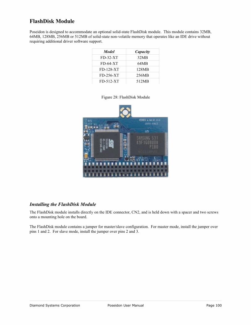
FlashDisk Module
Poseidon is designed to accommodate an optional solid-state FlashDisk module. This module contains 32MB, 64MB, 128MB, 256MB or 512MB of solid-state non-volatile memory that operates like an IDE drive without requiring additional driver software support.
Model CapacityFD-32-XT 32MBFD-64-XT 64MBFD-128-XT 128MBFD-256-XT 256MBFD-512-XT 512MB
Installing the FlashDisk ModuleThe FlashDisk module installs directly on the IDE connector, CN2, and is held down with a spacer and two screws onto a mounting hole on the board.
The FlashDisk module contains a jumper for master/slave configuration. For master mode, install the jumper over pins 1 and 2. For slave mode, install the jumper over pins 2 and 3.
Diamond Systems Corporation Poseidon User Manual Page 100
Figure 28: FlashDisk Module
Setting ValueType User
Cylinders 489 for 32MB flashdisk
Heads 4 for 32MB flashdisk
Sectors 32 for 32MB flashdisk
Multi Sector Transfer Disable
LBA Mode Control Enable
32 Bit I/O Disable
Transfer Mode Fast PIO 1
Ultra DMA Mode Disable
Exit the BIOS and save the change. The system will now boot and recognize the FlashDisk module as drive C:.
Using the FlashDisk with Another IDE DriveThe FlashDisk occupies the board’s 44-pin IDE connector and does not provide a pass-through connector. To utilize both the FlashDisk and a notebook drive, the Diamond Systems Corporation ACC-IDEEXT adapter and cables are required.
Power SupplyThe 44-pin cable carries power from the CPU to the adapter board and powers the FlashDisk module and any drive using a 44-pin connector, such as a notebook hard drive.
A drive utilizing a 40-pin connector, such as a CD-ROM or full-size hard drive, requires an external power source through an additional cable. The power may be provided from the CPU’s power out connector, J12, or from one of the two 4-pin headers on the ACC-IDEEXT board. Poseidon cable no. 698006 may be used with either power connector to bring power to the drive.
Diamond Systems Corporation Poseidon User Manual Page 101
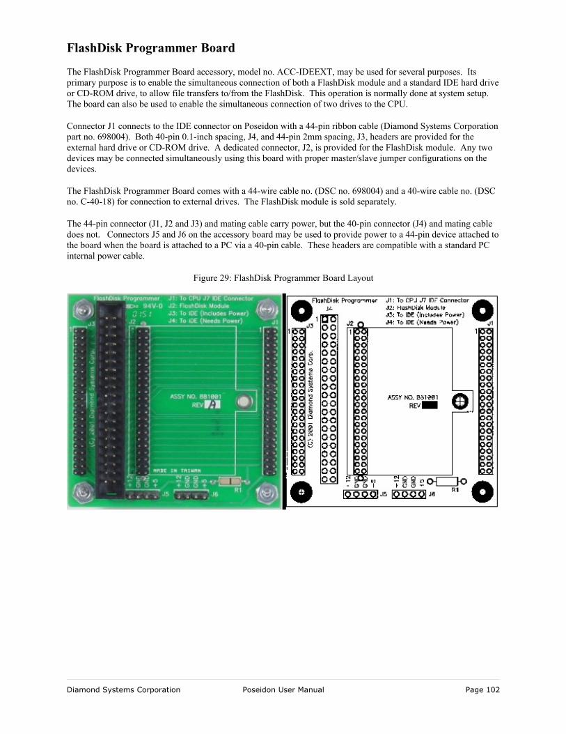
FlashDisk Programmer Board
The FlashDisk Programmer Board accessory, model no. ACC-IDEEXT, may be used for several purposes. Its primary purpose is to enable the simultaneous connection of both a FlashDisk module and a standard IDE hard drive or CD-ROM drive, to allow file transfers to/from the FlashDisk. This operation is normally done at system setup. The board can also be used to enable the simultaneous connection of two drives to the CPU.
Connector J1 connects to the IDE connector on Poseidon with a 44-pin ribbon cable (Diamond Systems Corporation part no. 698004). Both 40-pin 0.1-inch spacing, J4, and 44-pin 2mm spacing, J3, headers are provided for the external hard drive or CD-ROM drive. A dedicated connector, J2, is provided for the FlashDisk module. Any two devices may be connected simultaneously using this board with proper master/slave jumper configurations on the devices.
The FlashDisk Programmer Board comes with a 44-wire cable no. (DSC no. 698004) and a 40-wire cable no. (DSC no. C-40-18) for connection to external drives. The FlashDisk module is sold separately.
The 44-pin connector (J1, J2 and J3) and mating cable carry power, but the 40-pin connector (J4) and mating cable does not. Connectors J5 and J6 on the accessory board may be used to provide power to a 44-pin device attached to the board when the board is attached to a PC via a 40-pin cable. These headers are compatible with a standard PC internal power cable.
Diamond Systems Corporation Poseidon User Manual Page 102
Figure 29: FlashDisk Programmer Board Layout
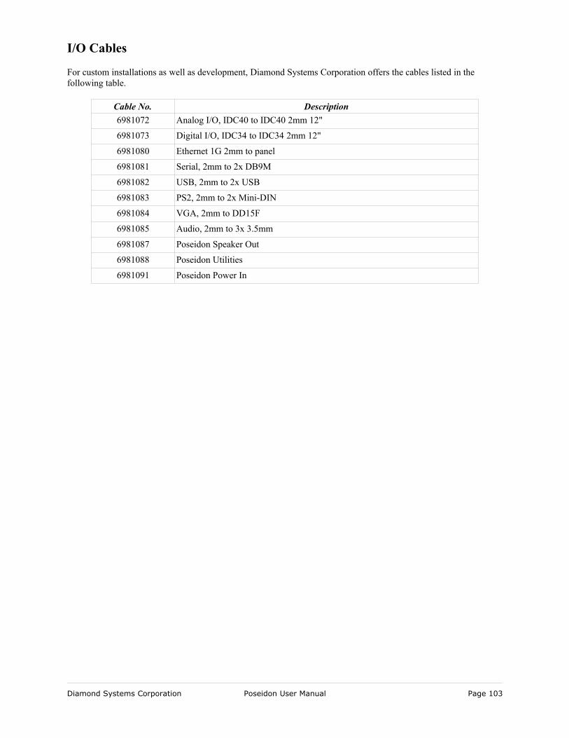
I/O Cables
For custom installations as well as development, Diamond Systems Corporation offers the cables listed in the following table.
Cable No. Description6981072 Analog I/O, IDC40 to IDC40 2mm 12"
6981073 Digital I/O, IDC34 to IDC34 2mm 12"
6981080 Ethernet 1G 2mm to panel
6981081 Serial, 2mm to 2x DB9M
6981082 USB, 2mm to 2x USB
6981083 PS2, 2mm to 2x Mini-DIN
6981084 VGA, 2mm to DD15F
6981085 Audio, 2mm to 3x 3.5mm
6981087 Poseidon Speaker Out
6981088 Poseidon Utilities
6981091 Poseidon Power In
Diamond Systems Corporation Poseidon User Manual Page 103

Mounting PC/104-Plus Cards onto a Poseidon Baseboard
Poseidon is designed to serve as a baseboard for a stack of PC/104 or PC/104-Plus boards. Up to four PC/104-Plus boards are supported. Any PC/104 boards should be mounted on top of the PC/104-Plus board stack, when both board types are to be combined.
PC/104-Plus requires a board configuration setting for each board in a PC/104-Plus board stack. Ensure that the lowest board in the stack is assigned to the lowest board ID, as per the PC/104-Plus specification. This setting establishes the PCI Clock, PCI Interrupt routing, the Bus Master signals, and the device ID setting for PCI configuration. These settings are critical. Two boards should never be configured with identical board stack settings, because this will result in problems accessing PCI devices and may cause damage to the main board and/or the PC/104-Plus boards in the stack.
Note: Do not configure two PC/104-Plus boards with the same board stack ID!
PC/104 is much less critical in this regard, but care should be taken to ensure that the ISA resource allocations allow space for the specific boards added in the stack. Resources (IRQs, in particular) can be very limited in a system with so many devices present on the main board. It is important to ensure that ISA I/O, Memory, IRQ, and DMA configuration conflicts are resolved before powering-up the system. Otherwise, it is possible that the system boot sequence will be impeded by these conflicts.
Take care to read through this documentation, particularly the section on ISA Resource defaults, to familiarize yourself with the internal resources used before adding components that might cause conflicts.
When adding boards to the PC/104(+) board stack, be sure to include board standoffs. Inordinate flexing of the main PC/104 and PC/104-Plus connectors can seriously reduce the effective lifespan of the connectors, as well as cause potential system instability due to incomplete connection across system buses.
Diamond Systems Corporation Poseidon User Manual Page 104
Customization Options
There are many customer-specific customizations that can be done for the Poseidon, including:
• Latching connectors (replacing the box headers used for most of the board I/O connections).• Connectors with extra gold contact plating.• Alternative heatsinks for low air-flow and dusty environments.• Conformal Coating.• Jumperless configuration (all settings made on-board with no jumper headers required).
Contact your sales representative for details on these special-order options.
Diamond Systems Corporation Poseidon User Manual Page 105
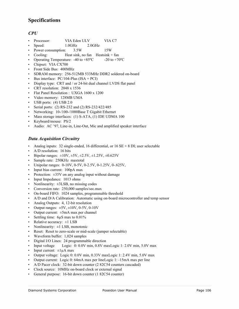
Specifications
CPU• Processor: VIA Eden ULV VIA C7• Speed: 1.0GHz 2.0GHz• Power consumption: 3.5W 15W• Cooling: Heat sink, no fan Heatsink + fan• Operating Temperature: -40 to +85ºC -20 to +70ºC• Chipset: VIA CX700• Front Side Bus: 400MHz• SDRAM memory: 256-512MB 533MHz DDR2 soldered on-board • Bus interface: PC/104-Plus (ISA + PCI)• Display type: CRT and / or 24-bit dual channel LVDS flat panel• CRT resolution: 2048 x 1536• Flat Panel Resolution : UXGA 1600 x 1200• Video memory: 128MB UMA• USB ports: (4) USB 2.0• Serial ports: (2) RS-232 and (2) RS-232/422/485• Networking: 10-/100-/1000Base T Gigabit Ethernet• Mass storage interfaces: (1) S-ATA, (1) IDE UDMA 100• Keyboard/mouse: PS/2• Audio: AC ’97, Line-in, Line-Out, Mic and amplified speaker interface
Data Acquisition Circuitry• Analog inputs: 32 single-ended, 16 differential, or 16 SE + 8 DI; user selectable• A/D resolution: 16 bits• Bipolar ranges: ±10V, ±5V, ±2.5V, ±1.25V, ±0.625V• Sample rate: 250KHz maxtotal• Unipolar ranges: 0-10V, 0-5V, 0-2.5V, 0-1.25V, 0-.625V,• Input bias current: 100pA max• Protection: ±35V on any analog input without damage• Input Impedance: 1013 ohms• Nonlinearity: ±3LSB, no missing codes• Conversion rate: 250,000 samples/sec.max• On-board FIFO: 1024 samples, programmable threshold• A/D and D/A Calibration: Automatic using on-board microcontroller and temp sensor• Analog Outputs: 4, 12-bit resolution• Output ranges: ±5V, ±10V, 0-5V, 0-10V• Output current: ±5mA max per channel• Settling time: 6µS max to 0.01%• Relative accuracy: ±1 LSB• Nonlinearity: ±1 LSB, monotonic• Reset: Reset to zero-scale or mid-scale (jumper selectable)• Waveform buffer: 1,024 samples• Digital I/O Lines: 24 programmable direction• Input voltage Logic: 0: 0.0V min, 0.8V maxLogic 1: 2.0V min, 5.0V max• Input current: ±1µA max• Output voltage: Logic 0: 0.0V min, 0.33V maxLogic 1: 2.4V min, 5.0V max• Output current: Logic 0: 64mA max per lineLogic 1: -15mA max per line• A/D Pacer clock: 32-bit down counter (2 82C54 counters cascaded)• Clock source: 10MHz on-board clock or external signal• General purpose: 16-bit down counter (1 82C54 counter)
Diamond Systems Corporation Poseidon User Manual Page 106

Power Supply• Input Voltage: +5VDC ±5%
General• Dimensions: 4.528” x 6.496” (115mm x 165mm)• Weight: TBD
Diamond Systems Corporation Poseidon User Manual Page 107

Additional Information
Additional information can be found at the following websites.
1. Diamond Systems Corporation: http://www.diamondsystems.com/
2. VIA Technologies, Inc. (Processors): http://www.via.com.tw/en/products/processors/
3. VIA Technologies, Inc. (North/South bridge): http://www.via.com.tw/en/products/chipsets/c-series/cx700/
Diamond Systems Corporation Poseidon User Manual Page 108

Technical Support
For technical support, please email [email protected] or contact Diamond Systems Corporation technical support at 1-650-810-2500.
Diamond Systems Corporation Poseidon User Manual Page 109