Embed Size (px)
Citation preview
by J. M. TendlerJ. S. DodsonJ. S. Fields, Jr.H. LeB. Sinharoy
POWER4systemmicroarchitecture
The IBM POWER4 is a new microprocessororganized in a system structure that includesnew technology to form systems. The namePOWER4 as used in this context refers notonly to a chip, but also to the structure usedto interconnect chips to form systems.In this paper we describe the processormicroarchitecture as well as the interconnectionarchitecture employed to form systems up toa 32-way symmetric multiprocessor.
IntroductionIBM announced the RISC System/6000* (RS/6000*, thepredecessor of today’s IBM eServer pSeries*) family ofprocessors in 1990. The initial models ranged in frequencyfrom 20 MHz to 30 MHz [1] and achieved performancelevels exceeding those of many of their contemporaries[2]. In 1993, the POWER2 microprocessor was introduced,operating initially at frequencies ranging from 55 MHz to71.5 MHz [3]. The POWER2 microprocessor was capableof simultaneous execution of up to six instructions perclock cycle. The PowerPC 601* microprocessor was alsointroduced in 1993 [4]. The PowerPC 601 resulted from ajoint development effort by IBM, Apple, and Motorola atthe Somerset Design Center in Austin, Texas. Like theirpredecessors, systems built using these microprocessorswere 32-bit architectures, though the PowerPCArchitecture* did recognize a 64-bit implementation. Withthe RS64 microprocessor introduced in 1997 and thePOWER3 microprocessor introduced in 1998 [5], 64-bitarchitected UNIX**-based RS/6000 systems became
commonplace. The RS64 and its follow-onmicroprocessors, the RS64-II [6], RS64-III [7], and RS64-IV [8], were optimized for commercial applications. TheRS64 initially appeared in systems operating at 125 MHz.Most recently, the RS64-IV has been shipping in systemsoperating at up to 750 MHz. The POWER3 and its follow-on, the POWER3-II [9], were optimized for technicalapplications. Initially introduced at 200 MHz, most recentsystems using the POWER3-II have been operating at450 MHz. The RS64 microprocessor and its follow-onswere also used in AS/400* systems (the predecessorto today’s eServer iSeries*).
POWER4 was designed to address both commercial andtechnical requirements. It implements and extends in acompatible manner the 64-bit PowerPC Architecture [10].First used in pSeries systems, it will be staged into theiSeries at a later date. It leverages IBM technology usingan 0.18-�m-lithography copper and silicon-on-insulator(SOI) technology [11]. In the ongoing debate betweenthe “speed demons” (high clock rate) and the “braniacs”(more complex design but a higher instructions-per-cyclerate [12]), IBM UNIX-based systems have traditionallybeen in the braniac camp. With the POWER4, IBMopted to also embrace the speed-demon approach. ThePOWER4 design was initially introduced at processorfrequencies of 1.1 GHz and 1.3 GHz, surpassing allother 64-bit microprocessors in some key performancebenchmarks [13].
In this paper we first describe the objectives that wereestablished for the design. We then take a closer lookat the components of the resultant systems from a
�Copyright 2002 by International Business Machines Corporation. Copying in printed form for private use is permitted without payment of royalty provided that (1) eachreproduction is done without alteration and (2) the Journal reference and IBM copyright notice are included on the first page. The title and abstract, but no other portions, of thispaper may be copied or distributed royalty free without further permission by computer-based and other information-service systems. Permission to republish any other portion of
this paper must be obtained from the Editor.
0018-8646/02/$5.00 © 2002 IBM
IBM J. RES. & DEV. VOL. 46 NO. 1 JANUARY 2002 J. M. TENDLER ET AL.
5

microarchitecture perspective. We begin by first discussingthe POWER4 chip. One of IBM’s major strengths is itssystem expertise—the ability to design multiple partsin a consistent and synergistic manner. In that light,POWER4 cannot be considered only a chip, but ratheran architecture within which a set of chips are designedtogether to realize a system. As such, POWER4 can beconsidered a technology in its own right. In that light, wediscuss how systems are built by interconnecting POWER4chips to form symmetric multiprocessors (SMPs) of anysize up to a 32-way SMP. The interconnect topology,referred to as a distributed switch, is new to the industry.Finally, no system discussion would be complete withoutsome view of the reliability, availability, and serviceability(RAS) features and philosophy incorporated intoPOWER4 systems. A more complete discussion of thePOWER4 RAS features may be found in a companionpaper by Bossen et al. [14].
Guiding principlesIn designing POWER4, the engineering team was guidedby a set of principles which included the following:
● SMP optimization: The server must be designed for high-throughput multitasking environments. The system mustbe optimized for SMP operation, in which a largenumber of transistors can be used to improve totalsystem performance. By their very nature, serversprocess disparate information, often with multipleprocesses active concurrently.
● Full-system design approach: To optimize the system,we began with the full design in mind up front. Thismarriage of process technology, packaging, andmicroarchitecture was designed to allow softwareto exploit them. The processor was designed to fiteffectively in this environment. We designed the entiresystem together, from the processor to memory and I/Obridge chips. A new high-performance processor needsa new subsystem to feed it effectively.
● Very-high-frequency design: To maintain a leadershipposition, we planned from the outset to deliver best-of-breed operating frequencies. We revamped our chipdesign with new transistor-level tools [15], and havetransformed complex control logic into regular dataflowconstructs. Additionally, we have designed the systemto permit system balance to be preserved as technologyimprovements become available, allowing even higherprocessor frequencies to be delivered.
● Leadership in reliability, availability, and serviceability(RAS): Servers have evolved toward continuousoperation. We had already begun designing intoour systems RAS attributes previously seen only inmainframe systems. With POWER4, we accepted theprinciple that one does not achieve high levels of
reliability only by choosing reliable parts andincorporating error-correction-code (ECC) logic intomajor arrays. Instead, we required an approach thateliminated outages and provided redundancy in caseswhere errors could not be eliminated. Where possible,if an error occurred, we worked to transform hardmachine stops (checkstops) into synchronous machineinterrupts to software to allow the system to circumventproblems if possible.
● Balanced technical and commercial performance: As webalanced the system, we made sure the design couldhandle a varied and robust set of workloads. This isespecially important as the e-business world evolvesand data-intensive demands on systems merge withcommercial requirements. The need to satisfy high-performance computing requirements with theirhistorical high-bandwidth demands and commercialrequirements with their data-sharing and SMP scalingrequirements dictated a single design to address bothenvironments. This would also allow us to meet theneeds of what became pSeries and iSeries eServerswith a single design.
● Binary compatibility: Several internal IBM task forcesin the first half of the 1990s had concluded that thePowerPC Architecture had no technical impedimentsto prevent it from scaling up to significantly higherfrequencies with excellent performance. With notechnical reason to change, in order to keep ourcustomers’ software investment intact, we accepted theabsolute requirement of maintaining binary compatibilityfor both 32-bit and 64-bit applications with priorPowerPC* and PowerPC AS systems.
POWER4 chipThe components of the POWER4 chip are shown inFigure 1. The design features two processors on one chip;included in what we are referring to as the processorare the various execution units and the split first-levelinstruction and data caches. The two processors share aunified second-level cache, also on the same chip, througha core interface unit (CIU), as shown in Figure 1. TheCIU is a crossbar switch between the L2, implementedas three separate, autonomous cache controllers, andthe two processors. Each L2 cache controller can operateconcurrently and feed 32 bytes of data per cycle. The CIUconnects each of the three L2 controllers to either thedata cache or the instruction cache in either of the twoprocessors. Additionally, the CIU accepts stores from theprocessors across 8-byte-wide buses and sequences them tothe L2 controllers. Each processor has associated with it anoncacheable unit, the NC unit in Figure 1, responsiblefor handling instruction-serializing functions and performingany noncacheable operations in the storage hierarchy.Logically, this is part of the L2.
J. M. TENDLER ET AL. IBM J. RES. & DEV. VOL. 46 NO. 1 JANUARY 2002
6

The directory for a third-level cache, L3, and itscontroller are also located on the POWER4 chip. Theactual L3 is on a separate chip. A separate functionalunit, referred to as the fabric controller, is responsible forcontrolling dataflow between the L2 and L3 controller forthe chip and for POWER4 communication. The GXcontroller is responsible for controlling the flow ofinformation into and out of the system. Typically, thiswould be the interface to an I/O drawer attached tothe system. With the POWER4 architecture, however,this is also the point at which we would directly attachan interface to a switch for clustering multiple POWER4nodes.
Also included on the chip are functions we logicallycall pervasive function. These include trace and debugfacilities used for first-failure data capture, built-in self-test (BIST) facilities, a performance-monitoring unit, aninterface to the service processor (SP) used to control theoverall system, power-on reset (POR) sequencing logic,and error detection and logging circuitry.
A die photo of the POWER4 chip is shown in Figure 2.The chip contains 174 million transistors interconnectedacross seven layers of copper metallurgy. For clarity, themajor components of the chip are labeled. Their operationis described in the remainder of this paper.
Four POWER4 chips can be packaged on a singlemodule to form an eight-way SMP. Four such modules canbe interconnected to form a 32-way SMP. To accomplishthis, each chip contains five primary interfaces. Tocommunicate with other POWER4 chips on the samemodule, there are logically four 16-byte buses. Physically,these four logical buses are implemented with six buses,three on and three off, as shown in Figure 1. Tocommunicate with POWER4 chips on other modules,there are two 8-byte buses, one on and one off. Each chiphas its own interface to the off-chip L3 across two 16-byte-wide buses, one on and one off, operating at one-thirdprocessor frequency. To communicate with I/O devicesand other computing nodes, two 4-byte-wide GX buses,one on and one off, operating at one-third processor
Figure 1
POWER4 chip logical view.
Trace anddebug
BIST engines
Performancemonitor
SPcontroller
PORsequencer
Error detectionand logging
Processor core 1 Processor core 1
IFetch Store Loads IFetch Store Loads
CIU switch
Core 1NCunit
Core 2NCunit
L2cache
L2cache
L2cache
32B32B
32B32B
32B 32B 32B
32B 32B 32B32B32B32B
8B 8B
8B
8B 8B 8B
8B8B8B
8B
16B
16B
16B
8B
16B
16B
16B
8B
16B
16B
4B
4B
8B
Fabric controller
L3 controllerMemory controller
GX controllerL3
directory
Chip–chipfabric(2:1)
MCM–MCM(2:1)
Chip–chipfabric(2:1)
MCM–MCM(2:1)
L3/memory bus(3:1)
GX bus(n:1)
JTAG
IBM J. RES. & DEV. VOL. 46 NO. 1 JANUARY 2002 J. M. TENDLER ET AL.
7

frequency, are used. Finally, each chip has its own JTAGinterface to the system service processor. All of the abovebuses, except for the JTAG interface, scale with processorfrequency. POWER4 systems will be offered at more thanone frequency. It is also anticipated that technologicaladvances will allow us to increase processor frequencyover time. As this occurs, bus frequencies will scaleproportionately, allowing system balance to be maintained.
POWER4 processorFigure 3 shows a high-level block diagram of a POWER4processor. The two processors on the chip are identicaland provide a two-way SMP model to software. Theinternal microarchitecture of the core is a speculativesuperscalar out-of-order execution design. Up to eightinstructions can be issued each cycle, with a sustainedcompletion rate of five instructions. Register-renamingpools and other out-of-order resources coupled with thepipeline structure allow the design to have more than 200instructions in flight at any given time. In order to exploitinstruction-level parallelism, there are eight executionunits, each capable of being issued an instruction eachcycle. Two identical floating-point execution units, eachcapable of starting a fused multiply and add each cycle[i.e., a maximum four floating-point operations (FLOPs)per cycle per processor] are provided. In order to feedthe dual floating-point units, two load/store units, eachcapable of performing address-generation arithmetic,
are provided. Additionally, there are dual fixed-pointexecution units, a branch execution unit, and an executionunit to perform logical operations on the condition register.
Branch predictionTo help mitigate the effects of the long pipelinenecessitated by the high-frequency design, POWER4invests heavily in branch-prediction mechanisms. Branch-prediction schemes are not new [16, 17]. POWER4 uses amultilevel branch-prediction scheme to predict whetheror not a conditional branch instruction is taken. Similarschemes have been implemented in other systems; see [18]for example. Additionally, branch target addresses arepredicted for those instructions that branch to an addressspecified in either the count register or the link register.Similar concepts have been discussed in the literature[19, 20].
In POWER4, up to eight instructions are fetched eachcycle from the direct-mapped 64KB instruction cache. Thebranch-prediction logic scans the fetched instructions,looking for up to two branches each cycle. Dependingupon the branch type found, various branch-predictionmechanisms engage to help predict the branch directionor the target address of the branch or both. Branchdirection for unconditional branches is not predicted. Allconditional branches are predicted, even if the conditionregister bits upon which they are dependent are known atinstruction fetch time. Branch target addresses for thePowerPC branch-to-link-register (bclr) and branch-to-count-register (bcctr) instructions are predicted using ahardware-implemented link stack and count cachemechanism, respectively. Target addresses for absoluteand relative branches are computed directly as part of thebranch scan function.
As branch instructions flow through the rest of thepipeline and ultimately execute in the branch-executionunit, the actual outcomes of the branches are determined.At that point, if the predictions were found to be correct,the branch instructions are simply completed like all otherinstructions. If a prediction is found to be incorrect, theinstruction-fetch logic causes the mispredicted instructionsto be discarded and begins refetching instructions alongthe corrected path.
POWER4 uses a set of three branch-history tables topredict the direction of branch instructions. The firsttable, called the local predictor, is similar to a traditionalbranch-history table (BHT). It is a 16 384-entry arrayindexed by the branch instruction address producing a1-bit predictor that indicates whether the branch directionshould be taken or not taken. The second table, called theglobal predictor, predicts the branch direction on the basisof the actual path of execution to reach the branch. Thepath of execution is identified by an 11-bit vector, one bitper group of instructions fetched from the instruction
Figure 2
POWER4 chip photograph showing the principal functional units in the microprocessor core and in the memory subsystem.
J. M. TENDLER ET AL. IBM J. RES. & DEV. VOL. 46 NO. 1 JANUARY 2002
8

cache for each of the previous eleven fetch groups. Thisvector is referred to as the global history vector. Each bitin the global history vector indicates whether or not thenext group of instructions fetched are from a sequentialcache sector. The global history vector captures thisinformation for the actual path of execution through thesesectors. That is, if there is a redirection of instructionfetching, some of the fetched group of instructions arediscarded and the global history vector is immediatelycorrected. The global history vector is hashed, using abitwise exclusive or with the address of the branchinstruction. The result indexes into a 16 384-entry globalhistory table to produce another 1-bit branch-directionpredictor. Like the local predictor, this 1-bit globalpredictor indicates whether the branch should bepredicted to be taken or not taken. Finally, a third table,called the selector table, keeps track of which of the twoprediction schemes works better for a given branchand is used to select between the local and the globalpredictions. The 16 384-entry selector table is indexedexactly the same way as the global history table to producethe 1-bit selector. This combination of branch-predictiontables has been shown to produce very accuratepredictions across a wide range of workload types.
If the first branch encountered in a particular cycle ispredicted as not taken and a second branch is found inthe same cycle, POWER4 predicts and acts on the secondbranch in the same cycle. In this case, the machineregisters both branches as predicted, for subsequentresolution at branch execution, and redirects theinstruction fetching on the basis of the second branch.
As branch instructions are executed and resolved,the branch-history tables and the other predictors areupdated to reflect the latest and most accurate information.Dynamic branch prediction can be overridden by software.This is useful for cases in which software can predictbranches better than the hardware. It is accomplished bysetting two previously reserved bits in conditional branchinstructions, one to indicate a software override and theother to predict the direction. When these two bits arezero (suggested use for reserved bits), hardware branchprediction is used. Since only reserved bits are used forthis purpose, 100% binary compatibility with earliersoftware is maintained.
POWER4 uses a link stack to predict the targetaddress for a branch-to-link instruction that it believescorresponds to a subroutine return. By setting the hint bitsin a branch-to-link instruction, software communicatesto the processor whether a branch-to-link instructionrepresents a subroutine return, a target address that islikely to repeat, or neither. When instruction-fetch logicfetches a branch-and-link instruction (either conditional orunconditional) predicted as taken, it pushes the address ofthe next instruction onto the link stack. When it fetches a
branch-to-link instruction with taken prediction and withhint bits indicating a subroutine return, the link stack ispopped, and instruction fetching starts from the poppedaddress.
To preserve the integrity of the link stack in the faceof mispredicted branch target link instructions, POWER4employs an extensive speculation tolerance mechanism inits link stack implementation to allow recovery of the linkstack under most circumstances.
The target address of a branch-to-count instruction isoften repetitive. This is also true for some of the branch-to-link instructions that are not predictable through theuse of the link stack (because they do not correspond to asubroutine return). By setting the hint bits appropriately,software communicates to the hardware whether the targetaddresses for such branches are repetitive. In these cases,POWER4 uses a 32-entry, tagless, direct-mapped cache,called a count cache, to predict the repetitive targets, asindicated by the software hints. Each entry in the countcache can hold a 62-bit address. When a branch-to-linkor branch-to-count instruction is executed, for whichthe software indicates that the target is repetitive andtherefore predictable, the target address is written in the
Figure 3
POWER4 core.
IFAR
Instruction queue
BRpredict
BRscan
Decode, crack andgroup formation
I-cache
D-cache
GCT
BR/CRissuequeue
FX/LD 1issuequeue
FX/LD 2issuequeue
FPissuequeue
BR
exec
utio
n un
it
CR
exec
utio
n un
it
FX1
exec
utio
n un
it
LD
1ex
ecut
ion
unit
LD
2ex
ecut
ion
unit
FX2
exec
utio
n un
it
FP1
exec
utio
n un
it
FP2
exec
utio
n un
it
Storagequeue
IBM J. RES. & DEV. VOL. 46 NO. 1 JANUARY 2002 J. M. TENDLER ET AL.
9

count cache. When such an instruction is fetched, thetarget address is predicted using the count cache.
Instruction fetchInstructions are fetched from the instruction cache (I-cache)on the basis of the contents of the instruction-fetchaddress register (IFAR). The IFAR is normally loadedwith an address determined by the branch-prediction logic.As noted earlier, for cases in which the branch-predictionlogic is in error, the branch-execution unit will cause theIFAR to be loaded with the corrected address of theinstruction stream to be fetched. Additionally, thereare other factors that can cause a redirection of theinstruction stream, some based on internal events, otherson interrupts from external events. In any case, once theIFAR is loaded, the I-cache is accessed and retrieves upto eight instructions per cycle. Each line in the I-cache canhold 32 PowerPC instructions, i.e., 128 bytes. Each line isdivided into four equal sectors. Since I-cache misses areinfrequent, to save area, the I-cache has been designed tocontain a single port that can be used to read or write onesector per cycle. The I-cache directory (IDIR) is indexedby the effective address and contains 42 bits of realaddress per entry.
On an I-cache miss, instructions are returned from theL2 in four 32-byte transmissions. The L2 normally returnsthe critical sector (the sector containing the specific wordaddress that references the cache line) in one of the firsttwo beats. Instruction-fetch logic forwards these demand-oriented instructions into the pipeline as quickly aspossible. In addition, the cache line is written into oneentry of the instruction-prefetch buffer so that the I-cacheitself is available for successive instruction fetches. Theinstructions are written to the I-cache during cycles wheninstruction fetching is not using the I-cache, as is the casewhen another I-cache miss occurs. In this way, writes tothe I-cache are hidden and do not interfere with normalinstruction fetching.
The PowerPC Architecture specifies a translation-lookaside buffer (TLB) and a segment-lookaside buffer(SLB) to translate from the effective address (EA) usedby software and the real address (RA) used by hardwareto locate instructions and data in storage. Since thesetranslation mechanisms take several cycles, oncetranslated, the EA, RA pair is stored in a 128-entry,two-way set-associative array, called the effective-to-realaddress translation (ERAT) table. POWER4 implementsseparate ERATs for instruction-cache (IERAT) and data-cache (DERAT) accesses. Both ERATs are indexed usingthe effective address. A common 1024-entry four-way set-associative TLB is implemented for each processor.
When the instruction pipeline is ready to acceptinstructions, the IFAR content is sent to the I-cache,IDIR, IERAT, and branch-prediction logic. The IFAR is
updated with the address of the first instruction in thenext sequential sector. In the next cycle, instructions arereceived from the I-cache and forwarded to an instructionqueue from which the decode, crack, and group formationlogic shown in Figure 3 pulls instructions. This is doneeven before it is known that there is a I-cache hit. Alsoreceived in the same cycle are the RA from the IDIR,the EA, RA pair from the IERAT, and the branch-direction-prediction information. The IERAT is checkedto ensure that it has a valid entry and that its RA matchesthe contents of the IDIR. If the IERAT has an invalidentry, the EA must be translated from the TLB and SLB.Instruction fetching is then stalled. Assuming that theIERAT is valid, if the RA from the IERAT matches thecontents of the IDIR, an I-cache hit is validated. Usingthe branch-prediction logic, the IFAR is reloaded and theprocess is repeated. Filling the instruction queue in frontof the decode, crack, and group formation logic allowsinstruction fetching to run ahead of the rest of the systemand queue work for the remainder of the system. In thisway, when there is an I-cache miss, there often areadditional instructions in the instruction queue tobe processed, thereby not freezing the pipeline.
If there is an I-cache miss, several different scenariosare possible. First, the instruction-prefetch buffers areexamined to see whether the requested instructions arethere, and, if so, logic steers these instructions intothe pipeline as though they came from the I-cache andwill also write the critical sector into the I-cache. If theinstructions are not found in the instruction-prefetchbuffer, a demand-fetch reload request is sent to the L2.The L2 processes this reload request with high priority.When it is returned from the L2, an attempt will bemade to write it into the I-cache.
In addition to these demand-oriented instruction-fetching mechanisms, POWER4 prefetches instruction-cache lines that might soon be referenced into itsinstruction-prefetch buffer, which is capable of holdingfour entries of 32 instructions each. The instruction-prefetch logic monitors demand instruction-fetch requestsand initiates prefetches for the next one (if there is a hitin the prefetch buffer) or two (if there is a miss in theprefetch buffer) sequential cache lines after verifying thatthey are not already in the I-cache. When these requestsreturn cache lines, the returned lines are stored in theinstruction-prefetch buffer so that they do not pollute thedemand-oriented I-cache. The I-cache contains only cachelines that have had a reference to at least one instruction.
Decode, crack, and group formationAs instructions are executed out of order, it is necessaryto remember the program order of all instructions inflight. To minimize the logic necessary to track a largenumber of in-flight instructions, groups of instructions are
J. M. TENDLER ET AL. IBM J. RES. & DEV. VOL. 46 NO. 1 JANUARY 2002
10

formed. The individual groups are tracked through thesystem. That is, the state of the machine is preserved atgroup boundaries, not at an instruction boundary within agroup. Any exception causes the machine to be restoredto the state of the oldest group prior to the exception.
A group contains up to five internal instructionsreferred to as IOPs. In the decode stages, the instructionsare placed sequentially in a group—the oldest instructionis placed in slot 0, the next oldest one in slot 1, andso on. Slot 4 is reserved solely for branch instructions.If required, no-ops are inserted to force the branchinstruction to be in the fourth slot. If there is no branchinstruction, slot 4 contains a no-op. Only one groupof instructions can be dispatched in a cycle, and allinstructions in a group are dispatched together. (Bydispatch, we mean the movement of a group of instructionsinto the issue queues.) Groups are dispatched in programorder. Individual IOPs are issued from the issue queuesto the execution units out of program order.
Results are committed when the group completes. Agroup can complete when all older groups have completedand when all instructions in the group have finishedexecution. Only one group can complete in a cycle.
For correct operation, certain instructions are notallowed to execute speculatively. To ensure that theinstruction executes nonspeculatively, it is not executeduntil it is the next one to complete. This mechanismis called completion serialization. To simplify theimplementation, such instructions form single instructiongroups. Examples of completion serialization instructionsinclude loads and stores to guarded space and context-synchronizing instructions such as the move-to-machine-state-register instruction that is used to alter the stateof the machine.
In order to implement out-of-order execution, manyof the architected registers are renamed, but not all.To ensure proper execution of these instructions, anyinstruction that sets a nonrenamed register terminates agroup.
Internal instructions, in most cases, are architectedinstructions. However, instructions are sometimes splitinto one or more internal instructions. To achieve high-frequency operation, we have limited instructions to readat most two registers and write at most one register.(Some floating-point operations do not obey thisrestriction for performance reasons; for example, thefused multiply and add series of instructions are handleddirectly in the floating-point unit, though they requirethree sources.) If this is not the case, the instructionis split to satisfy this requirement. As an example, theload with update instruction that loads one register andincrements an index register is split into a load and an addinstruction. Similarly, the load multiple word instruction isimplemented with multiple load word instructions. With
respect to group formation, we differentiate two classes.If an instruction is split into two instructions, such as loadwith update, that action is considered to be cracking. If aninstruction is split into more than two IOPs, it is called amillicoded instruction. Cracked instructions flow intogroups like any other instructions, with the restrictionthat both IOPs must be in the same group. If both IOPscannot fit into the current group, the group is terminatedand a new group is initiated. The instruction following thecracked instruction may be in the same group as thecracked instruction, assuming there is room in the group.Millicoded instructions always begin a new group. Theinstruction following the millicoded instruction alsoinitiates a new group.
Instructions performing logical operations on thecondition register appear at a lower frequency than otherinstructions. As such, a single execution unit is dedicated tothis function. With the instruction-issue rules described inthe next section, this condition requires restricting thisclass of instructions to only two of the four slots,specifically slots 0 and 1.
Group dispatch and instruction issueInstruction groups are dispatched into the issue queuesone group at a time. As a group is dispatched, controlinformation for the group is stored in the groupcompletion table (GCT). The GCT can store up to 20groups. The GCT entry contains the address of the firstinstruction in the group. As instructions finish execution,that information is registered in the GCT entry for thegroup. Information is maintained in the GCT until thegroup is retired, i.e., either all of its results arecommitted, or the group is flushed from the system.
Each instruction slot feeds separate issue queues for thefloating-point units, the branch-execution unit, the CRexecution unit, the fixed-point execution units, and theload/store execution units. The fixed-point and load/storeexecution units share common issue queues. Table 1summarizes the depth of each issue queue and the numberof queues available for each type of queue. For thefloating-point issue queues and the common issue queuesfor the fixed-point and load/store units, the issue queuesfed from instruction slots 0 and 3 hold instructions to beexecuted in one of the execution units, while the issue
Table 1 Issue queues.
Queue type Entries perqueue
Number ofqueues
Fixed-point and load/store 9 4Floating-point 5 4Branch execution 12 1CR logical 5 2
IBM J. RES. & DEV. VOL. 46 NO. 1 JANUARY 2002 J. M. TENDLER ET AL.
11

queues fed from instruction slots 1 and 2 feed theother execution unit. The CR execution unit draws itsinstructions from the CR logical issue queue fed frominstruction slots 0 and 1.
Instructions are dispatched into the top of an issuequeue. As they are issued from the queue, the remaininginstructions move down in the queue. In the case of twoqueues feeding a common execution unit, the two queuesare interleaved. The oldest instruction that has all of itssources set in the common interleaved queue is issuedto the execution unit.
Before a group can be dispatched, all resources tosupport that group must be available. If they are not, thegroup is held until the necessary resources are available.To successfully dispatch, the following resources areassigned:
● GCT entry: One GCT entry is assigned for each group.It is released when the group retires.
● Issue queue slot: An appropriate issue queue slot mustbe available for each instruction in the group. It isreleased when the instruction in it has successfullybeen issued to the execution unit. Note that in somecases this is not known until several cycles after theinstruction has been issued. As an example, a fixed-pointoperation dependent on an instruction loading a registercan be speculatively issued to the fixed-point unit beforeit is known whether the load instruction resulted in anL1 data cache hit. Should the load instruction miss inthe cache, the fixed-point instruction is effectively pulledback and sits in the issue queue until the data on whichit depends is successfully loaded into the register.
● Rename register: For each register that is renamed andset by an instruction in the group, a correspondingrenaming resource must be available. Table 2summarizes the renaming resources available to eachPOWER4 processor. The renaming resource is releasedwhen the next instruction writing to the same logicalresource is committed. As a result of cracking andmillicode used in forming groups, it is necessary insome situations to use additional logical registers. Fouradditional GPRs and one additional 4-bit CR field are
required. The condition register is architected to be one32-bit register comprising eight 4-bit fields. Each field istreated internal to the system as a separate register andis renamed. Not all of the fixed-point exception register(XER) is renamed; only four of the XER fields arerenamed.
● Load reorder queue (LRQ) entry: An LRQ entry must beavailable for each load instruction in the group. Theseentries are released when the group completes. TheLRQ contains 32 entries.
● Store reorder queue (SRQ) entry: An SRQ entry must beavailable for each store instruction in the group. Theseentries are released when the result of the store issuccessfully sent to the L2, after the group completes.The SRQ contains 32 entries.
The operation of the LRQ and the SRQ is described inthe section on the load/store unit.
As noted previously, certain instructions requirecompletion serialization. Groups so marked are not issueduntil that group is the next to complete (i.e., all priorgroups have successfully completed). Additionally,instructions that read a nonrenamed register cannot beexecuted until we are sure that all writes to that registerhave completed. To simplify the implementation, anyinstruction that writes to a nonrenamed register sets aswitch that is reset when the instruction finishes execution.If the switch is set, this blocks dispatch of an instructionthat reads a nonrenamed register. Writes to a nonrenamedregister are guaranteed to be in program order by makingthem completion-serialization operations.
Since instruction progression through the machine istracked in groups, when a particular instruction within agroup must signal an interrupt, this is achieved by flushingall of the instructions (and results) of the group and thenredispatching the instructions into single instructiongroups. A similar mechanism is used to ensure that thefixed-point exception register summary overflow bit iscorrectly maintained.
Load/store unit operationThe load/store unit requires special attention in an out-of-order execution machine in order to ensure memoryconsistency. Since we cannot be sure that the resultof a store operation will be committed at the time it isexecuted, a special mechanism is employed. Associatedwith each SRQ entry is a store data queue (SDQ) entry.The SDQ entry maintains the desired result to be storeduntil the group containing the store instruction iscommitted. Once committed, the data maintained inthe SDQ is written to the caches. Additionally, threeparticular hazards must be avoided:
Table 2 Rename resources.
Resource type Logicalsize
Physicalsize
GPRs 32 (36) 80FPRs 32 72CRs 8 (9) 4-bit fields 32Link/count registers 2 16FPSCR 1 20XER 4 fields 24
J. M. TENDLER ET AL. IBM J. RES. & DEV. VOL. 46 NO. 1 JANUARY 2002
12
● Load hit store: A younger load that executes before anolder store to the same memory location has written itsdata to the caches must retrieve the data from the SDQ.As loads execute, they check the SRQ to see whetherthere is any older store to the same memory locationwith data in the SDQ. If one is found, the data isforwarded from the SDQ rather than from the cache. Ifthe data cannot be forwarded (as is the case if the loadand store instructions operate on overlapping memorylocations and the load data is not the same as orcontained within the store data), the group containingthe load instruction is flushed; that is, it and all youngergroups are discarded and refetched from the instructioncache. If we can tell that there is an older storeinstruction that will write to the same memory locationbut has yet to write its result to the SDQ, the loadinstruction is rejected and reissued, again waiting forthe store instruction to execute.
● Store hit load: If a younger load instruction executesbefore we have had a chance to recognize that an olderstore will be writing to the same memory location, theload instruction has received stale data. To guardagainst this, as a store instruction executes it checks theLRQ; if it finds a younger load that has executed andloaded from memory locations to which the store iswriting, the group containing the load instruction andall younger groups are flushed and refetched from theinstruction cache. To simplify the logic, all groupsfollowing the store are flushed. If the offending load isin the same group as the store instruction, the group isflushed, and all instructions in the group form single-instruction groups.
● Load hit load: Two loads to the same memory locationmust observe the memory reference order and preventa store to the memory location from another processorbetween the intervening loads. If the younger loadobtains old data, the older load must not obtainnew data. This requirement is called sequential loadconsistency. To guard against this, LRQ entries for allloads include a bit which, if set, indicates that a snoophas occurred to the line containing the loaded datafor that entry. When a load instruction executes, itcompares its load address against all addresses in theLRQ. A match against a younger entry which has beensnooped indicates that a sequential load consistencyproblem exists. To simplify the logic, all groupsfollowing the older load instruction are flushed. If bothload instructions are in the same group, the flushrequest is for the group itself. In this case, eachinstruction in the group when refetched forms a single-instruction group in order to avoid this situation thesecond time around.
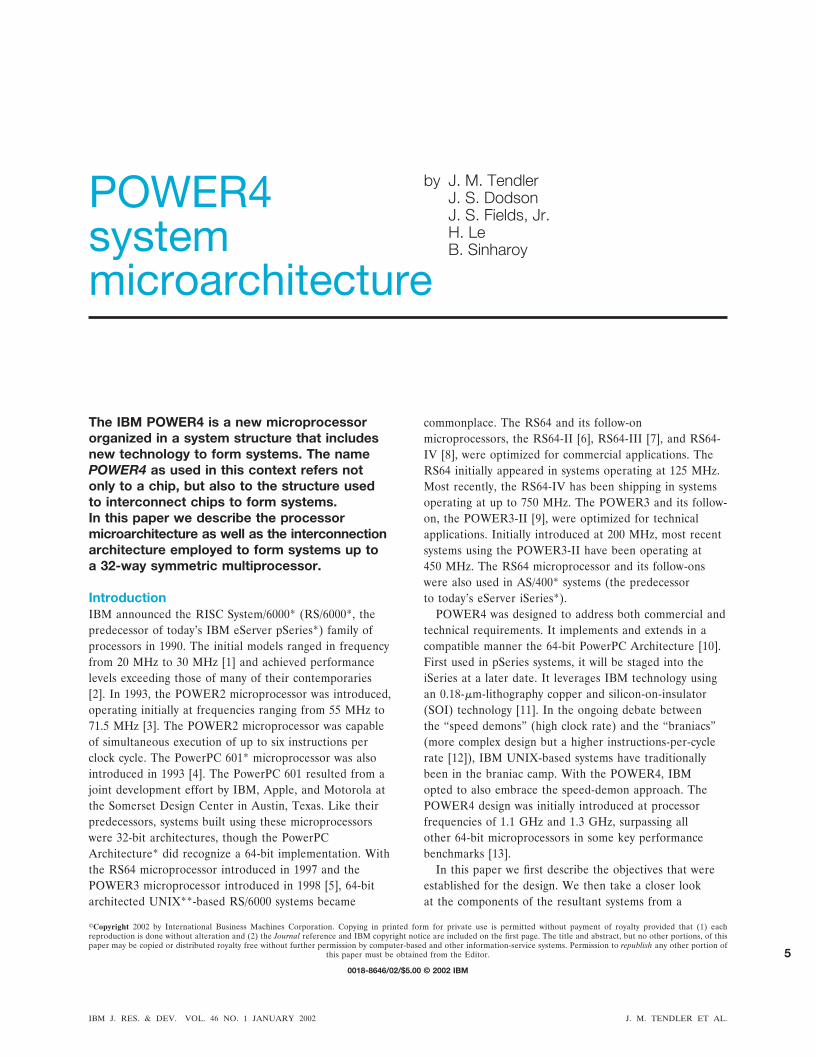
Instruction execution pipelineFigure 4 shows the POWER4 instruction executionpipeline for the various pipelines. The IF, IC, and BPcycles correspond to the instruction-fetching and branch-prediction cycles. The D0 through GD cycles are thecycles during which instruction decode and groupformation occur. The MP cycle is the mapper cycle,in which all dependencies are determined, resourcesassigned, and the group dispatched into the appropriateissue queues. During the ISS cycle, the IOP is issued tothe appropriate execution unit, reads the appropriate
Figure 4
POWER4 instruction execution pipeline.
EA DC WB
MP ISS RF EX WB
MP ISS RF
MP ISS RF
F6
MP ISS RF
CP
LD/ST
FX
FP
WB
Fmt
D0
ICIF BP
EXD1 D2 D3 Xfer
Xfer
Xfer
GD
Branch redirects
Instruction fetch
Xfer
Xfer
BR
WB
Out-of-order processing
Instruction crack andgroup formation
Interrupts and flushes
IBM J. RES. & DEV. VOL. 46 NO. 1 JANUARY 2002 J. M. TENDLER ET AL.
13

register to retrieve its sources during the RF cycle, andexecutes during the EX cycle, writing its result back to theappropriate register during the WB cycle. At this point,the instruction has finished execution but has not yet beencompleted. It cannot complete for at least two morecycles, the Xfer and CP cycle, assuming that all oldergroups have completed and all other instructions in thesame group have also finished.
Instructions waiting in the instruction queue after beingfetched from the instruction cache wait prior to the D1cycle. This is the case if instructions are fetched (up toeight per cycle) faster than they can be formed intogroups. Similarly, instructions can wait prior to the MPcycle if resources are not available to dispatch the entiregroup into the issue queues. Instructions wait in the issuequeues prior to the ISS cycle. Similarly, they can wait tocomplete prior to the CP cycle.
Though not shown, the CR logical execution unit (theunit responsible for executing logical operations on thecondition register) is identical to the fixed-point executionpipeline, shown as the FX pipeline in the figure. Thebranch-execution-unit pipeline is shown as the BRpipeline. If a branch instruction is mispredicted withrespect to either direction or target, there is at least a12-cycle branch-mispredict penalty, depending on howlong the mispredicted branch had to wait to be issued.
The pipeline for the two load/store units is identicaland is shown as the LD/ST pipeline in Figure 4. Afteraccessing the register file, load and store instructionsgenerate the effective address in the EA cycle. TheDERAT and, for load instructions, the data cachedirectory and the data cache, are all accessed during theDC cycle. If a DERAT miss should occur, the instructionis rejected; i.e., it is kept in the issue queue. Meanwhile, arequest is made to the TLB to reload the DERAT withthe translation information. The rejected instructionis reissued again a minimum of seven cycles after itwas first issued. If the DERAT still does not contain thetranslation information, the instruction is rejected again.This process continues until the DERAT is reloaded.If a TLB miss occurs (i.e., we do not have translationinformation in the TLB), the translation is initiatedspeculatively. However, the TLB is not updated until weare certain that the instruction failing translation will beexecuted. To ensure that this occurs, the TLB updates areheld off until the group that contains the instructionfailing translation is the next group to complete. Twodifferent page sizes, 4 KB and 16 MB, are supported.This provides a performance benefit for applicationsrequiring large memory, as is the case in many technicalapplications and database applications that managean in-memory pool for indexes or caching data.
In the case of loads, if the directory indicates that theL1 data cache contains the cache line, the requested bytesfrom the returned data are formatted (the fmt cycle) andwritten into the appropriate register. They are alsoavailable for use by dependent instructions during thiscycle. In anticipation of a data cache hit, dependentinstructions are issued so that their RF cycle lines up withthe writeback cycle of the load instructions. If a cachemiss is indicated, a request is initiated to the L2 toretrieve the line. Requests to the L2 are stored in theload miss queue (LMQ). The LMQ can hold up to eightrequests to the L2. If the LMQ is full, the load instructionmissing in the data cache is rejected and reissued againin seven cycles, and the process is repeated. If there isalready a request to the L2 for the same line from anotherload instruction, the second request is merged into thesame LMQ entry. If this is the third request to the sameline, the load instruction is rejected, and processingcontinues as above. All reloads from the L2 check theLMQ to see whether there is an outstanding request yetto be honored against a just-returned line. If there is, therequested bytes are forwarded to the register to completethe execution of the load instruction. After the line hasbeen reloaded, the LMQ entry is freed for reuse.
In the case of store instructions, rather than writedata to the data cache, the data is stored in the SDQ asdescribed above. Once the group containing the storeinstruction is completed, an attempt is made to write thedata into the data cache. If the cache line containing thedata is already in the L1 data cache, the changed datais written to the data cache. If it is not, the line is notreloaded from the L2. In both cases, the changed data iswritten to the L2. The coherency point for POWER4 isthe L2 cache. Additionally, all data in the L1 data cacheare also in the L2 cache. If data has to be cast out of theL2, the line is marked invalid in the L1 data cache if it isresident there.
The pipeline for the two fixed-point execution unitsis shown as the FX pipe in Figure 4. Two fixed-pointinstructions, with one dependent on the other, cannotissue on successive cycles. There must be at least onedead cycle between their issue cycles. However,another instruction may issue in this cycle.
The pipeline for the two floating-point execution unitsis shown as the FP pipe in the figure. Floating-pointinstructions require six execution cycles. However, bothpipelines are fully piped; that is, two instructions can beissued to the floating-point pipes each cycle. A floating-point instruction dependent on a prior floating-pointinstruction cannot issue within six cycles of the instructionon which it is dependent. However, as is the case with theother execution units, other floating-point instructions mayissue during this period.
J. M. TENDLER ET AL. IBM J. RES. & DEV. VOL. 46 NO. 1 JANUARY 2002
14
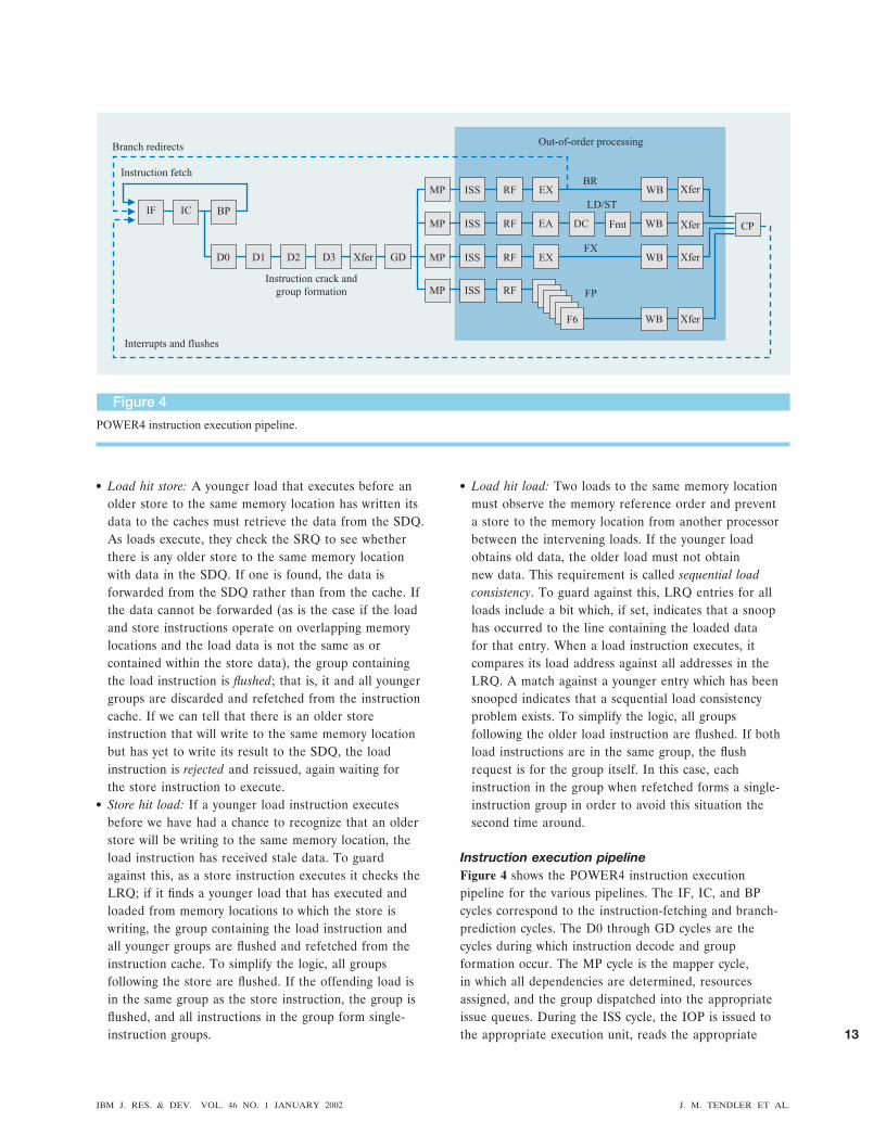
Storage hierarchyThe POWER4 storage hierarchy consists of three levels ofcache and the memory subsystem. The first and secondlevels of the hierarchy are actually on the POWER4 chip.The directory for the third-level cache, the L3, is on thechip, but the actual cache is off-chip. Table 3 showscapacities and organization of the various levels of thehierarchy on a per-chip basis.
L1 cachesThe L1 instruction cache is single-ported, capable ofeither one 32-byte read or one 32-byte write each cycle.The store through L1 data cache is triple-ported, capableof two 8-byte reads and one 8-byte write per cycle with noblocking. L1 data-cache reloads are 32 bytes per cycle.The L1 caches are parity-protected. A parity errordetected in the L1 instruction cache forces the line to beinvalidated and reloaded from the L2. Errors encounteredin the L1 data cache are reported as a synchronousmachine-check interrupt. To support error recovery, themachine-check interrupt handler is implemented in system-specific firmware code. When the interrupt occurs, thefirmware saves the processor-architected states andexamines the processor registers to determine the recoveryand error status. If the interrupt is recoverable, the systemfirmware removes the error by invalidating the L1 data-cache line and incrementing an error counter. If the L1data-cache error counter is greater than a predefinedthreshold, which is an indication of a solid error, the systemfirmware disables the failing portion of the L1 datacache. The system firmware then restores the processor-architected states and “calls back” the operating systemmachine-check handler with the “fully recovered” status.The operating system checks the return status fromfirmware and resume execution. With the L1 data-cacheline invalidated, data is now reloaded from the L2. Alldata stored in the L1 data cache is available in the L2cache, guaranteeing no data loss.
Data in the L1 cache can be in one of two states: I (theinvalid state, in which the data is invalid) or V (the validstate, in which the data is valid).
L2 cacheThe unified second-level cache is shared across the twoprocessors on the POWER4 chip. Figure 5 shows a logicalview of the L2 cache. The L2 is implemented as threeidentical slices, each with its own controller. Cache linesare hashed across the three controllers.
Figure 5
L2 logical view.
Fabric controller
L2 cache array and directory(~0.5 MB)
Snoop Snoop
Rdrequest
L3request
Fabricrequest
Coherencyprocessor 4
Coherencyprocessor 3
Coherencyprocessor 2
Coherencyprocessor 1
Snoopqueue
Castoutqueue
NC unit NC unit
L2 controller C
L2 controller B
L2 controller A
CIU
Core 1 request Core 2 request
Core 1storequeue
Core 2storequeue
Coherency processor arbiter
Table 3 Storage hierarchy organization and size.
Component Organization Capacity per chip
L1 instruction cache Direct map, 128-byte linemanaged as four 32-byte sectors
128 KB (64 KB per processor)
L1 data cache Two-way, 128-byte line 64 KB (32 KB per processor)
L2 Eight-way, 128-byte line �1.5 MB
L3 Eight-way, 512-byte linemanaged as four 128-bytesectors
32 MB
Memory — 0 –16 GB
IBM J. RES. & DEV. VOL. 46 NO. 1 JANUARY 2002 J. M. TENDLER ET AL.
15

Each slice contains four SRAM partitions, each capableof supplying 16 bytes of data every other cycle. The fourpartitions can supply 32 bytes per cycle, taking fourconsecutive cycles to transfer a 128-byte line to theprocessor. The data arrays are ECC-protected (single-error correct, double-error detect). Both wordline andbitline redundancy are implemented.
The L2 cache directory is implemented in tworedundant eight-way set-associative parity-protectedarrays. The redundancy, in addition to providing a backupcapability, also provides two nonblocking read ports topermit snoops to proceed without causing interference toload and store requests.
A pseudo-LRU replacement algorithm is implementedas a standard 7-bit tree structure.
Since the L1 is a store-through design, store requeststo the L2 are at most eight bytes per request. The L2implements two four-entry 64-byte queues for gatheringindividual stores and minimizing L2 requests for stores.
The majority of control for L2 cache management ishandled by four coherency processors in each controller.A separate coherency processor is assigned to handle eachrequest to the L2. Requests can come from either of thetwo processors (for either an L1 data-cache reload or aninstruction fetch) or from one of the store queues. Eachcoherency processor has associated with it a cast-outprocessor to handle deallocation of cache lines toaccommodate L2 reloads on L2 misses. The coherencyprocessor does the following:
● Controls the return of data from the L2 (hit) or fromthe fabric controller (miss) to the requesting processorvia the CIU.
● Updates the L2 directory as needed.● Issues fabric commands for L2 misses on fetch requests
and for stores that do not hit in the L2 in the M, Me,or Mu state (described below).
● Controls writing into the L2 when reloading because offetch misses in the L2 or when accepting stores from theprocessors.
● Initiates back-invalidates to a processor via the CIUresulting from a store from one processor that hits acache line marked as resident in the other processor’sL1 data cache.
Included in each L2 controller are four snoopprocessors responsible for managing coherency operationssnooped from the fabric. When a fabric operation hits ona valid L2 directory entry, a snoop processor is assignedto take the appropriate action. Depending on the type ofoperation, the inclusivity bits in the L2 directory, and thecoherency state of the cache line, one or more of thefollowing actions may result:
● Sending a back-invalidate request to the processor(s)to invalidate a cache line in its L1 data cache.
● Reading the data from the L2 cache.● Updating the directory state of the cache line.● Issuing a push operation to the fabric to write modified
data back to memory.● Sourcing data to another L2 from this L2.
In addition to dispatching a snoop processor, the L2provides a snoop response to the fabric for all snoopedoperations. When a fabric operation is snooped by theL2, the directory is accessed to determine whether thetargeted cache line is resident in the L2 cache and, if so,its coherency state. Coincident with the snoop directorylookup, the snooped address is compared with theaddresses of any currently active coherency, cast-out, andsnoop processors to detect address-collision scenarios. Theaddress is also compared to the per-processor reservationaddress registers. On the basis of this information, thesnoop response logic determines the appropriate snoopresponse to send back.
The L2 cache controller also acts as the reservationstation for the two processors on the chip in support ofthe load [double] word and reserve indexed (lwarx/ldarx)and the store [double] word conditional (stwcx/stdcx)instructions. One address register for each processor isused to hold the reservation address. The reservation logicmaintains a reservation flag per processor to indicatewhen a reservation is set. The flag is set when a lwarx orldarx instruction is received from the processor; it is resetwhen certain invalidating type operations are snooped,including a store to the reservation address from otherprocessors in the system, or when a stwcx or stdcxinstruction succeeds. (A successful store occurs if thereservation flag was not reset by another operation. Thesuccess or failure of the conditional store instruction iscommunicated to the program by setting a bit in thecondition register.)
The L2 cache implements an enhanced version of theMESI coherency protocol, supporting seven states asfollows:
● I (invalid state): The data is invalid. This is the initialstate of the L2 entered from a power-on reset or asnoop invalidate hit.
● SL (shared state, can be source to local requesters): Thedata is valid. The cache line may also be valid in otherL2 caches. From this state, the data can be sourced toanother L2 on the same module via intervention. Thisstate is entered as a result of a processor L1 data-cacheload request or instruction-fetch request that misses inthe L2 and is sourced from another cache or frommemory when not in other L2s.
J. M. TENDLER ET AL. IBM J. RES. & DEV. VOL. 46 NO. 1 JANUARY 2002
16
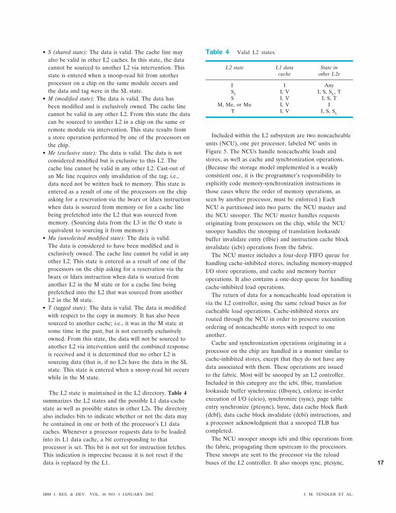
● S (shared state): The data is valid. The cache line mayalso be valid in other L2 caches. In this state, the datacannot be sourced to another L2 via intervention. Thisstate is entered when a snoop-read hit from anotherprocessor on a chip on the same module occurs andthe data and tag were in the SL state.
● M (modified state): The data is valid. The data hasbeen modified and is exclusively owned. The cache linecannot be valid in any other L2. From this state the datacan be sourced to another L2 in a chip on the same orremote module via intervention. This state results froma store operation performed by one of the processors onthe chip.
● Me (exclusive state): The data is valid. The data is notconsidered modified but is exclusive to this L2. Thecache line cannot be valid in any other L2. Cast-out ofan Me line requires only invalidation of the tag; i.e.,data need not be written back to memory. This state isentered as a result of one of the processors on the chipasking for a reservation via the lwarx or ldarx instructionwhen data is sourced from memory or for a cache linebeing prefetched into the L2 that was sourced frommemory. (Sourcing data from the L3 in the O state isequivalent to sourcing it from memory.)
● Mu (unsolicited modified state): The data is valid.The data is considered to have been modified and isexclusively owned. The cache line cannot be valid in anyother L2. This state is entered as a result of one of theprocessors on the chip asking for a reservation via thelwarx or ldarx instruction when data is sourced fromanother L2 in the M state or for a cache line beingprefetched into the L2 that was sourced from anotherL2 in the M state.
● T (tagged state): The data is valid. The data is modifiedwith respect to the copy in memory. It has also beensourced to another cache; i.e., it was in the M state atsome time in the past, but is not currently exclusivelyowned. From this state, the data will not be sourced toanother L2 via intervention until the combined responseis received and it is determined that no other L2 issourcing data (that is, if no L2s have the data in the SLstate. This state is entered when a snoop-read hit occurswhile in the M state.
The L2 state is maintained in the L2 directory. Table 4summarizes the L2 states and the possible L1 data-cachestate as well as possible states in other L2s. The directoryalso includes bits to indicate whether or not the data maybe contained in one or both of the processor’s L1 datacaches. Whenever a processor requests data to be loadedinto its L1 data cache, a bit corresponding to thatprocessor is set. This bit is not set for instruction fetches.This indication is imprecise because it is not reset if thedata is replaced by the L1.
Included within the L2 subsystem are two noncacheableunits (NCU), one per processor, labeled NC units inFigure 5. The NCUs handle noncacheable loads andstores, as well as cache and synchronization operations.(Because the storage model implemented is a weaklyconsistent one, it is the programmer’s responsibility toexplicitly code memory-synchronization instructions inthose cases where the order of memory operations, asseen by another processor, must be enforced.) EachNCU is partitioned into two parts: the NCU master andthe NCU snooper. The NCU master handles requestsoriginating from processors on the chip, while the NCUsnooper handles the snooping of translation lookasidebuffer invalidate entry (tlbie) and instruction cache blockinvalidate (icbi) operations from the fabric.
The NCU master includes a four-deep FIFO queue forhandling cache-inhibited stores, including memory-mappedI/O store operations, and cache and memory barrieroperations. It also contains a one-deep queue for handlingcache-inhibited load operations.
The return of data for a noncacheable load operation isvia the L2 controller, using the same reload buses as forcacheable load operations. Cache-inhibited stores arerouted through the NCU in order to preserve executionordering of noncacheable stores with respect to oneanother.
Cache and synchronization operations originating in aprocessor on the chip are handled in a manner similar tocache-inhibited stores, except that they do not have anydata associated with them. These operations are issuedto the fabric. Most will be snooped by an L2 controller.Included in this category are the icbi, tlbie, translationlookaside buffer synchronize (tlbsync), enforce in-orderexecution of I/O (eieio), synchronize (sync), page tableentry synchronize (ptesync), lsync, data cache block flush(dcbf), data cache block invalidate (dcbi) instructions, anda processor acknowledgment that a snooped TLB hascompleted.
The NCU snooper snoops icbi and tlbie operations fromthe fabric, propagating them upstream to the processors.These snoops are sent to the processor via the reloadbuses of the L2 controller. It also snoops sync, ptesync,
Table 4 Valid L2 states.
L2 state L1 datacache
State inother L2s
I I AnySL I, V I, S, SL, TS I, V I, S, T
M, Me, or Mu I, V IT I, V I, S, SL
IBM J. RES. & DEV. VOL. 46 NO. 1 JANUARY 2002 J. M. TENDLER ET AL.
17

lsync, and eieio. These are snooped because they mayhave to be retried because of an icbi or TLB that has notyet completed to the same processor.
L3 cacheFigure 6 shows a logical view of the L3 cache. The L3consists of two components, the L3 controller and the L3data array. The L3 controller is located on the POWER4chip and contains the tag directory as well as the queuesand arbitration logic to support the L3 and the memorybehind it. The data array is stored in two 16MB eDRAMchips mounted on a separate module. A separate memorycontroller can be attached to the back side of the L3module.
To facilitate physical design and minimize bankconflicts, the embedded DRAM on the L3 chip isorganized as eight banks at 2 MB per bank, with banks
grouped in pairs to divide the chip into four 4MBquadrants. The L3 controller is also organized inquadrants. Each quadrant contains two coherencyprocessors to service requests from the fabric, performany L3 cache and/or memory accesses, and update the L3tag directory. Additionally, each quadrant contains twoprocessors to perform the memory cast-outs, invalidatefunctions, and DMA writes for I/O operations. Each pairof quadrants shares one of the two L3 tag directory SRAMs.
The L3 cache is eight-way set-associative, organized in512-byte blocks, with coherence maintained on 128-bytesectors for compatibility with the L2 cache. Five coherencystates are supported for each of the 128-byte sectors, asfollows:
● I (invalid state): The data is invalid.● S (shared state): The data is valid. In this state, the L3
can source data only to L2s for which it is caching data.● T (tagged state): The data is valid. The data is modified
relative to the copy stored in memory. The data may beshared in other L2 or L3 caches.
● Trem (remote tagged state): This is the same as the Tstate, but the data was sourced from memory attachedto another chip.
● O (prefetch data state): The data in the L3 is identical tothe data in memory. The data was sourced from memoryattached to this L3. The status of the data in other L2or L3 caches is unknown.
Each L3 coherency processor supports one randomcache or memory access. For sequential accesses, the L3coherency processors can support up to four concurrentload/store requests within a 512-byte L3 cache block. Thisallows the L3 to support increased cache and memorythroughput for many common technical workloads to takeadvantage of the bandwidth capability available with thehigh-speed buses in POWER4 systems.
The L3 is designed to be used as a standalone 32MBL3 cache, or to be combined with other L3s on the sameprocessor module in pairs or groups of four to create alarger, address-interleaved L3 cache of 64 MB or 128 MB.Combining L3s into groups not only increases the L3cache size, but also scales the available L3 bandwidth.When combined into groups, L3s and the memory behindthem are interleaved on 512-byte granularity. The fabricbus controller selects the quadrant of the L3 to which aparticular real address is mapped, and the selected L3controller adjusts the mapping from real address to L3index and tag to account for the increase in the effectivecache size. Table 5 shows the mapping of real address bitsto L3 index and tag, as well as the algorithm for routingan address to the corresponding L3 controller andquadrant. The custom address flow logic is optimized forthe 128MB combined case. To handle the index/tag
Figure 6
L3 logical view.
Memory
16MBL3 cache(eDRAM)
16MBL3 cache(eDRAM)
L3 directory
Coherencyprocessor
L3 resource manager
Fabric controller
Eightsnoop/castoutqueues
Coherencyprocessor
Coherencyprocessor
Coherencyprocessor
Coherencyprocessor
Coherencyprocessor
Coherencyprocessor
Coherencyprocessor
Table 5 Mapping of real address bits to access L3depending on L3 size.
Logical L3size
L3 index L3 tag L3 chipselect
L3 quadrantselect
32 MB 51:52, 42:50 22:41 — 53:5464 MB 51, 41:50 22:40 54 52:53
128 MB 40:50 22:39 53:54 51:52
J. M. TENDLER ET AL. IBM J. RES. & DEV. VOL. 46 NO. 1 JANUARY 2002
18

adjustment for the smaller L3 cache sizes, the appropriatebits are swapped as the L3 controller receives an addressfrom the fabric bus controller. This approach causes theindex bits to appear in a nonintuitive order, but avoidsthe need for the custom address flow logic to shift all ofthe address bits to make this adjustment. All address-bitranges in Table 5 assume that the full 42-bit address isdenoted as bits 22:63. Bits 55:56 are the sector ID bits,and bits 57:63 are the offset within the 128-byte coherencegranule.
The L3 caches data, either from memory that residesbeneath it or from elsewhere in the system, on behalf ofthe processors attached to its processor module. Whenone of its processors issues a load request that misses theL3 cache, the L3 controller allocates a copy of the data inthe S (shared) state. Inclusivity with the L1 and L2 is notenforced. Hence, when the L3 deallocates data, it doesnot invalidate any L1 or L2 copies. The L3 enters the T orTrem state when one of its local L2 caches does a castoutfrom the M or T state. An address decode is performedat snoop time to determine whether the address maps tomemory behind the L3 or elsewhere in the system, andthis causes the L3 to transition to the T or Trem state asappropriate. This design point was chosen to avoid theneed for a memory address-range decode when the L3performs a cast-out operation. The L3 can use the T/Tremdistinction to determine whether the data can be writtento the attached memory controller, or whether the cast-out operation must be issued as a fabric bus transaction.
When in the T or Trem state, the L3 sources data toany requestor in the system. However, when in the Sstate, the L3 will source data only to its own L2s. Thisminimizes data traffic on the buses between processormodules, since, whenever possible, data is sourced by anL3 cache on the requesting processor module. When inthe O state, the L3 sources data to any requestor usingthe same rules that determine when it is permitted to senddata from its attached memory controller; i.e., no cacheis sourcing data and no snooper retried the request.
The L3 tag directory is ECC-protected to supportsingle-bit error correct and double-bit error detect.Uncorrectable errors result in a system checkstop. If adirectory access results in a correctable error, the access isstalled while the error is corrected. After correction, theoriginal access takes place. When an error is corrected,a recovered attention message is sent to the serviceprocessor for thresholding purposes.
The L3 address, memory address, and control buseshave parity bits for single-bit error detection. The L3 andmemory data buses, as well as the L3-cache-embeddedDRAMs, have ECC to support single-bit error correct anddouble-bit error detect. Uncorrectable errors are flaggedand delivered to the requesting processor with an errorindication, resulting in a machine-check interrupt.
Correctable errors are corrected in-line, and a recoveredattention message is sent to the service processor forthresholding purposes.
The L3 supports cache-line delete. The cache-linedelete function is used to mask stuck faults in the L3-cache-embedded DRAMs. Line-delete control registersallow the service processor to specify L3 index values forwhich a particular member should not be used. When theL3 controller snoops a request that matches a specified L3index, it masks the tag-directory compare for the memberin question. The replacement algorithm also avoids thedeleted member when choosing a victim in the specifiedcongruence class. Cache-line delete can be invoked at IPLtime on the basis of results of power-on diagnostic testing,or it can be enabled dynamically because of a faultdetected at run time.
If an L3 tag directory develops a stuck fault, or L3-cache-embedded DRAMs develop more stuck faults thancan be handled with the line-delete control registers, theL3 cache on the failing processor chip can be reconfiguredand logically removed from the system without removingother L3 caches in the system and without reconfiguringthe memory attached to that L3. Memory accessescontinue to pass through the reconfigured L3 module, butthat L3 controller no longer performs cache operations.
Memory subsystemA logical view of the memory subsystem is shown inFigure 7. Each POWER4 chip can have an optionalmemory controller attached behind the L3 cache. Memorycontrollers are packaged two to a memory card andsupport two of the four processor chips on a module.A module can attach a maximum of two memory cards.Memory controllers can have either one or two portsto memory.
The memory controller is attached to the L3 eDRAMchips, with each chip having two 8-byte buses, one in eachdirection, to the data interface in the memory controller.These buses operate at one-third processor speed usingthe synchronous wave pipeline interface [21] to operateat high frequencies.
Each port to memory has four 4-byte bidirectionalbuses operating at a fixed frequency of 400 MHz connectingload/store buffers in the memory controller to four systemmemory interface (SMI) chips used to read and write datafrom memory. When two memory ports are available, theyeach work on 512-byte boundaries. The memory controllerhas a 64-entry read command queue, a 64-entry writecommand queue, and a 16-entry write cache queue.
The memory is protected by a single-bit error correct,double-bit error detect ECC. Additionally, memoryscrubbing is used in the background to find and correctsoft errors. Each memory extent has an extra DRAM toallow for transparent replacement of one failing DRAM
IBM J. RES. & DEV. VOL. 46 NO. 1 JANUARY 2002 J. M. TENDLER ET AL.
19

per group of four DIMMs using chip-kill technology.Redundant bit steering is also employed.
Hardware data prefetchPOWER4 systems employ hardware to prefetch datatransparently to software into the L1 data cache. Whenload instructions miss sequential cache lines, eitherascending or descending, the prefetch engine initiatesaccesses to the following cache lines before beingreferenced by load instructions. In order to ensure thatthe data will be in the L1 data cache, data is prefetchedinto the L2 from the L3 and into the L3 from memory.Figure 8 shows the sequence of prefetch operations. Eightsuch streams per processor are supported.
Once a sequential reference stream is recognized,whenever a load instruction initiates a request for data ina new cache line, the prefetch engine begins staging thenext sequential line into the L1 data cache from the L2.At the same time, it initiates a request to the L3 to stagea line into the L2. However, since latencies to load the L2from the L3 are longer than the latency to load the L1from the L2, rather than prefetch the second cache line,
the fifth is prefetched, as shown in Figure 8. Priorreferences, or the initial ramp-up on stream initiation, hasalready staged the second through fourth lines from theL2 to the L1 data cache. Similarly, a line is replaced inthe L3 from memory. To minimize processing required toretrieve data from memory into the L3, a 512-byte line isprefetched. This has to be done only every fourth linereferenced. In the case shown in the figure, lines 17through 20 are prefetched from memory to the L3.
Because memory references are based on real addresses,whenever a page boundary is crossed, the prefetching mustbe stopped, since we do not know the real address of thenext page. To reduce the performance impact, POWER4implements two page sizes, 4 KB and 16 MB. In additionto allowing the prefetch to continue for longer streams,it saves translation time. This is especially useful fortechnical applications, where it is common to sequentiallyreference large amounts of data.
To guard against prematurely initiating a data-prefetchstream by the hardware, POWER4 ramps up theprefetches slowly, requiring an additional four sequentialcache misses to occur before all of the cache lines in theentire sequence are in various stages of prefetch to theL1 data cache. However, software can often tell that aprefetch stream should be initiated. Toward this end,the data cache block touch (dcbt) instruction has beenextended, using a previously reserved bit to indicate tothe hardware that a prefetch stream should be installedimmediately without waiting for confirmation.
Special logic to implement data prefetching exists in theprocessor load/store unit (LSU) and in the L2 and L3.The direction to prefetch, up or down, is determined bythe actual load address within the line that causes thecache miss. If the load address is in the lower portion ofthe line, the guessed direction is up. If the load address isin the upper portion of the line, the guessed direction isdown. The prefetch engine initiates a new prefetch whenit detects a reference to the line it guessed will be used.If the initial guess on the direction is not correct, thesubsequent access will not confirm to the prefetch enginethat it had a stream. The incorrectly initiated stream willeventually be deallocated, and the corrected stream will beinstalled as a new stream.
Interconnecting chips to form larger SMPsThe basic building block is a multichip module (MCM)with four POWER4 chips to form an eight-way SMP.Multiple MCMs can be further interconnected to form16-, 24-, and 32-way SMPs.
Four-chip, eight-way SMP moduleFigure 9 shows the logical interconnection of fourPOWER4 chips across four logical buses to form an eight-way SMP. Each chip writes to its own bus, arbitrating
Figure 7
Memory subsystem logical view.
8888
1616
16 16
44444444
Memory controller
Command interface Data interface
Command/address decode
Load and storebuffers
Loadqueues
Storequeues
Port0
Port1
16MBL3 cache(eDRAM)
16MBL3 cache(eDRAM)
200-MHz DDR DIMM quads
SMI chips(4/port)
J. M. TENDLER ET AL. IBM J. RES. & DEV. VOL. 46 NO. 1 JANUARY 2002
20

among the L2, I/O controller, and L3 controller for thebus. Each of the four chips snoops all of the buses, andif it finds a transaction that it must act on, it takes theappropriate action. Requests for data from an L2 aresnooped by all chips to see a) whether it is in their L2 andin a state that permits sourcing it from the holding chip’sL2 to the requesting chip, or b) whether it is in its L3 orin memory behind its L3 cache based on the real addressof the request. If it is, the sourcing chip returns therequested data to the requesting chip on its bus.
The interconnection topology appears like a bus-basedsystem from the perspective of a single chip. From theperspective of the module, it appears like a switch.
Multiple module interconnectFigure 10 shows the interconnection of multiple four-chipMCMs to form larger SMPs. One to four MCMs can beinterconnected. When interconnecting multiple MCMs, theintermodule buses act as repeaters, moving requests andresponses from one module to another module in a ringtopology. As with the single MCM configuration, eachchip always sends requests/commands and data on itsown bus but snoops all buses.
L3 memory configurationsAs noted earlier, each MCM can have from zero to twomemory cards. In the case of two memory cards, there isno requirement that they be of equal size. In the caseof no memory cards or two equal-size memory cardsconnected to an MCM, the four L3s attached to themodule act as a single 128MB L3. In a single MCMsystem, each L3 caches data sourced from the memoryattached behind its L3 cache. In the case of multipleMCMs and data being sourced from memory attached toanother module, an attempt is made to cache the returneddata on the requesting module. The particular L3 chosenis the L3 attached to the chip controlling the bus on which
the data is returned. However, if the L3 is busy servicingrequests, the line is not cached. Also, data is not cachedon the sourcing module if it is being sourced to a chipon another module.
If one memory card or two memory cards of unequalsize are attached to a module, the L3s attached to themodule function as two 64MB L3s. The two L3s thatact in concert are the L3s that would be in front of thememory card. (Note that one memory card is attached totwo chips.) The caching of requests to remote modulesdescribed above functions in this case in a comparablemanner, with the exception that the two L3s acting asa single L3 are considered to logically form a moduleboundary (for caching purposes).
Figure 8
POWER4 hardware data prefetch.
L2
L3Memory
DL1
EU l0 l1l1 l2 l3 l4 l5
l5 l6 l7 l8
l9 l10 l11 l12
l13 l14 l15 l16
l17 l18 l19 l20
l17 l18 l19 l20
Core
Figure 9
POWER4 multichip module with four chips forming an eight-way SMP.
L2
L3
C CC C
L2
L3
GX busGX busGX busGX bus
C C
L2
L3
MemoryMemoryMemory
L2
C C
L3
Memory
To other modules
From other modules
L3 controller/directory
L3 controller/directory
L3 controller/directory
L3 controller/directory
IOCC IOCC IOCCIOCC
IBM J. RES. & DEV. VOL. 46 NO. 1 JANUARY 2002 J. M. TENDLER ET AL.
21

I/O structureFigure 11 shows the I/O structure in POWER4 systems.Attached to a POWER4 GX bus is a remote I/O (RIO)bridge chip. This chip transmits the data across two 1-byte-wide RIO buses to PCI host bridge (PHB) chips. Twoseparate PCI buses attach to PCI–PCI bridge chips thatfurther fan the data out across multiple PCI buses. Whenmultiple nodes are interconnected to form clusters ofsystems, the RIO bridge chip is replaced with a chipthat connects with the switch. This provides increasedbandwidth and reduced latency over switches attachedvia the PCI interface.
System balancePOWER4 systems are designed to deliver balancedperformance. As an example, as additional chips and
MCMs are added to form larger SMP systems, additionalresources are added, as can be seen from Figure 10. Withthe addition of each pair of POWER4 chips, the ability toadd a memory card is provided. In addition to memorycapacity, memory bandwidth is increased. Each additionalPOWER4 chip provides additional L3 resource.
All buses interconnecting POWER4 chips, whether ornot on- or off-module, operate at half processor speed.As future technology is exploited, allowing chip size todecrease and operating frequencies to increase, systembalance is maintained, since bus speeds are no longer fixedbut are geared to processor frequency.
The multi-MCM configuration provides a worst-casememory access latency of slightly greater than 10% morethan the best-case memory access latency maintaining theflat memory model, simplifying programming.
Figure 10
Multiple POWER4 multichip module interconnection.
GX bus GX bus GX bus GX bus GX bus GX bus GX bus GX bus
GX bus GX bus GX bus GX bus GX bus GX bus GX bus GX bus
MemoryMemoryMemory
MemoryMemoryMemory
L3L3 L3
L3L3 L3
Memory
Memory
L3
L3
Memory
Memory
L3
L3
Memory
Memory
L3
L3
Memory
Memory
L3
L3
Memory
Memory
L3
L3
J. M. TENDLER ET AL. IBM J. RES. & DEV. VOL. 46 NO. 1 JANUARY 2002
22

The eight-way MCM is the building block for thesystem. It is only available with four chips, each with itsattached L3. A single processor on a chip has all of theL3 resources attached to the module, and the full L2on the chip itself. If this processor is the only processorexecuting, it exhibits extremely good performance. If onlyone chip of the four on the module is active, the situationis similar, though both processors now share a commonL2. They both have full access to all of the L3s attachedto the module. When analyzing measurements comparingone-way to two-way to four-way to eight-way performance,one must account for the full L3 available in all of theseconfigurations.
Future roadmapEnhancements to the current POWER4 system in thecoming years will take several directions.
We are in the process of leveraging newer technologiesto allow us to increase frequency while further decreasingpower. We will aggressively increase processor frequenciesto the 2� GHz range while maintaining the systembalance offered by our current design.
The current design introduces parallelism throughoutthe system so as to overcome the increasing memorylatencies (in processor cycles) resulting from high-frequency operations. The parallelism allows the processorto continue executing in the presence of cache misses.Future POWER4 systems will continue this design,increasing parallelism and providing larger caches.
We have already invested in ensuring that softwarecan exploit the increased performance levels POWER4systems will be offering. We will continue making system-level enhancements in order to provide even greaterperformance increases over time.
SummaryPOWER4 development has met our objectives in terms ofperformance and schedule as defined at the beginning ofthe project in 1996. Enormous levels of bandwidth andconcurrency contribute to superior performance acrossa broad range of commercial and high-performancecomputing environments. These unprecedented performancelevels are achieved by a total system design that exploitsleading IBM technologies. We are well along in developingfollow-on systems to the current POWER4 to furtherenhance its leadership. POWER4 is redefining what ismeant by a server and how a server must be designed.
AcknowledgmentsAn effort like this requires a large design, development,verification, and test team. This project included engineersand programmers from several IBM research anddevelopment laboratories. The focal point for the projectwas in the IBM Server Group Development Laboratory in
Austin, Texas, with major contributions from ServerGroup development laboratories in Poughkeepsie, NewYork, and Rochester, Minnesota, as well as IBM researchlaboratories in Yorktown Heights, New York, and Austin,Texas. It is impossible to single out specific contributors,as the list would be too lengthy. Suffice it to say that asauthors we represent a large, proud team that havedocumented the contributions of many individuals.
*Trademark or registered trademark of International BusinessMachines Corporation.
**Trademark or registered trademark of The Open Group.
References1. H. B. Bakoglu, G. F. Grohoski, and R. K. Montoye, “The
IBM RISC System/6000 Processor Hardware Overview,”IBM J. Res. & Dev. 34, No. 1, 12–22 (January 1990).
2. John Cocke and V. Markstein, “The Evolution of RISCTechnology at IBM,” IBM J. Res. & Dev. 34, No. 1, 4 –11(January 1990).
3. S. W. White and S. Dhawan, “POWER2: Next Generationof the RISC System/6000 Family,” IBM J. Res. & Dev. 38,No. 5, 493–502 (September 1994).
4. M. T. Vaden, L. J. Merkel, C. R. Moore, T. M. Potter,and R. J. Reese, “Design Considerations for the PowerPC601 Microprocessor,” IBM J. Res. & Dev. 38, No. 5,605– 620 (September 1994).
5. Mark Papermaster, Robert Dinkjan, Michael Mayfield,Peter Lenk, Bill Ciarfella, Frank O’Connell, and RaymondDuPont, “POWER3: Next Generation 64-bit PowerPCProcessor Design,” IBM White Paper, October 1998,available on the World Wide Web at http://www-1.ibm.com/servers/eserver/pseries/hardware/whitepapers/power3wp.pdf.
6. John Borkenhagen and Salvatore Storino, “4th Generation64-bit PowerPC-Compatible Commercial Processor
Figure 11
I/O logical view.
C CL2
IOCC
L3 controller/directory
L3
Memory
POWER4
GX bus4 B @ 3:1
Remote I/O(RIO)
bridge chip
PCIhost bridge(PHB) chip
RemoteI/O bus1 B @
500 MHz
PCI 32 b/64 b@ 33/66 MHz
PCI–PCIbridge chip
PCI–PCIbridge chip
PCI PCI
IBM J. RES. & DEV. VOL. 46 NO. 1 JANUARY 2002 J. M. TENDLER ET AL.
23

Design,” IBM White Paper, January 1999, available athttp://www-1.ibm.com/servers/eserver/pseries/hardware/whitepapers/nstar.pdf.
7. John Borkenhagen and Salvatore Storino, “5th Generation64-bit PowerPC-Compatible Commercial ProcessorDesign,” IBM White Paper, September 1999, available athttp://www-1.ibm.com/servers/eserver/pseries/hardware/whitepapers/pulsar.pdf.
8. J. M. Borkenhagen, R. J. Eickemeyer, R. N. Kalla, andS. R. Kunkel, “A Multithreaded PowerPC Processor forCommercial Servers,” IBM J. Res. & Dev. 44, No. 6,885– 898 (November 2000).
9. F. P. O’Connell and S. W. White, “POWER3: The NextGeneration of PowerPC Processors,” IBM J. Res. & Dev.44, No. 6, 873– 884 (November 2000).
10. C. May (Ed.), E. M. Silha, R. Simpson, and H. S. Warren,Jr. (Ed.), The PowerPC Architecture: A Specification fora New Family of RISC Processors, Morgan KaufmannPublishers, Inc., San Francisco, 1994.
11. E. Leobandung, E. Barth, M. Sherony, S.-H. Lo, R.Schulz, W. Chu, M. Khare, D. Sadana, D. Schepis, R.Bolam, J. Sleight, F. White, F. Assaderaghi, D. Moy,G. Biery, R. Goldblatt, T.-C. Chen, B. Davari, and G.Shahidi, “High-Performance 0.18 �m SOI CMOSTechnology,” IEDM Tech Digest, pp. 679 – 682 (1999).
12. Linley Gwennap, “Speed Kills,” Microprocessor Report,March 8, 1993, p. 3.
13. See for example the results for the SPECint2000 andSPECfp2000 benchmarks available at www.spec.org.
14. D. C. Bossen, A. Kitamorn, K. F. Reick, and M. S. Floyd,“Fault-Tolerant Design of the IBM pSeries 690 SystemUsing POWER4 Processor Technology,” IBM J. Res. &Dev. 46, No. 1, 77– 86 (2002, this issue).
15. J. D. Warnock, J. M. Keaty, J. Petrovick, J. G. Clabes,C. J. Kircher, B. L. Krauter, P. J. Restle, B. A. Zoric, andC. J. Anderson, “The Circuit and Physical Design of thePOWER4 Microprocessor,” IBM J. Res. & Dev. 46, No. 1,27–51 (2002, this issue).
16. T.-Y. Yeh and Y. N. Patt, “A Comparison of DynamicBranch Predictors that Use Two Levels of BranchHistory,” Proceedings of the 24th Annual ACM/IEEEInternational Symposium on Microarchitecture, 1993, pp.257–266.
17. S. McFarling, “Combining Branch Predictors,” TechnicalReport TN-36, Digital Western Research Laboratory, PaloAlto, CA, June 1993.
18. R. E. Kessler, “The Alpha 21264 Microprocessor,” IEEEMicro 19, No. 2, 24 –36 (March–April 1999).
19. P. Y. Chang, E. Hao, and Y. N. Patt, “Target Predictionfor Indirect Jumps,” Proceedings of the 24th AnnualInternational Symposium on Computer Architecture,Denver, June 1997, pp. 274 –283.
20. C. F. Webb, “Subroutine Call/Return Stack,” IBM Tech.Disclosure Bull. 30, No. 11, 18 –20 (April 1988).
21. Frank Ferraiolo, Edgar Cordero, Daniel Dreps, MichaelFloyd, Kevin Gower, and Bradley McCredie, “POWER4Synchronous Wave-Pipelined Interface,” paper presentedat the Hot Chips 11 Conference, Palo Alto, August 1999.
Received October 29, 2001; accepted for publicationDecember 27, 2001
Joel M. Tendler IBM Server Group, 11400 Burnet Road,Austin, Texas 78758 ([email protected]). Dr. Tendler isProgram Director of Technology Assessment, responsible forassessing emerging technologies for applicability in futureeServer iSeries and pSeries product offerings. He hasextensive hardware and software design experience in S/390and RS/6000 systems. Before assuming his current position, hewas the lead performance analyst on the POWER4 project.Dr. Tendler received a B.E. degree in electrical engineeringfrom the Cooper Union, and a Ph.D. degree in electricalengineering from Syracuse University. He has seven U.S.patents pending and one published; he has received a FirstPlateau IBM Invention Achievement Award.
J. Steve Dodson IBM Server Group, 11400 Burnet Road,Austin, Texas 78758 ([email protected]). Mr. Dodsonreceived his B.S.E.E. degree from the University of Kentuckyin 1982 and joined IBM in 1983 in Lexington, Kentucky.While in Lexington, he worked in VLSI componentengineering, performing characterization and reliability studiesof various vendor SRAMs, EPROMs, and microcontrollers.He moved to Austin in 1987 as a logic designer on the firstPOWER microprocessors. After serving as the design lead fortwo I/O host bridge chip development efforts, he moved onto develop two generations of level-2 cache controller chipswhich were used in the RS/6000 Model F50 server and relatedproducts. He then joined the POWER4 team as team lead forthe level-2 cache controller unit, and is currently involved inthe development effort of a future POWER microprocessor astechnical lead for the memory subsystem design. Mr. Dodsonwas appointed to the position of Senior Technical StaffMember in 2000. He has coauthored numerous patentapplications in the areas of SMP cache coherency, cachehierarchy, and system bus protocols.
J. S. Fields, Jr. (Steve) IBM Server Group, 11400 BurnetRoad, Austin, Texas 78758 ([email protected]). Mr. Fieldsreceived a B.S.E.E. degree from the University of Illinois. Hehas designed I/O, memory, and cache subsystems for serversfor 13 years. He was the lead designer on the POWER4 L3cache, and led the hardware bringup and validation efforts forthe POWER4 storage subsystem. Mr. Fields holds nine U.S.patents, with another 69 patents pending.
Hung Le IBM Server Group, 11400 Burnet Road, Austin,Texas 78758 ([email protected]). Mr. Le is a Senior TechnicalStaff Member in the POWER4 Development team in Austin,Texas. He joined IBM in 1979 after receiving a B.S. degree inelectrical and computer engineering from Clarkson University.He has worked in the development of several ES/9000mainframe CPUs as well as the POWER3 and POWER4microprocessors. His technical interest is in superscalarand multithreading design. Mr. Le has received an IBMOutstanding Innovation Award and holds 31 issued patents.
Balaram Sinharoy IBM Server Group, 522 South Road,Poughkeepsie, New York 12601 ([email protected]).Dr. Sinharoy is a Senior Engineer in the IBM advancedmicroprocessor design group, where he is currently thechief scientist and technical lead for a future POWERmicroprocessor. He designed the branch-prediction unit inPOWER4 and led several architectural, design, performance,and verification aspects of the POWER4 design. Before
J. M. TENDLER ET AL. IBM J. RES. & DEV. VOL. 46 NO. 1 JANUARY 2002
24

joining the POWER4 microprocessor development group in1996, Dr. Sinharoy worked in the IBM VLIW compiler andarchitecture research group on hardware multithreading.He joined IBM in 1992 after receiving his Ph.D. degree incomputer science from Rensselaer Polytechnic Institute.He received the 1992 Robert McNaughton Award as arecognition of his research contributions. His research anddevelopment interests include advanced microprocessordesign, computer architecture and performance analysis,instruction-level parallel processing, and compileroptimization. Dr. Sinharoy has published numerous articlesand received patents in these areas. He has received a SixthPlateau IBM Invention Achievement Award and a ThirdPlateau IBM Publication Achievement Award. Dr. Sinharoyis a Senior Member of IEEE and a member of ACM.
IBM J. RES. & DEV. VOL. 46 NO. 1 JANUARY 2002 J. M. TENDLER ET AL.
25


