Embed Size (px)
Citation preview


Printing Flexible Electronics for health care Applications
Pit Teunissen
Eric Rubingh
Ruben Lelieveld
Marc Koetse
Juliane Gabel
Pim Groen
SVC TechCon, Providence
April 23, 2013

Presentationoverview
SVC TechCon Providence, April 23, 2013
1. Introduction Holst Centre
2. Introduction smart blister
3. Device architecture
4. Way of working
5. Results
6. Towards high volume production
7. Conclusions and outlook

© Holst Centre
Holst Centre
An ‘open innovation’ research institute for
large area flexible electronics and ultralow power wireless sensor technology
Independent, with reputed parents
founded by imec (1300 fte, Belgium)and TNO (4500 fte, The Netherlands)
located in Eindhoven, The Netherlands
established in 2005
Critical mass
own staff 180
25 nationalities
Characteristics
• perform joint research with industrial partners
• Ca. 60 industrial residents
SVC TechCon Providence, April 23, 2013
4

© Holst Centre
SVC TechCon Providence, April 23, 2013
Open Innovation Hot-Spot
High Tech CampusEindhoven, The Netherlands
Holst CentreR2R lab
Holst Centre Offices
Thin Filmclean room
Device Processing Facilities
Mechatronics Test & Assy Lab
ReliabilityTest Centre
Analytical Labs
EMC Test Centre
Electronic TestCentre
InstrumentRental
High-Tech Campus, initiated by Philips
• Site-sharing: ~120 companies, 7000 researchers
• Facility-sharing: MiPlaza (includes >8000m² cleanrooms)
• Program Sharing: Open Innovation research (e.g. Holst Centre)
5
© Holst Centre
SVC TechCon Providence, April 23, 2013
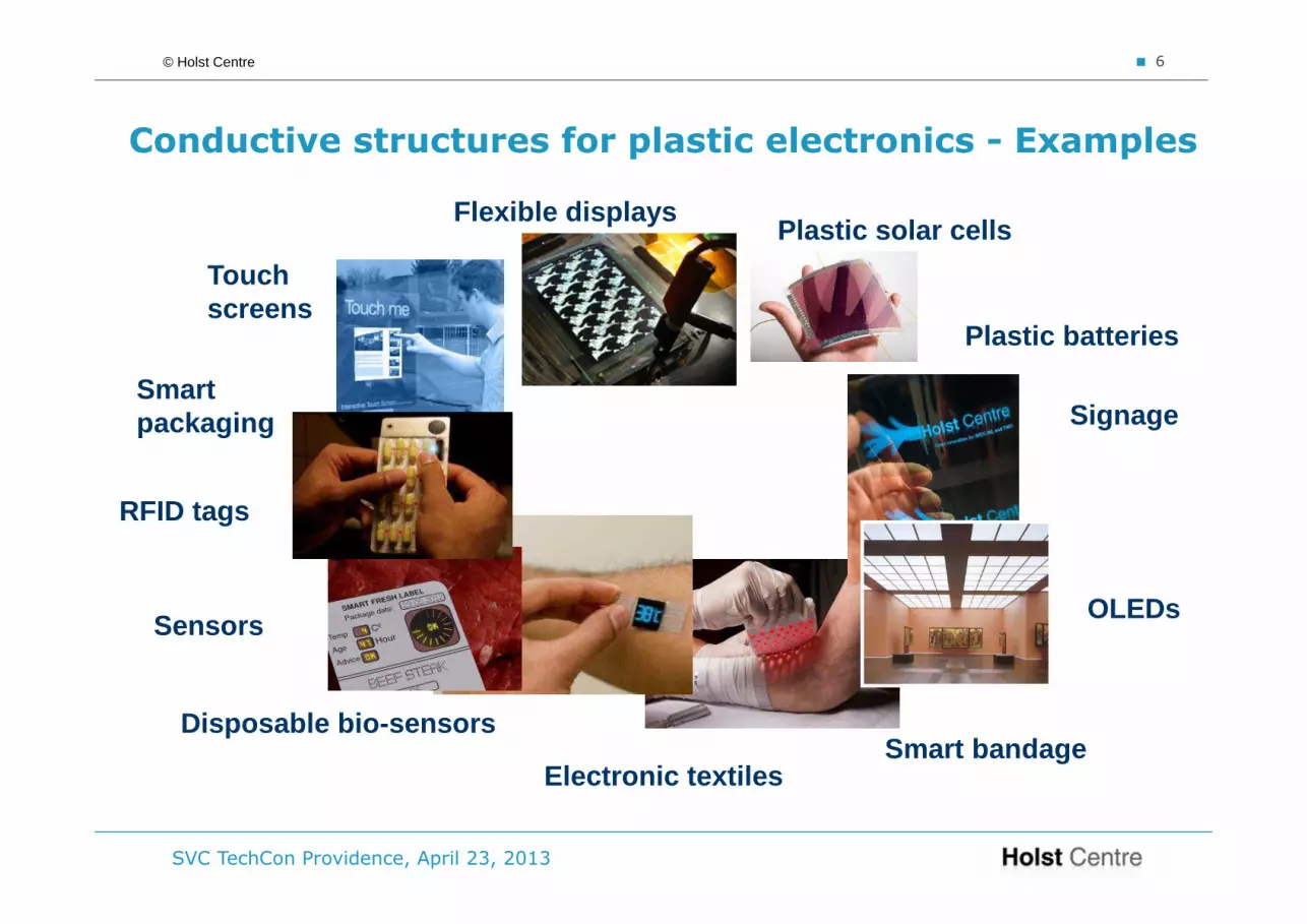
Conductive structures for plastic electronics - Examples
OLEDs
Disposable bio-sensors
Electronic textiles
Plastic solar cells
Smart bandage
Smart packaging
Sensors
RFID tags
Flexible displays
Touch screens
Signage
Plastic batteries
6

© Holst Centre
Large area flexible electronics - manufacturing
One of the key challenges: How to manufacture these products?
Large quantities and large sizes…
• roll-to-roll (R2R) manufacturing preferred
easier to make large quantities at low costs
• to be build on low cost flex foils
not on polyimide-foil: ~ 50 euro/m2
but on PET-foil: ~ 3 euro/m2
Printing preferred over lithographic patterning
• easier for roll-to-roll processing
• fine features without complicated masks
7
SVC TechCon Providence, April 23, 2013

© Holst Centre
SVC TechCon Providence, April 23, 2013
8
• Research objective
Develop R2R compatible printing and sintering technology for functional structures on flexible substrates
• Applications targetted
OLEDs: Anode structure
OPV: Electrodes
Smart blisters/packaging: Circuit
RFID: Antenna structures
• General requirements
High conductivity: ≤ 5 X bulk silver resistivity
Low sintering temperature: ≤ 130ºC, foil compatible
Short sintering time: <(<) 1 min, R2R compatible
Compatible with device stack
Potential for multiple types of materials
Conductive structures for plastic electronics – General goal
Presentationoverview
SVC TechCon Providence, April 23, 2013
1. Introduction Holst Centre
2. Introduction smart blister
3. Device architecture
4. Way of working
5. Results
6. Towards high volume production
7. Conclusions and outlook

© Holst Centre
Smart Blister
• Pharmaceutical package capable of monitoring when a pill is taken out of its packaging
• Data can easily be transferred wireless via NFC
• Main purpose: To ensure that patients in clinical trials take their medicine at the time and frequency recommended to avoid non-compliance issues
SVC TechCon Providence, April 23, 2013
10

© Holst Centre
Smart blister: Partner request
SVC TechCon Providence, April 23, 2013
• Assembled
• “3D”-system
• High cost
• Added to existing package
• Fully integrated
• 2D-System in Foil
• Low cost, mass fabrication
• Roll to Roll compatible
Request from partner: from assembled PCB to low-cost integrated system in foil
11

© Holst Centre
Technological challenges
System engineering
• Simplification, cost reduction
• Optimal chip set
• Design rules
Printing
• Conductivity (Antenna)
• Multi layer (circuitry)
• Overlay precision
Assembly
• Adhesives
• Accuracy
• Reliability and durability
SVC TechCon Providence, April 23, 2013
12
Presentationoverview
SVC TechCon Providence, April 23, 2013
1. Introduction Holst Centre
2. Introduction Smart blister
3. Device architecture
4. Way of Working
5. results
6. Towards high volume production
7. Conclusions and outlook

© Holst Centre
Substrate selection
Substrate:
• Price
PI >50€/m2
PEN <10 €/m2
PET <1 €/m2
SVC TechCon Providence, April 23, 2013
Preferred substrate PET
• Tg PET ~ 100°C
Processing temperature < 130 °C
14

© Holst Centre
Building Blocks
SVC TechCon Providence, April 23, 2013
sensing
logic
radio
antenna
power Thin film battery
Resistance ladder to monitor which pill was taken from package
Integrated chips for measuring and registration
Printed antenna for data transfer
Integrated chips for RFID communication and data storage
15

© Holst Centre
Vacuum process vs. printingStandard Lift-off process
Substrate
Lithography mask
exposure
developing
Deposition(sputtering, ebeamevaporation…)
Lift off
Next
layer
Photo resist
vacuum
Substrate with resist pattern
Resist deposition
Substrate with structure
Standard print process
Substrate
Printing
Curing (UV, photonic, heat…)
Normal pressure
Substrate with structure
Next
layer
ink
SVC TechCon Providence, April 23, 2013
16

© Holst Centre
Printing Conventional Vacuum process
Advantages - Cost efficient / Low cost- Fast- Efficient material use- Easy R2R- Pattern on demand
(inkjet)- Non-stop production
possible- Easy to upscale
- High resolution features- Bulk conductivity
(metals)- Well established process
Disadvantages - Lower resolution- Lower conductivity
- Relatively Slow - Expensive vacuum
equipment- Waiting times for vacuum- Inefficient use of
materials - Upscaling limited
Vacuum process vs. printing
SVC TechCon Providence, April 23, 2013
17
© Holst Centre
Deposition method
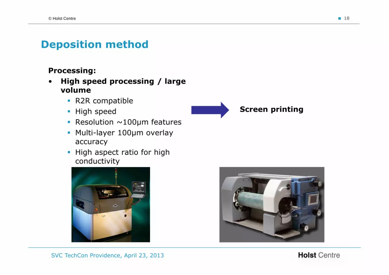
Processing:
• High speed processing / large volume
R2R compatible
High speed
Resolution ~100µm features
Multi-layer 100µm overlay accuracy
High aspect ratio for high conductivity
SVC TechCon Providence, April 23, 2013
Screen printing
18
© Holst Centre
SVC TechCon Providence, April 23, 2013
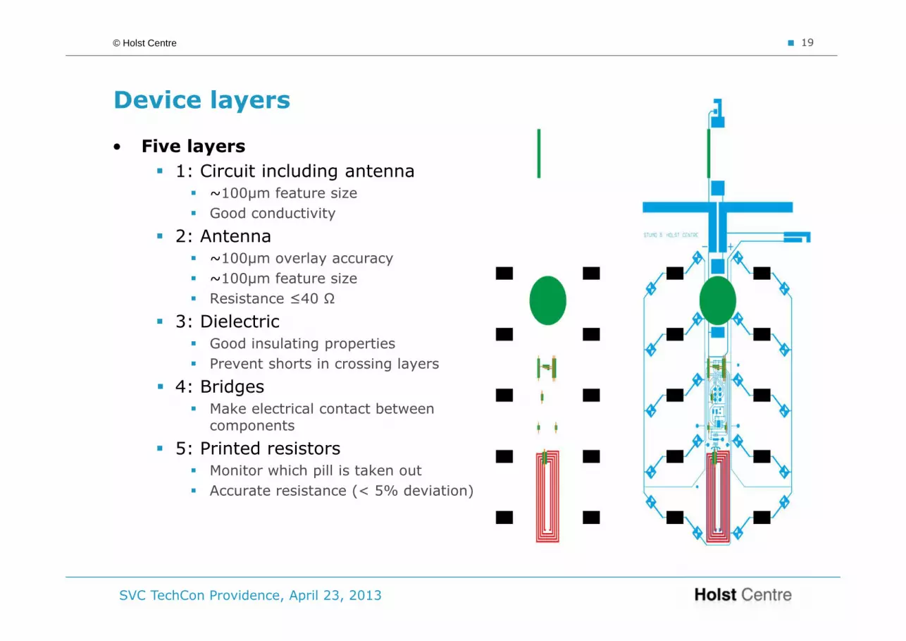
Device layers
• Five layers
1: Circuit including antenna
~100µm feature size
Good conductivity
2: Antenna
~100µm overlay accuracy
~100µm feature size
Resistance ≤40 Ω
3: Dielectric
Good insulating properties
Prevent shorts in crossing layers
4: Bridges
Make electrical contact between components
5: Printed resistors
Monitor which pill is taken out
Accurate resistance (< 5% deviation)
19

© Holst Centre
SVC TechCon Providence, April 23, 2013
Components
Components
• 3 chip solution
MC: micro controller (measure and register)
RTC: real time clock (date, time)
NFC Eeprom: RFID communication and data storage
• Thin components
Components can be integrated in foil
• Assembly
No soldering possible!
Use novel low T cure isotropic conductive adhesives (100 °C cure)
withoutpackage
thinning chipdown to 20-30 µm
chip becomesflexible
20

Presentationoverview
SVC TechCon Providence, April 23, 2013
1. Introduction Holst Centre
2. Introduction smart blister
3. Device architecture
4. Way of working
5. Results
6. Towards high volume production
7. Conclusions and outlook

© Holst Centre
Way of Working – Deposition method
• Screen printing: principle
Ink is applied in a patterned mesh
Mesh is positioned above substrate
Ink is pushed through the mesh and a direct image of the screen is made on the substrate
SVC TechCon Providence, April 23, 2013
smallest feature size (lab)
30 µµµµm
smallest feature size (industrial scale)
80 µµµµm
ink viscosity range 100 – 800,000 mPas
wet layer thickness 12 – 500 µµµµm
dry layer thickness 0.5 – 50 µm
dry layer thickness accuracy
15 – 40 %
alignment/overlay accuracy
100 µµµµm
Processing time < 1 min. / sheet
Woven mesh
22

© Holst Centre
SVC TechCon Providence, April 23, 2013
Way of working – Equipment and materials
• S2S screen printer
DEK Horizon 03i
• Mesh technology
Stainless steel woven mesh
Stork Prints PlanoMesh, electroformed Nickel
• Materials
Silver paste (layer 1, 2 and 4)
1: Circuit, including antenna (DuPont 5025)
2: Antenna (DuPont PV410)
4: Bridges (DuPont 5025)
Isolator (layer 3)
3: Dielectric (DuPont 7165)
Carbon (layer 5)
5: Resistors (DuPont 7082 + DuPont 5036)
Stork Prints PlanoMesh
Dek screen printer
23

© Holst Centre
SVC TechCon Providence, April 23, 2013
Way of working – Sintering
• Sintering
Metal nano,- and micro particle need to be dried and/or sintered to become conductive
Sintering = merging particles via atomic diffusion
Fraction of the bulk melting temperature
Nanoparticle inks are ideal for conductive structures on temperature-sensitive substrates
Sintering can be done thermally, photonically, electrically, using plasma, chemically, etc.
Here we use thermal sintering in an oven at 130°C
Sintered Ag nanoparticles
24

Presentationoverview
SVC TechCon Providence, April 23, 2013
1. Introduction Holst Centre
2. Introduction smart blister
3. Device architecture
4. Way of working
5. Results
6. Towards high volume production
7. Conclusions and outlook

© Holst Centre
Results
SVC TechCon Providence, April 23, 2013
• 1st layer: circuit for electrical contacts
Smallest line width: 100µm
Good Conductivity
Typical line height ~6µm
Profile measurement antenna Screen printed circuit
26
© Holst Centre
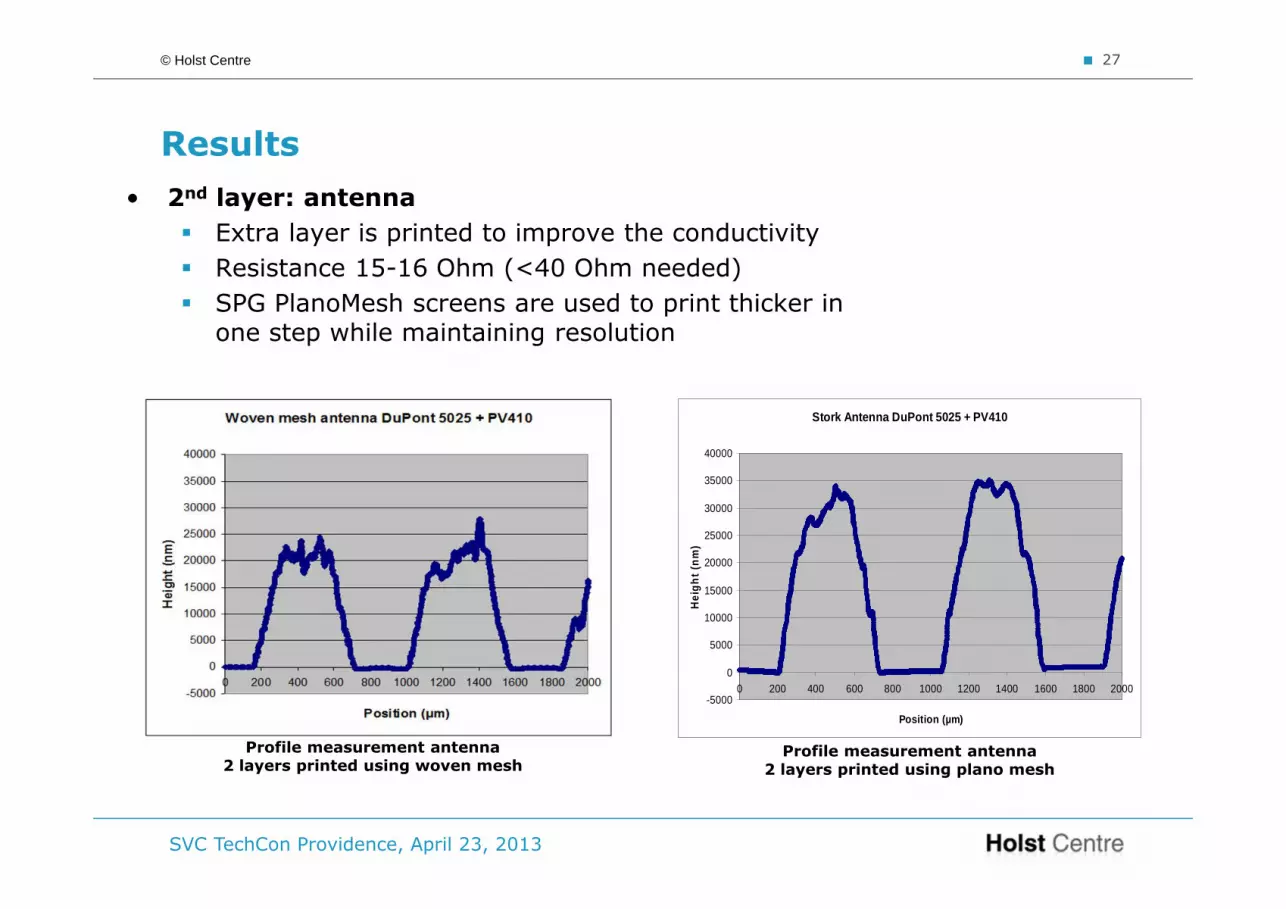
Results
SVC TechCon Providence, April 23, 2013
• 2nd layer: antenna
Extra layer is printed to improve the conductivity
Resistance 15-16 Ohm (<40 Ohm needed)
SPG PlanoMesh screens are used to print thicker in one step while maintaining resolution
Stork Antenna DuPont 5025 + PV410
-5000
0
5000
10000
15000
20000
25000
30000
35000
40000
0 200 400 600 800 1000 1200 1400 1600 1800 2000
Position (µm)
Hei
ght (
nm)
Profile measurement antenna2 layers printed using woven mesh
Profile measurement antenna2 layers printed using plano mesh
27

© Holst Centre
Results
SVC TechCon Providence, April 23, 2013
• 3rd layer: dielectric
Al spikes in Silver should be covered
No pinholes allowed
Back scatter: White Silver; black dielectricLeft Silver; right Silver+dielectric
28
Defect piercing dielectric

© Holst Centre
Results
SVC TechCon Providence, April 23, 2013
• 3rd layer: dielectric
Depending on 1st layer, up to 4 layers needed to give optimal isolation
Pinhole in dielectric
Antenna silver lines
Cross section dielectric on Silver
Profile of antenna covered with dielectric
29

© Holst Centre
Results
SVC TechCon Providence, April 23, 2013
• 4th layer: bridges
Challenge is to print high resolution lines on multi layer stack with >30µm step height
Printed 100µm lines on top of 2 layers of silver and 4 layers of dielectric
Dielectric
Silver bridges
Profile of printed silver bridges on top of silver and dielectric
30

© Holst Centre
Results
SVC TechCon Providence, April 23, 2013
• 5th layer: printed resistors
• Results carbon resistors
Resistance accuracy < 5% within one sheet
Practical tests show that with a resistance ladder for 4 different pills pushed out all combinations can be correctly registered (DAC converter behavior)
Low value resistors have larger resistance than designed
A theoretical model was made and showed the same effect
The edges of the large carbon resistors have a relative larger contribution to the conductivity compared with small carbon resistors
31

© Holst Centre
Results
• Towards lower cost materials
Use printed copper for main circuit and bridges
Antenna is still silver to get the high conductivity needed
Working blisters were made
160°C processing temperature needed
Lifetime not yet good enough
SVC TechCon Providence, April 23, 2013
Cross section Copper-dielectric-CopperSmart blister made of screen printed Copper
32

© Holst Centre
Results
• Current process suits for low volume production
High volume needs continuous production process
SVC TechCon Providence, April 23, 2013
4 intermediate generations of smart blister
• Several working devices were made
Components on top Components in blister
Components in blisterComponents in blister
Final version of smart blister
33

Presentationoverview
SVC TechCon Providence, April 23, 2013
1. Introduction Holst Centre
2. Introduction smart blister
3. Device architecture
4. Way of working
5. Results
6. Towards high volume production
7. Conclusions and outlook

© Holst Centre
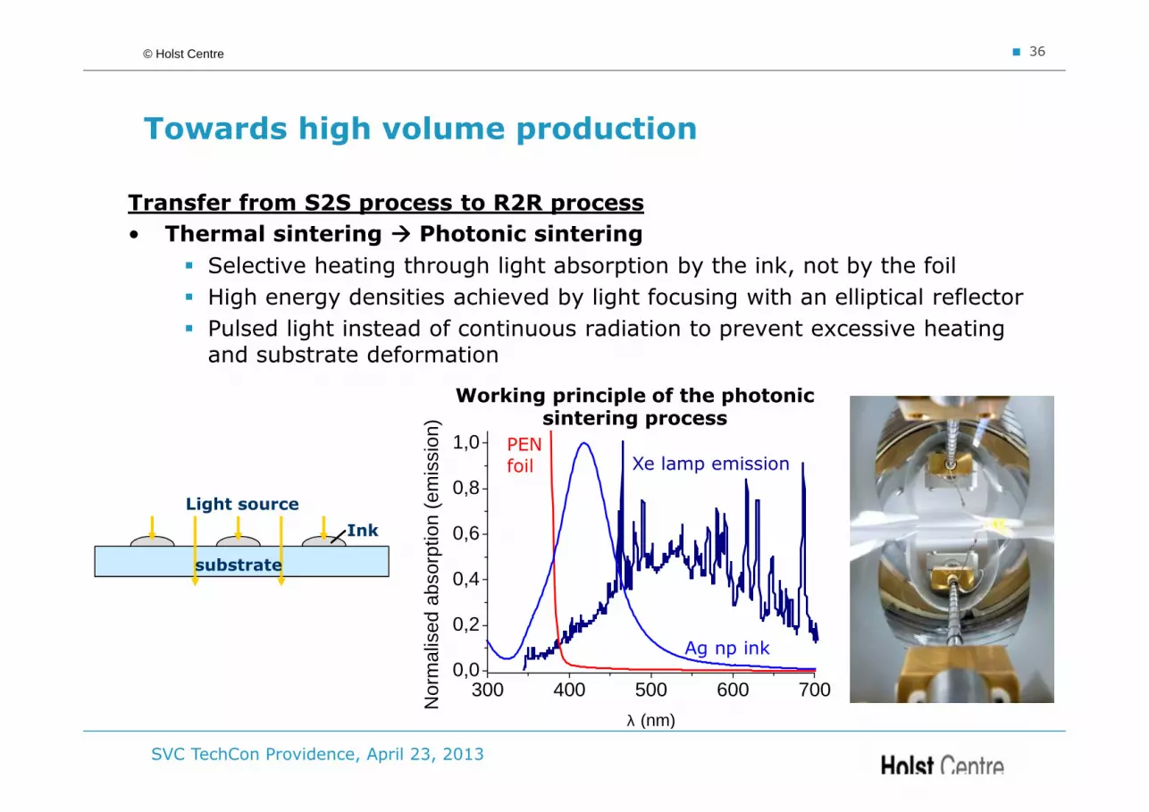
Towards high volume production
Transfer from S2S process to R2R process
• Flatbed screen printing Rotary screen printing
Similar process as flatbed screen printing
Circular formed mesh for continuous production
SVC TechCon Providence, April 23, 2013
smallest feature size (lab)
70 µµµµm
smallest feature size (industrial scale)
100 µµµµm
ink viscosity range 100 – 80,000 mPas
wet layer thickness 12 – 500 µµµµm
dry layer thickness 500 – 50,000 nm
dry layer thickness accuracy
15 – 40 %
alignment/overlay accuracy
100 µµµµm
linear line speed >> 10 m/min, independent from resolution
35
© Holst Centre
Towards high volume production
Transfer from S2S process to R2R process
• Thermal sintering Photonic sintering
Selective heating through light absorption by the ink, not by the foil
High energy densities achieved by light focusing with an elliptical reflector
Pulsed light instead of continuous radiation to prevent excessive heating and substrate deformation
SVC TechCon Providence, April 23, 2013
300 400 500 600 7000,0
0,2
0,4
0,6
0,8
1,0N
orm
alis
ed a
bsor
ptio
n (e
mis
sion
)
λ (nm)
PENfoil
Ag np ink
Xe lamp emission
Working principle of the photonic sintering process
Light source
Ink
substrate
36

© Holst Centre
SVC TechCon Providence, April 23, 2013
• Inline temperature and resistance measurement
The temperature profile reveals the change in material properties of the conductive ink. DuPont W693 (Ag development paste) on PEN
Photonic Sintering: Process study
Thermal conductivity: LowHeat capacity: High
Thermal conductivity: HighHeat capacity: Low
Tg of PEN
37

© Holst Centre
SVC TechCon Providence, April 23, 2013
• Sequence flash sintering (Suntronic U5603)
To achieve highly conductive structures without deforming the temperature-sensitive substrate, two flash settings are used
Two stage sintering flash parameters:
Process Time Temperature Pulse settings
Solvent evaporation seconds < Tg low intensity, high frequency
Sintering milliseconds >(>) 250°C high intensity, short pulse(s)
50x
Photonic Sintering: Process study
38

© Holst Centre
SVC TechCon Providence, April 23, 2013
• Stand alone photonic sintering unit
Research tool to investigate sintering behavior of conductive inks
Elliptic shaped reflector to focus light
Inline resistance and temperature measurement (4-point)
Nitrogen atmosphere possible (copper inks)
• S2S photonic sintering unit
Research tool to upscale from single line to 30x30 cm
2 side illumination
Up to 10 lamps
Inline resistance and temp.
measurement (4-point)
Photonic sintering: Experimental setup
Stand alone photonic sintering unit
39

© Holst Centre
Rotary screen printing
Material: DuPont 5064 micron Ag
Screen: RotaMesh 305 80 µm
Foil: Agfa PET, 125 µm
Print speed: 5 m/min
Sheet resistance of full printed large areas: ~30 mΩ//mil
(Process demonstration video can be found on YouTube: Holst Centre Photonic Sintering)
Photonic sintering module
6 lamps used (3 top, 3 bottom)
2 lamps at 300 Hz, 50% power
4 lamps at 10-15 Hz, 50-60% intensity
Photograph of the R2R system containing the rotary screen printer and the sintering module
R2R rotary screen printing and in-line photonic sintering
SVC TechCon Providence, April 23, 2013
40

Presentationoverview
SVC TechCon Providence, April 23, 2013
1. Introduction Holst Centre
2. Introduction smart blister
3. Device architecture
4. Way of working
5. Results
6. Towards high volume production
7. Conclusions and outlook

© Holst Centre
Conclusions
SVC TechCon Providence, April 23, 2013
• Screen printing was demonstrated as a cheap manufacturing method for smart blisters
5 different layers were printed
Good conductivity
Overlay accuracy of ~100µm; even on multi-layer stack
Printed resistance ladders to monitor which pill is removed
Thinned down components integrated in foil
• Rotary screen printing and photonic curing was shown to be a way for high volume production
Proof of principle R2R photonic curing demonstrated
With a non optimized process 10 m/min was achieved
42

© Holst Centre
Roll to roll inkjet printing
Printer: SPG inkjet printer
Print head: Xaar 1001
Material: Sun Chemical EMD5603
Foil: Agfa PET, 125 µm
Print speed: 4 m/min
Outlook processing
SVC TechCon Providence, April 23, 2013
Movie: R2R Inkjet printing and sintering
Sintering module
NIR dryer
60% Power
Photonic sintering
2 lamps used;10Hz, 60% intensity
43

© Holst Centre
General purpose flexible sensor label
- demonstrated to work with humidty, temperature, amines, (ethylene)
low power
low cost
unified plug&playplatform
for different sensors
allows data logging forseveral weeks
compatiblewith NFC and RFID standards
SVC TechCon Providence, April 23, 2013
Outlook application
44

© Holst Centre
Outlook application
SVC TechCon Providence, April 23, 2013
Skinpatch
• Wellness and healthcare application
• Demonstrated to work with monitoring skin temperature, skin humidity and skin movement
45

© Holst Centre
SVC TechCon Providence, April 23, 2013
Outlook application
Storeskin
• shelve can detect spatially resolved presence of objects
• done by integration of a ‘large area pressure sensing foil’
• electronics external, hidden in box
46
© Holst Centre
Aknowledgements
SVC TechCon Providence, April 23, 2013
• Program partners
47

Thank you for your attention!


