Embed Size (px)
Citation preview

www.afm-journal.de
FULL P
APER
www.MaterialsViews.com
Rodrigo F. P. Martins , * Arman Ahnood , Nuno Correia , Luís M. N. P. Pereira , Raquel Barros , Pedro M. C. B. Barquinha , Ricardo Costa , Isabel M. M. Ferreira , Arokia Nathan , * and Elvira E. M. C. Fortunato *
Recyclable, Flexible, Low-Power Oxide Electronics
The ability to process and dimensionally scale fi eld-effect transistors with and on paper and to integrate them as a core component for low-power-consump-tion analog and digital circuits is demonstrated. Low-temperature-processed p- and n-channel integrated oxide thin-fi lm transistors in the complementary metal oxide semiconductor (CMOS) inverter architecture are seamlessly layered on mechanically fl exible, low-cost, recyclable paper substrates. The possibility of building these circuits using low-temperature processes opens the door to new applications ranging from smart labels and sensors on clothing and packaging to electronic displays printed on paper pages for use in newspapers, magazines, books, signs, and advertising billboards. Because the CMOS circuits reported constitute fundamental building blocks for analog and digital electronics, this development creates the potential to have fl exible form factor computers seamlessly layered onto paper. The holistic approach of merging low-power circuitry with a recyclable substrate is an important step towards greener electronics.
1. Introduction
The complementary metal oxide semiconductor (CMOS) archi-tecture, which combines n-channel and p-channel transistors, inherently lends itself to low power consumption [ 1–4 ] and sim-plicity in design [ 2–4 ] making possible computer memories, dig-ital logic, microprocessors, and linear analog circuits, [ 4 ] all of which have been traditionally processed at high temperatures on crystalline silicon (c-Si) substrates. [ 3 , 4 ] The high processing tem-perature rules out use of lightweight, fl exible and low-cost sub-strates, [ 5–7 ] thus creating a new window of opportunity for novel low temperature processed semiconductors. [ 8–12 ] In particular, paper is a mechanically fl exible, lightweight, robust, low cost, and fully recyclable substrate material. [ 5 , 13–15 ] Implementing
© 2013 WILEY-VCH Verlag GmbH & Co. KGaA, WeinheiAdv. Funct. Mater. 2013, 23, 2153–2161
DOI: 10.1002/adfm.201202907
Prof R. F. P. Martins, N. Correia, Dr. L. M. N. P. Pereira, R. Barros, Dr. P. M. C. B. Barquinha, R. Costa, Prof. I. M. M. Ferreira, Prof. E. M. C. FortunatoDepartamento de Ciência dos MateriaisCENIMAT/I3N, Faculdade de Ciências e TecnologiaFCT CEMOP/UninovaUniversidade Nova de Lisboa, 2829-516 Caparica, Portugal E-mail: [email protected]; [email protected] Dr. A. Ahnood, Prof. A. NathanCentre for Advanced Photonics and ElectronicsCambridge University, Cambridge, CB3 0FA, UKE-mail: [email protected]
circuits based on the complimentary archi-tecture on paper will open the door for a range of novel applications such as elec-tronic displays that are attached to printed media, clothes and packaging. [ 16 , 17 ]
In order to address this broad range of applications, both n- and p-channel transistors with high performance and seamlessly co-integrated are needed. In spite of recent attempts to produce full organic CMOS circuits, [ 1 ] the issue still remains that holes exhibit low mobility, while electrons have orders of magnitude even lower mobility, [ 18 ] thus limiting their application domain. The same is true for thin fi lm silicon CMOS circuits, but now the electrons have higher mobility while holes exhibit the lower mobility. [ 19 ] Although attempts have been made to fabricate a hybrid CMOS architecture, [ 20 ] taking advantage of both organic and inor-
ganic material systems, the fabrication processes used have not been as straightforward due to material incompatibility. In recent years n-channel oxide thin-fi lm transistors (TFT) [ 9 ] have emerged since they can be processed at low temperatures [ 8 , 9 , 21 ] exhibiting mobilities at least one order of magnitude higher than the organic p- or amorphous silicon n-channel counter-parts. [ 22 ] More importantly, the ability to deposit p-channel oxides at low temperatures with high mobilities, in excess of 1 cm 2 V − 1 s − 1 , [ 22–24 ] is creating an opportunity to integrate analog and digital CMOS circuits, in which both p-channel and n-channel behavior are harnessed. Recent developments in the fabrication of fi eld-effect transistors (FET) with and on paper, acting as both the gate dielectric and the substrate, [ 25 ] combine the high mobility semiconducting oxides with the high static gate capacitance of paper. This stems from paper’s foam-like structure [ 26 ] yielding FETs with a large on-current capability at lower bias voltages.
This work describes CMOS digital and analog electronic circuits on paper, which harness the complimentary operation of oxide FETs with electron and hole mobilities greater than 23 cm 2 V − 1 s − 1 and 1.3 cm 2 V − 1 s − 1 , respectively. And since such circuits have a low static power consumption and well-defi ned voltage transfer characteristic with a sharp state transition, they are used as building blocks for more complex circuits, analo-gous to the traditional c-Si CMOS technology. We examine the role of the physical dimensions of the FET and compactness of the paper fi ber on the performance, along with scaling down size limits using low cost techniques such as inkjet printing.
2153wileyonlinelibrary.comm

FULL
PAPER
2154
www.afm-journal.dewww.MaterialsViews.com
These fi ndings open up opportunities that shape tomorrow’s low cost, lightweight, and fl exible form factor electronics, by bridging the gap between the domain of large area elec-tronics and the sub-micron world of c-Si CMOS technology, in which the combination of fully recyclable paper electronics and low power consumption brings us a step closer to green electronics.
2. Results and Discussions
2.1. Paper as the Gate Dielectric and FET Geometrical Scaling Limitations
The FET transconductance ( g m ), i.e., the output current change per unit input voltage change (∂ I DS /∂ V GS ), is limited by device geometry and mobility, which in the saturation regime can be extracted from:
IDS= (µCpaperW/L )[(VGS − VT)2/2] = gm(VGS − VT)/2
(1.1)
Here, g m = ( μ C paper W / L )( V GS – V T ) is the transconductance, V T the threshold voltage, μ the FET mobility, L and W the channel length and width, respectively, and C paper the gate capacitance per unit area. We see that g m is dependent on the gate capacitance besides the aspect ratio. From the circuit design standpoint, a high g m is advantageous as it allows the desired drain-source current to be achieved at lower operating voltages. [ 12 , 27 ] The use of paper as the gate dielectric enhances device transconduct-ance, because of the foam-like structure of paper, which yields a large gate capacitance at low frequencies. In addition, there is the drift of charged species though cation exchange at the nega-tively charged carboxyl and phenolic hydroxyl sites in the paper matrix, and anion migration due to the negative zeta potential of paper, [ 28 ] leading to formation of electric double layers along the fi bers beneath the channel region and on the gate electrode. This is a function of the amount of moisture retained inside the paper structure (as discussed in the Supporting Informa-tion) and is akin to what has been demonstrated in some elec-trolyte dielectrics used in organic thin fi lm transistors. [ 27 , 29–31 ] The result is an increase in the gate dielectric capacitance which is responsible for the enhanced transconductance observed at low operating voltages. Indeed the foam-like structure of paper allows us to obtain a quasi-static gate capacitance of (40 ± 4) nF cm − 2 (see Supporting Information Figure S3), cor-responding to an apparent dielectric thickness of only 0.5 μ m, which is signifi cantly smaller than the actual paper geometric thickness (60 μ m). [ 22 ] At very low frequencies ( < 0.1Hz), the discrete paper fi bers respond to the measurement signal and therefore the apparent dielectric thickness is the product of serial and parallel combination of the discrete fi ber capacitors located at different planes within the paper matrix.
The paper’s porosity and hydrophobicity infl uences perform-ance, reproducibility and geometric scaling of the FETs. In the present study we use common tracing paper (TP) and compared it to three different types of laboratory paper samples (LPS). The LPS had geometric thickness of 68 ± 8 μ m and were com-posed of highly compacted cellulose fi bers (100%) with a cross
wileyonlinelibrary.com © 2013 WILEY-VCH Verlag
sectional area around 5 times smaller than that of tracing paper. Two of the LPS papers (LPS34 and LPS35) were coated with a biopolymer on both sides in order to reduce their porosity (see Supporting Information Figure S2). The remaining sample (LPS36) was left untreated.
The biopolymer coated samples (LPS34 and LPS35) exhibit quasi-static capacitance of 1.2 ± 0.2 nF cm − 2 and 2.5 ± 0.3 nF cm − 2 , respectively. These values are signifi cantly lower than that of uncoated paper (LPS36) whose capacitance is 44 ± 4 nF cm − 2 . This suggests that the active thickness of the coated LPS is about one order of magnitude larger than the uncoated counterpart, confi rming the role of the paper’s fi brous struc-ture in obtaining high gate capacitance. It should be noted that without the capacitance enhancement effect, gate biases in excess of 1000 V would be required for switching of the FETs, making their application impractical.
Apart from the porosity of paper, which impacts the FET’s gate capacitance, its surface roughness infl uences the FET char-acteristics and its correlation with the channel length and width. Given the typical paper’s fi ber dimension of about 10 μ m, this would ultimately dictate the uniformity of the FET characteris-tics as the channel dimensions scale below the limits imposed by the shadow mask which is in the range of a few μ m. Sub-sequently, for the range of dimensions of W and L examined in this work, the density of pores present in the active channel area reduces with reduction in L and W , leading to enhance-ment in device performance, albeit at the expense of yield and performance reproducibility.
As depicted in Table 1 , N-channel FET structures using TP with different channel lengths and widths were fabricated. A fi xed range of W / L ratios (10, 5, 3.47, and 1) were used in order to observe the role of lateral size ( W ) on overall device perform-ance, as well as the effect of device scaling when approaching dimensions of the order of fi ber width. Although shadow masking technology has been used in this work, we can never-theless use this information to estimate the possible limitations of down scaling using low cost technologies, such as the inkjet printing, in which present feature size limits are in the range of 40 μ m, but with the potential to scale to smaller sizes with more sophisticated printing processes.
The semiconducting channel layer for the n-channel FETs was gallium-indium-zinc-oxide (GIZO). The GIZO fi lm has a thickness of 40 ± 4 nm and was deposited at room tempera-ture by radio frequency (RF) sputtering of a ceramic target with the composition of 1:1:1 mol of Ga 2 O 3 :In 2 O 3 :ZnO. [ 32 ] A 450 nm high conductivity indium-zinc-oxide (IZO) fi lm was used as the gate electrode. Since the paper fi bers are more than two orders of magnitude thicker than the active channel layer, non-con-tinuous mesh-like channel layers are formed (see Supporting Information Figure S1,S2). This is much less pronounced for the gate electrode, whose thickness is at least one order of mag-nitude larger than the active channel layers. Similarly, the drain and source electrodes consist of 500nm thick Ni/Au electron beam evaporated fi lms, ensuring consistent electrical contacts at the drain and source. Figure 1 a,b depicts the transfer char-acteristics and gate leakage current ( I GS ) of a n-channel FET fabricated using tracing paper measured at drain-source bias of 15 V. The former shows the variation in transfer characteris-tics with channel widths of 2560 μ m and 1280 μ m at a fi xed
GmbH & Co. KGaA, Weinheim Adv. Funct. Mater. 2013, 23, 2153–2161

FULL P
APER
www.afm-journal.dewww.MaterialsViews.com
Table 1. Summary of the FET electrical performances obtained on the different type of papers used and with different channel dimensions.
Sample V D [V] I On / I Off V On [V] S [V dec − 1 ] I DOff [A] Δ V [V] W / L [ μ m μ m − 1 ] μ [cm 2 V − 1 s − 1 ]
TP10 15 1.8 × 10 5 –0.7 1.12 1.79 × 10 − 8 ± 0.7 100/1001 22.5
TP10 1 1.5 × 10 5 –1 1.28 1 × 10 − 10 100/1001 28
TP11 15 1.76 × 10 4 0 1.16 8.96 × 10 − 9 ± 3 1000/2005 22
TP12 15 3.78 × 10 4 –1 1.52 1.88 × 10 − 8 ± 4.5 1000/2005 22
TP12 1 3.5 × 10 4 0 1.21 9.6 × 10 − 10 1000/2005 23
TP13 15 1.37 × 10 3 –4.5 1.4 1.91 × 10 − 7 ± 3.5 2560/25610 23
TP13 15 6.5 × 10 3 –4.0 1.35 1.54 × 10 − 7 ± 2.2 1280/2565 23
LPS34 25 4.4 × 10 4 –0.5 4.8 5 × 10 − 10 ± 9 2000/20010 1.9
LPS35 25 3.8 × 10 4 1 4.1 2 × 10 − 10 ± 9.5 2000/20010 3.1
LPS35 25 2 × 10 5 1.5 2.4 1.5 × 10 − 10 ± 9 1000/2005 3.8
LPS36 25 4 × 10 4 –3 1.6 2.8 × 10 − 8 ± 2 1000/2005 22
LPS36 15 4 × 10 4 1.5 1.6 2.8 × 10 − 8 ± 1 1000/2005 22
channel length of 256 μ m, corresponding to a W / L ratio of 10 and 5. The latter highlights the variation in transfer char-acteristics when the channel length increases from 100 μ m to 200 μ m, while maintaining a fi xed W of 1000 μ m. It should be noted that the smallest channel dimension used in this work was W / L = 100/100 μ m.
The electrical characteristics of the devices, namely their I ON / I OFF ratio, I OFF , threshold voltage, hysteresis, sub-threshold slope ( S ) and fi eld effect mobility ( μ ) are summarized in Table 1 (see also Supporting Information Figure S6). It can be seen the extracted fi eld effect mobility of μ = 23 ± 2.0 cm 2 V − 1 s − 1 is
© 2013 WILEY-VCH Verlag GmAdv. Funct. Mater. 2013, 23, 2153–2161
Figure 1 . Transfer characteristics of n-channel FET processed with and onpaper (TP) at V DS = 15 V for: a) L = 256 μ m and different W as shown in the L and W / L as shown in the inset. c) The transfer characteristics of n-channellaboratory paper samples (LPS), keeping L = 200 μ m and different W as sho
consistent and independent of the channel geometry. Other indicators include the observed enhancement in performance as the devices are scaled down, which can be attributed to the decrease in pinhole probability in the channel as its width and length are reduced. The observed hysteresis behavior in the transfer characteristics (see Table 1 ) of n-channel FETs can be attributed to a combination of ion migration [ 31 , 33 ] and charge trapping effects. [ 34 ] This can be further minimized by: reducing the number of trap states; scaling down the channel dimen-sion ( L ) towards the limits of paper fi ber width; increasing the smoothness of the paper using passivation techniques,
bH & Co. KGaA, Wein
common tracing inset. b) Different FET processed on wn in the inset.
and using low ion bombardment deposition processes. It should be noted that hysteresis becomes less signifi cant with reduction in W and L , confi rming our previous argument on the existence of a foam like fi ber structure (see Supporting Information). Moreover the devices operate in enhancement mode, as opposed to depletion mode, leading to more stable operation. The hysteresis behavior gives rise to a small discrepancy in the output and transfer characteristics.
2.2. Yield and Reproducibility of FETs
An important consideration for the applica-bility of the technology demonstrated in this work to electronic systems is its yield and reproducibility. As highlighted in Table 1 , the FET characteristics become more consistent at low drain voltages (e.g., V DS = 1 V). This accompanied by the two orders of magnitude reduction in the leakage current at V DS = 1 V, compared with that at V DS = 15 V, and can be attributed to the paper’s porosity as well as the drift of embedded charged species within the bulk of the paper, [ 28 ] which is a strongly bias dependent phenomena. The
2155wileyonlinelibrary.comheim
FULL
PAPER
2156
www.afm-journal.dewww.MaterialsViews.com
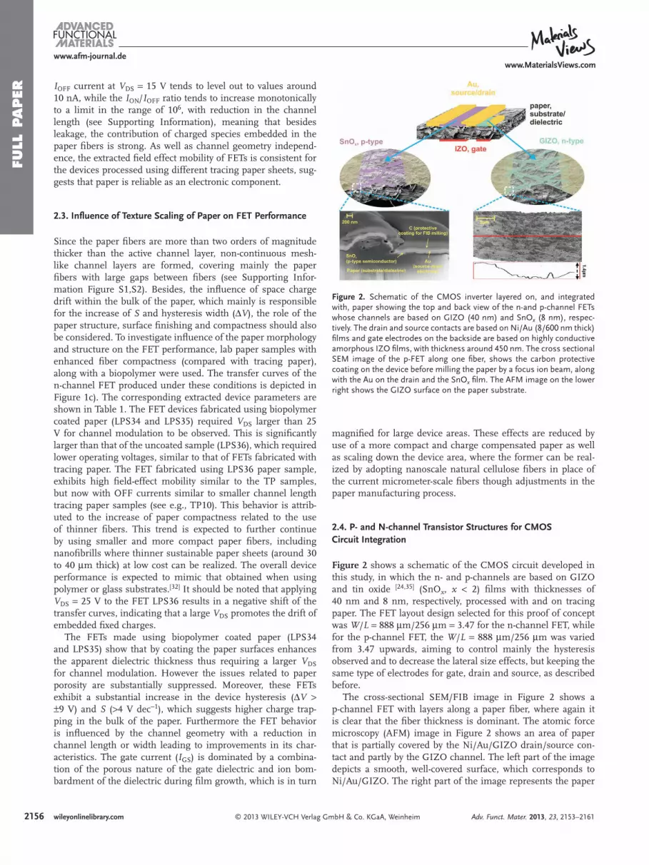
Figure 2 . Schematic of the CMOS inverter layered on, and integrated with, paper showing the top and back view of the n-and p-channel FETs whose channels are based on GIZO (40 nm) and SnO x (8 nm), respec-tively. The drain and source contacts are based on Ni/Au (8/600 nm thick) fi lms and gate electrodes on the backside are based on highly conductive amorphous IZO fi lms, with thickness around 450 nm. The cross sectional SEM image of the p-FET along one fi ber, shows the carbon protective coating on the device before milling the paper by a focus ion beam, along with the Au on the drain and the SnO x fi lm. The AFM image on the lower right shows the GIZO surface on the paper substrate.
I OFF current at V DS = 15 V tends to level out to values around 10 nA, while the I ON / I OFF ratio tends to increase monotonically to a limit in the range of 10 6 , with reduction in the channel length (see Supporting Information), meaning that besides leakage, the contribution of charged species embedded in the paper fi bers is strong. As well as channel geometry independ-ence, the extracted fi eld effect mobility of FETs is consistent for the devices processed using different tracing paper sheets, sug-gests that paper is reliable as an electronic component.
2.3. Infl uence of Texture Scaling of Paper on FET Performance
Since the paper fi bers are more than two orders of magnitude thicker than the active channel layer, non-continuous mesh-like channel layers are formed, covering mainly the paper fi bers with large gaps between fi bers (see Supporting Infor-mation Figure S1,S2). Besides, the infl uence of space charge drift within the bulk of the paper, which mainly is responsible for the increase of S and hysteresis width ( Δ V ), the role of the paper structure, surface fi nishing and compactness should also be considered. To investigate infl uence of the paper morphology and structure on the FET performance, lab paper samples with enhanced fi ber compactness (compared with tracing paper), along with a biopolymer were used. The transfer curves of the n-channel FET produced under these conditions is depicted in Figure 1 c). The corresponding extracted device parameters are shown in Table 1 . The FET devices fabricated using biopolymer coated paper (LPS34 and LPS35) required V DS larger than 25 V for channel modulation to be observed. This is signifi cantly larger than that of the uncoated sample (LPS36), which required lower operating voltages, similar to that of FETs fabricated with tracing paper. The FET fabricated using LPS36 paper sample, exhibits high fi eld-effect mobility similar to the TP samples, but now with OFF currents similar to smaller channel length tracing paper samples (see e.g., TP10). This behavior is attrib-uted to the increase of paper compactness related to the use of thinner fi bers. This trend is expected to further continue by using smaller and more compact paper fi bers, including nanofi brills where thinner sustainable paper sheets (around 30 to 40 μ m thick) at low cost can be realized. The overall device performance is expected to mimic that obtained when using polymer or glass substrates. [ 32 ] It should be noted that applying V DS = 25 V to the FET LPS36 results in a negative shift of the transfer curves, indicating that a large V DS promotes the drift of embedded fi xed charges.
The FETs made using biopolymer coated paper (LPS34 and LPS35) show that by coating the paper surfaces enhances the apparent dielectric thickness thus requiring a larger V DS for channel modulation. However the issues related to paper porosity are substantially suppressed. Moreover, these FETs exhibit a substantial increase in the device hysteresis ( Δ V > ± 9 V) and S ( > 4 V dec − 1 ), which suggests higher charge trap-ping in the bulk of the paper. Furthermore the FET behavior is infl uenced by the channel geometry with a reduction in channel length or width leading to improvements in its char-acteristics. The gate current ( I GS ) is dominated by a combina-tion of the porous nature of the gate dielectric and ion bom-bardment of the dielectric during fi lm growth, which is in turn
wileyonlinelibrary.com © 2013 WILEY-VCH Verlag G
magnifi ed for large device areas. These effects are reduced by use of a more compact and charge compensated paper as well as scaling down the device area, where the former can be real-ized by adopting nanoscale natural cellulose fi bers in place of the current micrometer-scale fi bers though adjustments in the paper manufacturing process.
2.4. P- and N-channel Transistor Structures for CMOS Circuit Integration
Figure 2 shows a schematic of the CMOS circuit developed in this study, in which the n- and p-channels are based on GIZO and tin oxide [ 24 , 35 ] (SnO x , x < 2) fi lms with thicknesses of 40 nm and 8 nm, respectively, processed with and on tracing paper. The FET layout design selected for this proof of concept was W / L = 888 μ m/256 μ m = 3.47 for the n-channel FET, while for the p-channel FET, the W / L = 888 μ m/256 μ m was varied from 3.47 upwards, aiming to control mainly the hysteresis observed and to decrease the lateral size effects, but keeping the same type of electrodes for gate, drain and source, as described before.
The cross-sectional SEM/FIB image in Figure 2 shows a p-channel FET with layers along a paper fi ber, where again it is clear that the fi ber thickness is dominant. The atomic force microscopy (AFM) image in Figure 2 shows an area of paper that is partially covered by the Ni/Au/GIZO drain/source con-tact and partly by the GIZO channel. The left part of the image depicts a smooth, well-covered surface, which corresponds to Ni/Au/GIZO. The right part of the image represents the paper
mbH & Co. KGaA, Weinheim Adv. Funct. Mater. 2013, 23, 2153–2161

FULL P
APER
www.afm-journal.dewww.MaterialsViews.com
Figure 3 . Transfer and output characteristics of interstrate FET processed on common tracing paper for a W / L = (888 μ m/256 μ m) = 3.47: a,b) n-channel FET that exhibits a threshold voltage of 2.1 ± 0.5 V, mobility of 23 ± 2.0 cm 2 V − 1 s − 1 , sub-threshold slope of 3.1 V dec − 1 and ON/OFF ratio of about 10 4 . c,d) p-channel FET that exhibits a threshold voltage of 1.4 ± 0.5 V, mobility of 1.3 ± 0.2 cm 2 V − 1 s − 1 , sub-threshold slope of 6.9 V dec − 1 and ON/OFF ratio of over 10 2 .
covered by GIZO only, which has a much higher roughness due to the paper texture. The transfer and output characteristics of the n- and p-channel FETs are depicted in Figure 3 . Both n- and p-channel FETs were characterized for a gate voltage range of up to ± 100 V. Neither of the devices exhibit any breakdown in this range.
The industrial applicability of the p- and n-channel transis-tors on paper is demonstrated by performing all of the electrical characterization throughout this work in ambient atmosphere. The observed hysteresis behavior in the transfer characteristics (Figure 3 a,c) are in-line with our previous observations, with a minor discrepancy in the output and transfer characteris-tics of less than 10% as measured in ambient conditions. This variation over a set of 10 devices is within tolerance limits for operation of CMOS circuits. The p-channel FET presented here works in depletion mode with a gate leakage current about one order of magnitude higher than that of the n-channel FET. This behavior can be partly attributed to the high radio-frequency power density used during the deposition of the SnO x fi lm and
© 2013 WILEY-VCH Verlag GmAdv. Funct. Mater. 2013, 23, 2153–2161
the subsequent damage to the paper dielectric. Furthermore, the polycrystalline nature of SnO x yields a fi lm with a rougher surface and less compact structure [ 32 ] than its GIZO counter-part. This leads to enhancement of defects at fi ber interfaces, thus contributing to the observed decrease in the I ON / I OFF ratio, S and μ , as compared to the n-channel FETs. The p-channel FET’s output characteristics do not show hard saturation behavior, which again is in-line with previous arguments con-cerning leakage current and operation mode. As discussed in the next section, this behavior would have an infl uence on the input-output characteristic of the CMOS inverter circuit pre-sented here.
The overall evaluation of the results leads to the following: a) n-channel transistors operate in enhancement mode and exhibit hard output saturation currents, with the following FET performance metrics: V T = 2.1 ± 0.5 V, μ n = 23 ± 2 cm 2 V − 1 s − 1 , S = 3.1 ± 0.2 V dec − 1 and ON/OFF ratio = 10 4 ± 5 × 10 3 , for W / L = 888 μ m/256 μ m = 3.47. The hysteresis behavior after 100 cycles is Δ V = 0.7 V. b) p-channel transistors operate in
2157wileyonlinelibrary.combH & Co. KGaA, Weinheim

FULL
PAPER
2158
www.afm-journal.dewww.MaterialsViews.com
Figure 4 . a) Image of paper CMOS inverter where the large ( W / L ) p = 21.8 and small ( W / L ) n = 11.8 correspond to the p-FET and n-FET, respectively. b) VTC of the CMOS inverter and the corresponding gain. The VTC was used to extract the high and low states, associated with the input and output voltages ( V IL , V OH and V IH , V OL ) defi nitions of which are given in Table 2 .
Figure 5 . Input-output characteristics of various analog and digital circuits using paper CMOS technology. a) Simulated and measured input-output voltage characteristics of the inverter shown in Figure 3 b, based on which a number of basic building blocks (b–f) are shown. Char-acteristics of b) transmission gate, c) common source CMOS amplifi er d) differential CMOS amplifi er, e) NOR gate, and f) NAND gate. Panels (c,d) represent analog circuit examples while panels (b,e,f) represent digital circuit examples. Panel (a) can be used for both digital or analog applications.
depletion mode and do not exhibit hard satu-ration behavior. Comparatively it has higher hysteresis and leakage current and with the following metrics: V T = 1.4 ± 0.5 V, μ p = 1.3 ± 0.2 cm 2 V − 1 s − 1 , S = 6.9 V ± 0.5 dec − 1 and ON/OFF ratio over 100 ± 25. The hysteresis behavior after 100 cycles is Δ V = –1.0 V.
2.5. CMOS Digital and Analog Circuit Characterization
The p-channel FET performance is suffi cient for use in the CMOS architecture, proving the feasibility of seamlessly co-integrating both n- and p-channel transistors on paper. The CMOS inverter using the n- and p-channel FET described above with geometric aspect ratio ( W / L ) p /( W / L ) n of 1.85 was fabricated on the same substrate. For realizing the proof of concept of the CMOS circuit, we kept L = 256 μ m while W was increased for the p-type FET and reduced for the n-type FET (see Figure 4 a). Figure 4 shows the inverter circuit and its voltage transfer characteristic (VTC) along with its gain defi ned as:
Gain = − VOUT
VIN= (gmn + gmp)(rDSn
∥∥rDSp )
(1.2)
Here, r DSn and r DSp represent the output resistances of the n and p-channel FETs, respectively. Additional CMOS inverters with different geometric aspect ratios were fabricated on the paper substrate and tested using different supply voltages and reported earlier. [ 22 ]
wileyonlinelibrary.com © 2013 WILEY-VCH Verlag GmbH & Co. KGaA, Wein
The DC characteristics of the n- and p-channel FET were simulated using a phys-ically-based compact TFT model reported for fast thin fi lm circuit simulations . [ 36 ] Details of the circuit model are given in Supporting Information. For the range of voltages shown , the simulation is in reasonably good agree-ment with measurements with a discrepancy less than 10%, except for the high current transition regime. Here, there is V T -shift that is not accounted for in the simulations. Based on this, the VTC of the inverter circuit was simulated and compared with measured results as shown in Figure 5 a). Using this approach additional digital circuits namely the transmission gate, the universal logic gates (NOR and NAND) as well as analog circuits such as the common source and dif-ferential amplifi ers were investigated. Their
heim Adv. Funct. Mater. 2013, 23, 2153–2161

FULL P
APER
www.afm-journal.dewww.MaterialsViews.com
Table 2. Key performance parameters of the digital paper CMOS devices extracted from Figure 5 .
Digital Circuit NMH a) [V] | NML | b) [V] VTW c) [V] VLS d) [V]
NOR gate (VB = –5) 8.6 1.8 3 9.8
NAND gate (VB = 10) 12.2 2.1 2.1 12.17
Transmission gate 1.12 0.15 13.5 12.2
Inverter (simulated) 11.0 1.9 3.0 12.1
Inverter (measured) 9.8 ± 0.7 1.0 ± 0.1 4.3 ± 0.3 12.4 ± 0.6
a) NMH = V OH – V IH , high noise margin; b) NML = V IL – V OL low noise margin; c) VTW = ( V IH – V IL ) the transition width; d) V LS = ( V OH – V OL ), the swing logic. Here,
V OH , V IH , V IL and V OL , are associated with the knee points ( ∂ V OUT / ∂ V IN = –1) of the
VTC curves, i.e., Δ V OUT = – Δ V IN .
VTCs are depicted in Figure 5 . Tables 2 and 3 summarize the key performance metrics of the digital and analog circuits, respectively. Overall the VTC curves show asymmetry due to asymmetry in the inverter circuit geometry used, where we observe that the maximum gain of the devices was 4.2 ± 0.4, corresponding to V IN = 2.3 ± 0.5 V and V OUT = 15.2 ± 0.8 V, under V DD = 17 V.
Moreover, we also investigated the impact of paper bending on the circuit performance. It was observed that bending (without creating foldlines) allows the performance of the cir-cuit to be recovered. The creation of foldlines leads to electrical breakdown. In a conventional thin fi lm transistor on fl exible substrate, bending can lead to electrical breakdown stemming from cracking/peeling of gate dielectric or channel layer, [ 37 , 38 ] leading to large gate leakage current and/or loss of drain-source current. The paper FETs presented in this work are robust. The paper gate dielectric is relatively thin, which combined with its unique mechanical properties, [ 39 , 40 ] result in a higher tolerance for radius of curvature. The channel material is in effect a mesh network of very a thin semiconductor on the paper fi bers. This limits strain propagation providing an extra degree of freedom to the channel, therefore making it resilient to bending. The combination of these two effects allows the paper FETs to with-stand larger mechanical deformation than conventional TFTs on fl exible substrates.
2.6. Power Consumption Analysis
As discussed earlier in this paper, one of the most powerful advantages of CMOS circuits (over their unipolar counterparts)
© 2013 WILEY-VCH Verlag GmAdv. Funct. Mater. 2013, 23, 2153–2161
Table 3. Key performance parameters of the analog paper CMOS devices extracted from Figure 5 .
Analog Circuit Gain [V/V] Dynamic Range [V]
Gain Nonlinearity
Output Swing [V]
Differential amplifi er 4.1 3.9 0.5 11.7
Common source amplifi er 16.3 1.8 1.2 7.7
Inverter (simulated) 11.4 3.3 0.75 15.6
Inverter (measured) 4.9 3.5 0.5 14.4
is their low power consumption, realized by concurrent opera-tion of both p- and n-channel devices. The complimentary oper-ation of the p-channel and n-channel FETs in CMOS circuits ensure that only one of the two devices is switched on at a given time (except for the state transition phase). Given that the two types of FETs are often connected in series across the power supply lines ( V DD and V SS in Figure 5 ), this design ensures that there is always a switched-off device in the FET chain leading to a permanent high resistance path cross the power line (except during state transition). This is especially benefi cial for digital CMOS circuits such as inverters, NOR gates and NAND gates as they are predominantly in the high or low states. The lowest static power leakage current of the CMOS inverter circuit on paper is less than 1.9 pA. [ 22 ] Depending on the microstruc-ture of the paper used, this static leakage current in the case of tracing paper, can increase up to 5nA. The lower value cor-responds to a maximum static power consumption of 32 pW per inverter. With use of compacted LPS without biopolymer coating (sample LPS36), the leakage current goes below 150 pA, which corresponds to a consumption of 6.6 pW per inverter.
Circuit simulations performed on the NOR and NAND gates point to a maximum static current leakage and power con-sumption of 3.5 μ A and 59 μ W per gate, respectively. This is associated to the state when the one or the other transistor in the inverter chain is ON. Given that the leakage current can be scaled down with reduction in the FET’s lateral geometry and improved gate dielectric integrity, the power consumption dem-onstrated in this work can be reduced. For instance a reduction of channel width from the current 10 4 μ m to 10 μ m can poten-tially reduce the power consumption from 32 pW to 32 fW in the case of the inverter, and 59 μ W to 59 nW in the case of the NOR and NAND gates.
Although features used in this work are relatively large, the technology does exist to scale down shadow mask features down to 10 μ m scale yielding a fi ner pitch size than that obtained by inkjet printing. Nonetheless by combining advanced fabrica-tion techniques with shadow mask deposition, sub-micrometer features have been demonstrated. [ 41 , 42 ] Alignment of the gate with drain/source and channel poses an insignifi cant chal-lenge through use of readily available backside alignment tech-niques. [ 43 –47 ] Furthermore, given that the fabrication methods used in this work are commonly used in the large area elec-tronics industry, there is potential for scale-up of the complexity and functionality of the devices and circuits presented here. More importantly, all electrical characterization carried out throughout this work was under ambient conditions.
3. Conclusions
The present study demonstrates the ability to produce FETs with an interstrate structure with and on paper, which can be dimen-sionally scaled leading to better electrical performance. The use of more compact papers with thinner fi bers results in reduced leakage current with performance similar to that obtained using polymer or glass substrates. It is also shown that the use of paper with biopolymer coating increases the operating voltage as well as promotes retention of fi xed charges, either fi eld induced or charged trapped along the fi bers, giving rise to
2159wileyonlinelibrary.combH & Co. KGaA, Weinheim

FULL
PAPER
2160
www.afm-journal.dewww.MaterialsViews.com
signifi cant hysteresis. Scaling down device dimensions reduces the probability of locating porous sites and voids in the active channel area, leading to an enhancement in FET performance.
The results and underlying technology reported in this work is not intended to compete with the conventional c-Si CMOS technology but to create a parallel platform for the large area electronics, along with the added benefi t of recyclability. For instance, although the reported operating voltages in this work are higher than c-Si CMOS circuits, they are within the range used in the large area electronics industry [ 14 , 41–44 ] thus not lim-iting their adoption. Also they can be further improved by using technologies amenable to scaling down device dimensions. The electrical and mechanical performance of the circuit presented here creates an opportunity for the realization of large area, light weight, low cost, low power, mechanically fl exible, and fully recyclable digital logic, microprocessors, memories and linear integrated circuits that are expected to create applications ranging from smart labels and tags to sensors, MEMS, and active matrix arrays in the large area electronics industry.
4. Experimental Section As a fi rst step, a 450 nm IZO gate electrode [ 48 ] was sputtered on one side of the paper substrate followed by 40 nm GIZO fi lm on the opposite side of the substrate to form the n-channel FETs’ channel layers. We then sputtered approximately 8 nm SnO x fi lm [ 49 , 50 ] to form the p-channel FETs’ channel layers. In all cases the sputtering was performed using a radio frequency magnetron sputtering system at room temperature. Shadow masks were used to defi ne the gate electrodes, and n- and p-channel FET islands. Finally an electron-beam evaporator was used to deposit a nickel/gold (8/600 nm) double-layer, which acts as the drain and a source contacts as well as circuit interconnects. The metallization regions were defi ned also using shadow masks. The fabricated devices were annealed in air at 150 ° C for 1 h using a Barnstead Thermolyne F21130 tubular furnace.
Acknowledgements This work was funded by the Portuguese Science Foundation (FCT-MCTES) through projects PTDC/CTM/103465/2008, PTDC/EEA-ELC/099490/2008, ERC 2008 Advanced Grant (INVISIBLE contract number 228144, awarded to E.F.), Royal Society Wolfson Research Award (awarded to A.N.), and by EU-FP7 Projects ORAMA CP-IP 246334-2 and Apple NMP-2010-SME-4, GRANT nº 262782.
Received: October 7, 2012Published online: November 29, 2012
[ 1 ] H. Klauk , U. Zschieschang , J. Pfl aum , M. Halik , Nature 2007 , 445 , 745 .
[ 2 ] B. Crone , A. Dodabalapur , Y.-Y. Lin , R. W. Filas , Z. Bao , A. LaDuca , R. Sarpeshkar , H. E. Katz , W. Li , Nature 2000 , 403 , 521 .
[ 3 ] A. L. Robinson , Science 1984 , 224 , 705 . [ 4 ] N. H. E. Weste , K. Eshraghian , Principles of CMOS VLSI Design: A
Systems Perspective , Addison-Wesley Pub. Co. , Reading, MA 1993 , Ch. 3.
[ 5 ] D.-H. Kim , Y.-S. Kim , J. Wu , Z. Liu , J. Song , H.-S. Kim , Y. Y. Huang , K.-C. Hwang , J. A. Rogers , Adv. Mater. 2009 , 21 , 3703 .
[ 6 ] Y. Sun , W. M. Choi , H. Jiang , Y. Y. Huang , J. A. Rogers , Nat. Nano-technol. 2006 , 1 , 201 .
wileyonlinelibrary.com © 2013 WILEY-VCH Verlag G
[ 7 ] B. D. Gates , Science 2009 , 323 , 1566 . [ 8 ] K. K. Banger , Y. Yamashita , K. Mori , R. L. Peterson , T. Leedham ,
J. Rickard , H. Sirringhaus , Nat. Mater. 2010 , 10 , 45 . [ 9 ] K. Nomura , H. Ohta , A. Takagi , T. Kamiya , M. Hirano , H. Hosono ,
Nature 2004 , 432 , 488 . [ 10 ] S. Ju , A. Facchetti , Y. Xuan , J. Liu , F. Ishikawa , P. Ye , C. Zhou ,
T. J. Marks , D. B. Janes , Nat. Nanotechnol. 2007 , 2 , 378 . [ 11 ] S. R. Forrest , Nature 2004 , 428 , 911 . [ 12 ] G. Eda , G. Fanchini , M. Chhowalla , Nat. Nanotechnol. 2008 , 3 , 270 . [ 13 ] B. Scrosati , Nat. Nanotechnol. 2007 , 2 , 598 . [ 14 ] E. J. Meijer , D. M. De Leeuw , S. Setayesh , E. V. Veenendaal ,
B.-H. Huisman , P. W. M. Blom , J. C. Hummelen , U. Scherf , T. M. Klapwijk , Nat. Mater. 2003 , 2 , 678 .
[ 15 ] R. Martins , I. Ferreira , E. Fortunato , Phys. Status Solidi RRL 2011 , 5 , 332 .
[ 16 ] M. Berggren , D. Nilsson , N. D. Robinson , Nat. Mater. 2007 , 6 , 3 . [ 17 ] V. L. Pushparaj , M. M. Shaijumon , A. Kumar , S. Murugesan , L. Ci ,
R. Vajtai , R. J. Linhardt , O. Nalamasu , P. M. Ajayan , Proc. Natl. Acad. Sci. USA 2007 , 104 , 13574 .
[ 18 ] L.-L. Chua , J. Zaumseil , J.-F. Chang , E. C.-W. Ou , P. K.-H. Ho , H. Sirringhaus , R. H. Friend , Nature 2005 , 434 , 194 .
[ 19 ] T. Tiedje , J. Cebulka , D. Morel , B. Abeles , Phys. Rev. Lett. 1981 , 46 , 1425 .
[ 20 ] S. Gowrisanker , M. A. Quevedo-Lopez , H. N. Alshareef , B. E. Gnade , S. Venugopal , R. Krishna , K. Kaftanoglu , D. R. Allee , Org. Electron. 2009 , 10 , 1217 .
[ 21 ] E. M. C. Fortunato , P. M. C. Barquinha , A. C. M. B. G. Pimentel , A. M. F. Gonalves , A. J. S. Marques , L. M. N. Pereira , R. F. P. Martins , Adv. Mater. 2005 , 17 , 590 .
[ 22 ] R. Martins , A. Nathan , R. Barros , L. Pereira , P. Barquinha , N. Correia , R. Costa , A. Ahnood , I. Ferreira , E. Fortunato , Adv. Mater. 2011 , 23 , 4491 .
[ 23 ] L. Liao , Z. Zhang , B. Yan , Z. Zheng , Q. L. Bao , T. Wu , C. M. Li , Z. X. Shen , J. X. Zhang , H. Gong , J. C. Li , T. Yu , Nanotechnology 2009 , 20 , 085203 .
[ 24 ] E. Fortunato , V. Figueiredo , P. Barquinha , E. Elamurugu , R. Barros , G. Gonçalves , S.-H. K. Park , C.-S. Hwang , R. Martins , Appl. Phys. Lett. 2010 , 96 , 192102 .
[ 25 ] E. Fortunato , N. Correia , P. Barquinha , L. Pereira , G. Goncalves , R. Martins , IEEE Electron. Device Lett. 2008 , 29 , 988 .
[ 26 ] R. Martins , P. Barquinha , L. Pereira , N. Correia , G. Gonçalves , WI. Ferreira , E. Fortunato , Appl. Phys. Lett. 2008 , 93 , 203501
[ 27 ] M. Halik , H. Klauk , U. Zschieschang , G. Schmid , C. Dehm , M. Schütz , S. Maisch , F. Effenberger , M. Brunnbauer , F. Stellacci , Nature 2004 , 431 , 963 .
[ 28 ] P. J. Simons , M. Spiro , J. F. Levy , J. Chem. Soc., Faraday Trans. 1998 , 94 , 223 .
[ 29 ] A. Laiho , L. Herlogsson , R. Forchheimer , X. Crispin , M. Berggren , Proc. Natl. Acad. Sci. USA 2011 , 108 , 15069 .
[ 30 ] A. S. Dhoot , J. D. Yuen , M. Heeney , I. McCulloch , D. Moses , A. J. Heeger , Proc. Natl. Acad. Sci. USA 2006 , 103 , 11834 .
[ 31 ] M. J. Panzer , C. D. Frisbie , Adv. Mater. 2008 , 20 , 3177 . [ 32 ] A. Olziersky , P. Barquinha , A. Vilà , C. Magana , E. Fortunato ,
J. R. Morante , R. Martins , Mater. Chem. Phys. 2011 , 131 , 512 . [ 33 ] L. Herlogsson , X. Crispin , N. D. Robinson , M. Sandberg ,
O.-J. Hagel , G. Gustafsson , M. Berggren , Adv. Mater. 2007 , 19 , 97 . [ 34 ] B. N. Pal , B. M. Dhar , K. C. See , H. E. Katz , Nat. Mater. 2009 , 8 ,
898 . [ 35 ] Y. Ogo , H. Hiramatsu , K. Nomura , H. Yanagi , T. Kamiya , M. Hirano ,
H. Hosono , Appl. Phys. Lett. 2008 , 93 , 032113 . [ 36 ] P. Servati , D. Striakhilev , A. Nathan , IEEE Trans. Electron. Dev. 2003 ,
50 , 2227 . [ 37 ] J. Lewis , Mater. Today 2006 , 9 , 38 . [ 38 ] H. Gleskova , S. Wagner , Z. Suo , Appl. Phys. Lett. 1999 , 75 , 3011 . [ 39 ] M. Alava , K. Niskanen , Rep. Prog. Phys. 2006 , 69 , 669 .
mbH & Co. KGaA, Weinheim Adv. Funct. Mater. 2013, 23, 2153–2161

FULL P
APER
www.afm-journal.dewww.MaterialsViews.com
[ 40 ] D. Rodney , M. Fivel , R. Dendievel , Phys. Rev. Lett. 2005 , 95 , 108004 . [ 41 ] G. H. Gelinck , H. E. A. Huitema , E. van Veenendaal , E. Cantatore ,
L. Schrijnemakers , J. B. P. H. van der Putten , T. C. T. Geuns , M. Beenhakkers , J. B. Giesbers , B.-H. Huisman , E. J. Meijer , E. M. Benito , F. J. Touwslager , A. W. Marsman , B. J. E. van Rens , D. M. de Leeuw , Nat. Mater. 2004 , 3 , 106 .
[ 42 ] T. Sekitani , H. Nakajima , H. Maeda , T. Fukushima , T. Aida , K. Hata , T. Someya , Nat. Mater. 2009 , 8 , 494 .
[ 43 ] D. B. Mitzi , L. L. Kosbar , C. E. Murray , M. Copel , A. Afzali , Nature 2004 , 428 , 299 .
[ 44 ] H. Yan , Z. Chen , Y. Zheng , C. Newman , J. R. Quinn , F. Dötz , M. Kastler , A. Facchetti , Nature 2009 , 457 , 679 .
© 2013 WILEY-VCH Verlag GAdv. Funct. Mater. 2013, 23, 2153–2161
[ 45 ] S. R. Quake , Science 2000 , 290 , 1536 . [ 46 ] S. Egger , A. Ilie , Y. Fu , J. Chongsathien , D.-J. Kang , M. E. Welland ,
Nano Lett. 2005 , 5 , 15 – 20 . [ 47 ] C. Stampfer , T. Helbling , D. Obergfell , B. Schöberle , M. K. Tripp ,
A. Jungen , S. Roth , V. M. Bright , C. Hierold , Nano Lett. 2006 , 6 , 233 .
[ 48 ] R. Martins , P. Almeida , P. Barquinha , L. Pereira , A. Pimentel , I. Ferreira , E. Fortunato , J. Non-Cryst. Solids 2006 , 352 , 1471 .
[ 49 ] R. Martins , V. Figueiredo , R. Barros , P. Barquinha , G. Goncalves , L. Pereira , I. Ferreira , E. Fortunato , Proc. SPIE 2012 , 8263 , 826315 .
[ 50 ] E. Fortunato , P. Barquinha , R. Martins , Adv. Mater. 2012 , 24 , 2945.
2161wileyonlinelibrary.commbH & Co. KGaA, Weinheim


