Embed Size (px)
Citation preview

BULLETIN OF THE POLISH ACADEMY OF SCIENCESTECHNICAL SCIENCESVol. 53, No. 2, 2005
Growth of MOCVD HgCdTe heterostructures for uncooledinfrared photodetectors
A. PIOTROWSKI1, P. MADEJCZYK2, W. GAWRON2, K. KŁOS1, J. PAWLUCZYK1,M. GRUDZIEŃ1, J. PIOTROWSKI1, and A. ROGALSKI2∗
1VIGO System S.A., 3 Świetlików Str., 01-389 Warsaw, Poland2Institute of Applied Physics, Military University of Technology, 2 Kaliskiego Str., 00-908 Warsaw, Poland
Abstract. In the paper recent progress at VIGO/MUT (Military University of Technology) MOCVD Laboratory in the growthof Hg1−xCdxTe (HgCdTe) multilayer heterostructures on GaAs/CdTe substrates is presented. The optimum conditions for thegrowth of single layers and complex multilayer heterostructures have been established. One of the crucial stages of HgCdTeepitaxy is CdTe nucleation on GaAs substrate. Successful composite substrates have been obtained with suitable substratepreparation, liner and susceptor treatment, proper control of background fluxes and appropriate nucleation conditions. Theother critical stage is the interdiffused multilayer process (IMP). The growth of device-quality HgCdTe heterostructures requirescomplete homogenization of CdTe-HgTe pairs preserving at the same time suitable sharpness of composition and doping profiles.This requires for IMP pairs to be very thin and grown in a short time.
Arsenic and iodine have been used for acceptor and donor doping. Suitable growth conditions and post growth anneal isessential for stable and reproducible doping. In situ anneal seems to be sufficient for iodine doping at any required level. Incontrast, efficient As doping with near 100% activation requires ex situ anneal at near saturated mercury vapours. As a result weare able to grow multilayer fully doped (100) and (111) heterostructures for various infrared devices including photoconductors,photoelectromagnetic and photovoltaic detectors. The present generation of uncooled long wavelength infrared devices is basedon multijunction photovoltaic devices. The technology steps in fabrication of devices are described. It is shown that near-BLIPperformance is possible to achieve at ≈ 230 K with optical immersion. These devices are especially promising as 7.8–9.5-µmdetectors, indicating the potential for achieving detectivities above 109 cmHz1/2/W.
Key words: MOCVD growth, HgCdTe ternary alloy, room temperature infrared photodetectors.
1. Introduction
The common believe is that infrared photodetector needsto be cooled to achieve a high sensitivity. Detectionof long wavelength infrared (LWIR) radiation, charac-terized by low photon energy, requires transitions offree charge carriers which have energy not much lowerthan the photon one. Therefore, at near room temper-atures the thermal energy kT becomes comparable tothe transition energy. The direct consequence of this isa very high rate of thermal generation of charge carri-ers. The statistical nature of this process generates signalnoise. As a result LWIR detectors become very noisywhen they operated at near room temperature. Cool-ing is a direct, straightforward, and very efficient way tosuppress the thermal generation of charge carriers, be-ing at the same time a very impractical method. Theneed for cooling is a major limitation of photodetectors,and inhibits the more widespread application of IR tech-nology. Affordable high performance infrared imagingcameras, require cost-effective IR detectors that operatewithout cooling or, at least, at temperatures achievableby low power and low cost coolers. Since cooling re-
quirements add considerably to the cost weight, powerconsumption and inconvenience of an IR system, it ishighly desirable to eliminate or reduce the cooling require-ments.
VIGO System S.A. has developed a number of typesof unique photodetectors for short, medium and longwavelength IR radiation operating without cryogenic cool-ing [1–3]. Isothermal vapour phase epitaxy (ISOVPE)has been the base technology for HgCdTe growth formany years [1,4]. It is very mature and stable tech-nique with a lot of limitations. Further improvementin detector performance requires application of more so-phisticated devices which can be fabricated with ad-vanced epitaxial techniques like metalorganic chemicalvapour deposition (MOCVD) or molecular beam epitaxy(MBE).
This paper presents recent progress at VIGO/MUTMOCVD Laboratory in the growth of Hg1−xCdxTe(HgCdTe) multilayer heterostructures on GaAs/CdTesubstrates for uncooled infrared photodetectors. The spe-cial attention is focused on the improvement in multijunc-tion LWIR photovolatic detectors.
∗e-mail: [email protected]
139

A. Piotrowski, P. Madejczyk, W. Gawron, K. Kłos, J. Pawluczyk, M. Grudzień, J. Piotrowski, and A. Rogalski
2. Impact of epitaxial growthon development of HgCdTe detectors
The time line for the evolution of HgCdTe growth tech-nologies is illustrated in Fig. 1. Historically, crystalgrowth of HgCdTe has been a major problem mainlybecause a relatively high Hg pressure is present duringgrowth, which makes it difficult to control the stoichiom-etry and composition of the grown material.
Fig. 1. Evolution of HgCdTe crystal growth technology from1958 to present (after Ref. 5)
Early experiments and a significant fraction of earlyproduction were done using a quench-anneal or solid-staterecrystalization process. Bridgman growth was attemptedfor several years near the mid-70s last century. At thesame time, solvent growth methods from Te-rich meltswere initiated to reduce the grown temperature. One suc-cessful implementation was the traveling heater methodup to 5-cm diameter [6].
The bulk HgCdTe crystals were initially used for anytypes of infrared photodetectors. At present they arestill used for some infrared applications such as n-typesingle element photoconductors, SPRITE detectors andlinear arrays. Bulk growth produced thin rods, gener-ally up to 15 mm in diameter, about 20 cm in length,and with non-uniform distribution of composition. Largetwo-dimensional arrays could not be realized with bulkcrystals. Another drawback to bulk material was the
need to thin the bulk wafers, generally cut about 500-µmthick, down to final device thickness of about 10 µm. Alsofurther fabrication steps (polishing the wafers, mountingthem to suitable substrates, and polishing to the final de-vice thickness) were intensive labour.
The epitaxial techniques offer, in comparison withbulk growth techniques, the possibilities to grow largearea epilayers and sophisticated device structures withgood lateral homogeneity, abrupt and complex compo-sition and doping profiles, which can be configured to im-prove the performance of photodetectors. The growth isperformed at low temperatures, which makes it possibleto reduce the native defects density. The properties ofHgCdTe grown by the variety of techniques are summa-rized in Table 1.
Among various epitaxial techniques, the liquid phaseepitaxy (LPE) is the most matured method. At presentthe growth of HgCdTe by vapour phase epitaxy (VPE)is typically done by nonequilibrium methods: MOCVD,MBE, and their derivatives. The great potential benefitof MBE and MOCVD over the equilibrium methods is theability to modify the growth conditions dynamically dur-ing growth to tailor band gaps, add and remove dopants,prepare surfaces and interfaces, add passivations, performanneals, and even grow on selected areas of a substrate.The growth control is exercised with great precision to ob-tain basic materials properties comparable to those rou-tinely obtained from equilibrium growth.
LPE growth of thin layer on CdTe substrates beganin the early-to-mid 70’s. Initially, Te solutions with dis-solved Cd (Cd has a high solubility in Te) and saturatedwith Hg vapour were used to efficiently grow HgCdTe intemperature range 420–600C. This allowed small-volumemelts to be used with slider techniques which did not ap-preciably deplete during the growth run. Experimentswith Hg-solvent LPE began in the late 70’s. Because ofthe limited solubility of Cd in Hg, the volume of the Hgmelts had to be much larger then Te melts (typically ofabout 20 kg) in order to minimize melt depletion duringlayer growth in temperature range 380–500C. This pre-cluded the slider growth approach and Hg-melt epitaxyhas been developed using large dipping vessels.
Table 1Comparison of various methods used to grow HgCdTe
Bulk Liquid phase epitaxy Vapour phase epitaxySSR Traveling heater method
HCT melt Te melt Hg melt Te melt ISOVPE MOCVD MBETemperature (C) 950 950 500 350–550 400–550 500 275–400 160–200
Pressure (Torr) 150 000 150 000 760–8000 760–11400 760–8000 760 300–760 10−3–10−4
Growth rate (µm/hr) 250 250 80 30–60 5–60 1–10 2–10 1–5Dimensions w (cm) 0.8–1.2 dia 0.8–1.2 dia 2.5 dia 5 5 1 dia 7.5 dia 7.5 dia
l (cm) – – – 6 5 – 4 4t (cm) 15 15 15 0.0002–0.0030 0.0005–0.012 0.001 0.0005–0.001 0.0005–0.001
Density of dis. (cm−2) <105 – <105 <105 <105–107 5×10⁵–107 <5×10⁴–106
Purity (cm−3) 5×10¹⁴ 5×10¹⁴ 5×10¹⁴ 5×10¹⁴ 5×10¹⁴ ≈ 1×10¹⁵ <1×10¹⁵ <1×10¹⁵
n-type dop. (cm−3) N/A N/A N/A 1×10¹⁴–1×10¹⁸ 1×10¹⁵–1×10¹⁶ 1×10¹⁵ 5×10¹⁴–5×10¹⁸ 5×10¹⁴–1×10¹⁹
p-type dop. (cm−3) N/A N/A N/A 1×10¹⁵–1×10¹⁸ 1×10¹⁵–5×10¹⁶ 1×10¹⁶–1×10¹⁷ 3×10¹⁵–5×10¹⁷ 1×10¹⁶–5×10¹⁸
X-ray r. c. (arc sec) – – 20–60 <20 <20 – 50–90 20–30Uniformity (∆x) <0.002 <0.004 <0.005 <0.002 <0.002 <0.001 ±0.01–0.0005 ±0.01–0.0006
140 Bull. Pol. Ac.: Tech. 53(2) 2005

Growth of MOCVD HgCdTe heterostructures for uncooled infrared photodetectors
In the early 90’s, bulk growth was replaced by LPEand now it is very mature for production of the first- andsecond-generation detectors. LPE technique has been suc-cessfully used in fabrication of double layer heterojunc-tion p-on-n photodiodes, where p+ cap layer is formedusing arsenic as the dopant. However, LPE technology islimited for a variety of advanced HgCdTe structures re-quired for third generation detectors. LPE typically meltsoff a thin layer of the underlying material and each timean additional layer is grown as a result of relatively highgrowth temperature. Additionally, the gradient in x-valuein the base layer of p+-on-n junction can generate a bar-rier transport in certain cases due to interdiffusion. Theselimitations provided an opportunity for vapour phase epi-taxy: MBE and MOCVD.
The era of MBE and MOCVD began in the early 80’sby adopting both methods well established in the III-Vsemiconductor materials. Through the next decade a vari-ety of metalorganic compounds were developed along witha number of reaction-chamber designs [7]. In the case ofMBE, a specially designed Hg-source ovens were success-fully designed to overcome the low sticking coefficient ofHg at the growth temperature [8] The growth tempera-ture is less than 200C for MBE but around 350–400C forMOCVD, making it more difficult to control the p-typedoping in the MOCVD due to formation of Hg vacanciesat higher growth temperatures. The vacancies can be re-moved by a low (<200C) temperature anneal, however.
However, in the case of MBE application, post growthannealing at high temperatures is necessary for activationof acceptor dopant. At present, MBE is the dominantvapour phase method for HgCdTe. It offers low tempera-ture growth under ultrahigh vacuum environment, in situn-type and p-type doping, and control of composition,doping and interfacial profiles. Although the quality ofMBE material is not yet on a par with LPE, it has madetremendous progress in the past decade.
3. MOCVD systemOne of the important advantages of MOCVD systemis the possibility to use low-cost composite substrates(GaAs, Si, sapphire) as the viable alternative to costlyCdZnTe substrates. This system does not require highvacuum for growth, is easier serviceable technique withlarger throughput. Last, but not least, donor and accep-tor doping at medium and high level, essential for nearroom temperature devices, is simpler with MOCVD. Thatis why we selected MOCVD as the technique of choicefor uncooled MOCVD devices. Aixtron Aix-200 II–VIMOCVD system was purchased in 2004. Fast switch-ing valves, high quality materials and proper reactor de-sign allow us to run fully computer-controlled processes.Low to atmospheric pressure growth is possible. Draw-back of this technique, in comparison with previously usedISOVPE one, is high cost of equipment and high toxicityof precursors which is prevented by an advanced safetysystem.
The MOCVD system was installed in March 2003.The laboratory infrastructure was constructed from theground in cooperation between VIGO System S.A. andMilitary University of Technology. It took half a year todevelop CdTe buffer layer technology. In November 2003,fully doped heterostructures for devices became available.Since then we develop optimum growth parameters fordevices covering the whole 2–16-µm range. Until Au-gust 2004 we grew over 380 heterostructures. Most ofthem were experiments on fundamental growth parame-ters, only small percent of all runs was useful for produc-tion purposes.
Aixtron Aix-200 II–VI MOCVD system is a horizontalreactor customized for Hg1−xCdxTe growth on 2” wafers(see Fig. 2). Pd-cell purified hydrogen is used as a carriergas. Between processes the system is filled with nitrogenfined by getter purifier. Liquid nitrogen is used as thenitrogen source.
Fig. 2. Schematic drawing of Aix-200 II–VI reactor
Bull. Pol. Ac.: Tech. 53(2) 2005 141
A. Piotrowski, P. Madejczyk, W. Gawron, K. Kłos, J. Pawluczyk, M. Grudzień, J. Piotrowski, and A. Rogalski
Dimethylcadmium (DMCd), diisopropyltelluride(DIPTe) and diethylzinc (DEZn) used as precursors areheld in temperature-stabilized baths. Elementary mer-cury is held in a quartz container in the lower inputchannel of the container. AsH3 has been used as arsenicprecursor. The drawback of arsine is its toxicity. Specialsafety preventive measures must have been applied tothe laboratory. Ethyl iodide (EI) is used for donor dop-ing. Because of its high vapour pressures, the metalor-ganic source for iodine must be held in low temperatures(< 5C). DMCd/EI and DIPTe/AsH3 input channelsare separated to prevent premature gas mixing and dustformation. In the lower channel a mercury container isplaced. Evapourating mercury is carried by hydrogen tothe growth zone. Drawback of this solution is the disso-lution of Te and As sources in the elementary mercurycontainer. This may result in As memory effects. The sur-face of the mercury is covered with black skin, probablyHgTe after deposition causing growth instabilities. Hy-drogen from the upper channel dilutes mercury saturatedhydrogen from the lower channel. Therefore, decreasein the mercury partial pressure over the wafer must betaken into account and it can be altered by changing thelower to upper channel flow ratio. In practice, the flow isselected separately for each phase; for example 100/500sccm or 1200/1200 sccm flow ratios have been used. Inthis notation the first number is mass gas flow in the up-per channel and the former is mass gas flow in the lowerchannel.
Two temperature zones are in the reactor: the mer-cury source zone (up to 300C) and the growth zone withgraphite susceptor (up to 900C). Reactor temperatures360–410C have been used and mercury has been heldin 200–220C. Higher temperatures are used for reactorcleaning. Substrate is laying on a rotating disk using Aix-tron’s gas foil rotation technique. Vacuum system pro-vides the possibilities to keep reactor at the pressures from50 mbar to atmospheric pressure. Reactor pressure of 500mbar was used for all successful growth runs.
MOCVD system contains explosive materials suchas hydrogen and toxic materials as AsH3, mercury andmetalorganics precursors. Therefore, the laboratory isequipped with advanced safety feature devices such ashydrogen, arsine and mercury detectors, effective venti-lation system and different safety interlocks embedded inthe Aixtron’s system. Large quantities of mercury arebeing transported during growth. They are condensedat low temperature Hg trap. Glovebox nitrogen atmo-sphere contains a lot of mercury and all its gas outlets areequipped with activated coal filters. All toxic gases areneutralized in the wet scrubber system.
4. CdTe buffer growthCdTe buffer growth on GaAs is probably the most criti-cal stage in HgCdTe growth due to lattice mismatch. ForGaAs and CdTe, the mismatch is approximately 14.3%.
So huge mismatch is neutralized by 2–10-µm thick CdTebuffer. The buffer plays also a role of Ga diffusion bar-rier [9].
Careful chemical and thermal treatment of the reactormust be carried out after each grow run to prevent resid-ual deposits of HgCdTe on substrate that adversely affectnucleation stage of growth. Different phases on the edgesand in the middle of the wafer were frequently observedfor poorly cleaned reactor.
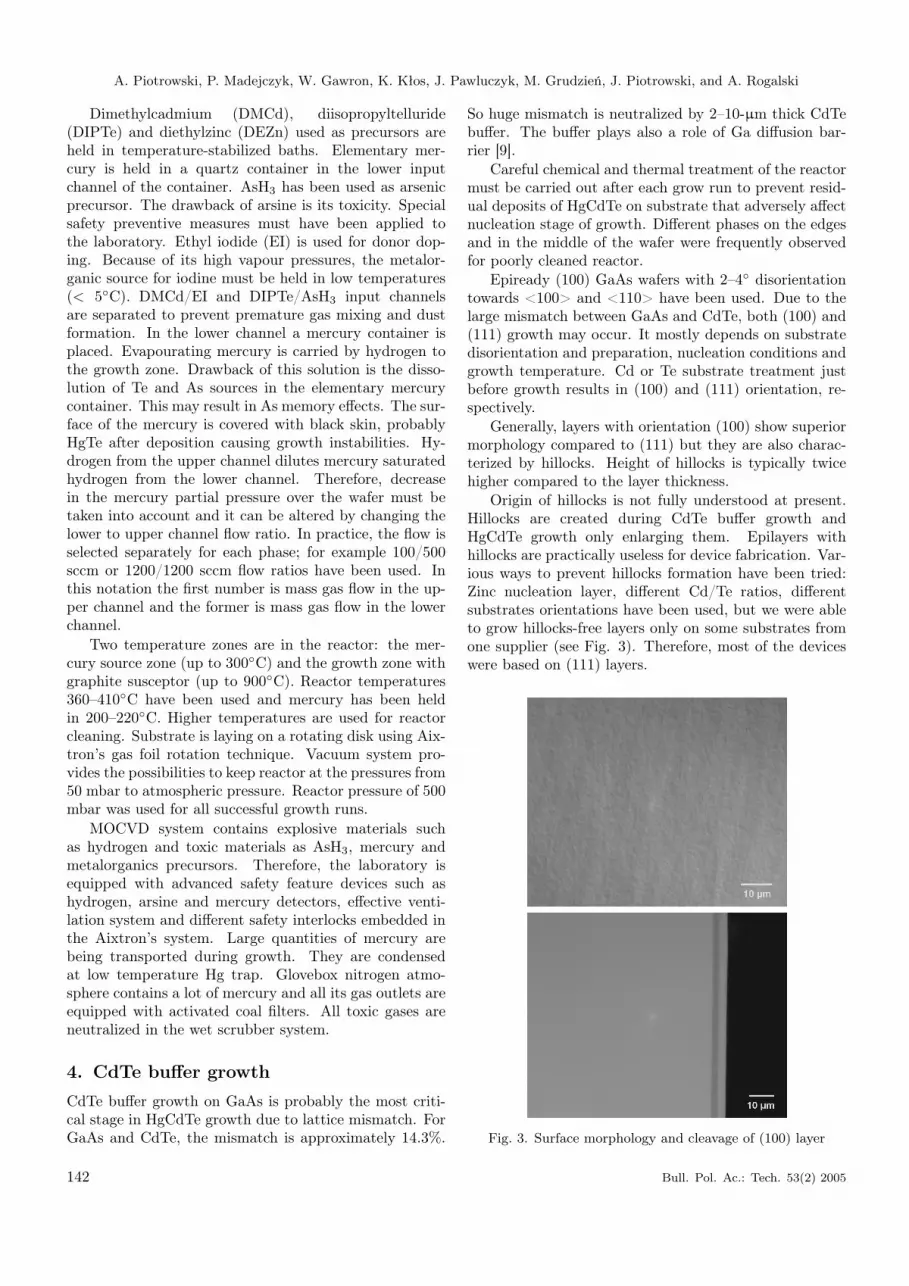
Epiready (100) GaAs wafers with 2–4 disorientationtowards <100> and <110> have been used. Due to thelarge mismatch between GaAs and CdTe, both (100) and(111) growth may occur. It mostly depends on substratedisorientation and preparation, nucleation conditions andgrowth temperature. Cd or Te substrate treatment justbefore growth results in (100) and (111) orientation, re-spectively.
Generally, layers with orientation (100) show superiormorphology compared to (111) but they are also charac-terized by hillocks. Height of hillocks is typically twicehigher compared to the layer thickness.
Origin of hillocks is not fully understood at present.Hillocks are created during CdTe buffer growth andHgCdTe growth only enlarging them. Epilayers withhillocks are practically useless for device fabrication. Var-ious ways to prevent hillocks formation have been tried:Zinc nucleation layer, different Cd/Te ratios, differentsubstrates orientations have been used, but we were ableto grow hillocks-free layers only on some substrates fromone supplier (see Fig. 3). Therefore, most of the deviceswere based on (111) layers.
Fig. 3. Surface morphology and cleavage of (100) layer
142 Bull. Pol. Ac.: Tech. 53(2) 2005

Growth of MOCVD HgCdTe heterostructures for uncooled infrared photodetectors
5. Hg1−xCdxTe growth
Direct Hg1−xCdxTe growth is difficult due to differ-ent thermodynamic properties of HgTe and CdTe [7,10].We applied interdiffused multilayer process (IMP) forHg1−xCdxTe growth to avoid this problem. IMP givesthe possibility for controllable growth of heterostructureswith complex composition and doping profiles. HgTe andCdTe layers are deposited one after another with period100–200 nm and homogenized by interdiffusion duringgrowth. Any composition can be achieved this way byproper selection of HgTe and CdTe layer growth times.
IMP growth depends in a complex way on precursorsconcentration, flow velocities, growth temperature andmany other factors, frequently dependent on the reactordesign. A lot of optimization is required to obtain goodquality layers.
One of the critical factors is a proper control of pre-cursors delivery to the growth zone. For practical deviceswe need multilayer heterostructures with uniform lateralcomposition and doping level within each layer and, atthe same time, with sharp interfaces. This implies verythin IMP pairs and quite short times of CdTe and HgTegrowth phases. The practical consequence is that IMPtimes become comparable to the times required for precur-sor transport from bubblers to the growth zone. The othercomplications are significant differences in the transporttimes for different precursors, mixing effects and differentcarrier gas flow velocities for the CdTe and HgTe growthstages [7]. This may result in poor control of the actualconcentration of precursors that could adversely affect thequality, homogeneity and doping of the HgCdTe layers.Reduction of precursor’s delivery times is possible withincreased carrier gas flow but the shorten residence timeof precursors decreases pyrolysis efficiency, which lead tothe waste of expensive metalorganic precursors.
The problems described above can be solved to somedegree by the use of four-phase IMP process proposedby Svoronos et al [11]. The carrier gas flow throughDIPTe bubbler is switched on at start of HgTe phase andswitched off at the beginning of HgTe flush phase. DIPTeand DMCd bubblers are switched on and off at the startand at the end of CdTe phase, respectively. Typically, thecarrier gas flow during CdTe/CdTe flush phase is approxi-mately 4 times longer of that during the HgTe/HgTe flushone [12]. The CdTe phase is usually used also to intro-duce doping precursors. CdTe growth phase is critical forgrowth of low composition MCT because of its shortness.
Careful selection of the flows and valve switching timesis necessary to ensure optimum growth conditions. Exper-imental optimization of the growth conditions is costlyand time consuming. The theoretical modeling has beenused as the first approximation that could be eventuallycorrected with suitable experiments. Figure 4 shows mod-eled partial pressures of precursors in growth zone duringfour-stage IMP. The most simple approximation is theplug flow (PF) model that describes temporal changes of
precursor concentration as rectangular pulses character-ized by delays compared to the nominal HgTe and CdTephases (see Fig. 4 – DIPTe PF). This means that theHgTe and CdTe growth occurs partially during the HgTeand CdTe phases, and partially are continued during theflush phases.
The PF model is usually a good approximation of gasflow through a thin pipe but poor for the liner volumes ofcomplex shape, where mixing effects are significant. Themixing effects and changes of carrier gas flow may causesignificant distortion of the pulses (Fig. 4). The distor-tion depends on the design of particular gas system anddiffers for various precursors.
Fig. 4. Modeling precursor concentration during IMP tech-nique. DMCd and DIPTe in scale, Hg scale ×17, EI scale×200. We assume equal delays for all precursors in CdTe
growth phase
1. HgTe growth phaseLow carrier gas total flow velocity causes large delayof DIPTe precursor. Time needed for precursor topass through pipes from bubbler to reactor is esti-mated with PF model (DIPTe PF – Fig. 2).
2. HgTe flush phaseTotal flow rate is changed during that phase. In-crease in total gas flow rate during CdTe phase couldcause unstable growth conditions because of chang-ing partial pressure of DMCd and DIPTe at the be-ginning of CdTe deposition. Time of the flush af-ter HgTe is a compromise. From one hand it mustbe carefully selected to ensure no residual DIPTeprecursor pressure during the CdTe growth phase.From the other hand it must be short enough toavoid evapouration of HgTe. Low residual DIPTepartial pressure after the flush phase is particularlyimportant for doping, where DMCd/DIPTe ratiomust be precisely controlled.
3. CdTe growthCdTe layers deposited during IMP cycle must inter-diffuse during next few cycles to ensure compositionuniformity. Injected precursors have different deliv-ery times, so they can’t be switched on simultane-ously. Delays and bad switching moments can causedeterioration of morphology (especially (100) one),inefficient doping, and unintentional DAG.
Bull. Pol. Ac.: Tech. 53(2) 2005 143

A. Piotrowski, P. Madejczyk, W. Gawron, K. Kłos, J. Pawluczyk, M. Grudzień, J. Piotrowski, and A. Rogalski
4. CdTe flushCdTe flush phase is less critical for growth, becauseof low evapouration velocity of CdTe.
In practice, the partial pressures of precoursors could bepredicted with limited accuracy and the process’ designhave to be experimentally adjusted. Doping and flushestimes are longer than modeling results pointing at. In re-ality, during IMP the precursors switching are much morecomplicated. Properties of mass flow controllers forced usto use delta doping to achieve low-doped MCT layers.CdTe growth time is kept constant in all absorber layers.We observed large, nonlinear, composition shifts when wechange CdTe growth time, therefore the composition cal-ibration was adjusted through HgTe growth time. Wehave created library with growth parameters.
Linear deposition characteristics over substrate mustbe assured to avoid non-uniformity of HgCdTe compo-sition. First of all, deposition characteristics depend onlinear flow velocity over substrate.
Figure 5 shows transmission of HgCdTe epilayers. Theabsorption edge is mostly determined by the layer withthe lowest x-value and can be used to determine composi-tion. We can evaluate composition uniformity across thewafer by mapping. The compositional uniformity over thewafer as low as ±0.1% is achieved.
The infrared transmittance spectra of high quality lay-ers are close to the theoretical ones. This is an evidence ofgood in-depth homogeneity. Complex interferences pat-terns are observed for long wavelength.
Compositional profiles were evaluated for some sam-ples by differential reflection spectra or with SIMSmethod.
Fig. 5. Infrared transmission spectra of multilayer heterostruc-ture
6. Hg1−xCdxTe doping
6.1. Undoped layers. Electrical properties of nomi-nally undoped Hg1−xCdxTe layer are determined by na-tive acceptors (metal vacancies) and uncontrolled back-ground doping. Vacancy concentration strongly dependson reactor temperature, vapour pressure and materialcomposition. The native doping level after growth at360C with mercury temperature 200C is approximately5×1016 cm−3. This is much below the expected level of>1×1017 cm−3 for this temperature conditions [13]. Wesuspect that it is due to partial annihilation of vacanciesduring cool down. It could be influenced by hydrogenpresence in the layer.
The vacancy concentration can be changed by post-growth annealing in mercury vapours. Vacancies may bepractically eliminated by a prolonged, low temperature(≈200C) annealing at near saturated mercury pressures.Such annealing reveals the background doping level.We have observed the uncontrolled background aboutNd −Na = (1− 3)×1015 cm−3 for our MOCVD system.
Ex-situ anneal in sealed quartz ampoules in mercuryvapours is typically used to maintain isothermal condi-tions. This technique is not practical for production pur-poses. Instead, we developed more convenient ex-situ an-neal technique in which a wafer after growth was trans-ported into reusable quartz container. Temperatures upto 400C and Hg pressures up to 2 bars could be used.
High and low temperature annealing was used. Typ-ically, a short (approx. 20 min – 3 h) high temperature(360C) anneal was used for doping homogenization fol-lowed by long (>2 h) low temperature (250C) anneal forvacancy annihilation. Mercury pressure has been changedduring both stages of this annealing to maintain condi-tions close to isothermal ones.
In-situ annealing is very practical for production pur-poses. This eliminates the need for any “hot” processes af-ter removal of wafers from the MOCVD reactor, and thepossibility to introduce additional impurities. We havedeveloped in-situ annealing technique which can be ap-plied for many practical purposes. The annealing is car-ried out in the reactor immediately after the growth.
When the growth is finished, the temperature of thewafer is gradually lowered to 210C for 1–6 hours keepingthe mercury source temperature at the 200–220C. Afterthat both reactor and mercury are cooled down. It mustbe avoided to cool down the rector below the mercurylevel to prevent Hg droplet formation. During annealingit is not possible to close the reactor and stop hydrogenflow. This result in significant mercury loses. In practice,this means that we cannot obtain near saturated mer-cury pressures at temperatures >220C. This effect canbe limited by selecting optimal upper to lower channelflow ratio.
Vacancy and background doping is not sufficient foradvanced infrared devices that require donor and accep-tor doping at medium and high doping levels.
144 Bull. Pol. Ac.: Tech. 53(2) 2005

Growth of MOCVD HgCdTe heterostructures for uncooled infrared photodetectors
6.2. Doping with foreign impurities. Iodine and ar-senic have been used as foreign dopants. Both are well be-haved, stable and slowly diffusing dopants. To be activedopants they must occupy Te sites. Metal-rich conditionsare favorable for iodine incorporation and are required forarsine. Therefore they have been introduced during CdTephase with Cd/Te ratio > 1. Most of doping experimentshave been carried out for (111) Hg1−xCdxTe layers.
Iodine doping. Iodine is well behaved dopant and it istypically used to obtain heavily doped n+-layers. There-fore it is important to establish conditions for iodine dop-ing at > 1017 cm−3 level. Cd/Te ratio of 1.1–1.3 has beenused during CdTe phase to improve efficiency of I incor-poration and activation. It allows doping concentrationbetween 1×10¹⁷ and 1×1018 cm−3 for the compositionsof about 0.3.
Multi-level staircase structure quickly yielded dopantsource calibration curves. Figure 6 shows calibrationstructure obtained using ethyliodode (EI) which was as-sessed by SIMS measurements and differential 77K Hallprofiling. The obtained correlation between the electri-cal and chemical results implied the iodine incorporatedon the correct Te lattice site; and that within the accu-racy of the techniques, the activation efficiency is close to100%. However, along with increasing iodine concentra-tion its activation decreases. Probably for high iodine con-centration it starts to occupy interstitials or metal sites.Although EI shows the desirable properties of a donordopant source, the minimum EI concentration about 0.2ppm could be obtained with sensible choices of sourcetemperature and double dilution mass flow controllers(MFC) settings. The range of 0.05 ppm (first step atcalibration structure) was obtained by setting very shortinjection times to the reactor – 0.4 s of EI. The control ofiodine concentration is difficult below 1×1016 cm−3.
Improved efficiency of doping has been observed withex-situ annealing at 360oC at near saturated mercurypressures. This effect may be related to incomplete io-dine homogenization during growth and in-situ annealing,since iodine diffusion is very slow (noticeably slower thenCd diffusion into HgTe).
Heterostructure photovolataic IR detectors requireheavily doped n+-layers with relatively high x composi-tion (x > 0.45). It is expected that such layers shouldhave resistivity as small as possible to provide good elec-trical contact. Until now, the Hg1−xCdxTe layers withcomposition x > 0.45 doped with EI doses above 10 ppmhad electron concentration lower than 7×1017 cm−3 andsheet resistance above 10 Ω. These parameters indicatethat significant part of iodine atoms are not located in Telattice and are not electically active. Preliminary experi-ments with increasing Cd/Te ratio and ex-situ annealinghave not improved EI doping noticeably. No or insignifi-cant I doping memory effects have been observed. Goodreproducibility of I doping has been observed.
Fig. 6. Calibration profile of staircase structure doped usingethyliodide. Composition x = 0.30
Arsenic doping. Arsine incorporation into Te sites isvery sensitive for metallic rich conditions. This assuresconditions for arsenic to enter Te sites where it acts likean acceptor. Otherwise arsenic can show amphoteric be-havior.
High doping concentrations (> 5×1017 cm−3) havebeen achieved in higher x materials (x > 0.25) with Hgtemperature 220C and arsine fraction of 10 ppm. It ismuch more difficult to achieve heavily doped low x mate-rials. Arsenic incorporates only during CdTe cycle in IMPgrowth process. The growth time of CdTe cycle (the ac-tive time of As doping) is considerably shorter than HgTecycle for low x layers. As a result, the relative arsenic in-corporation is worse in epilayers with low x compositionsthan in high x ones. The investigation of optimal growthconditions for more effective doping in low x layers is stillcontinued. So far concentrations of up to 2×1017 cm−3
have been achieved for mercury temperature of 220C,Cd/Te ratio equal to 5 and arsine fraction of 5 ppm inthe growth zone.
High doping concentrations (> 5×1017 cm−3) havebeen achieved in higher x materials (x > 0.25) with Hgtemperature 220C and arsine fraction of 10 ppm. It ismuch more difficult to achieve heavily doped low x materi-als. concentrations up to 2×1017 cm−3 have been achievedfor mercury temperature of 220C, Cd/Te ratio equal 5and arsine fraction of 4 ppm in the growth zone.
Figure 7 shows the efficiency of arsenic doping as afunction of AsH3 partial pressure for two crystallograficorientations: for the (100) and (111). Different orien-tations were obtained by different nucleation conditions.The difference in doping efficiency for the two orientationsis clearly evident, with near an order of magnitude higherincorporation rate in (100) orientation. The detailed ex-planation of this phenomenon is presented in [14].
Bull. Pol. Ac.: Tech. 53(2) 2005 145

A. Piotrowski, P. Madejczyk, W. Gawron, K. Kłos, J. Pawluczyk, M. Grudzień, J. Piotrowski, and A. Rogalski
Fig. 7. Arsenic incorporation in HgCdTe vs AsH3 partial pres-sure, measured by SIMS, for the (100) and (111) orientations.
Composition x = 0.28–0.33
Ex-situ isothermal annealing in high mercury vapours(360/350C) shows significant effects on acceptor doping.It is probably related to arsenic activation in the material.
Strong dependence of CdTe growth rate was visiblefor different arsine concentrations. It is between 4 and8 µm/h and it strongly depends on dopants partial pres-sures.
7. Uncooled HgCdTe deviceswith improved performance
The class of photon detectors is sub-divided into differenttypes depending on how the electric or magnetic fields aredeveloped. Initial efforts to produce near room temper-ature LWIR photon detectors have concentrated mainlyon optimization of photoconductors and PEM detectors.More information can be found in previously publishedpapers [1,3,15]. The room temperature photovoltaic de-vice of conventional design suffers from— poor quantum efficiency, and— low differential resistance.
Only charge carriers that are photogenerated at a dis-tance shorter than the diffusion length from junction canbe collected. The absorption depth of long wavelength IRradiation (λ > 5µm) is longer than the diffusion length.Therefore only a limited fraction of the photogeneratedcharge contributes to the quantum efficiency. Let us on-sider an example of an uncooled 10.6 µm photodiode. Thecalculations show that the ambipolar diffusion length isless than 2 µm while the absorption depth is ≈ 13 µm.This reduces the quantum efficiency to ≈ 15% for singlepass of radiation through the detector.
The resistance of the p-n junction is very low due to ahigh thermal generation. In the materials with a high elec-
tron to hole mobility ration, the resistance is additionallyreduced by ambipolar effects [16] As a result, the pream-plifier noise and noise of parasitic resistances may exceedthe thermal generation-recombination noise. Thus, theperformance of conventional devices is very poor, so theyare not usable for practical applications.
The present generation of uncooled LWIR devices isbased on photovoltaic devices [17–22] The problems ofpoor quantum efficiency and large series resistance havebeen solved through adoption of sophisticated heterojunc-tion architectures of photovoltaic devices in combinationwith the methods of reduction of physical size of an activeelement.
An efficient improvement was development of multi-ple heterojunction photovoltaic devices to increase thevoltage responsivity of the devices. Practical realizationof the multi-heterojunction device that is consisted of astructure based on backside illuminated n+-p-P photo-diodes (symbol “+” denotes strong doping, capital let-ter – wider gap) have been presented in several papers[17–21] The individual detector elements were preparedby a combination of conventional dry etching, angledion milling, and angled thermal evapouration for con-tact metal deposition (see Fig. 8). p-type active layerwith thickness of approximately 3 µm and doping lev-els of about 1016 cm−3 were grown on GaAs substratesusing MOCVD and in-situ As doping. The delineationtrenches in the epilayer were wet chemical etched usingBr/ethylene glycol or Br/HBr solutions to a depth of2/3 of the thickness of epilayer. The etch was followedby shallow ion beam milling using a Kaufman-type iongun. The sample was placed at ≈ 45 to the directionof the Ar+ beam so that only one wall of the trench wasexposed to the beam. The ion beam milling results inn-type conversion and the formation of n+-p junctionson the uppermost surface and on one side of the trenchwalls. Due to the grading of the epilayer composition anddoping with depth, the final structure approximates ann+-p-P+ photodiode. Cr/Au metallization was requiredto provide external contact to the device and to short-circuited n+-p junction formed at the base of trench, effec-tively connecting side-by-side diodes in series. As a finalstep, the devices were passivated by thermal evapoura-tion of 200 nm of CdZnTe followed by 300 nm of ZnS. Foran ≈3-µm thick epilayer, the minimum practical multi-junction period using existing wet etching technology is≈10 µm.
The critical issue of multiple HgCdTe photodiodesmay arise from requirement of a very small size of in-dividual element (for LW room temperature devices theoptimum length of an individual element is below 5 µm)which makes difficult to achieve a high ratio of the ac-tive to the dead areas. Moreover, such devices suffer fromthe non-uniform response across the active area. Theseproblems have been mostly overcome and the devices arecommercially available at present. The devices are man-ufactured as single devices optimized for any wavelength
146 Bull. Pol. Ac.: Tech. 53(2) 2005

Growth of MOCVD HgCdTe heterostructures for uncooled infrared photodetectors
Fig. 8. Backside illuminated multiple heterojunction device
within the 2–16 µm range, with active area sizes from afew micrometers to a few millimeters. Linear arrays upto 120 elements and small 2D arrays are manufactured ascustom devices.
Figure 9 shows the room temperature spectral re-sponse of HgCdTe multi-heterojunction devices monolith-ically immersed to the CdZnTe lens. The devices werebased on multiple junctions with a period of 10 µm. Gen-erally, these room temperature devices have responsivitiesthat are comparable to, or better than, photoelectromag-netic devices operating under the same conditions. Peltiercooled devices exhibit performance that is comparable tophotoconductors operating at the same wavelength andtemperatures. However, in contrast to photoconductors,multi-heterojunction detectors can be used at both lowand very high frequencies. Heterodyne experiments indi-cate that the response time of LWIR devices at a wave-length of 10.6 µm is only of about 1 ns.
Fig. 9. Measured detectivity of multi-heterojunction uncooledHgCdTe detectors; optical immersion has been used to improve
the performance
Without optical immersion, photovoltaic detectorsare sub-BLIP devices with performance close to the
generation-recombination limit. Well designed opticallyimmersed devices when thermoelectrically cooled with2-stage Peltier coolers, show detectivities up to 1011
cmHz1/2/W at 5 µm, closely approaching the BLIPlimit.
Situation is less favorable for LWIR photovoltaic de-tectors. Detectivities exceeding 1×10⁹ cmHz1/2/W and≈ 6×10⁹ cmHz1/2/W have been measured with uncooledλ = 8.5 µm non-immersed and optically immersed de-vices, respectively. Optically immersed 10.6 µm PV de-vices cooled with 2-stage Peltier cooler with detectivities> 4×10⁹ cmHz1/2/W has been also measured. Despite ofall improvements (advanced architecture, optical immer-sion, Peltier cooling) they show detectivities below theBLIP limit by almost one order of magnitude.
The devices are especially promising as uncooled 7.8–9.5-µm detectors that can be used for thermal imagers.Initial results are encouraging, indicating the potentialfor achieving ≈ 109 cmHz1/2/W at λ ≈ 9 µm. Thiswould enable thermal resolution better than 0.1 K forstaring thermal imagers operating with f/1 optics. More-over, the devices exhibit very fast response with a timeconstant of ≈ 1 ns. This is due to the short time requiredfor photogenerated carriers in small size active region toreach heavily doped contacts and a short RC time con-stant as well.
The frequency response of photovoltaic devices islimited by transport of photogenerated charge carriersthrough the absorber region and by RC time constant.Transport through the absorber region is a combinationof diffusion and drift. The p-type Hg1−xCdxTe is thematerial of choice for an absorber of a fast photodiodedue to a large diffusion coefficient of electrons. The diffu-sion transit times are ≈ 100 ps for extrinsic p-type 2-µmthick Hg0.82Cd0.18Te absorber. Further reduction can beachieved with thinner absorber. Drift transport in reversebiased devices can further reduce the transit time.
The main limitation of response time is usually theRC time constant. For transimpedance preamplifier witha low input resistance, the RC time constant is determinedby the junction capacitance and the photodiode series re-sistance. Reduction of series resistance by almost two
Bull. Pol. Ac.: Tech. 53(2) 2005 147

A. Piotrowski, P. Madejczyk, W. Gawron, K. Kłos, J. Pawluczyk, M. Grudzień, J. Piotrowski, and A. Rogalski
orders of magnitude is possible using the structures withheavily doped n-type material for the mesa base layer,with corresponding reduction of the RC time constant.
Very short RC time constant is expected in opticallyimmersed photodiodes with a very small area of an activeregion. With these improvements, photodiodes can be usefor gigahertz range detection of IR radiation.
Optical immersion has been used almost exclusivelyfor single element devices. The use of a single immer-sion lens to a large array is problematic in view of opticalaberrations and the large lens size. The problem can besolved by implementation of a small size 2D array mono-lithically integrated with microlenses matrix. The smallsize of active element (≈ 7×7 µm) is beneficial for goodcollection of photogenerated charge carriers especially inLWIR devices. The individual elements can be accessedindividually or connected in series.
8. Conclusions
Practical implementation of the advanced photodetectorarchitecture requires well established epitaxial technology.In Poland, for a long time, the isothermal vapour phaseepitaxy (ISOVPE) in reusable growth system was used inVIGO System S.A. to grow HgCdTe heterostructure de-vices. Now, the ISOVPE has been replaced with MOCVD(a common investment of VIGO System and Military Uni-versity of Technology, Warsaw). This technique has beenselected for its inherent versatility (low growth temper-ature, ability to grow layered structures with complexcomposition and doping profiles while maintaining sharpinterfaces). MOCVD makes possible to use low-cost andhigh quality substrates (GaAs, sapphire and silicon), hasthe potential for a large-scale production and is cost-effective. Physical properties of MOCVD HgCdTe het-erostructures on GaAs substrates exceed those on costlyCdTe substrates.
HgCdTe heterostructures have been grown on 2”(100)GaAs. Reproducible n- and p-type doping at thelow, intermediate and high level (1015–1018 cm−3) hasbeen achieved with stable iodine and arsenic dopants. Thedopants are easily activated during growth in contrast toMBE. This technology is used for photoconductive, pho-toelectromagnetic, and photovoltaic HgCdTe devices.
The present generation of uncooled LWIR devices isbased on photovoltaic devices. The problems of poorquantum efficiency and large series resistance have beensolved through adoption of sophisticated multiheterojunc-tion architectures in combination with the methods ofreduction of physical size of an active element. Thesedevices are especially promising as uncooled 7.8–9.5-µmdetectors that can be used for thermal imagers. Initial re-sults are encouraging, indicating the potential for achiev-ing ≈ 109 cmHz1/2/W at λ ≈ 9 µm. Near-BLIP perfor-mance is possible at ≈ 230 K with optical immersion.
Acknowledgements. This work was supported by thePolish Ministry of Science and Information Technology inthe frame of the Project No. PBZ-MIN-009/T11/2003.
References
[1] J. Piotrowski, W. Galus and M. Grudzień, “Near room-temperature IR photodetectors”, Infrared Phys. 31, 1–48(1990).
[2] J. Piotrowski, “Uncooled operation of IR photodetectors”,Opto-Electron. Rev. 12, 111–122 (2004).
[3] J. Piotrowski and A. Rogalski, “Uncooled long wavelengthinfrared photon detectors”, Infrared Phys. Technol. 46,115–131 (2004).
[4] K. Adamiec, M. Grudzień, Z. Nowak, J. Pawluczyk, J.Piotrowski, J. Antoszewski, J. Dell, C. Musca and L.Faraone, “Isothermal vapour phase epitaxy as a versa-tile technology for infrared photodetectors”, Proc. SPIE2999, 34–43 (1997).
[5] P. Norton, “HgCdTe infrared detectors”, Opto-Electron.Rev. 10, 159–174 (2002).
[6] L. Colombo, R.R. Chang, C.J. Chang, and B.A. Baird”,Growth of Hg-based alloys by the travelling heatermethod,” J. Vac. Sci. Technol. A6, 2795–2799 (1988).
[7] S.J.C. Irvine, “Metal-organic vapour phase epitaxy”,Narrow-gap II–VI Compounds for Optoelectronic andElectromagnetic Applications, pp. 71–96, edited by P.Capper, Chapman & Hall, London, 1997.
[8] O.K. Wu, T.J. de Lyon, R.D. Rajavel, and J.E. Jensen,“Molecular beam epitaxy of HgCdTe”, in Narrow-Gap II–VI Compounds for Optoelectronic and ElectromagneticApplications, pp. 97–130, edited by P. Capper, Chapman& Hall, London, 1997.
[9] W.E. Tennant, C.A. Cockrum, J.B. Gilpin, M.A. Kinch,M. B. Reine and R. P. Ruth “Key issues in HgCdTe-basedfocal plane arrays: An industry perspective”, J. Vac. Sci.Technol. 10, 1359–1369(1992).
[10] L.M. Smith and J. Thompson, “Metal organic chem-ical vapour deposition (MOCVD) of cadmium tel-luride, mercury telluride and cadmium mercury tel-luride”, Chemtronics 4, 60 (1989).
[11] S.A. Svoronos, W.W Woo, S.J.C. Irvine, H.O. Sankur,and J. Bajaj, “A model of the interdiffused multilayerprocess”, J. Electron. Mater. 25, 1561–1571 (1996).
[12] C. Theodoropoulos, N.K. Ingle, and T.J. Mountziaris:“Computational studies of the transient behavior of hor-izontal MOVPE reactors”, J. Cryst. Growth 170, 72–76(1997).
[13] H.R. Vydyanath, “Donor and acceptor dopants inHg1−xCdxTe alloys”, J. Vac. Sci. Technol. B9, 1716–1723(1991).
[14] L. Svob, I. Cheye, A. Lusson, D. Ballutaud, J.F. Rom-meluere and Y. Marfaing, “Crystallographic orientationdependence of As incorporation in MOVPE-grown CdTeand corresponding acceptor electrical state activation”, J.Cryst. Growth 184/185, 459–464 (1998).
[15] J. Piotrowski and A. Rogalski, “Photoelectromagnetic,magnetoconcentration and Dember infrared detectors” inNarrow-Gap II–VI Compounds and Electromagnetic Ap-plications, pp. 506–525, edited by P. Capper, Chapman& Hall, London 1997.
[16] J. Piotrowski, W. Gawron, and Z. Djuric, “New gen-
148 Bull. Pol. Ac.: Tech. 53(2) 2005

Growth of MOCVD HgCdTe heterostructures for uncooled infrared photodetectors
eration of near-room-temperature photodetectors”, Opt.Eng. 33, 1413–1421 (1994).
[17] J. Piotrowski and W. Gawron, “Extension of longwave-length IR photovoltaic detector operation to near room-temperatures”, Infrared Phys. Technol. 36, 1045–1051(1995).
[18] C. Musca, J. Antoszewski, J. Dell, L. Faraone, J. Pi-otrowski, and Z. Nowak, “Multi-heterojunction large areaHgCdTe long wavelength infrared photovoltaic detectorfor operation at near room temperature”, J. Electron.Mater. 27, 740–746 (1998).
[19] J. Piotrowski, Z. Nowak, J. Antoszewski, C. Musca,J. Dell, and L. Faraone, “A novel multi-heterojunction
HgCdTe long-wavelength infrared photovoltaic detectorfor operation under reduced cooling conditions”, Semi-cond. Sci. Technol. 13, 1209–1214 (1998).
[20] W. Gawron and A. Rogalski, “HgCdTe buried multi-junction photodiodes fabricated by the liquid phase epi-taxy”, Infrared Phys. Technol. 43, 157–163 (2002).
[21] J. Piotrowski, M. Grudzień, Z. Nowak, Z. Orman, J.Pawluczyk, M. Romanis, and W. Gawron, “Uncooledphotovoltaic Hg1−xCdxTe LWIR detectors”, Proc. SPIE4130, 175–184 (2000).
[22] J. Piotrowski, P. Brzozowski, and K. Jóźwikowski,“Stacked multijunction photodetectors of long wavelengthradiation”, J. Electron. Mater. 32, 672–676 (2003).
Bull. Pol. Ac.: Tech. 53(2) 2005 149


