Embed Size (px)
Citation preview

This content has been downloaded from IOPscience. Please scroll down to see the full text.
Download details:
IP Address: 144.122.172.67
This content was downloaded on 25/10/2013 at 07:09
Please note that terms and conditions apply.
Transparent, highly flexible, all nanowire network germanium photodetectors
View the table of contents for this issue, or go to the journal homepage for more
2012 Nanotechnology 23 325202
(http://iopscience.iop.org/0957-4484/23/32/325202)
Home Search Collections Journals About Contact us My IOPscience
IOP PUBLISHING NANOTECHNOLOGY
Nanotechnology 23 (2012) 325202 (8pp) doi:10.1088/0957-4484/23/32/325202
Transparent, highly flexible, all nanowirenetwork germanium photodetectorsBurcu Aksoy1, Sahin Coskun1, Seyda Kucukyildiz1 andHusnu Emrah Unalan1,2
1 Department of Metallurgical and Materials Engineering, Middle East Technical University,Ankara 06800, Turkey2 Center for Solar Energy Research and Applications, Middle East Technical University, Ankara 06800,Turkey
E-mail: [email protected]
Received 26 April 2012, in final form 26 June 2012Published 25 July 2012Online at stacks.iop.org/Nano/23/325202
AbstractWe report on the fabrication and characterization of all nanowire (NW) networkphotodetectors. For this purpose, germanium (Ge) NW networks are used as activesemiconducting elements, whereas single walled carbon nanotube (SWNT) and silver (Ag)NW networks are used as the contacts. Following their synthesis, all NW networks aredeposited through simple solution based methods. Photoresponse characteristics andtransparency of the photodetectors for different Ge NW densities are measured. The fabricateddevices show a large response with short relaxation times (<10 ms), are flexible andtransparent within the visible spectrum.
S Online supplementary data available from stacks.iop.org/Nano/23/325202/mmedia
(Some figures may appear in colour only in the online journal)
1. Introduction
NWs have several advantages over their bulk counterpartsdue to their large surface area to volume ratio and quantumconfinement effect. Random networks of conducting NWsprovide transparent, conductive and flexible coatings, whichcould be easily fabricated through simple solution basedprocesses. On the other hand, semiconducting NWs providebetter performance compared to their thin film counterpartswhen utilized in devices as the active material. Zinc oxide(ZnO), gallium arsenide (GaAs), silicon (Si) and germanium(Ge) NWs are widely used semiconducting NWs in manyprototype applications such as field effect transistors, sensorsand solar cells [1–8]. Sensor devices and in particularphotodetectors are other alternatives to previously listedapplications, in which NWs exhibit better performancescompared to bulk [9, 10]. Ge, semiconductor with an energyband gap of 0.68 eV, in NW form has been used extensivelyfor photodetection [11–14]. It has gained interest because ofits large excitonic Bohr radius, small effective mass and highercarrier mobility, compared to Si [15].
In most of the previous studies, only a single GeNW with conventional metal thin film electrodes has been
used for photodetection [12–14, 16]. In these studies, singleNW photodetectors show slow response and high noise.In addition, although utilized, metal thin films for contactsare not desired for fully flexible devices. Moreover, devicesutilizing a single NW require intense lithographical processesfor their fabrication, limiting their commercial applications.Instead of individual NWs, using NW networks as the activematerial enhances photodetection, decreases response timeand increases sensitivity [17–23]. The network concept indevices allows the fabrication of devices through economicand wide scale available methods such as transfer printing,stamping or spray coating [24]. This could also shift theresearch focus to large area electronics that are flexible andtransparent. However, fabrication of a uniform NW networkover large areas is still missing for Ge. The drop castingmethod is not suitable over large areas, giving a non-uniformnetwork that would lead to irreproducible devices [17].
Transparent and flexible devices require transparencyand flexibility for both their active semiconducting andpassive metallic elements. Transparency using thin filmelemental semiconducting materials (such as Ge and Si)is not possible for optoelectronic devices. SemiconductingNW networks at this stage provide unique advantages.
10957-4484/12/325202+08$33.00 c© 2012 IOP Publishing Ltd Printed in the UK & the USA
Nanotechnology 23 (2012) 325202 B Aksoy et al
Transparent contacts, on the other hand, necessitate the useof very thin metallic films, inorganic oxides or NW/nanotubenetworks. Indium tin oxide (ITO) is the most widely usedinorganic oxide for transparent and conducting electrodes.However, several inherent problems associated with it,limit its wide scale utilization. A few of these problemsinclude limited availability of indium in contrast to largescale demand for it for flat panels, vacuum depositionrequirement due to inferior properties of its solution depositedcounterparts and limited chemical stability and flexibility.Networks of one-dimensional conducting nanostructures suchas SWNTs [25, 26] and NWs [27] with graphene [28] offerunique advantages if only the performance metric of ITO hasbeen met. They can be solution deposited over large areas. Forinstance, SWNT and Ag NW networks have been successfullyused as electrode materials in many devices such as flexibleorganic thin film transistors [29], solar cells [30], resistivetouch screens [27, 31], photodetectors [32, 33] and organiclight emitting diodes [28].
An important point in the fabrication of flexible devices,on the other hand, is to make both the active semiconductingelement and the contacts flexible. Although many groupsreport on flexible active semiconductors, they still usenon-flexible and crystalline evaporated metallic thin films forcontacts [34–39].
All NW Ge photodetectors, which consist of NWsboth in the active channel and electrode are fabricated inthis study. Network enhanced, transparent, flexible, highefficiency, fast response and recovery time Ge photodetectorsare fabricated using SWNT and Ag NWs as solution depositedand transparent electrodes. For this, transparent Ge NWnetworks are fabricated uniformly through a vacuum filtrationand stamping method over similarly prepared Ag and SWNTnetwork electrodes. This method precisely allows the controlover the NW network densities, enabling the fabrication ofphotodetectors with desired transparency and dark current. GeNW network properties with the photoresponse characteristicsof the photodetector devices are investigated.
2. Experimental procedure
2.1. Ge NW growth
All glassware used in the experiments was cleaned withdeionized water, basic solution (pH 11), acidic solution(pH 2), acetone (99.8%), isopropanol (99.8%) and finallydeionized water (18.3 M�).
Ge NWs were synthesized by the vapor transport methodin a horizontal tube furnace. In this method, 10 mg Ge powder(Aldrich, 99.99%) was placed in a small quartz tube and thetube was placed in the middle of a horizontal tube furnace.Two nm gold (Au) coated silicon (Si) growth substrates wereplaced at the cold end of the furnace. The whole systemwas taken under vacuum in order to decrease the oxygencontent and then the pressure was maintained at 100 mbar.The temperature of the furnace during the reaction was kept at950 ◦C, while the temperature of the Si substrate was around750 ◦C. At this temperature, Ge powder got vaporized andcarried towards the Si substrate with the help of carrying
argon gas. Then it formed an eutectic alloy with Au andgrew in the form of a NW by the vapor–liquid–solid (VLS)mechanism [40, 41]. The duration of the reaction determinedthe length of the NWs. At the end of a 1 h reaction, the lengthand the diameter of the NWs were found to be around 15 µmand 60 nm, respectively.
Ge NWs were characterized by x-ray diffraction (XRD),x-ray photoelectron spectroscopy (XPS), scanning electronmicroscopy (SEM) and transmission electron microscopy(TEM). The SEM studies were performed on a FEI NovaNanoSEM 430 microscope operated at 10 kV. High resolutiontransmission electron microscopy (HRTEM) was performedon a JEOL TEM 2100F microscope, operated at 200 kV. Forthe preparation of TEM samples, isopropanol dispersions ofGe NWs were drop cast onto carbon coated copper grids. Thecrystal structure of the Ge NWs was investigated by XRD on aRigaku D/Max-2000 pc diffractometer with Cu Kα radiationoperating at 40 kV.
2.2. NW device processing
For the fabrication of photodetectors, Ag NWs, SWNTsand Ge NWs were used and they were separately depositedon device substrates, which are glass and polyethyleneterephthalate (PET).
Ag NWs were synthesized using the polyol processas reported elsewhere [42]. Following the synthesis, NWswere centrifuged twice in acetone and once in ethanol at10 000 rpm, for purification. Right after purification, NWswere dispersed in isopropanol and spray coated onto devicesubstrates. The device substrates to be coated were heated to150 ◦C on a hot plate. The transparency and sheet resistanceof Ag NW networks used in this study was 85% (at 550 nm)and 15 �/sq, respectively.
SWNTs on the other hand were coated onto devicesubstrates by the vacuum filtration method, describedelsewhere [43]. In brief, 2 mg L−1 SWNTs (Carbon Solutions‘P3’) were dispersed in deionized water with the help ofsodium dodecyl sulfate (SDS) through tip sonication. Afterthat, the suspension was vacuum filtered on mixed celluloseester (MCE) membranes and transferred to glass and PETsubstrates. For the transfer, samples were compressivelyloaded and dried at 80 ◦C. Finally membranes were etchedwithin consecutive acetone and isopropanol alcohol baths. Allsamples were nitric acid (65%) treated for 3 h to improvetheir conductivities [44]. Sheet resistance and transmittanceof the SWNT thin films prepared was 100 �/sq and 85% (at550 nm), respectively.
Following growth, the surface of the as-synthesized GeNWs was found to be highly oxidized. The thickness ofthe oxide layer was around 10 nm. In order to remove thisinsulating layer, hydrobromic acid (HBr) etching (20 wt%)was carried out for a few minutes. After that, the growthsubstrate was sonicated for a few seconds in isopropanol toobtain a suspension of Ge NWs. In this step, NWs werecracked from the substrate and dispersed in isopropanol.Excessive sonication was avoided to prevent further ruptureof the NWs. The Ge NW suspension was then vacuum
2
Nanotechnology 23 (2012) 325202 B Aksoy et al
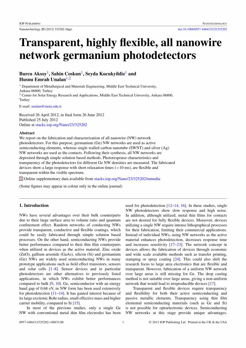
Figure 1. (a) SEM and (b) TEM image of the as-synthesized Ge NWs. (c) XRD pattern for the NWs (JCPDS Card no. 04-0545). (d) TEMimage of HBr etched single crystal Ge NWs without oxide layer.
filtered onto MCE membranes. A similar filtration processwas applied by Smith et al to produce Ge NW fabric [45].Then, the filter paper was stamped onto device substrates anddissolved through consecutive acetone washings, allowing thetransfer of the Ge NW network onto the device substrate.
For the fabrication of photodetectors, SWNT or Ag NWnetworks were coated onto device substrates as describedbefore. This was followed by a 20 µm gap formation simplyby mechanical scratching with a scalpel. After that, Ge NWnetworks were deposited in between the SWNT or Ag NWnetwork electrodes as mentioned before.
The devices were also characterized by SEM. For SEManalysis, the photodetectors on glass and PET substrateswere coated with a thin layer of gold. Current–voltage(I–V) characteristics of the photodetectors were obtainedusing a Keithley 2400 sourcemeter and an AM 1.5G solarsimulator was used as the light source. Photoresponsetime was measured with a semiconductor parameteranalyzer using a 2 kW white light source. All I–Vand photoresponse measurements have been carried out atatmospheric conditions.
3. Results and discussion
3.1. Ge NW growth
Morphologies of the as-synthesized Ge NWs are shown infigures 1(a), (b) and (d). The SEM image in figure 1(a) showsGe NWs with high aspect ratio. The TEM image in figure 1(b)illustrates the oxidized surface of the as-synthesized Ge
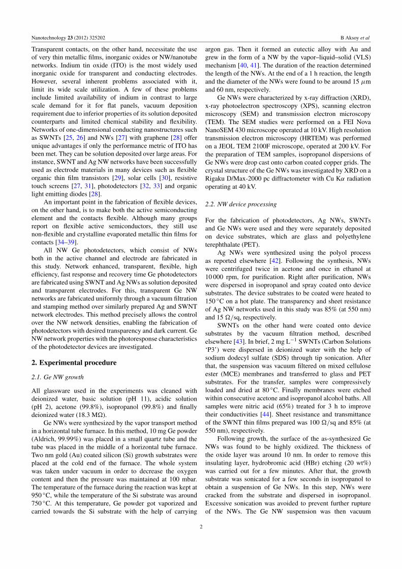
Figure 2. Photographs of (a) ethanolic dispersion of Ge NWs,(b) Ge NWs on the filtration membrane after vacuum filtration,(c) Ge NW networks on glass substrate.
NWs. A typical 10 nm thick oxide layer was observedwithin the growth pressure and temperature investigated. Theoxide free Ge NWs were obtained after etching, as can beseen in figure 1(d). Oxide removal was also confirmed byXPS analysis (figure S1 available at stacks.iop.org/Nano/23/325202/mmedia). XRD analysis in figure 1(c) showed that theNWs consist of only Ge without any noticeable impurities.
3.2. NW device processing
The fabrication procedure of Ge NW networks is illustratedin figure 2. Figure 2(a) shows a Ge NW solution aftersonication and figure 2(b) shows Ge NWs on filter paper with
3
Nanotechnology 23 (2012) 325202 B Aksoy et al
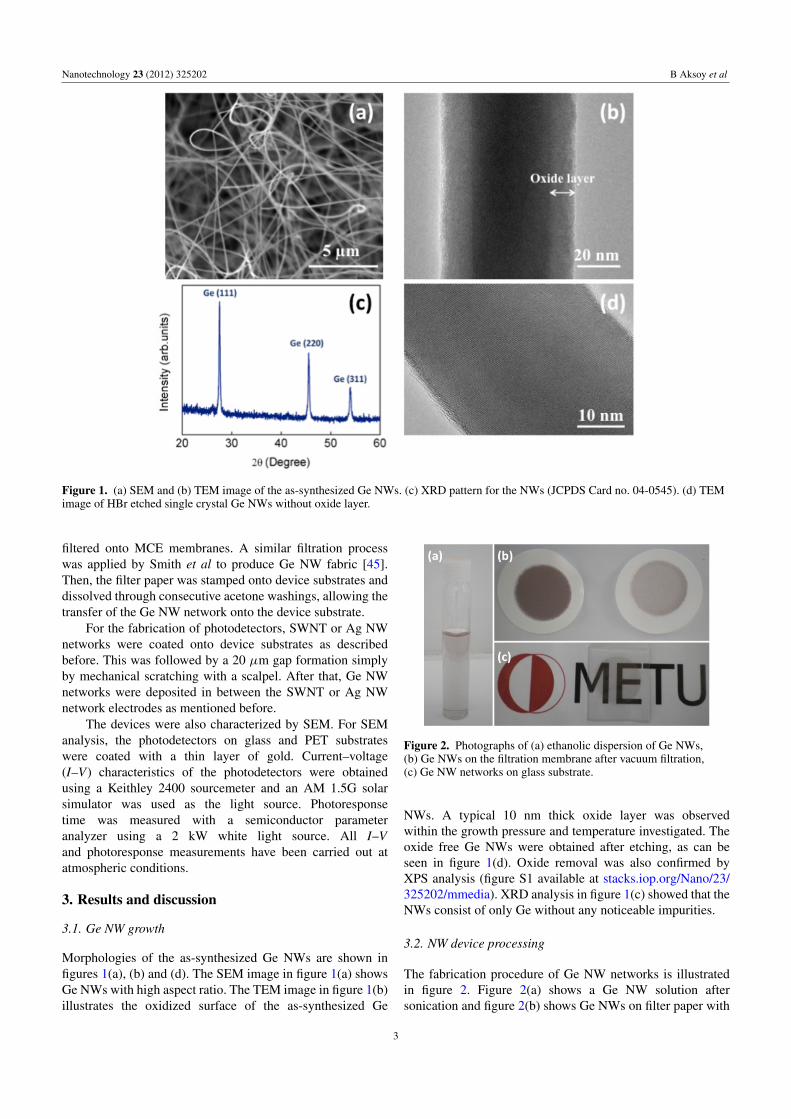
Figure 3. SEM images of Ge NW networks deposited onto glass substrates with densities of (a) 1.4, (b) 1.8, (c) 2.0 and (d) 2.5 NWs µm−2.(e) Transparency of the Ge NW networks with different densities. (f) Resistance variation of the networks with transparency measured at550 nm.
two different densities following vacuum filtration. Densityof the NWs could be controlled in this step by filteringthe desired amount of NW solution, which can also controlthe conductivity and transparency of the network. The finalstructure of the Ge NW network on a glass substrate canbe seen in figure 2(c). The etched NWs were sonicatedin a 20 ml ethanol solution. Then 2, 4, 6, and 8 mlof the same solution was filtered and stamped to obtainnetworks with different densities, as shown in figures 3(a)–(d).Corresponding densities for these solutions were computedto be 1.4, 1.8, 2.0 and 2.5 NWs µm−2, respectively. ImageJ (software developed by National Institutes of Health) wasused for the network density calculations. Figure 3(e) plots thetransparency variation of the Ge NW networks with differentdensities within the wavelength range of 300–800 nm. Arelatively uniform transmittance was obtained within the
investigated range. Transmittance was 75% (at 550 nm) forthe network with a density of 1.4 NWsµm−2, and it decreaseddown to 40% for a network with a density of 2.5 NWs/µm2.In figure 3(f), the relation between transparency and darkresistance of the NW network is shown. As expected,transparency decreases as dark resistance decreases, due tocreation of alternate current paths.
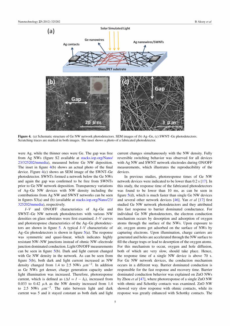
Figure 4(a) shows the schematic of the fabricatedphotodetectors. For this, Ge NW networks were depositedonto prior deposited and scratched Ag NW and SWNTnetworks. Ge NWs were in direct contact with Ag NWs andSWNTs. During the I–V and light ON/OFF measurements,silver paint was used as contact pads. Both Ag–Ge andSWNT–Ge photodetectors were examined on PET and glasssubstrates. An SEM image of the channel region of theAg–Ge photodetector is shown in figure 4(b). Thicker NWs
4
Nanotechnology 23 (2012) 325202 B Aksoy et al
Figure 4. (a) Schematic structure of Ge NW network photodetectors. SEM images of (b) Ag–Ge, (c) SWNT–Ge photodetectors.Scratching traces are marked in both images. The inset shows a photo of a fabricated photodetector.
were Ag, while the thinner ones were Ge. The gap was freefrom Ag NWs (figure S2 available at stacks.iop.org/Nano/23/325202/mmedia), measured before Ge NW deposition.The inset in figure 4(b) shows an actual photo of the finaldevice. Figure 4(c) shows an SEM image of the SWNT–Gephotodetector. SWNTs formed a network below the Ge NWsand again the gap was confirmed to be free from SWNTsprior to Ge NW network deposition. Transparency variationsof Ag–Ge NW devices with NW density including thecontributions from Ag NW and SWNT networks can be seenin figures S3(a) and (b) (available at stacks.iop.org/Nano/23/325202/mmedia), respectively.
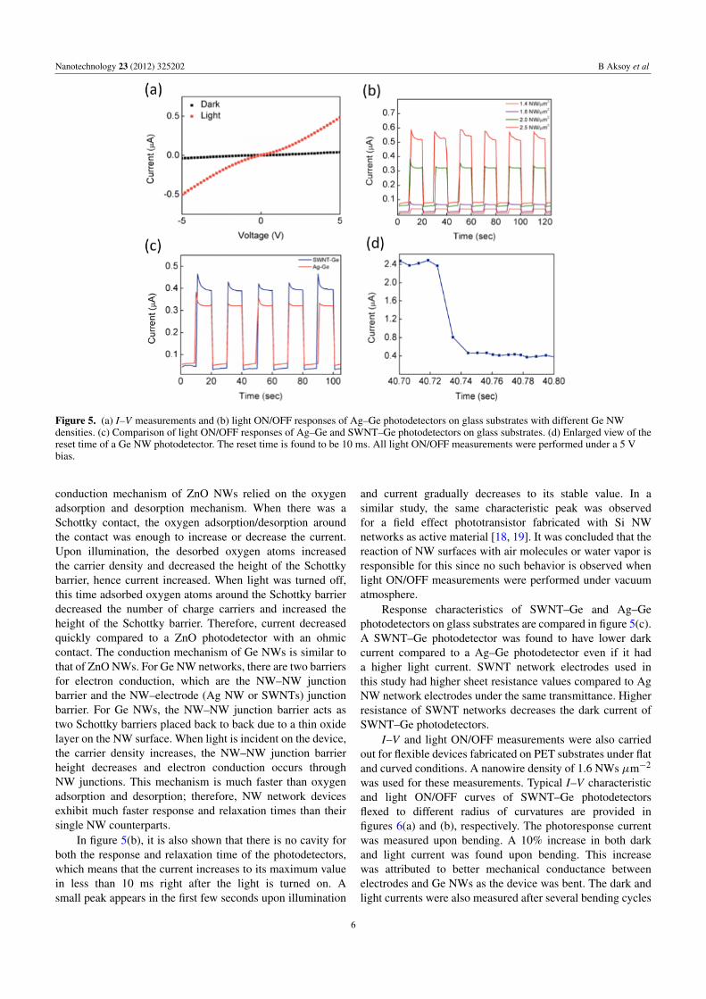
I–V and ON/OFF characteristics of Ag–Ge andSWNT–Ge NW network photodetectors with various NWdensities on glass substrates were first examined. I–V curvesand photoresponse characteristics of the Ag–Ge photodetec-tors are shown in figure 5. A typical I–V characteristic ofAg–Ge photodetectors is shown in figure 5(a). The responsewas symmetric and quasi-linear, which indicates highlyresistant NW–NW junctions instead of ohmic NW–electrodejunction dominated conduction. Light ON/OFF measurementscan be seen in figure 5(b). Dark and light current changedwith Ge NW density in the network. As can be seen fromfigure 5(b), both dark and light current increased as NWdensity changed from 1.4 to 2.5 NWs µm−2. In additionas Ge NWs get denser, charge generation capacity underlight illumination was increased. Therefore, photoresponsecurrent, which is defined as (1I = I − I0), increased from0.033 to 0.42 µA as the NW density increased from 1.4to 2.5 NWs µm−2. The ratio between light and darkcurrent was 5 and it stayed constant as both dark and light
current changes simultaneously with the NW density. Fullyreversible switching behavior was observed for all deviceswith Ag NW and SWNT network electrodes during ON/OFFmeasurements, which illustrates the reproducibility of thedevices.
In previous studies, photoresponse times of Ge NWnetwork devices were indicated to be lower than 0.2 s [17]. Inthis study, the response time of the fabricated photodetectorswas found to be lower than 10 ms, as can be seen infigure 5(d), which is much faster than single Ge NW devicesand several other network devices [46]. Yan et al [17] firststudied Ge NW network photodetectors and they attributedthis fast response to barrier dominated conductance. Forindividual Ge NW photodetectors, the electron conductionmechanism occurs by desorption and adsorption of oxygenatoms through the surface of the NWs. Upon exposure toair, oxygen atoms get adsorbed on the surface of NWs bycapturing electrons. Upon illumination, charge carriers aregenerated and holes are accelerated through the NW surface tofill the charge traps or lead to desorption of the oxygen atoms.For this mechanism to occur, oxygen and hole diffusion,both of which are very slow, should take place. Hence,the response time of a single NW device is above 70 s.For Ge NW network devices, the conduction mechanismoccurs in a different way. Barrier dominated conduction isresponsible for the fast response and recovery time. Barrierdominated conduction behavior was explained on ZnO NWsby Zhou et al [47], where photoresponse of a single ZnO NWwith ohmic and Schottky contacts was examined. ZnO NWshowed very slow response with ohmic contacts, while itsresponse was greatly enhanced with Schottky contacts. The
5
Nanotechnology 23 (2012) 325202 B Aksoy et al
Figure 5. (a) I–V measurements and (b) light ON/OFF responses of Ag–Ge photodetectors on glass substrates with different Ge NWdensities. (c) Comparison of light ON/OFF responses of Ag–Ge and SWNT–Ge photodetectors on glass substrates. (d) Enlarged view of thereset time of a Ge NW photodetector. The reset time is found to be 10 ms. All light ON/OFF measurements were performed under a 5 Vbias.
conduction mechanism of ZnO NWs relied on the oxygenadsorption and desorption mechanism. When there was aSchottky contact, the oxygen adsorption/desorption aroundthe contact was enough to increase or decrease the current.Upon illumination, the desorbed oxygen atoms increasedthe carrier density and decreased the height of the Schottkybarrier, hence current increased. When light was turned off,this time adsorbed oxygen atoms around the Schottky barrierdecreased the number of charge carriers and increased theheight of the Schottky barrier. Therefore, current decreasedquickly compared to a ZnO photodetector with an ohmiccontact. The conduction mechanism of Ge NWs is similar tothat of ZnO NWs. For Ge NW networks, there are two barriersfor electron conduction, which are the NW–NW junctionbarrier and the NW–electrode (Ag NW or SWNTs) junctionbarrier. For Ge NWs, the NW–NW junction barrier acts astwo Schottky barriers placed back to back due to a thin oxidelayer on the NW surface. When light is incident on the device,the carrier density increases, the NW–NW junction barrierheight decreases and electron conduction occurs throughNW junctions. This mechanism is much faster than oxygenadsorption and desorption; therefore, NW network devicesexhibit much faster response and relaxation times than theirsingle NW counterparts.
In figure 5(b), it is also shown that there is no cavity forboth the response and relaxation time of the photodetectors,which means that the current increases to its maximum valuein less than 10 ms right after the light is turned on. Asmall peak appears in the first few seconds upon illumination
and current gradually decreases to its stable value. In asimilar study, the same characteristic peak was observedfor a field effect phototransistor fabricated with Si NWnetworks as active material [18, 19]. It was concluded that thereaction of NW surfaces with air molecules or water vapor isresponsible for this since no such behavior is observed whenlight ON/OFF measurements were performed under vacuumatmosphere.
Response characteristics of SWNT–Ge and Ag–Gephotodetectors on glass substrates are compared in figure 5(c).A SWNT–Ge photodetector was found to have lower darkcurrent compared to a Ag–Ge photodetector even if it hada higher light current. SWNT network electrodes used inthis study had higher sheet resistance values compared to AgNW network electrodes under the same transmittance. Higherresistance of SWNT networks decreases the dark current ofSWNT–Ge photodetectors.
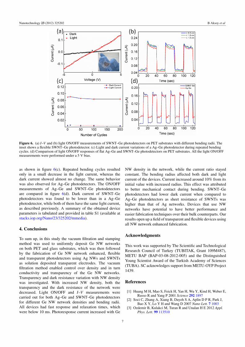
I–V and light ON/OFF measurements were also carriedout for flexible devices fabricated on PET substrates under flatand curved conditions. A nanowire density of 1.6 NWs µm−2
was used for these measurements. Typical I–V characteristicand light ON/OFF curves of SWNT–Ge photodetectorsflexed to different radius of curvatures are provided infigures 6(a) and (b), respectively. The photoresponse currentwas measured upon bending. A 10% increase in both darkand light current was found upon bending. This increasewas attributed to better mechanical conductance betweenelectrodes and Ge NWs as the device was bent. The dark andlight currents were also measured after several bending cycles
6
Nanotechnology 23 (2012) 325202 B Aksoy et al
Figure 6. (a) I–V and (b) light ON/OFF measurements of SWNT–Ge photodetectors on PET substrates with different bending radii. Theinset shows a flexible SWNT–Ge photodetector. (c) Light and dark current variations of a Ag–Ge photodetector during repeated bendingcycles. (d) Comparison of light ON/OFF responses of flat Ag–Ge and SWNT–Ge photodetectors on PET substrates. All the light ON/OFFmeasurements were performed under a 5 V bias.
as shown in figure 6(c). Repeated bending cycles resultedonly in a small decrease in the light current, whereas thedark current showed almost no change. The same behaviorwas also observed for Ag–Ge photodetectors. The ON/OFFmeasurements of Ag–Ge and SWNT–Ge photodetectorsare compared in figure 6(d). Dark current of SWNT–Gephotodetectors was found to be lower than in a Ag–Gephotodetector, while both of them have the same light current,as described previously. A summary of the obtained deviceparameters is tabulated and provided in table S1 (available atstacks.iop.org/Nano/23/325202/mmedia).
4. Conclusions
To sum up, in this study the vacuum filtration and stampingmethod was used to uniformly deposit Ge NW networkson both PET and glass substrates, which was then followedby the fabrication of Ge NW network enhanced, flexibleand transparent photodetectors using Ag NWs and SWNTsas solution deposited transparent electrodes. The vacuumfiltration method enabled control over density and in turnconductivity and transparency of the Ge NW networks.Transparency and dark resistance variation with NW densitywas investigated. With increased NW density, both thetransparency and the dark resistance of the network weredecreased. Light ON/OFF and I–V measurements werecarried out for both Ag–Ge and SWNT–Ge photodetectorsfor different Ge NW network densities and bending radii.All devices had fast response and relaxation times, whichwere below 10 ms. Photoresponse current increased with Ge
NW density in the network, while the current ratio stayedconstant. The bending radius affected both dark and lightcurrent of the devices. Current increased around 10% from itsinitial value with increased radius. This effect was attributedto better mechanical contact during bending. SWNT–Gephotodetectors had lower dark current when compared toAg–Ge photodetectors as sheet resistance of SWNTs washigher than that of Ag networks. Devices that use NWnetworks have potential to have better performance andeasier fabrication techniques over their bulk counterparts. Ourresults open up a field of transparent and flexible devices usingall NW network enhanced fabrication.
Acknowledgments
This work was supported by The Scientific and TechnologicalResearch Council of Turkey (TUBITAK, Grant 109M487),METU BAP (BAP-03-08-2012-005) and the DistinguishedYoung Scientist Award of the Turkish Academy of Sciences(TUBA). SC acknowledges support from METU-OYP Project1439.
References
[1] Huang M H, Mao S, Feick H, Yan H, Wu Y, Kind H, Weber E,Russo R and Yang P 2001 Science 292 1897
[2] Soci C, Zhang A, Xiang B, Dayeh S A, Aplin D P R, Park J,Bao X Y, Lo Y H and Wang D 2007 Nano Lett. 7 1003
[3] Ozdemir B, Kulakci M, Turan R and Unalan H E 2012 Appl.Phys. Lett. 99 113510
7
Nanotechnology 23 (2012) 325202 B Aksoy et al
[4] Duan X, Niu C, Sahi V, Chen J, Parce J W, Empedocles S andGoldman J L 2003 Nature 425 274
[5] Wang Z L and Song J 2006 Science 312 242[6] Moon K J, Choi J H, Lee T I, Ham M H, Maeng W J,
Hwang I, Kim H and Myoung J M 2010 Microelectron.Eng. 87 2407
[7] Smith P A, Nordquist C D, Jackson T N, Mayer T S andMartin B R 2000 Appl. Phys. Lett. 77 1399
[8] Cui Y, Wei Q, Park H and Lieber C M 2001 Science 293 1289[9] Cao L, White J S, Park J-S, Schuller J A, Clemens B M and
Brongersma M L 2009 Nature Mater. 8 643[10] Duan X, Huang Y, Cui Y, Wang J and Lieber C M 2011
Nature 409 66[11] Gu G, Burghard M, Kim G T, Dusberg G S, Chiu P W,
Krstic V, Roth S and Han W Q 2001 J. Appl. Phys. 90 5747[12] Ahn Y H and Park J 2007 Appl. Phys. Lett. 91 162102[13] Colace L, Sorianello V, Balbi M and Assanto G 2007 Appl.
Phys. Lett. 91 021107[14] Claeys C and Smoen E 2007 Germanium-Based Technologies
From Materials to Devices (Amsterdam: Elsevier)[15] Ogawa Y, Yuasa Y, Minami F and Oda S 2011 Appl. Phys.
Lett. 99 053112[16] Gu G, Burghard M, Kim G T, Dusberg G S, Chiu P W,
Krstic V, Roth S and Han W Q 2001 J. Appl. Phys. 90 5747[17] Yan C, Singh N, Cai H, Gan C L and Lee P S 2010 ACS Appl.
Mater. Interfaces 2 1794[18] Huang B R, Hsu J F, Huang C S, Shih Y T and Lu K S 2007
Mater. Sci. Eng. 27 1197[19] Zhou X T, Hu J Q, Li C P, Ma D D D, Lee C S and
Lee S T 2003 Chem. Phys. Lett. 369 220[20] Yan C, Singh N and Lee P S 2010 Appl. Phys. Lett. 96 053108[21] Sahoo S, Husale S, Colwill B, Lu T-M, Nayak S and
Ajayan P M 2009 ACS Nano 3 3935[22] Lin C C, Lin W H and Li Y Y 2009 J. Nanosci. Nanotechnol.
9 2813[23] Bao H, Li C M, Cui X, Song Q, Yang H and Guo J 2008
Nanotechnology 19 335302[24] Unalan H E, Zhang Y, Hiralal P, Dalal S, Chu D, Eda G,
Teo K B K, Chhowalla M, Milne W I andAmaratunga G A J 2009 Appl. Phys. Lett. 94 163501
[25] Pasquier A D, Unalan H E, Kanwal A, Miller S andChhowalla M 2005 Appl. Phys. Lett. 87 203511
[26] Unalan H E, Fanchini G, Kanwal A, Pasquier A D andChhowalla M 2006 Nano Lett. 6 677
[27] De S, Miggins T M, Lyons P E, Doherty E M, Nirmalraj P N,Blau W J, Boland J J and Coleman J N 2009 ACS Nano3 1767
[28] Wu J, Agrawal M, Becerril H A, Bao Z, Liu Z, Chen Y andPeumans P 2010 ACS Nano 4 43
[29] Cao Q, Zhu Z T, Lemaitre M G, Xia M G and Shim M 2006Appl. Phys. Lett. 88 113511
[30] Rowell M W, Topinka M A, McGehee M D, Prall H J,Dennler G, Sariciftci N S, Hu L and Gruner G 2006Appl.Phys. Lett. 88 233506
[31] Hu L, Hecht D S and Gruuner G 2009 Appl. Phys. Lett.94 081103
[32] Bonaccorso F, Sun Z, Hasan T and Ferrari A C 2010 NaturePhoton. 4 611
[33] Behnam A, Johnson J, Choi Y, Noriega L, Ertosun M G,Wu Z, Rinzler A G, Kapur P, Saraswat K C andUral A 2008 J. Appl. Phys. 103 114315
[34] Yuan L et al 2011 ACS Nano 5 4007[35] McAlpine M C, Ahmad H, Wang D and Heat J R 2007 Nature
Mater. 6 379[36] Zhang W F, He Z B, Yuan G D, Jie J S, Luo L B, Zhang X J,
Chen Z H, Lee C S, Zhang W J and Lee S T 2012 Appl.Phys. Lett. 94 123103
[37] Nadarajah A, Word R C, Meiss J and Konenkamp R 2008Nano Lett. 8 534
[38] Zhu G, Yang R, Wang S and Wang Z L 2010 Nano Lett.10 3151
[39] Kuang D, Brillet J, Chen P, Takata M, Uchida S, Miura H,Sumioka K, Zakeeruddin S M and Gratzel M 2008 ACSNano 2 1113
[40] Dailey J W, Taraci J, Clement T, Smith D J, Drucker J andPicraux S T 2004 J. Appl. Phys. 96 7556
[41] Wagner R S and Ellis W C 1964 Appl. Phys. Lett. 4 89[42] Coskun S, Aksoy B and Unalan H E 2011 Cryst. Growth Des.
11 4963[43] Fanchini G, Unalan H E and Chhowalla M 2006 Appl. Phys.
Lett. 88 191919[44] Parekh B B, Fanchini G, Eda G and Chhowalla M 2007 Appl.
Phys. Lett. 90 121913[45] Smith D A 2009 Mechanical, electromechanical and optical
properties of germanium nanowires PhD Thesis Universityof Texas, Austin
[46] Heo K et al 2012 J. Mater. Chem. 22 2173[47] Zhou J, Gu Y, Hu Y, Mai W, Yeh P H, Bao G, Sood A K,
Polla D L and Wang Z L 2009 Appl. Phys. Lett. 94 191103
8


