Embed Size (px)
Citation preview
© 2006 Panasonic Shikoku Electronics Co., Ltd. Allrights reserved. Unauthorized copying anddistribution is a violation of law.
PT-60LCX64-KMulti Media Display
ORDER NO. MKE0601864CE
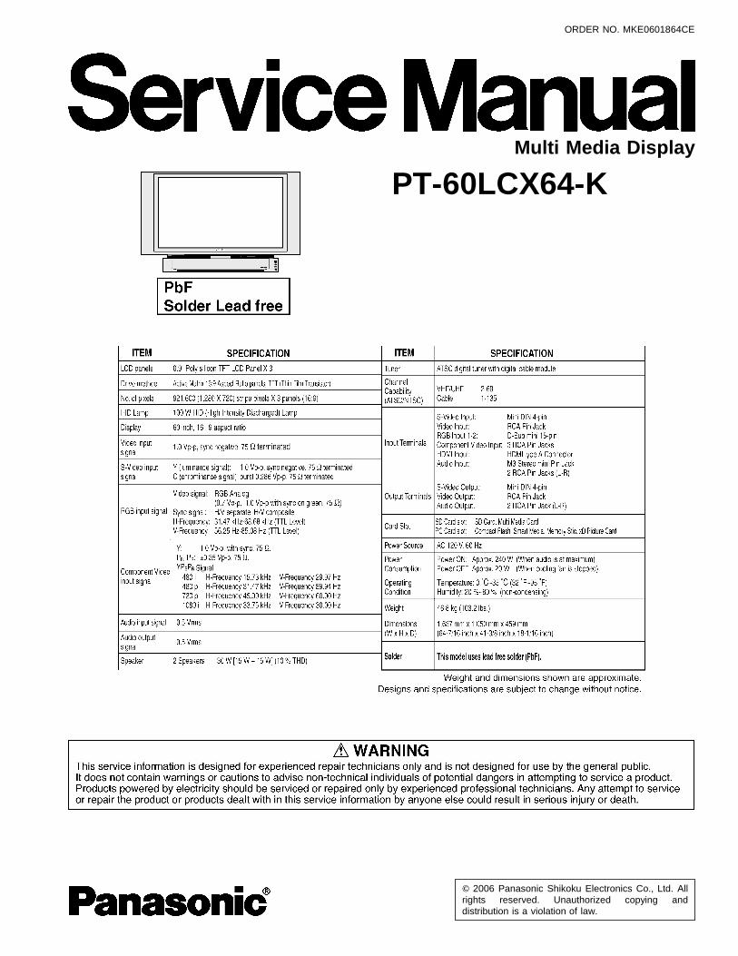
1 SAFETY PRECAUSIONS 3
1.1. GENERAL GUIDELINES 3
1.2. LEAKAGE CURRENT COLD CHECK 3
1.3. LEAKAGE CURRENT HOT CHECK 3
1.4. UV-PRECAUTION 3
2 PREVENTION OF ELECTROSTATIC DISCHARGE (ESD) TO
ELECTROSTATICALLY SENSITIVE (ES) DEVICES 4
3 ABOUT LEAD FREE SOLDER (PbF) 5
4 SERVICE NOTES 6
5 SERVICE POSITION 28
6 DISASSEMBLY/ASSEMBLY PROCEDURES 46
6.1. CABINET SECTION 46
6.2. PROJECTION SECTION 72
7 SERVICE FIXTURES AND TOOLS 82
8 ADJUSTMENT PROCEDURES 1 84
9 ADJUSTMENT PROCEDURES 2 87
10 TROUBLESHOOTING HINTS 112
10.1. TROUBLESHOOTING HINTS FOR BLOCK LEVEL
REPAIR 112
10.2. TROUBLESHOOTING HINTS FOR COMPONENT LEVEL
REPAIR 117
11 BLOCK DIAGRAMS 141
12 SCHEMATIC DIAGRAMS 159
12.1. SCHEMATIC DIAGRAM & CIRCUIT BOARD LAYOUT
NOTES 159
12.2. INTERCONNECTION SCHEMATIC DIAGRAM 160
12.3. MAIN SCHEMATIC DIAGRAMS 161
12.4. POWER SCHEMATIC DIAGRAMS 179
12.5. BALLAST SCHEMATIC DIAGRAM 181
12.6. REAR JACK SCHEMATIC DIAGRAM 182
12.7. LCD DRIVE SCHEMATIC DIAGRAM (Models: PT-
43LCX64/PT-50LCX64) 186
12.8. LCD DRIVE SCHEMATIC DIAGRAM (Model: PT-
60LCX64) 194
12.9. FRONT JACK SCHEMATIC DIAGRAM 202
12.10. NETWORK / THERMISTOR 1 / THERMISTOR 2 /
OPERATION / COVER SWITCH SCHEMATIC
DIAGRAMS 203
12.11. AUDIO AMP SCHEMATIC DIAGRAM 204
12.12. TUNER SCHEMATIC DIAGRAM 205
12.13. DIGITAL TUNER POWER SCHEMATIC DIAGRAM 206
12.14. VOLTAGE CHART 207
13 CIRCUIT BOARD LAYOUT 215
13.1. MAIN C.B.A. 215
13.2. POWER C.B.A. 217
13.3. BALLAST C.B.A. 218
13.4. REAR JACK C.B.A 219
13.5. LCD DRIVE C.B.A. (Models: PT-43LCX64/PT-50LCX64)
221
13.6. LCD DRIVE C.B.A. (Model: PT-60LCX64) 223
13.7. FRONT JACK C.B.A. / OPERATION C.B.A. / NETWORK
C.B.A. 225
13.8. AUDIO AMP C.B.A. / THERMISTOR 1 C.B.A. /
THERMISTOR 2 C.B.A. / COVER SWITCH C.B.A. 226
13.9. TUNER C.B.A. / DIGITAL TUNER POWER C.B.A. 227
14 EXPLODED VIEWS (CABINET SECTION) 229
14.1. MAIN PARTS SECTION 229
14.2. FRONT AND BASE SECTION 230
14.3. DISPLAY SECTION 231
14.4. PROJECTION SECTION 233
14.5. TV AND TUNER SECTION (1) 234
14.6. TV AND TUNER SECTION (2) 235
14.7. BALLAST C.B.A. SECTION 236
14.8. PACKING PARTS AND ACCESSORIES SECTION 237
15 REPLACEMENT PARTS LIST (CABINET SECTION) 238
15.1. REPLACEMENT NOTES 238
15.2. MECHANICAL REPLACEMENT PARTS LIST 239
15.3. OPTIONAL ACCESSORY REPLACEMENT PARTS LIST
240
15.4. SERVICE FIXTURES AND TOOLS REPLACEMENT
PARTS LIST 241
15.5. ELECTRICAL REPLACEMENT PARTS LIST 241
16 EXPLODED VIEWS (PROJECTION SECTION) 265
16.1. PROJECTION SECTION (1) 265
16.2. PROJECTION SECTION (2) 266
16.3. PROJECTION SECTION (3) 267
16.4. PROJECTION SECTION (4) 268
17 REPLACEMENT PARTS LIST (PROJECTION SECTION) 269
17.1. REPLACEMENT NOTES 269
17.2. MECHANICAL REPLACEMENT PARTS LIST 270
17.3. OPTIONAL ACCESSORY REPLACEMENT PARTS LIST
271
17.4. ELECTRICAL REPLACEMENT PARTS LIST 271
CONTENTS Page Page
2
PT-60LCX64-K
1 SAFETY PRECAUSIONS1.1. GENERAL GUIDELINES 1. For continued safety, no modification of any circuit should
be attempted.
2. Disconnect AC Plug before disassembling this unit.
3. It is advisable to use an isolation transformer in the ACsupply before servicing.
4. When servicing, observe the original lead dress. If a shortcircuit is found, replace all parts which have beenoverheated or damaged by the short circuit.
5. After servicing, see to it that all the protective devices suchas insulation barriers, insulation papers, shield, andisolation R-C combinations etc. are properly installed.
6. After servicing, be sure to restore the wires, leads,insulation barriers, shields, etc.
7. After servicing, make the leakage current checks to preventthe customer from being exposed to shock hazards.
Caution:
Use a separate Isolation Transformer for this unit whenservicing.
1.2. LEAKAGE CURRENT COLDCHECK
1. Unplug the AC cord and connect a jumper between the twoprongs on the plug.
2. For physically operated power switches, turn power on.Otherwise skip step 2.
3. Measure the resistance value, with an ohmmeter, betweenthe jumpered AC plug and each exposed metallic cabinetpart on the receiver, such as screwheads, connectors, etc.When the exposed metallic part has a return path to thechassis, the reading should be between 1 MΩ and 12 MΩ.When the exposed metal does not have a return path to thechassis, the reading must be infinity.
1.3. LEAKAGE CURRENT HOTCHECK
1. Plug the AC cord directly into the AC outlet.
Do not use a isolation transformer for this check.
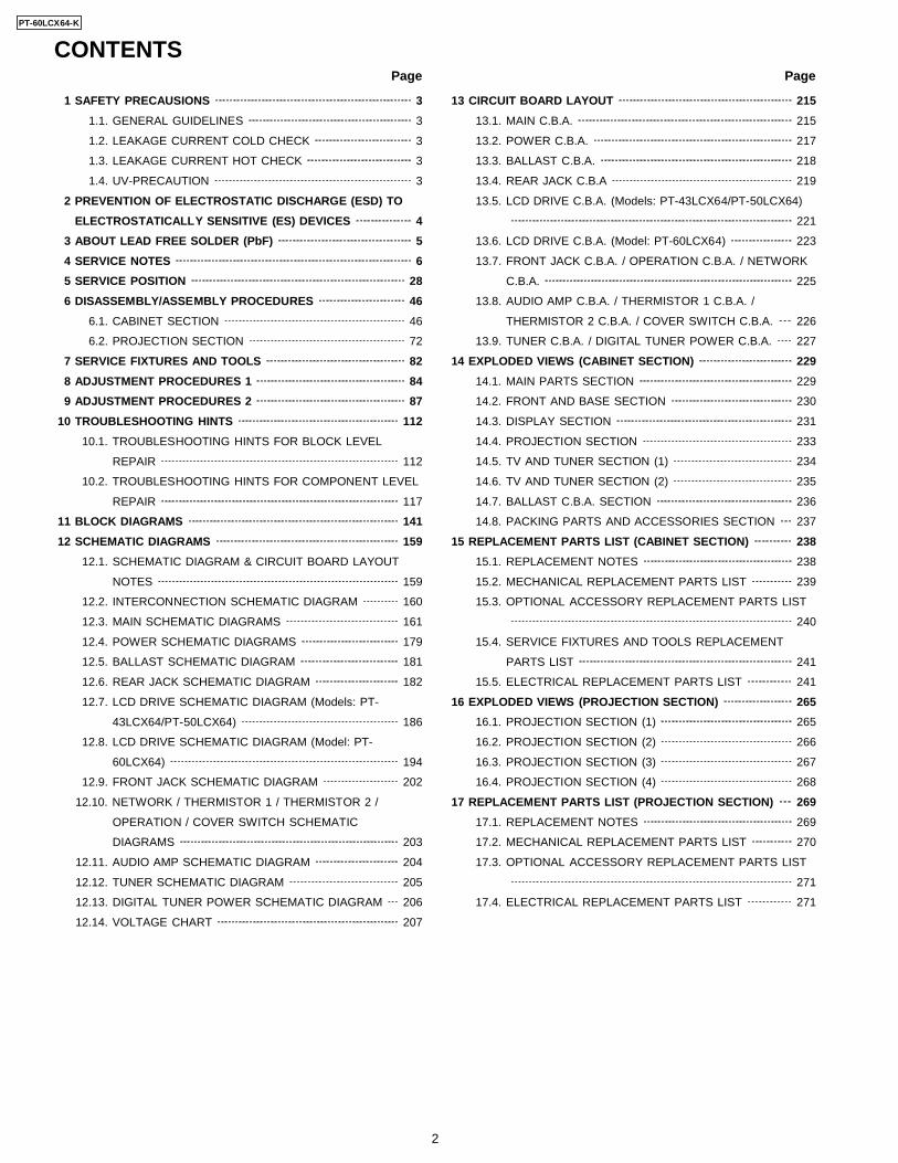
2. Connect a 1.5 kΩ, 10 W resistor, in parallel with a 0.15 µFcapacitor, between each exposed metallic part on the setand a good earth ground, as shown in Figure 1.
3. Use an AC voltmeter, with 1 kΩ/V or more sensitivity, tomeasure the potential across the resistor.
4. Check each exposed metallic part, and measure thevoltage at each point.
5. Reverse the AC plug in the AC outlet and repeat each of theabove measurements.
6. The potential at any point should not exceed 0.75 V RMS.
A leakage current tester (Simpson Model 229 equivalent)may be used to make the hot checks. Leakage current must
not exceed 1/2 mA. In case a measurement is outside ofthe limits specified, there is a possibility of shock hazard,and the receiver should be repaired and rechecked beforeit is returned to the customer.
Figure 1
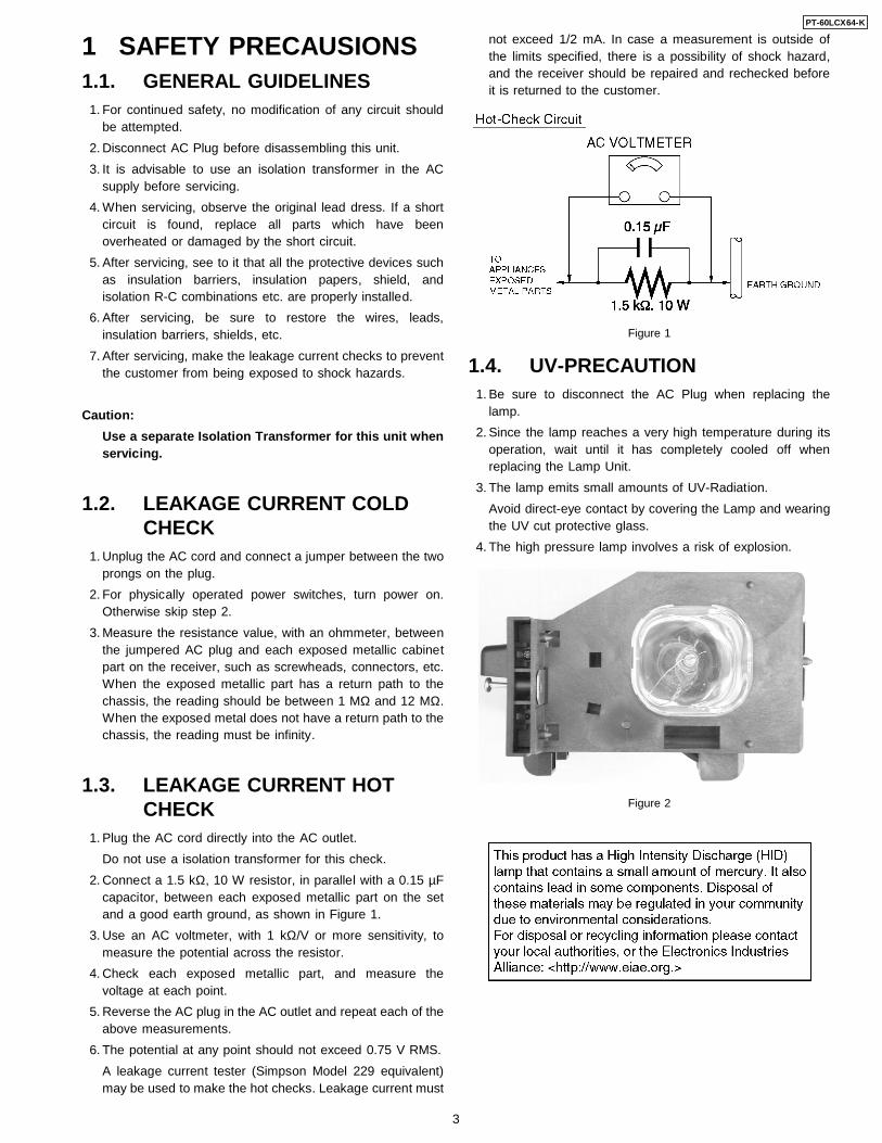
1.4. UV-PRECAUTION 1. Be sure to disconnect the AC Plug when replacing the
lamp.
2. Since the lamp reaches a very high temperature during itsoperation, wait until it has completely cooled off whenreplacing the Lamp Unit.
3. The lamp emits small amounts of UV-Radiation.
Avoid direct-eye contact by covering the Lamp and wearingthe UV cut protective glass.
4. The high pressure lamp involves a risk of explosion.
Figure 2
3
PT-60LCX64-K
2 PREVENTION OFELECTROSTATICDISCHARGE (ESD) TOELECTROSTATICALLYSENSITIVE (ES) DEVICES
Some semiconductor (solid state) devices can be damagedeasily by static electricity. Such components commonly arecalled Electrostatically Sensitive (ES) Devices. Examples oftypical ES devices are integrated circuits and some field-effecttransistors and semiconductor "chip" components. Thefollowing techniques should be used to help reduce theincidence of component damage caused by electro staticdischarge (ESD).
1. Immediately before handling any semiconductorcomponent or semiconductor-equipped assembly, drain offany ESD on your body by touching a known earth ground.Alternatively, obtain and wear a commercially availabledischarging ESD wrist strap, which should be removed forpotential shock reasons prior to applying power to the unitunder test.
2. After removing an electrical assembly equipped with ESdevices, place the assembly on a conductive surface suchas aluminum foil, to prevent electrostatic charge buildup orexposure of the assembly.
3. Use only a grounded-tip soldering iron to solder or unsolderES devices.
4. Use only an antistatic solder removal device. Some solderremoval devices not classified as "antistatic (ESDprotected)" can generate electrical charge sufficient todamage ES devices.
5. Do not use freon-propelled chemicals. These can generateelectrical charges sufficient to damage ES devices.
6. Do not remove a replacement ES device from its protectivepackage until immediately before you are ready to install it.(Most replacement ES devices are packaged with leadselectrically shorted together by conductive foam, aluminumfoil or comparable conductive material).
7. Immediately before removing the protective material fromthe leads of a replacement ES device, touch the protectivematerial to the chassis or circuit assembly into which thedevice will be installed.
CAUTION :
Be sure no power is applied to the chassis or circuit, andobserve all other safety precautions.
8. Minimize bodily motions when handling unpackagedreplacement ES devices. (Otherwise harmless motion suchas the brushing together of your clothes fabric or the liftingof your foot from a carpeted floor can generate staticelectricity (ESD) sufficient to damage an ES device).
4
PT-60LCX64-K
3 ABOUT LEAD FREE SOLDER (PbF)
5
PT-60LCX64-K
4 SERVICE NOTES
LED INDICATIONS FOR ERROR CONDITIONEach LED indication facilitates finding the cause of the error.When an error is detected, the Lamp comes off and the LED on the front will flash.
TEMP LED
POWER LED
LAMP LED
TV/VIDEO
Error InformationError No. LAMP OFFLAMP LED OSD
(Note 2) (Note 3)
TEMP LEDPOWER LED
Note:1. When two or more errors have occurred at the same time, the LED will alternate flash patterns as shown above every 5 seconds.2. Warning OSD appears when the air filter is clogged.3. LAMP OFF: The LED will flash immediately after the Lamp comes off.
Clogged air filter17)
1)
2)
3)
4)
6)
7)
8)
12)
9)
10)
11)
15)
16)
flashes 5 times every 5 seconds
Fan1, Fan2 or Fan3 stopped flashes orange once every 5 seconds - -
Lamp Cover open
Temperature Sensor shorted or open(Thermistor 1 C.B.A.)
flashes orange twice every 5 seconds
flashes orange 5 times every 5 seconds
flashes orange 6 times every 5 seconds
flashes orange 7 times every 5 seconds
flashes orange 8 times every 5 seconds
flashes onceevery 5 seconds
flashes onceevery 5 seconds
flashes onceevery 5 seconds
-
-
-
-
Abnormal Temperature(Thermistor 1 C.B.A.)
flashes twiceevery 5 seconds
flashes twiceevery 5 seconds
- -
Ballast Error (abnormal Lamp voltage) -
flashes 3 times every 5 seconds
Ballast Error (abnormal temperature)-
flashes 4 times every 5 seconds
Ballast Error (other causes)-
-
-
-
-
-
-
-
-
-
Abnormal Voltage on 33 V line
flashes twiceevery 5 seconds
flashes twiceevery 5 seconds
Abnormal Voltage on 9 V line
flashes 3 times every 5 seconds
flashes 3 times every 5 seconds
Abnormal Voltage on 5 V line
flashes 4 times every 5 seconds
flashes 4 times every 5 seconds
flashes 3 times every 5 seconds
flashes 4 times every 5 seconds
Abnormal Voltage on 3.3 V line
Temperature Sensor shorted or open(Thermistor 2 C.B.A.)
Abnormal Temperature(Thermistor 2 C.B.A.)
5) flashes onceevery 5 seconds
Ballast Error (abnormal Lamp or Ballast) --
13) flashes orange 9 times every 5 seconds
flashes 5 times every 5 seconds
flashes 5 times every 5 seconds
Abnormal Voltage on -5 V line
14) flashes orange 10 times every 5 seconds
flashes 6 times every 5 seconds
flashes 6 times every 5 seconds
Abnormal Voltage on 6.5 V line
-flashes green allthe time
DTV Tuner PowerError
18)-
PT-60LCX64-K
6
MAIN PARTS LOCATION
Front Jack C.B.A. Ballast C.B.A.
Audio Amp C.B.A.
Rear Jack C.B.A.Power C.B.A.
Main C.B.A. DTV Tuner Unit
TV/Tuner Unit
Tuner C.B.A.
Digital Tuner Power C.B.A.
Fan 4
Fan 5
Lamp Cover
Cover Switch C.B.A.
Front Cover Unit Operation C.B.A.
Network C.B.A.
Network C.B.A.
<Front View>
<Rear View>
Optical Cover
Rear Cover
Fan 3
Fan Case Unit(Fan 1)
Fan 2
Thermistor 2 C.B.A.
LCD Drive C.B.A.
Projection Unit
Thermistor 1 C.B.A.
Thermal Fuse Unit
Air Filter
Air Filter
Air Filter
TEMP LEDLAMP LED
POWER LED
PT-60LCX64-K
7
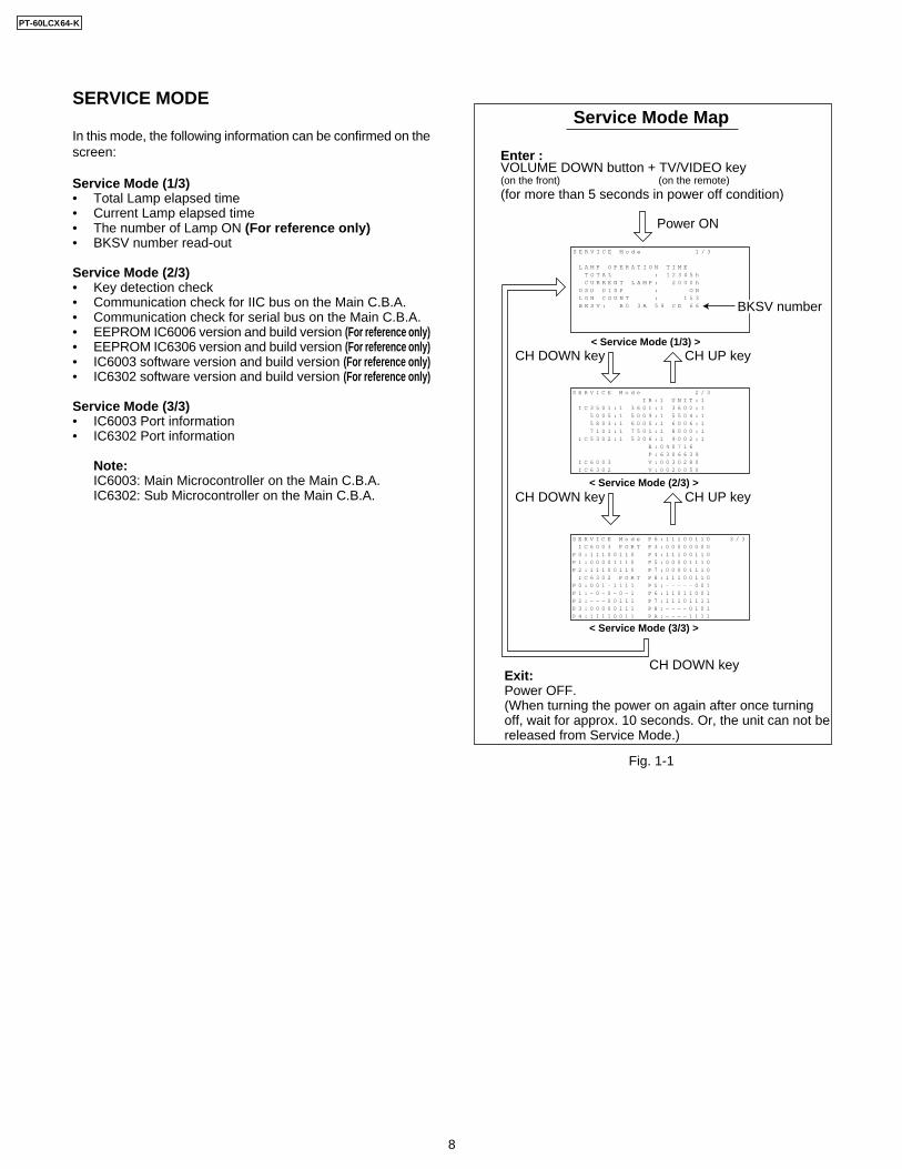
SERVICE MODE
In this mode, the following information can be confirmed on thescreen:
Service Mode (1/3)• Total Lamp elapsed time• Current Lamp elapsed time• The number of Lamp ON (For reference only)• BKSV number read-out
Service Mode (2/3)• Key detection check• Communication check for IIC bus on the Main C.B.A.• Communication check for serial bus on the Main C.B.A.• EEPROM IC6006 version and build version (For reference only)• EEPROM IC6306 version and build version (For reference only)• IC6003 software version and build version (For reference only)• IC6302 software version and build version (For reference only)
Service Mode (3/3)• IC6003 Port information• IC6302 Port information
Note:IC6003: Main Microcontroller on the Main C.B.A.IC6302: Sub Microcontroller on the Main C.B.A.
Fig. 1-1
Service Mode Map
CH DOWN key CH UP key
CH DOWN key
CH DOWN key
CH UP key
Enter :VOLUME DOWN button + TV/VIDEO key (on the front) (on the remote)(for more than 5 seconds in power off condition)
Exit:Power OFF.(When turning the power on again after once turning off, wait for approx. 10 seconds. Or, the unit can not be released from Service Mode.)
< Service Mode (2/3) >
< Service Mode (3/3) >
< Service Mode (1/3) >
S E R V I C E M o d e 1 / 3
L A M P O P E R A T I O N T I M E T O T A L : 1 2 3 4 5 h C U R R E N T L A M P : 2 0 0 0 h O S D D I S P : O N L O N C O U N T : 1 5 3 B K S V : B 0 3 A 5 9 C D 6 6
Power ON
S E R V I C E M o d e P 6 : 1 1 1 0 0 1 1 0 3 / 3 I C 6 0 0 3 P O R T P 3 : 0 0 0 0 0 0 0 0P 0 : 1 1 1 0 0 1 1 0 P 4 : 1 1 1 0 0 1 1 0P 1 : 0 0 0 0 1 1 1 0 P 5 : 0 0 0 0 1 1 1 0P 2 : 1 1 1 0 0 1 1 0 P 7 : 0 0 0 0 1 1 1 0 I C 6 3 0 2 P O R T P 8 : 1 1 1 0 0 1 1 0P 0 : 0 0 1 - 1 1 1 1 P 5 : - - - - - 0 0 1P 1 : - 0 - 0 - 0 - 1 P 6 : 1 1 0 1 1 0 0 1P 2 : - - - 0 0 1 1 1 P 7 : 1 1 1 0 1 1 1 1P 3 : 0 0 0 0 0 1 1 1 P 8 : - - - - 0 1 0 1P 4 : 1 1 1 1 0 0 1 1 P A : - - - - 1 1 1 1
S E R V I C E M o d e 2 / 3 I R : 1 U N I T : 1 I C 3 5 0 1 : 1 3 6 0 1 : 1 3 6 0 2 : 1 5 0 0 5 : 1 5 0 0 9 : 1 5 5 0 4 : 1 5 8 0 3 : 1 6 0 0 5 : 1 6 0 0 6 : 1 7 1 0 1 : 1 7 5 0 1 : 1 8 0 0 0 : 1 I C 5 3 0 2 : 1 5 3 0 6 : 1 9 0 0 2 : 1 E : 0 4 0 7 1 6 F : 6 3 0 6 6 3 9 I C 6 0 0 3 V : 0 0 3 0 2 8 0 I C 6 3 0 2 V : 0 0 2 0 0 5 0
BKSV number
PT-60LCX64-K
8
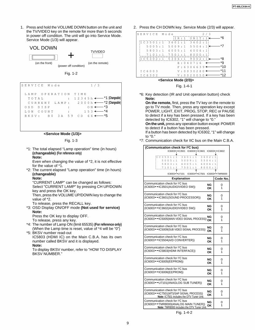
1. Press and hold the VOLUME DOWN button on the unit andthe TV/VIDEO key on the remote for more than 5 secondsin power off condition. The unit will go into Service Mode.Service Mode (1/3) will appear.
Fig. 1-2
Fig. 1-3
*1: The total elapsed “Lamp operation” time (in hours)(changeable) (For reference only)Note:Even when changing the value of *2, it is not effectivefor the value of *1.
*2: The current elapsed "Lamp operation" time (in hours)(changeable)Note:"CURRENT LAMP" can be changed as follows:Select "CURRENT LAMP" by pressing CH UP/DOWNkey and press the OK key.Then, press the VOLUME UP/DOWN key to change thevalue of *2.To release, press the RECALL key.
*3: OSD Display ON/OFF mode (Not used for service)Note:Press the OK key to display OFF.To release, press any key.
*4: The number of Lamp ON (limit 65535) (For reference only)(When the Lamp time is reset, value of *4 will be “0”)
*5: BKSV number read-outIC5803 (HDMI IC) on the Main C.B.A. has its ownnumber called BKSV and it is displayed.Note:To display BKSV number, refer to "HOW TO DISPLAYBKSV NUMBER."
2. Press the CH DOWN key. Service Mode (2/3) will appear.
Fig. 1-4-1
*6: Key detection (IR and Unit operation button) checkNote:On the remote, first, press the TV key on the remote togo to TV mode. Then, press any operation key exceptPOWER, LIGHT, EXIT, PROG, STOP, REC or PAUSEto detect if a key has been pressed. If a key has beendetected by IC6302, “1” will change to “0.”On the unit, press any operation button except POWERto detect if a button has been pressed.If a button has been detected by IC6302, “1” will changeto “0.”
*7: Communication check for IIC bus on the Main C.B.A.
Fig. 1-4-2
(on the front)(power off condition)
VOL DOWNTV/VIDEO
(on the remote)
<Service Mode (1/3)>
*1 (Changeable)*2 (Changeable)*3*4*5
S E R V I C E M o d e 1 / 3
L A M P O P E R A T I O N T I M E T O T A L : 1 2 3 4 5 h C U R R E N T L A M P : 2 0 0 0 h O S D D I S P : O N L O N C O U N T : 1 5 3 B K S V : B 0 3 A 5 9 C D 6 6
<Service Mode (2/3)>
*6
*7
*8*9*10*11*12
S E R V I C E M o d e 2 / 3 I R : 1 U N I T : 1 I C 3 5 0 1 : 1 3 6 0 1 : 1 3 6 0 2 : 1 5 0 0 5 : 1 5 0 0 9 : 1 5 5 0 4 : 1 5 8 0 3 : 1 6 0 0 5 : 1 6 0 0 6 : 1 7 1 0 1 : 1 7 5 0 1 : 1 8 0 0 0 : 1 I C 5 3 0 2 : 1 5 3 0 6 : 1 9 0 0 2 : 1 E : 0 4 0 7 1 6 F : 6 3 0 6 6 3 9 I C 6 0 0 3 V : 0 0 3 0 2 8 0 I C 6 3 0 2 V : 0 0 2 0 0 5 0
(Communication check for I2C bus)
Communication check for I2C bus (IC6003 IC6005(EEPROM))
Communication check for I2C bus (IC6003 IC5803(HDMI INTERFACE))
Communication check for I2C bus (IC6003 IC6006(EEPROM))
Communication check for I2C bus (IC6003 U7101(ANAGLOG SUB TUNER))
Communication check for I2C bus (IC6003 TMR8000(ANALOG MAIN TUNER))
Communication check for I2C bus (IC6003 IC7501(MTS/SAP SIGNAL PROCESS))
IC6003 IC3501 IC6003 IC3601 IC6003 IC3602
IC6003 U7101 IC6003 TMR8000IC6003 IC7501
I C 3 5 0 1 : 1 3 6 0 1 : 1 3 6 0 2 : 1 5 0 0 5 : 1 5 0 0 9 : 1 5 5 0 4 : 1 5 8 0 3 : 1 6 0 0 5 : 1 6 0 0 6 : 1 7 1 0 1 : 1 7 5 0 1 : 1 8 0 0 0 : 1
01
NGOK
Explanation Code No.
Communication check for I2C bus (IC6003 IC3501(AUDIO/VIDEO SW))
01
NGOK
01
NGOK
01
NGOK
01
NGOK
01
NGOK
01
NGOK
01
NGOK
01
NGOK
01
NGOK
01
NGOK
01
NGOK
Communication check for I2C bus(IC6003 IC3601(SOUND PROCESSOR))
Communication check for I2C bus (IC6003 IC3602(AUDIO/VIDEO SW))
Communication check for I2C bus (IC6003 IC5005(MAIN VIDEO SIGNAL PROCESS))
Communication check for I2C bus (IC6003 IC5009(SUB VIDEO SIGNAL PROCESS))
Communication check for I2C bus (IC6003 IC5504(A/D CONVERTER))
Note: IC7501 includes the DTV Tuner Unit.
Note: TMR8000 includes the DTV Tuner Unit.
PT-60LCX64-K
9
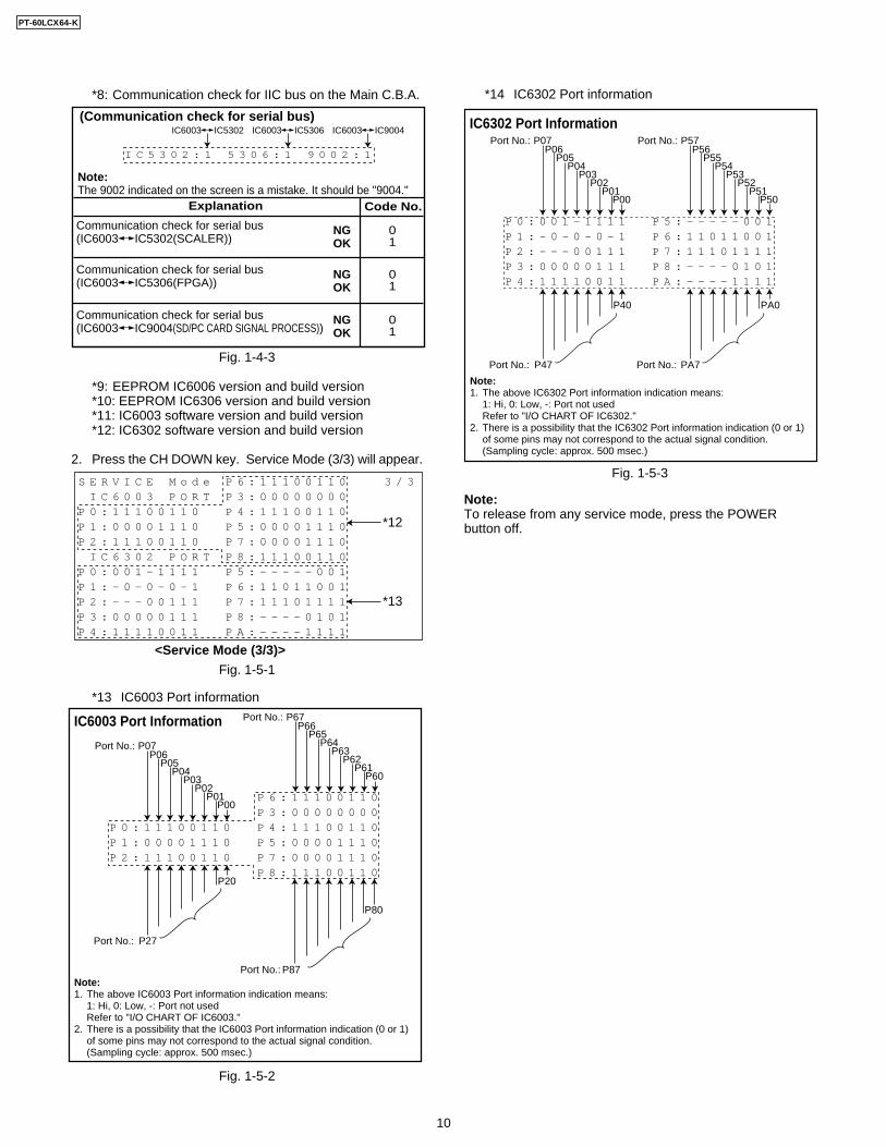
Note:To release from any service mode, press the POWERbutton off.
IC6003 Port Information
P00P01
P02P03
P04P05
P06P07Port No.:
P60P61
P62P63
P64P65
P66P67Port No.:
P20
P27Port No.:
P80
P87Port No.:
P 6 : 1 1 1 0 0 1 1 0 P 3 : 0 0 0 0 0 0 0 0P 0 : 1 1 1 0 0 1 1 0 P 4 : 1 1 1 0 0 1 1 0P 1 : 0 0 0 0 1 1 1 0 P 5 : 0 0 0 0 1 1 1 0P 2 : 1 1 1 0 0 1 1 0 P 7 : 0 0 0 0 1 1 1 0 P 8 : 1 1 1 0 0 1 1 0
Note:1. The above IC6003 Port information indication means:
1: Hi, 0: Low, -: Port not usedRefer to "I/O CHART OF IC6003."
2. There is a possibility that the IC6003 Port information indication (0 or 1) of some pins may not correspond to the actual signal condition. (Sampling cycle: approx. 500 msec.)
IC6302 Port Information
P00P01
P02P03
P04P05
P06P07Port No.:
P50P51
P52P53
P54P55
P56P57Port No.:
P40
P47Port No.:
PA0
PA7Port No.:
P 0 : 0 0 1 - 1 1 1 1 P 5 : - - - - - 0 0 1P 1 : - 0 - 0 - 0 - 1 P 6 : 1 1 0 1 1 0 0 1P 2 : - - - 0 0 1 1 1 P 7 : 1 1 1 0 1 1 1 1P 3 : 0 0 0 0 0 1 1 1 P 8 : - - - - 0 1 0 1P 4 : 1 1 1 1 0 0 1 1 P A : - - - - 1 1 1 1
Note:1. The above IC6302 Port information indication means:
1: Hi, 0: Low, -: Port not usedRefer to "I/O CHART OF IC6302."
2. There is a possibility that the IC6302 Port information indication (0 or 1) of some pins may not correspond to the actual signal condition. (Sampling cycle: approx. 500 msec.)
*8: Communication check for IIC bus on the Main C.B.A.
Fig. 1-4-3
*9: EEPROM IC6006 version and build version*10: EEPROM IC6306 version and build version*11: IC6003 software version and build version*12: IC6302 software version and build version
2. Press the CH DOWN key. Service Mode (3/3) will appear.
Fig. 1-5-1
*13 IC6003 Port information
Fig. 1-5-2
<Service Mode (3/3)>
*12
*13
S E R V I C E M o d e P 6 : 1 1 1 0 0 1 1 0 3 / 3 I C 6 0 0 3 P O R T P 3 : 0 0 0 0 0 0 0 0P 0 : 1 1 1 0 0 1 1 0 P 4 : 1 1 1 0 0 1 1 0P 1 : 0 0 0 0 1 1 1 0 P 5 : 0 0 0 0 1 1 1 0P 2 : 1 1 1 0 0 1 1 0 P 7 : 0 0 0 0 1 1 1 0 I C 6 3 0 2 P O R T P 8 : 1 1 1 0 0 1 1 0P 0 : 0 0 1 - 1 1 1 1 P 5 : - - - - - 0 0 1P 1 : - 0 - 0 - 0 - 1 P 6 : 1 1 0 1 1 0 0 1P 2 : - - - 0 0 1 1 1 P 7 : 1 1 1 0 1 1 1 1P 3 : 0 0 0 0 0 1 1 1 P 8 : - - - - 0 1 0 1P 4 : 1 1 1 1 0 0 1 1 P A : - - - - 1 1 1 1
01
NGOK
Explanation Code No.
Communication check for serial bus(IC6003 IC5302(SCALER))
(Communication check for serial bus)
01
NGOK
Communication check for serial bus(IC6003 IC5306(FPGA))
01
NGOK
Communication check for serial bus(IC6003 IC9004(SD/PC CARD SIGNAL PROCESS))
IC6003 IC5302 IC6003 IC5306 IC6003 IC9004
I C 5 3 0 2 : 1 5 3 0 6 : 1 9 0 0 2 : 1
Note:The 9002 indicated on the screen is a mistake. It should be "9004."
*14 IC6302 Port information
Fig. 1-5-3
PT-60LCX64-K
10
Pin No. Part No.Part No.I/O1 P55
P54
P53P52
P74P27P26P25P24P23P22P21P20
P73
P72
P14P13
P12P11P10P71
P70P07P06P05P04P03P02P01P00P87
P86
P85
P60P57P56
P61
P17P16P15
P51
P50
P84
P83
P82
P81P47
P46P45P44P43P42P41
P40P37
P36P35P34P76
P33
P32
P31
P30
P75
P77
P80
MAIN_LCD_MSDATADescription
2345678910111213141516171819202122232425262728293031323334353637383940
515253545556575859
Pin No. I/O
60
Signal NameSignal Name Description
616263646566676869707172737475767778798081828384
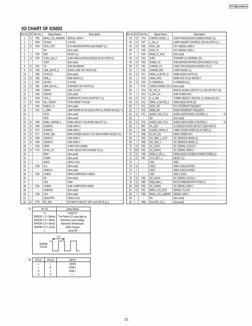
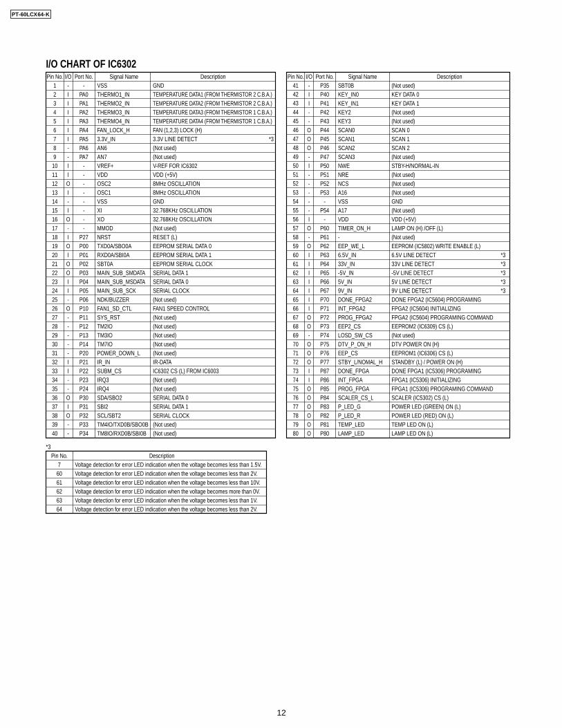
I/O CHART OF IC6003
- -
-
O
OVSYNCATSC_RSTNCRST
I
O
OOOOOO
O
O
O
O
O
O
I
I
I
I
I
I
I
I
I
-
-
--
I
--
-
--
---
-
--
-
-
-
-
-
-
-
3.45V_ON_HTESTYSLINE_MUTE_HSYSCLKRGB_LHSYNCAMP_MUTE_LOSDXIOSDXOCPS_LDLL_RESETRGB1/2_HL_ERRVCOIPDORGB1_H/RGB2_LOSDDT3OSDDT2SYNC_SEL
VREFSYNC_CSIREFCOMP
VREFLS
AVDDCLL
CVBS1NCVSS
(Not used)
(Not used)
(Not used)
(Not used)
HDMI AUDIO MUTE (H)HDMI HOT PLUG DETECT
(Not used)
HDMI INTERRUPT REQUEST(Not used)
(Not used)(Not used)
(Not used)(Not used)
(Not used)(Not used)
(Not used)
RF INPUT SELECT (RF-A (H) /RF-B (L) )
(Not used)
(Not used)
DTV MICROCONTROLLER RESET (L)
(Not used)
MAIN TUNER AFC
HDMI AUDIO (IC5805) POWER DOWN (L)
(Not used)(Not used)
CVBS0VREFHS
GND
GND
MULTI WINDOW WITH RGB (L)
CLH
CARDM_RESET_LL_ON_H
OSDDT1OSDDT0
ATSC_SO
- -
----
-
I
I
-
IO
--
-
O
ATSC_SIMAIN_IC_SCKSTBYSUBM_CSCARDM_CSCARDM_RDYHDMI_A_MUTE_HHDMI_HPDH_FREERUNCARDM_POWER_ON_HPC_NC_HS_AFC_IND_A_SWHDMI_A_MUTE2_LATSC_INTHDMI_INTAUDIO_SW_CTL2NCAUDIO_SW_CTL1FIL_DETCOVER_OPEN_HM_AFC_INI2C_SRV_L_3.3VI2C_SRV_LI2C_SCK1
II
II
II
I
II
I
I
I
I2C_DATA1HDMI_A_PD_LSYS_RET_LVSSOSC2OSC1VDDI2C_SCK0RGB_MW_LI2C_DATA0MAIN_LCD_SCKMAIN_LCD_LMDATA
4344454647484950
4241 NC
SCALER_CS_LRF_SWVDD(VPP) VDD(+3.3V)
VDD(+3.3V)
VDD (+3.3V)
SERIAL DATA 0V-SYNC
RESET (L)3.45V REGULATOR (IC5015) ON (H) /OFF (L)
OSD BLANKINGAUDIO LINE OUT MUTE (H)
RGB MODE (L)H-SYNCSPEAKER OUT MUTE (L)OSD CLOCK
FPGA RESET PULSE COMPOSITE SYNC IN DETECT (L)
LAMP ERROR PULSE (ON (H) /OFF (L) /ERROR (PULSE)
RGB1 SELECT (H) /RGB2 SELECT (L)OSD DATA 3OSD DATA 2MAIN SCREEN SELECT (H) /SUB SCREEN SELECT (L)OSD DATA 1OSD DATA 0V-REF FOR IC6003SYNC SELECTOR (IC5306) CS (L)
MAIN COMPOSITE VIDEO
SUB COMPOSITE VIDEO
O
--
CARD PROCESSOR (IC9004) RESET (L)LAMP ON/OFF CONTROL (ON (H) /OFF (L) )
*2
*2
DTV SERIAL DATA 0DTV SERIAL DATA 1(Not used)STANDBY (L) /NORMAL (H)
SUB MICROCONTROLLER (IC6302) CS (L)CARD PROCESSOR (IC9004) CS (L)CARD READY (L)
H-FREERUN (L)
RGB IN SIGNAL DETECT (L) /NO DETECT (H)SUB TUNER AFCTUNER SELECT (DIGITAL (L) /ANALOG (H) )HDMI AUDIO MUTE (H)DTV INTERRUPT REQUEST
AUDIO SWITCHING CONTROL 2
AUDIO SWITCHING CONTROL 1
LAMP COVER OPEN (H) /CLOSE (L)CLOGGED FILTER DETECT (A/D INPUT)
I2C SERVICE MODE (L)I2C SERVICE MODE (L)I2C SERIAL CLOCK 0I2C SERIAL DATA 0
RESET (L)
4MHz OSCILLATION4MHz OSCILLATION
I2C SERIAL CLOCK 1
I2C SERIAL DATA 1SERIAL CLOCKSERIAL DATA 1
O
OO
O
O
O
O
O
O
O
OOO
OOO
I/O
I/O
O
-
*1
*2
Pin 19
Pin 62 Pin 64 INPUT
HERROR 1 (T=128ms)ERROR 2 (T= 96ms)ERROR 3 (T= 64ms)ERROR 4 (T= 32ms)
L
Lamp StatusLamp On
The Failure Of Lamp light upAbnormal Lamp VoltageAbnormal Temperature
Other CausesLamp Off
LLHH
LHLH
HDMIRGB 2RGB 1
*1
"2T"
ERRORPULSE
PT-60LCX64-K
11
515253545556575859
Pin No.
Pin No.
I/O
II
O
60
Signal NamePin No. I/O DescriptionSignal Name Description
DescriptionVoltage detection for error LED indication when the voltage becomes less than 1.5V.Voltage detection for error LED indication when the voltage becomes less than 2V.Voltage detection for error LED indication when the voltage becomes less than 10V.Voltage detection for error LED indication when the voltage becomes more than 0V.Voltage detection for error LED indication when the voltage becomes less than 1V.Voltage detection for error LED indication when the voltage becomes less than 2V.
61626364
6061626364
65666768697071727374757677787980
I/O CHART OF IC6302
VDD (+5V)
GND
KEY_IN0KEY_IN1KEY2KEY3
O
- -
-
- P35
--
I-
---
-
O
II
O-O
-O
O
O
O
O
OOOOOO
I
III
II
II
SCAN0SCAN1SCAN2SCAN3NWENRENCSA16VSSA17VDDTIMER_ON_H-EEP_WE_L6.5V_IN33V_IN-5V_IN5V_IN9V_INDONE_FPGA2INT_FPGA2
KEY DATA 1KEY DATA 0
PROG_FPGA2EEP2_CSLOSD_SW_CSDTV_P_ON_HEEP_CSSTBY_L/NOMAL_HDONE_FPGAINT_FPGA
SCAN 1SCAN 0
SCAN 2
PROG_FPGASCALER_CS_LP_LED_GP_LED_RTEMP_LEDLAMP_LED
424344454647484950
41 SBT0B (Not used)
(Not used)(Not used)
(Not used)STBY-H/NORMAL-IN(Not used)(Not used)(Not used)
(Not used)EEPROM (IC5802) WRITE ENABLE (L)
DONE FPGA2 (IC5604) PROGRAMINGFPGA2 (IC5604) INITIALIZINGFPGA2 (IC5604) PROGRAMING COMMANDEEPROM2 (IC6309) CS (L)(Not used)DTV POWER ON (H)EEPROM1 (IC6306) CS (L)
DONE FPGA1 (IC5306) PROGRAMINGFPGA1 (IC5306) INITIALIZINGFPGA1 (IC5306) PROGRAMING COMMAND
(Not used)
LAMP ON (H) /OFF (L)
6.5V LINE DETECT33V LINE DETECT-5V LINE DETECT5V LINE DETECT9V LINE DETECT
STANDBY (L) / POWER ON (H)
SCALER (IC5302) CS (L)POWER LED (GREEN) ON (L)POWER LED (RED) ON (L)TEMP LED ON (L)LAMP LED ON (L)
1PA0PA1PA2PA3PA4PA5PA6PA7
P27P00
P02P03P04P05P06P10P11P12P13P14P20P21P22P23P24P30P31P32P33P34
P01
VSS234567
7
8910111213141516171819202122232425262728293031323334353637383940
IIIIII
- -
--
--------
THERMO1_INTHERMO2_INTHERMO3_INTHERMO4_IN
I
I
I
I
I
II
-I
I
-
I
I
-
-
-
----
--
3.3V_INAN6AN7VREF+
OSC2OSC1VSSXIXOMMODNRSTTXD0A/SBO0ARXD0A/SBI0ASBT0AMAIN_SUB_SMDATAMAIN_SUB_MSDATAMAIN_SUB_SCKNDK/BUZZER
TM2IOTM3IOTM7IOPOWER_DOWN_L
IRQ3
VDD (+5V)
IR_INSUBM_CS
GND
GND
IRQ4SDA/SBO2SBI2SCL/SBT2TM4IO/TXD0B/SBO0BTM8IO/RXD0B/SBI0B
FAN1_SD_CTLSYS_RST
O
O
O
OO
O
O
O-
FAN_LOCK_H
VDD
(Not used)(Not used)
(Not used)
(Not used)FAN1 SPEED CONTROL(Not used)(Not used)(Not used)(Not used)(Not used)
(Not used)(Not used)
(Not used)(Not used)
TEMPERATURE DATA1 (FROM THERMISTOR 2 C.B.A.)TEMPERATURE DATA2 (FROM THERMISTOR 2 C.B.A.)TEMPERATURE DATA3 (FROM THERMISTOR 1 C.B.A.)TEMPERATURE DATA4 (FROM THERMISTOR 1 C.B.A.)FAN (1,2,3) LOCK (H)3.3V LINE DETECT
V-REF FOR IC6302
8MHz OSCILLATION8MHz OSCILLATION
32.768KHz OSCILLATION32.768KHz OSCILLATION
RESET (L)EEPROM SERIAL DATA 0EEPROM SERIAL DATA 1EEPROM SERIAL CLOCKSERIAL DATA 1SERIAL DATA 0SERIAL CLOCK
IR-DATAIC6302 CS (L) FROM IC6003
SERIAL DATA 0SERIAL DATA 1SERIAL CLOCK
Port No. Port No.
P40P41P42P43P44P45P46P47P50P51P52P53
P54
P60P61P62P63P64P65P66P67P70P71P72P73P74P75P76P77P87P86P85P84P83P82P81P80
*3*3*3*3*3
*3
*3
PT-60LCX64-K
12
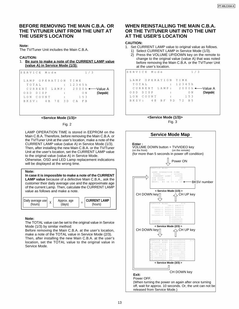
Note:The TV/Tuner Unit includes the Main C.B.A.
CAUTION:1. Be sure to make a note of the CURRENT LAMP value
(value A) in Service Mode (1/3):
Fig. 2
LAMP OPERATION TIME is stored in EEPROM on theMain C.B.A. Therefore, before removing the Main C.B.A. orthe TV/Tuner Unit at the user’s location, make a note of theCURRENT LAMP value (value A) in Service Mode (1/3).Then, after installing the new Main C.B.A. or the TV/TunerUnit at the user’s location, set the CURRENT LAMP valueto the original value (value A) in Service Mode.Otherwise, OSD and LED Lamp replacement indicationswill be displayed at the wrong time.
Note:In case it is impossible to make a note of the CURRENTLAMP value because of a defective Main C.B.A., ask thecustomer their daily average use and the approximate ageof the current Lamp. Then, calculate the CURRENT LAMPvalue as follows and make a note.
Note:The TOTAL value can be set to the original value in ServiceMode (1/3) by similar method:Before removing the Main C.B.A. at the user’s location,make a note of the TOTAL value in Service Mode (2/3).Then, after installing the new Main C.B.A. at the user’slocation, set the TOTAL value to the original value inService Mode.
BEFORE REMOVING THE MAIN C.B.A. ORTHE TV/TUNER UNIT FROM THE UNIT ATTHE USER’S LOCATION
Value A (Changeable)
<Service Mode (1/3)>
S E R V I C E M o d e 1 / 3
L A M P O P E R A T I O N T I M E T O T A L : 1 2 3 4 5 h C U R R E N T L A M P : 2 0 0 0 h O S D D I S P : O N L O N C O U N T : 1 5 3 B K S V : 4 B 7 E 3 D C A F B
Daily average use X =Approx. age CURRENT LAMP (hours) (days) (hours)
CAUTION:1. Set CURRENT LAMP value to original value as follows.
1) Select CURRENT LAMP in Service Mode (1/3).2) Press the VOLUME UP/DOWN key on the remote to
change to the original value (value A) that was notedbefore removing the Main C.B.A. or the TV/Tuner Unitat the user’s location.
Value A (Changeable)
<Service Mode (1/3)>
S E R V I C E M o d e 1 / 3
L A M P O P E R A T I O N T I M E T O T A L : 1 2 3 4 5 h C U R R E N T L A M P : 2 0 0 0 h O S D D I S P : O N L O N C O U N T : 1 5 3 B K S V : 4 8 B F 9 D 7 2 B 5
WHEN REINSTALLING THE MAIN C.B.A.OR THE TV/TUNER UNIT INTO THE UNITAT THE USER’S LOCATION
Fig. 3
Service Mode Map
CH DOWN key CH UP key
CH DOWN key
CH DOWN key
CH UP key
Enter :VOLUME DOWN button + TV/VIDEO key (on the front) (on the remote)(for more than 5 seconds in power off condition)
Exit:Power OFF.(When turning the power on again after once turning off, wait for approx. 10 seconds. Or, the unit can not be released from Service Mode.)
< Service Mode (2/3) >
< Service Mode (3/3) >
< Service Mode (1/3) >
S E R V I C E M o d e 1 / 3
L A M P O P E R A T I O N T I M E T O T A L : 1 2 3 4 5 h C U R R E N T L A M P : 2 0 0 0 h O S D D I S P : O N L O N C O U N T : 1 5 3 B K S V : B 0 3 A 5 9 C D 6 6
Power ON
S E R V I C E M o d e P 6 : 1 1 1 0 0 1 1 0 3 / 3 I C 6 0 0 3 P O R T P 3 : 0 0 0 0 0 0 0 0P 0 : 1 1 1 0 0 1 1 0 P 4 : 1 1 1 0 0 1 1 0P 1 : 0 0 0 0 1 1 1 0 P 5 : 0 0 0 0 1 1 1 0P 2 : 1 1 1 0 0 1 1 0 P 7 : 0 0 0 0 1 1 1 0 I C 6 3 0 2 P O R T P 8 : 1 1 1 0 0 1 1 0P 0 : 0 0 1 - 1 1 1 1 P 5 : - - - - - 0 0 1P 1 : - 0 - 0 - 0 - 1 P 6 : 1 1 0 1 1 0 0 1P 2 : - - - 0 0 1 1 1 P 7 : 1 1 1 0 1 1 1 1P 3 : 0 0 0 0 0 1 1 1 P 8 : - - - - 0 1 0 1P 4 : 1 1 1 1 0 0 1 1 P A : - - - - 1 1 1 1
S E R V I C E M o d e 2 / 3 I R : 1 U N I T : 1 I C 3 5 0 1 : 1 3 6 0 1 : 1 3 6 0 2 : 1 5 0 0 5 : 1 5 0 0 9 : 1 5 5 0 4 : 1 5 8 0 3 : 1 6 0 0 5 : 1 6 0 0 6 : 1 7 1 0 1 : 1 7 5 0 1 : 1 8 0 0 0 : 1 I C 5 3 0 2 : 1 5 3 0 6 : 1 9 0 0 2 : 1 E : 0 4 0 7 1 6 F : 6 3 0 6 6 3 9 I C 6 0 0 3 V : 0 0 3 0 2 8 0 I C 6 3 0 2 V : 0 0 2 0 0 5 0
BKSV number
PT-60LCX64-K
13
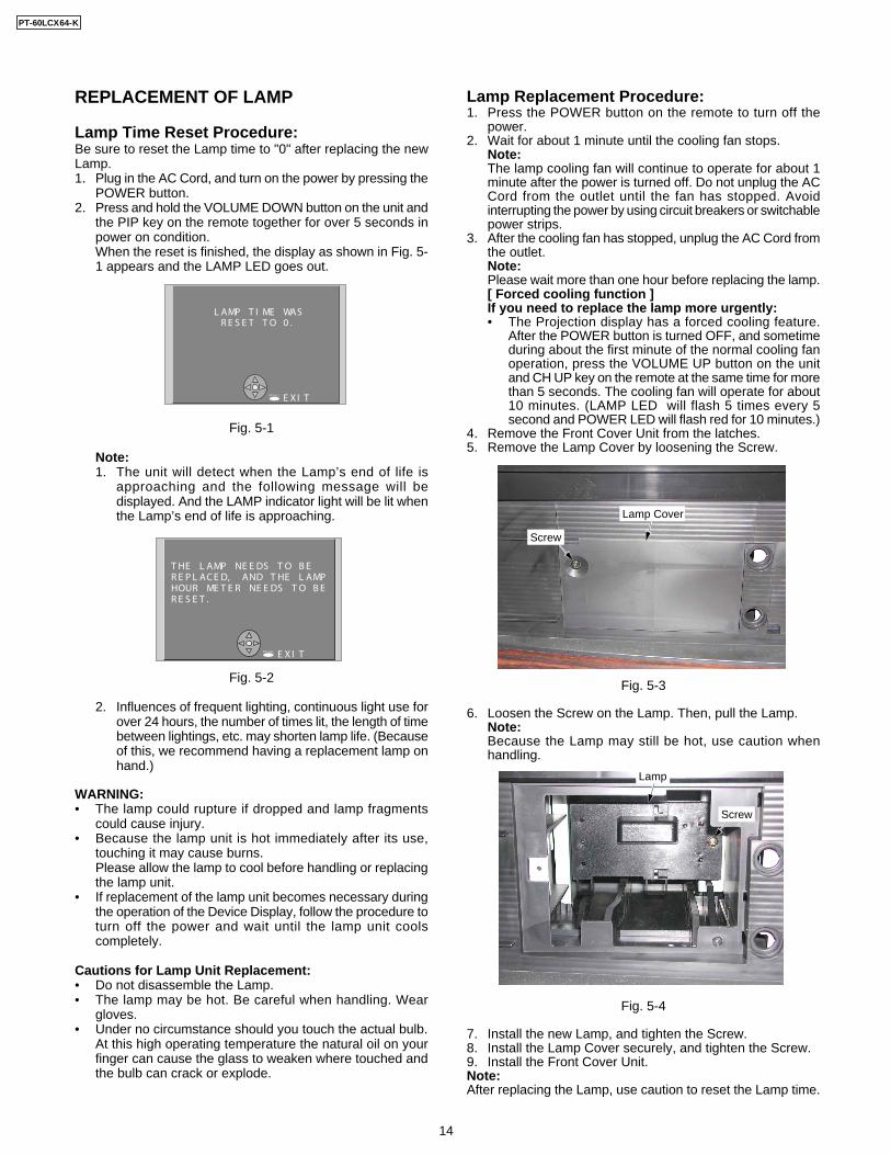
Lamp Replacement Procedure:1. Press the POWER button on the remote to turn off the
power.2. Wait for about 1 minute until the cooling fan stops.
Note:The lamp cooling fan will continue to operate for about 1minute after the power is turned off. Do not unplug the ACCord from the outlet until the fan has stopped. Avoidinterrupting the power by using circuit breakers or switchablepower strips.
3. After the cooling fan has stopped, unplug the AC Cord fromthe outlet.Note:Please wait more than one hour before replacing the lamp.[ Forced cooling function ]If you need to replace the lamp more urgently:• The Projection display has a forced cooling feature.
After the POWER button is turned OFF, and sometimeduring about the first minute of the normal cooling fanoperation, press the VOLUME UP button on the unitand CH UP key on the remote at the same time for morethan 5 seconds. The cooling fan will operate for about10 minutes. (LAMP LED will flash 5 times every 5second and POWER LED will flash red for 10 minutes.)
4. Remove the Front Cover Unit from the latches.5. Remove the Lamp Cover by loosening the Screw.
Fig. 5-3
6. Loosen the Screw on the Lamp. Then, pull the Lamp.Note:Because the Lamp may still be hot, use caution whenhandling.
Fig. 5-4
7. Install the new Lamp, and tighten the Screw.8. Install the Lamp Cover securely, and tighten the Screw.9. Install the Front Cover Unit.Note:After replacing the Lamp, use caution to reset the Lamp time.
Lamp Cover
Screw
Screw
Lamp
REPLACEMENT OF LAMP
Lamp Time Reset Procedure:Be sure to reset the Lamp time to "0" after replacing the newLamp.1. Plug in the AC Cord, and turn on the power by pressing the
POWER button.2. Press and hold the VOLUME DOWN button on the unit and
the PIP key on the remote together for over 5 seconds inpower on condition.When the reset is finished, the display as shown in Fig. 5-1 appears and the LAMP LED goes out.
Fig. 5-1
Note:1. The unit will detect when the Lamp’s end of life is
approaching and the following message will bedisplayed. And the LAMP indicator light will be lit whenthe Lamp’s end of life is approaching.
Fig. 5-2
2. Influences of frequent lighting, continuous light use forover 24 hours, the number of times lit, the length of timebetween lightings, etc. may shorten lamp life. (Becauseof this, we recommend having a replacement lamp onhand.)
WARNING:• The lamp could rupture if dropped and lamp fragments
could cause injury.• Because the lamp unit is hot immediately after its use,
touching it may cause burns.Please allow the lamp to cool before handling or replacingthe lamp unit.
• If replacement of the lamp unit becomes necessary duringthe operation of the Device Display, follow the procedure toturn off the power and wait until the lamp unit coolscompletely.
Cautions for Lamp Unit Replacement:• Do not disassemble the Lamp.• The lamp may be hot. Be careful when handling. Wear
gloves.• Under no circumstance should you touch the actual bulb.
At this high operating temperature the natural oil on yourfinger can cause the glass to weaken where touched andthe bulb can crack or explode.
PT-60LCX64-K
14
THE SCREEN UNIT AND THE MIRROR•THE SCREEN UNIT (Lenticular Screen, Fresnel Lens)It is strongly recommended that the Lenticular Screen surface(outside) and the Fresnel Lens surface (inside) should bewiped gently with a clean, soft, dry cloth to remove the dirt.
Note:1. If the dirt cannot be removed by wiping with a clean, soft, dry
cloth, use a clean, soft, dry cloth moistened with dilutedneutral pH liquid cleanser or a lens cleaner (usuallycontaining a small amount of ethyl alcohol) and wipe lightly.Take care not to leave any streaks.Do not use cleaning materials containing methyl alcohol,acetone, or dichloromethane.
2. Use an air blower to clean the inner surface of the LenticularScreen and the outer surface of the Fresnel Lens (thesurfaces that one another). These surfaces must not bewiped with a cloth.
•THE MIRRORRemove any dirt with an air blower or wipe with a clean, soft,dry cloth. If wiped too forcefully, the surface of the Mirror canbe damaged. If wiping with a clean, dry cloth does not removethe dirt, the Mirror must be replaced.
Fig. 6-1
THE PROJECTION LENSUse lens cleaning paper and cleaner available at your localcamera shop, etc. Dampen the cleaning paper with cleanerand gently wipe the surface of the lens from the center outwardto remove dust.
Fig. 6-4
Lens
CLEANING METHOD
THE LAMPGently wipe the surface of the glass of the Lamp with cleaningpaper or soft cloth.
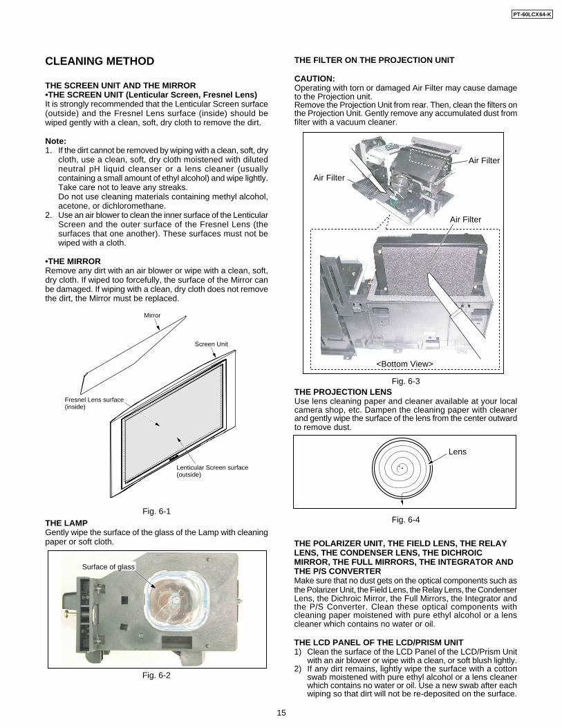
THE FILTER ON THE PROJECTION UNIT
CAUTION:Operating with torn or damaged Air Filter may cause damageto the Projection unit.Remove the Projection Unit from rear. Then, clean the filters onthe Projection Unit. Gently remove any accumulated dust fromfilter with a vacuum cleaner.
Fig. 6-3
THE POLARIZER UNIT, THE FIELD LENS, THE RELAYLENS, THE CONDENSER LENS, THE DICHROICMIRROR, THE FULL MIRRORS, THE INTEGRATOR ANDTHE P/S CONVERTERMake sure that no dust gets on the optical components such asthe Polarizer Unit, the Field Lens, the Relay Lens, the CondenserLens, the Dichroic Mirror, the Full Mirrors, the Integrator andthe P/S Converter. Clean these optical components withcleaning paper moistened with pure ethyl alcohol or a lenscleaner which contains no water or oil.
THE LCD PANEL OF THE LCD/PRISM UNIT1) Clean the surface of the LCD Panel of the LCD/Prism Unit
with an air blower or wipe with a clean, or soft blush lightly.2) If any dirt remains, lightly wipe the surface with a cotton
swab moistened with pure ethyl alcohol or a lens cleanerwhich contains no water or oil. Use a new swab after eachwiping so that dirt will not be re-deposited on the surface.
Surface of glass
Fig. 6-2
Air Filter
Air Filter
Air Filter
<Bottom View>
Lenticular Screen surface(outside)
Screen Unit
Mirror
Fresnel Lens surface(inside)
PT-60LCX64-K
15
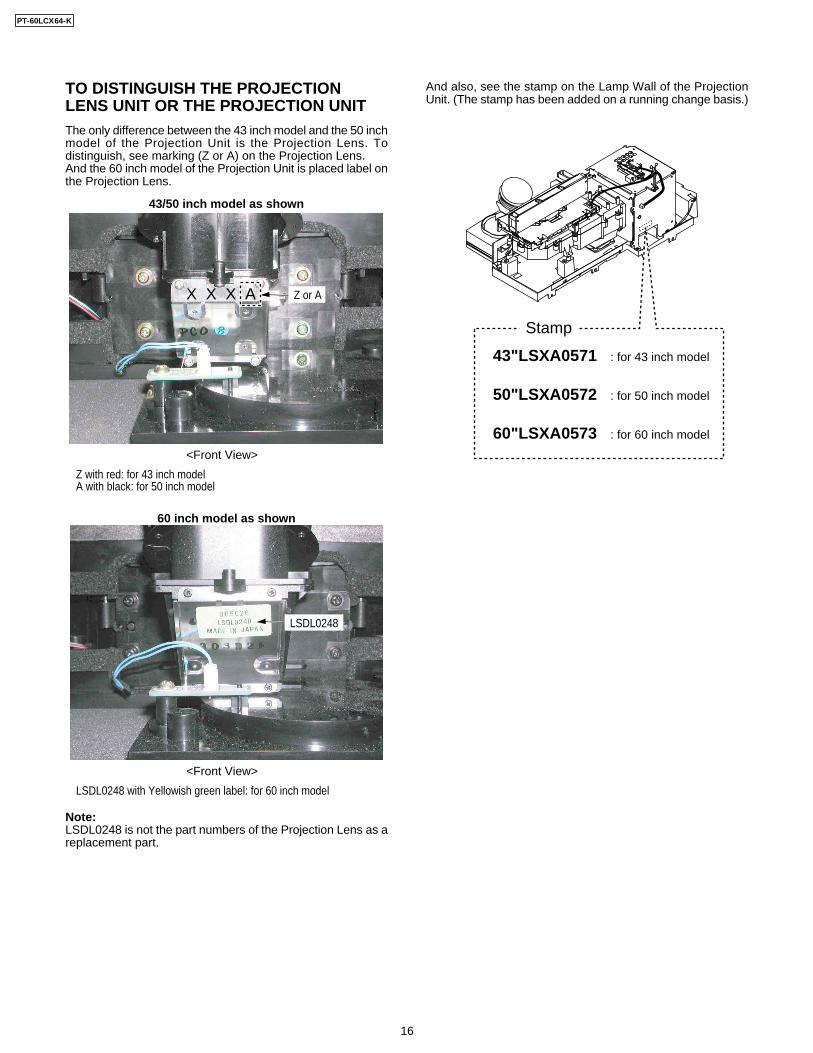
LSDL0248 with Yellowish green label: for 60 inch model
<Front View>
Z with red: for 43 inch modelA with black: for 50 inch model
<Front View>
60 inch model as shown
43/50 inch model as shown
LSDL0248
Z or AX X X A
TO DISTINGUISH THE PROJECTIONLENS UNIT OR THE PROJECTION UNITThe only difference between the 43 inch model and the 50 inchmodel of the Projection Unit is the Projection Lens. Todistinguish, see marking (Z or A) on the Projection Lens.And the 60 inch model of the Projection Unit is placed label onthe Projection Lens.
Note:LSDL0248 is not the part numbers of the Projection Lens as areplacement part.
43"LSXA0571 : for 43 inch model
50"LSXA0572 : for 50 inch model
60"LSXA0573 : for 60 inch model
Stamp
And also, see the stamp on the Lamp Wall of the ProjectionUnit. (The stamp has been added on a running change basis.)
PT-60LCX64-K
16
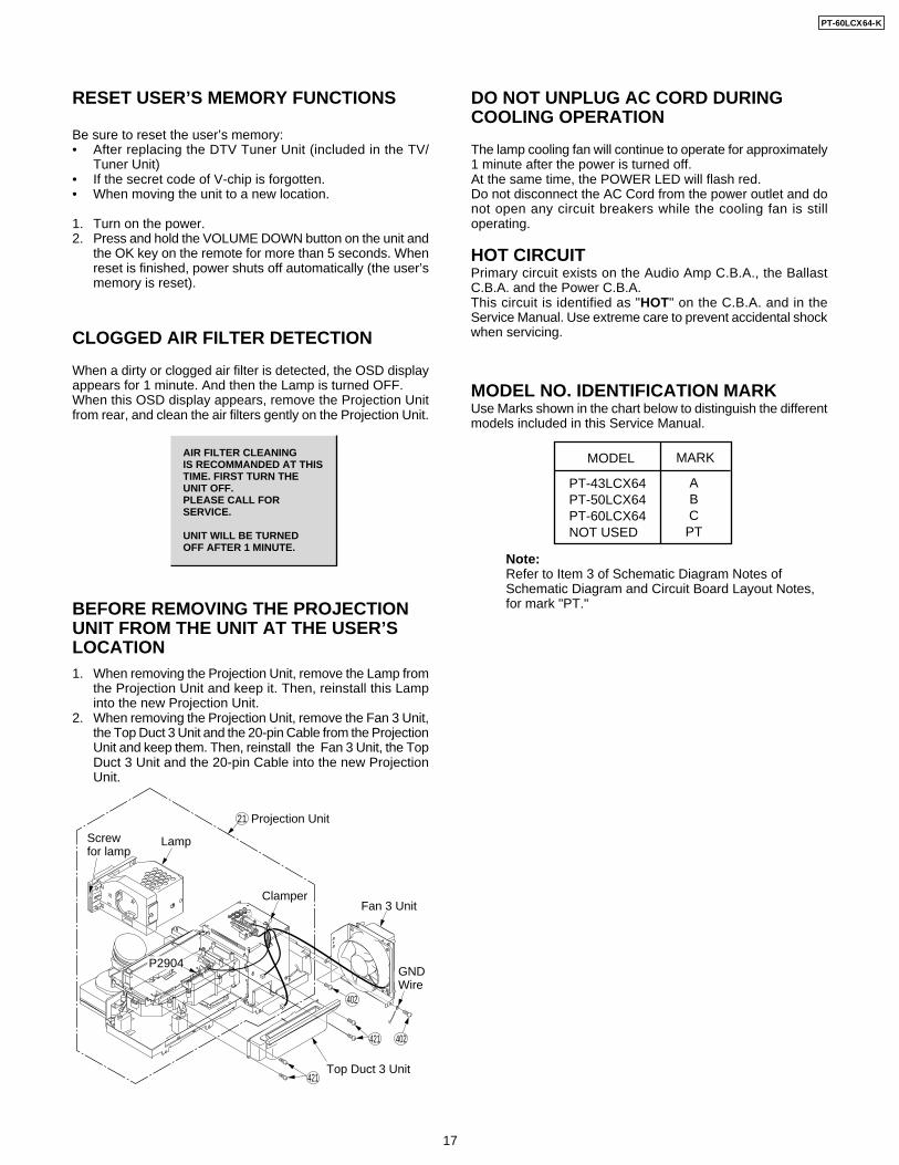
BEFORE REMOVING THE PROJECTIONUNIT FROM THE UNIT AT THE USER’SLOCATION1. When removing the Projection Unit, remove the Lamp from
the Projection Unit and keep it. Then, reinstall this Lampinto the new Projection Unit.
2. When removing the Projection Unit, remove the Fan 3 Unit,the Top Duct 3 Unit and the 20-pin Cable from the ProjectionUnit and keep them. Then, reinstall the Fan 3 Unit, the TopDuct 3 Unit and the 20-pin Cable into the new ProjectionUnit.
Fan 3 Unit
GND Wire
Top Duct 3 Unit
LampScrew for lamp
402
402
421
421
Clamper
Projection Unit21
P2904
MODEL NO. IDENTIFICATION MARKUse Marks shown in the chart below to distinguish the differentmodels included in this Service Manual.
MODEL
PT-43LCX64PT-50LCX64PT-60LCX64NOT USED
MARK
ABCPT
Note:Refer to Item 3 of Schematic Diagram Notes of Schematic Diagram and Circuit Board Layout Notes,for mark "PT."
HOT CIRCUITPrimary circuit exists on the Audio Amp C.B.A., the BallastC.B.A. and the Power C.B.A.This circuit is identified as "HOT" on the C.B.A. and in theService Manual. Use extreme care to prevent accidental shockwhen servicing.
DO NOT UNPLUG AC CORD DURINGCOOLING OPERATION
The lamp cooling fan will continue to operate for approximately1 minute after the power is turned off.At the same time, the POWER LED will flash red.Do not disconnect the AC Cord from the power outlet and donot open any circuit breakers while the cooling fan is stilloperating.
CLOGGED AIR FILTER DETECTION
When a dirty or clogged air filter is detected, the OSD displayappears for 1 minute. And then the Lamp is turned OFF.When this OSD display appears, remove the Projection Unitfrom rear, and clean the air filters gently on the Projection Unit.
AIR FILTER CLEANINGIS RECOMMANDED AT THIS TIME. FIRST TURN THEUNIT OFF. PLEASE CALL FOR SERVICE.
UNIT WILL BE TURNEDOFF AFTER 1 MINUTE.
RESET USER’S MEMORY FUNCTIONS
Be sure to reset the user’s memory:• After replacing the DTV Tuner Unit (included in the TV/
Tuner Unit)• If the secret code of V-chip is forgotten.• When moving the unit to a new location.
1. Turn on the power.2. Press and hold the VOLUME DOWN button on the unit and
the OK key on the remote for more than 5 seconds. Whenreset is finished, power shuts off automatically (the user’smemory is reset).
PT-60LCX64-K
17
WORK MODE AND FACTORY ADJUST MODE
Fig. 8
Work Mode Map
Exit:VOLUME DOWN button + RECALL key (on the front) (on the remote)(for more than 5 seconds in Work Mode)
VOLUME DOWN button + MOVE key (on the front) (on the remote)
OK key(on the remote)
CH UP/DOWNkey (on the remote)
CH UP/DOWNkey (on the remote)
CH UP/DOWNkey (on the remote)
RECALL key(on the remote)
RECALL key(on the remote)
< Factory Adjust Mode >(Main menu)
< Factory Adjust Mode >(Video ADJ menu 1/6)
< Factory Adjust Mode >(Sound menu 1/2)
< Factory Adjust Mode >(FAN menu 1/2)
(Not used for service)
(For PicturePositionadjustment)
(RGB Input level adjustment)
(Not used for service)
< Factory Adjust Mode >(Video ADJ menu 2/6~6/6)
< Factory Adjust Mode >(Sound menu 2/2)
< Factory Adjust Mode >(FAN menu 2/2)
< Factory Adjust Mode >(Other menu 1/1)
< Work Mode >
(for more than 5 seconds)
Enter:VOLUME DOWN button + RECALL key (on the front) (on the remote)(for more than 5 seconds in power on condition)
F A C T O R Y A D J U S T 1 / 1 M : 0 0 3 0 2 8 S : 0 0 2 0 0 5 0 V I D E O A D J S O U N D F A N O T H E R P A R T I A L E D I D
D E F A U L T S E T ( S E L F C H E C K )
C - C O R / G A M / W - B A L P U S H R E C A L L 5 S E C W O R K M O D E
Alternatively, Power OFF
F A N 1 / 2 F A N C H E C K W A I T 0 A D E F A U L T T I M E 1 1 E D E F A U L T T I M E 2 D 2
T H E R M O A L O W T e m p 4 C T H E R M O A H I T e m p 2 B T H E R M O A S T O P T e m p 2 B T H E R M O B S T O P T e m p 3 E
O t h e r 1 / 1
O P T H P O S I 0 7 O P T V P O S I 0 3 F I L T E R D E T 3 0 F P : 6 3 0 6 6 3 P R O T E C G C : 0 4 0 7 1 6
S O U N D 1 / 2 S U R E F F E C T 0 4 B B E P R O C E S S 0 E B B E C O N T O U R 0 0 A G C B a s s I N I 0 0 T N R B a s s I N I 0 0 A G C T r e b l e I N I 0 1 T N R T r e b l e I N I 0 3 B B E B a s s I N I 0 0 B B E T r e b l e I N I F A
V I D E O 1 / 6 B R I G H T R 4 6 L E V E L R 6 3 B R I G H T G 4 2 L E V E L G 6 2 B R I G H T B 4 2 L E V E L B 6 7
Factory Adjust ModeThis mode is required when:• Performing Mechanical Picture Position, Focus and Electrical Picture Position adjustment (Other menu).• Performing Electrical Adjustment for the Main C.B.A. (Video ADJ menu).To enter the Factory Adjust Mode:1) In Work Mode, press and hold the VOLUME DOWN button on the unit and the MOVE key on the remote together for m
than 5 seconds. The unit will go into Factory Adjust Mode. (“FACTORY ADJUST” will appear on the screen.)2) Press CH UP/DOWN key to select and press the OK key to set the item to be adjusted.3) After completing adjustments, press RECALL key twice to return to Work Mode.
Then the adjustment data will be written to the EEPROM IC (IC6005) on the Main C.B.A.Note:Do not unplug the AC Cord in Factory Adjust Mode or the adjustment data will not be written to the EEPROM IC.
PT-60LCX64-K
18
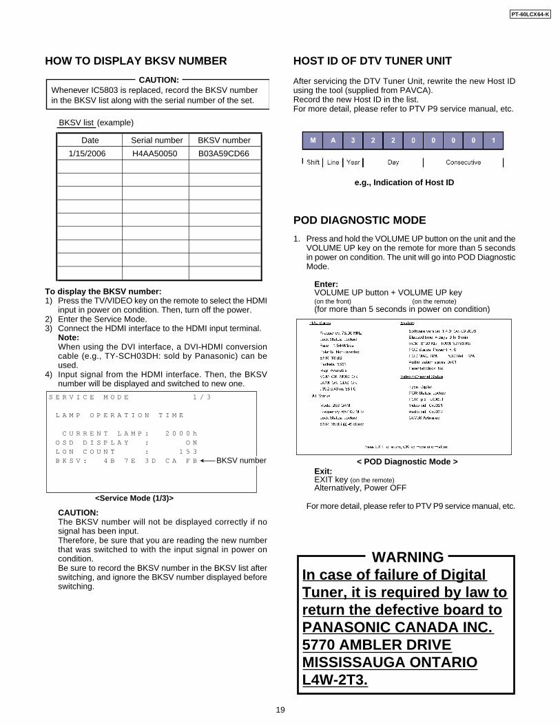
To display the BKSV number:1) Press the TV/VIDEO key on the remote to select the HDMI
input in power on condition. Then, turn off the power.2) Enter the Service Mode.3) Connect the HDMI interface to the HDMI input terminal.
Note:When using the DVI interface, a DVI-HDMI conversioncable (e.g., TY-SCH03DH: sold by Panasonic) can beused.
4) Input signal from the HDMI interface. Then, the BKSVnumber will be displayed and switched to new one.
CAUTION:The BKSV number will not be displayed correctly if nosignal has been input.Therefore, be sure that you are reading the new numberthat was switched to with the input signal in power oncondition.Be sure to record the BKSV number in the BKSV list afterswitching, and ignore the BKSV number displayed beforeswitching.
HOW TO DISPLAY BKSV NUMBER
<Service Mode (1/3)>
S E R V I C E M O D E 1 / 3
L A M P O P E R A T I O N T I M E C U R R E N T L A M P : 2 0 0 0 h O S D D I S P L A Y : O N L O N C O U N T : 1 5 3 B K S V : 4 B 7 E 3 D C A F B BKSV number
CAUTION:Whenever IC5803 is replaced, record the BKSV number in the BKSV list along with the serial number of the set.
BKSV list (example)
Date
1/15/2006
Serial number
H4AA50050
BKSV number
B03A59CD66
POD DIAGNOSTIC MODE
1. Press and hold the VOLUME UP button on the unit and theVOLUME UP key on the remote for more than 5 secondsin power on condition. The unit will go into POD DiagnosticMode.
For more detail, please refer to PTV P9 service manual, etc.
< POD Diagnostic Mode >
Enter:VOLUME UP button + VOLUME UP key (on the front) (on the remote)(for more than 5 seconds in power on condition)
Exit:EXIT key (on the remote)Alternatively, Power OFF
HOST ID OF DTV TUNER UNIT
After servicing the DTV Tuner Unit, rewrite the new Host IDusing the tool (supplied from PAVCA).Record the new Host ID in the list.For more detail, please refer to PTV P9 service manual, etc.
e.g., Indication of Host ID
WARNINGIn case of failure of Digital Tuner, it is required by law to return the defective board to PANASONIC CANADA INC.5770 AMBLER DRIVE MISSISSAUGA ONTARIO L4W-2T3.
PT-60LCX64-K
19
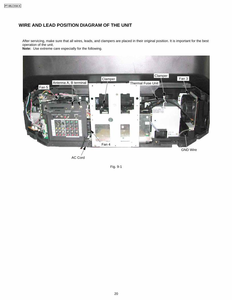
WIRE AND LEAD POSITION DIAGRAM OF THE UNIT
Fig. 9-1
After servicing, make sure that all wires, leads, and clampers are placed in their original position. It is important for the best operation of the unit.Note: Use extreme care especially for the following.
Antenna A, B terminalClamper
Fan 5
ClamperFan 3
Fan 4
GND Wire
AC Cord
Thermal Fuse Unit
PT-60LCX64-K
20
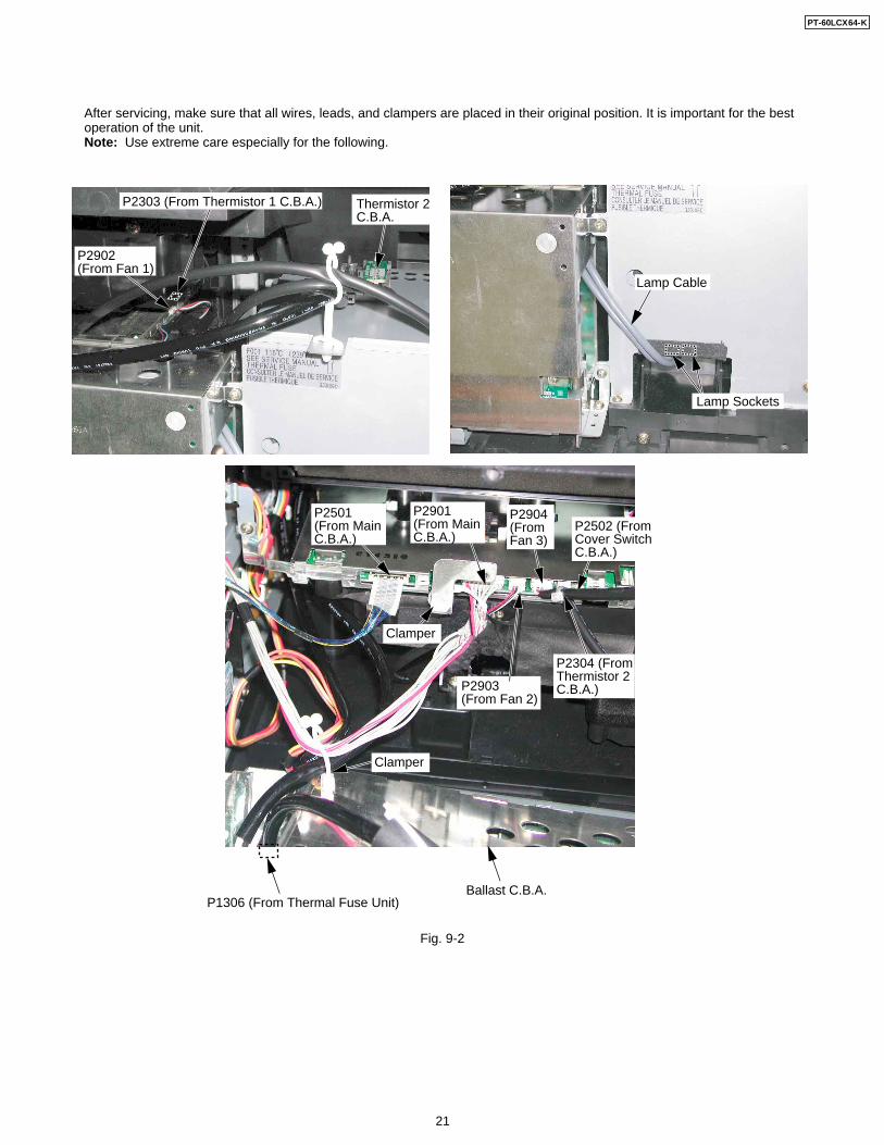
Fig. 9-2
After servicing, make sure that all wires, leads, and clampers are placed in their original position. It is important for the best operation of the unit.Note: Use extreme care especially for the following.
Lamp Sockets
Lamp Cable
P2903 (From Fan 2)
Clamper
Clamper
Ballast C.B.A.P1306 (From Thermal Fuse Unit)
Thermistor 2 C.B.A.
P2501(From Main C.B.A.)
P2901(From Main C.B.A.)
P2303 (From Thermistor 1 C.B.A.)
P2902 (From Fan 1)
P2304 (From Thermistor 2 C.B.A.)
P2904 (From Fan 3)
P2502 (From Cover Switch C.B.A.)
PT-60LCX64-K
21
After servicing, make sure that all wires, leads, and clampers are placed in their original position. It is important for the best operation of the unit.Note: Use extreme care especially for the following.
Clamper
Clampers
No connection
No connection
Clampers
P5501(From Front Jack C.B.A.) P7008
(From Fan 5)
P7002(From Digital Tuner Power C.B.A.)
P6305(From Operation C.B.A.)
P4503 (Speaker)
P3401(From Power C.B.A.)
P4501(From Power C.B.A.)
P3502(From Front Jack C.B.A.)
P3503(From Tuner C.B.A.)
P3604 (From Tuner C.B.A.)
Speaker ConnectorLeads
P3603(From Audio Amp C.B.A.)Clamper
No connection
P6003 (From Tuner C.B.A.)
P5601(From Tuner C.B.A.)
P6002 (From Ballast C.B.A.)
Fig. 9-3
PT-60LCX64-K
22
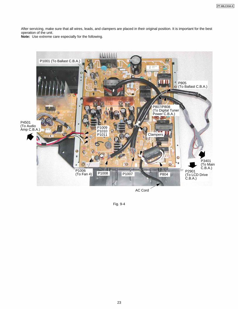
Fig. 9-4
After servicing, make sure that all wires, leads, and clampers are placed in their original position. It is important for the best operation of the unit.Note: Use extreme care especially for the following.
P4501 (To AudioAmp C.B.A.)
Clampers
P1007P1008P1006(To Fan 4)
P1001 (To Ballast C.B.A.)
P805(To Ballast C.B.A.)
P807/P808 (To Digital Tuner Power C.B.A.)
P804P2901 (To LCD Drive C.B.A.)
AC Cord
P1009P1010P1011
P3401 (To Main C.B.A.)
PT-60LCX64-K
23
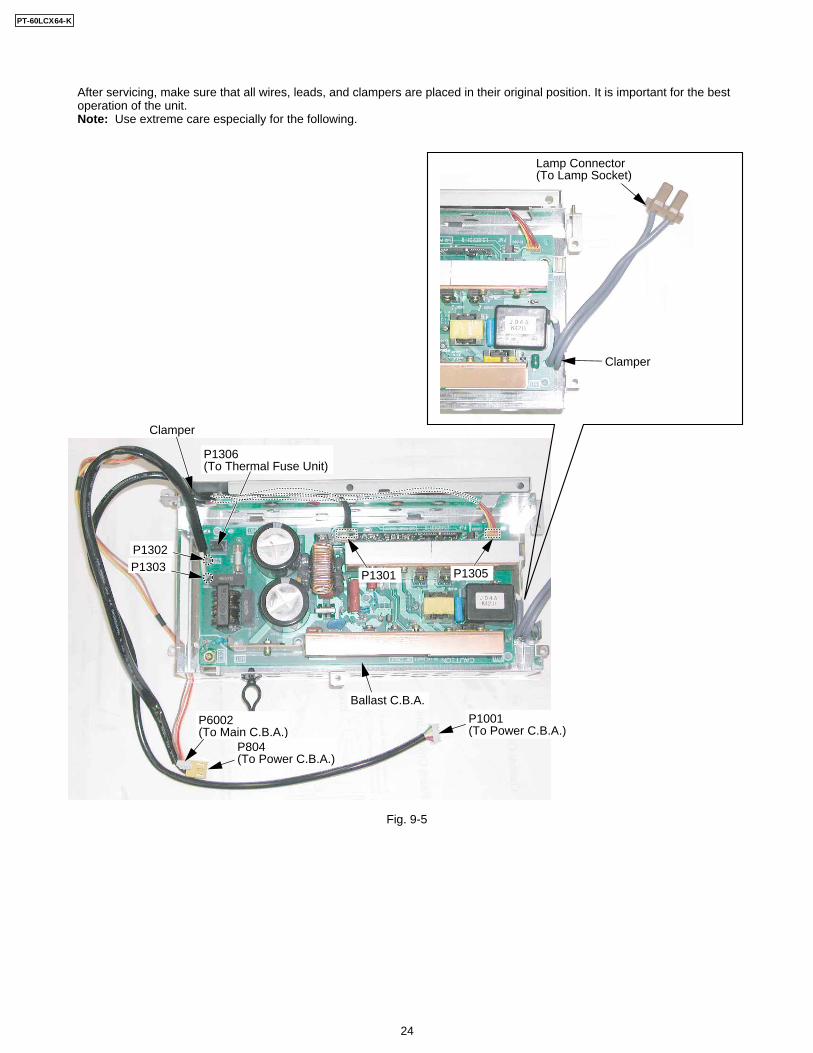
After servicing, make sure that all wires, leads, and clampers are placed in their original position. It is important for the best operation of the unit.Note: Use extreme care especially for the following.
Ballast C.B.A.
P1301
P6002(To Main C.B.A.)
P1302
P1306(To Thermal Fuse Unit)
P1303 P1305
P1001(To Power C.B.A.)
Lamp Connector(To Lamp Socket)
Clamper
Clamper
P804(To Power C.B.A.)
Fig. 9-5
PT-60LCX64-K
24
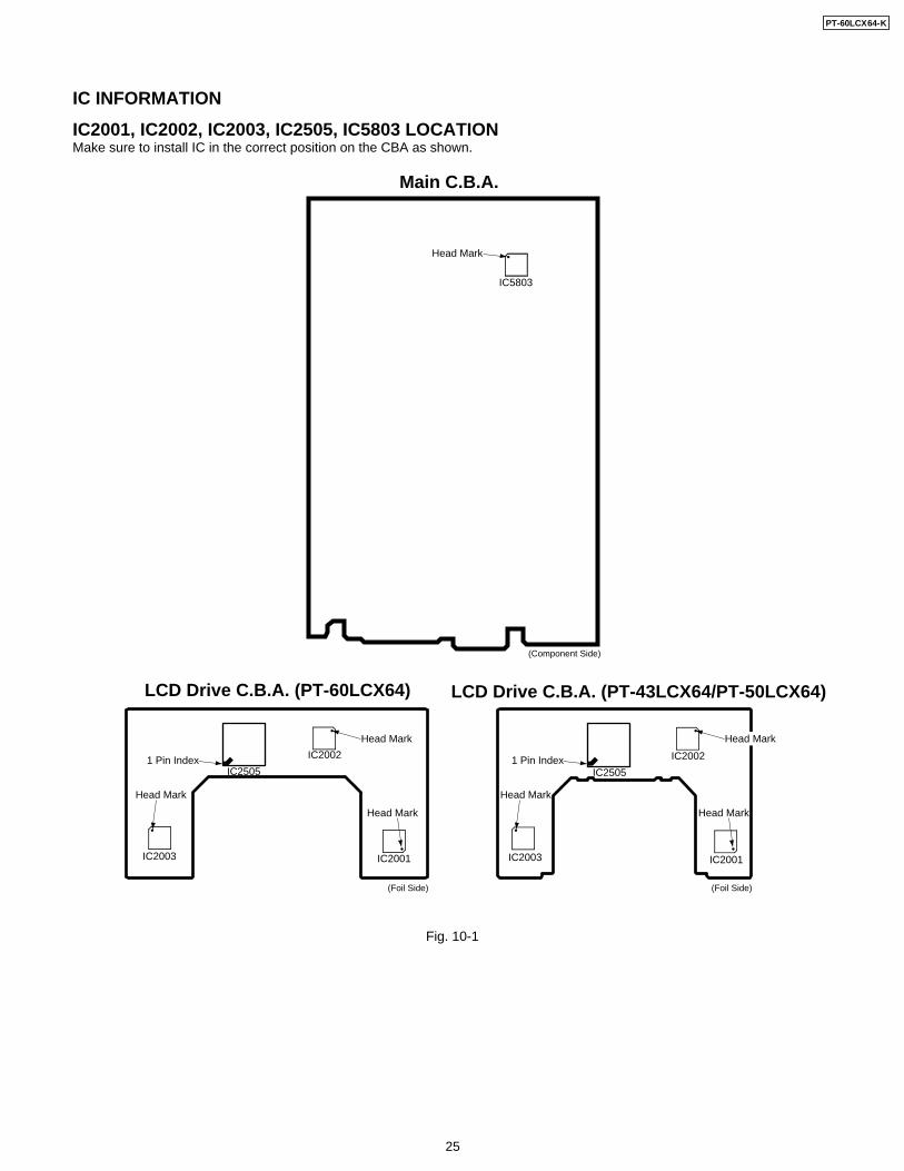
IC2001, IC2002, IC2003, IC2505, IC5803 LOCATIONMake sure to install IC in the correct position on the CBA as shown.
Fig. 10-1
IC INFORMATION
LCD Drive C.B.A. (PT-60LCX64)
Main C.B.A.
IC2505
IC2002
IC2001IC2003
IC2505
IC2002
IC2001IC2003
IC5803
Head Mark
LCD Drive C.B.A. (PT-43LCX64/PT-50LCX64)
(Foil Side)
(Component Side)
(Foil Side)
Head Mark
Head Mark
Head Mark
1 Pin Index
Head Mark
Head Mark
1 Pin Index
Head Mark
PT-60LCX64-K
25
<Bottom View>
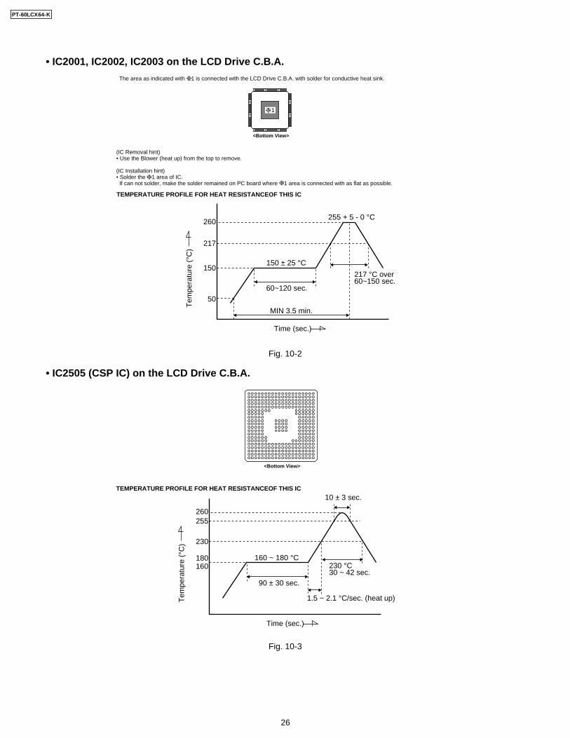
The area as indicated with 1 is connected with the LCD Drive C.B.A. with solder for conductive heat sink.
(IC Removal hint)• Use the Blower (heat up) from the top to remove.
(IC Installation hint)• Solder the 1 area of IC. If can not solder, make the solder remained on PC board where 1 area is connected with as flat as possible.
TEMPERATURE PROFILE FOR HEAT RESISTANCEOF THIS IC
1
Tem
pera
ture
(°C
)
50
150
217
260
Time (sec.)
150 ± 25 °C
255 + 5 - 0 °C
60~120 sec.
MIN 3.5 min.
217 °C over60~150 sec.
• IC2001, IC2002, IC2003 on the LCD Drive C.B.A.
Fig. 10-2
• IC2505 (CSP IC) on the LCD Drive C.B.A.
Fig. 10-3
Tem
pera
ture
(°C
) 230
180160
255260
Time (sec.)
160 ~ 180 °C
10 ± 3 sec.
90 ± 30 sec.
230 °C30 ~ 42 sec.
1.5 ~ 2.1 °C/sec. (heat up)
<Bottom View>
TEMPERATURE PROFILE FOR HEAT RESISTANCEOF THIS IC
PT-60LCX64-K
26
• IC5803 on the Main C.B.A.
Fig. 10-5
<Bottom View>
The ePad of this IC, located on the bottom of the IC, is connected on the Main C.B.A. with solder.
Note:This IC (HDMI IC) which was removed must be disposed of.
(IC Removal hint)• Use the Blower (heat up) from the top to remove.
(IC Installation hint)• It is necessary to connect the ePad erea with the solder.
TEMPERATURE PROFILE FOR HEAT RESISTANCEOF THIS IC
Tem
pera
ture
(°C
)
150
25
200
217
217 °C
245
Time (sec.)
150 ~ 200 °C
245 + 0 - 5 °C
3 °C/sec.(heat up)
10 ~ 30 sec.
60~80 sec.
MAX 8 min.
60~150 sec.
ePad
PT-60LCX64-K
27
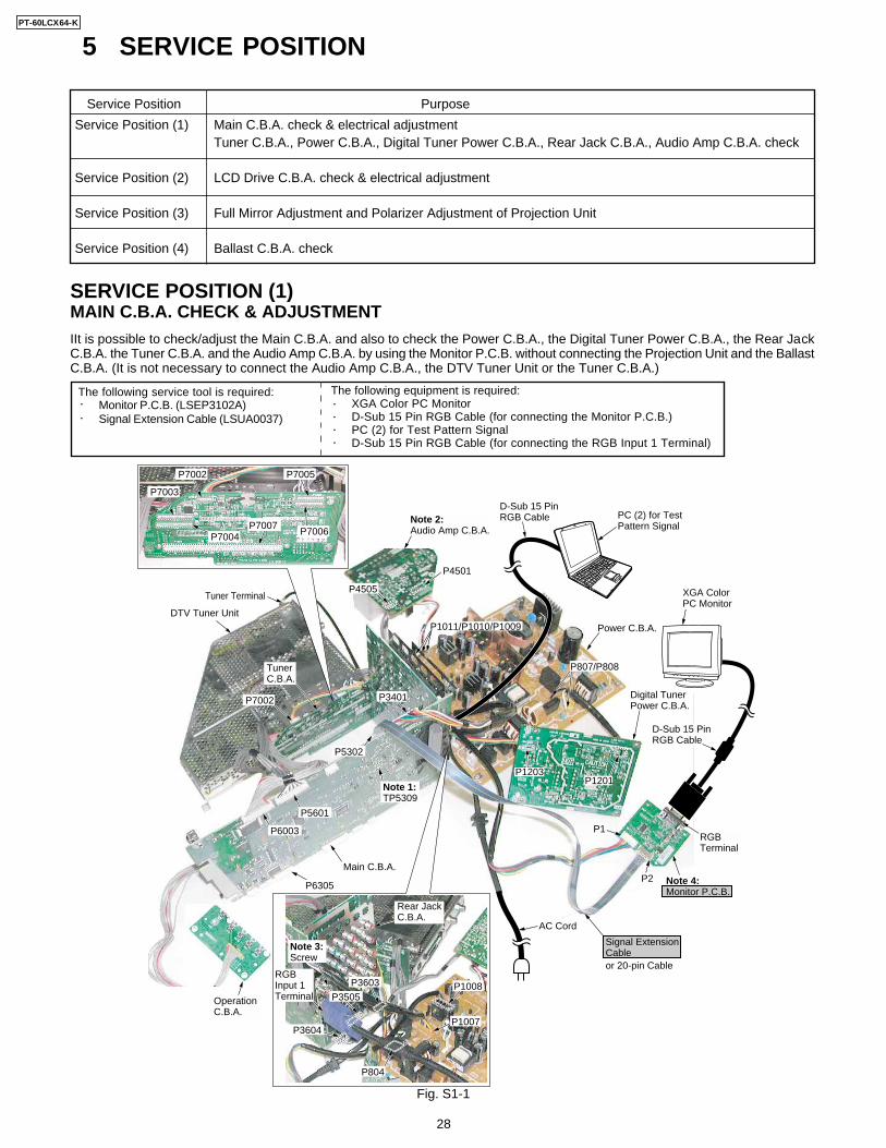
5 SERVICE POSITION
Fig. S1-1
IIt is possible to check/adjust the Main C.B.A. and also to check the Power C.B.A., the Digital Tuner Power C.B.A., the Rear JackC.B.A. the Tuner C.B.A. and the Audio Amp C.B.A. by using the Monitor P.C.B. without connecting the Projection Unit and the BallastC.B.A. (It is not necessary to connect the Audio Amp C.B.A., the DTV Tuner Unit or the Tuner C.B.A.)
SERVICE POSITION (1)MAIN C.B.A. CHECK & ADJUSTMENT
Digital TunerPower C.B.A.
Note 4:Monitor P.C.B.
D-Sub 15 PinRGB Cable
XGA ColorPC Monitor
Note 2:Audio Amp C.B.A.
DTV Tuner Unit
OperationC.B.A.
TunerC.B.A.
P7002
Main C.B.A.
AC Cord
D-Sub 15 PinRGB Cable
Power C.B.A.
P2
P1
PC (2) for Test Pattern Signal
RGBTerminal
Signal ExtensionCableor 20-pin Cable
Tuner Terminal
P6305
P6003
P5601
P5302
P4501
P4505
P1201P1203
P3401
Note 1:TP5309
P1011/P1010/P1009
P807/P808
P3505
P3603
P3604
Note 3: Screw
P7007
P1008
P1007
P804
RGB Input 1Terminal
Rear JackC.B.A.
P7005
P7006
P7002
P7003
P7004
The following service tool is required:Monitor P.C.B. (LSEP3102A)Signal Extension Cable (LSUA0037)
The following equipment is required:XGA Color PC MonitorD-Sub 15 Pin RGB Cable (for connecting the Monitor P.C.B.)PC (2) for Test Pattern SignalD-Sub 15 Pin RGB Cable (for connecting the RGB Input 1 Terminal)
Service Position (1)
Service Position (2)
Service Position (3)
Service Position (4)
Main C.B.A. check & electrical adjustmentTuner C.B.A., Power C.B.A., Digital Tuner Power C.B.A., Rear Jack C.B.A., Audio Amp C.B.A. check
LCD Drive C.B.A. check & electrical adjustment
Full Mirror Adjustment and Polarizer Adjustment of Projection Unit
Ballast C.B.A. check
PurposeService Position
PT-60LCX64-K
28
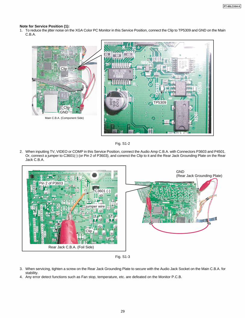
Note for Service Position (1):1. To reduce the jitter noise on the XGA Color PC Monitor in this Service Position, connect the Clip to TP5309 and GND on the Main
C.B.A.
Fig. S1-2
2. When inputting TV, VIDEO or COMP in this Service Position, connect the Audio Amp C.B.A. with Connectors P3603 and P4501.Or, connect a jumper to C3601(-) (or Pin 2 of P3603), and conenct the Clip to it and the Rear Jack Grounding Plate on the RearJack C.B.A.
Fig. S1-3
3. When servicing, tighten a screw on the Rear Jack Grounding Plate to secure with the Audio Jack Socket on the Main C.B.A. forstability.
4. Any error detect functions such as Fan stop, temperature, etc. are defeated on the Monitor P.C.B.
Main C.B.A. (Component Side)
Clip
Clip
GND
TP5309
C3601 (-)
Pin 2 of P3603
jumper wire
Rear Jack C.B.A. (Foil Side)
Clip
GND(Rear Jack Grounding Plate)
PT-60LCX64-K
29
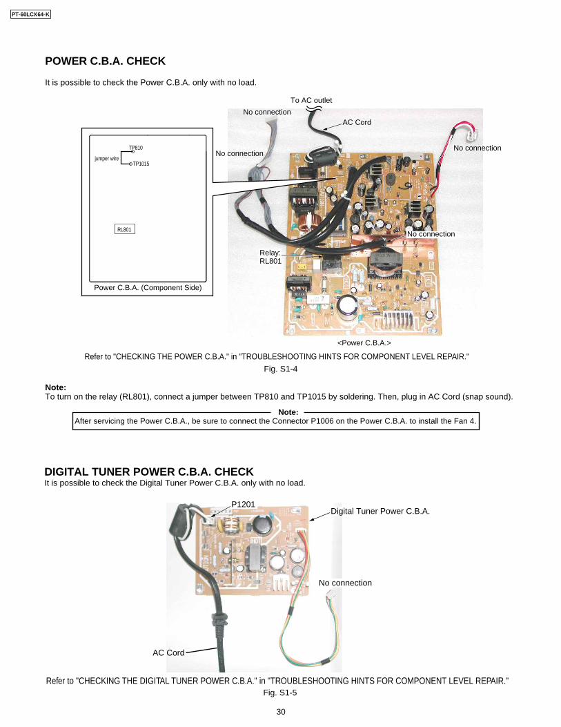
It is possible to check the Power C.B.A. only with no load.
Fig. S1-4
Note:To turn on the relay (RL801), connect a jumper between TP810 and TP1015 by soldering. Then, plug in AC Cord (snap sound).
POWER C.B.A. CHECK
After servicing the Power C.B.A., be sure to connect the Connector P1006 on the Power C.B.A. to install the Fan 4.Note:
AC Cord
No connection
No connection
No connection
To AC outlet
TP810
jumper wireTP1015
Power C.B.A. (Component Side)
<Power C.B.A.>
Relay:RL801
Refer to "CHECKING THE POWER C.B.A." in "TROUBLESHOOTING HINTS FOR COMPONENT LEVEL REPAIR."
RL801No connection
DIGITAL TUNER POWER C.B.A. CHECKIt is possible to check the Digital Tuner Power C.B.A. only with no load.
Fig. S1-5
AC Cord
P1201
No connection
Digital Tuner Power C.B.A.
Refer to "CHECKING THE DIGITAL TUNER POWER C.B.A." in "TROUBLESHOOTING HINTS FOR COMPONENT LEVEL REPAIR."
PT-60LCX64-K
30
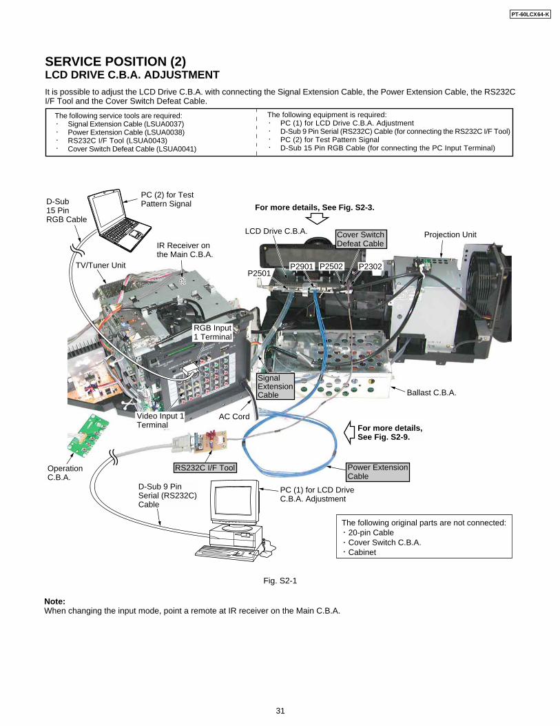
Fig. S2-1
SERVICE POSITION (2)LCD DRIVE C.B.A. ADJUSTMENTIt is possible to adjust the LCD Drive C.B.A. with connecting the Signal Extension Cable, the Power Extension Cable, the RS232CI/F Tool and the Cover Switch Defeat Cable.
Note:When changing the input mode, point a remote at IR receiver on the Main C.B.A.
The following service tools are required:Signal Extension Cable (LSUA0037)Power Extension Cable (LSUA0038)RS232C I/F Tool (LSUA0043)Cover Switch Defeat Cable (LSUA0041)
The following equipment is required:PC (1) for LCD Drive C.B.A. AdjustmentD-Sub 9 Pin Serial (RS232C) Cable (for connecting the RS232C I/F Tool)PC (2) for Test Pattern SignalD-Sub 15 Pin RGB Cable (for connecting the PC Input Terminal)
Signal ExtensionCable
D-Sub 9 Pin Serial (RS232C) Cable
PC (1) for LCD Drive C.B.A. Adjustment
Ballast C.B.A.
LCD Drive C.B.A.
For more details, See Fig. S2-9.
P2501P2901 P2302
Cover Switch Defeat Cable
Projection Unit
For more details, See Fig. S2-3.
P2502
RS232C I/F Tool
IR Receiver on the Main C.B.A.
Power Extension Cable
Operation C.B.A.
Video Input 1 Terminal
TV/Tuner Unit
The following original parts are not connected: 20-pin Cable Cover Switch C.B.A. Cabinet
AC Cord
RGB Input 1 Terminal
PC (2) for Test Pattern SignalD-Sub
15 Pin RGB Cable
PT-60LCX64-K
31
Fig. S2-2
<The Projection Unit is placed into the Cabinet>
VideoInput 1 Terminal
RS232C I/F Tool
TV/Tuner Unit
Operation C.B.A.
Projection Unit
IR Receiver on the Main C.B.A.
The following original parts are not connected: 20-pin Cable
LCD Drive C.B.A.
P2901
P2501 P2302P2502
Ballast C.B.A.RGB Input 1 Terminal
PC (1) for LCD Drive C.B.A. Adjustment
Signal ExtensionCable
Power ExtensionCable
D-Sub 9 Pin Serial (RS232C) Cable
AC Cord
D-Sub 15 Pin RGB Cable
Cabinet For more details, See Fig. S2-3.
For more details, See Fig. S2-9.
Cover Switch Defeat Cableor Connector Cable from Cover Switch C.B.A.
PC (2) for Test Pattern Signal
Note:When changing the input mode, point a remote at IR receiver on the Main C.B.A.
PT-60LCX64-K
32
Power Extension Cable
Signal ExtensionCable
RS232C I/F Tool
To P5302 on Main C.B.A.
Connect with Connector Cable from P1008 on Power C.B.A.
P2502
P2302
P2501 P2901
LCD Drive C.B.A.
Cover Switch Defeat Cableor Connector Cable from Cover Switch C.B.A.
Fig. S2-3
Detailed View for Service Position (2)
PT-60LCX64-K
33
Fig. S2-4
It is possible to check and adjust the LCD Drive C.B.A.LCD DRIVE C.B.A. CHECK & ADJUSTMENT
The following service tools are required:LCD Panel Flat Extension Cable (LSUA0042) X3Relay P.C.B. (LSEP3112A) X3Fan1,3 Extension Cable (LSUA0039) X2Fan2 Extension Cable (LSUA0040)Signal Extension Cable (LSUA0037)Power Extension Cable (LSUA0038)Thermistor 1 Defeat Cable (LSUA0003)Thermistor 2 Defeat Cable (LSUA0013)Cover Switch Defeat Cable (LSUA0041)RS232C I/F Tool (LSUA0043)
The following equipment is required:PC (1) for LCD Drive C.B.A. AdjustmentD-Sub 9 Pin Serial (RS232C) Cable (for connecting the RS232C I/F Tool)PC (2) for Test Pattern SignalD-Sub 15 Pin RGB Cable (for connecting the PC Input Terminal)
D-Sub 9 Pin Serial (RS232C) Cable
LCD Drive C.B.A.
RS232C I/F Tool
Signal Extension Cable
Operation C.B.A.
AC Cord
Video Input 1Terminal
TV/Tuner Unit
Ballast C.B.A.
Relay P.C.B.s
The following original parts are not connected: Thermistor 1 C.B.A. Thermistor 2 C.B.A. 20-pin Cable Cover Switch C.B.A. Cabinet
For more details, See Fig. S2-6.
For more details, See Fig. S2-7.
For more details, See Fig. S2-8, S2-9, S2-10.
LCD Panel Flat Extension Cables
PC (1) for LCD Drive C.B.A. Adjustment
Power Extension Cable
RGB Input 1 Terminal
PC (2) for Test Pattern SignalD-Sub
15 Pin RGB Cable
PT-60LCX64-K
34
Fig. S2-5
CAUTION:When disconnecting/reconnecting the LCD Panel Flexible Cables, be sure to unplug the AC Cord. Because whendisconnecting/reconnecting with AC plugged in, the LCD/Prism Unit may be damaged or broken.
D-Sub 9 Pin Serial (RS232C) Cable
LCD Drive C.B.A.
Ballast C.B.A.
RS232C I/F Tool
Signal Extension Cable
Power Extension Cable
Operation C.B.A.
AC Cord
TV/Tuner Unit
Relay P.C.B.s
The following original parts are not connected: Thermistor 1 C.B.A. Thermistor 2 C.B.A. 20-pin Cable Cover Switch C.B.A.
For more details, See Fig. S2-6.
For more details, See Fig. S2-8, S2-9, S2-10.
For more details, See Fig. S2-7.
PC (1) for LCD Drive C.B.A. Adjustment
Video Input 1Terminal
<The Projection Unit is placed into the Cabinet>Cabinet
LCD Panel Flat Extension Cables
LCD Panel Flat Extension Cables
PC (2) for Test Pattern Signal
RGB Input 1 Terminal
D-Sub 15 Pin RGB Cable
PT-60LCX64-K
35
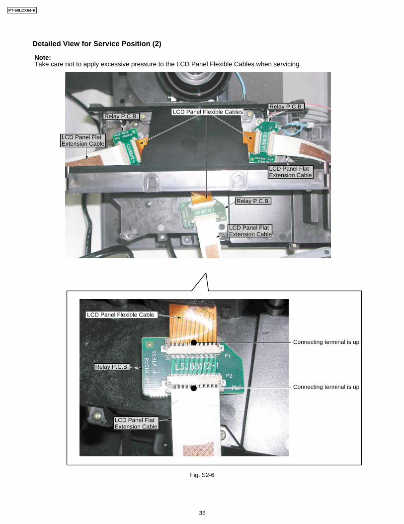
Fig. S2-6
Relay P.C.B.
Relay P.C.B.
LCD Panel Flat Extension Cable
Relay P.C.B.
Note:Take care not to apply excessive pressure to the LCD Panel Flexible Cables when servicing.
LCD Panel Flat Extension Cable
LCD Panel Flat Extension Cable
LCD Panel Flat Extension Cable
Relay P.C.B.
LCD Panel Flexible Cables
LCD Panel Flexible Cable
Connecting terminal is up
Connecting terminal is up
Detailed View for Service Position (2)
PT-60LCX64-K
36
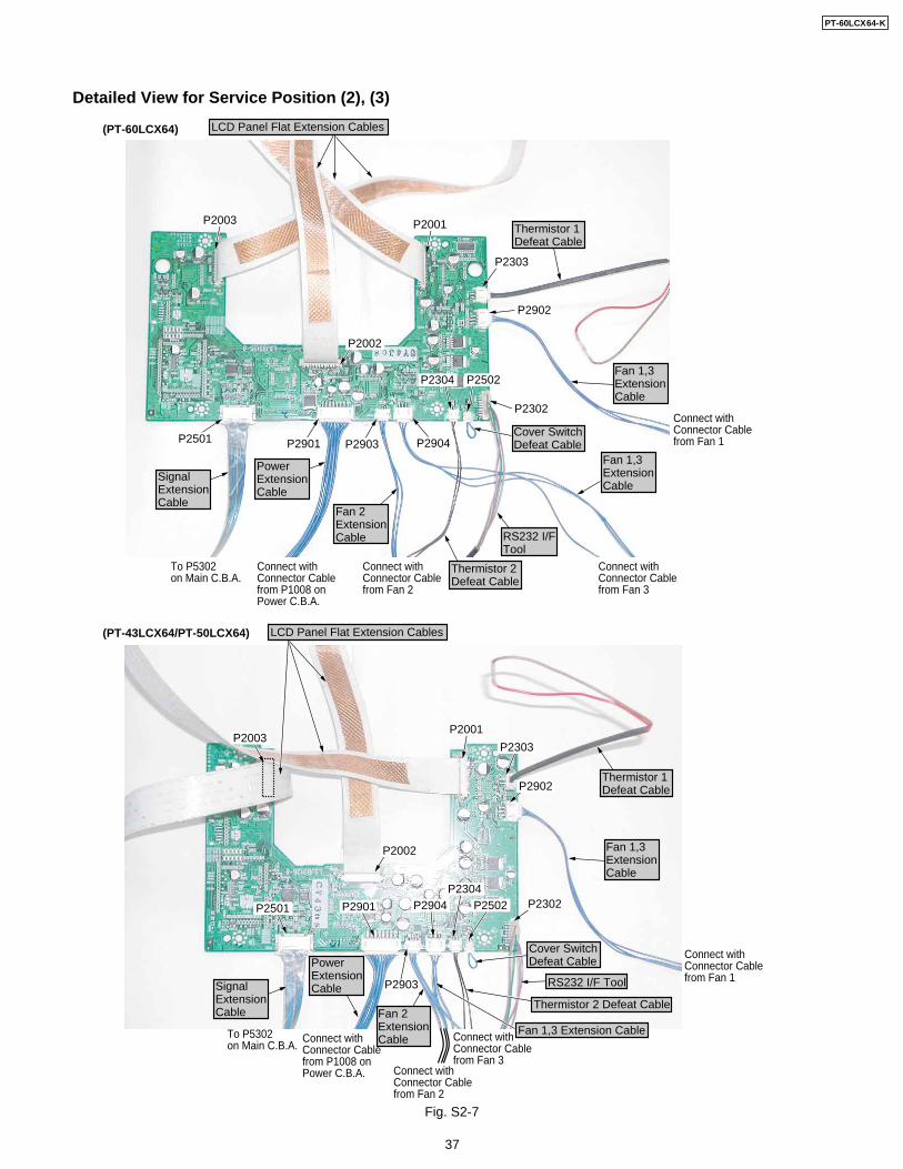
Fig. S2-7
(PT-60LCX64)
(PT-43LCX64/PT-50LCX64)
P2001
P2303
P2902
P2302
P2904
P2304 P2502
P2903P2901
P2003
To P5302on Main C.B.A.
Connect with Connector Cablefrom P1008 on Power C.B.A.
Connect withConnector Cable from Fan 2
Connect with Connector Cable from Fan 1
Connect withConnector Cable from Fan 3
P2002
P2002
P2501
Fan 1,3 ExtensionCable
LCD Panel Flat Extension Cables
Fan 2 Extension Cable
Thermistor 2Defeat Cable
Thermistor 1Defeat Cable
P2001
P2303
P2902Thermistor 1Defeat Cable
Power Extension Cable
Signal Extension Cable
Cover SwitchDefeat Cable
RS232 I/F Tool
Fan 1,3 ExtensionCable
Connect with Connector Cable from Fan 1
Fan 1,3 ExtensionCable
P2302P2502
Cover SwitchDefeat Cable
RS232 I/F Tool
P2304
Thermistor 2 Defeat Cable
P2904
P2903
Connect withConnector Cable from Fan 2
Connect withConnector Cable from Fan 3
Fan 2 Extension Cable
Fan 1,3 Extension Cable
P2901
Connect with Connector Cablefrom P1008 on Power C.B.A.
Power Extension Cable
To P5302on Main C.B.A.
P2501
Signal Extension Cable
P2003
LCD Panel Flat Extension Cables
Detailed View for Service Position (2), (3)
PT-60LCX64-K
37
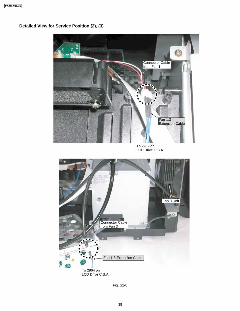
Fig. S2-8
Connector Cable from Fan 1
To 2902 on LCD Drive C.B.A.
To 2904 on LCD Drive C.B.A.
Connector Cable from Fan 3
Fan 3 Unit
Fan 1,3 Extension Cable
Fan 1,3 Extension Cable
Detailed View for Service Position (2), (3)
PT-60LCX64-K
38
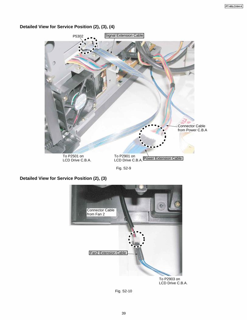
Fig. S2-9
Detailed View for Service Position (2), (3), (4)
Power Extension Cable
Signal Extension Cable
Connector Cable from Power C.B.A
To P2901 onLCD Drive C.B.A.
To P2501 onLCD Drive C.B.A.
P5302
Fig. S2-10
Fan2 Extension Cable
Connector Cable from Fan 2
To P2903 onLCD Drive C.B.A.
Detailed View for Service Position (2), (3)
PT-60LCX64-K
39
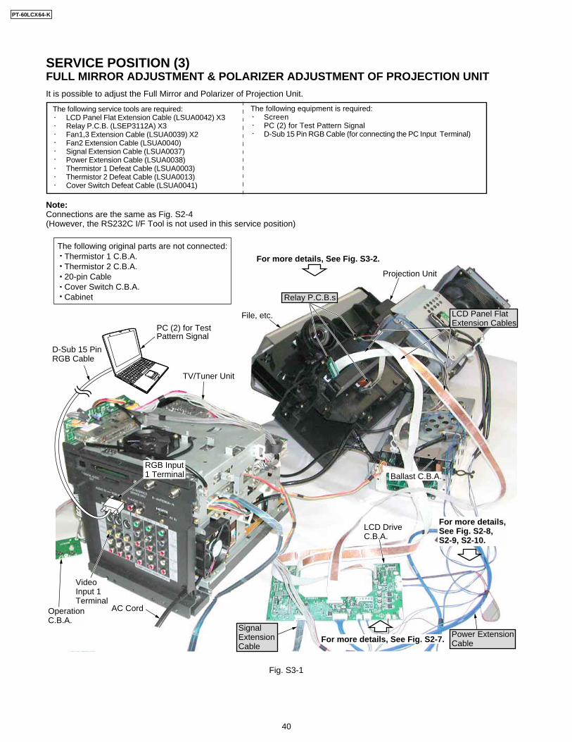
SERVICE POSITION (3)FULL MIRROR ADJUSTMENT & POLARIZER ADJUSTMENT OF PROJECTION UNITIt is possible to adjust the Full Mirror and Polarizer of Projection Unit.
Note:Connections are the same as Fig. S2-4(However, the RS232C I/F Tool is not used in this service position)
File, etc.
Projection Unit
Ballast C.B.A.
The following original parts are not connected: Thermistor 1 C.B.A. Thermistor 2 C.B.A. 20-pin Cable Cover Switch C.B.A. Cabinet
LCD Drive C.B.A.
Power Extension Cable
AC Cord
TV/Tuner Unit
Relay P.C.B.s
LCD Panel Flat Extension Cables
For more details, See Fig. S3-2.
For more details, See Fig. S2-7.
For more details, See Fig. S2-8, S2-9, S2-10.
SignalExtension Cable
Operation C.B.A.
PC (2) for Test Pattern Signal
VideoInput 1 Terminal
RGB Input 1 Terminal
D-Sub 15 Pin RGB Cable
Fig. S3-1
The following service tools are required:LCD Panel Flat Extension Cable (LSUA0042) X3Relay P.C.B. (LSEP3112A) X3Fan1,3 Extension Cable (LSUA0039) X2Fan2 Extension Cable (LSUA0040)Signal Extension Cable (LSUA0037)Power Extension Cable (LSUA0038)Thermistor 1 Defeat Cable (LSUA0003)Thermistor 2 Defeat Cable (LSUA0013)Cover Switch Defeat Cable (LSUA0041)
The following equipment is required:ScreenPC (2) for Test Pattern SignalD-Sub 15 Pin RGB Cable (for connecting the PC Input Terminal)
PT-60LCX64-K
40
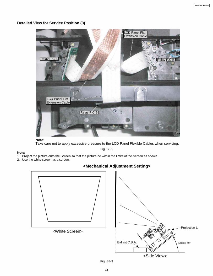
Note:1. Project the picture onto the Screen so that the picture be within the limits of the Screen as shown.2. Use the white screen as a screen.
Fig. S3-3
<Side View>
<White Screen>
Ballast C.B.A.
Projection U
Approx. 40
<Mechanical Adjustment Setting>
Fig. S3-2
Relay P.C.B. Relay P.C.B.
Relay P.C.B.
LCD Panel Flat Extension Cable
LCD Panel Flat Extension Cable
Note:Take care not to apply excessive pressure to the LCD Panel Flexible Cables when servicing.
Detailed View for Service Position (3)
PT-60LCX64-K
41
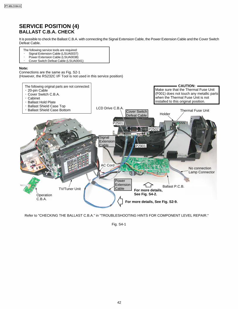
SERVICE POSITION (4)BALLAST C.B.A. CHECKIt is possible to check the Ballast C.B.A. with connecting the Signal Extension Cable, the Power Extension Cable and the Cover SwitchDefeat Cable.
The following service tools are required:Signal Extension Cable (LSUA0037)Power Extension Cable (LSUA0038)Cover Switch Defeat Cable (LSUA0041)
Refer to "CHECKING THE BALLAST C.B.A." in "TROUBLESHOOTING HINTS FOR COMPONENT LEVEL REPAIR."
For more details, See Fig. S2-9.
For more details, See Fig. S4-2.
Holder
The following original parts are not connected: 20-pin Cable Cover Switch C.B.A. Cabinet Ballast Hold Plate Ballast Shield Case Top Ballast Shield Case Bottom
Signal ExtensionCable
Cover Switch Defeat Cable
TV/Tuner Unit
AC Cord
Operation C.B.A.
Power Extension Cable
Ballast P.C.B.
LCD Drive C.B.A.Thermal Fuse Unit
P2501
P2901
P2502
No connectionLamp Connector
Make sure that the Thermal Fuse Unit(F001) does not touch any metallic partswhen the Thermal Fuse Unit is not installed to this original position.
CAUTION:
Note:Connections are the same as Fig. S2-1(However, the RS232C I/F Tool is not used in this service position)
Fig. S4-1
PT-60LCX64-K
42
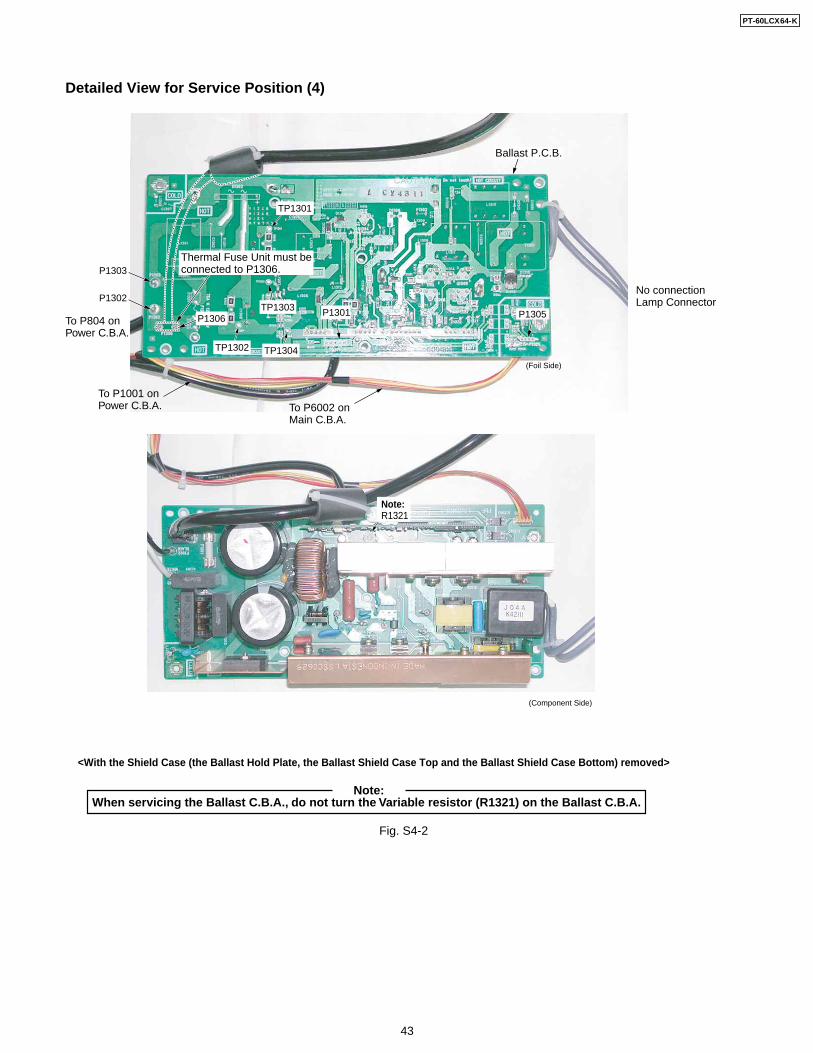
Fig. S4-2
Detailed View for Service Position (4)
<With the Shield Case (the Ballast Hold Plate, the Ballast Shield Case Top and the Ballast Shield Case Bottom) removed>
P1301 P1305
(Foil Side)
(Component Side)
Ballast P.C.B.
To P6002 onMain C.B.A.
No connectionLamp ConnectorTP1303
P1306
P1303
P1302
TP1301
TP1302 TP1304
Thermal Fuse Unit must be connected to P1306.
To P1001 onPower C.B.A.
To P804 onPower C.B.A.
Note: When servicing the Ballast C.B.A., do not turn the Variable resistor (R1321) on the Ballast C.B.A.
Note:R1321
PT-60LCX64-K
43
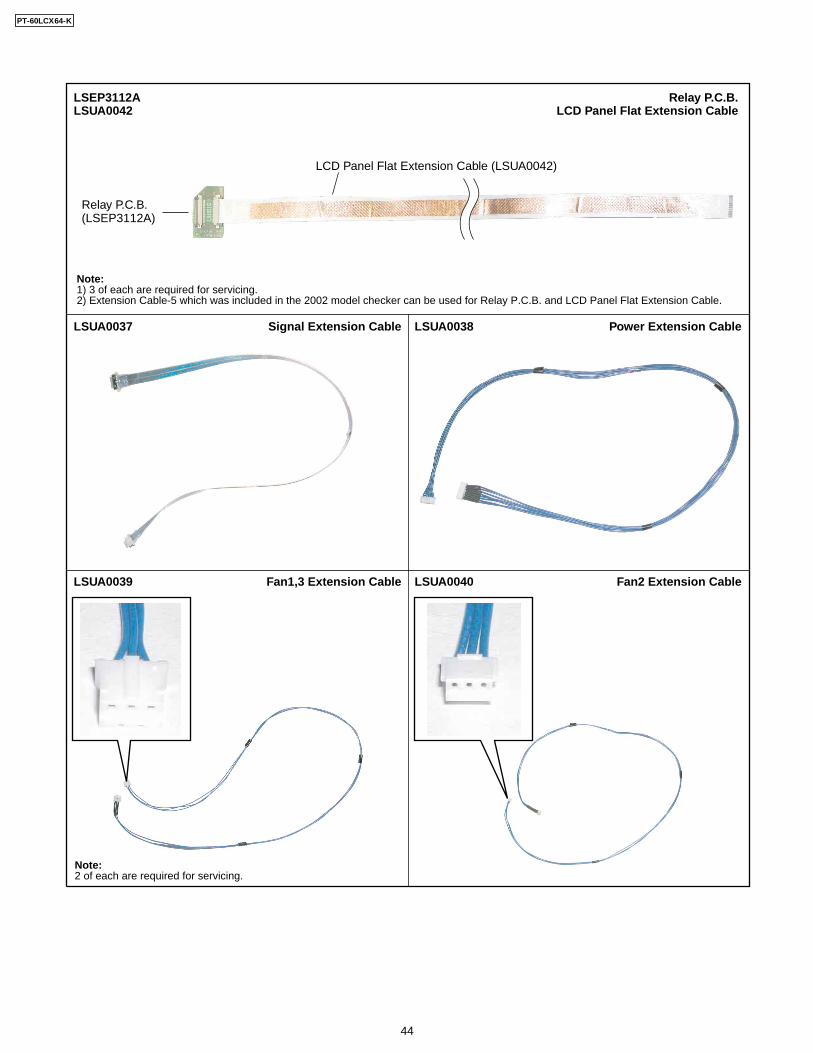
LSUA0042 LCD Panel Flat Extension Cable LSEP3112A Relay P.C.B.
LSUA0040 Fan2 Extension CableLSUA0039 Fan1,3 Extension Cable
LSUA0037 Signal Extension Cable LSUA0038 Power Extension Cable
Note:1) 3 of each are required for servicing.2) Extension Cable-5 which was included in the 2002 model checker can be used for Relay P.C.B. and LCD Panel Flat Extension Cable.
Note:2 of each are required for servicing.
Relay P.C.B. (LSEP3112A)
LCD Panel Flat Extension Cable (LSUA0042)
PT-60LCX64-K
44
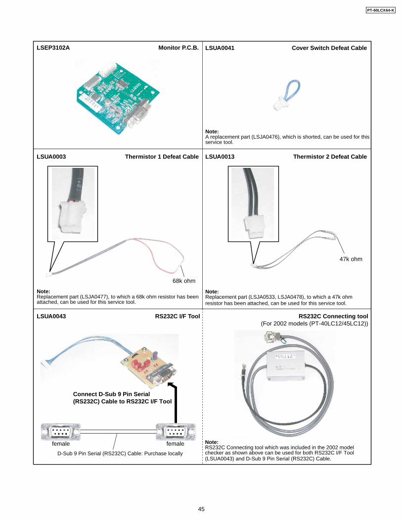
Note:Replacement part (LSJA0533, LSJA0478), to which a 47k ohm resistor has been attached, can be used for this service tool.
Note:Replacement part (LSJA0477), to which a 68k ohm resistor has been attached, can be used for this service tool.
Note:A replacement part (LSJA0476), which is shorted, can be used for this service tool.
68k ohm
LSUA0003 Thermistor 1 Defeat Cable LSUA0013 Thermistor 2 Defeat Cable
LSUA0041 Cover Switch Defeat Cable
LSUA0043 RS232C I/F Tool RS232C Connecting tool(For 2002 models (PT-40LC12/45LC12))
LSEP3102A Monitor P.C.B.
Note:RS232C Connecting tool which was included in the 2002 model checker as shown above can be used for both RS232C I/F Tool (LSUA0043) and D-Sub 9 Pin Serial (RS232C) Cable.
Connect D-Sub 9 Pin Serial(RS232C) Cable to RS232C I/F Tool
female female
D-Sub 9 Pin Serial (RS232C) Cable: Purchase locally
47k ohm
PT-60LCX64-K
45
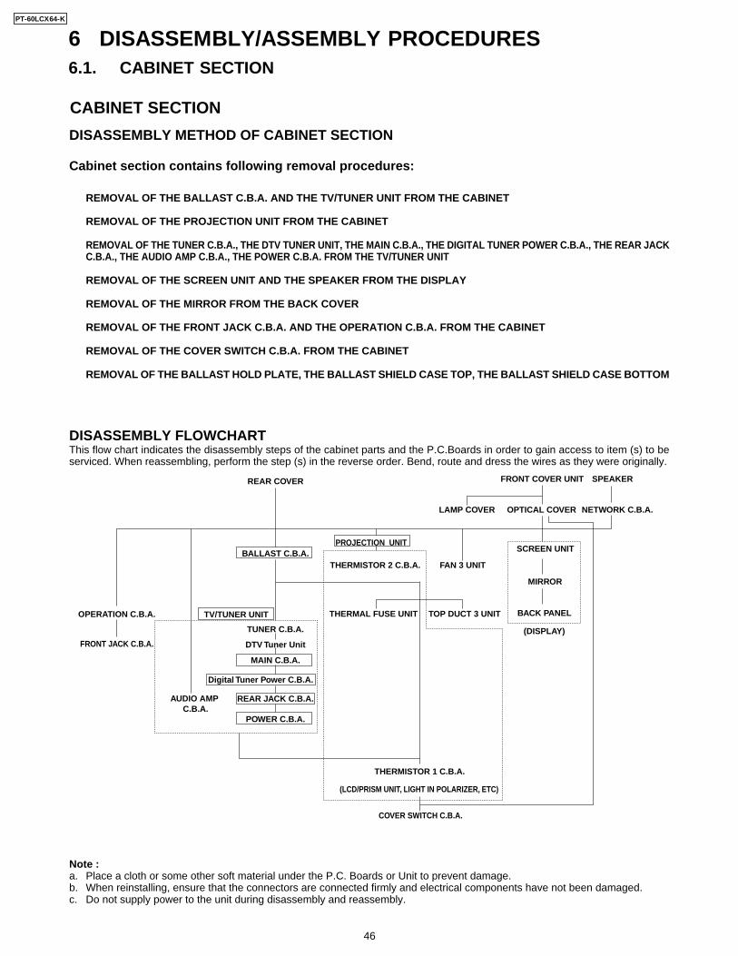
6 DISASSEMBLY/ASSEMBLY PROCEDURES6.1. CABINET SECTION
DISASSEMBLY METHOD OF CABINET SECTION
Cabinet section contains following removal procedures:
CABINET SECTION
BALLAST C.B.A.
REAR COVER FRONT COVER UNIT
OPTICAL COVERLAMP COVER NETWORK C.B.A.
TUNER C.B.A.
DTV Tuner Unit
OPERATION C.B.A. TV/TUNER UNIT
MAIN C.B.A.
REAR JACK C.B.A.AUDIO AMP C.B.A.
POWER C.B.A.
(LCD/PRISM UNIT, LIGHT IN POLARIZER, ETC)
THERMISTOR 2 C.B.A.
THERMISTOR 1 C.B.A.
THERMAL FUSE UNIT TOP DUCT 3 UNIT
(DISPLAY)
FAN 3 UNIT
FRONT JACK C.B.A.
COVER SWITCH C.B.A.
PROJECTION UNIT
SPEAKER
SCREEN UNIT
MIRROR
BACK PANEL
Digital Tuner Power C.B.A.
REMOVAL OF THE BALLAST C.B.A. AND THE TV/TUNER UNIT FROM THE CABINET
REMOVAL OF THE PROJECTION UNIT FROM THE CABINET
REMOVAL OF THE TUNER C.B.A., THE DTV TUNER UNIT, THE MAIN C.B.A., THE DIGITAL TUNER POWER C.B.A., THE REAR JACKC.B.A., THE AUDIO AMP C.B.A., THE POWER C.B.A. FROM THE TV/TUNER UNIT
REMOVAL OF THE SCREEN UNIT AND THE SPEAKER FROM THE DISPLAY
REMOVAL OF THE MIRROR FROM THE BACK COVER
REMOVAL OF THE FRONT JACK C.B.A. AND THE OPERATION C.B.A. FROM THE CABINET
REMOVAL OF THE COVER SWITCH C.B.A. FROM THE CABINET
REMOVAL OF THE BALLAST HOLD PLATE, THE BALLAST SHIELD CASE TOP, THE BALLAST SHIELD CASE BOTTOM
DISASSEMBLY FLOWCHARTThis flow chart indicates the disassembly steps of the cabinet parts and the P.C.Boards in order to gain access to item (s) to beserviced. When reassembling, perform the step (s) in the reverse order. Bend, route and dress the wires as they were originally.
Note :a. Place a cloth or some other soft material under the P.C. Boards or Unit to prevent damage.b. When reinstalling, ensure that the connectors are connected firmly and electrical components have not been damaged.c. Do not supply power to the unit during disassembly and reassembly.
PT-60LCX64-K
46
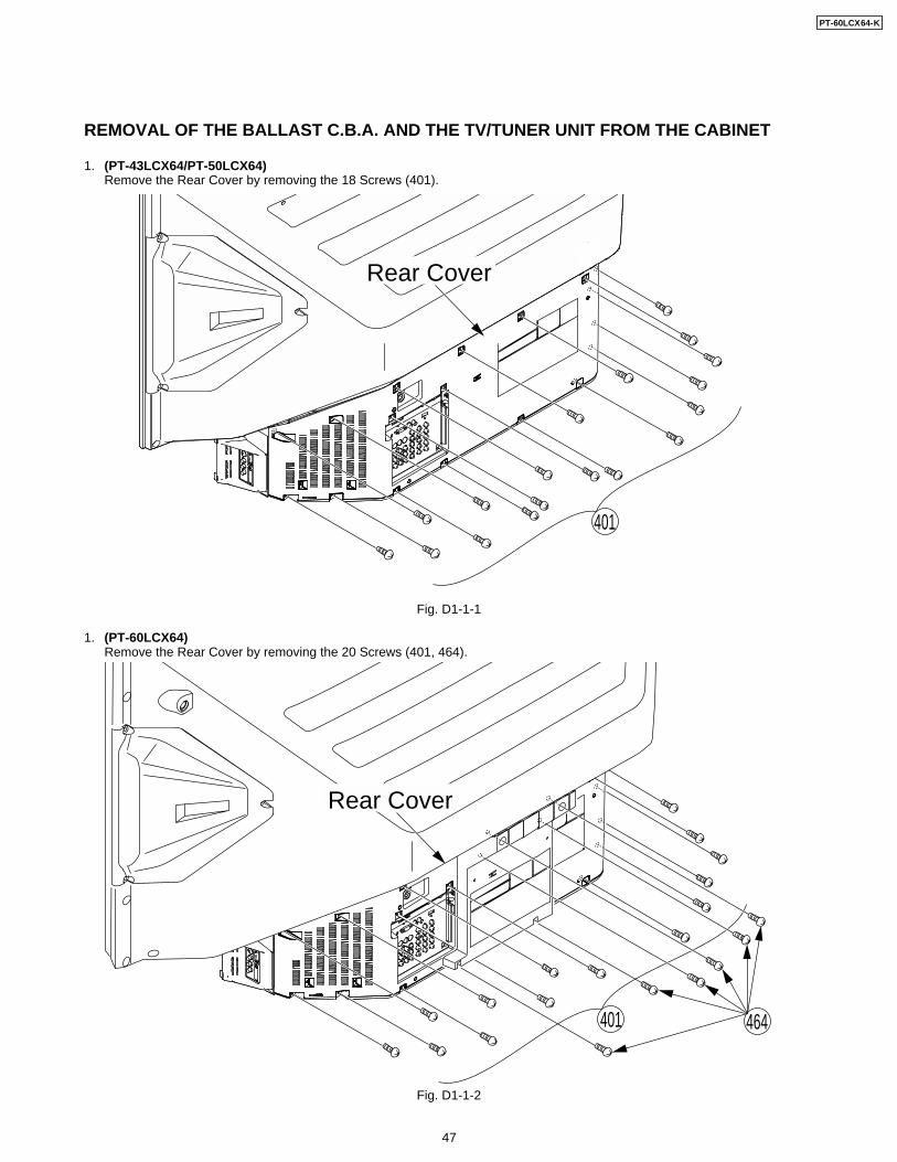
401
Rear Cover
REMOVAL OF THE BALLAST C.B.A. AND THE TV/TUNER UNIT FROM THE CABINET
1. (PT-43LCX64/PT-50LCX64)Remove the Rear Cover by removing the 18 Screws (401).
Fig. D1-1-1
1. (PT-60LCX64)Remove the Rear Cover by removing the 20 Screws (401, 464).
Fig. D1-1-2
401 464
Rear Cover
PT-60LCX64-K
47
Rear Support Plate
401
401
452
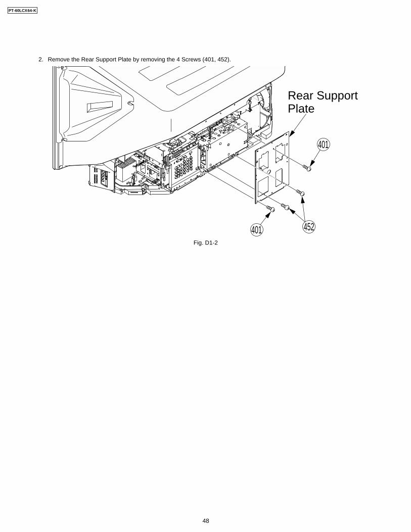
2. Remove the Rear Support Plate by removing the 4 Screws (401, 452).
Fig. D1-2
PT-60LCX64-K
48
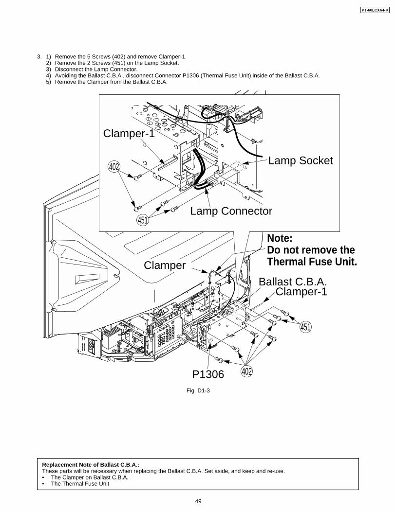
3. 1) Remove the 5 Screws (402) and remove Clamper-1.2) Remove the 2 Screws (451) on the Lamp Socket.3) Disconnect the Lamp Connector.4) Avoiding the Ballast C.B.A., disconnect Connector P1306 (Thermal Fuse Unit) inside of the Ballast C.B.A.5) Remove the Clamper from the Ballast C.B.A.
Fig. D1-3
Ballast C.B.A.
Note:Do not remove theThermal Fuse Unit.
P1306
Lamp Socket
Lamp Connector
402
451
402
451
Clamper
Clamper-1
Clamper-1
Replacement Note of Ballast C.B.A.:These parts will be necessary when replacing the Ballast C.B.A. Set aside, and keep and re-use.• The Clamper on Ballast C.B.A.• The Thermal Fuse Unit
PT-60LCX64-K
49
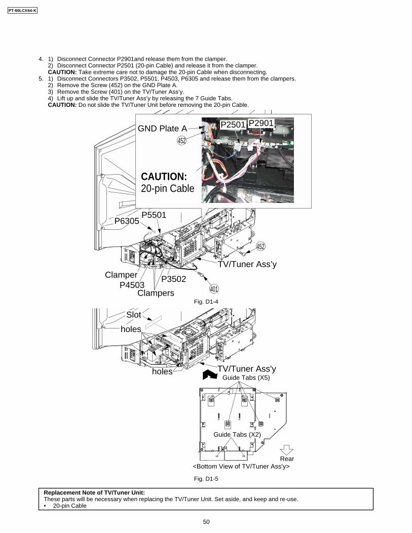
4. 1) Disconnect Connector P2901and release them from the clamper.2) Disconnect Connector P2501 (20-pin Cable) and release it from the clamper.CAUTION: Take extreme care not to damage the 20-pin Cable when disconnecting.
5. 1) Disconnect Connectors P3502, P5501, P4503, P6305 and release them from the clampers.2) Remove the Screw (452) on the GND Plate A.3) Remove the Screw (401) on the TV/Tuner Ass’y.4) Lift up and slide the TV/Tuner Ass’y by releasing the 7 Guide Tabs.CAUTION: Do not slide the TV/Tuner Unit before removing the 20-pin Cable.
Fig. D1-4
Fig. D1-5
TV/Tuner Ass'yGuide Tabs (X5)
Rear<Bottom View of TV/Tuner Ass'y>
Guide Tabs (X2)
holes
holes
Slot
TV/Tuner Ass’y
452
401Clampers
ClamperP4503
P3502
P5501P6305
GND Plate A P2501 P2901
452
CAUTION:20-pin Cable
Replacement Note of TV/Tuner Unit:These parts will be necessary when replacing the TV/Tuner Unit. Set aside, and keep and re-use.• 20-pin Cable
PT-60LCX64-K
50
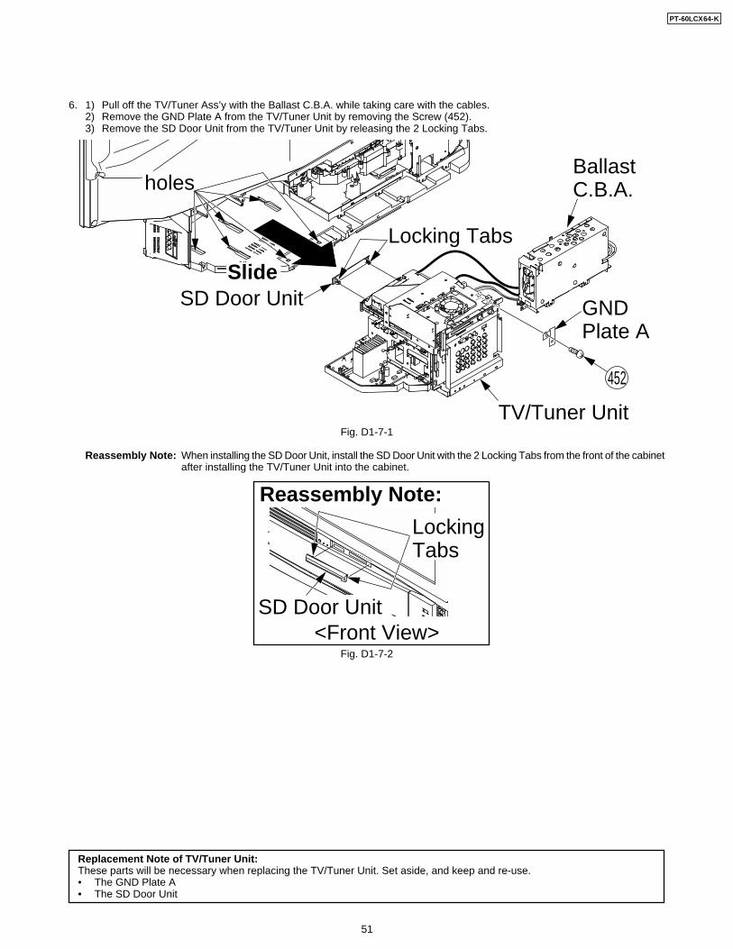
6. 1) Pull off the TV/Tuner Ass’y with the Ballast C.B.A. while taking care with the cables.2) Remove the GND Plate A from the TV/Tuner Unit by removing the Screw (452).3) Remove the SD Door Unit from the TV/Tuner Unit by releasing the 2 Locking Tabs.
Fig. D1-7-1
Reassembly Note: When installing the SD Door Unit, install the SD Door Unit with the 2 Locking Tabs from the front of the cabinetafter installing the TV/Tuner Unit into the cabinet.
Fig. D1-7-2
Replacement Note of TV/Tuner Unit:These parts will be necessary when replacing the TV/Tuner Unit. Set aside, and keep and re-use.• The GND Plate A• The SD Door Unit
Slide
holesBallast C.B.A.
TV/Tuner Unit
SD Door Unit GND Plate A
Locking Tabs
452
SD Door Unit
Locking Tabs
<Front View>
Reassembly Note:
PT-60LCX64-K
51
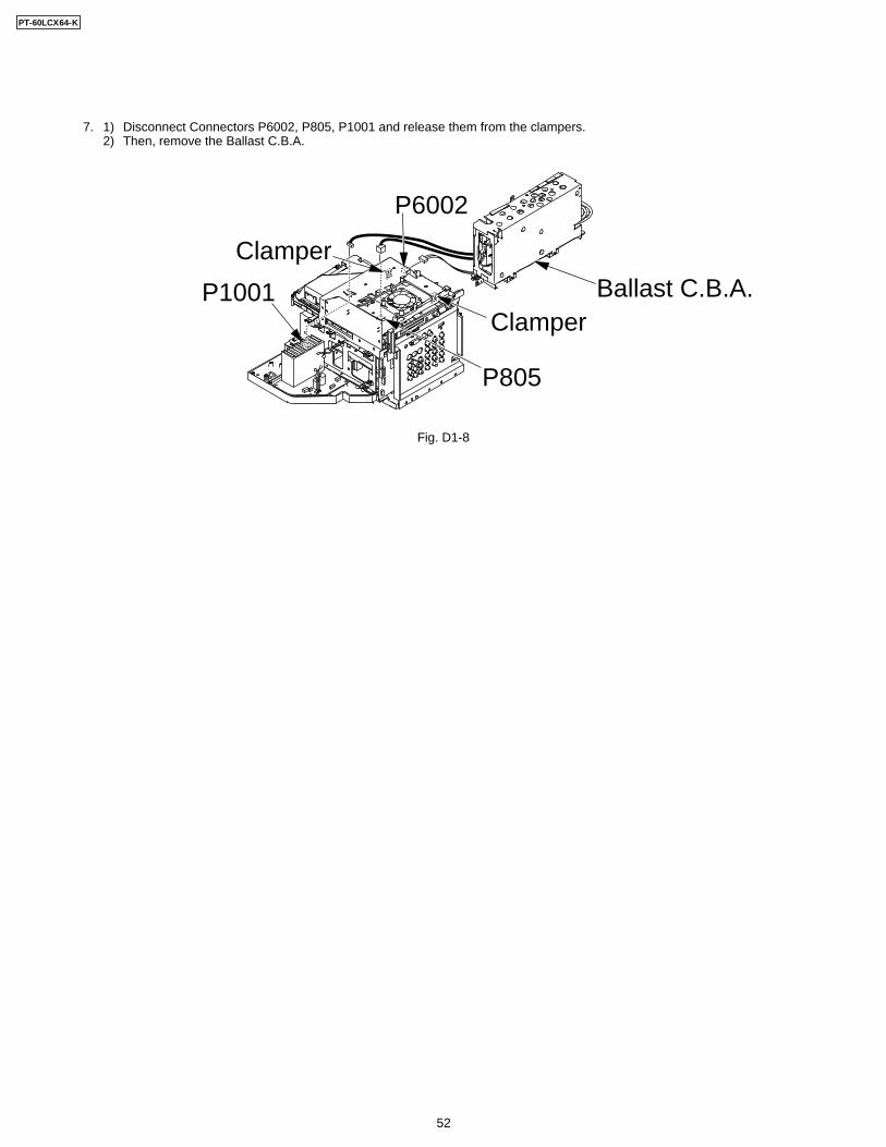
P1001
P6002
Clamper
ClamperBallast C.B.A.
P805
7. 1) Disconnect Connectors P6002, P805, P1001 and release them from the clampers.2) Then, remove the Ballast C.B.A.
Fig. D1-8
PT-60LCX64-K
52
REMOVAL OF THE PROJECTION UNIT FROM THE CABINET
1. Remove the Ballast C.B.A. and the TV/Tuner Unit. Refer to Steps 1~6 in "REMOVAL OF THE BALLAST C.B.A. AND THE TV/TUNER UNIT FROM THE CABINET."
2. 1) Disconnect Connector P2502. Then, hook the P2502 cable to the pin.2) Remove the 7 Screws (401) on the Projection Unit.3) Lift up and slide the Projection Unit by releasing the 5 Guide Tabs.
Tips on removal of the Projection Unit:First, slide the Projection Unit to the rear (approx. 1.5 inch (4 cm)). Then, lift up the front and the rear portions of the ProjectionUnit by both hand to release the Guide Tabs. Then, slide out the Projection Unit.Or, remove the Fan 3 Unit from the Projection Unit at first. Refer to Fig. D2-3.
Fig. D2-1
Lift up and slide the Projection Unit by approx. 1.5 inch (4 cm).Lift up the front portion.
Slide out the Projection Unit.
Slide
Tips on removal of the Projection Unit
Up2
Up
Up Up
3
3 2
4 1
4
1
2
Lift up the rear portion.3
<Side View>
401
Boss
P2502
Pin
Cover Switch C.B.A.
P2502Cable
CAUTION:Disconnect Connector P2502 and hook it as follows.
PT-60LCX64-K
53
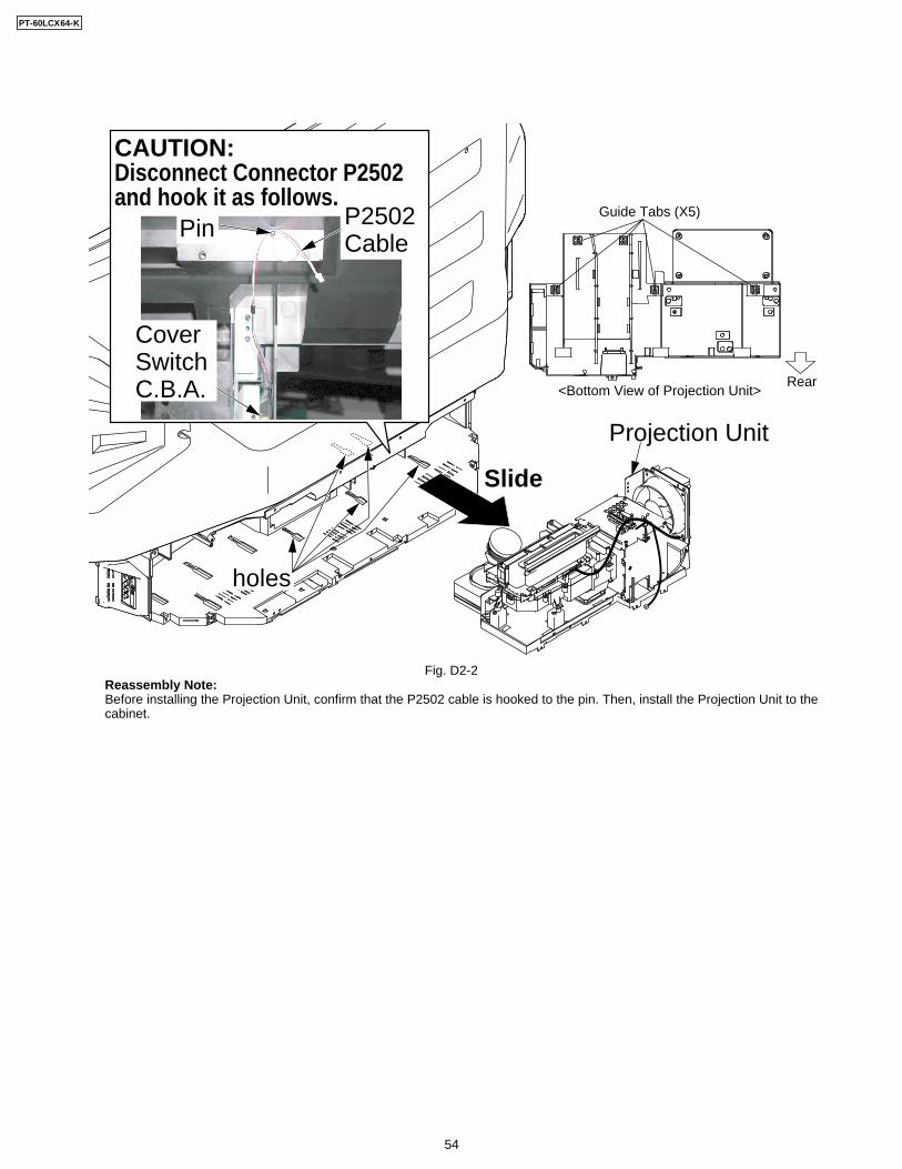
Guide Tabs (X5)
Rear<Bottom View of Projection Unit>
Projection Unit
holes
Slide
Pin
Cover Switch C.B.A.
P2502Cable
CAUTION:Disconnect Connector P2502and hook it as follows.
Fig. D2-2Reassembly Note:Before installing the Projection Unit, confirm that the P2502 cable is hooked to the pin. Then, install the Projection Unit to thecabinet.
PT-60LCX64-K
54
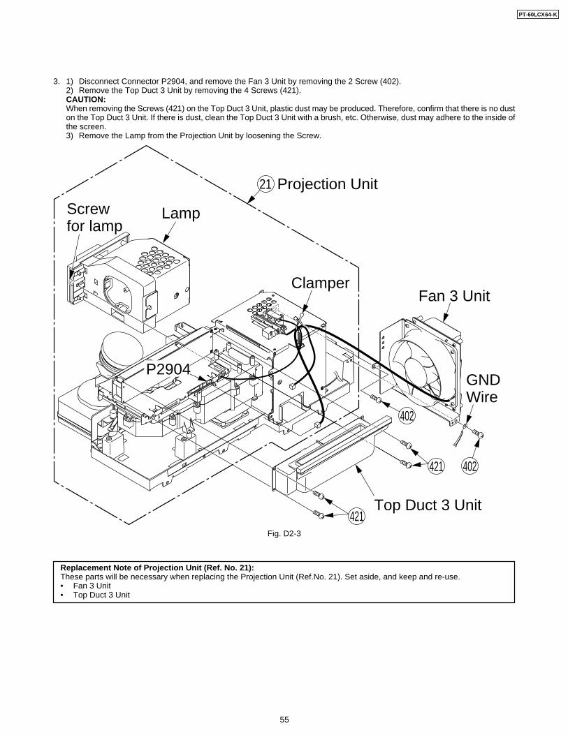
3. 1) Disconnect Connector P2904, and remove the Fan 3 Unit by removing the 2 Screw (402).2) Remove the Top Duct 3 Unit by removing the 4 Screws (421).CAUTION:When removing the Screws (421) on the Top Duct 3 Unit, plastic dust may be produced. Therefore, confirm that there is no duston the Top Duct 3 Unit. If there is dust, clean the Top Duct 3 Unit with a brush, etc. Otherwise, dust may adhere to the inside ofthe screen.3) Remove the Lamp from the Projection Unit by loosening the Screw.
Fig. D2-3
Replacement Note of Projection Unit (Ref. No. 21):These parts will be necessary when replacing the Projection Unit (Ref.No. 21). Set aside, and keep and re-use.• Fan 3 Unit• Top Duct 3 Unit
Fan 3 Unit
GND Wire
Top Duct 3 Unit
LampScrew for lamp
402
402
421
421
Clamper
Projection Unit21
P2904
PT-60LCX64-K
55
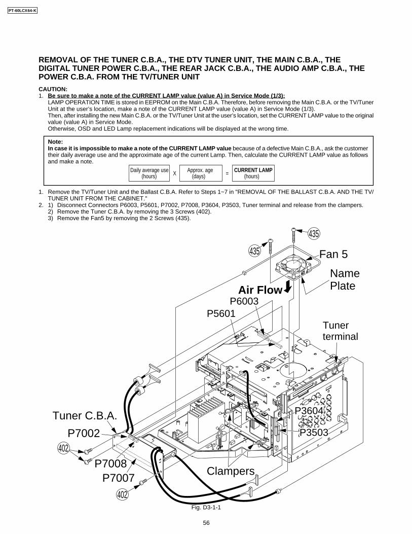
REMOVAL OF THE TUNER C.B.A., THE DTV TUNER UNIT, THE MAIN C.B.A., THEDIGITAL TUNER POWER C.B.A., THE REAR JACK C.B.A., THE AUDIO AMP C.B.A., THEPOWER C.B.A. FROM THE TV/TUNER UNIT
1. Remove the TV/Tuner Unit and the Ballast C.B.A. Refer to Steps 1~7 in "REMOVAL OF THE BALLAST C.B.A. AND THE TV/TUNER UNIT FROM THE CABINET."
2. 1) Disconnect Connectors P6003, P5601, P7002, P7008, P3604, P3503, Tuner terminal and release from the clampers.2) Remove the Tuner C.B.A. by removing the 3 Screws (402).3) Remove the Fan5 by removing the 2 Screws (435).
Fig. D3-1-1
CAUTION:1. Be sure to make a note of the CURRENT LAMP value (value A) in Service Mode (1/3):
LAMP OPERATION TIME is stored in EEPROM on the Main C.B.A. Therefore, before removing the Main C.B.A. or the TV/TunerUnit at the user’s location, make a note of the CURRENT LAMP value (value A) in Service Mode (1/3).Then, after installing the new Main C.B.A. or the TV/Tuner Unit at the user’s location, set the CURRENT LAMP value to the originalvalue (value A) in Service Mode.Otherwise, OSD and LED Lamp replacement indications will be displayed at the wrong time.
Note:In case it is impossible to make a note of the CURRENT LAMP value because of a defective Main C.B.A., ask the customertheir daily average use and the approximate age of the current Lamp. Then, calculate the CURRENT LAMP value as followsand make a note.
Daily average use X =Approx. age CURRENT LAMP (hours) (days) (hours)
NamePlateAir Flow
Fan 5
402
402
P7008P7007
P7002
Tuner C.B.A. P3604
P6003
Tuner terminal
P5601
435
435
Clampers
P3503
PT-60LCX64-K
56
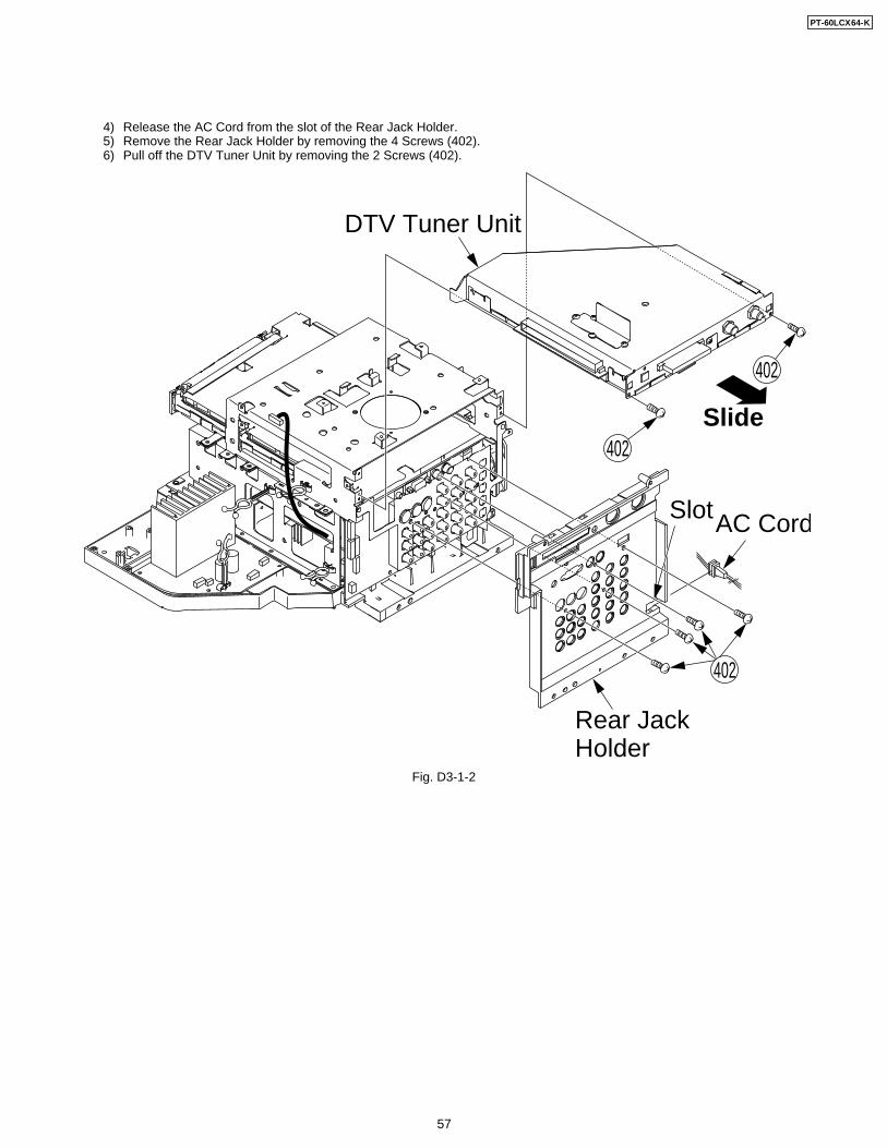
AC Cord
Slide
Slot
402
402
402
Rear Jack Holder
DTV Tuner Unit
4) Release the AC Cord from the slot of the Rear Jack Holder.5) Remove the Rear Jack Holder by removing the 4 Screws (402).6) Pull off the DTV Tuner Unit by removing the 2 Screws (402).
Fig. D3-1-2
PT-60LCX64-K
57
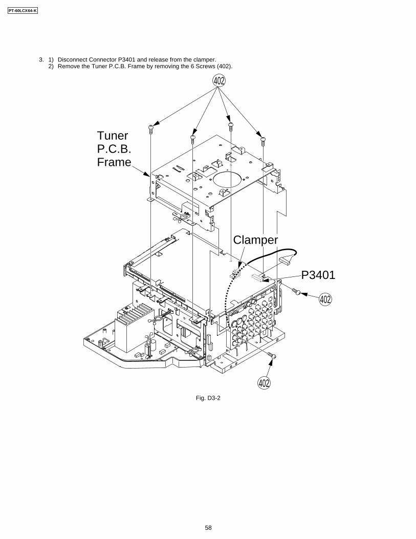
3. 1) Disconnect Connector P3401 and release from the clamper.2) Remove the Tuner P.C.B. Frame by removing the 6 Screws (402).
Fig. D3-2
402
402
P3401
402
Tuner P.C.B. Frame
Clamper
PT-60LCX64-K
58
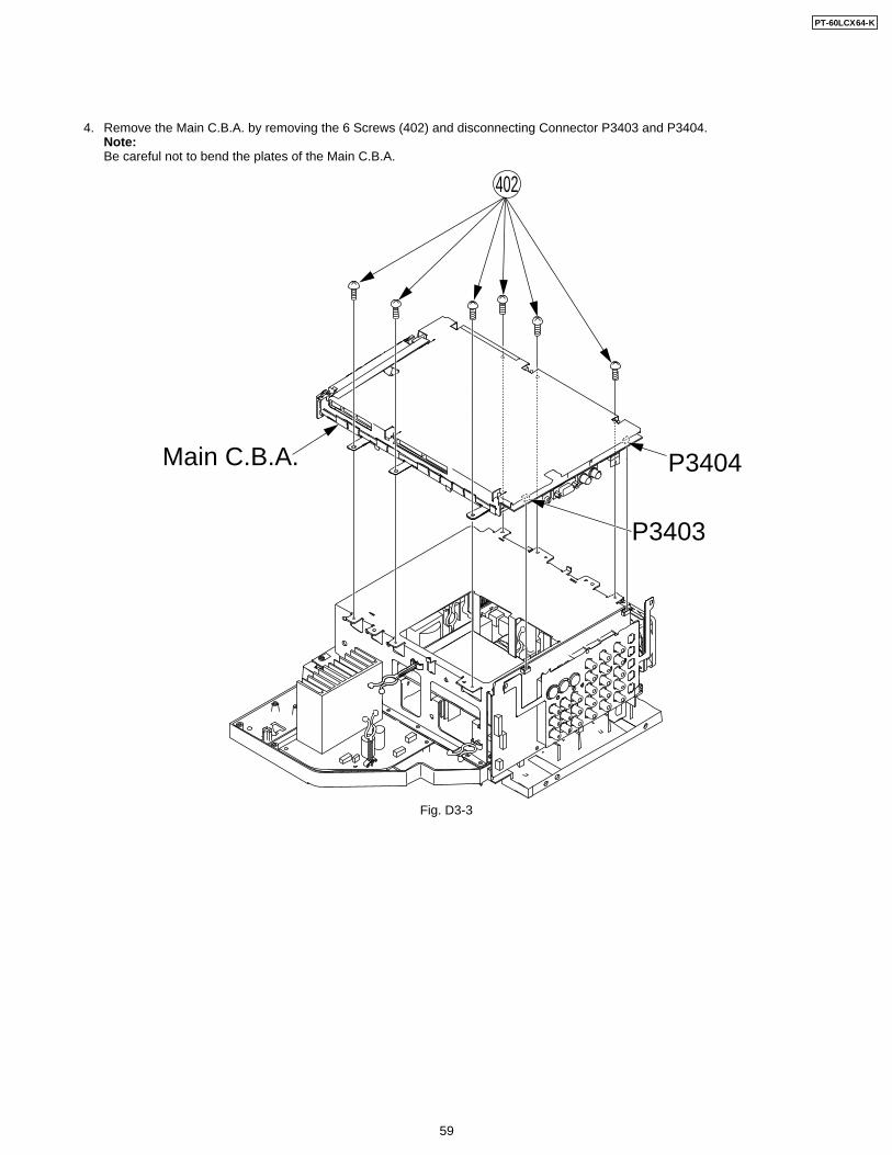
4. Remove the Main C.B.A. by removing the 6 Screws (402) and disconnecting Connector P3403 and P3404.Note:Be careful not to bend the plates of the Main C.B.A.
Fig. D3-3
Main C.B.A. P3404
402
P3403
PT-60LCX64-K
59
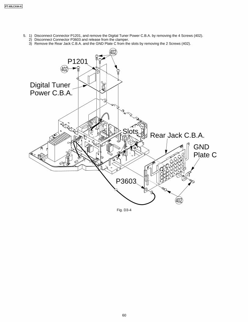
5. 1) Disconnect Connector P1201, and remove the Digital Tuner Power C.B.A. by removing the 4 Screws (402).2) Disconnect Connector P3603 and release from the clamper.3) Remove the Rear Jack C.B.A. and the GND Plate C from the slots by removing the 2 Screws (402).
Fig. D3-4
Rear Jack C.B.A.
GND Plate C
P3603
Slots
402
402
402
Digital Tuner Power C.B.A.
P1201
PT-60LCX64-K
60
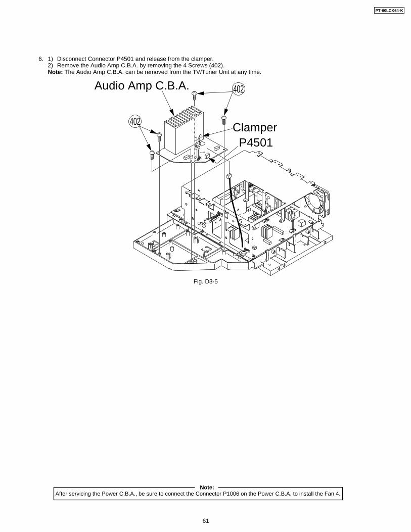
After servicing the Power C.B.A., be sure to connect the Connector P1006 on the Power C.B.A. to install the Fan 4.Note:
6. 1) Disconnect Connector P4501 and release from the clamper.2) Remove the Audio Amp C.B.A. by removing the 4 Screws (402).Note: The Audio Amp C.B.A. can be removed from the TV/Tuner Unit at any time.
Fig. D3-5
Audio Amp C.B.A.
P4501Clamper
402
402
PT-60LCX64-K
61
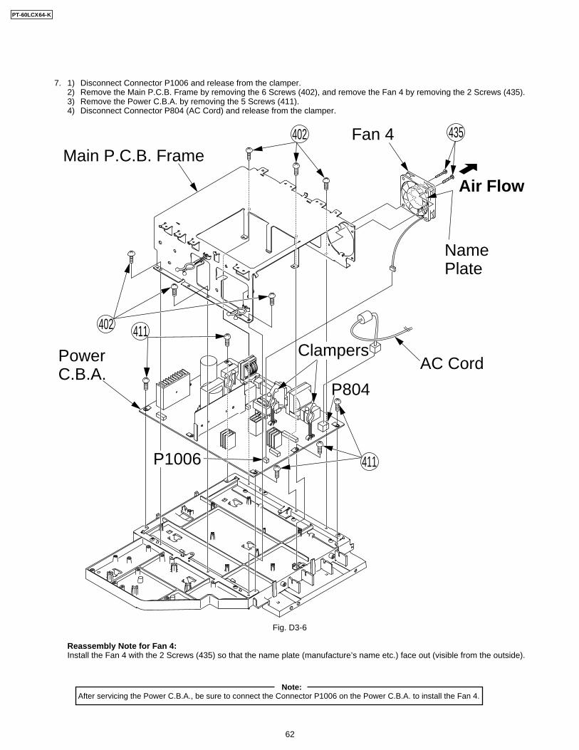
7. 1) Disconnect Connector P1006 and release from the clamper.2) Remove the Main P.C.B. Frame by removing the 6 Screws (402), and remove the Fan 4 by removing the 2 Screws (435).3) Remove the Power C.B.A. by removing the 5 Screws (411).4) Disconnect Connector P804 (AC Cord) and release from the clamper.
Fig. D3-6
Reassembly Note for Fan 4:Install the Fan 4 with the 2 Screws (435) so that the name plate (manufacture’s name etc.) face out (visible from the outside).
Main P.C.B. Frame
Power C.B.A.
AC Cord
P804
Fan 4
NamePlate
411
402 411
402 435
Clampers
P1006
Air Flow
After servicing the Power C.B.A., be sure to connect the Connector P1006 on the Power C.B.A. to install the Fan 4.Note:
PT-60LCX64-K
62
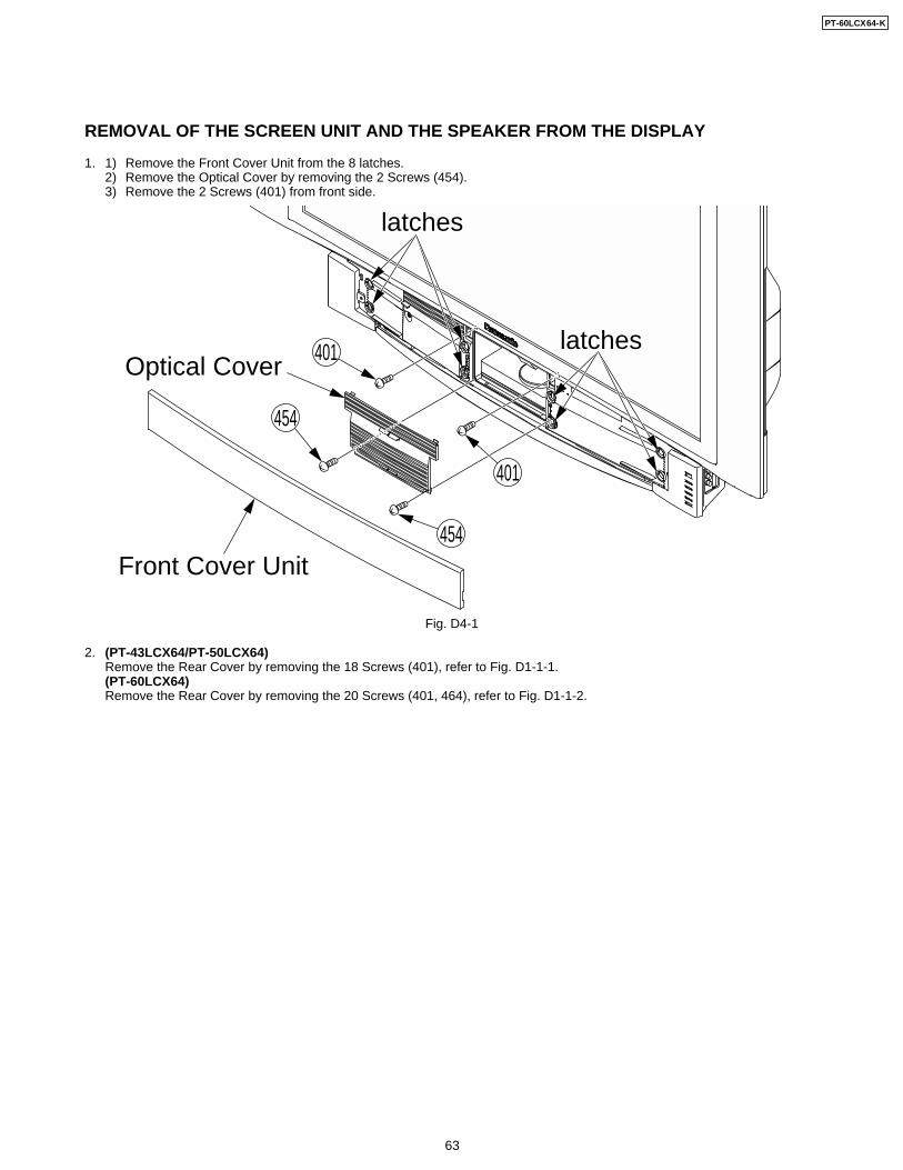
REMOVAL OF THE SCREEN UNIT AND THE SPEAKER FROM THE DISPLAY
1. 1) Remove the Front Cover Unit from the 8 latches.2) Remove the Optical Cover by removing the 2 Screws (454).3) Remove the 2 Screws (401) from front side.
Fig. D4-1
2. (PT-43LCX64/PT-50LCX64)Remove the Rear Cover by removing the 18 Screws (401), refer to Fig. D1-1-1.(PT-60LCX64)Remove the Rear Cover by removing the 20 Screws (401, 464), refer to Fig. D1-1-2.
401
401
454
454
Front Cover Unit
Optical Cover
latches
latches
PT-60LCX64-K
63
Display
401
401
P4503 Clamper
3. 1) Disconnect Connector P4503 (speaker cables) and release it from the clamper.2) Remove the 2 Screws (401) from rear side, and remove the Display.
Fig. D4-3
PT-60LCX64-K
64
401
401
477478
477
477
477478
Screen Unit
Speaker R
Speaker L
P4553
P4553
4. 1) Remove the Speaker-L and the Speaker-R by removing the 6 Screws (477, 478) and disconnect the connectors P4553.2) (PT-43LCX64/PT-50LCX64)
Remove the Screen Unit by removing the 16 Screws (401).
Fig. D4-4-1
PT-60LCX64-K
65
477478
P4553
477
Speaker L
401
401
Screen Unit
478
477477
Speaker R
P4553
2) (PT-60LCX64)Remove the Screen Unit by removing the 26 Screws (401).
Fig. D4-4-2
PT-60LCX64-K
66
REMOVAL OF THE MIRROR FROM THE BACK COVER
(PT-43LCX64/PT-50LCX64)1. Remove the Screen Unit. Refer to Steps 1~4 in "REMOVAL OF THE SCREEN UNIT AND THE SPEAKER FROM THE DISPLAY."2. 1) Remove the 2 Mirror Holder H and the 2 Mirror Holder V Unit by removing the 12 Screws (401).
2) Remove the Mirror from the top by releasing the Back Cover slots.Note: Be careful that the Mirror does not fall down when removing.
Fig. D4-6-1Reassembly Notes for Mirror:Install the Mirror as following procedures:1) Place the 3 sheets on the top and bottom edges of the Mirror.
Fig. D4-7-1
2) Hold the sheet portions of the Mirror, and insert the Mirror from the top into the Back Cover slots carefully.When handling the Mirror, do not touch the Mirror surface.
3) Install the 2 Mirror Holder H and the 2 Mirror Holder V on the Mirror and tighten the 12 Screws (401).
Mirror surface
Sheet
Sheet
Sheet60 mm 10 mm
20 mm 5 mm
60 mm 10 mm
20 mm 5 mm
10 m
m ~
15
mm
Sheet
Top edge of Mirror
Bottom edge of Mirror
Sheet
15 m
m ~
20
mm
10 m
m ~
15
mm
15 m
m ~
20
mmMirror surface
Sheet
Sheet
Sheet0 mm ~ 5 mm
3 mm 5 mm
0 mm ~ 5 mm
3 mm 5 mm
10 m
m ~
15
mm
<Front View>
(PT-50LCX64)
<Front View>
(PT-43LCX64)
15 m
m ~
20
mm
10 m
m ~
15
mm
15 m
m ~
20
mm
401
401
401
401
Mirror Holder V Unit
Mirror Holder HBack Cover slots
PT-60LCX64-K
67
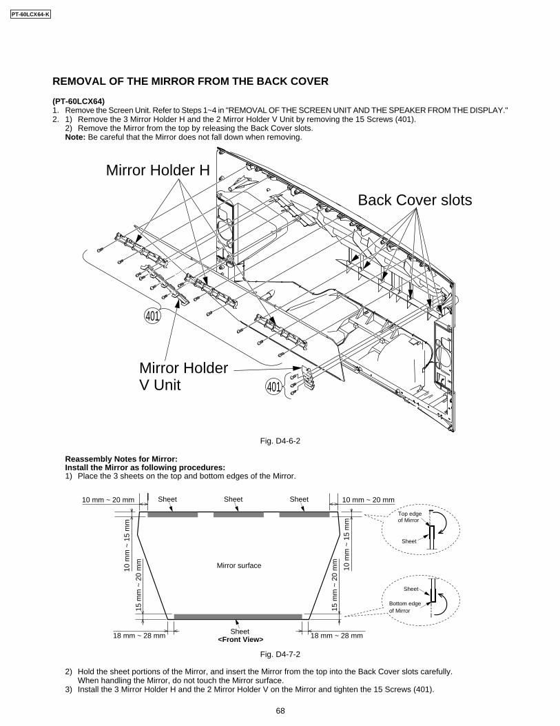
REMOVAL OF THE MIRROR FROM THE BACK COVER
(PT-60LCX64)1. Remove the Screen Unit. Refer to Steps 1~4 in "REMOVAL OF THE SCREEN UNIT AND THE SPEAKER FROM THE DISPLAY."2. 1) Remove the 3 Mirror Holder H and the 2 Mirror Holder V Unit by removing the 15 Screws (401).
2) Remove the Mirror from the top by releasing the Back Cover slots.Note: Be careful that the Mirror does not fall down when removing.
Fig. D4-6-2
Reassembly Notes for Mirror:Install the Mirror as following procedures:1) Place the 3 sheets on the top and bottom edges of the Mirror.
Fig. D4-7-2
2) Hold the sheet portions of the Mirror, and insert the Mirror from the top into the Back Cover slots carefully.When handling the Mirror, do not touch the Mirror surface.
3) Install the 3 Mirror Holder H and the 2 Mirror Holder V on the Mirror and tighten the 15 Screws (401).
Mirror surface
Sheet
10 mm ~ 20 mm
10 m
m ~
15
mm
<Front View>18 mm ~ 28 mm
15 m
m ~
20
mm
18 mm ~ 28 mm
10 mm ~ 20 mm
10 m
m ~
15
mm
SheetSheet Sheet
15 m
m ~
20
mm
Sheet
Top edge of Mirror
Bottom edge of Mirror
Sheet
Mirror Holder V Unit
Mirror Holder H
401
401
Back Cover slots
PT-60LCX64-K
68
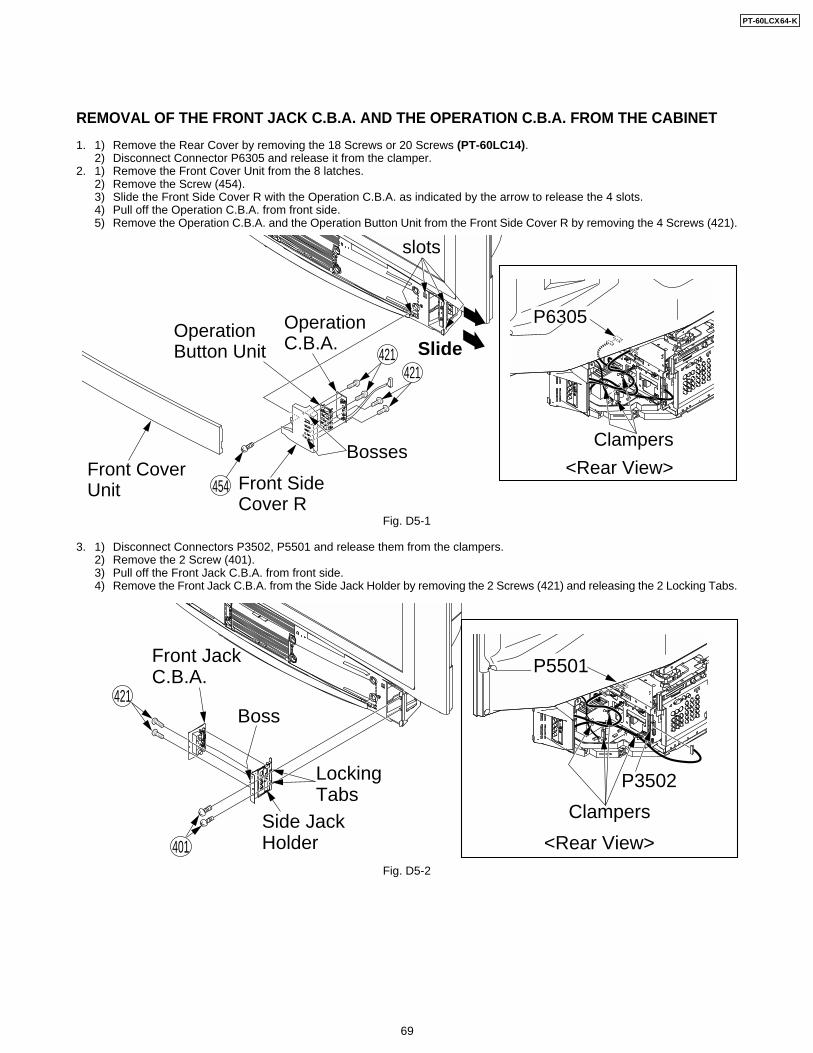
REMOVAL OF THE FRONT JACK C.B.A. AND THE OPERATION C.B.A. FROM THE CABINET
1. 1) Remove the Rear Cover by removing the 18 Screws or 20 Screws (PT-60LC14).2) Disconnect Connector P6305 and release it from the clamper.
2. 1) Remove the Front Cover Unit from the 8 latches.2) Remove the Screw (454).3) Slide the Front Side Cover R with the Operation C.B.A. as indicated by the arrow to release the 4 slots.4) Pull off the Operation C.B.A. from front side.5) Remove the Operation C.B.A. and the Operation Button Unit from the Front Side Cover R by removing the 4 Screws (421).
Fig. D5-1
3. 1) Disconnect Connectors P3502, P5501 and release them from the clampers.2) Remove the 2 Screw (401).3) Pull off the Front Jack C.B.A. from front side.4) Remove the Front Jack C.B.A. from the Side Jack Holder by removing the 2 Screws (421) and releasing the 2 Locking Tabs.
Fig. D5-2
454
421421
Front Cover Unit
Bosses
Operation C.B.A.
Operation Button Unit Slide
Front Side Cover R
slots
<Rear View>
Clampers
P6305
401
421
Side Jack Holder
Front JackC.B.A.
Boss
Locking Tabs
P5501
<Rear View>
Clampers
P3502
PT-60LCX64-K
69
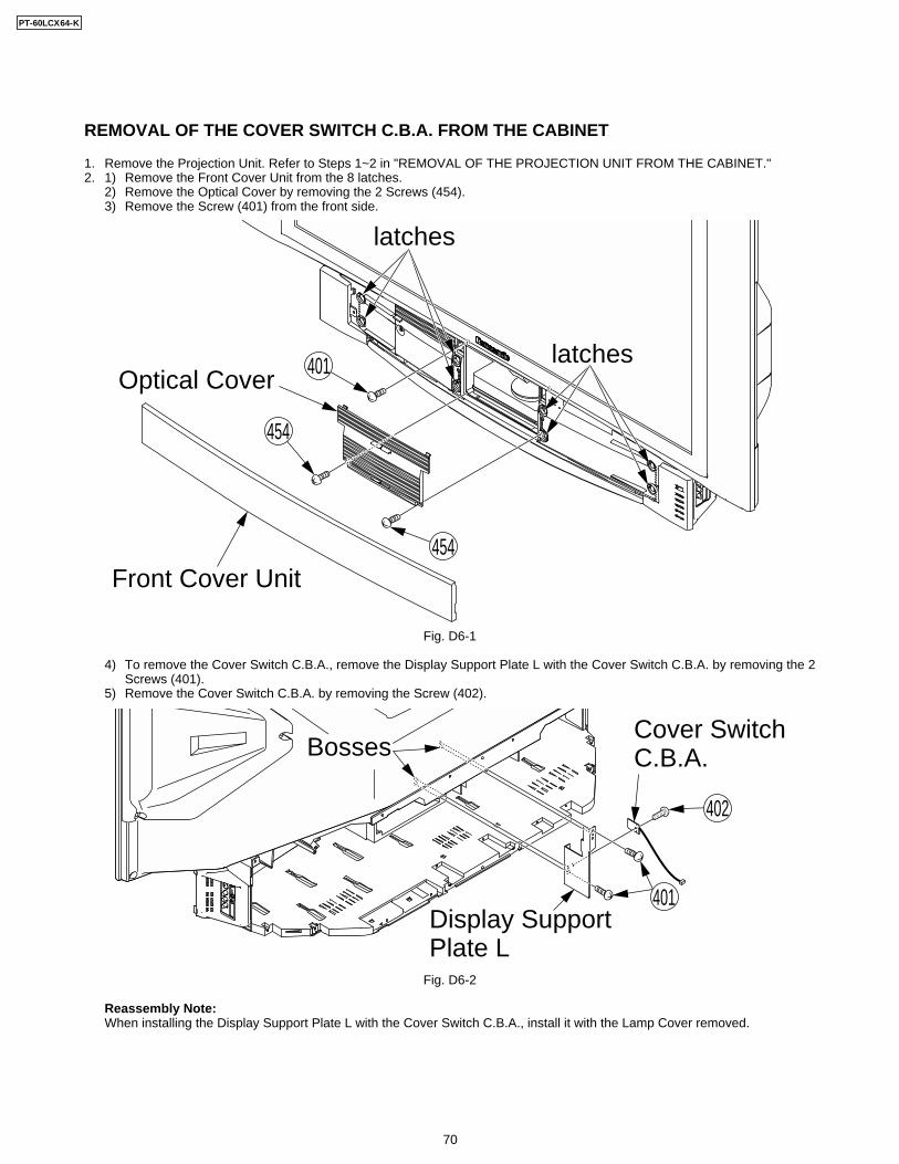
REMOVAL OF THE COVER SWITCH C.B.A. FROM THE CABINET
1. Remove the Projection Unit. Refer to Steps 1~2 in "REMOVAL OF THE PROJECTION UNIT FROM THE CABINET."2. 1) Remove the Front Cover Unit from the 8 latches.
2) Remove the Optical Cover by removing the 2 Screws (454).3) Remove the Screw (401) from the front side.
Fig. D6-1
4) To remove the Cover Switch C.B.A., remove the Display Support Plate L with the Cover Switch C.B.A. by removing the 2Screws (401).
5) Remove the Cover Switch C.B.A. by removing the Screw (402).
Fig. D6-2
Reassembly Note:When installing the Display Support Plate L with the Cover Switch C.B.A., install it with the Lamp Cover removed.
401
454
454
Front Cover Unit
Optical Cover
latches
latches
Cover Switch C.B.A.
Display SupportPlate L
401
402
Bosses
PT-60LCX64-K
70
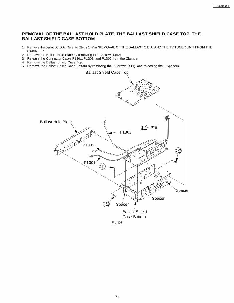
REMOVAL OF THE BALLAST HOLD PLATE, THE BALLAST SHIELD CASE TOP, THEBALLAST SHIELD CASE BOTTOM
1. Remove the Ballast C.B.A. Refer to Steps 1~7 in "REMOVAL OF THE BALLAST C.B.A. AND THE TV/TUNER UNIT FROM THECABINET."
2. Remove the Ballast Hold Plate by removing the 2 Screws (452).3. Release the Connector Cable P1301, P1302, and P1305 from the Clamper.4. Remove the Ballast Shield Case Top.5. Remove the Ballast Shield Case Bottom by removing the 2 Screws (411), and releasing the 3 Spacers.
Fig. D7
452
452
411
411
P1302
Ballast Shield Case Top
Ballast Hold Plate
Spacer
Spacer
Spacer
P1305
P1301
Ballast Shield Case Bottom
PT-60LCX64-K
71
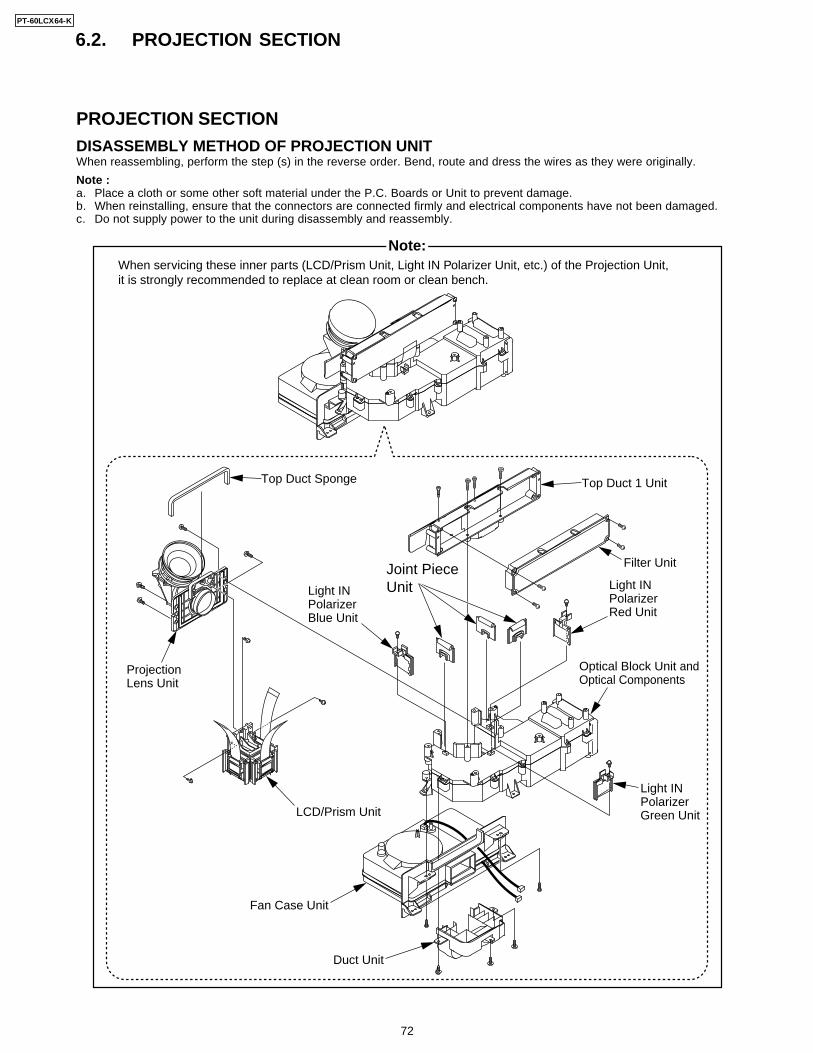
6.2. PROJECTION SECTION
DISASSEMBLY METHOD OF PROJECTION UNITWhen reassembling, perform the step (s) in the reverse order. Bend, route and dress the wires as they were originally.
PROJECTION SECTION
Note :a. Place a cloth or some other soft material under the P.C. Boards or Unit to prevent damage.b. When reinstalling, ensure that the connectors are connected firmly and electrical components have not been damaged.c. Do not supply power to the unit during disassembly and reassembly.
When servicing these inner parts (LCD/Prism Unit, Light IN Polarizer Unit, etc.) of the Projection Unit, it is strongly recommended to replace at clean room or clean bench.
Note:
Fan Case Unit
Duct Unit
Top Duct 1 Unit
Filter Unit
Light IN Polarizer Red Unit
Light IN Polarizer Green Unit
Optical Block Unit and Optical Components
Joint Piece UnitLight IN
Polarizer Blue Unit
Projection Lens Unit
LCD/Prism Unit
Top Duct Sponge
PT-60LCX64-K
72
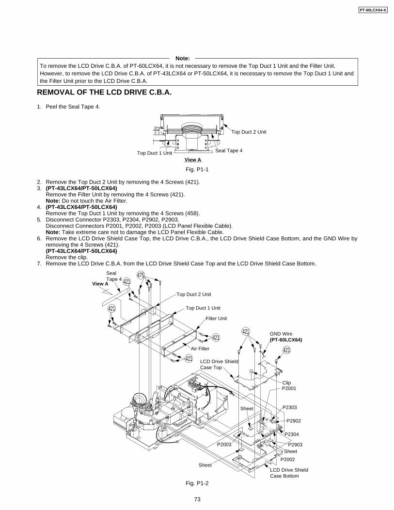
REMOVAL OF THE LCD DRIVE C.B.A.
1. Peel the Seal Tape 4.
Fig. P1-1
2. Remove the Top Duct 2 Unit by removing the 4 Screws (421).3. (PT-43LCX64/PT-50LCX64)
Remove the Filter Unit by removing the 4 Screws (421).Note: Do not touch the Air Filter.
4. (PT-43LCX64/PT-50LCX64)Remove the Top Duct 1 Unit by removing the 4 Screws (458).
5. Disconnect Connector P2303, P2304, P2902, P2903.Disconnect Connectors P2001, P2002, P2003 (LCD Panel Flexible Cable).Note: Take extreme care not to damage the LCD Panel Flexible Cable.
6. Remove the LCD Drive Shield Case Top, the LCD Drive C.B.A., the LCD Drive Shield Case Bottom, and the GND Wire byremoving the 4 Screws (421).(PT-43LCX64/PT-50LCX64)Remove the clip.
7. Remove the LCD Drive C.B.A. from the LCD Drive Shield Case Top and the LCD Drive Shield Case Bottom.
Fig. P1-2
421
Top Duct 1 Unit
Filter Unit
Air Filter
421
475
421
421Seal Tape 4
View A
Top Duct 2 Unit
421
421
LCD Drive Shield Case Top
LCD Drive Shield Case Bottom
P2903
P2002
P2003
Sheet
Sheet
Sheet
P2304
P2902
P2303
P2001Clip
GND Wire(PT-60LCX64)
View A
Top Duct 2 Unit
Top Duct 1 Unit Seal Tape 4
Note:To remove the LCD Drive C.B.A. of PT-60LCX64, it is not necessary to remove the Top Duct 1 Unit and the Filter Unit. However, to remove the LCD Drive C.B.A. of PT-43LCX64 or PT-50LCX64, it is necessary to remove the Top Duct 1 Unit and the Filter Unit prior to the LCD Drive C.B.A.
PT-60LCX64-K
73
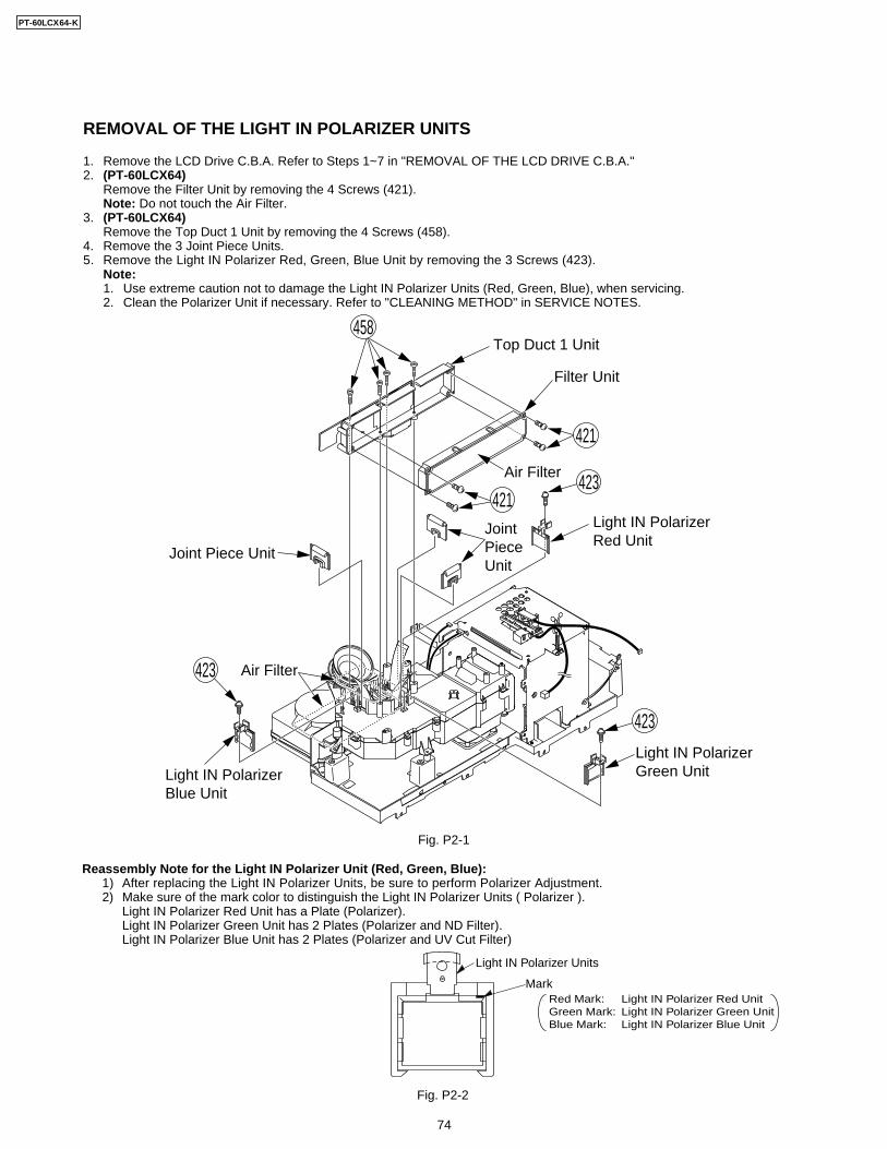
REMOVAL OF THE LIGHT IN POLARIZER UNITS
1. Remove the LCD Drive C.B.A. Refer to Steps 1~7 in "REMOVAL OF THE LCD DRIVE C.B.A."2. (PT-60LCX64)
Remove the Filter Unit by removing the 4 Screws (421).Note: Do not touch the Air Filter.
3. (PT-60LCX64)Remove the Top Duct 1 Unit by removing the 4 Screws (458).
4. Remove the 3 Joint Piece Units.5. Remove the Light IN Polarizer Red, Green, Blue Unit by removing the 3 Screws (423).
Note:1. Use extreme caution not to damage the Light IN Polarizer Units (Red, Green, Blue), when servicing.2. Clean the Polarizer Unit if necessary. Refer to "CLEANING METHOD" in SERVICE NOTES.
Fig. P2-1
Reassembly Note for the Light IN Polarizer Unit (Red, Green, Blue):1) After replacing the Light IN Polarizer Units, be sure to perform Polarizer Adjustment.2) Make sure of the mark color to distinguish the Light IN Polarizer Units ( Polarizer ).
Light IN Polarizer Red Unit has a Plate (Polarizer).Light IN Polarizer Green Unit has 2 Plates (Polarizer and ND Filter).Light IN Polarizer Blue Unit has 2 Plates (Polarizer and UV Cut Filter)
Fig. P2-2
421
Top Duct 1 Unit
Filter Unit
Air Filter
Air Filter
423
Light IN Polarizer Red Unit
423
Light IN Polarizer Green Unit
421Joint Piece Unit
Joint Piece Unit
423
Light IN Polarizer Blue Unit
458
Mark
Light IN Polarizer Units
Red Mark: Light IN Polarizer Red Unit Green Mark: Light IN Polarizer Green Unit Blue Mark: Light IN Polarizer Blue Unit
PT-60LCX64-K
74
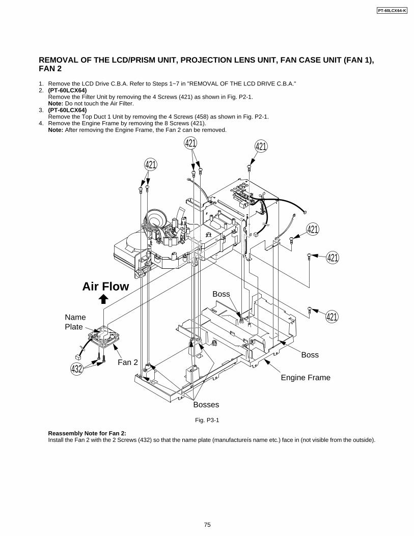
REMOVAL OF THE LCD/PRISM UNIT, PROJECTION LENS UNIT, FAN CASE UNIT (FAN 1),FAN 2
1. Remove the LCD Drive C.B.A. Refer to Steps 1~7 in "REMOVAL OF THE LCD DRIVE C.B.A."2. (PT-60LCX64)
Remove the Filter Unit by removing the 4 Screws (421) as shown in Fig. P2-1.Note: Do not touch the Air Filter.
3. (PT-60LCX64)Remove the Top Duct 1 Unit by removing the 4 Screws (458) as shown in Fig. P2-1.
4. Remove the Engine Frame by removing the 8 Screws (421).Note: After removing the Engine Frame, the Fan 2 can be removed.
Fig. P3-1
Reassembly Note for Fan 2:Install the Fan 2 with the 2 Screws (432) so that the name plate (manufactureís name etc.) face in (not visible from the outside).
421
421
421
421
Bosses
Boss
Engine Frame
421
Boss
421
432
Name Plate
Fan 2
Air Flow
PT-60LCX64-K
75
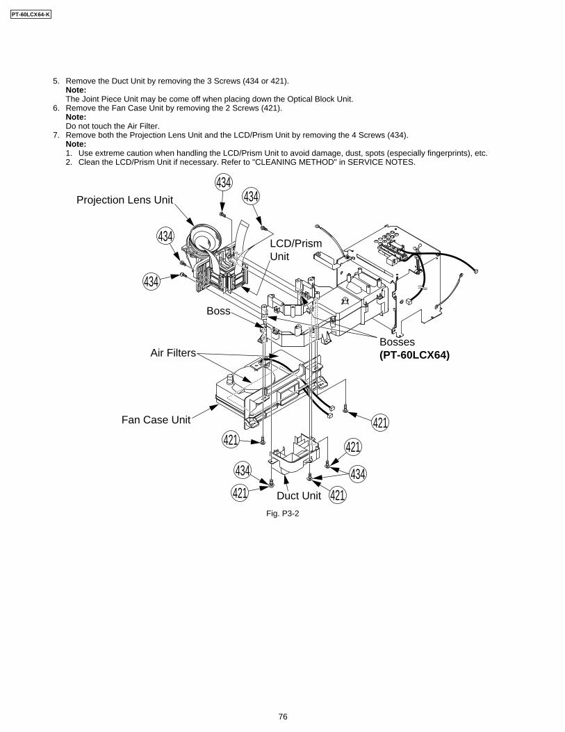
5. Remove the Duct Unit by removing the 3 Screws (434 or 421).Note:The Joint Piece Unit may be come off when placing down the Optical Block Unit.
6. Remove the Fan Case Unit by removing the 2 Screws (421).Note:Do not touch the Air Filter.
7. Remove both the Projection Lens Unit and the LCD/Prism Unit by removing the 4 Screws (434).Note:1. Use extreme caution when handling the LCD/Prism Unit to avoid damage, dust, spots (especially fingerprints), etc.2. Clean the LCD/Prism Unit if necessary. Refer to "CLEANING METHOD" in SERVICE NOTES.
Fig. P3-2
434434
434
434
421
434Duct Unit
434
421
421 421
421
Fan Case Unit
Air Filters
Projection Lens Unit
LCD/Prism Unit
Boss
Bosses(PT-60LCX64)
PT-60LCX64-K
76
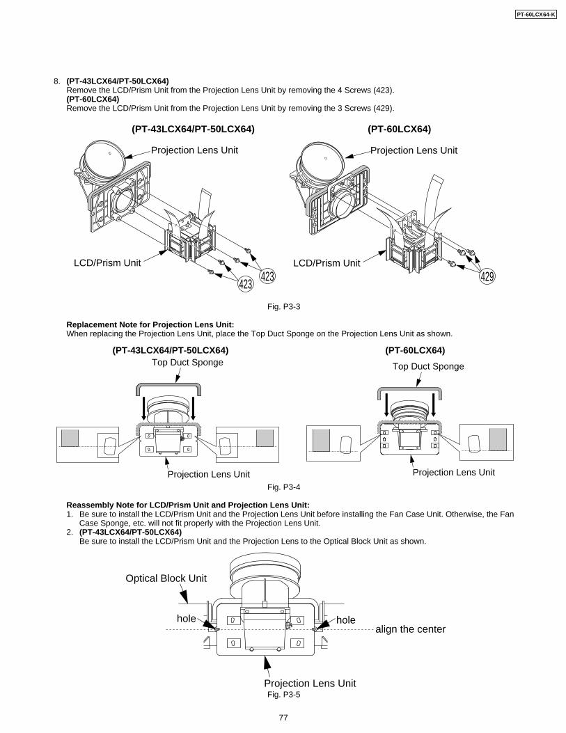
8. (PT-43LCX64/PT-50LCX64)Remove the LCD/Prism Unit from the Projection Lens Unit by removing the 4 Screws (423).(PT-60LCX64)Remove the LCD/Prism Unit from the Projection Lens Unit by removing the 3 Screws (429).
Fig. P3-3
Replacement Note for Projection Lens Unit:When replacing the Projection Lens Unit, place the Top Duct Sponge on the Projection Lens Unit as shown.
Fig. P3-4
Reassembly Note for LCD/Prism Unit and Projection Lens Unit:1. Be sure to install the LCD/Prism Unit and the Projection Lens Unit before installing the Fan Case Unit. Otherwise, the Fan
Case Sponge, etc. will not fit properly with the Projection Lens Unit.2. (PT-43LCX64/PT-50LCX64)
Be sure to install the LCD/Prism Unit and the Projection Lens to the Optical Block Unit as shown.
Fig. P3-5Projection Lens Unit
Optical Block Unit
holealign the center
hole
Projection Lens Unit
(PT-43LCX64/PT-50LCX64) (PT-60LCX64)
LCD/Prism Unit
423423
Projection Lens Unit
LCD/Prism Unit
429
Projection Lens Unit
Top Duct Sponge
Projection Lens Unit
Top Duct Sponge
(PT-43LCX64/PT-50LCX64) (PT-60LCX64)
PT-60LCX64-K
77
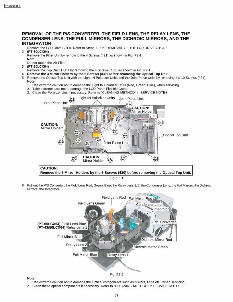
REMOVAL OF THE P/S CONVERTER, THE FIELD LENS, THE RELAY LENS, THECONDENSER LENS, THE FULL MIRRORS, THE DICHROIC MIRRORS, AND THEINTEGRATOR1. Remove the LCD Drive C.B.A. Refer to Steps 1~7 in "REMOVAL OF THE LCD DRIVE C.B.A."2. (PT-60LCX64)
Remove the Filter Unit by removing the 4 Screws (421) as shown in Fig. P2-1.Note:Do not touch the Air Filter.
3. (PT-60LCX64)Remove the Top Duct 1 Unit by removing the 4 Screws (458) as shown in Fig. P2-1.
4. Remove the 3 Mirror Holders by the 6 Screws (430) before removing the Optical Top Unit.5. Remove the Optical Top Unit with the Light IN Polarizer Units and the Joint Piece Units by removing the 10 Screws (424).
Note:1. Use extreme caution not to damage the Light IN Polarizer Units (Red, Green, Blue), when servicing.2. Take extreme care not to damage the LCD Panel Flexible Cable.3. Clean the Polarizer Unit if necessary. Refer to "CLEANING METHOD" in SERVICE NOTES.
Fig. P5-1
6. Pull out the P/S Converter, the Field Lens Red, Green, Blue, the Relay Lens 1, 2, the Condenser Lens, the Full Mirrors, the DichroicMirrors, the Integrator.
Fig. P5-2Note:1. Use extreme caution not to damage the Optical components such as Mirrors, Lens etc., when servicing.2. Clean these optical components if necessary. Refer to "CLEANING METHOD" in SERVICE NOTES.
Optical Top Unit
Joint Piece UnitJoint Piece Unit
Light IN Polarizer Units
CAUTION:Mirror Holder
424424
424424
430
424
424
424424
424430
430 Joint Piece Unit
CAUTION:Mirror Holder
424
CAUTION:Remove the 3 Mirror Holders by the 6 Screws (430) before removing the Optical Top Unit.
CAUTION:Mirror Holder
Dichroic Mirror Red
Dichroic Mirror Green
P/S Converter
Integrator
Relay Lens 1
Field Lens Red
Field Lens GreenFull Mirror Red
Condenser Lens
(PT-60LCX64) Field Lens Blue(PT-43/50LCX64) Relay Lens 1
Full Mirror Blue
Relay Lens 2
Full Mirror Blue
PT-60LCX64-K
78
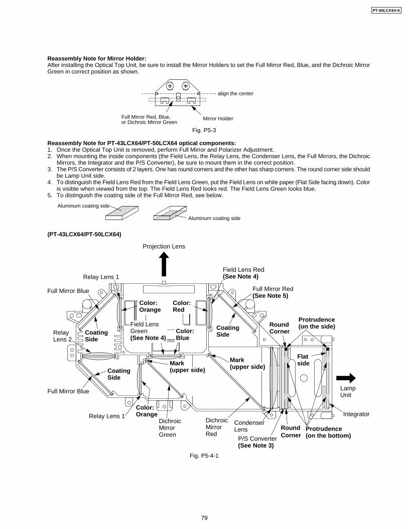
Reassembly Note for Mirror Holder:After installing the Optical Top Unit, be sure to install the Mirror Holders to set the Full Mirror Red, Blue, and the Dichroic MirrorGreen in correct position as shown.
Fig. P5-3
Reassembly Note for PT-43LCX64/PT-50LCX64 optical components:1. Once the Optical Top Unit is removed, perform Full Mirror and Polarizer Adjustment.2. When mounting the inside components (the Field Lens, the Relay Lens, the Condenser Lens, the Full Mirrors, the Dichroic
Mirrors, the Integrator and the P/S Converter), be sure to mount them in the correct position.3. The P/S Converter consists of 2 layers. One has round corners and the other has sharp corners. The round corner side should
be Lamp Unit side.4. To distinguish the Field Lens Red from the Field Lens Green, put the Field Lens on white paper (Flat Side facing down). Color
is visible when viewed from the top. The Field Lens Red looks red. The Field Lens Green looks blue.5. To distinguish the coating side of the Full Mirror Red, see below.
(PT-43LCX64/PT-50LCX64)
Fig. P5-4-1
Mirror HolderFull Mirror Red, Blue, or Dichroic Mirror Green
align the center
Full Mirror Blue
Relay Lens 2
Coating Side
Full Mirror Blue
Coating Side
Relay Lens 1Field Lens Red(See Note 4)
Color: Orange Integrator
Lamp Unit
P/S Converter(See Note 3)
Protrudence (on the bottom)
Flat side
Protrudence (on the side)
Condenser Lens
Dichroic Mirror Green
Dichroic Mirror Red
Relay Lens 1
Full Mirror Red(See Note 5)
Round Corner
Round Corner
Projection Lens
Color: Orange
Field Lens Green(See Note 4)
Color: Blue
Color: Red
Mark(upper side)
Coating Side
Mark(upper side)
Aluminum coating side
Aluminum coating side
PT-60LCX64-K
79
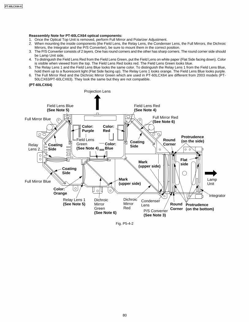
(PT-60LCX64)
Fig. P5-4-2
Full Mirror Blue
Relay Lens 2
Coating Side
Full Mirror Blue
Coating Side
Field Lens Blue(See Note 5)
Field Lens Red(See Note 4)
Color: Orange
Integrator
Lamp Unit
P/S Converter(See Note 3)
Protrudence (on the bottom)
Flat side
Protrudence (on the side)
Condenser Lens
Dichroic Mirror Green(See Note 6)
Dichroic Mirror Red
Relay Lens 1(See Note 5)
Full Mirror Red(See Note 6)
Round Corner
Round Corner
Mark(upper side)
Projection Lens
Coating Side
Mark(upper side)
Color: Purple
Field Lens Green(See Note 4)
Color: Blue
Color: Red
Reassembly Note for PT-60LCX64 optical components:1. Once the Optical Top Unit is removed, perform Full Mirror and Polarizer Adjustment.2. When mounting the inside components (the Field Lens, the Relay Lens, the Condenser Lens, the Full Mirrors, the Dichroic
Mirrors, the Integrator and the P/S Converter), be sure to mount them in the correct position.3. The P/S Converter consists of 2 layers. One has round corners and the other has sharp corners. The round corner side should
be Lamp Unit side.4. To distinguish the Field Lens Red from the Field Lens Green, put the Field Lens on white paper (Flat Side facing down). Color
is visible when viewed from the top. The Field Lens Red looks red. The Field Lens Green looks blue.5. The Relay Lens 1 and the Field Lens Blue looks the same color. To distinguish the Relay Lens 1 from the Field Lens Blue,
hold them up to a fluorescent light (Flat Side facing up). The Relay Lens 1 looks orange. The Field Lens Blue looks purple.6. The Full Mirror Red and the Dichroic Mirror Green which are used in PT-60LCX64 are different from 2003 models (PT-
50LCX63/PT-60LCX63). They look the same but they are not compatible.
PT-60LCX64-K
80
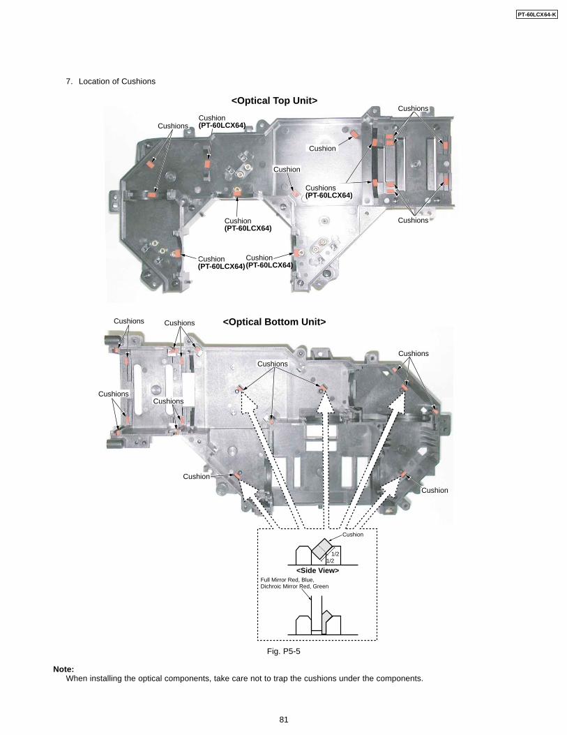
7. Location of Cushions
Fig. P5-5
Note:When installing the optical components, take care not to trap the cushions under the components.
Cushion(PT-60LCX64)
Cushion(PT-60LCX64)
Cushion(PT-60LCX64)
Cushion
Cushions
Cushions
<Optical Bottom Unit>
<Optical Top Unit>
Cushions
Cushions
Cushions
Cushion
Cushions
Full Mirror Red, Blue,Dichroic Mirror Red, Green
Cushion
1/21/2
<Side View>
CushionsCushion(PT-60LCX64)
Cushions(PT-60LCX64)
Cushion
Cushions
Cushions
Cushion
PT-60LCX64-K
81
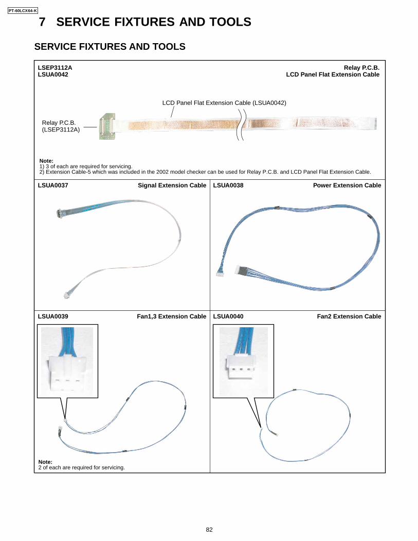
7 SERVICE FIXTURES AND TOOLS
SERVICE FIXTURES AND TOOLS
LSUA0042 LCD Panel Flat Extension Cable LSEP3112A Relay P.C.B.
LSUA0040 Fan2 Extension CableLSUA0039 Fan1,3 Extension Cable
LSUA0037 Signal Extension Cable LSUA0038 Power Extension Cable
Note:1) 3 of each are required for servicing.2) Extension Cable-5 which was included in the 2002 model checker can be used for Relay P.C.B. and LCD Panel Flat Extension Cable.
Note:2 of each are required for servicing.
Relay P.C.B. (LSEP3112A)
LCD Panel Flat Extension Cable (LSUA0042)
PT-60LCX64-K
82
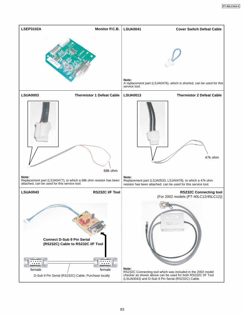
Note:Replacement part (LSJA0533, LSJA0478), to which a 47k ohm resistor has been attached, can be used for this service tool.
Note:Replacement part (LSJA0477), to which a 68k ohm resistor has been attached, can be used for this service tool.
Note:A replacement part (LSJA0476), which is shorted, can be used for this service tool.
68k ohm
LSUA0003 Thermistor 1 Defeat Cable LSUA0013 Thermistor 2 Defeat Cable
LSUA0041 Cover Switch Defeat Cable
LSUA0043 RS232C I/F Tool RS232C Connecting tool(For 2002 models (PT-40LC12/45LC12))
LSEP3102A Monitor P.C.B.
Note:RS232C Connecting tool which was included in the 2002 model checker as shown above can be used for both RS232C I/F Tool (LSUA0043) and D-Sub 9 Pin Serial (RS232C) Cable.
Connect D-Sub 9 Pin Serial(RS232C) Cable to RS232C I/F Tool
female female
D-Sub 9 Pin Serial (RS232C) Cable: Purchase locally
47k ohm
PT-60LCX64-K
83
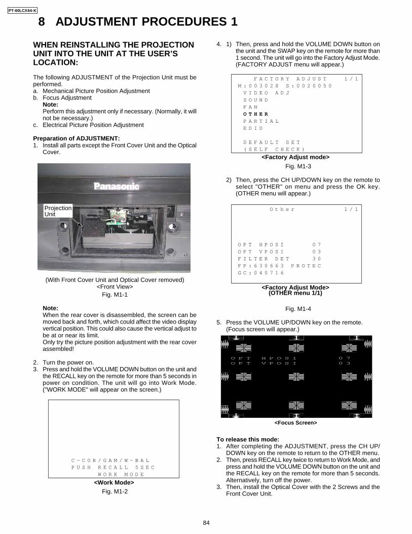
8 ADJUSTMENT PROCEDURES 1
WHEN REINSTALLING THE PROJECTIONUNIT INTO THE UNIT AT THE USER’SLOCATION:
The following ADJUSTMENT of the Projection Unit must beperformed.a. Mechanical Picture Position Adjustmentb. Focus Adjustment
Note:Perform this adjustment only if necessary. (Normally, it willnot be necessary.)
c. Electrical Picture Position Adjustment
Preparation of ADJUSTMENT:1. Install all parts except the Front Cover Unit and the Optical
Cover.
Fig. M1-1
Note:When the rear cover is disassembled, the screen can bemoved back and forth, which could affect the video displayvertical position. This could also cause the vertical adjust tobe at or near its limit.Only try the picture position adjustment with the rear coverassembled!
2. Turn the power on.3. Press and hold the VOLUME DOWN button on the unit and
the RECALL key on the remote for more than 5 seconds inpower on condition. The unit will go into Work Mode.("WORK MODE" will appear on the screen.)
Fig. M1-2
Projection Unit
<Front View>(With Front Cover Unit and Optical Cover removed)
C - C O R / G A M / W - B A L P U S H R E C A L L 5 S E C W O R K M O D E
<Work Mode>
4. 1) Then, press and hold the VOLUME DOWN button onthe unit and the SWAP key on the remote for more than1 second. The unit will go into the Factory Adjust Mode.(FACTORY ADJUST menu will appear.)
Fig. M1-3
2) Then, press the CH UP/DOWN key on the remote toselect "OTHER" on menu and press the OK key.(OTHER menu will appear.)
Fig. M1-4
5. Press the VOLUME UP/DOWN key on the remote.(Focus screen will appear.)
<Factory Adjust mode>
F A C T O R Y A D J U S T 1 / 1 M : 0 0 3 0 2 8 S : 0 0 2 0 0 5 0 V I D E O A D J S O U N D F A N O T H E R P A R T I A L E D I D
D E F A U L T S E T ( S E L F C H E C K )
O P T H P O S I 0 7 O P T V P O S I 0 3
<Focus Screen>
<Factory Adjust Mode>(OTHER menu 1/1)
O t h e r 1 / 1
O P T H P O S I 0 7 O P T V P O S I 0 3 F I L T E R D E T 3 0 F P : 6 3 0 6 6 3 P R O T E C G C : 0 4 0 7 1 6
To release this mode:1. After completing the ADJUSTMENT, press the CH UP/
DOWN key on the remote to return to the OTHER menu.2. Then, press RECALL key twice to return to Work Mode, and
press and hold the VOLUME DOWN button on the unit andthe RECALL key on the remote for more than 5 seconds.Alternatively, turn off the power.
3. Then, install the Optical Cover with the 2 Screws and theFront Cover Unit.
PT-60LCX64-K
84
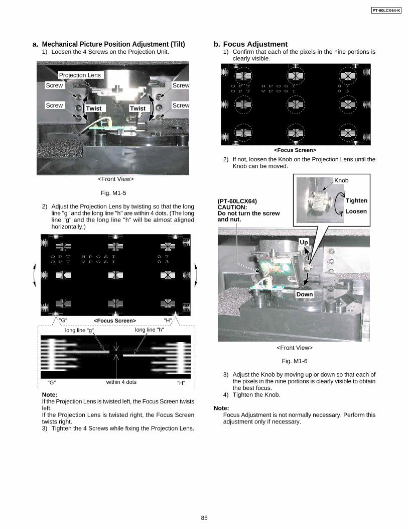
a. Mechanical Picture Position Adjustment (Tilt)1) Loosen the 4 Screws on the Projection Unit.
Fig. M1-5
2) Adjust the Projection Lens by twisting so that the longline "g" and the long line "h" are within 4 dots. (The longline "g" and the long line "h" will be almost alignedhorizontally.)
Note:If the Projection Lens is twisted left, the Focus Screen twistsleft.If the Projection Lens is twisted right, the Focus Screentwists right.3) Tighten the 4 Screws while fixing the Projection Lens.
Screw
Projection Lens
Twist TwistScrew
Screw
Screw
<Front View>
<Focus Screen>"G" "H"
within 4 dots
long line "g" long line "h"
"G" "H"
O P T H P O S I 0 7 O P T V P O S I 0 3
b. Focus Adjustment1) Confirm that each of the pixels in the nine portions is
clearly visible.
2) If not, loosen the Knob on the Projection Lens until theKnob can be moved.
Fig. M1-6
3) Adjust the Knob by moving up or down so that each ofthe pixels in the nine portions is clearly visible to obtainthe best focus.
4) Tighten the Knob.
Note:Focus Adjustment is not normally necessary. Perform thisadjustment only if necessary.
<Focus Screen>
O P T H P O S I 0 7 O P T V P O S I 0 3
<Front View>
(PT-60LCX64)CAUTION: Do not turn the screw and nut.
Up
Down
Knob
Tighten
Loosen
PT-60LCX64-K
85
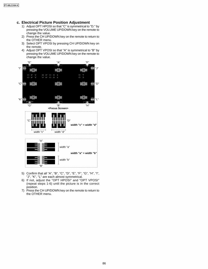
c. Electrical Picture Position Adjustment1) Adjust OPT HPOSI so that "C" is symmetrical to "D." by
pressing the VOLUME UP/DOWN key on the remote tochange the value.
2) Press the CH UP/DOWN key on the remote to return tothe OTHER menu.
3) Select OPT VPOSI by pressing CH UP/DOWN key onthe remote.
4) Adjust OPT VPOSI so that "A" is symmetrical to “B” bypressing the VOLUME UP/DOWN key on the remote tochange the value.
5) Confirm that all "A", "B", "C", "D", "E", "F", "G", "H", "I","J", "K", "L" are each almost symmetrical.
6) If not, adjust the "OPT HPOSI" and "OPT VPOSI"(repeat steps 1-6) until the picture is in the correctposition.
7) Press the CH UP/DOWN key on the remote to return tothe OTHER menu.
<Focus Screen>"G" "H""B"
"E"
"I"
"C"
"K"
"J"
"D"
"C"
width "c"
width "c" = width "d"
width "a" = width "b"
width "a"
width "b"
"D"
"L"
"F""A"
"B"
"A"
width "d"
O P T H P O S I 0 7 O P T V P O S I 0 3
PT-60LCX64-K
86
9 ADJUSTMENT PROCEDURES 2
INITIAL GUIDELINE
The table below shows which adjustments are necessary according to the unit parts and individual parts to be replaced. Make sureto perform these adjustments shown below as necessary.
Rep
lacemen
t Parts
RG
B Input Level A
djustment
Gam
ma A
djustment
Fan 2 Voltage A
djustment
Non-uniform
ity Color C
orrection (com
pensation by inputting data)
VC
OM
Adjustm
ent
Full M
irror Adjustm
ent
Polarizer A
djustment
White B
alance Adjustm
ent
IC2301 on
LCD
Drive C
.B.A
.
IC6005 on
Main C
.B.A
.
IC2301 on
LCD
Drive C
.B.A
.
IC2301 on
LCD
Drive C
.B.A
.
IC2301 on
LCD
Drive C
.B.A
.
IC2301 on
LCD
Drive C
.B.A
.
Ad
justm
ent Item
Ad
justm
ent d
ata is written
to
follo
win
g E
EP
RO
M IC
's
Mech
anical
(Projection Unit) A
dju
stmen
tS
ection
Fan 3 Voltage A
djustment
IC2301 on
LCD
Drive C
.B.A
.
Main C.B.A.IC5504 (A/D Conver)
IC6005 (8k EEPROM)
LCD Drive C.B.A.
(LSXA0595) (PT-43/50LCX64) (LSXA0605) (PT-60LCX64)Optical Block Unit
LCD/Prism Unit
Optical Top Unit
*Optical Top Unit is removed and installed
*Projection Lens Unit is removed and installed
Full Mirror Red/Blue/Dichroic Mirror Green
Light IN Polarizer R/G/B Unit
Projection Unit
IC2301 (32k EEPROM)
IC2903 (FAN2 Drive)
IC2904 (FAN3 Drive)
TV/Tuner Unit
Main C
.B.A
. A
dju
stmen
tS
ection
LC
D D
rive C
.B.A
. A
dju
stmen
tS
ection
: Adjustm
ent ItemN
ote:
No
te:
No
te: Once the O
ptical Top Unit is rem
oved, perform F
ull Mirror A
djustment and P
olarizer Adjustm
ent.N
ote: W
hen replacing the Projection U
nit, any of above adjustment are not needed.
: When replacing the LC
D D
rive C.B.A., the LCD
/Prism U
nit or IC2301(32k EEPRO
M), confirm
that the color of the entire screen. If OK, G
amm
a Adjustment is not needed. If N
G, perform
Gam
ma Adjustm
ent.: W
hen replacing the LCD
Drive C.B.A., O
ptical Block Unit, the LC
D/Prism
Unit or IC
2301(32k EEPROM
), confirm the color uniform
ity on the screen. If OK, N
on-uniformity C
olor Correction is not needed. If N
G,
perform N
on-uniformity C
olor Correction.
: When replacing the LC
D/Prism
Unit, confirm
the color uniformity on the screen. If O
K, Full Mirror/Polarizer Adjustm
ent are not needed. If NG
, perform Full M
irror/Polarizer Adjustment.
PT-60LCX64-K
87
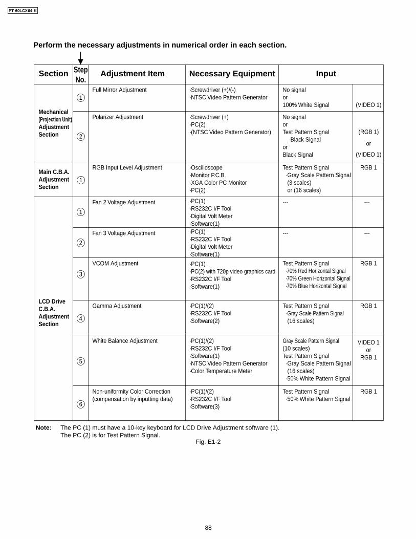
Fig. E1-2
Perform the necessary adjustments in numerical order in each section.
Necessary EquipmentAdjustment ItemSection StepNo.
Mechanical (Projection Unit)Adjustment Section
Main C.B.A. Adjustment Section
LCD Drive C.B.A.Adjustment Section
Input
·PC(1)/(2)·RS232C I/F Tool·Software(3)
·PC(1)·PC(2) with 720p video graphics card·RS232C I/F Tool·Software(1)
·PC(1)/(2)·RS232C I/F Tool·Software(2)
·Screwdriver (+)/(-)·NTSC Video Pattern Generator
·Screwdriver (+)·PC(2)·(NTSC Video Pattern Generator)
·PC(1)/(2)·RS232C I/F Tool·Software(1)·NTSC Video Pattern Generator·Color Temperature Meter
·Oscilloscope·Monitor P.C.B.·XGA Color PC Monitor·PC(2)
RGB Input Level Adjustment
Gamma Adjustment
Fan 2 Voltage Adjustment
Non-uniformity Color Correction (compensation by inputting data)
VCOM Adjustment
Full Mirror Adjustment
Polarizer Adjustment
White Balance Adjustment
No signalor 100% White Signal
Test Pattern Signal ·Gray Scale Pattern Signal (3 scales) or (16 scales)
Test Pattern Signal ·70% Red Horizontal Signal ·70% Green Horizontal Signal ·70% Blue Horizontal Signal
Gray Scale Pattern Signal (10 scales)Test Pattern Signal ·Gray Scale Pattern Signal (16 scales) ·50% White Pattern Signal
---
No signalorTest Pattern Signal ·Black SignalorBlack Signal
Test Pattern Signal ·50% White Pattern Signal
·PC(1)·RS232C I/F Tool·Digital Volt Meter ·Software(1)
·PC(1)·RS232C I/F Tool·Digital Volt Meter ·Software(1)
Fan 3 Voltage Adjustment ---
---
---
Test Pattern Signal ·Gray Scale Pattern Signal (16 scales)
1
2
1
1
2
3
4
5
6
(VIDEO 1)
(RGB 1)
or
(VIDEO 1)
RGB 1
RGB 1
RGB 1
VIDEO 1or
RGB 1
RGB 1
Note: The PC (1) must have a 10-key keyboard for LCD Drive Adjustment software (1).The PC (2) is for Test Pattern Signal.
PT-60LCX64-K
88
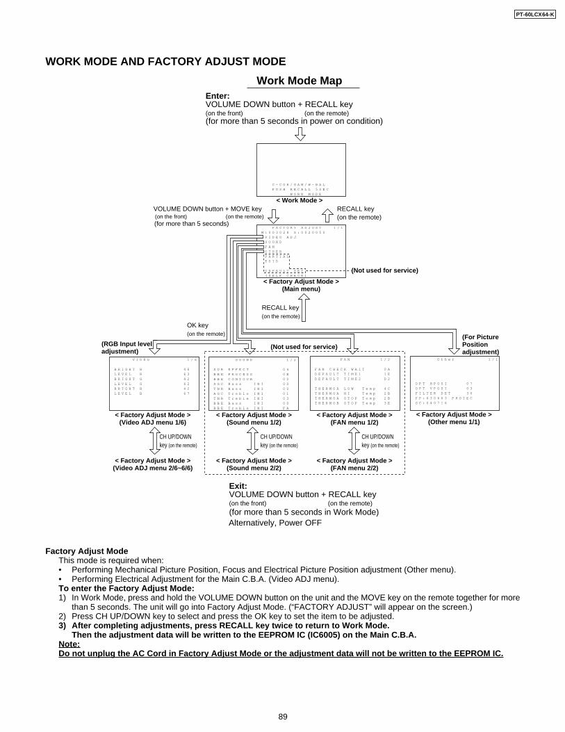
Work Mode Map
Exit:VOLUME DOWN button + RECALL key (on the front) (on the remote)(for more than 5 seconds in Work Mode)
VOLUME DOWN button + MOVE key (on the front) (on the remote)
OK key(on the remote)
CH UP/DOWNkey (on the remote)
CH UP/DOWNkey (on the remote)
CH UP/DOWNkey (on the remote)
RECALL key(on the remote)
RECALL key(on the remote)
< Factory Adjust Mode >(Main menu)
< Factory Adjust Mode >(Video ADJ menu 1/6)
< Factory Adjust Mode >(Sound menu 1/2)
< Factory Adjust Mode >(FAN menu 1/2)
(Not used for service)
(For PicturePositionadjustment)
(RGB Input level adjustment)
(Not used for service)
< Factory Adjust Mode >(Video ADJ menu 2/6~6/6)
< Factory Adjust Mode >(Sound menu 2/2)
< Factory Adjust Mode >(FAN menu 2/2)
< Factory Adjust Mode >(Other menu 1/1)
< Work Mode >
(for more than 5 seconds)
Enter:VOLUME DOWN button + RECALL key (on the front) (on the remote)(for more than 5 seconds in power on condition)
F A C T O R Y A D J U S T 1 / 1 M : 0 0 3 0 2 8 S : 0 0 2 0 0 5 0 V I D E O A D J S O U N D F A N O T H E R P A R T I A L E D I D
D E F A U L T S E T ( S E L F C H E C K )
C - C O R / G A M / W - B A L P U S H R E C A L L 5 S E C W O R K M O D E
Alternatively, Power OFF
F A N 1 / 2 F A N C H E C K W A I T 0 A D E F A U L T T I M E 1 1 E D E F A U L T T I M E 2 D 2
T H E R M O A L O W T e m p 4 C T H E R M O A H I T e m p 2 B T H E R M O A S T O P T e m p 2 B T H E R M O B S T O P T e m p 3 E
O t h e r 1 / 1
O P T H P O S I 0 7 O P T V P O S I 0 3 F I L T E R D E T 3 0 F P : 6 3 0 6 6 3 P R O T E C G C : 0 4 0 7 1 6
S O U N D 1 / 2 S U R E F F E C T 0 4 B B E P R O C E S S 0 E B B E C O N T O U R 0 0 A G C B a s s I N I 0 0 T N R B a s s I N I 0 0 A G C T r e b l e I N I 0 1 T N R T r e b l e I N I 0 3 B B E B a s s I N I 0 0 B B E T r e b l e I N I F A
V I D E O 1 / 6 B R I G H T R 4 6 L E V E L R 6 3 B R I G H T G 4 2 L E V E L G 6 2 B R I G H T B 4 2 L E V E L B 6 7
WORK MODE AND FACTORY ADJUST MODE
Factory Adjust ModeThis mode is required when:• Performing Mechanical Picture Position, Focus and Electrical Picture Position adjustment (Other menu).• Performing Electrical Adjustment for the Main C.B.A. (Video ADJ menu).To enter the Factory Adjust Mode:1) In Work Mode, press and hold the VOLUME DOWN button on the unit and the MOVE key on the remote together for more
than 5 seconds. The unit will go into Factory Adjust Mode. (“FACTORY ADJUST” will appear on the screen.)2) Press CH UP/DOWN key to select and press the OK key to set the item to be adjusted.3) After completing adjustments, press RECALL key twice to return to Work Mode.
Then the adjustment data will be written to the EEPROM IC (IC6005) on the Main C.B.A.Note:Do not unplug the AC Cord in Factory Adjust Mode or the adjustment data will not be written to the EEPROM IC.
PT-60LCX64-K
89
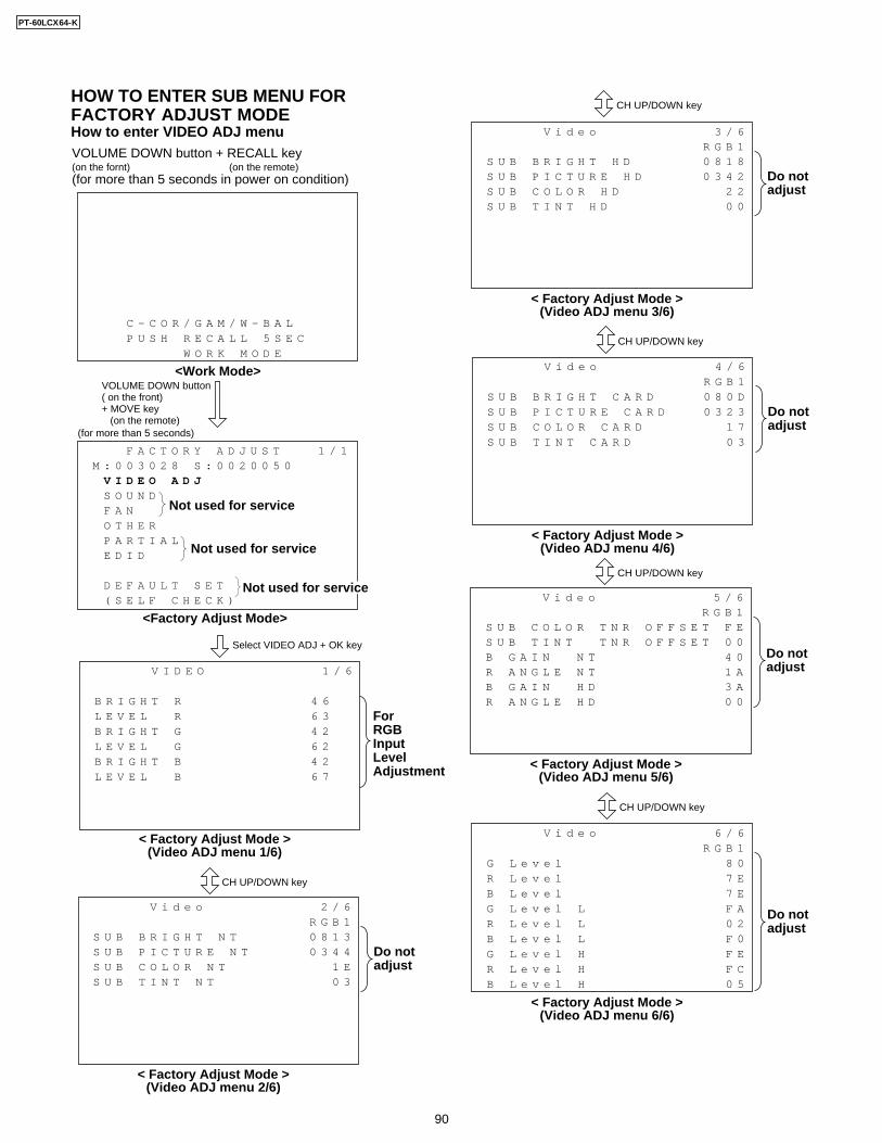
< Factory Adjust Mode >(Video ADJ menu 1/6)
V I D E O 1 / 6 B R I G H T R 4 6 L E V E L R 6 3 B R I G H T G 4 2 L E V E L G 6 2 B R I G H T B 4 2 L E V E L B 6 7
ForRGBInputLevelAdjustment
Select VIDEO ADJ + OK key
HOW TO ENTER SUB MENU FORFACTORY ADJUST MODEHow to enter VIDEO ADJ menu
VOLUME DOWN button( on the front)+ MOVE key (on the remote)
(for more than 5 seconds)
VOLUME DOWN button + RECALL key (on the fornt) (on the remote)(for more than 5 seconds in power on condition)
C - C O R / G A M / W - B A L P U S H R E C A L L 5 S E C W O R K M O D E
<Work Mode>
<Factory Adjust Mode>
Not used for service
Not used for service
Not used for service
F A C T O R Y A D J U S T 1 / 1 M : 0 0 3 0 2 8 S : 0 0 2 0 0 5 0 V I D E O A D J S O U N D F A N O T H E R P A R T I A L E D I D
D E F A U L T S E T ( S E L F C H E C K )
< Factory Adjust Mode >(Video ADJ menu 2/6)
V i d e o 2 / 6 R G B 1 S U B B R I G H T N T 0 8 1 3 S U B P I C T U R E N T 0 3 4 4 S U B C O L O R N T 1 E S U B T I N T N T 0 3
CH UP/DOWN key
Do notadjust
< Factory Adjust Mode >(Video ADJ menu 3/6)
V i d e o 3 / 6 R G B 1 S U B B R I G H T H D 0 8 1 8 S U B P I C T U R E H D 0 3 4 2 S U B C O L O R H D 2 2 S U B T I N T H D 0 0
CH UP/DOWN key
Do notadjust
< Factory Adjust Mode >(Video ADJ menu 4/6)
V i d e o 4 / 6 R G B 1 S U B B R I G H T C A R D 0 8 0 D S U B P I C T U R E C A R D 0 3 2 3 S U B C O L O R C A R D 1 7 S U B T I N T C A R D 0 3
CH UP/DOWN key
Do notadjust
< Factory Adjust Mode >(Video ADJ menu 5/6)
V i d e o 5 / 6 R G B 1 S U B C O L O R T N R O F F S E T F E S U B T I N T T N R O F F S E T 0 0 B G A I N N T 4 0 R A N G L E N T 1 A B G A I N H D 3 A R A N G L E H D 0 0
CH UP/DOWN key
Do notadjust
< Factory Adjust Mode >(Video ADJ menu 6/6)
V i d e o 6 / 6 R G B 1 G L e v e l 8 0 R L e v e l 7 E B L e v e l 7 E G L e v e l L F A R L e v e l L 0 2 B L e v e l L F 0 G L e v e l H F E R L e v e l H F C B L e v e l H 0 5
CH UP/DOWN key
Do notadjust
PT-60LCX64-K
90
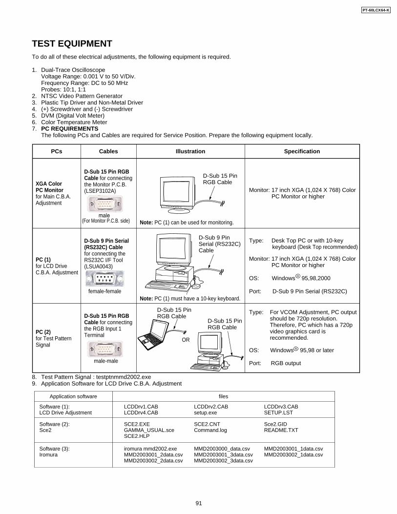
TEST EQUIPMENTTo do all of these electrical adjustments, the following equipment is required.
1. Dual-Trace OscilloscopeVoltage Range: 0.001 V to 50 V/Div.Frequency Range: DC to 50 MHzProbes: 10:1, 1:1
2. NTSC Video Pattern Generator3. Plastic Tip Driver and Non-Metal Driver4. (+) Screwdriver and (-) Screwdriver5. DVM (Digital Volt Meter)6. Color Temperature Meter7. PC REQUIREMENTS
The following PCs and Cables are required for Service Position. Prepare the following equipment locally.
8. Test Pattern Signal : testptnmmd2002.exe9. Application Software for LCD Drive C.B.A. Adjustment
XGA Color PC Monitorfor Main C.B.A.Adjustment
PCs Cables Illustration Specification
PC (1)for LCD DriveC.B.A. Adjustment
PC (2)for Test PatternSignal
D-Sub 15 Pin RGBCable for connectingthe Monitor P.C.B.(LSEP3102A)
(For Monitor P.C.B. side)
Monitor: 17 inch XGA (1,024 X 768) Color PC Monitor or higher
Monitor: 17 inch XGA (1,024 X 768) Color PC Monitor or higher
Port: D-Sub 9 Pin Serial (RS232C)
OS: Windows 95,98,2000
Type: Desk Top PC or with 10-key keyboard (Desk Top recommended)
Port: RGB output
OS: Windows 95,98 or later
Type: For VCOM Adjustment, PC output should be 720p resolution. Therefore, PC which has a 720p video graphics card is recommended.
Note: PC (1) can be used for monitoring.
Note: PC (1) must have a 10-key keyboard.
D-Sub 15 PinRGB Cable
D-Sub 15 PinRGB Cable
D-Sub 9 PinSerial (RS232C)Cable
D-Sub 15 PinRGB Cable
D-Sub 15 Pin RGBCable for connectingthe RGB Input 1Terminal
male-male
female-female
D-Sub 9 Pin Serial(RS232C) Cablefor connecting the RS232C I/F Tool(LSUA0043)
OR
LCDDrv1.CAB LCDDrv2.CAB LCDDrv3.CABLCDDrv4.CAB setup.exe SETUP.LST
SCE2.EXE SCE2.CNT Sce2.GIDGAMMA_USUAL.sce Command.log README.TXTSCE2.HLP
iromura mmd2002.exe MMD2003000_data.csv MMD2003001_1data.csvMMD2003001_2data.csv MMD2003001_3data.csv MMD2003002_1data.csvMMD2003002_2data.csv MMD2003002_3data.csv
MMD2004Checker.CAB SETUP.LSTsetup.exe
Software (1):LCD Drive Adjustment
Application software files
Software (2): Sce2
Software (3):Iromura
Software (4):LCD Checker
PT-60LCX64-K
91
HOW TO READ THE ADJUSTMENTPROCEDURES
Fig. E2-2
Fig. E2-3
TP ADJ. INPUT
EQUIPMENT SPECIFICATION
TP3602 R3662 (Video input Connector)NTSC Color Bar Signal
Oscilloscope, NTSC Video PatternGenerator
A=0.2 V ± 0.06 V DC
Equipmentrequired for adjustment
Specificationfor Adjustment
Connecting Point(Test Point) ofOscilloscope
Adjustmentcomponent
Supply NTSC COLOR BAR SIGNAL
to the Video Input Connector
TP3603
CH1: TP3603 CH2: TP3602
2 V 10 µs 11 V
1 2 3 4 5 6
1 Connecting Point3 Volts/DIV (CH2)5 Time/DIV
2 Volts/DIV (CH1)4 Connecting Point6 Trigger Channel of the Scope
1 : CH1 2 : CH2
CH1
CH2
Fig. E2-1
75 % Color Bar Signal (Standard)
75 % White 100 % White
INPUT TERMINAL INFORMATION
Video Input 1 Terminal
RGB Input 1 terminal
PT-60LCX64-K
92
TP
NTSC Video PatternGenerator,Screwdriver (+) (-)
Refer to Description below
SPECIFICATIONEQUIPMENT
ADJ. INPUT
No signal input (White Screen is displayed.) (SET UP 1)or (VIDEO Input 1 Terminal)White Signal (100%)(SET UP 2)
Dichroic Mirror GreenFull Mirror RedFull Mirror Blue
DICHROIC MIRROR GREEN ADJUSTMENT1. Loosen 2 Screws (A) of the Mirror Holder of the Dichroic
Mirror Green as they can be moved slightly.2. Insert a Screwdriver (-) into Portion (a) and/or (a’) and
turn it to move the Mirror Holder of the Dichroic MirrorGreen as indicated by the arrow. Stop moving at thepoint where there is no shadow around the screen.If there is shadow somewhere on the screen, repeat theabove process.Then, tighten 2 Screws (A) securely (0.2-0.3 N·m).
Fig. E3-1
Fig. E3-1-a
Screws (A)
Portion (a)
Mirror HolderDichroic Mirror Green
Portion (a')
<Screen>
No shadow (out of color) at all sides of the screen
<Screen>
No shadow (out of color) at all sides of the screen
FULL MIRROR ADJUSTMENT
Purpose:To set the Full Mirror in the proper position.
Symptom of Misadjustment:The non-uniformity color will appear.
Note:This adjustment should be done in a darkroom.
SET UP 1:1. Place the unit into Service Position (3).2. Set to a desired mode except TV mode by pressing TV/
VIDEO key on the remote.3. Turn off the unit power and unplug the AC Cord.4. Disconnect the LCD Flat Panel connectors to be no
signal input. Then, plug in the AC Cord and turn on thepower.CAUTION:When disconnecting/reconnecting the LCD Flat Panelconnectors, be sure to unplug the AC Cord.
5. Perform Full Mirror (Green, Red, and Blue) Adjustmentas follows in order.
OR
SET UP 2:1. Place the unit into Service Position (3).2. Connect the NTSC Video Pattern Generator to the
VIDEO Input 1 Terminal.3. Supply 100 % White Signal and set to VIDEO 1 mode by
pressing TV/VIDEO key on the remote.4. Perform Full Mirror (Green, Red, and Blue) Adjustment
as follows in order.
PT-60LCX64-K
93
FULL MIRROR RED ADJUSTMENT1. Loosen 2 Screws (B) of the Mirror Holder of the Full
Mirror Red as they can be moved slightly.2. Insert a Screwdriver (-) into Portion (b) and/or (b’) and
turn it to move the Mirror Holder of the Full Mirror Redas indicated by the arrow. Stop moving at the pointwhere there is no shadow around the screen.If there is shadow somewhere on the screen, repeat theabove process.Then, tighten 2 Screws (B) securely (0.2-0.3 N·m).
Fig. E3-2
Fig. E3-2-a
FULL MIRROR BLUE ADJUSTMENT1. Loosen 2 Screws (C) of the Mirror Holder of the Full
Mirror Blue as they can be moved slightly.2. Insert a Screwdriver (-) into Portion (c) and/or (c’) and
turn it to move the Mirror Holder of the Full Mirror Blueas indicated by the arrow. Stop moving at the pointwhere there is no shadow around the screen.If there is shadow somewhere on the screen, repeat theabove process.Then, tighten 2 Screws (C) securely (0.2-0.3 N·m).
Fig. E3-3
Fig. E3-3-a
<Screen>
No shadow (out of color) at all sides of the screen
<Screen>
No shadow (out of color) at all sides of the screen
Screws (B)
Portion (b)
Portion (b')
Mirror Holder
Full Mirror Red
Screws (C)
Portion (c)
Mirror Holder
Full Mirror Blue
Portion (c')
PT-60LCX64-K
94
TP
Screwdriver (+),PC(2), Test Pattern Signal,(NTSC Video Pattern Generator)
Refer to Description below
SPECIFICATIONEQUIPMENT
ADJ. INPUT
No signal input (Black screenis displayed.) (SET UP 1)or(RGB Input 1 Terminal)Black Signal (SET UP 2)or(VIDEO Input 1 Terminal)Black Signal (SET UP 3)
Light IN Polarizer GreenLight IN Polarizer RedLight IN Polarizer Blue
LIGHT IN POLARIZER RED ADJUSTMENT1. Loosen a Screw (B) of the Light IN Polarizer Red Unit.2. Move the Light IN Polarizer Red Unit to the right and left
so that there is no red tint on the whole screen, andthen tighten a Screw (B) (0.20-0.23 N·m).
Fig. E4-2
LIGHT IN POLARIZER BLUE ADJUSTMENT1. Loosen a Screw (C) of the Light IN Polarizer Blue Unit.2. Move the Light IN Polarizer Blue Unit to the right and left
so that there is no blue tint on the whole screen, andtighten a Screw (C) (0.20-0.23 N·m).
Fig. E4-3
Screw (B)
Light IN Polarizer Red Unit
Screw (C)
Light IN Polarizer Blue Unit
POLARIZER ADJUSTMENT
Note:Be sure to perform this adjustment after Full MirrorAdjustment are completed.
Purpose:To set the polarizer in the proper position.
Symptom of Misadjustment:The picture will become bluish or reddish or greenish.
Note:This adjustment should be done in a darkroom.
Test Pattern Signal:· Black Signal: "8 Black" in "1 Color"
SET UP 1:1. Place the unit into Service Position (3).2. Set to a desired mode except TV and Card mode by
pressing TV/VIDEO key on the remote.3. No signal input.4. Perform Light IN Polarizer (Green, Red and Blue)
Adjustment as follows in order.
OR
SET UP 2:1. Place the unit into Service Position (3).2. Connect the PC (2) to the RGB Input 1 Terminal with the
RGB cable.3. Supply Black Signal and set to RGB 1 mode by pressing
TV/VIDEO key on the remote.4. Perform Light IN Polarizer (Green, Red and Blue)
Adjustment as follows in order.
OR
SET UP 3:1. Place the unit into Service Position (3).2. Connect the NTSC Video Pattern Generator to the
VIDEO Input 1 Terminal.3. Supply Black Signal and set to VIDEO 1 mode by
pressing TV/VIDEO key on the remote.4. Perform Full Mirror (Green, Red, and Blue) Adjustment
as follows in order.
Screw (A)
Light IN Polarizer Green Unit
LIGHT IN POLARIZER GREEN ADJUSTMENT1. Loosen a Screw (A) of the Light IN Polarizer Green Unit.2. Move the Light IN Polarizer Green Unit to the right and
left so that there is no green tint on the whole screen,and then tighten a Screw (A) (0.20-0.23 N·m).
Fig. E4-1
Note:Confirm that the picture will become black (not become bluishor reddish or greenish) after adjustment.
PT-60LCX64-K
95
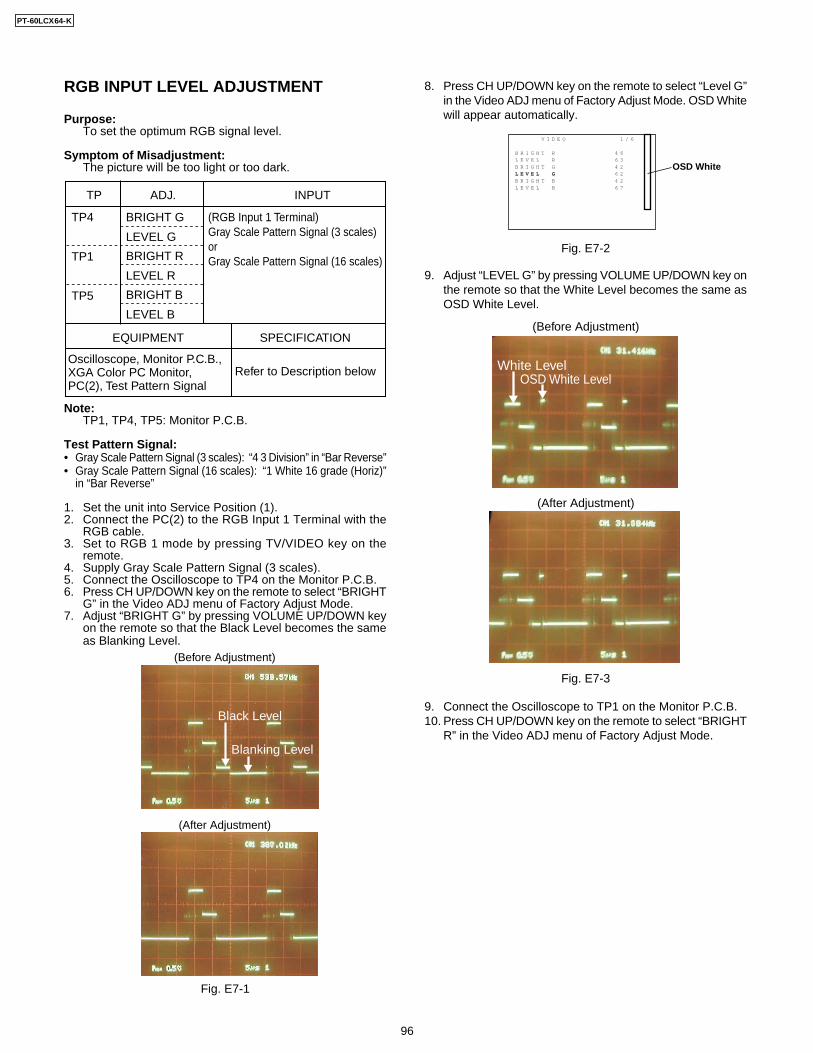
OSD White
V I D E O 1 / 6 B R I G H T R 4 6 L E V E L R 6 3 B R I G H T G 4 2 L E V E L G 6 2 B R I G H T B 4 2 L E V E L B 6 7
RGB INPUT LEVEL ADJUSTMENT
Purpose:To set the optimum RGB signal level.
Symptom of Misadjustment:The picture will be too light or too dark.
Note:TP1, TP4, TP5: Monitor P.C.B.
Test Pattern Signal:• Gray Scale Pattern Signal (3 scales): “4 3 Division” in “Bar Reverse”• Gray Scale Pattern Signal (16 scales): “1 White 16 grade (Horiz)”
in “Bar Reverse”
1. Set the unit into Service Position (1).2. Connect the PC(2) to the RGB Input 1 Terminal with the
RGB cable.3. Set to RGB 1 mode by pressing TV/VIDEO key on the
remote.4. Supply Gray Scale Pattern Signal (3 scales).5. Connect the Oscilloscope to TP4 on the Monitor P.C.B.6. Press CH UP/DOWN key on the remote to select “BRIGHT
G” in the Video ADJ menu of Factory Adjust Mode.7. Adjust “BRIGHT G” by pressing VOLUME UP/DOWN key
on the remote so that the Black Level becomes the sameas Blanking Level.
Fig. E7-1
TP
Refer to Description belowOscilloscope, Monitor P.C.B., XGA Color PC Monitor, PC(2), Test Pattern Signal
SPECIFICATIONEQUIPMENT
ADJ. INPUT
(RGB Input 1 Terminal)Gray Scale Pattern Signal (3 scales)orGray Scale Pattern Signal (16 scales)
TP4
TP1
TP5
BRIGHT R
LEVEL R
BRIGHT G
LEVEL G
BRIGHT B
LEVEL B
8. Press CH UP/DOWN key on the remote to select “Level G”in the Video ADJ menu of Factory Adjust Mode. OSD Whitewill appear automatically.
Fig. E7-2
9. Adjust “LEVEL G” by pressing VOLUME UP/DOWN key onthe remote so that the White Level becomes the same asOSD White Level.
Fig. E7-3
9. Connect the Oscilloscope to TP1 on the Monitor P.C.B.10. Press CH UP/DOWN key on the remote to select “BRIGHT
R” in the Video ADJ menu of Factory Adjust Mode.
(Before Adjustment)
(After Adjustment)
Black Level
Blanking Level
(Before Adjustment)
(After Adjustment)
OSD White LevelWhite Level
PT-60LCX64-K
96
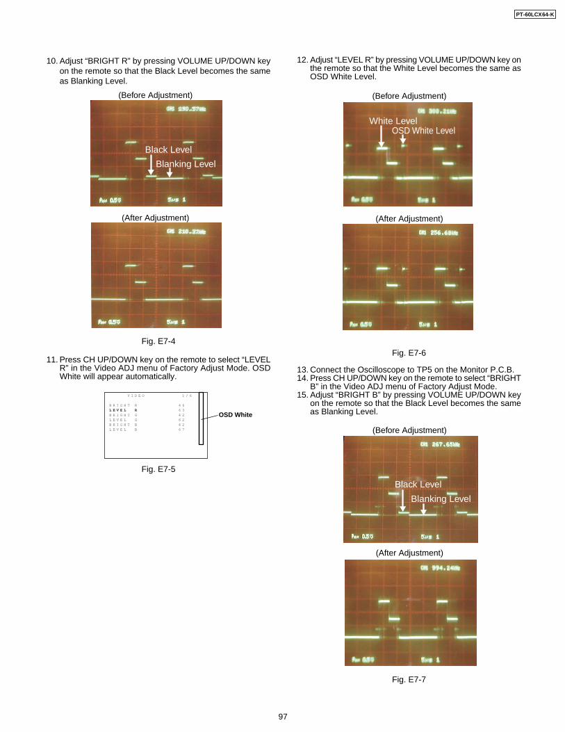
(Before Adjustment)
(After Adjustment)
Black Level
Blanking Level
(Before Adjustment)
(After Adjustment)
OSD White LevelWhite Level
(Before Adjustment)
(After Adjustment)
Black Level
Blanking Level
10. Adjust “BRIGHT R” by pressing VOLUME UP/DOWN keyon the remote so that the Black Level becomes the sameas Blanking Level.
Fig. E7-4
11. Press CH UP/DOWN key on the remote to select “LEVELR” in the Video ADJ menu of Factory Adjust Mode. OSDWhite will appear automatically.
Fig. E7-5
OSD White
V I D E O 1 / 6 B R I G H T R 4 6 L E V E L R 6 3 B R I G H T G 4 2 L E V E L G 6 2 B R I G H T B 4 2 L E V E L B 6 7
12. Adjust “LEVEL R” by pressing VOLUME UP/DOWN key onthe remote so that the White Level becomes the same asOSD White Level.
Fig. E7-6
13. Connect the Oscilloscope to TP5 on the Monitor P.C.B.14. Press CH UP/DOWN key on the remote to select “BRIGHT
B” in the Video ADJ menu of Factory Adjust Mode.15. Adjust “BRIGHT B” by pressing VOLUME UP/DOWN key
on the remote so that the Black Level becomes the sameas Blanking Level.
Fig. E7-7
PT-60LCX64-K
97
(Before Adjustment)
(After Adjustment)
OSD White LevelWhite Level
16. Press CH UP/DOWN key on the remote to select “LEVELB” in the Video ADJ menu of Factory Adjust Mode. OSDWhite will appear automatically.
Fig. E7-8
17. Adjust “LEVEL B” by pressing VOLUME UP/DOWN key onthe remote so that the White Level becomes the same asOSD White Level.
Fig. E7-9
OSD White
V I D E O 1 / 6 B R I G H T R 4 6 L E V E L R 6 3 B R I G H T G 4 2 L E V E L G 6 2 B R I G H T B 4 2 L E V E L B 6 7
PT-60LCX64-K
98
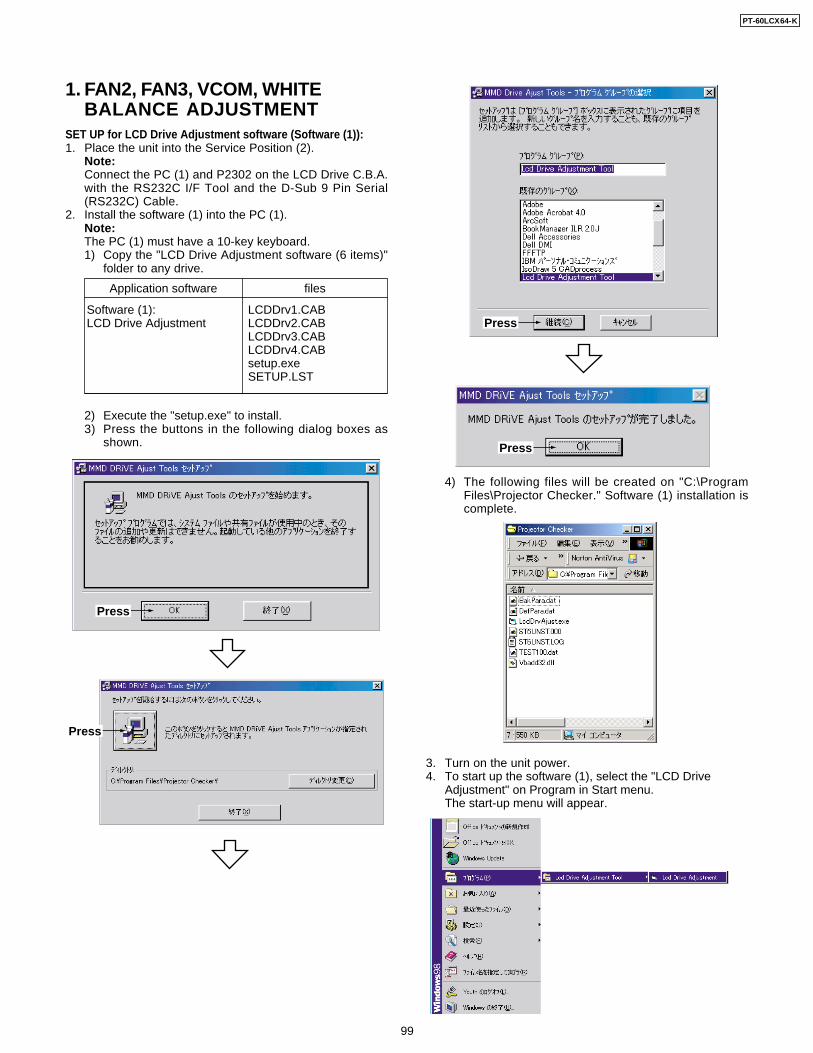
SET UP for LCD Drive Adjustment software (Software (1)):1. Place the unit into the Service Position (2).
Note:Connect the PC (1) and P2302 on the LCD Drive C.B.A.with the RS232C I/F Tool and the D-Sub 9 Pin Serial(RS232C) Cable.
2. Install the software (1) into the PC (1).Note:The PC (1) must have a 10-key keyboard.1) Copy the "LCD Drive Adjustment software (6 items)"
folder to any drive.
2) Execute the "setup.exe" to install.3) Press the buttons in the following dialog boxes as
shown.
4) The following files will be created on "C:\ProgramFiles\Projector Checker." Software (1) installation iscomplete.
3. Turn on the unit power.4. To start up the software (1), select the "LCD Drive
Adjustment" on Program in Start menu.The start-up menu will appear.
Press
Press
Press
Press
LCDDrv1.CABLCDDrv2.CABLCDDrv3.CABLCDDrv4.CABsetup.exeSETUP.LST
Software (1):LCD Drive Adjustment
Application software files
1. FAN2, FAN3, VCOM, WHITEBALANCE ADJUSTMENT
PT-60LCX64-K
99
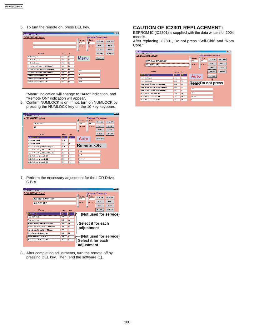
(Not used for service)
(Not used for service)
Select it for each adjustment
Select it for each adjustment
5. To turn the remote on, press DEL key.
"Manu" indication will change to "Auto" indication, and"Remote ON" indication will appear.
6. Confirm NUMLOCK is on. If not, turn on NUMLOCK bypressing the NUMLOCK key on the 10-key keyboard.
7. Perform the necessary adjustment for the LCD DriveC.B.A.
8. After completing adjustments, turn the remote off bypressing DEL key. Then, end the software (1).
Do not press
CAUTION OF IC2301 REPLACEMENT:EEPROM IC (IC2301) is supplied with the data written for 2004models.After replacing IC2301, Do not press “Self-Chk” and “RomCore.”
PT-60LCX64-K
100
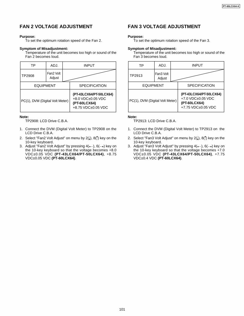
FAN 2 VOLTAGE ADJUSTMENT
Purpose:To set the optimum rotation speed of the Fan 2.
Symptom of Misadjustment:Temperature of the unit becomes too high or sound of theFan 2 becomes loud.
Note:TP2908: LCD Drive C.B.A.
1. Connect the DVM (Digital Volt Meter) to TP2908 on theLCD Drive C.B.A.
2. Select "Fan2 Volt Adjust" on menu by 2( ), 8( ) key on the10-key keyboard.
3. Adjust "Fan2 Volt Adjust" by pressing 4( ), 6( ) key onthe 10-key keyboard so that the voltage becomes +8.0VDC±0.05 VDC (PT-43LCX64/PT-50LCX64), +8.75VDC±0.05 VDC (PT-60LCX64).
TP
PC(1), DVM (Digital Volt Meter)
(PT-43LCX64/PT-50LCX64)+8.0 VDC±0.05 VDC(PT-60LCX64)+8.75 VDC±0.05 VDC
SPECIFICATIONEQUIPMENT
ADJ. INPUT
TP2908Fan2 Volt
Adjust
FAN 3 VOLTAGE ADJUSTMENT
Purpose:To set the optimum rotation speed of the Fan 3.
Symptom of Misadjustment:Temperature of the unit becomes too high or sound of theFan 3 becomes loud.
Note:TP2913: LCD Drive C.B.A.
1. Connect the DVM (Digital Volt Meter) to TP2913 on theLCD Drive C.B.A.
2. Select "Fan3 Volt Adjust" on menu by 2( ), 8( ) key on the10-key keyboard.
3. Adjust "Fan3 Volt Adjust" by pressing 4( ), 6( ) key onthe 10-key keyboard so that the voltage becomes +7.0VDC±0.05 VDC (PT-43LCX64/PT-50LCX64), +7.75VDC±0.4 VDC (PT-60LCX64).
TP
PC(1), DVM (Digital Volt Meter)
(PT-43LCX64/PT-50LCX64)+7.0 VDC±0.05 VDC(PT-60LCX64)+7.75 VDC±0.05 VDC
SPECIFICATIONEQUIPMENT
ADJ. INPUT
TP2913 Fan3 Volt Adjust
PT-60LCX64-K
101
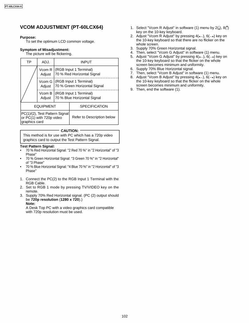
VCOM ADJUSTMENT (PT-60LCX64)
Purpose:To set the optimum LCD common voltage.
Symptom of Misadjustment:The picture will be flickering.
Test Pattern Signal:• 70 % Red Horizontal Signal: "2 Red 70 %" in "2 Horizontal" of "3
Phase"• 70 % Green Horizontal Signal: "3 Green 70 %" in "2 Horizontal"
of "3 Phase"• 70 % Blue Horizontal Signal: "4 Blue 70 %" in "2 Horizontal" of "3
Phase"
1. Connect the PC(2) to the RGB Input 1 Terminal with theRGB Cable.
2. Set to RGB 1 mode by pressing TV/VIDEO key on theremote.
3. Supply 70% Red Horizontal signal. (PC (2) output shouldbe 720p resolution (1280 x 720).)Note:A Desk Top PC with a video graphics card compatiblewith 720p resolution must be used.
1. Select "Vcom R Adjust" in software (1) menu by 2( ), 8( )key on the 10-key keyboard.
2. Adjust "Vcom R Adjust" by pressing 4( ), 6( ) key onthe 10-key keyboard so that there are no flicker on thewhole screen.
3. Supply 70% Green Horizontal signal.4. Then, select "Vcom G Adjust" in software (1) menu.5. Adjust "Vcom G Adjust" by pressing 4( ), 6( ) key on
the 10-key keyboard so that the flicker on the wholescreen becomes minimum and uniformity.
6. Supply 70% Blue Horizontal signal.7. Then, select "Vcom B Adjust" in software (1) menu.8. Adjust "Vcom B Adjust" by pressing 4( ), 6( ) key on
the 10-key keyboard so that the flicker on the wholescreen becomes minimum and uniformity.
9. Then, end the software (1).
TP
PC(1)/(2), Test Pattern Signalor PC(1) with 720p video graphics card
Refer to Description below
SPECIFICATIONEQUIPMENT
ADJ.
Vcom RAdjust
Vcom GAdjust
Vcom BAdjust
INPUT
(RGB Input 1 Terminal)70 % Red Horizontal Signal
(RGB Input 1 Terminal) 70 % Green Horizontal Signal
(RGB Input 1 Terminal)70 % Blue Horizontal Signal
CAUTION:This method is for use with PC which has a 720p video graphics card to output the Test Pattern Signal.
PT-60LCX64-K
102
VCOM ADJUSTMENT (PT-43LCX64/50LCX64)
Purpose:To set the optimum LCD common voltage.
Symptom of Misadjustment:The picture will be flickering.
Test Pattern Signal:• 70 % Red Horizontal Signal: "2 Red 70 %" in "2 Horizontal" of "3
Phase"• 70 % Green Horizontal Signal: "3 Green 70 %" in "2 Horizontal"
of "3 Phase"• 70 % Blue Horizontal Signal: "4 Blue 70 %" in "2 Horizontal" of "3
Phase"
1. Connect the PC(2) to the RGB Input 1 Terminal with theRGB Cable.
2. Set to RGB 1 mode by pressing TV/VIDEO key on theremote.
3. Supply 70% Red Horizontal signal. (PC (2) output shouldbe 720p resolution (1280 x 720).)Note:A Desk Top PC with a video graphics card compatiblewith 720p resolution must be used.
1. Select "Vcom R Adjust" in software (1) menu by 2( ), 8( )key on the 10-key keyboard.
2. Adjust "Vcom R Adjust" by pressing 4( ), 6( ) key onthe 10-key keyboard so that there are no flicker on thewhole screen.
3. Supply 70% Green Horizontal signal.4. Then, select "Vcom G Adjust" in software (1) menu.5. Adjust "Vcom G Adjust" by pressing 4( ), 6( ) key on
the 10-key keyboard so that the flicker on the wholescreen becomes minimum and uniformity.
6. Supply 70% Blue Horizontal signal.7. Then, select "Vcom B Adjust" in software (1) menu.8. Adjust "Vcom B Adjust" by pressing 4( ), 6( ) key on
the 10-key keyboard so that the flicker on the wholescreen becomes minimum and uniformity.
9. After above steps, add 16 steps to the data of "Vcom RAdjust", "Vcom G Adjust" and "Vcom B Adjust" bypressing 6( ) key on the 10-key keyboard.Note:The picture will be flickering a little bit immediately afterdata addition (This is normal).
10. Then, end the software (1).
TP
PC(1)/(2), Test Pattern Signalor PC(1) with 720p video graphics card
Refer to Description below
SPECIFICATIONEQUIPMENT
ADJ.
Vcom RAdjust
Vcom GAdjust
Vcom BAdjust
INPUT
(RGB Input 1 Terminal)70 % Red Horizontal Signal
(RGB Input 1 Terminal) 70 % Green Horizontal Signal
(RGB Input 1 Terminal)70 % Blue Horizontal Signal
CAUTION:Be sure to complete the VCOM adjustment within 10 minutes after turing on the unit power.If adjusting takes more than 10 minutes, wait for approx. 2 hours after turning off the unit power. Then, re-adjust.
CAUTION:This method is for use with PC which has a 720p video graphics card to output the Test Pattern Signal.
PT-60LCX64-K
103
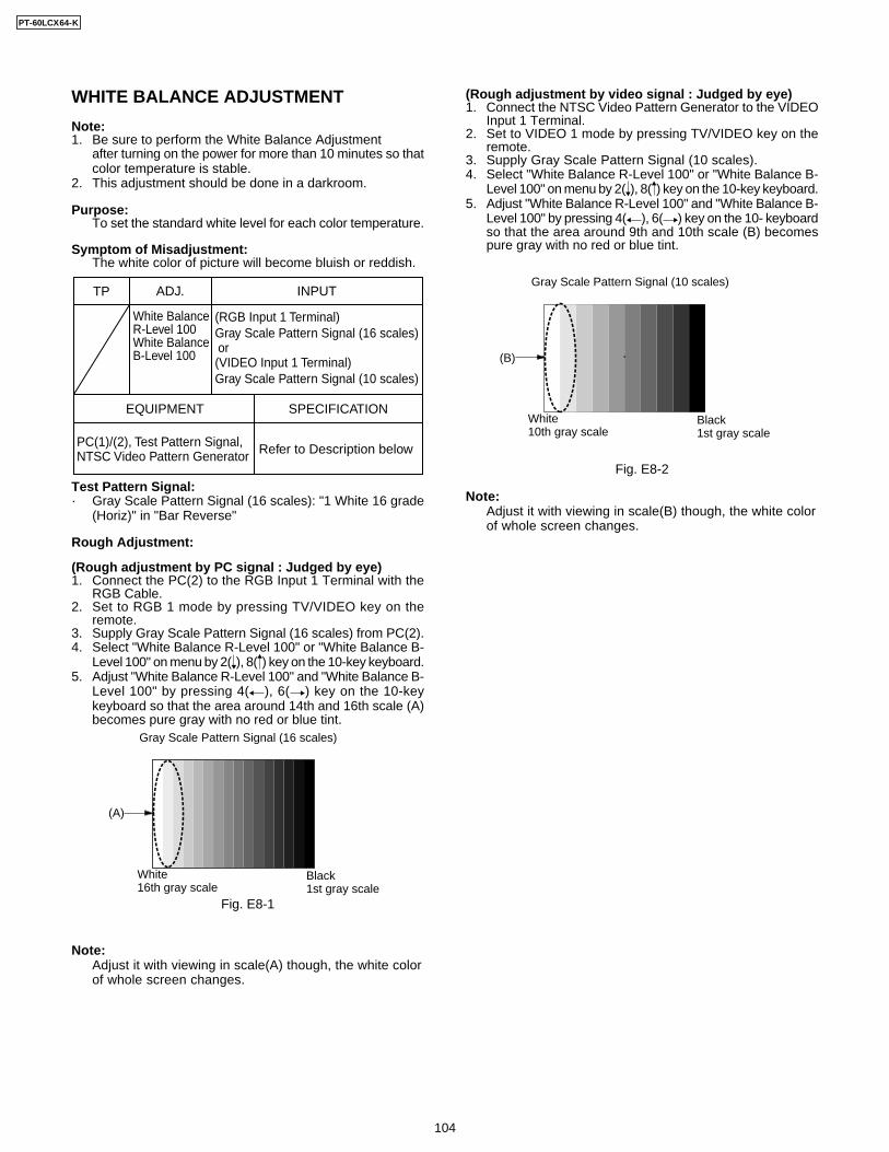
Gray Scale Pattern Signal (16 scales)
(A)
White16th gray scale
Black1st gray scale
Gray Scale Pattern Signal (10 scales)
(B)
White10th gray scale
Black1st gray scale
(Rough adjustment by video signal : Judged by eye)1. Connect the NTSC Video Pattern Generator to the VIDEO
Input 1 Terminal.2. Set to VIDEO 1 mode by pressing TV/VIDEO key on the
remote.3. Supply Gray Scale Pattern Signal (10 scales).4. Select "White Balance R-Level 100" or "White Balance B-
Level 100" on menu by 2( ), 8( ) key on the 10-key keyboard.5. Adjust "White Balance R-Level 100" and "White Balance B-
Level 100" by pressing 4( ), 6( ) key on the 10- keyboardso that the area around 9th and 10th scale (B) becomespure gray with no red or blue tint.
Fig. E8-2
Note:Adjust it with viewing in scale(B) though, the white colorof whole screen changes.
WHITE BALANCE ADJUSTMENT
Note:1. Be sure to perform the White Balance Adjustment
after turning on the power for more than 10 minutes so thatcolor temperature is stable.
2. This adjustment should be done in a darkroom.
Purpose:To set the standard white level for each color temperature.
Symptom of Misadjustment:The white color of picture will become bluish or reddish.
Test Pattern Signal:· Gray Scale Pattern Signal (16 scales): "1 White 16 grade
(Horiz)" in "Bar Reverse"
Rough Adjustment:
(Rough adjustment by PC signal : Judged by eye)1. Connect the PC(2) to the RGB Input 1 Terminal with the
RGB Cable.2. Set to RGB 1 mode by pressing TV/VIDEO key on the
remote.3. Supply Gray Scale Pattern Signal (16 scales) from PC(2).4. Select "White Balance R-Level 100" or "White Balance B-
Level 100" on menu by 2( ), 8( ) key on the 10-key keyboard.5. Adjust "White Balance R-Level 100" and "White Balance B-
Level 100" by pressing 4( ), 6( ) key on the 10-keykeyboard so that the area around 14th and 16th scale (A)becomes pure gray with no red or blue tint.
Fig. E8-1
Note:Adjust it with viewing in scale(A) though, the white colorof whole screen changes.
TP
PC(1)/(2), Test Pattern Signal,NTSC Video Pattern Generator Refer to Description below
SPECIFICATIONEQUIPMENT
ADJ. INPUT
or
(RGB Input 1 Terminal)Gray Scale Pattern Signal (16 scales)
(VIDEO Input 1 Terminal)Gray Scale Pattern Signal (10 scales)
White BalanceR-Level 100White BalanceB-Level 100
PT-60LCX64-K
104
Fine Adjustment:
Test Pattern Signal:· 50 % White Pattern Signal: "9 Gray" in "1 Color"· 100 % White Pattern Signal: "1 White" in "1 Color"
1. Set to RGB 1 mode by pressing TV/VIDEO key on theremote.
2. Supply 50 % White Pattern Signal from PC(2).3. Select "White Balance R-Level 100" or "White Balance B-
Level 100" on menu by 2( ), 8( ) key on the 10-key keyboard.4. Adjust "White Balance R-Level 100" and "White Balance B-
Level 100" by pressing 4( ), 6( ) key on the 10-keykeyboard so that the color temperature (K) and its deviation(uv) in the center of the screen are 9300 K to 10900 K, and-0.020 uv to -0.004 uv (x=0.283 - 0.291, y=0.259 - 0.289)respectively by Color Temperature Meter.
5. Supply 100 % White Pattern Signal from PC(2).6. Confirm that the color temperature (K) and its deviation
(uv) in the center of the screen are 8000 K to 13000 K, and-0.016 uv to 0.002 uv (x=0.273 - 0.299, y=0.263 - 0.295)respectively by Color Temperature Meter.
7. If OK, end the software (1).If NG, repeat steps 2 through 6 until color temperature (K)and its deviation (uv) become within the specification.
PC(1)/(2), Test Pattern Signal,Color Temperature Meter
(RGB Input 1 Terminal)50 % White Pattern Signal100 % White Pattern Signal
Refer to Description below
SPECIFICATIONEQUIPMENT
TP ADJ. INPUT
White BalanceR-Level 100White BalanceB-Level 100
PT-60LCX64-K
105
2. GAMMA ADJUSTMENT (Compensation by transmitting gamma data)Note:When replacing the LCD Drive C.B.A., the LCD/Prism Unit or IC2301 (32k EEPROM), confirm that the color of the entire screen.If NG, perform this adjustment.
SET UP:1. Place the unit into Service Position (2).2. Install the software (2) into the PC(1).
1) Copy the "SCE2 (7 items)" folder to any drive.
3. To start up the software (2), execute the "SCE2.EXE" by double clicking.4. Set to RGB mode by pressing TV/VIDEO key on the remote.5. Supply Gray Scale Pattern Signal (16 scales): "1 White 16 grade (Horiz)" in "Bar Reverse" of Test Pattern Signal from PC(2).6. Set the FULL mode by pressing ASPECT key.
PROCEDURES:
Set up is complete
Confirm the area around 1th and 2ndor 15th and 16th scale is clearly visible on the screen.
Case 1, 2, 3 or 4(one of any color)
OK
OK(no color)
OK(no color)
NG(too dark or bright)
Turn off the power to exit.
Turn off the power to exit.
Turn off the power to exit.
Transmit the gamma data "MMD2003GAMMA 2, 3, 4 or 5" (total 6 datas) to EEPROM according to each case in Case1, Case2, Case3 or Case4.
Execute the "SCE2.EXE."Then, transmit the gamma data "MMD2003GAMMA 1" (total 6 datas) to EEPROM.
Confirm that the color of the entire screen.Determine which case of color is on the screen. Refer to "Gamma data table."
Gray Scale Pattern Signal (16 scales)
White16th gray scale
15th and 16th 1st and 2nd
Black1st gray scale
SCE2.EXESCE2.CNTSce2.GIDGAMMA_USUAL.sceCommand.logREADME.TXTSCE2.HLP
Application software files
Software (2): Sce2
PT-60LCX64-K
106
How to transfer the gamma data using thesoftware (2):
1. Execute the "SCE2.EXE" file by double clicking. Thestart-up menu will appear.
2. Select "(C)" on option pull-down menu, and confirm thetransmission setting as shown.
3. Select "(O)" on file pull-down menu.
4. Select "GAMMA_USUAL.sce" file, and press "Open."
Select
Select
Select
Press
GAMMA_USUAL.sce
Select 1st fileSelect 2nd fileSelect 3rd fileSelect 4th fileSelect 5th fileSelect 6th file
red arrowblue arrowred arrow
blue arrowred arrow
blue arrowred arrow
blue arrowred arrow
blue arrowred arrow
blue arrow
5. Select desired gamma data of "MMD2003GAMMA"folder (MMD2003GAMMA 1-5). Then, double click the1st, 2nd, 3rd, 4th, 5th and 6th files in order.
When the file is double clicked, the transmission willstart. The red arrow will appear, and then the blue arrowappear. First, a red arrow will appear, then a blue arrow.The red and blue arrows will appear alternately.Note:If the blue arrow does not appear or the "Error"indication appears, transmission has failed. In this case,double click the file again until the blue arrow appears.
PT-60LCX64-K
107
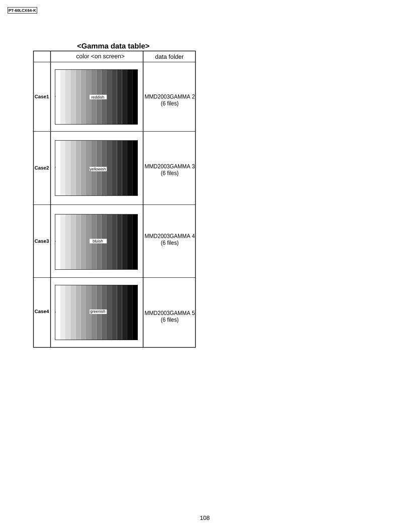
Case1
<Gamma data table> color <on screen> data folder
MMD2003GAMMA 2(6 files)
MMD2003GAMMA 3(6 files)
MMD2003GAMMA 4(6 files)
MMD2003GAMMA 5(6 files)
Case2
Case3
Case4
bluish
yellowish
reddish
greenish
PT-60LCX64-K
108
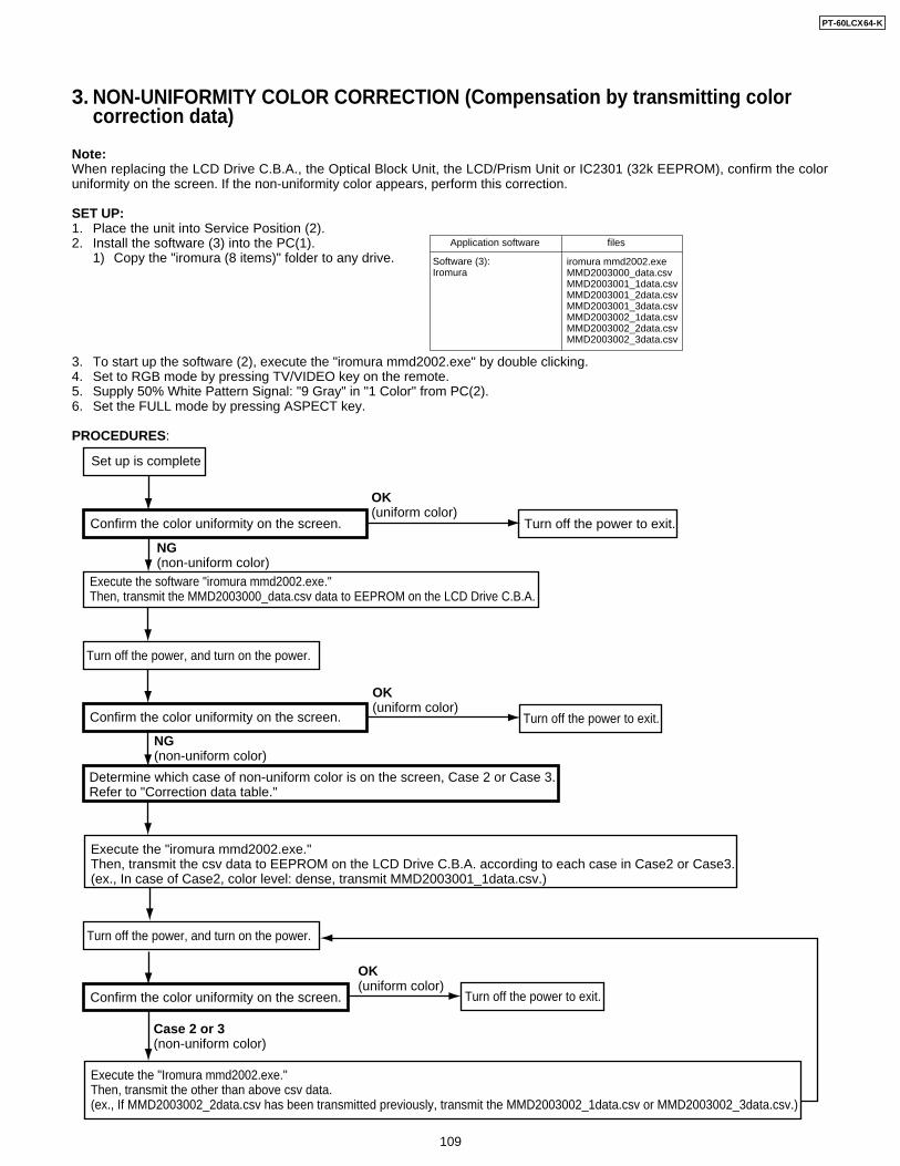
3. NON-UNIFORMITY COLOR CORRECTION (Compensation by transmitting colorcorrection data)
Note:When replacing the LCD Drive C.B.A., the Optical Block Unit, the LCD/Prism Unit or IC2301 (32k EEPROM), confirm the coloruniformity on the screen. If the non-uniformity color appears, perform this correction.
SET UP:1. Place the unit into Service Position (2).2. Install the software (3) into the PC(1).
1) Copy the "iromura (8 items)" folder to any drive.
3. To start up the software (2), execute the "iromura mmd2002.exe" by double clicking.4. Set to RGB mode by pressing TV/VIDEO key on the remote.5. Supply 50% White Pattern Signal: "9 Gray" in "1 Color" from PC(2).6. Set the FULL mode by pressing ASPECT key.
PROCEDURES:
Case 2 or 3(non-uniform color)
OK(uniform color)
Turn off the power to exit.
Turn off the power, and turn on the power.
Execute the "Iromura mmd2002.exe."Then, transmit the other than above csv data.(ex., If MMD2003002_2data.csv has been transmitted previously, transmit the MMD2003002_1data.csv or MMD2003002_3data.csv.)
Confirm the color uniformity on the screen.
Execute the "iromura mmd2002.exe."Then, transmit the csv data to EEPROM on the LCD Drive C.B.A. according to each case in Case2 or Case3.(ex., In case of Case2, color level: dense, transmit MMD2003001_1data.csv.)
OK(uniform color)
NG(non-uniform color)
Confirm the color uniformity on the screen.
Turn off the power, and turn on the power.
Determine which case of non-uniform color is on the screen, Case 2 or Case 3. Refer to "Correction data table."
Turn off the power to exit.
Set up is complete
Confirm the color uniformity on the screen.
OK(uniform color)
NG(non-uniform color)
Turn off the power to exit.
Execute the software "iromura mmd2002.exe."Then, transmit the MMD2003000_data.csv data to EEPROM on the LCD Drive C.B.A.
iromura mmd2002.exeMMD2003000_data.csvMMD2003001_1data.csvMMD2003001_2data.csv MMD2003001_3data.csvMMD2003002_1data.csvMMD2003002_2data.csvMMD2003002_3data.csv
Application software files
Software (3):Iromura
PT-60LCX64-K
109
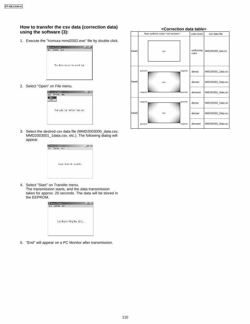
How to transfer the csv data (correction data)using the software (3):
1. Execute the "Iromura mmd2002.exe" file by double click.
2. Select "Open" on File menu.
3. Select the desired csv data file (MMD2003000_data.csv,MMD2003001_1data.csv, etc.). The following dialog willappear.
4. Select "Start" on Transfer menu.The transmission starts, and the data transmissiontakes for approx. 20 seconds. The data will be stored inthe EEPROM.
5. "End" will appear on a PC Monitor after transmission.
gray
magenta
magentagreenish
greenish
magenta
magentagreenish
greenish
gray
Case1
<Correction data table>Non-uniform color <on screen>
uniformity color
dense
denser
densest
dense
denser
densest
color level csv data file
MMD2003000_data.csv
MMD2003001_1data.csv
MMD2003001_2data.csv
MMD2003001_3data.csv
MMD2003002_1data.csv
MMD2003002_2data.csv
MMD2003002_3data.csv
gray
Case2
Case3
PT-60LCX64-K
110
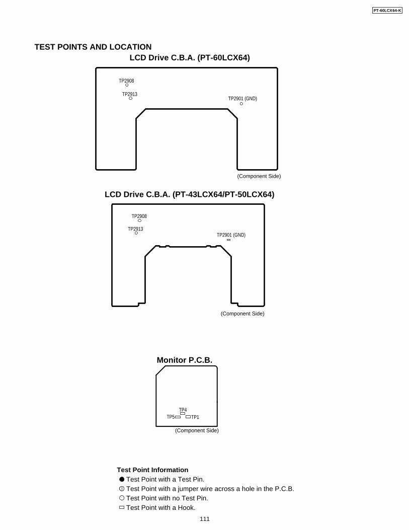
TEST POINTS AND LOCATION
Test Point Information Test Point with a Test Pin. Test Point with a jumper wire across a hole in the P.C.B. Test Point with no Test Pin. Test Point with a Hook.
LCD Drive C.B.A. (PT-60LCX64)
LCD Drive C.B.A. (PT-43LCX64/PT-50LCX64)
(Component Side)
(Component Side)
Monitor P.C.B.
TP4TP5 TP1
TP2901 (GND)
TP2908
TP2913
(Component Side)
TP2908
TP2913TP2901 (GND)
PT-60LCX64-K
111
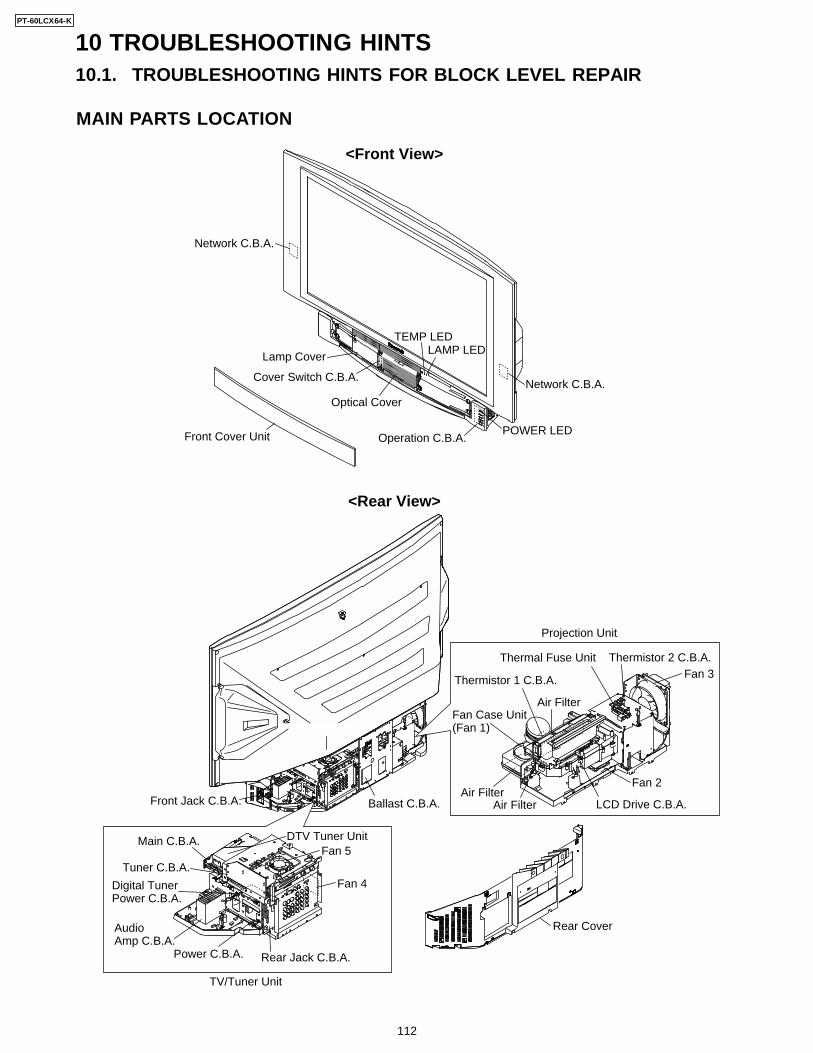
10 TROUBLESHOOTING HINTS10.1. TROUBLESHOOTING HINTS FOR BLOCK LEVEL REPAIR
Front Jack C.B.A. Ballast C.B.A.
Audio Amp C.B.A.
Rear Jack C.B.A.Power C.B.A.
Main C.B.A. DTV Tuner Unit
TV/Tuner Unit
Tuner C.B.A.
Digital Tuner Power C.B.A.
Fan 4
Fan 5
Lamp Cover
Cover Switch C.B.A.
Front Cover Unit Operation C.B.A.
Network C.B.A.
Network C.B.A.
<Front View>
<Rear View>
Optical Cover
Rear Cover
Fan 3
Fan Case Unit(Fan 1)
Fan 2
Thermistor 2 C.B.A.
LCD Drive C.B.A.
Projection Unit
Thermistor 1 C.B.A.
Thermal Fuse Unit
Air Filter
Air Filter
Air Filter
TEMP LEDLAMP LED
POWER LED
MAIN PARTS LOCATION
PT-60LCX64-K
112
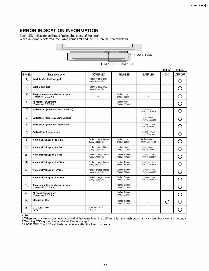
ERROR INDICATION INFORMATIONEach LED indication facilitates finding the cause of the error.When an error is detected, the Lamp comes off and the LED on the front will flash.
TEMP LED
POWER LED
LAMP LED
TV/VIDEO
Error InformationError No. LAMP OFFLAMP LED OSD
(Note 2) (Note 3)
TEMP LEDPOWER LED
Note:1. When two or more errors have occurred at the same time, the LED will alternate flash patterns as shown above every 5 seconds.2. Warning OSD appears when the air filter is clogged.3. LAMP OFF: The LED will flash immediately after the Lamp comes off.
Clogged air filter17)
1)
2)
3)
4)
6)
7)
8)
12)
9)
10)
11)
15)
16)
flashes 5 times every 5 seconds
Fan1, Fan2 or Fan3 stopped flashes orange once every 5 seconds - -
Lamp Cover open
Temperature Sensor shorted or open(Thermistor 1 C.B.A.)
flashes orange twice every 5 seconds
flashes orange 5 times every 5 seconds
flashes orange 6 times every 5 seconds
flashes orange 7 times every 5 seconds
flashes orange 8 times every 5 seconds
flashes onceevery 5 seconds
flashes onceevery 5 seconds
flashes onceevery 5 seconds
-
-
-
-
Abnormal Temperature(Thermistor 1 C.B.A.)
flashes twiceevery 5 seconds
flashes twiceevery 5 seconds
- -
Ballast Error (abnormal Lamp voltage) -
flashes 3 times every 5 seconds
Ballast Error (abnormal temperature)-
flashes 4 times every 5 seconds
Ballast Error (other causes)-
-
-
-
-
-
-
-
-
-
Abnormal Voltage on 33 V line
flashes twiceevery 5 seconds
flashes twiceevery 5 seconds
Abnormal Voltage on 9 V line
flashes 3 times every 5 seconds
flashes 3 times every 5 seconds
Abnormal Voltage on 5 V line
flashes 4 times every 5 seconds
flashes 4 times every 5 seconds
flashes 3 times every 5 seconds
flashes 4 times every 5 seconds
Abnormal Voltage on 3.3 V line
Temperature Sensor shorted or open(Thermistor 2 C.B.A.)
Abnormal Temperature(Thermistor 2 C.B.A.)
5) flashes onceevery 5 seconds
Ballast Error (abnormal Lamp or Ballast) --
13) flashes orange 9 times every 5 seconds
flashes 5 times every 5 seconds
flashes 5 times every 5 seconds
Abnormal Voltage on -5 V line
14) flashes orange 10 times every 5 seconds
flashes 6 times every 5 seconds
flashes 6 times every 5 seconds
Abnormal Voltage on 6.5 V line
-flashes green allthe time
DTV Tuner PowerError
18)-
PT-60LCX64-K
113
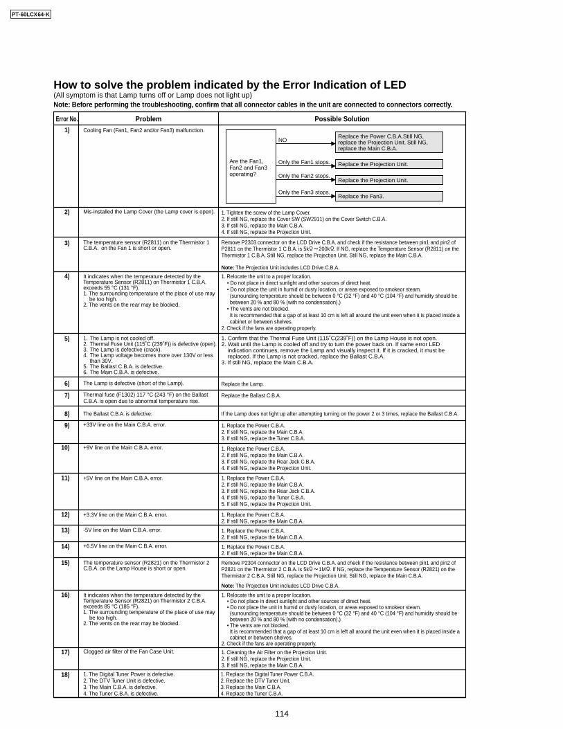
Cooling Fan (Fan1, Fan2 and/or Fan3) malfunction.
Mis-installed the Lamp Cover (the Lamp cover is open).
The temperature sensor (R2811) on the Thermistor 1 C.B.A. on the Fan 1 is short or open.
It indicates when the temperature detected by the Temperature Sensor (R2811) on Thermistor 1 C.B.A. exceeds 55 °C (131 °F).1. The surrounding temperature of the place of use may be too high.2. The vents on the rear may be blocked.
The temperature sensor (R2821) on the Thermistor 2 C.B.A. on the Lamp House is short or open.
It indicates when the temperature detected by the Temperature Sensor (R2821) on Thermistor 2 C.B.A. exceeds 85 °C (185 °F).1. The surrounding temperature of the place of use may be too high.2. The vents on the rear may be blocked.
Clogged air filter of the Fan Case Unit.
The Lamp is defective (short of the Lamp).
Thermal fuse (F1302) 117 °C (243 °F) on the Ballast C.B.A. is open due to abnormal temperature rise.
The Ballast C.B.A. is defective.
+33V line on the Main C.B.A. error.
1. The Lamp is not cooled off.2. Thermal Fuse Unit (115˚C (239˚F)) is defective (open).3. The Lamp is defective (crack).4. The Lamp voltage becomes more over 130V or less
than 30V.5. The Ballast C.B.A. is defective.6. The Main C.B.A. is defective.
How to solve the problem indicated by the Error Indication of LED(All symptom is that Lamp turns off or Lamp does not light up)
Error No. Problem Possible Solution
17)
1)
2)
3)
4)
6)
7)
8)
12)
9)
10)
11)
15)
16)
5)
13)
14)
+9V line on the Main C.B.A. error.
+5V line on the Main C.B.A. error.
+3.3V line on the Main C.B.A. error.
-5V line on the Main C.B.A. error.
+6.5V line on the Main C.B.A. error.
Are the Fan1, Fan2 and Fan3 operating?
Replace the Power C.B.A.Still NG, replace the Projection Unit. Still NG, replace the Main C.B.A.
NO
Replace the Projection Unit.
Replace the Projection Unit.
Only the Fan1 stops.
Only the Fan2 stops.
Only the Fan3 stops.Replace the Fan3.
1. Tighten the screw of the Lamp Cover. 2. If still NG, replace the Cover SW (SW2911) on the Cover Switch C.B.A. 3. If still NG, replace the Main C.B.A.4. If still NG, replace the Projection Unit.
1. Relocate the unit to a proper location. • Do not place in direct sunlight and other sources of direct heat. • Do not place the unit in humid or dusty location, or areas exposed to smokeor steam. (surrounding temperature should be between 0 °C (32 °F) and 40 °C (104 °F) and humidity should be between 20 % and 80 % (with no condensation).) • The vents are not blocked. It is recommended that a gap of at least 10 cm is left all around the unit even when it is placed inside a cabinet or between shelves.2. Check if the fans are operating properly.
1. Relocate the unit to a proper location. • Do not place in direct sunlight and other sources of direct heat. • Do not place the unit in humid or dusty location, or areas exposed to smokeor steam. (surrounding temperature should be between 0 °C (32 °F) and 40 °C (104 °F) and humidity should be between 20 % and 80 % (with no condensation).) • The vents are not blocked. It is recommended that a gap of at least 10 cm is left all around the unit even when it is placed inside a cabinet or between shelves.2. Check if the fans are operating properly.
1. Cleaning the Air Filter on the Projection Unit. 2. If still NG, replace the Projection Unit. 3. If still NG, replace the Main C.B.A.
1. Confirm that the Thermal Fuse Unit (115˚C(239˚F)) on the Lamp House is not open.2. Wait until the Lamp is cooled off and try to turn the power back on. If same error LED indication continues, remove the Lamp and visually inspect it. If it is cracked, it must be replaced. If the Lamp is not cracked, replace the Ballast C.B.A.3. If still NG, replace the Main C.B.A.
If the Lamp does not light up after attempting turning on the power 2 or 3 times, replace the Ballast C.B.A.
Replace the Lamp.
Replace the Ballast C.B.A.
Note: The Projection Unit includes LCD Drive C.B.A.
1. Replace the Power C.B.A. 2. If still NG, replace the Main C.B.A.3. If still NG, replace the Tuner C.B.A.
1. Replace the Power C.B.A. 2. If still NG, replace the Main C.B.A.3. If still NG, replace the Rear Jack C.B.A.4. If still NG, replace the Projection Unit.
1. Replace the Power C.B.A. 2. If still NG, replace the Main C.B.A.3. If still NG, replace the Rear Jack C.B.A. 4. If still NG, replace the Tuner C.B.A.5. If still NG, replace the Projection Unit.
1. Replace the Power C.B.A. 2. If still NG, replace the Main C.B.A.
1. Replace the Power C.B.A. 2. If still NG, replace the Main C.B.A.
1. Replace the Power C.B.A. 2. If still NG, replace the Main C.B.A.
Note: The Projection Unit includes LCD Drive C.B.A.
Remove P2303 connector on the LCD Drive C.B.A. and check if the resistance between pin1 and pin2 of P2811 on the Thermistor 1 C.B.A. is 5k 200k . If NG, replace the Temperature Sensor (R2811) on the Thermistor 1 C.B.A. Still NG, replace the Projection Unit. Still NG, replace the Main C.B.A.
Remove P2304 connector on the LCD Drive C.B.A. and check if the resistance between pin1 and pin2 of P2821 on the Thermistor 2 C.B.A. is 5k 1M . If NG, replace the Temperature Sensor (R2821) on the Thermistor 2 C.B.A. Still NG, replace the Projection Unit. Still NG, replace the Main C.B.A.
Note: Before performing the troubleshooting, confirm that all connector cables in the unit are connected to connectors correctly.
1. The Digital Tuner Power is defective.2. The DTV Tuner Unit is defective.3. The Main C.B.A. is defective.4. The Tuner C.B.A. is defective.
1. Replace the Digital Tuner Power C.B.A.2. Replace the DTV Tuner Unit.3. Replace the Main C.B.A.4. Replace the Tuner C.B.A.
18)
PT-60LCX64-K
114
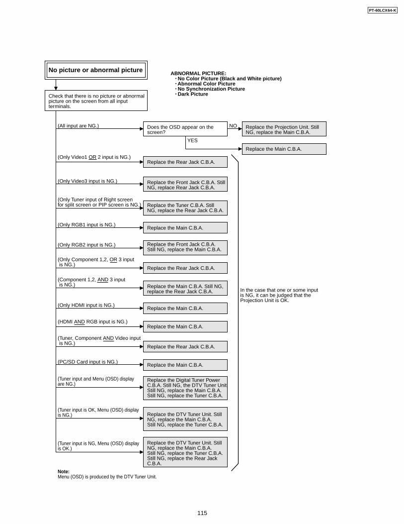
NO
YES
No picture or abnormal picture
(Only RGB1 input is NG.)
(All input are NG.)
(Only Video1 OR 2 input is NG.)
(Tuner, Component AND Video input is NG.)
Does the OSD appear on the screen?
Check that there is no picture or abnormalpicture on the screen from all inputterminals.
Replace the Projection Unit. StillNG, replace the Main C.B.A.
Replace the Main C.B.A.
Replace the Rear Jack C.B.A.
Replace the Rear Jack C.B.A.
Replace the Main C.B.A.
Replace the Rear Jack C.B.A.
(Tuner input is NG, Menu (OSD) display is OK.)
Replace the Digital Tuner Power C.B.A. Still NG, the DTV Tuner Unit. Still NG, replace the Main C.B.A. Still NG, replace the Tuner C.B.A.
Replace the DTV Tuner Unit. Still NG, replace the Main C.B.A. Still NG, replace the Tuner C.B.A.
Replace the DTV Tuner Unit. Still NG, replace the Main C.B.A. Still NG, replace the Tuner C.B.A.Still NG, replace the Rear JackC.B.A.
(Only Tuner input of Right screen for split screen or PIP screen is NG.) Replace the Tuner C.B.A. Still
NG, replace the Rear Jack C.B.A.
(Only Component 1,2, OR 3 input is NG.)
(Only Video3 input is NG.) Replace the Front Jack C.B.A. Still NG, replace Rear Jack C.B.A.
ABNORMAL PICTURE: No Color Picture (Black and White picture) Abnormal Color Picture No Synchronization Picture Dark Picture
(Only RGB2 input is NG.) Replace the Front Jack C.B.A.Still NG, replace the Main C.B.A.
(Only HDMI input is NG.)Replace the Main C.B.A.
(HDMI AND RGB input is NG.)
(PC/SD Card input is NG.)
(Tuner input and Menu (OSD) display are NG.)
(Tuner input is OK, Menu (OSD) display is NG.)
Note:Menu (OSD) is produced by the DTV Tuner Unit.
Replace the Main C.B.A.
Replace the Main C.B.A.
Replace the Main C.B.A. Still NG,replace the Rear Jack C.B.A.
(Component 1,2, AND 3 input is NG.)
In the case that one or some input is NG, it can be judged that the Projection Unit is OK.
PT-60LCX64-K
115
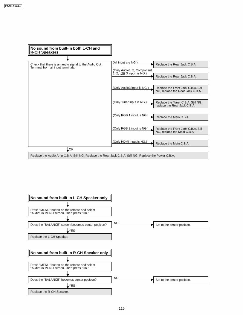
No sound from built-in both L-CH and R-CH Speakers
Replace the Rear Jack C.B.A.(All input are NG.)
Check that there is an audio signal to the Audio Out Terminal from all input terminals.
Replace the Main C.B.A.(Only HDMI input is NG.)
Replace the Main C.B.A.(Only RGB 1 input is NG.)
No sound from built-in L-CH Speaker only
Press "MENU" button on the remote and select "Audio" in MENU screen. Then press "OK."
Replace the L-CH Speaker.
Does the "BALANCE" screen becomes center position? Set to the center position.NO
YES
No sound from built-in R-CH Speaker only
Press "MENU" button on the remote and select "Audio" in MENU screen. Then press "OK."
Replace the R-CH Speaker.
Does the "BALANCE" becomes center position? Set to the center position.NO
YES
(Only Audio1, 2, Component 1, 2, OR 3 input is NG.)
(Only Tuner input is NG.)
(Only Audio3 input is NG.)
Replace the Rear Jack C.B.A.
OK
Replace the Audio Amp C.B.A. Still NG, Replace the Rear Jack C.B.A. Still NG, Replace the Power C.B.A.
Replace the Front Jack C.B.A. Still NG, replace the Rear Jack C.B.A.
Replace the Tuner C.B.A. Still NG, replace the Rear Jack C.B.A.
(Only RGB 2 input is NG.) Replace the Front Jack C.B.A. Still NG, replace the Main C.B.A.
PT-60LCX64-K
116
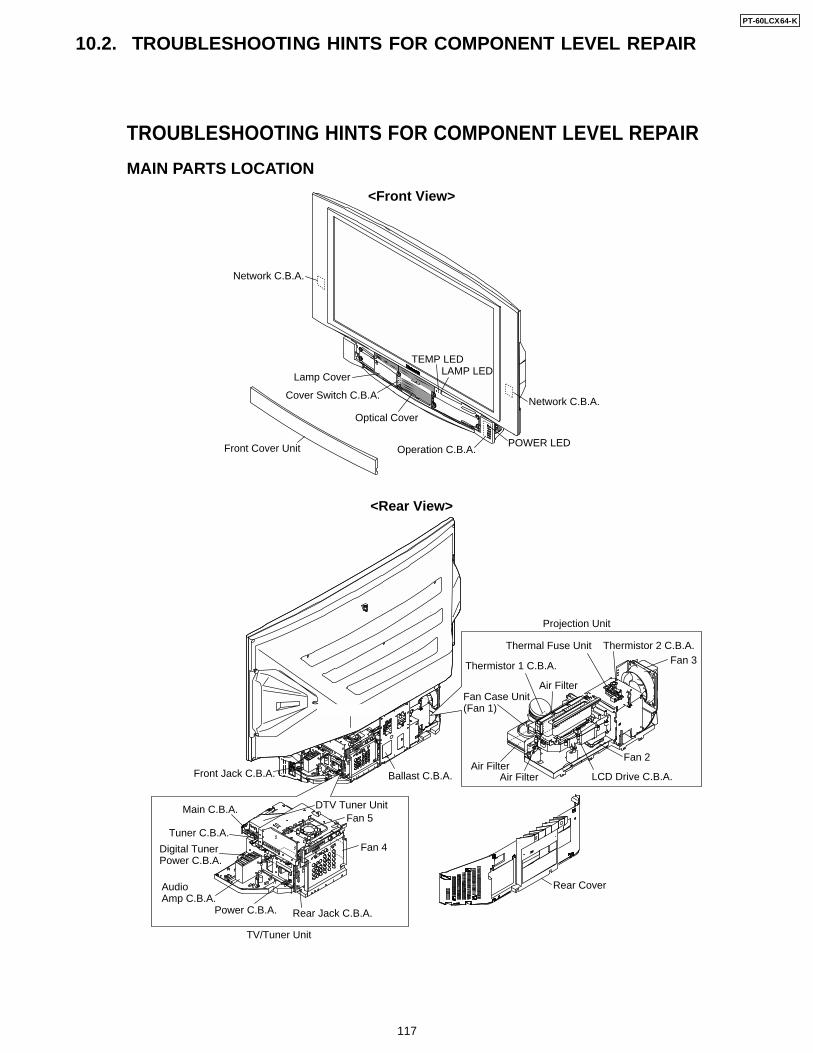
10.2. TROUBLESHOOTING HINTS FOR COMPONENT LEVEL REPAIR
Front Jack C.B.A. Ballast C.B.A.
Audio Amp C.B.A.
Rear Jack C.B.A.Power C.B.A.
Main C.B.A. DTV Tuner Unit
TV/Tuner Unit
Tuner C.B.A.
Digital Tuner Power C.B.A.
Fan 4
Fan 5
Lamp Cover
Cover Switch C.B.A.
Front Cover Unit Operation C.B.A.
Network C.B.A.
Network C.B.A.
<Front View>
<Rear View>
Optical Cover
Rear Cover
Fan 3
Fan Case Unit(Fan 1)
Fan 2
Thermistor 2 C.B.A.
LCD Drive C.B.A.
Projection Unit
Thermistor 1 C.B.A.
Thermal Fuse Unit
Air Filter
Air Filter
Air Filter
TEMP LEDLAMP LED
POWER LED
TROUBLESHOOTING HINTS FOR COMPONENT LEVEL REPAIR
MAIN PARTS LOCATION
PT-60LCX64-K
117
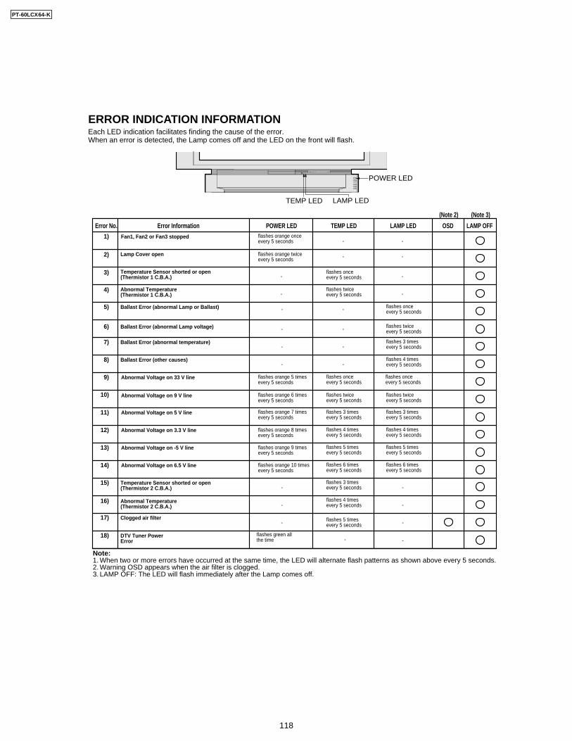
ERROR INDICATION INFORMATIONEach LED indication facilitates finding the cause of the error.When an error is detected, the Lamp comes off and the LED on the front will flash.
TEMP LED
POWER LED
LAMP LED
TV/VIDEO
Error InformationError No. LAMP OFFLAMP LED OSD
(Note 2) (Note 3)
TEMP LEDPOWER LED
Note:1. When two or more errors have occurred at the same time, the LED will alternate flash patterns as shown above every 5 seconds.2. Warning OSD appears when the air filter is clogged.3. LAMP OFF: The LED will flash immediately after the Lamp comes off.
Clogged air filter17)
1)
2)
3)
4)
6)
7)
8)
12)
9)
10)
11)
15)
16)
flashes 5 times every 5 seconds
Fan1, Fan2 or Fan3 stopped flashes orange once every 5 seconds - -
Lamp Cover open
Temperature Sensor shorted or open(Thermistor 1 C.B.A.)
flashes orange twice every 5 seconds
flashes orange 5 times every 5 seconds
flashes orange 6 times every 5 seconds
flashes orange 7 times every 5 seconds
flashes orange 8 times every 5 seconds
flashes onceevery 5 seconds
flashes onceevery 5 seconds
flashes onceevery 5 seconds
-
-
-
-
Abnormal Temperature(Thermistor 1 C.B.A.)
flashes twiceevery 5 seconds
flashes twiceevery 5 seconds
- -
Ballast Error (abnormal Lamp voltage) -
flashes 3 times every 5 seconds
Ballast Error (abnormal temperature)-
flashes 4 times every 5 seconds
Ballast Error (other causes)-
-
-
-
-
-
-
-
-
-
Abnormal Voltage on 33 V line
flashes twiceevery 5 seconds
flashes twiceevery 5 seconds
Abnormal Voltage on 9 V line
flashes 3 times every 5 seconds
flashes 3 times every 5 seconds
Abnormal Voltage on 5 V line
flashes 4 times every 5 seconds
flashes 4 times every 5 seconds
flashes 3 times every 5 seconds
flashes 4 times every 5 seconds
Abnormal Voltage on 3.3 V line
Temperature Sensor shorted or open(Thermistor 2 C.B.A.)
Abnormal Temperature(Thermistor 2 C.B.A.)
5) flashes onceevery 5 seconds
Ballast Error (abnormal Lamp or Ballast) --
13) flashes orange 9 times every 5 seconds
flashes 5 times every 5 seconds
flashes 5 times every 5 seconds
Abnormal Voltage on -5 V line
14) flashes orange 10 times every 5 seconds
flashes 6 times every 5 seconds
flashes 6 times every 5 seconds
Abnormal Voltage on 6.5 V line
-flashes green allthe time
DTV Tuner PowerError
18)-
PT-60LCX64-K
118
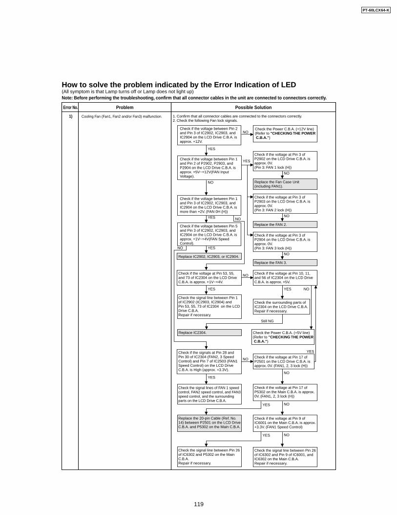
Cooling Fan (Fan1, Fan2 and/or Fan3) malfunction. 1)
How to solve the problem indicated by the Error Indication of LED(All symptom is that Lamp turns off or Lamp does not light up)Note: Before performing the troubleshooting, confirm that all connector cables in the unit are connected to connectors correctly.
Error No. Problem Possible Solution
Check if the voltage between Pin 2 and Pin 3 of IC2902, IC2903, and IC2904 on the LCD Drive C.B.A. is approx. +12V.
Check if the voltage between Pin 1 and Pin 3 of IC2902, IC2903, and IC2904 on the LCD Drive C.B.A. is more than +2V. (FAN 0H (H))
Check if the voltage between Pin 5 and Pin 3 of IC2902, IC2903, and IC2904 on the LCD Drive C.B.A. is approx. +1V~+4V(FAN Speed Control).
Check if the voltage between Pin 1 and Pin 2 of P2902, P2903, and P2904 on the LCD Drive C.B.A. is approx. +5V~+12V(FAN Input Voltage).
Check if the voltage at Pin 3 of P2902 on the LCD Drive C.B.A. is approx. 0V.(Pin 3: FAN 1 lock (H))
Replace the Fan Case Unit (including FAN1).
Check the Power C.B.A. (+12V line)(Refer to "CHECKING THE POWER C.B.A.")
NO
NO
YES
YES
YES
Check if the voltage at Pin 53, 55, and 73 of IC2304 on the LCD Drive C.B.A. is approx. +1V~+4V.
YES
NO
NO
NO
NO
1. Confirm that all connector cables are connected to the connectors correctly.2. Check the following Fan lock signals.
NO
Check if the voltage at Pin 3 of P2903 on the LCD Drive C.B.A. is approx. 0V.(Pin 3: FAN 2 lock (H))
Replace the FAN 2.
NONO
Replace IC2902, IC2903, or IC2904.
YES
Replace IC2304.
Check if the voltage at Pin 3 of P2904 on the LCD Drive C.B.A. is approx. 0V.(Pin 3: FAN 3 lock (H))
Check if the signals at Pin 28 and Pin 30 of IC2304 (FAN2, 3 Speed Control) and Pin 7 of IC2503 (FAN1 Speed Control) on the LCD Drive C.B.A. is High (approx. +3.3V).
NO
Still NG
NO
Check if the voltage at Pin 10, 11, and 56 of IC2304 on the LCD Drive C.B.A. is approx. +5V.
Check if the voltage at Pin 17 of P2501 on the LCD Drive C.B.A. is approx. 0V. (FAN1, 2, 3 lock (H))
Check if the voltage at Pin 17 of P5302 on the Main C.B.A. is approx. 0V. (FAN1, 2, 3 lock (H))
Check if the voltage at Pin 9 of IC6001 on the Main C.B.A. is approx. +3.3V. (FAN1 Speed Control)
NO
Check the signal line between Pin 26 of IC6302 and Pin 9 of IC6001, and IC6302 on the Main C.B.A.Repair if necessary.
Check the signal line between Pin 1 of IC2902 (IC2903, IC2904) and Pin 53, 55, 73 of IC2304 on the LCD Drive C.B.A.Repair if necessary.
YES
YES
Check the signal lines of FAN 1 speed control, FAN2 speed control, and FAN3 speed control, and the surrounding parts on the LCD Drive C.B.A.
Check the signal line between Pin 26 of IC6302 and P5302 on the MainC.B.A.Repair if necessary.
Replace the 20-pin Cable (Ref. No. 14) between P2501 on the LCD Drive C.B.A. and P5302 on the Main C.B.A.
YES
YES
Check the surrounding parts of IC2304 on the LCD Drive C.B.A.Repair if necessary.
Check the Power C.B.A. (+5V line)(Refer to "CHECKING THE POWER C.B.A.")
Replace the FAN 3.
NO
YES
PT-60LCX64-K
119
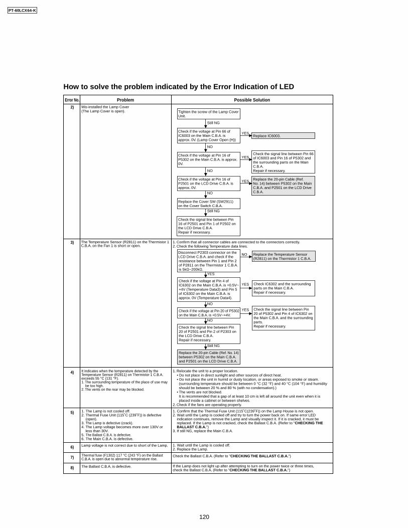
Mis-installed the Lamp Cover (The Lamp Cover is open).
The Temperature Sensor (R2811) on the Thermistor 1 C.B.A. on the Fan 1 is short or open.
Lamp voltage is not correct due to short of the Lamp.
The Ballast C.B.A. is defective.
1. The Lamp is not cooled off.2. Thermal Fuse Unit (115˚C (239˚F)) is defective
(open).3. The Lamp is defective (crack).4. The Lamp voltage becomes more over 130V or less than 30V.5. The Ballast C.B.A. is defective.6. The Main C.B.A. is defective.
1. Confirm that the Thermal Fuse Unit (115˚C(239˚F)) on the Lamp House is not open.2. Wait until the Lamp is cooled off and try to turn the power back on. If same error LED indication continues, remove the Lamp and visually inspect it. If it is cracked, it must be replaced. If the Lamp is not cracked, check the Ballast C.B.A. (Refer to "CHECKING THE BALLAST C.B.A.")3. If still NG, replace the Main C.B.A.
1. Wait until the Lamp is cooled off.2. Replace the Lamp.
Check the Ballast C.B.A. (Refer to "CHECKING THE BALLAST C.B.A.")
If the Lamp does not light up after attempting to turn on the power twice or three times, check the Ballast C.B.A. (Refer to "CHECKING THE BALLAST C.B.A.")
How to solve the problem indicated by the Error Indication of LED
Problem Possible Solution2)
3)
4)
6)
7)
8)
5)
1. Relocate the unit to a proper location. • Do not place in direct sunlight and other sources of direct heat. • Do not place the unit in humid or dusty location, or areas exposed to smoke or steam. (surrounding temperature should be between 0 °C (32 °F) and 40 °C (104 °F) and humidity should be between 20 % and 80 % (with no condensation).) • The vents are not blocked. It is recommended that a gap of at least 10 cm is left all around the unit even when it is placed inside a cabinet or between shelves.2. Check if the fans are operating properly.
It indicates when the temperature detected by the Temperature Sensor (R2811) on Thermistor 1 C.B.A. exceeds 55 °C (131 °F).1. The surrounding temperature of the place of use may be too high.2. The vents on the rear may be blocked.
Thermal fuse (F1302) 117 °C (243 °F) on the Ballast C.B.A. is open due to abnormal temperature rise.
Error No.
Tighten the screw of the Lamp Cover Unit.
Check if the voltage at Pin 66 of IC6003 on the Main C.B.A. is approx. 0V. (Lamp Cover Open (H))
Replace IC6003.
Still NG
Still NG
NO
1. Confirm that all connector cables are connected to the connectors correctly.2. Check the following Temperature data lines.
Check the signal line between Pin 66 of IC6003 and Pin 16 of P5302 and the surrounding parts on the Main C.B.A.Repair if necessary.
Replace the 20-pin Cable (Ref. No. 14) between P5302 on the Main C.B.A. and P2501 on the LCD Drive C.B.A.
NO
NO
Check if the voltage at Pin 16 of P2501 on the LCD Drive C.B.A. is approx. 0V.
Check if the voltage at Pin 16 of P5302 on the Main C.B.A. is approx. 0V.
Replace the Cover SW (SW2911) on the Cover Switch C.B.A.
Check the signal line between Pin 16 of P2501 and Pin 1 of P2502 on the LCD Drive C.B.A.Repair if necessary.
YES
YES
Disconnect P2303 connector on the LCD Drive C.B.A. and check if the resistance between Pin 1 and Pin 2 of P2811 on the Thermistor 1 C.B.A. is 5kΩ~200kΩ.
Check if the voltage at Pin 4 of IC6302 on the Main C.B.A. is +0.5V~ +4V (Temperature Data3) and Pin 5 of IC6302 on the Main C.B.A. is approx. 0V (Temperature Data4).
Check if the voltage at Pin 20 of P5302 on the Main C.B.A. is +0.5V~+4V.
Check the signal line between Pin 20 of P5302 and Pin 4 of IC6302 on the Main C.B.A. and the surrounding parts.Repair if necessary.
Replace the Temperature Sensor (R2811) on the Thermistor 1 C.B.A.
NO
NO
YES
Check the signal line between Pin 20 of P2501 and Pin 2 of P2303 on the LCD Drive C.B.A. Repair if necessary.
Replace the 20-pin Cable (Ref. No. 14) between P5302 on the Main C.B.A. and P2501 on the LCD Drive C.B.A.
Still NG
NO
YES
Check IC6302 and the surrounding parts on the Main C.B.A.Repair if necessary.
YES
YES
PT-60LCX64-K
120
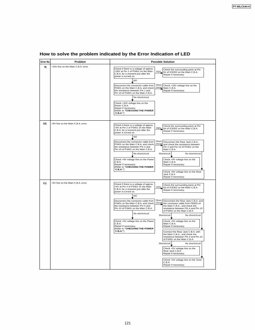
+33V line on the Main C.B.A. error.
How to solve the problem indicated by the Error Indication of LED
Problem Possible Solution
9)
10)
11)
+9V line on the Main C.B.A. error.
+5V line on the Main C.B.A. error.
Error No.
Check if there is a voltage of approx. +30V at Pin 1 of P3401 on the Main C.B.A. for a moment just after the power is turned on.
Disconnect the connector cable from P3401 on the Main C.B.A. and check the resistance between Pin 1 and Pin 10 of P3401 on the Main C.B.A.
No shortcircuit
Short-circuit
Check the surrounding parts at Pin 61 of IC6302 on the Main C.B.A.Repair if necessary
NO
Check +33V voltage line on the Power C.B.A.Repair if necessary.(Refer to "CHECKING THE POWER C.B.A.")
Check +33V voltage line on the Main C.B.A.Repair if necessary.
YES
Check if there is a voltage of approx. +9V at Pin 2 of P3401 on the Main C.B.A. for a moment just after the power is turned on.
Disconnect the connector cable from P3401 on the Main C.B.A. and check the resistance between Pin 2 and Pin 10 of P3401 on the Main C.B.A.
No shortcircuit No shortcircuit
Short-circuit
Shortcircuit
No shortcircuitShortcircuit
No shortcircuitShortcircuit
Check the surrounding parts at Pin 64 of IC6302 on the Main C.B.A.Repair if necessary.
NO
Check +9V voltage line on the Power C.B.A.Repair if necessary.(Refer to "CHECKING THE POWER C.B.A.")
Check +9V voltage line on the Main C.B.A.Repair if necessary.
Check +9V voltage line on the Rear Jack C.B.A.Repair if necessary.
YES
Disconnect the Rear Jack C.B.A., and check the resistance between Pin 2 and Pin 10 of P3401 on the Main C.B.A.
Check if there is a voltage of approx. +5V at Pin 4 of P3401 on the Main C.B.A. for a moment just after the power is turned on.
Disconnect the connector cable from P3401 on the Main C.B.A. and check the resistance between Pin 4 and Pin 10 of P3401 on the Main C.B.A.
No shortcircuit
Short-circuit
Check the surrounding parts at Pin 63 of IC6302 on the Main C.B.A.Repair if necessary.
NO
Check +5V voltage line on the Power C.B.A.Repair if necessary.(Refer to "CHECKING THE POWER C.B.A.")
Check +5V voltage line on the Tuner C.B.A.Repair if necessary.
Check +5V voltage line on the Main C.B.A.Repair if necessary.
Check +5V voltage line on the Rear Jack C.B.A.Repair if necessary.
Connect the Rear Jack C.B.A. with the Main C.B.A., and check the resistance between Pin 4 and Pin 10 of P3401 on the Main C.B.A.
YES
Disconnect the Rear Jack C.B.A. and the connector cable from P6003 on the Main C.B.A., and check the resistance between Pin 4 and Pin 10 of P3401 on the Main C.B.A.
PT-60LCX64-K
121
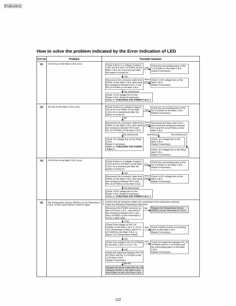
The Temperature Sensor (R2821) on the Thermistor 2 C.B.A. on the Lamp House is short or open.
How to solve the problem indicated by the Error Indication of LED
Problem Possible Solution
12)
15)
13)
14)
+3.3V line on the Main C.B.A. error.
-5V line on the Main C.B.A. error.
+6.5V line on the Main C.B.A. error.
Error No.
Check if there is a voltage of approx. +30V at Pin 6 and 7 of P3401 on the Main C.B.A. for a moment just after the power is turned on.
Disconnect the connector cable from P3401 on the Main C.B.A. and check the resistance between Pin 6, 7 and Pin 10 of P3401 on the Main C.B.A.
No shortcircuit
Short-circuit
Check the surrounding parts at Pin 7 of IC6302 on the Main C.B.A.Repair if necessary.
NO
Check +3.3V voltage line on the Power C.B.A. Repair if necessary.(Refer to "CHECKING THE POWER C.B.A.")
Check +3.3V voltage line on the Main C.B.A.Repair if necessary.
YES
Check if there is a voltage of approx. -5V at Pin 8 of P3401 on the Main C.B.A. for a moment just after the power is turned on.
Disconnect the connector cable from P3401 on the Main C.B.A. and check the resistance between Pin 8 and Pin 10 of P3401 on the Main C.B.A.
No shortcircuit No shortcircuit
Short-circuit
Shortcircuit
Check the surrounding parts at Pin 62 of IC6302 on the Main C.B.A.Repair if necessary.
NO
Check -5V voltage line on the Power C.B.A.Repair if necessary.(Refer to "CHECKING THE POWER C.B.A.")
Check -5V voltage line on the Main C.B.A.Repair if necessary.
Check -5V voltage line on the Rear Jack C.B.A.Repair if necessary.
YES
Disconnect the Rear Jack C.B.A., and check the resistance between Pin 8 and Pin 10 of P3401 on the Main C.B.A.
Check if there is a voltage of approx. +6.5V at Pin 5 of P3401 on the Main C.B.A. for a moment just after the power is turned on.
Disconnect the connector cable from P3401 on the Main C.B.A. and check the resistance between Pin 5 and Pin 10 of P3401 on the Main C.B.A.
No shortcircuit
Short-circuit
Check the surrounding parts at Pin 60 of IC6302 on the Main C.B.A.Repair if necessary.
NO
Check +6.5V voltage line on the Power C.B.A. Repair if necessary.(Refer to "CHECKING THE POWER C.B.A.")
Check +6.5V voltage line on the Main C.B.A.Repair if necessary.
YES
Disconnect the P2304 connector on the LCD Drive C.B.A., and check if the resistance between Pin 1 and Pin 2 of P2821 on the Thermistor 2 C.B.A. is 5kΩ~1MΩ.
Check if the voltage at Pin 2 of IC6302 on the Main C.B.A. is +0.1V~+4V (Temperature Data1) and Pin 3 of IC6302 on the Main C.B.A. is approx. 0V (Temperature Data2).
NO
Replace the Temperature Sensor (R2821) on the Thermistor 2 C.B.A.
NO
Check if the voltage at Pin 19 of P5302 on the Main C.B.A. is +0.1V~+4V.
NO
Check IC6302 and the surroundingparts on the Main C.B.A.Repair if necessary.
YES
YES
Check the signal line between Pin 19 of P5302 and Pin 2 of IC6302 and the surrounding parts on the Main C.B.A.Repair if necessary.
YES
1. Confirm that all connector cables are connected to the connectors correctly.2. Check the following Temperature data lines.
Check the signal line between Pin 19 of P2501 and Pin 2 of P2304 on the LCD Drive C.B.A.Repair if necessary.
Still NG
Replace the 20-pin Cable (Ref. No. 14) between P5302 on the Main C.B.A. and P2501 on the LCD Drive C.B.A.
PT-60LCX64-K
122
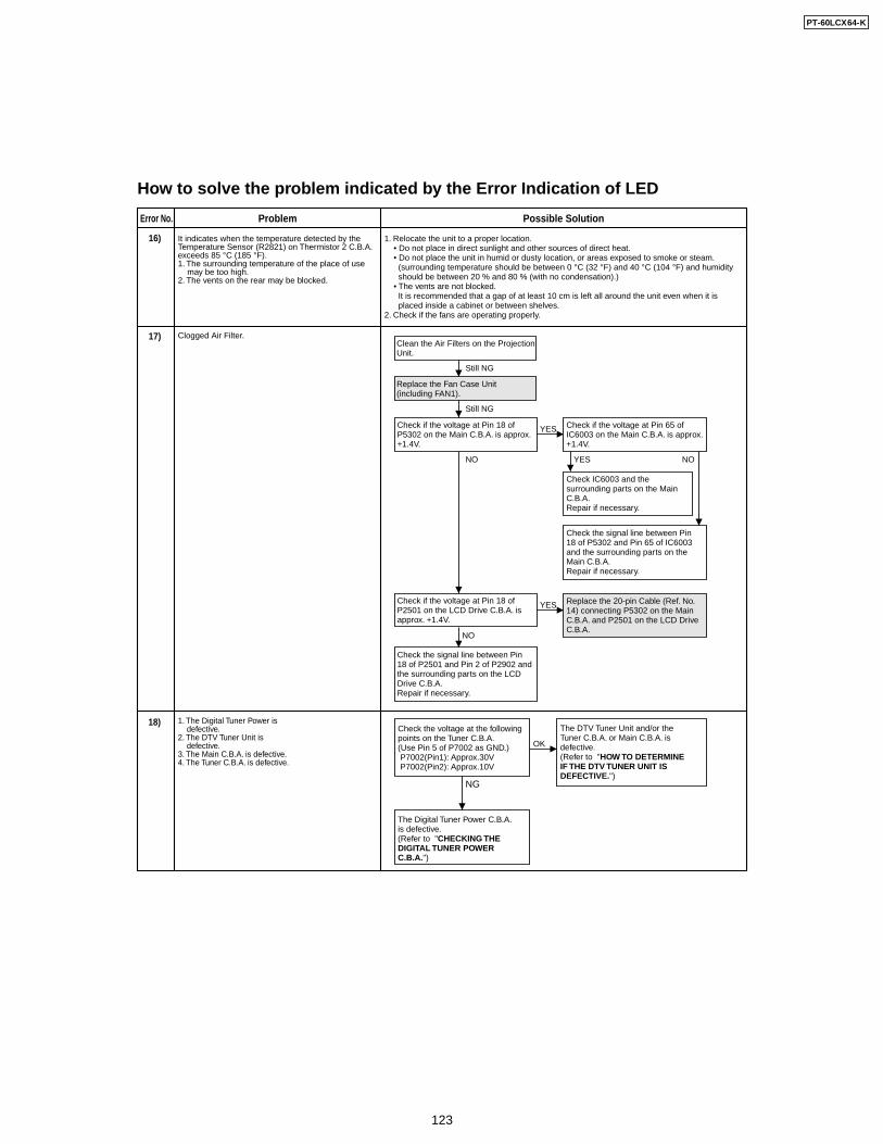
Clogged Air Filter.
How to solve the problem indicated by the Error Indication of LED
Problem Possible Solution
17)
16) 1. Relocate the unit to a proper location. • Do not place in direct sunlight and other sources of direct heat. • Do not place the unit in humid or dusty location, or areas exposed to smoke or steam. (surrounding temperature should be between 0 °C (32 °F) and 40 °C (104 °F) and humidity should be between 20 % and 80 % (with no condensation).) • The vents are not blocked. It is recommended that a gap of at least 10 cm is left all around the unit even when it is placed inside a cabinet or between shelves.2. Check if the fans are operating properly.
It indicates when the temperature detected by the Temperature Sensor (R2821) on Thermistor 2 C.B.A. exceeds 85 °C (185 °F).1. The surrounding temperature of the place of use may be too high.2. The vents on the rear may be blocked.
Error No.
18) 1. The Digital Tuner Power is defective.2. The DTV Tuner Unit is defective.3. The Main C.B.A. is defective.4. The Tuner C.B.A. is defective.
Clean the Air Filters on the Projection Unit.
Check if the voltage at Pin 18 of P5302 on the Main C.B.A. is approx.+1.4V.
Check if the voltage at Pin 65 of IC6003 on the Main C.B.A. is approx.+1.4V.
Check the signal line between Pin 18 of P5302 and Pin 65 of IC6003 and the surrounding parts on the Main C.B.A.Repair if necessary.
Check IC6003 and the surrounding parts on the Main C.B.A. Repair if necessary.
Check if the voltage at Pin 18 of P2501 on the LCD Drive C.B.A. is approx. +1.4V.
Still NG
Replace the Fan Case Unit (including FAN1).
Still NG
NO YES NO
Check the signal line between Pin 18 of P2501 and Pin 2 of P2902 and the surrounding parts on the LCD Drive C.B.A.Repair if necessary.
NO
YES
Replace the 20-pin Cable (Ref. No. 14) connecting P5302 on the Main C.B.A. and P2501 on the LCD Drive C.B.A.
YES
OK
NG
Check the voltage at the following points on the Tuner C.B.A.(Use Pin 5 of P7002 as GND.) P7002(Pin1): Approx.30V P7002(Pin2): Approx.10V
The Digital Tuner Power C.B.A. is defective.(Refer to "CHECKING THE DIGITAL TUNER POWER C.B.A.")
The DTV Tuner Unit and/or the Tuner C.B.A. or Main C.B.A. is defective.(Refer to "HOW TO DETERMINE IF THE DTV TUNER UNIT IS DEFECTIVE.")
PT-60LCX64-K
123
LAMP DOES NOT LIGHT UP
Plug in the AC Cord.
Note: :1. Before doing this troubleshooting, confirm that all
connector cables in the unit are connected to the connectors correctly.
2. When doing troubleshooting over again, be sure to turn the power off and unplug the AC Cord.
Is there a snap sound to turn the Relay ON?(Relay: RL801 on the Power C.B.A.)
YES
YES
NO
NO
Does the Power LED (D6701) on theOperation C.B.A. light up red?
YES
NODoes the Power LED (D6701) on the Operation C.B.A. flash green?
The Power C.B.A. is defective.(Refer to "CHECKING THE POWER C.B.A.")
There is a problem with the Main C.B.A. Check the LAMP ON (H) signal line between pin2 of P6002 and pin44 of IC6003, and IC6003 on the Main C.B.A. Repair if necessary.
Turn the power ON.
OK
NG
Power LED flashes green all the time.
Check the voltage at the following points on the Tuner C.B.A.(Use Pin 5 of P7002 as GND.) P7002(Pin1): Approx.30V P7002(Pin2): Approx.10V
Error 1), 2), 3), 4), 15), 16), 17), or 18) occurs.(Refer to "ERROR INDICATION INFORMATION")
Refer to "How to solve the problem indicated by the Error Indication of LED." And then, perform troubleshooting.
Refer to "How to solve the problem indicated by the Error Indication of LED." And then, perform troubleshooting.
Error 5), 6), 7), or 8) occurs.(Refer to "ERROR INDICATION INFORMATION") <<Ballast Error>>
The Ballast C.B.A. is defective.(Refer to "CHECKING THE BALLAST C.B.A.")
The Digital Tuner Power C.B.A. is defective.(Refer to "CHECKING THE DIGITAL TUNER POWER C.B.A.")
The DTV Tuner Unit and/or the Tuner C.B.A. or Main C.B.A. is defective.(Refer to "HOW TO DETERMINE IF THE DTV TUNER UNIT IS DEFECTIVE.")
Error 9), 10), 11), 12), 13), or 14)occurs.(Refer to "ERROR INDICATION INFORMATION") <<Abnormal Voltage Error>>
LAMP DOES NOT LIGHT UP
Resistance for Power Line of Power C.B.A.
Plug in the AC Cord.
Note: :1. Before doing this troubleshooting, confirm that all
connector cables in the unit are connected to the connectors correctly.
2. When doing troubleshooting over again, be sure to turn the power off and unplug the AC Cord.
Is there a snap sound to turn the Relay ON?(Relay: RL801 on the Power C.B.A.)
YES
YES
OK
NG
NO
NO
Does the Power LED (D6701) on theOperation C.B.A. light up red?
YES
NODoes the Power LED (D6701) on the Operation C.B.A. flash green?
Power LED flashes green all the time.
Check the voltage at the following points on the Tuner C.B.A.(Use Pin 5 of P7002 as GND.) P7002(Pin1): Approx.30V P7002(Pin2): Approx.10V
Power Line
REG 30V TP1008 More than 50 ohm
REG 9V TP1006 More than 50 ohm
STBY 9V TP810 More than 50 ohm
REG 5V TP1014 More than 50 ohm
REG 6.5V TP1010 More than 50 ohm
REG 3.3V TP1009 More than 50 ohm
REG -5V TP1007 More than 50 ohm
UNREG 17V TP1012 More than 50 ohm
UNREG 12V Pin2 of P1008 More than 50 ohm
FAN +B TP1013 More than 50 ohm
AMP +16V TP1004 More than 50 ohm
AMP -16V TP1003 More than 50 ohm
Check Point Resistance
Error 1), 2), 3), 4), 15), 16), 17), or 18) occurs.(Refer to "ERROR INDICATION INFORMATION")
Refer to "How to solve the problem indicated by the Error Indication of LED." And then, perform troubleshooting.
Refer to "How to solve the problem indicated by the Error Indication of LED." And then, perform troubleshooting.
Note: When measuring the resistance of above points on Power C.B.A.:1. Turn off the unit and the unplug the AC Cord.2. Disconnect the all connector cables of Power C.B.A.3. Use TP1005 as a Ground.
Error 5), 6), 7), or 8) occurs.(Refer to "ERROR INDICATION INFORMATION") <<Ballast Error>>
The Ballast C.B.A. is defective.(Refer to "CHECKING THE BALLAST C.B.A.")
The Digital Tuner Power C.B.A. is defective.(Refer to "CHECKING THE DIGITAL TUNER POWER C.B.A.")
The DTV Tuner Unit and/or the Tuner C.B.A. or Main C.B.A. is defective.(Refer to "HOW TO DETERMINE IF THE DTV TUNER UNIT IS DEFECTIVE.")
The Power C.B.A. is defective.(Refer to "CHECKING THE POWER C.B.A.")
Error 9), 10), 11), 12), 13), or 14)occurs.(Refer to "ERROR INDICATION INFORMATION") <<Abnormal Voltage Error>>
There is a problem with the Main C.B.A. Check the LAMP ON (H) signal line between pin2 of P6002 and pin44 of IC6003, and IC6003 on the Main C.B.A. Repair if necessary.
Turn the power ON.
PT-60LCX64-K
124
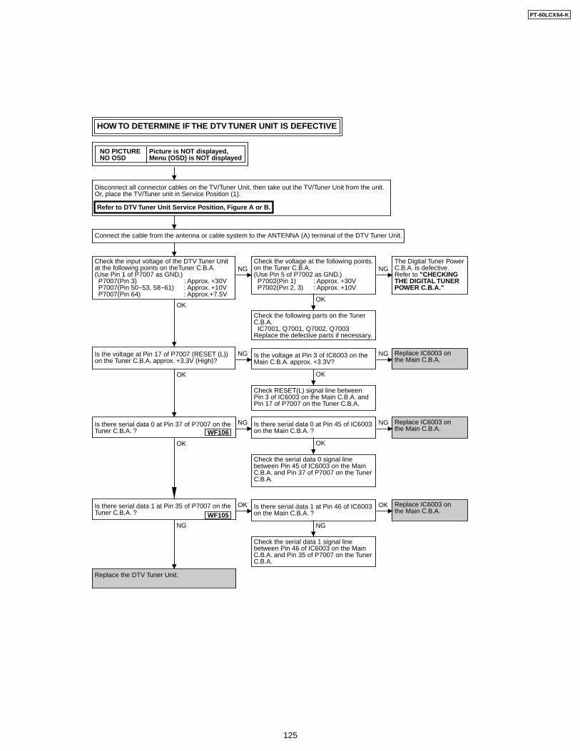
HOW TO DETERMINE IF THE DTV TUNER UNIT IS DEFECTIVE
Disconnect all connector cables on the TV/Tuner Unit, then take out the TV/Tuner Unit from the unit.Or, place the TV/Tuner unit in Service Position (1).
Refer to DTV Tuner Unit Service Position, Figure A or B.
Picture is NOT displayed,Menu (OSD) is NOT displayed
Connect the cable from the antenna or cable system to the ANTENNA (A) terminal of the DTV Tuner Unit.
Check the input voltage of the DTV Tuner Unit at the following points on theTuner C.B.A. (Use Pin 1 of P7007 as GND.) P7007(Pin 3) : Approx. +30V P7007(Pin 50~53, 58~61) : Approx. +10V P7007(Pin 64) : Approx.+7.5V
Is the voltage at Pin 17 of P7007 (RESET (L))on the Tuner C.B.A. approx. +3.3V (High)?
Replace the DTV Tuner Unit.
NG
OKOK
OK
NG
NO PICTURENO OSD
Is there serial data 0 at Pin 37 of P7007 on the Tuner C.B.A. ?
OK
Is there serial data 1 at Pin 35 of P7007 on the Tuner C.B.A. ?
Check the voltage at the following points.on the Tuner C.B.A.(Use Pin 5 of P7002 as GND.) P7002(Pin 1) : Approx. +30V P7002(Pin 2, 3) : Approx. +10V
Check the following parts on the Tuner C.B.A. IC7001, Q7001, Q7002, Q7003Replace the defective parts if necessary.
NGThe Digital Tuner Power C.B.A. is defective.Refer to "CHECKING THE DIGITAL TUNERPOWER C.B.A."
OK
NG
NG
Is the voltage at Pin 3 of IC6003 on theMain C.B.A. approx. +3.3V?
Check RESET(L) signal line betweenPin 3 of IC6003 on the Main C.B.A. and Pin 17 of P7007 on the Tuner C.B.A.
NG Replace IC6003 onthe Main C.B.A.
OK
Is there serial data 0 at Pin 45 of IC6003 on the Main C.B.A. ?
Check the serial data 0 signal line between Pin 45 of IC6003 on the Main C.B.A. and Pin 37 of P7007 on the TunerC.B.A.
NG Replace IC6003 onthe Main C.B.A.
OK
NG
Is there serial data 1 at Pin 46 of IC6003 on the Main C.B.A. ?
Check the serial data 1 signal line between Pin 46 of IC6003 on the Main C.B.A. and Pin 35 of P7007 on the TunerC.B.A.
OK Replace IC6003 onthe Main C.B.A.
WF106
WF105
PT-60LCX64-K
125
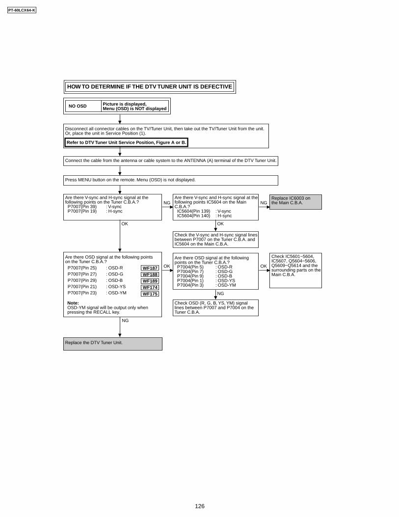
Disconnect all connector cables on the TV/Tuner Unit, then take out the TV/Tuner Unit from the unit.Or, place the unit in Service Position (1).
Refer to DTV Tuner Unit Service Position, Figure A or B.
Picture is displayed, Menu (OSD) is NOT displayed
Are there V-sync and H-sync signal at thefollowing points on the Tuner C.B.A.? P7007(Pin 39) : V-sync P7007(Pin 19) : H-sync
Are there OSD signal at the following pointson the Tuner C.B.A.? P7007(Pin 25) : OSD-R P7007(Pin 27) : OSD-G P7007(Pin 29) : OSD-B P7007(Pin 21) : OSD-YS P7007(Pin 23) : OSD-YM
Note:OSD-YM signal will be output only whenpressing the RECALL key.
Replace the DTV Tuner Unit.
OK OK
NG
NO OSD
Are there V-sync and H-sync signal at thefollowing points IC5604 on the Main C.B.A.? IC5604(Pin 139) : V-sync IC5604(Pin 140) : H-sync
Check the V-sync and H-sync signal linesbetween P7007 on the Tuner C.B.A. and IC5604 on the Main C.B.A.
NG
OK
Are there OSD signal at the following points on the Tuner C.B.A.? P7004(Pin 5) : OSD-R P7004(Pin 7) : OSD-G P7004(Pin 9) : OSD-B P7004(Pin 1) : OSD-YS P7004(Pin 3) : OSD-YM
Check OSD (R, G, B, YS, YM) signal lines between P7007 and P7004 on the Tuner C.B.A.
OK
Check IC5601~5604,IC5607, Q5604~5606,Q5609~Q5614 and thesurrounding parts on theMain C.B.A.
Replace IC6003 onthe Main C.B.A.
NG
NG
WF187WF188WF189WF174WF175
Connect the cable from the antenna or cable system to the ANTENNA (A) terminal of the DTV Tuner Unit.
Press MENU button on the remote. Menu (OSD) is not displayed.
HOW TO DETERMINE IF THE DTV TUNER UNIT IS DEFECTIVE
PT-60LCX64-K
126
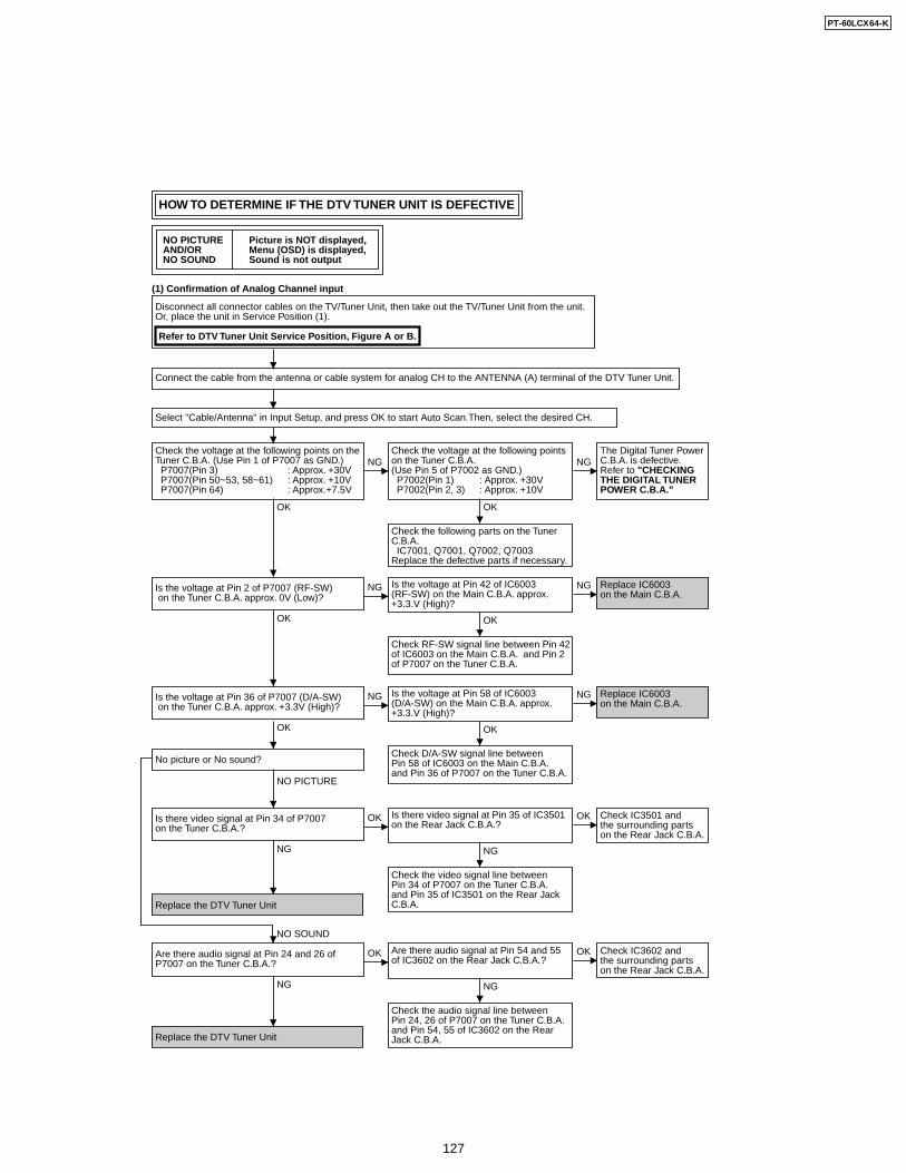
HOW TO DETERMINE IF THE DTV TUNER UNIT IS DEFECTIVE
Disconnect all connector cables on the TV/Tuner Unit, then take out the TV/Tuner Unit from the unit.Or, place the unit in Service Position (1).
Refer to DTV Tuner Unit Service Position, Figure A or B.
(1) Confirmation of Analog Channel input
Picture is NOT displayed,Menu (OSD) is displayed,Sound is not output
Connect the cable from the antenna or cable system for analog CH to the ANTENNA (A) terminal of the DTV Tuner Unit.
Check the voltage at the following points on theTuner C.B.A. (Use Pin 1 of P7007 as GND.) P7007(Pin 3) : Approx. +30V P7007(Pin 50~53, 58~61) : Approx. +10V P7007(Pin 64) : Approx.+7.5V
Is the voltage at Pin 2 of P7007 (RF-SW) on the Tuner C.B.A. approx. 0V (Low)?
OK OK
OK
NG
NO PICTUREAND/OR NO SOUND
Select "Cable/Antenna" in Input Setup, and press OK to start Auto Scan.Then, select the desired CH.
Is the voltage at Pin 36 of P7007 (D/A-SW) on the Tuner C.B.A. approx. +3.3V (High)?
OK
NO PICTURE
NO SOUND
No picture or No sound?
Check the voltage at the following pointson the Tuner C.B.A.(Use Pin 5 of P7002 as GND.) P7002(Pin 1) : Approx. +30V P7002(Pin 2, 3) : Approx. +10V
Check the following parts on the Tuner C.B.A. IC7001, Q7001, Q7002, Q7003Replace the defective parts if necessary.
NGThe Digital Tuner Power C.B.A. is defective.Refer to "CHECKING THE DIGITAL TUNERPOWER C.B.A."
OK
NG Is the voltage at Pin 42 of IC6003 (RF-SW) on the Main C.B.A. approx. +3.3.V (High)?
Check RF-SW signal line between Pin 42 of IC6003 on the Main C.B.A. and Pin 2 of P7007 on the Tuner C.B.A.
OK
Check D/A-SW signal line between Pin 58 of IC6003 on the Main C.B.A. and Pin 36 of P7007 on the Tuner C.B.A.
NG Replace IC6003 on the Main C.B.A.
NG Is the voltage at Pin 58 of IC6003 (D/A-SW) on the Main C.B.A. approx. +3.3.V (High)?
NG Replace IC6003 on the Main C.B.A.
Is there video signal at Pin 34 of P7007 on the Tuner C.B.A.?
NG
Replace the DTV Tuner Unit
NG
Check the video signal line between Pin 34 of P7007 on the Tuner C.B.A. and Pin 35 of IC3501 on the Rear Jack C.B.A.
OK Is there video signal at Pin 35 of IC3501 on the Rear Jack C.B.A.?
OK Check IC3501 and the surrounding parts on the Rear Jack C.B.A.
Are there audio signal at Pin 24 and 26 of P7007 on the Tuner C.B.A.?
NG
Replace the DTV Tuner Unit
NG
Check the audio signal line between Pin 24, 26 of P7007 on the Tuner C.B.A. and Pin 54, 55 of IC3602 on the Rear Jack C.B.A.
OK Are there audio signal at Pin 54 and 55 of IC3602 on the Rear Jack C.B.A.?
OK Check IC3602 and the surrounding parts on the Rear Jack C.B.A.
PT-60LCX64-K
127
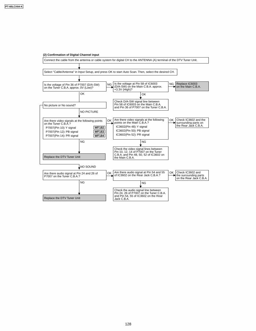
Is the voltage of Pin 36 of P7007 (D/A-SW) on the Tuner C.B.A. approx. 0V (Low)?
OK
Are there video signals at the following pointson the Tuner C.B.A.? P7007(Pin 10): Y signal P7007(Pin 12): PB signal P7007(Pin 14): PR signal
NG
OK
NG Is the voltage at Pin 58 of IC6003 (D/A-SW) on the Main C.B.A. approx. +3.3V (High)?
Check D/A-SW signal line between Pin 58 of IC6003 on the Main C.B.A. and Pin 36 of P7007 on the Tuner C.B.A.
NG
Check the video signal lines between Pin 10, 12, 14 of P7007 on the Tuner C.B.A. and Pin 48, 50, 52 of IC3602 on the Main C.B.A.
NG Replace IC6003 on the Main C.B.A.
OK Are there video signals at the following points on the Main C.B.A.? IC3602(Pin 48): Y signal IC3602(Pin 50): PB signal IC3602(Pin 52): PR signal
OK Check IC3602 and the surrounding parts onthe Rear Jack C.B.A.
Replace the DTV Tuner Unit
Connect the cable from the antenna or cable system for digital CH to the ANTENNA (A) terminal of the DTV Tuner Unit.
Select "Cable/Antenna" in Input Setup, and press OK to start Auto Scan. Then, select the desired CH.
WF184WF183WF182
(2) Confirmation of Digital Channel input
NO PICTURE
No picture or No sound?
Are there audio signal at Pin 24 and 26 of P7007 on the Tuner C.B.A.?
NG
Replace the DTV Tuner Unit
NG
Check the audio signal line between Pin 24, 26 of P7007 on the Tuner C.B.A. and Pin 54, 55 of IC3602 on the Rear Jack C.B.A.
OK Are there audio signal at Pin 54 and 55 of IC3602 on the Rear Jack C.B.A.?
OK Check IC3602 and the surrounding parts on the Rear Jack C.B.A.
NO SOUND
PT-60LCX64-K
128
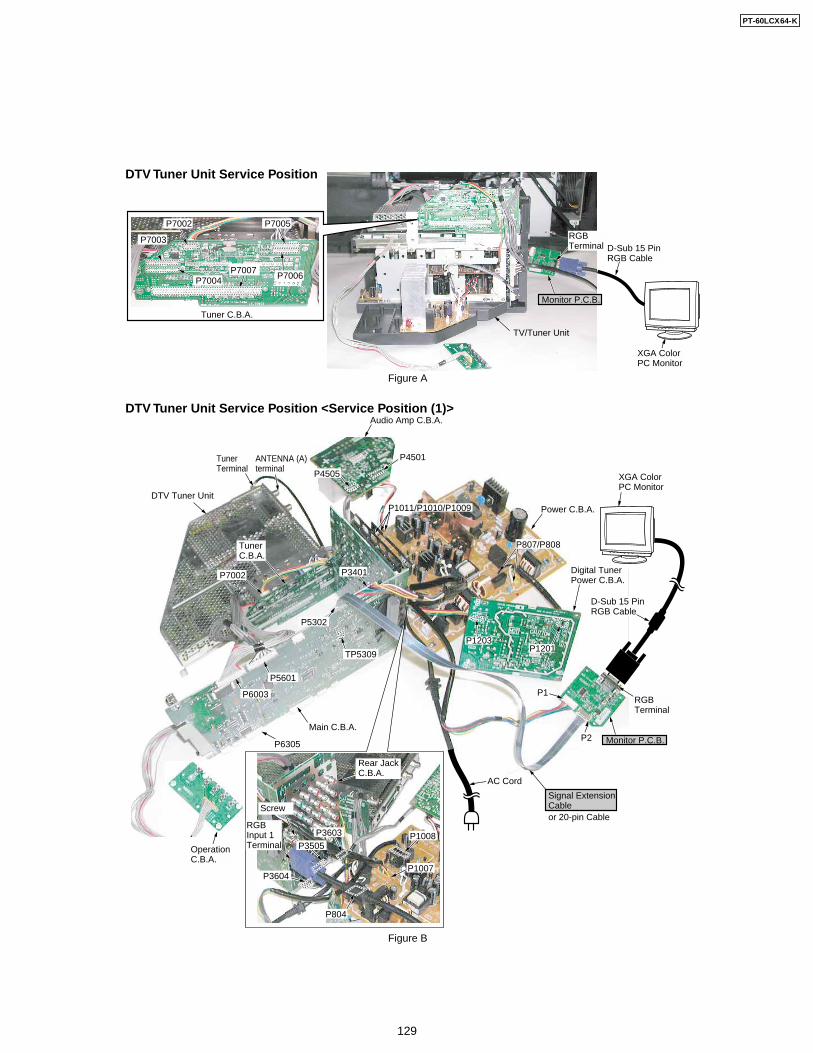
DTV Tuner Unit Service Position
DTV Tuner Unit Service Position <Service Position (1)>
Digital TunerPower C.B.A.
Monitor P.C.B.
Monitor P.C.B.
D-Sub 15 PinRGB Cable
XGA ColorPC Monitor
XGA ColorPC Monitor
Audio Amp C.B.A.
DTV Tuner Unit
OperationC.B.A.
TunerC.B.A.
P7002
Main C.B.A.
AC Cord
D-Sub 15 PinRGB Cable
Power C.B.A.
P2
P1
TV/Tuner Unit
RGBTerminal
RGBTerminal
Signal ExtensionCableor 20-pin Cable
TunerTerminal
ANTENNA (A)terminal
P6305
P6003
P5601
P5302
P4501
P4505
P1201P1203
P3401
TP5309
P1011/P1010/P1009
P807/P808
P3505
P3603
P3604
Screw
P1008
P1007
P804
RGB Input 1Terminal
Rear JackC.B.A.
Figure A
Figure B
P7007
P7005
P7006
P7002
P7003
P7004
Tuner C.B.A.
PT-60LCX64-K
129
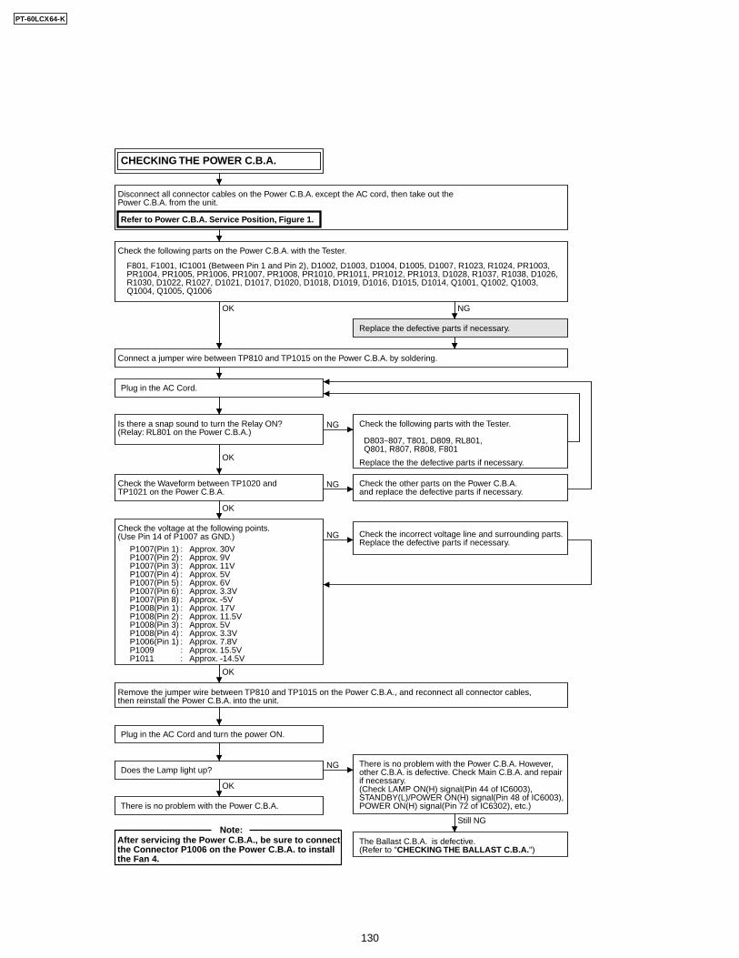
CHECKING THE POWER C.B.A.
Disconnect all connector cables on the Power C.B.A. except the AC cord, then take out the Power C.B.A. from the unit.
Refer to Power C.B.A. Service Position, Figure 1.
Check the following parts on the Power C.B.A. with the Tester.
Connect a jumper wire between TP810 and TP1015 on the Power C.B.A. by soldering.
Replace the defective parts if necessary.
Check the following parts with the Tester.
D803~807, T801, D809, RL801, Q801, R807, R808, F801
Replace the the defective parts if necessary.
F801, F1001, IC1001 (Between Pin 1 and Pin 2), D1002, D1003, D1004, D1005, D1007, R1023, R1024, PR1003, PR1004, PR1005, PR1006, PR1007, PR1008, PR1010, PR1011, PR1012, PR1013, D1028, R1037, R1038, D1026, R1030, D1022, R1027, D1021, D1017, D1020, D1018, D1019, D1016, D1015, D1014, Q1001, Q1002, Q1003, Q1004, Q1005, Q1006
P1007(Pin 1)P1007(Pin 2)P1007(Pin 3)P1007(Pin 4)P1007(Pin 5)P1007(Pin 6)P1007(Pin 8)P1008(Pin 1)P1008(Pin 2)P1008(Pin 3)P1008(Pin 4)P1006(Pin 1)P1009 P1011
::::::::::::::
Approx. 30VApprox. 9VApprox. 11VApprox. 5VApprox. 6VApprox. 3.3VApprox. -5VApprox. 17VApprox. 11.5VApprox. 5VApprox. 3.3VApprox. 7.8VApprox. 15.5VApprox. -14.5V
Is there a snap sound to turn the Relay ON?(Relay: RL801 on the Power C.B.A.)
OK
OK
NG
NG
Check the other parts on the Power C.B.A.and replace the defective parts if necessary.
NG
Check the incorrect voltage line and surrounding parts. Replace the defective parts if necessary.
NG
Still NG
NG
Plug in the AC Cord.
Plug in the AC Cord and turn the power ON.
Does the Lamp light up?There is no problem with the Power C.B.A. However,other C.B.A. is defective. Check Main C.B.A. and repair if necessary.(Check LAMP ON(H) signal(Pin 44 of IC6003), STANDBY(L)/POWER ON(H) signal(Pin 48 of IC6003), POWER ON(H) signal(Pin 72 of IC6302), etc.)
Check the Waveform between TP1020 and TP1021 on the Power C.B.A.
Remove the jumper wire between TP810 and TP1015 on the Power C.B.A., and reconnect all connector cables, then reinstall the Power C.B.A. into the unit.
OK
Check the voltage at the following points. (Use Pin 14 of P1007 as GND.)
OK
OK
The Ballast C.B.A. is defective. (Refer to "CHECKING THE BALLAST C.B.A.")
There is no problem with the Power C.B.A.
After servicing the Power C.B.A., be sure to connect the Connector P1006 on the Power C.B.A. to install the Fan 4.
Note:
PT-60LCX64-K
130
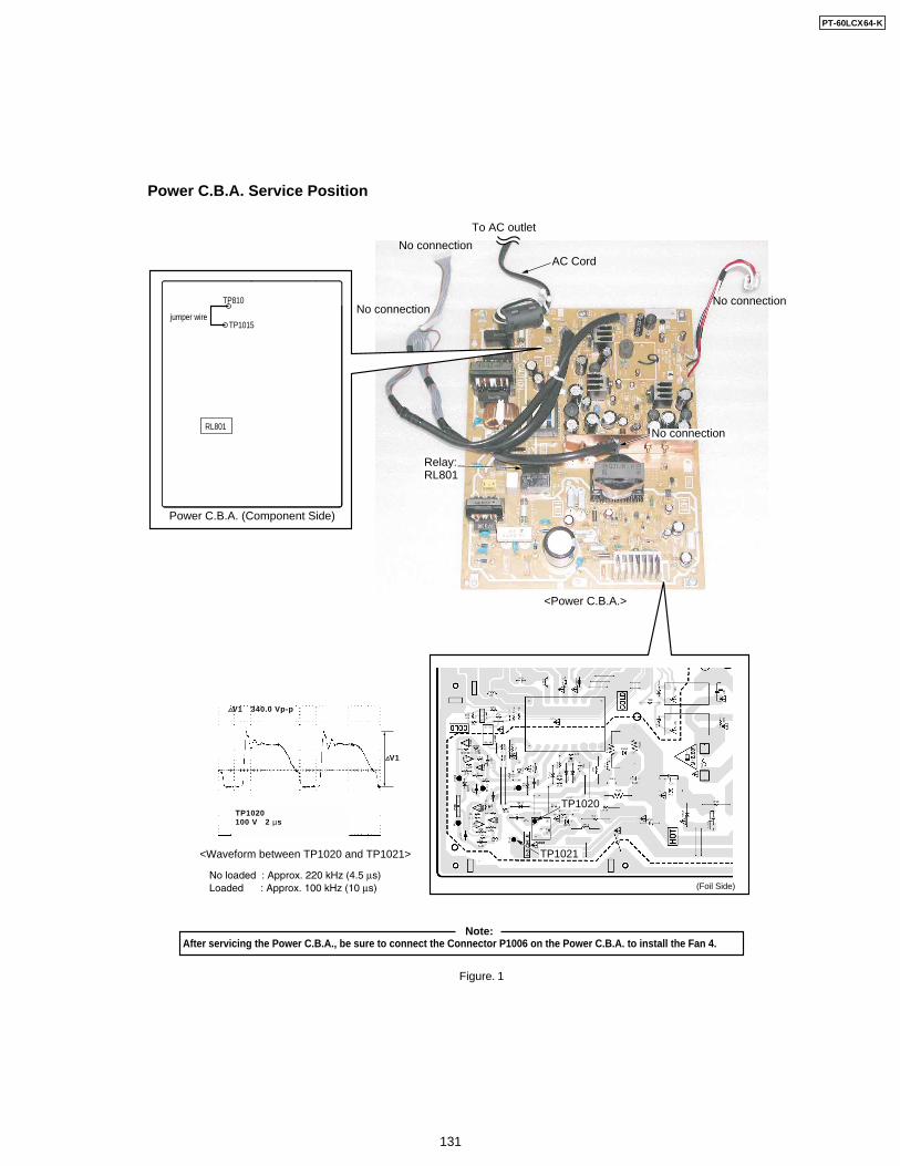
Power C.B.A. Service Position
After servicing the Power C.B.A., be sure to connect the Connector P1006 on the Power C.B.A. to install the Fan 4.
Figure. 1
Note:
AC Cord
No connection
No connection
No connection
To AC outlet
TP810
jumper wireTP1015
Power C.B.A. (Component Side)
<Power C.B.A.>
Relay:RL801
RL801No connection
(Foil Side)
<Waveform between TP1020 and TP1021>
V1
V1 340.0 Vp-p
TP1020100 V 2 µs
TP1020
TP1021
PT-60LCX64-K
131
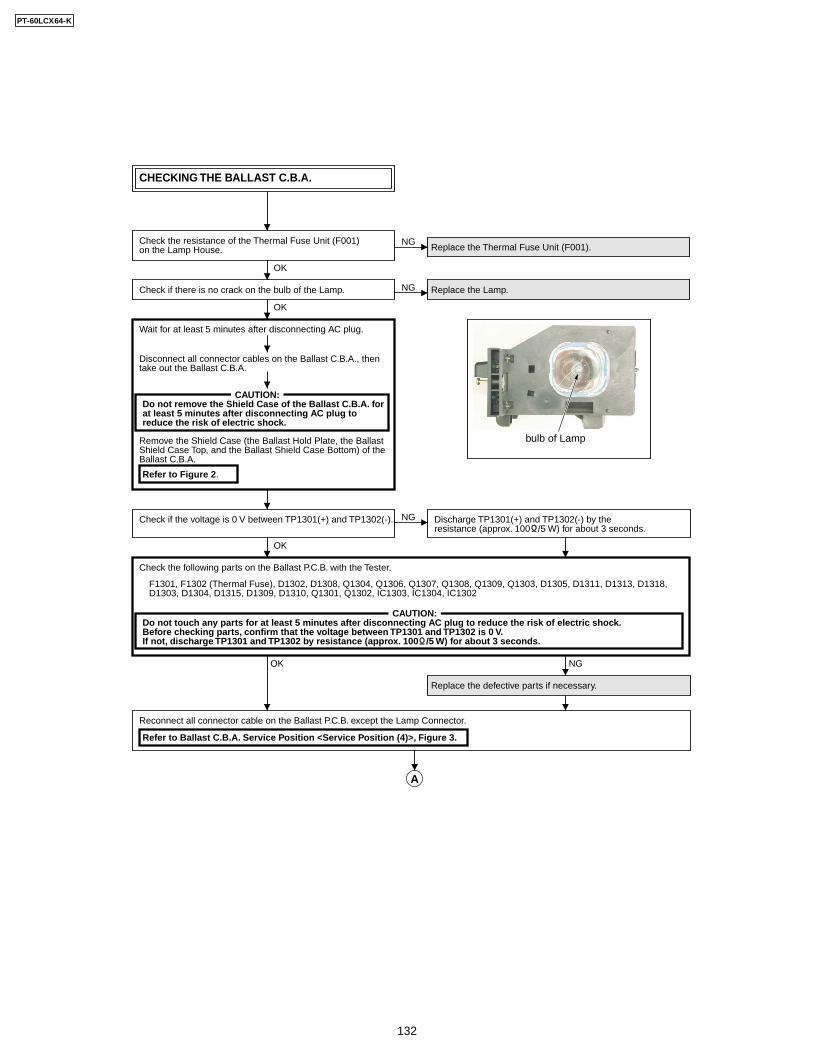
CHECKING THE BALLAST C.B.A.
OK
OK
NG
OK
NG
NG
Check the resistance of the Thermal Fuse Unit (F001) on the Lamp House.
Check if there is no crack on the bulb of the Lamp.
Wait for at least 5 minutes after disconnecting AC plug.
Disconnect all connector cables on the Ballast C.B.A., then take out the Ballast C.B.A.
Remove the Shield Case (the Ballast Hold Plate, the Ballast Shield Case Top, and the Ballast Shield Case Bottom) of the Ballast C.B.A.
Refer to Figure 2.
Check if the voltage is 0 V between TP1301(+) and TP1302(-). Discharge TP1301(+) and TP1302(-) by the resistance (approx. 100 /5 W) for about 3 seconds.
Replace the Lamp.
Replace the Thermal Fuse Unit (F001).
Check the following parts on the Ballast P.C.B. with the Tester.
Reconnect all connector cable on the Ballast P.C.B. except the Lamp Connector.
Refer to Ballast C.B.A. Service Position <Service Position (4)>, Figure 3.
Replace the defective parts if necessary.
F1301, F1302 (Thermal Fuse), D1302, D1308, Q1304, Q1306, Q1307, Q1308, Q1309, Q1303, D1305, D1311, D1313, D1318, D1303, D1304, D1315, D1309, D1310, Q1301, Q1302, IC1303, IC1304, IC1302
OK NG
CAUTION:Do not remove the Shield Case of the Ballast C.B.A. for at least 5 minutes after disconnecting AC plug to reduce the risk of electric shock.
CAUTION:Do not touch any parts for at least 5 minutes after disconnecting AC plug to reduce the risk of electric shock.Before checking parts, confirm that the voltage between TP1301 and TP1302 is 0 V.If not, discharge TP1301 and TP1302 by resistance (approx. 100 /5 W) for about 3 seconds.
bulb of Lamp
A
PT-60LCX64-K
132
NG
There is no problem with the Ballast C.B.A. After discharging the voltage between TP1301(+) and TP1302(-), reinstall the Shield Case (the Ballast Hold Plate, the Ballast Shield Case Top, and the Ballast Shield Case Bottom) of the Ballast C.B.A.
NG
P1301-Pin 1(+) <--> TP1304(-): Approx. 19VP1301-Pin 4(+) <--> P1301-Pin 5(-): Approx. 17V
Check the voltage at the following points during flashing the Power LED (D6701) green.
Plug in the AC Cord and turn the power ON.
Plug in the AC Cord again and turn the power ON.
After the Lamp Error (Error No. 5)) is indicated (the Lamp LED flashes once), unplug the AC Cord and connect the Lamp Connector to the Lamp.
Is there a slight crackle sound from the Ballast P.C.B. after approx. 5 seconds?
Unplug the AC Cord and then, plug in the AC Cord again. And turn the power ON.
Does the Lamp light up? Replace U1301.(If still NG even after replacement of U1301,replace the Ballast C.B.A.)
Check the Power C.B.A.(Refer to "CHECKING THE POWER C.B.A.")
NG
OK
OK
OK
CAUTION:Do not touch any parts for at least 5 minutes after disconnecting AC plug to reduce the risk of electric shock.Before checking parts, confirm that the voltage between TP1301 and TP1302 is 0 V.If not, discharge TP1301 and TP1302 by resistance (approx. 100 /5 W) for about 3 seconds.
CAUTION:Do not touch any parts for at least 5 minutes after disconnecting AC plug to reduce the risk of electric shock.Before checking parts, confirm that the voltage between TP1301 and TP1302 is 0 V.If not, discharge TP1301 and TP1302 by resistance (approx. 100 /5 W) for about 3 seconds.
CAUTION:Do not touch any parts for at least 5 minutes after disconnecting AC plug to reduce the risk of electric shock.Before checking parts, confirm that the voltage between TP1301 and TP1302 is 0 V.If not, discharge TP1301 and TP1302 by resistance (approx. 100 /5 W) for about 3 seconds.
A
B
C
<Service Position (4)>
PT-60LCX64-K
133
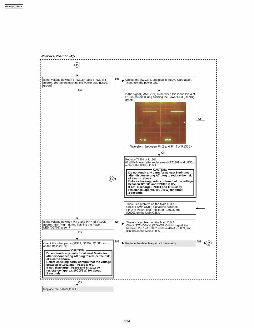
OK
OK
NG
Is the voltage between TP1303(+) and TP1304(-) approx. 19V during flashing the Power LED (D6701) green?
Unplug the AC Cord, and plug in the AC Cord again. Then, turn the power ON.
Replace the Ballast C.B.A.
Replace the defective parts if necessary.Check the other parts (Q1301, Q1302, Q1303, etc.) on the Ballast P.C.B.
Replace T1301 or U1301.(If still NG, even after replacement of T1301 and U1301,replace the Ballast C.B.A.
NG
NG
NG
NG
OK
OK
There is a problem on the Main C.B.A. Check LAMP ON(H) signal line between Pin 2 of P6002 and Pin 44 of IC6003, and IC6003 on the Main C.B.A.
Is the voltage between Pin 1 and Pin 4 of P1305 approx. +5V (High) during flashing the Power LED (D6701) green?
There is a problem on the Main C.B.A. Check STANDBY (L)/POWER ON (H) signal line between Pin 1 of P6002 and Pin 48 of IC6003, and IC6003 on the Main C.B.A.
Is the signal(LAMP ON(H)) between Pin 2 and Pin 4 of P1305 correct during flashing the Power LED (D6701) green?
CAUTION:Do not touch any parts for at least 5 minutes after disconnecting AC plug to reduce the risk of electric shock.Before checking parts, confirm that the voltage between TP1301 and TP1302 is 0 V.If not, discharge TP1301 and TP1302 by resistance (approx. 100 /5 W) for about 3 seconds.
CAUTION:Do not touch any parts for at least 5 minutes after disconnecting AC plug to reduce the risk of electric shock.Before checking parts, confirm that the voltage between TP1301 and TP1302 is 0 V.If not, discharge TP1301 and TP1302 by resistance (approx. 100 /5 W) for about 3 seconds.
<Service Position (4)>
B
C
C
<Waveform between Pin2 and Pin4 of P1305>
PT-60LCX64-K
134
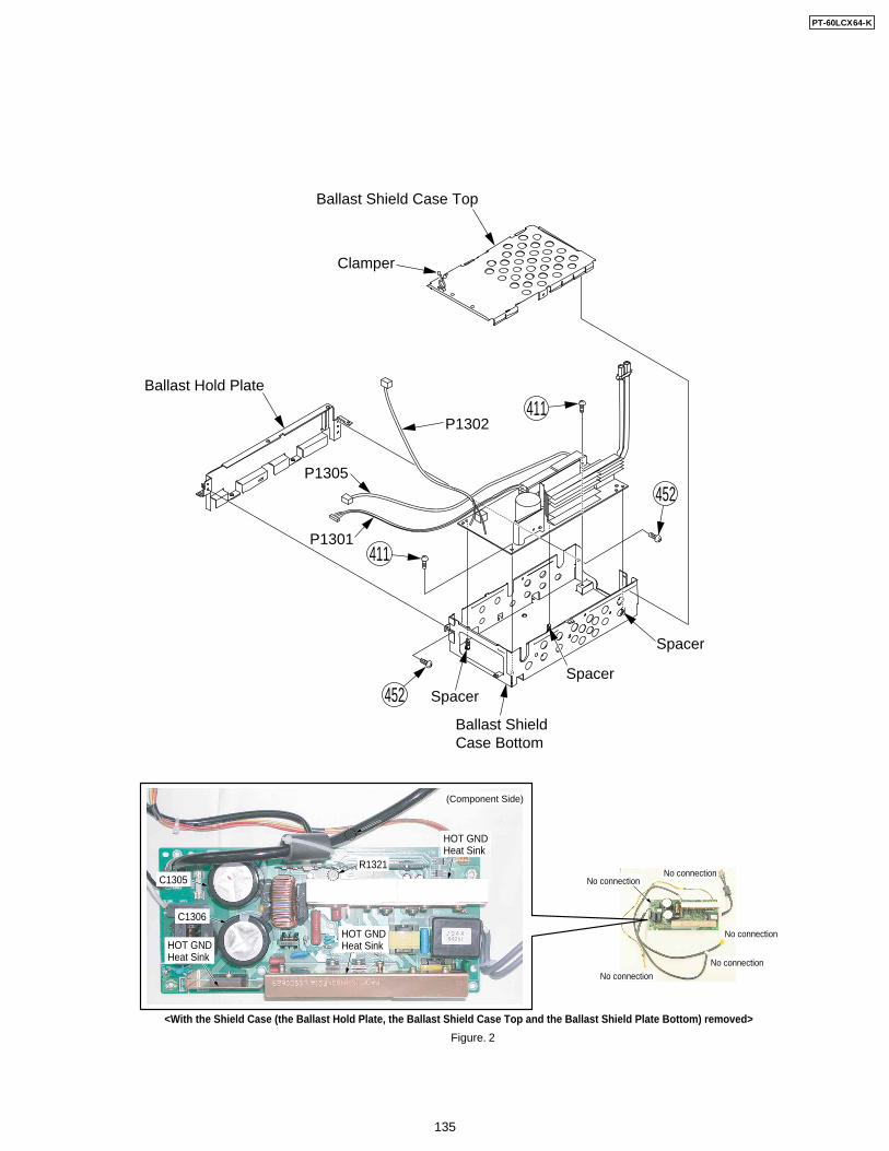
No connection
No connection
No connectionNo connection
No connection
<With the Shield Case (the Ballast Hold Plate, the Ballast Shield Case Top and the Ballast Shield Plate Bottom) removed>
Figure. 2
HOT GNDHeat Sink
HOT GNDHeat Sink
HOT GNDHeat Sink
C1305
C1306
(Component Side)
R1321
452
452
411
411
P1302
Ballast Shield Case Top
Clamper
Ballast Hold Plate
Spacer
Spacer
Spacer
P1305
P1301
Ballast Shield Case Bottom
PT-60LCX64-K
135
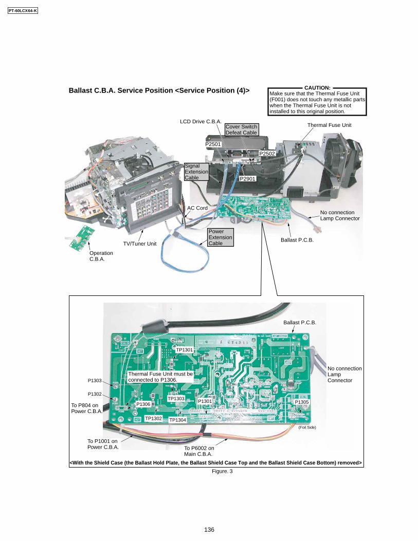
Signal ExtensionCable
Cover Switch Defeat Cable
TV/Tuner Unit
AC Cord
Operation C.B.A.
Power Extension Cable
Ballast P.C.B.
LCD Drive C.B.A.Thermal Fuse Unit
P2501
P2901
P2502
No connectionLamp Connector
Make sure that the Thermal Fuse Unit(F001) does not touch any metallic partswhen the Thermal Fuse Unit is not installed to this original position.
CAUTION:Ballast C.B.A. Service Position <Service Position (4)>
Figure. 3
<With the Shield Case (the Ballast Hold Plate, the Ballast Shield Case Top and the Ballast Shield Case Bottom) removed>
P1301 P1305
(Foil Side)
Ballast P.C.B.
TP1303P1306
P1303
P1302
TP1301
TP1302 TP1304
Thermal Fuse Unit must be connected to P1306.
To P804 onPower C.B.A.
To P1001 onPower C.B.A. To P6002 on
Main C.B.A.
No connectionLamp Connector
PT-60LCX64-K
136
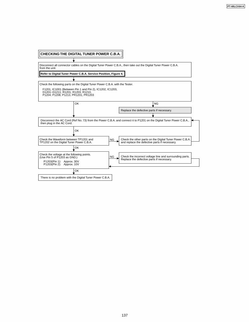
CHECKING THE DIGITAL TUNER POWER C.B.A.
Disconnect all connector cables on the Digital Tuner Power C.B.A., then take out the Digital Tuner Power C.B.A. from the unit.
Refer to Digital Tuner Power C.B.A. Service Position, Figure 4.
Check the following parts on the Digital Tuner Power C.B.A. with the Tester.
Replace the defective parts if necessary.
F1201, IC1001 (Between Pin 1 and Pin 2), IC1202, IC1203,D1201~D1211, R1201, R1203, R1210, P1204, P1208, P1213, PR1201, PR1203
P1203(Pin 1):P1203(Pin 2):
Approx. 30VApprox. 10V
OK
OK
NG
Check the other parts on the Digital Tuner Power C.B.A.and replace the defective parts if necessary.
NG
Check the incorrect voltage line and surrounding parts. Replace the defective parts if necessary.
NG
Disconnect the AC Cord (Ref No. 73) from the Power C.B.A. and connect it to P1201 on the Digital Tuner Power C.B.A., then plug in the AC Cord.
Check the Waveform between TP1201 and TP1202 on the Digital Tuner Power C.B.A.
OK
Check the voltage at the following points. (Use Pin 5 of P1203 as GND.)
OK
There is no problem with the Digital Tuner Power C.B.A.
PT-60LCX64-K
137
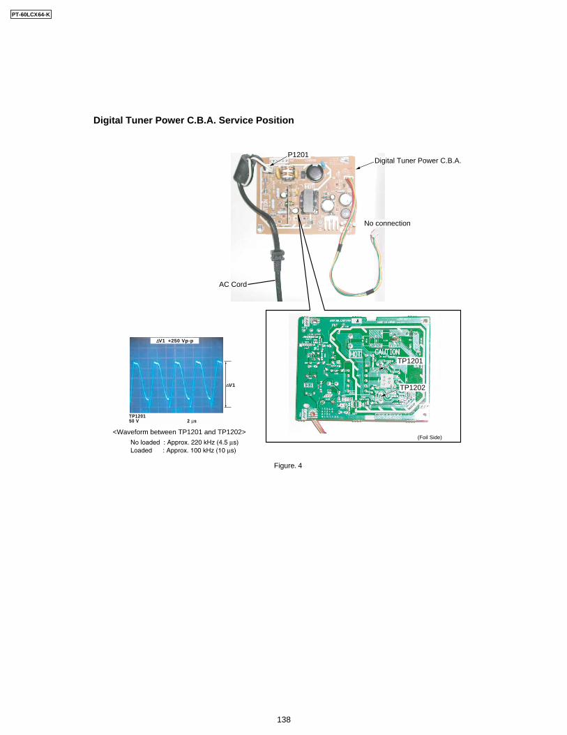
Digital Tuner Power C.B.A. Service Position
Figure. 4
<Waveform between TP1201 and TP1202>
V1 +250 Vp-p
TP120150 V 2 µs
V1
AC Cord
P1201
No connection
Digital Tuner Power C.B.A.
(Foil Side)
TP1201
TP1202
PT-60LCX64-K
138
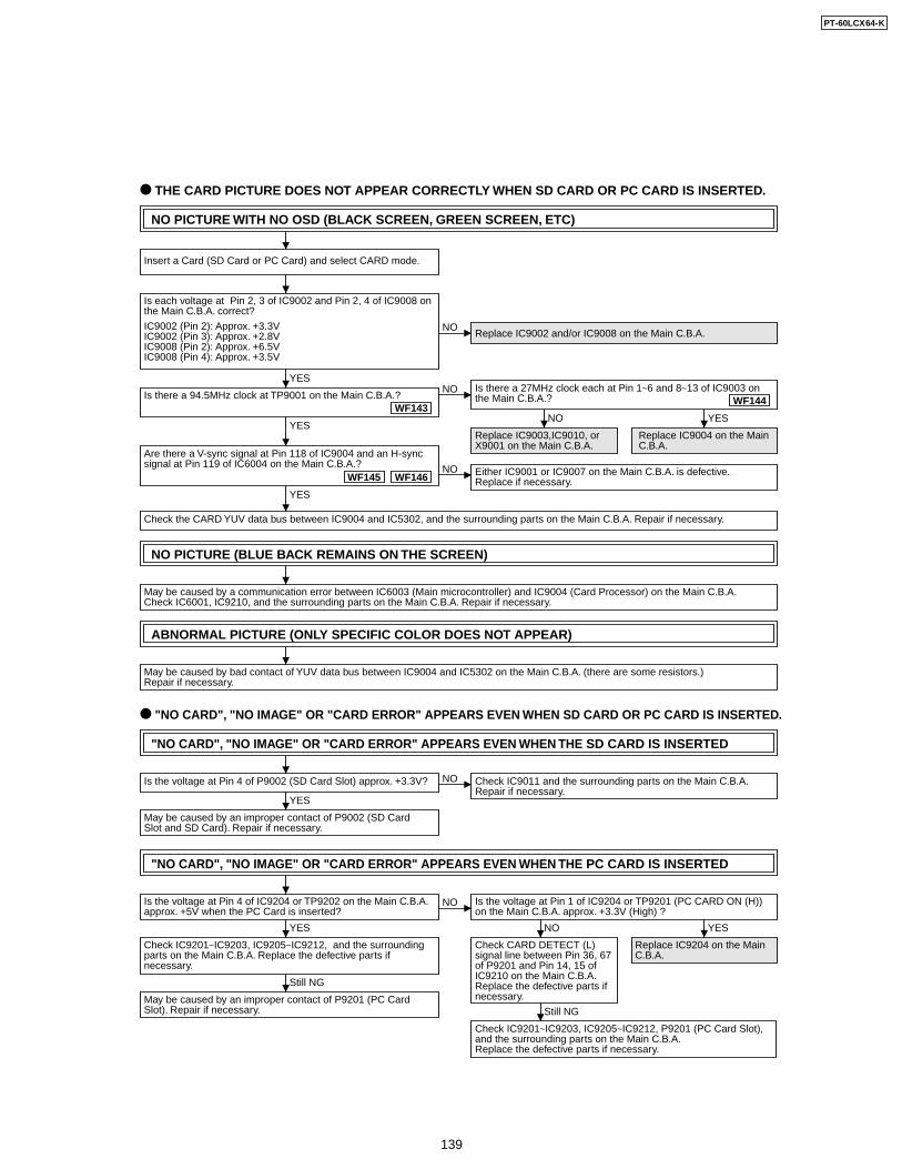
Insert a Card (SD Card or PC Card) and select CARD mode.
Replace IC9002 and/or IC9008 on the Main C.B.A. NO
NO
Is there a 27MHz clock each at Pin 1~6 and 8~13 of IC9003 on the Main C.B.A.?
Replace IC9003,IC9010, or X9001 on the Main C.B.A.
Replace IC9004 on the Main C.B.A.
NO
Either IC9001 or IC9007 on the Main C.B.A. is defective.Replace if necessary.
YES
NO YES
Check CARD DETECT (L) signal line between Pin 36, 67of P9201 and Pin 14, 15 of IC9210 on the Main C.B.A.Replace the defective parts ifnecessary.
Replace IC9204 on the Main C.B.A.
Check IC9201~IC9203, IC9205~IC9212, P9201 (PC Card Slot),and the surrounding parts on the Main C.B.A.Replace the defective parts if necessary.
NO
Still NG
YES
Is there a 94.5MHz clock at TP9001 on the Main C.B.A.?
YES
Are there a V-sync signal at Pin 118 of IC9004 and an H-sync signal at Pin 119 of IC6004 on the Main C.B.A.?
YES
NO Check IC9011 and the surrounding parts on the Main C.B.A.Repair if necessary.
Is the voltage at Pin 4 of P9002 (SD Card Slot) approx. +3.3V?
May be caused by an improper contact of P9002 (SD Card Slot and SD Card). Repair if necessary.
YES
May be caused by a communication error between IC6003 (Main microcontroller) and IC9004 (Card Processor) on the Main C.B.A.Check IC6001, IC9210, and the surrounding parts on the Main C.B.A. Repair if necessary.
Is each voltage at Pin 2, 3 of IC9002 and Pin 2, 4 of IC9008 on the Main C.B.A. correct?
Check the CARD YUV data bus between IC9004 and IC5302, and the surrounding parts on the Main C.B.A. Repair if necessary.
THE CARD PICTURE DOES NOT APPEAR CORRECTLY WHEN SD CARD OR PC CARD IS INSERTED.
NO PICTURE WITH NO OSD (BLACK SCREEN, GREEN SCREEN, ETC)
"NO CARD", "NO IMAGE" OR "CARD ERROR" APPEARS EVEN WHEN THE SD CARD IS INSERTED
NOIs the voltage at Pin 4 of IC9204 or TP9202 on the Main C.B.A. approx. +5V when the PC Card is inserted?
Is the voltage at Pin 1 of IC9204 or TP9201 (PC CARD ON (H)) on the Main C.B.A. approx. +3.3V (High) ?
Check IC9201~IC9203, IC9205~IC9212, and the surrounding parts on the Main C.B.A. Replace the defective parts if necessary.
YES
May be caused by an improper contact of P9201 (PC Card Slot). Repair if necessary.
Still NG
"NO CARD", "NO IMAGE" OR "CARD ERROR" APPEARS EVEN WHEN THE PC CARD IS INSERTED
NO PICTURE (BLUE BACK REMAINS ON THE SCREEN)
May be caused by bad contact of YUV data bus between IC9004 and IC5302 on the Main C.B.A. (there are some resistors.)Repair if necessary.
ABNORMAL PICTURE (ONLY SPECIFIC COLOR DOES NOT APPEAR)
"NO CARD", "NO IMAGE" OR "CARD ERROR" APPEARS EVEN WHEN SD CARD OR PC CARD IS INSERTED.
IC9002 (Pin 2): Approx. +3.3VIC9002 (Pin 3): Approx. +2.8VIC9008 (Pin 2): Approx. +6.5VIC9008 (Pin 4): Approx. +3.5V
WF144WF143
WF146WF145
PT-60LCX64-K
139

PT-60LCX64-K
140
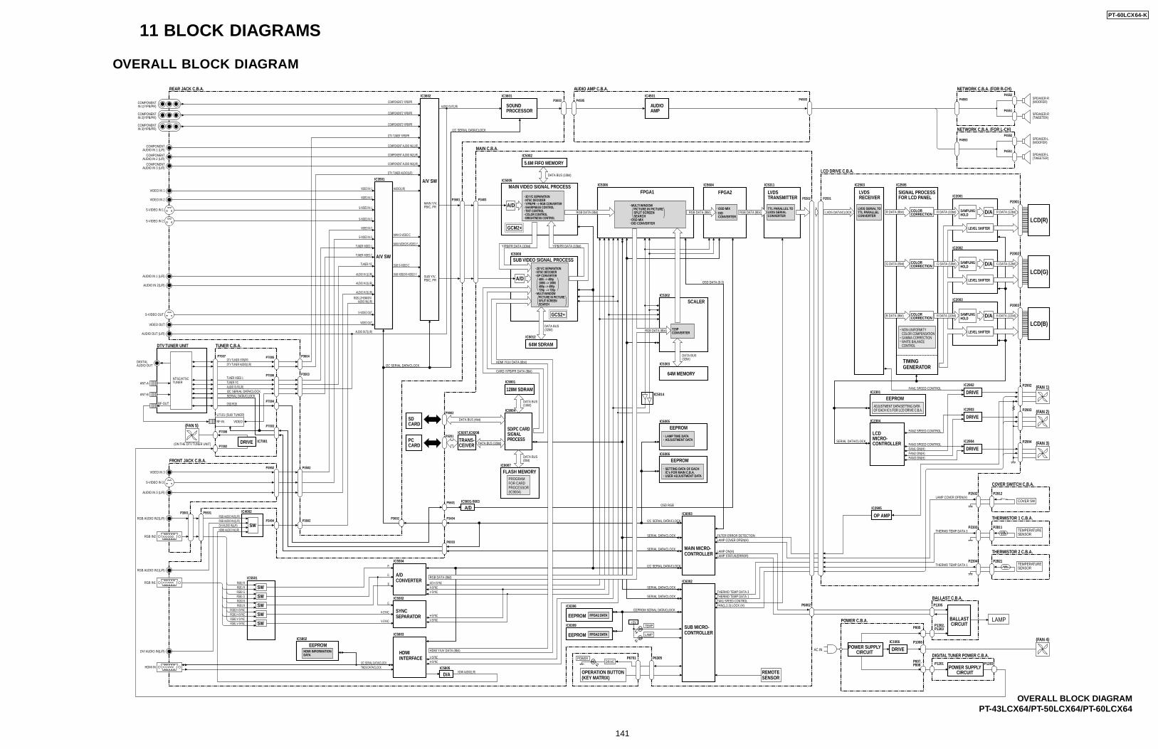
11 BLOCK DIAGRAMS
PT-43LCX64/PT-50LCX64/PT-60LCX64OVERALL BLOCK DIAGRAM
RGB AUDIO IN2(L/R)
REAR JACK C.B.A. NETWORK C.B.A. (FOR R-CH)
NETWORK C.B.A. (FOR L-CH)
MAIN C.B.A.
BALLAST C.B.A.
POWER C.B.A.
COMPONENT IN 1(Y/PB/PR)
COMPONENT1 Y/PB/PR
VIDEO IN 1
VIDEO IN 2
S-VIDEO IN 1
S-VIDEO IN 2
VIDEO IN 3
S-VIDEO IN 3
TUNER VIDEO 1
TUNER VIDEO 1
TUNER VIDEO 2
AUDIO IN 1(L/R)
AUDIO IN 2(L/R)
AUDIO IN 3(L/R)
RGB1,2/HDMI/DVI AUDIO IN(L/R)
DTV TUNER AUDIO(L/R)
DTV TUNER AUDIO(L/R)
S-VIDEO OUT
VIDEO OUT
AUDIO OUT(L/R)
AUDIO OUT(L/R)
OSD-RGB
AUDIO OUT(L/R)
COMPONENT IN 2(Y/PB/PR)
MAIN VIDEO/S-VIDEO Y
MAIN S-VIDEO C
SUB VIDEO/S-VIDEO Y
SUB S-VIDEO C
S-VIDEO OUT
VIDEO OUT
AUDIO OUT (L/R)
DIGITALAUDIO OUT
FRONT JACK C.B.A.
TUNER C.B.A.DTV TUNER UNIT
RGB IN2
P3901 P5501
THERMO TEMP DATA 3
FAN1 SPEED CONTROL
LAMP COVER OPEN(H)
LAMP ON(H)LAMP STATUS(ERROR)
SERIAL DATA/CLOCK
EEPROM SERIAL DATA/CLOCK
POWER
SERIAL DATA/CLOCK
SERIAL DATA/CLOCK
SERIAL DATA/CLOCK
SERIAL DATA/CLOCK
I2C SERIAL DATA/CLOCK
THERMO TEMP DATA 1
FAN(1,2,3) LOCK (H)
RF-IN
RF-OUT
ANT-A
ANT-B
VIDEO
U7101 (SUB TUNER)
NTSC/ATSCTUNER
IC5311VIDEO IN 1
IC3501 IC5005
IC3601
IC5002
IC5012
IC5306
IC5302
IC5014
IC5009
IC9004
IC9007
IC9207,IC9208
IC3602
A/V SW
A/V SW
5.6M FIFO MEMORY
SOUNDPROCESSOR
IC4501
AUDIOAMP
64M SDRAM
GCS2+
FLASH MEMORY
SD/PC CARDSIGNALPROCESS
IC6306
EEPROM
IC5802
EEPROM
IC6006
EEPROM
IC6005
EEPROM
TRANS-CEIVER
TUNER Y/C
TUNER Y/C
AUDIO IN 1 (L/R)
AUDIO IN 2(L/R)
COMPONENTAUDIO IN 1 (L/R)
COMPONENTAUDIO IN 2 (L/R)
AUDIO(L/R)
COMPONENTAUDIO IN 3 (L/R)
VIDEO IN 2
S-VIDEO IN 1
S-VIDEO IN 2
SPEAKER-R(WOOFER)
SPEAKER-R(TWEETER)
SPEAKER-L(WOOFER)
SPEAKER-L(TWEETER)
IC6003
MAIN MICRO-CONTROLLER
IC6302
SUB MICRO-CONTROLLER
IC4002
SW
SYNCSEPARATOR
HDMIINTERFACE
A/DCONVERTER
P1305P6002
P6701 P6305
A/D
A/D
RGB2 R
R
G
B
G
V-SYNC
H-SYNCH-SYNC
A/D H-SYNC
H-SYNCV-SYNC
V-SYNC
H-SYNCV-SYNCRGB2 G
RGB2 B
RGB2 H-SYNC
RGB2 V-SYNC
RGB1 R
RGB1 G
RGB1 B
RGB1 H-SYNC
RGB1 V-SYNC
IC5501
IC5504
IC5502
IC5803
SW
SW
SW
SW
SWLAMPBALLAST
CIRCUIT
IC1006
DRIVEP1006
P1201 P1203
(FAN 4)
(FAN 5)
P805 P1302,P1303
P807,P808
COMPONENT IN 3(Y/PB/PR)
COMPONENT3 Y/PB/PR
COMPONENT2 Y/PB/PR
DTV TUNER Y/PB/PR
DTV TUNER Y/PB/PR
COMPONENT AUDIO IN1(L/R)
COMPONENT AUDIO IN2(L/R)
COMPONENT AUDIO IN3(L/R)
HDMI AUDIO IN(L/R)DVI AUDIO IN(L/R)
TMDS DATA/CLOCKI2C SERIAL DATA/CLOCK
HDMI AUDIO(L/R)
RGB AUDIO IN2(L/R)RGB AUDIO IN1(L/R)
FILTER ERROR DETECTION
P7005P7007 P3604
P7006 P3503
P7003
P7004
P7002
P7008
P6003
P3404 P3602
VIDEO IN 3
S-VIDEO IN 3
P3902 P3502
RGB AUDIO IN1(L/R)
RGB IN1
DVI AUDIO IN(L/R)
HDMI IN
AUDIO IN 3 (L/R)
P3601 P3403 P5302
P9002
P3603 P4503P4505 P4553
P4553
P4552
P4552
P4551
P4551
IC9001
128M SDRAM
IC5303
64M MEMORY
SCALER
P9201
SDCARD
PCCARD
AUDIO AMP C.B.A.
P3602 P3404
P5601
720PCONVERTER
LAMP TIME DATAADJUSTMENT DATA
SETTING DATA OF EACHIC's FOR MAIN C.B.A.USER ADJUSTMENT DATA
HDMI INFORMATIONDATA
FPGA1 DATA
IC6309
EEPROM FPGA2 DATA
FPGA1 LVDSTRANSMITTER
IC5604
FPGA2MAIN VIDEO SIGNAL PROCESS
SUB VIDEO SIGNAL PROCESS
MULTI WINDOW PICTURE IN PICTURE SPLIT SCREEN SEARCHOSD MIXD/D CONVERTER
TTL PARALLEL TOLVDS SERIALCONVERTER
OSD MIXD/D CONVERTER
3D Y/C SEPARATIONNTSC DECODERY/PB/PR --> RGB CONVERTERSHARPNESS CONTROLTINT CONTROLCOLOR CONTROLBRIGHTNESS CONTROL
2D Y/C SEPARATIONNTSC DECODERI/iP CONVERTER 480i --> 480p 1080i --> 1080i 480p --> 480p 720p --> 720pMULTI WINDOW PICTURE IN PICTURE SPLIT SCREEN SEARCH
RGB DATA (8bit)RGB DATA (8bit)
Y/PB/PR DATA (10bit)
MAIN Y/V, PB/C, PR
SUB Y/V, PB/C, PR
Y/PB/PR DATA (10bit)
CARD Y/PB/PR DATA (8bit)
DATA BUS (16bit)
DATA BUS (4bit)
OSD DATA (0-3)
OSD RGB
DATA BUS (32bit)
DATA BUS (8bit)
DATA BUS (16bit)
DATA BUS (32bit)
DATA BUS (10bit)
IC5805
D/A
IC5601-5603
A/D
I2C SERIAL DATA/CLOCK
I2C SERIAL DATA/CLOCK
I2C SERIAL DATA/CLOCK
I2C SERIAL DATA/CLOCK
GCM2+
AC IN POWER SUPPLYCIRCUIT
DIGITAL TUNER POWER C.B.A.
POWER SUPPLYCIRCUIT
RGB DATA (8bit)
RGB DATA (8bit)
REMOTESENSOR
OPERATION BUTTON(KEY MATRIX)
TEMP
LAMP
DRIVE
+5V
PROGRAM FOR CARD PROCESSOR (IC9004)
RGB DATA (8bit)
HDMI Y/UV DATA (8bit)
IC7001DRIVE(ON THE DTV TUNER UNIT)
HDMI Y/UV DATA (8bit)
LCD DRIVE C.B.A.
THERMISTOR 1 C.B.A.
COVER SWITCH C.B.A.
FAN2 SPEED CONTROL
FAN1 ON(H)FAN2 ON(H)FAN3 ON(H)
FAN1 SPEED CONTROL
IC2304
LCDMICRO-CONTROLLER
THERMO TEMP DATA 3
FAN3 SPEED CONTROLSERIAL DATA/CLOCK
LAMP COVER OPEN(H)
THERMO TEMP DATA 1
IC2503 IC2505
TIMINGGENERATOR
IC2301
EEPROM
IC2905
OP AMP
IC2902
DRIVE
IC2903
DRIVE
R DATA (8bit)
G DATA (8bit)
B DATA (8bit)
D/ACOLORCORRECTION
SAMPLINGHOLD
SAMPLINGHOLD
SAMPLINGHOLD
COLORCORRECTION
COLORCORRECTION
IC2001
IC2002
IC2003
LCD(R)
LCD(G)
LCD(B)
LEVEL SHIFTER
P2001
P2002
P2003
P2902
P2903
P2904
P2502
P2303 P2811
P2304 P2821
P2912
LEVEL SHIFTER
LEVEL SHIFTER
D/A
D/A
R DATA (12bit)
G DATA (12bit)
B DATA (12bit)
(FAN 1)
TEMPERATURESENSOR
COVER SW
(FAN 2)
(FAN 3)
TEMPERATURESENSOR
THERMISTOR 2 C.B.A.
IC2904
DRIVE
NON-UNIFORMITYCOLOR COMPENSATIONGAMMA CORRECTIONWHITE BALANCECONTROL
ADJUSTMENT DATA/SETTING DATAOF EACH IC's FOR LCD DRIVE C.B.A.
R DATA (10bit)
G DATA (10bit)
B DATA (10bit)
P2501
LVDSRECEIVER
SIGNAL PROCESSFOR LCD PANEL
LVDS SERIAL TOTTL PARALLELCONVERTER
LVDS DATA/CLOCK
OVERALL BLOCK DIAGRAM
PT-60LCX64-K
141
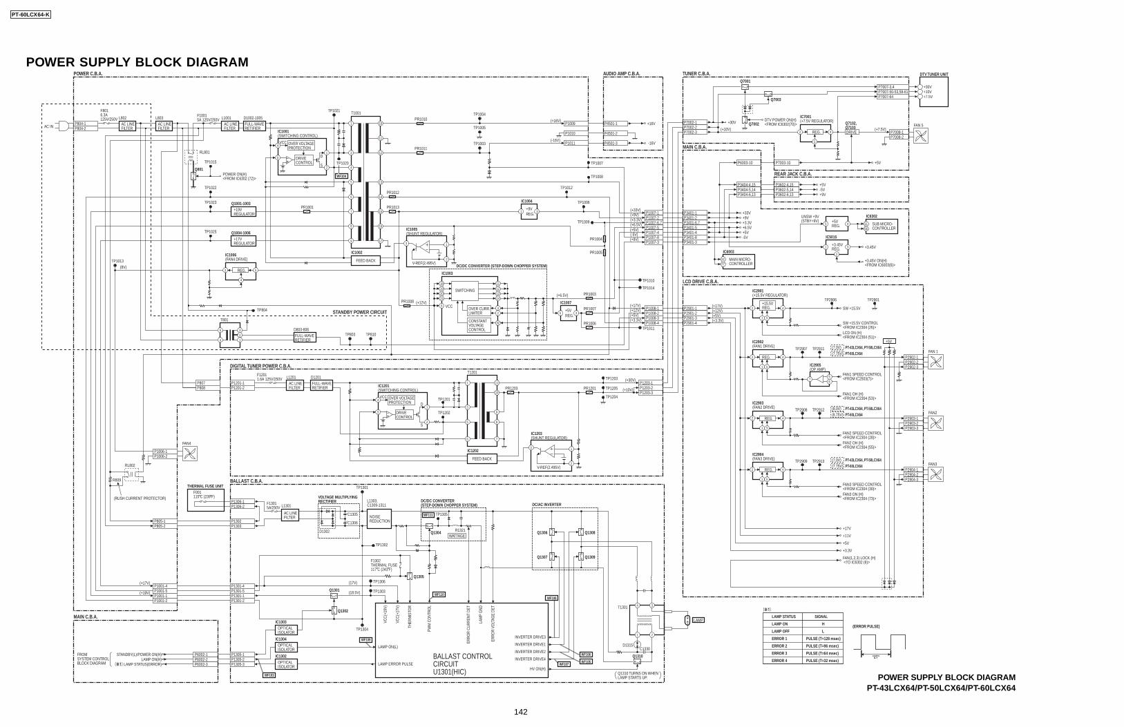
PT-43LCX64/PT-50LCX64/PT-60LCX64
WF104
D1002-1005FULL-WAVERETIFIER
D803-806FULL-WAVERETIFIER
AC LINEFILTER
F8016.3A 125V/250V L802
AC LINEFILTER
L803AC LINEFILTER
L1001F10015A 125V/250V
POWER ON(H)<FROM IC6302 (72)>
D1201FULL-WAVERETIFIER
AC LINEFILTER
L1201F12011.6A 125V/250V
F001115 C (239 F)
THERMAL FUSE UNIT
STANDBY(L)/POWER ON(H)FROMSYSTEM CONTROLBLOCK DIAGRAM
LAMP ON(H)LAMP STATUS(ERROR)
T801
R809
(RUSH CURRENT PROTECTOR)
RL801
RL802
IC1002
IC1005(SHUNT REGULATOR)
IC1001(SWITCHING CONTROL)
Q1001-1003
POWER C.B.A.
STANDBY POWER CIRCUIT
DIGITAL TUNER POWER C.B.A.
MAIN C.B.A.
Q1004-1006
Q801
IC1003
V-REF(2.495V)FEED BACK
IC1202
FEED BACK
3 1
2
FAN 5
P7008-1P7008-2
IC7001 (+7.5V REGULATOR)
REG. 4
5
T1001
1
15
16
17
3
4
12
11
10
14
135
6
T1201
1
3
5
9
8
10
11
76
7
8
9
P804-1P804-2
P1201-1P1201-2
P805-1P805-2
P1006-1P1006-2
P1009
P1011
P1007-1P1007-2P1007-6,7P1007-5P1007-4P1007-8P1007-3
P1008-1P1008-2P1008-3
P1203-1P1203-2P1203-3
P1008-4
P1010
P4501-1
P4501-3
P3401-1P3401-2P3401-6,7P3401-5P3401-4P3401-8P3401-3
P4501-2
P1001-4P1001-5P1001-1P1001-2
AC IN
42
6
1
3
1
4
5
2
PR1010
PR1012
PR1001 PR1013
IC1203(SHUNT REGULATOR)
V-REF(2.495V)
3 1
2
18192021
11121314
6
PR1011
PR1004
PR1005
PR1008 (+12V)
(+6.5V)
VCC
PR1003
TP1012
PR1007
PR1006
AUDIO AMP C.B.A.
MAIN C.B.A.
IC1007
35+5VREG.
IC1004
31+9VREG.
P6002-1P6002-2P6002-3
+19VREGULATOR
+17VREGULATOR
OVER VOLTAGEPROTECTION
DRIVECONTROL
VCC
SWITCHING
OVER CURR.LIMITER
CONSTANTVOLTAGE CONTROL
32
32
TP1010
TP1203
TP1205
TP1204
TP1003
TP1008
TP1009
TP1007
TP1006
TP1004
+16V
-16V
+33V+9V+3.3V+6.5V+5V-5V
UNSW +9V(STBY+9V)
TP1005
TP1014
TP1011
+3.45V
IC5015
+3.45VREG.
Q7102,Q7103
+5VREG.
31IC6003
MAIN MICRO-CONTROLLER
322
+3.45V ON(H)<FROM IC6003(6)>
FAN4
IC1006(FAN4 DRIVE)
REG.3 5
4
TP1015
TP1022
TP1023
TP1025
TP804
(8V)TP1013
TP1021
TP1020
D
S
TP810TP803
77
IC6302
SUB MICRO-CONTROLLER
1156
5 4
DC/DC CONVERTER (STEP-DOWN CHOPPER SYSTEM)
LAMP STATUS
LAMP ON H
LLAMP OFF
ERROR 1
(ERROR PULSE)
"2T"
PULSE (T=128 msec)
PULSE (T=96 msec)
PULSE (T=64 msec)
PULSE (T=32 msec)
ERROR 2
ERROR 3
ERROR 4
SIGNAL
TUNER C.B.A.
P7002-1 +30VP7002-2P7002-3
P6003-10 P7003-10 +5V
REAR JACK C.B.A.
P3602-4,15 +5VP3602-5,14 -5V
P3404-4,15P3404-5,14
P3602-6,13 +9VP3404-6,13
IC1201(SWITCHING CONTROL)
1
4
5
2
OVER VOLTAGEPROTECTION
DRIVECONTROL
VCC
D
S
PR1201PR1203
2
P807P808
DRIVE
TP1201
TP1202
Q7001
Q7002DTV POWER ON(H)<FROM IC6302(70)>
Q7003
P7007-3,4P7007-50-53,58-61P7007-64
DTV TUNER UNIT
+30V+10V+7.5V
(+17V)
(+19V)
(+16V)
(-16V)
(+33V)(+9V)(+3.3V)(+6.5V)(+5V)(-5V)
(+17V)(+12V)(+5V)(+3.3V)
(+9V)
(+30V)
(+10V)
(+10V) (+7.5V)
WF103
AC LINEFILTER
L1301
C1305
D1302
C1306NOISEREDUCTION
DC/DC CONVERTER(STEP-DOWN CHOPPER SYSTEM)
VOLTAGE MULTIPLYINGRECTIFIER
BALLAST CONTROL CIRCUITU1301(HIC)
L1303,C1309-1311F1301
5A/250V
PT-43LCX64, PT-50LCX64PT-60LCX64
BALLAST C.B.A.
LCD DRIVE C.B.A.
IC1303
Q1301
Q1305
Q1304
F1302THERMAL FUSE117 C (243 F)
R1321WATTAGE
VCC
(+19
V)
VCC
(+17
V)
THER
MIS
TOR
ERRO
R V
OLT
AGE
DET
LAM
P G
ND
ERRO
R C
UR
REN
T D
ET
PWM
CO
NTR
OL
LAMP ON(L)
INVERTER DRIVE3
INVERTER DRIVE1
INVERTER DRIVE2
INVERTER DRIVE4
HV ON(H)LAMP ERROR PULSE
Q1302
IC1304
IC1302
LAMP
+17V
SW +15.5V
TP2906
SW +15.5V CONTROL<FROM IC2304 (26)>LCD ON (H) <FROM IC2304 (51)>
+11V
FAN1 SPEED CONTROL <FROM IC2503(7)>
FAN2 SPEED CONTROL <FROM IC2304 (28)>FAN2 OH (H) <FROM IC2304 (55)>
FAN3 ON (H) <FROM IC2304 (73)>
FAN(1,2,3) LOCK (H) <TO IC6302 (6)>
FAN 1
FAN2
FAN3
P2901-1P2901-2P2901-3P2901-4
P2902-1P2902-2P2902-3
P2903-2P2903-3
P2903-1
P2904-1P2904-2P2904-3
IC2901 (+15.5V REGULATOR)
+15.5V REG.2 4
51
IC2902 (FAN1 DRIVE)
IC2905 (OP AMP)
REG.2 4
51
IC2903 (FAN2 DRIVE)
REG.2 4
51
IC2904 (FAN3 DRIVE)
REG.2 4
1
FAN3 SPEED CONTROL <FROM IC2304 (30)>
5
FAN1 OH (H) <FROM IC2304 (53)>
+5V
TP2901
TP2907 TP2911
TP2912
TP2913(7.75V)
(8.75V)(8.0V)
(7.75V)(7.0V)
TP2908
TP2909
P1302P1303
P1306-1P1306-2
P1301-4P1301-5P1301-1
P1305-1P1305-2P1305-3
P1301-2
T1301
Q1310 TURNS ON WHENLAMP STARTS UP.
D1315C1330
Q1310
(+5V)(+3.3V)
(+12V) (+17V)
+5V
+3.3V
756
Q1306
DC/AC INVERTER
Q1307
Q1308
Q1309
4 3
1 2
OPTICALISOLATOR
OPTICALISOLATOR
OPTICALISOLATOR
(17V)
(18.5V)
TP1301
TP1302
TP1305
TP1303
TP1306
TP1304
(7.0V)
PT-43LCX64, PT-50LCX64PT-60LCX64
PT-43LCX64, PT-50LCX64PT-60LCX64
WF109
WF110
WF111
WF108
WF106
WF105WF107
POWER SUPPLY BLOCK DIAGRAM
POWER SUPPLY BLOCK DIAGRAM
PT-60LCX64-K
142
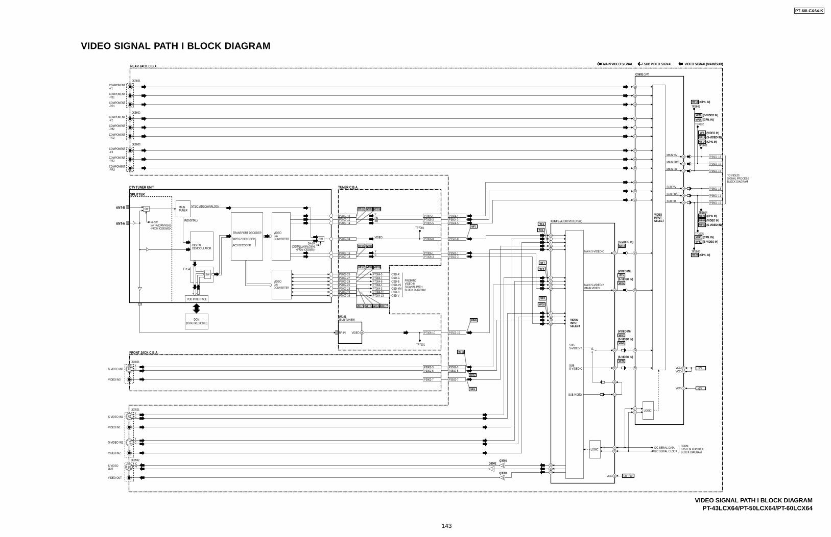
PT-43LCX64/PT-50LCX64/PT-60LCX64
VIDEO SIGNAL PATH I BLOCK DIAGRAM
VIDEO SIGNAL PATH I BLOCK DIAGRAM
WF2
WF3
WF7
WF9
WF8
WF10
WF11
WF12
WF4
WF1
WF46
WF50(S-VIDEO IN)
WF49(S-VIDEO IN)WF47
(VIDEO IN)
WF22 (CPN. IN)
WF17 (CPN. IN)
WF18 (CPN. IN)WF16 (S-VIDEO IN)
WF19 (CPN. IN)
WF15 (S-VIDEO IN)WF6 (VIDEO IN)
WF21 (CPN. IN)WF52 (S-VIDEO IN)
WF20 (CPN. IN)WF48 (VIDEO IN)WF51 (S-VIDEO IN)
WF14
WF13
(S-VIDEO IN)
(S-VIDEO IN)
WF5(VIDEO IN)
WF182 WF183
WF185 WF186
WF184
WF187 WF188 WF189
WF174 WF175 WF176 WF177
S-VIDEO IN1
FRONT JACK C.B.A.
TUNER C.B.A.DTV TUNER UNIT
SPLITTER
ANT-A
ANT-B
REAR JACK C.B.A.
Q3501Q3502
Q3503
VIDEO IN1
VIDEO IN2
S-VIDEO IN2
IC3501 (AUDIO/VIDEO SW)
IC3602 (SW)
VIDEORF-IN
SW
U7101 (SUB TUNER)
18
P7006-8
P7006-1P7006-3
S-VIDEO IN3
OSD-R
FROM/TOVIDEO IISIGANAL PATHBLOCK DIAGRAM
OSD-GOSD-BOSD-YSOSD-YMOSD-HOSD-V
VIDEO IN3
COMPONENT-Y1
COMPONENT-PB1
COMPONENT-PR1
COMPONENT-Y2
COMPONENT-PB2
COMPONENT-PR2
YC
YC
YC
S-VIDEO OUT
VIDEO OUT
P7006-10 P3503-10
P3503-8
P3503-1P3503-3
P3604-1P3604-3P3604-5
P7005-1P7005-3P7005-5
P7007-34
P7007-16P7007-18
P7007-10P7007-12P7007-14
P3502-7
P3502-5P3502-3
P3902-7
P3601-18MAIN Y/V
MAIN PB/C
MAIN PR
SUB Y/V
TO VIDEO I SIGNAL PROCESSBLOCK DIAGRAM
SUB PB/C
SUB PR
TP3601
TP3604
TP3605
TP3606
TP3602
TP3603
P3601-16
P3601-15
P3902-5P3902-3
63181530
31017
51219
24
26
373941
47
44
56
58
53
49
MAIN S-VIDEO-C
MAIN S-VIDEO-Y/MAIN VIDEO
VIDEOINPUTSELECT
VIDEOINPUTSELECT
LOGIC I2C SERIAL DATA FROMSYSTEM CONTROLBLOCK DIAGRAM
SUB VIDEO
SUB S-VIDEO-Y
SUB S-VIDEO-C
I2C SERIAL CLOCK
B
BB
3433
LOGIC
JK3601
JK3602
JK3501
JK4801
JK3502CY
COMPONENT-Y3
COMPONENT-PB3
COMPONENT-PR3
JK3603
VCC 42 SW +9V
14
16
18
5
7
9
57
59
61
48
50
52
67
66
74
75
23
46
44
43
P3601-13
P3601-11
P3601-10
38
36
35
31VCC +9V47VCC
1VCC +5V
TP7001
TP7101
MAIN VIDEO SIGNAL SUB VIDEO SIGNAL VIDEO SIGNAL(MAIN/SUB)
P7007-25 P7004-5P7004-7P7004-9P7004-1P7004-3P7004-11P7004-13
P7007-27P7007-29P7007-21P7007-23P7007-19P7007-39
SW
SW
MAIN TUNER
DIGITALDEMODULATOR
IF(DIGITAL)
NTSC VIDEO(ANALOG)
FPGA
POD INTERFACE
VIDEOD/ACONVERTER
VIDEOD/ACONVERTER
TRANSPORT DECODER
MPEG2 DECODER
AC3 DECODER
DCM(DIGITAL CABLE MODULE)
YPBPR
VIDEO
YC
RF-SW(ANT-A(L)/ANT-B(H))<FROM IC6003(42)>
D/A-SW(DIGITAL(L)/ANALOG(H))
<FROM IC6003(58)>
PT-60LCX64-K
143
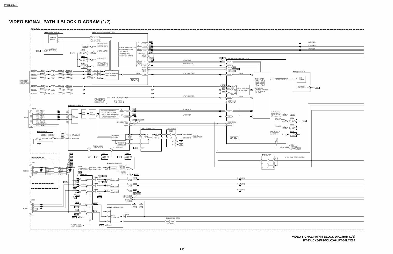
PT-43LCX64/PT-50LCX64/PT-60LCX64
VIDEO SIGNAL PATH II BLOCK DIAGRAM (1/2)
WF60
WF59
WF62
WF61
WF58
WF56
WF193
WF57
WF194
WF53
WF195
WF71
WF72
WF73
WF75 WF74
WF63 WF64
WF196
WF197
WF198
WF199
WF190
WF192
WF191
WF54
WF55
WF23
WF24
WF25
WF29
WF32
WF33
WF34
WF35
WF26
WF27
WF28
WF36
WF37WF38
WF39
WF30
WF31
WF65
WF66
WF67 WF68 WF69
MAIN C.B.A.
IC5005 (MAIN VIDEO SIGNAL PROCESS)IC5002 (5.6M FIFO MEMORY)
IC5009 (SUB VIDEO SIGNAL PROCESS)
FRONT JACK C.B.A.
FROMSYSTEM CONTROLBLOCK DIAGRAM
Q5001B
Q5006B
Q5010B
Q5002B
Q5003B
Q5507
B
Q5508
B
Q5509
Q5510
B
P3901-1P3901-3P3901-5P3901-7P3901-9
P5501-1P5501-3P5501-5P5501-7P5501-9
R
HDMI-IN
GBH-SYNCV-SYNC
JK3901
JK5801
R
RGB-IN 1
RGB-IN 2
GBH-SYNCV-SYNC
JK5501
IC5501 (SW)
Q5803
IC5803 (HDMI INTERFACE)
IC5805 (D/A CONVERTER)
IC5504 (A/D CONVERTER)
IC5502 (SYNC SEPARATION)
IC5802 (EEPROM)
IC5301 (LEVEL SHIFTER)
21
19
15
22
14
HL
R
G
B
HL
HL
HL
HL
16
RGB1(H)RGB2(L)<FROM IC6003(22)>
VCC20
P3403-18
P3403-16
P3403-15
P3403-13
P3403-11
P3403-10
17
39
511
2423
1213
54
5756
48
43
A/DCONVERTER
A/D H-SYNCA/D CLOCK
H-SYNCV-SYNC
I2CCONTROL
D/AAUDIODATAINTERFACE
I2C SERIAL DATA 1 I2C SERIAL CLOCK 1
TP5501
TP5502
TP5504 TP5505
TP5503
I2C SERIAL CLOCK
TMDS DATA0(+)TMDS DATA0(-)TMDS DATA1(+)TMDS DATA1(-)TMDS DATA2(+)TMDS DATA2(-)
I2C SERIAL CLOCKI2C SERIAL DATA
TMDS CLOCK(+)TMDS CLOCK(-)
I2C SERIAL DATA
I2C SERIAL CLOCK
I2C SERIAL DATA
CARD Y/PB/PR DATA(8BIT)
3D Y/C SEPARATIONNTSC DECODER
A/D
2D Y/C SEPARATIONNTSC DECODER
I/P CONVERTER
Y/PB/PR --RGB CONVERTERSHARPNESS CONTROLTINT CONTROLCOLOR CONTROLBRIGHTNESS CONTROL
FROM SD/PC CARDSIGNAL PROCESS BLOCK DIAGRAM
70-77
A/DCONVERTER
2-9
A/DCONVERTER
SYNCSEPARATION
12-19
Y
R DATA(8BIT)
G DATA(8BIT)
B DATA(8BIT)
UV
H-SYNCV-SYNC
HDMI CLOCK(76MHz)H-SYNCV-SYNC
CLOCK(76MHz)
49-55,58
95
72
83
LPF
Q5007B
Q5012,Q5013 BLPF
Q5008B
Q5011BLPF
Q5015B
Q5023B
Q5027B
Q5016B
Q5017B
103
89
101
LPF
Q5024B
Q5029,Q5030 BLPF
Q5025B
Q5028BLPF
TMDS DECODER
XORMASK
MODECONTROL
AUDIO DATADECODER
MAIN CLOCKGENERATOR
VIDEO DATA CONVERSIONCOLOR RANGE SCALINGCOLOR SPACE CONVERSIONUP/DOWN CONVERSION
A/D
A/D
14
136
8
4
6766
3130
1 2
IC5804 (OP AMP)
3 1
5 7
4
8
135-142
193-200,216-231,246-253
49-58
22-31
36-45
180-189
162-171
148-157
6-13
153-160
123-127,140-144
120-122,128,129,138,139,145-147
199-206
FROM VIDEO ISIGNAL PATHBLOCK DIAGRAM
5.6M FIFOMEMORY
IC5012 (64M SDRAM)
64MSDRAM
36-39,42-44,48
8786929197968483
6
5
77
76
DRIVEQ5802
DRIVE
3334
46
D/A
MULTI WINDOW
480i --> 480p1080i --> 1080i480p --> 480p720p --> 720p
PICTURE IN PICTURESPLIT SCREENSEARCH
Y/V
R R DATA (8BIT)
G DATA (8BIT)
B DATA (8BIT)
Y/PB/PR
76MHz CLOCK
Y/PB/PR
Y/PB/PR
CLOCKV-SYNCH-SYNC
Y Y DATA (10BIT)
PB/PR DATA (10BIT)
Y/PB/PR DATA (10BIT)
Y/PB/PR DATA (8BIT)
UV DATA (8BIT)
HDMI AUDIO (R) TO AUDIOBLOCK DIAGRAM
HDMI AUDIO (L)
Y DATA (8BIT)
PB/PR
G
B
PB/C
PR
Y/V
PB/C
PR
VCC8
+5V
+3.3V VCC1,13,19,22,35,41,49,52,53,58,66
+3.45V VCC
2,18,34,47,60,107,119,132,149,166,181,185,195,197,208,213,224
VCC67,69,77,79,89,91,100
VCC173,177,189,229,233
VCC
3,17,33,46,59,106,131,151,170,183,193,211,236,241,246,253
+3.3V
VCC
1,6,11,14,17,,21,40,47,56,64,67,100
VCC80,82,89,93,95
+5V
IC5801
+3.3VREG. +5V23
IC5503
+3.3VREG. 18
+5V
VCC16+5V
+3.3V
-5V
+5V
11,22,23,69,78,79
VCC
VCC
14+5V VCC
VEE
26,27,34,35,39,42,45,46,51,52,59,62 VCC
130CARD V-SYNC129
131
CARD H-SYNCCARD V-SYNCCARD H-SYNC
+3.3V
IC5006
+2.5VREG. 45
IC5003
+2.5VREG. 31
IC5004
+2.5VREG. 45
+3.3V1,3,9,15,29,35,41,43,49,55,75,81 VCC
FROMSD/PC CARDSIGNAL PROCESSBLOCK DIAGRAM
27MHz CLOCK
RGB MW(L) <FROM IC6003(79)>
+3.45V
+3.3V
VCC
11,27,43,60,64,109,119,133,146,159,175,191,202,214,233,244,255
VCC3,8,67,73
VCC76,86,96,106
VCC
CLO
CK(2
7MHz
)
12,26,42,59,110,118,134,147,160,176,190,201,213,232,243,254
IC5011
+2.5VREG. 54
IC5008
+2.5VREG. 13
IC5010
+2.5VREG. 54
34-41Y
47-54UV
A/D
A/D
A/D
GCM2+
GCS2+
16
V-SYNC 162
H-SYNC
CLOCKV-SYNCH-SYNC
163
161172173
322120
555657
IC5014 (BUFFER)
8
11
6
109131245
323031
26
23
10
114
1
27
4.4 dB
5V --> 3.3V
VIDEO SIGNAL PATH II BLOCK DIAGRAM (1/2)
PT-60LCX64-K
144
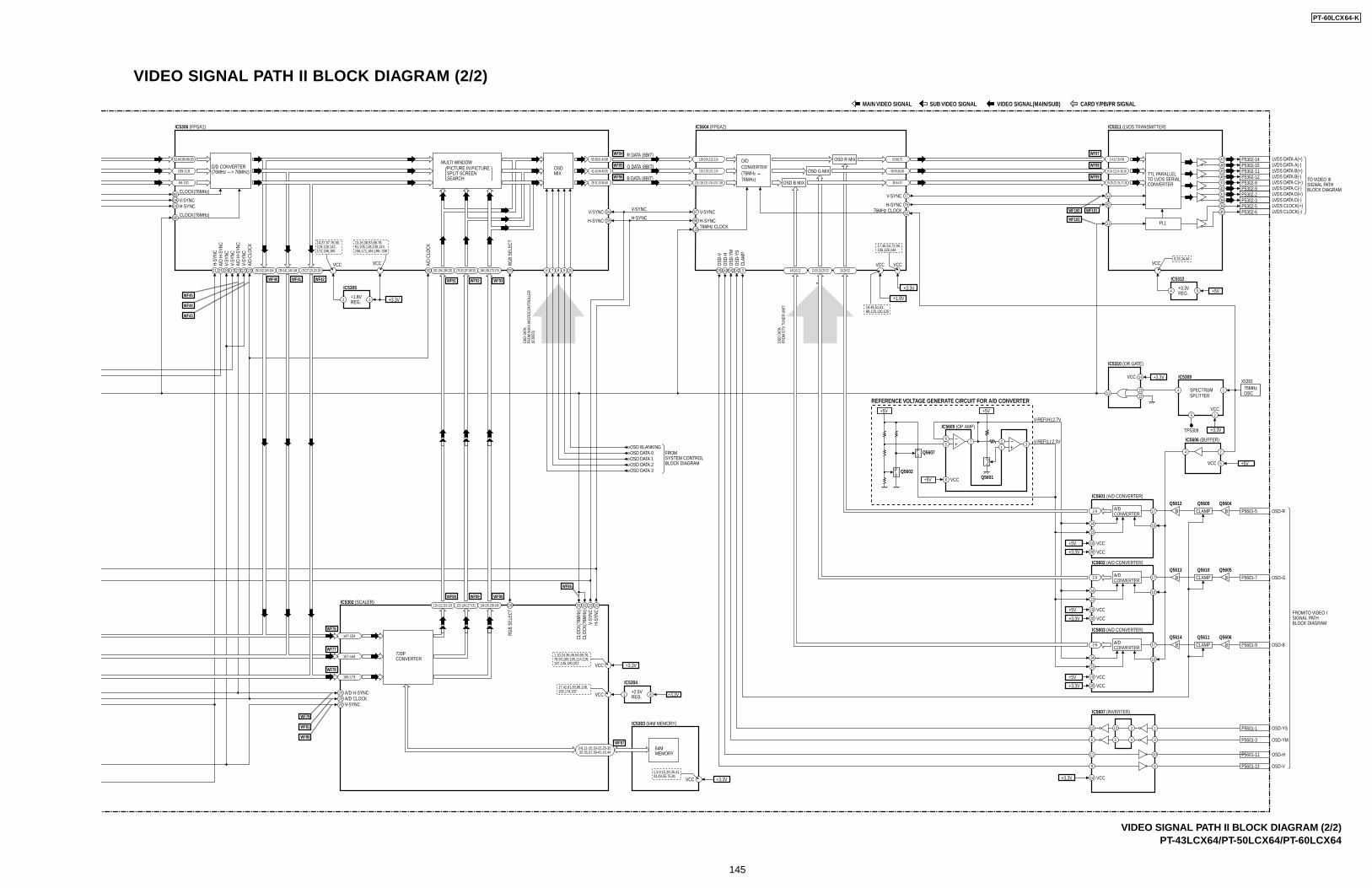
PT-43LCX64/PT-50LCX64/PT-60LCX64
VIDEO SIGNAL PATH II BLOCK DIAGRAM (2/2)
WF40
WF45
WF44
WF43
WF41 WF42
WF76
WF77
WF78
WF91 WF92 WF93
WF94
WF95
WF96
WF97
WF98
WF99
WF100 WF101
WF102
WF88 WF89 WF90
WF87
WF79
WF81
WF80
WF86
321
Q5601
+5V
765
8 VCC
Q5607
Q5602
+5V
+5V
P5601-1
P5601-3
P5601-11
P5601-13
IC5306 (FPGA1)
P5302-14D/D CONVERTER(76MHz ---> 76MHz)
720PCONVERTER
R DATA (8BIT)
G DATA (8BIT)
B DATA (8BIT)
V-SYNC
H-SYNCH-
SYNC
A/D
H-SY
NCV-
SYNC
V-SY
NCA/
D H-
SYNC
V-SY
NCA/
D CL
OCK
CLOCK(76MHz)
CLOCK(76MHz)
A/D
CLO
CK
RGB
SELE
CTRG
B SE
LECT
Q5604Q5609
OSDMIX
IC5311 (LVDS TRANSMITTER)
IC5302 (SCALER)
IC5303 (64M MEMORY)
47
P5302-1548
P5302-1145
P5302-1246
P5302-841
P5302-942
P5302-237
P5302-338
P5302-539
P5302-6
P5601-5
40
175178176
11 15 16 17 123 182122 120 6 7 8 9 10
110-112,115-119
147-154
82-84,86-89,93
109-116
150-152,160-164 192-194,198-202
56-58,61-64,68
41-43,46-49,55
29-31,33-36,40
2-4,6,7,54-56
8,10-12,14-16,18
19,20,22-25,27,28
IC5604 (FPGA2)
100-104,112-114
115-118,121-124
125,126,131-134,137,138
63-69,75
48-50,56-60
38-44,47
24,26-3213-15,18,20-234-8,10-12178-181,187-189,191 166-169,173-176138-141,145-148 125-127,129,133-136
94-101
157-164
166-173
122-124,127-131 134,135,138-143 102 101
185
81 92
OSD DATA 0OSD DATA 1OSD DATA 2OSD DATA 3
H-SY
NCV-
SYNC
CLO
CK(7
6MHz
)CL
OCK
(76M
Hz)
OSD BLANKING
LVDS DATA A(+)
TO VIDEO IIISIGNAL PATHBLOCK DIAGRAM
LVDS DATA A(-)LVDS DATA B(+)LVDS DATA B(-)LVDS DATA C(+)LVDS DATA C(-)LVDS DATA D(+)LVDS DATA D(-)LVDS CLOCK(+)LVDS CLOCK(-)
FROMSYSTEM CONTROLBLOCK DIAGRAM
64MMEMORY
31
51
52
204
205
A/D H-SYNCA/D CLOCKV-SYNC
MULTI WINDOWPICTURE IN PICTURESPLIT SCREENSEARCH
TTL PARALLELTO LVDS SERIALCONVERTER
PLL
OSD R MIXD/DCONVERTER(76MHZ
76MHZ)
OSD G MIX
OSD B MIX
VCC9,26,34,44
+5V
IC5312
+3.3VREG. 54
+3.3V
1,3,9,15,29,35,41,43,49,55,75,81
VCC
+3.3V
1,10,24,36,46,54,68,76,78,93,100,105,114,126,137,145,180,201 VCC
3-8,11-15,18-22,25-30,32-35,37,39-41,43,44
IC530417,42,61,83,86,108,156,174,207
VCC +3.3V+2.5VREG. 81
1312
11
VCC
VCC
VCC
X5301
SPECTRUMSPLITTER
A/DCONVERTER
14 +3.3V
+1.8V
+3.3V
IC5309
1
2
4
5
+3.3V
76MHzOSC
TP5309
VCC
13,26,38,53,66,78,91,105,118,130,143,156,171,184,196, 208
VCC
14,37,67,76,90,119,128,142,172,186,195
+3.3V
IC5305
+1.8VREG. 13
V-SYNC
H-SYNC
V-SYNC
H-SYNCV-SYNC
H-SYNC
IC5310 (OR GATE)
IC5601 (A/D CONVERTER)
MAIN VIDEO SIGNAL SUB VIDEO SIGNAL VIDEO SIGNAL(MAIN/SUB) CARD Y/PB/PR SIGNAL
+3.3V
+3.3V
+5V
+5V
V-SYNCH-SYNC
80108102
106
203
17
10
B
Q5612
B CLAMP2-9
Q5605Q5610
P5601-7A/DCONVERTER
IC5602 (A/D CONVERTER)
17
10
B
Q5613
B CLAMP2-9
Q5606Q5611
P5601-9A/DCONVERTER
VCC
VCC
OSD-R
OSD-G
OSD-B
FROM/TO VIDEO ISIGNAL PATHBLOCK DIAGRAM
OSD-YS
OSD-YM
OSD-H
OSD-V
VCC
IC5603 (A/D CONVERTER)
17
10
B
Q5614
B CLAMP2-9
IC5607 (INVERTER)
12
6
13
5
2
4
1
3
10
IC5606 (BUFFER)
4 2
5
11
8
14
19
20
9
97
98
76MHz CLOCK
OSD
-VO
SD-H
OSD
-YM
OSD
-YS
CLAM
P
129
139 141141 142 3
77
76
76MHz CLOCK52
VCC VCC
17,36,53,72,98,106,128,144
19,46,51,61,88,120,130,135
14
13
+3.3V
+5V VCC
VCC
19
20
14
13
+3.3V
+5V VCC
VCC
19
20
14
13
REFERENCE VOLTAGE GENERATE CIRCUIT FOR A/D CONVERTER
IC5605 (OP AMP)V-REF(H):2.7V
V-REF(L):2.3V
OSD
DAT
AFR
OM
DTV
TUN
ER U
NIT
OSD
DAT
AFR
OM
MAI
N M
ICRO
CONT
ROLL
ER(IC
6003
)
VIDEO SIGNAL PATH II BLOCK DIAGRAM (2/2)
PT-60LCX64-K
145
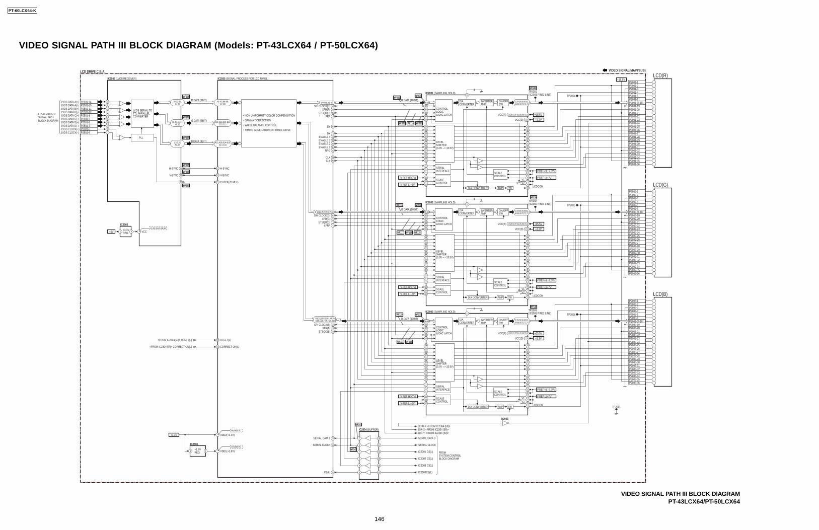
VIDEO SIGNAL PATH III BLOCK DIAGRAM (Models: PT-43LCX64 / PT-50LCX64)
VIDEO SIGNAL PATH III BLOCK DIAGRAM
WF125
WF126
WF127
WF128
WF129
WF130
WF141
WF142
WF131WF112
WF132WF116
WF117 WF118 WF119
WF133
WF121 WF122
WF120
WF140
WF139
WF138
WF113 WF114 WF115
LCD DRIVE C.B.A.
P2001-1P2001-2P2001-3P2001-4P2001-5P2001-6P2001-(7-18)P2001-19P2001-20P2001-21P2001-22P2001-23P2001-24P2001-25P2001-26P2001-27P2001-28P2001-29P2001-30P2001-31P2001-32P2001-33P2001-34P2001-35P2001-36
P2002-36
P2002-2P2002-1
P2002-3P2002-4P2002-5P2002-6P2002-(7-18)P2002-19P2002-20P2002-21P2002-22P2002-23P2002-24P2002-25P2002-26P2002-27P2002-28P2002-29P2002-30P2002-31P2002-32P2002-33P2002-34P2002-35P2002-36
P2003-1P2003-2P2003-3P2003-4P2003-5P2003-6P2003-(7-18)P2003-19P2003-20P2003-21P2003-22P2003-23P2003-24P2003-25P2003-26P2003-27P2003-28P2003-29P2003-30P2003-31P2003-32P2003-33P2003-34P2003-35P2003-36
P2501-14P2501-15P2501-11P2501-12P2501-8P2501-9P2501-2P2501-3P2501-5P2501-6
IC2505 (SIGNAL PROCESS FOR LCD PANEL)IC2503 (LVDS RECEIVER)
IC2501
+15.5VLCD(R)
LCD(G)
LCD(B)
VIDEO SIGNAL(MAIN/SUB)
W4-W6,Y1-Y7
W15-W19,Y16-Y20
A5-A7,B6-B8,C7,C8
A10-A12,B10-B12,C10,C11
A15,A16,B14-B16,C14-C16
30,32-35,37-39
41-43,45-47,49,50
1-3,5,51,53-55
VDD2(+3.3V)+3.3V
+5V
+1.8VREG. VDD1(+1.8V)
V1V2
W3U1
V13Y15Y13
K18K20
W13
J19
1091211161520191817
E2
D2
E1
H2
29
27
26
C19
18
IC2502
+3.3VREG. VCC45
13,23,31,40,48,56
H-SYNC
V-SYNC
H-SYNC
R DATA (8BIT) R DATA (10BIT)
G DATA (10BIT)
B DATA (10BIT)
LVDS DATA A(+)
FROM VIDEO II SIGNAL PATH BLOCK DIAGRAM
LVDS DATA A(-)LVDS DATA B(+)LVDS DATA B(-)LVDS DATA C(+)LVDS DATA C(-)LVDS DATA D(+)LVDS DATA D(-)LVDS CLOCK(+)LVDS CLOCK(-)
G DATA (8BIT)
B DATA (8BIT)
V-SYNC
CLOCK(76 MHz)
SERIAL CLOCK
SERIAL DATA 0
CS(L)
SERIAL CLOCK
FROMSYSTEM CONTROLBLOCK DIAGRAM
SERIAL DATA 0
DIR-X <FROM IC2304 (59)>DIR-Y <FROM IC2304 (50)>
IC2001 CS(L)
IC2002 CS(L)
IC2003 CS(L)
IC2505CS(L)
<FROM IC2304(52)> RESET(L)
<FROM IC2304(57)> CORRECT ON(L)
RESET(L)
CORRECT ON(L)
FRP
DY
DXENABLE 4ENABLE 3ENABLE 2ENABLE 1
NRG
CLXCLY
XFRP
STSQO(R)XFR(R)
S/H CLOCK(R)
STSQO(G)XFR(G)
S/H CLOCK(G)
STSQO(B)XFR(B)
S/H CLOCK(B)
LVDS SERIAL TOTTL PARALLELCONVERTER
PLL
+3.3V
+15.5V
V-REF-H(+7V)
V-REF-L(+5V)
V-REF-H(+7.5V)
V-REF-L(+7V)
IC2001 (SAMPLING HOLD)
96979899100 VCC(D)
TP2004
VCC(A)
86-95 52,54,56,58,60,62,64,66,68,70,72,74
15,26,53,57,61,65,69,73,82
1,50
CONTROL LOGIC& DAC LATCH
LEVEL SHIFTER(3.3V --> 15.5V)
D/A CONVERTER
INVERTERAMP
INVERTERAMP
ON/OFFSW
ON/OFFSW
INVERTERAMP
ON/OFFSW
D/A CONVERTER AMP SW
M19
Y10V9W9Y9W10M1
W8M18
2423333736353427223825
354
SERIALINTERFACE
SCALECONTROL
V1V2
121110
818079777813
SCALECONTROL
V-REF-H(+7.5V)
V-REF-L(+7V)
V-REF-H(+7.5V)
V-REF-L(+7V)
1918394342414028
44452021
+3.3V
+15.5V
IC2002 (SAMPLING HOLD)
IC2003 (SAMPLING HOLD)
+3.3V
+15.5V
IC2504 (BUFFER)
V-REF-H(+7V)
V-REF-L(+5V)
V-REF-H(+7V)
V-REF-L(+5V)
D20,E19,E20,F19,F20,G19,G20,H19,H20,J18
2
3
7
5
4
6
18
17
13
15
16
14
B18
B20
B19
XDIR-X <FROM IC2304 (60)>
Q2003
TP2005
TP2006
TP2901
96979899100 VCC(D)
VCC(A)
86-95 52,54,56,58,60,62,64,66,68,70,72,74
15,26,53,57,61,65,69,73,82
1,50
CONTROL LOGIC& DAC LATCH
LEVEL SHIFTER(3.3V --> 15.5V)
D/A CONVERTER
D/A CONVERTER AMP SW
2423333736353427223825
354
SERIALINTERFACE
SCALECONTROL
V1V2
LCDCOM
LCDCOM
LCDCOM
121110
818079777813
SCALECONTROL
19183943424140281744452021
96979899100 VCC(D)
VCC(A)
86-95 52,54,56,58,60,62,64,66,68,70,72,74
15,26,53,57,61,65,69,73,82
1,50
CONTROL LOGIC& DAC LATCH
LEVEL SHIFTER(3.3V --> 15.5V)
D/A CONVERTER
D/A CONVERTER AMP SW
2423333736353427223825
354
SERIALINTERFACE
SCALECONTROL
V1V2
121110
818079777813
SCALECONTROL
1918394342414028
44452021
NON UNIFORMITY COLOR COMPENSATION
GAMMA CORRECTION
WHITE BALANCE CONTROL
TIMING GENERATOR FOR PANEL DRIVE
6
6
6
TP2001(IC2001 PIN52 LINE)
TP2003(IC2003 PIN52 LINE)
TP2002(IC2002 PIN74 LINE)
H4,H5,ETC
D7,D8,ETC
PT-43LCX64/PT-50LCX64
PT-60LCX64-K
146
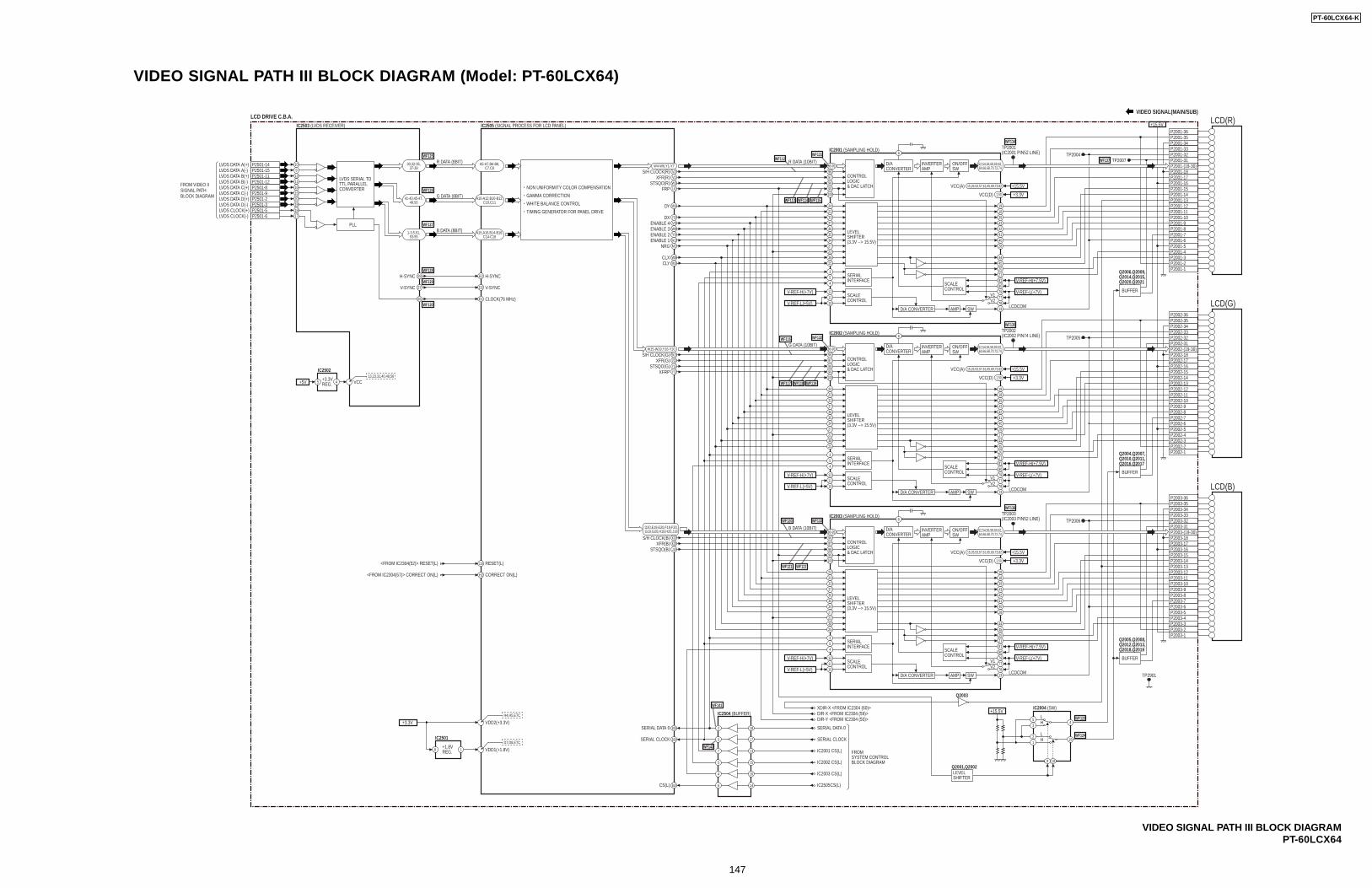
VIDEO SIGNAL PATH III BLOCK DIAGRAM (Model: PT-60LCX64)
VIDEO SIGNAL PATH III BLOCK DIAGRAM
WF125
WF126
WF127
WF128
WF129
WF130
WF141
WF142
WF133
WF117 WF118 WF119
WF132WF116
WF131WF112
WF113 WF114 WF115
WF134
WF135
WF137
WF136
WF123
WF124
WF121 WF122
WF120
LCD DRIVE C.B.A.
P2001-36P2001-35P2001-34P2001-33P2001-32P2001-31P2001-(19-30)P2001-18P2001-17P2001-16P2001-15P2001-14P2001-13P2001-12P2001-11P2001-10P2001-9P2001-8P2001-7P2001-6P2001-5P2001-4P2001-3P2001-2P2001-1
P2002-36
P2002-35P2002-36
P2002-34P2002-33P2002-32P2002-31P2002-(19-30)P2002-18P2002-17P2002-16P2002-15P2002-14P2002-13P2002-12P2002-11P2002-10P2002-9P2002-8P2002-7P2002-6P2002-5P2002-4P2002-3P2002-2P2002-1
P2003-36P2003-35P2003-34P2003-33P2003-32P2003-31P2003-(19-30)P2003-18P2003-17P2003-16P2003-15P2003-14P2003-13P2003-12P2003-11P2003-10P2003-9P2003-8P2003-7P2003-6P2003-5P2003-4P2003-3P2003-2P2003-1
P2501-14P2501-15P2501-11P2501-12P2501-8P2501-9P2501-2P2501-3P2501-5P2501-6
IC2505 (SIGNAL PROCESS FOR LCD PANEL)IC2503 (LVDS RECEIVER)
IC2501
BUFFER
BUFFER
BUFFER
+15.5V LCD(R)
LCD(G)
LCD(B)
Q2006,Q2009,Q2014,Q2015,Q2020,Q2021
Q2004,Q2007,Q2010,Q2011,Q2016,Q2017
Q2005,Q2008,Q2012,Q2013,Q2018,Q2019
VIDEO SIGNAL(MAIN/SUB)
W4-W6,Y1-Y7
W15-W19,Y16-Y20
A5-A7,B6-B8,C7,C8
A10-A12,B10-B12,C10,C11
A15,A16,B14-B16,C14-C16
30,32-35,37-39
41-43,45-47,49,50
1-3,5,51,53-55
VDD2(+3.3V)+3.3V
+5V
+1.8VREG. VDD1(+1.8V)
V1V2
W3U1
V13Y15Y13
K18K20
W13
J19
109
1211161520191817
E2
D2
E1
H2
29
27
26
C19
18
IC2502
+3.3VREG. VCC45
13,23,31,40,48,56
H-SYNC
V-SYNC
H-SYNC
R DATA (8BIT) R DATA (10BIT)
G DATA (10BIT)
B DATA (10BIT)
LVDS DATA A(+)
FROM VIDEO II SIGNAL PATH BLOCK DIAGRAM
LVDS DATA A(-)LVDS DATA B(+)LVDS DATA B(-)LVDS DATA C(+)LVDS DATA C(-)LVDS DATA D(+)LVDS DATA D(-)LVDS CLOCK(+)LVDS CLOCK(-)
G DATA (8BIT)
B DATA (8BIT)
V-SYNC
CLOCK(76 MHz)
SERIAL CLOCK
SERIAL DATA 0
CS(L)
SERIAL CLOCK
FROMSYSTEM CONTROLBLOCK DIAGRAM
SERIAL DATA 0
DIR-X <FROM IC2304 (59)>DIR-Y <FROM IC2304 (50)>
IC2001 CS(L)
IC2002 CS(L)
IC2003 CS(L)
IC2505CS(L)
<FROM IC2304(52)> RESET(L)
<FROM IC2304(57)> CORRECT ON(L)
RESET(L)
CORRECT ON(L)
FRP
DY
DXENABLE 4ENABLE 3ENABLE 2ENABLE 1
NRG
CLXCLY
XFRP
STSQO(R)XFR(R)
S/H CLOCK(R)
STSQO(G)XFR(G)
S/H CLOCK(G)
STSQO(B)XFR(B)
S/H CLOCK(B)
LVDS SERIAL TOTTL PARALLELCONVERTER
PLL
+3.3V
+15.5V
V-REF-H(+7V)
V-REF-L(+5V)
V-REF-H(+7.5V)
V-REF-L(+7V)
IC2001 (SAMPLING HOLD)
96979899100 VCC(D)
TP2004
VCC(A)
86-95 52,54,56,58,60,62,64,66,68,70,72,74
15,26,53,57,61,65,69,73,82
1,50
CONTROL LOGIC& DAC LATCH
LEVEL SHIFTER(3.3V --> 15.5V)
D/A CONVERTER
INVERTERAMP
INVERTERAMP
ON/OFFSW
ON/OFFSW
INVERTERAMP
ON/OFFSW
D/A CONVERTER AMP SW
M19
Y10V9W9Y9W10M1
W8M18
2423333736353427223825
354
SERIALINTERFACE
SCALECONTROL
V1V2
121110
818079777813
SCALECONTROL
V-REF-H(+7.5V)
V-REF-L(+7V)
V-REF-H(+7.5V)
V-REF-L(+7V)
1918394342414028
44452021
+3.3V
+15.5V
IC2002 (SAMPLING HOLD)
IC2003 (SAMPLING HOLD)
+3.3V
+15.5V
+15.5VIC2504 (BUFFER)IC2004 (SW)
HL
HL
V-REF-H(+7V)
V-REF-L(+5V)
V-REF-H(+7V)
V-REF-L(+5V)
D20,E19,E20,F19,F20,G19,G20,H19,H20,J18
2
3
7
5
4
6
18
17
13
15
16
14
B18
B20
B19
XDIR-X <FROM IC2304 (60)>
453
1521
9 10
LEVEL SHIFTER
Q2001,Q2002
Q2003
TP2007
TP2005
TP2006
TP2901
96979899100 VCC(D)
VCC(A)
86-95 52,54,56,58,60,62,64,66,68,70,72,74
15,26,53,57,61,65,69,73,82
1,50
CONTROL LOGIC& DAC LATCH
LEVEL SHIFTER(3.3V --> 15.5V)
D/A CONVERTER
D/A CONVERTER AMP SW
2423333736353427223825
354
SERIALINTERFACE
SCALECONTROL
V1V2
LCDCOM
LCDCOM
LCDCOM
121110
818079777813
SCALECONTROL
19183943424140281744452021
96979899100 VCC(D)
VCC(A)
86-95 52,54,56,58,60,62,64,66,68,70,72,74
15,26,53,57,61,65,69,73,82
1,50
CONTROL LOGIC& DAC LATCH
LEVEL SHIFTER(3.3V --> 15.5V)
D/A CONVERTER
D/A CONVERTER AMP SW
2423333736353427223825
354
SERIALINTERFACE
SCALECONTROL
V1V2
121110
818079777813
SCALECONTROL
1918394342414028
44452021
NON UNIFORMITY COLOR COMPENSATION
GAMMA CORRECTION
WHITE BALANCE CONTROL
TIMING GENERATOR FOR PANEL DRIVE
6
6
6
TP2001(IC2001 PIN52 LINE)
TP2003(IC2003 PIN52 LINE)
TP2002(IC2002 PIN74 LINE)
H4,H5,ETC
D7,D8,ETC
PT-60LCX64
PT-60LCX64-K
147
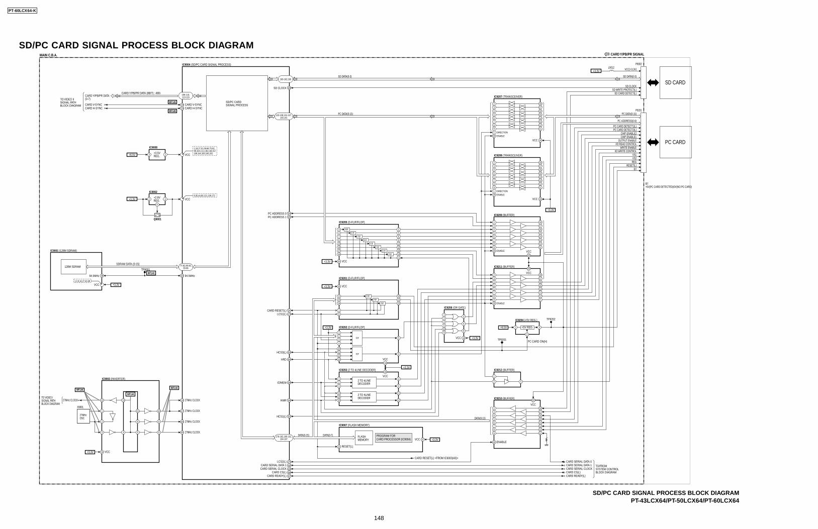
PT-43LCX64/PT-50LCX64/PT-60LCX64
SD/PC CARD SIGNAL PROCESS BLOCK DIAGRAM
SD/PC CARD SIGNAL PROCESS BLOCK DIAGRAM
IC9004 (SD/PC CARD SIGNAL PROCESS)
IC9001 (128M SDRAM)
IC9003 (INVERTER)
IC9207 (TRANSCEIVER)
160-162,165
106-110,113-115
77-82,85-90,93-96
178-182,185-191,194-197
122-128,131-137,140,141
169
IC9208 (TRANSCEIVER)
IC9209 (BUFFER)
IC9211 (BUFFER)
234567891
19
119
19
19
1817161514131211
IC9206 (OR GATE)
IC9204 (+5V REG.)
23456789
1817161514131211
23456789
1817161514131211
IC9210 (BUFFER)
1817161514131211
23456789
1817161514131211
IC9205 (D-FLIP/FLOP)
3478
13141718
11
2569
12151619
IC9201 (D-FLIP/FLOP)
111314
19
101215
F/FF/F
F/F
IC9202 (D-FLIP/FLOP)
1234
101112
5
9
F/F
13
F/F
IC9203 (2 TO 4LINE DECODER)
123
131415
4
5
11
12
2 TO 4LINE DECODER
2 TO 4LINE DECODER
F/FF/F
F/FF/F
F/FF/F
F/F
DIRECTIONENABLE
DIRECTIONENABLE
ENABLE
ENABLE
F/F
154155
118119
128M SDRAMSDRAM DATA (0-15)
CARD V-SYNCCARD H-SYNC
CARD V-SYNCSD/PC CARDSIGNAL PROCESS
SD CLOCK
PC ADDRESS 0PC ADDRESS 1
CARD RESET(L)LCS1(L)
HCS3(L)
HRD
IO/MEM
HWR
HCS1(L)
CARD H-SYNC
CARD Y/PB/PR DATA(0-7)
CARD Y/PB/PR DATA (8BIT) : 480i
TO VIDEO IISIGNAL PATHBLOCK DIAGRAM
IC9007 (FLASH MEMORY)
FLASH MEMORY
SD CARD
PC CARD
SD WRITE PROTECT(L)SD CARD DETECT(L)
PC CARD DETECT1(L)PC CARD DETECT2(L)
CHIP ENABLE2CHIP ENABLE1
OUTPUT ENABLEI/O READ CONTROL
WRITE ENABLEI/O WRITE CONTROL
VS1VS2REG
RESET(L)
+5V(PC CARD DETECTED)/0V(NO PC CARD)
SD CLOCK
P9002
P9201
SD DATA(0-3)
VCC(+3.3V)L9012
SD DATA(0-3)
PC DATA(0-15)
DATA(0-15) DATA(0-7)
DATA(8-15)
PC DATA(0-15)
PC ADDRESS(0-9)
13
4
11
9
5 6
8
10
12
1
2
3
27MHzOSC
27MHz CLOCK 27MHz CLOCK
27MHz CLOCK
27MHz CLOCK
27MHz CLOCK
TO VIDEO I SIGNAL PATHBLOCK DIAGRAM
X9001
116
117
105
49
MAIN C.B.A.
12
3
45
6
109
8
IC9212 (BUFFER)
2
1
4
17424
153
150
149
152
CARD RESET(L) <FROM IC6003(43)>
+3.3V +6.5V
158
+5V REG.1
2
3
142143166
CARD SERIAL DATA 0TO/FROMSYSTEM CONTROLBLOCK DIAGRAM
CARD SERIAL DATA 1CARD SERIAL CLOCKCARD CS(L)
CARD SERIAL DATA 1CARD SERIAL CLOCK
CARD CS(L)167 CARD READY(L)CARD READY(L)
175LCS2(L)
23456789
IC9008
+3.5VREG.
+2.8VREG.
23
1,18,27,51,59,68,75,92,99,104,111,130,148,157,159,164,183,193,201VCC
9,35,44,83,121,139,172
VCC
IC9002
32
4
+6.5V
+3.3V
Q9001
VCC14+3.3V
VCC 37 +3.3V
VCC20+3.3V
VCC16+3.3V
VCC
VCC
14
16
+3.3V
+3.3V
VCC20
VCCPC CARD ON(H)
14 +3.3V
RESET(L)
PROGRAM FORCARD PROCESSOR (IC9004)
12
ENABLE19
1,3,9,14,27,43,49
VCC
94.5MHz94.5MHz
TP9001
VCC
VCC
20
20
VCC 20
VCC 20
+3.3V
+3.3V
CARD Y/PB/PR SIGNAL
10238
TP9201
TP9202
WF143
WF144
WF144
WF144
WF145
WF146
PT-60LCX64-K
148
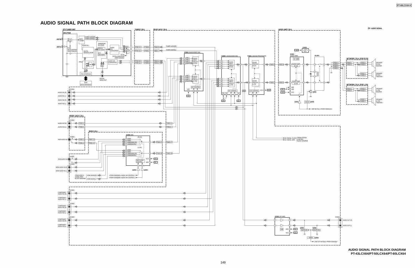
PT-43LCX64/PT-50LCX64/PT-60LCX64
AUDIO SIGNAL PATH BLOCK DIAGRAM
AUDIO SIGNAL PATH BLOCK DIAGRAM
P3404-18
AUDIO IN3 (R)
Q3505
Q3504
Q3506
I2C SERIAL DATAI2C SERIAL CLOCK FROM SYSTEM
CONTROLBLOCK DIAGRAM
AUDIO IN3 (L)
RGB AUDIO IN2
RGB AUDIO IN1
JK4801
R
L
R
L
JK3501
JK4802
AUDIOINPUTSELECT(R-CH)
TUNER C.B.A. AUDIO AMP C.B.A. AUDIO SIGNALREAR JACK C.B.A.
FRONT JACK C.B.A.
MAIN C.B.A.
NETWORK C.B.A. (FOR R-CH)
NETWORK C.B.A. (FOR L-CH)
P7005-9
P7005-7
P3604-9
AUDIO IN1 (R)
DIGITALAUDIO OUT
AUDIO IN1 (L)
AUDIO IN2 (R)
AUDIO IN2 (L)
IC4002 (SW)(R-CH)
(L-CH)
RGB2
LINE 1
TUNER AUDIO(R)
TUNER AUDIO(L)
LINE 2LINE 3HDMI/RGB
RGB1HDMI(ANALOG)
RGB2RGB1HDMI(ANALOG)
IC3501 (AUDIO/VIDEO SW)
IC3502 (OP AMP)
7
13
5
HDMI(DIGITAL)
HDMI(DIGITAL)
254
151411
1
12
3
13
9 10
P3603-3 P4505-3
P4505-1P3603-1
AUDIOINPUTSELECT(L-CH)
MUTE-ONMUTE-ON
40
38
4111861
29
1659
RL4501
IC4503
SPEAKER(R-CH)WOOFER
3
4
6
1
5
2
IC4501 (AUDIO AMP)
Q4504
Q4501 Q4505
11
7 4
3
5
2 P4552-2P4552-1
P4553-2P4553-1
P4553-2P4553-1
P4502-4P4502-3P4502-2P4503-1
SPEAKER(R-CH)TWEETER
SPEAKER(L-CH)WOOFER
SPEAKER(L-CH)TWEETER
P4551-2P4551-1
P4552-2P4552-1
P4551-2P4551-1
LINE 1LINE 2LINE 3HDMI/RGB
I2C CONTROL
34 33
HDMI AUDIO IN (R)
HDMI AUDIO IN (L)
JK4003
COMPONENTAUDIO IN1 (R)
COMPONENTAUDIO IN1 (L)
COMPONENTAUDIO IN2 (R)
COMPONENTAUDIO IN2 (L)
COMPONENTAUDIO IN3 (R)
COMPONENTAUDIO IN3 (L)
AUDIO OUT (R)
AUDIO OUT (L)
<FROM IC6003(62)> AUDIO SW CONTROL 2HDMI AUDIO(R)FROM VIDEO IISIGNAL PATHBLOCK DIAGRAM HDMI AUDIO(L)
SWITCHING CONTROL
<FROM IC6003(64)> AUDIO SW CONTROL 1
Q4002 Q4001
JK4001
JK3601
JK3602
JK3603 JK3502
VCC
VEEVEEVCC
42
VCC 16
7VEE
+5V
-5V
-VEE
VCC
4 -5V
LINE OUT MUTE(H) <FROM IC6003(9)>
8 +5V
P3604-7
P7006-6P7006-5
P7007-24
P7007-26
P7007-20P7007-22
P3503-6P3503-5
P3902-11
P3902-9
P3502-11
P3502-9
P5501-13
P3404-17
P3602-18
P3602-17P5501-11
P3901-13
P3901-11
+9V
DRIVE
AUDIOINPUTSELECT(R-CH)
IC3602 (AUDIO/VIDEO SW)
AUDIOINPUTSELECT(L-CH)
23
24
7121126455
7020116354
I2C CONTROL
2 3VCC
+5V
1VCC
+9V
31VCC
47
SOUNDPROCESS(R-CH)
SOUNDPROCESS(L-CH)
IC3601 (SOUND PROCESSOR)
12
21
5
28
I2C CONTROL
AMP MUTE(L) <FROM IC6003(13)>
DRIVE
AUDIO AMP(R-CH)
+12VREG.
AUDIO AMP(L-CH)
18 17
VCC +9V+16V
-16V
+16V
1561
31
DTV TUNER UNIT
SPLITTER
ANT-A
ANT-B SW
SWSW
SW
SW
MAIN TUNER
DIGITALDEMODULATOR
IF(DIGITAL)
TUNER AUDIO(L)
FPGA
POD INTERFACE
AUDIOD/ACONVERTER
TRANSPORT DECODER
MPEG2 DECODER
AC3 DECODER
TUNER AUDIO(R)
DCM(DIGITAL CABLE MODULE)
D/A-SW(DIGITAL(L)/ANALOG(H))
<FROM IC6003(58)>
AUDIO A/DCONVERTER
RF-SW(ANT-A(L)/ANT-B(H))<FROM IC6003(42)>
32~33dB
0dB
PT-60LCX64-K
149
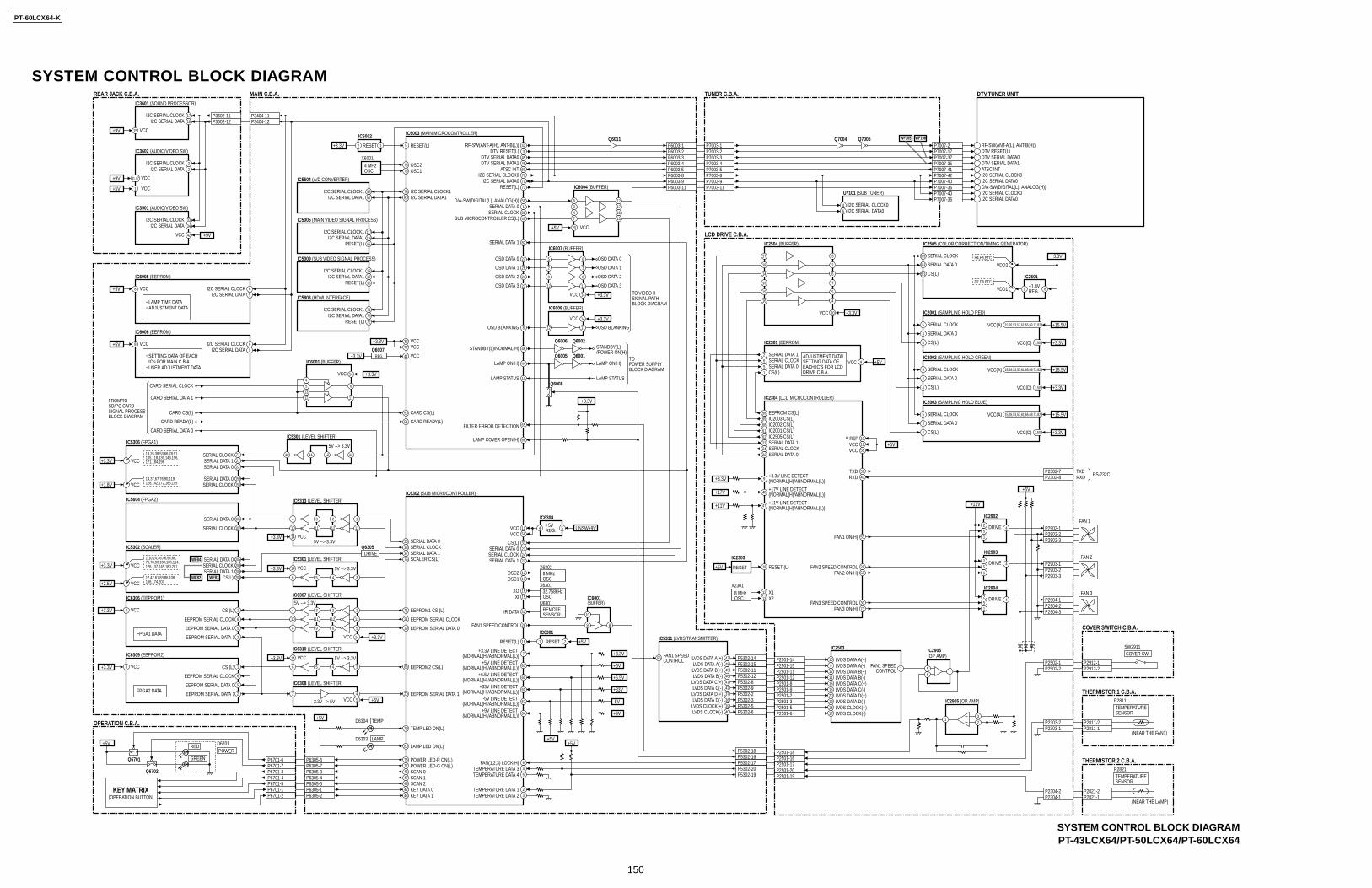
PT-43LCX64/PT-50LCX64/PT-60LCX64
SYSTEM CONTROL BLOCK DIAGRAM
WF84
WF82 WF83
WF106WF105IC6003 (MAIN MICROCONTROLLER)
IC6302 (SUB MICROCONTROLLER)
IC6306 (EEPROM1)
Q6305
IC6004 (BUFFER)
Q6011
IC3601 (SOUND PROCESSOR)
IC3602 (AUDIO/VIDEO SW)
+3.3V
OSC2OSC1
4 MHzOSC
7576
X6001
OSC2OSC1
8 MHzOSC
1213
X6302
XOXI
32.768kHzOSC
REMOTESENSOR
1615
X6301
U6301
IR DATA 32
REAR JACK C.B.A.
OPERATION C.B.A.
MAIN C.B.A. TUNER C.B.A. DTV TUNER UNIT
P5302-16P5302-18
P5302-17P5302-20P5302-19
IC6002
+3.3V 2 1RESET RESET(L)P7003-2P7003-1
P7003-3P7003-4P7003-5
P6003-2P6003-1
P6003-3P6003-4P6003-5
P7003-8P7003-9P7003-11
P7007-17P7007-2
P7007-37P7007-35P7007-41P7007-42P7007-40
P6003-8P6003-9P6003-11
IC6307 (LEVEL SHIFTER)
IC6308 (LEVEL SHIFTER)
Q6701
KEY MATRIX
Q6702
4
10
3
11
9
2
12
6
1
13
4
5
IC5313 (LEVEL SHIFTER)
U7101 (SUB TUNER)
45
1716
181
31258 8
47 13
7071
65
82
66
645
32
33232422
1
6
5
2
71
21
19
20
5
2
9
27
26
24
12
6
3
8
1123
7880
IC6001 (BUFFER)
5
1718
32
IC6005 (EEPROM)
IC6007 (BUFFER)
Q6006 Q6002
Q6005 Q6001
IC5306 (FPGA1)
IC5604 (FPGA2)
IC6006 (EEPROM)
65
65
P3404-12P3404-11
P3602-12P3602-11
P6701-7P6701-6
P6701-4P6701-3
P6701-1P6701-5
P6701-2
P6305-7P6305-6
P6305-4P6305-3
P6305-1P6305-5
P6305-2
OSD DATA 0
TO VIDEO IISIGNAL PATHBLOCK DIAGRAM
TO POWER SUPPLYBLOCK DIAGRAM
OSD DATA 1
OSD DATA 2
OSD DATA 3
OSD DATA 0
OSD DATA 1
OSD DATA 2
OSD DATA 3
54
6
1213
11
50
772122
I2C SERIAL CLOCKI2C SERIAL DATA
VCC
I2C SERIAL CLOCKI2C SERIAL DATA
IC3501 (AUDIO/VIDEO SW)
3334
I2C SERIAL CLOCK
LAMP TIME DATAADJUSTMENT DATA
SETTING DATA OF EACH IC's FOR MAIN C.B.A.USER ADJUSTMENT DATA
I2C SERIAL DATA
I2C SERIAL CLOCKI2C SERIAL DATA
I2C SERIAL CLOCKI2C SERIAL DATA
I2C SERIAL CLOCK1I2C SERIAL DATA1
SERIAL DATA 0
SERIAL DATA 1
SERIAL DATA 0
FILTER ERROR DETECTION
SERIAL DATA 1
42
15
VCC
I2C SERIAL CLOCK060ATSC INT46DTV SERIAL DATA145DTV SERIAL DATA03DTV RESET(L)
42RF-SW(ANT-A(H), ANT-B(L))
I2C SERIAL DATA0I2C SERIAL CLOCK0ATSC INTDTV SERIAL DATA1DTV SERIAL DATA0DTV RESET(L)RF-SW(ANT-A(L), ANT-B(H))
I2C SERIAL DATA0D/A-SW(DIGITAL(L), ANALOG(H))I2C SERIAL CLOCK0I2C SERIAL DATA0
I2C SERIAL CLOCK0I2C SERIAL DATA0
SERIAL CLOCK
SERIAL CLOCKSUB MICROCONTROLLER CS(L)
SERIAL DATA 1SERIAL CLOCK
SERIAL DATA 0
155153
SERIAL CLOCKSERIAL DATA 0
107
105
SERIAL CLOCK
SERIAL DATA 0
IC5302 (SCALER)
203208
205
SERIAL DATA 1204CS(L)
SERIAL CLOCKSERIAL DATA 0
CARD CS(L)CARD CS(L)
CARD SERIAL DATA 1
CARD SERIAL DATA 0
FROM/TOSD/PC CARD SIGNAL PROCESS BLOCK DIAGRAM
CARD SERIAL CLOCK
EEPROM1 CS (L)5V --> 3.3V
4
10
3
11
2
12
1
13
5V --> 3.3V
5V --> 3.3V
IC5301 (LEVEL SHIFTER)
6 5 4 3
IC5301 (LEVEL SHIFTER)
10 11 12 13
5V --> 3.3V
D6304 TEMP
3.3V --> 5V
EEPROM SERIAL CLOCK
EEPROM SERIAL DATA 0
EEPROM SERIAL DATA 1
TEMP LED ON(L)
LAMP LED ON(L)
SERIAL DATA 1SERIAL CLOCK
FAN(1,2,3) LOCK(H)
SERIAL DATA 0
TEMPERATURE DATA 3TEMPERATURE DATA 4
TEMPERATURE DATA 1TEMPERATURE DATA 2
CS(L)
CS (L)
EEPROM SERIAL CLOCK
EEPROM SERIAL DATA 0
EEPROM SERIAL DATA 1
+5V+5V
+5V
+5V
12 11
IC6008 (BUFFER)
OSD BLANKINGOSD BLANKING
48
8
44
19
STANDBY(L)/NORMAL(H)
LAMP ON(H)
LAMP STATUS
STANDBY(L)/POWER ON(H)
LAMP ON(H)
LAMP STATUS
LAMP COVER OPEN(H)
RESET(L)
D/A-SW(DIGITAL(L), ANALOG(H))
IC5504 (A/D CONVERTER)
5657
I2C SERIAL CLOCK1I2C SERIAL DATA1
IC5005 (MAIN VIDEO SIGNAL PROCESS)
I2C SERIAL CLOCK1I2C SERIAL DATA1
IC5009 (SUB VIDEO SIGNAL PROCESS)
I2C SERIAL CLOCK1I2C SERIAL DATA1
117116
1817
RESET(L)
RESET(L)
65
15
IC5803 (HDMI INTERFACE)
I2C SERIAL CLOCK1I2C SERIAL DATA1
7475
RESET(L) 72
73
49
8
2
79
80
POWER LED-R ON(L)78
POWER LED-G ON(L)77
SCAN 046
SCAN 147
SCAN 248
KEY DATA 042
KEY DATA 143
EEPROM2 CS(L)68
D6701POWER
RED
GREEN
(OPERATION BUTTON)
D6303 LAMP
51 CARD READY(L)CARD READY(L)
373836
DRIVESCALER CS(L)76
+9V
14VCC +3.3V
+3.3V
+3.3V
+9V
VCC1+5V
VCC+9V 31,47
VCC8+5V
VCC8+5V
VCC20+5V
VCC 14 +3.3V
VCC 14 +3.3V
Q6008
IC6304
UNSW+9V4 5+5VREG.VCC 11
VCC 56
IC6301
+5V
+3.3V
+5V
+6.5V
+33V
-5V
+9V
1 2RESETRESET(L) 18
+3.3V LINE DETECT (NORMAL(H)/ABNORMAL(L)) 7
+5V LINE DETECT (NORMAL(H)/ABNORMAL(L)) 63
+6.5V LINE DETECT (NORMAL(H)/ABNORMAL(L)) 60
+33V LINE DETECT (NORMAL(H)/ABNORMAL(L)) 61
-5V LINE DETECT (NORMAL(H)/ABNORMAL(L)) 62
+9V LINE DETECT (NORMAL(H)/ABNORMAL(L)) 64
VCC 14 +3.3V
VCC 5 +5V
VCC14+3.3V
VCC14+3.3V
+3.3V
5V --> 3.3V
IC6310 (LEVEL SHIFTER)
6 5 4 3
VCC14+3.3V
VCC8
VCC32VCC77
VCC41Q6007
REG.
13,26,38,53,66,78,91,105,118,130,143,156,171,184,196VCC+3.3V
+1.8V VCC14,37,67,76,90,119,128,142,172,186,195
1,10,24,36,46,54,68,76,78,93,100,105,114,126,137,145,180,201VCC+3.3V
+2.5V VCC17,42,61,83,86,108,156,174,207
FPGA1 DATA
IC6309 (EEPROM2)
1
6
5
2
CS (L)
EEPROM SERIAL CLOCK
EEPROM SERIAL DATA 0
EEPROM SERIAL DATA 1
+3.3V VCC8
FPGA2 DATA
IC6001
FAN1 SPEED CONTROL 26
(BUFFER)
10
9 8
50 FAN1 SPEEDCONTROL P5302-14
IC5311 (LVDS TRANSMITTER)
47
P5302-1548
P5302-1145
P5302-1246
P5302-841
P5302-942
P5302-237
P5302-338
P5302-539
P5302-640
LVDS DATA A(+)LVDS DATA A(-)LVDS DATA B(+)LVDS DATA B(-)
LVDS DATA C(+)LVDS DATA C(-)LVDS DATA D(+)LVDS DATA D(-)
LVDS CLOCK(+)LVDS CLOCK(-)
Q7004 Q7005
P7007-36P7007-40P7007-36
IC2304 (LCD MICROCONTROLLER)
IC2301 (EEPROM)
IC2504 (BUFFER) IC2505 (COLOR CORRECTION/TIMING GENERATOR)
IC2905 (OP. AMP)
IC2303
X1X2
RESET (L)
TXDRXD
TXDRXD
8 MHzOSC
1213
X2301
+5V RESET
LCD DRIVE C.B.A.
THERMISTOR 2 C.B.A.
P2821-2P2821-1
R2821TEMPERATURESENSOR
THERMISTOR 1 C.B.A.
P2811-2P2811-1
P2304-2P2304-1
P2303-2P2303-1
R2811TEMPERATURESENSOR
COVER SWITCH C.B.A.
P2912-1P2912-2
P2502-1
P2501-16P2501-18
P2501-17P2501-20P2501-19
P2502-2
SW2911COVER SW
+11V
+5V
DRIVE 452
IC2903
IC2902
IC2503
DRIVE 452
IC2904
DRIVE 452
FAN 1
FAN 2
7
P2902-1P2902-2P2902-3
P2903-2P2903-3
P2903-1
FAN 3
P2904-2P2904-3
P2904-1
32
1
2651
23
3940
2422
18
P2302-8P2302-7
28
30
6162
SERIAL CLOCKSERIAL DATA 1
SERIAL DATA 0
SERIAL DATA 0
CS(L)
SERIAL DATA 0
SERIAL CLOCK
SERIAL CLOCK
SERIAL DATA 0
CS(L)
SERIAL CLOCK
SERIAL DATA 0
CS(L)
SERIAL CLOCK
SERIAL DATA 0
CS(L)
SERIAL CLOCK
SERIAL DATA 1
CS(L)
IC2001 CS(L)68 IC2002 CS(L)69 IC2003 CS(L)58 EEPROM CS(L)
IC2505 CS(L)
FAN1 SPEEDCONTROL
FAN2 SPEED CONTROL
53FAN1 ON(H)
FAN3 SPEED CONTROL
VCC +5V8
VCC +3.3V20
+3.3V
+15.5V
VCC +5V11
VCC 56
9+3.3V +3.3V LINE DETECT (NORMAL(H)/ABNORMAL(L))
48+17V +17V LINE DETECT (NORMAL(H)/ABNORMAL(L))
47+11V +11V LINE DETECT (NORMAL(H)/ABNORMAL(L))
67
IC2905(OP AMP)
5
RS-232C
(NEAR THE FAN1)
(NEAR THE LAMP)
ADJUSTMENT DATA/SETTING DATA OFEACH IC'S FOR LCDDRIVE C.B.A.
V-REF 10
1
55FAN2 ON(H) 1
73FAN3 ON(H) 1
P2501-14P2501-15P2501-11P2501-12P2501-8P2501-9P2501-2P2501-3P2501-5P2501-6
109
1211161520191817
LVDS DATA A(+)LVDS DATA A(-)LVDS DATA B(+)LVDS DATA B(-)LVDS DATA C(+)LVDS DATA C(-)LVDS DATA D(+)LVDS DATA D(-)LVDS CLOCK(+)LVDS CLOCK(-)
3
2
6
7
5
4
17
18
14
13
15
16
B20
B18
B19
IC2001 (SAMPLING HOLD RED)
5
3
4
IC2002 (SAMPLING HOLD GREEN)
5
3
4
IC2003 (SAMPLING HOLD BLUE)
5
3
4
VDD2
+3.3V
VDD1
IC2501
+1.8VREG.1 8
VCC(A) 15,26,53,57,61,65,69,73,82
VCC(D) 1,50
+3.3V
+15.5VVCC(A) 15,26,53,57,61,65,69,73,82
VCC(D) 1,50
+3.3V
+15.5VVCC(A) 15,26,53,57,61,65,69,73,82
VCC(D) 1,50
H4,H5,ETC
D7,D8,ETC
SYSTEM CONTROL BLOCK DIAGRAM
PT-60LCX64-K
150
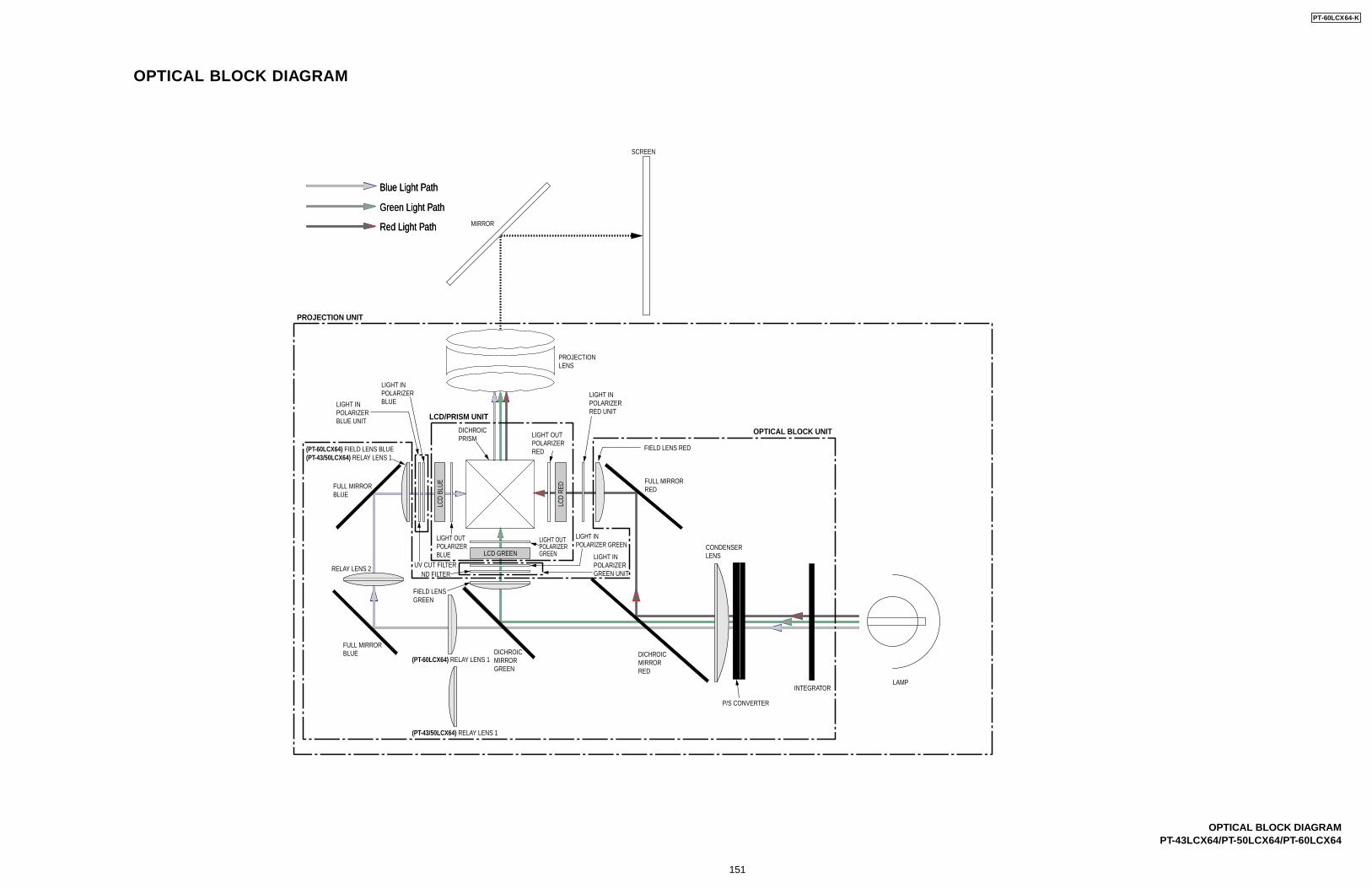
PT-43LCX64/PT-50LCX64/PT-60LCX64
OPTICAL BLOCK DIAGRAM
OPTICAL BLOCK DIAGRAM
Blue Light Path
Green Light Path
Red Light Path
Blue Light Path
Green Light Path
Red Light Path
INTEGRATORLAMP
P/S CONVERTER
CONDENSER LENS
(PT-60LCX64) RELAY LENS 1
(PT-43/50LCX64) RELAY LENS 1
RELAY LENS 2
(PT-60LCX64) FIELD LENS BLUE(PT-43/50LCX64) RELAY LENS 1
FIELD LENS GREEN
FIELD LENS RED
DICHROIC MIRROR RED
DICHROIC MIRROR GREEN
FULL MIRROR BLUE
FULL MIRROR BLUE
DICHROIC PRISM
LCD
RED
LCD
BLUE
LCD GREEN LIGHT IN POLARIZER GREEN UNIT
LIGHT IN POLARIZER GREEN
FULL MIRROR RED
PROJECTION LENS
SCREEN
LCD/PRISM UNIT
OPTICAL BLOCK UNIT
PROJECTION UNIT
MIRROR
LIGHT OUT POLARIZER RED
LIGHT OUT POLARIZER BLUE
LIGHT OUT POLARIZER GREEN
LIGHT IN POLARIZER RED UNIT
LIGHT IN POLARIZER BLUELIGHT IN
POLARIZER BLUE UNIT
UV CUT FILTERND FILTER
PT-60LCX64-K
151
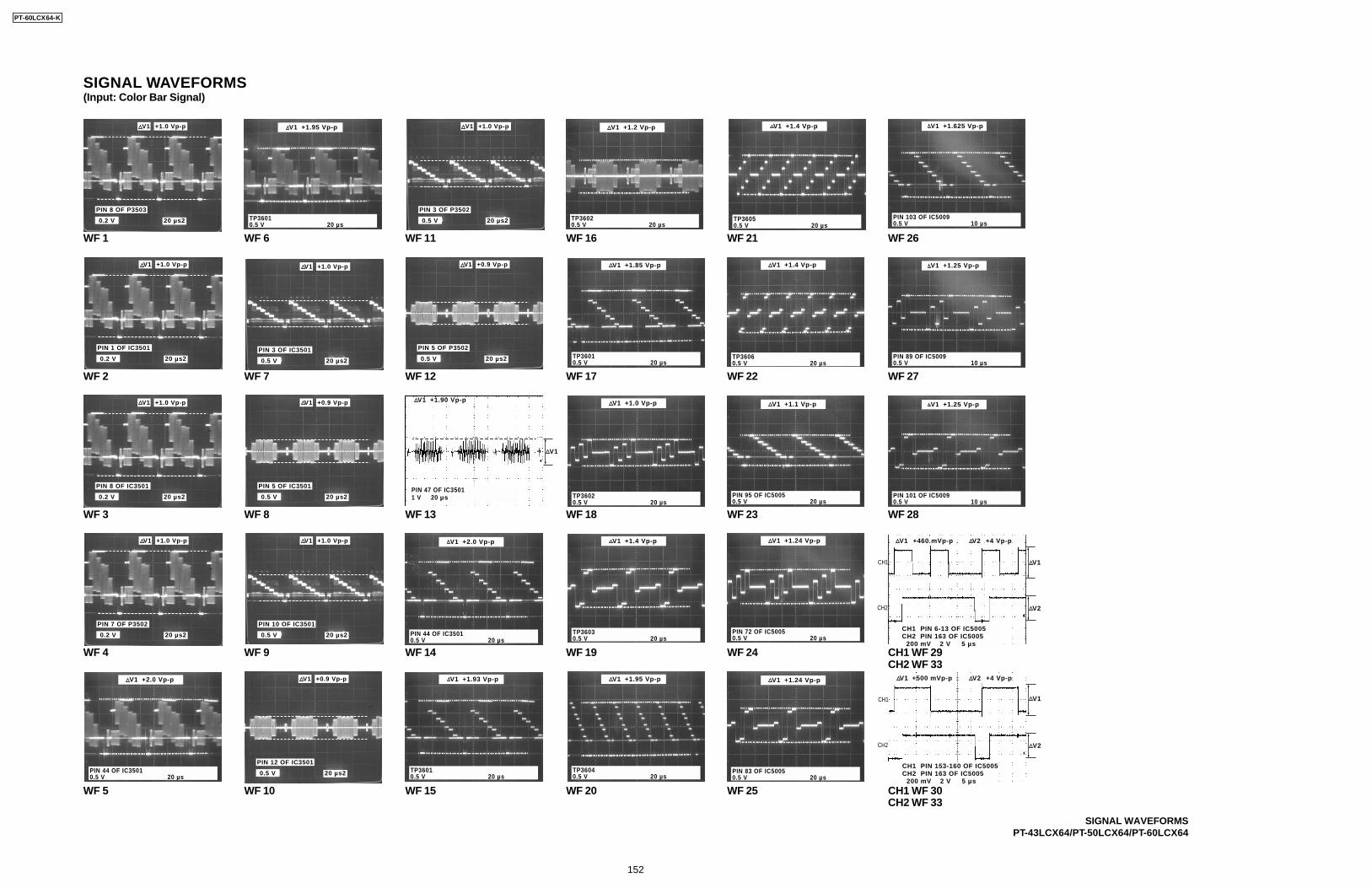
SIGNAL WAVEFORMSPT-43LCX64/PT-50LCX64/PT-60LCX64
WF 1
WF 2
WF 3
WF 4
WF 5
WF 6
WF 8
WF 9
WF 10
WF 11
WF 12
WF 14
WF 15
WF 16
WF 17
WF 18
WF 20
WF 21
WF 22
WF 23
WF 24
WF 26
WF 27
WF 28
CH1 WF 29CH2 WF 33
CH1 WF 30CH2 WF 33
WF 7
WF 19
WF 25
+1.0 Vp-pV1
PIN 8 OF P3503
0.2 V 20 µs2
+1.0 Vp-pV1
PIN 1 OF IC3501
0.2 V 20 µs2
+1.0 Vp-pV1
PIN 8 OF IC3501
0.2 V 20 µs2
+1.0 Vp-pV1
PIN 7 OF P3502
0.2 V 20 µs2
V1 +2.0 Vp-p
PIN 44 OF IC35010.5 V 20 µs
V1 +1.95 Vp-p
TP36010.5 V 20 µs
+1.0 Vp-pV1
PIN 3 OF IC3501
0.5 V 20 µs2
+0.9 Vp-pV1
PIN 5 OF IC3501
0.5 V 20 µs2
+1.0 Vp-pV1
PIN 10 OF IC3501
0.5 V 20 µs2
+0.9 Vp-pV1
PIN 12 OF IC3501
0.5 V 20 µs2
+1.0 Vp-pV1
PIN 3 OF P3502
0.5 V 20 µs2
+0.9 Vp-pV1
PIN 5 OF P3502
0.5 V 20 µs2
V1 +2.0 Vp-p
PIN 44 OF IC3501 0.5 V 20 µs
V1 +1.93 Vp-p
TP36010.5 V 20 µs
V1 +1.2 Vp-p
TP36020.5 V 20 µs
V1 +1.85 Vp-p
TP3601 0.5 V 20 µs
V1 +1.0 Vp-p
TP3602 0.5 V 20 µs
V1 +1.4 Vp-p
TP3603 0.5 V 20 µs
V1 +1.95 Vp-p
TP3604 0.5 V 20 µs
V1 +1.4 Vp-p
TP3605 0.5 V 20 µs
V1 +1.4 Vp-p
TP3606 0.5 V 20 µs
V1 +1.1 Vp-p
PIN 95 OF IC5005 0.5 V 20 µs
V1 +1.24 Vp-p
PIN 72 OF IC5005 0.5 V 20 µs
V1 +1.24 Vp-p
PIN 83 OF IC5005 0.5 V 20 µs
V1 +1.625 Vp-p
PIN 103 OF IC5009 0.5 V 10 µs
V1 +1.25 Vp-p
PIN 89 OF IC5009 0.5 V 10 µs
V1 +1.25 Vp-p
PIN 101 OF IC5009 0.5 V 10 µs
CH1
CH2
V1
V2
V1 +460 mVp-p V2 +4 Vp-p
CH1 PIN 6-13 OF IC5005 CH2 PIN 163 OF IC5005 200 mV 2 V 5 µs
CH1
CH2
V1
V2
V1 +500 mVp-p V2 +4 Vp-p
CH1 PIN 153-160 OF IC5005 CH2 PIN 163 OF IC5005 200 mV 2 V 5 µs
SIGNAL WAVEFORMS(Input: Color Bar Signal)
WF 13
V1 +1.90 Vp-p
PIN 47 OF IC3501 1 V 20 µs
V1
PT-60LCX64-K
152
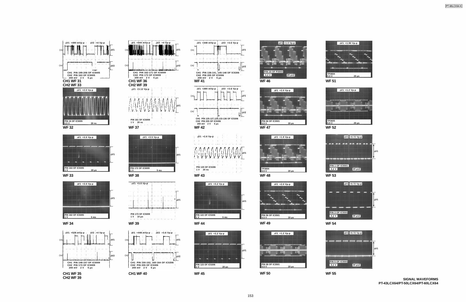
SIGNAL WAVEFORMSPT-43LCX64/PT-50LCX64/PT-60LCX64
WF 47
WF 48
WF 49
WF 50
WF 51
WF 43
WF 44
WF 45
WF 46
WF 32
WF 33
WF 34
CH1 WF 35CH2 WF 39
CH1 WF 36CH2 WF 39
WF 38
WF 39
CH1 WF 40
WF 41
WF 42WF 37
V1 +3.5 Vp-p
PIN 163 OF IC5005 1 V 20 µs
V1
V1 +3.5 Vp-p
PIN 162 OF IC5005 1 V 5 ms
V1
CH1
CH2
V1
V2
V1 +528 mVp-p V2 +4 Vp-p
CH1 PIN 148-157 OF IC5009 CH2 PIN 173 OF IC5009 200 mV 2 V 5 µs
CH1
CH2
V1
V2
V1 +544 mVp-p V2 +4 Vp-p
CH1 PIN 162-171 OF IC5009 CH2 PIN 173 OF IC5009 200 mV 2 V 5 µs
V1 +3.12 Vp-p
PIN 161 OF IC5009 1 V 20 ns
V1
V1 +3.5 Vp-p
PIN 172 OF IC5009 1 V 5 ms
V1
CH1
CH2
V1
V2
V1 +448 mVp-p V2 +3.6 Vp-p
CH1 PIN 150-152, 160-164 OF IC5306CH2 PIN 205 OF IC5306 200 mV 2 V 5 µs
CH1
CH2
V1
V2
V1 +448 mVp-p V2 +3.6 Vp-p
CH1 PIN 138-141, 145-148 OF IC5306CH2 PIN 205 OF IC5306 200 mV 2 V 5 µs
CH1
CH2
V1
V2
V1 +480 mVp-p V2 +3.6 Vp-p
CH1 PIN 125-127,129,133-136 OF IC5306CH2 PIN 205 OF IC5306 200 mV 2 V 5 µs
V1 +2.6 Vp-p
PIN 120 OF IC53061 V 20 ns
V1
V1 +3.2 Vp-p
PIN 122 OF IC5306 1 V 5 ms
V1
V1 +3.2 Vp-p
PIN 123 OF IC5306 1 V 20 µs
V1
+1.0 Vp-pV1
PIN 10 OF P3503
0.2 V 20 µs2
V1 +2.0 Vp-p
PIN 56 OF IC35010.5 V 20 µs
V1 +1.9 Vp-p
TP36040.5 V 20 µs
V1 +2.0 Vp-p
PIN 56 OF IC35010.5 V 20 µs
V1 +1.2 Vp-p
PIN 58 OF IC35010.5 V 20 µs
V1 +1.90 Vp-p
TP3604 0.5 V 20 µs
WF 52
WF 53
WF 54
WF 55
V1 +1.2 Vp-p
TP3605 0.5 V 20 µs
+0.72 Vp-pV1
PIN 1 OF IC5501
0.2 V 20 µs2
V1
+0.72 Vp-pV1
PIN 3 OF IC5501
0.2 V 20 µs2
V1
+0.72 Vp-pV1
PIN 5 OF IC5501
0.2 V 20 µs2
V1
V1 +3.6 Vp-p
PIN 173 OF IC50091 V 10 µs
V1
V1 +2.0 Vp-p
PIN 16 OF IC5005 0.5 V 20 ns
CH1 WF 31CH2 WF 33
CH1
CH2
V1
V2
V1 +490 mVp-p V2 +4 Vp-p
CH1 PIN 199-206 OF IC5005 CH2 PIN 163 OF IC5005 200 mV 2 V 5 µs
PT-60LCX64-K
153
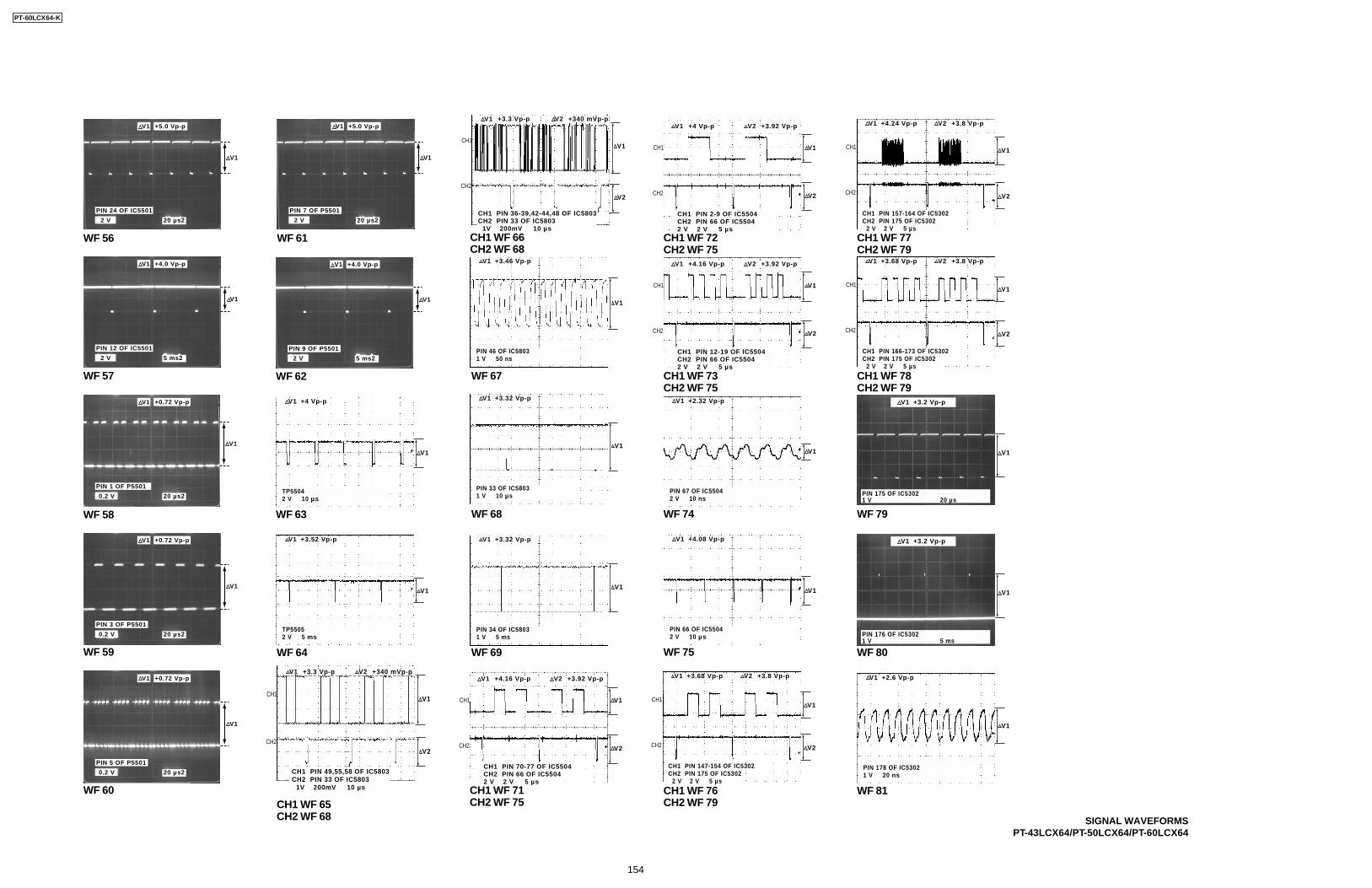
SIGNAL WAVEFORMSPT-43LCX64/PT-50LCX64/PT-60LCX64
WF 57
WF 58
WF 59
WF 60
WF 61
WF 62
WF 63
WF 64
WF 67
WF 68
WF 69
CH1 WF 71CH2 WF 75
CH1 WF 72CH2 WF 75
CH1 WF 73CH2 WF 75
WF 74
WF 75
CH1 WF 76CH2 WF 79
CH1 WF 77CH2 WF 79
CH1 WF 78CH2 WF 79
+4.0 Vp-pV1
PIN 12 OF IC5501
2 V 5 ms2
V1
+0.72 Vp-pV1
PIN 1 OF P5501
0.2 V 20 µs2
V1
+0.72 Vp-pV1
PIN 3 OF P5501
0.2 V 20 µs2
V1
+0.72 Vp-pV1
PIN 5 OF P5501
0.2 V 20 µs2
V1
V1
+5.0 Vp-pV1
PIN 7 OF P5501
2 V 20 µs2
+4.0 Vp-pV1
PIN 9 OF P5501
2 V 5 ms2
V1
V1 +4 Vp-p
TP55042 V 10 µs
V1
V1 +3.52 Vp-p
TP55052 V 5 ms
V1
CH1
CH2
V1
V2
V1 +4.16 Vp-p V2 +3.92 Vp-p
CH1 PIN 70-77 OF IC5504 CH2 PIN 66 OF IC55042 V 2 V 5 µs
CH1
CH2
V1
V2
V1 +4 Vp-p V2 +3.92 Vp-p
CH1 PIN 2-9 OF IC5504 CH2 PIN 66 OF IC55042 V 2 V 5 µs
CH1
CH2
V1
V2
V1 +4.16 Vp-p V2 +3.92 Vp-p
CH1 PIN 12-19 OF IC5504CH2 PIN 66 OF IC55042 V 2 V 5 µs
V1 +2.32 Vp-p
PIN 67 OF IC55042 V 10 ns
V1
V1 +4.08 Vp-p
PIN 66 OF IC55042 V 10 µs
V1
CH1
CH2
V1
V2
V1 +3.68 Vp-p V2 +3.8 Vp-p
CH1 PIN 147-154 OF IC5302 CH2 PIN 175 OF IC5302 2 V 2 V 5 µs
CH1
CH2
V1
V2
V1 +4.24 Vp-p V2 +3.8 Vp-p
CH1 PIN 157-164 OF IC5302 CH2 PIN 175 OF IC5302 2 V 2 V 5 µs
CH1
CH2
V1
V2
V1 +3.68 Vp-p V2 +3.8 Vp-p
CH1 PIN 166-173 OF IC5302 CH2 PIN 175 OF IC5302 2 V 2 V 5 µs
V1 +3.2 Vp-p
PIN 175 OF IC5302 1 V 20 µs
V1
WF 79
WF 80
V1 +3.2 Vp-p
PIN 176 OF IC5302 1 V 5 ms
V1
WF 81
V1 +2.6 Vp-p
PIN 178 OF IC53021 V 20 ns
V1
WF 56
V1
+5.0 Vp-pV1
PIN 24 OF IC5501
2 V 20 µs2
CH1
CH2
V1
V2
V1 +3.3 Vp-p V2 +340 mVp-p
CH1 PIN 49,55,58 OF IC5803CH2 PIN 33 OF IC5803 1V 200mV 10 µs
CH1 WF 65CH2 WF 68
CH1 WF 66CH2 WF 68
CH1
CH2
V1
V2
V1 +3.3 Vp-p V2 +340 mVp-p
CH1 PIN 36-39,42-44,48 OF IC5803CH2 PIN 33 OF IC5803 1V 200mV 10 µs
V1 +3.46 Vp-p
PIN 46 OF IC58031 V 50 ns
V1
V1 +3.32 Vp-p
PIN 33 OF IC58031 V 10 µs
V1
V1 +3.32 Vp-p
PIN 34 OF IC58031 V 5 ms
V1
PT-60LCX64-K
154
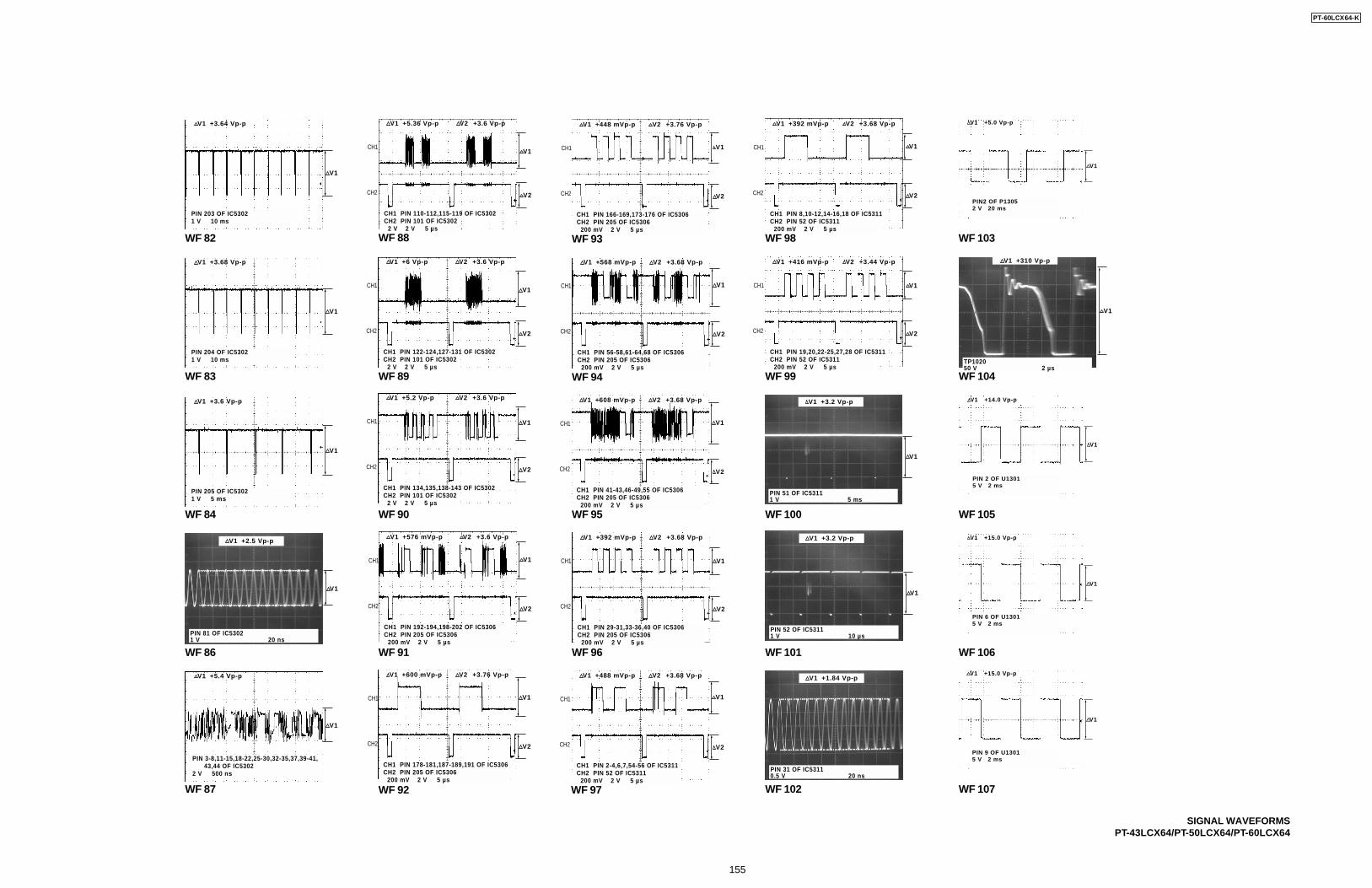
SIGNAL WAVEFORMSPT-43LCX64/PT-50LCX64/PT-60LCX64
WF 82
WF 83
WF 84
V1 +3.64 Vp-p
PIN 203 OF IC5302 1 V 10 ms
V1
V1 +3.68 Vp-p
PIN 204 OF IC5302 1 V 10 ms
V1
V1 +3.6 Vp-p
PIN 205 OF IC53021 V 5 ms
V1
WF 86
WF 87
WF 88
WF 89
WF 90
V1 +2.5 Vp-p
PIN 81 OF IC5302 1 V 20 ns
V1
CH1
CH2
V1
V2
V1 +5.36 Vp-p V2 +3.6 Vp-p
CH1 PIN 110-112,115-119 OF IC5302 CH2 PIN 101 OF IC5302 2 V 2 V 5 µs
CH1
CH2
V1
V2
V1 +6 Vp-p V2 +3.6 Vp-p
CH1 PIN 122-124,127-131 OF IC5302 CH2 PIN 101 OF IC5302 2 V 2 V 5 µs
CH1
CH2
V1
V2
V1 +5.2 Vp-p V2 +3.6 Vp-p
CH1 PIN 134,135,138-143 OF IC5302 CH2 PIN 101 OF IC5302 2 V 2 V 5 µs
WF 91
WF 92
WF 93
WF 94
WF 95
CH1
CH2
V1
V2
V1 +576 mVp-p V2 +3.6 Vp-p
CH1 PIN 192-194,198-202 OF IC5306CH2 PIN 205 OF IC5306 200 mV 2 V 5 µs
CH1
CH2
V1
V2
V1 +600 mVp-p V2 +3.76 Vp-p
CH1 PIN 178-181,187-189,191 OF IC5306CH2 PIN 205 OF IC5306 200 mV 2 V 5 µs
CH1
CH2
V1
V2
V1 +448 mVp-p V2 +3.76 Vp-p
CH1 PIN 166-169,173-176 OF IC5306CH2 PIN 205 OF IC5306 200 mV 2 V 5 µs
CH1
CH2
V1
V2
V1 +568 mVp-p V2 +3.68 Vp-p
CH1 PIN 56-58,61-64,68 OF IC5306CH2 PIN 205 OF IC5306 200 mV 2 V 5 µs
CH1
CH2
V1
V2
V1 +608 mVp-p V2 +3.68 Vp-p
CH1 PIN 41-43,46-49,55 OF IC5306CH2 PIN 205 OF IC5306 200 mV 2 V 5 µs
WF 96
WF 97
WF 98
WF 99
WF 100
CH1
CH2
V1
V2
V1 +392 mVp-p V2 +3.68 Vp-p
CH1 PIN 29-31,33-36,40 OF IC5306CH2 PIN 205 OF IC5306 200 mV 2 V 5 µs
CH1
CH2
V1
V2
V1 +488 mVp-p V2 +3.68 Vp-p
CH1 PIN 2-4,6,7,54-56 OF IC5311 CH2 PIN 52 OF IC5311 200 mV 2 V 5 µs
CH1
CH2
V1
V2
V1 +392 mVp-p V2 +3.68 Vp-p
CH1 PIN 8,10-12,14-16,18 OF IC5311 CH2 PIN 52 OF IC5311 200 mV 2 V 5 µs
CH1
CH2
V1
V2
V1 +416 mVp-p V2 +3.44 Vp-p
CH1 PIN 19,20,22-25,27,28 OF IC5311 CH2 PIN 52 OF IC5311 200 mV 2 V 5 µs
V1 +3.2 Vp-p
PIN 51 OF IC5311 1 V 5 ms
V1
WF 101
WF 102
V1 +3.2 Vp-p
PIN 52 OF IC5311 1 V 10 µs
V1
V1 +1.84 Vp-p
PIN 31 OF IC5311 0.5 V 20 ns
V1 +5.4 Vp-p
PIN 3-8,11-15,18-22,25-30,32-35,37,39-41, 43,44 OF IC53022 V 500 ns
V1
WF 103
WF 104
V1 +310 Vp-p
TP1020 50 V 2 µs
V1
WF 105
WF 106
WF 107
V1
V1 +5.0 Vp-p
PIN2 OF P13052 V 20 ms
V1
V1 +14.0 Vp-p
PIN 2 OF U13015 V 2 ms
V1
V1 +15.0 Vp-p
PIN 6 OF U13015 V 2 ms
V1
V1 +15.0 Vp-p
PIN 9 OF U13015 V 2 ms
PT-60LCX64-K
155
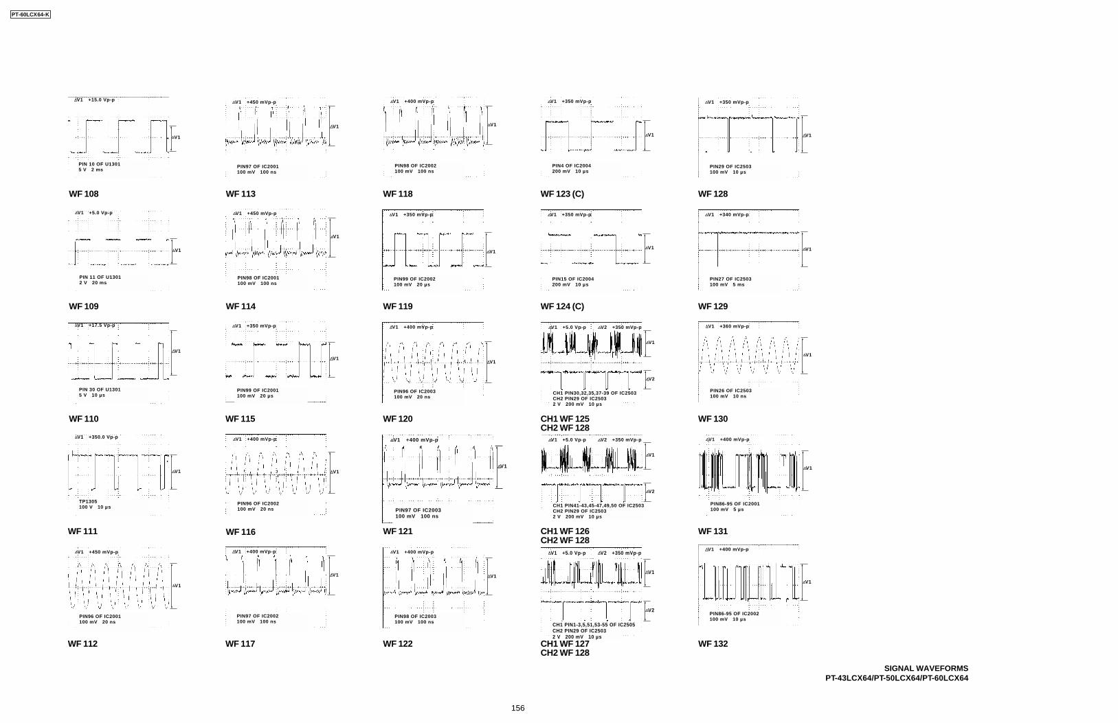
SIGNAL WAVEFORMSPT-43LCX64/PT-50LCX64/PT-60LCX64
WF 108
WF 109
WF 110
WF 111
WF 112
WF 113
WF 114
WF 115
WF 116
WF 117
WF 118
WF 119
WF 120
WF 121
WF 122
WF 123 (C)
WF 124 (C)
CH1 WF 127
WF 128
WF 129
WF 130
WF 131
WF 132CH2 WF 128
CH1 WF 126CH2 WF 128
CH1 WF 125CH2 WF 128
V1
V1 +15.0 Vp-p
PIN 10 OF U13015 V 2 ms
V1
V1 +5.0 Vp-p
PIN 11 OF U13012 V 20 ms
V1
V1 +17.5 Vp-p
PIN 30 OF U13015 V 10 µs
V1
V1 +350.0 Vp-p
TP1305100 V 10 µs
V1
V1 +450 mVp-p
PIN96 OF IC2001100 mV 20 ns
V1
V1 +450 mVp-p
PIN98 OF IC2001100 mV 100 ns
V1
V1 +350 mVp-p
PIN99 OF IC2001100 mV 20 µs
V1
V1 +400 mVp-p
PIN96 OF IC2002100 mV 20 ns
V1
V1 +400 mVp-p
PIN97 OF IC2002100 mV 100 ns
V1
V1 +400 mVp-p
PIN98 OF IC2002100 mV 100 ns
V1
V1 +350 mVp-p
PIN99 OF IC2002100 mV 20 µs
V1
V1 +400 mVp-p
PIN96 OF IC2003100 mV 20 ns
V1
V1 +400 mVp-p
PIN97 OF IC2003100 mV 100 ns
V1
V1 +450 mVp-p
PIN97 OF IC2001100 mV 100 ns
V1
V1 +400 mVp-p
PIN98 OF IC2003100 mV 100 ns
V1
V1 +350 mVp-p
PIN4 OF IC2004200 mV 10 µs
V1
V1 +350 mVp-p
PIN15 OF IC2004200 mV 10 µs
V1
V2
V1 +5.0 Vp-p V2 +350 mVp-p
CH1 PIN30,32,35,37-39 OF IC2503CH2 PIN29 OF IC25032 V 200 mV 10 µs
V1
V2
V1 +5.0 Vp-p V2 +350 mVp-p
CH1 PIN41-43,45-47,49,50 OF IC2503CH2 PIN29 OF IC25032 V 200 mV 10 µs
V1
V2
V1 +5.0 Vp-p V2 +350 mVp-p
CH1 PIN1-3,5,51,53-55 OF IC2505CH2 PIN29 OF IC25032 V 200 mV 10 µs
V1
V1 +350 mVp-p
PIN29 OF IC2503100 mV 10 µs
V1
V1 +340 mVp-p
PIN27 OF IC2503100 mV 5 ms
V1
V1 +360 mVp-p
PIN26 OF IC2503100 mV 10 ns
V1
V1 +400 mVp-p
PIN86-95 OF IC2001100 mV 5 µs
V1
V1 +400 mVp-p
PIN86-95 OF IC2002100 mV 10 µs
PT-60LCX64-K
156
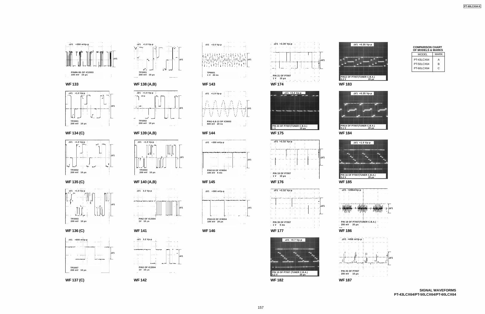
SIGNAL WAVEFORMSPT-43LCX64/PT-50LCX64/PT-60LCX64
WF 138 (A,B)
WF 139 (A,B)
WF 140 (A,B)
WF 141
WF 142
WF 143
WF 144
WF 145
WF 146
V1
V1 +1.0 Vp-p
TP2001200 mV 10 µs
V1
V1 +1.0 Vp-p
TP2002200 mV 10 µs
V1
V1 +1.0 Vp-p
TP2003200 mV 10 µs
V1
V1 3.2 Vp-p
PIN2 OF IC25041V 10 µs
V1
V1 3.2 Vp-p
PIN3 OF IC25041V 10 µs
V1
V1 +3.0 Vp-p
TP90011 V 20 ns
V1
V1 +1.9 Vp-p
PIN1-6,8-13 OF IC9003500 mV 20 ns
V1
V1 +350 mVp-p
PIN118 OF IC9004100 mV 5 ms
V1
V1 +360 mVp-p
PIN119 OF IC9004100 mV 20 µs
WF 174
WF 175
WF 176
WF 177
V1 +3.30 Vp-p
PIN 21 OF P70071 V 10 µs
V1
V1 +3.32 Vp-p
PIN 19 OF P70071 V 10 µs
V1
V1 +3.32 Vp-p
PIN 39 OF P70071 V 5 ms
V1
V1 +3.2 Vp-p
PIN 23 OF P7007(TUNER C.B.A.)1 V 10 µs
WF 182
V1 +0.7 Vp-p
PIN 10 OF P7007 (TUNER C.B.A.)0.2 V 20 µs
WF 183
WF 184
WF 185
WF 186
WF 187
V1 +456 mVp-p
PIN 25 OF P7007200 mV 10 µs
V1
V1 +0.35 Vp-p
PIN12 OF P7007(TUNER C.B.A.)0.2 V 20 µs
V1 +0.35 Vp-p
PIN14 OF P7007(TUNER C.B.A.)0.1 V 20 µs
V1 +1.0 Vp-p
PIN 16 OF P7007(TUNER C.B.A.)0.2 V 20 µs
V1 +286mVp-p
PIN 18 OF P7007(TUNER C.B.A.)200 mV 20 µs
V1
WF 133
WF 134 (C)
WF 135 (C)
WF 136 (C)
V1
V1 +350 mVp-p
PIN86-95 OF IC2003100 mV 10 µs
V1
V1 +1.0 Vp-p
TP2001200 mV 10 µs
V1
V1 +1.0 Vp-p
TP2002200 mV 10 µs
V1
V1 +1.0 Vp-p
TP2003200 mV 10 µs
V1
V1 +600 mVp-p
TP2007200 mV 10 µs
WF 137 (C)
COMPARISON CHART OF MODELS & MARKS
PT-43LCX64
PT-50LCX64
PT-60LCX64
A
B
C
MODEL MARK
PT-60LCX64-K
157
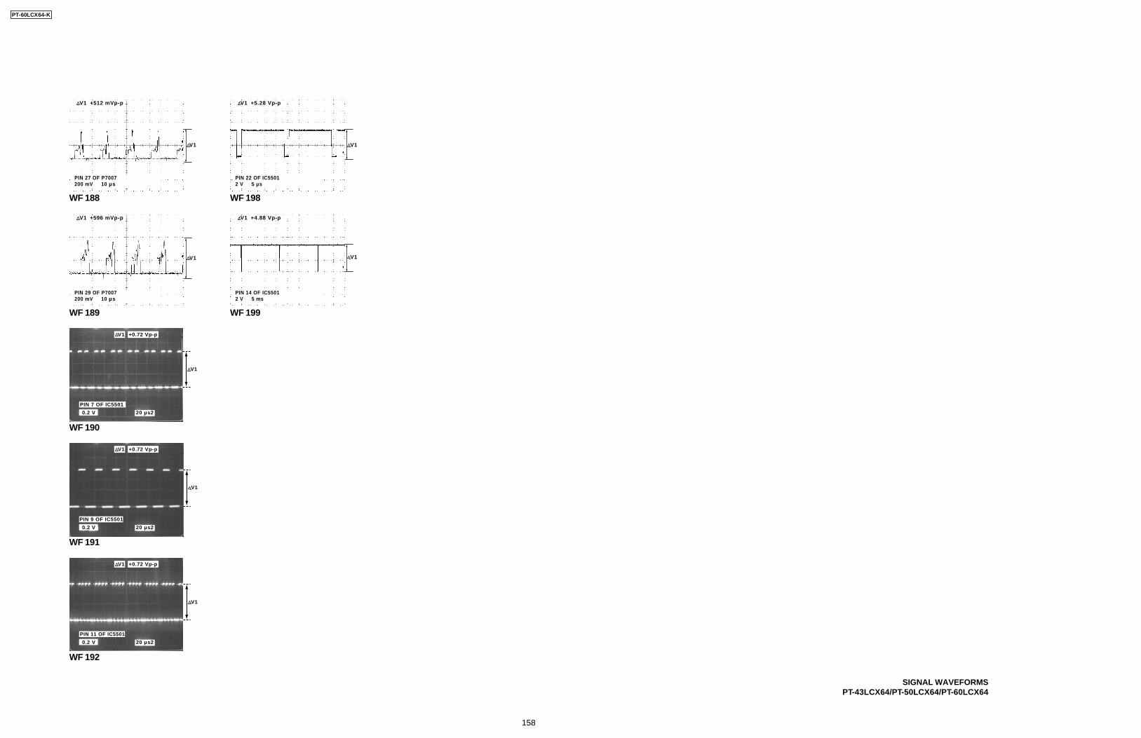
SIGNAL WAVEFORMSPT-43LCX64/PT-50LCX64/PT-60LCX64
WF 190
WF 191
WF 192
+0.72 Vp-pV1
PIN 7 OF IC5501
0.2 V 20 µs2
V1
+0.72 Vp-pV1
PIN 9 OF IC5501
0.2 V 20 µs2
V1
+0.72 Vp-pV1
PIN 11 OF IC5501
0.2 V 20 µs2
V1
WF 189
WF 188
V1 +512 mVp-p
PIN 27 OF P7007200 mV 10 µs
V1
V1 +596 mVp-p
PIN 29 OF P7007 200 mV 10 µs
V1
WF 198
WF 199
V1 +5.28 Vp-p
PIN 22 OF IC5501 2 V 5 µs
V1
V1 +4.88 Vp-p
PIN 14 OF IC5501 2 V 5 ms
V1
PT-60LCX64-K
158
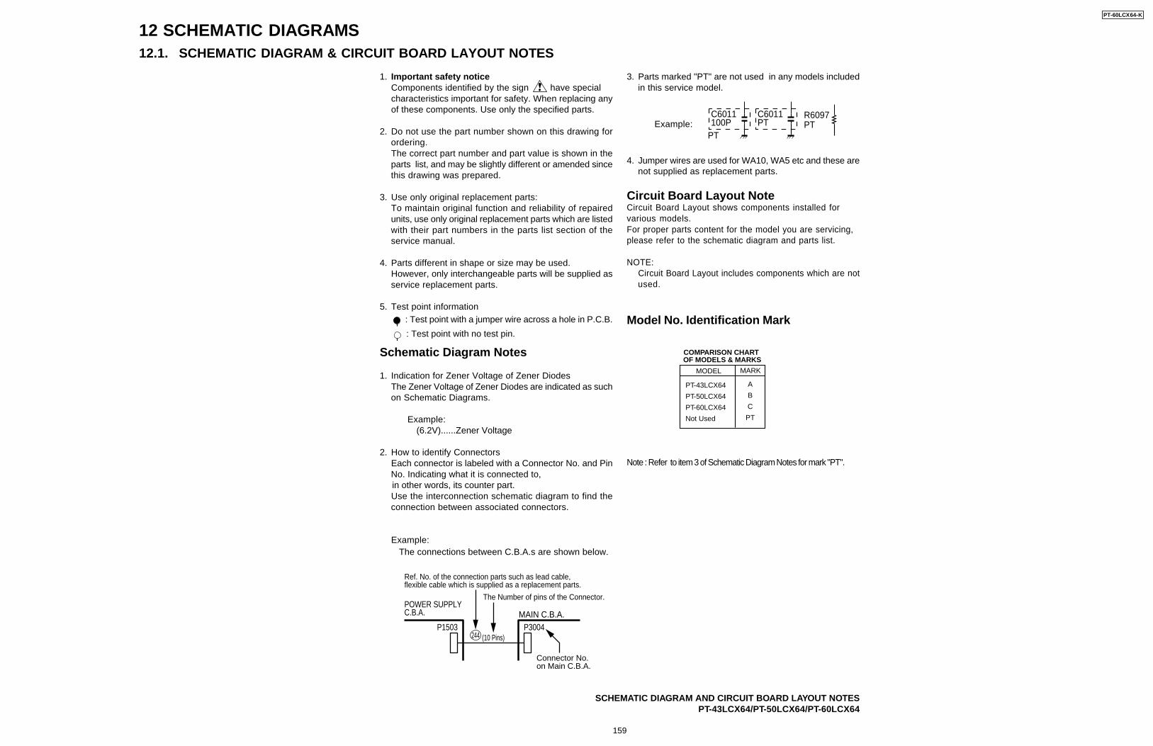
12 SCHEMATIC DIAGRAMS12.1. SCHEMATIC DIAGRAM & CIRCUIT BOARD LAYOUT NOTES
1. Important safety noticeComponents identified by the sign have specialcharacteristics important for safety. When replacing anyof these components. Use only the specified parts.
2. Do not use the part number shown on this drawing forordering.The correct part number and part value is shown in theparts list, and may be slightly different or amended sincethis drawing was prepared.
3. Use only original replacement parts:To maintain original function and reliability of repairedunits, use only original replacement parts which are listedwith their part numbers in the parts list section of theservice manual.
4. Parts different in shape or size may be used.However, only interchangeable parts will be supplied asservice replacement parts.
5. Test point information : Test point with a jumper wire across a hole in P.C.B.
: Test point with no test pin.
Schematic Diagram Notes
1. Indication for Zener Voltage of Zener DiodesThe Zener Voltage of Zener Diodes are indicated as suchon Schematic Diagrams.
Example:(6.2V)......Zener Voltage
2. How to identify ConnectorsEach connector is labeled with a Connector No. and PinNo. Indicating what it is connected to,
in other words, its counter part.Use the interconnection schematic diagram to find theconnection between associated connectors.
Example: The connections between C.B.A.s are shown below.
POWER SUPPLYC.B.A. MAIN C.B.A.
The Number of pins of the Connector.
Connector No.on Main C.B.A.
P1503 P3004(10 Pins)
Ref. No. of the connection parts such as lead cable, flexible cable which is supplied as a replacement parts.
244
3. Parts marked "PT" are not used in any models includedin this service model.
Example: 100PPT
C6011 R6097PTPT
C6011
4. Jumper wires are used for WA10, WA5 etc and these arenot supplied as replacement parts.
Circuit Board Layout NoteCircuit Board Layout shows components installed forvarious models.For proper parts content for the model you are servicing,please refer to the schematic diagram and parts list.
NOTE:Circuit Board Layout includes components which are notused.
SCHEMATIC DIAGRAM AND CIRCUIT BOARD LAYOUT NOTESPT-43LCX64/PT-50LCX64/PT-60LCX64
Model No. Identification Mark
COMPARISON CHART OF MODELS & MARKS
PT-43LCX64
PT-50LCX64
PT-60LCX64
Not Used
A
B
C
PT
MODEL MARK
Note : Refer to item 3 of Schematic Diagram Notes for mark "PT".
PT-60LCX64-K
159
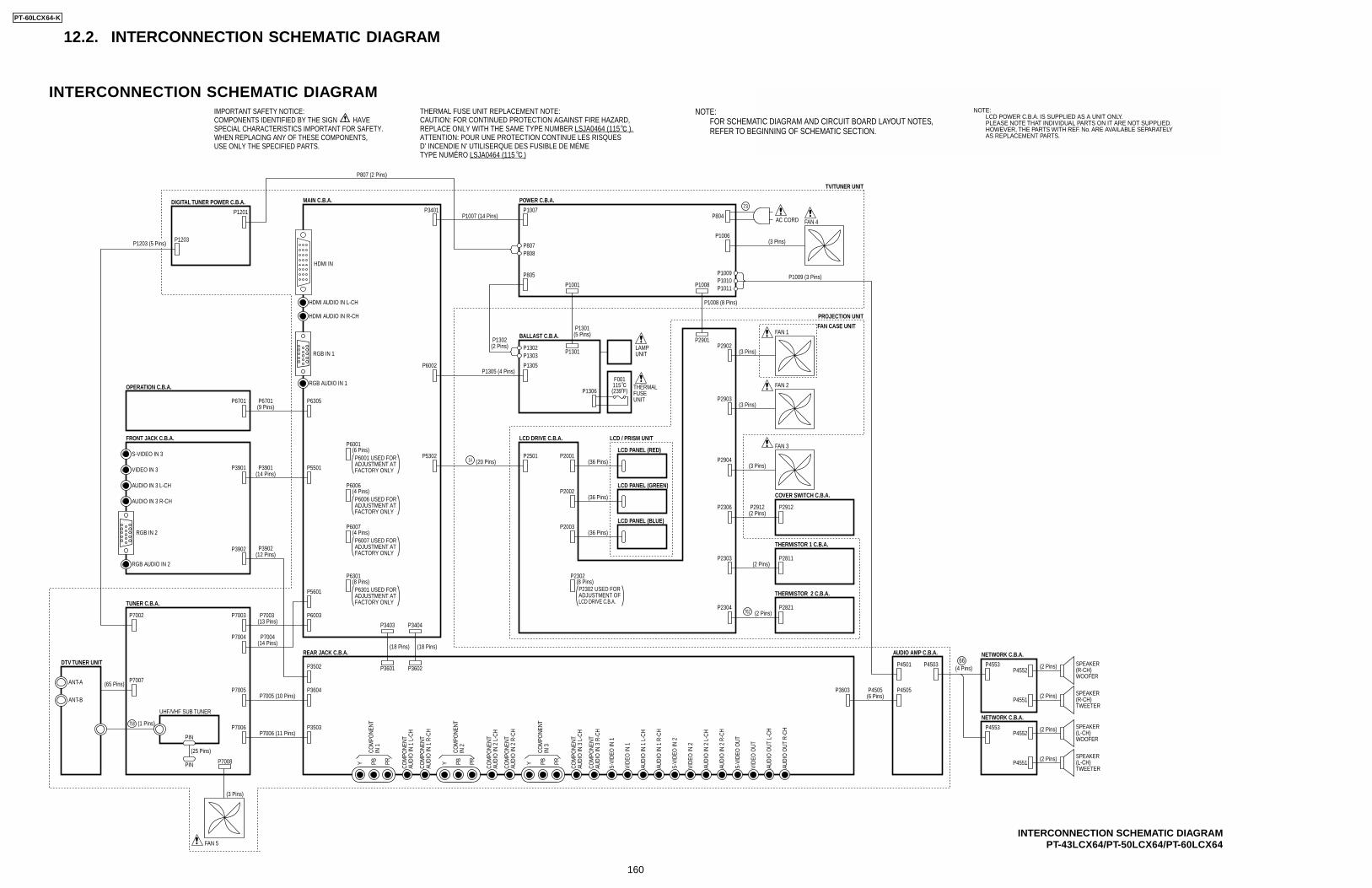
12.2. INTERCONNECTION SCHEMATIC DIAGRAM
NOTE:FOR SCHEMATIC DIAGRAM AND CIRCUIT BOARD LAYOUT NOTES,REFER TO BEGINNING OF SCHEMATIC SECTION.
NOTE: For placing a purchase order of the parts, be sure to use the part number listed in the parts list. Do not use the part number on this diagram.
NOTE:PARTS MARKED "PT" ARE NOT USED.
INTERCONNECTION SCHEMATIC DIAGRAMIMPORTANT SAFETY NOTICE:COMPONENTS IDENTIFIED BY THE SIGN HAVESPECIAL CHARACTERISTICS IMPORTANT FOR SAFETY.WHEN REPLACING ANY OF THESE COMPONENTS,USE ONLY THE SPECIFIED PARTS.
NOTE:LCD POWER C.B.A. IS SUPPLIED AS A UNIT ONLY.PLEASE NOTE THAT INDIVIDUAL PARTS ON IT ARE NOT SUPPLIED.HOWEVER, THE PARTS WITH REF. No. ARE AVAILABLE SEPARATELYAS REPLACEMENT PARTS.
THERMAL FUSE UNIT REPLACEMENT NOTE:CAUTION: FOR CONTINUED PROTECTION AGAINST FIRE HAZARD,REPLACE ONLY WITH THE SAME TYPE NUMBER LSJA0464 (115 ).ATTENTION: POUR UNE PROTECTION CONTINUE LES RISQUESD’ INCENDIE N’ UTILISERQUE DES FUSIBLE DE MÉMETYPE NUMÉRO LSJA0464 (115 )
NOTE:FOR SCHEMATIC DIAGRAM AND CIRCUIT BOARD LAYOUT NOTES,REFER TO BEGINNING OF SCHEMATIC SECTION.
INTERCONNECTION SCHEMATIC DIAGRAMPT-43LCX64/PT-50LCX64/PT-60LCX64
P1203 (5 Pins)
MAIN C.B.A.
REAR JACK C.B.A.
POWER C.B.A.
LCD DRIVE C.B.A.
LCD PANEL (RED)
LCD / PRISM UNIT
LCD PANEL (GREEN)
LCD PANEL (BLUE)
(6 Pins)P6001
P6305P6701
P1203
OPERATION C.B.A.
(3 Pins)
FAN 4
P1006
P1008
P1008 (8 Pins)
P2901
(3 Pins)
(36 Pins)
(36 Pins)
(36 Pins)
FAN 1
P2902
P2001
(3 Pins)
FAN 2
P2903P6701(9 Pins)
P2501P5302(20 Pins)
P3602
P3404
P3601
P3403
(18 Pins) (18 Pins)
AUDI
O O
UT R
-CH
AUDI
O O
UT L
-CH
VIDE
O O
UT
S-VI
DEO
OUT
AUDI
O IN
2 R
-CH
AUDI
O IN
2 L
-CH
VIDE
O IN
2
S-VI
DEO
IN 2
AUDI
O IN
1 R
-CH
AUDI
O IN
1 L
-CH
VIDE
O IN
1
S-VI
DEO
IN 1
COM
PONE
NTAU
DIO
IN 1
L-C
H
COM
PONE
NTAU
DIO
IN 1
R-C
H
COM
PONE
NTAU
DIO
IN 2
L-C
H
COM
PONE
NTAU
DIO
IN 2
R-C
H
COM
PONE
NTIN
1
Y PB PR
COM
PONE
NTIN
2
Y PB PR
THERMISTOR 1 C.B.A.
P2303 P2811(2 Pins)
P2002
P2003
14
(8 Pins)P2302
P2302 USED FORADJUSTMENT OFLCD DRIVE C.B.A.
P6001 USED FORADJUSTMENT ATFACTORY ONLY
THERMISTOR 2 C.B.A.
P2304 P2821(2 Pins)
COVER SWITCH C.B.A.
P2306 P2912P2912(2 Pins)
(3 Pins)
FAN 3
P2904
UHF/VHF SUB TUNER
PIN
PIN
(25 Pins)
(3 Pins)
TUNER C.B.A.
DTV TUNER UNIT
P7005
P7008
P3604P7005 (10 Pins)
P7003 P6003P7003 (13 Pins)
P7004(14 Pins)
P5601
P7004
FRONT JACK C.B.A.
AUDIO IN 3 R-CH
AUDIO IN 3 L-CH
VIDEO IN 3
S-VIDEO IN 3
RGB IN 2
P3901 P5501P3901(14 Pins)
P3902
P3502
P3902(12 Pins)
COM
PONE
NTAU
DIO
IN 3
L-C
H
COM
PONE
NTAU
DIO
IN 3
R-C
H
COM
PONE
NTIN
3
Y PB PR
RGB IN 1
P4503 P4553(4 Pins)
NETWORK C.B.A.
P4552(2 Pins) SPEAKER
(R-CH)WOOFER
P4551(2 Pins) SPEAKER
(R-CH)TWEETER
P4553
NETWORK C.B.A.
P4552(2 Pins) SPEAKER
(L-CH)WOOFER
P4551(2 Pins) SPEAKER
(L-CH)TWEETER
P3603 P4505P4505(6 Pins)
AUDIO AMP C.B.A.
BALLAST C.B.A.
P1305P6002 P1305 (4 Pins)
P805
P807P808
P1302P1303
P1301
P1001
P804
73
AC CORD
P1007P3401P1007 (14 Pins)
P1009P1010P1011
P4501
LAMPUNIT
P1306THERMALFUSEUNIT
RGB AUDIO IN 2
RGB AUDIO IN 1
HDMI IN
HDMI AUDIO IN R-CH
HDMI AUDIO IN L-CH
(4 Pins)P6006
P6006 USED FORADJUSTMENT ATFACTORY ONLY
(4 Pins)P6007
P6007 USED FORADJUSTMENT ATFACTORY ONLY
(8 Pins)P6301
P6301 USED FORADJUSTMENT ATFACTORY ONLY
P1302(2 Pins)
P1009 (3 Pins)
P1301(5 Pins)
762
F001115 (239 F)
PROJECTION UNIT
TV/TUNER UNIT
FAN CASE UNIT
DIGITAL TUNER POWER C.B.A.
P1201
P807 (2 Pins)
P7002
P7007ANT-A
ANT-B
(65 Pins)
(1 Pins)
FAN 5
P7006 P3503P7006 (11 Pins)
758
66
PT-60LCX64-K
160
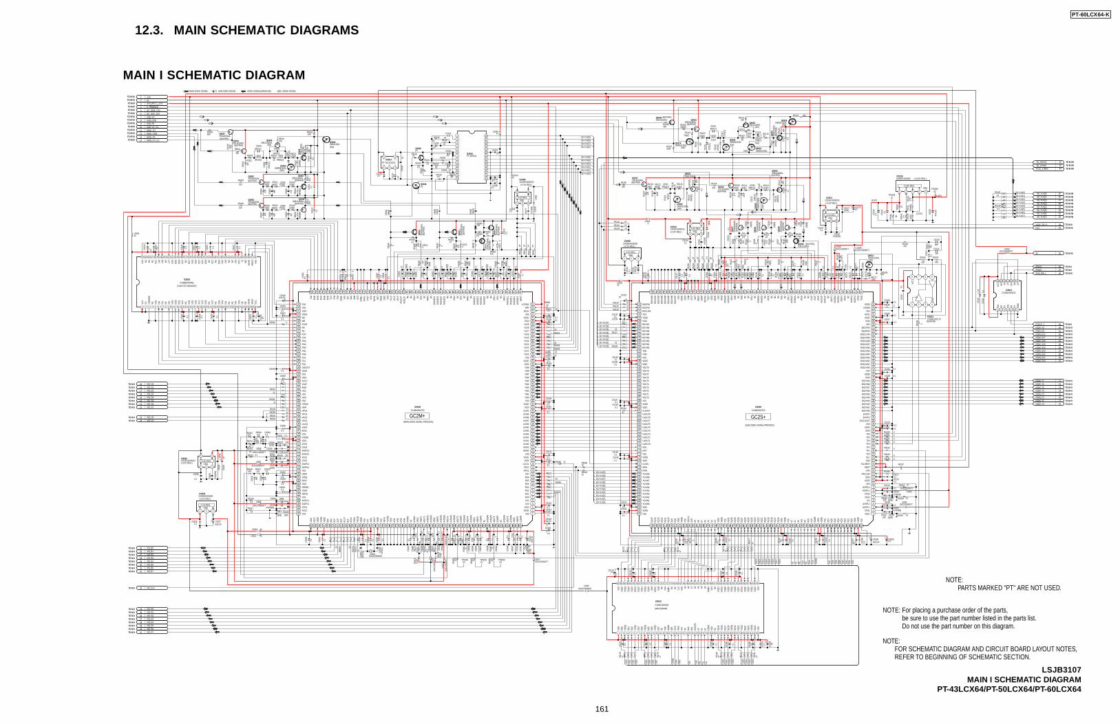
12.3. MAIN SCHEMATIC DIAGRAMS
MAIN I SCHEMATIC DIAGRAM
NOTE:FOR SCHEMATIC DIAGRAM AND CIRCUIT BOARD LAYOUT NOTES,REFER TO BEGINNING OF SCHEMATIC SECTION.
NOTE: For placing a purchase order of the parts, be sure to use the part number listed in the parts list. Do not use the part number on this diagram.
NOTE:PARTS MARKED "PT" ARE NOT USED.
LSJB3107MAIN I SCHEMATIC DIAGRAM
PT-43LCX64/PT-50LCX64/PT-60LCX64
VID_G015
3.3V1
VID_VS24
VID_HS23
VID_G722
VID_G621
VID_G520
VID_G419
VID_G318
VID_G217
VID_G116
H_FREERUN4
I2C_SCK_3.3V6I2C_DATA_3.3V5
9V2
SYS_RST_L_3.3V3
VID_CLK33
IC5012
C3ABPJ000063
1 2 3 4 5 6 7 8 9 10 11 12 13 14 15 16 17 18 19 20 21 22 23 24 25 26 27 28 29 30 31 32 33 34 35
444546474849505152535455565758596061626364656667686970
36 37 38 39 40 41 42 43
71727374757677787980818283848586
C518
6
0.1
C517
7
0.1
C518
8
0.1
C519
2PT
C517
9
0.1
C5176PT
C518
1
0.1
C518
7
0.1
C518
9
0.1
C518
0
0.1
0R5
175
IC5002C3HBKZ000001
1 2 3 4 5 6 7 8 9 10 11 12 13 14 15 16 17 18 19 20 21 22 23 24 25 26 27 28 29 30 31 32 33 34 35
3637383940414243444546474849505152535455565758596061626364656667686970
C501
80.
1
C502
3PTC5
016
0.1
C502
1
0.1
C501
40.
1
C502
0
0.1
C501
3
PT
C502
2
0.1
C501
5
0.1
C501
7
0.1
C501
9
0.1
0R5029
22
R5091
22R5092
22R5094 22
R5093
22
R5141
22R5097
22R5098
22R5099
C508
6
0.1
C508
1
0.1
C5104
PT
C50480.1
C508
4
0.1
C505
7
0.1
C504510/6.3V
C508
3
0.1
C505
8
0.1C5
055
PT
C5114
0.1
C505
60.
1
C5047
0.1
C514
9
0.1
C519
60.
1
C5208 0.1
C52100.1
C5142
0.1
C5200PT
C5209 0.1
C5132PT
C5141
0.1
C52130.1
C515
10.
1
C52060.1
C514
7
0.1
C515
0
0.1
C52070.1
C52050.1
C52110.1
C519
50.
1
C519
40.
1
C519
30.
1
C518
50.
1
C518
40.
1
C518
30.
1
C518
20.
1
C519
70.
1 C519
80.
1
C51400.1
C51390.1
C51370.1
C51380.1
C51360.1
C51350.1
C51340.1
C51330.1
C50240.1
C502710/6.3V
C5111
0.1C5112
0.1
C5110
0.1
C5109
0.1
C5108
0.1
C5107
0.1
C5106 0.1C5105 0.1
C508
0
0.1
C5049
0.1
C5051 0.1
C5053
0.1
C5050
0.1
C5052
0.1
C50540.1
C52120.1
C519910/6.3V
C516
80.
1
C516
60.
1
C517
00.
1
C510310/6.3V
C5113
0.1
C5046
0.1
C517
8
0.1
C519
00.
1
C519
10.
1
22R5033
22R5034
VID_B631VID_B732
VID_B025VID_B126
VID_B328
VID_B530
VID_B227
VID_B429
22
R507
022
R506
9
22R5035PTR5036
22R5068
22R5090
0
R5197
0
R506
7
C50760.1
C506
30.
1
C506
40.
1
C506
9
0.1
C507
00.
1
C507
40.
1C5
075
0.1
C505
90.
1
33[D
]R5
062
150[
D]
R506
4
33[D
]
R506
6
C507
10.
1
C507
2
0.1
33[D
]R5
052
C506
60.
1
150[
D]R5
054
C506
7
0.1
33[D
]
R505
7
150[
D]R5
047
33[D
]R5
045
33[D
]
R505
0
C506
10.
1
C506
2
0.1
2SD1
819A
SLQ
5010
2SD1
819A
SLQ
5011
2SD1
819A
SLQ
5013
2SB1
218A
SLQ
5012
*
10[K
B]C5
068*
10[K
B]C5
065*
10[K
B]C5
060
0R5
065
0R5
056
100
R504
915
00
R504
8
470
R505
5
470R5063
10KR5060
0
R504
4
0
R505
1
0R5
058
PTR5059 PT
R5061
PTR5053
PTR5046
0R5
042
0R5
043
*
1[KB]C5043
*
1[KB]C5042
*
1[KB]C5044
*1[KB]C5039
*1[KB]C5040
*
1[KB]
C5041
PTC5036
PTC5037
470P[KB]C5038
330R5037
330R5038
1800R5039
470R5024
470R5026
470R5025
470R5027
33P
C503
2
33P
C503
368
PC5
030
68P
C503
1
0.1C5034
0.1C5035
X5001H0J20250000215
P[JC
]C5
082
15P[
JC]
C508
5
C508
80.
1
C508
70.
1
2700
R507
2
2700
R507
6
470
R507
5
470
R507
9
5.6[
F]R5
074
5.6[
F]R5
078
1KR5
073
1KR5
077
0.1
C508
9
0.1
C509
2
0.1
C509
0
0.1
C509
1
C509
30.
1
C509
50.
1
C509
80.
1
C510
00.
1 2700
R508
7
0.1
C510
20.
1C5
101
0.1
C509
6
1C5
099
1C5
097
1C5
094
1500R5088
1200R5089
75R5
086
75R5
082
75R5
080
220
R508
5
220
R508
3
220
R508
1
2700
R508
4
0.1
C507
3
470P[KB]C5202
0.01[KB]C5201
*
1[KB]C5203
*
1[KB]C5204
330R5187
330R5186
C52150.1
C52140.1
0R5196
22R507
1
0R5194
0R5195
0R5193
0R51890R51900R51910R5192
0.1
C521
6
0R5188
0
R519
8
47K
R5202
22K
R5200 0.1C5
217
PTC517
2
*
1[KB
]C5
175
1500R5172
0.1[
KB]
C517
4
UNR521300LQ5031
68P
C5218
33P
C5219
470
R516
8
470
R520
1
470R5199
2700
R517
1
5.6[
F]
R516
91KR5
170
PTR5157
0
R516
0
*
10[K
B]
C515
9 *
10[K
B]
C516
4
220
R514
8
0R5
147
2SD1
819A
SLQ
5027
0R5
150
470
R515
5
0.1
C515
4
0
R515
3
*
10[K
B]
C515
6
0
R515
8
PTR5152
2SD1
819A
SLQ
5028
0
R516
7
PT
R5165
2SB1218ASLQ5030
2SD1
819A
SLQ
5029
470
R516
1
PTR5163
10K
R516
4C5
163
0.1
33[D
]
R514
5
33[D
]R5
151
C515
50.
1
C515
70.
1
C515
20.
1
150[
D]R5
154
33[D
]
R515
9
C516
0
0.1
150[
D]R5
162
33[D
]
R515
6
33[D
]R5
166
150[
D]
R514
6
C516
10.
1
33[D
]R5
149
0.1
C516
5
0.1
C516
2
0.1
C515
8
0.1
C515
3
22R5096
22
R5095
VID_R438VID_R539
VID_R135
VID_R640VID_R741
VID_R236VID_R337
VID_R034
C513
110
/6.3
V
C513
00.
1
C0CBCAD00012IC5006
1 2
5
3
4
0.01
[KB]
C507
7
*
C507
81[
KB]
C0CBCAD00012IC5010
1 2
5
3
4
0.01
[KB]
C514
5
*
C514
61[
KB]
C51440.1
C0CBCAD00012IC5011
1 2
5
3
4
0.01[KB]C5169
* C51711[KB]
C51670.1
PTC5173
C0CBCAD00012IC5004
1 2
5
3
4
0.01
[KB]
C502
6
*
C502
81[
KB]
C5025
0.1
PTC5
029
HDMI_VS 60HDMI_HS 61HDMI_CLK 62HDMI_UV7 63HDMI_UV6 64HDMI_UV5 65HDMI_UV4 66HDMI_UV3 67
HDMI_UV0 70
HDMI_UV2 68HDMI_UV1 69
HDMI_Y7 71HDMI_Y6 72HDMI_Y5 73HDMI_Y4 74
HDMI_Y0 78
HDMI_Y3 75HDMI_Y2 76HDMI_Y1 77
0.1
C522
1
PTC5
220
POCLK_1 59
/POHS 57/POVS 56
SUB_V/Y7SUB_C/PB8SUB_PR9
MAIN_PR13
MAIN_V/Y11MAIN_C/PB12
5V 55
RGB_MW_L 58
150
R5001
220
R5004
330
R500
2
330
R500
6
470[D]
R5003
270[D]R5008
180[D]R5011
120[D]R5014
33
R5010 270[D]R5013
1200
[D]
R501
7
6800
[D]
R501
8
2SD1819A0LQ5001
2SD1819A0LQ5002
2SB1
218A
0LQ
5006
2SB1218A0LQ5007
2R2U[J]
L5001
5R6U[J]
L5002
10U[J]L5003
0.1
C501
00.
1C5
011
15P[
JC]
C500
2
15P[JC]C5001
22P[JC]
C5006
22P[
JC]
C500
7
47P
C500
8
68P
C500
4
UNR521300LQ5004
UN521300LQ5009
10KR5023
10KR5016
680
R502
082
0R5
021
68P
C500
5
220
R50052SD1819A0LQ5003
2SB1218A0LQ5008
270[D]R5009
180[D]R5012
330
R500
7
47P
C500
9
120[D]R5015
6800
[D]
R501
9
820
R502
2
0.1
C501
210U[J]L5004
27P[
JC]
C511
7
UNR521300LQ5026
2SB1
218A
0LQ
5023
470
R510
6
2SD1819A0LQ5015
39R5116
1U[J]
L5018
6800
[D]
R511
8
15P[
JC]
C512
2
2SD1819A0LQ5016
0.1
C512
8
330
R510
2
680
R512
0
180[D]R5111
2SB1218A0LQ5024
39
R5110
120[D]R5114
330
R5104
10KR5113
150[D]R5103
0.1
C512
7
2200
[D]
R511
7
33PC5121
UNR521300LQ5019
100P
C511
9
8P[CC]C5116
820
R512
1
750[F]R5101
330[D]R5100
UNR521300LQ5014
22P[
JC]
C511
5
UNR521300LQ5018
1U[J]L5019
1U[J]
L5022
120[D]R5108
5R6U[J]L5020
47P
C512
5UN
R521
300L
Q50
20
15P[
JC]
C512
3
120[D]R5115
120[D]R5109
2SD1819A0LQ5017
330
R5105
180[D]R5112
0.1
C512
9
100P
C512
0
2SB1218A0LQ5025
47P
C512
6 820
R512
268
00[D
]R5
119
5R6U[J]L5021
470
R510
7
UNR521300LQ5021
47R517
3
47R517
4
47R517
6
47R517
7
47R517
8
47R517
9
47R518
0
47R518
1
22R5126
22R512522R5124
22R5127
22
R5128
33P
C5124
PCLK_27MHZ 44
SD_HSYNC 42
SD_VSYNC 43
SD_YUV[7] 52
C522
210
/6.3
V
IC5015C0DBEZG00005
1 2 3 4 5
PT
R503
21K
R504
0
TP5005
47/6
.3V
C522
5
PTC522
3
PTR5
0410.
1C5
224
TP5004
1K[D
]R5
132
270
R513
3R5
131
1500
[D]
3.45V_ON_H 53
PTR5
203
PTR5
204
PTR5
205
PTR5206
PTR5207
PTR5208
PTR5209
PTR5
210
PTR5
211
PTR5
212
PTR5
213
PT
R5214
PTR5215
PT
R5216
PT
R5217
PTR5218
2SB1218ASLQ5005
2SB1218ASLQ5022
IC5016PT AD9214
12345678910
2122
151617181920
1112
2324
1314
25262728
PT TK11133CSIC5017
1 2
5
3
4
C5226PT
*
C522
8PT
PTC522
7
PT
C5232
PT
C5230
PT
C5234
PTC5236
PTC5237
PTC5238
PT
C5235PT
C5231
PTC5239
PT
R5219
PT
R5220
PT
R5221
PT
R5222
PT
R522
3
PTR5224
PT
R5225
PTQ5035
PTR5226
PTR5233
C514
310
/6.3
V
6.5V 54
2SD1819A0LQ5037
2SD1819A0LQ5038
560R5234
1500
R523
5
1500R5237
560R5236
MAIN_V/Y_CC14
SUB_V/Y_CC10
22P[
JC]
C511
8
PTR523822R5239
PTR5142
PTR5143PTR5144
PTQ5036
TP5003TP5001 TP5002
PTR5
240
PTR5
241
PTR5
242
SD_YUV[6] 51SD_YUV[5] 50SD_YUV[4] 49SD_YUV[3] 48
SD_YUV[1] 46SD_YUV[2] 47
SD_YUV[0] 45
PTR5130
PT
R5129
10KR5123
L5028J0JCC0000077
0L5
013
L5007
J0JCC0000077
L501
5J0
JCC0
0000
77
0L5011 0L5
027
L5008
J0JCC0000077
L501
6J0
JCC0
0000
77
0L5012 0L5
026
L5009 42
L5017J0JCC0000077
L5032J0JCC0000077
0
L502
5
L5010 42
L500542
L502342
L5031J0JCC0000077
JOJCC0000077L5033
PTL5034
L5030J0JHC0000018
L5029J0JCC0000077
0L5014
L5006
J0JCC0000077
0L5024
IC5005C1AB00001702
123456789
10111213141516171819202122232425262728293031323334353637383940414243444546474849505152535455565758596061626364
65 667778798081828384858687888990919293949596979899100
101
102
103
104
105
106
107
108
109
110
111
112
113
114
115
116
117
118
119
120
121
122
123
124
125
126
127
128
133134135136137138139140141142143144145146147148149150151152153154155156157158159160161162163164165166167168169170171172173174175176177178179180181182183184185186187188189190191192
193
194
195
196
197
198
205
206
207
208
209
210
211
212
213
214
215
216
217
218
219
220
221
222
223
224
225
226
227
228
229
230
231
232
233
234
235
236
237
238
239
240
241
242
243
244
245
246
247
248
249
250
251
252
253
254
255
256
76 73 70 6775 72 69 6874 71
129130131132
199
200
201
202
203
204
IC5009C1AB00001703
123456789
10111213141516171819202122232425262728293031323334353637383940414243444546474849505152535455565758596061626364
65 667778798081828384858687888990919293949596979899100
101
102
103
104
105
106
107
108
109
110
111
112
113
114
115
116
117
118
119
120
121
122
123
124
125
126
127
128
133134135136137138139140141142143144145146147148149150151152153154155156157158159160161162163164165166167168169170171172173174175176177178179180181182183184185186187188189190191192
193
194
195
196
197
198
205
206
207
208
209
210
211
212
213
214
215
216
217
218
219
220
221
222
223
224
225
226
227
228
229
230
231
232
233
234
235
236
237
238
239
240
241
242
243
244
245
246
247
248
249
250
251
252
253
254
255
256
76 73 70 6775 72 69 6874 71
129130131132
199
200
201
202
203
204
IC5013C0JBAZ002170
1 2 3 4
5678
IC5014
1 2 3 4 5 6 7
891011121314
IC5003C0CBAAG00008
1 2 3
IC5008C0CBAAG00008
1 2 3
GC2M+ GC2S+
DQ21
DQ22
VSSQ
VSSQ
DQ26
VDDQ
VDDQ
DQ13
CLK
VDDQ
DQ27A6
NC
A7
A1A4
DQ18
VSS
VDDQNC
VSSQ
DQ0
CKE
DQ8
DQ1
DQ9
DQ20
VSSQ
BA0
VSSQ
/RAS
DQ29A3
DQ2
BA1
DQ6
DQ14
DQ28
DQ7
NC
DQ10
/CS
DQM
0
DQ15
NCVSSQ
VSSQ
A2 VDDQ
DQ11
VDD
A8
/WE
DQ30
DQM
1
DQ4
DQ23
DQ25
VSS A5
DQ17
A9
VDD
DQ3
VDDQ
DQ16
DQ5
A10(
AP)
/CAS
DQ31
DQ24
VDD
VDDQ VS
S
VDDQ
VSSQ
DQ19
VDD
VSS
DQM
2
DQ12
NC
DQM
3
A0
NCNC
RO1
CLKIN
UVIN5
VDDI
UVIN6
VSS
VDDEVSS
RO5
UVIN0
VDDE
HPIN2
VDDE
UVIN9
RO6
YIN0
UVIN7
RO0
UV0
VPIN2
UV1
RO2
UVIN8
RO3
VPO1LCLK1
YUV0
VDDI
VSS
R07HPO1
UVIN3UVIN4
RO4
VDDI
UVIN2UVIN1
YIN1YIN2YIN3YIN4YIN5YIN6YIN7YIN8YIN9VDDI
VSSVDDE
VDDI
VSSVDDE
YUV1
YUV3YUV2
YUV5YUV4
YUV7YUV6
YUV9YUV8
LCDSW
BCLKHFR
AVSA
D12
NRST
VRL1
VIN1NCNC
VRH1NC
AVDA
D12
AVSA
D11
AVDA
D11
AVSA
D22
AVDA
D22
AVSA
D21
AVDA
D21NC
VRH2NC
VIN2
VRL2 NCNCNCNCNCNCNCNC
AVSA
D32
AVDA
D32
AVDA
D31
AVSA
D31
VIN3
VRH3
VRL3
AVSC
LPAV
DCLP
UCLP
VCLP
YCLPVS
SVD
DIVD
DE
XTST
VPIN
1
SCS
HPIN
1
XSM
SDA
SCL
VSS
MST
VPD
SMCK
VDDEFIN7
FIN8F0
6
FIN6
FIN9
FIN5 FO
8FO
9
FO7
WRFCKR
VDDEWE
VDDIVSSFO5
REFO4
RR
FO3FIN4FIN3FIN2FIN1FIN0FO2FO1FO0
VDDEVSS
OSDCNT
VDDIINTLCVDAFEWO
HO1HDO
HO2
PSOHTRAPHINPHPO3
HPO2VPO2
VPO3
LCLK2
AVSPL3
VSSCW358VDDI
BXS3VDDE
CPO3AVDPL3
VGS3
VGS2CPO2AVDPL2AVSPL2VSS
VDDEHREF
VDDIBXS2
CPO1AVDPL1
VSS
VDDE
AVSPL1VSSFBPIN
VGS1
FBPMO
VDDE
VDDE
VDDE
VDDI
POUT
VSAW
RCF
BCF
RDV
BDV
GCF
HPO
4
FRCL
K
HCLP
BLK
VPO
4
VSS
VSS
VDDE
VDDI
XIN
XOUT
YUVO
E
AOUT
1
VMYS
AIN2
AIN4
TEST
AIN1
AIN3
AVDA
D
VREF
1
AVSA
DVR VR
O1
AVSD
A1
AVDD
A2AV
SDA2
VRO
2AV
DDA1
VREF
2
AVSD
A3AO
UT2
AVDD
A3AO
UT3
AOUT
4
VRO
4
COM
P3
AVDD
A4
AVSD
A4
VREF
4CO
MP4
NC AVDD
A5AV
SDA5
COM
P5AO
UT5
NC AVSD
A6
AVDD
A6VR
O6
COM
P6VR
EF6
AOUT
6
CPO2
BS2YIN0
CPO1VGS1
VDDE
SCL
EXVPO
VDDI
EXCLKOUT
VGS2
AVSPL1NC
AVDPL2
EXHPO
AVSPL2
NRSTPLLNRST
SDA
TP0
FRCLKINVPD
VSS
AVDPL1
VDDI
VSSVDDE
VDDIVSS
VDDEBXS1
VGS3
CPO
3
NCNC
AVSD
A1AV
DDA1
AVSC
LPAV
DCLP
AVSA
D3AV
DAD3 NC
VRO
1
NC
AOUT
1
VRL1 NC
VIN1 NCNCNC NC NCNC
AVDA
D1AV
SAD1
VREF
1
VRH2
VRH3
UCLP
VCLP
YCLP
VSS
VDDI
VDDE
TEST
IOCT
RL
SMCK
SADRMST
XTST
XSM
VSS
VDDE
BSUV
IN7
VDDI
VDDEVDDI
BSVPINBSHPIN
YIN1YIN0
YOUT9
VDDE
VSS
VDDI
CLKOUTUVOUT9
HPOVPO
VPINHPIN
VDDI
VSSVDDE
DQ15
CKE
SDCL
K
A9 RAS
SDW
ECA
S
BS
TP1TP2TP3
TP5TP4
TP6
VDDEVSS
VDDI
BS2YIN1
BS2YIN3BS2YIN2
BS2YIN5BS2YIN4
BS2YIN7BS2YIN6
BS2YIN9BS2YIN8
BS2UVIN0BS2UVIN1BS2UVIN2BS2UVIN3BS2UVIN4BS2UVIN5BS2UVIN6BS2UVIN7BS2UVIN8BS2UVIN9BS2CLKIN
BS2VPINBS2HPIN
VSSCW358
VDDE
AVDP
L3AV
SPL3
VRH1NC
AVDA
D2AV
SAD2
VRL2
VIN2 NCNC
VIN3
VRL3
BSUV
IN6
BSUV
IN5
BSUV
IN4
BSUV
IN3
BSUV
IN2
BSUV
IN1
BSUV
IN0
BSCLKIN
BSYIN7BSYIN6
BSYIN4BSYIN5
BSYIN2BSYIN3
BSYIN0BSYIN1
VSS
YOUT8
YOUT6YOUT7
YOUT4YOUT5
YOUT2YOUT3
YOUT0YOUT1
VSSVDDEVDDI
UVOUT8
UVOUT6UVOUT7
UVOUT4UVOUT5
UVOUT2UVOUT3
UVOUT0UVOUT1
VDDEVSS
VDDICLKIN
YUVIN9YUVIN8
YUVIN6YUVIN7
YUVIN4YUVIN5
YUVIN2YUVIN3
YUVIN0YUVIN1
DQ14
DQ12
DQ13
DQ10
DQ11
DQ8
DQ9
VSS
VDDE
VDDI
A8 A6A7 A4A5 A3 VSS
VDDI
VDDE
VSS
VDDI
VDDE
VSS
VDDI
VDDE
DQ31
DQ30
DQ28
DQ29
DQ26
DQ27
DQ24
DQ25
DQ23
DQ22
DQ20
DQ21
DQ18
DQ19
DQ16
DQ17
A2 A0A1 A10
VSS
VDDI
VDDE
DQ7
DQ6
DQ4
DQ5
DQ2
DQ3
DQ0
DQ1
CSM
ODE
VCC
SWCK
NC
RSTWW
E
NC
CS
DI8
DI9
NC
NC VSS
VSS IE
VCC
DI0
NC
NC NC
DI1
DI2
VSS
DO0
DO1
VCC
NC DO2
VSS
VSS
VCC
VCC
DO3
NC VCC
VSS
DO4
VCC
SRCK
RSTR
REOE
VSS
DI4
NCNCDI3
DI7
VSS
DO9
DO8
VCC NC VSS
DO7
VSS
VCC
VCC
DO6
NC VCC NC DO5
VSS
VSS
DI6
NC NC DI5
VCC
GND
GND
VCC
1Y 2Y GND
/2G
/3G
1A/4
GVC
C 3A
/1G
4A 3Y4Y2A
[3.45V]
[6.5V]
[1.25V]
IN OUT
CONT NPGND
SD-YUV[0]SD-YUV[1]SD-YUV[2]SD-YUV[3]SD-YUV[4]SD-YUV[5]SD-YUV[6]SD-YUV[7]
SD-YUV[2]
SD-YUV[0]
SD-YUV[6]SD-YUV[7]
SD-YUV[4]SD-YUV[3]
SD-YUV[1]
SD-YUV[5]
DQ23
DQ22
DQ21
DQ20
DQ19
DQ18
DQ17
DQ16
DQ20
DQ21
DQ23
DQ17
DQ19
DQ22
DQ18
DQ16
A2 A1 A0 A10
BS
A0 A1 A2A10
SDW
E
RAS
CAS
CAS
BSRAS
SDW
E
DQ7
DQ6
DQ5
DQ4
DQ3
DQ2
DQ1
DQ0
DQ2
DQ3
DQ1
DQ0
DQ4
DQ6
DQ5
DQ7
SD-YUV[4]
SD-YUV[2]
SD-YUV[8]SD-YUV[9]
SD-YUV[6]SD-YUV[5]
SD-YUV[3]
SD-YUV[7]
SD-YUV[0]SD-YUV[1]
SD-YUV[2]
SD-YUV[5]
SD-YUV[7]
SD-YUV[9]
SD-YUV[6]
SD-YUV[8]
SD-YUV[4]
SD-YUV[1]SD-YUV[0]
SD-YUV[3]
AUDIO SIGNALVIDEO SIGNAL(MAIN/SUB)SUB VIDEO SIGNALMAIN VIDEO SIGNAL
TO M VIITO M VIITO M IIITO M IIITO M IIITO M III
TO M VIITO M VIITO M VIITO M III
TO M VII
TO M IIITO M VIITO M VII
TO M IITO M IITO M IITO M IITO M IITO M IITO M IITO M II
TO M IITO M II
TO M II
TO M II
TO M IITO M II
TO M IITO M II
TO M II
TO M II
TO M II
TO M IITO M II
TO M II
TO M II
TO M II
TO M II
TO M IITO M II
(MAIN VIDEO SIGNAL PROCESS)(SUB VIDEO SIGNAL PROCESS)
(64M SDRAM)
(BUFFER)
(SW)
(+2.5V REG.)
(+3.45V REG.)
(SW)(SW)
(SW)
(SW)(SW)
(SW)
(BUFFER)
(BUFFER)
(BUFFER)
(BUF
FER)
(BUFFER)
(SW
)
(BUFFER)
(BUF
FER)
(+2.5V REG.)
(+2.5V REG.) (BUF
FER)
(BUF
FER)
(BUF
FER)
(BUFFER)
(+2.5V REG.)
(BUF
FER)
(BUF
FER)
(BUF
FER)
(BUF
FER)
(+2.5V REG.)
(+2.5V REG.)
(5.6M FIFO MEMORY)
(BUFFER)
(BUFFER)
(BUFFER)
(BUFFER)
(BUF
FER)
(BUFFER)
(BUFFER)
(SW)
(SW)
(SW)
TO M VIIITO M VIII
TO M VIII
TO M VIIITO M VIIITO M VIIITO M VIIITO M VIIITO M VIIITO M VIIITO M VIII
TO M IIITO M VII
TO M VII
TO M IITO M IITO M III
TO M IITO M VITO M VITO M VITO M VITO M VITO M VITO M VITO M VITO M VI
TO M VITO M VI
TO M VI
TO M VITO M VI
TO M VI
TO M VI
TO M VI
TO M VITO M VI
+2.5V REG.
+2.5V REG.
+2.5V REG.
+2.5V REG.
+2.5V REG.
+2.5V REG.GND
GND
GND
GND
GND
+3.45V REG.GND
COJBZZ000222
PT-60LCX64-K
161
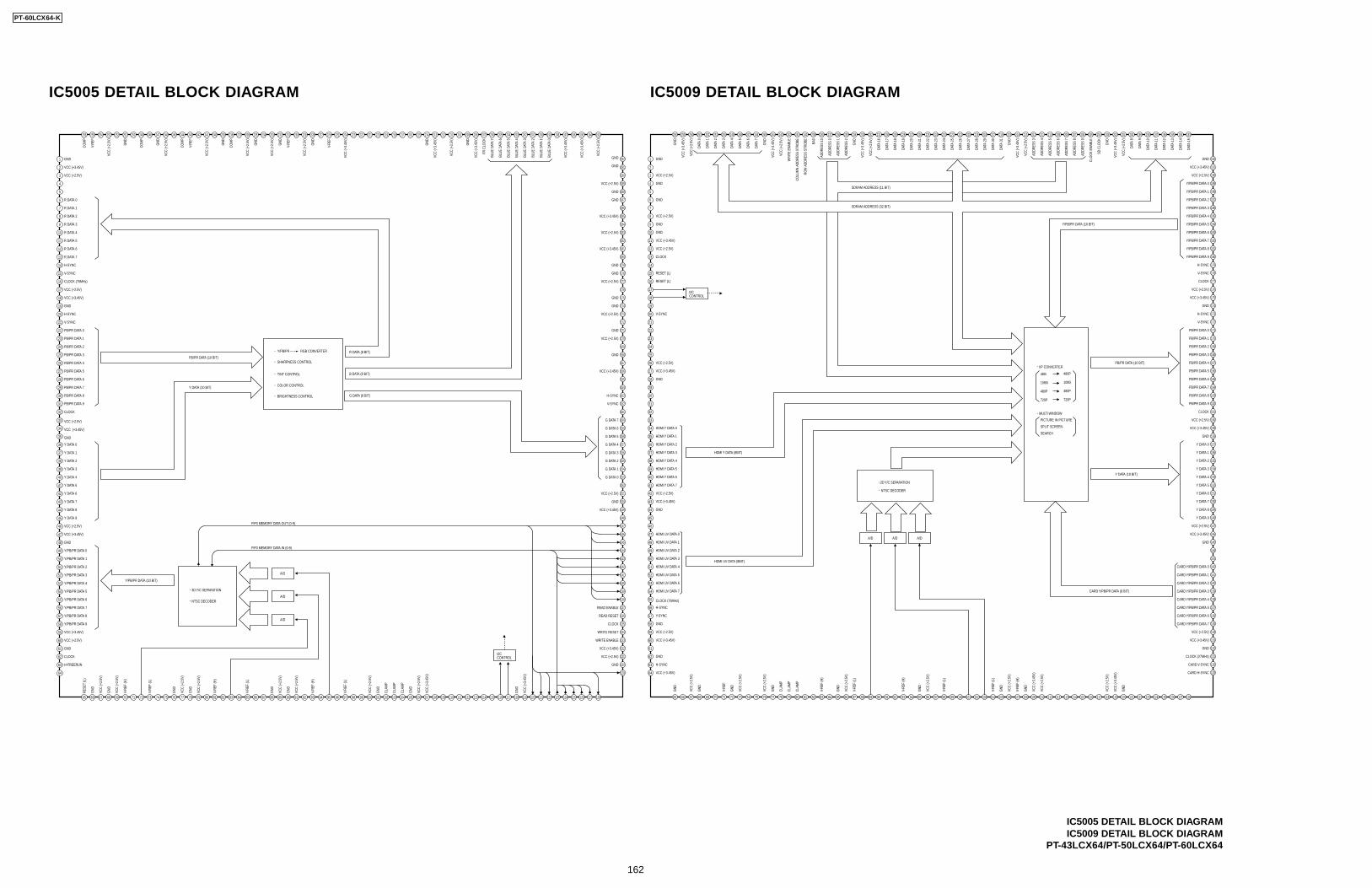
IC5005 DETAIL BLOCK DIAGRAM
1
2
3
4
5
6
7
8
9
10
11
12
13
14
15
16
17
18
19
20
21
22
23
24
25
26
27
28
29
30
31
32
33
34
35
36
37
38
39
40
41
42
43
44
45
46
47
48
49
50
51
52
53
54
55
56
57
58
59
60
61
62
63
64
65 66 67 68 69 70 71 72 73 74 75 76 77 78 79 80 81 82 83 84 85 86 87 88 89 90 91 92 93 94 95 96 97 98 99 100 101 102 103 104 105 106 107 108 109 110 111 112 113 114 115 116 117 118 119 120 121 122 123 124 125 126 127 128
129
130
131
132
133
134
135
136
137
138
139
140
141
142
143
144
145
146
147
148
149
150
151
152
153
154
155
156
157
158
159
160
161
162
163
164
165
166
167
168
169
170
171
172
173
174
175
176
177
178
179
180
181
182
183
184
185
186
187
188
189
190
191
192
256 255 254 253 252 251 250 249 248 247 246 245 244 243 242 241 240 239 238 237 236 235 234 233 232 231 230 229 228 227 226 225 224 223 222 221 220 219 218 217 216 215 214 213 212 211 210 209 208 207 206 205 204 203 202 201 200 199 198 197 196 195 194 193
GND
VCC (+3.45V)
VCC (+2.5V)
R DATA 0
Y/PB/PR RGB CONVERTER
R DATA 1
R DATA 2
R DATA 3
R DATA 4
R DATA 5
R DATA 6
R DATA 7
H-SYNC
V-SYNC
H-SYNC
V-SYNC
PB/PR DATA 0
PB/PR DATA (10 BIT)R DATA (8 BIT)
B DATA (8 BIT)
G DATA (8 BIT)
Y DATA (10 BIT)
PB/PR DATA 1
PB/PR DATA 2
PB/PR DATA 3
PB/PR DATA 4
PB/PR DATA 5
PB/PR DATA 6
PB/PR DATA 7
PB/PR DATA 8
PB/PR DATA 9
Y DATA 0
Y DATA 2
Y DATA 1
Y DATA 3
Y DATA 4
Y DATA 5
Y DATA 6
Y DATA 7
Y DATA 8
Y DATA 9
CLOCK (76MHz)
GND
CLOCK
VCC (+3.45V)
VCC (+2.5V)
GND
VCC (+3.45V)
VCC (+2.5V)
GND
GND
GND
GND
VCC (+3.45V)
VCC (+3.45V)
VCC (+2.5V)
VCC (+2.5V)
VCC
(+2.
5V)
GND
VCC
(+2.
5V)
VCC
(+2.
5V)
GND
VCC
(+2.
5V)
GND
VCC
(+2.
5V)
GND
GND
CLAM
P
CLAM
P
CLAM
P
VCC
(+2.
5V)
VCC
(+2.
5V)
VCC
(+3.
45V)
GND
VCC
(+2.
5V)
Y/PB/PR DATA 0
Y/PB/PR DATA 1
Y/PB/PR DATA 2
Y/PB/PR DATA 3
Y/PB/PR DATA 4
Y/PB/PR DATA 5
Y/PB/PR DATA 6
Y/PB/PR DATA 7
Y/PB/PR DATA 8
Y/PB/PR DATA 9
CLOCK
RESE
T (L
)
V-RE
F (H
)
H-FREERUN
V-RE
F (L
)
V-RE
F (H
)
V-RE
F (H
)
V-RE
F (L
)
V-RE
F (L
)
GND
VCC
(+3.
45V)
GND
CLOCK
VCC (+3.45V)
WRITE ENABLE
READ ENABLE
WRITE RESET
READ RESET
VCC (+2.5V)
GND
GND
GND
GND
GND
GND
GND
GND
GND
GND
GND
BLUE
DAT
A 0
BLUE
DAT
A 1
BLUE
DAT
A 2
BLUE
DAT
A 3
BLUE
DAT
A 4
BLUE
DAT
A 5
BLUE
DAT
A 6
BLUE
DAT
A 7
FR C
LOCK
GND
GND
GND
V-RE
F
V-RE
F
V-RE
F
VCC (+3.45V)
VCC (+3.45V)
VCC (+2.5V)
VCC (+2.5V)
VCC (+3.45V)
VCC (+3.45V)
VCC
(+3.
45V)
VCC
(+3.
45V)
VCC
(+3.
45V)
VCC
(+3.
45V)
VCC
(+3.
45V)
VCC (+2.5V)
VCC (+2.5V)
VCC (+2.5V)
VCC
(+2.
5V)
VCC
(+2.
5V)
VCC
(+2.
5V)
GND
VCC
(+2.
5V)
GND
VCC
(+2.
5V)
VCC
(+2.
5V)
VCC
(+2.
5V)
GND
GND
GND
COM
P
COM
P
V-RE
F
COM
P
COM
P
VCC
(+2.
5V)
VCC (+2.5V)
V-SYNC
H-SYNC
G DATA 0
G DATA 1
G DATA 2
G DATA 3
G DATA 6
G DATA 7
G DATA 4
G DATA 5
SHARPNESS CONTROL
TINT CONTROL
COLOR CONTROL
BRIGHTNESS CONTROL
3D Y/C SEPARATION
NTSC DECODER
Y/PB/PR DATA (10 BIT)
FIF0 MEMORY DATA OUT (0-9)
FIF0 MEMORY DATA IN (0-9)
A/D
I2CCONTROL
A/D
A/D
1
2
3
4
5
6
7
8
9
10
11
12
13
14
15
16
17
18
19
20
21
22
23
24
25
26
27
28
29
30
31
32
33
34
35
36
37
38
39
40
41
42
43
44
45
46
47
48
49
50
51
52
53
54
55
56
57
58
59
60
61
62
63
64
65 66 67 68 69 70 71 72 73 74 75 76 77 78 79 80 81 82 83 84 85 86 87 88 89 90 91 92 93 94 95 96 97 98 99 100 101 102 103 104 105 106 107 108 109 110 111 112 113 114 115 116 117 118 119 120 121 122 123 124 125 126 127 128
129
130
131
132
133
134
135
136
137
138
139
140
141
142
143
144
145
146
147
148
149
150
151
152
153
154
155
156
157
158
159
160
161
162
163
164
165
166
167
168
169
170
171
172
173
174
175
176
177
178
179
180
181
182
183
184
185
186
187
188
189
190
191
192
256 255 254 253 252 251 250 249 248 247 246 245 244 243 242 241 240 239 238 237 236 235 234 233 232 231 230 229 228 227 226 225 224 223 222 221 220 219 218 217 216 215 214 213 212 211 210 209 208 207 206 205 204 203 202 201 200 199 198 197 196 195 194 193
I/P CONVERTERPB/PR DATA (10 BIT)
Y/PB/PR DATA (10 BIT)
SDRAM ADDRESS (11 BIT)
SDRAM ADDRESS (32 BIT)
Y DATA (10 BIT)
480i
1080i
480P
720P
480P
1080i
480P
720P
MULTI WINDOW
2D Y/C SEPARATION
NTSC DECODER
A/D A/D A/D
GND
GND
GND
GND
GND
VCC (+2.5V)
GND
HDMI Y DATA 0
HDMI Y DATA 1
HDMI Y DATA 2
HDMI Y DATA 3
HDMI Y DATA 4
HDMI Y DATA 5
HDMI Y DATA 6
HDMI Y DATA 7
HDMI UV DATA 0
HDMI UV DATA (8BIT)
HDMI Y DATA (8BIT)
HDMI UV DATA 1
HDMI UV DATA 2
HDMI UV DATA 3
HDMI UV DATA 4
HDMI UV DATA 5
HDMI UV DATA 6
HDMI UV DATA 7
GND
GND
GND
VCC
(+2.
5V)
V-RE
F
V-RE
F (H
)
V-RE
F (H
)
V-RE
F (L
)
V-RE
F (L
)
V-RE
F (H
)
V-RE
F (L
)
GND
GND
GND
GND
CLAM
P
CLAM
P
CLAM
P
GND
GND
GND
GND
GND
GND
CARD H-SYNC
CARD V-SYNC
CLOCK (27MHz)
GND
VCC (+3.45V)
VCC (+2.5V)
VCC (+3.45V)
VCC (+2.5V)
GND
VCC (+3.45V)
VCC (+2.5V)
GND
VCC (+3.45V)
VCC (+2.5V)
GND
VCC (+3.45V)
VCC (+2.5V)
GND
VCC
(+3.
45V)
VCC
(+2.
5V)
GND
VCC
(+3.
45V)
VCC
(+2.
5V)
GND
VCC
(+3.
45V)
VCC
(+2.
5V)
GND BA
0
COLU
MN
ADDR
ESS
STRO
BE
ROW
ADD
RESS
STR
OBE
WRI
TE E
NABL
E
VCC
(+3.
45V)
VCC
(+2.
5V)
GND
VCC
(+3.
45V)
VCC
(+2.
5V)
VCC (+2.5V)
VCC (+2.5V)
VCC (+2.5V)
VCC (+3.45V)
VCC (+3.45V)
VCC (+2.5V)
VCC (+3.45V)
VCC (+2.5V)
VCC (+3.45V)
VCC (+3.45V)
H-SYNC
Y-SYNC
H-SYNC
CLOCK (76MHz)
V-SYNC
RESET (L)
RESET (L)
CLOCK
I2CCONTROL
VCC
(+2.
5V)
VCC
(+2.
5V)
VCC
(+2.
5V)
VCC
(+2.
5V)
VCC
(+2.
5V)
VCC
(+3.
45V)
VCC
(+2.
5V)
VCC
(+2.
5V)
VCC
(+3.
45V)
CARD Y/PB/PR DATA 0
CARD Y/PB/PR DATA 1
CARD Y/PB/PR DATA 2
CARD Y/PB/PR DATA 3
CARD Y/PB/PR DATA 4
CARD Y/PB/PR DATA 5
CARD Y/PB/PR DATA 6
CARD Y/PB/PR DATA 7
Y DATA 0
Y DATA 2
Y DATA 1
Y DATA 3
Y DATA 4
Y DATA 5
Y DATA 6
Y DATA 7
Y DATA 8
Y DATA 9
PB/PR DATA 0
PB/PR DATA 1
PB/PR DATA 2
PB/PR DATA 3
PB/PR DATA 4
PB/PR DATA 5
PB/PR DATA 6
PB/PR DATA 7
PB/PR DATA 8
PB/PR DATA 9
CLOCK
Y/PB/PR DATA 0
Y/PB/PR DATA 1
Y/PB/PR DATA 2
Y/PB/PR DATA 3
Y/PB/PR DATA 4
Y/PB/PR DATA 5
Y/PB/PR DATA 6
Y/PB/PR DATA 7
Y/PB/PR DATA 8
Y/PB/PR DATA 9
H-SYNC
V-SYNC
CLOCK
H-SYNC
V-SYNC
DATA
0
DATA
1
DATA
2
DATA
3
ADDR
ESS
10
ADDR
ESS
0
ADDR
ESS
1
ADDR
ESS
2
DATA
4
DATA
5
DATA
6
DATA
7
DATA
16
DATA
17
DATA
18
DATA
19
DATA
20
DATA
21
DATA
22
DATA
23
DATA
24
DATA
25
DATA
26
DATA
27
DATA
28
DATA
29
DATA
30
DATA
31
ADDR
ESS
3
ADDR
ESS
4
ADDR
ESS
5
ADDR
ESS
6
ADDR
ESS
7
ADDR
ESS
8
ADDR
ESS
9
CLO
CK E
NABL
E
SD C
LOCK
DATA
8
DATA
9
DATA
10
DATA
11
DATA
12
DATA
13
DATA
14
DATA
15
PICTURE IN PICTURE
SPLIT SCREEN
SEARCH
CARD Y/PB/PR DATA (8 BIT)
IC5009 DETAIL BLOCK DIAGRAM
IC5005 DETAIL BLOCK DIAGRAMIC5009 DETAIL BLOCK DIAGRAM
PT-43LCX64/PT-50LCX64/PT-60LCX64
PT-60LCX64-K
162
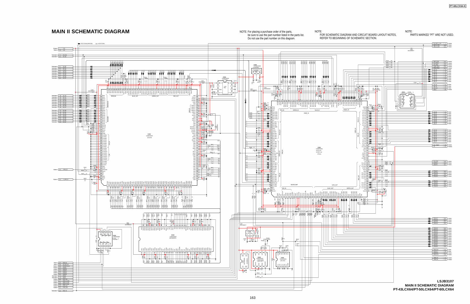
NOTE:FOR SCHEMATIC DIAGRAM AND CIRCUIT BOARD LAYOUT NOTES,REFER TO BEGINNING OF SCHEMATIC SECTION.
NOTE: For placing a purchase order of the parts, be sure to use the part number listed in the parts list. Do not use the part number on this diagram.
NOTE:PARTS MARKED "PT" ARE NOT USED.
MAIN II SCHEMATIC DIAGRAM
VID_R7 41
C5331
0.1
C532
7
0.1
AD_R182
AD_G089
C532
0
0.1
VID_R1 35
VID_B6 31
VID_G5 20
4700
R5317
C532
6
PT
R5408 PT
22R532
6
PTR535
2
22R532
8
C532
4
0.1 VID_G7 22
22R533
4
C5305
0.1
C5334
0.1
VID_B5 30
C5329
PT
OSDDT1112
RGB_VS122
VID_R6 40
PTR534
9
22R5342VID_R3 37
AD_B299
22R533
3
VID_B2 27
22R5
338
C530
8
0.1
VID_B4 29
C530
60.
1
22
R5355
OSDEN110
C530210/6.3V
C5332
0.1
PTR5315
MAIN_IC_SDI119
3.3V1
22R5344
OSDDT0111
22R5348
R5434 PT
22R532
2
RGB_HS107
C531
7
0.1
C532
3
0.1
C533010/6.3V
MAIN_IC_SCK118
MAIN_IC_SDO117
VID_R0 34
AD_R485
AD_R081
AD_G594
AD_G190
VID_B7 320R5311
VID_G4 19
22R5346
AD_G291
AD_R586
TP5302
R545
50
C531
8
0.1
IC5303C3ABPJ000063
1 2 3 4 5 6 7 8 9 10 11 12 13 14 15 16 17 18 19 20 21 22 23 24 25 26 27 28 29 30 31 32 33 34 35
444546474849505152535455565758596061626364656667686970
36 37 38 39 40 41 42 43
71727374757677787980818283848586
C531
6
0.1
22R5356
10K
R535
0
VID_B1 26
22R5347
TP53
05
TP5301
22R532
1
0R53140R5313
SYNC_CS120
22R5354
R545
0PT
VID_R5 39
22R5353
TP5307
/POHS57
AD_HS80
C5337
0.1
C531
3
0.1
TP53
06
R5407 0
C531
4
0.1
OSDDT2113
22R5345
C530
9
0.1
AD_G695
C531
5
0.1
VID_G2 17
VID_B3 28
AD_G796
22
R533
9
10K
R532
9
R532
4PT
AD_R384
AD_R283
C531
0
PT
C531
9
0.1
R5406 0
C531
110
/6.3
V
10K
R535
1
AD_B3100
22R5
341
AD_G493
C5335
0.1
AD_B6103
AD_B198
22R533
6
C531
2
0.1
C5304
0.1
AD_B7104
TP5304
C5338 0.1
C532
5
PT
C5336
0.1
AD_G392
SYS_RST_L_3.3V 3
C530
7
0.1
VID_R4 38
C5333
0.1
/POVS56
TP5303
22R5343
22R533
1
C532
2
0.1
VID_B0 25
AD_B5102
C532
8
0.1
R532
30
C532
1
0.1
VID_G3 18AD_R687
VID_G6 21
AD_R788
AD_CLK79
VID_G1 16
AD_B4101
0R5312
AD_B097
OSDDT3114
VID_G0 15
VID_R2 36
C5303
0.1
X530
1H1
A760
5B00
01
C53580.1
22
R541
6
PTR5410
C5359 0.1
C536
0
0.1
PT
R541
1
22R534
0
C530
10.
1
22R5302
22
R530
3
AD_REF_HS108
5V 55
RGB_L 136
VID_HS 23VID_VS 24VID_CLK 33
POCLK_1 59
SYNC_SEL121
0R5301
HDMI_DE105
OSD_CLK115
470P[KB]
C5340
*
2R2[
KB]
C533
9
1C5373
1500
R543
3
C5343
0.1
C5387 0.1
C5388
0.1
C5349 0.1
C5391
0.1
C5389 0.1
C535
10.
1
C535
20.
1
C537
5
0.1
C537
7
0.1
C53900.1
C53480.1
C5347 0.1
C53460.1
C535
30.
1
C537
4
0.1
C538
10.
1
C538
20.
1
C535
00.
1
C538
3
0.1
CLK_FPGA 124INT_FPGA 125DONE_FPGA 126
R536
6
3300
R540
247
00
R5449
300
22
R5330
47
R5454
47
R5453
47
R539
6 47
R539
8 47
R540
147
R539
9
PTR5451PTR5452
PTR5
388
0R5
372
0R5
305
0R5
304
100R5459100R5458100R5457
R5456 100
C53410.1
C534210/6.3V
0R5
377
0R5
376
0R5
379
0R5
382
0R5
380
0R5
381
0R5
384
0R5448
0R5
385
47R5
395
47R5
383
47R5
37847
R537
547
R537
1
R532747
R536
7
0
R536
5PT
R536
9
PT
R537
4
PT
R539
30
R539
0 PT
R539
733
00
R540
3PT
R540
40
R540
5PT
PTR5437
PTR5439
0R5438
0R5446
0R5440
PTR5441
PTR5447
0R5443
PTR5442
PTR5
400
PTR5
392
PTR539
4
0R5
391
PTR5
389
3300
R538
7
PTR5
373
PTR5
370
PTR5
368
R5364 PT
R5363 0R5362 4700
R5358 PTR5359 0
R5360PT
R5361 PT
R5337 0
R5357 PT
R5335 PTR5332 PT
0
R5460
PROG_FPGA 127100R5461
R546
247
00
R5463 4700
4700
R546
4
DATA_FPGA 123
C5386 0.1
C538
00.
1
C5385 0.1
C537
6
0.1
C537
8
0.1
C5344
0.1
C5345
0.1
C537
90.
110/6
.3V
C539
4
10/6
.3V
C539
5
PTC539
6
PTC539
7
/DLL_RESET 128
C539
8
PT
C5399 0.1
SCALER_CS_S109
22
R546
9
S_DATA_IN10622
R5470
22R5471
C5403PT
C5404
PT
C540
5
PTR5
472
0
TP5308
TP5309D0YBR0000015
100
R547
3
PT
C535
5C5354PT
IC5308PT TK11133CS
1 2
5
3
4*
C535
61[
KB]
PTC5
357
IC5302C1AB00001524
1 2 3 4 5 6 7 8 9 10 11 12 13 14 15 16 17 18 19 20 21 22 23 24 25 26 27 28 29 30 31 32 33 34 35 36 37 38 39 40 41 42 43 44 45 46 47 48 49 50 51 52
53545556575859606162636465666768697071727374757677787980818283848586878889909192939495
96979899
100101102
103104
105
106
107
108
109
110
111
112
113
114
115
116
117
118
119
120
121
122
123
124
125
126
127
128
129
130
131
132
133
134
135
136
137
138
139
140
141
142
143
144
145
146
147
148
149
150
151
152
153
154
155
156
157158
159160161162
163164165
166167168169170171172173174175176177178179
180181
182183184185186
187188189
190191192193194195196197198199
200201202203
204205206
207208
IC5306C1ZBZ0002352
1 2 3 4 5 6 7 8 9 10 11 12 13 14 15 16 17 18 19 20 21 22 23 24 25 26 27 28 29 30 31 32 33 34 35 36 37 38 39 40 41 42 43 44 45 46 47 48 49 50 51 52
53545556575859606162636465666768697071727374757677787980818283848586878889909192939495
96979899
100101102
103104
105
106
107
108
109
110
111
112
113
114
115
116
117
118
119
120
121
122
123
124
125
126
127
128
129
130
131
132
133
134
135
136
137
138
139
140
141
142
143
144
145
146
147
148
149
150
151
152
153
154
155
156
157158
159160161162
163164165
166167168169170171172173174175176177178179
180181
182183184185
186
187188189190191192193194195196197198
199200201202203
204205206
207208
IC5304C0DBFFD00005
1
2
3
4 5
6
7
8
IC5309C0JAAZ002420
1 2 3 4
5678
IC5313C0JBAZ000994
12
34
56
7 89
1011
1213
14
IC5310C0JBAE000231
1 2 3 4 5 6 7
891011121314
IC5301C0JBAZ000994
1 2 3 4 5 6 7
891011121314
L5326J0JCC0000077
L5322J0JHC0000018
L532
3J0
JCC0
0000
77
L5320J0JHC0000018
L5301J0JHC0000018
L5321
J0JHC0000018
J0JCC0000077L5302
L5304J0JHC0000018
22R5414
22R5415
22R5417
PTR5413
1.8V116
SUB_IC_SCK 149SUB_IC_SDO 150
UN_LOCK 228LVDS-HS 190LVDS-VS 191
FPGA-R7 192FPGA-R6 193FPGA-R5 194FPGA-R4 195
FPGA-R1 198
FPGA-R3 196FPGA-R2 197
FPGA-R0 199
FPGA-G5 202
FPGA-G7 200FPGA-G6 201
FPGA-G4 203
FPGA-G1 206
FPGA-G3 204FPGA-G2 205
FPGA-G0 207
FPGA-B5 210
FPGA-B7 208FPGA-B6 209
FPGA-B4 211
FPGA-B1 214
FPGA-B3 212FPGA-B2 213
FPGA-B0 215
FPGA-CLK 216
LVDS-CLK 217POCLK_76 218
HDMI_VS 60HDMI_HS 61
IC5305
1 2 3
VDDE
VDDQ
DQM
3
BA1
DQ29
/WE
GND
A9
SO
VSSQ
MD9
POD2
PLLGND
POD9
MA11
VDDE
MD1
9
MD2
4
YUVPID7
VDDI
MD1
1
POD8
PID2
GND
PID7
DQ14
VDDE
SI
MD1
YUVPID14
VDDE
YUVPID8
PID0
/CS
MD7
MD1
0
YUVPID6
VSS
DQ26
DQ24
VDDE
MD1
7
NC
MD2
VDDE
POD1
2
PID8
VDDQ
YUVPID9
CKE
DQ30
POD5
DQ28
YUVPID4
POD1
7
YUVPID2
VSSQ
PID18
NC
GREEN_OUT
YUVPID11
/CS
DQ12
OSDDT2
VDDE
PID23
POD2
8
DQ6
PID15
DQM
0
POD1
8
/MWR
MD1
4
POD1
0
BA0
DQ9
VDDE
GND
GND
DQ19
MD1
5
MA9
GRE
EN(Y
)IN
POD1
/SCLK
YUVPID3
VDDE
DQM
1
PID3
MD2
9
VDDQ
VDDE
MD2
7
YUVCLK
MD1
3
/RST
POD3
POFLD
DQ18
VDDQ
VDDI
DQM
2
GND
DQ17
POD2
6
MD8
VDDI
DQ22
PID1
YUVPID15
PID14
GND
MD2
2
MD4
/PO
ACTB
YUVPID13
POD2
1
NC
YUVPID10
POD2
9
MA2
GND
NC
POD1
5
MA8
DQ2
GND
MD2
3
POCLK
RED_OUT
Y_IN
DQ5
GND
PID6
VDDQ
GND
PID10
DQ3
A5
MA6
PID19
MD3
1
VSS
MA7
MD1
8
POD2
2
/TEST1
NC
POD2
5
POD2
7
/PIVSGOB
PID17
VDD
VDDQ
MD0
POEX
T
U/V_
INPID16
SS
GND
MD2
6
PIFLD
MD5
MA5
OSDDT1
GND
MA1
VSSQ
POD6
POD2
0
OSD
_IN
DQ27
GND
POD1
9
GND
VDDE
PID5
GND
GND
MCLKI
VDDI
BA1
DQ8
RED(V)IN
A8
/PIHSB
GND
MA4
VDDE
VDD
VDDI
MD2
1
PLLVDD
VDDQ
/POHSB
VDDE
PID21
DQ15
DQM
0
PID4
YUVPID12
VDDE
POD1
3
POD0
DQ31
/TEST0
VSSQ
DQ1
A6
GND
GND
POD7
VDDE
MCLKSEL1
VDD
VDDE
BLUE_OUT
POD2
3
/YUVVSB
MD2
0
DQ10
PID12
TESTH
OSDDT0
DQ25
POD1
6
GND
MD2
8
DQ23
DQ16
MD1
6
NC
MD3
GND
GND
DQ20
POD2
4
VDDE
MD1
2
MA0
A0
DQM
1
/RAS
VDDI
A4
MD3
0
VDDE
VDDI
GND
YUVPID0VD
DI
/YUVHSB
VDDQ
OSDEN
BA0
OSDDT3
BULE
(U)IN
GND
A2 DQM
2
DQ13
VSS
PID22
CLK
PID20
/POVSB
/CAS
DQ11
DQ21
VSSQ
/CAS
VDD
POD4
POD1
1
MCLKSEL0
/RAS
VSSQ
PICLK
MD6
/PIVSB
MD2
5
PID9
VSS
MA3
DQ0
DQ7
MCLKO
A1
DQM
3
PID11
DQ4
MA10
PID13
A7
POD1
4
YUVPID5 GNDVS
SQ
NC
A3
A10(
AP)
YUVPID1
VSSQ
GND
4B 3Y3B2A1Y
S1
OUT
OE
4Y
GND
4A
LEE
1A 2Y3A
/PD
CLKI
N
VCC
VDD(S
G-8
002J
C)
CLKO
UT
1B 2B
VDD
S0
GND
VDD
VSS
GND
B6_VID
VCCINT
RGB_L
R7_LVDS
G6_
LVDS
B2_VID
R5_RGB
VCCI
NT
B5_L
VDS
I/O
B1_VID
RGB_SEL
TCK
GND
GND
G2_RGB
BO3_
RGB
M1
GND
R1_RGB
VCCI
NT
B2_L
VDS
R4_LVDS
G2_
LVDS
TRDY
,I/O
B4_VIDB3_VID
R3_VID
CLKO
_RG
B
HS_V
ID
G3_
VID
G1_RGB
I/O
DIN
G2_
VID
I/O
BO2_
RGB
VCCO
G4_
LVDS
OSD
ENG
O1_
RGB
G0_
LVDS
R6_VID
VSO
_RG
B
VCCINT
VCCO
G0_RGB
MDA
TA
RO5_
RGB
TDO RO7_
RGB
B3_RGB
GO
3_RG
B
GND
SYNC
_SEL
I/O
I/O
SCK
GCK2,I
VCCO
BO6_
RGB
B5_VID
VCCO
VCCO
BO7_
RGB
G4_
VID
GND
GND
G1_
LVDS
GO
6_RG
B
B0_VID
B2_RGB
VCCO
G6_RGB
R2_LVDS
HS_A
I/O
GND
MO
I/O
VCCI
NT
GND
DONE
I/O
I/O(DLL)
VS_B
OSD
1
B7_L
VDS
G5_
LVDS
VCCO
R0_RGB
VCCO
R5_VID
G3_RGB
B3_L
VDS
GND
RO4_RGB
VCCO
VCCOVCCINT
RO0_RGB
GND
CCLK
TDI
R3_RGB
B6_RGB
VCCI
NT
R1_LVDS
R2_RGB
R4_VID
SDAT
A
G1_
VID
HS_LVDS
I/O
CLK_
LVDS
HS_B
BO5_
RGB
CLK_VID
R2_VID
RO2_RGB
RO6_
RGB
GND
GO
0_RG
B
G6_
VID
BLUE_IN
GND
G5_
VID
RCLK_RGB
G4_RGB
R6_RGB
VS_VID
VCCO
R7_VID
G0_
VID
BUSY
BO1_
RGB
MICROCOMP
BO4_
RGB
SCS
I/O,VREF
VCCO
I/O
G5_RGB
RO1_RGB
VCCI
NT
VCCO
I/O
R4_RGB
M2
G7_RGB
GO
5_RG
B
GND
GND
GND
VCCO
GO
2_RG
B
R0_VID
B1_L
VDS
BO0_
RGB
B1_RGB
VCCINT
HSO
_RG
B
I/O
B4_L
VDS
VIDE
O_I
N
VCCINT
VS_A
VS_LVDS
R6_LVDS
(INT)
GND
GND
GRE
EN_I
N
RGB_
IN
RO3_RGB
R3_LVDS
B0_RGB
GND
B5_RGB
I/O(DLL)
GND
VCCINT
G7_
VID
GND
GND
VCCO
R0_LVDS
R5_LVDS
R4_RGBB
B7_RGB
B0_L
VDS
B6_L
VDS
G3_
LVDS
GREEN_IN
B7_VID
R1_VID
OSD
0
HS_RGBVS_RGB
RED_
IN
OSD
2O
SD3
R7_RGB
GND
PRO
GRA
M
GND
VCCI
NT
VCCOVCCO=3.3VVCCINT=1.8V
LVDS_OUT
BLUE_OUT GREEN_OUT
RED_
OUT
OSD_IN
RED_
INBL
UE_I
N
GREEN_IN
RGBO_IN
RED_IN
BULU
E_IN
GO
4_RG
B
GO
7_RG
B
G7_LVDS
I/OOSD
_CLK
VDD
VSS
TMS
GND
1 2 3 4 5 6
5
123
6
4
87
87
9 1310 11 12
1110
12
9
13
1614 15
1415
16
1817 19 20 21
171819
2021
22 23 24
222324
OUT
CONT NPGND
IN
DQ7
DQ6
DQ5
DQ4
DQ3
DQ0
DQ1
DQ2
DQ7
DQ3
DQ1
DQ0
DQ2
DQ4
DQ6
DQ5
DQ18
DQ19
DQ23
DQ21
DQ16
DQ20
DQ17
DQ22
DQ23
DQ22
DQ21
DQ18
DQ17
DQ16
DQ19
DQ20
DQ27
DQ26
DQ25
DQ24
DQ29
DQ28
DQ31
DQ30
DQ28
DQ31
DQ30
DQ27
DQ29
DQ26
DQ25
DQ24
DQ11
DQ8
DQ10
DQ9
DQ15
DQ13
DQ12
DQ14
DQ14
DQ13
DQ15
DQ12
DQ10
DQ9
DQ8
DQ11
DQM
1
DQM
3
DQM
3
DQM
1DQ
M0
DQM
2
BA1
BA0
DQM
0
BA0
BA1
DQM
2
/WE
/CAS
/CS
/RAS
/CAS
/CS/WE
/RAS
A9 A8 A7 A6
A8
A6
A9
A7
A10
A10
A5 A3A4
A4A3A2
A5
A1A0
A0 A2A1
CLK
CLK
ADG0ADG1ADG2ADG3ADG4ADG5ADG6ADG7
ADB0ADB1ADB2ADB3ADB4ADB5ADB6ADB7
ADG
0
ADG
3
ADG
1
ADG
6
ADG
2
ADG
4
ADG
7
ADG
5
ADB2
ADB1
ADB4
ADB0
ADB3
ADB6
ADB7
ADB5
ADR6
ADR4
ADR7
ADR5
ADR4
ADR7
ADR5
ADR6
ADR1
ADR3
ADR0
ADR2
ADR1
ADR3
ADR0
ADR2
(64M MEMORY)
(SCALER)
(FPGA1)
AUDIO SIGNALVIDEO SIGNAL(MAIN/SUB)
SPECTRUMSPLITTER
(+2.5V REG.)
(+1.8V REG.)
LEVELSHIFTER
LEVELSHIFTER
TO M VII
TO M V,M VITO M V,M VI
TO M V,M VITO M V,M VITO M V,M VITO M V,M VITO M V,M VITO M V,M VITO M V,M VITO M V,M VI
TO M V,M VITO M V,M VI
TO M V,M VI
TO M V,M VITO M V,M VITO M V,M VI
TO M V,M VI
TO M V,M VI
TO M V,M VI
TO M V,M VI
TO M V,M VI
TO M V,M VITO M V,M VI
TO M V,M VI
TO M V,M VITO M V,M VI
TO M VI
TO M IV
TO M VTO M V
TO M IVTO M IIITO M IIITO M IIITO M III
TO M I,M IIITO M I,M III
TO M III
TO M IIITO M IIITO M IIITO M IIITO M IIITO M III
TO M V,M VI
TO M III
TO M IVTO M IVTO M IVTO M IV
TO M ITO M IV
TO M ITO M ITO M ITO M ITO M ITO M ITO M I
TO M ITO M ITO M ITO M III
TO M ITO M I
TO M I
TO M I
TO M ITO M I
TO M I
TO M I
TO M I
TO M I
TO M I
TO M ITO M I
TO M I
TO M ITO M I
TO M IIITO M VII
TO M I
+1.8V REG.GND
+2.5VREG.
(OR GATE)
TO M XTO M XTO M XTO M X
TO M X
TO M XTO M X
TO M X
TO M XTO M XTO M XTO M X
TO M X
TO M X
TO M XTO M X
TO M XTO M XTO M X
TO M X
TO M XTO M XTO M X
TO M X
TO M I
TO M XTO M X
TO M VI
TO M X
TO M XTO M X
TO M XTO M XTO M X
TO M VI
COCBAAG00009
LSJB3107MAIN II SCHEMATIC DIAGRAM
PT-43LCX64/PT-50LCX64/PT-60LCX64
PT-60LCX64-K
163
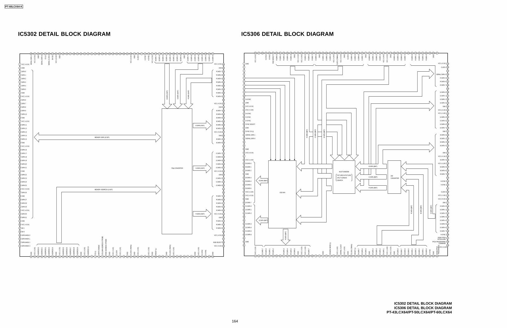
1
2
3
4
5
6
7
8
9
10
11
12
13
14
15
16
17
18
19
20
21
22
23
24
25
26
27
28
29
30
31
32
33
34
35
36
37
38
39
40
41
42
43
44
45
46
47
48
49
50
51
52
156
155
154
153
152
151
150
149
148
147
146
145
144
143
142
141
140
139
138
137
136
135
134
133
132
131
130
129
128
127
126
125
124
123
122
121
120
119
118
117
116
115
114
113
112
111
110
109
108
107
106
105
53 54 55 56 57 58 59 60 61 62 63 64 65 66 67 68 69 70 71 72 73 74 75 76 77 78 79 80 81 82 83 84 85 86 87 88 89 90 91 92 93 94 95 96 97 98 99 100 101 102 103 104
208 207 206 205 204 203 202 201 200 199 198 197 196 195 194 193 192 191 190 189 188 187 186 185 184 183 182 181 180 179 178 177 176 175 174 173 172 171 170 169 168 167 166 165 164 163 162 161 160 159 158 157
GND
GND
GND
CS (L
)
GND
GND
GND
GND
WRI
TE E
NABL
E
GND
GND
GND
GND
CLO
CK (7
6MHz
)
CLO
CK (7
6MHz
)
CLO
CK
GND
GND
ROW
ADD
RESS
STR
OBE
COLU
MN
ADDR
ESS
STRO
BE
ADDR
ESS
10
ADDR
ESS
9
ADDR
ESS
0
ADDR
ESS
1
ADDR
ESS
2
ADDR
ESS
3
ADDR
ESS
4
ADDR
ESS
5
ADDR
ESS
6
ADDR
ESS
7
ADDR
ESS
8
GND
DATA 31
DATA 30
DATA 29
DATA 28
GND
GND
GND
VCC (+2.5V)
VCC (+3.3V)
VCC (+3.3V)
VCC (+3.3V)
VCC (+3.3V)
VCC (+3.3V)
VCC (+2.5V)
VCC
(+3.
3V)
VCC
(+3.
3V)
VCC
(+2.
5V)
VCC
(+3.
3V)
VCC
(+3.
3V)
VCC
(+3.
3V)
VCC
(+3.
3V)
VCC (+3.3V)
VCC (+3.3V)
VCC (+2.5V)
VCC
(+2.
5V)
VCC
(+2.
5V)
BA 1
BA 0
DATA MASK 3
DATA MASK 2
DATA MASK 1
DATA MASK 0
RESE
T (L
)
V-SY
NC
H-SY
NC
R DATA 2
R DATA 3
R DATA 1
R DATA 0
RGB SELECT
R DATA 4
R DATA 7
R DATA 6
R DATA 5
G DATA 3
G DATA 2
G DATA 1
G DATA 0
G DATA 7
G DATA 6
B DATA 4
B DATA 5
B DATA 6
B DATA 7
B DATA 3
B DATA 2
R DATA 5
R DATA 6
R DATA 7
R DATA 4
R DATA 3
R DATA 2
B DATA 1
B DATA 0
G DATA 5
G DATA 4
VCC (+3.3V)
VCC (+2.5V)
GND
GND
GND
GND
R DATA 0
R DATA 1
GND
GND
GND
GND
VCC
(+3.
3V)
VCC
(+2.
5V)
CS (L
)
DVI D
E
SERI
AL D
ATA
1
SERI
AL D
ATA
0
SERI
AL C
LOCK
V-SY
NC
H-SY
NC
G D
ATA
1
G D
ATA
0
G D
ATA
2
G D
ATA
3
G D
ATA
4
G D
ATA
5
G D
ATA
6
G D
ATA
7
B DA
TA 4
B DA
TA 3
B DA
TA 2
B DA
TA 1
B DA
TA 0
B DA
TA 5
B DA
TA 6
B DA
TA 7
CLO
CK
VCC
(+3.
3V)
VCC
(+2.
5V)
R DA
TA (8
BIT
)
B DATA (8 BIT)
G DATA (8 BIT)
R DATA (8 BIT)
MEMORY DATA (32 BIT)
MEMORY ADDRESS (10 BIT)
B DA
TA (8
BIT
)
G D
ATA
(8 B
IT)
DATA 1
DATA 0
DATA 3
DATA 2
DATA 5
DATA 4
DATA 6
DATA 8
DATA 7
DATA 10
DATA 9
DATA 11
DATA 13
DATA 12
DATA 15
DATA 14
DATA 16
DATA 18
DATA 17
DATA 20
DATA 21
DATA 22
DATA 23
DATA 24
DATA 25
DATA 26
DATA 27
DATA 19
VCC (+3.3V)
GND
VCC (+3.3V)
720p CONVERTER
1
2
3
4
5
6
7
8
9
10
11
12
13
14
15
16
17
18
19
20
21
22
23
24
25
26
27
28
29
30
31
32
33
34
35
36
37
38
39
40
41
42
43
44
45
46
47
48
49
50
51
52
156
155
154
153
152
151
150
149
148
147
146
145
144
143
142
141
140
139
138
137
136
135
134
133
132
131
130
129
128
127
126
125
124
123
122
121
120
119
118
117
116
115
114
113
112
111
110
109
108
107
106
105
53 54 55 56 57 58 59 60 61 62 63 64 65 66 67 68 69 70 71 72 73 74 75 76 77 78 79 80 81 82 83 84 85 86 87 88 89 90 91 92 93 94 95 96 97 98 99 100 101 102 103 104
208 207 206 205 204 203 202 201 200 199 198 197 196 195 194 193 192 191 190 189 188 187 186 185 184 183 182 181 180 179 178 177 176 175 174 173 172 171 170 169 168 167 166 165 164 163 162 161 160 159 158 157
GND
GND
GND
GND
GND
GND
GND
GND
GND
GND
GND
DONE
FPG
APR
OG
RAM
ING
RESE
T (L
)
SERI
AL C
LOCK
CLO
CK (7
6MHz
)
RGB/
DVI M
ODE
(L)
GND
SERIAL DATA 1
SERIAL DATA 0
B DATA 0
B DATA 1
B DATA 2
B DATA 3 G DATA (8BIT)D/DCONVERTER
R DATA (8BIT)
B DATA (8BIT)
B DATA 4
B DATA 5
B DATA 6
B DATA 7
G DATA 0
G DATA 1
G DATA 2
GND
H-SYNC
H-SYNC
V-SYNC
V-SYNC
SYNC SELECT
SYNC CS (L)
VCC (+1.8V)
VCC (+3.3V)
VCC (+1.8V)
VCC (+1.8V)
VCC (+3.3V)
VCC (+3.3V)
VCC
(+3.
3V)
VCC
(+3.
3V)
VCC
(+3.
3V)
VCC
(+3.
3V) VCC (+3.3V)
VCC (+1.8V)
VCC (+1.8V)
VCC (+3.3V)
VCC (+3.3V)
VCC (+3.3V)
VCC (+1.8V)
VCC (+3.3V)
VCC
(+1.
8V)
VCC
(+1.
8V)
VCC
(+1.
8V)
G DATA 3
G DATA 4
G DATA 5
G DATA 6
G D
ATA
7
R DA
TA 0
R DA
TA 1
R DA
TA 2
R DA
TA 3
R DA
TA 4
R DA
TA (8
BIT)
R DA
TA 5
R DA
TA 6
R DA
TA 7
R DA
TA 7
R DA
TA 6
R DA
TA 5
R DA
TA 3
R DA
TA 2
R DA
TA 1
R DA
TA 4
B DA
TA 6
B DA
TA 5
B DA
TA 4
B DA
TA 7
B DA
TA 2
B DA
TA 1
B DA
TA 0
V-SY
NC
B DA
TA 3
R DA
TA 0
R DA
TA (8
BIT)
B DA
TA (8
BIT)
G D
ATA
(8BI
T)
G DATA 2
G DATA 3
G DATA 4
G DATA 1
G DATA 5
G DATA 6
G DATA 7
G DATA 0
B DATA 5
B DATA 6
B DATA 7
G DATA 5
G DATA 4
G DATA 6
G DATA 7
R DATA 5
SERIAL DATA 0
R DATA 6
R DATA 7
B DATA 2
B DATA 3
B DATA 0
B DATA 1
B DATA 4
FPGA PROGRAMINGCOMMAND
DONE FPGAINITIALIZING
GND
GND
GND
GND
CLOCK
H-SYNC
H-SYNC
V-SYNC
CLOCK
G DATA 1
G DATA 0
G DATA 2
G DATA 3
GND
GND
GND
GND
GND
GND
VCC
(+3.
3V)
VCC
(+3.
3V)
VCC
(+3.
3V)
H-SY
NC
V-SY
NC
RGB
SERE
CT
R DA
TA 0
G D
ATA
0
G D
ATA
1
G D
ATA
2
G D
ATA
3
B DA
TA 1
B DA
TA 0
B DA
TA 2
B DA
TA 3
R DA
TA 1
R DA
TA 0
R DA
TA 2
R DA
TA 3
R DA
TA 4
G D
ATA
4
G D
ATA
5
G D
ATA
6
G D
ATA
7
B DA
TA 4
B DA
TA 5
B DA
TA 6
B DA
TA 7
CLO
CK (7
6MHz
)
CLO
CK
R DA
TA 1
R DA
TA 2
R DA
TA 3
R DA
TA 4
R DA
TA 6
R DA
TA 7
R DA
TA 5
VCC
(+3.
3V)
VCC
(+1.
8V)
VCC
(+1.
8V)
VCC
(+1.
8V)
MULTI WINDOW
OSD MIX
PICTURE IN PICTURE
SPLIT SCREEN
SEARCH
G DATA (8BIT)
B DATA (8BIT)
R DA
TA (8
BIT)
G D
ATA
(8BI
T)
B DA
TA (8
BIT)
IC5302 DETAIL BLOCK DIAGRAM
IC5302 DETAIL BLOCK DIAGRAMIC5306 DETAIL BLOCK DIAGRAM
PT-43LCX64/PT-50LCX64/PT-60LCX64
IC5306 DETAIL BLOCK DIAGRAM
PT-60LCX64-K
164
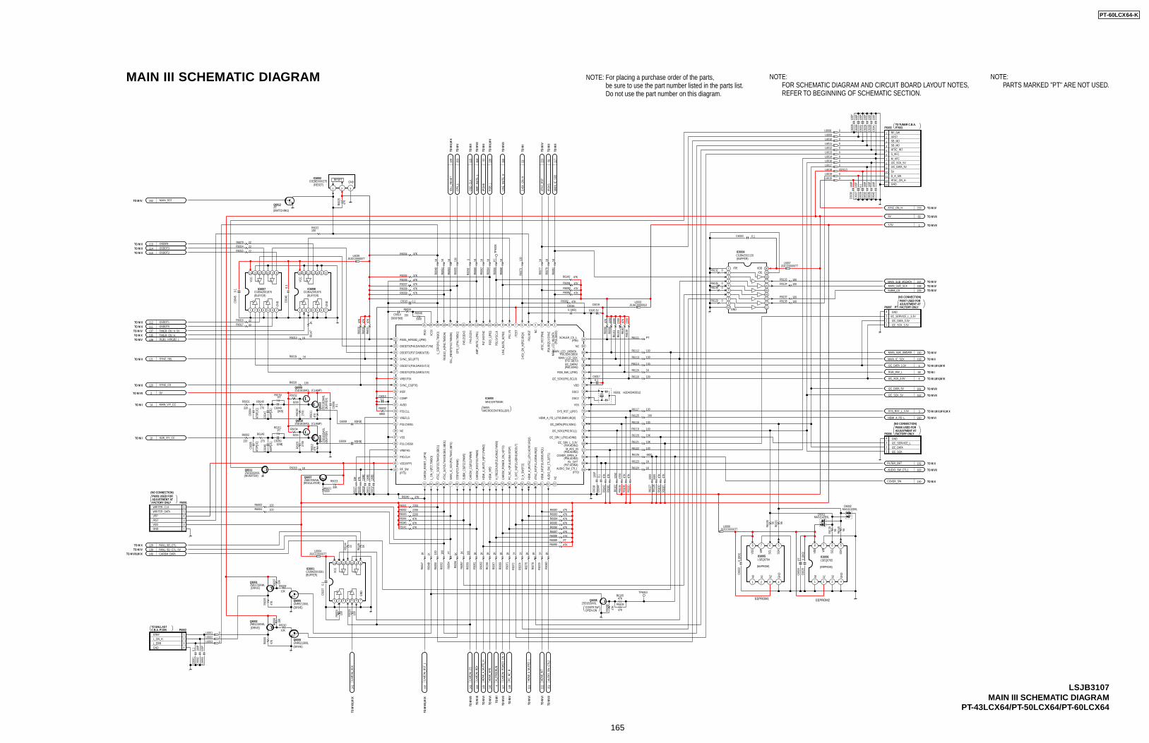
NOTE:FOR SCHEMATIC DIAGRAM AND CIRCUIT BOARD LAYOUT NOTES,REFER TO BEGINNING OF SCHEMATIC SECTION.
NOTE: For placing a purchase order of the parts, be sure to use the part number listed in the parts list. Do not use the part number on this diagram.
NOTE:PARTS MARKED "PT" ARE NOT USED.
MAIN III SCHEMATIC DIAGRAM
LSJB3107MAIN III SCHEMATIC DIAGRAM
PT-43LCX64/PT-50LCX64/PT-60LCX64
100
R605
2
47K
R602
5
100
R605
9
CARD
M_R
ST_L
142
PTR6
054
100
R605
0
CARD
M_C
S14
3
1KR6
047
1KR6
061
1KR6
049
1KR6
048
100P
C601
8
CARD
M_R
DY14
4
6800R6126
Q60082SD1819A0L
R610547K
R609
8
47K
R6106
47K
TP6010
R612
833
00R6
127
3300
1KR6018
0.1C6013
1KR6
067
1KR6
080
1KR6
076
1KR6
057
SYNC_CS120
2200R60412200R6042
2200R6043
SYNC_SEL121
47K
R610
0
47K
R611
0
1KR6
063
47KR6044
47K
R609
6
2200
R609
947
KR6
095
1KR6
056
1KR6
156
3.3V 1
FILTER_DET 132
IC6003MN102H75KMK
1234567891011121314151617181920
22
23
24
25
26
27
28
29
30
31
32
33
34
35
36
37
38
39
40
43 44 45 46 47 48 49 50 51 52 53 54 55 56 57 58 59 60
65
66
67
68
69
70
71
72
73
74
75
76
77
78
79
80
21
41
42
61 62 63
64
81
82
83
84
2200
R610
2
4700
R610
4
100R6119
100R6118
I2C_DATA_5V 161
I2C_SCK_5V 162
2200
R610
9
2200
R610
3
100R6114
100R6116 I2C_SCK_3.3V 6
I2C_DATA_3.3V 5
1KR6
071
1KR6
069
1KR6
075
CARD
M_P
OW
ER_O
N_H
147
PC_N
C_H
148
1KR6
072
1KR6
074
1KR6
078
1KR6124
1KR6123
100R6122
10KR6120
SYS_RST_L_3.3V 3100R6117
1KR6115
MAIN_SUB_SCK 158
100R6113
MAIN_SUB_SMDATA 160100R6112
PTR6111
47KR6094
47KR6091
47KR6093
47KR6034
47KR6036
47KR6092
33K
R602
7
47KR603947KR603847KR6037
47KR6035
1KR6
051
1KR6
053
100
R605
5
AMP_
MUT
E_L
154
1KR6
060
/PO
HS57
1KR6
062
1KR6
064
LINE
_MUT
E_H
155
1KR6
068
OSDEN11022R6070
1KR6
077
/PO
VS56
1KR6
079
MAIN_SUB_MSDATA 157
1KR6
081
22R6017OSDDT0111
22R6016OSDDT1112
22R6015OSDDT2115
22R6014OSDDT3114
1KR6013
0.1[KB]C6016
0.1C6015
0.1C6017
1KR6019
100R6020
5V 55
47KR6040
47K
R602
9
47KR6045
47KR608347KR608447KR608547KR608647KR608747KR6088
PTR6089
47KR6090
2200
R610
1
47K
R610
7
47K
R603
147
KR6
030
6800
R6032
*
1[KB
]C6
011
* 10[KB]C6008
* 10[KB]C6009
*
1[KB
]C6
010
0.1C6023
100R6133
100R6134
C600
70.
1
SUBM_CS 159
100R6137
100R61380R6129
CARD
M_S
CK14
110
0
R602
6
47KR6082
100
R602
4
OSD
_CLK
115
0R6
058
PTR6
066
TP60
05
R6022100
2SB0709AHLQ6007
*
1[KB
]C6
012
5600R6021 22K
R6023
100/6.3V
C6019
9V2
MAIN_V/Y_CC14
SUB_V/Y_CC10
2SD1
819A
0LQ
6003
2SD1
819A
0LQ
6004
470
R601
147
0R6
012
220
R6001
220
R6002
470P
[JC]
C600
4
470P
[JC]
C600
5
0.1
C600
6
3900P[KB]C6014 150
R6033
3300
R6046
47K
R610
8
100R6125
47K
R602
8
P6001
1GND2VDD3/RST4VPP5WRITER_DATA6WRITER_CLK
100R6003
100R6004
R600
5
47K
R6009
10K
100P
C600
2
R600
7
10KQ6001
2SB1218AHL
Q6005UNR521300L
P60021STBY2L_ON_H3L_ERR4GND
0.1
C600
1
100P
C600
3
R600
6
47K Q6006
UNR521300L
R600
8
10K
R6010
10K
Q60022SB1218AHL
100P
C604
210
0PC6
035
100P
C603
20.
1C6
029
100P
C603
8
100P
C602
8
100P
C603
4
100P
C602
6
100P
C603
1
0.1[
KB]
C602
2
56
R613
9
MA3J142D0LD6002
56
R613
1
0.1[
KB]
C602
5PT
C602
4
56
R614
0
MA3J142E0LD6001
56
R613
0
AUDI
O_S
W_C
TL2
151
AUDIO_SW_CTL1 163
100P
C604
1
100P
C602
7
47KR6141
X6001 H2D400400012
P60064 GND3 I2C_SERVICE_L2 I2C_DATA1 I2C_SCK
P6003
13 GND12 ATSC_ON_H11 D_A_SW10 5V9 I2C_DATA_5V8 I2C_SCK_5V7 M_AFC6 S_AFC5 ATSC_INT4 SB_MD3 SB_MD2 XRST1 RF_SW
RGB1_H/RGB2_L138
H_FR
EERU
N4
HDM
I_A_
MUT
E_H
145
HDM
I_HP
D14
6
RGB_MW_L 58
RGB_
L13
6
0.1
C604
4
47K
R614
2
P6007 PT4 GND3 I2C_SERVICE_L_3.3V2 I2C_DATA_3.3V1 I2C_SCK_3.3V
10KR6121
47K
R609
7
3.45
V_O
N_H
5310
0R6
073
47KR6143
COVER_SW 130
FAN1_SD_CTL129FAN1_SD_CTL_5V139
TIMER_ON_H_5V137TIMER_ON_H135
22
R614
4
1K
R614
5
IC6004C0JBAZ001120
1 /OE
2345678910
13141516171819/OE20VDD
1112
/DLL
_RES
ET12
8
CPS_
L15
3
C604
50.
1
C604
60.
1
1KR6
147
CARDM_DATA140
270
R6148
270
R6149
PTR6150
PTR6151
560P
[JC]
C604
7
560P
[JC]
C604
8
*
1[KB]C6049
*
1[KB]C6050
8200
R6152
2700
R615
3
8200
R6154
2700
R615
5
2SD1819A0LQ6009
2SD1819A0LQ6010
IC6007C0JBAZ001876
1 2 3 4 5 6 7
GND
891011121314
VCC
IC6008C0JBAZ001876
1 2 3 4 5 6 7
GND
891011121314
VCC
IC6001C0JBAZ001591
1 2 3 4 5 6 7
891011121314LSEQ0765IC6006
1 2 3 4
5678
LSEQ0764IC6005
1 2 3 4
5678
100P
C603
0
0R61360R6135
0R6132
MAI
N_IC
_SD0
117
Q60112SD1819A0L
0L6003
0L6010
J0JCC0000077L6006
0L6014
0L6015
0L6001
0L6008
0L6016
0L6002
0L6009
L6005J0JHC0000018
J0JCC0000077L6026
0L6013
L6018 0[2012]
J0JCC0000077L6007
0L6011
0L6019
J0JCC0000077L6004
0L6012
0L6017
Q6012PT
MAIN_RST152
ATSC
_RST
223
ATSC_ON_H 219
MAIN_IC_SCK 118
HDMI_A_PD_L 220
HDM
I_A_
MUT
E2_L
221
HDM
I_IN
T22
2
IC6002C0EBE0000275
1 2 3
GND
GND
VCC
A1
(EEPROM)
VDD
SDA
SCL
A2
WP
A0GND
A2
EEPROM2
WP
A1
EEPROM1
VDD
A0
(EEPROM)
GND
SDA
SCL
TO M IV
TO M IITO M IITO M II
TO M IITO M II
TO M IVTO M XTO M V
TO M II
TO M II
TO M VII
TO M I
TO M I
TO M XTO M IV
TO M VIII,M IX
P6001 USED FORADJUSTMENT ATFACTORY ONLY
(NO CONNECTION)
TO BALLAST C.B.A. P1305
TO TUNER C.B.A.P7003
(NO CONNECTION)P6007 USED FORADJUSTMENT ATFACTORY ONLY
(NO CONNECTION)P6006 USED FORADJUSTMENT ATFACTORY ONLY
TO M VII
TO M VII
TO M IVTO M IVTO M IV
TO M IV
TO M I,M V,M VI
TO M I
TO M I,M V,M VI
TO M VII
TO M VII
TO M I,M II,M VI,M X
TO M X
TO M VII
TO M X
TO M
II,M
X
TO M
V
TO M
II
TO M
VII
TO M
II
TO M
II,M
V
TO M
VII
TO M
I
TO M
II
TO M
VIII
,M IX
TO M
VIII
,M IX
TO M
VIII
TO M
IX
TO M
VI
TO M
VI
TO M
I
TO M
VII
TO M
V
TO M
VII
(RESET)
(BUFFER)(BUFFER)
(BUF
FER)
(BUF
FER)
(CLAMP)
(CLAMP)
(REGULATOR)
(BUFFER)
(DRIVE)
(DRIVE)
(DRIVE)
(DRIVE)
MAINMICROCONTROLLER)
COVER SWOPEN-ON
(BUFFER)
RESET
GND
TO M II
TO M
II
TO M
IV
TO M VI
IREF
STBY
(P23
,PW
M6)
L_O
N_H(
P27,
TM0I
O)
P32,CVBS1
COVER_OPEN_HCP
S_L(
P44,
TM5I
C)
L_ER
R(P4
1,TM
1IO
)
RGB_MW_L(P86)
CARD
M_R
ESET
_L(P
74)
ATSC
_SI(P
25,T
M4I
OB,
SBI1
,SBD
1)
/DLL
_RES
ET(P
43,T
M5I
OB)
VDD(VPP)
P46,
OSD
XI
HDMI_A_PD_L(P00,RMIN,IRQ0)
(P85)
HDM
I_A_
MUT
E_H(
P17,
PWM
2)
OSDDT1(P36,DAGOUT,G)
NC
VCO
I
P30,CLH
SYS_RST_L(P87)
S_AF
C_IN
(P13
,ADI
N8,W
DOUT
)
P51,
YS
(P75)
(P60,SDA0)
CARD
M_C
S(P2
1,PW
M4)
VREFLS
PC_N
C_H(
P14,
ADIN
9,ST
OP)
HDM
I_HP
D
I2C_SCK1(P02,SCL1)
MAIN_LCD_LMDATA
/TES
T
(P04,ADIN1)
HDM
I_A_
MUT
E2_L
(P12
,ADI
N7,IR
Q3)
RGB_
L(P8
2)
NC
D_A_
SW(P
72)
SCALER_CS_L
I2C_DATA1(P01,SDA1)
OSDDT3(P40,DAYMOUT,YM)
(P05,ADIN2)
(P06,ADIN3)
MAI
N_IC
_SCK
(P24
,TM
4IC,
SBT1
)
(P07,ADIN4)
I2C_SCK0(P61,SCL0)
ATSC
_INT
(P11
,ADI
N6,IR
Q2) M_AFC_IN
SYNC_SEL(P77)
OSDDT2(P37,DABOUT,B)
MAI
N_LC
D_M
LDAT
A
P45,
OSD
XO
P33,CLL
SYNC_CS(P76)
OSC1
H_FR
EERU
N(P1
5,AD
IN10
,PW
M0)
NCAUDI
O_S
W_C
TL2(
P71)
(P70)
VREF,P34
VSS
ATSC
_RST
(P84
)
3.45
V_O
N_H(
P52,
IRQ
4)
COMP OSC2
PDO
VSS
P54,
IRQ
5,/V
SYNC
FIL_DET
OSDDT0(P35,DAROUT,R)
I2C_DATA0
P50,
SYSC
LK
VDD
P53,
/RST
(P55
,SBO
0)
RGB1
/2_H
(P42
,TM
5IO
A)
AMP_
MUT
E_L(
P81)
HDM
I_IN
T(P1
0,AD
IN5,
IRQ
1)
RF_SW
P31,CVBS0
AVDD
CARD
M_R
DY(P
20,P
WM
3)
P47,
/HSY
NC
ATSC
_SO
(P26
,TM
4IO
A,SB
O1)
I2C_SRV_L(P03,ADIN0)
CARD
M_P
OW
ER_O
N_H(
P73)
AUDIO_SW_CTL1
(P57,SBT0)
RGB1_H/RGB2_L(P80)
NC
VREFHS
SUBM
_CS(
P22,
PWM
5)
I2C_SRV_L_3.3V
LINE
_MUT
E_H(
P83)
MAIN_LCD_SCKP56,SBI0,SBD0
TO M
VI
TO M
VI
(SWITCHING)
TO M IV
(INVERTER)
PT-60LCX64-K
165
I/O CHART OF IC6003
I/O CHART OF IC6003PT-43LCX64/PT-50LCX64/PT-60LCX64
Pin No. Part No.Part No.I/O1 P55
P54
P53P52
P74P27P26P25P24P23P22P21P20
P73
P72
P14P13
P12P11P10P71
P70P07P06P05P04P03P02P01P00P87
P86
P85
P60P57P56
P61
P17P16P15
P51
P50
P84
P83
P82
P81P47
P46P45P44P43P42P41
P40P37
P36P35P34P76
P33
P32
P31
P30
P75
P77
P80
MAIN_LCD_MSDATADescription
2345678910111213141516171819202122232425262728293031323334353637383940
515253545556575859
Pin No. I/O
60
Signal NameSignal Name Description
616263646566676869707172737475767778798081828384
- -
-
O
OVSYNCATSC_RSTNCRST
I
O
OOOOOO
O
O
O
O
O
O
I
I
I
I
I
I
I
I
I
-
-
--
I
--
-
--
---
-
--
-
-
-
-
-
-
-
3.45V_ON_HTESTYSLINE_MUTE_HSYSCLKRGB_LHSYNCAMP_MUTE_LOSDXIOSDXOCPS_LDLL_RESETRGB1/2_HL_ERRVCOIPDORGB1_H/RGB2_LOSDDT3OSDDT2SYNC_SEL
VREFSYNC_CSIREFCOMP
VREFLS
AVDDCLL
CVBS1NCVSS
(Not used)
(Not used)
(Not used)
(Not used)
HDMI AUDIO MUTE (H)HDMI HOT PLUG DETECT
(Not used)
HDMI INTERRUPT REQUEST(Not used)
(Not used)(Not used)
(Not used)(Not used)
(Not used)(Not used)
(Not used)
RF-SW (ANT-A (H) /ANT-B (L) )
(Not used)
(Not used)
DTV MICROCONTROLLER RESET (L)
(Not used)
MAIN TUNER AFC
HDMI AUDIO (IC5805) POWER DOWN (L)
(Not used)(Not used)
CVBS0VREFHS
GND
GND
MULTI WINDOW WITH RGB (L)
CLH
CARDM_RESET_LL_ON_H
OSDDT1OSDDT0
ATSC_SO
- -
----
-
I
I
-
IO
--
-
O
ATSC_SIMAIN_IC_SCKSTBYSUBM_CSCARDM_CSCARDM_RDYHDMI_A_MUTE_HHDMI_HPDH_FREERUNCARDM_POWER_ON_HPC_NC_HS_AFC_IND_A_SWHDMI_A_MUTE2_LATSC_INTHDMI_INTAUDIO_SW_CTL2NCAUDIO_SW_CTL1FIL_DETCOVER_OPEN_HM_AFC_INI2C_SRV_L_3.3VI2C_SRV_LI2C_SCK1
II
II
II
I
II
I
I
I
I2C_DATA1HDMI_A_PD_LSYS_RET_LVSSOSC2OSC1VDDI2C_SCK0RGB_MW_LI2C_DATA0MAIN_LCD_SCKMAIN_LCD_LMDATA
4344454647484950
4241 NC
SCALER_CS_LRF_SWVDD(VPP) VDD(+3.3V)
VDD(+3.3V)
VDD (+3.3V)
SERIAL DATA 0V-SYNC
RESET (L)3.45V REGULATOR (IC5015) ON (H) /OFF (L)
OSD BLANKINGAUDIO LINE OUT MUTE (H)
RGB MODE (L)H-SYNCSPEAKER OUT MUTE (L)OSD CLOCK
FPGA RESET PULSE COMPOSITE SYNC IN DETECT (L)
LAMP ERROR PULSE (ON (H) /OFF (L) /ERROR (PULSE)
RGB1 SELECT (H) /RGB2 SELECT (L)OSD DATA 3OSD DATA 2MAIN SCREEN SELECT (H) /SUB SCREEN SELECT (L)OSD DATA 1OSD DATA 0V-REF FOR IC6003SYNC SELECTOR (IC5306) CS (L)
MAIN COMPOSITE VIDEO
SUB COMPOSITE VIDEO
O
--
CARD PROCESSOR (IC9004) RESET (L)LAMP ON/OFF CONTROL (ON (H) /OFF (L) )
*2
*2
DTV SERIAL DATA 0DTV SERIAL DATA 1(Not used)STANDBY (L) /NORMAL (H)
SUB MICROCONTROLLER (IC6302) CS (L)CARD PROCESSOR (IC9004) CS (L)CARD READY (L)
H-FREERUN (L)
RGB IN SIGNAL DETECT (L) /NO DETECT (H)SUB TUNER AFCD/A-SW (DIGITAL (L) /ANALOG (H) )HDMI AUDIO MUTE (H)DTV INTERRUPT REQUEST
AUDIO SWITCHING CONTROL 2
AUDIO SWITCHING CONTROL 1
LAMP COVER OPEN (H) /CLOSE (L)CLOGGED FILTER DETECT (A/D INPUT)
I2C SERVICE MODE (L)I2C SERVICE MODE (L)I2C SERIAL CLOCK 0I2C SERIAL DATA 0
RESET (L)
4MHz OSCILLATION4MHz OSCILLATION
I2C SERIAL CLOCK 1
I2C SERIAL DATA 1SERIAL CLOCKSERIAL DATA 1
O
OO
O
O
O
O
O
O
O
OOO
OOO
I/O
I/O
O
-
*1
*2
Pin 19
Pin 62 Pin 64 INPUT
HERROR 1 (T=128ms)ERROR 2 (T= 96ms)ERROR 3 (T= 64ms)ERROR 4 (T= 32ms)
L
Lamp StatusLamp On
The Failure Of Lamp light upAbnormal Lamp VoltageAbnormal Temperature
Other CausesLamp Off
LLHH
LHLH
HDMIRGB 2RGB 1
*1
"2T"
ERRORPULSE
PT-60LCX64-K
166
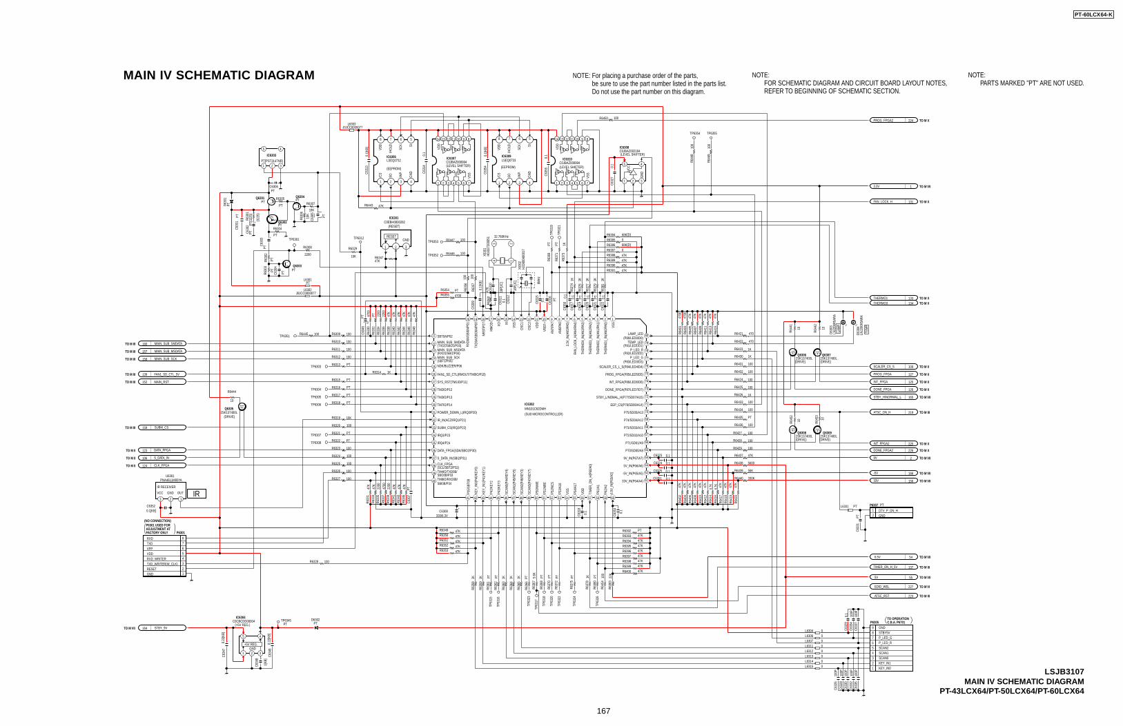
NOTE:FOR SCHEMATIC DIAGRAM AND CIRCUIT BOARD LAYOUT NOTES,REFER TO BEGINNING OF SCHEMATIC SECTION.
NOTE: For placing a purchase order of the parts, be sure to use the part number listed in the parts list. Do not use the part number on this diagram.
NOTE:PARTS MARKED "PT" ARE NOT USED.
MAIN IV SCHEMATIC DIAGRAM
LSJB3107MAIN IV SCHEMATIC DIAGRAM
PT-43LCX64/PT-50LCX64/PT-60LCX64
1KR6314
47KR6353
100R6326
0.1[
KB]
C630
9
PTR6313
100R6434
100R6310
100R6309
PTR6
369
100R6432
47K
R634
3
100R643147
KR6
331
STBY_9V164
TP6312
100R6436
TP6308
47K
R640
8
47KR6395
2200
R633
4
100
R635
6
TP6303
PTC6
321
47K
R640
6
4700
R633
0
PTC6
316
1KR6
373
PTR6392
47K
R640
4
47K
R634
547
KR6
342
TP63
21
0.1
C631
8
47K
R641
0
47K
R640
2
0R6385
0.1
C631
5
100R6425
1KR6
379
47KR6393
47K
R641
2
100R6324
10KR6319
2200
R633
9
100R6424
4700
R640
3
0.1C6325
47K
R634
1
4700R6355
47K
R634
4
PTR6316
4700
R640
1
47K
R634
6
PTR6318
0.1
C631
1
0.1C6324
PTR6322
47K
R642
0
47K
R633
3
100R6427
47KR6350
PTR6315
TP6305
2200
R633
5
4.7K
R641
6
47K
R641
3
47KR6389
47KR6352
PTR6354
47K
R640
7
PTR6
332
4.7K
R641
4
0.1C6323
47K
R641
1
PTR6
375
100R6312
100R6311
0.1
C632
0
47K
R640
5
4700
R633
7
PTR6
372
47KR6351
47K
R636
0
330KR6440
47K
R640
9
100R6328
TP6306
47K
R641
7
1KR6430
1KR6
377
100R6433
100R6429
100
R635
7
47K
R641
8
47K
R634
0
47K
R634
8
47K
R641
9
100R6428
0R6387
100R6327
1KR6
376
47K
R633
8
PTR6435
TP6307
PTC6
319
2200
R633
6
0.1
C632
2
47KR6394
1KR6
381
47KR6390
68K[D]R6384
PTR6317
47K
R641
5
68K[D]R6386
100R6320
PTR6321
1KR6423
47KR6349
PTR6
371
PTQ6302
PTQ6301
PT
C630
5
10K
R6329
PTR630
2PTQ6303
R6305
PT
PTC6306
PTC6
301
10K
R630
6
TP6301
PTC6
303
PT
R630
3
PTQ6304
R6308
2200
*
PT[3
225]
R630
1
PTD630
1
PTC630
2
PT
R6304
18K
R6307
C630
4
PT
47KR6391
TP63
19
47KR6388
18P[
JC]
C631
0
18P[
JC]
C631
2
100R6323
100R6325
TP63
16PT
R636
2TP
6315
PTR6
361
PTR6
380
TP63
26
22K
R638
3
100
R645
4
1KR6
378
TP63
17
TP63
20
PTR6
368
5.6K
R636
7
TP63
18
PTR6
370
47KR6398
47KR6396
47KR6399
47KR6397
47KR6400
1KR6
358
1KR6
359
1KR6
363
1KR6
364
1KR6
365
PTR6
366
MAIN_SUB_SMDATA160
PTC6
307
MAIN_SUB_MSDATA157
MAIN_SUB_SCK158
SUBM_CS159
56KR6439
5600R6438
47KR6437
STBY_H/NORMAL_L 1651KR6426
100P
C633
510
0PC6
332
100P
C633
0
100P
C632
6
100P
C632
8
0.1
C632
9
100P
C633
710
0PC6
334
47KR6347
1KR6
374
0.1
C631
7
FAN1_SD_CTL_5V139
5V 55
TP63
22
TP63
24
TP6304
P6301
87654321
X630
2H2
D800
4000
17
FAN_LOCK_H 131
PTC6
346
X630
1H0
J327
2000
51
14
23
PT[PST3147NR]
IC6303
1 2
5
3
4
DONE_FPGA 126
CLK_FPGA124
DATA_FPGA123
PROG_FPGA 127
PTTP6345
*
1[KB
]
C634
8
*0.22
[KB]
C634
7
*0.22
[KB]
C634
9
PTD6302
THERMO3 134
THERMO1 133
IC6304C0CBCDD00004
1 2
5
3
4
TIMER_ON_H_5V 137
-5V 166
33V 156
9V 2
0.1
C635
0
0.1C6351
3.3V 1
U6301PNA4611M00YA
123
C63520.1[KB]
D630
4LN
J206
R5AR
A
D630
3LN
J206
R5AR
A
TP63
23
*
R6421 470
*R6422 470
P63059 GND8 STBY5V7 P_LED_G6 P_LED_R5 SCAN24 SCAN13 SCAN02 KEY_IN11 KEY_IN0
6.5V 54
0.1
C635
3
S_DATA_IN106
SCALER_CS_S 109
10
R644
2
INT_FPGA 125
10
R644
1
2SK137400LQ6305
10
R6444
2SK137400LQ6306
2SK137400LQ6307
0.1[
KB]
C631
3
C0JBAZ002164IC6308
1 2
5
VCC
3
GND
4
C631
40.
1
47KR6443
C632
70.
1
330/6.3VC6308
MN101C62DMHIC6302
1234567891011121314151617181920
21
22
23
24
25
26
27
28
29
30
31
32
33
34
35
36
37
38
39
40
41 42 43 44 45 46 47 48 49 50 51 52 53 54 55 56 57 58 59 60
61
62
63
64
65
66
67
68
69
70
71
72
73
74
75
76
77
78
79
80
LSEQ0732IC6306
1 2 3 4
5678
IC6307C0JBAZ000994
1 2 3 4 5 6 7
891011121314
MAIN_RST152
100R6445TP6351
100R6447TP6353
100R6446TP6352
0L6311
0L6313
0L6307
0L6312
0L6306
L6303J0JCC0000077
L6301PT
0L6314
0L6304
0L6315
L6302J0JCC0000077
2SK137400LQ6308
2SK137400LQ6309
10
R645
3
10R645
2
C635
50.
1
IC6310C0JBAZ000994
1 2 3 4 5 6 7
891011121314
0.1[
KB]
C635
4
LSEQ0733IC6309
1 2 3 4
5678
P630712
L6331 PT
PTC6
331
100R6450
100
R644
8
TP6354 TP6355
100
R644
9
PROG_FPGA2 224
ATSC_ON_H 219
INT_FPGA2 225
DONE_FPGA2 226
EDID_WEL 227
ATSC_RST 223
IC6301C0EBH0000282
1 2 3
P52/
NCS
OSC
2
VSS
(P82/LED2/D2)P_LED_R
SBO0B/P33
P50/
NWE
P71/SD01/A9
(TXD1/SBO1/P03)
6.5V
_IN[
P63/
A3]
TXD
MAIN_SUB_SCK
SUBM_CS(IRQ2/P22)
P35/
SBT0
B
P51/
NRE
SYS_RST(TM1IO/P11)
TIM
ER_O
N_H(
P60/
A0)
MAIN_SUB_MSDATA
SBT0A/P02
POWER_DOWN_L(IRQ0/P20)
TEMP_LED
P72/SD02/A10
P74/SD04/A12
VDD
P75/SD05/A13
SCAN
3(P4
7/KE
Y7)
THER
MO
1_IN
(AN0
/PA0
)
DONE_FPGA(P87/LED7/D7)
P54/
A17
VDD
SCAN
0(P4
4/KE
Y4)
OSC
1
5V_IN(P66/A6)
SCAN
2(P4
6/KE
Y3)
XI
DATA_FPGA(SDA/SBO2/P30)
VPP
LAMP_LED
SCAN
1(P4
5/KE
Y5)
-5V_IN(P65/A5)
RXD
S_DATA_IN(SBI2/P31)
AN7/
PA7
XO
(SCL/SBT2/P32)
SBI0B/P34
AN6/
PA6
TM4IO/TXD0B/
TXD_WRITER(W_CLK)
IRQ3/P23
P73/SD03/A11
MAIN_SUB_SMDATA
NRST
/P27
TM8IO/RXD0B/KE
Y_IN
1(P4
1/KE
Y1)
33V_IN(P64/A4)
KEY_
IN0(
P40/
KEY0
)
IR_IN(ACZ/IRQ1/P21)
INT_FPGA(P86/LED6/D6)
PROG_FPGA(P85/LED5/D5)
FAN_
LOCK
_H(A
N4/P
A4)
THER
MO
2_IN
(AN1
/PA1
)
TM7IO/P14
STBY_L/NOMAL_H(P77/SD07/A15)
(SBT1/P05)
EEP_CS(P76/SD06/A14)
TM2IO/P12
(RXD1/SBI1/P04)
FAN1_SD_CTL(RMOUT/TM0IO/P10)
RXD0
A/SB
I0A/
P01
MM
OD
9V_IN(P67/A7)
GND
IRQ4/P24
P62/
A2
THER
MO
3_IN
(AN2
/PA2
)
P53/
A16
(P81/LED1/D1)
(P83/LED3/D3)
P42/
KEY2
P61/
A1
THER
MO
4_IN
(AN3
/PA3
)
RESET
VSS
P43/
KEY3
TM3IO/P13
3.3V
_IN(
AN5/
PA5)
SCALER_CS_L_S(P84/LED4/D4)
VSS
VDD
(P80/LED0/D0)
TXD0
A/SB
O0A
/P00
VREF
+
NDK/BUZZER/P06
(322
5)
32.768KHz
P_LED_G
GND
(RESET)
RXD_WRITER
8MHz
P70/SD00/A8
IRIR RECEIVER
GNDVCC OUT
SO/H
OLD
/WP
SI
VDD
SCK
(EEPROM)
/CS
GND
CLK_FPGA
VDD
VSS
TO M III
TO M III
TO M III
TO M III
TO M III
TO M II
TO M II
TO M II
TO M VII
TO M VII
TO M X
TO M XTO M X
TO M II
TO M II
TO M II
TO M II
TO M VII
TO M VII
TO M VII
TO M VII
TO M VII
TO M III
TO M VII
TO OPERATIONC.B.A. P6701
(DRIVE)(DRIVE)
TEM
P
LAM
P
(LEVEL SHIFTER)
(LEVEL SHIFTER)
(DRIVE)
(+5V REG.)
(SUB MICROCONTROLLER)
RESET
+5V REG.GND
P6301 USED FORADJUSTMENT ATFACTORY ONLY
(NO CONNECTION)
TO M III
TO M VI
TO M III
(DRIVE)(DRIVE)
TO M X
TO M X
TO M III
VSS
SO
VDD
GND
/HO
LD
SCK
/WP
(EEPROM)
VDDSI
(LEVEL SHIFTER)
/CS
DTV_P_ON_HGND
TO M X
PT
PT-60LCX64-K
167
I/O CHART OF IC6302
I/O CHART OF IC6302PT-43LCX64/PT-50LCX64/PT-60LCX64
515253545556575859
Pin No.
Pin No.
I/O
II
O
60
Signal NamePin No. I/O DescriptionSignal Name Description
DescriptionVoltage detection for error LED indication when the voltage becomes less than 1.5V.Voltage detection for error LED indication when the voltage becomes less than 2V.Voltage detection for error LED indication when the voltage becomes less than 10V.Voltage detection for error LED indication when the voltage becomes more than 0V.Voltage detection for error LED indication when the voltage becomes less than 1V.Voltage detection for error LED indication when the voltage becomes less than 2V.
61626364
6061626364
65666768697071727374757677787980
VDD (+5V)
GND
KEY_IN0KEY_IN1KEY2KEY3
O
- -
-
- P35
--
I-
---
-
O
II
O-O
-O
O
O
O
O
OOOOOO
I
III
II
II
SCAN0SCAN1SCAN2SCAN3NWENRENCSA16VSSA17VDDTIMER_ON_H-EEP_WE_L6.5V_IN33V_IN-5V_IN5V_IN9V_INDONE_FPGA2INT_FPGA2
KEY DATA 1KEY DATA 0
PROG_FPGA2EEP2_CSLOSD_SW_CSDTV_P_ON_HEEP_CSSTBY_L/NOMAL_HDONE_FPGAINT_FPGA
SCAN 1SCAN 0
SCAN 2
PROG_FPGASCALER_CS_LP_LED_GP_LED_RTEMP_LEDLAMP_LED
424344454647484950
41 SBT0B (Not used)
(Not used)(Not used)
(Not used)STBY-H/NORMAL-IN(Not used)(Not used)(Not used)
(Not used)EEPROM (IC5802) WRITE ENABLE (L)
DONE FPGA2 (IC5604) PROGRAMINGFPGA2 (IC5604) INITIALIZINGFPGA2 (IC5604) PROGRAMING COMMANDEEPROM2 (IC6309) CS (L)(Not used)DTV POWER ON (H)EEPROM1 (IC6306) CS (L)
DONE FPGA1 (IC5306) PROGRAMINGFPGA1 (IC5306) INITIALIZINGFPGA1 (IC5306) PROGRAMING COMMAND
(Not used)
LAMP ON (H) /OFF (L)
6.5V LINE DETECT33V LINE DETECT-5V LINE DETECT5V LINE DETECT9V LINE DETECT
STANDBY (L) / POWER ON (H)
SCALER (IC5302) CS (L)POWER LED (GREEN) ON (L)POWER LED (RED) ON (L)TEMP LED ON (L)LAMP LED ON (L)
1PA0PA1PA2PA3PA4PA5PA6PA7
P27P00
P02P03P04P05P06P10P11P12P13P14P20P21P22P23P24P30P31P32P33P34
P01
VSS234567
7
8910111213141516171819202122232425262728293031323334353637383940
IIIIII
- -
--
--------
THERMO1_INTHERMO2_INTHERMO3_INTHERMO4_IN
I
I
I
I
I
II
-I
I
-
I
I
-
-
-
----
--
3.3V_INAN6AN7VREF+
OSC2OSC1VSSXIXOMMODNRSTTXD0A/SBO0ARXD0A/SBI0ASBT0AMAIN_SUB_SMDATAMAIN_SUB_MSDATAMAIN_SUB_SCKNDK/BUZZER
TM2IOTM3IOTM7IOPOWER_DOWN_L
IRQ3
VDD (+5V)
IR_INSUBM_CS
GND
GND
IRQ4SDA/SBO2SBI2SCL/SBT2TM4IO/TXD0B/SBO0BTM8IO/RXD0B/SBI0B
FAN1_SD_CTLSYS_RST
O
O
O
OO
O
O
O-
FAN_LOCK_H
VDD
(Not used)(Not used)
(Not used)
(Not used)FAN1 SPEED CONTROL(Not used)(Not used)(Not used)(Not used)(Not used)
(Not used)(Not used)
(Not used)(Not used)
TEMPERATURE DATA1 (FROM THERMISTOR 2 C.B.A.)TEMPERATURE DATA2 (FROM THERMISTOR 2 C.B.A.)TEMPERATURE DATA3 (FROM THERMISTOR 1 C.B.A.)TEMPERATURE DATA4 (FROM THERMISTOR 1 C.B.A.)FAN (1,2,3) LOCK (H)3.3V LINE DETECT
V-REF FOR IC6302
8MHz OSCILLATION8MHz OSCILLATION
32.768KHz OSCILLATION32.768KHz OSCILLATION
RESET (L)EEPROM SERIAL DATA 0EEPROM SERIAL DATA 1EEPROM SERIAL CLOCKSERIAL DATA 1SERIAL DATA 0SERIAL CLOCK
IR-DATAIC6302 CS (L) FROM IC6003
SERIAL DATA 0SERIAL DATA 1SERIAL CLOCK
Port No. Port No.
P40P41P42P43P44P45P46P47P50P51P52P53
P54
P60P61P62P63P64P65P66P67P70P71P72P73P74P75P76P77P87P86P85P84P83P82P81P80
*3*3*3*3*3
*3
*3
PT-60LCX64-K
168
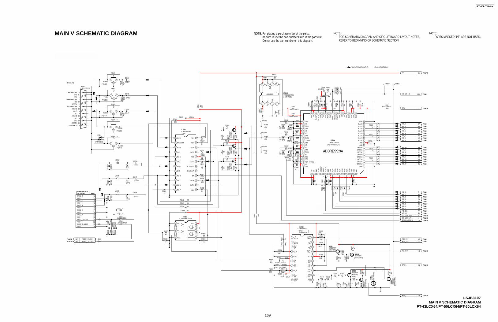
NOTE:FOR SCHEMATIC DIAGRAM AND CIRCUIT BOARD LAYOUT NOTES,REFER TO BEGINNING OF SCHEMATIC SECTION.
NOTE: For placing a purchase order of the parts, be sure to use the part number listed in the parts list. Do not use the part number on this diagram.
NOTE:PARTS MARKED "PT" ARE NOT USED.
MAIN V SCHEMATIC DIAGRAM
LSJB3107MAIN V SCHEMATIC DIAGRAM
PT-43LCX64/PT-50LCX64/PT-60LCX64
5V 55
560P
[JC]
C553
3
1800
R55570.01[KB]C5519
PTR558
1
8200R5579
2SD1
819A
Q55
10
RGB_HS 107
2SD1819AQ5513
0.068[KB]C5518
PC_NC_H 14856K
R5561
100KR5584
180K
R558
7
2SD1819AQ5511
PTC554
0
1800
R5556470R5562
RGB_VS 122
0.01
C5536
1KR5563
8200R5577
18K
R5576
0.1
C555
1
10/16VC5523
PTR559
1
120PC5535
R552047
C55630.1
C5530
0.047[KB]
C5539
10P[DC]
C5537
10P[DC]
0R5
594
R5575 0
C554410/6.3V
C555
8
0.1
C555
30.
1[KB
]
0R5
586
C554
9PT
C555
0
0.1
C55450.1
R552147
C5543
0.1
C5541
0.1[KB]
C55460.1
R551
8 47
0R5595
R552347
C555
90.
1
C556
2
10/6
.3V
R5574 0
3.3V 1
C5557
3900P[KB]
R551
9 47
C5538
10P[DC]
C55560.039[KB]
C556
00.
1
22R5
589
C55420.1
R552247
PTR5596
IC5504C0FBAD000069
123456789
1011121314151617181920
2122232425262728293031323334353637383940
41
424344454647484950515253
54555657585960
61 62 63 64 65 66 67 68 69 70 71 72 73 74 75 76 77 78 79 80
R5578
10K
C555
50.
1
0R5593
R55903300
C555
410
/6.3
V
C5531
0.047[KB]
C5532
0.047[KB]
C556
10.
1
I2C_SCK_3.3V 6I2C_DATA_3.3V 5
AD_R7 88
AD_R6 87
AD_R5 86
AD_R4 85
AD_HS 80AD_CLK 79
AD_REF_HS 108
IC5502C1AB00000753
1
2
3
4
5
6
7
8
9
10 11
12
13
14
15
16
17
18
19
20
47/6.3V
C5534
39R556
4
220
R5567
220
R5566
220
R5565
AD_R1 82
AD_R3 84
AD_R0 81
AD_R2 83
AD_G7 96
AD_B7 104
AD_G6 95
AD_B6 103
AD_G5 94
AD_B4 101AD_B5 102
AD_G4 93
AD_B0 97
AD_G3 92
AD_B1 98
AD_G0 89AD_G1 90
AD_B2 99AD_B3 100
AD_G2 91
R558
30
10/16V
C5521
10/16VC5520
0.1
C5517
10/16V
C5503
R55471K
PT[3225]
FL55021 2
3
75[D
]
R551
1
220
R5552
R5502
0
R5555
1K
220
R5554
PT[3225]
FL55091 2
3
75[D
]
R551
210K
R5548
2200
R5553
0.1
C5516
PT[2012]FL5504
1 2
3
220
R5551
R5549
1K
R5503
0
PT[3225]
FL55031 2
3
10/16V
C5501
100/6.3VC5515
IC5501C1AB00001365
1
2
3
4
5
6
7
8
9
10
21
22
13
14
15
16
17
18
19
20
11
12
23
24
R5550
1K
PT[3225]
FL55011 2
3
75[D
]
R551
5
R5501
0
10/16V
C5502
JK5501K1FB115B0079
515
10
414
9
313
8
212
7
111
6
R5504 0
R5505 0
MAZT068H0L
D5501
PTR551
3
PTR551
4
PTR551
6
10/16V
C5506
10/16V
C5504
10/16V
C5505
RGB1_H/RGB2_L 138
33U
L550
4
33U
L550
3
560
R5573
560
R5572
560
R5571
1
C5524
*
2R2[
KB]
C552
5
470P
[KB]
C556
4
10K
R5517
P5501
14GND13RGB2_R_AUDIO12GND11RGB2_L_AUDIO10GND9RGB2_V8GND7RGB2_H6GND5RGB2_B4GND3RGB2_G2GND1RGB2_R
RGB2_L_AUDIO168
RGB2_R_AUDIO167
10P[
DC]
C556
9
10P[
DC]
C557
0
10P[
DC]
C557
110
0PC5
565
100P
C556
610
P[DC
]C5
567
10P[
DC]
C556
8
2SD1
819A
0LQ
5507
560
R555
8
2SD1
819A
0LQ
5508
2SD1
819A
0LQ
5509
560
R555
9
560
R556
0
*
1[KB
]
C552
2
RGB_L 136
UN52
13Q
5514
100PC5
547
47K
R5580
100K
R558
8
PTR559
2
100PC5
548
47K
R5582
100KR5585
1
C555
2
CPS_L 153
2SD1819AQ5512
2SD1
819A
Q55
16
C557
2PT
TP5501
TP5502
TP5503
TP5504 TP5505
PTR5569
PTR5568
PTR5570
PTC5514
R5537
PT R5539
PTR5538
PT
R5540
PT
R5541
PT
R5543
PT
R5545
PT
R554
2PT
R554
4PT
R554
6PT
C557
312
P[JC
]
PT_SN74AHCT32PWIC5505
12
34
56
7 89
1011
1213
14
IC5503C0CBCBE00001
1 2 3 4
5678
0L5512
L5506
J0JHC0000018
J0JBC0000034L5513
0L5509
0L5511
0L5508
L5507J0JCC0000077
J0JBC0000034L5514
L5505
J0JCC0000077
0L5510
RED4
VD
RED0
PVD
GND
GND
MID
SCV
GND
VSYN
C
VD
COAS
T
GREEN5
A0
BLUE1
VD
GREEN4SDA
BLUE0
SCL
GND
GND
GND
GND
HSYN
C
GREEN7
FILT
BLUE6
SOG
OUT
GREEN6
BLUE3BLUE4
BLUE2
HSO
UT
GND
BLUE5
GREEN0
VSO
UT
VD
GREEN1
VDD
VDD
GND
GND
GREEN3
CLAM
P
RAIN
GND
BLUE7
RED5
DATA
CK
GREEN2
GND
BAIN
VD
VDD
RED3
GND
VDD
VD
GND
RED1
GND
RED6
GND
REF_BYPASS
VD
GAIN
RED2
PVD
RED7
SOGIN
GND
VDD
GND
VD
VDD
VD
VD
GND
GND
VSTATE
VGATE SW
VDET
VSSOUT
CLPSW
VCC
HD-OUT
GND
V_IN
HPOL
HD+OUT
HSTATE
C/HDET
VSSIN
VD+OUT
VPOL
G_IN
C/HIN
CLP+OUT
CLMPTMNG
ADDRESS:9A
GND
IN2-R
IN2-G
SYNC-DET IN2-H
IN1-G OUT-H
G.SYNC-IN
IN1-B
OUT-R
GND
GND
IN1-H
RGB_IN1
GND
SYNC-OUT
SW
OUT-G
OUT-B
IN1-R
IN2-VIN1-V
OUT-V
VCC
IN2-B
2
NC
13
GREEN8
1GND
I2C7
I2C SCK
BLUE RETURN
5
GND
RED RETURN
9
1015
12
CSYNC(MAC2)
3
4
6
GREEN RETURN
HSYNC
NCBLUE
11
VSYNC 14
RED
GND
NCSU
B
VSS
VDD
TO M VII
AUDIO SIGNAL
TO FRONT JACKC.B.A. P3901
SYNCSEPARATION
(BUFFER)
(BUFFER)
(SWITCHING)
(SW
ITCH
ING
)
(SW
ITCH
ING
)
(SW
ITCH
ING
)
(BUF
FER)
(BUF
FER)
(BUF
FER)
(SW)
(+3.3V REG.)
(A/D CONVERTER)
TO M VII
TO M VII
TO M II
TO M VII
TO M IITO M IITO M IITO M IITO M IITO M IITO M IITO M II
TO M IITO M IITO M IITO M IITO M IITO M IITO M IITO M II
TO M IITO M IITO M IITO M IITO M IITO M IITO M IITO M IITO M IITO M IITO M IIITO M IIITO M III
TO M IITO M II
TO M III
TO M III
TO M III
+3.3V REG.
VIDEO SIGNAL(MAIN/SUB)
PT-60LCX64-K
169
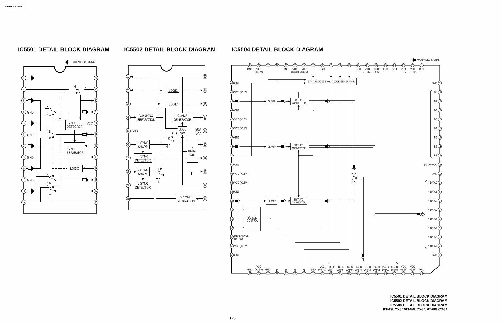
IC5501 DETAIL BLOCK DIAGRAM
IC5501 DETAIL BLOCK DIAGRAMIC5502 DETAIL BLOCK DIAGRAMIC5504 DETAIL BLOCK DIAGRAM
PT-43LCX64/PT-50LCX64/PT-60LCX64
1
2
3
4
SYNCDETECTOR
H L
H
L
H
GND
GND
GND
GND
L
H
LH
L
LOGIC
VCC
SYNCSEPARATOR
5
6
7
8
9
10
11
12 13
14
15
16
17
18
19
20
21
22
23
24
SUB VIDEO SIGNAL
IC5502 DETAIL BLOCK DIAGRAM
1
2
3
4
5
6
7
8
9
10 11
12
13
14
15
16
17
18
19
20
V/H SYNCSEPARATION
H SYNCSHAPE
EDGESW
CLAMPGENERATOR
H SYNCDETECTOR
V SYNCSHAPE
V SYNCDETECTOR
LOGIC
LOGIC
VTIMINGGATE
V SYNCSEPARATION
L
L
H
GND (+5V) VCC
H
IC5504 DETAIL BLOCK DIAGRAM
25262728293031323334353637383940
41
42
43
44
45
46
47
48
49
50
51
52
53
54
55
56
57
58
59
60
61 62 63 64 65 66 67 68 69 70 71 72 73 74 75 76 77 78 79 80
1
2
3
4
5
6
7
8
9
10
11
12
13
14
15
16
17
18
19
20
21222324
REFERENCEBYPASS
VCC (+3.3V)
GND
VCC (+3.3V)
GND
VCC (+3.3V)
GND
VCC (+3.3V)
GND
VCC (+3.3V)
GND
VCC (+3.3V)
GND
GND VCC(+3.3V)
GND GNDVCC(+3.3V)
VCC(+3.3V)
GND GNDVCC(+3.3V)
VCC(+3.3V)
GND GNDVCC(+3.3V)
VCC(+3.3V)
GND GNDVCC
(+3.3V)VCC
(+3.3V)GNDPR,PBDATA7
PR,PBDATA6
PR,PBDATA5
PR,PBDATA4
PR,PBDATA3
PR,PBDATA2
PR,PBDATA1
PR,PBDATA0 GND
VCC(+3.3V)
VCC(+3.3V)
GND
B0
B1
B2
B3
B4
B5
B6
B7
(+3.3V) VCC
GND
Y DATA0
Y DATA1
Y DATA2
Y DATA3
Y DATA4
Y DATA5
Y DATA6
Y DATA7
GND
8BIT A/DCONVERTER
I2C BUSCONTROL
CLAMP
8BIT A/DCONVERTERCLAMP
8BIT A/DCONVERTERCLAMP
SYNC PROCESSING / CLOCK GENERATOR
MAIN VIDEO SIGNAL
PT-60LCX64-K
170
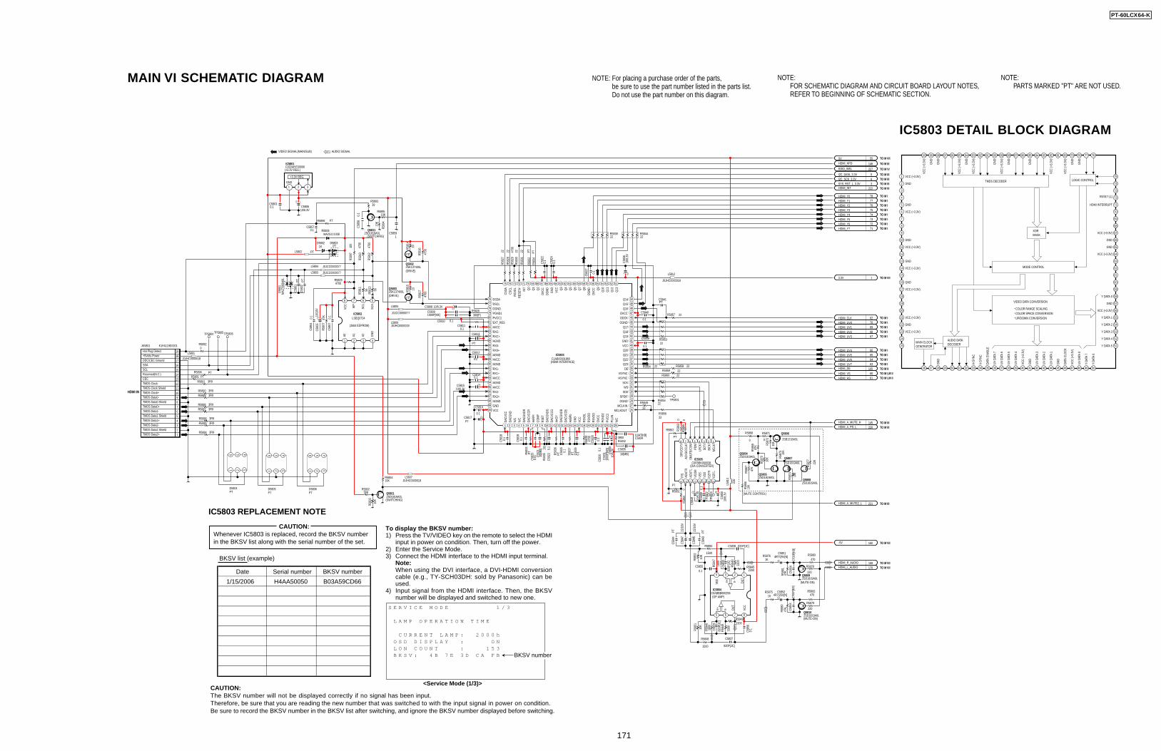
NOTE:FOR SCHEMATIC DIAGRAM AND CIRCUIT BOARD LAYOUT NOTES,REFER TO BEGINNING OF SCHEMATIC SECTION.
NOTE: For placing a purchase order of the parts, be sure to use the part number listed in the parts list. Do not use the part number on this diagram.
NOTE:PARTS MARKED "PT" ARE NOT USED.
MAIN VI SCHEMATIC DIAGRAM
1
2
3
4
5
6
7
8
9
10
11
12
13
14
15
16
17
18
19
20
21
22
23
24
25
75
74
73
72
71
70
69
68
67
66
65
64
63
62
61
60
59
58
57
56
55
54
53
52
51
26 27 28 29 30 31 32 33 34 35 36 37 38 39 40 41 42 43 44 45 46 47 48 49 50
100 99 98 97 96 95 94 93 92 91 90 89 88 87 86 85 84 83 82 81 80 79 78 77 76
VCC (+3.3V)
VCC (+3.3V)
VCC (+3.3V)
GND
GND
VCC (+3.3V)
VCC (+3.3V)
VCC (+3.3V)
GND
GND
GND
VCC
(+3.
3V)
VCC
(+3.
3V)
DATA
CLO
CK
GND
GND
GND
GND
VCC (+3.3V)
GND
VCC (+3.3V)
GND
VCC (+3.3V)
VCC (+3.3V)
GND
VCC
(+3.
3V)
GND
VCC
(+3.
3V)
VCC
(+3.
3V)
VCC
(+3.
3V)
VCC
(+3.
3V)
VCC
(+3.
3V)
GND
GND
GND
GND
GND
GND
GND
RESET (L)
HDMI INTERRUPT
Y DATA 0
Y DATA 1
Y DATA 2
Y DATA 3
Y DATA 4
Y DATA 5
Y DA
TA 7
UV D
ATA
0
UV D
ATA
1
UV D
ATA
2
UV D
ATA
3
UV D
ATA
4
UV D
ATA
5
UV D
ATA
6
UV D
ATA
7
V-SY
NC
H-SY
NC
DATA
ENA
BLE
Y DA
TA 6
MAIN CLOCKGENERATOR
XORMASK
AUDIO DATADECODER
LOGIC CONTROL
MODE CONTROL
TMDS DECODER
VIDEO DATA CONVERSION
COLOR RANGE SCALINGCOLOR SPACE CONVERSIONUP/DOWN CONVERSION
IC5803 DETAIL BLOCK DIAGRAM
1KR5876
10K
R580
3
C582
9
820P
[JC]
C582
40.
1
C5812
0.1
0R5
864
L5807J0JHC0000018
22R5855
PTC5
801
22/1
6VC5
846
47K
R586
7
47K
R588
0
C58340.047[KB]
390[F]R5826
L5806J0JHC0000018
JK5801 K1FA119E0001
181716151413121110987654321
19
PTR5801
22R5859
2SK137400LQ5802
PTR5
834
C585
427
00P[
KB]
2SB1218ASL
Q5806
220
R5879
22R5
828
IC5804C0ABBB000256
1234
5 6 7 8
470R5882
2200R5841
IC5805C0FBBK000038
12345678
11 12 13 14 15 169 10
2SD1819A0LQ5804
C581
90.
1
1KD5802
TP5801
PT
R5862
TP58
03
10R581
5
C5839
0.1
1KR5875
3300
R584
0
C582
30.
1
56KR5802
C582
50.
1
C5840
0.1
C581510/6.3V
J0JCC0000077
L5805
C582
20.
1
C583
00.
1
PTR583
3
2SD1819A0LQ5809
C58091000P[KB]
470R5883
220
R5878
PTR583
7
C583
310
/6.3
V
C5838 820P[JC]
22R5858
33R5856
C58524R7/25V[N]
1800
R584
7
22K
R587
7
2SD1819A0LQ5807
1500
R5848
1800
R584
6
C584
90.
1
0R5
863
47K
R586
9
C5813
PT
10K
R587
0
C5810 0.1
C58030.1
MAZ
T068
H0L
D580
1
J0JCC0000077L5803
56
R581
3
4700
R581
0
IC5803C1AB00001865
1 2 3 4 5 6 7 8 9 10 11 12 13 14 15 16 17 18 19 20 21 22 23 24 25
26272829303132333435363738394041424344454647484950
51525354555657585960616263646566676869707172737475
7677787980
86
81
91
85
89
83
99
87
9495
100
98
92
84
82
93
90
88
9697
4700
R581
7
22R5853
C58140.1
2SD1819A0LQ5801
10K
R587
3
22/1
6VC5
847
2SD1819A0LQ5808
10K
R585
2
C583
110
00P[
KB]
10KR5804
22R5
830
0R5
865
0.1
C580
7
PTD5803
10K
R587
4
3300
R584
3
4700
R582
9
2SK137400LQ5803
10K
R585
1
47K
R580
7
PT
R5861
4700
R581
6
L5801
J0JHC0000018
C581
80.
1
10/6
.3V
C584
8
C58514R7/25V[N]
C5841PT
C583
2
820P
[JC]
LSEQ0734IC5802
1 2 3 4
5678
C582
00.
01
10/6.3VC5806
4700R5809
33
R5849
TP58
02
0.1
C580
4
10R581
4
22R5854
J0JCC0000077L5804
C582
7
0.1
22R5860
C5808 10/6.3V
10/6
.3V
C583
6
PTC5
802
PTL5802
1500
R5850
10K
R587
2
C582
8
0.1
56
R581
1
PTR5
832
C5817PT
C5816
0.1
47K
R588
1
C585
327
00P[
KB]
0
R5871
L5812
J0JHC0000018
2SD1819A0LQ5810
22R5
827
150
R583
5
C5837
820P[JC]
0
R5868
22R5
831
22R5844
22R5857
22R5839
3900R5842
C582
60.
1
2200R5845
C58110.1
2SD1819A0LQ5805
4700
R583
8
10K
R586
6
C585
010
/6.3
V
4700
R581
2
10/1
0VC5
805
PTR583
6
PTR5896
*
C582
110
[MB]
*
C5835
10[MB]
*
C584
3PT
*
C584
4PT
0.1C5855
0.1
C585
6
33U
L581
3
3R9R5884
3R9R58853R9R5886
3R9R58873R9R5888
3R9R58893R9R5890
3R9R5891
D5805PT
4561 2 3
D5806PT
4561 2 3
0R5892
10K
R589
4
10KR5895
2SD1819A0LQ5811
39R5893
PTR5898
C58570.1
C585
80.
1
C58591
100
R589
7
TP5805TP5804 TP5806
MA2S111008R5808
D5804PT
4561 2 3
HDMI_HPD 146
5V 55
EDID_WEL 227
I2C_DATA_3.3V 5I2C_SCK_3.3V 6SYS_RST_L_3.3V 3HDMI_INT 222
HDMI_Y0 78HDMI_Y1 77HDMI_Y2 76HDMI_Y3 75HDMI_Y4 74HDMI_Y5 73HDMI_Y6 72HDMI_Y7 71
3.3V 1
HDMI_CLK 62HDMI_UV0 70HDMI_UV1 69HDMI_UV2 68HDMI_UV3 67
HDMI_UV6 64
HDMI_UV4 66
HDMI_UV7 63
HDMI_UV5 65
HDMI_DE 105HDMI_VS 60HDMI_HS 61
HDMI_A_MUTE_H 145HDMI_A_PD_L 220
HDMI_A_MUTE2_L 221
-5V 160
HDMI_R_AUDIO 169HDMI_L_AUDIO 170
IC5801C0CBAYF00006
1 2 3
Q14
Q18
Q1
DSCLDSDA
DACV
CC
VCO
M
RX2+
HSYNC
WS
N/C
HDMI IN
SCL
BICK
SDTI
RX1+
TMDS Data2-
AnG
Y
Q20
DACG
NDB
AVCC
VDD
PGND1
Q17
CSCL
RSVD
O
SCL
SD0
CSDA
Q16
TMDS Data1-
A2
RX1-AGND Q23
TMDS Data1+
AGND
RESE
T#
OGND
AVCC
VCC
GNDQ
0
PLLI
N
OVC
C Q4
GND
TMDS Data2+
AGND
Q8
DACG
NDG
ODCKOGND
CEC
Q9
WP
DE
Q13
Hot Plug Detect
RSVD
O
DZFR
AGND
VSYNC
INT
RX2-
TMDS Data0+
AOUT
L
OVC
C
TMDS Data1 Shield
RXC-
DACG
NDR
A0
TMDS Data2 Shield
PVCC1
Q12
SCA
MCL
K
P/S
Q5
Q6
Q2
GND
DIF0
/CDT
I
OG
ND
VCC
SMUT
E/CS
N
MCLKOUT
AVCC
DACV
CCG
RSVD
L
VCC
EXT_RES
PGND
2
RX0-
TMDS Clock Shield
TMDS Data0 Shield
LRCK
VSS
RX0+
N/C
VCC
RSVD
L
COM
P
TMDS Clock+
OVC
C
TMDS Clock-
SPDIF
DACV
CCR
GND
Q15
RXC+
Q10
AnBP
b
Q7
A1 GND
RSET
ACKS
/CCL
K
OVCC
(2kbit EEPROM)
Q3
N/C
TMDS Data0-
AVCC
DDC/CEC Ground
PDN
PVCC
2
Reserved(N.C.)
AGND+5Volts Power
Q19
AOUT
R
AnRP
r
DZFL
VCC
OGND
DACV
CCB
Q21
SDA
OG
ND
DACG
ND
Q11
SCK
Q22
MCLKIN
V+ V-V+VE
E
V-
VCC
OUT
OUT
AUDIO SIGNALVIDEO SIGNAL(MAIN/SUB)
TO M III
TO M VII
TO M IV
TO M IIITO M IIITO M IIITO M III
TO M ITO M ITO M ITO M ITO M ITO M ITO M ITO M I
TO M VII
TO M ITO M ITO M ITO M ITO M I
TO M I
TO M ITO M I
TO M ITO M IITO M I,M IITO M I,M II
TO M IIITO M III
TO M III
TO M VII
TO M VIITO M VII
(+3.3V REG.)
+3.3V REG.
GND
(SWITCHING)
(DRIVE)
(DRIVE)
(SWITCHING)
(HDMI INTERFACE)
(D/A CONVERTER)
(OP AMP)
(MUTE-ON)
(MUTE-ON)
(MUTE CONTROL)
To display the BKSV number:1) Press the TV/VIDEO key on the remote to select the HDMI
input in power on condition. Then, turn off the power.2) Enter the Service Mode.3) Connect the HDMI interface to the HDMI input terminal.
Note:When using the DVI interface, a DVI-HDMI conversioncable (e.g., TY-SCH03DH: sold by Panasonic) can beused.
4) Input signal from the HDMI interface. Then, the BKSVnumber will be displayed and switched to new one.
<Service Mode (1/3)>
S E R V I C E M O D E 1 / 3
L A M P O P E R A T I O N T I M E C U R R E N T L A M P : 2 0 0 0 h O S D D I S P L A Y : O N L O N C O U N T : 1 5 3 B K S V : 4 B 7 E 3 D C A F B BKSV number
Date
1/15/2006 H4AA50050
BKSV number
B03A59CD66
CAUTION:The BKSV number will not be displayed correctly if no signal has been input.Therefore, be sure that you are reading the new number that was switched to with the input signal in power on condition.Be sure to record the BKSV number in the BKSV list after switching, and ignore the BKSV number displayed before switching.
IC5803 REPLACEMENT NOTE
CAUTION:Whenever IC5803 is replaced, record the BKSV number in the BKSV list along with the serial number of the set.
BKSV list (example)
Serial number
PT-60LCX64-K
171
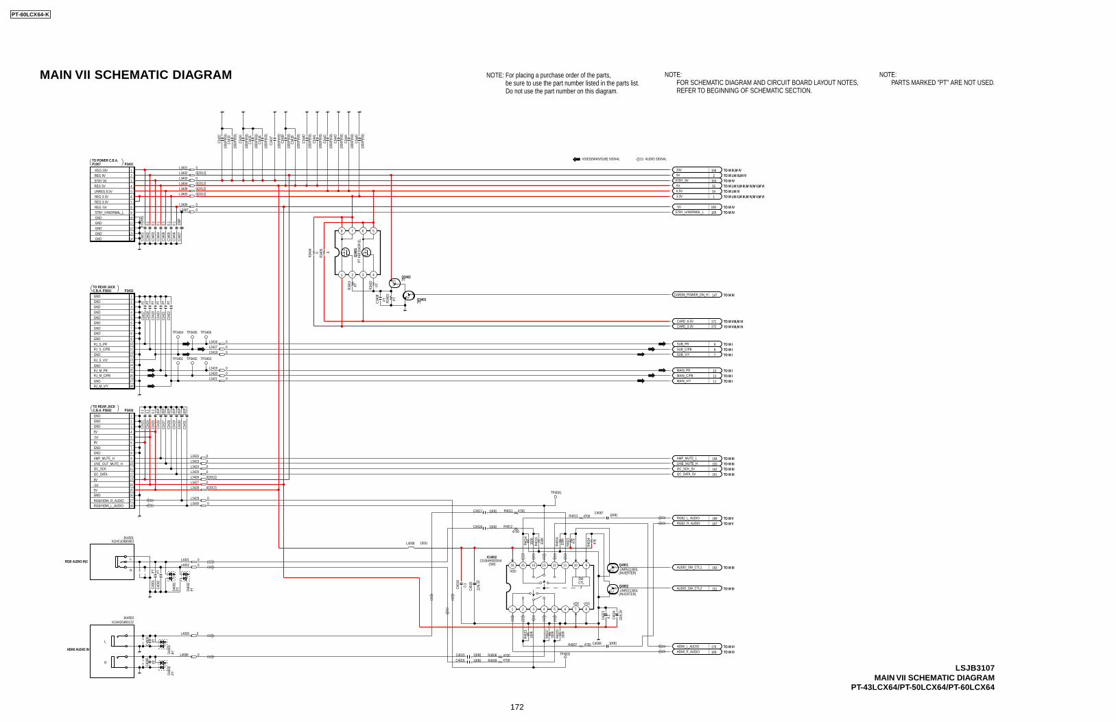
NOTE:FOR SCHEMATIC DIAGRAM AND CIRCUIT BOARD LAYOUT NOTES,REFER TO BEGINNING OF SCHEMATIC SECTION.
NOTE: For placing a purchase order of the parts, be sure to use the part number listed in the parts list. Do not use the part number on this diagram.
NOTE:PARTS MARKED "PT" ARE NOT USED.
MAIN VII SCHEMATIC DIAGRAM
LSJB3107MAIN VII SCHEMATIC DIAGRAM
PT-43LCX64/PT-50LCX64/PT-60LCX64
I2C_SCK_5V 162
PTD400
1
4700R4009
47K
R402
1
MAIN_PR 13
K2HC103B0063JK4001
330K
R401
5
HDMI_R_AUDIO 169
100P
C342
9
0.1
C401
9
100P
C342
7
22/6
.3V
C402
4
HDMI_L_AUDIO 170
100P
C342
8
AUDIO_SW_CTL1 163
0.1
C340
6
P3401
1413121110987654321
LINE_MUTE_H 155
3.3V 1
9V 2
330K
R401
6
TP4001
100P
C343
1
0.01
[KB]
C340
1
PTC4
002
PTC4
001
0.1
C342
5
330K
R401
4
330K
R402
0
0.1
C340
4
0.1
C402
3
AUDIO_SW_CTL2 151
SUB_V/Y 7
0.1
C340
2
5V 55
4700R4012
22/6
.3V
C402
0
0.1
C340
3
0.1
C340
5
MAIN_C/PB 12
100P
C343
0
0.1
C342
3
MAIN_V/Y 11
TP4002
100UL4008
0.1
C342
4
I2C_DATA_5V 161
PTD400
2
PTD400
6PTD4
005
PT
C400
5
PT
C400
6
330K
R401
9
4700R4011
330K
R401
7
4700R4008
47K
R402
4
UNR521300LQ4001
UNR521300LQ4002
PTC3
422
PTC3
420
PTC3
421
PTC3
418
PTC3
417
PTC3
419
PT
R340
1
PT
R340
2
PTR340
3 CARDM_POWER_ON_H 147
33V 156
STBY_H/NORMAL_L 165
STBY_9V 16410
0PC3
407
PTQ3402
PTC340
8
P3404
18RGB/HDMI_L_AUDIO17RGB/HDMI_R_AUDIO
16GND155V
14-5V
139V
12I2C_DATA11I2C_SCK10LINE_OUT_MUTE_H9AMP_MUTE_H8GND7GND69V5-5V45V3GND2GND1GND
P3403
18RJ_M_V/Y17GND
16RJ_M_C/PB15RJ_M_PR
14GND
13RJ_S_V/Y
12GND11RJ_S_C/PB10RJ_S_PR
9GND8GND7GND6GND5GND4GND3GND2GND1GND
AMP_MUTE_L 154
100P
C342
6
4700R4007
4700R4013 RGB2_L_AUDIO 168RGB2_R_AUDIO 167
CARD_6.5V 171CARD_3.3V 172
* 1[KB]C4008* 1[KB]C4016
* 1[KB]C4017
* 1[KB]C4007
* 1[KB]C4015
* 1[KB]C4018
0
R340
4
0
R340
5
6.5V 54
0.1
C340
9
-5V 166
SUB_PR 9SUB_C/PB 8
Q3403PT
TP3401 TP3402 TP3403
TP3404 TP3406TP3405
JK4003K2HA204B0132
PT H
AT20
43R-
ELQ
3401
1000
P(KB
)
C343
9
C343
8
1000
P(KB
)
C344
5
1000
P(KB
)
C344
4
1000
P(KB
)
C344
3
1000
P(KB
)
C344
2
1000
P(KB
)
C344
1
1000
P(KB
)
C344
0
1000
P(KB
)
C343
7
1000
P(KB
)
1000
P(KB
)
C343
3
C343
2
1000
P(KB
)
1000
P(KB
)
C343
5
C343
4
1000
P(KB
)
1000
P(KB
)
C343
6
0L3421
0L3425
L3408 0[2012]L3404 0[2012]
0L3423
0L3401
0L4002
0L3422
0L3430
L3402 0[2012]
0L3420
0L3418
0L3424
0L3427L3428 0[2012]
0L4005
0L3419
L3426 0[2012]
0L3407
0L4001
0L3416
0L3406
L3405 0[2012]
0L3429
0L3417
0L3403
0L4006
IC4002C0JBAR000344
1 2 3 4 5 6 7 8
111213141516 910
VDD
REG 9V
R
REG 3.3V
UNREG 6.5VREG 3.3V
GND
STBY_H/NORMAL_L
STBY 9V
GND
L
REG 5V
GNDGND
VEE
REG 33V
GND
REG -5V
VSS
R
L
TO POWER C.B.A.P1007
TO REAR JACKC.B.A. P3601
TO REAR JACKC.B.A. P3602
RGB AUDIO IN2
HDMI AUDIO IN
VIDEO(MAIN/SUB) SIGNAL AUDIO SIGNAL
TO M III,M IVTO M I,M III,M IVTO M IVTO M I,M II,M III,M IV,M V,M VITO M I,M IV
TO M IVTO M IV
TO M I,M II,M III,M IV,M V,M VI
TO M III
TO M VIII,M IXTO M VIII,M IX
TO M ITO M ITO M I
TO M ITO M I
TO M I
TO M IIITO M IIITO M IIITO M III
TO M VTO M V
TO M III
TO M III
TO M VITO M VI
8 7 6 5
421 3
SWCTL
(SW)
(INVERTER)
(INVERTER)
PT-60LCX64-K
172
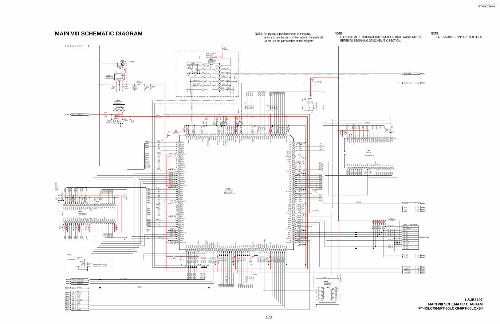
NOTE:FOR SCHEMATIC DIAGRAM AND CIRCUIT BOARD LAYOUT NOTES,REFER TO BEGINNING OF SCHEMATIC SECTION.
NOTE: For placing a purchase order of the parts, be sure to use the part number listed in the parts list. Do not use the part number on this diagram.
NOTE:PARTS MARKED "PT" ARE NOT USED.
MAIN VIII SCHEMATIC DIAGRAM
LSJB3107MAIN VIII SCHEMATIC DIAGRAM
PT-43LCX64/PT-50LCX64/PT-60LCX64
PTC9
029
SD_YUV[0-7]45-52
LSLF0027
L9003
33R9015
TP90
03
0.1C9017
TP9002
0.1C9019
R905
91K
LD[0-15] 184
0.1C9051
0.1C9020
0.1C90180.1C9046
/LCS2 185
0.1
C903
5
0.1C9050
0.1
C904
4
0.1
C903
0
L9005LSLF0027
C902
8
0.1
C903
90.
10.1C9023
0.1
C903
6
0.1C9047
CARD_3.3V172
TP9001
TP90
06
0.1C9048
0.1
C904
3TP90
05TP
9004
L9002LSLF0027
0.1
C904
2
R906
01K
0.1C9021
LSLF0027
L9006
0.1
C904
1
0.1C9049
0.1C9045
0.1
C904
0
0.1
C903
1
0.1
C903
8
0.1C9022
0.1
C903
7
1M
R902
612P[JC]C9026
12P[JC]
C9027
22R9084
22R908722R9086
22R9085
22R9083
33R9018
33R902033R902133R902233R9023
33R9016
33R9017
PTIC9005
1 2
3
SW90
01PT
10KR9099
PT
C905
2
PT
R909
7
0R9100
4700
R905
7
10
C901
6
1
C902
51
C902
4
4700
R903
7
PTR904
1
PTR904
8
4700
R904
2
PTR903
6
4700
R905
3
4700
R904
7
33
R9052
CARD_6.5V171
22R9094
22R909522R9096
/LCS1 186
120R9090120R9091120R909222R9093
120R9089
33R9
025
33R9
027
33R9
028
33R9
029
33R9
032
33R9
033
33R9
034
33R9
035
10R9
039
10R9
040
SD_VSYNC43SD_HSYNC42
HD[0-15]173
/PC_HI174HIORDY175/HWR176/HRD177/HIOCS16178
47R9
071
47R9
072
47R9
075
47R9
076
33R9
077
33R9
078
33R9088
47R9
068
/HCS3180HA0181HA1182
47R9
067
0R9
069
0R9
073
PCLK_27MHZ 44
TP9007
1K
R9024
82R9031
82R9046
82R9045
33
R9030
0
L9008
0
L9011
0
L9010
33
R9051
82R9044
33
R9050
0
L9009
PT
R905
5
1C9033C9034 1000P[KB]
LSLF0027L9007
22/16VC9032
33R9019
47R9008
47R9010
47
R9009
10R9011
10R9012
10R9013
10R9014
PTR9
049
PTR905
622/6.3VC9010
47R900
6
PT
R9007
47/6.3VC9014
10
C901
2
10R9
043
10R9
054
10R9
058
10R9
063
0R9
038
22R9
065
22R9
066
/HCS1179
IO/MEM183
/IREQ 187
120R9082
120R9081
120R9098
120R9080
120R9079
120
R907
4
120R9070
120
R906
4
120
R906
2
CARDM_RST_L 142
CARDM_CS 143
0.01
C900
2
0.1
C900
7
0.1
C900
4
R900
10
1C9
001
0.1
C901
3
0.1
C900
5
JOJH
C000
0055
L900
1
0.1
C900
6
0.1
C900
8
0.1
C900
3
PTR9
002
33R9
104
33R9
107
33R9
103
PTR9
105
0.01
C905
4
1C905
3
IC9007LSEQ0756
1
A15
2
A14
3
A13
4
A12
5
A11
6
A10
7
A9
8
A8
9
NC
10
NC
27
VSS
28
/OE
29
DQ0
30
DQ8
31
DQ1
32
DQ9
33
DQ2
34
DQ10
35
DQ3
36
DQ11
25
A0
26
/CE
11
/WE
12
/RST
13
NC
14
NC
15
RDY/
/BSY
16
A18
17
A17
18
A7
19
A6
20
A5
21
A4
22
A3
37
VCC
38
DQ4
39
DQ12
40
DQ5
41
DQ13
42
DQ6
43
DQ14
44
DQ7
23
A2
45
DQ15
A-1
46
VSS
24
A1
47
/BYT
E
48
A16
47K
R911
3
22R9116
47K
R911
1 22R9114
47K
R911
0
22R9118
47K
R910
8
22R9121
C9055
10[KB]
47K
R910
9
SD_WP 188
47K
R911
2
P9002 K1NA12E00008
12 WP11 COMMON10 CD9 DAT28 DAT17 DAT06 GND5 CLK4 D_3.3V3 GND2 CMD1 DAT3
22R9117
47K
R910
6
22R9120
22R9119
22R9115
SD_CD 189
IC9002C0DBZFZ00008
1 2
5
3
4
2SB10730RLQ9001
10/6.3VC9009
47/6.3VC9011
*
1/0.5W
R9003
*
100[
3225
]R9
00533K
R9004
PTR9122PT
R9123
PTTP9008
PTTP9009
C9056 0.1
JOJH
C000
0027
L901
3
1
CARDM_RDY 144
CARDM_DATA 140CARDM_SCK 141
C9058PT 10
C9015
C905
7
10[K
B]
C905
910
[KB]
DSX840GA-27.000MHZX9001
IC9004C1AB00001835
VEE(
3.3V
)
1
LA4
2
LA5
3
LA6
4
LA7
5
LA8
6
LA9
7
VSS
8
VCC(
2.5V
)
9
LA10
10
LA11
11
LA12
12
LA13
13
LA14
14
LA15
15
LA16
16
VSS
17
VEE(
3.3V
)
18
LA17
19
LA18
20
LA19
21
LA20
22
LA21
23
/RES
ET
24
TDM
DX/R
SEL
25
VSS
26
VEE(
3.3V
)
27
TDM
DR
28
TDM
CLK
29
TDM
FS
30
/TDM
TSC
31
TWS/
SWL_
PLL2
32
TSD0
/SEL
_PLL
0
33
VSS
34
VCC(
2.5V
)
35
TSD1
/SEL
_PLL
1
36
TSD2
37
TSD3
38
MCL
K
39
TBCK
40
SPDI
F/SE
L_PL
L3
41
NC
42
VSS
43
VCC(
2.5V
)
44
RSD
45
RWS
46
RBCK
47
NC
48
XIN
49
XOUT
50
AVEE
(3.3
V)
51
VSS
52
DMA053
DMA154DMA255DMA356DMA457DMA558VEE(3.3V)59VSS60DMA661DMA762DMA863
DMA964DMA1065DMA1166VSS67VEE(3.3V)68/DCAS69/DOE70/DWE71/DRAS72/DMBS073/DMBS174VEE(3.3V)75VSS76DB077DB178DB279DB380DB481DB582VCC(2.5V)83VSS84DB685DB786DB887DB988DB1089DB1190VSS91VEE(3.3V)92DB1293DB1394DB1495DB1596/DCS197VSS98VEE(3.3V)99/DCS0100DQM101DSCK102VSS103VEE(3.3V)104
DCLK
105
YUV0
106
YUV1
107
YUV2
108
YUV3
109
YUV4
110
ADVE
E(3.
3V)
111
VSS
112
YUV5
113
YUV6
114
YUV7
/CAM
IN3
115
PCLK
2XSC
N
116
AUX3
[2]
117
AUX3
[1]/V
D
118
AUX3
[0]/H
D
119
VSS
120
VCC(
2.5V
)
121
HD0
122
HD1
123
HD2
124
HD3
125
HD4
126
HD5
127
HD6
128
VSS
129
VEE(
3.3V
)
130
HD7
131
HD8
132
HD9
133
HD10
134
HD11
135
HD12
136HD
13137
VSS
138
VCC(
2.5V
)
139
HD14
140
HD15
141
AUX4
[1]
142
AUX4
[0]
143
HIRQ
144
/HRS
T/EA
UX3[
5]
145
HIO
RDY
146
VSS
147
VEE(
3.3V
)
148
/HW
R
149
/HRD
150
/HIO
CS16
151
/HCS
1
152
/HCS
3
153
HA0
154
HA1
155
VSS
156
VEE(3.3V) 157
HA2 158
VEE(3.3V) 159
AUX[0] 160
AUX[1] 161
AUX[2] 162
VSS 163
VEE(3.3V) 164
AUX[3] 165
AUX[4] 166
AUX[5] 167
AUX[6] 168
AUX[7] 169
/LOE 170
VSS 171
VCC(2.5V) 172
/LCS0 173
/LCS1 174
/LCS2 175
/LCS3 176
VSS 177
LD0 178
LD1 179
LD2 180
LD3 181
LD4 182
VEE(3.3V) 183
VSS 184
LD5 185
LD6 186
LD7 187
LD8 188
LD9 189
LD10 190
LD11 191
VSS 192
VEE(3.3V) 193
LD12 194
LD13 195
LD14 196
LD15 197
/LWRLL 198
/LWRHL 199
VSS 200
VEE(3.3V) 201
CAMIN0 202
CAMIN1 203
LA0 204
LA1 205
LA2 206
LA3 207
VSS 208
IC9009C0JBAZ000994
12
34
56
7 89
1011
1213
14
IC9001C3ABPG000133
1
VDD
2
DQ0
3
VDDQ
4
DQ1
5
DQ2
6
VSSQ
7
DQ3
8
DQ4
9
VDDQ
10
DQ5
11
DQ6
12
VSSQ
13
DQ7
14
VDD
15
LDQ
M
16
/WE
17
/CAS
18
/RAS
19
/CS
20
BA0
21
BA1
22
A10/
AP
23 24 25 26 27
282930313233343536373839404142434445464748495051525354
120R9124
J0JHC0000018L9012
C0JBAB000397IC9003
1
2
3
4
5
6
7 8
9
10
11
12
13
14
IC9008C0CBAYF00006
1 2 3
LA[1]LA[2]
LA[0]
LD[0]LD[1]LD[2]LD[3]
LD[8]LD[9]
LD[10]LD[11]
LD[12]LD[13]LD[14]LD[15]
SD_YUV[0-7] SD_Y
UV[7
]SD
_YUV
[6]
SD_Y
UV[5
]
SD_Y
UV[4
]SD
_YUV
[3]
SD_Y
UV[2
]SD
_YUV
[1]
SD_Y
UV[0
]
HD[0-15]
DMA[11]DMA[10]DMA[9]DMA[8]DMA[7]DMA[6]DMA[5]DMA[4]
DMA[3]DMA[2]DMA[1]DMA[0]
DB[15]DB[14]DB[13]DB[12]
DB[11]DB[10]DB[9]DB[8]
DB[7]DB[6]DB[5]DB[4]DB[3]DB[2]DB[1]DB[0]
HD[0
]HD
[1]
HD[2
]HD
[3]
HD[4
]HD
[5]
HD[6
]HD
[7]
HD[8
]HD
[9]
HD[1
0]HD
[11]
HD[1
2]HD
[13]
HD[1
4]HD
[15]
LD[4]LD[5]LD[6]LD[7]
LA[7
]LA
[6]
LA[5
]
LA[8
]LA
[9]
LA[1
0]LA
[11]
LA[1
2]LA
[13]
LA[1
4]LA
[15]
LA[1
9]LA
[18]
LA[1
7]LA
[16]
LA[3]
LA[4
]
DB[1
5]
DB[1
2]
DMA[
0]
DMA[
2]
DMA[
9]
DB[6
] DMA[
10]
DB[4
]
DMA[
8]
DB[3
]
DMA[
11]
DB[7
]
DB[1
4]
DB[0
-15]
DB[1
1]
DB[1
]
DMA[
6]DM
A[1]
DB[5
]
DB[1
3]
DMA[
3]DM
A[4]
DMA[
5]DB[9
]
DB[0
]
DB[2
]
DMA[
7]DB[1
0]
DMA[
0-11
]
DB[8
]
LA[1
8]
LD[4
]
LA[5
]LA
[4]
LA[7
]
LD[2
]
LD[3
]
LA[1
3]
LA[1
9]
LA[1
1]LA
[10]
LA[6
]
LA[9
]
LD[0-15]
LD[7
]
LA[2
]LA
[1]
LA[1
4]
LD[6
]
LA[1
6]
LD[1
]
LA[0
]
LA[3
]
LD[5
]
LA[1
2]
LA[1
5]
LA[8
]
LD[0
]
LA[1
7]
LA[0-19]
SD CARD SLOT
(EVQ
PJS0
5K)
DEBUG
Composite out
VDD
VSS
(330)(33) ES6420F 109pin-0.1u-3.3V
ES6420F 107pin-0.1u-GND
A0 A1 A3A2 VDD
VSSA4A5A6A7A8A9A11
NCCKE
CLK
UDQ
MNC
/RFUVS
SDQ
BVD
DQDQ9
DQ10
VSSQ
DQ11
DQ12
VDDQ
DQ13
DQ14
VSSQ
DQ15
VSS
(+3.5V REG.)
SD/PC CARDSIGNAL PROCESS
(12M SDRAM)
(INVERTER)
(FLASH MEMORY)
TO M I
TO M VII
TO M VII
(INVERTER)
TO M ITO M ITO M I
TO M IX
TO M IXTO M IXTO M IXTO M IXTO M IXTO M IXTO M IXTO M IXTO M IXTO M IX
TO M III
TO M IX
TO M IXTO M IXTO M IX
TO M IXTO M IX
TO M IIITO M IIITO M IIITO M III
GND
VCC
(+2.8V REG.)
DRIVE
VCC
+-(COMPARATOR)
+3.5V REG.GND LA
[0-1
9]
PT-60LCX64-K
173
1
2
3
4
5
6
7
8
9
10
11
12
13
14
15
16
17
18
19
20
21
22
23
24
25
26
27
28
29
30
31
32
33
34
35
36
37
38
39
40
41
42
43
44
45
46
47
48
49
50
51
52
156
155
154
153
152
151
150
149
148
147
146
145
144
143
142
141
140
139
138
137
136
135
134
133
132
131
130
129
128
127
126
125
124
123
122
121
120
119
118
117
116
115
114
113
112
111
110
109
108
107
106
105
53 54 55 56 57 58 59 60 61 62 63 64 65 66 67 68 69 70 71 72 73 74 75 76 77 78 79 80 81 82 83 84 85 86 87 88 89 90 91 92 93 94 95 96 97 98 99 100 101 102 103 104
208 207 206 205 204 203 202 201 200 199 198 197 196 195 194 193 192 191 190 189 188 187 186 185 184 183 182 181 180 179 178 177 176 175 174 173 172 171 170 169 168 167 166 165 164 163 162 161 160 159 158 157
GND
MBS
0
MBS
1
GND
GND
DATA
0
DATA
1
DATA
2
DATA
3
DATA
4
DATA
5
DATA
6
DATA
7
DATA
8
DATA
9
DATA
10
DATA
11
DATA
12
DATA
13
DATA
14
DATA
15
OUT
PUT
ENAB
LE
WRI
TE E
NABL
E
GND
GND
GND
GND
ROW
ADD
RESS
STR
OBE
COLU
MN
ADDR
ESS
STRO
BE
ADDR
ESS
9
ADDR
ESS
10
ADDR
ESS
11
ADDR
ESS
0
ADDR
ESS
1
ADDR
ESS
2
ADDR
ESS
3
ADDR
ESS
4
ADDR
ESS
5
ADDR
ESS
6
ADDR
ESS
7
ADDR
ESS
8
VCC (+3.5V)
VCC (+3.5V)
VCC (+2.8V)
VCC (+3.5V)
VCC (+2.8V)
VCC (+2.8V)
VCC
(+3.
5V)
VCC
(+3.
5V)
VCC
(+3.
5V)
VCC
(+3.
5V)
VCC
(+3.
5V)
VCC
(+3.
5V)
SDRA
M C
S ( L
)
SDRA
M C
LOCK
VCC (+3.5V)
VCC (+3.5V)
VCC (+2.8V)
VCC (+3.5V)
VCC
(+2.
8V)
DATA
MAS
K
CLOCK (27MHz)
CLOCK (27MHz)
CLOCK (27MHz)
CARD V-SYNC
CARD H-SYNC
Y/PB/PR DATA 4
Y/PB/PR DATA 3
Y/PB/PR DATA 2
Y/PB/PR DATA 7
Y/PB/PR DATA 6
Y/PB/PR DATA 5
Y/PB/PR DATA 1
Y/PB/PR DATA 0
DATA 3
DATA 2
DATA 1
DATA 0
DATA 7
DATA 6
HCS 1 (L)
HCS 3 (L)
WRITE PROTECT
READ CONTROL
WRITE CONTROL
DATA 8
DATA 9
DATA 10
DATA 11
DATA 12
DATA 13
DATA 14
DATA 15
DATA 5
DATA 4
VCC (+2.8V)
GND
GND
GND
GND
GND
GND
ADDRESS 1
ADDRESS 0
CARD SERIAL DATA 1
CARD SERIAL CLOCK
IRQ
RESET (L)
READY
GND
GND
GND
GND
GND
GND
GND
VCC
(+3.
5V)
VCC
(+3.
5V)
ADDR
ESS
0
ADDR
ESS
1
ADDR
ESS
2
ADDR
ESS
3
LCS
1 (L
)
LCS
2 (L
)
LCS
3 (L
)
IO-M
EM
DATA
0
DATA
1
DATA
2
DATA
3
DATA
0
DATA
1
DATA
2
DATA
3
DATA
4
DATA
5
DATA
6
DATA
7
DATA
8
DATA
9
DATA
10
DATA
11
DATA
12
DATA
13
DATA
14
DATA
15
WRI
TE E
NABL
E
OUT
PUT
ENAB
LE
SD C
LOCK
CMD
CARD
REA
DY (L
)
CARD
CS
(L)
VCC
(+3.
5V)
VCC
(+2.
8V)
VCC
(+3.
5V)
VCC
(+3.
5V)
VCC
(+3.
5V)
PC CARD DATA (16 BIT)
SD CARD DATA (4 BIT)
CARD Y/PB/PR DATA (8 BIT:480:)
SD/PC CARD
SIGNAL PROCESS
FLASH MEMORY ADDRESS (20 BIT)
FLAS
H M
EMO
RY D
ATA
(16
BIT)
SDRA
M A
DDRE
SS (1
2 BI
T)
SDRA
M D
ATA
(16
BIT)
ADDRESS 4
ADDRESS 5
ADDRESS 6
ADDRESS 7
ADDRESS 8
ADDRESS 9
ADDRESS 10
ADDRESS 11
ADDRESS 12
ADDRESS 13
ADDRESS 14
ADDRESS 15
ADDRESS 16
ADDRESS 17
ADDRESS 18
ADDRESS 19
GND
GND
GND
GND
GND
VCC (+3.5V)
GND
CLOCK (27MHz)
RESET (L)
IC9004 DETAIL BLOCK DIAGRAM
IC9004 DETAIL BLOCK DIAGRAMPT-43LCX64/PT-50LCX64/PT-60LCX64
PT-60LCX64-K
174
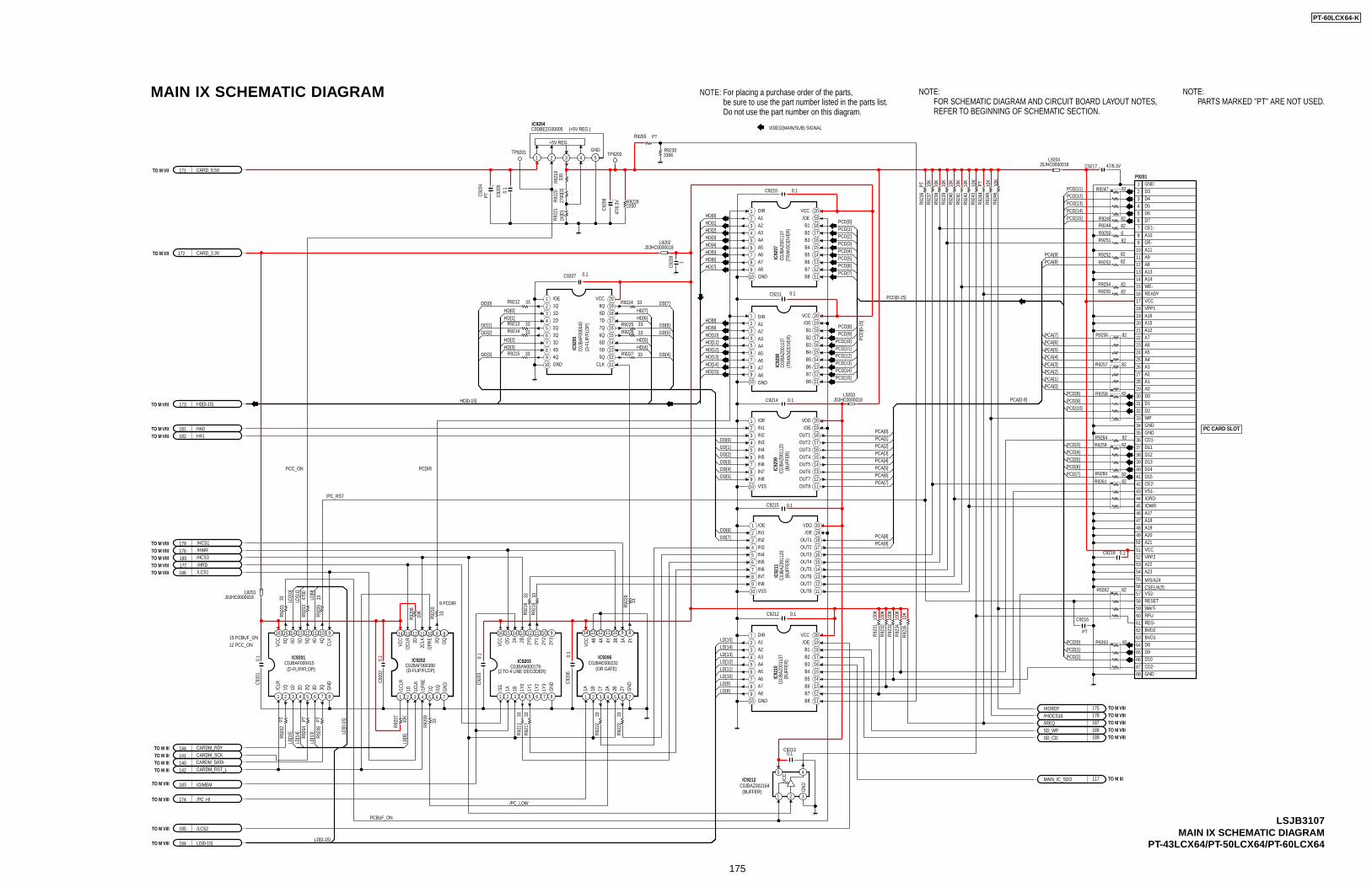
NOTE:FOR SCHEMATIC DIAGRAM AND CIRCUIT BOARD LAYOUT NOTES,REFER TO BEGINNING OF SCHEMATIC SECTION.
NOTE: For placing a purchase order of the parts, be sure to use the part number listed in the parts list. Do not use the part number on this diagram.
NOTE:PARTS MARKED "PT" ARE NOT USED.
MAIN IX SCHEMATIC DIAGRAM
0R9250
82R9253
R9247 82
R9259 82
82R9248
82R9260
R9257 82
R9263 82
CARD_6.5V171
CARD_3.3V172
2200R9228
82R9264
HD[0-15]173
/HCS1179
IO/MEM183
/HWR176
/PC_HI174
82R9251
82R9249
82R9252
82R925582R9254
R9256 82
R9258 82
R9261 82
R9262 82
33R9212
33R9213
33R9214
33R9215 33R9227
33R9226
33R9225
33R9224
33R9
218
33R9
216
33R9
217
33R9
211
33R9
223
33R9
222
33
R922
9
HA0181HA1182
/IREQ 187/HIOCS16 178HIORDY 175
0.1C9214
0.1C9215
0.1C9211
0.1C9210
0.1
C920
6
0.1
C920
3
330KR9230
SD_WP 188
SD_CD 189
LD[0-15]184
/LCS2185
100K
R923
110
0KR9
232
100K
R923
310
0KR9
234
1
C920
9
47/6.3VC9217
10K
R923
710
KR9
238
10K
R923
910
KR9
240
10K
R924
210
KR9
241
PTR9
236
PT
C9216
PTR9
244
10K
R924
5
10K
R924
6
10K
R923
5
0.1C9207
0.1C9212
C0JBAZ002164IC9212
1 2
5
VCC
3G
ND
4
0.1C9213
10K
R924
3
MAIN_IC_SDO 117
47/6
.3V
C920
8PTC920
4
R922
027
00[D
]
0.1
C920
5
TP9201
330
R921
9
TP9202
1K[D
]R9
221
CARDM_RDY144
/HCS3180/HRD177
10K
R920
7
/LCS1186
33
R921
0
0.1
C920
2
CARDM_RST_L142
CARDM_SCK141
0.1
C920
1
PTR9
202
10K
R920
8
PTR9
204
33
R920
9
PTR9
206
33R9
201
33R9
205
CARDM_DATA140
4700
R920
3
C0JBAF000415IC9201
1
/CLR
2
1Q
3
1D
4
2D
5
2Q
6
3D
7
3Q
8
GND
11
4D
12
5Q
13
5D
14
6D
15
6Q
16
VCC
9
CLK
10
4Q
0.1C9218
R9265 PT
P92011 GND2 D33 D44 D55 D66 D77 CE1-8 A109 OE-
10 A1111 A912 A813 A1314 A1415 WE-16 READY17 VCC18 VPP119 A1620 A1521 A1222 A723 A624 A525 A426 A327 A228 A129 A030 D031 D132 D233 WP34 GND35 GND36 CD1-37 D1138 D1239 D1340 D1441 D1542 CE2-43 VS1-44 IORD-45 IOWR-46 A1747 A1848 A1949 A2050 A2151 VCC52 VPP253 A2254 A2355 M/S/A2456 CSEL/A2557 VS2-58 RESET59 WAIT-60 RFU61 REG-62 BVD263 BVD164 D865 D966 D1067 CD2-68 GND
IC9202C0JBAF000380
1
/1CL
R
2
1D
3
1CLK
4
/1PR
E
5
1Q
6
/1Q
7
GND
8
/2Q
9
2Q
10
/2PR
E
11
2CLK
12
2D
13
/2CL
R
14
VCC
IC9206C0JBAE000231
1
1A
2
1B
3
1Y
4
2A
5
2B
6
2Y
7
GND
83Y
9
3A
10
3B
11
4Y
12
4A
13
4B
14
VCC
J0JHC0000018L9203
J0JHC0000018L9201
J0JHC0000018L9204
J0JHC0000018L9202
IC9203C0JBAN000179
1
/1G
2
1A
3
1B
4
1Y0
5
1Y1
6
1Y2
7
1Y3
8
GND
11
2Y1
12
2Y0
13
2B
14
2A
15
/2G
16
VCC
9
2Y3
10
2Y2
IC9204C0DBEZG00005
1 2 3 4 5
IC92
07C0
JBAZ
0011
37
1 DIR
2 A1
3 A2
4 A3
5 A4
6 A5
7 A6
8 A7
9 A8
10 GND 11B812B713B614B515B416B317B218B119/OE20VCC
IC92
08C0
JBAZ
0011
37
1 DIR2 A13 A24 A35 A46 A57 A68 A79 A810 GND 11B8
12B713B614B515B416B317B218B119/OE20VCC
IC92
09C0
JBAZ
0011
20
1 /OE
2 IN1
3 IN2
4 IN3
5 IN4
6 IN5
7 IN6
8 IN7
9 IN8
10 VSS 11OUT812OUT713OUT614OUT515OUT416OUT317OUT218OUT119/OE20VDD
IC92
11C0
JBAZ
0011
20
1 /OE
2 IN1
3 IN2
4 IN3
5 IN4
6 IN5
7 IN6
8 IN7
9 IN8
10 VSS 11OUT812OUT713OUT614OUT515OUT416OUT317OUT218OUT119/OE20VDD
IC92
10C0
JBAZ
0011
37
1 DIR
2 A1
3 A2
4 A3
5 A4
6 A5
7 A6
8 A7
9 A8
10 GND 11B812B713B614B515B416B317B218B119/OE20VCC
IC92
05C0
JBAF
0004
40
1 /OE
2 1Q
3 1D
4 2D
5 2Q
6 3Q
7 3D
8 4D
9 4Q
10 GND 11CLK125Q135D146D156Q167Q177D188D198Q20VCC
HD[3]HD[2]
HD[1] HD[6]
HD[5]HD[4]
DD[0]
DD[1]DD[2]
DD[3] DD[4]
DD[5]DD[6]
DD[7]
DD[0]DD[1]DD[2]DD[3]DD[4]DD[5]
DD[6]DD[7]
HD[0]HD[1]HD[2]HD[3]HD[4]HD[5]HD[6]HD[7]
HD[8]HD[9]HD[10]HD[11]HD[12]HD[13]HD[14]HD[15]
HD[0-15]
HD[0] HD[7]
PCD[0]PCD[1]PCD[2]PCD[3]PCD[4]PCD[5]PCD[6]PCD[7]
PCD[8]PCD[9]
PCD[10]PCD[11]PCD[12]PCD[13]PCD[14]PCD[15]
PCA[0]PCA[1]PCA[2]PCA[3]PCA[4]PCA[5]PCA[6]PCA[7]
PCA[8]PCA[9]
PCA[0]PCA[1]PCA[2]PCA[3]PCA[4]PCA[5]PCA[6]PCA[7]
PCA[8]PCA[9]
PCA[0-9]
LD[0-15]
LD[15]LD[14]LD[13]LD[12]LD[11]LD[10]LD[9]LD[8]
PCD[2]PCD[1]PCD[0]
PCD[7]PCD[6]PCD[5]PCD[4]PCD[3]
PCD[10]PCD[9]PCD[8]
PCD[15]PCD[14]PCD[13]PCD[12]PCD[11]
LD[1
5]
LD[1
3]
LD[1
4]LD
[10]
LD[1
1]
LD[9
]
/PC_LOW
LD[8
]LD[0
-15]
/PC_RST
PCD[
0-15
]
PCD[0-15]
PCDIRPCC_ON
PCBUF_ON
15 PCBUF_ON12 PCC_ON
9 PCDIR
TO M VIII
PC CARD SLOT
TO M VIIITO M VIIITO M VIIITO M VIII
TO M III
TO M VII
TO M VII
TO M VIII
TO M VIIITO M VIII
TO M VIIITO M VIIITO M VIIITO M VIIITO M VIII
TO M IIITO M IIITO M IIITO M III
TO M VIII
TO M VIII
TO M VIII
TO M VIII
(D-FLIP/FLOP) (D-FLIP/FLOP) (2 TO 4 LINE DECODER) (OR GATE)
(BUF
FER)
(BUFFER)(B
UFFE
R)(B
UFFE
R)(T
RANS
CEIV
ER)
(TRA
NSCE
IVER
)
(D-F
LIP/
FLO
P)
(+5V REG.)
+5V REG.GND
VIDEO(MAIN/SUB) SIGNAL
LSJB3107MAIN IX SCHEMATIC DIAGRAM
PT-43LCX64/PT-50LCX64/PT-60LCX64
PT-60LCX64-K
175
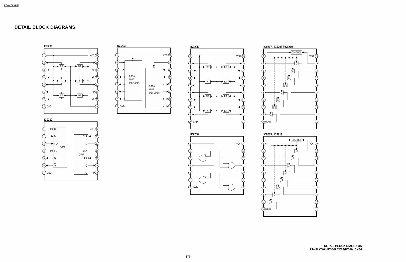
DETAIL BLOCK DIAGRAMS
DETAIL BLOCK DIAGRAMSPT-43LCX64/PT-50LCX64/PT-60LCX64
IC9207 / IC9208 / IC9210
1 20
2
3
4
5
6
7
8
9
10
19
18
17
16
15
14
13
12
11
IC9201
1
2
3
4
5
6
7
8 9
10
16
15
14
13
12
11
IC9202
1
2
3
4
5
6
7 8
9
10
14
13
12
11
IC9206
1
2
3
4
5
6
7 8
9
10
14
13
12
11
IC9203
1
2
3
4
5
6
7
8 9
10
16
15
14
13
12
11
GND
GND
CONTROLVCC
IC9209 / IC9211
1 20
2
3
4
5
6
7
8
9
10
19
18
17
16
15
14
13
12
11GND
CONTROLVCC
IC9205
1 20
2
3
4
5
6
7
8
9
10
19
18
17
16
15
14
13
12
11GND
VCCVCC
GND
VCC
GND
GND
VCC
VCC
F/F
F/F
F/F
F/F
F/F
F/F
F/F
F/F
F/F
F/F
F/F
F/F
F/F
F/F
D-F/F
CLR
D
CLK
PR
Q
Q
D-F/F
2 TO 4LINEDECODER
2 TO 4LINEDECODER
CLR
D
CLK
PR
Q
Q
PT-60LCX64-K
176
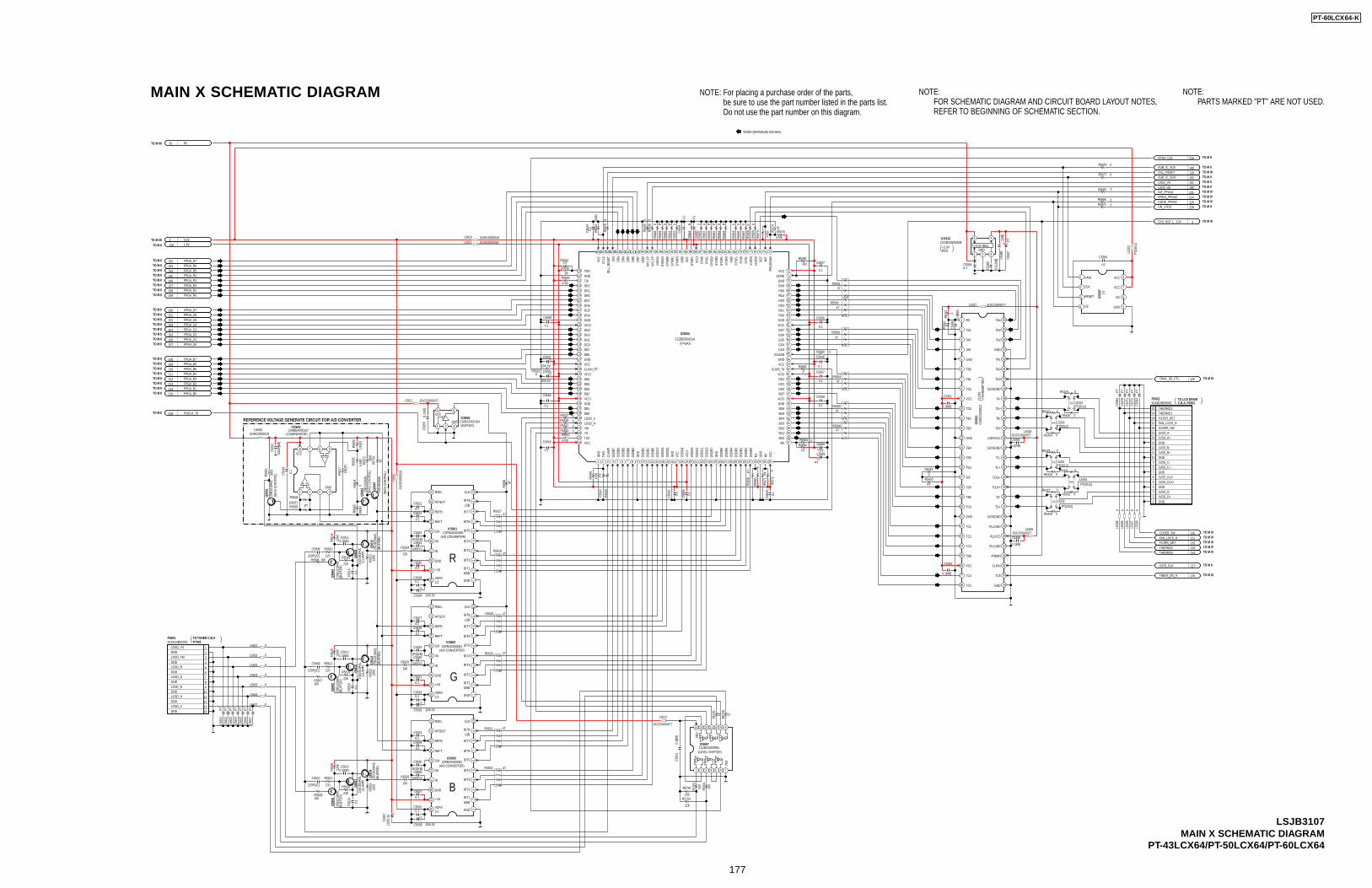
NOTE:FOR SCHEMATIC DIAGRAM AND CIRCUIT BOARD LAYOUT NOTES,REFER TO BEGINNING OF SCHEMATIC SECTION.
NOTE: For placing a purchase order of the parts, be sure to use the part number listed in the parts list. Do not use the part number on this diagram.
NOTE:PARTS MARKED "PT" ARE NOT USED.
MAIN X SCHEMATIC DIAGRAM
0L5607
P5601K1KA14B00003
14GND13LOSD_V12GND11LOSD_H10GND9LOSD_B8GND7LOSD_G6GND5LOSD_R4GND3LOSD_YM2GND1LOSD_YS
0L5603
SYS_RST_L_3.3V TO M III
TIMER_ON_H TO M III2SB1
218A
0LQ
5604
5VTO M VII
0R5427
2200
R561
4 J0JCC0000077L5329
0R5
638
C561
710
0/6.
3V
0L5605
PTR5
652
C56180.1
220P[JC]
C56080.1[KB]
C5369
PTC5
604
C564
2
0.1
0R5
650
2200
R561
6
47R5696
0R560
4
LVDS_HS TO M II
FPGA_G5TO M II
2SD1
819A
SLQ
5613
0.1[KB]C5611
120
R5611
FPGA_G4TO M II
C5624
10P[DC]
100R5607
R5625
150
*
2R2[KB]
C5623
0R5428
0L5
339
L5610 J0JHC0000018
0L5604
FPGA_B4TO M II
PTC5
606
PTC5
603
2200
R562
2
10K[
F]
R560
5
0R5423
0L5606
C5627
0.1
100R5606
0R5639
IC53
11C0
JBCZ
0005
12
1
2
3
4
5
6
7
8
9
10
29
30
31
32
33
34
35
36
11
12
13
14
15
16
17
18
19
20
21
22
37
38
39
40
41
42
43
44
23
24
25
45
46
47
48
49
50
26
27
28
51
52
53
54
55
56
0R5431
C5622
0.1
*
2R2[KB]
C5629
P5302K1KB20B00042
18 FILTER_DET17 FAN_LOCK_H16 COVER_SW15 LVDS_A-14 LVDS_A+13 GND12 LVDS_B-11 LVDS_B+10 GND9 LVDS_C-8 LVDS_C+7 GND6 LVDS_CLK-5 LVDS_CLK+4 GND3 LVDS_D-2 LVDS_D+1 GND
19 THERMO120 THERMO3
FPGA_B6TO M II
C537
0PT
FPGA_R4TO M II
FAN_LOCK_H TO M IV
0L5
338
0R5425
2SB1
218A
0LQ
5606
FPGA_G1TO M II
C5631
0.1
0.1[KB]C5612
0L5
337
0R5432
L5334PT[2012]
1243
0.1[KB]
C5368
0R5680
FPGA_R6TO M II
2200
R562
3
2SD1
819A
0LQ
5611
C5639
0.1
*
2R2[KB]
C5635
0R5
636
0L5
336
PTC5
602
COVER_SW TO M III
FPGA_B5TO M II
0R5426
47
R569
8
0.01
[KB]
C536
5
0R5641
R562847
C5641
10/6.3V
FPGA_B7TO M II
C564
3
0.1
THERMO3 TO M IV
0R5424
FPGA_B2TO M II
R5629 47
0R5633
THERMO1 TO M IV
C53640.1
2SB1
218A
0LQ
5601
C5647
0.1
FPGA_R3TO M II
C5646
PT
PT
R5420
C5633
0.1
C56190.1
0.1
C561
4
L5330PT[2012]12
43
FPGA_G7TO M II
PTC5
601
C5632 10/6.3V
2200
R561
5
0R5637
FPGA_B3TO M II
47R5693
R562747
22K
R5618
0
R5419
FPGA_G6TO M II
PTC5
605
C5634
0.1
PTR5
422
C5640
0.1
L560
9
J0JH
C000
0018
2SB1
218A
0LQ
5605
C537
1PT
2SD1
819A
0LQ
5610
2SD1
819A
SLQ
5612
L5333PT[2012]12
43
0L5
335
IC5603C0FBAD000081
12
34
56
78
91011
1213
1415
1617
1819
20
0.1[
KB]
C536
3
0.1
C561
6
47R5694
L5332
PT[2012]1243
0
R542
1
3.3VTO M VII
0.1[KB]
C5362
R5631 47
0R5
648
FPGA_R7TO M II
120
R5612
220P[JC]
C5609PT
R564
9
FPGA_G2TO M II
SUB_IC_SCK TO M II
0.1[KB]
C5361
FPGA_G0TO M II
0.1
C561
5
POCLK_76TO M II
IC5601C0FBAD000081
12
34
56
78
91011
1213
1415
1617
1819
20
*
C536
61[
KB]
2SD1
819A
0LQ
5609
FPGA_G3TO M II
0R5643
C5637
0.1
FPGA_R1TO M II
R5630 47
2SD1
819A
SLQ
5614
3900
R560
1
10K[
F]
R560
2
FPGA_R2TO M II
2200
R562
1
C56200.1
C5625
0.1
L5331PT[2012]12
43
0R5
645
C5638 10/6.3V
0L5601
C537
2PT
FILTER_DET TO M III
R5684
PT
0.1[KB]C5613
PTC5
367
LVDS_CLK TO M II
R5632 47
22K
R5620
IC5602C0FBAD000081
12
34
56
78
91011
1213
1415
1617
1819
20
LVDS_VS TO M II
0R5430
C5626 10/6.3V
22K
R5619
C539
3PT
FPGA_R0TO M II
R5624
150
J0JCC0000077L5328
47R5692
100R5608
0R5679
PTC5
607
47R5695
C5636
10P[DC]
C5630
10P[DC]
47R5691
120
R5610
C5648
0.1
R5626
150
0L5602
220P[JC]
C5610
FPGA_R5TO M II
0R5
653
C5621
0.1
FPGA_B1TO M II
FPGA_B0TO M II
C0CBCBD00008IC5312
1 2
5
3
4
J0JCC0000077L5327
C5628
0.1
C564
40.
1
SUB_IC_SDO TO M II0R5677
FAN1_SD_CTL TO M III
0R5429
C539
2PT
IC5605C0ABBA000137
1 2 3 4
5678
L5608J0JHC0000018
10K[F]
R5609
3900
R561
32S
B121
8AHL
Q56
02 2SD1
819A
HLQ
5607
20K[
F]
R561
7
PTR5699
*
39R570
0
0.1
C564
9
FPGA_CLK TO M II
C0JBAZ002164IC5606
1 2
5VCC
3GND
4
IC5607C0JBAZ000994
1 2 3 4 5 6 7
891011121314
J0JCC0000077L5611
J0JCC0000077
L5612
22K
R570222K
R5701
0.1[
KB]
C565
0
0.1[
KB]
C565
1
100
R570
3
100
R570
4
22
R570
5
22
R570
6
5.6[
F]
R560
3
C565
2
1000
P[KB
]
IC5604
C1ZBZ0002314
1 2 3 4 5 6 7 8 9 10 11 12 13 14 15 16 17 18 19 20 21 22 23 24 25 26 27 28 29 30 31 32 33 34 35 36
37383940
4142434445464748495051
525354
555657585960616263646566676869
707172
737475767778798081828384858687888990919293949596979899100101102103104105106107108
109110111112113114115116117118119120121122123124125126127128129130131132133134135136137138139140141142143144
PTR5634
L5613 J0JHC0000018
PTR5
647
PT
R5635
PTR5
658
0R5
660
PT
R567
4
4700
R567
3
4700
R5676
PTR5
671
0R5
669
0R5
668
0R5
672
0R5
654
0R5
657
0R5
655
PTR5
659
PTR5
661
0R5
662
PTR5
663
0R5
666
0R5
667
0R5
664
3300
R564
4
4700
R5642
4700
R564
6
4700
R5640
0R5683
0
R5682
300
R5681
C564
50.
1
C5653
10/6.3V
C5654
0.1
C565
5
0.1
C5656
0.1
C5657
0.1
C5659
PT
C5658
0.1
C566
00.
1
0R5
678
/DLL_RESET TO M III
1.8VTO M II
INT_FPGA2 TO M IV
PROG_FPGA2 TO M IV
DONE_FPGA2 TO M IV
C5384
PT
IC53
07 PT
1
2
3
4 5
6
7
8
PT[2
012]
L530
3
0R5685
R5686 0
UN_LOCK TO M IIR5675 0
TC3
TB1
+VS
BIT7
GND
LVDSVCC
TD-CLK
CLK
BIT2
TD+
/IN
VDRV
INT/EXT
TD2
CLKIN
IN
MSB
REFT
TD1
RSEL
TB-
TC4GND
BIT6
REFB
CLK
LSB
IN
LVDSGND
BIT2
BIT3
LSB
TA3
TB4
B
GND
3.3
3.3
TC+
TD6
TA4
TA2
RS
TC-
BIT6
/IN
TA-
BIT1
TD5
GND
LSB
TC1
BIT4
TB2
LVDSGND
BIT1
BIT4
TB6
TB5
BIT5
/IN
INT/EXT BIT8
TA6
BIT3
TD4
TA0
TA+
3.3
R/F
PLLGND
BIT3
PLLGND
G
TCLK+
TC0
BIT5
GND
MSB
BIT7
TA5
BIT2
BIT8
MSB
CM
GND
BIT5
+VS
/PDWN
TB0
TC6
CM
TCLK-
BIT4
GND
TB3 TB+
TD3
VDRV
RSEL
+VS
CM
LVDSGND
VCC
GND
VDRV
PLLVCC
BIT1
GND
REFT
RSEL
IN
TC5
R
VCC
TA1GND
TD0
REFT
BIT7
GND
REFB
BIT6
INT/EXT
TC2
REFB
BIT8
VSS
VDD
YS
HDIN
V
DG4
BO4
VCCI
VCCI
CLKIN_76
DG6
SYSF
0
GO3
TMS
RO4
CCLK
SYS1
GO7
GND
CLKIN_FP
GND
SYM
F0
SYM
1
VCC
GND
LOSD_V
OSD
R2
VCC
DR4
RO6
CLAM
P
RO1
OSD
G4
OSD
R3
DG0
DR2
OSD
B7
DB2
OSD
G1
DB4
OSD
G2
SYM
R0
OSD
R7
SYM
R1
DB6
OSD
B6
GND
BO6
OSD
B5
DB3
OSD
G5
GO5
OSD
R5
HIN_
FPO
SDB0
RO2
HLVD
S
SYM
0
OSD
B1
OSD
R4
GND
RO0
SYM
AO RO7
OSD
R1
/CLEAR
DR5
VLVD
S
GND
OSD
G7
OSD
B3
OSD
B2
DB7
SYSF
1
OSD
G0
YM
TDI
OSD
R6
GND
BO1
GND
DG2
SYSA
O
TDO
GO1
GND
OSD
B4
GND
GND
TCK
/DLL
_RES
ET
DG1
SYS0
BO0M2
OSD
G6
RO5DR1
GND
DB1
GO2
DR3
BO2
VCCI
OSD
R0
LOSD_H
SYSR
1
VCCI
GO6
DB5
DB0
GO4
/PRO
GRA
M
DONE
SYSR
0
GND
VCC
VCCI
OSD
G3
DR6
DG7
BO5
VIN_
FP
GND
GO0
INIT
SYM
F1
RO3
BO3
GND
GND
DR0
DG3
DG5
BO7
DIN
DR7
VCC
VCC
M1
M0
VCCI
VCC
VCCI
VCC
VCC
VCCI
RESET
CE
CLK
NC
VCC
VCC
GND
DATA
216
149128150191190225224226228
3
129
130131132133134
217
135
55
1116
192193194195196197198199
200201202203204205206207
208209210211212213214215
218
(FPGA2)
TO LCD DRIVEC.B.A. P2501
+3.3VREG.
+3.3V REG.
LVDS
TRAN
SMIT
TER
(LEVEL SHIFTER)
(A/D CONVERTER)
(A/D CONVERTER)
(A/D CONVERTER)
TO TUNER C.B.AP7004
(BIA
S CO
NTRO
L)
(BIA
S CO
NTRO
L)
(BIA
S CO
NTRO
L)
(BUF
FER)
(BUF
FER)
(CLA
MP)
(COMPARATOR)
(CLA
MP)
(BUF
FER)
(BUF
FER)
(BUF
FER)
(CLA
MP)
(BUF
FER)
(BUFFER)
GND
GND
VCC
VIDEO (MAIN/SUB) SIGUNAL
REFERENCE VOLTAGE GENERATE CIRCUIT FOR A/D CONVERTER
LSJB3107MAIN X SCHEMATIC DIAGRAM
PT-43LCX64/PT-50LCX64/PT-60LCX64
PT-60LCX64-K
177
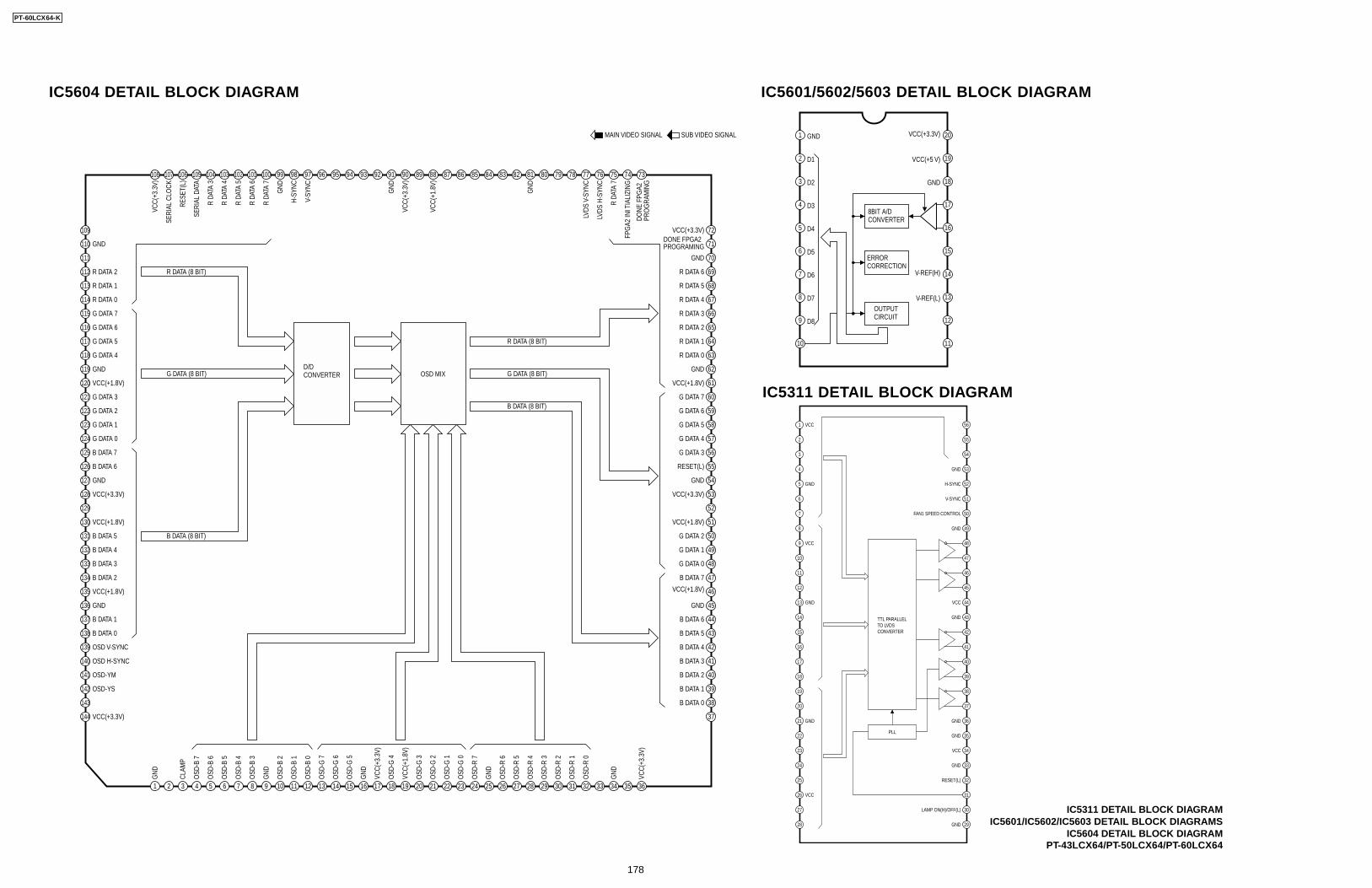
1 2 3 4 5 6 7 8 9 10 11 12 13 14 15 16 17 18 19 20 21 22 23 24 25 26 27 28 29 30 31 32 33 34 35 36
37
38
39
40
41
42
43
44
45
46
47
48
49
50
51
52
144
143
142
141
140
139
138
137
136
135
134
133
72
71
70
69
68
67
66
65
64
63
62
61
60
59
58
57
56
55
54
53
84 83 82 81 80 79 78 77 76 75 74 73
132
131
130
129
128
127
126
125
124
123
122
121
120
119
118
117
116
115
114
113
112
111
110
109
108 107 106 105 92 91 90 89 88 87 86 85104 103 102 101 100 99 98 97 96 95 94 93
VCC(
+1.8
V)
VCC(
+3.3
V)
OSD
-R 0
OSD
-R 1
OSD
-R 2
OSD
-G 0
OSD
-G 1
OSD
-G 2
OSD
-G 3
OSD
-G 5
OSD
-G 6
OSD
-G 7
OSD
-B 5
OSD
-B 4
OSD
-B 3
OSD
-B 6
OSD
-B 7
CLAM
P
OSD
-B 0
OSD
-B 1
OSD
-B 2
OSD
-G 4
OSD
-R 3
OSD
-R 4
OSD
-R 5
OSD
-R 6
OSD
-R 7
GND
GND
RESET(L)
VCC(+1.8V)
VCC(+3.3V)
VCC(+1.8V)
VCC(+1.8V)
VCC(+1.8V)
VCC(+3.3V)
VCC(
+3.3
V)
RESE
T(L)
SERI
AL C
LOCK
SERI
AL D
ATA
B DATA 0
B DATA 1
B DATA 4
B DATA 3
B DATA 2
G DATA 0
G DATA 1
G DATA 2
G DATA 3
B DATA 7
B DATA 6
R DATA 0
R DATA 1
R DATA 2
R DA
TA 3
R DA
TA 4
H-SY
NC
V-SY
NC
VCC(
+3.3
V)
VCC(
+1.8
V)
R DA
TA 5
R DA
TA 6
R DA
TA 7
G DATA 5
G DATA 4
G DATA 6
G DATA 7
B DATA 5
OSD-YS
OSD-YM
VCC(+3.3V)
OSD H-SYNC
OSD V-SYNC
GND
GND
GND
GND
GND
GND
GND
DONE
FPG
A2PR
OG
RAM
ING
DONE FPGA2 PROGRAMING
R DA
TA 7
FPG
A2 IN
I TIA
LIZI
NG
LVDS
V-S
YNC
LVDS
H-S
YNC
VCC(
+3.3
V)
VCC(+3.3V)
VCC(+1.8V)
VCC(+1.8V)
D/DCONVERTER OSD MIX
GND
GND
GND
GND
GND
MAIN VIDEO SIGNAL SUB VIDEO SIGNAL
GND
GND
R DATA 6
R DATA 5
R DATA 4
R DATA 3
G DATA 7
G DATA 6
G DATA 5
G DATA 4
G DATA 3
G DATA 2
G DATA 1
G DATA 0
B DATA 7
B DATA 6
B DATA 5
B DATA 4
B DATA 3
B DATA 2
B DATA 1
B DATA 0
R DATA 2
R DATA 1
R DATA 0
R DATA (8 BIT)
R DATA (8 BIT)
G DATA (8 BIT)
B DATA (8 BIT)
G DATA (8 BIT)
B DATA (8 BIT)
IC5604 DETAIL BLOCK DIAGRAM
1
2
3
4
5
6
7
8
9
10 11
12
13
14
15
16
17
18
19
20GND
GND
VCC(+3.3V)
VCC(+5 V)
V-REF(H)
V-REF(L)
D1
D2
D3
D4
D5
D6
D7
D8
OUTPUT CIRCUIT
8BIT A/DCONVERTER
ERRORCORRECTION
IC5601/5602/5603 DETAIL BLOCK DIAGRAM
IC5311 DETAIL BLOCK DIAGRAM
1
2
3
4
5
6
7
8
9
10
11
12
13
14
15
16
17
18
19
20
21
22
23
24
25
26
27
28
56
55
54
53
52
51
50
49
48
47
46
45
44
43
42
41
40
39
38
37
36
35
34
33
32
31
30
29
GND
GND
GND
LAMP ON(H)/OFF(L)
RESET(L)
FAN1 SPEED CONTROL
V-SYNC
VCC
VCC
VCC
VCC
VCC
H-SYNC
GND
GND
GND
GND
GND
GND
GND
TTL PARALLEL TO LVDS CONVERTER
PLL
IC5311 DETAIL BLOCK DIAGRAMIC5601/IC5602/IC5603 DETAIL BLOCK DIAGRAMS
IC5604 DETAIL BLOCK DIAGRAMPT-43LCX64/PT-50LCX64/PT-60LCX64
PT-60LCX64-K
178
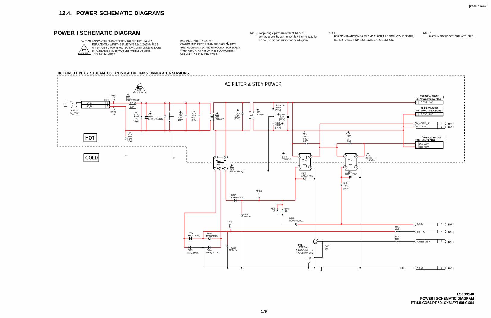
12.4. POWER SCHEMATIC DIAGRAMS
NOTE:FOR SCHEMATIC DIAGRAM AND CIRCUIT BOARD LAYOUT NOTES,REFER TO BEGINNING OF SCHEMATIC SECTION.
NOTE: For placing a purchase order of the parts, be sure to use the part number listed in the parts list. Do not use the part number on this diagram.
NOTE:PARTS MARKED "PT" ARE NOT USED.
POWER I SCHEMATIC DIAGRAMCAUTION: FOR CONTINUED PROTECTION AGAINST FIRE HAZARD,
REPLACE ONLY WITH THE SAME TYPE 6.3A 125V/250V FUSE.ATTENTION: POUR UNE PROTECTION CONTINUE LES RISQUESD’ INCENDIE N’ UTILISERQUE DES FUSIBLE DE MÉMETYPE 6.3A 125V/250V6.3A 125V/250V
IMPORTANT SAFETY NOTICE:COMPONENTS IDENTIFIED BY THE SIGN HAVESPECIAL CHARACTERISTICS IMPORTANT FOR SAFETY.WHEN REPLACING ANY OF THESE COMPONENTS,USE ONLY THE SPECIFIED PARTS.
LSJB3148POWER I SCHEMATIC DIAGRAM
PT-43LCX64/PT-50LCX64/PT-60LCX64
C806 0.47[250V]
B0HAGP000012D808
SW17V 3
C8081000P[250V]
RL801TSEH0019
4 1
2 3
1KR805
Q8012SD1819AHL
TP801PT
PTTP804
PTTP809
1KR806
PTTP803
C8134700P[250V]
C803 0.47[250V]
P807
1
D809MA2C16700E
D801ERZV10V361CS
STBY_9V 4
1000/25VC805
L803LSLQ0081-1
L802LSLF0077
B0HAGP000012D807
MA2Q73600LD803
R80710K
TP802PT
P808
1
10[5W]
R809R801 8.2M[1/2W]
RL802TSEH0019
1 4
2 3
MA2Q73600LD806
C811 0.47[250V]
POWER_ON_H 5
TV_AC120V_S 1
R802 470K[1/2W]
270R810
C8091000P[250V]
1000/16VC804
D810MA2C16700E
MA2Q73600LD804
MA2Q73600LD805
R8084700
TV_AC120V_R 2
P_GND 6
C802 0.47[250V]
P804
21
F801LSSF0013B63T
T801ETP28KBZA1QG
1 2 3
46
P805
21
WA15TP810
6.3A125V/250V
D_TNR_120V
D_TNR_120V
6.3A
LSJA0456
LCD_120V
AC_CORD
[1/2W]
LCD_120V
AC_INAC_IN
TO BALLAST C.B.A.P1302, P1303
SWITCHING POWER ON-ON
TO P II
TO P II
TO P II
TO P II
TO P IITO P II
HOT CIRCUIT. BE CAREFUL AND USE AN ISOLATION TRANSFORMER WHEN SERVICING.
HOT
AC FILTER & STBY POWER
COLD
TO DIGITAL TUNERPOWER C.B.A. P1201
TO DIGITAL TUNERPOWER C.B.A. P1201
PT-60LCX64-K
179
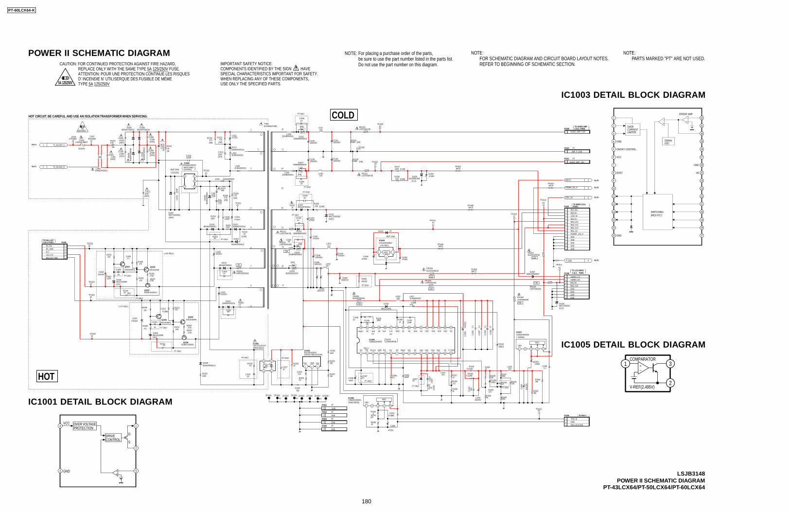
NOTE:FOR SCHEMATIC DIAGRAM AND CIRCUIT BOARD LAYOUT NOTES,REFER TO BEGINNING OF SCHEMATIC SECTION.
NOTE: For placing a purchase order of the parts, be sure to use the part number listed in the parts list. Do not use the part number on this diagram.
NOTE:PARTS MARKED "PT" ARE NOT USED.
POWER II SCHEMATIC DIAGRAMCAUTION: FOR CONTINUED PROTECTION AGAINST FIRE HAZARD,
REPLACE ONLY WITH THE SAME TYPE 5A 125/250V FUSE.ATTENTION: POUR UNE PROTECTION CONTINUE LES RISQUESD’ INCENDIE N’ UTILISERQUE DES FUSIBLE DE MÉMETYPE 5A 125/250V5A 125/250V
IMPORTANT SAFETY NOTICE:COMPONENTS IDENTIFIED BY THE SIGN HAVESPECIAL CHARACTERISTICS IMPORTANT FOR SAFETY.WHEN REPLACING ANY OF THESE COMPONENTS,USE ONLY THE SPECIFIED PARTS.
LSJB3148POWER II SCHEMATIC DIAGRAM
PT-43LCX64/PT-50LCX64/PT-60LCX64
COMPARATOR
V-REF(2.495V)
1
2
3
IC1005 DETAIL BLOCK DIAGRAM
1
2
3
4
5
6
7
8
9
10
11
12
13
14
15
16
32
31
30
29
28
27
26
25
24
23
22
21
20
19
18
17
GND
GND
GND
VCC
SWITCHING(MOS FET)
ERROR AMP
250kHzOSC
OVERCURRENTLIMITER
ON/OFF CONTROL
BOOT VB
IC1003 DETAIL BLOCK DIAGRAM
4 1
2
53
OVER VOLTAGEPROTECTION
DRIVECONTROL
VCC
GND
D
S
IC1001 DETAIL BLOCK DIAGRAM
PTC1047
2.2
C106
5
C105
647
0/25
V
0.01C1055
10K[D]R1061
10R107
0
0.1C1048
1000PC1054
2.2
C106
7
1/50VC1059
22R1054
PTC1
069
0.1[1W]R1044
390R1064
15UL1015
0.1[1W]R1043
10U
C106
3
1M
R1036
IC1003C0DBAJG00006
1 2 3 4 5 6 7 8 9 10
272829303132 1920212223242526
11 12 13 14 15 16
1718 2.2
C106
8
1KR1056
22R1057
330R1053
MA2J11300L
D1024
D1027PT
1000
PC1
057
820/
25V
C106
0
3300R1047
47R1069
1KR1059
2200R1049
390R1063
270R1058
3900R1039
PTR1048
470PC1066
1/50VC1046 220
R10460.1C1051
270R1055
820/25VC1058
0.47C1034
1KR1026
D1001MAZ41500MF
C10411000/35V
0.1C1061
Q10012SD1819AHL
1200R1038
TP1020
TP1011PT
C10060.1
P_GND 6
TV_AC120V_R2
TP1010PT
330R1032
C10403300/10V
PTR1025
P1001
54321
P10111
100/35VC1020
P1007
1413121110987654321
Q1006B1BDCG000011
R10030.82
PTR1019
1000
PC1
017
C10120.1[KB]
3300R1015
B0HARM000063D1018
B0HAHP000014D1013
R1041470
TP1013PT
C1003
PT
D1016B0JBSG000024
22UL1013
R10072700
4700P[250V]
C1008
10KR1033
B0HAHP000014D1020
R101247K
C10351000/35V
D1022MAZ730000BC
ZP1001
4700P[250V]
C1004
TP1021 R10301200
R1004PT
75R1023
C1002470/25V
1000
PC1
064
C104947/25V
EYF52BCZ1002
MAZ40510MFD1026
Q10042SD1819AHL
0.1[KB]C1053
680R1017
C1019220P[1KV]
ZP1005
IC1004C0CAAHG00012
1 3
2
C10393300/10V
D100
5BO
AAKT
0000
10
TP1012PT
P1003 PT
1
D1002BOAAKT000010
10R1027
C1037470/25V
C10214.7/25V
1500R1021
C10094700P[250V]
B0HAHP000014D1008
47/25V
C1050
ZP1006
2200PC1016
D1007MAZ730000BC
R100547K
PTC1027
C1010
PT
2200R1016
P1006
321
R101147K
100/35VC1062
R102247K
27KR1014
PT
ZP1004
3300R1031
P1008
87654321
B0HAGP000012D1010
Q10022SD1819AHL
IC1007C0DAZHH00006
1 2 3 4 5
T1001ETS39AG3T3ND
1
2
3
4
5
6
7
8
9
10
11
12
18
13
14
15
16
17
POWER_ON_H 4
820/
200V
C101
4IC1001
C5HABZZ00103
5
2
3
14
47/25VC1045
PTC1025
TP1022
R10132700
STBY_9V 5
47/25VC1052
B0HAGP000012
D1015
C10381000/25V
R1010PT
2700R1052
D1021B0HBRM000019
C10010.082
[250V]
PTC1029
L1011
0R1040
1KR1029
PTC1031
MAZ70620BCD1028
PTC1030
3300/10VC1044
D1019B0HBRM000019
D1004BOAAKT000010
PTTP1004
PTC1028
PTC1023
L1010
33[1W]R1050
D100
9B0
JAG
E000
001
PTC1026
D1017B0HBRM000019
680R1028
D100
3BO
AAKT
0000
10
P1002 PT
1
100/35VC1022
SW17V 3
JOHBLH000001L1001
B0HAGP000012D1012
ZP1003
TP1014PT
0.33R1060
3.3R1024
R10421K
2700R1051
0.33R1020
47/50VC1024
R1008220
P1005 PT
1
1800R1035
TP1023
R1001220
Q1003B1BDCG000011
B1AZKD000001IC1005
1 2 3
D1011B0HAHP000014
PTC1032
C101
510
00P
P10091
P10101
Q10052SD1819ARS
10UL1012
R1009470
PT
ZP1007
B0HAHP000014D1014
PT
ZP1002
D1023 PT
1200R1037
C10361000/35V
C1043470/25V
TP1025
EYF52BCZ1001
ZP1008
R101847K
4700P[250V]
C1005PTTP1005
C0DAZGG00001IC1006
1 2 3 4 5
C10421000/35V
TP1024
D1006MAZ41500MF
R100647K
R10021200
1800R1034
P1004 PT
1
PTTP1003
TV_AC120V_S1
1200PC1018
C103347/50V
C1011 470P[250V]
C1007470/25V
10UL1016
10UL1014
B0ECKP000007D1029
F1001LSSF0013B50T
J0JHB0000021L1004
L1017J0JHB0000021
L1008J0JHB0000021
J0JKA0000015L1005
L1003 J0JKA0000015
L1009J0JHB0000021
PR1013LSSF009A100E
PR1011LSSF009A70E
PR1005LSSF009A25E
PR1003LSSF009A25E
B1ZAZ0000016PR1007
PR1006LSSF009A25E
D4FA1R000003PR1001
B1ZAZ0000016PR1008
PR1010LSSF009A70E
PR1012LSSF009A70E
PR1004B1ZAZ0000016
CNC1S101R1KTIC1002
1
23
4
WA15TP1015
WA15TP1007
WA15TP1008
WA15TP1006
WA7.5TP1009
5A125V/250V
VDD
PT ONLY
Vcc
NC
S/S
amp
[1/2
W]
VGL
VGH VDD
Vboot
amp(-)out
VDD
Vout P_GNDOCL(+)
GND3.3VNC NC
F/B
Vref
VoutNC
PT ONLY
NC
/5V
PT ONLY
VDD
OCL(-)GND Vout NC
NC
Vout
NC
R/C
Vb
HEAT SINK
POWER _ON_H
1.5A
[3W]
PT ONLY GND
REG 3.3V
[FIN]
PT ONLY
DC_GND GND
10U
PT ONLY
GND
AUDIO_AMP_+16V
GND
10U
GND
GND
UNREG 12V
FAN +B
GND
[1/2W]
[1/2W]
GND
1.5A
PT ONLY
BALLAST GND
[FIN]
STBY 9V
PT ONLY
REG 30V
2.5A
Vref
PT ONLY
REG 5V
LSSC0562
GND
DC 19VGND
[3W]
PT ONLY
[FIN]
GND
Vout
PT ONLY
REG 9V
2.5A
GND
1A
[1W]
[8G]
2W
PT ONLY
5W
PT ONLY
REG 5V
1.5A
AUDIO_AMP_-16V
HEAT SINK
REG 6.5V
GND
AMP_P_GND
REG -5V
VCC 17V
[2W]
FAN LOCK [NC]
[1/2W]
PT ONLY
5A/250V
GND
2.5A
[2W]
[FIN]
PT ONLY
[1/2W]
REG 3.3V
UNREG 17V
[1W]
N C
GND
REG 3.3V
SWITCHINGCONTROL
DC/DCCONVERTER
TO BALLASTC.B.A. P1301
(SHUNT REGULATOR)
TO AUDIO AMPC.B.A. P4501
TO P I
TO P I
TO P I
TO MAIN C.B.A.P3401
TO LCD DRIVE C.B.A. P2901
TO P I
( )TO FAN 4
(FAN4 DRIVE) GNDREG.
HOT CIRCUIT. BE CAREFUL AND USE AN ISOLATION TRANSFORMER WHEN SERVICING.
HOT
TO P I
TO P I
COLD
GNDREG.
(FEED BACK)
REG.
(+9V REG.)
+5V REG.( )
(300V)(300V)
(5.1V)
(6.2V)
PT
PT
(15V)
(15V)
10A(+19V REG.)
(+17V REG.)
PT-60LCX64-K
180
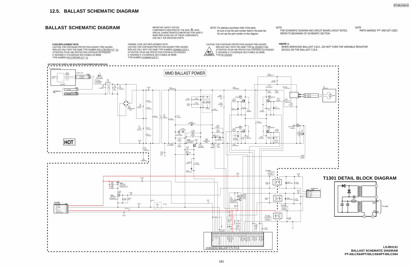
12.5. BALLAST SCHEMATIC DIAGRAM
NOTE:FOR SCHEMATIC DIAGRAM AND CIRCUIT BOARD LAYOUT NOTES,REFER TO BEGINNING OF SCHEMATIC SECTION.
NOTE: For placing a purchase order of the parts, be sure to use the part number listed in the parts list. Do not use the part number on this diagram.
NOTE:PARTS MARKED "PT" ARE NOT USED.
BALLAST SCHEMATIC DIAGRAM
THERMAL FUSE UNIT REPLACEMENT NOTE:CAUTION: FOR CONTINUED PROTECTION AGAINST FIRE HAZARD,REPLACE ONLY WITH THE SAME TYPE NUMBER LSJA0464 (115 ).ATTENTION: POUR UNE PROTECTION CONTINUE LES RISQUESD’ INCENDIE N’ UTILISERQUE DES FUSIBLE DE MÉMETYPE NUMÉRO LSJA0464 (115 )
F1302 REPLACEMENT NOTE:CAUTION: FOR CONTINUED PROTECTION AGAINST FIRE HAZARD,REPLACE ONLY WITH THE SAME TYPE NUMBER K5C117BC0003 (117 ).ATTENTION: POUR UNE PROTECTION CONTINUE LES RISQUESD’ INCENDIE N’ UTILISERQUE DES FUSIBLE DE MÉMETYPE NUMÉRO K5C117BC0003 (117 )
IMPORTANT SAFETY NOTICE:COMPONENTS IDENTIFIED BY THE SIGN HAVESPECIAL CHARACTERISTICS IMPORTANT FOR SAFETY.WHEN REPLACING ANY OF THESE COMPONENTS,USE ONLY THE SPECIFIED PARTS.
CAUTION: FOR CONTINUED PROTECTION AGAINST FIRE HAZARD,REPLACE ONLY WITH THE SAME TYPE 5A 125/250V FUSE.ATTENTION: POUR UNE PROTECTION CONTINUE LES RISQUESD’ INCENDIE N’ UTILISERQUE DES FUSIBLE DE MÉMETYPE 5A 125/250V5A 125/250V
2
1
3 4
Low
High
To Lamp
T1301 DETAIL BLOCK DIAGRAM
PTC1
313
270P/1KVC1312
B0ECKP000007D1304
2SB1219ARLQ1301
75K[1/2W]R1313
31 30 29 28 27 26 25 24 23 22 21 18 17 16 15 14 13 12 11 10 9 8 7 6 5 4 3 2 11920
TP1304
B0FABR000003D1308
10KR1338
D1305MA727000C
B0ECKP000007D1310
0.47[2W]R1317
TP1307
68[1/4W]R1331
L1305J0KA00000020
10KR1318
0.01[KB]C1303
B1DEGQ000011Q1309
470[1/4W]
R1324
B1DEGQ000011Q1308
10KR1332
220P/630VC1322
82KR1328
0.01[KB]C1331
D1302
-+
~
~B0FBBR000004
MA2J111008D1316
47UL1307
680R1343
2200
[1/4
W]
R134
2
5600PC1326
3900P/1KVC1328
ELF20N030AL1301
MA2J111008D1317
1000/220VC1306
0.01U/630VC1319
1.2U/400VC1311
B1DEGQ000011Q1304
680R1341
EULSPJ004AT1301
1
4
2
3
39K[1/4W]R1325
TP1305
0.1U/400VC1310
6.2K[3W]R1339
8200R1306
10KR1308
P1305
4321
2SD1
819A
HL
Q13
05
5600PC1329
1.2U/400VC1316
TP1301
B1DEGQ000011Q1306
75K[1/2W]R1312
39K[1/4W]R1326
P13031
6.2K[3W]R1340
MA727000CD1313
470K[1/2W]R1301
PTD1314
120/25VC1321
0.47/250V
C1302
B1DFCQ000001Q1310
PTR1327
L1303LSLQ0291
PTR1315
B0ECKP000007D1306
0.47[2W]R1323
10KR1335
PTC1
314
PTC131
8
1000/220VC1305
1000P/630VC1323
TP1302
120/
25V
C132
0
0.47[2W]R1316
0.01[KB]C1332
75K[1/2W]R1310
100R1329
0R1314
G0ZZ00002195L1310
68[1/4W]R1337
0.47/250VC1301
2SD1819AHLQ1302
8200R1307
68[1/4W]R1336
68[1/4W]R1330
1000P/250VC1307
L1306600UH
G0A601J00011
VLPS0083L1304
J0JHB0000021
5600PC1327
PTD1312
22KR1309
10KR1333
MA727000CD1311
L1309J0JHB0000021
0.33[2W]R1322
22/50V[GE]C1317
B2ZAZ0000020
D1315
B0ECKP000007D1303
MAZ
7270
00C
D131
8
TP1303
0.1u/450VC1330
L1308J0JHB0000021
TP1306
2200PC1304
75K[1/2W]R1311
R1321500
L1302J0JHB0000021
0.1U/400VC1309
470[1/4W]
R1344
P13021
G0ZZ00002173L1311
B1DEGQ000011Q1307
B0ECKP000007D1309
P130112345
1000P/630VC1324
220P/630VC1325
PTC1
315
10KR1334
MA2Q73600LD1307
R131910[1/2W]
100[1/2W]R1320
2200PC1334
10[1W]R1345
270P/1KVC1335
270P/1KVC1333
L1312J0JHB0000021
L1313J0JHB0000021
0.1[
KB]
C133
6
P1306
21
LSSF0013B50TF1301
K5C117BC0003F1302
CNC1S101R1KTIC1303
2
14
3
CNC1S101R1KTIC1302
2
1 4
3
CNC1S101R1KTIC1304
2
14
3
5A 125V/250V
LSJA0464
INV2
_GAT
E
LAM
P_ER
R
TEST
[FIN]
LAM
P_O
N
DC+19V
INV2
_VCC
PT ONLY
THER
MIS
TOR
MA1Z270
BALL
AST
GND
[1%]
[FIN]
INV1
_GAT
E
AC_IN(L1)
NC
GND
N C
AC_IN(N)
W/O DAC
PT ONLY
VCC+
19V
IlaNC NC NC
2
DC_GND
L
LAMP [+]
VCC+
17V
CLM
-
INV3
_GAT
E
INV1
_VCC
AC_IN(L2)
PT ONLY
BALL
AST
HOT
GND
MA1Z270
LAM
P G
ND
L_ON
CTLNC NC
[FIN]
VCC+17V
PT ONLY
5A 125V/250V
[1%]
PT O
NLY
HV_O
N
U1301(E31) BALLAST CTL P.C.B
1
H
Vout
DC/D
C_O
N_H
INV2
_GND
INV1
_GND NC
[FIN]
TO TEMP_FUSE
STBY_L
BALLAST GND
L_ERR
[FIN]
Vla
INV4
_GAT
E
AC_IN(L)
LAMP [-]
BALL
AST
GND
(2KV)
THERMAL FUSE UNIT
Z0002LSLQ0392
TO POWER C.B.A.P805
HOT
SWITCHINGPOWER ON-ON
SWITCHINGPOWER ON-ON
(SWITCHING)
(SW
ITCH
ING
)
OPTICALISOLATOR
OPTICALISOLATOR
OPTICALISOLATOR
TO MAIN C.B.A.P6002
(IGNITER)
LAMP UNIT
LAMP
HOT CIRCUIT. BE CAREFUL AND ISOLATION TRANSFORMER WHEN SERVICING.
TO POWERC.B.A. P1001
PT
MMD BALLAST POWER
THERMAL FUSE 117 (243 )
THERMAL FUSE
*NOTE 1
LSJB3131BALLAST SCHEMATIC DIAGRAM
PT-43LCX64/PT-50LCX64/PT-60LCX64
NOTE 1: WHEN SERVICING BALLAST C.B.A., DO NOT TURN THE VARIABLE RESISTOR (R1321) ON THE BALLAST C.B.A.
*
PT-60LCX64-K
181
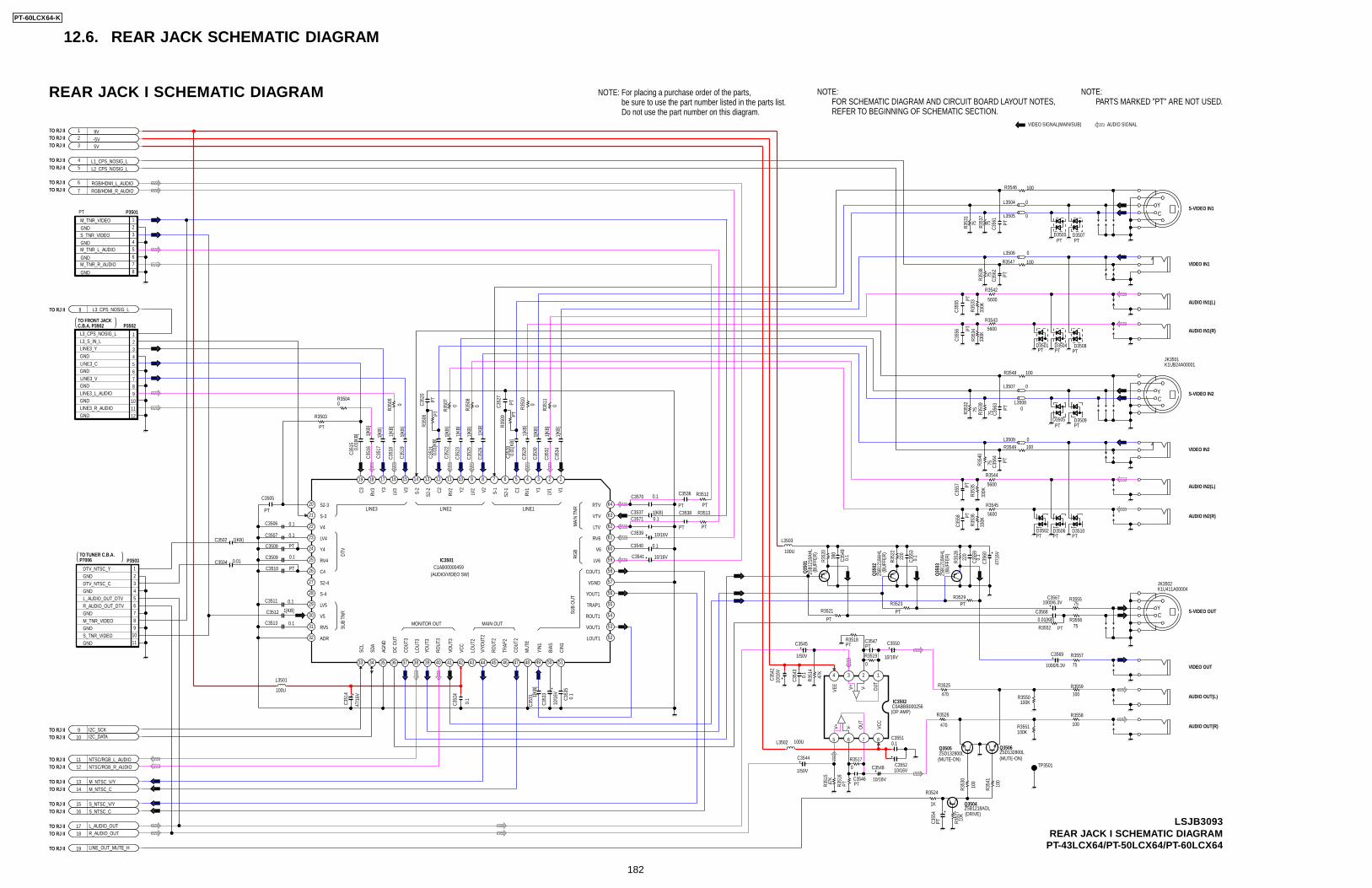
12.6. REAR JACK SCHEMATIC DIAGRAM
NOTE:FOR SCHEMATIC DIAGRAM AND CIRCUIT BOARD LAYOUT NOTES,REFER TO BEGINNING OF SCHEMATIC SECTION.
NOTE: For placing a purchase order of the parts, be sure to use the part number listed in the parts list. Do not use the part number on this diagram.
NOTE:PARTS MARKED "PT" ARE NOT USED.
REAR JACK I SCHEMATIC DIAGRAM
Q35
022S
B121
8AHL
75R353
1
0.01
[KB]
C352
8
5V3
PTR351
6
100
R353
0
5600
R3544
75R353
9
C35671000/6.3V
PT
C355
7
PTR3518
C354
210
/16V
R355575
330K
R353
6
C353
3
10/1
6V
PTC3546
0.01
[KB]
C351
5
C3504
5600
R3543
C3569
1000/6.3V
0.01
[KB]
C352
1
C3568
0.01[KB]
R3558
100
0.1
C354
9
PT
C355
8
PT
C356
2
10/16V
C3550
100U
L3503
75R353
2
100KR3550
470
R3525
10/16V
C3548
Q35
032S
B121
8AHL
Q35
012S
B121
8AHL
330K
R353
5
R351
4
47K
PT
C355
5
100U
L3501
75R353
7
C3506 0.1
C3513 0.1
PTD3507
C3511 0.1
PT
C356
3
47/1
6V
C351
4
R3559
100
R3557
75
0.1
C355
3
R352
0
390
2SD132800LQ3506
R355675
2SD132800LQ3505
R352
8
220
PTC3547
9V1
C3544
1/50V
C354
3
0.1
PT
C356
1
C355210/16V
0.1
C355
9
0
R3517
5600
R3545
75R354
0
5600
R3542
0
R3519
R351
547
K
75
R353
8
0.1
C352
4
47/1
6V
C356
0
R352
2
220
C35510.1
100KR3551
PT
C356
4
PT
C355
6
100
R354
133
0K
R353
4
330K
R353
3
0.1
C353
5
C3545
1/50V
PTD3505
470
R3526
1[KB
]C3
534
1[KB
]C3
526
C351
71[
KB]
C351
91[
KB]
1[KB]C3537
1[KB
]C3
531
1[KB
]C3
523
1[KB
]C3
530
0R3504
0
R350
5
0
R350
7
0
R350
8
0
R351
1
PT
R3512
PT
R3513
PTD3503
PTD3508
PTD3504
PTD3501
PTD3509
PTD3510
PTD3506
PTD3502
0
R351
0
100UL3502
TP3501
PT
R3503 PT
R350
6 PT
R350
9
PTR3552
PT
R3521 PT
R3523 PTR3529
C3502
C3512 1[KB]
C3539 10/16V
C3541 10/16V
0.1C3540
I2C_SCK9I2C_DATA10
L2_CPS_NOSIG_L5L1_CPS_NOSIG_L4
M_NTSC_V/Y13M_NTSC_C14
S_NTSC_C16S_NTSC_V/Y15
NTSC/RGB_R_AUDIO12NTSC/RGB_L_AUDIO11
R_AUDIO_OUT18
L_AUDIO_OUT17
L3_CPS_NOSIG_L8
RGB/HDMI_R_AUDIO7
RGB/HDMI_L_AUDIO6
C3507 0.1
C3509 0.1
100R3546
100R3547
100R3548
100R3549
2SB1218AOLQ35041K
R3524
10K
R352
7
PTC355
4
P3501
8GND
7M_TNR_R_AUDIO6GND
5M_TNR_L_AUDIO4GND
3S_TNR_VIDEO
2GND
1M_TNR_VIDEO
P3502
12GND11LINE3_R_AUDIO10GND9LINE3_L_AUDIO8GND7LINE3_V6GND5LINE3_C4GND3LINE3_Y2L3_S_IN_L1L3_CPS_NOSIG_L
LINE_OUT_MUTE_H19
-5V2
C3510 PT
C3508 PT
P3503
11GND
10S_TNR_VIDEO
9GND
8M_TNR_VIDEO
7GND
6R_AUDIO_OUT_DTV
5L_AUDIO_OUT_DTV
4GND3DTV_NTSC_C2GND1DTV_NTSC_Y
1[KB
]C3
532
1[KB
]C3
529
C351
61[
KB]
C351
81[
KB]
C3538
PT
C3536
PT
1[KB
]C3
525
1[KB
]C3
522
C3570
C3571PTC3
527
PT
C3505
PT
C352
0
IC3501C1AB00000459
12345678910111213141516171819
20
21
22
23
24
25
26
27
28
29
30
31
32
33 34 35 36 37 38 39 40 41 42 43 44 45 46 47 48 49 50 51
52
53
54
55
56
57
58
59
60
61
62
63
64
C0ABBB000256IC3502
1234
5 6 7 8
0L3505
0L3504
0L3506
0L3508
0L3507
0L3509
OUT
LINE2
VCC
MONITOR OUT
LINE3
VEE
V+
V-
C
OUT
DTV
LINE1
V-
Y
RGB
SUB
OUT
V+
MAI
N TN
R
MAIN OUT
C1V2
S2-1S-1
LV3
S-2V3 LV2C2
S2-2 Y2
RV2 V1LV1Y1
RV1Y3
RV3C3
S2-3
LV4
S-3
V4
C4
Y4
S-4
S2-4
RV4
V5
RV5
LV5
ADR
VCC
SCL
AGND
SDA
COUT
3
DC O
UT
MUT
E
TRAP
2
LOUT
3
YOUT
3
ROUT
3
VOUT
3
V/YO
UT2
ROUT
2
LOUT
2
COUT
2
LTV
YIN1
RTV
VGND
V6
LV6
ROUT1
YOUT1
LOUT1
COUT1
BIAS
RV6
CIN1
VOUT1
TRAP1
VTV
YC
YC
SUB
TNR
JK3502K1U411A00004
JK3501K1UB24A00001
AUDIO SIGNALVIDEO SIGNAL(MAIN/SUB)
VIDEO IN1
AUDIO IN1(R)
AUDIO IN1(L)
S-VIDEO IN1
S-VIDEO IN2
VIDEO IN2
AUDIO IN2(L)
AUDIO IN2(R)
S-VIDEO OUT
VIDEO OUT
AUDIO OUT(L)
AUDIO OUT(R)
(BUF
FER)
(BUF
FER)
(BUF
FER)
(OP AMP)
(AUDIO/VIDEO SW)
TO TUNER C.B.A.P7006
TO FRONT JACKC.B.A. P3902
TO RJ IITO RJ IITO RJ II
TO RJ IITO RJ II
TO RJ IITO RJ II
TO RJ II
TO RJ IITO RJ II
TO RJ IITO RJ II
TO RJ IITO RJ II
TO RJ IITO RJ II
TO RJ IITO RJ II
TO RJ II
(DRIVE)
(MUTE-ON)(MUTE-ON)
PT
1[KB]
0.01
0.1
0.1
LSJB3093REAR JACK I SCHEMATIC DIAGRAM
PT-43LCX64/PT-50LCX64/PT-60LCX64
PT-60LCX64-K
182
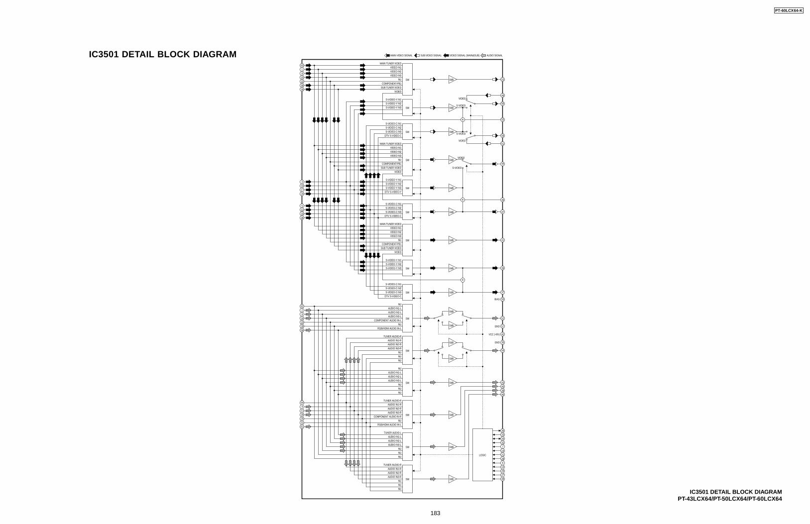
IC3501 DETAIL BLOCK DIAGRAM
IC3501 DETAIL BLOCK DIAGRAMPT-43LCX64/PT-50LCX64/PT-60LCX64
VCC (+9V)
GND
BIAS
6318
15223030
3101724
5121926
50
35
GND 57
42
54
52
6229
16232959
644
1118253161
6dB
6dB
6dB
6dB
6dB
6dB
6dB
MAIN VIDEO SIGNAL
SW
SW
SW
SW
SW
SW
SW
SW
SW
SW
SW
SW
SW
SW
LOGIC
SW
53
49
56
55
58
51
44
46
47
41
6dB 39
6dB
6dB
6dB
6dB
6dB
6dB
0dB
6dB
0dB
37
43453840
363334327
1421286
13202748
SUB VIDEO SIGNAL VIDEO SIGNAL (MAIN&SUB) AUDIO SIGNAL
MAIN TUNER VIDEO
SUB TUNER VIDEO VIDEO
VIDEO
VIDEO
VIDEO IN1VIDEO IN2VIDEO IN3
COMPONENT-PB1NU
MAIN TUNER VIDEO
SUB TUNER VIDEO
S-VIDEO-Y IN1
VIDEO IN1VIDEO IN2VIDEO IN3
COMPONENT-PB1
MAIN TUNER VIDEO
SUB TUNER VIDEO
VIDEO IN1VIDEO IN2VIDEO IN3
COMPONENT-PB1
NU
DTV S-VIDEO-Y
S-VIDEO-Y IN2S-VIDEO-Y IN3
S-VIDEO-Y IN1S-VIDEO-Y IN2S-VIDEO-Y IN3
S-VIDEO-Y IN1 VIDEO
S-VIDEO
VIDEO
VIDEO
S-VIDEO
S-VIDEO
S-VIDEO-Y IN2S-VIDEO-Y IN3
S-VIDEO-C IN1
NU
S-VIDEO-C IN2S-VIDEO-C IN3
S-VIDEO-C IN1
NUAUDIO IN1-L
DTV S-VIDEO-C
NURGB/HDMI AUDIO IN-L
S-VIDEO-C IN2S-VIDEO-C IN3
S-VIDEO-C IN1
DTV S-VIDEO-C
S-VIDEO-C IN2S-VIDEO-C IN3
AUDIO IN2-LAUDIO IN3-L
COMPONENT AUDIO IN-L
NUAUDIO IN1-L
NUNU
AUDIO IN2-LAUDIO IN3-L
NU
TUNER AUDIO-LAUDIO IN1-L
NUNU
AUDIO IN2-LAUDIO IN3-L
NU
TUNER AUDIO-RAUDIO IN1-R
NURGB/HDMI AUDIO IN-L
AUDIO IN2-RAUDIO IN3-R
COMPONENT AUDIO IN-R
TUNER AUDIO-RAUDIO IN1-R
NUNU
AUDIO IN2-RAUDIO IN3-R
NU
TUNER AUDIO-RAUDIO IN1-R
NUNU
AUDIO IN2-RAUDIO IN3-R
NU
DTV S-VIDEO-C
PT-60LCX64-K
183
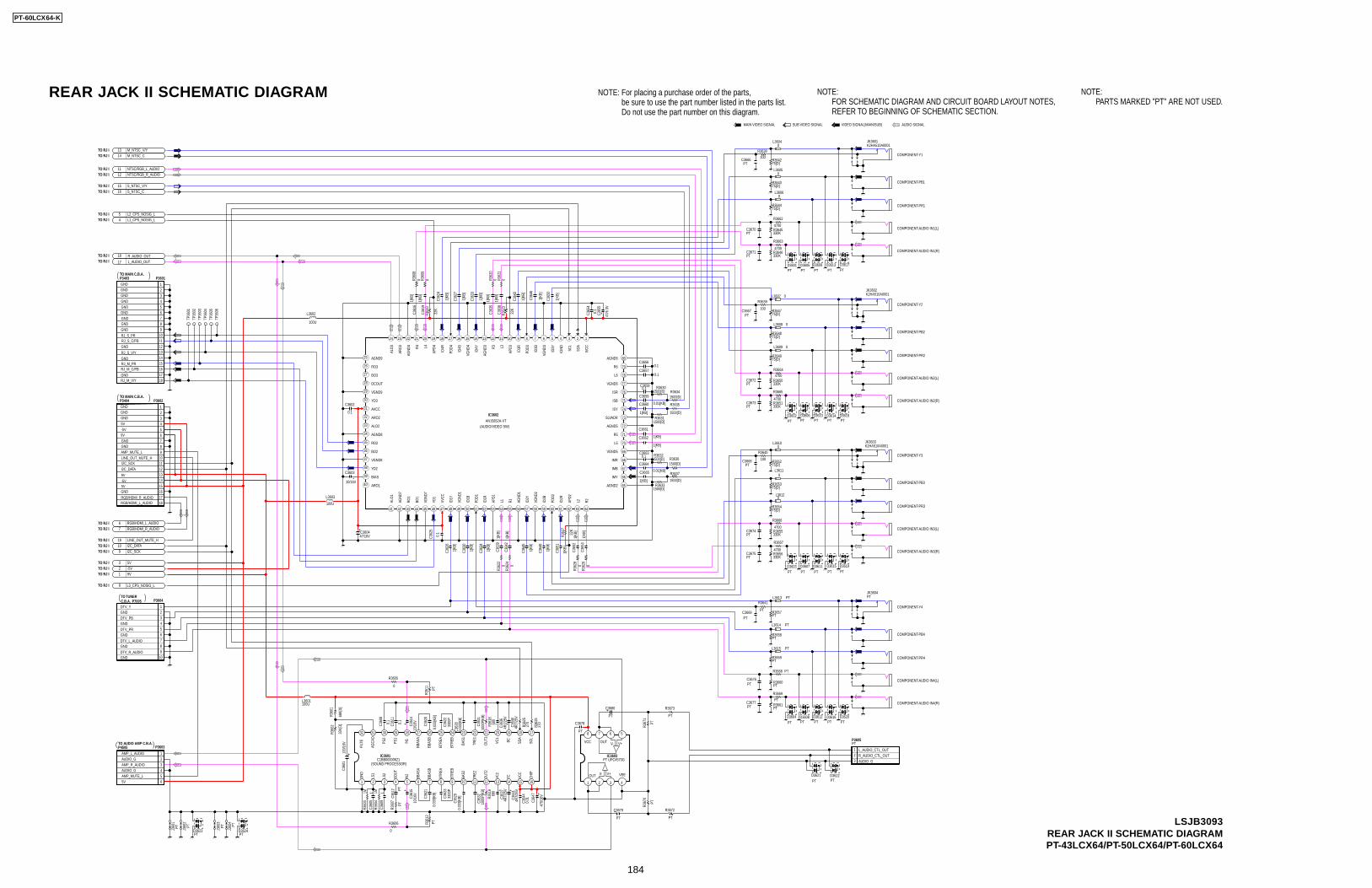
NOTE:FOR SCHEMATIC DIAGRAM AND CIRCUIT BOARD LAYOUT NOTES,REFER TO BEGINNING OF SCHEMATIC SECTION.
NOTE: For placing a purchase order of the parts, be sure to use the part number listed in the parts list. Do not use the part number on this diagram.
NOTE:PARTS MARKED "PT" ARE NOT USED.
REAR JACK II SCHEMATIC DIAGRAM
LSJB3093REAR JACK II SCHEMATIC DIAGRAMPT-43LCX64/PT-50LCX64/PT-60LCX64
75[D]R3648
PTD3609
PTD3614
75[D]R3642
L2_CPS_NOSIG_L5
PTD3618
L1_CPS_NOSIG_L4
75[D]R3644
75[D]R3643
PTD3606
75[D]R3647
47/16VC3604
PTD3617
PTD3610
L3_CPS_NOSIG_L8
0.1
C3602
75[D]R3649
PTD3613
PTD3605
PTD3616
PTD3611
PTD3615
PTD3607
PTD3619
75[D]R3653
PTD3612
75[D]R3654
75[D]R3652
PTR3657
PTD3620
PTR3659
PTD3608
PTR3658
L_AUDIO_OUT17
R_AUDIO_OUT18
100
R3638
100
R3639
100
R3640
PT
R3641
PTC3666
PTC3667
PTC3668
PTC3669
PTD3601
PTD3602
PTD3603
PTD3604
PT
R3669
PTR3668
4700
R3667
4700
R3666
4700
R3665
4700
R3664
4700
R3663
4700
R3662
330KR3645
330KR3646
330KR3650
330KR3651
330KR3655
330KR3656
PTR3660
PTR3661PT
C3677
PTC3676
PTC3675
PTC3674
PTC3673
PTC3672
PTC3671
PTC3670
1[KB
]
C362
6
1[KB
]
C363
0
1[KB
]
C363
4
1[KB
]
C364
5
1[KB
]
C364
8
1[KB
]
C365
1
1[KB
]
C363
3
1[KB
]
C362
7
1[KB
]
C362
4
1[KB
]
C364
3
1[KB
]
C364
6
1[KB
]
C365
0
0R360
8
0R360
9
0R362
0
0R362
10
R362
2
0R3
624
0R3
628
0R3
629
M_NTSC_C14
NTSC/RGB_L_AUDIO11NTSC/RGB_R_AUDIO12
M_NTSC_V/Y13
S_NTSC_V/Y15S_NTSC_C16
0.1
C362
5
100U
L3603
22K
R362
3
22K
R361
0
22K
R362
7
100U
L3602 0.1
C365
4
47/6
.3V
C365
5
10/16V
C3603 0.01[KB]
C3664
0.01[KB]
C3659
1[KB]
C3660
1[KB]
C3665
1500[D]
R3637
1500[D]R3636
1500[D]
R3635
1500[D]R36341500[D]
R3630
1500[D]R3631
1500[D]R3632
1500[D]R3633
0.1C3658
0.1C3663
0.1C3656
0.1C3657
5V3
9V1
I2C_SCK9I2C_DATA10
-5V2
RGB/HDMI_R_AUDIO7RGB/HDMI_L_AUDIO6
LINE_OUT_MUTE_H19
270
R362
5
680
R361
9
4R7/
25V
C363
6
0.03
3[KB
]C3
629
100/
16V
C360
1
680
R361
8
270
R362
6
0.03
3[KB
]
C362
1
3300
PC3
622
1MR3
604
0.03
3[KB
]
C362
0
PT
R360
7
0.1
C361
1
R361
2
PT
0.01
C364
4
3300
PC3
623
4R7/
25V
C364
0
1MR3
603
R361
1
PT
4R7/
25V
C364
1
4R7/
25V
C363
7
1000
P[KB
]C3
632
0.1
C360
8
470/
16V
C364
7
R3605
0
1000
P[KB
]C3
63168
K[D]
R360
1
IC3601C1BB00000621
1
GND
2
LS1
3
LS2
4
SOUT
5
IN2
6
BBAS
A
7
BBAS
B
8
BTRE
A
9
BTRE
B
10
BAS2
27
BBAS
A
28
IN1
29
PS1
30
PS2
31
AGCA
D
32
FILT
E
19
BC
20
VC1
21
OUT
1
22
TRE1
23
BAS1
24
BTRE
B
25
BTRE
A
26
BBAS
B
11
TRE2
12
OUT
2
13
VC2
14
TC
15
VCC
16
CHIP
17
SCL
18
SDA
33K[
D]
R360
2
PT
C361
2
R3606
0
0.03
3[KB
]C3
628
100UL3601
P3601
18RJ_M_V/Y17GND
16RJ_M_C/PB15RJ_M_PR
14GND
13RJ_S_V/Y
12GND11RJ_S_C/PB10RJ_S_PR
9GND8GND7GND6GND5GND4GND3GND2GND1GND
P3602
18RGB/HDMI_L_AUDIO17RGB/HDMI_R_AUDIO
16GND155V
14-5V
139V
12I2C_DATA11I2C_SCK10LINE_OUT_MUTE_H9AMP_MUTE_L8GND7GND69V5-5V45V3GND2GND1GND
C3679
PT
R367
0
PT
C3680
PT
PT
C3678
R367
1
PT
PTD3621
PTD3622
R3673
PT
R3672
PT
10/1
6VC361
410
/16VC3
615
P3604
10GND
9DTV_R_AUDIO
8GND
7DTV_L_AUDIO
6GND
5DTV_PR
4GND
3DTV_PB
2GND
1DTV_Y
1C3
605
1C3
609
P3605PT
3 AUDIO_G
2 R_AUDIO_CTL_OUT
1 L_AUDIO_CTL_OUT
1[KB
]C3
619
1[KB
]C3
635
1[KB
]C3
616
1[KB]
C3661
1[KB]
C3662
1[KB
]C3
638
1[KB
]C3
639
1[KB
]C3
642
1[KB
]C3
652
1[KB
]C3
653
PTD3623
PTD3624
P3603
65V5AMP_MUTE_L4AUDIO_G3AMP_R_AUDIO2AUDIO_G1AMP_L_AUDIO
TP36
04TP
3603
TP36
06
TP36
02
TP36
05
TP36
01
IC3602
AN15852A-VT
123456789101112131415161718192021222324
25
26
27
28
29
30
31
32
33
34
35
36
37
38
39
40
41 42 43 44 45 46 47 48 49 50 51 52 53 54 55 56 57 58 59 60 61 62 63 64
65
66
67
68
69
70
71
72
73
74
75
76
77
78
79
80
PT UPC4570GIC3603
1 2 3 4
5678
0L3607
0L3608
0L3609
0L3604
0L3605
0L3606
0L3610
0L3611
0L3612
J360
4PT
J360
3PT
J360
2PT
J360
1PT
PTL3613
PTL3614
PTL3615
IVCCSD
A
SCL
IGND
VGND
3
ID3Y
ID3B
PDD3
ID3R
APD3R3 L3
AGND
3
ID4Y
VGND
4
ID4B
ID4R
PDD4
APD4L4R4
AGND
4
ALO
3
ARO
3
ARO1
BIAS
VGND8
YO2
BO2
RO2
AGND8
ALO2
AVCC
ARO2
YO3
VGND9
DCOUT
BO3
AGND9
RO3
AGND
1
R1APD1
L1ID1R
PDD1
ID1B
VGND
1
VVCC
ID1Y
YO1
VGND
7
BO1
RO1
ALO
1
AGND
7
VGND
2
ID2B
PDD2
ID2R
L2APD2
R2ID2Y
AGND2
IMY
IMR
IMB
VGND5
L5
R5
AGND5
ISY
SLVADR
ISB
ISR
VGND6
L6
AGND6
R6
OUT VEE
V-
V- V+
OUTVCC V+
JK3604PT
JK3603K2HA510A0001
JK3602K2HA510A0001
JK3601K2HA510A0001
TO MAIN C.B.A.P3403
TO RJ ITO RJ I
TO RJ ITO RJ I
TO RJ ITO RJ I
TO RJ ITO RJ I
TO RJ ITO RJ I
TO MAIN C.B.A.P3404
AUDIO SIGNALVIDEO SIGNAL(MAIN/SUB)MAIN VIDEO SIGNAL SUB VIDEO SIGNAL
TO RJ ITO RJ I
TO RJ ITO RJ ITO RJ I
TO RJ I
TO RJ ITO RJ I
TO RJ I
(AUDIO/VIDEO SW)
(SOUND PROCESSOR)
COMPONENT-Y1
COMPONENT-PB1
COMPONENT-PR1
COMPONENT-AUDIO IN1(L)
COMPONENT-AUDIO IN1(R)
COMPONENT-AUDIO IN2(L)
COMPONENT-AUDIO IN2(R)
COMPONENT-PB2
COMPONENT-Y2
COMPONENT-PR2
COMPONENT-AUDIO IN3(L)
COMPONENT-AUDIO IN3(R)
COMPONENT-PB3
COMPONENT-Y3
COMPONENT-PR3
COMPONENT-AUDIO IN4(L)
COMPONENT-AUDIO IN4(R)
COMPONENT-PB4
COMPONENT-Y4
COMPONENT-PR4
TO AUDIO AMP C.B.A.P4505
TO TUNERC.B.A. P7005
PT-60LCX64-K
184
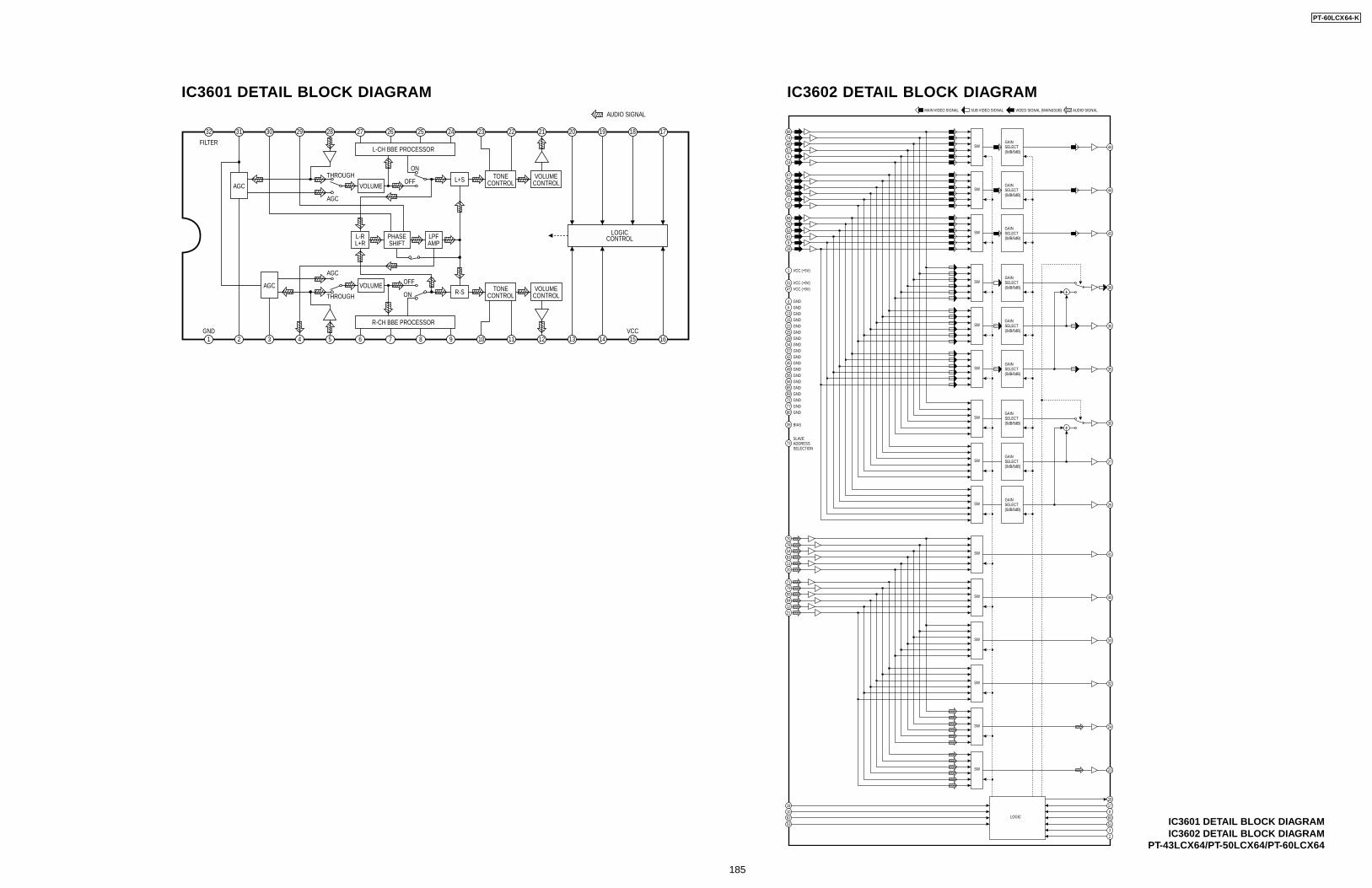
IC3601 DETAIL BLOCK DIAGRAM
IC3601 DETAIL BLOCK DIAGRAMIC3602 DETAIL BLOCK DIAGRAM
PT-43LCX64/PT-50LCX64/PT-60LCX64
1 2 3 4 5 6 7 8 9 10 11 12 13 14 15 16
17181920212223242526272829303132
VCC
LOGICCONTROL
R-CH BBE PROCESSOR
L-RL+R
AGC
AGC
THROUGH
THROUGH
AGC
ON
OFF
ON
OFF
AGC
LPFAMP
PHASESHIFT
R-SVOLUME
TONECONTROL
TONECONTROL
VOLUMECONTROL
VOLUMECONTROL
L-CH BBE PROCESSOR
L+SVOLUME
GND
FILTER
AUDIO SIGNAL
VCC (+9V)VCC (+9V)
VCC (+5V)
BIAS
SLAVE ADDRESSSELECTION
GNDGNDGNDGNDGNDGNDGNDGNDGNDGNDGNDGNDGNDGNDGNDGNDGNDGNDGND
MAIN VIDEO SIGNAL
SW
LOGIC
667448575
14
36
281786051
19106253
32
SUB VIDEO SIGNAL VIDEO SIGNAL (MAIN&SUB) AUDIO SIGNAL
SW
677550597
16
SW
687652619
18
1
3147
46
1315222529343742454956586569727780
39
73
46
44
43
36
38
35
SW
SW
SW
SW
SW
SW
27
30
26
41
40
SW
707854631120
SW
SW
SW
717955641221
SW
SW
33
32
24
23
GAINSELECT(0dB/6dB)
GAINSELECT(0dB/6dB)
GAINSELECT(0dB/6dB)
GAINSELECT(0dB/6dB)
GAINSELECT(0dB/6dB)
GAINSELECT(0dB/6dB)
GAINSELECT(0dB/6dB)
GAINSELECT(0dB/6dB)
GAINSELECT(0dB/6dB)
IC3602 DETAIL BLOCK DIAGRAM
PT-60LCX64-K
185
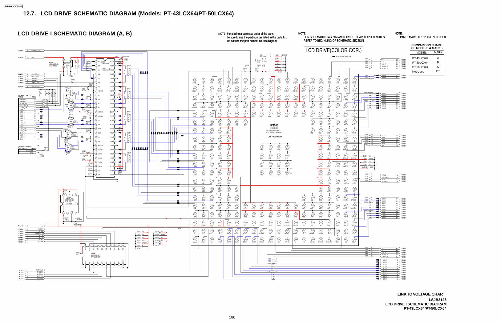
12.7. LCD DRIVE SCHEMATIC DIAGRAM (Models: PT-43LCX64/PT-50LCX64)
NOTE:FOR SCHEMATIC DIAGRAM AND CIRCUIT BOARD LAYOUT NOTES,REFER TO BEGINNING OF SCHEMATIC SECTION.
NOTE: For placing a purchase order of the parts, be sure to use the part number listed in the parts list. Do not use the part number on this diagram.
NOTE:PARTS MARKED "PT" ARE NOT USED.
LCD DRIVE I SCHEMATIC DIAGRAM (A, B) NOTE:FOR SCHEMATIC DIAGRAM AND CIRCUIT BOARD LAYOUT NOTES,REFER TO BEGINNING OF SCHEMATIC SECTION.
NOTE: For placing a purchase order of the parts, be sure to use the part number listed in the parts list. Do not use the part number on this diagram.
NOTE:PARTS MARKED "PT" ARE NOT USED.
D_RESET10
SD_DATA16
SD_SCK15
CORRECT_CS12
+3.3V9
STSQO_G 46
GOUT3 53
GOUT8 48
SH_CLK_G 44
BOUT9 62
BOUT7 64
GOUT7 49
BOUT0 71
BOUT2 69
GOUT9 47
BOUT3 68
GOUT2 54
XFR_G 43
GOUT4 52
GOUT0 56
BOUT1 70
GOUT1 55
GOUT5 51
BOUT6 65
GOUT6 50
BOUT5 66
BOUT8 63
BOUT4 67
ENB1 41
ENB4 38ENB3 39ENB2 40
CLX 37
DX 42
XFRP 45
DY 58
CLY 57
NRG 22
47R2528
47R2527
47R2526
47R2525
47R2524
22R2515
47R2516
47R2523
+5V2
0.1C2515
0.1
C2513
0.1C2519
0.1C2521
0.1C2522
47R2514
10/10VC2514
10/10VC2516
10/10VC2523
0.1C2520
P2501
18FILTER_DET17FAN_LOCK_H16COVER_SW15LVDS_A-14LVDS_A+13GND12LVDS_B-11LVDS_B+10GND9LVDS_C-8LVDS_C+7GND6LVDS_CLK-5LVDS_CLK+4GND3LVDS_D-2LVDS_D+1GND
19THERMO1
20THERMO3100R2518
100R2519
100R2520
100R2521
100R2522
L2509PT[2012]
12
43
0R2512
0R2513
L2505PT[2012]
12
43
0R2504
0R2505
L2508PT[2012]
12
43
0R2510
0R2511
0R2509
0R2502
0R2503
L2504PT[2012]
12
43
L2507PT[2012]
12
43
0R2508
C0CBCBD00008IC2502
1 2
5
3
4
C250
91[
KB]
0.01[KB]C2508
PTC2
510
C25070.1
CORRECT_ON_L1
C25180.1 STSQO_B 60
XFR_B 59
SH_CLK_B 61
FAN1_SD_CTL8100KR2517
10/10VC2512
TIMER_ON_H7
SD_DATA_O17SD_SCK_O18
SH_CSR11
SH_CSR_O21
IC2504C0JBAZ001137
1 2 3 4 5 6 7 8 9 10
11121314151617181920
SH_CSG_O20
SH_CSG13
SH_CSB_O19
SH_CSB14
IC2505C1AB00001945
ROUT1 35
ROUT8 28
ROUT3 33
STSQO_R 26
ROUT9 27
FRP 23
ROUT0 36
SH_CLK_R 25
ROUT4 32ROUT5 31
XFR_R 24
ROUT7 29
ROUT2 34
ROUT6 30
47R2564
47R2562
47R256047R2558
68R254268R2541
68R254047R2539
22R254822R254922R255022R255122R255222R2553
68R255547R2554
68R255768R2556
47R2565
47R2563
47R2561
47R2559
47R254347R254468R254568R254668R2547
47R2537
47R2536
47R2534
47R2535
PTC2517
47R2538
0R2531
0R2529
PTR2530
20KR2532
75R2533
C25400.01
C254
10.
1
0.1[KB]C2502
PTC2
501
PTC2
503
PTC2
504
FILTER_DET4
C2537 0.1
C2539
10/10V
C2538 0.1
C2535 0.1
C2554 0.1
C2556 0.1
C2557 0.1
C2558 10/10V
C2527 0.1
C2526 0.1
C2529 0.1
C2528 0.1
C2531
10/10V
0R2501
2R2[KB]C2505
1
C2506
470P[KB]C2511
2R2[KB]C2530
2R2[KB]C2536
2R2[KB]C2555
THERMO_36THERMO_15
FAN_LOCK_H3
PTC2
559
PTC2
560
IC2503C0ZBZ0000850
1
2
3
4
5
6
7
8
9
10
29
30
31
32
33
34
35
36
11
12
13
14
15
16
17
18
19
20
21
22
37
38
39
40
41
42
43
44
23
24
25
45
46
47
48
49
50
26
27
28
51
52
53
54
55
56
L2512J0JCC0000077
100L2515
L2514J0JCC0000077
L2511J0JCC0000077
100L2502100L2516
L2513 J0JCC0000077
100L2501
100L2503
L2510J0JHC0000018
P2502
21
2R2[KB]C2547
C2542
10/10V
C2544 0.1
C2543 0.1
C2545 0.1
C2546 0.1
MM1561JFBEIC2501
C0DBFFD00003
1 2 3 4
567
RC3
RD6
RC4
RC5
RC6
RD0
GND
LVDSGND
LVDSGND
LVDSGND
PLLGND
PLLGND
PLLVCC
/PDWN
RA-
RA+
RB+
RB-
LVDSVCC
RC-
RC+
RD-
RD+
RCLK-
RCLK+
CLKOUT
RA0
GND
VCC
RC2
RC1
VCC
VCC
VCC
GND
GND
GND
RC0
RD4
RD5
RB6
RB3
RB4
RB5
RD2
RD3
RB2
RA6
RB0
RB1
RA4
RD1
RA5
RA3
RA1
RA2
DIR
A1 A2 A3 A4 A5 A6 A7 A8 GND
B2
XOE B1 B8B3 B7B6B4 B5VC
C
COVER_SWGND
GND
TMS TDI TRST HPLL DCLK HRESETO NC CPOUT VCOIN VSEL DIRY NRG ENBX3R DXOUTR CLYOUTR DIRXRN FRPR XFRR STSQER ROUT9
ROUT8NCSHCLKRVDD2DIRXRDYOUTRMONRENBX2RCLXOUTRNCTESTVDDPSELECTCLP1VRESETOHSYNCVSYNCTDOTCKOSDSW
OSDRIN0 OSDRIN1 GND NC NC NC NC CLP2 EN GNDP SHENB ENBX4R ENBX1R NC NC NCNC GND STSQOR ROUT7
ROUT6ROUT5NCGNDGNDGNDVDD2VDD2VDD2VDD2VDD2 VDD2VDD2GND GND GND GNDOSDBIN0OSDGIN1OSDGIN0
RIN9 OSDBIN1 VDD2 GND GNDGNDGND VDD2 VDD2 VDD2 VDD2VDD2 VDD2VDD2 NCGND GNDGND ROUT3 ROUT4
ROUT1 ROUT2GND GNDGND NCGND GNDGND GNDTEST4RIN8RIN7
RIN4 RIN5 RIN6 VDD1 VDD1 GND GNDGND NC NC ROUT0
RIN1 RIN2 RIN3 VDD1 VDD1 VDD1 VDD1 NC CLXOUTG NC
NC NC RIN0 VDD1 VDD1 GND GNDGNDGND VDD1 VDD1 ENBX4G ENBX3G ENBX2G
GIN9 GIN8 GIN7 VDD1VDD1 GNDGNDGND GND VDD1 VDD1 NC ENBX1G DXOUTG
GIN6 GIN5 GIN4 VDD1 VDD1 GNDGND GNDGND VDD1 VDD1 DYOUTG CLYOUTG MONG
DIRXGN
FRPG
NC
STSQOG
GOUT8
GOUT6
GOUT4
GOUT2
GOUT0NC
GOUT7
GOUT1
GOUT3
GOUT5
GOUT9
STSQEG
SHCLKG
DIRXGNC
XFRG
NC
NC
NC
NC
GND
NC
TEST1
VDD1VDD1
VDD1VDD1
VDD1VDD1
GND GNDGND GND
GND GNDGND GND
GND GNDGND GND
VDD2
NC
CLXOUTBENBX3B
ENBX4B
NC NC NC
ENBX2B
ENBX1B
NC
NCNCNC DIRXBNSHCLKBSTSQEBBOUT8BOUT6BOUT4BOUT2BOUT0
NC BOUT7BOUT5BOUT3BOUT1 STSQOB NC FRPB DYOUTB MONB
DXOUTB
VDD2VDD2VDD2VDD2VDD2VDD2VDD2
VDD2VDD2 VDD2 VDD2VDD2VDD2 VDD2
CLYOUTBDIRXBXFRBBOUT9NCNCNCVDD2 TEST2
GNDGND GND
GND GND GND
GND GND GND
GNDGND GND
GNDGND GNDGNDVDD1VDD1
VDD1 VDD1
NC
NC
NC
RESET
GND
BIN2
BIN5
BIN8
GIN1GIN2
NC
BIN9
BIN6
BIN3
BIN0
SDATA
SCS
SCLK
NC
NC
NC
GIN0
GIN3
BIN1
BIN4
BIN7
TEST3
TO MAIN C.B.A.P5302
A1
A2
A3
A4
A5
A6
A7
A8
A9
A10
A11
A12
A13
A14
A15
A16
A17
A18
A19
A20
B1
B2
B3
B4
B5
B6
B7
B8
B9
B10
B11
B12
B13
B14
B15
B16
B17
B18
B19
B20
C1
C2
C3
C4
C5
C6
C7
C8
C9
C10
C11
C12
C13
C14
C15
C16
C17
C18
C19
C20
D1
D2
D3
D4
D5
D6
D7
D8
D9
D10
D11
D12
D13
D14
D15
D16
D17
D18
D19
D20
E1
E2
E3
E4
E5
E6
E7
E8
E9
E10
E11
E12
E13
E14
E15
E16
E17
E18
E19
E20
F1
F2
F3
F4
F5
F6
F14
F15
F16
F17
F18
F19
F20
G1
G2
G3
G4
NC
G5
G6
G16
G17
G18
G19
G20
H1
H2
H4
H3
H5
H16
H17
H18
H19
H20
J1
J2
J4
J3
J5
J9
J10
J12
J11
J17
J16
J19
J18
J20
K1 L1 M1 N1 P1 R1 T1 U1 V1 W1 Y1
U2M2 V2R2K2 N2 W2L2 P2 Y2T2
U3M3 V3R3K3 N3 W3L3 P3 Y3T3
U4M4 V4R4K4 N4 W4L4 P4 Y4T4
U5M5 V5R5K5 N5 W5L5 P5 Y5T5
U6 V6R6 W6 Y6T6
U7 V7R7 W7 Y7T7
U8 V8 W8 Y8T8
U9M9 V9K9 W9L9 Y9T9
U10M10 V10K10 W10L10 Y10T10
U11M11 V11K11 W11L11 Y11T11
U12M12 V12K12 W12L12 Y12T12
U13 V13 W13 Y13T13
U14 V14 W14 Y14T14
U15 V15R15 W15P15 Y15T15
U16M16 V16R16K16 N16 W16L16 P16 Y16T16
U17M17 V17R17K17 N17 W17L17 P17 Y17T17
U18M18 V18R18K18 N18 W18L18 P18 Y18T18
U19M19 V19R19K19 N19 W19L19 P19 Y19T19
U20M20 V20R20K20 N20 W20L20 P20 Y20T20
GND+3.3V REG.
(+3.3V REG.)
LVDSRECEIVER
+1.8V REG.(+1.8V REG.)
(TRANSCEIVER)
COLOR CORRECTION/LCD TIMING GENERATOR
TO LD III
TO LD IV
TO LD IVTO LD IVTO LD IIITO LD IIITO LD III
TO LD IV
TO LD IV
TO LD IIITO LD IIITO LD IIITO LD IIITO LD IIITO LD IIITO LD III
TO LD IITO LD IITO LD IITO LD IITO LD II
TO LD IITO LD IITO LD IITO LD IITO LD II
TO LD IITO LD II
TO LD IITO LD IITO LD IITO LD IITO LD IITO LD IITO LD II
TO LD II
TO LD IITO LD II
TO LD II
TO LD II
TO LD II
TO LD II
TO LD IITO LD II
TO LD II
TO LD II
TO LD II
TO LD II
TO LD IITO LD II
TO LD II
TO LD II
TO LD II
TO LD IITO LD II
TO LD II
TO LD II
TO LD IITO LD II
TO LD II
TO LD II
TO LD II
TO LD II
TO LD IITO LD II
TO LD II
TO LD II
TO LD II
TO LD IITO LD II
TO LD II
VIDEO SIGNAL(MAIN/SUB)
TO COVER SWITCHC.B.A. P2912
LCD DRIVE(COLOR COR.)
LINK TO VOLTAGE CHART
LINK TO I/O CHART
COMPARISON CHART OF MODELS & MARKS
PT-43LCX64
PT-50LCX64
PT-60LCX64
Not Used
A
B
C
PT
MODEL MARK
LSJB3126LCD DRIVE I SCHEMATIC DIAGRAM
PT-43LCX64/PT-50LCX64
PT-60LCX64-K
186
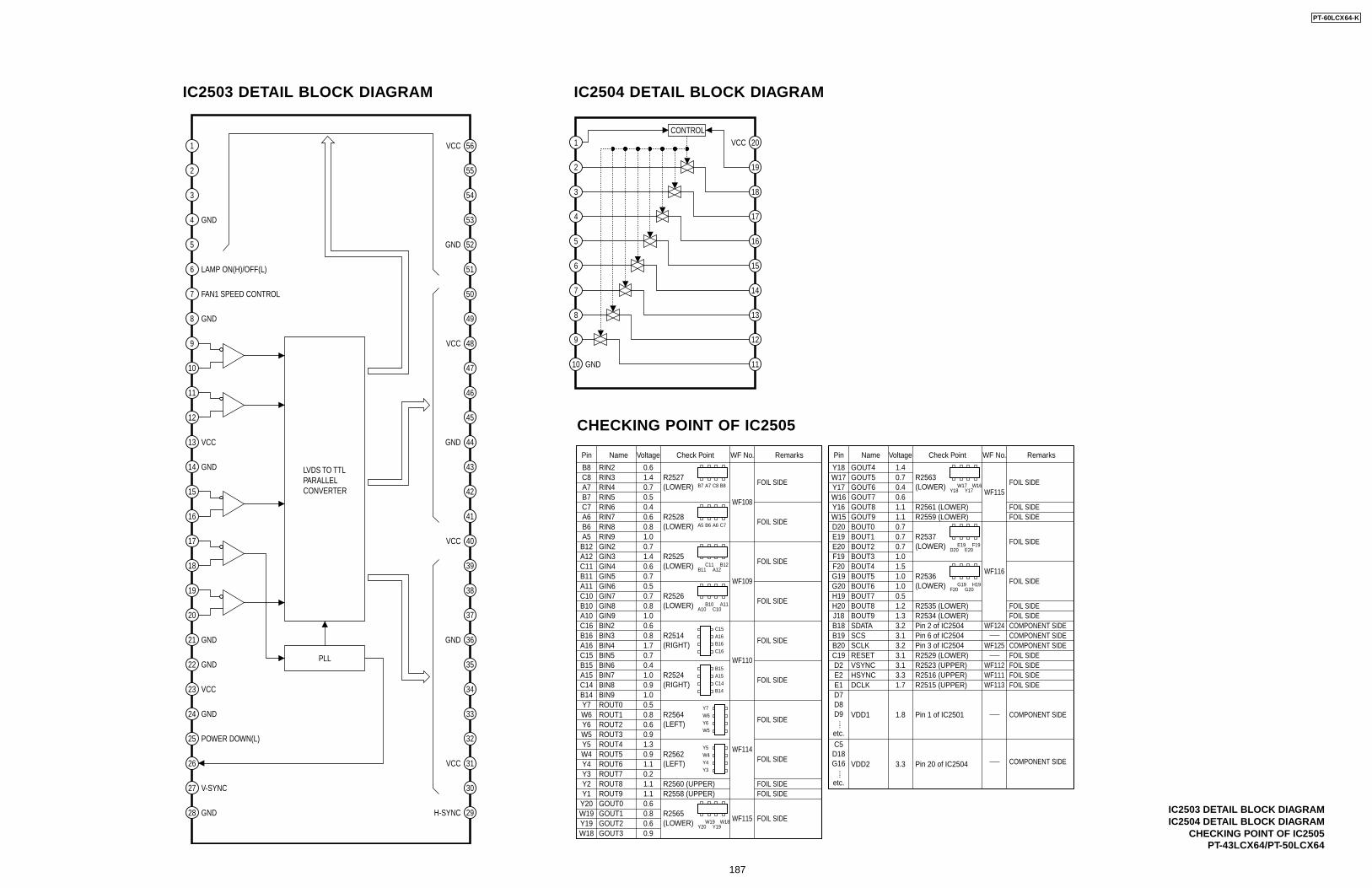
IC2503 DETAIL BLOCK DIAGRAM
IC2503 DETAIL BLOCK DIAGRAMIC2504 DETAIL BLOCK DIAGRAM
CHECKING POINT OF IC2505PT-43LCX64/PT-50LCX64
IC2504 DETAIL BLOCK DIAGRAM
1
2
3
4
5
6
7
8
9
10
11
12
13
14
15
16
17
18
19
20
21
22
23
24
25
26
27
28
56
55
54
53
52
51
50
49
48
47
46
45
44
43
42
41
40
39
38
37
36
35
34
33
32
31
30
29
GND
LAMP ON(H)/OFF(L)
FAN1 SPEED CONTROL
GND
GND
GND
GND
GND
POWER DOWN(L)
V-SYNC
GND
VCC
VCC
VCC
VCC
VCC
VCC
H-SYNC
GND
GND
GND
LVDS TO TTLPARALLELCONVERTER
PLL
1 20
2
3
4
5
6
7
8
9
10
19
18
17
16
15
14
13
12
11GND
CONTROLVCC
Pin
B8C8
RIN2RIN3 R2527
(LOWER)
FOIL SIDE
FOIL SIDE
FOIL SIDE
FOIL SIDE
FOIL SIDE
FOIL SIDE
WF108
WF109
WF110
WF114
WF115
WF115
WF116
WF124
WF125
WF112WF111WF113
FOIL SIDE
FOIL SIDE
FOIL SIDEFOIL SIDE
FOIL SIDE
R2528(LOWER)
R2525(LOWER)
R2526(LOWER)
R2514(RIGHT)
R2524(RIGHT)
R2565(LOWER)
RIN4RIN5
Name Voltage Check Point WF No. Remarks
0.5
0.61.4
0.6
0.7
0.5
1.4
0.8
0.8
0.7
0.6
0.4
0.9
0.7
0.6
0.7
0.8
0.7
1.0
1.7
1.0
1.0
1.0
0.50.4
0.80.60.91.3
0.80.60.9
0.91.10.21.11.10.6
A7B7C7A6
RIN6RIN7RIN8RIN9
B6A5
C7A6B6A5
B12A12
GIN2GIN3GIN4GIN5
C11B11
B12A12
C11B11
A11C10
GIN6GIN7GIN8GIN9
B10A10
A11C10
B10A10
C16B16
BIN2BIN3BIN4BIN5
A16C15
C16B16A16C15
B15A15
BIN6BIN7BIN8BIN9
C14B14
B15A15C14B14
ROUT0Y7
Y20W19
GOUT0GOUT1GOUT2GOUT3
Y19W18
Y20W19
Y19W18
ROUT1W6ROUT2Y6ROUT3W5
Y7W6Y6W5
ROUT4Y5ROUT5W4ROUT6Y4ROUT7Y3
Y5W4Y4Y3
ROUT8Y2Y1 ROUT9
B7 A7 C8 B8
R2564(LEFT)
R2562(LEFT)
R2560 (UPPER)R2558 (UPPER)
COMPONENT SIDECOMPONENT SIDECOMPONENT SIDE
COMPONENT SIDE
COMPONENT SIDE
FOIL SIDE
FOIL SIDEFOIL SIDE
FOIL SIDE
FOIL SIDE
FOIL SIDEFOIL SIDE
FOIL SIDEFOIL SIDEFOIL SIDEFOIL SIDE
R2563(LOWER)
VDD1
D7D8D9
etc.
Pin Name Voltage Check Point WF No. Remarks
....
VDD2
C5D18G16
etc.
....
1.40.70.4
Y18W17
GOUT4GOUT5GOUT6Y17
0.61.11.1
W16Y18
W17Y17
W16
Y16GOUT7GOUT8GOUT9W15
0.70.71.01.51.01.0
0.7D20E19
BOUT0BOUT1BOUT2BOUT3
E20F19
D20E19
E20F19
F20G19
BOUT4BOUT5BOUT6G20
0.51.21.3
1.8
3.3
H19F20
G19G20
H19
H20BOUT7BOUT8BOUT9J18
R2561 (LOWER)R2559 (LOWER)
R2535 (LOWER)R2534 (LOWER)
R2529 (LOWER)
3.2SDATAB18 Pin 2 of IC25043.1SCSB19 Pin 6 of IC25043.2SCLKB20 Pin 3 of IC25043.1RESETC19
R2523 (UPPER)3.1VSYNCD2R2516 (UPPER)3.3HSYNCE2R2515 (UPPER)1.7DCLKE1
Pin 1 of IC2501
Pin 20 of IC2504
R2537(LOWER)
R2536(LOWER)
CHECKING POINT OF IC2505
PT-60LCX64-K
187
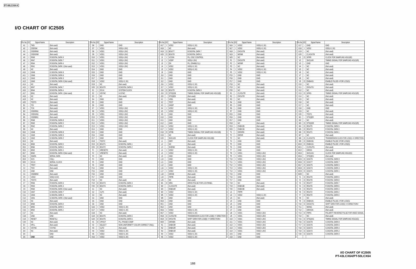
Pin No. I/O DescriptionSignal NameA1A2A3A4A5A6A7A8A9A10A11A12A13A14A15A16A17A18A19A20
T1T2T3T4T5T6T7T8T9
T10T11T12T13T14T15T16T17T18T19T20U1U2U3U4U5U6U7U8U9
U10U11U12U13U14U15U16
U17U18U19U20V1V2V3V4V5V6V7V8V9
V10V11V12V13V14V15V16V17V18V19V20W1W2W3W4W5W6W7W8W9
W10W11W12W13W14W15W16W17W18W19W20Y1Y2Y3Y4Y5Y6Y7Y8Y9
Y10Y11Y12Y13Y14Y15Y16Y17Y18Y19Y20
D1D2D3D4D5
D6D7D8D9
D10D11D12D13D14D15D16D17D18D19D20E1E2E3E4E5E6E7E8E9
E10E11E12E13E14E15E16E17E18E19E20
B1B2B3B4B5B6B7B8B9B10B11B12B13B14B15B16B17B18B19B20C1C2C3C4C5
F1F2F3F4F5F6
G1G2G3G4G5G6
F14F15F16F17F18F19F20
G16G17G18G19G20H1H2H3H4H5
H16
N1N2N3N4N5
N16
J1J2J3J4J5J9
J10J11J12J16J17J18J19J20K1K2K3K4K5K9
K10K11K12K16K17K18K19K20
H17H18H19H20
L1L2L3L4L5L9
L10L11L12L16L17L18L19L20M1M2M3M4M5M9
M10M11M12M16M17M18M19M20
N17N18N19N20P1P2P3P4P5
P16P15
P17P18P19P20R1R2R3R4R5R6R7
R16R15
R17R18R19R20
C6C7C8C9C10C11C12C13C14C15
Pin No. I/O DescriptionSignal Name Pin No. I/O DescriptionSignal Name
C16C17C18C19C20
Pin No. I/O DescriptionSignal Name Pin No. I/O DescriptionSignal Name
-GND
GND- GND GND
-I VDD1 VDD(+1.8V)I VDD1 VDD(+1.8V)I VDD1 VDD(+1.8V)I VDD1 VDD(+1.8V)I VDD1 VDD(+1.8V)I VDD1 VDD(+1.8V)I VDD1 VDD(+1.8V)
I VDD(+1.8V)
I VDD1 VDD(+1.8V)I VDD1 VDD(+1.8V)I VDD1 VDD(+1.8V)I VDD1 VDD(+1.8V)I VDD1 VDD(+1.8V)I VDD1 VDD(+1.8V)I VDD1 VDD(+1.8V)
I VDD1 VDD(+1.8V)I VDD1 VDD(+1.8V)I VDD1 VDD(+1.8V)I VDD1 VDD(+1.8V)I VDD1 VDD(+1.8V)I VDD1 VDD(+1.8V)I VDD1 VDD(+1.8V)
I VDD2 VDD(+3..3V)
I VDD2 VDD(+3..3V)I VDD2 VDD(+3..3V)
I VDD2 VDD(+3..3V)I VDD2 VDD(+3..3V)I VDD2 VDD(+3..3V)
I VDD2 VDD(+3..3V)
I VDD2 VDD(+3..3V)I VDD2 VDD(+3..3V)
I VDD2 VDD(+3..3V)I VDD2 VDD(+3..3V)
I VDD2 VDD(+3..3V)I VDD2 VDD(+3..3V)
I VDD2 VDD(+3..3V)I VDD2 VDD(+3..3V)
I VDD2 VDD(+3..3V)
I VDD(+3..3V)
I VDD2 VDD(+3..3V)
I VDD2 VDD(+3..3V)I VDD2 VDD(+3..3V)
I VDD2 VDD(+3..3V)I VDD2 VDD(+3..3V)
I VDD2 VDD(+3..3V)I VDD2
CLYOUTBDYOUTBDIRXBNENBX3RENBX2RENBX1R
VDD(+3..3V)
I VDD2 VDD(+3..3V)I VDD2 VDD(+3..3V)
I VDD2
DXOUTBMONB
DXOUTRMONR
CLYOUTRDYOUTR
ENBX2BENBX1BDIRXRNDIRXR
ENBX4BENBX3BFRPRVDD2
VDD(+3..3V)I VDD2 VDD(+3..3V)
I VDD2 VDD(+3..3V)
I VDD(+3..3V)
I VDD2 VDD(+3..3V)
I VDD1 VDD(+1.8V)I VDD1 VDD(+1.8V)I VDD1 VDD(+1.8V)I VDD1 VDD(+1.8V)I VDD1 VDD(+1.8V)I VDD1 VDD(+1.8V)I VDD1 VDD(+1.8V)
BOUT0DCLKHSYNC
TEST2BOUT1BOUT2HRESETOVRESETO
NCBOUT3BOUT4
CLP1
GND
BOUT5BOUT6CPOUTSELECTCLP2
GND
-- GND
GND
NC
TMSOSDSWOSDRIN0OSDGIN0RIN9RIN7RIN4RIN1
GIN9
GIN3
NCBIN7BIN4BIN1
TEST3TDITCKOSDRIN1OSDGIN1OSDBIN1RIN8RIN5RIN2
GIN8GIN5GIN2
BIN9BIN6BIN3BIN0SDATASCSSCLKTRSTTDOGNDOSDBIN0VDD2TEST4RIN6RIN3RIN0GIN7GIN4GIN1
BIN8BIN5BIN2
GND GNDRESET
HPLLVSYNC
GND- GND GND- GND GND- GND GND
- GND GND- GND GND- GND GND
- GND GND- GND GND- GND GND- GND GND
- GND GND- GND GND- GND GND- GND GND- GND GND- GND GND- GND GND
- GND GND- GND GND- GND
- GND
- GND GND- GND GND- GND GND- GND GND
- GND GND- GND GND- GND GND- GND GND
- GND GND
- GND
- GND GND- GND GND- GND GND
- GND GND- GND GND- GND GND- GND GND
- GND GND- GND GND- GND GND
- GND GND- GND GND- GND GND- GND GND- GND GND- GND GND- GND GND
- GND GND- GND GND- GND GND- GND GND
- GND GND- GND GND- GND GND
- GND GND- GND GND- GND GND- GND GND
- GND GND- GND GND
- GNDVDD2
CLXOUTBXFRRSHCLKR
ENB4XG
DYOUTG
XFRG
TEST1STSQER
STSQORROUT5ROUT3ROUT1NCCLXOUTGENBX3GENBX1GCLYOUTGDIRXGSHCLKGSTSQEGGOUT9GOUT7GOUT5GOUT3GOUT1
ROUT9ROUT8ROUT7ROUT6ROUT4ROUT2ROUT0
ENBX2GDXOUTGMONGDIRXGNFRPG
GOUT8
GOUT4
GOUT0
GOUT6
GOUT2
STSQOG
GND
- GND GND
- GND GND
(Not used)-
GIN6
GIN0(Not used)
- NC (Not used)- NC (Not used)
- NC (Not used)
- NC (Not used)
-NC (Not used)
--
NC (Not used)
- NC (Not used)
- NC (Not used)
- NC (Not used)
- (Not used)
- NC (Not used)
- NC (Not used)
- NCBOUT7BOUT8VCOINVDDPEN
BOUT9STSQOBSTSQEBVSELTESTGNDP
XFRB
SHCLKBDIRY
SHENB
DIRXBFRPB
NRGCLXOUTRENBX4R
(Not used)
- NC (Not used)
- NC (Not used)
- NC (Not used)
- NC (Not used)
- NC (Not used)
- NC (Not used)- NC (Not used)- NC (Not used)
- NC (Not used)
- NC (Not used)
- NC (Not used)
- NC (Not used)
- NC (Not used)
- NC (Not used)
- NC (Not used)- NC (Not used)- NC (Not used)- NC (Not used)- NC (Not used)
- NC (Not used)
- NC (Not used)
- NC (Not used)- NC (Not used)- NC (Not used)- NC (Not used)
- NC (Not used)
- NC (Not used)
- NC (Not used)
- (Not used)
- NC (Not used)
- NC (Not used)
- NC (Not used)
- NC (Not used)
- NC (Not used)
(Not used)(Not used)(Not used)(Not used)R DIGITAL DATA 9R DIGITAL DATA 7R DIGITAL DATA 4R DIGITAL DATA 1 (Not used)
G DIGITAL DATA 9G DIGITAL DATA 6G DIGITAL DATA 3
B DIGITAL DATA 7
G DIGITAL DATA 0 (Not used)
B DIGITAL DATA 1 (Not used)B DIGITAL DATA 4
----
----
-
-
--
III
III
II
I
III
-
III
III
III
-
--
-
-II-II
-II
-
I
I
I
(Not used)(Not used)(Not used)(Not used)(Not used)(Not used)R DIGITAL DATA 8R DIGITAL DATA 5R DIGITAL DATA 2
G DIGITAL DATA 8G DIGITAL DATA 5G DIGITAL DATA 2
B DIGITAL DATA 9B DIGITAL DATA 6B DIGITAL DATA 3B DIGITAL DATA 0 (Not used)SERIAL DATACS(L)SERIAL CLOCK(Not used)(Not used)
(Not used)VDD(+3.3V)(Not used)R DIGITAL DATA 6R DIGITAL DATA 3R DIGITAL DATA 0 (Not used)G DIGITAL DATA 7G DIGITAL DATA 4G DIGITAL DATA 1 (Not used)
B DIGITAL DATA 8B DIGITAL DATA 5B DIGITAL DATA 2
RESET(L)
V-SYNC(Not used)
-
IO
I
O
I
O
IO
B DIGITAL DATA 0
H-SYNCSYSTEM CLOCK
(Not used)B DIGITAL DATA 1B DIGITAL DATA 2(Not used)(Not used)
OO
B DIGITAL DATA 3B DIGITAL DATA 4
(Not used)
OOI-
B DIGITAL DATA 5B DIGITAL DATA 6PLL PHASE COMPNON-UNIFORMITY COLOR CORRECT ON(L)(Not used)
I
OOI
OO---
O
-
-
--
-O
-
O
-O
---
B DIGITAL DATA 7B DIGITAL DATA 8PLL OSC CONTROL
PLL ENABLE (L)
B DIGITAL DATA 9
(Not used)TIMING SIGNAL FOR SAMPLING HOLD(B)
(Not used)(Not used)
TIMING SIGNAL FOR SAMPLING HOLD(B)
CLOCK FOR SAMPLING HOLD(B)(Not used)
(Not used)
(Not used)(Not used)
(Not used)(Not used)
DRIVE PULSE FOR LCD PANEL
(Not used)(Not used)(Not used)(Not used)
TRANSMISSION CLOCK FOR LCD(B) <Y DIRECTION>SHIFT DATA FOR LCD(B) <Y DIRECTION>
--
--
--
--
--
--
(Not used)(Not used)
(Not used)(Not used)
(Not used)(Not used)
(Not used)(Not used)(Not used)(Not used)
(Not used)(Not used)
-O
-
O
-
O
-
O
-O
OOO
OO
-
-OOOO
OOO
O
OOOO
--
OO
O
OOOOOO
(Not used)CLOCK FOR SAMPLING HOLD(R)TIMING SIGNAL FOR SAMPLING HOLD(R)
ENABLE PULSE 4 FOR LCD(G)
(Not used)
TIMING SIGNAL FOR SAMPLING HOLD(R)
(Not used)(Not used)
TIMING SIGNAL FOR SAMPLING HOLD(R)R DIGITAL DATA 5R DIGITAL DATA 3R DIGITAL DATA 1
TRANSMISSION CLOCK FOR LCD(G) <X DIRECTION>ENABLE PULSE 3 FOR LCD(G)ENABLE PULSE 1 FOR LCD(G)(Not used)(Not used)CLOCK FOR SAMPLING HOLD(G)(Not used)G DIGITAL DATA 9G DIGITAL DATA 7G DIGITAL DATA 5G DIGITAL DATA 3G DIGITAL DATA 1
R DIGITAL DATA 9R DIGITAL DATA 8R DIGITAL DATA 7R DIGITAL DATA 6R DIGITAL DATA 4R DIGITAL DATA 2R DIGITAL DATA 0
ENABLE PULSE 2 FOR LCD(G)SHIFT DATA FOR LCD(G) <X DIRECTION>(Not used)(Not used)POLARITY REVERSE PULSE FOR VIDEO SIGNAL
TIMING SIGNAL FOR SAMPLING HOLD(G)G DIGITAL DATA 8G DIGITAL DATA 6G DIGITAL DATA 4G DIGITAL DATA 2G DIGITAL DATA 0
I/O CHART OF IC2505
I/O CHART OF IC2505PT-43LCX64/PT-50LCX64
PT-60LCX64-K
188
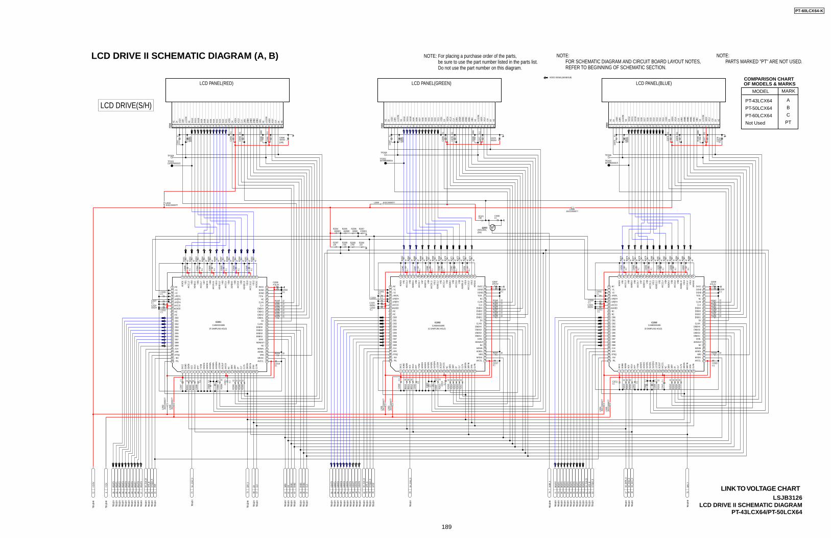
LCD DRIVE II SCHEMATIC DIAGRAM (A, B) NOTE:FOR SCHEMATIC DIAGRAM AND CIRCUIT BOARD LAYOUT NOTES,REFER TO BEGINNING OF SCHEMATIC SECTION.
NOTE: For placing a purchase order of the parts, be sure to use the part number listed in the parts list. Do not use the part number on this diagram.
NOTE:PARTS MARKED "PT" ARE NOT USED.
LSJB3126LCD DRIVE II SCHEMATIC DIAGRAM
PT-43LCX64/PT-50LCX64
XFRP
45
DIR_
Y75
DY58
0.1
C206
9
0.1
C207
1
CLY
57
DIR_
X73
TP2005
STSQ
O_G
46XF
R_G
43
GO
UT3
53
GO
UT5
51G
OUT
650
GO
UT1
55
GO
UT4
52
GO
UT7
49G
OUT
848
GO
UT0
56
GO
UT9
47
GO
UT2
54
+3.3
V9
P200
2
353433323130292827262524232221181716151413121110987654321 19 20 36
SH_C
LK_G
44
0.1
C206
7
0.1
C207
0
SD_D
ATA_
O17
SH_C
SB_O
19
SD_S
CK_O
18
22KR2087
220R2090
2700R2089
3300[D]R2094
1500[D]R2095
2700R2088
330[D]R2096
4700[D]R2097
R207
2
47
C200
90.
1
C20170.1
C205
0
0.1
R206
3
47
C20220.1
C203747/6.3V
C20310.1
R206
5
47
C204
6
0.1
IC2002C1AB00001895
1 2 3 4 5 6 7 8 9 10 11 12 13 14 15 16 17 18 19 20 21 22 23 24 25
26272829303132333435363738394041424344454647484950
51525354555657585960616263646566676869707172737475
7677787980
86
81
91
85
89
83
99
87
9495
100
98
92
84
82
93
90
88
9697
C20340.1
R206
6
47 R207
0
47R206
9
47
C205
1
0.1
C204
7
0.1
R207
3
47R207
1
47 R207
4
47
C202533/25V
C201
0
0.1
R206
4
47
C201
40.
1
R206
8
47C2
049
0.1
C204
8
0.1
R206
7
47
R201
022
R201
122
R201
222
R2043 22R2046 22
R2040 22R2037 22R2033 22R2030 22
R2027 22
R201
522
R201
422
R201
622
R201
322
R201
722
C2029 0.1
R2044 22
C20180.1
R201
822
0.1
C207
6
R202
322
R202
522
C20350.1
0.1
C207
3
BOUT
467
C205
4
0.1
BOUT
962
R202
422
BOUT
170
SH_C
LK_B
61
BOUT
269
R2031 22
R201
922
BOUT
368
R208
0
47
IC2003C1AB00001895
1 2 3 4 5 6 7 8 9 10 11 12 13 14 15 16 17 18 19 20 21 22 23 24 25
26272829303132333435363738394041424344454647484950
51525354555657585960616263646566676869707172737475
7677787980
86
81
91
85
89
83
99
87
9495
100
98
92
84
82
93
90
88
9697
C205
5
0.1
R207
8
47
C20110.1
R208
3
47
BOUT
764
C201
50.
1
R207
6
47C2
053
0.1
0.1
C207
5
TP2006
C201
20.
1
C20320.1
BOUT
863
R2041 22
R208
2
47
R2038 22
C203847/6.3V
C20230.1
0.1
C207
7
C205
2
0.1
R208
4
47
R2047 22
R202
022
R2028 22
C205
7
0.1
C205
6
0.1
BOUT
566
P200
3
353433323130292827262524232221181716151413121110987654321 19 20 36
R208
5
47R207
7
47
R202
222
R2034 22
R202
122
R208
6
47R207
5
47
XFR_
B59
BOUT
665
C20280.1
R208
1
47
BOUT
071
STSQ
O_B
60
R207
9
47
R2036 22
R200
222
0.1
C206
3
ROUT
531
R200
922
R206
0
47
C200
70.
1
C20300.1
R205
4
47R205
2
47
TP2004
CLX
37C20210.1
0.1
C206
5
ROUT
333
R206
1
47C2
045
0.1
ROUT
630
R2029 22
R205
3
47
R2026 22
C204
0
0.1
DX42
R205
9
47
ROUT
036
R200
422
C200
8
0.1
R2045 22
R205
7
47R205
1
47
FRP
23
ROUT
432
C204
4
0.1
C20330.1
R200
822
ROUT
135
R200
122
ENB3
39
ROUT
927
R200
722
0.1
C206
4
R2042 22
XFR_
R24
C20160.1
TP2001D0YBR0000015
R205
5
47 R206
2
47
0.1
C206
1
STSQ
O_R
26
SH_C
LK_R
25
R200
622
ENB1
41
IC2001C1AB00001895
1 2 3 4 5 6 7 8 9 10 11 12 13 14 15 16 17 18 19 20 21 22 23 24 25
26272829303132333435363738394041424344454647484950
51525354555657585960616263646566676869707172737475
7677787980
86
81
91
85
89
83
99
87
9495
100
98
92
84
82
93
90
88
9697
ROUT
729
C204
3
0.1
C204
2
0.1
R200
322
ENB2
40
ENB4
38
C204
1
0.1
C20270.1
R205
8
47
R2032 22
C202433/25V
NRG
22
C201
3
0.1
R205
6
47
R2039 22
ROUT
234
ROUT
828
+15.
5V72
Q2003UN521300L
R210115K
C20600.1
C200
10.
1
C200
40.
1
C200
2
0.1
C200
30.
1
C200
50.
1
C200
60.
1
TP2002D0YBR0000015 TP2003
D0YBR0000015
C202633/25V
C203647/6.3V
C206633/25V
C207233/25V C2
078
33/2
5V
SH_C
SR_O
21
SH_C
SG_O
20
P200
1
353433323130292827262524232221181716151413121110987654321 19 20 36
XDIR
_X74
R200
522
L200
1J0
JCC0
0000
77
L2010J0JCC0000077
L2009 J0JCC0000077
L200
6J0
JCC0
0000
77
L200
4J0
JCC0
0000
77
L2008J0JCC0000077
L200
5J0
JCC0
0000
77
L200
2J0
JCC0
0000
77
L200
3J0
JCC0
0000
77
33/2
5VC2
074
33/2
5VC2
062
33/2
5VC2
068
R209
810
0K
R209
910
0K
R210
010
0K
NRG
SIG
12
SIG
3SI
G4
SIG
2
NCDY XCLX
ENB1
SIG
6
ENB2
DX VDDX
NC SIG
11
SIG
9
CLY
ENB4
SIG
8
LCCO
M
SIG
5
ENB3
VSSY
DYSIG
10
SIG
1
NCDIRY
LCCO
MVD
DY
NC VSSX
XCLY
SIG
7
CLX
DIRX
AVCC
1,3
VID5
AGND
12
NC
AVCCD
TSTA
DXIN
CLYN
SVRE
FH
AVCC
10,1
2
VID4
XFR
V2
NC
CLXIN
NRG
DIRY
AGND
S
AGND
1VI
D1
VID1
0
INV
DB6
CLX
ENBX2
DYLCCO
M
DVCC
VID2
AGND
11,2
VREFH
V1
DB7
ENBX4I
AGNDL
CLY
TSTM
VID3
AGND
8,10
STSQ
DB2
CLXN
ENBX1I
DIRY
IN
NCDGND
AVCC
6,8
VID1
1
DB3
VREFH
NC
DX
MONIN
DYIN
SCLK
AGND
4,6
AGND
7,9
DB8
DB5
DGND
ENBX2I
DIRX
AVCC
S
SCS
VID7
VID9
DB9
DB1
AGNDDENBX3
NC
CLYI
N
DCO
UT
VID6
AVCC
9,11
NC
DB4
DGND
ENBX3I
AVCCL
SVRE
FL
SDAT
A
AVCC
5,7
VID8
VID1
2
R/L
VREFL
ENBX4
MONOUT
DIRX
IN
SVRE
FL
AGND
3,5
AVCC
2,4
CLK
DB0
DVCC
ENBX1
NRGIN
AGND
S
BYP
DVCC
DIRX
AGND
S
NC
SDAT
A
VDDX
AVCCD
VID2
AVCC
S
AGND
11,2
AGND
1DI
RY
NC
SCS
VREFH
VID1
AGND
12
AGNDD
LCCO
M
VID7
SIG
11
V1
NRG
VID1
0
ENBX3
VID9
DB7
AVCC
1,3
INV
VDDY
SIG
9
SIG
12
NC
TSTA
DB9
CLXN
ENBX4I
DB6
NC
CLYI
N
CLY
DXIN
SIG
3
DB1
ENBX1I
AGNDL
DCO
UT
CLYN
VSSX
DIRY
INEN
B4
SIG
4
VID6
SVRE
FH
SCLK
NC
XFR
XCLY
SIG
8
SIG
2
AVCC
9,11
VID1
1
AVCC
10,1
2
AGND
4,6
DGND
V2
DIRX
IN
SIG
7
DB3
LCCO
M
VID4
AVCC
5,7
NC
AGND
7,9
AVCC
6,8
NC
SVRE
FL
VREFH
CLY
VID8
DB8
CLX
CLXIN
SIG
5
DY
AGND
3,5
NC
TSTM
VID1
2
ENBX1
DB5
NRG
AVCC
2,4
DIRX
ENB3
XCLX
DX
VID3
R/LNRGIN
DGND
DIRY
NC
CLK MONIN
AGND
8,10
VSSY
VREFL
ENB1
AGND
S
ENBX2IDB4
DB0
DYIN
STSQ
ENBX4CLX
BYP
DY
DGND
SIG
6
DVCC
DB2
MONOUT
ENBX2
ENBX3I
SIG
10
ENB2
DY
AVCCL
SIG
1
LCCO
M
VID5
DX
SVRE
FL
NC
AVCC
9,11
CLX
CLXIN
SIG
5
DY
VID1
1
ENBX1I
DB8
VID4
DB9
DIRX
IN
NRG
DB3
DIRY
IN
DIRX
ENB3
DB5
XCLX
DB1
SVRE
FL
DIRY
VREFH
NC
DGND
ENBX1
AGND
3,5
VSSY
ENB1
NC
DGND
ENBX2I
NRGIN
AVCC
2,4
DYSIG
6
DX
AVCC
6,8
NC
AGND
S
CLK MONIN
DB4
CLY
SIG
10
ENB2
BYP
DB0
DYIN
DGND
TSTM
AVCC
5,7
DVCC
SIG
1
DX
ENBX3I
VID3
VID8
NCVDDX
AVCCL
AGND
8,10
VID1
2
AGND
11,2
AGND
S
SVRE
FL
STSQ
R/L
DIRY
NC
VREFH
AGND
1
SDAT
A
DB2
VREFL
CLX
AVCC
1,3
LCCO
M
SIG
11
V1
NRG
VID1
ENBX4
ENBX2
DB7
VID5
VID1
0
NC
VDDY
SIG
9
SIG
12
MONOUT
DY
AGNDD
ENBX4I
INV
AVCCD
LCCO
M
NC CLY
SIG
3
ENBX3
AGNDL
DB6
TSTA
DVCC
DIRX
NC
VSSX
ENB4
SIG
4
DXIN
VID2
AVCC
S
AGND
12CL
YIN
XFR
XCLY
SIG
8
SCLK
SIG
2
CLYN
SCS
DCO
UT
V2
AGND
4,6
SVRE
FH
VID7
SIG
7
LCCO
M
NC
VID6
NCCLXN
AGND
7,9
AVCC
10,1
2
VID9
LCD PANEL(RED)
[105]
LCD PANEL(GREEN) LCD PANEL(BLUE)
(R SAMPLING HOLD) (B SAMPLING HOLD)
TO L
D IV
TO L
D IV
TO L
D I
TO L
D I
TO L
D I
TO L
D I
TO L
D I
TO L
D I
TO L
D I
TO L
D I
TO L
D I
TO L
D I
TO L
D I
TO L
D I
TO L
D I
TO L
D I
TO L
D I
TO L
D I
TO L
D I
TO L
D III
TO L
D I
TO L
D I
TO L
D I
TO L
D I
TO L
D I
TO L
D I
TO L
D I
TO L
D I
TO L
D I
TO L
D I
TO L
D I
TO L
D I
TO L
D I
TO L
D I
TO L
D I
TO L
D I
TO L
D I
TO L
D I
TO L
D I
TO L
D I
TO L
D I
TO L
D I
TO L
D I
TO L
D I
TO L
D I
TO L
D III
TO L
D I
TO L
D I
TO L
D I
TO L
D I
TO L
D I
TO L
D I
TO L
D I
TO L
D I
TO L
D I
TO L
D I
TO L
D I
TO L
D III
TO L
D I
TO L
D I
(G SAMPLING HOLD)
(SW)
VIDEO SIGNAL(MAIN/SUB)
LCD DRIVE(S/H)
LINK TO VOLTAGE CHART
COMPARISON CHART OF MODELS & MARKS
PT-43LCX64
PT-50LCX64
PT-60LCX64
Not Used
A
B
C
PT
MODEL MARK
PT-60LCX64-K
189
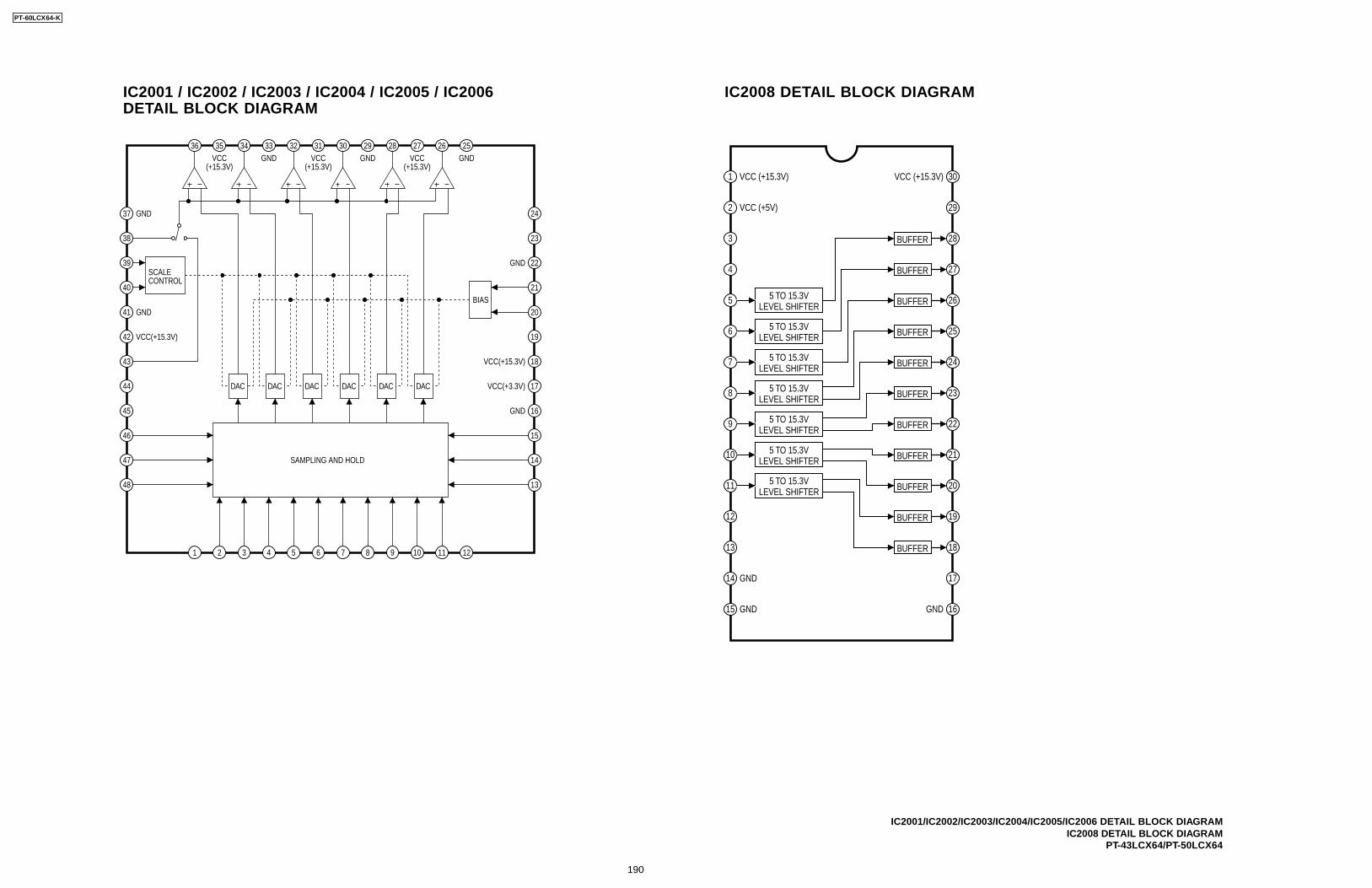
IC2001 / IC2002 / IC2003 / IC2004 / IC2005 / IC2006DETAIL BLOCK DIAGRAM
IC2001/IC2002/IC2003/IC2004/IC2005/IC2006 DETAIL BLOCK DIAGRAMIC2008 DETAIL BLOCK DIAGRAM
PT-43LCX64/PT-50LCX64
IC2008 DETAIL BLOCK DIAGRAM
1 2 3 4 5 6 7 8 9 10 11 12
36 35 34 33 32 31 30 29 28 27 26 25
13
14
15
16
17
18
19
20
21
22
23
24
48
47
46
45
44
43
42
41
40
39
38
37 GND
GND
GND
GND
VCC(+3.3V)
VCC(+15.3V)
VCC(+15.3V)
GNDGND GNDVCC(+15.3V)
VCC(+15.3V)
VCC(+15.3V)
SCALECONTROL
BIAS
DAC DAC DAC DAC DAC DAC
SAMPLING AND HOLD
1
2
3
4
5
6
7
8
9
10
11
12
13
14
15 16
17
18
19
20
21
22
23
25
26
27
28
29
30
24
BUFFER
BUFFER
BUFFER
BUFFER
BUFFER
BUFFER
BUFFER
BUFFER
BUFFER
BUFFER
BUFFER
5 TO 15.3VLEVEL SHIFTER
5 TO 15.3VLEVEL SHIFTER
5 TO 15.3VLEVEL SHIFTER
5 TO 15.3VLEVEL SHIFTER
5 TO 15.3VLEVEL SHIFTER
5 TO 15.3VLEVEL SHIFTER
5 TO 15.3VLEVEL SHIFTER
GND
GND GND
VCC (+15.3V)VCC (+15.3V)
VCC (+5V)
PT-60LCX64-K
190
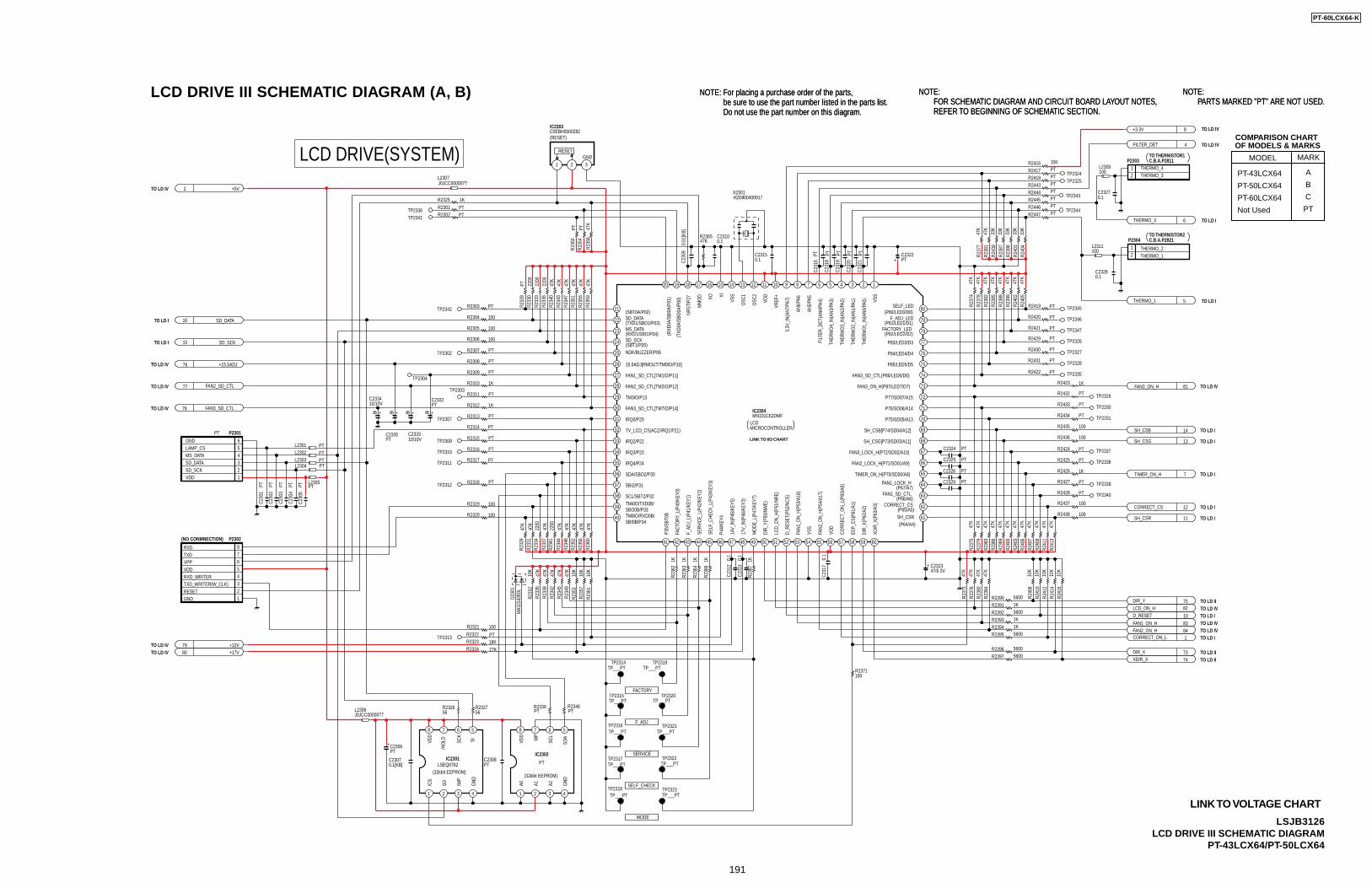
NOTE:FOR SCHEMATIC DIAGRAM AND CIRCUIT BOARD LAYOUT NOTES,REFER TO BEGINNING OF SCHEMATIC SECTION.
NOTE: For placing a purchase order of the parts, be sure to use the part number listed in the parts list. Do not use the part number on this diagram.
NOTE:PARTS MARKED "PT" ARE NOT USED.
LCD DRIVE III SCHEMATIC DIAGRAM (A, B) NOTE:FOR SCHEMATIC DIAGRAM AND CIRCUIT BOARD LAYOUT NOTES,REFER TO BEGINNING OF SCHEMATIC SECTION.
NOTE: For placing a purchase order of the parts, be sure to use the part number listed in the parts list. Do not use the part number on this diagram.
NOTE:PARTS MARKED "PT" ARE NOT USED.
LSJB3126LCD DRIVE III SCHEMATIC DIAGRAM
1KR2325
47/6.3VC2323
0.1
C231
7
SD_SCK15
0.1C2315
18KR2323
PTC2322
27KR2324
0.01
[KB]
C230
9
LCD_ON_H 82D_RESET 10
PTR2322
DIR_X 73
10K
R236
110
KR2
357
10K
R235
3
0.1
C231
2
0.1
C231
3
+3.3V 9
+17V80
MA3
J142
E0L
D230
1
+5V2
CORRECT_CS 12
CORRECT_ON_L 1
DIR_Y 75
2200
R233
4
PTC2306
56R2327
0.1[KB]C2307
56R2326
47K
R234
947
KR2
345
47K
R234
247
KR2
338
1KR2
362
1KR2
363
1KR2
364
1KR2
366
10K
R240
8
47K
R237
6
10K
R241
0
47K
R238
0
10K
R241
5
10K
R241
2
47K
R237
3
10K
R241
4
47K
R238
4
10K
R233
2
5600R23901KR23915600R23921KR23931KR23945600R2395
5600R23965600R2397
100R2371
47K
R241
3
47K
R241
1
47K
R240
9
47K
R240
7
100R2438
100R2437
47K
R240
347
KR2
406
TIMER_ON_H 7
PTC2325
PTC2326
47K
R240
0
47K
R237
5
47K
R238
9
47K
R237
947
KR2
383
47K
R238
6
100R2436
PTR2434 TP2331
100R2435
PTR2432
TP2330PTR2433
47K
R238
8
47K
R238
2
47K
R239
9
47K
R238
5
47K
R237
447
KR2
378
47K
R240
5
47K
R240
2
PTR2429
PTC2
321
PTC2
320
PTC2
319
PTC2
318
2200
R234
1
47K
R232
9
47K
R233
1
100R2320
PTR2318TP2312
47K
R233
7
47K
R234
4
47K
R234
8
47K
R235
2
47K
R235
6
47K
R236
0
TP2311
PTR2313
PTR2316
TP2307
PTR2317
TP2310
TP2309 PTR2315
PTR2314
47K
R233
5
47K
R235
947
KR2
355
47K
R234
7
47K
R235
1
47K
R234
347
KR2
340
PTR2
328
100R2304
100R2305
PTR2303
100R2306
TP2302 PTR2307
PTR2308
PTR2309
1KR2310
PTR2311
1KR2312
TP2325
PTR2417TP2324
10KR2416
PTR2418
47K
R237
747
KR2
381
33K
R240
4
33K
R238
7
33K
R240
1
33K
R239
8
PTR2
350
PTR2
354
47K
R235
8
PTR2301PTR2302
IC2303C0EBH0000282
1 2 3
+12V79
0.1C2328
0.1C2327
PTC2324 PTR2424
PTR2425
1KR2426
TP2326
TP2329
1KR2423
FILTER_DET 4
PTC2
316
PTR2428
FAN2_SD_CTL77
PTR2427
PTR2422
FAN3_SD_CTL78
PTR2430
PTR2431 TP2328
TP2327
PTR2419
PTR2420
PTR2421
100R2321
1KR2
367
100R2319
PTR2339
PTR2346
PTC2308
TP2313
47KR2365
0.1C2310
P2302
87654321
X2301H2D800400017
TP2335
TP2314TP___PT
TP2319TP___PT
TP2315TP___PT
TP2320TP___PT
TP2316TP___PT
TP2321TP___PT
TP2317TP___PT
TP2322TP___PT
TP2318TP___PT
TP2323TP___PT
2200
R233
0
2200
R233
3
2200
R233
6
PTR2444TP2343
TP2344PTR2446
PTR2443
PTR2445
FAN3_ON_H 81
FAN1_ON_H 83FAN2_ON_H 84
TP2341TP2336
TP2342
SD_DATA16
10/10VC2333
10/10VC2334
TP2345
TP2347
TP2346
SH_CSR 11
+15.5ADJ76
PTC2335
SH_CSG 13
SH_CSB 14
33K
R243
9
TP2340
PTC2332
P2301PT
1VDD2SD_SCK3SD_DATA4MS_DATA5LAMP_CS6GND
PTC2
304
PTC2
302
PTC2
303
PTC2
301
PTC2
305
PTR2447
PTC2329
THERMO_3 6
THERMO_1 5
TP2339
TP2338
TP2337
TP2303
TP2304
XDIR_X 74
L2307J0JCC0000077
100L2309
100L2311
PTL2305
PTL2303PTL2304
PTL2302
L2306J0JCC0000077
PTL2301
IC2304MN101C62DMF
1234567891011121314151617181920
21
22
23
24
25
26
27
28
29
30
31
32
33
34
35
36
37
38
39
40
41 42 43 44 45 46 47 48 49 50 51 52 53 54 55 56 57 58 59 60
61
62
63
64
65
66
67
68
69
70
71
72
73
74
75
76
77
78
79
80
PT
IC2302
1 2 3 4
5678
IC2301LSEQ0762
1 2 3 4
5678
P2304
21
P2303
21
RESETGND
RXD_WRITERVDD
RXDTXD
VDD
VSS
VSS
THER
MO
1_IN
(AN0
/PA0
)
THER
MO
2_IN
(AN1
/PA1
)
THER
MO
4_IN
(AN3
/PA3
)
THER
MO
3_IN
(AN2
/PA2
)
AN6/
PA6
3.3V
_IN(
AN7/
PA7)
AN5/
PA5
FILT
ER_D
ET(A
N4/P
A4)
VREF
+
OSC
2
OSC
1XIXO
MM
OD
NRST
/P27
(TXD
0A/S
BO0A
/P00
)
(RXD
0A/S
BI0A
/P01
)
(SBT0A/P02)
(TXD1/SBO1/P03)MS_DATA
(SBT1/P05)NDK/BUZZER/P06
15.5ADJ[RMOUT/TM0IO/P10]
FAN1_SD_CTL[TM1IO/P11]
FAN2_SD_CTL[TM2IO/P12]
FAN3_SD_CTL[TM7IO/P14]
TM3IO/P13
IRQ0/P20
TV_LCD_CS(ACZ/IRQ1/P21)
IRQ2/P22
IRQ3/P23
IRQ4/P24
SDA/SBO2/P30
SBI2/P31
SCL/SBT2/P32TM4IO/TXD0B/
TM8IO/RXD0B/
(P64/A4)
CORRECT_CS
(P67/A7)
(P66/A6)
FAN2_LOCK_H(P71/SD01/A9)
TIMER_ON_H(P70/SD00/A8)
SH_CSG[P73/SD03/A11]
FAN3_LOCK_H(P72/SD02/A10)
P75/SD05/A13
P77/SD07/A15
P76/SD06/A14
SH_CSB[P74/SD04/A12]
FAN3_ON_H(P87/LED7/D7)
FAN3_SD_CTL(P86/LED6/D6)
P85/LED5/D5
P84/LED4/D4
(P80/LED0/D0)
(P81/LED1/D1)
P83/LED3/D3
(P82/LED2/D2)
XDIR
_X(P
63/A
3)
DIR_
X(P6
2/A2
)
EEP_
CS(P
61/A
1)
CORR
ECT_
ON_
L(P6
0/A0
)
FAN1
_ON_
H(P5
3/A1
6)
FAN2
_ON_
H(P5
4/A1
7)
VDD
VSS
D_RE
SET(
P52/
NCS)
LCD_
ON_
H(P5
1/NR
E)
DIR_
Y(P5
0/NW
E)
FACT
ORY
_L(P
40/K
EY0)
F_AD
J_L(
P41/
KEY1
)
SELF
_CHE
CK_L
(P43
/KEY
3)
SERV
ICE_
L(P4
2/KE
Y2)
17V_
IN(P
46/K
EY3)
MO
DE_L
(P47
/KEY
7)
14V_
IN(P
45/K
EY5)
P44/
KEY4
P35/
SBT0
B
SBO0B/P33
SBI0B/P34
/CS
GND
(32kbit EEPROM)
VDD
SI
/HO
LD SCK
/WP
SO
(RXD1/SBI1/P04)
SD_DATA
SD_SCK
(P65/A5)
FAN1_LOCK_H
FAN1_SD_CTL
THERMO_2THERMO_1
SELF_LED
F_ADJ_LED
FACTORY_LED
FACTORY
F_ADJ
SELF_CHECK
MODE
SERVICE
WP
A0VD
D
GND
(32kbit EEPROM)
A2
SDA
SCL
A1
VPP
TXD_WRITER(W_CLK)
SH_CSR
THERMO_4THERMO_3
GNDRESET
(NO CONMNECTION)
TO THERNISTOR1C.B.A.P2811
TO THERNISTOR2C.B.A.P2821
(RESET)
LCDMICROCONTROLLER
TO LD IV
TO LD I
TO LD I
TO LD IV
TO LD IV
TO LD IV
TO LD IVTO LD IV
TO LD IV
TO LD IV
TO LD I
TO LD I
TO LD IV
TO LD I
TO LD I
TO LD I
TO LD I
TO LD I
TO LD IITO LD IVTO LD ITO LD IVTO LD IVTO LD I
TO LD IITO LD II
LCD DRIVE(SYSTEM)
PT-43LCX64/PT-50LCX64
LINK TO I/O CHART
COMPARISON CHART OF MODELS & MARKS
PT-43LCX64
PT-50LCX64
PT-60LCX64
Not Used
A
B
C
PT
MODEL MARK
LINK TO VOLTAGE CHART
PT-60LCX64-K
191
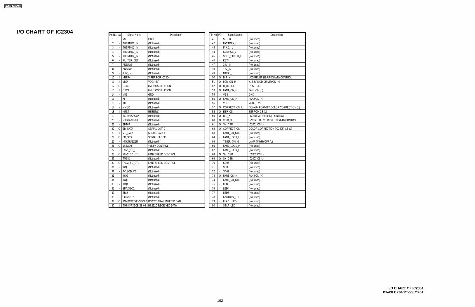
I/O CHART OF IC2304
I/O CHART OF IC2304PT-43LCX64/PT-50LCX64
Pin No. I/O1
Description
23456789
10111213141516171819202122232425262728293031323334353637383940
515253545556575859
Pin No. I/O
60
Signal NameSignal Name Description
6162636465666768697071727374757677787980
-
--
---
-
-
-
-------
O
-
O
O
O
O---
-
O
I
I
-I
I
I
--
-
I
(Not used)(Not used)(Not used)
(Not used)(Not used)(Not used)(Not used)(Not used)
(Not used)
(Not used)
IC2001 CS(L)
(Not used)(Not used)
(Not used)(Not used)IC2002 CS(L)IC2003 CS(L)(Not used)(Not used)(Not used)
(Not used)(Not used)(Not used)(Not used)(Not used)(Not used)(Not used)
(Not used)(Not used)
(Not used)
(Not used)(Not used)(Not used)
(Not used) +15.5V CONTROL(Not used)
(Not used)
(Not used)(Not used)(Not used)(Not used)(Not used)
(Not used)
(Not used)(Not used)
(Not used)(Not used)
VDD(+5V)
(Not used)
VDD (+5V)
GND
GND GND
INVERTED LCD REVERSE (L/R) CONTROL
(Not used)(Not used)
-
--
--
-
------
--
-
------
-
I
I
--
424344454647484950
41VSSTHERMO1_INTHERMO2_INTHERMO3_INTHERMO4_IN
AN6/PA63.3V_IN
AN5/PA5
VREF+
OSC2OSC1VSS
XOXI
MMODNRSTTXD0A/SBO0ARXD0A/SBI0ASBT0ASD_DATAMS_DATASD_SCKNDK/BUZZER
TM3IOFAN3_SD_CTL
FAN2_SD_CTL
IRQ3
IRQ0
IRQ2
IRQ4SDA/SBO2SBI2SCL/SBT2TM4IO/TXD0B/SBO0BTM8IO/RXD0B/SBI0B
15.5ADJFAN1_SD_CTL
FIL_TER_DET
VDD
FACTORY_LF_ADJ_LSERVICE_LSELF_CHECK_LKEY414V_IN17V_INMODE_LDIR_YLCD_ON_HD_RESETFAN1_ON_HVSSFAN2_ON_HVDDCORRECT_ON_LEEP_CSDIR_XXDIR_XSH_CSRCORRECT_CSFAN1_SD_CTLFAN1_LOCK_HTIMER_ON_HFAN2_LOCK_HFAN3_LOCK_HSH_CSGSH_CSBSD05SD06SD07FAN3_ON_HFAN3_SD_CTLLED5LED4LED3FACTORY_LEDF_ADJ_LEDSELF_LED
SBT0B
TV_LCD_CS
V-REF FOR IC2304
8MHz OSCILLATION8MHz OSCILLATION
RESET(L)
SERIAL DATA 0SERIAL DATA 1SERIAL CLOCK
FAN2 SPEED CONTROL
FAN3 SPEED CONTROL
(Not used)
(Not used)RS232C TRANSMITTED DATARS232C RECEIVED DATA
OOOO
O
OOOO
O
O
+15.5V (LCD DRIVE) ON (H)RESET (L)
LCD REVERSE (UP/DOWN) CONTROL
LCD REVERSE (L/R) CONTROL
FAN1 ON (H)
FAN2 ON (H)
NON-UNIFORMITY COLOR CORRECT ON (L)EEPROM CS (L)
COLOR CORRECTION (IC2505) CS (L)
LAMP ON (H)/OFF (L)
FAN3 ON (H)
O
O
OO
-
-
PT-60LCX64-K
192
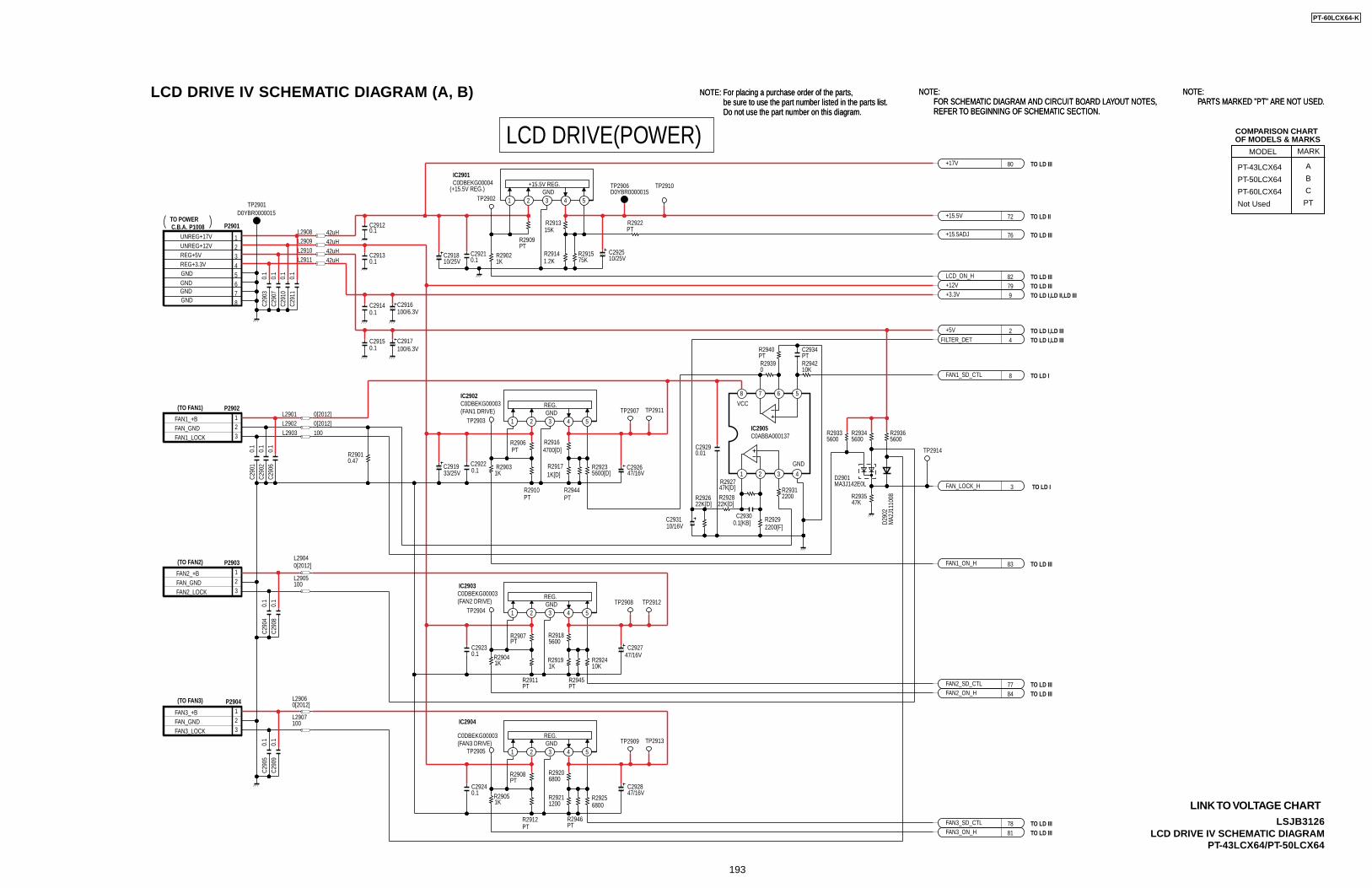
NOTE:FOR SCHEMATIC DIAGRAM AND CIRCUIT BOARD LAYOUT NOTES,REFER TO BEGINNING OF SCHEMATIC SECTION.
NOTE: For placing a purchase order of the parts, be sure to use the part number listed in the parts list. Do not use the part number on this diagram.
NOTE:PARTS MARKED "PT" ARE NOT USED.
LCD DRIVE IV SCHEMATIC DIAGRAM (A, B) NOTE:FOR SCHEMATIC DIAGRAM AND CIRCUIT BOARD LAYOUT NOTES,REFER TO BEGINNING OF SCHEMATIC SECTION.
NOTE: For placing a purchase order of the parts, be sure to use the part number listed in the parts list. Do not use the part number on this diagram.
NOTE:PARTS MARKED "PT" ARE NOT USED.
LSJB3126LCD DRIVE IV SCHEMATIC DIAGRAM
PT-43LCX64/PT-50LCX64
TP2902
0.1C2921
1.2KR2914
75KR2915
PTR2909
10/25VC2925
R291315K
1KR2902
10/25VC2918
TP2906D0YBR0000015
TP2910
+17V 80
TP2911
+5V 2
0.1C2922
1KR2919
+15.5V 72
FAN2_SD_CTL 77
0.1C2923
TP2912
TP2903
+3.3V 9
TP2904
R29164700[D]
LCD_ON_H 82
TP2908
PTR2910
PTR2911
TP2907
R29185600
47/16VC2926
33/25VC2919
P2902
321
P2903
321
FAN1_SD_CTL 8
1K[D]R2917
TP2901D0YBR0000015
0.1C2915
0.1C2914
0.1C2912
+12V 79
0.1C2913
100/6.3VC2916
TP2909
0.1C2924
FAN3_SD_CTL 78
R29206800
1200R2921
PTR2912
P2904
321
TP2913
TP2905
0.47R2901
2200R2931
22K[D]R2928
22K[D]R2926
2200[F]R29290.1[KB]
C2930
47K[D]R2927
FILTER_DET 4
5600[D]R2923
10KR2924
6800R2925
0.1
C290
30.
1C2
907
0.1
C291
00.
1C2
911
0.1
C290
1
0.1
C290
60.
1C2
902
0.1
C290
80.
1C2
904
0.1
C290
90.
1C2
905
5600R2933
5600R2934
5600R2936
PTR2906
PTR2907
PTR2908
0.01C2929
10/16VC2931
+15.5ADJ 76
PTC2934
10KR2942
PTR2940
0R2939
FAN1_ON_H 83
1KR2903
FAN2_ON_H 84
FAN3_ON_H 81
1KR2904
1KR2905
PTR2944
PTR2945
PTR2946
IC2901C0DBEKG00004
1 2 3 4 5
PTR2922
IC2902C0DBEKG00003
1 2 3 4 5
IC2903C0DBEKG00003
1 2 3 4 5
IC2904
C0DBEKG00003
1 2 3 4 5
47/16VC2927
47/16VC2928
100/6.3VC2917
FAN_LOCK_H 3
TP2914
MA3J142E0LD2901
47KR2935
MA2
J111
008
D290
2
P2901
87654321
L2903 100
L2905100
L2907100
L2909 42uHL2910 42uHL2911 42uH
L2908 42uH
L2902 0[2012]
L29040[2012]
L29060[2012]
L2901 0[2012]
IC2905C0ABBA000137
1 2 3 4
5678
FAN1_LOCK
FAN_GND
FAN_GNDFAN1_+B
FAN2_LOCK
FAN2_+B
FAN_GNDFAN3_LOCK
FAN3_+B
GND
UNREG+12V
GND
REG+3.3VREG+5V
GNDGND
UNREG+17V
TO POWER C.B.A.
(TO FAN1)
(TO FAN2)
(TO FAN3)
P1008
TO LD III
GND+15.5V REG.
(+15.5V REG.)
(FAN1 DRIVE) GNDREG.
GNDREG.
GNDREG.
TO LD II
TO LD III
TO LD IIITO LD IIITO LD I,LD II,LD III
TO LD I,LD IIITO LD I,LD III
TO LD I
TO LD I
TO LD III
TO LD IIITO LD III
TO LD IIITO LD III
VCC
GND
(FAN2 DRIVE)
(FAN3 DRIVE)
LCD DRIVE(POWER) COMPARISON CHART OF MODELS & MARKS
PT-43LCX64
PT-50LCX64
PT-60LCX64
Not Used
A
B
C
PT
MODEL MARK
LINK TO VOLTAGE CHART
PT-60LCX64-K
193
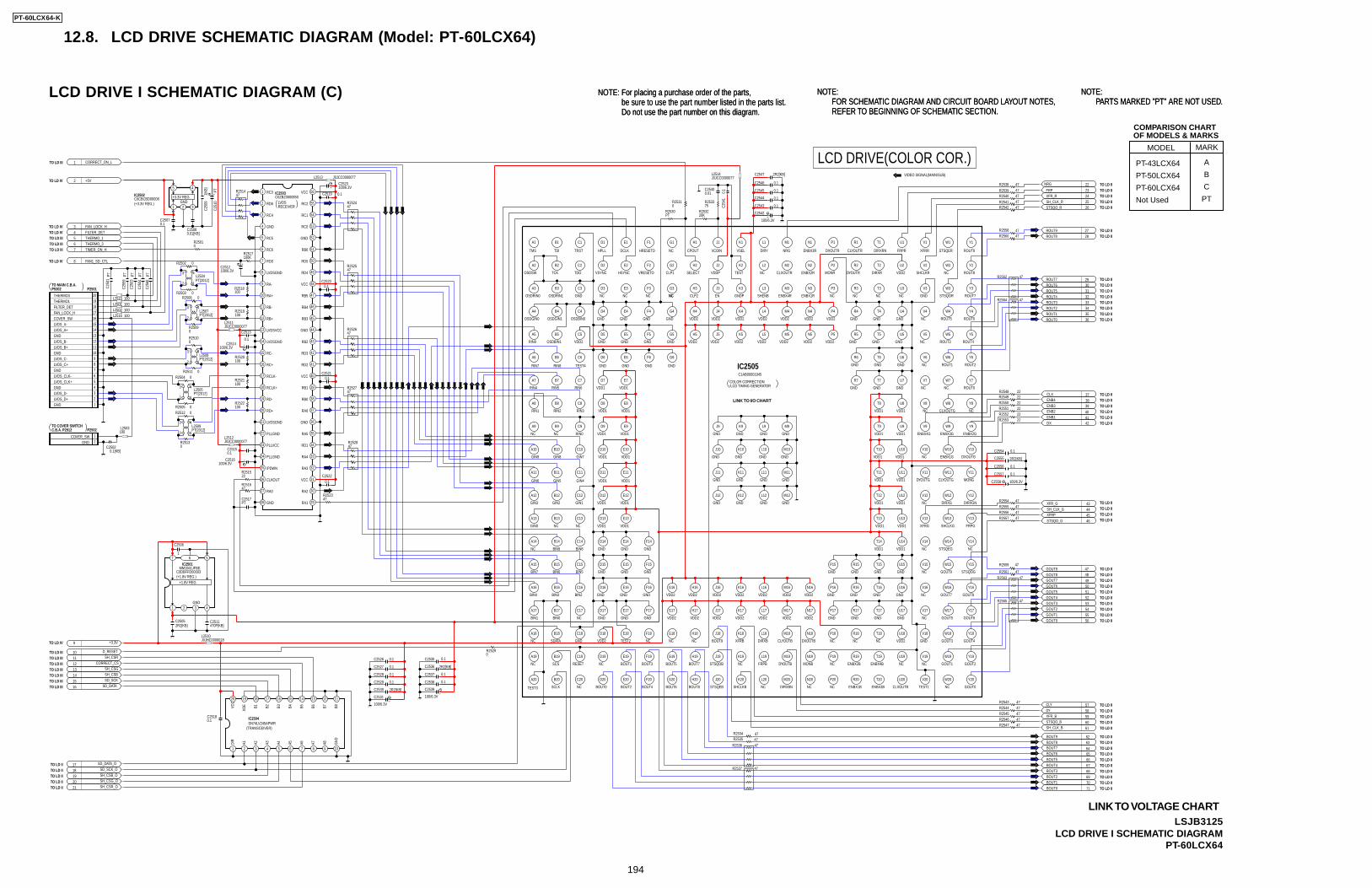
12.8. LCD DRIVE SCHEMATIC DIAGRAM (Model: PT-60LCX64)
NOTE:FOR SCHEMATIC DIAGRAM AND CIRCUIT BOARD LAYOUT NOTES,REFER TO BEGINNING OF SCHEMATIC SECTION.
NOTE: For placing a purchase order of the parts, be sure to use the part number listed in the parts list. Do not use the part number on this diagram.
NOTE:PARTS MARKED "PT" ARE NOT USED.
D_RESET10
SD_DATA16
SD_SCK15
CORRECT_CS12
+3.3V9
STSQO_G 46
GOUT3 53
GOUT8 48
SH_CLK_G 44
BOUT9 62
BOUT7 64
GOUT7 49
BOUT0 71
BOUT2 69
GOUT9 47
BOUT3 68
GOUT2 54
XFR_G 43
GOUT4 52
GOUT0 56
BOUT1 70
GOUT1 55
GOUT5 51
BOUT6 65
GOUT6 50
BOUT5 66
BOUT8 63
BOUT4 67
ENB1 41
ENB4 38ENB3 39ENB2 40
CLX 37
DX 42
XFRP 45
DY 58
CLY 57
NRG 22
47R2528
47R2527
47R2526
47R2525
47R2524
22R2515
47R2516
47R2523
+5V2
0.1C2515
0.1
C2513
0.1C2519
0.1C2521
0.1C2522
47R2514
100/6.3VC2514
100/6.3VC2516
100/6.3VC2523
0.1C2520
P2501
18FILTER_DET17FAN_LOCK_H16COVER_SW15LVDS_A-14LVDS_A+13GND12LVDS_B-11LVDS_B+10GND9LVDS_C-8LVDS_C+7GND6LVDS_CLK-5LVDS_CLK+4GND3LVDS_D-2LVDS_D+1GND
19THERMO1
20THERMO3100R2518
100R2519
100R2520
100R2521
100R2522
L2509PT[2012]
12
43
0R2512
0R2513
L2505PT[2012]
12
43
0R2504
0R2505
L2508PT[2012]
12
43
0R2510
0R2511
0R2509
0R2502
0R2503
L2504PT[2012]
12
43
L2507PT[2012]
12
43
0R2508
C0CBCBD00008IC2502
1 2
5
3
4
C250
91[
KB]
0.01[KB]C2508
PTC2
510
C25070.1
CORRECT_ON_L1
C25180.1 STSQO_B 60
XFR_B 59
SH_CLK_B 61
FAN1_SD_CTL8100KR2517
100/6.3VC2512
TIMER_ON_H7
SD_DATA_O17SD_SCK_O18
SH_CSR11
SH_CSR_O21
IC2504SN74LV245APWR
1 2 3 4 5 6 7 8 9 10
11121314151617181920
SH_CSG_O20
SH_CSG13
SH_CSB_O19
SH_CSB14
ROUT1 35
ROUT8 28
ROUT3 33
STSQO_R 26
ROUT9 27
FRP 23
ROUT0 36
SH_CLK_R 25
ROUT4 32ROUT5 31
XFR_R 24
ROUT7 29
ROUT2 34
ROUT6 30
47R2564
47R2562
47R256047R2558
47R254247R2541
47R254047R2539
22R254822R254922R255022R255122R255222R2553
47R255547R2554
47R255747R2556
47R2565
47R2563
47R2561
47R2559
47R254347R254447R254547R254647R2547
47R2537
47R2536
47R2534
47R2535
PTC2517
47R2538
0R2531
0R2529
PTR2530
20KR2532
75R2533
C25400.01
C254
10.
1
0.1[KB]C2502
PTC2
501
PTC2
503
PTC2
504
FILTER_DET4
C2537 0.1
C2539
100/6.3V
C2538 0.1
C2535 0.1
C2554 0.1
C2556 0.1
C2557 0.1
C2558 100/6.3V
C2527 0.1
C2526 0.1
C2529 0.1
C2528 0.1
C2531
100/6.3V
0R2501
2R2[KB]C2505
1
C2506
470P[KB]C2511
2R2[KB]C2530
2R2[KB]C2536
2R2[KB]C2555
THERMO_36THERMO_15
FAN_LOCK_H3
PTC2
559
PTC2
560
IC2503C0ZBZ0000850
1
2
3
4
5
6
7
8
9
10
29
30
31
32
33
34
35
36
11
12
13
14
15
16
17
18
19
20
21
22
37
38
39
40
41
42
43
44
23
24
25
45
46
47
48
49
50
26
27
28
51
52
53
54
55
56
L2512J0JCC0000077
100L2515
L2514J0JCC0000077
L2511J0JCC0000077
100L2502100L2516
L2513 J0JCC0000077
100L2501
100L2503
L2510J0JHC0000018
P2502
21
2R2[KB]C2547
C2542
100/6.3V
C2544 0.1
C2543 0.1
C2545 0.1
C2546 0.1
MM1561JFBEIC2501
C0DBFFD00003
1 2 3 4
567
IC2505C1AB00001945
RC3
RD6
RC4
RC5
RC6
RD0
GND
LVDSGND
LVDSGND
LVDSGND
PLLGND
PLLGND
PLLVCC
/PDWN
RA-
RA+
RB+
RB-
LVDSVCC
RC-
RC+
RD-
RD+
RCLK-
RCLK+
CLKOUT
RA0
GND
VCC
RC2
RC1
VCC
VCC
VCC
GND
GND
GND
RC0
RD4
RD5
RB6
RB3
RB4
RB5
RD2
RD3
RB2
RA6
RB0
RB1
RA4
RD1
RA5
RA3
RA1
RA2
DIR
A1 A2 A3 A4 A5 A6 A7 A8 GND
B2
XOE B1 B8B3 B7B6B4 B5VC
C
COVER_SWGND
GND
TMS TDI TRST HPLL DCLK HRESETO NC CPOUT VCOIN VSEL DIRY NRG ENBX3R DXOUTR CLYOUTR DIRXRN FRPR XFRR STSQER ROUT9
ROUT8NCSHCLKRVDD2DIRXRDYOUTRMONRENBX2RCLXOUTRNCTESTVDDPSELECTCLP1VRESETOHSYNCVSYNCTDOTCKOSDSW
OSDRIN0 OSDRIN1 GND NC NC NC NC CLP2 EN GNDP SHENB ENBX4R ENBX1R NC NC NCNC GND STSQOR ROUT7
ROUT6ROUT5NCGNDGNDGNDVDD2VDD2VDD2VDD2VDD2 VDD2VDD2GND GND GND GNDOSDBIN0OSDGIN1OSDGIN0
RIN9 OSDBIN1 VDD2 GND GNDGNDGND VDD2 VDD2 VDD2 VDD2VDD2 VDD2VDD2 NCGND GNDGND ROUT3 ROUT4
ROUT1 ROUT2GND GNDGND NCGND GNDGND GNDTEST4RIN8RIN7
RIN4 RIN5 RIN6 VDD1 VDD1 GND GNDGND NC NC ROUT0
RIN1 RIN2 RIN3 VDD1 VDD1 VDD1 VDD1 NC CLXOUTG NC
NC NC RIN0 VDD1 VDD1 GND GNDGNDGND VDD1 VDD1 ENBX4G ENBX3G ENBX2G
GIN9 GIN8 GIN7 VDD1VDD1 GNDGNDGND GND VDD1 VDD1 NC ENBX1G DXOUTG
GIN6 GIN5 GIN4 VDD1 VDD1 GNDGND GNDGND VDD1 VDD1 DYOUTG CLYOUTG MONG
DIRXGN
FRPG
NC
STSQOG
GOUT8
GOUT6
GOUT4
GOUT2
GOUT0NC
GOUT7
GOUT1
GOUT3
GOUT5
GOUT9
STSQEG
SHCLKG
DIRXGNC
XFRG
NC
NC
NC
NC
GND
NC
TEST1
VDD1VDD1
VDD1VDD1
VDD1VDD1
GND GNDGND GND
GND GNDGND GND
GND GNDGND GND
VDD2
NC
CLXOUTBENBX3B
ENBX4B
NC NC NC
ENBX2B
ENBX1B
NC
NCNCNC DIRXBNSHCLKBSTSQEBBOUT8BOUT6BOUT4BOUT2BOUT0
NC BOUT7BOUT5BOUT3BOUT1 STSQOB NC FRPB DYOUTB MONB
DXOUTB
VDD2VDD2VDD2VDD2VDD2VDD2VDD2
VDD2VDD2 VDD2 VDD2VDD2VDD2 VDD2
CLYOUTBDIRXBXFRBBOUT9NCNCNCVDD2 TEST2
GNDGND GND
GND GND GND
GND GND GND
GNDGND GND
GNDGND GNDGNDVDD1VDD1
VDD1 VDD1
NC
NC
NC
RESET
GND
BIN2
BIN5
BIN8
GIN1GIN2
NC
BIN9
BIN6
BIN3
BIN0
SDATA
SCS
SCLK
NC
NC
NC
GIN0
GIN3
BIN1
BIN4
BIN7
TEST3
TO MAIN C.B.A.P5302
A1
A2
A3
A4
A5
A6
A7
A8
A9
A10
A11
A12
A13
A14
A15
A16
A17
A18
A19
A20
B1
B2
B3
B4
B5
B6
B7
B8
B9
B10
B11
B12
B13
B14
B15
B16
B17
B18
B19
B20
C1
C2
C3
C4
C5
C6
C7
C8
C9
C10
C11
C12
C13
C14
C15
C16
C17
C18
C19
C20
D1
D2
D3
D4
D5
D6
D7
D8
D9
D10
D11
D12
D13
D14
D15
D16
D17
D18
D19
D20
E1
E2
E3
E4
E5
E6
E7
E8
E9
E10
E11
E12
E13
E14
E15
E16
E17
E18
E19
E20
F1
F2
F3
F4
F5
F6
F14
F15
F16
F17
F18
F19
F20
G1
G2
G3
G4
NC
G5
G6
G16
G17
G18
G19
G20
H1
H2
H4
H3
H5
H16
H17
H18
H19
H20
J1
J2
J4
J3
J5
J9
J10
J12
J11
J17
J16
J19
J18
J20
K1 L1 M1 N1 P1 R1 T1 U1 V1 W1 Y1
U2M2 V2R2K2 N2 W2L2 P2 Y2T2
U3M3 V3R3K3 N3 W3L3 P3 Y3T3
U4M4 V4R4K4 N4 W4L4 P4 Y4T4
U5M5 V5R5K5 N5 W5L5 P5 Y5T5
U6 V6R6 W6 Y6T6
U7 V7R7 W7 Y7T7
U8 V8 W8 Y8T8
U9M9 V9K9 W9L9 Y9T9
U10M10 V10K10 W10L10 Y10T10
U11M11 V11K11 W11L11 Y11T11
U12M12 V12K12 W12L12 Y12T12
U13 V13 W13 Y13T13
U14 V14 W14 Y14T14
U15 V15R15 W15P15 Y15T15
U16M16 V16R16K16 N16 W16L16 P16 Y16T16
U17M17 V17R17K17 N17 W17L17 P17 Y17T17
U18M18 V18R18K18 N18 W18L18 P18 Y18T18
U19M19 V19R19K19 N19 W19L19 P19 Y19T19
U20M20 V20R20K20 N20 W20L20 P20 Y20T20
GND+3.3V REG.
(+3.3V REG.) LVDSRECEIVER
+1.8V REG.(+1.8V REG.)
(TRANSCEIVER)
COLOR CORRECTION/LCD TIMING GENERATOR
TO LD III
TO LD IV
TO LD IVTO LD IVTO LD IIITO LD IIITO LD III
TO LD IV
TO LD IV
TO LD IIITO LD IIITO LD IIITO LD IIITO LD IIITO LD IIITO LD III
TO LD IITO LD IITO LD IITO LD IITO LD II
TO LD IITO LD IITO LD IITO LD IITO LD II
TO LD IITO LD II
TO LD IITO LD IITO LD IITO LD IITO LD IITO LD IITO LD II
TO LD II
TO LD IITO LD II
TO LD II
TO LD II
TO LD II
TO LD II
TO LD IITO LD II
TO LD II
TO LD II
TO LD II
TO LD II
TO LD IITO LD II
TO LD II
TO LD II
TO LD II
TO LD IITO LD II
TO LD II
TO LD II
TO LD IITO LD II
TO LD II
TO LD II
TO LD II
TO LD II
TO LD IITO LD II
TO LD II
TO LD II
TO LD II
TO LD IITO LD II
TO LD II
VIDEO SIGNAL(MAIN/SUB)
TO COVER SWITCHC.B.A. P2912
LCD DRIVE(COLOR COR.)
LCD DRIVE I SCHEMATIC DIAGRAM (C) NOTE:FOR SCHEMATIC DIAGRAM AND CIRCUIT BOARD LAYOUT NOTES,REFER TO BEGINNING OF SCHEMATIC SECTION.
NOTE: For placing a purchase order of the parts, be sure to use the part number listed in the parts list. Do not use the part number on this diagram.
NOTE:PARTS MARKED "PT" ARE NOT USED.
LSJB3125LCD DRIVE I SCHEMATIC DIAGRAM
PT-60LCX64
LINK TO VOLTAGE CHART
LINK TO I/O CHART
COMPARISON CHART OF MODELS & MARKS
PT-43LCX64
PT-50LCX64
PT-60LCX64
Not Used
A
B
C
PT
MODEL MARK
PT-60LCX64-K
194
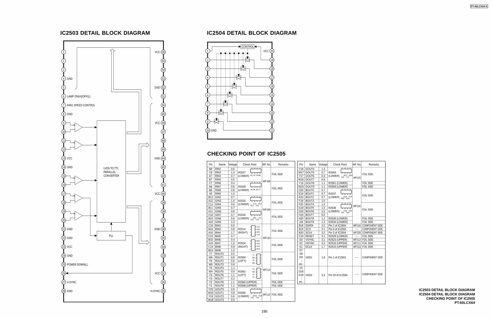
IC2503 DETAIL BLOCK DIAGRAM
IC2503 DETAIL BLOCK DIAGRAMIC2504 DETAIL BLOCK DIAGRAM
CHECKING POINT OF IC2505PT-60LCX64
IC2504 DETAIL BLOCK DIAGRAM
1
2
3
4
5
6
7
8
9
10
11
12
13
14
15
16
17
18
19
20
21
22
23
24
25
26
27
28
56
55
54
53
52
51
50
49
48
47
46
45
44
43
42
41
40
39
38
37
36
35
34
33
32
31
30
29
GND
LAMP ON(H)/OFF(L)
FAN1 SPEED CONTROL
GND
GND
GND
GND
GND
POWER DOWN(L)
V-SYNC
GND
VCC
VCC
VCC
VCC
VCC
VCC
H-SYNC
GND
GND
GND
LVDS TO TTLPARALLELCONVERTER
PLL
1 20
2
3
4
5
6
7
8
9
10
19
18
17
16
15
14
13
12
11GND
CONTROLVCC
Pin
B8C8
RIN2RIN3 R2527
(LOWER)
FOIL SIDE
FOIL SIDE
FOIL SIDE
FOIL SIDE
FOIL SIDE
FOIL SIDE
WF108
WF109
WF110
WF114
WF115
WF115
WF116
WF124
WF125
WF112WF111WF113
FOIL SIDE
FOIL SIDE
FOIL SIDEFOIL SIDE
FOIL SIDE
R2528(LOWER)
R2525(LOWER)
R2526(LOWER)
R2514(RIGHT)
R2524(RIGHT)
R2565(LOWER)
RIN4RIN5
Name Voltage Check Point WF No. Remarks
0.5
0.61.4
0.6
0.7
0.5
1.4
0.8
0.8
0.7
0.6
0.4
0.9
0.7
0.6
0.7
0.8
0.7
1.0
1.7
1.0
1.0
1.0
0.50.4
0.80.60.91.3
0.80.60.9
0.91.10.21.11.10.6
A7B7C7A6
RIN6RIN7RIN8RIN9
B6A5
C7A6B6A5
B12A12
GIN2GIN3GIN4GIN5
C11B11
B12A12
C11B11
A11C10
GIN6GIN7GIN8GIN9
B10A10
A11C10
B10A10
C16B16
BIN2BIN3BIN4BIN5
A16C15
C16B16A16C15
B15A15
BIN6BIN7BIN8BIN9
C14B14
B15A15C14B14
ROUT0Y7
Y20W19
GOUT0GOUT1GOUT2GOUT3
Y19W18
Y20W19
Y19W18
ROUT1W6ROUT2Y6ROUT3W5
Y7W6Y6W5
ROUT4Y5ROUT5W4ROUT6Y4ROUT7Y3
Y5W4Y4Y3
ROUT8Y2Y1 ROUT9
B7 A7 C8 B8
R2564(LEFT)
R2562(LEFT)
R2560 (UPPER)R2558 (UPPER)
COMPONENT SIDECOMPONENT SIDECOMPONENT SIDE
COMPONENT SIDE
COMPONENT SIDE
FOIL SIDE
FOIL SIDEFOIL SIDE
FOIL SIDE
FOIL SIDE
FOIL SIDEFOIL SIDE
FOIL SIDEFOIL SIDEFOIL SIDEFOIL SIDE
R2563(LOWER)
VDD1
D7D8D9
etc.
Pin Name Voltage Check Point WF No. Remarks
....
VDD2
C5D18G16
etc.
....
1.40.70.4
Y18W17
GOUT4GOUT5GOUT6Y17
0.61.11.1
W16Y18
W17Y17
W16
Y16GOUT7GOUT8GOUT9W15
0.70.71.01.51.01.0
0.7D20E19
BOUT0BOUT1BOUT2BOUT3
E20F19
D20E19
E20F19
F20G19
BOUT4BOUT5BOUT6G20
0.51.21.3
1.8
3.3
H19F20
G19G20
H19
H20BOUT7BOUT8BOUT9J18
R2561 (LOWER)R2559 (LOWER)
R2535 (LOWER)R2534 (LOWER)
R2529 (LOWER)
3.2SDATAB18 Pin 2 of IC25043.1SCSB19 Pin 6 of IC25043.2SCLKB20 Pin 3 of IC25043.1RESETC19
R2523 (UPPER)3.1VSYNCD2R2516 (UPPER)3.3HSYNCE2R2515 (UPPER)1.7DCLKE1
Pin 1 of IC2501
Pin 20 of IC2504
R2537(LOWER)
R2536(LOWER)
CHECKING POINT OF IC2505
PT-60LCX64-K
195
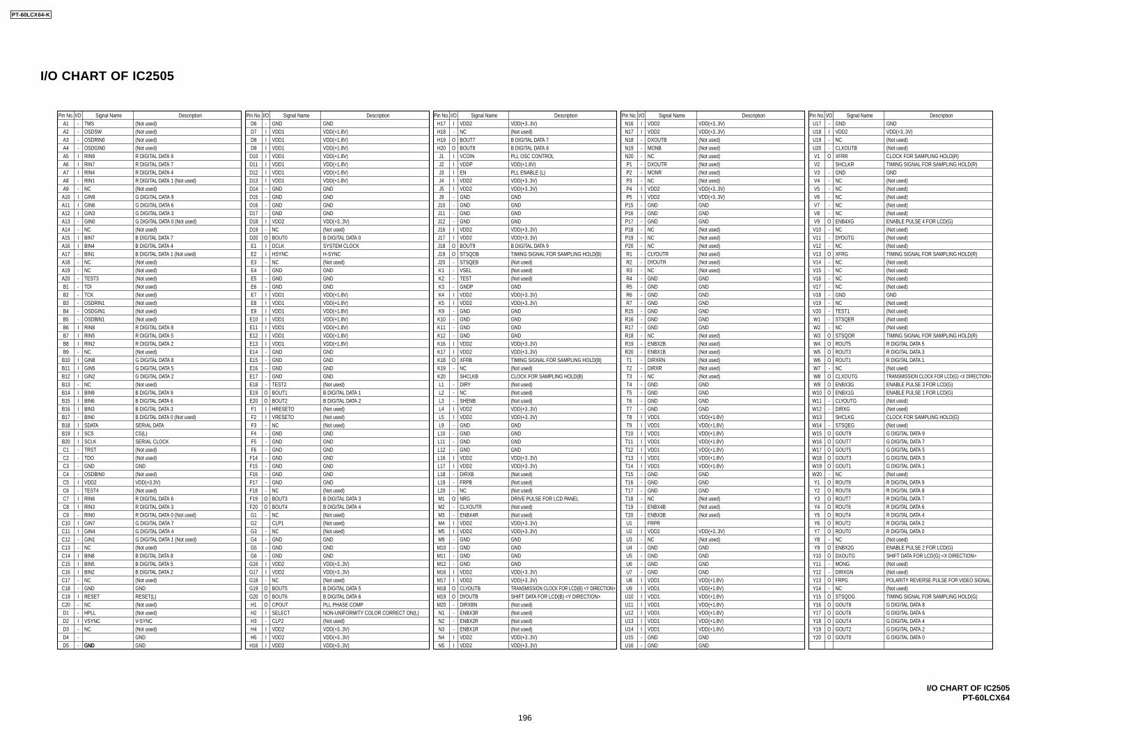
Pin No. I/O DescriptionSignal NameA1A2A3A4A5A6A7A8A9A10A11A12A13A14A15A16A17A18A19A20
T1T2T3T4T5T6T7T8T9
T10T11T12T13T14T15T16T17T18T19T20U1U2U3U4U5U6U7U8U9
U10U11U12U13U14U15U16
U17U18U19U20V1V2V3V4V5V6V7V8V9
V10V11V12V13V14V15V16V17V18V19V20W1W2W3W4W5W6W7W8W9
W10W11W12W13W14W15W16W17W18W19W20Y1Y2Y3Y4Y5Y6Y7Y8Y9
Y10Y11Y12Y13Y14Y15Y16Y17Y18Y19Y20
D1D2D3D4D5
D6D7D8D9
D10D11D12D13D14D15D16D17D18D19D20E1E2E3E4E5E6E7E8E9
E10E11E12E13E14E15E16E17E18E19E20
B1B2B3B4B5B6B7B8B9B10B11B12B13B14B15B16B17B18B19B20C1C2C3C4C5
F1F2F3F4F5F6
G1G2G3G4G5G6
F14F15F16F17F18F19F20
G16G17G18G19G20H1H2H3H4H5
H16
N1N2N3N4N5
N16
J1J2J3J4J5J9
J10J11J12J16J17J18J19J20K1K2K3K4K5K9
K10K11K12K16K17K18K19K20
H17H18H19H20
L1L2L3L4L5L9
L10L11L12L16L17L18L19L20M1M2M3M4M5M9
M10M11M12M16M17M18M19M20
N17N18N19N20P1P2P3P4P5
P16P15
P17P18P19P20R1R2R3R4R5R6R7
R16R15
R17R18R19R20
C6C7C8C9C10C11C12C13C14C15
Pin No. I/O DescriptionSignal Name Pin No. I/O DescriptionSignal Name
C16C17C18C19C20
Pin No. I/O DescriptionSignal Name Pin No. I/O DescriptionSignal Name
-GND
GND- GND GND
-I VDD1 VDD(+1.8V)I VDD1 VDD(+1.8V)I VDD1 VDD(+1.8V)I VDD1 VDD(+1.8V)I VDD1 VDD(+1.8V)I VDD1 VDD(+1.8V)I VDD1 VDD(+1.8V)
I VDD(+1.8V)
I VDD1 VDD(+1.8V)I VDD1 VDD(+1.8V)I VDD1 VDD(+1.8V)I VDD1 VDD(+1.8V)I VDD1 VDD(+1.8V)I VDD1 VDD(+1.8V)I VDD1 VDD(+1.8V)
I VDD1 VDD(+1.8V)I VDD1 VDD(+1.8V)I VDD1 VDD(+1.8V)I VDD1 VDD(+1.8V)I VDD1 VDD(+1.8V)I VDD1 VDD(+1.8V)I VDD1 VDD(+1.8V)
I VDD2 VDD(+3..3V)
I VDD2 VDD(+3..3V)I VDD2 VDD(+3..3V)
I VDD2 VDD(+3..3V)I VDD2 VDD(+3..3V)I VDD2 VDD(+3..3V)
I VDD2 VDD(+3..3V)
I VDD2 VDD(+3..3V)I VDD2 VDD(+3..3V)
I VDD2 VDD(+3..3V)I VDD2 VDD(+3..3V)
I VDD2 VDD(+3..3V)I VDD2 VDD(+3..3V)
I VDD2 VDD(+3..3V)I VDD2 VDD(+3..3V)
I VDD2 VDD(+3..3V)
I VDD(+3..3V)
I VDD2 VDD(+3..3V)
I VDD2 VDD(+3..3V)I VDD2 VDD(+3..3V)
I VDD2 VDD(+3..3V)I VDD2 VDD(+3..3V)
I VDD2 VDD(+3..3V)I VDD2
CLYOUTBDYOUTBDIRXBNENBX3RENBX2RENBX1R
VDD(+3..3V)
I VDD2 VDD(+3..3V)I VDD2 VDD(+3..3V)
I VDD2
DXOUTBMONB
DXOUTRMONR
CLYOUTRDYOUTR
ENBX2BENBX1BDIRXRNDIRXR
ENBX4BENBX3BFRPRVDD2
VDD(+3..3V)I VDD2 VDD(+3..3V)
I VDD2 VDD(+3..3V)
I VDD(+3..3V)
I VDD2 VDD(+3..3V)
I VDD1 VDD(+1.8V)I VDD1 VDD(+1.8V)I VDD1 VDD(+1.8V)I VDD1 VDD(+1.8V)I VDD1 VDD(+1.8V)I VDD1 VDD(+1.8V)I VDD1 VDD(+1.8V)
BOUT0DCLKHSYNC
TEST2BOUT1BOUT2HRESETOVRESETO
NCBOUT3BOUT4
CLP1
GND
BOUT5BOUT6CPOUTSELECTCLP2
GND
-- GND
GND
NC
TMSOSDSWOSDRIN0OSDGIN0RIN9RIN7RIN4RIN1
GIN9
GIN3
NCBIN7BIN4BIN1
TEST3TDITCKOSDRIN1OSDGIN1OSDBIN1RIN8RIN5RIN2
GIN8GIN5GIN2
BIN9BIN6BIN3BIN0SDATASCSSCLKTRSTTDOGNDOSDBIN0VDD2TEST4RIN6RIN3RIN0GIN7GIN4GIN1
BIN8BIN5BIN2
GND GNDRESET
HPLLVSYNC
GND- GND GND- GND GND- GND GND
- GND GND- GND GND- GND GND
- GND GND- GND GND- GND GND- GND GND
- GND GND- GND GND- GND GND- GND GND- GND GND- GND GND- GND GND
- GND GND- GND GND- GND
- GND
- GND GND- GND GND- GND GND- GND GND
- GND GND- GND GND- GND GND- GND GND
- GND GND
- GND
- GND GND- GND GND- GND GND
- GND GND- GND GND- GND GND- GND GND
- GND GND- GND GND- GND GND
- GND GND- GND GND- GND GND- GND GND- GND GND- GND GND- GND GND
- GND GND- GND GND- GND GND- GND GND
- GND GND- GND GND- GND GND
- GND GND- GND GND- GND GND- GND GND
- GND GND- GND GND
- GNDVDD2
CLXOUTBXFRRSHCLKR
ENB4XG
DYOUTG
XFRG
TEST1STSQER
STSQORROUT5ROUT3ROUT1NCCLXOUTGENBX3GENBX1GCLYOUTGDIRXGSHCLKGSTSQEGGOUT9GOUT7GOUT5GOUT3GOUT1
ROUT9ROUT8ROUT7ROUT6ROUT4ROUT2ROUT0
ENBX2GDXOUTGMONGDIRXGNFRPG
GOUT8
GOUT4
GOUT0
GOUT6
GOUT2
STSQOG
GND
- GND GND
- GND GND
(Not used)-
GIN6
GIN0(Not used)
- NC (Not used)- NC (Not used)
- NC (Not used)
- NC (Not used)
-NC (Not used)
--
NC (Not used)
- NC (Not used)
- NC (Not used)
- NC (Not used)
- (Not used)
- NC (Not used)
- NC (Not used)
- NCBOUT7BOUT8VCOINVDDPEN
BOUT9STSQOBSTSQEBVSELTESTGNDP
XFRB
SHCLKBDIRY
SHENB
DIRXBFRPB
NRGCLXOUTRENBX4R
(Not used)
- NC (Not used)
- NC (Not used)
- NC (Not used)
- NC (Not used)
- NC (Not used)
- NC (Not used)- NC (Not used)- NC (Not used)
- NC (Not used)
- NC (Not used)
- NC (Not used)
- NC (Not used)
- NC (Not used)
- NC (Not used)
- NC (Not used)- NC (Not used)- NC (Not used)- NC (Not used)- NC (Not used)
- NC (Not used)
- NC (Not used)
- NC (Not used)- NC (Not used)- NC (Not used)- NC (Not used)
- NC (Not used)
- NC (Not used)
- NC (Not used)
- (Not used)
- NC (Not used)
- NC (Not used)
- NC (Not used)
- NC (Not used)
- NC (Not used)
(Not used)(Not used)(Not used)(Not used)R DIGITAL DATA 9R DIGITAL DATA 7R DIGITAL DATA 4R DIGITAL DATA 1 (Not used)
G DIGITAL DATA 9G DIGITAL DATA 6G DIGITAL DATA 3
B DIGITAL DATA 7
G DIGITAL DATA 0 (Not used)
B DIGITAL DATA 1 (Not used)B DIGITAL DATA 4
----
----
-
-
--
III
III
II
I
III
-
III
III
III
-
--
-
-II-II
-II
-
I
I
I
(Not used)(Not used)(Not used)(Not used)(Not used)(Not used)R DIGITAL DATA 8R DIGITAL DATA 5R DIGITAL DATA 2
G DIGITAL DATA 8G DIGITAL DATA 5G DIGITAL DATA 2
B DIGITAL DATA 9B DIGITAL DATA 6B DIGITAL DATA 3B DIGITAL DATA 0 (Not used)SERIAL DATACS(L)SERIAL CLOCK(Not used)(Not used)
(Not used)VDD(+3.3V)(Not used)R DIGITAL DATA 6R DIGITAL DATA 3R DIGITAL DATA 0 (Not used)G DIGITAL DATA 7G DIGITAL DATA 4G DIGITAL DATA 1 (Not used)
B DIGITAL DATA 8B DIGITAL DATA 5B DIGITAL DATA 2
RESET(L)
V-SYNC(Not used)
-
IO
I
O
I
O
IO
B DIGITAL DATA 0
H-SYNCSYSTEM CLOCK
(Not used)B DIGITAL DATA 1B DIGITAL DATA 2(Not used)(Not used)
OO
B DIGITAL DATA 3B DIGITAL DATA 4
(Not used)
OOI-
B DIGITAL DATA 5B DIGITAL DATA 6PLL PHASE COMPNON-UNIFORMITY COLOR CORRECT ON(L)(Not used)
I
OOI
OO---
O
-
-
--
-O
-
O
-O
---
B DIGITAL DATA 7B DIGITAL DATA 8PLL OSC CONTROL
PLL ENABLE (L)
B DIGITAL DATA 9
(Not used)TIMING SIGNAL FOR SAMPLING HOLD(B)
(Not used)(Not used)
TIMING SIGNAL FOR SAMPLING HOLD(B)
CLOCK FOR SAMPLING HOLD(B)(Not used)
(Not used)
(Not used)(Not used)
(Not used)(Not used)
DRIVE PULSE FOR LCD PANEL
(Not used)(Not used)(Not used)(Not used)
TRANSMISSION CLOCK FOR LCD(B) <Y DIRECTION>SHIFT DATA FOR LCD(B) <Y DIRECTION>
--
--
--
--
--
--
(Not used)(Not used)
(Not used)(Not used)
(Not used)(Not used)
(Not used)(Not used)(Not used)(Not used)
(Not used)(Not used)
-O
-
O
-
O
-
O
-O
OOO
OO
-
-OOOO
OOO
O
OOOO
--
OO
O
OOOOOO
(Not used)CLOCK FOR SAMPLING HOLD(R)TIMING SIGNAL FOR SAMPLING HOLD(R)
ENABLE PULSE 4 FOR LCD(G)
(Not used)
TIMING SIGNAL FOR SAMPLING HOLD(R)
(Not used)(Not used)
TIMING SIGNAL FOR SAMPLING HOLD(R)R DIGITAL DATA 5R DIGITAL DATA 3R DIGITAL DATA 1
TRANSMISSION CLOCK FOR LCD(G) <X DIRECTION>ENABLE PULSE 3 FOR LCD(G)ENABLE PULSE 1 FOR LCD(G)(Not used)(Not used)CLOCK FOR SAMPLING HOLD(G)(Not used)G DIGITAL DATA 9G DIGITAL DATA 7G DIGITAL DATA 5G DIGITAL DATA 3G DIGITAL DATA 1
R DIGITAL DATA 9R DIGITAL DATA 8R DIGITAL DATA 7R DIGITAL DATA 6R DIGITAL DATA 4R DIGITAL DATA 2R DIGITAL DATA 0
ENABLE PULSE 2 FOR LCD(G)SHIFT DATA FOR LCD(G) <X DIRECTION>(Not used)(Not used)POLARITY REVERSE PULSE FOR VIDEO SIGNAL
TIMING SIGNAL FOR SAMPLING HOLD(G)G DIGITAL DATA 8G DIGITAL DATA 6G DIGITAL DATA 4G DIGITAL DATA 2G DIGITAL DATA 0
I/O CHART OF IC2505
I/O CHART OF IC2505PT-60LCX64
PT-60LCX64-K
196
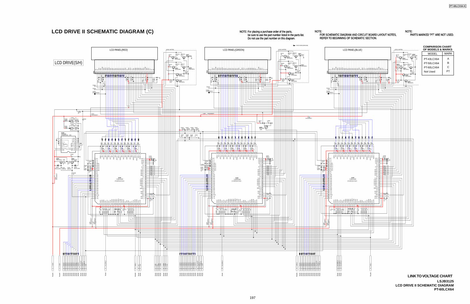
NOTE:FOR SCHEMATIC DIAGRAM AND CIRCUIT BOARD LAYOUT NOTES,REFER TO BEGINNING OF SCHEMATIC SECTION.
NOTE: For placing a purchase order of the parts, be sure to use the part number listed in the parts list. Do not use the part number on this diagram.
NOTE:PARTS MARKED "PT" ARE NOT USED.
LCD DRIVE II SCHEMATIC DIAGRAM (C) NOTE:FOR SCHEMATIC DIAGRAM AND CIRCUIT BOARD LAYOUT NOTES,REFER TO BEGINNING OF SCHEMATIC SECTION.
NOTE: For placing a purchase order of the parts, be sure to use the part number listed in the parts list. Do not use the part number on this diagram.
NOTE:PARTS MARKED "PT" ARE NOT USED.
LSJB3125LCD DRIVE II SCHEMATIC DIAGRAM
PT-60LCX64
XFRP
45
DIR_
Y75
DY58
0.1
C206
9
0.1
C207
1
CLY
57
DIR_
X73
TP2005
STSQ
O_G
46XF
R_G
43
GO
UT3
53
GO
UT5
51G
OUT
650
GO
UT1
55
GO
UT4
52
GO
UT7
49G
OUT
848
GO
UT0
56
GO
UT9
47
GO
UT2
54
+3.3
V9
P200
2
35 34 33 32 31 30 29 28 27 26 25 24 23 22 21 18 17 16 15 14 13 12 11 10 9 8 7 6 5 4 3 2 1192036
SH_C
LK_G
44
0.1
C206
7
0.1
C207
0
SD_D
ATA_
O17
SH_C
SB_O
19
SD_S
CK_O
18
22KR2087
0R2090
2700R2089
3300[D]R2094
1500[D]R2095
2700R2088
330[D]R2096
4700[D]R2097
R207
2
22
C200
90.
1
C20170.1
C205
0
0.1
R206
3
22
C20220.1
C203747/6.3V
C20310.1
R206
5
22
C204
6
0.1
IC2002C1AB00001895
1 2 3 4 5 6 7 8 9 10 11 12 13 14 15 16 17 18 19 20 21 22 23 24 25
26272829303132333435363738394041424344454647484950
51525354555657585960616263646566676869707172737475
7677787980
86
81
91
85
89
83
99
87
9495
100
98
92
84
82
93
90
88
9697
C20340.1
R206
6
22 R207
0
22R206
9
22
C205
1
0.1
C204
7
0.1
R207
3
22R207
1
22 R207
4
22
C202533/25V
C201
0
0.1
R206
4
22
C201
40.
1
R206
8
22C2
049
0.1
C204
8
0.1
R206
7
22
R201
022
R201
122
R201
222
R2043 22R2046 22
R2040 22R2037 22R2033 22R2030 22
R2027 22
R201
522
R201
422
R201
622
R201
322
R201
722
C2029 0.1
R2044 22
C20180.1
R201
822
0.1
C207
6
R202
322
R202
522
C20350.1
0.1
C207
3
BOUT
467
C205
4
0.1
BOUT
962
R202
422
BOUT
170
SH_C
LK_B
61
BOUT
269
R2031 22
R201
922
BOUT
368
R208
0
22
IC2003C1AB00001895
1 2 3 4 5 6 7 8 9 10 11 12 13 14 15 16 17 18 19 20 21 22 23 24 25
26272829303132333435363738394041424344454647484950
51525354555657585960616263646566676869707172737475
7677787980
86
81
91
85
89
83
99
87
9495
100
98
92
84
82
93
90
88
9697
C205
5
0.1
R207
8
22
C20110.1
R208
3
22
BOUT
764
C201
50.
1
R207
6
22C2
053
0.1
0.1
C207
5
TP2006
C201
20.
1
C20320.1
BOUT
863
R2041 22
R208
2
22
R2038 22
C203847/6.3V
C20230.1
0.1
C207
7
C205
2
0.1
R208
4
22
R2047 22
R202
022
R2028 22
C205
7
0.1
C205
6
0.1
BOUT
566
P200
3
35 34 33 32 31 30 29 28 27 26 25 24 23 22 21 18 17 16 15 14 13 12 11 10 9 8 7 6 5 4 3 2 1192036
R208
5
22R207
7
22
R202
222
R2034 22
R202
122
R208
6
22R207
5
22
XFR_
B59
BOUT
665
C20280.1
R208
1
22
BOUT
071
STSQ
O_B
60
R207
9
22
R2036 22
R200
222
0.1
C206
3
ROUT
531
R200
922
R206
0
22
C200
70.
1
C20300.1
R205
4
22R205
2
22
TP2004
CLX
37
C20210.1
0.1
C206
5
ROUT
333
R206
1
22C2
045
0.1
ROUT
630
R2029 22
R205
3
22
R2026 22
C204
0
0.1
DX42
R205
9
22
ROUT
036
R200
422
C200
8
0.1
R2045 22
R205
7
22R205
1
22
FRP
23
ROUT
432
C204
4
0.1
C20330.1
R200
822
ROUT
135
R200
122
ENB3
39
ROUT
927
R200
722
0.1
C206
4
R2042 22
XFR_
R24
C20160.1
TP2001D0YBR0000015
R205
5
22 R206
2
22
0.1
C206
1
STSQ
O_R
26
SH_C
LK_R
25
R200
622
ENB1
41
IC2001C1AB00001895
1 2 3 4 5 6 7 8 9 10 11 12 13 14 15 16 17 18 19 20 21 22 23 24 25
26272829303132333435363738394041424344454647484950
51525354555657585960616263646566676869707172737475
7677787980
86
81
91
85
89
83
99
87
9495
100
98
92
84
82
93
90
88
9697
ROUT
729
C204
3
0.1
C204
2
0.1
R200
322
ENB2
40
ENB4
38
C204
1
0.1
C20270.1
R205
8
22
R2032 22
C202433/25V
NRG
22
C201
3
0.1
R205
6
22
R2039 22
ROUT
234
ROUT
828
+15.
5V72
Q2003UN521300L
R210115K
C20600.1
C200
10.
1
C200
40.
1
C200
2
0.1
C200
30.
1
C200
50.
1
C200
60.
1
TP2002D0YBR0000015 TP2003
D0YBR0000015
C202633/25V
C203647/6.3V
C206633/25V
C207233/25V C2
078
33/2
5V
SH_C
SR_O
21
SH_C
SG_O
20
P200
1
35 34 33 32 31 30 29 28 27 26 25 24 23 22 21 18 17 16 15 14 13 12 11 10 9 8 7 6 5 4 3 2 1192036
220
R2100
1500
R2093
1500[D]
R2099
10K[D]
R2092
0.1C2039
0.1C2059
CD4053BMIC2004
C0JBAR000338
12345678
111213141516
910
PTR2102
12K[D]R2091
0R2050
12K[D]R2098
4700R2105
4700R2108
10R2126
2SD1819AHLQ2020
2SD1819AHLQ2014
68R2112
68R2121
2SB1218AHLQ2015
2SB1218AHLQ202110
R2124
2SD1819AHLQ2009
10R2115
10R2117
2SB1218AHLQ2006
10R2122
2SB1218AHLQ2017
2SD1819AHLQ2016
10R2110
4700R2106
10R2113
2SD1819AHLQ2010
4700R2103
2SB1218AHLQ2004
68R2109
10R2119
68R2118
2SD1819AHLQ2007
2SB1218AHLQ2011
10R2125
2SB1218AHLQ2019
2SD1819AHLQ2018
10R2114
4700R2107
10R2116
2SD1819AHLQ2012
4700R2104
2SB1218AHLQ2005
68R2111
10R2123
68R2120
2SD1819AHLQ2008
2SB1218AHLQ2013
2SB1218AHLQ2001
10R2048
MA2J111008D2001
10R2049
220P[JC]C2019
2SD1819AHLQ2002
56R2035
220P[JC]C2020
MA2J111008D2002
TP2007
0.1C2058
1[KB
]C2
062
1[KB
]C2
068
1[KB
]C2
074
XDIR
_X74
R200
522
0
L201
6
L200
1J0
JCC0
0000
77
0L2
012
0L2
014
L2010J0JCC0000077
0L2
015
L2009 J0JCC0000077
L200
6J0
JCC0
0000
77
L200
4J0
JCC0
0000
77
0L2
011
L2008J0JCC0000077
L200
7J0
JCC0
0000
77
L200
5J0
JCC0
0000
77
0L2
013
L200
2J0
JCC0
0000
77
L200
3J0
JCC0
0000
77
NRG
SIG
12
SIG
3SI
G4
SIG
2
NCDY XCLX
ENB1
SIG
6
ENB2
DX VDDX
NC SIG
11
SIG
9
CLY
ENB4
SIG
8
LCCO
M
SIG
5
ENB3
VSSY
DYSIG
10
SIG
1
NCDIRY
LCCO
MVD
DY
NRS2
VSSX
XCLY
SIG
7
CLX
DIRX
AVCC
1,3
VID5
AGND
12
NC
AVCCD
TSTA
DXIN
CLYN
SVRE
FH
AVCC
10,1
2
VID4
XFR
V2
NC
CLXIN
NRG
DIRY
AGND
S
AGND
1VI
D1
VID1
0
INV
DB6
CLX
ENBX2
DYLCCO
M
DVCC
VID2
AGND
11,2
VREFH
V1
DB7
ENBX4I
AGNDL
CLY
TSTM
VID3
AGND
8,10
STSQ
DB2
CLXN
ENBX1I
DIRY
IN
NCDGND
AVCC
6,8
VID1
1
DB3
VREFH
NC
DX
MONIN
DYIN
SCLK
AGND
4,6
AGND
7,9
DB8
DB5
DGND
ENBX2I
DIRX
AVCC
S
SCS
VID7
VID9
DB9
DB1
AGNDDENBX3
NC
CLYI
N
DCO
UT
VID6
AVCC
9,11
NC
DB4
DGND
ENBX3I
AVCCL
SVRE
FL
SDAT
A
AVCC
5,7
VID8
VID1
2
R/L
VREFL
ENBX4
MONOUT
DIRX
IN
SVRE
FL
AGND
3,5
AVCC
2,4
CLK
DB0
DVCC
ENBX1
NRGIN
AGND
S
BYP
DVCC
DIRX
AGND
S
NRS1
SDAT
A
VDDX
AVCCD
VID2
AVCC
S
AGND
11,2
AGND
1DI
RY
NC
SCS
VREFH
VID1
AGND
12
AGNDD
LCCO
M
VID7
SIG
11
V1
NRG
VID1
0
ENBX3
VID9
DB7
AVCC
1,3
INV
VDDY
SIG
9
SIG
12
NC
TSTA
DB9
CLXN
ENBX4I
DB6
NRS2
CLYI
N
CLY
DXIN
SIG
3
DB1
ENBX1I
AGNDL
DCO
UT
CLYN
VSSX
DIRY
INEN
B4
SIG
4
VID6
SVRE
FH
SCLK
NC
XFR
XCLY
SIG
8
SIG
2
AVCC
9,11
VID1
1
AVCC
10,1
2
AGND
4,6
DGND
V2
DIRX
IN
SIG
7
DB3
LCCO
M
VID4
AVCC
5,7
NC
AGND
7,9
AVCC
6,8
NC
SVRE
FL
VREFH
CLY
VID8
DB8
CLX
CLXIN
SIG
5
DY
AGND
3,5
NC
TSTM
VID1
2
ENBX1
DB5
NRG
AVCC
2,4
DIRX
ENB3
XCLX
DX
VID3
R/LNRGIN
DGND
DIRY
NC
CLK MONIN
AGND
8,10
VSSY
VREFL
ENB1
AGND
S
ENBX2IDB4
DB0
DYIN
STSQ
ENBX4CLX
BYP
DY
DGND
SIG
6
DVCC
DB2
MONOUT
ENBX2
ENBX3I
SIG
10
ENB2
DY
AVCCL
SIG
1
LCCO
M
VID5
DX
SVRE
FL
NC
AVCC
9,11
CLX
CLXIN
SIG
5
DY
VID1
1
ENBX1I
DB8
VID4
DB9
DIRX
IN
NRG
DB3
DIRY
IN
DIRX
ENB3
DB5
XCLX
DB1
SVRE
FL
DIRY
VREFH
NC
DGND
ENBX1
AGND
3,5
VSSY
ENB1
NC
DGND
ENBX2I
NRGIN
AVCC
2,4
DYSIG
6
DX
AVCC
6,8
NC
AGND
S
CLK MONIN
DB4
CLY
SIG
10
ENB2
BYP
DB0
DYIN
DGND
TSTM
AVCC
5,7
DVCC
SIG
1
DX
ENBX3I
VID3
VID8
NRS1
VDDX
AVCCL
AGND
8,10
VID1
2
AGND
11,2
AGND
S
SVRE
FL
STSQ
R/L
DIRY
NC
VREFH
AGND
1
SDAT
A
DB2
VREFL
CLX
AVCC
1,3
LCCO
M
SIG
11
V1
NRG
VID1
ENBX4
ENBX2
DB7
VID5
VID1
0
NC
VDDY
SIG
9
SIG
12
MONOUT
DY
AGNDD
ENBX4I
INV
AVCCD
LCCO
M
NRS2
CLY
SIG
3
ENBX3
AGNDL
DB6
TSTA
DVCC
DIRX
NC
VSSX
ENB4
SIG
4
DXIN
VID2
AVCC
S
AGND
12CL
YIN
XFR
XCLY
SIG
8
SCLK
SIG
2
CLYN
SCS
DCO
UT
V2
AGND
4,6
SVRE
FH
VID7
SIG
7
LCCO
M
NC
VID6
NCCLXN
AGND
7,9
AVCC
10,1
2
VID9
LCD PANEL(RED)
INH
H
VEE
HH
VDD
VSS
[105]
LCD PANEL(GREEN) LCD PANEL(BLUE)(LEVEL SHIFTER) (LEVEL SHIFTER) (LEVEL SHIFTER)
(SW)
(SW)(SW)
(R SAMPLING HOLD) (G SAMPLING HOLD) (B SAMPLING HOLD)
TO L
D IV
TO L
D IV
TO L
D I
TO L
D I
TO L
D I
TO L
D I
TO L
D I
TO L
D I
TO L
D I
TO L
D I
TO L
D I
TO L
D I
TO L
D I
TO L
D I
TO L
D I
TO L
D I
TO L
D I
TO L
D I
TO L
D I
TO L
D III
TO L
D I
TO L
D I
TO L
D I
TO L
D I
TO L
D I
TO L
D I
TO L
D I
TO L
D I
TO L
D I
TO L
D I
TO L
D I
TO L
D I
TO L
D I
TO L
D I
TO L
D I
TO L
D I
TO L
D I
TO L
D I
TO L
D I
TO L
D I
TO L
D I
TO L
D I
TO L
D I
TO L
D I
TO L
D I
TO L
D III
TO L
D I
TO L
D I
TO L
D I
TO L
D I
TO L
D I
TO L
D I
TO L
D I
TO L
D I
TO L
D I
TO L
D I
TO L
D I
TO L
D III
TO L
D I
TO L
D I
(SW)
VIDEO SIGNAL(MAIN/SUB)
LCD DRIVE(S/H)
COMPARISON CHART OF MODELS & MARKS
PT-43LCX64
PT-50LCX64
PT-60LCX64
Not Used
A
B
C
PT
MODEL MARK
LINK TO VOLTAGE CHART
PT-60LCX64-K
197
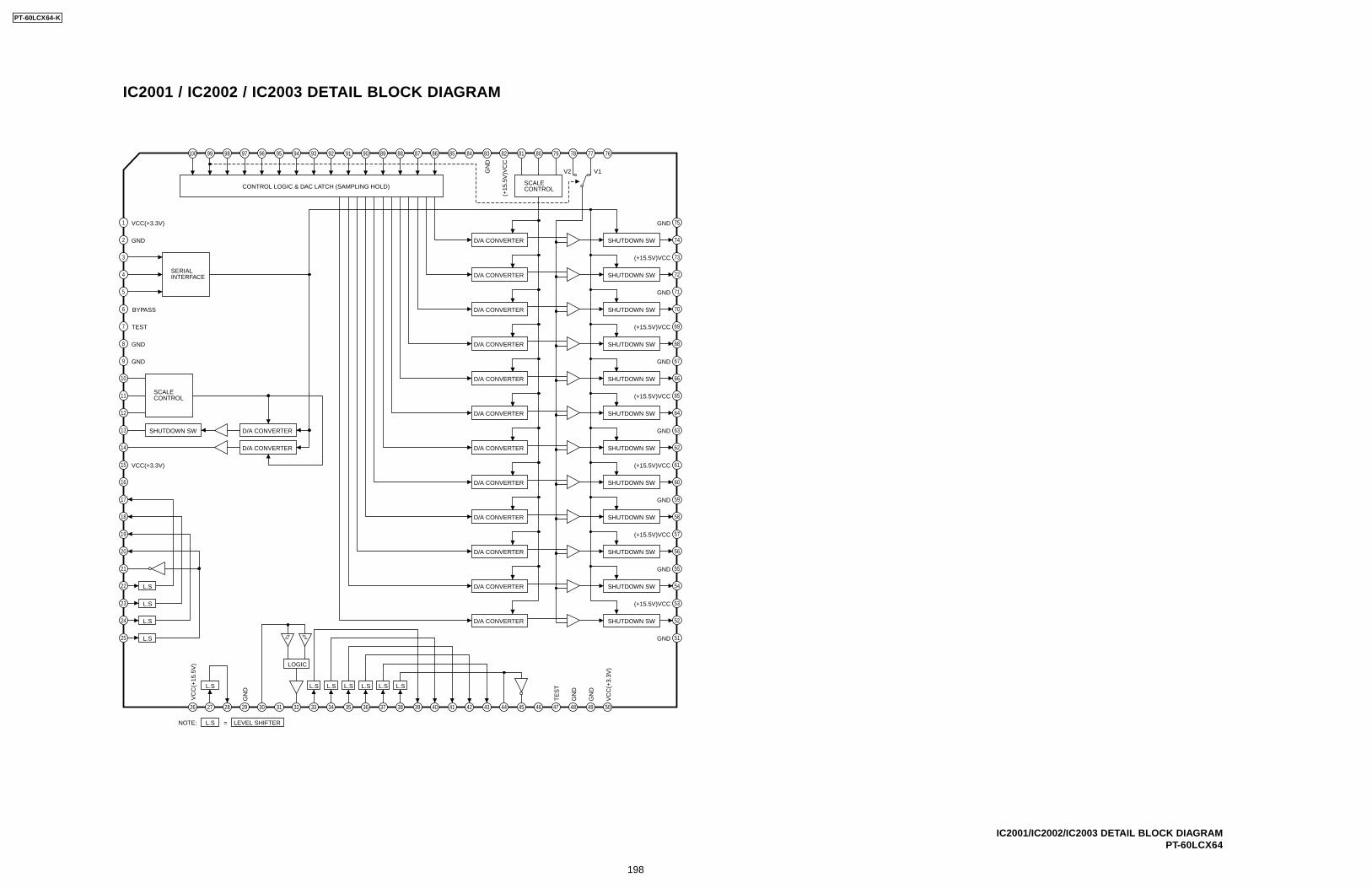
IC2001 / IC2002 / IC2003 DETAIL BLOCK DIAGRAM
IC2001/IC2002/IC2003 DETAIL BLOCK DIAGRAMPT-60LCX64
1
2
3
4
5
6
7
8
9
10
11
12
13
14
15
16
17
18
19
20
21
22
23
24
25
26 27 28 29 30 31 32 33 34 35 36 37 38 39 40 41 42 43 44 45 46 47 48 49 50
100 99 98 97 96 95 94 93 92 91 90 89 88 87 86 85 84 83 82 81 80 79 78 77 76
75
74
73
72
71
70
69
68
67
66
65
64
63
62
61
60
59
58
57
56
55
54
53
52
51
SERIALINTERFACE
VCC(+3.3V)
GND
BYPASS
TEST
GND
GND
SCALECONTROL
SHUTDOWN SW D/A CONVERTER
D/A CONVERTER
VCC(+3.3V)
L.S
VC
C(+
15.5
V)
GN
D
L.S
L.S
L.S
L.S
LOGIC
L.S L.S L.S L.S L.S L.S
VC
C(+
3.3V
)
GN
D
GN
D
TE
ST
GND
CONTROL LOGIC & DAC LATCH (SAMPLING HOLD)SCALECONTROL
(+15
.5V
)VC
C
GN
D
V1V2
SHUTDOWN SWD/A CONVERTER
SHUTDOWN SWD/A CONVERTER
SHUTDOWN SWD/A CONVERTER
SHUTDOWN SWD/A CONVERTER
SHUTDOWN SWD/A CONVERTER
SHUTDOWN SWD/A CONVERTER
SHUTDOWN SWD/A CONVERTER
SHUTDOWN SWD/A CONVERTER
SHUTDOWN SWD/A CONVERTER
SHUTDOWN SWD/A CONVERTER
SHUTDOWN SWD/A CONVERTER
SHUTDOWN SWD/A CONVERTER
NOTE: =L.S LEVEL SHIFTER
(+15.5V)VCC
GND
(+15.5V)VCC
GND
(+15.5V)VCC
GND
(+15.5V)VCC
GND
(+15.5V)VCC
GND
(+15.5V)VCC
GND
PT-60LCX64-K
198
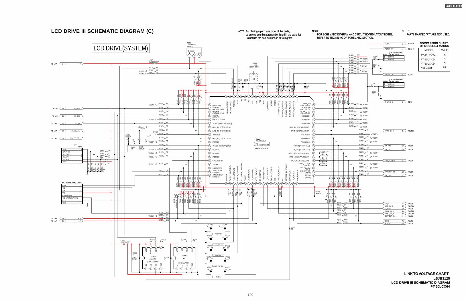
NOTE:FOR SCHEMATIC DIAGRAM AND CIRCUIT BOARD LAYOUT NOTES,REFER TO BEGINNING OF SCHEMATIC SECTION.
NOTE: For placing a purchase order of the parts, be sure to use the part number listed in the parts list. Do not use the part number on this diagram.
NOTE:PARTS MARKED "PT" ARE NOT USED.
LCD DRIVE III SCHEMATIC DIAGRAM (C) NOTE:FOR SCHEMATIC DIAGRAM AND CIRCUIT BOARD LAYOUT NOTES,REFER TO BEGINNING OF SCHEMATIC SECTION.
NOTE: For placing a purchase order of the parts, be sure to use the part number listed in the parts list. Do not use the part number on this diagram.
NOTE:PARTS MARKED "PT" ARE NOT USED.
LSJB3125LCD DRIVE III SCHEMATIC DIAGRAM
PT-60LCX64
1KR2325
47/6.3VC2323
0.1
C231
7
SD_SCK15
0.1C2315
18KR2323
PTC2322
27KR2324
0.01
[KB]
C230
9
LCD_ON_H 82D_RESET 10
PTR2322
DIR_X 73
10K
R236
110
KR2
357
10K
R235
3
0.1
C231
2
0.1
C231
3
+3.3V 9
+17V80
MA3
J142
E0L
D230
1
+5V2
CORRECT_CS 12
CORRECT_ON_L 1
DIR_Y 75
2200
R233
4
PTC2306
56R2327
0.1[KB]C2307
56R2326
47K
R234
947
KR2
345
47K
R234
247
KR2
338
1KR2
362
1KR2
363
1KR2
364
1KR2
366
10K
R240
8
47K
R237
6
10K
R241
0
47K
R238
0
10K
R241
5
10K
R241
2
47K
R237
3
10K
R241
4
47K
R238
4
10K
R233
2
5600R23901KR23915600R23921KR23931KR23945600R2395
5600R23965600R2397
100R2371
47K
R241
3
47K
R241
1
47K
R240
9
47K
R240
7
100R2438
100R2437
47K
R240
347
KR2
406
TIMER_ON_H 7
PTC2325
PTC2326
47K
R240
0
47K
R237
5
47K
R238
9
47K
R237
947
KR2
383
47K
R238
6
100R2436
PTR2434 TP2331
100R2435
PTR2432
TP2330PTR2433
47K
R238
8
47K
R238
2
47K
R239
9
47K
R238
5
47K
R237
447
KR2
378
47K
R240
5
47K
R240
2
PTR2429
PTC2
321
PTC2
320
PTC2
319
PTC2
318
2200
R234
1
47K
R232
9
47K
R233
1
100R2320
PTR2318TP2312
47K
R233
7
47K
R234
4
47K
R234
8
47K
R235
2
47K
R235
6
47K
R236
0
TP2311
PTR2313
PTR2316
TP2307
PTR2317
TP2310
TP2309 PTR2315
PTR2314
47K
R233
5
47K
R235
947
KR2
355
47K
R234
7
47K
R235
1
47K
R234
347
KR2
340
PTR2
328
100R2304
100R2305
PTR2303
100R2306
TP2302 PTR2307
PTR2308
PTR2309
1KR2310
PTR2311
1KR2312
TP2325
PTR2417TP2324
10KR2416
PTR2418
47K
R237
747
KR2
381
33K
R240
4
33K
R238
7
33K
R240
1
33K
R239
8
PTR2
350
PTR2
354
47K
R235
8
PTR2301PTR2302
IC2303C0EBH0000282
1 2 3
+12V79
0.1C2328
0.1C2327
PTC2324 PTR2424
PTR2425
1KR2426
TP2326
TP2329
1KR2423
FILTER_DET 4
PTC2
316
PTR2428
FAN2_SD_CTL77
PTR2427
PTR2422
FAN3_SD_CTL78
PTR2430
PTR2431 TP2328
TP2327
PTR2419
PTR2420
PTR2421
100R2321
1KR2
367
100R2319
PTR2339
PTR2346
PTC2308
TP2313
47KR2365
0.1C2310
P2302
87654321
X23018MHz
H2D800400017
TP2335
TP2314TP___PT
TP2319TP___PT
TP2315TP___PT
TP2320TP___PT
TP2316TP___PT
TP2321TP___PT
TP2317TP___PT
TP2322TP___PT
TP2318TP___PT
TP2323TP___PT
2200
R233
0
2200
R233
3
2200
R233
6
PTR2444TP2343
TP2344PTR2446
PTR2443
PTR2445
FAN3_ON_H 81
FAN1_ON_H 83FAN2_ON_H 84
TP2341TP2336
TP2342
SD_DATA16
100/6.3VC2333
100/6.3VC2334
TP2345
TP2347
TP2346
SH_CSR 11
+15.5ADJ76
PTC2335
SH_CSG 13
SH_CSB 14
33K
R243
9
TP2340
PTC2332
P2301PT
1VDD2SD_SCK3SD_DATA4MS_DATA5LAMP_CS6GND
PTC2
304
PTC2
302
PTC2
303
PTC2
301
PTC2
305
PTR2447
PTC2329
THERMO_3 6
THERMO_1 5
TP2339
TP2338
TP2337
TP2303
TP2304
XDIR_X 74
L2307J0JCC0000077
100L2309
100L2311
PTL2305
PTL2303PTL2304
PTL2302
L2306J0JCC0000077
PTL2301
IC2304MN101C62DMF
1234567891011121314151617181920
21
22
23
24
25
26
27
28
29
30
31
32
33
34
35
36
37
38
39
40
41 42 43 44 45 46 47 48 49 50 51 52 53 54 55 56 57 58 59 60
61
62
63
64
65
66
67
68
69
70
71
72
73
74
75
76
77
78
79
80
PT
IC2302
1 2 3 4
5678
IC2301LSEQ0763
1 2 3 4
5678
P2304
21
P2303
21
RESETGND
RXD_WRITERVDD
RXDTXD
VDD
VSS
VSS
THER
MO
1_IN
(AN0
/PA0
)
THER
MO
2_IN
(AN1
/PA1
)
THER
MO
4_IN
(AN3
/PA3
)
THER
MO
3_IN
(AN2
/PA2
)
AN6/
PA6
3.3V
_IN(
AN7/
PA7)
AN5/
PA5
FILT
ER_D
ET(A
N4/P
A4)
VREF
+
OSC
2
OSC
1XIXO
MM
OD
NRST
/P27
(TXD
0A/S
BO0A
/P00
)
(RXD
0A/S
BI0A
/P01
)
(SBT0A/P02)
(TXD1/SBO1/P03)MS_DATA
(SBT1/P05)NDK/BUZZER/P06
15.5ADJ[RMOUT/TM0IO/P10]
FAN1_SD_CTL[TM1IO/P11]
FAN2_SD_CTL[TM2IO/P12]
FAN3_SD_CTL[TM7IO/P14]
TM3IO/P13
IRQ0/P20
TV_LCD_CS(ACZ/IRQ1/P21)
IRQ2/P22
IRQ3/P23
IRQ4/P24
SDA/SBO2/P30
SBI2/P31
SCL/SBT2/P32TM4IO/TXD0B/
TM8IO/RXD0B/
(P64/A4)
CORRECT_CS
(P67/A7)
(P66/A6)
FAN2_LOCK_H(P71/SD01/A9)
TIMER_ON_H(P70/SD00/A8)
SH_CSG[P73/SD03/A11]
FAN3_LOCK_H(P72/SD02/A10)
P75/SD05/A13
P77/SD07/A15
P76/SD06/A14
SH_CSB[P74/SD04/A12]
FAN3_ON_H(P87/LED7/D7)
FAN3_SD_CTL(P86/LED6/D6)
P85/LED5/D5
P84/LED4/D4
(P80/LED0/D0)
(P81/LED1/D1)
P83/LED3/D3
(P82/LED2/D2)
XDIR
_X(P
63/A
3)
DIR_
X(P6
2/A2
)
EEP_
CS(P
61/A
1)
CORR
ECT_
ON_
L(P6
0/A0
)
FAN1
_ON_
H(P5
3/A1
6)
FAN2
_ON_
H(P5
4/A1
7)
VDD
VSS
D_RE
SET(
P52/
NCS)
LCD_
ON_
H(P5
1/NR
E)
DIR_
Y(P5
0/NW
E)
FACT
ORY
_L(P
40/K
EY0)
F_AD
J_L(
P41/
KEY1
)
SELF
_CHE
CK_L
(P43
/KEY
3)
SERV
ICE_
L(P4
2/KE
Y2)
17V_
IN(P
46/K
EY3)
MO
DE_L
(P47
/KEY
7)
14V_
IN(P
45/K
EY5)
P44/
KEY4
P35/
SBT0
B
SBO0B/P33
SBI0B/P34
/CS
GND
(32kbit EEPROM)
VDD
SI
/HO
LD SCK
/WP
SO
(RXD1/SBI1/P04)
SD_DATA
SD_SCK
(P65/A5)
FAN1_LOCK_H
FAN1_SD_CTL
THERMO_2THERMO_1
SELF_LED
F_ADJ_LED
FACTORY_LED
FACTORY
F_ADJ
SELF_CHECK
MODE
SERVICE
WP
A0VD
D
GND
(32kbit EEPROM)
A2
SDA
SCL
A1
VPP
TXD_WRITER(W_CLK)
SH_CSR
THERMO_4THERMO_3
GNDRESET
(NO CONMNECTION)
TO THERNISTOR1C.B.A.P2811
TO THERNISTOR2C.B.A.P2821
(RESET)
LCDMICROCONTROLLER
TO LD IV
TO LD I
TO LD I
TO LD IV
TO LD IV
TO LD IV
TO LD IVTO LD IV
TO LD IV
TO LD IV
TO LD I
TO LD I
TO LD IV
TO LD I
TO LD I
TO LD I
TO LD I
TO LD I
TO LD IITO LD IVTO LD ITO LD IVTO LD IVTO LD I
TO LD IITO LD II
LCD DRIVE(SYSTEM)
LINK TO VOLTAGE CHART
LINK TO I/O CHART
COMPARISON CHART OF MODELS & MARKS
PT-43LCX64
PT-50LCX64
PT-60LCX64
Not Used
A
B
C
PT
MODEL MARK
PT-60LCX64-K
199
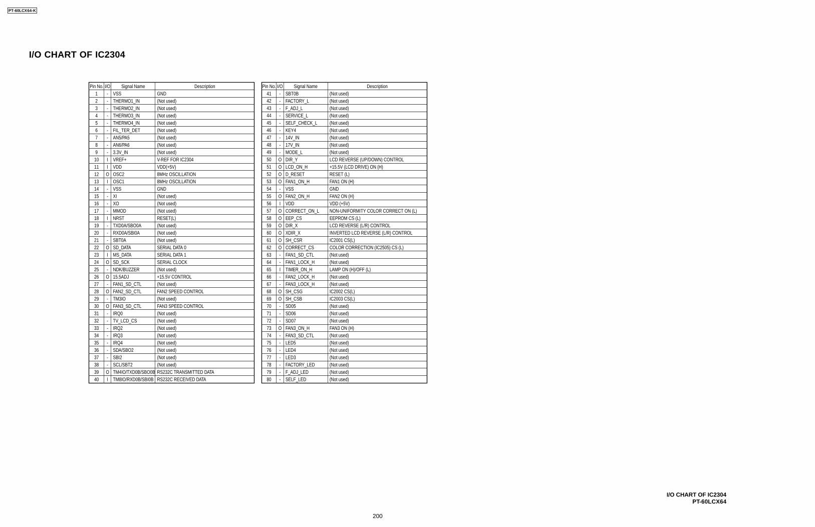
I/O CHART OF IC2304
I/O CHART OF IC2304PT-60LCX64
Pin No. I/O1
Description
23456789
10111213141516171819202122232425262728293031323334353637383940
515253545556575859
Pin No. I/O
60
Signal NameSignal Name Description
6162636465666768697071727374757677787980
-
--
---
-
-
-
-------
O
-
O
O
O
O---
-
O
I
I
-I
I
I
--
-
I
(Not used)(Not used)(Not used)
(Not used)(Not used)(Not used)(Not used)(Not used)
(Not used)
(Not used)
IC2001 CS(L)
(Not used)(Not used)
(Not used)(Not used)IC2002 CS(L)IC2003 CS(L)(Not used)(Not used)(Not used)
(Not used)(Not used)(Not used)(Not used)(Not used)(Not used)(Not used)
(Not used)(Not used)
(Not used)
(Not used)(Not used)(Not used)
(Not used) +15.5V CONTROL(Not used)
(Not used)
(Not used)(Not used)(Not used)(Not used)(Not used)
(Not used)
(Not used)(Not used)
(Not used)(Not used)
VDD(+5V)
(Not used)
VDD (+5V)
GND
GND GND
INVERTED LCD REVERSE (L/R) CONTROL
(Not used)(Not used)
-
--
--
-
------
--
-
------
-
I
I
--
424344454647484950
41VSSTHERMO1_INTHERMO2_INTHERMO3_INTHERMO4_IN
AN6/PA63.3V_IN
AN5/PA5
VREF+
OSC2OSC1VSS
XOXI
MMODNRSTTXD0A/SBO0ARXD0A/SBI0ASBT0ASD_DATAMS_DATASD_SCKNDK/BUZZER
TM3IOFAN3_SD_CTL
FAN2_SD_CTL
IRQ3
IRQ0
IRQ2
IRQ4SDA/SBO2SBI2SCL/SBT2TM4IO/TXD0B/SBO0BTM8IO/RXD0B/SBI0B
15.5ADJFAN1_SD_CTL
FIL_TER_DET
VDD
FACTORY_LF_ADJ_LSERVICE_LSELF_CHECK_LKEY414V_IN17V_INMODE_LDIR_YLCD_ON_HD_RESETFAN1_ON_HVSSFAN2_ON_HVDDCORRECT_ON_LEEP_CSDIR_XXDIR_XSH_CSRCORRECT_CSFAN1_SD_CTLFAN1_LOCK_HTIMER_ON_HFAN2_LOCK_HFAN3_LOCK_HSH_CSGSH_CSBSD05SD06SD07FAN3_ON_HFAN3_SD_CTLLED5LED4LED3FACTORY_LEDF_ADJ_LEDSELF_LED
SBT0B
TV_LCD_CS
V-REF FOR IC2304
8MHz OSCILLATION8MHz OSCILLATION
RESET(L)
SERIAL DATA 0SERIAL DATA 1SERIAL CLOCK
FAN2 SPEED CONTROL
FAN3 SPEED CONTROL
(Not used)
(Not used)RS232C TRANSMITTED DATARS232C RECEIVED DATA
OOOO
O
OOOO
O
O
+15.5V (LCD DRIVE) ON (H)RESET (L)
LCD REVERSE (UP/DOWN) CONTROL
LCD REVERSE (L/R) CONTROL
FAN1 ON (H)
FAN2 ON (H)
NON-UNIFORMITY COLOR CORRECT ON (L)EEPROM CS (L)
COLOR CORRECTION (IC2505) CS (L)
LAMP ON (H)/OFF (L)
FAN3 ON (H)
O
O
OO
-
-
PT-60LCX64-K
200
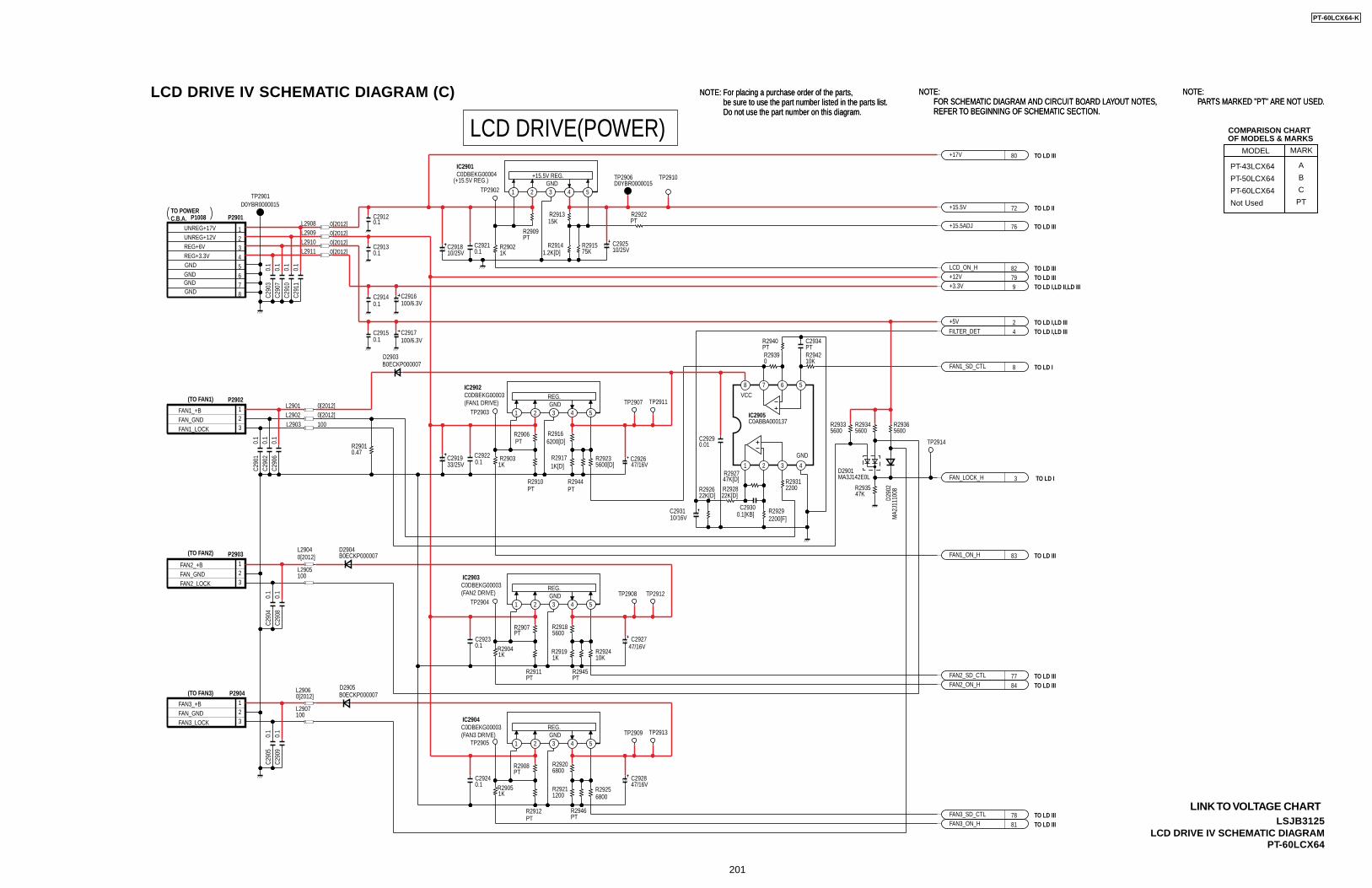
NOTE:FOR SCHEMATIC DIAGRAM AND CIRCUIT BOARD LAYOUT NOTES,REFER TO BEGINNING OF SCHEMATIC SECTION.
NOTE: For placing a purchase order of the parts, be sure to use the part number listed in the parts list. Do not use the part number on this diagram.
NOTE:PARTS MARKED "PT" ARE NOT USED.
LCD DRIVE IV SCHEMATIC DIAGRAM (C) NOTE:FOR SCHEMATIC DIAGRAM AND CIRCUIT BOARD LAYOUT NOTES,REFER TO BEGINNING OF SCHEMATIC SECTION.
NOTE: For placing a purchase order of the parts, be sure to use the part number listed in the parts list. Do not use the part number on this diagram.
NOTE:PARTS MARKED "PT" ARE NOT USED.
LSJB3125LCD DRIVE IV SCHEMATIC DIAGRAM
PT-60LCX64
TP2902
0.1C2921
1.2K[D]R2914
75KR2915
PTR2909
10/25VC2925
R291315K
1KR2902
10/25VC2918
TP2906D0YBR0000015
TP2910
+17V 80
TP2911
+5V 2
0.1C2922
1KR2919
+15.5V 72
FAN2_SD_CTL 77
0.1C2923
TP2912
TP2903
+3.3V 9
TP2904
R29166200[D]
LCD_ON_H 82
TP2908
PTR2910
PTR2911
TP2907
R29185600
47/16VC2926
33/25VC2919
P2902
321
P2903
321
FAN1_SD_CTL 8
1K[D]R2917
TP2901D0YBR0000015
0.1C2915
0.1C2914
0.1C2912
+12V 79
0.1C2913
100/6.3VC2916
TP2909
0.1C2924
FAN3_SD_CTL 78
R29206800
1200R2921
PTR2912
P2904
321
TP2913
TP2905
0.47R2901
2200R2931
22K[D]R2928
22K[D]R2926
2200[F]R29290.1[KB]
C2930
47K[D]R2927
FILTER_DET 4
5600[D]R2923
10KR2924
6800R2925
0.1
C290
30.
1C2
907
0.1
C291
00.
1C2
911
0.1
C290
1
0.1
C290
60.
1C2
902
0.1
C290
80.
1C2
904
0.1
C290
90.
1C2
905
5600R2933
5600R2934
5600R2936
PTR2906
PTR2907
PTR2908
0.01C2929
10/16VC2931
+15.5ADJ 76
PTC2934
10KR2942
PTR2940
0R2939
FAN1_ON_H 83
1KR2903
FAN2_ON_H 84
FAN3_ON_H 81
1KR2904
1KR2905
PTR2944
PTR2945
PTR2946
IC2901C0DBEKG00004
1 2 3 4 5
PTR2922
IC2902C0DBEKG00003
1 2 3 4 5
IC2903C0DBEKG00003
1 2 3 4 5
IC2904C0DBEKG00003
1 2 3 4 5
47/16VC2927
47/16VC2928
100/6.3VC2917
FAN_LOCK_H 3
TP2914
MA3J142E0LD2901
47KR2935
MA2
J111
008
D290
2
P2901
87654321
D2903B0ECKP000007
D2904B0ECKP000007
D2905B0ECKP000007
L2903 100
L2905100
L2907100
L2909 0[2012]L2910 0[2012]L2911 0[2012]
L2908 0[2012]
L2902 0[2012]
L29040[2012]
L29060[2012]
L2901 0[2012]IC2905C0ABBA000137
1 2 3 4
5678
FAN1_LOCK
FAN_GND
FAN_GNDFAN1_+B
(TO FAN1)
(TO FAN2)
(TO FAN3)
FAN2_LOCK
FAN2_+B
FAN_GNDFAN3_LOCK
FAN3_+B
GND
UNREG+12V
GND
REG+3.3VREG+6V
GNDGND
UNREG+17V
TO POWERC.B.A. P1008
TO LD III
GND+15.5V REG.
(+15.5V REG.)
(FAN1 DRIVE) GNDREG.
GNDREG.
GNDREG.
TO LD II
TO LD III
TO LD IIITO LD IIITO LD I,LD II,LD III
TO LD I,LD IIITO LD I,LD III
TO LD I
TO LD I
TO LD III
TO LD IIITO LD III
TO LD IIITO LD III
VCC
GND
(FAN2 DRIVE)
(FAN3 DRIVE)
LCD DRIVE(POWER) COMPARISON CHART OF MODELS & MARKS
PT-43LCX64
PT-50LCX64
PT-60LCX64
Not Used
A
B
C
PT
MODEL MARK
LINK TO VOLTAGE CHART
PT-60LCX64-K
201
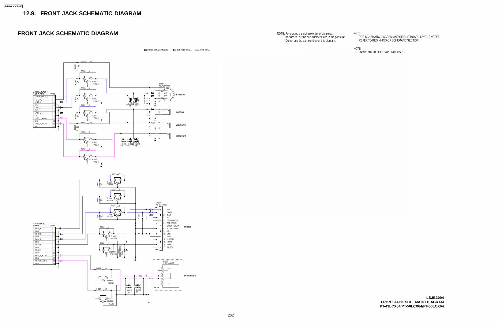
12.9. FRONT JACK SCHEMATIC DIAGRAM
NOTE:FOR SCHEMATIC DIAGRAM AND CIRCUIT BOARD LAYOUT NOTES,REFER TO BEGINNING OF SCHEMATIC SECTION.
NOTE: For placing a purchase order of the parts, be sure to use the part number listed in the parts list. Do not use the part number on this diagram.
NOTE:PARTS MARKED "PT" ARE NOT USED.
FRONT JACK SCHEMATIC DIAGRAM
PT
D459
3
PT
D459
2
0R3907
0R3906
PT[3216]FL3905
12
3
75[F
]
R390
2
PT[3216]FL3903
12
3
0R3908
JK3901K1FB115A0015
PT[3216]FL3904
12
3
PT[2012]FL3902
12
3
75[F
]
R390
3
PT[3216]FL3901
12
3
75[F
]
R390
1
P3901
14GND13RGB2_R_AUDIO12GND11RGB2_L_AUDIO10GND9RGB2_V8GND7RGB2_H6GND5RGB2_B4GND3RGB2_G2GND1RGB2_R
B0BD
6R20
0002
D390
1
0R3904
0R3905
100R4803
100R4804
PT[2012]FL4803
12
3
PT[2012]FL4804
12
3
PTD4803
PTD4804
PT[2012]FL4802
12
3
0R4802
PT[2012]FL4801
12
3
0R4801
100R3918
PTD3913
PT
C356
1
100R3914
PT
C356
2
75
R391
3
PTD3912
PTD3911
PTD4801
PTD4802
PT[2012]FL3913
12
3
PT[2012]FL3912
12
3
0R3916
0R3917
0R3915
PT[2012]FL3911
12
375
R391
1
75
R391
2
P3902
12GND11LINE3_R_AUDIO10GND9LINE3_L_AUDIO8GND7LINE3_V6GND5LINE3_C4GND3LINE3_Y2L3_S_IN_L1L3_CPS_NOSIG_L PTR4
595
PTR4596
PTR459
8PT
D459
5
PTR4597
PT
D459
4
P4592PT4SUB_H/P_GND3SUB_H/P_OUT_L2SUB_H/P_GND1SUB_H/P_OUT_R
P4591PT
7SW_IN_L6SW_OUT_L5H/P_IN_L4AMP_GND3H/P_IN_R2SW_IN_R1SW_OUT_R
JK4802K2HC103A0017
21
345
76
JK4590
21
345
76
JK4591PT
21
345
76
HEAD PHONE
CSYNC(MAC2)
2
12
GREENBLUE
GND
I2C SCK
NC
VSYNC
6
BLUE RETURN
5
10
8
I2C DATA
RED RETURN
HSYNC13
15
NC
4
11
14
RED
9
GREEN RETURN
3
7
GND
1
YC
SUB HEAD PHONE
JK4801K1U412A00008
TO REAR JACKC.B.A. P3502
RGB IN 2
AUDIO IN3(R)
AUDIO IN3(L)
VIDEO IN3
S-VIDEO IN3
RGB AUDIO IN2
TO MAIN C.B.A.P5501
SUB VIDEO SIGNALVIDEO SIGNAL(MAIN/SUB) AUDIO SIGNAL
(6.2
V)
PT
LSJB3094FRONT JACK SCHEMATIC DIAGRAM
PT-43LCX64/PT-50LCX64/PT-60LCX64
PT-60LCX64-K
202
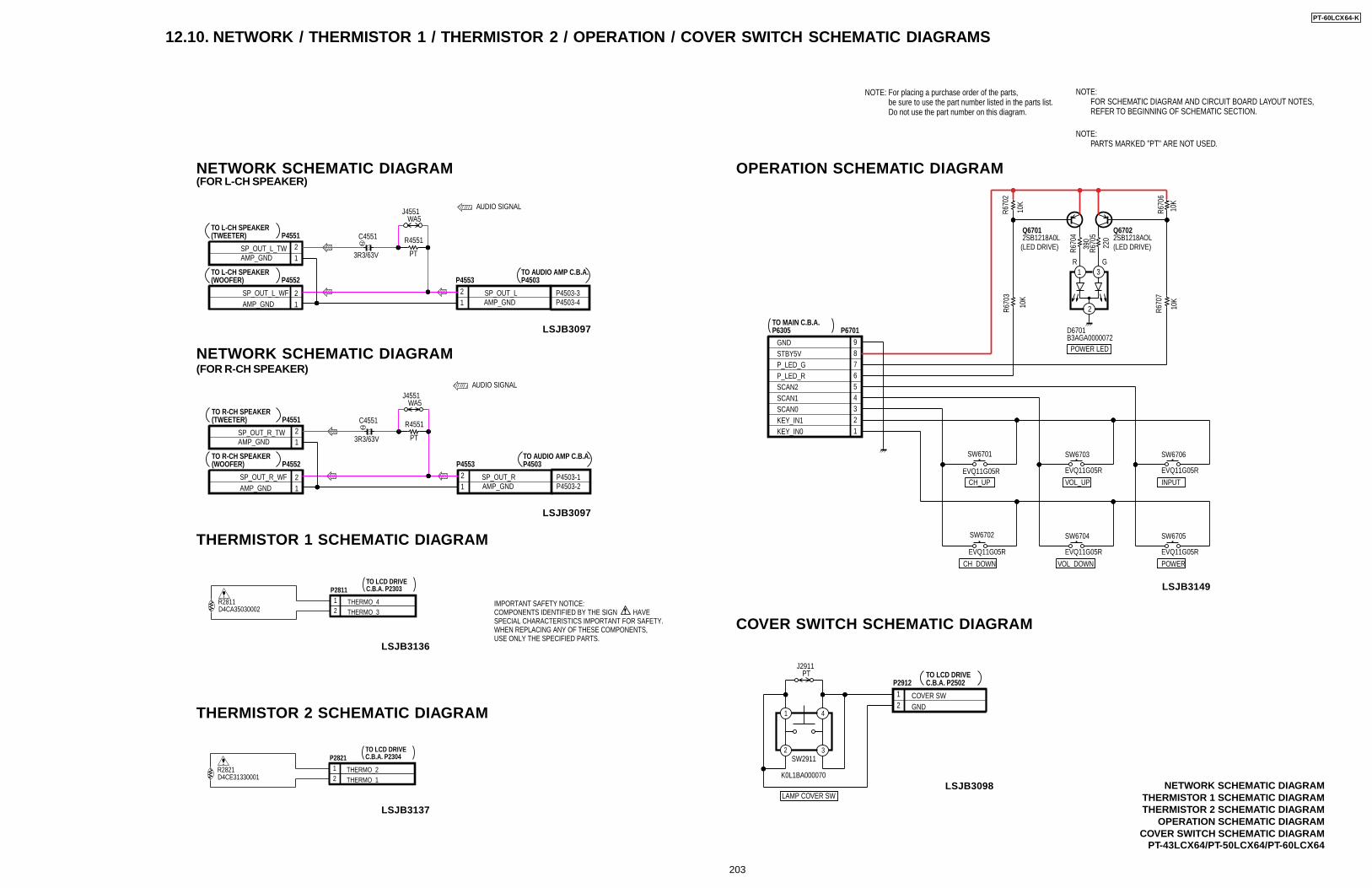
12.10. NETWORK / THERMISTOR 1 / THERMISTOR 2 / OPERATION / COVER SWITCH SCHEMATIC DIAGRAMS
NOTE:FOR SCHEMATIC DIAGRAM AND CIRCUIT BOARD LAYOUT NOTES,REFER TO BEGINNING OF SCHEMATIC SECTION.
NOTE: For placing a purchase order of the parts, be sure to use the part number listed in the parts list. Do not use the part number on this diagram.
NOTE:PARTS MARKED "PT" ARE NOT USED.
NETWORK SCHEMATIC DIAGRAM
C4551
3R3/63V
R4551
PT
P4551
1AMP_GND2SP_OUT_L_TW
P4552
1AMP_GND2SP_OUT_L_WF
P4553
1 AMP_GND2 SP_OUT_L
J4551WA5
TO L-CH SPEAKER(TWEETER)
TO L-CH SPEAKER(WOOFER)
TO AUDIO AMP C.B.A.P4503
P4503-3P4503-4
AUDIO SIGNAL
NETWORK SCHEMATIC DIAGRAM
C4551
3R3/63V
R4551
PT
P4551
1AMP_GND2SP_OUT_R_TW
P4552
1AMP_GND2SP_OUT_R_WF
P4553
1 AMP_GND2 SP_OUT_R
J4551WA5
TO R-CH SPEAKER(TWEETER)
TO R-CH SPEAKER(WOOFER)
TO AUDIO AMP C.B.A.P4503
P4503-1P4503-2
AUDIO SIGNAL
THERMISTOR 1 SCHEMATIC DIAGRAM
THERMISTOR 2 SCHEMATIC DIAGRAM
IMPORTANT SAFETY NOTICE:COMPONENTS IDENTIFIED BY THE SIGN HAVESPECIAL CHARACTERISTICS IMPORTANT FOR SAFETY.WHEN REPLACING ANY OF THESE COMPONENTS,USE ONLY THE SPECIFIED PARTS.
COVER SWITCH SCHEMATIC DIAGRAM
SW2911
K0L1BA000070
2
1
3
4
P291212
J2911PT
COVER SWGND
TO LCD DRIVEC.B.A. P2502
LAMP COVER SW
OPERATION SCHEMATIC DIAGRAM(FOR L-CH SPEAKER)
(FOR R-CH SPEAKER)
P2811
21R2811
D4CA35030002 THERMO_3THERMO_4
TO LCD DRIVEC.B.A. P2303
P2821
21R2821
D4CE31330001THERMO_2THERMO_1
TO LCD DRIVEC.B.A. P2304
SW6703
EVQ11G05R
10K
R670
6
2SB1218A0LQ6701
SW6702
EVQ11G05R
10K
R670
7
R670
4
390
SW6704
EVQ11G05R
D6701B3AGA0000072
1 3
2
10K
R670
2
10K
R670
3
SW6705
EVQ11G05R
SW6701
EVQ11G05R
Q67022SB1218AOL
P67019GND8STBY5V7P_LED_G6P_LED_R5SCAN24SCAN13SCAN02KEY_IN11KEY_IN0
R670
5
220
SW6706
EVQ11G05R
VOL_DOWN
G
CH_UP
R
POWER
VOL_UP
CH_DOWN
INPUT
(LED DRIVE) (LED DRIVE)
TO MAIN C.B.A.P6305
POWER LED
NETWORK SCHEMATIC DIAGRAMTHERMISTOR 1 SCHEMATIC DIAGRAMTHERMISTOR 2 SCHEMATIC DIAGRAM
OPERATION SCHEMATIC DIAGRAMCOVER SWITCH SCHEMATIC DIAGRAM
PT-43LCX64/PT-50LCX64/PT-60LCX64
LSJB3137
LSJB3097
LSJB3097
LSJB3136
LSJB3098
LSJB3149
PT-60LCX64-K
203
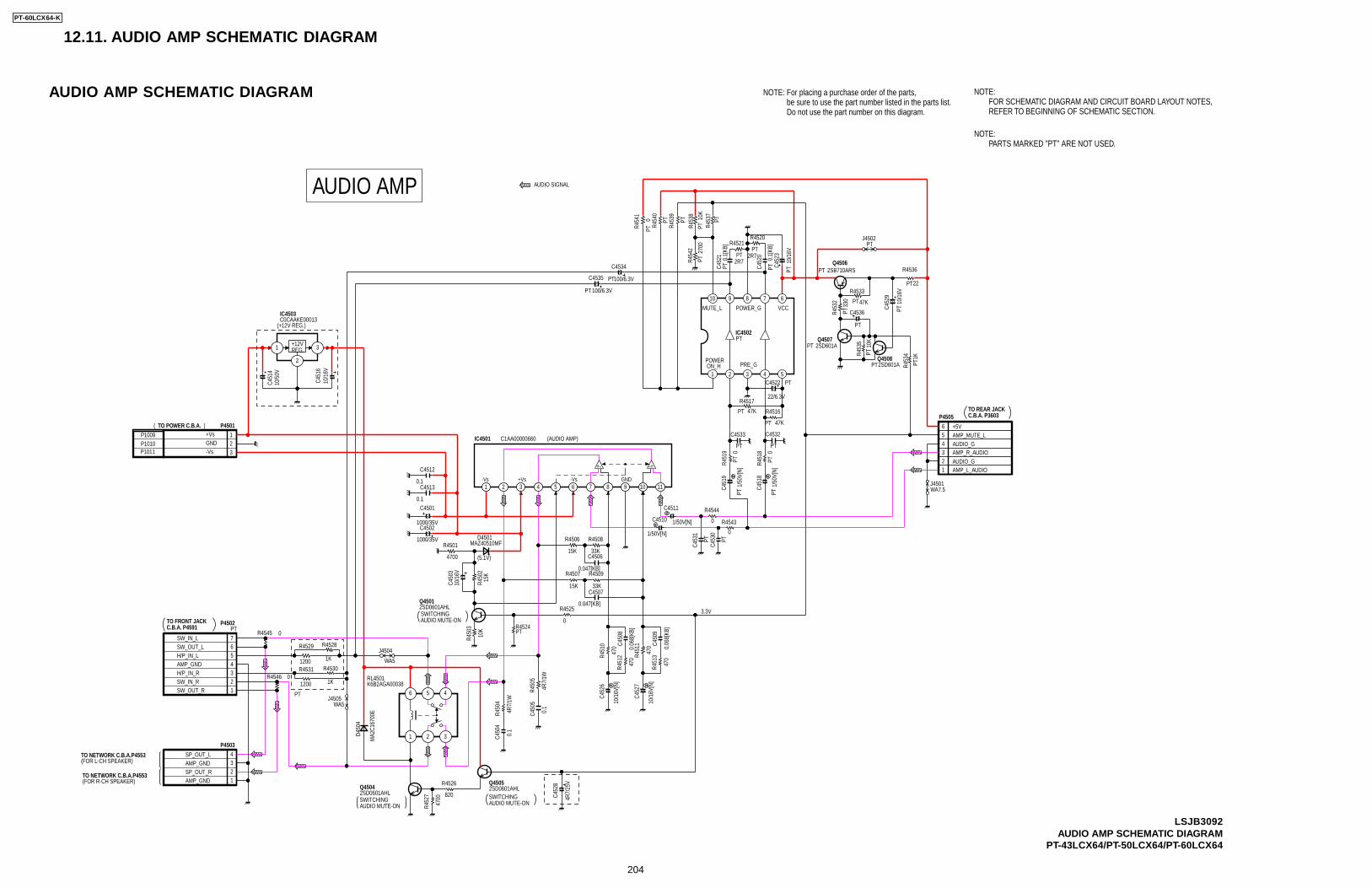
12.11. AUDIO AMP SCHEMATIC DIAGRAM
NOTE:FOR SCHEMATIC DIAGRAM AND CIRCUIT BOARD LAYOUT NOTES,REFER TO BEGINNING OF SCHEMATIC SECTION.
NOTE: For placing a purchase order of the parts, be sure to use the part number listed in the parts list. Do not use the part number on this diagram.
NOTE:PARTS MARKED "PT" ARE NOT USED.
AUDIO AMP SCHEMATIC DIAGRAM
R4506
15K
R451
0
470
R451
1
470
R4507
15K
C4501
1000/35VC4502
1000/35V D4501MAZ40510MF
R450
215
K
R4501
4700
Q45012SD0601AHL
R450
3
10K
C450
310
/16V
P4501
1+Vs
2GND
3-Vs
C450
4
0.1
C450
5
0.1
R4508
33K
R4509
33K
C4506
0.047[KB]
C4507
0.047[KB]
R451
2
470
R451
3
470
C450
9
0.06
8[KB
]
C450
8
0.06
8[KB
]
C4512
0.1C4513
0.1
R450
5
4R7/
1W
R450
4
4R7/
1W
PTC452
0
C4511
1/50V[N]C4510
1/50V[N]
R4517
PT
PTC452
1
R4521
PT
C452
3
PT
R4520
PT
R4516
PT
C4522 PTC451
410
/50V
C451
610
/16V
R4524PT
R4525
0
C452
6
10/1
6V[N
]
Q45042SD0601AHL
Q45052SD0601AHL
R4526
820
R452
7
4700
D450
4
MA2
C167
00E
IC4503C0CAAKE00013
1 3
2
C452
8
4R7/
25V
P45034SP_OUT_L3AMP_GND2SP_OUT_R1AMP_GND
P4502PT
7SW_IN_L6SW_OUT_L5H/P_IN_L4AMP_GND3H/P_IN_R2SW_IN_R1SW_OUT_R
P4505
1 AMP_L_AUDIO2 AUDIO_G
3 AMP_R_AUDIO4 AUDIO_G
5 AMP_MUTE_L
6 +5V
IC4502PT
1 2 3 4 5
8910 67
C451
8
PT
C451
9
PT
R451
9
PT R451
8
PT
R4528
1K
R4529
1200R4530
1K
R4531
1200
R453
2
PT
R4533
PT
Q4506PT
Q4507PT
R453
4
PT
R453
5
PT
R4536
PT
R453
7PT
R453
8
PTR453
9
PT
R454
0
PT
R454
1
PT
Q4508PT
C452
9
PT
R454
2
PT
R4544
0 R4543
0
C453
0
PT
C453
1
PT
C4532
PT
C4533
PT
C4535
PT
C4534
PT
C4536
PT
C452
7
10/1
6V[N
]
R4545 0
R4546 0
J4504
WA5
J4505WA5
J4502PT
J4501WA7.5
RL4501K6B2AGA00038
1 2
6
3
45
IC4501 C1AA00000660
GND-Vs-Vs +Vs
VCCPOWER_G
3.3V
PRE_GPOWERON_H
MUTE_L
2SD601A
1K
10K
2SD601A
330 47K
22
2SB710ARS
10/1
6V
10/1
6V
47K
47K
22/6.3V
1/50
V[N]
1/50
V[N]
00
100/6.3V
100/6.3V
0 10K
2700
0.1[
KB]
0.1[
KB]
2R72R7
1 2 3 4 5 6 7 8 9 10 11
(AUDIO AMP)
AUDIO SIGNAL
TO REAR JACKC.B.A. P3603
TO POWER C.B.A.
TO NETWORK C.B.A.P4553
SWITCHINGAUDIO MUTE-ONSWITCHING
AUDIO MUTE-ON
SWITCHINGAUDIO MUTE-ON
P1011P1010P1009
(+12V REG.)
+- -+
(5.1V)
+12VREG.
( )
TO FRONT JACKC.B.A. P4591
PT
(FOR L-CH SPEAKER)
(FOR R-CH SPEAKER)TO NETWORK C.B.A.P4553
AUDIO AMP
LSJB3092AUDIO AMP SCHEMATIC DIAGRAM
PT-43LCX64/PT-50LCX64/PT-60LCX64
PT-60LCX64-K
204
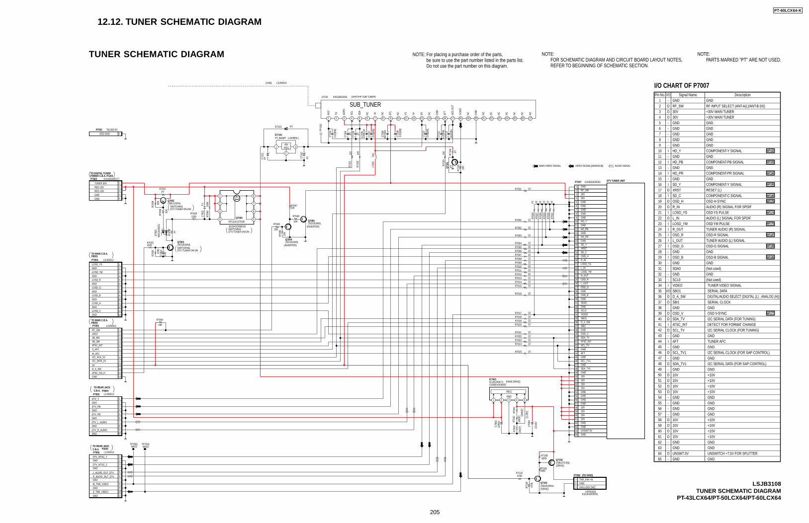
12.12. TUNER SCHEMATIC DIAGRAM
NOTE:FOR SCHEMATIC DIAGRAM AND CIRCUIT BOARD LAYOUT NOTES,REFER TO BEGINNING OF SCHEMATIC SECTION.
NOTE: For placing a purchase order of the parts, be sure to use the part number listed in the parts list. Do not use the part number on this diagram.
NOTE:PARTS MARKED "PT" ARE NOT USED.
TUNER SCHEMATIC DIAGRAM
LSJB3108TUNER SCHEMATIC DIAGRAM
PT-43LCX64/PT-50LCX64/PT-60LCX64
Q71
01PT
R710
4
PT
C710
647
0/6.
3V
Z7001 LSJA0510
P7001 TEL302-5X
1ESD GND
R710
5
100
C710
4
PT
L710
110
U
R710
310
0
C710
5
PT
R710
122
0
220
R710
2
P7003 LSJA0511
13GND12ATSC_ON_H11D_A_SW105V9I2C_DATA_5V8I2C_SCK_5V7M_AFC6S_AFC5ATSC_INT4SB_DM3SB_MD2XRST1RF_SW
C710
7
0.01
[KB]
C710
3
0.01
[KB]
P7007 K1KB65A00002
6564636261605958575655545352515049484746454443424140393837363534333231302928272625242322212019181716151413121110987654321
P7006 LSJA0514
11GND
10S_TNR_VIDEO
9GND
8M_TNR_VIDEO
7GND6R_AUDIO_OUT_DTV
5L_AUDIO_OUT_DTV
4GND3DTV_NTSC_C2GND1DTV_NTSC_Y
P7005 LSJA0513
10GND
9DTV_R_AUDIO
8GND
7DTV_L_AUDIO
6GND
5DTV_PR
4GND
3DTV_PB
2GND
1DTV_Y
U7101 ENG366320G
272625242322212019181716151413121110987654321
C710
2
PTPTC710
1
IC7101PT_BA09T
1 3
2
D7101 PT
P7002 K1KA05A00177
54321
2R2/
50V
C711
2TP71
02
4R7/
50V
C710
8
C711
0
0.01
[KB]
0.22
[KB]
C711
1
22R7031
22R7001
22R7002
22R7003
22R7004
22R7006
22R7008
22R7010
22R7012
22R7014
22R701722R701822R701922R7020
22R702222R702322R7024
22R7025
PTR7
027
PTR7
028
PTR7
029
PTR7
030
PTR7
032
22R7005
PTR7
026
P7004 LSJA0512
14GND13LOSD_V12GND11LOSD_H10GND9LOSD_B8GND7LOSD_G6GND5LOSD_R4GND3LOSD_YM2GND1LOSD_YS
22R7007
22R7009
22R7011
22R7013
22R7015
22R7016
22R7021
TP7101WA10
TP7001WA10
24K[
F]
R704
3
SI-3012KM-TLIC7001
C0DBEKG00003
1 2 3 4 5
22/1
6V
C700
4
100K
[F]
R704
1
XP132A1275SRQ7003
B1DHDC000018
1
2
3
4 5
6
7
8
2SD1819A0LQ7002
2SB1218ASLQ7001
10/5
0VC7
003
PT
R703
8
100K
R704
082K
R703
682
K
R703
4
PTR7037
4700R7033
4700
R703
5
MA3
J142
E0L
D700
1
C700
20.
1
C700
1
0.01
*
1200R7039
R704
2
18K[
F]
P7008
VJPS0326K1KA03A00091
321
2SB1073-0QLQ7102
2SB1819AHLQ7103
1800R7106
8200R7108
4700
R710
9
4700R7110
2SD1819A0LQ7004
2SD1819A0LQ7005
10K
R7044
10K
R7048
22K
R7045
22K
R704
6
22KR7047
C710
90.
01[K
B]
NCNC GND
+B BVTPTU NCSCL
AGC
OUT
AGC
SDA
ADRS
GND
NC AFT
VIDE
O
SUB_TUNER
HD_PR
OSD_G
HD_PB
HD_Y
30V
LOSD_YM
L_OUT
SDA0
XRST
VIDEO
GND
OSD_R
L_IN
OSD_H
SD_Y
30V
R_INLOSD_YS
SCL0
R_OUT
OSD_B
SD_C
SCL_TV
D_A_SW
SDA_TV
SBI1
SCL_TV1
ATSC_INT
OSD_V
SDA_TV1
SBO1
10V
AFT
RF_SW
GNDGNDGNDGNDGND
GNDGNDGNDGND
GNDGNDUNSW7.5VGND
GND
GND
GND
GND
GND
GND
GND
GND
GND
GND
GND
10V10V10V
10V
10V10V
10V
BTL
NC NC IF1
NC NC NCNC NCNC
REG 10VREG 10V
GND
TUNER 30V
GND
[1.2
8V]
FAN LOCK [NC]
SWITCHING
GNDTNR_FAN +B
(FAN5 DRIVE)
(DRIVE)
DTV TUNER ON-ON
SWITCHINGDTV TUNER ON-ON
POWER C.B.A. P1203TO DIGITAL TUNER
P5601TO MAIN C.B.A.
P6003TO MAIN C.B.A.
P3604
P3503TO REAR JACKC.B.A.
(INVERTER)
(UHF/VHF SUB TUNER)
(TO FAN5)
(DRIVE)
+9VREG.
(+9VREG.)
DTV TUNER UNIT
SWITCHINGDTV TUNER ON-ON
(INVERTER)
AUDIO SIGNALVIDEO SIGNAL(MAIN/SUB)MAIN VIDEO SIGNAL
REG.
GND
TO REAR JACKC.B.A.
Pin No. I/O1
Description
23456789
101112131415161718192021222324252627282930313233
515253545556575859
I/O
60
Signal Name
6162636465
I/O CHART OF P7007
-
-
II
I
O----
O
I
O
I
I
I
I
I
O
OO
II
-
----
-
-
-
I
GND GND
GNDGNDGNDGNDGND
GND
GND
GND
GND
GND
GNDGND
GNDGNDGNDGND
GND
GND
GND
GND
GND
GND
GND
GNDGNDGNDGNDGND
GND
GND
GND
GND
GNDSCL0
GND
RF_SW RF INPUT SELECT (ANT-A(L)/ANT-B (H))
-
-
--
--
-
-
-
424344454647484950
41
-
-
-
34353637383940
30V +30V MAIN TUNER+30V MAIN TUNER30V
HD_Y
HD_PB
HD_PR
SD_Y
SDA0
SD_COSD_H
OSD_R
OSD_G
OSD_B
R_IN
R_OUT
L_OUT
L_INLOSD_YS
LOSD_YM
XRST
VIDEOSBO1
SBI1D_A_SW
OSD_V OSD V-SYNCSDA_TV
SCL_TV
SCL_TV1
SDA_TV1
GND
GND
GND
GNDGNDGND
GNDGND
GND
GND
GND
GND
ATSC_INT
AFT
10V10V10V10V
+10V
10V10V10V10V
UNSW7.5V UNSWITCH +7.5V FOR SPLITTER
(Not used)
(Not used)
O
COMPONENT-Y SIGNAL
COMPONENT-Y SIGNAL
COMPONENT-PB SIGNAL
COMPONENT-PR SIGNAL
OSD-B SIGNAL
OSD-G SIGNAL
OSD YM PULSE
OSD YS PULSE
OSD-R SIGNAL
OSD H-SYNC
TUNER AUDIO (L) SIGNAL
AUDIO (R) SIGNAL FOR SPDIF
AUDIO (L) SIGNAL FOR SPDIF
TUNER AUDIO (R) SIGNAL
COMPONENT-C SIGNALRESET (L)
OO
OO
O
O
O
OOOO
OOOO
O
I
I
I
+10V+10V+10V
+10V+10V+10V+10V
I2C SERIAL DATA (FOR TUNING)
I2C SERIAL DATA (FOR SAP CONTROL)
I2C SERIAL CLOCK (FOR SAP CONTROL)
I2C SERIAL CLOCK (FOR TUNING)
SERIAL CLOCK
TUNER AFC
DETECT FOR FORMAT CHANGE
DIGITAL/AUDIO SELECT (DIGITAL (L) , ANALOG (H))SERIAL DATATUNER VIDEO SIGNAL
WF182
WF183
WF184
WF185
WF186
WF176
WF174
WF175
WF187
WF188
WF189
WF177
PT-60LCX64-K
205
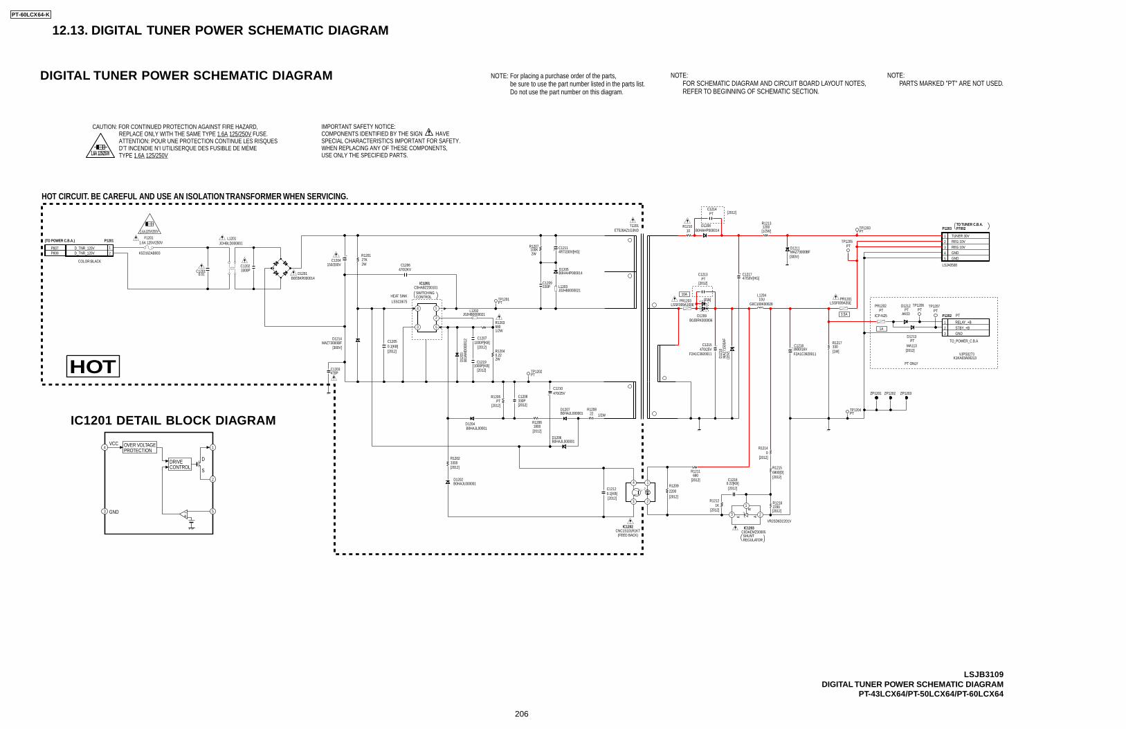
12.13. DIGITAL TUNER POWER SCHEMATIC DIAGRAM
NOTE:FOR SCHEMATIC DIAGRAM AND CIRCUIT BOARD LAYOUT NOTES,REFER TO BEGINNING OF SCHEMATIC SECTION.
NOTE: For placing a purchase order of the parts, be sure to use the part number listed in the parts list. Do not use the part number on this diagram.
NOTE:PARTS MARKED "PT" ARE NOT USED.
DIGITAL TUNER POWER SCHEMATIC DIAGRAM
CAUTION: FOR CONTINUED PROTECTION AGAINST FIRE HAZARD,REPLACE ONLY WITH THE SAME TYPE 1.6A 125/250V FUSE.ATTENTION: POUR UNE PROTECTION CONTINUE LES RISQUESD’T INCENDIE N’I UTILISERQUE DES FUSIBLE DE MÉMETYPE 1.6A 125/250V1.6A 125/250V
IMPORTANT SAFETY NOTICE:COMPONENTS IDENTIFIED BY THE SIGN HAVESPECIAL CHARACTERISTICS IMPORTANT FOR SAFETY.WHEN REPLACING ANY OF THESE COMPONENTS,USE ONLY THE SPECIFIED PARTS.
LSJB3109DIGITAL TUNER POWER SCHEMATIC DIAGRAM
PT-43LCX64/PT-50LCX64/PT-60LCX64
R1207100K
C1210470/25V
R1203680
C1204150/200V
L1203J0JHB0000021
IC1203C0DAEMZ00005
23
1
R12040.22
R1205PT
D1206B0HAJL000001
C12120.1[KB]
C12071000P[KB]
R12121K
D1204B0HAJL00001
D1205B0HAHP000014
D120
3B0
JAM
D000
012
R12023300
C12114R7/200V[HG]
C12050.1[KB]
R1211680
R120822
C1208330P
P1201
12
C1206470/2KV
C1209220P
R12092200
C12160.22[KB]
C12023300P
D1207B0HAJL000001
D1202B0HAJL000001
C121747/50V[HG]
PTC1214
B0HAHP000014D1208 R1213
120010
R1210
PTC1213
C12183900/16VF2A1C3920011
D1209B0JBRK000006
10UL1204
G0C100K00028
C1215470/25V
F2A1C3920011
IC1201C5HABZZ00101
5
2
3
14
(15V
)
D121
0M
AZ71
500A
F
LSSF009A35EPR1201
R1217330
R12140
F1201
K5D162AB003
C12010.01
JOHBLD000001L1201
D1201B0EBKR000014
L1202J0JHB0000021
R12061800
P1202 PT
321
PTD1212
PTD1213
1000P[KB]C1219
470PC1203
MAZ73000BF(300V)
D1211
2200R1216
PTPR1202
6800[D]R1215
MAZ73000BF[300V]
D1214
27KR1201
PTTP1202
PTTP1201
PTTP1204
PTTP1205
PTTP1203
PTTP1206
PTTP1207
ZP1201 ZP1202 ZP1203
LSSF009A100EPR1203
IC1202CNC1S101R1KT
2
14
3
P1203
LSJA0508
54321
2W
1/2W
2W
A
2W
[2012]
VRJSD6D2201V
1/2W
K
1.6A 125V/250V
R
[1/2W]
[FIN]LSSC0675HEAT SINK
TUNER 30VREG 10VREG 10VGNDGND
D_TNR_120VD_TNR_120V
[2012]
[2012]
[2012]
[2012]
[2012]
[2012]
[2012]
[2012]
[2012][2012]
[2012] [2012]
[2012]
[2012]
[2012]
3.5A
1A
[2012]
GND
RELAY_+BSTBY_+B
TO_POWER_C.B.A
[2012]
K1KA03A00213VJPS0273
AK03
MA113
ICP-N25
PT ONLY
COLOR:BLACK
[1W]
10A
TO TUNER C.B.A.P7002
SHUNTREGULATOR
SWITCHINGCONTROL
P807P808
HOT CIRCUIT. BE CAREFUL AND USE AN ISOLATION TRANSFORMER WHEN SERVICING.
(FEED BACK)
1.6A125V/250V
(TO POWER C.B.A.)
T1201ET528AZ1G3ND
HOT
4 1
2
53
OVER VOLTAGEPROTECTION
DRIVECONTROL
VCC
GND
D
S
IC1201 DETAIL BLOCK DIAGRAM
PT-60LCX64-K
206
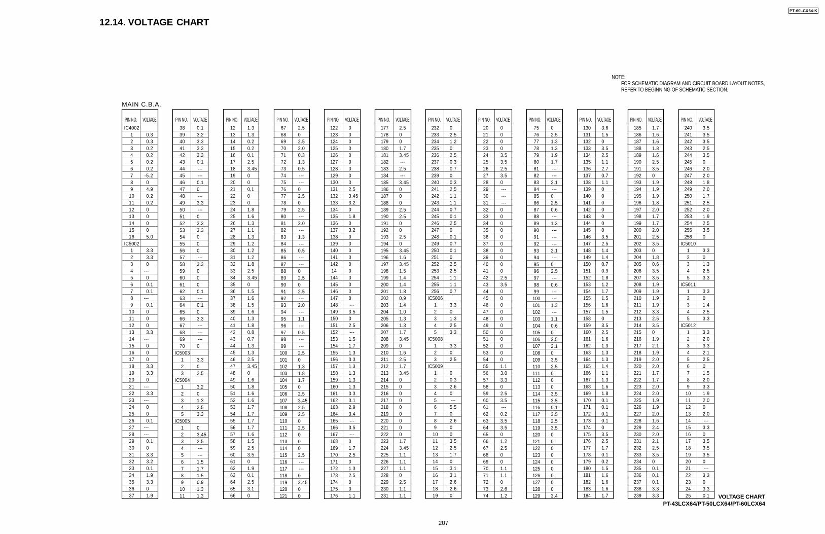
12.14. VOLTAGE CHART
PIN NO. VOLTAGE
NOTE:FOR SCHEMATIC DIAGRAM AND CIRCUIT BOARD LAYOUT NOTES,REFER TO BEGINNING OF SCHEMATIC SECTION.
PIN NO. VOLTAGE PIN NO. VOLTAGE PIN NO. VOLTAGE PIN NO. VOLTAGE PIN NO. VOLTAGE PIN NO. VOLTAGE PIN NO. VOLTAGE PIN NO. VOLTAGE PIN NO. VOLTAGE PIN NO. VOLTAGE PIN NO. VOLTAGE
VOLTAGE CHARTPT-43LCX64/PT-50LCX64/PT-60LCX64
MAIN C.B.A.
IC40021 0.32 0.33 0.24 0.25 0.26 0.27 -5.28 09 4.9
10 0.211 0.212 013 014 015 016 5.0
IC50021 3.32 3.33 04 ---5 06 0.17 0.18 ---9 0.1
10 011 012 013 3.314 ---15 016 017 018 3.319 3.320 021 ---22 3.323 ---24 025 026 0.127 ---28 ---29 0.130 031 3.332 3.233 0.134 1.935 3.336 037 1.9
38 0.139 3.240 3.341 3.342 3.343 0.144 ---45 ---46 0.147 048 ---49 3.350 ---51 052 3.353 3.354 055 056 057 ---58 3.359 060 061 062 0.163 ---64 0.165 066 3.367 ---68 ---69 ---70 0
IC50031 3.32 03 2.5
IC50041 3.22 03 1.34 2.55 3.3
IC50051 02 3.453 2.54 ---5 ---6 1.57 1.78 1.59 0.9
10 1.311 1.3
12 1.313 1.314 0.215 0.216 0.117 2.518 3.4519 020 021 0.122 023 024 1.825 1.626 1.327 1.128 1.329 1.230 1.231 1.232 1.833 2.534 3.4535 036 1.537 1.638 1.539 1.640 1.341 1.842 0.843 0.744 1.345 1.346 2.547 3.4548 049 1.650 1.851 1.652 1.653 1.754 1.755 1.756 1.757 1.658 1.559 2.560 3.561 062 1.963 0.164 2.565 3.166 0
67 2.568 069 2.570 2.071 0.372 1.373 0.574 ---75 ---76 077 2.578 079 2.580 ---81 2.082 ---83 1.384 ---85 0.586 ---87 ---88 089 2.590 091 2.592 ---93 2.094 ---95 1.196 ---97 0.598 ---99 ---100 2.5101 0102 1.3103 1.8104 1.7105 0106 2.5107 3.45108 2.5109 2.5110 0111 2.5112 0113 0114 0115 2.5116 ---117 ---118 0119 3.45120 0121 0
122 0123 0124 0125 0126 0127 0128 0129 0130 0131 2.5132 3.45133 3.2134 0135 1.8136 0137 3.2138 0139 0140 0141 0142 014 0144 0145 0146 0147 0148 ---149 3.5150 0151 2.5152 ---153 1.5154 1.7155 1.3156 0.3157 1.3158 1.3159 1.3160 1.3161 0.3162 0.1163 2.9164 3.4165 ---166 3.5167 ---168 0169 1.7170 2.5171 0172 1.3173 2.5174 0175 0176 1.1
177 2.5178 0179 0180 1.7181 3.45182 ---183 2.5184 ---185 3.45186 0187 0188 0189 2.5190 2.5191 0192 0193 2.5194 0195 3.45196 1.6197 3.45198 1.5199 1.4200 1.4201 1.8202 0.9203 1.4204 1.0205 1.3206 1.3207 1.7208 3.45209 0210 1.6211 2.5212 1.7213 3.45214 0215 0216 0217 0218 0219 0220 0221 0222 0223 1.7224 3.45225 1.1226 1.1227 1.1228 0229 2.5230 1.1231 1.1
232 0233 2.5234 1.2235 0236 2.5237 0.3238 0.7239 0240 0.3241 2.5242 1.1243 1.1244 0.7245 0.1246 2.5247 0248 0.1249 0.7250 0.1251 0252 2.5253 2.5254 1.1255 1.1256 0.7
IC50061 3.32 03 1.34 2.55 3.3
IC50081 3.32 03 2.5
IC50091 02 0.33 2.64 05 ---6 5.57 08 2.69 0
10 011 3.512 2.513 1.714 015 3.116 3.117 2.618 2.619 0
20 021 022 023 024 3.525 3.526 2.527 3.528 029 ---30 ---31 ---32 033 034 035 036 037 038 039 040 041 042 2.543 3.544 045 046 047 048 049 050 051 052 053 054 055 1.156 3.057 3.358 059 2.560 3.561 ---62 0.263 3.564 3.565 066 1.267 2.568 069 070 1.171 1.172 073 2.674 1.2
75 076 2.577 1.378 1.379 1.980 1.781 ---82 ---83 2.184 ---85 086 2.587 0.688 ---89 1.390 ---91 ---92 ---93 2.194 ---95 096 2.597 ---98 0.699 ---100 ---101 1.3102 ---103 1.1104 0.6105 0106 2.5107 2.1108 0109 3.5110 2.5111 0112 0113 0114 3.5115 3.5116 0.1117 3.5118 2.5119 3.5120 0121 0122 0123 0124 0125 0126 0127 0128 0129 3.4
130 3.6131 1.5132 0133 3.5134 2.5135 1.1136 2.7137 0.7138 1.1139 0140 0141 0142 0143 0144 0145 0146 3.5147 2.5148 1.4149 1.4150 0.7151 0.9152 1.8153 1.2154 1.7155 1.5156 1.6157 1.5158 0159 3.5160 2.5161 1.6162 1.3163 1.3164 1.3165 1.4166 1.1167 1.3168 1.6169 1.8170 0.1171 0.1172 0.1173 0.1174 0175 3.5176 2.5177 1.7178 0.1179 0.2180 1.5181 1.6182 1.6183 1.6184 1.7
185 1.7186 1.6187 1.6188 1.8189 1.6190 2.5191 3.5192 0193 1.9194 1.9195 1.9196 1.8197 2.0198 1.7199 1.7200 2.0201 2.5202 3.5203 0204 1.8205 0.6206 3.5207 3.5208 1.9209 1.9210 1.9211 1.9212 3.3213 2.5214 3.5215 0216 1.9217 2.1218 1.9219 2.0220 2.0221 1.7222 1.7223 2.0224 2.0225 1.9226 1.9227 2.0228 1.6229 2.4230 2.0231 2.1232 2.5233 3.5234 0235 0.1236 0.1237 0.1238 3.3239 3.3
240 3.5241 3.5242 3.5243 2.5244 3.5245 0246 2.0247 2.0248 1.8249 2.0250 1.7251 2.5252 2.0253 1.9254 2.5255 3.5256 0
IC50101 3.32 03 1.34 2.55 3.3
IC50111 3.32 03 1.44 2.55 3.3
IC50121 3.32 2.03 3.34 2.15 2.56 07 1.58 2.09 3.3
10 1.911 2.012 013 2.014 ---15 3.316 017 3.518 3.519 3.520 021 ---22 3.323 024 3.325 0.1
PT-60LCX64-K
207
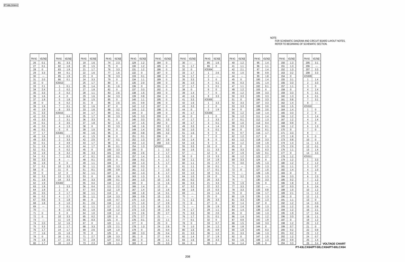
PIN NO. VOLTAGE
NOTE:FOR SCHEMATIC DIAGRAM AND CIRCUIT BOARD LAYOUT NOTES,REFER TO BEGINNING OF SCHEMATIC SECTION.
PIN NO. VOLTAGE PIN NO. VOLTAGE PIN NO. VOLTAGE PIN NO. VOLTAGE PIN NO. VOLTAGE PIN NO. VOLTAGE PIN NO. VOLTAGE PIN NO. VOLTAGE PIN NO. VOLTAGE PIN NO. VOLTAGE PIN NO. VOLTAGE
VOLTAGE CHARTPT-43LCX64/PT-50LCX64/PT-60LCX64
81 3.382 1.883 1.984 0.185 1.986 0.1
IC50131 0.12 0.23 0.24 05 1.86 0.27 0.18 3.5
IC50151 6.42 3.13 3.54 1.35 0
IC53011 0.32 3.33 4.94 0.25 0.26 3.27 0.28 ---9 0
10 3.311 012 013 3.214 3.3
IC53021 3.32 03 1.74 1.75 1.86 1.07 0.18 1.59 0
10 3.311 1.612 1.613 1.714 1.715 1.816 0.117 2.618 1.0
19 1.620 1.521 1.722 1.623 024 3.325 1.726 1.427 1.828 1.129 1.630 1.531 032 1.633 1.634 1.735 1.736 3.337 1.838 039 1.040 1.641 1.542 2.543 1.744 1.745 046 3.347 0.148 0.149 1.150 1.151 0.152 1.153 054 3.355 0.456 0.457 0.458 1.159 1.160 061 2.662 1.163 1.064 1.065 0.266 0.367 068 3.369 2.670 071 2.772 2.973 2.3
74 2.375 076 3.377 1.678 3.379 080 081 1.682 083 2.684 3.385 086 2.687 088 3.289 0.190 3.391 092 1.593 3.394 095 096 097 0.198 099 0.1100 3.3101 3.0102 0.1103 0104 0105 3.3106 0.9107 0108 2.6109 0.1110 1.2111 2.2112 1.0113 0114 3.3115 0.7116 1.2117 1.2118 1.2119 1.2120 0121 0122 1.1123 2.1124 1.0125 0126 3.3127 0.3128 1.1
129 1.2130 1.2131 1.2132 0133 0.1134 1.1135 2.0136 0137 3.3138 1.5139 0.8140 1.1141 0.9142 1.2143 1.2144 0145 3.3146 3.3147 1.5148 1.6149 1.4150 0.8151 0.1152 1.3153 1.3154 1.3155 0156 2.6157 1.4158 0.2159 1.3160 0.3161 1.2162 1.3163 1.3164 1.3165 0166 1.4167 1.4168 1.8169 0.9170 1.3171 1.0172 1.3173 1.3174 2.6175 2.7176 0.1177 0178 1.3179 0180 3.3181 0182 0183 0
184 0185 0186 0187 0188 0189 0190 0191 0192 0193 0194 0195 0196 0197 0198 0199 0200 0201 3.3202 0203 3.2204 3.2205 3.2206 0207 2.6208 3.3
IC53031 3.32 1.73 3.34 1.75 1.76 07 1.08 1.79 3.3
10 1.511 1.612 013 1.614 0.115 3.316 1.117 2.918 2.319 2.420 2.721 ---22 1.123 024 2.625 0.426 0.427 0.428 1.129 3.3
30 ---31 1.732 033 1.734 1.735 3.336 1.037 1.738 039 1.440 1.641 3.342 1.643 3.344 045 1.746 047 1.748 1.749 3.350 1.051 1.652 053 1.454 1.655 3.356 1.657 ---58 059 1.160 1.161 1.162 1.163 1.064 1.065 0.266 0.367 3.268 1.669 ---70 ---71 1.172 073 ---74 1.775 3.376 1.777 0.178 079 1.080 1.681 3.382 1.483 1.684 0
85 1.686 0
IC53041 2.62 ---3 04 0.15 0.16 07 08 3.3
IC53051 3.32 03 1.9
IC53061 02 3.33 0.14 1.45 0.16 07 08 09 0
10 011 3.312 013 3.314 1.915 2.716 0.117 0.118 0.119 020 3.321 3.322 3.223 0.324 1.425 026 3.327 028 1.929 1.130 2.031 0.132 033 0.734 1.235 0.936 1.237 1.938 3.339 0
40 1.241 1.142 2.143 1.044 ---45 046 0.347 1.148 1.249 1.250 3.351 052 3.353 3.354 055 1.256 1.257 0.158 1.059 3.360 061 0.762 1.263 1.264 1.265 066 3.367 1.968 1.269 3.370 3.071 ---72 073 ---74 3.275 ---76 1.977 3.378 3.379 080 1.981 3.382 1.483 1.484 1.485 086 1.487 0.988 1.589 1.890 1.991 3.392 093 1.694 1.4
95 1.496 1.197 1.498 0.999 1.8100 1.4101 1.4102 0.1103 0104 3.3105 3.3106 3.3107 3.3108 3.0109 3.0110 1.4111 1.4112 1.3113 0.4114 0.1115 0.1116 1.7117 0118 3.3119 1.9120 1.3121 0.3122 0.1123 2.7124 0125 1.3126 1.3127 1.0128 1.9129 1.3130 3.3131 0132 ---133 0.8134 1.7135 1.3136 1.3137 0138 1.3139 1.3140 1.3141 1.2142 1.9143 3.3144 0145 0.3146 1.3147 1.5148 1.3149 0
150 1.3151 1.3152 1.3153 3.2154 0155 3.1156 3.3157 1.1158 0159 3.3160 1.3161 0.8162 1.4163 1.5164 1.4165 3.3166 1.2167 1.2168 0.9169 1.2170 0171 3.3172 1.8173 0.8174 1.4175 2.0176 1.1177 0178 1.2179 1.2180 1.2181 1.1182 1.4183 0184 3.3185 0.2186 1.8187 0.3188 1.0189 2.1190 0191 1.1192 1.2193 1.2194 1.2195 1.9196 3.3197 0198 1.2199 0.7200 0.2201 0.2202 1.2203 0.9204 3.3
205 3.1206 ---207 3.3208 3.3
IC53091 1.42 3.33 04 1.45 3.16 0.17 3.18 ---
IC53101 02 03 1.44 1.45 06 1.37 08 ---9 0
10 011 1.312 0.113 1.414 3.3
IC53111 3.32 1.23 0.74 1.05 06 2.37 1.28 1.29 3.4
10 1.211 1.212 1.113 014 0.315 0.916 2.117 3.418 1.119 1.220 1.221 022 0.923 1.224 0.725 1.426 3.4
26 0.127 0.128 029 3.330 ---31 2.032 033 2.134 2.435 3.336 1.637 1.938 039 1.940 1.941 3.342 2.043 3.344 0.145 2.046 0.147 1.748 1.649 3.350 0.151 1.952 0.153 1.954 0.155 3.356 1.957 0.158 059 060 3.361 1.962 1.963 1.964 1.965 3.566 0.267 0.668 1.869 ---70 ---71 072 073 ---74 2.075 3.376 1.777 1.678 079 1.980 1.7
PT-60LCX64-K
208
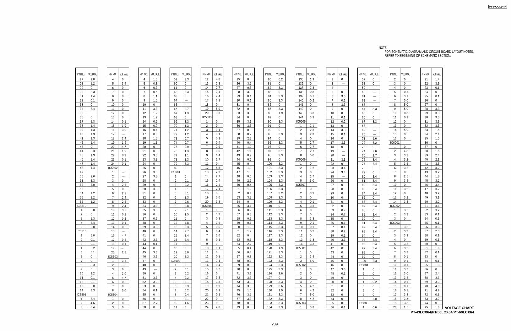
PIN NO. VOLTAGE
NOTE:FOR SCHEMATIC DIAGRAM AND CIRCUIT BOARD LAYOUT NOTES,REFER TO BEGINNING OF SCHEMATIC SECTION.
PIN NO. VOLTAGE PIN NO. VOLTAGE PIN NO. VOLTAGE PIN NO. VOLTAGE PIN NO. VOLTAGE PIN NO. VOLTAGE PIN NO. VOLTAGE PIN NO. VOLTAGE PIN NO. VOLTAGE PIN NO. VOLTAGE PIN NO. VOLTAGE
VOLTAGE CHARTPT-43LCX64/PT-50LCX64/PT-60LCX64
4 1.05 0.36 0.77 0.58 1.19 1.0
10 011 3.312 1.213 1.214 0.515 0.916 0.417 0.818 1.619 1.120 021 022 3.323 3.324 025 026 3.327 3.328 029 030 3.331 032 033 034 3.335 3.336 037 0.238 039 3.340 041 042 3.343 0.144 045 3.346 3.347 048 049 ---50 051 3.352 3.353 054 0.155 056 057 2.758 0
59 3.360 061 062 3.363 064 ---65 ---66 2.767 1.368 069 3.370 1.371 1.272 1.273 0.774 0.775 0.976 1.377 1.178 3.379 3.380 0
IC56011 02 0.13 0.24 0.15 0.16 3.37 0.68 2.89 2.1
10 1.511 012 4.813 2.314 2.715 2.416 2.417 2.118 019 5.020 3.3
IC56021 02 0.13 0.24 0.25 0.16 3.37 0.28 0.49 2.1
10 1.611 0
12 4.813 2.314 2.715 2.416 2.417 2.118 019 5.020 3.3
IC56031 02 03 0.14 0.15 0.16 0.47 2.98 0.69 1.4
10 1.711 012 4.813 2.314 2.715 2.416 2.417 2.118 019 5.020 3.3
IC56041 02 3.33 0.34 1.45 0.66 0.47 3.08 0.19 0
10 0.111 012 0.113 2.114 0.415 0.216 017 3.318 3.319 1.920 0.121 0.122 023 024 2.8
25 026 3.127 0.328 3.329 0.130 0.131 032 033 3.334 035 3.336 3.337 038 0.739 2.340 0.441 1.042 1.143 0.744 0.645 046 1.947 1.048 0.649 2.150 0.451 1.952 0.453 3.354 055 3.156 0.957 0.858 0.559 0.560 1.061 1.962 063 0.664 2.265 0.466 0.867 0.868 0.369 0.870 071 3.372 3.373 3.374 3.375 1.076 3.177 3.378 079 0
80 0.281 082 3.383 084 3.385 3.386 087 3.388 1.989 090 3.391 092 093 3.394 095 3.396 097 3.198 3.399 0100 3.3101 3.3102 3.3103 3.3104 3.3105 3.3106 3.3107 3.2108 3.3109 3.3110 0111 3.3112 3.3113 3.3114 3.3115 3.3116 3.3117 3.3118 3.3119 0120 1.9121 3.3122 3.3123 3.3124 3.3125 3.3126 2.6127 0128 3.3129 0.6130 1.9131 3.3132 3.3133 3.3134 3.3
135 1.9136 0137 2.3138 0.8139 0.1140 0.2141 0142 0143 3.3144 3.3
IC56051 2.12 2.33 2.34 05 2.76 2.77 2.78 5.0
IC56061 02 1.23 04 1.75 5.0
IC56071 02 3.33 04 0.15 3.36 07 08 3.39 0.1
10 0.111 0.212 013 3.314 3.3
IC58011 02 3.43 5.0
IC58021 02 03 04 05 4.26 4.27 5.08 4.2
IC58031 3.3
2 03 ---4 ---5 06 3.37 0.28 3.39 0
10 011 0.112 0.213 014 3.315 0.116 017 3.318 019 ---20 ---21 3.322 023 3.424 3.425 ---26 027 028 029 030 031 032 033 0.734 0.735 036 0.137 0.138 0.239 0.140 3.341 042 043 044 045 046 047 3.348 0.149 050 051 052 053 054 055 056 0.1
57 058 059 ---60 ---61 ---62 ---63 ---64 3.365 066 067 3.368 ---69 ---70 ---71 1.672 3.273 074 2.675 2.776 3.477 3.478 079 080 3.481 3.482 3.483 3.484 3.485 086 3.487 3.488 089 3.490 091 3.492 3.493 3.494 095 3.496 3.497 3.498 099 0100 3.3
IC58041 02 03 04 -5.25 06 07 08 5.0
IC58051 0.6
2 03 04 05 0.16 3.17 5.08 5.09 5.0
10 0.311 0.312 013 014 5.015 016 0
IC60011 02 4.83 3.24 3.25 3.66 3.27 08 2.59 3.9
10 011 3.212 013 3.214 3.3
IC60021 3.22 3.33 0
IC60031 3.32 3.33 3.34 05 3.36 3.27 3.38 0.19 0.1
10 0.111 3.312 3.013 3.214 0.115 0.116 0.117 3.318 3.319 3.320 1.5
21 1.422 3.323 0.124 025 0.126 027 028 3.329 3.330 3.331 3.332 3.333 1.534 2.435 1.536 037 038 1.539 2.440 2.141 3.342 3.243 3.244 1.845 3.246 3.447 3.248 3.249 3.150 3.251 3.652 3.253 0.154 0.155 0.156 3.357 2.358 0.159 0.160 061 1.662 0.163 064 0.165 1.366 067 2.468 3.369 3.370 4.971 4.972 0.173 3.274 075 1.6
27 2.028 1.229 030 3.331 1.432 0.133 034 3.435 036 037 1.338 1.439 1.340 1.341 1.342 1.443 044 3.345 1.346 1.447 1.448 1.449 050 2.651 3.352 3.053 054 1.255 1.256 1.2
IC53121 5.02 03 1.34 3.45 5.0
IC53131 5.02 0.13 0.14 3.25 5.16 07 08 3.39 0
10 3.211 0.112 0.113 5.014 3.3
IC55011 3.42 4.63 3.4
4 05 3.46 07 08 09 0
10 011 012 013 014 0.115 1.916 3.017 ---18 2.419 1.920 4.721 1.922 0.123 0.124 0.1
IC55021 ---2 ---3 04 2.65 06 2.27 2.48 2.29 2.4
10 3.211 0.212 0.213 0.114 0.215 ---16 4.717 0.218 0.119 ---20 2.8
IC55031 3.32 ---3 04 2.05 4.76 07 08 5.0
IC55041 02 03 0
PT-60LCX64-K
209
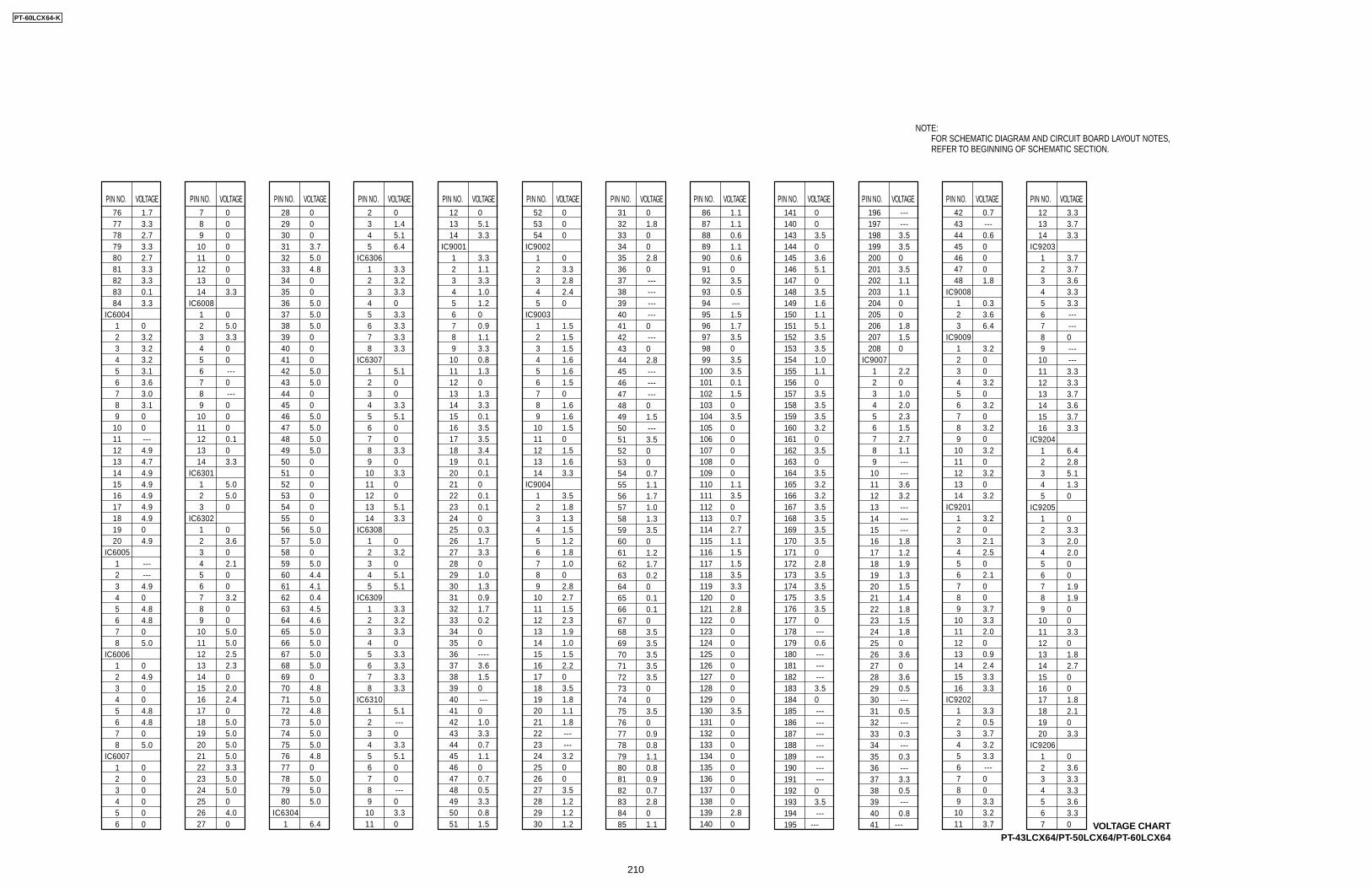
PIN NO. VOLTAGE
NOTE:FOR SCHEMATIC DIAGRAM AND CIRCUIT BOARD LAYOUT NOTES,REFER TO BEGINNING OF SCHEMATIC SECTION.
PIN NO. VOLTAGE PIN NO. VOLTAGE PIN NO. VOLTAGE PIN NO. VOLTAGE PIN NO. VOLTAGE PIN NO. VOLTAGE PIN NO. VOLTAGE PIN NO. VOLTAGE PIN NO. VOLTAGE PIN NO. VOLTAGE PIN NO. VOLTAGE
VOLTAGE CHARTPT-43LCX64/PT-50LCX64/PT-60LCX64
2 03 1.44 5.15 6.4
IC63061 3.32 3.23 3.34 05 3.36 3.37 3.38 3.3
IC63071 5.12 03 04 3.35 5.16 07 08 3.39 0
10 3.311 012 013 5.114 3.3
IC63081 02 3.23 04 5.15 5.1
IC63091 3.32 3.23 3.34 05 3.36 3.37 3.38 3.3
IC63101 5.12 ---3 04 3.35 5.16 07 08 ---9 0
10 3.311 0
12 013 5.114 3.3
IC90011 3.32 1.13 3.34 1.05 1.26 07 0.98 1.19 3.3
10 0.811 1.312 013 1.314 3.315 0.116 3.517 3.518 3.419 0.120 0.121 022 0.123 0.124 025 0.326 1.727 3.328 029 1.030 1.331 0.932 1.733 0.234 035 036 ----37 3.638 1.539 040 ---41 042 1.043 3.344 0.745 1.146 047 0.748 0.549 3.350 0.851 1.5
52 053 054 0
IC90021 02 3.33 2.84 2.45 0
IC90031 1.52 1.53 1.54 1.65 1.66 1.57 08 1.69 1.6
10 1.511 012 1.513 1.614 3.3
IC90041 3.52 1.83 1.34 1.55 1.26 1.87 1.08 09 2.8
10 2.711 1.512 2.313 1.914 1.015 1.516 2.217 018 3.519 1.820 1.121 1.822 ---23 ---24 3.225 026 027 3.528 1.229 1.230 1.2
31 032 1.833 034 035 2.836 037 ---38 ---39 ---40 ---41 042 ---43 044 2.845 ---46 ---47 ---48 049 1.550 ---51 3.552 053 054 0.755 1.156 1.757 1.058 1.359 3.560 061 1.262 1.763 0.264 065 0.166 0.167 068 3.569 3.570 3.571 3.572 3.573 074 075 3.576 077 0.978 0.879 1.180 0.881 0.982 0.783 2.884 085 1.1
86 1.187 1.188 0.689 1.190 0.691 092 3.593 0.594 ---95 1.596 1.797 3.598 099 3.5100 3.5101 0.1102 1.5103 0104 3.5105 0106 0107 0108 0109 0110 1.1111 3.5112 0113 0.7114 2.7115 1.1116 1.5117 1.5118 3.5119 3.3120 0121 2.8122 0123 0124 0125 0126 0127 0128 0129 0130 3.5131 0132 0133 0134 0135 0136 0137 0138 0139 2.8140 0
141 0140 0143 3.5144 0145 3.6146 5.1147 0148 3.5149 1.6150 1.1151 5.1152 3.5153 3.5154 1.0155 1.1156 0157 3.5158 3.5159 3.5160 3.2161 0162 3.5163 0164 3.5165 3.2166 3.2167 3.5168 3.5169 3.5170 3.5171 0172 2.8173 3.5174 3.5175 3.5176 3.5177 0178 ---179 0.6180 ---181 ---182 ---183 3.5184 0185 ---186 ---187 ---188 ---189 ---190 ---191 ---192 0193 3.5194 ---195 ---
196 ---197 ---198 3.5199 3.5200 0201 3.5202 1.1203 1.1204 0205 0206 1.8207 1.5208 0
IC90071 2.22 03 1.04 2.05 2.36 1.57 2.78 1.19 ---
10 ---11 3.612 3.213 ---14 ---15 ---16 1.817 1.218 1.919 1.320 1.521 1.422 1.823 1.524 1.825 026 3.627 028 3.629 0.530 ---31 0.532 ---33 0.334 ---35 0.336 ---37 3.338 0.539 ---40 0.841 ---
42 0.743 ---44 0.645 046 047 048 1.8
IC90081 0.32 3.63 6.4
IC90091 3.22 03 04 3.25 06 3.27 08 3.29 0
10 3.211 012 3.213 014 3.2
IC92011 3.22 03 2.14 2.55 06 2.17 08 09 3.7
10 3.311 2.012 013 0.914 2.415 3.316 3.3
IC92021 3.32 0.53 3.74 3.25 3.36 ---7 08 09 3.3
10 3.211 3.7
12 3.313 3.714 3.3
IC92031 3.72 3.73 3.64 3.35 3.36 ---7 ---8 09 ---
10 ---11 3.312 3.313 3.714 3.615 3.716 3.3
IC92041 6.42 2.83 5.14 1.35 0
IC92051 02 3.33 2.04 2.05 06 07 1.98 1.99 0
10 011 3.312 013 1.814 2.715 016 017 1.818 2.119 020 3.3
IC92061 02 3.63 3.34 3.35 3.66 3.37 0
76 1.777 3.378 2.779 3.380 2.781 3.382 3.383 0.184 3.3
IC60041 02 3.23 3.24 3.25 3.16 3.67 3.08 3.19 0
10 011 ---12 4.913 4.714 4.915 4.916 4.917 4.918 4.919 020 4.9
IC60051 ---2 ---3 4.94 05 4.86 4.87 08 5.0
IC60061 02 4.93 04 05 4.86 4.87 08 5.0
IC60071 02 03 04 05 06 0
7 08 09 0
10 011 012 013 014 3.3
IC60081 02 5.03 3.34 05 06 ---7 08 ---9 0
10 011 012 0.113 014 3.3
IC63011 5.02 5.03 0
IC63021 02 3.63 04 2.15 06 07 3.28 09 0
10 5.011 5.012 2.513 2.314 015 2.016 2.417 018 5.019 5.020 5.021 5.022 3.323 5.024 5.025 026 4.027 0
28 029 030 031 3.732 5.033 4.834 035 036 5.037 5.038 5.039 040 041 042 5.043 5.044 045 046 5.047 5.048 5.049 5.050 051 052 053 054 055 056 5.057 5.058 059 5.060 4.461 4.162 0.463 4.564 4.665 5.066 5.067 5.068 5.069 070 4.871 5.072 4.873 5.074 5.075 5.076 4.877 078 5.079 5.080 5.0
IC63041 6.4
PT-60LCX64-K
210
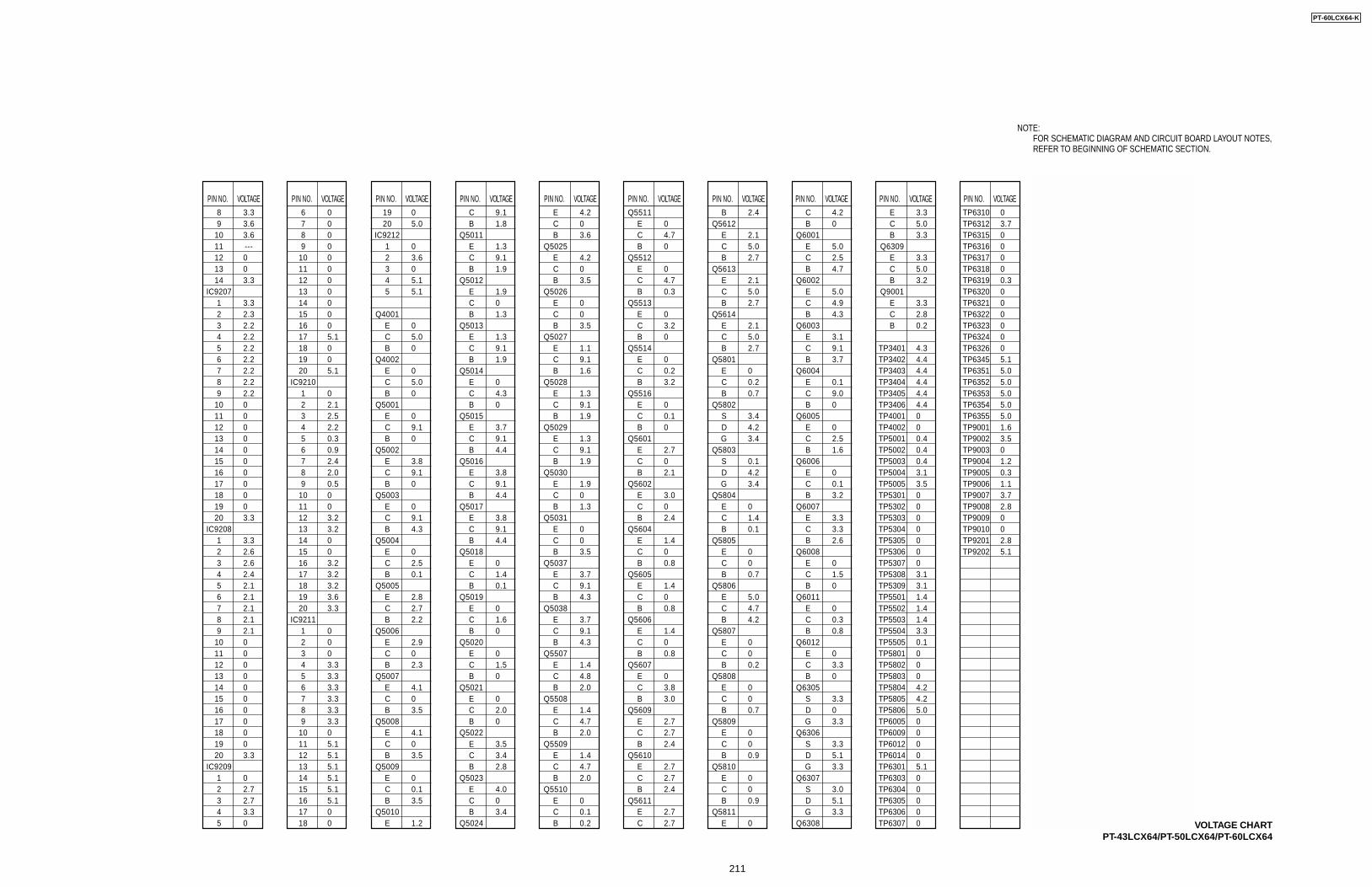
PIN NO. VOLTAGE
NOTE:FOR SCHEMATIC DIAGRAM AND CIRCUIT BOARD LAYOUT NOTES,REFER TO BEGINNING OF SCHEMATIC SECTION.
PIN NO. VOLTAGE PIN NO. VOLTAGE PIN NO. VOLTAGE PIN NO. VOLTAGE PIN NO. VOLTAGE PIN NO. VOLTAGE PIN NO. VOLTAGE PIN NO. VOLTAGE PIN NO. VOLTAGE PIN NO. VOLTAGE PIN NO. VOLTAGE
VOLTAGE CHARTPT-43LCX64/PT-50LCX64/PT-60LCX64
C 9.1B 1.8
Q5011E 1.3C 9.1B 1.9
Q5012E 1.9C 0B 1.3
Q5013E 1.3C 9.1B 1.9
Q5014E 0C 4.3B 0
Q5015E 3.7C 9.1B 4.4
Q5016E 3.8C 9.1B 4.4
Q5017E 3.8C 9.1B 4.4
Q5018E 0C 1.4B 0.1
Q5019E 0C 1.6B 0
Q5020E 0C 1.5B 0
Q5021E 0C 2.0B 0
Q5022E 3.5C 3.4B 2.8
Q5023E 4.0C 0B 3.4
Q5024
8 3.39 3.6
10 3.611 ---12 013 014 3.3
IC92071 3.32 2.33 2.24 2.25 2.26 2.27 2.28 2.29 2.2
10 011 012 013 014 015 016 017 018 019 020 3.3
IC92081 3.32 2.63 2.64 2.45 2.16 2.17 2.18 2.19 2.1
10 011 012 013 014 015 016 017 018 019 020 3.3
IC92091 02 2.73 2.74 3.35 0
6 07 08 09 0
10 011 012 013 014 015 016 017 5.118 019 020 5.1
IC92101 02 2.13 2.54 2.25 0.36 0.97 2.48 2.09 0.5
10 011 012 3.213 3.214 015 016 3.217 3.218 3.219 3.620 3.3
IC92111 02 03 04 3.35 3.36 3.37 3.38 3.39 3.3
10 011 5.112 5.113 5.114 5.115 5.116 5.117 018 0
19 020 5.0
IC92121 02 3.63 04 5.15 5.1
Q4001E 0C 5.0B 0
Q4002E 0C 5.0B 0
Q5001E 0C 9.1B 0
Q5002E 3.8C 9.1B 0
Q5003E 0C 9.1B 4.3
Q5004E 0C 2.5B 0.1
Q5005E 2.8C 2.7B 2.2
Q5006E 2.9C 0B 2.3
Q5007E 4.1C 0B 3.5
Q5008E 4.1C 0B 3.5
Q5009E 0C 0.1B 3.5
Q5010E 1.2
E 4.2C 0B 3.6
Q5025E 4.2C 0B 3.5
Q5026E 0C 0B 3.5
Q5027E 1.1C 9.1B 1.6
Q5028E 1.3C 9.1B 1.9
Q5029E 1.3C 9.1B 1.9
Q5030E 1.9C 0B 1.3
Q5031E 0C 0B 3.5
Q5037E 3.7C 9.1B 4.3
Q5038E 3.7C 9.1B 4.3
Q5507E 1.4C 4.8B 2.0
Q5508E 1.4C 4.7B 2.0
Q5509E 1.4C 4.7B 2.0
Q5510E 0C 0.1B 0.2
Q5511E 0C 4.7B 0
Q5512E 0C 4.7B 0.3
Q5513E 0C 3.2B 0
Q5514E 0C 0.2B 3.2
Q5516E 0C 0.1B 0
Q5601E 2.7C 0B 2.1
Q5602E 3.0C 0B 2.4
Q5604E 1.4C 0B 0.8
Q5605E 1.4C 0B 0.8
Q5606E 1.4C 0B 0.8
Q5607E 0C 3.8B 3.0
Q5609E 2.7C 2.7B 2.4
Q5610E 2.7C 2.7B 2.4
Q5611E 2.7C 2.7
B 2.4Q5612
E 2.1C 5.0B 2.7
Q5613E 2.1C 5.0B 2.7
Q5614E 2.1C 5.0B 2.7
Q5801E 0C 0.2B 0.7
Q5802S 3.4D 4.2G 3.4
Q5803S 0.1D 4.2G 3.4
Q5804E 0C 1.4B 0.1
Q5805E 0C 0B 0.7
Q5806E 5.0C 4.7B 4.2
Q5807E 0C 0B 0.2
Q5808E 0C 0B 0.7
Q5809E 0C 0B 0.9
Q5810E 0C 0B 0.9
Q5811E 0
C 4.2B 0
Q6001E 5.0C 2.5B 4.7
Q6002E 5.0C 4.9B 4.3
Q6003E 3.1C 9.1B 3.7
Q6004E 0.1C 9.0B 0
Q6005E 0C 2.5B 1.6
Q6006E 0C 0.1B 3.2
Q6007E 3.3C 3.3B 2.6
Q6008E 0C 1.5B 0
Q6011E 0C 0.3B 0.8
Q6012E 0C 3.3B 0
Q6305S 3.3D 0G 3.3
Q6306S 3.3D 5.1G 3.3
Q6307S 3.0D 5.1G 3.3
Q6308
E 3.3C 5.0B 3.3
Q6309E 3.3C 5.0B 3.2
Q9001E 3.3C 2.8B 0.2
TP3401 4.3TP3402 4.4TP3403 4.4TP3404 4.4TP3405 4.4TP3406 4.4TP4001 0TP4002 0TP5001 0.4TP5002 0.4TP5003 0.4TP5004 3.1TP5005 3.5TP5301 0TP5302 0TP5303 0TP5304 0TP5305 0TP5306 0TP5307 0TP5308 3.1TP5309 3.1TP5501 1.4TP5502 1.4TP5503 1.4TP5504 3.3TP5505 0.1TP5801 0TP5802 0TP5803 0TP5804 4.2TP5805 4.2TP5806 5.0TP6005 0TP6009 0TP6012 0TP6014 0TP6301 5.1TP6303 0TP6304 0TP6305 0TP6306 0TP6307 0
TP6310 0TP6312 3.7TP6315 0TP6316 0TP6317 0TP6318 0TP6319 0.3TP6320 0TP6321 0TP6322 0TP6323 0TP6324 0TP6326 0TP6345 5.1TP6351 5.0TP6352 5.0TP6353 5.0TP6354 5.0TP6355 5.0TP9001 1.6TP9002 3.5TP9003 0TP9004 1.2TP9005 0.3TP9006 1.1TP9007 3.7TP9008 2.8TP9009 0TP9010 0TP9201 2.8TP9202 5.1
PT-60LCX64-K
211
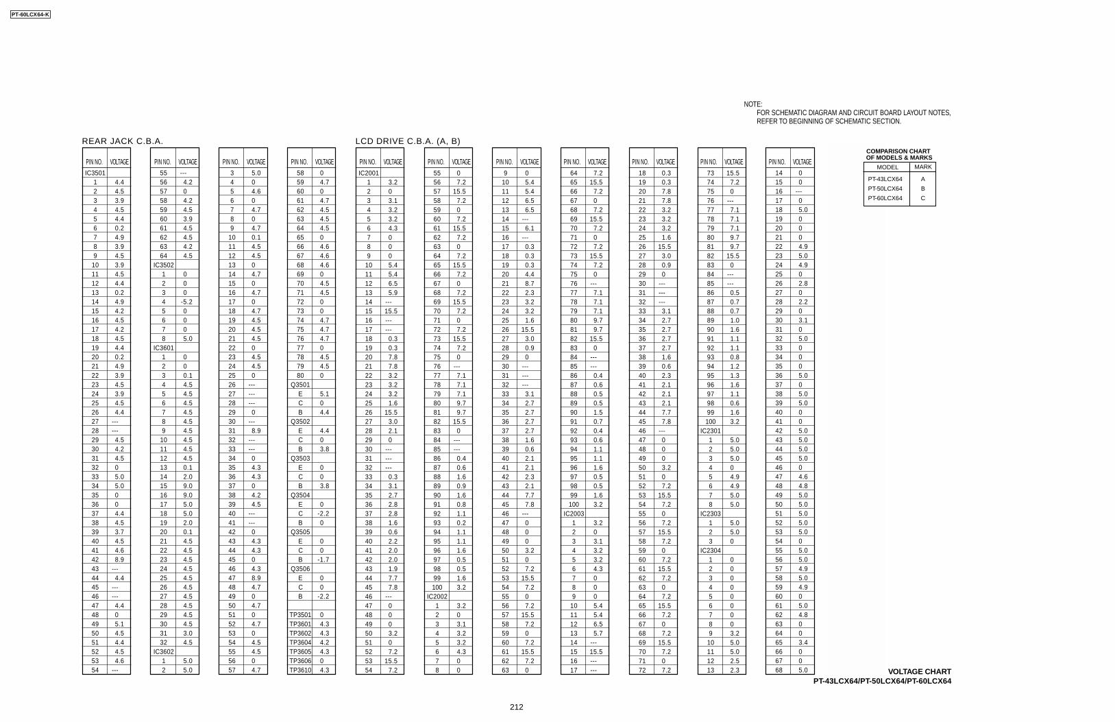
PIN NO. VOLTAGE
NOTE:FOR SCHEMATIC DIAGRAM AND CIRCUIT BOARD LAYOUT NOTES,REFER TO BEGINNING OF SCHEMATIC SECTION.
PIN NO. VOLTAGE PIN NO. VOLTAGE PIN NO. VOLTAGE PIN NO. VOLTAGE PIN NO. VOLTAGE PIN NO. VOLTAGE PIN NO. VOLTAGE PIN NO. VOLTAGE PIN NO. VOLTAGE PIN NO. VOLTAGE PIN NO. VOLTAGE
VOLTAGE CHARTPT-43LCX64/PT-50LCX64/PT-60LCX64
REAR JACK C.B.A.
IC35011 4.42 4.53 3.94 4.55 4.46 0.27 4.98 3.99 4.5
10 3.911 4.512 4.413 0.214 4.915 4.216 4.517 4.218 4.519 4.420 0.221 4.922 3.923 4.524 3.925 4.526 4.427 ---28 ---29 4.530 4.231 4.532 033 5.034 5.035 036 037 4.438 4.539 3.740 4.541 4.642 8.943 ---44 4.445 ---46 ---47 4.448 049 5.150 4.551 4.452 4.553 4.654 ---
55 ---56 4.257 058 4.259 4.560 3.961 4.562 4.563 4.264 4.5
IC35021 02 03 04 -5.25 06 07 08 5.0
IC36011 02 03 0.14 4.55 4.56 4.57 4.58 4.59 4.5
10 4.511 4.512 4.513 0.114 2.015 9.016 9.017 5.018 5.019 2.020 0.121 4.522 4.523 4.524 4.525 4.526 4.527 4.528 4.529 4.530 4.531 3.032 4.5
IC36021 5.02 5.0
3 5.04 05 4.66 07 4.78 09 4.7
10 0.111 4.512 4.513 014 4.715 016 4.717 018 4.719 4.520 4.521 4.522 023 4.524 4.525 026 ---27 ---28 ---29 030 ---31 8.932 ---33 ---34 035 4.336 4.337 038 4.239 4.540 ---41 ---42 043 4.344 4.345 046 4.347 8.948 4.749 050 4.751 052 4.753 054 4.555 4.556 057 4.7
58 059 4.760 061 4.762 4.563 4.564 4.565 066 4.667 4.668 4.669 070 4.571 4.572 073 074 4.775 4.776 4.777 078 4.579 4.580 0
Q3501E 5.1C 0B 4.4
Q3502E 4.4C 0B 3.8
Q3503E 0C 0B 3.8
Q3504E 0C -2.2B 0
Q3505E 0C 0B -1.7
Q3506E 0C 0B -2.2
TP3501 0TP3601 4.3TP3602 4.3TP3604 4.2TP3605 4.3TP3606 0TP3610 4.3
IC20011 3.22 03 3.14 3.25 3.26 4.37 08 09 0
10 5.411 5.412 6.513 5.914 ---15 15.516 ---17 ---18 0.319 0.320 7.821 7.822 3.223 3.224 3.225 1.626 15.527 3.028 2.129 030 ---31 ---32 ---33 0.334 3.135 2.736 2.837 2.838 1.639 0.640 2.241 2.042 2.043 1.944 7.745 7.846 ---47 048 049 050 3.251 052 7.253 15.554 7.2
55 056 7.257 15.558 7.259 060 7.261 15.562 7.263 064 7.265 15.566 7.267 068 7.269 15.570 7.271 072 7.273 15.574 7.275 076 ---77 7.178 7.179 7.180 9.781 9.782 15.583 084 ---85 ---86 0.487 0.688 1.689 0.990 1.691 0.892 1.193 0.294 1.195 1.196 1.697 0.598 0.599 1.6100 3.2
IC20021 3.22 03 3.14 3.25 3.26 4.37 08 0
9 010 5.411 5.412 6.513 6.514 ---15 6.116 ---17 0.318 0.319 0.320 4.421 8.722 2.323 3.224 3.225 1.626 15.527 3.028 0.929 030 ---31 ---32 ---33 3.134 2.735 2.736 2.737 2.738 1.639 0.640 2.141 2.142 2.343 2.144 7.745 7.846 ---47 048 049 050 3.251 052 7.253 15.554 7.255 056 7.257 15.558 7.259 060 7.261 15.562 7.263 0
64 7.265 15.566 7.267 068 7.269 15.570 7.271 072 7.273 15.574 7.275 076 ---77 7.178 7.179 7.180 9.781 9.782 15.583 084 ---85 ---86 0.487 0.688 0.589 0.590 1.591 0.792 0.493 0.694 1.195 1.196 1.697 0.598 0.599 1.6100 3.2
IC20031 3.22 03 3.14 3.25 3.26 4.37 08 09 0
10 5.411 5.412 6.513 5.714 ---15 15.516 ---17 ---
18 0.319 0.320 7.821 7.822 3.223 3.224 3.225 1.626 15.527 3.028 0.929 030 ---31 ---32 ---33 3.134 2.735 2.736 2.737 2.738 1.639 0.640 2.341 2.142 2.143 2.144 7.745 7.846 ---47 048 049 050 3.251 052 7.253 15.554 7.255 056 7.257 15.558 7.259 060 7.261 15.562 7.263 064 7.265 15.566 7.267 068 7.269 15.570 7.271 072 7.2
73 15.574 7.275 076 ---77 7.178 7.179 7.180 9.781 9.782 15.583 084 ---85 ---86 0.587 0.788 0.789 1.090 1.691 1.192 1.193 0.894 1.295 1.396 1.697 1.198 0.699 1.6100 3.2
IC23011 5.02 5.03 5.04 05 4.96 4.97 5.08 5.0
IC23031 5.02 5.03 0
IC23041 02 03 04 05 06 07 08 09 3.2
10 5.011 5.012 2.513 2.3
14 015 016 ---17 018 5.019 020 021 022 4.923 5.024 4.925 026 2.827 028 2.229 030 3.131 032 5.033 034 035 036 5.037 038 5.039 5.040 041 042 5.043 5.044 5.045 5.046 047 4.648 4.849 5.050 5.051 5.052 5.053 5.054 055 5.056 5.057 4.958 5.059 4.960 061 5.062 4.863 064 065 3.466 067 068 5.0
COMPARISON CHART OF MODELS & MARKS
PT-43LCX64
PT-50LCX64
PT-60LCX64
A
B
C
MODEL MARK
LCD DRIVE C.B.A. (A, B)
PT-60LCX64-K
212
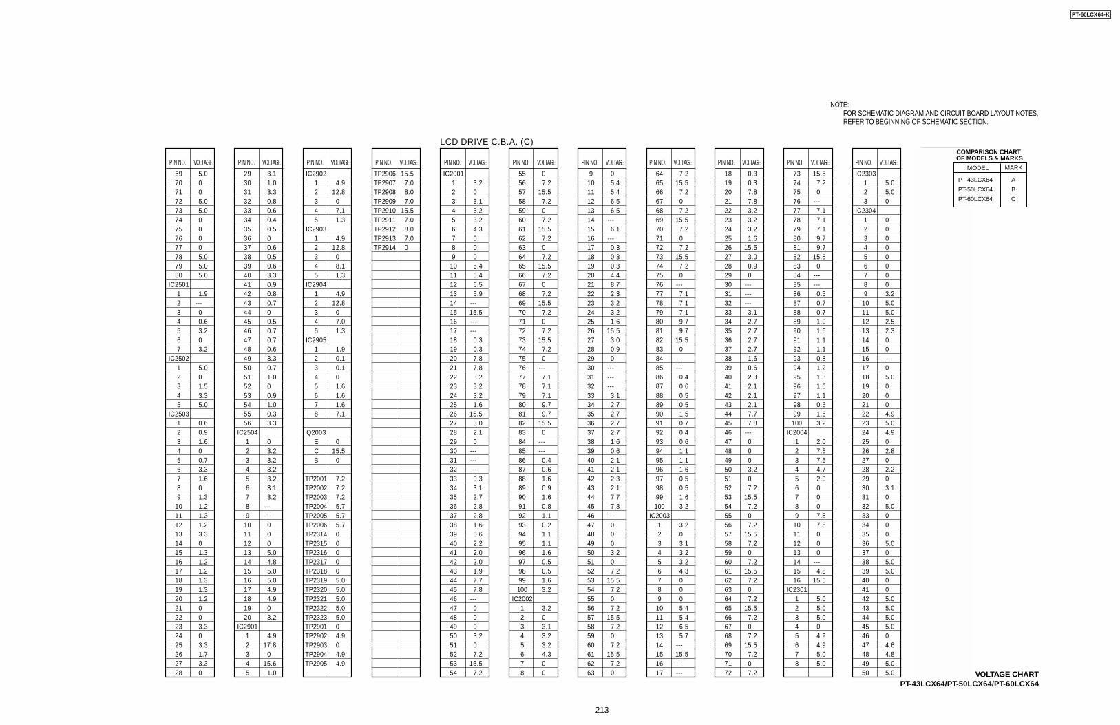
PIN NO. VOLTAGE
NOTE:FOR SCHEMATIC DIAGRAM AND CIRCUIT BOARD LAYOUT NOTES,REFER TO BEGINNING OF SCHEMATIC SECTION.
PIN NO. VOLTAGE PIN NO. VOLTAGE PIN NO. VOLTAGE PIN NO. VOLTAGE PIN NO. VOLTAGE PIN NO. VOLTAGE PIN NO. VOLTAGE PIN NO. VOLTAGE PIN NO. VOLTAGE PIN NO. VOLTAGE PIN NO. VOLTAGE
VOLTAGE CHARTPT-43LCX64/PT-50LCX64/PT-60LCX64
TP2906 15.5TP2907 7.0TP2908 8.0TP2909 7.0TP2910 15.5TP2911 7.0TP2912 8.0TP2913 7.0TP2914 0
29 3.130 1.031 3.332 0.833 0.634 0.435 0.536 037 0.638 0.539 0.640 3.341 0.942 0.843 0.744 045 0.546 0.747 0.748 0.649 3.350 0.751 1.052 053 0.954 1.055 0.356 3.3
IC25041 02 3.23 3.24 3.25 3.26 3.17 3.28 ---9 ---
10 011 012 013 5.014 4.815 5.016 5.017 4.918 4.919 020 3.2
IC29011 4.92 17.83 04 15.65 1.0
IC29021 4.92 12.83 04 7.15 1.3
IC29031 4.92 12.83 04 8.15 1.3
IC29041 4.92 12.83 04 7.05 1.3
IC29051 1.92 0.13 0.14 05 1.66 1.67 1.68 7.1
Q2003E 0C 15.5B 0
TP2001 7.2TP2002 7.2TP2003 7.2TP2004 5.7TP2005 5.7TP2006 5.7TP2314 0TP2315 0TP2316 0TP2317 0TP2318 0TP2319 5.0TP2320 5.0TP2321 5.0TP2322 5.0TP2323 5.0TP2901 0TP2902 4.9TP2903 0TP2904 4.9TP2905 4.9
69 5.070 071 072 5.073 5.074 075 076 077 078 5.079 5.080 5.0
IC25011 1.92 ---3 04 0.65 3.26 07 3.2
IC25021 5.02 03 1.54 3.35 5.0
IC25031 0.62 0.93 1.64 05 0.76 3.37 1.68 09 1.3
10 1.211 1.312 1.213 3.314 015 1.316 1.217 1.218 1.319 1.320 1.221 022 023 3.324 025 3.326 1.727 3.328 0
LCD DRIVE C.B.A. (C)
IC20011 3.22 03 3.14 3.25 3.26 4.37 08 09 0
10 5.411 5.412 6.513 5.914 ---15 15.516 ---17 ---18 0.319 0.320 7.821 7.822 3.223 3.224 3.225 1.626 15.527 3.028 2.129 030 ---31 ---32 ---33 0.334 3.135 2.736 2.837 2.838 1.639 0.640 2.241 2.042 2.043 1.944 7.745 7.846 ---47 048 049 050 3.251 052 7.253 15.554 7.2
55 056 7.257 15.558 7.259 060 7.261 15.562 7.263 064 7.265 15.566 7.267 068 7.269 15.570 7.271 072 7.273 15.574 7.275 076 ---77 7.178 7.179 7.180 9.781 9.782 15.583 084 ---85 ---86 0.487 0.688 1.689 0.990 1.691 0.892 1.193 0.294 1.195 1.196 1.697 0.598 0.599 1.6100 3.2
IC20021 3.22 03 3.14 3.25 3.26 4.37 08 0
9 010 5.411 5.412 6.513 6.514 ---15 6.116 ---17 0.318 0.319 0.320 4.421 8.722 2.323 3.224 3.225 1.626 15.527 3.028 0.929 030 ---31 ---32 ---33 3.134 2.735 2.736 2.737 2.738 1.639 0.640 2.141 2.142 2.343 2.144 7.745 7.846 ---47 048 049 050 3.251 052 7.253 15.554 7.255 056 7.257 15.558 7.259 060 7.261 15.562 7.263 0
64 7.265 15.566 7.267 068 7.269 15.570 7.271 072 7.273 15.574 7.275 076 ---77 7.178 7.179 7.180 9.781 9.782 15.583 084 ---85 ---86 0.487 0.688 0.589 0.590 1.591 0.792 0.493 0.694 1.195 1.196 1.697 0.598 0.599 1.6100 3.2
IC20031 3.22 03 3.14 3.25 3.26 4.37 08 09 0
10 5.411 5.412 6.513 5.714 ---15 15.516 ---17 ---
18 0.319 0.320 7.821 7.822 3.223 3.224 3.225 1.626 15.527 3.028 0.929 030 ---31 ---32 ---33 3.134 2.735 2.736 2.737 2.738 1.639 0.640 2.341 2.142 2.143 2.144 7.745 7.846 ---47 048 049 050 3.251 052 7.253 15.554 7.255 056 7.257 15.558 7.259 060 7.261 15.562 7.263 064 7.265 15.566 7.267 068 7.269 15.570 7.271 072 7.2
73 15.574 7.275 076 ---77 7.178 7.179 7.180 9.781 9.782 15.583 084 ---85 ---86 0.587 0.788 0.789 1.090 1.691 1.192 1.193 0.894 1.295 1.396 1.697 1.198 0.699 1.6100 3.2
IC20041 2.02 7.63 7.64 4.75 2.06 07 08 09 7.8
10 7.811 012 013 014 ---15 4.816 15.5
IC23011 5.02 5.03 5.04 05 4.96 4.97 5.08 5.0
IC23031 5.02 5.03 0
IC23041 02 03 04 05 06 07 08 09 3.2
10 5.011 5.012 2.513 2.314 015 016 ---17 018 5.019 020 021 022 4.923 5.024 4.925 026 2.827 028 2.229 030 3.131 032 5.033 034 035 036 5.037 038 5.039 5.040 041 042 5.043 5.044 5.045 5.046 047 4.648 4.849 5.050 5.0
COMPARISON CHART OF MODELS & MARKS
PT-43LCX64
PT-50LCX64
PT-60LCX64
A
B
C
MODEL MARK
PT-60LCX64-K
213
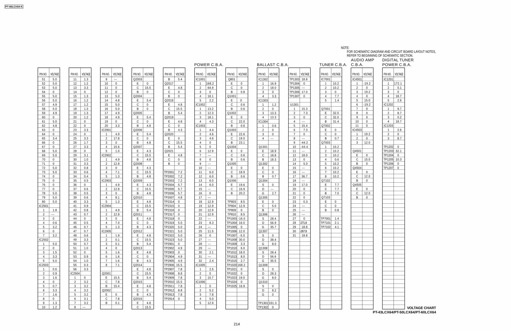
PIN NO. VOLTAGE
NOTE:FOR SCHEMATIC DIAGRAM AND CIRCUIT BOARD LAYOUT NOTES,REFER TO BEGINNING OF SCHEMATIC SECTION.
PIN NO. VOLTAGE PIN NO. VOLTAGE PIN NO. VOLTAGE PIN NO. VOLTAGE PIN NO. VOLTAGE PIN NO. VOLTAGE PIN NO. VOLTAGE PIN NO. VOLTAGE PIN NO. VOLTAGE PIN NO. VOLTAGE PIN NO. VOLTAGE
VOLTAGE CHARTPT-43LCX64/PT-50LCX64/PT-60LCX64
51 5.052 5.053 5.054 055 5.056 5.057 4.958 5.059 4.960 061 5.062 4.863 064 065 3.466 067 068 5.069 5.070 071 072 5.073 5.074 075 076 077 078 5.079 5.080 5.0
IC25011 1.82 ---3 04 0.65 3.26 07 3.2
IC25021 5.02 03 1.54 3.35 5.0
IC25031 0.62 0.93 1.64 05 0.76 3.37 1.68 09 1.3
10 1.2
11 1.312 1.213 3.314 015 1.316 1.217 1.218 1.319 1.320 1.221 022 023 3.324 025 3.326 1.727 3.328 029 3.130 1.031 3.332 0.833 0.634 0.435 0.536 037 0.638 0.539 0.640 3.341 0.942 0.843 0.744 045 0.546 0.747 0.748 0.649 3.350 0.751 1.052 053 0.954 1.055 0.356 3.3
IC25041 02 3.23 3.24 3.25 3.26 3.17 3.28 ---
9 ---10 011 012 013 5.014 4.815 5.016 5.017 4.918 4.919 020 3.3
IC29011 4.92 17.83 04 15.65 1.0
IC29021 4.92 12.83 04 7.15 1.3
IC29031 4.92 12.83 04 8.15 1.3
IC29041 4.92 12.83 04 7.05 1.3
IC29051 1.92 0.13 0.14 05 1.66 1.67 1.68 7.1
Q2001E 15.5C 7.8B 15.4
Q2002E 0C 7.8B 0.1
Q2003E 0C 15.5B 0
Q2004E 5.4C 0B 0
Q2005E 5.4C 0B 4.8
Q2006E 5.4C 0B 4.8
Q2007E 4.3C 15.5B 4.8
Q2008E 4.3C 15.5B 4.8
Q2009E 4.3C 15.5B 4.8
Q2010E 4.8C 15.5B 5.4
Q2011E 4.8C 0B 4.3
Q2012E 4.8C 15.5B 5.4
Q2013E 4.8C 0B 4.3
Q2014E 4.8C 15.5B 5.4
Q2015E 4.8C 0B 4.3
Q2016E 4.8C 15.5
B 5.4Q2017
E 4.8C 0B 0
Q2018E 4.8C 15.5B 5.4
Q2019E 4.8C 0B 4.3
Q2020E 0C 15.5B 5.4
Q2021E 4.8C 0B 0
TP2001 7.2TP2002 7.2TP2003 7.2TP2004 5.7TP2005 5.7TP2006 5.7TP2007 4.8TP2314 0TP2315 0TP2316 0TP2317 0TP2318 0TP2319 5.0TP2320 5.0TP2321 5.0TP2322 5.0TP2323 5.0TP2901 0TP2902 4.9TP2903 0TP2904 4.9TP2905 4.9TP2906 15.5TP2907 7.8TP2908 8.8TP2909 7.8TP2910 15.5TP2911 7.8TP2912 8.8TP2913 7.8TP2914 0
POWER C.B.A.
IC10011 168.22 64.93 04 18.15 2.2
IC10021 13.22 12.33 18.14 4.3
IC10031 4.42 4.63 4.64 05 06 12.97 ---8 09 ---
10 ---11 6.012 6.013 6.014 6.015 ---16 017 ---18 12.919 12.920 12.921 12.922 ---23 8.324 ---25 11.526 027 ---28 ---29 ---30 2.131 ---32 2.4
IC10051 2.52 03 10.7
IC10061 02 5.23 7.84 5.05 12.9
Q801E 0C 0B 0.8
Q1001E 0C 0.6B 0.6
Q1002E 0C 22.0B 0.6
Q1003E 22.6C 19.0B 23.1
Q1004E 0C 0.6B 0.6
Q1005E 0C 18.9B 0.6
Q1006E 19.6C 16.9B 20.2
TP803 8.5TP804 12.9TP809 0TP810 8.5TP1003 -16.0TP1004 16.0TP1005 0TP1006 12.0TP1007 -5.0TP1008 30.0TP1009 3.3TP1010 6.0TP1012 18.0TP1013 8.0TP1015 2.7TP1020 168.2TP1021 0TP1022 0TP1023 19.0TP1024 0TP1025 16.9
IC13021 16.92 18.03 04 3.3
IC13031 1.22 03 13.34 13.3
IC13041 0.62 03 04 ---
Q1301E 18.9C 18.8B 18.3
Q1302E 0C 0B 0.7
Q1304S 0D ---G 2.7
Q1305E 0C 5.0B 0
Q1306S 28.4D 56.9G 35.7
Q1307S 0D 38.4G 8.0
Q1308S 28.4D 56.6G 35.5
Q1309S 0D 28.3G 8.0
Q1310S 0D 8.2G 0
TP1301 331.3TP1302 0
TP1303 18.8TP1304 0TP1305 ---TP1306 17.0TP1307 0
U13011 15.32 7.33 04 ---5 15.46 7.37 08 ---9 -44.2
10 -44.411 ---12 18.013 014 5.015 ---16 ---17 36.718 ---19 17.020 021 022 023 0.324 ---25 ---26 ---27 028 -271.829 18.830 -267.831 18.8
BALLAST C.B.A. TUNER C.B.A.
IC70011 10.22 10.23 04 7.75 1.4
Q7001E 32.0C 32.0B 31.4
Q7002E 0C 0B 0.7
Q70031 10.22 10.23 10.24 0.65 10.26 10.27 10.28 10.2
Q7102E 7.7C 7.7B 7.0
Q7103E 0C 0B 0.8
TP7001 1.4TP7101 2.1TP7102 4.1
AUDIO AMPC.B.A.
IC45011 -19.22 03 19.24 05 15.06 -19.27 08 09 0
10 011 0
IC45031 19.22 03 12.0
Q4501E 0C 15.0B 0
Q4504E 0C 12.0B 0
Q4505E 0C 12.0B 0
DIGITAL TUNERPOWER C.B.A.
IC12011 172.12 0.13 04 18.75 2.6
IC12021 9.72 8.73 0.24 18.7
IC12031 2.62 03 8.7
TP1202 0TP1203 32.1TP1204 0TP1205 10.3TP1206 0TP1207 0
PT-60LCX64-K
214
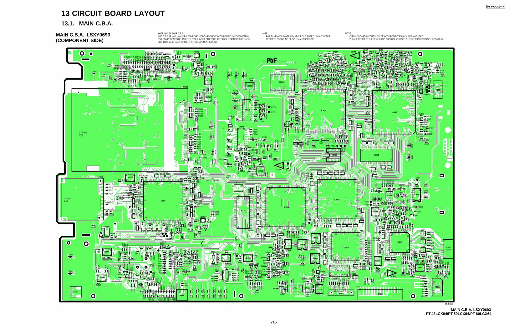
13 CIRCUIT BOARD LAYOUT13.1. MAIN C.B.A.
MAIN C.B.A. LSXY0693 NOTE:FOR SCHEMATIC DIAGRAM AND CIRCUIT BOARD LAYOUT NOTES,REFER TO BEGINNING OF SCHEMATIC SECTION.
NOTE:CIRCUIT BOARD LAYOUT INCLUDES COMPONENTS WHICH ARE NOT USED.PLEASE REFER TO THE SCHEMATIC DIAGRAM AND PARTS LIST FOR PROPER PARTS CONTENT.(COMPONENT SIDE)
NOTE: MULTILAYER C.B.A.THIS C.B.A. IS Multi-Layer C.B.A. THIS CIRCUIT BOARD SHOWS COMPONENT LAYOUT-PATTERNFOR COMPONENT SIDE AND FOIL SIDE. LAYOUT PATETRNS ARE SINGLE PATTERN FOR EACHSIDE THAT MAKE EASY TO SIGHT THE COMPONENT LAYOUT.
BC E
BC E
BC E
BC E
BC
EBC
E
BC
E
BC
EBC
E
BC
E
BC
E BC
E
BC
EBC
E BC E BC E
BC E
BC E
BC E
BC E
BC E
BC E
BC E
BC E
BC
E
BC
E
BC
E
BC
E
BC
EBC
E BC
E
B CE
BC E
BC
E
BC
E
BC
E
BC EBC E
BC
E
BC
E
BC
E
BC
EBC
E
BC
E BC
E BC
E
BC
E BC
E
BC
E
BC
E
BC E
BC E BC
E BC
EBC
E
B CE
BC
E
BC
E
BC
E
BC
E
BC
E BC
E BC EBC E
BC E
BC E BC
E
BC
E
BC
E
BC
EBC
E
BC
E
BC
E
BC
E
BC
E
BC
E
B CE
B CE
B CE
BC E
C6327C6313
L6303
C631
4
C6347
R6415
R635
5R6
354
R633
2R6
334
R633
6R6
338
R634
0R6
342
R634
4
R634
6R6
348
R634
5
R634
3R6
341
R633
9R6
337
R633
3R6
331
R632
7
R635
1
R630
3
R630
4
R630
6
R613
9
C550
4
C550
5
C550
6
R630
5
R613
0
R925
8
C921
6C9
217
C921
8R9
262
R613
1
C602
2
R644
1
R644
2
R614
0
C602
5D6
001
D600
2
R630
4
R632
6R6
325
R632
4C6
337
C633
2C6
330
C632
8
C632
6L63
15L6
314
L631
3
L631
2L6
311
C633
5
C633
4C6
329
R632
3R6
322R6
321
R632
0R6
310
R631
8R6
317
R631
6R6
315
R631
3R6
312
R631
1
R631
4 R633
5R633
0
R6411R6419
C6346R6414R6410R6406
R6403R6402
R6407
TP6312
TP63
08
TP63
07
TP63
06
TP63
04
TP63
03
TP63
44
TP63
05
R641
7
R636
0
R631
9
C632
3
C632
4
C631
5
C631
1
C630
9C6
308
C630
7
C632
5
R6350
C6302
C6303 C6306C6305
C6308C6316
R6349
R6302R6329
1 345
R6307
L6307L6306
L6304Q6303
IC6303
Q6302
Q63
04
Q6301
Q6306 Q6307
IC6005
IC6006C5514
C5501
R5551
R5552
R5555
R5554
R554
7
R5576
R555
8R5
559
R556
0
C5536
C5534
C5549
C5535
TP5503
TP5502
TP5501
R5550
R5549C5502
C5503
L5503
L5504
C551
5
C920
8C9
204
R900
3
L900
3
R926
4R9
261
R903
4
R901
4R9
013
R901
2
R901
1R9
010
R900
5
R900
9R9
008
R905
5
C905
7C3
436
C901
5
C903
2 C902
6
C902
7 C902
5
R906
0 C902
8C9
029
C903
1
C901
9C9
018
C901
7
R903
5
C901
0
R500
1
R501
6C5
007
R501
0
R500
4 R5006
R500
8
R5007
R500
9
R501
1R5
012
C500
5 C50
04
R500
5
R504
4
C506
5
C506
8
R5046
R503
4R5
033
R504
8 L501
1R5
049
R505
1R50
53R5
055
L501
2R5
056
R505
8
R506
5
R509
1R5
092
R509
4R5
097R5
061
R505
9 R506
3
R502
2
R521
0
R5021R501
8R5
014
R5015
R501
9C500
8
C501
2
C507
7
R522
2 R522
1
R521
9
R514
8 R511
8
R511
4R5
155 R5
164
R512
2
C523
5
C507
3
C500
9
IC5505
IC5002
Q50
01Q
5002
Q5003
Q5010
IC5005
Q50
11 Q5012
Q50
13 Q
5008
Q5007
Q50
06
Q50
04
Q50
09
IC5501
Q5507
Q5508
Q5509
C5520
C9014
C9059
R9039 R9040R9033R9028
R9015
R9017R9027
R9025
R9032R9029
R9016
TP9001
C5521
C5523
C6024
L6006
C5522
TP9002
R9021
R9019
R532
2 R532
1R5
326
R532
8R5
331
R533
3R5
334
R533
6
C343
5
C343
4
C5301C5398
R5303
R3404
TP5504
R5469R5
339
C552
4
C555
4C5
555
C554
2C5
543
C555
9
C556
3
C502
7
C554
5
C5544 C5558
C5561
C5024
C554
1C5
546
C555
0
C552
5
C556
2
R558
8
C556
4
C9001C9002
R9018
R9023R9022
R9020
C9016
C9036C9038C9041
C904
4
C904
5C9
047
C904
6
R907
9
R908
1
R908
2R9
098
R908
0
C9043
C9058
R9026R9062R9064R9070R9074
R9024 L9002
L9006
L9007
TP9006
TP9003
TP9004
TP9005
TP6010
X9001
IC9002
Q9001
IC5303
IC5503
Q5516
Q5512
IC5502
Q55
10
Q5511
Q5513IC5003
IC5313
R9089
R9100R9097
R9099
C905
2 SW9001
R5035R5036
R5238
R5239
L5007
L500
8C5
044
C502
9
C502
6
C502
5
C502
8 L5006C5042C5043
R5029
C5060
R5060
R5067
R5090
R5125
R5124
R5126
R512
7R5
128
R5093
R5141R5068
R5129
R5174 R5176
R5179R5180 R5181
R5178
R5177 R5187
R5186
R5209
R5207
R5195R5194
R5192R5190
R5191
R5189
R5188
R524
0TP
3402
TP34
01TP
3403
TP34
05TP34
04
TP3406
C5202C5215
C5203
C5214
C5201
L5032
L5031
C5204
C522
5C5
223
R5173
R5098R5099
R509
5R5
096
R513
0
R517
5
R508
6
C5238 C5237
R5043R5042
L5002
L5003
R5211
C5002
R5002
R500
3
C5001C5006
R5234R5023
R5013R5017C5010
C5020C5011
C5078
1
1
3
3 45
13 4
52
C5076
L5024
L501
4
C5130
C5232C5230
C5231R5220R5152L5025
R5205
C5126 R5112 R5117
R5109R5107
R5105
R5108R5106R5104
R5111
R5116
C5120
C5124C5123R5115
R5119
C5129
C514
5 C514
6C5
154
C515
9
C516
4
L503
4
L502
6
R522
6
R514
7
R515
0
R517
2C5
172
C517
4C5
216
R515
3R5
158
R516
7
R517
0 C516
7
C516
9
R512
3
C512
1
C511
9 L501
9
L502
2
R516
9C5
166
C516
8C5
170
R516
1
R516
0
C515
6 C5128C5125
L5020
L5021
C5122
C5239
R5121
R5157 R5165 L5028
C5175L5029
R5163
L5027
C5131C5144
R5235
L5001
L5004
L5013
C4024
C4023
C4015
C4008
C4020
C4019
L4008
C400
7
R588
3R5
882
R588
0
R584
6R5
840
R584
8R5
851
R584
7R5
843
R585
0
R588
1
R585
2
R584
6R5
845
R586
1
R545
3
C585
3C5
832
C584
7 C583
8
C585
4
R587
9R5
872
R587
8
R582
7
R580
9
R583
4
R583
2
R583
1R5
830
R582
9R5
828
R589
6C5
802
C580
1 R589
2
R581
0
R580
8R5
812 R5
802
R580
3
L580
3
L580
1
L580
2
JK5801
L580
4
L580
6
C4016
C401
7
C5852C5846
R5841 R5875
C582
9
C583
7
C584
3
C584
8
C585
0
C401
8
C585
1
IC4002
IC5805
Q58
08
Q5805
Q5809
Q5810IC5804
Q5807Q5806
Q5804
LSJB3107
R5826
R5811R5813
D5802
D5801
D5803R5804
R5897
R5814
R5815
R5805
L5805
R5891R5890
R5889R5888R5887
R5886R5885R5884
D5806
D5805
D5804
C5810
C5805C5808
C5806
C5804
C5809
C581
9C5
818
C581
7C5
816
C582
0C5
821
C582
5C5
823
C582
6C5
828
R585
4
R581
7R5
816
R585
3
R562
7R5
628
R563
0R5
632
R563
1
R537
2R5
373
R537
6R5
387
C540
4R5
388
R5396 R5398 R5399 R5401
R5454
R562
9
R562
2R5
623
R560
4
R560
1
R560
9 R561
7
R560
3R5
602
R561
3 R5
699
R5620
R5616
R561
9
C561
3
C600
3
C600
2
C600
1
C561
1
R541
4R5
473
R569
8
R541
0
C535
4
C535
6
L532
6C5
357
L600
1
L600
2
L600
3C5617
R5624
R5417R5415
R5416R5413
C5360
R5610R5606
R561
8
R5621
C5614
C5615
C5616
C561
2
C5610
C5609
C5608
R5611
R5612
R5605
R5607
R5615R5608
R5614
C3440
143
5
C5359
C535
8C5355
X5301
R5411TP5309
C540
3
C565
0L5
611
R542
8R5
427
L533
2
L533
4
L533
1
L533
0
L533
3
R542
6R5
425
R542
4R5
423
R543
0R5
429
R543
2R5
431
R534
7R5
346
R535
4
R534
2R5
352
R535
1R5
350
R534
8 R534
3
R534
4
R534
9
R6009R6010C6023
L6007
R6008R6133R6134R6137R6138
C344
5
C560
1
C560
2
R6005R6006
R6007
R587
3
R5842
R5856R5849TP5801
R585
5
R587
0R5
869
R587
1
R5649R5652R5654R5657R5661R5663
R5668R5669
R5844
C5220C344
2C3
438
C343
3C3
432
C580
3
R567
5
R567
3R5
676
R568
1
R5839IC5014
IC5803
Q5803
IC5802
Q580
1
Q5802IC5801
R5674
R5691
R5666
R5860R5859
R5858
C5833
C5844
R5866R5867
C5831C5830
R587
7
R586
2R5
865
R586
3C5
835
C5834
L5807
R5356 R5355 R5353
R5338
R5341R5
587
R558
4
C555
1
R559
2R5
581
R558
2R55
80 R557
9R5
577
R559
1
R5517
R5069 R5070 C5082 C5085
C509
6
C510
2C5
101
R508
0
R5083
TP5001
TP50
02
TP50
03
R5085
R508
8R5
089
R5081 R5082
X5001
R507
1
R9245R9243R9246R9236
L9204
R9241R9242R9240R9237R9239
R9238R9249R9250R9251
R9255R9254
R9244
IC5301 Q5606
Q5605Q6005Q6006
Q6002
IC6004
Q6001Q5604
R9115
R9084
R9087
R9083 R9124
R9091R9105
R9119
R9117 R9110
R9109R9118
R9107R9090 R9092TP9007 R9
093
R9094
R9078 R9077R9063 R9054 R9043
R9085R9086
R9116R9121
R9120
L9013
C905
6
R908
8C9
051
C904
8C9
049
IC9009
IC9004
P9002
IC9005
IC6001R6145
C6007
C3437
C601
6
C6017
R6104
R6102
C3441 L601
5 L501
4L5
013
L501
2L5
011
L501
0L5
009
L500
8C6045
23 1
132
R6094
R6093
R6091
R6143
R6036 R6049
R6021
R6040 R6004 R6002
C6050
C6004
C6019
C6005
C6049 C6047R6150
R6148R6001
R6153R6152
R601
1
R6012R6041
R600
3
R6043R6042
R6089R6087R6085R6083R6082
R6084
R6088R6090
R6045
R6086
R6041R6044
R6032
C6013
R6037
R6038
L6004
R6144
R601
6 R609
2
R602
5
R603
5
R603
4
R603
9
R602
8R6
030
R603
1
R602
3 R610
6R6
105
R609
8
C601
5
C601
0
C601
2
L600
5
R615
4
R615
5
R614
8
R6151R614
9
C601
1
R602
2
R609
6R6
099
R610
3
C604
2
C603
2C6
029
C602
7
C603
0 C603
5
L601
6
L601
7L6
018
L601
9
C604
1C6
038
C603
4C6
031
C602
8C6
026
R612
8
R612
7R6
142
R612
0R611
0R6
118
R610
8R6
097
R609
5
R611
9
R610
0
R611
7
C604
4C6
018
R610
9
R610
7
R610
1
R601
4R6
015
R601
7
IC6007 IC6002
X6001C6331L6331
P6007
R3405C3408
R3403R3402
R3401
R6132
R6135R6136R6129
L600
2
C560
3 L6
003
C560
4 L6
004
C560
5 L6
005
C560
6L6
006
C560
7L6
007
L600
1 IC5308
Q5612
Q5613
Q5609
Q5610
Q5614Q5611
Q5601
IC5309IC5310
IC5311IC5606
IC5312
P3401P5302
L3430L3429
L3428L3427L3426
L3425
L3423L3422
L3424
P3404
IC5604IC5605
IC5602
IC5603
IC5601
IC5306
IC5302
TP53
05TP
5306
C5560
L5507
L5506
C5552TP5505
R558
5
C5547C5548
C5540C5533
L5505
IC5009
P3403IC5013
IC5011
Q5031
Q5014
Q5015
Q5038
Q5022
Q50
18
Q50
19
Q5016
Q5017
Q50
26
Q50
23
Q5029
Q50
30Q5028Q50
27
Q5024
Q5020
Q5025
Q5021
IC5016
IC50
06
IC5008Q5037
Q50
05 IC5010
C5118C5113C5117
C5116C5115
R5103
R5120
R5101R5236R5237
R5203
R510
0
C512
7
R510
2
C5110
L5018
IC5004
1
1
3
3
45
Q60
10
Q60
04 Q3402
Q3403
Q6009
Q6003
Q6007
Q6008
D6304
D6303
P9201
18
10
1
116
9
89
193 256192 1
6465128
129
1
9
18
1041
135 4
58
114
15 28
6465128
129
192193 256
1
86
1
44
43
58
1
R5367R5365C5350
R532
7
R5371 R5375 R5378 R5383 R5395
IC5012IC5307
1 5253208
3736
108109144
7372
111
28
1 345
120
5629
1
1
14
18
11 7
4
5
1 14
7 8
43
1
1
10 11
20
44
1 24
14
8 7
1
14
8 7
1
5253208
1
1
78
1412
1
104105150
151
35
68
1
34 1 4
58
1 4
58
1
1
1
12
10 11
201
1 4
57
13
24
14
87
3670
35
14
87
861
1
105104
1
8
7
14
5051 75
76
2625
16 9
2
PC CARDSLOT
SD CARDSLOT
8
4
5
1
11
20
10 1
11
20
10
1
11
20
10
C5644
1
1
814
157
157
156
156
104105
5352
1208
U6301
61
100
5
81
4
4
8
5
8
1 4
5
TP5802
TP5803 C5849R5864
1
19
4
12
3
15
34
HDMI IN
MAIN C.B.A. LSXY0693PT-43LCX64/PT-50LCX64/PT-60LCX64
PT-60LCX64-K
215
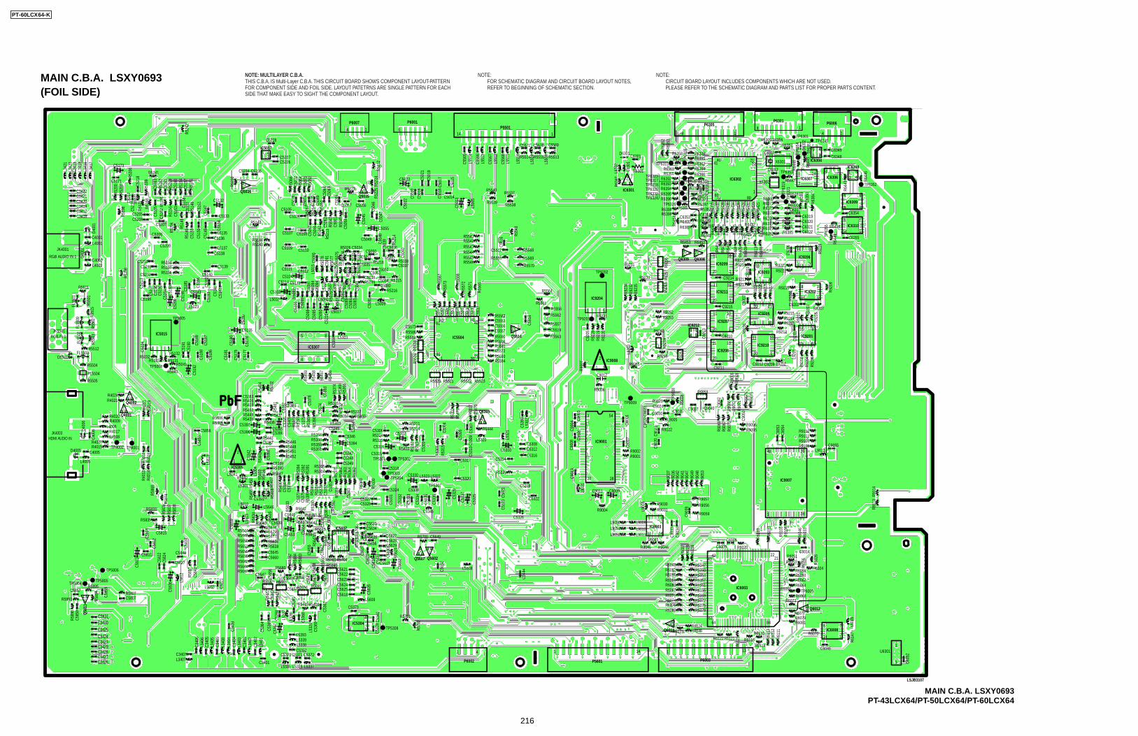
PT-43LCX64/PT-50LCX64/PT-60LCX64
NOTE:FOR SCHEMATIC DIAGRAM AND CIRCUIT BOARD LAYOUT NOTES,REFER TO BEGINNING OF SCHEMATIC SECTION.
NOTE:CIRCUIT BOARD LAYOUT INCLUDES COMPONENTS WHICH ARE NOT USED.PLEASE REFER TO THE SCHEMATIC DIAGRAM AND PARTS LIST FOR PROPER PARTS CONTENT.(FOIL SIDE)
NOTE: MULTILAYER C.B.A.THIS C.B.A. IS Multi-Layer C.B.A. THIS CIRCUIT BOARD SHOWS COMPONENT LAYOUT-PATTERNFOR COMPONENT SIDE AND FOIL SIDE. LAYOUT PATETRNS ARE SINGLE PATTERN FOR EACHSIDE THAT MAKE EASY TO SIGHT THE COMPONENT LAYOUT.
MAIN C.B.A. LSXY0693
MAIN C.B.A. LSXY0693
B CEBC
E
BC E
B CEB CE
BC E
BC
EB
CE
BC
E
BC
E
BC
E
BC
E
B CE
L342
1L3
420
L341
9
L341
6L3
417
R520
6
R519
9
R516
2
R515
9R5
156R5
166
R516
8
R517
1
R520
2R5
200
R520
1
R515
4
R515
1R5
242
C521
8
C516
3
C516
1
C515
7C5
158
C516
5
C521
9C521
7
C515
3C5
160
L341
8
C5173
R5241
C5171
C3420C3419C3417C3418
C4001
C4002
L4001
L4002
R5511
FL55
01FL
5509
FL55
02
FL5503
FL5504
R550
1R5
515
R550
2R5
503
C3421C3422
D400
1
D400
2
R5512
R5505
R5504
D5501
R4020
R4021R4024
Q4001
Q4002
R4017
R4009
R4008R4007
R401
3
R586
8
R587
4R5
836
R583
7R5
838
R401
4R4
016
R401
2R4
019
R401
1
C4005
D400
6
C400
6
L4005
D4005R4015 TP4002 TP4001
L4006
R5032
C522
4
C519
1C5
190 C5
189
C518
7C5
188
C518
6
C518
1C5
180
L503
0
C514
2C5
141C5
182
C518
5C5
199
C519
3C5
194
C519
5C521
3R520
8
C519
7C5
196
C520
0
C518
4
C518
3
C517
9
C517
7C5
178
C519
2
R5040
R5041R5131R5133
R5132
TP5004
C5176
L5023
C5143
C5198
C5212
C5211C5210 R5193
C5209
C5208
R5197R5196 C5140
C5139
C5138C5137
C5136
C5133
C5132
Q5036
IC5017
C5234
C5226C5227
C5228
1 345
C5236
R523
3C5135
TP5005
R519
8
C516
2
R520
4
R514
9R5
146
R514
5
C515
5C5
152
C515
1C5
147
C515
0
C514
9 C513
4C5205C5206
C5207
R5143
R5142
C5109
C5107 C5108
C5110
C5111 C5112C5104
C5114 C5113
C509
9C5
097
C509
4
C5092C5
100
R508
7 R508
4
R507
6R50
74L5
016
L501
5
R521
3
R505
2 R504
7
R504
5
R522
5R5
224
R521
2
R505
7
R506
6
R506
4
R506
2R5
054
R505
0
C506
6C5
067
C506
4C507
1C5
074
C507
0C5
069
C507
5C5
072
C506
3C5
061
C505
8
C505
9
C506
2
R507
2C5
087
R521
7
R507
9R507
7R5
075
R502
4
R507
8
R502
5
R507
3
C508
9C5
084
C508
3C5
041
C503
3C5
031C5
091
C503
2C5
030
C509
0
C508
8
C508
9
C504
0C503
9C5
048
C504
7C504
6
C502
2 C502
0
C502
1C5
018
C501
9
C501
7
C501
5
C501
6
C501
3
L500
5
C556
5
C556
6
C556
7
C556
8
L551
4
L551
3
L551
2
L551
1
L551
0
L550
9
L550
8
C5014
C504
5
R521
4
C508
1
C509
3C5
222
C538
4
C537
8R5
390
R539
3
R539
7R5
372
C537
4
C534
4
C535
3
C509
5C5
098
C5103
L5010
R5144
C5105
C5106
L5017
L53035 8
L5009
R5216
R5215
R5038R5037
C5080
C5037C5052
C5053
C5051
C5035
C5050C5036
C5049
C5055
C5023
C5034R5026
R5027
C5038R5039
R5218
C5054
R5539
R5537
R5538
R5540
C5057 C5056
R5223
Q5035
P6001P5501
P6305P6301 P6006
IC6304
IC6302 IC6306IC6307
IC6308
R6309 R6356R6357
R6369
R642
1R6
423
R643
1R6
424
R642
6R6
434
R643
6R6
428
R643
7R6
438
R641
6R6
412
R640
8
R640
4
R640
9
R641
3
C920
3
R640
1
C920
6
R922
9 R644
9TP63
55
TP6352
R920
9
R920
8
R920
5R920
3
C920
1L9
201
R920
2R9
204
R920
6
L9202
R920
1
R9212
R9213R9214R9215
R640
5
R642
9R6
427
R643
3
R642
2R6
430R6432
R6425R643
5
R643
9
R645
4
R6371R6373R6374R6376R6377R6379R6381
D630
2
R644
8
R644
5
R644
3 R644
6
C6310
C6312
R6447
TP6353
C6319
R6450
C6355
C6354
C6320C6321C6322R6385
R9223R9222
R9210
R9207C9202
R6386R6387
R6388
R6391
R6390
R638
9TP63
19TP
6321
C635
0R6
384
C6317
C6349
C6348X6301
X6302
TP6301TP6345
TP63
54
TP63
51
R6328R6359R6362R6364R6366
R6367
R6380
R6370
R637
2C6
318R6368
R6375R6378R6397
R6382
R6420R6418
R6440
C6351C6353R6400R6383
R6453 R6452
R9218R9216
C9214
C9215
R9211R9217
IC9209Q6309 Q6308
IC9203
IC9206
IC6310
IC6309
IC9211
IC9207
IC9208
IC9205
IC9202
IC9201
IC9210
IC9212
C9209C9212C9211
C9040 C904
2
C905
0
C905
3C9
054
R906
5R9
066
R907
2 R907
6
R907
3
R910
3
R601
3
R601
9
R604
6R6
055
R602
6
R603
3
R911
4R9
113
R910
4
R906
7R9
069
R907
5
R907
1R9
068
R9096R9095 R9112
R9111R9106R9108
L9012
IC9007
C9055
R6020
C6008
C6009
IC6003
P6003P5601P6002
IC9003
IC5015
C5571 C5570 C5569
R5514 R5516 R5513
IC6301
D6301C6301
L630
1
L630
2R6
347
R635
2R6
353
R6301
21 3
R6358
R6363
R6361
R6365R6392R6393R6394R6395R6396
R6399R6398
TP6315
TP6317TP6318TP6320TP6322TP6324
TP6326
TP6323
TP63
16
C6014R6051R6053
R6060
R6064R6066
R6068TP6005
Q6012
R6073
R6077R6079
R6114R6116
R6115R6122 R6121
C6046
R6070
R614
7
U6301
R6081
L602
6
C635
2
R611
1R6
112
R611
3
R612
5
R6062
R6058R6024
IC6008
LSJB3107
R6126R6124
R6123Q6011
R6080 R6078R6075R6072R6069R6156R6061R6057R6054R6050R6052
R6056R6059R6063R6067R6071R6074R6076
R6047
R602
7
L900
8
R903
7R9
036
R904
2R9
041
R904
7R9
049
R904
8R9
053
C903
4
C903
9
C903
3
R602
9R6
018
R6048
R9044
R9059
R9056R9057
R9030R9004
R9001R9002
R9122
R9123
R9058
L9005
C9011
IC9001
IC9008
IC9204
C9009
C900
7
C902
0C9
021C9
022
C902
3
C900
5
C900
3
C900
4
C900
6
C900
8C9
013
L900
1
R9031
L9009
L9010L9011
L9050L9051L9052
R9045
R9046
C9030
C9024
TP90
08
R903
8
TP9009
C9035 C9037
R926054
3 1C9210
R925
9 C921
3
C920
7R9
230
R922
4R9
225
R922
6R9
227
R924
7
R9248
R9253R9252
R9233
R9221TP9201
TP9202
R9231
R926
3
R923
5R9
232
R923
4
R922
0
R922
8
R900
7C9
205
R921
9
R925
7R9
256
R9006
R5563
R5557
R5562R5556
R5561
R5583
R5590R5596R5595
R5593R5594
R5523R5522R5521R5520
R5589R5586C5573
C5553C5556C5557
C5572
R5564
R5570
R5569
R5568
R5553
R5541R5542R5543R5544R5545R5546
R556
5
R557
1
R557
2
R557
3
R557
8
R556
7R5
575
R551
9R5
518
R557
4C5
532
C553
3
C553
1C5
538
C553
0C5
537
R556
6
R554
8
C5517
C551
6
C5519
C551
8
R9265
L920
3
C9012
Q5514IC5504
P6007
C5326
C5320
C5317
R6444
C5308C5312C5316
C5319
C532
1C5
323 C5322
C5314
C5310
R5329
Q6305
L5320 L532
1
C344
4C565
2
L5608
C5649R5700
R570
2
C533
9C5
340
C563
2
C563
8C5
620
R567
1
R567
2
R5703 R5704R5696
R564
7
R564
6R5641
R565
8 R566
0
R568
2R5
684
R568
3
C564
3
C565
6C5
363
C536
1
C536
6
C536
8
C536
9
C536
7C5
365
C536
4
C340
2
C340
3
C340
4
C340
9
C340
5
C340
6
L532
7
L340
1
L340
2
L340
4L3
408
L340
5
L340
6
L340
3
L532
8
L532
9
C532
5
C533
7
C532
9
C533
4
C533
5
C533
6
C533
3
C5633C5634
C5636
R5626
C5327
C5324
C5318
C5315
C5311
C5302C5306
R5433
R5323
R531
2R5
313
R530
1R5
315
C530
3
C530
4
C530
7
C539
9L5
302
R531
7
R530
2R5
471
R547
0
C530
5
C530
9C5
313
R5324
R5311R5314
C5338
C5330
TP5307
TP5304 TP5303
TP5302TP5301
L5323 L5322
C5345
C5328
C565
5
C564
2 C565
1L5
612
C5648
C5657
C5658C5647
R5692 R5693
R5667R5664R5662R5659R5655
R5638R5636
R5677R5679R5678
R5642
R5637
R5639
R5643
R5645R5644
R5640 C5639
C5646
R5648R5650R5653
C5645
C5653 C565
4 C564
0
C5641
C5660C5619
C5627C5628C5629
C563
0
C563
1C563
7C5
635
R534
0
R533
0
C533
1
C533
2
R5305R5304
C5389
R5442R5447R5390
R5452R5451R5448R5446
R5440
R5438
R5437R5686R5685
C5386
C5381
C5345
C5346
C5347C5348C5349
C5394
R5358
R5335
R533
2
R5463
R5337R5357 R5460
R5359R5360
R5361
R5439R5449R5462R5403R5405
C5385
C5387
C5396
IC5305
C5397
C5383
C535
1C5
352
C5391
C5341
C5856
1
C585
5
L581
3
C538
0C5
379
C537
7C5
375
C534
3
R536
8
R537
9R5
384
R538
5R5
380
R537
7 R538
2
R538
1
R546
4
R536
4R5
363
R536
2
R537
0
C538
8
C539
5
C537
9
C540
5C5
382
R546
1R5
402 R5
459
R545
8
R545
7
R545
6
R536
9R5
366
R537
4
R540
4
C534
2R5
450
R545
5
R543
4R5
408
L530
4
R563
3
R563
5R5
407
R540
0
R540
6R5
403
R544
1
C565
9
L561
3
L5610
L5301
R563
4
R539
1R5
392
R539
4
R538
9
R570
6R5
705
R562
5
TP5308
R5701
L5609
C5373
Q5607 Q5602
C5618C5625C5624C5623C5622C5621
C3443
C562
6
IC5607
IC5304
C536
2
R5694
R5680
R5695
R5419R5420
R542
1
R542
2
C5393
C5392C5370
C3401
C5371 C5372
L5339L5338
L5335 L5336 L5337
C3407L3407
R585
7
L581
2
L5033
R5807
TP5805TP5804
TP5806
C5807
C3431C3430C3425C3424C3423C3429C3428C3427C3426
JK4001
JK5501
6061
801 2120
4041
4 614 1 9 1
4041
8 11
1
1 34
4
43 41 5
5
5
8
1
7 8
14
2120
18061
60
14
14
8
8
7
7
1
1
1
45
8
1
14
8
8
9
8
7
1
1
1
1
10
10
11
1110
10
10
10
11
11
11
11
20
201
1
1
1
20
20
20
20
48
1 24
25
2221
4243
6463
1 84
13
8 7
14 1
916
16
1 4 1 114
541
27 28
1
1411
7
1 5
1
1
2
3
5
1
3
RGB AUDIO IN 1
RGB IN 1
1 1
5 4
17
1 7
14 8
R5833
C5815
C5811
C581
2
C581
3
C585
9
Q58
11
C585
8
C5857R5895
R5893 R589
4
R589
8
C583
9
C584
1
C522
1
C343
9
C582
2C5
824
C583
6
C5840
C5827
C581
4
R5835
14
IC5307
2
3
JK4003HDMI AUDIO IN
PT-60LCX64-K
216
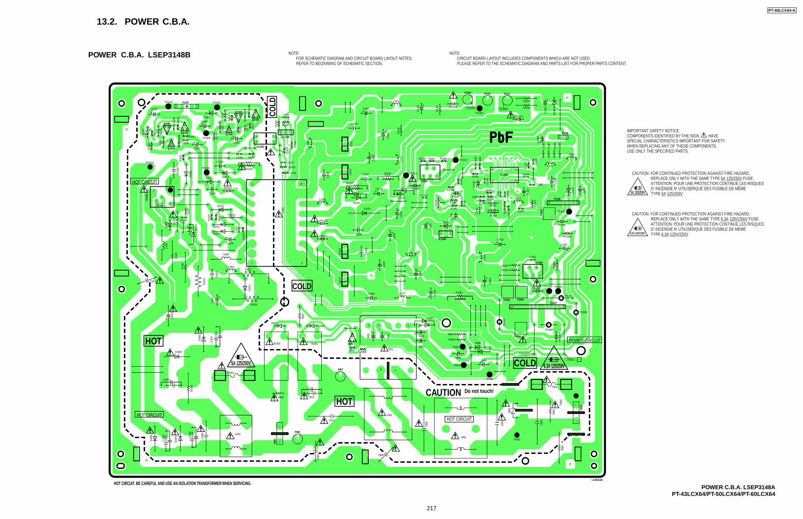
13.2. POWER C.B.A.
PT-43LCX64/PT-50LCX64/PT-60LCX64
NOTE:FOR SCHEMATIC DIAGRAM AND CIRCUIT BOARD LAYOUT NOTES,REFER TO BEGINNING OF SCHEMATIC SECTION.
IMPORTANT SAFETY NOTICE:COMPONENTS IDENTIFIED BY THE SIGN HAVESPECIAL CHARACTERISTICS IMPORTANT FOR SAFETY.WHEN REPLACING ANY OF THESE COMPONENTS,USE ONLY THE SPECIFIED PARTS.
CAUTION: FOR CONTINUED PROTECTION AGAINST FIRE HAZARD,REPLACE ONLY WITH THE SAME TYPE 5A 125/250V FUSE.ATTENTION: POUR UNE PROTECTION CONTINUE LES RISQUESD’ INCENDIE N’ UTILISERQUE DES FUSIBLE DE MÉMETYPE 5A 125/250V5A 125/250V
NOTE:CIRCUIT BOARD LAYOUT INCLUDES COMPONENTS WHICH ARE NOT USED.PLEASE REFER TO THE SCHEMATIC DIAGRAM AND PARTS LIST FOR PROPER PARTS CONTENT.
POWER C.B.A. LSEP3148B
POWER C.B.A. LSEP3148A
CAUTION: FOR CONTINUED PROTECTION AGAINST FIRE HAZARD,REPLACE ONLY WITH THE SAME TYPE 6.3A 125V/250V FUSE.ATTENTION: POUR UNE PROTECTION CONTINUE LES RISQUESD’ INCENDIE N’ UTILISERQUE DES FUSIBLE DE MÉMETYPE 6.3A 125V/250V6.3A 125V/250V
5A 125/250V 6.3A 125/250V
C802
C105
0
C106
8
C106
9
C106
7
C106
5C1
052
D102
6
R106
9 C106
6
D202
9
D202
8
3 1P1006
L1017
L1014
R105
8
R105
7C1
054
C105
1
D102
7
R107
0
C1057
R1044
C1055
L1015
D1024
C105
6
P100
3
17
16
TP1003
PR1011
R1038
R1037
IC1003
C104
7
32
1
1
1
24
5 3
8R1054R1059
R1056
R1043
C106
3
C1061
C1062
C104
6
TP1013
R103
6
C104
8
R1039
R1041 R1040R1042
4 2
1
1
3
3
5
C1053
PR1008
TP1012
TP1014
TP1011
L101
0
R1030C1032
C103
6
C1033
L1013
D1022
C104
3
C104
5
C104
9
D1018
R104
8
C103
8
C103
7
C103
9
C102
8
C1029
D101
6
C1040 L1012
T801
D803
D806
R808R807
Q801
P807
1 2 3
46
D804
R806
TP804
C805
TP803
R805
D807
D805
C804
D808
TP809
TP10
06
P1005
P1002
P100714 1
PR1003
TP1009
TP810
TP1005
TP1004PR1010
IC1006
IC1004
IC1007
R103
5
C104
2
C104
1
R103
4
L1011
R1053
R1049
R106
1
R1047
D1023
R1055
R104
6
C1059
TP1010
PR10
07
PR1006
PR1005
PR10
04
R1064
R1063
C106
0
P1004
C1058
L101
6
R1050
C104
4
TP1007
TP1008
P804
2
1
R802D8
01
C803
F801
TP80
1R8
01
TP802L802
C806
L803
C808
C809
C811
1
P808
P805
R809 C813
L1001
F1001
RL801RL802
R810
D809
R1018
D101
1
C102
1
C101
9
L1004
L1005
R1022
171
D810
C1024R1
016C1
018
R1023
R102
1
D1010
C1023
PR1001
D1013 D1014
9
T100
1
C101
7
D100
7
D100
9
R101
7R1
020
R106
0
L100
3
D1015
D1012
R101
9
R101
4
D100
8
C101
6
TP1021
TP10
20
IC10
01
R101
5
R100
4Q1003
Q1006
Q1004
Q1005
Q1002
Q1001
R100
6
C1020
43
2
5
TP1022
C1025
C1064
C1015
1
C1011
C101
4
D100
2
C100
4
D1003
C1005
R100
3
C100
1
C100
8
D100
4
C100
9
D100
5
R101
1R1
008
C1022
C1026
R1024
R101
0
R101
3
R1025
TP1025
C1006
R1005
R100
1
C100
3
R105
1
R100
2
C1002
R100
7
D1006
C1007
TP1024
R105
2
C101
0
TP1023
1 5
R101
2
C101
2
4 2
13 2 1
R103
2
IC1005
R1033
C1034
R102
9
R102
8
R1031
C1027
R1026
C103
1
L1009
IC1002
10
L100
8
3
R100
9
D100
1
C1035
D102
1D1
017
D1020
PR1012
R1027
D101
9
PR1013
P1010 P1011P1009
C1030
TP1015
B
C
EB
CE
BC
E
B
C
E BC
E
BCE
P1001
HOT CIRCUIT
BC
E
P1008
COLD
HOT
Do not touch!CAUTION
HOT CIRCUITHOT CIRCUIT
POWER CIRCUIT
COLD
COLD
HOT
HOT CIRCUIT. BE CAREFUL AND USE AN ISOLATION TRANSFORMER WHEN SERVICING.LSJB3148
2
PT-60LCX64-K
217
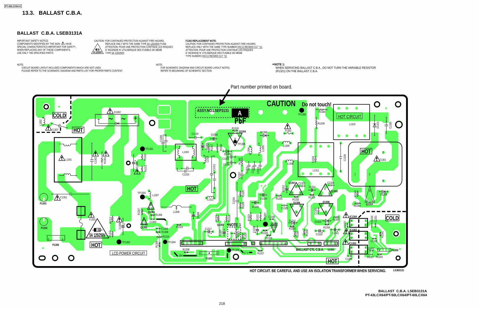
13.3. BALLAST C.B.A.
PT-43LCX64/PT-50LCX64/PT-60LCX64
NOTE:FOR SCHEMATIC DIAGRAM AND CIRCUIT BOARD LAYOUT NOTES,REFER TO BEGINNING OF SCHEMATIC SECTION.
NOTE:CIRCUIT BOARD LAYOUT INCLUDES COMPONENTS WHICH ARE NOT USED.PLEASE REFER TO THE SCHEMATIC DIAGRAM AND PARTS LIST FOR PROPER PARTS CONTENT.
BALLAST C.B.A. LSEB3131A
BALLAST C.B.A. LSEB3131A
IMPORTANT SAFETY NOTICE:COMPONENTS IDENTIFIED BY THE SIGN HAVESPECIAL CHARACTERISTICS IMPORTANT FOR SAFETY.WHEN REPLACING ANY OF THESE COMPONENTS,USE ONLY THE SPECIFIED PARTS.
CAUTION: FOR CONTINUED PROTECTION AGAINST FIRE HAZARD,REPLACE ONLY WITH THE SAME TYPE 5A 125/250V FUSE.ATTENTION: POUR UNE PROTECTION CONTINUE LES RISQUESD’ INCENDIE N’ UTILISERQUE DES FUSIBLE DE MÉMETYPE 5A 125/250V5A 125/250V
F1302 REPLACEMENT NOTE:CAUTION: FOR CONTINUED PROTECTION AGAINST FIRE HAZARD,REPLACE ONLY WITH THE SAME TYPE NUMBER K5C117BC0003 (117 ).ATTENTION: POUR UNE PROTECTION CONTINUE LES RISQUESD’ INCENDIE N’ UTILISERQUE DES FUSIBLE DE MÉMETYPE NUMÉRO K5C117BC0003 (117 )
CEB
CEB
LCD POWER CIRCUIT
R1314
R1338
D130
7
R132
5
D130
6
R132
6
R131
9
R132
0
C131
6
R132
4
R132
1 C131
8
R132
3
R132
2
R1308
R1306R130
7
R131
2
C1303
D130
3
C1304Q1303
Q1304
Q1301
Q1302
TP1304
R130
9
R131
3
C130
6
TP1306R1327
R1334
D
R1332
R1329
R1328
TP13
07
R1337
C132
5
R133
6
R133
0
R134
2
R1344
C132
7 D131
6C1
331
R134
1
C1329
C1321C1320
C1332
C1326D1317 R1343
TP1303
TP1301R1
311
TP1305
D1308R1318
R131
6
R134
5
R131
7
D1304
D1305
C130
9
C130
5
R131
0
C1310
C1334
L1303
C131
1
C1333
C1335
C131
4
C131
2 C131
3
C131
5
C1323
C1322
C1336
C1324
D1314
R1335R1333R1331
R1339
R1340
C131
9
C132
8
D131
2
Q1305
Q1306
Q1307
Q1309
Q1308
P1301
D1309
D1310
R1315
L130
2
C1307
L1301
C1301
P1303
F1301
P1302
P1306
12
S
L1308
L130
5
L130
4
L131
3
L1311
HOT CIRCUIT
L1309
T1301
D131
5
C133
0
21
3
4
D1318
D1313D1311
C1317
L1306
L1307
31 27 23 19 17 15 9
5
7 5 3 1
U1301
SS GG
D
D
SG
D
SG
4
4
3
4
3
3
1
1
2
2
1
2
Q1310
IC1304
IC1302
IC1303
F1302
GD
4 1 P1305
LSJB3131
CAUTION Do not touch!
- +
HOT CIRCUIT. BE CAREFUL AND USE AN ISOLATION TRANSFORMER WHEN SERVICING.
1
D1302
C130
2
R130
1
HOT
L1312
19V17 V
TP1302HOT
HOT
COLD
L1310
HOT
D
SG
CE B
TP1350ASSY.NO.LSEP3131 A
Part number printed on board.
*NOTE 1
COLD
HOT
5A 125/250V
BALLAST CTL C.B.A.
NOTE 1: WHEN SERVICING BALLAST C.B.A., DO NOT TURN THE VARIABLE RESISTOR (R1321) ON THE BALLAST C.B.A.
*
PT-60LCX64-K
218
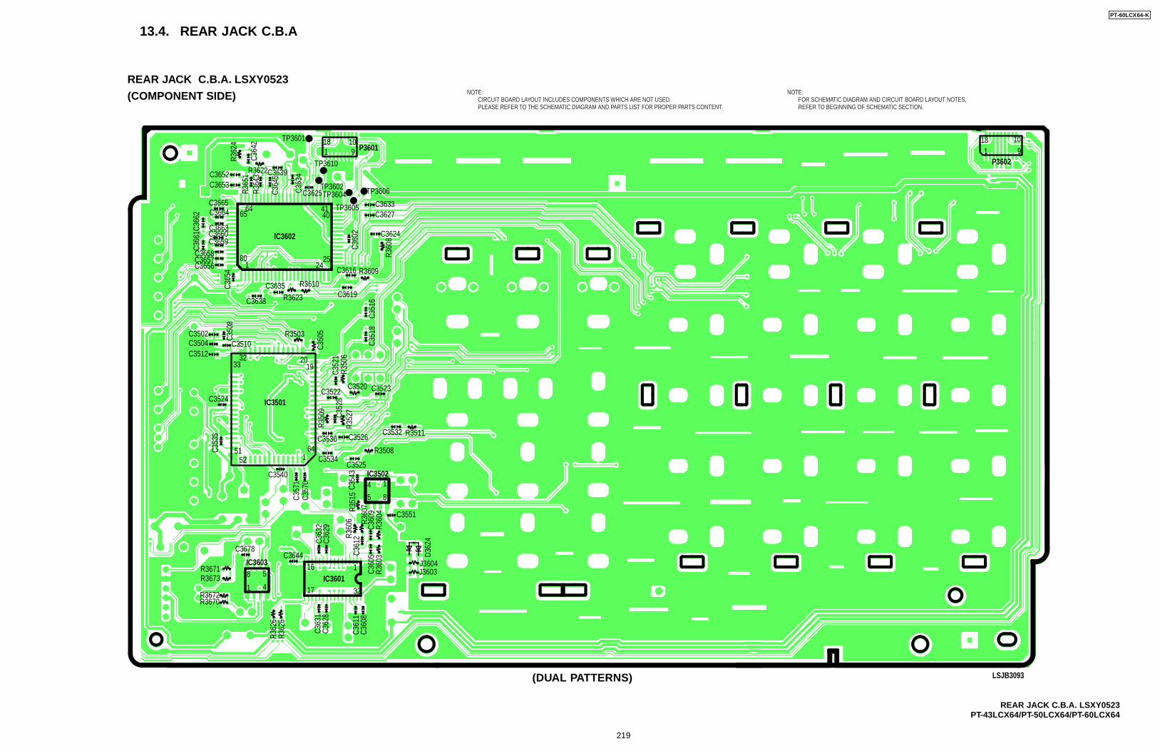
13.4. REAR JACK C.B.A
PT-43LCX64/PT-50LCX64/PT-60LCX64
(COMPONENT SIDE)
(DUAL PATTERNS)
REAR JACK C.B.A. LSXY0523
REAR JACK C.B.A. LSXY0523
R362
4R3
651
R364
3
C364
5
C363
4
C364
2
C3652C3653
C3664
C3663 C3660C3659
C3658C3657C3656
C3638
C3635R3623
R3503C3502C3504C3512
C3524
C3510
C350
8
C353
5
R3610
C366
2
C366
1
C365
4
C3665
C3639
C3625C3633C3627
C3624
C3616
C351
6C3
518
C350
5
C352
1C3
528
C357
1C3
570
R351
5R3
606
R360
3
R362
5R3
626
R360
4
D362
4
R360
7
R350
6R3
527
C354
3C3
612C3
629
C363
2 C360
9C3
605
C361
1C3
608
C362
8C3
631
R350
9
C3619
C3523C3520C3522
C3530
C3540
C3534
C3526C3532
R3508
R3511
C3525
C3551
C3644C3678
R3671R3673
R3672R3670
J3604J3603
R3609
R360
8
C360
2
TP3602
P3601
TP3606TP3604
TP3605
TP3610
TP3601
R3622
IC3602
IC3501
IC3502
IC3601
IC3603
P3602
LSJB3093
18 101 91 9
1018
6465
180
2425
4041
192032
33
5152 1
64
1
1
1
3217
16
4
4
5
5 8
8
NOTE:FOR SCHEMATIC DIAGRAM AND CIRCUIT BOARD LAYOUT NOTES,REFER TO BEGINNING OF SCHEMATIC SECTION.
NOTE:CIRCUIT BOARD LAYOUT INCLUDES COMPONENTS WHICH ARE NOT USED.PLEASE REFER TO THE SCHEMATIC DIAGRAM AND PARTS LIST FOR PROPER PARTS CONTENT.
PT-60LCX64-K
219
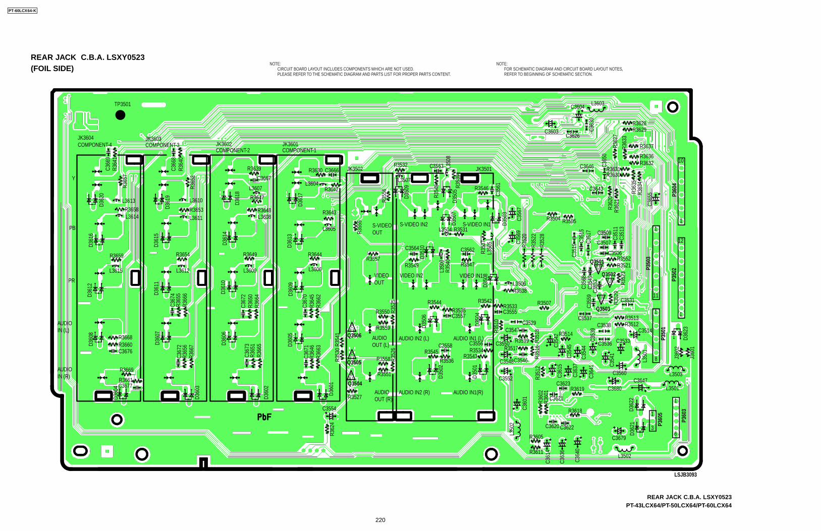
PT-43LCX64/PT-50LCX64/PT-60LCX64REAR JACK C.B.A. LSXY0523
NOTE:FOR SCHEMATIC DIAGRAM AND CIRCUIT BOARD LAYOUT NOTES,REFER TO BEGINNING OF SCHEMATIC SECTION.
NOTE:CIRCUIT BOARD LAYOUT INCLUDES COMPONENTS WHICH ARE NOT USED.PLEASE REFER TO THE SCHEMATIC DIAGRAM AND PARTS LIST FOR PROPER PARTS CONTENT.
(FOIL SIDE)
BC
E
BC
E
BC
E
BC
E
BC
E
BC
E
R3639
R3647
R3648
R3649 R3644
R3643
R3642
R3630 C3666
L3605
R3557R3549
C3564
D351
0
D350
7
R353
7L3
505
D350
3C3
561
D350
5
D350
9
L350
8
R354
8
R355
6
R355
5
R353
9
L350
9R3
540
C3667L3604
L3607
L3608
L3609
R3654
R3653R3658
R3659
R3668R3660
R3669
R3661
C3676
C3677
L3612
L3611
L3613
L3614
L3615
L3610
L3606
D361
8
D361
9
D362
0
D361
2D3
616
R365
2
R365
7
R364
1
C366
8
C366
9
R364
0
D361
7
D361
3
D361
4
D361
5D3
611
D360
7
D360
8
D360
4
D360
3
D360
2
D361
0
D360
9
C367
2R3
650
R366
4
C367
0R3
645
R366
2
C367
1R3
646
R366
3
C367
3R3
651
R366
5
C367
2R3
656
R366
7
C367
4R3
655
R366
6
R362
4D3
601
R354
1
R352
5R3
526
R353
0
D360
5
D360
6
R3559
R3550
R3544R3535C3557
D350
6
R3542R3533
R3534
R3536
R3519R3514
R3517R3543
R3545
L3506R3538
R3507
R3513R3512
L3503
C3680
C3679
C3647C3560
C354
1
L3501
L3502
C3555
C3529 C3538
C3531
C3536 C3533
C3514
C3537
C3556C3558
C3547
C3546
D350
4D3
501
D350
2
R351
0
R351
8R3
516
C356
9C3
567
C355
3C3
559
R352
3
R352
0
R352
2R3
528
C351
7
C365
0
C363
0
R362
0R3
627
R363
5R3
634
C365
5
11
P360
4
R363
3R3
621
C351
1C3
513
C351
5C3
519
R352
9
D362
3
J360
2
L350
1
C353
9
C354
4
C354
5C354
2
C364
1
C363
7
C361
5
C360
1
C361
4
C363
6
C364
0
L350
2
J360
1
D362
2D3
621
C356
8C3
549
R351
2R3
601
R360
2
D350
8
R3551
R3527
R3558
Q3506
Q3505
Q3504
Q3501
Q3502
Q3503
LSJB3093
R3611
R3605
C3620 C3622
C3623
C3621
C3552
C3548
C3550
R3618
R3619
R3505
C3643
C3646 R3631R3632R3636
R3637
R3629R3628
R3630
C3626
C3604L3603
C3603
R3504
C3509
C3507
C3506R3552R3521
L3504 R3531
R3547
C3562
R3546
C3563R3532
L3507
10
12
11
11
6
1
1
3
P350
1
P360
3
P360
5
P350
2P350
3
C3554
8
TP3501
JK3603JK3602COMPONENT-2
JK3601
JK3502
COMPONENT-1COMPONENT-3COMPONENT-4
JK3604
JK3501
VIDEO IN2VIDEOOUT
S-VIDEOOUT
S-VIDEO IN2 S-VIDEO IN1
VIDEO IN1
Y
PB
PR
AUDIOIN (L)
AUDIOIN (R)
AUDIO IN2 (L)AUDIO OUT (L)
AUDIO OUT (R)
AUDIO IN1 (L)
AUDIO IN2 (R) AUDIO IN1(R)
REAR JACK C.B.A. LSXY0523
PT-60LCX64-K
220
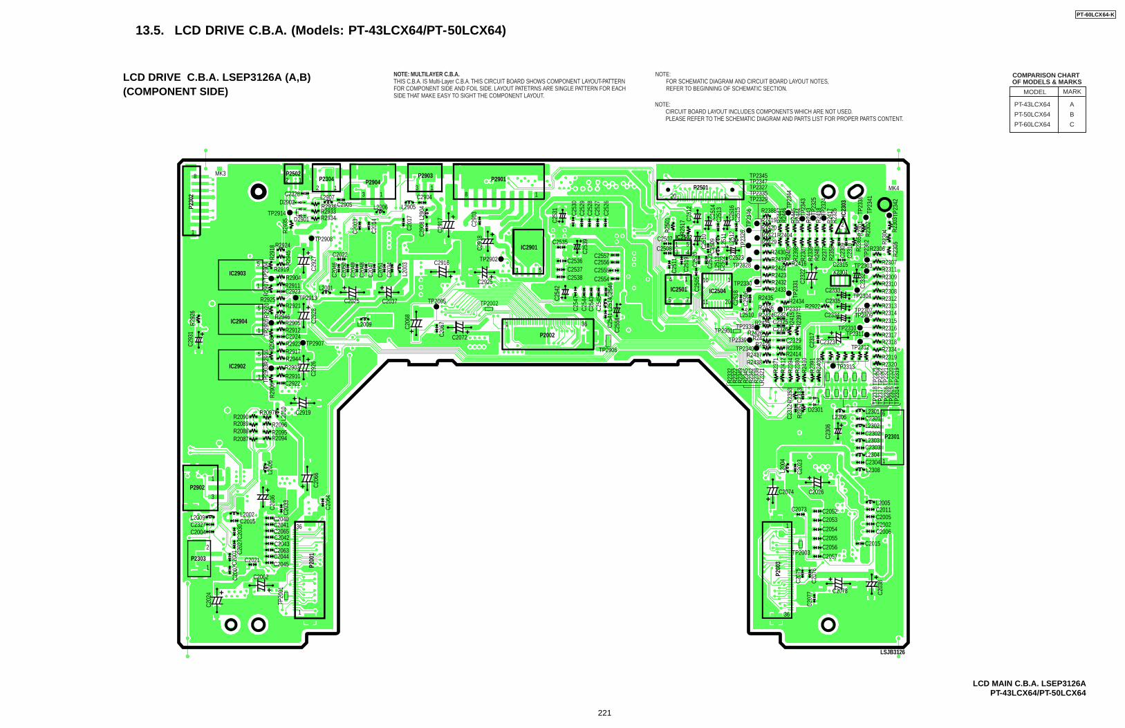
13.5. LCD DRIVE C.B.A. (Models: PT-43LCX64/PT-50LCX64)
LCD MAIN C.B.A. LSEP3126APT-43LCX64/PT-50LCX64
(COMPONENT SIDE)LCD DRIVE C.B.A. LSEP3126A (A,B) NOTE: MULTILAYER C.B.A.
THIS C.B.A. IS Multi-Layer C.B.A. THIS CIRCUIT BOARD SHOWS COMPONENT LAYOUT-PATTERNFOR COMPONENT SIDE AND FOIL SIDE. LAYOUT PATETRNS ARE SINGLE PATTERN FOR EACHSIDE THAT MAKE EASY TO SIGHT THE COMPONENT LAYOUT.
P230
2
IC2903
IC2904
IC2902
P2902
P2303
P2304P25022 1
2 1
8
1
1
MK3
5
1
5
1
5
1
3
2
C2021
C2016L2002L2009
C200
1C2
007
C202
7C20
30
P200
1
C2045C2044
C2043C2042
C2041C2065
C2063
C2040
C203
3
C206
6
R290
6
R292
6C2
931
R291
6 R290
8R2
920
R290
7
C292
6C2
928
L2001
L2009
C204
6
C205
0
C205
1C2
034
C254
7C254
2
C254
4
C254
5 C254
6C2
541
C255
8
C254
3
C251
9C2
520
C2507
C2508
C252
1
C251
8
C250
6
C252
2
C251
5C2
516
C251
4C2
513
C251
2
L251
3L2
511
L251
2
C250
9C2
510
C251
1R2
517
R250
1
C250
5
C231
7
R237
1R2
412
R239
4R2
380
R241
0R2
391
R240
8
R241
5R2
397
TP2337
TP23
31
R2404
R244
7R2
446
R244
5R2
444
R244
3
R241
8
R241
7R2
325
R240
1R2
398
R238
7R2
339
R235
8
R230
1R2
302
IC23
03
R230
3
R230
4
R230
5
R2306
R2307R2311R2309R2310R2308R2312R2313R2314R2315R2316R2317R2318
R2319R2320
R2334
TP23
42
C232
2
C2315
C230
9C2
310
R236
5C2
332
TP23
43
TP23
25
TP23
24
TP23
36
TP23
41
TP23
44
R2419
R2388
R2420R2421R2429
R2430 R2431
R2416R2422 R2423
TP2303
TP2304
TP2307TP2309
TP2310TP2311
TP2312
TP2313
TP23
23
R235
3
R235
7C23
13
C231
2
TP23
22TP
2321
TP23
20TP
2319
TP23
14TP
2315
TP23
16TP
2317
TP23
18TP
2302
R248
1R2
377
L251
4
L200
3
C204
9C2
048
C204
7
L201
0
C2327C2004
R2090R2089R2088R2087 R2094
R2095R2096
R2097 C2919
C2922
C2924
R2910R2903R2944R2917R2923
R2912R2905
R2946
R2921R2925
TP29
04
C2923R2911R2904
TP29
03
TP2907C2072C2
067
C206
8
TP2002
TP2902
C291
8
C291
7
C201
7
C290
8 C290
3
C201
4
C200
3
C292
7
C253
9
C253
0C2
529
C253
1
C252
8C2
527
C252
6
C2916
C2925
TP29
05
C206
4
C203
6L2
006
C2062
C202
4
1
36
C2538 C2554C2555
C2557C2556
C2537C2536
C2535
P2002
5 7 11 20
IC2501
IC2502
P2501
IC2504
X2301
C2333
C2335
C2334R2922
C2323R2428
R2437 R2414R2396C2329
R2438
R2427R2426
R2425
R2433R2435
R2436R2424C2324
C2325C2326
R2432
R2434
D2301L2306
L2308
L2301
L2302
L2303
L2304
C2301
C2302
C2303
C2304 1
L2005C2052C2073
C2074 C2026
C207
6
C207
5
C203
8
C207
7
C2015
C2053
C2054C2055C2056
C2057
C2078
C2002C2006
C2005C2011
C230
6
P2301
LSJB3126
L200
4
C202
3
TP2003
P200
3
MK4
1
1
5
81
IC2901
P2901
C2022
C2905
C2025 C2037
R293
5
R2924
R294
5
R2919
L2907
L2906 L2905
L290
4
C2904C2328
R291
8
R2933R2934
R2936TP2914
D2901
D2902
TP2908
P2904P2903
313
6
36
TP2906
TP2901
TP2339TP2340
TP2338
TP2330
TP2329TP2335
TP2328
TP2327
TP23
26
TP2347
TP23
46
TP2345
10 114
20 1
C2523
L2510
1
R233
2R2
322
R234
9R2
345
R234
2R2
338
R232
1
1
TP2005
1
36
TP20
01
12
3
13 4
5
TP2913
NOTE:CIRCUIT BOARD LAYOUT INCLUDES COMPONENTS WHICH ARE NOT USED.PLEASE REFER TO THE SCHEMATIC DIAGRAM AND PARTS LIST FOR PROPER PARTS CONTENT.
NOTE:FOR SCHEMATIC DIAGRAM AND CIRCUIT BOARD LAYOUT NOTES,REFER TO BEGINNING OF SCHEMATIC SECTION.
COMPARISON CHART OF MODELS & MARKS
PT-43LCX64
PT-50LCX64
PT-60LCX64
A
B
C
MODEL MARK
PT-60LCX64-K
221
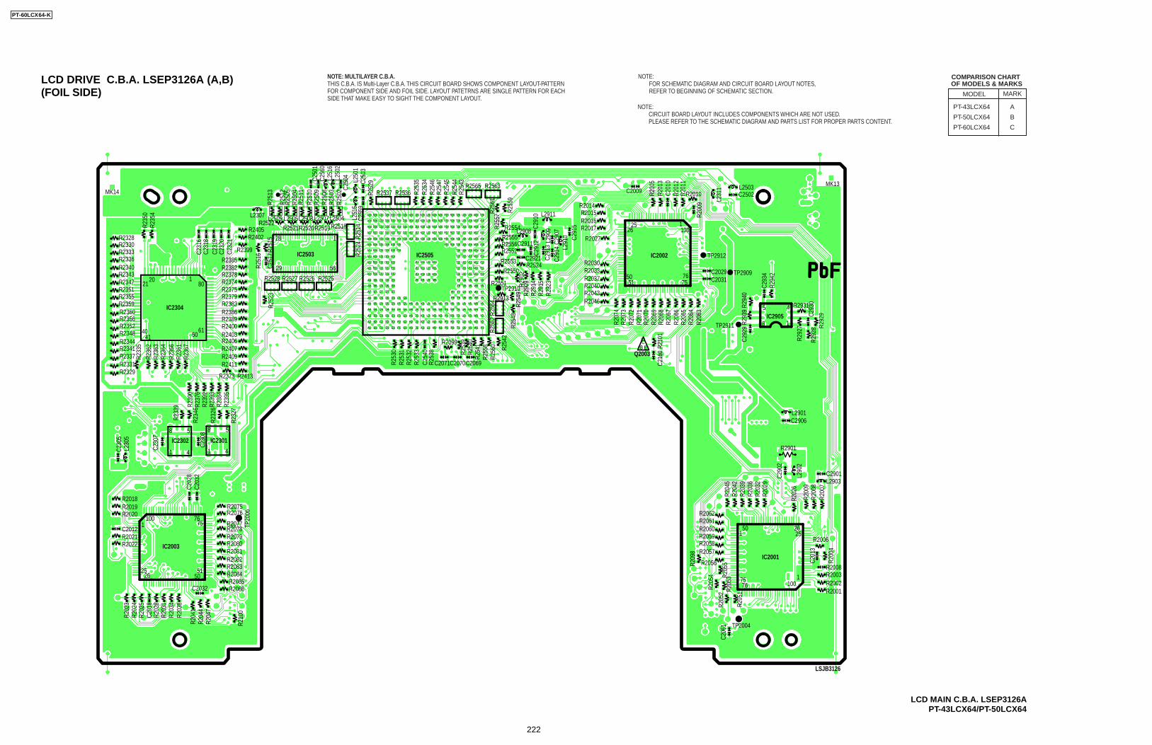
LCD MAIN C.B.A. LSEP3126APT-43LCX64/PT-50LCX64
(FOIL SIDE)LCD DRIVE C.B.A. LSEP3126A (A,B) NOTE:
FOR SCHEMATIC DIAGRAM AND CIRCUIT BOARD LAYOUT NOTES,REFER TO BEGINNING OF SCHEMATIC SECTION.
NOTE:CIRCUIT BOARD LAYOUT INCLUDES COMPONENTS WHICH ARE NOT USED.PLEASE REFER TO THE SCHEMATIC DIAGRAM AND PARTS LIST FOR PROPER PARTS CONTENT.
NOTE: MULTILAYER C.B.A.THIS C.B.A. IS Multi-Layer C.B.A. THIS CIRCUIT BOARD SHOWS COMPONENT LAYOUT-PATTERNFOR COMPONENT SIDE AND FOIL SIDE. LAYOUT PATETRNS ARE SINGLE PATTERN FOR EACHSIDE THAT MAKE EASY TO SIGHT THE COMPONENT LAYOUT.
BCE
IC2505A12 B12 C12 D12 E12 T12 U12 V12 W12 Y12
T11 U11 V11 W11 Y11
T10 U10 V10 W10 Y10
T9 U9 V9 W9 Y9
T8 U8 V8 W8 Y8
R7 T7 U7 V7 W7 Y7
R6 T6 U6 V6 W6 Y6
A5 B5 C5 D5 E5 F5 G5 H5 J5 K5 L5 M5 N5 P5 R5 T5 U5 V5 W5 Y5
A11 B11 C11 D11 E11
A10 B10 C10 D10 E10
A9 B9 C9 D9 E9
A8 B8 C8 D8 E8
A7 B7 C7 D7 E7
A6 B6 C6 D6 E6 F6 G6
A4 B4 C4 D4 E4 F4 G4 H4 J4 K4 L4 M4 N4 P4 R4 T4 U4 V4 W4 Y4
A3 B3 C3 D3 E3 F3 G3 H3 J3 K3 L3 M3 N3 P3 R3 T3 U3 V3 W3 Y3
A2 B2 C2 D2 E2 F2 G2 H2 J2 K2 L2 M2 N2 P2 R2 T2 U2 V2 W2 Y2
A1 B1 C1 D1 E1 F1 G1 H1 J1 K1 L1 M1 N1 P1 R1 T1 U1 V1 W1 Y1
J12 K12 L12 M12
J11 K11 L11 M11
J10 K10 L10 M10
J9 K9 L9 M9
A20 B20 C20 D20 E20 F20 G20 H20 J20 K20 L20 M20 N20 P20 R20 T20 U20 V20 W20 Y20
A19 B19 C19 D19 E19 F19 G19 H19 J19 K19 L19 M19 N19 P19 R19 T19 U19 V19 W19 Y19
A18 B18 C18 D18 E18 F18 G18 H18 J18 K18 L18 M18 N18 P18 R18 T18 U18 V18 W18 Y18
A17 B17 C17 D17 E17 F17 G17 H17 J17 K17 L17 M17 N17 P17 R17 T17 U17 V17 W17 Y17
A16 B16 C16 D16 E16 F16 G16 H16 J16 K16 L16 M16 N16 P16 R16 T16 U16 V16 W16 Y16
A15 B15 C15 D15 E15 F15
A14 B14 C14 D14 E14 F14
P15 R15 T15 U15 V15 W15 Y15
A13 B13 C13 D13 E13 T13 U13 V13 W13 Y13
T14 U14 V14 W14 Y14
R2328R2330R2333R2336R2340R2343R2347R2351R2355R2359R2360R2356R2352R2348R2344R2341R2337R2331R2329
C231
6C2
318
R235
0R2
354
C232
0C2
321
C251
7R2
523
R251
5 R251
4R2
524
R251
6
R251
2R2
505
R250
4R2
511
R250
8R2
503
R250
2 R252
9C250
3
C250
4C256
0C2
501
C255
9
L2507L2504L2508L2505L2509L2307
R250
9R2
510
R251
3
C231
9
R233
5
R236
2
R236
4R2
363
R236
6
R236
7R2
361
R239
0R2
376
R233
9
L230
5C2
305
C230
7
C230
8R2
346
R232
6
R232
7R239
3R2
392
R238
4R2
395
6160
2021
28
29
IC2304
4041
180
R2405R2402
R2399
R2385R2382R2378
R2383R2386
R2403
R2411
R2413R2373
R2409R2407R2406
R2400R2389
R2379R2375R2374
R2522R2521R2520
L251
5L2
501
L251
6L2
502
R2518
R2537 R2536R2565 R2563
R253
5R2
534
R254
6R2
547
R254
5R2
544
R254
3
R255
9
R256
1
R2528 R2525R2527 R2526
R2519
1
56
IC2503
8 5
41
8 5
41
R2018 R2019 R2020
R2021
C202
8C2
032
C2012
R2022
2625
5051
7576100
1
IC2003
R2075R2076
TP20
06
C2032
R2077R2078R2079R2080R2081R2082 R2083R2084
R2086
R204
7
R210
0
R204
4R2
041
R203
8R2
034
R203
1
C201
8
R202
4R2
023
R202
5
R202
8
R2085
IC2301IC2302
MK14
R253
0R2
531
R253
2
C254
0R2
533
R253
8
R291
5R2
914
R290
9R2
549
R290
2
C291
0
C290
7
R2027
R207
4R2
073
R207
2R2
071
R207
0R2
069
R206
8R2
067
R206
6R2
065
R206
4R2
063
L291
0
L2911
L2908
L290
9
R256
4R2
562
R254
2
R254
1R2
540
R253
9
R256
0R2
558
R254
8
R2913
R2099
C2071C2070C2069
R232
3
R2550
R2553R2524C2921
C2911R2552
R2551
R2556
R255
7
R2554
R2555
C291
3C2
914
C291
5
C291
2
R2015R2014
R2010
R2016R2017
R2033R2030
R2037R2040R2043R2046
C2031C2029
C2009 R201
1R2
012
C201
0R2
013
R200
5
R200
9 L231
1 L2503C2502
TP2910
5051 75
76
1100
2526
IC2002
R294
0
R294
2C2
934
C292
9
R210
1C2
160
R293
9
R292
9
R292
7
R292
8C2
930
TP2909
TP2911
TP2912
5
8
4
1IC2905
R2931
LSJB3126
R2002R2001
R200
4
C201
3
R2061R2062
R2060R2059R2058R2057
R2056R209
8
R205
5
R205
4
R205
3R2
052
R205
1
C206
1
7576
1100
2526
150
R202
6
R200
9R2
008
R200
7
R203
6R2
039
R204
2R2
045
R203
2R2
029
C290
2
L2903
L290
2
C2901
L2901C2906
R2901
R2006
R2008R2003
IC2001
TP2004
MK13
Q2003
COMPARISON CHART OF MODELS & MARKS
PT-43LCX64
PT-50LCX64
PT-60LCX64
A
B
C
MODEL MARK
PT-60LCX64-K
222
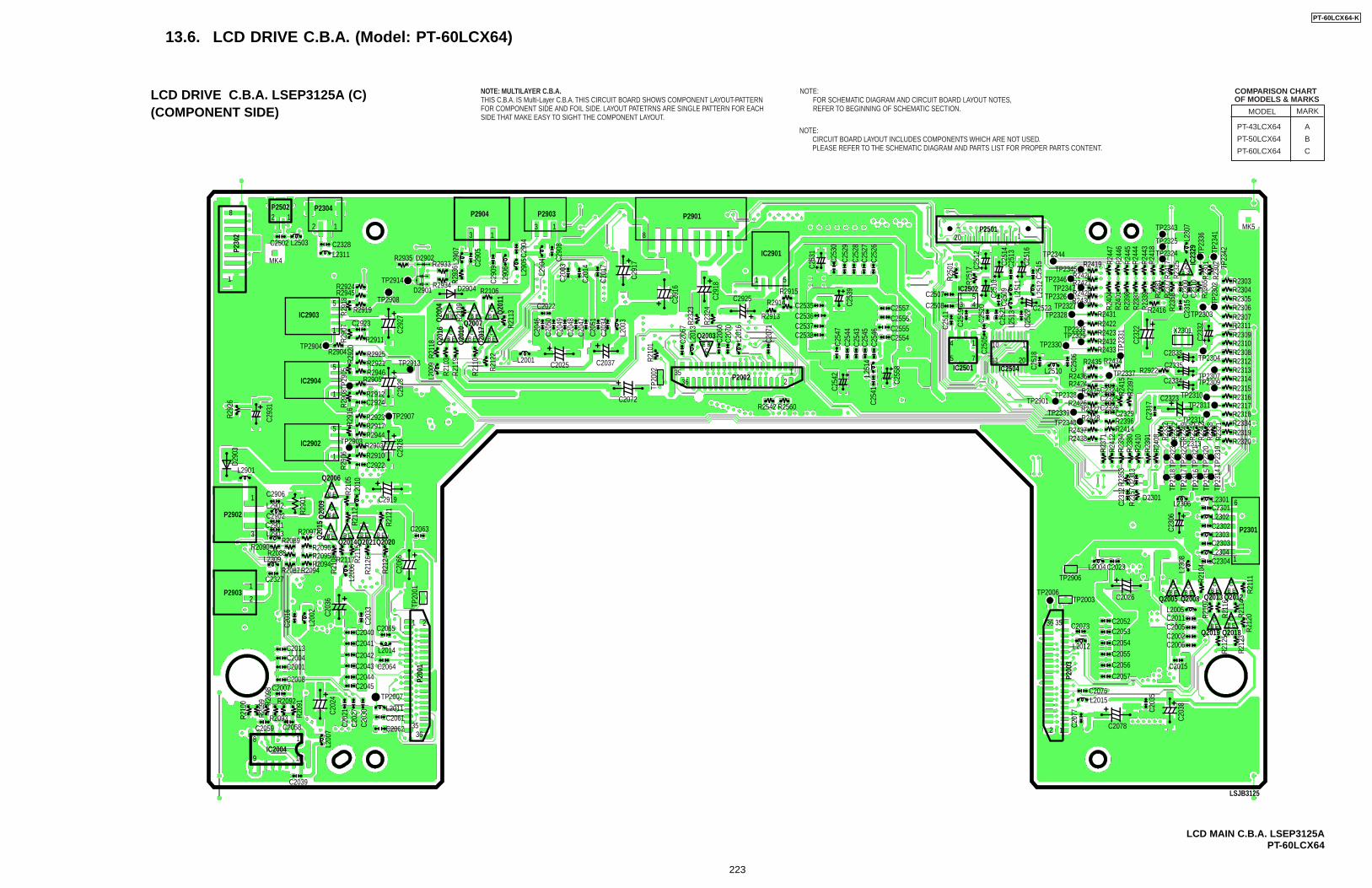
13.6. LCD DRIVE C.B.A. (Model: PT-60LCX64)
(COMPONENT SIDE)LCD DRIVE C.B.A. LSEP3125A (C) NOTE: MULTILAYER C.B.A.
THIS C.B.A. IS Multi-Layer C.B.A. THIS CIRCUIT BOARD SHOWS COMPONENT LAYOUT-PATTERNFOR COMPONENT SIDE AND FOIL SIDE. LAYOUT PATETRNS ARE SINGLE PATTERN FOR EACHSIDE THAT MAKE EASY TO SIGHT THE COMPONENT LAYOUT.
BC
EBCE B
CE B
CE
BCEB
CEB
CE
BCE
BCE
BCE
BCE B
CE B
CE
BCE B
CE B
CE B
CE
BCE B
CE
P230
2
IC2903
IC2904
IC2902
P2902
P2903
P2304P25022 1
2 1
8
1
1
MK4
5
1
5
1
5
1
3
2
C2013C2004C2001
C2008C2007
C2059
C2039
L200
7
IC2004
P200
1
C2058
C2045C2044
C2064
TP2007
L2011C2061C2062
3635
C2043C2042
C2041C2040
C203
3
R212
4
R212
6R211
5
R210
8
R211
2R2
105
R290
6
R290
1
D290
3R2
926
C293
1
R291
6R290
8R2
920
R290
7
C292
6C2
928 L2
009
R211
8
R210
3R2
119
R211
0
R212
2
C204
6
C205
0
C205
1C2
034
R210
1
R232
3
R232
4
C206
7
C206
0C2
070
C207
1
C254
2
C255
8
C254
7
C253
9
C252
6C2
527
C252
8C2
529
C253
0
C253
1
C254
4
C254
5C2
546 C2
511
C251
9R2
501
R251
7
C252
0
C252
1
C252
2C2
518
C250
6
C231
7
R237
1R2
412
R239
4R2
380
R241
0R2
391
R240
8
R241
5R2
397
R233
2R2
322
R234
9R2
345
R234
2R2
338
R232
1
L251
3
L2510
TP2330
TP2338
TP2337
TP23
31
R240
4R2
447
R244
6R2
445
R244
4R2
443
R241
8
L230
7
R241
7R2
325
R240
1R2
398
R238
7R2
339
R235
8
R230
1R2
302
TP2339TP2340
TP2901
TP2328TP2327
TP2324
IC23
29
R2303R2304R2305R2306R2307R2311R2309R2310R2308R2312R2313R2314R2315R2316R2317R2318
R2319R2320
R2334
TP23
36
TP23
41TP
2342
TP2325
TP2343
C232
2
C231
5C2
309
C231
0R2
365
C233
2
TP2326TP2347
TP2346TP2345
TP2344R2419
R2420R2421R2429R2430
R2416 TP2303
TP2304
TP2307TP2309
TP2310TP2311
TP2312
TP2313
TP23
23
R235
3R2
357 C
2313
C231
2
TP23
22
TP23
21TP
2320
TP23
19TP
2314
TP23
15TP
2316
TP23
17TP
2318
TP23
02
R248
1R2
377
TP2329TP2335
L251
2C2
515C2
516
C251
4C2
513
C251
2
L251
1
C250
9C2
510
C250
5
C254
1L2
514
C254
3
L201
3
L201
6
L200
3
C204
9C2
048
C204
7
R212
1
L201
0
R2117
C2906
C2902C2901
C2327
L2902
L2901
L2903
L2309
R2090R2089
R2087 R2094R2094
R2096
R2097
R2095R2088
C2063
C2919
C2922
C2924
R2910R2903R2944R2917R2923
R2912
R2905R2946R2921R2925R2904
TP2904
C2923
R2911
TP2903
TP2907
TP2913 C2025 C2037
C2072
TP20
02
C291
6
C291
7
C201
7
C201
4
C200
3
C290
4
C290
9C290
5
C290
8
L290
4
L290
5L290
7R2
936
R210
9
C292
7
R211
3L2
906
C291
8
C2022
L2001
TP29
05
Q20
15Q
2009
Q2006
Q2014Q2021Q2020
C206
6
TP20
01
C201
6 C203
6
L200
2
L200
6
C2065
L2014
C202
4
C202
1C2
027
C203
0
R209
1R2092R209
8R2
099
R210
0
R2093
1
8
9 16
1
21
3536
12
R2542 R2560
C2538
R2913
R2915R2914C2925
C2537C2536C2535
P2002
C2554
C2508C2507
C2523
C2555C2556C2557
5
4 1
7 11
10 1
20IC2501
IC2502
P2501
IC2504
X2301
C2333
C2335
C2334R2922
R2438R2414R2396C2329
C2323C2326
C2324C2325
R2437
R2428R2427
R2426
R2425R2424R2436
R2435
R2433R2432
R2431
R2423R2422
R2434
D2301L2306
L230
8
R210
4
R211
1
R210
7
R211
6
R211
4R2
123
R212
5
R212
0
L2301
L2302
L2303
L2304
C2301
C2302
C2303
C2304 1
L2005
C2015
C2052C2073
C2076
C2078
C203
8
C207
7 C203
5
L2015
L2012
C2053
C2054C2055C2056
C2057
C2002C2006
C2005C2011
C230
6
P2301
LSJB3125
Q2008 Q2012Q2013
Q2019 Q2018
Q2005
L2004 C2023
C2026TP2003TP2006
TP2906
P200
3
MK520 1
1
1
5
81
Q2003
IC2901
P2901
D2904D2901
D2902
R2106
R2935
R2924R2945
R2919
L2311
L2503 C2328C2502
R291
8
R2933
R2934TP2914
TP2908
P2904 P2903
313
Q20
04Q
2016
Q20
10
Q20
17
Q2007
Q20
116
2
3536
1
123
13 4
5
NOTE:CIRCUIT BOARD LAYOUT INCLUDES COMPONENTS WHICH ARE NOT USED.PLEASE REFER TO THE SCHEMATIC DIAGRAM AND PARTS LIST FOR PROPER PARTS CONTENT.
NOTE:FOR SCHEMATIC DIAGRAM AND CIRCUIT BOARD LAYOUT NOTES,REFER TO BEGINNING OF SCHEMATIC SECTION.
LCD MAIN C.B.A. LSEP3125APT-60LCX64
COMPARISON CHART OF MODELS & MARKS
PT-43LCX64
PT-50LCX64
PT-60LCX64
A
B
C
MODEL MARK
PT-60LCX64-K
223
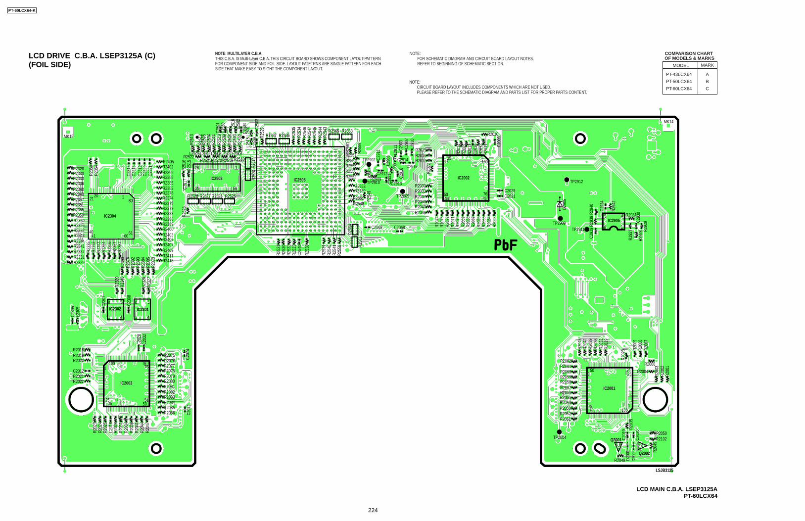
(FOIL SIDE)LCD DRIVE C.B.A. LSEP3125A (C) NOTE: MULTILAYER C.B.A.
THIS C.B.A. IS Multi-Layer C.B.A. THIS CIRCUIT BOARD SHOWS COMPONENT LAYOUT-PATTERNFOR COMPONENT SIDE AND FOIL SIDE. LAYOUT PATETRNS ARE SINGLE PATTERN FOR EACHSIDE THAT MAKE EASY TO SIGHT THE COMPONENT LAYOUT.
B CEB
CE
R2328R2330R2333R2336R2340R2343R2347R2351R2355R2359R2360R2356R2352R2348R2344R2341R2337R2331R2329
C231
6C2
318
R235
0R2
354
C232
0C2
321
C251
7R2
523
R251
5
R251
4R2
524R2
516
R251
2R2
505
R250
4R2
511
R250
8R2
503
R250
2 R252
9C250
3
C250
4
C256
0C2
501
C255
9
L2507L2508L2505L2509 L2504
R250
9R2
510
R251
3
C231
9
R233
5R2
362
R236
4R2
363
R236
6
R236
7R2
361
R239
0R2
376
R233
9
L230
5C2
305 C2
307
C230
8
R234
6
R232
6R2
327
R239
3R2
392
R238
4
R237
3R2
395
6160
2021
28
29
IC2304
4041
180
R2405R2402R2399R2388R2385R2382R2378
R2383R2386
R2403
R2411R2413
R2409R2407R2406
R2400R2389
R2379R2375R2374
R2522R2521R2520
L251
5L2
501L2
516
L250
2
R2518
R2537 R2536R2565 R2563
R253
5R2
534
R254
6R2
547
R254
5R2
544
R254
3
R255
9
R256
1
R2528 R2525R2527 R2526
R2519
1
56
IC2503 IC2505
8 5
41
8 5
41
R2018 R2019 R2020
R2021
C202
8C2
032
C2012
R2022
2625
5051
7576100
1
IC2003
R2075R2076 C207
4C2
072
R2077R2078R2079R2080R2081R2082 R2083R2084
R2086
R204
7R2
044
R204
1R2
038
R203
4R2
031
C201
8
R202
4R2
023
R202
5
R202
8
R2085
IC2301IC2302
MK15
R253
1R2
530
R253
2
C254
0R2
533
R253
8
R254
0R2
541
R253
9
R255
8 R256
2
R254
9
C291
0
C291
1 C290
3C2
907
R202
7
R207
4R2
073
R207
2R2
071
R207
0R2
069
R206
8R2
067
R206
6R2
065
R206
4R2
063
L290
9L290
8 L291
1 L291
0
C292
1
R256
4
C2069
R2548R2551
R2550R2553
R2552R2556
R290
2
R2557R2554R2555
R2909C2913
C2912
C2914
R2015R2016R2017
R2033R2030
R2037R2040R2043R2046
C2031C2029
C200
9
R201
1R2
012
C201
0R2
013
R201
4R2
005
C2068
C2915
TP2902
TP2910
TP2005 5051 75
76
1100
2526
IC2002
R2010
R294
0
R294
2
C293
4
C292
9R2
939
R292
9
R292
7
R292
8C2
930
D290
5
TP2909TP2911
TP2912
5
8
4
1IC2905
R2931
LSJB3125
Q2002
R2050R2102
R2048
R203
5D2
002
D200
1
C202
0
C201
9
R204
9
R2061R2062
R2060R2059R2058R2057R2056R2055R2054R2053R2052R2051
7576
1100
2526
150
R202
6
R200
3R2
002
R200
1
R200
9R2
008
R200
7
R203
6R2
039
R204
2R2
045
R203
2R2
029
R2006
R2004
IC2001
Q2001TP2004
MK14
A12 B12 C12 D12 E12 T12 U12 V12 W12 Y12
T11 U11 V11 W11 Y11
T10 U10 V10 W10 Y10
T9 U9 V9 W9 Y9
T8 U8 V8 W8 Y8
R7 T7 U7 V7 W7 Y7
R6 T6 U6 V6 W6 Y6
A5 B5 C5 D5 E5 F5 G5 H5 J5 K5 L5 M5 N5 P5 R5 T5 U5 V5 W5 Y5
A11 B11 C11 D11 E11
A10 B10 C10 D10 E10
A9 B9 C9 D9 E9
A8 B8 C8 D8 E8
A7 B7 C7 D7 E7
A6 B6 C6 D6 E6 F6 G6
A4 B4 C4 D4 E4 F4 G4 H4 J4 K4 L4 M4 N4 P4 R4 T4 U4 V4 W4 Y4
A3 B3 C3 D3 E3 F3 G3 H3 J3 K3 L3 M3 N3 P3 R3 T3 U3 V3 W3 Y3
A2 B2 C2 D2 E2 F2 G2 H2 J2 K2 L2 M2 N2 P2 R2 T2 U2 V2 W2 Y2
A1 B1 C1 D1 E1 F1 G1 H1 J1 K1 L1 M1 N1 P1 R1 T1 U1 V1 W1 Y1
J12 K12 L12 M12
J11 K11 L11 M11
J10 K10 L10 M10
J9 K9 L9 M9
A20 B20 C20 D20 E20 F20 G20 H20 J20 K20 L20 M20 N20 P20 R20 T20 U20 V20 W20 Y20
A19 B19 C19 D19 E19 F19 G19 H19 J19 K19 L19 M19 N19 P19 R19 T19 U19 V19 W19 Y19
A18 B18 C18 D18 E18 F18 G18 H18 J18 K18 L18 M18 N18 P18 R18 T18 U18 V18 W18 Y18
A17 B17 C17 D17 E17 F17 G17 H17 J17 K17 L17 M17 N17 P17 R17 T17 U17 V17 W17 Y17
A16 B16 C16 D16 E16 F16 G16 H16 J16 K16 L16 M16 N16 P16 R16 T16 U16 V16 W16 Y16
A15 B15 C15 D15 E15 F15
A14 B14 C14 D14 E14 F14
P15 R15 T15 U15 V15 W15 Y15
A13 B13 C13 D13 E13 T13 U13 V13 W13 Y13
T14 U14 V14 W14 Y14
NOTE:CIRCUIT BOARD LAYOUT INCLUDES COMPONENTS WHICH ARE NOT USED.PLEASE REFER TO THE SCHEMATIC DIAGRAM AND PARTS LIST FOR PROPER PARTS CONTENT.
NOTE:FOR SCHEMATIC DIAGRAM AND CIRCUIT BOARD LAYOUT NOTES,REFER TO BEGINNING OF SCHEMATIC SECTION.
LCD MAIN C.B.A. LSEP3125APT-60LCX64
COMPARISON CHART OF MODELS & MARKS
PT-43LCX64
PT-50LCX64
PT-60LCX64
A
B
C
MODEL MARK
PT-60LCX64-K
224
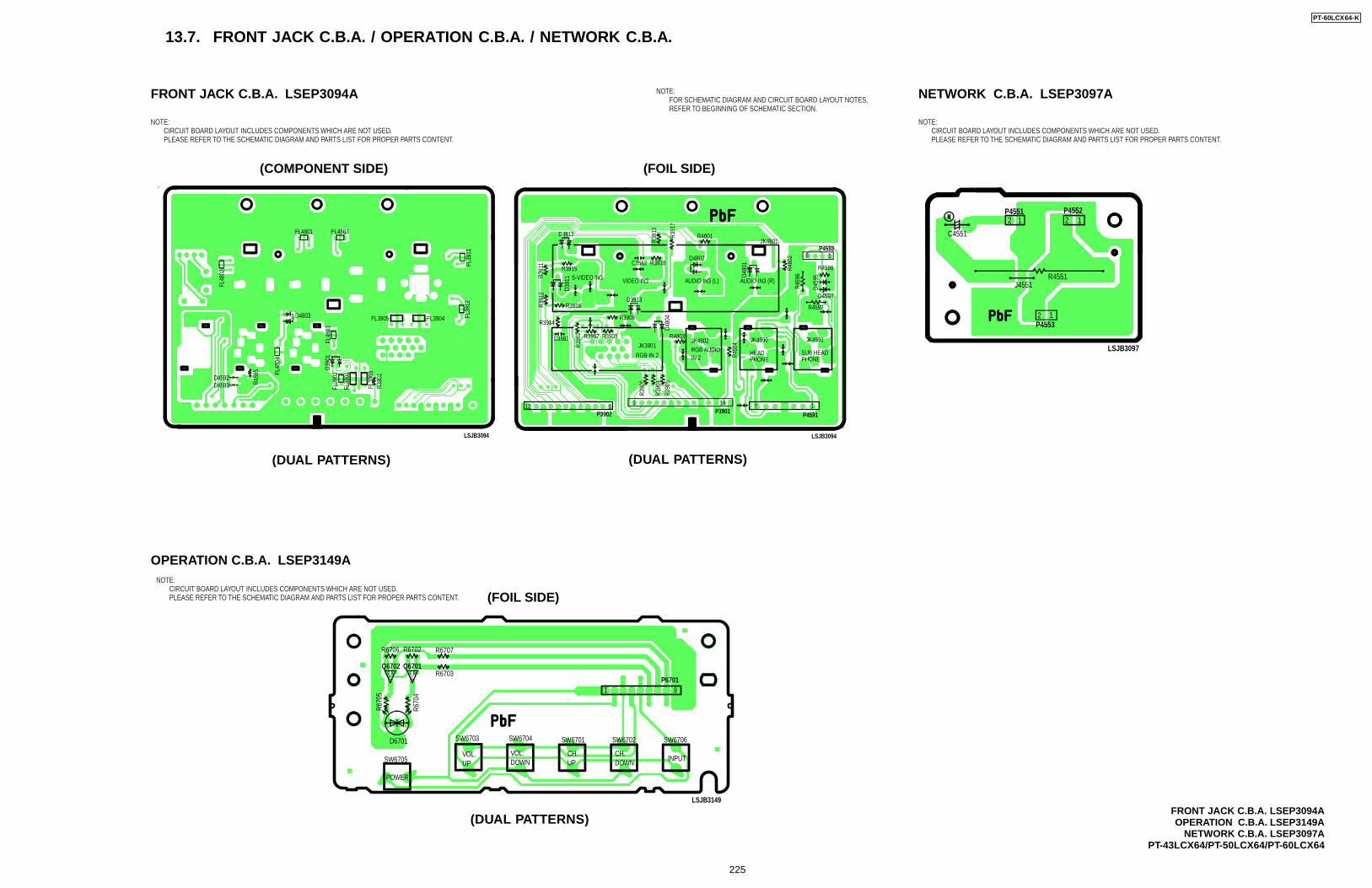
13.7. FRONT JACK C.B.A. / OPERATION C.B.A. / NETWORK C.B.A.
FRONT JACK C.B.A. LSEP3094A
OPERATION C.B.A. LSEP3149A
FRONT JACK C.B.A. LSEP3094AOPERATION C.B.A. LSEP3149A
NETWORK C.B.A. LSEP3097APT-43LCX64/PT-50LCX64/PT-60LCX64
NOTE:CIRCUIT BOARD LAYOUT INCLUDES COMPONENTS WHICH ARE NOT USED.PLEASE REFER TO THE SCHEMATIC DIAGRAM AND PARTS LIST FOR PROPER PARTS CONTENT.
NOTE:CIRCUIT BOARD LAYOUT INCLUDES COMPONENTS WHICH ARE NOT USED.PLEASE REFER TO THE SCHEMATIC DIAGRAM AND PARTS LIST FOR PROPER PARTS CONTENT.
NOTE:FOR SCHEMATIC DIAGRAM AND CIRCUIT BOARD LAYOUT NOTES,REFER TO BEGINNING OF SCHEMATIC SECTION.
NETWORK C.B.A. LSEP3097A
(FOIL SIDE)(COMPONENT SIDE)
BC
E BC
E
R6706 R6702 R6707
R6703
1
R670
5
R670
4
Q6701
LSJB3149
Q6702
P6701
D6701
POWER
SW6705
SW6703 SW6704 SW6701 SW6702 SW6706
INPUTCH.DOWN
CH.UP
VOL.DOWN
VOL.UP
9
2 1
C4551
R4551J4551
2 21 1P4551
P4553
LSJB3097
P4552
(DUAL PATTERNS) (DUAL PATTERNS)
NOTE:CIRCUIT BOARD LAYOUT INCLUDES COMPONENTS WHICH ARE NOT USED.PLEASE REFER TO THE SCHEMATIC DIAGRAM AND PARTS LIST FOR PROPER PARTS CONTENT.
FL48
02
FL4801
FL48
03
FL48
04
R459
5
D4592D4593 FL
3902
FL39
01
FL39
03
FL39
12FL
3911
R390
1
D390
1
FL4803
D4803 FL3905 FL3904
LSJB3094
17P4591
JK3901
RGB-IN 2
D3912
D391
1
D3913
D480
4R3
905
R390
4
R390
6
D480
1
R480
4
R391
1R3
912
R3914
R390
2
R391
3
R391
7
R480
2
R3915
R3916
R3907 R3903
R3908
C3562 R3918
R4801
LSJB3094
R4598
D459
5
D4594
R4803
D4802
C3561
141112P3901P3902
JK4591
SUB HEADPHONE
JK4590
HEADPHONE
JK4802RGB AUDIOIN 2
AUDIO IN3 (R)AUDIO IN3 (L)VIDEO IN3S-VIDEO IN3
P459215
JK4801
R4597
R459
6
(FOIL SIDE)
(DUAL PATTERNS)
PT-60LCX64-K
225
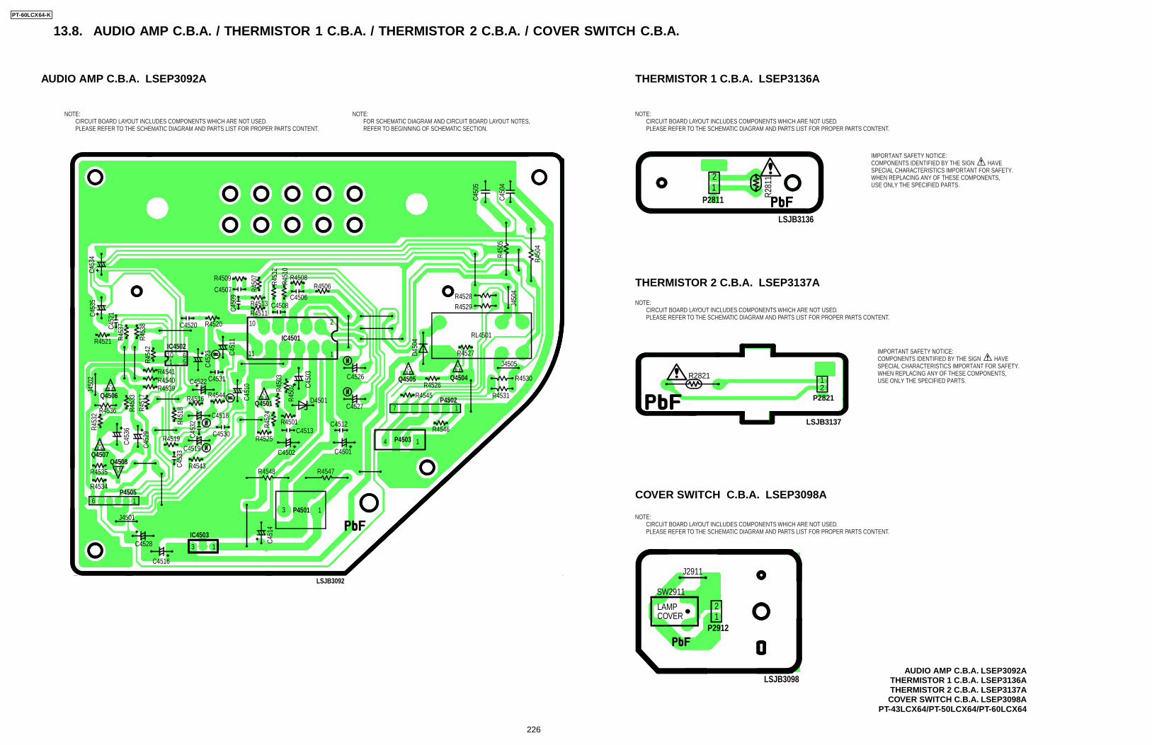
13.8. AUDIO AMP C.B.A. / THERMISTOR 1 C.B.A. / THERMISTOR 2 C.B.A. / COVER SWITCH C.B.A.
THERMISTOR 1 C.B.A. LSEP3136A
AUDIO AMP C.B.A. LSEP3092ATHERMISTOR 1 C.B.A. LSEP3136ATHERMISTOR 2 C.B.A. LSEP3137ACOVER SWITCH C.B.A. LSEP3098A
PT-43LCX64/PT-50LCX64/PT-60LCX64
NOTE:FOR SCHEMATIC DIAGRAM AND CIRCUIT BOARD LAYOUT NOTES,REFER TO BEGINNING OF SCHEMATIC SECTION.
IMPORTANT SAFETY NOTICE:COMPONENTS IDENTIFIED BY THE SIGN HAVESPECIAL CHARACTERISTICS IMPORTANT FOR SAFETY.WHEN REPLACING ANY OF THESE COMPONENTS,USE ONLY THE SPECIFIED PARTS.
AUDIO AMP C.B.A. LSEP3092A
COVER SWITCH C.B.A. LSEP3098A
BC
E BC
E
BC
E
BC
E
BC
E
BC
E
651
7
R4521
R4541R4540R4539
R4535
R4534
Q4506
IC4502IC4501
Q4507Q4508
P4505
IC4503
P4501
LSJB3092
P4503
P4502
C452
1
C453
4C4
535
R453
7
R453
8R4
542
R451
7
R451
8C4
533
C452
9
C453
6
J450
2
R452
4
R450
3
R450
2 C450
3
D450
4
C451
0
C452
3 C451
1
R453
3
R453
2
R4543
C4528
C4516
C451
4
J4501
R4516 R4544
R4525
R4501
R4547R4548
C4513
C4526
C4527
C4502
D4501
C4512
C4501
R4545
R4546
R4526
R4527
R4529R4528
R450
5
R450
4
J450
4
C450
4
C450
5
R4530
J4505
R4531
RL4501
C4530C453
2
C4519
C4518
R4519
R4536Q4501
Q4505 Q4504
C4508C4506
R4508R4506C4507
R4511R4513
R4509
R4520C4520
C4531C4522
R450
7
R451
2
C450
9
R451
0
10
10
11
2
1
6 1
1
1
3
3
1
14
J2911
P2912
LSJB3098
SW2911
21
LAMPCOVER
21
P2811
LSJB3136
R281
1
THERMISTOR 2 C.B.A. LSEP3137A
LSJB3137
P2821
R2821 12
NOTE:CIRCUIT BOARD LAYOUT INCLUDES COMPONENTS WHICH ARE NOT USED.PLEASE REFER TO THE SCHEMATIC DIAGRAM AND PARTS LIST FOR PROPER PARTS CONTENT.
NOTE:CIRCUIT BOARD LAYOUT INCLUDES COMPONENTS WHICH ARE NOT USED.PLEASE REFER TO THE SCHEMATIC DIAGRAM AND PARTS LIST FOR PROPER PARTS CONTENT.
NOTE:CIRCUIT BOARD LAYOUT INCLUDES COMPONENTS WHICH ARE NOT USED.PLEASE REFER TO THE SCHEMATIC DIAGRAM AND PARTS LIST FOR PROPER PARTS CONTENT.
NOTE:CIRCUIT BOARD LAYOUT INCLUDES COMPONENTS WHICH ARE NOT USED.PLEASE REFER TO THE SCHEMATIC DIAGRAM AND PARTS LIST FOR PROPER PARTS CONTENT.
IMPORTANT SAFETY NOTICE:COMPONENTS IDENTIFIED BY THE SIGN HAVESPECIAL CHARACTERISTICS IMPORTANT FOR SAFETY.WHEN REPLACING ANY OF THESE COMPONENTS,USE ONLY THE SPECIFIED PARTS.
PT-60LCX64-K
226
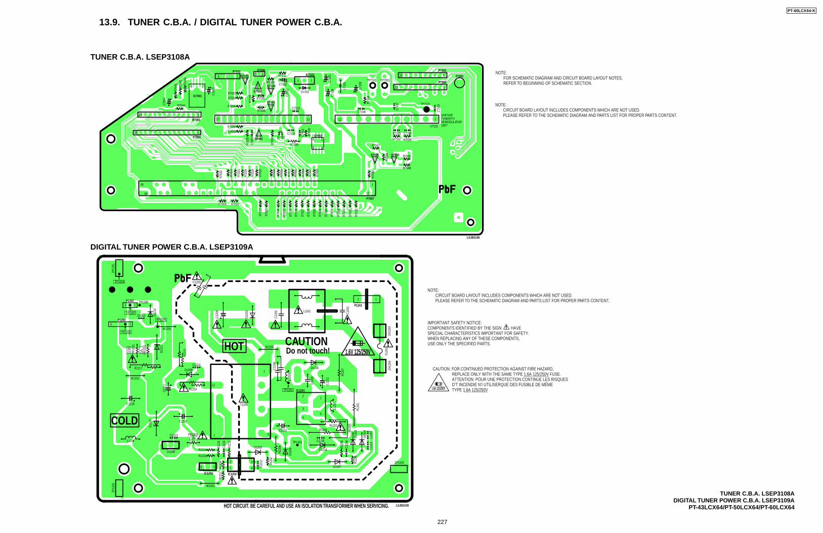
13.9. TUNER C.B.A. / DIGITAL TUNER POWER C.B.A.
PT-43LCX64/PT-50LCX64/PT-60LCX64
TUNER C.B.A. LSEP3108A
TUNER C.B.A. LSEP3108ADIGITAL TUNER POWER C.B.A. LSEP3109A
NOTE:FOR SCHEMATIC DIAGRAM AND CIRCUIT BOARD LAYOUT NOTES,REFER TO BEGINNING OF SCHEMATIC SECTION.
NOTE:CIRCUIT BOARD LAYOUT INCLUDES COMPONENTS WHICH ARE NOT USED.PLEASE REFER TO THE SCHEMATIC DIAGRAM AND PARTS LIST FOR PROPER PARTS CONTENT.
BC
E BC
E
BC
E
BC
E
BC
E
BC
E
BC
E
R704
3
C700
4
C700
3
R7037
R7108
R7105
R7103
R7033
R703
5
R703
8
R704
0
C700
2
D7001
R7039C700
1
R7034
R7036
R710
6
R704
2R7
041
R7044
IC7001
Q7001
Q7102
Q7103
Q7101
Q7002
C7111
C7110
R7110
R7109
Q7003
R710
4
C710
7
C710
3
C7109
C7105 C7104
R7102 R7101
R7047
R7045
R7046
R704
8
R703
1
Q7005 Q7004
TP7102
R700
5
R700
9
R701
1
R701
3
R701
5
R701
6
R701
8R7
017
R702
6
R701
4
R701
2
R701
0
R700
8
R702
7
R702
8
R702
9
R703
0
R703
2
R700
1
R700
6
R700
4
R700
3
R700
2
R701
9
R702
0
R702
1
R702
3
R702
5
R700
7
R7024 R7022
P7002 P7008
P7003
P7004
P7007
LSJB3108
27
5 113
15
1
1
13
14
65
64
1
2
14
5 8
11 112
3
IC7101
1
D7101
C7102
C711
2
C710
1
C710
6
TP7101 TP7001
C710
8 L710
1
U7101
UHF/VHFTUNER/TVDEMODULATORUNIT
10 1
111
P7005
P7006
P7001
DIGITAL TUNER POWER C.B.A. LSEP3109A
CAUTION: FOR CONTINUED PROTECTION AGAINST FIRE HAZARD,REPLACE ONLY WITH THE SAME TYPE 1.6A 125/250V FUSE.ATTENTION: POUR UNE PROTECTION CONTINUE LES RISQUESD’T INCENDIE N’I UTILISERQUE DES FUSIBLE DE MÉMETYPE 1.6A 125/250V1.6A 125/250V
IMPORTANT SAFETY NOTICE:COMPONENTS IDENTIFIED BY THE SIGN HAVESPECIAL CHARACTERISTICS IMPORTANT FOR SAFETY.WHEN REPLACING ANY OF THESE COMPONENTS,USE ONLY THE SPECIFIED PARTS.
NOTE:CIRCUIT BOARD LAYOUT INCLUDES COMPONENTS WHICH ARE NOT USED.PLEASE REFER TO THE SCHEMATIC DIAGRAM AND PARTS LIST FOR PROPER PARTS CONTENT.
1.6V 125/250V
TP1204
TP1207
TP1203
C120
4
C120
2
C120
1
F120
1ZH
1203
ZH12
04
D120
1
TP1206P1202
P1203
TP1205
D1213 D121
2
D121
1
R121
3
C1213
R1214
R1216
R121
5R1
211
R121
2
R120
9
R120
2
D120
6
R120
8C121
6
C121
2
TP1202
TP1201
C1205
C1210
W1206
R120
5
R120
6
C120
8
D120
4
D120
3
C121
9C1
207
C1214
1
1
3
5
PR12
02
PR12
01
10A
1A3.5A
R1217 D1208
R1210
C1218
C1215
W1202
W1201
W1204
D1209
PR1203
L1204
D121
0
C121
7
3 1
ZP12
01
L1201
12
P1201
D1205
C120
9
C120
6
L120
3
C121
1
L120
2
R120
7
R120
1
W12
05R1203R1204
D1214
D1207ZP1202
IC1201
T1201
1
12
45
67
11
1
2 3
4
D1202
IC1203 IC1202
ZP12
03
C1203
LSJB3109
HOT
COLD
CAUTIONDo not touch!
3
HOT CIRCUIT. BE CAREFUL AND USE AN ISOLATION TRANSFORMER WHEN SERVICING.
PT-60LCX64-K
227

PT-60LCX64-K
228
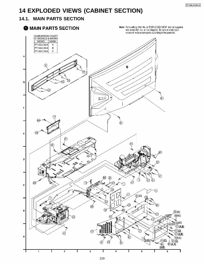
14 EXPLODED VIEWS (CABINET SECTION)14.1. MAIN PARTS SECTION
PT-60LCX64-K
229
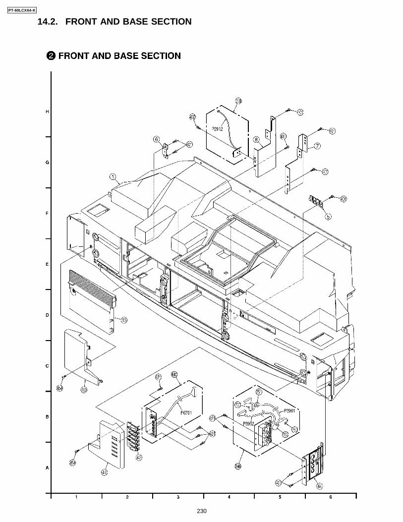
14.2. FRONT AND BASE SECTIONPT-60LCX64-K
230
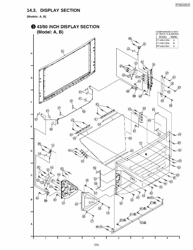
14.3. DISPLAY SECTION(Models: A, B)
PT-60LCX64-K
231
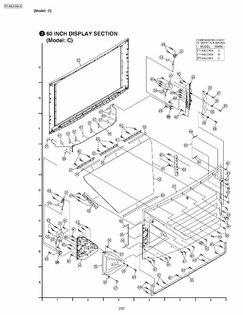
(Model: C)PT-60LCX64-K
232
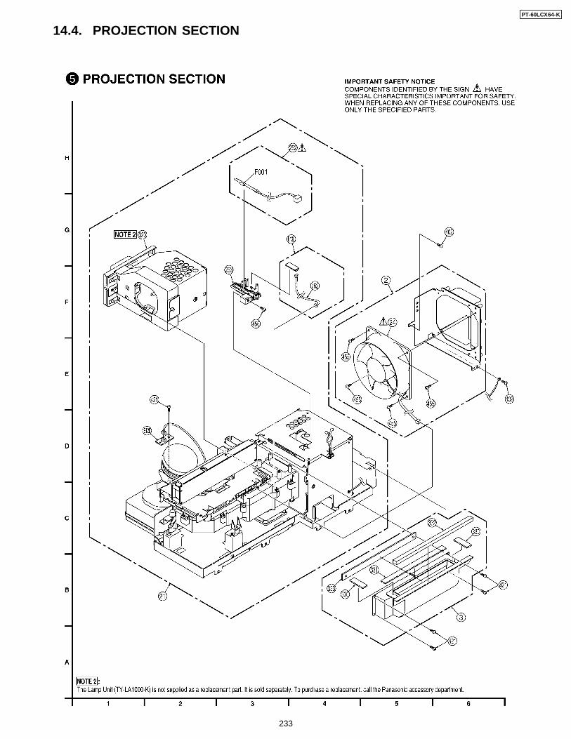
14.4. PROJECTION SECTIONPT-60LCX64-K
233
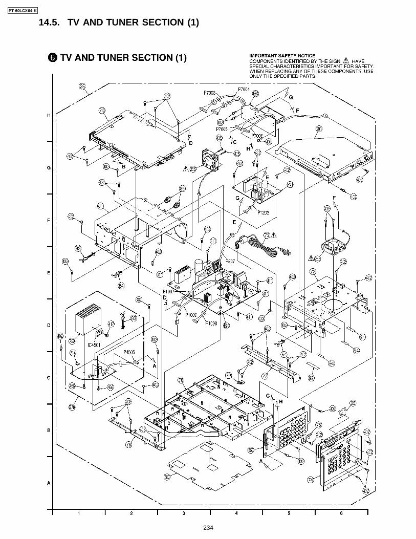
14.5. TV AND TUNER SECTION (1)PT-60LCX64-K
234
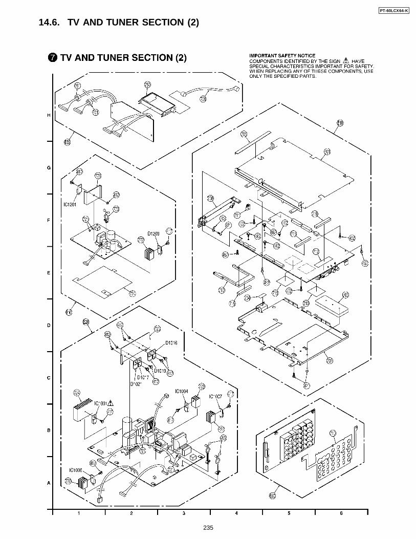
14.6. TV AND TUNER SECTION (2)PT-60LCX64-K
235
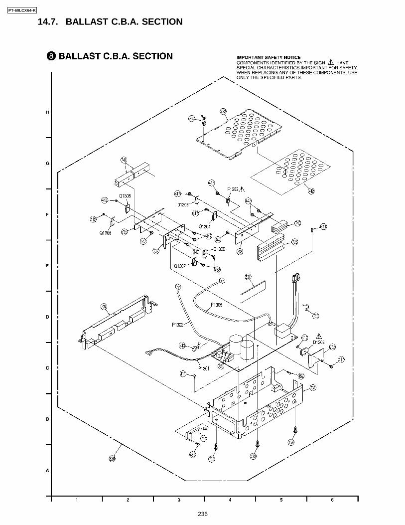
14.7. BALLAST C.B.A. SECTIONPT-60LCX64-K
236
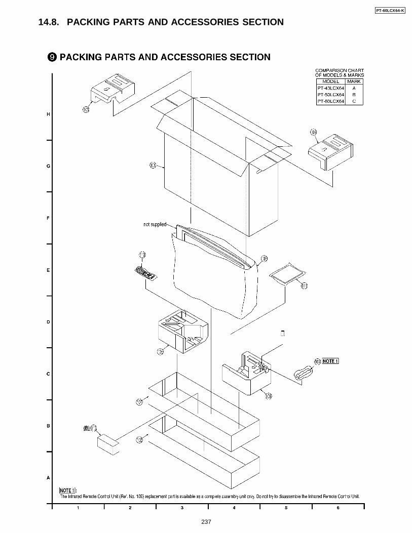
14.8. PACKING PARTS AND ACCESSORIES SECTIONPT-60LCX64-K
237
BEFORE REPLACING PARTS, READ THE FOLLOWING:
15.1. REPLACEMENT NOTES
15.1.1. General Notes
1. Use only original replacement parts:
To maintain original function and reliability of repaired units,use only original replacement parts which are listed withtheir part numbers in the parts list.
2. IMPORTANT SAFETY NOTICE
Components identified by the sign have specialcharacteristics important for safety. When replacing any ofthese components, use only the specified parts.
3. SPECIAL NOTE
All integrated circuits and many other semiconductordevices are electrostatically sensitive and therefore requirethe special handling techniques described under the"ELECTROSTATICALLY SENSITIVE (ES) DEVICES"section of this service manual.
4. Parts with no Ref. No. in "EXPLODED VIEWS" are notsupplied. And some Ref. No. will be skipped. Be sure tomake your orders of replacement parts according to theparts list.
5. Parts different in shape or size may be used. However, onlyinterchangeable parts will be supplied as servicereplacement parts.
6. Definition of Parts supplier:
a. Parts with mark "PSEC" in the Remarks column aresupplied from PSEC.
b. Parts without mark in the Remarks column are suppliedfrom PASC-NPC.
7. Item numbers with capital letter E (Example: E10, E20,...) inthe Ref. No. column are shown in the exploded views.
8. Parts whose Ref. Nos. are the same are interchangeable asreplacement parts. Any of these parts may be ordered andused as a replacement part.
15.1.2. Mechanical Replacement Notes
1. Section No. of parts shown in Exploded Views are indicatedin the Remarks column.
2. Abbreviation
RTL: Retention Time Limited
This indicates that the retention time is limited for this item.After the discontinuation of this item in production, it will nolonger be available.
3. After replacing the Projection Unit (Ref. No. 21), be sure toperform "ADJUSTMENT of the Projection Unit." Refer to"WHEN REINSTALLING THE PROJECTION UNIT INTOTHE UNIT AT THE USER´S LOCATION"; inADJUSTMENT PROCEDURES 1.
4. The Infrared Remote Control Unit (Ref. No. 109)replacement part is available as a complete assembly unitonly. Do not try to disassemble the Infrared Remote ControlUnit.
15.1.3. Electrical Replacement Notes
1. Unless otherwise specified;
All resistors are in Ω, K = 1,000 Ω, M = 1,000 kΩ.
2. Abbreviation
RTL: Retention Time Limited
This indicates that the retention time islimited for this item. After thediscontinuation of this item inproduction, it will no longer beavailable.
NR: Non Repairable Board Ass´yMGF CHIP: Metal Glaze Film ChipC CHIP: Ceramic ChipCOMPLX CMP: Complex ComponentW FLMPRF: Wirewound FlameproofC.B.A.: Circuit Board AssemblyP.C.B.: Printed Circuit BoardE.S.D.: Electrostatically Sensitive Devices
3. When replacing 0 Ω resistor, a wire can be substituted forit.
4. Since SUB TUNER,UHF/VHF (Ref. No. 757) has alreadybeen pre-adjusted at the factory, do not try to adjust them.The replacement parts for them are available as a completeassembly unit only.
15 REPLACEMENT PARTS LIST (CABINET SECTION)
238
PT-60LCX64-K
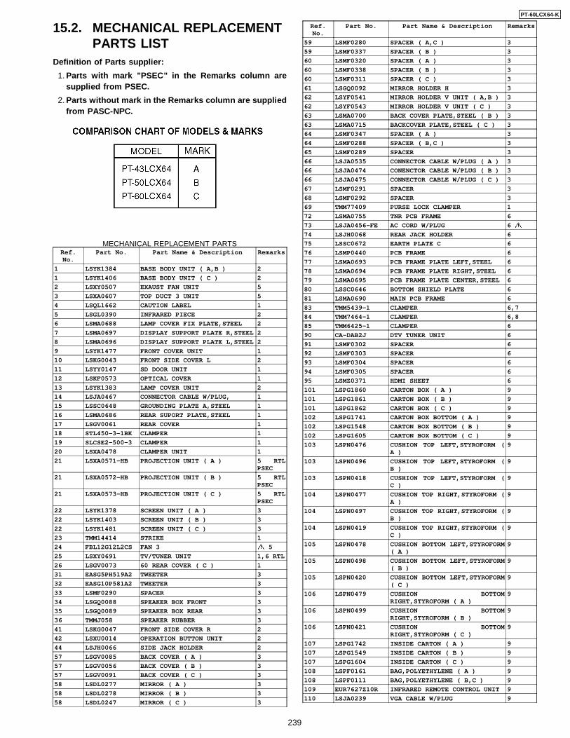
15.2. MECHANICAL REPLACEMENTPARTS LIST
Definition of Parts supplier:
1. Parts with mark "PSEC" in the Remarks column aresupplied from PSEC.
2. Parts without mark in the Remarks column are suppliedfrom PASC-NPC.
MECHANICAL REPLACEMENT PARTSRef.No.
Part No. Part Name & Description Remarks
1 LSYK1384 BASE BODY UNIT ( A,B ) 2
1 LSYK1406 BASE BODY UNIT ( C ) 2
2 LSXY0507 EXAUST FAN UNIT 5
3 LSXA0607 TOP DUCT 3 UNIT 5
4 LSQL1662 CAUTION LABEL 1
5 LSGL0390 INFRARED PIECE 2
6 LSMA0688 LAMP COVER FIX PLATE,STEEL 2
7 LSMA0697 DISPLAY SUPPORT PLATE R,STEEL 2
8 LSMA0696 DISPLAY SUPPORT PLATE L,STEEL 2
9 LSYK1477 FRONT COVER UNIT 1
10 LSKG0043 FRONT SIDE COVER L 2
11 LSYY0147 SD DOOR UNIT 1
12 LSKF0573 OPTICAL COVER 1
13 LSYK1383 LAMP COVER UNIT 2
14 LSJA0467 CONNECTOR CABLE W/PLUG, 1
15 LSSC0648 GROUNDING PLATE A,STEEL 1
16 LSMA0686 REAR SUPORT PLATE,STEEL 1
17 LSGV0061 REAR COVER 1
18 STL450-3-1BK CLAMPER 1
19 SLCSE2-500-3 CLAMPER 1
20 LSXA0478 CLAMPER UNIT 1
21 LSXA0571-HB PROJECTION UNIT ( A ) 5 RTLPSEC
21 LSXA0572-HB PROJECTION UNIT ( B ) 5 RTLPSEC
21 LSXA0573-HB PROJECTION UNIT ( C ) 5 RTLPSEC
22 LSYK1378 SCREEN UNIT ( A ) 3
22 LSYK1403 SCREEN UNIT ( B ) 3
22 LSYK1481 SCREEN UNIT ( C ) 3
23 TMM14414 STRIKE 1
24 FBL12G12L2CS FAN 3 5
25 LSXY0691 TV/TUNER UNIT 1,6 RTL
26 LSGV0073 60 REAR COVER ( C ) 1
31 EASG5PH519A2 TWEETER 3
32 EASG10P581A2 TWEETER 3
33 LSMF0290 SPACER 3
34 LSGQ0088 SPEAKER BOX FRONT 3
35 LSGQ0089 SPEAKER BOX REAR 3
36 TMMJ058 SPEAKER RUBBER 3
41 LSKG0047 FRONT SIDE COVER R 2
42 LSXU0014 OPERATION BUTTON UNIT 2
44 LSJH0066 SIDE JACK HOLDER 2
57 LSGV0085 BACK COVER ( A ) 3
57 LSGV0056 BACK COVER ( B ) 3
57 LSGV0091 BACK COVER ( C ) 3
58 LSDL0277 MIRROR ( A ) 3
58 LSDL0278 MIRROR ( B ) 3
58 LSDL0247 MIRROR ( C ) 3
Ref.No.
Part No. Part Name & Description Remarks
59 LSMF0280 SPACER ( A,C ) 3
59 LSMF0337 SPACER ( B ) 3
60 LSMF0320 SPACER ( A ) 3
60 LSMF0338 SPACER ( B ) 3
60 LSMF0311 SPACER ( C ) 3
61 LSGQ0092 MIRROR HOLDER H 3
62 LSYF0541 MIRROR HOLDER V UNIT ( A,B ) 3
62 LSYF0543 MIRROR HOLDER V UNIT ( C ) 3
63 LSMA0700 BACK COVER PLATE,STEEL ( B ) 3
63 LSMA0715 BACKCOVER PLATE,STEEL ( C ) 3
64 LSMF0347 SPACER ( A ) 3
64 LSMF0288 SPACER ( B,C ) 3
65 LSMF0289 SPACER 3
66 LSJA0535 CONNECTOR CABLE W/PLUG ( A ) 3
66 LSJA0474 CONENCTOR CABLE W/PLUG ( B ) 3
66 LSJA0475 CONNECTOR CABLE W/PLUG ( C ) 3
67 LSMF0291 SPACER 3
68 LSMF0292 SPACER 3
69 TMM77409 PURSE LOCK CLAMPER 1
72 LSMA0755 TNR PCB FRAME 6
73 LSJA0456-FE AC CORD W/PLUG 6
74 LSJH0068 REAR JACK HOLDER 6
75 LSSC0672 EARTH PLATE C 6
76 LSMP0440 PCB FRAME 6
77 LSMA0693 PCB FRAME PLATE LEFT,STEEL 6
78 LSMA0694 PCB FRAME PLATE RIGHT,STEEL 6
79 LSMA0695 PCB FRAME PLATE CENTER,STEEL 6
80 LSSC0646 BOTTOM SHIELD PLATE 6
81 LSMA0690 MAIN PCB FRAME 6
83 TMM5439-1 CLAMPER 6,7
84 TMM7464-1 CLAMPER 6,8
85 TMM6425-1 CLAMPER 6
90 CA-DAB2J DTV TUNER UNIT 6
91 LSMF0302 SPACER 6
92 LSMF0303 SPACER 6
93 LSMF0304 SPACER 6
94 LSMF0305 SPACER 6
95 LSMZ0371 HDMI SHEET 6
101 LSPG1860 CARTON BOX ( A ) 9
101 LSPG1861 CARTON BOX ( B ) 9
101 LSPG1862 CARTON BOX ( C ) 9
102 LSPG1741 CARTON BOX BOTTOM ( A ) 9
102 LSPG1548 CARTON BOX BOTTOM ( B ) 9
102 LSPG1605 CARTON BOX BOTTOM ( C ) 9
103 LSPN0476 CUSHION TOP LEFT,STYROFORM (A )
9
103 LSPN0496 CUSHION TOP LEFT,STYROFORM (B )
9
103 LSPN0418 CUSHION TOP LEFT,STYROFORM (C )
9
104 LSPN0477 CUSHION TOP RIGHT,STYROFORM (A )
9
104 LSPN0497 CUSHION TOP RIGHT,STYROFORM (B )
9
104 LSPN0419 CUSHION TOP RIGHT,STYROFORM (C )
9
105 LSPN0478 CUSHION BOTTOM LEFT,STYROFORM( A )
9
105 LSPN0498 CUSHION BOTTOM LEFT,STYROFORM( B )
9
105 LSPN0420 CUSHION BOTTOM LEFT,STYROFORM( C )
9
106 LSPN0479 CUSHION BOTTOMRIGHT,STYROFORM ( A )
9
106 LSPN0499 CUSHION BOTTOMRIGHT,STYROFORM ( B )
9
106 LSPN0421 CUSHION BOTTOMRIGHT,STYROFORM ( C )
9
107 LSPG1742 INSIDE CARTON ( A ) 9
107 LSPG1549 INSIDE CARTON ( B ) 9
107 LSPG1604 INSIDE CARTON ( C ) 9
108 LSPF0161 BAG,POLYETHYLENE ( A ) 9
108 LSPF0111 BAG,POLYETHYLENE ( B,C ) 9
109 EUR7627Z10R INFRARED REMOTE CONTROL UNIT 9
110 LSJA0239 VGA CABLE W/PLUG 9
239
PT-60LCX64-K
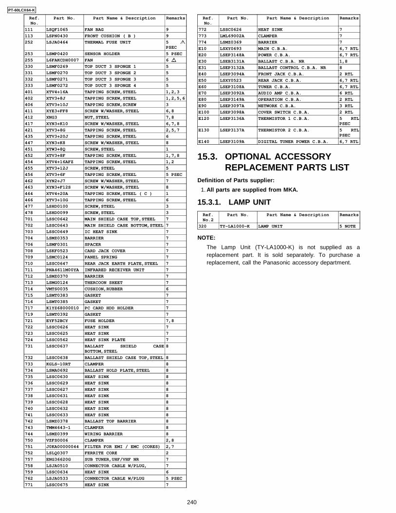
Ref.No.
Part No. Part Name & Description Remarks
111 LSQF1065 FAN BAG 9
113 LSPN0430 FRONT CUSHION ( B ) 9
252 LSJA0464 THERMAL FUSE UNIT 5PSEC
253 LSMP0420 SENSOR HOLDER 5 PSEC
255 L6FAKCDH0007 FAN 6
330 LSMF0269 TOP DUCT 3 SPONGE 1 5
331 LSMF0270 TOP DUCT 3 SPONGE 2 5
332 LSMF0271 TOP DUCT 3 SPONGE 3 5
333 LSMF0272 TOP DUCT 3 SPONGE 4 5
401 XTV4+16A TAPPING SCREW,STEEL 1,2,3
402 XTV3+8J TAPPING SCREW,STEEL 1,2,5,6
406 XTV3+10J TAPPING SCREW,SCREW 3
411 XYE3+FF8 SCREW W/WASHER,STEEL 6,8
412 XNG3 NUT,STEEL 7,8
417 XYN3+K10 SCREW W/WASHER,STEEL 6,7,8
421 XTV3+8G TAPPING SCREW,STEEL 2,5,7
435 XTV3+20J TAPPING SCREW,STEEL 6
447 XYN3+K8 SCREW W/WASHER,STEEL 8
451 XTW3+8Q SCREW,STEEL 1
452 XTV3+8F TAPPING SCREW,STEEL 1,7,8
454 XTV4+16AFZ TAPPING SCREW,STEEL 1,2
455 XTV3+12J SCREW,STEEL 5
456 XTV3+6F TAPPING SCREW,STEEL 5 PSEC
462 XYN2+J7 SCREW W/WASHER,STEEL 7
463 XYN3+F12S SCREW W/WASHER,STEEL 8
464 XTV4+20A TAPPING SCREW,STEEL ( C ) 1
466 XTV3+10G TAPPING SCREW,STEEL 6
477 LSHD0100 SCREW,STEEL 3
478 LSHD0099 SCREW,STEEL 3
701 LSSC0642 MAIN SHIELD CASE TOP,STEEL 7
702 LSSC0643 MAIN SHIELD CASE BOTTOM,STEEL 7
703 LSSC0649 IC HEAT SINK 7
704 LSMZ0353 BARRIER 7
706 LSMF0301 SPACER 7
708 LSKF0523 CARD JACK COVER 7
709 LSMC0124 PANEL SPRING 7
710 LSSC0647 REAR JACK EARTH PLATE,STEEL 7
711 PNA4611M00YA INFRARED RECEIVER UNIT 7
712 LSMZ0370 BARRIER 7
713 LSMG0124 THERCOON SHEET 7
714 VMTS0035 CUSHION,RUBBER 6
715 LSMT0383 GASKET 7
716 LSMT0385 GASKET 7
717 K1YZ68000010 PC CARD HDD HOLDER 7
719 LSMT0392 GASKET 7
721 EYF52BCY FUSE HOLDER 7,8
722 LSSC0626 HEAT SINK 7
723 LSSC0625 HEAT SINK 7
724 LSSC0562 HEAT SINK PLATE 7
731 LSSC0637 BALLAST SHIELD CASEBOTTOM,STEEL
8
732 LSSC0638 BALLAST SHIELD CASE TOP,STEEL 8
733 KGLS-10RT CLAMPER 8
734 LSMA0692 BALLAST HOLD PLATE,STEEL 8
735 LSSC0630 HEAT SINK 8
736 LSSC0629 HEAT SINK 8
737 LSSC0627 HEAT SINK 8
738 LSSC0631 HEAT SINK 8
739 LSSC0628 HEAT SINK 8
740 LSSC0632 HEAT SINK 8
741 LSSC0633 HEAT SINK 8
742 LSMZ0378 BALLAST TOP BARRIER 8
743 TMM4643-1 CLAMPER 8
744 LSMZ0399 WIRING BARRIER 8
750 VZFS0006 CLAMPER 2,8
751 J0KA00000044 FILTER FOR EMI / EMC (CORES) 2,7
752 LSLQ0307 FERRITE CORE 2
757 ENG36620G SUB TUNER,UHF/VHF NR 7
758 LSJA0510 CONNECTOR CABLE W/PLUG, 7
759 LSSC0634 HEAT SINK 6
762 LSJA0533 CONNECTOR CABLE W/PLUG 5 PSEC
771 LSSC0675 HEAT SINK 7
Ref.No.
Part No. Part Name & Description Remarks
772 LSSC0626 HEAT SINK 7
773 LML69002A CLAMPER 7
774 LSMZ0369 BARRIER 7
E10 LSXY0693 MAIN C.B.A. 6,7 RTL
E20 LSEP3148A POWER C.B.A. 6,7 RTL
E30 LSEB3131A BALLAST C.B.A. NR 1,8
E31 LSEP3132A BALLAST CONTROL C.B.A. NR 8
E40 LSEP3094A FRONT JACK C.B.A. 2 RTL
E50 LSXY0523 REAR JACK C.B.A. 6,7 RTL
E60 LSEP3108A TUNER C.B.A. 6,7 RTL
E70 LSEP3092A AUDIO AMP C.B.A. 6 RTL
E80 LSEP3149A OPERATION C.B.A. 2 RTL
E90 LSEP3097A NETWORK C.B.A. 3 RTL
E100 LSEP3098A COVER SWITCH C.B.A. 2 RTL
E120 LSEP3136A THERMISTOR 1 C.B.A. 5 RTLPSEC
E130 LSEP3137A THERMISTOR 2 C.B.A. 5 RTLPSEC
E140 LSEP3109A DIGITAL TUNER POWER C.B.A. 6,7 RTL
15.3. OPTIONAL ACCESSORYREPLACEMENT PARTS LIST
Definition of Parts supplier:
1. All parts are supplied from MKA.
15.3.1. LAMP UNITRef.No.2
Part No. Part Name & Description Remarks
320 TY-LA1000-K LAMP UNIT 5 NOTE
NOTE:
The Lamp Unit (TY-LA1000-K) is not supplied as areplacement part. It is sold separately. To purchase areplacement, call the Panasonic accessory department.
240
PT-60LCX64-K
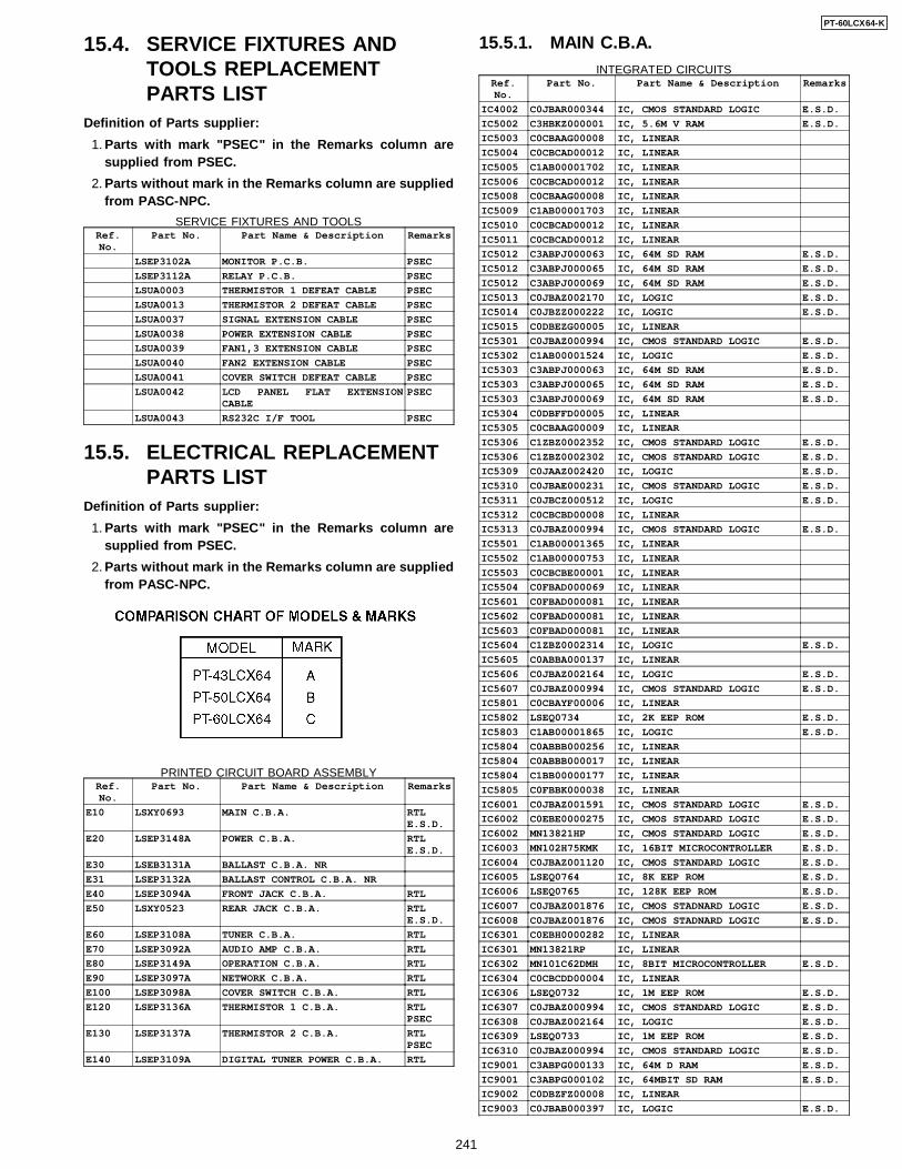
15.4. SERVICE FIXTURES ANDTOOLS REPLACEMENTPARTS LIST
Definition of Parts supplier:
1. Parts with mark "PSEC" in the Remarks column aresupplied from PSEC.
2. Parts without mark in the Remarks column are suppliedfrom PASC-NPC.
SERVICE FIXTURES AND TOOLSRef.No.
Part No. Part Name & Description Remarks
LSEP3102A MONITOR P.C.B. PSEC
LSEP3112A RELAY P.C.B. PSEC
LSUA0003 THERMISTOR 1 DEFEAT CABLE PSEC
LSUA0013 THERMISTOR 2 DEFEAT CABLE PSEC
LSUA0037 SIGNAL EXTENSION CABLE PSEC
LSUA0038 POWER EXTENSION CABLE PSEC
LSUA0039 FAN1,3 EXTENSION CABLE PSEC
LSUA0040 FAN2 EXTENSION CABLE PSEC
LSUA0041 COVER SWITCH DEFEAT CABLE PSEC
LSUA0042 LCD PANEL FLAT EXTENSIONCABLE
PSEC
LSUA0043 RS232C I/F TOOL PSEC
15.5. ELECTRICAL REPLACEMENTPARTS LIST
Definition of Parts supplier:
1. Parts with mark "PSEC" in the Remarks column aresupplied from PSEC.
2. Parts without mark in the Remarks column are suppliedfrom PASC-NPC.
PRINTED CIRCUIT BOARD ASSEMBLYRef.No.
Part No. Part Name & Description Remarks
E10 LSXY0693 MAIN C.B.A. RTLE.S.D.
E20 LSEP3148A POWER C.B.A. RTLE.S.D.
E30 LSEB3131A BALLAST C.B.A. NR
E31 LSEP3132A BALLAST CONTROL C.B.A. NR
E40 LSEP3094A FRONT JACK C.B.A. RTL
E50 LSXY0523 REAR JACK C.B.A. RTLE.S.D.
E60 LSEP3108A TUNER C.B.A. RTL
E70 LSEP3092A AUDIO AMP C.B.A. RTL
E80 LSEP3149A OPERATION C.B.A. RTL
E90 LSEP3097A NETWORK C.B.A. RTL
E100 LSEP3098A COVER SWITCH C.B.A. RTL
E120 LSEP3136A THERMISTOR 1 C.B.A. RTLPSEC
E130 LSEP3137A THERMISTOR 2 C.B.A. RTLPSEC
E140 LSEP3109A DIGITAL TUNER POWER C.B.A. RTL
15.5.1. MAIN C.B.A.INTEGRATED CIRCUITS
Ref.No.
Part No. Part Name & Description Remarks
IC4002 C0JBAR000344 IC, CMOS STANDARD LOGIC E.S.D.
IC5002 C3HBKZ000001 IC, 5.6M V RAM E.S.D.
IC5003 C0CBAAG00008 IC, LINEAR
IC5004 C0CBCAD00012 IC, LINEAR
IC5005 C1AB00001702 IC, LINEAR
IC5006 C0CBCAD00012 IC, LINEAR
IC5008 C0CBAAG00008 IC, LINEAR
IC5009 C1AB00001703 IC, LINEAR
IC5010 C0CBCAD00012 IC, LINEAR
IC5011 C0CBCAD00012 IC, LINEAR
IC5012 C3ABPJ000063 IC, 64M SD RAM E.S.D.
IC5012 C3ABPJ000065 IC, 64M SD RAM E.S.D.
IC5012 C3ABPJ000069 IC, 64M SD RAM E.S.D.
IC5013 C0JBAZ002170 IC, LOGIC E.S.D.
IC5014 C0JBZZ000222 IC, LOGIC E.S.D.
IC5015 C0DBEZG00005 IC, LINEAR
IC5301 C0JBAZ000994 IC, CMOS STANDARD LOGIC E.S.D.
IC5302 C1AB00001524 IC, LOGIC E.S.D.
IC5303 C3ABPJ000063 IC, 64M SD RAM E.S.D.
IC5303 C3ABPJ000065 IC, 64M SD RAM E.S.D.
IC5303 C3ABPJ000069 IC, 64M SD RAM E.S.D.
IC5304 C0DBFFD00005 IC, LINEAR
IC5305 C0CBAAG00009 IC, LINEAR
IC5306 C1ZBZ0002352 IC, CMOS STANDARD LOGIC E.S.D.
IC5306 C1ZBZ0002302 IC, CMOS STANDARD LOGIC E.S.D.
IC5309 C0JAAZ002420 IC, LOGIC E.S.D.
IC5310 C0JBAE000231 IC, CMOS STANDARD LOGIC E.S.D.
IC5311 C0JBCZ000512 IC, LOGIC E.S.D.
IC5312 C0CBCBD00008 IC, LINEAR
IC5313 C0JBAZ000994 IC, CMOS STANDARD LOGIC E.S.D.
IC5501 C1AB00001365 IC, LINEAR
IC5502 C1AB00000753 IC, LINEAR
IC5503 C0CBCBE00001 IC, LINEAR
IC5504 C0FBAD000069 IC, LINEAR
IC5601 C0FBAD000081 IC, LINEAR
IC5602 C0FBAD000081 IC, LINEAR
IC5603 C0FBAD000081 IC, LINEAR
IC5604 C1ZBZ0002314 IC, LOGIC E.S.D.
IC5605 C0ABBA000137 IC, LINEAR
IC5606 C0JBAZ002164 IC, LOGIC E.S.D.
IC5607 C0JBAZ000994 IC, CMOS STANDARD LOGIC E.S.D.
IC5801 C0CBAYF00006 IC, LINEAR
IC5802 LSEQ0734 IC, 2K EEP ROM E.S.D.
IC5803 C1AB00001865 IC, LOGIC E.S.D.
IC5804 C0ABBB000256 IC, LINEAR
IC5804 C0ABBB000017 IC, LINEAR
IC5804 C1BB00000177 IC, LINEAR
IC5805 C0FBBK000038 IC, LINEAR
IC6001 C0JBAZ001591 IC, CMOS STANDARD LOGIC E.S.D.
IC6002 C0EBE0000275 IC, CMOS STANDARD LOGIC E.S.D.
IC6002 MN13821HP IC, CMOS STANDARD LOGIC E.S.D.
IC6003 MN102H75KMK IC, 16BIT MICROCONTROLLER E.S.D.
IC6004 C0JBAZ001120 IC, CMOS STANDARD LOGIC E.S.D.
IC6005 LSEQ0764 IC, 8K EEP ROM E.S.D.
IC6006 LSEQ0765 IC, 128K EEP ROM E.S.D.
IC6007 C0JBAZ001876 IC, CMOS STADNARD LOGIC E.S.D.
IC6008 C0JBAZ001876 IC, CMOS STADNARD LOGIC E.S.D.
IC6301 C0EBH0000282 IC, LINEAR
IC6301 MN13821RP IC, LINEAR
IC6302 MN101C62DMH IC, 8BIT MICROCONTROLLER E.S.D.
IC6304 C0CBCDD00004 IC, LINEAR
IC6306 LSEQ0732 IC, 1M EEP ROM E.S.D.
IC6307 C0JBAZ000994 IC, CMOS STANDARD LOGIC E.S.D.
IC6308 C0JBAZ002164 IC, LOGIC E.S.D.
IC6309 LSEQ0733 IC, 1M EEP ROM E.S.D.
IC6310 C0JBAZ000994 IC, CMOS STANDARD LOGIC E.S.D.
IC9001 C3ABPG000133 IC, 64M D RAM E.S.D.
IC9001 C3ABPG000102 IC, 64MBIT SD RAM E.S.D.
IC9002 C0DBZFZ00008 IC, LINEAR
IC9003 C0JBAB000397 IC, LOGIC E.S.D.
241
PT-60LCX64-K
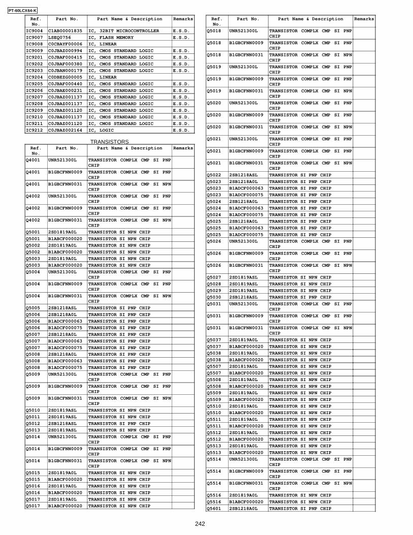
Ref.No.
Part No. Part Name & Description Remarks
IC9004 C1AB00001835 IC, 32BIT MICROCONTROLLER E.S.D.
IC9007 LSEQ0756 IC, FLASH MEMORY E.S.D.
IC9008 C0CBAYF00006 IC, LINEAR
IC9009 C0JBAZ000994 IC, CMOS STANDARD LOGIC E.S.D.
IC9201 C0JBAF000415 IC, CMOS STANDARD LOGIC E.S.D.
IC9202 C0JBAF000380 IC, CMOS STANDARD LOGIC E.S.D.
IC9203 C0JBAN000179 IC, CMOS STANDARD LOGIC E.S.D.
IC9204 C0DBEZG00005 IC, LINEAR
IC9205 C0JBAF000440 IC, CMOS STANDARD LOGIC E.S.D.
IC9206 C0JBAE000231 IC, CMOS STANDARD LOGIC E.S.D.
IC9207 C0JBAZ001137 IC, CMOS STANDARD LOGIC E.S.D.
IC9208 C0JBAZ001137 IC, CMOS STANDARD LOGIC E.S.D.
IC9209 C0JBAZ001120 IC, CMOS STANDARD LOGIC E.S.D.
IC9210 C0JBAZ001137 IC, CMOS STANDARD LOGIC E.S.D.
IC9211 C0JBAZ001120 IC, CMOS STANDARD LOGIC E.S.D.
IC9212 C0JBAZ002164 IC, LOGIC E.S.D.
TRANSISTORSRef.No.
Part No. Part Name & Description Remarks
Q4001 UNR521300L TRANSISTOR COMPLX CMP SI PNPCHIP
Q4001 B1GBCFNN0009 TRANSISTOR COMPLX CMP SI PNPCHIP
Q4001 B1GBCFNN0031 TRANSISTOR COMPLX CMP SI NPNCHIP
Q4002 UNR521300L TRANSISTOR COMPLX CMP SI PNPCHIP
Q4002 B1GBCFNN0009 TRANSISTOR COMPLX CMP SI PNPCHIP
Q4002 B1GBCFNN0031 TRANSISTOR COMPLX CMP SI NPNCHIP
Q5001 2SD1819A0L TRANSISTOR SI NPN CHIP
Q5001 B1ABCF000020 TRANSISTOR SI NPN CHIP
Q5002 2SD1819A0L TRANSISTOR SI NPN CHIP
Q5002 B1ABCF000020 TRANSISTOR SI NPN CHIP
Q5003 2SD1819A0L TRANSISTOR SI NPN CHIP
Q5003 B1ABCF000020 TRANSISTOR SI NPN CHIP
Q5004 UNR521300L TRANSISTOR COMPLX CMP SI PNPCHIP
Q5004 B1GBCFNN0009 TRANSISTOR COMPLX CMP SI PNPCHIP
Q5004 B1GBCFNN0031 TRANSISTOR COMPLX CMP SI NPNCHIP
Q5005 2SB1218ASL TRANSISTOR SI PNP CHIP
Q5006 2SB1218A0L TRANSISTOR SI PNP CHIP
Q5006 B1ADCF000063 TRANSISTOR SI PNP CHIP
Q5006 B1ADCF000075 TRANSISTOR SI PNP CHIP
Q5007 2SB1218A0L TRANSISTOR SI PNP CHIP
Q5007 B1ADCF000063 TRANSISTOR SI PNP CHIP
Q5007 B1ADCF000075 TRANSISTOR SI PNP CHIP
Q5008 2SB1218A0L TRANSISTOR SI PNP CHIP
Q5008 B1ADCF000063 TRANSISTOR SI PNP CHIP
Q5008 B1ADCF000075 TRANSISTOR SI PNP CHIP
Q5009 UNR521300L TRANSISTOR COMPLX CMP SI PNPCHIP
Q5009 B1GBCFNN0009 TRANSISTOR COMPLX CMP SI PNPCHIP
Q5009 B1GBCFNN0031 TRANSISTOR COMPLX CMP SI NPNCHIP
Q5010 2SD1819ASL TRANSISTOR SI NPN CHIP
Q5011 2SD1819ASL TRANSISTOR SI NPN CHIP
Q5012 2SB1218ASL TRANSISTOR SI PNP CHIP
Q5013 2SD1819ASL TRANSISTOR SI NPN CHIP
Q5014 UNR521300L TRANSISTOR COMPLX CMP SI PNPCHIP
Q5014 B1GBCFNN0009 TRANSISTOR COMPLX CMP SI PNPCHIP
Q5014 B1GBCFNN0031 TRANSISTOR COMPLX CMP SI NPNCHIP
Q5015 2SD1819A0L TRANSISTOR SI NPN CHIP
Q5015 B1ABCF000020 TRANSISTOR SI NPN CHIP
Q5016 2SD1819A0L TRANSISTOR SI NPN CHIP
Q5016 B1ABCF000020 TRANSISTOR SI NPN CHIP
Q5017 2SD1819A0L TRANSISTOR SI NPN CHIP
Q5017 B1ABCF000020 TRANSISTOR SI NPN CHIP
Ref.No.
Part No. Part Name & Description Remarks
Q5018 UNR521300L TRANSISTOR COMPLX CMP SI PNPCHIP
Q5018 B1GBCFNN0009 TRANSISTOR COMPLX CMP SI PNPCHIP
Q5018 B1GBCFNN0031 TRANSISTOR COMPLX CMP SI NPNCHIP
Q5019 UNR521300L TRANSISTOR COMPLX CMP SI PNPCHIP
Q5019 B1GBCFNN0009 TRANSISTOR COMPLX CMP SI PNPCHIP
Q5019 B1GBCFNN0031 TRANSISTOR COMPLX CMP SI NPNCHIP
Q5020 UNR521300L TRANSISTOR COMPLX CMP SI PNPCHIP
Q5020 B1GBCFNN0009 TRANSISTOR COMPLX CMP SI PNPCHIP
Q5020 B1GBCFNN0031 TRANSISTOR COMPLX CMP SI NPNCHIP
Q5021 UNR521300L TRANSISTOR COMPLX CMP SI PNPCHIP
Q5021 B1GBCFNN0009 TRANSISTOR COMPLX CMP SI PNPCHIP
Q5021 B1GBCFNN0031 TRANSISTOR COMPLX CMP SI NPNCHIP
Q5022 2SB1218ASL TRANSISTOR SI PNP CHIP
Q5023 2SB1218A0L TRANSISTOR SI PNP CHIP
Q5023 B1ADCF000063 TRANSISTOR SI PNP CHIP
Q5023 B1ADCF000075 TRANSISTOR SI PNP CHIP
Q5024 2SB1218A0L TRANSISTOR SI PNP CHIP
Q5024 B1ADCF000063 TRANSISTOR SI PNP CHIP
Q5024 B1ADCF000075 TRANSISTOR SI PNP CHIP
Q5025 2SB1218A0L TRANSISTOR SI PNP CHIP
Q5025 B1ADCF000063 TRANSISTOR SI PNP CHIP
Q5025 B1ADCF000075 TRANSISTOR SI PNP CHIP
Q5026 UNR521300L TRANSISTOR COMPLX CMP SI PNPCHIP
Q5026 B1GBCFNN0009 TRANSISTOR COMPLX CMP SI PNPCHIP
Q5026 B1GBCFNN0031 TRANSISTOR COMPLX CMP SI NPNCHIP
Q5027 2SD1819ASL TRANSISTOR SI NPN CHIP
Q5028 2SD1819ASL TRANSISTOR SI NPN CHIP
Q5029 2SD1819ASL TRANSISTOR SI NPN CHIP
Q5030 2SB1218ASL TRANSISTOR SI PNP CHIP
Q5031 UNR521300L TRANSISTOR COMPLX CMP SI PNPCHIP
Q5031 B1GBCFNN0009 TRANSISTOR COMPLX CMP SI PNPCHIP
Q5031 B1GBCFNN0031 TRANSISTOR COMPLX CMP SI NPNCHIP
Q5037 2SD1819A0L TRANSISTOR SI NPN CHIP
Q5037 B1ABCF000020 TRANSISTOR SI NPN CHIP
Q5038 2SD1819A0L TRANSISTOR SI NPN CHIP
Q5038 B1ABCF000020 TRANSISTOR SI NPN CHIP
Q5507 2SD1819A0L TRANSISTOR SI NPN CHIP
Q5507 B1ABCF000020 TRANSISTOR SI NPN CHIP
Q5508 2SD1819A0L TRANSISTOR SI NPN CHIP
Q5508 B1ABCF000020 TRANSISTOR SI NPN CHIP
Q5509 2SD1819A0L TRANSISTOR SI NPN CHIP
Q5509 B1ABCF000020 TRANSISTOR SI NPN CHIP
Q5510 2SD1819A0L TRANSISTOR SI NPN CHIP
Q5510 B1ABCF000020 TRANSISTOR SI NPN CHIP
Q5511 2SD1819A0L TRANSISTOR SI NPN CHIP
Q5511 B1ABCF000020 TRANSISTOR SI NPN CHIP
Q5512 2SD1819A0L TRANSISTOR SI NPN CHIP
Q5512 B1ABCF000020 TRANSISTOR SI NPN CHIP
Q5513 2SD1819A0L TRANSISTOR SI NPN CHIP
Q5513 B1ABCF000020 TRANSISTOR SI NPN CHIP
Q5514 UNR521300L TRANSISTOR COMPLX CMP SI PNPCHIP
Q5514 B1GBCFNN0009 TRANSISTOR COMPLX CMP SI PNPCHIP
Q5514 B1GBCFNN0031 TRANSISTOR COMPLX CMP SI NPNCHIP
Q5516 2SD1819A0L TRANSISTOR SI NPN CHIP
Q5516 B1ABCF000020 TRANSISTOR SI NPN CHIP
Q5601 2SB1218A0L TRANSISTOR SI PNP CHIP
242
PT-60LCX64-K
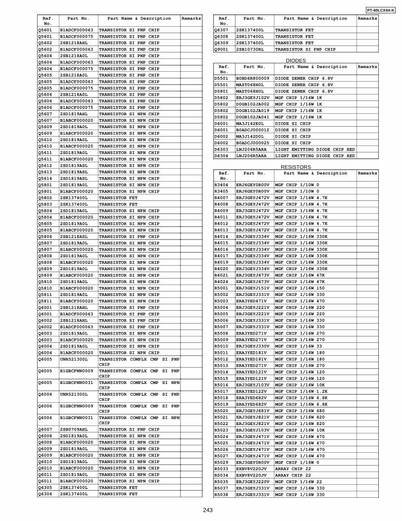
Ref.No.
Part No. Part Name & Description Remarks
Q5601 B1ADCF000063 TRANSISTOR SI PNP CHIP
Q5601 B1ADCF000075 TRANSISTOR SI PNP CHIP
Q5602 2SB1218AHL TRANSISTOR SI PNP CHIP
Q5602 B1ADCF000063 TRANSISTOR SI PNP CHIP
Q5604 2SB1218A0L TRANSISTOR SI PNP CHIP
Q5604 B1ADCF000063 TRANSISTOR SI PNP CHIP
Q5604 B1ADCF000075 TRANSISTOR SI PNP CHIP
Q5605 2SB1218A0L TRANSISTOR SI PNP CHIP
Q5605 B1ADCF000063 TRANSISTOR SI PNP CHIP
Q5605 B1ADCF000075 TRANSISTOR SI PNP CHIP
Q5606 2SB1218A0L TRANSISTOR SI PNP CHIP
Q5606 B1ADCF000063 TRANSISTOR SI PNP CHIP
Q5606 B1ADCF000075 TRANSISTOR SI PNP CHIP
Q5607 2SD1819AHL TRANSISTOR SI NPN CHIP
Q5607 B1ABCF000020 TRANSISTOR SI NPN CHIP
Q5609 2SD1819A0L TRANSISTOR SI NPN CHIP
Q5609 B1ABCF000020 TRANSISTOR SI NPN CHIP
Q5610 2SD1819A0L TRANSISTOR SI NPN CHIP
Q5610 B1ABCF000020 TRANSISTOR SI NPN CHIP
Q5611 2SD1819A0L TRANSISTOR SI NPN CHIP
Q5611 B1ABCF000020 TRANSISTOR SI NPN CHIP
Q5612 2SD1819ASL TRANSISTOR SI NPN CHIP
Q5613 2SD1819ASL TRANSISTOR SI NPN CHIP
Q5614 2SD1819ASL TRANSISTOR SI NPN CHIP
Q5801 2SD1819A0L TRANSISTOR SI NPN CHIP
Q5801 B1ABCF000020 TRANSISTOR SI NPN CHIP
Q5802 2SK137400L TRANSISTOR FET
Q5803 2SK137400L TRANSISTOR FET
Q5804 2SD1819A0L TRANSISTOR SI NPN CHIP
Q5804 B1ABCF000020 TRANSISTOR SI NPN CHIP
Q5805 2SD1819A0L TRANSISTOR SI NPN CHIP
Q5805 B1ABCF000020 TRANSISTOR SI NPN CHIP
Q5806 2SB1218ASL TRANSISTOR SI PNP CHIP
Q5807 2SD1819A0L TRANSISTOR SI NPN CHIP
Q5807 B1ABCF000020 TRANSISTOR SI NPN CHIP
Q5808 2SD1819A0L TRANSISTOR SI NPN CHIP
Q5808 B1ABCF000020 TRANSISTOR SI NPN CHIP
Q5809 2SD1819A0L TRANSISTOR SI NPN CHIP
Q5809 B1ABCF000020 TRANSISTOR SI NPN CHIP
Q5810 2SD1819A0L TRANSISTOR SI NPN CHIP
Q5810 B1ABCF000020 TRANSISTOR SI NPN CHIP
Q5811 2SD1819A0L TRANSISTOR SI NPN CHIP
Q5811 B1ABCF000020 TRANSISTOR SI NPN CHIP
Q6001 2SB1218AHL TRANSISTOR SI PNP CHIP
Q6001 B1ADCF000063 TRANSISTOR SI PNP CHIP
Q6002 2SB1218AHL TRANSISTOR SI PNP CHIP
Q6002 B1ADCF000063 TRANSISTOR SI PNP CHIP
Q6003 2SD1819A0L TRANSISTOR SI NPN CHIP
Q6003 B1ABCF000020 TRANSISTOR SI NPN CHIP
Q6004 2SD1819A0L TRANSISTOR SI NPN CHIP
Q6004 B1ABCF000020 TRANSISTOR SI NPN CHIP
Q6005 UNR521300L TRANSISTOR COMPLX CMP SI PNPCHIP
Q6005 B1GBCFNN0009 TRANSISTOR COMPLX CMP SI PNPCHIP
Q6005 B1GBCFNN0031 TRANSISTOR COMPLX CMP SI NPNCHIP
Q6006 UNR521300L TRANSISTOR COMPLX CMP SI PNPCHIP
Q6006 B1GBCFNN0009 TRANSISTOR COMPLX CMP SI PNPCHIP
Q6006 B1GBCFNN0031 TRANSISTOR COMPLX CMP SI NPNCHIP
Q6007 2SB0709AHL TRANSISTOR SI PNP CHIP
Q6008 2SD1819A0L TRANSISTOR SI NPN CHIP
Q6008 B1ABCF000020 TRANSISTOR SI NPN CHIP
Q6009 2SD1819A0L TRANSISTOR SI NPN CHIP
Q6009 B1ABCF000020 TRANSISTOR SI NPN CHIP
Q6010 2SD1819A0L TRANSISTOR SI NPN CHIP
Q6010 B1ABCF000020 TRANSISTOR SI NPN CHIP
Q6011 2SD1819A0L TRANSISTOR SI NPN CHIP
Q6011 B1ABCF000020 TRANSISTOR SI NPN CHIP
Q6305 2SK137400L TRANSISTOR FET
Q6306 2SK137400L TRANSISTOR FET
Ref.No.
Part No. Part Name & Description Remarks
Q6307 2SK137400L TRANSISTOR FET
Q6308 2SK137400L TRANSISTOR FET
Q6309 2SK137400L TRANSISTOR FET
Q9001 2SB10730RL TRANSISTOR SI PNP CHIP
DIODESRef.No.
Part No. Part Name & Description Remarks
D5501 B0BD6R800009 DIODE ZENER CHIP 6.8V
D5501 MAZT068H0L DIODE ZENER CHIP 6.8V
D5801 MAZT068H0L DIODE ZENER CHIP 6.8V
D5802 ERJ3GEYJ102V MGF CHIP 1/16W 1K
D5802 D0GB102JA002 MGF CHIP 1/16W 1K
D5802 D0GB102JA019 MGF CHIP 1/16W 1K
D5802 D0GB102JA041 MGF CHIP 1/16W 1K
D6001 MA3J142E0L DIODE SI CHIP
D6001 B0ADCJ000012 DIODE SI CHIP
D6002 MA3J142D0L DIODE SI CHIP
D6002 B0ADCJ000025 DIODE SI CHIP
D6303 LNJ206R5ARA LIGHT EMITTING DIODE CHIP RED
D6304 LNJ206R5ARA LIGHT EMITTING DIODE CHIP RED
RESISTORSRef.No.
Part No. Part Name & Description Remarks
R3404 ERJ6GEY0R00V MGF CHIP 1/10W 0
R3405 ERJ6GEY0R00V MGF CHIP 1/10W 0
R4007 ERJ3GEYJ472V MGF CHIP 1/16W 4.7K
R4008 ERJ3GEYJ472V MGF CHIP 1/16W 4.7K
R4009 ERJ3GEYJ472V MGF CHIP 1/16W 4.7K
R4011 ERJ3GEYJ472V MGF CHIP 1/16W 4.7K
R4012 ERJ3GEYJ472V MGF CHIP 1/16W 4.7K
R4013 ERJ3GEYJ472V MGF CHIP 1/16W 4.7K
R4014 ERJ3GEYJ334V MGF CHIP 1/16W 330K
R4015 ERJ3GEYJ334V MGF CHIP 1/16W 330K
R4016 ERJ3GEYJ334V MGF CHIP 1/16W 330K
R4017 ERJ3GEYJ334V MGF CHIP 1/16W 330K
R4019 ERJ3GEYJ334V MGF CHIP 1/16W 330K
R4020 ERJ3GEYJ334V MGF CHIP 1/16W 330K
R4021 ERJ3GEYJ473V MGF CHIP 1/16W 47K
R4024 ERJ3GEYJ473V MGF CHIP 1/16W 47K
R5001 ERJ3GEYJ151V MGF CHIP 1/16W 150
R5002 ERJ3GEYJ331V MGF CHIP 1/16W 330
R5003 ERA3YED471V MGF CHIP 1/16W 470
R5004 ERJ3GEYJ221V MGF CHIP 1/16W 220
R5005 ERJ3GEYJ221V MGF CHIP 1/16W 220
R5006 ERJ3GEYJ331V MGF CHIP 1/16W 330
R5007 ERJ3GEYJ331V MGF CHIP 1/16W 330
R5008 ERA3YED271V MGF CHIP 1/16W 270
R5009 ERA3YED271V MGF CHIP 1/16W 270
R5010 ERJ3GEYJ330V MGF CHIP 1/16W 33
R5011 ERA3YED181V MGF CHIP 1/16W 180
R5012 ERA3YED181V MGF CHIP 1/16W 180
R5013 ERA3YED271V MGF CHIP 1/16W 270
R5014 ERA3YED121V MGF CHIP 1/16W 120
R5015 ERA3YED121V MGF CHIP 1/16W 120
R5016 ERJ3GEYJ103V MGF CHIP 1/16W 10K
R5017 ERA3YED122V MGF CHIP 1/16W 1.2K
R5018 ERA3YED682V MGF CHIP 1/16W 6.8K
R5019 ERA3YED682V MGF CHIP 1/16W 6.8K
R5020 ERJ3GEYJ681V MGF CHIP 1/16W 680
R5021 ERJ3GEYJ821V MGF CHIP 1/16W 820
R5022 ERJ3GEYJ821V MGF CHIP 1/16W 820
R5023 ERJ3GEYJ103V MGF CHIP 1/16W 10K
R5024 ERJ3GEYJ471V MGF CHIP 1/16W 470
R5025 ERJ3GEYJ471V MGF CHIP 1/16W 470
R5026 ERJ3GEYJ471V MGF CHIP 1/16W 470
R5027 ERJ3GEYJ471V MGF CHIP 1/16W 470
R5029 ERJ3GEY0R00V MGF CHIP 1/16W 0
R5033 EXBV8V220JV ARRAY CHIP 22
R5034 EXBV8V220JV ARRAY CHIP 22
R5035 ERJ3GEYJ220V MGF CHIP 1/16W 22
R5037 ERJ3GEYJ331V MGF CHIP 1/16W 330
R5038 ERJ3GEYJ331V MGF CHIP 1/16W 330
243
PT-60LCX64-K
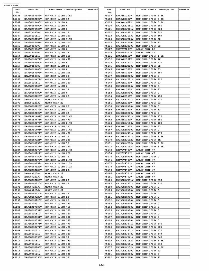
Ref.No.
Part No. Part Name & Description Remarks
R5039 ERJ3GEYJ182V MGF CHIP 1/16W 1.8K
R5040 ERJ3GEYJ102V MGF CHIP 1/16W 1K
R5042 ERJ3GEY0R00V MGF CHIP 1/16W 0
R5043 ERJ3GEY0R00V MGF CHIP 1/16W 0
R5044 ERJ3GEY0R00V MGF CHIP 1/16W 0
R5045 ERA3YHD330V MGF CHIP 1/16W 33
R5047 ERA3YED151V MGF CHIP 1/16W 150
R5048 ERJ3GEYJ152V MGF CHIP 1/16W 1.5K
R5049 ERJ3GEYJ101V MGF CHIP 1/16W 100
R5050 ERA3YHD330V MGF CHIP 1/16W 33
R5051 ERJ3GEY0R00V MGF CHIP 1/16W 0
R5052 ERA3YHD330V MGF CHIP 1/16W 33
R5054 ERA3YED151V MGF CHIP 1/16W 150
R5055 ERJ3GEYJ471V MGF CHIP 1/16W 470
R5056 ERJ3GEY0R00V MGF CHIP 1/16W 0
R5057 ERA3YHD330V MGF CHIP 1/16W 33
R5058 ERJ3GEY0R00V MGF CHIP 1/16W 0
R5060 ERJ3GEYJ103V MGF CHIP 1/16W 10K
R5062 ERA3YHD330V MGF CHIP 1/16W 33
R5063 ERJ3GEYJ471V MGF CHIP 1/16W 470
R5064 ERA3YED151V MGF CHIP 1/16W 150
R5065 ERJ3GEY0R00V MGF CHIP 1/16W 0
R5066 ERA3YHD330V MGF CHIP 1/16W 33
R5067 ERJ3GEY0R00V MGF CHIP 1/16W 0
R5068 ERJ3GEYJ220V MGF CHIP 1/16W 22
R5069 EXBV8V220JV ARRAY CHIP 22
R5070 EXBV8V220JV ARRAY CHIP 22
R5071 ERJ3GEYJ220V MGF CHIP 1/16W 22
R5072 ERJ3GEYJ272V MGF CHIP 1/16W 2.7K
R5073 ERJ3GEYJ102V MGF CHIP 1/16W 1K
R5074 ERJ3EKF1401V MGF CHIP 1/16W 1.4K
R5075 ERJ3GEYJ471V MGF CHIP 1/16W 470
R5076 ERJ3GEYJ272V MGF CHIP 1/16W 2.7K
R5077 ERJ3GEYJ102V MGF CHIP 1/16W 1K
R5078 ERJ3EKF1401V MGF CHIP 1/16W 1.4K
R5079 ERJ3GEYJ471V MGF CHIP 1/16W 470
R5080 ERJ3GEYJ750V MGF CHIP 1/16W 75
R5081 ERJ3GEYJ221V MGF CHIP 1/16W 220
R5082 ERJ3GEYJ750V MGF CHIP 1/16W 75
R5083 ERJ3GEYJ221V MGF CHIP 1/16W 220
R5084 ERJ3GEYJ272V MGF CHIP 1/16W 2.7K
R5085 ERJ3GEYJ221V MGF CHIP 1/16W 220
R5086 ERJ3GEYJ750V MGF CHIP 1/16W 75
R5087 ERJ3GEYJ272V MGF CHIP 1/16W 2.7K
R5088 ERJ3GEYJ152V MGF CHIP 1/16W 1.5K
R5089 ERJ3GEYJ122V MGF CHIP 1/16W 1.2K
R5090 ERJ3GEYJ220V MGF CHIP 1/16W 22
R5091 EXBV8V220JV ARRAY CHIP 22
R5092 EXBV8V220JV ARRAY CHIP 22
R5093 ERJ3GEYJ220V MGF CHIP 1/16W 22
R5094 ERJ3GEYJ220V MGF CHIP 1/16W 22
R5095 EXBV8V220JV ARRAY CHIP 22
R5096 EXBV8V220JV ARRAY CHIP 22
R5097 ERJ3GEYJ220V MGF CHIP 1/16W 22
R5098 ERJ3GEYJ220V MGF CHIP 1/16W 22
R5099 ERJ3GEYJ220V MGF CHIP 1/16W 22
R5100 ERA3YED331V MGF CHIP 1/16W 330
R5101 ERJ3EKF7500V MGF CHIP 1/16W 750
R5102 ERJ3GEYJ331V MGF CHIP 1/16W 330
R5103 ERA3YED151V MGF CHIP 1/16W 150
R5104 ERJ3GEYJ331V MGF CHIP 1/16W 330
R5105 ERJ3GEYJ331V MGF CHIP 1/16W 330
R5106 ERJ3GEYJ471V MGF CHIP 1/16W 470
R5107 ERJ3GEYJ471V MGF CHIP 1/16W 470
R5108 ERA3YED121V MGF CHIP 1/16W 120
R5109 ERA3YED121V MGF CHIP 1/16W 120
R5110 ERJ3GEYJ390V MGF CHIP 1/16W 39
R5111 ERA3YED181V MGF CHIP 1/16W 180
R5112 ERA3YED181V MGF CHIP 1/16W 180
R5113 ERJ3GEYJ103V MGF CHIP 1/16W 10K
R5114 ERA3YED121V MGF CHIP 1/16W 120
R5115 ERA3YED121V MGF CHIP 1/16W 120
R5116 ERJ3GEYJ390V MGF CHIP 1/16W 39
Ref.No.
Part No. Part Name & Description Remarks
R5117 ERA3YED222V MGF CHIP 1/16W 2.2K
R5118 ERA3YED682V MGF CHIP 1/16W 6.8K
R5119 ERA3YED682V MGF CHIP 1/16W 6.8K
R5120 ERJ3GEYJ681V MGF CHIP 1/16W 680
R5121 ERJ3GEYJ821V MGF CHIP 1/16W 820
R5122 ERJ3GEYJ821V MGF CHIP 1/16W 820
R5123 ERJ3GEYJ103V MGF CHIP 1/16W 10K
R5124 ERJ3GEYJ220V MGF CHIP 1/16W 22
R5125 ERJ3GEYJ220V MGF CHIP 1/16W 22
R5126 ERJ3GEYJ220V MGF CHIP 1/16W 22
R5127 EXBV8V220JV ARRAY CHIP 22
R5128 EXBV8V220JV ARRAY CHIP 22
R5131 ERA3YED152V MGF CHIP 1/16W 1.5K
R5132 ERA3YED102V MGF CHIP 1/16W 1K
R5133 ERJ3GEYJ271V MGF CHIP 1/16W 270
R5141 ERJ3GEYJ220V MGF CHIP 1/16W 22
R5145 ERA3YHD330V MGF CHIP 1/16W 33
R5146 ERA3YED151V MGF CHIP 1/16W 150
R5147 ERJ3GEY0R00V MGF CHIP 1/16W 0
R5148 ERJ3GEYJ221V MGF CHIP 1/16W 220
R5149 ERA3YHD330V MGF CHIP 1/16W 33
R5150 ERJ3GEY0R00V MGF CHIP 1/16W 0
R5151 ERA3YHD330V MGF CHIP 1/16W 33
R5153 ERJ3GEY0R00V MGF CHIP 1/16W 0
R5154 ERA3YED151V MGF CHIP 1/16W 150
R5155 ERJ3GEYJ471V MGF CHIP 1/16W 470
R5156 ERA3YHD330V MGF CHIP 1/16W 33
R5158 ERJ3GEY0R00V MGF CHIP 1/16W 0
R5159 ERA3YHD330V MGF CHIP 1/16W 33
R5160 ERJ3GEY0R00V MGF CHIP 1/16W 0
R5161 ERJ3GEYJ471V MGF CHIP 1/16W 470
R5162 ERA3YED151V MGF CHIP 1/16W 150
R5164 ERJ3GEYJ103V MGF CHIP 1/16W 10K
R5166 ERA3YHD330V MGF CHIP 1/16W 33
R5167 ERJ3GEY0R00V MGF CHIP 1/16W 0
R5168 ERJ3GEYJ471V MGF CHIP 1/16W 470
R5169 ERJ3EKF1401V MGF CHIP 1/16W 1.4K
R5170 ERJ3GEYJ102V MGF CHIP 1/16W 1K
R5171 ERJ3GEYJ272V MGF CHIP 1/16W 2.7K
R5172 ERJ3GEYJ152V MGF CHIP 1/16W 1.5K
R5173 EXBV8V470JV ARRAY CHIP 47
R5174 EXBV8V470JV ARRAY CHIP 47
R5175 ERJ3GEY0R00V MGF CHIP 1/16W 0
R5176 EXBV8V470JV ARRAY CHIP 47
R5177 EXBV8V470JV ARRAY CHIP 47
R5178 EXBV8V470JV ARRAY CHIP 47
R5179 EXBV8V470JV ARRAY CHIP 47
R5180 EXBV8V470JV ARRAY CHIP 47
R5181 EXBV8V470JV ARRAY CHIP 47
R5186 ERJ3GEYJ331V MGF CHIP 1/16W 330
R5187 ERJ3GEYJ331V MGF CHIP 1/16W 330
R5188 ERJ3GEY0R00V MGF CHIP 1/16W 0
R5189 ERJ3GEY0R00V MGF CHIP 1/16W 0
R5190 ERJ3GEY0R00V MGF CHIP 1/16W 0
R5191 ERJ3GEY0R00V MGF CHIP 1/16W 0
R5192 ERJ3GEY0R00V MGF CHIP 1/16W 0
R5193 ERJ3GEY0R00V MGF CHIP 1/16W 0
R5194 ERJ3GEY0R00V MGF CHIP 1/16W 0
R5195 ERJ3GEY0R00V MGF CHIP 1/16W 0
R5196 ERJ3GEY0R00V MGF CHIP 1/16W 0
R5197 ERJ3GEY0R00V MGF CHIP 1/16W 0
R5198 ERJ3GEY0R00V MGF CHIP 1/16W 0
R5199 ERJ3GEYJ471V MGF CHIP 1/16W 470
R5200 ERJ3GEYJ223V MGF CHIP 1/16W 22K
R5201 ERJ3GEYJ471V MGF CHIP 1/16W 470
R5202 ERJ3GEYJ473V MGF CHIP 1/16W 47K
R5234 ERJ3GEYJ561V MGF CHIP 1/16W 560
R5235 ERJ3GEYJ152V MGF CHIP 1/16W 1.5K
R5236 ERJ3GEYJ561V MGF CHIP 1/16W 560
R5237 ERJ3GEYJ152V MGF CHIP 1/16W 1.5K
R5239 ERJ3GEYJ220V MGF CHIP 1/16W 22
R5301 ERJ3GEY0R00V MGF CHIP 1/16W 0
R5302 ERJ3GEYJ220V MGF CHIP 1/16W 22
244
PT-60LCX64-K
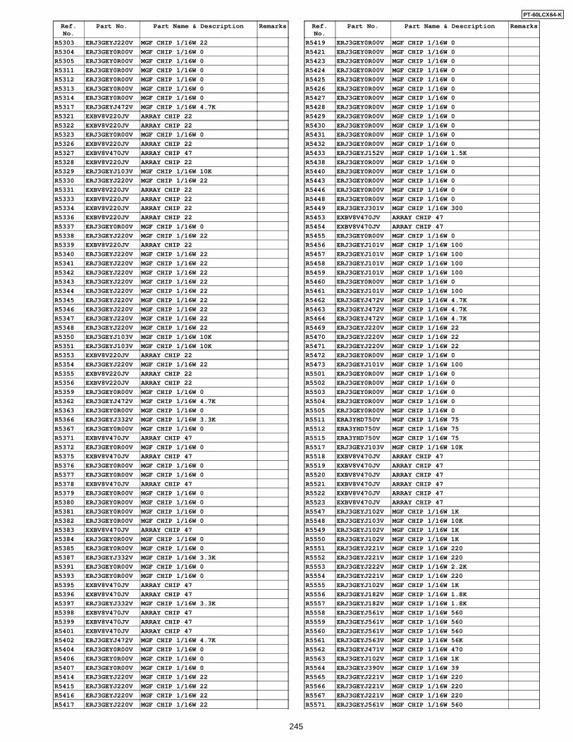
Ref.No.
Part No. Part Name & Description Remarks
R5303 ERJ3GEYJ220V MGF CHIP 1/16W 22
R5304 ERJ3GEY0R00V MGF CHIP 1/16W 0
R5305 ERJ3GEY0R00V MGF CHIP 1/16W 0
R5311 ERJ3GEY0R00V MGF CHIP 1/16W 0
R5312 ERJ3GEY0R00V MGF CHIP 1/16W 0
R5313 ERJ3GEY0R00V MGF CHIP 1/16W 0
R5314 ERJ3GEY0R00V MGF CHIP 1/16W 0
R5317 ERJ3GEYJ472V MGF CHIP 1/16W 4.7K
R5321 EXBV8V220JV ARRAY CHIP 22
R5322 EXBV8V220JV ARRAY CHIP 22
R5323 ERJ3GEY0R00V MGF CHIP 1/16W 0
R5326 EXBV8V220JV ARRAY CHIP 22
R5327 EXBV8V470JV ARRAY CHIP 47
R5328 EXBV8V220JV ARRAY CHIP 22
R5329 ERJ3GEYJ103V MGF CHIP 1/16W 10K
R5330 ERJ3GEYJ220V MGF CHIP 1/16W 22
R5331 EXBV8V220JV ARRAY CHIP 22
R5333 EXBV8V220JV ARRAY CHIP 22
R5334 EXBV8V220JV ARRAY CHIP 22
R5336 EXBV8V220JV ARRAY CHIP 22
R5337 ERJ3GEY0R00V MGF CHIP 1/16W 0
R5338 ERJ3GEYJ220V MGF CHIP 1/16W 22
R5339 EXBV8V220JV ARRAY CHIP 22
R5340 ERJ3GEYJ220V MGF CHIP 1/16W 22
R5341 ERJ3GEYJ220V MGF CHIP 1/16W 22
R5342 ERJ3GEYJ220V MGF CHIP 1/16W 22
R5343 ERJ3GEYJ220V MGF CHIP 1/16W 22
R5344 ERJ3GEYJ220V MGF CHIP 1/16W 22
R5345 ERJ3GEYJ220V MGF CHIP 1/16W 22
R5346 ERJ3GEYJ220V MGF CHIP 1/16W 22
R5347 ERJ3GEYJ220V MGF CHIP 1/16W 22
R5348 ERJ3GEYJ220V MGF CHIP 1/16W 22
R5350 ERJ3GEYJ103V MGF CHIP 1/16W 10K
R5351 ERJ3GEYJ103V MGF CHIP 1/16W 10K
R5353 EXBV8V220JV ARRAY CHIP 22
R5354 ERJ3GEYJ220V MGF CHIP 1/16W 22
R5355 EXBV8V220JV ARRAY CHIP 22
R5356 EXBV8V220JV ARRAY CHIP 22
R5359 ERJ3GEY0R00V MGF CHIP 1/16W 0
R5362 ERJ3GEYJ472V MGF CHIP 1/16W 4.7K
R5363 ERJ3GEY0R00V MGF CHIP 1/16W 0
R5366 ERJ3GEYJ332V MGF CHIP 1/16W 3.3K
R5367 ERJ3GEY0R00V MGF CHIP 1/16W 0
R5371 EXBV8V470JV ARRAY CHIP 47
R5372 ERJ3GEY0R00V MGF CHIP 1/16W 0
R5375 EXBV8V470JV ARRAY CHIP 47
R5376 ERJ3GEY0R00V MGF CHIP 1/16W 0
R5377 ERJ3GEY0R00V MGF CHIP 1/16W 0
R5378 EXBV8V470JV ARRAY CHIP 47
R5379 ERJ3GEY0R00V MGF CHIP 1/16W 0
R5380 ERJ3GEY0R00V MGF CHIP 1/16W 0
R5381 ERJ3GEY0R00V MGF CHIP 1/16W 0
R5382 ERJ3GEY0R00V MGF CHIP 1/16W 0
R5383 EXBV8V470JV ARRAY CHIP 47
R5384 ERJ3GEY0R00V MGF CHIP 1/16W 0
R5385 ERJ3GEY0R00V MGF CHIP 1/16W 0
R5387 ERJ3GEYJ332V MGF CHIP 1/16W 3.3K
R5391 ERJ3GEY0R00V MGF CHIP 1/16W 0
R5393 ERJ3GEY0R00V MGF CHIP 1/16W 0
R5395 EXBV8V470JV ARRAY CHIP 47
R5396 EXBV8V470JV ARRAY CHIP 47
R5397 ERJ3GEYJ332V MGF CHIP 1/16W 3.3K
R5398 EXBV8V470JV ARRAY CHIP 47
R5399 EXBV8V470JV ARRAY CHIP 47
R5401 EXBV8V470JV ARRAY CHIP 47
R5402 ERJ3GEYJ472V MGF CHIP 1/16W 4.7K
R5404 ERJ3GEY0R00V MGF CHIP 1/16W 0
R5406 ERJ3GEY0R00V MGF CHIP 1/16W 0
R5407 ERJ3GEY0R00V MGF CHIP 1/16W 0
R5414 ERJ3GEYJ220V MGF CHIP 1/16W 22
R5415 ERJ3GEYJ220V MGF CHIP 1/16W 22
R5416 ERJ3GEYJ220V MGF CHIP 1/16W 22
R5417 ERJ3GEYJ220V MGF CHIP 1/16W 22
Ref.No.
Part No. Part Name & Description Remarks
R5419 ERJ3GEY0R00V MGF CHIP 1/16W 0
R5421 ERJ3GEY0R00V MGF CHIP 1/16W 0
R5423 ERJ3GEY0R00V MGF CHIP 1/16W 0
R5424 ERJ3GEY0R00V MGF CHIP 1/16W 0
R5425 ERJ3GEY0R00V MGF CHIP 1/16W 0
R5426 ERJ3GEY0R00V MGF CHIP 1/16W 0
R5427 ERJ3GEY0R00V MGF CHIP 1/16W 0
R5428 ERJ3GEY0R00V MGF CHIP 1/16W 0
R5429 ERJ3GEY0R00V MGF CHIP 1/16W 0
R5430 ERJ3GEY0R00V MGF CHIP 1/16W 0
R5431 ERJ3GEY0R00V MGF CHIP 1/16W 0
R5432 ERJ3GEY0R00V MGF CHIP 1/16W 0
R5433 ERJ3GEYJ152V MGF CHIP 1/16W 1.5K
R5438 ERJ3GEY0R00V MGF CHIP 1/16W 0
R5440 ERJ3GEY0R00V MGF CHIP 1/16W 0
R5443 ERJ3GEY0R00V MGF CHIP 1/16W 0
R5446 ERJ3GEY0R00V MGF CHIP 1/16W 0
R5448 ERJ3GEY0R00V MGF CHIP 1/16W 0
R5449 ERJ3GEYJ301V MGF CHIP 1/16W 300
R5453 EXBV8V470JV ARRAY CHIP 47
R5454 EXBV8V470JV ARRAY CHIP 47
R5455 ERJ3GEY0R00V MGF CHIP 1/16W 0
R5456 ERJ3GEYJ101V MGF CHIP 1/16W 100
R5457 ERJ3GEYJ101V MGF CHIP 1/16W 100
R5458 ERJ3GEYJ101V MGF CHIP 1/16W 100
R5459 ERJ3GEYJ101V MGF CHIP 1/16W 100
R5460 ERJ3GEY0R00V MGF CHIP 1/16W 0
R5461 ERJ3GEYJ101V MGF CHIP 1/16W 100
R5462 ERJ3GEYJ472V MGF CHIP 1/16W 4.7K
R5463 ERJ3GEYJ472V MGF CHIP 1/16W 4.7K
R5464 ERJ3GEYJ472V MGF CHIP 1/16W 4.7K
R5469 ERJ3GEYJ220V MGF CHIP 1/16W 22
R5470 ERJ3GEYJ220V MGF CHIP 1/16W 22
R5471 ERJ3GEYJ220V MGF CHIP 1/16W 22
R5472 ERJ3GEY0R00V MGF CHIP 1/16W 0
R5473 ERJ3GEYJ101V MGF CHIP 1/16W 100
R5501 ERJ3GEY0R00V MGF CHIP 1/16W 0
R5502 ERJ3GEY0R00V MGF CHIP 1/16W 0
R5503 ERJ3GEY0R00V MGF CHIP 1/16W 0
R5504 ERJ3GEY0R00V MGF CHIP 1/16W 0
R5505 ERJ3GEY0R00V MGF CHIP 1/16W 0
R5511 ERA3YHD750V MGF CHIP 1/16W 75
R5512 ERA3YHD750V MGF CHIP 1/16W 75
R5515 ERA3YHD750V MGF CHIP 1/16W 75
R5517 ERJ3GEYJ103V MGF CHIP 1/16W 10K
R5518 EXBV8V470JV ARRAY CHIP 47
R5519 EXBV8V470JV ARRAY CHIP 47
R5520 EXBV8V470JV ARRAY CHIP 47
R5521 EXBV8V470JV ARRAY CHIP 47
R5522 EXBV8V470JV ARRAY CHIP 47
R5523 EXBV8V470JV ARRAY CHIP 47
R5547 ERJ3GEYJ102V MGF CHIP 1/16W 1K
R5548 ERJ3GEYJ103V MGF CHIP 1/16W 10K
R5549 ERJ3GEYJ102V MGF CHIP 1/16W 1K
R5550 ERJ3GEYJ102V MGF CHIP 1/16W 1K
R5551 ERJ3GEYJ221V MGF CHIP 1/16W 220
R5552 ERJ3GEYJ221V MGF CHIP 1/16W 220
R5553 ERJ3GEYJ222V MGF CHIP 1/16W 2.2K
R5554 ERJ3GEYJ221V MGF CHIP 1/16W 220
R5555 ERJ3GEYJ102V MGF CHIP 1/16W 1K
R5556 ERJ3GEYJ182V MGF CHIP 1/16W 1.8K
R5557 ERJ3GEYJ182V MGF CHIP 1/16W 1.8K
R5558 ERJ3GEYJ561V MGF CHIP 1/16W 560
R5559 ERJ3GEYJ561V MGF CHIP 1/16W 560
R5560 ERJ3GEYJ561V MGF CHIP 1/16W 560
R5561 ERJ3GEYJ563V MGF CHIP 1/16W 56K
R5562 ERJ3GEYJ471V MGF CHIP 1/16W 470
R5563 ERJ3GEYJ102V MGF CHIP 1/16W 1K
R5564 ERJ3GEYJ390V MGF CHIP 1/16W 39
R5565 ERJ3GEYJ221V MGF CHIP 1/16W 220
R5566 ERJ3GEYJ221V MGF CHIP 1/16W 220
R5567 ERJ3GEYJ221V MGF CHIP 1/16W 220
R5571 ERJ3GEYJ561V MGF CHIP 1/16W 560
245
PT-60LCX64-K
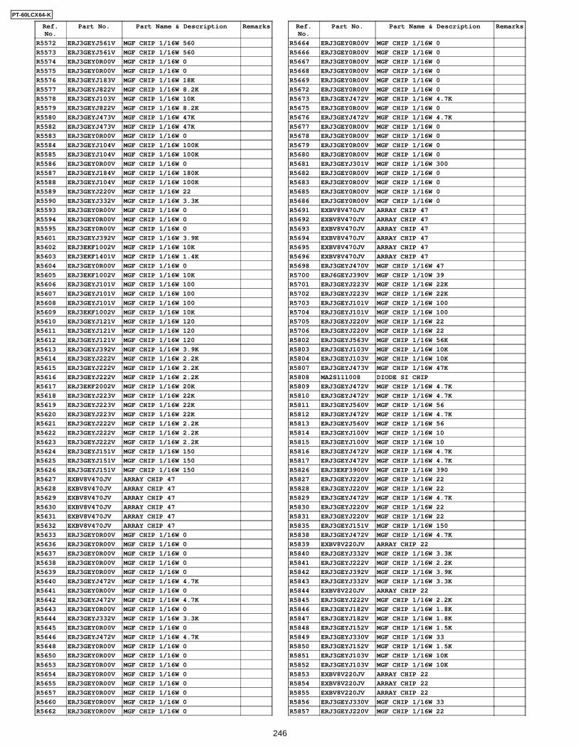
Ref.No.
Part No. Part Name & Description Remarks
R5572 ERJ3GEYJ561V MGF CHIP 1/16W 560
R5573 ERJ3GEYJ561V MGF CHIP 1/16W 560
R5574 ERJ3GEY0R00V MGF CHIP 1/16W 0
R5575 ERJ3GEY0R00V MGF CHIP 1/16W 0
R5576 ERJ3GEYJ183V MGF CHIP 1/16W 18K
R5577 ERJ3GEYJ822V MGF CHIP 1/16W 8.2K
R5578 ERJ3GEYJ103V MGF CHIP 1/16W 10K
R5579 ERJ3GEYJ822V MGF CHIP 1/16W 8.2K
R5580 ERJ3GEYJ473V MGF CHIP 1/16W 47K
R5582 ERJ3GEYJ473V MGF CHIP 1/16W 47K
R5583 ERJ3GEY0R00V MGF CHIP 1/16W 0
R5584 ERJ3GEYJ104V MGF CHIP 1/16W 100K
R5585 ERJ3GEYJ104V MGF CHIP 1/16W 100K
R5586 ERJ3GEY0R00V MGF CHIP 1/16W 0
R5587 ERJ3GEYJ184V MGF CHIP 1/16W 180K
R5588 ERJ3GEYJ104V MGF CHIP 1/16W 100K
R5589 ERJ3GEYJ220V MGF CHIP 1/16W 22
R5590 ERJ3GEYJ332V MGF CHIP 1/16W 3.3K
R5593 ERJ3GEY0R00V MGF CHIP 1/16W 0
R5594 ERJ3GEY0R00V MGF CHIP 1/16W 0
R5595 ERJ3GEY0R00V MGF CHIP 1/16W 0
R5601 ERJ3GEYJ392V MGF CHIP 1/16W 3.9K
R5602 ERJ3EKF1002V MGF CHIP 1/16W 10K
R5603 ERJ3EKF1401V MGF CHIP 1/16W 1.4K
R5604 ERJ3GEY0R00V MGF CHIP 1/16W 0
R5605 ERJ3EKF1002V MGF CHIP 1/16W 10K
R5606 ERJ3GEYJ101V MGF CHIP 1/16W 100
R5607 ERJ3GEYJ101V MGF CHIP 1/16W 100
R5608 ERJ3GEYJ101V MGF CHIP 1/16W 100
R5609 ERJ3EKF1002V MGF CHIP 1/16W 10K
R5610 ERJ3GEYJ121V MGF CHIP 1/16W 120
R5611 ERJ3GEYJ121V MGF CHIP 1/16W 120
R5612 ERJ3GEYJ121V MGF CHIP 1/16W 120
R5613 ERJ3GEYJ392V MGF CHIP 1/16W 3.9K
R5614 ERJ3GEYJ222V MGF CHIP 1/16W 2.2K
R5615 ERJ3GEYJ222V MGF CHIP 1/16W 2.2K
R5616 ERJ3GEYJ222V MGF CHIP 1/16W 2.2K
R5617 ERJ3EKF2002V MGF CHIP 1/16W 20K
R5618 ERJ3GEYJ223V MGF CHIP 1/16W 22K
R5619 ERJ3GEYJ223V MGF CHIP 1/16W 22K
R5620 ERJ3GEYJ223V MGF CHIP 1/16W 22K
R5621 ERJ3GEYJ222V MGF CHIP 1/16W 2.2K
R5622 ERJ3GEYJ222V MGF CHIP 1/16W 2.2K
R5623 ERJ3GEYJ222V MGF CHIP 1/16W 2.2K
R5624 ERJ3GEYJ151V MGF CHIP 1/16W 150
R5625 ERJ3GEYJ151V MGF CHIP 1/16W 150
R5626 ERJ3GEYJ151V MGF CHIP 1/16W 150
R5627 EXBV8V470JV ARRAY CHIP 47
R5628 EXBV8V470JV ARRAY CHIP 47
R5629 EXBV8V470JV ARRAY CHIP 47
R5630 EXBV8V470JV ARRAY CHIP 47
R5631 EXBV8V470JV ARRAY CHIP 47
R5632 EXBV8V470JV ARRAY CHIP 47
R5633 ERJ3GEY0R00V MGF CHIP 1/16W 0
R5636 ERJ3GEY0R00V MGF CHIP 1/16W 0
R5637 ERJ3GEY0R00V MGF CHIP 1/16W 0
R5638 ERJ3GEY0R00V MGF CHIP 1/16W 0
R5639 ERJ3GEY0R00V MGF CHIP 1/16W 0
R5640 ERJ3GEYJ472V MGF CHIP 1/16W 4.7K
R5641 ERJ3GEY0R00V MGF CHIP 1/16W 0
R5642 ERJ3GEYJ472V MGF CHIP 1/16W 4.7K
R5643 ERJ3GEY0R00V MGF CHIP 1/16W 0
R5644 ERJ3GEYJ332V MGF CHIP 1/16W 3.3K
R5645 ERJ3GEY0R00V MGF CHIP 1/16W 0
R5646 ERJ3GEYJ472V MGF CHIP 1/16W 4.7K
R5648 ERJ3GEY0R00V MGF CHIP 1/16W 0
R5650 ERJ3GEY0R00V MGF CHIP 1/16W 0
R5653 ERJ3GEY0R00V MGF CHIP 1/16W 0
R5654 ERJ3GEY0R00V MGF CHIP 1/16W 0
R5655 ERJ3GEY0R00V MGF CHIP 1/16W 0
R5657 ERJ3GEY0R00V MGF CHIP 1/16W 0
R5660 ERJ3GEY0R00V MGF CHIP 1/16W 0
R5662 ERJ3GEY0R00V MGF CHIP 1/16W 0
Ref.No.
Part No. Part Name & Description Remarks
R5664 ERJ3GEY0R00V MGF CHIP 1/16W 0
R5666 ERJ3GEY0R00V MGF CHIP 1/16W 0
R5667 ERJ3GEY0R00V MGF CHIP 1/16W 0
R5668 ERJ3GEY0R00V MGF CHIP 1/16W 0
R5669 ERJ3GEY0R00V MGF CHIP 1/16W 0
R5672 ERJ3GEY0R00V MGF CHIP 1/16W 0
R5673 ERJ3GEYJ472V MGF CHIP 1/16W 4.7K
R5675 ERJ3GEY0R00V MGF CHIP 1/16W 0
R5676 ERJ3GEYJ472V MGF CHIP 1/16W 4.7K
R5677 ERJ3GEY0R00V MGF CHIP 1/16W 0
R5678 ERJ3GEY0R00V MGF CHIP 1/16W 0
R5679 ERJ3GEY0R00V MGF CHIP 1/16W 0
R5680 ERJ3GEY0R00V MGF CHIP 1/16W 0
R5681 ERJ3GEYJ301V MGF CHIP 1/16W 300
R5682 ERJ3GEY0R00V MGF CHIP 1/16W 0
R5683 ERJ3GEY0R00V MGF CHIP 1/16W 0
R5685 ERJ3GEY0R00V MGF CHIP 1/16W 0
R5686 ERJ3GEY0R00V MGF CHIP 1/16W 0
R5691 EXBV8V470JV ARRAY CHIP 47
R5692 EXBV8V470JV ARRAY CHIP 47
R5693 EXBV8V470JV ARRAY CHIP 47
R5694 EXBV8V470JV ARRAY CHIP 47
R5695 EXBV8V470JV ARRAY CHIP 47
R5696 EXBV8V470JV ARRAY CHIP 47
R5698 ERJ3GEYJ470V MGF CHIP 1/16W 47
R5700 ERJ6GEYJ390V MGF CHIP 1/10W 39
R5701 ERJ3GEYJ223V MGF CHIP 1/16W 22K
R5702 ERJ3GEYJ223V MGF CHIP 1/16W 22K
R5703 ERJ3GEYJ101V MGF CHIP 1/16W 100
R5704 ERJ3GEYJ101V MGF CHIP 1/16W 100
R5705 ERJ3GEYJ220V MGF CHIP 1/16W 22
R5706 ERJ3GEYJ220V MGF CHIP 1/16W 22
R5802 ERJ3GEYJ563V MGF CHIP 1/16W 56K
R5803 ERJ3GEYJ103V MGF CHIP 1/16W 10K
R5804 ERJ3GEYJ103V MGF CHIP 1/16W 10K
R5807 ERJ3GEYJ473V MGF CHIP 1/16W 47K
R5808 MA2S111008 DIODE SI CHIP
R5809 ERJ3GEYJ472V MGF CHIP 1/16W 4.7K
R5810 ERJ3GEYJ472V MGF CHIP 1/16W 4.7K
R5811 ERJ3GEYJ560V MGF CHIP 1/16W 56
R5812 ERJ3GEYJ472V MGF CHIP 1/16W 4.7K
R5813 ERJ3GEYJ560V MGF CHIP 1/16W 56
R5814 ERJ3GEYJ100V MGF CHIP 1/16W 10
R5815 ERJ3GEYJ100V MGF CHIP 1/16W 10
R5816 ERJ3GEYJ472V MGF CHIP 1/16W 4.7K
R5817 ERJ3GEYJ472V MGF CHIP 1/16W 4.7K
R5826 ERJ3EKF3900V MGF CHIP 1/16W 390
R5827 ERJ3GEYJ220V MGF CHIP 1/16W 22
R5828 ERJ3GEYJ220V MGF CHIP 1/16W 22
R5829 ERJ3GEYJ472V MGF CHIP 1/16W 4.7K
R5830 ERJ3GEYJ220V MGF CHIP 1/16W 22
R5831 ERJ3GEYJ220V MGF CHIP 1/16W 22
R5835 ERJ3GEYJ151V MGF CHIP 1/16W 150
R5838 ERJ3GEYJ472V MGF CHIP 1/16W 4.7K
R5839 EXBV8V220JV ARRAY CHIP 22
R5840 ERJ3GEYJ332V MGF CHIP 1/16W 3.3K
R5841 ERJ3GEYJ222V MGF CHIP 1/16W 2.2K
R5842 ERJ3GEYJ392V MGF CHIP 1/16W 3.9K
R5843 ERJ3GEYJ332V MGF CHIP 1/16W 3.3K
R5844 EXBV8V220JV ARRAY CHIP 22
R5845 ERJ3GEYJ222V MGF CHIP 1/16W 2.2K
R5846 ERJ3GEYJ182V MGF CHIP 1/16W 1.8K
R5847 ERJ3GEYJ182V MGF CHIP 1/16W 1.8K
R5848 ERJ3GEYJ152V MGF CHIP 1/16W 1.5K
R5849 ERJ3GEYJ330V MGF CHIP 1/16W 33
R5850 ERJ3GEYJ152V MGF CHIP 1/16W 1.5K
R5851 ERJ3GEYJ103V MGF CHIP 1/16W 10K
R5852 ERJ3GEYJ103V MGF CHIP 1/16W 10K
R5853 EXBV8V220JV ARRAY CHIP 22
R5854 EXBV8V220JV ARRAY CHIP 22
R5855 EXBV8V220JV ARRAY CHIP 22
R5856 ERJ3GEYJ330V MGF CHIP 1/16W 33
R5857 ERJ3GEYJ220V MGF CHIP 1/16W 22
246
PT-60LCX64-K
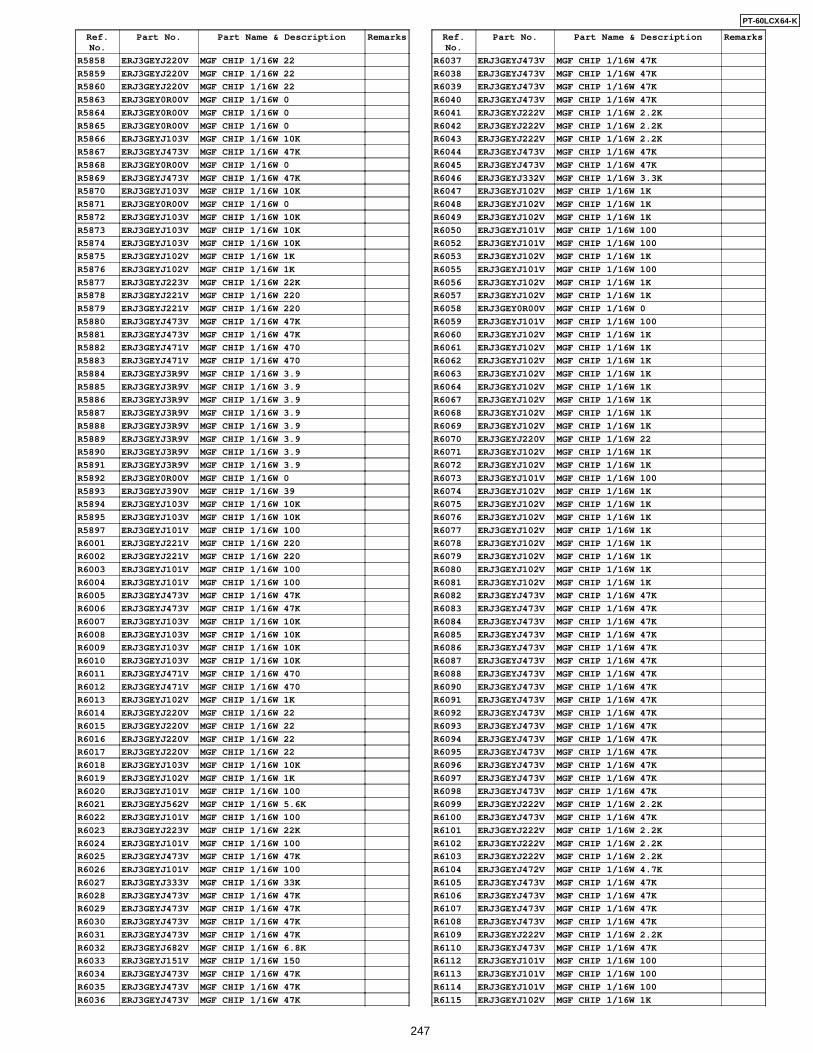
Ref.No.
Part No. Part Name & Description Remarks
R5858 ERJ3GEYJ220V MGF CHIP 1/16W 22
R5859 ERJ3GEYJ220V MGF CHIP 1/16W 22
R5860 ERJ3GEYJ220V MGF CHIP 1/16W 22
R5863 ERJ3GEY0R00V MGF CHIP 1/16W 0
R5864 ERJ3GEY0R00V MGF CHIP 1/16W 0
R5865 ERJ3GEY0R00V MGF CHIP 1/16W 0
R5866 ERJ3GEYJ103V MGF CHIP 1/16W 10K
R5867 ERJ3GEYJ473V MGF CHIP 1/16W 47K
R5868 ERJ3GEY0R00V MGF CHIP 1/16W 0
R5869 ERJ3GEYJ473V MGF CHIP 1/16W 47K
R5870 ERJ3GEYJ103V MGF CHIP 1/16W 10K
R5871 ERJ3GEY0R00V MGF CHIP 1/16W 0
R5872 ERJ3GEYJ103V MGF CHIP 1/16W 10K
R5873 ERJ3GEYJ103V MGF CHIP 1/16W 10K
R5874 ERJ3GEYJ103V MGF CHIP 1/16W 10K
R5875 ERJ3GEYJ102V MGF CHIP 1/16W 1K
R5876 ERJ3GEYJ102V MGF CHIP 1/16W 1K
R5877 ERJ3GEYJ223V MGF CHIP 1/16W 22K
R5878 ERJ3GEYJ221V MGF CHIP 1/16W 220
R5879 ERJ3GEYJ221V MGF CHIP 1/16W 220
R5880 ERJ3GEYJ473V MGF CHIP 1/16W 47K
R5881 ERJ3GEYJ473V MGF CHIP 1/16W 47K
R5882 ERJ3GEYJ471V MGF CHIP 1/16W 470
R5883 ERJ3GEYJ471V MGF CHIP 1/16W 470
R5884 ERJ3GEYJ3R9V MGF CHIP 1/16W 3.9
R5885 ERJ3GEYJ3R9V MGF CHIP 1/16W 3.9
R5886 ERJ3GEYJ3R9V MGF CHIP 1/16W 3.9
R5887 ERJ3GEYJ3R9V MGF CHIP 1/16W 3.9
R5888 ERJ3GEYJ3R9V MGF CHIP 1/16W 3.9
R5889 ERJ3GEYJ3R9V MGF CHIP 1/16W 3.9
R5890 ERJ3GEYJ3R9V MGF CHIP 1/16W 3.9
R5891 ERJ3GEYJ3R9V MGF CHIP 1/16W 3.9
R5892 ERJ3GEY0R00V MGF CHIP 1/16W 0
R5893 ERJ3GEYJ390V MGF CHIP 1/16W 39
R5894 ERJ3GEYJ103V MGF CHIP 1/16W 10K
R5895 ERJ3GEYJ103V MGF CHIP 1/16W 10K
R5897 ERJ3GEYJ101V MGF CHIP 1/16W 100
R6001 ERJ3GEYJ221V MGF CHIP 1/16W 220
R6002 ERJ3GEYJ221V MGF CHIP 1/16W 220
R6003 ERJ3GEYJ101V MGF CHIP 1/16W 100
R6004 ERJ3GEYJ101V MGF CHIP 1/16W 100
R6005 ERJ3GEYJ473V MGF CHIP 1/16W 47K
R6006 ERJ3GEYJ473V MGF CHIP 1/16W 47K
R6007 ERJ3GEYJ103V MGF CHIP 1/16W 10K
R6008 ERJ3GEYJ103V MGF CHIP 1/16W 10K
R6009 ERJ3GEYJ103V MGF CHIP 1/16W 10K
R6010 ERJ3GEYJ103V MGF CHIP 1/16W 10K
R6011 ERJ3GEYJ471V MGF CHIP 1/16W 470
R6012 ERJ3GEYJ471V MGF CHIP 1/16W 470
R6013 ERJ3GEYJ102V MGF CHIP 1/16W 1K
R6014 ERJ3GEYJ220V MGF CHIP 1/16W 22
R6015 ERJ3GEYJ220V MGF CHIP 1/16W 22
R6016 ERJ3GEYJ220V MGF CHIP 1/16W 22
R6017 ERJ3GEYJ220V MGF CHIP 1/16W 22
R6018 ERJ3GEYJ103V MGF CHIP 1/16W 10K
R6019 ERJ3GEYJ102V MGF CHIP 1/16W 1K
R6020 ERJ3GEYJ101V MGF CHIP 1/16W 100
R6021 ERJ3GEYJ562V MGF CHIP 1/16W 5.6K
R6022 ERJ3GEYJ101V MGF CHIP 1/16W 100
R6023 ERJ3GEYJ223V MGF CHIP 1/16W 22K
R6024 ERJ3GEYJ101V MGF CHIP 1/16W 100
R6025 ERJ3GEYJ473V MGF CHIP 1/16W 47K
R6026 ERJ3GEYJ101V MGF CHIP 1/16W 100
R6027 ERJ3GEYJ333V MGF CHIP 1/16W 33K
R6028 ERJ3GEYJ473V MGF CHIP 1/16W 47K
R6029 ERJ3GEYJ473V MGF CHIP 1/16W 47K
R6030 ERJ3GEYJ473V MGF CHIP 1/16W 47K
R6031 ERJ3GEYJ473V MGF CHIP 1/16W 47K
R6032 ERJ3GEYJ682V MGF CHIP 1/16W 6.8K
R6033 ERJ3GEYJ151V MGF CHIP 1/16W 150
R6034 ERJ3GEYJ473V MGF CHIP 1/16W 47K
R6035 ERJ3GEYJ473V MGF CHIP 1/16W 47K
R6036 ERJ3GEYJ473V MGF CHIP 1/16W 47K
Ref.No.
Part No. Part Name & Description Remarks
R6037 ERJ3GEYJ473V MGF CHIP 1/16W 47K
R6038 ERJ3GEYJ473V MGF CHIP 1/16W 47K
R6039 ERJ3GEYJ473V MGF CHIP 1/16W 47K
R6040 ERJ3GEYJ473V MGF CHIP 1/16W 47K
R6041 ERJ3GEYJ222V MGF CHIP 1/16W 2.2K
R6042 ERJ3GEYJ222V MGF CHIP 1/16W 2.2K
R6043 ERJ3GEYJ222V MGF CHIP 1/16W 2.2K
R6044 ERJ3GEYJ473V MGF CHIP 1/16W 47K
R6045 ERJ3GEYJ473V MGF CHIP 1/16W 47K
R6046 ERJ3GEYJ332V MGF CHIP 1/16W 3.3K
R6047 ERJ3GEYJ102V MGF CHIP 1/16W 1K
R6048 ERJ3GEYJ102V MGF CHIP 1/16W 1K
R6049 ERJ3GEYJ102V MGF CHIP 1/16W 1K
R6050 ERJ3GEYJ101V MGF CHIP 1/16W 100
R6052 ERJ3GEYJ101V MGF CHIP 1/16W 100
R6053 ERJ3GEYJ102V MGF CHIP 1/16W 1K
R6055 ERJ3GEYJ101V MGF CHIP 1/16W 100
R6056 ERJ3GEYJ102V MGF CHIP 1/16W 1K
R6057 ERJ3GEYJ102V MGF CHIP 1/16W 1K
R6058 ERJ3GEY0R00V MGF CHIP 1/16W 0
R6059 ERJ3GEYJ101V MGF CHIP 1/16W 100
R6060 ERJ3GEYJ102V MGF CHIP 1/16W 1K
R6061 ERJ3GEYJ102V MGF CHIP 1/16W 1K
R6062 ERJ3GEYJ102V MGF CHIP 1/16W 1K
R6063 ERJ3GEYJ102V MGF CHIP 1/16W 1K
R6064 ERJ3GEYJ102V MGF CHIP 1/16W 1K
R6067 ERJ3GEYJ102V MGF CHIP 1/16W 1K
R6068 ERJ3GEYJ102V MGF CHIP 1/16W 1K
R6069 ERJ3GEYJ102V MGF CHIP 1/16W 1K
R6070 ERJ3GEYJ220V MGF CHIP 1/16W 22
R6071 ERJ3GEYJ102V MGF CHIP 1/16W 1K
R6072 ERJ3GEYJ102V MGF CHIP 1/16W 1K
R6073 ERJ3GEYJ101V MGF CHIP 1/16W 100
R6074 ERJ3GEYJ102V MGF CHIP 1/16W 1K
R6075 ERJ3GEYJ102V MGF CHIP 1/16W 1K
R6076 ERJ3GEYJ102V MGF CHIP 1/16W 1K
R6077 ERJ3GEYJ102V MGF CHIP 1/16W 1K
R6078 ERJ3GEYJ102V MGF CHIP 1/16W 1K
R6079 ERJ3GEYJ102V MGF CHIP 1/16W 1K
R6080 ERJ3GEYJ102V MGF CHIP 1/16W 1K
R6081 ERJ3GEYJ102V MGF CHIP 1/16W 1K
R6082 ERJ3GEYJ473V MGF CHIP 1/16W 47K
R6083 ERJ3GEYJ473V MGF CHIP 1/16W 47K
R6084 ERJ3GEYJ473V MGF CHIP 1/16W 47K
R6085 ERJ3GEYJ473V MGF CHIP 1/16W 47K
R6086 ERJ3GEYJ473V MGF CHIP 1/16W 47K
R6087 ERJ3GEYJ473V MGF CHIP 1/16W 47K
R6088 ERJ3GEYJ473V MGF CHIP 1/16W 47K
R6090 ERJ3GEYJ473V MGF CHIP 1/16W 47K
R6091 ERJ3GEYJ473V MGF CHIP 1/16W 47K
R6092 ERJ3GEYJ473V MGF CHIP 1/16W 47K
R6093 ERJ3GEYJ473V MGF CHIP 1/16W 47K
R6094 ERJ3GEYJ473V MGF CHIP 1/16W 47K
R6095 ERJ3GEYJ473V MGF CHIP 1/16W 47K
R6096 ERJ3GEYJ473V MGF CHIP 1/16W 47K
R6097 ERJ3GEYJ473V MGF CHIP 1/16W 47K
R6098 ERJ3GEYJ473V MGF CHIP 1/16W 47K
R6099 ERJ3GEYJ222V MGF CHIP 1/16W 2.2K
R6100 ERJ3GEYJ473V MGF CHIP 1/16W 47K
R6101 ERJ3GEYJ222V MGF CHIP 1/16W 2.2K
R6102 ERJ3GEYJ222V MGF CHIP 1/16W 2.2K
R6103 ERJ3GEYJ222V MGF CHIP 1/16W 2.2K
R6104 ERJ3GEYJ472V MGF CHIP 1/16W 4.7K
R6105 ERJ3GEYJ473V MGF CHIP 1/16W 47K
R6106 ERJ3GEYJ473V MGF CHIP 1/16W 47K
R6107 ERJ3GEYJ473V MGF CHIP 1/16W 47K
R6108 ERJ3GEYJ473V MGF CHIP 1/16W 47K
R6109 ERJ3GEYJ222V MGF CHIP 1/16W 2.2K
R6110 ERJ3GEYJ473V MGF CHIP 1/16W 47K
R6112 ERJ3GEYJ101V MGF CHIP 1/16W 100
R6113 ERJ3GEYJ101V MGF CHIP 1/16W 100
R6114 ERJ3GEYJ101V MGF CHIP 1/16W 100
R6115 ERJ3GEYJ102V MGF CHIP 1/16W 1K
247
PT-60LCX64-K
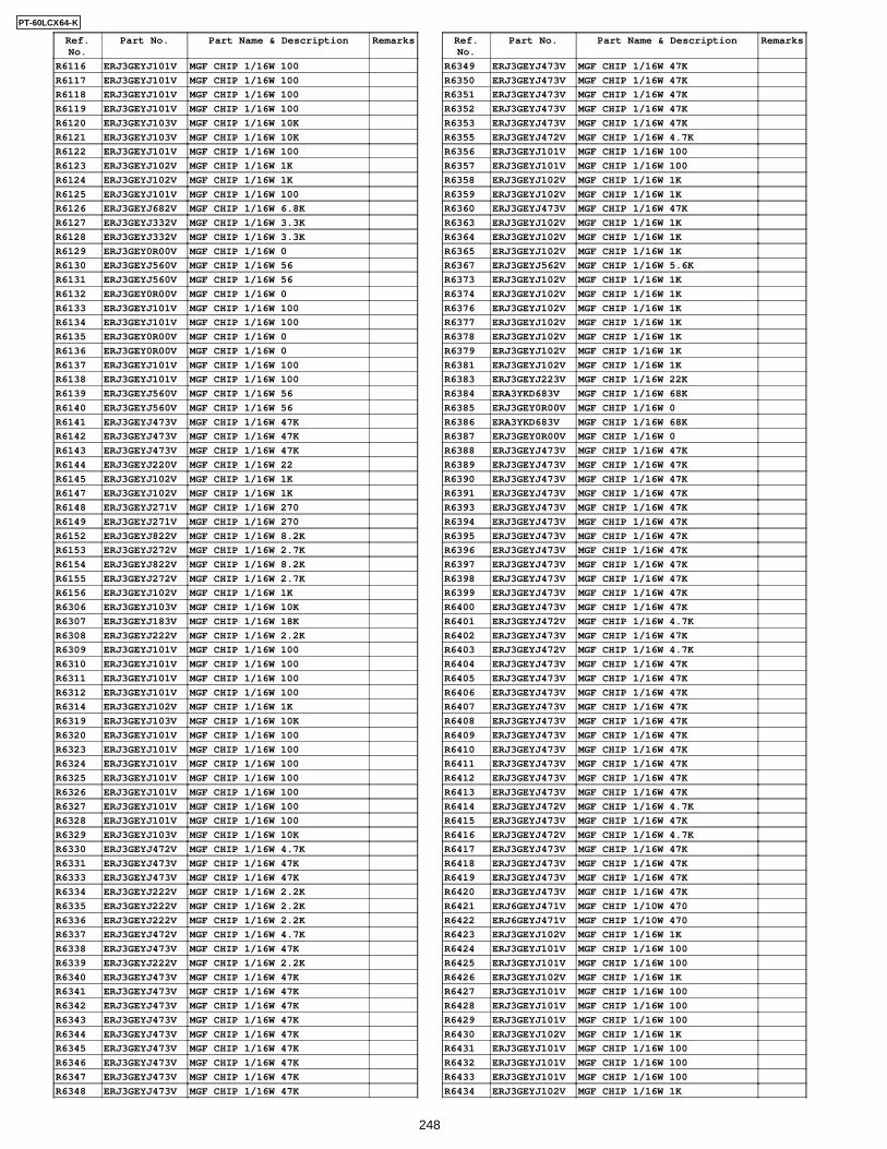
Ref.No.
Part No. Part Name & Description Remarks
R6116 ERJ3GEYJ101V MGF CHIP 1/16W 100
R6117 ERJ3GEYJ101V MGF CHIP 1/16W 100
R6118 ERJ3GEYJ101V MGF CHIP 1/16W 100
R6119 ERJ3GEYJ101V MGF CHIP 1/16W 100
R6120 ERJ3GEYJ103V MGF CHIP 1/16W 10K
R6121 ERJ3GEYJ103V MGF CHIP 1/16W 10K
R6122 ERJ3GEYJ101V MGF CHIP 1/16W 100
R6123 ERJ3GEYJ102V MGF CHIP 1/16W 1K
R6124 ERJ3GEYJ102V MGF CHIP 1/16W 1K
R6125 ERJ3GEYJ101V MGF CHIP 1/16W 100
R6126 ERJ3GEYJ682V MGF CHIP 1/16W 6.8K
R6127 ERJ3GEYJ332V MGF CHIP 1/16W 3.3K
R6128 ERJ3GEYJ332V MGF CHIP 1/16W 3.3K
R6129 ERJ3GEY0R00V MGF CHIP 1/16W 0
R6130 ERJ3GEYJ560V MGF CHIP 1/16W 56
R6131 ERJ3GEYJ560V MGF CHIP 1/16W 56
R6132 ERJ3GEY0R00V MGF CHIP 1/16W 0
R6133 ERJ3GEYJ101V MGF CHIP 1/16W 100
R6134 ERJ3GEYJ101V MGF CHIP 1/16W 100
R6135 ERJ3GEY0R00V MGF CHIP 1/16W 0
R6136 ERJ3GEY0R00V MGF CHIP 1/16W 0
R6137 ERJ3GEYJ101V MGF CHIP 1/16W 100
R6138 ERJ3GEYJ101V MGF CHIP 1/16W 100
R6139 ERJ3GEYJ560V MGF CHIP 1/16W 56
R6140 ERJ3GEYJ560V MGF CHIP 1/16W 56
R6141 ERJ3GEYJ473V MGF CHIP 1/16W 47K
R6142 ERJ3GEYJ473V MGF CHIP 1/16W 47K
R6143 ERJ3GEYJ473V MGF CHIP 1/16W 47K
R6144 ERJ3GEYJ220V MGF CHIP 1/16W 22
R6145 ERJ3GEYJ102V MGF CHIP 1/16W 1K
R6147 ERJ3GEYJ102V MGF CHIP 1/16W 1K
R6148 ERJ3GEYJ271V MGF CHIP 1/16W 270
R6149 ERJ3GEYJ271V MGF CHIP 1/16W 270
R6152 ERJ3GEYJ822V MGF CHIP 1/16W 8.2K
R6153 ERJ3GEYJ272V MGF CHIP 1/16W 2.7K
R6154 ERJ3GEYJ822V MGF CHIP 1/16W 8.2K
R6155 ERJ3GEYJ272V MGF CHIP 1/16W 2.7K
R6156 ERJ3GEYJ102V MGF CHIP 1/16W 1K
R6306 ERJ3GEYJ103V MGF CHIP 1/16W 10K
R6307 ERJ3GEYJ183V MGF CHIP 1/16W 18K
R6308 ERJ3GEYJ222V MGF CHIP 1/16W 2.2K
R6309 ERJ3GEYJ101V MGF CHIP 1/16W 100
R6310 ERJ3GEYJ101V MGF CHIP 1/16W 100
R6311 ERJ3GEYJ101V MGF CHIP 1/16W 100
R6312 ERJ3GEYJ101V MGF CHIP 1/16W 100
R6314 ERJ3GEYJ102V MGF CHIP 1/16W 1K
R6319 ERJ3GEYJ103V MGF CHIP 1/16W 10K
R6320 ERJ3GEYJ101V MGF CHIP 1/16W 100
R6323 ERJ3GEYJ101V MGF CHIP 1/16W 100
R6324 ERJ3GEYJ101V MGF CHIP 1/16W 100
R6325 ERJ3GEYJ101V MGF CHIP 1/16W 100
R6326 ERJ3GEYJ101V MGF CHIP 1/16W 100
R6327 ERJ3GEYJ101V MGF CHIP 1/16W 100
R6328 ERJ3GEYJ101V MGF CHIP 1/16W 100
R6329 ERJ3GEYJ103V MGF CHIP 1/16W 10K
R6330 ERJ3GEYJ472V MGF CHIP 1/16W 4.7K
R6331 ERJ3GEYJ473V MGF CHIP 1/16W 47K
R6333 ERJ3GEYJ473V MGF CHIP 1/16W 47K
R6334 ERJ3GEYJ222V MGF CHIP 1/16W 2.2K
R6335 ERJ3GEYJ222V MGF CHIP 1/16W 2.2K
R6336 ERJ3GEYJ222V MGF CHIP 1/16W 2.2K
R6337 ERJ3GEYJ472V MGF CHIP 1/16W 4.7K
R6338 ERJ3GEYJ473V MGF CHIP 1/16W 47K
R6339 ERJ3GEYJ222V MGF CHIP 1/16W 2.2K
R6340 ERJ3GEYJ473V MGF CHIP 1/16W 47K
R6341 ERJ3GEYJ473V MGF CHIP 1/16W 47K
R6342 ERJ3GEYJ473V MGF CHIP 1/16W 47K
R6343 ERJ3GEYJ473V MGF CHIP 1/16W 47K
R6344 ERJ3GEYJ473V MGF CHIP 1/16W 47K
R6345 ERJ3GEYJ473V MGF CHIP 1/16W 47K
R6346 ERJ3GEYJ473V MGF CHIP 1/16W 47K
R6347 ERJ3GEYJ473V MGF CHIP 1/16W 47K
R6348 ERJ3GEYJ473V MGF CHIP 1/16W 47K
Ref.No.
Part No. Part Name & Description Remarks
R6349 ERJ3GEYJ473V MGF CHIP 1/16W 47K
R6350 ERJ3GEYJ473V MGF CHIP 1/16W 47K
R6351 ERJ3GEYJ473V MGF CHIP 1/16W 47K
R6352 ERJ3GEYJ473V MGF CHIP 1/16W 47K
R6353 ERJ3GEYJ473V MGF CHIP 1/16W 47K
R6355 ERJ3GEYJ472V MGF CHIP 1/16W 4.7K
R6356 ERJ3GEYJ101V MGF CHIP 1/16W 100
R6357 ERJ3GEYJ101V MGF CHIP 1/16W 100
R6358 ERJ3GEYJ102V MGF CHIP 1/16W 1K
R6359 ERJ3GEYJ102V MGF CHIP 1/16W 1K
R6360 ERJ3GEYJ473V MGF CHIP 1/16W 47K
R6363 ERJ3GEYJ102V MGF CHIP 1/16W 1K
R6364 ERJ3GEYJ102V MGF CHIP 1/16W 1K
R6365 ERJ3GEYJ102V MGF CHIP 1/16W 1K
R6367 ERJ3GEYJ562V MGF CHIP 1/16W 5.6K
R6373 ERJ3GEYJ102V MGF CHIP 1/16W 1K
R6374 ERJ3GEYJ102V MGF CHIP 1/16W 1K
R6376 ERJ3GEYJ102V MGF CHIP 1/16W 1K
R6377 ERJ3GEYJ102V MGF CHIP 1/16W 1K
R6378 ERJ3GEYJ102V MGF CHIP 1/16W 1K
R6379 ERJ3GEYJ102V MGF CHIP 1/16W 1K
R6381 ERJ3GEYJ102V MGF CHIP 1/16W 1K
R6383 ERJ3GEYJ223V MGF CHIP 1/16W 22K
R6384 ERA3YKD683V MGF CHIP 1/16W 68K
R6385 ERJ3GEY0R00V MGF CHIP 1/16W 0
R6386 ERA3YKD683V MGF CHIP 1/16W 68K
R6387 ERJ3GEY0R00V MGF CHIP 1/16W 0
R6388 ERJ3GEYJ473V MGF CHIP 1/16W 47K
R6389 ERJ3GEYJ473V MGF CHIP 1/16W 47K
R6390 ERJ3GEYJ473V MGF CHIP 1/16W 47K
R6391 ERJ3GEYJ473V MGF CHIP 1/16W 47K
R6393 ERJ3GEYJ473V MGF CHIP 1/16W 47K
R6394 ERJ3GEYJ473V MGF CHIP 1/16W 47K
R6395 ERJ3GEYJ473V MGF CHIP 1/16W 47K
R6396 ERJ3GEYJ473V MGF CHIP 1/16W 47K
R6397 ERJ3GEYJ473V MGF CHIP 1/16W 47K
R6398 ERJ3GEYJ473V MGF CHIP 1/16W 47K
R6399 ERJ3GEYJ473V MGF CHIP 1/16W 47K
R6400 ERJ3GEYJ473V MGF CHIP 1/16W 47K
R6401 ERJ3GEYJ472V MGF CHIP 1/16W 4.7K
R6402 ERJ3GEYJ473V MGF CHIP 1/16W 47K
R6403 ERJ3GEYJ472V MGF CHIP 1/16W 4.7K
R6404 ERJ3GEYJ473V MGF CHIP 1/16W 47K
R6405 ERJ3GEYJ473V MGF CHIP 1/16W 47K
R6406 ERJ3GEYJ473V MGF CHIP 1/16W 47K
R6407 ERJ3GEYJ473V MGF CHIP 1/16W 47K
R6408 ERJ3GEYJ473V MGF CHIP 1/16W 47K
R6409 ERJ3GEYJ473V MGF CHIP 1/16W 47K
R6410 ERJ3GEYJ473V MGF CHIP 1/16W 47K
R6411 ERJ3GEYJ473V MGF CHIP 1/16W 47K
R6412 ERJ3GEYJ473V MGF CHIP 1/16W 47K
R6413 ERJ3GEYJ473V MGF CHIP 1/16W 47K
R6414 ERJ3GEYJ472V MGF CHIP 1/16W 4.7K
R6415 ERJ3GEYJ473V MGF CHIP 1/16W 47K
R6416 ERJ3GEYJ472V MGF CHIP 1/16W 4.7K
R6417 ERJ3GEYJ473V MGF CHIP 1/16W 47K
R6418 ERJ3GEYJ473V MGF CHIP 1/16W 47K
R6419 ERJ3GEYJ473V MGF CHIP 1/16W 47K
R6420 ERJ3GEYJ473V MGF CHIP 1/16W 47K
R6421 ERJ6GEYJ471V MGF CHIP 1/10W 470
R6422 ERJ6GEYJ471V MGF CHIP 1/10W 470
R6423 ERJ3GEYJ102V MGF CHIP 1/16W 1K
R6424 ERJ3GEYJ101V MGF CHIP 1/16W 100
R6425 ERJ3GEYJ101V MGF CHIP 1/16W 100
R6426 ERJ3GEYJ102V MGF CHIP 1/16W 1K
R6427 ERJ3GEYJ101V MGF CHIP 1/16W 100
R6428 ERJ3GEYJ101V MGF CHIP 1/16W 100
R6429 ERJ3GEYJ101V MGF CHIP 1/16W 100
R6430 ERJ3GEYJ102V MGF CHIP 1/16W 1K
R6431 ERJ3GEYJ101V MGF CHIP 1/16W 100
R6432 ERJ3GEYJ101V MGF CHIP 1/16W 100
R6433 ERJ3GEYJ101V MGF CHIP 1/16W 100
R6434 ERJ3GEYJ102V MGF CHIP 1/16W 1K
248
PT-60LCX64-K
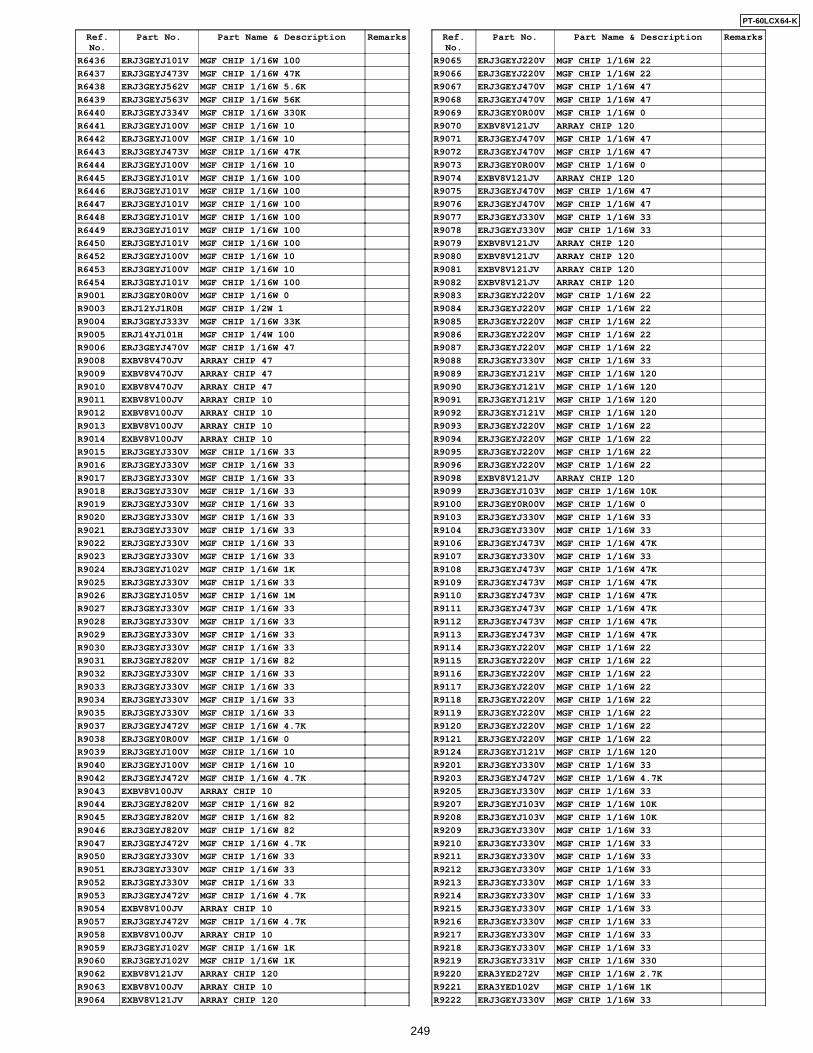
Ref.No.
Part No. Part Name & Description Remarks
R6436 ERJ3GEYJ101V MGF CHIP 1/16W 100
R6437 ERJ3GEYJ473V MGF CHIP 1/16W 47K
R6438 ERJ3GEYJ562V MGF CHIP 1/16W 5.6K
R6439 ERJ3GEYJ563V MGF CHIP 1/16W 56K
R6440 ERJ3GEYJ334V MGF CHIP 1/16W 330K
R6441 ERJ3GEYJ100V MGF CHIP 1/16W 10
R6442 ERJ3GEYJ100V MGF CHIP 1/16W 10
R6443 ERJ3GEYJ473V MGF CHIP 1/16W 47K
R6444 ERJ3GEYJ100V MGF CHIP 1/16W 10
R6445 ERJ3GEYJ101V MGF CHIP 1/16W 100
R6446 ERJ3GEYJ101V MGF CHIP 1/16W 100
R6447 ERJ3GEYJ101V MGF CHIP 1/16W 100
R6448 ERJ3GEYJ101V MGF CHIP 1/16W 100
R6449 ERJ3GEYJ101V MGF CHIP 1/16W 100
R6450 ERJ3GEYJ101V MGF CHIP 1/16W 100
R6452 ERJ3GEYJ100V MGF CHIP 1/16W 10
R6453 ERJ3GEYJ100V MGF CHIP 1/16W 10
R6454 ERJ3GEYJ101V MGF CHIP 1/16W 100
R9001 ERJ3GEY0R00V MGF CHIP 1/16W 0
R9003 ERJ12YJ1R0H MGF CHIP 1/2W 1
R9004 ERJ3GEYJ333V MGF CHIP 1/16W 33K
R9005 ERJ14YJ101H MGF CHIP 1/4W 100
R9006 ERJ3GEYJ470V MGF CHIP 1/16W 47
R9008 EXBV8V470JV ARRAY CHIP 47
R9009 EXBV8V470JV ARRAY CHIP 47
R9010 EXBV8V470JV ARRAY CHIP 47
R9011 EXBV8V100JV ARRAY CHIP 10
R9012 EXBV8V100JV ARRAY CHIP 10
R9013 EXBV8V100JV ARRAY CHIP 10
R9014 EXBV8V100JV ARRAY CHIP 10
R9015 ERJ3GEYJ330V MGF CHIP 1/16W 33
R9016 ERJ3GEYJ330V MGF CHIP 1/16W 33
R9017 ERJ3GEYJ330V MGF CHIP 1/16W 33
R9018 ERJ3GEYJ330V MGF CHIP 1/16W 33
R9019 ERJ3GEYJ330V MGF CHIP 1/16W 33
R9020 ERJ3GEYJ330V MGF CHIP 1/16W 33
R9021 ERJ3GEYJ330V MGF CHIP 1/16W 33
R9022 ERJ3GEYJ330V MGF CHIP 1/16W 33
R9023 ERJ3GEYJ330V MGF CHIP 1/16W 33
R9024 ERJ3GEYJ102V MGF CHIP 1/16W 1K
R9025 ERJ3GEYJ330V MGF CHIP 1/16W 33
R9026 ERJ3GEYJ105V MGF CHIP 1/16W 1M
R9027 ERJ3GEYJ330V MGF CHIP 1/16W 33
R9028 ERJ3GEYJ330V MGF CHIP 1/16W 33
R9029 ERJ3GEYJ330V MGF CHIP 1/16W 33
R9030 ERJ3GEYJ330V MGF CHIP 1/16W 33
R9031 ERJ3GEYJ820V MGF CHIP 1/16W 82
R9032 ERJ3GEYJ330V MGF CHIP 1/16W 33
R9033 ERJ3GEYJ330V MGF CHIP 1/16W 33
R9034 ERJ3GEYJ330V MGF CHIP 1/16W 33
R9035 ERJ3GEYJ330V MGF CHIP 1/16W 33
R9037 ERJ3GEYJ472V MGF CHIP 1/16W 4.7K
R9038 ERJ3GEY0R00V MGF CHIP 1/16W 0
R9039 ERJ3GEYJ100V MGF CHIP 1/16W 10
R9040 ERJ3GEYJ100V MGF CHIP 1/16W 10
R9042 ERJ3GEYJ472V MGF CHIP 1/16W 4.7K
R9043 EXBV8V100JV ARRAY CHIP 10
R9044 ERJ3GEYJ820V MGF CHIP 1/16W 82
R9045 ERJ3GEYJ820V MGF CHIP 1/16W 82
R9046 ERJ3GEYJ820V MGF CHIP 1/16W 82
R9047 ERJ3GEYJ472V MGF CHIP 1/16W 4.7K
R9050 ERJ3GEYJ330V MGF CHIP 1/16W 33
R9051 ERJ3GEYJ330V MGF CHIP 1/16W 33
R9052 ERJ3GEYJ330V MGF CHIP 1/16W 33
R9053 ERJ3GEYJ472V MGF CHIP 1/16W 4.7K
R9054 EXBV8V100JV ARRAY CHIP 10
R9057 ERJ3GEYJ472V MGF CHIP 1/16W 4.7K
R9058 EXBV8V100JV ARRAY CHIP 10
R9059 ERJ3GEYJ102V MGF CHIP 1/16W 1K
R9060 ERJ3GEYJ102V MGF CHIP 1/16W 1K
R9062 EXBV8V121JV ARRAY CHIP 120
R9063 EXBV8V100JV ARRAY CHIP 10
R9064 EXBV8V121JV ARRAY CHIP 120
Ref.No.
Part No. Part Name & Description Remarks
R9065 ERJ3GEYJ220V MGF CHIP 1/16W 22
R9066 ERJ3GEYJ220V MGF CHIP 1/16W 22
R9067 ERJ3GEYJ470V MGF CHIP 1/16W 47
R9068 ERJ3GEYJ470V MGF CHIP 1/16W 47
R9069 ERJ3GEY0R00V MGF CHIP 1/16W 0
R9070 EXBV8V121JV ARRAY CHIP 120
R9071 ERJ3GEYJ470V MGF CHIP 1/16W 47
R9072 ERJ3GEYJ470V MGF CHIP 1/16W 47
R9073 ERJ3GEY0R00V MGF CHIP 1/16W 0
R9074 EXBV8V121JV ARRAY CHIP 120
R9075 ERJ3GEYJ470V MGF CHIP 1/16W 47
R9076 ERJ3GEYJ470V MGF CHIP 1/16W 47
R9077 ERJ3GEYJ330V MGF CHIP 1/16W 33
R9078 ERJ3GEYJ330V MGF CHIP 1/16W 33
R9079 EXBV8V121JV ARRAY CHIP 120
R9080 EXBV8V121JV ARRAY CHIP 120
R9081 EXBV8V121JV ARRAY CHIP 120
R9082 EXBV8V121JV ARRAY CHIP 120
R9083 ERJ3GEYJ220V MGF CHIP 1/16W 22
R9084 ERJ3GEYJ220V MGF CHIP 1/16W 22
R9085 ERJ3GEYJ220V MGF CHIP 1/16W 22
R9086 ERJ3GEYJ220V MGF CHIP 1/16W 22
R9087 ERJ3GEYJ220V MGF CHIP 1/16W 22
R9088 ERJ3GEYJ330V MGF CHIP 1/16W 33
R9089 ERJ3GEYJ121V MGF CHIP 1/16W 120
R9090 ERJ3GEYJ121V MGF CHIP 1/16W 120
R9091 ERJ3GEYJ121V MGF CHIP 1/16W 120
R9092 ERJ3GEYJ121V MGF CHIP 1/16W 120
R9093 ERJ3GEYJ220V MGF CHIP 1/16W 22
R9094 ERJ3GEYJ220V MGF CHIP 1/16W 22
R9095 ERJ3GEYJ220V MGF CHIP 1/16W 22
R9096 ERJ3GEYJ220V MGF CHIP 1/16W 22
R9098 EXBV8V121JV ARRAY CHIP 120
R9099 ERJ3GEYJ103V MGF CHIP 1/16W 10K
R9100 ERJ3GEY0R00V MGF CHIP 1/16W 0
R9103 ERJ3GEYJ330V MGF CHIP 1/16W 33
R9104 ERJ3GEYJ330V MGF CHIP 1/16W 33
R9106 ERJ3GEYJ473V MGF CHIP 1/16W 47K
R9107 ERJ3GEYJ330V MGF CHIP 1/16W 33
R9108 ERJ3GEYJ473V MGF CHIP 1/16W 47K
R9109 ERJ3GEYJ473V MGF CHIP 1/16W 47K
R9110 ERJ3GEYJ473V MGF CHIP 1/16W 47K
R9111 ERJ3GEYJ473V MGF CHIP 1/16W 47K
R9112 ERJ3GEYJ473V MGF CHIP 1/16W 47K
R9113 ERJ3GEYJ473V MGF CHIP 1/16W 47K
R9114 ERJ3GEYJ220V MGF CHIP 1/16W 22
R9115 ERJ3GEYJ220V MGF CHIP 1/16W 22
R9116 ERJ3GEYJ220V MGF CHIP 1/16W 22
R9117 ERJ3GEYJ220V MGF CHIP 1/16W 22
R9118 ERJ3GEYJ220V MGF CHIP 1/16W 22
R9119 ERJ3GEYJ220V MGF CHIP 1/16W 22
R9120 ERJ3GEYJ220V MGF CHIP 1/16W 22
R9121 ERJ3GEYJ220V MGF CHIP 1/16W 22
R9124 ERJ3GEYJ121V MGF CHIP 1/16W 120
R9201 ERJ3GEYJ330V MGF CHIP 1/16W 33
R9203 ERJ3GEYJ472V MGF CHIP 1/16W 4.7K
R9205 ERJ3GEYJ330V MGF CHIP 1/16W 33
R9207 ERJ3GEYJ103V MGF CHIP 1/16W 10K
R9208 ERJ3GEYJ103V MGF CHIP 1/16W 10K
R9209 ERJ3GEYJ330V MGF CHIP 1/16W 33
R9210 ERJ3GEYJ330V MGF CHIP 1/16W 33
R9211 ERJ3GEYJ330V MGF CHIP 1/16W 33
R9212 ERJ3GEYJ330V MGF CHIP 1/16W 33
R9213 ERJ3GEYJ330V MGF CHIP 1/16W 33
R9214 ERJ3GEYJ330V MGF CHIP 1/16W 33
R9215 ERJ3GEYJ330V MGF CHIP 1/16W 33
R9216 ERJ3GEYJ330V MGF CHIP 1/16W 33
R9217 ERJ3GEYJ330V MGF CHIP 1/16W 33
R9218 ERJ3GEYJ330V MGF CHIP 1/16W 33
R9219 ERJ3GEYJ331V MGF CHIP 1/16W 330
R9220 ERA3YED272V MGF CHIP 1/16W 2.7K
R9221 ERA3YED102V MGF CHIP 1/16W 1K
R9222 ERJ3GEYJ330V MGF CHIP 1/16W 33
249
PT-60LCX64-K
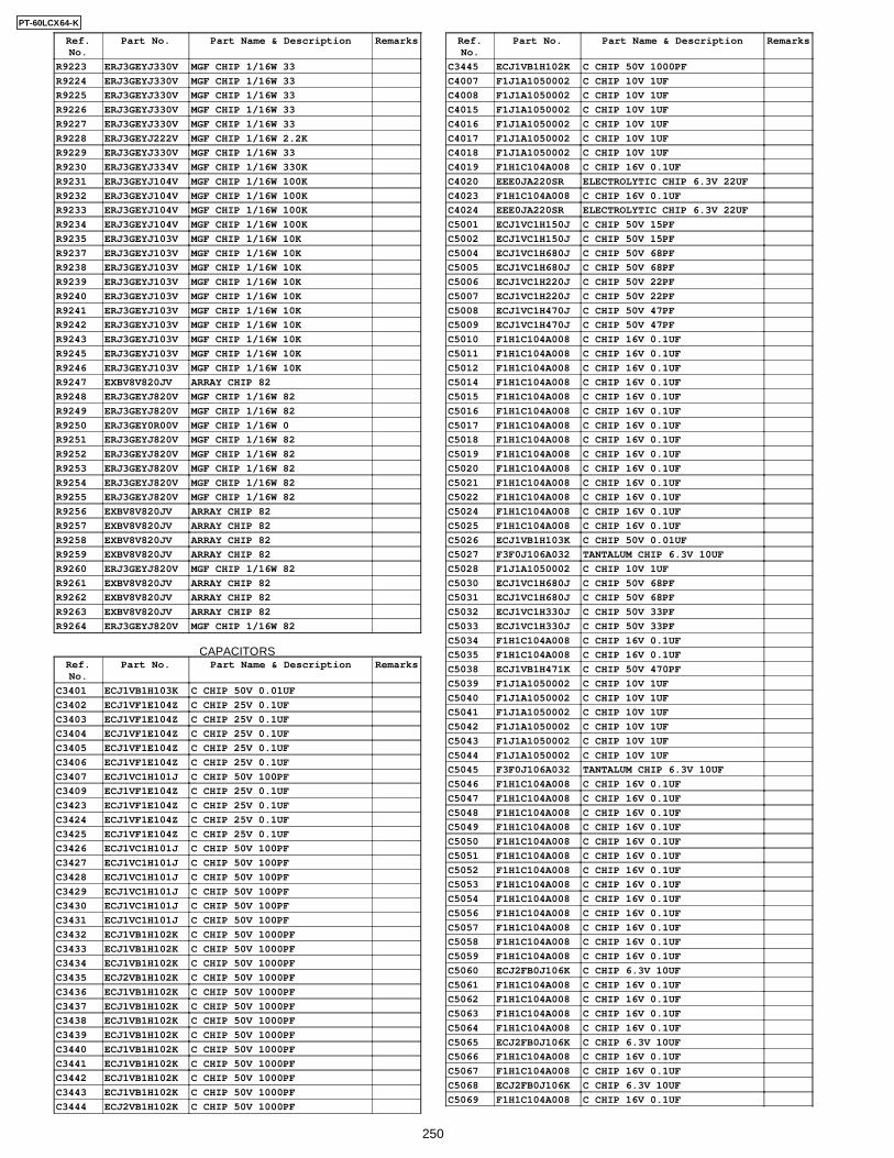
Ref.No.
Part No. Part Name & Description Remarks
R9223 ERJ3GEYJ330V MGF CHIP 1/16W 33
R9224 ERJ3GEYJ330V MGF CHIP 1/16W 33
R9225 ERJ3GEYJ330V MGF CHIP 1/16W 33
R9226 ERJ3GEYJ330V MGF CHIP 1/16W 33
R9227 ERJ3GEYJ330V MGF CHIP 1/16W 33
R9228 ERJ3GEYJ222V MGF CHIP 1/16W 2.2K
R9229 ERJ3GEYJ330V MGF CHIP 1/16W 33
R9230 ERJ3GEYJ334V MGF CHIP 1/16W 330K
R9231 ERJ3GEYJ104V MGF CHIP 1/16W 100K
R9232 ERJ3GEYJ104V MGF CHIP 1/16W 100K
R9233 ERJ3GEYJ104V MGF CHIP 1/16W 100K
R9234 ERJ3GEYJ104V MGF CHIP 1/16W 100K
R9235 ERJ3GEYJ103V MGF CHIP 1/16W 10K
R9237 ERJ3GEYJ103V MGF CHIP 1/16W 10K
R9238 ERJ3GEYJ103V MGF CHIP 1/16W 10K
R9239 ERJ3GEYJ103V MGF CHIP 1/16W 10K
R9240 ERJ3GEYJ103V MGF CHIP 1/16W 10K
R9241 ERJ3GEYJ103V MGF CHIP 1/16W 10K
R9242 ERJ3GEYJ103V MGF CHIP 1/16W 10K
R9243 ERJ3GEYJ103V MGF CHIP 1/16W 10K
R9245 ERJ3GEYJ103V MGF CHIP 1/16W 10K
R9246 ERJ3GEYJ103V MGF CHIP 1/16W 10K
R9247 EXBV8V820JV ARRAY CHIP 82
R9248 ERJ3GEYJ820V MGF CHIP 1/16W 82
R9249 ERJ3GEYJ820V MGF CHIP 1/16W 82
R9250 ERJ3GEY0R00V MGF CHIP 1/16W 0
R9251 ERJ3GEYJ820V MGF CHIP 1/16W 82
R9252 ERJ3GEYJ820V MGF CHIP 1/16W 82
R9253 ERJ3GEYJ820V MGF CHIP 1/16W 82
R9254 ERJ3GEYJ820V MGF CHIP 1/16W 82
R9255 ERJ3GEYJ820V MGF CHIP 1/16W 82
R9256 EXBV8V820JV ARRAY CHIP 82
R9257 EXBV8V820JV ARRAY CHIP 82
R9258 EXBV8V820JV ARRAY CHIP 82
R9259 EXBV8V820JV ARRAY CHIP 82
R9260 ERJ3GEYJ820V MGF CHIP 1/16W 82
R9261 EXBV8V820JV ARRAY CHIP 82
R9262 EXBV8V820JV ARRAY CHIP 82
R9263 EXBV8V820JV ARRAY CHIP 82
R9264 ERJ3GEYJ820V MGF CHIP 1/16W 82
CAPACITORSRef.No.
Part No. Part Name & Description Remarks
C3401 ECJ1VB1H103K C CHIP 50V 0.01UF
C3402 ECJ1VF1E104Z C CHIP 25V 0.1UF
C3403 ECJ1VF1E104Z C CHIP 25V 0.1UF
C3404 ECJ1VF1E104Z C CHIP 25V 0.1UF
C3405 ECJ1VF1E104Z C CHIP 25V 0.1UF
C3406 ECJ1VF1E104Z C CHIP 25V 0.1UF
C3407 ECJ1VC1H101J C CHIP 50V 100PF
C3409 ECJ1VF1E104Z C CHIP 25V 0.1UF
C3423 ECJ1VF1E104Z C CHIP 25V 0.1UF
C3424 ECJ1VF1E104Z C CHIP 25V 0.1UF
C3425 ECJ1VF1E104Z C CHIP 25V 0.1UF
C3426 ECJ1VC1H101J C CHIP 50V 100PF
C3427 ECJ1VC1H101J C CHIP 50V 100PF
C3428 ECJ1VC1H101J C CHIP 50V 100PF
C3429 ECJ1VC1H101J C CHIP 50V 100PF
C3430 ECJ1VC1H101J C CHIP 50V 100PF
C3431 ECJ1VC1H101J C CHIP 50V 100PF
C3432 ECJ1VB1H102K C CHIP 50V 1000PF
C3433 ECJ1VB1H102K C CHIP 50V 1000PF
C3434 ECJ1VB1H102K C CHIP 50V 1000PF
C3435 ECJ2VB1H102K C CHIP 50V 1000PF
C3436 ECJ1VB1H102K C CHIP 50V 1000PF
C3437 ECJ1VB1H102K C CHIP 50V 1000PF
C3438 ECJ1VB1H102K C CHIP 50V 1000PF
C3439 ECJ1VB1H102K C CHIP 50V 1000PF
C3440 ECJ1VB1H102K C CHIP 50V 1000PF
C3441 ECJ1VB1H102K C CHIP 50V 1000PF
C3442 ECJ1VB1H102K C CHIP 50V 1000PF
C3443 ECJ1VB1H102K C CHIP 50V 1000PF
C3444 ECJ2VB1H102K C CHIP 50V 1000PF
Ref.No.
Part No. Part Name & Description Remarks
C3445 ECJ1VB1H102K C CHIP 50V 1000PF
C4007 F1J1A1050002 C CHIP 10V 1UF
C4008 F1J1A1050002 C CHIP 10V 1UF
C4015 F1J1A1050002 C CHIP 10V 1UF
C4016 F1J1A1050002 C CHIP 10V 1UF
C4017 F1J1A1050002 C CHIP 10V 1UF
C4018 F1J1A1050002 C CHIP 10V 1UF
C4019 F1H1C104A008 C CHIP 16V 0.1UF
C4020 EEE0JA220SR ELECTROLYTIC CHIP 6.3V 22UF
C4023 F1H1C104A008 C CHIP 16V 0.1UF
C4024 EEE0JA220SR ELECTROLYTIC CHIP 6.3V 22UF
C5001 ECJ1VC1H150J C CHIP 50V 15PF
C5002 ECJ1VC1H150J C CHIP 50V 15PF
C5004 ECJ1VC1H680J C CHIP 50V 68PF
C5005 ECJ1VC1H680J C CHIP 50V 68PF
C5006 ECJ1VC1H220J C CHIP 50V 22PF
C5007 ECJ1VC1H220J C CHIP 50V 22PF
C5008 ECJ1VC1H470J C CHIP 50V 47PF
C5009 ECJ1VC1H470J C CHIP 50V 47PF
C5010 F1H1C104A008 C CHIP 16V 0.1UF
C5011 F1H1C104A008 C CHIP 16V 0.1UF
C5012 F1H1C104A008 C CHIP 16V 0.1UF
C5014 F1H1C104A008 C CHIP 16V 0.1UF
C5015 F1H1C104A008 C CHIP 16V 0.1UF
C5016 F1H1C104A008 C CHIP 16V 0.1UF
C5017 F1H1C104A008 C CHIP 16V 0.1UF
C5018 F1H1C104A008 C CHIP 16V 0.1UF
C5019 F1H1C104A008 C CHIP 16V 0.1UF
C5020 F1H1C104A008 C CHIP 16V 0.1UF
C5021 F1H1C104A008 C CHIP 16V 0.1UF
C5022 F1H1C104A008 C CHIP 16V 0.1UF
C5024 F1H1C104A008 C CHIP 16V 0.1UF
C5025 F1H1C104A008 C CHIP 16V 0.1UF
C5026 ECJ1VB1H103K C CHIP 50V 0.01UF
C5027 F3F0J106A032 TANTALUM CHIP 6.3V 10UF
C5028 F1J1A1050002 C CHIP 10V 1UF
C5030 ECJ1VC1H680J C CHIP 50V 68PF
C5031 ECJ1VC1H680J C CHIP 50V 68PF
C5032 ECJ1VC1H330J C CHIP 50V 33PF
C5033 ECJ1VC1H330J C CHIP 50V 33PF
C5034 F1H1C104A008 C CHIP 16V 0.1UF
C5035 F1H1C104A008 C CHIP 16V 0.1UF
C5038 ECJ1VB1H471K C CHIP 50V 470PF
C5039 F1J1A1050002 C CHIP 10V 1UF
C5040 F1J1A1050002 C CHIP 10V 1UF
C5041 F1J1A1050002 C CHIP 10V 1UF
C5042 F1J1A1050002 C CHIP 10V 1UF
C5043 F1J1A1050002 C CHIP 10V 1UF
C5044 F1J1A1050002 C CHIP 10V 1UF
C5045 F3F0J106A032 TANTALUM CHIP 6.3V 10UF
C5046 F1H1C104A008 C CHIP 16V 0.1UF
C5047 F1H1C104A008 C CHIP 16V 0.1UF
C5048 F1H1C104A008 C CHIP 16V 0.1UF
C5049 F1H1C104A008 C CHIP 16V 0.1UF
C5050 F1H1C104A008 C CHIP 16V 0.1UF
C5051 F1H1C104A008 C CHIP 16V 0.1UF
C5052 F1H1C104A008 C CHIP 16V 0.1UF
C5053 F1H1C104A008 C CHIP 16V 0.1UF
C5054 F1H1C104A008 C CHIP 16V 0.1UF
C5056 F1H1C104A008 C CHIP 16V 0.1UF
C5057 F1H1C104A008 C CHIP 16V 0.1UF
C5058 F1H1C104A008 C CHIP 16V 0.1UF
C5059 F1H1C104A008 C CHIP 16V 0.1UF
C5060 ECJ2FB0J106K C CHIP 6.3V 10UF
C5061 F1H1C104A008 C CHIP 16V 0.1UF
C5062 F1H1C104A008 C CHIP 16V 0.1UF
C5063 F1H1C104A008 C CHIP 16V 0.1UF
C5064 F1H1C104A008 C CHIP 16V 0.1UF
C5065 ECJ2FB0J106K C CHIP 6.3V 10UF
C5066 F1H1C104A008 C CHIP 16V 0.1UF
C5067 F1H1C104A008 C CHIP 16V 0.1UF
C5068 ECJ2FB0J106K C CHIP 6.3V 10UF
C5069 F1H1C104A008 C CHIP 16V 0.1UF
250
PT-60LCX64-K
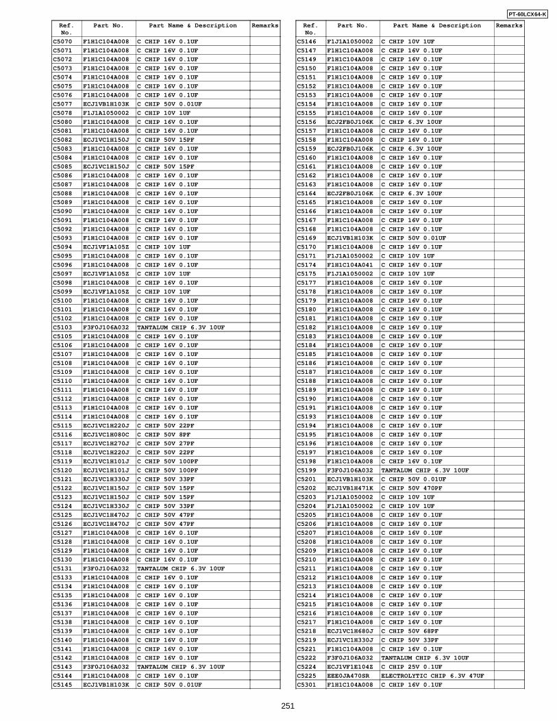
Ref.No.
Part No. Part Name & Description Remarks
C5070 F1H1C104A008 C CHIP 16V 0.1UF
C5071 F1H1C104A008 C CHIP 16V 0.1UF
C5072 F1H1C104A008 C CHIP 16V 0.1UF
C5073 F1H1C104A008 C CHIP 16V 0.1UF
C5074 F1H1C104A008 C CHIP 16V 0.1UF
C5075 F1H1C104A008 C CHIP 16V 0.1UF
C5076 F1H1C104A008 C CHIP 16V 0.1UF
C5077 ECJ1VB1H103K C CHIP 50V 0.01UF
C5078 F1J1A1050002 C CHIP 10V 1UF
C5080 F1H1C104A008 C CHIP 16V 0.1UF
C5081 F1H1C104A008 C CHIP 16V 0.1UF
C5082 ECJ1VC1H150J C CHIP 50V 15PF
C5083 F1H1C104A008 C CHIP 16V 0.1UF
C5084 F1H1C104A008 C CHIP 16V 0.1UF
C5085 ECJ1VC1H150J C CHIP 50V 15PF
C5086 F1H1C104A008 C CHIP 16V 0.1UF
C5087 F1H1C104A008 C CHIP 16V 0.1UF
C5088 F1H1C104A008 C CHIP 16V 0.1UF
C5089 F1H1C104A008 C CHIP 16V 0.1UF
C5090 F1H1C104A008 C CHIP 16V 0.1UF
C5091 F1H1C104A008 C CHIP 16V 0.1UF
C5092 F1H1C104A008 C CHIP 16V 0.1UF
C5093 F1H1C104A008 C CHIP 16V 0.1UF
C5094 ECJ1VF1A105Z C CHIP 10V 1UF
C5095 F1H1C104A008 C CHIP 16V 0.1UF
C5096 F1H1C104A008 C CHIP 16V 0.1UF
C5097 ECJ1VF1A105Z C CHIP 10V 1UF
C5098 F1H1C104A008 C CHIP 16V 0.1UF
C5099 ECJ1VF1A105Z C CHIP 10V 1UF
C5100 F1H1C104A008 C CHIP 16V 0.1UF
C5101 F1H1C104A008 C CHIP 16V 0.1UF
C5102 F1H1C104A008 C CHIP 16V 0.1UF
C5103 F3F0J106A032 TANTALUM CHIP 6.3V 10UF
C5105 F1H1C104A008 C CHIP 16V 0.1UF
C5106 F1H1C104A008 C CHIP 16V 0.1UF
C5107 F1H1C104A008 C CHIP 16V 0.1UF
C5108 F1H1C104A008 C CHIP 16V 0.1UF
C5109 F1H1C104A008 C CHIP 16V 0.1UF
C5110 F1H1C104A008 C CHIP 16V 0.1UF
C5111 F1H1C104A008 C CHIP 16V 0.1UF
C5112 F1H1C104A008 C CHIP 16V 0.1UF
C5113 F1H1C104A008 C CHIP 16V 0.1UF
C5114 F1H1C104A008 C CHIP 16V 0.1UF
C5115 ECJ1VC1H220J C CHIP 50V 22PF
C5116 ECJ1VC1H080C C CHIP 50V 8PF
C5117 ECJ1VC1H270J C CHIP 50V 27PF
C5118 ECJ1VC1H220J C CHIP 50V 22PF
C5119 ECJ1VC1H101J C CHIP 50V 100PF
C5120 ECJ1VC1H101J C CHIP 50V 100PF
C5121 ECJ1VC1H330J C CHIP 50V 33PF
C5122 ECJ1VC1H150J C CHIP 50V 15PF
C5123 ECJ1VC1H150J C CHIP 50V 15PF
C5124 ECJ1VC1H330J C CHIP 50V 33PF
C5125 ECJ1VC1H470J C CHIP 50V 47PF
C5126 ECJ1VC1H470J C CHIP 50V 47PF
C5127 F1H1C104A008 C CHIP 16V 0.1UF
C5128 F1H1C104A008 C CHIP 16V 0.1UF
C5129 F1H1C104A008 C CHIP 16V 0.1UF
C5130 F1H1C104A008 C CHIP 16V 0.1UF
C5131 F3F0J106A032 TANTALUM CHIP 6.3V 10UF
C5133 F1H1C104A008 C CHIP 16V 0.1UF
C5134 F1H1C104A008 C CHIP 16V 0.1UF
C5135 F1H1C104A008 C CHIP 16V 0.1UF
C5136 F1H1C104A008 C CHIP 16V 0.1UF
C5137 F1H1C104A008 C CHIP 16V 0.1UF
C5138 F1H1C104A008 C CHIP 16V 0.1UF
C5139 F1H1C104A008 C CHIP 16V 0.1UF
C5140 F1H1C104A008 C CHIP 16V 0.1UF
C5141 F1H1C104A008 C CHIP 16V 0.1UF
C5142 F1H1C104A008 C CHIP 16V 0.1UF
C5143 F3F0J106A032 TANTALUM CHIP 6.3V 10UF
C5144 F1H1C104A008 C CHIP 16V 0.1UF
C5145 ECJ1VB1H103K C CHIP 50V 0.01UF
Ref.No.
Part No. Part Name & Description Remarks
C5146 F1J1A1050002 C CHIP 10V 1UF
C5147 F1H1C104A008 C CHIP 16V 0.1UF
C5149 F1H1C104A008 C CHIP 16V 0.1UF
C5150 F1H1C104A008 C CHIP 16V 0.1UF
C5151 F1H1C104A008 C CHIP 16V 0.1UF
C5152 F1H1C104A008 C CHIP 16V 0.1UF
C5153 F1H1C104A008 C CHIP 16V 0.1UF
C5154 F1H1C104A008 C CHIP 16V 0.1UF
C5155 F1H1C104A008 C CHIP 16V 0.1UF
C5156 ECJ2FB0J106K C CHIP 6.3V 10UF
C5157 F1H1C104A008 C CHIP 16V 0.1UF
C5158 F1H1C104A008 C CHIP 16V 0.1UF
C5159 ECJ2FB0J106K C CHIP 6.3V 10UF
C5160 F1H1C104A008 C CHIP 16V 0.1UF
C5161 F1H1C104A008 C CHIP 16V 0.1UF
C5162 F1H1C104A008 C CHIP 16V 0.1UF
C5163 F1H1C104A008 C CHIP 16V 0.1UF
C5164 ECJ2FB0J106K C CHIP 6.3V 10UF
C5165 F1H1C104A008 C CHIP 16V 0.1UF
C5166 F1H1C104A008 C CHIP 16V 0.1UF
C5167 F1H1C104A008 C CHIP 16V 0.1UF
C5168 F1H1C104A008 C CHIP 16V 0.1UF
C5169 ECJ1VB1H103K C CHIP 50V 0.01UF
C5170 F1H1C104A008 C CHIP 16V 0.1UF
C5171 F1J1A1050002 C CHIP 10V 1UF
C5174 F1H1C104A041 C CHIP 16V 0.1UF
C5175 F1J1A1050002 C CHIP 10V 1UF
C5177 F1H1C104A008 C CHIP 16V 0.1UF
C5178 F1H1C104A008 C CHIP 16V 0.1UF
C5179 F1H1C104A008 C CHIP 16V 0.1UF
C5180 F1H1C104A008 C CHIP 16V 0.1UF
C5181 F1H1C104A008 C CHIP 16V 0.1UF
C5182 F1H1C104A008 C CHIP 16V 0.1UF
C5183 F1H1C104A008 C CHIP 16V 0.1UF
C5184 F1H1C104A008 C CHIP 16V 0.1UF
C5185 F1H1C104A008 C CHIP 16V 0.1UF
C5186 F1H1C104A008 C CHIP 16V 0.1UF
C5187 F1H1C104A008 C CHIP 16V 0.1UF
C5188 F1H1C104A008 C CHIP 16V 0.1UF
C5189 F1H1C104A008 C CHIP 16V 0.1UF
C5190 F1H1C104A008 C CHIP 16V 0.1UF
C5191 F1H1C104A008 C CHIP 16V 0.1UF
C5193 F1H1C104A008 C CHIP 16V 0.1UF
C5194 F1H1C104A008 C CHIP 16V 0.1UF
C5195 F1H1C104A008 C CHIP 16V 0.1UF
C5196 F1H1C104A008 C CHIP 16V 0.1UF
C5197 F1H1C104A008 C CHIP 16V 0.1UF
C5198 F1H1C104A008 C CHIP 16V 0.1UF
C5199 F3F0J106A032 TANTALUM CHIP 6.3V 10UF
C5201 ECJ1VB1H103K C CHIP 50V 0.01UF
C5202 ECJ1VB1H471K C CHIP 50V 470PF
C5203 F1J1A1050002 C CHIP 10V 1UF
C5204 F1J1A1050002 C CHIP 10V 1UF
C5205 F1H1C104A008 C CHIP 16V 0.1UF
C5206 F1H1C104A008 C CHIP 16V 0.1UF
C5207 F1H1C104A008 C CHIP 16V 0.1UF
C5208 F1H1C104A008 C CHIP 16V 0.1UF
C5209 F1H1C104A008 C CHIP 16V 0.1UF
C5210 F1H1C104A008 C CHIP 16V 0.1UF
C5211 F1H1C104A008 C CHIP 16V 0.1UF
C5212 F1H1C104A008 C CHIP 16V 0.1UF
C5213 F1H1C104A008 C CHIP 16V 0.1UF
C5214 F1H1C104A008 C CHIP 16V 0.1UF
C5215 F1H1C104A008 C CHIP 16V 0.1UF
C5216 F1H1C104A008 C CHIP 16V 0.1UF
C5217 F1H1C104A008 C CHIP 16V 0.1UF
C5218 ECJ1VC1H680J C CHIP 50V 68PF
C5219 ECJ1VC1H330J C CHIP 50V 33PF
C5221 F1H1C104A008 C CHIP 16V 0.1UF
C5222 F3F0J106A032 TANTALUM CHIP 6.3V 10UF
C5224 ECJ1VF1E104Z C CHIP 25V 0.1UF
C5225 EEE0JA470SR ELECTROLYTIC CHIP 6.3V 47UF
C5301 F1H1C104A008 C CHIP 16V 0.1UF
251
PT-60LCX64-K
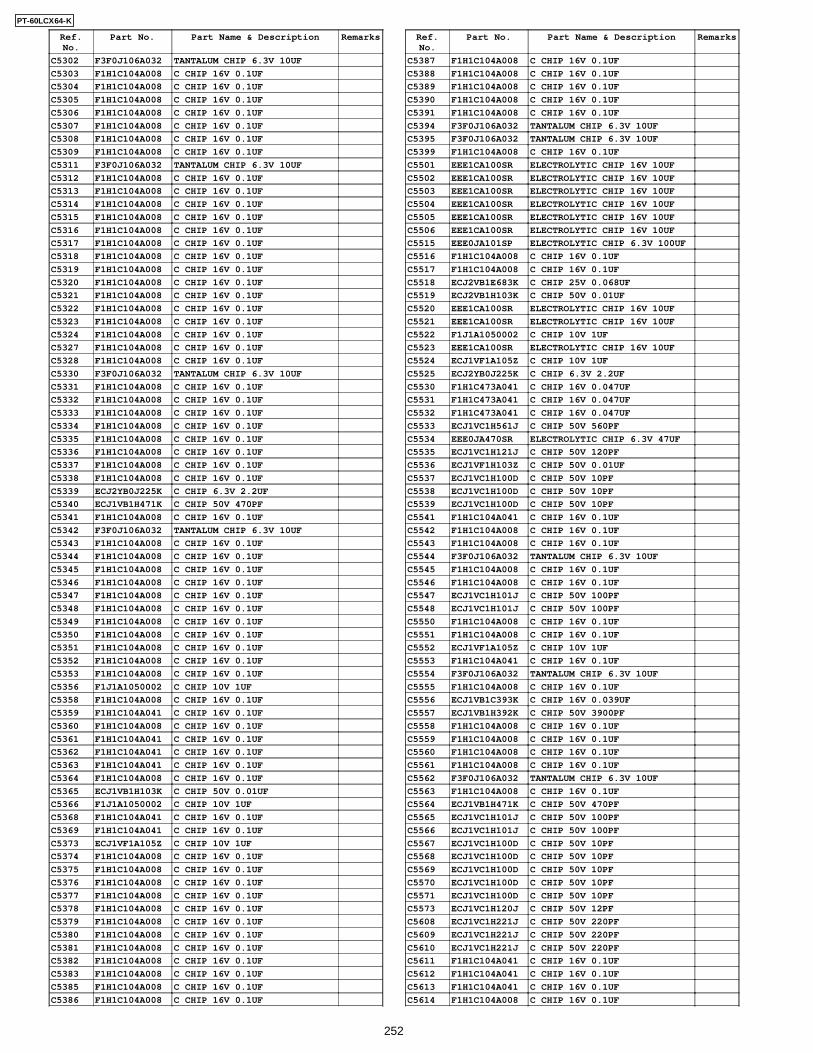
Ref.No.
Part No. Part Name & Description Remarks
C5302 F3F0J106A032 TANTALUM CHIP 6.3V 10UF
C5303 F1H1C104A008 C CHIP 16V 0.1UF
C5304 F1H1C104A008 C CHIP 16V 0.1UF
C5305 F1H1C104A008 C CHIP 16V 0.1UF
C5306 F1H1C104A008 C CHIP 16V 0.1UF
C5307 F1H1C104A008 C CHIP 16V 0.1UF
C5308 F1H1C104A008 C CHIP 16V 0.1UF
C5309 F1H1C104A008 C CHIP 16V 0.1UF
C5311 F3F0J106A032 TANTALUM CHIP 6.3V 10UF
C5312 F1H1C104A008 C CHIP 16V 0.1UF
C5313 F1H1C104A008 C CHIP 16V 0.1UF
C5314 F1H1C104A008 C CHIP 16V 0.1UF
C5315 F1H1C104A008 C CHIP 16V 0.1UF
C5316 F1H1C104A008 C CHIP 16V 0.1UF
C5317 F1H1C104A008 C CHIP 16V 0.1UF
C5318 F1H1C104A008 C CHIP 16V 0.1UF
C5319 F1H1C104A008 C CHIP 16V 0.1UF
C5320 F1H1C104A008 C CHIP 16V 0.1UF
C5321 F1H1C104A008 C CHIP 16V 0.1UF
C5322 F1H1C104A008 C CHIP 16V 0.1UF
C5323 F1H1C104A008 C CHIP 16V 0.1UF
C5324 F1H1C104A008 C CHIP 16V 0.1UF
C5327 F1H1C104A008 C CHIP 16V 0.1UF
C5328 F1H1C104A008 C CHIP 16V 0.1UF
C5330 F3F0J106A032 TANTALUM CHIP 6.3V 10UF
C5331 F1H1C104A008 C CHIP 16V 0.1UF
C5332 F1H1C104A008 C CHIP 16V 0.1UF
C5333 F1H1C104A008 C CHIP 16V 0.1UF
C5334 F1H1C104A008 C CHIP 16V 0.1UF
C5335 F1H1C104A008 C CHIP 16V 0.1UF
C5336 F1H1C104A008 C CHIP 16V 0.1UF
C5337 F1H1C104A008 C CHIP 16V 0.1UF
C5338 F1H1C104A008 C CHIP 16V 0.1UF
C5339 ECJ2YB0J225K C CHIP 6.3V 2.2UF
C5340 ECJ1VB1H471K C CHIP 50V 470PF
C5341 F1H1C104A008 C CHIP 16V 0.1UF
C5342 F3F0J106A032 TANTALUM CHIP 6.3V 10UF
C5343 F1H1C104A008 C CHIP 16V 0.1UF
C5344 F1H1C104A008 C CHIP 16V 0.1UF
C5345 F1H1C104A008 C CHIP 16V 0.1UF
C5346 F1H1C104A008 C CHIP 16V 0.1UF
C5347 F1H1C104A008 C CHIP 16V 0.1UF
C5348 F1H1C104A008 C CHIP 16V 0.1UF
C5349 F1H1C104A008 C CHIP 16V 0.1UF
C5350 F1H1C104A008 C CHIP 16V 0.1UF
C5351 F1H1C104A008 C CHIP 16V 0.1UF
C5352 F1H1C104A008 C CHIP 16V 0.1UF
C5353 F1H1C104A008 C CHIP 16V 0.1UF
C5356 F1J1A1050002 C CHIP 10V 1UF
C5358 F1H1C104A008 C CHIP 16V 0.1UF
C5359 F1H1C104A041 C CHIP 16V 0.1UF
C5360 F1H1C104A008 C CHIP 16V 0.1UF
C5361 F1H1C104A041 C CHIP 16V 0.1UF
C5362 F1H1C104A041 C CHIP 16V 0.1UF
C5363 F1H1C104A041 C CHIP 16V 0.1UF
C5364 F1H1C104A008 C CHIP 16V 0.1UF
C5365 ECJ1VB1H103K C CHIP 50V 0.01UF
C5366 F1J1A1050002 C CHIP 10V 1UF
C5368 F1H1C104A041 C CHIP 16V 0.1UF
C5369 F1H1C104A041 C CHIP 16V 0.1UF
C5373 ECJ1VF1A105Z C CHIP 10V 1UF
C5374 F1H1C104A008 C CHIP 16V 0.1UF
C5375 F1H1C104A008 C CHIP 16V 0.1UF
C5376 F1H1C104A008 C CHIP 16V 0.1UF
C5377 F1H1C104A008 C CHIP 16V 0.1UF
C5378 F1H1C104A008 C CHIP 16V 0.1UF
C5379 F1H1C104A008 C CHIP 16V 0.1UF
C5380 F1H1C104A008 C CHIP 16V 0.1UF
C5381 F1H1C104A008 C CHIP 16V 0.1UF
C5382 F1H1C104A008 C CHIP 16V 0.1UF
C5383 F1H1C104A008 C CHIP 16V 0.1UF
C5385 F1H1C104A008 C CHIP 16V 0.1UF
C5386 F1H1C104A008 C CHIP 16V 0.1UF
Ref.No.
Part No. Part Name & Description Remarks
C5387 F1H1C104A008 C CHIP 16V 0.1UF
C5388 F1H1C104A008 C CHIP 16V 0.1UF
C5389 F1H1C104A008 C CHIP 16V 0.1UF
C5390 F1H1C104A008 C CHIP 16V 0.1UF
C5391 F1H1C104A008 C CHIP 16V 0.1UF
C5394 F3F0J106A032 TANTALUM CHIP 6.3V 10UF
C5395 F3F0J106A032 TANTALUM CHIP 6.3V 10UF
C5399 F1H1C104A008 C CHIP 16V 0.1UF
C5501 EEE1CA100SR ELECTROLYTIC CHIP 16V 10UF
C5502 EEE1CA100SR ELECTROLYTIC CHIP 16V 10UF
C5503 EEE1CA100SR ELECTROLYTIC CHIP 16V 10UF
C5504 EEE1CA100SR ELECTROLYTIC CHIP 16V 10UF
C5505 EEE1CA100SR ELECTROLYTIC CHIP 16V 10UF
C5506 EEE1CA100SR ELECTROLYTIC CHIP 16V 10UF
C5515 EEE0JA101SP ELECTROLYTIC CHIP 6.3V 100UF
C5516 F1H1C104A008 C CHIP 16V 0.1UF
C5517 F1H1C104A008 C CHIP 16V 0.1UF
C5518 ECJ2VB1E683K C CHIP 25V 0.068UF
C5519 ECJ2VB1H103K C CHIP 50V 0.01UF
C5520 EEE1CA100SR ELECTROLYTIC CHIP 16V 10UF
C5521 EEE1CA100SR ELECTROLYTIC CHIP 16V 10UF
C5522 F1J1A1050002 C CHIP 10V 1UF
C5523 EEE1CA100SR ELECTROLYTIC CHIP 16V 10UF
C5524 ECJ1VF1A105Z C CHIP 10V 1UF
C5525 ECJ2YB0J225K C CHIP 6.3V 2.2UF
C5530 F1H1C473A041 C CHIP 16V 0.047UF
C5531 F1H1C473A041 C CHIP 16V 0.047UF
C5532 F1H1C473A041 C CHIP 16V 0.047UF
C5533 ECJ1VC1H561J C CHIP 50V 560PF
C5534 EEE0JA470SR ELECTROLYTIC CHIP 6.3V 47UF
C5535 ECJ1VC1H121J C CHIP 50V 120PF
C5536 ECJ1VF1H103Z C CHIP 50V 0.01UF
C5537 ECJ1VC1H100D C CHIP 50V 10PF
C5538 ECJ1VC1H100D C CHIP 50V 10PF
C5539 ECJ1VC1H100D C CHIP 50V 10PF
C5541 F1H1C104A041 C CHIP 16V 0.1UF
C5542 F1H1C104A008 C CHIP 16V 0.1UF
C5543 F1H1C104A008 C CHIP 16V 0.1UF
C5544 F3F0J106A032 TANTALUM CHIP 6.3V 10UF
C5545 F1H1C104A008 C CHIP 16V 0.1UF
C5546 F1H1C104A008 C CHIP 16V 0.1UF
C5547 ECJ1VC1H101J C CHIP 50V 100PF
C5548 ECJ1VC1H101J C CHIP 50V 100PF
C5550 F1H1C104A008 C CHIP 16V 0.1UF
C5551 F1H1C104A008 C CHIP 16V 0.1UF
C5552 ECJ1VF1A105Z C CHIP 10V 1UF
C5553 F1H1C104A041 C CHIP 16V 0.1UF
C5554 F3F0J106A032 TANTALUM CHIP 6.3V 10UF
C5555 F1H1C104A008 C CHIP 16V 0.1UF
C5556 ECJ1VB1C393K C CHIP 16V 0.039UF
C5557 ECJ1VB1H392K C CHIP 50V 3900PF
C5558 F1H1C104A008 C CHIP 16V 0.1UF
C5559 F1H1C104A008 C CHIP 16V 0.1UF
C5560 F1H1C104A008 C CHIP 16V 0.1UF
C5561 F1H1C104A008 C CHIP 16V 0.1UF
C5562 F3F0J106A032 TANTALUM CHIP 6.3V 10UF
C5563 F1H1C104A008 C CHIP 16V 0.1UF
C5564 ECJ1VB1H471K C CHIP 50V 470PF
C5565 ECJ1VC1H101J C CHIP 50V 100PF
C5566 ECJ1VC1H101J C CHIP 50V 100PF
C5567 ECJ1VC1H100D C CHIP 50V 10PF
C5568 ECJ1VC1H100D C CHIP 50V 10PF
C5569 ECJ1VC1H100D C CHIP 50V 10PF
C5570 ECJ1VC1H100D C CHIP 50V 10PF
C5571 ECJ1VC1H100D C CHIP 50V 10PF
C5573 ECJ1VC1H120J C CHIP 50V 12PF
C5608 ECJ1VC1H221J C CHIP 50V 220PF
C5609 ECJ1VC1H221J C CHIP 50V 220PF
C5610 ECJ1VC1H221J C CHIP 50V 220PF
C5611 F1H1C104A041 C CHIP 16V 0.1UF
C5612 F1H1C104A041 C CHIP 16V 0.1UF
C5613 F1H1C104A041 C CHIP 16V 0.1UF
C5614 F1H1C104A008 C CHIP 16V 0.1UF
252
PT-60LCX64-K
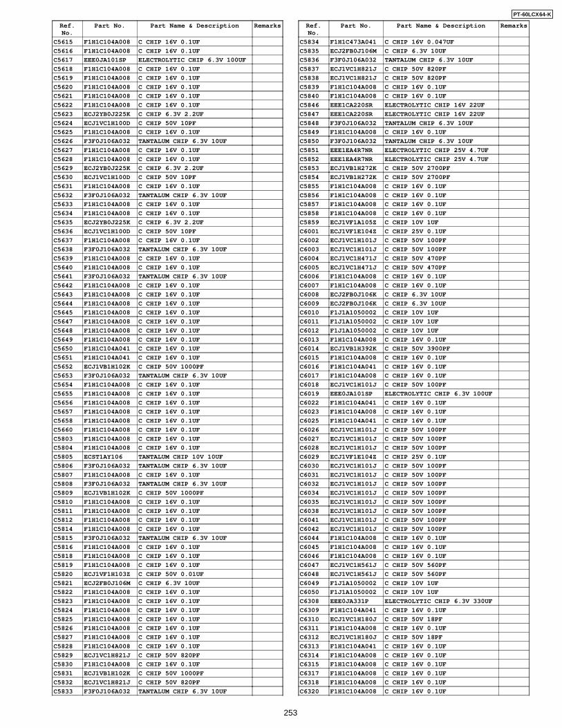
Ref.No.
Part No. Part Name & Description Remarks
C5615 F1H1C104A008 C CHIP 16V 0.1UF
C5616 F1H1C104A008 C CHIP 16V 0.1UF
C5617 EEE0JA101SP ELECTROLYTIC CHIP 6.3V 100UF
C5618 F1H1C104A008 C CHIP 16V 0.1UF
C5619 F1H1C104A008 C CHIP 16V 0.1UF
C5620 F1H1C104A008 C CHIP 16V 0.1UF
C5621 F1H1C104A008 C CHIP 16V 0.1UF
C5622 F1H1C104A008 C CHIP 16V 0.1UF
C5623 ECJ2YB0J225K C CHIP 6.3V 2.2UF
C5624 ECJ1VC1H100D C CHIP 50V 10PF
C5625 F1H1C104A008 C CHIP 16V 0.1UF
C5626 F3F0J106A032 TANTALUM CHIP 6.3V 10UF
C5627 F1H1C104A008 C CHIP 16V 0.1UF
C5628 F1H1C104A008 C CHIP 16V 0.1UF
C5629 ECJ2YB0J225K C CHIP 6.3V 2.2UF
C5630 ECJ1VC1H100D C CHIP 50V 10PF
C5631 F1H1C104A008 C CHIP 16V 0.1UF
C5632 F3F0J106A032 TANTALUM CHIP 6.3V 10UF
C5633 F1H1C104A008 C CHIP 16V 0.1UF
C5634 F1H1C104A008 C CHIP 16V 0.1UF
C5635 ECJ2YB0J225K C CHIP 6.3V 2.2UF
C5636 ECJ1VC1H100D C CHIP 50V 10PF
C5637 F1H1C104A008 C CHIP 16V 0.1UF
C5638 F3F0J106A032 TANTALUM CHIP 6.3V 10UF
C5639 F1H1C104A008 C CHIP 16V 0.1UF
C5640 F1H1C104A008 C CHIP 16V 0.1UF
C5641 F3F0J106A032 TANTALUM CHIP 6.3V 10UF
C5642 F1H1C104A008 C CHIP 16V 0.1UF
C5643 F1H1C104A008 C CHIP 16V 0.1UF
C5644 F1H1C104A008 C CHIP 16V 0.1UF
C5645 F1H1C104A008 C CHIP 16V 0.1UF
C5647 F1H1C104A008 C CHIP 16V 0.1UF
C5648 F1H1C104A008 C CHIP 16V 0.1UF
C5649 F1H1C104A008 C CHIP 16V 0.1UF
C5650 F1H1C104A041 C CHIP 16V 0.1UF
C5651 F1H1C104A041 C CHIP 16V 0.1UF
C5652 ECJ1VB1H102K C CHIP 50V 1000PF
C5653 F3F0J106A032 TANTALUM CHIP 6.3V 10UF
C5654 F1H1C104A008 C CHIP 16V 0.1UF
C5655 F1H1C104A008 C CHIP 16V 0.1UF
C5656 F1H1C104A008 C CHIP 16V 0.1UF
C5657 F1H1C104A008 C CHIP 16V 0.1UF
C5658 F1H1C104A008 C CHIP 16V 0.1UF
C5660 F1H1C104A008 C CHIP 16V 0.1UF
C5803 F1H1C104A008 C CHIP 16V 0.1UF
C5804 F1H1C104A008 C CHIP 16V 0.1UF
C5805 ECST1AY106 TANTALUM CHIP 10V 10UF
C5806 F3F0J106A032 TANTALUM CHIP 6.3V 10UF
C5807 F1H1C104A008 C CHIP 16V 0.1UF
C5808 F3F0J106A032 TANTALUM CHIP 6.3V 10UF
C5809 ECJ1VB1H102K C CHIP 50V 1000PF
C5810 F1H1C104A008 C CHIP 16V 0.1UF
C5811 F1H1C104A008 C CHIP 16V 0.1UF
C5812 F1H1C104A008 C CHIP 16V 0.1UF
C5814 F1H1C104A008 C CHIP 16V 0.1UF
C5815 F3F0J106A032 TANTALUM CHIP 6.3V 10UF
C5816 F1H1C104A008 C CHIP 16V 0.1UF
C5818 F1H1C104A008 C CHIP 16V 0.1UF
C5819 F1H1C104A008 C CHIP 16V 0.1UF
C5820 ECJ1VF1H103Z C CHIP 50V 0.01UF
C5821 ECJ2FB0J106M C CHIP 6.3V 10UF
C5822 F1H1C104A008 C CHIP 16V 0.1UF
C5823 F1H1C104A008 C CHIP 16V 0.1UF
C5824 F1H1C104A008 C CHIP 16V 0.1UF
C5825 F1H1C104A008 C CHIP 16V 0.1UF
C5826 F1H1C104A008 C CHIP 16V 0.1UF
C5827 F1H1C104A008 C CHIP 16V 0.1UF
C5828 F1H1C104A008 C CHIP 16V 0.1UF
C5829 ECJ1VC1H821J C CHIP 50V 820PF
C5830 F1H1C104A008 C CHIP 16V 0.1UF
C5831 ECJ1VB1H102K C CHIP 50V 1000PF
C5832 ECJ1VC1H821J C CHIP 50V 820PF
C5833 F3F0J106A032 TANTALUM CHIP 6.3V 10UF
Ref.No.
Part No. Part Name & Description Remarks
C5834 F1H1C473A041 C CHIP 16V 0.047UF
C5835 ECJ2FB0J106M C CHIP 6.3V 10UF
C5836 F3F0J106A032 TANTALUM CHIP 6.3V 10UF
C5837 ECJ1VC1H821J C CHIP 50V 820PF
C5838 ECJ1VC1H821J C CHIP 50V 820PF
C5839 F1H1C104A008 C CHIP 16V 0.1UF
C5840 F1H1C104A008 C CHIP 16V 0.1UF
C5846 EEE1CA220SR ELECTROLYTIC CHIP 16V 22UF
C5847 EEE1CA220SR ELECTROLYTIC CHIP 16V 22UF
C5848 F3F0J106A032 TANTALUM CHIP 6.3V 10UF
C5849 F1H1C104A008 C CHIP 16V 0.1UF
C5850 F3F0J106A032 TANTALUM CHIP 6.3V 10UF
C5851 EEE1EA4R7NR ELECTROLYTIC CHIP 25V 4.7UF
C5852 EEE1EA4R7NR ELECTROLYTIC CHIP 25V 4.7UF
C5853 ECJ1VB1H272K C CHIP 50V 2700PF
C5854 ECJ1VB1H272K C CHIP 50V 2700PF
C5855 F1H1C104A008 C CHIP 16V 0.1UF
C5856 F1H1C104A008 C CHIP 16V 0.1UF
C5857 F1H1C104A008 C CHIP 16V 0.1UF
C5858 F1H1C104A008 C CHIP 16V 0.1UF
C5859 ECJ1VF1A105Z C CHIP 10V 1UF
C6001 ECJ1VF1E104Z C CHIP 25V 0.1UF
C6002 ECJ1VC1H101J C CHIP 50V 100PF
C6003 ECJ1VC1H101J C CHIP 50V 100PF
C6004 ECJ1VC1H471J C CHIP 50V 470PF
C6005 ECJ1VC1H471J C CHIP 50V 470PF
C6006 F1H1C104A008 C CHIP 16V 0.1UF
C6007 F1H1C104A008 C CHIP 16V 0.1UF
C6008 ECJ2FB0J106K C CHIP 6.3V 10UF
C6009 ECJ2FB0J106K C CHIP 6.3V 10UF
C6010 F1J1A1050002 C CHIP 10V 1UF
C6011 F1J1A1050002 C CHIP 10V 1UF
C6012 F1J1A1050002 C CHIP 10V 1UF
C6013 F1H1C104A008 C CHIP 16V 0.1UF
C6014 ECJ1VB1H392K C CHIP 50V 3900PF
C6015 F1H1C104A008 C CHIP 16V 0.1UF
C6016 F1H1C104A041 C CHIP 16V 0.1UF
C6017 F1H1C104A008 C CHIP 16V 0.1UF
C6018 ECJ1VC1H101J C CHIP 50V 100PF
C6019 EEE0JA101SP ELECTROLYTIC CHIP 6.3V 100UF
C6022 F1H1C104A041 C CHIP 16V 0.1UF
C6023 F1H1C104A008 C CHIP 16V 0.1UF
C6025 F1H1C104A041 C CHIP 16V 0.1UF
C6026 ECJ1VC1H101J C CHIP 50V 100PF
C6027 ECJ1VC1H101J C CHIP 50V 100PF
C6028 ECJ1VC1H101J C CHIP 50V 100PF
C6029 ECJ1VF1E104Z C CHIP 25V 0.1UF
C6030 ECJ1VC1H101J C CHIP 50V 100PF
C6031 ECJ1VC1H101J C CHIP 50V 100PF
C6032 ECJ1VC1H101J C CHIP 50V 100PF
C6034 ECJ1VC1H101J C CHIP 50V 100PF
C6035 ECJ1VC1H101J C CHIP 50V 100PF
C6038 ECJ1VC1H101J C CHIP 50V 100PF
C6041 ECJ1VC1H101J C CHIP 50V 100PF
C6042 ECJ1VC1H101J C CHIP 50V 100PF
C6044 F1H1C104A008 C CHIP 16V 0.1UF
C6045 F1H1C104A008 C CHIP 16V 0.1UF
C6046 F1H1C104A008 C CHIP 16V 0.1UF
C6047 ECJ1VC1H561J C CHIP 50V 560PF
C6048 ECJ1VC1H561J C CHIP 50V 560PF
C6049 F1J1A1050002 C CHIP 10V 1UF
C6050 F1J1A1050002 C CHIP 10V 1UF
C6308 EEE0JA331P ELECTROLYTIC CHIP 6.3V 330UF
C6309 F1H1C104A041 C CHIP 16V 0.1UF
C6310 ECJ1VC1H180J C CHIP 50V 18PF
C6311 F1H1C104A008 C CHIP 16V 0.1UF
C6312 ECJ1VC1H180J C CHIP 50V 18PF
C6313 F1H1C104A041 C CHIP 16V 0.1UF
C6314 F1H1C104A008 C CHIP 16V 0.1UF
C6315 F1H1C104A008 C CHIP 16V 0.1UF
C6317 F1H1C104A008 C CHIP 16V 0.1UF
C6318 F1H1C104A008 C CHIP 16V 0.1UF
C6320 F1H1C104A008 C CHIP 16V 0.1UF
253
PT-60LCX64-K
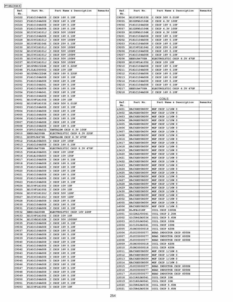
Ref.No.
Part No. Part Name & Description Remarks
C6322 F1H1C104A008 C CHIP 16V 0.1UF
C6323 F1H1C104A008 C CHIP 16V 0.1UF
C6324 F1H1C104A008 C CHIP 16V 0.1UF
C6325 F1H1C104A008 C CHIP 16V 0.1UF
C6326 ECJ1VC1H101J C CHIP 50V 100PF
C6327 F1H1C104A008 C CHIP 16V 0.1UF
C6328 ECJ1VC1H101J C CHIP 50V 100PF
C6329 ECJ1VF1E104Z C CHIP 25V 0.1UF
C6330 ECJ1VC1H101J C CHIP 50V 100PF
C6332 ECJ1VC1H101J C CHIP 50V 100PF
C6334 ECJ1VC1H101J C CHIP 50V 100PF
C6335 ECJ1VC1H101J C CHIP 50V 100PF
C6337 ECJ1VC1H101J C CHIP 50V 100PF
C6347 ECJ2VB1C224K C CHIP 16V 0.22UF
C6348 F1J1A1050002 C CHIP 10V 1UF
C6349 ECJ2VB1C224K C CHIP 16V 0.22UF
C6350 F1H1C104A008 C CHIP 16V 0.1UF
C6351 F1H1C104A008 C CHIP 16V 0.1UF
C6352 F1H1C104A041 C CHIP 16V 0.1UF
C6353 F1H1C104A008 C CHIP 16V 0.1UF
C6354 F1H1C104A041 C CHIP 16V 0.1UF
C6355 F1H1C104A008 C CHIP 16V 0.1UF
C9001 ECJ1VF1A105Z C CHIP 10V 1UF
C9002 ECJ1VF1H103Z C CHIP 50V 0.01UF
C9003 F1H1C104A008 C CHIP 16V 0.1UF
C9004 F1H1C104A008 C CHIP 16V 0.1UF
C9005 F1H1C104A008 C CHIP 16V 0.1UF
C9006 F1H1C104A008 C CHIP 16V 0.1UF
C9007 F1H1C104A008 C CHIP 16V 0.1UF
C9008 F1H1C104A008 C CHIP 16V 0.1UF
C9009 F3F0J106A032 TANTALUM CHIP 6.3V 10UF
C9010 EEE0JA220SR ELECTROLYTIC CHIP 6.3V 22UF
C9011 ECST0JX476R TANTALUM CHIP 6.3V 47UF
C9012 F1K1A106A005 C CHIP 10V 10UF
C9013 F1H1C104A008 C CHIP 16V 0.1UF
C9014 EEE0JA470SR ELECTROLYTIC CHIP 6.3V 47UF
C9015 F1K1A106A005 C CHIP 10V 10UF
C9016 F1K1A106A005 C CHIP 10V 10UF
C9017 F1H1C104A008 C CHIP 16V 0.1UF
C9018 F1H1C104A008 C CHIP 16V 0.1UF
C9019 F1H1C104A008 C CHIP 16V 0.1UF
C9020 F1H1C104A008 C CHIP 16V 0.1UF
C9021 F1H1C104A008 C CHIP 16V 0.1UF
C9022 F1H1C104A008 C CHIP 16V 0.1UF
C9023 F1H1C104A008 C CHIP 16V 0.1UF
C9024 ECJ1VF1A105Z C CHIP 10V 1UF
C9025 ECJ1VF1A105Z C CHIP 10V 1UF
C9026 ECJ1VC1H120J C CHIP 50V 12PF
C9027 ECJ1VC1H120J C CHIP 50V 12PF
C9028 F1H1C104A008 C CHIP 16V 0.1UF
C9030 F1H1C104A008 C CHIP 16V 0.1UF
C9031 F1H1C104A008 C CHIP 16V 0.1UF
C9032 EEE1CA220SR ELECTROLYTIC CHIP 16V 22UF
C9033 ECJ1VF1A105Z C CHIP 10V 1UF
C9034 ECJ1VB1H102K C CHIP 50V 1000PF
C9035 F1H1C104A008 C CHIP 16V 0.1UF
C9036 F1H1C104A008 C CHIP 16V 0.1UF
C9037 F1H1C104A008 C CHIP 16V 0.1UF
C9038 F1H1C104A008 C CHIP 16V 0.1UF
C9039 F1H1C104A008 C CHIP 16V 0.1UF
C9040 F1H1C104A008 C CHIP 16V 0.1UF
C9041 F1H1C104A008 C CHIP 16V 0.1UF
C9042 F1H1C104A008 C CHIP 16V 0.1UF
C9043 F1H1C104A008 C CHIP 16V 0.1UF
C9044 F1H1C104A008 C CHIP 16V 0.1UF
C9045 F1H1C104A008 C CHIP 16V 0.1UF
C9046 F1H1C104A008 C CHIP 16V 0.1UF
C9047 F1H1C104A008 C CHIP 16V 0.1UF
C9048 F1H1C104A008 C CHIP 16V 0.1UF
C9049 F1H1C104A008 C CHIP 16V 0.1UF
C9050 F1H1C104A008 C CHIP 16V 0.1UF
C9051 F1H1C104A008 C CHIP 16V 0.1UF
C9053 ECJ1VF1A105Z C CHIP 10V 1UF
Ref.No.
Part No. Part Name & Description Remarks
C9054 ECJ1VF1H103Z C CHIP 50V 0.01UF
C9055 ECJ2FB0J106K C CHIP 6.3V 10UF
C9056 F1H1C104A008 C CHIP 16V 0.1UF
C9057 ECJ2FB0J106K C CHIP 6.3V 10UF
C9059 ECJ2FB0J106K C CHIP 6.3V 10UF
C9201 F1H1C104A008 C CHIP 16V 0.1UF
C9202 F1H1C104A008 C CHIP 16V 0.1UF
C9203 F1H1C104A008 C CHIP 16V 0.1UF
C9205 ECJ1VF1E104Z C CHIP 25V 0.1UF
C9206 F1H1C104A008 C CHIP 16V 0.1UF
C9207 F1H1C104A008 C CHIP 16V 0.1UF
C9208 EEE0JA470SR ELECTROLYTIC CHIP 6.3V 47UF
C9209 ECJ1VF1A105Z C CHIP 10V 1UF
C9210 F1H1C104A008 C CHIP 16V 0.1UF
C9211 F1H1C104A008 C CHIP 16V 0.1UF
C9212 F1H1C104A008 C CHIP 16V 0.1UF
C9213 F1H1C104A008 C CHIP 16V 0.1UF
C9214 F1H1C104A008 C CHIP 16V 0.1UF
C9215 F1H1C104A008 C CHIP 16V 0.1UF
C9217 EEE0JA470SR ELECTROLYTIC CHIP 6.3V 47UF
C9218 F1H1C104A008 C CHIP 16V 0.1UF
COILSRef.No.
Part No. Part Name & Description Remarks
L3401 ERJ3GEY0R00V MGF CHIP 1/16W 0
L3402 ERJ6GEY0R00V MGF CHIP 1/10W 0
L3403 ERJ3GEY0R00V MGF CHIP 1/16W 0
L3404 ERJ6GEY0R00V MGF CHIP 1/10W 0
L3405 ERJ6GEY0R00V MGF CHIP 1/10W 0
L3406 ERJ3GEY0R00V MGF CHIP 1/16W 0
L3407 ERJ3GEY0R00V MGF CHIP 1/16W 0
L3408 ERJ6GEY0R00V MGF CHIP 1/10W 0
L3416 ERJ3GEY0R00V MGF CHIP 1/16W 0
L3417 ERJ3GEY0R00V MGF CHIP 1/16W 0
L3418 ERJ3GEY0R00V MGF CHIP 1/16W 0
L3419 ERJ3GEY0R00V MGF CHIP 1/16W 0
L3420 ERJ3GEY0R00V MGF CHIP 1/16W 0
L3421 ERJ3GEY0R00V MGF CHIP 1/16W 0
L3422 ERJ3GEY0R00V MGF CHIP 1/16W 0
L3423 ERJ3GEY0R00V MGF CHIP 1/16W 0
L3424 ERJ3GEY0R00V MGF CHIP 1/16W 0
L3425 ERJ3GEY0R00V MGF CHIP 1/16W 0
L3426 ERJ6GEY0R00V MGF CHIP 1/10W 0
L3427 ERJ3GEY0R00V MGF CHIP 1/16W 0
L3428 ERJ6GEY0R00V MGF CHIP 1/10W 0
L3429 ERJ3GEY0R00V MGF CHIP 1/16W 0
L3430 ERJ3GEY0R00V MGF CHIP 1/16W 0
L4001 ERJ3GEY0R00V MGF CHIP 1/16W 0
L4002 ERJ3GEY0R00V MGF CHIP 1/16W 0
L4005 ERJ3GEY0R00V MGF CHIP 1/16W 0
L4006 ERJ3GEY0R00V MGF CHIP 1/16W 0
L4008 ELJFA101KF COIL CHIP 100UH
L5001 G1C2R2J00041 COIL CHIP 2.2UH
L5002 G1C5R6JA0036 COIL CHIP 5.6UH
L5003 G1C100JA0041 COIL CHIP 10UH
L5004 G1C100JA0041 COIL CHIP 10UH
L5005 J0JHC0000018 COIL CHIP 42UH
L5006 J0JCC0000077 BEAD INDUCTOR CHIP 600UH
L5007 J0JCC0000077 BEAD INDUCTOR CHIP 600UH
L5008 J0JCC0000077 BEAD INDUCTOR CHIP 600UH
L5009 J0JHC0000018 COIL CHIP 42UH
L5010 J0JHC0000018 COIL CHIP 42UH
L5011 ERJ3GEY0R00V MGF CHIP 1/16W 0
L5012 ERJ3GEY0R00V MGF CHIP 1/16W 0
L5013 ERJ3GEY0R00V MGF CHIP 1/16W 0
L5014 ERJ3GEY0R00V MGF CHIP 1/16W 0
L5015 J0JCC0000077 BEAD INDUCTOR CHIP 600UH
L5016 J0JCC0000077 BEAD INDUCTOR CHIP 600UH
L5017 J0JCC0000077 BEAD INDUCTOR CHIP 600UH
L5018 G1C1R0JA0041 COIL CHIP 1UH
L5019 G1C1R0JA0041 COIL CHIP 1UH
L5020 G1C5R6JA0036 COIL CHIP 5.6UH
L5021 G1C5R6JA0036 COIL CHIP 5.6UH
254
PT-60LCX64-K
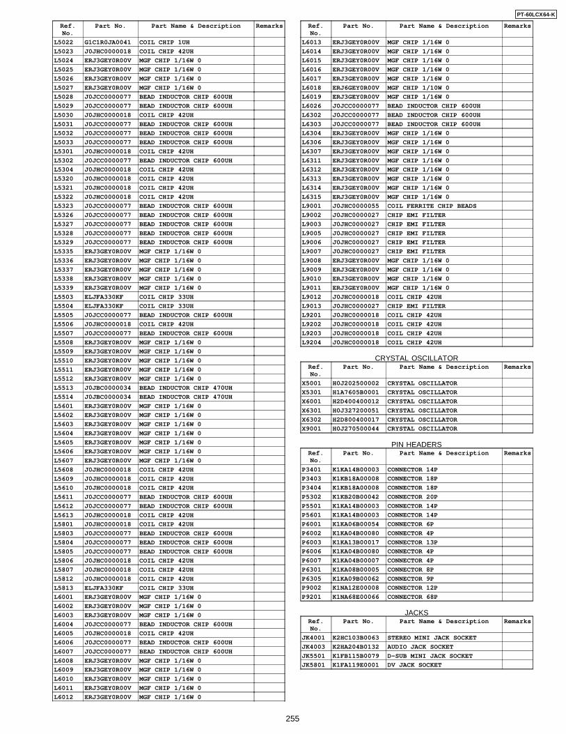
Ref.No.
Part No. Part Name & Description Remarks
L5022 G1C1R0JA0041 COIL CHIP 1UH
L5023 J0JHC0000018 COIL CHIP 42UH
L5024 ERJ3GEY0R00V MGF CHIP 1/16W 0
L5025 ERJ3GEY0R00V MGF CHIP 1/16W 0
L5026 ERJ3GEY0R00V MGF CHIP 1/16W 0
L5027 ERJ3GEY0R00V MGF CHIP 1/16W 0
L5028 J0JCC0000077 BEAD INDUCTOR CHIP 600UH
L5029 J0JCC0000077 BEAD INDUCTOR CHIP 600UH
L5030 J0JHC0000018 COIL CHIP 42UH
L5031 J0JCC0000077 BEAD INDUCTOR CHIP 600UH
L5032 J0JCC0000077 BEAD INDUCTOR CHIP 600UH
L5033 J0JCC0000077 BEAD INDUCTOR CHIP 600UH
L5301 J0JHC0000018 COIL CHIP 42UH
L5302 J0JCC0000077 BEAD INDUCTOR CHIP 600UH
L5304 J0JHC0000018 COIL CHIP 42UH
L5320 J0JHC0000018 COIL CHIP 42UH
L5321 J0JHC0000018 COIL CHIP 42UH
L5322 J0JHC0000018 COIL CHIP 42UH
L5323 J0JCC0000077 BEAD INDUCTOR CHIP 600UH
L5326 J0JCC0000077 BEAD INDUCTOR CHIP 600UH
L5327 J0JCC0000077 BEAD INDUCTOR CHIP 600UH
L5328 J0JCC0000077 BEAD INDUCTOR CHIP 600UH
L5329 J0JCC0000077 BEAD INDUCTOR CHIP 600UH
L5335 ERJ3GEY0R00V MGF CHIP 1/16W 0
L5336 ERJ3GEY0R00V MGF CHIP 1/16W 0
L5337 ERJ3GEY0R00V MGF CHIP 1/16W 0
L5338 ERJ3GEY0R00V MGF CHIP 1/16W 0
L5339 ERJ3GEY0R00V MGF CHIP 1/16W 0
L5503 ELJFA330KF COIL CHIP 33UH
L5504 ELJFA330KF COIL CHIP 33UH
L5505 J0JCC0000077 BEAD INDUCTOR CHIP 600UH
L5506 J0JHC0000018 COIL CHIP 42UH
L5507 J0JCC0000077 BEAD INDUCTOR CHIP 600UH
L5508 ERJ3GEY0R00V MGF CHIP 1/16W 0
L5509 ERJ3GEY0R00V MGF CHIP 1/16W 0
L5510 ERJ3GEY0R00V MGF CHIP 1/16W 0
L5511 ERJ3GEY0R00V MGF CHIP 1/16W 0
L5512 ERJ3GEY0R00V MGF CHIP 1/16W 0
L5513 J0JBC0000034 BEAD INDUCTOR CHIP 470UH
L5514 J0JBC0000034 BEAD INDUCTOR CHIP 470UH
L5601 ERJ3GEY0R00V MGF CHIP 1/16W 0
L5602 ERJ3GEY0R00V MGF CHIP 1/16W 0
L5603 ERJ3GEY0R00V MGF CHIP 1/16W 0
L5604 ERJ3GEY0R00V MGF CHIP 1/16W 0
L5605 ERJ3GEY0R00V MGF CHIP 1/16W 0
L5606 ERJ3GEY0R00V MGF CHIP 1/16W 0
L5607 ERJ3GEY0R00V MGF CHIP 1/16W 0
L5608 J0JHC0000018 COIL CHIP 42UH
L5609 J0JHC0000018 COIL CHIP 42UH
L5610 J0JHC0000018 COIL CHIP 42UH
L5611 J0JCC0000077 BEAD INDUCTOR CHIP 600UH
L5612 J0JCC0000077 BEAD INDUCTOR CHIP 600UH
L5613 J0JHC0000018 COIL CHIP 42UH
L5801 J0JHC0000018 COIL CHIP 42UH
L5803 J0JCC0000077 BEAD INDUCTOR CHIP 600UH
L5804 J0JCC0000077 BEAD INDUCTOR CHIP 600UH
L5805 J0JCC0000077 BEAD INDUCTOR CHIP 600UH
L5806 J0JHC0000018 COIL CHIP 42UH
L5807 J0JHC0000018 COIL CHIP 42UH
L5812 J0JHC0000018 COIL CHIP 42UH
L5813 ELJFA330KF COIL CHIP 33UH
L6001 ERJ3GEY0R00V MGF CHIP 1/16W 0
L6002 ERJ3GEY0R00V MGF CHIP 1/16W 0
L6003 ERJ3GEY0R00V MGF CHIP 1/16W 0
L6004 J0JCC0000077 BEAD INDUCTOR CHIP 600UH
L6005 J0JHC0000018 COIL CHIP 42UH
L6006 J0JCC0000077 BEAD INDUCTOR CHIP 600UH
L6007 J0JCC0000077 BEAD INDUCTOR CHIP 600UH
L6008 ERJ3GEY0R00V MGF CHIP 1/16W 0
L6009 ERJ3GEY0R00V MGF CHIP 1/16W 0
L6010 ERJ3GEY0R00V MGF CHIP 1/16W 0
L6011 ERJ3GEY0R00V MGF CHIP 1/16W 0
L6012 ERJ3GEY0R00V MGF CHIP 1/16W 0
Ref.No.
Part No. Part Name & Description Remarks
L6013 ERJ3GEY0R00V MGF CHIP 1/16W 0
L6014 ERJ3GEY0R00V MGF CHIP 1/16W 0
L6015 ERJ3GEY0R00V MGF CHIP 1/16W 0
L6016 ERJ3GEY0R00V MGF CHIP 1/16W 0
L6017 ERJ3GEY0R00V MGF CHIP 1/16W 0
L6018 ERJ6GEY0R00V MGF CHIP 1/10W 0
L6019 ERJ3GEY0R00V MGF CHIP 1/16W 0
L6026 J0JCC0000077 BEAD INDUCTOR CHIP 600UH
L6302 J0JCC0000077 BEAD INDUCTOR CHIP 600UH
L6303 J0JCC0000077 BEAD INDUCTOR CHIP 600UH
L6304 ERJ3GEY0R00V MGF CHIP 1/16W 0
L6306 ERJ3GEY0R00V MGF CHIP 1/16W 0
L6307 ERJ3GEY0R00V MGF CHIP 1/16W 0
L6311 ERJ3GEY0R00V MGF CHIP 1/16W 0
L6312 ERJ3GEY0R00V MGF CHIP 1/16W 0
L6313 ERJ3GEY0R00V MGF CHIP 1/16W 0
L6314 ERJ3GEY0R00V MGF CHIP 1/16W 0
L6315 ERJ3GEY0R00V MGF CHIP 1/16W 0
L9001 J0JHC0000055 COIL FERRITE CHIP BEADS
L9002 J0JHC0000027 CHIP EMI FILTER
L9003 J0JHC0000027 CHIP EMI FILTER
L9005 J0JHC0000027 CHIP EMI FILTER
L9006 J0JHC0000027 CHIP EMI FILTER
L9007 J0JHC0000027 CHIP EMI FILTER
L9008 ERJ3GEY0R00V MGF CHIP 1/16W 0
L9009 ERJ3GEY0R00V MGF CHIP 1/16W 0
L9010 ERJ3GEY0R00V MGF CHIP 1/16W 0
L9011 ERJ3GEY0R00V MGF CHIP 1/16W 0
L9012 J0JHC0000018 COIL CHIP 42UH
L9013 J0JHC0000027 CHIP EMI FILTER
L9201 J0JHC0000018 COIL CHIP 42UH
L9202 J0JHC0000018 COIL CHIP 42UH
L9203 J0JHC0000018 COIL CHIP 42UH
L9204 J0JHC0000018 COIL CHIP 42UH
CRYSTAL OSCILLATORRef.No.
Part No. Part Name & Description Remarks
X5001 H0J202500002 CRYSTAL OSCILLATOR
X5301 H1A7605B0001 CRYSTAL OSCILLATOR
X6001 H2D400400012 CRYSTAL OSCILLATOR
X6301 H0J327200051 CRYSTAL OSCILLATOR
X6302 H2D800400017 CRYSTAL OSCILLATOR
X9001 H0J270500044 CRYSTAL OSCILLATOR
PIN HEADERSRef.No.
Part No. Part Name & Description Remarks
P3401 K1KA14B00003 CONNECTOR 14P
P3403 K1KB18A00008 CONNECTOR 18P
P3404 K1KB18A00008 CONNECTOR 18P
P5302 K1KB20B00042 CONNECTOR 20P
P5501 K1KA14B00003 CONNECTOR 14P
P5601 K1KA14B00003 CONNECTOR 14P
P6001 K1KA06B00054 CONNECTOR 6P
P6002 K1KA04B00080 CONNECTOR 4P
P6003 K1KA13B00017 CONNECTOR 13P
P6006 K1KA04B00080 CONNECTOR 4P
P6007 K1KA04B00007 CONNECTOR 4P
P6301 K1KA08B00005 CONNECTOR 8P
P6305 K1KA09B00062 CONNECTOR 9P
P9002 K1NA12E00008 CONNECTOR 12P
P9201 K1NA68E00066 CONNECTOR 68P
JACKSRef.No.
Part No. Part Name & Description Remarks
JK4001 K2HC103B0063 STEREO MINI JACK SOCKET
JK4003 K2HA204B0132 AUDIO JACK SOCKET
JK5501 K1FB115B0079 D-SUB MINI JACK SOCKET
JK5801 K1FA119E0001 DV JACK SOCKET
255
PT-60LCX64-K
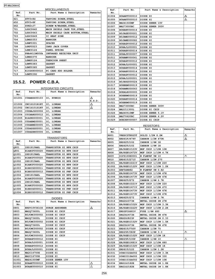
MISCELLANEOUSRef.No.
Part No. Part Name & Description Remarks
421 XTV3+8G TAPPING SCREW,STEEL
452 XTV3+8F TAPPING SCREW,STEEL
462 XYN2+J7 SCREW W/WASHER,STEEL
701 LSSC0642 MAIN SHIELD CASE TOP,STEEL
702 LSSC0643 MAIN SHIELD CASE BOTTOM,STEEL
703 LSSC0649 IC HEAT SINK
704 LSMZ0353 BARRIER
706 LSMF0301 SPACER
708 LSKF0523 CARD JACK COVER
709 LSMC0124 PANEL SPRING
711 PNA4611M00YA INFRARED RECEIVER UNIT
712 LSMZ0370 BARRIER
713 LSMG0124 THERCOON SHEET
715 LSMT0383 GASKET
716 LSMT0385 GASKET
717 K1YZ68000010 PC CARD HDD HOLDER
719 LSMT0392 GASKET
15.5.2. POWER C.B.A.INTEGRATED CIRCUITS
Ref.No.
Part No. Part Name & Description Remarks
IC1001 C5HABZZ00103 IC, HYBRIDE.S.D.
IC1002 CNC1S101R1KT IC, LINEAR
IC1002 CNC1S101S1KT IC, LINEAR
IC1003 C0DBAJG00006 IC, LINEAR
IC1004 C0CAAHG00012 IC, LINEAR
IC1005 B1AZKD000001 IC, LINEAR
IC1005 C0DAEMZ00001 IC, LINEAR
IC1005 C0DAEMZ00005 IC, LINEAR
IC1006 C0DAZGG00001 IC, LINEAR
IC1007 C0DAZHH00006 IC, LINEAR
TRANSISTORSRef.No.
Part No. Part Name & Description Remarks
Q801 2SD1819AHL TRANSISTOR SI NPN CHIP
Q801 B1ABCF000020 TRANSISTOR SI NPN CHIP
Q1001 2SD1819AHL TRANSISTOR SI NPN CHIP
Q1001 B1ABCF000020 TRANSISTOR SI NPN CHIP
Q1002 2SD1819AHL TRANSISTOR SI NPN CHIP
Q1002 B1ABCF000020 TRANSISTOR SI NPN CHIP
Q1003 B1BDCG000011 TRANSISTOR SI PNP CHIP
Q1003 B1BDCG000012 TRANSISTOR SI PNP CHIP
Q1004 2SD1819AHL TRANSISTOR SI NPN CHIP
Q1004 B1ABCF000020 TRANSISTOR SI NPN CHIP
Q1005 2SD1819AHL TRANSISTOR SI NPN CHIP
Q1005 B1ABCF000020 TRANSISTOR SI NPN CHIP
Q1006 B1BDCG000011 TRANSISTOR SI PNP CHIP
Q1006 B1BDCG000012 TRANSISTOR SI PNP CHIP
DIODESRef.No.
Part No. Part Name & Description Remarks
D801 ERZV10V361CS SURGE ABSORBER
D803 MA2Q73600L DIODE SI CHIP
D803 B0JCMC000002 DIODE SI CHIP
D804 MA2Q73600L DIODE SI CHIP
D804 B0JCMC000002 DIODE SI CHIP
D805 MA2Q73600L DIODE SI CHIP
D805 B0JCMC000002 DIODE SI CHIP
D806 MA2Q73600L DIODE SI CHIP
D806 B0JCMC000002 DIODE SI CHIP
D807 B0HAGP000012 DIODE SI
D807 B0HAJL000001 DIODE SI
D808 B0HAGP000012 DIODE SI
D808 B0HAJL000001 DIODE SI
D809 MA2C16700E DIODE SI
D810 MA2C16700E DIODE SI
D1001 MAZ41500MF DIODE ZENER 15V
D1002 B0AAKT000010 DIODE SI
D1003 B0AAKT000010 DIODE SI
Ref.No.
Part No. Part Name & Description Remarks
D1004 B0AAKT000010 DIODE SI
D1005 B0AAKT000010 DIODE SI
D1006 MAZ41500MF DIODE ZENER 15V
D1007 MAZ73000BC DIODE ZENER 300V
D1008 B0HAHP000014 DIODE SI
D1009 B0JAGE000001 DIODE SI
D1009 B0JAMD000012 DIODE SI
D1009 B0JAME000082 DIODE SI
D1010 B0HAGP000012 DIODE SI
D1010 B0HAJL000001 DIODE SI
D1011 B0HAHP000014 DIODE SI
D1011 B0HAJP000007 DIODE SI
D1011 B0HAMP000061 DIODE SI
D1012 B0HAGP000012 DIODE SI
D1012 B0HAJL000001 DIODE SI
D1013 B0HAHP000014 DIODE SI
D1014 B0HAHP000014 DIODE SI
D1015 B0HAGP000012 DIODE SI
D1015 B0HAJL000001 DIODE SI
D1016 B0JBSG000024 DIODE SI
D1017 B0HBRM000019 DIODE SI
D1018 B0HAMR000063 DIODE SI
D1018 B0EALR000005 DIODE SI
D1019 B0HBRM000019 DIODE SI
D1020 B0HAHP000014 DIODE SI
D1021 B0HBRM000019 DIODE SI
D1022 MAZ73000BC DIODE ZENER 300V
D1024 MA2J11300L DIODE SI CHIP
D1026 MAZ40510MF DIODE ZENER 5.1V
D1028 MAZ70620BC DIODE ZENER 6.2V
D1029 B0ECKP000007 DIODE SI CHIP
RESISTORSRef.No.
Part No. Part Name & Description Remarks
R801 VRESC2TK825T SOLID 1/2W 8.2M
R802 ERDS1FJ474T CARBON 1/2W 470K
R805 ERDS2TJ102 CARBON 1/4W 1K
R806 ERDS2TJ102 CARBON 1/4W 1K
R807 ERJ6GEYJ103V MGF CHIP 1/10W 10K
R808 ERJ6GEYJ472V MGF CHIP 1/10W 4.7K
R809 D1FZ100E0001 W FLMPRF 5W 10
R810 ERDS1TJ271T CARBON 1/2W 270
R1001 ERJ6GEYJ221V MGF CHIP 1/10W 220
R1002 ERJ6GEYJ122V MGF CHIP 1/10W 1.2K
R1003 ERF5ZKR82 W FLMPRF 5W 0.82
R1005 ERJ6GEYJ473V MGF CHIP 1/10W 47K
R1006 ERJ6GEYJ473V MGF CHIP 1/10W 47K
R1007 ERDS2TJ272 CARBON 1/4W 2.7K
R1008 ERJ6GEYJ221V MGF CHIP 1/10W 220
R1009 ERJ6GEYJ471V MGF CHIP 1/10W 470
R1011 ERJ6GEYJ473V MGF CHIP 1/10W 47K
R1012 ERJ6GEYJ473V MGF CHIP 1/10W 47K
R1013 ERDS2TJ272 CARBON 1/4W 2.7K
R1014 ERG2SJ273H METAL OXIDE 2W 27K
R1015 ERJ6GEYJ332V MGF CHIP 1/10W 3.3K
R1016 ERJ6GEYJ222V MGF CHIP 1/10W 2.2K
R1017 ERD2FCG681V FUSE 1/4W 680
R1018 ERG3SJ473H METAL OXIDE 3W 47K
R1020 ERX2SJR33P METAL OXIDE 2W 0.33
R1021 ERJ6GEYJ152V MGF CHIP 1/10W 1.5K
R1022 ERG3SJ473H METAL OXIDE 3W 47K
R1023 ERDS1TJ750T CARBON 1/2W 75
R1024 ERD25FJ3R3P CARBON 1/4W 3.3
R1026 ERJ6GEYJ102V MGF CHIP 1/10W 1K
R1027 ERD25FJ100P CARBON 1/4W 10
R1028 ERJ6GEYJ681V MGF CHIP 1/10W 680
R1029 ERJ6GEYJ102V MGF CHIP 1/10W 1K
R1030 ERDS1TJ122 CARBON 1/2W 1.2K
R1031 D0HD332ZA002 MGF CHIP 1/10W 3.3K
R1032 D0HD331ZA002 MGF CHIP 1/10W 330
R1033 D0HD103ZA002 MGF CHIP 1/10W 10K
R1034 ERG1SJ182E METAL OXIDE 1W 1.8K
R1035 ERG1SJ182E METAL OXIDE 1W 1.8K
256
PT-60LCX64-K
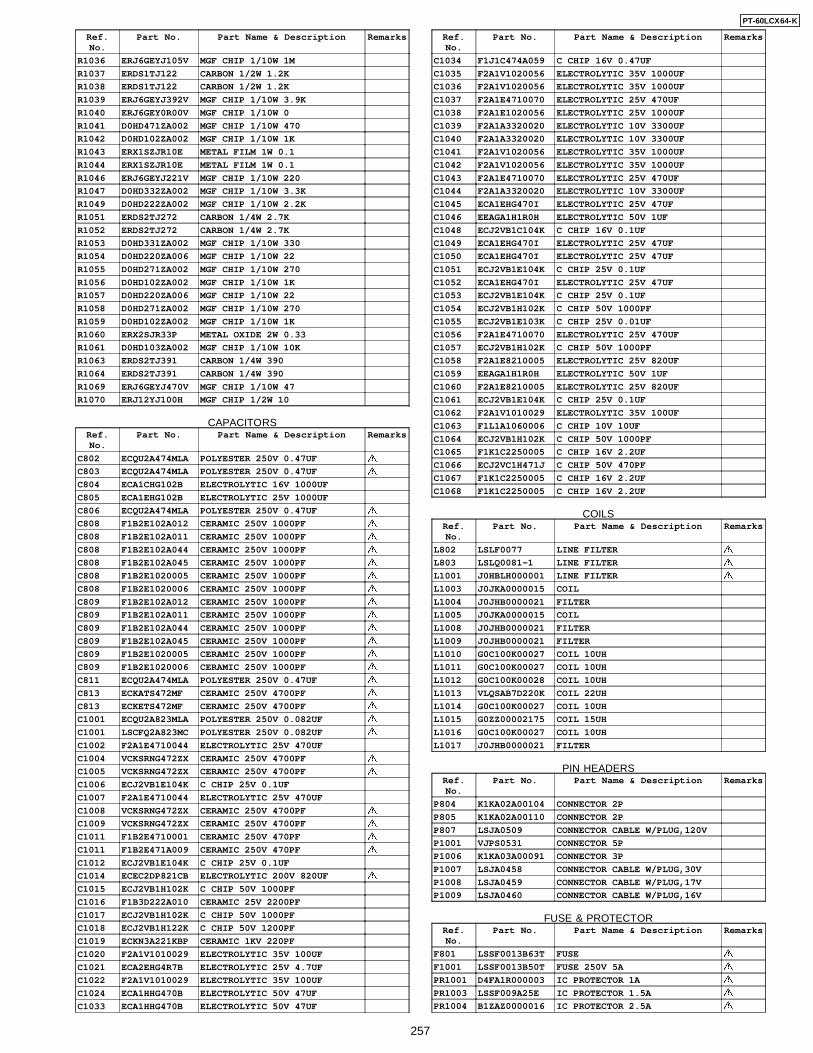
Ref.No.
Part No. Part Name & Description Remarks
R1036 ERJ6GEYJ105V MGF CHIP 1/10W 1M
R1037 ERDS1TJ122 CARBON 1/2W 1.2K
R1038 ERDS1TJ122 CARBON 1/2W 1.2K
R1039 ERJ6GEYJ392V MGF CHIP 1/10W 3.9K
R1040 ERJ6GEY0R00V MGF CHIP 1/10W 0
R1041 D0HD471ZA002 MGF CHIP 1/10W 470
R1042 D0HD102ZA002 MGF CHIP 1/10W 1K
R1043 ERX1SZJR10E METAL FILM 1W 0.1
R1044 ERX1SZJR10E METAL FILM 1W 0.1
R1046 ERJ6GEYJ221V MGF CHIP 1/10W 220
R1047 D0HD332ZA002 MGF CHIP 1/10W 3.3K
R1049 D0HD222ZA002 MGF CHIP 1/10W 2.2K
R1051 ERDS2TJ272 CARBON 1/4W 2.7K
R1052 ERDS2TJ272 CARBON 1/4W 2.7K
R1053 D0HD331ZA002 MGF CHIP 1/10W 330
R1054 D0HD220ZA006 MGF CHIP 1/10W 22
R1055 D0HD271ZA002 MGF CHIP 1/10W 270
R1056 D0HD102ZA002 MGF CHIP 1/10W 1K
R1057 D0HD220ZA006 MGF CHIP 1/10W 22
R1058 D0HD271ZA002 MGF CHIP 1/10W 270
R1059 D0HD102ZA002 MGF CHIP 1/10W 1K
R1060 ERX2SJR33P METAL OXIDE 2W 0.33
R1061 D0HD103ZA002 MGF CHIP 1/10W 10K
R1063 ERDS2TJ391 CARBON 1/4W 390
R1064 ERDS2TJ391 CARBON 1/4W 390
R1069 ERJ6GEYJ470V MGF CHIP 1/10W 47
R1070 ERJ12YJ100H MGF CHIP 1/2W 10
CAPACITORSRef.No.
Part No. Part Name & Description Remarks
C802 ECQU2A474MLA POLYESTER 250V 0.47UF
C803 ECQU2A474MLA POLYESTER 250V 0.47UF
C804 ECA1CHG102B ELECTROLYTIC 16V 1000UF
C805 ECA1EHG102B ELECTROLYTIC 25V 1000UF
C806 ECQU2A474MLA POLYESTER 250V 0.47UF
C808 F1B2E102A012 CERAMIC 250V 1000PF
C808 F1B2E102A011 CERAMIC 250V 1000PF
C808 F1B2E102A044 CERAMIC 250V 1000PF
C808 F1B2E102A045 CERAMIC 250V 1000PF
C808 F1B2E1020005 CERAMIC 250V 1000PF
C808 F1B2E1020006 CERAMIC 250V 1000PF
C809 F1B2E102A012 CERAMIC 250V 1000PF
C809 F1B2E102A011 CERAMIC 250V 1000PF
C809 F1B2E102A044 CERAMIC 250V 1000PF
C809 F1B2E102A045 CERAMIC 250V 1000PF
C809 F1B2E1020005 CERAMIC 250V 1000PF
C809 F1B2E1020006 CERAMIC 250V 1000PF
C811 ECQU2A474MLA POLYESTER 250V 0.47UF
C813 ECKATS472MF CERAMIC 250V 4700PF
C813 ECKETS472MF CERAMIC 250V 4700PF
C1001 ECQU2A823MLA POLYESTER 250V 0.082UF
C1001 LSCFQ2A823MC POLYESTER 250V 0.082UF
C1002 F2A1E4710044 ELECTROLYTIC 25V 470UF
C1004 VCKSRNG472ZX CERAMIC 250V 4700PF
C1005 VCKSRNG472ZX CERAMIC 250V 4700PF
C1006 ECJ2VB1E104K C CHIP 25V 0.1UF
C1007 F2A1E4710044 ELECTROLYTIC 25V 470UF
C1008 VCKSRNG472ZX CERAMIC 250V 4700PF
C1009 VCKSRNG472ZX CERAMIC 250V 4700PF
C1011 F1B2E4710001 CERAMIC 250V 470PF
C1011 F1B2E471A009 CERAMIC 250V 470PF
C1012 ECJ2VB1E104K C CHIP 25V 0.1UF
C1014 ECEC2DP821CB ELECTROLYTIC 200V 820UF
C1015 ECJ2VB1H102K C CHIP 50V 1000PF
C1016 F1B3D222A010 CERAMIC 25V 2200PF
C1017 ECJ2VB1H102K C CHIP 50V 1000PF
C1018 ECJ2VB1H122K C CHIP 50V 1200PF
C1019 ECKN3A221KBP CERAMIC 1KV 220PF
C1020 F2A1V1010029 ELECTROLYTIC 35V 100UF
C1021 ECA2EHG4R7B ELECTROLYTIC 25V 4.7UF
C1022 F2A1V1010029 ELECTROLYTIC 35V 100UF
C1024 ECA1HHG470B ELECTROLYTIC 50V 47UF
C1033 ECA1HHG470B ELECTROLYTIC 50V 47UF
Ref.No.
Part No. Part Name & Description Remarks
C1034 F1J1C474A059 C CHIP 16V 0.47UF
C1035 F2A1V1020056 ELECTROLYTIC 35V 1000UF
C1036 F2A1V1020056 ELECTROLYTIC 35V 1000UF
C1037 F2A1E4710070 ELECTROLYTIC 25V 470UF
C1038 F2A1E1020056 ELECTROLYTIC 25V 1000UF
C1039 F2A1A3320020 ELECTROLYTIC 10V 3300UF
C1040 F2A1A3320020 ELECTROLYTIC 10V 3300UF
C1041 F2A1V1020056 ELECTROLYTIC 35V 1000UF
C1042 F2A1V1020056 ELECTROLYTIC 35V 1000UF
C1043 F2A1E4710070 ELECTROLYTIC 25V 470UF
C1044 F2A1A3320020 ELECTROLYTIC 10V 3300UF
C1045 ECA1EHG470I ELECTROLYTIC 25V 47UF
C1046 EEAGA1H1R0H ELECTROLYTIC 50V 1UF
C1048 ECJ2VB1C104K C CHIP 16V 0.1UF
C1049 ECA1EHG470I ELECTROLYTIC 25V 47UF
C1050 ECA1EHG470I ELECTROLYTIC 25V 47UF
C1051 ECJ2VB1E104K C CHIP 25V 0.1UF
C1052 ECA1EHG470I ELECTROLYTIC 25V 47UF
C1053 ECJ2VB1E104K C CHIP 25V 0.1UF
C1054 ECJ2VB1H102K C CHIP 50V 1000PF
C1055 ECJ2VB1E103K C CHIP 25V 0.01UF
C1056 F2A1E4710070 ELECTROLYTIC 25V 470UF
C1057 ECJ2VB1H102K C CHIP 50V 1000PF
C1058 F2A1E8210005 ELECTROLYTIC 25V 820UF
C1059 EEAGA1H1R0H ELECTROLYTIC 50V 1UF
C1060 F2A1E8210005 ELECTROLYTIC 25V 820UF
C1061 ECJ2VB1E104K C CHIP 25V 0.1UF
C1062 F2A1V1010029 ELECTROLYTIC 35V 100UF
C1063 F1L1A1060006 C CHIP 10V 10UF
C1064 ECJ2VB1H102K C CHIP 50V 1000PF
C1065 F1K1C2250005 C CHIP 16V 2.2UF
C1066 ECJ2VC1H471J C CHIP 50V 470PF
C1067 F1K1C2250005 C CHIP 16V 2.2UF
C1068 F1K1C2250005 C CHIP 16V 2.2UF
COILSRef.No.
Part No. Part Name & Description Remarks
L802 LSLF0077 LINE FILTER
L803 LSLQ0081-1 LINE FILTER
L1001 J0HBLH000001 LINE FILTER
L1003 J0JKA0000015 COIL
L1004 J0JHB0000021 FILTER
L1005 J0JKA0000015 COIL
L1008 J0JHB0000021 FILTER
L1009 J0JHB0000021 FILTER
L1010 G0C100K00027 COIL 10UH
L1011 G0C100K00027 COIL 10UH
L1012 G0C100K00028 COIL 10UH
L1013 VLQSAB7D220K COIL 22UH
L1014 G0C100K00027 COIL 10UH
L1015 G0ZZ00002175 COIL 15UH
L1016 G0C100K00027 COIL 10UH
L1017 J0JHB0000021 FILTER
PIN HEADERSRef.No.
Part No. Part Name & Description Remarks
P804 K1KA02A00104 CONNECTOR 2P
P805 K1KA02A00110 CONNECTOR 2P
P807 LSJA0509 CONNECTOR CABLE W/PLUG,120V
P1001 VJPS0531 CONNECTOR 5P
P1006 K1KA03A00091 CONNECTOR 3P
P1007 LSJA0458 CONNECTOR CABLE W/PLUG,30V
P1008 LSJA0459 CONNECTOR CABLE W/PLUG,17V
P1009 LSJA0460 CONNECTOR CABLE W/PLUG,16V
FUSE & PROTECTORRef.No.
Part No. Part Name & Description Remarks
F801 LSSF0013B63T FUSE
F1001 LSSF0013B50T FUSE 250V 5A
PR1001 D4FA1R000003 IC PROTECTOR 1A
PR1003 LSSF009A25E IC PROTECTOR 1.5A
PR1004 B1ZAZ0000016 IC PROTECTOR 2.5A
257
PT-60LCX64-K
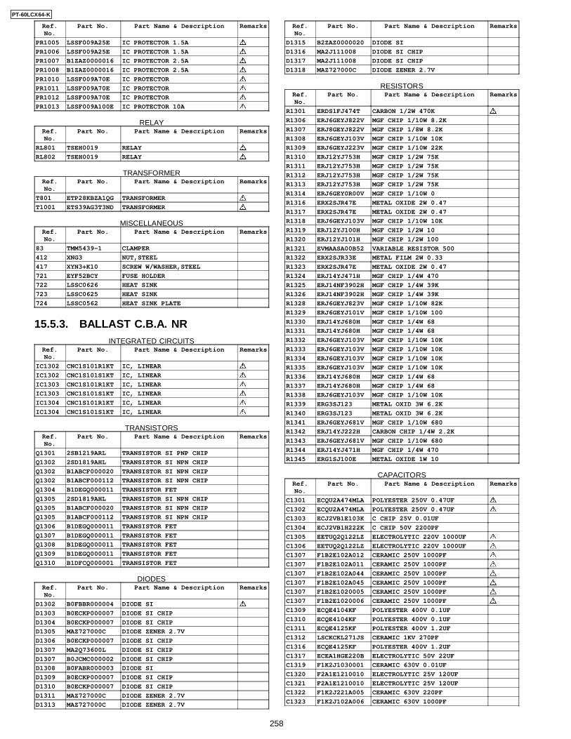
Ref.No.
Part No. Part Name & Description Remarks
PR1005 LSSF009A25E IC PROTECTOR 1.5A
PR1006 LSSF009A25E IC PROTECTOR 1.5A
PR1007 B1ZAZ0000016 IC PROTECTOR 2.5A
PR1008 B1ZAZ0000016 IC PROTECTOR 2.5A
PR1010 LSSF009A70E IC PROTECTOR
PR1011 LSSF009A70E IC PROTECTOR
PR1012 LSSF009A70E IC PROTECTOR
PR1013 LSSF009A100E IC PROTECTOR 10A
RELAYRef.No.
Part No. Part Name & Description Remarks
RL801 TSEH0019 RELAY
RL802 TSEH0019 RELAY
TRANSFORMERRef.No.
Part No. Part Name & Description Remarks
T801 ETP28KBZA1QG TRANSFORMER
T1001 ETS39AG3T3ND TRANSFORMER
MISCELLANEOUSRef.No.
Part No. Part Name & Description Remarks
83 TMM5439-1 CLAMPER
412 XNG3 NUT,STEEL
417 XYN3+K10 SCREW W/WASHER,STEEL
721 EYF52BCY FUSE HOLDER
722 LSSC0626 HEAT SINK
723 LSSC0625 HEAT SINK
724 LSSC0562 HEAT SINK PLATE
15.5.3. BALLAST C.B.A. NRINTEGRATED CIRCUITS
Ref.No.
Part No. Part Name & Description Remarks
IC1302 CNC1S101R1KT IC, LINEAR
IC1302 CNC1S101S1KT IC, LINEAR
IC1303 CNC1S101R1KT IC, LINEAR
IC1303 CNC1S101S1KT IC, LINEAR
IC1304 CNC1S101R1KT IC, LINEAR
IC1304 CNC1S101S1KT IC, LINEAR
TRANSISTORSRef.No.
Part No. Part Name & Description Remarks
Q1301 2SB1219ARL TRANSISTOR SI PNP CHIP
Q1302 2SD1819AHL TRANSISTOR SI NPN CHIP
Q1302 B1ABCF000020 TRANSISTOR SI NPN CHIP
Q1302 B1ABCF000112 TRANSISTOR SI NPN CHIP
Q1304 B1DEGQ000011 TRANSISTOR FET
Q1305 2SD1819AHL TRANSISTOR SI NPN CHIP
Q1305 B1ABCF000020 TRANSISTOR SI NPN CHIP
Q1305 B1ABCF000112 TRANSISTOR SI NPN CHIP
Q1306 B1DEGQ000011 TRANSISTOR FET
Q1307 B1DEGQ000011 TRANSISTOR FET
Q1308 B1DEGQ000011 TRANSISTOR FET
Q1309 B1DEGQ000011 TRANSISTOR FET
Q1310 B1DFCQ000001 TRANSISTOR FET
DIODESRef.No.
Part No. Part Name & Description Remarks
D1302 B0FBBR000004 DIODE SI
D1303 B0ECKP000007 DIODE SI CHIP
D1304 B0ECKP000007 DIODE SI CHIP
D1305 MAZ727000C DIODE ZENER 2.7V
D1306 B0ECKP000007 DIODE SI CHIP
D1307 MA2Q73600L DIODE SI CHIP
D1307 B0JCMC000002 DIODE SI CHIP
D1308 B0FABR000003 DIODE SI
D1309 B0ECKP000007 DIODE SI CHIP
D1310 B0ECKP000007 DIODE SI CHIP
D1311 MAZ727000C DIODE ZENER 2.7V
D1313 MAZ727000C DIODE ZENER 2.7V
Ref.No.
Part No. Part Name & Description Remarks
D1315 B2ZAZ0000020 DIODE SI
D1316 MA2J111008 DIODE SI CHIP
D1317 MA2J111008 DIODE SI CHIP
D1318 MAZ727000C DIODE ZENER 2.7V
RESISTORSRef.No.
Part No. Part Name & Description Remarks
R1301 ERDS1FJ474T CARBON 1/2W 470K
R1306 ERJ6GEYJ822V MGF CHIP 1/10W 8.2K
R1307 ERJ8GEYJ822V MGF CHIP 1/8W 8.2K
R1308 ERJ6GEYJ103V MGF CHIP 1/10W 10K
R1309 ERJ6GEYJ223V MGF CHIP 1/10W 22K
R1310 ERJ12YJ753H MGF CHIP 1/2W 75K
R1311 ERJ12YJ753H MGF CHIP 1/2W 75K
R1312 ERJ12YJ753H MGF CHIP 1/2W 75K
R1313 ERJ12YJ753H MGF CHIP 1/2W 75K
R1314 ERJ6GEY0R00V MGF CHIP 1/10W 0
R1316 ERX2SJR47E METAL OXIDE 2W 0.47
R1317 ERX2SJR47E METAL OXIDE 2W 0.47
R1318 ERJ6GEYJ103V MGF CHIP 1/10W 10K
R1319 ERJ12YJ100H MGF CHIP 1/2W 10
R1320 ERJ12YJ101H MGF CHIP 1/2W 100
R1321 EVMAASA00B52 VARIABLE RESISTOR 500
R1322 ERX2SJR33E METAL FILM 2W 0.33
R1323 ERX2SJR47E METAL OXIDE 2W 0.47
R1324 ERJ14YJ471H MGF CHIP 1/4W 470
R1325 ERJ14NF3902H MGF CHIP 1/4W 39K
R1326 ERJ14NF3902H MGF CHIP 1/4W 39K
R1328 ERJ6GEYJ823V MGF CHIP 1/10W 82K
R1329 ERJ6GEYJ101V MGF CHIP 1/10W 100
R1330 ERJ14YJ680H MGF CHIP 1/4W 68
R1331 ERJ14YJ680H MGF CHIP 1/4W 68
R1332 ERJ6GEYJ103V MGF CHIP 1/10W 10K
R1333 ERJ6GEYJ103V MGF CHIP 1/10W 10K
R1334 ERJ6GEYJ103V MGF CHIP 1/10W 10K
R1335 ERJ6GEYJ103V MGF CHIP 1/10W 10K
R1336 ERJ14YJ680H MGF CHIP 1/4W 68
R1337 ERJ14YJ680H MGF CHIP 1/4W 68
R1338 ERJ6GEYJ103V MGF CHIP 1/10W 10K
R1339 ERG3SJ123 METAL OXID 3W 6.2K
R1340 ERG3SJ123 METAL OXID 3W 6.2K
R1341 ERJ6GEYJ681V MGF CHIP 1/10W 680
R1342 ERJ14YJ222H CARBON CHIP 1/4W 2.2K
R1343 ERJ6GEYJ681V MGF CHIP 1/10W 680
R1344 ERJ14YJ471H MGF CHIP 1/4W 470
R1345 ERG1SJ100E METAL OXIDE 1W 10
CAPACITORSRef.No.
Part No. Part Name & Description Remarks
C1301 ECQU2A474MLA POLYESTER 250V 0.47UF
C1302 ECQU2A474MLA POLYESTER 250V 0.47UF
C1303 ECJ2VB1E103K C CHIP 25V 0.01UF
C1304 ECJ2VB1H222K C CHIP 50V 2200PF
C1305 EETUQ2Q122LZ ELECTROLYTIC 220V 1000UF
C1306 EETUQ2Q122LZ ELECTROLYTIC 220V 1000UF
C1307 F1B2E102A012 CERAMIC 250V 1000PF
C1307 F1B2E102A011 CERAMIC 250V 1000PF
C1307 F1B2E102A044 CERAMIC 250V 1000PF
C1307 F1B2E102A045 CERAMIC 250V 1000PF
C1307 F1B2E1020005 CERAMIC 250V 1000PF
C1307 F1B2E1020006 CERAMIC 250V 1000PF
C1309 ECQE4104KF POLYESTER 400V 0.1UF
C1310 ECQE4104KF POLYESTER 400V 0.1UF
C1311 ECQE4125KF POLYESTER 400V 1.2UF
C1312 LSCKCKL271JS CERAMIC 1KV 270PF
C1316 ECQE4125KF POLYESTER 400V 1.2UF
C1317 ECEA1HGE220B ELECTROLYTIC 50V 22UF
C1319 F1K2J1030001 CERAMIC 630V 0.01UF
C1320 F2A1E1210010 ELECTROLYTIC 25V 120UF
C1321 F2A1E1210010 ELECTROLYTIC 25V 120UF
C1322 F1K2J221A005 CERAMIC 630V 220PF
C1323 F1K2J102A006 CERAMIC 630V 1000PF
258
PT-60LCX64-K
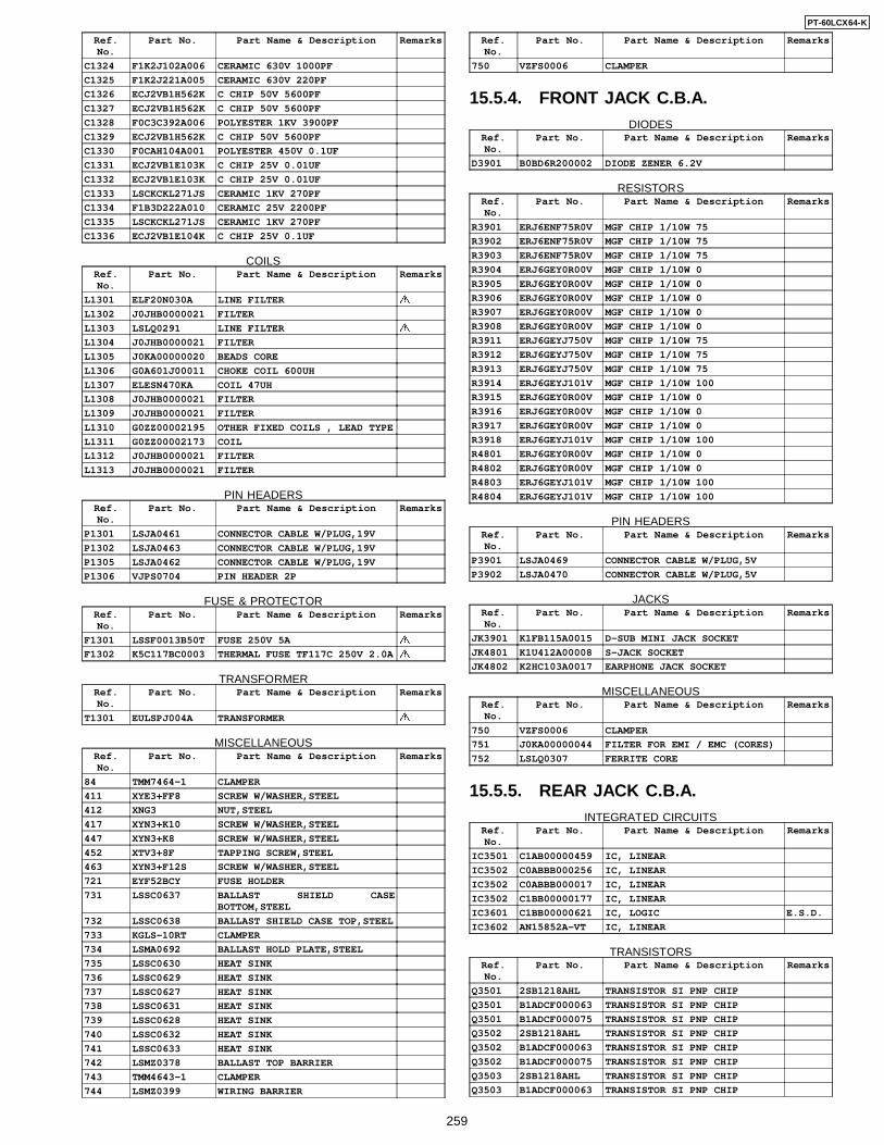
Ref.No.
Part No. Part Name & Description Remarks
C1324 F1K2J102A006 CERAMIC 630V 1000PF
C1325 F1K2J221A005 CERAMIC 630V 220PF
C1326 ECJ2VB1H562K C CHIP 50V 5600PF
C1327 ECJ2VB1H562K C CHIP 50V 5600PF
C1328 F0C3C392A006 POLYESTER 1KV 3900PF
C1329 ECJ2VB1H562K C CHIP 50V 5600PF
C1330 F0CAH104A001 POLYESTER 450V 0.1UF
C1331 ECJ2VB1E103K C CHIP 25V 0.01UF
C1332 ECJ2VB1E103K C CHIP 25V 0.01UF
C1333 LSCKCKL271JS CERAMIC 1KV 270PF
C1334 F1B3D222A010 CERAMIC 25V 2200PF
C1335 LSCKCKL271JS CERAMIC 1KV 270PF
C1336 ECJ2VB1E104K C CHIP 25V 0.1UF
COILSRef.No.
Part No. Part Name & Description Remarks
L1301 ELF20N030A LINE FILTER
L1302 J0JHB0000021 FILTER
L1303 LSLQ0291 LINE FILTER
L1304 J0JHB0000021 FILTER
L1305 J0KA00000020 BEADS CORE
L1306 G0A601J00011 CHOKE COIL 600UH
L1307 ELESN470KA COIL 47UH
L1308 J0JHB0000021 FILTER
L1309 J0JHB0000021 FILTER
L1310 G0ZZ00002195 OTHER FIXED COILS , LEAD TYPE
L1311 G0ZZ00002173 COIL
L1312 J0JHB0000021 FILTER
L1313 J0JHB0000021 FILTER
PIN HEADERSRef.No.
Part No. Part Name & Description Remarks
P1301 LSJA0461 CONNECTOR CABLE W/PLUG,19V
P1302 LSJA0463 CONNECTOR CABLE W/PLUG,19V
P1305 LSJA0462 CONNECTOR CABLE W/PLUG,19V
P1306 VJPS0704 PIN HEADER 2P
FUSE & PROTECTORRef.No.
Part No. Part Name & Description Remarks
F1301 LSSF0013B50T FUSE 250V 5A
F1302 K5C117BC0003 THERMAL FUSE TF117C 250V 2.0A
TRANSFORMERRef.No.
Part No. Part Name & Description Remarks
T1301 EULSPJ004A TRANSFORMER
MISCELLANEOUSRef.No.
Part No. Part Name & Description Remarks
84 TMM7464-1 CLAMPER
411 XYE3+FF8 SCREW W/WASHER,STEEL
412 XNG3 NUT,STEEL
417 XYN3+K10 SCREW W/WASHER,STEEL
447 XYN3+K8 SCREW W/WASHER,STEEL
452 XTV3+8F TAPPING SCREW,STEEL
463 XYN3+F12S SCREW W/WASHER,STEEL
721 EYF52BCY FUSE HOLDER
731 LSSC0637 BALLAST SHIELD CASEBOTTOM,STEEL
732 LSSC0638 BALLAST SHIELD CASE TOP,STEEL
733 KGLS-10RT CLAMPER
734 LSMA0692 BALLAST HOLD PLATE,STEEL
735 LSSC0630 HEAT SINK
736 LSSC0629 HEAT SINK
737 LSSC0627 HEAT SINK
738 LSSC0631 HEAT SINK
739 LSSC0628 HEAT SINK
740 LSSC0632 HEAT SINK
741 LSSC0633 HEAT SINK
742 LSMZ0378 BALLAST TOP BARRIER
743 TMM4643-1 CLAMPER
744 LSMZ0399 WIRING BARRIER
Ref.No.
Part No. Part Name & Description Remarks
750 VZFS0006 CLAMPER
15.5.4. FRONT JACK C.B.A.DIODES
Ref.No.
Part No. Part Name & Description Remarks
D3901 B0BD6R200002 DIODE ZENER 6.2V
RESISTORSRef.No.
Part No. Part Name & Description Remarks
R3901 ERJ6ENF75R0V MGF CHIP 1/10W 75
R3902 ERJ6ENF75R0V MGF CHIP 1/10W 75
R3903 ERJ6ENF75R0V MGF CHIP 1/10W 75
R3904 ERJ6GEY0R00V MGF CHIP 1/10W 0
R3905 ERJ6GEY0R00V MGF CHIP 1/10W 0
R3906 ERJ6GEY0R00V MGF CHIP 1/10W 0
R3907 ERJ6GEY0R00V MGF CHIP 1/10W 0
R3908 ERJ6GEY0R00V MGF CHIP 1/10W 0
R3911 ERJ6GEYJ750V MGF CHIP 1/10W 75
R3912 ERJ6GEYJ750V MGF CHIP 1/10W 75
R3913 ERJ6GEYJ750V MGF CHIP 1/10W 75
R3914 ERJ6GEYJ101V MGF CHIP 1/10W 100
R3915 ERJ6GEY0R00V MGF CHIP 1/10W 0
R3916 ERJ6GEY0R00V MGF CHIP 1/10W 0
R3917 ERJ6GEY0R00V MGF CHIP 1/10W 0
R3918 ERJ6GEYJ101V MGF CHIP 1/10W 100
R4801 ERJ6GEY0R00V MGF CHIP 1/10W 0
R4802 ERJ6GEY0R00V MGF CHIP 1/10W 0
R4803 ERJ6GEYJ101V MGF CHIP 1/10W 100
R4804 ERJ6GEYJ101V MGF CHIP 1/10W 100
PIN HEADERSRef.No.
Part No. Part Name & Description Remarks
P3901 LSJA0469 CONNECTOR CABLE W/PLUG,5V
P3902 LSJA0470 CONNECTOR CABLE W/PLUG,5V
JACKSRef.No.
Part No. Part Name & Description Remarks
JK3901 K1FB115A0015 D-SUB MINI JACK SOCKET
JK4801 K1U412A00008 S-JACK SOCKET
JK4802 K2HC103A0017 EARPHONE JACK SOCKET
MISCELLANEOUSRef.No.
Part No. Part Name & Description Remarks
750 VZFS0006 CLAMPER
751 J0KA00000044 FILTER FOR EMI / EMC (CORES)
752 LSLQ0307 FERRITE CORE
15.5.5. REAR JACK C.B.A.INTEGRATED CIRCUITS
Ref.No.
Part No. Part Name & Description Remarks
IC3501 C1AB00000459 IC, LINEAR
IC3502 C0ABBB000256 IC, LINEAR
IC3502 C0ABBB000017 IC, LINEAR
IC3502 C1BB00000177 IC, LINEAR
IC3601 C1BB00000621 IC, LOGIC E.S.D.
IC3602 AN15852A-VT IC, LINEAR
TRANSISTORSRef.No.
Part No. Part Name & Description Remarks
Q3501 2SB1218AHL TRANSISTOR SI PNP CHIP
Q3501 B1ADCF000063 TRANSISTOR SI PNP CHIP
Q3501 B1ADCF000075 TRANSISTOR SI PNP CHIP
Q3502 2SB1218AHL TRANSISTOR SI PNP CHIP
Q3502 B1ADCF000063 TRANSISTOR SI PNP CHIP
Q3502 B1ADCF000075 TRANSISTOR SI PNP CHIP
Q3503 2SB1218AHL TRANSISTOR SI PNP CHIP
Q3503 B1ADCF000063 TRANSISTOR SI PNP CHIP
259
PT-60LCX64-K
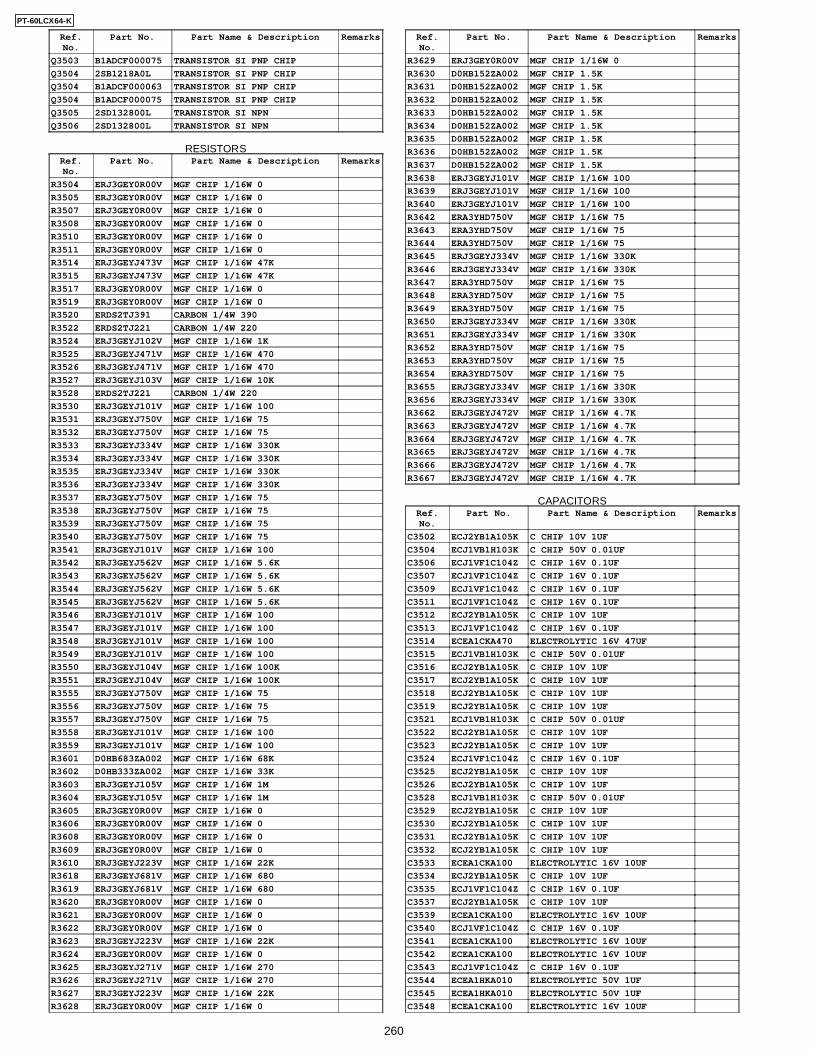
Ref.No.
Part No. Part Name & Description Remarks
Q3503 B1ADCF000075 TRANSISTOR SI PNP CHIP
Q3504 2SB1218A0L TRANSISTOR SI PNP CHIP
Q3504 B1ADCF000063 TRANSISTOR SI PNP CHIP
Q3504 B1ADCF000075 TRANSISTOR SI PNP CHIP
Q3505 2SD132800L TRANSISTOR SI NPN
Q3506 2SD132800L TRANSISTOR SI NPN
RESISTORSRef.No.
Part No. Part Name & Description Remarks
R3504 ERJ3GEY0R00V MGF CHIP 1/16W 0
R3505 ERJ3GEY0R00V MGF CHIP 1/16W 0
R3507 ERJ3GEY0R00V MGF CHIP 1/16W 0
R3508 ERJ3GEY0R00V MGF CHIP 1/16W 0
R3510 ERJ3GEY0R00V MGF CHIP 1/16W 0
R3511 ERJ3GEY0R00V MGF CHIP 1/16W 0
R3514 ERJ3GEYJ473V MGF CHIP 1/16W 47K
R3515 ERJ3GEYJ473V MGF CHIP 1/16W 47K
R3517 ERJ3GEY0R00V MGF CHIP 1/16W 0
R3519 ERJ3GEY0R00V MGF CHIP 1/16W 0
R3520 ERDS2TJ391 CARBON 1/4W 390
R3522 ERDS2TJ221 CARBON 1/4W 220
R3524 ERJ3GEYJ102V MGF CHIP 1/16W 1K
R3525 ERJ3GEYJ471V MGF CHIP 1/16W 470
R3526 ERJ3GEYJ471V MGF CHIP 1/16W 470
R3527 ERJ3GEYJ103V MGF CHIP 1/16W 10K
R3528 ERDS2TJ221 CARBON 1/4W 220
R3530 ERJ3GEYJ101V MGF CHIP 1/16W 100
R3531 ERJ3GEYJ750V MGF CHIP 1/16W 75
R3532 ERJ3GEYJ750V MGF CHIP 1/16W 75
R3533 ERJ3GEYJ334V MGF CHIP 1/16W 330K
R3534 ERJ3GEYJ334V MGF CHIP 1/16W 330K
R3535 ERJ3GEYJ334V MGF CHIP 1/16W 330K
R3536 ERJ3GEYJ334V MGF CHIP 1/16W 330K
R3537 ERJ3GEYJ750V MGF CHIP 1/16W 75
R3538 ERJ3GEYJ750V MGF CHIP 1/16W 75
R3539 ERJ3GEYJ750V MGF CHIP 1/16W 75
R3540 ERJ3GEYJ750V MGF CHIP 1/16W 75
R3541 ERJ3GEYJ101V MGF CHIP 1/16W 100
R3542 ERJ3GEYJ562V MGF CHIP 1/16W 5.6K
R3543 ERJ3GEYJ562V MGF CHIP 1/16W 5.6K
R3544 ERJ3GEYJ562V MGF CHIP 1/16W 5.6K
R3545 ERJ3GEYJ562V MGF CHIP 1/16W 5.6K
R3546 ERJ3GEYJ101V MGF CHIP 1/16W 100
R3547 ERJ3GEYJ101V MGF CHIP 1/16W 100
R3548 ERJ3GEYJ101V MGF CHIP 1/16W 100
R3549 ERJ3GEYJ101V MGF CHIP 1/16W 100
R3550 ERJ3GEYJ104V MGF CHIP 1/16W 100K
R3551 ERJ3GEYJ104V MGF CHIP 1/16W 100K
R3555 ERJ3GEYJ750V MGF CHIP 1/16W 75
R3556 ERJ3GEYJ750V MGF CHIP 1/16W 75
R3557 ERJ3GEYJ750V MGF CHIP 1/16W 75
R3558 ERJ3GEYJ101V MGF CHIP 1/16W 100
R3559 ERJ3GEYJ101V MGF CHIP 1/16W 100
R3601 D0HB683ZA002 MGF CHIP 1/16W 68K
R3602 D0HB333ZA002 MGF CHIP 1/16W 33K
R3603 ERJ3GEYJ105V MGF CHIP 1/16W 1M
R3604 ERJ3GEYJ105V MGF CHIP 1/16W 1M
R3605 ERJ3GEY0R00V MGF CHIP 1/16W 0
R3606 ERJ3GEY0R00V MGF CHIP 1/16W 0
R3608 ERJ3GEY0R00V MGF CHIP 1/16W 0
R3609 ERJ3GEY0R00V MGF CHIP 1/16W 0
R3610 ERJ3GEYJ223V MGF CHIP 1/16W 22K
R3618 ERJ3GEYJ681V MGF CHIP 1/16W 680
R3619 ERJ3GEYJ681V MGF CHIP 1/16W 680
R3620 ERJ3GEY0R00V MGF CHIP 1/16W 0
R3621 ERJ3GEY0R00V MGF CHIP 1/16W 0
R3622 ERJ3GEY0R00V MGF CHIP 1/16W 0
R3623 ERJ3GEYJ223V MGF CHIP 1/16W 22K
R3624 ERJ3GEY0R00V MGF CHIP 1/16W 0
R3625 ERJ3GEYJ271V MGF CHIP 1/16W 270
R3626 ERJ3GEYJ271V MGF CHIP 1/16W 270
R3627 ERJ3GEYJ223V MGF CHIP 1/16W 22K
R3628 ERJ3GEY0R00V MGF CHIP 1/16W 0
Ref.No.
Part No. Part Name & Description Remarks
R3629 ERJ3GEY0R00V MGF CHIP 1/16W 0
R3630 D0HB152ZA002 MGF CHIP 1.5K
R3631 D0HB152ZA002 MGF CHIP 1.5K
R3632 D0HB152ZA002 MGF CHIP 1.5K
R3633 D0HB152ZA002 MGF CHIP 1.5K
R3634 D0HB152ZA002 MGF CHIP 1.5K
R3635 D0HB152ZA002 MGF CHIP 1.5K
R3636 D0HB152ZA002 MGF CHIP 1.5K
R3637 D0HB152ZA002 MGF CHIP 1.5K
R3638 ERJ3GEYJ101V MGF CHIP 1/16W 100
R3639 ERJ3GEYJ101V MGF CHIP 1/16W 100
R3640 ERJ3GEYJ101V MGF CHIP 1/16W 100
R3642 ERA3YHD750V MGF CHIP 1/16W 75
R3643 ERA3YHD750V MGF CHIP 1/16W 75
R3644 ERA3YHD750V MGF CHIP 1/16W 75
R3645 ERJ3GEYJ334V MGF CHIP 1/16W 330K
R3646 ERJ3GEYJ334V MGF CHIP 1/16W 330K
R3647 ERA3YHD750V MGF CHIP 1/16W 75
R3648 ERA3YHD750V MGF CHIP 1/16W 75
R3649 ERA3YHD750V MGF CHIP 1/16W 75
R3650 ERJ3GEYJ334V MGF CHIP 1/16W 330K
R3651 ERJ3GEYJ334V MGF CHIP 1/16W 330K
R3652 ERA3YHD750V MGF CHIP 1/16W 75
R3653 ERA3YHD750V MGF CHIP 1/16W 75
R3654 ERA3YHD750V MGF CHIP 1/16W 75
R3655 ERJ3GEYJ334V MGF CHIP 1/16W 330K
R3656 ERJ3GEYJ334V MGF CHIP 1/16W 330K
R3662 ERJ3GEYJ472V MGF CHIP 1/16W 4.7K
R3663 ERJ3GEYJ472V MGF CHIP 1/16W 4.7K
R3664 ERJ3GEYJ472V MGF CHIP 1/16W 4.7K
R3665 ERJ3GEYJ472V MGF CHIP 1/16W 4.7K
R3666 ERJ3GEYJ472V MGF CHIP 1/16W 4.7K
R3667 ERJ3GEYJ472V MGF CHIP 1/16W 4.7K
CAPACITORSRef.No.
Part No. Part Name & Description Remarks
C3502 ECJ2YB1A105K C CHIP 10V 1UF
C3504 ECJ1VB1H103K C CHIP 50V 0.01UF
C3506 ECJ1VF1C104Z C CHIP 16V 0.1UF
C3507 ECJ1VF1C104Z C CHIP 16V 0.1UF
C3509 ECJ1VF1C104Z C CHIP 16V 0.1UF
C3511 ECJ1VF1C104Z C CHIP 16V 0.1UF
C3512 ECJ2YB1A105K C CHIP 10V 1UF
C3513 ECJ1VF1C104Z C CHIP 16V 0.1UF
C3514 ECEA1CKA470 ELECTROLYTIC 16V 47UF
C3515 ECJ1VB1H103K C CHIP 50V 0.01UF
C3516 ECJ2YB1A105K C CHIP 10V 1UF
C3517 ECJ2YB1A105K C CHIP 10V 1UF
C3518 ECJ2YB1A105K C CHIP 10V 1UF
C3519 ECJ2YB1A105K C CHIP 10V 1UF
C3521 ECJ1VB1H103K C CHIP 50V 0.01UF
C3522 ECJ2YB1A105K C CHIP 10V 1UF
C3523 ECJ2YB1A105K C CHIP 10V 1UF
C3524 ECJ1VF1C104Z C CHIP 16V 0.1UF
C3525 ECJ2YB1A105K C CHIP 10V 1UF
C3526 ECJ2YB1A105K C CHIP 10V 1UF
C3528 ECJ1VB1H103K C CHIP 50V 0.01UF
C3529 ECJ2YB1A105K C CHIP 10V 1UF
C3530 ECJ2YB1A105K C CHIP 10V 1UF
C3531 ECJ2YB1A105K C CHIP 10V 1UF
C3532 ECJ2YB1A105K C CHIP 10V 1UF
C3533 ECEA1CKA100 ELECTROLYTIC 16V 10UF
C3534 ECJ2YB1A105K C CHIP 10V 1UF
C3535 ECJ1VF1C104Z C CHIP 16V 0.1UF
C3537 ECJ2YB1A105K C CHIP 10V 1UF
C3539 ECEA1CKA100 ELECTROLYTIC 16V 10UF
C3540 ECJ1VF1C104Z C CHIP 16V 0.1UF
C3541 ECEA1CKA100 ELECTROLYTIC 16V 10UF
C3542 ECEA1CKA100 ELECTROLYTIC 16V 10UF
C3543 ECJ1VF1C104Z C CHIP 16V 0.1UF
C3544 ECEA1HKA010 ELECTROLYTIC 50V 1UF
C3545 ECEA1HKA010 ELECTROLYTIC 50V 1UF
C3548 ECEA1CKA100 ELECTROLYTIC 16V 10UF
260
PT-60LCX64-K
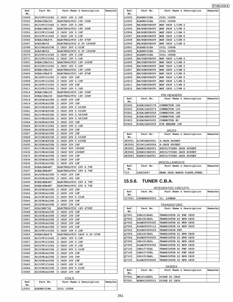
Ref.No.
Part No. Part Name & Description Remarks
C3549 ECJ1VF1C104Z C CHIP 16V 0.1UF
C3550 ECEA1CKA100 ELECTROLYTIC 16V 10UF
C3551 ECJ1VF1C104Z C CHIP 16V 0.1UF
C3552 ECEA1CKA100 ELECTROLYTIC 16V 10UF
C3553 ECJ1VF1C104Z C CHIP 16V 0.1UF
C3559 ECJ1VF1C104Z C CHIP 16V 0.1UF
C3560 ECEA1CKA470 ELECTROLYTIC 16V 47UF
C3567 ECA0JM102 ELECTROLYTIC 6.3V 1000UF
C3568 ECJ1VB1H103K C CHIP 50V 0.01UF
C3569 ECA0JM102 ELECTROLYTIC 6.3V 1000UF
C3570 ECJ1VF1C104Z C CHIP 16V 0.1UF
C3571 ECJ1VF1C104Z C CHIP 16V 0.1UF
C3601 ECEA1CKA101I ELECTROLYTIC 16V 100UF
C3602 ECJ1VF1C104Z C CHIP 16V 0.1UF
C3603 ECEA1CKA100 ELECTROLYTIC 16V 10UF
C3604 ECEA1CKA470 ELECTROLYTIC 16V 47UF
C3605 ECJ2VF1C105Z C CHIP 16V 1UF
C3608 ECJ1VF1C104Z C CHIP 16V 0.1UF
C3609 ECJ2VF1C105Z C CHIP 16V 1UF
C3611 ECJ1VF1C104Z C CHIP 16V 0.1UF
C3614 ECEA1CKA100 ELECTROLYTIC 16V 10UF
C3615 ECEA1CKA100 ELECTROLYTIC 16V 10UF
C3616 ECJ2YB1A105K C CHIP 10V 1UF
C3619 ECJ2YB1A105K C CHIP 10V 1UF
C3620 ECJ1VB1E333K C CHIP 25V 0.033UF
C3621 ECJ1VB1E333K C CHIP 25V 0.033UF
C3622 ECJ1VB1H332K C CHIP 50V 0.0033UF
C3623 ECJ1VB1H332K C CHIP 50V 0.0033UF
C3624 ECJ2YB1A105K C CHIP 10V 1UF
C3625 ECJ1VF1C104Z C CHIP 16V 0.1UF
C3626 ECJ2YB1A105K C CHIP 10V 1UF
C3627 ECJ2YB1A105K C CHIP 10V 1UF
C3628 ECJ1VB1E333K C CHIP 25V 0.033UF
C3629 ECJ1VB1E333K C CHIP 25V 0.033UF
C3630 ECJ2YB1A105K C CHIP 10V 1UF
C3631 ECJ1VB1H102K C CHIP 50V 1000PF
C3632 ECJ1VB1H102K C CHIP 50V 1000PF
C3633 ECJ2YB1A105K C CHIP 10V 1UF
C3634 ECJ2YB1A105K C CHIP 10V 1UF
C3635 ECJ2YB1A105K C CHIP 10V 1UF
C3636 ECEA1EKA4R7 ELECTROLYTIC 25V 4.7UF
C3637 ECEA1EKA4R7 ELECTROLYTIC 25V 4.7UF
C3638 ECJ2YB1A105K C CHIP 10V 1UF
C3639 ECJ2YB1A105K C CHIP 10V 1UF
C3640 ECEA1EKA4R7 ELECTROLYTIC 25V 4.7UF
C3641 ECEA1EKA4R7 ELECTROLYTIC 25V 4.7UF
C3642 ECJ2YB1A105K C CHIP 10V 1UF
C3643 ECJ2YB1A105K C CHIP 10V 1UF
C3644 ECJ1VF1H103Z C CHIP 50V 0.01UF
C3645 ECJ2YB1A105K C CHIP 10V 1UF
C3646 ECJ2YB1A105K C CHIP 10V 1UF
C3647 ECA1CM471B ELECTROLYTIC 16V 470UF
C3648 ECJ2YB1A105K C CHIP 10V 1UF
C3650 ECJ2YB1A105K C CHIP 10V 1UF
C3651 ECJ2YB1A105K C CHIP 10V 1UF
C3652 ECJ2YB1A105K C CHIP 10V 1UF
C3653 ECJ2YB1A105K C CHIP 10V 1UF
C3654 ECJ1VF1C104Z C CHIP 16V 0.1UF
C3655 ECEA0JKA470 ELECTROLYTIC CHIP 6.3V 47UF
C3656 ECJ1VF1C104Z C CHIP 16V 0.1UF
C3657 ECJ1VF1C104Z C CHIP 16V 0.1UF
C3658 ECJ1VF1C104Z C CHIP 16V 0.1UF
C3659 ECJ1VB1H103K C CHIP 50V 0.01UF
C3660 ECJ2YB1A105K C CHIP 10V 1UF
C3661 ECJ2YB1A105K C CHIP 10V 1UF
C3662 ECJ2YB1A105K C CHIP 10V 1UF
C3663 ECJ1VF1C104Z C CHIP 16V 0.1UF
C3664 ECJ1VB1H103K C CHIP 50V 0.01UF
C3665 ECJ2YB1A105K C CHIP 10V 1UF
COILSRef.No.
Part No. Part Name & Description Remarks
L3501 ELESN101KA COIL 100UH
Ref.No.
Part No. Part Name & Description Remarks
L3502 ELESN101KA COIL 100UH
L3503 ELESN101KA COIL 100UH
L3504 ERJ6GEY0R00V MGF CHIP 1/10W 0
L3505 ERJ6GEY0R00V MGF CHIP 1/10W 0
L3506 ERJ6GEY0R00V MGF CHIP 1/10W 0
L3507 ERJ6GEY0R00V MGF CHIP 1/10W 0
L3508 ERJ6GEY0R00V MGF CHIP 1/10W 0
L3509 ERJ6GEY0R00V MGF CHIP 1/10W 0
L3601 ELESN101KA COIL 100UH
L3602 ELESN101KA COIL 100UH
L3603 ELESN101KA COIL 100UH
L3604 ERJ3GEY0R00V MGF CHIP 1/16W 0
L3605 ERJ3GEY0R00V MGF CHIP 1/16W 0
L3606 ERJ3GEY0R00V MGF CHIP 1/16W 0
L3607 ERJ3GEY0R00V MGF CHIP 1/16W 0
L3608 ERJ3GEY0R00V MGF CHIP 1/16W 0
L3609 ERJ3GEY0R00V MGF CHIP 1/16W 0
L3610 ERJ3GEY0R00V MGF CHIP 1/16W 0
L3611 ERJ3GEY0R00V MGF CHIP 1/16W 0
L3612 ERJ3GEY0R00V MGF CHIP 1/16W 0
PIN HEADERSRef.No.
Part No. Part Name & Description Remarks
P3502 K1KA12A00176 CONNECTOR 12P
P3503 K1KA11A00073 CONNECTOR 11P
P3601 K1KA18B00009 CONNECTOR 18P
P3602 K1KA18B00009 CONNECTOR 18P
P3603 K1KA06A00220 CONNECTOR 6P
P3604 K1KA10A00259 PIN HEADER 10P
JACKSRef.No.
Part No. Part Name & Description Remarks
JK3501 K1U824A00001 S-JACK SOCKET
JK3502 K1U411A00004 S-JACK SOCKET
JK3601 K2HA510A0001 AUDIO/VIDEO JACK SOCKET
JK3602 K2HA510A0001 AUDIO/VIDEO JACK SOCKET
JK3603 K2HA510A0001 AUDIO/VIDEO JACK SOCKET
MISCELLANEOUSRef.No.
Part No. Part Name & Description Remarks
710 LSSC0647 REAR JACK EARTH PLATE,STEEL
15.5.6. TUNER C.B.A.INTEGRATED CIRCUITS
Ref.No.
Part No. Part Name & Description Remarks
IC7001 C0DBEKG00003 IC, LINEAR
TRANSISTORSRef.No.
Part No. Part Name & Description Remarks
Q7001 2SB1218ASL TRANSISTOR SI PNP CHIP
Q7002 2SD1819A0L TRANSISTOR SI NPN CHIP
Q7002 B1ABCF000020 TRANSISTOR SI NPN CHIP
Q7002 B1ABCF000112 TRANSISTOR SI NPN CHIP
Q7003 B1DHDC000018 TRANSISTOR FET
Q7004 2SD1819A0L TRANSISTOR SI NPN CHIP
Q7004 B1ABCF000020 TRANSISTOR SI NPN CHIP
Q7005 2SD1819A0L TRANSISTOR SI NPN CHIP
Q7005 B1ABCF000020 TRANSISTOR SI NPN CHIP
Q7102 2SB10730QL TRANSISTOR SI PNP CHIP
Q7102 2SB10730RL TRANSISTOR SI PNP CHIP
Q7103 2SD1819AHL TRANSISTOR SI NPN CHIP
Q7103 B1ABCF000020 TRANSISTOR SI NPN CHIP
DIODESRef.No.
Part No. Part Name & Description Remarks
D7001 MA3J142E0L DIODE SI CHIP
D7001 B0ADCJ000012 DIODE SI CHIP
261
PT-60LCX64-K
RESISTORSRef.No.
Part No. Part Name & Description Remarks
R7001 ERJ6GEYJ220V MGF CHIP 1/10W 22
R7002 ERJ6GEYJ220V MGF CHIP 1/10W 22
R7003 ERJ6GEYJ220V MGF CHIP 1/10W 22
R7004 ERJ6GEYJ220V MGF CHIP 1/10W 22
R7005 ERJ6GEYJ220V MGF CHIP 1/10W 22
R7006 ERJ6GEYJ220V MGF CHIP 1/10W 22
R7007 ERJ6GEYJ220V MGF CHIP 1/10W 22
R7008 ERJ6GEYJ220V MGF CHIP 1/10W 22
R7009 ERJ6GEYJ220V MGF CHIP 1/10W 22
R7010 ERJ6GEYJ220V MGF CHIP 1/10W 22
R7011 ERJ6GEYJ220V MGF CHIP 1/10W 22
R7012 ERJ6GEYJ220V MGF CHIP 1/10W 22
R7013 ERJ6GEYJ220V MGF CHIP 1/10W 22
R7014 ERJ6GEYJ220V MGF CHIP 1/10W 22
R7015 ERJ6GEYJ220V MGF CHIP 1/10W 22
R7016 ERJ6GEYJ220V MGF CHIP 1/10W 22
R7017 ERJ6GEYJ220V MGF CHIP 1/10W 22
R7018 ERJ6GEYJ220V MGF CHIP 1/10W 22
R7019 ERJ6GEYJ220V MGF CHIP 1/10W 22
R7020 ERJ6GEYJ220V MGF CHIP 1/10W 22
R7021 ERJ6GEYJ220V MGF CHIP 1/10W 22
R7022 ERJ6GEYJ220V MGF CHIP 1/10W 22
R7023 ERJ6GEYJ220V MGF CHIP 1/10W 22
R7024 ERJ6GEYJ220V MGF CHIP 1/10W 22
R7025 ERJ6GEYJ220V MGF CHIP 1/10W 22
R7031 ERJ6GEYJ220V MGF CHIP 1/10W 22
R7033 ERJ6GEYJ472V MGF CHIP 1/10W 4.7K
R7034 ERJ6GEYJ823V MGF CHIP 1/10W 82K
R7035 ERJ6GEYJ472V MGF CHIP 1/10W 4.7K
R7036 ERJ6GEYJ823V MGF CHIP 1/10W 82K
R7039 ERDS2TJ122 CARBON 1/4W 1.2K
R7040 ERJ6GEYJ104V MGF CHIP 1/10W 100K
R7041 ERJ6ENF1003V MGF CHIP 1/10W 100K
R7042 ERJ6ENF1802V CARBON CHIP 1/10W 18K
R7043 ERJ6ENF2402V CARBON CHIP 1/10W 24K
R7044 ERJ6GEYJ103V MGF CHIP 1/10W 10K
R7045 ERJ6GEYJ223V MGF CHIP 1/10W 22K
R7046 ERJ6GEYJ223V MGF CHIP 1/10W 22K
R7047 ERJ6GEYJ223V MGF CHIP 1/10W 22K
R7048 ERJ6GEYJ103V MGF CHIP 1/10W 10K
R7101 ERJ6GEYJ221V MGF CHIP 1/10W 220
R7102 ERJ6GEYJ221V MGF CHIP 1/10W 220
R7103 ERJ6GEYJ101V MGF CHIP 1/10W 100
R7105 ERJ6GEYJ101V MGF CHIP 1/10W 100
R7106 ERJ6GEYJ182V MGF CHIP 1/10W 1.8K
R7108 ERJ6GEYJ822V MGF CHIP 1/10W 8.2K
R7109 ERJ6GEYJ472V MGF CHIP 1/10W 4.7K
R7110 ERJ6GEYJ472V MGF CHIP 1/10W 4.7K
CAPACITORSRef.No.
Part No. Part Name & Description Remarks
C7001 ECJ2VF1H103Z C CHIP 50V 0.01UF
C7002 ECJ2VF1E104Z C CHIP 25V 0.1UF
C7003 ECEA1HKA100I ELECTROLYTIC 50V 10UF
C7004 ECEA1CKA220 ELECTROLYTIC 16V 22UF
C7103 ECJ2VB1H103K C CHIP 50V 0.01UF
C7106 ECA0JM471B ELECTROLYTIC 6.3V 470UF
C7107 ECJ2VB1H103K C CHIP 50V 0.01UF
C7108 ECEA1HKA4R7 ELECTROLYTIC 50V 4.7UF
C7109 ECJ2VB1H103K C CHIP 50V 0.01UF
C7110 ECJ2VB1H103K C CHIP 50V 0.01UF
C7111 ECJ2VB1C224K C CHIP 16V 0.22UF
C7112 ECEA1HKA2R2 ELECTROLYTIC 50V 2.2UF
COILSRef.No.
Part No. Part Name & Description Remarks
L7101 VLQSAB7D100K COIL 10UH
PIN HEADERSRef.No.
Part No. Part Name & Description Remarks
P7001 TEL302-5X TEST PIN
Ref.No.
Part No. Part Name & Description Remarks
P7002 K1KA05A00177 CONNECTOR 5P
P7003 LSJA0511 CONNECTOR CABLE W/PLUG,5V
P7004 LSJA0512 CONNECTOR CABLE W/PLUG
P7005 LSJA0513 CONENCTOR CABLE W/LUG
P7006 LSJA0514 CONNECTOR CABLE W/PLUG
P7007 K1KB65A00002 CONNECTOR 65P
P7008 K1KA03A00091 CONNECTOR 3P
MISCELLANEOUSRef.No.
Part No. Part Name & Description Remarks
751 J0KA00000044 FILTER FOR EMI / EMC (CORES)
757 ENG36620G SUB TUNER,UHF/VHF NR
758 LSJA0510 CONNECTOR CABLE W/PLUG,
15.5.7. AUDIO AMP C.B.A.INTEGRATED CIRCUITS
Ref.No.
Part No. Part Name & Description Remarks
IC4501 C1AA00000660 IC, LINEAR
IC4503 C0CAAKE00013 IC, LINEAR
TRANSISTORSRef.No.
Part No. Part Name & Description Remarks
Q4501 2SD0601AHL TRANSISTOR SI NPN CHIP
Q4501 B1ABCF000011 TRANSISTOR SI NPN CHIP
Q4501 B1ABCF000106 TRANSISTOR SI NPN CHIP
Q4504 2SD0601AHL TRANSISTOR SI NPN CHIP
Q4504 B1ABCF000011 TRANSISTOR SI NPN CHIP
Q4504 B1ABCF000106 TRANSISTOR SI NPN CHIP
Q4505 2SD0601AHL TRANSISTOR SI NPN CHIP
Q4505 B1ABCF000011 TRANSISTOR SI NPN CHIP
Q4505 B1ABCF000106 TRANSISTOR SI NPN CHIP
DIODESRef.No.
Part No. Part Name & Description Remarks
D4501 MAZ40510MF DIODE ZENER 5.1V
D4501 HZS5C2TD DIODE ZENER 5.1V
D4501 HZS5C3TD DIODE ZENER 5.1V
D4504 MA2C16700E DIODE SI
D4504 B0AAEL000001 DIODE SI
RESISTORSRef.No.
Part No. Part Name & Description Remarks
R4501 ERJ6GEYJ472V MGF CHIP 1/10W 4.7K
R4502 ERJ6GEYJ153V MGF CHIP 1/10W 15K
R4503 ERJ6GEYJ103V MGF CHIP 1/10W 10K
R4504 ERX1SJ4R7P METAL OXIDE 1W 4.7
R4505 ERX1SJ4R7P METAL OXIDE 1W 4.7
R4506 ERJ6GEYJ153V MGF CHIP 1/10W 15K
R4507 ERJ6GEYJ153V MGF CHIP 1/10W 15K
R4508 ERJ6GEYJ333V MGF CHIP 1/10W 33K
R4509 ERJ6GEYJ333V MGF CHIP 1/10W 33K
R4510 ERJ6GEYJ471V MGF CHIP 1/10W 470
R4511 ERJ6GEYJ471V MGF CHIP 1/10W 470
R4512 ERJ6GEYJ471V MGF CHIP 1/10W 470
R4513 ERJ6GEYJ471V MGF CHIP 1/10W 470
R4525 ERJ6GEY0R00V MGF CHIP 1/10W 0
R4526 ERJ6GEYJ821V MGF CHIP 1/10W 820
R4527 ERJ6GEYJ472V MGF CHIP 1/10W 4.7K
R4543 ERJ6GEY0R00V MGF CHIP 1/10W 0
R4544 ERJ6GEY0R00V MGF CHIP 1/10W 0
R4545 ERJ6GEY0R00V MGF CHIP 1/10W 0
R4546 ERJ6GEY0R00V MGF CHIP 1/10W 0
CAPACITORSRef.No.
Part No. Part Name & Description Remarks
C4501 ECA1VM102B ELECTROLYTIC 35V 1000UF
C4502 ECA1VM102B ELECTROLYTIC 35V 1000UF
C4503 ECEA1CKA100 ELECTROLYTIC 16V 10UF
C4504 ECQB1H104KF POLYESTER 50V 0.1UF
262
PT-60LCX64-K
Ref.No.
Part No. Part Name & Description Remarks
C4505 ECQB1H104KF POLYESTER 50V 0.1UF
C4506 ECJ2VB1E473K C CHIP 25V 0.047UF
C4507 ECJ2VB1E473K C CHIP 25V 0.047UF
C4508 ECJ2VB1E683K C CHIP 25V 0.068UF
C4509 ECJ2VB1E683K C CHIP 25V 0.068UF
C4510 ECEA1HKN010B ELECTROLYTIC 50V 1UF
C4511 ECEA1HKN010B ELECTROLYTIC 50V 1UF
C4512 ECJ2VF1H104Z C CHIP 50V 0.1UF
C4513 ECJ2VF1H104Z C CHIP 50V 0.1UF
C4514 ECA1HM100B ELECTROLYTIC 50V 10UF
C4516 ECEA1CKA100 ELECTROLYTIC 16V 10UF
C4526 ECEA1CKN100 ELECTROLYTIC 16V 10UF
C4527 ECEA1CKN100 ELECTROLYTIC 16V 10UF
C4528 ECEA1EKA4R7 ELECTROLYTIC 25V 4.7UF
PIN HEADERSRef.No.
Part No. Part Name & Description Remarks
P4501 K1KA03A00008 CONNECTOR 3P
P4503 K1KA04A00192 CONNECTOR 4P
P4505 LSJA0473 CONNECTOR CABLE W/PLUG,5V
RELAYRef.No.
Part No. Part Name & Description Remarks
RL4501 K6B2AGA00038 RELAY
MISCELLANEOUSRef.No.
Part No. Part Name & Description Remarks
83 TMM5439-1 CLAMPER
417 XYN3+K10 SCREW W/WASHER,STEEL
466 XTV3+10G TAPPING SCREW,STEEL
714 VMTS0035 CUSHION,RUBBER
759 LSSC0634 HEAT SINK
15.5.8. OPERATION C.B.A.TRANSISTORS
Ref.No.
Part No. Part Name & Description Remarks
Q6701 2SB1218A0L TRANSISTOR SI PNP CHIP
Q6701 B1ADCF000063 TRANSISTOR SI PNP CHIP
Q6701 B1ADCF000075 TRANSISTOR SI PNP CHIP
Q6702 2SB1218A0L TRANSISTOR SI PNP CHIP
Q6702 B1ADCF000063 TRANSISTOR SI PNP CHIP
Q6702 B1ADCF000075 TRANSISTOR SI PNP CHIP
DIODESRef.No.
Part No. Part Name & Description Remarks
D6701 B3AGA0000072 LIGHT EMITTING DIODE GREEN
RESISTORSRef.No.
Part No. Part Name & Description Remarks
R6702 ERJ6GEYJ103V MGF CHIP 1/10W 10K
R6703 ERJ6GEYJ103V MGF CHIP 1/10W 10K
R6704 ERJ6GEYJ391V MGF CHIP 1/10W 390
R6705 ERJ6GEYJ221V MGF CHIP 1/10W 220
R6706 ERJ6GEYJ103V MGF CHIP 1/10W 10K
R6707 ERJ6GEYJ103V MGF CHIP 1/10W 10K
PIN HEADERSRef.No.
Part No. Part Name & Description Remarks
P6701 LSJA0472 CONNECTOR CABLE W/PLUG,5V
SWITCHESRef.No.
Part No. Part Name & Description Remarks
SW6701 EVQ11G05R SWITCH PUSH
SW6702 EVQ11G05R SWITCH PUSH
SW6703 EVQ11G05R SWITCH PUSH
SW6704 EVQ11G05R SWITCH PUSH
SW6705 EVQ11G05R SWITCH PUSH
SW6706 EVQ11G05R SWITCH PUSH
15.5.9. NETWORK C.B.A.CAPACITORS
Ref.No.
Part No. Part Name & Description Remarks
C4551 F2J1J3R3A003 ELECTROLYTIC 63V 3.3UF
PIN HEADERSRef.No.
Part No. Part Name & Description Remarks
P4551 K1KA02A00229 CONNECTOR 2P
P4552 K1KA02A00188 CONNECTOR 2P
P4553 K1KA02A00008 CONNECTOR 2P
15.5.10. COVER SWITCH C.B.A.PIN HEADERS
Ref.No.
Part No. Part Name & Description Remarks
P2912 LSJA0476 CONNECTOR CABLE W/PLUG,
SWITCHESRef.No.
Part No. Part Name & Description Remarks
SW2911 K0L1BA000070 SWITCH PUSH
15.5.11. THERMISTOR 1 C.B.A.RESISTORS
Ref.No.
Part No. Part Name & Description Remarks
R2811 D4CA35030002 THERMISTER PSEC
PIN HEADERSRef.No.
Part No. Part Name & Description Remarks
P2811 K1KA02A00229 CONNECTOR 2P PSEC
15.5.12. THERMISTOR 2 C.B.A.RESISTORS
Ref.No.
Part No. Part Name & Description Remarks
R2821 D4CE31330001 THERMISTOR PSEC
PIN HEADERSRef.No.
Part No. Part Name & Description Remarks
P2821 K1KA02A00100 CONNECTOR 2P PSEC
MISCELLANEOUSRef.No.
Part No. Part Name & Description Remarks
762 LSJA0533 CONNECTOR CABLE W/PLUG PSEC
15.5.13. DIGITAL TUNER POWER C.B.A.INTEGRATED CIRCUITS
Ref.No.
Part No. Part Name & Description Remarks
IC1201 C5HABZZ00101 IC, LINEAR
IC1202 CNC1S101R1KT IC, LINEAR
IC1202 CNC1S101S1KT IC, LINEAR
IC1203 C0DAEMZ00005 IC, LINEAR
IC1203 B1AZKD000001 IC, LINEAR
IC1203 C0DAEMZ00001 IC, LINEAR
DIODESRef.No.
Part No. Part Name & Description Remarks
D1201 B0EBKR000014 DIODE SI
D1202 B0HAJL000001 DIODE SI
D1202 B0HAGP000012 DIODE SI
D1203 B0JAMD000012 DIODE SI
D1203 B0JAGE000001 DIODE SI
D1203 B0JAME000082 DIODE SI
D1204 B0HAJL000001 DIODE SI
D1204 B0HAGP000012 DIODE SI
D1205 B0HAHP000014 DIODE SI
263
PT-60LCX64-K
Ref.No.
Part No. Part Name & Description Remarks
D1205 B0HAJP000007 DIODE SI
D1205 B0HAMP000061 DIODE SI
D1205 B0HAMP000069 DIODE SI
D1206 B0HAJL000001 DIODE SI
D1206 B0HAGP000012 DIODE SI
D1207 B0HAJL000001 DIODE SI
D1207 B0HAGP000012 DIODE SI
D1208 B0HAHP000014 DIODE SI
D1209 B0JBRK000006 DIODE SI
D1210 MAZ71500AF DIODE ZENER
D1211 MAZ73000BF ZENER DIODE
D1214 MAZ73000BF ZENER DIODE
RESISTORSRef.No.
Part No. Part Name & Description Remarks
R1201 ERG2SJ273H METAL OXIDE 2W 27K
R1202 ERJ6GEYJ332V MGF CHIP 1/10W 3.3K
R1203 ERD2FCG681P CARBON 1/4W 680
R1204 ERX2SJR22P METAL FILM 2W 0.22
R1206 ERJ6GEYJ182V MGF CHIP 1/10W 1.8K
R1207 ERG2SJ104P METAL OXIDE 2W 100K
R1208 ERDS2TJ220 CARBON 1/4W 22
R1209 ERJ6GEYJ222V MGF CHIP 1/10W 2.2K
R1210 ERD25FJ100P CARBON 1/4W 10
R1210 ERD25FPJ100P CARBON 1/4W 10
R1210 VRESF4FJ100P CARBON 1/4W 10
R1211 ERJ6GEYJ681V MGF CHIP 1/10W 680
R1212 ERJ6GEYJ102V MGF CHIP 1/10W 1K
R1213 ERDS1TJ122 CARBON 1/2W 1.2K
R1214 ERJ6GEY0R00V MGF CHIP 1/10W 0
R1215 D0HD682ZA002 CARBON CHIP 1/10W 6.8K
R1216 D0HD222ZA002 MGF CHIP 1/10W 2.2K
R1217 ERG1SJ331P METAL OXIDE 1W 330
CAPACITORSRef.No.
Part No. Part Name & Description Remarks
C1201 ECKATS103MF CERAMIC 250V 0.01UF
C1201 ECKETS103MF CERAMIC 125V 0.01UF
C1201 VCKST3G103MY CERAMIC 250V 0.01UF
C1201 VCKSU3D103MY CERAMIC 125V 0.01UF
C1202 ECKATS332ME8 CERAMIC 250V 3300PF
C1202 ECKDNB332ME8 CERAMIC 125V 3300PF
C1202 ECKETS332ME8 CERAMIC 125V 3300PF
C1202 VCKST3G332MX CERAMIC 250V 3300PF
C1202 VCKSU3D332MX CERAMIC 125V 3300PF
C1203 F1B2E4710001 CERAMIC 250V 470PF
C1203 F1B2E471A009 CERAMIC 250V 470PF
C1204 EC0S2DG151DL ELECTROLYTIC 200V 150
C1205 ECJ2VB1E104K C CHIP 25V 0.1UF
C1206 ECKN3D471KBP CERAMIC 470PF
C1207 ECJ2VB1H102K C CHIP 50V 1000PF
C1208 ECJ2VC1H331J C CHIP 50V 330PF
C1209 ECKN3A221KBP CERAMIC 1KV 220PF
C1210 F2A1V1510013 ELECTROLYTIC 35V 150UF
C1211 ECA2DHG4R7B ELECTROLYTIC 200V 4.7UF
C1212 ECJ2VB1E104K C CHIP 25V 0.1UF
C1215 F2A1C3920011 ELECTROLYTIC 16V 3900UF
C1216 ECJ2VB1C224K C CHIP 16V 0.22UF
C1217 ECA1HHG470B ELECTROLYTIC 50V 47UF
C1218 F2A1C3920011 ELECTROLYTIC 16V 3900UF
C1219 ECJ2VB1H102K C CHIP 50V 1000PF
COILSRef.No.
Part No. Part Name & Description Remarks
L1201 J0HBLD000001 LINE FILTER 0.5A 18MH
L1201 ELF15N005A LINE FILTER 0.5A 18M
L1202 J0JHB0000021 FILTER
L1203 J0JHB0000021 FILTER
L1204 G0C100K00028 COIL 10UH
PIN HEADERSRef.No.
Part No. Part Name & Description Remarks
P1201 VJPS0704 PIN HEADER 2P
P1203 LSJA0508 CONNECTOR CABLE W/PLUG,30V
FUSE & PROTECTORRef.No.
Part No. Part Name & Description Remarks
F1201 K5D162AB0003 FUSE 125V 1.6A
F1201 K5D162AQ0004 FUSE 125V 1.6A
PR1201 LSSF009A35E IC PROTECTOR
PR1203 LSSF009A100E IC PROTECTOR 10A
TRANSFORMERRef.No.
Part No. Part Name & Description Remarks
T1201 ETS28AZ1G3ND TRANSFORMER
MISCELLANEOUSRef.No.
Part No. Part Name & Description Remarks
412 XNG3 NUT,STEEL
417 XYN3+K10 SCREW W/WASHER,STEEL
721 EYF52BCY FUSE HOLDER
771 LSSC0675 HEAT SINK
772 LSSC0626 HEAT SINK
773 LML69002A CLAMPER
774 LSMZ0369 BARRIER
264
PT-60LCX64-K
16 EXPLODED VIEWS (PROJECTION SECTION)16.1. PROJECTION SECTION (1)
PT-60LCX64-K
265
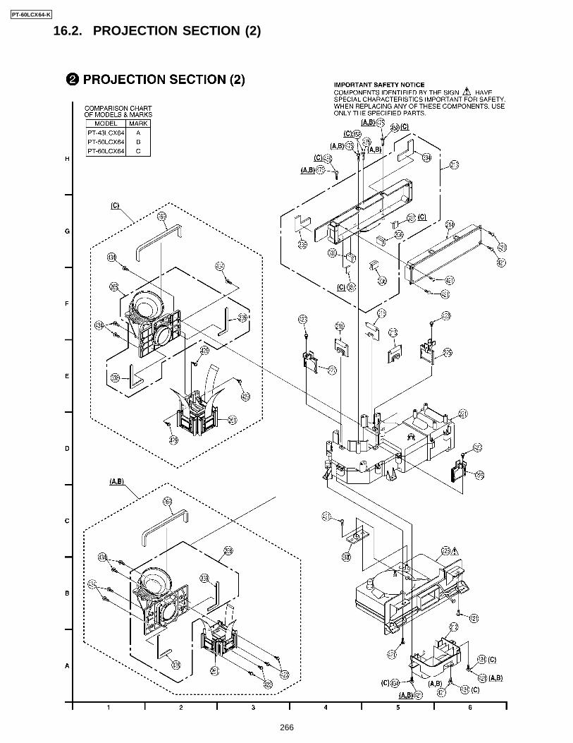
16.2. PROJECTION SECTION (2)PT-60LCX64-K
266
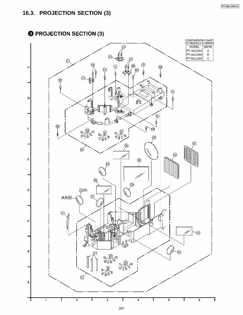
16.3. PROJECTION SECTION (3)PT-60LCX64-K
267
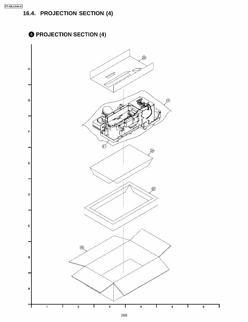
16.4. PROJECTION SECTION (4)PT-60LCX64-K
268
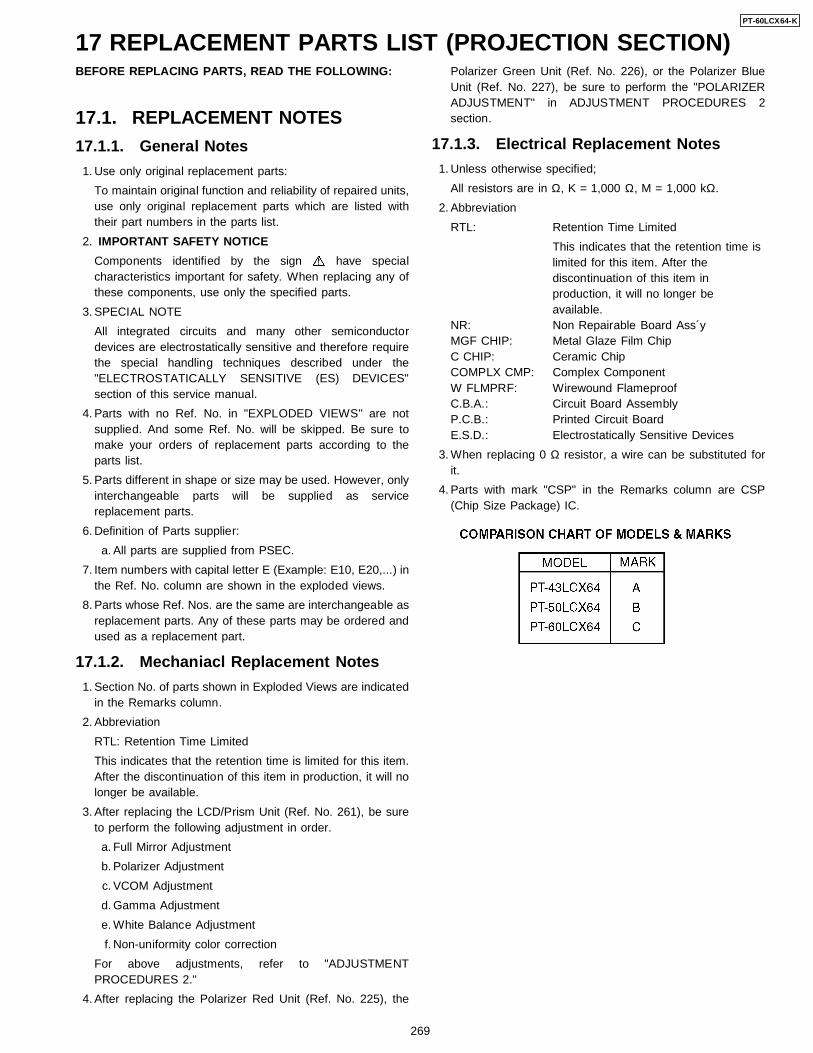
BEFORE REPLACING PARTS, READ THE FOLLOWING:
17.1. REPLACEMENT NOTES
17.1.1. General Notes
1. Use only original replacement parts:
To maintain original function and reliability of repaired units,use only original replacement parts which are listed withtheir part numbers in the parts list.
2. IMPORTANT SAFETY NOTICE
Components identified by the sign have specialcharacteristics important for safety. When replacing any ofthese components, use only the specified parts.
3. SPECIAL NOTE
All integrated circuits and many other semiconductordevices are electrostatically sensitive and therefore requirethe special handling techniques described under the"ELECTROSTATICALLY SENSITIVE (ES) DEVICES"section of this service manual.
4. Parts with no Ref. No. in "EXPLODED VIEWS" are notsupplied. And some Ref. No. will be skipped. Be sure tomake your orders of replacement parts according to theparts list.
5. Parts different in shape or size may be used. However, onlyinterchangeable parts will be supplied as servicereplacement parts.
6. Definition of Parts supplier:
a. All parts are supplied from PSEC.
7. Item numbers with capital letter E (Example: E10, E20,...) inthe Ref. No. column are shown in the exploded views.
8. Parts whose Ref. Nos. are the same are interchangeable asreplacement parts. Any of these parts may be ordered andused as a replacement part.
17.1.2. Mechaniacl Replacement Notes
1. Section No. of parts shown in Exploded Views are indicatedin the Remarks column.
2. Abbreviation
RTL: Retention Time Limited
This indicates that the retention time is limited for this item.After the discontinuation of this item in production, it will nolonger be available.
3. After replacing the LCD/Prism Unit (Ref. No. 261), be sureto perform the following adjustment in order.
a. Full Mirror Adjustment
b. Polarizer Adjustment
c. VCOM Adjustment
d. Gamma Adjustment
e. White Balance Adjustment
f. Non-uniformity color correction
For above adjustments, refer to "ADJUSTMENTPROCEDURES 2."
4. After replacing the Polarizer Red Unit (Ref. No. 225), the
Polarizer Green Unit (Ref. No. 226), or the Polarizer BlueUnit (Ref. No. 227), be sure to perform the "POLARIZERADJUSTMENT" in ADJUSTMENT PROCEDURES 2section.
17.1.3. Electrical Replacement Notes
1. Unless otherwise specified;
All resistors are in Ω, K = 1,000 Ω, M = 1,000 kΩ.
2. Abbreviation
RTL: Retention Time Limited
This indicates that the retention time islimited for this item. After thediscontinuation of this item inproduction, it will no longer beavailable.
NR: Non Repairable Board Ass´yMGF CHIP: Metal Glaze Film ChipC CHIP: Ceramic ChipCOMPLX CMP: Complex ComponentW FLMPRF: Wirewound FlameproofC.B.A.: Circuit Board AssemblyP.C.B.: Printed Circuit BoardE.S.D.: Electrostatically Sensitive Devices
3. When replacing 0 Ω resistor, a wire can be substituted forit.
4. Parts with mark "CSP" in the Remarks column are CSP(Chip Size Package) IC.
17 REPLACEMENT PARTS LIST (PROJECTION SECTION)
269
PT-60LCX64-K
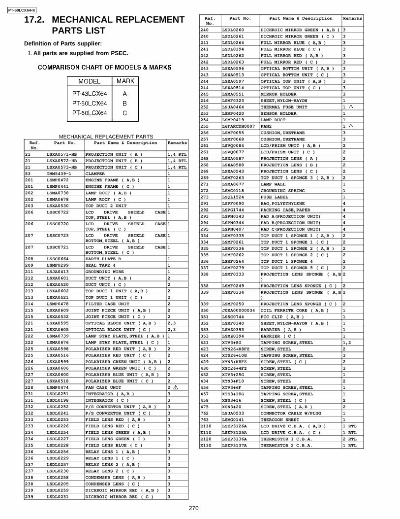
17.2. MECHANICAL REPLACEMENTPARTS LIST
Definition of Parts supplier:
1. All parts are supplied from PSEC.
MECHANICAL REPLACEMENT PARTSRef.No.
Part No. Part Name & Description Remarks
21 LSXA0571-HB PROJECTION UNIT ( A ) 1,4 RTL
21 LSXA0572-HB PROJECTION UNIT ( B ) 1,4 RTL
21 LSXA0573-HB PROJECTION UNIT ( C ) 1,4 RTL
83 TMM5439-1 CLAMPER 1
201 LSMP0472 ENGINE FRAME ( A,B ) 1
201 LSMP0441 ENGINE FRAME ( C ) 1
202 LSMA0738 LAMP ROOF ( A,B ) 1
202 LSMA0678 LAMP ROOF ( C ) 1
203 LSXA0530 TOP DUCT 2 UNIT 1
206 LSSC0722 LCD DRIVE SHIELD CASETOP,STEEL ( A,B )
1
206 LSSC0720 LCD DRIVE SHIELD CASETOP,STEEL ( C )
1
207 LSSC0723 LCD DRIVE SHIELD CASEBOTTOM,STEEL ( A,B )
1
207 LSSC0721 LCD DRIVE SHIELD CASEBOTTOM,STEEL ( C )
1
208 LSSC0664 EARTH PLATE B 1
209 LSMF0299 SEAL TAPE 4 1
211 LSJA0413 GROUNDING WIRE 1
212 LSXA0601 DUCT UNIT ( A,B ) 2
212 LSXA0520 DUCT UNIT ( C ) 2
213 LSXA0602 TOP DUCT 1 UNIT ( A,B ) 2
213 LSXA0521 TOP DUCT 1 UNIT ( C ) 2
214 LSMP0478 FILTER CASE UNIT 2
215 LSXA0609 JOINT PIECE UNIT ( A,B ) 2
215 LSXA0532 JOINT PIECE UNIT ( C ) 2
221 LSXA0595 OPTICAL BLOCK UNIT ( A,B ) 2,3
221 LSXA0605 OPTICAL BLOCK UNIT ( C ) 2,3
222 LSMA0739 LAMP STAY PLATE,STEEL ( A,B ) 1
222 LSMA0676 LAMP STAY PLATE,STEEL ( C ) 1
225 LSXA0598 POLARIZER RED UNIT ( A,B ) 2
225 LSXA0516 POLARIZER RED UNIT ( C ) 2
226 LSXA0599 POLARIZER GREEN UNIT ( A,B ) 2
226 LSXA0606 POLARIZER GREEN UNIT ( C ) 2
227 LSXA0600 POLARIZER BLUE UNIT ( A,B ) 2
227 LSXA0518 POLARIZER BLUE UNIT ( C ) 2
228 LSMP0474 FAN CASE UNIT 2
231 LSDL0251 INTEGRATOR ( A,B ) 3
231 LSDL0198 INTEGRATOR ( C ) 3
232 LSDL0252 P/S CONVERTOR UNIT ( A,B ) 3
232 LSDL0241 P/S CONVERTOR UNIT ( C ) 3
233 LSDL0253 FIELD LENS RED ( A,B ) 3
233 LSDL0226 FIELD LENS RED ( C ) 3
234 LSDL0254 FIELD LENS GREEN ( A,B ) 3
234 LSDL0227 FIELD LENS GREEN ( C ) 3
235 LSDL0228 FIELD LENS BLUE ( C ) 3
236 LSDL0256 RELAY LENS 1 ( A,B ) 3
236 LSDL0229 RELAY LENS 1 ( C ) 3
237 LSDL0257 RELAY LENS 2 ( A,B ) 3
237 LSDL0230 RELAY LENS 2 ( C ) 3
238 LSDL0258 CONDENSER LENS ( A,B ) 3
238 LSDL0205 CONDENSER LENS ( C ) 3
239 LSDL0259 DICHROIC MIRROR RED ( A,B ) 3
239 LSDL0231 DICHROIC MIRROR RED ( C ) 3
Ref.No.
Part No. Part Name & Description Remarks
240 LSDL0260 DICHROIC MIRROR GREEN ( A,B ) 3
240 LSDL0261 DICHROIC MIRROR GREEN ( C ) 3
241 LSDL0264 FULL MIRROR BLUE ( A,B ) 3
241 LSDL0194 FULL MIRROR BLUE ( C ) 3
242 LSDL0262 FULL MIRROR RED ( A,B ) 3
242 LSDL0263 FULL MIRROR RED ( C ) 3
243 LSXA0596 OPTICAL BOTTOM UNIT ( A,B ) 3
243 LSXA0513 OPTICAL BOTTOM UNIT ( C ) 3
244 LSXA0597 OPTICAL TOP UNIT ( A,B ) 3
244 LSXA0514 OPTICAL TOP UNIT ( C ) 3
245 LSMA0551 MIRROR HOLDER 3
246 LSMF0323 SHEET,NYLON-RAYON 1
252 LSJA0464 THERMAL FUSE UNIT 1
253 LSMP0420 SENSOR HOLDER 1
254 LSMP0419 LAMP DUCT 1
255 L6FAKCDH0007 FAN2 1
256 LSMF0055 CUSHION,URETHANE 3
257 LSMF0068 CUSHION,URETHANE 3
261 LSVQ0084 LCD/PRISM UNIT ( A,B ) 2
261 LSVQ0077 LCD/PRISM UNIT ( C ) 2
268 LSXA0587 PROJECTION LENS ( A ) 2
268 LSXA0588 PROJECTION LENS ( B ) 2
268 LSXA0543 PROJECTION LENS ( C ) 2
269 LSMF0263 TOP DUCT 1 SPONGE 3 ( A,B ) 2
271 LSMA0677 LAMP WALL 1
272 LSMC0118 GROUNDING SPRING 1
273 LSQL1524 FUSE LABEL 1
291 LSPF0090 BAG,POLYETHYLENE 4
292 LSPG1744 PACKING CASE,PAPER 4
293 LSPN0343 PAD A(PROJECTION UNIT) 4
294 LSPN0344 PAD B(PROJECTION UNIT) 4
295 LSPN0407 PAD C(PROJECTION UNIT) 4
334 LSMF0335 TOP DUCT 1 SPONGE 1 ( A,B ) 2
334 LSMF0261 TOP DUCT 1 SPONGE 1 ( C ) 2
335 LSMF0336 TOP DUCT 1 SPONGE 2 ( A,B ) 2
335 LSMF0262 TOP DUCT 1 SPONGE 2 ( C ) 2
336 LSMF0264 TOP DUCT 1 SPONGE 4 2
337 LSMF0279 TOP DUCT 1 SPONGE 5 ( C ) 2
338 LSMF0333 PROJECTION LENS SPONGE ( A,B)
2
338 LSMF0249 PROJECTION LENS SPONGE ( C ) 2
339 LSMF0334 PROJECTION LENS SPONGE ( A,B)
2
339 LSMF0250 PROJECTION LENS SPONGE ( C ) 2
350 J0KA00000034 COIL FERRITE CORE ( A,B ) 1
351 LSSC0744 FCC CLIP ( A,B ) 1
352 LSMF0340 SHEET,NYLON-RAYON ( A,B ) 1
353 LSMZ0393 BARRIER ( A,B ) 1
353 LSMZ0394 BARRIER ( C ) 1
421 XTV3+8G TAPPING SCREW,STEEL 1,2
423 XYN26+K8FZ SCREW,STEEL 2
424 XTN26+10G TAPPING SCREW,STEEL 3
429 XYN3+K8FZ SCREW,STEEL ( C ) 2
430 XST26+4FZ SCREW,STEEL 3
432 XTV3+25G SCREW,STEEL 1
434 XYN3+F10 SCREW,STEEL 2
456 XTV3+6F TAPPING SCREW,STEEL 1
457 XTS3+10G TAPPING SCREW,STEEL 1
458 XSN3+16 SCREW,STEEL ( C ) 2
475 XSN3+20 SCREW,STEEL ( A,B ) 2
762 LSJA0533 CONNECTOR CABLE W/PLUG 1
763 LSMG0141 THERCOON SHEET 1
E110 LSEP3126A LCD DRIVE C.B.A. ( A,B ) 1 RTL
E110 LSEP3125A LCD DRIVE C.B.A. ( C ) 1 RTL
E120 LSEP3136A THERMISTOR 1 C.B.A. 2 RTL
E130 LSEP3137A THERMISTOR 2 C.B.A. 1 RTL
270
PT-60LCX64-K
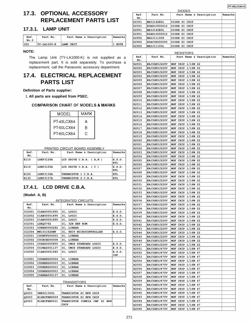
17.3. OPTIONAL ACCESSORYREPLACEMENT PARTS LIST
17.3.1. LAMP UNITRef.No.2
Part No. Part Name & Description Remarks
320 TY-LA1000-K LAMP UNIT 1 NOTE
NOTE:
The Lamp Unit (TY-LA1000-K) is not supplied as areplacement part. It is sold separately. To purchase areplacement, call the Panasonic accessory department.
17.4. ELECTRICAL REPLACEMENTPARTS LIST
Definition of Parts supplier:
1. All parts are supplied from PSEC.
PRINTED CIRCUIT BOARD ASSEMBLYRef.No.
Part No. Part Name & Description Remarks
E110 LSEP3126A LCD DRIVE C.B.A. ( A,B ) E.S.D.RTL
E110 LSEP3125A LCD DRIVE C.B.A. ( C ) E.S.D.RTL
E120 LSEP3136A THERMISTOR 1 C.B.A. RTL
E130 LSEP3137A THERMISTOR 2 C.B.A. RTL
17.4.1. LCD DRIVE C.B.A.
(Model: A, B)
INTEGRATED CIRCUITSRef.No.
Part No. Part Name & Description Remarks
IC2001 C1AB00001895 IC, LOGIC E.S.D.
IC2002 C1AB00001895 IC, LOGIC E.S.D.
IC2003 C1AB00001895 IC, LOGIC E.S.D.
IC2301 LSEQ0762 IC, 32K EEP ROM E.S.D.
IC2303 C0EBH0000282 IC, LINEAR
IC2304 MN101C62DMF IC, 8BIT MICROCONTROLLER E.S.D.
IC2501 C0DBFFD00003 IC, LINEAR
IC2502 C0CBCBD00008 IC, LINEAR
IC2503 C0ZBZ0000850 IC, CMOS STANDARD LOGIC E.S.D.
IC2504 C0JBAZ001137 IC, CMOS STANDARD LOGIC E.S.D.
IC2505 C1AB00001945 IC, LOGIC E.S.D.CSP
IC2901 C0DBEKG00004 IC, LINEAR
IC2902 C0DBEKG00003 IC, LIENAR
IC2903 C0DBEKG00003 IC, LIENAR
IC2904 C0DBEKG00003 IC, LIENAR
IC2905 C0ABBA000137 IC, LINEAR
TRANSISTORSRef.No.
Part No. Part Name & Description Remarks
Q2003 UNR521300L TRANSISTOR SI NPN CHIP
Q2003 B1GBCFNN0009 TRANSISTOR SI NPN CHIP
Q2003 B1GBCFNN0031 TRANSISTOR COMPLX CMP SI NPNCHIP
DIODESRef.No.
Part No. Part Name & Description Remarks
D2301 MA3J142E0L DIODE SI CHIP
D2301 B0ADCJ000012 DIODE SI CHIP
D2901 MA3J142E0L DIODE SI CHIP
D2901 B0ADCJ000012 DIODE SI CHIP
D2902 MA2J111008 DIODE SI CHIP
D2902 B0ACCK000005 DIODE SI CHIP
D2902 MA2J11100L DIODE SI CHIP
RESISTORSRef.No.
Part No. Part Name & Description Remarks
R2001 ERJ3GEYJ220V MGF CHIP 1/16W 22
R2002 ERJ3GEYJ220V MGF CHIP 1/16W 22
R2003 ERJ3GEYJ220V MGF CHIP 1/16W 22
R2004 ERJ3GEYJ220V MGF CHIP 1/16W 22
R2005 ERJ3GEYJ220V MGF CHIP 1/16W 22
R2006 ERJ3GEYJ220V MGF CHIP 1/16W 22
R2007 ERJ3GEYJ220V MGF CHIP 1/16W 22
R2008 ERJ3GEYJ220V MGF CHIP 1/16W 22
R2009 ERJ3GEYJ220V MGF CHIP 1/16W 22
R2010 ERJ3GEYJ220V MGF CHIP 1/16W 22
R2011 ERJ3GEYJ220V MGF CHIP 1/16W 22
R2012 ERJ3GEYJ220V MGF CHIP 1/16W 22
R2013 ERJ3GEYJ220V MGF CHIP 1/16W 22
R2014 ERJ3GEYJ220V MGF CHIP 1/16W 22
R2015 ERJ3GEYJ220V MGF CHIP 1/16W 22
R2016 ERJ3GEYJ220V MGF CHIP 1/16W 22
R2017 ERJ3GEYJ220V MGF CHIP 1/16W 22
R2018 ERJ3GEYJ220V MGF CHIP 1/16W 22
R2019 ERJ3GEYJ220V MGF CHIP 1/16W 22
R2020 ERJ3GEYJ220V MGF CHIP 1/16W 22
R2021 ERJ3GEYJ220V MGF CHIP 1/16W 22
R2022 ERJ3GEYJ220V MGF CHIP 1/16W 22
R2023 ERJ3GEYJ220V MGF CHIP 1/16W 22
R2024 ERJ3GEYJ220V MGF CHIP 1/16W 22
R2025 ERJ3GEYJ220V MGF CHIP 1/16W 22
R2026 ERJ3GEYJ220V MGF CHIP 1/16W 22
R2027 ERJ3GEYJ220V MGF CHIP 1/16W 22
R2028 ERJ3GEYJ220V MGF CHIP 1/16W 22
R2029 ERJ3GEYJ220V MGF CHIP 1/16W 22
R2030 ERJ3GEYJ220V MGF CHIP 1/16W 22
R2031 ERJ3GEYJ220V MGF CHIP 1/16W 22
R2032 ERJ3GEYJ220V MGF CHIP 1/16W 22
R2033 ERJ3GEYJ220V MGF CHIP 1/16W 22
R2034 ERJ3GEYJ220V MGF CHIP 1/16W 22
R2036 ERJ3GEYJ220V MGF CHIP 1/16W 22
R2037 ERJ3GEYJ220V MGF CHIP 1/16W 22
R2038 ERJ3GEYJ220V MGF CHIP 1/16W 22
R2039 ERJ3GEYJ220V MGF CHIP 1/16W 22
R2040 ERJ3GEYJ220V MGF CHIP 1/16W 22
R2041 ERJ3GEYJ220V MGF CHIP 1/16W 22
R2042 ERJ3GEYJ220V MGF CHIP 1/16W 22
R2043 ERJ3GEYJ220V MGF CHIP 1/16W 22
R2044 ERJ3GEYJ220V MGF CHIP 1/16W 22
R2045 ERJ3GEYJ220V MGF CHIP 1/16W 22
R2046 ERJ3GEYJ220V MGF CHIP 1/16W 22
R2047 ERJ3GEYJ220V MGF CHIP 1/16W 22
R2051 ERJ3GEYJ470V MGF CHIP 1/16W 47
R2052 ERJ3GEYJ470V MGF CHIP 1/16W 47
R2053 ERJ3GEYJ470V MGF CHIP 1/16W 47
R2054 ERJ3GEYJ470V MGF CHIP 1/16W 47
R2055 ERJ3GEYJ470V MGF CHIP 1/16W 47
R2056 ERJ3GEYJ470V MGF CHIP 1/16W 47
R2057 ERJ3GEYJ470V MGF CHIP 1/16W 47
R2058 ERJ3GEYJ470V MGF CHIP 1/16W 47
R2059 ERJ3GEYJ470V MGF CHIP 1/16W 47
R2060 ERJ3GEYJ470V MGF CHIP 1/16W 47
R2061 ERJ3GEYJ470V MGF CHIP 1/16W 47
R2062 ERJ3GEYJ470V MGF CHIP 1/16W 47
R2063 ERJ3GEYJ470V MGF CHIP 1/16W 47
R2064 ERJ3GEYJ470V MGF CHIP 1/16W 47
R2065 ERJ3GEYJ470V MGF CHIP 1/16W 47
R2066 ERJ3GEYJ470V MGF CHIP 1/16W 47
271
PT-60LCX64-K
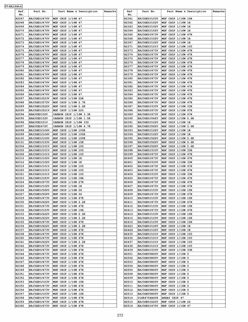
Ref.No.
Part No. Part Name & Description Remarks
R2067 ERJ3GEYJ470V MGF CHIP 1/16W 47
R2068 ERJ3GEYJ470V MGF CHIP 1/16W 47
R2069 ERJ3GEYJ470V MGF CHIP 1/16W 47
R2070 ERJ3GEYJ470V MGF CHIP 1/16W 47
R2071 ERJ3GEYJ470V MGF CHIP 1/16W 47
R2072 ERJ3GEYJ470V MGF CHIP 1/16W 47
R2073 ERJ3GEYJ470V MGF CHIP 1/16W 47
R2074 ERJ3GEYJ470V MGF CHIP 1/16W 47
R2075 ERJ3GEYJ470V MGF CHIP 1/16W 47
R2076 ERJ3GEYJ470V MGF CHIP 1/16W 47
R2077 ERJ3GEYJ470V MGF CHIP 1/16W 47
R2078 ERJ3GEYJ470V MGF CHIP 1/16W 47
R2079 ERJ3GEYJ470V MGF CHIP 1/16W 47
R2080 ERJ3GEYJ470V MGF CHIP 1/16W 47
R2081 ERJ3GEYJ470V MGF CHIP 1/16W 47
R2082 ERJ3GEYJ470V MGF CHIP 1/16W 47
R2083 ERJ3GEYJ470V MGF CHIP 1/16W 47
R2084 ERJ3GEYJ470V MGF CHIP 1/16W 47
R2085 ERJ3GEYJ470V MGF CHIP 1/16W 47
R2086 ERJ3GEYJ470V MGF CHIP 1/16W 47
R2087 ERJ3GEYJ223V MGF CHIP 1/16W 22K
R2088 ERJ3GEYJ272V MGF CHIP 1/16W 2.7K
R2089 ERJ3GEYJ222V MGF CHIP 1/16W 2.2K
R2090 ERJ3GEYJ221V MGF CHIP 1/16W 220
R2094 ERA3YED332V CARBON CHIP 1/16W 3.3K
R2095 ERA3YED152V CARBON CHIP 1/16W 1.5K
R2096 ERA3YED331V CARBON CHIP 1/16W 330
R2097 ERA3YED472V CARBON CHIP 1/16W 4.7K
R2098 ERJ3GEYJ104V MGF CHIP 1/16W 100K
R2099 ERJ3GEYJ104V MGF CHIP 1/16W 100K
R2100 ERJ3GEYJ104V MGF CHIP 1/16W 100K
R2101 ERJ3GEYJ153V MGF CHIP 1/16W 15K
R2304 ERJ3GEYJ101V MGF CHIP 1/16W 100
R2305 ERJ3GEYJ101V MGF CHIP 1/16W 100
R2306 ERJ3GEYJ101V MGF CHIP 1/16W 100
R2310 ERJ3GEYJ102V MGF CHIP 1/16W 1K
R2312 ERJ3GEYJ102V MGF CHIP 1/16W 1K
R2319 ERJ3GEYJ101V MGF CHIP 1/16W 100
R2320 ERJ3GEYJ101V MGF CHIP 1/16W 100
R2321 ERJ3GEYJ101V MGF CHIP 1/16W 100
R2323 ERJ3GEYJ183V MGF CHIP 1/16W 18K
R2324 ERJ3GEYJ273V MGF CHIP 1/16W 27K
R2325 ERJ3GEYJ102V MGF CHIP 1/16W 1K
R2326 ERJ3GEYJ560V MGF CHIP 1/16W 56
R2327 ERJ3GEYJ560V MGF CHIP 1/16W 56
R2329 ERJ3GEYJ473V MGF CHIP 1/16W 47K
R2330 ERJ3GEYJ222V MGF CHIP 1/16W 2.2K
R2331 ERJ3GEYJ473V MGF CHIP 1/16W 47K
R2332 ERJ3GEYJ103V MGF CHIP 1/16W 10K
R2333 ERJ3GEYJ222V MGF CHIP 1/16W 2.2K
R2334 ERJ3GEYJ222V MGF CHIP 1/16W 2.2K
R2335 ERJ3GEYJ473V MGF CHIP 1/16W 47K
R2336 ERJ3GEYJ222V MGF CHIP 1/16W 2.2K
R2337 ERJ3GEYJ473V MGF CHIP 1/16W 47K
R2338 ERJ3GEYJ473V MGF CHIP 1/16W 47K
R2340 ERJ3GEYJ473V MGF CHIP 1/16W 47K
R2341 ERJ3GEYJ222V MGF CHIP 1/16W 2.2K
R2342 ERJ3GEYJ473V MGF CHIP 1/16W 47K
R2343 ERJ3GEYJ473V MGF CHIP 1/16W 47K
R2344 ERJ3GEYJ473V MGF CHIP 1/16W 47K
R2345 ERJ3GEYJ473V MGF CHIP 1/16W 47K
R2347 ERJ3GEYJ473V MGF CHIP 1/16W 47K
R2348 ERJ3GEYJ473V MGF CHIP 1/16W 47K
R2349 ERJ3GEYJ473V MGF CHIP 1/16W 47K
R2351 ERJ3GEYJ473V MGF CHIP 1/16W 47K
R2352 ERJ3GEYJ473V MGF CHIP 1/16W 47K
R2353 ERJ3GEYJ103V MGF CHIP 1/16W 10K
R2355 ERJ3GEYJ473V MGF CHIP 1/16W 47K
R2356 ERJ3GEYJ473V MGF CHIP 1/16W 47K
R2357 ERJ3GEYJ103V MGF CHIP 1/16W 10K
R2358 ERJ3GEYJ473V MGF CHIP 1/16W 47K
R2359 ERJ3GEYJ473V MGF CHIP 1/16W 47K
R2360 ERJ3GEYJ473V MGF CHIP 1/16W 47K
Ref.No.
Part No. Part Name & Description Remarks
R2361 ERJ3GEYJ103V MGF CHIP 1/16W 10K
R2362 ERJ3GEYJ102V MGF CHIP 1/16W 1K
R2363 ERJ3GEYJ102V MGF CHIP 1/16W 1K
R2364 ERJ3GEYJ102V MGF CHIP 1/16W 1K
R2365 ERJ3GEYJ473V MGF CHIP 1/16W 47K
R2366 ERJ3GEYJ102V MGF CHIP 1/16W 1K
R2367 ERJ3GEYJ102V MGF CHIP 1/16W 1K
R2371 ERJ3GEYJ101V MGF CHIP 1/16W 100
R2373 ERJ3GEYJ473V MGF CHIP 1/16W 47K
R2374 ERJ3GEYJ473V MGF CHIP 1/16W 47K
R2375 ERJ3GEYJ473V MGF CHIP 1/16W 47K
R2376 ERJ3GEYJ473V MGF CHIP 1/16W 47K
R2377 ERJ3GEYJ473V MGF CHIP 1/16W 47K
R2378 ERJ3GEYJ473V MGF CHIP 1/16W 47K
R2379 ERJ3GEYJ473V MGF CHIP 1/16W 47K
R2380 ERJ3GEYJ473V MGF CHIP 1/16W 47K
R2381 ERJ3GEYJ473V MGF CHIP 1/16W 47K
R2382 ERJ3GEYJ473V MGF CHIP 1/16W 47K
R2383 ERJ3GEYJ473V MGF CHIP 1/16W 47K
R2384 ERJ3GEYJ473V MGF CHIP 1/16W 47K
R2385 ERJ3GEYJ473V MGF CHIP 1/16W 47K
R2386 ERJ3GEYJ473V MGF CHIP 1/16W 47K
R2387 ERJ3GEYJ333V MGF CHIP 1/16W 33K
R2388 ERJ3GEYJ473V MGF CHIP 1/16W 47K
R2389 ERJ3GEYJ473V MGF CHIP 1/16W 47K
R2390 ERJ3GEYJ562V MGF CHIP 1/16W 5.6K
R2391 ERJ3GEYJ102V MGF CHIP 1/16W 1K
R2392 ERJ3GEYJ562V MGF CHIP 1/16W 5.6K
R2393 ERJ3GEYJ102V MGF CHIP 1/16W 1K
R2394 ERJ3GEYJ102V MGF CHIP 1/16W 1K
R2395 ERJ3GEYJ562V MGF CHIP 1/16W 5.6K
R2396 ERJ3GEYJ562V MGF CHIP 1/16W 5.6K
R2397 ERJ3GEYJ562V MGF CHIP 1/16W 5.6K
R2398 ERJ3GEYJ333V MGF CHIP 1/16W 33K
R2399 ERJ3GEYJ473V MGF CHIP 1/16W 47K
R2400 ERJ3GEYJ473V MGF CHIP 1/16W 47K
R2401 ERJ3GEYJ333V MGF CHIP 1/16W 33K
R2402 ERJ3GEYJ473V MGF CHIP 1/16W 47K
R2403 ERJ3GEYJ473V MGF CHIP 1/16W 47K
R2404 ERJ3GEYJ333V MGF CHIP 1/16W 33K
R2405 ERJ3GEYJ473V MGF CHIP 1/16W 47K
R2406 ERJ3GEYJ473V MGF CHIP 1/16W 47K
R2407 ERJ3GEYJ473V MGF CHIP 1/16W 47K
R2408 ERJ3GEYJ103V MGF CHIP 1/16W 10K
R2409 ERJ3GEYJ473V MGF CHIP 1/16W 47K
R2410 ERJ3GEYJ103V MGF CHIP 1/16W 10K
R2411 ERJ3GEYJ473V MGF CHIP 1/16W 47K
R2412 ERJ3GEYJ103V MGF CHIP 1/16W 10K
R2413 ERJ3GEYJ473V MGF CHIP 1/16W 47K
R2414 ERJ3GEYJ103V MGF CHIP 1/16W 10K
R2415 ERJ3GEYJ103V MGF CHIP 1/16W 10K
R2416 ERJ3GEYJ103V MGF CHIP 1/16W 10K
R2423 ERJ3GEYJ102V MGF CHIP 1/16W 1K
R2426 ERJ3GEYJ102V MGF CHIP 1/16W 1K
R2435 ERJ3GEYJ101V MGF CHIP 1/16W 100
R2436 ERJ3GEYJ101V MGF CHIP 1/16W 100
R2437 ERJ3GEYJ101V MGF CHIP 1/16W 100
R2438 ERJ3GEYJ101V MGF CHIP 1/16W 100
R2439 ERJ3GEYJ333V MGF CHIP 1/16W 33K
R2501 ERJ3GEY0R00V MGF CHIP 1/16W 0
R2502 ERJ3GEY0R00V MGF CHIP 1/16W 0
R2503 ERJ3GEY0R00V MGF CHIP 1/16W 0
R2504 ERJ3GEY0R00V MGF CHIP 1/16W 0
R2505 ERJ3GEY0R00V MGF CHIP 1/16W 0
R2508 ERJ3GEY0R00V MGF CHIP 1/16W 0
R2509 ERJ3GEY0R00V MGF CHIP 1/16W 0
R2510 ERJ3GEY0R00V MGF CHIP 1/16W 0
R2511 ERJ3GEY0R00V MGF CHIP 1/16W 0
R2512 ERJ3GEY0R00V MGF CHIP 1/16W 0
R2513 ERJ3GEY0R00V MGF CHIP 1/16W 0
R2514 D1H84704A008 ARRAY CHIP 47
R2515 ERJ3GEYJ220V MGF CHIP 1/16W 22
R2516 ERJ3GEYJ470V MGF CHIP 1/16W 47
272
PT-60LCX64-K
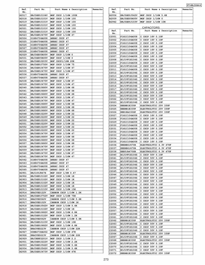
Ref.No.
Part No. Part Name & Description Remarks
R2517 ERJ3GEYJ104V MGF CHIP 1/16W 100K
R2518 ERJ3GEYJ101V MGF CHIP 1/16W 100
R2519 ERJ3GEYJ101V MGF CHIP 1/16W 100
R2520 ERJ3GEYJ101V MGF CHIP 1/16W 100
R2521 ERJ3GEYJ101V MGF CHIP 1/16W 100
R2522 ERJ3GEYJ101V MGF CHIP 1/16W 100
R2523 ERJ3GEYJ470V MGF CHIP 1/16W 47
R2524 D1H84704A008 ARRAY CHIP 47
R2525 D1H84704A008 ARRAY CHIP 47
R2526 D1H84704A008 ARRAY CHIP 47
R2527 D1H84704A008 ARRAY CHIP 47
R2528 D1H84704A008 ARRAY CHIP 47
R2529 ERJ3GEY0R00V MGF CHIP 1/16W 0
R2531 ERJ3GEY0R00V MGF CHIP 1/16W 0
R2532 ERJ3GEYJ203V MGF CHIP1/16W 20K
R2533 ERJ3GEYJ750V MGF CHIP 1/16W 75
R2534 ERJ3GEYJ470V MGF CHIP 1/16W 47
R2535 ERJ3GEYJ470V MGF CHIP 1/16W 47
R2536 D1H84704A008 ARRAY CHIP 47
R2537 D1H84704A008 ARRAY CHIP 47
R2538 ERJ3GEYJ470V MGF CHIP 1/16W 47
R2539 ERJ3GEYJ470V MGF CHIP 1/16W 47
R2540 ERJ3GEYJ680V MGF CHIP 1/16W 68
R2541 ERJ3GEYJ680V MGF CHIP 1/16W 68
R2542 ERJ3GEYJ680V MGF CHIP 1/16W 68
R2543 ERJ3GEYJ470V MGF CHIP 1/16W 47
R2544 ERJ3GEYJ470V MGF CHIP 1/16W 47
R2545 ERJ3GEYJ680V MGF CHIP 1/16W 68
R2546 ERJ3GEYJ680V MGF CHIP 1/16W 68
R2547 ERJ3GEYJ680V MGF CHIP 1/16W 68
R2548 ERJ3GEYJ220V MGF CHIP 1/16W 22
R2549 ERJ3GEYJ220V MGF CHIP 1/16W 22
R2550 ERJ3GEYJ220V MGF CHIP 1/16W 22
R2551 ERJ3GEYJ220V MGF CHIP 1/16W 22
R2552 ERJ3GEYJ220V MGF CHIP 1/16W 22
R2553 ERJ3GEYJ220V MGF CHIP 1/16W 22
R2554 ERJ3GEYJ470V MGF CHIP 1/16W 47
R2555 ERJ3GEYJ680V MGF CHIP 1/16W 68
R2556 ERJ3GEYJ680V MGF CHIP 1/16W 68
R2557 ERJ3GEYJ680V MGF CHIP 1/16W 68
R2558 ERJ3GEYJ470V MGF CHIP 1/16W 47
R2559 ERJ3GEYJ470V MGF CHIP 1/16W 47
R2560 ERJ3GEYJ470V MGF CHIP 1/16W 47
R2561 ERJ3GEYJ470V MGF CHIP 1/16W 47
R2562 D1H84704A008 ARRAY CHIP 47
R2563 D1H84704A008 ARRAY CHIP 47
R2564 D1H84704A008 ARRAY CHIP 47
R2565 D1H84704A008 ARRAY CHIP 47
R2901 ERJ14YJR47H MGF CHIP 1/4W 0.47
R2902 ERJ3GEYJ102V MGF CHIP 1/16W 1K
R2903 ERJ3GEYJ102V MGF CHIP 1/16W 1K
R2904 ERJ3GEYJ102V MGF CHIP 1/16W 1K
R2905 ERJ3GEYJ102V MGF CHIP 1/16W 1K
R2913 ERJ3GEYJ153V MGF CHIP 1/16W 15K
R2914 ERA3YED122V CARBON CHIP 1/16W 1.2K
R2915 ERJ3GEYJ752V MGF CHIP 1/16W 75K
R2916 ERA3YED562V CARBON CHIP 1/16W 5.6K
R2917 ERA3YED102V CARBON CHIP 1/16W 1K
R2918 ERJ3GEYJ562V MGF CHIP 1/16W 5.6K
R2919 ERJ3GEYJ102V MGF CHIP 1/16W 1K
R2920 ERJ3GEYJ682V MGF CHIP 1/16W 6.8K
R2921 ERJ3GEYJ122V MGF CHIP 1/16W 1.2K
R2923 ERA3YED562V CARBON CHIP 1/16W 5.6K
R2924 ERJ3GEYJ103V MGF CHIP 1/16W 10K
R2925 ERJ3GEYJ682V MGF CHIP 1/16W 6.8K
R2926 ERA3YED223V CARBON CHIP 1/16W 22K
R2927 D0HB473ZA002 MGF CHIP 1/16W 47K
R2928 ERA3YED223V CARBON CHIP 1/16W 22K
R2929 ERJ3EKF2201V MGF CHIP 1/16W 2.2
R2931 ERJ3GEYJ222V MGF CHIP 1/16W 2.2K
R2933 ERJ3GEYJ562V MGF CHIP 1/16W 5.6K
R2934 ERJ3GEYJ562V MGF CHIP 1/16W 5.6K
R2935 ERJ3GEYJ473V MGF CHIP 1/16W 47K
Ref.No.
Part No. Part Name & Description Remarks
R2936 ERJ3GEYJ562V MGF CHIP 1/16W 5.6K
R2939 ERJ3GEY0R00V MGF CHIP 1/16W 0
R2942 ERJ3GEYJ103V MGF CHIP 1/16W 10K
CAPACITORSRef.No.
Part No. Part Name & Description Remarks
C2001 F1H1C104A008 C CHIP 16V 0.1UF
C2002 F1H1C104A008 C CHIP 16V 0.1UF
C2003 F1H1C104A008 C CHIP 16V 0.1UF
C2004 F1H1C104A008 C CHIP 16V 0.1UF
C2005 F1H1C104A008 C CHIP 16V 0.1UF
C2006 F1H1C104A008 C CHIP 16V 0.1UF
C2007 F1H1C104A008 C CHIP 16V 0.1UF
C2008 ECJ1VF1E104Z C CHIP 50V 0.1UF
C2009 F1H1C104A008 C CHIP 16V 0.1UF
C2010 ECJ1VF1E104Z C CHIP 50V 0.1UF
C2011 F1H1C104A008 C CHIP 16V 0.1UF
C2012 ECJ1VF1E104Z C CHIP 50V 0.1UF
C2013 ECJ1VF1E104Z C CHIP 50V 0.1UF
C2014 ECJ1VF1E104Z C CHIP 50V 0.1UF
C2015 ECJ1VF1E104Z C CHIP 50V 0.1UF
C2016 ECJ1VF1E104Z C CHIP 50V 0.1UF
C2017 ECJ1VF1E104Z C CHIP 50V 0.1UF
C2018 ECJ1VF1E104Z C CHIP 50V 0.1UF
C2021 ECJ1VF1E104Z C CHIP 50V 0.1UF
C2022 ECJ1VF1E104Z C CHIP 50V 0.1UF
C2023 ECJ1VF1E104Z C CHIP 50V 0.1UF
C2024 EEEHB1E330P ELECTROLYTIC 25V 33UF
C2025 EEEHB1E330P ELECTROLYTIC 25V 33UF
C2026 EEE1EA330SP ELECTROLYTIC 25V 33UF
C2027 F1H1C104A008 C CHIP 16V 0.1UF
C2028 F1H1C104A008 C CHIP 16V 0.1UF
C2029 F1H1C104A008 C CHIP 16V 0.1UF
C2030 F1H1C104A008 C CHIP 16V 0.1UF
C2031 F1H1C104A008 C CHIP 16V 0.1UF
C2032 F1H1C104A008 C CHIP 16V 0.1UF
C2033 F1H1C104A008 C CHIP 16V 0.1UF
C2034 F1H1C104A008 C CHIP 16V 0.1UF
C2035 F1H1C104A008 C CHIP 16V 0.1UF
C2036 EEEHB0J470R ELECTROLYTIC 6.3V 47UF
C2037 EEEHB0J470R ELECTROLYTIC 6.3V 47UF
C2038 EEE0JA470SR ELECTROLYTIC 6.3V 47UF
C2040 ECJ1VF1E104Z C CHIP 50V 0.1UF
C2041 ECJ1VF1E104Z C CHIP 50V 0.1UF
C2042 ECJ1VF1E104Z C CHIP 50V 0.1UF
C2043 ECJ1VF1E104Z C CHIP 50V 0.1UF
C2044 ECJ1VF1E104Z C CHIP 50V 0.1UF
C2045 ECJ1VF1E104Z C CHIP 50V 0.1UF
C2046 ECJ1VF1E104Z C CHIP 50V 0.1UF
C2047 ECJ1VF1E104Z C CHIP 50V 0.1UF
C2048 ECJ1VF1E104Z C CHIP 50V 0.1UF
C2049 ECJ1VF1E104Z C CHIP 50V 0.1UF
C2050 ECJ1VF1E104Z C CHIP 50V 0.1UF
C2051 ECJ1VF1E104Z C CHIP 50V 0.1UF
C2052 ECJ1VF1E104Z C CHIP 50V 0.1UF
C2053 ECJ1VF1E104Z C CHIP 50V 0.1UF
C2054 ECJ1VF1E104Z C CHIP 50V 0.1UF
C2055 ECJ1VF1E104Z C CHIP 50V 0.1UF
C2056 ECJ1VF1E104Z C CHIP 50V 0.1UF
C2057 ECJ1VF1E104Z C CHIP 50V 0.1UF
C2060 ECJ1VF1E104Z C CHIP 50V 0.1UF
C2061 ECJ1VF1E104Z C CHIP 50V 0.1UF
C2062 EEEHB1E330P ELECTROLYTIC 25V 33UF
C2063 ECJ1VF1E104Z C CHIP 50V 0.1UF
C2064 ECJ1VF1E104Z C CHIP 50V 0.1UF
C2065 ECJ1VF1E104Z C CHIP 50V 0.1UF
C2066 EEEHB1E330P ELECTROLYTIC 25V 33UF
C2067 ECJ1VF1E104Z C CHIP 50V 0.1UF
C2068 EEEHB1E330P ELECTROLYTIC 25V 33UF
C2069 ECJ1VF1E104Z C CHIP 50V 0.1UF
C2070 ECJ1VF1E104Z C CHIP 50V 0.1UF
C2071 ECJ1VF1E104Z C CHIP 50V 0.1UF
C2072 EEEHB1E330P ELECTROLYTIC 25V 33UF
273
PT-60LCX64-K
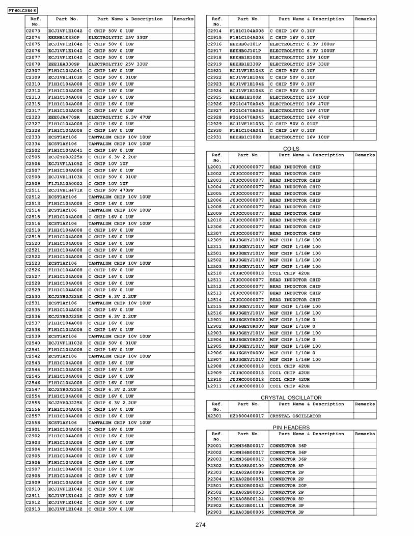
Ref.No.
Part No. Part Name & Description Remarks
C2073 ECJ1VF1E104Z C CHIP 50V 0.1UF
C2074 EEEHB1E330P ELECTROLYTIC 25V 33UF
C2075 ECJ1VF1E104Z C CHIP 50V 0.1UF
C2076 ECJ1VF1E104Z C CHIP 50V 0.1UF
C2077 ECJ1VF1E104Z C CHIP 50V 0.1UF
C2078 EEE1EA330SP ELECTROLYTIC 25V 33UF
C2307 F1H1C104A041 C CHIP 16V 0.1UF
C2309 ECJ1VB1H103K C CHIP 50V 0.01UF
C2310 F1H1C104A008 C CHIP 16V 0.1UF
C2312 F1H1C104A008 C CHIP 16V 0.1UF
C2313 F1H1C104A008 C CHIP 16V 0.1UF
C2315 F1H1C104A008 C CHIP 16V 0.1UF
C2317 F1H1C104A008 C CHIP 16V 0.1UF
C2323 EEE0JA470SR ELECTROLYTIC 6.3V 47UF
C2327 F1H1C104A008 C CHIP 16V 0.1UF
C2328 F1H1C104A008 C CHIP 16V 0.1UF
C2333 ECST1AY106 TANTALUM CHIP 10V 10UF
C2334 ECST1AY106 TANTALUM CHIP 10V 10UF
C2502 F1H1C104A041 C CHIP 16V 0.1UF
C2505 ECJ2YB0J225K C CHIP 6.3V 2.2UF
C2506 ECJ1VF1A105Z C CHIP 10V 1UF
C2507 F1H1C104A008 C CHIP 16V 0.1UF
C2508 ECJ1VB1H103K C CHIP 50V 0.01UF
C2509 F1J1A1050002 C CHIP 10V 1UF
C2511 ECJ1VB1H471K C CHIP 50V 470PF
C2512 ECST1AY106 TANTALUM CHIP 10V 10UF
C2513 F1H1C104A008 C CHIP 16V 0.1UF
C2514 ECST1AY106 TANTALUM CHIP 10V 10UF
C2515 F1H1C104A008 C CHIP 16V 0.1UF
C2516 ECST1AY106 TANTALUM CHIP 10V 10UF
C2518 F1H1C104A008 C CHIP 16V 0.1UF
C2519 F1H1C104A008 C CHIP 16V 0.1UF
C2520 F1H1C104A008 C CHIP 16V 0.1UF
C2521 F1H1C104A008 C CHIP 16V 0.1UF
C2522 F1H1C104A008 C CHIP 16V 0.1UF
C2523 ECST1AY106 TANTALUM CHIP 10V 10UF
C2526 F1H1C104A008 C CHIP 16V 0.1UF
C2527 F1H1C104A008 C CHIP 16V 0.1UF
C2528 F1H1C104A008 C CHIP 16V 0.1UF
C2529 F1H1C104A008 C CHIP 16V 0.1UF
C2530 ECJ2YB0J225K C CHIP 6.3V 2.2UF
C2531 ECST1AY106 TANTALUM CHIP 10V 10UF
C2535 F1H1C104A008 C CHIP 16V 0.1UF
C2536 ECJ2YB0J225K C CHIP 6.3V 2.2UF
C2537 F1H1C104A008 C CHIP 16V 0.1UF
C2538 F1H1C104A008 C CHIP 16V 0.1UF
C2539 ECST1AY106 TANTALUM CHIP 10V 10UF
C2540 ECJ1VF1H103Z C CHIP 50V 0.01UF
C2541 F1H1C104A008 C CHIP 16V 0.1UF
C2542 ECST1AY106 TANTALUM CHIP 10V 10UF
C2543 F1H1C104A008 C CHIP 16V 0.1UF
C2544 F1H1C104A008 C CHIP 16V 0.1UF
C2545 F1H1C104A008 C CHIP 16V 0.1UF
C2546 F1H1C104A008 C CHIP 16V 0.1UF
C2547 ECJ2YB0J225K C CHIP 6.3V 2.2UF
C2554 F1H1C104A008 C CHIP 16V 0.1UF
C2555 ECJ2YB0J225K C CHIP 6.3V 2.2UF
C2556 F1H1C104A008 C CHIP 16V 0.1UF
C2557 F1H1C104A008 C CHIP 16V 0.1UF
C2558 ECST1AY106 TANTALUM CHIP 10V 10UF
C2901 F1H1C104A008 C CHIP 16V 0.1UF
C2902 F1H1C104A008 C CHIP 16V 0.1UF
C2903 F1H1C104A008 C CHIP 16V 0.1UF
C2904 F1H1C104A008 C CHIP 16V 0.1UF
C2905 F1H1C104A008 C CHIP 16V 0.1UF
C2906 F1H1C104A008 C CHIP 16V 0.1UF
C2907 F1H1C104A008 C CHIP 16V 0.1UF
C2908 F1H1C104A008 C CHIP 16V 0.1UF
C2909 F1H1C104A008 C CHIP 16V 0.1UF
C2910 ECJ1VF1E104Z C CHIP 50V 0.1UF
C2911 ECJ1VF1E104Z C CHIP 50V 0.1UF
C2912 ECJ1VF1E104Z C CHIP 50V 0.1UF
C2913 ECJ1VF1E104Z C CHIP 50V 0.1UF
Ref.No.
Part No. Part Name & Description Remarks
C2914 F1H1C104A008 C CHIP 16V 0.1UF
C2915 F1H1C104A008 C CHIP 16V 0.1UF
C2916 EEEHB0J101P ELECTROLYTIC 6.3V 100UF
C2917 EEEHB0J101P ELECTROLYTIC 6.3V 100UF
C2918 EEEHB1E100R ELECTROLYTIC 25V 10UF
C2919 EEEHB1E330P ELECTROLYTIC 25V 33UF
C2921 ECJ1VF1E104Z C CHIP 50V 0.1UF
C2922 ECJ1VF1E104Z C CHIP 50V 0.1UF
C2923 ECJ1VF1E104Z C CHIP 50V 0.1UF
C2924 ECJ1VF1E104Z C CHIP 50V 0.1UF
C2925 EEEHB1E100R ELECTROLYTIC 25V 10UF
C2926 F2G1C470A045 ELECTROLYTIC 16V 47UF
C2927 F2G1C470A045 ELECTROLYTIC 16V 47UF
C2928 F2G1C470A045 ELECTROLYTIC 16V 47UF
C2929 ECJ1VF1H103Z C CHIP 50V 0.01UF
C2930 F1H1C104A041 C CHIP 16V 0.1UF
C2931 EEEHB1C100R ELECTROLYTIC 16V 10UF
COILSRef.No.
Part No. Part Name & Description Remarks
L2001 J0JCC0000077 BEAD INDUCTOR CHIP
L2002 J0JCC0000077 BEAD INDUCTOR CHIP
L2003 J0JCC0000077 BEAD INDUCTOR CHIP
L2004 J0JCC0000077 BEAD INDUCTOR CHIP
L2005 J0JCC0000077 BEAD INDUCTOR CHIP
L2006 J0JCC0000077 BEAD INDUCTOR CHIP
L2008 J0JCC0000077 BEAD INDUCTOR CHIP
L2009 J0JCC0000077 BEAD INDUCTOR CHIP
L2010 J0JCC0000077 BEAD INDUCTOR CHIP
L2306 J0JCC0000077 BEAD INDUCTOR CHIP
L2307 J0JCC0000077 BEAD INDUCTOR CHIP
L2309 ERJ3GEYJ101V MGF CHIP 1/16W 100
L2311 ERJ3GEYJ101V MGF CHIP 1/16W 100
L2501 ERJ3GEYJ101V MGF CHIP 1/16W 100
L2502 ERJ3GEYJ101V MGF CHIP 1/16W 100
L2503 ERJ3GEYJ101V MGF CHIP 1/16W 100
L2510 J0JHC0000018 COIL CHIP 42UH
L2511 J0JCC0000077 BEAD INDUCTOR CHIP
L2512 J0JCC0000077 BEAD INDUCTOR CHIP
L2513 J0JCC0000077 BEAD INDUCTOR CHIP
L2514 J0JCC0000077 BEAD INDUCTOR CHIP
L2515 ERJ3GEYJ101V MGF CHIP 1/16W 100
L2516 ERJ3GEYJ101V MGF CHIP 1/16W 100
L2901 ERJ6GEY0R00V MGF CHIP 1/10W 0
L2902 ERJ6GEY0R00V MGF CHIP 1/10W 0
L2903 ERJ3GEYJ101V MGF CHIP 1/16W 100
L2904 ERJ6GEY0R00V MGF CHIP 1/10W 0
L2905 ERJ3GEYJ101V MGF CHIP 1/16W 100
L2906 ERJ6GEY0R00V MGF CHIP 1/10W 0
L2907 ERJ3GEYJ101V MGF CHIP 1/16W 100
L2908 J0JHC0000018 COIL CHIP 42UH
L2909 J0JHC0000018 COIL CHIP 42UH
L2910 J0JHC0000018 COIL CHIP 42UH
L2911 J0JHC0000018 COIL CHIP 42UH
CRYSTAL OSCILLATORRef.No.
Part No. Part Name & Description Remarks
X2301 H2D800400017 CRYSTAL OSCILLATOR
PIN HEADERSRef.No.
Part No. Part Name & Description Remarks
P2001 K1MN36B00017 CONNECTOR 36P
P2002 K1MN36B00017 CONNECTOR 36P
P2003 K1MN36B00017 CONNECTOR 36P
P2302 K1KA08A00100 CONNECTOR 8P
P2303 K1KA02A00096 CONNECTOR 2P
P2304 K1KA02B00051 CONNECTOR 2P
P2501 K1KB20B00042 CONNECTOR 20P
P2502 K1KA02B00053 CONNECTOR 2P
P2901 K1KA08B00124 CONNECTOR 8P
P2902 K1KA03B00111 CONNECTOR 3P
P2903 K1KA03B00006 CONNECTOR 3P
274
PT-60LCX64-K
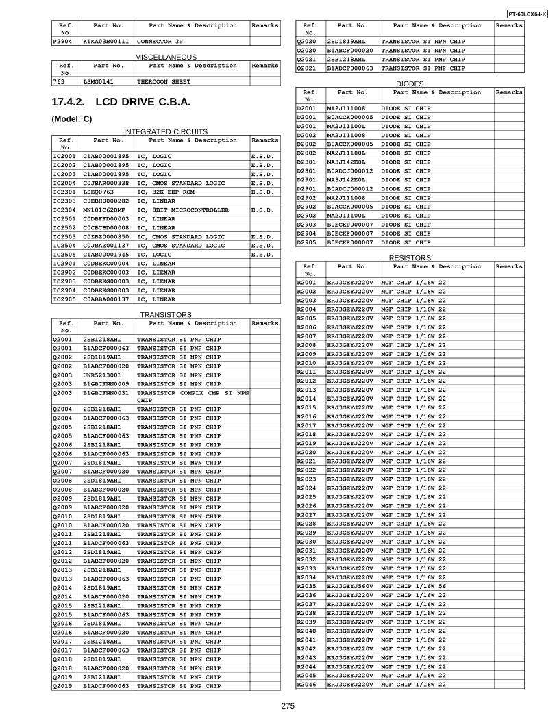
Ref.No.
Part No. Part Name & Description Remarks
P2904 K1KA03B00111 CONNECTOR 3P
MISCELLANEOUSRef.No.
Part No. Part Name & Description Remarks
763 LSMG0141 THERCOON SHEET
17.4.2. LCD DRIVE C.B.A.
(Model: C)
INTEGRATED CIRCUITSRef.No.
Part No. Part Name & Description Remarks
IC2001 C1AB00001895 IC, LOGIC E.S.D.
IC2002 C1AB00001895 IC, LOGIC E.S.D.
IC2003 C1AB00001895 IC, LOGIC E.S.D.
IC2004 C0JBAR000338 IC, CMOS STANDARD LOGIC E.S.D.
IC2301 LSEQ0763 IC, 32K EEP ROM E.S.D.
IC2303 C0EBH0000282 IC, LINEAR
IC2304 MN101C62DMF IC, 8BIT MICROCONTROLLER E.S.D.
IC2501 C0DBFFD00003 IC, LINEAR
IC2502 C0CBCBD00008 IC, LINEAR
IC2503 C0ZBZ0000850 IC, CMOS STANDARD LOGIC E.S.D.
IC2504 C0JBAZ001137 IC, CMOS STANDARD LOGIC E.S.D.
IC2505 C1AB00001945 IC, LOGIC E.S.D.
IC2901 C0DBEKG00004 IC, LINEAR
IC2902 C0DBEKG00003 IC, LIENAR
IC2903 C0DBEKG00003 IC, LIENAR
IC2904 C0DBEKG00003 IC, LIENAR
IC2905 C0ABBA000137 IC, LINEAR
TRANSISTORSRef.No.
Part No. Part Name & Description Remarks
Q2001 2SB1218AHL TRANSISTOR SI PNP CHIP
Q2001 B1ADCF000063 TRANSISTOR SI PNP CHIP
Q2002 2SD1819AHL TRANSISTOR SI NPN CHIP
Q2002 B1ABCF000020 TRANSISTOR SI NPN CHIP
Q2003 UNR521300L TRANSISTOR SI NPN CHIP
Q2003 B1GBCFNN0009 TRANSISTOR SI NPN CHIP
Q2003 B1GBCFNN0031 TRANSISTOR COMPLX CMP SI NPNCHIP
Q2004 2SB1218AHL TRANSISTOR SI PNP CHIP
Q2004 B1ADCF000063 TRANSISTOR SI PNP CHIP
Q2005 2SB1218AHL TRANSISTOR SI PNP CHIP
Q2005 B1ADCF000063 TRANSISTOR SI PNP CHIP
Q2006 2SB1218AHL TRANSISTOR SI PNP CHIP
Q2006 B1ADCF000063 TRANSISTOR SI PNP CHIP
Q2007 2SD1819AHL TRANSISTOR SI NPN CHIP
Q2007 B1ABCF000020 TRANSISTOR SI NPN CHIP
Q2008 2SD1819AHL TRANSISTOR SI NPN CHIP
Q2008 B1ABCF000020 TRANSISTOR SI NPN CHIP
Q2009 2SD1819AHL TRANSISTOR SI NPN CHIP
Q2009 B1ABCF000020 TRANSISTOR SI NPN CHIP
Q2010 2SD1819AHL TRANSISTOR SI NPN CHIP
Q2010 B1ABCF000020 TRANSISTOR SI NPN CHIP
Q2011 2SB1218AHL TRANSISTOR SI PNP CHIP
Q2011 B1ADCF000063 TRANSISTOR SI PNP CHIP
Q2012 2SD1819AHL TRANSISTOR SI NPN CHIP
Q2012 B1ABCF000020 TRANSISTOR SI NPN CHIP
Q2013 2SB1218AHL TRANSISTOR SI PNP CHIP
Q2013 B1ADCF000063 TRANSISTOR SI PNP CHIP
Q2014 2SD1819AHL TRANSISTOR SI NPN CHIP
Q2014 B1ABCF000020 TRANSISTOR SI NPN CHIP
Q2015 2SB1218AHL TRANSISTOR SI PNP CHIP
Q2015 B1ADCF000063 TRANSISTOR SI PNP CHIP
Q2016 2SD1819AHL TRANSISTOR SI NPN CHIP
Q2016 B1ABCF000020 TRANSISTOR SI NPN CHIP
Q2017 2SB1218AHL TRANSISTOR SI PNP CHIP
Q2017 B1ADCF000063 TRANSISTOR SI PNP CHIP
Q2018 2SD1819AHL TRANSISTOR SI NPN CHIP
Q2018 B1ABCF000020 TRANSISTOR SI NPN CHIP
Q2019 2SB1218AHL TRANSISTOR SI PNP CHIP
Q2019 B1ADCF000063 TRANSISTOR SI PNP CHIP
Ref.No.
Part No. Part Name & Description Remarks
Q2020 2SD1819AHL TRANSISTOR SI NPN CHIP
Q2020 B1ABCF000020 TRANSISTOR SI NPN CHIP
Q2021 2SB1218AHL TRANSISTOR SI PNP CHIP
Q2021 B1ADCF000063 TRANSISTOR SI PNP CHIP
DIODESRef.No.
Part No. Part Name & Description Remarks
D2001 MA2J111008 DIODE SI CHIP
D2001 B0ACCK000005 DIODE SI CHIP
D2001 MA2J11100L DIODE SI CHIP
D2002 MA2J111008 DIODE SI CHIP
D2002 B0ACCK000005 DIODE SI CHIP
D2002 MA2J11100L DIODE SI CHIP
D2301 MA3J142E0L DIODE SI CHIP
D2301 B0ADCJ000012 DIODE SI CHIP
D2901 MA3J142E0L DIODE SI CHIP
D2901 B0ADCJ000012 DIODE SI CHIP
D2902 MA2J111008 DIODE SI CHIP
D2902 B0ACCK000005 DIODE SI CHIP
D2902 MA2J11100L DIODE SI CHIP
D2903 B0ECKP000007 DIODE SI CHIP
D2904 B0ECKP000007 DIODE SI CHIP
D2905 B0ECKP000007 DIODE SI CHIP
RESISTORSRef.No.
Part No. Part Name & Description Remarks
R2001 ERJ3GEYJ220V MGF CHIP 1/16W 22
R2002 ERJ3GEYJ220V MGF CHIP 1/16W 22
R2003 ERJ3GEYJ220V MGF CHIP 1/16W 22
R2004 ERJ3GEYJ220V MGF CHIP 1/16W 22
R2005 ERJ3GEYJ220V MGF CHIP 1/16W 22
R2006 ERJ3GEYJ220V MGF CHIP 1/16W 22
R2007 ERJ3GEYJ220V MGF CHIP 1/16W 22
R2008 ERJ3GEYJ220V MGF CHIP 1/16W 22
R2009 ERJ3GEYJ220V MGF CHIP 1/16W 22
R2010 ERJ3GEYJ220V MGF CHIP 1/16W 22
R2011 ERJ3GEYJ220V MGF CHIP 1/16W 22
R2012 ERJ3GEYJ220V MGF CHIP 1/16W 22
R2013 ERJ3GEYJ220V MGF CHIP 1/16W 22
R2014 ERJ3GEYJ220V MGF CHIP 1/16W 22
R2015 ERJ3GEYJ220V MGF CHIP 1/16W 22
R2016 ERJ3GEYJ220V MGF CHIP 1/16W 22
R2017 ERJ3GEYJ220V MGF CHIP 1/16W 22
R2018 ERJ3GEYJ220V MGF CHIP 1/16W 22
R2019 ERJ3GEYJ220V MGF CHIP 1/16W 22
R2020 ERJ3GEYJ220V MGF CHIP 1/16W 22
R2021 ERJ3GEYJ220V MGF CHIP 1/16W 22
R2022 ERJ3GEYJ220V MGF CHIP 1/16W 22
R2023 ERJ3GEYJ220V MGF CHIP 1/16W 22
R2024 ERJ3GEYJ220V MGF CHIP 1/16W 22
R2025 ERJ3GEYJ220V MGF CHIP 1/16W 22
R2026 ERJ3GEYJ220V MGF CHIP 1/16W 22
R2027 ERJ3GEYJ220V MGF CHIP 1/16W 22
R2028 ERJ3GEYJ220V MGF CHIP 1/16W 22
R2029 ERJ3GEYJ220V MGF CHIP 1/16W 22
R2030 ERJ3GEYJ220V MGF CHIP 1/16W 22
R2031 ERJ3GEYJ220V MGF CHIP 1/16W 22
R2032 ERJ3GEYJ220V MGF CHIP 1/16W 22
R2033 ERJ3GEYJ220V MGF CHIP 1/16W 22
R2034 ERJ3GEYJ220V MGF CHIP 1/16W 22
R2035 ERJ3GEYJ560V MGF CHIP 1/16W 56
R2036 ERJ3GEYJ220V MGF CHIP 1/16W 22
R2037 ERJ3GEYJ220V MGF CHIP 1/16W 22
R2038 ERJ3GEYJ220V MGF CHIP 1/16W 22
R2039 ERJ3GEYJ220V MGF CHIP 1/16W 22
R2040 ERJ3GEYJ220V MGF CHIP 1/16W 22
R2041 ERJ3GEYJ220V MGF CHIP 1/16W 22
R2042 ERJ3GEYJ220V MGF CHIP 1/16W 22
R2043 ERJ3GEYJ220V MGF CHIP 1/16W 22
R2044 ERJ3GEYJ220V MGF CHIP 1/16W 22
R2045 ERJ3GEYJ220V MGF CHIP 1/16W 22
R2046 ERJ3GEYJ220V MGF CHIP 1/16W 22
275
PT-60LCX64-K
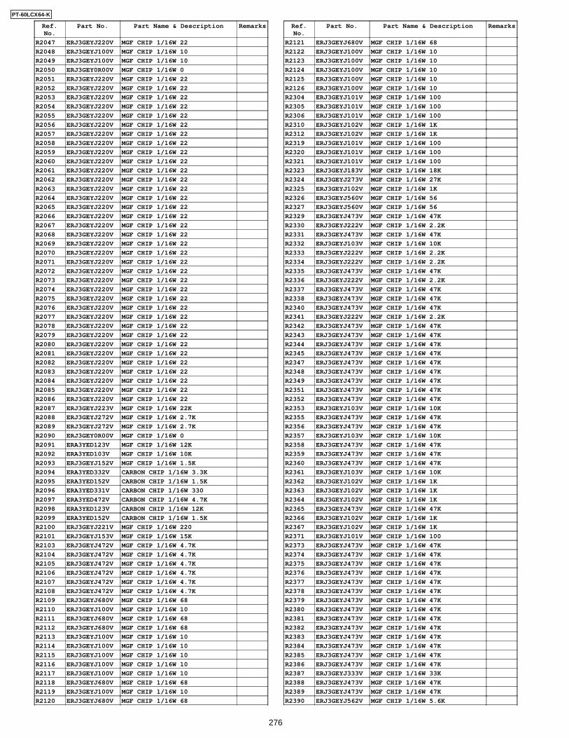
Ref.No.
Part No. Part Name & Description Remarks
R2047 ERJ3GEYJ220V MGF CHIP 1/16W 22
R2048 ERJ3GEYJ100V MGF CHIP 1/16W 10
R2049 ERJ3GEYJ100V MGF CHIP 1/16W 10
R2050 ERJ3GEY0R00V MGF CHIP 1/16W 0
R2051 ERJ3GEYJ220V MGF CHIP 1/16W 22
R2052 ERJ3GEYJ220V MGF CHIP 1/16W 22
R2053 ERJ3GEYJ220V MGF CHIP 1/16W 22
R2054 ERJ3GEYJ220V MGF CHIP 1/16W 22
R2055 ERJ3GEYJ220V MGF CHIP 1/16W 22
R2056 ERJ3GEYJ220V MGF CHIP 1/16W 22
R2057 ERJ3GEYJ220V MGF CHIP 1/16W 22
R2058 ERJ3GEYJ220V MGF CHIP 1/16W 22
R2059 ERJ3GEYJ220V MGF CHIP 1/16W 22
R2060 ERJ3GEYJ220V MGF CHIP 1/16W 22
R2061 ERJ3GEYJ220V MGF CHIP 1/16W 22
R2062 ERJ3GEYJ220V MGF CHIP 1/16W 22
R2063 ERJ3GEYJ220V MGF CHIP 1/16W 22
R2064 ERJ3GEYJ220V MGF CHIP 1/16W 22
R2065 ERJ3GEYJ220V MGF CHIP 1/16W 22
R2066 ERJ3GEYJ220V MGF CHIP 1/16W 22
R2067 ERJ3GEYJ220V MGF CHIP 1/16W 22
R2068 ERJ3GEYJ220V MGF CHIP 1/16W 22
R2069 ERJ3GEYJ220V MGF CHIP 1/16W 22
R2070 ERJ3GEYJ220V MGF CHIP 1/16W 22
R2071 ERJ3GEYJ220V MGF CHIP 1/16W 22
R2072 ERJ3GEYJ220V MGF CHIP 1/16W 22
R2073 ERJ3GEYJ220V MGF CHIP 1/16W 22
R2074 ERJ3GEYJ220V MGF CHIP 1/16W 22
R2075 ERJ3GEYJ220V MGF CHIP 1/16W 22
R2076 ERJ3GEYJ220V MGF CHIP 1/16W 22
R2077 ERJ3GEYJ220V MGF CHIP 1/16W 22
R2078 ERJ3GEYJ220V MGF CHIP 1/16W 22
R2079 ERJ3GEYJ220V MGF CHIP 1/16W 22
R2080 ERJ3GEYJ220V MGF CHIP 1/16W 22
R2081 ERJ3GEYJ220V MGF CHIP 1/16W 22
R2082 ERJ3GEYJ220V MGF CHIP 1/16W 22
R2083 ERJ3GEYJ220V MGF CHIP 1/16W 22
R2084 ERJ3GEYJ220V MGF CHIP 1/16W 22
R2085 ERJ3GEYJ220V MGF CHIP 1/16W 22
R2086 ERJ3GEYJ220V MGF CHIP 1/16W 22
R2087 ERJ3GEYJ223V MGF CHIP 1/16W 22K
R2088 ERJ3GEYJ272V MGF CHIP 1/16W 2.7K
R2089 ERJ3GEYJ272V MGF CHIP 1/16W 2.7K
R2090 ERJ3GEY0R00V MGF CHIP 1/16W 0
R2091 ERA3YED123V MGF CHIP 1/16W 12K
R2092 ERA3YED103V MGF CHIP 1/16W 10K
R2093 ERJ3GEYJ152V MGF CHIP 1/16W 1.5K
R2094 ERA3YED332V CARBON CHIP 1/16W 3.3K
R2095 ERA3YED152V CARBON CHIP 1/16W 1.5K
R2096 ERA3YED331V CARBON CHIP 1/16W 330
R2097 ERA3YED472V CARBON CHIP 1/16W 4.7K
R2098 ERA3YED123V CARBON CHIP 1/16W 12K
R2099 ERA3YED152V CARBON CHIP 1/16W 1.5K
R2100 ERJ3GEYJ221V MGF CHIP 1/16W 220
R2101 ERJ3GEYJ153V MGF CHIP 1/16W 15K
R2103 ERJ3GEYJ472V MGF CHIP 1/16W 4.7K
R2104 ERJ3GEYJ472V MGF CHIP 1/16W 4.7K
R2105 ERJ3GEYJ472V MGF CHIP 1/16W 4.7K
R2106 ERJ3GEYJ472V MGF CHIP 1/16W 4.7K
R2107 ERJ3GEYJ472V MGF CHIP 1/16W 4.7K
R2108 ERJ3GEYJ472V MGF CHIP 1/16W 4.7K
R2109 ERJ3GEYJ680V MGF CHIP 1/16W 68
R2110 ERJ3GEYJ100V MGF CHIP 1/16W 10
R2111 ERJ3GEYJ680V MGF CHIP 1/16W 68
R2112 ERJ3GEYJ680V MGF CHIP 1/16W 68
R2113 ERJ3GEYJ100V MGF CHIP 1/16W 10
R2114 ERJ3GEYJ100V MGF CHIP 1/16W 10
R2115 ERJ3GEYJ100V MGF CHIP 1/16W 10
R2116 ERJ3GEYJ100V MGF CHIP 1/16W 10
R2117 ERJ3GEYJ100V MGF CHIP 1/16W 10
R2118 ERJ3GEYJ680V MGF CHIP 1/16W 68
R2119 ERJ3GEYJ100V MGF CHIP 1/16W 10
R2120 ERJ3GEYJ680V MGF CHIP 1/16W 68
Ref.No.
Part No. Part Name & Description Remarks
R2121 ERJ3GEYJ680V MGF CHIP 1/16W 68
R2122 ERJ3GEYJ100V MGF CHIP 1/16W 10
R2123 ERJ3GEYJ100V MGF CHIP 1/16W 10
R2124 ERJ3GEYJ100V MGF CHIP 1/16W 10
R2125 ERJ3GEYJ100V MGF CHIP 1/16W 10
R2126 ERJ3GEYJ100V MGF CHIP 1/16W 10
R2304 ERJ3GEYJ101V MGF CHIP 1/16W 100
R2305 ERJ3GEYJ101V MGF CHIP 1/16W 100
R2306 ERJ3GEYJ101V MGF CHIP 1/16W 100
R2310 ERJ3GEYJ102V MGF CHIP 1/16W 1K
R2312 ERJ3GEYJ102V MGF CHIP 1/16W 1K
R2319 ERJ3GEYJ101V MGF CHIP 1/16W 100
R2320 ERJ3GEYJ101V MGF CHIP 1/16W 100
R2321 ERJ3GEYJ101V MGF CHIP 1/16W 100
R2323 ERJ3GEYJ183V MGF CHIP 1/16W 18K
R2324 ERJ3GEYJ273V MGF CHIP 1/16W 27K
R2325 ERJ3GEYJ102V MGF CHIP 1/16W 1K
R2326 ERJ3GEYJ560V MGF CHIP 1/16W 56
R2327 ERJ3GEYJ560V MGF CHIP 1/16W 56
R2329 ERJ3GEYJ473V MGF CHIP 1/16W 47K
R2330 ERJ3GEYJ222V MGF CHIP 1/16W 2.2K
R2331 ERJ3GEYJ473V MGF CHIP 1/16W 47K
R2332 ERJ3GEYJ103V MGF CHIP 1/16W 10K
R2333 ERJ3GEYJ222V MGF CHIP 1/16W 2.2K
R2334 ERJ3GEYJ222V MGF CHIP 1/16W 2.2K
R2335 ERJ3GEYJ473V MGF CHIP 1/16W 47K
R2336 ERJ3GEYJ222V MGF CHIP 1/16W 2.2K
R2337 ERJ3GEYJ473V MGF CHIP 1/16W 47K
R2338 ERJ3GEYJ473V MGF CHIP 1/16W 47K
R2340 ERJ3GEYJ473V MGF CHIP 1/16W 47K
R2341 ERJ3GEYJ222V MGF CHIP 1/16W 2.2K
R2342 ERJ3GEYJ473V MGF CHIP 1/16W 47K
R2343 ERJ3GEYJ473V MGF CHIP 1/16W 47K
R2344 ERJ3GEYJ473V MGF CHIP 1/16W 47K
R2345 ERJ3GEYJ473V MGF CHIP 1/16W 47K
R2347 ERJ3GEYJ473V MGF CHIP 1/16W 47K
R2348 ERJ3GEYJ473V MGF CHIP 1/16W 47K
R2349 ERJ3GEYJ473V MGF CHIP 1/16W 47K
R2351 ERJ3GEYJ473V MGF CHIP 1/16W 47K
R2352 ERJ3GEYJ473V MGF CHIP 1/16W 47K
R2353 ERJ3GEYJ103V MGF CHIP 1/16W 10K
R2355 ERJ3GEYJ473V MGF CHIP 1/16W 47K
R2356 ERJ3GEYJ473V MGF CHIP 1/16W 47K
R2357 ERJ3GEYJ103V MGF CHIP 1/16W 10K
R2358 ERJ3GEYJ473V MGF CHIP 1/16W 47K
R2359 ERJ3GEYJ473V MGF CHIP 1/16W 47K
R2360 ERJ3GEYJ473V MGF CHIP 1/16W 47K
R2361 ERJ3GEYJ103V MGF CHIP 1/16W 10K
R2362 ERJ3GEYJ102V MGF CHIP 1/16W 1K
R2363 ERJ3GEYJ102V MGF CHIP 1/16W 1K
R2364 ERJ3GEYJ102V MGF CHIP 1/16W 1K
R2365 ERJ3GEYJ473V MGF CHIP 1/16W 47K
R2366 ERJ3GEYJ102V MGF CHIP 1/16W 1K
R2367 ERJ3GEYJ102V MGF CHIP 1/16W 1K
R2371 ERJ3GEYJ101V MGF CHIP 1/16W 100
R2373 ERJ3GEYJ473V MGF CHIP 1/16W 47K
R2374 ERJ3GEYJ473V MGF CHIP 1/16W 47K
R2375 ERJ3GEYJ473V MGF CHIP 1/16W 47K
R2376 ERJ3GEYJ473V MGF CHIP 1/16W 47K
R2377 ERJ3GEYJ473V MGF CHIP 1/16W 47K
R2378 ERJ3GEYJ473V MGF CHIP 1/16W 47K
R2379 ERJ3GEYJ473V MGF CHIP 1/16W 47K
R2380 ERJ3GEYJ473V MGF CHIP 1/16W 47K
R2381 ERJ3GEYJ473V MGF CHIP 1/16W 47K
R2382 ERJ3GEYJ473V MGF CHIP 1/16W 47K
R2383 ERJ3GEYJ473V MGF CHIP 1/16W 47K
R2384 ERJ3GEYJ473V MGF CHIP 1/16W 47K
R2385 ERJ3GEYJ473V MGF CHIP 1/16W 47K
R2386 ERJ3GEYJ473V MGF CHIP 1/16W 47K
R2387 ERJ3GEYJ333V MGF CHIP 1/16W 33K
R2388 ERJ3GEYJ473V MGF CHIP 1/16W 47K
R2389 ERJ3GEYJ473V MGF CHIP 1/16W 47K
R2390 ERJ3GEYJ562V MGF CHIP 1/16W 5.6K
276
PT-60LCX64-K
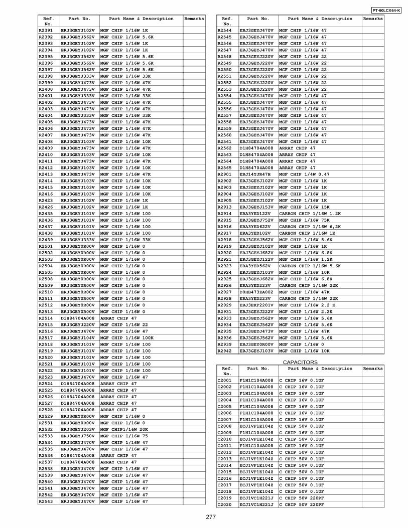
Ref.No.
Part No. Part Name & Description Remarks
R2391 ERJ3GEYJ102V MGF CHIP 1/16W 1K
R2392 ERJ3GEYJ562V MGF CHIP 1/16W 5.6K
R2393 ERJ3GEYJ102V MGF CHIP 1/16W 1K
R2394 ERJ3GEYJ102V MGF CHIP 1/16W 1K
R2395 ERJ3GEYJ562V MGF CHIP 1/16W 5.6K
R2396 ERJ3GEYJ562V MGF CHIP 1/16W 5.6K
R2397 ERJ3GEYJ562V MGF CHIP 1/16W 5.6K
R2398 ERJ3GEYJ333V MGF CHIP 1/16W 33K
R2399 ERJ3GEYJ473V MGF CHIP 1/16W 47K
R2400 ERJ3GEYJ473V MGF CHIP 1/16W 47K
R2401 ERJ3GEYJ333V MGF CHIP 1/16W 33K
R2402 ERJ3GEYJ473V MGF CHIP 1/16W 47K
R2403 ERJ3GEYJ473V MGF CHIP 1/16W 47K
R2404 ERJ3GEYJ333V MGF CHIP 1/16W 33K
R2405 ERJ3GEYJ473V MGF CHIP 1/16W 47K
R2406 ERJ3GEYJ473V MGF CHIP 1/16W 47K
R2407 ERJ3GEYJ473V MGF CHIP 1/16W 47K
R2408 ERJ3GEYJ103V MGF CHIP 1/16W 10K
R2409 ERJ3GEYJ473V MGF CHIP 1/16W 47K
R2410 ERJ3GEYJ103V MGF CHIP 1/16W 10K
R2411 ERJ3GEYJ473V MGF CHIP 1/16W 47K
R2412 ERJ3GEYJ103V MGF CHIP 1/16W 10K
R2413 ERJ3GEYJ473V MGF CHIP 1/16W 47K
R2414 ERJ3GEYJ103V MGF CHIP 1/16W 10K
R2415 ERJ3GEYJ103V MGF CHIP 1/16W 10K
R2416 ERJ3GEYJ103V MGF CHIP 1/16W 10K
R2423 ERJ3GEYJ102V MGF CHIP 1/16W 1K
R2426 ERJ3GEYJ102V MGF CHIP 1/16W 1K
R2435 ERJ3GEYJ101V MGF CHIP 1/16W 100
R2436 ERJ3GEYJ101V MGF CHIP 1/16W 100
R2437 ERJ3GEYJ101V MGF CHIP 1/16W 100
R2438 ERJ3GEYJ101V MGF CHIP 1/16W 100
R2439 ERJ3GEYJ333V MGF CHIP 1/16W 33K
R2501 ERJ3GEY0R00V MGF CHIP 1/16W 0
R2502 ERJ3GEY0R00V MGF CHIP 1/16W 0
R2503 ERJ3GEY0R00V MGF CHIP 1/16W 0
R2504 ERJ3GEY0R00V MGF CHIP 1/16W 0
R2505 ERJ3GEY0R00V MGF CHIP 1/16W 0
R2508 ERJ3GEY0R00V MGF CHIP 1/16W 0
R2509 ERJ3GEY0R00V MGF CHIP 1/16W 0
R2510 ERJ3GEY0R00V MGF CHIP 1/16W 0
R2511 ERJ3GEY0R00V MGF CHIP 1/16W 0
R2512 ERJ3GEY0R00V MGF CHIP 1/16W 0
R2513 ERJ3GEY0R00V MGF CHIP 1/16W 0
R2514 D1H84704A008 ARRAY CHIP 47
R2515 ERJ3GEYJ220V MGF CHIP 1/16W 22
R2516 ERJ3GEYJ470V MGF CHIP 1/16W 47
R2517 ERJ3GEYJ104V MGF CHIP 1/16W 100K
R2518 ERJ3GEYJ101V MGF CHIP 1/16W 100
R2519 ERJ3GEYJ101V MGF CHIP 1/16W 100
R2520 ERJ3GEYJ101V MGF CHIP 1/16W 100
R2521 ERJ3GEYJ101V MGF CHIP 1/16W 100
R2522 ERJ3GEYJ101V MGF CHIP 1/16W 100
R2523 ERJ3GEYJ470V MGF CHIP 1/16W 47
R2524 D1H84704A008 ARRAY CHIP 47
R2525 D1H84704A008 ARRAY CHIP 47
R2526 D1H84704A008 ARRAY CHIP 47
R2527 D1H84704A008 ARRAY CHIP 47
R2528 D1H84704A008 ARRAY CHIP 47
R2529 ERJ3GEY0R00V MGF CHIP 1/16W 0
R2531 ERJ3GEY0R00V MGF CHIP 1/16W 0
R2532 ERJ3GEYJ203V MGF CHIP1/16W 20K
R2533 ERJ3GEYJ750V MGF CHIP 1/16W 75
R2534 ERJ3GEYJ470V MGF CHIP 1/16W 47
R2535 ERJ3GEYJ470V MGF CHIP 1/16W 47
R2536 D1H84704A008 ARRAY CHIP 47
R2537 D1H84704A008 ARRAY CHIP 47
R2538 ERJ3GEYJ470V MGF CHIP 1/16W 47
R2539 ERJ3GEYJ470V MGF CHIP 1/16W 47
R2540 ERJ3GEYJ470V MGF CHIP 1/16W 47
R2541 ERJ3GEYJ470V MGF CHIP 1/16W 47
R2542 ERJ3GEYJ470V MGF CHIP 1/16W 47
R2543 ERJ3GEYJ470V MGF CHIP 1/16W 47
Ref.No.
Part No. Part Name & Description Remarks
R2544 ERJ3GEYJ470V MGF CHIP 1/16W 47
R2545 ERJ3GEYJ470V MGF CHIP 1/16W 47
R2546 ERJ3GEYJ470V MGF CHIP 1/16W 47
R2547 ERJ3GEYJ470V MGF CHIP 1/16W 47
R2548 ERJ3GEYJ220V MGF CHIP 1/16W 22
R2549 ERJ3GEYJ220V MGF CHIP 1/16W 22
R2550 ERJ3GEYJ220V MGF CHIP 1/16W 22
R2551 ERJ3GEYJ220V MGF CHIP 1/16W 22
R2552 ERJ3GEYJ220V MGF CHIP 1/16W 22
R2553 ERJ3GEYJ220V MGF CHIP 1/16W 22
R2554 ERJ3GEYJ470V MGF CHIP 1/16W 47
R2555 ERJ3GEYJ470V MGF CHIP 1/16W 47
R2556 ERJ3GEYJ470V MGF CHIP 1/16W 47
R2557 ERJ3GEYJ470V MGF CHIP 1/16W 47
R2558 ERJ3GEYJ470V MGF CHIP 1/16W 47
R2559 ERJ3GEYJ470V MGF CHIP 1/16W 47
R2560 ERJ3GEYJ470V MGF CHIP 1/16W 47
R2561 ERJ3GEYJ470V MGF CHIP 1/16W 47
R2562 D1H84704A008 ARRAY CHIP 47
R2563 D1H84704A008 ARRAY CHIP 47
R2564 D1H84704A008 ARRAY CHIP 47
R2565 D1H84704A008 ARRAY CHIP 47
R2901 ERJ14YJR47H MGF CHIP 1/4W 0.47
R2902 ERJ3GEYJ102V MGF CHIP 1/16W 1K
R2903 ERJ3GEYJ102V MGF CHIP 1/16W 1K
R2904 ERJ3GEYJ102V MGF CHIP 1/16W 1K
R2905 ERJ3GEYJ102V MGF CHIP 1/16W 1K
R2913 ERJ3GEYJ153V MGF CHIP 1/16W 15K
R2914 ERA3YED122V CARBON CHIP 1/16W 1.2K
R2915 ERJ3GEYJ752V MGF CHIP 1/16W 75K
R2916 ERA3YED622V CARBON CHIP 1/16W 6,2K
R2917 ERA3YED102V CARBON CHIP 1/16W 1K
R2918 ERJ3GEYJ562V MGF CHIP 1/16W 5.6K
R2919 ERJ3GEYJ102V MGF CHIP 1/16W 1K
R2920 ERJ3GEYJ682V MGF CHIP 1/16W 6.8K
R2921 ERJ3GEYJ122V MGF CHIP 1/16W 1.2K
R2923 ERA3YED562V CARBON CHIP 1/16W 5.6K
R2924 ERJ3GEYJ103V MGF CHIP 1/16W 10K
R2925 ERJ3GEYJ682V MGF CHIP 1/16W 6.8K
R2926 ERA3YED223V CARBON CHIP 1/16W 22K
R2927 D0HB473ZA002 MGF CHIP 1/16W 47K
R2928 ERA3YED223V CARBON CHIP 1/16W 22K
R2929 ERJ3EKF2201V MGF CHIP 1/16W 2.2 K
R2931 ERJ3GEYJ222V MGF CHIP 1/16W 2.2K
R2933 ERJ3GEYJ562V MGF CHIP 1/16W 5.6K
R2934 ERJ3GEYJ562V MGF CHIP 1/16W 5.6K
R2935 ERJ3GEYJ473V MGF CHIP 1/16W 47K
R2936 ERJ3GEYJ562V MGF CHIP 1/16W 5.6K
R2939 ERJ3GEY0R00V MGF CHIP 1/16W 0
R2942 ERJ3GEYJ103V MGF CHIP 1/16W 10K
CAPACITORSRef.No.
Part No. Part Name & Description Remarks
C2001 F1H1C104A008 C CHIP 16V 0.1UF
C2002 F1H1C104A008 C CHIP 16V 0.1UF
C2003 F1H1C104A008 C CHIP 16V 0.1UF
C2004 F1H1C104A008 C CHIP 16V 0.1UF
C2005 F1H1C104A008 C CHIP 16V 0.1UF
C2006 F1H1C104A008 C CHIP 16V 0.1UF
C2007 F1H1C104A008 C CHIP 16V 0.1UF
C2008 ECJ1VF1E104Z C CHIP 50V 0.1UF
C2009 F1H1C104A008 C CHIP 16V 0.1UF
C2010 ECJ1VF1E104Z C CHIP 50V 0.1UF
C2011 F1H1C104A008 C CHIP 16V 0.1UF
C2012 ECJ1VF1E104Z C CHIP 50V 0.1UF
C2013 ECJ1VF1E104Z C CHIP 50V 0.1UF
C2014 ECJ1VF1E104Z C CHIP 50V 0.1UF
C2015 ECJ1VF1E104Z C CHIP 50V 0.1UF
C2016 ECJ1VF1E104Z C CHIP 50V 0.1UF
C2017 ECJ1VF1E104Z C CHIP 50V 0.1UF
C2018 ECJ1VF1E104Z C CHIP 50V 0.1UF
C2019 ECJ1VC1H221J C CHIP 50V 220PF
C2020 ECJ1VC1H221J C CHIP 50V 220PF
277
PT-60LCX64-K
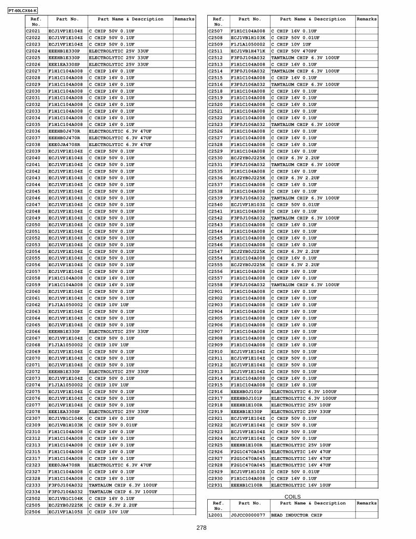
Ref.No.
Part No. Part Name & Description Remarks
C2021 ECJ1VF1E104Z C CHIP 50V 0.1UF
C2022 ECJ1VF1E104Z C CHIP 50V 0.1UF
C2023 ECJ1VF1E104Z C CHIP 50V 0.1UF
C2024 EEEHB1E330P ELECTROLYTIC 25V 33UF
C2025 EEEHB1E330P ELECTROLYTIC 25V 33UF
C2026 EEE1EA330SP ELECTROLYTIC 25V 33UF
C2027 F1H1C104A008 C CHIP 16V 0.1UF
C2028 F1H1C104A008 C CHIP 16V 0.1UF
C2029 F1H1C104A008 C CHIP 16V 0.1UF
C2030 F1H1C104A008 C CHIP 16V 0.1UF
C2031 F1H1C104A008 C CHIP 16V 0.1UF
C2032 F1H1C104A008 C CHIP 16V 0.1UF
C2033 F1H1C104A008 C CHIP 16V 0.1UF
C2034 F1H1C104A008 C CHIP 16V 0.1UF
C2035 F1H1C104A008 C CHIP 16V 0.1UF
C2036 EEEHB0J470R ELECTROLYTIC 6.3V 47UF
C2037 EEEHB0J470R ELECTROLYTIC 6.3V 47UF
C2038 EEE0JA470SR ELECTROLYTIC 6.3V 47UF
C2039 ECJ1VF1E104Z C CHIP 50V 0.1UF
C2040 ECJ1VF1E104Z C CHIP 50V 0.1UF
C2041 ECJ1VF1E104Z C CHIP 50V 0.1UF
C2042 ECJ1VF1E104Z C CHIP 50V 0.1UF
C2043 ECJ1VF1E104Z C CHIP 50V 0.1UF
C2044 ECJ1VF1E104Z C CHIP 50V 0.1UF
C2045 ECJ1VF1E104Z C CHIP 50V 0.1UF
C2046 ECJ1VF1E104Z C CHIP 50V 0.1UF
C2047 ECJ1VF1E104Z C CHIP 50V 0.1UF
C2048 ECJ1VF1E104Z C CHIP 50V 0.1UF
C2049 ECJ1VF1E104Z C CHIP 50V 0.1UF
C2050 ECJ1VF1E104Z C CHIP 50V 0.1UF
C2051 ECJ1VF1E104Z C CHIP 50V 0.1UF
C2052 ECJ1VF1E104Z C CHIP 50V 0.1UF
C2053 ECJ1VF1E104Z C CHIP 50V 0.1UF
C2054 ECJ1VF1E104Z C CHIP 50V 0.1UF
C2055 ECJ1VF1E104Z C CHIP 50V 0.1UF
C2056 ECJ1VF1E104Z C CHIP 50V 0.1UF
C2057 ECJ1VF1E104Z C CHIP 50V 0.1UF
C2058 F1H1C104A008 C CHIP 16V 0.1UF
C2059 F1H1C104A008 C CHIP 16V 0.1UF
C2060 ECJ1VF1E104Z C CHIP 50V 0.1UF
C2061 ECJ1VF1E104Z C CHIP 50V 0.1UF
C2062 F1J1A1050002 C CHIP 10V 1UF
C2063 ECJ1VF1E104Z C CHIP 50V 0.1UF
C2064 ECJ1VF1E104Z C CHIP 50V 0.1UF
C2065 ECJ1VF1E104Z C CHIP 50V 0.1UF
C2066 EEEHB1E330P ELECTROLYTIC 25V 33UF
C2067 ECJ1VF1E104Z C CHIP 50V 0.1UF
C2068 F1J1A1050002 C CHIP 10V 1UF
C2069 ECJ1VF1E104Z C CHIP 50V 0.1UF
C2070 ECJ1VF1E104Z C CHIP 50V 0.1UF
C2071 ECJ1VF1E104Z C CHIP 50V 0.1UF
C2072 EEEHB1E330P ELECTROLYTIC 25V 33UF
C2073 ECJ1VF1E104Z C CHIP 50V 0.1UF
C2074 F1J1A1050002 C CHIP 10V 1UF
C2075 ECJ1VF1E104Z C CHIP 50V 0.1UF
C2076 ECJ1VF1E104Z C CHIP 50V 0.1UF
C2077 ECJ1VF1E104Z C CHIP 50V 0.1UF
C2078 EEE1EA330SP ELECTROLYTIC 25V 33UF
C2307 ECJ1VB1C104K C CHIP 16V 0.1UF
C2309 ECJ1VB1H103K C CHIP 50V 0.01UF
C2310 F1H1C104A008 C CHIP 16V 0.1UF
C2312 F1H1C104A008 C CHIP 16V 0.1UF
C2313 F1H1C104A008 C CHIP 16V 0.1UF
C2315 F1H1C104A008 C CHIP 16V 0.1UF
C2317 F1H1C104A008 C CHIP 16V 0.1UF
C2323 EEE0JA470SR ELECTROLYTIC 6.3V 47UF
C2327 F1H1C104A008 C CHIP 16V 0.1UF
C2328 F1H1C104A008 C CHIP 16V 0.1UF
C2333 F3F0J106A032 TANTALUM CHIP 6.3V 100UF
C2334 F3F0J106A032 TANTALUM CHIP 6.3V 100UF
C2502 ECJ1VB1C104K C CHIP 16V 0.1UF
C2505 ECJ2YB0J225K C CHIP 6.3V 2.2UF
C2506 ECJ1VF1A105Z C CHIP 10V 1UF
Ref.No.
Part No. Part Name & Description Remarks
C2507 F1H1C104A008 C CHIP 16V 0.1UF
C2508 ECJ1VB1H103K C CHIP 50V 0.01UF
C2509 F1J1A1050002 C CHIP 10V 1UF
C2511 ECJ1VB1H471K C CHIP 50V 470PF
C2512 F3F0J106A032 TANTALUM CHIP 6.3V 100UF
C2513 F1H1C104A008 C CHIP 16V 0.1UF
C2514 F3F0J106A032 TANTALUM CHIP 6.3V 100UF
C2515 F1H1C104A008 C CHIP 16V 0.1UF
C2516 F3F0J106A032 TANTALUM CHIP 6.3V 100UF
C2518 F1H1C104A008 C CHIP 16V 0.1UF
C2519 F1H1C104A008 C CHIP 16V 0.1UF
C2520 F1H1C104A008 C CHIP 16V 0.1UF
C2521 F1H1C104A008 C CHIP 16V 0.1UF
C2522 F1H1C104A008 C CHIP 16V 0.1UF
C2523 F3F0J106A032 TANTALUM CHIP 6.3V 100UF
C2526 F1H1C104A008 C CHIP 16V 0.1UF
C2527 F1H1C104A008 C CHIP 16V 0.1UF
C2528 F1H1C104A008 C CHIP 16V 0.1UF
C2529 F1H1C104A008 C CHIP 16V 0.1UF
C2530 ECJ2YB0J225K C CHIP 6.3V 2.2UF
C2531 F3F0J106A032 TANTALUM CHIP 6.3V 100UF
C2535 F1H1C104A008 C CHIP 16V 0.1UF
C2536 ECJ2YB0J225K C CHIP 6.3V 2.2UF
C2537 F1H1C104A008 C CHIP 16V 0.1UF
C2538 F1H1C104A008 C CHIP 16V 0.1UF
C2539 F3F0J106A032 TANTALUM CHIP 6.3V 100UF
C2540 ECJ1VF1H103Z C CHIP 50V 0.01UF
C2541 F1H1C104A008 C CHIP 16V 0.1UF
C2542 F3F0J106A032 TANTALUM CHIP 6.3V 100UF
C2543 F1H1C104A008 C CHIP 16V 0.1UF
C2544 F1H1C104A008 C CHIP 16V 0.1UF
C2545 F1H1C104A008 C CHIP 16V 0.1UF
C2546 F1H1C104A008 C CHIP 16V 0.1UF
C2547 ECJ2YB0J225K C CHIP 6.3V 2.2UF
C2554 F1H1C104A008 C CHIP 16V 0.1UF
C2555 ECJ2YB0J225K C CHIP 6.3V 2.2UF
C2556 F1H1C104A008 C CHIP 16V 0.1UF
C2557 F1H1C104A008 C CHIP 16V 0.1UF
C2558 F3F0J106A032 TANTALUM CHIP 6.3V 100UF
C2901 F1H1C104A008 C CHIP 16V 0.1UF
C2902 F1H1C104A008 C CHIP 16V 0.1UF
C2903 F1H1C104A008 C CHIP 16V 0.1UF
C2904 F1H1C104A008 C CHIP 16V 0.1UF
C2905 F1H1C104A008 C CHIP 16V 0.1UF
C2906 F1H1C104A008 C CHIP 16V 0.1UF
C2907 F1H1C104A008 C CHIP 16V 0.1UF
C2908 F1H1C104A008 C CHIP 16V 0.1UF
C2909 F1H1C104A008 C CHIP 16V 0.1UF
C2910 ECJ1VF1E104Z C CHIP 50V 0.1UF
C2911 ECJ1VF1E104Z C CHIP 50V 0.1UF
C2912 ECJ1VF1E104Z C CHIP 50V 0.1UF
C2913 ECJ1VF1E104Z C CHIP 50V 0.1UF
C2914 F1H1C104A008 C CHIP 16V 0.1UF
C2915 F1H1C104A008 C CHIP 16V 0.1UF
C2916 EEEHB0J101P ELECTROLYTIC 6.3V 100UF
C2917 EEEHB0J101P ELECTROLYTIC 6.3V 100UF
C2918 EEEHB1E100R ELECTROLYTIC 25V 10UF
C2919 EEEHB1E330P ELECTROLYTIC 25V 33UF
C2921 ECJ1VF1E104Z C CHIP 50V 0.1UF
C2922 ECJ1VF1E104Z C CHIP 50V 0.1UF
C2923 ECJ1VF1E104Z C CHIP 50V 0.1UF
C2924 ECJ1VF1E104Z C CHIP 50V 0.1UF
C2925 EEEHB1E100R ELECTROLYTIC 25V 10UF
C2926 F2G1C470A045 ELECTROLYTIC 16V 47UF
C2927 F2G1C470A045 ELECTROLYTIC 16V 47UF
C2928 F2G1C470A045 ELECTROLYTIC 16V 47UF
C2929 ECJ1VF1H103Z C CHIP 50V 0.01UF
C2930 F1H1C104A008 C CHIP 16V 0.1UF
C2931 EEEHB1C100R ELECTROLYTIC 16V 10UF
COILSRef.No.
Part No. Part Name & Description Remarks
L2001 J0JCC0000077 BEAD INDUCTOR CHIP
278
PT-60LCX64-K
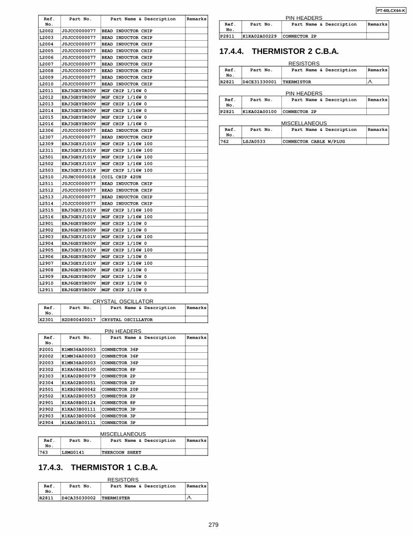
Ref.No.
Part No. Part Name & Description Remarks
L2002 J0JCC0000077 BEAD INDUCTOR CHIP
L2003 J0JCC0000077 BEAD INDUCTOR CHIP
L2004 J0JCC0000077 BEAD INDUCTOR CHIP
L2005 J0JCC0000077 BEAD INDUCTOR CHIP
L2006 J0JCC0000077 BEAD INDUCTOR CHIP
L2007 J0JCC0000077 BEAD INDUCTOR CHIP
L2008 J0JCC0000077 BEAD INDUCTOR CHIP
L2009 J0JCC0000077 BEAD INDUCTOR CHIP
L2010 J0JCC0000077 BEAD INDUCTOR CHIP
L2011 ERJ3GEY0R00V MGF CHIP 1/16W 0
L2012 ERJ3GEY0R00V MGF CHIP 1/16W 0
L2013 ERJ3GEY0R00V MGF CHIP 1/16W 0
L2014 ERJ3GEY0R00V MGF CHIP 1/16W 0
L2015 ERJ3GEY0R00V MGF CHIP 1/16W 0
L2016 ERJ3GEY0R00V MGF CHIP 1/16W 0
L2306 J0JCC0000077 BEAD INDUCTOR CHIP
L2307 J0JCC0000077 BEAD INDUCTOR CHIP
L2309 ERJ3GEYJ101V MGF CHIP 1/16W 100
L2311 ERJ3GEYJ101V MGF CHIP 1/16W 100
L2501 ERJ3GEYJ101V MGF CHIP 1/16W 100
L2502 ERJ3GEYJ101V MGF CHIP 1/16W 100
L2503 ERJ3GEYJ101V MGF CHIP 1/16W 100
L2510 J0JHC0000018 COIL CHIP 42UH
L2511 J0JCC0000077 BEAD INDUCTOR CHIP
L2512 J0JCC0000077 BEAD INDUCTOR CHIP
L2513 J0JCC0000077 BEAD INDUCTOR CHIP
L2514 J0JCC0000077 BEAD INDUCTOR CHIP
L2515 ERJ3GEYJ101V MGF CHIP 1/16W 100
L2516 ERJ3GEYJ101V MGF CHIP 1/16W 100
L2901 ERJ6GEY0R00V MGF CHIP 1/10W 0
L2902 ERJ6GEY0R00V MGF CHIP 1/10W 0
L2903 ERJ3GEYJ101V MGF CHIP 1/16W 100
L2904 ERJ6GEY0R00V MGF CHIP 1/10W 0
L2905 ERJ3GEYJ101V MGF CHIP 1/16W 100
L2906 ERJ6GEY0R00V MGF CHIP 1/10W 0
L2907 ERJ3GEYJ101V MGF CHIP 1/16W 100
L2908 ERJ6GEY0R00V MGF CHIP 1/10W 0
L2909 ERJ6GEY0R00V MGF CHIP 1/10W 0
L2910 ERJ6GEY0R00V MGF CHIP 1/10W 0
L2911 ERJ6GEY0R00V MGF CHIP 1/10W 0
CRYSTAL OSCILLATORRef.No.
Part No. Part Name & Description Remarks
X2301 H2D800400017 CRYSTAL OSCILLATOR
PIN HEADERSRef.No.
Part No. Part Name & Description Remarks
P2001 K1MN36A00003 CONNECTOR 36P
P2002 K1MN36A00003 CONNECTOR 36P
P2003 K1MN36A00003 CONNECTOR 36P
P2302 K1KA08A00100 CONNECTOR 8P
P2303 K1KA02B00079 CONNECTOR 2P
P2304 K1KA02B00051 CONNECTOR 2P
P2501 K1KB20B00042 CONNECTOR 20P
P2502 K1KA02B00053 CONNECTOR 2P
P2901 K1KA08B00124 CONNECTOR 8P
P2902 K1KA03B00111 CONNECTOR 3P
P2903 K1KA03B00006 CONNECTOR 3P
P2904 K1KA03B00111 CONNECTOR 3P
MISCELLANEOUSRef.No.
Part No. Part Name & Description Remarks
763 LSMG0141 THERCOON SHEET
17.4.3. THERMISTOR 1 C.B.A.RESISTORS
Ref.No.
Part No. Part Name & Description Remarks
R2811 D4CA35030002 THERMISTER
PIN HEADERSRef.No.
Part No. Part Name & Description Remarks
P2811 K1KA02A00229 CONNECTOR 2P
17.4.4. THERMISTOR 2 C.B.A.RESISTORS
Ref.No.
Part No. Part Name & Description Remarks
R2821 D4CE31330001 THERMISTOR
PIN HEADERSRef.No.
Part No. Part Name & Description Remarks
P2821 K1KA02A00100 CONNECTOR 2P
MISCELLANEOUSRef.No.
Part No. Part Name & Description Remarks
762 LSJA0533 CONNECTOR CABLE W/PLUG
279
PT-60LCX64-K