Embed Size (px)
Citation preview
Quantum dots for memory applications
P. Dimitrakis*,1, P. Normand1, V. Ioannou-Sougleridis1, C. Bonafos2,S. Schamm-Chardon2, G. BenAssayag2, and E. Iliopoulos3,4
1 Department of Microelectronics, Institute of Advanced Materials, Physicochemical Processes, Nanotechnology and Microsystems,National Centre for Scientific Research “Demokritos”, P.O. Box 60228, Aghia Paraskevi, 15310 Athens, Greece
2 CEMES-CNRS et Université de Toulouse, nMat group, BP 94347, 31055 Toulouse Cedex 4, France3Nano-MicroElectronics Research Group (NMRG), IESL-FORTH, P.O. Box 1527, 71110 Heraklion, Greece4 Physics Department, University of Crete, P.O. Box 2208, 71003 Heraklion, Greece
Received 7 March 2013, revised 15 May 2013, accepted 28 May 2013Published online 15 July 2013
Keywords gallium nitride, nanocrystals, non-volatile memories, quantum dots
* Corresponding author: e-mail [email protected], Phone: þ30 210 6503118, Fax: þ30 210 6511723
In this paper, we review the fabrication and the electricalcharacteristics of metal–insulator–semiconductor (MIS) deviceswith semiconductor quantum dots (QD) embedded into the gatedielectric. Our results originate from experiments performed thelast decade and cover Si QDs realized by low-energy ion-beamsynthesis (IBS) as well as GaN QDs formed by molecular beamdeposition (MBD). Besides the basic capacitance-to-voltage(C–V) and current-to-voltage (I–V) characterization, the memoryproperties of the fabricated MIS devices were investigated interms of memory window under pulse operation and charge
retention. The optimization of Si-QD memory cells is reviewedand a methodology for both the extraction of various deviceparameters and the identification of mechanisms governing thecharge loss process are presented. GaN QDs, which exhibitnegative conduction band-offset with respect to the Siconduction band, offer an interesting alternative to Si QDs asdiscussed herein based on our investigations of GaN-QDcapacitors fabricated by a complementary-metal-oxide-semicon-ductor (CMOS) compatible process.
� 2013 WILEY-VCH Verlag GmbH & Co. KGaA, Weinheim
1 Introduction For more than two decades there hasbeen increasing interest in the development of semiconduc-tor quantum dots (QDs) in dielectric matrices for electronicand optoelectronic applications. In particular, major effortshave been placed on the realization of the so-called QD(or nanocrystal) memories in an attempt to overcome thescaling issues of conventional flash and primarily forembedded memory applications such as built-in memoryarrays for microcontrollers (MCU) and system-on-chip(SoC). It should be noticed that there is a gap between thelogic and the memories technology nodes. More specifically,memory technology node lags behind the leading logictechnology by about three generations [1]. Embeddednon-volatile memories (e-NVM) do not require highstorage capabilities. Nevertheless, a technology for e-NVMsshould support operation compatibility with the logiccircuit transistors, design libraries, CMOS performanceand reduced cost. The latest is strongly related to theadditional masks and processing steps required in e-NVMsintegration. The limitations in the scaling of conventionalfloating-gate (FG) MOSFET [Ref. [2], see Fig. 1(a)] as theunit memory cell, rise basically from reliability concerns [1].
Following the transistor scaling rules, the equivalent oxidethickness (EOT) of the gate dielectric above the channel(called injection oxide) should be smaller than 6–7 nm. Inthis case, the injection oxide becomes less resistant to defectformation which may cause, under operating conditions ofthe memory cell, the total loss of charge stored in the FG(made of conductive poly-Si), i.e., the total loss of data.Moreover, for very small EOT the FG charge cannot beretained for a long time due to the quantum mechanical directtunneling effect. Furthermore, scaling of transistors requiresthe scaling of the isolation between them in order to increasetheir density on a wafer. While for logic circuits thisrequirement can be implemented easily, in the case of FGNVMs the isolation between neighboring cells is not scalabledue to significant capacitance coupling between the adjacentFGs which causes serious cross-talk interference [3].
Memory devices with Si-QDs have been demonstratedfor the first time by Tiwari et al. [4]. Since then, a hugeresearch effort has been devoted to this technology.According to the original QD-NVM concept [see Fig. 1(b)], the charges are injected from the channel into the QDswhere they are trapped. Utilizing a device with QDs as
Phys. Status Solidi A 210, No. 8, 1490–1504 (2013) / DOI 10.1002/pssa.201300029
Invited Articleapplications and materials science
a
statu
s
soli
di
www.pss-a.comph
ysi
ca
� 2013 WILEY-VCH Verlag GmbH & Co. KGaA, Weinheim

discrete charge storage nodes it is possible to tackle theFG-NVMs scaling issues. First, the injected charges can bestored in deep traps of the QDs and therefore, theirprobability to tunnel back to the Si channel by directtunneling is very low. Second, using an injection oxidethinner than 6–7 nm, a lower electric field is required forcharge injection and thus the introduction of oxide defectsdue to electrical stress is minimized. Finally, the capacitancecoupling between nanometer size QDs of adjacent memorycells is almost zero.
The most commonly used techniques to form two-dimensional (2D) arrays of QDs are the chemical vapordeposition (CVD) either at low-pressure (LP) or plasmaenhanced (PE), the ion beam synthesis (IBS) and physicalvapor deposition (PVD) either by sputtering or electronbeam [1]. CVD is a well established technique in CMOSmanufacturing and is mainly used to deposit Si-QDs. IBS isused to synthesize Si, Ge, or metal QDs while utilizing PVDmainly metal QDs can be deposited. The formation of QDsutilizing the previous techniques and materials is based onself-assembly mechanisms. For the preparation of QDs byCVD, the nucleation and growth mechanisms can bemanipulated separately, thus allowing a good control of theQD’s size and density [5]. For IBS, the implanted dose ofatoms and their distribution profile inside the dielectric layerin combination with the annealing conditions control the sizeand the density of the QDs [6]. Finally, to realize metal QDsby PVD, an ultra-thin metallic wetting layer is properlyannealed, generally under rapid thermal annealing (RTA)conditions [7]. It should be noticed that recently, Si QDse-NVMs have been integrated successfully in MCU at90 nm technology node [8], while preliminary resultssuggest that their integration at the 45 nm technology nodeis also functional.
Since the transistor scaling roadmap demands smallerdevice dimensions, the variability of the QDs distributionshould become smaller too raising the serious questionof whether the QD-NVM technology can provide reliabledevices to technology nodes as short as 45 nm andbelow. Obviously, to answer this question the fluctuationsinduced by a self-assembly process should be eliminated,a task which can be fulfilled by developing template-assisted-deposition techniques. Relevant templates can beformed by e-beam lithography (EBL) or using diblock
copolymers [9, 10]. Following the latter approach that ismore cost effective, functional memory devices have beendemonstrated using the PVD technique [10]. It shouldbe noted that other non-CMOS techniques such as theLangmuir–Blodgett deposition technique have also beentested for the ordered formation of functionalized Au-QDson SiO2 over a Si channel [11]. Using the latter approach,hybrid devices (Si/organic materials) with very attractivememory characteristics have been demonstrated. Further-more, the successful combination of QDs with organicmaterials leads to a new category of two-terminal memorydevices as shown in Fig. 1(c) [12, 13]. The presence ofcharges in theQDs embedded in an organic layer modifies theconductivity of the device and the energy band-alignment ofthe materials. The new device exhibits two stable operatingstages: one high-resistance stage (HRS) and a second low-resistance stage (LRS). Such devices have been demonstratedas standalone memory cells in electronic circuits [14].
In this work we address the development of group IVand III-N QDs embedded into very thin insulators with focuson their application to NVM devices. More specifically, wereport on 2D arrays of Si and GaN QDs in SiO2 formedby ultra-low-energy IBS (ULE-IBS) [15] and molecularbeam deposition (MBD) [16], respectively. A review on thefabrication of Si and Ge QDs by ULE-IBS in differentinsulators has recently been published by Bonafos et al. [17].
The ULE-IBS technique allows the fabrication of2D-arrays of Si QDs in thin SiO2 layers but does notguarantee their effectiveness as charge storage centers andmore generally, the memory functionality of the whole gatestructure. The latter depends not only on the properties ofthe QDs (size, size uniformity, density, spatial distribution)but also on the properties (integrity, thickness) of thetunnel and control oxides. This requires a tight control overprocess parameters such as the thickness of the starting oxideand the implantation/annealing conditions. As emphasizedthroughout this communication, a challenging task fortaking full advantage of the ULE-IBS technique is thefabrication of functional QD dielectric structures which donot necessitate the additional step of depositing a control(or blocking) oxide layer.
According to theoretical and experimental investiga-tions, work-function engineering of the QDs may improvethe performance of NVMs in terms of operating voltages andretention time [18, 19]. This can be achieved by formingsemiconductor QDs which exhibit negative conduction bandoffset with respect to the substrate. Assuming a Si substratewith a thin SiO2 tunneling layer, GaN QDs fulfill theserequirements [16, 20]. As stressed herein the MBDtechnique is well adapted for making GaN QDs ontoamorphous dielectrics with negligible cross-contaminationeffects under specific process conditions.
2 Experimental procedures2.1 Preparation of Si-QD samples High quality 5,
7, 9, and 10 nm thick SiO2 layers were first thermally grownon 8-inch p-type (100) silicon substrate (1–10 V cm) in dry
Figure 1 Schematic description of (a) a conventional FG-NVMcell, (b) a QD-NVM cell, and (c) a two-terminal organic bistablememory cell with QDs. The electron injection layer (EIL) andelectron blocking layer (EBL) can be the same material.
Phys. Status Solidi A 210, No. 8 (2013) 1491
www.pss-a.com � 2013 WILEY-VCH Verlag GmbH & Co. KGaA, Weinheim
Invited
Article

oxidizing ambient. Ion implantation of Si atoms wasperformed at 1 keV in an Axcelis GSD-implanter undercharge neutralization conditions. Three different doses of Siatoms were tested, namely 0.5, 1.0, and 2.0 � 1016 cm�2.This set of samples is summarized in Table 1.
All samples were subjected to a post-implantationannealing (PIA) at 950 8C in N2 for 30 min in atmosphericfurnace. Following, MOS capacitors were fabricated usingAl for the backside contact and control gate electrode. Thelatter of 10�4 cm2 area was defined by photolithography andwet etching.
For each oxide thickness, a reference sample wasfabricated for comparison purpose. The electrical propertiesof these reference samples exhibited no significant deviationfrom that of typical MOS structures and will not be furtherdiscussed herein. Furthermore, it should be emphasized thatthe integrity of the implanted oxide, which is altered due toexcess Si atoms and implantation induced defects, as well asthe quality of the QD/SiO2 interface play a significant role incarrier dynamics, thus affecting the charge injection andtrapping characteristics of the structures. It is so important todevelop a post-implantation step for addressing these issueswithout adding process complexity. In that direction weexamined the possibility of optimizing the PIA step by usingdifferent recipes. Emphasis is herein placed upon the case ofthe 7 nm-thick SiO2 samples, which have been subjected tothe five different PIA recipes (AP1-5) described in Table 2.
AP1 is the standard annealing process used for theformation of QDs and minimization of ion implantationinduced defects [21, 22]. AP2 is a thermal treatment recipe ina mild oxidizing ambient, which allows simultaneously QDsformation, oxidation of part of the excess Si atoms andoxidation of the QD/SiO2 interface. AP3–AP5 have been
applied for understanding the structural and electricalchanges resulting from a combination of thermal treatmentsin inert and oxidizing atmosphere.
2.2 Preparation of GaN-QD samples The GaN-QDs were formed by radio frequency plasma assisted MBD(RF-MBD) onto 3.5 nm SiO2 films grown on 4 inch. (100)n-Si substrates. Several deposition conditions were employedin order to evaluate a range of QDs size and densitydistributions. Table 3 summarizes the deposition conditions.It should be mentioned that the deposition conditions aredetermined by the GaN dose which was measured inequivalent number of monolayers (MLs) of epitaxial GaN.LPCVD SiO2 layer of 20 nm in thickness was used ascapping dielectric material. For comparison, a control samplewithout QDs, but treated in similar conditions and exposedto RF N-plasma was also fabricated. Standard Al-gate MOScapacitors were realized. The devices were MESA isolatedusing dry reactive-ion-etching (DRIE) process.
Transmission-electron-microscopy (TEM) investiga-tions revealed the presence of crystalline GaN QDs andthe variation of their characteristics with respect to theMBD conditions [16]. The variation of the number of MLsallowed tuning the size/density of QDs from discrete 3.5 nmin diameter up to poly-crystalline GaN layer.
3 Electrical characterization results anddiscussion Standard C–G–V–f (HP 4284) and I–V (HP4140B, HP 4155) measurements were performed in order toinvestigate the electrical properties and memory character-istics of the produced QD-SiO2 layers.
3.1 Si-QD samples Symmetric bi-directional C–Vmeasurements at 1 MHz were applied to samples reportedin Table 1 (AP1 PIA recipe). Typical C–V characteristics arepresented in Fig. 2 for the 5, 7, and 9 nm-thick SiO2 Si-implanted samples. The flat-band voltage VFB shifts withrespect to the fresh sample as extracted from the measuredC–V hysteresis, DVFB, are shown in Fig. 3.
DVFB is a measure of the memory effect. Starting thegate voltage sweep from a positive value on a p-MOSmemory capacitor, electrons are expected to be injectedfrom the inversion layer, formed at the SiO2/p-Si substrateinterface, into the QDs where they are trapped. As a result of
Table 1 The LE-IBS samples implanted with 1 keV Si atoms.
dose (cm�2) 0.5 � 1016 1 � 1016 2 � 1016
SiO2 thickness (nm)
5 AX5114 AX5214 AX53147 X711 X721 X7319 X911 X921 X93110 X1011 X1021 X1031
Table 2 The different recipes used for PIA optimization of 7 nm-thick SiO2 samples implanted with 1 keV Si atoms to a dose of2 � 1016 cm�2.
PIA ID PIA recipe
AP1 950 8C N2 30 minAP2 950 8C N2/O2 30 min ([O2]/[N2] þ [O2] ¼ 1.5%)AP3 950 8C N2 30 min þ 800 8C O2 10 minAP4 950 8C N2 15 min þ 950 8C N2/O2 15 min ([O2]/[N2]
þ [O2] ¼ 1.5%)AP5 950 8C N2/O2 15 min ([O2]/[N2] þ [O2] ¼ 1.5%)
þ 950 8C N2 15 min
Table 3 The fabrication parameters of the MBD treated samples.
no. tunnelSiO2
(nm)
dose(GaN MLs)
controlSiO2
(nm)
gate stackCET(nm)
1 3.5 0 20 24.42 3.5 5 20 25.43 3.5 8 20 25.94 3.5 10 20 25.95 3.5 14 20 26.16 3.5 18 20 25.9
1492 P. Dimitrakis et al.: Quantum dots for memory applications
� 2013 WILEY-VCH Verlag GmbH & Co. KGaA, Weinheim www.pss-a.com
ph
ysic
a ssp stat
us
solid
i a

this negative charge trapping event, the depletion layer willinitiate earlier causing a shift in the flat-band voltage (orthreshold voltage, VTH) of the capacitor to a higher value,VþFB (or Vþ
TH), compared to the flat-band voltage, VFB0 (orVTH0), of the capacitor with uncharged QDs (fresh or virgincapacitor). Under negative voltage sweep conditions, thetrapped electrons may be ejected from the QDs back to thep-Si substrate and/or hole injection from the accumulation
layer, formed at the SiO2/p-Si substrate, into the QDs maytake place. In the latter case, positive charges are trapped intothe QDs. Next, the backward voltage sweep is applied, i.e.,the gate voltage is swept from negative to positive values.With positive charges trapped into the QDs, the depletionlayer is formed at a much lower voltage (i.e., at a morenegative voltage), V�
FB (or V�TH), compared to VFB0. As
the voltage becomes less negative towards to zero, the
Figure 2 Typical 1 MHz C–V hysteresis curves for samples withinitial SiO2 thickness (a) 5 nm, (b) 7 nm, and (c) 9 nm.
Figure 3 Dependence of the flat-band voltage shift on voltagesweep limits during C–V measurements, obtained for samples withinitial SiO2 thickness (a) 5 nm, (b) 7 nm, and (c) 9 nm.
Phys. Status Solidi A 210, No. 8 (2013) 1493
www.pss-a.com � 2013 WILEY-VCH Verlag GmbH & Co. KGaA, Weinheim
Invited
Article

positive trapped charge may be ejected back to the p-Sisubstrate. The C–V branch with the high VFB value is called“programming” or “write branch” while the branch with thelow VFB value is called “erase branch”. The memorywindow, DVFB, in this case is defined as DVFB ¼ Vþ
FB �V�FB. In the above example the hysteresis of the C–V
characteristic is counterclockwise. Clockwise hysteresis isobserved when electrons are injected from the gate electrodeinto the QDs [see e.g., Fig. 1(b)]. During the reverse voltagesweep, the previously injected charges return back to theiroriginal sites.
Obviously, the characteristics obtained from the 5 nm-SiO2 implanted samples are suffering from significantstretch-out, which can be attributed to interface traps. Thestrong increase of capacitance in the accumulation regimefor the high-dose implanted sample (AX5314) indicates aneffective oxide thickness of 3.7 nm (Cmax�93.6 pF). This isdue to the strong coupling between the Si substrate and theSi-QDs layer which is formed very close to the SiO2/Siinterface (�2 nm) as revealed by TEM analysis [23, 24].
The counter-clockwise C–V hystereses for the 5 and7 nm SiO2 implanted samples point out that chargeexchange takes place between the QDs and the Si substrate,while for the 9 nm samples the clockwise C–V hysteresisindicates that charge exchange occurs between the QDs andthe control gate. The latter can be due to a larger or/and betterquality of the tunnel oxide compared to the controloxide [23]. Plots in Fig. 3 demonstrate that both electronand hole trapping in the Si-QDs occur under C–V sweepmeasurements. For the 5 nm SiO2 sample implanted at thehighest dose (AX5314), the extraction of VFB was notpossible due to the misleading value of the capacitancemaximum. For the rest of the samples, we found that thehigher the implantation dose, the lower the voltage neededfor charge injection. Further, analyses of the C–V character-istics allow calculation of the oxide thickness, tox, as well asextraction of the density of interface states, Dit. Results forthe 7, 9, and 10 nm SiO2 samples are shown in Fig. 4.
Clearly, tox increases as the implantation dose increasesmainly due to the space taken by the Si implanted atoms and,in the case of oxidizing conditions, to the oxidation of theimplanted Si-atoms and/or their aggregates. This phenome-non is known as oxide swelling. The expansion of theimplanted SiO2 layers depends mainly on the implanteddose [22]. The Dit remains at acceptable levels (1–3 � 1011 eV�1 cm�2) and exhibits a weak dependence onimplantation dose for all samples. Evidently, the sampleswith a 7 nm initial oxide thickness are the most attractive interms of QDs array position, charge injection characteristicsand related memory window.
Typical high-frequency C–V characteristics of the7 nm-samples annealed under the different PIA conditionsdescribed in Table 2 are shown in Fig. 5. The correspondingflat-band voltage shifts are presented in Fig. 6. In thecase of low implanted dose [Fig. 5a, Fig. 6(a)], a verynarrow hysteresis is observed after application of the AP1recipe, which is mainly due to trapping and de-trapping
of electrons. The annealing environments used in theAP2–AP5 recipes eliminate this hysteresis effect andlead, at voltages higher than 6 V, to electron injectionand cumulative charge trapping without effective chargedetrapping [see inset Fig. 6(a)]. In the case of the mediumdose (1 � 1016 cm�2) implanted sample, both electron andhole trapping occur [Fig. 5(b), Fig. 6(b)]; the latter beingmore efficient than the former, especially after the AP4 andAP5 treatments. Finally, in the case of the high dose(2 � 1016 cm�2) sample [Fig. 5(c), Fig. 6(c)], the memorywindows attainable after the AP2, AP4, and AP5 treatmentsare significantly enhanced compared to the medium dosesamples. While charge injection and trapping occur at lowerapplied gate bias for the AP4 and AP5 treatments comparedto the AP2 recipe, the latter leads to larger memory windowsand better charge retention characteristics (not shown).
TEM investigations [24] revealed that after AP2 PIA(mild oxidizing ambient) the control oxide slightly increases
Figure 4 The dependence on the implantation dose of (a) theimplanted oxide thickness, tox, and (b) the density of interfacestates, Dit, after PIA (AP1).
1494 P. Dimitrakis et al.: Quantum dots for memory applications
� 2013 WILEY-VCH Verlag GmbH & Co. KGaA, Weinheim www.pss-a.com
ph
ysic
a ssp stat
us
solid
i a

Figure 5 Typical 1 MHz C–V hysteresis curves for 7 nm samplesimplanted with 1 keV Si atoms to doses of (a) 0.5 � 1016,(b) 1.0 � 1016, and (c) 2.0 � 1016 cm�2 and annealed underdifferent conditions (Table 2).
Figure 6 Dependence of the flat-band voltage shift on voltagesweep limits during C–Vmeasurements, obtained for 7 nm samplesimplanted with 1 keV Si to doses of (a) 0.5, (b) 1.0, and (c)2 � 1016 cm�2 and subjected to the annealing conditions describedin Table 2. Insets emphasize details of the main plots.
Phys. Status Solidi A 210, No. 8 (2013) 1495
www.pss-a.com � 2013 WILEY-VCH Verlag GmbH & Co. KGaA, Weinheim
Invited
Article

to 5 nm compared to 3.7 nm achieved after the AP1treatment (inert ambient), whereas the tunnel oxide thicknessremains almost constant, ca. 6.5 nm. Furthermore, while nosignificant dependence of the QD mean-size between theAP1 and AP2 treatments was detected, TEM examinationshowed that the AP2 recipe leads to a more uniform QD sizedistribution and slightly larger QD separation; a traitimportant for memory operation since it mitigates the lateraltransport of the trapped carriers from QD to QD. The densityof QDs after the AP2 treatment was found to be around1.7 � 1012 cm�2. Combining ToF-SIMS and XPS analyses,Perego et al. [25] have shown that for 9 nm-thick SiO2 layersimplanted under the same conditions and subsequently AP1and AP2 annealed, the density of Si nano-aggregates in thecontrol oxide (i.e., above the QD plane) is reduced and thepresence of sub-stoichiometric oxide in the QD layer isenhanced in the case of the AP2 treatment. These resultssuggest a possible scenario for the effect of AP2 treatment onthe specific samples: at the early annealing stages, phase-separation and QD formation is taking place. Meanwhile, theoxygen species oxidize part of the excess Si atoms in thecontrol oxide and because their concentration is low (1.5%),the majority of them are blocked by the interconnected Siislands and subsequently oxidize them providing mutuallyisolated QDs. It is so expected that only a small number ofoxidizing species can cross the QD layer, thus limiting theirreaction with the excess of Si atoms present in the tunneloxide. The above could explain why effective chargeinjection from the substrate to the QD layer is detectedduring C–V sweep measurements (see Fig. 5) despite thethinner physical thickness of the control oxide compared tothat of the tunnel oxide.
Further analysis of the experimental C–V characteristicsshown in Fig. 5 reveals the effect of the annealing treatmenton the total oxide thickness, tox (see Fig. 7). Note from Fig. 7that the AP2 and AP3 treatments have the strongest effect on
tox. No significant differences are observed between the AP4and AP5 recipes.
Figure 8 presents the current density versus electric field(J–V) characteristics of the 7 nm-SiO2 samples implantedto low, medium and high Si doses after the AP1–AP5treatments [26]. Clearly, samples subjected to the AP3treatment (pure oxidizing ambient) exhibit the highestdielectric strength while the samples annealed following theAP1 treatment (neutral ambient) exhibit the lowest. Thisis because during the AP3 treatment the majority of theimplanted Si atoms are oxidized preventing the formationof Si-QDs. Thus any parasitic conduction due to excessSi atoms and implantation-induced-defects is minimizedand charge storage in Si-QDs is omitted (Figs. 5 and 6).Furthermore, the samples treated following AP2 annealingconditions combine acceptable dielectric strength withremarkable memory windows.
As presented in Fig. 8(c), the J–E characteristics of thehigh-dose implanted samples after the AP2 and AP5treatments are comparable. Nevertheless, the AP5 treatedsamples have slightly higher conductivity especially atlow electric fields (<5 MV cm�1). This low electric fieldconduction can explain the large memory windowsobserved at low voltages shown in Fig. 6(c). This directlink between oxide conductivity and charge injectionsignifies the crucial role of the remaining Si atoms insidethe oxide matrix.
If the concentration of un-clustered Si atoms and/or tinySi nano-aggregates [25] is significant after PIA, the silicondioxide can be regarded as a silicon rich oxide with poordielectric properties. It is necessary to develop a methodol-ogy utilizing electrical characterization methods that allowsthe evaluation of the oxide’s insulating properties after thePIA. For this purpose, we consider two methods based onthe analysis of the J–E characteristics shown in Fig. 8. Thefirst method is based on the high electric field conduction[Fowler–Nordheim (F–N) regime] where the energy barrierFB that the electrons have to overcome in order to tunnelthrough the silicon dioxide can be estimated according tothe F–N approximation [27],
J ¼ AE2 � exp �B=Eð Þ; ð1Þ
FB ¼ffiffiffi2
pB
6:83� 107
� �2=3
; ð2Þ
where A (A V�2) and B (V cm�1) are the F–N constants bothdependent on the electron effective mass, E ¼ V/tox, V is theapplied voltage across the dielectric, tox is the oxidethickness after the PIA (see Fig. 7). The un-cluster Si atomsmodify spatially the dielectric constant of the SiO2 layercontributing to the reduction of the potential energy barrier atSi/SiO2 and SiO2/Al interfaces. In addition, excess Si atomsare responsible for the formation of oxide traps [28] whichmay contribute to trap-assisted tunneling. For these reasons,the tunneling resistance of the Si-rich SiO2 layers is reducedand become transparent for electrons with relatively low
Figure 7 The dependence of the oxide thickness, tox, on theimplanted dose after different PIA.
1496 P. Dimitrakis et al.: Quantum dots for memory applications
� 2013 WILEY-VCH Verlag GmbH & Co. KGaA, Weinheim www.pss-a.com
ph
ysic
a ssp stat
us
solid
i a

potential energy. This method has been presented inRef. [29].
The second method is based on the comparison of theelectric field needed to achieve a certain value of leakagecurrent density. Figure 9 presents the electric field E afterthe applied PIA treatments at which the current densityflowing through the SiO2/Si-QDs/SiO2 is 1 mA cm�2. Thehigher the electric field, the better the oxide insulationproperties. At this point, we introduce the dielectricresistivity [30], r(¼E/J) as a figure of merit for the insulationproperties. Following this representation, the physicalinterpretation of data shown in Fig. 9 is more evident: thedielectric resistivity after AP2 PIA treatment is higher than anyother PIA treatment for which memory effects are detected.
Briefly summarizing, we found that the LE-IBStechnique can provide attractive memory characteristicswhen a 7 nm SiO2 layer is implanted with 1 keV Si ions to afluence of 2 � 1016 cm�2 and subsequently annealed at950 8C for 30 min in mild oxidizing ambient, i.e., 1.5% O2
in N2.Further, optimization of the annealing process requires
an experimental study on the effect of the relative percentageof O2 in N2. For this purpose we performed the PIAexperiments shown in Table 4 [26]. As depicted in Fig. 10,application of gate voltage sweeps of �8 V and higher leadto similar memory windows in the case of 1, 1.5, and 2% O2
PIA treatments, while charge injection and trapping initiateat highest gate voltages as the oxygen content increases; atrait which relates mainly with tunnel oxide conductivity.Figure 10 reveals also that the charge trapping capabilities ofthe samples subjected to the 3 and 5% O2 PIA treatments aresignificantly reduced. This can be attributed not only to thequality of the tunnel oxide but also to the properties ofthe QDs. Further investigations of the effect of the O2
content on the memory properties of the 1, 1.5, and 2% O2
Figure 8 J–E characteristics obtained for 7 nm samples implantedwith 1 keV Si to doses of (a) 0.5, (b) 1.0, and (c) 2.0 � 1016 cm�2
and subjected to the annealing processes described inTable 2.
Figure 9 Plot of the electric field E at which the current throughthe gate oxide of the memory capacitor is 1 mA cm�2 as a functionof the annealing process. The experimental data (symbols) wereobtained for from J–E characteristics presented in Fig. 8.
Phys. Status Solidi A 210, No. 8 (2013) 1497
www.pss-a.com � 2013 WILEY-VCH Verlag GmbH & Co. KGaA, Weinheim
Invited
Article

PIA treated samples have been conducted through chargeretention measurements at 85 8C. The capacitors werepreviously programmed and erased using þ9 V/10 ms and�9 V/10 ms pulses. The results are shown in Fig. 11. Forthe erase state, the VFB transients have almost the same decay
rate for all samples. For the program state, the VFB transientsafter annealing in 1.5 and 2% O2 ambient are comparableafter 105s while a much faster transient is detected in thecase of the 1% O2 PIA treatment. Because a largerprogramming window at a lower applied electric field isobtained for the sample annealed in 1.5% O2, we concludethat 1.5% [O2] in diluted [N2] is the most appropriateannealing atmosphere for a 7 nm SiO2 implanted at 1 keVusing a dose 2 � 1016 cm�2.
The last optimization parameter is the annealing time.For this purpose dedicated experiments were performed in1.5% O2 ambient, as shown in Table 5.
Typical normalizedC–V characteristics (1 MHz) obtainedfrom samples annealed for different time durations areshown in Fig. 12. For comparison, a reference sample ispresented.
As reference sample we consider a MOS capacitorwith 7 nm dry SiO2, non-implanted and annealed in thesame oxidizing ambient for 30 min. According to ourexpectations, the part of the reference C–V characteristic indepletion regime is very similar to that of the Si-implantedsamples after 120 min PIA in 1.5% O2, because underthese conditions the majority of the implanted Si atoms
Table 4 The conditions for the optimization of the oxygenpercentage diluted in N2 during the PIA of samples with 7 nm SiO2
implanted with 1 keV Si to a fluence of 2 � 1016 cm�2.
no. temperature(8C)
time(min)
[O2]/([N2] þ [O2])(%)
1 950 30 12 950 30 1.53 950 30 24 950 30 35 950 30 5
Figure 10 (a) Typical normalized bidirectional C–V (1 MHz)characteristics and (b) flat-band voltage shift diagrams obtainedfromMOS capacitors annealed in different oxidizing environments.
Table 5 The conditions for the optimization of the PIA time forsamples with 7 nm SiO2 implanted with 1 keV Si to a fluence of2 � 1016 cm�2.
no. temperature(8C)
time(min)
[O2]/([N2] þ [O2])(%)
ref 950 30 1.51 950 5 1.52 950 15 1.53 950 30 1.54 950 120 1.5
Figure 11 (a) Charge-retention transients for samples annealed atdifferent oxidizing ambient. The horizontal lines define the flat-band voltage VFB0 for each one of the tested memory capacitors.
1498 P. Dimitrakis et al.: Quantum dots for memory applications
� 2013 WILEY-VCH Verlag GmbH & Co. KGaA, Weinheim www.pss-a.com
ph
ysic
a ssp stat
us
solid
i a

are oxidized. According to TEM investigations [24] forannealing durations shorter than 30 min elongated andconnected Si islands were observed; a trait which affects theretention time characteristics. For long annealing durationssuch as 120 min descrete spherical (2 nm in diameter) Si-QDs were found. In the latter sample the surface coverage isas low as 6% compared to 23% after 30 min PIA.
The above processing conditions have been utilizedfor the realization of NMOS field-effect transistors withself-alligned nþ poly-Si gate. All the required details forNMOSFET fabrication as well as their performance assingle-memory cells are described in Ref. [31]. Furtherinvestigations on charge retention at elevated temperatureshave been presented in Ref. [32]. It was found thatthe cells exhibit true-nonvolatile characteristics afterapplication of programming (P) and erasing (E) voltagepulses ofþ9 V/10 ms and�9 V/10 ms, respectively. Underthese conditions, the cells can withstand more than 106 P/E
cyles and exhibit a significant 10-year extrapolated memorywindow.
The threshold voltage shift for QD-NVM devices isdescribed by [15]
DVTH ¼ tCOeCO
þ 12tqdeqd
� �Qqd ¼ K � Qqd; ð3Þ
where K is a constant depending on the gate dielectric stackcharacteristics, tCO and tqd are the thickness of the controloxide and the diameter of the QDs, eCO and eqd are thedielectric constants for the control oxide and the QDs,respectively. Charge loss is estimated by threshold voltageVTH transients. Detailed studies [15, 33] have shown that Eq.(3) should be corrected dividing the constantK by the surfacecoverage R of the QDs,
R ¼ 0:25p � t2qd � nqd; ð4Þ
where nqd is the surface density of the QDs. Typical, VTH
transients at room and elevated temperatures on a pre-cycleddevice are shown in Fig. 13(a). Obviously, VTH has alogarithmic dependence on time
VTHðtÞ ¼ VTHð0Þ �M � logðtÞ; ð5Þ
where M is the decay rate of VTH. Comparable charge lossrates or equivalently VTH decay rates, dVTH/dt, are found forVTH transients from the erase state. Contrary, the decay ratesof VTH transients from the program state are temperaturedependent. Figure 13(b) shows the Arrhenius plots for thedecay rates obtained from VTH transients for the programand erase states. Considering a simple Arrhenius relation,dVTH/dt / exp(�EA/kBT), the activation energies for thecharge loss rates from the program and erase states areestimated to 40 and 5 meV, respectively. The activationenergy represents the minimum energy required to initiate areaction or a physico-chemical mechanism. It is a measure ofthe sensitivity of the mechanism to temperature. In our case,the calculated values indicate that the decay rates of thecharge loss process are strongly affected by the ambienttemperature. Retention time tR is defined as the time requiredfor VTH to reach the threshold voltage of a fresh (unstressed)cell, VTH0, and can be extracted from the extrapolation of theVTH ransient [see Fig. 13(a)]. Figure 13(c) represents theArrhenius plot of tR, from which activation energies of 1.48and 0.21 eV can be extracted for the program and erasestates, respectively. The physical interpretation of theseactivation energies denote that the trapping sites for electronsare deeper compared to holes and therefore more thermalenergy is required for electron detrapping to occur.
A charge loss transient defines an equivalent charge losscurrent, Jdet, corresponding to de-trapped charges (electrons orholes) that escape back to the Si substrate at a given time
JdetðtÞ ¼ R�1 dQqd
dt: ð6Þ
Figure 12 (a) Typical normalized bidirectional C–V (1 MHz)characteristics and (b) flat-band voltage shift diagrams obtainedfrom MOS capacitors annealed for different time durations in mild(1.5% O2) oxidizing environment, utilizing C–V measurements.
Phys. Status Solidi A 210, No. 8 (2013) 1499
www.pss-a.com � 2013 WILEY-VCH Verlag GmbH & Co. KGaA, Weinheim
Invited
Article

In Fig. 14, Jdet transients at various temperatures arepresented. The experimental data can be fitted by lines inlog–log plot, revealing that
JdetðtÞ ¼ H � tm; ð7Þ
where H is a constant and the values of the exponent m aregiven in Table 6.
According to the previous experimental results on theproperties of tunnel and control oxides, we assume thatthe charge loss is taking place through the tunnel oxide. Theinternal electric field across the tunnel oxide is given by
ETO ¼ Qqd= eCOtTOtCO
þ eTO
� �R: ð8Þ
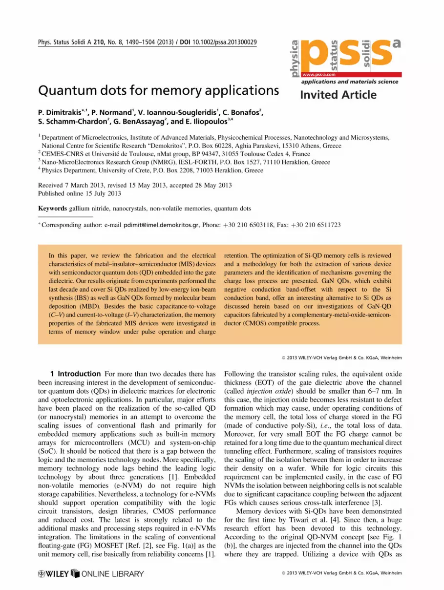
In order to investigate the charge loss mechanism, Jdet isplotted following F–N representations and Poole–Frenkel(P–F) as shown in Fig. 15. The linear least-squares fitting ofthe experimental data in both representations revealed thatthe trapped charge is lost more probably via a P–F currentmechanism [see Fig. 15(b)] than an F–N mechanism [seeFig. 15(a)]. This is an indication that charge loss is taking
Figure 13 (a) VTH transients from the program and erase states dueto thermally activated charge loss, (b) Arrhenius plots for the decayrates of the previous transients and (c) Arrhenius plots for thecharge retention time from the program and the erase states.
Figure 14 Current transients due to charge loss from program(electrons) and erase (holes) states at various temperatures.Excellent linear fitting were obtained in all cases.
Table 6 The values of exponent m at various temperatures for de-trapping current due to electron and hole loss as extracted from datain Fig. 15.
temperature (8C) m
electrons holes
25 0.359 �0.84885 0.560 �0.936115 0.610 �0.945150 0.700 �0.958
1500 P. Dimitrakis et al.: Quantum dots for memory applications
� 2013 WILEY-VCH Verlag GmbH & Co. KGaA, Weinheim www.pss-a.com
ph
ysic
a ssp stat
us
solid
i a
place through the TO via a trap-assisted current conductionmechanism.
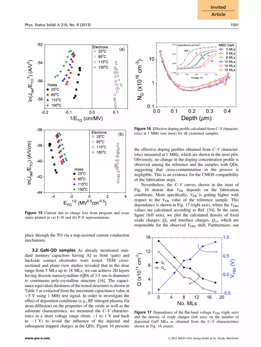
3.2 GaN-QD samples As already mentioned stan-dard memory capacitors having Al as front (gate) andbackside contact electrodes were tested. TEM cross-sectional and plane-view studies revealed that in the doserange from 5 MLs up to 18 MLs, we can achieve 2D layershaving discrete nanocrystalline (QDs of 3.5 nm in diameter)to continuous poly-crystalline structure [16]. The capaci-tance equivalent thickness of the tested structures is shown inTable 3 as extracted from the maximum capacitance value atþ5 V using 1 MHz test signal. In order to investigate theeffect of deposition conditions (e.g., RF nitrogen plasma, Gaatom diffusion) on the properties of the oxide as well as thesubstrate characteristics, we measured the C–V character-istics in a short voltage range (from �1 to 1 V and backto �1 V) to avoid the influence of the injected andsubsequent trapped charges at the QDs. Figure 16 presents
the effective doping profiles obtained from C–V character-istics measured at 1 MHz, which are shown in the inset plot.Obviously, no change in the doping concentration profile isobserved among the reference and the samples with QDs,suggesting that cross-contamination in the process isnegligible. This is an evidence for the CMOS compatibilityof the fabrication steps.
Nevertheless, the C–V curves shown in the inset ofFig. 16 denote that VFB depends on the fabricationconditions. More specifically, VFB is getting higher withrespect to the VFB value of the reference sample. Thisdependence is shown in Fig. 17 (right axis), where the VFB0
values are calculated according to Ref. [34]. In the samefigure (left axis), we plot the calculated density of fixedoxide charges, Qf, and interface charges, Qss, which areresponsible for the observed VFB0 shift. Furthermore, our
Figure 16 Effective doping profile calculated from C–V character-istics at 1 MHz (see inset) for all examined samples.
Figure 17 Dependence of the flat-band voltage VFB0 (right axis)and the density of oxide charges (left axis) on the number ofdeposited GaN MLs as obtained from the C–V characteristicsshown in Fig. 16 (inset).
Figure 15 Current due to charge loss from program and erasestates plotted in (a) F–N and (b) P–F representations.
Phys. Status Solidi A 210, No. 8 (2013) 1501
www.pss-a.com � 2013 WILEY-VCH Verlag GmbH & Co. KGaA, Weinheim
Invited
Article

recent investigations [20] suggest that it is possible tominimize the adverse effect of the inversion layer thesecharges induced beyond the area of the capacitor by makingMESA isolated structures. Note also that the latter structuresprohibit any possible communication among neighboringQDs and lead to stable and repeatable memory windows.
In Fig. 18(a), we present the C–V characteristics(1 MHz) for the tested samples with and without MESAisolation after a �5 V sweep. The difference between theG–V peaks under forward and reverse sweep directions isequal to the VFB clockwise hysteresis. A typical example isshown in Fig. 18(b) for MESA isolated structures. No C–Vhysteresis or G–V peak shift is observed for the controlsample. TheC–V hysteresis andG–V peak shifts detected forthe 5 and 18 MLs capacitors are attributed to electron trapsin GaN QDs or at the interface QD/SiO2 and not to statesat the substrate/tunnel oxide interface [35]. Comparing thememory windows between MESA and non-MESA isolatedstructures, such as extracted from the C–V curves in Fig. 18(a), we found a more efficient electron detrapping under
negative voltages for the latter structures, which may beattributed to the permanent inversion layer surrounding eachmemory capacitor.
The memory windows for all samples calculated frombi-directional C–V characteristics (1 MHz) under symmetricvoltage sweeps are shown in Fig. 19. For all samples, weobserve that the symmetric voltage sweeps do not allow thefull discharge of the trapped electrons; i.e., V�
FB–VFB0 > 0.The interpretation of this experimental evidence is that theelectric field used to detrap an electron from the GaN QDsshould be larger than the electric field used to inject thiselectron. This may be attributed to the higher energy barrierthat the trapped electron should overcome compared to anelectron in Si substrate.
It should be stressed herein that detrapping of electronsis not enhanced during C–Vmeasurements under white lightillumination conditions. The interpretation of this experi-mental result is twofold. First, the change in surface potentialand electric field under illumination is not enough to reducethe energy barrier for the trapped electrons. Second, thegenerated minority carriers (holes) in the Si substrate cannotbe injected and subsequently compensate the stored negativecharges in GaN QDs.
C–V measurements with a �5 V voltage sweep atdifferent frequencies were carried out for all samples andthe VFB hysteresis (DVFB) was extracted. The results aresummarized in Fig. 20. Obviously, DVFB exhibits nodispersion as a function of the applied frequency. This isconsistent with our assumption that at room temperaturethe observed hysteresis (charge trapping) is not due tointerface traps, which generally give rise to frequencydependent characteristics.
Room temperature charge retention measurements(Fig. 21) of the program state were performed in sampleswith 5 and 18 MLs. Both devices were programmed by asingle voltage pulse þ15 V/100 ms. In the case of samplewith a poly-crystalline GaN layer (18 MLs), an electron loss
Figure 19 Extracted memory windows from hysteresis obtainedfrom C–V characteristics (1 MHz) under symmetric voltage sweepsfor MESA isolated samples.
Figure 18 (a) C–V characteristics (1 MHz) for samples without(top) and with (bottom)MESA structures. No hysteresis is observedfor the reference device. (b) Typical C–V and G–V characteristics(1 MHz) for three different samples.
1502 P. Dimitrakis et al.: Quantum dots for memory applications
� 2013 WILEY-VCH Verlag GmbH & Co. KGaA, Weinheim www.pss-a.com
ph
ysic
a ssp stat
us
solid
i a

rate of 0.46 V dec�1 was measured for the first 1000 scorresponding to a 70% loss of the initial stored charge. Forlonger time the memorywindow remains constant at 0.071 V.Sample with discrete QDs (5 MLs) exhibited a charge lossrate of 0.25 V dec�1 and can retain data for 10 years with anextrapolated remaining memory window of about 1 V.
4 Conclusions The application of QDs as discretecharge storage nodes in nanofloating memory devices is apromising alternative for scalable NVM devices. Among thedifferent materials utilized to fabricate QDs, Si seems to bethe most promising. However, the employment of QDs from
materials having negative conduction band-offset withrespect to the Si conduction band are also very attractive.In this direction, we developed a CMOS compatible processto fabricate MOS memory capacitors with GaN QDsembedded in SiO2 with excellent charge retention propertiesat room temperature.
References
[1] B. DeSalvo (ed.), Silicon Non-Volatile Memories: Paths ofInnovation (John Wiley & Sons, Inc., New York, 2009).
[2] D. Kahng and S. M. Sze, Bell Syst. Tech. J. 46, 1288 (1967).[3] B. Govoreanu, D. P. Brunco, and J. Van Houdt, Solid-State
Electron. 49, 1841 (2005).[4] S. Tiwari, F. Rana, H. Hanafi, A. Hartstein, E. F. Crabbe, and
K. Chan, Appl. Phys. Lett. 68, 1377 (1996).[5] R. Rao, R. F. Steimle, M. Sadd, C. T. Swift, B. Hradsky, S.
Straub, T. Merchant, M. Stoker, S. G. H. Anderson, M.Rossow, J. Yater, B. Acred, K. Harber, E. J. Prinz, B. E.White, Jr., and R. Muralidhar, Solid-State Electron. 48, 1463(2004).
[6] T. Muller, K.-H. Heinig, and W. Moller, Appl. Phys. Lett. 81,3049 (2002).
[7] T.-H. Hou, C. Lee, V. Narayanan, U. Ganguly, and E. C. Kan,IEEE Trans. Electron. Devices 53, 3095 (2006).
[8] J. Yater, M. Suhail, S.-T. Kang, J. Shen, C. Hong, T.Merchant, R. R. H. Gasquet, K. Loiko, B. Winstead, S.Williams, M. Rossow, W. Malloch, R. Syzdek, and G.Chindalore, IEEE Int. Memory Workshop (IMW), Monterey,USA, May 2009, pp. 1–2.J. Yater, C. Hong, S.-T. Kang, D. Kolar, B. Min, J. Shen, G.Chindalore, K. Loiko, B. Winstead, S. Williams, H. Gasquet,M. Suhail, K. Broeker, E. Lepore, A. Hardell, W. Malloch, R.Syzdek, Y. Chen, Y. Ju, S. Kumarasamy, H. Liu, L. Lei, andB. Indajang, IEEE Int. MemoryWorkshop (IMW), Monterey,USA, May 2011, pp. 79–82.S.-T. Kang, B.Winstead, J. Yater, M. Suhail, G. Zhang, C.-M.Hong, H. Gasquet, D. Kolar, J. Shen, B. Min, K. Loiko, A.Hardell, E. LePore, R. Parks, R. Syzdek, S. Williams, W.Malloch, G. Chindalore, Y. Chen, Y. Shao, L. Huajun, L.Louis, and S. Chwa, IEEE Int. Memory Workshop (IMW),Monterey, USA, May 2012, pp. 131–134.
[9] C. Castro, S. Schamm-Chardon, B. Pecassou, A. Andreozzi,G. Seguini, M. Perego, and G. Benassayag, Nanotechnology24, 075302 (2013).
[10] K. W. Guarini, C. T. Black, Y. Zhang, I. V. Babich, E. M.Sikorski, and L. M. Gignac, IEDM Tech. Digest (IEEE) 541,(2003).
[11] S. Paul, C. Pearson, A. Molloy, M. A. Cousins, M. Green, S.Kolliopoulou, P. Dimitrakis, P. Normand, D. Tsoukalas, andM. C. Petty, Nano Lett. 3, 533–536 (2003).
[12] P. Dimitrakis, P. Normand, D. Tsoukalas, C. Pearson, J. H.Ahn, M. F. Mabrook, D. A. Zeze, M. C. Petty, K. T.Kamtekar, C. Wang, M. R. Bryce, and M. Green, J. Appl.Phys. 104, 044510 (2008).
[13] J. Ouyang, Org. Electron. 14, 665–675 (2013).[14] H.-T. Lin, Z. Pei, J.-R. Chen, C.-P. Kung, Y.-C. Lin, C.-M.
Tseng, and Y.-J. Chan, IEDM Tech. Digest (IEEE) 233–236(2007).
[15] P. Dimitrakis, P. Normand, and D. Tsoukalas, Si nanocrystalmemories, in: Silicon Nanophotonics, edited by L.Khriachtchev (Pan Publishing, Singapore, 2008), chap. 8.
Figure 20 Memory windows as a function of the test signalfrequency of the C–V measurements for all tested samples.
Figure 21 Charge retention measurements for sample separatedGaN-QDs (5 MLs) and continuous polycrystalline GaN layer(18 MLs).
Phys. Status Solidi A 210, No. 8 (2013) 1503
www.pss-a.com � 2013 WILEY-VCH Verlag GmbH & Co. KGaA, Weinheim
Invited
Article

[16] P. Dimitrakis, P. Normand, C. Bonafos, E. Papadomanolaki,and E. Iliopoulos, Appl. Phys. Lett. 102, 053117 (2013).
[17] C. Bonafos, M. Carrada, G. Benassayag, S. Schamm-Chardon, J. Groenen, V. Paillard, B. Pecassou, A. Claverie,P. Dimitrakis, E. Kapetanakis, V. Ioannou-Sougleridis, P.Normand, B. Sahu, and A. Slaoui, Mater. Sci. Semicond.Process. 15, 615–626 (2012).
[18] M. She, and T.-J. King, IEEE Trans. Electron Device 50,1934–1940 (2003).
[19] T.-H. Hou, C. Lee, V. Narayanan, U. Ganguly, and E. C. Kan,IEEE Trans. Electron Devices 53, 3095 (2006).
[20] P. Dimitrakis, P. Normand, C. Bonafos, E. Papadomanolaki,and E. Iliopoulos, in: Materials and Physics of EmergingNonvolatile Memories, edited by E. Tokumitsu, Y. Fujisaki,P. Dimitrakis, and M. Kozicki, Mater. Res. Soc. Symp. Proc.,Vol. 1430 (Oxford University Press, NY, USA), mrss12-1430-e02-02.
[21] I. Hanafi, S. Tiwari, and I. Khan, IEEE Trans. ElectronDevices 43, 1553 (1996).
[22] C. Bonafos, M. Carrada, N. Cherkashin, H. Coffin, D.Chassaing, G. Ben Assayag, A. Claverie, T. Müller, K. H.Heinig, M. Perego, M. Fanciulli, P. Dimitrakis, and P.Normand, J. Appl. Phys. 95, 5696–5702 (2004).
[23] P. Normand, E. Kapetanakis, P. Dimitrakis, D. Tsoukalas, K.Beltsios, N. Cherkashin, C. Bonafos, G. Benassayag, H.Coffin, A. Claverie, V. Soncini, A. Agarwal, and M. Ameen,Appl. Phys. Lett. 83, 168–170 (2003).
[24] C. Bonafos, H. Coffin, S. Schamm, N. Cherkashin, G. BenAssayag, P. Dimitrakis, P. Normand, M. Carrada, V. Paillard,and A. Claverie, Solid-State Electron. 49, 1734–1744 (2005).
[25] M. Perego, S. Ferrari, M. Fanciulli, G. Ben Assayag, C.Bonafos, M. Carrada, and A. Claverie, Appl. Surf. Sci. 231–232, 813–816 (2004).
[26] D. Tsoukalas, P. Dimitrakis, S. Koliopoulou, and P. Normand,Mater. Sci. Eng. B 124–125, 93–101 (2005).
[27] D. K. Schroder, Semiconductor Material and DeviceCharacterization, 3rd ed. (Wiley-Interscience, New York,2006).
[28] C. J. Nicklaw,M. P. Pagey, S. T. Pantelides, D.M. Fleetwood,R. D. Schrimpf, K. F. Galloway, J. E. Wittig, B. M. Howard,E. Taw, W. H. McNeil, and J. F. Conley, IEEE Trans. Nucl.Sci. 47, 2269–2275 (2000).
[29] P. Dimitrakis, C. Bonafos, S. Schamm, P. Normand, and G.Ben Assayag, Mater. Res. Soc. Symp. Proc., Vol. 1250, editedby C. Bonafos, Y. Fujisaki, P. Dimitrakis, and E. Tokumitsu(MRS, Warrendale, PA, USA, 2010), 1250-G01-02.
[30] H. C. Card and M. I. Elmasry, Solid-State Electron. 19, 863–870 (1976).
[31] P. Dimitrakis, E. Kapetanakis, D. Tsoukalas, D. Skarlatos, C.Bonafos, G. Ben Asssayag, A. Claverie, M. Perego, M.Fanciulli, V. Soncini, R. Sotgiu, A. Agarwal, M. Ameen, andP. Normand, Solid-State Electron. 48, 1511–1517 (2004).
[32] P. Dimitrakis and P. Normand, Mater. Res. Soc. Symp. Proc.830, D5.1C (2005).
[33] M. Compagnoni, D. Ielmini, A. S. Spinelli, A. L. Lacaita, C.Previtali, and C. Gerardi, IEEE IRPS 506 (2003).
[34] M. Zhu, J. Zhu, J. M. Liu, and Z. G. Liu, Appl. Phys. A 80,135–139 (2005).
[35] S. Huang, S. Banerjee, R. T. Tung, and S. Oda, J. Appl. Phys.93, 576 (2003).
1504 P. Dimitrakis et al.: Quantum dots for memory applications
� 2013 WILEY-VCH Verlag GmbH & Co. KGaA, Weinheim www.pss-a.com
ph
ysic
a ssp stat
us
solid
i a


