Embed Size (px)
Citation preview
REVIEW
ibly
Anisotropic thermocouples articleA. A. Snarski
Ukrainian National Technical University, 252056 Kiev, Ukraine
A. M. Pal’ti
Institute of Metal Physics, Ukrainian National Academy of Sciences, 252680 Kiev, Ukraine
A. A. Ashcheulov
Chernovtsy State University, 274003 Chernovtsy, Ukraine~Submitted April 17 1996; accepted February 24 1997!Fiz. Tekh. Poluprovodn.31, 1281–1298~November 1997!
IN MEMORY OF ANATOLII GRIGOR’EVICH SAMOILOVICH
Theoretical and experimental investigations of the generation of transverse thermoelectric powerin anisotropic media and methods of direct conversion of heat, which are based on thisgeneration, are described. Converters based on both semiconductors and high-Tc superconductorfilms are examined. ©1997 American Institute of Physics.@S1063-7826~97!00111-7#
INTRODUCTION discovered very recently. The appearance of new, poss
di
st be
p-e
ibns
o
lthoeo
Ao-deeo
l f
sre
st,nd
c
cts
or
ce
t-
s-
s.l-
l-
nd
le-
/1
In a homogeneous isotropic material, a temperatureference produces a irrotational~potential! electric field. Thecondition for an emf to appear in an isotropic material aresult of a temperature difference is that the material musinhomogeneous. The inhomogeneity is ordinarily producby creating a junction of two materials with different proerties. For this reason, a thermoelement is ordinarily a thmocouple.
In general, a temperature difference in a material exhiting a thermoelectric power anisotropy produces a traverse~perpendicular to the temperature gradient! thermoelec-tric field1–3
ET52a“T. ~1!
Here a is the thermoelectric power tensor, andET is theso-called thermoelectric field. In general, the existenceboth Ei
Ti“T andE'T'“T follows from Eq. ~1!. This trans-
verse thermoelectric fieldE'T , in contrast to the longitudina
field EiT employed in ordinary thermocouples, can lead to
appearance of an electric current even in a homogeneclosed circuit.3,4 For this reason, even a homogeneous, thmoelectrically anisotropic medium can serve as a thermelectric power generator, i.e., a thermoelement.5
Investigations of the anisotropy ofa for the purpose ofthermoelectric power generation were initiated in 1964 byG. Samo�lovich and continued in the Department of Anistropic Semiconductors at Chernovtsy State University unhis guidance. Great progress was made in both the thand practical applications.
CdSb single crystals served as the standard materiaanisotropic thermoelements~ATs!. Anomalously large,transverse-type, thermoelectric responses in single-cryfilms of high-Tc superconductors in the normal state we
1101 Semiconductors 31 (11), November 1997 1063-7826/97
f-
aed
r-
--
f
eusr--
.
rry
or
tal
much more efficient, materials for ATs is rekindling intereit would appear, in the transverse thermoelectric effect amakes the present review article timely.
The review article consists of the following sections:1. Theoretical investigations.
1.1. Elementary theory of anisotropithermoelements.6,7
1.2. Anisotropic thermoelements with end conta~rigorous approach!
1.3. Anisotropic thermoelements with allowance fend contacts
1.3.1. Rectangular anisotropic thermoelements1.3.2. Anisotropic thermoelements with allowan
for thermal conductivity anisotropy1.3.3. Allowance for electrical conductivity aniso
ropy1.3.4. Ring-shaped anisotropic thermoelements1.3.5. Anisotropic thermoelements with quasicry
tallographic axes1.4. Anisotropic thermoelements with point contact
1.4.1. EMF of anisotropic thermoelements with alowance for thermal conductivity anisotropy~Fig. 6a!.
1.4.2. EMF of anisotropic thermoelements with alowance for thermal conductivity anisotropy~Fig. 6b!.
1.5. Efficiency of anisotropic thermoelements1.6. Anisotropic thermoelements in a magnetic field1.7. Artificially anisotropic media
1.7.1. Effective properties of layered media2. Experimental investigations
2.1. Semiconductor anisotropic thermoelements adevices
2.2. Anisotropic thermoelements based on singcrystal high-Tc superconductor films
110111101-17$10.00 © 1997 American Institute of Physics
mh
eh
ry
ie
ll
r-nce
notples.thforngth
e
-aseir
lye
her-a-
eac-
ts
bemfthero-
on
the
1. THEORETICAL INVESTIGATIONS
1.1. Elementary theory of anisotropic thermoelements 6,7
Let us consider a thermoelectrically anisotropic mediuwhose thermoelectric power tensor in the crystallograpaxes has the form
a5S a i 0
0 a'D . ~2!
For simplicity, we shall consider the two-dimensional casWe cut from this medium a plate in a manner so that tcrystallographicX axis makes an angleu with the edgeAB~Fig. 1!. The thermoelectric power tensor in the laboratocoordinate system has the form
a5S a i cos2 u1a' sin2 u ~a i2a'!sin u cosu
~a i2a'!sin u cosu a i sin2 u1a' cos2 u D .
~3!
If the temperatures at the top and bottom boundar(AB and CD) are maintained equal toT1 and T0 , respec-tively, then~ignoring lateral heat transfer! a one-dimensionaltemperature distribution with a constant gradient
]T
]y5
T12T0
b[
DT
b,
]T
]x50 ~4!
will be produced inside the plate.According to Eqs.~1!, ~3!, and~4!, the transverse~with
respect to“T) thermoelectric field arising in the process wihave the form
ExT5a12
DT
b, ~5!
wherea125(a i2a')sinu cosu is the off-diagonal compo-nent of the tensor~3!. In what follows, for convenience, weshall often employ the notation for the indices 1, 25x, y.
According to Eq.~5!, the thermoelectric power arisingbetween the endsAD andBC has the form
«5E2a/2
a/2
ExTdx5a12DT
a
b. ~6!
FIG. 1. Thermoelectrically anisotropic plate.X,Y — crystallographic axes,T1 ,T0 — temperatures of the top and bottom faces,u — angle of inclinationof the crystallographic axesX,Y with respect to the laboratory axesx,y.
1102 Semiconductors 31 (11), November 1997
ic
.e
s
The fundamental difference of AT from ordinary themocouples is seen immediately from this expression, sithe emf of an AT contains the geometric factora/b. At thesame time, the emf of an ordinary thermocouple doesdepend on the geometric dimensions of these thermocouIn the case of an AT, the emf is proportional to the lengand inversely proportional to the thickness. Therefore,example, the emf can be increased by increasing the leof the AT.
The expression~6! for the emf of an AT is qualitativelycorrect, but it has a number of important drawbacks. Wshall list some of them.
1! On the one hand, the derivation of the expression~6!assumed that the plate is finite (2a/2<x<a/2). On theother hand, the expression~5! was written for a plate whichis infinite along thex axis; i.e., the possible boundary conditions atx56a/2 were neglected. Since any real AT hcurrent collecting contacts, allowance must be made for thpresence in the corresponding boundary conditions.
2! The temperature distribution in an AT can be strongnonuniform. For this reason, Eq.~6! must be extended to thcase¹TÞconst.
3! The temperature dependence of the electric and tmal conductivities and the thermoelectric power of real mterials can alter Eq.~6! substantially.
4! The expression~6! disregards the possibility that thelectric and thermal conductivity can be of a tensor charter. As a rule, a medium exhibiting anisotropy ofa alsoexhibits anisotropy ofs.
1.2. Anisotropic thermoelement with end contacts „rigorousapproach …
In any real AT, metallic current-collecting contac~CCs! must be soldered to the lateral faces~Fig. 2!. Twoboundary-value problems of mathematical physics mustsolved in order to allow for the effect of the CCs on the eof an AT. These problems make it possible to establisheffect of a CC on the temperature distribution and electchemical potential distribution inside the AT.
Ignoring the effect of thermoelectric eddy currentsthe temperature distribution~we shall estimate it below!, theequation for the latter follows from the condition¹–q50and for isotropic thermal conductivity
FIG. 2. Anisotropic thermoelement. Regions1 and 3 — end contacts forextracting the thermoelectric signal, region2 — thermoelectrically aniso-tropic plate. The lines of the thermoelectric eddy currents are shown onright-hand side of the figure.
1102Snarski et al.
]2T ]2T
fs
h-
e
df-
ontiavi
wedihe
owtt
z~2a/2,y!5z~1!~2a/2,y!, z~a/2,y!5z~3!~a/2,y!,
he
bu-
e
of
es-
han
onison-
s
antedrbi-
ab-atethis
ec-
ibeas
]x21
]y250. ~7!
The boundary conditions are: 1! continuity of the tempera-tures and heat fluxes at a boundary between the CCs~regions1 and3! and an anisotropic plate~region2!; 2! the values ofthe temperaturesT1 and T0 on the top and bottom faces othe plate and the CCs; and 3! heat transfer on the lateral faceof the CCs:
2k]T~3,1!
]x5b~T~3,1!2T0!
at x56(a/21 l ). The superscripts denote the regions of tAT and CCs, andb is the heat-transfer coefficient; the temperature of the surrounding medium is assumed to beT0 . Itis obvious that the isotherms is horizontal ifb50 ~the con-dition of adiabaticity on the outer ends of the contacts!. ForbÞ0, the solution of the boundary-value problem is rathcomplicated:6
T5T01DT
by12
bbDT
k9(k51
`
~21!kdk coshkpx
bsin
kpy
b,
1
dk5S kp1
bb
k9D S cosh
kpa
2b1
k
k9sinh
kpa
2b D3exp
kpd
b
2S kp2bb
k9D S cosh
kpa
2b2
k
k9sinh
kpa
2b D3expS 2
kpd
b D , ~8!
wherek andk9 are the thermal conductivities of the AT anCCs, respectively. Taking into account the real value ob(b'0.4– 4.2 W/m2
•K! shows that the deviation of the temperature distribution from a linear distribution is small.
In contrast to the effect on the temperature distributithe effect on the distribution of the electrochemical potenz is fundamental. We assume that the electrical conductiof the AT and CCs are equal, respectively, tos ands9, thatboth of them are isotropic, and that the thermoelectric poof the CCs can be ignored since they are metallic. Thetribution z(r ) in the stationary case is determined by tcontinuity equation for the current density¹• j50, where
j52s¹z2sa¹T, ~9!
which reduces to the equation
]2z
]x21
]2z
]y2522a12
]2T
]x]y. ~10!
We assume that the thermoelement is insulated. The folling conditions are satisfied at the boundaries betweenanisotropic plate and the CC (z is continuous and the currendensity is perpendicular to the boundary!:
1103 Semiconductors 31 (11), November 1997
e
r
,l
ty
rs-
-he
~11!j x~2a/2,y!5 j x
~1!~2a/2,y!, j x~a/2,y!5 j x~3!~a/2,y!.
The solution of the boundary-value problem by tmethod of separation of variables gives the expression
Dz5z~1!~2a/2,y!2z~3!~a/2,y!,
Dz5a12DTa
b12
a12DTbb
k9
a
b (k51
`
~21!kgk coskp
by,
~12!
gk5dk
sinhkp
bsinh
kp
b
a
21
s
s9cosh
kp
bcosh
kp
b
a
2
,
wheredk is determined in Eq.~8!.We note that in the case of a linear temperature distri
tion the right side of Eq.~10! vanishes and only the first termremains in the expression forDz. However, even in the casof a nonlinear temperature distribution, ifs/s9→0, for finitel the second term in Eq.~12! approaches zero. Thus,Dzceases to depend ony, and since the thermoelectric powerthe CCsa950, the value obtained forDz can be taken as thethermoelectric power. A detailed investigation of the exprsion forz5z(x,y) in the the limits/s9→0 showed that thefunction z vanishes at the boundariesx56(a/21 l ) for ar-bitrary l . The latter can be assumed to be much smaller ta/2.
The main conclusion to be drawn from the investigatiof the effect of the CCs on the emf of an AT is that theffect can be taken into account by simplified boundary cditions
z~a/2,y!5w1 , z~2a/2,y!5w2 , ~13!
wherew1 andw2 are the potentials on the endsDT and areconstants1 independent ofy. Under the boundary condition~13! the boundary-value problem~10! and ~11! simplifiessubstantially and in many cases it is possible to obtainanalytical expression for the emf in much more complicacases than in the one studied above, for example, for atrary T5T(x,y).
We also note that in determiningT5T(x,y) in the heat-conduction equation the terms describing the release orsorption of heat by eddy currents were dropped. An estimmade of these currents in Refs. 7 and 8 shows that incase they can be ignored.
1.3. Anisotropic thermoelements with allowance for endcontacts
It is assumed thatsat!sec , wheresat andsec are theconductivities of the thermoelement and end contact, resptively.
1.3.1. Rectangular anisotropic thermoelements
The equations and boundary conditions which descrthe distributions of the fields and currents in an AT now hthe form
1103Snarski et al.
“• j50, ~14!
ioa
bd
th
s
o
lectore
di
eio
ack
uc
ot
1.3.2. Anisotropic thermoelement with allowance forthermal conductivity anisotropy
toua-ee
era-uals
llyex-
f
dthe
etric
theiedera-ns.ti-alm-alof
nythesee,
j y~x,y50,b!50, ~15!
z~a/2,y!5w~a/2!, z~2a/2,y!5w~2a/2!, ~16!
where the boundary condition~16! takes into account thepresence of the CCs.
As shown in Ref. 9, in this case a general expresssuitable for an arbitrary temperature distribution and anbitrary temperature dependencea ik5a ik(T) (a ik can alsodepend onr ) can be obtained for the emf:
«521
bE0
b
dyE2a/2
a/2
ExTdx,
~17!
ExT52a11
]T
]x2a12
]T
]y.
whereExT is a component of the thermoelectric field.
The expression obtained for the emf of an AT caneasily extended to the three-dimensional case and inclumany previously known particular cases, starting withstandard thermocouple.
Rewriting Eq. ~17! in dimensionless coordinate(X5x/a, Y5y/b) and substituting the explicit form ofEx
T,we obtain
«5E0
1
dYE21/2
1/2
a11
]T
]XdX1
a
bE0
1
dYE21/2
1/2
a12
]T
]YdX.
~18!
The main conclusion for the entire question of generationemf by anisotropic media follows immediately from Eq.~18!— the part of the emf that is associated with the thermoetric power anisotropy always appears in the geometric faa/b. The expression~17! can be extended to the case whes5s(y). Then
«521
bE0
b
dyE2a/2
a/2
ExTdxY 1
bE0
b
s~y!dy. ~19!
An expression for the emf without the boundary contion ~16! was obtained in Ref. 10. It was assumed thata@band the indicated condition is thereby unimportant. Furthmore, and this is very important, the temperature distributwas assumed to be one-dimensional (]T/]x50), whichmade it possible to replace, to a high degree of accur]T/]y by DT/b. These assumptions made it possible to tainto account the anisotropy of the electrical conductivity
«5
aE0
b a12
r11
]T
]ydy
E0
b dy
r11
.a
bDT
aET0
T1 a12
r11dT
E0
b dy
r11
, ~20!
wherer115s22/(s11s222s122 ).
The dependence ony r115r11(y), but not onx, canalso be taken into account. For isotropic electrical condtivity the expression~20! is a particular case of Eq.~19!.
In some cases taking into account]T/]x is fundamental.One such case is an AT with thermal conductivity anisropy.
1104 Semiconductors 31 (11), November 1997
nr-
eese
f
c-r
-
r-n
y,e
-
-
To determine the emf of an AT it is first necessaryfind the temperature distribution. The heat-conduction eqtion, in contrast to Eq.~7!, now includes components of ththermal conductivity tensor. Its form is similar to that of ththermoelectric power tensor~3!
k11
]2T
]x212k12
]2T
]x]y1k22
]2T
]y250. ~21!
We choose the previous boundary conditions — the tempture is constant at the top and bottom boundaries and eqT(0,x)5T0 , T(b,x)5T1 , and we ignore heat transfer fromthe lateral faces.
This boundary-value problem can be solved analyticaonly in the presence of a small parameter, which, forample, can bek12/Ak11k22 and has the form11
T~x,y!5T01DTS y
b2
4k12
Ak11k22
3 (k51,3, . . .
`sinh~kpx/b!sin~kpy/b!
~kp!3cosh~kpa/2b!D . ~22!
Numerical simulation confirms this solution.11 Substitutingthe expression~22! into the general expression for the em~17! of an AT gives9 ~see also Ref. 11!
«5a12DTa
b2a11DT
16k12
p3Ak11k22
3 (k51,3 . . .
`
k23 tankp
2Ak22
k11. ~23!
The first term in Eq.~23! is the standard emf of an AT, anthe second term is the part of the emf that is produced bytemperature gradient appearing along thex axis as a result ofthe thermal conductivity anisotropy (k12Þ0). It is importantthat this term remains finite asa/b→`. If Ak2 /k11'1, theneven ata/b'3 the sum in Eq.~23! equals 1.05, to a highdegree of accuracy, and therefore
«~a/b@1!'a12DTa
b21.7
k12
Ak11k22
a11DT. ~24!
We note that the second term does not include the geomfactor a/b.
Questions concerning the generation of an emf incase of an anisotropic thermal conductivity were also studin Ref. 12, but the expression obtained there for the tempture distribution does not satisfy the boundary conditioThis work was criticized in Ref. 13. Besides the valid cricism, the following assertion was made in Ref. 13: ‘‘Thermconductivity anisotropy can to some degree distort the teperature, potential, and current distributions in a thermelectric medium but it cannot itself serve as a sourceemf.’’ We cannot concur with this assertion. Indeed, asource of emf contains CCs, which unavoidably makeAT as a whole inhomogeneous. In this case, as one can
1104Snarski et al.
for example, from Eq.~22!, even under conditions of an
-ra
ndnua
-i
emoetsn
er
mis
ca
oso
th
haee
-
e
ria
eyof
tionatnto
nd-tedx-
g is
m
usct-
. Ifges
s of
emi-
line
ith
g,
isotropic thermoemf (a1250, a115a) the emf is not zeroand equals«;ak12. In reality, this is a standard ‘‘thermocouple’’ emf with an unusual method of creating a tempeture difference at the junctions~CCs! — by thermal conduc-tivity anisotropy. The thermoelectric power of the secobranch does not appear in Eq.~23!, since it was assumed iadvance that the thermoelectric power of the CCs eqzero.
1.3.3. Allowance for electrical conductivity anisotropy
By analogy with thermal conductivity anisotropy, allowing for electrical conductivity anisotropy does not makepossible to obtain a solution of the boundary-value probland therefore the emf in an analytic form for anisotropyarbitrary magnitude. In the presence of the small params12/As11s22, allowing for the CCs in boundary conditionof the type~16! makes it possible to obtain the emf in aanalytical form14
«5a12DTa
b
1a22DTa
b
s12
s11S 12
16
p3 (k51,3, . . .
`
k23 tanhkpa
2b D .
~25!
For a/b.4 and s11/s22'1 the sum in Eq.~25! equals1.052, to a high degree of accuracy, and fora/b>5 the 1 inparentheses can be ignored in contrast with the second t
«'a12DTa
b2
1
2a12DTS a
bD 2
s12As22/s113 . ~26!
It follows from Eq. ~26! that, besides the standard ter(a12DT (a/b)), the emf of an AT also contains a term thatproportional to the off-diagonal component of the electriconductivity and a geometric factora/b. We note that theterm that takes into account the thermal conductivity anisropy in Eq.~24! does not include a geometric factor. We alnote that the expression~26!, obtained for the emf of an ATtaking into account the CCs, also differs from the emf~20! ofan AT neglecting the CCs. The latter does not includeterm with s12.
1.3.4. Ring-shaped anisotropic thermoelements
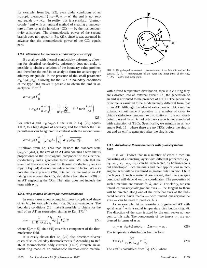
In some cases a nonrectangular, more complicated sof an AT, for example, a ring~Fig. 3!, is advantageous. Thboundary conditions~16! make it possible to obtain for themf of an AT an expression similar to Eq.~17!:15
«521
ln~R1 /R0!E
R0
R1drE
0
u
EuTdu, ~27!
whereEuT52Ex
T sinu1EyT cosu is a component of the ther
moelectric field.It is easily shown that Eq.~27! also describes divers
cases of so-called eddy thermoelements.16 According to Ref.16, if thermoelectric eddy currents~TECs! circulate in anuncut ring made of an anisotropic thermoelectric mate
1105 Semiconductors 31 (11), November 1997
-
ls
t
fer
m:
l
t-
e
pe
l
with a fixed temperature distribution, then in a cut ring thare extracted into an external circuit; i.e., the generationan emf is attributed to the presence of a TEC. The generaprinciple is assumed to be fundamentally different from thin an AT. Although the idea of extraction of TECs into aexternal circuit made it possible in a number of casesobtain satisfactory temperature distributions, from our stapoint, the emf in an AT of arbitrary shape is not associawith extraction of TECs. Specifically, we mention as an eample Ref. 15 , where there are no TECs before the rincut and an emf is generated after the ring is cut.
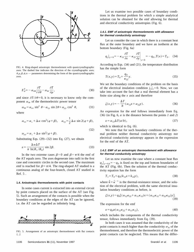
1.3.5. Anisotropic thermoelements with quasicrystallineaxes
It is well known that in a number of cases a mediuconsisting of alternating layers with different properties (k1 ,a1 , s1 , k2 , a2 , s2) can be represented as homogeneobut anisotropic. Such materials and their applications in reangular ATs will be examined in greater detail in Sec. 1.6the layers of such a material are curved, then the averadescribed will depend on the coordinates: The propertiesuch a medium are tensorss, a, andk. For clarity, we canintroduce quasicrystallographic axes — the tangent to thwill be directed along one of the principal axes of the indcated tensors. Such media — with curved quasicrystalaxes — can be used to produce ATs.
As an example, let us consider a ring-shaped AT wspiral axes17 with a radial temperature distribution~Fig. 4!.The direction of the axes is fixed by the unit vectorn, tan-gent to this axis. The components of the tensora ik are ex-pressed in terms ofn as
a ik5a'd ik1Danink , Da5a i2a' . ~28!
The temperature distribution has the form
T5T01DT
ln~R1 /R0!ln
r
R0. ~29!
The emf is calculated from Eq.~27!, where
FIG. 3. Ring-shaped anisotropic thermoelement:1 — Metallic end of thecontact,T1 ,T0 — temperatures of the outer and inner parts of the rinR1 ,R2 — outer and inner radii.
1105Snarski et al.
-
fir
ai
cu
tre
Let us examine two possible cases of boundary condi-alal
eatthe
sis
s a
q.
er-orion
fluxofc-
lu-u-
ity
the
theffer-
phxehi
c
EuT52auu
]T
r ]u2aur
]T
]r, ~30!
and since]T/]u50, it is necessary to know only the componentaur of the thermoelectric power tensor
aur5axx sin2 u2axy sin 2u1ayy cos2 u, ~31!
where
axx5a'1Da cos2~w1b!, axy51
2Da sin 2~w1b!,
~32!ayy5a'1Da sin2~w1b!.
Substituting Eqs.~29!–~32! into Eq. ~27!, we obtain
«5DaDT
p ln~R1 /R0!sin 2b. ~33!
In the two extreme casesb50 andb5p/4 the emf ofthe AT equals zero. The axes degenerate into radii in thecase and concentric circles in the second case. The maximemf is reached forb5p/4. The ring-shaped AT studied iscontinuous analog of the four-branch, closed AT studiedRef. 5 .
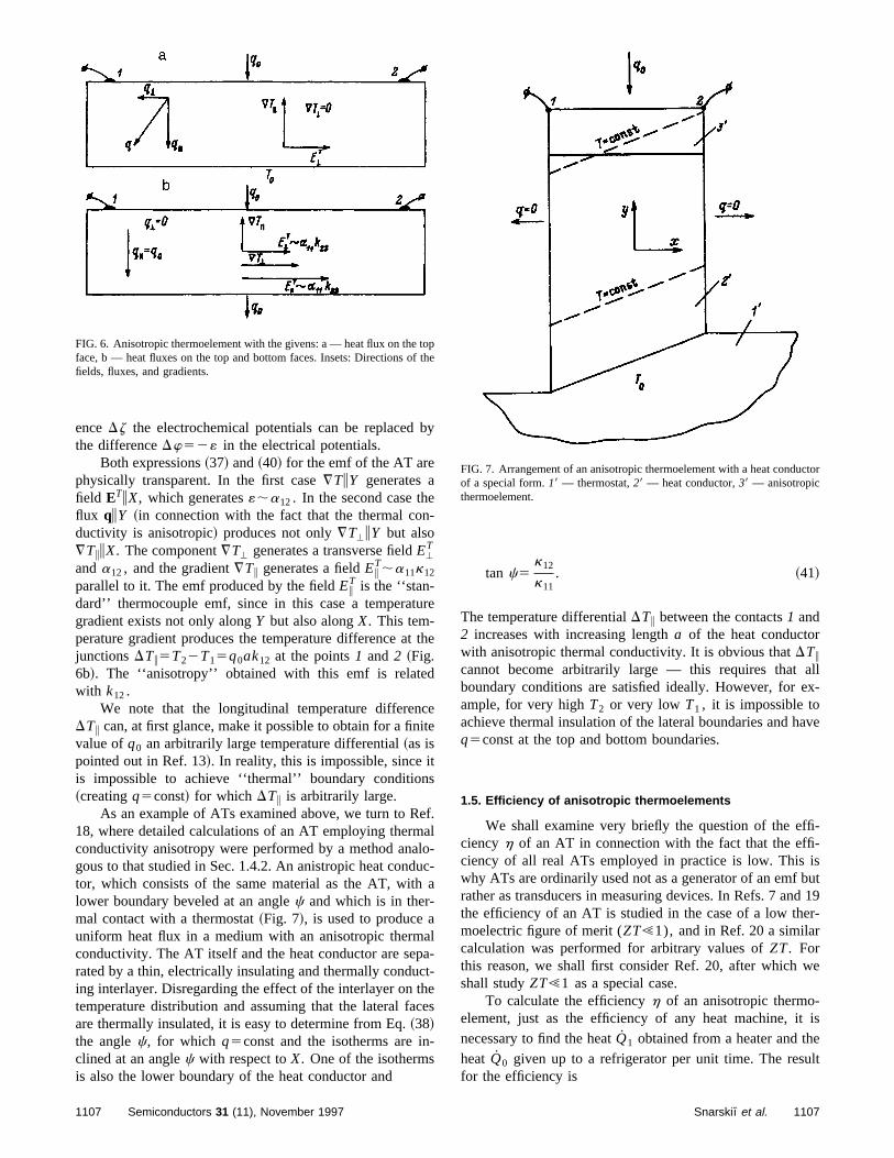
1.4. Anisotropic thermoelements with point contacts
In some cases current is extracted into an external cirby point contacts placed on the surface of the AT~see Fig.5!. Such an arrangement of the contacts is possible whenboundary conditions at the edges of the AT can be ignoi.e. the AT can be regarded as infinitely long.
FIG. 4. Ring-shaped anisotropic thermoelement with quasicrystallograaxes. The dashed line indicates the direction of the crystallographic au,r,b,c,n — parameters determining the form of the quasicrystallograpaxes.
FIG. 5. Arrangement of an anisotropic thermoelement with flat conta1, 2.
1106 Semiconductors 31 (11), November 1997
stum
n
it
hed,
tions in the thermal problem for which a simple analyticsolution can be obtained for the emf allowing for thermand electrical conductivity anisotropies~Fig. 6!.
1.4.1. EMF of anisotropic thermoelements with allowancefor thermal conductivity anisotropy
Let us consider the case in which there is a constant hflux at the outer boundary and we have an isotherm atbottom boundary~Fig. 6a!
qyuy5b52k12
]T
]x2k22
]T
]yUy5b
52q0 ,T~x!5T0 . ~34!
According to Eqs.~34! and~21!, the temperature distributionhas the simple form
T~x,y!5T01q0
k22y. ~35!
We set the boundary conditions of the problem on the baof the electrical insulation conditionj nus50. Now, we cantake into account the fact that a real thermal element hafinite size along thex axis and therefore
z~x,y!52DT
b~a12x1a22y!. ~36!
An expression for the emf follows immediately from E~36! ~in Fig. 6,a is the distance between the points1 and2!
«5a12DT~a/b!, ~37!
which is identical to Eq.~6!.We note that for such boundary conditions of the th
mal problem neither thermal conductivity anisotropy nelectrical conductivity anisotropy appears in the expressfor the emf of the AT.
1.4.2. EMF of an anisotropic thermoelement with allowancefor thermal conductivity anisotropy
Let us now examine the case where a constant heatqyuy50,b52q0 is fixed on the top and bottom boundariesthe AT ~Fig. 6b!. Then the solution of the thermal condutivity equation has the form
T15T01q0~k12x1k22y!, ~38!
wherek5k21 is the thermal-resistance tensor, and the sotion of the electrical problem, with the same electrical inslation boundary conditions as before, is
z~x,y!5q0@~a12k221a11k12!x1~a12k121a22k22!y#.~39!
The expression for the emf
«5q0a~a12k221a11k12!, ~40!
which includes the components of the thermal conductivtensor, follows immediately from Eq.~39!.
In both cases it was assumed that the conductivity ofpoint contacts is much higher than the conductivitys ik of thethermoelement, and therefore the thermoelectric power ofpoint contacts can be neglected. This means that the di
ics;
c
ts
1106Snarski et al.
b
en-
u
t
d
ceite
ts
ealou
apacthc
-
allx-
ave
fi--isbutd 19r-
we
iselt
th
ctor
enceDz the electrochemical potentials can be replacedthe differenceDw52« in the electrical potentials.
Both expressions~37! and~40! for the emf of the AT arephysically transparent. In the first case¹TiY generates afield ETiX, which generates«;a12. In the second case thflux qiY ~in connection with the fact that the thermal coductivity is anisotropic! produces not only¹T'iY but also¹TiiX. The component¹T' generates a transverse fieldE'
T
anda12, and the gradient¹Ti generates a fieldEiT;a11k12
parallel to it. The emf produced by the fieldEiT is the ‘‘stan-
dard’’ thermocouple emf, since in this case a temperatgradient exists not only alongY but also alongX. This tem-perature gradient produces the temperature difference ajunctionsDTi5T22T15q0ak12 at the points1 and2 ~Fig.6b!. The ‘‘anisotropy’’ obtained with this emf is relatewith k12.
We note that the longitudinal temperature differenDTi can, at first glance, make it possible to obtain for a finvalue ofq0 an arbitrarily large temperature differential~as ispointed out in Ref. 13!. In reality, this is impossible, since iis impossible to achieve ‘‘thermal’’ boundary condition~creatingq5const! for which DTi is arbitrarily large.
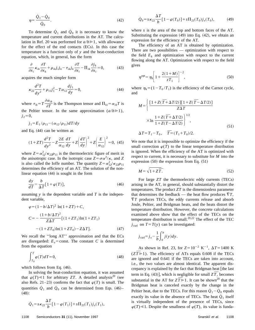
As an example of ATs examined above, we turn to R18, where detailed calculations of an AT employing thermconductivity anisotropy were performed by a method anagous to that studied in Sec. 1.4.2. An anistropic heat condtor, which consists of the same material as the AT, withlower boundary beveled at an anglec and which is in ther-mal contact with a thermostat~Fig. 7!, is used to produce auniform heat flux in a medium with an anisotropic thermconductivity. The AT itself and the heat conductor are serated by a thin, electrically insulating and thermally conduing interlayer. Disregarding the effect of the interlayer on ttemperature distribution and assuming that the lateral faare thermally insulated, it is easy to determine from Eq.~38!the anglec, for which q5const and the isotherms are inclined at an anglec with respect toX. One of the isothermsis also the lower boundary of the heat conductor and
FIG. 6. Anisotropic thermoelement with the givens: a — heat flux on the topface, b — heat fluxes on the top and bottom faces. Insets: Directions offields, fluxes, and gradients.
1107 Semiconductors 31 (11), November 1997
y
re
the
f.l-c-a
l--ees
tan c5k12
k11. ~41!
The temperature differentialDTi between the contacts1 and2 increases with increasing lengtha of the heat conductorwith anisotropic thermal conductivity. It is obvious thatDTicannot become arbitrarily large — this requires thatboundary conditions are satisfied ideally. However, for eample, for very highT2 or very low T1 , it is impossible toachieve thermal insulation of the lateral boundaries and hq5const at the top and bottom boundaries.
1.5. Efficiency of anisotropic thermoelements
We shall examine very briefly the question of the efciencyh of an AT in connection with the fact that the efficiency of all real ATs employed in practice is low. Thiswhy ATs are ordinarily used not as a generator of an emfrather as transducers in measuring devices. In Refs. 7 anthe efficiency of an AT is studied in the case of a low themoelectric figure of merit (ZT!1), and in Ref. 20 a similarcalculation was performed for arbitrary values ofZT. Forthis reason, we shall first consider Ref. 20, after whichshall studyZT!1 as a special case.
To calculate the efficiencyh of an anisotropic thermo-element, just as the efficiency of any heat machine, itnecessary to find the heatQ1 obtained from a heater and thheatQ0 given up to a refrigerator per unit time. The resufor the efficiency is
e
FIG. 7. Arrangement of an anisotropic thermoelement with a heat conduof a special form.18 — thermostat,28 — heat conductor,38 — anisotropicthermoelement.
1107Snarski et al.
Q12Q0
cu
n
n
s
e
Q 5skDT
@12w~T !#1sP ~T ! j ~T !, ~49!
T.
.tontld
,
enth
heer
sorbt theonsthe
sunt,dis-
the
ce
h5Q0
. ~42!
To determineQ1 and Q0 it is necessary to know thetemperature and current distributions in the AT. The callation in Ref. 20 was performed fora/b@1, with allowancefor the effect of the end contacts~ECs!. In this case thetemperature is a function only ofy and the heat-conductioequation, which, in general, has the form
]
]xik ik
]T
]xk1r ik j i j k2t ik j k
]T
]xi2P ik
] j k
]xi50, ~43!
acquires the much simpler form
k22
d2T
dy21r11j 1
22Ta12
d j1dy
50, ~44!
wheret ik5T]a ik
]Tis the Thompson tensor andPki5a ikT is
the Peltier tensor. In the same approximation (a/b@1),j 250,
j 15E1 /r112~a12/r11!dT/dy
and Eq.~44! can be written as
~11ZT!d2T
dy22Z
2E
a12
dT
dy1ZS dT
dyD 2
1ZS E
a12D 2
50, ~45!
whereZ5a122 /k22r11 is the thermoelectric figure of merit in
the anisotropic case. In the isotropic caseZ5sa2/k, andZis also called the Ioffe number. The quantityZ5a12
2 /k22r11
determines the efficiency of an AT. The solution of the nolinear equation~44! is sought in the form
dy
dT5
b
DT@11w~T!#, ~46!
assumingy is the dependent variable andT is the indepen-dent variable,
w5~12b/DT!2 ln~11ZT!1C,
C52~11b/DT!2
ZDT@~11ZT1!ln~11ZT1!
2~11ZT0!ln~11ZT0!2ZDT#. ~47!
We recall the ‘‘long AT’’ approximation and that the ECare disregarded:Ex5const. The constantC is determinedfrom the equation
ET0
T
w~T!dT50, ~48!
which follows from Eq.~46!.In solving the heat-conduction equation, it was assum
that w(T)!1 for arbitrary ZT. A detailed analysis20 ~seealso Refs. 21–23! confirms the fact thatw(T) is small. ThequantitiesQ1 and Q0 can be determined from Eqs.~46!–~48!:
Q15sk22
DT
b@12w~T1!#1sP21~T1! j x~T1!,
1108 Semiconductors 31 (11), November 1997
-
-
d
0 22 b 0 21 0 x 0
wheres is the area of the top and bottom faces of the ASubstituting the expression~49! into Eq. ~42!, we obtain anexpression for the efficiency of the AT.
The efficiency of an AT is obtained by optimizationThere are two possibilities — optimization with respectthe field Ek and optimization with respect to the curreflowing along the AT. Optimization with respect to the fiegives
hopt5hkF112~11M !
zT1G22
, ~50!
wherehk5(12T0 /T1) is the efficiency of the Carnot cycleand
M5H @11Z~ T1DT/2!#@11Z~ T2DT/2!#
ZDT
3 ln11Z~ T1DT/2!
11Z~T2DT/2!J 1/2
,~51!
DT5T12T0 , T5~T11T0!/2.
We note that it is impossible to optimize the efficiency if thsmall correctionw(T) to the linear temperature distributiois ignored. When the efficiency of the AT is optimized wirespect to current, it is necessary to substitute forM into theexpression~50! the expression from Eq.~51!
M5A11ZT. ~52!
For largeZT the thermoelectric eddy currents~TECs!arising in the AT, in general, should substantially distort ttemperatures. The productZT is the dimensionless parametthat determines the feedback — the heat flow produces¹T,¹T produces TECs, the eddy currents release and abJoule, Peltier, and Bridgman heats, and the heats distortemperature distribution. However, the concrete calculatiexamined above show that the effect of the TECs ontemperature distribution is small.20,22 The effect of the TECj curl on T5T(y) can be investigated:
j curl5 j x21
bE0
b
j ~y!dy.
As shown in Ref. 23, forZ51022 K21, DT51400 K(ZT@1). The efficiency of ATs equals 0.608 if the TECare ignored and 0.641 if the TECs are taken into accoi.e., the two values are almost identical. The apparentcrepancy is explained by the fact that Bridgman heat@the lastterm in Eq.~43!#, which is negligible for smallZT, becomessubstantial in the AT forZT@1. It can be shown20 that theBridgman heat is canceled exactly by the change inPeltier heat, due to the TECs. For this reasonQ12Q0 equalsexactly its value in the absence of TECs. The heatQ1 itselfis virtually independent of the presence of TECs, sinw(T)!1. Despite the smallness ofw(T), its value is funda-
1108Snarski et al.
mental — the distortion of the temperature gradient is ofo
eieda
the
fs
a-en
rae
c
te
anothin
aieei
pi2n-d
ouses
much
de-but
p-
aretsgesat
alstiesra-2
de iteat
ofle-
if
als.theis
ishe
tde-
sys-0
ent
er-istic
paramount importance in the calculation of the efficiencyATs.
Optimization of the efficiency of converters built on thbasis of artificially anisotropic thermoelements was studin Ref. 24. However, in the case of the approach employethe present paper~layered isotropic medium is replaced byhomogeneous but anisotropic medium! the thermoelemenunder study is in no way different from a standard AT. Tresults obtained in Ref. 24 using approximate methodssolve the nonlinear heat-conduction equation~in Ref. 22 itwas solved exactly! are close to the results obtained in Re20 and 22.
A generalized thermoelectric figure of merit of the mterial was introduced in Ref. 25. The entropy production dsity
S5¹–jS , ~53!
wherejS5 ( j /T) (P j2k¹T) is the entropy flux density peunit time, was determined for an element of volume ofanisotropic material with an arbitrary angle between the hflux k and the currentj .
On the one handjS is determined in terms ofk, P, andr and, on the other, it is possible to introduce the efficienDh of an element of volume
Dh5DhkS 11d ln j S
d ln T D ~54!
which can be optimized.Therefore, according to Ref. 25~‘‘It is possible to obtain
a general expression for the maximum efficiency of a marial, which is determined only bya, r, andk, rather than bythe geometric characteristics of the thermoelement’’!
Dh5DT
T2b
j–r j1¹T•
k
T¹T
2t–P j1t–k¹T, ~55!
where the unit vectorti¹T, andb is the height of the ther-moelement.
It is evident immediately from Eq.~55! that this ap-proach is possible only in the case where the currenttemperature gradient are independent of one another. Hever, as shown in Refs. 8 and 19–23, the deviation oftemperature from a linear law is fundamental for calculatthe efficiency of ATs.
1.6.. Anisotropic thermoelements in a magnetic field
In this review article we cannot investigate in any detthe efficiency and emf of ATs in a magnetic field. Wpresent, with minimum commentary, only some referencA classification of thermogalvanomagnetic phenomenaanisotropic media is given in Refs. 26 and 27. Anisotrothermoelements in a magnetic field were studied in Ref.The figure of merit of an AT operating in both the emf geerator mode and the refrigerator mode was investigateRefs. 29–31.
1109 Semiconductors 31 (11), November 1997
f
din
to
.
-
nat
y
-
dw-e
g
l
s.nc8.
in
1.7.. Artificially anisotropic media
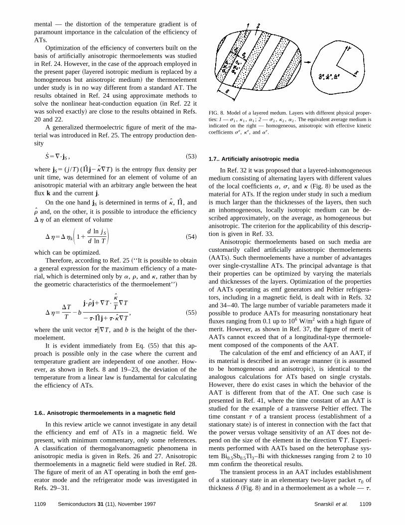
In Ref. 32 it was proposed that a layered-inhomogenemedium consisting of alternating layers with different valuof the local coefficientsa, s, andk ~Fig. 8! be used as thematerial for ATs. If the region under study in such a mediuis much larger than the thicknesses of the layers, then san inhomogeneous, locally isotropic medium can bescribed approximately, on the average, as homogeneousanisotropic. The criterion for the applicability of this descrition is given in Ref. 33.
Anisotropic thermoelements based on such mediacustomarily called artificially anisotropic thermoelemen~AATs!. Such thermoelements have a number of advantaover single-crystalline ATs. The principal advantage is ththeir properties can be optimized by varying the materiand thicknesses of the layers. Optimization of the properof AATs operating as emf generators and Peltier refrigetors, including in a magnetic field, is dealt with in Refs. 3and 34–40. The large number of variable parameters mapossible to produce AATs for measuring nonstationary hfluxes ranging from 0.1 up to 106 W/m2 with a high figure ofmerit. However, as shown in Ref. 37, the figure of meritAATs cannot exceed that of a longitudinal-type thermoement composed of the components of the AAT.
The calculation of the emf and efficiency of an AAT,its material is described in an average manner~it is assumedto be homogeneous and anisotropic!, is identical to theanalogous calculations for ATs based on single crystHowever, there do exist cases in which the behavior ofAAT is different from that of the AT. One such casepresented in Ref. 41, where the time constant of an AATstudied for the example of a transverse Peltier effect. Ttime constantt of a transient process~establishment of astationary state! is of interest in connection with the fact thathe power versus voltage sensitivity of an AT does notpend on the size of the element in the direction¹T. Experi-ments performed with AATs based on the heterophasetem Bi0.5Sb0.5Tl3–Bi with thicknesses ranging from 2 to 1mm confirm the theoretical results.
The transient process in an AAT includes establishmof a stationary state in an elementary two-layer packett0 ofthicknessd ~Fig. 8! and in a thermoelement as a whole —t.
FIG. 8. Model of a layered medum. Layers with different physical propties:1 — s1 , k1 , a1 ; 2 — s2 , k2 , a2 . The equivalent average mediumindicated on the right — homogeneous, anisotropic with effective kinecoefficientsse, ke, andae.
1109Snarski et al.
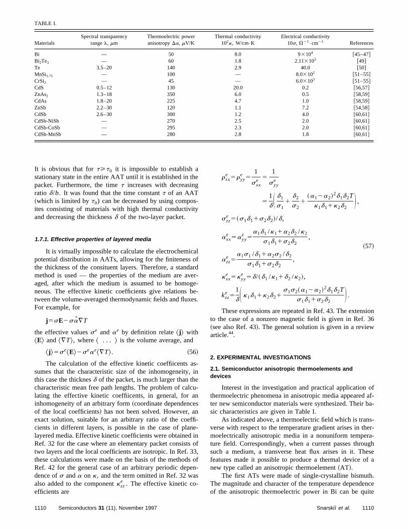
TABLE I.
Spectral transparency Thermoelectric power Thermal conductivity Electrical conductivityMaterials rangel, mm anisotropyDa, mV/K 102k, W/cm•K 10s, V21
•cm21 References
Bi — 50 8.0 93104 @45–47#Bi2Te3 — 60 1.8 2.113103 @49#Te 3.5–20 140 2.9 40.0 @50#MnSi1.75 — 100 — 8.03102 @51–55#CrSi2 — 45 — 6.03103 @51–55#CdS 0.5–12 130 20.0 0.2 @56,57#ZnAs2 1.3–18 350 6.0 0.5 @58,59#CdAs 1.8–20 225 4.7 1.0 @58,59#ZnSb 2.2–30 120 1.1 7.2 @54,58#CdSb 2.6–30 300 1.2 4.0 @60,61#CdSb-NiSb — 270 2.5 2.0 @60,61#CdSb-CoSb — 295 2.3 2.0 @60,61#CdSb-MnSb — 280 2.8 1.8 @60,61#
It is obvious that fort>t0 it is impossible to establish aheg
sity
af
davege
xe
s-,elcansn
ffine
its33ses
1 1
sion36
w
ofaf-
ba-
s-her-ra-ughese
of a
h.enceite
stationary state in the entire AAT until it is established in tpacket. Furthermore, the timet increases with decreasinratio d/b. It was found that the time constantt of an AAT~which is limited byt0) can be decreased by using compoites consisting of materials with high thermal conductivand decreasing the thicknessd of the two-layer packet.
1.7.1. Effective properties of layered media
It is virtually impossible to calculate the electrochemicpotential distribution in AATs, allowing for the finiteness othe thickness of the consituent layers. Therefore, a stanmethod is used — the properties of the medium are aaged, after which the medium is assumed to be homoneous. The effective kinetic coefficients give relations btween the volume-averaged thermodynamic fields and fluFor example, for
j5sE2sa¹T
the effective valuesse and ae by definition relate j & with^E& and ^¹T&, where^ . . . & is the volume average, and
^ j &5se^E&2seae^¹T&. ~56!
The calculation of the effective kinetic coeffiicents asumes that the characteristic size of the inhomogeneitythis case the thicknesd of the packet, is much larger than thcharacteristic mean free path lengths. The problem of calating the effective kinetic coeffiicents, in general, forinhomogeneity of an arbitrary form~coordinate dependenceof the local coefficients! has not been solved. However, aexact solution, suitable for an arbitrary ratio of the coecients in different layers, is possible in the case of plalayered media. Effective kinetic coefficients were obtainedRef. 32 for the case where an elementary packet consistwo layers and the local coefficients are isotropic. In Ref.these calculations were made on the basis of the methodRef. 42 for the general case of an arbitrary periodic depdence ofs anda on k, and the term omitted in Ref. 32 waalso added to the componentkzz
e . The effective kinetic co-efficients are
1110 Semiconductors 31 (11), November 1997
-
l
rdr-e--s.
in
u-
--
nof,of
n-
rxxe 5ryy
e 5sxx
e5
syye
51
dS d1
s11
d2
s21
~a12a2!2d1d2T
k1d11k2d2D ,
szze 5~s1d11s2d2!/d,
axxe 5ayy
e 5a1d1 /k11a2d2 /k2
s1d11s2d2,
~57!
azze 5
a1s1 /d11a2s2 /d2
s1d11s2d2,
kxxe 5kyy
e 5d/~d1 /k11d2 /k2!,
kzze 5
1
dS k1d11k2d21s1s2~a12a2!2d1d2T
s1d11s2d2D .
These expressions are repeated in Ref. 43. The extento the case of a nonzero magnetic field is given in Ref.~see also Ref. 43!. The general solution is given in a reviearticle.44.
2. EXPERIMENTAL INVESTIGATIONS
2.1. Semiconductor anisotropic thermoelements anddevices
Interest in the investigation and practical applicationthermoelectric phenomena in anisotropic media appearedter new semiconductor materials were synthesized. Theirsic characteristics are given in Table I.
As indicated above, a thermoelectric field which is tranverse with respect to the temperature gradient arises in tmoelectrically anisotropic media in a nonuniform tempeture field. Correspondingly, when a current passes throsuch a medium, a transverse heat flux arises in it. Thfeatures made it possible to produce a thermal devicenew type called an anisotropic thermoelement~AT!.
The first ATs were made of single-crystalline bismutThe magnitude and character of the temperature dependof the anisotropic thermoelectric power in Bi can be qu
1110Snarski et al.
easily controlled by doping and introducing double45,46 t
hKn
-ismfo
si
y
pi
ert
non
rsicig
sxe
ala
M
ofonthen
emeffesi
dua
sAT
ty
of the AT is determined mainly by the thermoelectric powertor
is
werrialcanted
r-t ofionple,artis-
sal-ndra-x-
a
oaltionesr-
le-per-ityeatofvents.ea-ndmffancere
od-id,
interlayers. Bismuth has proven itself well in differenradiation detectors and microelements. Bi–Sb alloys withigh thermoelectric figure of merit in the range 140–180are used in thermoelectric refrigerators operating in a traverse magnetic field.47,48
Single crystals such as Bi2Te3 and Te, which are technologically inefficient, are highly layered and ductile. Thisdue to instability of their thermoelectric and electric paraeters. As a result, such materials are difficult to useATs.49,50
Single crystals of some silicon compounds with trantion elements, for example, MnSi1.75 and CrSi2 , are ofinterest.51–56 The high thermoelectric power anisotrop(Da.100 mV/K at 300 K!, which remains in a very widetemperature range~200–1000 K for CrSi2), makes it pos-sible to use them as high-sensitivity, low-noise anisotroradiation detectors. These detectors possess a giganticnamic range and a high linearity of the output parametFurthermore, these compounds are promising for use asbasis for high-voltage, anisotropic, heat-to-electricity coverters operating, for example, in combination with silicsolar cells.
Some single crystals of II–V semiconducto(Da5120– 350mV/K57–59! possess a high thermoelectrpower anisotropy at high temperatures combined with hoptical transparency in the infrared range~IR!. These mate-rials are employed for optical ATs operating in optical tranmission regimes and make it possible to control heat fluexceeding 1.0 MW/m2.
The group of anisotropic thermoelectric and opticthermoelectric materials based on CdSb single crystalsdirectionally crystallized eutectics CdSb–MeSb, wheredenotes a metal~Ni, Co, Mn!, must be specially singledout.60,61The low anisotropic thermoelectric figure of meritthese materials makes it difficult to use them for direct cversion of heat into electricity. However, because ofweak temperature-dependence of the voltage–power stivity of the ATs in the range 210–310 K~the temperaturecoefficient is ms51.1%•K21 for CdSb andms50.12– 0.15%•K21 for CdSb–CoSb! and the high valueof this sensitivity, as well as the temporal stability of thparameters62 and large geometric size of the crystals, a nuber of devices and systems are serially produced. The kincharacteristics and other parameters of ATs based on dient classes of anisotropic materials can be compared uTable I.
When ATs are used as temperature or heat flux transers, the following basic parameters are used: temperaturevoltage–power sensitivitySt andSq , the time constantt, thethreshold sensitivityPmin , and the detection powerD.63,64
The chief characteristic of ATs is the voltage–power sentivity Sq . From the heat balance equation for a vacuumoperating as a radiation sensor, we obtain63
Sq50.5~a ik'2a'k i!~k ik'!21c21, ~58!
wherec is the width of the AT. The temperature sensitivi
1111 Semiconductors 31 (11), November 1997
a
s-
-r
-
cdy-s.he-
h
-s
-nde
-esi-
-ticr-ng
c-nd
i-
anisotropy coefficient of the material and the shape faca/b
St5~a i2a'!a/b. ~59!
If the Peltier effect is weak, the time constant of the ATgiven by the expression65
t50.4b2/j, ~60!
wherej is the thermal diffusivity of the AT material in thedirection of heat flow.
The threshold sensitivity of the AT~the equivalent noisepower! is limited only by the thermal noise
Pmin58k ik'~s0rTacb21!0.5
~a ik'2a'k i!, ~61!
wheres0 is the Stefan–Boltzmann constant,T is the tem-perature of the AT, andr is the resistivity of the AT. Analy-sis of this expression shows that the equivalent noise pois determined by the geometry of the AT and the mateparameters. Depending on the specific problem, the ATbe optimized with respect to one of the parameters lisabove.63,65
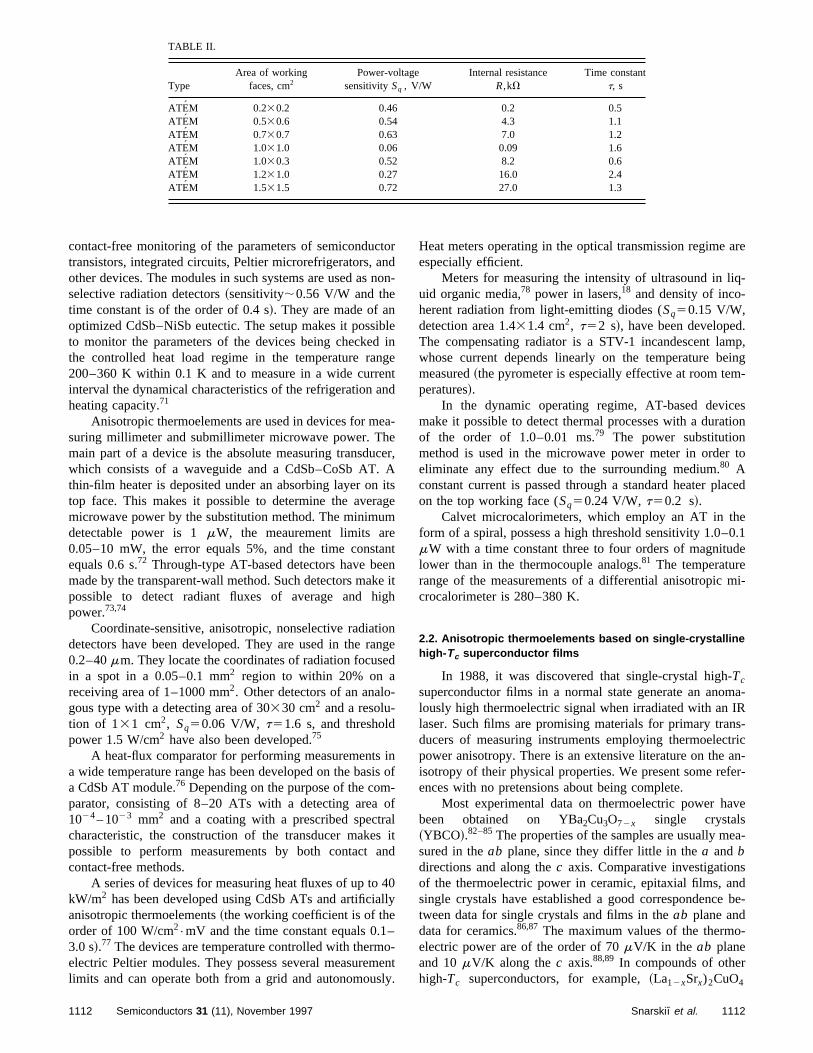
Optimization of the physical properties of a highly pefect CdSb single crystal and the technology of treatmenthe crystal made it possible to build and put into producta number of new optical devices and systems. For examthis material can be used to delimit the short-wavelength pof the IR region of the spectrum with a substantial transmsion ~98%! in the range 2.6–40mm ~Refs. 66 and 67!. Thehigh refractive index (n54) makes it possible to use thimaterial for immersion IR filters–lenses and internabsorption ATs.68 Such devices reliably protect onboard astationary apparatus of different kinds from backgrounddiation as well as artificial and natural illuminations. An eample of such an apparatus is the ‘‘Fakel’’ fire detector insmoky atmosphere; ‘‘Kvant,’’ ‘‘Kvant-RT,’’ and RPI py-rometers; and sensors for prevention of explosions in cmines and for other objects. The construction and fabricatechnology of a unified thermoelectric module and AT pilhave been developed~the characteristics of anisotropic themoelectric modules are presented in Table II!.
The characteristic features of anisotropic thermoements — the presence of one branch, the heat flow ispendicular to the electric field, the voltage–power sensitivis independent of the geometric size in the direction of hflow combined with optical transparency and possibilityproducing a device with a short time constant — haopened up prospects for wide applications of such eleme
One of the first devices developed is a device for msuring the effective values of high-frequency currents avoltages~measurement range 1–500 mA with a nominal eof the AT of 20–60 mV!.69,70 The transducer consisted otwo ATs, connected electrically in series, together withelectrically insulated ohmic heater with a definite resistanbetween them. Different working faces of the ATs weequipped with radiators.
The weak temperature-dependence of AT-based mules made it possible to use them in systems for rap
1111Snarski et al.
contact-free mo
TABLE II.
ant
Area of working Power-voltage Internal resistance Time constType faces, cm2 sensitivitySq , V/W R,kV t, sATEM 0.230.2 0.46 0.2 0.5ATEM 0.530.6 0.54 4.3 1.1ATEM 0.730.7 0.63 7.0 1.2ATEM 1.031.0 0.06 0.09 1.6ATEM 1.030.3 0.52 8.2 0.6ATEM 1.231.0 0.27 16.0 2.4ATEM 1.531.5 0.72 27.0 1.3
nitoring of the parameters of semiconductorann
ibdngnn
ehec.
iagm
etaekeig
tioane
-
isis
-o
rasan
4ll
–o
msl
Heat meters operating in the optical transmission regime are
q-
.mp,ing-
estion
to
laced
e0.1de
mi-
ma-IRns-trican-fer-
ve
ea-
snd
be-
-
transistors, integrated circuits, Peltier microrefrigerators,other devices. The modules in such systems are used asselective radiation detectors~sensitivity;0.56 V/W and thetime constant is of the order of 0.4 s!. They are made of anoptimized CdSb–NiSb eutectic. The setup makes it possto monitor the parameters of the devices being checkethe controlled heat load regime in the temperature ra200–360 K within 0.1 K and to measure in a wide curreinterval the dynamical characteristics of the refrigeration aheating capacity.71
Anisotropic thermoelements are used in devices for msuring millimeter and submillimeter microwave power. Tmain part of a device is the absolute measuring transduwhich consists of a waveguide and a CdSb–CoSb ATthin-film heater is deposited under an absorbing layer ontop face. This makes it possible to determine the avermicrowave power by the substitution method. The minimudetectable power is 1mW, the meaurement limits ar0.05–10 mW, the error equals 5%, and the time consequals 0.6 s.72 Through-type AT-based detectors have bemade by the transparent-wall method. Such detectors mapossible to detect radiant fluxes of average and hpower.73,74
Coordinate-sensitive, anisotropic, nonselective radiadetectors have been developed. They are used in the r0.2–40mm. They locate the coordinates of radiation focusin a spot in a 0.05–0.1 mm2 region to within 20% on areceiving area of 1–1000 mm2. Other detectors of an analogous type with a detecting area of 30330 cm2 and a resolu-tion of 131 cm2, Sq50.06 V/W, t51.6 s, and thresholdpower 1.5 W/cm2 have also been developed.75
A heat-flux comparator for performing measurementsa wide temperature range has been developed on the baa CdSb AT module.76 Depending on the purpose of the comparator, consisting of 8–20 ATs with a detecting area1024– 1023 mm2 and a coating with a prescribed spectcharacteristic, the construction of the transducer makepossible to perform measurements by both contactcontact-free methods.
A series of devices for measuring heat fluxes of up tokW/m2 has been developed using CdSb ATs and artificiaanisotropic thermoelements~the working coefficient is of theorder of 100 W/cm2
•mV and the time constant equals 0.13.0 s!.77 The devices are temperature controlled with thermelectric Peltier modules. They possess several measurelimits and can operate both from a grid and autonomou
1112 Semiconductors 31 (11), November 1997
don-
leinetd
a-
er,Atse
ntn
ith
nge
d
nof
flitd
0y
-enty.
especially efficient.Meters for measuring the intensity of ultrasound in li
uid organic media,78 power in lasers,18 and density of inco-herent radiation from light-emitting diodes (Sq50.15 V/W,detection area 1.431.4 cm2, t52 s!, have been developedThe compensating radiator is a STV-1 incandescent lawhose current depends linearly on the temperature bemeasured~the pyrometer is especially effective at room temperatures!.
In the dynamic operating regime, AT-based devicmake it possible to detect thermal processes with a duraof the order of 1.0–0.01 ms.79 The power substitutionmethod is used in the microwave power meter in ordereliminate any effect due to the surrounding medium.80 Aconstant current is passed through a standard heater pon the top working face (Sq50.24 V/W, t50.2 s!.
Calvet microcalorimeters, which employ an AT in thform of a spiral, possess a high threshold sensitivity 1.0–mW with a time constant three to four orders of magnitulower than in the thermocouple analogs.81 The temperaturerange of the measurements of a differential anisotropiccrocalorimeter is 280–380 K.
2.2. Anisotropic thermoelements based on single-crystallinehigh- Tc superconductor films
In 1988, it was discovered that single-crystal high-Tc
superconductor films in a normal state generate an anolously high thermoelectric signal when irradiated with anlaser. Such films are promising materials for primary traducers of measuring instruments employing thermoelecpower anisotropy. There is an extensive literature on theisotropy of their physical properties. We present some reences with no pretensions about being complete.
Most experimental data on thermoelectric power habeen obtained on YBa2Cu3O72x single crystals~YBCO!.82–85The properties of the samples are usually msured in theab plane, since they differ little in thea andbdirections and along thec axis. Comparative investigationof the thermoelectric power in ceramic, epitaxial films, asingle crystals have established a good correspondencetween data for single crystals and films in theab plane anddata for ceramics.86,87 The maximum values of the thermoelectric power are of the order of 70mV/K in the ab planeand 10mV/K along thec axis.88,89 In compounds of otherhigh-Tc superconductors, for example,~La12xSrx)2CuO4
1112Snarski et al.
~Refs. 89 and 90!, Bi2Sr2CaCu2O8 ~Refs. 91 and 92!, and-
th
in
-k
th
o
le
gheerOma
u
oo
gut
ss
e
ererf il
ertha
igal
lsohrlyditoau
not change sign when the direction of irradiation is reversed.onnot
ts apres-olt-aseenal
ethe
nalade
s. Inre-
a-ana
on-
W.the
eeakthege.
an-K.
uch
en-esubt-m-
d
sese-
on-
-here-
heAn
nalcted
EuBa2Cu3O7 ~Ref. 93!, a similar behavior of the thermoelectric power tensor componentsaab andac , differing mainlyin the magnitude of the coefficient, is observed.
The greatest amount of data on the anisotropy ofresistivity is available for high-Tc superconductors of thetype MBa2Cu3O72x , where M is ytterbium or differentlanthanides.94–98 Data on other compounds can be foundother works: Bi2Sr2.2Ca0.8Cu2O3 ~Refs. 99–101! andLa22xSrxCuO4 ~Refs.102–104!. We note that the thermoelectric power anisotropy in these materials is much weathan the resistivity anisotropy (ac /aab.3 – 6,rc /rab.30250).
The thermal conductivity of polycrystalline samples withe composition RBa2Cu3Ox , where R5Y, Eu, Gd, Dy, Er,Sm, and Ho~the so-called 123 system! has been studiedextensively.105–109Another class of materials are samplesthe type La22xSrxCuO4 ~214 system!.106,110,111The thermalconductivity anisotropy of these materials has receivedattention.92,112
The investigation of the responses of single crystal hiTc superconductor samples for thermal and electromagneffects started immediately after these materials wsynthesized.113 The results obtained on single-crystal YBCfilms with c axis inclined with respect to the surface at rootemperatures are especially interesting. When such filmsirradiated with IR laser radiation~in the cw or pulsedmodes!, gigantic voltaic signals are generated@according tosome data, up to 100 V~Ref. 114!#. The mechanism leadingto such a response is still being discussed by different groof investigators. Analysis of the published data115–121showsthat the dominant mechanism is anisotropy of the thermelectric properties of these materials. Arguments in favorthis assertion are presented below.
In one of the first investigations, the transverse voltaunder laser irradiation of YBCO films, both with and withoa transport current, was measured.116 Films ranging in thick-ness from 0.1 to 1.5mm were irradiated with 10–20 npulses with wavelengths of 355, 532, and 1064 nm. The laradiation energy density was equal to 10–300 J/m2. SrTiO3 ,Al2O3 , and MgO wafers were used as substrates. The msured transverse voltage reached 0.2 mV~when a transportcurrent is present, this voltage is approximately 30% low!.The amplitude of the laser pulse dropped practically to zover 50 ns, while the measured signal dropped to 30% omaximum value over 200 ns and then dropped more slowThe signal changed very little when the contacts wscreened from irradiation and dropped by 95% when onlyregion of each contact was irradiated. As the beam wscanned along the sample between the contacts, the sexhibited a wide maximum. The polarity of the signchanged when the contacts were interchanged.
Similar results were obtained in Ref. 122. It was aestablished there that the polarity of the signal changes wthe backside of the film is irradiated. This behavior cleaindicates that the signal depends on the temperature grain the film. In Ref. 123 these data are explained by a phoeffect with a tensorial photoconductivity. However, even inmedium with tensorial properties, the photoresponse sho
1113 Semiconductors 31 (11), November 1997
e
er
f
ss
-tice
re
ps
-f
e
er
a-
otsy.ees
nal
en
ent-
ld
This change in polarity indicates that the signal dependsthe temperature gradient in the film. The response doesdepend on the polarization of the laser beam and exhibistrong temperature-dependence, characterized by theence of two temperature thresholds. The laser-induced vage arises not only in the pulsed regime but also in the cof irradiation in the cw regime. A signal is present in thorthorhombic phase of YBCO and is absent in the tetragophase. Crystals withc axis making different angles with thsubstrate were investigated. Electrodes for measuringvoltage were placed along a circle every 22.5°. The sigwas strongest when the line connecting the electrodes man angle of 45° with thec axis ~or coincided with the pro-jection of this axis onto the surface of the film!.
These results have been reproduced in many sampleexperiments where thec axis of the films was perpendiculato the MgO or SrTO3 substrates, the signal strength dpended strongly on the disorientation of thec axis ~in therange of angles 1–3°). For example, films with an inclintion of 1.0° gave 20 times stronger signals than films withinclination of 0.3°. Films with a zero disorientation gavenegligible signal. Stable signals were also obtained with ctinuous irradiation of the film by a 20-mW He–Ne laser.117
In the experiments, they reached a magnitude of 1 mSince the signal does not depend on the polarization oflaser beam, the tensorial photoeffect mechanism~occurringin the case of the piezoelectricity! cannot be used to describthe phenomenon. We note that under conditions of wthermal actions and strong conductive coupling betweenfilm and the substrate, the polarity of the signal can chanOther experimental results confirm the thermoelectricallyisotropic nature of the effect at temperatures above 240Furthermore, the values obtained for the signals are mhigher than the expected photoresponse~the authors evencalled the phenomenon an anomalous photoeffect!. The de-pendence of the signal magnitude on the density of theergy incident on the film is confirmed by all known studiwhere such measurements were performed. This undoedly also confirms the thermoelectric nature of the phenoenon.
The photoresponse of a 0.5mm thick Bi2Sr2CaCu2O8
film, carrying a current ranging from 2 to 200 mA, irradiatewith IR laser pulses (l5447mm, pulse repetition frequency165 Hz, average pulse duration at half-height 65 ns! wasinvestigated in Ref. 98. It was observed that the responare nonbolometric~i.e., the film resistance did not changnear the signal maximum!. These data attest to a weak temperature dependence of the thermoelectric power.124,88
The nonbolometric nature of the responses was cfirmed in Ref. 125. The maximum signal reached 2 V withbeam energy density 30 mJ/cm2. The magnitude of the signal was proportional to the irradiation energy but not tenergy density. This stems from the fact that the signalmained constant when the region of illumination with tlaser beam on the film between the contacts changed.influence due to the Seebeck effect and the off-diagocomponents of the thermoelectric power tensor was rejeon the basis of the symmetry of the YBCO structure~i.e., the
1113Snarski et al.
presence of thermoelectric power anisotropy was rejected!.t
rm
geolwo
matthorf tco
iu
frt
eas
wpeamg
d0trs2he
o
nd
Thap
re
10tserlmrrltt
s
utan
malization of the temperature gradient with respect to theethere
umthe
wasasthetothe
gnald iner-s in-ult ofare
nles
ar-
in
theid
nals
heIn-at
re-isr ofthence
inbe-ps.
nalting
ong
thenalor-at
The signal was found to depend on the angle betweenlaser beam and the film. When the angle between the noto the film and the beam changed from255° to 155°, thesignal decreased linearly~from 110 to 55 mV!, i.e., itchanged antisymmetrically. It was also asserted that theerated signal does not depend on the wavelength and pization of the radiation. In our opinion, it is incorrect to draconclusions about the macroscopic kinetic coefficientsreal high-Tc superconductor films on the basis of the symetry properties of an ideal lattice. The experimental dpresented in the paper mainly are in agreement withmechanism due to the anisotropy of thermoelectricity. Inder to describe some specific experiments on the basis oindicated mechanism, it is necessary to construct a spemathematical model allowing for the concrete conditionsheat transfer between the film and the surrounding medand the location of the electric contacts on the film.
The dependence of the response on the irradiationquency on 16 laser lines with frequencies ranging from 101000 mm was investigated in Ref. 118. It was establishthat the sensitivity of the signal decays strongly with increing frequency (;v22.3). A current ranging from 2 to 40mAwas passed through single-phasec-oriented films. The dura-tion of the response was less than 4 ns and its maximumproportional to the bias current passed through the samThe authors believe that the mechanisms of electronic hing and the regions of heating proposed for very thin fil~thickness less than 100 nm! are unsuitable for describingranular films exceeding 200 nm in thickness.
A thin ~0.3mm! Bi2Sr2CaCu2O8 film was investigated inRef. 127. Laser pulses with a sharp leading edge with aration of about 5 ms in the wavelength range from 80 to 2mm were employed. A rapid response and a slow bolomecomponent were recorded. The energy density in the lapulses irradiating the sample fell into the range 2–kW/cm2. Only rapid responses with a time constant of torder of 1 ns were observed above a critical wavelength100 mm.
The preparation and investigation of 500-nm-thick a10310-mm2 films with a small angle between thec axis andthe normal to the substrate are described in Ref. 119.films were investigated at room temperature. A signalpeared in the films heated with 100-ns laser pulses (l51.06mm! with an energy of 1–10 mJ per pulse. The centralgion of the film was irradiated with a beam with a 2 mm indiameter region of illumination and energy densitymJ/cm2. Under direct irradiation the signal from contacseparated by 6 mm was equal to about 1 V with a tempture difference of 50–100 K between the surface of the fiand the substrate. The behavior of the signal in time cosponded to decay of the temperature gradient as a resuheat conduction. These experiments were compared withresults of numerical simulation~the modified Schmidtmethod was used127!. When the backside of the film wairradiated~through the substrate!, the sign of the signal wasdifferent from the case of direct irradiation of the film, bafter termination of the heating the polarity of the signchanged once again. These data were attributed to the
1114 Semiconductors 31 (11), November 1997
heal
n-ar-
f-ae-heialfm
e-od-
asle.t-
s
u-0icer4
f
e-
-
a-
e-of
he
lor-
surface of the film. When the heat flux from the film to thsubstrate is higher than the flux from the free surface offilm into the surrounding air, the direction of the temperatugradient in the freely cooled film can change. The maximsignal was obtained when the spot was located betweencontacts. The sign of the signal changed when the spotmoved beyond the limits of the contacts. When the film wrotated relative to the axis passing through its center,signal maximum dropped sinusoidally. A model accordingwhich the laser beam produces a dipole heat source infilm was proposed. The authors note that the recorded siwas several orders of magnitude stronger than expectethe ordinary Seebeck effect, and a model of ‘‘atomic thmocouples’’ was proposed. The essence of the model liethe fact that the CuO2 layers and the lower-conductivity layers separating them are treated as a thermopile. As a resthe fact that the signals from separate thermocouplessummed, the ratio of the diametera of the region of illumi-nation to the thicknessb of the film appears in the expressiofor the thermoelectric power. The number of thermocoupis also related with the angle between thec axis and thesubstrate~see also Ref. 128!. Thus the following expressionwas obtained:
U5~a/b!DT~aab2ac!sin u. ~62!
Using the data from Ref. 84 on the Seebeck coefficient pallel and perpendicular to thec axis~15 and 5mV/K, respec-tively! and the valuesa52 mm,u510°, andDT5100 K, athermoelectric power of the same order of magnitude asthe experiment was obtained:U50.7 V. Furthermore, a cor-relation was found between the quality of the films andmagnitude of the thermoelectric signal. Granular films dnot exhibit a thermoelectric response. The strongest sigwere obtained from smooth films with a mirror surface.
The following objections can be made concerning tmechanism described by the formula presented above.deed, the formula predicts that the effect will be maximumu590°, while experimentally the strongest effect wascorded atu545°.117 Furthermore, when the laser spotscanned in the region between the contacts, the numbe‘‘atomic’’ thermocouples does not change and thereforesignal magnitude should not change, which is at variawith the experimental data obtained by the authors.
Additional detailed investigations were performedRef. 120 for the purpose of clarifying the discrepanciestween the results obtained by different experimental grouFilms with a different angle between thec axis and the sub-strate surface were studied. It was found that the sigstrength depends on the angle between the line connecthe contacts and the projection of thec axis onto the filmsurface. The experimental samples consisted of 2-mm-land 20 to1000-mm-wide bridges. A beam from a cw ion~As!laser illuminated, through a rectangular spectral filter,entire width of the bridge. It was determined that the sigdoes not depend on the width of the bridge but is proptional to the length of the bridge. The result of Ref. 119 ththe signal is generated along thec axis only was confirmed.For small angles of incilnation from thec axis the signal is
1114Snarski et al.
proportional to the angleu. The increase in temperature wasw-o
nuwvea
enlo
re
t
gne
dhe
ericd
th-tu
e
emiory
D
,
er
11V. N. Slipchenko and A. A. Snarski�, Fiz. Tekh. Poluprovodn.8, 2010~1974! @Sov. Phys. Semicond.8, 1305~1974!#.
.
s.
.
nd
very small ~2.2 mK! in the case where a laser with a loradiation density~1.4 W/cm2) was used. Hence it was concluded that the use of pulsed lasers, which give an enormtemperature increase, only complicates the interpretatiothe measurements. The signal strength remained virtuallychanged when the region between the electrodesscanned~in contrast to Ref. 103 , where a peak was obserat the midpoint!. This fact was attributed to large pulsed heloads~greater thanDT).
Different temperature dependences of the signal wobserved in experiments with different films for films growon substrates with different orientations of the crystalgraphic axes (SrTiO3 ,110 SrTiO3 ,100 and SrTiO3
103!. Evenfor the same film, different measurements gave differentsults when a different pair of contacts was chosen~i.e., whenthe direction of the line connecting the contacts relativethe c axis was changed!. The temperature dependenceR(T)remained unchanged. The mechanism producing the siwas attributed to the recently observed, long-period, timdependent changes in the superconductivity.129 More accu-rately, it is postulated that the changes indicated incluoxygen-ordered charge transfer, which influences the tmoelectric power.
The last study virtually confirms the results of the prceding study and is consistent with the thermoelectanisotropy mechanism. The discrepancies are essentiallyto the specific experimental conditions.
Analysis of the studies described above shows thatdetermining mechanism of the gigantic response of highTc
superconductor films to thermal and electromagnetic perbations is anisotropy of their thermoelectric properties.
The questions considered in this review were discussat different times, with P. I. Baranski�, A. B. Belikov, L. P.Bulat, O. S. Gorya, T. S. Gudkin, V. I. Ka�danov, S. L.Korolyuk, G. N. Logvinov, V. M. Pan, I. M. Pilat, I. M.Rarenko, and E. E. Fiskind. We are deeply grateful to thall. We wish to acknowledge separately the contributmade by V. M. Slipchenko during his short life to the theoof anisotropic thermocouples.
1!The possibility of using such boundary conditions was pointed by A.Myshkis.
1 A. G. Samo�lovich and L. L. Korenblit, Usp. Fiz. Nauk49, 243 ~1953!.2L. D. Landau and E. M. Lifshitz,Electrodynamics of Continuous MediaPergamon Press, N. Y.@Russian original, Nauka, Moscow, 1989#.
3W. Thomson, Math. Phys. Pap.1, 266 ~1882!.4C. Herring, Phys. Rev.59, 889 ~1941!.5A. G. Samoilovich and L. L. Korenblit, Patent UK N 1088764, Octob25, 1964.
6S. L. Kopolyuk, I. M. Pilat, A. G. Samo�lovich, V. I. Slipchenko, A. A.Snarski�, and E. V. Tsar’kov, Fiz. Tekh. Poluprovodn.7, 725 ~1973!@Sov. Phys. Semicond.7, 502 ~1973!#.
7A. G. Samo�lovich in Problems in Modern Physics@in Russian#, Nauka,Leningrad, 1980, p. 304.
8A. G. Samo�lovich and A. A. Snarski�, Fiz. Tekh. Poluprovodn.13, 1539~1979! @Sov. Phys. Semicond.13, 1539~1979!#.
9A. A. Snarski�, Fiz. Tekh. Poluprovodn.11, 2053 ~1977! @Sov. Phys.Semicond.11, 1207~1977!#.
10A. G. Samo�lovich and V. N. Slipchenko, Fiz. Tekh. Poluprovodn.9, 594~1975! @Sov. Phys. Semicond.9, 397 ~1975!#.
1115 Semiconductors 31 (11), November 1997
usofn-asdt
re
-
-
o
al-
er-
--ue
e
r-
d,
n
.
12I. M. Pilat, A. B. Belikov, L. L. Kazanskaya, and A. A. Ashcheulov, FizTekh. Poluprovodn.10, 1019 ~1976! @Sov. Phys. Semicond.10, 604~1976!#.
13O. Ya. Luste and A. G. Samo�lovich, Fiz. Tekh. Poluprovodn.11, 209~1977! @Sov. Phys. Semicond.11, 121 ~1977!.
14A. A. Snarski� and S. S. Trofimov, Fiz. Tekh. Poluprovodn.17, 953~1983! @Sov. Phys. Semicond.17, 600 ~1983!#.
15A. A. Snarski�, Fiz. Tekh. Poluprovodn.12, 815~1978! @Sov. Phys. Semi-cond.12, 479 ~1978!#.
16L. I. Anatychuk, Thermoelements and Thermoelectric Devices@in Rus-sian#, Naukova. Dumka, Kiev, 1970.
17A. A. Snarski�, Fiz. Tekh. Poluprovodn.14, 170~1980! @Sov. Phys. Semi-cond.14, 99 ~1980!#.
18A. A. Ashcheulov, A. B. Belikov, and A. I. Rarenko, Ukr. Fiz. Zh.8, 825~1993!.
19A. G. Samo�lovich and V. N. Slipchenko, Fiz. Tekh. Poluprovodn.7, 725~1973! @Sov. Phys. Semicond.7, 502 ~1973!#.
20V. N. Slipchenko, Ukr. Fiz. Zh.21, 126 ~1976!.21A. G. Samo�lovich and V. N. Slipchenko, Fiz. Tekh. Poluprovodn.15, 427
~1981! @Sov. Phys. Semicond.15, 247 ~1981!#.22A. G. Samo�lovich and V. N. Slipchenko, Fiz. Tekh. Poluprovodn.15, 968
~1981! @Sov. Phys. Semicond.15, 554 ~1981!#.23A. G. Samo�lovich and V. I. Shevuk, Fiz. Tekh. Poluprovodn.16, 1951
~1982! @Sov. Phys. Semicond.16, 1260~1982!#.24O. S. Gorya and E. F. Lupashko, Zh. Tekh. Fiz.50, 2602 ~1980! @Sov.
Phys. Tech. Phys.25, 1525~1980!#.25O. S. Gryaznov, B. Ya. Mo�zhes, and V. A. Nemchinski�, Zh. Tekh. Fiz.
48, 1720~1978! @Zh. Tekh. Fiz.23, 975 ~1978!#.26P. I. Baranskii, I. S. Buda, I. V. Dakhovskii, and A. G. Samoilovich, Phy
Status Solidi B67, 201 ~1975!.27P. I. Baranskii, I. S. Buda, and V. V. Savyak, Phys. Status Solidi B112,
111 ~1989!.28A. G. Samo�lovich and V. N. Slipchenko, Fiz. Tekh. Poluprovodn.9, 1897
~1975! @Sov. Phys. Semicond.9, 1249~1975!#.29A. G. Samo�lovich and V. N. Slipchenko, Fiz. Tekh. Poluprovodn.15, 965
~1981! @Sov. Phys. Semicond.15, 724 ~1981!#.30E. F. Lupashko, Fiz. Tekh. Poluprovodn.15, 724 ~1981! @Sov. Phys.
Semicond.15, 411 ~1981!#.31A. G. Samo�lovich and V. N. Slipchenko, Fiz. Tekh. Poluprovodn.16, 736
~1982! @Sov. Phys. Semicond.16, 474 ~1982!#.32V. P. Babin, T. S. Gudkin, Z. M. Dashevxki�, L. D. Dudkin, E. K. Ior-
danishvili, V. I. Ka�danov, N. V. Kololmoets, O. M. Narva, and L. SStil’bans, Fiz. Tekh. Poluprovodn.8, 748~1974! @Sov. Phys. Semicond.8,478 ~1974!#.
33E. D. Belotski�, A. A. Snarski�, and S. S. Trofimov, Ukr. Fiz. Zh.27, 91~1974!.
34T. S. Gudkin, E. K. Iordanishvili, and E. E´ . Fiskind, Fiz. Tekh. Polupro-vodn.11, 1790~1977! @Sov. Phys. Semicond.11, 1048~1977!#.
35T. S. Gudkin, E. K. Iordanishvili, and E. E´ . Fiskind, Pis’ma Zh. Tekh. Fiz.4, 607 ~1978! @Sov. Tech. Phys. Lett.4, 244 ~1978!#.
36T. S. Gudkin, E. K. Iordanishvili, V. A. Kudinov, and E. E´ . Fiskind, Fiz.Tekh. Poluprovodn.16, 1620 ~1982! @Sov. Phys. Semicond.16, 1034~1982!#.
37T. S. Gudkin and E. E´ . Fiskind, Fiz. Tekh. Poluprovodn.18, 234 ~1984!@Sov. Phys. Semicond.18, 145 ~1984!#.
38L. I. Bytenski�, T. S. Gudkin, E. K. Iordanishvili, and E. E´ . Fiskind, Fiz.Tekh. Poluprovodn.12, 538 ~1978! @Sov. Phys. Semicond.12, 310~1978!#.
39O. A. Gerashchenko, E. K. Iordanishvili, T. S. Gudkin, E. F. Fiskind, aZh. L. Pogurskaya, Inzh. Fiz. Zh.35, 229 ~1978!.
40O. S. Gorya and E. F. Lupashko, Fiz. Tekh. Poluprovodn.13, 340 ~1979!@Sov. Phys. Semicond.13, 196 ~1979!#.
41T. S. Gudkin nad E. E´ . Fiskind, Pis’ma Zh. Tekh. Fiz.4, 844~1978! @Sov.Tech. Phys. Lett.4, 340 ~1978!#.
42V. A. Kudinov and B. Ya. Mo�zhes, Tekh. Fiz.42, 591 ~1972!@Sov. Phys. Tech. Phys.17, 467 ~1972!#.
43B. Ya. Balagurov, Fiz. Tverd. Tela~Leningrad! 28, 2068 ~1986! @Sov.Phys. Solid State28, 1156~1986!#.
44A. A. Snarski� and P. M. Tomchuk, Ukr. Fiz. Zh.32, 66 ~1987!.45W. Lukosz, Z. Naturforsch.19, 1599~1964!.46G. A. Ivanov and V. M. Grabov, Fiz. Tekh. Poluprovodn.29, 1040~1995!
@Semiconductors29, 538 ~1995!#.
1115Snarski et al.
47A. R. Regel’, G. A. Ivanov, V. M. Grabov, L. I. Anatychuk, and O. Ya.Luste, Inventor’s Certificate N 245859~1969!.
-
.
C
ec
ev
v,
n-
th
k,
n
-th
v,
bn
ie
o
m
79S. I. Pirozhenko, V. N. Slipchenko, amd B. G. Shabashkevich inAbstractsof Reports on Materials Science of II-V Semiconductor Compounds@in
F.
B
a,
ys.
.
au,
ser,
.
V.
. B
io,
. S.
a,
and
. D.
ys.
ys.
48V. M. Grabov and A. F. Panarin inAbstracts of Reports at the 4th International Seminar on Materials for Thermoelectric Transducers@in Rus-sian#, St. Petersburg, 1995, p. 66.
49B. M. Gol’tsman, V. A. Kudinov, and I. A. Smirnov,Semiconductor Ther-moelectric Materials Based on Bi2Te3 @in Russian#, Nauka, Moscow,1972.
50E. O. Movchan,Tellurium @in Russian#, Tekhnika, Kiev, 1967.51B. K. Voronov, L. D. Dudkin, and N. N. Trusov, Kristallografiya12, 519
~1967! @Sov. Phys. Crystallogr.12, 448 ~1967!#.52V. I. Ka�danov, V. A. Tselishchev, A. P. Usov, L. D. Dudkin, B. K
Voronov, and N. N. Trusov, Fiz. Tekh. Poluprovodn.4, 1338 ~1970!@Sov. Phys. Semicond.4, 1135~1970!#.
53V. K. Zaitsev, Thermoelectric Properties of Anisotropic MNSI. CRHandbook of Thermoelectrics,N. Y., 1995, p. 299.
54A. T. Burkov, A. Heinrich, and M. V. Vedernikov inProceedings 13thInternational Conference on Thermoelectrics, N. Y., 1995, p. 76–80.
55S. V. Ordin inProceedings 14th International Conference on Thermoeltrics, June 27–30, 1995, St. Petersburg, Russia, p. 212.
56A. A. Ashcheulov, OMP12, 47 ~1989!.57P. I. Baranski�, V. P. Klochkov, and I. V. Potykevich,Handbook of Semi-
conductor Electronics@in Russian#, Naukova Dumka, Kiev, 1971.58V. B. Lazarev, V. Ya. Shevchenko, Ya. L. Grinberg, and V. V. Sobol
II –V Semiconductor Compounds@in Russian#, Nauka, Moscow, 1978.59S. F. Marenkin, A. M. Raukhman, D. I. Pishchikov, and V. B. Lazare
Neorg. Mater.28, 1813~1992!.60A. A. Ashcheulov, N. K. Voronka, S. M. Kulikovskaya, and S. F. Mare
kin, Izv. Akad. Nauk SSSR, Neorg. Mater.25, 1614~1989!.61A. A. Ashcheulov, V. A. Grebenshchikov, V. A. Belotski�, and S. M.
Kulikovskaya, Izv. Akad. Nauk SSSR, UKhZh.57, 597 ~1991!.62A. A. Ashcheulov, A. F. Semizorov, and I. M. Rarenko inThermal Ra-
diation Detectors@in Russian#, GOI, Leningrad, 1980, p. 74.63I. M. Pilat, V. S. Vetoshnikov, and O. A. Gorbatyuk inAbstracts of Re-
ports at the All-Union Conference on Thermoelectric Materials and Meods for Investigating Them@in Russian#, Kishinev, 1971, p. 123.
64L. I. Antychuk, V. T. Dmitrashchuk, O. Ya. Luste, and Yu. S. TsyganoIzv. Vyssh. Uchebn. Zaved. Fiz.6, 149 ~1971!.
65L. I. Anatychuk, L. I. Bogomolov, O. I. Kupchinksi�, and O. Ya. Luste,OMP 1, 27 ~1971!.
66I. M. Rarenko, P. A. Bogomolov, and A. N. Borets, OMP10, 64 ~1972!.67A. A. Ashcheulov, V. M. Kondratenko, and I. M. Rarenko,Thermoele-
ments@in Russian#, Voronezh State University, Voronezh, 1987, p. 94.68A. A. Ashcheulov, N. V. Karpan, and I. M. Rarenko, Izv. Vyssh. Ucheb
Zaved., Elektromekh.12, 1336~1980!.69I. M. Pilat, A. A. Ashcheulov, A. B. Belikov, K. D. Soli�chuk, V. S.
Vetoshnikov, E. A. Osipov, and N. I. Trishin,Thermoelements. Prospectus of the Exposition of Achievements of the National Economy ofSoviet Union@in Russian#, Chernovtsy, 1975.
70I. M. Pilat, K. D. Soli�chuk, B. G. Shabashkevich, V. S. VetoshnikoA. M. Skubak, and V. I. Deba inThermal Radiation Detectors@in Rus-sian#, GOI, Leningrad, 1982, p. 65.
71A. A. Ashcheulov, N. N. Glemba, and L. I. Prostebi, Izv. Vyssh. UcheZaved., Elektromekh.12, 1333~1980!.
72V. Ya. Shevchenko, S. F. Marenkin, and A. A. Ashcheulov,MaterialsScience of II–V Semiconductors Materials@in Russian#, Prospectus of theExposition of Achievements of the National Economy of the SovUnion, Moscow, 1975, p. 12.
73A. A. Ashcheulov, V. M. Kondratenko, N. K. Voronka, and I. M. Rarenkin Direct Methods of Energy Conversion@in Russian#, Ashkhabad, 1986,p. 210.
74A. A. Ashchulov, I. M. Gutsul, and I. M. Rarenko, Ukr. Fiz. Zh.38, 923~1993!.
75A. A. Ashcheulov and S. F. Marenkin inAbstracts of Reports at the 7thAll-Union Conference on Materials Science of II-V Semiconductor Copounds@in Russian#, Chernovtsy, 1990, p. 111.
76I. M. Pilat, V. S. Vetoshnikov, and M. E. Belov inAbstracts of Reports onMaterials Science of II-V Semiconductor Compounds@in Russian#, Dush-anbe, 1982, p. 124.
77I. M. Pilat, V. S. Vetoshnikov, and M. E. Belov inAbstracts of Reports onMaterials Science of II–V Semiconductor Compounds@in Russian#, Dus-hanbe, 1982, p. 125.
78A. G. Samo�lovich, I. M. Pilat, V. S. Vetoshnikov, I. G. Mikha�lov, V. A.Shutilov, and V. G. Krivtsov, Inventor’s Certificate N 259503~1969!.
1116 Semiconductors 31 (11), November 1997
-
,
-
.
e
.
t
-
Russian#, Kamenets-Podol’sk, 1984, p. 92.80V. I. Trifonov, V. A. Stukan, V. B. Lazarev, V. Ya. Shevchenko, and S.
Marenkin, Elektron. Tekh., No. 1, 119~1977!.81Yu. F. Red’ko, Author’s Abstract of Candidate’s Dissertation,Cher-
novtsy, 1981.82Z. Z. Wong and N. P. Ong, Phys. Rev. B38, 7160~1988!.83Li Lu, Europhys. Lett.7, 555 ~1988!.84M. F. Crommie, A. Zettl, T. W. Barbee, and M. L. Cohen, Phys. Rev.
37, 9734~1988!.85K. A. Ge�m and S. V. Dubonos, SFKhT2, 7 ~1989!.86V. E. Gosuyants, S. A. Kaz’min, V. I. Ka�danov, and V. A. Tselishchev
SFKhT 6, 1836~1993!.87P. P. Konstantinov, V. N. Vasil’ev, A. T. Burkov, and V. B. Glushkov
SFKhT 4, 295 ~1991!.88J. L. Cohn, E. F. Skelton, S. A. Wolf, J. Z. Liu, and R. N. Shelton, Ph
Rev. B45, 13140~1992!.89M. Sera, S. Shamoto, and M. Sato, Solid State Commun.68, 649 ~1988!.90R. C. Yu, N. J. Naughton, and X. Yan, Phys. Rev. B37, 7962~1988!.91I. M. Tsidil’kovski�, V. L. Konstantinov, K. R. Krylov, A. I. Ponomarev,
M. B. Kosmyna, A. B. Levin, and T. B. Chirikova, SFKhT2, 45 ~1989!.92M. F. Crommie, A. Y. Liu, L. Marvin, M. L. Cohen, and A. Zettl, Phys
Rev. B41, 2526~1990!.93V. F. Kra�denov and E. S. Itskevich, Fiz. Nizk. Temp.18, 1187 ~1992!
@Sov. J. Low Temp. Phys.18, 829 ~1992!#.94P. G. Huggard, Gi. Schneider, T. O’Brien, P. Lemoine, and W. Bl
Appl. Phys. Lett.58, 2549~1991!.95S. W. Tozer, A. W. Kleinsasser, and D. Penney, Phys. Rev. Lett.59, 1768
~1987!.96T. Penney, S. von Molnar, D. Kaiser, F. Holtzberg, and A. W. Kliensas
Phys. Rev. B38, 2918~1988!.97Physical Properties of High-Temperature Superconductors@Russian
translation#, Mir, Moscow, 1990.98H. L. Stormer, A. F. J. Levi, K. W. Baldwin, M. Anzlowar, and G. S
Beebinger, Phys. Rev. B38, 2472~1988!.99S. Martin, A. T. Fiory, R. M. Fleming, L. F. Schneemeyer, and I.
Wasczak, Phys. Rev. Lett.60, 2194~1988!.100V. L. Arbuzov, O. M. Bakunin, A. E´ . Davletshin, S. M. Klotsman, M. B.
Kosmyna, A. B. Levin, and V. P. Seminozhenko, JETP Lett.48, 440~1988!.
101M. Brinkmann, H. Somnitz, H. Bach, and K. Westerholt, Physica C217,418 ~1993!.
102M. Gurvitch and A. T. Fiory, Phys. Rev. Lett.59, 1337~1987!.103S. A. Wolf and V. Z. Kresin@Eds.#, Novel Sperconductivity, Plenum
Press, N. Y., 1987.104M. Gurvitch, A. T. Fiory, and L. S. Schneemeyer, Physica C153–155,
1369 ~1988!.105Yu. A. Kirichenko, K. V. Rusanov, and E. G. Tyurina, SFKhT3, 1385
~1990!.106S. T. Hagen, Z. Z. Wang, and N. P. Ong, Phys. Rev. B40, 9398~1989!.107M. A. Izbizky, M. R. Nunez, P. Esquinuri, and C. Fainstain, Phys. Rev
38, 9220~1988!.108M. R. Nunez, D. Castello, M. A. Izbizky, D. Esparza, and C. D. Ovid
Phys. Rev. B36, 8813~1987!.109D. T. Morelli, J. Heremans, and D. E. Swets, Phys. Rev. B36, 3917
~1987!.110D. T. Morelli, J. Heremans, G. Doll, P. I. Picone, H. P. Jenssen, and V
Dresselehaus, Phys. Rev. B39, 804 ~1989!.111J. Heremans, D. T. Morelli, W. Smith, and S. C. Strite, Phys. Rev. B37,
1604 ~1988!.112A. V. Inyushkin, A. N. Taldenkov, L. N. Dem’yanets, and T. G. Uvarov
SFKhT 6, 985 ~1993!.113M. Leung, P. R. Broussard, J. H. Claassen, M. Osofsky, S. A. Wolf,
U. Strom, Appl. Phys. Lett.51, 2046~1987!.114H. Lengfellner, S. Zeuner, W. Prettl, and K. Renk, Europhys. Lett.25,
375 ~994!.115J. C. Culbertson, U. Strom, S. A. Wolf, P. Skeath, E. J. West, and W
Burns, Phys. Rev. B39, 12359~1989!.116C. L. Chang, A. Kleinhammes, W. G. Moulton, and L. R. Tetardi, Ph
Rev. B41, 11564~1990!.117H. S. Kwok, J. P. Zheng, and S. Y. Dong, Phys. Rev. B43, 6270~1991!.118A. Kleinhammes, C. L. Chang, W. G. Moulton, and L. R. Testardi, Ph
Rev. B44, 2313~1991!.
1116Snarski et al.
119H. Lengfellner, G. Kremb, A. Schnellbogl, J. Betz, K. Renk, and
ys
n,
125G. Schneider, P. G. Huggard, T. O’Brien, P. Lemoine, and W. Blau,Appl. Phys. Lett.60, 648 ~1992!.
J.
W. Prettl, Appl. Phys. Lett.60, 501 ~1992!.120H. S. Kwok and J. P. Zheng, Phys. Rev. B46, 3692~1992!.121A. Palti, V. Svetchnikov, V. Pan, and A. Snarskii, J. Appl. Phys.77, 2814
~1995!.122K. L. Tate, R. D. Johnson, C. L. Chang, and E. F. Hilinski, J. Appl. Ph
67, 375 ~1990!.123J. F. Scott, Appl. Phys. Lett.56, 1914~1990!.124H. Ma, G. Xiong, L. Wang, H. Zhang, L. Tong, S. Liang, and S. Ya
Phys. Rev. B40, 9374~1989!.
1117 Semiconductors 31 (11), November 1997
.
126W. Prettl, H. Lengfellner, G. P. Kaminnski, and G. Schneider, Int.Infrared Millim. Waves13, 1659~1992!.
127H. S. Carlslow and J. C. Jaeger,Conduction of Heat in Solids, ClarendonPress, Oxford, 1959.
128J. D. Budai, M. F. Chisholm, and R. Feenstra, Appl. Phys. Lett.58, 2174~1991!.
129V. I. Kudinov, A. I. Kiriluk, and N. M. Kreines, Phys. Lett. A151, 358~1990!.
Translated by M. E. Alferieff
1117Snarski et al.
ELECTRONIC AND OPTICAL PROPERTIES OF SEMICONDUCTORS
to
Low-energy nonparabolicity and condenson states in In 4Se3 crystals
D. M. Bercha, L. Yu. Kharkhalis, and A. I. Bercha
Uzhgorod State University 294000 Uzhgorod, Ukraine
M. Shnajder
Institute of Physics of the Pedagogical University Rzhesow, Poland~Submitted August 30, 1996; accepted for publication December 16, 1996!Fiz. Tekh. Poluprovodn.31, 1299–1303~November 1997!
It is shown that a condenson state and instability of the electron–phonon system, which resolveinto a nonuniform state, are possible in the three-dimensional case of an In4Se3 crystalbecause of low-energy nonparabolicity and the characteristic features of the density ofstates. ©1997 American Institute of Physics.@S1063-7826~97!00211-1#
In4Se3 is a promising material for solar power applica- valence band~VB! consists of 60 subbands, grouped in20
y.reb
ue
feetta
ne
nd
sta
thefrg
iaheu
rgin
tip
eaalpe
he
ted,istic
ts
V
thed
urare
ionis of
rth
thethetionef
ril-ts
/1
tions. In recent years, it has been under intensive studboth the crystalline and film states~see, for example, Refs1–10!. Since an In4Se3 crystal possesses a layered structusome of its unique properties can probably be explainedthese features of the structure and chemical bond. The qtion of current-carrier localization, which is due to the spcific nature of defects11,12 and the capability of forminglarge-scale fluctuations as a result of the existence of difent polytypic states or as a result of the existence of mstable states of unknown nature in real samples is imporfor these crystals.
The simplest form of localization is electron localizationear a deformation caused by the field of the electron itsas first indicated by Landau.13 An analysis in ionic14 andhomeopolar15 dielectrics led to the concept of a polaron acondenson. As shown by Pekar and De�gen,15 the condensonstate is due to the interaction of an electron with acouphonons. This interaction was described in an adiabaticproximation and the effective-mass approximation withaid of a deformation potential. The criterion obtained in R15 showed that in principle condensons with a rather laradius can exist only in the one-dimensional case.16 For two-and three-dimensional systems, the criterion is essentnot satisfied for any known semiconductor material, if tformation of the condenson state is analyzed only for a qdratic current-carrier dispersion law. Kibis17 showed that intwo-dimensional layers of hole semiconductors a hole enespectrumE(k);k4 is realized under some conditions, andthis case a large-radius condenson state can form for anbitrarily weak interaction of the charge carriers with acousphonons. We shall show that condenson states are alsosible for three-dimensional systems, specifically, for In4Se3
crystals. According to Ref. 17, the dispersion law is of grsignificance for solving this problem. Therefore, we shbriefly discuss the characteristic features of the band strum of an In4Se3 crystal.
An In4Se3 crystal contains 14 atoms in a unit cell witthe lattice parametersa1515.297 Å and is described by thspace groupPnnm.18 According to our calculations,19–21 the
1118 Semiconductors 31 (11), November 1997 1063-7826/97
in
,y
es--
r-a-nt
lf,
icp-e.e
lly
a-
y
ar-cos-
tlc-
minimal band complexes with two subbands each.Theband structure at the valence band edge is very complicasince a large number of subband crossings is characterfor it. The smallest band gap is localized at the pointG(k50, Eg50.67 eV!. The VB and the conduction band~CB!contain additional extrema, localized at the poin(0,0,2p/a2,0) and (0,0,0,425p/a3). The energy splitting be-tween two minima of the CB is of the order of 0.06–0.08 eand the splitting between two maxima of the VB is;0.05eV.
Detailed investigations of the dispersion curves nearextremal pointG ~Ref. 20! showed that they can be describeby the analytical expression
E~k!52a1kx22a2ky
22a3kz21b1kx
41b2ky41b3kz
4 , ~1!
although it has not been ruled out, as follows from oanalysis,20 that the electron and hole dispersion relationsmuch more complicated.
For further analysis, we shall use the dispersion relat~1! with parameters obtained from a least-squares analysthe computed data: a151.348310218 eV•m2,a251.996310218 eV•m2, a355.245310220 eV•m2,b152.697310235 eV•m4, b252.092310235 eV•m4,b358.452310237 eV•m4, for the CB anda1525.445310219 eV•m2, a256.911310219 eV•m2,a355.680310219 eV•m2, b1525.870310236 eV•m4,b257.106310236 eV•m4, b353.799310237 eV•m4 for theCB. Rewriting the expression~1! in terms of the dimension-less quantities, we find that the coefficients of the foupowers of the variableskxa1 /p, kya2 /p, and kza3 /p aretwo orders of magnitude larger than the coefficients ofquadratic terms. It should be noted that the coefficients ofquadratic terms are negative, and that the dispersion rela~1! differs substantially, by its nonparabolicity, from thstandard dispersion relation used for rather large values ok,as happens in III–V semiconductors.
It is evident from the expression~1! that the absoluteextrema are localized not exactly at the center of the Blouin zone (k50); rather, they are shifted into the poin
111811118-05$10.00 © 1997 American Institute of Physics
ki56(a i /2b i)1/2 ( i 51,2,3). A region of negative curvature
ioth
athd
oni
tion
ne
fnp
tica
ghso
th
l21l332l13l23 B b2l332b3l23 2
-
nc-di-
ua-
eere
is present near the pointG ~see Fig. 2 from Ref. 21!. Thedepth of the band minimum is determined from the relatE0i5a i
2/4b i ; as numerical estimates for the CB showed,largest depth is observed in the directionG2Y: E02547.6meV, and the smallest depth lies in theG2Z direction(E0351.0 meV!.
In summary, the dispersion relation~1! is characterizedby a many-valley nonparabolicity with negative curvaturethe smallest wave numbers. The dispersion relations ofadditional valleys have essentially no anomalies and arescribed quite well by a quadratic function.
To solve the problem of the formation of a condensstate we shall examine the interaction of charge carriers wacoustic phonons, taking into account the dispersion rela~1!. Accordingly, we employ a variational procedure, as doin the classical work by De�gen and Pekar.15 The problemconsists of finding the extremals of the functional
E~c,ui j !52E Fa1S ]c
]x D 2
1a2S ]c
]y D 2
1a3S ]c
]z D 2Gd3r
1E Fb1S ]2c
]x2 D 2
1b2S ]2c
]y2 D 2
1b3S ]2c
]z2 D 2Gd3r1E (i j
bi j ui j ucu2d3r
11
2 (i jkl
l i jkl ui j ukl , ~2!
wherebi j (bii [bi 8) are the components of the deformatiopotential tensor, andl i jkl [l i 8k8 are the components of thtensor of elastic moduli.
The extremalc(r ), which is a characteristic function othe Schro¨dinger equation, in the presence of an electrophonon interaction term in the deformation potential aproximation is determined with the additional condition
E ucu2d3r51. ~3!
For the interaction of an electron with longitudinal acousphonons, the diagonal terms of the deformation tensorsufficient:ui j 5uii ( i 51,2,3).
The absolute minimum of the functional can be souby varying first the components of the deformation tenwith a fixed arbitrary functionc and then varyingc. Weequate to zero the variation of the functionalE with respectto ui j . For the case of an orthorhombic crystal, we obtainsystem of equations
l11u111l12u221l13u331b1c250,
l22u221l12u111l23u331b2c250, ~4!
l33u331l13u111l23u221b3c250.
It follows from the system~4! that
u1152B
Lc2;
1119 Semiconductors 31 (11), November 1997
ne
tee-
thn
e
--
re
tr
e
u225F2l23
2 2l22l33L
1l23
2 2l22l33Gc ;
u335F2l22l132l21l23
l232 2l22l33
B
L1
b3l222b2l23
l232 2l22l33
Gc2, ~5!
where
B5l12
b2l332b3l23
l232 2l22l33
1l13
b3l222b2l23
l232 2l22l33
,
L5l111l12
l21l332l13l23
l232 2l22l33
1l13
l22l132l21l23
l232 2l22l33
.
Eliminating ui j from Eqs.~2!, we reduce the problem tofinding the extremals of a new functional. The result is
E~c!5E0~c!2AE ucu4d3r . ~6!
HereE0(c) is the part of the functional without the electronphonon interaction, and
A5b1
B
L1b2Fl21l332l13l23
l232 2l22l33
B
L2
b2l332b3l23
l232 2l22l33
G1b3Fl22l132l21l23
l232 2l22l33
B
L2
b3l222b2l23
l232 2l22l33
G . ~7!
We minimize the functional~5! with the aid of the trialfunction23
c~r !5S ~m1m2m3!1/3A2
~a1a2a3!1/3 D 3/2
expF2pF S m1
a1D 2
x2
1S m2
a2D 2
y21S m3
a3D 2
z2G G , ~8!
which satisfies the normalization condition;m1 , m2 , andm3
are dimensionless variational parameters, anda1 , a2 , anda3
are lattice constants.After integrating we obtain
E~m!52pFa1S m1
a1D 2
1a2S m2
a2D 2
1a3S m3
a3D 2G
13p2Fb1S m1
a1D 4
1b2S m2
a2D 4
1b3S m3
a3D 4G
2Am1m2m3
a1a2a3. ~9!
In order for stable condenson states to form, the futional E(m) must possess a minimum. The necessary contion for an extremum can be found from the system of eqtions
22pa1
ai2
m i112p2b i
ai4
m i32A
m jmk
aiajak50, ~10!
i 51,2,3; j 52,3,1; and,k53,2,1. However, for the purposof estimation, we restrict the discussion to the case wh
1119Bercha et al.
m1 , m2 , and m3 are equal to one another, and the latticealu
r
e
o
d
is
idat
b
ueon;om
o
2rve
oureos
The conditions for forming ‘‘drops’’ of a multiconden-m
e,op-
thever-is
rgy.
of
miis
ny-oraen-S
the,nd-
gy.onhthe
tro-
-
thes ofig.s’’of
IS,
parameters can be replaced by the reduced vaav5(a1a2a3)1/3 and only one of the equations in~10! needbe used.
Solving Eq.~10!, we obtain the following expression fommin :
mmin5Aaav1aav~ A2196p3ab!1/2
24p2b, ~11!
wherea andb assume the valuesa1 ,a2 ,a3 andb1 ,b2 ,b3 ,which are presented above.
We shall estimateA on the basis of the data on thdeformation potentials1)24 and elastic moduli25 for an In4Se3
crystal: A55.588310229 eV•m3. Thenmmin;0.06. As onecan easily see from Eq.~11!, the parametersa andb in thedispersion relation make the main contribution tommin .Since E(mmin),0, a condenson state forms. The radiusthis state is determined from the expression
a02;
1
p
aav2
m,
from which we finda059.4aav;100 Å@aav .The latter estimate shows that a condenson state is
termined in the model with the parameters of In4Se3 in thecontinuum approximation, and its binding energyEb;431022 eV.
The role of the electron-phonon interaction in the In4Se3
crystal actually reduces to scattering of current carriers insa complicated valley, where an electron can occupy stwith different ‘‘effective masses’’~positive, negative, andinfinite!, which promotes mixing of the states describedthe Bloch functionsmk and formation of a localized functionof the form
c5E C~k!ckdk. ~12!
The condenson model corresponds to the situationwhich each current carrier interacts with the lattice individally via a deformation potential. Such an analysis is justififor low, free-carrier densities. Since in insulators or semicductors a lattice is formed in the absence of free carrierstheir presence the electron-phonon system can becunstable.26–28 In Ref. 26 a critical parameterA for the ap-pearance of such an instability at low temperatures wastained for the isotropic case:
A53b2n
2lE~kf~n!!5~a0
3n!1/3,
wherea0 is the condenson radius. As indicated in Refs.and 27 , the instability criterionA.1 corresponds to carriedensities for which the regions of the condenson states olap, i.e., a case in which a multicondenson forms~condensonliquid!. However, since a condenson state in the continuapproximation is not obtained in the quadratic dispersionlation approximation, in this approach finite multicondensstates could not be obtained. In our case, such obstacleparently do not arise.
1120 Semiconductors 31 (11), November 1997
e
f
e-
ees
y
in-d-
ine
b-
6
r-
s-
nap-
sate liquid, most often in the region of deformation randowells, which exist in the spatial relief of the CB or VB edgare created by producing additional current carriers by ding, injection, or photogeneration.
Stable, nonuniform states are sure to be obtained ifdecrease in the electronic energy, associated with the oflow of carriers into the region where the band bottomlowered, exceeds the gain in the lattice deformation eneThe parameterA is then defined as27
A5b2
l]Ef~N,T!/]N. ~13!
Since the density of states~DS! as a function of density isdirectly proportional to the reciprocal of the rate of changethe Fermi energyEf as a function of density, it follows fromEq. ~13! that an instability arises for a high DS at the Ferlevel. Substantial growth of the DS at the Fermi levelachieved by two avenues: by carrier redistribution in mavalley semiconductors from a lighter to a heavier valleyby ‘‘explosive’’ growth of the DS at the Fermi level asresult of the characteristic features of the topology of isoergetic surfaces~ISs!. We shall show that in our case the Dpossesses features that ensure the criterionA.1 for the stan-dard values of the constantsb of the deformation potentialsand elastic modulil.
Figure 1 shows the sequence of ISs for electrons inmain valley of an In4Se3 crystal. As one can see from Fig. 1the topology of the IS changes abruptly, and this correspoingly results in a change of the DS as a function of ener
Since the anisotropy is not very important for realizatiof a stable condenson state~only the presence of terms witfourth powers of the components of the wave numbers indispersion law~1! is important!, to find the characteristicfeatures in the DS we shall restrict the analysis to the isopic case of the current-carrier dispersion relation~1!.
Equation~1! in spherical coordinates is
E~k,u,w!52k21A~u,w!k4, ~14!
where
A~u,w!5b
a2@~sin4 w1cos4 w!cos4 u1sin4 u#.
We thus find
K2~E,u,w!516@114EA~u,w!#1/2
2A~u,w!. ~15!
The surface of minima~Fig. 2a! depends on the directions and is determined by the expression
Emin521
4A~u,w!; kmin
2 51
2A~u,w!. ~16!
The absolute minima of the energy are concentrated atvertices of a cube. Figure 2b shows the IS, which consisttwo parts — internal and external. As one can see from F2b, the surface is an average between a torus with ‘‘loopof minima and a three-dimensional torus with a surfaceminima. As a result of the change in the topology of the
1120Bercha et al.
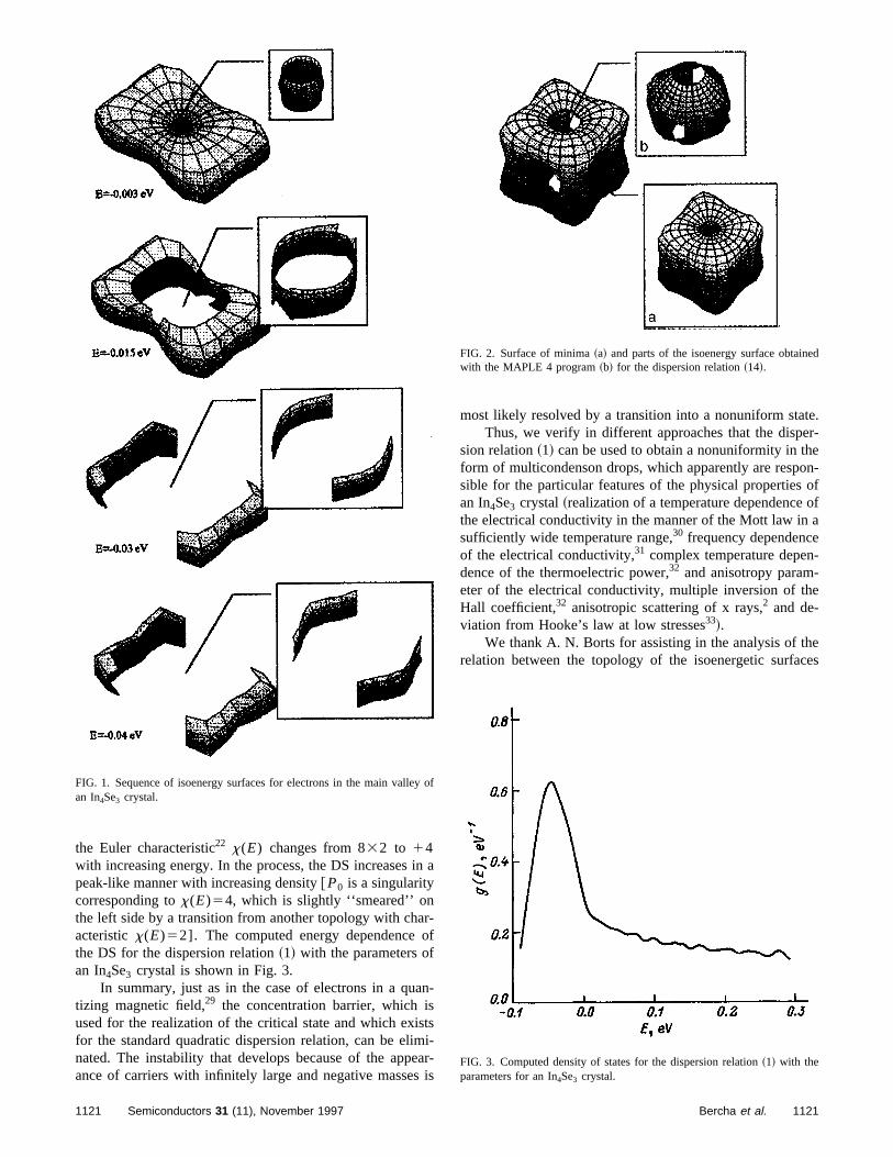
n
r
n
t
a
te.er-eon-ofofa
e-
-e
heces
ed
the Euler characteristic22 x(E) changes from 832 to 14with increasing energy. In the process, the DS increases ipeak-like manner with increasing density@P0 is a singularitycorresponding tox(E)54, which is slightly ‘‘smeared’’ onthe left side by a transition from another topology with chaacteristicx(E)52]. The computed energy dependence othe DS for the dispersion relation~1! with the parameters ofan In4Se3 crystal is shown in Fig. 3.
In summary, just as in the case of electrons in a quatizing magnetic field,29 the concentration barrier, which isused for the realization of the critical state and which exisfor the standard quadratic dispersion relation, can be elimnated. The instability that develops because of the appeance of carriers with infinitely large and negative masses
FIG. 1. Sequence of isoenergy surfaces for electrons in the main valleyan In4Se3 crystal.
1121 Semiconductors 31 (11), November 1997
a
-f
-
si-r-
is
most likely resolved by a transition into a nonuniform staThus, we verify in different approaches that the disp
sion relation~1! can be used to obtain a nonuniformity in thform of multicondenson drops, which apparently are respsible for the particular features of the physical propertiesan In4Se3 crystal~realization of a temperature dependencethe electrical conductivity in the manner of the Mott law insufficiently wide temperature range,30 frequency dependencof the electrical conductivity,31 complex temperature dependence of the thermoelectric power,32 and anisotropy parameter of the electrical conductivity, multiple inversion of thHall coefficient,32 anisotropic scattering of x rays,2 and de-viation from Hooke’s law at low stresses33!.
We thank A. N. Borts for assisting in the analysis of trelation between the topology of the isoenergetic surfa
of
FIG. 2. Surface of minima~a! and parts of the isoenergy surface obtainwith the MAPLE 4 program~b! for the dispersion relation~14!.
FIG. 3. Computed density of states for the dispersion relation~1! with theparameters for an In4Se3 crystal.
1121Bercha et al.
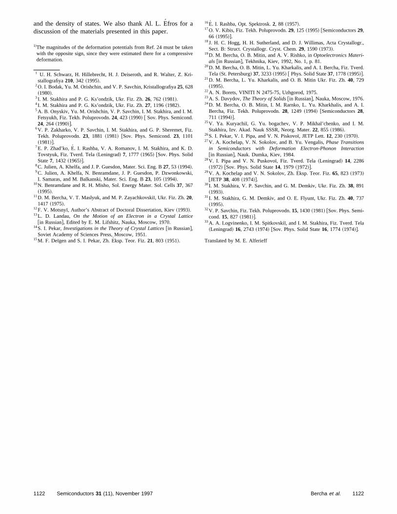
and the density of states. We also thank Al. L. E´ fros for a
kess
ri-
..
Fiz
.
sk
16E. I. Rashba, Opt. Spektrosk.2, 88 ~1957!.17O. V. Kibis, Fiz. Tekh. Poluprovodn.29, 125~1995! @Semiconductors29,
r.,
.
.
.
on
discussion of the materials presented in this paper.
1!The magnitudes of the deformation potentials from Ref. 24 must be tawith the opposite sign, since they were estimated there for a compredeformation.
1 U. H. Schwarz, H. Hillebrecht, H. J. Deiseroth, and R. Walter, Z. Kstallografiya210, 342 ~1995!.
2O. I. Bodak, Yu. M. Orishchin, and V. P. Savchin, Kristallografiya25, 628~1980!.
3I. M. Stakhira and P. G. Ks’ondzik, Ukr. Fiz. Zh.26, 762 ~1981!.4I. M. Stakhira and P. G. Ks’ondzik, Ukr. Fiz. Zh.27, 1196~1982!.5A. B. Onyskiv, Yu. M. Orishchin, V. P. Savchin, I. M. Stakhira, and I. MFetsyukh, Fiz. Tekh. Poluprovodn.24, 423~1990! @ Sov. Phys. Semicond24, 264 ~1990!#.
6V. P. Zakharko, V. P. Savchin, I. M. Stakhira, and G. P. Sheremet,Tekh. Poluprovodn.23, 1881 ~1981! @Sov. Phys. Semicond.23, 1101~1981!#.
7E. P. Zhad’ko, E´ . I. Rashba, V. A. Romanov, I. M. Stakhira, and K. DTovstyuk, Fiz. Tverd. Tela~Leningrad! 7, 1777~1965! @Sov. Phys. SolidState7, 1432~1965!#.
8C. Julien, A. Khelfa, and J. P. Guesdon, Mater. Sci. Eng. B27, 53 ~1994!.9C. Julien, A. Khelfa, N. Benramdane, J. P. Guesdon, P. DzwonkowI. Samaras, and M. Balkanski, Mater. Sci. Eng. B23, 105 ~1994!.
10N. Benramdane and R. H. Misho, Sol. Energy Mater. Sol. Cells37, 367~1995!.
11D. M. Bercha, V. T. Maslyuk, and M. P. Zayachkovski�, Ukr. Fiz. Zh.20,1417 ~1975!.
12F. V. Motsny�, Author’s Abstract of Doctoral Dissertation, Kiev~1993!.13L. D. Landau, On the Motion of an Electron in a Crystal Lattice
@in Russian#, Edited by E. M. Lifshitz, Nauka, Moscow, 1970.14S. I. Pekar,Investigations in the Theory of Crystal Lattices@in Russian#,
Soviet Academy of Sciences Press, Moscow, 1951.15M. F. De�gen and S. I. Pekar, Zh. E´ ksp. Teor. Fiz.21, 803 ~1951!.
1122 Semiconductors 31 (11), November 1997
nive
.
i,
66 ~1995!#.18J. H. C. Hogg, H. H. Sutherland, and D. J. Willimas, Acta Crystallog
Sect. B: Struct. Crystallogr. Cryst. Chem.29, 1590~1973!.19D. M. Bercha, O. B. Mitin, and A. V. Rishko, inOptoelectronics Materi-
als @in Russian#, Tekhnika, Kiev, 1992, No. 1, p. 81.20D. M. Bercha, O. B. Mitin, L. Yu. Kharkalis, and A. I. Bercha, Fiz. Tverd
Tela~St. Petersburg! 37, 3233~1995! @ Phys. Solid State37, 1778~1995!#.21D. M. Bercha, L. Yu. Kharkalis, and O. B. Mitin Ukr. Fiz. Zh.40, 729
~1995!.22A. N. Borets, VINITI N 2475-75, Uzhgorod, 1975.23A. S. Davydov,The Theory of Solids@in Russian#, Nauka, Moscow, 1976.24D. M. Bercha, O. B. Mitin, I. M. Rarnko, L. Yu. Kharkhalis, and A. I
Bercha, Fiz. Tekh. Poluprovodn.28, 1249 ~1994! @Semiconductors28,711 ~1994!#.
25V. Ya. Kuryachi�, G. Yu. bogachev, V. P. Mikhal’chenko, and I. MStakhira, Izv. Akad. Nauk SSSR, Neorg. Mater.22, 855 ~1986!.
26S. I. Pekar, V. I. Pipa, and V. N. Piskovo�, JETP Lett.12, 230 ~1970!.27V. A. Kochelap, V. N. Sokolov, and B. Yu. Vengalis,Phase Transitions
in Semiconductors with Deformation Electron-Phonon Interacti@in Russian#, Nauk. Dumka, Kiev, 1984.
28V. I. Pipa and V. N. Puskovo�, Fiz. Tverd. Tela~Leningrad! 14, 2286~1972! @Sov. Phys. Solid State14, 1979~1972!#.
29V. A. Kochelap and V. N. Sokolov, Zh. E´ ksp. Teor. Fiz.65, 823 ~1973!@JETP38, 408 ~1974!#.
30I. M. Stakhira, V. P. Savchin, and G. M. Demkiv, Ukr. Fiz. Zh.38, 891~1993!.
31I. M. Stakhira, G. M. Demkiv, and O. E. Flyunt, Ukr. Fiz. Zh.40, 737~1995!.
32V. P. Savchin, Fiz. Tekh. Poluprovodn.15, 1430~1981! @Sov. Phys. Semi-cond.15, 827 ~1981!#.
33A. A. Logvinenko, I. M. Spitkovski�, and I. M. Stakhira, Fiz. Tverd. Tela~Leningrad! 16, 2743~1974! @Sov. Phys. Solid State16, 1774~1974!#.
Translated by M. E. Alferieff
1122Bercha et al.
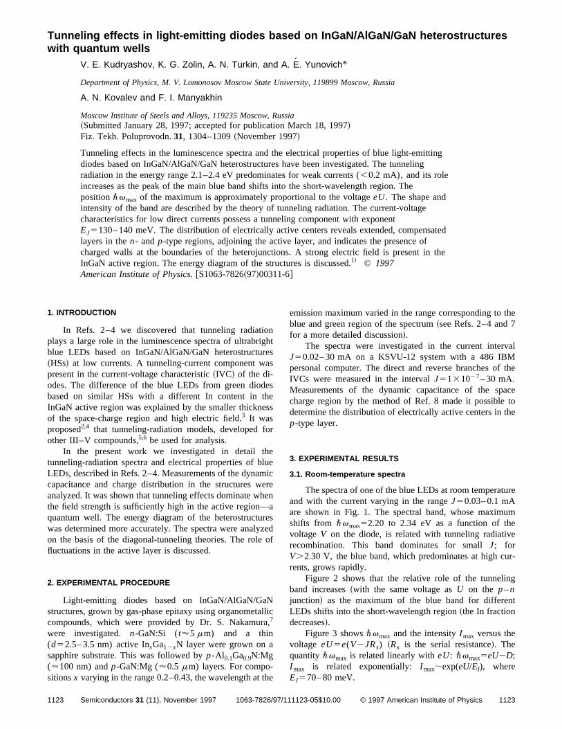
Tunneling effects in light-emitting diodes based on InGaN/AlGaN/GaN heterostructures
the
with quantum wellsV. E. Kudryashov, K. G. Zolin, A. N. Turkin, and A. E. Yunovich*
Department of Physics, M. V. Lomonosov Moscow State University, 119899 Moscow, Russia
A. N. Kovalev and F. I. Manyakhin
Moscow Institute of Steels and Alloys, 119235 Moscow, Russia~Submitted January 28, 1997; accepted for publication March 18, 1997!Fiz. Tekh. Poluprovodn.31, 1304–1309~November 1997!
Tunneling effects in the luminescence spectra and the electrical properties of blue light-emittingdiodes based on InGaN/AlGaN/GaN heterostructures have been investigated. The tunnelingradiation in the energy range 2.1–2.4 eV predominates for weak currents (,0.2 mA), and its roleincreases as the peak of the main blue band shifts into the short-wavelength region. Theposition\vmax of the maximum is approximately proportional to the voltageeU. The shape andintensity of the band are described by the theory of tunneling radiation. The current-voltagecharacteristics for low direct currents possess a tunneling component with exponentEJ5130– 140 meV. The distribution of electrically active centers reveals extended, compensatedlayers in then- andp-type regions, adjoining the active layer, and indicates the presence ofcharged walls at the boundaries of the heterojunctions. A strong electric field is present in theInGaN active region. The energy diagram of the structures is discussed.1! © 1997American Institute of Physics.@S1063-7826~97!00311-6#
1. INTRODUCTION emission maximum varied in the range corresponding to
onigreas
ehees
or
helume
heare
yzo
Nala,
th
val
the
aceto
he
ure
umee
ur-
ng
nt
/1
In Refs. 2–4 we discovered that tunneling radiatiplays a large role in the luminescence spectra of ultrabrblue LEDs based on InGaN/AlGaN/GaN heterostructu~HSs! at low currents. A tunneling-current component wpresent in the current-voltage characteristic~IVC! of the di-odes. The difference of the blue LEDs from green diodbased on similar HSs with a different In content in tInGaN active region was explained by the smaller thicknof the space-charge region and high electric field.3 It wasproposed2,4 that tunneling-radiation models, developed fother III–V compounds,5,6 be used for analysis.
In the present work we investigated in detail ttunneling-radiation spectra and electrical properties of bLEDs, described in Refs. 2–4. Measurements of the dynacapacitance and charge distribution in the structures wanalyzed. It was shown that tunneling effects dominate wthe field strength is sufficiently high in the active region—quantum well. The energy diagram of the heterostructuwas determined more accurately. The spectra were analon the basis of the diagonal-tunneling theories. The rolefluctuations in the active layer is discussed.
2. EXPERIMENTAL PROCEDURE
Light-emitting diodes based on InGaN/AlGaN/Gastructures, grown by gas-phase epitaxy using organometcompounds, which were provided by Dr. S. Nakamur7
were investigated. n-GaN:Si (t'5 mm) and a thin(d52.5– 3.5 nm) active InxGa12xN layer were grown on asapphire substrate. This was followed byp-Al0.1Ga0.9N:Mg('100 nm) andp-GaN:Mg ('0.5 mm) layers. For compo-sitionsx varying in the range 0.2–0.43, the wavelength at
1123 Semiconductors 31 (11), November 1997 1063-7826/97
hts
s
s
eicren
sedf
lic
e
blue and green region of the spectrum~see Refs. 2–4 and 7for a more detailed discussion!.
The spectra were investigated in the current interJ50.02– 30 mA on a KSVU-12 system with a 486 IBMpersonal computer. The direct and reverse branches ofIVCs were measured in the intervalJ5131027– 30 mA.Measurements of the dynamic capacitance of the spcharge region by the method of Ref. 8 made it possibledetermine the distribution of electrically active centers in tp-type layer.
3. EXPERIMENTAL RESULTS
3.1. Room-temperature spectra
The spectra of one of the blue LEDs at room temperatand with the current varying in the rangeJ50.03– 0.1 mAare shown in Fig. 1. The spectral band, whose maximshifts from \vmax52.20 to 2.34 eV as a function of thvoltage V on the diode, is related with tunneling radiativrecombination. This band dominates for smallJ; forV.2.30 V, the blue band, which predominates at high crents, grows rapidly.
Figure 2 shows that the relative role of the tunneliband increases~with the same voltage asU on the p–njunction! as the maximum of the blue band for differeLEDs shifts into the short-wavelength region~the In fractiondecreases!.
Figure 3 shows\vmax and the intensityI max versus thevoltage eU5e(V2JRs) ~Rs is the serial resistance!. Thequantity\vmax is related linearly witheU: \vmax5eU2D;I max is related exponentially:I max;exp(eU/EI), whereEI570– 80 meV.
112311123-05$10.00 © 1997 American Institute of Physics
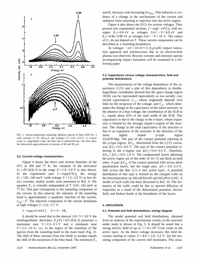
th
h
og
e
a
andRs decrease with increasing\vmax. This behavior is evi-and.ey
be
holeectral-
ca-e-gionon-ry
e. Into
is
e isthe
to
e-
ngothse
on
for-ofric
eduret a
de-
a-
o
3.2. Current-voltage characteristics
Figure 4 shows the direct and reverse branches ofIVC at 300 and 77 K; the variation of the derivativeEJ5dV/d(ln J) in the rangeU51.8– 3.0 V is also shown.In the exponential part J;exp(eU/EJ), the energyEJ5130– 140 meV~with voltageV51.5– 2.5 V! at low di-rect currents; similar results were presented in Ref. 9. TquantityEJ is virtually independent ofT ~155– 165 meV at77 K!. This part corresponds to the tunneling componentthe current. In this interval, the intensity of the tunnelinband is approximately a quadratic function of the currenI max;J2. The injection component of the current dominateat high voltagesV.2.6– 2.7 V:
J;exp~eU/mkT!; U5V2JRs .
It should be noted that in the interval 1.8,V,3.0 V thesemilogarithmic derivativeEJ(V)5dV/d(ln J) possesses amaximum near V52.3– 2.5 V and a minimum nearV52.5– 2.6 V, i.e., in the region of the transition of thspectra from the tunneling band to the main band~Fig. 2!.The shift of these extrema from one diode to another equthe shift of the maximum of the blue band. The minimumEJ
FIG. 1. Room-temperature tunneling radiation spectra of blue LED No.with currents J535– 100mA and voltagesV52.16– 2.34 V. a—Linearscale; b—logarithmic scale, the blue line is subtracted out. The dots shthe theoretical approximation at currents of 60 and 90mA.
1124 Semiconductors 31 (11), November 1997
e
e
f
t,s
ls
dence of a change in the mechanisms of the currentradiation from tunneling to injection into the active region
Figure 4 also shows the IVCs for reverse voltages. Thpossess two exponential sections,J;exp(2eV/EJ), with en-ergies EJ'0.6 eV at voltages 3.4,2V,6.8 eV andEJ'0.96– 0.98 eV at voltages 6.8,2V,10 V. The valuesof EJ do not depend onT. These current components candescribed as a tunneling breakdown.
At voltages2eV.10 eV'3•Eg(GaN) impact ioniza-tion appeared and luminescence due to an electron-plasma was observed. Reverse currents and emission spaccompanying impact ionization will be examined in a folowing paper.
3.3. Capacitance versus voltage characteristics, field andpotential distributions
The measurements of the voltage dependence of thepacitanceC(V) and a plot of this dependence in doubllogarithmic coordinates showed that the space charge re~SCR! can be represented equivalently as two serially cnected capacitances:Cn , whose magnitude depends velittle on the reciprocal of the voltage, andCp , which deter-mines the change in the capacitance of the entire structurthe absence of a bias voltage, the contribution of the SCRCn equals about 45% of the total width of the SCR. Thcapacitance is due to the charge in then-layer, whose expan-sion is limited by the strongly dopedn-region of the struc-ture. The change in the total capacitance of the structurdue to an expansion of the structure in the direction ofmore lightly doped p-type region~GaAlN:Mg!. The part of the contact potential referringthe p-type region,DVp , determined from theC(V) curves,was DVp'0.5– 0.6 V. The part of the contact potential rferring to the n-region wasDVn'0.450.5 V. Therefore,DVp1DVn'0.9– 1.0 V. The compensated layers adjoinithe active region are of the order of 10–15 nm thick on bsides. A partDVqn of the contact potential falls across thequasineutral layers, but the larger part,DVi'2.0– 2.4 V,falls across the thin~2.5–4 nm! active layer. A potentialdistribution of this type is formed by the charged wallsthe heterojunctions~p-AlGaN/InGaN and InGaN/n-GaN!. Amodel of such walls has been discussed in Ref. 10. Themation of the walls could be due to upward diffusionimpurities as a result of the deformation potential, electfield, and broken bonds at the boundaries of the layers.
4. DISCUSSION
4.1. Potential and field distributions; energy diagram
The model potential and field distributions, obtainfrom an analysis of the experimental results, in the structunder study is shown in Fig. 5. It should be noted thastrong electric field of up toE563106 V/cm exists in theactive layer. As the direct voltage increases, this fieldcreases starting at valuesU'DVi'2.0– 2.2 V, but the tun-neling component of the current still dominates. This situ
3
w
1124Kudryashov et al.
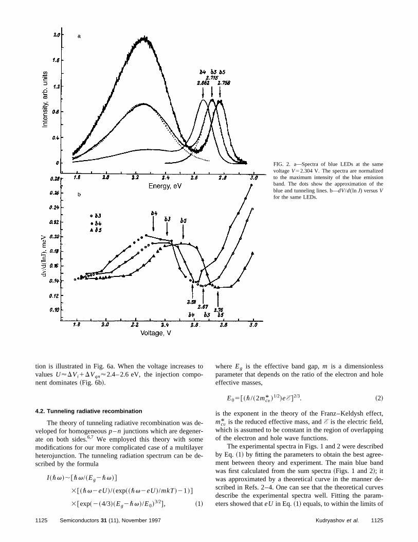
edne
FIG. 2. a—Spectra of blue LEDs at the samvoltageV52.304 V. The spectra are normalizeto the maximum intensity of the blue emissioband. The dots show the approximation of thblue and tunneling lines. b—dV/d(ln J) versusVfor the same LEDs.
tion is illustrated in Fig. 6a. When the voltage increases to-
e-eed
where Eg is the effective band gap,m is a dimensionlesshole
ct,
ing
bedee-and
de-rvesm-
valuesU'DVi1DVqn'2.4– 2.6 eV, the injection component dominates~Fig. 6b!.
4.2. Tunneling radiative recombination
The theory of tunneling radiative recombination was dveloped for homogeneousp–n junctions which are degenerate on both sides.6,7 We employed this theory with sommodifications for our more complicated case of a multilayheterojunction. The tunneling radiation spectrum can bescribed by the formula
I ~\v!;@\v/~Eg2\v!#
3@~\v2eU!/~exp~~\v2eU!/mkT!21!#
3@exp~2~4/3!~Eg2\v!/E0!3/2#, ~1!
1125 Semiconductors 31 (11), November 1997
-
re-
parameter that depends on the ratio of the electron andeffective masses,
E05@~\/~2mcv* !1/2!eE #2/3. ~2!
is the exponent in the theory of the Franz–Keldysh effemcv* is the reduced effective mass, andE is the electric field,which is assumed to be constant in the region of overlappof the electron and hole wave functions.
The experimental spectra in Figs. 1 and 2 were describy Eq. ~1! by fitting the parameters to obtain the best agrment between theory and experiment. The main blue bwas first calculated from the sum spectra~Figs. 1 and 2!; itwas approximated by a theoretical curve in the mannerscribed in Refs. 2–4. One can see that the theoretical cudescribe the experimental spectra well. Fitting the paraeters showed thateU in Eq. ~1! equals, to within the limits of
1125Kudryashov et al.
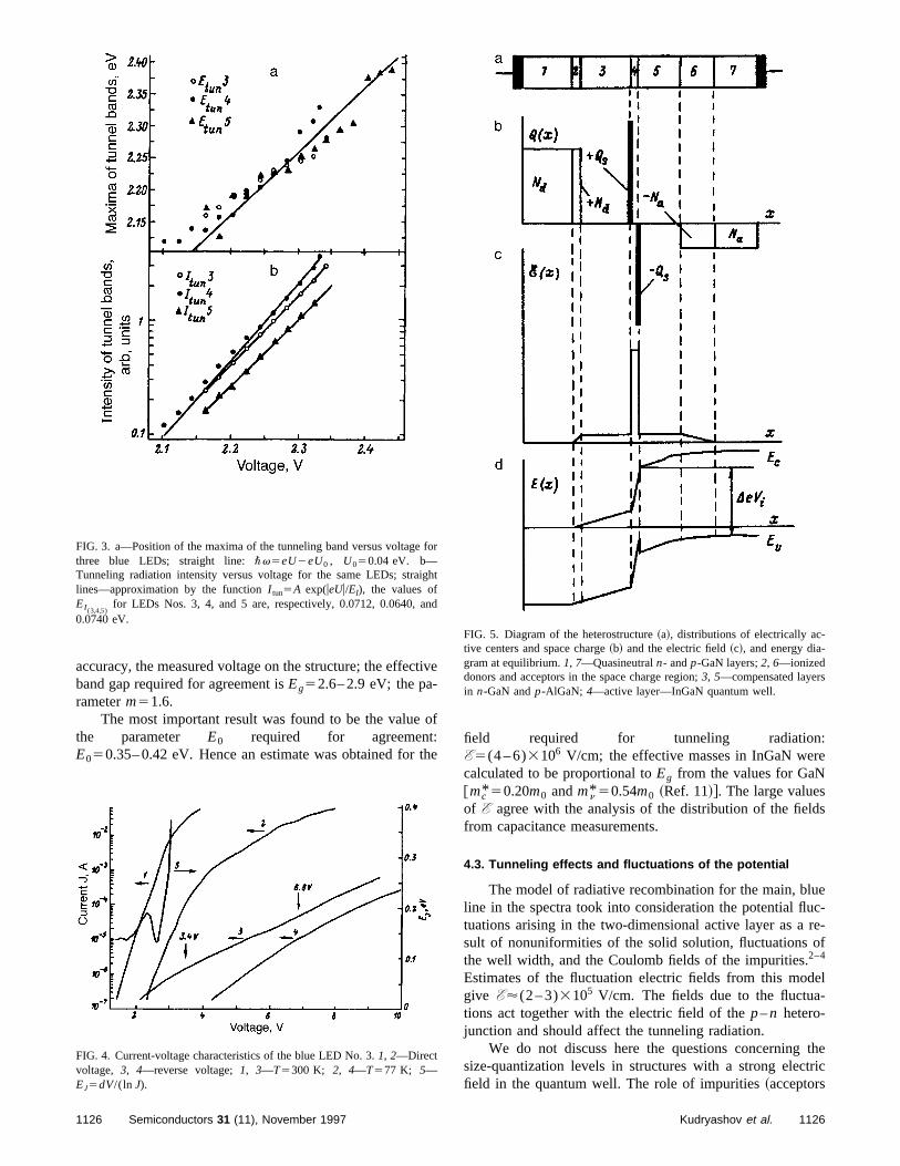
ct
o:th
:re
ds
uec-re-of
el-
thetric
fo
igh
an
accuracy, the measured voltage on the structure; the effeband gap required for agreement isEg52.6– 2.9 eV; the pa-rameterm51.6.
The most important result was found to be the valuethe parameter E0 required for agreementE050.35– 0.42 eV. Hence an estimate was obtained for
FIG. 3. a—Position of the maxima of the tunneling band versus voltagethree blue LEDs; straight line:\v5eU2eU0 , U050.04 eV. b—Tunneling radiation intensity versus voltage for the same LEDs; stralines—approximation by the functionI tun5A exp(ueUu/EI), the values ofEI (3,4,5)
for LEDs Nos. 3, 4, and 5 are, respectively, 0.0712, 0.0640,0.0740 eV.
FIG. 4. Current-voltage characteristics of the blue LED No. 3.1, 2—Directvoltage, 3, 4—reverse voltage;1, 3—T5300 K; 2, 4—T577 K; 5—EJ5dV/( ln J).
1126 Semiconductors 31 (11), November 1997
ive
f
efield required for tunneling radiationE5(4 – 6)3106 V/cm; the effective masses in InGaN wecalculated to be proportional toEg from the values for GaN@mc* 50.20m0 andmn* 50.54m0 ~Ref. 11!#. The large valuesof E agree with the analysis of the distribution of the fielfrom capacitance measurements.
4.3. Tunneling effects and fluctuations of the potential
The model of radiative recombination for the main, blline in the spectra took into consideration the potential flutuations arising in the two-dimensional active layer as asult of nonuniformities of the solid solution, fluctuationsthe well width, and the Coulomb fields of the impurities.2–4
Estimates of the fluctuation electric fields from this modgive E'(2 – 3)3105 V/cm. The fields due to the fluctuations act together with the electric field of thep–n hetero-junction and should affect the tunneling radiation.
We do not discuss here the questions concerningsize-quantization levels in structures with a strong elecfield in the quantum well. The role of impurities~acceptors
r
t
d
FIG. 5. Diagram of the heterostructure~a!, distributions of electrically ac-tive centers and space charge~b! and the electric field~c!, and energy dia-gram at equilibrium.1, 7—Quasineutraln- andp-GaN layers;2, 6—ionizeddonors and acceptors in the space charge region;3, 5—compensated layersin n-GaN andp-AlGaN; 4—active layer—InGaN quantum well.
1126Kudryashov et al.
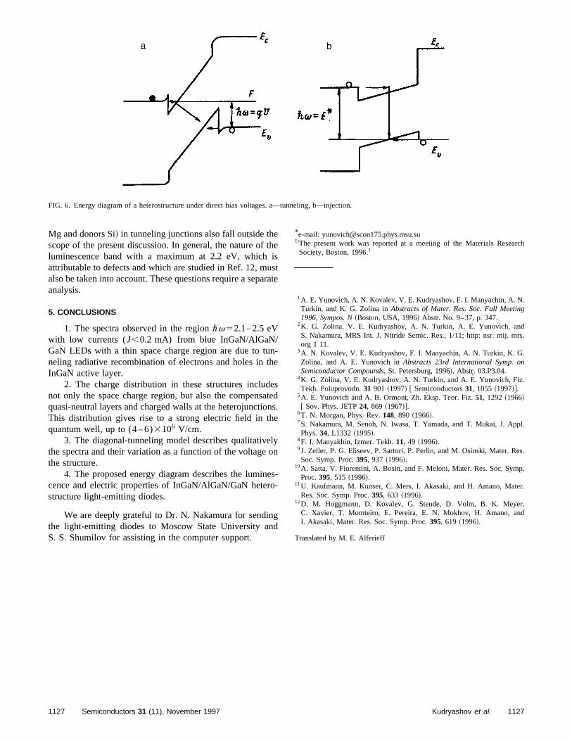
*
FIG. 6. Energy diagram of a heterostructure under direct bias voltages. a—tunneling, b—injection.
Mg and donors Si! in tunneling junctions also fall outside thef tiua
unth
eaonhe
elo
ero
ngnd
e-mail: [email protected]! arch
.g
rs.
.n
pl.
es.
p.
er.
r,d
scope of the present discussion. In general, the nature oluminescence band with a maximum at 2.2 eV, whichattributable to defects and which are studied in Ref. 12, malso be taken into account. These questions require a sepanalysis.
5. CONCLUSIONS
1. The spectra observed in the region\v52.1– 2.5 eVwith low currents (J,0.2 mA) from blue InGaN/AlGaN/GaN LEDs with a thin space charge region are due to tneling radiative recombination of electrons and holes inInGaN active layer.
2. The charge distribution in these structures includnot only the space charge region, but also the compensquasi-neutral layers and charged walls at the heterojunctiThis distribution gives rise to a strong electric field in tquantum well, up to (4 – 6)3106 V/cm.
3. The diagonal-tunneling model describes qualitativthe spectra and their variation as a function of the voltagethe structure.
4. The proposed energy diagram describes the lumincence and electric properties of InGaN/AlGaN/GaN hetestructure light-emitting diodes.
We are deeply grateful to Dr. N. Nakamura for sendithe light-emitting diodes to Moscow State University aS. S. Shumilov for assisting in the computer support.
1127 Semiconductors 31 (11), November 1997
hesstrate
-e
steds.
yn
s--
The present work was reported at a meeting of the Materials ReseSociety, Boston, 1996.1
1A. E. Yunovich, A. N. Kovalev, V. E. Kudryashov, F. I. Manyachin, A. NTurkin, and K. G. Zolina inAbstracts of Mater. Res. Soc. Fall Meetin1996, Sympos. N~Boston, USA, 1996! Abstr. No. 9–37, p. 347.
2K. G. Zolina, V. E. Kudryashov, A. N. Turkin, A. E. Yunovich, andS. Nakamura, MRS Int. J. Nitride Semic. Res., 1/11; http: nsr. mij. morg 1 11.
3A. N. Kovalev, V. E. Kudryashov, F. I. Manyachin, A. N. Turkin, K. GZolina, and A. E. Yunovich inAbstracts 23rd International Symp. oSemiconductor Compounds, St. Petersburg, 1996!, Abstr. 03.P3.04.
4K. G. Zolina, V. E. Kudryashov, A. N. Turkin, and A. E´ . Yunovich, Fiz.Tekh. Poluprovodn.31 901 ~1997! @ Semiconductors31, 1055~1997!#.
5A. E. Yunovich and A. B. Ormont, Zh. E´ ksp. Teor. Fiz.51, 1292~1966!@ Sov. Phys. JETP24, 869 ~1967!#.
6T. N. Morgan, Phys. Rev.148, 890 ~1966!.7S. Nakamura, M. Senoh, N. Iwasa, T. Yamada, and T. Mukai, J. ApPhys.34, L1332 ~1995!.
8F. I. Manyakhin, Izmer. Tekh.11, 49 ~1996!.9J. Zeller, P. G. Eliseev, P. Sartori, P. Perlin, and M. Osinski, Mater. RSoc. Symp. Proc.395, 937 ~1996!.
10A. Satta, V. Fiorentini, A. Bosin, and F. Meloni, Mater. Res. Soc. SymProc.395, 515 ~1996!.
11U. Kaufmann, M. Kunser, C. Mers, I. Akasaki, and H. Amano, MatRes. Soc. Symp. Proc.395, 633 ~1996!.
12D. M. Hoggmann, D. Kovalev, G. Steude, D. Volm, B. K. MeyeC. Xavier, T. Momteiro, E. Pereira, E. N. Mokhov, H. Amano, anI. Akasaki, Mater. Res. Soc. Symp. Proc.395, 619 ~1996!.
Translated by M. E. Alferieff
1127Kudryashov et al.
Electron-structural metastability of cationic donor centers in GaAs
D. E. Onopko and A. I. RyskinAll-Russia Science Center ‘‘S. I. Vavilov State Optics Institute’’ 199034 St. Petersburg, Russia
N. T. Bagraev
A. F. Ioffe Physicotechnical Institute, Russian Academy of Sciences 194021 St. Petersburg, Russia~Submitted February 27 1997; accepted April 10 1997!Fiz. Tekh. Poluprovodn.31, 1310–1313~November 1997!
The reconstruction of shallow donors in GaAs–Ga12xAl xAs crystals, which is accompanied bythe formation of deep cationicDX centers, is studied for the first time in a clusterapproximation using the self-consistent, scattered-wave method. It is demonstrated that theformation of aC3n DX2 state could be due to the difference in the electronic structure of a shallowdonor from the structure of a lattice atom. This difference is the reason why an impurityatom transfers into the nearest tetrahedral interstice. The model proposed for cationicDX centersis based on the fundamental possibility of localization of two antibonding electrons on anantobonding orbital of one of the four tetrahedral bonds of an impurity center with arsenic ligands.This greatly weakens the bond and results in a corresponding formation of a trigonalDX2
state. © 1997 American Institute of Physics.@S1063-7826~97!00411-0#
1. INTRODUCTION lattice sites into positions of tetrahedral interstices.5–8 Such
ort
reofohe–Vteoohle
rouaso-,rethhethiii
ibu
drenVw
bid
m
ors,
mi-er-rllow
ellk
hengintheemesticsex-ten-
eraltheof
ofis-
/1
The formation of substitution centers in semiconductin many cases is accompanied by a reconstruction of bothimpurity ion and the surrounding lattice atoms. This isflected in a corresponding lowering of the full symmetrythe defect. The possible crystallographic avenues for recstruction of impurity centers as a result of relaxation of tcrystal lattice of elementary semiconductors as well as IIIand II–VI compounds have been studied in the clusapproximation.1–4 The self-consistent scattered-wave methmade it possible to determine the most likely symmetrythe defect and substantiate its metastable properties, warise as a result of the distinguishing features of the etronic structures of the impurity ion and lattice atom.1–4
If the electronic structures of the impurity atom diffesubstantially from that of a lattice atom, then a spontanereconstruction of a substitution center is accompanied,rule, by a lowering of its symmetry from tetrahedral to trignal (C3n) or orthorhombic (C2n).1 In the opposite casewhen the electronic structure of the impurity center corsponds to the structure of the corresponding fragment ofregular crystal, the tetrahedral symmetry of a defect eitdoes not change at all or it changes slightly as a result ofJahn–Teller effect. However, even when the differencethe electronic structures of the impurity and lattice atomssmall, as is the case, for example, for shallow donorssemiconductors, there is a potential for the above-descrreconstruction of the impurity substitution center to occunder the influence of external perturbations, such as hystatic and uniaxial compression of the crystal or isovaldoping, for the purpose of obtaining solid solutions of III–and II–VI semiconductors. The reconstruction of shallodonors, which thus far has been studied within the capaties of the pseudopotential and density functional methoconsists of the formation of deep, negatively chargedC3n
centers as a result of transition of the impurity ions fro
1128 Semiconductors 31 (11), November 1997 1063-7826/97
she-
n-
rdfichc-
sa
-ere
nsnedro-t
li-s,
amphoteric defects, formed on the basis of shallow donare so-calledDX centers,9 which are metastable impuritycenters with negative correlation energy~negativeU cen-ters!, which tunnel, in a charge transfer process, in the seconductor lattice between positions corresponding to diffent symmetries.8,10–14 A direct consequence of theiappearance is self-compensation in the system of shadonors: 2d0→DX21d1 ~where DX2 is the state corre-sponding to the reconstructed, negatively chargedC3n cen-ter, andd0 and d1 are the filled and ionized states of thtetrahedral shallow donor!, which determines the electricaproperties induced by Fermi level pinning of both buGa12xAl xAs crystals5,15 and GaAs–Ga12xAl xAs-typesuperlattices.16
In our study we have examined for the first time, treconstruction of shallow donors, which stimulates loweriof the symmetry of an impurity center, from the standpoof the difference in their electronic structure from that of tregular lattice atoms. This method for studying the problof the reconstruction of impurity substitution centers donot make it possible to determine the energy characterisof the deep defects that appear. This is achieved, forample, in calculations of metastable centers by pseudopotial and density functional methods.6,8,12,13 However, themethod employed makes it possible to establish the genquantum-mechanical foundations of the reconstruction ofimpurity centers and directly relate them to the symmetrythe reconstructed point defects.
2. CATIONIC DONOR SILICON AND TIN CENTERS IN GaASAND Ga12xAl xAs
Cationic donor centers form in GaAs in the processintroducing group-IV impurities. The electronic charge dtribution on the valence orbitals ofAB4
3q2 clusters (q is theabsolute magnitude of the ion charge! shows that SiGa sub-
112811128-04$10.00 © 1997 American Institute of Physics
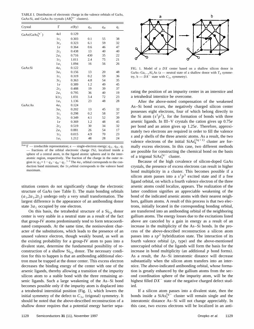
ni
en
fadihafla
rei-ectrthityaronnt
op
nd
edterto
5
cetwo
odsasis
Asghera
eethe
theigh-ec-al,ingted
f ano-tomsde
seer-a-
ec-ed-
the
Innti-
TABLE I. Distribution of electronic charge in the valence orbitals of GaAs,GaAs:Si, and GaAs:As crystals (AB4
3q2 clusters!.
ntere
-d
in
stitution centers do not significantly change the electrostructure of GaAs~see Table I!. The main bonding orbitals(a1,2a1,2t2) undergo only a very small transformation. Thlargest difference is the appearance of an antibonding dostate 3a1 occupied by one electron.
On this basis, the tetrahedral structure of a SiGa donorcenter is very stable in a neutral state as a result of thethat group-IV atoms predominantly tend to form tetracoornated compounds. At the same time, the nonisovalent cacter of the substitutions, which leads to the presence ounused valence electron, though weakly bound, as welthe existing probability for a group-IV atom to pass intodivalent state, determine the fundamental possibility ofconstruction of a shallow SiGa donor. The necessary condtion for this to happen is that an antibonding additional eltron must be trapped at the donor center. This excess elecdecreases the binding energy of the center with one ofarsenic ligands, thereby allowing a transition of the impursilicon atom to a stable bond with the three remainingsenic ligands. Such a large weakening of the As–Si bbecomes possible only if the impurity atom is displaced ia tetrahedral interstitial position~Fig. 1!, which lowers theinitial symmetry of the defect toC3n ~trigonal! symmetry. Itshould be noted that the above-described reconstructionshallow donor requires that a potential energy barrier se
Crystal G «~Ry! qA qB qi
GaAs~GaAs43q2
) 4a1 0.129
1t1 0.303 0.1 55 383t2 0.323 6.1 59 321e 0.364 0.6 46 472t2 0.438 13 40 402a1 0.716 430 35 221t2 1.011 2.4 75 211a1 1.094 16 56 26
GaAs:Si 4a1 0.1223a1 0.156 13 20 481t1 0.319 0.2 59 363t2 0.363 4.8 54 351e 0.389 1.2 49 452t2 0.488 19 39 372a1 0.795 36 40 19k1t2 1.031 3.4 72 231a1 1.136 23 48 28
GaAs:As 4a1 0.1243a1 0.202 13 45 321t1 0.298 0.2 58 373t2 0.349 4.1 52 391e 0.369 1.2 48 452t2 0.519 30 34 322a1 0.881 26 54 171t2 0.015 4.9 70 231a1 1.212 48 28 24
Note:G — irreducible representation;« — single-electron energy;qA , qB , qi— fractions of the orbital electronic charge~%!, localized inside asphere of a central atom, in the ligand atomic spheres and in the iatomic region, respectively. The fraction of the charge in the outergion is:qui512qA2qB2qi .1–3 The 4a1 orbital corresponds to the conduction band minimum; the 1t1orbital corresponds to the valence banmaximum.
1129 Semiconductors 31 (11), November 1997
c
or
ct-r-
anas
-
-one
-d
o
f aa-
rating the position of an impurity center in an interstice aa tetrahedral interstice be overcome.
After the above-noted compensation of the weakenAs–Si bond occurs, the negatively charged silicon cenpossesses eight electrons, four of which belong directlythe Si atom (s2p2), for the formation of bonds with threearsenic ligands. In III–V crystals the cation gives up 0.7eper bond and an anion gives up 1.25e. Therefore, approxi-mately two electrons are required in order to fill the valens andp shells of the three arsenic atoms. As a result, thevalence electrons of the initial SiAs4
(3q11) cluster are for-mally excess electrons. In this case, two different methare possible for constructing the chemical bond on the bof a trigonal SiAs3
2q2 cluster.Because of the high covalence of silicon-doped Ga
crystals, the presence of excess electrons can result in hibond multiplicity in a cluster. This becomes possible ifsilicon atom passes into as1p3 excited state and if a freeligand orbital, on which a fourth valence electron of the thrarsenic atoms could localize, appears. The realization oflatter condition signifies an appreciable weakening ofbond of the indicated arsenic atoms with their nearest nebors, gallium atoms. A result of this process is that two eltrons, initially located in the corresponding bonding orbitare transferred into an antibonding orbital of the neighborgallium atoms. The energy losses due to the excitations lisabove are canceled by a gain in energy as a result oincrease in the multiplicity of the As–Si bonds. In the prcess of the above-described reconstruction a silicon apasses into asp2 hybridization state. The interaction of itfourth valence orbital (pz type! and the above-mentioneunoccupied orbital of the ligands will form the basis for thincrease in bond multiplicity~an additionalp bond forms!.As a result, the As–Si interatomic distance will decreasubstantially when the silicon atom transfers into an intstice. The above-indicated antibonding orbital, whose formtion is greatly enhanced by the gallium atoms from the sond coordination sphere of the impurity atom, will be thhighest filledDX2 state of the negative charged defect stuied.
If a silicon atom passes into a divalent state, thenbonds inside a SiAs3
2q2 cluster will remain single and theinteratomic distance As–Si will not change appreciably.this case, two excess electrons will be localized in an a
r--
FIG. 1. Model of a DX center based on a shallow silicon donorGaAs–Ga12xAl xAs ~a — neutral state of a shallow donor withTd symme-try, b — DX2 state withC3n symmetry!.
1129Onopko et al.
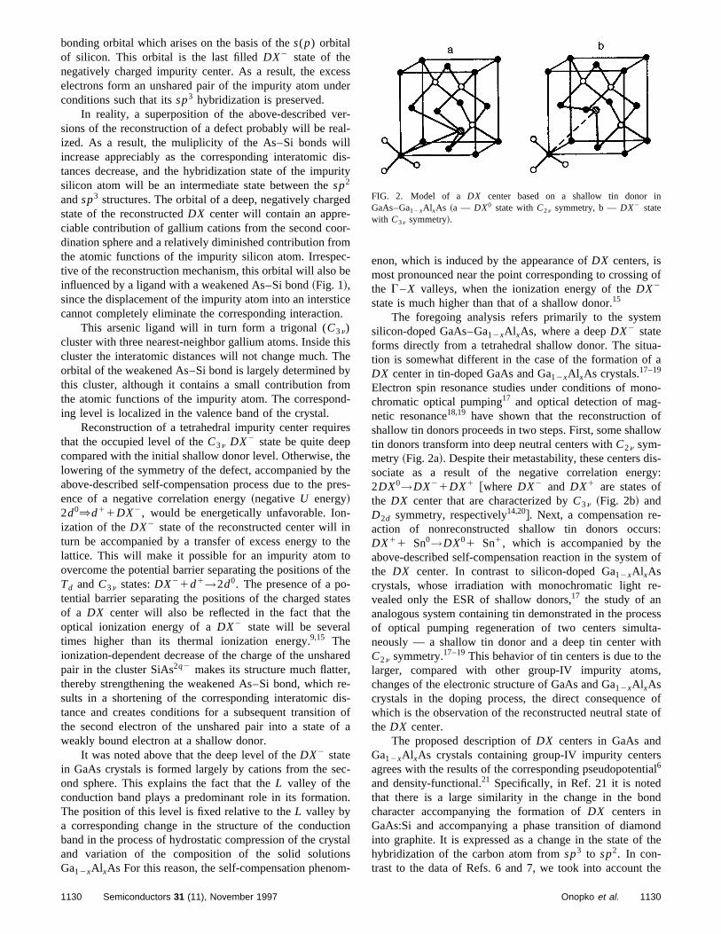
bonding orbital which arises on the basis of thes(p) orbital2
esde
eralilldr
e-ormcbe
ticn.
thhbmd
re
hethpr
-in
toth-ate
l
ar,risnof
ec
on
tiostnsm
g of
m
a-f a
no--ofllow
is-gy:
-rs:
of
e-
cessta-thes,
ofe of
stial
nd
ondthe
the
n
of silicon. This orbital is the last filledDX state of thenegatively charged impurity center. As a result, the excelectrons form an unshared pair of the impurity atom unconditions such that itssp3 hybridization is preserved.
In reality, a superposition of the above-described vsions of the reconstruction of a defect probably will be reized. As a result, the muliplicity of the As–Si bonds wincrease appreciably as the corresponding interatomictances decrease, and the hybridization state of the impusilicon atom will be an intermediate state between thesp2
andsp3 structures. The orbital of a deep, negatively chargstate of the reconstructedDX center will contain an appreciable contribution of gallium cations from the second codination sphere and a relatively diminished contribution frothe atomic functions of the impurity silicon atom. Irrespetive of the reconstruction mechanism, this orbital will alsoinfluenced by a ligand with a weakened As–Si bond~Fig. 1!,since the displacement of the impurity atom into an interscannot completely eliminate the corresponding interactio
This arsenic ligand will in turn form a trigonal (C3n)cluster with three nearest-neighbor gallium atoms. Insidecluster the interatomic distances will not change much. Torbital of the weakened As–Si bond is largely determinedthis cluster, although it contains a small contribution frothe atomic functions of the impurity atom. The corresponing level is localized in the valence band of the crystal.
Reconstruction of a tetrahedral impurity center requithat the occupied level of theC3n DX2 state be quite deepcompared with the initial shallow donor level. Otherwise, tlowering of the symmetry of the defect, accompanied byabove-described self-compensation process due to theence of a negative correlation energy~negativeU energy!2d0⇒d11DX2, would be energetically unfavorable. Ionization of theDX2 state of the reconstructed center willturn be accompanied by a transfer of excess energy tolattice. This will make it possible for an impurity atom tovercome the potential barrier separating the positions ofTd andC3n states:DX21d1→2d0. The presence of a potential barrier separating the positions of the charged stof a DX center will also be reflected in the fact that thoptical ionization energy of aDX2 state will be severatimes higher than its thermal ionization energy.9,15 Theionization-dependent decrease of the charge of the unshpair in the cluster SiAs2q2 makes its structure much flattethereby strengthening the weakened As–Si bond, whichsults in a shortening of the corresponding interatomic dtance and creates conditions for a subsequent transitiothe second electron of the unshared pair into a stateweakly bound electron at a shallow donor.
It was noted above that the deep level of theDX2 statein GaAs crystals is formed largely by cations from the sond sphere. This explains the fact that theL valley of theconduction band plays a predominant role in its formatiThe position of this level is fixed relative to theL valley bya corresponding change in the structure of the conducband in the process of hydrostatic compression of the cryand variation of the composition of the solid solutioGa12xAl xAs For this reason, the self-compensation pheno
1130 Semiconductors 31 (11), November 1997
sr
--
is-ity
d
-
-
e
isey
-
s
ees-
he
e
es
red
e--ofa
-
.
nal
-
enon, which is induced by the appearance ofDX centers, ismost pronounced near the point corresponding to crossinthe G –X valleys, when the ionization energy of theDX2
state is much higher than that of a shallow donor.15
The foregoing analysis refers primarily to the systesilicon-doped GaAs–Ga12xAl xAs, where a deepDX2 stateforms directly from a tetrahedral shallow donor. The sitution is somewhat different in the case of the formation oDX center in tin-doped GaAs and Ga12xAl xAs crystals.17–19
Electron spin resonance studies under conditions of mochromatic optical pumping17 and optical detection of magnetic resonance18,19 have shown that the reconstructionshallow tin donors proceeds in two steps. First, some shatin donors transform into deep neutral centers withC2n sym-metry ~Fig. 2a!. Despite their metastability, these centers dsociate as a result of the negative correlation ener2DX0→DX21DX1 @where DX2 and DX1 are states ofthe DX center that are characterized byC3n ~Fig. 2b! andD2d symmetry, respectively14,20#. Next, a compensation reaction of nonreconstructed shallow tin donors occuDX11 Sn0→DX01 Sn1, which is accompanied by theabove-described self-compensation reaction in the systemthe DX center. In contrast to silicon-doped Ga12xAl xAscrystals, whose irradiation with monochromatic light rvealed only the ESR of shallow donors,17 the study of ananalogous system containing tin demonstrated in the proof optical pumping regeneration of two centers simulneously — a shallow tin donor and a deep tin center wiC2n symmetry.17–19This behavior of tin centers is due to thlarger, compared with other group-IV impurity atomchanges of the electronic structure of GaAs and Ga12xAl xAscrystals in the doping process, the direct consequencewhich is the observation of the reconstructed neutral statthe DX center.
The proposed description ofDX centers in GaAs andGa12xAl xAs crystals containing group-IV impurity centeragrees with the results of the corresponding pseudopoten6
and density-functional.21 Specifically, in Ref. 21 it is notedthat there is a large similarity in the change in the bocharacter accompanying the formation ofDX centers inGaAs:Si and accompanying a phase transition of diaminto graphite. It is expressed as a change in the state ofhybridization of the carbon atom fromsp3 to sp2. In con-trast to the data of Refs. 6 and 7, we took into account
FIG. 2. Model of a DX center based on a shallow tin donor iGaAs–Ga12xAl xAs ~a — DX0 state withC2n symmetry, b —DX2 statewith C3n symmetry!.
1130Onopko et al.
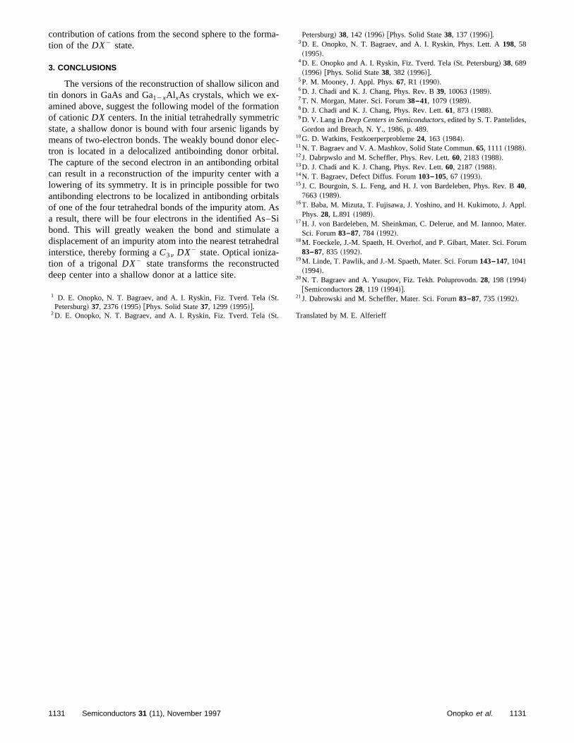
contribution of cations from the second sphere to the forma-2
nd
ioicb
lealita
oalAS
dr
ed
Petersburg! 38, 142 ~1996! @Phys. Solid State38, 137 ~1996!#.3D. E. Onopko, N. T. Bagraev, and A. I. Ryskin, Phys. Lett. A198, 58
,
pl.
ter.
rum
tion of theDX state.
3. CONCLUSIONS
The versions of the reconstruction of shallow silicon atin donors in GaAs and Ga12xAl xAs crystals, which we ex-amined above, suggest the following model of the formatof cationicDX centers. In the initial tetrahedrally symmetrstate, a shallow donor is bound with four arsenic ligandsmeans of two-electron bonds. The weakly bound donor etron is located in a delocalized antiboinding donor orbitThe capture of the second electron in an antibonding orbcan result in a reconstruction of the impurity center withlowering of its symmetry. It is in principle possible for twantibonding electrons to be localized in antibonding orbitof one of the four tetrahedral bonds of the impurity atom.a result, there will be four electrons in the identified As–bond. This will greatly weaken the bond and stimulatedisplacement of an impurity atom into the nearest tetraheinterstice, thereby forming aC3n DX2 state. Optical ioniza-tion of a trigonalDX2 state transforms the reconstructdeep center into a shallow donor at a lattice site.
1 D. E. Onopko, N. T. Bagraev, and A. I. Ryskin, Fiz. Tverd. Tela~St.Petersburg! 37, 2376~1995! @Phys. Solid State37, 1299~1995!#.
2D. E. Onopko, N. T. Bagraev, and A. I. Ryskin, Fiz. Tverd. Tela~St.
1131 Semiconductors 31 (11), November 1997
n
yc-.al
ssiaal
~1995!.4D. E. Onopko and A. I. Ryskin, Fiz. Tverd. Tela~St. Petersburg! 38, 689~1996! @Phys. Solid State38, 382 ~1996!#.
5P. M. Mooney, J. Appl. Phys.67, R1 ~1990!.6D. J. Chadi and K. J. Chang, Phys. Rev. B39, 10063~1989!.7T. N. Morgan, Mater. Sci. Forum38–41, 1079~1989!.8D. J. Chadi and K. J. Chang, Phys. Rev. Lett.61, 873 ~1988!.9D. V. Lang inDeep Centers in Semiconductors, edited by S. T. PantelidesGordon and Breach, N. Y., 1986, p. 489.
10G. D. Watkins, Festkoerperprobleme24, 163 ~1984!.11N. T. Bagraev and V. A. Mashkov, Solid State Commun.65, 1111~1988!.12J. Dabrpwslo and M. Scheffler, Phys. Rev. Lett.60, 2183~1988!.13D. J. Chadi and K. J. Chang, Phys. Rev. Lett.60, 2187~1988!.14N. T. Bagraev, Defect Diffus. Forum103–105, 67 ~1993!.15J. C. Bourgoin, S. L. Feng, and H. J. von Bardeleben, Phys. Rev. B40,
7663 ~1989!.16T. Baba, M. Mizuta, T. Fujisawa, J. Yoshino, and H. Kukimoto, J. Ap
Phys.28, L.891 ~1989!.17H. J. von Bardeleben, M. Sheinkman, C. Delerue, and M. Iannoo, Ma
Sci. Forum83–87, 784 ~1992!.18M. Foeckele, J.-M. Spaeth, H. Overhof, and P. Gibart, Mater. Sci. Fo
83–87, 835 ~1992!.19M. Linde, T. Pawlik, and J.-M. Spaeth, Mater. Sci. Forum143–147, 1041
~1994!.20N. T. Bagraev and A. Yusupov, Fiz. Tekh. Poluprovodn.28, 198 ~1994!
@Semiconductors28, 119 ~1994!#.21J. Dabrowski and M. Scheffler, Mater. Sci. Forum83–87, 735 ~1992!.
Translated by M. E. Alferieff
1131Onopko et al.
Optical properties of thin n -Pb12xSnxSe/BaF2 epitaxial layers in the plasmon–phonon
ated
interaction regionA. A. Kopylov, V. A. Moshnikov, and A. N. Kholodilov
St. Petersburg State Electrical Engineering University, 197376 St. Petersburg, Russia~Submitted September 20, 1995; accepted for publication April 24, 1997!Fiz. Tekh. Poluprovodn.31, 1314–1320~November 1997!
The optical reflection and transmission spectra of submicron epitaxial Pb12xSnxSe/BaF2 layerswith x50.04– 0.21 have been investigated. The parameters of the electron plasma aredetermined by modeling the shape of the spectra. The interband contribution to the dielectricfunction of Pb12xSnxSe is estimated. ©1997 American Institute of Physics.@S1063-7826~97!00711-4#
The band structure and the optical and electrical proper-surface treatment of the samples was performed. Repe
wio
ll
apimantht
foioo
tio,t
3M
ododyemp
th0iet otsia
t the
om-ater.
ctra. Aruc-
ee
theolid
-nd
ter,os-
btainentaln ingree
/1
ties of the lead chalcogenides PbTe, PbSe, and PbS asas the solid solutions Pb12xSnxTe, which are widely used inpractice, have now been well studied.1–3 The properties ofsolid solutions in the system Pb12xSnxSe have been givenmuch less attention.
In this study we have investigated, the optical reflectand transmission spectra of micron-thickn-Pb12xSnxSe ep-itaxial layers withx50.04– 0.21 on BaF2 substrates by usingthe method of infrared-range Fourier spectroscopy.
1. SAMPLES AND MEASUREMENT PROCEDURE
The Pb12xSnxSe layers were grown by the hot-wamethod on fresh cleavage faces of BaF2 substrates with111&orientation. Growth was conducted in an URM 3279011paratus. The construction of the evaporation chamber is slar to that described in Ref. 4. S-0000 lead, ultrapure tin,analytically pure selenium were employed to synthesizeinitial charge. Prior to growth, the charge was subjectedhomogenizing isothermal annealing at 850–1000 K8–10 h under dynamic vacuum conditions. The compositof the initial charge varied in the range 0.1–0.2 of the mlecular fraction of SnSe. The temperatures in the sublimaand substrate zones were equal to 770 and 500–550 Kspectively. The growth rate of the layers was equal0.7–1.0mm/h.
The layers grown possessed^100& orientation. The com-position of the solid solution was measured on a DRON-diffractometer. A tube with a copper anode~Cu Ka radia-tion! was used. In the operating regime of the tube, the anpotential was equal to 30–35 mV and 15–35 mA the ancurrent was equal to, depending on the thickness of the laThe uniformity of the composition of the layers was checkby x-ray spectral microanalysis on a Cameca MS-46croanalyzer. The basic characteristics of the samples aresented in Table I.
The measurements of the optical reflection spectra inrange 30– 650 cm21 were performed at temperatures of 180, and 300 K using a LFS-1000 long-wavelength Fourspectrometer5. The samples were secured on the cold duca nitrogen or helium vacuum cryostat. The measuremenT'10 K were performed with a R-118 cryostat. No spec
1132 Semiconductors 31 (11), November 1997 1063-7826/97
ell
n
-i-deorn-nre-o
ee
er.di-re-
e,rfatl
measurements performed every few months showed thashape of the reflection spectra was stable.
The transmission spectra in the range 500– 2700 cm21
were measured on a LAFS-02 rapid-scan Fourier spectreter at temperatures of 300–520 K using a resistance he
2. ANALYSIS OF THE SHAPE OF THE REFLECTIONSPECTRA
Figures 1 and 2 show examples of the reflection speof the experimental samples at different temperaturescharacteristic feature of all spectra is the presence of stture, due to a band of residual rays from BaF2, in the region150– 350 cm21. The sharp drop in the frequency rangabove 300 cm21 is due to plasma oscillations of free chargcarriers. An appreciable peak near 40 cm21, due to trans-verse optical phonons in the solid solution Pb12xSnxSe, isalso observed for all samples.
The analysis of the reflection spectra was based onmodel of an ‘‘epitaxial layer on a semiinfinite substrate.’’ Tdescribe the dispersion of the refractive index of the sosolution we used a dielectric function of the form
«~v!5«`2«`vp
2
v~v1 i /t!1
SvT2
vT22v22 ivg
, ~1!
wherev is the frequency,«` is the high-frequency permittivity, vp andt are, respectively, the plasma frequency arelaxation time of free charge carriers, andS, g, andvT are,respectively, the oscillator strength, the damping parameand the frequency of the transverse optical phonon. Thecillator strength was determined in the formS5«s2«` ,where«s is the static permittivity.
The parametersvp andt, which most strongly influencethe shape of the model spectrum, were chosen so as to othe best agreement between the computed and experimspectra. Examples of the computed spectra are showFigs. 1 and 2 by the dashed lines and demonstrate the deof agreement with experiment. The values obtained forvp
andt are presented in Table II.
113211132-06$10.00 © 1997 American Institute of Physics
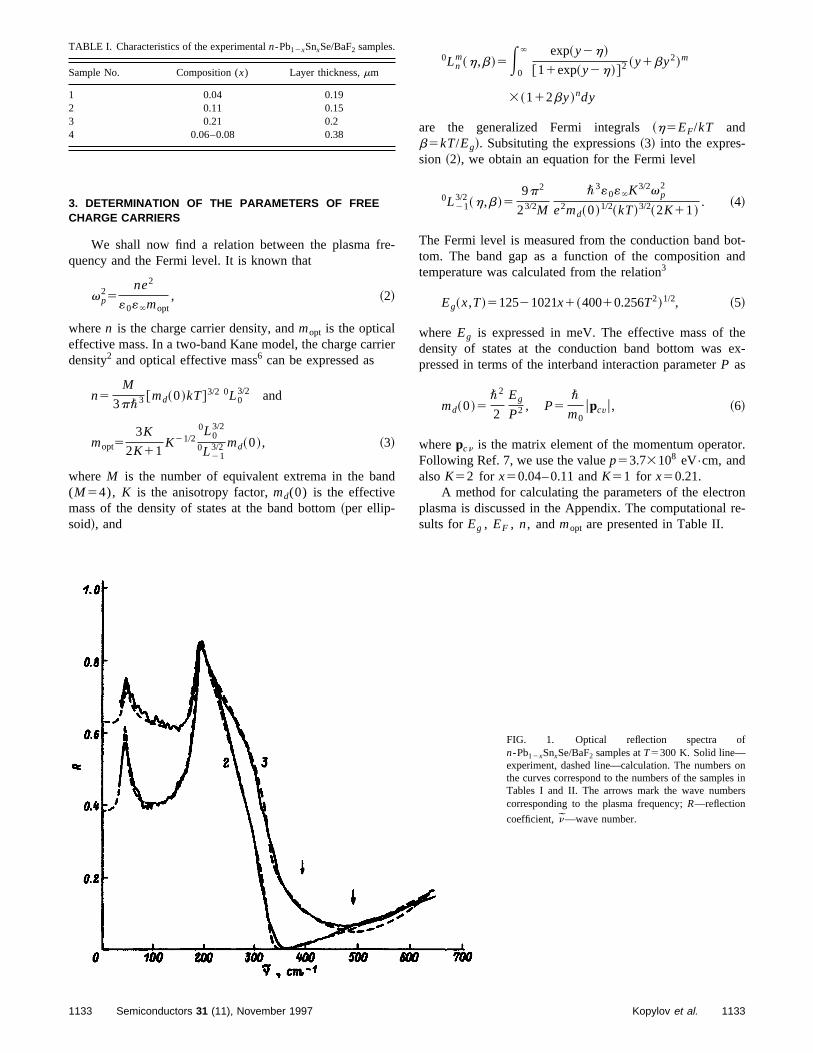
r
r
n
0Lm~h,b!5E` exp~y2h!~y1by2!m
ot-nd
heex-
r.
onre-
TABLE I. Characteristics of the experimentaln-Pb12xSnxSe/BaF2 samples.
3. DETERMINATION OF THE PARAMETERS OF FREECHARGE CARRIERS
We shall now find a relation between the plasma fquency and the Fermi level. It is known that
vp25
ne2
«0«`mopt, ~2!
wheren is the charge carrier density, andmopt is the opticaleffective mass. In a two-band Kane model, the charge cadensity2 and optical effective mass6 can be expressed as
n5M
3p\3 @md~0!kT#3/2 0L03/2 and
mopt53K
2K11K21/2
0L03/2
0L213/2 md~0!, ~3!
where M is the number of equivalent extrema in the ba(M54), K is the anisotropy factor,md(0) is the effectivemass of the density of states at the band bottom~per ellip-soid!, and
Sample No. Composition (x) Layer thickness,mm
1 0.04 0.192 0.11 0.153 0.21 0.24 0.06–0.08 0.38
e-
rier
d
n0 @11exp~y2h!#2
3~112by!ndy
are the generalized Fermi integrals~h5EF/kT andb5kT/Eg!. Subsituting the expressions~3! into the expres-sion ~2!, we obtain an equation for the Fermi level
0L213/2~h,b!5
9p2
23/2M
\3«0«`K3/2vp2
e2md~0!1/2~kT!3/2~2K11!. ~4!
The Fermi level is measured from the conduction band btom. The band gap as a function of the composition atemperature was calculated from the relation3
Eg~x,T!512521021x1~40010.256T2!1/2, ~5!
where Eg is expressed in meV. The effective mass of tdensity of states at the conduction band bottom waspressed in terms of the interband interaction parameterP as
md~0!5\2
2
Eg
P2 , P5\
m0upcvu, ~6!
wherepcn is the matrix element of the momentum operatoFollowing Ref. 7, we use the valuep53.73108 eV•cm, andalsoK52 for x50.04– 0.11 andK51 for x50.21.
A method for calculating the parameters of the electrplasma is discussed in the Appendix. The computationalsults forEg , EF , n, andmopt are presented in Table II.
f
ons inrs
FIG. 1. Optical reflection spectra on-Pb12xSnxSe/BaF2 samples atT5300 K. Solid line—experiment, dashed line—calculation. The numbersthe curves correspond to the numbers of the sampleTables I and II. The arrows mark the wave numbecorresponding to the plasma frequency;R—reflection
coefficient, n —wave number.
1133 1133Semiconductors 31 (11), November 1997 Kopylov et al.
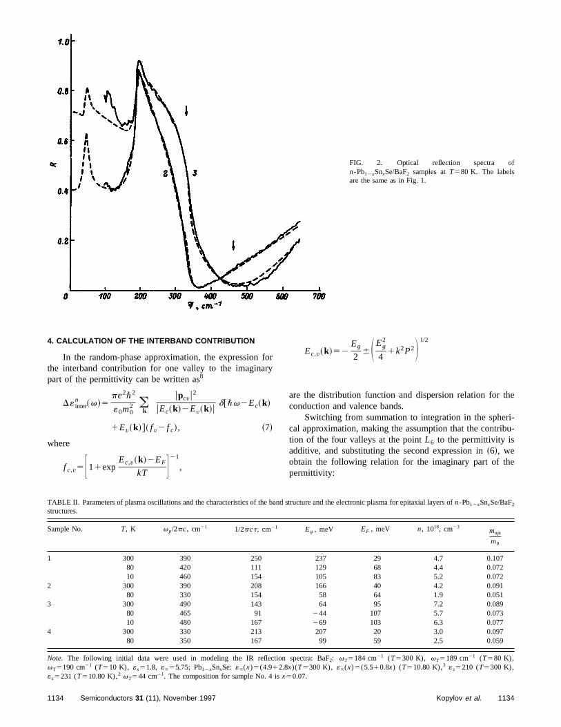
f
FIG. 2. Optical reflection spectra on-Pb12xSnxSe/BaF2 samples atT580 K. The labelsare the same as in Fig. 1.4. CALCULATION OF THE INTERBAND CONTRIBUTION
fory
Eg Eg2 1/2
he
ri-bu-
e
In the random-phase approximation, the expressionthe interband contribution for one valley to the imaginapart of the permittivity can be written as8
D« intern ~v!5
pe2\2
«0m02 (
k
upcvu2
uEc~k!2Ev~k!ud@\v2Ec~k!
1Ev~k!#~ f v2 f c!, ~7!
where
f c,v5F11expEc,v~k!2EF
kT G21
,
TABLE II. Parameters of plasma oscillations and the characteristics of thestructures.
rEc,v~k!52
26S 4
1k2P2Dare the distribution function and dispersion relation for tconduction and valence bands.
Switching from summation to integration in the sphecal approximation, making the assumption that the contrition of the four valleys at the pointL6 to the permittivity isadditive, and substituting the second expression in~6!, weobtain the following relation for the imaginary part of thpermittivity:
band structure and the electronic plasma for epitaxial layers ofn-Pb12xSnxSe/BaF2
Sample No. T, K vp/2pc, cm21 1/2pct, cm21 Eg , meV EF , meV n, 1018, cm23mopt
m0
1 300 390 250 237 29 4.7 0.10780 420 111 129 68 4.4 0.07210 460 154 105 83 5.2 0.072
2 300 390 208 166 40 4.2 0.09180 330 154 58 64 1.9 0.051
3 300 490 143 64 95 7.2 0.08980 465 91 244 107 5.7 0.07310 480 167 269 103 6.3 0.077
4 300 330 213 207 20 3.0 0.09780 350 167 99 59 2.5 0.059
Note. The following initial data were used in modeling the IR reflection spectra: BaF2: vT5184 cm21 (T5300 K), vT5189 cm21 (T580 K),vT5190 cm21 (T510 K), «s51.8, «`55.75; Pb12xSnxSe: «`(x)5(4.912.8x)(T5300 K), «`(x)5(5.510.8x) (T510.80 K),3 «s5210 (T5300 K),«s5231 (T510.80 K),2 vT544 cm21. The composition for sample No. 4 isx50.07.
1134 1134Semiconductors 31 (11), November 1997 Kopylov et al.
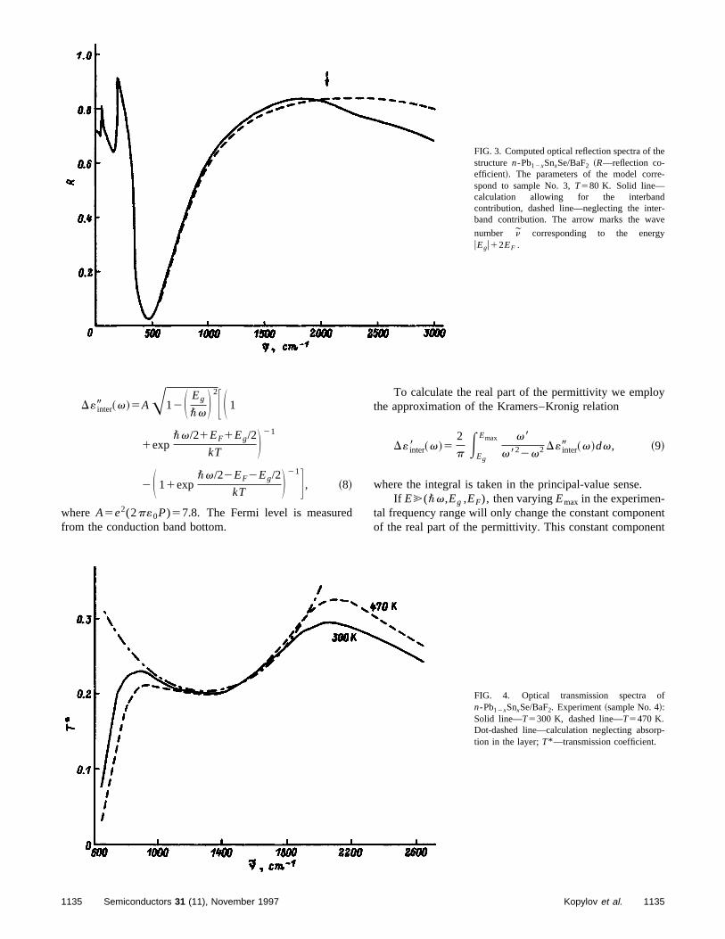
e
-
r-e
FIG. 3. Computed optical reflection spectra of thstructuren-Pb12xSnxSe/BaF2 ~R—reflection co-efficient!. The parameters of the model correspond to sample No. 3,T580 K. Solid line—calculation allowing for the interbandcontribution, dashed line—neglecting the inteband contribution. The arrow marks the wav
number n corresponding to the energyuEgu12EF .
Eg2
d
To calculate the real part of the permittivity we employ
entnt
D« inter9 ~v!5AA12S \v D F S 1
1exp\v/21EF1Eg/2
kT D 21
2S 11exp\v/22EF2Eg/2
kT D 21G , ~8!
where A5e2(2p«0P)57.8. The Fermi level is measurefrom the conduction band bottom.
the approximation of the Kramers–Kronig relation
D« inter8 ~v!52
p EEg
Emax v8
v822v2 D« inter9 ~v!dv, ~9!
where the integral is taken in the principal-value sense.If E@(\v,Eg ,EF), then varyingEmax in the experimen-
tal frequency range will only change the constant componof the real part of the permittivity. This constant compone
f
p-
FIG. 4. Optical transmission spectra on-Pb12xSnxSe/BaF2. Experiment~sample No. 4!:Solid line—T5300 K, dashed line—T5470 K.Dot-dashed line—calculation neglecting absortion in the layer;T* —transmission coefficient.
1135 1135Semiconductors 31 (11), November 1997 Kopylov et al.
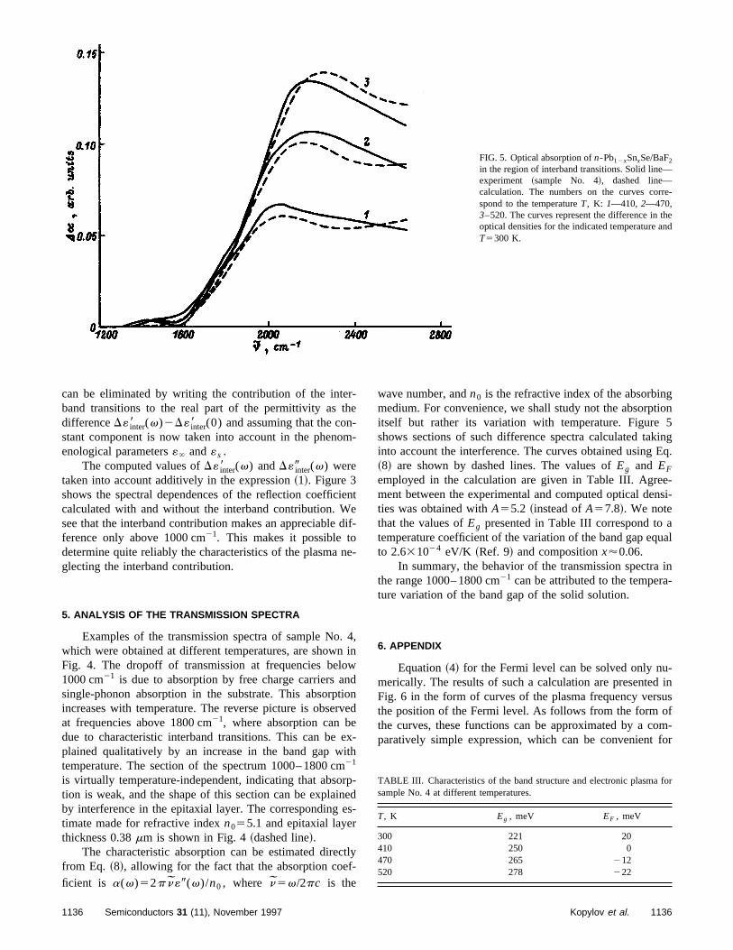
e-
hend
FIG. 5. Optical absorption ofn-Pb12xSnxSe/BaF2in the region of interband transitions. Solid line—experiment ~sample No. 4!, dashed line—calculation. The numbers on the curves corrspond to the temperatureT, K: 1—410, 2—470,3–520. The curves represent the difference in toptical densities for the indicated temperature aT5300 K.
can be eliminated by writing the contribution of the inter-he-
om
ieed
n
.nowntiorveeitmrp
ine
ctf-
wave number, andn0 is the refractive index of the absorbingtion5
kingEq.
e-nsi-
aual
in-
-d inusfom-for
for
band transitions to the real part of the permittivity as tdifferenceD« inter8 (v)2D« inter8 (0) and assuming that the constant component is now taken into account in the phenenological parameters«` and«s .
The computed values ofD« inter8 (v) andD« inter9 (v) weretaken into account additively in the expression~1!. Figure 3shows the spectral dependences of the reflection coefficcalculated with and without the interband contribution. Wsee that the interband contribution makes an appreciableference only above 1000 cm21. This makes it possible todetermine quite reliably the characteristics of the plasmaglecting the interband contribution.
5. ANALYSIS OF THE TRANSMISSION SPECTRA
Examples of the transmission spectra of sample Nowhich were obtained at different temperatures, are showFig. 4. The dropoff of transmission at frequencies bel1000 cm21 is due to absorption by free charge carriers asingle-phonon absorption in the substrate. This absorpincreases with temperature. The reverse picture is obseat frequencies above 1800 cm21, where absorption can bdue to characteristic interband transitions. This can beplained qualitatively by an increase in the band gap wtemperature. The section of the spectrum 1000– 1800 c21
is virtually temperature-independent, indicating that absotion is weak, and the shape of this section can be explaby interference in the epitaxial layer. The correspondingtimate made for refractive indexn055.1 and epitaxial layerthickness 0.38mm is shown in Fig. 4~dashed line!.
The characteristic absorption can be estimated direfrom Eq. ~8!, allowing for the fact that the absorption coeficient is a(v)52p n «9(v)/n0 , where n 5v/2pc is the
1136 Semiconductors 31 (11), November 1997
-
nt
if-
e-
4,in
dned
x-h
-eds-
ly
medium. For convenience, we shall study not the absorpitself but rather its variation with temperature. Figureshows sections of such difference spectra calculated tainto account the interference. The curves obtained using~8! are shown by dashed lines. The values ofEg and EF
employed in the calculation are given in Table III. Agrement between the experimental and computed optical deties was obtained withA55.2 ~instead ofA57.8!. We notethat the values ofEg presented in Table III correspond totemperature coefficient of the variation of the band gap eqto 2.631024 eV/K ~Ref. 9! and compositionx'0.06.
In summary, the behavior of the transmission spectrathe range 1000– 1800 cm21 can be attributed to the temperature variation of the band gap of the solid solution.
6. APPENDIX
Equation~4! for the Fermi level can be solved only numerically. The results of such a calculation are presenteFig. 6 in the form of curves of the plasma frequency versthe position of the Fermi level. As follows from the form othe curves, these functions can be approximated by a cparatively simple expression, which can be convenient
TABLE III. Characteristics of the band structure and electronic plasmasample No. 4 at different temperatures.
T, K Eg , meV EF , meV
300 221 20410 250 0470 265 212520 278 222
1136Kopylov et al.
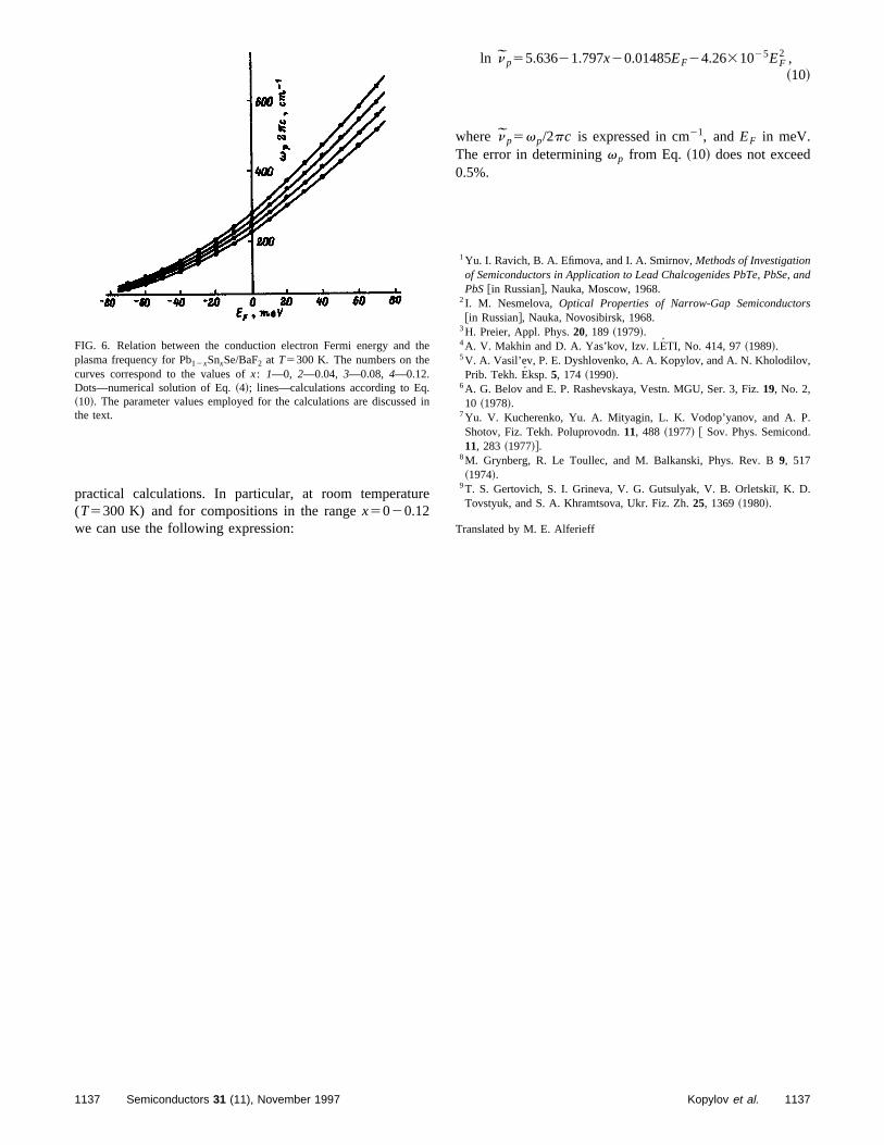
ur
ln n p55.63621.797x20.01485EF24.2631025EF2 ,
and
rs
,
..
th
.ed
practical calculations. In particular, at room temperat(T5300 K) and for compositions in the rangex5020.12we can use the following expression:
FIG. 6. Relation between the conduction electron Fermi energy andplasma frequency for Pb12xSnxSe/BaF2 at T5300 K. The numbers on thecurves correspond to the values ofx: 1—0, 2—0.04, 3—0.08, 4—0.12.Dots—numerical solution of Eq.~4!; lines—calculations according to Eq~10!. The parameter values employed for the calculations are discussthe text.
1137 Semiconductors 31 (11), November 1997
e
~10!
where n p5vp/2pc is expressed in cm21, andEF in meV.The error in determiningvp from Eq. ~10! does not exceed0.5%.
1Yu. I. Ravich, B. A. Efimova, and I. A. Smirnov,Methods of Investigationof Semiconductors in Application to Lead Chalcogenides PbTe, PbSe,PbS@in Russian#, Nauka, Moscow, 1968.
2I. M. Nesmelova,Optical Properties of Narrow-Gap Semiconducto@in Russian#, Nauka, Novosibirsk, 1968.
3H. Preier, Appl. Phys.20, 189 ~1979!.4A. V. Makhin and D. A. Yas’kov, Izv. LE´ TI, No. 414, 97~1989!.5V. A. Vasil’ev, P. E. Dyshlovenko, A. A. Kopylov, and A. N. KholodilovPrib. Tekh. Eksp.5, 174 ~1990!.
6A. G. Belov and E. P. Rashevskaya, Vestn. MGU, Ser. 3, Fiz.19, No. 2,10 ~1978!.
7Yu. V. Kucherenko, Yu. A. Mityagin, L. K. Vodop’yanov, and A. PShotov, Fiz. Tekh. Poluprovodn.11, 488 ~1977! @ Sov. Phys. Semicond11, 283 ~1977!#.
8M. Grynberg, R. Le Toullec, and M. Balkanski, Phys. Rev. B9, 517~1974!.
9T. S. Gertovich, S. I. Grineva, V. G. Gutsulyak, V. B. Orletski�, K. D.Tovstyuk, and S. A. Khramtsova, Ukr. Fiz. Zh.25, 1369~1980!.
Translated by M. E. Alferieff
e
in
1137Kopylov et al.
Position of antimony impurity atoms in a PbTe lattice, determined by emission
Mossbauer spectroscopyV. F. Masterov, F. S. Nasredinov, S. A. Nemov, P. P. Seregin, N. N. Troitskaya,and S. I. Bondarevski
St. Petersburg State University, 195251 St. Petersburg, Russia~Submitted May 12, 1997; accepted for publication May 15, 1997!Fiz. Tekh. Poluprovodn.31, 1321–1322~November 1997!
It is shown by emission Mo¨ssbauer spectroscopy on119Sb(119mSn) that the localization ofantimony impurity atoms in a PbTe lattice depends on the conductivity type of the material:Antimony is localized prodominantly in the anionic sublattice in electronic samples andin the cationic sublattice in hole samples. It is noted that the charge state of an antistructuraldefect119mSn formed in the anionic sublattice of PbTe after119Sb undergoes nuclear decay doesnot depend on the position of the Fermi level. ©1997 American Institute of Physics.@S1063-7826~97!00911-3#
Interest in the investigation of the nature of impurity electronic type~with excess lead,n;1018 cm23! and hole
-IVeieerin
lewnalm:in
ic
ono
rit-ft
enesui
sio-s
-iohlnd
b
oe
18 23
sa
Hru-hethein
ads
thingoftoent
bee
tainsms
icldf
tershethe
t-
eom-
/1
states formed in lead chalcogenides by group-III andatoms has increased substantially in recent years. This isplained mainly by the resonance scattering of current carrby impurities1 observed in these systems and the discovof dielectronic centers with negative correlation energythese materials.2 However, virtually no studies are availabon the group-V impurities in these compounds. It is knoonly that As, Sb, and Bi impurities are donors in lead chcogenides, although the fraction of electrically active atois much less than unity.3 There are two explanations for thisEither an appreciable number of the impurity atoms formthe lattice electrically inactive complexes~of the typeSb2Te3! or the impurity is distributed between the cationsublattice~where it is a donor! and the anionic sublattice~where it is most likely an acceptor!. A choice between al-ternative models can be made if the position of the antimatoms in the lead chalcogenide lattices is determined. Instudy we made such a determination for antimony impuatoms in lead telluride PbTe by emission Mo¨ssbauer spectroscopy on the isotope119Sb(119mSn). The arrangement othe Mossbauer level of119mSn, obtained using the parenisotope119Sb ~half-life 38 h!, is shown in Fig. 1a. Since threcoil energy of the daughter119mSn atoms due to electrocapture in119Sb and emission of a neutrino does not exce1.4 eV,4 it can be expected that nuclear decay does not rein a displacement of the tin atoms from the normal sitesthe crystal lattice. Therefore, the parameters of the emisMossbauer spectra of119Sb(119mSn) should reflect the valence~charge! state of the119mSn atoms localized at the siteoccupied by antimony atoms.
The radioactive isotope119Sb was obtained by the reaction 120Sn(p,2n)119Sb. To separate a carrier-free preparatof 119Sb, the target was dissolved in concentrated hydrocric acid, SbCl3 was extracted with isopropylene alcohol, athe preparation was purified by anionic exchange. The Mo¨ss-bauer sources were prepared by melting together the Psamples and the carrier-free preparation119SbCl3, so that theapproximate concentration of the tin impurity atoms did nexceed 1017 cm23. The initial PbTe samples were of th
1138 Semiconductors 31 (11), November 1997 1063-7826/97
x-rsy
-s
yury
dlt
nn
no-
Te
t
type ~with exces tellurium,p;10 cm !.The Mossbauer spectra of119Sb(119mSn) were measured
with a commercial SM-2201 spectrometer atT580 K with aCaSnO3 absorber~surface density with respect to tin wa5 mg/cm22!. The spectrum with such an absorber andCa119mSnO3 source consisted of a single line with FWHG50.7960.01 mm/s, which was assumed to be the instmental width of the spectral line. The typical spectra of tPbTe:119Sb samples are presented in Figs. 1b and 1c, andresults of an analysis of the spectra are summarizedTable I.
The spectra of then- and p-type samples consist ofsuperposition of two lines, whose relative intensity depenon the conductivity type of the material. The widths of bolines are much larger than the instrumental width, indicatdistortion of the cubic symmetry of the local environmentthe daughter119mSn atoms. This distortion could be duethe difference in the sizes of the replaced and substituatoms.
One of these lines~it predominates inn-type samplesand we designate it as the spectrum I! has an isomeric shiftcharacteristic of intermetallic tin compounds and it shouldattributed to119mSn0 centers in the anionic PbTe sublattic~the nearest-neighbor environment of these centers conlead atoms and the interaction of tin with the lead atoresults in an isomeric shift typical of metallic tin alloys!. It isobvious that the119mSn0 atoms are formed from119Sb atomsoccupying the anionic sublattice of PbTe.
The second line~it predominates inp-type samples andwe designate it as the spectrum II! possesses an isomershift characteristic of divalent tin compounds and it shoube attributed119mSn21 centers in the cationic sublattice oPbTe ~the nearest-neighbor environment of these cencontains tellurium atoms and the interaction of tin with ttellurium atoms leads to an isomeric shift close to that of119Sn spectrum of the compound SnTe!. It is obvious that the119mSn21 atoms form from119Sb atoms located in the caionic sublattice of PbTe.
Thus, the localization of tin impurity atoms in a PbTlattice depends on the character of the deviation of the c
113811138-02$10.00 © 1997 American Institute of Physics
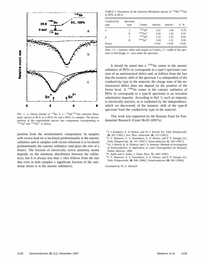
si
e
sla
t
actthean-thef
tyce,-II
n-
n.
Fiz.
Fiz.
TABLE I. Parameters of the emission Mo¨ssbauer spectra of119Sb(119mSn)in PbTe at 80 K.
position from the stoichiometric composition: In samplewith excess lead tin is localized predominantly in the anionsublattice and in samples with excess tellurium it is localizpredominantly the cationic sublattice~and plays the role of adonor!. The fraction of electrically active antimony atomdepends on the antimony distribution between the subtices, but it is always less than 1~this follows from the factthat even in hole samples a significant fraction of the anmony atoms is in the anionic sublattice!.
FIG. 1. a—Decay scheme of119Sb; b, c—119Sb(119mSn) emission Mo¨ss-bauer spectra at 80 K ofp-PbTe~b! andn-PbTe~c! samples. The decom-position of the experimental spectra into components corresponding119mSn0 and119mSn21 is shown.
1139 Semiconductors 31 (11), November 1997
cd
t-
i-
It should be noted that a119mSn center in the anionicsublattice of PbTe~it corresponds to a type-I spectrum! con-sists of an antistructural defect and, as follows from the fthat the isomeric shift of the spectrum I is independent ofconductivity type in the material, the charge state of thetistructural defect does not depend on the position ofFermi level. A 119mSn center in the cationic sublattice oPbTe ~it corresponds to a type-II spectrum! is an isovalentsubstitution impurity. According to Ref. 5, such an impuriis electrically inactive, as is confirmed by the independenwhich we discovered, of the isomeric shift of the typespectrum from the conductivity type in the material.
This work was supported by the Russian Fund for Fudamental Research~Grant 96-02-16957a!.
1V. I. Ka�danov, S. A. Nemov, and Yu. I. Ravich, Fiz. Tekh. Poluprovod26, 201 ~1992! @ Sov. Phys. Semicond.26, 113 ~1992!#.
2V. F. Masterov, F. S. Nasredinov, S. A. Nemov, and P. P. Seregin,Tekh. Poluprovodn.31, 197 ~1997! @ Semiconductors31, 100 ~1997!#.
3Yu. I. Ravich, B. A. Efimova, and I. A. Smirnov,Methods of Investigationof Semiconductors in Application to Lead Chalcogenides@in Russian#,Nauka, Moscow, 1968.
4F. Ambe and S. Ambe, J. Chem. Phys.75, 2463~1981!.5V. F. Masterov, F. S. Nasredinov, S. A. Nemov, and P. P. Seregin,Tekh. Poluprovodn.30, 840 ~1996! @ Semiconductors30, 450 ~1996!#.
Translated by M. E. Alferieff
to
Conductivitytype
Spectrumtype Center mm/sec mm/sec S, %
n I 119mSn0 2.31 1.30 0.79II 119mSn21 3.41 1.32 0.21
p I 119mSn0 2.33 1.32 0.05II 119mSn21 3.43 1.31 0.95
Errors 60.01 60.02 60.02
Note. I.S.—isomeric shifts with respect to CaSnO3, G—width of the spec-trum at half-height,S—area under the spectrum.
1139Masterov et al.
Extraction of charge carriers in semiconductors with a monopolar component of the
photoconductivityA. I. Vlasenko,a) Z. K. Vlasenko, and A. V. Lyubchenko
Institute of Semiconductor Physics, Ukrainian National Academy of Sciences, 252650 Kiev, Ukraine~Submitted August 13 1996; accepted March 5 1997!Fiz. Tekh. Poluprovodn.31, 1323–1326~November 1997!
Extraction of minority charge carriers in semiconductors with a monopolar component of thephotoconductivity has been investigated theoretically and experimentally for the exampleof CdxHg12xTe (x'0.2) at different temperatures. ©1997 American Institute of Physics.@S1063-7826~97!01011-9#
INTRODUCTION mechanism~mechanism B! predominates.6–8 In ‘‘classical’’
ci
ac
el
inedra
rres
fs.ivito
ofn
tna-x
Withu
-
rwCherah
crefe
es
eter-
,
lard
—
r
-ec-
/1
The amount by which the sensitivity of the semicondutor photoresistive radiation detectors can be increased bycreasing the bias voltage is in principle limited by the extrtion of minority nonequilibrium charge carriers~MNCs!from the volume of the semiconductor as the electric fiintensityE increases above a certain valueE5E* . This ef-fect has been studied theoretically and experimentally main connection with the development of threshold infrar~IR! radiation detectors. Specifically, in Refs. 1–3 the opetion of photodetectors based on CdxHg12xTe ~CMT!(x'0.2) is analyzed in the extraction regime, and the cosponding expressions are obtained for the photoresponsenal, the detection power, and other characteristics. In Reand 5, the electric field dependences of the photoconduct~PC! in n-, p-, and mixed-type CMT were investigated. Athe same time, it should be noted that the extractionMNCs has been analyzed theoretically only for the casebipolar PC, when the density of nonequilibrium electroand holes and their lifetimes are equal (Dn5Dp, tn5tp).In the opposite case (tnÞtp), the conductivity componenwhich does not depend on the field and which is proportioto the density differenceuDn2Dpu, where the lower quantity determines the density of the nonequilibrium pairs etracted from the volume, should be taken into account.will analyze the extraction of MNCs in semiconductors wallowance for the monopolar component of the photocondtivity.
1. CURRENT-VOLTAGE CHARACTERISTICS„PHOTOCOMPONENT…
The ratio oftn andtp is determined by the recombination mechanism realized in the crystal: interband~type A! orimpurity ~type B!. In the first case, the PC is bipola(tn5tp). It can be realized in semiconductors with a lodensity of recombination levels, when the number of MNbound on them can be ignored. In the second case, wthese densities cannot be disregarded, the PC is genemonopolar (tnÞtp). In narrow-gap semiconductors whicare not strongly compensated (CdxHg12xTe, InS, PbxSn12x ,Te, and others! at high temperatures, when intrinsic condutivity is realized, interband recombination mechanisms pdominate~mechanism A!. In materials with a high degree ocompensation, at low temperatures the Shockley–R
1140 Semiconductors 31 (11), November 1997 1063-7826/97
-n--
d
ly
-
-ig-4
ty
fa
s
l
-e
c-
srelly
--
ad
wide-gap semiconductors~CdS, CdSe! the PC is highlymonopolar, since the ratio of the lifetimes reachtn /tp>1042106 ~Ref. 9!.
In an arbitrary case the specific photoconductivity (Ds)and photocurrent (j pc) in a uniform semiconductor
Ds5e~mnDn1mpDp!;e~mntn1mptp!G,~1!
j pc5eDsE
in the case of the uniform excitation mechanism~with rateG) will consist of two components — monopolarDsm andbipolar Dsb , the latter depending onE,
Ds5Dsm1Dsb~E!5emnDn@~12w!1w~11b21!#,~2!
whereb5mn /mp , andmn andmp are the electron and holmobilities. Here we have introduced a parameter that demines the degree of bipolarity of the PC:
w5Dp
Dn5
tp
tn<1. ~3!
In Eq. ~3! it is assumed thattp<tn . In the opposite casetp>tn, the parameterw5tn /tp<1.
In the case of the type A mechanisms the PC is bipoand w51. In the extraction region, all MNCs are extractefrom the volume. As a result,Ds drops off with increasingEand the photocurrent~1! saturates.
In the case where several recombination channelstypes A and B — participate~compete!, tnÞtp and w51.The quantityw ~3! can be calculated using the probability fotrapping of MNCs in recombination levels (Arn ,Arp) andinterband annihilation of the carriers (Anp):
An51/tn5Arn1Anp , Ap51/tp5Arp1Anp . ~4!
The parameterw ~3! is
w5tp
tn5
An
Ap5
tp8
t8n
tn81tnp
tp81tnp
,
~5!
tn851
Arn, tp85
1
Arp, tnp5
1
Anp.
The equations~5! allow for the fact that the trapping probabilities are inversely proportional to the corresponding eltronic and hole times (tn8 ,tp8). It is easy to see that in the
114011140-04$10.00 © 1997 American Institute of Physics
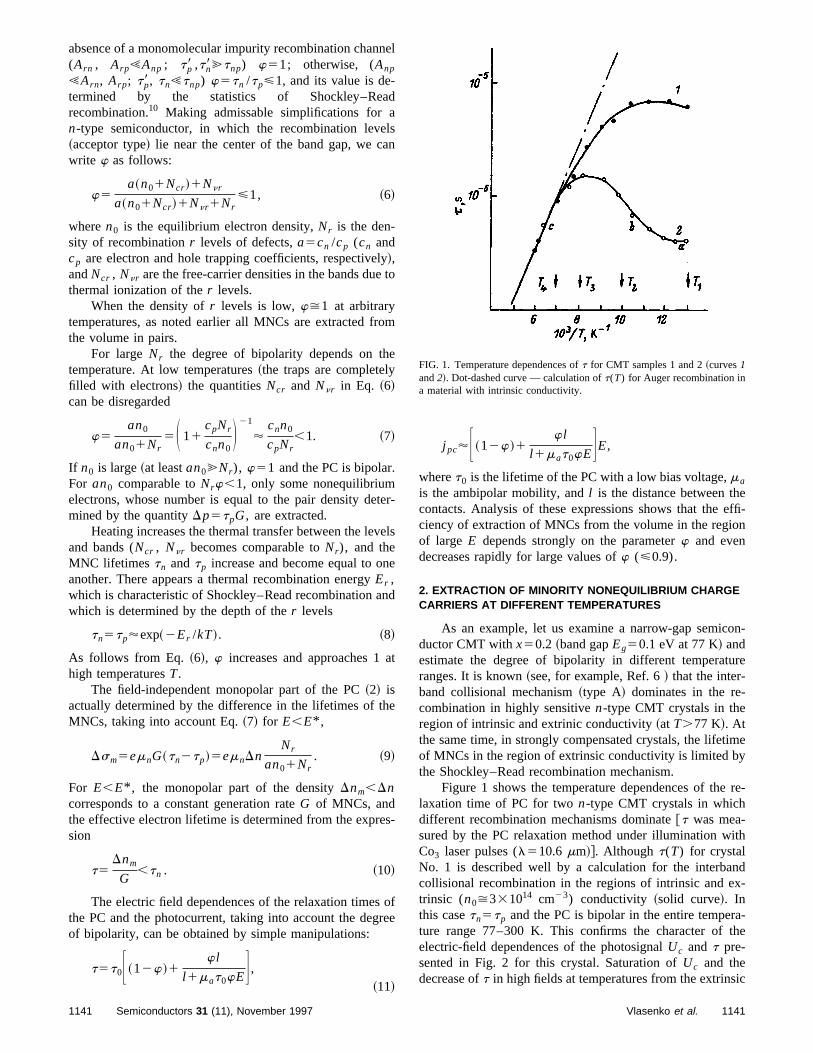
absence of a monomolecular impurity recombination channel
dal
an
lyt
ro
e
te
ve
ne
n
a
he
s
or
eeffi-n
on-
re
imey
re-
ith
ndx-
a-the
ic
(Arn , Arp!Anp ; tp8 ,tn8@tnp) w51; otherwise, (Anp
!Arn, Arp; tp8, tn!tnp) w5tn /tp<1, and its value is de-termined by the statistics of Shockley–Rearecombination.10 Making admissable simplifications forn-type semiconductor, in which the recombination leve~acceptor type! lie near the center of the band gap, we cwrite w as follows:
w5a~n01Ncr!1Nnr
a~n01Ncr!1Nnr1Nr<1, ~6!
wheren0 is the equilibrium electron density,Nr is the den-sity of recombinationr levels of defects,a5cn /cp (cn andcp are electron and hole trapping coefficients, respective!,andNcr , Nnr are the free-carrier densities in the bands duethermal ionization of ther levels.
When the density ofr levels is low,w>1 at arbitrarytemperatures, as noted earlier all MNCs are extracted fthe volume in pairs.
For large Nr the degree of bipolarity depends on thtemperature. At low temperatures~the traps are completelyfilled with electrons! the quantitiesNcr and Nnr in Eq. ~6!can be disregarded
w5an0
an01Nr5S 11
cpNr
cnn0D 21
'cnn0
cpNr,1. ~7!
If n0 is large~at leastan0@Nr), w51 and the PC is bipolar.For an0 comparable toNrw,1, only some nonequilibriumelectrons, whose number is equal to the pair density demined by the quantityDp5tpG, are extracted.
Heating increases the thermal transfer between the leand bands (Ncr , Nnr becomes comparable toNr), and theMNC lifetimes tn andtp increase and become equal to oanother. There appears a thermal recombination energyEr ,which is characteristic of Shockley–Read recombination awhich is determined by the depth of ther levels
tn5tp'exp~2Er /kT!. ~8!
As follows from Eq. ~6!, w increases and approaches 1high temperaturesT.
The field-independent monopolar part of the PC~2! isactually determined by the difference in the lifetimes of tMNCs, taking into account Eq.~7! for E,E* ,
Dsm5emnG~tn2tp!5emnDnNr
an01Nr. ~9!
For E,E* , the monopolar part of the densityDnm,Dncorresponds to a constant generation rateG of MNCs, andthe effective electron lifetime is determined from the expresion
t5Dnm
G,tn . ~10!
The electric field dependences of the relaxation timesthe PC and the photocurrent, taking into account the degof bipolarity, can be obtained by simple manipulations:
t5t0F ~12w!1w l
l 1mat0wEG ,~11!
1141 Semiconductors 31 (11), November 1997
s
o
m
r-
ls
d
t
-
fee
j pc'F ~12w!1w l
l 1mat0wEGE,
wheret0 is the lifetime of the PC with a low bias voltage,ma
is the ambipolar mobility, andl is the distance between thcontacts. Analysis of these expressions shows that theciency of extraction of MNCs from the volume in the regioof large E depends strongly on the parameterw and evendecreases rapidly for large values ofw (<0.9).
2. EXTRACTION OF MINORITY NONEQUILIBRIUM CHARGECARRIERS AT DIFFERENT TEMPERATURES
As an example, let us examine a narrow-gap semicductor CMT withx50.2 ~band gapEg50.1 eV at 77 K! andestimate the degree of bipolarity in different temperaturanges. It is known~see, for example, Ref. 6! that the inter-band collisional mechanism~type A! dominates in the re-combination in highly sensitiven-type CMT crystals in theregion of intrinsic and extrinic conductivity~at T.77 K!. Atthe same time, in strongly compensated crystals, the lifetof MNCs in the region of extrinsic conductivity is limited bthe Shockley–Read recombination mechanism.
Figure 1 shows the temperature dependences of thelaxation time of PC for twon-type CMT crystals in whichdifferent recombination mechanisms dominate@t was mea-sured by the PC relaxation method under illumination wCo3 laser pulses (l510.6 mm!#. Although t(T) for crystalNo. 1 is described well by a calculation for the interbacollisional recombination in the regions of intrinsic and etrinsic (n0>331014 cm23) conductivity ~solid curve!. Inthis casetn5tp and the PC is bipolar in the entire temperture range 77–300 K. This confirms the character ofelectric-field dependences of the photosignalUc and t pre-sented in Fig. 2 for this crystal. Saturation ofUc and thedecrease oft in high fields at temperatures from the extrins
FIG. 1. Temperature dependences oft for CMT samples 1 and 2~curves1and2!. Dot-dashed curve — calculation oft(T) for Auger recombination ina material with intrinsic conductivity.
1141Vlasenko et al.
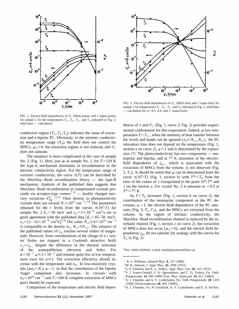
-iv-
p
tho
-Bthpr
i-
ldesor--
rit
en
m-en
s-o-ic-
e
e-tu-ee
in-
-r
.
,
conduction region (T1 ,T2 ,T3) indicates the onset of extraction and a bipolar PC. Obviously, in the intrinsic conductity temperature range (T4) the field does not control theMNCs, mn50, the extraction regime is not realized, andUc
does not saturate.The situation is more complicated in the case of sam
No. 2 ~Fig. 1!. Here, just as in sample No. 1, forT.120 Kthe type-A mechanism dominates in recombination inintrinsic conductivity region. For the temperature rangeextrinsic conductivity, the curvet(T) can be described bythe Shockley–Read recombination theory — the typemechanism. Analysis of the published data suggestsShockley–Read recombination in compensated crystalsceeds via acceptor-type centers7–9 — doubly charged mer-cury vacanciesVHg
22 .11,12 Their density in photosensitivitycrystals does not exceedNr<1015 cm23.7,8 The parametersobtained for ther levels from the curvest(103/T) forsample No. 2Er550 meV andcn5331029 cm3/s are ingood agreement with the published data@Er545– 50 meV,cn5(1 – 3)31029 cm3/s#.7,8 The valueNnr>431014 cm23
is comparable to the densityn0 , Ncr!Nnr . The variance ofthe published values ofcp reaches several orders of magntude. However, from considerations of the charge of ar cen-ter ~holes are trapped in a Coulomb attractive fie!cn,cp , despite the difference in the thermal velocitiof the nonequilibrium electrons and holes. Fa51021 w>231022 and remains quite low at low temperatures even fora>1. The extraction efficiency should increase with the temperature andn0 . In low-resistivity crys-tals (an0.Nr) w→1, so that the contribution of the bipolaAuger component also increases. In crystals wn0.1015 cm23 andT.100 K complete extraction of MNCspairs should be expected.
Comparison of the temperature and electric field dep
FIG. 2. Electric-field dependences ofUc ~filled points! andt ~open points!for sample 1 for the temperaturesT1 , T2 , T3 , andT4 indicated in Fig. 1;solid lines — calculation.
1142 Semiconductors 31 (11), November 1997
le
ef
ato-
h
-
dences oft andUc ~Fig. 1, curve2; Fig. 3! provides experi-mental confirmation for this expectation. Indeed, at low teperaturesT,TC , when the intensity of heat transfer betwethe levels and bands can be ignored (n0@Ncr ,Nnr), the PCrelaxation time does not depend on the temperature~Fig. 1,section a on curve2!, w,1 and is determined by the expresion ~7!. The photoconductivity has two components — mnopolar and bipolar, and at 77 K saturation of the electrfield dependence ofj pc , which is associated with theextraction of MNCs from the volume, is not observed~Fig.3, T1). It should be noted thatw can be determined from thcurve t(103/T) ~Fig. 1, section b! with T* ,T0 from theratio of the values oft extrapolated to the point 103/T* andt on the section a. For crystal No. 2 it amounts to'0.5 atT* '77 K.
As T.T0 increases~Fig. 1, section b on curve2!, thecontribution of the monopolar component to the PC dcreases,w→1, the electric-field dependence of the PC sarates~Fig. 3, T2 ,T3), and the MNCs are extracted from thvolume. In the region of intrinsic conductivity, thShockley–Read recombination channel is replaced by theterband channel~Fig. 1, section c on curve2!, but extractionof MNCs does not occur (ma50), and the electric-field dependencesj pc do not saturate~by analogy with the curves foT4 in Fig. 2!.
a!Fax: ~044!-2658342; e-mail: [email protected]
1 R. L. Williams, Infrared Phys.8, 337 ~1968!.2M. R. Johnson, J. Appl. Phys.43, 3090~1972!.3S. P. Emmons and K. L. Ashley, Appl. Phys. Lett.20, 162 ~1972!.4V. I. Ivanov-Omski�, V. K. Ogorodnikov, and T. Ts. Totieva, Fiz. TekhPoluprovodn.14, 699 ~1980! @Sov. Phys. Semicond.14, 412 ~1980!#.
5A. I. Vlasenko and A. V. Lyubchenko, Fiz. Tekh. Poluprovodn.28, 1219~1994! @Semiconductors28, 695 ~1994!#.
6A. I. Vlasenko, Yu. N. Gavrilyuk, A. V. Lyubchenko, and E. A. Sal’kov
FIG. 3. Electric-field dependences ofUc ~filled dots! andt ~open dots! forsample 2 for temperaturesT1 , T2 , T3 , andT4 indicated in Fig. 1; solid lines— calculation forw'0.5, 0.9, and 1, respectively.
1142Vlasenko et al.
Fiz. Tekh. Poluprovodn.13, 2180~1979! @Sov. Phys. Semicond.13, 1274
~1979!#.
h.
rium Processes in Photoconductors@in Russian#, Kiev, 1981, p. 263.10J. S. Blakemore,Semiconductor Statistics, Pergamon Press, N. Y., 1962
7L. A. Karachevtseva, A. V. Lyubchenko, and V. D. Sobolev, Ukr. Fiz. Z38, 1071~1993!.
8D. L. Polla and C. E. Jones, J. Appl. Phys.52, 5119~1981!.9V. E. Lashkarev, A. V. Lyubchenko, and M. K. She�nkman,Nonequilib-
1143 Semiconductors 31 (11), November 1997
@Russian translation, Moscow, 1964#.11K. Lischka, Phys. Status Solidi133, 17 ~1986!.12H. R. Vydynath, Electr. Soc. Sol. St. Sci. Technol.128, 2609~1981!.
Translated by M. E. Alferieff
1143Vlasenko et al.
Photoluminescence of n -type ZnSe crystals doped with donor and acceptor impurities
00
from a LiCl salt meltG. N. Ivanova, V. A. Kasiyan, and D. D. Nedeoglo
Moldavian State University, 2009 Kishinev, Moldavia~Submitted February 7, 1997; accepted for publication March 20, 1997!Fiz. Tekh. Poluprovodn.31, 1327–1331~November 1997!
The photoluminescence spectra and luminescence excitation spectra~LESs! of n-type ZnSesingle crystals annealed in LiCl melt is investigated in the temperature range from 82 to 420 K. Itis established that such heat treatment of the crystals greatly decreases the intensity of thelong-wavewlength luminescence bands and intensifies the edge radiation. The excitation spectrumof the long-wavelength photoluminescence bands contains several maxima near thefundamental and impurity absorption edges. it is shown that the complicated structure of theluminescence excitation spectra is due to relocation of a nonequilibrium hole from a shallowacceptor to a deeper acceptor by an Auger process with the participation of carrierslocalized at these centers. ©1997 American Institute of Physics.@S1063-7826~97!01111-3#
The problems of modern optoelectronics require the de-sion of 14 Å/mm in the wavelength range from 440 to 7
ninons
enae
igrsu,easiit
ng
inm.
n-dthn
rK1
ster
of
s
ice
e-
ane in-
dsinranda-dith
twothe
/1
velopment of devices that operate in the blue-green regiothe spectrum. A promising material for these purposes is zselenide. However, in addition to edge luminescence,observes wide, intense, long-wavelength emission bandthe photoluminescence~PL! spectrum of undopedn-ZnSe.This raises the problem of identifying the luminescence cters responsible for these bands and searching for dopthat can decrease the number of long-wavelength lumincence centers and increase the intensity of the htemperature edge luminescence of ZnSe. Since the centethe long-wavelength luminescence in ZnSe are, as a rintrinsic defects (VZn) or impurities such as Cu, Ag, and Auwhich produce deep acceptor centers, the problem of incring the edge radiation intensity can be solved by decreacenters of this type in the process of doping of crystals wshallow acceptor and donor impurities.
1. DOPING OF SAMPLES AND EXPERIMENTAL CONDITIONS
We used low-temperature~750 °C! annealing ofn-typeZnSe crystals in a melt of LiCl salt as a method of dopisuch crystals simultaneously with shallow donor (ClSe!- andacceptor (LiZn!-type impurities. Annealing was conductedevacuated cells for 6 to 100 h. When annealing was copleted, the cells were rapidly cooled to room temperatureis known1 that a melt of LiCl salt is a typical ionic liquid(Li1 and Cl2) with a very high electrical conductivity(6.308 V21
•cm21). It should be expected that during anealing ofn-ZnSe crystals in a LiCl salt melt the lithium anchlorine ions diffuse into the crystal and occupy sites inzinc and selenium sublattices, producing, respectively, do(ClSe! and acceptor (LiZn! centers.
The PL spectra of the initial and doped crystals weinvestigated in the temperature interval from 82 to 420The PL was excited by 337 nm radiation from a LGI-2laser. Luminescence excitation spectra~LES! were also in-vestigated at 82 K. The PL spectra and LES were invegated using a MDR-23 monochromator with a linear disp
1144 Semiconductors 31 (11), November 1997 1063-7826/97
ofcein
-ntss-h-
ofle,
s-ngh
-It
eor
e.
i--
nm.
2. EXPERIMENTAL RESULTS
The PL spectrum of an undopedn-type ZnSe crystal at82 K, shown in Fig. 1, consists of bandsA ~445 nm! andC ~540 nm! of equal intensity. A weak bandD ~600 nm!, inthe form of an inflection, and a clearly expressed bandE~635 nm! are observed on the long-wavelength shoulderthe bandC. The bandB has the lowest intensity.
Short anneal~6 h! of the initial crystals in a LiCl saltmelt strongly decreases the intensity of theC band~Fig. 1,curve2!, shifts the maximum of theE band to 640 nm, andsingles out more clearly the bandD without changing itsspectral position. The PL bandsA andB do not undergo anychanges.
A longer anneal~100 h! of the crystals strongly increasethe intensity of the edge-radiation bandB and shifts themaximum of this band to 456 nm~Fig. 1, curve3!. This bandbecomes dominant in the PL spectrum. Its intensity is twthat of the shortest wavelength bandA against the back-ground of the vanishingly low intensities of longer wavlength PL bands. The maximum of theE band shifts to649 nm.
Thus, the intensity of the long-wavelength radiation cbe substantially decreased and the edge radiation can btensified by prolonged annealing ofn-ZnSe crystals in a LiClsalt melt.
The excitation spectra of the long-wavelength PL banof an undopedn-type ZnSe crystal at 82 K are presentedFig. 2 ~curves1–3!. A characteristic feature of these spectis the presence of several excitation bands near the fumental absorption edge. For example, the LES of the banEin the nonannealed crystal consists of three bands wmaxima at 420, 445, and 470 nm. The LES of the bandDpossesses approximately the same structure, and onlybands with maxima at 420 and 450 nm are present inLES of the bandC. Bands due to excitation of impuritylevels dominate in the LES of the bandE of doped crystals
114411144-04$10.00 © 1997 American Institute of Physics
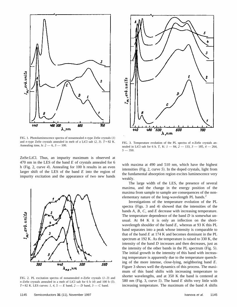
a
n
nd
est
very
ralthenon-
Lere.
t-
le toLthe
t as
s-nch-
xi-to
d at
ZnSe:LiCl. Thus, an impurity maximum is observed470 nm in the LES of the bandE of crystals annealed for 6h ~Fig. 2, curve4!. Annealing for 100 h results in an evelarger shift of the LES of the bandE into the region ofimpurity excitation and the appearance of two new ba
FIG. 1. Photoluminescence spectra of nonannealedn-type ZnSe crystals~1!and n-type ZnSe crystals annealed in melt of a LiCl salt~2, 3!. T582 K.Annealing time, h:2 — 6, 3 — 100.
FIG. 2. PL excitation spectra of nonannealedn-ZnSe crystals~1–3! andn-ZnSe crystals annealed in a melt of LiCl salt for 6 h~4! and 100 h~5!.T582 K. LES curves:1, 4, 5 — E band,2 — D band,3 — C band.
1145 Semiconductors 31 (11), November 1997
t
s
with maxima at 490 and 510 nm, which have the highintensities~Fig. 2, curve5!. In the doped crystals, light fromthe fundamental absorption region excites luminescenceweakly.
The large width of the LES, the presence of sevemaxima, and the change in the energy position ofmaxima from sample to sample are consequences of theelementary nature of the long-wavelength PL bands.2
Investigations of the temperature evolution of the Pspectra~Figs. 3 and 4! showed that the intensities of thbandsA, B, C, andE decrease with increasing temperatuThe temperature dependence of the bandD is somewhat un-usual. At 84 K it is only an inflection on the shorwavelength shoulder of the bandE, whereas at 93 K this PLband separates into a peak whose intensity is comparabthat of the bandE at 174 K and becomes dominant in the Pspectrum at 192 K. As the temperature is raised to 330 K,intensity of the bandD increases and then decreases, justhe intensity of the other bands in the PL spectrum~Fig. 5!.The initial growth in the intensity of this band with increaing temperature is apparently due to the temperature queing of the more intense, close-lying, neighboring bandE.Figure 3 shows well the dynamics of this process. The mamum of this band shifts with increasing temperatureshorter wavelengths, and at 350 K the band is centere580 nm~Fig. 3, curve5!. The bandE shifts very little withincreasing temperature. The maximum of the bandA shifts
FIG. 3. Temperature evolution of the PL spectra ofn-ZnSe crystals an-nealed in LiCl salt for 6 h.T, K: 1 — 84, 2 — 133, 3 — 185, 4 — 264,5 — 350.
1145Ivanova et al.
he
th
osth
urs
nth
thK7
e
f t
igh
e-Asan
,bu-eethe
ionure
en-of
ed
them-
into
elygly
e
ds
into the long-wavelength region with the coefficient of ttemperature shift equal to23.831024 eV/K and is close invalue to the coefficients of the temperature variation ofband gap in ZnSe@2431024 eV/K ~Ref. 3!#. The half-width of the bandA increases from 24 meV at 84 K t80 meV at 350 K. As the temperature increases, the intenof the bandB decreases much more rapidly than doesintensity of the bandA ~Fig. 4!, and this PL band is virtuallyundetectable at 180 K. The coefficient of the temperatshift of the bandB into the long-wavelength region i23.231024 eV/K. The large half-width of this PL band~68 meV at 82 K! is due to the contribution of the phonorepetitions, as is indicated by the appreciable inflection inlong-wavelength shoulder~Fig. 4, curves1 and2!.
The activation energy of temperature quenching ofbandsA andB in the temperature interval from 80 to 120~Fig. 4, inset! for different samples was found to be 10–2and 37–39 meV, respectively. At temperatures above 220the intensity in the maximum of the bandA decreases rapidlyand the activation energy of the temperature quenchingthis band increases to 39–52 meV~Fig. 5!. At temperaturesin the range;2202250 K the temperature quenching of thbandsE andD also changes. The curves lnI5f(103/T) forthese bands have two slopes. The activation energies otemperature quenching of the intensity of the bandE equal
FIG. 4. Effect of temperature on the edge PL spectra of an-ZnSe crystalannealed in LiCl salt for 100 h.T, K: 1 — 82,2 — 101,3 — 112,4 — 182.Inset: Curves of temperature quenching of the intensities of the PL banB~5! andA ~6!.
1146 Semiconductors 31 (11), November 1997
e
itye
e
e
e
K,
of
he
4–13 meV at low temperatures and 100–150 meV at htemperatures for different samples.
3. DISCUSSION OF THE EXPERIMENTAL RESULTS
The bandA at low temperatures lies next to a freexciton emission line and is due to exciton annhilation.the temperature is raised, shallow donors transfer intoionized state and atT.200 K exciton–impurity complexeswhich are associated with ionized donors, whose contrition to the formation of the bandA becomes dominant, armost likely to form. This introduces an asymmetry in thobserved band on the long-wavelength side, broadensband, shifts the spectrum into the long-wavelength reg~Fig. 3!, and increases the activation energy of temperatquenching of the intensity of this PL band~Fig. 5!. Theobserved sample-to-sample variance in the values of thisergy is evidently due to the presence of several typesshallow donor impurity. In Ref. 4, we made a more detailanalysis of the nature of the bandsA andB. It was found thatthe structure of the luminescence centers responsible forband B changes with increasing temperature. At low teperatures these are associative centers of the typeVZnD. Athigh temperatures the associative centers decomposedsimple, deeper acceptorsVZn and shallow donors. For thisreason, annealing of ZnSe crystals in liquid zinc completquenched this band and annealing in liquid selenium stronincreased its intensity.4 The low activation energies of th
FIG. 5. Temperature dependence of the intensity of the PL of an-ZnSe:LiClcrystal ~6 h! at the maximaA, E, D, andB.
1146Ivanova et al.
temperature quenching of this band do not reflect the depth,
cis.e
ingluf
sal
i
dlf
iCes
nrp
hroicip-c-
gleen
i
chhexcax-ti
hea
ishe
n-
. 2o
-
ciate consisting of zinc vacancies, a donor, and a shallow2
m-ns.
w
ts ofcess
iate,
rplypar-ndum-
n-
anseow
nde
ssi-sece
P.
V.
v.
-
v,
of the luminescence center, since quenching occursshown in Ref. 4, by an internal mechanism.
The intense bandC, observed in the luminescence spetra of the starting crystals, with a maximum at 540 nmordinarily attributed to the presence of copper in ZnSe5,6
The decrease in the intensity of this band after heat treatmof the crystals in LiCl salt~Fig. 1! is explained by extractionof copper from the crystal in the process of such anneal
The luminescence centers forming the self-activatedminescence bandD with a maximum at 600 nm consist othe associatesVZnVSe.
7,8 The complete vanishing of thiband with prolonged annealing of the crystals in LiCl s~Fig. 1! that we recorded in an earlier work9 is due to simul-taneous filling of the zinc and selenium vacancies by LZn
and ClSe atoms, respectively.The presence of three maxima in the LES of the banE
~Fig. 2, curves1 and 5! and the shift of the PL band itse~Fig. 1! and its excitation spectrum~Fig. 2! into the long-wavelength region when the crystals are annealed in a Lsalt attest to the complexity of the structure of the lumincence centers responsible for theE band and the mechanismleading to the excitation of this band. It was recently show2
that the relocation of a nonequilibrium hole from an absotion center~AC! to a deeper luminescence center~LC! oc-curs in the process of excitation of the 630-nm PL band. Tprocess is accompanied by transfer of excitation energy fthe AC to the deeper LC. An Auger process with the partpation of carriers localized at AC and LC occurs: After otical excitation of an electron from an AC into the condution band ~or onto a shallow donor! the electron returnsnonradiatively into the AC, giving up in the process enerto an electron localized in a deeper LC and exciting the etron into the conduction band.10 Subsequent trapping of thelectron by a luminescence center gives rise to the lowavelength luminescence.
According to this model, the shorter-wavelength bandthe LES of the bandE ~Fig. 2, curve1! is due to the excita-tion of an electron from a relatively shallow acceptor, whiis an AC, into the conduction band. The difference in tenergy of the absorbed photon at the maximum of this etation band and the energy of the emitted photon at the mmum of the bandB is of the order of 0.25 eV and corresponds to a Stokes shift. This suggests that the absorpcenters are luminescence centers of the bandB, i.e., associ-atesVZnD. Assuming that a transition corresponding to texcitation of an electron into the conduction band fromdeeper LC of the bandE as a result of an Auger processalso manifested in the LES, it is logical to attribute tlonger wavelength band in the excitation spectrum~Fig. 2,curve 1! to this optical transition. The difference in the eergies in the maxima of this bandE is 0.45 eV, in goodagreement with the Stokes shift of this band, found in Ref
Adopting as a working hypothesis the idea that the LCthe 630-nm PL band of the bandE is a three-particle asso
1147 Semiconductors 31 (11), November 1997
as
-
nt
.-
t
l-
-
ism-
yc-
g-
n
i-i-
on
.f
acceptor separated from them by a large distance,the an-nealing of ZnSe crystals in LiCl salt should result in decoposition of these complicated associates for two reasoFirst, as we showed earlier,9 even a short anneal~10 h! ofZnSe crystals in LiCl salt results in extraction of shallodonors ~Al, Ga, In! and acceptors~Na! from the crystal.These donors and acceptors probably are the constituenthe associate under study. Second, in such an anneal prozinc vacancies, which are also constituents of the assocare filled with lithium atoms (LiZn!. According to Ref. 9,increasing the anneal time to 20 h and longer again shaincreases the density of zinc vacancies as a result of deture of lithium atoms from the sites in the zinc sublattice aoccupation of the interstitial states. This decreases the nber of shallow acceptors LiZn (EA5114 meV!, which im-pedes repeated formation of LC of the bandE, despite thehigh density ofVZn and shallow donors Lii (ED517– 20meV!. However, this leads to the creation of favorable coditions for the formation of the associatesVZnLi i which areresponsible for the luminescence bandB in crystals annealedin LiCl. An increase in the density of the associatesVZnLi i
with prolonged annealing of the crystals in LiCl salt andincrease in the probability of radiative transitions on thecenters, since nonequilibrium holes under conditions of ldensity of LC of the bandE remain localized onVZnLi i
centers, result in rapid growth of the intensity of the PL baB ~Fig. 1, curve3!. An increase in the total density of thimpurities (Lii , ClSe! and intrinsic defects (VZn) during along anneal of the crystals in LiCl salt decreases the pobility of excitonic luminescence, which results in a decreaof the intensity and in broadening of the luminescenbandA.
1 Handbook of Fused Salts@in Russian#, Khimiya, Leningrad, 1970.2B. E. Embergenov, N. E. Korsynskaya, V. D. Ryzhikov, L.Gal’chinski�, and E. K. Lisetskaya, Fiz. Tekh. Poluprovodn.27, 1240~1993! @Semiconductors27, 686 ~1993!#.
3V. V. Sobolev, V. I. Donetsikh, and E. F. Zaga�nov, Fiz. Tekh. Polupro-vodn.12, 1089~1978! @Sov. Phys. Semicond.12, 646 ~1978!#.
4G. N. Ivanova, V. A. Kasiyan, N. D. Nedeoglo, D. D. Nedeoglo, and A.Simashkevich, Fiz. Tekh. Poluprovodn.@Semiconductors#, submitted forpublication.
5M. Godlewski, W. E. Lamb, and B. C. Cavenett, Solid State Commun.39,595 ~1981!.
6G. N. Ivanova, V. A. Kasiyan, D. D. Nedeoglo, and S. V. Oprya, IzAkad. Nauk RM, Fiz. i Tekh., No. 2, 34~1995!.
7P. A. Kukk and N. V. Palmre, Izv. Akad. Nauk SSSR, Neorg. Mater.16,1916 ~1980!.
8M. B. Kotlyarevski�, A. A. Pegov, O. V. Leont’eva, and B. G. Chernyavski�, Dep. N506-B86~1986!.
9V. Z. Bolboshenko, G. N. Ivanova, D. D. Nedeoglo, and B. V. NovikoOpt. Spektrosk.72, 149 ~1992! @Opt. Spektrosk.72, 82 ~1992!#.
10V. V. Dyakin, E. A. Sal’kov, V. A. Khvostov, and M. K. She�nkman, Fiz.Tekh. Poluprovodn.10, 2288 ~1976! @Sov. Phys. Semicond.10, 1357~1976!#.
Translated by M. E. Alferieff
1147Ivanova et al.
Effect of band-gap narrowing on the diffusion of charged impurities in semiconductors
B. S. Sokolovski and L. S. MonastyrskiIv. Franko L’vov State University 290602 L’vov, Ukraine~Submitted December 11 1996; accepted April 1 1997!Fiz. Tekh. Poluprovodn.31, 1332–1335~November 1997!
It is shown theoretically that allowance for the internal electric field due to band-gap narrowingas a result of strong doping of the semiconductor decreases the diffusion of the chargedimpurity and forms a descending section on its impurity density dependence. ©1997 AmericanInstitute of Physics.@S1063-7826~97!01211-8#
Diffusion of charged impurities in semiconductors, in the case of acceptor impurity diffusion. HereNc and Nn
andle
ai-ein
heo
bencditrimf
n
nd
tiena
altri
va-
nce
isped
ofavy
Aityity
apsde-eia-ed
n
/1
which is important for semiconductor device technology, hbeen studied extensively, both theoretically aexperimentally.1,2 Despite those studies, there is very littpublished information on how band-gap narrowing~BGN!,which occurs with high levels of doping insemiconductor,3–12 influences diffusion of charged impurties. We know of only one work13 that touches upon somaspects of this problem in application to the diffusion of PSi. As shown in Ref. 13, the Coulomb interaction of tcarriers together with BGN lower the formation energyvacancies and increase the vacancy diffusion.
In the present paper, we investigate theoretically thesic mechanisms of the effect of BGN on the density depdence of the diffusion of a charged impurity. The approaemployed for calculating the density dependence of thefusion is based on taking into account the internal elecfield due to the spatial nonuniformity of the energy diagraof a heavily doped semiconductor under the conditions odopant density gradient.
In the presence of an electric field, the one-dimensio~along thex axis! acceptorqa and donorqd fluxes of singlycharged impurities with local densitiesNa andNd at an ar-bitrary time t can be expressed as2
qa,d~x,t !52Da,d0 S ]Na,d
]x7
e
kT
]w
]xNa,dD , ~1!
whereDa,d0 are the diffusion coefficients of the acceptor a
donor impurities at low impurity concentrations,w is theelectrostatic potential,e is the elementary charge,T is thetemperature, andk is Boltzmann’s constant.
We assume that the characteristic length of the spadistribution of the impurity is much greater than the screing length, and that the impurity density is much higher ththe intrinsic densityni of the charge carriers. The internelectric field can then be found from the equation of elecneutrality
Nd~x,t !5NcF1/2FEF2DEc~x,t !1ew~x,t !
kT G ~2!
under conditions of donor impurity diffusion and
Na~x,t !5NvF1/2FDEv~x,t !2ew~x,t !2Eg02EF
kT G ~3!
1148 Semiconductors 31 (11), November 1997 1063-7826/97
s
f
a--
hf-csa
al
al-n
c
are the effective density of states in the conduction andlence bands,F1/2 is the Fermi integral,DEc andDEn is thedisplacement of the edges of the conduction and valebands as a result of heavy doping,Eg0 is the band gap in theundoped semiconductor, andEF is the Fermi energy. In writ-ing the expressions~2! and~3! it was assumed that energymeasured from the conduction band bottom in the undosemiconductor.
Assuming local equilibrium (EF5const!, we find fromEqs.~2! and ~3! the internal electric field
2]w
]x52
kT
eNcF21/2@F1/2* ~Nd /Nc!#
]Nd
]x2
]DEc
]x~4!
in a n-type semiconductor and
2]w
]x5
kT
eNvF21/2@F1/2* ~Na /Nv!#
]Na
]x2
]DEv
]x~5!
in a p-type semiconductor, andF1/2* is the function inverse tothe Fermi integral. The derivations of Eqs.~4! and ~5! tookaccount of the fact thatdF1/2(z)/dz5F21/2(z).
The second terms in Eqs.~4! and~5! describe the effecton the internal electric field of the change in the positionsthe edges of the allowed-energy bands as a result of hedoping of the semiconductor with a diffusing impurity.necessary condition for this effect to occur is nonuniformof doping ~evidently, these terms vanish when the impurdistribution becomes uniform!. We note that similar termsare present in the internal electric field of variable band-gsemiconductor solid solutions.14 However, in the latter casethe gradients of the edges of the allowed-energy bandspend not only on the impurity distribution, but also on thchemical composition, whereas the profile of the energy dgram in heavily doped semiconductors is determinuniquely by the coordinate distribution of the impurity.
Substituting the expressions~4! and~5! into Eq. ~1!, werepresent the impurity fluxes in the form of the diffusiofluxes
qa,d~x,t !52Da,d
]Na,d
]x~6!
with density-dependent diffusion coefficients
114811148-03$10.00 © 1997 American Institute of Physics
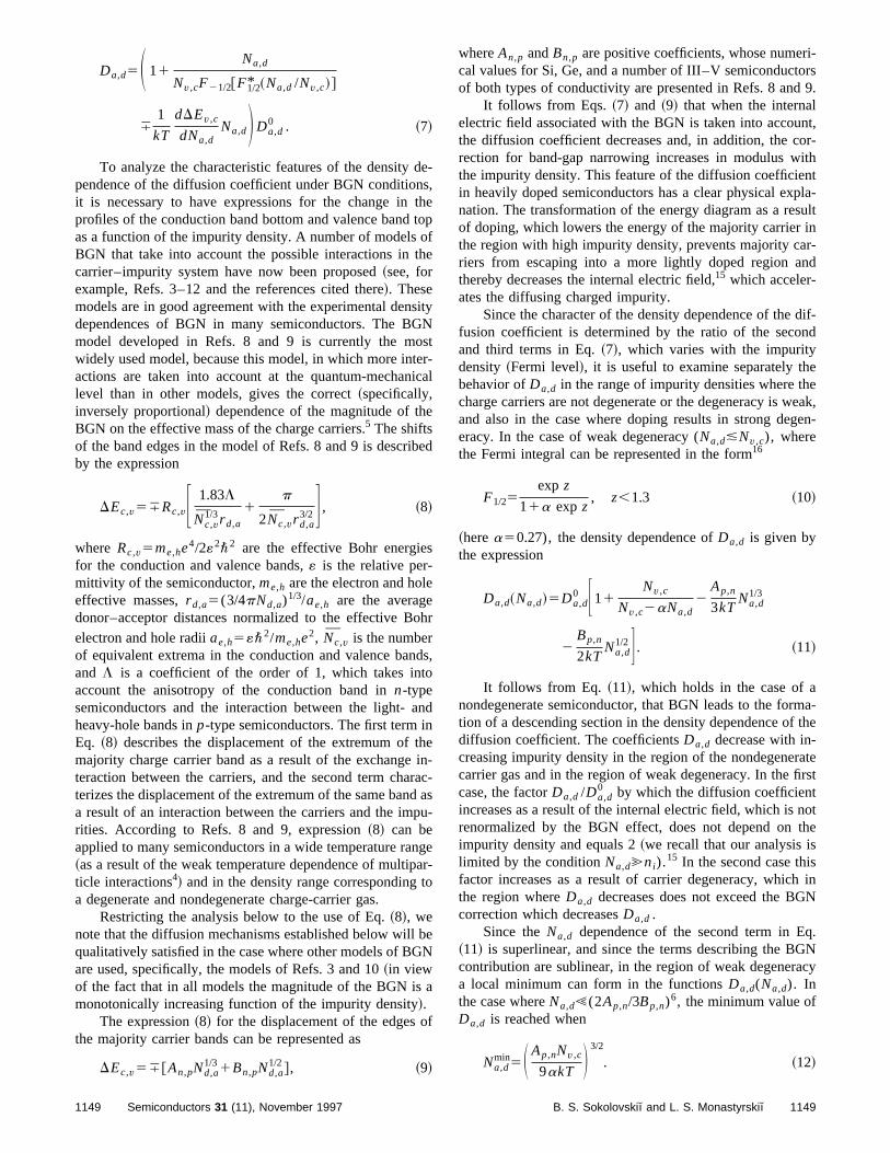
Na,d
dnsttooth
sGosteic
e
ib
s
e
o
dto
aninthirdp
nipto
l bG
a
of
whereAn,p andBn,p are positive coefficients, whose numeri-ors
9.lnt,or-ithntpla-sultinr-nd
dif-nd
eeeak,en-
ma-f the
atefirst
notthe
sh inN
q.GNacy
Da,d5S 11Nv,cF21/2@F1/2* ~Na,d /Nv,c!#
71
kT
dDEv,c
dNa,dNa,dD Da,d
0 . ~7!
To analyze the characteristic features of the densitypendence of the diffusion coefficient under BGN conditioit is necessary to have expressions for the change inprofiles of the conduction band bottom and valence bandas a function of the impurity density. A number of modelsBGN that take into account the possible interactions incarrier–impurity system have now been proposed~see, forexample, Refs. 3–12 and the references cited there!. Thesemodels are in good agreement with the experimental dendependences of BGN in many semiconductors. The Bmodel developed in Refs. 8 and 9 is currently the mwidely used model, because this model, in which more inactions are taken into account at the quantum-mechanlevel than in other models, gives the correct~specifically,inversely proportional! dependence of the magnitude of thBGN on the effective mass of the charge carriers.5 The shiftsof the band edges in the model of Refs. 8 and 9 is descrby the expression
DEc,v57Rc,vF 1.83L
Nc,v1/3r d,a
1p
2Nc,vr d,a3/2G , ~8!
where Rc,v5me,he4/2«2\2 are the effective Bohr energiefor the conduction and valence bands,« is the relative per-mittivity of the semiconductor,me,h are the electron and holeffective masses,r d,a5(3/4pNd,a)1/3/ae,h are the averagedonor–acceptor distances normalized to the effective Belectron and hole radiiae,h5«\2/me,he2, Nc,v is the numberof equivalent extrema in the conduction and valence banand L is a coefficient of the order of 1, which takes inaccount the anisotropy of the conduction band inn-typesemiconductors and the interaction between the light-heavy-hole bands inp-type semiconductors. The first termEq. ~8! describes the displacement of the extremum ofmajority charge carrier band as a result of the exchangeteraction between the carriers, and the second term chaterizes the displacement of the extremum of the same bana result of an interaction between the carriers and the imrities. According to Refs. 8 and 9, expression~8! can beapplied to many semiconductors in a wide temperature ra~as a result of the weak temperature dependence of multticle interactions4! and in the density range correspondinga degenerate and nondegenerate charge-carrier gas.
Restricting the analysis below to the use of Eq.~8!, wenote that the diffusion mechanisms established below wilqualitatively satisfied in the case where other models of Bare used, specifically, the models of Refs. 3 and 10~in viewof the fact that in all models the magnitude of the BGN ismonotonically increasing function of the impurity density!.
The expression~8! for the displacement of the edgesthe majority carrier bands can be represented as
DEc,v57@An,pNd,a1/31Bn,pNd,a
1/2#, ~9!
1149 Semiconductors 31 (11), November 1997
e-,hep
fe
ityNt
r-al
ed
hr
s,
d
en-ac-asu-
gear-
eN
cal values for Si, Ge, and a number of III–V semiconductof both types of conductivity are presented in Refs. 8 and
It follows from Eqs.~7! and ~9! that when the internaelectric field associated with the BGN is taken into accouthe diffusion coefficient decreases and, in addition, the crection for band-gap narrowing increases in modulus wthe impurity density. This feature of the diffusion coefficiein heavily doped semiconductors has a clear physical exnation. The transformation of the energy diagram as a reof doping, which lowers the energy of the majority carrierthe region with high impurity density, prevents majority cariers from escaping into a more lightly doped region athereby decreases the internal electric field,15 which acceler-ates the diffusing charged impurity.
Since the character of the density dependence of thefusion coefficient is determined by the ratio of the secoand third terms in Eq.~7!, which varies with the impuritydensity~Fermi level!, it is useful to examine separately thbehavior ofDa,d in the range of impurity densities where thcharge carriers are not degenerate or the degeneracy is wand also in the case where doping results in strong degeracy. In the case of weak degeneracy (Na,d&Nv,c), wherethe Fermi integral can be represented in the form16
F1/25exp z
11a exp z, z,1.3 ~10!
~herea50.27), the density dependence ofDa,d is given bythe expression
Da,d~Na,d!5Da,d0 F11
Nv,c
Nv,c2aNa,d2
Ap,n
3kTNa,d
1/3
2Bp,n
2kTNa,d
1/2G . ~11!
It follows from Eq. ~11!, which holds in the case of anondegenerate semiconductor, that BGN leads to the fortion of a descending section in the density dependence odiffusion coefficient. The coefficientsDa,d decrease with in-creasing impurity density in the region of the nondegenercarrier gas and in the region of weak degeneracy. In thecase, the factorDa,d /Da,d
0 by which the diffusion coefficientincreases as a result of the internal electric field, which isrenormalized by the BGN effect, does not depend onimpurity density and equals 2~we recall that our analysis islimited by the conditionNa,d@ni).
15 In the second case thifactor increases as a result of carrier degeneracy, whicthe region whereDa,d decreases does not exceed the BGcorrection which decreasesDa,d .
Since theNa,d dependence of the second term in E~11! is superlinear, and since the terms describing the Bcontribution are sublinear, in the region of weak degenera local minimum can form in the functionsDa,d(Na,d). Inthe case whereNa,d!(2Ap,n/3Bp,n)6, the minimum value ofDa,d is reached when
Na,dmin5S Ap,nNv,c
9akT D 3/2
. ~12!
1149B. S. Sokolovski and L. S. Monastyrski
The position of the minimum of the functionsDa,d(Na,d)res
t-
peetu0resi
tte
ffi,e
to
an
ac
stronger density nonlinearity of the second term in Eq.~13!
e-Ae of
cy,u-xi-
hed.
.
.
.
shifts with increasing temperature into the high-densitygion. In the process, the depth of the minimum decreasomewhat. For example,1) for p-type Si the minimum valueis Da51.82Da
0 at T5600 °C and Da51.85Da0 at
T5900 °C. This behavior of the diffusion coefficient is atributable to the fact that the BGN correction forDa,d in-creases with decreasing temperature because of the temture factor 1/kT ~in the BGN model of Refs. 8 and 9 thdisplacements of the band edges are virtually temperaindependent!. It is obvious that the models of Refs. 3 and 1where BGN decreases with increasing temperature, willsult in a stronger temperature transformation of the dendependences of the diffusion coefficient.
We note that the presence of a descending section indensity dependence of the diffusion coefficient can resulan instability of the diffusion flux. Specifically, it can causimpurities to coagulate into bunches.
As the impurity density increases further (Na,d.Na,dmin),
the absolute and relative deviations of the diffusion coecients Da,d and Da,d8 , calculated with and without BGNrespectively, increase. The calculation of the density depdence of the diffusion coefficient inp-Si using Eq.~7! showsthat the ratioDa,d8 /Da,d reaches its maximum value, equal1.3, at T5900 °C andNa51.131021 cm23, which corre-sponds to the position of the Fermi level in the valence bat a distance of 4kT from the valence band top.
Under doping conditions that result in strong degenerof the charge carriers (Na,d@Nv,c), we obtain forDa,d fromEqs.~7! and ~9! the expression
Da,d5Da,d0 F11S p
6 D 1/3S Na,d
Nv,cD 2/3
2Ap,nNa,d
1/3
3kT
2Bp,nNa,d
1/2
2kT G . ~13!
In the region of strong degeneracy, the differenceDa,d82Da,d grows monotonically withNa,d . As a result of the
1150 Semiconductors 31 (11), November 1997
-es
ra-
re,-
ty
hein
-
n-
d
y
than in the case of the BGN terms, the ratioDa,d8 /Da,d de-creases with increasing doping level.
In summary, we showed in this paper that BGN dcreases the diffusion coefficient of a charged impurity.descending section is observed in the density dependencthe diffusion coefficient in the region of weak degeneraand the ratio of the diffusion coefficients, which are calclated with and without allowance for BGN, reaches its mamum value in the intermediate degeneracy range.
1For numerical estimates,p-type Si was chosen as a material with one of tstrongest density dependences of the edge of the majority carrier ban8,9
1D. Shaw@Ed.#, Atomic Diffusion in SemiconductorsPlenum Press, N. Y.,1973 @Russian translation, Mir, Moscow, 1975#.
2B. I. Boltaks,Diffusion and Point Defects in Semiconductors@in Russian#,Nauka, Leningrad, 1972.
3H. P. D. Lanyon and R. A. Tuft, IEEE Trans. Electron Devices26, 1014~1979!; S. Sze,Physics of Semiconductor Devices, Wiley, N. Y. @Russiantranslation, Mir, Moscow, 1984, Vol. 1#.
4H. S. Bennett and J. R. Lowney, J. Appl. Phys.52, 5633~1981!.5B. E. Sernelius, Phys. Rev. B33, 8582~1986!.6H. S. Bennett and J. R. Lowney, J. Appl. Phys.62, 521 ~1987!.7S. C. Jain, E. Heasell, and D. J. Roulston, Prog. Quantum Electron11,105 ~1987!.
8S. C. Jain, J. M. McGregor, and D. J. Roulston, J. Appl. Phys.68, 3747~1990!.
9S. C. Jain and D. J. Roulston, Solid-State Electron.34, 453 ~1991!.10D. I. Bychkovski�, O. V. Konstantinov, and B. V. Tsarenkov, Fiz. Tekh
Poluprovodn.24, 1848~1990! @Sov. Phys. Semicond.24, 1151~1990!#.11Z. H. Lu, M. C. Hanna, and A. Majerfeld, Appl. Phys. Lett.64, 88 ~1994!.12B. P. Yan, J. S. Luo, and Q. L. Zhang, J. Appl. Phys.77, 4822~1995!.13A. O. Konstantinov, Fiz. Tekh. Poluprovodn.26, 339 ~1992! @Sov. Phys.
Semicond.26, 191 ~1992!#.14L. S. Monastyrski� and B. S. Sokolovski�, Fiz. Tekh. Poluprovodn.26, 339
~1992! @Sov. Phys. Semicond.26, 191 ~1992!#.15K. Lehovec and A. Slobodskoy, Solid-State Electron.3, 45 ~1961!.16J. S. Blakemore,Semiconductor Statistics, Pergamon Press, N. Y., 1962
Translated by M. E. Alferieff
1150B. S. Sokolovski and L. S. Monastyrski
Photoconductivity of CuInSe 2 films
°C,
V. Yu. Rud’
State Technical University 195251 St. Petersburg, Russia
Yu. V. Rud’a)
A. F. Ioffe Physicotechnical Institute, Russian Academy of Sciences 194021 St. Petersburg, Russia~Submitted April 11 1997; accepted April 16 1997!Fiz. Tekh. Poluprovodn.31, 1336–1339~November 1997!
CuInSe2 thin films were grown by vacuum sputtering of presynthesized material from a singlesource. The room-temperature photoconductivity spectra of the films were obtained. Itwas determined that the photoconductivity of these films depends strongly on the preparationconditions and, especially, on the source temperature. A shift of the long-wavelengthphotoactive absorption edge and the evolution of the photoconductivity spectra of the films wereobserved. This influence can be explained by allowing for deviations of the composition ofthe condensed phase from CuInSe2 stoichiometry. The phenomenon established can findapplication in the production of highly efficient thin-film phototransducers based onCuInSe2 . © 1997 American Institute of Physics.@S1063-7826~97!01311-2#
The ternary semiconductor compound CuInSe2 ~CIS! is heated by an electric current up to a temperature of 1350
ialcaicdo
seu
-ISd-s
nt
onin
tiolitygbiooli
ssuriohe
lacedrate
thepor
trate-rayandm-m-.
de of
withdur-ctsde-
theuxfluxbeby
etion
sta-n
n seeureourty,IS
/1
now one of the most widely used multicomponent materfor highly efficient thin-film solar cells~SCs!.1–3 The effi-ciency of such SCs has already reached 17%3–5 and furtherprogress in this field can be made by controlling the optiand electronic properties of CIS films. The band gap, whis the most important parameter for such applications,pends on the atomic composition of the material and alsothe degree of ordering of the atoms in the semiconductorsuch complex composition.6,7 In the system Cu–In–Se, thratio of the copper and indium atom densities directly inflences the crystal lattice and the ordering of the Cu andatoms.2,8,9 Until now, the spectral position of the longwavelength limit of photosensitivity in SCs based on Cthin films was controlled by forming solid solutions by aditionally introducing Ga, Te, or S into the filmdeposited.2,10–12
In the present paper we report the results of experimeinvestigations of the stationary photoconductivity~PC! ofCIS films as a function of their vacuum thermal depositiconditions. Photoconductivity measurements give directformation about the character of the photoactive absorpand ultimately have led to the discovery of a new possibifor controlling the spectral position and structure of the lonwavelength photoactive absorption edge exclusivelymonitoring the technological parameters of the depositprocess, avoiding the need to introduce into the reaction znew components which are required in order to form sosolutions with the appropriate composition.
Thin polycrystalline CIS films were deposited on glasubstrates by evaporation into a vacuum from a single sointo which a presynthesized material close to the stoichmetric composition of the ternary compound was placed. Tstarting material was evaporated in the growth chambevacuated to pressures 1026 Torr. A graphite cylinder,
a!e-mail: [email protected]
1151 Semiconductors 31 (11), November 1997 1063-7826/97
s
lhe-nof
-In
al
-n
-ynned
ce-er,
was used as the evaporator. The substrate holder was p200–400 mm directly above the evaporator. The substtemperature was regulated by a flat resistance furnace inrange 300–450 °C. To stabilize the parameters of the vaphase during deposition of the CIS, the evaporator–subssystem was enclosed in a metallic screen. As x-ray and xmicroprobe investigations showed, the lattice parameterscompositions of the films obtained with evaporation teperaturesTS5900– 1350 °C and substrates heated to teperatureTO5300– 450 °C corresponded to the initial CISThe film thicknesses with fixedTS and TO were monitoredby the evaporation time and reached 1–1.5mm at t515 min.The film surfaces were mirror-smooth. All films obtaineexhibited, as a rule, rather good adhesion to the surfacthe glass substrates.
The PC measurements were performed on samplesaverage sizes 15– 203325 mm. The samples were prepareby etching off CIS films, deposited on the glass, on the sface which was not coated with lacquer. Ohmic contawere produced by soldering pure indium. The spectralpendences of the PC were measured in the region wherephotocurrent was proportional to the incident radiation fldensity, which served as a basis for converting the photointo the equivalent number of incident photons. It shouldunderscored that a photovoltage could not be detectedscanning the obtained film surfaces with a light probe~0.2mm in diameter!. This indicated that the homogeneity of thCIS samples obtained by the method of thermal evaporawas adequate.13
Figure 1 shows typical spectral dependences of thetionary PC of CIS films obtained with different evaporatiotemperatures and a fixed deposition temperature. One cafrom the figure that controlling the evaporation temperatmakes it possible to influence effectively the spectral contof the PC. Until now, only a dependence of the resistivitype of conductivity, and charge carrier density in the Cfilms on the deposition conditions was known.14 According
115111151-04$10.00 © 1997 American Institute of Physics
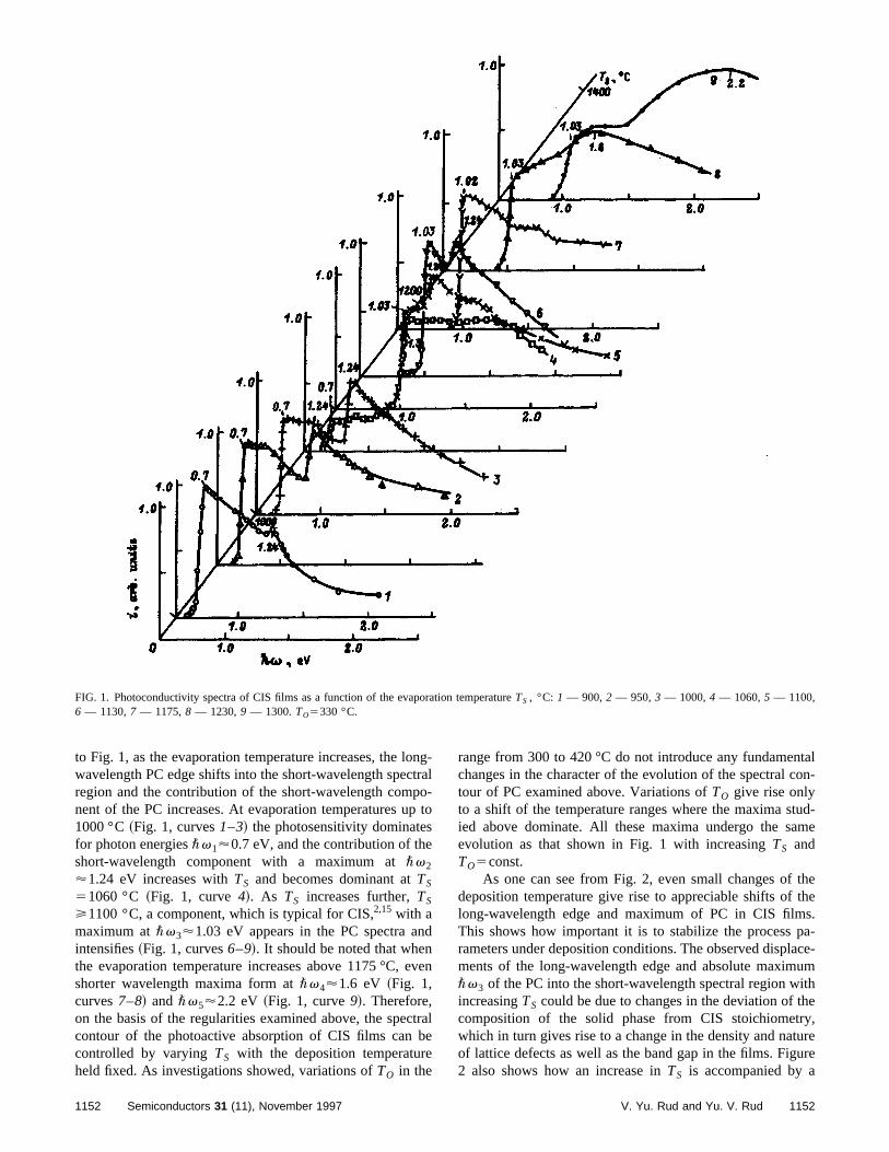
FIG. 1. Photoconductivity spectra of CIS films as a function of the evaporation temperatureTS , °C: 1 — 900,2 — 950,3 — 1000,4 — 1060,5 — 1100,6 — 1130,7 — 1175,8 — 1230,9 — 1300.TO5330 °C.
to Fig. 1, as the evaporation temperature increases, the long-ctrpopse
ndnev
ctbe
range from 300 to 420 °C do not introduce any fundamentalon-
tud-me
thethes.
pa-ace-umithhery,ureure
wavelength PC edge shifts into the short-wavelength speregion and the contribution of the short-wavelength comnent of the PC increases. At evaporation temperatures u1000 °C~Fig. 1, curves1–3! the photosensitivity dominatefor photon energies\v1'0.7 eV, and the contribution of thshort-wavelength component with a maximum at\v2
'1.24 eV increases withTS and becomes dominant atTS
51060 °C ~Fig. 1, curve4!. As TS increases further,TS
>1100 °C, a component, which is typical for CIS,2,15 with amaximum at\v3'1.03 eV appears in the PC spectra aintensifies~Fig. 1, curves6–9!. It should be noted that whethe evaporation temperature increases above 1175 °C,shorter wavelength maxima form at\v4'1.6 eV ~Fig. 1,curves7–8! and \v5'2.2 eV ~Fig. 1, curve9!. Therefore,on the basis of the regularities examined above, the specontour of the photoactive absorption of CIS films cancontrolled by varyingTS with the deposition temperaturheld fixed. As investigations showed, variations ofTO in the
1152 Semiconductors 31 (11), November 1997
al-to
en
rale
changes in the character of the evolution of the spectral ctour of PC examined above. Variations ofTO give rise onlyto a shift of the temperature ranges where the maxima sied above dominate. All these maxima undergo the saevolution as that shown in Fig. 1 with increasingTS andTO5const.
As one can see from Fig. 2, even small changes ofdeposition temperature give rise to appreciable shifts oflong-wavelength edge and maximum of PC in CIS filmThis shows how important it is to stabilize the processrameters under deposition conditions. The observed displments of the long-wavelength edge and absolute maxim\v3 of the PC into the short-wavelength spectral region wincreasingTS could be due to changes in the deviation of tcomposition of the solid phase from CIS stoichiometwhich in turn gives rise to a change in the density and natof lattice defects as well as the band gap in the films. Fig2 also shows how an increase inTS is accompanied by a
1152V. Yu. Rud and Yu. V. Rud
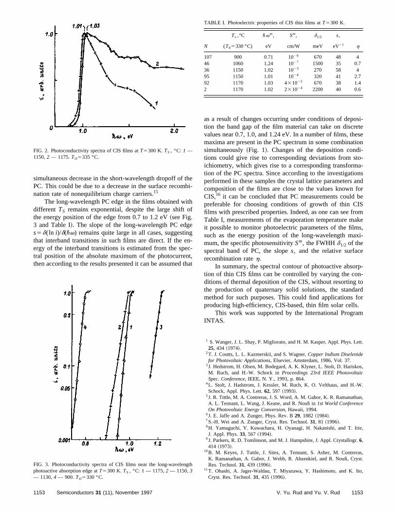
thm
itho
geinnent
osi-eteesetioni-to-a-
onsand
forbe
ISromakes,xi-
rp-n-toardfor.m
ett.
s,
W.
an,
ie,
.
as,yst.
to,gt
TABLE I. Photoelectric properties of CIS thin films atT5300 K.
simultaneous decrease in the short-wavelength dropoff ofPC. This could be due to a decrease in the surface reconation rate of nonequilibrium charge carriers.15
The long-wavelength PC edge in the films obtained wdifferent TS remains exponential, despite the large shiftthe energy position of the edge from 0.7 to 1.2 eV~see Fig.3 and Table I!. The slope of the long-wavelength PC eds5d(ln i)/d(\v) remains quite large in all cases, suggestthat interband transitions in such films are direct. If the eergy of the interband transitions is estimated from the sptral position of the absolute maximum of the photocurrethen according to the results presented it can be assumed
FIG. 2. Photoconductivity spectra of CIS films atT5300 K. TS , °C: 1 —1150,2 — 1175.TO5335 °C.
FIG. 3. Photoconductivity spectra of CIS films near the long-wavelenphotoactive absorption edge atT5300 K. TS , °C: 1 — 1175,2 — 1150,3— 1130,4 — 900.TO5330 °C.
1153 Semiconductors 31 (11), November 1997
ebi-
f
g-c-t,hat
as a result of changes occurring under conditions of deption the band gap of the film material can take on discrvalues near 0.7, 1.0, and 1.24 eV. In a number of films, thmaxima are present in the PC spectrum in some combinasimultaneously~Fig. 1!. Changes of the deposition condtions could give rise to corresponding deviations from sichiometry, which gives rise to a corresponding transformtion of the PC spectra. Since according to the investigatiperformed in these samples the crystal lattice parameterscomposition of the films are close to the values knownCIS,16 it can be concluded that PC measurements couldpreferable for choosing conditions of growth of thin Cfilms with prescribed properties. Indeed, as one can see fTable I, measurements of the evaporation temperature mit possible to monitor photoelectric parameters of the filmsuch as the energy position of the long-wavelength mamum, the specific photosensitivitySm, the FWHHd1/2 of thespectral band of PC, the slopes, and the relative surfacerecombination rateh.
In summary, the spectral contour of photoactive absotion of thin CIS films can be controlled by varying the coditions of thermal deposition of the CIS, without resortingthe production of quaternary solid solutions, the standmethod for such purposes. This could find applicationsproducing high-efficiency, CIS-based, thin film solar cells
This work was supported by the International PrograINTAS.
1 S. Wanger, J. L. Shay, P. Migliorato, and H. M. Kasper, Appl. Phys. L25, 434 ~1974!.
2T. J. Coutts, L. L. Kazmerskii, and S. Wagner,Copper Indium Diselenidefor Photovoltaic Applications, Elsevier, Amsterdam, 1986, Vol. 37.
3J. Hedstrom, H. Olsen, M. Bodegard, A. K. Klyner, L. Stolt, D. HariskoM. Ruch, and H.-W. Schock inProceedings 23rd IEEE PhotovoltaicSpec. Conference, IEEE, N. Y., 1993, p. 864.
4L. Stolt, J. Hadstrom, J. Kessler, M. Ruch, K. O. Velthaus, and H.-Schock, Appl. Phys. Lett.62, 597 ~1993!.
5J. R. Tittle, M. A. Contreras, J. S. Word, A. M. Gabor, K. R. RamanathA. L. Tennant, L. Wang, J. Keane, and R. Noufi in1st World ConferenceOn Photovoltaic Energy Conversion, Hawaii, 1994.
6J. E. Jaffe and A. Zunger, Phys. Rev. B29, 1882~1984!.7S.-H. Wei and A. Zunger, Cryst. Res. Technol.31, 81 ~1996!.8H. Yamaguchi, Y. Kuwachara, H. Oyanagi, H. Nakanishi, and T. IrJ. Appl. Phys.33, 567 ~1994!.
9J. Parkers, R. D. Tomlinson, and M. J. Hampshire, J. Appl. Crystallogr6,414 ~1973!.
10B. M. Keyes, J. Tuttle, J. Sites, A. Tennant, S. Asher, M. ContrerK. Ramanathan, A. Gabor, J. Webb, R. Ahzenkiel, and R. Noufi, CrRes. Technol.31, 439 ~1996!.
11T. Ohashi, A. Jager-Waldau, T. Miyazawa, Y. Hashimoto, and K. ICryst. Res. Technol.31, 435 ~1996!.
h
N
Ts ,°C \vm, Sm, d1/2 s,
h(T05330 °C) eV cm/W meV eV21
107 900 0.71 1026 670 48 446 1060 1.24 1027 1500 35 0.736 1150 1.02 1023 270 58 495 1150 1.01 1024 320 41 2.792 1170 1.03 431025 670 38 1.42 1170 1.02 231024 2200 40 0.6
1153V. Yu. Rud and Yu. V. Rud
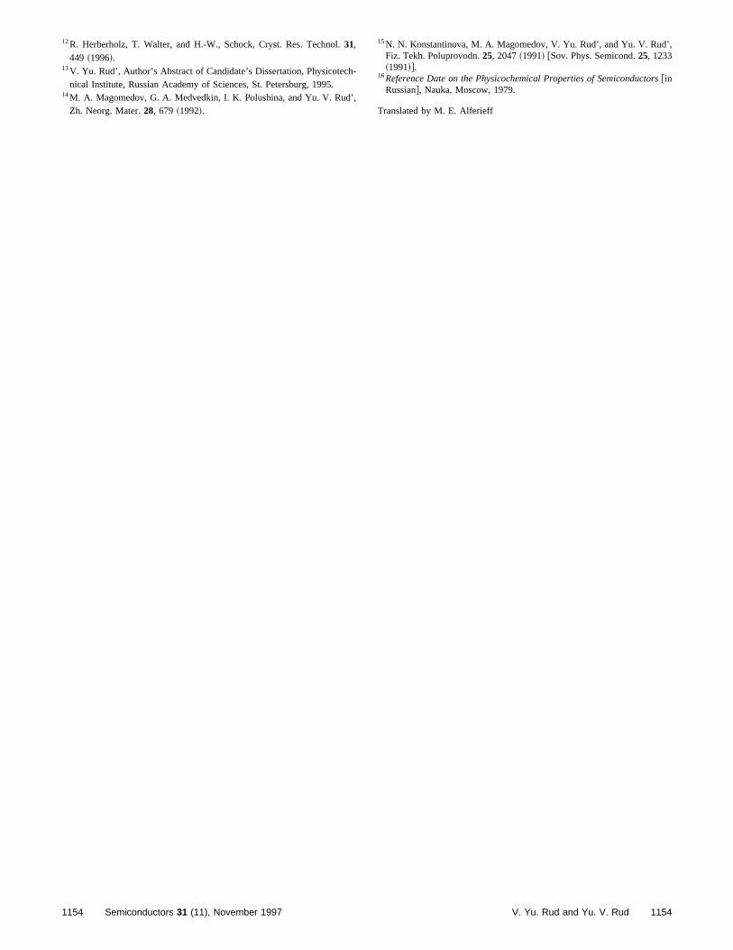
12R. Herberholz, T. Walter, and H.-W., Schock, Cryst. Res. Technol.31,
449 ~1996!.
ch
’,
15N. N. Konstantinova, M. A. Magomedov, V. Yu. Rud’, and Yu. V. Rud’,Fiz. Tekh. Poluprovodn.25, 2047~1991! @Sov. Phys. Semicond.25, 1233
s
13V. Yu. Rud’, Author’s Abstract of Candidate’s Dissertation, Physicotenical Institute, Russian Academy of Sciences, St. Petersburg, 1995.14M. A. Magomedov, G. A. Medvedkin, I. K. Polushina, and Yu. V. Rud
Zh. Neorg. Mater.28, 679 ~1992!.
1154 Semiconductors 31 (11), November 1997
- ~1991!#.16Reference Date on the Physicochemical Properties of Semiconductor@in
Russian#, Nauka, Moscow, 1979.
Translated by M. E. Alferieff
1154V. Yu. Rud and Yu. V. Rud
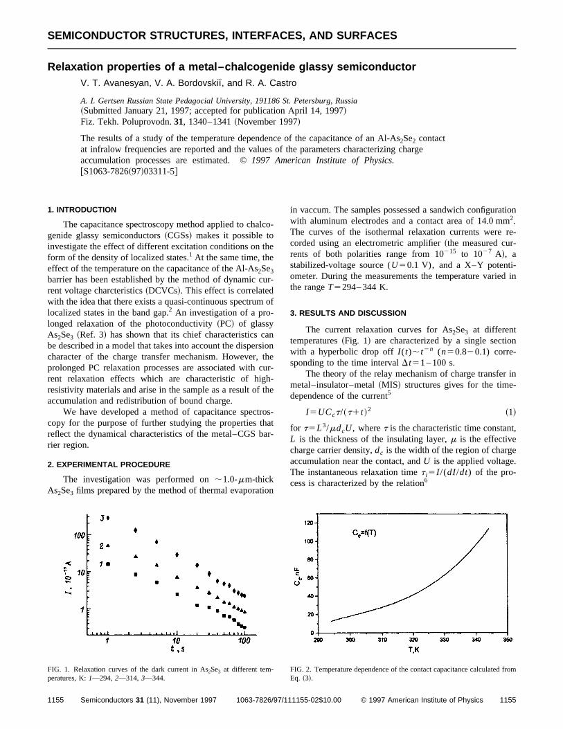
SEMICONDUCTOR STRUCTURES, INTERFACES, AND SURFACES
ation
Relaxation properties of a metal–chalcogenide glassy semiconductorV. T. Avanesyan, V. A. Bordovski , and R. A. Castro
A. I. Gertsen Russian State Pedagocial University, 191186 St. Petersburg, Russia~Submitted January 21, 1997; accepted for publication April 14, 1997!Fiz. Tekh. Poluprovodn.31, 1340–1341~November 1997!
The results of a study of the temperature dependence of the capacitance of an Al-As2Se2 contactat infralow frequencies are reported and the values of the parameters characterizing chargeaccumulation processes are estimated. ©1997 American Institute of Physics.@S1063-7826~97!03311-5#
1. INTRODUCTION in vaccum. The samples possessed a sandwich configur2
lc
he
cu
ansitchth
trohaa
io
mre-
-
d in
n
r in-
t,
from
/1
The capacitance spectroscopy method applied to chagenide glassy semiconductors~CGSs! makes it possible toinvestigate the effect of different excitation conditions on tform of the density of localized states.1 At the same time, theeffect of the temperature on the capacitance of the Al-As2Se3
barrier has been established by the method of dynamicrent voltage charcteristics~DCVCs!. This effect is correlatedwith the idea that there exists a quasi-continuous spectrumlocalized states in the band gap.2 An investigation of a pro-longed relaxation of the photoconductivity~PC! of glassyAs2Se3 ~Ref. 3! has shown that its chief characteristics cbe described in a model that takes into account the dispercharacter of the charge transfer mechanism. However,prolonged PC relaxation processes are associated withrent relaxation effects which are characteristic of higresistivity materials and arise in the sample as a result ofaccumulation and redistribution of bound charge.
We have developed a method of capacitance speccopy for the purpose of further studying the properties treflect the dynamical characteristics of the metal–CGS brier region.
2. EXPERIMENTAL PROCEDURE
The investigation was performed on;1.0-mm-thickAs2Se3 films prepared by the method of thermal evaporat
FIG. 1. Relaxation curves of the dark current in As2Se3 at different tem-peratures, K:1—294,2—314,3—344.
1155 Semiconductors 31 (11), November 1997 1063-7826/97
o-
r-
of
onheur--e
s-tr-
n
with aluminum electrodes and a contact area of 14.0 m.The curves of the isothermal relaxation currents werecorded using an electrometric amplifier~the measured currents of both polarities range from 10215 to 1027 A!, astabilized-voltage source (U50.1 V), and a X–Y potenti-ometer. During the measurements the temperature variethe rangeT5294– 344 K.
3. RESULTS AND DISCUSSION
The current relaxation curves for As2Se3 at differenttemperatures~Fig. 1! are characterized by a single sectiowith a hyperbolic drop offI (t);t2n (n50.820.1) corre-sponding to the time intervalDt51 – 100 s.
The theory of the relay mechanism of charge transfemetal–insulator–metal~MIS! structures gives for the timedependence of the current5
I 5UCct/~t1t !2 ~1!
for t5L3/mdcU, wheret is the characteristic time constanL is the thickness of the insulating layer,m is the effectivecharge carrier density,dc is the width of the region of chargeaccumulation near the contact, andU is the applied voltage.The instantaneous relaxation timet i5I /(dI/dt) of the pro-cess is characterized by the relation6
FIG. 2. Temperature dependence of the contact capacitance calculatedEq. ~3!.
115511155-02$10.00 © 1997 American Institute of Physics
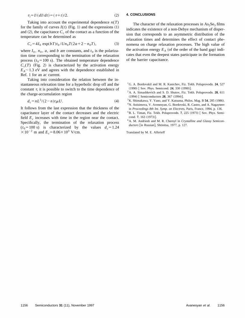
t i5I /~dI/dt!5~t1t !/2. ~2!
e
ionncgyd
intho
thccs
4. CONCLUSIONS
per-thehe-e of
ation
ev
-
Taking into account the experimental dependencen(T)for the family of curvesI (t) ~Fig. 1! and the expressions~1!and~2!, the capacitanceCc of the contact as a function of thtemperature can be determined as
Cc54I 0 exp~bT!t0 /Un0T~2a122n0T!, ~3!
whereI 0 , n0 , a, andb are constants, andt0 is the polariza-tion time corresponding to the termination of the relaxatprocess (t05100 s). The obtained temperature dependeCc(T) ~Fig. 2! is characterized by the activation enerEA;1.3 eV and agrees with the dependence establisheRef. 1 for an ac current.
Taking into consideration the relation between thestantaneous relexation time for a hyperbolic drop off andconstantt, it is possible to switch to the time dependencethe charge-accumulation region
dc5nL3/~22n!tmU. ~4!
It follows from the last expression that the thickness ofcapacitance layer of the contact decreases and the elefield Ec increases with time in the region near the contaSpecifically, the termination of the relaxation proce(t05100 s) is characterized by the valuesdc51.2431022 m andEc58.063103 V/cm.
1156 Semiconductors 31 (11), November 1997
e
in
-ef
etrict.s
The character of the relaxation processes in As2Se3 filmsindicates the existence of a non-Debye mechanism of dission that corresponds to an asymmetric distribution ofrelaxation times and determines the effect of contact pnomena on charge relaxation processes. The high valuthe activation energyEA ~of the order of the band gap! indi-cates that even the deepest states participate in the formof the barrier capacitance.
1G. A. Bordovski� and M. R. Kanichev, Fiz. Tekh. Poluprovodn.24, 527~1990! @ Sov. Phys. Semicond.24, 330 ~1990!#.
2A. A. Simashkevich and S. D. Shutov, Fiz. Tekh. Poluprovodn.28, 611~1994! @ Semiconductors28, 367 ~1994!#.
3K. Shimakawa, Y. Yano, and Y. Katsuma, Philos. Mag. B54, 285~1986!.4N. Anisimova, V. Avenesyan, G. Bordovski, R. Castro, and A. Nagaytein Proceedings 8th Int. Symp. on Electrets, Paris, France, 1994, p. 136.
5B. L. Timan, Fiz. Tekh. Poluprovodn.7, 225 ~1973! @ Sov. Phys. Semi-cond.7, 163 ~1973!#.
6A. M. Andriesh and M. R. Cherny� in Crystalline and Glassy Semiconductors@in Russian#, Shtinitsa, 1977, p. 127.
Translated by M. E. Alferieff
1156Avanesyan et al.
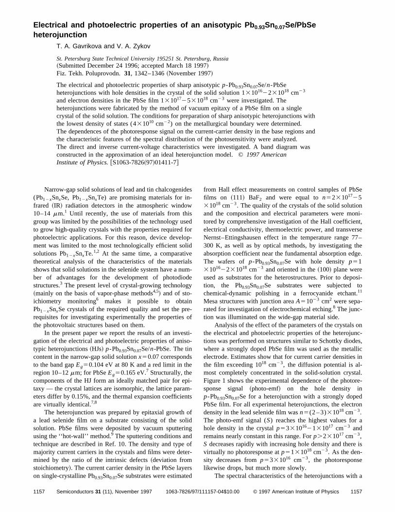
Electrical and photoelectric properties of an anisotypic Pb 0.93Sn0.07Se/PbSe
Se
heterojunctionT. A. Gavrikova and V. A. Zykov
St. Petersburg State Technical University 195251 St. Petersburg, Russia~Submitted December 24 1996; accepted March 18 1997!Fiz. Tekh. Poluprovodn.31, 1342–1346~November 1997!
The electrical and photoelectric properties of sharp anisotypicp-Pb0.93Sn0.07Se/n-PbSeheterojunctions with hole densities in the crystal of the solid solution 1310162231018 cm23
and electron densities in the PbSe film 1310172531018 cm23 were investigated. Theheterojunctions were fabricated by the method of vacuum epitaxy of a PbSe film on a singlecrystal of the solid solution. The conditions for preparation of sharp anisotypic heterojunctions withthe lowest density of states (431010 cm22) on the metallurgical boundary were determined.The dependences of the photoresponse signal on the current-carrier density in the base regions andthe characteristic features of the spectral distribution of the photosensitivity were analyzed.The direct and inverse current-voltage characteristics were investigated. A band diagram wasconstructed in the approximation of an ideal heterojunction model. ©1997 AmericanInstitute of Physics.@S1063-7826~97!01411-7#
Narrow-gap solid solutions of lead and tin chalcogenidesfrom Hall effect measurements on control samples of Pb17
-wise
fololideiaudy
reo
stso
pmn
oolrindete
red
noni-nt,rse77–hege.
posi-tot.
onnc-es,allics in
tal.ore-
dron
a
e is
h a
/1
(Pb12xSnxSe, Pb12xSnxTe) are promising materials for infrared ~IR! radiation detectors in the atmospheric windo10–14 mm.1 Until recently, the use of materials from thgroup was limited by the possibilities of the technology usto grow high-quality crystals with the properties requiredphotoelectric applications. For this reason, device devement was limited to the most technologically efficient sosolutions Pb12xSnxTe.1,2 At the same time, a comparativtheoretical analysis of the characteristics of the matershows that solid solutions in the selenide system have a nber of advantages for the development of photodiostructures.3 The present level of crystal-growing technolog~mainly on the basis of vapor-phase methods4,5! and of sto-ichiometry monitoring6 makes it possible to obtainPb12xSnxSe crystals of the required quality and set the prequisites for investigating experimentally the propertiesthe photovoltaic structures based on them.
In the present paper we report the results of an invegation of the electrical and photoelectric properties of anitypic heterojunctions~HJs! p-Pb0.93Sn0.07Se/n-PbSe. The tincontent in the narrow-gap solid solutionx50.07 correspondsto the band gapEg50.104 eV at 80 K and a red limit in theregion 10–12mm; for PbSeEg50.165 eV.7 Structurally, thecomponents of the HJ form an ideally matched pair for etaxy — the crystal lattices are isomorphic, the lattice paraeters differ by 0.15%, and the thermal expansion coefficieare virtually identical.7,8
The heterojunction was prepared by epitaxial growtha lead selenide film on a substrate consisting of the ssolution. PbSe films were deposited by vacuum sputteusing the ‘‘hot-wall’’ method.9 The sputtering conditions antechnique are described in Ref. 10. The density and typmajority current carriers in the crystals and films were demined by the ratio of the intrinsic defects~deviation fromstoichiometry!. The current carrier density in the PbSe layeon single-crystalline Pb0.93Sn0.07Se substrates were estimat
1157 Semiconductors 31 (11), November 1997 1063-7826/97
drp-
lsm-e
-f
i--
i--ts
fidg
ofr-
s
films on ~111! BaF2 and were equal ton52310 2531018 cm23. The quality of the crystals of the solid solutioand the composition and electrical parameters were mtored by comprehensive investigation of the Hall coefficieelectrical conductivity, thermoelectric power, and transveNernst–Ettingshausen effect in the temperature range300 K, as well as by optical methods, by investigating tabsorption coefficient near the fundamental absorption edThe wafers of p-Pb0.93Sn0.07Se with hole densityp51310162231018 cm23 and oriented in the~100! plane wereused as substrates for the heterostructures. Prior to detion, the Pb0.93Sn0.07Se substrates were subjectedchemical-dynamic polishing in a ferrocyanide etchan11
Mesa structures with junction areaA51023 cm2 were sepa-rated for investigation of electrochemical etching.8 The junc-tion was illuminated on the wide-gap material side.
Analysis of the effect of the parameters of the crystalsthe electrical and photoelectric properties of the heterojutions was performed on structures similar to Schottky diodwhere a strongly doped PbSe film was used as the metelectrode. Estimates show that for current carrier densitiethe film exceeding 1018 cm23, the diffusion potential is al-most completely concentrated in the solid-solution crysFigure 1 shows the experimental dependence of the photsponse signal ~photo-emf! on the hole density inp-Pb0.93Sn0.07Se for a heterojunction with a strongly dopePbSe film. For all experimental heterojunctions, the electdensity in the lead selenide film wasn5(2 – 3)31018 cm23.The photo-emf signal (S) reaches the highest values forhole density in the crystalp53310162131017 cm23 andremains nearly constant in this range. Forp.231017 cm23,S decreases rapidly with increasing hole density and thervirtually no photoresponse atp5131018 cm23. As the den-sity decreases fromp5331016 cm23, the photoresponselikewise drops, but much more slowly.
The spectral characteristics of the heterojunctions wit
115711157-04$10.00 © 1997 American Institute of Physics
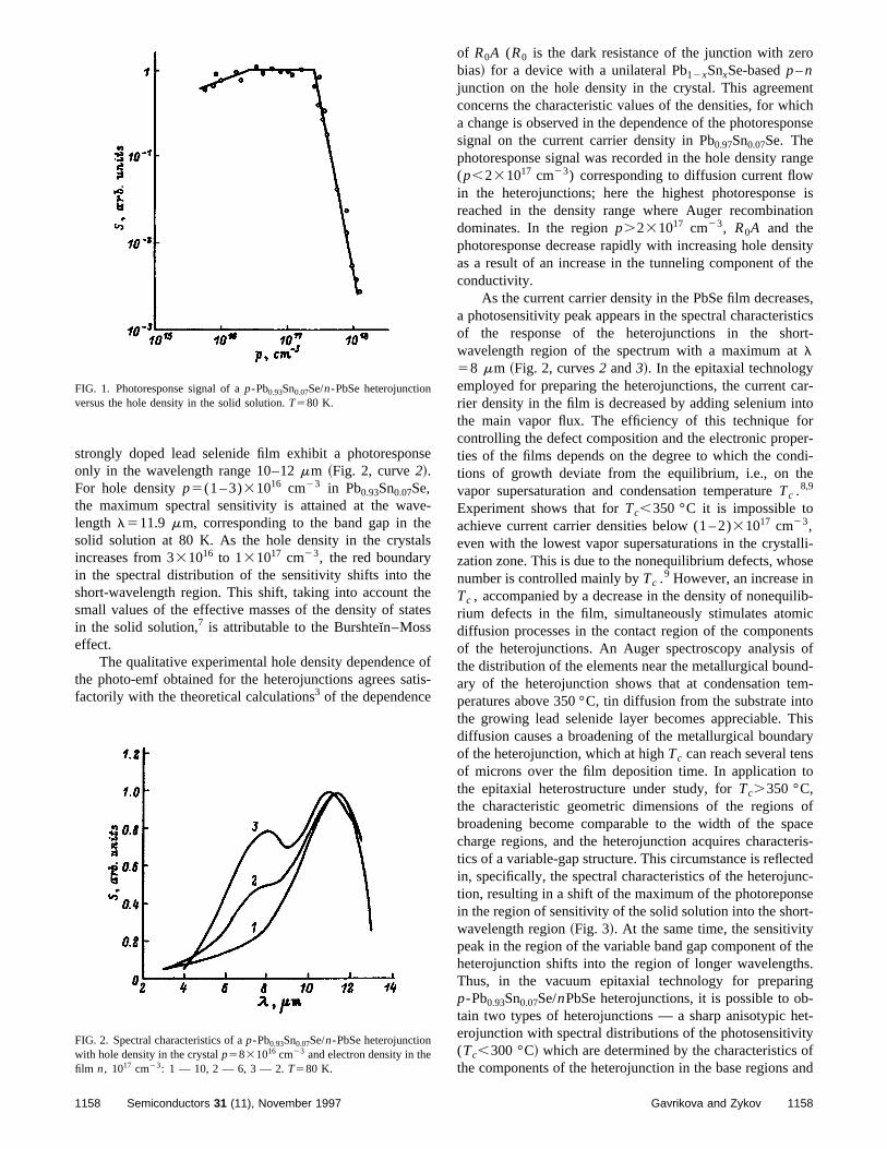
ns
veels
ethat
eat
of R0A (R0 is the dark resistance of the junction with zero
entichonse
nge
e istion
sitythe
es,sticsrt-
ar-ntoorer-di-e
lli-ose
ilib-icntsof
nd-m-
ntohis
arysto
ofaceeris-tednc-sert-ythe
hs.ngb--ityofand
strongly doped lead selenide film exhibit a photorespoonly in the wavelength range 10–12mm ~Fig. 2, curve2!.For hole densityp5(1 – 3)31016 cm23 in Pb0.93Sn0.07Se,the maximum spectral sensitivity is attained at the walength l511.9 mm, corresponding to the band gap in thsolid solution at 80 K. As the hole density in the crystaincreases from 331016 to 131017 cm23, the red boundaryin the spectral distribution of the sensitivity shifts into thshort-wavelength region. This shift, taking into accountsmall values of the effective masses of the density of stin the solid solution,7 is attributable to the Burshte�n–Mosseffect.
The qualitative experimental hole density dependencthe photo-emf obtained for the heterojunctions agrees sfactorily with the theoretical calculations3 of the dependence
FIG. 1. Photoresponse signal of ap-Pb0.93Sn0.07Se/n-PbSe heterojunctionversus the hole density in the solid solution.T580 K.
FIG. 2. Spectral characteristics of ap-Pb0.93Sn0.07Se/n-PbSe heterojunctionwith hole density in the crystalp5831016 cm23 and electron density in thefilm n, 1017 cm23: 1 — 10, 2 — 6, 3 — 2.T580 K.
1158 Semiconductors 31 (11), November 1997
e
-
ees
ofis-
bias! for a device with a unilateral Pb12xSnxSe-basedp–njunction on the hole density in the crystal. This agreemconcerns the characteristic values of the densities, for wha change is observed in the dependence of the photorespsignal on the current carrier density in Pb0.97Sn0.07Se. Thephotoresponse signal was recorded in the hole density ra(p,231017 cm23) corresponding to diffusion current flowin the heterojunctions; here the highest photoresponsreached in the density range where Auger recombinadominates. In the regionp.231017 cm23, R0A and thephotoresponse decrease rapidly with increasing hole denas a result of an increase in the tunneling component ofconductivity.
As the current carrier density in the PbSe film decreasa photosensitivity peak appears in the spectral characteriof the response of the heterojunctions in the showavelength region of the spectrum with a maximum atl58 mm ~Fig. 2, curves2 and3!. In the epitaxial technologyemployed for preparing the heterojunctions, the current crier density in the film is decreased by adding selenium ithe main vapor flux. The efficiency of this technique fcontrolling the defect composition and the electronic propties of the films depends on the degree to which the contions of growth deviate from the equilibrium, i.e., on thvapor supersaturation and condensation temperatureTc .8,9
Experiment shows that forTc,350 °C it is impossible toachieve current carrier densities below (1 – 2)31017 cm23,even with the lowest vapor supersaturations in the crystazation zone. This is due to the nonequilibrium defects, whnumber is controlled mainly byTc .9 However, an increase inTc , accompanied by a decrease in the density of nonequrium defects in the film, simultaneously stimulates atomdiffusion processes in the contact region of the componeof the heterojunctions. An Auger spectroscopy analysisthe distribution of the elements near the metallurgical bouary of the heterojunction shows that at condensation teperatures above 350 °C, tin diffusion from the substrate ithe growing lead selenide layer becomes appreciable. Tdiffusion causes a broadening of the metallurgical boundof the heterojunction, which at highTc can reach several tenof microns over the film deposition time. In applicationthe epitaxial heterostructure under study, forTc.350 °C,the characteristic geometric dimensions of the regionsbroadening become comparable to the width of the spcharge regions, and the heterojunction acquires characttics of a variable-gap structure. This circumstance is reflecin, specifically, the spectral characteristics of the heterojution, resulting in a shift of the maximum of the photoreponin the region of sensitivity of the solid solution into the showavelength region~Fig. 3!. At the same time, the sensitivitpeak in the region of the variable band gap component ofheterojunction shifts into the region of longer wavelengtThus, in the vacuum epitaxial technology for preparip-Pb0.93Sn0.07Se/nPbSe heterojunctions, it is possible to otain two types of heterojunctions — a sharp anisotypic heterojunction with spectral distributions of the photosensitiv(Tc,300 °C! which are determined by the characteristicsthe components of the heterojunction in the base regions
1158Gavrikova and Zykov
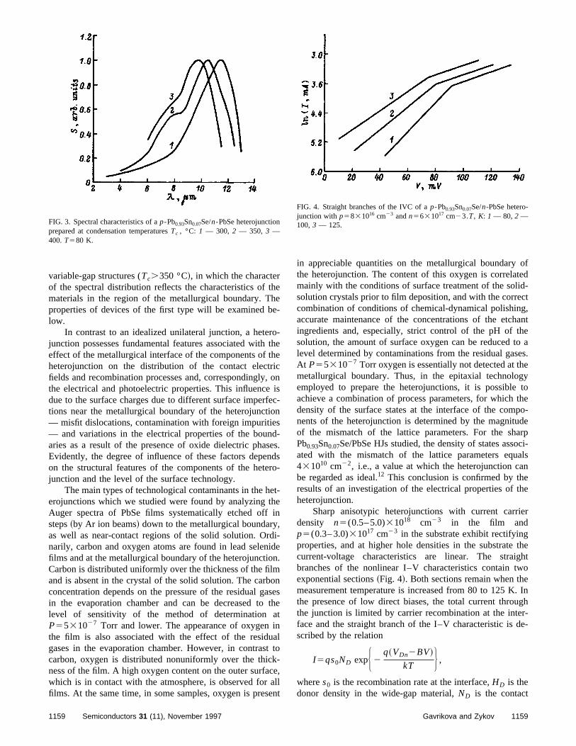
thhe
rohthric,
feiosdsener
ethi,
rdid
onlmoat
atin
uatkceae
oftedid-ctg,hantheto aes.
hegy
tothepo-
udearpoci-alsn
ethe
ier
theghtwoe. In
ughr-de-
variable-gap structures (Tc.350 °C!, in which the characterof the spectral distribution reflects the characteristics ofmaterials in the region of the metallurgical boundary. Tproperties of devices of the first type will be examined blow.
In contrast to an idealized unilateral junction, a hetejunction possesses fundamental features associated witeffect of the metallurgical interface of the components ofheterojunction on the distribution of the contact electfields and recombination processes and, correspondinglythe electrical and photoelectric properties. This influencedue to the surface charges due to different surface impertions near the metallurgical boundary of the heterojunct— misfit dislocations, contamination with foreign impuritie— and variations in the electrical properties of the bounaries as a result of the presence of oxide dielectric phaEvidently, the degree of influence of these factors depeon the structural features of the components of the hetjunction and the level of the surface technology.
The main types of technological contaminants in the herojunctions which we studied were found by analyzingAuger spectra of PbSe films systematically etched offsteps~by Ar ion beams! down to the metallurgical boundaryas well as near-contact regions of the solid solution. Onarily, carbon and oxygen atoms are found in lead selenfilms and at the metallurgical boundary of the heterojunctiCarbon is distributed uniformly over the thickness of the fiand is absent in the crystal of the solid solution. The carbconcentration depends on the pressure of the residual gin the evaporation chamber and can be decreased tolevel of sensitivity of the method of determinationP5531027 Torr and lower. The appearance of oxygenthe film is also associated with the effect of the residgases in the evaporation chamber. However, in contrascarbon, oxygen is distributed nonuniformly over the thicness of the film. A high oxygen content on the outer surfawhich is in contact with the atmosphere, is observed forfilms. At the same time, in some samples, oxygen is pres
FIG. 3. Spectral characteristics of ap-Pb0.93Sn0.07Se/n-PbSe heterojunctionprepared at condensation temperaturesTc , °C: 1 — 300, 2 — 350, 3 —400.T580 K.
1159 Semiconductors 31 (11), November 1997
ee-
-thee
onisc-n
-s.
dso-
t-en
i-e.
nseshe
lto-,
llnt
in appreciable quantities on the metallurgical boundarythe heterojunction. The content of this oxygen is correlamainly with the conditions of surface treatment of the solsolution crystals prior to film deposition, and with the correcombination of conditions of chemical-dynamical polishinaccurate maintenance of the concentrations of the etcingredients and, especially, strict control of the pH of tsolution, the amount of surface oxygen can be reducedlevel determined by contaminations from the residual gasAt P5531027 Torr oxygen is essentially not detected at tmetallurgical boundary. Thus, in the epitaxial technoloemployed to prepare the heterojunctions, it is possibleachieve a combination of process parameters, for whichdensity of the surface states at the interface of the comnents of the heterojunction is determined by the magnitof the mismatch of the lattice parameters. For the shPb0.93Sn0.07Se/PbSe HJs studied, the density of states assated with the mismatch of the lattice parameters equ431010 cm22, i.e., a value at which the heterojunction cabe regarded as ideal.12 This conclusion is confirmed by thresults of an investigation of the electrical properties ofheterojunction.
Sharp anisotypic heterojunctions with current carrdensity n5(0.5– 5.0)31018 cm23 in the film andp5(0.3– 3.0)31017 cm23 in the substrate exhibit rectifyingproperties, and at higher hole densities in the substratecurrent-voltage characteristics are linear. The straibranches of the nonlinear I–V characteristics contain texponential sections~Fig. 4!. Both sections remain when thmeasurement temperature is increased from 80 to 125 Kthe presence of low direct biases, the total current throthe junction is limited by carrier recombination at the inteface and the straight branch of the I–V characteristic isscribed by the relation
I 5qs0ND expH 2q~VDn2BV!
kT J ,
wheres0 is the recombination rate at the interface,HD is thedonor density in the wide-gap material,ND is the contact
FIG. 4. Straight branches of the IVC of ap-Pb0.93Sn0.07Se/n-PbSe hetero-junction withp5831016 cm23 andn5631017 cm23.T, K: 1 — 80, 2 —100,3 — 125.
1159Gavrikova and Zykov
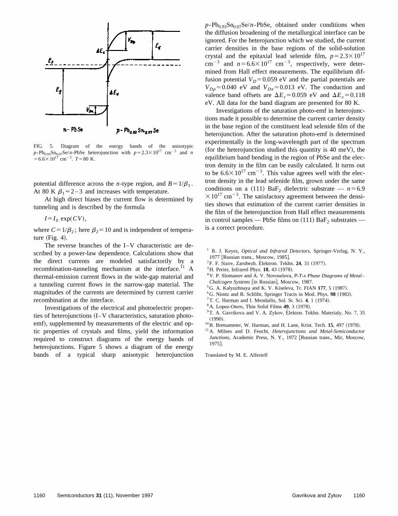
by
a-
dtha
nhrri
er-ono
rgon
p-Pb0.93Sn0.07Se/n-PbSe, obtained under conditions whenbeention
-if-red
.c-sitytheed
um
lec-ut-me
si-in
nts
r
ic
potential difference across then-type region, andB51/b1 .At 80 K b152 – 3 and increases with temperature.
At high direct biases the current flow is determinedtunneling and is described by the formula
I 5I 0 exp~CV!,
whereC51/b2 ; hereb2510 and is independent of temperture ~Fig. 4!.
The reverse branches of the I–V characteristic arescribed by a power-law dependence. Calculations showthe direct currents are modeled satisfactorily byrecombination-tunneling mechanism at the interface.11 Athermal-emission current flows in the wide-gap material aa tunneling current flows in the narrow-gap material. Tmagnitudes of the currents are determined by current carecombination at the interface.
Investigations of the electrical and photoelectric propties of heterojunctions~I–V characteristics, saturation photoemf!, supplemented by measurements of the electric andtic properties of crystals and films, yield the informatiorequired to construct diagrams of the energy bandsheterojunctions. Figure 5 shows a diagram of the enebands of a typical sharp anisotypic heterojuncti
FIG. 5. Diagram of the energy bands of the anisotypp-Pb0.93Sn0.07Se/n-PbSe heterojunction withp52.331017 cm23 and n56.631017 cm23. T580 K.
1160 Semiconductors 31 (11), November 1997
e-at
deer
-
p-
fy
the diffusion broadening of the metallurgical interface canignored. For the heterojunction which we studied, the currcarrier densities in the base regions of the solid-solutcrystal and the epitaxial lead selenide film,p52.331017
cm23 and n56.631017 cm23, respectively, were determined from Hall effect measurements. The equilibrium dfusion potentialVD50.059 eV and the partial potentials aVDp50.040 eV andVDn50.013 eV. The conduction anvalence band offsets areDEc50.059 eV andDEv50.118eV. All data for the band diagram are presented for 80 K
Investigations of the saturation photo-emf in heterojuntions made it possible to determine the current carrier denin the base region of the constituent lead selenide film ofheterojunction. After the saturation photo-emf is determinexperimentally in the long-wavelength part of the spectr~for the heterojunction studied this quantity is 40 meV!, theequilibrium band bending in the region of PbSe and the etron density in the film can be easily calculated. It turns oto be 6.631017 cm23. This value agrees well with the electron density in the lead selenide film, grown under the saconditions on a~111! BaF2 dielectric substrate —n56.931017 cm23. The satisfactory agreement between the denties shows that estimation of the current carrier densitiesthe film of the heterojunction from Hall effect measuremein control samples — PbSe films on~111! BaF2 substrates —is a correct procedure.
1 R. J. Keyes,Optical and Infrared Detectors, Springer-Verlag, N. Y.,1977 @Russian trans., Moscow, 1985#.
2F. F. Sizov, Zarubezh. E´ lektron. Tekhn.24, 31 ~1977!.3H. Preier, Infrared Phys.18, 43 ~1978!.4V. P. Slomanov and A. V. Novoselova,P-T-x Phase Diagrams of Metal–Chalcogen Systems@in Russian#, Moscow, 1987.
5G. A. Kalyuzhnaya and K. V. Kiseleva, Tr. FIAN177, 5 ~1987!.6G. Nimtz and B. Schliht, Springer Tracts in Mod. Phys.98 ~1983!.7T. C. Harman and I. Mendailis, Sol. St. Sci.4, 1 ~1974!.8A. Lopez-Otero, Thin Solid Films49, 3 ~1978!.9T. A. Gavrikova and V. A. Zykov, E´ lekton. Tekhn. Materialy, No. 7, 35~1990!.
10B. Bretsameter, W. Harman, and H. Lane, Krist. Tech.15, 497 ~1978!.11A. Milnes and D. Feucht,Heterojunctions and Metal-Semiconducto
Junctions, Academic Press, N. Y., 1972@Russian trans., Mir, Moscow,1975#.
Translated by M. E. Alferieff
1160Gavrikova and Zykov
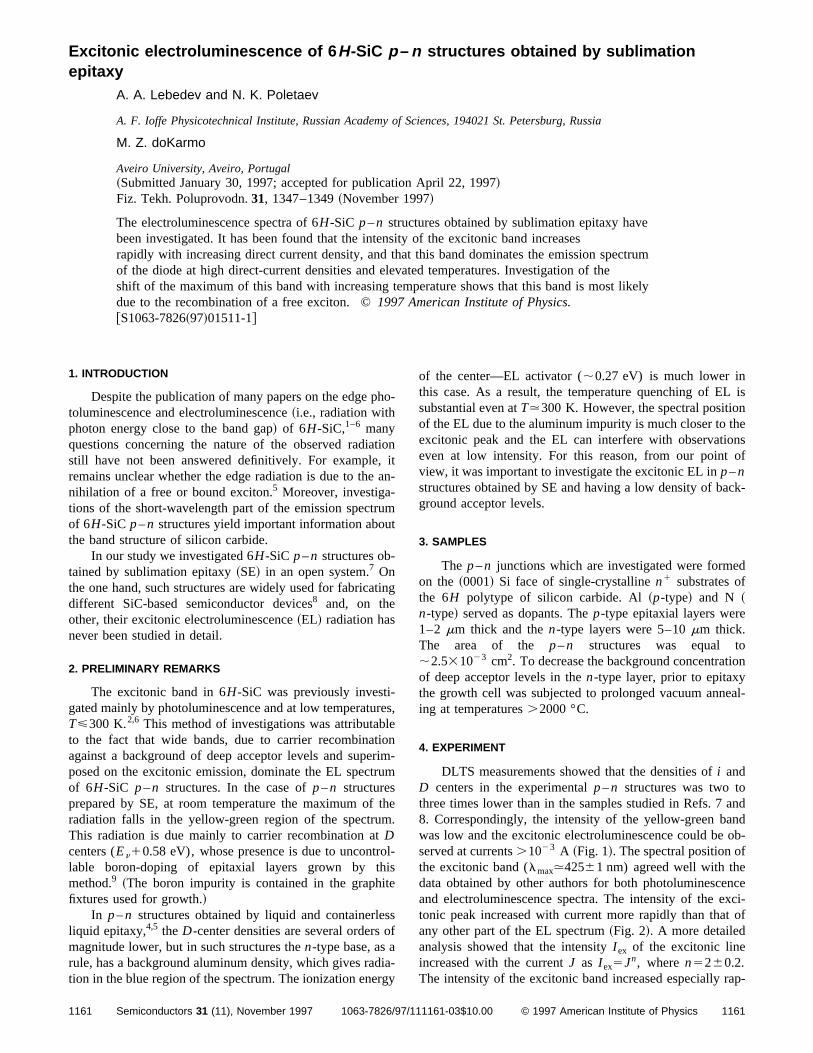
Excitonic electroluminescence of 6 H-SiC p – n structures obtained by sublimation
epitaxyA. A. Lebedev and N. K. Poletaev
A. F. Ioffe Physicotechnical Institute, Russian Academy of Sciences, 194021 St. Petersburg, Russia
M. Z. doKarmo
Aveiro University, Aveiro, Portugal~Submitted January 30, 1997; accepted for publication April 22, 1997!Fiz. Tekh. Poluprovodn.31, 1347–1349~November 1997!
The electroluminescence spectra of 6H-SiC p–n structures obtained by sublimation epitaxy havebeen investigated. It has been found that the intensity of the excitonic band increasesrapidly with increasing direct current density, and that this band dominates the emission spectrumof the diode at high direct-current densities and elevated temperatures. Investigation of theshift of the maximum of this band with increasing temperature shows that this band is most likelydue to the recombination of a free exciton. ©1997 American Institute of Physics.@S1063-7826~97!01511-1#
1. INTRODUCTION of the center—EL activator (;0.27 eV) is much lower in
h
tio,a
uut
tin
releioriru
thm
oliste
so
diarg
isnhensof
ck-
d
ion
eal-
andndob-
ncexci-of
ap-
/1
Despite the publication of many papers on the edge ptoluminescence and electroluminescence~i.e., radiation withphoton energy close to the band gap! of 6H-SiC,1–6 manyquestions concerning the nature of the observed radiastill have not been answered definitively. For exampleremains unclear whether the edge radiation is due to thenihilation of a free or bound exciton.5 Moreover, investiga-tions of the short-wavelength part of the emission spectrof 6H-SiC p–n structures yield important information abothe band structure of silicon carbide.
In our study we investigated 6H-SiC p–n structures ob-tained by sublimation epitaxy~SE! in an open system.7 Onthe one hand, such structures are widely used for fabricadifferent SiC-based semiconductor devices8 and, on theother, their excitonic electroluminescence~EL! radiation hasnever been studied in detail.
2. PRELIMINARY REMARKS
The excitonic band in 6H-SiC was previously investi-gated mainly by photoluminescence and at low temperatuT<300 K.2,6 This method of investigations was attributabto the fact that wide bands, due to carrier recombinatagainst a background of deep acceptor levels and supeposed on the excitonic emission, dominate the EL spectof 6H-SiC p–n structures. In the case ofp–n structuresprepared by SE, at room temperature the maximum ofradiation falls in the yellow-green region of the spectruThis radiation is due mainly to carrier recombination atDcenters (En10.58 eV), whose presence is due to uncontrlable boron-doping of epitaxial layers grown by thmethod.9 ~The boron impurity is contained in the graphifixtures used for growth.!
In p–n structures obtained by liquid and containerleliquid epitaxy,4,5 the D-center densities are several ordersmagnitude lower, but in such structures then-type base, as arule, has a background aluminum density, which gives ration in the blue region of the spectrum. The ionization ene
1161 Semiconductors 31 (11), November 1997 1063-7826/97
o-
nitn-
m
g
s,
nm-m
e.
-
sf
-y
this case. As a result, the temperature quenching of ELsubstantial even atT.300 K. However, the spectral positioof the EL due to the aluminum impurity is much closer to texcitonic peak and the EL can interfere with observatioeven at low intensity. For this reason, from our pointview, it was important to investigate the excitonic EL inp–nstructures obtained by SE and having a low density of baground acceptor levels.
3. SAMPLES
The p–n junctions which are investigated were formeon the ~0001! Si face of single-crystallinen1 substrates ofthe 6H polytype of silicon carbide. Al~p-type! and N ~n-type! served as dopants. Thep-type epitaxial layers were1–2 mm thick and then-type layers were 5–10mm thick.The area of the p–n structures was equal to;2.531023 cm2. To decrease the background concentratof deep acceptor levels in then-type layer, prior to epitaxythe growth cell was subjected to prolonged vacuum anning at temperatures.2000 °C.
4. EXPERIMENT
DLTS measurements showed that the densities ofi andD centers in the experimentalp–n structures was two tothree times lower than in the samples studied in Refs. 78. Correspondingly, the intensity of the yellow-green bawas low and the excitonic electroluminescence could beserved at currents.1023 A ~Fig. 1!. The spectral position ofthe excitonic band (lmax.42561 nm) agreed well with thedata obtained by other authors for both photoluminesceand electroluminescence spectra. The intensity of the etonic peak increased with current more rapidly than thatany other part of the EL spectrum~Fig. 2!. A more detailedanalysis showed that the intensityI ex of the excitonic lineincreased with the currentJ as I ex5Jn, wheren5260.2.The intensity of the excitonic band increased especially r
116111161-03$10.00 © 1997 American Institute of Physics
n
ins
sicres
L
theheig. 4ta,ncemataey
ow elec-
idly at low currentsJ5(1 – 6)31022 A. This could be dueto an increase in the hole diffusion length with increasiinjection level.10
As the sample temperature and the direct currentcreased, the excitonic peak became dominant in the emisspectrum of the diode~Fig. 3!. This occurred for the follow-ing reasons: 1! more rapid growth ofI ex with J than anyother EL bands; 2! increase of the hole diffusion length withtemperature;11 and 3! temperature quenching of all EL bandexcept the excitonic band. At 650 K the intensity of excitonband exhibited the same dependence on the direct curdensity with n52 as previously. As the temperature wa
FIG. 1. Edge electroluminescence spectrum ofp–n structures at room tem-perature.J530 mA.
FIG. 2. Electroluminescence band intensities versus direct current: yellgreen band at 300 K~1!; excitonic band at 300 K~2! and 650 K~3!.
1162 Semiconductors 31 (11), November 1997
g
-ion
nt
raised, the position of the maximum of the excitonic Eshifted into the long-wavelength region~Fig. 4!.
5. DISCUSSION
There are several papers devoted to determiningband gap in 6H-SiC and its temperature dependence. Tresults of the three best-known studies are presented in F~Refs. 12–14!. The figure also shows experimental dawhich were obtained by us, on the temperature dependeof the maximum of the excitonic EL. As one can see frothe figure, even at room temperature the experimental dlie above the curve obtained in Ref. 12, and at 650 K th
-
FIG. 3. Electroluminescence spectrum ofp–n structures atT5450 K.J5500 mA.
FIG. 4. Temperature dependence of the band gapEg in 6H-SiC accordingto data from different studies:1—Ref. 13, 2—Ref. 14, 3—Ref. 12. 4—experimental temperature dependence of the position of the excitonictroluminescence maximumEm .
1162Lebedev et al.
agree with the band gap obtained in Ref. 14. In our opinion,r
heemaxin-
y:luregr1
dgno
a
1E. E. Violin and G. F. Kholuyanov, Fiz. Tverd. Tela~Leningrad! 6, 593~1964! @Sov. Phys. Solid State6, 465 ~1964!#.
.
.
.
on
the experimental data obtained in the present work agonly with the results of Ref. 13, since the energy of texcitonic radiation cannot exceed the band gap at any tperature. As one can see from Fig. 4, the energy of the mmum of the excitonic EL decreases more slowly withcreasing temperature than the band gapEg ; i.e., there existsa temperature dependenceEg2hnmax.2kT which is charac-teristic of radiation due to free-exciton annihilation.2
6. CONCLUSIONS
We can draw the following conclusions from our stud1. The position of the maximum of the edge electro
minescence of 6H-SiC p–n structures and its temperatudependence, which were obtained in the present work, aonly with the results of measurements, presented in Ref.of the temperature dependence ofEg in 6H-SiC.
2. The quadratic dependence of the intensity of the eEL of p–n structures, just as the temperature dependeEg2hnmax.2kT, indicate that the EL is most likely due tfree-exciton recombination in 6H-SiC.
This work was sponsored by the University of Arizon~USA!.
1163 Semiconductors 31 (11), November 1997
ee
-i-
-
ee3,
ece
2M. Ikeda, T. Haykava, H. Matsunami, and T. Tanaka, J. Appl. Phys.50,8215 ~1979!.
3W. v. Munch and W. Ku¨rzinger, Solid-State Electron.21, 1129~1978!.4V. A. Dmitriev, P. A. Ivanov, Ya. V. Morozenko, I. V. Popov, and V. EChelnokov, Pis’ma Zh. Tekh. Fiz.11, 246 ~1985! @Sov. Tech. Phys. Lett.11, 101 ~1985!#.
5M. M. Anikin, A. M. Strel’chuk, A. L. Syrkin, V. E. Chelnokov, and A. E.Cherenkov, Fiz. Tekh. Poluprovodn.28, 284 ~1994! @Semiconductors28,171 ~1994!#.
6A. M. Danishevski� and A. Yu. Rogachev, Fiz. Tekh. Poluprovodn.30, 17~1996! @Semiconductors30, 9 ~1996!#.
7M. M. Anikin, A. A. Lebedev, S. N. Pyatko, A. M. Strel’chuk, and A. LSyrkin, Mater. Sci. Eng. B11, 113 ~1992!.
8M. M. Anikin, P. A. Ivanov, A. A. Lebedev, S. N. Pyatko, and A. MStrel’chuk in Semiconductor Interfaces and Microstructures, Edited byZ. C. Feng, World Scientific, Singapore, p. 280.
9A. A. Lebedev and V. E. Chelnokov, Diamond Relat. Mater.3, 1393~1994!.
10A. A. Lebedev, Fiz. Tekh. Poluprovodn.30, 999 ~1996! @Semiconductors30, 531 ~1996!#.
11A. M. Strel’chuk, Fiz. Tekh. Poluprovodn.29, 1190~1995! @Semiconduc-tors 29, 614 ~1995!#.
12H. R. Philipp and E. A. Taft inSilicon Carbide–A High-TemperatureSemiconductor, Edited by J. R. O’Connor and J. Smiltens, PergamPress, N. Y., 1960, p. 306.
13W. J. Choyke, Mater. Res. Bull.4, S141~1968!.14A. N. Pikhtin and D. A. Yas’kov, Fiz. Tverd. Tela~Leningrad! 12, 1597
~1970! @Sov. Phys. Solid State12, 1267~1970!#.
Translated by M. E. Alferieff
1163Lebedev et al.
Passivation of GaAs in alcohol solutions of ammonium sulfide
V. N. Bessolov, E. V. Konenkova, and M. V. LebedevA. F. Ioffe Physicotechnical Institute, Russian Academy of Sciences, 194021 St. Petersburg, Russia
D. R. T. Zahn
Institute fur Physik, TU Chemnitz D-09107 Chemnitz, Germany~Submitted April 28, 1997; accepted for publication April 29, 1997!Fiz. Tekh. Poluprovodn.31, 1350–1356~November 1997!
The chemical composition and position of the surface Fermi level inn- andp-type GaAs~100!under conditions of passivation in alcohol solutions of ammonium sulfide were studied byx-ray photoelectron and Raman spectroscopies. It is shown that sulfidizing GaAs decreases theamount of oxides on the surface, forms a sulfide coating on the surface, and decreasesthe surface barrier; inn-GaAs the surface Fermi level shifts in the direction of the conductionband and inp-GaAs it shifts in the direction of the valence band. It was established thatas the permittivity of the sulfide solution decreases, the rate constant of the reaction, which leadsto the formation of sulfides on the surface, and the magnitude of the shift of the surfaceFermi level increase. The shift equals 0.53 eV inn-GaAs and 0.27 eV inp-GaAs in the case ofpassivation in a solution of ammonium sulfide in tret-butanol. A model explaining theseexperimental results on the basis of the reactivity of the sulfide ion in solution is proposed.© 1997 American Institute of Physics.@S1063-7826~97!01711-0#
1. INTRODUCTION photoluminescence of bothn- and p-GaAs can be greatly
enI–icthe
eansu
itt-onn
thc-sm
thetes
ur
r
sue
lucedg
y is-
ud-
PHI
umm-dard
hean
oom
lti-e it
so
pec-
/1
One of the main problems holding back the developmof semiconductor electronics based on GaAs and other IIcompounds is the presence of a natural oxide layer, whresults in a high density of surface states and pinning ofFermi level near the center of the band gap. In this conntion, there has appeared in recent years an avenue of reson surface passivation whose goal is to decrease the deof surface states in the band gap and, ideally, to remove sstates completely.
Intensive development of sulfide passivation started wthe work of Sandroffet al.,1 where it was shown that treament of GaAs/AlGaAs bipolar transistors in a water solutiof sodium sulfide improves the transistor characteristics amoreover, sulfide passivation initiated investigations ofinteraction of sulfur with GaAs and other III–V semicondutor surfaces in solutions and in the gas phase. Sulfur pavation results in the removal of the natural oxide layer frothe surface and formation of a thin sulfide coating onsurface. These chemical processes appreciably decreassurface nonradiative recombination rate, which is manifesas a strong increase in the edge photoluminescence offidized GaAs.
Investigations of the electronic properties of GaAs sfaces showed that the surface Fermi level (EFs) can shift inthe direction of the conduction band2–5 and in the directionof the valence band6 in the case of sulfidization in watesolutions2,3,6 or from the gas phase.4,5 Later investigations ofGaAs surfaces sulfidized in water solutions showed thatfidization changes very little the position of the Fermi levat the surface.7,8
Passivation of a GaAs surface in alcohol sulfide sotions is a highly promising technology for modifying surfaproperties. It has been shown that the intensity of the e
1164 Semiconductors 31 (11), November 1997 1063-7826/97
tVhec-rchitych
h
d,e
si-
ethedul-
-
l-l
-
e
increased by using as solvents alcohols whose permittivitlower than that of water~for example, isopropanol, tretbutanol, and so on!.9–12
We will investigate the atomic structure~chemical com-position! and electronic properties of a GaAs~100! surface~position of the surface Fermi level! sulfidized in differentalcohol solutions of ammonium sulfide.
2. EXPERIMENTAL PROCEDURE
The chemical composition of the GaAs surface was stied by x-ray photoelectron spectroscopy~XRPS!. The photo-electron spectra were measured with a Perkin–Elmer5400 spectrometer, using 300-W MgKa x-rays(hn51253.6 eV). The structures were placed in a vacuchamber no later than 10 min after sulfidization was copleted. The spectra were decomposed using a stanPerkin–Elmer computer program.
To determine the position of the surface Fermi level, tsurface barrier of the semiconductor was studied by Ramspectroscopy. The Raman spectra were recorded at rtemperature in the range from 200 to 400 cm21 with a DilorXY spectrometer equipped with a CCD camera for muchannel detection and an optical microscope, which madpossible to focus a laser beam into a 1mm in diameterspot.1,3 Excitation was performed with thel5457.9-nm lineof a Ar1 laser~the penetration depth of the radiation in GaAwas equal to 50.3 nm~Ref. 14!!; the laser power was equal t2.5 mW. In accordance with the selection rules,15 only opti-cal LO phonons should be observed in the spectra. The stra were recorded in air.
The objects of investigation were GaAs:Te~100! waferswith electron densityn5131018 cm23 and GaAs:Zn waferswith hole densityp5231018 cm23.
116411164-06$10.00 © 1997 American Institute of Physics
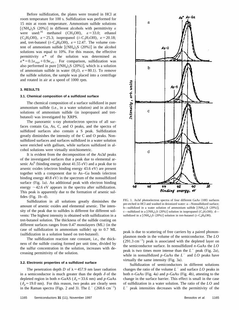
Before sulfidization, the plates were treated in HCl atfon
-
tivss
ug
r
ura
ontioal
l
dgonu
eteol-
ao
ckbde
ee
on-
on
s
ase
he
ace;
room temperature for 100 s. Sulfidization was performed15 min at room temperature. Ammonium sulfide solutio@(NH4!2S ~20%!# in different alcohols with permittivity«were used:16 methanol (CH3OH), «533.0; ethanol(C2H5OH), «525.3; isopropanol (i -C3H7OH), «520.18;and, tret-butanol (t-C4H9OH), «512.47. The volume content of ammonium sulfide@(NH4!2S ~20%!# in the alcoholsolutions was equal to 10%. For this reason, the effecpermittivity «* of the solution was determined a«* 50.1«aqe10.9«alc . For comparison, sulfidization waalso performed in pure@~NH4!2S ~20%!#, which is a solutionof ammonium sulfide in water~H2O, «580.1!. To removethe sulfide solution, the sample was placed into a centrifand rotated in air at a speed of 1000 rpm.
3. RESULTS
3.1. Chemical composition of a sulfidized surface
The chemical composition of a surface sulfidized in puammonium sulfide~i.e., in a water solution! and in alcoholsolutions of ammonium sulfide~in isopropanol and tret-butanol! was investigated by XRPS.
The panoramic x-ray photoelectron spectra of all sfaces contain Ga, As, C, and O peaks, and the spectrsulfidized surfaces also contain a S peak. Sulfidizationgreatly diminishes the intensity of the C and O peaks. Nsulfidized surfaces and surfaces sulfidized in a water soluwere enriched with gallium, while surfaces sulfidized incohol solutions were virtually stoichiometric.
It is evident from the decomposition of the As3d peaksof the investigated surfaces that a peak due to elementasenic As0 ~binding energy about 41.55 eV! and a peak due toarsenic oxides~electron binding energy 43.6 eV! are presenttogether with a component due to As–Ga bonds~electronbinding energy 40.8 eV! in the spectrum of the nonsulfidizesurface~Fig. 1a!. An additional peak with electron bindinenergy;42.6 eV appears in the spectra after sulfidizatiThis peak is apparently due to the formation of arsenic sfides ~Fig. 1b–d!.
Sulfidization in all solutions greatly diminishes thamount of arsenic oxides and elemental arsenic. The insity of the peak due to sulfides is different for different svents: The highest intensity is obtained with sulfidization intret-butanol solution. The thickness of the sulfide coatingdifferent surfaces ranges from 0.47 monolayers~ML ! ~in thecase of sulfidization in ammonium sulfide! up to 0.7 ML~sulfidization in a solution based on tret-butanol!.
The sulfidization reaction rate constant, i.e., the thiness of the sulfide coating formed per unit time, dividedthe sulfur concentration in the solution, increases withcreasing permittivity of the solution.
3.2. Electronic properties of a sulfidized surface
The penetration depthD of l5457.9 nm laser radiationin a semiconductor is much greater than the depthd of thedepleted region in bothn-GaAS (dn533.6 nm) andp-GaAs(dp519.0 nm). For this reason, two peaks are clearly sin the Raman spectra~Figs. 2 and 3!. TheL2 (268.6 cm21)
1165 Semiconductors 31 (11), November 1997
rs
e
e
e
-of
-n
-
ar-
.l-
n-
n
-y-
n
peak is due to scattering of free carriers by a paired phonplasmon mode in the volume of the semiconductor. TheLO(291.3 cm21) peak is associated with the depleted layerthe semiconductor surface. In nonsulfidizedn-GaAs theLOpeak is two times more intense than theL2 peak~Fig. 2a!,while in nonsulfidizedp-GaAs theL2 and LO peaks havevirtually the same intensity~Fig. 3a!.
Sulfidization of semiconductors in different solutionchanges the ratio of the volumeL2 and surfaceLO peaks inbothn-GaAs~Fig. 4a! andp-GaAs~Fig. 4b!, attesting to thechange in the surface barrier. This effect is small in the cof sulfidization in a water solution. The ratio of theLO andL2 peak intensities decreases with the permittivity of t
FIG. 1. As3d photoelectron spectra of four different GaAs~100! surfacespre-etched in HCl and washed in deionized water: a—Nonsulfidized surfb—sulfidized in a water solution of ammonium sulfide@~NH4!2S ~20%!#;c—sulfidized in a@~NH4!2S ~20%!# solution in isopropanol (C3H7OH); d—sulfidized in a@~NH4!2S ~20%!# solution in tret-butanol (t-C4H9OH).
1165Bessolov et al.
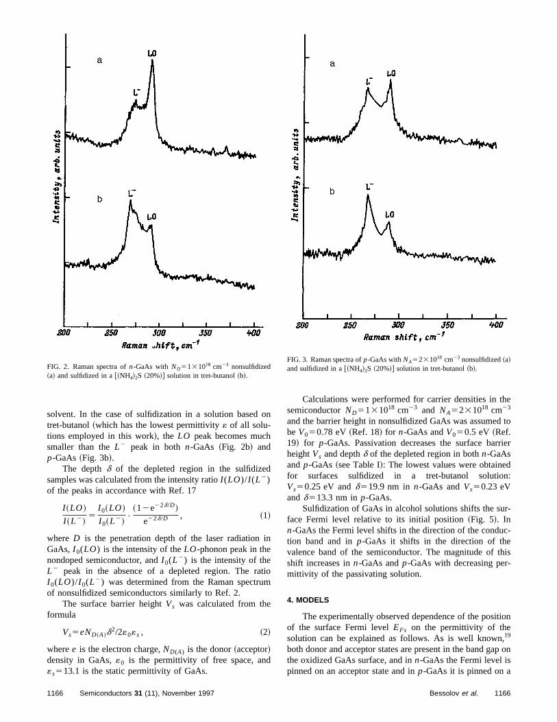
o
h
d
in
atm
d
he
d to
rrier
dn:
r-
c-
this-
tion
,p on
solvent. In the case of sulfidization in a solution basedtret-butanol~which has the lowest permittivity« of all solu-tions employed in this work!, the LO peak becomes mucsmaller than theL2 peak in bothn-GaAs ~Fig. 2b! andp-GaAs ~Fig. 3b!.
The depthd of the depleted region in the sulfidizesamples was calculated from the intensity ratioI (LO)/I (L2)of the peaks in accordance with Ref. 17
I ~LO!
I ~L2!5
I 0~LO!
I 0~L2!•
~12e22d/D!
e22d/D , ~1!
where D is the penetration depth of the laser radiationGaAs,I 0(LO) is the intensity of theLO-phonon peak in thenondoped semiconductor, andI 0(L2) is the intensity of theL2 peak in the absence of a depleted region. The rI 0(LO)/I 0(L2) was determined from the Raman spectruof nonsulfidized semiconductors similarly to Ref. 2.
The surface barrier heightVs was calculated from theformula
Vs5eND~A!d2/2«0«s , ~2!
wheree is the electron charge,ND(A) is the donor~acceptor!density in GaAs,«0 is the permittivity of free space, an«s513.1 is the static permittivity of GaAs.
FIG. 2. Raman spectra ofn-GaAs with ND5131018 cm23 nonsulfidized~a! and sulfidized in a@~NH4!2S ~20%!# solution in tret-butanol~b!.
1166 Semiconductors 31 (11), November 1997
n
io
Calculations were performed for carrier densities in tsemiconductorND5131018 cm23 and NA5231018 cm23
and the barrier height in nonsulfidized GaAs was assumebeV050.78 eV~Ref. 18! for n-GaAs andV050.5 eV ~Ref.19! for p-GaAs. Passivation decreases the surface baheightVs and depthd of the depleted region in bothn-GaAsandp-GaAs ~see Table I!: The lowest values were obtainefor surfaces sulfidized in a tret-butanol solutioVs50.25 eV andd519.9 nm inn-GaAs andVs50.23 eVandd513.3 nm inp-GaAs.
Sulfidization of GaAs in alcohol solutions shifts the suface Fermi level relative to its initial position~Fig. 5!. Inn-GaAs the Fermi level shifts in the direction of the condution band and inp-GaAs it shifts in the direction of thevalence band of the semiconductor. The magnitude ofshift increases inn-GaAs andp-GaAs with decreasing permittivity of the passivating solution.
4. MODELS
The experimentally observed dependence of the posiof the surface Fermi levelEFs on the permittivity of thesolution can be explained as follows. As is well known19
both donor and acceptor states are present in the band gathe oxidized GaAs surface, and inn-GaAs the Fermi level ispinned on an acceptor state and inp-GaAs it is pinned on a
FIG. 3. Raman spectra ofp-GaAs withNA5231018 cm23 nonsulfidized~a!and sulfidized in a@~NH4!2S ~20%!# solution in tret-butanol~b!.
1166Bessolov et al.
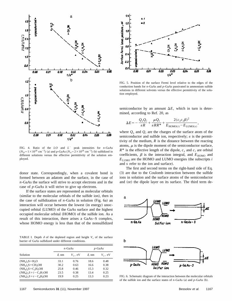
eh
it
t
ee
he
gce,
Eq.de
ctore-
-
theelu-
itals
donor state. Correspondingly, when a covalent bondformed between an adatom and the surface, in the casn-GaAs the surface will strive to accept electrons and in tcase ofp-GaAs it will strive to give up electrons.
If the surface states are represented as molecular orb~similar to the molecular orbitals of the sulfide ion!, then inthe case of sulfidization ofn-GaAs in solution~Fig. 6a! aninteraction will occur between the lowest~in energy! unoc-cupied orbital~LUMO! of the GaAs surface and the highesoccupied molecular orbital~HOMO! of the sulfide ion. As aresult of this interaction, there arises a GaAs–S complwhose HOMO energy is less than that of the nonsulfidiz
FIG. 4. Ratio of the LO and L2 peak intensities for n-GaAs(ND5131018 cm23) ~a! andp-GaAs (NA5231018 cm23) ~b! sulfidized indifferent solutions versus the effective permittivity of the solution employed.
TABLE I. Depth d of the depleted region and heightVs of the surfacebarrier of GaAs sulfidized under different conditions.
Solution
n-GaAs p-GaAs
d, nm Vs , eV d, nm Vs , eV
~NH4!2S1H2O 33.1 0.76 18.6 0.48~NH4!2S1CH3OH 30.2 0.63 16.6 0.38~NH4!2S1C2H5OH 25.8 0.46 15.3 0.32(NH4)2S1 i 2C3H7OH 23.5 0.38 13.4 0.25(NH4)2S1t2C4H9OH 19.9 0.25 13.3 0.23
1167 Semiconductors 31 (11), November 1997
isofe
als
x,d
semiconductor by an amountDE, which in turn is deter-mined, according to Ref. 20, as
DE52QsQi
«R1
mQi
«RR*1
2~cscib!2
EHOMO~ i !2ELUMO~s!,
whereQs andQi are the charges of the surface atom of tsemiconductor and sulfide ion, respectively;« is the permit-tivity of the medium,R is the distance between the reactinatoms,m is the dipole moment of the semiconductor surfaR* is the effective length of the dipole,cs andci are orbitalcoefficients,b is the interaction integral, andEHOMO andELUMO are the HOMO and LUMO energies~the subscriptsiands refer to the ion and surface!.
The first and second terms on the right-hand side of~3! are due to the Coulomb interaction between the sulfiions in solution and the surface atoms of the semiconduand ~or! the dipole layer on its surface. The third term d
FIG. 5. Position of the surface Fermi level relative to the edges ofconduction bands forn-GaAs andp-GaAs passivated in ammonium sulfidsolutions in different solvents versus the effective permittivity of the sotion employed.
FIG. 6. Schematic diagram of the interaction between the molecular orbof the sulfide ion and the surface states ofn-GaAs ~a! andp-GaAs ~b!.
1167Bessolov et al.
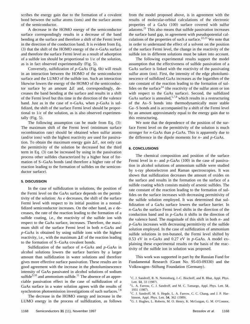
scribes the energy gain due to the formation of a covalents
toavq
ti
toioc
-s
ce
orn
sa
irdiofoeon
omcel-
oftha
es
georren
um-
f a
s.ths
from the model proposed above, is in agreement with theic
rsescal-
ionthent.el
of angi-f theul-
blevel
e to
ur-h
o
ce-edwas
onf aheul-
y oful-In
he
dem
by
ac-
for
ys.
ar-
or,
bond between the sulfur atoms~ions! and the surface atomof the semiconductor.
A decrease in the HOMO energy of the semiconducsurface correspondingly results in a decrease of the bbending at the surface and therefore a shift of the Fermi lein the direction of the conduction band. It is evident from E~3! that the shift of the HOMO energy of then-GaAs surfaceand therefore the surface Fermi level as a result of adsorpof a sulfide ion should be proportional to 1/« of the solution,as is in fact observed experimentally~Fig. 5!.
Conversely, sulfidization ofp-GaAs~Fig. 6b! will resultin an interaction between the HOMO of the semiconducsurface and the LUMO of the sulfide ion. Such an interactlikewise lowers the energy of the HOMO of the semicondutor surface by an amountDE and, correspondingly, decreases the band bending at the surface and results in aof the Fermi level but this time in the direction of the valenband. Just as in the case ofn-GaAs, whenp-GaAs is sul-fidized, the shift of the surface Fermi level should be proptional to 1/« of the solution, as is also observed experimetally ~Fig. 5!.
The following assumption can be made from Eq.~3!:The maximum shift of the Fermi level~minimum surfacerecombination rate! should be obtained when sulfur atom~and/or ions! with the highest reactivity are used for passivtion. To obtain the maximum energy gainDE, not only canthe permittivity of the solution be decreased but the thterm in Eq.~3! can be increased by using in the passivatprocess other sulfides characterized by a higher heat ofmation of S–GaAs bonds~and therefore a higher rate of threaction leading to the formation of sulfides on the semicductor surface!.
5. DISCUSSION
In the case of sulfidization in solutions, the positionthe Fermi level on the GaAs surface depends on the pertivity of the solution: As« decreases, the shift of the surfaFermi level with respect to its initial position in a nonsufidized semiconductor increases. On the other hand, as« de-creases, the rate of the reaction leading to the formationsulfide coating, i.e., the reactivity of the sulfide ion wirespect to the GaAs surface, increases. Therefore, the mmum shift of the surface Fermi level in bothn-GaAs andp-GaAs is obtained by using sulfide ions with the highreactivity, i.e., with the maximumDE of the reaction leadingto the formation of S–GaAs covalent bonds.
Sulfidization of the surface ofn-GaAs andp-GaAs inalcohol solutions lowers the surface barriers by a laramount than sulfidization in water solutions and therefgives more effective surface passivation. These results agood agreement with the increase in the photoluminesceintensity of GaAs passivated in alcohol solutions of sodisulfide9,10and ammonium sulfide.11 The absence of an appreciable passivation effect in the case of sulfidization oGaAs surface in a water solution agrees with the resultssynchrotron photoemission investigations of such surface7,8
The decrease in the HOMO energy and increase inLUMO energy in the process of sulfidization, as follow
1168 Semiconductors 31 (11), November 1997
rndel.
on
rn-
hift
--
-
nr-
-
fit-
a
xi-
t
reince
of
e
results of molecular-orbital calculations of the electronproperties of a GaAs~100! surface covered with sulfuadatoms.21 This also means that sulfide passivation increathe surface band gap, in agreement with pseudopotentialculations of the properties of such a surface.22,23We note thatin order to understand the effect of a solvent on the positof the surface Fermi level, the change in the reactivity ofsulfide ion in different solutions must be taken into accou
The following experimental results support the modassumption that the effectiveness of sulfide passivationGaAs surface is linked with the reactivity of the passivatisulfur atom~ion!. First, the intensity of the edge photolumnescence of sulfidized GaAs increases as the logarithm orate constant of the reaction leading to the formation of sfides on the surface14 ~the reactivity of the sulfur atom or ionwith respect to the GaAs surface!. Second, the sulfidizedGaAs surface is annealed,5,7,8which results in a restructuringof the As–S bonds into thermodynamically more staGa–S bonds and is accompanied by a shift of the Fermi leby an amount approximately equal to the energy gain duthis restructuring.
We note that the dependence of the position of the sface Fermi level on the permittivity of the solution is mucstronger forn-GaAs thanp-GaAs. This is apparently due tthe difference in the dipole moments forn- andp-GaAs.
6. CONCLUSIONS
The chemical composition and position of the surfaFermi level inn- and p-GaAs ~100! in the case of passivation in alcohol solutions of ammonium sulfide were studiby x-ray photoelectron and Raman spectroscopies. Itshown that sulfidization decreases the amount of oxidesthe surface and results in the formation on the surface osulfide coating which consists mainly of arsenic sulfides. Trate constant of the reaction leading to the formation of sfides on the surface increases with decreasing permittivitthe sulfide solution employed. It was determined that sfidization of a GaAs surface lowers the surface barrier.n-GaAs the surface Fermi level shifts in the direction of tconduction band and inp-GaAs it shifts in the direction ofthe valence band. The magnitude of this shift in bothn- andp-GaAs increases with decreasing permittivity of the sulfisolution employed. In the case of sulfidization of ammoniusulfide solutions in tret-butanol, the Fermi level shifted0.53 eV in n-GaAs and 0.27 eV inp-GaAs. A model ex-plaining these experimental results on the basis of the retivity of the sulfide ion in solution was proposed.
This work was supported in part by the Russian FundFundamental Research~Grant No. 95-03-09330! and theVolkswagen–Stiftung Foundation~Germany!.
1C. J. Sandroff, R. N. Nottenburg, J.-C. Bischoff, and R. Bhat, Appl. PhLett. 51, 33 ~1987!.
2L. A. Farrow, C. J. Sandroff, and M. C. Tamargo, Appl. Phys. Lett.51,1931 ~1987!.
3C. J. Sandroff, M. S. Hegde, L. A. Farrow, C. C. Chang, and J. P. Hbinson, Appl. Phys. Lett.54, 362 ~1989!.
4G. J. Hughes, L. Roberts, M. O. Henry, K. McGuigan, G. M. O’Conn
1168Bessolov et al.
F. G. Anderson, G. P. Morgan, and T. Glynn, Mater. Sci. Eng. B9, 37~1991!.
d
ch
ur
v,
ch
la
kh
Fiz. 22~18!, 37 ~1996! @ Tech. Phys. Lett.22, 749 ~1996!#.13G. Bauer and W. Richter,Optical Characterization of Epitaxial Semicon-
ci.
5P. Moriarty, B. Murphy, L. Roberts, A. A. Cafolla, L. Koenders, anP. Bailey, Phys. Rev. B51, 14 237~1994!.
6V. L. Berkovits, V. N. Bessolov, T. V. L’vova, E. B. Novikov, V. I.Safarov, R. V. Khasieva, and B. V. Tsarenkov, J. Appl. Phys.70, 3707~1991!.
7H. Sugahara, M. Oshima, H. Oigawa, H. Shigekawa, and Y. NanniJ. Appl. Phys.69, 4349~1991!.
8H. Sugahara, M. Oshima, R. Klauser, H. Oigawa, and Y. Nannichi, SSci. 242, 335 ~1991!.
9V. N. Bessolov, A. F. Ivankov, E. K. Konenkova, and M. V. LevedePis’ma Z. Tekh. Fiz.21, No. 46~1995! @ Tech. Phys. Lett.21, 20 ~1995!#.
10V. N. Bessolov, E. V. Konenkova, and M. V. Lebedev, J. Vac. Sci. Tenol. B 14, 2761~1996!.
11V. N. Bessolov, E. V. Konenkova, and M. V. Lebedev, Fiz. Tverd. Te~St. Petersburg! 39, 63 ~1997! @ Phys. Solid State39, 54 ~1997!#.
12V. N. Bessolov, E. V. Konenkova, and M. V. Lebedev, Pis’ma Zh. Te
1169 Semiconductors 31 (11), November 1997
i,
f.
-
.
ductor Layers, Springer, Berlin, 1996.14D. E. Aspnes and A. A. Studna, Phys. Rev. B27, 985 ~1983!.15W. Haes and R. London,Scattering of Light by Crystals, Wiley, N. Y.,
1978.16D. R. Lide, CRC Handbook of Chemistry and Physics, CRC Press, Boca
Raton, Florida, 1995.17J. Geurts, Surf. Sci. Rep.18, 1 ~1993!.18G. P. Schwartz and G. J. Gualtieri, J. Electrochem. Soc.133, 1266~1986!.19N. Newman, W. E. Spicer, T. Kendelewicz, and I. Lindau, J. Vac. S
Technol. B4, 931 ~1986!.20G. Klopman, J. Am. Chem. Soc.90, 223 ~1968!.21J. Guo-Ping and H. E. Ruda, J. Appl. Phys.79, 3758~1996!.22T. Ohno and K. Shiraishi, Phys. Rev. B42, 11 194~1990!.23K. N. Ow and X. W. Wang, Phys. Rev. B54, 17 661~1996!.
Translated by M. E. Alferieff
1169Bessolov et al.
LOW-DIMENSIONAL SYSTEMS
fill-
Heating of a two-dimensional electron gas by the electric field of a surface acousticwave
I. L. Drichko, A. M. D’yakonov, V. D. Kagan, A. M. Kreshchuk, T. A. Polyanskaya,I. G. Savel’ev, I. Yu. Smirnov, and A. V. Suslov
A. F. Ioffe Physicotechnical Institute, Russian Academy of Sciences, 194021 St. Petersburg, Russia~Submitted May 16, 1997; accepted for publication June 20, 1997!Fiz. Tekh. Poluprovodn.31, 1357–1366~November 1997!
The heating of a two-dimensional electron gas by an rf electric field generated by a surfaceacoustic wave, which can be described by an electron temperatureTe , has been investigated. It isshown that the energy balance of the electron gas is determined by electron scattering bythe piezoelectric potential of the acoustic phonons withTe determined from measurements atfrequenciesf 530 and 150 MHz. The experimental curves of the energy lossQ versusTe at different SAW frequencies depend on the value ofv t e compared to 1, wheret e is therelaxation time of the average electron energy. Theoretical calculations of the heating ofa two-dimensional electron gas by the electric field of the surface acoustic wave are presentedfor the case of thermal electrons (DT!T). The calculations show that for the sameenergy lossesQ the degree of heating of the two-dimensional electrons~i.e., the ratioTe /T! forv t e.1 ( f 5150 MHz) is less than forv t e,1 ( f 530 MHz). Experimental resultsconfirming this calculation are presented. ©1997 American Institute of Physics.@S1063-7826~97!02011-5#
1. INTRODUCTION the magnetic field range corresponding to small integer
tveve
na
d-gh
ity
onashetiode.one
eeonhll
sy
ing numbers—the quantum Hall effect regime, when theex-G.
onsof
ldty
10ne
esl
-s is
theweas
asfill-ethe
/1
The investigation of nonlinear~with respect to the inpupower! effects in the absorption of piezoelectrically actiultrasonic waves, arising due to the interaction of the wawith three-dimensional electron gas~in the case of Boltz-mann statistics!, has shown that the mechanisms of the nolinearity depend on the state of the electrons. If electronsfree ~delocalized!, then the nonlinearity mechanism for moerately high sound intensities is usually due to the heatinthe electrons in the electric field of an ultrasonic wave. Tcharacter of the heating depends on the quantityvt« , wherev is the sound frequency, andt« is the energy relaxationtime.1,2 If the electrons are localized, then the nonlinearmechanism is due to the character of the localization~on anindividual impurity or in the wells of a fluctuation potential!.In Ref. 3, it was shown that in the case where the electrare localized on individual impurities, the nonlinearity wdetermined by impurity breakdown in the electric field of tsound wave. When the electrons occupied the conducband as a result of this effect, their temperature startegrow as a result of heating in the electric field of the wav4
The study of structures with a two-dimensional electrgas~2DEG! opens up a unique possibility of studying in onseries of measurements performed on the same samplmechanisms of nonlinearity in delocalized and localizelectron states, since under quantum Hall effect conditiboth states are realized by varying the magnetic field. Tchange in the absorption coefficient for a piezoelectricaactive surface acoustic wave~SAW! interactimg with a2DEG as a function of the SAW intensity in GaAs/AlGaAstructures was previously observed in Refs. 5 and 6 onl
1170 Semiconductors 31 (11), November 1997 1063-7826/97
s
-re
ofe
s
nto
thedsey
in
two-dimensional electrons are localized. The authorsplained the data which they obtained by heating of a 2DE
In the present paper we report some of our investigaticoncerning nonlinear effects accompanying the interactiondelocalized two-dimensional electrons with the electric fieof a SAW for the purpose of investigating nonlinearimechanisms.
2. EXPERIMENTAL PROCEDURE
We investigated the absorption coefficient for a 30–2MHz SAW in a two-dimensional electron gas iGaAs/Al0.75Ga0.25As heterostructures as a function of thtemperature in the rangeT.1.4– 4.2 K in the linear regime~the input power did not exceed 1027 W! and the SAWpower atT51.5 K in magnetic fields up to 30 kOe. Samplstudied previously in Ref. 7 with Haldensity ns
H56.731011 cm22 and mobility mH51.283105 cm2/~V•s! at T54.2 K were used for the investigations. The technology used to fabricate the heterostructuredescribed in Ref. 8 and the procedure for performingsound absorption experiment is described in Ref. 7. Hereonly note that the experimental structure with 2DEG wlocated on the surface of the piezodielectric~lithium niobateLiNbO3!, along which the SAW propagates. The SAW wexcited in a pulsed regime by sending radio pulses withing frequency 30–210 MHz from an rf oscillator into thexcited interdigital transducer. The pulse duration was of
117011170-08$10.00 © 1997 American Institute of Physics
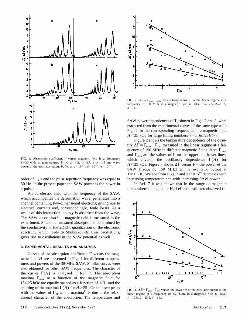
l tr i
,totsvethdicn
a-r
nr
an
s ineld
an--
,
tic
order of 1ms and the pulse repetition frequency was equa50 Hz. In the present paper the SAW power is the powea pulse.An ac electric field with the frequency of the SAWwhich accompanies the deformation wave, penetrates inchannel containing two-dimensional electrons, giving riseelectrical currents and, correspondingly, Joule losses. Aresult of this interaction, energy is absorbed from the waThe SAW absorption in a magnetic field is measured inexperiment. Since the measured absorption is determinethe conductivity of the 2DEG, quantization of the electronspectrum, which leads to Shubnikov-de Haas oscillatiogives rise to oscillations in the SAW potential as well.
3. EXPERIMENTAL RESULTS AND ANALYSIS
Curves of the absorption coefficientG versus the mag-netic field H are presented in Fig. 1 for different tempertures and powers of the 30-MHz SAW. Similar curves wealso obtained for other SAW frequencies. The characterthe curvesG(H) is analyzed in Ref. 7. The absorptiomaxima Gmax as a function of the magnetic field foH,25 kOe are equally spaced as a function of 1/H, and thesplitting of the maximaG(H) for H.25 kOe into two peakswith the values ofGM at the maxima1! is due to the relax-ational character of the absorption. The temperature
FIG. 1. Absorption coefficientG versus magnetic fieldH at frequencyf 530 MHz at temperaturesT, K: a—4.2, b—3.8, c–e—1.5 and wavepower at the oscillator outputP, W: a–c—1025, d—1024, e—1023.
1171 Semiconductors 31 (11), November 1997
on
aoa.
eby
s,
eof
d
SAW power dependences ofG, shown in Figs. 2 and 3, wereextracted from the experimental curves of the same type aFig. 1 for the corresponding frequencies in a magnetic fiH,25 kOe for large filling numbersn5nshc/2eH.7.
Figure 2 shows the temperature dependence of the qutity DG5Gmax2Gmin measured in the linear regime at a frequency of 150 MHz in different magnetic fields. HereGmax
and Gmin are the values ofG on the upper and lower lineswhich envelop the oscillatory dependenceG(H) forH,25 kOe. Figure 3 showsDG versusP—the power of theSAW ~frequency 150 MHz! at the oscillator output atT51.5 K. We see from Figs. 2 and 3 thatDG decreases withincreasing temperature and with increasing SAW power.
In Ref. 7 it was shown that in the range of magnefields where the quantum Hall effect is still not observed~in
FIG. 2. DG5Gmax2Gmin versus temperatureT in the linear regime at afrequency of 150 MHz in a magnetic fieldH, kOe: 1—17.5, 2—15.5,3—14.1.
FIG. 3. DG5Gmax2Gmin versus the powerP at the oscillator output in thelinear regime at a frequency of 150 MHz in a magnetic fieldH, kOe:1—17.5,2—15.5,3—14.1.
1171Drichko et al.
our caseH,25 kOe! the dissipative conductivities are
ed
umintrosere
t
g
a
atinta
stitioitde
ndco
itpewe
he
s-
e
ltn
in-l
opis
where K2 is the electromechanical coupling constant;5 d
he
ri-otTheal-sso-erre-ere
lineWtode-
mit-the
ses
on-
-
Anves
ed
asetial
in
sxxac5sxx
dc ,
wheresxxdc is the conductivity calculated from the measur
dc resistivitiesrxx(H) and rxy(H), andsxxac is the conduc-
tivity found from the absorption coefficientG(H) measuredin the linear regime. This result gave us the basis for assing that in this range of magnetic fields the electrons aredelocalized state. As we have already indicated in the induction, we shall analyze here nonlinearity only in this ca
In a previous work9 we showed that if the electrons adelocalized, then the characteristics of the 2DEG, such ascarrier densityns, the transport relaxation timet, and thequantum2! relaxation time, can be determined from the manetic field dependencessxx
ac(H). In addition, the mobilitym5et/m and the concentrationns at H50 are close to thevalues obtained from dc measurements: the Hall densitymobility of the electrons, as well asns found from theShubnikov–de Haas oscillations. For this reason, it was nral to assume thatG depends on the SAW power, just asthe static case, because of the heating of the 2DEG but inelectric field of the SAW. The heating of the 2DEG instatic electric field in similar heterostructures was invegated in Refs. 11–15. In those papers it was shown thaliquid-helium temperatures the electron energy relaxatprocesses are determined in a wide range of 2DEG densby the piezoacoustic electron-phonon interaction unsmall-angle scattering and weak screening conditions.
We shall employ, by analogy with Refs. 11–14, the cocept of the temperatureTe of two-dimensional electrons andetermine it by comparing the curves of the absorptionefficient G versus the SAW power with the curves ofG ver-sus the lattice temperatureT. Such a comparison makespossible to establish a correspondence between the temture of the two-dimensional electrons and the output poof the oscillator. The values ofTe were extracted by twomethods: 1! by comparing the curves of the amplitude of toscillationsDG5Gmax2Gmin versus the temperatureT ~Fig.2! and versus the powerP ~Fig. 3! for the same value of themagnetic fieldH; 2! by comparing curves of the ratioGmax/GM5f(T) and Gmax/GM5f(P) versus the lattice temperatureT and the powerP. Here the values ofGmax(T) andGmax(P) were also taken for the same value ofH, andGM isthe absorption atH528 kOe~Fig. 1!. The use of the ratiosinstead of the absolute values ofG decreased the effect of thexperimental variance inG on the error in determiningTe .As a result, the accuracy in determiningTe by these twomethods was no worse than 10%.
To determine the absolute energy losses as a resuabsorption of SAW in the case of interaction with electro(Q), the following calculations must be performed. ThetensityE of the electric field, in which the two-dimensionaelectrons of the heterostructure are located during the prgation of a SAW in a piezoelectric material placed at a dtancea from a high-conductivity channel, is
uEu25K232p
v~«11«0!
bqexp~22qa!
11S 4psxx
v«sD 2
c2
W, ~1!
1172 Semiconductors 31 (11), November 1997
-a-.
he
-
nd
u-
he
-atniesr
-
-
ra-r
ofs
a--
n53.5310 cm/s andq are, respectively, the velocity anwave number of sound in LiNbO3; a is the width of thevacuum gap between the sample and the LiNbO3 plate;«0 ,«1 , and«s are the permittivities of free space, LiNbO3, andthe semiconductor with the 2DEG, respectively; andW is theinput SAW power scaled to the width of the sound track. Tfunctionsb andc are
b5@«11«s
12«12«s
2exp~22qa!#22,
c51
2$11b1/2@«1
1«s22«1
2«s1exp~22qa!#%,
«115«11«0 , «s
15«s1«0 ,
«125«12«0 , «s
25«s2«0 .
The magnitude of the electric losses is defined asQ5sxxE2.
Multiplying both sides of Eq.~1! by sxx , we obtainQ54WG, whereG is the absorption measured in the expement. The powerW at the entrance to the sample is nmeasured very accurately in acoustic measurements.problem is that this quantity is determined by, first, the quity of the interdigital transducers; second, by the losses aciated with the mismatch of the line that feeds electric powinto the transmitting transducer as well as the line thatmoves electrical power from the detecting transducer, whthe losses in the receiving and transmitting parts of themay not be the same; and, third, by absorption of the SAin the susbtrate, whose absolute magnitude is difficultmeasure in our experiment. The effect of these lossescreases with frequency, so that in determiningW at 30 MHzwe assumed that both the conversion losses for the transting and receiving transducers as well as the losses intransmitting and receiving lines are identical. The total loswere found to beDP516 dB, if SAW absorption in theheterostructure substrate is ignored. If it is assumed that nlinear effects at 150 MHz start at the same value ofQ as at30 MHz, then the ‘‘threshold’’ value ofQ at which the de-viation of Gmax(Q)/GM at 30 MHz from a constant value becomes appreciable@we recall thatG(H)/GM;1/sxx(H) inthe region of delocalized electronic states, i.e.,H,25 kOe7#can be used to determine the total losses at 150 MHz.estimate of the total losses by this method at 150 MHz giDP518 dB. Therefore, the powerW at the entrance to thesample is determined by the output powerP of the oscillator,taking into account the total lossesDP.
With the results of Refs. 11–14 in mind, we constructthe curves
Q5Q/ns5 f ~Te32T3!,
which correspond to the energy balance equation in the cof the interaction of electrons with the piezoelectric potenof the acoustic phonons~PA scattering! under the conditionof weak screening at frequencies of 30 and 150 MHzdifferent magnetic fields
QPA5emE25A3~Te32T3!. ~2!
1172Drichko et al.
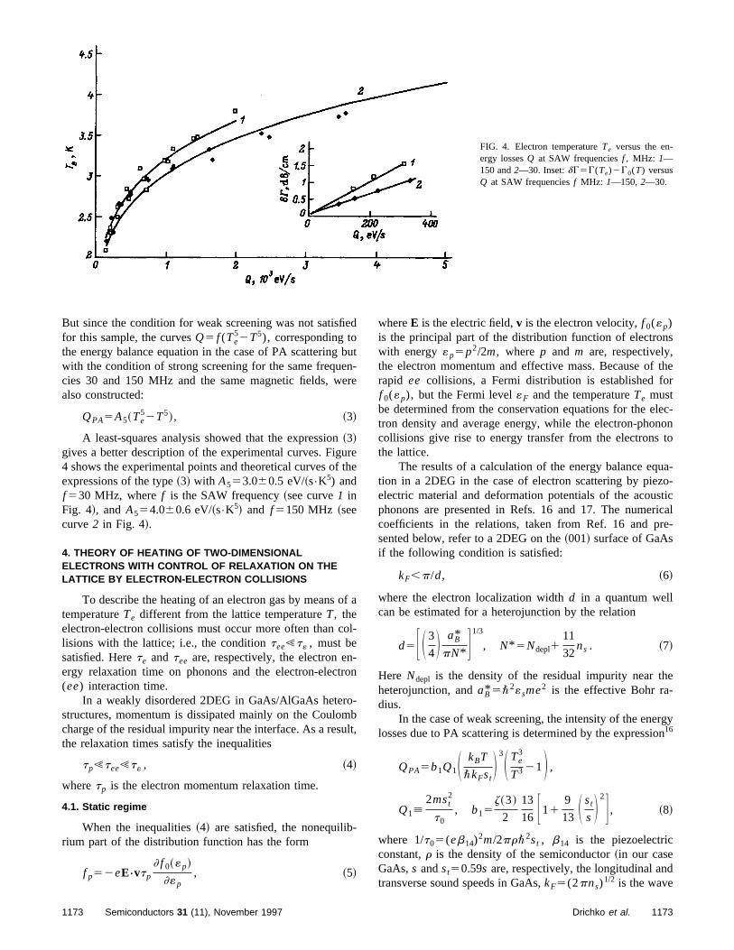
FIG. 4. Electron temperatureTe versus the en-ergy lossesQ at SAW frequenciesf , MHz: 1—150 and2—30. Inset:dG5G(Te)2G0(T) versusQ at SAW frequenciesf MHz: 1—150,2—30.
But since the condition for weak screening was not satisfied
bene
uth
of
o
n-tro
o-mu
-
whereE is the electric field,v is the electron velocity,f 0(«p)s
ther
lec-nonto
ua-zo-sticricalre-
e
rgyon
d
for this sample, the curvesQ5 f (Te52T5), corresponding to
the energy balance equation in the case of PA scatteringwith the condition of strong screening for the same frequcies 30 and 150 MHz and the same magnetic fields, walso constructed:
QPA5A5~Te52T5!, ~3!
A least-squares analysis showed that the expression~3!gives a better description of the experimental curves. Fig4 shows the experimental points and theoretical curves ofexpressions of the type~3! with A553.060.5 eV/~s•K5) andf 530 MHz, wheref is the SAW frequency~see curve1 inFig. 4!, and A554.060.6 eV/~s•K5! and f 5150 MHz ~seecurve2 in Fig. 4!.
4. THEORY OF HEATING OF TWO-DIMENSIONALELECTRONS WITH CONTROL OF RELAXATION ON THELATTICE BY ELECTRON-ELECTRON COLLISIONS
To describe the heating of an electron gas by meanstemperatureTe different from the lattice temperatureT, theelectron-electron collisions must occur more often than clisions with the lattice; i.e., the conditiontee!t« , must besatisfied. Herete and tee are, respectively, the electron eergy relaxation time on phonons and the electron-elec(ee) interaction time.
In a weakly disordered 2DEG in GaAs/AlGaAs heterstructures, momentum is dissipated mainly on the Coulocharge of the residual impurity near the interface. As a resthe relaxation times satisfy the inequalities
tp!tee!t« , ~4!
wheretp is the electron momentum relaxation time.
4.1. Static regime
When the inequalities~4! are satisfied, the nonequilibrium part of the distribution function has the form
f p52eE–vtp
] f 0~«p!
]«p, ~5!
1173 Semiconductors 31 (11), November 1997
ut-
re
ree
a
l-
n
blt,
is the principal part of the distribution function of electronwith energy«p5p2/2m, where p and m are, respectively,the electron momentum and effective mass. Because ofrapid ee collisions, a Fermi distribution is established fof 0(«p), but the Fermi level«F and the temperatureTe mustbe determined from the conservation equations for the etron density and average energy, while the electron-phocollisions give rise to energy transfer from the electronsthe lattice.
The results of a calculation of the energy balance eqtion in a 2DEG in the case of electron scattering by pieelectric material and deformation potentials of the acouphonons are presented in Refs. 16 and 17. The numecoefficients in the relations, taken from Ref. 16 and psented below, refer to a 2DEG on the~001! surface of GaAsif the following condition is satisfied:
kF,p/d, ~6!
where the electron localization widthd in a quantum wellcan be estimated for a heterojunction by the relation
d5F S 3
4D aB*
pN* G1/3
, N* 5Ndepl111
32ns . ~7!
Here Ndepl is the density of the residual impurity near thheterojunction, andaB* 5\2«sme2 is the effective Bohr ra-dius.
In the case of weak screening, the intensity of the enelosses due to PA scattering is determined by the expressi16
QPA5b1Q1S kBT
\kFstD 3S Te
3
T3 21D ,
Q1[2mst
2
t0, b15
z~3!
2
13
16 F119
13 S st
s D 2G , ~8!
where 1/t05(eb14)2m/2pr\2st , b14 is the piezoelectric
constant,r is the density of the semiconductor~in our caseGaAs,s andst50.59s are, respectively, the longitudinal antransverse sound speeds in GaAs,kF5(2pns)
1/2 is the wave
1173Drichko et al.
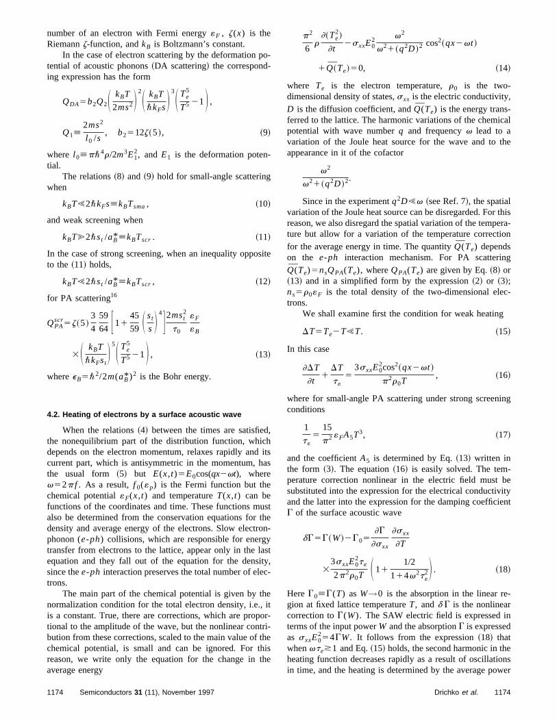
number of an electron with Fermi energy«F , z(x) is the
po
-
s
d,h
da
uth
roy
laityc
he, ipotrithhith
p2
r]~Te
2!2s E2 v2
cos2~qx2vt !
cal
the
thisera-on
g
c-
ing
-beityent
-
n
eonswer
Riemannz-function, andkB is Boltzmann’s constant.In the case of electron scattering by the deformation
tential of acoustic phonons~DA scattering! the correspond-ing expression has the form
QDA5b2Q2S kBT
2ms2D 2S kBT
\kFsD3S Te
5
T5 21D ,
Q1[2ms2
l 0 /s, b2512z~5!, ~9!
where l 0[p\4r/2m3E12, and E1 is the deformation poten
tial.The relations~8! and ~9! hold for small-angle scattering
when
kBT!2\kFs[kBTsma, ~10!
and weak screening when
kBT@2\st /aB* [kBTscr . ~11!
In the case of strong screening, when an inequality oppoto the ~11! holds,
kBT!2\st /aB* [kBTscr , ~12!
for PA scattering16
QPAscr5z~5!
3
4
59
64 F1145
59 S st
s D 4G2mst2
t0
«F
«B
3S kBT
\kFstD 5S Te
5
T5 21D , ~13!
whereeB5\2/2m(aB* )2 is the Bohr energy.
4.2. Heating of electrons by a surface acoustic wave
When the relations~4! between the times are satisfiethe nonequilibrium part of the distribution function, whicdepends on the electron momentum, relaxes rapidly ancurrent part, which is antisymmetric in the momentum, hthe usual form ~5! but E(x,t)5E0cos(qx2vt), wherev52p f . As a result,f 0(«p) is the Fermi function but thechemical potential«F(x,t) and temperatureT(x,t) can befunctions of the coordinates and time. These functions malso be determined from the conservation equations fordensity and average energy of the electrons. Slow electphonon (e-ph) collisions, which are responsible for energtransfer from electrons to the lattice, appear only in theequation and they fall out of the equation for the denssince thee-ph interaction preserves the total number of eletrons.
The main part of the chemical potential is given by tnormalization condition for the total electron density, i.e.is a constant. True, there are corrections, which are protional to the amplitude of the wave, but the nonlinear conbution from these corrections, scaled to the main value ofchemical potential, is small and can be ignored. For treason, we write only the equation for the change inaverage energy
1174 Semiconductors 31 (11), November 1997
-
ite
itss
sten-
st,-
tr--ese
6 ]t xx 0 v21~q2D !2
1Q~Te!50, ~14!
where Te is the electron temperature,r0 is the two-dimensional density of states,sxx is the electric conductivity,D is the diffusion coefficient, andQ(Te) is the energy trans-ferred to the lattice. The harmonic variations of the chemipotential with wave numberq and frequencyv lead to avariation of the Joule heat source for the wave and toappearance in it of the cofactor
v2
v21~q2D !2.
Since in the experimentq2D!v ~see Ref. 7!, the spatialvariation of the Joule heat source can be disregarded. Forreason, we also disregard the spatial variation of the tempture but allow for a variation of the temperature correctifor the average energy in time. The quantityQ(Te) dependson the e-ph interaction mechanism. For PA scatterinQ(Te)5nsQPA(Te), whereQPA(Te) are given by Eq.~8! or~13! and in a simplified form by the expression~2! or ~3!;ns5r0«F is the total density of the two-dimensional eletrons.
We shall examine first the condition for weak heating
DT5Te2T!T. ~15!
In this case
]DT
]t1
DT
t«5
3sxxE02cos2~qx2vt !
p2r0T, ~16!
where for small-angle PA scattering under strong screenconditions
1
t«5
15
p2 «FA5T3, ~17!
and the coefficientA5 is determined by Eq.~13! written inthe form ~3!. The equation~16! is easily solved. The temperature correction nonlinear in the electric field mustsubstituted into the expression for the electrical conductivand the latter into the expression for the damping coefficiG of the surface acoustic wave
dG5G~W!2G05]G
]sxx
]sxx
]T
33sxxE0
2t«
2p2r0T S 111/2
114v2t«2D . ~18!
HereG0[G(T) asW→0 is the absorption in the linear region at fixed lattice temperatureT, andd G is the nonlinearcorrection toG(W). The SAW electric field is expressed iterms of the input powerW and the absorptionG is expressedas sxxE0
254GW. It follows from the expression~18! thatwhenvte*1 and Eq.~15! holds, the second harmonic in thheating function decreases rapidly as a result of oscillatiin time, and the heating is determined by the average po
1174Drichko et al.
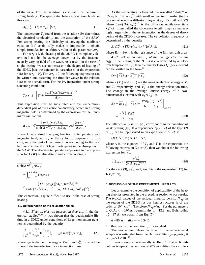
of the wave. This last assertion is also valid for the case of
Warn
e-taog
sio
ion
urnu
d
firo
re
n
-ns
As the temperature is lowered, the so-called ‘‘dirty’’ or(N)
as-r-
a.-c-
.o-
f
t-ults.
he
tal
-
strong heating. The quasistatic balance condition holdsthis case:
A5~Te52T5!5sxxE0
2/2ns . ~19!
The temperatureTe found from the relation~19! determinesthe electrical conductivity and the absorption of the SAFor strong heating, the difficulty of solving the nonlineequation ~14! analytically makes it impossible to obtaisimple formulas for an arbitrary value of the parametervt« .
For vt«!1, the heating of the 2DEG is completely dtermined not by the average power but by the instanneously varying field of the wave. As a result, in the caseslight heating, we see an increase in the degree of heatinthe 2DEG@see the cofactor in parentheses in the expres~18! for vt«→0#. For vt«→0 the following expression canbe written out, assuming the time derivative in the relat~16! to be a small term. For the PA interaction under stroscreening conditions
Te~x,t !5FT51sxxE0
2cos2~qx2vt !
A5nsG1/5
.
This expression must be substituted into the temperatdependent part of the electric conductivity, which in a stromagnetic field is determined by the expression for the Shnikov oscillations
Dsxx5C2p2Te~x,t !/\vc
sinh@2p2Te~x,t !/\vc#cosS 2p«F
\vcD ,
where C is a slowly varying function of temperature anmagnetic field, andvc is the cyclotron frequency. In thiscase, only the part of the current corresponding to theharmonic in the 2DEG layer participates in the absorptionthe SAW. The effective temperature appearing in the expsion for G(W) is also determined correspondingly:
Te
sinh~2p2Te /\vc!
5E0
2p dw
p~cos2w!
3@T51~sxxE0
2/A5ns!cos2w#1/5
sinh$~2p2/\vc!@T51~sxxE02/A5ns!cos2w#1/5%
.
This expression is quite difficult to use in the case of stroheating.
4.3. Determination of the relaxation times
4.3.1.Electron-electron interaction timetee. In the the-oretical studies18,19 it was shown that the quasiparticle lifetime in a 2DEG under conditions of large momentum trafers is determined by the quantity
\
tee~p! 5
p2T2
2«F0lnS «F0
TmD , Tm5max$T,\/tp%, ~20!
where«F0 is the Fermi energy atT50, andtee(p) is called the
‘‘pure’’ electron-electron (ee) interaction time.
1175 Semiconductors 31 (11), November 1997
in
.
-fofn
ng
e-gb-
stfs-
g
-
‘‘Nyquist’’ time tee with small momentum transfer~in theprocess of electron diffusion! Dq'1/LT , ~Ref. 20 and 22!where LT5(D\/kBT)1/2 is the diffusion length over timekBT/\, often called the coherence length, plays an increingly larger role in theee interaction as the degree of disodering of the 2DEG increases. Theee collision frequency isdetermined by the quantity
\/tee~N!5~TRhe2/h!ln~h/2e2Rh!, ~21!
whereRh51/sxx is the resistance of the film per unit are4.3.2. Relaxation timet « of the average electron en
ergy. If the heating of the 2DEG is characterized by an eletron temperatureTe , then the energy lossesQ ~per electron!can be written in the form10
Q5@ « ~Te!2 « ~T!#/ t « , ~22!
where« (Te) and « (T) are the average electron energy atTe
and T, respectively, andt « is the energy relaxation timeThe change in the average kinetic energy of a twdimensional electron with«F!kBT is
D«5 « ~Te!2 « ~T!5p2kB
2
6
~Te22T2!
«F0U
DT!T
5p2kB
2
3
TDT
«F0. ~23!
The latter equality in Eq.~23! corresponds to the condition oweak heating~15!. If a dependenceQ(Te ,T) of the type~2!or ~3! can be represented in an expansion inDT/T as
Q~T,DT!5gAgTg21DT,
whereg is the exponent ofTe and T in the expression thefollowing expression~2! or ~3!, then we obtain the followingexpression fort «:
t «uDT!T5p2kB
2
3gAg«F0Tg22 . ~24!
For the case~3!, i.e.,g55, we obtain the expression~17! for1/t «51/t« .
5. DISCUSSION OF THE EXPERIMENTAL RESULTS
Let us examine the condition of applicability of the heaing theories presented in the preceding section to our resThe typical values of the residual impurity densityNdepl inthe region of the 2DEG for our heterostructures is of torder of 1010 cm22. ThereforeNdepl!ns . For the parametersof GaAsm50.07m0 , permittivity «s512.8, and Bohr radiusaB* 597 Å, we obtain from Eq.~7!
d585 Å, dkF /p>0.3,1.
In other words, the condition~6! is satisfied.The momentum relaxation time for the experimen
sample was estimated from the Hall mobilitytp.mHm/e; itis tp55.1310212 s.
It was shown experimentally in Ref. 23 that at liquidhelium temperatures and low 2DEG mobilities theee inter-
1175Drichko et al.
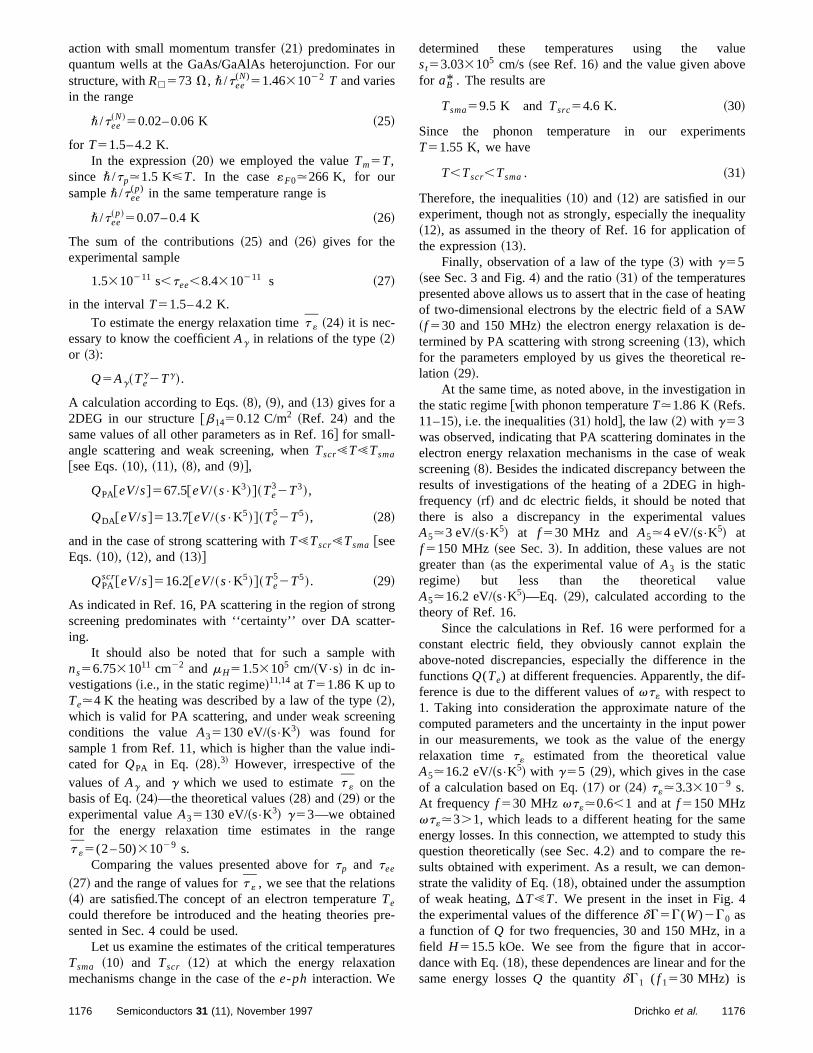
action with small momentum transfer~21! predominates inu
ngr-
ith
in
di
g
s
pr
ren
determined these temperatures using the value5 e
nts
lityof
atingW-
re-
in
theeaktheh-atues
t
e
r ahethe
f-
thewerrgye
ethis-on-n
4
ar-
the
quantum wells at the GaAs/GaAlAs heterojunction. For ostructure, withRh573 V, \/tee
(N)51.4631022 T and variesin the range
\/tee~N!50.02– 0.06 K ~25!
for T51.5– 4.2 K.In the expression~20! we employed the valueTm5T,
since \/tp.1.5 K<T. In the case«F0.266 K, for oursample\/tee
(p) in the same temperature range is
\/tee~p!50.07– 0.4 K ~26!
The sum of the contributions~25! and ~26! gives for theexperimental sample
1.5310211 s,tee,8.4310211 s ~27!
in the intervalT51.5– 4.2 K.To estimate the energy relaxation timet « ~24! it is nec-
essary to know the coefficientAg in relations of the type~2!or ~3!:
Q5Ag~Teg2Tg!.
A calculation according to Eqs.~8!, ~9!, and~13! gives for a2DEG in our [email protected] C/m2 ~Ref. 24! and thesame values of all other parameters as in Ref. 16# for small-angle scattering and weak screening, whenTscr!T!Tsma
@see Eqs.~10!, ~11!, ~8!, and~9!#,
QPA@eV/s#567.5@eV/~s•K3!#~Te32T3!,
QDA@eV/s#513.7@eV/~s•K5!#~Te52T5!, ~28!
and in the case of strong scattering withT!Tscr!Tsma @seeEqs.~10!, ~12!, and~13!#
QPAscr@eV/s#516.2@eV/~s•K5!#~Te
52T5!. ~29!
As indicated in Ref. 16, PA scattering in the region of stroscreening predominates with ‘‘certainty’’ over DA scatteing.
It should also be noted that for such a sample wns56.7531011 cm22 and mH51.53105 cm/~V•s! in dc in-vestigations~i.e., in the static regime!11,14at T51.86 K up toTe.4 K the heating was described by a law of the type~2!,which is valid for PA scattering, and under weak screenconditions the valueA35130 eV/~s•K3! was found forsample 1 from Ref. 11, which is higher than the value incated for QPA in Eq. ~28!.3! However, irrespective of thevalues ofAg and g which we used to estimatet « on thebasis of Eq.~24!—the theoretical values~28! and~29! or theexperimental valueA35130 eV/~s•K3! g53—we obtainedfor the energy relaxation time estimates in the rant «5(2 – 50)31029 s.
Comparing the values presented above fortp and tee
~27! and the range of values fort « , we see that the relation~4! are satisfied.The concept of an electron temperatureTe
could therefore be introduced and the heating theoriessented in Sec. 4 could be used.
Let us examine the estimates of the critical temperatuTsma ~10! and Tscr ~12! at which the energy relaxatiomechanisms change in the case of thee-ph interaction. We
1176 Semiconductors 31 (11), November 1997
r
g
-
e
e-
s
st53.03310 cm/s ~see Ref. 16! and the value given abovfor aB* . The results are
Tsma59.5 K and Tsrc54.6 K. ~30!
Since the phonon temperature in our experimeT51.55 K, we have
T,Tscr,Tsma. ~31!
Therefore, the inequalities~10! and ~12! are satisfied in ourexperiment, though not as strongly, especially the inequa~12!, as assumed in the theory of Ref. 16 for applicationthe expression~13!.
Finally, observation of a law of the type~3! with g55~see Sec. 3 and Fig. 4! and the ratio~31! of the temperaturespresented above allows us to assert that in the case of heof two-dimensional electrons by the electric field of a SA~f 530 and 150 MHz! the electron energy relaxation is determined by PA scattering with strong screening~13!, whichfor the parameters employed by us gives the theoreticallation ~29!.
At the same time, as noted above, in the investigationthe static regime@with phonon temperatureT.1.86 K ~Refs.11–15!, i.e. the inequalities~31! hold#, the law~2! with g53was observed, indicating that PA scattering dominates inelectron energy relaxation mechanisms in the case of wscreening~8!. Besides the indicated discrepancy betweenresults of investigations of the heating of a 2DEG in higfrequency~rf! and dc electric fields, it should be noted ththere is also a discrepancy in the experimental valA5.3 eV/~s•K5! at f 530 MHz and A5.4 eV/~s•K5! atf 5150 MHz ~see Sec. 3!. In addition, these values are nogreater than~as the experimental value ofA3 is the staticregime! but less than the theoretical valuA5.16.2 eV/~s•K5!—Eq. ~29!, calculated according to thetheory of Ref. 16.
Since the calculations in Ref. 16 were performed foconstant electric field, they obviously cannot explain tabove-noted discrepancies, especially the difference infunctionsQ(Te) at different frequencies. Apparently, the diference is due to the different values ofvt« with respect to1. Taking into consideration the approximate nature ofcomputed parameters and the uncertainty in the input poin our measurements, we took as the value of the enerelaxation time t« estimated from the theoretical valuA5.16.2 eV/~s•K5! with g55 ~29!, which gives in the caseof a calculation based on Eq.~17! or ~24! t«.3.331029 s.At frequencyf 530 MHz vt«.0.6,1 and atf 5150 MHzvt«.3.1, which leads to a different heating for the samenergy losses. In this connection, we attempted to studyquestion theoretically~see Sec. 4.2! and to compare the results obtained with experiment. As a result, we can demstrate the validity of Eq.~18!, obtained under the assumptioof weak heating,DT!T. We present in the inset in Fig.the experimental values of the differencedG5G(W)2G0 asa function ofQ for two frequencies, 30 and 150 MHz, infield H515.5 kOe. We see from the figure that in accodance with Eq.~18!, these dependences are linear and forsame energy lossesQ the quantitydG1 ( f 1530 MHz) is
1176Drichko et al.
greater thandG2 ( f 25150 MHz), the ratiodG1 /dG2 is
r-
tedeen
onn
tine
o
tath
r
tu
thd
caga
oe
a-
pon
er
una
-hee
2!We take this term to mean the so-called escape timet0 , which is inverselyproportional to the almost total scattering cross section.10 In experiments
n
-.
.
tors
nd
m-
,n.
P.
P.
kh.
v,ro-
v,un.
I.
.
.
s.
equal, to within 10%, to the theoretical value
S 111/2
114v12t«
2D Y S 111/2
114v22t«
2Dwith v1,252p f 1,2. A similar result was also obtained fodG1 /dG2 in the magnetic fieldH514.1 kOe. Therefore, experiment confirms the theoretical conclusion that forDT!Tthe energy losses depend onwt« .
It should be noted that in determiningQ at f 5150 MHzit was assumed thatd@G(W)/GM# is frequency-independen~see Sec. 3!, which is at variance with the result presentabove. However,Q andd G are so small at the onset of thnonlinear effects that their differences at different frequcies fall within the limits of error of our measurements.
As one can see from the theory~see Sec. 4.2!, an ana-lytical expression could not be obtained in the case of strheating of a 2DEG in an rf electric field of a SAW, but it cabe assumed that, by analogy with the case of weak heathe difference in the coefficientsA5 remains also in the casof heating up toT.4 K.
A more accurate numerical development of the theoryheating of a 2DEG for arbitrary values ofvt« from v50 upto vt«@1, including in the transitional regionsT.Tscr andT.Tsma, could explain the discrepancy in the experimenresults obtained in constant and rf electric fields withsame direction of the inequalities~31!.
5. CONCLUSIONS
In our study we observed heating of a 2DEG by aelectric field generated by a surface acoustic wave~SAW!.The heating could be described by an electron temperaTe exceeding the lattice temperatureT.
It was shown that the experimental dependences ofenergy lossesQ on Te at different SAW frequencies depenon the value ofvt« with respect to 1, wheret« is the energyrelaxation time of two-dimensional electrons. Theoreticalculations of the heating of a two-dimensional electronby the electric field of a SAW were presented for the casewarm electrons (DT!T). The results showed that for thsame energy lossesQ the degree of heating~i.e., the ratioTe /T! with vt«.1 ( f 5150 MHz) is less than withvt«<1( f 530 MHz). Experimental results confirming this calcultion were presented.
It was shown that the electron energy relaxation timet«
is determined by energy dissipation in the piezoelectrictential of the acoustic phonons under conditions of stroscreening for the SAW frequencies employed in the expment.
This work was supported by the Russian Fund for Fdamental Research~Grants 95-02-04066a and 95-02-04042!and by the Fund of International Associations~GrantINTAS-1403-93-ext!.
1!In Ref. 7 it is shown that the values ofGM do not depend on the conductivity of the 2DEG, and that they are determined, within the limits of texperimental error, only by the SAW characteristics and the gap betwthe sample and LiNbO3.
1177 Semiconductors 31 (11), November 1997
-
g
g,
f
le
f
re
e
lsf
-gi-
-
en
on quantum oscillations it is defined ast05\/2pT* , where T* is theDingle temperature.
3!As V. Karpus has shown,16 the experimental data of Ref. 11 in the regioTe@T fall well within the general picture ofQ(Te ,T) ~see Fig. 4 fromRef. 16!. It should be noted that the valueb1450.12 C/m2 ~Ref. 24!, whichwe used for calculation of Eqs.~28! and ~29!, corresponds toh1451.063107 V/cm ~in the notation of Ref. 16!. For this reason, thetheoretical value ofAg ~g53 or 5! in Refs. 11, 14, and 16 for PA scattering ~see, for example,a[I 3 for the theoretical curve in Fig. 3 from Ref11! is 1.3 times higher than the corresponding values forQPA , presented inthe relations~28! and ~29!, for similar values ofns .
1Yu. M. Gal’perin, I. L. Drichko, and B. D. La�khtman, Fiz. Tverd. Tela~Leningrad! 12, 1437~1970! @Sov. Phys. Solid State12, 1128~1970!#.
2I. L. Drichko, Fiz. Tverd. Tela~Leningrad! 27, 499 ~1985! @Sov. Phys.Solid State27, 305 ~1985!#.
3Yu. M. Gal’perin, I. L. Drichko, and L. B. Litvak-Gorskaya, Fiz. TverdTela ~Leningrad! 28, 3374 ~1986! @Sov. Phys. Solid State28, 1899~1986!#.
4Yu. M. Gal’perin, I. L. Drichko, and L. B. Litvak-Gorskaya inProceed-ings of a Conference on Plasma and Instabilities in Semiconduc@in Russian#, Vil’nyus, 1986, p. 186.
5A. Wixforth, J. Scriba, M. Wassermeir, J. P. Kotthaus, G. Weimann, aW. Schlapp, Phys. Rev. B40, 7874~1989!.
6A. Schenstrom, M. Levy, B. K. Sarma, and H. Morkoc, Solid State Comun.68, 357 ~1988!.
7I. L. Drichko, A. M. D’yakonov, A. M. Kreshchuk, T. A. PolyanskayaI. G. Savel’ev, I. Yu. Smirnov, and A. V. Suslov, Fiz. Tekh. Poluprovod31, 451 ~1997! @Semiconductors31, 384 ~1997!#.
8M. G. Blyumina, A. G. Denisov, T. A. Polyanskaya, I. G. Savel’ev, A.Senichkin, and Yu. V. Shmartsev, Fiz. Tekh. Poluprovodn.19, 164~1985!@Sov. Phys. Semicond.19, 102 ~1985!#.
9I. L. Drichko and I. Yu. Smirnov, Fiz. Tekh. Poluprovodn.31, 1092~1997! @Semiconductors31, 933 ~1997!#.
10V. F. Gantmakher and I. B. Levinson,Current Carrier Scattering in Met-als and Semiconductors@in Russian#, Nauka, Moscow, 1984.
11M. G. Blyumina, A. G. Denisov, T. A. Polyanskaya, I. G. Savel’ev, A.Senichkin, and Yu. V. Shmartsev, JETP Lett.44, 331 ~1986!.
12I. G. Savel’ev, T. A. Polyanskaya, and Yu. V. Shmartsev, Fiz. TePoluprovodn.21, 2096~1987! @Sov. Phys. Semicond.21, 1271~1987!#.
13A. M. Kreshchuk, M. Yu. Martisov, T. A. Polyanskaya, I. G. Savel’eI. I. Sa�dashev, A. Yu. Shik, and Yu. V. Shmartsev, Fiz. Tekh. Polupvodn.22, 604 ~1988! @Sov. Phys. Semicond.22, 377 ~1988!#.
14A. M. Kreshchuk, M. Yu. Martisov, T. A. Polyanskaya, I. G. Savel’eI. I. Sa�dashev, A. Yu. Shik, and Yu. V. Shmartsev, Solid State Comm65, 1189~1988!.
15A. M. Kreshchuk, E. P. Laurs, T. A. Polyanskaya, I. G. Savel’ev, I.Sa�dashev, and E. M. Semashko, Fiz. Tekh. Poluprovodn.22, 2162~1988!@Sov. Phys. Semicond.22, 1364~1988!#.
16V. Karpus, Fiz. Tekh. Poluprovodn.22, 439~1988! @Sov. Phys. Semicond22, 268 ~1988!#.
17V. Karpus, Fiz. Tekh. Poluprovodn.20, 12 ~1986! @Sov. Phys. Semicond20, 6 ~1986!#.
18A. V. Chaplik, Zh. Eksp. Teor. Fiz.60, 1845~1971! @Sov. Phys. JETP33,997 ~1971!#.
19H. Fukuyama and E. Abrahams, Phys. Rev. B27, 5976~1983!.20B. L. Al’tshuler and A. G. Aronov, JETP30, 482 ~1979!.21F. Schmid, Z. Phys.217, 251 ~1979!.22B. L. Altshuler, A. G. Aronov, and D. E. Khmelnitskii, J. Phys.: Conden
Matter 15, 73 ~1982!.23I. G. Savel’ev and T. A. Polyanskaya, Fiz. Tekh. Poluprovodn.22, 1818
~1988! @Sov. Phys. Semicond.22, 1150~1988!#.24A. R. Hutson and D. L. White, J. Appl. Phys.33, 40 ~1962!.
Translated by M. E. Alferieff
1177Drichko et al.
Optical spectroscopy of two-dimensional electronic states in modulation-doped
re-
N-AlGaAs/GaAs heterostructures
A. V. Guk, V. E. Kaminski , V. G. Mokerov, Yu. V. Fedorov, and Yu. V. Khabarov
Institute of Radio Engineering and Electronics, Russian Academy of Sciences, 103907 Moscow, Russia~Submitted October 22, 1996; accepted for publication March 18, 1997!Fiz. Tekh. Poluprovodn.31, 1367–1374~November 1997!
Photoluminescence spectra, associated with the two-dimensional electron gas in modulation-dopedN-AlGaAs/GaAs heterostructures with different thicknessesds of the undoped spacer layer,have been investigated at 77 K. All experimental samples possessed an undoped superlatticebuffer layer~as the second heterojunction!, located at a distanceda below the main heterojunction.The data obtained are subjected to a theoretical analysis by comparing with spectracalculated on the basis of a self-consistent solution of the Schro¨dinger and Poisson equations.For 13<da<40 nm the photoluminescence spectra possessed two lines with photonenergieshn1 andhn2 (hn2.hn1) and intensitiesI 1 and I 2 , respectively. This doublet structureis due to optical transitions between the bottom electronic subbandsEe
1 andEe2 and the
lowest heavy-holeEhh1 , Ehh
2 and light-holeElh1 subbands. It is shown that the increase in the
intensity ratioI 2 /I 1 with decreasingds is due to an increase in the population of the upper subbandEe
2 and a decrease in the probability of optical transitions from the lower subbandEe1 . The
shift of both lines in this case in the direction of lower energies is due to an increase in the bandbending. It is shown that the change in the distanceda influences differently the intensitiesI 1 and I 2 and the spectral position of the componentshn1 andhn2 of the doublet. This is due tothe large difference in the spatial extent of the electron wave functionsCe
1(z) andCe2(z).
© 1997 American Institute of Physics.@S1063-7826~97!02111-X#
Optical investigations of the two-dimensional electrontrum and to investigate the PL spectra due to radiative
leofoowdsoans
in
in
eofa
e
o
ac
ie
ec
combination of 2DEG and holes in the system AlGaAs/GaAs
ap-PLs of
sub-s a
r-
d
r
ckionis-up
zeentchare
tra
/1
gas ~2DEG! in AlGaAs/GaAs heterostructures~HSs! yielddirect information about the basic parameters of the etronic subbands~energy, width, degree of filling, and son!,1–4 supplementing and sometimes exceeding the inmation supplied by galvanomagnetic measurements. Hever, thus far they have been directed mainly toward stuing the quantum Hall effect and Wigner crystallization,that they have been performed at very low temperaturesas a rule, were limited to low 2DEG densitie(,1011 cm22).
At the same time, it has been shown5,6 for the pseudo-morphic heterostructures AlGaAs/InGaAs/GaAs that thevestigation of the photoluminescence~PL! spectra at liquid-nitrogen temperatures and even room temperature iseffective method for studying electronic statesmodulation-doped HSs~MDHSs!.
However, such investigations have not been performfor the system AlGaAs/GaAs. This is due to the difficultyrevealing effects associated with the 2DEG because theymasked by intense photoluminescence corresponding toterband radiative recombination of three-dimensional currcarriers.
The present work is devoted to a study of the twdimensional electron states in the MDHSN-AlGaAs/GaAsby the PL method, including their characteristic behaviorcompanying the introduction of a second~nondoped! heter-obarrier~HB! on the substrate side~at a distanceda from themain HB! into a standard HS. Using such double-barrMDHSs, we were able to weaken substantially~for smallda!the contribution of three-dimensional carriers to the PL sp
1178 Semiconductors 31 (11), November 1997 1063-7826/97
c-
r--
y-
d,
-
an
d
rein-nt
-
-
r
-
at liquid-nitrogen temperature.In the present paper, we discuss the theoretical
proaches describing the main regularities observed in thespectra and we calculate the wave functions and energiethe electronic and hole subbands, the populations of thebands, and the matrix elements of optical transitions afunction of the densityn2d of the 2DEG and the distanceda
between the heterobarriers~HBs!.
1. EXPERIMENTAL PROCEDURE
Double-barrier MDHSs were grown by moleculabeam epitaxy ~MBE! on semi-insulating ~001! GaAssubstrates. They included a 0.5-mm-thick undopedGaAs buffer layer, an undoped 20-perioAl0.25Ga0.75As ~1.5 nm!/GaAs ~1.2 nm! superlattice ~form-ing the bottom heterobarrier!, an active undoped GaAs layewith thicknessda and then an undoped Al0.25Ga0.75As spacerlayer of thicknessds and a 60-nm-thick silicon-doped(N5131018 cm23) n-Al0.25Ga0.75As layer forming the mainMDHB. The structure was completed with a 10-nm-thiundoped GaAs layer at the top. The profile of the conductband of the structure obtained is shown in Fig. 1. The dtanceda between the heterobarriers ranged from 6.5 nmto 1 mm and more. To investigate the contribution of siquantization in the GaAs active layer, due to its confinemexclusively by the walls of the heterojunctions HSs in whino layer was doped were also grown so as to form a sququantum well~QW!. The measurements of the PL spec
117811178-07$10.00 © 1997 American Institute of Physics
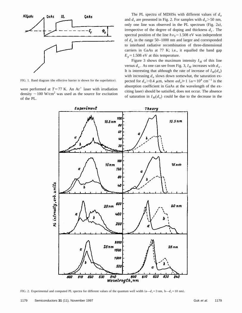
on
The PL spectra of MDHSs with different values ofda
tdednalap
x-
ex-ncee
were performed atT577 K. An Ar1 laser with irradiationdensity;100 W/cm2 was used as the source for excitatiof the PL.
FIG. 1. Band diagram~the effective barrier is shown for the superlattice!.
andds are presented in Fig. 2. For samples withda.50 nm,only one line was observed in the PL spectrum~Fig. 2a!,irrespective of the degree of doping and thicknessds . Thespectral position of the linehn051.508 eV was independenof da in the range 50–1000 nm and larger and corresponto interband radiative recombination of three-dimensiocarriers in GaAs at 77 K; i.e., it equalled the band gEg51.508 eV at this temperature.
Figure 3 shows the maximum intensityI M of this lineversusda . As one can see from Fig. 3,I M increases withda .It is interesting that although the rate of increase ofI M(da)with increasingda slows down somewhat, the saturation epected forda.0.4 mm, whereada@1 ~a'104 cm21 is theabsorption coefficient in GaAs at the wavelength of theciting laser! should be satisifed, does not occur. The abseof saturation inI M(da) could be due to the decrease in th
FIG. 2. Experimental and computed PL spectra for different values of the quantum well width~a—ds53 nm, b—ds510 nm!.
1179 1179Semiconductors 31 (11), November 1997 Guk et al.
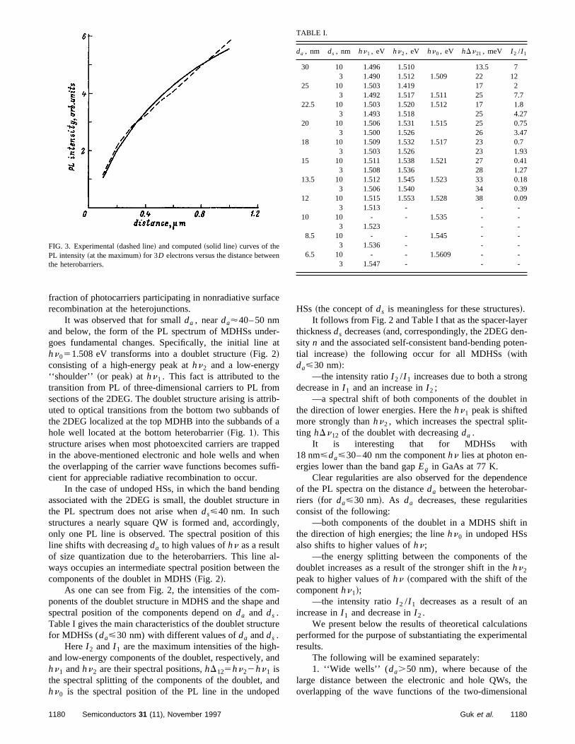
c
era
mribo
f
pheffi
in
glhi
at
man
tu
-an
ned
er-ten-
g
in
t-
nce-s
in
the
n
nsntal
etheal
en
TABLE I.
5
1
8
9
fraction of photocarriers participating in nonradiative surfarecombination at the heterojunctions.
It was observed that for smallda , nearda'40– 50 nmand below, the form of the PL spectrum of MDHSs undgoes fundamental changes. Specifically, the initial linehn051.508 eV transforms into a doublet structure~Fig. 2!consisting of a high-energy peak athn2 and a low-energy‘‘shoulder’’ ~or peak! at hn1 . This fact is attributed to thetransition from PL of three-dimensional carriers to PL frosections of the 2DEG. The doublet structure arising is attuted to optical transitions from the bottom two subbandsthe 2DEG localized at the top MDHB into the subbands ohole well located at the bottom heterobarrier~Fig. 1!. Thisstructure arises when most photoexcited carriers are trapin the above-mentioned electronic and hole wells and wthe overlapping of the carrier wave functions becomes sucient for appreciable radiative recombination to occur.
In the case of undoped HSs, in which the band bendassociated with the 2DEG is small, the doublet structurethe PL spectrum does not arise whends<40 nm. In suchstructures a nearly square QW is formed and, accordinonly one PL line is observed. The spectral position of tline shifts with decreasingda to high values ofhn as a resultof size quantization due to the heterobarriers. This lineways occupies an intermediate spectral position betweencomponents of the doublet in MDHS~Fig. 2!.
As one can see from Fig. 2, the intensities of the coponents of the doublet structure in MDHS and the shapespectral position of the components depend onda and ds .Table I gives the main characteristics of the doublet strucfor MDHSs (da<30 nm) with different values ofda andds .
Here I 2 and I 1 are the maximum intensities of the highand low-energy components of the doublet, respectively,hn1 andhn2 are their spectral positions,hD125hn22hn1 isthe spectral splitting of the components of the doublet, ahn0 is the spectral position of the PL line in the undop
FIG. 3. Experimental~dashed line! and computed~solid line! curves of thePL intensity~at the maximum! for 3D electrons versus the distance betwethe heterobarriers.
1180 Semiconductors 31 (11), November 1997
e
-t
-f
a
edn-
gin
y,s
l-he
-d
re
d
d
HSs ~the concept ofds is meaningless for these structures!.It follows from Fig. 2 and Table I that as the spacer-lay
thicknessds decreases~and, correspondingly, the 2DEG density n and the associated self-consistent band-bending potial increase! the following occur for all MDHSs~withda<30 nm!:
—the intensity ratioI 2 /I 1 increases due to both a strondecrease inI 1 and an increase inI 2 ;
—a spectral shift of both components of the doubletthe direction of lower energies. Here thehn1 peak is shiftedmore strongly thanhn2 , which increases the spectral spliting hDn12 of the doublet with decreasingda .
It is interesting that for MDHSs with18 nm<da<30– 40 nm the componenthn lies at photon en-ergies lower than the band gapEg in GaAs at 77 K.
Clear regularities are also observed for the dependeof the PL spectra on the distanceda between the heterobarriers ~for da<30 nm!. As da decreases, these regularitieconsist of the following:
—both components of the doublet in a MDHS shiftthe direction of high energies; the linehn0 in undoped HSsalso shifts to higher values ofhn;
—the energy splitting between the components ofdoublet increases as a result of the stronger shift in thehn2
peak to higher values ofhn ~compared with the shift of thecomponenthn1!;
—the intensity ratioI 2 /I 1 decreases as a result of aincrease inI 1 and decrease inI 2 .
We present below the results of theoretical calculatioperformed for the purpose of substantiating the experimeresults.
The following will be examined separately:1. ‘‘Wide wells’’ ( da.50 nm), where because of th
large distance between the electronic and hole QWs,overlapping of the wave functions of the two-dimension
da , nm ds , nm hn1 , eV hn2 , eV hn0 , eV hDn21 , meV I 2 /I 1
30 10 1.496 1.510 13.5 73 1.490 1.512 1.509 22 12
25 10 1.503 1.419 17 23 1.492 1.517 1.511 25 7.7
22.5 10 1.503 1.520 1.512 17 1.83 1.493 1.518 25 4.27
20 10 1.506 1.531 1.515 25 0.73 1.500 1.526 26 3.47
18 10 1.509 1.532 1.517 23 0.73 1.503 1.526 23 1.93
15 10 1.511 1.538 1.521 27 0.43 1.508 1.536 28 1.27
13.5 10 1.512 1.545 1.523 33 0.13 1.506 1.540 34 0.39
12 10 1.515 1.553 1.528 38 0.03 1.513 - - -
10 10 - - 1.535 - -3 1.523 - -
8.5 10 - - 1.545 - -3 1.536 - - -
6.5 10 - - 1.5609 - -3 1.547 - - -
1180Guk et al.
electrons and holes is small, so that only interband recombi-P
ic
en
m
gofeio
a--It
ehe
si
ra
sit
2. Quantum wells (da<30– 40 nm).t ines-su-g
the
hatt be
theon
s,
-u-
n
te
rgy
theane
thefac-out
inn
r-lf-
nation of three-dimensional carriers contributes to thespectrum.
2. Quantum wells~for da<30– 40 nm!, for which the PLspectrum corresponds to optical transitions with the partpation of a 2DEG.
2. THEORETICAL MODELS
1. We shall analyze first the dependence of the PL intsity onda in wide wells~Fig. 3!. As is well known, the mainmechanism of relaxation of the energy of nonequilibriucarriers in GaAs at temperaturesT>77 K is the emission ofoptical phonons. The characteristic energy relaxation lenfor such processes is;50 nm. For this reason, in the casewide wells all photoexcited carriers must recombine insidwell. In the case of stationary pumping and weak excitatthe distribution of excess electronsdn and holes dp(dn5dp) over the coordinatez ~in the direction of growthof the layers! is described by the equation
Dd2~dn!
dz2 5Ge2az1dn
t, ~1!
whereD is the ambipolar diffusion coefficient,G is the pho-togeneration rate atz50, andt is the effective lifetime
1
t5
1
t r1
1
tnr,
where t r is the lifetime for interband radiative recombintion, andtnr is the total lifetime for all other types of nonradiative and radiative volume recombination processes.obvious that the PL intensityI is given by
I;E0
dadn~z!dz. ~2!
If it is assumed that the surface recombination rateS0 is thesame for both heterojunctions, then integrating Eq.~1! andsubstituting the result into Eq.~2!, we obtain
I 5BS@cosh~da /L !21#1sinh~da /L !
~11S2!sinh~da /L !12S•sinh~da /L !@~aL1S!
3~aL2S!exp~2ada!#2@12exp~2ada!#/aL, ~3!
where S5S0L/D, L5ADt is the ambipolar diffusionlength, andB is a proportionality coefficient.
In the case of our experiments the conditionsda /L!1andaL@1 are satisfied. Comparing the experimental valuof I in Fig. 3 with the computational results shows that tbest agreement with experiment is attained forS!1 and Eq.~3! can be written in the simplified form
I 5BaLda
da12SL~12e2ada!. ~4!
Least-squares analysis of the experimental results, uEq. ~4!, gives S52.731023, which corresponds toS0510 cm/s. This means that the surface recombinationin the HSs investigated is very low and the expression~4!describes well the well-width dependence of the PL inten~Fig. 2!.
1181 Semiconductors 31 (11), November 1997
L
i-
-
th
an
is
s
ng
te
y
The calculation of the PL characteristics revealed thaorder to obtain good agreement with experiment it is necsary to determine accurately the effective height of theperlattice~SL! barrier. This height was calculated accordinto the Kronig–Penney model. The results are 0.48DEc and0.44DEv for electrons and holes, respectively, whereDEc
andDEv are the conduction and valence band offsets atGaAs/Al0.25Ga0.75As heterojunction, respectively.
If it is assumed in the calculations for undoped HSs tthe QW is square, then agreement with experiment cannoobtained. The reason is band bending~Fig. 1!. The energies,wave functions, and populations of the subbands of2DEG in the MHDS were calculated in the approximatidn!n ~quasiequilibrium situation! by solving the system ofequations~the Kohn–Sham system7!
2\2
2mc
d2Cei
dz2 1Ue~z!Cei 5Ee
i Cei , ~5!
xd2w
dz2 5q@n2N~z!#, ~6!
wherez is the direction perpendicular to the heterojunctionCe
i (z) is the envelope wave function,Ue(z) is the potentialenergy,x is the permittivity,w(z) is the electrostatic potential which is determined by the equilibrium electron distribtion, Ee
i is the energy of electron motion alongz, N(z) is theimpurity density,
Ue~z!5DEc~z!2q~w1wxc!, ~7!
wherewxc5 q/3px n1/3 is the exchange-correlation electrointeraction potential, and
n5E nsEuCeu2dE, ~8!
wherensEis the layer density of electrons with energyE.
In Eq. ~8! the integration extends over both the discreand continuous sections of the spectrum. For holes, Eq.~5!has the same form as for electrons with the potential ene
Up~z!5DEv~z!1q~w1wxc!. ~9!
The motion of electrons and holes is unbounded inplane of the heterojunction and the wave functions are plwaves. The new aspect of the expression~9! is that anexchange-correlation interaction potentialwxc , which de-pends only on the electron density, is introduced intohole potential energy. The calculations showed that satistory agreement with experiment cannot be obtained withit. The introduction ofwxc is strictly justified in Ref. 7 forelectrons. We know of no justification for the introductionEq. ~9! of a potentialwxc that depends only on the electrodensity.
The problem of calculating the optical-transition enegies was systematically solved by first solving the seconsistent system of equations~5!–~8! for the electrons andthen, using the values obtained for the potential~9!, the sys-tem of equations~5! and ~9! for holes. This simplified ap-proach is possible in our case sincedp!n.
1181Guk et al.
In the casedn;n, it would be necessary to solve self-on,
thtiaro
ndrie
on
tit
a
e
f
f
id
Qth
nof
dyor
aum
en-n
and
ofn
-
not
the.si-of
l,inalds.
cal
ec-
consistently the complete system of equations for electrand holes. This does not present any special difficultiesthe carrier energy distribution functions are known.
It should be noted that in the case of electronsMDHS studied consists of two almost independent potenwells ~in front of and behind the superlattice heterobarrie!.For this reason, to simplify the calculations the systemequations~5!–~8! were solved separately for each well, athe coupling equation for the potentials at the SL boundawas obtained from the solution of Eq.~6! in the region of theSL with n50.
The solution was obtained numerically by an iteratimethod. This procedure is described in detail in Ref. 8.
After these calculations are completed, it is quite easycalculate the PL spectrum. The Fermi–Dirac functions welectron and hole quasi-Fermi levelsEF,e5EF2dekT andEF,n5EF2dhkT for electrons and holes, respectively~EF isthe equilibrium value of the Fermi energy! were taken as thecarrier energy distribution functions. It can be shown thdh@de in the casedn!n. We can then obtain from theBoltzmann collision integral the following expression for thPL intensity:
I ~hn!5B~edn21!
3(i , j
Wi j
11me /mh
expS 2hn2Eg
kT D11expS EF2Ee
i 2Ei j
kt D Q~Ei j /kT!,
~10!
whereEei is the energy of thei th quantum-well subband o
the 2DEG,hn is the energy of the emitted photons,
Ei j 5hn2Eg2Ee
i 2Ehj
11me /mh, ~11!
Ehj is the energy of thej th hole quantum-well subband,Q is
the theta function, andWi j is the squared overlap integral othe envelopes of the electron and hole wave functionsCe
i
andChj .
It should be noted that, in contrast with the case of wwells,B in Eq. ~10! depends onda andds . This is due to thefact that the number of electrons and holes trapped in adepends on the size of the well and the magnitude ofband bending and, correspondingly, the 2DEG densityn2d .9
For this reason, the expression~10! is admissable, strictlyspeaking, only for qualitative comparison of the peak intesities of the PL spectrum of MDHSs with different valuesda or ds .
3. DISCUSSION
Since the intensity of the PL in wide wells has alreabeen analyzed, here we shall discuss only the results fQW.
We start with an analysis of undoped HSs. As one csee from Fig. 4, the picture of an ideally square quant
1182 Semiconductors 31 (11), November 1997
sif
el
f
s
oh
t
e
We
-
a
n
well makes it impossible to explain the experimental depdencehn0(da) ~curve 1!. Satisfactory agreement betweetheory and experiment is achieved if the presence of bbendingw0 is taken into account~Fig. 4, curve3!. As anexact calculation shows, the magnitude ofw0 in an undopedHS ~with background impurity density;131014 cm23!equals approximately 20 meV. In this case, the energyoptical transitions can be approximated by the expressio
hn05Eg1Eei 1Eh
j 2qFda , ~12!
whereEei 1Eh
j ; 11me /mh /da2 is the total energy of the bot
tom electron and hole subbands, andqFda is the band-bending potential inside the QW, whereF is the effectiveband-bending electric field.
Since the deviation of the QW from a square shape islarge, the selection rulesWi j '1 for i 5 j and Wi j '0 foriÞ j ~for heavy and light holes! hold approximately, as thecalculation shows. Since there is no special doping,population of all subbandsi .1 should be close to zeroTherefore, only one line corresponding to the optical trantion Ee
1→Ehh1 should be observed in the PL spectrum
undoped HSs.For MDHSs, band bending is substantia
w0'80– 120 meV and, correspondingly, the electric fieldthe QW is strong. This lifts the restriction on the optictransitions between different electron and hole subbanThe high 2DEG densityn2d;(6 – 10)31011 cm2 ensuresthat two bottom electronic subbands,Ee
1 andEe2, are filled in
most MDHSs. Calculations showed that six types of optitransitions between electronic subbandsEe
1 and Ee2, on the
one hand, and hole subbandsElh1 andEhh
2 , on the other~Elh
and Ehh are the light- and heavy-hole subbands, resp
FIG. 4. E1e2E1
hh2Eg versus the width of undoped well~1—self-consistentcalculation,2—experiment,3—calculation in the square-well model!.
1182Guk et al.
lehe
se
-t
fohathana
dd
po
eld
ra
nll
esethe
si-
6.the
b-
ther-
ing
tral
s in
a-nds
tively!, can make an appreciable contribution to the doubstructure in the PL spectrum of a MDHS. In addition, tcontributions of each depend onda andds .
The optical transitionEe1→Ehh
1 as well as the transitionEe
1→Ehh1 and Ee
2→Ehh2 make the main contribution to th
low-energy componenthn of the doublet.The transitionsEe
2→Elh1 andEe
2→Ehh2 contribute to the
high-energy peak athn2 ; the contribution of the latter transition decreases with decreasingda . It should be noted thathe peakI 2 should appear only when theEe
2 subband is ap-preciably filled with electrons, i.e., when the Fermi levelEF
lies either above or slightly belowEe2 ~so that optical pump-
ing would ensure that it is filled!.The experimental and computed PL spectra
da520 nm are shown in Fig. 2. Comparing them shows tthe theoretical model explains, at least qualitatively,shape of the PL spectra, including the spectral positionintensity ratio of the components of the doublet and the chacter of their variation with decreasingds .
The energies and squared overlap integrals computefunctions ofds for different optical transitions are presentein Fig. 5. In accordance with experiment, here the comnents of the doublet shift to lower values ofhn with decreas-ing ds . This is due to an increase in the band bending~as aresult of an increase in the 2DEG densityn2d!, which resultsin a decrease of the effective energy gaps between thetron and hole subbands. The theory also explains thecrease inI 1 and the increase inI 2 and, correspondingly, theincrease in the ratioI 2 /I 1 with decreasingds . In this case,the decrease inI 1 is due to a decrease in the overlap integof the wave function of the ground stateCe
1 of the 2DEGwith the hole wave functions because of the narrowing a‘‘sharpening’’ of the lower part of the quasitriangular we
FIG. 5. Eje2Ej
h2Eg ~solid lines! and squared overlap integrals~dashedlines! versus spacer-layer thickness~transitions: 1—1e21hh, 2—1e22hh, 3—2e21hh, 4—2e21lh! for ds510 nm.
1183 Semiconductors 31 (11), November 1997
t
rt
edr-
as
-
ec-e-
l
d
that contains the 2DEG, which decrease the extent ofCe1(z)
in the z direction. The intensityI 2 increases because thpopulation of the stateEe
2 increases as a result of an increain n2d . At the same time, because of the large extent ofwave functionCe
2(z), its overlap integrals with the holewave functions are virtually independent ofds .
The theoretical curves of the energies of optical trantions and the corresponding overlap integralsWi j versus thedistanceda between the heterobarriers are shown in Fig.
According to these results, the observed increase inintensity of the peakI 1 with decreasingda is due to an in-crease in the overlap integral of the wave functionCe
1 withthe wave functions of the bottom heavy- and light-hole subands. The decrease in the intensity of the peakI 2, whichoccurs in this case, must be attributed to the decrease inpopulation of theEe
2 subband, since the corresponding ovelap integrals are virtually independent ofda . The theory pre-dicts, in agreement with experiment~Fig. 6!, that the ener-gies of all optical transitions studied increase with decreasda ; here the predicted shift is larger for thehn2 peak thanfor the hn1 peak. This results in an increase of the specsplitting hDn125hn22hn1 of the doublet. As a result of therapid increase in the energyEe
2 relative to the Fermi energyEF , the population of this subband decreases withda .
The results presented demonstrate clear differencethe behavior of the wave functions of the subbandsEe
1 andEe
2 of the 2DEG. The weaker dependence onda of the over-lap integrals for optical transitions from theEe
2 subband thanfor transitions from theEe
1 subband and the opposite sitution for theda dependences of the energies of these subbaare due to differences in the extent of wave functionsce
2(z)and Ce
1(z) in the z direction. It follows from the resultsobtained that the spatial extent ofCe
1(z) equals about 12–15
FIG. 6. Eie2Ej
h2Eg ~solid lines! and squared overlap integrals~dashedlines! versus well width ~transitions: 1—1e21hh, 2—1e22hh, 3—2e21hh, 4—2e21lh! for da520 nm.
1183Guk et al.
nm, while the spatial extent ofCe2(z) is estimated to be
1
rlar.rrt
nth
s
do--
eGitare-thbl
-exof-
eces
nity
ic
transitions from the subbandEe1, on the other. The accompa-
all
o-
-aviort of
, ofole
bt-ionods
ofof
l.
.
n,
-
;30 nm. The small extent ofCe(z) is responsible for theweak effect of the approach of the second heterobarrier~forda>15 nm! on the energy of the subbandEe
1, on the onehand, and a strong effect of this heterobarrier on the oveintegral ofCe
1(z) with the hole wave functions, on the otheAt the same time, the approach of the second heterobastrongly influences the more extended state described bywave functionCe
2(z), increasing its energyEe2 and corre-
spondingly decreasing its population.In this connection, measurements of the depende
I 1(da) can be used to obtain an experimental estimate ofspatial extent of the wave functionCe
1(z) and measurementof I 2 can be used to estimate the population of theE2
2 sub-band. The latter makes it possible to use the PL methoinvestigate the electron distribution over the twdimensional subbands~this is usually done by means of lowtemperature Shubnikov–de Haas measurements!, even athigh temperatures.
In conclusion, we note that a transition from PL of thredimensional carriers to PL with the participation of a 2DEis observed in the PL spectra of double-barrier MDHSs wdecreasing distanceda between the heterobarriers. Neda'40 nm thehn0 line, which corresponds to interband rcombination of three-dimensional electrons and holes, inPL spectrum vanishes and is replaced by a new doustructure with components athn1 and hn2 . This PL inMDHSs with different distancesda and spacer-layer thicknessesds was investigated experimentally and were theperimental data were analyzed theoretically on the basisself-consistent solution of the Schro¨dinger and Poisson equations.
It was found that the doublet structure in the PL sptrum is due to optical transitions between the two lowsubbands with a 2DEGEe
1 andEe2 and hole subbandsEhh
1 ,Elh
1 , andEhh2 . The relative contributions of each transitio
depend onda andds . The observed increase in the intensratio I 2 /I 1 of the doublet components with decreasingds isdue to an increase in the populations of theEe
2 subband, onthe one hand, and a decrease in the probability of opt
1184 Semiconductors 31 (11), November 1997
p
ierhe
cee
to
-
h
eet
-a
-t
al
nying increase in the band bending gives rise to a shift ofoptical transitions in the direction of lower values ofhn as aresult of a decrease in the effective interband gap.
It was found that a decrease in the distanceds influencesdifferently the spectral position and intensity of the compnents of the doublet in the PL spectrum. For thehn2 peak, amuch larger shift is observed in the direction of largehnthan for thehn1 peak. The intensity of the first peak decreases and that of the second peak increases. This behis attributable to the large differences in the spatial extenthe wave functionsCe
1(z) andCe2(z), which account for the
different da dependences of the energies of the subbandstheir populations, and of the overlap integrals with the hwave functions.
The results which we obtained in our study are undouedly of interest which we for understanding size-quantizatphenomena in a 2DEG and for developing effective methfor diagnostics of the parameters of a 2DEG.
This work was supported by the Ministry of Sciencethe Russian Federation as part of the program ‘‘Physicssolid-state nanostructures.’’
1Y. K. Yuan, K. Mohammed, M. A. A. Pudensi., and J. L. Mezz, AppPhys. Lett.45, 739 ~1984!.
2Zh. I. Alferov, A. M. Vasil’ev, and P. S. Kop’ev,@JETP Lett.44, 669~1986!#.
3P. D. Altukhov, A. A. Bakun, B. K. Medvevdev, V. G. Mokerov, A. ARogachev, and G. P. Rubtsov, Fiz. Tekh. Poluprovodn.21, 449 ~1987!@Sov. Phys. Semicond.21, 279 ~1987!#.
4I. V. Kukushkin, K. V. Klitzing, and K. Ploog, Phys. Rev. B37, 8509~1988!.
5S. K. Lyo and E. D. Jones, Phys. Rev. B38, 4113~1988!.6H. J. Polland, K. Leo, K. Rother, and K. Ploog, Phys. Rev. B38, 7635~1988!.
7S. Lundqvist and N. March@Eds.#, Theory of Inhomogeneous ElectroGas, Plenum Press, N. Y., 1983@Russian translation, Mir, Moscow1987#.
8V. E. Kaminski�, Fiz. Tekh. Poluprovodn.23, 662 ~1989! @Sov. Phys.Semicond.23, 414 ~1989!#.
9V. A. Solov’ev, I. N. Yassievich, and V. M. Chistyakov, Fiz. Tekh. Poluprovodn.29, 1264~1995! @Semiconductors29, 654 ~1995!#.
Translated by M. E. Alferieff
1184Guk et al.
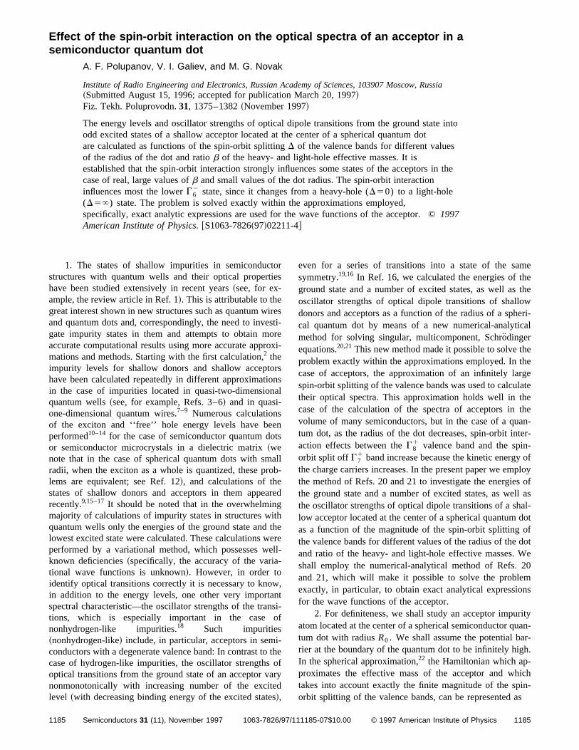
Effect of the spin-orbit interaction on the optical spectra of an acceptor in a
me
semiconductor quantum dotA. F. Polupanov, V. I. Galiev, and M. G. Novak
Institute of Radio Engineering and Electronics, Russian Academy of Sciences, 103907 Moscow, Russia~Submitted August 15, 1996; accepted for publication March 20, 1997!Fiz. Tekh. Poluprovodn.31, 1375–1382~November 1997!
The energy levels and oscillator strengths of optical dipole transitions from the ground state intoodd excited states of a shallow acceptor located at the center of a spherical quantum dotare calculated as functions of the spin-orbit splittingD of the valence bands for different valuesof the radius of the dot and ratiob of the heavy- and light-hole effective masses. It isestablished that the spin-orbit interaction strongly influences some states of the acceptors in thecase of real, large values ofb and small values of the dot radius. The spin-orbit interactioninfluences most the lowerG6
2 state, since it changes from a heavy-hole (D50) to a light-hole(D5`) state. The problem is solved exactly within the approximations employed,specifically, exact analytic expressions are used for the wave functions of the acceptor. ©1997American Institute of Physics.@S1063-7826~97!02211-4#
1. The states of shallow impurities in semiconductoreven for a series of transitions into a state of the sa19,16
ieiresorro
ronna
ents
aro
arg
iththe
e-
wn
nso
i-to
aeds
hethe
weri-
cal
hehegelatehethean-ter--ofploys ofll asal-dotofdotWe20mns
rityuan-r-h.
ichin-s
/1
structures with quantum wells and their optical properthave been studied extensively in recent years~see, for ex-ample, the review article in Ref. 1!. This is attributable to thegreat interest shown in new structures such as quantum wand quantum dots and, correspondingly, the need to invgate impurity states in them and attempts to obtain maccurate computational results using more accurate appmations and methods. Starting with the first calculation,2 theimpurity levels for shallow donors and shallow acceptohave been calculated repeatedly in different approximatiin the case of impurities located in quasi-two-dimensioquantum wells~see, for example, Refs. 3–6! and in quasi-one-dimensional quantum wires.7–9 Numerous calculationsof the exciton and ‘‘free’’ hole energy levels have beperformed10–14 for the case of semiconductor quantum door semiconductor microcrystals in a dielectric matrix~wenote that in the case of spherical quantum dots with smradii, when the exciton as a whole is quantized, these plems are equivalent; see Ref. 12!, and calculations of thestates of shallow donors and acceptors in them apperecently.9,15–17 It should be noted that in the overwhelminmajority of calculations of impurity states in structures wquantum wells only the energies of the ground state andlowest excited state were calculated. These calculations wperformed by a variational method, which possesses wknown deficiencies~specifically, the accuracy of the variational wave functions is unknown!. However, in order toidentify optical transitions correctly it is necessary to knoin addition to the energy levels, one other very importaspectral characteristic—the oscillator strengths of the trations, which is especially important in the casenonhydrogen-like impurities.18 Such impurities~nonhydrogen-like! include, in particular, acceptors in semconductors with a degenerate valence band: In contrast tocase of hydrogen-like impurities, the oscillator strengthsoptical transitions from the ground state of an acceptor vnonmonotonically with increasing number of the excitlevel ~with decreasing binding energy of the excited state!,
1185 Semiconductors 31 (11), November 1997 1063-7826/97
s
esti-exi-
ssl
llb-
ed
ere
ll-
,ti-
f
hef
ry
symmetry. In Ref. 16, we calculated the energies of tground state and a number of excited states, as well asoscillator strengths of optical dipole transitions of shallodonors and acceptors as a function of the radius of a sphcal quantum dot by means of a new numerical-analytimethod for solving singular, multicomponent, Schro¨dingerequations.20,21This new method made it possible to solve tproblem exactly within the approximations employed. In tcase of acceptors, the approximation of an infinitely larspin-orbit splitting of the valence bands was used to calcutheir optical spectra. This approximation holds well in tcase of the calculation of the spectra of acceptors involume of many semiconductors, but in the case of a qutum dot, as the radius of the dot decreases, spin-orbit inaction effects between theG8
1 valence band and the spinorbit split off G7
1 band increase because the kinetic energythe charge carriers increases. In the present paper we emthe method of Refs. 20 and 21 to investigate the energiethe ground state and a number of excited states, as wethe oscillator strengths of optical dipole transitions of a shlow acceptor located at the center of a spherical quantumas a function of the magnitude of the spin-orbit splittingthe valence bands for different values of the radius of theand ratio of the heavy- and light-hole effective masses.shall employ the numerical-analytical method of Refs.and 21, which will make it possible to solve the probleexactly, in particular, to obtain exact analytical expressiofor the wave functions of the acceptor.
2. For definiteness, we shall study an acceptor impuatom located at the center of a spherical semiconductor qtum dot with radiusR0 . We shall assume the potential barier at the boundary of the quantum dot to be infinitely higIn the spherical approximation,22 the Hamiltonian which ap-proximates the effective mass of the acceptor and whtakes into account exactly the finite magnitude of the sporbit splitting of the valence bands, can be represented a
118511185-07$10.00 © 1997 American Institute of Physics
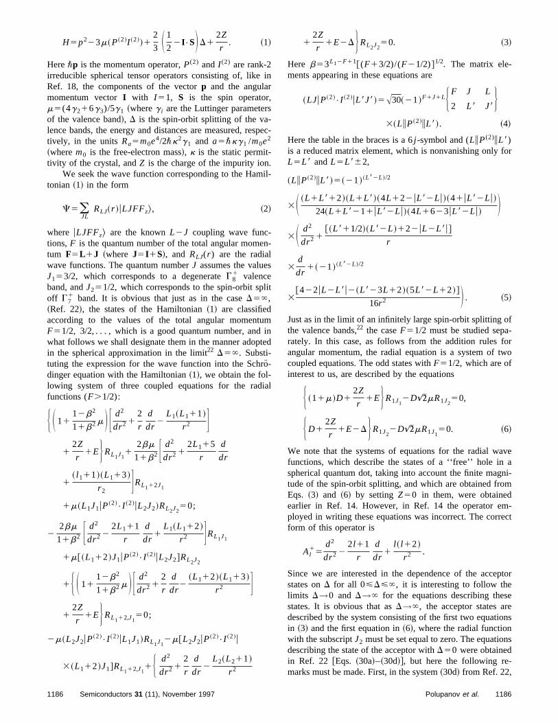
H5p223m~P~2!I ~2!!12 1
2I•S D12Z
. ~1!
i
,s-s
.i
n
s
lit
uminte
ro
ia
12Z
1E2D R 50. ~3!
for
f-ortwo
aveani-m
m-ect
ptor
eeons
ns
3 S 2 D r
Here\p is the momentum operator,P(2) and I (2) are rank-2irreducible spherical tensor operators consisting of, likeRef. 18, the components of the vectorp and the angularmomentum vectorI with I 51, S is the spin operatorm5(4g216g3)/5g1 ~whereg i are the Luttinger parameterof the valence band!, D is the spin-orbit splitting of the valence bands, the energy and distances are measured, retively, in the unitsRa5m0e4/2\k2g1 and a5\kg1 /m0e2
~wherem0 is the free-electron mass!, k is the static permit-tivity of the crystal, andZ is the charge of the impurity ion
We seek the wave function corresponding to the Hamtonian ~1! in the form
C5(JL
RLJ~r !uLJFFz&, ~2!
where uLJFFz& are the knownL2J coupling wave func-tions,F is the quantum number of the total angular mometum F5L1J ~where J5I1S!, and RLJ(r ) are the radialwave functions. The quantum numberJ assumes the valueJ153/2, which corresponds to a degenerateG8
1 valenceband, andJ251/2, which corresponds to the spin-orbit spoff G7
1 band. It is obvious that just as in the caseD5`,~Ref. 22!, the states of the Hamiltonian~1! are classifiedaccording to the values of the total angular momentF51/2, 3/2,. . . , which is a good quantum number, andwhat follows we shall designate them in the manner adopin the spherical approximation in the limit22 D5`. Substi-tuting the expression for the wave function into the Sch¨-dinger equation with the Hamiltonian~1!, we obtain the fol-lowing system of three coupled equations for the radfunctions (F.1/2):
H S 1112b2
11b2 m D F d2
dr2 12
r
d
dr2
L1~L111!
r 2 G1
2Z
r1EJ RL1J1
12bm
11b2 F d2
dr2 12L115
r
d
dr
1~ l 111!~L113!
r 2GRL112J1
1m~L1J1uP~2!•I ~2!uL2J2!RL2J2
50;
22bm
11b2 F d2
dr2 22L111
r
d
dr1
L1~L112!
r 2 GRL1J1
1m@~L112!J1uP~2!•I ~2!uL2J2#RL2J2
1H S 1112b2
11b2 m D F d2
dr2 12
r
d
dr2
~L112!~L113!
r 2 G1
2Z
r1EJ RL112,J1
50;
2m~L2J2uP~2!•I ~2!uL1J1!RL1J1
2m@L2J2uP~2!•I ~2!u
3~L112!J1#RL112,J11H d2
dr2 12
r
d
dr2
L2~L211!
r 2
1186 Semiconductors 31 (11), November 1997
n
pec-
l-
-
d
l
r J L2J2
Here b53L12F11@(F13/2)/(F21/2)#1/2. The matrix ele-ments appearing in these equations are
~LJuP~2!•I ~2!uL8J8!5A30~21!F1J1LH F J L
2 L8 J8J
3~LiP~2!iL8!. ~4!
Here the table in the braces is a 6j -symbol and (LiP(2)iL8)is a reduced matrix element, which is nonvanishing onlyL5L8 andL5L862,
~LiP~2!iL8!5~21!~L82L !/2
3S ~L1L812!~L1L8!~4L122uL82Lu!~41uL82Lu!24~L1L8211uL82Lu!~4L1623uL82Lu! D
3S d2
dr2 1@~L811/2!~L82L !122uL2L8u#
r
3d
dr1~21!~L82L !/2
3@422uL2L8u2~L823L12!~5L82L12!#
16r 2 D . ~5!
Just as in the limit of an infinitely large spin-orbit splitting othe valence bands,22 the caseF51/2 must be studied separately. In this case, as follows from the addition rules fangular momentum, the radial equation is a system ofcoupled equations. The odd states withF51/2, which are ofinterest to us, are described by the equations
H ~11m!D12Z
r1EJ R1J1
2D&mR1J250,
H D12Z
r1E2DJ R1J2
2D&mR1J150. ~6!
We note that the systems of equations for the radial wfunctions, which describe the states of a ‘‘free’’ hole inspherical quantum dot, taking into account the finite magtude of the spin-orbit splitting, and which are obtained froEqs. ~3! and ~6! by setting Z50 in them, were obtainedearlier in Ref. 14. However, in Ref. 14 the operator eployed in writing these equations was incorrect. The corrform of this operator is
Al15
d2
dr2 22l 11
r
d
dr1
l ~ l 12!
r 2 .
Since we are interested in the dependence of the accestates onD for all 0<D<`, it is interesting to follow thelimits D→0 and D→` for the equations describing thesstates. It is obvious that asD→`, the acceptor states ardescribed by the system consisting of the first two equatiin ~3! and the first equation in~6!, where the radial functionwith the subscriptJ2 must be set equal to zero. The equatiodescribing the state of the acceptor withD50 were obtainedin Ref. 22 @Eqs. ~30a!–~30d!#, but here the following re-marks must be made. First, in the system~30d! from Ref. 22,
1186Polupanov et al.
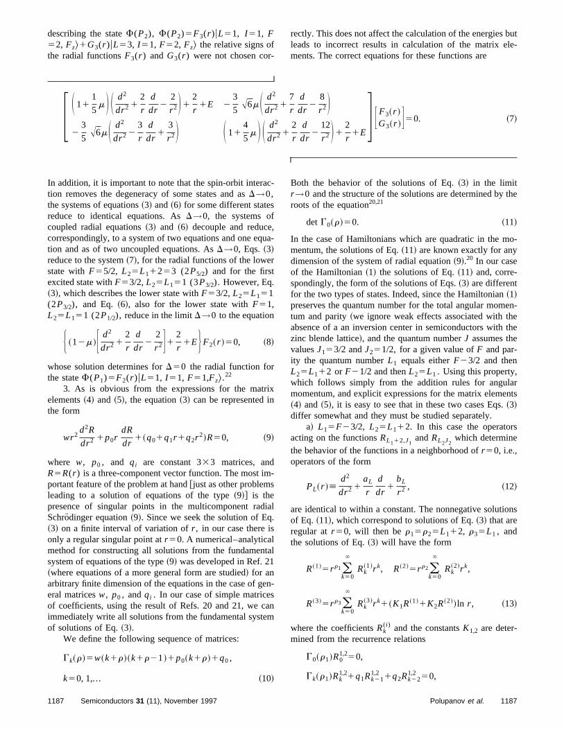
describing the stateF(P2), F(P2)5F3(r )uL51, I 51, F
-
rectly. This does not affect the calculation of the energies butle-
52, Fz&1G3(r )uL53, I 51, F52, Fz& the relative signs ofthe radial functionsF3(r ) and G3(r ) were not chosen cor
,u
r
rixn
m
ia.
ta
ensam
leads to incorrect results in calculation of the matrix ements. The correct equations for these functions are
F S 111
5m D S d2
dr2 12
r
d
dr2
2
r 2D12
r1E 2
3
5A6mS d2
dr2 17
r
d
dr2
8
r 2D2
3
5A6mS d2
dr2 23
r
d
dr1
3
r 2D S 114
5m D S d2
dr2 12
r
d
dr2
12
r 2 D12
r1E
G F F3~r !
G3~r !G50. ~7!
In addition, it is important to note that the spin-orbit interac- Both the behavior of the solutions of Eq.~3! in the limit
theo-
en-hethe
rnts
s
ns
tion removes the degeneracy of some states and asD→0,the systems of equations~3! and~6! for some different statesreduce to identical equations. AsD→0, the systems ofcoupled radial equations~3! and ~6! decouple and reducecorrespondingly, to a system of two equations and one eqtion and as of two uncoupled equations. AsD→0, Eqs.~3!reduce to the system~7!, for the radial functions of the lowestate withF55/2, L25L11253 (2P5/2) and for the firstexcited state withF53/2,L25L151 (3P3/2). However, Eq.~3!, which describes the lower state withF53/2, L25L151(2P3/2), and Eq.~6!, also for the lower state withF51,L25L151 (2P1/2), reduce in the limitD→0 to the equation
H ~12m!F d2
dr2 12
r
d
dr2
2
r 2G12
r1EJ F2~r !50, ~8!
whose solution determines forD50 the radial function forthe stateF(P1)5F2(r )uL51, I 51, F51,Fz&.
22
3. As is obvious from the expressions for the matelements~4! and ~5!, the equation~3! can be represented ithe form
wr2d2R
dr2 1p0rdR
dr1~q01q1r 1q2r 2!R50, ~9!
where w, p0 , and qi are constant 333 matrices, andR5R(r ) is a three-component vector function. The most iportant feature of the problem at hand@just as other problemsleading to a solution of equations of the type~9!# is thepresence of singular points in the multicomponent radSchrodinger equation~9!. Since we seek the solution of Eq~3! on a finite interval of variation ofr , in our case there isonly a regular singular point atr 50. A numerical–analyticalmethod for constructing all solutions from the fundamensystem of equations of the type~9! was developed in Ref. 21~where equations of a more general form are studied! for anarbitrary finite dimension of the equations in the case of geral matricesw, p0 , andqi . In our case of simple matriceof coefficients, using the result of Refs. 20 and 21, we cimmediately write all solutions from the fundamental systeof solutions of Eq.~3!.
We define the following sequence of matrices:
Gk~r!5w~k1r!~k1r21!1p0~k1r!1q0 ,
k50, 1,... ~10!
1187 Semiconductors 31 (11), November 1997
a-
-
l
l
-
n
r→0 and the structure of the solutions are determined byroots of the equation20,21
det G0~r!50. ~11!
In the case of Hamiltonians which are quadratic in the mmentum, the solutions of Eq.~11! are known exactly for anydimension of the system of radial equation~9!.20 In our caseof the Hamiltonian~1! the solutions of Eq.~11! and, corre-spondingly, the form of the solutions of Eqs.~3! are differentfor the two types of states. Indeed, since the Hamiltonian~1!preserves the quantum number for the total angular momtum and parity~we ignore weak effects associated with tabsence of a an inversion center in semiconductors withzinc blende lattice!, and the quantum numberJ assumes thevaluesJ153/2 andJ251/2, for a given value ofF and par-ity the quantum numberL1 equals eitherF23/2 and thenL25L112 or F21/2 and thenL25L1 . Using this property,which follows simply from the addition rules for angulamomentum, and explicit expressions for the matrix eleme~4! and ~5!, it is easy to see that in these two cases Eqs.~3!differ somewhat and they must be studied separately.
a! L15F23/2, L25L112. In this case the operatoracting on the functionsRL112,J1
andRL2J2which determine
the behavior of the functions in a neighborhood ofr 50, i.e.,operators of the form
PL~r 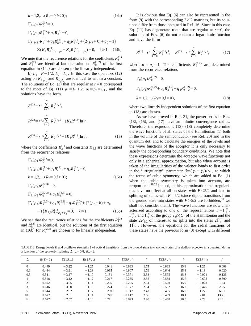
k51,2,...~Rl50,l ,0!; ~14a!
t.
on
It is obvious that Eq.~6! can also be represented in the
se
ion
qs.s.
andto
thatnot
t isder
rei-
r-
of
G0~r3!R0~3!50,
G1~r3!R1~3!1q1R0
~3!50,
Gk~r3!Rk~3!1q1Rk21
~3! 1q2Rk22~3! 1$2~r31k!1q021%
3~K1Rk2r11r3
~1! 1K2Rk2r11r3
~2! !50, k>1. ~14b!
We note that the recurrence relations for the coefficientsRk(1)
and Rk(2) are identical but the solutionsR0
(1,2) of the firstequation in~14a! are chosen to be linearly independent.
b! L15F21/2, L25L1 . In this case the operators~12!acting onRL1J1
andRL2J2are identical to within a constan
The solutions of Eq.~3! that are reqular atr 50 correspondto the roots of Eq.~11! r15L112, r25r35L1 , and thesolutions have the form
R~1!5r r1(k50
`
Rk~1!r k,
R~2!5r r2(k50
`
Rk~2!r k1~K2R~1!!ln r ,
R~3!5r r3(k50
`
Rk~3!r k1~K3R~1!!ln r , ~15!
where the coefficientsRk( i ) and constantsK2,3 are determined
from the recurrence relations
G0~r1!R0~1!50,
Gk~r1!Rk~1!1q1Rk21
~1! 1q2Rk22~1! 50,
k51,2,...~Rl50,l ,0!; ~16a!
G0~r3!R0~2,3!50,
G1~r3!R1~2,3!1q1R0
~2,3!50,
Gk~r3!Rk~2,3!1q1Rk21
~2,3!1q2Rk22~2,3!1$2~r31k!1q0
21%K2,3Rk2r21r3
~1! 50, k>1. ~16b!
We see that the recurrence relations for the coefficientsRk(2)
andRk(3) are identical, but the solutions of the first equati
in ~16b! for R0(2,3) are chosen to be linearly independent.
TABLE I. Energy levelsE and oscillator strengthsf of optical transitions froma function of the spin-orbit splittingD. m50.8, R053.
form ~9! with the corresponding 232 matrices, but its solu-tions differ from those obtained in Ref. 16. Since in this caEq. ~11! has degenerate roots that are regular atr 50, thesolutions of Eqs.~6! do not contain a logarithmic functionand have the form
R~1!5r r1(k50
`
Rk~1!r k, R~2!5r r2(
k50
`
Rk~2!r k, ~17!
where r15r251. The coefficientsRk(1,2) are determined
from the recurrence relations
G0~r1!R0~1,2!50,
Gk~r1!Rk~1,2!1q1Rk21
~1,2!1q2Rk22~1,2!50,
k51,2,...~Rl50,l ,0!, ~18!
where two linearly independent solutions of the first equatin ~18! are chosen.
As we have proved in Ref. 21, the power series in E~13!, ~15!, and ~17! have an infinite convergence radiuTherefore, the expressions~13!–~18! completely determinethe wave functions of all states of the Hamiltonian~1! bothin the volume of the semiconductor~see Ref. 20! and in thequantum dot, and to calculate the energies of the levelsthe wave functions of the acceptor it is only necessarysatisfy the corresponding boundary conditions. We notethese expressions determine the acceptor wave functionsonly in a spherical approximation, but also when accountaken of the irregularities of the valence bands to first orin the ‘‘irregularity’’ parameterd5(g32g2)/g1 , to whichthe terms of cubic symmetry, which are added to Eq.~1!when the cubic symmetry is taken into account, aproportional.18,22Indeed, in this approximation the irregularties have no effect at all on states withF,5/2 and lead tosplitting of states withF55/2 ~since dipole transitions fromthe ground state into states withF.5/2 are forbidden,18 weshall not consider them!. The wave functions are now chaacterized according to one of the representationsG5G8
6 ,G7
6 , andG66 of the groupTd3Ci of the Hamiltonian and the
state 2P5/2 of interest to us splits into the states 2G82 and
1G72 . However, the equations for the radial functions
these states have the previous form~3! except with different
the ground state into excited states of a shallow acceptor in a quantum dot as
D E(Z50) E(1S3/2) E(2P3/2) f E(3P3/2) f E(2P5/2) f E(2P1/2) f
0 0.449 23.22 21.25 0.041 20.663 1.75 20.663 15.8 21.25 0.0080.1 0.464 23.21 21.23 0.065 20.607 1.79 20.646 15.8 21.18 0.0200.5 0.511 23.17 21.19 0.151 20.371 2.53 20.595 15.8 20.921 0.1261 0.548 23.12 21.17 0.217 20.255 2.52 20.558 15.7 20.608 0.3902 0.592 23.05 21.14 0.265 20.205 2.31 20.520 15.9 20.028 1.543 0.616 23.00 21.13 0.274 20.177 2.34 20.502 16.2 0.476 2.955 0.644 22.92 21.12 0.269 20.147 2.42 20.485 16.9 1.22 6.91
10 0.672 22.81 21.11 0.245 20.117 2.56 20.469 18.1 2.01 13.2` 0.677 22.57 21.10 0.21 20.073 2.90 20.450 20.5 2.78 21.3
1188 1188Semiconductors 31 (11), November 1997 Polupanov et al.
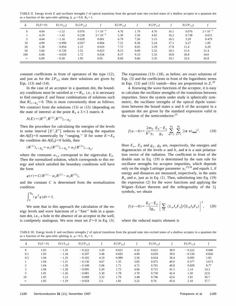
TABLE II. Energy levelsE and oscillator strengthsf of optical transitions from the ground state into excited states of a shallow acceptor in a quantum dotas a function of the spin-orbit splittingD. m50.8, R051.
D E(Z50) E(1S3/2) E(2P3/2) f E(3P3/2) f E(2P5/2) f E(2P1/2) f
0 4.04 21.52 0.076 131024 4.76 1.79 4.76 16.1 0.076 231025
1 4.19 21.42 0.228 331026 5.30 2.50 4.92 16.2 0.738 0.0155 4.64 21.16 0.639 0.001 6.79 7.26 5.15 16.5 3.29 0.479
10 4.99 20.999 0.927 0.004 7.31 8.30 5.24 17.1 6.27 1.8520 5.38 20.854 1.23 0.010 7.72 8.65 5.29 17.8 11.4 6.2050 5.84 20.720 1.55 0.023 8.15 9.09 5.32 18.5 21.0 21.4
100 6.08 20.659 1.72 0.034 8.37 9.33 5.33 18.8 26.8 34.0` 6.09 20.58 1.95 0.05 8.69 9.66 5.35 19.1 32.6 45.8
constant coefficients in front of operators of the type~12!,y
n
hs.
ven
env
n
enn-e
The expressions~13!–~18!, as before, are exact solutions ofs
syeenm-si-
in
d
erds
units
e3
and just as for the 2P5/2 state their solutions are given bEqs.~13! and ~14!.
In the case of an acceptor in a quantum dot, the bouary conditions must be satisfied atr 5R0 , i.e., it is necessaryto find energiesE and linear combinations of solutions sucthat Rur 5R0
50. This is most conveniently done as followWe construct from the solutions~13! or ~15! ~depending onthe state of interest! at the pointR0 a 333 matrix A
A~E!5~R~1!,R~2!,R~3!!r 5R0.
Then the procedure for calculating the energies of the lein some interval@E8,E9# reduces to solving the equatiodetA(E)50 numerically by ‘‘ranging.’’ If for someE5E0
the condition detA(E0)50 holds, then
~R~1!!r 5R05a1~R~2!!r 5R0
1a2~R~3!!r 5R0,
where the constantsa1,2 correspond to the eigenvalueE0 .Then the normalized solution, which corresponds to thisergy and which satisfied the boundary conditions will hathe form
w~r !5C~R~1!2a1R~2!2a2R~3!!,
and the constantC is determined from the normalizatiocondition
E0
R0~wTw!dr51.
We note that in this approach the calculation of theergy levels and wave functions of a ‘‘free’’ hole in a quatum dot, i.e., a hole in the absence of an acceptor in the wis comlpetely analogous. We now must setZ50 in Eq. ~3!.
TABLE III. Energy levelsE and oscillator strengthsf of optical transitions froas a function of the spin-orbit splittingD. m50.5, R053.
d-
ls
-e
-
ll,
Eqs.~3! and the coefficients in front of the logarithmic termin Eqs.~13! and ~15! vanish—they are proportional toZ.20
4. Knowing the wave functions of the acceptor, it is eato calculate the oscillator strengths of the transitions betwimpurities. Since the system under study is spherically symetric, the oscillator strengths of the optical dipole trantions between the bound statesa andb of the acceptor in aquantum dot are given by the standard expression validthe volume of the semiconductor:23
f ~a→b!52m0
\2g1
Eb2Ea
ga(
m51
ga
(n51
gb
u~e•r !mnu2. ~19!
HereEa , Eb andga , gb are, respectively, the energies andegeneracies of the levelsa andb, ande is a unit polariza-tion vector of the radiation. The coefficient in front of thdouble sum in Eq.~19! is determined by the sum rule fooscillator strengths for acceptor impurities, which depenonly on the single Luttinger parameterg1
23,18and equals 1, ifenergy and distances are measured, respectively, in theRa anda, just as in Eq.~1!. Then, substituting into Eq.~19!the expression~2! for the wave functions and applying thWigner–Eckart theorem and the orthogonality of thejsymbols, we obtain
f ~a→b!5Eb2Ea
3gaH(
JL~LaJaFair iLbJbFb!J 2
, ~20!
where the reduced matrix element is
m the ground state into excited states of a shallow acceptor in a quantum dot
D E(Z50) E(1S3/2) E(2P3/2) f E(3P3/2) f E(2P5/2) f E(2P1/2) f
0 1.03 21.35 20.222 3.20 0.621 4.32 0.621 38.9 20.222 0.6400.1 1.03 21.34 20.207 3.46 0.692 4.09 0.629 39.0 20.156 0.8260.5 1.04 21.33 20.165 4.19 0.989 3.56 0.654 39.4 0.095 1.831 1.04 21.31 20.136 4.67 1.35 3.85 0.675 40.0 0.377 3.6732 1.04 21.29 20.108 5.06 1.71 4.72 0.701 40.8 0.829 8.773 1.04 21.28 20.095 5.20 1.75 4.06 0.715 41.5 1.14 14.35 1.05 21.26 20.081 5.30 1.78 3.70 0.730 42.4 1.50 22.6
10 1.05 1.23 0.069 3.32 1.79 3.48 0.746 43.6 1.81 30.7` 1.05 21.19 20.054 5.3 1.81 3.22 0.76 45.6 2.10 37.7
1189 1189Semiconductors 31 (11), November 1997 Polupanov et al.
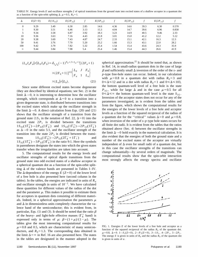
TABLE IV. Energy levelsE and oscillator strengthsf of optical transitions from the ground state into excited states of a shallow acceptor in a quantum dotas a function of the spin-orbit splittingD. m50.5, R051.
22
D E(Z50) E(1S3/2) E(2P3/2) f E(3P3/2) f E(2P5/2) f E(2P1/2) f
0 9.29 3.49 6.30 2.85 14.6 4.36 14.6 39.3 6.30 0.5701 9.30 3.51 6.46 3.13 15.3 4.04 14.7 39.6 6.96 0.8305 9.34 3.58 6.87 3.92 18.3 3.23 14.9 40.5 9.46 2.33
10 9.36 3.63 7.16 4.43 21.8 3.01 15.0 41.2 12.2 5.1220 9.38 3.69 7.43 4.87 24.7 2.33 15.1 42.1 16.3 12.350 9.41 3.76 7.70 5.20 25.2 1.66 15.3 43.1 22.0 28.2
100 9.42 3.79 7.82 5.32 25.4 1.54 15.4 43.6 24.3 35.9` 9.44 3.84 7.98 5.4 25.4 1.46 15.4 44.3 26.6 41.9
~LaJaFair iLbJbFb!5dJaJb~21!Fb1J1La11@~2Fa11!
ra
or
in
th
s
hei-
sta
nherliIV
domersvai
foonintet
spherical approximation. It should be noted that, as shownrge
tion
te
theandforptors of
rosinsnd aallyt
canTheiontor
a
3~2Fb11!#1/2H Lb J Fb
Fa 1 LaJ
3~Lair iLb!. ~21!
Since some different excited states become degene~they are described by identical equations; see Sec. 2! in thelimit D→0, it is interesting to determine how the oscillatstrength, which corresponds atD50 to a transition into agiven degenerate state, is distributed between transitionsthe excited states which make up the oscillator strengththe limit D→0. A direct calculation from Eqs.~20! and~21!shows that the oscillator strength of a transition fromground state~1S1 in the notation of Ref. 22,D50! into theexcited state 2P1 is divided between the transition1S3/2(1G8
1)→2P3/2(1G82) and 1S3/2(1G8
1)→2P1/2(1G62)
as D→0 in the ratio 5:1, and the oscillator strength of ttransition into the state 2P2 is divided between the transtions 1S3/2(1G8
1)→2P5/2(2G8211G7
2) and1S3/2(1G8
1)→3P3/2(3G82) in the ratio 9:1. Here the symbol
in parentheses designate the states into which the given stransfer when the irregularities are taken into account.
5. The computational results for the energy levels aoscillator strengths of optical dipole transitions from tground state into odd excited states of a shallow acceptoa spherical quantum dot as a function of the spin-orbit spting D of the valence bands are presented in Tables I–TheD-dependence of the energyE (Z50) of the lower levelof a free hole is also presented here~second column in thetables!. In the tables, the energies are indicated in units ofRa
and oscillator strength in units of 1022. We have calculatedthese quantities for different values of the radius of theand the parameterm. This makes it possible to estimate thefor acceptors in quantum dots consisting of different matals. Indeed, in a spherical approximation the parametermandD in dimensionless units completely characterize thelence band of the semiconductor; this is evident from,particular, Eqs.~1! and~3!. It should be noted that the ratiobof the heavy- and light-hole effective masses~G8
1 band! isexpressed only in terms ofm: b5(11m)/(12m). Thetables give the most interesting computational resultsm50.8 and 0.5, which are characteristic of many semicductors, andR051.3. The corresponding data obtainedthe limit D5` in Ref. 16 are also presented here. The stain the tables are designated in the manner adopted in
1190 Semiconductors 31 (11), November 1997
te
toin
e
tes
d
int-.
t
i-
-n
r-
she
in Ref. 14, in small-radius quantum dots in the case of lab and sufficiently smallD inversion of the order of thes- andp-type free-hole states can occur. Indeed, in our calculawith m50.8 in a quantum dot with radiusR053 and0<D<12 and in a dot with radiusR051 and 0<D<103,the bottom quantum-well level of a free hole is the staP3/2, while for large D and in the casem50.5 for all0<D<` the bottom quantum-well level is the stateS3/2.Inversion of the acceptor states does not occur for any ofparameters investigated, as is evident from the tablesfrom the figure, which shows the computational resultsthe energies of the lower levels of a free hole and accelevels as a function of the squared reciprocal of the radiua quantum dot for the ‘‘critical’’ valuesD50 andm50.8,when inversion of the order ofs-p type hole states occurs foall finite dot radii. It is evident from the tables that the ratiobtained above~Sec. 4! between the oscillator strengthsthe limit D→0 hold exactly in the numerical calculation. It ialso evident that the energies of both the ground state anumber of the excited states of the acceptor are virtuindependent ofD even for small radii of a quantum dot, buin this case the oscillator strengths of the transitionschange substantially—by several orders of magnitude.computational results show that the spin-orbit interactmost strongly affects the energy spectra and oscilla
FIG. 1. EnergiesE of the lower levels of a free hole and acceptor asfunction of the squared reciprocal of the radiusR0 of the quantum dot.m50.8, D50. 1—S1(Z50), 2—P1(Z50), 3—1S1 , 4—2P1 , 5—2P2 .The energyE is given in units ofR0 and the radiusR0 of the quantum dotis given in units ofa.
1190Polupanov et al.
strengths of optical transitions for large values ofb and
f
m
meti
otgbe
fo
6S. Fraizzoli and A. Pasquarello, Phys. Rev. B44, 1118~1991!.7G. W. Bryant, Phys. Rev. B29, 6632~1984!.
pl.
small dot radii. It is obvious that for smallb, i.e., in the limitm→0, the acceptor states no longer depend onD—this iseasy to see from Eqs.~3! and ~6!. The spin-orbit interactionaffects most strongly the energy and oscillator strength otransition into the lowerG6
2 state~designated as 2P1/2 in thespherical approximation!, since its character changes froheavy-hole~for D50! to light-hole ~for D5`!. Indeed, asone can see from Eqs.~6! and ~8!, in the spherical approxi-mation and in first order of perturbation theory in the paraeter d, to which terms describing the irregularities of thvalence bands are proportional, the corresponding equahas in these limits a purely ‘hydrogen-like’’ form withL51and strongly different masses, proportional to 1/(12m) and1/(11m), respectively. This is why for small quantum-dradii the approximation of infinitely large spin-orbit splittinof valence bands, which is widely used in calculations,comes applicable for these states only for very largeD.
This work was supported in part by the Russian FundFundamental Research.
1S. Fraizzoli and A. Pasquarello, Physica Scripta T39, 182 ~1991!.2G. Bastard, Phys. Rev. B24, 4714~1981!.3C. Mailhiot, Y.-C. Chang, and T. C. McGill, Phys. Rev. B26, 4449~1982!.
4R. L. Green and K. K. Bajaj, Phys. Rev. B34, 961 ~1986!.5W. T. Masselink, Y.-C. Chang, and H. Morkoc, Phys. Rev. B32, 5190~1985!.
1191 Semiconductors 31 (11), November 1997
a
-
on
-
r
8J. Lee and H. N. Spector, J. Vac. Sci. Technol. B16 ~1984!.9D. S. Chuu, C. M. Hsiao, and W. N. Mei, Phys. Rev. B46, 3898~1992!.
10Al. L. Efros and A. L. Efros, Fiz. Tekh. Poluprovodn.16, 1209 ~1982!@Sov. Phys. Semicond.16, 772 ~1982!#.
11L. E. Brus, J. Chem. Phys.80, 4403~1984!.12A. I. Ekimov, A. A. Onushchenko, A. G. Plyukhin, and Al. L. E´ fros, Zh.
Eksp. Teor. Fiz.88, 1490~1985! @Sov. Phys. JETP61, 891 ~1985!#.13M. Sweeny and J. Xu, Solid State Commun.72, 301 ~1989!.14G. B. Grigoryan, E´ . M. Kazaryan, Al. L. Efros, and T. V. Yazeva, Fiz.
Tverd. Tela~Leningrad! 32, 1772~1990! @Sov. Phys. Solid State32, 1031~1990!#.
15J.-L. Zhu, Phys. Rev. B39, 8780~1989!; J.-L. Zhu, J.-J. Xiong, B.-L. Gu.Phys. Rev. B41, 6001~1990!.
16V. I. Galiev and A. F. Polupanov, Fiz. Tekh. Poluprovodn.27, 1202~1993! @Semiconductors27, 663 ~1993!#.
17J.-L. Zhu and X. Chen, J. Phys.: Condens. Matter6, L123 ~1994!.18Sh. M. Kogan and A. F. Polupanov, Zh. E´ ksp. Teor. Fiz.80, 394 ~1981!
@Sov. Phys. JETP53, 201 ~1981!#.19A. F. Polupanov and Sh. M. Kogan, Fiz. Tekh. Poluprovodn.13, 2338
~1979! @Sov. Phys. Semicond.13, 1368~1979!#.20V. I. Galiev and A. F. Polupanov, Preprint N 18~519!, Institute of Radio
Electronics of the Soviet Academy of Sciences, Moscow, 1989.21V. I. Galiev, A. F. Polupanov, and I. E. Shparlinski, J. Comput. Ap
Math. 39, 151 ~1992!.22A. Baldereschi and N. O. Lipari, Phys. Rev. B8, 1525~1973!; Phys. Rev.
B 9, 1525~1974!.23Sh. M. Kogan and A. F. Polupanov, Solid State Commun.27, 1281
~1978!.
Translated by M. E. Alferieff
1191Polupanov et al.
AMORPHOUS, GLASSY, AND POROUS SEMICONDUCTORS
F
Photoluminescence of porous gallium arsenideD. N. Goryachev and O. M. Sreseli
A. F. Ioffe Physicotechnical Institute, Russian Academy of Sciences, 194021 St. Petersburg, Russia~Submitted June 10, 1997; accepted for publication June 11, 1997!Fiz. Tekh. Poluprovodn.31, 1383–1386~November 1997!
Photoluminescence in the visible and infrared regions of the spectrum is investigated for porousgallium arsenide prepared by the electrolytic or chemical etching of GaAs. The IRluminescence band of porous GaAs is shifted from the maximum for crystalline GaAs into thelong-wavelength region of the spectrum and has a greater width. All the samples arecharacterized by a broad emission band in the visible region; the intensity and shape of the banddepend on the layer preparation conditions. Two maxima are discernible in the band in thevicinity of 420 nm and 560 nm. An explanation is given for both the visible luminescence and themodification of the IR band of porous GaAs. It is concluded from a comparison of thevisible luminescence of porous GaAs with emission from hydrated oxides of arsenic and galliumthat the visible-range luminescence of porous GaAs, especially when prepared by chemicaletching, is determined in large measure by the presence of oxides. Considerations are set forth asto ways of creating quantum-size formations on the surface of GaAs. ©1997 AmericanInstitute of Physics.@S1063-7826~97!02511-8#
INTRODUCTION performed either in a 1.0 N HCl solution or in a 40% H
n-tselrale
heatn
ytiaP
tso
no
h
as
lur aic
aco
-an
theully
ofyd atsingere
te.rsess.
y
s
weroub-
/1
The escalation of research on the photoluminesceproperties of porous silicon~por-Si! in recent years, beginning with the work of Canham,1 holds encouraging prospecfor many investigators seeking an inexpensive, relativsimple, and ultimately a universal technique for the prepation of low-dimensional semiconductor materials. The roof quantum-well effects in the evolution of at least part of tphotoluminescence spectrum was in fact first demonstrin the example ofpor-Si. More recently, attempts have beeundertaken to create similar porous layers by electroletching on binary and more complex materials: GaAs, Getc.2–5 We have not found any published data on attemptsform similar structures by chemical etching, which is alused extensively for the preparation ofpor-Si.
Existing accounts of research on the photoluminescespectra of porous layers on GaAs are highly conflicting. Fexample, Schmukiet al.3 report a slight short-wavelengtshift of the infrared maximum of porous GaAs~por-GaAs!,whereas Lebedev and Rud’4 deny the existence of suchshift. Substantial disparities are observed in the positionthe visible photoluminescence maximum~Fig. 1!. Finally,nothing is really known about the nature of visible photominescence. In principle, it can be characterized eithequantum-well effects or as the presence of new chemcompounds on the sample surface.
We have investigated the photoluminescence of surflayers formed by electrolytic and by chemical etchingGaAs.
EXPERIMENTAL CONDITIONS
Electrolytic anodic etching ofn-type GaAs~100! withcarrier densities from 131016 cm23 to 831018 cm23 was
1192 Semiconductors 31 (11), November 1997 1063-7826/97
ce
y-
ed
c,
o
cer
of
-s
al
ef
solution with a 1% HNO3 additive. In some of the experiments the samples were illuminated by white light fromincandescent lamp. For the chemical etching ofp-type andn-type GaAs withn,p51016–1019cm23, 65% HNO3 wasused, in some cases with concentrated H2SO4 additives tobind water or acetic acid as a means of slowing downetching process. After etching, the samples were carefwashed in water and air-dried at 30–40 °C.
Photoluminescence was stimulated by laser pulseswavelength l5337 nm, duration 10 ns, and frequenc100 Hz. The photoluminescence spectra were measureroom temperature by means of a computerized system uan MDR-2 monochromator. The radiation detectors wphotomultipliers of the type FE´ U-79 ~visible range of thespectrum! and FEU-62 ~IR range!.
EXPERIMENTAL RESULTS AND DISCUSSION
In the electrolytic etching of n-type GaAs(n51.431018 cm23) in HCl solutions, beginning with acurrent densityJ'5 mA/cm2, a dark, dense film forms onthe surface of the sample, firmly bonding with the substraAt higher current densities the layer breaks up and dispeinto a fine powder even while electrolysis is still in progresThe replacement of the solvent~water! by an alcohol-watermixture ~1:1! lowers the ‘‘dispersal’’ current threshold broughly one half.
Instead of a thick layer, only inhomogeneous thin filmform onn-GaAs withn5131016 cm23 over a wide range ofcurrent densities in darkness.
An electrolyte composition containing HF1HNO3
forms a thin, dark film on the surface of GaAs only a feseconds after immersion of the sample in the solution at zcurrent, i.e., the electrolyte acts as a chemical etchant. S
119211192-04$10.00 © 1997 American Institute of Physics
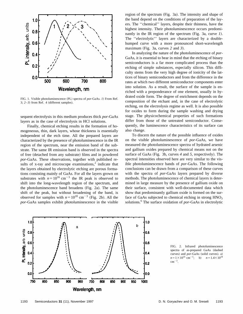
o-tiaareu
ec
re
aonon
is
bl
region of the spectrum~Fig. 3a!. The intensity and shape oflay-themi-
e-gth
arythe
ffi-t-
thenteren-hy-thetic
iblengonsse-can
es
senicthe
vis-
rveseter-on
ichur-O
sequent electrolysis in this medium produces thickpor-GaAslayers as in the case of electrolysis in HCl solutions.
Finally, chemical etching results in the formation of hmogeneous, thin, dark layers, whose thickness is essenindependent of the etch time. All the prepared layerscharacterized by the presence of photoluminescence in thregion of the spectrum, near the emission band of the sstrate. The same IR emission band is observed in the spof free ~detached from any substrate! films and in powderedpor-GaAs. These observations, together with publishedsults of x-ray and microscope examinations,2 indicate thatthe layers obtained by electrolytic etching are porous formtions consisting mainly of GaAs. For all the layers grownsubstrates withn51016 cm23 the IR peak is observed tshift into the long-wavelength region of the spectrum, athe photoluminescence band broadens~Fig. 2a!. The sameshift of the peak, but without broadening of the band,observed for samples withn51018 cm23 ~Fig. 2b!. All thepor-GaAs samples exhibit photoluminescence in the visi
FIG. 1. Visible photoluminescence~PL! spectra ofpor-GaAs.1! From Ref.3; 2–3! from Ref. 4~different samples!.
llyeIRb-tra
-
-
d
e
the band depend on the conditions of preparation of theers. The ‘‘chemical’’ layers, despite their thinness, havehighest intensity. Their photoluminescence occurs predonantly in the IR region of the spectrum~Fig. 3a, curve1!.The ‘‘electrolytic’’ layers are characterized by a doublhumped curve with a more pronounced short-wavelenmaximum~Fig. 3a, curves2 and3!.
In analyzing the nature of the photoluminescence ofpor-GaAs, it is essential to bear in mind that the etching of binsemiconductors is a far more complicated process thanetching of simple substances, especially silicon. This diculty stems from the very high degree of ionicity of the latices of binary semiconductors and from the difference inrates at which two different semiconductor components einto solution. As a result, the surface of the sample isriched with a preponderance of one element, usually indrated oxide form. The degree of enrichment depends oncomposition of the etchant and, in the case of electrolyetching, on the electrolysis regime as well. It is also possfor oxides to form during the sample washing and dryistage. The physicochemical properties of such formatidiffer from those of the untreated semiconductor. Conquently, the luminescence characteristics of its surfacealso change.
To discern the nature of the possible influence of oxidon the visible photoluminescence ofpor-GaAs, we havemeasured the photoluminescence spectra of hydrated arand gallium oxides prepared by chemical means not onsurface of GaAs~Fig. 3b, curves4 and5, respectively!. Thespectral intensities observed here are very similar to theible photoluminescence bands ofpor-GaAs. The followingconclusions can be drawn from a comparison of these cuwith the spectra ofpor-GaAs layers prepared by diversmethods. The photoluminescence of chemical layers is demined in large measure by the presence of gallium oxidetheir surface, consistent with well-documented data whshow that predominantly gallium oxide is formed on the sface of GaAs subjected to chemical etching in strong HN3
solutions.6 The surface oxidation ofpor-GaAs in electrolytic
e
FIG. 2. Infrared photoluminescencspectra of as-prepared GaAs~dashedcurves! and por-GaAs ~solid curves!. a!n5131016 cm23; b! n51.431018cm23.
1193 1193Semiconductors 31 (11), November 1997 D. N. Goryachev and O. M. Sreseli
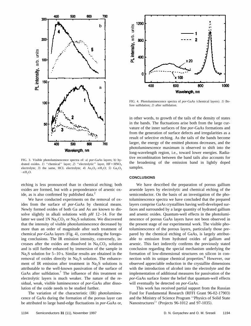
oo
ox.is
db
t-in
ith-
onre
a
esur-
s amethe
theia-for
ed
mtheho-aredur-um
i-d in
ho-re-
ut-d
edthen-
onse
thects
ian
te
etching is less pronounced than in chemical etching; boxides are formed, but with a preponderance of arsenicide, as is also confirmed by published data.2
We have conducted experiments on the removal ofides from the surface ofpor-GaAs by chemical meansNewly formed oxides of both Ga and As are known to dsolve slightly in alkali solutions withpH 12–14. For thelatter we used 1N Na2CO3 or Na2S solutions. We discoverethat the intensity of visible photoluminescence decreasedmore than an order of magnitude after such treatmenchemicalpor-GaAs layers~Fig. 4!, corroborating the foregoing conclusions. The IR emission intensity, conversely,creases after the oxides are dissolved in Na2CO3 solutionand is still further enhanced by immersion of the sampleNa2S solution for 5–10 s. Similar results are obtained inremoval of oxides directly in Na2S solution. The enhancement of IR emission after treatment in Na2S solutions isattributable to the well-known passivation of the surfaceGaAs after sulfidation.7 The influence of this treatment oelectrolytic layers is much weaker. The nature of thesidual, weak, visible luminescence ofpor-GaAs after disso-lution of the oxide needs to be studied further.
The variation of the characteristic~IR! photolumines-cence of GaAs during the formation of the porous layer cbe attributed to large band-edge fluctuations inpor-GaAs or,
FIG. 3. Visible photoluminescence spectra of: a! por-GaAs layers; b! hy-drated oxides.1! ‘‘chemical’’ layer; 2! ‘‘electrolytic’’ layer, HF1HNO3
electrolyte; 3! the same, HCL electrolyte;4! As2O3•nH2O; 5! Ga2O3
•nH2O.
1194 Semiconductors 31 (11), November 1997
thx-
-
-
yof
-
ne
f
-
n
in other words, to growth of the tails of the density of statin the bands. The fluctuations arise both from the large cvature of the inner surfaces of finepor-GaAs formations andfrom the generation of surface defects and irregularities aresult of selective etching. As the tails of the bands becolarger, the energy of the emitted photons decreases, andphotoluminescence maximum is observed to shift intolong-wavelength region, i.e., toward lower energies. Radtive recombination between the band tails also accountsthe broadening of the emission band in lightly dopsamples.
CONCLUSIONS
We have described the preparation of porous galliuarsenide layers by electrolytic and chemical etching ofsemiconductor. On the basis of an investigation of the ptoluminescence spectra we have concluded that the preplayers comprise GaAs crystallites having well-developed sfaces and surrounded by a large quantity of hydrated galliand arsenic oxides. Quantum-well effects in the photolumnescence of porous GaAs layers have not been observethe present stage of our experimental work. The visible ptoluminescence of the porous layers, particularly those ppared by the chemical etching of GaAs, is largely attribable to emission from hydrated oxides of gallium anarsenic. This fact indirectly confirms the previously statconclusion regarding the special mechanism underlyingformation of low-dimensional structures on silicon in conection with its unique chemical properties.8 However, ourobserved appreciable reduction in the crystallite dimensiwith the introduction of alcohol into the electrolyte and thimplementation of additional measures for passivation ofpor-GaAs surface foster the belief that quantum-well effewill eventually be detected onpor-GaAs.
This work has received partial support from the RussFund for Fundamental Research~RFFI Grant 96-02-17903!and the Ministry of Science Program ‘‘Physics of Solid StaNanostructures’’~Projects 96-1012 and 97-1035!.
FIG. 4. Photoluminescence spectra ofpor-GaAs ~chemical layers!. 1! Be-fore sulfidation;2! after sulfidation.
1194D. N. Goryachev and O. M. Sreseli
1L. T. Canham, Appl. Phys. Lett.57, 1046~1990!.2P. Schmuki, J. Frazer, C. M. Vitus, M. J. Graham, and H. S. Isaacs,
u.
Timoshenko, Fiz. Tekh. Poluprovodn.30, 1473 ~1996! @Semiconductors30, 775 ~1996!#.
ys.
ii,
J. Electrochem. Soc.143, 3316~1996!.3P. Schmuki, D. J. Lockwood, H. J. Labbe´, and J. W. Frazer,69, 1620~1996!.
4A. A. Lebedev and Yu. V. Rud’, Pis’ma Zh. Tekh. Fiz.22, 484 ~1996!@Tech. Phys. Lett.22, 483 ~1996!#.
5B. H. Erne, D. Vanmeakelbergh, and J. J. Kelly, Adv. Mater.7, 739~1995!; A. V. Zoteev, P. K. Kashkarov, A. N. Obraztsov, and V. Y
1195 Semiconductors 31 (11), November 1997
6B. Schwartz, Crit. Rev. Solid State Sci.5, 4, 609~1975!.7C. J. Sandroff, R. N. Nottenburg, J.-C. Bischoff, and R. Bhat, Appl. PhLett. 51, 33 ~1987!.
8D. N. Goryachev, L. V. Belyakov, O. M. Sreseli, and I. D. YaroshetskSemicond. Sci. Technol.10, 373 ~1995!.
Translated by James S. Wood
1195D. N. Goryachev and O. M. Sreseli
Polarization memory in an oxidized porous SiC layer
d
A. M. Danishevski , A. Yu. Rogachev, V. B. Shuman, and E. G. Guk
A. F. Ioffe Physicotechnical Institute, Russian Academy of Sciences, 194021 St. Petersburg, Russia~Submitted January 21, 1997; accepted for publication February 25, 1997!Fiz. Tekh. Poluprovodn.31, 1387–1391~November 1997!
Polarization and polarization memory of pulsed photoluminescence are observed on porouslayers prepared on microcrystalline, cubic SiC films deposited on silicon substrates. The porouslayer is oxidized by electrochemical means. A qualitative model is proposed to account forthe mechanism underlying the onset of polarization of photoluminescence for linearly polarizedexcitation. © 1997 American Institute of Physics.@S1063-7826~97!02611-2#
Porous nanodimensional semiconductor materials are al-In our opinion, this consideration diminishes the likelihoo
ngelaSnh-hnesethly
ldrah
er
rsesifo
ineth
ioviCisnte
nlewA
th
tg
ofssueris-eenrousisnceforce.b-val6
ofe
a-urtheodi-oid
theths,tionis
er-bic
o-icu-es-dge
asples
ag-he-
ofe
in
/1
luring to researchers for the possibility of observing strowideband photoluminescence resulting from quantum-weffects in nanocrystals. Studies of the polarization and poization memory of photoluminescence in poroussamples1–4 have enabled investigators to draw conclusioabout the crystallite geometries~the model of more or lessprolate ellipsoids! for a particular material preparation tecnique, and also about the distribution of crystallites in tformation of porous layers on various crystallographic plaof the original material. However, the theoretical modelforth in Ref. 3 to describe the mechanism underlyingorigin of the polarization of photoluminescence is pureclassical~randomly arrayed ellipsoidal crystallites in the fieof a light wave! and does not account for either the spector the time dependence of the degree of polarization of ptoluminescence.
Polarization memory has also been observed in sevamorphous semiconductors such asa-Si12xCx :H, a-C:H,and a-As2S3 ~Refs. 5–7!. The authors of the cited papeattribute the nature of the phenomenon to the presencsmall clusters having a narrower-gap composition and reing in a matrix of a wider-gap material. This is the case,example, ina-C:H ~Ref. 6! or aSi12xCx :H ~Ref. 5!, whereclusters incorporating graphite-like (sp2) carbon bonds arebuilt into a structural grid matrix withsp3 carbon bonds. Theauthors believe that if photoexcited pairs are localizedsmall crystallites, polarization memory can persist for a lotime, so that the emitted photoluminescence is polarizConsequently, polarization memory ostensibly reflectsdegree of localization of photoexcited carriers.5 It is sug-gested in Ref. 5 that the primary cause of the polarizatdependence of photoluminescence is anisotropy of thelence bonds, because the valence bond of amorphous Smade up of Si and Cp orbitals. In essence, therefore, thinterpretation characterizes the phenomenon of ‘‘alignmeof nonequilibrium carriers, investigated in bulk crystallinsemiconductors of the GaAs~Ref. 8! and Ga12xAl xAs type.In the latter material, however, polarization is observed ofor ‘‘hot’’ photoluminescence, because the emission of a fphonons is sufficient to eradicate polarization memory.fairly high degree of polarization has been recorded forphotoluminescence of thermalized carriers ina-SiC, and itwas found not to have a very strong dependence either onexciting photon energy or on the luminescing photon ener
1196 Semiconductors 31 (11), November 1997 1063-7826/97
,llr-is
este
lo-
al
ofd-r
ngd.e
na-is
’’
y
e
hey.
of the given explanation.The investigation of porous SiC from the standpoint
the above-stated problems has important bearing on the iof the existence of polarization memory and its charactetics. The existence of polarization memory has never bdiscussed in any of the papers published to date on poSiC ~Refs. 9–13!. On the other hand, the investigation of thproblem could help to resolve the question of the existeand geometry of nanostructural crystallites responsiblethe onset of quantum-well effects in photoluminescenSpecifically, in Refs. 9–13 the spectral maximum of the oserved radiation from porous layers occurred in the inter2.45–2.6 eV. Since the given layers were prepared onH-SiC crystals, whose band gap has a width of the order3.1 eV, it has been concluded13 that the appearance of thgiven photoluminescence band is attributable to the formtion of defects during anodic etching of the crystal. In oprevious work14,15 we have advanced the hypothesis thatnature of the given luminescence is associated with nanmensional layers of a cubic phase, which appear at the vboundaries during electrolytic etching of the hexagonal 6H-SiC used to create the porous layer. The broadening ofphotoluminescence band toward shorter wavelengachieved by varying the conditions attending the preparaof the layer, can be linked to quantum-well effects in thcase, but now in cubic crystallites~the width of the band gapof bulk 3C-SiC is Eg52.3 eV!.
Pursuant to the discussion in Ref. 15, we have undtaken an investigation of porous layers prepared from cupolycrystalline SiC films grown on silicon substrates.16 Thelayers were coated with an oxide film by an electrolytic prcess in an aqueous HCl solution for passivation of the retlated porous surface. Strong, very wideband photolumincence is observed in this case, its short-wavelength eattaining 3.4–3.5 eV.
Anodic oxidation of the surface of a porous layer walso used repeatedly in the preparation of porous Si samemitting in the blue-green region (hnmax52.4 eV!. The pho-toluminescence intensity increased by several orders of mnitude in this case. However, in the earliest studies the pnomenon was thought to be associated with passivationthe surface layer17 and a significant reduction in the surfacrecombination rate, whereas the authors of later papers~see,e.g., Ref. 18! concluded that the emission sources exist
119611196-04$10.00 © 1997 American Institute of Physics
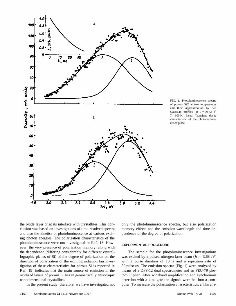
as
-
FIG. 1. Photoluminescence spectrof porous SiC at two temperatureand their approximation by twoGaussian profiles. a! T590 K; b!T5300 K. Inset: Transient decaycharacteristic of the photoluminescence pulse.
the oxide layer or at its interface with crystallites. This con-ctcthwit
-e
ihepic
n
only the photoluminescence spectra, but also polarizationde-
ns
of
usm-na-
clusion was based on investigations of time-resolved speand also the kinetics of photoluminescence at various exing photon energies. The polarization characteristics ofphotoluminescence were not investigated in Ref. 18. Hoever, the very presence of polarization memory, along wthe dependence~differing considerably for different crystallographic planes of Si! of the degree of polarization on thdirection of polarization of the exciting radiation~an inves-tigation of these characteristics for porous Si is reportedRef. 19! indicates that the main source of emission in toxidized layers of porous Si lies in geometrically anisotronanodimensional crystallites.
In the present study, therefore, we have investigated
1197 Semiconductors 31 (11), November 1997
rait-e-h
n
ot
memory effects and the emission-wavelength and timependence of the degree of polarization.
EXPERIMENTAL PROCEDURE
The sample for the photoluminescence investigatiowas excited by a pulsed nitrogen laser beam (hn53.68 eV!with a pulse duration of 10 ns and a repetition rate50 pulses/s. The emission spectra~Fig. 1! were analyzed bymeans of a DFS-12 dual spectrometer and an FE´ U-79 pho-tomultiplier. After wideband amplification and synchronodetection with a 4-ns gate the signals were fed into a coputer. To measure the polarization characteristics, a film a
1197Danishevski et al.
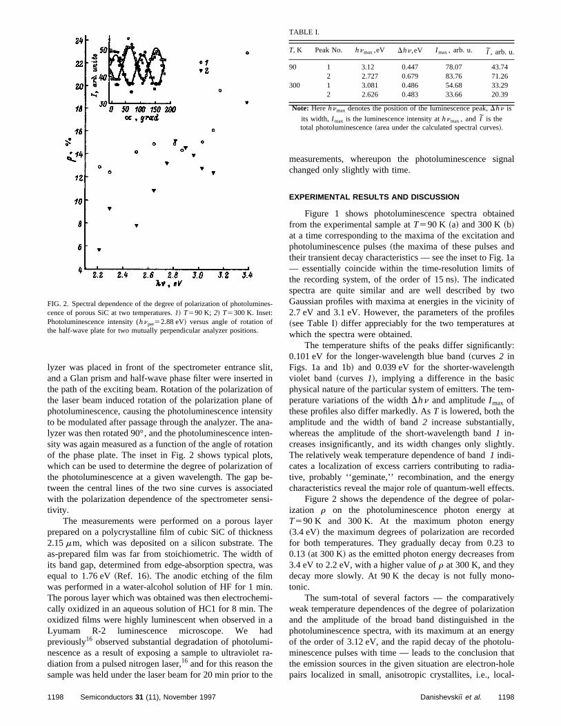
sldoo
nsatetiots
nbten
ysshow
inm
he
ai
t r
th
ignal
ned
ndd. 1af
wooflesat
ly:
th
m-
,
tly.
ia-gyts.lar-atyedto
om
-
lytion
thergylu-thatole
al-
ine
TABLE I.
lyzer was placed in front of the spectrometer entranceand a Glan prism and half-wave phase filter were insertethe path of the exciting beam. Rotation of the polarizationthe laser beam induced rotation of the polarization planephotoluminescence, causing the photoluminescence inteto be modulated after passage through the analyzer. Thelyzer was then rotated 90°, and the photoluminescence insity was again measured as a function of the angle of rotaof the phase plate. The inset in Fig. 2 shows typical plowhich can be used to determine the degree of polarizatiothe photoluminescence at a given wavelength. The gaptween the central lines of the two sine curves is associawith the polarization dependence of the spectrometer setivity.
The measurements were performed on a porous laprepared on a polycrystalline film of cubic SiC of thickne2.15mm, which was deposited on a silicon substrate. Tas-prepared film was far from stoichiometric. The widthits band gap, determined from edge-absorption spectra,equal to 1.76 eV~Ref. 16!. The anodic etching of the filmwas performed in a water-alcohol solution of HF for 1 mThe porous layer which was obtained was then electrochecally oxidized in an aqueous solution of HC1 for 8 min. Toxidized films were highly luminescent when observed inLyumam R-2 luminescence microscope. We hpreviously16 observed substantial degradation of photolumnescence as a result of exposing a sample to ultraviolediation from a pulsed nitrogen laser,16 and for this reason thesample was held under the laser beam for 20 min prior to
FIG. 2. Spectral dependence of the degree of polarization of photolumcence of porous SiC at two temperatures.1! T590 K; 2! T5300 K. Inset:Photoluminescence intensity (hnper52.88 eV! versus angle of rotation ofthe half-wave plate for two mutually perpendicular analyzer positions.
1198 Semiconductors 31 (11), November 1997
it,inffityna-n-n,
ofe-d
si-
er
efas
.i-
ad-a-
e
measurements, whereupon the photoluminescence schanged only slightly with time.
EXPERIMENTAL RESULTS AND DISCUSSION
Figure 1 shows photoluminescence spectra obtaifrom the experimental sample atT590 K ~a! and 300 K~b!at a time corresponding to the maxima of the excitation aphotoluminescence pulses~the maxima of these pulses antheir transient decay characteristics — see the inset to Fig— essentially coincide within the time-resolution limits othe recording system, of the order of 15 ns!. The indicatedspectra are quite similar and are well described by tGaussian profiles with maxima at energies in the vicinity2.7 eV and 3.1 eV. However, the parameters of the profi~see Table I! differ appreciably for the two temperatureswhich the spectra were obtained.
The temperature shifts of the peaks differ significant0.101 eV for the longer-wavelength blue band~curves2 inFigs. 1a and 1b! and 0.039 eV for the shorter-wavelengviolet band ~curves1!, implying a difference in the basicphysical nature of the particular system of emitters. The teperature variations of the widthDhn and amplitudeI max ofthese profiles also differ markedly. AsT is lowered, both theamplitude and the width of band2 increase substantiallywhereas the amplitude of the short-wavelength band1 in-creases insignificantly, and its width changes only slighThe relatively weak temperature dependence of band1 indi-cates a localization of excess carriers contributing to radtive, probably ‘‘geminate,’’ recombination, and the enercharacteristics reveal the major role of quantum-well effec
Figure 2 shows the dependence of the degree of poization r on the photoluminescence photon energyT590 K and 300 K. At the maximum photon energ~3.4 eV! the maximum degrees of polarization are recordfor both temperatures. They gradually decay from 0.230.13~at 300 K! as the emitted photon energy decreases fr3.4 eV to 2.2 eV, with a higher value ofr at 300 K, and theydecay more slowly. At 90 K the decay is not fully monotonic.
The sum-total of several factors — the comparativeweak temperature dependences of the degree of polarizaand the amplitude of the broad band distinguished inphotoluminescence spectra, with its maximum at an eneof the order of 3.12 eV, and the rapid decay of the photominescence pulses with time — leads to the conclusionthe emission sources in the given situation are electron-hpairs localized in small, anisotropic crystallites, i.e., loc
s-
T, K Peak No. hnmax,eV Dhn,eV I max, arb. u. I , arb. u.
90 1 3.12 0.447 78.07 43.742 2.727 0.679 83.76 71.26
300 1 3.081 0.486 54.68 33.292 2.626 0.483 33.66 20.39
Note: Herehnmax denotes the position of the luminescence peak,Dhn is
its width, I max is the luminescence intensity athnmax, and I is thetotal photoluminescence~area under the calculated spectral curves!.
1198Danishevski et al.
ized excitons. The significant broadening of the spectrume
S
or
ant tlos-tu-m
e.thmnithut
irea
thngndusyr
i
r-Foerathofgt
tr
cal anisotropy!. Also possible, of course, are radiative pro-stal-at
ion
is
s-
of
n,
to,
nd
-7,a-
z.
s.
v,
.
z.
s of
a,
.
tt.
into the short-wavelength range indicates the presencquantum-well effects in these crystals.
Ellipsometric measurements in a study of porous~Ref. 20! have revealed that the dielectric constants« i and«' are not equal for a porous layer formed on the~100!plane. We know from electron microscope measurements21,22
that the elongated crystallites in the given situation areented predominantly in the@100# direction, so that the in-equality of« i and«' is most likely indicative of a differencein the structure of the electron energy spectrum alongacross the crystallite axis. It is reasonable to assume thasame difference accounts for the existence, degree, andtime (;10ms! retention of the polarization of photoluminecence. For the SiC samples investigated in the present sthe carrier lifetime is fairly short (,15 ns!. Nonetheless, taking into account the other noted features of the photolunescence behavior, we can assume that the mechanismderlying the origin of polarization memory is uniquPhoton-excited electrons with velocities perpendicular tocrystallite axis are scattered by lattice vibrations and becothermalized predominantly into lower energy states, chaing the direction of their velocities. The same carriers wvelocities oriented along the crystallite axis under the inflence of photoexcitation must acquire additional energyovercome the energy barrier before they can have the dtion of their velocities changed by scattering. As a result,excess-carrier distribution oriented in momentum spacecreated in each crystallite. Allowance must be made forfact that the carrier generation rate depends on the abetween the direction of polarization of the exciting light athe long axis of the crystallite. The recombination rate mdepend on the carrier density~in the case of predominantlradiative recombination! and on the direction of the carrievelocity.
The degree of polarization of photoluminescencegiven by the expression
r;^t rel&
^t rel1t0&,
wheret rel is the relaxation time of the oriented state of cariers in a crystallite, andt0 is their lifetime; the angle brackets signify averaging over the ensemble of crystallites.thermalized excess carriers the indicated quantities can bthe same order of magnitude, in principle, but their tempeture dependences will probably differ and should dictatetemperature dependence ofr. The decrease in the degreepolarization with increasing photoluminescence wavelencan be attributed to emission from larger crystallites~it isalso conceivable that larger crystallites have lower geome
1199 Semiconductors 31 (11), November 1997
of
i
i-
dheng-
dy
i-un-
ee
g-
-oc-nisele
t
s
-
rof-e
h
i-
cesses associated with impurity levels, defects, and crylite boundary states. Future studies will be aimedelucidating and tracing the process by which the polarizatof photoluminescence is retained in this case as well.
We wish to thank V. E. Chenokov for interest in thinvestigation.
This work has received financial support from the Rusian Fund for Fundamental Research~RFFI Grant 95-02-04115! and partial support from the Ministry of ScienceRussia ~Project 1-079/4! and the University of Arizona,USA.
1A. V. Andrianov, D. I. Kovalev, N. N. Zinov’ev, and I. D. Yaroshetski�,JETP Lett.58, 427 ~1993!.
2A. V. Andrianov, D. I. Kovalev, and I. D. Yaroshetski�, Fiz. Tverd. Tela~St. Petersburg! 35, 2677~1993! @Phys. Solid State35, 1323~1993!#.
3D. Kovalev, M. Ben Chorin, J. Diener, F. Koch, Al. L. Efros, M. RoseM. A. Gippius, and S. G. Tikhodeev, Appl. Phys. Lett.67, 1585~1995!.
4H. Koyama and N. Koshida, Phys. Rev. B52, 2649~1995!.5V. Masumoto, H. Kunitomo, S. Shinoya, H. Munekata, and H. KukimoSolid State Commun.51, 209 ~1984!.
6Rusli, G. A. J. Amaratunga, and J. Robertson, Phys. Rev. B53, 16306~1996!.
7K. Murayama and M. A. Bo¨sch, Phys. Rev. B25, 6542~1982!.8V I. Zemski�, B. P. Zakharchenya, and D. M. Mirlin, JETP Lett.24, 82~1976!.
9T. Matsumoto, J. Takahashi, T. Tamaki, T. Futaki, H. Mimura, aY. Kanemitsu, Appl. Phys. Lett.64, 226 ~1994!.
10A. O. Konstantinov, C. I. Harris, and E. Yanzen, Appl. Phys. Lett.65,2699 ~1994!.
11J. S. Shor, L. Bemis, A. D. Kurtz, M. McMillan, W. J. Choyke, I. Grimberg, and B. Z. Weiss, inInstitute of Physics Conference Series, No. 13Silicon Carbide and Related Materials, Proceedings of the Fifth Interntional Conference, edited by M. G. Spenceret al. ~IOP Publ., Bristol-Philadelphia, 1993!, p. 193.
12A. A. Lebedev, A. A. Lebedev, and Yu. V. Rud’, Pis’ma Zh. Tekh. Fi21~3!, 64 ~1995! @Tech. Phys. Lett.21, 117 ~1995!#.
13A. O. Konstantinov, A. Henry, C. I. Harris, and E. Yanzen, Appl. PhyLett. 66, 2250~1995!.
14A. M. Danishevski�, V. B. Shuman, A. Yu. Rogachev, and P. A. IvanoFiz. Tekh. Poluprovodn.29, 2122 ~1995! @Semiconductors29, 1106~1995!#.
15A. M. Danishevski�, V. B. Shuman, A. Yu. Rogachev, E. G. Guk, P. AIvanov, A. A. Mal’tsev, Fiz. Tekh. Poluprovodn.30, 1064~1996! @Semi-conductors30, 564 ~1996!#.
16A. M. Danishevski�, V. B. Shuman, E. G. Guk, and A. Yu. Rogachev, FiTekh. Poluprovodn.31, 420 ~1997! @Semiconductors31, 354 ~1997!#.
17A. Bsiesyet al., Surf. Sci.254, 195 ~1991!.18S. Komuro, T. Kato, and T. Morikava, J. Appl. Phys.80, 1749~1996!.19F. Koch, inDigests of the Second Russian Conference on the Physic
Semiconductors@in Russian#, St. Petersburg-Zelenogorsk~1996!, p. 118.20P. Basmaji, V. S. Bagnato, V. Grivickas, G. I. Surdotovich, R. Vitlin
Thin Solid Films223, 131 ~1993!.21A. G. Cullis, L. T. Canham, G. H. Williams, P. W. Smith, and O. D
Dosser, Mater. Res. Soc. Symp. Proc.283, 257 ~1993!.22O. Teschke, F. Alvarez, L. Tessler, and M. U. Kleinke, Appl. Phys. Le
63, 1927~1993!.
Translated by James S. Wood
1199Danishevski et al.
THE PHYSICS OF SEMICONDUCTOR DEVICES
Current tuning of the emission wavelength of low-threshold mesa stripe lasers utilizingInAsSb/InAsSbP double heterostructures and emitting in the vicinity of 3 .3mm
T. N. Danilova, A. P. Danilova, O. G. Ershov, A. N. Imenkov, M. V. Stepanov,V. V. Sherstnev, and Yu. P. Yakovlev
A. F. Ioffe Physicotechnical Institute, Russian Academy of Sciences, 194021 St. Petersburg, Russia~Submitted March 3, 1997; accepted for publication March 6, 1997!Fiz. Tekh. Poluprovodn.31, 1392–1395~November 1997!
Diode lasers based on InAsSb/InAsSbP double heterostructures with a low threshold current(;12 mA! and a narrow mesa stripe~of width ;10mm! are investigated over a wide range ofcurrents up to five times the threshold current. The modes of such lasers in the measuredcurrent range are observed to shift toward shorter wavelengths by approximately the amount ofthe spacing between modes as a result of an increase in the density of nonequilibriumcarriers in the active zone. The rate at which the modes shift with the current differs in differentcurrent intervals, depending on the degree of single-mode dominance of the laser emissionspectrum. ©1997 American Institute of Physics.@S1063-7826~97!02911-6#
1. The creation of tunable injection lasers operating invarious pumping points is shown in Fig. 1~V-12192 laser
tha
eucsunavre
on
id
d
ityd
byo
diin
tiouise
e
er
anbut
thetss
odein-as-
r ex-
ve
tioto
ue
nc-.tentee of
the
-rentshiftt
in
/1
the spectral interval 3–4mm looks exceptionally promisingfor high-resolution molecular spectroscopy, becausespectral interval encompasses many strong characteristicsorption lines of natural and industrial gases. The presstudy is a continuation of work begun by us on the constrtion and design of InAsSb/InAsSbP-based tunable laser1–5
and is devoted to an investigation of current-controlled ting of the emission wavelength of low-threshold lasers hing a narrow mesa stripe and emitting in the absorptiongion of methane and hydrocarbons (l53.3mm!.
We have investigated lasers basedN-InAs0.52Sb0.18P0.30/n-InAs0.95Sb0.05/p-InAs0.52Sb0.18P0.30
heterostructures prepared by liquid-phase epitaxy. The wgap emitters had a thickness;3 mm each, with an activezone of thickness;1 mm. TheN-InAsSbP layer was dopewith Sn to an electron density of (2 –5)31018 cm23, and theP-InAsSbP layer was doped with Zn to a hole dens;131018 cm23. The active zone was not specially dopeand its electron density was;1016 cm23. Mesa stripes ofwidth ;10mm were formed on the as-grown structurestandard photolithography. Lasers with a cavity length225–300mm were created by cleaving.
We have investigated the emission spectrum, the ration pattern, and the total emission intensity of the lasersquasi-continuous-wave regime. The lasers were pumpedmeander-type rectangular current pulses with a repetirate of 80 Hz. The measurements were performed at liqnitrogen temperature. An MDR-2 monochromator was uas a dispersing instrument to obtain the spectra.
2. The coherent emission spectra of the lasers were msured in the current range from threshold (I th) to I >5I th .The radiation pattern and the total emission intensity wmeasured in the same current range.
The threshold current for the better lasers is;12 mA,and the threshold current densityJth[530 A/cm2 at 77 K.The mode composition of the coherent emission spectrum
1200 Semiconductors 31 (11), November 1997 1063-7826/97
isb-
nt-
---
e-
,
f
a-abyn
d-d
a-
e
at
No. 1!. The mode spacing is.60 Å. At the threshold cur-rent the laser has two consecutive dominant modes withintensity more than double that of all the other modes,not far above the threshold a single mode emerges asdominant oneI 51.25I th . The single-mode regime persisup to currentsI >3.5I th , above which the spectrum acquireanother mode on the short-wavelength side at four mspacings from the first and with approximately the sametensity. As the current is increased, this second modesumes dominance, but a single-mode spectrum no longeists.
The fraction of emission of the dominant mode relatito the emission of all modes in the spectrum (Fmax/(Fi) isestimated numerically in Fig. 2. We see that the raFmax/(Fi depends on the current and has values from 0.8;1 in the current interval whereI /I th>1.5–3. At I 5I th wehaveFmax/(Fi >0.3. At high currents, such thatI /I th.3.5,Fmax/(Fi does not vary with the current and has a val;0.45.
Characteristics of the laser emission are plotted as futions of the currentI ~or I /I th) in Fig. 3 for the same laserFigure 3a shows the current dependence of the incremenDlof the spectral position of the dominant mode in the currinterval 1.5I th–3I th and a comparison with its position at ththreshold current. Figure 3b shows the current dependencthe full width at half maximum~FWHM! DQ of the radia-tion pattern in the plane of thep–n junction ~curve1! and inthe plane perpendicular to the plane of thep–n junction~curve 2!. Figure 3c shows the current dependence oftotal emission intensityFS .
It is evident~Fig. 3a! that the mode position in the spectrum shifts toward shorter wavelengths as the pump curis increased, and in the measured current range the totalis ;55 Å. However, the rate of this shift differs in differencurrent intervals. TheDl(I ) curve has the greatest slopethe current interval fromI th to 1.5I th . In this interval
120011200-04$10.00 © 1997 American Institute of Physics
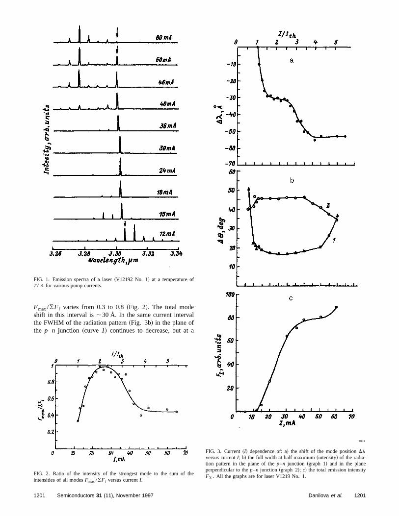
l
a
th
Fmax/(Fi varies from 0.3 to 0.8~Fig. 2!. The total modeshift in this interval is;30 Å. In the same current intervathe FWHM of the radiation pattern~Fig. 3b! in the plane ofthe p–n junction ~curve 1! continues to decrease, but at
FIG. 1. Emission spectra of a laser~V12192 No. 1! at a temperature of77 K for various pump currents.
FIG. 2. Ratio of the intensity of the strongest mode to the sum ofintensities of all modesFmax/(Fi versus currentI.
1201 Semiconductors 31 (11), November 1997
e
FIG. 3. Current~I! dependence of: a! the shift of the mode positionDlversus currentI; b! the full width at half maximum~intensity! of the radia-tion pattern in the plane of thep–n junction ~graph 1! and in the planeperpendicular to thep–n junction ~graph 2!; c! the total emission intensityFS . All the graphs are for laser V1219 No. 1.
1201Danilova et al.
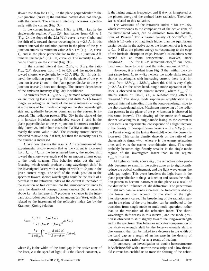
slower rate than forI ,I th . In the plane perpendicular to thegelin
s
nc
agng
i
-xiss
heasif
quel
hofed
t
r-
o
is the lasing angular frequency, and if\v0 is interpreted asre,
ofula-
m
dgeerece
K.r-din-
he
isato
ia-
rdt isease
the
ode
me
ntlythethe-
t ofn
orp-htat-
eerrt-osi-thn of, ah of
of
resh-er-
p–n junction ~curve2! the radiation pattern does not chanwith the current. The emission intensity increases superearly with the current~Fig. 3c!.
In the current interval from 1.5I th to 2.8I th , i.e., in thesingle-mode regime,Fmax/(Fi has values from 0.8 to 1~Fig. 2!, the slope of theDl(I /I th) curve is very slight, andthe shift ofl toward shorter wavelengths is;2.5 Å. In thiscurrent interval the radiation pattern in the plane of thep–njunction attains its minimum valueDQ'17° ~Fig. 3b, curve1!, and in the plane perpendicular to thep–n junction DQremains unchanged~Fig. 3b, curve2!. The intensityFS de-pends linearly on the current~Fig. 3c!.
In the current interval from 2.5I th to 3.5I th the ratioFmax/(Fi decreases from;1 to 0.5, and the mode shifttoward shorter wavelengths by;20 Å ~Fig. 3a!. In this in-terval the radiation pattern~Fig. 3b! in the plane of thep–njunction ~curve1! and in the plane perpendicular to thep–njunction ~curve2! does not change. The current dependeof the emission intensity~Fig. 3c! is sublinear.
At currents from 3.5I th to 5.5I th the mode whose positionwe are tracking loses its dominance and shifts 2–3 Å towlonger wavelengths. A mode of the same intensity emerat a distance of four mode spacings on the short-waveleside and gradually becomes dominant as the current iscreased. The radiation pattern~Fig. 3b! in the plane of thep–n junction broadens considerably~curve 1! and in theplane perpendicular to thep–n junction it narrows considerably ~curve2!, and in both cases the FWHM attains appromately the same value;36°. The intensity-current curve iobserved to have a shelf at first, but then the intensity risethe current is increased.
3. We now discuss the results. An examination of texperimental results reveals that as the current is increfrom I th to 4I th in the investigated lasers, the modes shtoward the short-wavelength end by an amount almost eto the mode spacing. This behavior rules out the sfocusing, which would produce a long-wavelength shift,4 inthe investigated lasers with a stripe of width;10mm in thegiven current range. The shift of the mode position in tspectrum toward shorter wavelengths could be the resultdecrease in the refractive index as the current is increasthe injection of free carriers into the semiconductor tendsraise the density of nonequilibrium carriers~N! at currentsaboveI th . An increase inN produces a change in the inteband absorption coefficient by an amountDa(\v), which isrelated to the increment of the refractive indexDn by theKramers–Kronig relation
Dn5\c
p E0
` Da~\v!
~\v!22~\v0!2d~\v!
'\c
2pEgE
0
`
520Da~\v!
\v2\v0d~\v!,
whereEg is the width of the band gap in the active zonethe laser,c is the speed of light,\ is the Planck constant,v
1202 Semiconductors 31 (11), November 1997
-
e
rdesthn-
-
as
edtalf-
eaif
o
f
the photon energy of the emitted laser radiation. TherefoDn is related to this radiation.
The variations of the refractive indexn for x50.05,which corresponds to the composition of the active zonethe investigated lasers, can be estimated from the calctions of Paskov.7 For a carrier density of 531017cm23,which is 1.5 orders of magnitude higher than the equilibriucarrier density in the active zone, the increment ofn is equalto 0.1–0.15 at the photon energy corresponding to the eof the intrinsic absorption edge. Paskov’s calculations wcarried out at room temperature. However, sins5dn/dN;21/T for III–V semiconductors,6,8 our incre-ment would have to be at least the stated amount at 77
However, it is evident from Fig. 3 that within the curent range fromI th to ;4I th , where the mode shifts towarshorter wavelengths with increasing current, there is anterval from 1.5I /I th to 2.8I /I th where this shift is very slight(;2.5 Å!. On the other hand, single-mode operation of tlaser is observed in this current interval, whereFmax/(Fi
attains values of 0.8–1, i.e., a self-stabilizing effectobserved.6 The strong mode suppresses amplification inspectral interval extending from the long-wavelength sidethe short-wavelength side. Maximum narrowing of the radtion patterns in the plane of thep–n junction is observed inthis same interval. The slowing of the mode shift towashorter wavelengths in single-mode lasing as the currenincreased is an experimental consequence of a slight incrin the density of nonequilibrium carriers withE.EF (EF isthe Fermi energy at the lasing threshold! when the current isincreased. This carrier density depends on the ratio ofcharacteristic timest/t r , wheret is the energy relaxationtime, andt r is the carrier recombination time. This ratiprobably becomes significantly smaller in the single-moregime of the investigated lasers than in the regiFmax/(Fi,0.8.
At higher currents, above 4I th , the refractive index prob-ably becomes so small in the active zone as to significareduce the optical confinement, and the light wave enterswide-gap region. This event broadens the light beam inplane perpendicular to thep–n junction and causes the radiation pattern to become narrower in this plane as a resulthe diminished influence of slit diffraction. The penetratioof light into passive zones increases the free-carrier abstion losses and can account for the shelf of the ligintensity-current curve. The broadening of the radiation ptern in the plane of thep–n junction can be attributed to thtransition from single-mode to multimode operation, raththan to the variation of the refractive index. The showavelength shift ceases in this interval, and the mode ption is observed to shift slightly toward the long-wavelengend in the spectrum. This behavior indicates compensatiothe short-wavelength shift by the long-wavelength shiftphenomenon that can be linked to a decrease in the widtthe band gap as a result of an increase in the densitynonequilibrium carriers9 or as a result of heating.
In summary, an investigation of double-heterostructuInAsSb/InAsSbP with a narrow mesa stripe and a low threold current has enabled us to trace the shifting of the coh
1202Danilova et al.
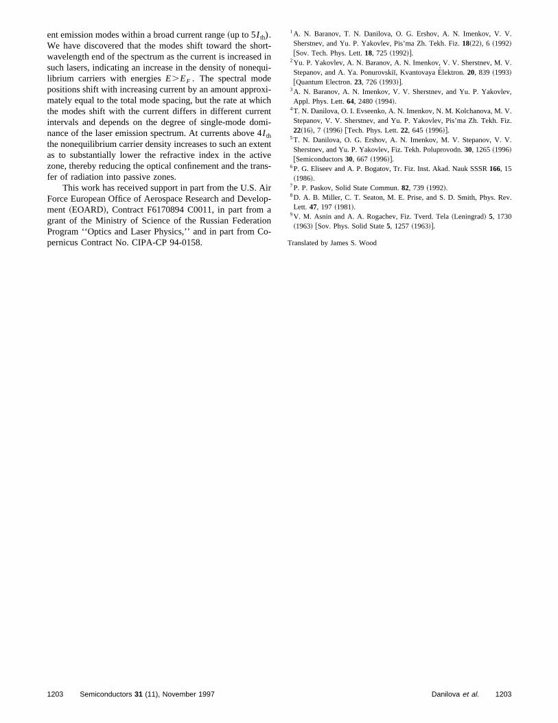
ent emission modes within a broad current range~up to 5I th).odqu
xicnm4teivean
irloaioo
1A. N. Baranov, T. N. Danilova, O. G. Ershov, A. N. Imenkov, V. V.Sherstnev, and Yu. P. Yakovlev, Pis’ma Zh. Tekh. Fiz.18~22!, 6 ~1992!
.
v,
.iz.
.
v.
We have discovered that the modes shift toward the shwavelength end of the spectrum as the current is increasesuch lasers, indicating an increase in the density of nonelibrium carriers with energiesE.EF . The spectral modepositions shift with increasing current by an amount appromately equal to the total mode spacing, but the rate at whthe modes shift with the current differs in different curreintervals and depends on the degree of single-mode donance of the laser emission spectrum. At currents aboveI th
the nonequilibrium carrier density increases to such an exas to substantially lower the refractive index in the actzone, thereby reducing the optical confinement and the trfer of radiation into passive zones.
This work has received support in part from the U.S. AForce European Office of Aerospace Research and Devement ~EOARD!, Contract F6170894 C0011, in part fromgrant of the Ministry of Science of the Russian FederatProgram ‘‘Optics and Laser Physics,’’ and in part from Cpernicus Contract No. CIPA-CP 94-0158.
1203 Semiconductors 31 (11), November 1997
rt-ini-
i-h
ti-
nt
s-
p-
n-
@Sov. Tech. Phys. Lett.18, 725 ~1992!#.2Yu. P. Yakovlev, A. N. Baranov, A. N. Imenkov, V. V. Sherstnev, M. VStepanov, and A. Ya. Ponurovski�, Kvantovaya E´ lektron. 20, 839 ~1993!@Quantum Electron.23, 726 ~1993!#.
3A. N. Baranov, A. N. Imenkov, V. V. Sherstnev, and Yu. P. YakovleAppl. Phys. Lett.64, 2480~1994!.
4T. N. Danilova, O. I. Evseenko, A. N. Imenkov, N. M. Kolchanova, M. VStepanov, V. V. Sherstnev, and Yu. P. Yakovlev, Pis’ma Zh. Tekh. F22~16!, 7 ~1996! @Tech. Phys. Lett.22, 645 ~1996!#.
5T. N. Danilova, O. G. Ershov, A. N. Imenkov, M. V. Stepanov, V. VSherstnev, and Yu. P. Yakovlev, Fiz. Tekh. Poluprovodn.30, 1265~1996!@Semiconductors30, 667 ~1996!#.
6P. G. Eliseev and A. P. Bogatov, Tr. Fiz. Inst. Akad. Nauk SSSR166, 15~1986!.
7P. P. Paskov, Solid State Commun.82, 739 ~1992!.8D. A. B. Miller, C. T. Seaton, M. E. Prise, and S. D. Smith, Phys. ReLett. 47, 197 ~1981!.
9V. M. Asnin and A. A. Rogachev, Fiz. Tverd. Tela~Leningrad! 5, 1730~1963! @Sov. Phys. Solid State5, 1257~1963!#.
Translated by James S. Wood
1203Danilova et al.
Influence of valence band absorption on the threshold characteristics of long-
ly
wavelength InAs lasersN. A. Gun’ko, G. G. Zegrya, N. V. Zotova, Z. N. Sokolova, N. M. Stus’, and V. B. Khalfin
A. F. Ioffe Physicotechnical Institute, Russian Academy of Sciences, 194021 St. Petersburg, Russia~Submitted April 2, 1997; accepted for publication April 10, 1997!Fiz. Tekh. Poluprovodn.31, 1396–1403~November 1997!
The mechanism of intraband absorption of radiation with hole transition into the spin-orbit split-off band, or so-called intervalence-band absorption~IVA !, is subjected to microscopicanalysis. It is shown that this IVA mechanism significantly influences the threshold characteristicsand quantum efficiency of InAs-based heterolasers. The dependences of the laser thresholdcharacteristics on the temperature and the parameters of the laser heterostructure are analyzed indetail, taking into account the new~IVA ! channel of intraband absorption by holes.© 1997 American Institute of Physics.@S1063-7826~97!03011-1#
1. INTRODUCTION It has been found that IVA in InAs lasers and similar
eedgt
tnoe
thtivrstiobaho
d
iteheto
r aersb
AthoscymAn
loalcea
velerfulers
thethe
e. 2tsthendyti-in.ectof
ffi-
eAs
our
mitg-
u-toin
tric
/1
Superior long-wavelength InAs-based lasers have bconstructed recently,1 but the working temperatures anquantum efficiency are far below those of short-wavelen(<1.5mm! lasers.2 It has been shown3 that the low workingtemperature of long-wavelength lasers is attributablestrong band-to-band Auger recombination, which doeshowever, account for the quantum efficiency of these lasat 77 K.
The maximum working temperature of long-wavelenglasers is known to depend on the rate factor of nonradiachannels for the recombination of nonequilibrium carriebut it also depends on the intraband radiation absorpcoefficient.4 An analysis has shown that the intraband asorption mechanism depends significantly on the actual bstructure of the semiconductor. A unique attribute of tband structure of InAs and solid solutions of similar compsition is the fact that the width of the band gapEg is close tothe spin-orbit splittingD. Consequently, radiation generatein a laser with\v;Eg would be highly prone to strongabsorption by holes in the valence band, which are excinto the spin-orbit split-off band in this case. We refer to tabsorption of light by holes with transition of the latter inthe split-off band as intervalence-~sub!band absorption~IVA !. Such absorption will necessarily be much strongethe lasing frequency in InAs than in lasers utilizing quatnary InGaAsP/InP solid solutions, in which the indicated lomechanism is substantial, despite the large differencetweenEg andD ~Ref. 5!.
The objective of the present study is to investigate IVin InAs and the influence of this loss mechanism oncharacteristics of long-wavelength InAs lasers. We propto show that IVA is one cause of the low quantum efficienof lasers made from InAs and solid solutions of similar coposition. We look at the recombination processes in Inand calculate the IVA coefficients associated with transitioof heavy and light holes into the split-off band. The anagous coefficients for nondegenerate holes have been clated previously.6 Intraband absorption within the valencband, on the other hand, has never been investigated inplication to long-wavelength lasers.
1204 Semiconductors 31 (11), November 1997 1063-7826/97
n
h
ot,rs
e,n-nde-
d
t-se-
ee
-ss-u-
p-
constituted solid solutions can be comparable with the leof light amplification in band-to-band transitions from thconduction to the valence band and can have a poweinfluence on the threshold current of long-wavelength lasemitting at wavelengths of 3 –3.5mm and on the maximumworking temperature. This assertion is corroborated byexperimental investigations reported below in regard tocharacteristics of InAs heterolasers.
The paper is divided into four sections, including thintroduction, two main sections, and conclusions. In Secwe calculate the heavy-hole and light-hole IVA coefficienand the optical gain. The calculations are carried out infirst approximation with respect to the ratio of the intrabahole energy to the width of the band gap. We derive analcal expressions for the IVA coefficients and the optical gaWe also take into account intraband relaxation with respto the momentum for the absorption and amplificationradiation. We then repeat the calculations of the IVA coecients using the exact Kane model.
In Sec. 3 we investigate the influence of IVA on thcharacteristics of long-wavelength heterolasers with an Inactive zone. We compare the theoretical relations withexperimental results.
In Sec. 4 we discuss the results of the study and subrecommendations for improving the characteristics of lonwavelength lasers.
2. CALCULATION OF THE INTERVALENCE-BANDABSORPTION COEFFICIENTS AND THE OPTICAL GAIN
a! The IVA coefficients and the optical gain are calclated in the 4-band Kane model, which is fully applicableInAs, where the wave vectors of all particles involvedabsorption are small by virtue of the closeness ofEg to D.
The absorption coefficienta and the optical gaing areexpressed in terms of the imaginary part of the dielecpermittivity «9:
a52g5v
cA«`
«9~v!, ~1!
120411204-08$10.00 © 1997 American Institute of Physics
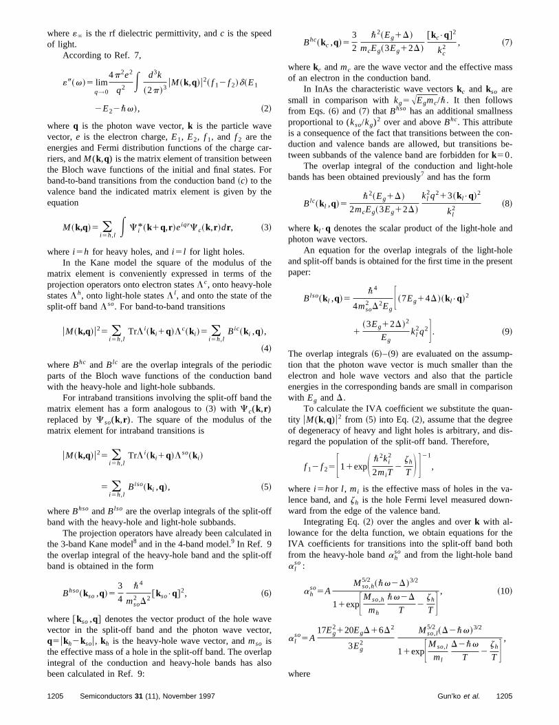
where«` is the rf dielectric permittivity, andc is the speed
ano
th
thth
e
icn
e
e
ff
d
-o
veor
laal
Bhc~k ,q!53 \2~Eg1D! @kc•q#2
, ~7!
ss
s
con-be-
le
nd
leent
p-theicleison
n-eis-
-n-
heh
of light.According to Ref. 7,
«9~v!5 limq→0
4p2e2
q2 E d3k
~2p!3uM ~k,q!u2~ f 12 f 2!d~E1
2E22\v!, ~2!
whereq is the photon wave vector,k is the particle wavevector, e is the electron charge,E1, E2, f 1, and f 2 are theenergies and Fermi distribution functions of the charge criers, andM (k,q) is the matrix element of transition betweethe Bloch wave functions of the initial and final states. Fband-to-band transitions from the conduction band~c! to thevalence band the indicated matrix element is given byequation
M ~k,q!5 (i 5h,l
E C i* ~k1q,r !eiqrCc~k,r !dr , ~3!
wherei 5h for heavy holes, andi 5 l for light holes.In the Kane model the square of the modulus of
matrix element is conveniently expressed in terms ofprojection operators onto electron statesLc, onto heavy-holestatesLh, onto light-hole statesL l , and onto the state of thsplit-off bandLso. For band-to-band transitions
uM ~k,q!u25 (i 5h,l
TrL i~k i1q!Lc~k i !5 (i 5h,l
Bic~k i ,q!,
~4!
whereBhc and Blc are the overlap integrals of the periodparts of the Bloch wave functions of the conduction bawith the heavy-hole and light-hole subbands.
For intraband transitions involving the split-off band thmatrix element has a form analogous to~3! with Cc(k,r )replaced byCso(k,r ). The square of the modulus of thmatrix element for intraband transitions is
uM ~k,q!u25 (i 5h,l
TrL i~k i1q!Lso~k i !
5 (i 5h,l
Biso~k i ,q!, ~5!
whereBhso andBlso are the overlap integrals of the split-oband with the heavy-hole and light-hole subbands.
The projection operators have already been calculatethe 3-band Kane model8 and in the 4-band model.9 In Ref. 9the overlap integral of the heavy-hole band and the splitband is obtained in the form
Bhso~kso ,q!53
4
\4
mso2 D2
@kso•q#2, ~6!
where@kso ,q# denotes the vector product of the hole wavector in the split-off band and the photon wave vectq5ukh2ksou, kh is the heavy-hole wave vector, andmso isthe effective mass of a hole in the split-off band. The overintegral of the conduction and heavy-hole bands hasbeen calculated in Ref. 9:
1205 Semiconductors 31 (11), November 1997
r-
r
e
ee
d
in
ff
,
pso
c 2 mcEg~3Eg12D! kc2
wherekc andmc are the wave vector and the effective maof an electron in the conduction band.
In InAs the characteristic wave vectorskc and kso aresmall in comparison withkg5AEgmc/\. It then followsfrom Eqs.~6! and ~7! that Bhso has an additional smallnesproportional to (kso/kg)2 over and aboveBhc. This attributeis a consequence of the fact that transitions between theduction and valence bands are allowed, but transitionstween subbands of the valence band are forbidden fork50.
The overlap integral of the conduction and light-hobands has been obtained previously7 and has the form
Blc~k l ,q!5\2~Eg1D!
2mcEg~3Eg12D!
kl2q213~k l•q!2
kl2
~8!
wherek l•q denotes the scalar product of the light-hole aphoton wave vectors.
An equation for the overlap integrals of the light-hoand split-off bands is obtained for the first time in the prespaper:
Blso~k l ,q!5\4
4mso2 D2Eg
F ~7Eg14D!~k l•q!2
1~3Eg12D!2
Egkl
2q2G . ~9!
The overlap integrals~6!–~9! are evaluated on the assumtion that the photon wave vector is much smaller thanelectron and hole wave vectors and also that the partenergies in the corresponding bands are small in comparwith Eg andD.
To calculate the IVA coefficient we substitute the quatity uM (k,q)u2 from ~5! into Eq. ~2!, assume that the degreof degeneracy of heavy and light holes is arbitrary, and dregard the population of the split-off band. Therefore,
f 12 f 25F11expS \2ki2
2miT2
zh
T D G21
,
where i 5hor l , mi is the effective mass of holes in the valence band, andzh is the hole Fermi level measured dowward from the edge of the valence band.
Integrating Eq.~2! over the angles and overk with al-lowance for the delta function, we obtain equations for tIVA coefficients for transitions into the split-off band botfrom the heavy-hole bandah
so and from the light-hole banda l
so :
ahso5A
Mso,h5/2 ~\v2D!3/2
11expFMso,h
mh
\v2D
T2
zh
T G , ~10!
a lso5A
17Eg2120EgD16D2
3Eg2
Mso,l5/2 ~D2\v!3/2
11expFMso,l
ml
D2\v
T2
zh
T G ,
where
1205Gun’ko et al.
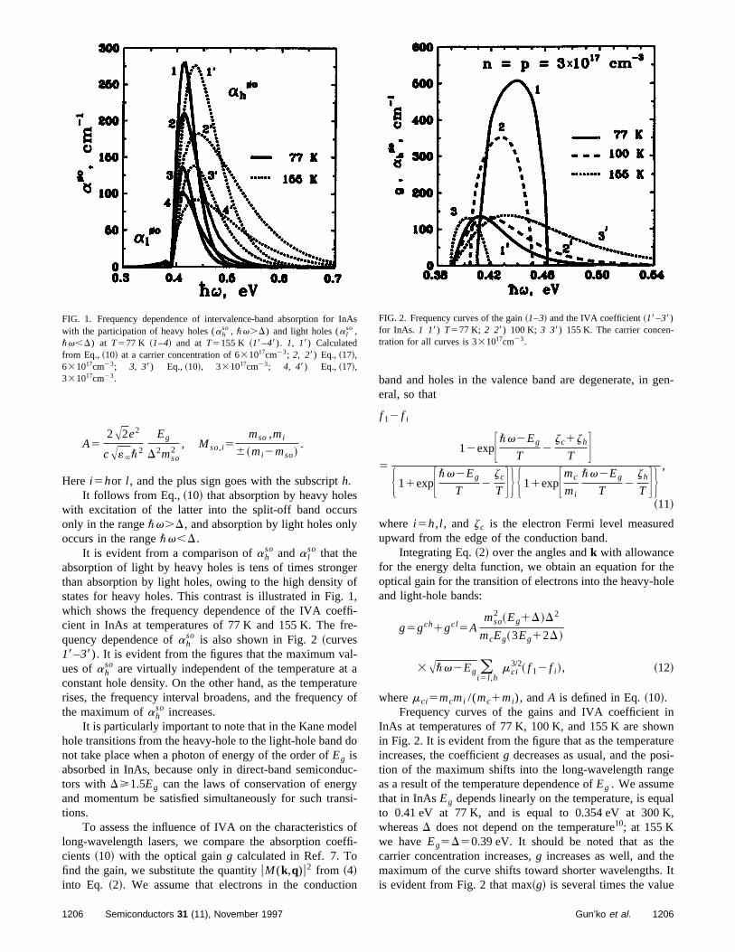
srsy
geo
. 1ffie
l-t atu
y
ed
uyns
oef
io
gen-
d
theole
inwnuresi-ge
ualK,
ee. It
InA
A52A2e2
cA«`\2
Eg
D2mso2
, Mso,i5mso ,mi
6~mi2mso!.
Here i 5hor l , and the plus sign goes with the subscripth.It follows from Eq.,~10! that absorption by heavy hole
with excitation of the latter into the split-off band occuonly in the range\v.D, and absorption by light holes onloccurs in the range\v,D.
It is evident from a comparison ofahso anda l
so that theabsorption of light by heavy holes is tens of times stronthan absorption by light holes, owing to the high densitystates for heavy holes. This contrast is illustrated in Figwhich shows the frequency dependence of the IVA coecient in InAs at temperatures of 77 K and 155 K. The frquency dependence ofah
so is also shown in Fig. 2~curves18–38). It is evident from the figures that the maximum vaues ofah
so are virtually independent of the temperature aconstant hole density. On the other hand, as the temperarises, the frequency interval broadens, and the frequencthe maximum ofah
so increases.It is particularly important to note that in the Kane mod
hole transitions from the heavy-hole to the light-hole bandnot take place when a photon of energy of the order ofEg isabsorbed in InAs, because only in direct-band semicondtors with D>1.5Eg can the laws of conservation of energand momentum be satisfied simultaneously for such trations.
To assess the influence of IVA on the characteristicslong-wavelength lasers, we compare the absorption cocients~10! with the optical gaing calculated in Ref. 7. Tofind the gain, we substitute the quantityuM (k,q)u2 from ~4!into Eq. ~2!. We assume that electrons in the conduct
FIG. 1. Frequency dependence of intervalence-band absorption forwith the participation of heavy holes (ah
so , \v.D) and light holes (a lso ,
\v,D) at T577 K ~1–4! and atT5155 K ~18–48). 1, 18) Calculatedfrom Eq.,~10! at a carrier concentration of 631017cm23; 2, 28) Eq.,~17!,631017cm23; 3, 38) Eq.,~10!, 331017cm23; 4, 48) Eq.,~17!,331017cm23.
1206 Semiconductors 31 (11), November 1997
rf,--
reof
lo
c-
i-
ffi-
n
band and holes in the valence band are degenerate, ineral, so that
f 12 f i
5
12expF\v2Eg
T2
zc1zh
T GH 11expF\v2Eg
T2
zc
T G J H 11expFmc
mi
\v2Eg
T2
zh
T G J ,
~11!
where i 5h,l , and zc is the electron Fermi level measureupward from the edge of the conduction band.
Integrating Eq.~2! over the angles andk with allowancefor the energy delta function, we obtain an equation foroptical gain for the transition of electrons into the heavy-hand light-hole bands:
g5gch1gcl5Amso
2 ~Eg1D!D2
mcEg~3Eg12D!
3A\v2Eg (i 5 l ,h
mci3/2~ f 12 f i !, ~12!
wheremci5mcmi /(mc1mi), andA is defined in Eq.~10!.Frequency curves of the gains and IVA coefficient
InAs at temperatures of 77 K, 100 K, and 155 K are shoin Fig. 2. It is evident from the figure that as the temperatincreases, the coefficientg decreases as usual, and the potion of the maximum shifts into the long-wavelength ranas a result of the temperature dependence ofEg . We assumethat in InAsEg depends linearly on the temperature, is eqto 0.41 eV at 77 K, and is equal to 0.354 eV at 300whereasD does not depend on the temperature10; at 155 Kwe haveEg5D50.39 eV. It should be noted that as thcarrier concentration increases,g increases as well, and thmaximum of the curve shifts toward shorter wavelengthsis evident from Fig. 2 that max~g! is several times the value
sFIG. 2. Frequency curves of the gain~1–3! and the IVA coefficient~18–38)for InAs. 1 18) T577 K; 2 28) 100 K; 3 38) 155 K. The carrier concen-tration for all curves is 331017cm23.
1206Gun’ko et al.
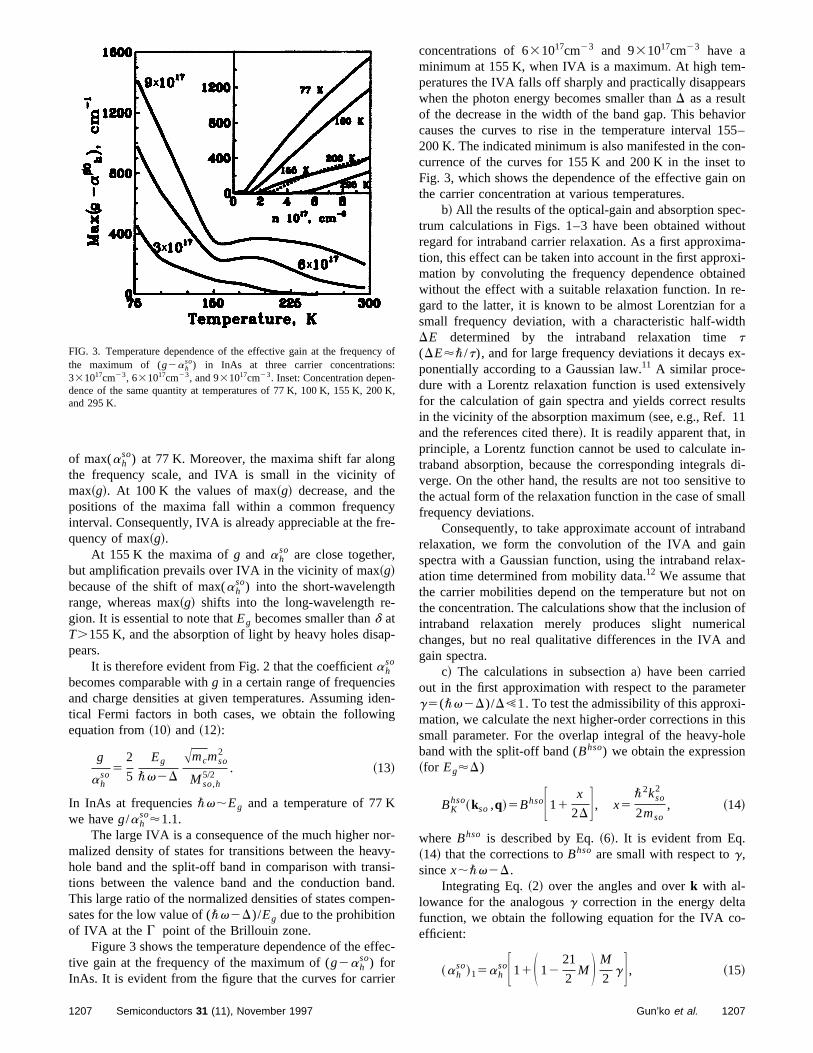
gf
ecyre
,
-
p
sdeng
orvsiane
ffe
ie
concentrations of 631017cm23 and 931017cm23 have a-ars
vior55–n-toon
c-outa-xi-nede-a
th
x-
elyults
in-s di-e toall
ndinlax-t
onof
calnd
ter-hisole
-
y:-0 K
of max(ahso) at 77 K. Moreover, the maxima shift far alon
the frequency scale, and IVA is small in the vicinity omax~g!. At 100 K the values of max~g! decrease, and thpositions of the maxima fall within a common frequeninterval. Consequently, IVA is already appreciable at the fquency of max~g!.
At 155 K the maxima ofg and ahso are close together
but amplification prevails over IVA in the vicinity of max~g!because of the shift of max(ah
so) into the short-wavelengthrange, whereas max~g! shifts into the long-wavelength region. It is essential to note thatEg becomes smaller thand atT.155 K, and the absorption of light by heavy holes disapears.
It is therefore evident from Fig. 2 that the coefficientahso
becomes comparable withg in a certain range of frequencieand charge densities at given temperatures. Assuming itical Fermi factors in both cases, we obtain the followiequation from~10! and ~12!:
g
ahso
52
5
Eg
\v2D
Amcmso2
Mso,h5/2
. ~13!
In InAs at frequencies\v;Eg and a temperature of 77 Kwe haveg/ah
so'1.1.The large IVA is a consequence of the much higher n
malized density of states for transitions between the heahole band and the split-off band in comparison with trantions between the valence band and the conduction bThis large ratio of the normalized densities of states compsates for the low value of (\v2D)/Eg due to the prohibitionof IVA at the G point of the Brillouin zone.
Figure 3 shows the temperature dependence of the etive gain at the frequency of the maximum of (g2ah
so) forInAs. It is evident from the figure that the curves for carr
FIG. 3. Temperature dependence of the effective gain at the frequencthe maximum of (g2ah
so) in InAs at three carrier concentrations331017cm23, 631017cm23, and 931017cm23. Inset: Concentration dependence of the same quantity at temperatures of 77 K, 100 K, 155 K, 20and 295 K.
1207 Semiconductors 31 (11), November 1997
-
-
n-
-y--d.
n-
c-
r
minimum at 155 K, when IVA is a maximum. At high temperatures the IVA falls off sharply and practically disappewhen the photon energy becomes smaller thanD as a resultof the decrease in the width of the band gap. This behacauses the curves to rise in the temperature interval 1200 K. The indicated minimum is also manifested in the cocurrence of the curves for 155 K and 200 K in the insetFig. 3, which shows the dependence of the effective gainthe carrier concentration at various temperatures.
b! All the results of the optical-gain and absorption spetrum calculations in Figs. 1–3 have been obtained withregard for intraband carrier relaxation. As a first approximtion, this effect can be taken into account in the first appromation by convoluting the frequency dependence obtaiwithout the effect with a suitable relaxation function. In rgard to the latter, it is known to be almost Lorentzian forsmall frequency deviation, with a characteristic half-widDE determined by the intraband relaxation timet(DE'\/t), and for large frequency deviations it decays eponentially according to a Gaussian law.11 A similar proce-dure with a Lorentz relaxation function is used extensivfor the calculation of gain spectra and yields correct resin the vicinity of the absorption maximum~see, e.g., Ref. 11and the references cited there!. It is readily apparent that, inprinciple, a Lorentz function cannot be used to calculatetraband absorption, because the corresponding integralverge. On the other hand, the results are not too sensitivthe actual form of the relaxation function in the case of smfrequency deviations.
Consequently, to take approximate account of intrabarelaxation, we form the convolution of the IVA and gaspectra with a Gaussian function, using the intraband reation time determined from mobility data.12 We assume thathe carrier mobilities depend on the temperature but notthe concentration. The calculations show that the inclusionintraband relaxation merely produces slight numerichanges, but no real qualitative differences in the IVA again spectra.
c! The calculations in subsection a! have been carriedout in the first approximation with respect to the parameg5(\v2D)/D!1. To test the admissibility of this approximation, we calculate the next higher-order corrections in tsmall parameter. For the overlap integral of the heavy-hband with the split-off band (Bhso) we obtain the expression~for Eg'D)
BKhso~kso ,q!5BhsoF11
x
2D G , x5\2kso
2
2mso, ~14!
whereBhso is described by Eq.~6!. It is evident from Eq.~14! that the corrections toBhso are small with respect tog,sincex;\v2D.
Integrating Eq.~2! over the angles and overk with al-lowance for the analogousg correction in the energy deltafunction, we obtain the following equation for the IVA coefficient:
~ahso!15ah
soF11S 1221
2M D M
2gG , ~15!
of
,
1207Gun’ko et al.
where parameter in the correction toahso for InAs is preceded by a
nd-
nal-ct
rgybe
M5mh
mh2mso,
andahso is given by Eq.~10!.
For InAs we haveM51.52 and
~ahso!15ah
so~11b!, ~16!
whereb5211g. It is evident from Eq.,~16! that the small
ua
y
ti
giert
only
ee
e
lais
racw
gaal
numerical coefficient of the order of 10, and the correspoing correction (b) is significant. It is evident from Eq.,~10!and Fig. 1 that\v2D5(3/2)kT. We haveb520.28 at77 K andb520.56 at 155 K, and the validity of the giveexpansion is no longer justified at 155 K. We therefore cculate the IVA coefficient for heavy holes using the exaKane model in the overlap integral and also in the eneconservation law. In this case the IVA coefficient canwritten in the form
d a
~ahso!K5
2Amso5/2x3/2
F11expS M1
x
T2
zh
T D GFM11~Eg1D!~3Eso12D!
3Eso2 12Eso~D2Eg!2EgD23x~Eg1D!
G , ~17!
where M15mso /mh , Eso52D2«so , «so is the Kane en- 100 meV and 0.03, respectively. The confining layers ha
ees-ur-
sedin
hase
2–ni-
er-the
ow-wela-s inieror
ac-
s,edtherved
-
ffi-
ergy of a hole in the split-off band,A is defined in~10!, andx is defined in~14!. The relation betweenx andEso is speci-fied by the energy conservation law
Eso1M1x1\v50 ~18!
and by the following relation deduced from the Kane eqtion:
x5Eso@Eso
2 1~D2Eg!Eso2EgD#
~Eg1D!~3Eso12D!. ~19!
The spectral curves of (ahso)K for InAs are represented b
curves2, 28, 4, and48 in Fig. 1. It is evident from the figurethat the quantitative differences between the exact equa~17! and the approximation expression~10! are significant.Calculations using the exact and approximate equationsthe same energy position of the IVA maximum. Howevwhen the exact equation~17! is used, the absorption level athe maximum is roughly 30% lower. Also, the absorptispectra extend into the short-wavelength range, especial155 K.
3. INFLUENCE OF INTERVALENCE-BAND ABSORPTION ONTHE CHARACTERISTICS OF HETEROLASERS
a! We have investigated the influence of IVA on thcharacteristics of heterolasers. The investigated objects wlong-wavelength, double-heterostructure, injection laswith an n-InAs active zone.
Double heterostructures of compositionn-InAs12x2y
SbxPy/n-InAs/p-InAs12x2ySbxPy (0.05,x,0.09; 0.09,y,0.18) were grown on ann-InAs~111! substrate by liquid-phase epitaxy under conditions creating high substrate pticity so as to reduce the misfit voltages induced by mmatch of the lattice constants through the prepondeformation of dislocations in the substrate. The end produwere structurally perfect epitaxial layers with an all-time lodislocation density<1013cm22. The p-type emitter wasdoped with zinc. The energy differential across the bandand the refractive index at the heterointerfaces were equ
1208 Semiconductors 31 (11), November 1997
-
on
ve,
at
rers
s--ntts
pto
thickness of 4 –6mm, and the thickness of the active zon~d! varies from 0.8mm to 6mm. The refractive index of theactive zone was equal to 3.52. Four-chip lasers were invtigated together with wide-contact lasers, whose lateral sfaces were sufficiently rough to suppress internal clomode configurations. The width of the contact was variedthe interval 35–200mm, and the cavity had a lengtL5100–1500mm. The wavelength of the laser mode w3.05mm ~at 77 K!, corresponding to the maximum of thphotoluminescence peak of undopedn-InAs in the activezone. Lasing was observed in the temperature range150 K in pulsed and continuous-wave operation with mimum threshold current densities of 60 A/cm2 and 100 A/cm2, respectively~at 77 K!.
We now discuss the influence of IVA on the charactistics of the above-described heterolasers. We note thatinfluence of the heterointerfaces on absorption is weak,ing to the considerable width of the active zone, andignore it. We use the exact Kane model for all the calcutions in this section. We analyze the laser characteristicthe following order. We first determine the threshold carrconcentrationnth in the active zone of the heterolaser fvarious values ofd, L, andT. According to Ref. 13,
G@max~g2ahso!#5a* , ~20!
where only two types of optical losses are taken intocount: IVA (ah
so) and output lossesa* 5(1/L)ln(1/R),whereR50.3 is the reflection coefficient of the laser mirrorand G is the optical confinement factor in the investigatheterostructure. It is evident from the calculations thatgreatest increase in the threshold density should be obsein lasers having thinner active zones (d<1 mm! and shortcavities (L50.03 cm!, for which the output losses are highest.
Next we calculate the external differential quantum eciency (h i), defined as the ratio of the output losses (a* ) tothe total losses:
1208Gun’ko et al.
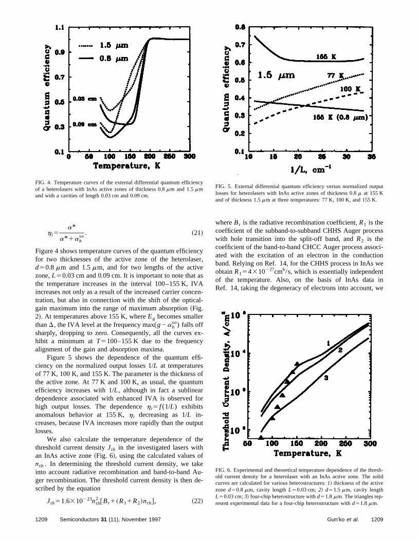
nseeaVAcel-
r
ey
ffi
our
tp
thfk
Aud
ess
oci-onwetinwe
ncput
resh-olid
h i5a*
a* 1ahso
. ~21!
Figure 4 shows temperature curves of the quantum efficiefor two thicknesses of the active zone of the heterolad50.8mm and 1.5mm, and for two lengths of the activzone,L50.03 cm and 0.09 cm. It is important to note thatthe temperature increases in the interval 100–155 K, Iincreases not only as a result of the increased carrier contration, but also in connection with the shift of the opticagain maximum into the range of maximum absorption~Fig.2!. At temperatures above 155 K, whereEg becomes smallethanD, the IVA level at the frequency max(g2ah
so) falls offsharply, dropping to zero. Consequently, all the curveshibit a minimum atT5100–155 K due to the frequencalignment of the gain and absorption maxima.
Figure 5 shows the dependence of the quantum eciency on the normalized output losses 1/L at temperaturesof 77 K, 100 K, and 155 K. The parameter is the thicknessthe active zone. At 77 K and 100 K, as usual, the quantefficiency increases with 1/L, although in fact a sublineadependence associated with enhanced IVA is observedhigh output losses. The dependenceh i5 f (1/L) exhibitsanomalous behavior at 155 K,h i decreasing as 1/L in-creases, because IVA increases more rapidly than the oulosses.
We also calculate the temperature dependence ofthreshold current densityJth in the investigated lasers witan InAs active zone~Fig. 6!, using the calculated values onth . In determining the threshold current density, we tainto account radiative recombination and band-to-bandger recombination. The threshold current density is thenscribed by the equation
Jth51.6310223nth2 @Br1~R11R2!nth#, ~22!
FIG. 4. Temperature curves of the external differential quantum efficieof a heterolasers with InAs active zones of thickness 0.8mm and 1.5mmand with a cavities of length 0.03 cm and 0.09 cm.
1209 Semiconductors 31 (11), November 1997
cyr,
s
n-
x-
-
fm
for
ut
he
e-
e-
whereBr is the radiative recombination coefficient,R1 is thecoefficient of the subband-to-subband CHHS Auger procwith hole transition into the split-off band, andR2 is thecoefficient of the band-to-band CHCC Auger process assated with the excitation of an electron in the conductiband. Relying on Ref. 14, for the CHHS process in InAsobtainR154310227cm6/s, which is essentially independenof the temperature. Also, on the basis of InAs dataRef. 14, taking the degeneracy of electrons into account,
yFIG. 5. External differential quantum efficiency versus normalized outlosses for heterolasers with InAs active zones of thickness 0.8m at 155 Kand of thickness 1.5mm at three temperatures: 77 K, 100 K, and 155 K.
FIG. 6. Experimental and theoretical temperature dependence of the thold current density for a heterolaser with an InAs active zone. The scurves are calculated for various heterostructures:1! thickness of the activezone d50.8mm, cavity lengthL50.03 cm;2! d51.5mm, cavity lengthL50.03 cm;3! four-chip heterostructure withd51.8mm. The triangles rep-resent experimental data for a four-chip heterostructure withd51.8mm.
1209Gun’ko et al.
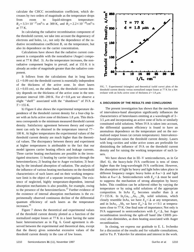
calculate the CHCC recombination coefficient, which de-ro:
oy
t
m
ni
om
rsenern
em
dla
rre7thre
eounvee
ohoerisrnin
etiatu
uethmocth
ismthef 3–lynt,annor-
sersforntla-
esr,in
avytheate
,
is
ger
kons,
rk.
het-
creases by two orders of magnitude as the temperature dfrom room to liquid-nitrogen temperatureR253.3310227cm6/s at 300 K, andR252.2310229cm6/sat 77 K.
In calculating the radiative recombination componentthe threshold current, we take into account the degeneracelectrons and holes, i.e., not only the dependence of thediative recombination coefficientBr on the temperature, bualso its dependence on the carrier concentration.
Calculations have shown that the radiative current coponent is comparable with the nonradiative~Auger! compo-nent at 77 K~Ref. 3!. As the temperature increases, the noradiative component begins to prevail, and at 155 K italready an order of magnitude greater than the radiative cponent.
It follows from the calculations that in long lase(L50.09 cm! the threshold current is essentially independof the thickness of the active zone. In short las(L50.03 cm!, on the other hand, the threshold current desity depends on the thickness of the active zone in the tperature interval 100–200 K. Ford50.8mm we observe aslight ‘‘shelf’’ associated with the ‘‘shutdown’’ of IVA atT.155 K.
b! Figure 6 also shows the experimental temperaturependence of the threshold current density for a four-chipser with an InAs active zone of thickness 1.8mm. This thick-ness corresponds to the minimum measured threshold cudensity. Satisfactory agreement between theory and expment can only be obtained in the temperature interval 7100 K. At higher temperatures the experimental values ofthreshold current density are much higher than the theocal values. The discrepancy between theory and experimat higher temperatures is attributable to the fact thatmodel ignores carrier heating effects and leakage curreThree carrier heating mechanisms are possible in the intigated structures: 1! heating by carrier injection through thheterointerfaces; 2! heating due to Auger excitation; 3! heat-ing by the intraband absorption of radiation. The analysisthe influence of various heating mechanisms on the threscharacteristics of such lasers and on their working tempture limit is the object of a separate investigation. The extence of neglected, highly temperature-dependent, inteabsorption mechanisms is also possible, for example, owto the presence of the heterointerfaces.15 Further evidence ofthe existence of internal absorption mechanisms is theperimentally observed continuous decline of the differenquantum efficiency of such lasers as the temperaincreases.16
Figure 7 shows the theoretical and experimental valof the threshold current density plotted as a function ofnormalized output losses at 77 K in a laser having the sabasic heterostructure as in Fig. 6. Good agreement isserved between the experimental and theoretical data, exthat the theory gives somewhat excessive values ofthreshold current density in the case of low losses.
1210 Semiconductors 31 (11), November 1997
ps
fof
ra-
-
-s
-
ts--
e--
entri-–eti-ntr
ts.s-
flda--alg
x-l
re
see
b-epte
4. DISCUSSION OF THE RESULTS AND CONCLUSIONS
The present investigation has shown that the mechanof intervalence-band absorption significantly influencescharacteristics of heterolasers emitting at a wavelength o3.5mm and incorporating an active zone of InAs or similarconstituted solid solutions. When IVA is taken into accouthe differential quantum efficiency is found to haveanomalous dependence on the temperature and on themalized output losses~at certain temperatures!. Intervalence-band absorption raises the threshold current density. Lawith long cavities and wider active zones are preferablediminishing the influence of IVA on the threshold curredensity and for raising the working temperature of suchsers.
We have shown that in III–V semiconductors, as in G~Ref. 6!, the heavy-hole IVA coefficient is tens of timehigher than the long-wavelength IVA coefficient. Howevethe absorption of light by heavy and light holes takes placedifferent frequency ranges: heavy holes at\v.D and lightholes at\v,D. Semiconductors withEg,D must be usedto suppress the mechanism of strong absorption by heholes. This condition can be achieved either by varyingtemperature or by using solid solutions of the appropricomposition. In InAs Eg becomes smaller thanD atT.155 K. In InyGa12yAs12xSbx solid solutions, whichclosely resemble InAs, we haveEg,D at any temperatureand in InAs12xSbx we haveEg.D for x,0.1 at tempera-tures close to 77 K. One final note of importance; Not onlyIVA suppressed in semiconductors withEg,D, but Augerrecombination involving the split-off band~the CHHS pro-cess! also diminishes, as does heating associated with Aurecombination.
In closing, we express our gratitude to E. L. Ivchenfor a discussion of the results and for valuable consultatioand to Yu. P. Yakovlev for attention and interest in the wo
FIG. 7. Experimental~triangles! and theoretical~solid curve! plots of thethreshold current density versus normalized output losses at 77 K for aerolaser with an InAs active zone of thicknessd51.8mm.
1210Gun’ko et al.
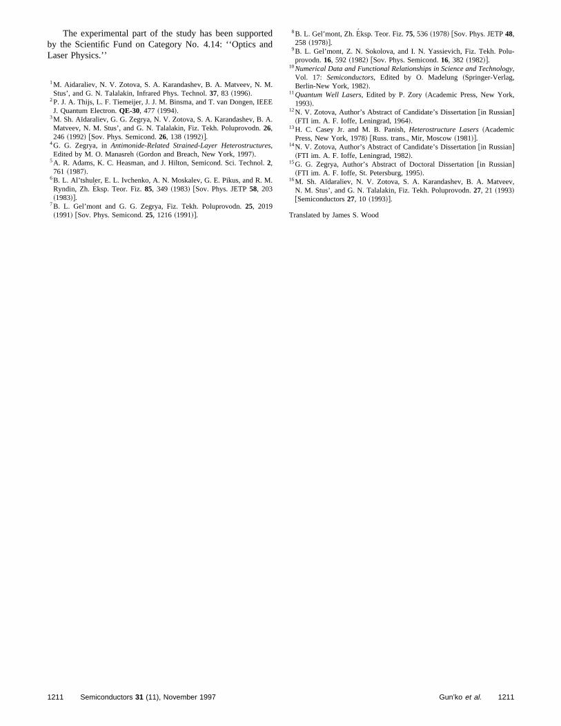
The experimental part of the study has been supportednd
.
EE
A.
s
l.
.
8B. L. Gel’mont, Zh. Eksp. Teor. Fiz.75, 536~1978! @Sov. Phys. JETP48,258 ~1978!#.
u-
gy
v,
by the Scientific Fund on Category No. 4.14: ‘‘Optics aLaser Physics.’’
1M. Aidaraliev, N. V. Zotova, S. A. Karandashev, B. A. Matveev, N. MStus’, and G. N. Talalakin, Infrared Phys. Technol.37, 83 ~1996!.
2P. J. A. Thijs, L. F. Tiemeijer, J. J. M. Binsma, and T. van Dongen, IEJ. Quantum Electron.QE-30, 477 ~1994!.
3M. Sh. A�daraliev, G. G. Zegrya, N. V. Zotova, S. A. Karandashev, B.Matveev, N. M. Stus’, and G. N. Talalakin, Fiz. Tekh. Poluprovodn.26,246 ~1992! @Sov. Phys. Semicond.26, 138 ~1992!#.
4G. G. Zegrya, inAntimonide-Related Strained-Layer Heterostructure,Edited by M. O. Manasreh~Gordon and Breach, New York, 1997!.
5A. R. Adams, K. C. Heasman, and J. Hilton, Semicond. Sci. Techno2,761 ~1987!.
6B. L. Al’tshuler, E. L. Ivchenko, A. N. Moskalev, G. E. Pikus, and R. MRyndin, Zh. Eksp. Teor. Fiz.85, 349 ~1983! @Sov. Phys. JETP58, 203~1983!#.
7B. L. Gel’mont and G. G. Zegrya, Fiz. Tekh. Poluprovodn.25, 2019~1991! @Sov. Phys. Semicond.25, 1216~1991!#.
1211 Semiconductors 31 (11), November 1997
9B. L. Gel’mont, Z. N. Sokolova, and I. N. Yassievich, Fiz. Tekh. Polprovodn.16, 592 ~1982! @Sov. Phys. Semicond.16, 382 ~1982!#.
10Numerical Data and Functional Relationships in Science and Technolo,Vol. 17: Semiconductors, Edited by O. Madelung~Springer-Verlag,Berlin-New York, 1982!.
11Quantum Well Lasers, Edited by P. Zory~Academic Press, New York,1993!.
12N. V. Zotova, Author’s Abstract of Candidate’s Dissertation@in Russian#~FTI im. A. F. Ioffe, Leningrad, 1964!.
13H. C. Casey Jr. and M. B. Panish,Heterostructure Lasers~AcademicPress, New York, 1978! @Russ. trans., Mir, Moscow~1981!#.
14N. V. Zotova, Author’s Abstract of Candidate’s Dissertation@in Russian#~FTI im. A. F. Ioffe, Leningrad, 1982!.
15G. G. Zegrya, Author’s Abstract of Doctoral Dissertation@in Russian#~FTI im. A. F. Ioffe, St. Petersburg, 1995!.
16M. Sh. A�daraliev, N. V. Zotova, S. A. Karandashev, B. A. MatveeN. M. Stus’, and G. N. Talalakin, Fiz. Tekh. Poluprovodn.27, 21 ~1993!@Semiconductors27, 10 ~1993!#.
Translated by James S. Wood
1211Gun’ko et al.
Influence of plasma treatment of the surface of silicon carbide on the characteristics
mer
of buried-gate junction field-effect transistorsP. A. Ivanov, O. I. Kon’kov, V. N. Panteleev, and T. P. Samsonova
A. F. Ioffe Physicotechnical Institute, Russian Academy of Sciences, 194021 St. Petersburg, Russia~Submitted April 11, 1997; accepted for publication April 16, 1997!Fiz. Tekh. Poluprovodn.31, 1404–1407~November 1997!
For SiC buried-gate junction field-effect transistors it is demonstrated that the charge state of thechannel surface, which functions as a secondary, ‘‘floating’’ gate in such transistors, can bestabilized by treating it in a hydrogen plasma at room temperature. It is shown that the need forsuch stabilization is especially crucial for transistors having a relatively low donor densityin the channel~high-voltage type!, in which the surface charge can strongly modulate the drainvoltage under the influence of short-channel effects. ©1997 American Institute ofPhysics.@S1063-7826~97!03111-6#
1. INTRODUCTION short-channel effects can be more pronounced in the for
ofnpe
ait,ico
s
stldeeo
nastargat
b-io
hi
san
by
oreo-
p-id-rgefor-ra-
igh-
a.
-sed
tan-ic
ctive-
w-
ogenhe
re in
re,om-ma
ce-ace-
re
/1
It is a well-known fact that the surface propertiessemiconductors have a strong influence on the operatiomany electronic devices utilizing them. For this reason, scial techniques are employed in device technology withview toward modifying the surface in such a way as to obta particular combination of surface properties. At presencrucial aspect of the development of devices based on silcarbide is the reliable passivation~or stabilization! of the SiCsurface at sites where it connects with the active zonedevices~especially the high-voltage kind!.
As a rule, no special measures are implemented tobilize the channel surface in SiC buried-gate junction fieeffect transistors fabricated by various groups worldwid1
On the other hand, one needs to be aware that the channthis type of transistor is cut off by the space-charge regionthep–n gate on the surface~Fig. 1!, whose charge state cavary, in principle. This means that the surface emergeskind of ‘‘floating’’ gate, so that steps must be taken to sbilize the surface charge. Ideally the density of this chashould be either much smaller or, conversely, much grethan the surface density of donors in the channel,Na ~N isthe bulk density of donors, anda is the thickness of thechannel!. In the first case ‘‘flat-band’’ conditions are estalished on the surface~so that a surface space-charge regionsimply nonexistent!, and in the second case the thicknessthe subsurface space-charge region is stabilized by thesurface charge~Fermi level pinning on the surface!. It isimportant to note the practice exercised in several studieSiC buried-gate junction transistors, of protecting the chnel surface with a heat-resistant oxide~mainly to safeguardthe transistors against environmental effects!. For surfacecharge stabilization, however, oxidation cannot reallydeemed an effective method, because the total densitstates at the SiO2–SiC interface~of the order of 1012 cm22,Ref. 2! is commensurate with the surface density of donin the transistor channel. Surface-charge stabilization ispecially crucial for transistors having a low channel dondensity ~high-voltage type!. Since the channel length-tothickness ratio in such transistors is usually smaller thantransistors having a high donor density~low-voltage type!,
1212 Semiconductors 31 (11), November 1997 1063-7826/97
of-
anan
of
a--.l off
a-eer
sfgh
of-
eof
ss-r
in
and have a definite influence on the surface charge.In previous work we have shown that the surface pro
erties of crystalline silicon carbide can be modified conserably by treatment in hydrogen and helium gas-dischaplasmas. In particular, this technique has resulted in themation of high-resistivity surface layers through the genetion of a high density of electrically active point defects.3 Wenow propose to demonstrate how the characteristics of hvoltage buried-gate transistors are influenced by: 1! reactiveion etching of the channel in a SF6 gas-discharge plasma; 2!subsequent treatment of the surface in a hydrogen plasm
2. OBJECT AND PROCEDURE OF THE INVESTIGATIONS
The transistors were prepared on the basis of 6H-SiCepitaxial p1~substrate!–n0–n1 structures grown by chemical deposition from the gaseous phase. The technology uto fabricate discrete mesa-insulated transistors involved sdard procedures for the formation of nickel-based ohmcontacts to the source, the drain, and the gate and selereactive ion etching of SiC in a SF6 plasma. The donor density in the channel was 331016cm23 ~we note that this valueis set approximately an order of magnitude higher for lovoltage transistors!, and the channel length was 5mm.
After the transistor characteristics~the current-voltageand capacitance-voltage curves of the controlp–n junction!had been measured, the samples were treated in a hydrplasma to modify the surface properties of the channel. Tparameters of this process included: the hydrogen pressuthe dc-discharge reaction chamber 231023 torr; the acceler-ating voltage between the anode and the cathode 600 V~thedischarge power density did not exceed 1 W/cm2); roomtemperature; treatment time 1 h. Following this proceduthe transistor characteristics were again measured for cparison with the characteristics before hydrogen-plastreatment.
In addition, for comparative analysis the capacitanvoltage curves were measured for reference Au–SiC surfbarrier structures~usingn-type 6H-SiC films grown by sub-limation epitaxy!, which were formed on each crystal befo
121211212-04$10.00 © 1997 American Institute of Physics
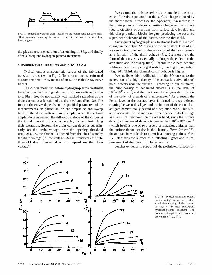
eddur
esishe
f teg
sgrlolb
-ra
We assume that this behavior is attributable to the influ-by
ace
ved
dicall,rent
theetion
tes,ofis
cts,l antu-ageface
an
ace
sta-
elda
the plasma treatments, then after etching in SF6, and finallyafter subsequent hydrogen-plasma treatment.
3. EXPERIMENTAL RESULTS AND DISCUSSION
Typical output characteristic curves of the fabricattransistors are shown in Fig. 2~for measurements performeat room temperature by means of an L2-56 cathode-ray ctracer!.
The curves measured before hydrogen-plasma treatmhave features that distinguish them from low-voltage trantors. First, they do not exhibit well-marked saturation of tdrain current as a function of the drain voltage~Fig. 2a!. Theform of the curves depends on the specified parameters omeasurements, in particular, on the amplitude and swtime of the drain voltage. For example, when the voltaamplitude is increased, the differential slope of the curvethe initial interval drops considerably, further diminishintheir saturation. Second, the drain current depends supeearly on the drain voltage near the opening thresh~Fig. 2b!, i.e., the channel is opened from the closed statethe drain voltage~in low-voltage 6H-SiC transistors the subthreshold drain current does not depend on the dvoltage4!.
FIG. 1. Schematic vertical cross section of the buried-gate junction fieffect transistor, showing the surface charge in the role of a secondfloating gate.
ve
nt-
heepein
in-dy
in
ence of the drain potential on the surface charge inducedthe short-channel effect~see the Appendix!: An increase inthe drain potential induces a positive charge on the surf~due to ejections of electrons from surface-state levels!, andthis charge partially blocks the gate, producing the obsersuperlinear behavior of the curves near the threshold.
Subsequent hydrogen-plasma treatment leads to a rachange in the outputI-V curves of the transistors. First of alwe see an improvement in the saturation of the drain curas a function of the drain voltage~Fig. 2c; moreover, theform of the curves is essentially no longer dependent onamplitude and the sweep time!. Second, the curves becomsublinear near the opening threshold, tending to satura~Fig. 2d!. Third, the channel cutoff voltage is higher.
We attribute this modification of theI-V curves to thegeneration of a high density of electrically active~donor!point defects near the surface. According to our estimathe bulk density of generated defects is at the level1018–1019 cm23, and the thickness of the generation zoneof the order of a tenth of a micrometer.3 As a result, theFermi level in the surface layer is pinned to deep defecreating between this layer and the interior of the channeantigate barrier totally devoid of a depletion zone. This siation accounts for the increase in the channel cutoff voltas a result of treatment. On the other hand, since the surdensity of generated defects is greater than 1013–1014 cm22
~which itself is one or two orders of magnitude higher ththe surface donor density in the channel,Na51012 cm22),the antigate barrier leads to Fermi level pinning at the surf~i.e., stabilizes the surface as a ‘‘floating’’ gate! and to im-provement of the transistor characteristics.
Further evidence in support of the postulated surface
-ry,
l
ere
FIG. 2. Typical transistor outputcurrent-voltage curves. a, b! Mea-sured after etching of the channein SF6; c, d! after subsequenthydrogen-plasma treatment. Thnumbers alongside the curves athe values ofVGS @V#.
1213 1213Semiconductors 31 (11), November 1997 Ivanov et al.
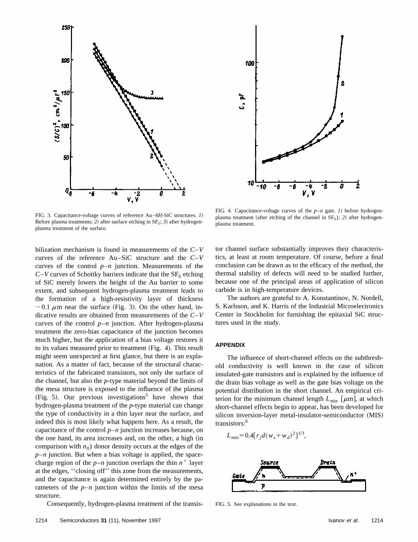
e
edss
-
ms
pra
ofsm
enthnhhece
tsp
s
ris-nalther,on
ll,csc-
sh-ne ofthe
ri-
d for
bilization mechanism is found in measurements of theC–Vcurves of the reference Au–SiC structure and theC–Vcurves of the controlp–n junction. Measurements of thC–V curves of Schottky barriers indicate that the SF6 etchingof SiC merely lowers the height of the Au barrier to somextent, and subsequent hydrogen-plasma treatment leathe formation of a high-resistivity layer of thicknes;0.1mm near the surface~Fig. 3!. On the other hand, indicative results are obtained from measurements of theC–Vcurves of the controlp–n junction. After hydrogen-plasmatreatment the zero-bias capacitance of the junction becomuch higher, but the application of a bias voltage restoreto its values measured prior to treatment~Fig. 4!. This resultmight seem unexpected at first glance, but there is an exnation. As a matter of fact, because of the structural chateristics of the fabricated transistors, not only the surfacethe channel, but also thep-type material beyond the limits othe mesa structure is exposed to the influence of the pla~Fig. 5!. Our previous investigations5 have shown thathydrogen-plasma treatment of thep-type material can changthe type of conductivity in a thin layer near the surface, aindeed this is most likely what happens here. As a result,capacitance of the controlp–n junction increases because, othe one hand, its area increases and, on the other, a hig~incomparison withn0) donor density occurs at the edges of tp–n junction. But when a bias voltage is applied, the spacharge region of thep–n junction overlaps the thinn1 layerat the edges, ‘‘closing off’’ this zone from the measuremenand the capacitance is again determined entirely by therameters of thep–n junction within the limits of the mesastructure.
Consequently, hydrogen-plasma treatment of the tran
FIG. 3. Capacitance-voltage curves of reference Au–6H-SiC structures.1!Before plasma treatments;2! after surface etching in SF6; 3! after hydrogen-plasma treatment of the surface.
1214 Semiconductors 31 (11), November 1997
to
esit
la-c-f
a
de
-
,a-
is-
tor channel surface substantially improves their charactetics, at least at room temperature. Of course, before a ficonclusion can be drawn as to the efficacy of the method,thermal stability of defects will need to be studied furthebecause one of the principal areas of application of siliccarbide is in high-temperature devices.
The authors are grateful to A. Konstantinov, N. NordeS. Karlsson, and K. Harris of the Industrial MicroelectroniCenter in Stockholm for furnishing the epitaxial SiC strutures used in the study.
APPENDIX
The influence of short-channel effects on the subthreold conductivity is well known in the case of silicoinsulated-gate transistors and is explained by the influencthe drain bias voltage as well as the gate bias voltage onpotential distribution in the short channel. An empirical cterion for the minimum channel lengthLmin @mm#, at whichshort-channel effects begin to appear, has been developesilicon inversion-layer metal-insulator-semiconductor~MIS!transistors:6
Lmin50.4@r jd~ws1wd!2#1/3,
FIG. 4. Capacitance-voltage curves of thep–n gate.1! before hydrogen-plasma treatment~after etching of the channel in SF6); 2! after hydrogen-plasma treatment.
FIG. 5. See explanations in the text.
1214Ivanov et al.
where r j @mm# is the depth of the drain and sourcep–ndceckt-f
y
-ell
~with a doping level 331016cm23), the calculated value of
ov,
v,
. A.re
inRe-d,
ns.
junctions, d @Å# is the thickness of the insulator, anws1wd @mm# is the sum of the thicknesses of the sourand drain depletion layers. For an MIS transistor the thiness of the insulatord characterizes the degree of ‘‘shorrange action’’ of the gate on the channel. In the case otransistor utilizing a buriedp–n junction as the gate thechannel thicknessa functions in the same role. By analogwith the above equation, an analogous criterionLmin for ourtransistors can be introduced by replacingd @and, for roughestimates, (ws1wd) and r j # by the channel thicknessa.Then, taking into account the relationVp5qNa2/2«, we candetermineLmin as a function of the degree of dopingN of thechannel and the specified cutoff voltageVp . It becomes clearthat Lmin will be significantly higher for a high-voltage transistor, which requires a low donor density in the channthan for a low-voltage transistor. In our case specifica
1215 Semiconductors 31 (11), November 1997
-
a
l,y
Lmin is approximately 9mm, as opposed toL55 mm.
1P. A. Ivanov and V. E. Chelnokov, Fiz. Tekh. Poluprovodn.29, 1921~1995! @Semiconductors29, 1003~1995!#.
2P. A. Ivanov, V. N. Panteleev, R. P. Samsonova, and V. E. ChelnokFiz. Tekh. Poluprovodn.29, 271~1995! @Semiconductors29, 135~1995!#.
3A. O. Konstantinov, N. S. Konstantinova, O. I. Kon’kov, E. I. Terukoand P. A. Ivanov, Fiz. Tekh. Poluprovodn.28, 342 ~1994! @Semiconduc-tors 28, 209 ~1994!#.
4P. A. Ivanov, N. S. Savkina, V. N. Panteleev, T. P. Samsonova, and AMaltsev, in Transactions of the Third International High TemperatuElectronics Conferences (HiTEC)~Albuquerque, N.M., 1996!, p. P-213.
5A. O. Konstantinov, P. A. Ivanov, O. I. Konkov, and E. I. Terukov,Institute of Physics Conference Series, No. 137, Silicon Carbide andlated Materials, edited by M. G. Spencer, R. P. Devaty, J. A. EdmonM. Asif Khan, R. Karlan, and M. Rahman~IOP Publ., Bristol-Philadelphia, 1993!, p. 275.
6J. R. Brews, W. Fitchner, E. H. Nicolian, and S. M. Sze, IEEE TraElectron DevicesEDL-1, 2 ~1980!.
Translated by James S. Wood
1215Ivanov et al.
SIMC-X 1998
10th Conference on
Semiconducting and Insulating MaterialsJune 1–5, 1998
Berkeley, California
Scope of the Conference
This conference has traditionally been the leading meeting for fundamental materials problems of compound semiconductorsof relevance for electronic and optoelectronic devices. In its early years, the conference focused on defect problems insemi-insulating substrates used for device fabrication. Later, following the decision of the International Advisory Committee,the scope of the conference was extended to include other device-relevant issues in compound semiconductor materials. Theconference brings together specialists from various fields, including materials science, solid state physics, and device andprocess engineering. The purpose of the meeting is to discuss growth, characterization, theory, device applications, andmaterials problems related to semiconducting and insulating compounds such as GaAs, InP, III-nitrides, II–VI compounds,and SiGe. Participants in the conference will have an opportunity to exchange ideas and to discuss future directions in thedevelopment of this expanding field. The conference program will include invited, oral, and poster presentations.
Novel Materials Systems of Special Interest for this Conference:III-nitridesIII-oxidesNon-stoichiometric III-Vs
Topics
Growth: Bulk and epitaxial growth~molecular-beam epitaxy and metal-organic chemical vapor deposition!, control ofstoichiometry, and defect control.
Characterization: Electrical and optical evaluation, deep level analysis, structure of point and extended defects andinterface studies.
Theory: Heat and mass transport in technological processes, surface and interface states, identification of defects andimpurities, and compensation processes.
Applications: Electronic and optoelectronic devices, the role of point and extended defect, reliability and processingissues, application of wide-gap materials, aluminum based oxides, and nonstoichiometric III-Vs. The program and otherdetails will be posted on the conference web site: http://www.lbl.gov/3sinc
You are encouraged to joint the mailing list by using e-mail: [email protected]. Please include your e-mail address and yourpostal address.
Abstract deadline: December 15, 1997. Additional information will be given in the second announcement.
Abstracts and questions can be sent to the conference chair:Dr. Zuzanna Liliental-WeberLawrence Berkeley National Laboratory Program Committee *
MS 62-203 Wladek Walukiewicz, Chairman1 Cyclotron Road Jon AbrokwahBerkeley, CA 95720, USA Kent [email protected] Robert Davis
Richard DepuisInternational Advisory Committee Tim DrummondA. Claverie~Chair! ~France! Lester EastmanI. Akasaki ~Japan! Diana HuffakerM. Brozel ~UK! Robert HullJ. Baranowski ~Poland! Chris KocotF. Dubecki ~Slovakia! David LookR. Fornari ~Italy! Umesh MishraC. Jagadish ~Australia! William MitchelW. Jantz ~Germany! Fernando PonceD. Look ~USA! Don ShawC. Miner ~Canada! Chris Van de WalleB. Monemar ~Sweden! Gerald WittE. Weber ~USA! Jerry WoodallW. Zanguo ~China! *All from USA
1216 1216


