Embed Size (px)
Citation preview
R&S®EGTSLEnhanced Generic Test SoftwareLibraryUser Manual
1143414042Version 16
(;[YXZ)

This Software Description is valid for the following software versions. R&S®GTSL version 3.00 and higher versions R&S®EGTSL version 3.00 and higher versions
© 2021 Rohde & Schwarz GmbH & Co. KGMühldorfstr. 15, 81671 München, GermanyPhone: +49 89 41 29 - 0Email: [email protected]: www.rohde-schwarz.comSubject to change – data without tolerance limits is not binding.R&S® is a registered trademark of Rohde & Schwarz GmbH & Co. KG.Trade names are trademarks of the owners.
1143.4140.42 | Version 16 | R&S®EGTSL
The following abbreviations are used throughout this manual: R&S®EGTSL is abbreviated as R&S EGTSL.
ContentsR&S®EGTSL
3User Manual 1143.4140.42 16
Contents1 General..................................................................................................15
1.1 User Information......................................................................................................... 15
1.2 Reference Documents................................................................................................ 15
1.3 Explanation of Symbols............................................................................................. 15
2 Software Installation............................................................................162.1 General.........................................................................................................................16
2.2 Installation................................................................................................................... 16
2.3 File Structure............................................................................................................... 16
3 Functional Description........................................................................ 193.1 General.........................................................................................................................19
3.2 ICT Test Library........................................................................................................... 20
3.2.1 General......................................................................................................................... 20
3.2.2 Entries in PHYSICAL.INI...............................................................................................21
3.2.3 Entries in APPLICATION.INI......................................................................................... 22
3.2.4 Functions.......................................................................................................................24
3.3 R&S EGTSL Loader.....................................................................................................25
3.4 R&S EGTSL user interface (R&S EGTSL IDE).......................................................... 25
3.5 Automatic Test Generator ATG.................................................................................. 27
3.6 ICT Correction Data.................................................................................................... 27
3.7 Hardware for in-circuit test........................................................................................ 27
4 Getting Started..................................................................................... 284.1 General.........................................................................................................................28
4.2 Development Process for an In-circuit Test............................................................. 28
4.3 Preparation of the Circuit Documentation................................................................28
4.3.1 Example Circuit............................................................................................................. 29
4.3.2 Preparation of the Circuit Description........................................................................... 29
4.3.2.1 Entry of the Resistors....................................................................................................30
4.3.2.2 Entry of Capacitors........................................................................................................30
4.3.2.3 Entry of the Transistor................................................................................................... 32
4.4 Preparing the ICT program.........................................................................................33
ContentsR&S®EGTSL
4User Manual 1143.4140.42 16
4.5 Adapter Manufacture.................................................................................................. 34
4.6 Commissioning and Debugging................................................................................ 34
5 User Interface (R&S EGTSL IDE)........................................................ 375.1 General.........................................................................................................................37
5.2 Menu Structure............................................................................................................38
5.3 Main Screen................................................................................................................. 39
5.4 Subwindow.................................................................................................................. 39
5.4.1 Positioning of the Subwindows..................................................................................... 39
5.4.2 Program Subwindow..................................................................................................... 40
5.4.2.1 Context Menu................................................................................................................41
5.4.3 Report Subwindow........................................................................................................ 42
5.4.3.1 Context Menu................................................................................................................42
5.4.4 Test Properties Subwindow...........................................................................................43
5.4.5 Results Subwindow.......................................................................................................43
5.4.5.1 Context Menu................................................................................................................43
5.4.5.2 Results Tbl.................................................................................................................... 44
5.4.5.3 Results Gfx....................................................................................................................44
5.4.5.4 Results Hist................................................................................................................... 45
5.4.5.5 Results Details.............................................................................................................. 45
5.4.6 Debug Subwindow........................................................................................................ 46
5.5 Test Steps.................................................................................................................... 47
5.5.1 Contact..........................................................................................................................47
5.5.1.1 General......................................................................................................................... 47
5.5.1.2 Results Details.............................................................................................................. 48
5.5.2 Continuity...................................................................................................................... 49
5.5.2.1 General......................................................................................................................... 49
5.5.2.2 Timing............................................................................................................................50
5.5.2.3 Results Details.............................................................................................................. 51
5.5.3 Diode.............................................................................................................................51
5.5.3.1 Limits.............................................................................................................................52
5.5.3.2 Settings......................................................................................................................... 53
5.5.3.3 CNX...............................................................................................................................55
5.5.3.4 Timing............................................................................................................................55
ContentsR&S®EGTSL
5User Manual 1143.4140.42 16
5.5.3.5 Results Details.............................................................................................................. 57
5.5.4 Discharge...................................................................................................................... 57
5.5.4.1 General......................................................................................................................... 58
5.5.4.2 Results Details.............................................................................................................. 58
5.5.5 FET............................................................................................................................... 59
5.5.5.1 Limits.............................................................................................................................59
5.5.5.2 Settings......................................................................................................................... 60
5.5.5.3 Measurement................................................................................................................ 62
5.5.5.4 CNX...............................................................................................................................62
5.5.5.5 Timing............................................................................................................................63
5.5.5.6 Results Details.............................................................................................................. 64
5.5.6 Impedance.................................................................................................................... 65
5.5.6.1 Limits.............................................................................................................................66
5.5.6.2 Method.......................................................................................................................... 67
5.5.6.3 Settings......................................................................................................................... 69
5.5.6.4 Timing............................................................................................................................71
5.5.6.5 Determination of Measured Value.................................................................................72
5.5.6.6 Results Details.............................................................................................................. 73
5.5.7 Resistor......................................................................................................................... 75
5.5.7.1 Limits.............................................................................................................................75
5.5.7.2 Method.......................................................................................................................... 76
5.5.7.3 Settings......................................................................................................................... 78
5.5.7.4 Timing............................................................................................................................80
5.5.7.5 Results Details.............................................................................................................. 81
5.5.8 Short..............................................................................................................................82
5.5.8.1 General......................................................................................................................... 82
5.5.8.2 Timing............................................................................................................................84
5.5.8.3 Results Details.............................................................................................................. 84
5.5.9 Transistor...................................................................................................................... 85
5.5.9.1 Limits.............................................................................................................................85
5.5.9.2 Settings......................................................................................................................... 86
5.5.9.3 CNX...............................................................................................................................87
5.5.9.4 Timing............................................................................................................................88
ContentsR&S®EGTSL
6User Manual 1143.4140.42 16
5.5.9.5 Results Details.............................................................................................................. 89
5.5.10 Transistor Beta..............................................................................................................90
5.5.10.1 Limits.............................................................................................................................90
5.5.10.2 Settings......................................................................................................................... 91
5.5.10.3 Measurement................................................................................................................ 93
5.5.10.4 CNX...............................................................................................................................94
5.5.10.5 Timing............................................................................................................................95
5.5.10.6 Results Details.............................................................................................................. 96
5.5.11 Zener Diode.................................................................................................................. 97
5.5.11.1 Limits.............................................................................................................................98
5.5.11.2 Settings......................................................................................................................... 99
5.5.11.3 CNX.............................................................................................................................100
5.5.11.4 Timing..........................................................................................................................101
5.5.11.5 Results Details............................................................................................................ 102
5.5.12 Explanations................................................................................................................103
5.5.12.1 Timing..........................................................................................................................103
5.5.12.2 Editing Pin Lists...........................................................................................................105
5.5.13 User-defined Test Methods......................................................................................... 107
5.5.13.1 Limits...........................................................................................................................107
5.5.13.2 Settings....................................................................................................................... 108
5.5.13.3 Info.............................................................................................................................. 109
5.5.13.4 Results Details............................................................................................................ 109
5.6 Menu bar Functions.................................................................................................. 110
5.6.1 Main Menu Command <File>...................................................................................... 110
5.6.1.1 Menu Command <Open>............................................................................................110
5.6.1.2 Menu Command <Save>.............................................................................................111
5.6.1.3 Menu Command <Save Copy As>.............................................................................. 111
5.6.1.4 Menu Command <Select>...........................................................................................111
5.6.1.5 Menu Command <Close>............................................................................................112
5.6.1.6 Menu Command <Program Properties>......................................................................112
5.6.1.7 Menu Command <Limits>........................................................................................... 114
5.6.1.8 Menu Command <Print>............................................................................................. 117
5.6.1.9 Menu Command <Print Setup>...................................................................................117
ContentsR&S®EGTSL
7User Manual 1143.4140.42 16
5.6.1.10 Menu Command <Exit>...............................................................................................118
5.6.2 Main Menu Command <Edit>......................................................................................119
5.6.2.1 Functions.....................................................................................................................119
5.6.2.2 Menu Command <Find>............................................................................................. 120
5.6.2.3 Menu Command <Step Properties>............................................................................121
5.6.2.4 Menu Point <Breakpoints>..........................................................................................124
5.6.3 Main Menu Command <View>....................................................................................125
5.6.4 Main Menu Command <Debug>................................................................................. 125
5.6.5 Main Menu Command <Report>.................................................................................127
5.6.6 Main Menu Command <Help>.................................................................................... 127
5.6.6.1 Menu Command <About EGTSL>.............................................................................. 127
5.7 Toolbar Functions..................................................................................................... 128
5.7.1 Main Toolbar................................................................................................................128
5.7.2 Debug Toolbar.............................................................................................................130
5.7.3 Toolbar for Insert......................................................................................................... 131
5.7.4 Toolbar for User-defined Tests.................................................................................... 132
5.8 Shortcuts................................................................................................................... 132
6 License Management.........................................................................134
7 Configuration Files............................................................................ 1367.1 Syntax........................................................................................................................ 136
7.1.1 Naming Conventions...................................................................................................136
7.1.2 [LogicalNames] Section.............................................................................................. 137
7.1.3 [Device] Section.......................................................................................................... 138
7.1.4 [Bench] Section........................................................................................................... 139
7.1.5 [ResourceManager] Section........................................................................................140
7.1.6 [Extlct] Section............................................................................................................ 140
7.2 PHYSICAL.INI............................................................................................................ 140
7.2.1 Example File for PHYSICAL.INI (Example_Physical.ini)............................................ 141
7.2.2 Description of example file PHYSICAL.INI..................................................................141
7.3 APPLICATION.INI.......................................................................................................143
7.3.1 Example File for APPLICATION.INI (Example_Application.ini)...................................143
7.3.2 Description of Example File APPLICATION.INI.......................................................... 144
ContentsR&S®EGTSL
8User Manual 1143.4140.42 16
8 Circuit Description.............................................................................1478.1 Definition of Meta Language.................................................................................... 147
8.1.1 Terminology, Symbols................................................................................................. 147
8.1.2 Structure of a Metaprogram........................................................................................ 148
8.1.3 Structure of Rule Bodies............................................................................................. 148
8.2 External File Format (BDL).......................................................................................151
8.2.1 Syntax......................................................................................................................... 151
8.2.1.1 Resistor List................................................................................................................ 151
8.2.1.2 Variable Resistor List...................................................................................................152
8.2.1.3 Potentiometer List....................................................................................................... 152
8.2.1.4 Resistor Array List.......................................................................................................153
8.2.1.5 Capacitor List.............................................................................................................. 153
8.2.1.6 Pol. Capacitor List....................................................................................................... 153
8.2.1.7 Inductor List.................................................................................................................154
8.2.1.8 Diode List.................................................................................................................... 154
8.2.1.9 LED List.......................................................................................................................155
8.2.1.10 Zener Diode List..........................................................................................................155
8.2.1.11 Transistor List..............................................................................................................156
8.2.1.12 Jumper List..................................................................................................................156
8.2.1.13 IC List.......................................................................................................................... 157
8.2.1.14 Connector List............................................................................................................. 157
8.2.1.15 Black Box List..............................................................................................................157
8.2.1.16 Track List.....................................................................................................................158
8.2.1.17 Node List..................................................................................................................... 158
8.2.1.18 Basic Constructs......................................................................................................... 158
8.2.1.19 FET List.......................................................................................................................160
8.2.2 Semantics................................................................................................................... 160
8.2.2.1 General....................................................................................................................... 160
8.2.2.2 Resistor List................................................................................................................ 162
8.2.2.3 Variable Resistor List...................................................................................................163
8.2.2.4 Potentiometer List....................................................................................................... 163
8.2.2.5 Resistor Array List.......................................................................................................164
8.2.2.6 Capacitor List.............................................................................................................. 166
ContentsR&S®EGTSL
9User Manual 1143.4140.42 16
8.2.2.7 Pol. Capacitor List....................................................................................................... 166
8.2.2.8 Inductor List.................................................................................................................167
8.2.2.9 Diode List.................................................................................................................... 168
8.2.2.10 LED List.......................................................................................................................170
8.2.2.11 Zener Diode List..........................................................................................................170
8.2.2.12 Transistor List..............................................................................................................171
8.2.2.13 Jumper List..................................................................................................................172
8.2.2.14 IC List.......................................................................................................................... 173
8.2.2.15 Connector List............................................................................................................. 173
8.2.2.16 Black Box List..............................................................................................................174
8.2.2.17 Track List.....................................................................................................................175
8.2.2.18 Node List..................................................................................................................... 175
8.2.2.19 FET List.......................................................................................................................176
8.3 Important Additional Information............................................................................ 177
8.3.1 Node List..................................................................................................................... 177
8.3.2 Treatment of Specific Pins.......................................................................................... 177
9 Automatic Test Generation with ATG...............................................1789.1 Function..................................................................................................................... 178
9.2 Starting the Automatic Test Generator ATG........................................................... 179
9.3 Output Files............................................................................................................... 183
9.3.1 ICT Program................................................................................................................183
9.3.1.1 General....................................................................................................................... 183
9.3.1.2 Layout of the Test Program......................................................................................... 183
9.3.1.3 State of the Automatically Generated Test Program................................................... 183
9.3.1.4 Program Groups Generated........................................................................................184
9.3.1.5 Automatic Determination of the Guard Points in the Analog Test............................... 186
9.3.1.6 Safety Against Destruction of Components During the Test....................................... 186
9.3.1.7 Taking Account of Topological Problems.....................................................................186
9.3.2 ATG Report................................................................................................................. 187
9.3.2.1 Typical Warning Messages......................................................................................... 188
9.3.2.2 Alternative Proposals from the ATG............................................................................189
9.3.2.3 Test Coverage Report................................................................................................. 191
9.3.3 Application Layer Configuration File........................................................................... 192
ContentsR&S®EGTSL
10User Manual 1143.4140.42 16
9.3.4 Adapter Manufacture...................................................................................................193
9.3.5 ICC Program............................................................................................................... 194
10 Test Methods...................................................................................... 19510.1 Test Hardware............................................................................................................195
10.2 Ground Wiring........................................................................................................... 197
10.3 Contact Test...............................................................................................................197
10.4 Continuity Test.......................................................................................................... 199
10.5 Diode Test.................................................................................................................. 200
10.6 Discharging Capacitors............................................................................................201
10.7 FET Test..................................................................................................................... 202
10.8 Impedance Test......................................................................................................... 203
10.8.1 2- and 4-wire measurement........................................................................................ 204
10.8.2 Guarded Measurement............................................................................................... 205
10.8.3 Correct Phase Impedance Measurement................................................................... 207
10.8.4 System Residuals....................................................................................................... 207
10.8.5 Fixture Residuals........................................................................................................ 208
10.8.6 Measuring Small Capacitors....................................................................................... 208
10.8.7 Measurement of Polarized Capacitors/Electrolytic Capacitors................................... 209
10.9 Resistor Test..............................................................................................................209
10.9.1 2-wire Measurement................................................................................................... 209
10.9.2 4-wire Measurement................................................................................................... 210
10.9.3 Guarded Measurement................................................................................................211
10.10 Short-circuit Test.......................................................................................................213
10.11 Transistor Test...........................................................................................................214
10.12 Transistor Beta.......................................................................................................... 214
10.13 Zener Diode............................................................................................................... 216
11 Creating Test Programs.....................................................................21911.1 Program Groups........................................................................................................219
11.2 Variants...................................................................................................................... 220
11.2.1 Use..............................................................................................................................220
11.2.2 Definition..................................................................................................................... 221
11.2.3 Assignment................................................................................................................. 221
11.2.4 Execution.................................................................................................................... 222
ContentsR&S®EGTSL
11User Manual 1143.4140.42 16
11.3 Limit Files.................................................................................................................. 222
11.4 Multiple Panel Testing...............................................................................................222
11.4.1 Example of an Application Layer Configuration File for Multiple Uses........................223
12 Debugger............................................................................................ 22612.1 Overview.................................................................................................................... 226
12.2 Starting and Terminating the Debugger..................................................................226
12.3 Debug Status............................................................................................................. 227
12.4 Using the Debugger.................................................................................................. 228
12.5 Breakpoints............................................................................................................... 230
12.6 Stop Conditions........................................................................................................ 230
12.7 Typical Debugging Procedure..................................................................................230
12.8 Measuring Time Optimization.................................................................................. 231
12.9 Interpretation of the Results Sub-window.............................................................. 232
12.9.1 Results Gfx Sub-Window............................................................................................ 232
12.9.2 Results Hist Sub-Window............................................................................................234
13 Running R&S EGTSL IDE..................................................................23613.1 Starting Using a Function Call from the ICT Test Library..................................... 236
13.1.1 Example...................................................................................................................... 236
13.2 Starting Using the R&S EGTSL Loader...................................................................239
13.2.1 R&S EGTSL Loader, starting...................................................................................... 240
14 Report Format.................................................................................... 243
15 ICT Correction Data........................................................................... 24615.1 System Residual Compensation............................................................................. 246
15.1.1 Normal Operation........................................................................................................246
15.1.2 Silent Operation.......................................................................................................... 249
15.1.2.1 Parameter................................................................................................................... 249
15.1.2.2 Exit Codes...................................................................................................................249
15.1.2.3 Programming Example................................................................................................250
15.2 Adapter Compensation.............................................................................................251
16 Error Messages.................................................................................. 25816.1 Compile Errors.......................................................................................................... 258
16.2 Runtime Errors.......................................................................................................... 258
ContentsR&S®EGTSL
12User Manual 1143.4140.42 16
17 ICT Extension Libraries.....................................................................26117.1 Overview.................................................................................................................... 261
17.1.1 Objective..................................................................................................................... 261
17.1.2 Functionality................................................................................................................ 261
17.2 Using Extension Libraries........................................................................................261
17.2.1 Configuration...............................................................................................................261
17.2.2 Documentation............................................................................................................ 262
17.2.3 Inserting Test Steps.....................................................................................................262
17.2.4 Grouping Test Steps....................................................................................................263
17.2.5 Running and Debugging Test Steps............................................................................263
17.3 Creating Extension Libraries................................................................................... 264
17.3.1 Overview..................................................................................................................... 264
17.3.1.1 Software Structure...................................................................................................... 264
17.3.1.2 Working Principle........................................................................................................ 264
17.3.1.3 Integrating Hardware Modules.................................................................................... 265
17.3.1.4 File Structure...............................................................................................................265
17.3.2 Sample Projects.......................................................................................................... 265
17.3.2.1 RSSample................................................................................................................... 266
17.3.2.2 RSSamplePSU............................................................................................................266
17.3.2.3 Framework.................................................................................................................. 266
17.3.3 Internal Structure.........................................................................................................267
17.3.3.1 Project Structure......................................................................................................... 267
17.3.3.2 Export Interface...........................................................................................................268
17.3.3.3 Data Structures........................................................................................................... 268
17.3.3.4 Support Functions....................................................................................................... 271
17.3.3.5 Bitmap......................................................................................................................... 271
17.3.4 Description of Function............................................................................................... 272
17.3.4.1 Header Files................................................................................................................272
17.3.4.2 Exported Variables...................................................................................................... 272
17.3.4.3 Local Data Structures..................................................................................................274
17.3.4.4 Configuration Functions.............................................................................................. 278
17.3.4.5 Test-related Functions.................................................................................................280
17.3.4.6 Functions for Displaying Results.................................................................................282
ContentsR&S®EGTSL
13User Manual 1143.4140.42 16
17.3.5 Details of Implementation............................................................................................283
17.3.5.1 Error Handling............................................................................................................. 283
17.3.5.2 Simulation................................................................................................................... 285
17.3.5.3 Tracing........................................................................................................................ 286
17.3.5.4 Locking........................................................................................................................287
17.3.6 R&S EGTSL-internal Hardware Modules....................................................................287
17.3.7 Additional Hardware Modules..................................................................................... 288
17.3.7.1 Configuration of Hardware Modules............................................................................288
17.3.7.2 Co-operative Session Concept................................................................................... 289
17.3.7.3 Setup...........................................................................................................................290
17.3.7.4 Cleanup.......................................................................................................................290
17.3.7.5 Prolog and Epilog........................................................................................................291
17.3.8 Advanced Topics......................................................................................................... 293
17.3.8.1 Debugging ICT Extension Libraries............................................................................ 293
17.3.8.2 Non-numeric Test Results........................................................................................... 293
17.3.8.3 Time Optimization....................................................................................................... 294
17.3.8.4 Aspects of Compatibility..............................................................................................294
17.3.8.5 Communication between ICT Extension Libraries...................................................... 295
Annex.................................................................................................. 296
A Example 1........................................................................................... 296A.1 Circuit for Example 1................................................................................................ 296
A.2 BDL File for Example 1............................................................................................. 296
A.3 ICT Report Generated for Example 1...................................................................... 298
A.4 Application Layer Configuration File Generated for Example 1...........................299
B Example 2........................................................................................... 301B.1 Circuit for Example 2................................................................................................ 301
B.2 BDL File for Example 2............................................................................................. 301
B.3 ICT Report Generated for Example 2...................................................................... 302
B.4 Application Layer Configuration File Generated for Example 2...........................303
ContentsR&S®EGTSL
14User Manual 1143.4140.42 16
GeneralR&S®EGTSL
15User Manual 1143.4140.42 16
1 General
1.1 User Information
This software description applies to the following ROHDE & SCHWARZ products:
R&S TS-LEGT 1143.4140.02 Enhanced R&S GTSL Softwarefor ICT
R&S TS-LEG2 1166.3992.02 Enhanced R&S GTSL Softwarefor Basic ICT on R&S TS-PSAM
1.2 Reference Documents
The Enhanced Generic Test Software Library R&S EGTSL is part of the Generic TestSoftware Library R&S GTSL. For this reason, the following documentation is to benoted in addition to this software description:
Software Description Generic Test Software Library R&S GTSL
The related test hardware is required for performing in-circuit tests. The test hardwareis described in the following documentation:
User Manual Test System Versatile Platform R&S CompactTSVP TS-PCA3 User Manual Test System Versatile Platform R&S PowerTSVP TS-PWA3 User Manual Analog Source and Measurement Module R&S TS-PSAM User Manual ICT Extension Module R&S TS-PICT User Manual Matrix Module B R&S TS-PMB Documentation of the test adapter
1.3 Explanation of Symbols
Certain text passages in this software description are specially highlighted. The pas-sages marked in this way have the following significance:
Incorrect measurementsFailure to follow instructions can result in incorrect measurements.
Highlights important details to which special attention must be paid and that make yourwork easier.
Explanation of Symbols
Software InstallationR&S®EGTSL
16User Manual 1143.4140.42 16
2 Software Installation
2.1 General
Enhanced Generic Test Software Library R&S EGTSL is installed using the installationroutine for the Generic Test Software Library R&S GTSL.The Generic Test Software Library R&S GTSL can be downloaded from R&S GLORISserver. After extracting the compressed installation file, the whole contents of theinstallation can be found in the target directory. Please read the README.TXT filebefore starting the installation by executing the setup.exe file.To install the Generic Test Software Library R&S GTSL under Windows 10 or Windows7, the user must be logged in as administrator or as a user with administrator rights.For additional information on the de-installation of previous versions of the GenericTest Software Library R&S GTSL or concerning installation, consult the README.TXTfile in the installation package and the chapter “Installation of R&S CompactTSVP andR&S GTSL” of the “R&S System Manual TSVP”.
2.2 Installation
Refer to the "Installation" chapter of the R&S GTSL user manual.
Make sure that the "Enhanced GTSL" checkbox is marked in the "Select Features" dia-log of the setup procedure.
2.3 File Structure
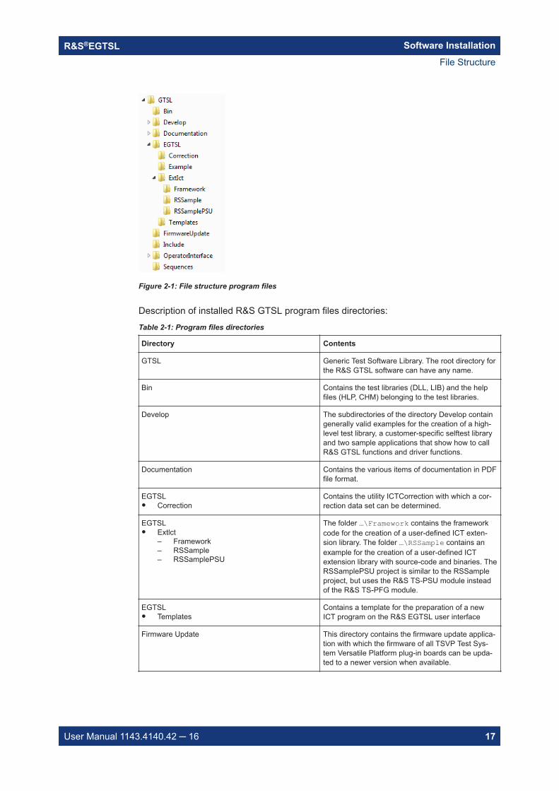
The test libraries supplied by ROHDE & SCHWARZ are stored in fixed directories atthe time of installation. The following directory structure can be found as subdirectoriesbelow the R&S GTSL program files directory which was specified during the installationprocess:
File Structure
Software InstallationR&S®EGTSL
17User Manual 1143.4140.42 16
Figure 2-1: File structure program files
Description of installed R&S GTSL program files directories:Table 2-1: Program files directories
Directory Contents
GTSL Generic Test Software Library. The root directory forthe R&S GTSL software can have any name.
Bin Contains the test libraries (DLL, LIB) and the helpfiles (HLP, CHM) belonging to the test libraries.
Develop The subdirectories of the directory Develop containgenerally valid examples for the creation of a high-level test library, a customer-specific selftest libraryand two sample applications that show how to callR&S GTSL functions and driver functions.
Documentation Contains the various items of documentation in PDFfile format.
EGTSL Correction
Contains the utility ICTCorrection with which a cor-rection data set can be determined.
EGTSL Extlct
– Framework– RSSample– RSSamplePSU
The folder …\Framework contains the frameworkcode for the creation of a user-defined ICT exten-sion library. The folder …\RSSample contains anexample for the creation of a user-defined ICTextension library with source-code and binaries. TheRSSamplePSU project is similar to the RSSampleproject, but uses the R&S TS-PSU module insteadof the R&S TS-PFG module.
EGTSL Templates
Contains a template for the preparation of a newICT program on the R&S EGTSL user interface
Firmware Update This directory contains the firmware update applica-tion with which the firmware of all TSVP Test Sys-tem Versatile Platform plug-in boards can be upda-ted to a newer version when available.
File Structure
Software InstallationR&S®EGTSL
18User Manual 1143.4140.42 16
Directory Contents
Include Contains the h-files (include files) needed for thedevelopment of new test libraries.
Operator Interface Contains the run time module for the operator inter-face of TestStand. A TestStand run time licence isrequired.
Sequences Contains the test sequence examples created byROHDE & SCHWARZ.
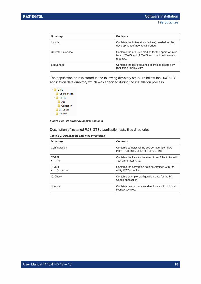
The application data is stored in the following directory structure below the R&S GTSLapplication data directory which was specified during the installation process.
Figure 2-2: File structure application data
Description of installed R&S GTSL application data files directories.Table 2-2: Application data files directories
Directory Contents
Configuration Contains samples of the two configuration filesPHYSICAL.INI and APPLICATION.INI.
EGTSL Atg
Contains the files for the execution of the AutomaticTest Generator ATG.
EGTSL Correction
Contains the correction data determined with theutility ICTCorrection.
IC-Check Contains example configuration data for the IC-Check application.
License Contains one or more subdirectories with optionallicense key files.
File Structure
Functional DescriptionR&S®EGTSL
19User Manual 1143.4140.42 16
3 Functional Description
3.1 General
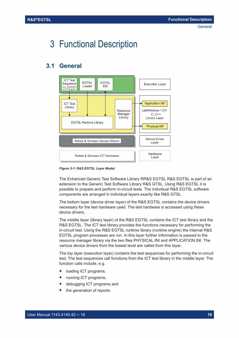
Figure 3-1: R&S EGTSL Layer Model
The Enhanced Generic Test Software Library RR&S EGTSL R&S EGTSL is part of anextension to the Generic Test Software Library R&S GTSL. Using R&S EGTSL it ispossible to prepare and perform in-circuit tests. The individual R&S EGTSL softwarecomponents are arranged in individual layers exactly like R&S GTSL.
The bottom layer (device driver layer) of the R&S EGTSL contains the device driversnecessary for the test hardware used. The test hardware is accessed using thesedevice drivers.
The middle layer (library layer) of the R&S EGTSL contains the ICT test library and theR&S EGTSL. The ICT test library provides the functions necessary for performing thein-circuit test. Using the R&S EGTSL runtime library (runtime engine) the internal R&SEGTSL program processes are run. In this layer further information is passed to theresource manager library via the two files PHYSICAL.INI and APPLICATION.INI. Thevarious device drivers from the lowest level are called from this layer.
The top layer (execution layer) contains the test sequences for performing the in-circuittest. The test sequences call functions from the ICT test library in the middle layer. Thefunction calls include, e.g.
loading ICT programs, running ICT programs, debugging ICT programs and the generation of reports.
General
Functional DescriptionR&S®EGTSL
20User Manual 1143.4140.42 16
The calls for the individual functions from the ICT test library can, e.g., be made usinga sequence editor (TestStand) or a dedicated C program.
The top layer (execution layer) also contains the R&S EGTSL Loader and the R&SEGTSL user interface (R&S EGTSL). The R&S EGTSL user interface (R&S EGTSL) isopened using the R&S EGTSL either by the R&S EGTSL Loader or a function call fromthe ICT test library.
Special test hardware is required for performing in-circuit tests. This hardware and thusthe individual test functions are called using the R&S GTSL/R&S EGTSL-typical func-tions in the test libraries.
For further information on R&S GTSL see “Software Description Generic Test SoftwareLibrary R&S GTSL”
R&S EGTSL includes the following parts and programs:
ICT runtime library ICT test library User interface ( IDE ) Loader Automatic Test Generator ATG (utility) ICT correction data (utility)
3.2 ICT Test Library
The following section provides a short overview of the test functions available in theICT test library.
The individual test functions and their parameters are described in the online help forthe ICT test library. The help files (.HLP) are in the folder ...\GTSL\BIN.
3.2.1 General
Starting with GTSL 3.30, no GTSL license is required.
Name of the dynamic link library (DLL): ICT.DLL
Name of the help file (HLP): ICT.HLP
ICT Test Library
Functional DescriptionR&S®EGTSL
21User Manual 1143.4140.42 16
License required R&S TS-LBAS and
R&S TS-LEGT or R&S TS-LEG2
Supported devices: R&S TS-PICT ICT Extension Module
R&S TS-PMB Matrix Module
R&S TS-PSAM Source and Measurement Module
R&S TS-PSU Power Supply / Load Module
R&S TS-PSU12 Power Supply / Load Module 12V
The in-circuit test library offers functions for the in-circuit test using the R&S EGTSLsoftware and the R&S TS-PSAM, R&S TS-PICT, R&S TS-PSU, R&S TS-PSU12 andR&S TS-PMB modules.
The functions allow to
load, run and debug ICT programs load limit files generate a report
3.2.2 Entries in PHYSICAL.INI
Section [device->...]
Keyword Value Description
Type String Mandatory entry
pict = R&S TS-PICT ICT Exten-sion Module
pmb = R&S TS-PMB Matrix Mod-ule
psam = R&S TS-PSAM Sourceand Measurement Module
psu = R&S TS-PSU Power Sup-ply/Load Module
psu12 = R&S TS-PSU12 PowerSupply/Load Module 12V
ResourceDesc String Mandatory entry
VISA resource descriptor in theform
PXI[segment number]::[devicenumber]::[function]::INSTR
CAN[board]::[controller]::[frame]::[slot]
ICT Test Library
Functional DescriptionR&S®EGTSL
22User Manual 1143.4140.42 16
Keyword Value Description
DriverPrefix String Mandatory entry
Prefix for the IVI driver functions,without underscore:
R&S TS-PICT : rspict
R&S TS-PMB : rspmb
R&S TS-PSAM : rspsam
R&S TS-PSU: rspsu
R&S TS-PSU12: rspsu
DriverDLL String Mandatory entry
File name of the driver DLL
R&S TS-PICT : rspict.dll
R&S TS-PMB : rspmb.dll
R&S TS-PSAM : rspsam.dll
R&S TS-PSU : rspsu.dll
R&S TS-PSU12 : rspsu.dll
DriverOption String Optional entry
Option string being passed to thedevice driver during theDriver_Init function. See theonline help file for the appropriatedevice driver.
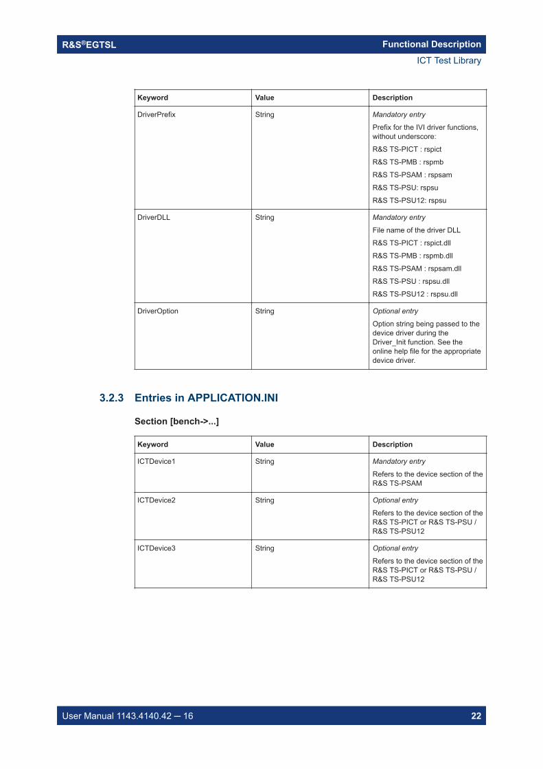
3.2.3 Entries in APPLICATION.INI
Section [bench->...]
Keyword Value Description
ICTDevice1 String Mandatory entry
Refers to the device section of theR&S TS-PSAM
ICTDevice2 String Optional entry
Refers to the device section of theR&S TS-PICT or R&S TS-PSU /R&S TS-PSU12
ICTDevice3 String Optional entry
Refers to the device section of theR&S TS-PICT or R&S TS-PSU /R&S TS-PSU12
ICT Test Library
Functional DescriptionR&S®EGTSL
23User Manual 1143.4140.42 16
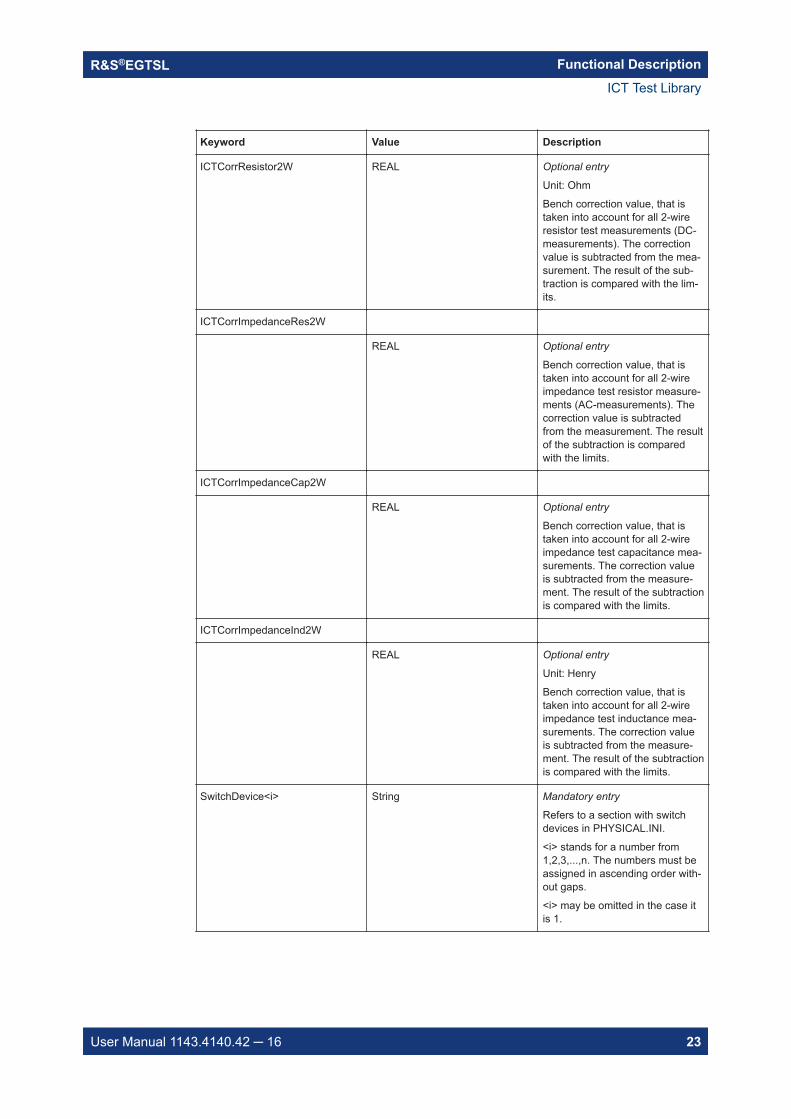
Keyword Value Description
ICTCorrResistor2W REAL Optional entry
Unit: Ohm
Bench correction value, that istaken into account for all 2-wireresistor test measurements (DC-measurements). The correctionvalue is subtracted from the mea-surement. The result of the sub-traction is compared with the lim-its.
ICTCorrImpedanceRes2W
REAL Optional entry
Bench correction value, that istaken into account for all 2-wireimpedance test resistor measure-ments (AC-measurements). Thecorrection value is subtractedfrom the measurement. The resultof the subtraction is comparedwith the limits.
ICTCorrImpedanceCap2W
REAL Optional entry
Bench correction value, that istaken into account for all 2-wireimpedance test capacitance mea-surements. The correction valueis subtracted from the measure-ment. The result of the subtractionis compared with the limits.
ICTCorrImpedanceInd2W
REAL Optional entry
Unit: Henry
Bench correction value, that istaken into account for all 2-wireimpedance test inductance mea-surements. The correction valueis subtracted from the measure-ment. The result of the subtractionis compared with the limits.
SwitchDevice<i> String Mandatory entry
Refers to a section with switchdevices in PHYSICAL.INI.
<i> stands for a number from1,2,3,...,n. The numbers must beassigned in ascending order with-out gaps.
<i> may be omitted in the case itis 1.
ICT Test Library
Functional DescriptionR&S®EGTSL
24User Manual 1143.4140.42 16
Keyword Value Description
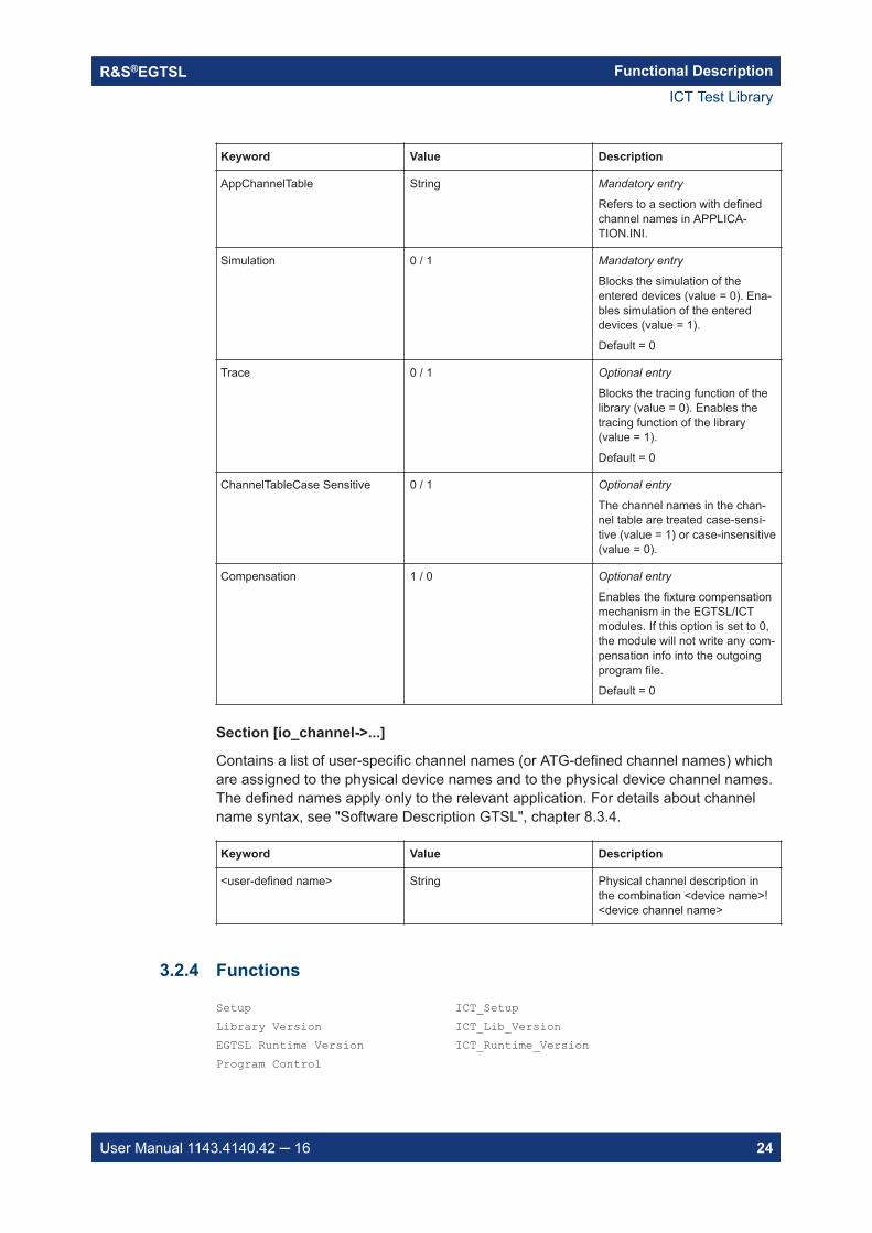
AppChannelTable String Mandatory entry
Refers to a section with definedchannel names in APPLICA-TION.INI.
Simulation 0 / 1 Mandatory entry
Blocks the simulation of theentered devices (value = 0). Ena-bles simulation of the entereddevices (value = 1).
Default = 0
Trace 0 / 1 Optional entry
Blocks the tracing function of thelibrary (value = 0). Enables thetracing function of the library(value = 1).
Default = 0
ChannelTableCase Sensitive 0 / 1 Optional entry
The channel names in the chan-nel table are treated case-sensi-tive (value = 1) or case-insensitive(value = 0).
Compensation 1 / 0 Optional entry
Enables the fixture compensationmechanism in the EGTSL/ICTmodules. If this option is set to 0,the module will not write any com-pensation info into the outgoingprogram file.
Default = 0
Section [io_channel->...]
Contains a list of user-specific channel names (or ATG-defined channel names) whichare assigned to the physical device names and to the physical device channel names.The defined names apply only to the relevant application. For details about channelname syntax, see "Software Description GTSL", chapter 8.3.4.
Keyword Value Description
<user-defined name> String Physical channel description inthe combination <device name>!<device channel name>
3.2.4 Functions
Setup ICT_SetupLibrary Version ICT_Lib_VersionEGTSL Runtime Version ICT_Runtime_VersionProgram Control
ICT Test Library
Functional DescriptionR&S®EGTSL
25User Manual 1143.4140.42 16
Load Program ICT_Load_Program Run Program ICT_Run_Program Debug Program ICT_Debug_Program Unload Program ICT_Unload_ProgramReport Generation Write Report to File ICT_Write_Report Load Detailed Report ICT_Load_Detailed_Report Get Detailed Report Entry ICT_Get_Detailed_Report_Entry Get Detailed Report Entry (Extended) ICT_Get_Detailed_Report_Entry_Ex Get TestStand Report Entry ICT_Get_TestStand_Report_Entry Transfer Report to QUOTIS ICT_Transfer_Quotis_ReportLimit Loader Load Limits ICT_Load_LimitsError Handling Get Error Log ICT_Get_Error_LogCleanup ICT_Cleanup
3.3 R&S EGTSL Loader
Using the R&S EGTSL Loader the R&S EGTSL user interface (R&S EGTSL IDE ) canbe opened directly. A function call from the ICT test library is not necessary.
The operation of the R&S EGTSL Loader is described in section 13.2.
3.4 R&S EGTSL user interface (R&S EGTSL IDE)
The R&S EGTSL user interface (R&S EGTSL IDE) for editing and debugging an ICTprogram is started either using a function from the ICT test library or using the R&SEGTSL Loader.
R&S EGTSL user interface (R&S EGTSL IDE)
Functional DescriptionR&S®EGTSL
26User Manual 1143.4140.42 16
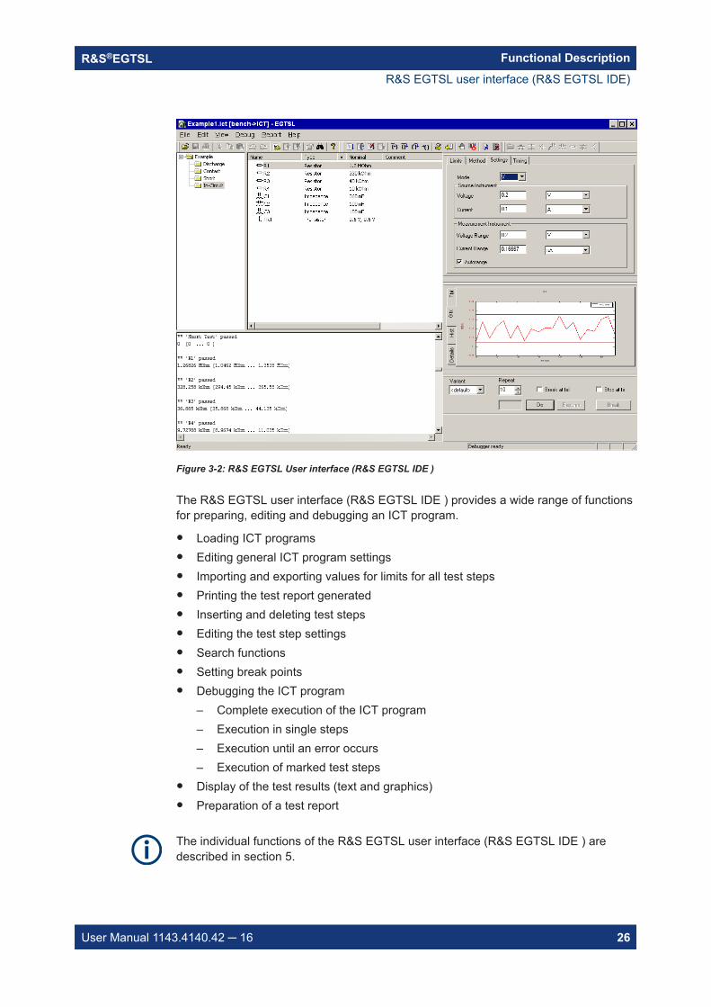
Figure 3-2: R&S EGTSL User interface (R&S EGTSL IDE )
The R&S EGTSL user interface (R&S EGTSL IDE ) provides a wide range of functionsfor preparing, editing and debugging an ICT program.
Loading ICT programs Editing general ICT program settings Importing and exporting values for limits for all test steps Printing the test report generated Inserting and deleting test steps Editing the test step settings Search functions Setting break points Debugging the ICT program
– Complete execution of the ICT program– Execution in single steps– Execution until an error occurs– Execution of marked test steps
Display of the test results (text and graphics) Preparation of a test report
The individual functions of the R&S EGTSL user interface (R&S EGTSL IDE ) aredescribed in section 5.
R&S EGTSL user interface (R&S EGTSL IDE)
Functional DescriptionR&S®EGTSL
27User Manual 1143.4140.42 16
3.5 Automatic Test Generator ATG
Using the Automatic Test Generator ATG utility, a circuit description and the descriptionof the test hardware available are used to generate an ICT program that will run in theEnhanced Generic Test Software Library R&S EGTSL. The ICT program generatedcan be opened in the R&S EGTSL user interface (R&S EGTSL IDE) and edited.
The individual functions of the Automatic Test Generator ATG are described in sec-tion 9.
3.6 ICT Correction Data
The test system is calibrated using the ICTCorrection utility. Resistances and capaci-tances in the system are determined and saved as correction data. Using this data, thevalues measured during the in-circuit test are corrected.
The individual functions of the ICTCorrection program are described in section 15.
3.7 Hardware for in-circuit test
To be able to perform an in-circuit test using R&S EGTSL the following test hardwaremust be available:
Test System Versatile Platform R&S CompactTSVP TS-PCA3 Test System Versatile Platform R&S PowerTSVP TS-PWA3 (alternative expansion) R&S TS-PSAM Source and Measurement Module R&S TS-PICT In-Circuit Test Module (alternative expansion for certain test meth-
ods) R&S TS-PSU Power Supply/Load Module / R&S TS-PSU12 Power Supply/Load
Module 12V (expansion for zener diode and transistor test methods). R&S TS-PMB Matrix Module B Test adapters developed and built especially for the Unit Under Test (UUT) and the
related test program
The precise composition and number of items of hardware is always dependent on thespecific project and the test methods required.
The individual components of test hardware are described in the related user manuals.
Hardware for in-circuit test
Getting StartedR&S®EGTSL
28User Manual 1143.4140.42 16
4 Getting Started
4.1 General
This section describes the development process for an in-circuit test in a step-by-stepmanner based on a simple example. The individual steps can be followed using theseinstructions so that you can rapidly become familiar with the Enhanced Generic TestSoftware Library R&S EGTSL.
The example circuit, the related BDL file and the files generated by the Automatic TestGenerator ATG are listed in appendix A. The related files are savedin ...\GTSL\EGTSL\Example.
4.2 Development Process for an In-circuit Test
Based on the (existing) circuit documents for a unit under test (for the in-circuit test theunit is generally a circuit board) an ICT program is to be prepared that can test whetherthe circuit board is correctly populated. The mechanical-electrical adaptation of the unitunder test to the test system, i.e. building a bed of nails adapter is also included.
The Enhanced Generic Test Software Library R&S EGTSL provides a series of utilitiesthat enable these tasks to be tackled largely automatically. Based on an example cir-cuit, the features provided by the software will be demonstrated.
To pass from the circuit documentation to the finished ICT program, the following stepsare necessary:
Preparation of the circuit documentation Entry of the circuit description Preparation of the test program by the Automatic Test Generator ATG Preparation of the adapter Commissioning and debugging the test program
4.3 Preparation of the Circuit Documentation
In the first step the test points, i.e. the pins on the bed of nails adapter, are entered onthe circuit diagram. As during the in-circuit test, every component is measured sepa-rately, it is important that the test system can make contact to every pin on every com-ponent. For this purpose, a test nail must be provided at every node of the circuit.
The names of the test points, also called nodes, appear later in the test program. Theymust therefore be clear, i.e. either refer to the function in the circuit (like INPUT, OUT-PUT) or to a component connected to the node (like TR1.B for the base of transistor
Preparation of the Circuit Documentation
Getting StartedR&S®EGTSL
29User Manual 1143.4140.42 16
TR1). Special rules apply for ground and supply voltage. The names of such test pointsmust always start with GND or VCC respectively, so that the automatic test generatorcan detect them as ground and supply voltage and treat them appropriately.
4.3.1 Example Circuit
Figure 4-1: Circuit example
Figure 4-1 shows the circuit for a low frequency amplifier stage. The names of the testpoints are already entered.
4.3.2 Preparation of the Circuit Description
For further processing in R&S EGTSL the circuit description for the circuit to be testedmust be available as a BDL file (see also section 8.2). There are now various ways youcan prepare the necessary BDL file.
1. Prepare the BDL file (circuit description) manually in a text editor based on the cir-cuit diagram.
2. Transfer the circuit description from a CAD system. Modern CAD systems for thepreparation of electronic circuits provide a feature for exporting the circuit descrip-tion. Using commercially available conversion software, the exported circuitdescription can be converted to the BDL format.
The manual preparation of the circuit description is of course tedious for larger circuits.Here it is best, if possible, to transfer the data from the CAD system. For the smallexample with only eight components, it is however easy to enter the BDL data by hand.
The BDL file is saved in ...\GTSL\EGTSL\Example\Example1.BDL.
Preparation of the Circuit Documentation
Getting StartedR&S®EGTSL
30User Manual 1143.4140.42 16
4.3.2.1 Entry of the Resistors
BDL example for resistor R1
RESISTOR
NAME 'R1' PART_ID '1234.5678.90' VALUE 1.2 MOHM TOL+ 10% TOL- 10% I_LIM 100.0 MA PIN_1 'VCC' PIN_2 'TR1.B' ERR_MSG 'Problem with R1'
The following information on a resistor must be entered in the text editor:
NAME Component name
PART_ID Optional component identifier for the component
VALUE Nominal value and unit for the component
TOL+ Positive component tolerance in % (default value 10%)
TOL- Negative component tolerance in % (default value10 %)
I_LIMIT Maximum measuring current for determining thevalue with unit (default value 100 mA)
PIN_1 Test point 1 for the component
PIN_2 Test point 2 for the component
ERR_MSG Optional error text The text entered here is dis-played in the report if the component has beendetected as faulty.
For the example circuit, all resistors must be entered in the same manner:
Name Value Pin 1 Pin 2
R1 1.2 MOHM VCC TR1.B
R2 330 KOHM TR1.B GND
R3 40 KOHM VCC TR1.C
R4 10 KOHM TR1.E GND
4.3.2.2 Entry of Capacitors
BDL example for capacitor C1
CAPACITOR
Preparation of the Circuit Documentation
Getting StartedR&S®EGTSL
31User Manual 1143.4140.42 16
NAME 'C1' PART_ID '0987.6543.21' VALUE 360 NF TOL+ 10% TOL- 10% PIN_1 'INPUT' PIN_2 'TR1.B' ERR_MSG 'Problem with C1'
The following information on a capacitor must be entered in the text editor:
NAME Component name
PART_ID Optional component identifier for the component
VALUE Nominal value and unit for the component
TOL+ Positive component tolerance in % (default value 10%)
TOL- Negative component tolerance in % (default value10 %)
PIN_1 Test point 1 for the component
PIN_2 Test point 2 for the component
ERR_MSG Optional error text The text entered here is dis-played in the report if the component has beendetected as faulty.
For the example circuit, all capacitors must be entered in the same manner:
Name Value Pin 1 Pin 2
C1 360 NF INPUT TR1.B
C2 100 NF TR1.C OUTPUT
When entering electrolytic capacitors, attention must be paid to two special aspects:the unit microfarad is identified using a “U”. The positive pole is termed pin A (=anode), the minus pole as pin C (=cathode).
BDL example for capacitor C3 (electrolytic)
POL_CAP
NAME 'C3' PART_ID 'C300.4711' VALUE 100 UF TOL+ 10% TOL- 10% PIN_A 'TR1.E' PIN_C 'GND' ERR_MSG 'Problem with C3'
Preparation of the Circuit Documentation
Getting StartedR&S®EGTSL
32User Manual 1143.4140.42 16
Name Value Pin A Pin C
C3 100 UF TR1.E GND
4.3.2.3 Entry of the Transistor
BDL example for transistor T1
TRANSISTOR
NAME 'TR1' PART_ID 'T1000' NPN UBE 0.6 V TOL+ 30% TOL- 30% I_LIM 100.0 MA PIN_E 'TR1.E' PIN_B 'TR1.B' PIN_C 'TR1.C' ERR_MSG 'Problem with T1'
The following information on a transistor must be edited in a text editor:
NAME Component name
PART_ID Optional component identifier for the component
NPN, PNP Type of transistor
UBE Base-emitter voltage of the transistor in the forwardbias region
TOL+ Positive component tolerance in %
TOL- Negative component tolerance in %
I_LIMIT Maximum measuring current for determining thevalue with unit (default value 100 mA)
PIN_E Test point for the transistor's emitter
PIN_B Test point for the transistor's base
PIN_C Test point for the transistor's collector
ERR_MSG Optional error text The text entered here is dis-played in the report if the component has beendetected as faulty.
Name Type Pin E Pin B Pin C
TR1 N TR1.E TR1.B TR1.C
Preparation of the Circuit Documentation
Getting StartedR&S®EGTSL
33User Manual 1143.4140.42 16
4.4 Preparing the ICT program
Once the circuit description is available as a BDL file, an ICT program can be preparedwith the aid of the Automatic Test Generator ATG.
The Automatic Test Generator ATG is described in section 9.2.
Start the Automatic Test Generator ATG using Start-> Programs -> GTSL -> Automatic Test Genera-tor.
The following files must be entered in the ATG:
Example1.BDLpath and file name for the BDL file (circuit description)
Example_Physical.INIpath and file name for the Physical Layer Configuration File (hardware descriptionof the test system)
Following the automatic generation process, the ATG prepares the following files:
Example1_Report.TXTreport with the data on the generation processAny errors that have occurred during the generation process are indicated in thereport using error messages and warning messages (see section 9.3.2.1). Onlywhen there are no error messages or warning messages is the ICT program pre-pared. In addition, the alternative suggestions (proposals) made by the ATG are tobe noted (see section 9.3.2.2).
Example1.ICTICT program for execution in R&S EGTSLThe layout of the automatically generated ICT program is defined by a structureanchored in the ATG. In principle, the fully generated test program has the follow-ing layout:– Capacitor discharging (Discharge)– Contact test (Contact)– Continuity and short-circuit test (Short)– Group of analog tests (In-Circuit)
Example1_Application.INIApplication Layer Configuration File for the execution of the ICT program gener-ated in R&S EGTSLIn the Application Layer Configuration File, the specific information for the usage ofthe hardware is compiled by the ATG for the ICT program generated. On the exe-cution of the ICT program, the name of the Application Layer Configuration Filegenerated must be given.
Example1.ICC
Preparing the ICT program
Getting StartedR&S®EGTSL
34User Manual 1143.4140.42 16
ICC program for execution with IC-Check program. See Chapter 9.3.5, "ICC Pro-gram", on page 194 and "Software Description IC-Check" for details.
4.5 Adapter Manufacture
In the Application Layer Configuration File generated by the Automatic Test GeneratorATG, an I/O channel on the R&S TS-PMB Matrix Module B is allocated to each testpoint (node) of the circuit.
Example:
[io_channel->ICT]GND = PMB1!P1INPUT = PMB1!P2OUTPUT = PMB1!P3TR1.B = PMB1!P4TR1.C = PMB1!P5TR1.E = PMB1!P6VCC = PMB1!P7
[io_wiring->ICT]GND = F1 S15 X10A1INPUT = F1 S15 X10A2OUTPUT = F1 S15 X10A3TR1.B = F1 S15 X10A4TR1.C = F1 S15 X10A5TR1.E = F1 S15 X10A6VCC = F1 S15 X10A7
This information can be used for the manufacture of the adapter.
4.6 Commissioning and Debugging
The newly prepared ICT program is now, together with the finished adapter, ready touse. However, correct operation should first be checked on a few circuit boards. It maybe necessary to slightly change test value limits or adjust settings.
The user interface for R&S EGTSL ( R&S EGTSL IDE ) for debugging (and executing)ICT programs can be started in two ways:
1. Start the user interface from a test sequence using a function call from the ICT testlibrary (see section 13.1)
2. Start the user interface using the Loader (see section 13.2)
Commissioning and Debugging
Getting StartedR&S®EGTSL
35User Manual 1143.4140.42 16
Figure 4-2: R&S EGTSL User Interface (R&S EGTSL IDE)
When starting the R&S EGTSL IDE from a test sequence, the ICT program is automat-ically opened with the corresponding bench. When starting the R&S EGTSL IDE usingthe R&S EGTSL Loader, the ICT program must be opened manually using the menucommand File -> Open. When opening the ICT file, the corresponding bench for exe-cuting the ICT program must be entered.
Modifications can be made to the ICT program in the various windows of the user inter-face. When the debugger is activated, various types of program execution are possi-ble:
Complete execution of the ICT program Execution in single steps Execution until an error occurs Execution of marked test steps
The various windows, menu commands and buttons on the R&S EGTSL user interface(R&S EGTSL IDE ) are described in section 5. The detailed procedure for debuggingICT programs is described in section 15.
As the example circuit will probable not be built and an adapter has not been pro-duced, the ICT program can only be tested and debugged in the simulation mode. Forthis purpose it is necessary to activate the simulation in the Application Layer Configu-ration File in the section [bench->...].
Commissioning and Debugging
Getting StartedR&S®EGTSL
36User Manual 1143.4140.42 16
[bench->ICT]Description = ICT bench (Simulation)Simulation = 1Trace = 0ICTDevice1 = device->psamICTDevice2 = device->pictSwitchDevice1 = device->pmb1AppChannelTable = io_channel->ICT
When the ICT program is opened with the corresponding bench, all functions in theICT program and the R&S EGTSL user interface can be executed in the simulationmode.
Commissioning and Debugging
User Interface (R&S EGTSL IDE)R&S®EGTSL
37User Manual 1143.4140.42 16
5 User Interface (R&S EGTSL IDE)
5.1 General
The EGTSL debugging environment has the familiar look of modern Windows applica-tions.
With this graphical user interface, you can quickly master the full spectrum of function-ality. There is no need to learn a special programming language or work with a prede-fined screen layout. Test engineers can create their own desktop and display allrequired information on one screen. They can scale, move, and display the windows asneeded.
Within the EGTSL debugging environment, you can do the following:
Create, delete or move test steps by a mouse click or drag and drop Change settings of test steps, e.g. limits, test method, stimuli and measurement Define specific timing models Use functionalities such as setting breakpoints, step into or over certain test steps Define and handle different variants Export and import limits Use statistical tools such as histograms to verify stable results Display a detailed test report.
To operate the Enhanced Generic Test Software Library R&S EGTSL, basic skills inthe usage of the Microsoft Windows operating systems are required.
General
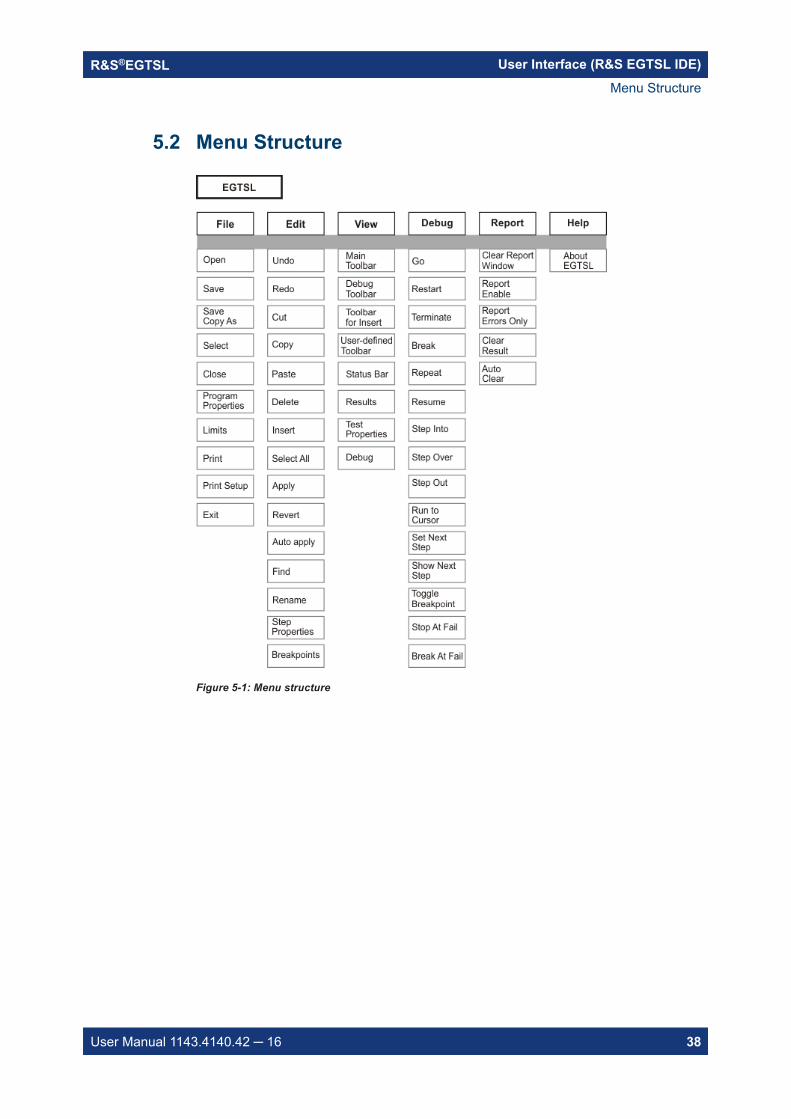
User Interface (R&S EGTSL IDE)R&S®EGTSL
38User Manual 1143.4140.42 16
5.2 Menu Structure
Figure 5-1: Menu structure
Menu Structure
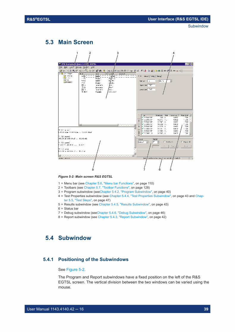
User Interface (R&S EGTSL IDE)R&S®EGTSL
39User Manual 1143.4140.42 16
5.3 Main Screen
Figure 5-2: Main screen R&S EGTSL
1 = Menu bar (see Chapter 5.6, "Menu bar Functions", on page 110)2 = Toolbars (see Chapter 5.7, "Toolbar Functions", on page 128)3 = Program subwindow (seeChapter 5.4.2, "Program Subwindow", on page 40)4 = Test Properties subwindow (see Chapter 5.4.4, "Test Properties Subwindow", on page 43 and Chap-
ter 5.5, "Test Steps", on page 47)5 = Results subwindow (see Chapter 5.4.5, "Results Subwindow", on page 43)6 = Status bar7 = Debug subwindow (seeChapter 5.4.6, "Debug Subwindow", on page 46)8 = Report subwindow (see Chapter 5.4.3, "Report Subwindow", on page 42)
5.4 Subwindow
5.4.1 Positioning of the Subwindows
See Figure 5-2.
The Program and Report subwindows have a fixed position on the left of the R&SEGTSL screen. The vertical division between the two windows can be varied using themouse.
Subwindow
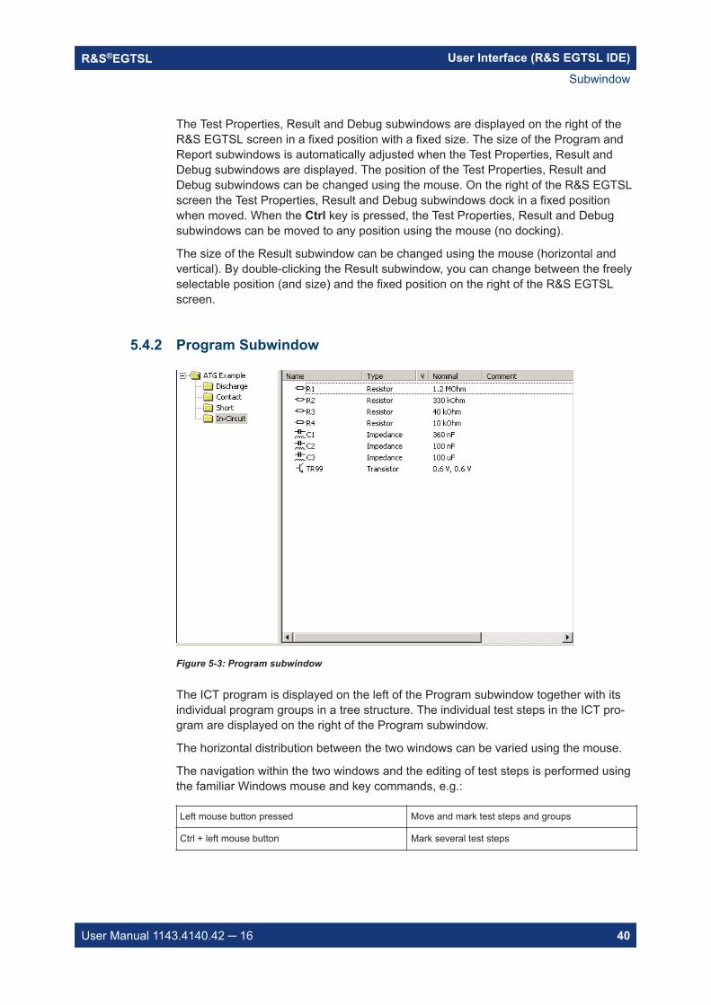
User Interface (R&S EGTSL IDE)R&S®EGTSL
40User Manual 1143.4140.42 16
The Test Properties, Result and Debug subwindows are displayed on the right of theR&S EGTSL screen in a fixed position with a fixed size. The size of the Program andReport subwindows is automatically adjusted when the Test Properties, Result andDebug subwindows are displayed. The position of the Test Properties, Result andDebug subwindows can be changed using the mouse. On the right of the R&S EGTSLscreen the Test Properties, Result and Debug subwindows dock in a fixed positionwhen moved. When the Ctrl key is pressed, the Test Properties, Result and Debugsubwindows can be moved to any position using the mouse (no docking).
The size of the Result subwindow can be changed using the mouse (horizontal andvertical). By double-clicking the Result subwindow, you can change between the freelyselectable position (and size) and the fixed position on the right of the R&S EGTSLscreen.
5.4.2 Program Subwindow
Figure 5-3: Program subwindow
The ICT program is displayed on the left of the Program subwindow together with itsindividual program groups in a tree structure. The individual test steps in the ICT pro-gram are displayed on the right of the Program subwindow.
The horizontal distribution between the two windows can be varied using the mouse.
The navigation within the two windows and the editing of test steps is performed usingthe familiar Windows mouse and key commands, e.g.:
Left mouse button pressed Move and mark test steps and groups
Ctrl + left mouse button Mark several test steps
Subwindow
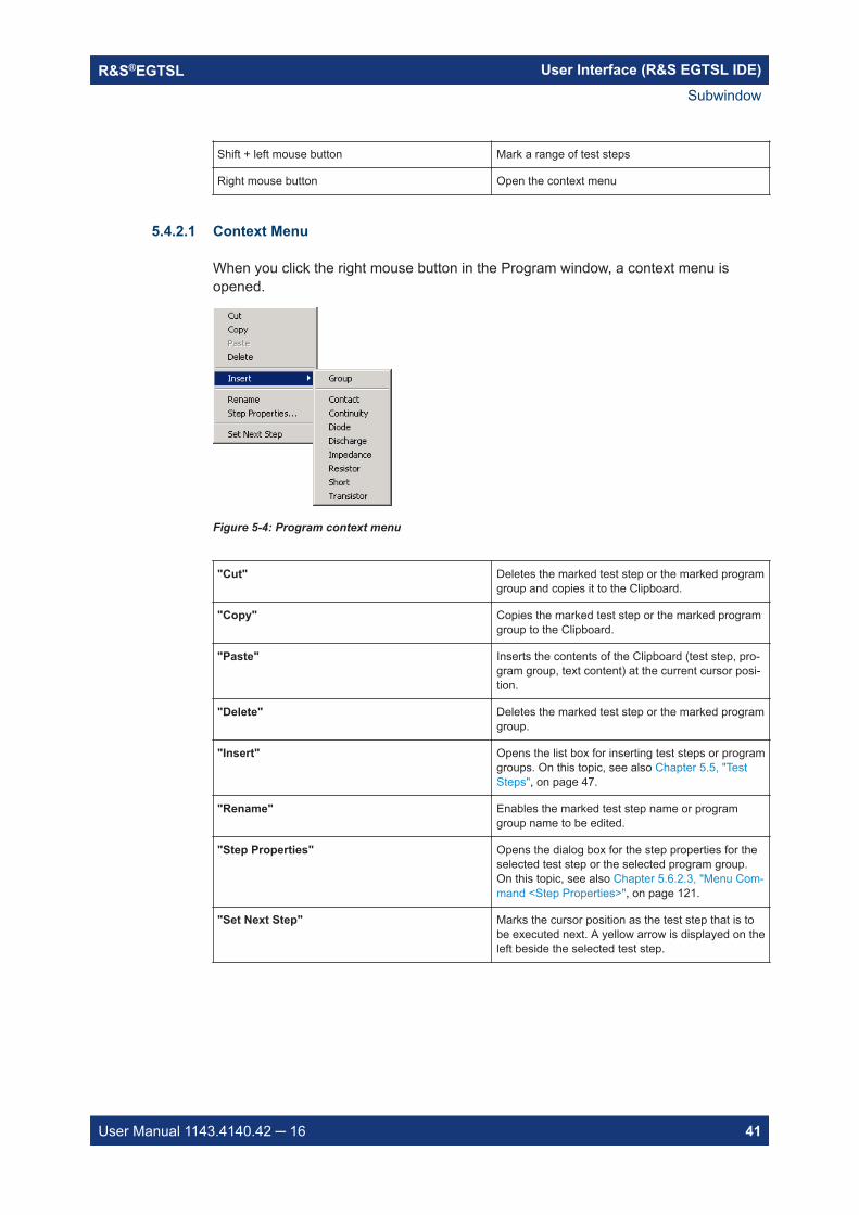
User Interface (R&S EGTSL IDE)R&S®EGTSL
41User Manual 1143.4140.42 16
Shift + left mouse button Mark a range of test steps
Right mouse button Open the context menu
5.4.2.1 Context Menu
When you click the right mouse button in the Program window, a context menu isopened.
Figure 5-4: Program context menu
"Cut" Deletes the marked test step or the marked programgroup and copies it to the Clipboard.
"Copy" Copies the marked test step or the marked programgroup to the Clipboard.
"Paste" Inserts the contents of the Clipboard (test step, pro-gram group, text content) at the current cursor posi-tion.
"Delete" Deletes the marked test step or the marked programgroup.
"Insert" Opens the list box for inserting test steps or programgroups. On this topic, see also Chapter 5.5, "TestSteps", on page 47.
"Rename" Enables the marked test step name or programgroup name to be edited.
"Step Properties" Opens the dialog box for the step properties for theselected test step or the selected program group.On this topic, see also Chapter 5.6.2.3, "Menu Com-mand <Step Properties>", on page 121.
"Set Next Step" Marks the cursor position as the test step that is tobe executed next. A yellow arrow is displayed on theleft beside the selected test step.
Subwindow
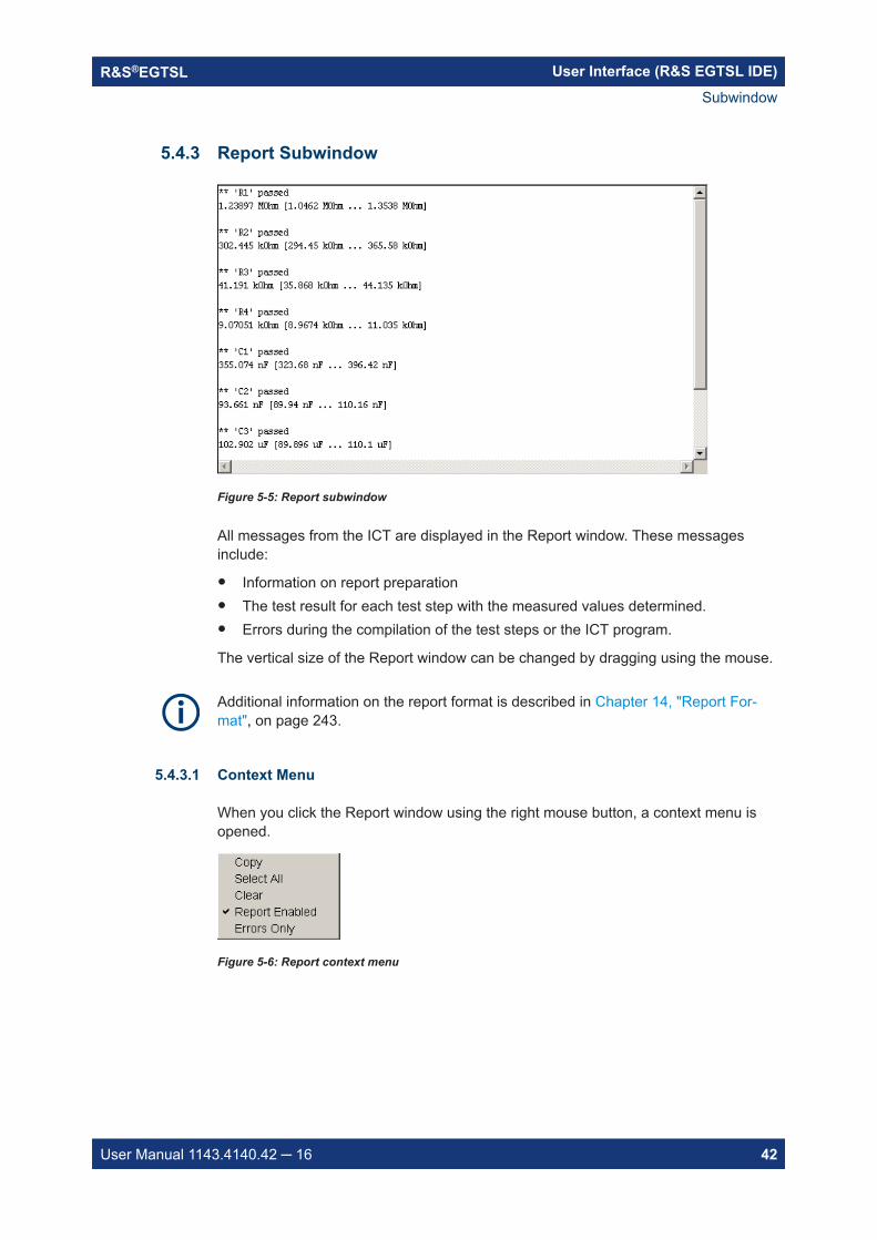
User Interface (R&S EGTSL IDE)R&S®EGTSL
42User Manual 1143.4140.42 16
5.4.3 Report Subwindow
Figure 5-5: Report subwindow
All messages from the ICT are displayed in the Report window. These messagesinclude:
Information on report preparation The test result for each test step with the measured values determined. Errors during the compilation of the test steps or the ICT program.
The vertical size of the Report window can be changed by dragging using the mouse.
Additional information on the report format is described in Chapter 14, "Report For-mat", on page 243.
5.4.3.1 Context Menu
When you click the Report window using the right mouse button, a context menu isopened.
Figure 5-6: Report context menu
Subwindow
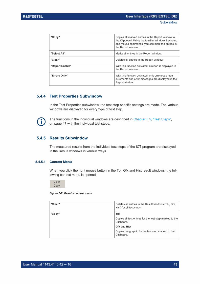
User Interface (R&S EGTSL IDE)R&S®EGTSL
43User Manual 1143.4140.42 16
"Copy" Copies all marked entries in the Report window tothe Clipboard. Using the familiar Windows keyboardand mouse commands, you can mark the entries inthe Report window.
"Select All" Marks all entries in the Report window.
"Clear" Deletes all entries in the Report window.
"Report Enable" With this function activated, a report is displayed inthe Report window.
"Errors Only" With this function activated, only erroneous mea-surements and error messages are displayed in theReport window.
5.4.4 Test Properties Subwindow
In the Test Properties subwindow, the test step-specific settings are made. The variouswindows are displayed for every type of test step.
The functions in the individual windows are described in Chapter 5.5, "Test Steps",on page 47 with the individual test steps.
5.4.5 Results Subwindow
The measured results from the individual test steps of the ICT program are displayedin the Result windows in various ways.
5.4.5.1 Context Menu
When you click the right mouse button in the Tbl, Gfx and Hist result windows, the fol-lowing context menu is opened.
Figure 5-7: Results context menu
"Clear" Deletes all entries in the Result windows (Tbl, Gfx,Hist) for all test steps.
"Copy" TblCopies all test entries for the test step marked to theClipboard.
Gfx and HistCopies the graphic for the test step marked to theClipboard.
Subwindow
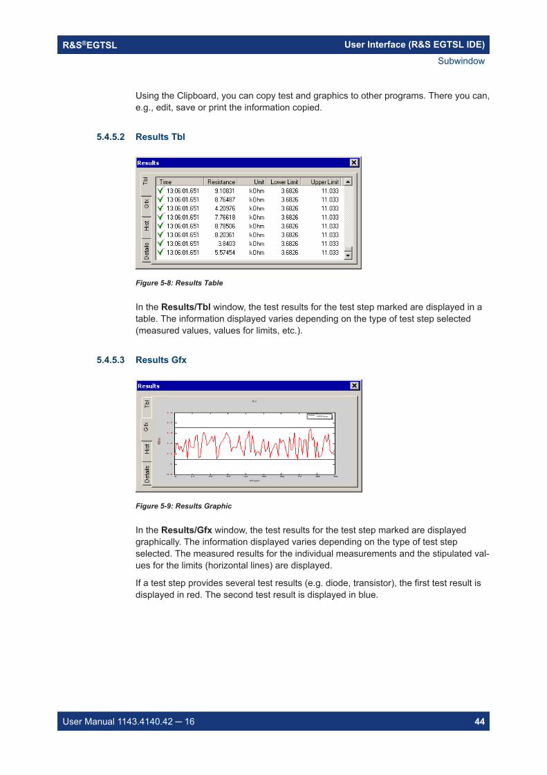
User Interface (R&S EGTSL IDE)R&S®EGTSL
44User Manual 1143.4140.42 16
Using the Clipboard, you can copy test and graphics to other programs. There you can,e.g., edit, save or print the information copied.
5.4.5.2 Results Tbl
Figure 5-8: Results Table
In the Results/Tbl window, the test results for the test step marked are displayed in atable. The information displayed varies depending on the type of test step selected(measured values, values for limits, etc.).
5.4.5.3 Results Gfx
Figure 5-9: Results Graphic
In the Results/Gfx window, the test results for the test step marked are displayedgraphically. The information displayed varies depending on the type of test stepselected. The measured results for the individual measurements and the stipulated val-ues for the limits (horizontal lines) are displayed.
If a test step provides several test results (e.g. diode, transistor), the first test result isdisplayed in red. The second test result is displayed in blue.
Subwindow
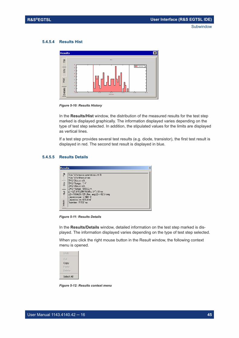
User Interface (R&S EGTSL IDE)R&S®EGTSL
45User Manual 1143.4140.42 16
5.4.5.4 Results Hist
Figure 5-10: Results History
In the Results/Hist window, the distribution of the measured results for the test stepmarked is displayed graphically. The information displayed varies depending on thetype of test step selected. In addition, the stipulated values for the limits are displayedas vertical lines.
If a test step provides several test results (e.g. diode, transistor), the first test result isdisplayed in red. The second test result is displayed in blue.
5.4.5.5 Results Details
Figure 5-11: Results Details
In the Results/Details window, detailed information on the test step marked is dis-played. The information displayed varies depending on the type of test step selected.
When you click the right mouse button in the Result window, the following contextmenu is opened.
Figure 5-12: Results context menu
Subwindow
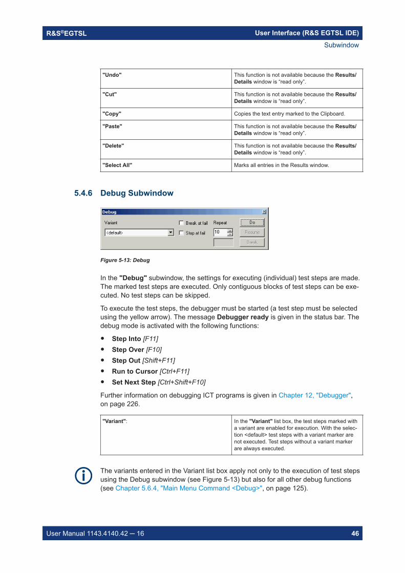
User Interface (R&S EGTSL IDE)R&S®EGTSL
46User Manual 1143.4140.42 16
"Undo" This function is not available because the Results/Details window is “read only”.
"Cut" This function is not available because the Results/Details window is “read only”.
"Copy" Copies the text entry marked to the Clipboard.
"Paste" This function is not available because the Results/Details window is “read only”.
"Delete" This function is not available because the Results/Details window is “read only”.
"Select All" Marks all entries in the Results window.
5.4.6 Debug Subwindow
Figure 5-13: Debug
In the "Debug" subwindow, the settings for executing (individual) test steps are made.The marked test steps are executed. Only contiguous blocks of test steps can be exe-cuted. No test steps can be skipped.
To execute the test steps, the debugger must be started (a test step must be selectedusing the yellow arrow). The message Debugger ready is given in the status bar. Thedebug mode is activated with the following functions:
Step Into [F11] Step Over [F10] Step Out [Shift+F11] Run to Cursor [Ctrl+F11] Set Next Step [Ctrl+Shift+F10]
Further information on debugging ICT programs is given in Chapter 12, "Debugger",on page 226.
"Variant": In the "Variant" list box, the test steps marked witha variant are enabled for execution. With the selec-tion <default> test steps with a variant marker arenot executed. Test steps without a variant markerare always executed.
The variants entered in the Variant list box apply not only to the execution of test stepsusing the Debug subwindow (see Figure 5-13) but also for all other debug functions(see Chapter 5.6.4, "Main Menu Command <Debug>", on page 125).
Subwindow
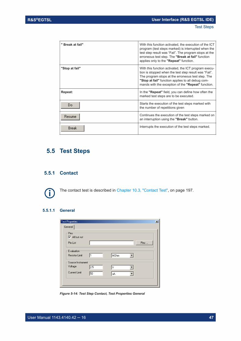
User Interface (R&S EGTSL IDE)R&S®EGTSL
47User Manual 1143.4140.42 16
" Break at fail" With this function activated, the execution of the ICTprogram (test steps marked) is interrupted when thetest step result was “Fail”. The program stops at theerroneous test step. The "Break at fail" functionapplies only to the "Repeat" function.
"Stop at fail" With this function activated, the ICT program execu-tion is stopped when the test step result was “Fail”.The program stops at the erroneous test step. The"Stop at fail" function applies to all debug com-mands with the exception of the "Repeat" function.
Repeat: In the "Repeat" field, you can define how often themarked test steps are to be executed.
Starts the execution of the test steps marked withthe number of repetitions given
Continues the execution of the test steps marked onan interruption using the "Break" button.
Interrupts the execution of the test steps marked.
5.5 Test Steps
5.5.1 Contact
The contact test is described in Chapter 10.3, "Contact Test", on page 197.
5.5.1.1 General
Figure 5-14: Test Step Contact, Test Properties General
Test Steps
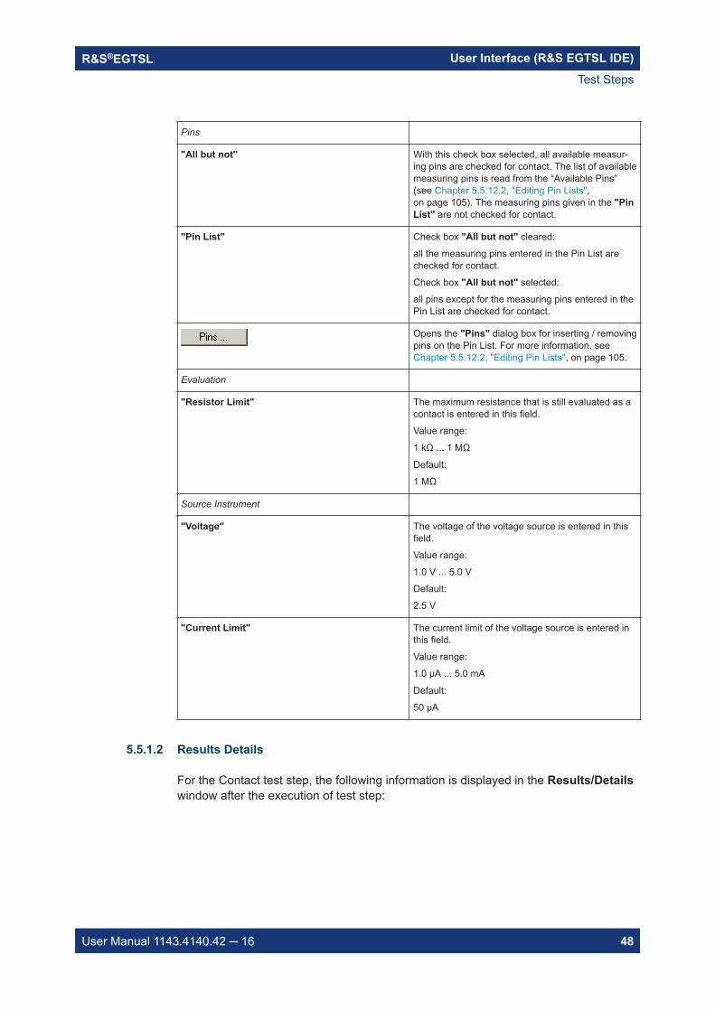
User Interface (R&S EGTSL IDE)R&S®EGTSL
48User Manual 1143.4140.42 16
Pins
"All but not" With this check box selected, all available measur-ing pins are checked for contact. The list of availablemeasuring pins is read from the “Available Pins”(see Chapter 5.5.12.2, "Editing Pin Lists",on page 105). The measuring pins given in the "PinList" are not checked for contact.
"Pin List" Check box "All but not" cleared:
all the measuring pins entered in the Pin List arechecked for contact.
Check box "All but not" selected:
all pins except for the measuring pins entered in thePin List are checked for contact.
Opens the "Pins" dialog box for inserting / removingpins on the Pin List. For more information, seeChapter 5.5.12.2, "Editing Pin Lists", on page 105.
Evaluation
"Resistor Limit" The maximum resistance that is still evaluated as acontact is entered in this field.
Value range:
1 kΩ ... 1 MΩ
Default:
1 MΩ
Source Instrument
"Voltage" The voltage of the voltage source is entered in thisfield.
Value range:
1.0 V ... 5.0 V
Default:
2.5 V
"Current Limit" The current limit of the voltage source is entered inthis field.
Value range:
1.0 µA ... 5.0 mA
Default:
50 µA
5.5.1.2 Results Details
For the Contact test step, the following information is displayed in the Results/Detailswindow after the execution of test step:
Test Steps
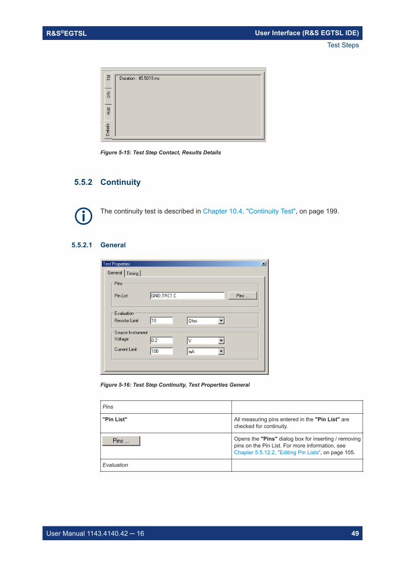
User Interface (R&S EGTSL IDE)R&S®EGTSL
49User Manual 1143.4140.42 16
Figure 5-15: Test Step Contact, Results Details
5.5.2 Continuity
The continuity test is described in Chapter 10.4, "Continuity Test", on page 199.
5.5.2.1 General
Figure 5-16: Test Step Continuity, Test Properties General
Pins
"Pin List" All measuring pins entered in the "Pin List" arechecked for continuity.
Opens the "Pins" dialog box for inserting / removingpins on the Pin List. For more information, seeChapter 5.5.12.2, "Editing Pin Lists", on page 105.
Evaluation
Test Steps
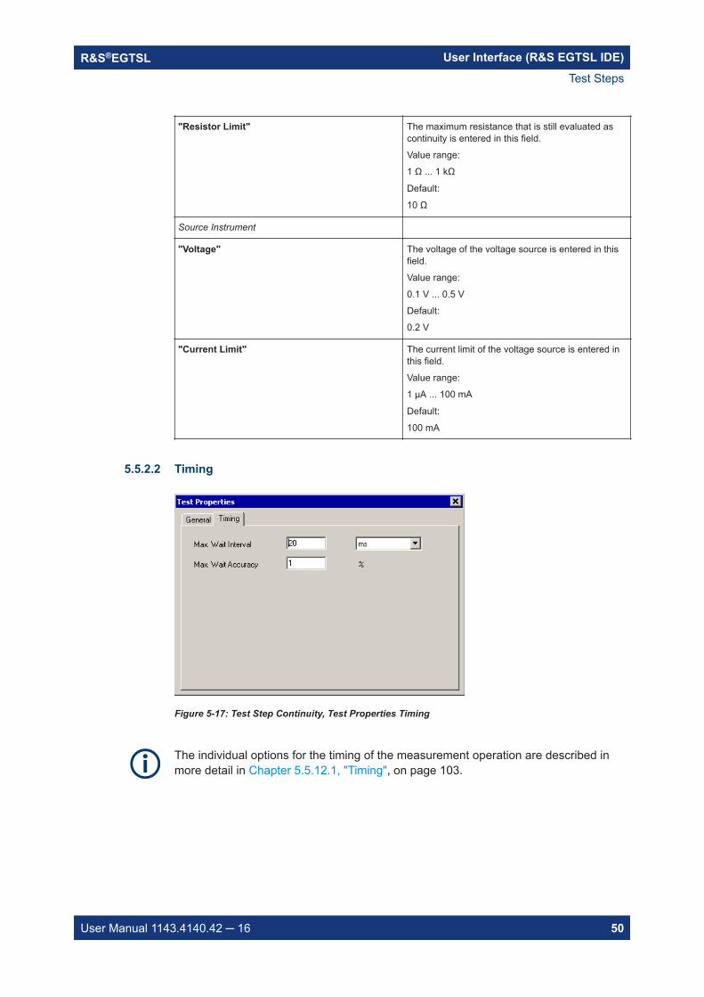
User Interface (R&S EGTSL IDE)R&S®EGTSL
50User Manual 1143.4140.42 16
"Resistor Limit" The maximum resistance that is still evaluated ascontinuity is entered in this field.
Value range:
1 Ω ... 1 kΩ
Default:
10 Ω
Source Instrument
"Voltage" The voltage of the voltage source is entered in thisfield.
Value range:
0.1 V ... 0.5 V
Default:
0.2 V
"Current Limit" The current limit of the voltage source is entered inthis field.
Value range:
1 µA ... 100 mA
Default:
100 mA
5.5.2.2 Timing
Figure 5-17: Test Step Continuity, Test Properties Timing
The individual options for the timing of the measurement operation are described inmore detail in Chapter 5.5.12.1, "Timing", on page 103.
Test Steps
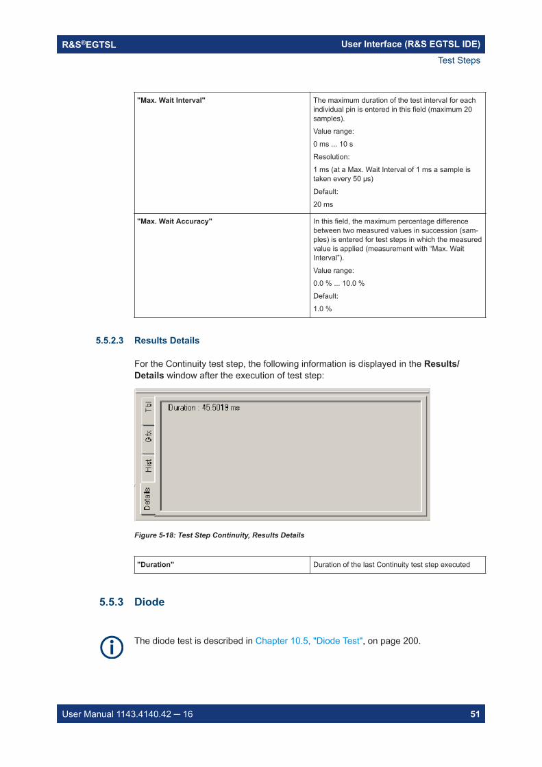
User Interface (R&S EGTSL IDE)R&S®EGTSL
51User Manual 1143.4140.42 16
"Max. Wait Interval" The maximum duration of the test interval for eachindividual pin is entered in this field (maximum 20samples).
Value range:
0 ms ... 10 s
Resolution:
1 ms (at a Max. Wait Interval of 1 ms a sample istaken every 50 μs)
Default:
20 ms
"Max. Wait Accuracy" In this field, the maximum percentage differencebetween two measured values in succession (sam-ples) is entered for test steps in which the measuredvalue is applied (measurement with “Max. WaitInterval”).
Value range:
0.0 % ... 10.0 %
Default:
1.0 %
5.5.2.3 Results Details
For the Continuity test step, the following information is displayed in the Results/Details window after the execution of test step:
Figure 5-18: Test Step Continuity, Results Details
"Duration" Duration of the last Continuity test step executed
5.5.3 Diode
The diode test is described in Chapter 10.5, "Diode Test", on page 200.
Test Steps
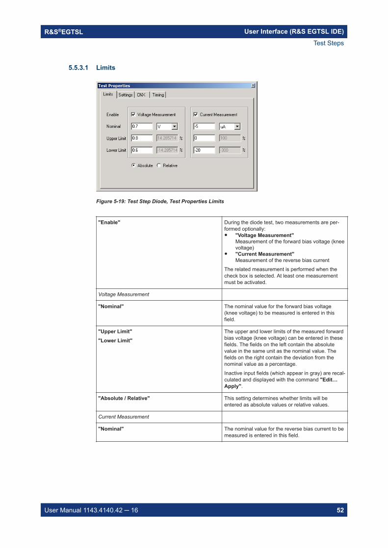
User Interface (R&S EGTSL IDE)R&S®EGTSL
52User Manual 1143.4140.42 16
5.5.3.1 Limits
Figure 5-19: Test Step Diode, Test Properties Limits
"Enable" During the diode test, two measurements are per-formed optionally: "Voltage Measurement"
Measurement of the forward bias voltage (kneevoltage)
"Current Measurement"Measurement of the reverse bias current
The related measurement is performed when thecheck box is selected. At least one measurementmust be activated.
Voltage Measurement
"Nominal" The nominal value for the forward bias voltage(knee voltage) to be measured is entered in thisfield.
"Upper Limit""Lower Limit"
The upper and lower limits of the measured forwardbias voltage (knee voltage) can be entered in thesefields. The fields on the left contain the absolutevalue in the same unit as the nominal value. Thefields on the right contain the deviation from thenominal value as a percentage.
Inactive input fields (which appear in gray) are recal-culated and displayed with the command "Edit…Apply".
"Absolute / Relative" This setting determines whether limits will beentered as absolute values or relative values.
Current Measurement
"Nominal" The nominal value for the reverse bias current to bemeasured is entered in this field.
Test Steps
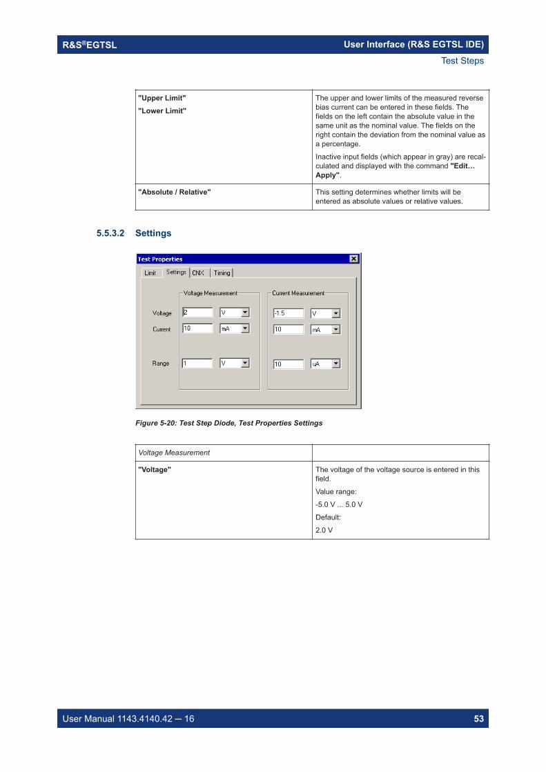
User Interface (R&S EGTSL IDE)R&S®EGTSL
53User Manual 1143.4140.42 16
"Upper Limit""Lower Limit"
The upper and lower limits of the measured reversebias current can be entered in these fields. Thefields on the left contain the absolute value in thesame unit as the nominal value. The fields on theright contain the deviation from the nominal value asa percentage.
Inactive input fields (which appear in gray) are recal-culated and displayed with the command "Edit…Apply".
"Absolute / Relative" This setting determines whether limits will beentered as absolute values or relative values.
5.5.3.2 Settings
Figure 5-20: Test Step Diode, Test Properties Settings
Voltage Measurement
"Voltage" The voltage of the voltage source is entered in thisfield.
Value range:
-5.0 V ... 5.0 V
Default:
2.0 V
Test Steps
User Interface (R&S EGTSL IDE)R&S®EGTSL
54User Manual 1143.4140.42 16
"Current" The current limit of the voltage source is entered inthis field.
Value range:
1.0 A ... 100 mA
Default:
10 mA
"Range" The measuring range of the voltmeter is entered inthis field.
Value range:
10 mV ... 5.0 V
Default:
1.0 V
Current Measurement
"Voltage" The voltage of the voltage source is entered in thisfield.
Value range:
-5.0 V ... 5.0 V
Default:
-1.5 V
"Current" The current limit of the voltage source is entered inthis field.
Value range:
1.0 µA ... 100.0 mA
Default:
10 mA
"Range" The measuring range of the current meter is enteredin this field.
Value range:
0.0 µA ... 200 mA
Default:
10.0 µA
Test Steps
User Interface (R&S EGTSL IDE)R&S®EGTSL
55User Manual 1143.4140.42 16
5.5.3.3 CNX
Figure 5-21: Test Step Diode, Test Properties CNX
"Pin HI" The Pin HI (diode anode) is entered in this field.Only one measuring pin can be entered.
"Pin LO" The Pin LO (diode cathode) is entered in this field.Only one measuring pin can be entered.
"Pin Guard" The Pin Guard is entered in this field. Several mea-suring pins can be entered. The individual entries(measuring pins) are separated with commas.
Opens the Pins dialog box for inserting / removingpins on the Pin List. For more information, seeChapter 5.5.12.2, "Editing Pin Lists", on page 105.
5.5.3.4 Timing
Figure 5-22: Test Step Diode, Test Properties Timing
Test Steps
User Interface (R&S EGTSL IDE)R&S®EGTSL
56User Manual 1143.4140.42 16
The individual options for the timing of the measuring process are described in moredetail in Chapter 5.5.12.1, "Timing", on page 103. The timing settings can be madeseparately for the Voltage Measurement and the Current Measurement.
"Delay" The fixed delay to the start of the measurement isentered in this field.
Value range:
0 ms ... 1 s
Resolution:
1 ms
Default:
0 ms
"Max. Wait Interval" The maximum duration of the test interval is enteredin this field (maximum 20 samples).
Value range:
0 ms ... 10 s
Resolution:
1 ms (at a Max. Wait Interval of 1 ms a sample istaken every 50 µs)
Default:
0 ms
"Max. Wait Accuracy" In this field, the maximum percentage differencebetween two measured values in succession (sam-ples) is entered for test steps in which the measuredvalue is applied (measurement with “Max. WaitInterval”).
Value range:
0.0 % ... 10.0 %
Default:
1.0 %
"Average" The number of measured values from which themean for the measured result is to be determined isentered in this field.
Value range:
1 ... 1000
Default:
1
"Sample Interval" The waiting time between the individual measure-ments for the formation of the mean is entered inthis field (measurement with "Average" ).
Value range:
5 µs ... 1 s
Resolution:
5 µs
Default:
5 µs (200 kHz)
Test Steps
User Interface (R&S EGTSL IDE)R&S®EGTSL
57User Manual 1143.4140.42 16
5.5.3.5 Results Details
For the Diode test step, the following information is displayed in the Results/Detailswindow after the execution of test step:
Figure 5-23: Test Step Diode, Results Details
MU = voltage measuring unit
CMU = current measuring unit
"Status" Status of the measuring hardware:
Normal, Overrange, Underrange, Max Wait Timeout.
"Range" Range of the measuring hardware in which the mea-surement was carried out.
"Duration" Duration of the last measurement carried out.
5.5.4 Discharge
The discharging of capacitors is described in Chapter 10.6, "Discharging Capacitors",on page 201.
Test Steps
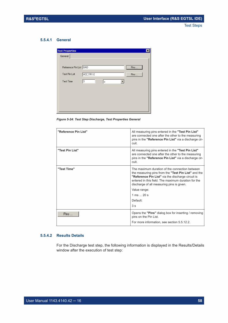
User Interface (R&S EGTSL IDE)R&S®EGTSL
58User Manual 1143.4140.42 16
5.5.4.1 General
Figure 5-24: Test Step Discharge, Test Properties General
"Reference Pin List" All measuring pins entered in the "Test Pin List"are connected one after the other to the measuringpins in the "Reference Pin List" via a discharge cir-cuit.
"Test Pin List" All measuring pins entered in the "Test Pin List"are connected one after the other to the measuringpins in the "Reference Pin List" via a discharge cir-cuit.
"Test Time" The maximum duration of the connection betweenthe measuring pins from the "Test Pin List" and the"Reference Pin List" via the discharge circuit isentered in this field. The maximum duration for thedischarge of all measuring pins is given.
Value range:
1 ms ... 20 s
Default:
3 s
Opens the "Pins" dialog box for inserting / removingpins on the Pin List.
For more information, see section 5.5.12.2.
5.5.4.2 Results Details
For the Discharge test step, the following information is displayed in the Results/Detailswindow after the execution of test step:
Test Steps
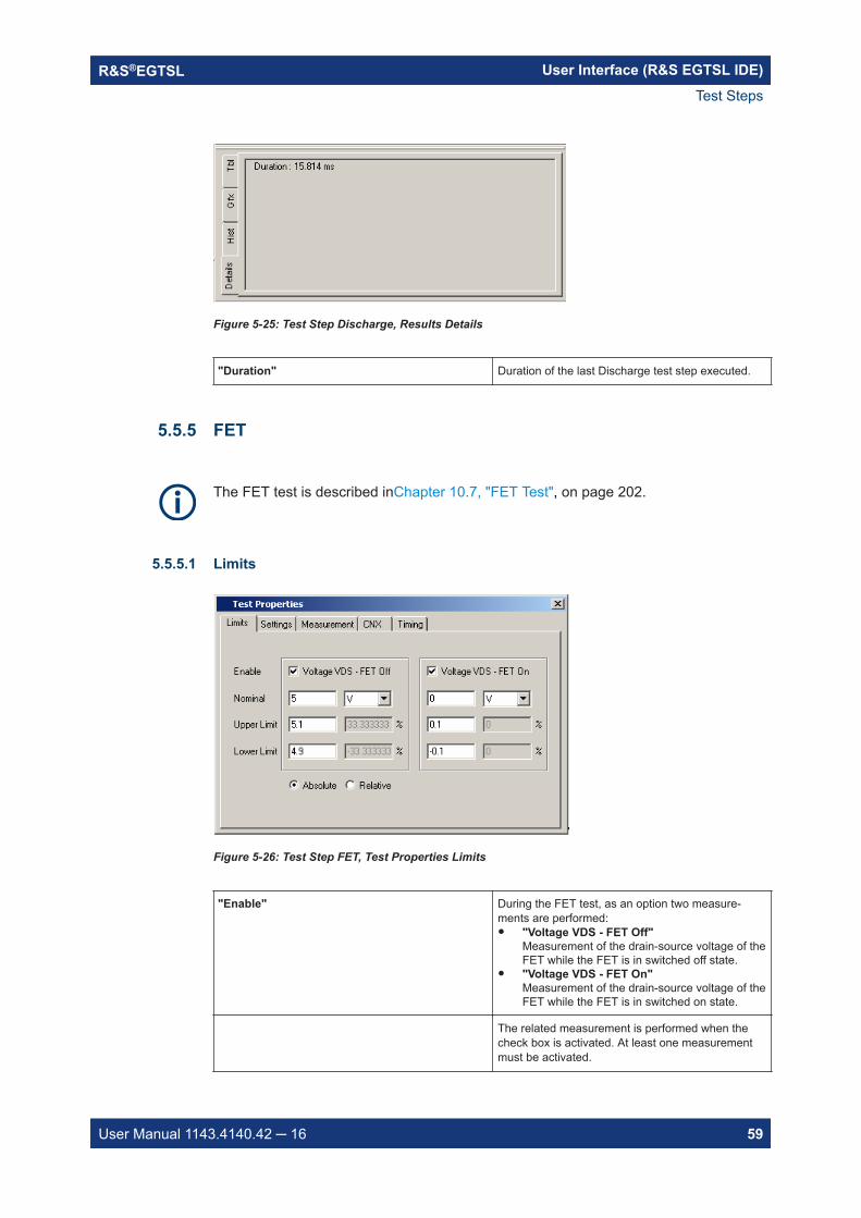
User Interface (R&S EGTSL IDE)R&S®EGTSL
59User Manual 1143.4140.42 16
Figure 5-25: Test Step Discharge, Results Details
"Duration" Duration of the last Discharge test step executed.
5.5.5 FET
The FET test is described inChapter 10.7, "FET Test", on page 202.
5.5.5.1 Limits
Figure 5-26: Test Step FET, Test Properties Limits
"Enable" During the FET test, as an option two measure-ments are performed: "Voltage VDS - FET Off"
Measurement of the drain-source voltage of theFET while the FET is in switched off state.
"Voltage VDS - FET On"Measurement of the drain-source voltage of theFET while the FET is in switched on state.
The related measurement is performed when thecheck box is activated. At least one measurementmust be activated.
Test Steps
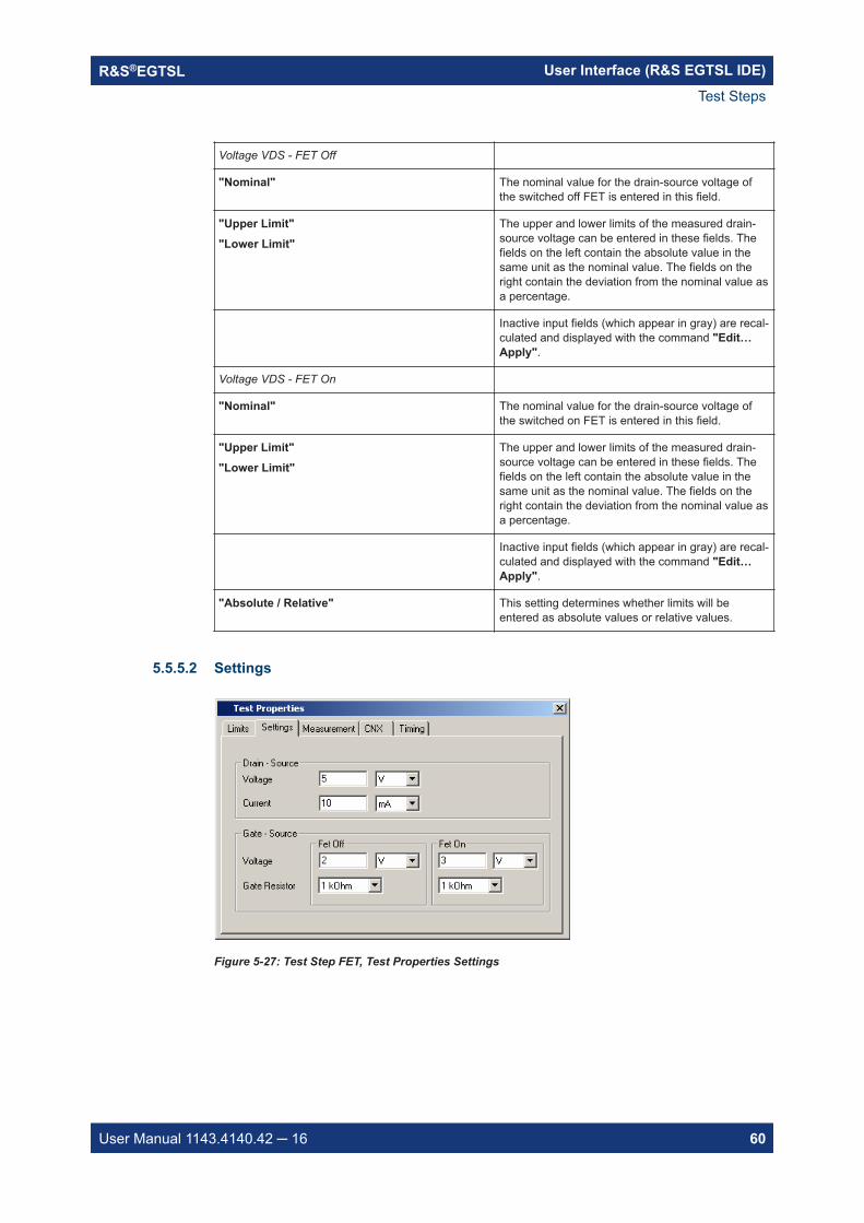
User Interface (R&S EGTSL IDE)R&S®EGTSL
60User Manual 1143.4140.42 16
Voltage VDS - FET Off
"Nominal" The nominal value for the drain-source voltage ofthe switched off FET is entered in this field.
"Upper Limit""Lower Limit"
The upper and lower limits of the measured drain-source voltage can be entered in these fields. Thefields on the left contain the absolute value in thesame unit as the nominal value. The fields on theright contain the deviation from the nominal value asa percentage.
Inactive input fields (which appear in gray) are recal-culated and displayed with the command "Edit…Apply".
Voltage VDS - FET On
"Nominal" The nominal value for the drain-source voltage ofthe switched on FET is entered in this field.
"Upper Limit""Lower Limit"
The upper and lower limits of the measured drain-source voltage can be entered in these fields. Thefields on the left contain the absolute value in thesame unit as the nominal value. The fields on theright contain the deviation from the nominal value asa percentage.
Inactive input fields (which appear in gray) are recal-culated and displayed with the command "Edit…Apply".
"Absolute / Relative" This setting determines whether limits will beentered as absolute values or relative values.
5.5.5.2 Settings
Figure 5-27: Test Step FET, Test Properties Settings
Test Steps
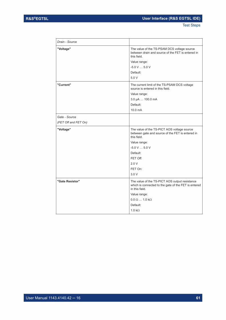
User Interface (R&S EGTSL IDE)R&S®EGTSL
61User Manual 1143.4140.42 16
Drain - Source
"Voltage" The value of the TS-PSAM DCS voltage sourcebetween drain and source of the FET is entered inthis field.
Value range:
-5.0 V … 5.0 V
Default:
5.0 V
"Current" The current limit of the TS-PSAM DCS voltagesource is entered in this field.
Value range:
3.0 µA … 100.0 mA
Default:
10.0 mA
Gate - Source
(FET Off and FET On)
"Voltage" The value of the TS-PICT AOS voltage sourcebetween gate and source of the FET is entered inthis field.
Value range:
-5.0 V … 5.0 V
Default:
FET Off:
2.0 V
FET On:
3.0 V
"Gate Resistor" The value of the TS-PICT AOS output resistancewhich is connected to the gate of the FET is enteredin this field.
Value range:
0.0 Ω … 1.0 kΩ
Default:
1.0 kΩ
Test Steps
User Interface (R&S EGTSL IDE)R&S®EGTSL
62User Manual 1143.4140.42 16
5.5.5.3 Measurement
Figure 5-28: Test Step FET, Test Properties Measurement
Voltage VDS-FET Off
and
Voltage VDS-FET On
"Voltage Range" The measuring range of the TS-PSAM voltmeter isentered in this field.
Value range:
10.0 mV … 200.0 V
Default:
5.0 V
"Autorange" The measuring range for the voltmeter is set auto-matically when this check box is selected.
5.5.5.4 CNX
Figure 5-29: Test Step FET, Test Properties CNX
Test Steps
User Interface (R&S EGTSL IDE)R&S®EGTSL
63User Manual 1143.4140.42 16
"Pin Gate" The gate pin (gate of the FET) is entered in thisfield. Only one measuring pin can be entered.
"Pin Drain" The drain pin (drain of the FET) is entered in thisfield. Only one measuring pin can be entered.
"Pin Source" The source pin (source of the FET) is entered inthis field. Only one measuring pin can be entered.
Opens the "Pins" dialog box for inserting / removingpins on the Pin List. For more information, see sec-tion 5.5.12.2.
5.5.5.5 Timing
Figure 5-30: Test Step FET, Test Properties Timing
The individual options for the timing measurement operation are described in moredetail in Chapter 5.5.12.1, "Timing", on page 103.
Voltage VDS-FET Off
and
Voltage VDS-FET On
"Delay" The fixed delay to the start of the measurement isentered in this field.
Value range:
0 ms ... 1 s
Resolution:
1 ms
Default:
0 ms
Test Steps
User Interface (R&S EGTSL IDE)R&S®EGTSL
64User Manual 1143.4140.42 16
"Max. Wait Interval" The maximum duration of the test interval is enteredin this field (maximum 20 samples).
Value range:
0 ms ... 10 s
Resolution:
1 ms
Default:
0 ms
"Max. Wait Accuracy" In this field, the maximum percentage differencebetween two measured values in succession (sam-ples) is entered for test steps in which the measuredvalue is applied (measurement with "Max. WaitInterval").
Value range:
0.0 % ... 10.0 %
Default:
1.0 %
"Average" The number of measured values from which themean for the measured result is to be determined isentered in this field.
Value range:
1 ... 1000
Default:
1
"Sample Interval" The waiting time between the individual measure-ments for the formation of the mean is entered inthis field (measurement with Average ).
Value range:
5 µs ... 1 s
Resolution:
5 µs
Default:
5 µs (200 kHz)
5.5.5.6 Results Details
For the FET test step, the following information is displayed in the Results/Details win-dow after the execution of the test step:
Test Steps
User Interface (R&S EGTSL IDE)R&S®EGTSL
65User Manual 1143.4140.42 16
Figure 5-31: Test Step FET, Results Details
VMU = Voltage measuring unit (TS-PSAM)DCS = DC Source (TS-PSAM)
Voltage VDS Off
and
Voltage VDS On
"Status VMU" Status of the voltage measurement unit:
Normal, Overrange, Underrange, Max Wait Timeout
"Range VMU" Range of the voltage measurement unit, in whichthe measurement was carried out.
"Duration" Duration of the last measurement carried out.
"Status DCS" Shows whether the TS-PSAM DCS voltage sourceis in the expected state. At the FET Off measure-ment the DCS must be in constant voltage state andat the FET On measurement the DCS must be inconstant current state. If the DCS is in the expectedstate 'Normal' is displayed.
5.5.6 Impedance
The impedance test is described in Chapter 10.8, "Impedance Test", on page 203.
Test Steps
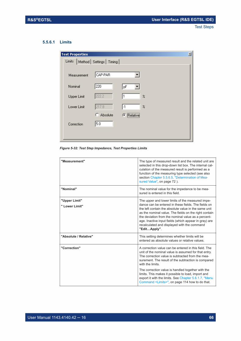
User Interface (R&S EGTSL IDE)R&S®EGTSL
66User Manual 1143.4140.42 16
5.5.6.1 Limits
Figure 5-32: Test Step Impedance, Test Properties Limits
"Measurement" The type of measured result and the related unit areselected in this drop-down list box. The internal cal-culation of the measured result is performed as afunction of the measuring type selected (see alsosection Chapter 5.5.6.5, "Determination of Mea-sured Value", on page 72 ).
"Nominal" The nominal value for the impedance to be mea-sured is entered in this field.
"Upper Limit"" Lower Limit"
The upper and lower limits of the measured impe-dance can be entered in these fields. The fields onthe left contain the absolute value in the same unitas the nominal value. The fields on the right containthe deviation from the nominal value as a percent-age. Inactive input fields (which appear in gray) arerecalculated and displayed with the command"Edit…Apply".
"Absolute / Relative" This setting determines whether limits will beentered as absolute values or relative values.
"Correction" A correction value can be entered in this field. Theunit of the nominal value is assumed for that entry.The correction value is subtracted from the mea-surement. The result of the subtraction is comparedwith the limits.
The correction value is handled together with thelimits. This makes it possible to load, import andexport it with the limits. See Chapter 5.6.1.7, "MenuCommand <Limits>", on page 114 how to do that.
Test Steps
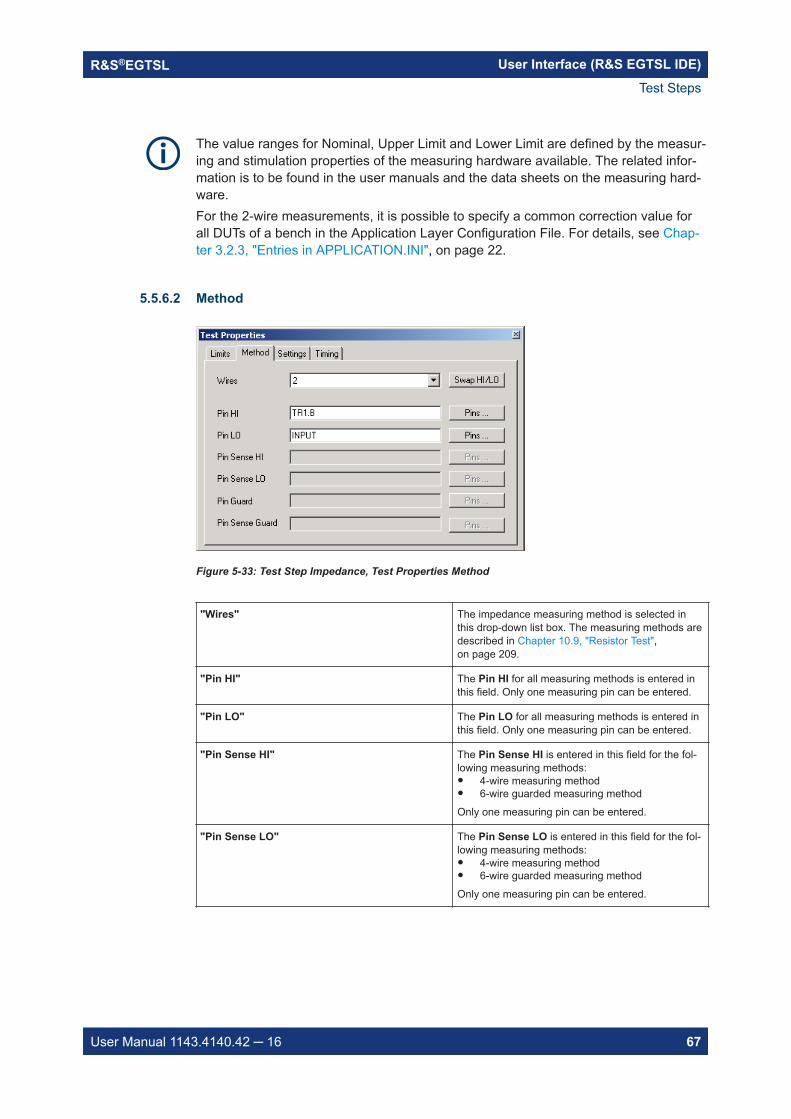
User Interface (R&S EGTSL IDE)R&S®EGTSL
67User Manual 1143.4140.42 16
The value ranges for Nominal, Upper Limit and Lower Limit are defined by the measur-ing and stimulation properties of the measuring hardware available. The related infor-mation is to be found in the user manuals and the data sheets on the measuring hard-ware.For the 2-wire measurements, it is possible to specify a common correction value forall DUTs of a bench in the Application Layer Configuration File. For details, see Chap-ter 3.2.3, "Entries in APPLICATION.INI", on page 22.
5.5.6.2 Method
Figure 5-33: Test Step Impedance, Test Properties Method
"Wires" The impedance measuring method is selected inthis drop-down list box. The measuring methods aredescribed in Chapter 10.9, "Resistor Test",on page 209.
"Pin HI" The Pin HI for all measuring methods is entered inthis field. Only one measuring pin can be entered.
"Pin LO" The Pin LO for all measuring methods is entered inthis field. Only one measuring pin can be entered.
"Pin Sense HI" The Pin Sense HI is entered in this field for the fol-lowing measuring methods: 4-wire measuring method 6-wire guarded measuring method
Only one measuring pin can be entered.
"Pin Sense LO" The Pin Sense LO is entered in this field for the fol-lowing measuring methods: 4-wire measuring method 6-wire guarded measuring method
Only one measuring pin can be entered.
Test Steps
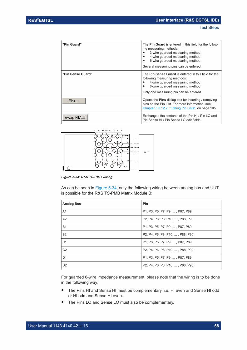
User Interface (R&S EGTSL IDE)R&S®EGTSL
68User Manual 1143.4140.42 16
"Pin Guard" The Pin Guard is entered in this field for the follow-ing measuring methods: 3-wire guarded measuring method 4-wire guarded measuring method 6-wire guarded measuring method
Several measuring pins can be entered.
"Pin Sense Guard" The Pin Sense Guard is entered in this field for thefollowing measuring methods: 4-wire guarded measuring method 6-wire guarded measuring method
Only one measuring pin can be entered.
Opens the Pins dialog box for inserting / removingpins on the Pin List. For more information, seeChapter 5.5.12.2, "Editing Pin Lists", on page 105.
Exchanges the contents of the Pin HI / Pin LO andPin Sense HI / Pin Sense LO edit fields.
Figure 5-34: R&S TS-PMB wiring
As can be seen in Figure 5-34, only the following wiring between analog bus and UUTis possible for the R&S TS-PMB Matrix Module B:
Analog Bus Pin
A1 P1, P3, P5, P7, P9, ... , P87, P89
A2 P2, P4, P6, P8, P10, ... , P88, P90
B1 P1, P3, P5, P7, P9, ... , P87, P89
B2 P2, P4, P6, P8, P10, ... , P88, P90
C1 P1, P3, P5, P7, P9, ... , P87, P89
C2 P2, P4, P6, P8, P10, ... , P88, P90
D1 P1, P3, P5, P7, P9, ... , P87, P89
D2 P2, P4, P6, P8, P10, ... , P88, P90
For guarded 6-wire impedance measurement, please note that the wiring is to be donein the following way:
The Pins HI and Sense HI must be complementary, i.e. HI even and Sense HI oddor HI odd and Sense HI even.
The Pins LO and Sense LO must also be complementary.
Test Steps
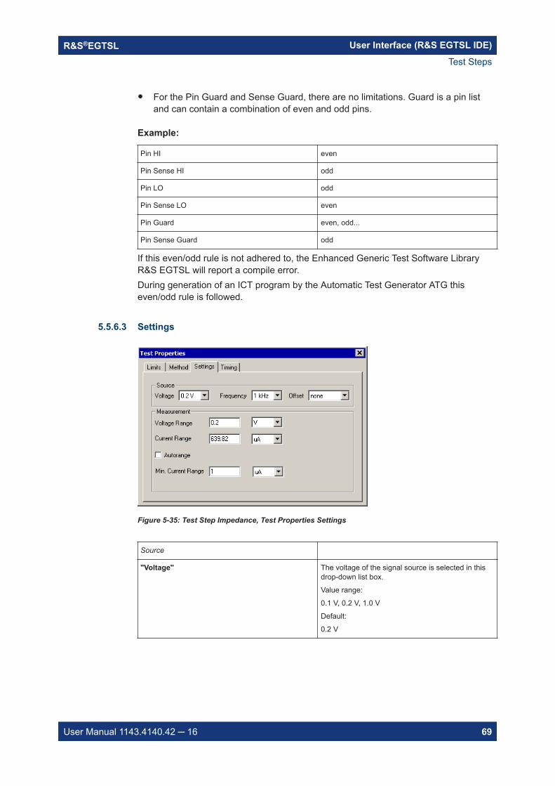
User Interface (R&S EGTSL IDE)R&S®EGTSL
69User Manual 1143.4140.42 16
For the Pin Guard and Sense Guard, there are no limitations. Guard is a pin listand can contain a combination of even and odd pins.
Example:
Pin HI even
Pin Sense HI odd
Pin LO odd
Pin Sense LO even
Pin Guard even, odd...
Pin Sense Guard odd
If this even/odd rule is not adhered to, the Enhanced Generic Test Software LibraryR&S EGTSL will report a compile error.During generation of an ICT program by the Automatic Test Generator ATG thiseven/odd rule is followed.
5.5.6.3 Settings
Figure 5-35: Test Step Impedance, Test Properties Settings
Source
"Voltage" The voltage of the signal source is selected in thisdrop-down list box.
Value range:
0.1 V, 0.2 V, 1.0 V
Default:
0.2 V
Test Steps
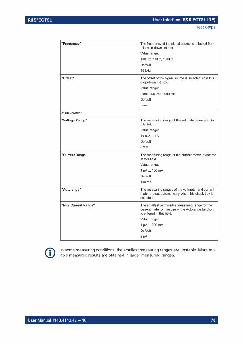
User Interface (R&S EGTSL IDE)R&S®EGTSL
70User Manual 1143.4140.42 16
"Frequency" The frequency of the signal source is selected fromthis drop-down list box.
Value range:
100 Hz, 1 kHz, 10 kHz
Default:
10 kHz
"Offset" The offset of the signal source is selected from thisdrop-down list box.
Value range:
none, positive, negative
Default:
none
Measurement
"Voltage Range" The measuring range of the voltmeter is entered inthis field.
Value range:
10 mV ... 5 V
Default:
0.2 V
"Current Range" The measuring range of the current meter is enteredin this field.
Value range:
1 µA ... 100 mA
Default:
100 mA
"Autorange" The measuring ranges of the voltmeter and currentmeter are set automatically when this check box isselected.
"Min. Current Range" The smallest permissible measuring range for thecurrent meter on the use of the Autorange functionis entered in this field.
Value range:
1 µA ... 200 mA
Default:
2 µA
In some measuring conditions, the smallest measuring ranges are unstable. More reli-able measured results are obtained in larger measuring ranges.
Test Steps
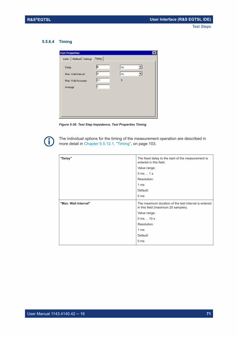
User Interface (R&S EGTSL IDE)R&S®EGTSL
71User Manual 1143.4140.42 16
5.5.6.4 Timing
Figure 5-36: Test Step Impedance, Test Properties Timing
The individual options for the timing of the measurement operation are described inmore detail in Chapter 5.5.12.1, "Timing", on page 103.
"Delay" The fixed delay to the start of the measurement isentered in this field.
Value range:
0 ms ... 1 s
Resolution:
1 ms
Default:
0 ms
"Max. Wait Interval" The maximum duration of the test interval is enteredin this field (maximum 20 samples).
Value range:
0 ms ... 10 s
Resolution:
1 ms
Default:
0 ms
Test Steps
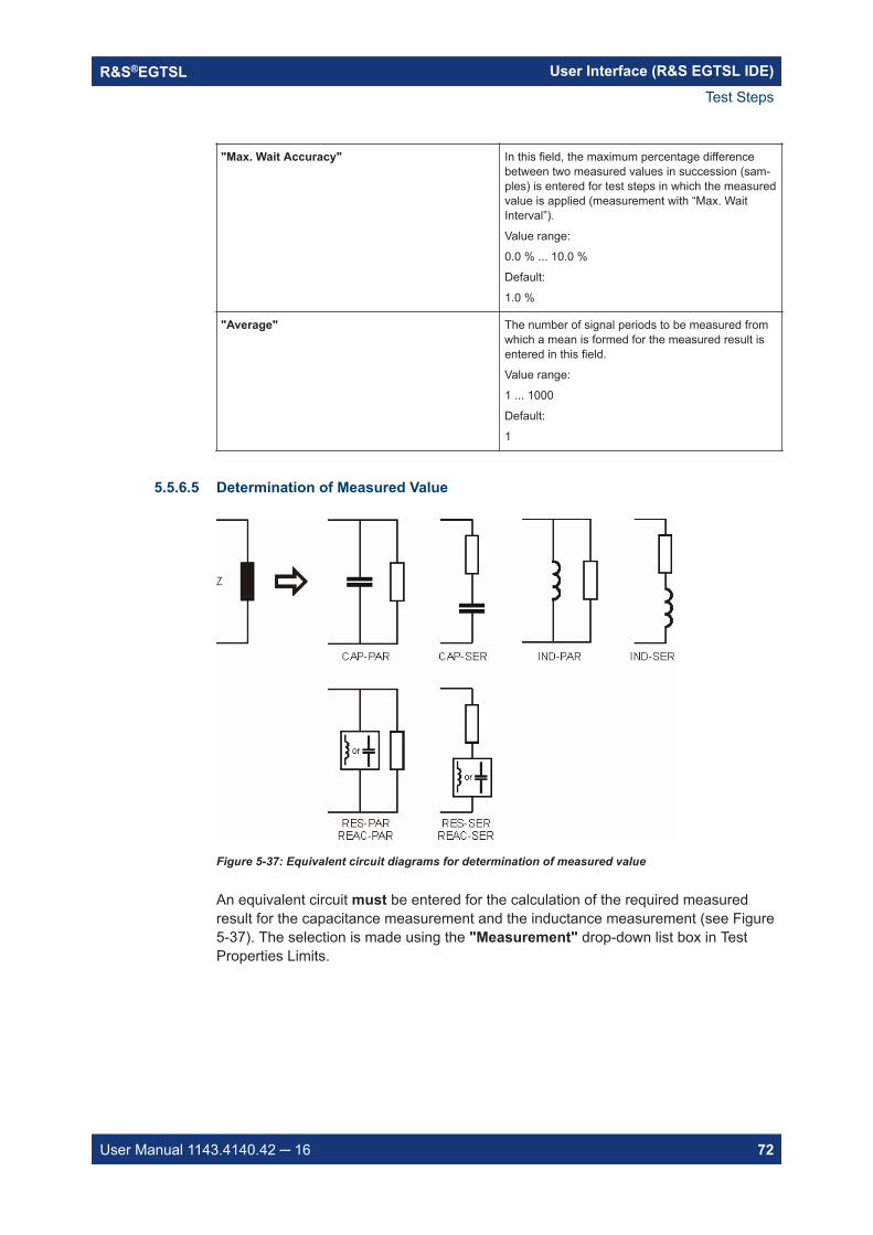
User Interface (R&S EGTSL IDE)R&S®EGTSL
72User Manual 1143.4140.42 16
"Max. Wait Accuracy" In this field, the maximum percentage differencebetween two measured values in succession (sam-ples) is entered for test steps in which the measuredvalue is applied (measurement with “Max. WaitInterval”).
Value range:
0.0 % ... 10.0 %
Default:
1.0 %
"Average" The number of signal periods to be measured fromwhich a mean is formed for the measured result isentered in this field.
Value range:
1 ... 1000
Default:
1
5.5.6.5 Determination of Measured Value
Figure 5-37: Equivalent circuit diagrams for determination of measured value
An equivalent circuit must be entered for the calculation of the required measuredresult for the capacitance measurement and the inductance measurement (see Figure5-37). The selection is made using the "Measurement" drop-down list box in TestProperties Limits.
Test Steps
User Interface (R&S EGTSL IDE)R&S®EGTSL
73User Manual 1143.4140.42 16
Table 5-1: Determination of measured value (1/2)
Measurement Measured result Equivalent circuit Unit
CAP-PAR Capacitance Capacitance measure-ment based on a parallelequivalent circuit
Farad (F)
CAP-SER Capacitance Capacitance measure-ment based on a serialequivalent circuit
Farad (F)
IND-PAR Inductance Inductance measure-ment based on a parallelequivalent circuit
Henry (H)
IND-SER Inductance Inductance measure-ment based on a serialequivalent circuit
Henry (H)
Two different representations of the impedance are available for the measurement ofthe impedance. On the one hand the representation in real and imaginary parts, on theother hand the representation in magnitude and phase. An equivalent circuit must beentered for the calculation of the required measured result for the representation in realand imaginary parts (see Figure 5-37 ).Table 5-2: Determination of measured value (2/2)
Measurement Measured result Equivalent circuit Unit
RES-SER Real part of the mea-sured impedance
Impedance measure-ment based on a serialequivalent circuit
Ohm (Ω)
RES-PAR Real part of the mea-sured impedance
Impedance measure-ment based on a parallelequivalent circuit
Ohm (Ω)
REAC-SER Imaginary part of themeasured impedance
Impedance measure-ment based on a serialequivalent circuit
Ohm (Ω)
REAC-PAR Imaginary part of themeasured impedance
Impedance measured Ohm (Ω)
IMP-MAG Magnitude of the impe-dance measured
Ohm (Ω)
IMP-PHASE Phase of the measuredimpedance
deg
5.5.6.6 Results Details
For the Impedance test step, the following information is displayed in the "Results/Detail"s window after the execution of test step:
Test Steps
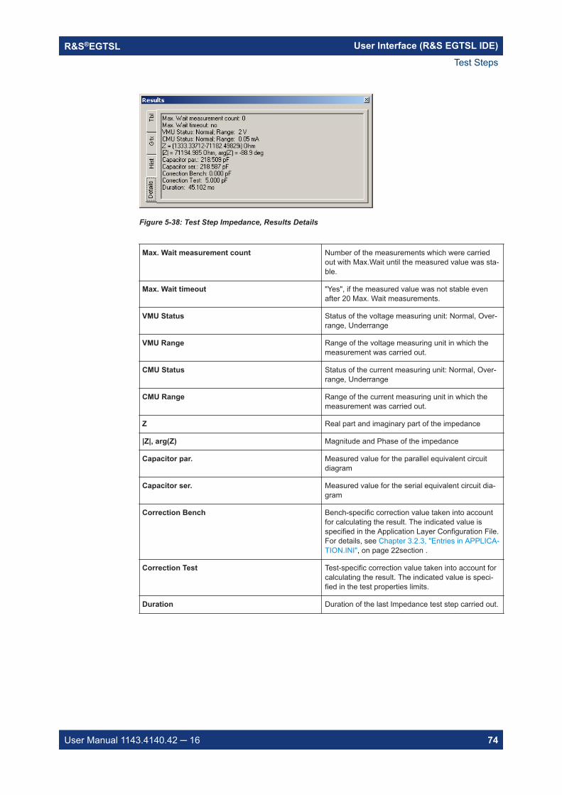
User Interface (R&S EGTSL IDE)R&S®EGTSL
74User Manual 1143.4140.42 16
Figure 5-38: Test Step Impedance, Results Details
Max. Wait measurement count Number of the measurements which were carriedout with Max.Wait until the measured value was sta-ble.
Max. Wait timeout "Yes", if the measured value was not stable evenafter 20 Max. Wait measurements.
VMU Status Status of the voltage measuring unit: Normal, Over-range, Underrange
VMU Range Range of the voltage measuring unit in which themeasurement was carried out.
CMU Status Status of the current measuring unit: Normal, Over-range, Underrange
CMU Range Range of the current measuring unit in which themeasurement was carried out.
Z Real part and imaginary part of the impedance
|Z|, arg(Z) Magnitude and Phase of the impedance
Capacitor par. Measured value for the parallel equivalent circuitdiagram
Capacitor ser. Measured value for the serial equivalent circuit dia-gram
Correction Bench Bench-specific correction value taken into accountfor calculating the result. The indicated value isspecified in the Application Layer Configuration File.For details, see Chapter 3.2.3, "Entries in APPLICA-TION.INI", on page 22section .
Correction Test Test-specific correction value taken into account forcalculating the result. The indicated value is speci-fied in the test properties limits.
Duration Duration of the last Impedance test step carried out.
Test Steps
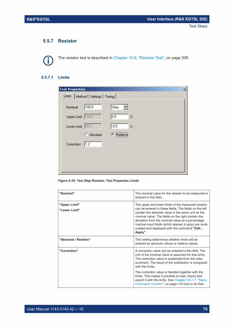
User Interface (R&S EGTSL IDE)R&S®EGTSL
75User Manual 1143.4140.42 16
5.5.7 Resistor
The resistor test is described in Chapter 10.9, "Resistor Test", on page 209.
5.5.7.1 Limits
Figure 5-39: Test Step Resistor, Test Properties Limits
"Nominal" The nominal value for the resistor to be measured isentered in this field.
"Upper Limit""Lower Limit"
The upper and lower limits of the measured resistorcan be entered in these fields. The fields on the leftcontain the absolute value in the same unit as thenominal value. The fields on the right contain thedeviation from the nominal value as a percentage.Inactive input fields (which appear in gray) are recal-culated and displayed with the command "Edit…Apply".
"Absolute / Relative" This setting determines whether limits will beentered as absolute values or relative values.
"Correction" A correction value can be entered in this field. Theunit of the nominal value is assumed for that entry.The correction value is subtracted from the mea-surement. The result of the subtraction is comparedwith the limits.
The correction value is handled together with thelimits. This makes it possible to load, import andexport it with the limits. See Chapter 5.6.1.7, "MenuCommand <Limits>", on page 114 how to do that.
Test Steps
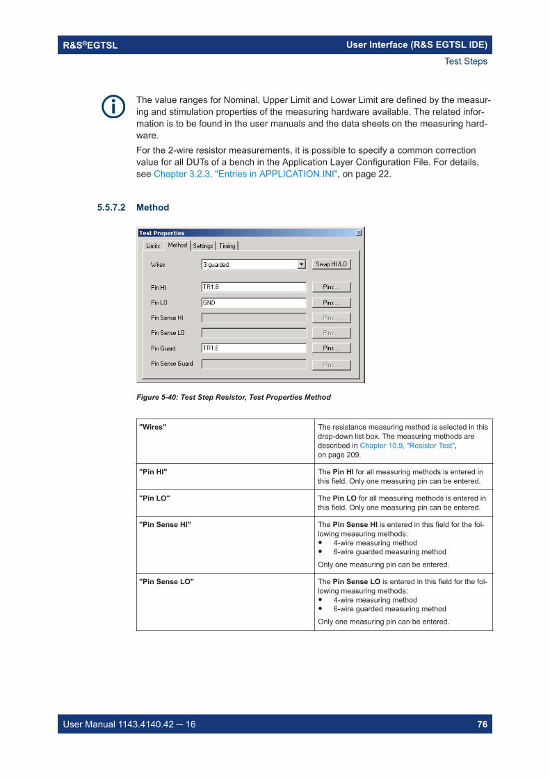
User Interface (R&S EGTSL IDE)R&S®EGTSL
76User Manual 1143.4140.42 16
The value ranges for Nominal, Upper Limit and Lower Limit are defined by the measur-ing and stimulation properties of the measuring hardware available. The related infor-mation is to be found in the user manuals and the data sheets on the measuring hard-ware.For the 2-wire resistor measurements, it is possible to specify a common correctionvalue for all DUTs of a bench in the Application Layer Configuration File. For details,see Chapter 3.2.3, "Entries in APPLICATION.INI", on page 22.
5.5.7.2 Method
Figure 5-40: Test Step Resistor, Test Properties Method
"Wires" The resistance measuring method is selected in thisdrop-down list box. The measuring methods aredescribed in Chapter 10.9, "Resistor Test",on page 209.
"Pin HI" The Pin HI for all measuring methods is entered inthis field. Only one measuring pin can be entered.
"Pin LO" The Pin LO for all measuring methods is entered inthis field. Only one measuring pin can be entered.
"Pin Sense HI" The Pin Sense HI is entered in this field for the fol-lowing measuring methods: 4-wire measuring method 6-wire guarded measuring method
Only one measuring pin can be entered.
"Pin Sense LO" The Pin Sense LO is entered in this field for the fol-lowing measuring methods: 4-wire measuring method 6-wire guarded measuring method
Only one measuring pin can be entered.
Test Steps
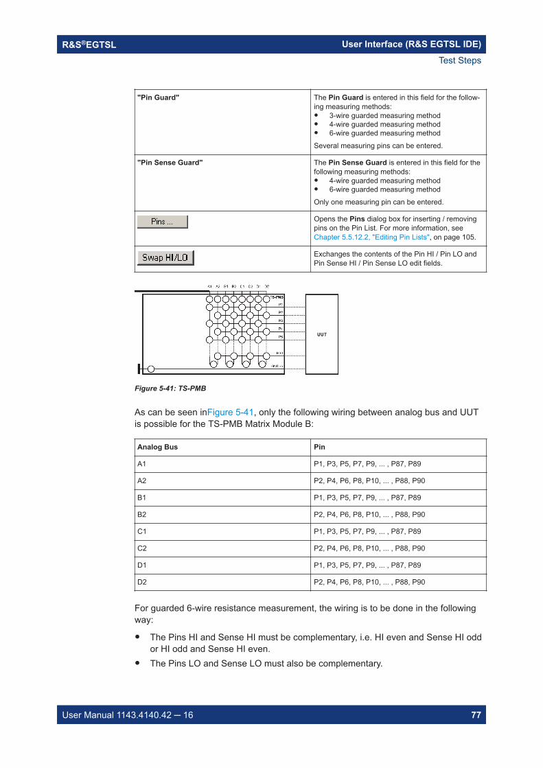
User Interface (R&S EGTSL IDE)R&S®EGTSL
77User Manual 1143.4140.42 16
"Pin Guard" The Pin Guard is entered in this field for the follow-ing measuring methods: 3-wire guarded measuring method 4-wire guarded measuring method 6-wire guarded measuring method
Several measuring pins can be entered.
"Pin Sense Guard" The Pin Sense Guard is entered in this field for thefollowing measuring methods: 4-wire guarded measuring method 6-wire guarded measuring method
Only one measuring pin can be entered.
Opens the Pins dialog box for inserting / removingpins on the Pin List. For more information, seeChapter 5.5.12.2, "Editing Pin Lists", on page 105.
Exchanges the contents of the Pin HI / Pin LO andPin Sense HI / Pin Sense LO edit fields.
Figure 5-41: TS-PMB
As can be seen inFigure 5-41, only the following wiring between analog bus and UUTis possible for the TS-PMB Matrix Module B:
Analog Bus Pin
A1 P1, P3, P5, P7, P9, ... , P87, P89
A2 P2, P4, P6, P8, P10, ... , P88, P90
B1 P1, P3, P5, P7, P9, ... , P87, P89
B2 P2, P4, P6, P8, P10, ... , P88, P90
C1 P1, P3, P5, P7, P9, ... , P87, P89
C2 P2, P4, P6, P8, P10, ... , P88, P90
D1 P1, P3, P5, P7, P9, ... , P87, P89
D2 P2, P4, P6, P8, P10, ... , P88, P90
For guarded 6-wire resistance measurement, the wiring is to be done in the followingway:
The Pins HI and Sense HI must be complementary, i.e. HI even and Sense HI oddor HI odd and Sense HI even.
The Pins LO and Sense LO must also be complementary.
Test Steps
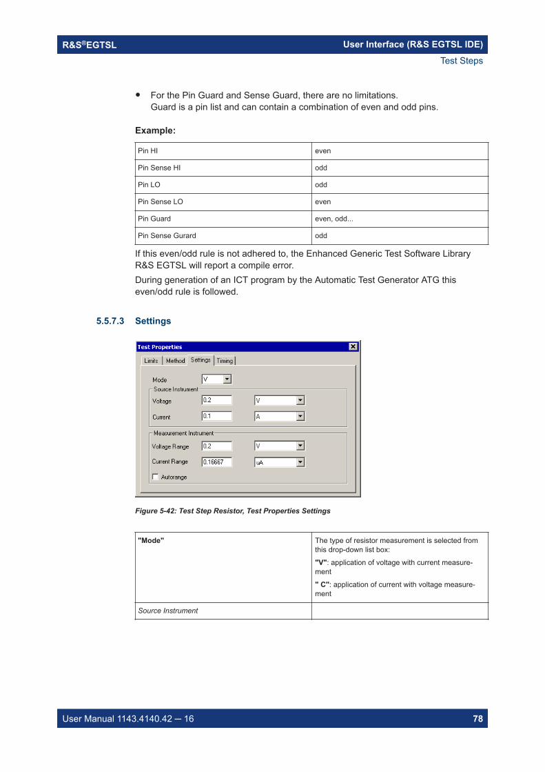
User Interface (R&S EGTSL IDE)R&S®EGTSL
78User Manual 1143.4140.42 16
For the Pin Guard and Sense Guard, there are no limitations.Guard is a pin list and can contain a combination of even and odd pins.
Example:
Pin HI even
Pin Sense HI odd
Pin LO odd
Pin Sense LO even
Pin Guard even, odd...
Pin Sense Gurard odd
If this even/odd rule is not adhered to, the Enhanced Generic Test Software LibraryR&S EGTSL will report a compile error.During generation of an ICT program by the Automatic Test Generator ATG thiseven/odd rule is followed.
5.5.7.3 Settings
Figure 5-42: Test Step Resistor, Test Properties Settings
"Mode" The type of resistor measurement is selected fromthis drop-down list box:
"V": application of voltage with current measure-ment
" C": application of current with voltage measure-ment
Source Instrument
Test Steps
User Interface (R&S EGTSL IDE)R&S®EGTSL
79User Manual 1143.4140.42 16
"Voltage" The voltage of the voltage source is entered in thisfield.
Value range:
1 mV ... 5 V
Default:
0.2 V
"Current" The current limit of the voltage source is entered inthis field.
Value range:
1 µA ... 100 mA
Default:
100 mA
Measurement Instrument
"Voltage Range" The measuring range of the voltmeter is entered inthis field.
Value range:
10 mV ... 5 V
Default:
0.2 V
"Current Range" The measuring range of the current meter is enteredin this field.
Value range:
0 µA ... 200 mA
Default:
100 mA
"Autorange" The measuring ranges for the voltmeter and currentmeter are set automatically when this check box isselected.
Only one measuring range is relevant depending on the type of resistor measurement:
Mode V: Current Range (application of voltage with currentmeasurement)
Mode C: Voltage Range (application of current with voltagemeasurement)
When Autorange is selected, the search for the optimal measuring range starts withthe values entered in the "Voltage Range" (voltage measurement) and "CurrentRange" (current measurement) fields.
Test Steps
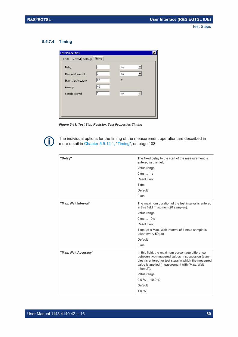
User Interface (R&S EGTSL IDE)R&S®EGTSL
80User Manual 1143.4140.42 16
5.5.7.4 Timing
Figure 5-43: Test Step Resistor, Test Properties Timing
The individual options for the timing of the measurement operation are described inmore detail in Chapter 5.5.12.1, "Timing", on page 103.
"Delay" The fixed delay to the start of the measurement isentered in this field.
Value range:
0 ms ... 1 s
Resolution:
1 ms
Default:
0 ms
"Max. Wait Interval" The maximum duration of the test interval is enteredin this field (maximum 20 samples).
Value range:
0 ms ... 10 s
Resolution:
1 ms (at a Max. Wait Interval of 1 ms a sample istaken every 50 μs)
Default:
0 ms
"Max. Wait Accuracy" In this field, the maximum percentage differencebetween two measured values in succession (sam-ples) is entered for test steps in which the measuredvalue is applied (measurement with “Max. WaitInterval”).
Value range:
0.0 % ... 10.0 %
Default:
1.0 %
Test Steps
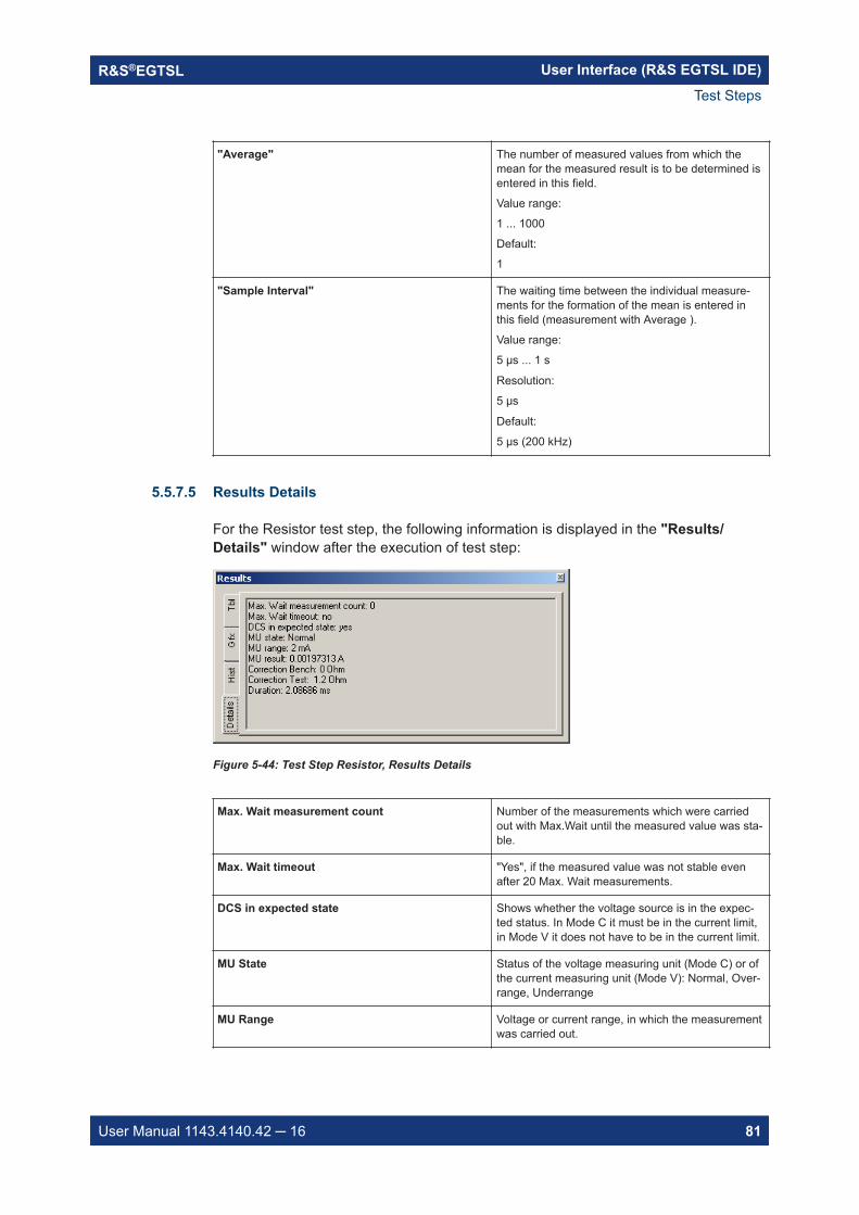
User Interface (R&S EGTSL IDE)R&S®EGTSL
81User Manual 1143.4140.42 16
"Average" The number of measured values from which themean for the measured result is to be determined isentered in this field.
Value range:
1 ... 1000
Default:
1
"Sample Interval" The waiting time between the individual measure-ments for the formation of the mean is entered inthis field (measurement with Average ).
Value range:
5 µs ... 1 s
Resolution:
5 µs
Default:
5 µs (200 kHz)
5.5.7.5 Results Details
For the Resistor test step, the following information is displayed in the "Results/Details" window after the execution of test step:
Figure 5-44: Test Step Resistor, Results Details
Max. Wait measurement count Number of the measurements which were carriedout with Max.Wait until the measured value was sta-ble.
Max. Wait timeout "Yes", if the measured value was not stable evenafter 20 Max. Wait measurements.
DCS in expected state Shows whether the voltage source is in the expec-ted status. In Mode C it must be in the current limit,in Mode V it does not have to be in the current limit.
MU State Status of the voltage measuring unit (Mode C) or ofthe current measuring unit (Mode V): Normal, Over-range, Underrange
MU Range Voltage or current range, in which the measurementwas carried out.
Test Steps
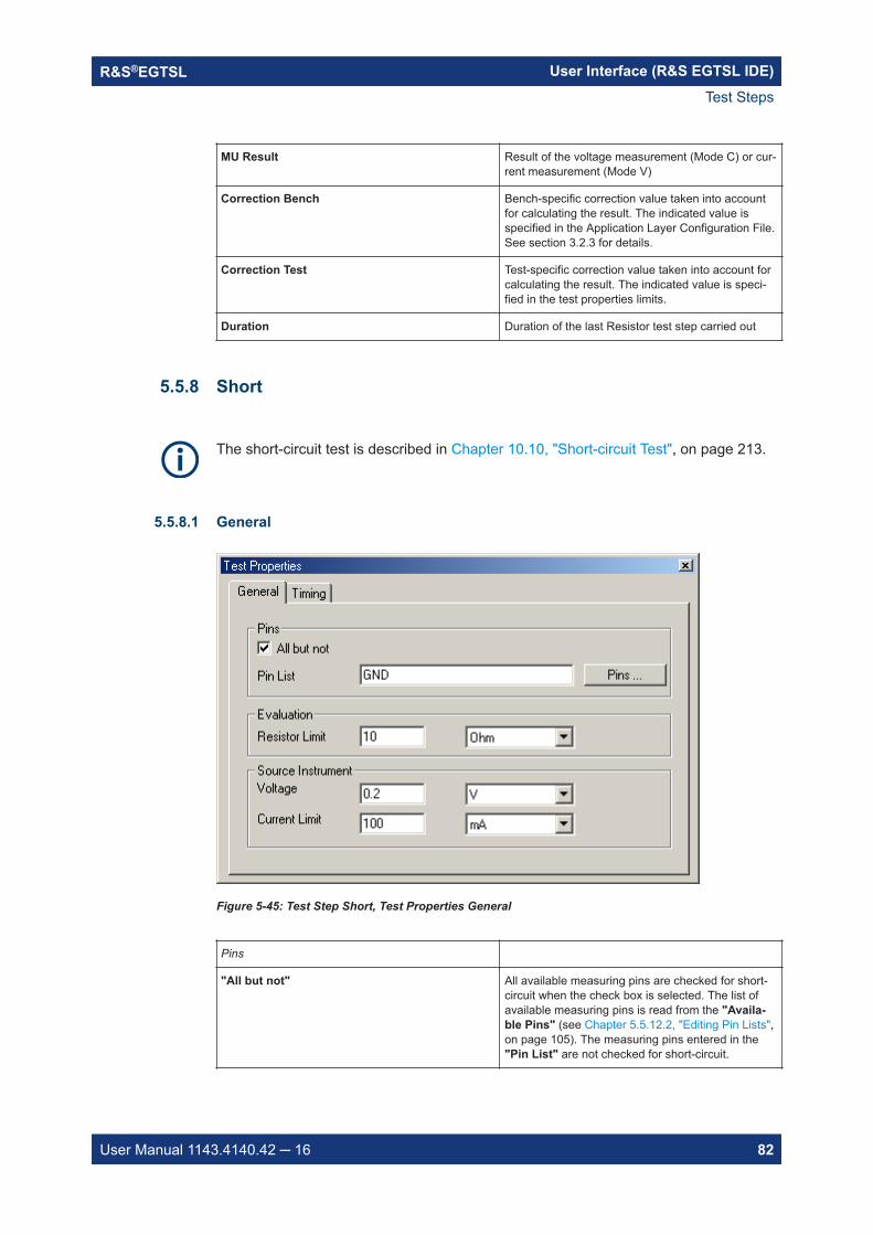
User Interface (R&S EGTSL IDE)R&S®EGTSL
82User Manual 1143.4140.42 16
MU Result Result of the voltage measurement (Mode C) or cur-rent measurement (Mode V)
Correction Bench Bench-specific correction value taken into accountfor calculating the result. The indicated value isspecified in the Application Layer Configuration File.See section 3.2.3 for details.
Correction Test Test-specific correction value taken into account forcalculating the result. The indicated value is speci-fied in the test properties limits.
Duration Duration of the last Resistor test step carried out
5.5.8 Short
The short-circuit test is described in Chapter 10.10, "Short-circuit Test", on page 213.
5.5.8.1 General
Figure 5-45: Test Step Short, Test Properties General
Pins
"All but not" All available measuring pins are checked for short-circuit when the check box is selected. The list ofavailable measuring pins is read from the "Availa-ble Pins" (see Chapter 5.5.12.2, "Editing Pin Lists",on page 105). The measuring pins entered in the"Pin List" are not checked for short-circuit.
Test Steps
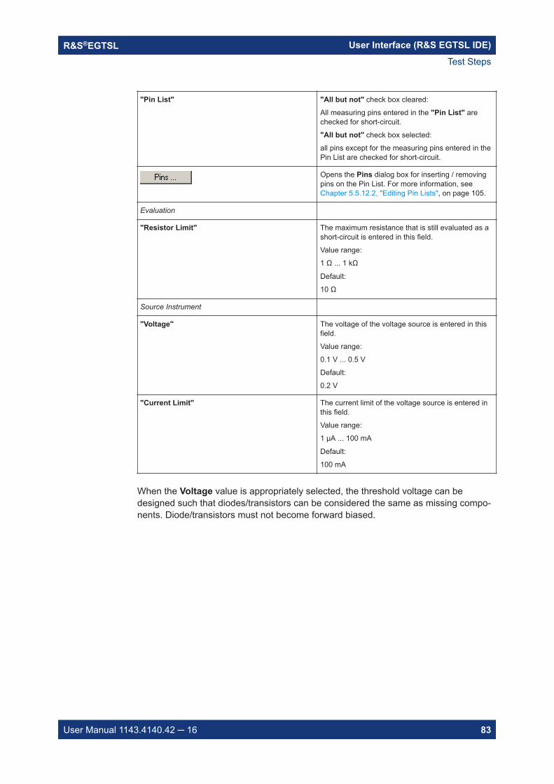
User Interface (R&S EGTSL IDE)R&S®EGTSL
83User Manual 1143.4140.42 16
"Pin List" "All but not" check box cleared:
All measuring pins entered in the "Pin List" arechecked for short-circuit.
"All but not" check box selected:
all pins except for the measuring pins entered in thePin List are checked for short-circuit.
Opens the Pins dialog box for inserting / removingpins on the Pin List. For more information, seeChapter 5.5.12.2, "Editing Pin Lists", on page 105.
Evaluation
"Resistor Limit" The maximum resistance that is still evaluated as ashort-circuit is entered in this field.
Value range:
1 Ω ... 1 kΩ
Default:
10 Ω
Source Instrument
"Voltage" The voltage of the voltage source is entered in thisfield.
Value range:
0.1 V ... 0.5 V
Default:
0.2 V
"Current Limit" The current limit of the voltage source is entered inthis field.
Value range:
1 µA ... 100 mA
Default:
100 mA
When the Voltage value is appropriately selected, the threshold voltage can bedesigned such that diodes/transistors can be considered the same as missing compo-nents. Diode/transistors must not become forward biased.
Test Steps
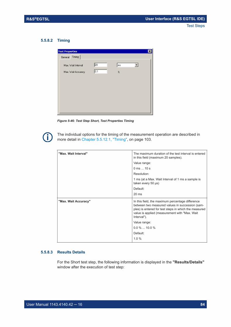
User Interface (R&S EGTSL IDE)R&S®EGTSL
84User Manual 1143.4140.42 16
5.5.8.2 Timing
Figure 5-46: Test Step Short, Test Properties Timing
The individual options for the timing of the measurement operation are described inmore detail in Chapter 5.5.12.1, "Timing", on page 103.
"Max. Wait Interval" The maximum duration of the test interval is enteredin this field (maximum 20 samples).
Value range:
0 ms ... 10 s
Resolution:
1 ms (at a Max. Wait Interval of 1 ms a sample istaken every 50 μs)
Default:
20 ms
"Max. Wait Accuracy" In this field, the maximum percentage differencebetween two measured values in succession (sam-ples) is entered for test steps in which the measuredvalue is applied (measurement with "Max. WaitInterval").
Value range:
0.0 % ... 10.0 %
Default:
1.0 %
5.5.8.3 Results Details
For the Short test step, the following information is displayed in the "Results/Details"window after the execution of test step:
Test Steps
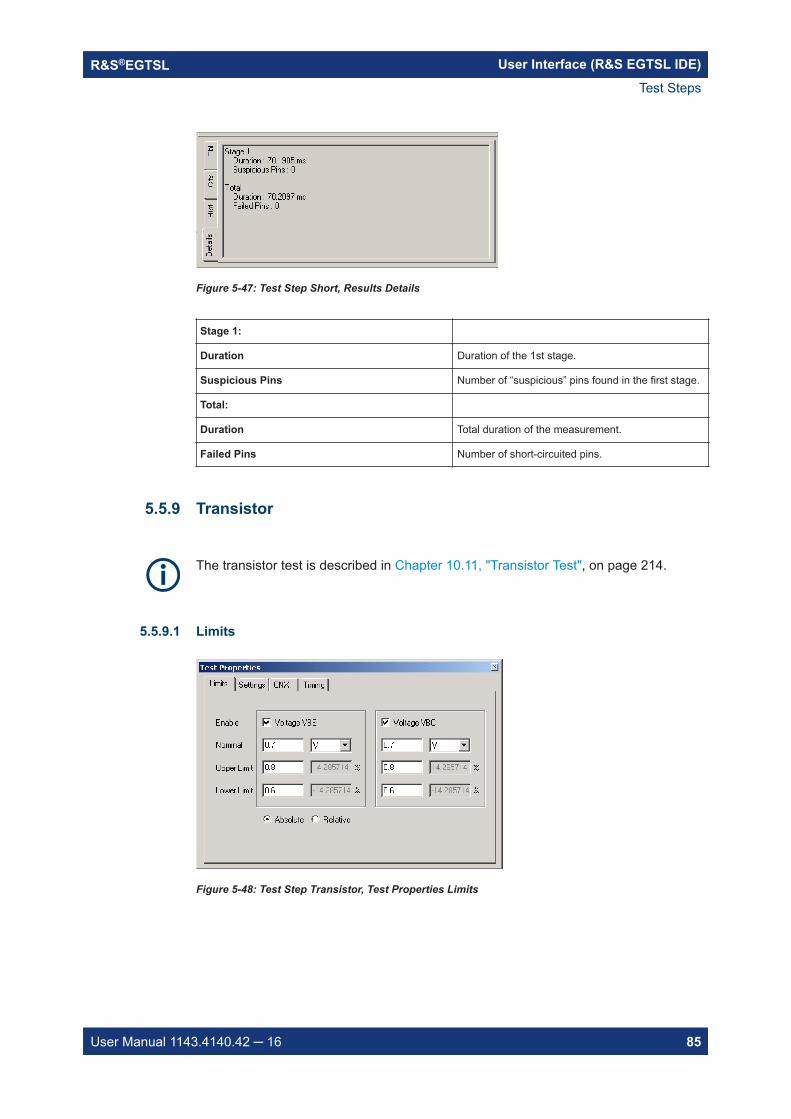
User Interface (R&S EGTSL IDE)R&S®EGTSL
85User Manual 1143.4140.42 16
Figure 5-47: Test Step Short, Results Details
Stage 1:
Duration Duration of the 1st stage.
Suspicious Pins Number of “suspicious” pins found in the first stage.
Total:
Duration Total duration of the measurement.
Failed Pins Number of short-circuited pins.
5.5.9 Transistor
The transistor test is described in Chapter 10.11, "Transistor Test", on page 214.
5.5.9.1 Limits
Figure 5-48: Test Step Transistor, Test Properties Limits
Test Steps
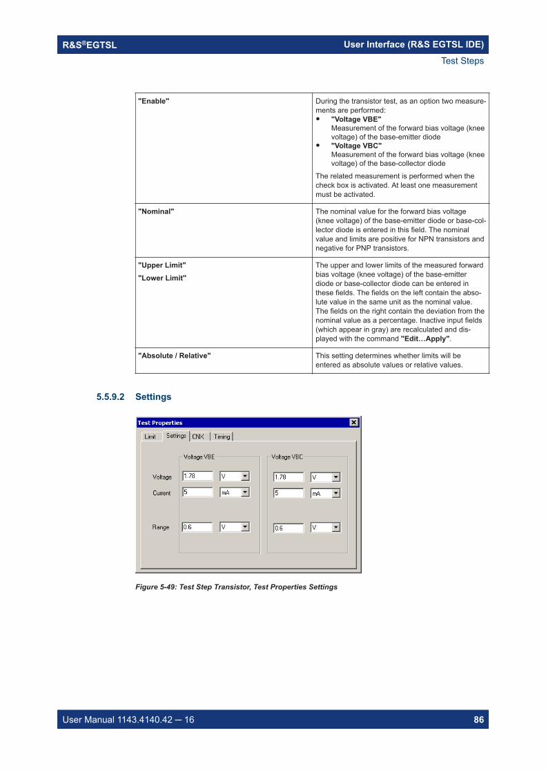
User Interface (R&S EGTSL IDE)R&S®EGTSL
86User Manual 1143.4140.42 16
"Enable" During the transistor test, as an option two measure-ments are performed: "Voltage VBE"
Measurement of the forward bias voltage (kneevoltage) of the base-emitter diode
"Voltage VBC"Measurement of the forward bias voltage (kneevoltage) of the base-collector diode
The related measurement is performed when thecheck box is activated. At least one measurementmust be activated.
"Nominal" The nominal value for the forward bias voltage(knee voltage) of the base-emitter diode or base-col-lector diode is entered in this field. The nominalvalue and limits are positive for NPN transistors andnegative for PNP transistors.
"Upper Limit""Lower Limit"
The upper and lower limits of the measured forwardbias voltage (knee voltage) of the base-emitterdiode or base-collector diode can be entered inthese fields. The fields on the left contain the abso-lute value in the same unit as the nominal value.The fields on the right contain the deviation from thenominal value as a percentage. Inactive input fields(which appear in gray) are recalculated and dis-played with the command "Edit…Apply".
"Absolute / Relative" This setting determines whether limits will beentered as absolute values or relative values.
5.5.9.2 Settings
Figure 5-49: Test Step Transistor, Test Properties Settings
Test Steps
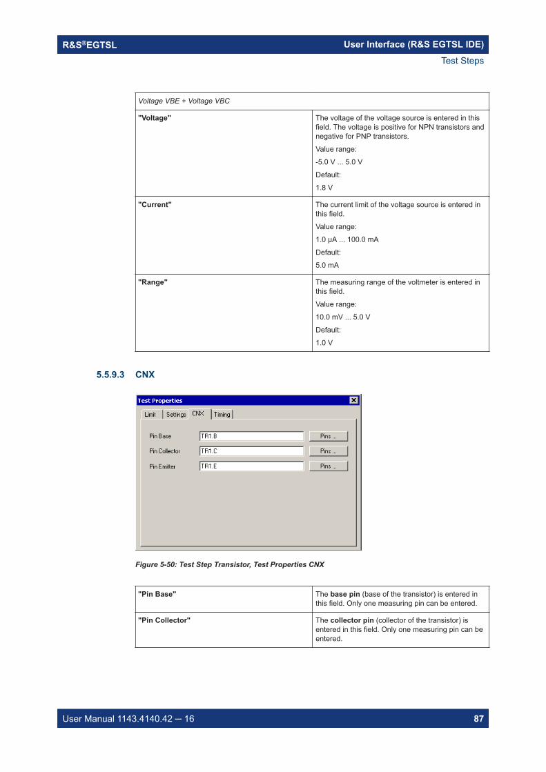
User Interface (R&S EGTSL IDE)R&S®EGTSL
87User Manual 1143.4140.42 16
Voltage VBE + Voltage VBC
"Voltage" The voltage of the voltage source is entered in thisfield. The voltage is positive for NPN transistors andnegative for PNP transistors.
Value range:
-5.0 V ... 5.0 V
Default:
1.8 V
"Current" The current limit of the voltage source is entered inthis field.
Value range:
1.0 µA ... 100.0 mA
Default:
5.0 mA
"Range" The measuring range of the voltmeter is entered inthis field.
Value range:
10.0 mV ... 5.0 V
Default:
1.0 V
5.5.9.3 CNX
Figure 5-50: Test Step Transistor, Test Properties CNX
"Pin Base" The base pin (base of the transistor) is entered inthis field. Only one measuring pin can be entered.
"Pin Collector" The collector pin (collector of the transistor) isentered in this field. Only one measuring pin can beentered.
Test Steps
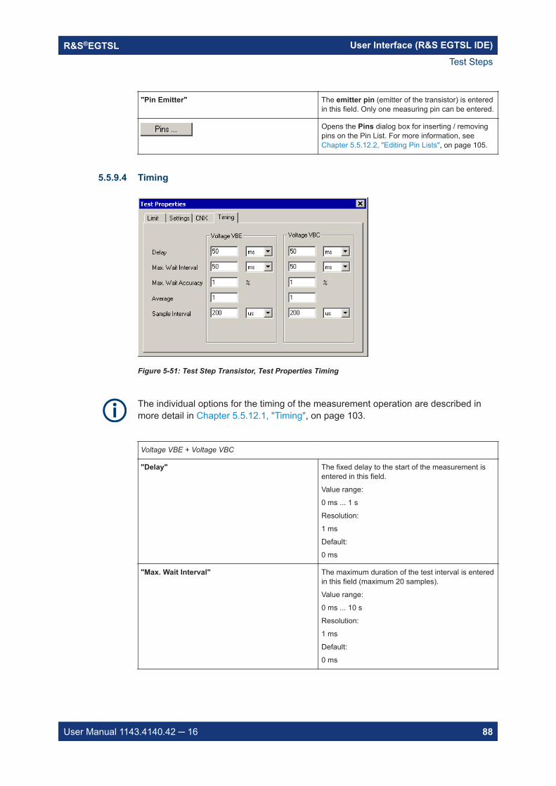
User Interface (R&S EGTSL IDE)R&S®EGTSL
88User Manual 1143.4140.42 16
"Pin Emitter" The emitter pin (emitter of the transistor) is enteredin this field. Only one measuring pin can be entered.
Opens the Pins dialog box for inserting / removingpins on the Pin List. For more information, seeChapter 5.5.12.2, "Editing Pin Lists", on page 105.
5.5.9.4 Timing
Figure 5-51: Test Step Transistor, Test Properties Timing
The individual options for the timing of the measurement operation are described inmore detail in Chapter 5.5.12.1, "Timing", on page 103.
Voltage VBE + Voltage VBC
"Delay" The fixed delay to the start of the measurement isentered in this field.
Value range:
0 ms ... 1 s
Resolution:
1 ms
Default:
0 ms
"Max. Wait Interval" The maximum duration of the test interval is enteredin this field (maximum 20 samples).
Value range:
0 ms ... 10 s
Resolution:
1 ms
Default:
0 ms
Test Steps
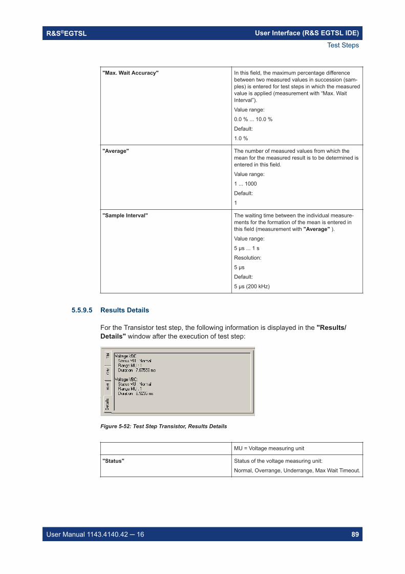
User Interface (R&S EGTSL IDE)R&S®EGTSL
89User Manual 1143.4140.42 16
"Max. Wait Accuracy" In this field, the maximum percentage differencebetween two measured values in succession (sam-ples) is entered for test steps in which the measuredvalue is applied (measurement with “Max. WaitInterval”).
Value range:
0.0 % ... 10.0 %
Default:
1.0 %
"Average" The number of measured values from which themean for the measured result is to be determined isentered in this field.
Value range:
1 ... 1000
Default:
1
"Sample Interval" The waiting time between the individual measure-ments for the formation of the mean is entered inthis field (measurement with "Average" ).
Value range:
5 µs ... 1 s
Resolution:
5 µs
Default:
5 µs (200 kHz)
5.5.9.5 Results Details
For the Transistor test step, the following information is displayed in the "Results/Details" window after the execution of test step:
Figure 5-52: Test Step Transistor, Results Details
MU = Voltage measuring unit
"Status" Status of the voltage measuring unit:
Normal, Overrange, Underrange, Max Wait Timeout.
Test Steps
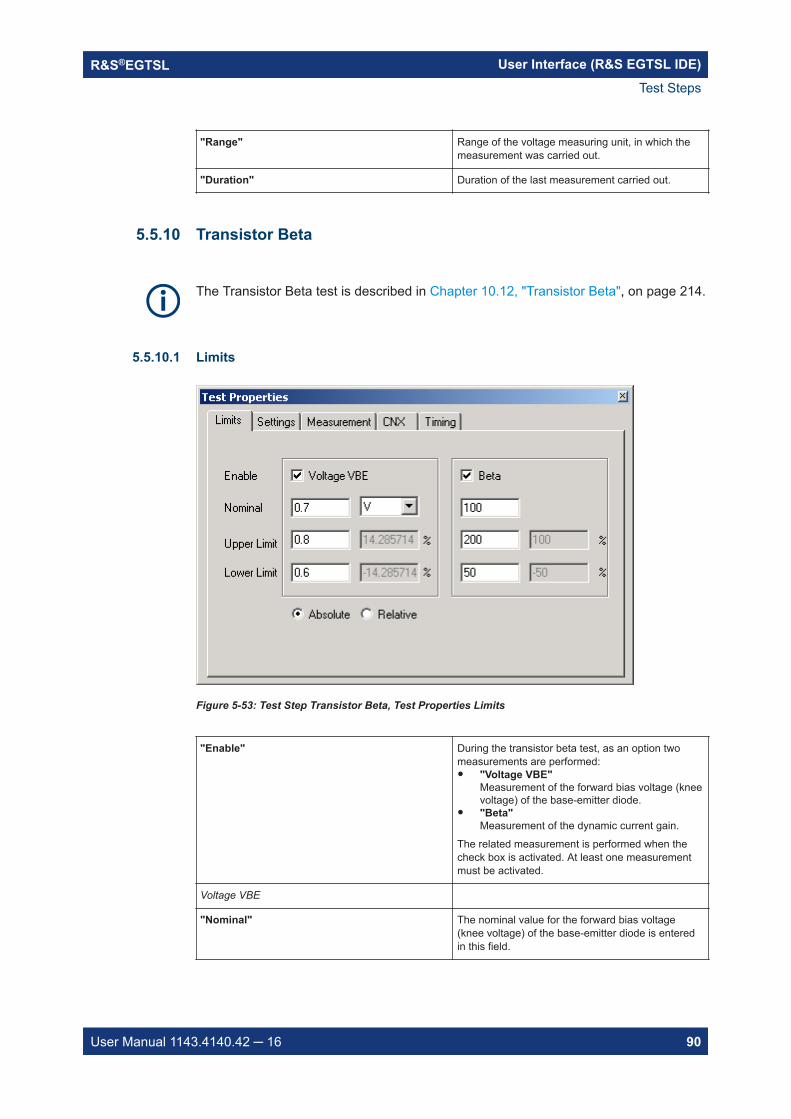
User Interface (R&S EGTSL IDE)R&S®EGTSL
90User Manual 1143.4140.42 16
"Range" Range of the voltage measuring unit, in which themeasurement was carried out.
"Duration" Duration of the last measurement carried out.
5.5.10 Transistor Beta
The Transistor Beta test is described in Chapter 10.12, "Transistor Beta", on page 214.
5.5.10.1 Limits
Figure 5-53: Test Step Transistor Beta, Test Properties Limits
"Enable" During the transistor beta test, as an option twomeasurements are performed: "Voltage VBE"
Measurement of the forward bias voltage (kneevoltage) of the base-emitter diode.
"Beta"Measurement of the dynamic current gain.
The related measurement is performed when thecheck box is activated. At least one measurementmust be activated.
Voltage VBE
"Nominal" The nominal value for the forward bias voltage(knee voltage) of the base-emitter diode is enteredin this field.
Test Steps
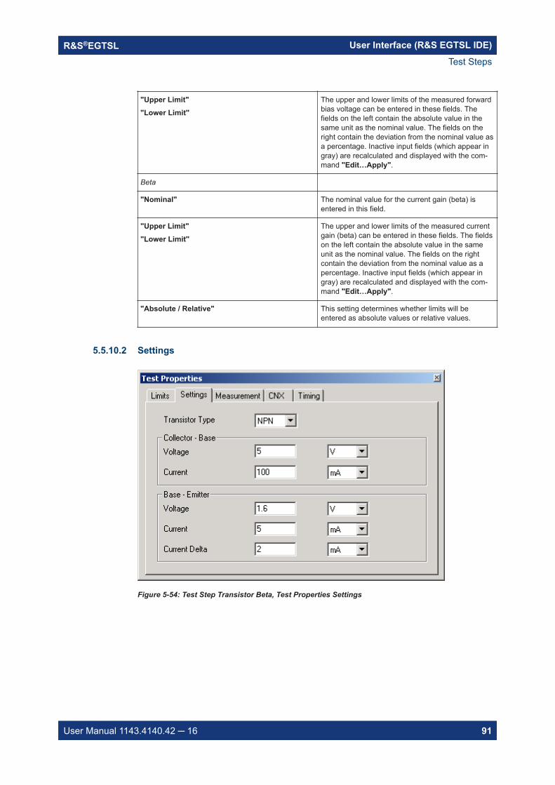
User Interface (R&S EGTSL IDE)R&S®EGTSL
91User Manual 1143.4140.42 16
"Upper Limit""Lower Limit"
The upper and lower limits of the measured forwardbias voltage can be entered in these fields. Thefields on the left contain the absolute value in thesame unit as the nominal value. The fields on theright contain the deviation from the nominal value asa percentage. Inactive input fields (which appear ingray) are recalculated and displayed with the com-mand "Edit…Apply".
Beta
"Nominal" The nominal value for the current gain (beta) isentered in this field.
"Upper Limit""Lower Limit"
The upper and lower limits of the measured currentgain (beta) can be entered in these fields. The fieldson the left contain the absolute value in the sameunit as the nominal value. The fields on the rightcontain the deviation from the nominal value as apercentage. Inactive input fields (which appear ingray) are recalculated and displayed with the com-mand "Edit…Apply".
"Absolute / Relative" This setting determines whether limits will beentered as absolute values or relative values.
5.5.10.2 Settings
Figure 5-54: Test Step Transistor Beta, Test Properties Settings
Test Steps
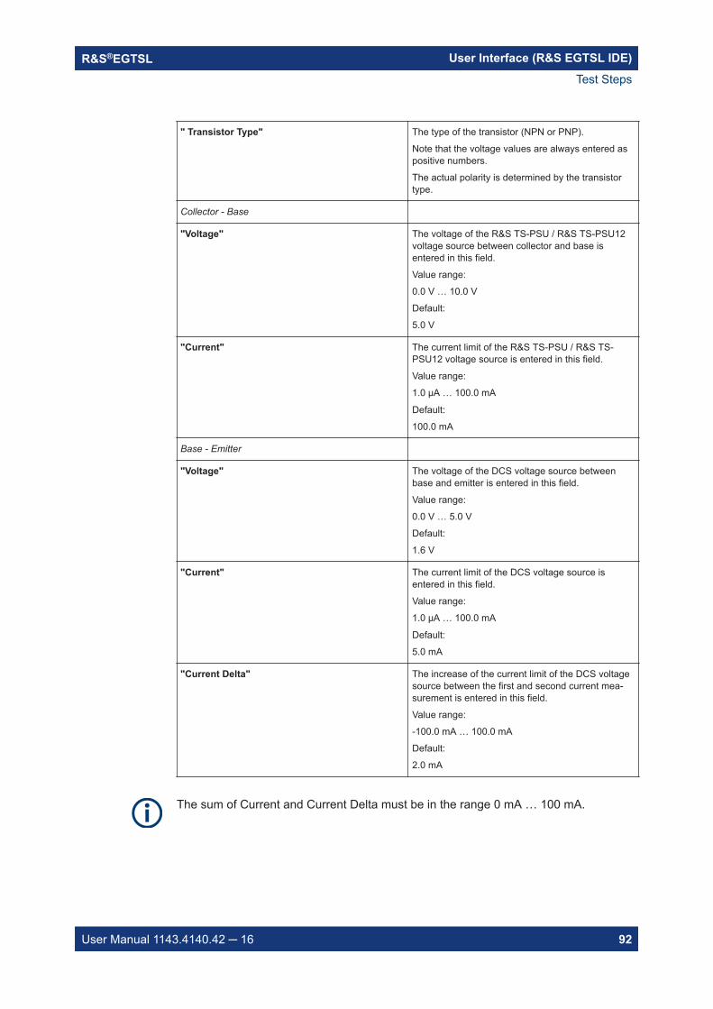
User Interface (R&S EGTSL IDE)R&S®EGTSL
92User Manual 1143.4140.42 16
" Transistor Type" The type of the transistor (NPN or PNP).
Note that the voltage values are always entered aspositive numbers.
The actual polarity is determined by the transistortype.
Collector - Base
"Voltage" The voltage of the R&S TS-PSU / R&S TS-PSU12voltage source between collector and base isentered in this field.
Value range:
0.0 V … 10.0 V
Default:
5.0 V
"Current" The current limit of the R&S TS-PSU / R&S TS-PSU12 voltage source is entered in this field.
Value range:
1.0 µA … 100.0 mA
Default:
100.0 mA
Base - Emitter
"Voltage" The voltage of the DCS voltage source betweenbase and emitter is entered in this field.
Value range:
0.0 V … 5.0 V
Default:
1.6 V
"Current" The current limit of the DCS voltage source isentered in this field.
Value range:
1.0 µA … 100.0 mA
Default:
5.0 mA
"Current Delta" The increase of the current limit of the DCS voltagesource between the first and second current mea-surement is entered in this field.
Value range:
-100.0 mA … 100.0 mA
Default:
2.0 mA
The sum of Current and Current Delta must be in the range 0 mA … 100 mA.
Test Steps
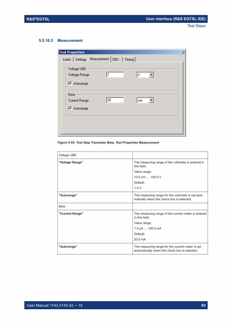
User Interface (R&S EGTSL IDE)R&S®EGTSL
93User Manual 1143.4140.42 16
5.5.10.3 Measurement
Figure 5-55: Test Step Transistor Beta, Test Properties Measurement
Voltage VBE
"Voltage Range" The measuring range of the voltmeter is entered inthis field.
Value range:
10.0 mV … 100.0 V
Default:
1.0 V
"Autorange" The measuring range for the voltmeter is set auto-matically when this check box is selected.
Beta
"Current Range" The measuring range of the current meter is enteredin this field.
Value range:
1.0 µA … 100.0 mA
Default:
20.0 mA
"Autorange" The measuring range for the current meter is setautomatically when this check box is selected.
Test Steps
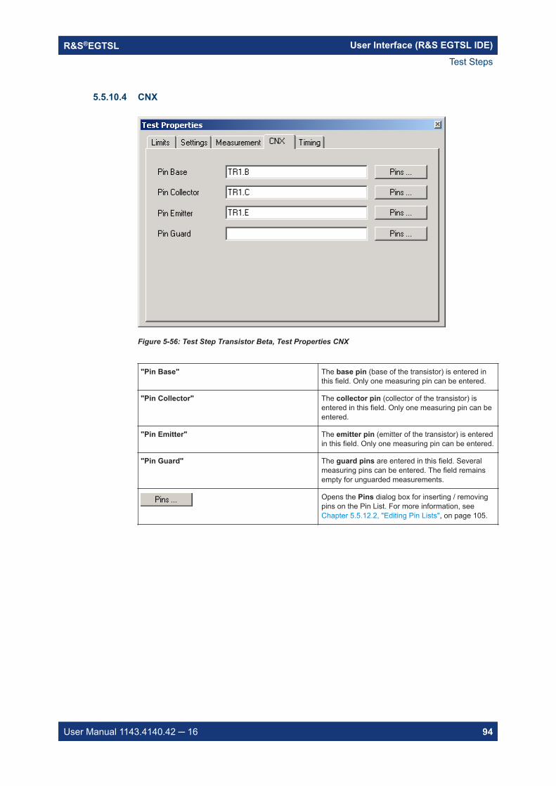
User Interface (R&S EGTSL IDE)R&S®EGTSL
94User Manual 1143.4140.42 16
5.5.10.4 CNX
Figure 5-56: Test Step Transistor Beta, Test Properties CNX
"Pin Base" The base pin (base of the transistor) is entered inthis field. Only one measuring pin can be entered.
"Pin Collector" The collector pin (collector of the transistor) isentered in this field. Only one measuring pin can beentered.
"Pin Emitter" The emitter pin (emitter of the transistor) is enteredin this field. Only one measuring pin can be entered.
"Pin Guard" The guard pins are entered in this field. Severalmeasuring pins can be entered. The field remainsempty for unguarded measurements.
Opens the Pins dialog box for inserting / removingpins on the Pin List. For more information, seeChapter 5.5.12.2, "Editing Pin Lists", on page 105.
Test Steps
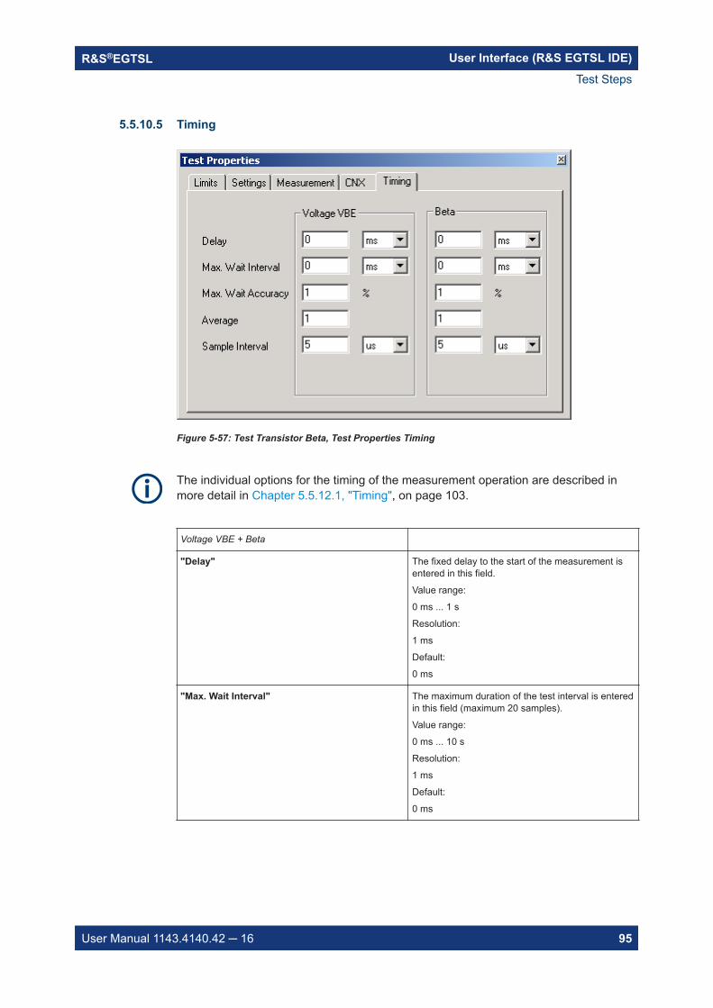
User Interface (R&S EGTSL IDE)R&S®EGTSL
95User Manual 1143.4140.42 16
5.5.10.5 Timing
Figure 5-57: Test Transistor Beta, Test Properties Timing
The individual options for the timing of the measurement operation are described inmore detail in Chapter 5.5.12.1, "Timing", on page 103.
Voltage VBE + Beta
"Delay" The fixed delay to the start of the measurement isentered in this field.
Value range:
0 ms ... 1 s
Resolution:
1 ms
Default:
0 ms
"Max. Wait Interval" The maximum duration of the test interval is enteredin this field (maximum 20 samples).
Value range:
0 ms ... 10 s
Resolution:
1 ms
Default:
0 ms
Test Steps

User Interface (R&S EGTSL IDE)R&S®EGTSL
96User Manual 1143.4140.42 16
"Max. Wait Accuracy" In this field, the maximum percentage differencebetween two measured values in succession (sam-ples) is entered for test steps in which the measuredvalue is applied (measurement with “Max. WaitInterval”).
Value range:
0.0 % ... 10.0 %
Default:
1.0 %
"Average" The number of measured values from which themean for the measured result is to be determined isentered in this field.
Value range:
1 ... 1000
Default:
1
"Sample Interval" The waiting time between the individual measure-ments for the formation of the mean is entered inthis field (measurement with Average ).
Value range:
5 s ... 1 s
Resolution:
5 µs
Default:
5 µs (200 kHz)
5.5.10.6 Results Details
For the Transistor Beta test step, the following information is displayed in the Results/Details window after the execution of the test step:
Figure 5-58: Test Step Transistor Beta, Results Details
Test Steps
User Interface (R&S EGTSL IDE)R&S®EGTSL
97User Manual 1143.4140.42 16
VMU = Voltage measuring unit (R&S TS-PSAM)
CMU = Current measuring unit (R&S TS-PICT)
DCS = DC Source (R&S TS-PSAM)
PSU = DC Source (R&S TS-PSU / R&S TS-PSU12)
Voltage VBE
Status VMU Status of the voltage measurement unit:
Normal, Overrange, Underrange, Max Wait Timeout
Range VMU Range of the voltage measurement unit, in whichthe measurement was carried out.
Duration Duration of the last measurement carried out.
Current gain BETA
Status CMU Status of the current measurement unit for the firstand second measurement:
Normal, Overrange, Underrange, Max Wait Timeout
Range CMU Range of the current measurement unit, in which themeasurement was carried out for the first and sec-ond measurement.
Duration Duration of the last measurement carried out.
Status DCS Status of the DC voltage source DCS:
Normal, Not in constant current state
Status PSU Status of the DC voltage source TS-PSU / TS-PSU12:
Normal, Not in constant voltage state
5.5.11 Zener Diode
The Zener Diode test is described in Chapter 5.5.11, "Zener Diode", on page 97.
Test Steps
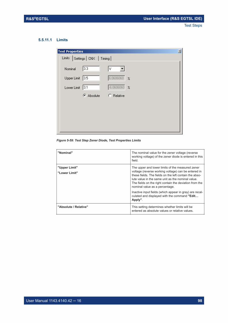
User Interface (R&S EGTSL IDE)R&S®EGTSL
98User Manual 1143.4140.42 16
5.5.11.1 Limits
Figure 5-59: Test Step Zener Diode, Test Properties Limits
"Nominal" The nominal value for the zener voltage (reverseworking voltage) of the zener diode is entered in thisfield.
"Upper Limit""Lower Limit"
The upper and lower limits of the measured zenervoltage (reverse working voltage) can be entered inthese fields. The fields on the left contain the abso-lute value in the same unit as the nominal value.The fields on the right contain the deviation from thenominal value as a percentage.
Inactive input fields (which appear in gray) are recal-culated and displayed with the command "Edit…Apply".
"Absolute / Relative" This setting determines whether limits will beentered as absolute values or relative values.
Test Steps
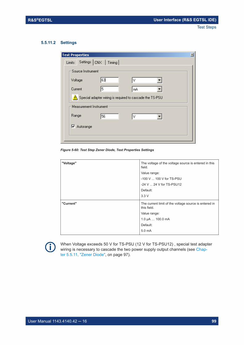
User Interface (R&S EGTSL IDE)R&S®EGTSL
99User Manual 1143.4140.42 16
5.5.11.2 Settings
Figure 5-60: Test Step Zener Diode, Test Properties Settings
"Voltage" The voltage of the voltage source is entered in thisfield.
Value range:
-100 V ... 100 V for TS-PSU
-24 V ... 24 V for TS-PSU12
Default:
3.3 V
"Current" The current limit of the voltage source is entered inthis field.
Value range:
1.0 µA … 100.0 mA
Default:
5.0 mA
When Voltage exceeds 50 V for TS-PSU (12 V for TS-PSU12) , special test adapterwiring is necessary to cascade the two power supply output channels (see Chap-ter 5.5.11, "Zener Diode", on page 97).
Test Steps
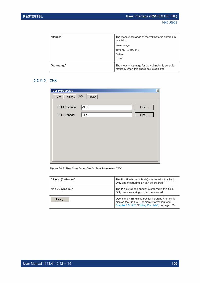
User Interface (R&S EGTSL IDE)R&S®EGTSL
100User Manual 1143.4140.42 16
"Range" The measuring range of the voltmeter is entered inthis field.
Value range:
10.0 mV … 100.0 V
Default:
5.0 V
"Autorange" The measuring range for the voltmeter is set auto-matically when this check box is selected.
5.5.11.3 CNX
Figure 5-61: Test Step Zener Diode, Test Properties CNX
" Pin HI (Cathode)" The Pin HI (diode cathode) is entered in this field.Only one measuring pin can be entered.
"Pin LO (Anode)" The Pin LO (diode anode) is entered in this field.Only one measuring pin can be entered.
Opens the Pins dialog box for inserting / removingpins on the Pin List. For more information, seeChapter 5.5.12.2, "Editing Pin Lists", on page 105.
Test Steps
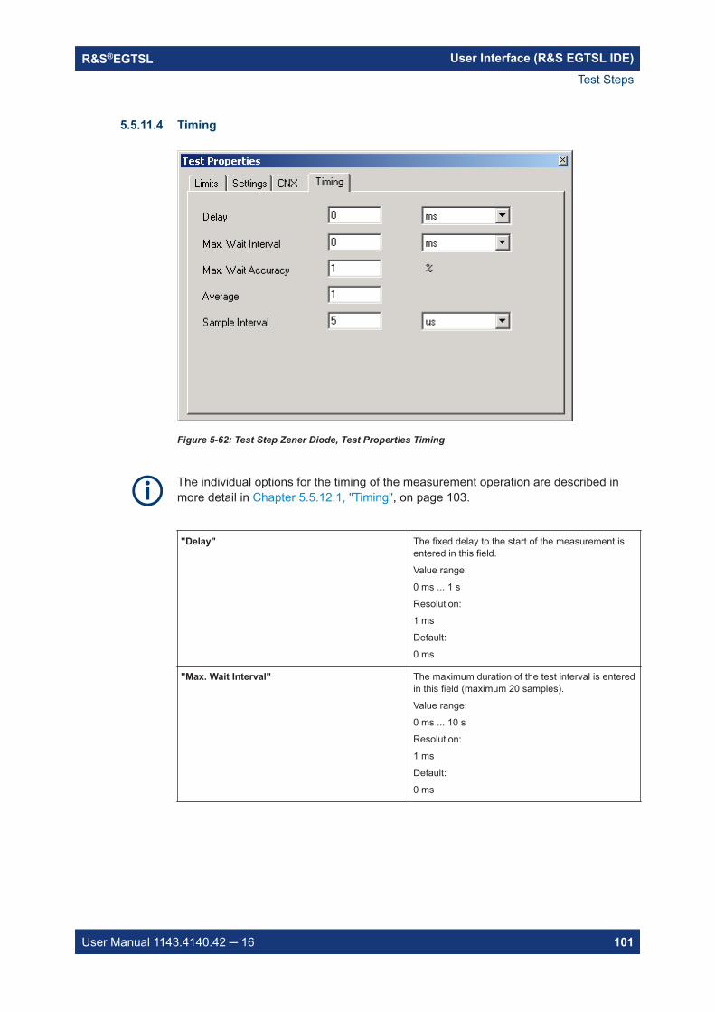
User Interface (R&S EGTSL IDE)R&S®EGTSL
101User Manual 1143.4140.42 16
5.5.11.4 Timing
Figure 5-62: Test Step Zener Diode, Test Properties Timing
The individual options for the timing of the measurement operation are described inmore detail in Chapter 5.5.12.1, "Timing", on page 103.
"Delay" The fixed delay to the start of the measurement isentered in this field.
Value range:
0 ms ... 1 s
Resolution:
1 ms
Default:
0 ms
"Max. Wait Interval" The maximum duration of the test interval is enteredin this field (maximum 20 samples).
Value range:
0 ms ... 10 s
Resolution:
1 ms
Default:
0 ms
Test Steps
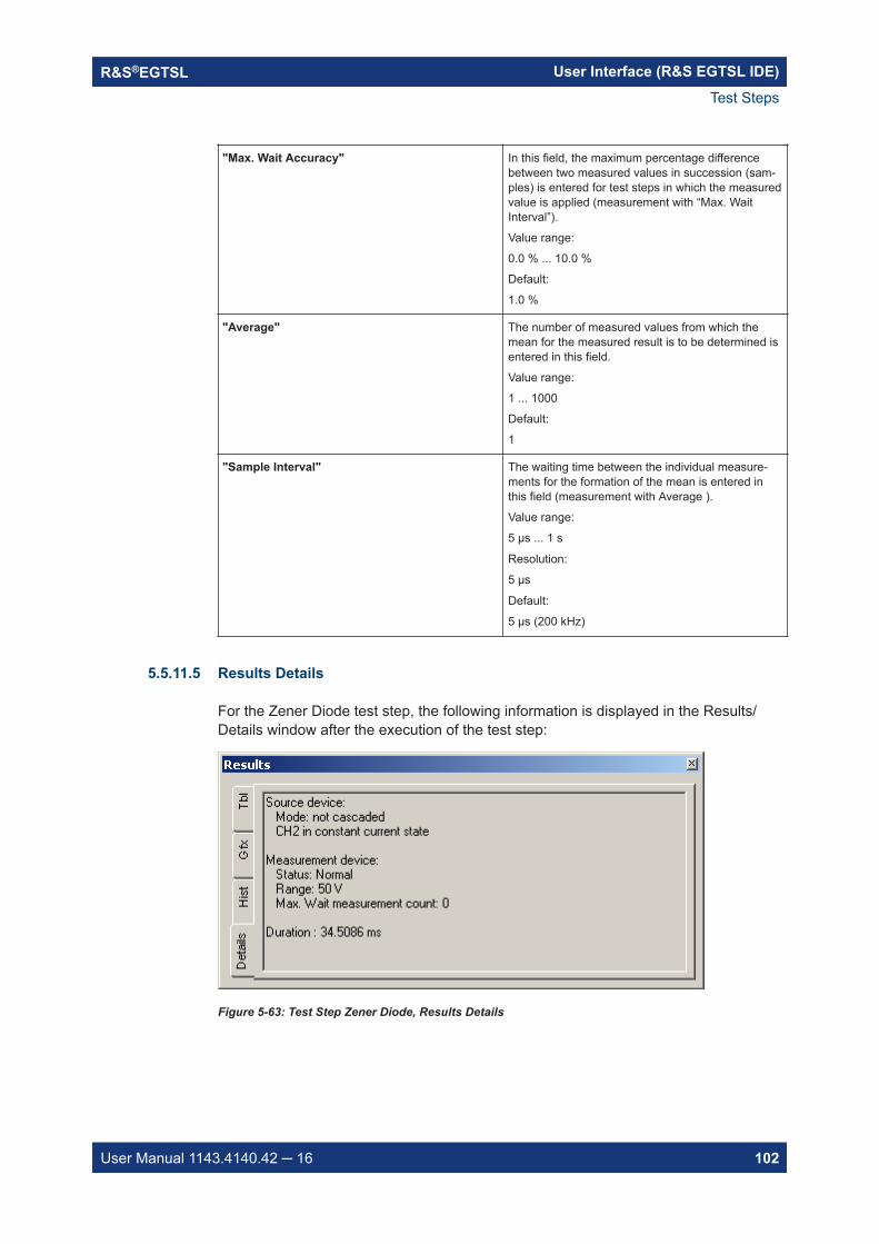
User Interface (R&S EGTSL IDE)R&S®EGTSL
102User Manual 1143.4140.42 16
"Max. Wait Accuracy" In this field, the maximum percentage differencebetween two measured values in succession (sam-ples) is entered for test steps in which the measuredvalue is applied (measurement with “Max. WaitInterval”).
Value range:
0.0 % ... 10.0 %
Default:
1.0 %
"Average" The number of measured values from which themean for the measured result is to be determined isentered in this field.
Value range:
1 ... 1000
Default:
1
"Sample Interval" The waiting time between the individual measure-ments for the formation of the mean is entered inthis field (measurement with Average ).
Value range:
5 µs ... 1 s
Resolution:
5 µs
Default:
5 µs (200 kHz)
5.5.11.5 Results Details
For the Zener Diode test step, the following information is displayed in the Results/Details window after the execution of the test step:
Figure 5-63: Test Step Zener Diode, Results Details
Test Steps
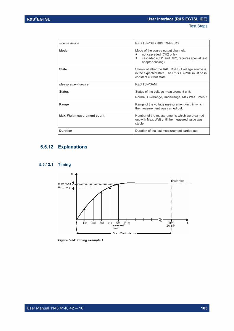
User Interface (R&S EGTSL IDE)R&S®EGTSL
103User Manual 1143.4140.42 16
Source device R&S TS-PSU / R&S TS-PSU12
Mode Mode of the source output channels: not cascaded (CH2 only) cascaded (CH1 and CH2, requires special test
adapter cabling)
State Shows whether the R&S TS-PSU voltage source isin the expected state. The R&S TS-PSU must be inconstant current state.
Measurement device R&S TS-PSAM
Status Status of the voltage measurement unit:
Normal, Overrange, Underrange, Max Wait Timeout
Range Range of the voltage measurement unit, in whichthe measurement was carried out.
Max. Wait measurement count Number of the measurements which were carriedout with Max. Wait until the measured value wasstable.
Duration Duration of the last measurement carried out.
5.5.12 Explanations
5.5.12.1 Timing
Figure 5-64: Timing example 1
Test Steps
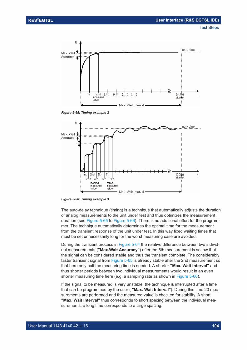
User Interface (R&S EGTSL IDE)R&S®EGTSL
104User Manual 1143.4140.42 16
Figure 5-65: Timing example 2
Figure 5-66: Timing example 3
The auto-delay technique (timing) is a technique that automatically adjusts the durationof analog measurements to the unit under test and thus optimizes the measurementduration (see Figure 5-65 to Figure 5-66). There is no additional effort for the program-mer. The technique automatically determines the optimal time for the measurementfrom the transient response of the unit under test. In this way fixed waiting times thatmust be set unnecessarily long for the worst measuring case are avoided.
During the transient process in Figure 5-64 the relative difference between two individ-ual measurements ("Max.Wait Accuracy") after the 5th measurement is so low thatthe signal can be considered stable and thus the transient complete. The considerablyfaster transient signal from Figure 5-65 is already stable after the 2nd measurement sothat here only half the measuring time is needed. A shorter "Max. Wait Interval" andthus shorter periods between two individual measurements would result in an evenshorter measuring time here (e.g. a sampling rate as shown in Figure 5-66).
If the signal to be measured is very unstable, the technique is interrupted after a timethat can be programmed by the user ( "Max. Wait Interval"). During this time 20 mea-surements are performed and the measured value is checked for stability. A short"Max. Wait Interval" thus corresponds to short spacing between the individual mea-surements, a long time corresponds to a large spacing.
Test Steps
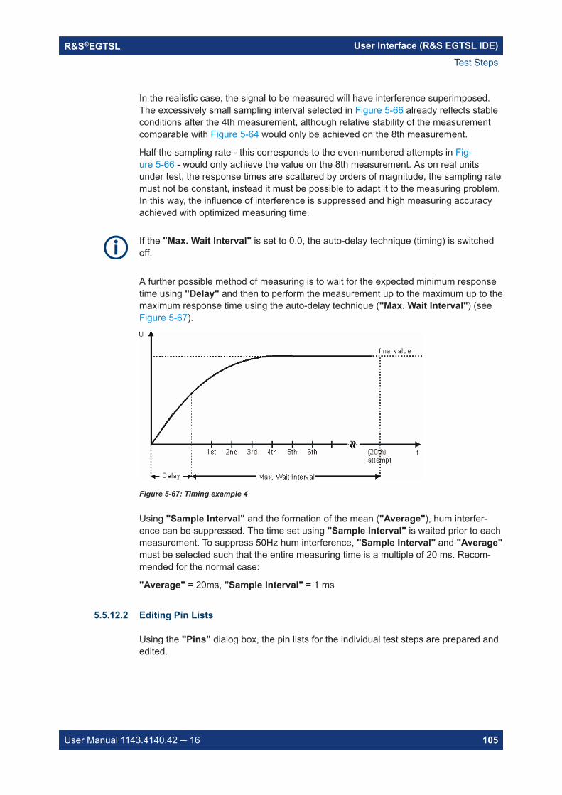
User Interface (R&S EGTSL IDE)R&S®EGTSL
105User Manual 1143.4140.42 16
In the realistic case, the signal to be measured will have interference superimposed.The excessively small sampling interval selected in Figure 5-66 already reflects stableconditions after the 4th measurement, although relative stability of the measurementcomparable with Figure 5-64 would only be achieved on the 8th measurement.
Half the sampling rate - this corresponds to the even-numbered attempts in Fig-ure 5-66 - would only achieve the value on the 8th measurement. As on real unitsunder test, the response times are scattered by orders of magnitude, the sampling ratemust not be constant, instead it must be possible to adapt it to the measuring problem.In this way, the influence of interference is suppressed and high measuring accuracyachieved with optimized measuring time.
If the "Max. Wait Interval" is set to 0.0, the auto-delay technique (timing) is switchedoff.
A further possible method of measuring is to wait for the expected minimum responsetime using "Delay" and then to perform the measurement up to the maximum up to themaximum response time using the auto-delay technique ("Max. Wait Interval") (seeFigure 5-67).
Figure 5-67: Timing example 4
Using "Sample Interval" and the formation of the mean ("Average"), hum interfer-ence can be suppressed. The time set using "Sample Interval" is waited prior to eachmeasurement. To suppress 50Hz hum interference, "Sample Interval" and "Average"must be selected such that the entire measuring time is a multiple of 20 ms. Recom-mended for the normal case:
"Average" = 20ms, "Sample Interval" = 1 ms
5.5.12.2 Editing Pin Lists
Using the "Pins" dialog box, the pin lists for the individual test steps are prepared andedited.
Test Steps
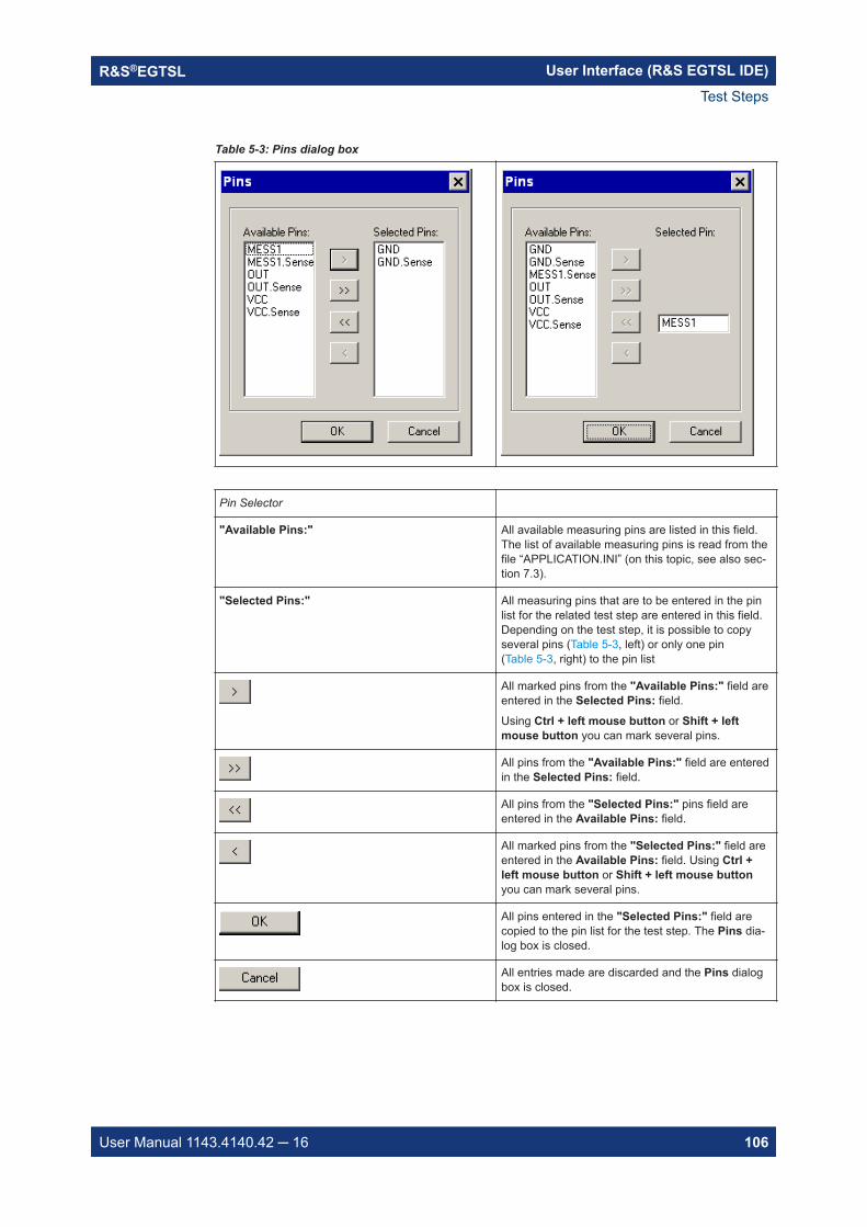
User Interface (R&S EGTSL IDE)R&S®EGTSL
106User Manual 1143.4140.42 16
Table 5-3: Pins dialog box
Pin Selector
"Available Pins:" All available measuring pins are listed in this field.The list of available measuring pins is read from thefile “APPLICATION.INI” (on this topic, see also sec-tion 7.3).
"Selected Pins:" All measuring pins that are to be entered in the pinlist for the related test step are entered in this field.Depending on the test step, it is possible to copyseveral pins (Table 5-3, left) or only one pin(Table 5-3, right) to the pin list
All marked pins from the "Available Pins:" field areentered in the Selected Pins: field.
Using Ctrl + left mouse button or Shift + leftmouse button you can mark several pins.
All pins from the "Available Pins:" field are enteredin the Selected Pins: field.
All pins from the "Selected Pins:" pins field areentered in the Available Pins: field.
All marked pins from the "Selected Pins:" field areentered in the Available Pins: field. Using Ctrl +left mouse button or Shift + left mouse buttonyou can mark several pins.
All pins entered in the "Selected Pins:" field arecopied to the pin list for the test step. The Pins dia-log box is closed.
All entries made are discarded and the Pins dialogbox is closed.
Test Steps
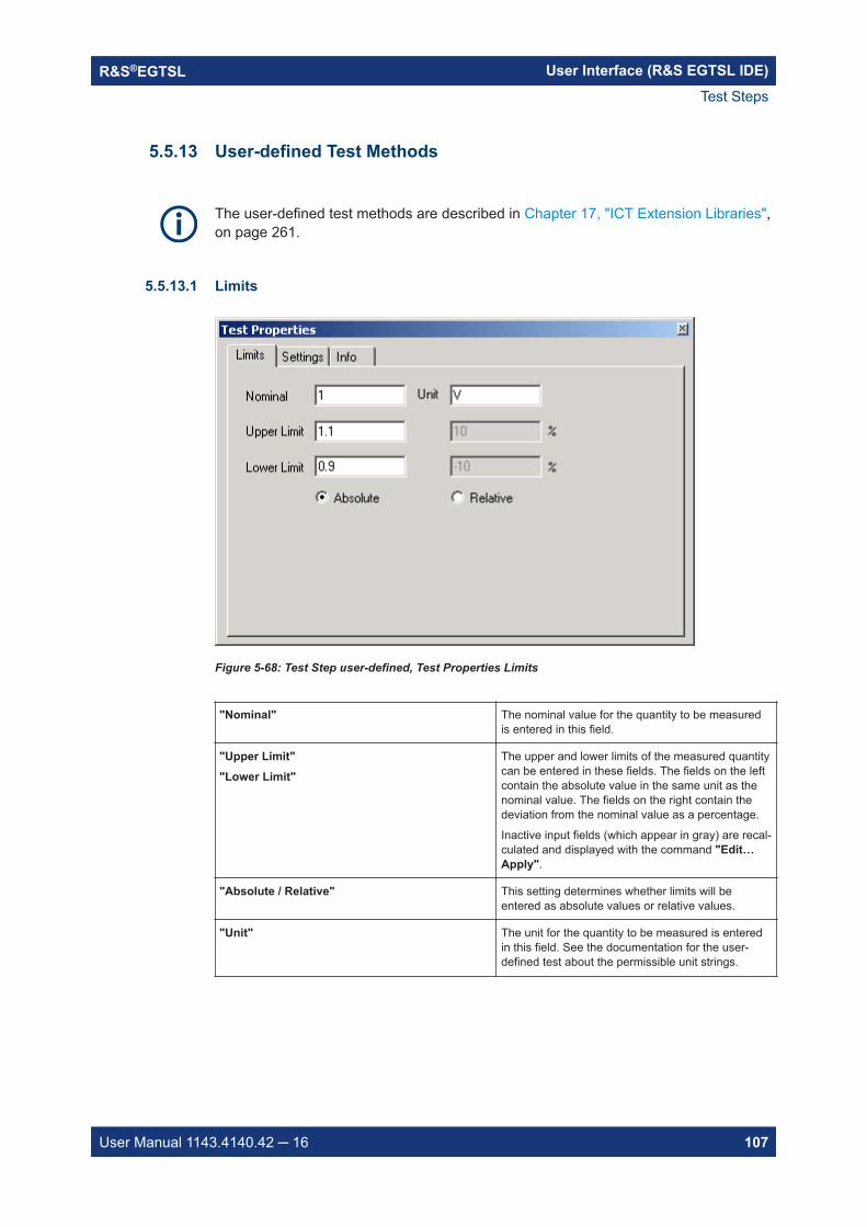
User Interface (R&S EGTSL IDE)R&S®EGTSL
107User Manual 1143.4140.42 16
5.5.13 User-defined Test Methods
The user-defined test methods are described in Chapter 17, "ICT Extension Libraries",on page 261.
5.5.13.1 Limits
Figure 5-68: Test Step user-defined, Test Properties Limits
"Nominal" The nominal value for the quantity to be measuredis entered in this field.
"Upper Limit""Lower Limit"
The upper and lower limits of the measured quantitycan be entered in these fields. The fields on the leftcontain the absolute value in the same unit as thenominal value. The fields on the right contain thedeviation from the nominal value as a percentage.
Inactive input fields (which appear in gray) are recal-culated and displayed with the command "Edit…Apply".
"Absolute / Relative" This setting determines whether limits will beentered as absolute values or relative values.
"Unit" The unit for the quantity to be measured is enteredin this field. See the documentation for the user-defined test about the permissible unit strings.
Test Steps
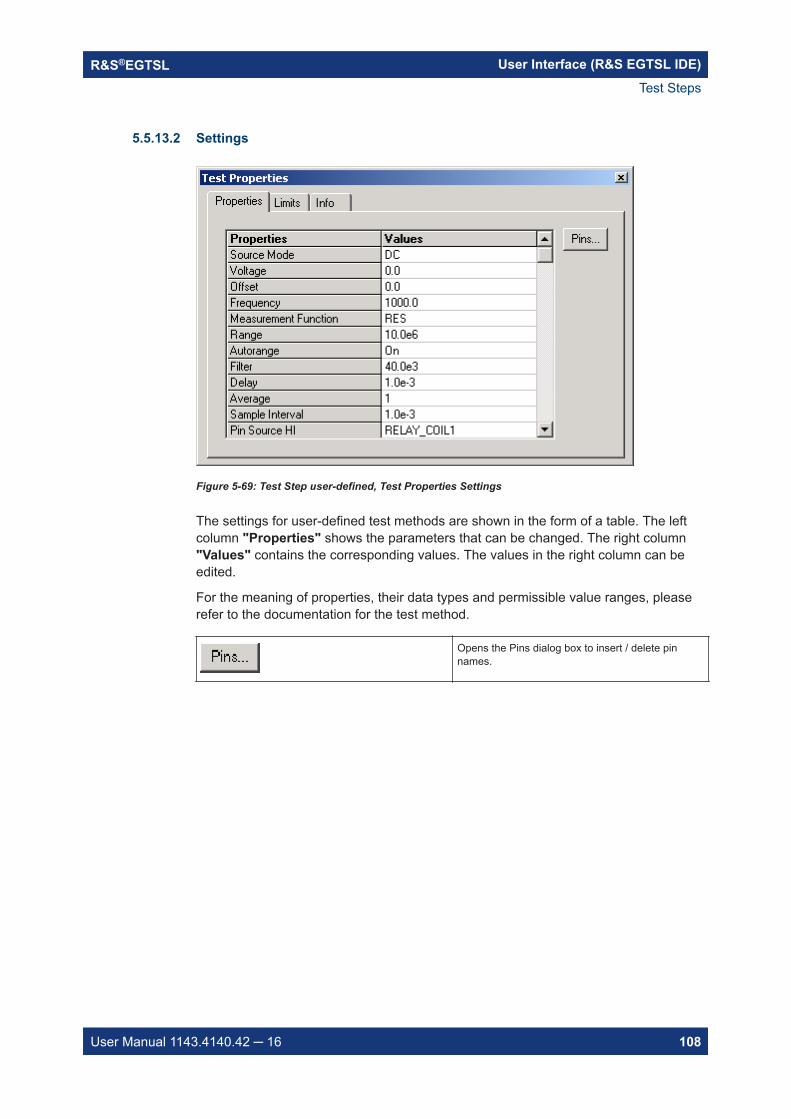
User Interface (R&S EGTSL IDE)R&S®EGTSL
108User Manual 1143.4140.42 16
5.5.13.2 Settings
Figure 5-69: Test Step user-defined, Test Properties Settings
The settings for user-defined test methods are shown in the form of a table. The leftcolumn "Properties" shows the parameters that can be changed. The right column"Values" contains the corresponding values. The values in the right column can beedited.
For the meaning of properties, their data types and permissible value ranges, pleaserefer to the documentation for the test method.
Opens the Pins dialog box to insert / delete pinnames.
Test Steps
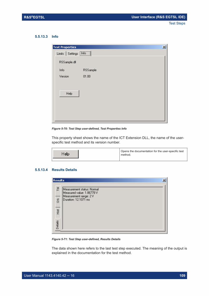
User Interface (R&S EGTSL IDE)R&S®EGTSL
109User Manual 1143.4140.42 16
5.5.13.3 Info
Figure 5-70: Test Step user-defined, Test Properties Info
This property sheet shows the name of the ICT Extension DLL, the name of the user-specific test method and its version number.
Opens the documentation for the user-specific testmethod.
5.5.13.4 Results Details
Figure 5-71: Test Step user-defined, Results Details
The data shown here refers to the last test step executed. The meaning of the output isexplained in the documentation for the test method.
Test Steps
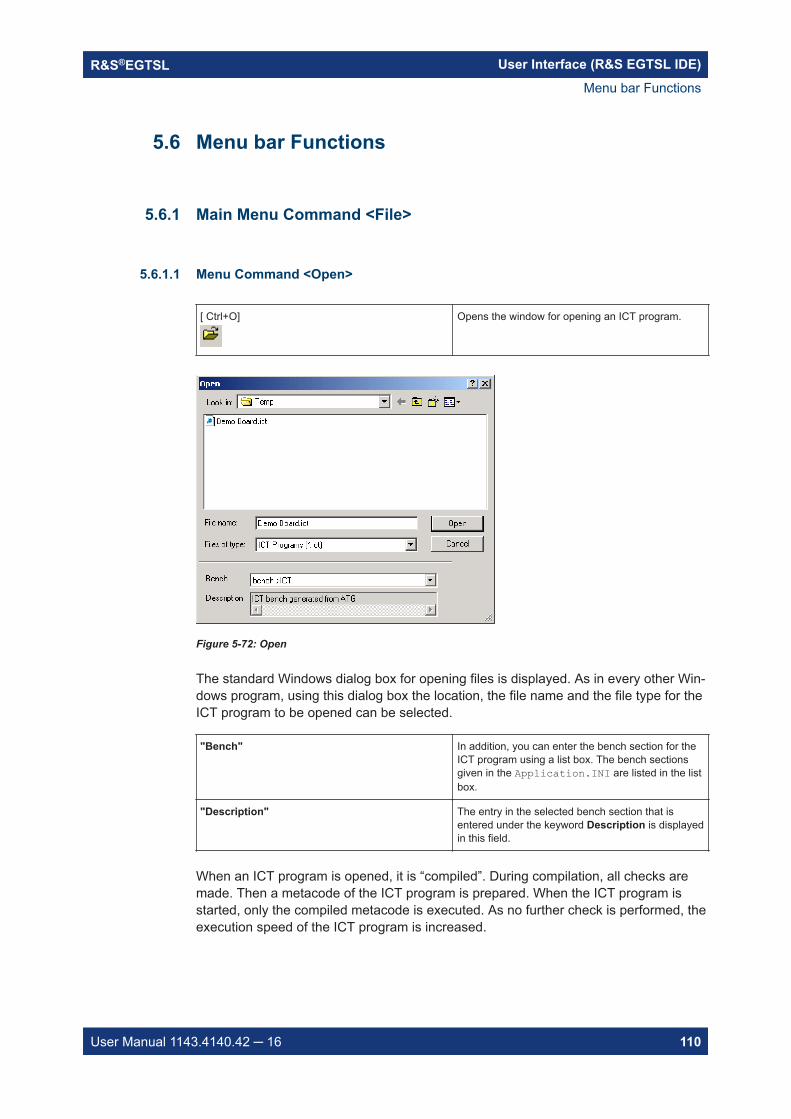
User Interface (R&S EGTSL IDE)R&S®EGTSL
110User Manual 1143.4140.42 16
5.6 Menu bar Functions
5.6.1 Main Menu Command <File>
5.6.1.1 Menu Command <Open>
[ Ctrl+O] Opens the window for opening an ICT program.
Figure 5-72: Open
The standard Windows dialog box for opening files is displayed. As in every other Win-dows program, using this dialog box the location, the file name and the file type for theICT program to be opened can be selected.
"Bench" In addition, you can enter the bench section for theICT program using a list box. The bench sectionsgiven in the Application.INI are listed in the listbox.
"Description" The entry in the selected bench section that isentered under the keyword Description is displayedin this field.
When an ICT program is opened, it is “compiled”. During compilation, all checks aremade. Then a metacode of the ICT program is prepared. When the ICT program isstarted, only the compiled metacode is executed. As no further check is performed, theexecution speed of the ICT program is increased.
Menu bar Functions
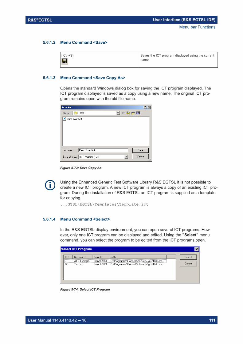
User Interface (R&S EGTSL IDE)R&S®EGTSL
111User Manual 1143.4140.42 16
5.6.1.2 Menu Command <Save>
[ Ctrl+S] Saves the ICT program displayed using the currentname.
5.6.1.3 Menu Command <Save Copy As>
Opens the standard Windows dialog box for saving the ICT program displayed. TheICT program displayed is saved as a copy using a new name. The original ICT pro-gram remains open with the old file name.
Figure 5-73: Save Copy As
Using the Enhanced Generic Test Software Library R&S EGTSL it is not possible tocreate a new ICT program. A new ICT program is always a copy of an existing ICT pro-gram. During the installation of R&S EGTSL an ICT program is supplied as a templatefor copying....GTSL\EGTSL\Templates\Template.ict
5.6.1.4 Menu Command <Select>
In the R&S EGTSL display environment, you can open several ICT programs. How-ever, only one ICT program can be displayed and edited. Using the "Select" menucommand, you can select the program to be edited from the ICT programs open.
Figure 5-74: Select ICT Program
Menu bar Functions
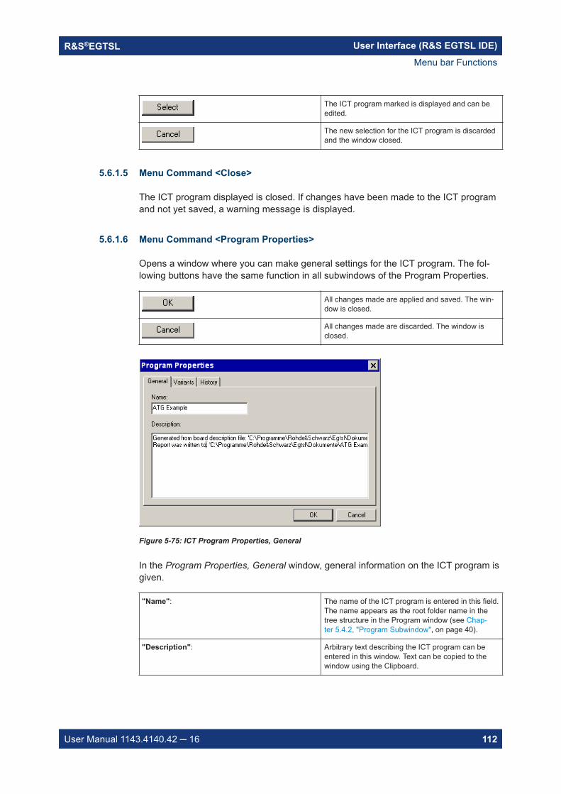
User Interface (R&S EGTSL IDE)R&S®EGTSL
112User Manual 1143.4140.42 16
The ICT program marked is displayed and can beedited.
The new selection for the ICT program is discardedand the window closed.
5.6.1.5 Menu Command <Close>
The ICT program displayed is closed. If changes have been made to the ICT programand not yet saved, a warning message is displayed.
5.6.1.6 Menu Command <Program Properties>
Opens a window where you can make general settings for the ICT program. The fol-lowing buttons have the same function in all subwindows of the Program Properties.
All changes made are applied and saved. The win-dow is closed.
All changes made are discarded. The window isclosed.
Figure 5-75: ICT Program Properties, General
In the Program Properties, General window, general information on the ICT program isgiven.
"Name": The name of the ICT program is entered in this field.The name appears as the root folder name in thetree structure in the Program window (see Chap-ter 5.4.2, "Program Subwindow", on page 40).
"Description": Arbitrary text describing the ICT program can beentered in this window. Text can be copied to thewindow using the Clipboard.
Menu bar Functions
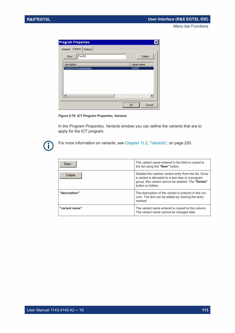
User Interface (R&S EGTSL IDE)R&S®EGTSL
113User Manual 1143.4140.42 16
Figure 5-76: ICT Program Properties, Variants
In the Program Properties, Variants window you can define the variants that are toapply for the ICT program.
For more information on variants, see Chapter 11.2, "Variants", on page 220.
The variant name entered in the field is copied tothe list using the "New" button.
Deletes the marked variant entry from the list. Oncea variant is allocated to a test step or a programgroup, this variant cannot be deleted. The "Delete"button is hidden.
"description" The description of the variant is entered in this col-umn. The text can be edited by clicking the entrymarked.
"variant name" The variant name entered is copied to this column.The variant name cannot be changed later.
Menu bar Functions
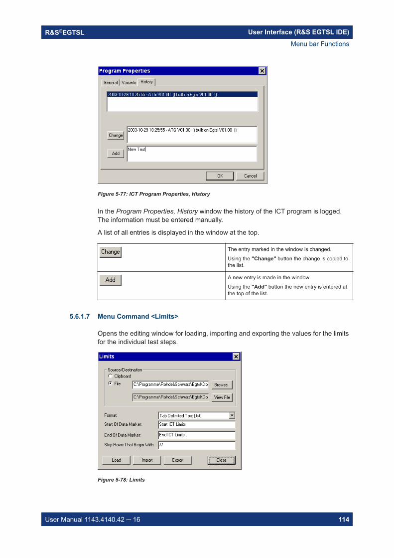
User Interface (R&S EGTSL IDE)R&S®EGTSL
114User Manual 1143.4140.42 16
Figure 5-77: ICT Program Properties, History
In the Program Properties, History window the history of the ICT program is logged.The information must be entered manually.
A list of all entries is displayed in the window at the top.
The entry marked in the window is changed.
Using the "Change" button the change is copied tothe list.
A new entry is made in the window.
Using the "Add" button the new entry is entered atthe top of the list.
5.6.1.7 Menu Command <Limits>
Opens the editing window for loading, importing and exporting the values for the limitsfor the individual test steps.
Figure 5-78: Limits
Menu bar Functions
User Interface (R&S EGTSL IDE)R&S®EGTSL
115User Manual 1143.4140.42 16
Source/Destination
"Clipboard" With this function activated, the data for loading,importing and exporting values for limits are writtento the Clipboard or read from the Clipboard.
"File" With this function activated, the data for loading,importing and exporting values for limits are writtento a txt file or read from a txt file.
Opens the standard Windows window for selectingan existing file with values for limits. In the standardWindows window, it is also possible to create a filefor exporting the values for the limits. The folder andthe file name for the selected export/import file aredisplayed next to the "Browse..." button and next tothe "View File" button.
Opens the selected export/import file in the Win-dows text editor. Changes can be made and savedin the editor.
"Format:" There is a choice of two data formats for exportingor importing: Tab-delimited Text (file extension *.txt )
The individual entries on a line are separatedby tabs (see example 1)
Comma-delimited Text (file extension *.csv )The individual entries on a line are separatedby commas (see example 2)
The data formats apply for Importing (loading) from the Clipboard. Exporting to the Clipboard. Importing (loading) from a file. Exporting to a
file.
"Start Of Data Marker:" The start of the data area in the import/export file ismarked with the text given here (format setting).
"End Of Data Marker:" The end of the data area in the import/export file ismarked with the text given here (format setting).
"Skip Rows That Begin With:" Lines in the import/export file that are to be skippedduring loading/importing are marked with the char-acters (text) given here (format setting).
Loads the values for the limits from the Clipboard orthe import file given. The values for the limits aretemporarily changed and displayed. The values loa-ded cannot be saved. When the ICT program isopened next time, the original values for the limitswill be displayed again.
The data format given and the format settings mustmatch the information in the file to be loaded.
Imports the values for the limits from the Clipboardor the import file given. The old values for the limitsare overwritten and saved with the ICT program.
The data format given and the format settings mustmatch the information in the file to be imported.
Menu bar Functions
User Interface (R&S EGTSL IDE)R&S®EGTSL
116User Manual 1143.4140.42 16
Exports the values for the limits for all test steps(when present) to the Clipboard or the export filegiven. The data format from the format settings isapplied during the export
The editing window for loading, importing andexporting the values for the limits is closed.
Examples for an export/import file with values for limits:
Example:
Start ICT Limits
<Step Name> Limits.High Limits.Low [Limits.High Limits.Low]
// example of acomment line
Discharge Test 0 0
Contact Test 0 0
Short Test 0 0
R1 1.3538 1.0462
R2 365.58 294.45
R3 44.135 35.868
R4 11.035 8.9674
C1 396.42 323.68
C2 110.16 89.94
C3 110.1 89.896
TR1 0.78 0.42 0.78 0.42
End ICT Limits
Example: START SECTION LIMITS<Step Name>,Limits.High,Limits.Low,[Limits.High,Limits.Low]// example of a comment lineDischarge Test,0,0Contact Test,0,0Short Test,0,0R1,1.3538,1.0462R2,365.58,294.45R3,44.135,35.868R4,11.035,8.9674C1,396.42,323.68C2,110.16,89.94C3,110.1,89.896TR1,0.78,0.42,0.78,0.42END SECTION LIMITS
Menu bar Functions
User Interface (R&S EGTSL IDE)R&S®EGTSL
117User Manual 1143.4140.42 16
The following points are to be observed when editing the export/import file with valuesfor the limits:
The numerical values have the English number format i.e. the decimal point andnot the decimal comma must be used.
The names of the individual tests are given in the first column. If there are teststeps with the same test step name (e.g. the resistor test Rx twice), the test stepnames are expanded by the test step ID .
Example: Rx[27]Rx[28]
Resistor and impedance tests have no second limit. The column “Limits.High” forthe second limit is used to store the optional correction value.
5.6.1.8 Menu Command <Print>
[ Ctrl+P] Opens the standard Windows print dialog box forprinting the report.
It is not possible to print an ICT program. It is only possible to print the contents of theReport window
Figure 5-79: Print
All marked areas of the Report window are printed. The entire report can be markedusing the context menu (see Chapter 5.4.3.1, "Context Menu", on page 42).
5.6.1.9 Menu Command <Print Setup>
Opens the standard Windows printer dialog box with the settings for the printer con-nected.
Menu bar Functions
User Interface (R&S EGTSL IDE)R&S®EGTSL
118User Manual 1143.4140.42 16
Figure 5-80: Print Setup
The standard Windows functions are used.
5.6.1.10 Menu Command <Exit>
Quits the program Enhanced Generic Test Software Library R&S EGTSL. If changeshave been made to the ICT program opened and these have not yet been saved, awarning message is displayed (see Figure 5-81).
Figure 5-81: Exit Warning
The ICT programs that have not yet been saved are listed.
The ICT programs marked with a check mark aresaved. The changes to ICT programs that are notmarked are discarded. The program is quit.
None of the ICT programs displayed is saved. Allchanges made are discarded. The program is quit.
The quitting of the program is canceled. The ICTprogram last edited is displayed.
Menu bar Functions
User Interface (R&S EGTSL IDE)R&S®EGTSL
119User Manual 1143.4140.42 16
5.6.2 Main Menu Command <Edit>
The descriptions of the menu commands that only execute functions and for which adedicated window is not opened are summarized in Chapter 5.6.2.1, "Functions",on page 119.
5.6.2.1 Functions
Undo [Ctrl+Z] Undoes the last action. Up to 256 actions can beundone.
Redo [Ctrl+Y] Reverses the action of the <Undo> command.
Cut [Ctrl+X] Removes the item currently marked (test step, pro-gram group, text content) and places it in the Clip-board.
Copy [Ctrl+C] Copies the item currently marked (test step, pro-gram group, text content) to the Clipboard.
Paste [Ctrl+V] Inserts the contents of the Clipboard (test step, pro-gram group, text content) at the current cursor posi-tion.
Delete [Ctrl+Del] Deletes a marked test step or the marked programgroup.
Insert Opens a list box for inserting test steps. On thistopic, see also section 5.5: Test Steps.
Select All [Ctrl+A] Marks all test steps or all entries in the Report win-dow. The function depends on the cursor position.
Apply [Ctrl+Enter] The changes made in the test properties for the teststep marked are applied. The entries are checkedfor plausibility and compliance with the valueranges. The metacode for the ICT program is upda-ted.
Revert [Ctrl+Back] The changes made in the test properties for the teststep marked are discarded. The values that appliedwhen the test step was marked are displayed again.
Auto apply When this button is activated, the changes made inthe test properties for the test step marked are auto-matically applied when you change to a different teststep. The entries are checked for plausibility andcompliance with the value ranges. The metacode forthe ICT program is updated.
Rename [F2] Enables the name of the marked test step to be edi-ted.
Menu bar Functions
User Interface (R&S EGTSL IDE)R&S®EGTSL
120User Manual 1143.4140.42 16
5.6.2.2 Menu Command <Find>
[ Ctrl+F] Opens the dialog box for the selection of the searchcriteria for individual test step names or programgroup names (see Figure 5-83) or for text in theReport window (see Figure 5-84 ). The functiondepends on the cursor position.
Search for text step name or program group name:
Figure 5-82: Find (Program)
"Step name" The search text for the test step name or programgroup name is entered in this field. The most recentsearch texts are saved and can be selected againusing the list box. When R&S EGTSL is quit, thesaved search texts are deleted.
"Case sensitive" When this function is activated, the search is onlyperformed for test step names or program groupnames with the same upper and lower case as inthe Step name field.
"Match whole word only" With this function activated, the search is only per-formed for test step names or program group namesthat exactly match the information in the Step namefield.
Find what
"Step with the given name" With this function activated, the search is performedfor test step names or program group names thatmatch the information in the Step name field.
"Step with compile error(s)" With this function activated, the search is only per-formed for test step names that have a compileerror. The information in the "Step name" field isignored.
Direction
"Up" Defines the direction starting from the cursor posi-tion in which the ICT
"Down" program is to be searched. With the Up functionactivated, the search is performed from the cursorposition upwards. With the Down function activated,the search is performed from the cursor positiondownwards.
Menu bar Functions
User Interface (R&S EGTSL IDE)R&S®EGTSL
121User Manual 1143.4140.42 16
The search is continued to the next entry (test stepname, program group name) that matches the entrymade. The test step or the program group found ismarked.
The search in the Program window is stopped.
Searching for text in the report:
Figure 5-83: Find (Report)
"Find what" The search text is entered in this field.
"Match case" With this function activated, the search is only per-formed for text with the same upper and lower caseas in the "Find what" field.
Direction
"Up" Defines the direction starting from the cursor posi-tion in which the report is to be searched. With theUp function activated, the search is performed fromthe cursor position upwards. With the Down functionactivated, the search is performed from the cursorposition downwards.
"Down"
The search is continued for the next entry thatmatches the information given. The test entry foundis marked.
The test search in the Report window is stopped.
5.6.2.3 Menu Command <Step Properties>
[Alt+Enter] Opens the dialog button for the step properties forthe test step or program group marked.
The dialog box for the step properties can also be opened using the program contextmenu (see Chapter 5.4.2.1, "Context Menu", on page 41).
The Step Properties, Common (see Figure 5-84) are displayed when opened from amarked test step or program group.
Menu bar Functions
User Interface (R&S EGTSL IDE)R&S®EGTSL
122User Manual 1143.4140.42 16
Figure 5-84: Step Properties, Common
"Name" The name of the test step or program group is edi-ted in this field.
"Comment" The comment for the test step or for the programgroup is entered in this field. The text entered is dis-played in the Program window in the Comment col-umn.
"ID" To be able to identify uniquely each test step andeach program group in the program, each entry isautomatically allocated an ID number when it is cre-ated. This ID is displayed in this window.
Variant Selection
"Available Variants" All variants for the ICT program are listed in this list.Variants are added in the program properties (seeChapter 5.6.1.6, "Menu Command <Program Prop-erties>", on page 112).
Selected Variants All variants allocated to the test step or the programgroup are given in this list. Several variants can beallocated to a test step or a program group. The teststep or the program group is only executed whenthe corresponding variant has been selected in theDebug subwindow (see Chapter 5.4.6, "Debug Sub-window", on page 46).
Exclude Selection With this function activated, the test step or the pro-gram group is executed for all variants and the<default> setting. The test step or the programgroup is not executed with the variants that are lis-ted in the Selected Variants list.
Moves the marked variant entry from the AvailableVariants list to the Selected Variants list.
Moves the marked variant entry from the SelectedVariants list to the Available Variants list.
Menu bar Functions
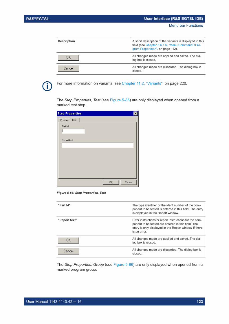
User Interface (R&S EGTSL IDE)R&S®EGTSL
123User Manual 1143.4140.42 16
Description A short description of the variants is displayed in thisfield (see Chapter 5.6.1.6, "Menu Command <Pro-gram Properties>", on page 112).
All changes made are applied and saved. The dia-log box is closed.
All changes made are discarded. The dialog box isclosed.
For more information on variants, see Chapter 11.2, "Variants", on page 220.
The Step Properties, Test (see Figure 5-85) are only displayed when opened from amarked test step.
Figure 5-85: Step Properties, Test
"Part Id" The type identifier or the ident number of the com-ponent to be tested is entered in this field. The entryis displayed in the Report window.
"Report text" Error instructions or repair instructions for the com-ponent to be tested are entered in this field. Theentry is only displayed in the Report window if thereis an error.
All changes made are applied and saved. The dia-log box is closed.
All changes made are discarded. The dialog box isclosed.
The Step Properties, Group (see Figure 5-86) are only displayed when opened from amarked program group.
Menu bar Functions
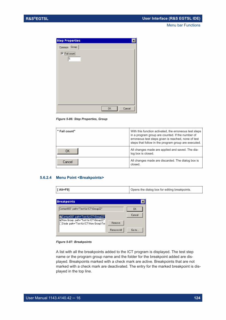
User Interface (R&S EGTSL IDE)R&S®EGTSL
124User Manual 1143.4140.42 16
Figure 5-86: Step Properties, Group
" Fail count" With this function activated, the erroneous test stepsin a program group are counted. If the number oferroneous test steps given is reached, none of teststeps that follow in the program group are executed.
All changes made are applied and saved. The dia-log box is closed.
All changes made are discarded. The dialog box isclosed.
5.6.2.4 Menu Point <Breakpoints>
[ Alt+F9] Opens the dialog box for editing breakpoints.
Figure 5-87: Breakpoints
A list with all the breakpoints added to the ICT program is displayed. The test stepname or the program group name and the folder for the breakpoint added are dis-played. Breakpoints marked with a check mark are active. Breakpoints that are notmarked with a check mark are deactivated. The entry for the marked breakpoint is dis-played in the top line.
Menu bar Functions
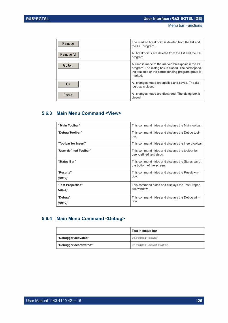
User Interface (R&S EGTSL IDE)R&S®EGTSL
125User Manual 1143.4140.42 16
The marked breakpoint is deleted from the list andthe ICT program.
All breakpoints are deleted from the list and the ICTprogram.
A jump is made to the marked breakpoint in the ICTprogram. The dialog box is closed. The correspond-ing test step or the corresponding program group ismarked.
All changes made are applied and saved. The dia-log box is closed.
All changes made are discarded. The dialog box isclosed.
5.6.3 Main Menu Command <View>
" Main Toolbar" This command hides and displays the Main toolbar.
"Debug Toolbar" This command hides and displays the Debug tool-bar.
"Toolbar for Insert" This command hides and displays the Insert toolbar.
"User-defined Toolbar" This command hides and displays the toolbar foruser-defined test steps.
"Status Bar" This command hides and displays the Status bar atthe bottom of the screen.
"Results"[Alt+0]
This command hides and displays the Result win-dow.
"Test Properties"[Alt+1]
This command hides and displays the Test Proper-ties window.
"Debug"[Alt+2]
This command hides and displays the Debug win-dow.
5.6.4 Main Menu Command <Debug>
Text in status bar
"Debugger activated" Debugger ready
"Debugger deactivated" Debugger deactivated
Menu bar Functions
User Interface (R&S EGTSL IDE)R&S®EGTSL
126User Manual 1143.4140.42 16
"Go"[F5]
Executes the ICT program once from the test stepmarked with the yellow arrow (current debuggerexecution point) to the end. If the debugger is deac-tivated, the ICT program is executed from start tofinish.
"Restart"[Ctrl+Shift+F5]
With the debugger activated, executes the ICT pro-gram from the start to the finish.
"Terminate"[Shift+F5]
Stops the execution of the ICT program. The mark-ing with the yellow arrow (current debugger execu-tion point) is removed. The debugger is deactivated.
"Break" Interrupts the execution of the ICT program. Thetest step at which the interruption takes place ismarked with the yellow arrow (current debuggerexecution point) and displayed. Using the Go com-mand the execution of the ICT program can be con-tinued.
"Repeat"[F4]
With the debugger activated, starts the execution ofthe test steps marked (test steps with a color back-ground) with the number of repetitions given.
"Resume"[Shift+F4]
Continues the execution of the marked test steps(test steps with a color background) following aninterruption using the Break button.
"Step Into "[F11]
Executes the ICT program from the test stepmarked with the yellow arrow (current executionpoint of the debugger) in single steps. If the test stepis a group, automatically each test step of the groupwill be executed in single steps.
"Step Over"[F10]
Executes the ICT program from the test stepmarked with the yellow arrow (current executionpoint of the debugger) in single steps. If the test stepis a group, all test steps in the group are performedautomatically.
"Step Out"[Shift+F11]
If the test step marked with the yellow arrow (currentexecution point of the debugger) is in a group, thegroup is left with this button. The test steps that fol-low in the group are performed automatically. If thetest step marked with the yellow arrow (current exe-cution point of the debugger) is at the top programlevel, all following test steps including groups areexecuted.
"Run to Cursor"[Ctrl+F10]
Executes the ICT program from the test stepmarked with the yellow arrow (current executionpoint of the debugger) to the test step marked withthe cursor. The test step marked by the position ofthe cursor is marked as the next test step that canbe executed using the yellow arrow.
"Set Next Step"[Ctrl+Shift+F10]
Marks the position of the cursor as the test step thatis to be executed next. A yellow arrow is displayedon the left beside the test step marked. The debug-ger is activated.
Menu bar Functions
User Interface (R&S EGTSL IDE)R&S®EGTSL
127User Manual 1143.4140.42 16
"Show Next Step "[Alt+F10]
Jumps to the current debugger execution position(test step marked with the yellow arrow). The teststep is the next that is executed.
"Toggle Breakpoint"[F9]
Sets a breakpoint at the cursor position. The break-point is deactivated when you click the button again.The third time you click the button, the breakpoint isdeleted (see also Chapter 5.6.2.4, "Menu Point<Breakpoints>", on page 124).
"Stop At Fail " With this function activated, the ICT program execu-tion is stopped when the test step result was “Fail”.The program stops at the erroneous test step. TheStop at fail function applies to all debug commandswith the exception of the Repeat function.
"Break At Fail" With this function activated, the execution of the ICTprogram (test steps marked) is interrupted when thetest step result was “Fail”. The program stops at theerroneous test step. The Break at fail functionapplies only to the Repeat function.
5.6.5 Main Menu Command <Report>
" Clear Report Window" Deletes all entries in the Report window.
"Report Enable" With this function activated a report is displayed inthe Report window.
"Report Errors Only" With this function activated, only erroneous mea-surements and error messages are displayed in theReport window.
"Clear Results" Deletes all entries in the Result windows (Tbl, Gfx,Hist, Details) for all test steps.
"Auto Clear" With this function activated, all entries in the Resultwindow (Tbl, Gfx, Hist, Details) will be deleted for alltest steps on any test step command (e.g. Run,Step, Repeat).
5.6.6 Main Menu Command <Help>
5.6.6.1 Menu Command <About EGTSL>
Opens the window with information on the software.
Menu bar Functions
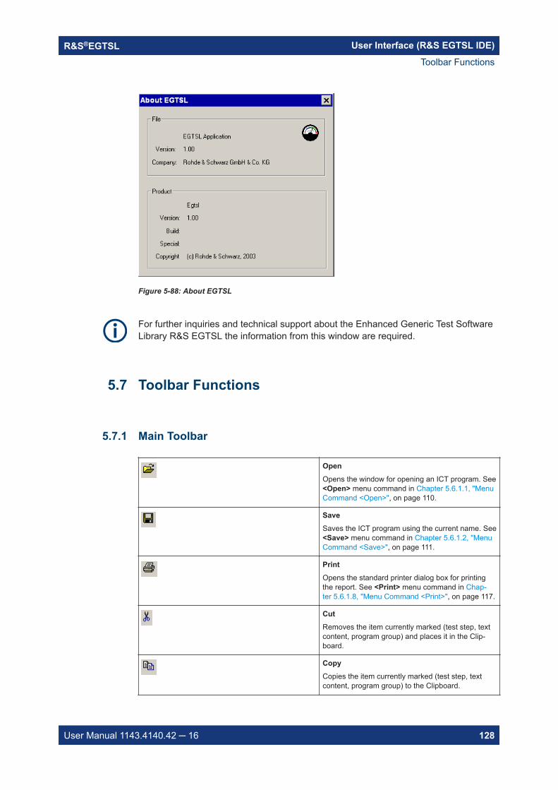
User Interface (R&S EGTSL IDE)R&S®EGTSL
128User Manual 1143.4140.42 16
Figure 5-88: About EGTSL
For further inquiries and technical support about the Enhanced Generic Test SoftwareLibrary R&S EGTSL the information from this window are required.
5.7 Toolbar Functions
5.7.1 Main Toolbar
OpenOpens the window for opening an ICT program. See<Open> menu command in Chapter 5.6.1.1, "MenuCommand <Open>", on page 110.
SaveSaves the ICT program using the current name. See<Save> menu command in Chapter 5.6.1.2, "MenuCommand <Save>", on page 111.
PrintOpens the standard printer dialog box for printingthe report. See <Print> menu command in Chap-ter 5.6.1.8, "Menu Command <Print>", on page 117.
CutRemoves the item currently marked (test step, textcontent, program group) and places it in the Clip-board.
CopyCopies the item currently marked (test step, textcontent, program group) to the Clipboard.
Toolbar Functions
User Interface (R&S EGTSL IDE)R&S®EGTSL
129User Manual 1143.4140.42 16
PasteInserts the contents of the Clipboard (test step, textcontent, program group) at the current position ofthe cursor.
UndoUndoes the last action.
RedoReverses the action of the <Undo> command.
Auto ApplyWhen this button is activated, the changes made inthe test properties for the test step marked areapplied automatically when you change test step.The entries are checked for plausibility and compli-ance with the value ranges. The metacode for theICT program is updated.
ApplyThe changes made in the test properties for the teststep marked are applied. The entries are checkedfor plausibility and compliance with the valueranges. The metacode for the ICT program is upda-ted.
RevertThe changes made in the test properties for the teststep marked are discarded. The values that appliedwhen the test step was marked are displayed again.
Step PropertiesOpens the dialog box for the entry of the generalstep properties. See <Step Properties> menu com-mand in Chapter 5.6.2.3, "Menu Command <StepProperties>", on page 121.
FindOpens the dialog box for selecting the search crite-ria for individual test steps or for text content in theReport window. The function depends on the posi-tion of the cursor. See <Find> menu command inChapter 5.6.2.2, "Menu Command <Find>",on page 120.
AboutOpen the window with information on the software.See <About EGTSL> menu command in Chap-ter 5.6.6.1, "Menu Command <About EGTSL>",on page 127.
Toolbar Functions
User Interface (R&S EGTSL IDE)R&S®EGTSL
130User Manual 1143.4140.42 16
5.7.2 Debug Toolbar
GoExecutes the ICT program once from the test stepmarked with the yellow arrow (current debuggerexecution point) to the end. If the debugger is deac-tivated, the ICT program is executed from start tofinish.
RestartWith the debugger activated executes the ICT pro-gram from the start to the finish.
TerminateStops the execution of the ICT program. The mark-ing with the yellow arrow (current debugger execu-tion point) is removed. The debugger is deactivated.
BreakInterrupts the execution of the ICT program. Thetest step at which the interruption takes place ismarked with the yellow arrow (current debuggerexecution point) and displayed. Using the Go com-mand the execution of the ICT program can be con-tinued.
Step IntoExecutes the ICT program from the test stepmarked with the yellow arrow (current executionpoint of the debugger) in single steps. If the test stepis a group, automatically each test step of the groupwill be executed in single steps.
Step OverExecutes the ICT program from the test stepmarked with the yellow arrow (current executionpoint of the debugger) in single steps. If the test stepis a group, all test steps in the group are performedautomatically.
Step OutIf the test step marked with the yellow arrow (currentexecution point of the debugger) is in a group, thegroup is left with this button. The test steps that fol-low in the group are performed automatically. If thetest step marked with the yellow arrow (current exe-cution point of the debugger) is at the top programlevel, all following test steps including groups areexecuted.
Run to CursorExecutes the ICT program from the test stepmarked with the yellow arrow (current executionpoint of the debugger) to the test step marked withthe cursor. The test step marked by the position ofthe cursor is marked as the next test step that canbe executed using the yellow arrow.
Toolbar Functions
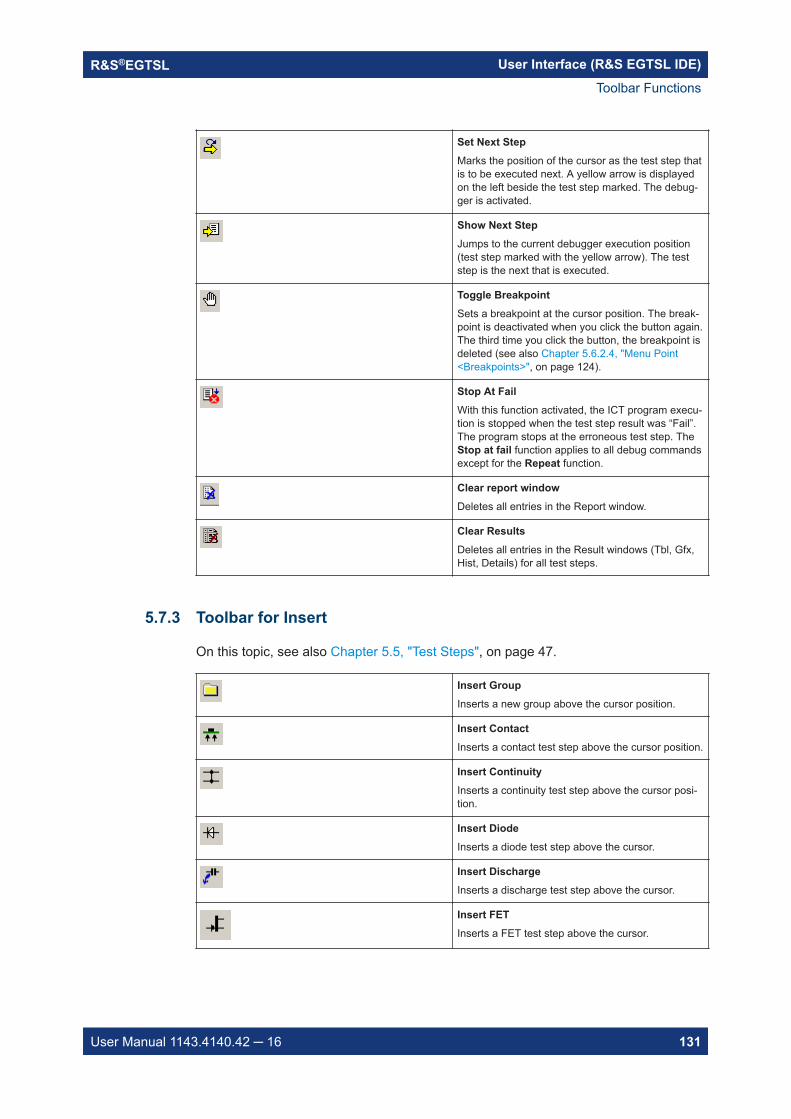
User Interface (R&S EGTSL IDE)R&S®EGTSL
131User Manual 1143.4140.42 16
Set Next StepMarks the position of the cursor as the test step thatis to be executed next. A yellow arrow is displayedon the left beside the test step marked. The debug-ger is activated.
Show Next StepJumps to the current debugger execution position(test step marked with the yellow arrow). The teststep is the next that is executed.
Toggle BreakpointSets a breakpoint at the cursor position. The break-point is deactivated when you click the button again.The third time you click the button, the breakpoint isdeleted (see also Chapter 5.6.2.4, "Menu Point<Breakpoints>", on page 124).
Stop At FailWith this function activated, the ICT program execu-tion is stopped when the test step result was “Fail”.The program stops at the erroneous test step. TheStop at fail function applies to all debug commandsexcept for the Repeat function.
Clear report windowDeletes all entries in the Report window.
Clear ResultsDeletes all entries in the Result windows (Tbl, Gfx,Hist, Details) for all test steps.
5.7.3 Toolbar for Insert
On this topic, see also Chapter 5.5, "Test Steps", on page 47.
Insert GroupInserts a new group above the cursor position.
Insert ContactInserts a contact test step above the cursor position.
Insert ContinuityInserts a continuity test step above the cursor posi-tion.
Insert DiodeInserts a diode test step above the cursor.
Insert DischargeInserts a discharge test step above the cursor.
Insert FETInserts a FET test step above the cursor.
Toolbar Functions
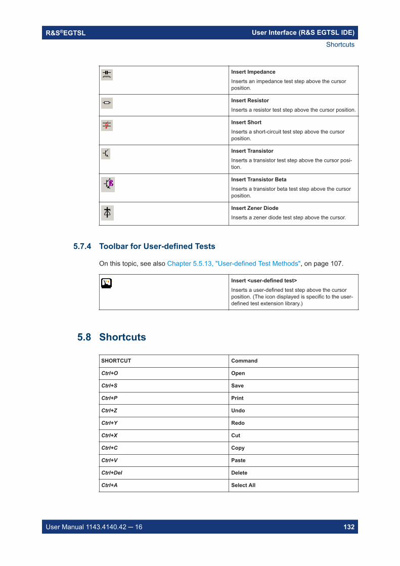
User Interface (R&S EGTSL IDE)R&S®EGTSL
132User Manual 1143.4140.42 16
Insert ImpedanceInserts an impedance test step above the cursorposition.
Insert ResistorInserts a resistor test step above the cursor position.
Insert ShortInserts a short-circuit test step above the cursorposition.
Insert TransistorInserts a transistor test step above the cursor posi-tion.
Insert Transistor BetaInserts a transistor beta test step above the cursorposition.
Insert Zener DiodeInserts a zener diode test step above the cursor.
5.7.4 Toolbar for User-defined Tests
On this topic, see also Chapter 5.5.13, "User-defined Test Methods", on page 107.
Insert <user-defined test>Inserts a user-defined test step above the cursorposition. (The icon displayed is specific to the user-defined test extension library.)
5.8 Shortcuts
SHORTCUT Command
Ctrl+O Open
Ctrl+S Save
Ctrl+P Print
Ctrl+Z Undo
Ctrl+Y Redo
Ctrl+X Cut
Ctrl+C Copy
Ctrl+V Paste
Ctrl+Del Delete
Ctrl+A Select All
Shortcuts
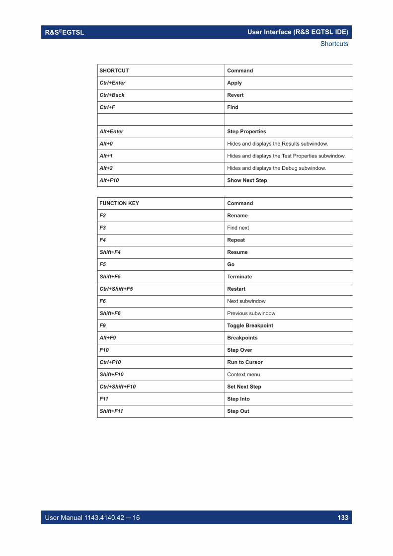
User Interface (R&S EGTSL IDE)R&S®EGTSL
133User Manual 1143.4140.42 16
SHORTCUT Command
Ctrl+Enter Apply
Ctrl+Back Revert
Ctrl+F Find
Alt+Enter Step Properties
Alt+0 Hides and displays the Results subwindow.
Alt+1 Hides and displays the Test Properties subwindow.
Alt+2 Hides and displays the Debug subwindow.
Alt+F10 Show Next Step
FUNCTION KEY Command
F2 Rename
F3 Find next
F4 Repeat
Shift+F4 Resume
F5 Go
Shift+F5 Terminate
Ctrl+Shift+F5 Restart
F6 Next subwindow
Shift+F6 Previous subwindow
F9 Toggle Breakpoint
Alt+F9 Breakpoints
F10 Step Over
Ctrl+F10 Run to Cursor
Shift+F10 Context menu
Ctrl+Shift+F10 Set Next Step
F11 Step Into
Shift+F11 Step Out
Shortcuts
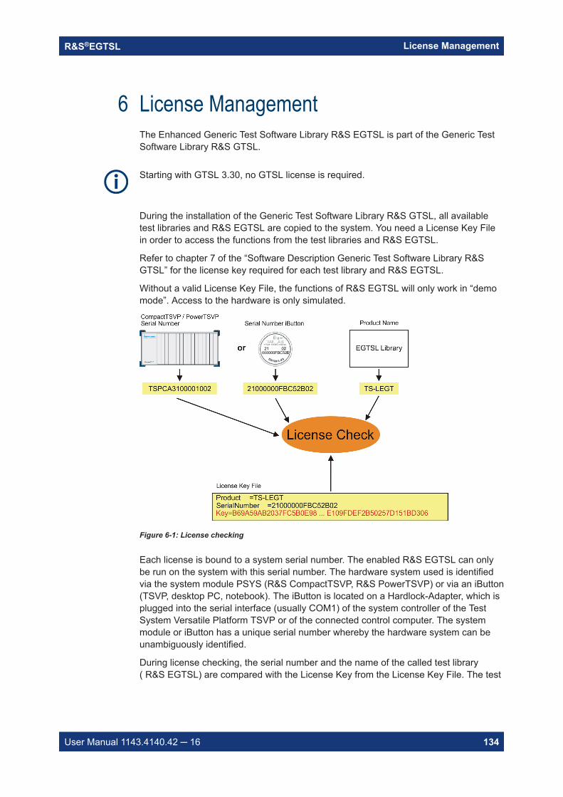
License ManagementR&S®EGTSL
134User Manual 1143.4140.42 16
6 License ManagementThe Enhanced Generic Test Software Library R&S EGTSL is part of the Generic TestSoftware Library R&S GTSL.
Starting with GTSL 3.30, no GTSL license is required.
During the installation of the Generic Test Software Library R&S GTSL, all availabletest libraries and R&S EGTSL are copied to the system. You need a License Key Filein order to access the functions from the test libraries and R&S EGTSL.
Refer to chapter 7 of the “Software Description Generic Test Software Library R&SGTSL” for the license key required for each test library and R&S EGTSL.
Without a valid License Key File, the functions of R&S EGTSL will only work in “demomode”. Access to the hardware is only simulated.
Figure 6-1: License checking
Each license is bound to a system serial number. The enabled R&S EGTSL can onlybe run on the system with this serial number. The hardware system used is identifiedvia the system module PSYS (R&S CompactTSVP, R&S PowerTSVP) or via an iButton(TSVP, desktop PC, notebook). The iButton is located on a Hardlock-Adapter, which isplugged into the serial interface (usually COM1) of the system controller of the TestSystem Versatile Platform TSVP or of the connected control computer. The systemmodule or iButton has a unique serial number whereby the hardware system can beunambiguously identified.
During license checking, the serial number and the name of the called test library( R&S EGTSL) are compared with the License Key from the License Key File. The test
License ManagementR&S®EGTSL
135User Manual 1143.4140.42 16
library (R&S EGTSL) in question will only be enabled if these coincide. The serial num-ber and the name of the test library (R&S EGTSL ) are encoded in the License Key.
Example of a License Key File:
[Header]FileVer=1.0[Project]Info=EGTSL[Modul]Product=TS-LEGTSerialNumber=850000008E4BD202Key=C146648E1DEF9AD78663728A5D8E8D25885F457367D7F7C359F2C63BDB926 ...
The serial number is queried and a new License Key File is installed via the R&SGTSL License Viewer. To open the R&S GTSL License Viewer, select the following:
"Start -> Programs -> GTSL -> License Viewer"
The R&S GTSL License Viewer is described in section 4 of the “Software DescriptionGeneric Test Software Library R&S GTSL”.
Configuration FilesR&S®EGTSL
136User Manual 1143.4140.42 16
7 Configuration FilesThe required configuration files are stored by default in the
..\GTSL\Configuration directory.
7.1 Syntax
The syntax of the Physical Layer Configuration File (PHYSICAL.INI) and of the Appli-cation Layer Configuration File (APPLICATION.INI) is identical. The only differencebetween the two files is in terms of how they are used (see sections Chapter 7.2,"PHYSICAL.INI", on page 140 and Chapter 7.3, "APPLICATION.INI", on page 143).
Both files use the standard INI file format.
Example: Standard INI file format:[section]
key = value...
A section begins with the section name written inside closed brackets ([ ]). The follow-ing lines contain pairs of keywords and values. The keywords and the assigned valuesare separated by an equals sign ("=").
In the section names and keywords, no distinction is made between upper and lowercase characters. However, the values after the equals sign are transferred exactly asthey are written in the file. Leading and trailing spaces are truncated.
7.1.1 Naming Conventions
In the Physical Layer Configuration File and in the Application Layer Configuration File,several groups of keywords and sections are allowed. These refer to other sectionsand reflect the relationships and interconnections. The section names follow the nam-ing conventions indicated below.
The section name begins with the section type followed by an arrow ("->", a minus signfollowed by a greater than sign). A unique name appears after the arrow. No spacesare permitted between the name and the arrow.
In the section names, no distinction is made between upper and lower case characters.
The following characters are permitted for the logical names, the device names and thebench names.
Syntax
Configuration FilesR&S®EGTSL
137User Manual 1143.4140.42 16
Table 7-1: Character set for names
"A" ... "Z" Upper case characters
"a" ... "z" Lower case characters
"0" ... "9" Numbers
"_" Underscore
"." Decimal point
The following maximum character lengths are permitted for section names, keywordsand values:Table 7-2: Maximum character lengths
section 80 characters
key 80 characters
value 260 characters
[LogicalNames] This section contains a list of names of devices andbenches. Any name can be used to identify a deviceor bench (Application Layer Configuration File).
[Device->...] A device section contains different keywords toidentify the devices. These include the GPIBaddress, the device type etc. (Physical Layer Con-figuration File and Application Layer ConfigurationFile).
[Bench->...] This section contains a group of device entrieswhich together form a bench. A High Level Libraryrequires the name of a bench in its setup routine(Application Layer Configuration File).
[ResourceManager] This section contains information for the configura-tion of the Resource Manager.
7.1.2 [LogicalNames] Section
The [LogicalNames] section is used to assign a short, meaningful name to a device orbench. Any name can be chosen. This section contains a list of unique name alloca-tions. The values on the right side of the expressions must be valid names of a benchor of a device section.
The [LogicalNames] section is an optional entry and is used only in the ApplicationLayer Configuration File.
Example: [LogicalNames]ICT = bench->ICTSIMU = bench->ICT_Simulation
Syntax
Configuration FilesR&S®EGTSL
138User Manual 1143.4140.42 16
7.1.3 [Device] Section
The [Device] section contains a list of keywords and assigned values. These keywordsand values precisely describe the relevant device. The name of the [Device] sectionbegins with "Device->" followed by a unique name. Any name can be chosen.
There must be a [Device] section for each device in the Physical Layer ConfigurationFile.
A [Device] section with the same name can be defined in the Application Layer Config-uration File. Additional device information can be given at this point by means of furtherkeywords and values, or device information from the Physical Layer Configuration Filecan be overwritten. However, it is not possible to define a [Device] section in the Appli-cation Layer Configuration File which is not present in the Physical Layer ConfigurationFile.
The keywords in a [Device] section and their meaning depend on the libraries used bythe devices.Table 7-3: Standard keywords of [Device] section
Keyword Description
Description Optional entry
Device description, remarks
Type Mandatory entry
Device type (e.g. PSAM, PICT, PMB etc.)
ResourceDesc Mandatory entry
VISA device properties and device description in theform:
GPIB[card number]::[primary address]::[secondaryaddress]
PXI[segment number]::[device number]::[func-tion]::INSTR
CAN[board]::[controller]::[frame]::[slot]
Example: "CAN0::0::1::15"
DriverSetup Optional entry
Special setup string for IVI driver, e.g. for simulationof devices
The "Type" and "ResourceDesc" entries are required for the test libraries (e.g.ICT.DLL). Both entries must be present in the Physical Layer Configuration File.
The information from the "Type" entry allows the test libraries to distinguish betweendifferent supported devices (such as PMB or PSM1). This information is also neededfor the system self-test. The information from the "ResourceDesc" entry is needed toset up the device driver and create the physical connection with the indicated device.
Syntax
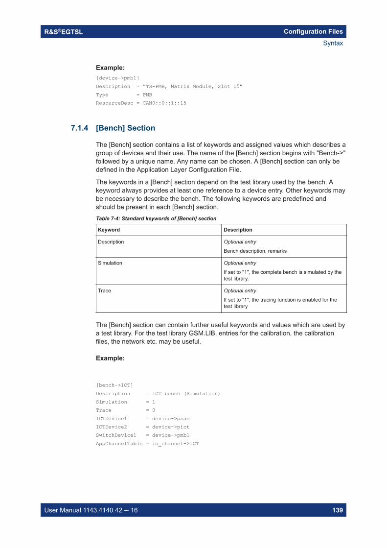
Configuration FilesR&S®EGTSL
139User Manual 1143.4140.42 16
Example: [device->pmb1]Description = "TS-PMB, Matrix Module, Slot 15"Type = PMBResourceDesc = CAN0::0::1::15
7.1.4 [Bench] Section
The [Bench] section contains a list of keywords and assigned values which describes agroup of devices and their use. The name of the [Bench] section begins with "Bench->"followed by a unique name. Any name can be chosen. A [Bench] section can only bedefined in the Application Layer Configuration File.
The keywords in a [Bench] section depend on the test library used by the bench. Akeyword always provides at least one reference to a device entry. Other keywords maybe necessary to describe the bench. The following keywords are predefined andshould be present in each [Bench] section.Table 7-4: Standard keywords of [Bench] section
Keyword Description
Description Optional entry
Bench description, remarks
Simulation Optional entry
If set to "1", the complete bench is simulated by thetest library.
Trace Optional entry
If set to "1", the tracing function is enabled for thetest library
The [Bench] section can contain further useful keywords and values which are used bya test library. For the test library GSM.LIB, entries for the calibration, the calibrationfiles, the network etc. may be useful.
Example:
[bench->ICT]Description = ICT bench (Simulation)Simulation = 1Trace = 0ICTDevice1 = device->psamICTDevice2 = device->pictSwitchDevice1 = device->pmb1AppChannelTable = io_channel->ICT
Syntax
Configuration FilesR&S®EGTSL
140User Manual 1143.4140.42 16
7.1.5 [ResourceManager] Section
The [ResourceManager] section contains keywords and assigned values to control thebehavior of the Resource Manager library. The following keywords are supported:Table 7-5: Keywords of [ResourceManager] section
Key name Remarks
Trace Blocks the tracing function (value = 0), enables thetracing function (value = 1). The function impacts onall libraries.
TraceFile Defines the path and the name of the trace file.
TraceToScreen The tracing information is displayed on the standardscreen (value = 1).
TraceTimeStamp Writes the time of day at the start of each tracingline (value = 1).
TraceThreadID Writes the ID of the current thread at the start ofeach tracing line (value = 1).
7.1.6 [Extlct] Section
The [ExtIct] section contains keywords and assigned values for the ICT extension libra-ries. The following keywords are supported:Table 7-6: Keywords of [ExtIct] section
Key name Remarks
UserDefinedDll Defines the path and name of the ICT extensionDLL.
7.2 PHYSICAL.INI
In the file PHYSICAL.INI (Physical Layer Configuration File), all hardware assem-blies available in the Enhanced Generic Test Software Library R&S EGTSL are descri-bed along with the corresponding definitions and settings (see examplePHYSICAL.INI file). This file also contains definitions which are applicable to all testapplications to be executed on the system (e.g. type definition). The informationentered in this file is used by all test libraries and thus by each test step.
The PHYSICAL.INI file normally exists only once in the system as it reflects the exactphysical structure. The file must only be modified in the event of a hardware change.
The Resource Manager calls and administers the information from the PHYSICAL.INIfile.
The file PHYSICAL.INI is saved in thefolder ...\GTSL\Configuration\physical.ini
PHYSICAL.INI
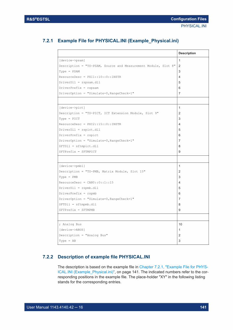
Configuration FilesR&S®EGTSL
141User Manual 1143.4140.42 16
7.2.1 Example File for PHYSICAL.INI (Example_Physical.ini)
Description
[device->psam]Description = "TS-PSAM, Source and Measurement Module, Slot 8"Type = PSAMResourceDesc = PXI1::10::0::INSTRDriverDll = rspsam.dllDriverPrefix = rspsamDriverOption = "Simulate=0,RangeCheck=1"
1
2
3
4
5
6
7
[device->pict]Description = "TS-PICT, ICT Extension Module, Slot 9"Type = PICTResourceDesc = PXI2::15::0::INSTRDriverDll = rspict.dllDriverPrefix = rspictDriverOption = "Simulate=0,RangeCheck=1"SFTDll = sftmpict.dllSFTPrefix = SFTMPICT
1
2
3
4
5
6
7
8
9
[device->pmb1]Description = "TS-PMB, Matrix Module, Slot 15"Type = PMBResourceDesc = CAN0::0::1::15DriverDll = rspmb.dllDriverPrefix = rspmbDriverOption = "Simulate=0,RangeCheck=1"SFTDll = sftmpmb.dllSFTPrefix = SFTMPMB
1
2
3
4
5
6
7
8
9
; Analog Bus[device->ABUS]Description = "Analog Bus"Type = AB
10
1
2
3
7.2.2 Description of example file PHYSICAL.INI
The description is based on the example file in Chapter 7.2.1, "Example File for PHYS-ICAL.INI (Example_Physical.ini)", on page 141. The indicated numbers refer to the cor-responding positions in the example file. The place-holder "XY" in the following listingstands for the corresponding entries.
PHYSICAL.INI
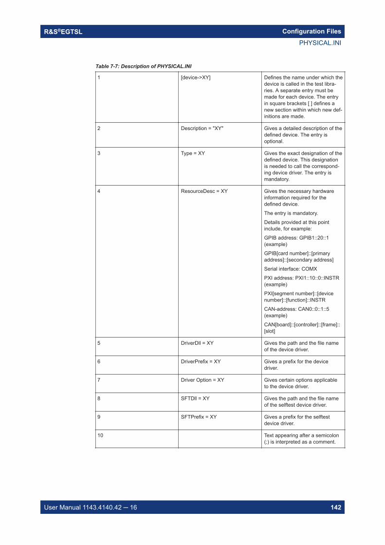
Configuration FilesR&S®EGTSL
142User Manual 1143.4140.42 16
Table 7-7: Description of PHYSICAL.INI
1 [device->XY] Defines the name under which thedevice is called in the test libra-ries. A separate entry must bemade for each device. The entryin square brackets [ ] defines anew section within which new def-initions are made.
2 Description = "XY" Gives a detailed description of thedefined device. The entry isoptional.
3 Type = XY Gives the exact designation of thedefined device. This designationis needed to call the correspond-ing device driver. The entry ismandatory.
4 ResourceDesc = XY Gives the necessary hardwareinformation required for thedefined device.
The entry is mandatory.
Details provided at this pointinclude, for example:
GPIB address: GPIB1::20::1(example)
GPIB[card number]::[primaryaddress]::[secondary address]
Serial interface: COMX
PXI address: PXI1::10::0::INSTR(example)
PXI[segment number]::[devicenumber]::[function]::INSTR
CAN-address: CAN0::0::1::5(example)
CAN[board]::[controller]::[frame]::[slot]
5 DriverDll = XY Gives the path and the file nameof the device driver.
6 DriverPrefix = XY Gives a prefix for the devicedriver.
7 Driver Option = XY Gives certain options applicableto the device driver.
8 SFTDll = XY Gives the path and the file nameof the selftest device driver.
9 SFTPrefix = XY Gives a prefix for the selftestdevice driver.
10 Text appearing after a semicolon(;) is interpreted as a comment.
PHYSICAL.INI
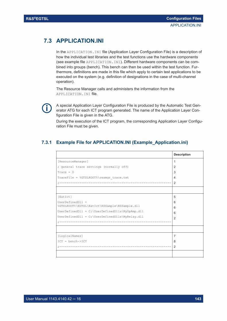
Configuration FilesR&S®EGTSL
143User Manual 1143.4140.42 16
7.3 APPLICATION.INI
In the APPLICATION.INI file (Application Layer Configuration File) is a description ofhow the individual test libraries and the test functions use the hardware components(see example file APPLICATION.INI). Different hardware components can be com-bined into groups (bench). This bench can then be used within the test function. Fur-thermore, definitions are made in this file which apply to certain test applications to beexecuted on the system (e.g. definition of designations in the case of multi-channeloperation).
The Resource Manager calls and administers the information from theAPPLICATION.INI file.
A special Application Layer Configuration File is produced by the Automatic Test Gen-erator ATG for each ICT program generated. The name of the Application Layer Con-figuration File is given in the ATG.During the execution of the ICT program, the corresponding Application Layer Configu-ration File must be given.
7.3.1 Example File for APPLICATION.INI (Example_Application.ini)
Description
[ResourceManager]; general trace settings (normally off)Trace = 0TraceFile = %GTSLROOT%\resmgr_trace.txt;-------------------------------------------------------------
1
2
3
4
2
[ExtIct]UserDefinedDll =%GTSLROOT%\EGTSL\ExtIct\RSSample\RSSample.dllUserDefinedDll = C:\UserDefinedDlls\MyOpAmp.dllUserDefinedDll = C:\UserDefinedDlls\MyRelay.dll;-------------------------------------------------------------
5
6
6
6
2
[LogicalNames]ICT = bench->ICT;-------------------------------------------------------------
7
8
2
APPLICATION.INI
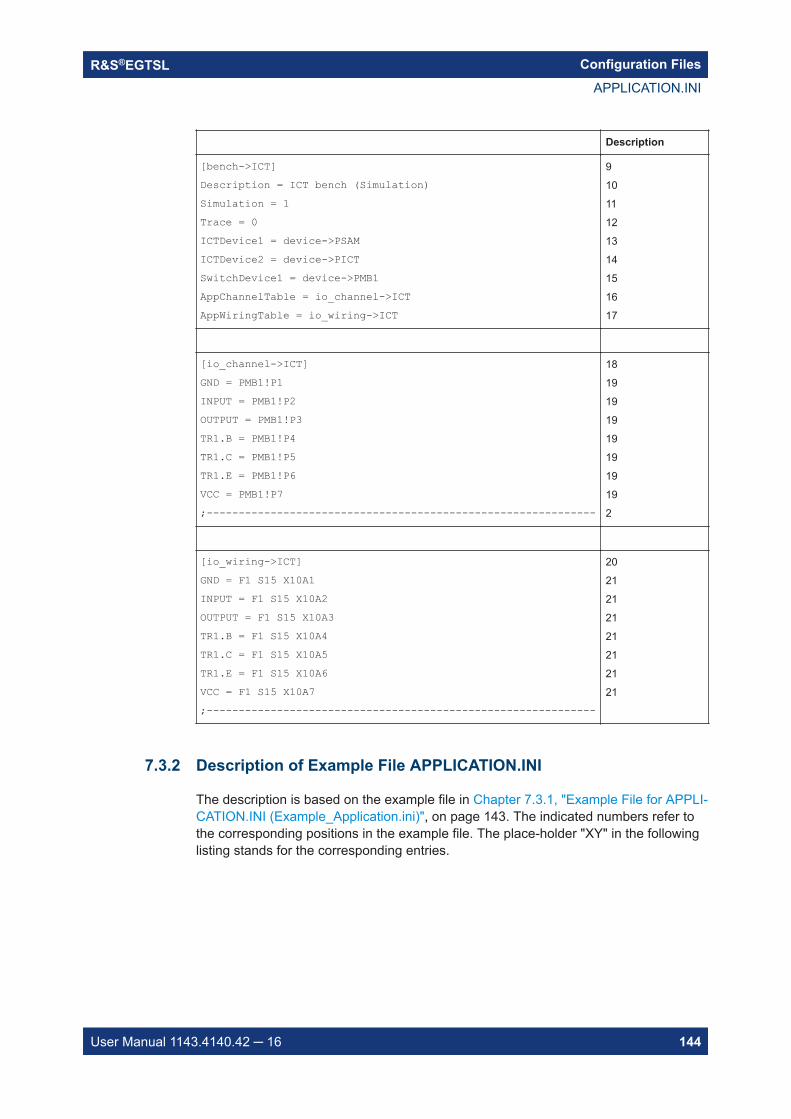
Configuration FilesR&S®EGTSL
144User Manual 1143.4140.42 16
Description
[bench->ICT]Description = ICT bench (Simulation)Simulation = 1Trace = 0ICTDevice1 = device->PSAMICTDevice2 = device->PICTSwitchDevice1 = device->PMB1AppChannelTable = io_channel->ICTAppWiringTable = io_wiring->ICT
9
10
11
12
13
14
15
16
17
[io_channel->ICT]GND = PMB1!P1INPUT = PMB1!P2OUTPUT = PMB1!P3TR1.B = PMB1!P4TR1.C = PMB1!P5TR1.E = PMB1!P6VCC = PMB1!P7;-------------------------------------------------------------
18
19
19
19
19
19
19
19
2
[io_wiring->ICT]GND = F1 S15 X10A1INPUT = F1 S15 X10A2OUTPUT = F1 S15 X10A3TR1.B = F1 S15 X10A4TR1.C = F1 S15 X10A5TR1.E = F1 S15 X10A6VCC = F1 S15 X10A7;-------------------------------------------------------------
20
21
21
21
21
21
21
21
7.3.2 Description of Example File APPLICATION.INI
The description is based on the example file in Chapter 7.3.1, "Example File for APPLI-CATION.INI (Example_Application.ini)", on page 143. The indicated numbers refer tothe corresponding positions in the example file. The place-holder "XY" in the followinglisting stands for the corresponding entries.
APPLICATION.INI
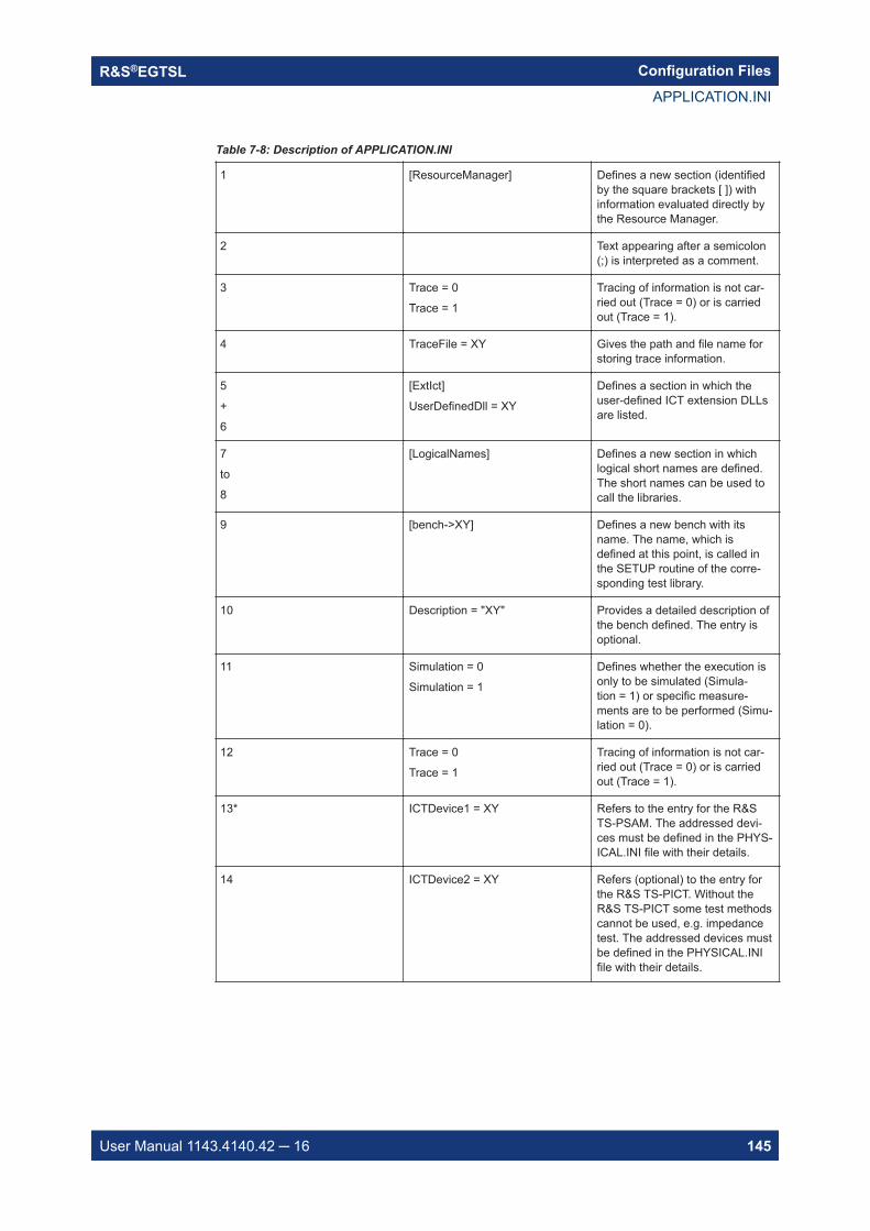
Configuration FilesR&S®EGTSL
145User Manual 1143.4140.42 16
Table 7-8: Description of APPLICATION.INI
1 [ResourceManager] Defines a new section (identifiedby the square brackets [ ]) withinformation evaluated directly bythe Resource Manager.
2 Text appearing after a semicolon(;) is interpreted as a comment.
3 Trace = 0
Trace = 1
Tracing of information is not car-ried out (Trace = 0) or is carriedout (Trace = 1).
4 TraceFile = XY Gives the path and file name forstoring trace information.
5
+
6
[ExtIct]
UserDefinedDll = XY
Defines a section in which theuser-defined ICT extension DLLsare listed.
7
to
8
[LogicalNames] Defines a new section in whichlogical short names are defined.The short names can be used tocall the libraries.
9 [bench->XY] Defines a new bench with itsname. The name, which isdefined at this point, is called inthe SETUP routine of the corre-sponding test library.
10 Description = "XY" Provides a detailed description ofthe bench defined. The entry isoptional.
11 Simulation = 0
Simulation = 1
Defines whether the execution isonly to be simulated (Simula-tion = 1) or specific measure-ments are to be performed (Simu-lation = 0).
12 Trace = 0
Trace = 1
Tracing of information is not car-ried out (Trace = 0) or is carriedout (Trace = 1).
13* ICTDevice1 = XY Refers to the entry for the R&STS-PSAM. The addressed devi-ces must be defined in the PHYS-ICAL.INI file with their details.
14 ICTDevice2 = XY Refers (optional) to the entry forthe R&S TS-PICT. Without theR&S TS-PICT some test methodscannot be used, e.g. impedancetest. The addressed devices mustbe defined in the PHYSICAL.INIfile with their details.
APPLICATION.INI
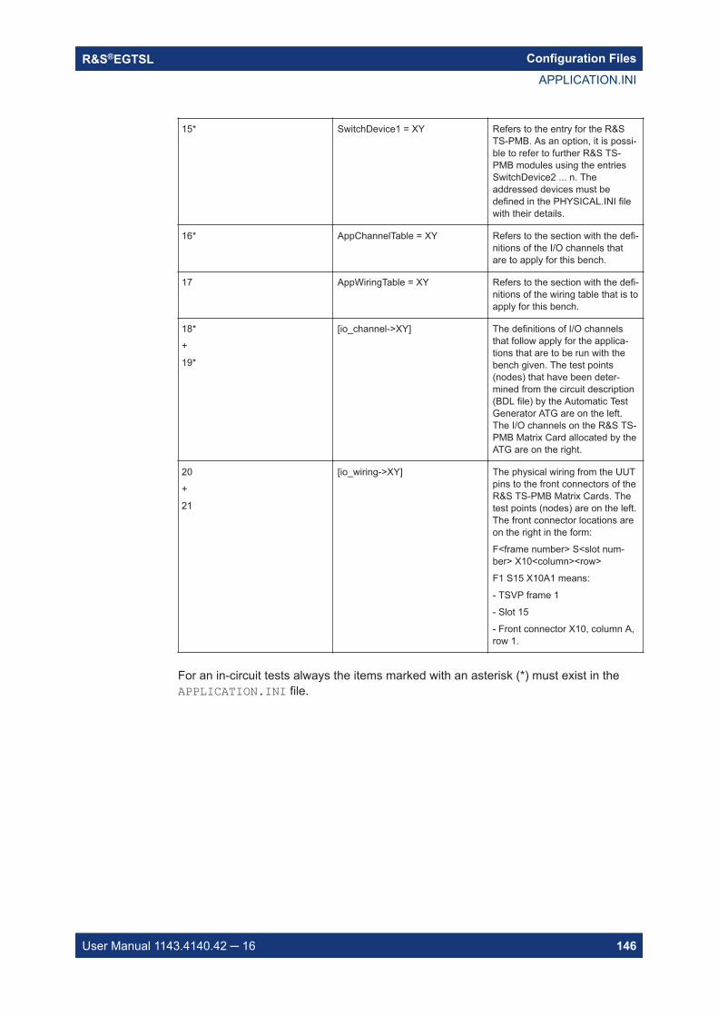
Configuration FilesR&S®EGTSL
146User Manual 1143.4140.42 16
15* SwitchDevice1 = XY Refers to the entry for the R&STS-PMB. As an option, it is possi-ble to refer to further R&S TS-PMB modules using the entriesSwitchDevice2 ... n. Theaddressed devices must bedefined in the PHYSICAL.INI filewith their details.
16* AppChannelTable = XY Refers to the section with the defi-nitions of the I/O channels thatare to apply for this bench.
17 AppWiringTable = XY Refers to the section with the defi-nitions of the wiring table that is toapply for this bench.
18*
+
19*
[io_channel->XY] The definitions of I/O channelsthat follow apply for the applica-tions that are to be run with thebench given. The test points(nodes) that have been deter-mined from the circuit description(BDL file) by the Automatic TestGenerator ATG are on the left.The I/O channels on the R&S TS-PMB Matrix Card allocated by theATG are on the right.
20
+
21
[io_wiring->XY] The physical wiring from the UUTpins to the front connectors of theR&S TS-PMB Matrix Cards. Thetest points (nodes) are on the left.The front connector locations areon the right in the form:
F<frame number> S<slot num-ber> X10<column><row>
F1 S15 X10A1 means:
- TSVP frame 1
- Slot 15
- Front connector X10, column A,row 1.
For an in-circuit tests always the items marked with an asterisk (*) must exist in theAPPLICATION.INI file.
APPLICATION.INI
Circuit DescriptionR&S®EGTSL
147User Manual 1143.4140.42 16
8 Circuit Description
8.1 Definition of Meta Language
In the following a meta language is explained that is used for the description of the syn-tax for the external representation of data. This metalanguage is a derivative of theBackus-Naur form.
8.1.1 Terminology, Symbols
The text that contains the formal description of the syntax comprises a sequence of so-called “tokens”. A token is either an identifier, a literal or an operator.
Identifier
An identifier is a string of lower case letters, numbers and special character. Each iden-tifier must start with a lower case letter that can then be followed by any number oflower case letters, numbers or special characters.
Example: ict-compilationprogram-header-stmtexecutiondd
Literals
Literals comprise a chain of alphanumeric characters that are enclosed in quotationmarks '"'. If there are also quotation marks in the literal, each quotation mark must begiven twice.
Example: "voltage""Literal with quotation mark "" in the text""SYSTEM"
Operators
The operators are used to be able to better represent the structure of a metaprogram.The following operators are used:
: = Separator between rule name and rule body
% = The preceding token occurs 1 to n-times
* = The preceding token occurs 0 to n-times
Definition of Meta Language
Circuit DescriptionR&S®EGTSL
148User Manual 1143.4140.42 16
n = The preceding token occurs exactly n-times
n-m = The preceding token occurs at least n-times, however m-times at the most
| = Alternative
= Start of the use of parenthesis for several tokens for a unit
= End of the use of parenthesis for several tokens for a unit
[ = Start of the optional use of parenthesis for one or more tokens
] = End of the optional use of parenthesis for one or more tokens
; = Conclusion of a production rule
! = Character for comment
Layout
For separation of the individual tokens as many spaces as required can be used.
Comments
Using the operator '!' a comment is started that is intended to make it easier to read themetaprogram. The comment starts after the operator and concludes at the end of theline.
8.1.2 Structure of a Metaprogram
The formal description of a language syntax is called a 'metaprogram'. A metaprogramcomprises a sequence of production rules.
A production rule comprises the following elements:
The rule name that is used for referencing the production rule in other productionrules
The operator ':' for separating rule names and rule body The rule body that defines the syntax or part of the syntax and a semicolon that concludes the production rule.
A metaprogram is complete when
Each rule name only occurs once and describes exactly one production rule There is exactly one and only one rule name that is not in a rule body. This rule
forms the start of the syntax.
8.1.3 Structure of Rule Bodies
Every rule body contains a sequence of identifiers or literals that are separated orlinked by operators.
Definition of Meta Language
Circuit DescriptionR&S®EGTSL
149User Manual 1143.4140.42 16
Daisy Chaining
If a rule is to comprise several tokens one after the other, then these tokens are simplywritten one after the other, separated by at least 1 space.
Example: while : "WHILE" condition "DO" ;
Information on Alternatives
If two or more tokens are to be allowed alternately in a rule, then this is represented bythe '|' operator.
Example: If the rule a is to be able to comprise the rule body b, as well as alternatively the rulebody c, the alternative operator is used:a: b | c ;
Optional Information
If a token is only to be present in a rule as an option, i.e. it can be present, but can alsobe missing, then this token must be placed in parenthesis using the "[" and "]" opera-tors.
Example: a: b; or a: bc;Can be represented bya: b[c];
Multiple Repetition
If a token is to be repeated several times in a rule, one of the following repetition oper-ators can be given after the token:
"%" Means that the preceding token must occur at least once, but can also occur as any number oftimes.
Example:
The following rules are equivalent:
a: b[n]; and a: b%;
"*" Means that the preceding token does not need to occur at all, and that it can also occur any num-ber of times.
Example:
The following rules are equivalent:
a: [b[n]]; and a: b*;
Definition of Meta Language
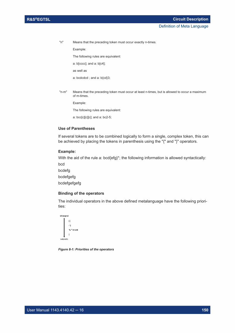
Circuit DescriptionR&S®EGTSL
150User Manual 1143.4140.42 16
"n" Means that the preceding token must occur exactly n-times.
Example:
The following rules are equivalent:
a: b[cccc]; and a: b[c4];
as well as
a: bcdcdcd ; and a: bcd3;
"n-m" Means that the preceding token must occur at least n-times, but is allowed to occur a maximumof m-times.
Example:
The following rules are equivalent:
a: bcc[c][c][c]; and a: bc2-5;
Use of Parentheses
If several tokens are to be combined logically to form a single, complex token, this canbe achieved by placing the tokens in parenthesis using the "" and "" operators.
Example: With the aid of the rule a: bcdefg*; the following information is allowed syntactically:bcdbcdefgbcdefgefgbcdefgefgefg
Binding of the operators
The individual operators in the above defined metalanguage have the following priori-ties:
Figure 8-1: Priorities of the operators
Definition of Meta Language
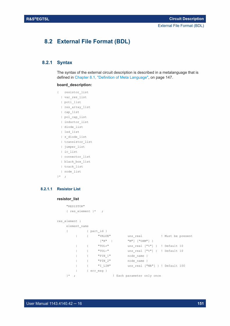
Circuit DescriptionR&S®EGTSL
151User Manual 1143.4140.42 16
8.2 External File Format (BDL)
8.2.1 Syntax
The syntax of the external circuit description is described in a metalanguage that isdefined in Chapter 8.1, "Definition of Meta Language", on page 147.
board_description:
resistor_list | var_res_list | poti_list | res_array_list | cap_list | pol_cap_list | inductor_list | diode_list | led_list | z_diode_list | transistor_list | jumper_list | ic_list | connector_list | black_box_list | track_list | node_list* ;
8.2.1.1 Resistor List
resistor_list
"RESISTOR" res_element * ;
res_element : element_name part_id | "VALUE" uns_real ! Must be present ["K" | "M"] ["OHM"] | "TOL+" uns_real ["%"] ! Default 10 | "TOL-" uns_real ["%"] ! Default 10 | "PIN_1" node_name | "PIN_2" node_name | "I_LIM" uns_real ["MA"] ! Default 100 | err_msg * ; ! Each parameter only once
External File Format (BDL)
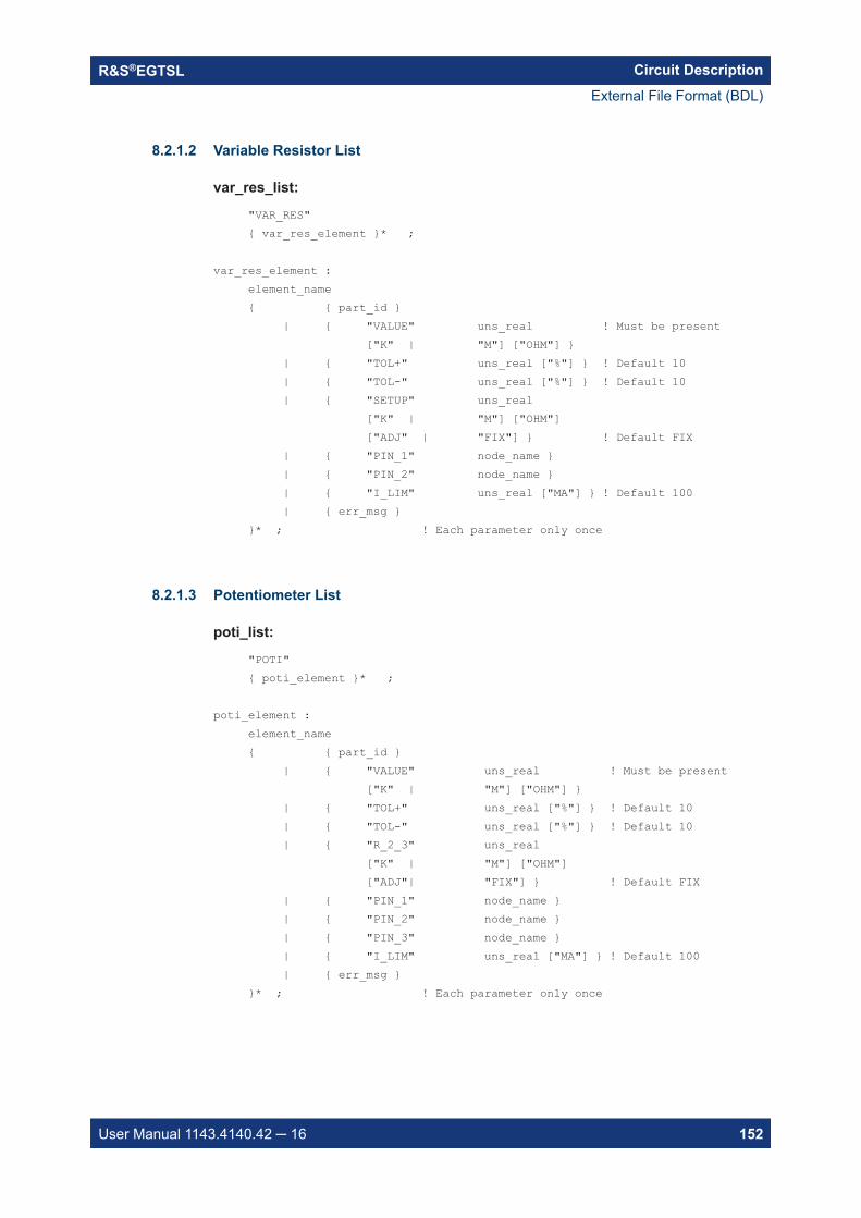
Circuit DescriptionR&S®EGTSL
152User Manual 1143.4140.42 16
8.2.1.2 Variable Resistor List
var_res_list:
"VAR_RES" var_res_element * ;
var_res_element : element_name part_id | "VALUE" uns_real ! Must be present ["K" | "M"] ["OHM"] | "TOL+" uns_real ["%"] ! Default 10 | "TOL-" uns_real ["%"] ! Default 10 | "SETUP" uns_real ["K" | "M"] ["OHM"] ["ADJ" | "FIX"] ! Default FIX | "PIN_1" node_name | "PIN_2" node_name | "I_LIM" uns_real ["MA"] ! Default 100 | err_msg * ; ! Each parameter only once
8.2.1.3 Potentiometer List
poti_list:
"POTI" poti_element * ;
poti_element : element_name part_id | "VALUE" uns_real ! Must be present ["K" | "M"] ["OHM"] | "TOL+" uns_real ["%"] ! Default 10 | "TOL-" uns_real ["%"] ! Default 10 | "R_2_3" uns_real ["K" | "M"] ["OHM"] ["ADJ"| "FIX"] ! Default FIX | "PIN_1" node_name | "PIN_2" node_name | "PIN_3" node_name | "I_LIM" uns_real ["MA"] ! Default 100 | err_msg * ; ! Each parameter only once
External File Format (BDL)
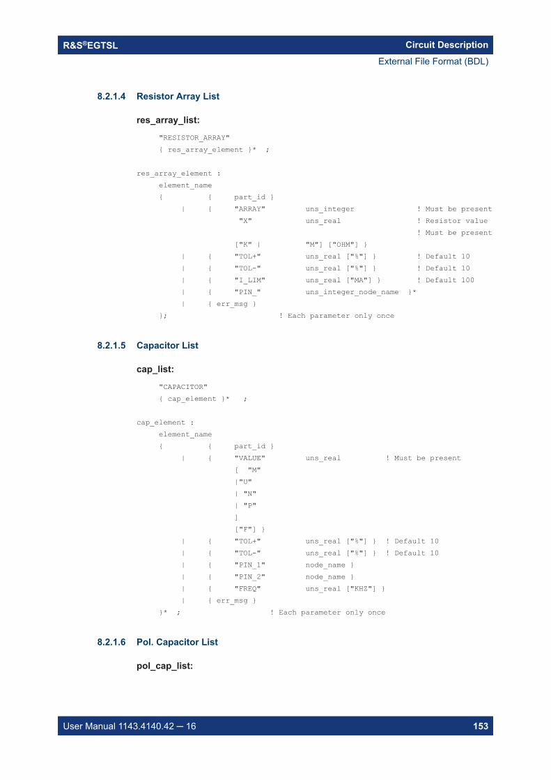
Circuit DescriptionR&S®EGTSL
153User Manual 1143.4140.42 16
8.2.1.4 Resistor Array List
res_array_list:
"RESISTOR_ARRAY" res_array_element * ;
res_array_element : element_name part_id | "ARRAY" uns_integer ! Must be present "X" uns_real ! Resistor value ! Must be present ["K" | "M"] ["OHM"] | "TOL+" uns_real ["%"] ! Default 10 | "TOL-" uns_real ["%"] ! Default 10 | "I_LIM" uns_real ["MA"] ! Default 100 | "PIN_" uns_integer_node_name * | err_msg ; ! Each parameter only once
8.2.1.5 Capacitor List
cap_list:
"CAPACITOR" cap_element * ;
cap_element : element_name part_id | "VALUE" uns_real ! Must be present [ "M" |"U" | "N" | "P" ] ["F"] | "TOL+" uns_real ["%"] ! Default 10 | "TOL-" uns_real ["%"] ! Default 10 | "PIN_1" node_name | "PIN_2" node_name | "FREQ" uns_real ["KHZ"] | err_msg * ; ! Each parameter only once
8.2.1.6 Pol. Capacitor List
pol_cap_list:
External File Format (BDL)
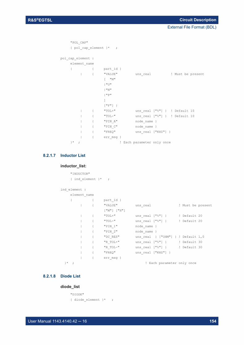
Circuit DescriptionR&S®EGTSL
154User Manual 1143.4140.42 16
"POL_CAP" pol_cap_element * ;
pol_cap_element : element_name part_id | "VALUE" uns_real ! Must be present [ "M" |"U" |"N" |"P" ] ["F"] | "TOL+" uns_real ["%"] ! Default 10 | "TOL-" uns_real ["%"] ! Default 10 | "PIN_A" node_name | "PIN_C" node_name | "FREQ" uns_real ["KHZ"] | err_msg * ; ! Each parameter only once
8.2.1.7 Inductor List
inductor_list:
"INDUCTOR" ind_element * ;
ind_element : element_name part_id | "VALUE" uns_real ! Must be present ["M"] ["H"] | "TOL+" uns_real ["%"] ! Default 20 | "TOL-" uns_real ["%"] ! Default 20 | "PIN_1" node_name | "PIN_2" node_name | "DC_RES" uns_real ["OHM"] ! Default 1,0 | "R_TOL+" uns_real ["%"] ! Default 30 | "R_TOL-" uns_real ["%"] ! Default 30 | "FREQ" uns_real ["KHZ"] | err_msg * ; ! Each parameter only once
8.2.1.8 Diode List
diode_list
"DIODE" diode_element * ;
External File Format (BDL)
Circuit DescriptionR&S®EGTSL
155User Manual 1143.4140.42 16
diode_element : element_name part_id | "VALUE" uns_real ["V"] ! Default 0.7 | "TOL+" uns_real ["%"] ! Default 25 | "TOL-" uns_real ["%"] ! Default 25 | "PIN_A" node_name | "PIN_C" node_name | "I_DCS" uns_real ["MA"] ! Default 100 | "I_DIO" uns_real ["MA"] ! Default 10 | err_msg * ; ! Each parameter only once
8.2.1.9 LED List
led_list:
"LED" led_element * ;
led_element : element_name part_id | "VALUE" uns_real ["V"] ! Default 1.2 | "TOL+" uns_real ["%"] ! Default 25 | "TOL-" uns_real ["%"] ! Default 25 | "PIN_A" node_name | "PIN_C" node_name | "I_DCS" uns_real ["MA"] ! Default 100 | "I_DIO" uns_real ["MA"] ! Default 10 | err_msg * ; ! Each parameter only once
8.2.1.10 Zener Diode List
z_diode_list:
"Z_DIODE" z_diode_element * ;
z_diode_element : element_name part_id | "VALUE" uns_real ["V"] ! Must be present | "TOL+" uns_real ["%"] ! Default 10 | "TOL-" uns_real ["%"] ! Default 10 | "PIN_A" node_name | "PIN_C" node_name
External File Format (BDL)
Circuit DescriptionR&S®EGTSL
156User Manual 1143.4140.42 16
| "I_Z" uns_real ["MA"] | "R_Z" uns_real ["OHM"] | err_msg * ; ! Each parameter only once
8.2.1.11 Transistor List
transistor_list:
"TRANSISTOR" trans_element * ;
trans_element : element_name part_id | "NPN" | "PNP" ! Must be present | "UBE" uns_real ["V"] ! Default 0.6 | "TOL+" uns_real ["%"] ! Default 30 | "TOL-" uns_real ["%"] ! Default 30 | "BETA" uns_integer ! Default 10 | "PIN_E" node_name | "PIN_B" node_name | "PIN_C" node_name | "UCE" uns_real ["V"] ! Default 5.0 | "I_C1" uns_real ["MA"] ! Default 9.0 | "I_C2" uns_real ["MA"] ! Default 11.0 | "I_LIM" uns_real ["MA"] ! Default 100 | err_msg * ; ! Each parameter only once
8.2.1.12 Jumper List
jumper_list:
"JUMPER" jumper_element * ;
jumper_element : element_name part_id | "PIN_1" node_name | "PIN_2" node_name | "OPEN" | "CLOSED" ! Default CLOSED | err_msg * ; ! Each parameter only once
External File Format (BDL)
Circuit DescriptionR&S®EGTSL
157User Manual 1143.4140.42 16
8.2.1.13 IC List
ic_list:
"IC" ic_element * ;
ic_element :
element_name part_id | "TYPE" type_name ! Must be present | "PINS" uns_integer ! Must be present | "PIN_" uns_integer node_name * | err_msg * ;
8.2.1.14 Connector List
connector_list:
"CONNECTOR" connector_element * ;
connector_element : element_name part_id | "TYPE" type_name | "PINS" uns_integer ! Must be present | "PIN_" uns_integer node_name * | err_msg * ;
8.2.1.15 Black Box List
black_box_list:
"BLACK_BOX" black_box_element * ;
black_box_element :
element_name part_id | "TYPE" type_name | "PINS" uns_integer ! Must be present | "PIN_" uns_integer node_name * | err_msg * ;
External File Format (BDL)
Circuit DescriptionR&S®EGTSL
158User Manual 1143.4140.42 16
8.2.1.16 Track List
track_list:
"TRACK" track_element * ;
track_element :
element_name node_name * ! At least 2 nodes | "PINS" uns_integer | err_msg * ;
8.2.1.17 Node List
node_list:
"NODE" node_element * ;
node_element :
element_name connection * ;
connection :
"DEV_NAME" log_name "PIN_" "A" | "B" | "C" | "E" | "T" | uns_integer * ;
8.2.1.18 Basic Constructs
element_name:
"NAME" log_name ;
part_id :
External File Format (BDL)
Circuit DescriptionR&S®EGTSL
159User Manual 1143.4140.42 16
"PART_ID" part_name ;
err_msg :
"ERR_MSG" message ;
log_name :
"'" printable % ! max. 15 characters "'" ;
part_name :
"'" printable % ! max. 15 characters "'" ;
type_name :
"'" printable % ! max. 15 characters "'" ;
node_name :
"'" node_chars % ! max. 80 characters "'" ;
message :
"'" printable % ! max. 63 characters "'" ;
uns_real : uns_integer [ "." | "." uns_integer ] | "." uns_integer [ "E" [ "+" | "-" ] uns_integer ] ;
uns_integer : dd % ;
dd : "0" | ... | "9" ;
printable : " " | ... | "&" | "(" | ... | "~" ; !all printable ASCII characters with the exception of the
External File Format (BDL)
Circuit DescriptionR&S®EGTSL
160User Manual 1143.4140.42 16
!quotation mark "'"
node_chars : "A" | ... | "Z" | "a" | ... | "z" | "0" | ... | "9" | "_" | "." | "!" | "#" | "$" | "%" | "&" | "*" | "+" | "-" | "/" | "\" | ":" | "?" | "@" | "^" | "|" | "~" | "(" | ")" | "" | "" | "[" | "]" | "<" | ">" ;
8.2.1.19 FET List
fet_list:
"FET" fet_element * ;
fet_element : element_name part_id | "JFET" | "DEP_MOSFET | ENH_MOSFET" ! Must be present | "N_CHANNEL" | "P_CHANNEL" ! Must be present | "VGS_OFF" real_num ["V"] ! Default depends on FET type; see semantics description | "VGS_ON" real_num ["V"] ! Default depends on FET type; see semantics description | "RDS_ON" uns_real ["OHM"] ! Default depends on FET type; see semantics description | "PIN_D" node_name | "PIN_G" node_name | "PIN_S" node_name | err_msg * ; ! Each parameter only once
8.2.2 Semantics
8.2.2.1 General
Components of the same type can be combined into lists in the external circuit descrip-tion. A list of components is started using the related keyword. The individual list ele-ments are separated by the component identifier (name). For this reason the name ofthe component must always be given at the start of a component description. All otherparameters in a component description can be occur in any order, however they canoccur a maximum of once.
The component identifier is marked by the keyword NAME and comprises a maximumof 15 characters that are enclosed in single quotation marks.
External File Format (BDL)
Circuit DescriptionR&S®EGTSL
161User Manual 1143.4140.42 16
In all component descriptions except TRACK and NODE, the PART_ID parameter isavailable for identifying the item number. The item number can comprise a maximum of15 characters that are enclosed in single quotation marks.
Circuit information on components is started using the keywords PIN_x (x = see syntaxfor the related component description). The keyword is followed by a node name. Thecircuit information in the component description is optional. A node name in circuitinformation comprises a maximum of 80 characters and is placed in parentheses using"'".
A node name is only allowed to contain the following characters:
"A"..."Z" uppercase letter
"a"..."z" lowercase letter
"0"..."9" digit
"_" underscore
"." decimal point/period
"!" exclamation mark
"#" number sign
"$" dollar sign
"%" percent
"&" ampersand
"*" asterisk
"+" plus
"-" minus
"/" slash
"\" backslash
":" colon
"?" question mark
"@" at sign
"^" caret
"|" vertical bar
"~" tilde
"(" opening parentheses
")" closing parentheses
"" opening curly brace
"" closing curly brace
"[" opening square bracket
"]" closing square bracket
External File Format (BDL)
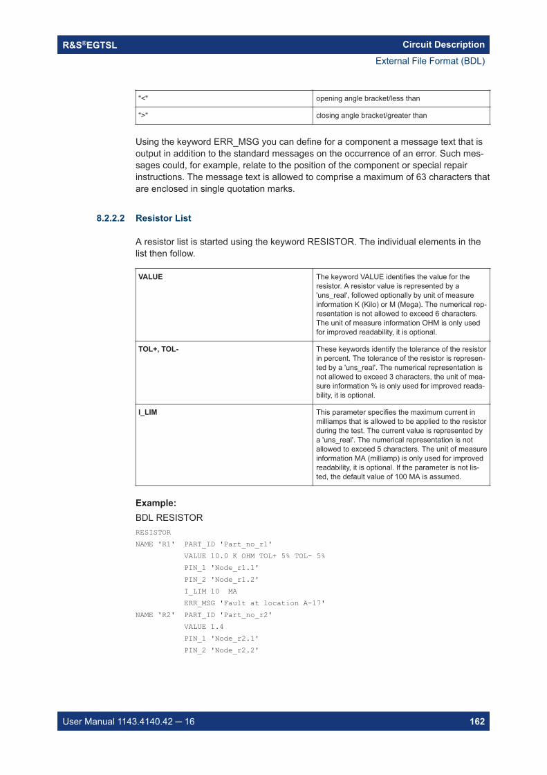
Circuit DescriptionR&S®EGTSL
162User Manual 1143.4140.42 16
"<" opening angle bracket/less than
">" closing angle bracket/greater than
Using the keyword ERR_MSG you can define for a component a message text that isoutput in addition to the standard messages on the occurrence of an error. Such mes-sages could, for example, relate to the position of the component or special repairinstructions. The message text is allowed to comprise a maximum of 63 characters thatare enclosed in single quotation marks.
8.2.2.2 Resistor List
A resistor list is started using the keyword RESISTOR. The individual elements in thelist then follow.
VALUE The keyword VALUE identifies the value for theresistor. A resistor value is represented by a'uns_real', followed optionally by unit of measureinformation K (Kilo) or M (Mega). The numerical rep-resentation is not allowed to exceed 6 characters.The unit of measure information OHM is only usedfor improved readability, it is optional.
TOL+, TOL- These keywords identify the tolerance of the resistorin percent. The tolerance of the resistor is represen-ted by a 'uns_real'. The numerical representation isnot allowed to exceed 3 characters, the unit of mea-sure information % is only used for improved reada-bility, it is optional.
I_LIM This parameter specifies the maximum current inmilliamps that is allowed to be applied to the resistorduring the test. The current value is represented bya 'uns_real'. The numerical representation is notallowed to exceed 5 characters. The unit of measureinformation MA (milliamp) is only used for improvedreadability, it is optional. If the parameter is not lis-ted, the default value of 100 MA is assumed.
Example: BDL RESISTORRESISTORNAME 'R1' PART_ID 'Part_no_r1' VALUE 10.0 K OHM TOL+ 5% TOL- 5% PIN_1 'Node_r1.1' PIN_2 'Node_r1.2' I_LIM 10 MA ERR_MSG 'Fault at location A-17'NAME 'R2' PART_ID 'Part_no_r2' VALUE 1.4 PIN_1 'Node_r2.1' PIN_2 'Node_r2.2'
External File Format (BDL)
Circuit DescriptionR&S®EGTSL
163User Manual 1143.4140.42 16
8.2.2.3 Variable Resistor List
A list of variable resistors is started with the keyword VAR_RES. The individual ele-ments in the list then follow.
VALUE The parameter VALUE defines the maximum resist-ance of the component. The information is given in asimilar manner to that for RESISTOR (see section8.2.1.1 ).
TOL+, TOL- Tolerance of the variable resistor. The same infor-mation as for RESISTOR apply (see section8.2.1.1 ).
I_LIM This parameter specifies the maximum current inmilliamps that is allowed to be applied to the resistorduring the test. The same information as for RESIS-TOR applies (see section 8.2.1.1 ).
SETUP This parameter defines the presetting for the resis-tor. The resistor value is represented by a 'uns_real',followed optionally by unit of measure information K(Kilo) or M (Mega). The numerical representation isnot allowed to exceed 6 characters. The unit ofmeasure information OHM is only used for improvedreadability, it is optional.
ADJ/FIX The parameter ADJ/FIX is not required in and isonly present for reasons of compatibility with TSS. Ifthe parameter is given in , it is only allowed to beFIX.
Example: BDL VAR_RESVAR_RES NAME 'VR1' PART_ID 'Part_vr1' VALUE 5.0 K OHM TOL+ 5% TOL- 5% SETUP 1.45 KOHM PIN_1 'Node_vr1.1' PIN_2 'Node_vr1.2' I_LIM 50 MA ERR_MSG 'Fault at location C-5'NAME 'VR2' PART_ID 'Part_vr2' VALUE 1.0 M SETUP 400 K I_LIM 50 MA ERR_MSG 'Fault at location R-43'
8.2.2.4 Potentiometer List
A list of potentiometers is started using the keyword POTI. The individual elements inthe list then follow.
Parameters
External File Format (BDL)
Circuit DescriptionR&S®EGTSL
164User Manual 1143.4140.42 16
The same information as for VARIABLE RESISTOR applies (see section Chap-ter 8.2.2.2, "Resistor List", on page 162).
R_2_3 The keyword SETUP is replaced by the keywordR_2_3 for improved understanding. The parameterR_2_3 defines the presetting for the resistorbetween the pins PIN_2 (wiper) and PIN_3.
Example: BDL POTIPOTI NAME 'Poti1' PART_ID 'Part_p1' VALUE 5.0 K OHM TOL+ 5% TOL-5% R_2_3 1.45 K OHM PIN_1 'Node_p1.1' PIN_2 'Node_p1.2' 'Node_p1.3' I_LIM 50 MA ERR_MSG 'Fault at location G-29'NAME 'Poti2' PART_ID 'Part_p2' VALUE 1.0 M R_2_3 400 K PIN_1 'Node_p1.1' PIN_2 'Node_p1.2' 'Node_p1.3' I_LIM 50 MA ERR_MSG 'Fault at location I-2'NAME 'Poti3' R_2_3 400 K VALUE 2 K PIN_1 'Node_p1.1' PIN_2 'Node_p1.2' 'Node_p1.3'NAME 'Poti4' VALUE 5.0 K TOL+ 10% TOL- 10% R_2_3 1 K PIN_1 'Node_p1.1' PIN_2 'Node_p1.2' 'Node_p1.3'
8.2.2.5 Resistor Array List
A list of resistor networks is started using the keyword RESISTOR_ARRAY. The indi-vidual elements in the list then follow.
External File Format (BDL)
Circuit DescriptionR&S®EGTSL
165User Manual 1143.4140.42 16
ARRAY The keyword ARRAY identifies the size of the resis-tor network, i.e. the number of resistors in the net-work. The size of the array is limited to 127 resis-tors. The number of resistors implicitly defines thenumber of pins on the network. Here the followingapplies: ARRAY n corresponds to n resistors and n+1 pins. PIN_1 is the common pin for the network.
X The number of resistors is followed by the keyword'X', followed by the resistor value in Ω, kΩ or MΩ.The information on the resistor value is given as'uns_real', followed optionally by the unit of measureinformation K or M. The entry of the code OHM isoptional, it is only used for improved readability.
TOL+, TOL- These keywords identify the tolerance of the resistorin percent. The tolerance of the resistor is represen-ted by a 'uns_real'. The numerical representation isnot allowed to exceed 3 characters, the unit of mea-sure information % is only used for improved reada-bility, it is optional.
I_LIM This parameter specifies the maximum current inmilliamps that is allowed to the applied to the resis-tor during the test. The value for the current is repre-sented by a 'uns_real'. The numerical representationis not allowed to exceed 5 characters. The unit ofmeasure information MA (milliamp) is only used forimproved readability, it is optional. If the parameteris not listed, the default value of 100 MA isassumed.
Example: BDL RESISTOR_ARRAYRESISTOR_ARRAY NAME 'R137' PART_ID '111,222' ARRAY 11 X 1 OHM TOL+ 10 TOL- 10 I_LIM 100.0 MA PIN_1 'A1_1' PIN_2 'A1_2' PIN_3 'A1_3' PIN_4 'A1_4' PIN_5 'A1_5' PIN_6 'A1_6' PIN_7 'A1_7' PIN_8 'A1_8' PIN_9 'A1_9' PIN_10 'A1_10' PIN_11 'A1_11' PIN_12 'A1_12' ERR_MSG 'ERROR in R137'
External File Format (BDL)
Circuit DescriptionR&S®EGTSL
166User Manual 1143.4140.42 16
8.2.2.6 Capacitor List
A list of capacitors is started using the keyword CAPACITOR. The individual elementsin the list then follow.
VALUE The parameter VALUE defines the value of thecapacitor. The value is represented by a 'uns_real'followed optionally by unit of measure information M(Milli), U (Micro), N (Nano), P (Pico). The numericalrepresentation is not allowed to exceed 6 charac-ters. The unit of measure information F is only usedfor improved readability, it is optional.
TOL+, TOL- These keywords identify the tolerance of the compo-nent in percent. The tolerance is represented by a'uns_real'. The numerical representation is notallowed to exceed 3 characters. The unit of measureinformation % is only used for improved readability,it is optional. If a parameter does not occur in thecomponent description, then a default tolerance of10 % is assumed.
FREQ This parameter specifies the test frequency in KHZat which the test on the capacitor is to be performed.The information on a test frequency is optional. Thetest frequency is represented by a 'uns_real'. Thenumerical representation is not allowed to exceed 4characters. Only the frequencies 0.1 KHZ, 1.0 KHZand 10.0 KHZ are allowed. To avoid errors in thereal number arithmetic, variations of up to 10 % fromthe setpoint in each case is allowed. The unit ofmeasure information KHZ is only used for improvedreadability, it is optional.
Example: BDL CAPACITORCAPACITORNAME 'C1' PART_ID 'Part_vr1' VALUE 5.0 N F TOL+ 15% TOL- 15% PIN_1 'Node_c1.1' PIN_2 'Node_c1.2' FREQ 1.0 KHZ ERR_MSG 'Fault at location A-32'NAME 'C2' VALUE 0.5 M TOL+ 5% TOL- 5% PIN_1 'Node_c2.1' PIN_2 'Node_c2.2' PART_ID 'Part_c2'
8.2.2.7 Pol. Capacitor List
A list of polarized capacitors with poles is started using the keyword POL_CAP. Theindividual elements in the list then follow.
The same information as for CAPACITOR applies (see section Chapter 8.2.2.6,"Capacitor List", on page 166).
External File Format (BDL)
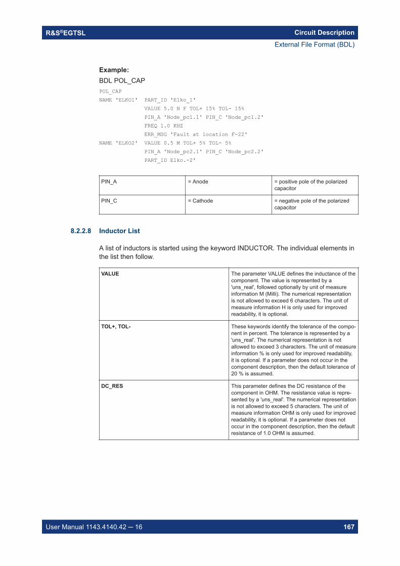
Circuit DescriptionR&S®EGTSL
167User Manual 1143.4140.42 16
Example: BDL POL_CAPPOL_CAP NAME 'ELKO1' PART_ID 'Elko_1' VALUE 5.0 N F TOL+ 15% TOL- 15% PIN_A 'Node_pc1.1' PIN_C 'Node_pc1.2' FREQ 1.0 KHZ ERR_MSG 'Fault at location F-22'NAME 'ELKO2' VALUE 0.5 M TOL+ 5% TOL- 5% PIN_A 'Node_pc2.1' PIN_C 'Node_pc2.2' PART_ID Elko.-2'
PIN_A = Anode = positive pole of the polarizedcapacitor
PIN_C = Cathode = negative pole of the polarizedcapacitor
8.2.2.8 Inductor List
A list of inductors is started using the keyword INDUCTOR. The individual elements inthe list then follow.
VALUE The parameter VALUE defines the inductance of thecomponent. The value is represented by a'uns_real', followed optionally by unit of measureinformation M (Milli). The numerical representationis not allowed to exceed 6 characters. The unit ofmeasure information H is only used for improvedreadability, it is optional.
TOL+, TOL- These keywords identify the tolerance of the compo-nent in percent. The tolerance is represented by a'uns_real'. The numerical representation is notallowed to exceed 3 characters. The unit of measureinformation % is only used for improved readability,it is optional. If a parameter does not occur in thecomponent description, then the default tolerance of20 % is assumed.
DC_RES This parameter defines the DC resistance of thecomponent in OHM. The resistance value is repre-sented by a 'uns_real'. The numerical representationis not allowed to exceed 5 characters. The unit ofmeasure information OHM is only used for improvedreadability, it is optional. If a parameter does notoccur in the component description, then the defaultresistance of 1.0 OHM is assumed.
External File Format (BDL)
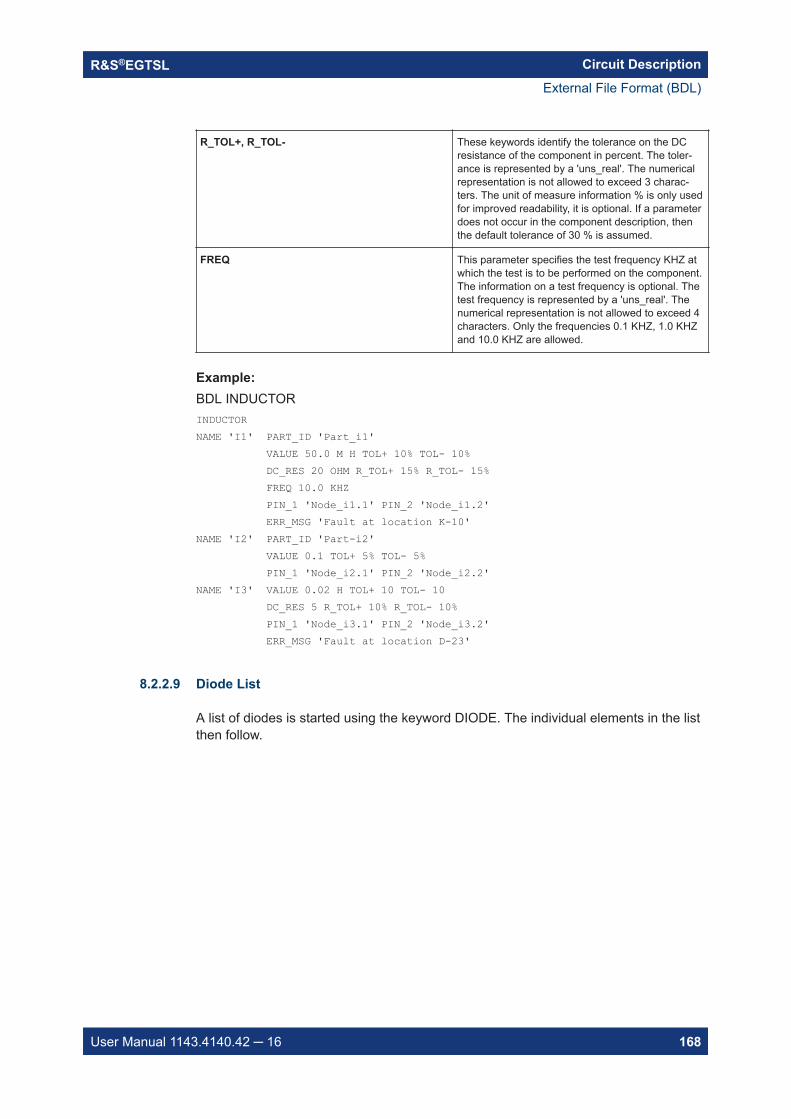
Circuit DescriptionR&S®EGTSL
168User Manual 1143.4140.42 16
R_TOL+, R_TOL- These keywords identify the tolerance on the DCresistance of the component in percent. The toler-ance is represented by a 'uns_real'. The numericalrepresentation is not allowed to exceed 3 charac-ters. The unit of measure information % is only usedfor improved readability, it is optional. If a parameterdoes not occur in the component description, thenthe default tolerance of 30 % is assumed.
FREQ This parameter specifies the test frequency KHZ atwhich the test is to be performed on the component.The information on a test frequency is optional. Thetest frequency is represented by a 'uns_real'. Thenumerical representation is not allowed to exceed 4characters. Only the frequencies 0.1 KHZ, 1.0 KHZand 10.0 KHZ are allowed.
Example: BDL INDUCTORINDUCTOR NAME 'I1' PART_ID 'Part_i1' VALUE 50.0 M H TOL+ 10% TOL- 10% DC_RES 20 OHM R_TOL+ 15% R_TOL- 15% FREQ 10.0 KHZ PIN_1 'Node_i1.1' PIN_2 'Node_i1.2' ERR_MSG 'Fault at location K-10'NAME 'I2' PART_ID 'Part-i2' VALUE 0.1 TOL+ 5% TOL- 5% PIN_1 'Node_i2.1' PIN_2 'Node_i2.2'NAME 'I3' VALUE 0.02 H TOL+ 10 TOL- 10 DC_RES 5 R_TOL+ 10% R_TOL- 10% PIN_1 'Node_i3.1' PIN_2 'Node_i3.2' ERR_MSG 'Fault at location D-23'
8.2.2.9 Diode List
A list of diodes is started using the keyword DIODE. The individual elements in the listthen follow.
External File Format (BDL)
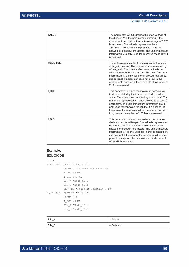
Circuit DescriptionR&S®EGTSL
169User Manual 1143.4140.42 16
VALUE The parameter VALUE defines the knee voltage ofthe diode in V. If the parameter is missing in thecomponent description, then a knee voltage of 0.7 Vis assumed. The value is represented by a'uns_real'. The numerical representation is notallowed to exceed 3 characters. The unit of measureinformation V is only used for improved readability, itis optional.
TOL+, TOL- These keywords identify the tolerance on the kneevoltage in percent. The tolerance is represented bya 'uns_real'. The numerical representation is notallowed to exceed 3 characters. The unit of measureinformation % is only used for improved readability,it is optional. If parameter does not occur in thecomponent description, then the default tolerance of25 % is assumed.
I_DCS This parameter defines the maximum permissibletotal current during the test on the diode in milli-amps. The value is represented by a 'uns_real'. Thenumerical representation is not allowed to exceed 5characters. The unit of measure information MA isonly used for improved readability, it is optional. Ifthe parameter is missing in the component descrip-tion, then a current limit of 100 MA is assumed.
I_DIO This parameter defines the maximum permissiblediode current in milliamps. The value is representedby a 'uns_real'. The numerical information is notallowed to exceed 4 characters. The unit of measureinformation MA is only used for improved readability,it is optional. If the parameter is missing in the com-ponent description, then a maximum diode currentof 10 MA is assumed.
Example: BDL DIODEDIODE NAME 'D1' PART_ID 'Part_d1' VALUE 0.4 V TOL+ 15% TOL- 15% I_DCS 50 MA I_DIO 5.0 MA PIN_A 'Node_d1.1' PIN_C 'Node_d1.2' ERR_MSG 'Fault at location H-19'NAME 'D2' PART_ID 'Part_d2' VALUE 0.4 I_DCS 20 MA PIN_A 'Node_d2.1' PIN_C 'Node_d2.2'
PIN_A = Anode
PIN_C = Cathode
External File Format (BDL)
Circuit DescriptionR&S®EGTSL
170User Manual 1143.4140.42 16
8.2.2.10 LED List
A list of light emitting diodes is started using the keyword LED. The same informationas for diodes applies (see section Chapter 8.2.2.9, "Diode List", on page 168), only thedefault value for VALUE here is 1.2 V.
8.2.2.11 Zener Diode List
A zener diode test is only generated if a R&S TS-PSU or R&S TS-PSU12 module isconfigured in the PHYSICAL.INI file. Otherwise, only a diode forward test is inserted.
A list of zener diodes is started using the keyword Z_DIODE. The individual elementsin the list then follow.
VALUE The parameter VALUE defines the nominal voltageof the zener diode in V. The value is represented bya 'uns_real'. The numerical information is notallowed to exceed 4 characters. The unit of measureinformation V is only used for improved readability, itis optional.
TOL+, TOL- These keywords identify the tolerance on the nomi-nal voltage in percent. The tolerance is representedby a 'uns_real'. The numerical representation is notallowed to exceed 3 characters. The unit of measureinformation % is only used for improved readability,it is optional. If a parameter does not occur in thecomponent description, then a default tolerance of10 % is assumed.
I_Z This parameter defines the zener current of thediode in milliamps. The information on the zenercurrent is optional. The value is represented by a'uns_real'. The numerical information is not allowedto exceed 4 characters. The unit of measure infor-mation MA is only used for improved readability, it isoptional.
R_Z This parameter defines the zener resistance of thediode in OHM. The information on the zener resist-ance is optional. The value is represented by a'uns_real'. The numerical information is not allowedto exceed 4 characters. The unit of measure infor-mation OHM is only used for improved readability, itis optional.
External File Format (BDL)
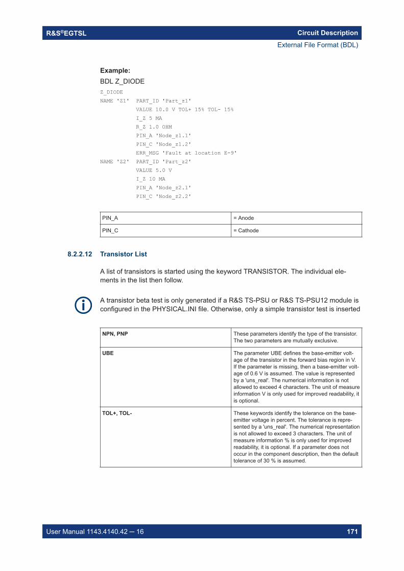
Circuit DescriptionR&S®EGTSL
171User Manual 1143.4140.42 16
Example: BDL Z_DIODEZ_DIODE NAME 'Z1' PART_ID 'Part_z1' VALUE 10.0 V TOL+ 15% TOL- 15% I_Z 5 MA R_Z 1.0 OHM PIN_A 'Node_z1.1' PIN_C 'Node_z1.2' ERR_MSG 'Fault at location E-9'NAME 'Z2' PART_ID 'Part_z2' VALUE 5.0 V I_Z 10 MA PIN_A 'Node_z2.1' PIN_C 'Node_z2.2'
PIN_A = Anode
PIN_C = Cathode
8.2.2.12 Transistor List
A list of transistors is started using the keyword TRANSISTOR. The individual ele-ments in the list then follow.
A transistor beta test is only generated if a R&S TS-PSU or R&S TS-PSU12 module isconfigured in the PHYSICAL.INI file. Otherwise, only a simple transistor test is inserted
NPN, PNP These parameters identify the type of the transistor.The two parameters are mutually exclusive.
UBE The parameter UBE defines the base-emitter volt-age of the transistor in the forward bias region in V.If the parameter is missing, then a base-emitter volt-age of 0.6 V is assumed. The value is representedby a 'uns_real'. The numerical information is notallowed to exceed 4 characters. The unit of measureinformation V is only used for improved readability, itis optional.
TOL+, TOL- These keywords identify the tolerance on the base-emitter voltage in percent. The tolerance is repre-sented by a 'uns_real'. The numerical representationis not allowed to exceed 3 characters. The unit ofmeasure information % is only used for improvedreadability, it is optional. If a parameter does notoccur in the component description, then the defaulttolerance of 30 % is assumed.
External File Format (BDL)
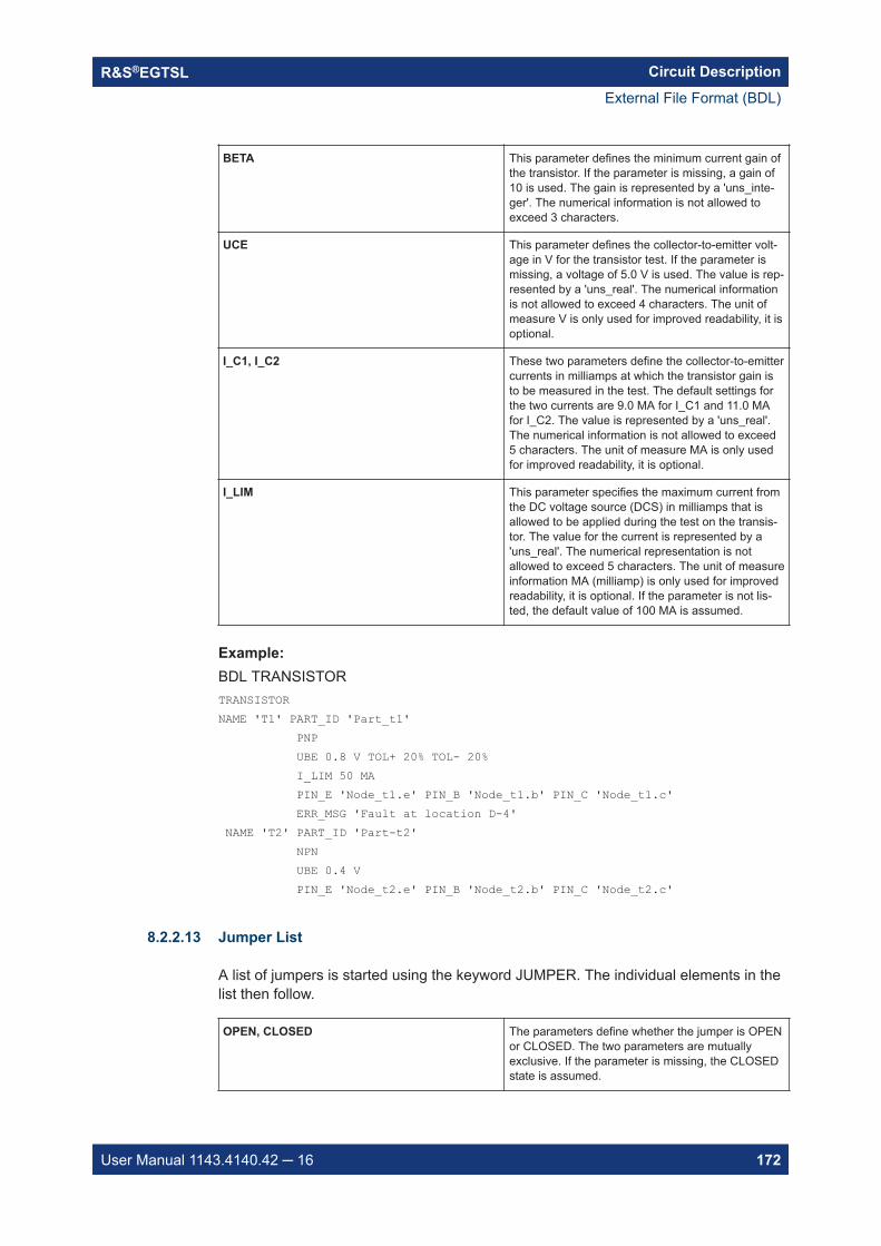
Circuit DescriptionR&S®EGTSL
172User Manual 1143.4140.42 16
BETA This parameter defines the minimum current gain ofthe transistor. If the parameter is missing, a gain of10 is used. The gain is represented by a 'uns_inte-ger'. The numerical information is not allowed toexceed 3 characters.
UCE This parameter defines the collector-to-emitter volt-age in V for the transistor test. If the parameter ismissing, a voltage of 5.0 V is used. The value is rep-resented by a 'uns_real'. The numerical informationis not allowed to exceed 4 characters. The unit ofmeasure V is only used for improved readability, it isoptional.
I_C1, I_C2 These two parameters define the collector-to-emittercurrents in milliamps at which the transistor gain isto be measured in the test. The default settings forthe two currents are 9.0 MA for I_C1 and 11.0 MAfor I_C2. The value is represented by a 'uns_real'.The numerical information is not allowed to exceed5 characters. The unit of measure MA is only usedfor improved readability, it is optional.
I_LIM This parameter specifies the maximum current fromthe DC voltage source (DCS) in milliamps that isallowed to be applied during the test on the transis-tor. The value for the current is represented by a'uns_real'. The numerical representation is notallowed to exceed 5 characters. The unit of measureinformation MA (milliamp) is only used for improvedreadability, it is optional. If the parameter is not lis-ted, the default value of 100 MA is assumed.
Example: BDL TRANSISTORTRANSISTOR NAME 'T1' PART_ID 'Part_t1' PNP UBE 0.8 V TOL+ 20% TOL- 20% I_LIM 50 MA PIN_E 'Node_t1.e' PIN_B 'Node_t1.b' PIN_C 'Node_t1.c' ERR_MSG 'Fault at location D-4' NAME 'T2' PART_ID 'Part-t2' NPN UBE 0.4 V PIN_E 'Node_t2.e' PIN_B 'Node_t2.b' PIN_C 'Node_t2.c'
8.2.2.13 Jumper List
A list of jumpers is started using the keyword JUMPER. The individual elements in thelist then follow.
OPEN, CLOSED The parameters define whether the jumper is OPENor CLOSED. The two parameters are mutuallyexclusive. If the parameter is missing, the CLOSEDstate is assumed.
External File Format (BDL)
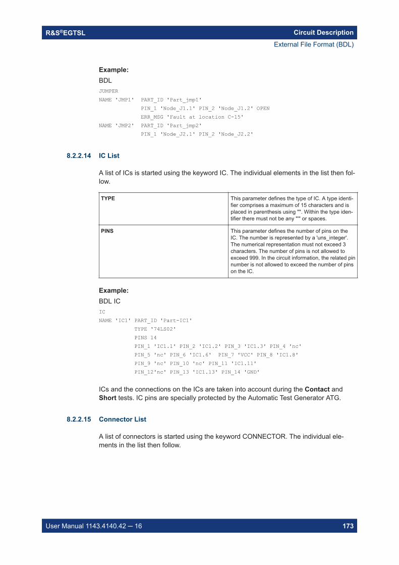
Circuit DescriptionR&S®EGTSL
173User Manual 1143.4140.42 16
Example: BDLJUMPER NAME 'JMP1' PART_ID 'Part_jmp1' PIN_1 'Node_J1.1' PIN_2 'Node_J1.2' OPEN ERR_MSG 'Fault at location C-15'NAME 'JMP2' PART_ID 'Part_jmp2' PIN_1 'Node_J2.1' PIN_2 'Node_J2.2'
8.2.2.14 IC List
A list of ICs is started using the keyword IC. The individual elements in the list then fol-low.
TYPE This parameter defines the type of IC. A type identi-fier comprises a maximum of 15 characters and isplaced in parenthesis using "". Within the type iden-tifier there must not be any "'" or spaces.
PINS This parameter defines the number of pins on theIC. The number is represented by a 'uns_integer'.The numerical representation must not exceed 3characters. The number of pins is not allowed toexceed 999. In the circuit information, the related pinnumber is not allowed to exceed the number of pinson the IC.
Example: BDL ICIC NAME 'IC1' PART_ID 'Part-IC1' TYPE '74LS02' PINS 14 PIN_1 'IC1.1' PIN_2 'IC1.2' PIN_3 'IC1.3' PIN_4 'nc' PIN_5 'nc' PIN_6 'IC1.6' PIN_7 'VCC' PIN_8 'IC1.8' PIN_9 'nc' PIN_10 'nc' PIN_11 'IC1.11' PIN_12'nc' PIN_13 'IC1.13' PIN_14 'GND'
ICs and the connections on the ICs are taken into account during the Contact andShort tests. IC pins are specially protected by the Automatic Test Generator ATG.
8.2.2.15 Connector List
A list of connectors is started using the keyword CONNECTOR. The individual ele-ments in the list then follow.
External File Format (BDL)
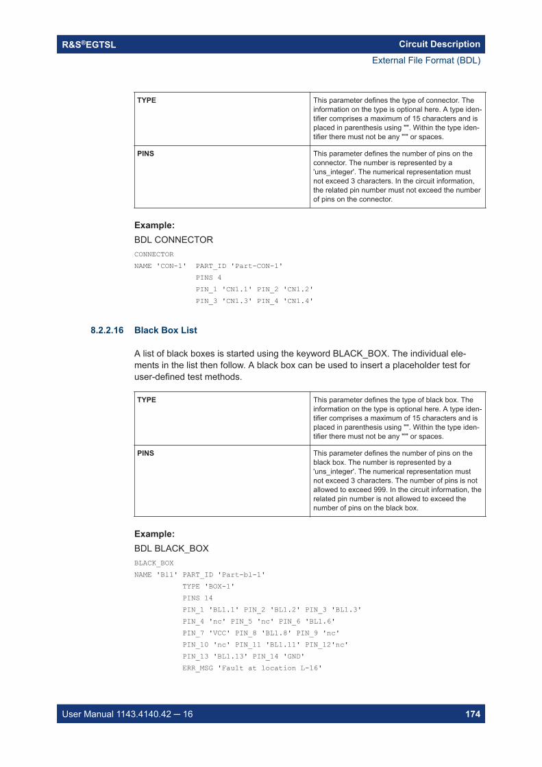
Circuit DescriptionR&S®EGTSL
174User Manual 1143.4140.42 16
TYPE This parameter defines the type of connector. Theinformation on the type is optional here. A type iden-tifier comprises a maximum of 15 characters and isplaced in parenthesis using "". Within the type iden-tifier there must not be any "'" or spaces.
PINS This parameter defines the number of pins on theconnector. The number is represented by a'uns_integer'. The numerical representation mustnot exceed 3 characters. In the circuit information,the related pin number must not exceed the numberof pins on the connector.
Example: BDL CONNECTORCONNECTOR NAME 'CON-1' PART_ID 'Part-CON-1' PINS 4 PIN_1 'CN1.1' PIN_2 'CN1.2' PIN_3 'CN1.3' PIN_4 'CN1.4'
8.2.2.16 Black Box List
A list of black boxes is started using the keyword BLACK_BOX. The individual ele-ments in the list then follow. A black box can be used to insert a placeholder test foruser-defined test methods.
TYPE This parameter defines the type of black box. Theinformation on the type is optional here. A type iden-tifier comprises a maximum of 15 characters and isplaced in parenthesis using "". Within the type iden-tifier there must not be any "'" or spaces.
PINS This parameter defines the number of pins on theblack box. The number is represented by a'uns_integer'. The numerical representation mustnot exceed 3 characters. The number of pins is notallowed to exceed 999. In the circuit information, therelated pin number is not allowed to exceed thenumber of pins on the black box.
Example: BDL BLACK_BOXBLACK_BOX NAME 'Bl1' PART_ID 'Part-bl-1' TYPE 'BOX-1' PINS 14 PIN_1 'BL1.1' PIN_2 'BL1.2' PIN_3 'BL1.3' PIN_4 'nc' PIN_5 'nc' PIN_6 'BL1.6' PIN_7 'VCC' PIN_8 'BL1.8' PIN_9 'nc' PIN_10 'nc' PIN_11 'BL1.11' PIN_12'nc' PIN_13 'BL1.13' PIN_14 'GND' ERR_MSG 'Fault at location L-16'
External File Format (BDL)
Circuit DescriptionR&S®EGTSL
175User Manual 1143.4140.42 16
Black boxes and the connections on black boxes are taken into account during theContact and Short tests.
In addition, a contact test is inserted for the black box as a placeholder.
8.2.2.17 Track List
A list of tracks is started using the keyword TRACK. The individual elements in the listthen follow.
The parameter is a list of node names that are connected to the track. At least 2 nodesmust be allocated to the track.
Example: BDL example TRACKTRACKNAME 'TRACK-1' PINS 4 'Node_1.1' 'Node_1.2' 'Node_1.3' 'Node_1.4' ERR_MSG 'Fault at location B-3 to B-22'NAME 'TRACK-2' PINS 2 'Node_2.1' 'Node_2.2'
8.2.2.18 Node List
A list of nodes is started using the keyword NODE. The individual elements in the listthen follow.
DEV_NAME This parameter identifies the logical name of thecomponent that is connected to this node.
External File Format (BDL)
Circuit DescriptionR&S®EGTSL
176User Manual 1143.4140.42 16
Example: BDL example NODENODE
NAME 'NODE1' DEV_NAME 'IC' PIN_1 DEV_NAME 'IC' PIN_2 DEV_NAME 'IC' PIN_3 DEV_NAME 'Transistor-1' PIN_A DEV_NAME 'LED_1' PIN_A
NAME 'NODE2' DEV_NAME 'LED_1' PIN_C DEV_NAME 'Transistor-1' PIN_B
NAME 'NODE3' DEV_NAME 'Transistor-1' PIN_C
8.2.2.19 FET List
A list of transistors is started using the keyword FET. The individual elements in the listthen follow.
JFET,DEP_MOSFET,ENH_MOSFET
Defines the type of field-effect transistor (FET).Junction field-effect transistors (junction-fet; JFET)and metal oxide semiconductor field-effect transis-tors (MOSFET) are distinguished. For MOSFETsthere are additionally the depletion-mode MOSFET(DEP_MOSFET) and enhancement-mode MOSFET(ENH_MOSFET) types.
N_CHANNEL,P_CHANNEL
Defines the channel type of a field-effect transistor.
VGS_OFF Defines the gate-source voltage at which the tran-sistor insulates (FET). If the parameter is omitted,the following default values will be used:
JFET
N_CHANNEL: -5 V
P_CHANNEL: 5 V
DEP_MOSFET
N_CHANNEL: -5 V
P_CHANNEL: 5 V
ENH_MOSFET
N_CHANNEL: 0 V
P_CHANNEL: 0 V
External File Format (BDL)
Circuit DescriptionR&S®EGTSL
177User Manual 1143.4140.42 16
VGS_ON Defines the gate-source voltage at which the tran-sistor conducts. If the parameter is omitted, the fol-lowing default values will be used:
JFET
N_CHANNEL: 0 V
P_CHANNEL: 0 V
DEP_MOSFET
N_CHANNEL: 0 V
P_CHANNEL: 0 V
ENH_MOSFET
N_CHANNEL: 5 V
P_CHANNEL: -5 V
RDS_ON Defines the drain-source resistance on conditionswitched on. If the parameter is omitted, the follow-ing default values will be used:
JFET: 1000 Ohm
DEP_MOSFET, ENH_MOSFET: 0.1 Ohm
8.3 Important Additional Information
8.3.1 Node List
The Automatic Test Generator ATG generates the relevant node list from the compo-nent data if no node list is given in the BDL file.
The node list must be completely and stable if it is given in the BDL file. The AutomaticTest Generator ATG compares only the content of the BDL file data with the node listentries. When there differences will be detected the ATG generates an error message.
8.3.2 Treatment of Specific Pins
When naming nodes, it must be observed that the following 2 node names will be trea-ted separately by Automatic Test Generator ATG because they are very important for acorrect test generation.
VCC... If the node name initials are VCC or vcc it meansthat it is a power supply node.
GND... If the node name initials are GND or gnd it meansthat it is a ground node.
VCC and GND nodes will particularly be considered on capacitor discharging (TestStep Discharge by ATG).
Important Additional Information
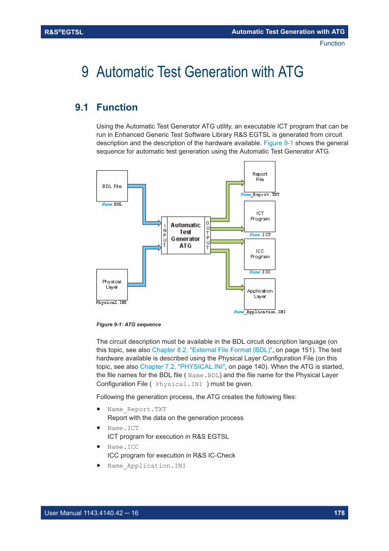
Automatic Test Generation with ATGR&S®EGTSL
178User Manual 1143.4140.42 16
9 Automatic Test Generation with ATG
9.1 Function
Using the Automatic Test Generator ATG utility, an executable ICT program that can berun in Enhanced Generic Test Software Library R&S EGTSL is generated from circuitdescription and the description of the hardware available. Figure 9-1 shows the generalsequence for automatic test generation using the Automatic Test Generator ATG.
Figure 9-1: ATG sequence
The circuit description must be available in the BDL circuit description language (onthis topic, see also Chapter 8.2, "External File Format (BDL)", on page 151). The testhardware available is described using the Physical Layer Configuration File (on thistopic, see also Chapter 7.2, "PHYSICAL.INI", on page 140). When the ATG is started,the file names for the BDL file ( Name.BDL) and the file name for the Physical LayerConfiguration File ( Physical.INI ) must be given.
Following the generation process, the ATG creates the following files:
Name_Report.TXTReport with the data on the generation process
Name.ICTICT program for execution in R&S EGTSL
Name.ICCICC program for execution in R&S IC-Check
Name_Application.INI
Function
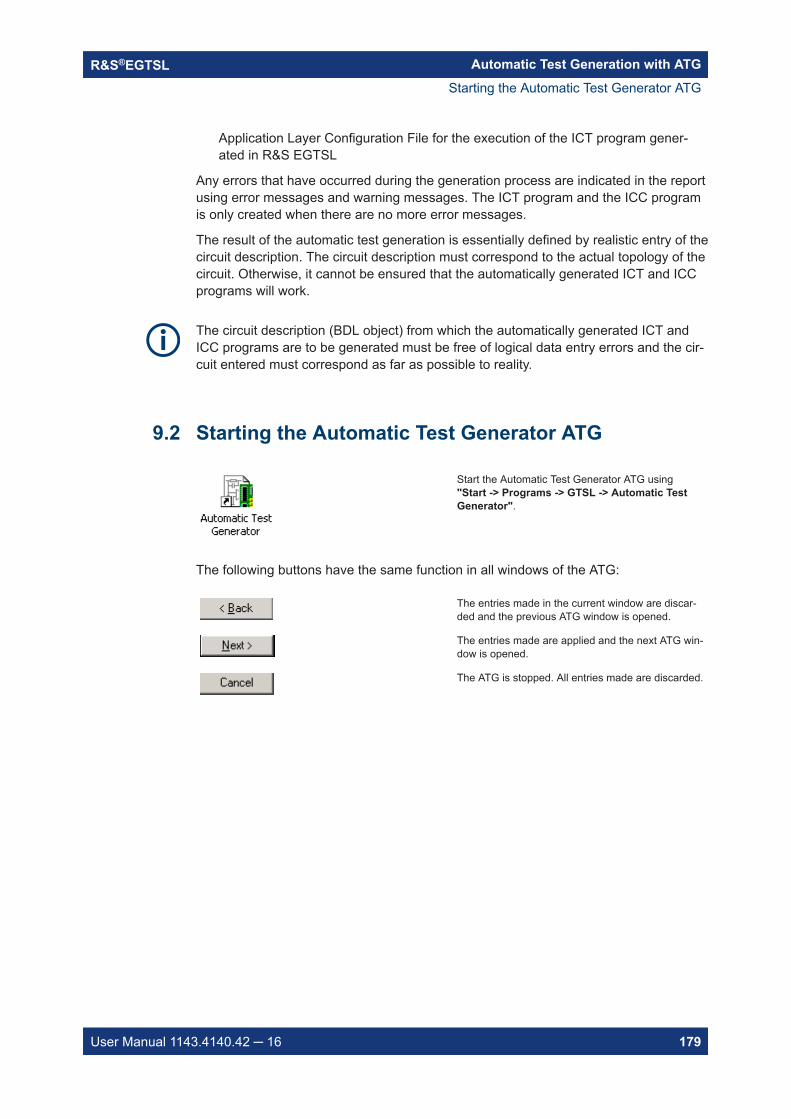
Automatic Test Generation with ATGR&S®EGTSL
179User Manual 1143.4140.42 16
Application Layer Configuration File for the execution of the ICT program gener-ated in R&S EGTSL
Any errors that have occurred during the generation process are indicated in the reportusing error messages and warning messages. The ICT program and the ICC programis only created when there are no more error messages.
The result of the automatic test generation is essentially defined by realistic entry of thecircuit description. The circuit description must correspond to the actual topology of thecircuit. Otherwise, it cannot be ensured that the automatically generated ICT and ICCprograms will work.
The circuit description (BDL object) from which the automatically generated ICT andICC programs are to be generated must be free of logical data entry errors and the cir-cuit entered must correspond as far as possible to reality.
9.2 Starting the Automatic Test Generator ATG
Start the Automatic Test Generator ATG using"Start -> Programs -> GTSL -> Automatic TestGenerator".
The following buttons have the same function in all windows of the ATG:
The entries made in the current window are discar-ded and the previous ATG window is opened.
The entries made are applied and the next ATG win-dow is opened.
The ATG is stopped. All entries made are discarded.
Starting the Automatic Test Generator ATG
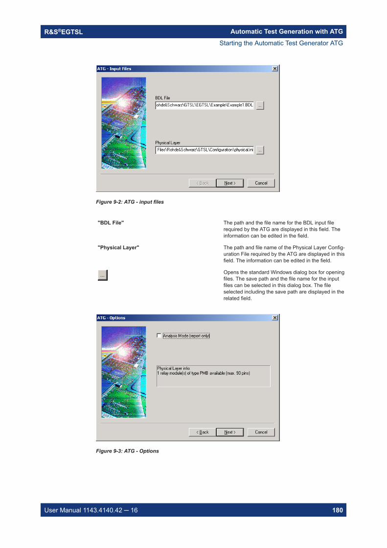
Automatic Test Generation with ATGR&S®EGTSL
180User Manual 1143.4140.42 16
Figure 9-2: ATG - input files
"BDL File" The path and the file name for the BDL input filerequired by the ATG are displayed in this field. Theinformation can be edited in the field.
"Physical Layer" The path and file name of the Physical Layer Config-uration File required by the ATG are displayed in thisfield. The information can be edited in the field.
Opens the standard Windows dialog box for openingfiles. The save path and the file name for the inputfiles can be selected in this dialog box. The fileselected including the save path are displayed in therelated field.
Figure 9-3: ATG - Options
Starting the Automatic Test Generator ATG
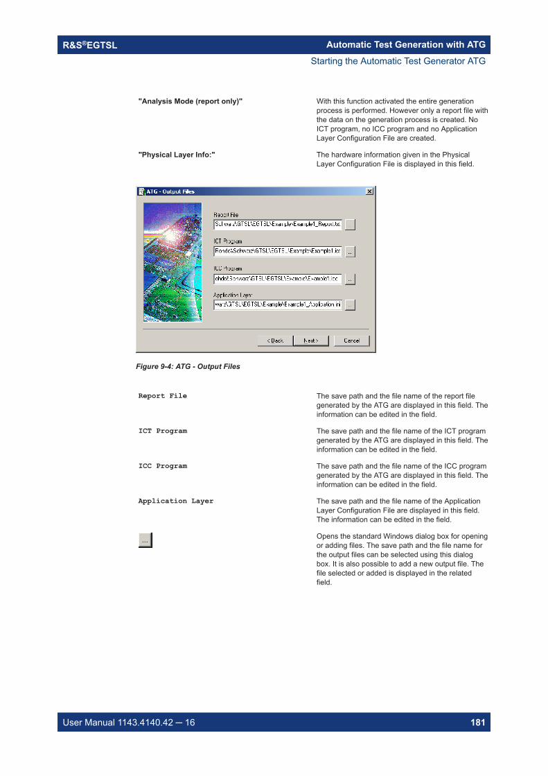
Automatic Test Generation with ATGR&S®EGTSL
181User Manual 1143.4140.42 16
"Analysis Mode (report only)" With this function activated the entire generationprocess is performed. However only a report file withthe data on the generation process is created. NoICT program, no ICC program and no ApplicationLayer Configuration File are created.
"Physical Layer Info:" The hardware information given in the PhysicalLayer Configuration File is displayed in this field.
Figure 9-4: ATG - Output Files
Report File The save path and the file name of the report filegenerated by the ATG are displayed in this field. Theinformation can be edited in the field.
ICT Program The save path and the file name of the ICT programgenerated by the ATG are displayed in this field. Theinformation can be edited in the field.
ICC Program The save path and the file name of the ICC programgenerated by the ATG are displayed in this field. Theinformation can be edited in the field.
Application Layer The save path and the file name of the ApplicationLayer Configuration File are displayed in this field.The information can be edited in the field.
Opens the standard Windows dialog box for openingor adding files. The save path and the file name forthe output files can be selected using this dialogbox. It is also possible to add a new output file. Thefile selected or added is displayed in the relatedfield.
Starting the Automatic Test Generator ATG
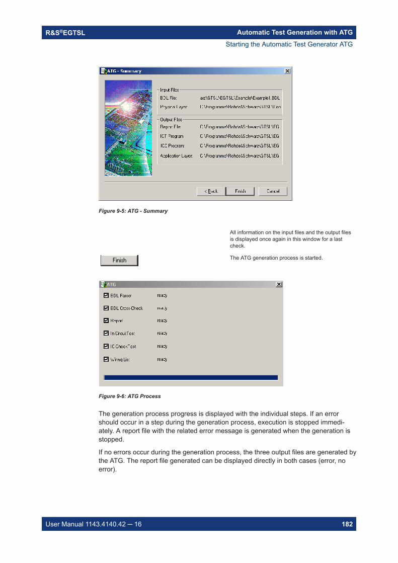
Automatic Test Generation with ATGR&S®EGTSL
182User Manual 1143.4140.42 16
Figure 9-5: ATG - Summary
All information on the input files and the output filesis displayed once again in this window for a lastcheck.
The ATG generation process is started.
Figure 9-6: ATG Process
The generation process progress is displayed with the individual steps. If an errorshould occur in a step during the generation process, execution is stopped immedi-ately. A report file with the related error message is generated when the generation isstopped.
If no errors occur during the generation process, the three output files are generated bythe ATG. The report file generated can be displayed directly in both cases (error, noerror).
Starting the Automatic Test Generator ATG
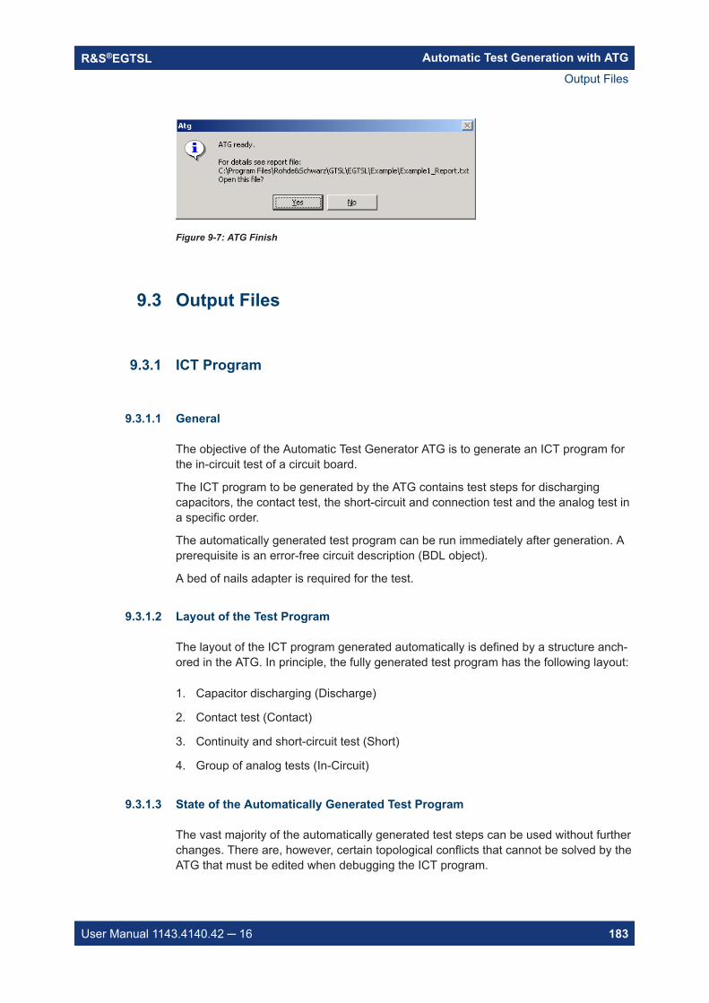
Automatic Test Generation with ATGR&S®EGTSL
183User Manual 1143.4140.42 16
Figure 9-7: ATG Finish
9.3 Output Files
9.3.1 ICT Program
9.3.1.1 General
The objective of the Automatic Test Generator ATG is to generate an ICT program forthe in-circuit test of a circuit board.
The ICT program to be generated by the ATG contains test steps for dischargingcapacitors, the contact test, the short-circuit and connection test and the analog test ina specific order.
The automatically generated test program can be run immediately after generation. Aprerequisite is an error-free circuit description (BDL object).
A bed of nails adapter is required for the test.
9.3.1.2 Layout of the Test Program
The layout of the ICT program generated automatically is defined by a structure anch-ored in the ATG. In principle, the fully generated test program has the following layout:
1. Capacitor discharging (Discharge)
2. Contact test (Contact)
3. Continuity and short-circuit test (Short)
4. Group of analog tests (In-Circuit)
9.3.1.3 State of the Automatically Generated Test Program
The vast majority of the automatically generated test steps can be used without furtherchanges. There are, however, certain topological conflicts that cannot be solved by theATG that must be edited when debugging the ICT program.
Output Files
Automatic Test Generation with ATGR&S®EGTSL
184User Manual 1143.4140.42 16
These test conflicts are prepared by the ATG such that they can be addressed by theuser as easily as possible. The aids generated by the ATG for this purpose comprisethe comments in the ATG report and test proposals in the ICT program that can beapplied by the user after review.
Test conflicts can, for example, be:
Direct parallel component paths (SHUNTS) Very small nominal values Very small parallel resistors Forward biased, parallel diode paths Hazards for components
All the above mentioned problems are detected by the network analysis in the ATGand processed accordingly.
9.3.1.4 Program Groups Generated
Capacitor discharging (Discharge)
The capacitor discharging is intended to prevent discharge currents from capacitorsproducing incorrect measurements or damaging the relays in the switching matrix.
The pins in the "Reference Pin List" are short-circuited at the start of the discharging.The pins in the "Test Pin List" are individually discharged to the reference pin poten-tial and then connected to the potential of the "Reference Pin List".
The ATG uses the following strategy for the layout of the pin lists:
The Reference Pin List contains the ground nodes with the largest number of com-ponent connections (ground nodes always start with “GND” or “gnd”).
The Test Pin List contains– All other ground nodes.– All nodes that start with “VCC” or “vcc”.– All nodes between which there is a total capacitance of 8 µF or more.
Contact Test (Contact)
The contact test is intended to exclude the possibility of missing nail contacts resultingin inappropriate error messages.
In the contact test generated by the ATG, all nodes on the circuit board for which thereis a corresponding entry in the related BDL object, i.e. in the table of nail allocations,are always checked. During this process the connection to all other nodes in theirentirety is tested. The resistance between a node and all others must not exceed thevalue of 1 MΩ (default value). This is defined by the parameter "Resistor Limit" in thecontact test.
If there are isolated nodes in the circuit to be tested, i.e. nodes that do not have a con-nection to any other point on the circuit board, these must be removed from the contacttest using the All but not function.
Output Files
Automatic Test Generation with ATGR&S®EGTSL
185User Manual 1143.4140.42 16
Continuity and Short-circuit Test (Short)
For closed jumpers and tracks connection tests are integrated into the ICT program bythe ATG. During this process the jumper and track nodes are tested for the existenceof the nominal connection; the limit for a connection that is still valid is preset in the"Resistor Limit" parameter to 10 Ω.
For open jumpers and connectors short-circuit tests are integrated into the ICT test bythe ATG. In contrary to the connection test, in this case the nodes given are tested formutual short-circuits. If a short-circuit is found, i.e. a connection with less than 10 Ω(default value), the result will be a FAIL.
A global short-circuit test is always generated over all nodes on the unit under test bythe ATG in the test program. During the generation of the global short-circuit test,nodes that have a nominal connection (e.g. closed jumpers, tracks or coils) are recor-ded by the ATG and removed from the short-circuit test using the All but not function.
The Automatically Generated Analog Test
Automatic test generation is possible for the following components that can be given inthe circuit description language BDL.Table 9-1: Possible analog tests
Description in BDL Test method
Resistor Resistor or Continuity
Resistor Array
Potentiometer Resistor
Variable Resistor
Capacitor Impedance or Short
Pol. Capacitor Impedance or Short
Inductor Impedance or Continuity
Diode Diode
LED
Z_Diode ZenerDiode or Diode
Transistor TransistorBeta or Transistor
Jumper Continuity or Short
IC No test
Connector Short
Black Box Contact (placeholder)
Track Continuity
FET FET (field-effect transistor)
Tests on the same analog component types are combined by the ATG and generatedtogether. Thus, in an automatically generated test you will find all resistor tests, capaci-
Output Files
Automatic Test Generation with ATGR&S®EGTSL
186User Manual 1143.4140.42 16
tor tests, etc. combined into groups. The order of the individual tests within a groupcorresponds to the entry in BDL.
9.3.1.5 Automatic Determination of the Guard Points in the Analog Test
Measuring errors can occur due to currents flowing parallel to the component paths tobe tested; these errors can degrade the effectiveness of an analog test. To prevent thisproblem occurring, the Guarding process is used in the analog in-circuit test. Duringthis process specific nodes (guard points) on the circuit are selected and brought to apotential with the measuring point. In this way it is ensured that the current measuredcorresponds to that which is flowing through the component path to be measured.
The relevant guard points are determined automatically by the ATG. During this proc-ess, those nodes that are in close proximity to the component to be tested are prefera-bly accepted as guard points. This condition is met,
When the topological distance between measuring and stimulation point is notlarger than one branch and
When the guard point is within a feedback branch to the component to be mea-sured, that is within the same cluster.
9.3.1.6 Safety Against Destruction of Components During the Test
During the circuit analysis and the editing of analog component tests, the ATG moni-tors the following possible hazards:
Application of a voltage > 0.7 V to an IC that is not supplied with power. Possible forward biasing of a diode in the vicinity of an IC during the test on a com-
ponent connected to the diode. Reverse polarization of an electrolytic capacitor during a test on an adjacent com-
ponent by more than 0.5 V.
If a hazard is found, the corresponding test configuration is skipped by the ATG and, ifpossible, a different configuration selected. A further possibility is the listing of suchhazards in the ATG report with the corresponding comments.
9.3.1.7 Taking Account of Topological Problems
The ATG detects and processes the following circuit situations:
Direct and indirect parallel circuit paths Orientation of parallel diode paths
During the generation of an analog component test, the measuring configurations thatpermit measurement on the component despite a topological problem are initially pre-ferred. In the case of a parallel diode, e.g., the direction in which the voltage is appliedis changed to utilize the higher resistance when the diode is reverse biased.
Output Files
Automatic Test Generation with ATGR&S®EGTSL
187User Manual 1143.4140.42 16
9.3.2 ATG Report
In the ATG all special aspects that are found by the ATG during the generation of theprogram are listed. Here all messages are allocated precisely to those components forwhich the generation of the test produced the related messages. At the same point, thewarnings that are generated by the ATG in case of components at risk are given.
Example (without warnings):
ATG REPORT==========
Created: 2009-08-12 15:00:08 ATG Version: ATG 02.83 EGTSL Version: EGTSL 02.83
Input:------Board Description: 'C:\Program Files\Rohde&Schwarz\GTSL\EGTSL\Example\Example1.BDL'Physical Layer: 'C:\Program Files\Rohde&Schwarz\GTSL\EGTSL\Example\Example_Physical.ini'
Output:-------ICT Program: 'C:\Program Files\Rohde&Schwarz\GTSL\EGTSL\Example\Example1.ict'ICC Program: 'C:\Program Files\Rohde&Schwarz\GTSL\EGTSL\Example\Example1.icc'Application Layer: 'C:\Program Files\Rohde&Schwarz\GTSL\EGTSL\Example\Example1_Application.ini'Report: 'C:\Program Files\Rohde&Schwarz\GTSL\EGTSL\Example\Example1_Report.txt'
BDL Parser: 0 error(s) and 0 warning(s).
BDL cross check: OK.
>>> Message from TR1 <<<TS-PSU not configured in 'physical.ini', simple transistor test inserted
Test coverage report Number Weight CoverageComponents 8Regular tests 7 1 87.5%Reduced tests 1 0.5 6.25%Short/Contact test only 0 0.1 0%Total test coverage 93.8%Wiring List info: Nodes mapped to a total number of 7 pin(s).
Output Files
Automatic Test Generation with ATGR&S®EGTSL
188User Manual 1143.4140.42 16
9.3.2.1 Typical Warning Messages
Example: BDL entryNAME 'R1' VALUE 10 kOHM Statement with Error TOL+ 10% TOL- 10% I_LIM 100.0 MA PIN_1 'VCC' PIN_2 'MESS1'
Error message in the ATG reportlexical error (NO BDL keyword) in line 4: k
BDL Parser: 1 error(s) and 0 warning(s).
ERRORS OCCURRED DURING TEST GENERATION:--------------------------------------ERROR: BDL Parser: syntax errors detected.
Error rectificationIn BDL it is only allowed to use upper case.
Example: BDL entryNAME 'R2' VALUE 100 OHM TOL+ 10% TOL- 10% I_LIM 100.0 MA PIN_1 'VCC' PIN_3 'GND' Statement with Error
Error message in the ATG reportline 15: syntax error, unexpected PIN_3.
BDL Parser: 1 error(s) and 0 warning(s).
ERRORS OCCURRED DURING TEST GENERATION:--------------------------------------
ERROR: BDL Parser: syntax errors detected.
Error rectificationKeyword PIN_3 is not defined for this component. For this component there is onlyPIN_1 and PIN_2.
Output Files
Automatic Test Generation with ATGR&S®EGTSL
189User Manual 1143.4140.42 16
Example: BDL entryNAME 'R3' VALUE 330 OHM TOL+ 10% TOL- 10% I_LIM 100.0 UA Statement with Error PIN_1 'MESS1' PIN_2 'GND'
Error message in the ATG reportError message in the ATG reportline 20: syntax error, unexpected 'U'.
BDL Parser: 1 error(s) and 0 warning(s).
ERRORS OCCURRED DURING TEST GENERATION:--------------------------------------
ERROR: BDL Parser: syntax errors detected.
Error rectificationIn the entry I_LIM only the unit MA (mA) is allowed, not UA (μA).
9.3.2.2 Alternative Proposals from the ATG
In some cases the ATG generates alternative proposals for measurements, e.g., forguarded resistor measurements or the measurement of very low value resistors. It gen-erates a standard test with higher error limits and, as an alternative, a more exact testwith lower error limits.
The following example information relates to Chapter B, "Example 2", on page 301.
The proposals for the individual components are listed in the ATG report.
Output Files
Automatic Test Generation with ATGR&S®EGTSL
190User Manual 1143.4140.42 16
Example: Example: Guarded measurement of the resistor R1 (10 kΩ) Measurement of the low value resistor R4 (10 Ω)
BDL Parser: 0 error(s) and 0 warning(s).
BDL cross check: OK.
>>> Message from R1 6-Wire Test Proposal <<<Total error for 3-wire mode: 25.52 % 6-wire mode: 3.1255%
>>> Message from R1 <<<Test only possible by exceeding the error limitsGuarding error limiting test quality
>>> Message from R4 4-Wire Test Proposal <<<Total error for 2-wire mode: 24,336% 4-wire mode: 1 %
>>> Message from R4 <<<Test only possible by exceeding the error limitsTest limits include system residuals of 2.4 Ohms
Wiring List info: Nodes mapped to a total number of 8 pin(s).
Output Files
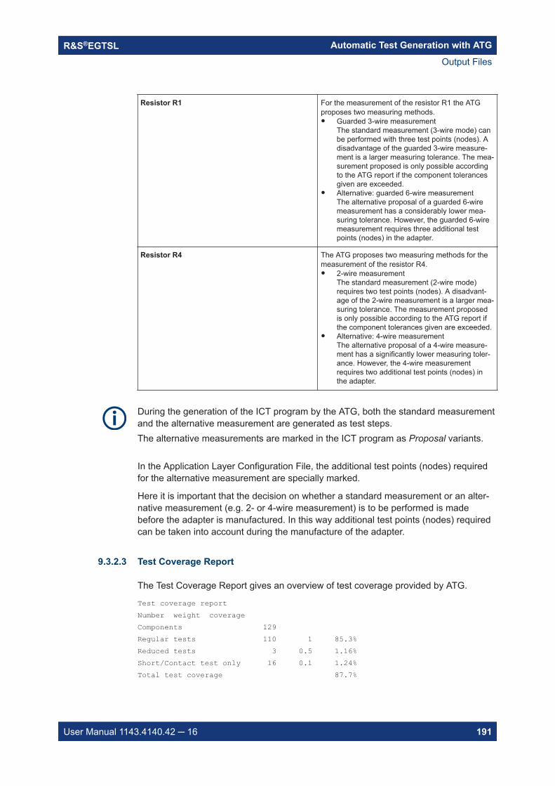
Automatic Test Generation with ATGR&S®EGTSL
191User Manual 1143.4140.42 16
Resistor R1 For the measurement of the resistor R1 the ATGproposes two measuring methods. Guarded 3-wire measurement
The standard measurement (3-wire mode) canbe performed with three test points (nodes). Adisadvantage of the guarded 3-wire measure-ment is a larger measuring tolerance. The mea-surement proposed is only possible accordingto the ATG report if the component tolerancesgiven are exceeded.
Alternative: guarded 6-wire measurementThe alternative proposal of a guarded 6-wiremeasurement has a considerably lower mea-suring tolerance. However, the guarded 6-wiremeasurement requires three additional testpoints (nodes) in the adapter.
Resistor R4 The ATG proposes two measuring methods for themeasurement of the resistor R4. 2-wire measurement
The standard measurement (2-wire mode)requires two test points (nodes). A disadvant-age of the 2-wire measurement is a larger mea-suring tolerance. The measurement proposedis only possible according to the ATG report ifthe component tolerances given are exceeded.
Alternative: 4-wire measurementThe alternative proposal of a 4-wire measure-ment has a significantly lower measuring toler-ance. However, the 4-wire measurementrequires two additional test points (nodes) inthe adapter.
During the generation of the ICT program by the ATG, both the standard measurementand the alternative measurement are generated as test steps.The alternative measurements are marked in the ICT program as Proposal variants.
In the Application Layer Configuration File, the additional test points (nodes) requiredfor the alternative measurement are specially marked.
Here it is important that the decision on whether a standard measurement or an alter-native measurement (e.g. 2- or 4-wire measurement) is to be performed is madebefore the adapter is manufactured. In this way additional test points (nodes) requiredcan be taken into account during the manufacture of the adapter.
9.3.2.3 Test Coverage Report
The Test Coverage Report gives an overview of test coverage provided by ATG.
Test coverage reportNumber weight coverageComponents 129Regular tests 110 1 85.3%Reduced tests 3 0.5 1.16%Short/Contact test only 16 0.1 1.24%Total test coverage 87.7%
Output Files
Automatic Test Generation with ATGR&S®EGTSL
192User Manual 1143.4140.42 16
Test coverage is calculated by the number of tests generated in reference to the num-ber of components in the BDL file. Tests that are generated are categorized in one ofthree classes and weighted according to their quality.
Components The number of components in the BDL file (NODEentries are not counted).
Regular tests The number of regular tests generated by ATG.Regular tests are rated with a factor of 1.0.
Reduced tests The number of reduced tests generated by ATG.These include: 0-Ohm resistors, because a continuity test is
inserted instead of a resistor test. Resistor arrays, if a test was not able to gener-
ate all resistors in the array. Inductors, if a continuity test was generated
instead of an impedance test. Diodes andLEDs, if it was not possible to generate anyreverse test (current measurement).
Zener diodes, if only a simple diode test couldbe generated.
Transistors, if only a simple transistor test andno transistor beta test could be generated.
Reduced tests are rated with a factor of 0.5.
Short / contact test only The number of components for which no test couldbe generated by ATG. Generally this includes ICsand Black Boxes. The pins of these componentsare, however, taken into account in the Contact andShort test. These components are rated with a fac-tor of 0.1.
Total test coverage Complete test coverage is calculated as a percent-age from:
9.3.3 Application Layer Configuration File
In the Application Layer Configuration File, the specific information for the use of thehardware is compiled by the ATG for the ICT program and the ICC program generated.On the execution of the ICT program or the ICC program, the name of the ApplicationLayer Configuration File generated must be given.
You will find further information on the Application Layer Configuration File in Chap-ter 7.3, "APPLICATION.INI", on page 143.
Example:
[ResourceManager]; general trace settings (normally off)Trace = 0TraceFile = %GTSLROOT%\resmgr_trace.txt
;--------------------------------------------------------------------------------[LogicalNames]
Output Files
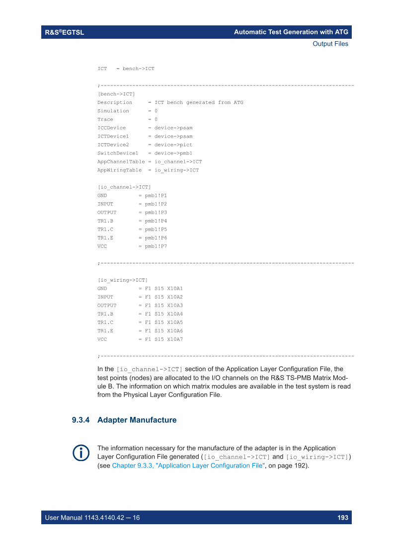
Automatic Test Generation with ATGR&S®EGTSL
193User Manual 1143.4140.42 16
ICT = bench->ICT
;--------------------------------------------------------------------------------[bench->ICT]Description = ICT bench generated from ATGSimulation = 0Trace = 0ICCDevice = device->psamICTDevice1 = device->psamICTDevice2 = device->pictSwitchDevice1 = device->pmb1AppChannelTable = io_channel->ICTAppWiringTable = io_wiring->ICT
[io_channel->ICT]GND = pmb1!P1INPUT = pmb1!P2OUTPUT = pmb1!P3TR1.B = pmb1!P4TR1.C = pmb1!P5TR1.E = pmb1!P6VCC = pmb1!P7
;--------------------------------------------------------------------------------
[io_wiring->ICT] GND = F1 S15 X10A1 INPUT = F1 S15 X10A2 OUTPUT = F1 S15 X10A3 TR1.B = F1 S15 X10A4 TR1.C = F1 S15 X10A5 TR1.E = F1 S15 X10A6 VCC = F1 S15 X10A7
;--------------------------------------------------------------------------------
In the [io_channel->ICT] section of the Application Layer Configuration File, thetest points (nodes) are allocated to the I/O channels on the R&S TS-PMB Matrix Mod-ule B. The information on which matrix modules are available in the test system is readfrom the Physical Layer Configuration File.
9.3.4 Adapter Manufacture
The information necessary for the manufacture of the adapter is in the ApplicationLayer Configuration File generated ([io_channel->ICT] and [io_wiring->ICT])(see Chapter 9.3.3, "Application Layer Configuration File", on page 192).
Output Files
Automatic Test Generation with ATGR&S®EGTSL
194User Manual 1143.4140.42 16
9.3.5 ICC Program
The Automatic Test Generator ATG generates an ICC program for the IC-Check test ofa circuit board.
An IC-Check program file is a test file with the extension .icc. It can be created oredited using any text editor. The logical structure of the ICC program file is made up ofinformation blocks on ICs to be tested. Each information block begins with the name ofthe block in square brackets. All the subsequent lines begin with a keyword and eitherdescribe the measurement configuration to be applied to test the individual pins of theIC or the names of the pins and reference pins to be tested. All pins of the BDL fileshaving the letter sequence "GND", "VSS" or "VCC" (case insensitive) are listed in theIC-Check program file as reference pins.
Refer to chapter 8 R&S IC-Check Test Programs of the document Software DescriptionIC-Check for a detailed description of the contents and usage of an ICC program file.
Output Files
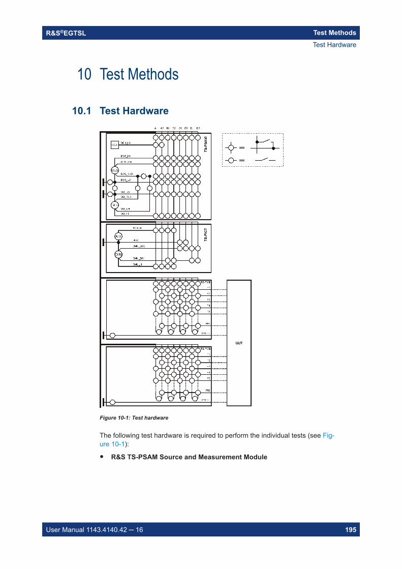
Test MethodsR&S®EGTSL
195User Manual 1143.4140.42 16
10 Test Methods
10.1 Test Hardware
Figure 10-1: Test hardware
The following test hardware is required to perform the individual tests (see Fig-ure 10-1):
R&S TS-PSAM Source and Measurement Module
Test Hardware
Test MethodsR&S®EGTSL
196User Manual 1143.4140.42 16
Table 10-1: DC stimulation source (DCS)
max. voltage 5 V
max. current 100 mA
The current limit is adjustable
Table 10-2: Voltage and current measurement unit (MU)
Voltage measuring range DC 10 mV to 125 V
Voltage measuring range AC 20 mV rms to 90 V rms
Current measuring range DC 1 μA to 1 A
Current measuring range AC 100 μA to 1 A
Recording the voltage curve during an impedancemeasurement
Table 10-3: Discharge unit DCH
max. voltage 30 V
max. current 400 mA
R&S TS-PICT In-Circuit Test ModuleThe R&S TS-PICT In-Circuit Test Module is only required for the diode test, theimpedance test and the guarded resistor test.
Table 10-4: AC voltage source (AOS)
max. voltage AC (rms) 1 V at 100 Hz, 1 kHz, 10 kHz
max. voltage DC 5 V
max. current DC 50 mA
Table 10-5: Current Measuring Unit (CMU)
Current measuring range AC 5 μA to 250 mA
R&S TS-PSU Power Supply/Load ModuleR&S TS-PSU12 Power Supply/Load Module 12VThe R&S TS-PSU Power Supply/Load Module / R&S TS-PSU Power Supply/LoadModule 12V is only required for the zener diode test and the transistor beta test.
max. voltage TS-PSU 50 V (single)
100 V (cascaded)
max. voltage TS-PSU12 12 V (single)
24 V (cascaded)
max. current 100 mA
R&S TS-PMB Matrix Module B– Connection of the individual measuring pins (nodes)
Test Hardware
Test MethodsR&S®EGTSL
197User Manual 1143.4140.42 16
The measuring and stimulation hardware are connected to the Unit Under Test (UUT)using the R&S TS-PMB and the analog bus.
The exact function and the technical data on the measuring and stimulation hardwareare described in detail in the user manuals and the data sheets for the individual mod-ules.
10.2 Ground Wiring
During the in-circuit tests, the UUT (Unit Under test) must be floating, i.e. it must not beconnected with the ground of the test system.
The correct ground wiring is shown in Figure 10-1. The ground of the UUT is connec-ted with the GNDno connectors of the matrix card. This can be connected through arelay with the system ground GND. During the in-circuit tests, these relays must beopened. For the function test, they can be closed.
10.3 Contact Test
Starting with GTSL 3.30, no GTSL license is required.
License required: R&S TS-LEGT or R&S TS-LEG2
Test hardware Module
DCS R&S TS-PSAM
MU R&S TS-PSAM
Contact Test
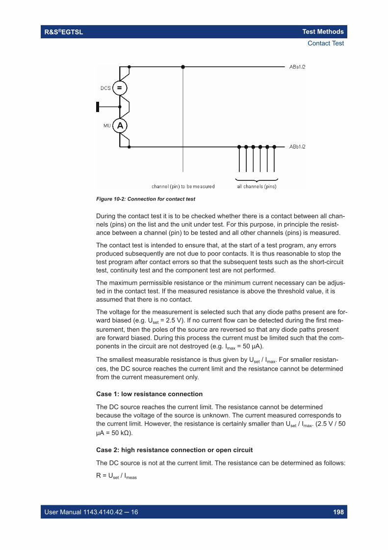
Test MethodsR&S®EGTSL
198User Manual 1143.4140.42 16
Figure 10-2: Connection for contact test
During the contact test it is to be checked whether there is a contact between all chan-nels (pins) on the list and the unit under test. For this purpose, in principle the resist-ance between a channel (pin) to be tested and all other channels (pins) is measured.
The contact test is intended to ensure that, at the start of a test program, any errorsproduced subsequently are not due to poor contacts. It is thus reasonable to stop thetest program after contact errors so that the subsequent tests such as the short-circuittest, continuity test and the component test are not performed.
The maximum permissible resistance or the minimum current necessary can be adjus-ted in the contact test. If the measured resistance is above the threshold value, it isassumed that there is no contact.
The voltage for the measurement is selected such that any diode paths present are for-ward biased (e.g. Uset = 2.5 V). If no current flow can be detected during the first mea-surement, then the poles of the source are reversed so that any diode paths presentare forward biased. During this process the current must be limited such that the com-ponents in the circuit are not destroyed (e.g. Imax = 50 μA).
The smallest measurable resistance is thus given by Uset / Imax. For smaller resistan-ces, the DC source reaches the current limit and the resistance cannot be determinedfrom the current measurement only.
Case 1: low resistance connection
The DC source reaches the current limit. The resistance cannot be determinedbecause the voltage of the source is unknown. The current measured corresponds tothe current limit. However, the resistance is certainly smaller than Uset / Imax. (2.5 V / 50μA = 50 kΩ).
Case 2: high resistance connection or open circuit
The DC source is not at the current limit. The resistance can be determined as follows:
R = Uset / Imeas
Contact Test
Test MethodsR&S®EGTSL
199User Manual 1143.4140.42 16
In the report on the contact test, the pins without contact are listed. All pins are tested,however a maximum of 10 pins without contact are listed.
10.4 Continuity Test
Starting with GTSL 3.30, no GTSL license is required.
License required: R&S TS-LEGT or R&S TS-LEG2
The connection for the continuity test is made in a similar manner to the connection forthe contact test (see Figure 10-2). However, only two pins (pin pair) are ever connec-ted to the analog bus.
With the aid of the continuity test it is checked whether there is continuity between a listof nodes (pins).
There is continuity when the resistance between two nodes (pins) is less than adefined value.
For the continuity test the voltage is selected such that diode paths are reverse biased(e.g. U set = 0.2 V). The current limit is set to the maximum possible value. In this waycapacitors in the circuit are charged more quickly. During the charging process, a largecurrent flows than could also be interpreted as continuity. If there is no continuity, thenafter the charging time the current will drop to an acceptable, stable value. If there iscontinuity, the DC source is either at the current limit and supplies the programmedcurrent, or a current limited by the system residuals (approx. 1.2 Ω) flows.
If the DC source is not at the current limit, the resistance of the continuity can be deter-mined as follows:
R = U set / Imeas - Rresid
The low resistance continuities or networks are listed in the report on the continuitytest.
Example for report entry:
P1 P2/P3 ... between P2 and P3 there is no continuity
Continuity Test
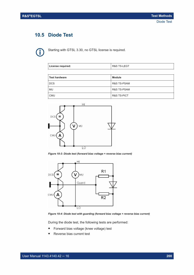
Test MethodsR&S®EGTSL
200User Manual 1143.4140.42 16
10.5 Diode Test
Starting with GTSL 3.30, no GTSL license is required.
License required: R&S TS-LEGT
Test hardware Module
DCS R&S TS-PSAM
MU R&S TS-PSAM
CMU R&S TS-PICT
Figure 10-3: Diode test (forward bias voltage + reverse bias current)
Figure 10-4: Diode test with guarding (forward bias voltage + reverse bias current)
During the diode test, the following tests are performed:
Forward bias voltage (knee voltage) test Reverse bias current test
Diode Test
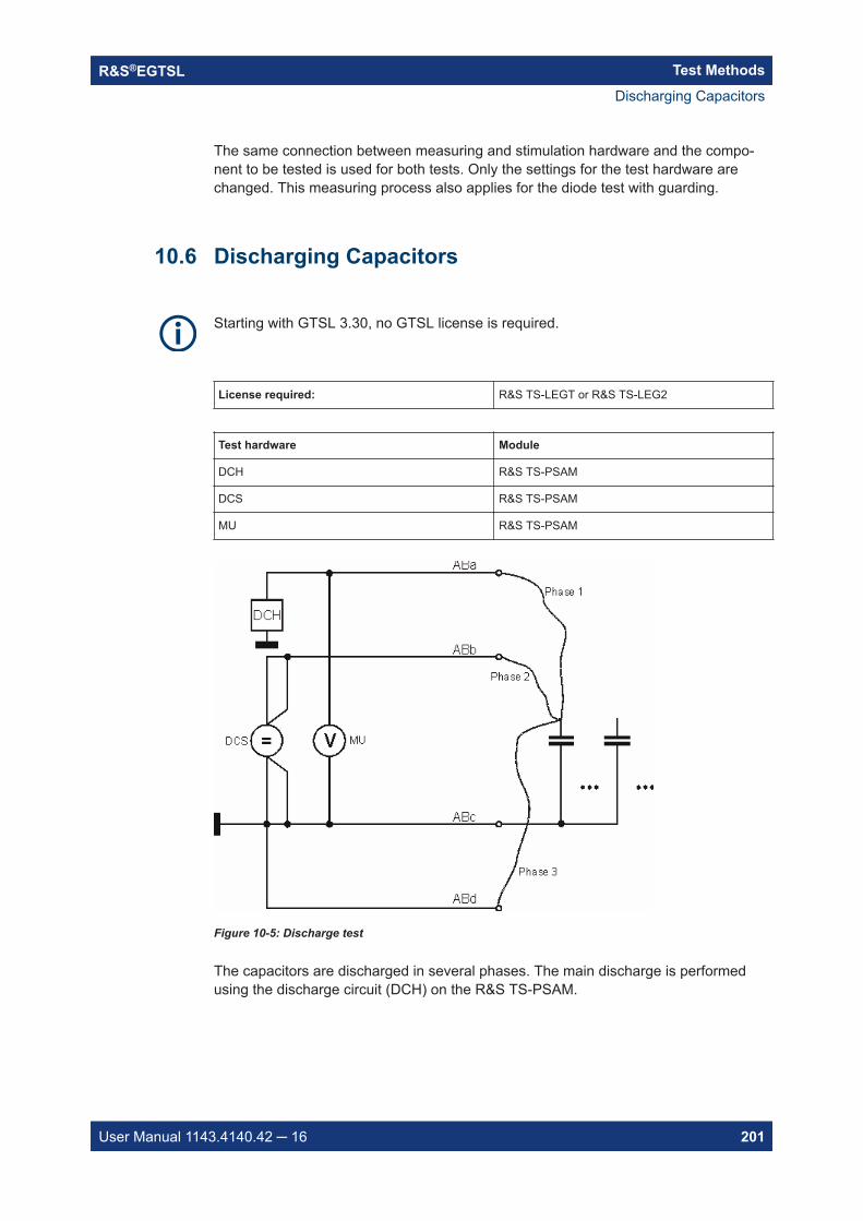
Test MethodsR&S®EGTSL
201User Manual 1143.4140.42 16
The same connection between measuring and stimulation hardware and the compo-nent to be tested is used for both tests. Only the settings for the test hardware arechanged. This measuring process also applies for the diode test with guarding.
10.6 Discharging Capacitors
Starting with GTSL 3.30, no GTSL license is required.
License required: R&S TS-LEGT or R&S TS-LEG2
Test hardware Module
DCH R&S TS-PSAM
DCS R&S TS-PSAM
MU R&S TS-PSAM
Figure 10-5: Discharge test
The capacitors are discharged in several phases. The main discharge is performedusing the discharge circuit (DCH) on the R&S TS-PSAM.
Discharging Capacitors
Test MethodsR&S®EGTSL
202User Manual 1143.4140.42 16
Phase 1 The node / capacitor to be discharged ( test pin ) isconnected using the analog bus A (ABa). The node /capacitor is discharged via the discharge circuit(DCH). The voltage at ABa is now measured cycli-cally. When the measured voltage drops below adefined value, phase 1 is complete.
Phase 2 The node / capacitor to be discharged( test pin ) isswitched from analog bus A (ABa) to analog bus B(ABb) and thus to the DC source (DCS). The dis-charge is now performed using the DCS at 100 mA.Phase 2 is complete when the DCS is no longer atthe current limit.
Phase 3 The node / capacitor to be discharged ( test pin) isswitched to analog bus D (ABd) and thus shorted tothe reference pin.During this phase the capacitordischarges via the cable resistances on the switch-ing matrix.
If the maximum duration for the discharging of all nodes / capacitors ( test pins ) isexceeded, the test pins that have not yet been discharged are listed in the report. Thepin on which the measuring time expired during discharging and for which the dis-charge process was not completed is also listed.
10.7 FET Test
Starting with GTSL 3.30, no GTSL license is required.
License required: R&S TS-LEGT
Test hardware Module
DCS TS-PSAM
VMU TS-PSAM
AOS TS-PICT
FET Test
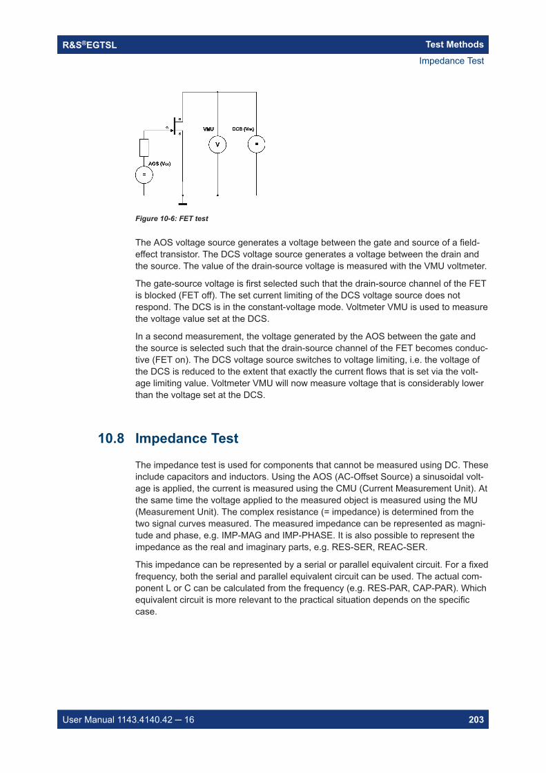
Test MethodsR&S®EGTSL
203User Manual 1143.4140.42 16
Figure 10-6: FET test
The AOS voltage source generates a voltage between the gate and source of a field-effect transistor. The DCS voltage source generates a voltage between the drain andthe source. The value of the drain-source voltage is measured with the VMU voltmeter.
The gate-source voltage is first selected such that the drain-source channel of the FETis blocked (FET off). The set current limiting of the DCS voltage source does notrespond. The DCS is in the constant-voltage mode. Voltmeter VMU is used to measurethe voltage value set at the DCS.
In a second measurement, the voltage generated by the AOS between the gate andthe source is selected such that the drain-source channel of the FET becomes conduc-tive (FET on). The DCS voltage source switches to voltage limiting, i.e. the voltage ofthe DCS is reduced to the extent that exactly the current flows that is set via the volt-age limiting value. Voltmeter VMU will now measure voltage that is considerably lowerthan the voltage set at the DCS.
10.8 Impedance Test
The impedance test is used for components that cannot be measured using DC. Theseinclude capacitors and inductors. Using the AOS (AC-Offset Source) a sinusoidal volt-age is applied, the current is measured using the CMU (Current Measurement Unit). Atthe same time the voltage applied to the measured object is measured using the MU(Measurement Unit). The complex resistance (= impedance) is determined from thetwo signal curves measured. The measured impedance can be represented as magni-tude and phase, e.g. IMP-MAG and IMP-PHASE. It is also possible to represent theimpedance as the real and imaginary parts, e.g. RES-SER, REAC-SER.
This impedance can be represented by a serial or parallel equivalent circuit. For a fixedfrequency, both the serial and parallel equivalent circuit can be used. The actual com-ponent L or C can be calculated from the frequency (e.g. RES-PAR, CAP-PAR). Whichequivalent circuit is more relevant to the practical situation depends on the specificcase.
Impedance Test
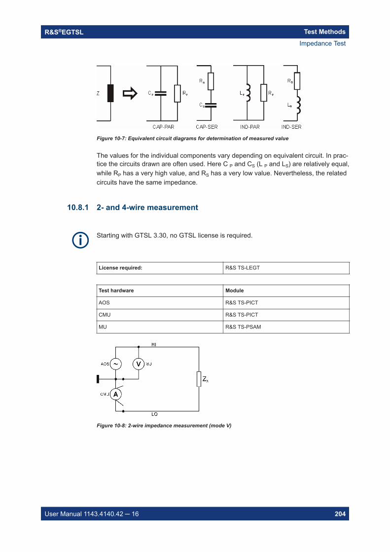
Test MethodsR&S®EGTSL
204User Manual 1143.4140.42 16
Figure 10-7: Equivalent circuit diagrams for determination of measured value
The values for the individual components vary depending on equivalent circuit. In prac-tice the circuits drawn are often used. Here C P and CS (L P and LS) are relatively equal,while RP has a very high value, and RS has a very low value. Nevertheless, the relatedcircuits have the same impedance.
10.8.1 2- and 4-wire measurement
Starting with GTSL 3.30, no GTSL license is required.
License required: R&S TS-LEGT
Test hardware Module
AOS R&S TS-PICT
CMU R&S TS-PICT
MU R&S TS-PSAM
Figure 10-8: 2-wire impedance measurement (mode V)
Impedance Test
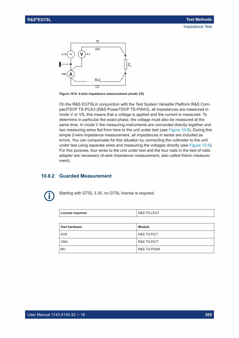
Test MethodsR&S®EGTSL
205User Manual 1143.4140.42 16
Figure 10-9: 4-wire impedance measurement (mode VS)
On the R&S EGTSLin conjunction with the Test System Versatile Platform R&S Com-pactTSVP TS-PCA3 (R&S PowerTSVP TS-PWA3), all impedances are measured inmode V or VS, this means that a voltage is applied and the current is measured. Todetermine in particular the exact phase, the voltage must also be measured at thesame time. In mode V the measuring instruments are connected directly together andtwo measuring wires fed from here to the unit under test (see Figure 10-8). During thissimple 2-wire impedance measurement, all impedances in series are included aserrors. You can compensate for this situation by connecting the voltmeter to the unitunder test using separate wires and measuring the voltages directly (see Figure 10-9).For this purpose, four wires to the unit under test and the four nails in the bed of nailsadapter are necessary (4-wire impedance measurement, also called Kelvin measure-ment).
10.8.2 Guarded Measurement
Starting with GTSL 3.30, no GTSL license is required.
License required: R&S TS-LEGT
Test hardware Module
AOS R&S TS-PICT
CMU R&S TS-PICT
MU R&S TS-PSAM
Impedance Test
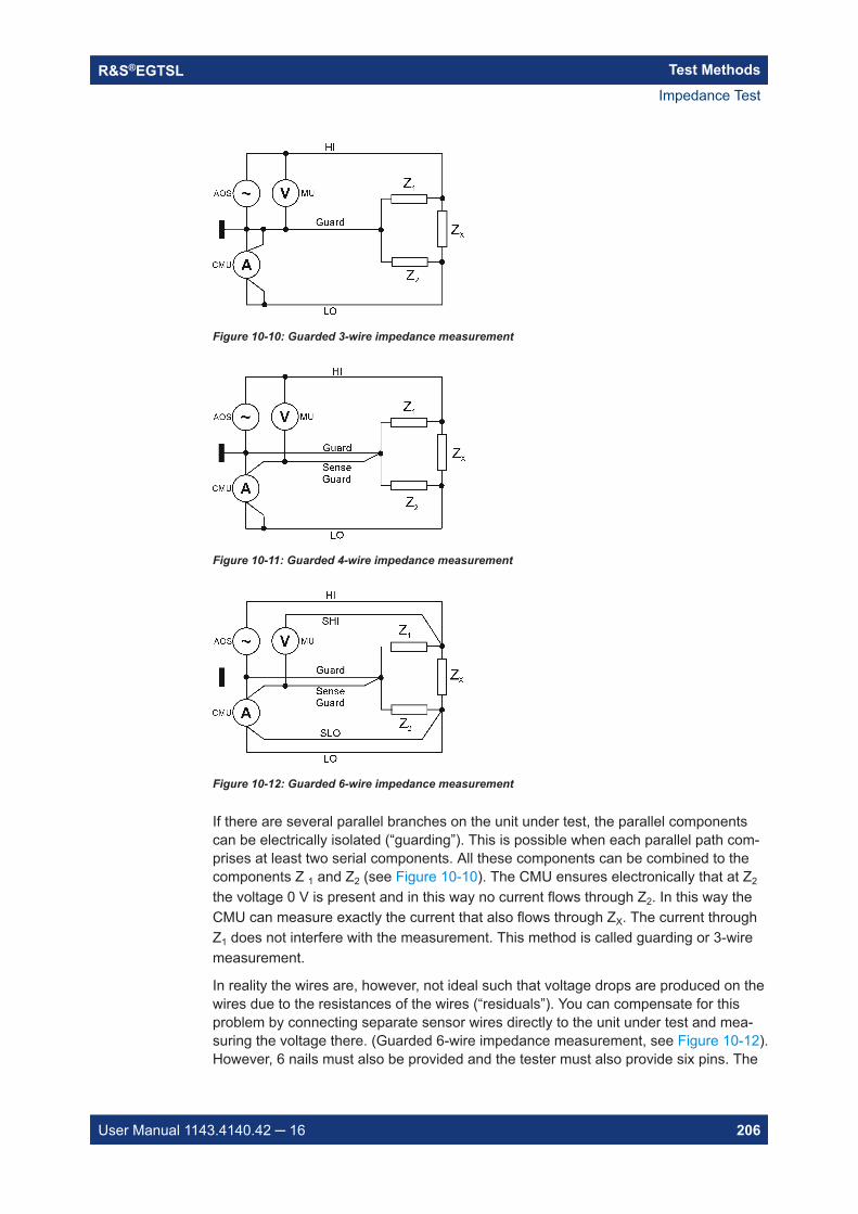
Test MethodsR&S®EGTSL
206User Manual 1143.4140.42 16
Figure 10-10: Guarded 3-wire impedance measurement
Figure 10-11: Guarded 4-wire impedance measurement
Figure 10-12: Guarded 6-wire impedance measurement
If there are several parallel branches on the unit under test, the parallel componentscan be electrically isolated (“guarding”). This is possible when each parallel path com-prises at least two serial components. All these components can be combined to thecomponents Z 1 and Z2 (see Figure 10-10). The CMU ensures electronically that at Z2
the voltage 0 V is present and in this way no current flows through Z2. In this way theCMU can measure exactly the current that also flows through ZX. The current throughZ1 does not interfere with the measurement. This method is called guarding or 3-wiremeasurement.
In reality the wires are, however, not ideal such that voltage drops are produced on thewires due to the resistances of the wires (“residuals”). You can compensate for thisproblem by connecting separate sensor wires directly to the unit under test and mea-suring the voltage there. (Guarded 6-wire impedance measurement, see Figure 10-12).However, 6 nails must also be provided and the tester must also provide six pins. The
Impedance Test
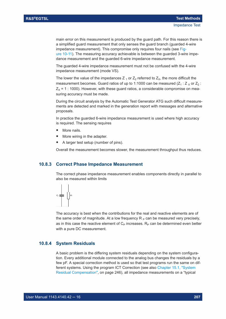
Test MethodsR&S®EGTSL
207User Manual 1143.4140.42 16
main error on this measurement is produced by the guard path. For this reason there isa simplified guard measurement that only senses the guard branch (guarded 4-wireimpedance measurement). This compromise only requires four nails (see Fig-ure 10-11). The measuring accuracy achievable is between the guarded 3-wire impe-dance measurement and the guarded 6-wire impedance measurement.
The guarded 4-wire impedance measurement must not be confused with the 4-wireimpedance measurement (mode VS).
The lower the value of the impedances Z 1 or Z2 referred to ZX, the more difficult themeasurement becomes. Guard ratios of up to 1:1000 can be measured (Z1 : Z X or Z2 :ZX = 1 : 1000). However, with these guard ratios, a considerable compromise on mea-suring accuracy must be made.
During the circuit analysis by the Automatic Test Generator ATG such difficult measure-ments are detected and marked in the generation report with messages and alternativeproposals.
In practice the guarded 6-wire impedance measurement is used where high accuracyis required. The sensing requires
More nails. More wiring in the adapter. A larger test setup (number of pins).
Overall the measurement becomes slower, the measurement throughput thus reduces.
10.8.3 Correct Phase Impedance Measurement
The correct phase impedance measurement enables components directly in parallel toalso be measured within limits
The accuracy is best when the contributions for the real and reactive elements are ofthe same order of magnitude. At a low frequency R P can be measured very precisely,as in this case the reactive element of CP increases. RP can be determined even betterwith a pure DC measurement.
10.8.4 System Residuals
A basic problem is the differing system residuals depending on the system configura-tion. Every additional module connected to the analog bus changes the residuals by afew pF. A special correction method is used so that test programs run the same on dif-ferent systems. Using the program ICT Correction (see also Chapter 15.1, "SystemResidual Compensation", on page 246), all impedance measurements on a “typical
Impedance Test
Test MethodsR&S®EGTSL
208User Manual 1143.4140.42 16
pin” can be corrected. In this way different configurations and module fits can be cor-rected.
10.8.5 Fixture Residuals
Besides residuals given by the actual circuit, additional impedances are inserted by themeasurement adapter. This is inevitable and can only be compensated but not elimina-ted. If a test is done on different measurement adapter, it is necessary to distinguishingthe residual impedances and the fixture residuals. Only with separated residuals, it ispossible to define the fixture residuals for the different adapter. The actual compensa-tion is done in two steps.
1. An overall correction value is applied by debugging the ICT program. Those cor-rection values include both residuals since the system residual cannot be mea-sured on its own.
2. The fixture residual must be determined by running an open adapter measurement.With the measured values, the difference to the values in step 1 are calculated andpreserved as correction values.It is not necessary to scope with the complete complexity of the residual compen-sation. If only one adapter shall be used, the correction step is sufficient to com-pensate any disturbances of the actual measurement setup. To enable the fixtureresidual compensation, an option in the APPLICATION.INI file must be set, seeChapter 3.2.3, "Entries in APPLICATION.INI", on page 22. Per default, when thisoption is not active, the EGTSL works in a legacy mode. This is to maintain com-patibility of stored ICT programs with older EGTSL versions (≤3.33).
Programs that are enhanced by the compensation information cannot be loaded withinan EGTSL Software with Version ≤3.33.If such a file must be loaded again in an EGTSL Software with Version ≤3.33, the ICTprogram can be transformed back. For this reason, load the ICT again in an EGTSLVersion ≥3.34 with deactivated compensation support, and save the file directly after-wards. This will result in the same file, except the compensation information is deleted.If there are already compensation values not equal 0.0, the software automaticallyadds those compensation values to the correction value and deletes the compensationtag afterwards.
See also Chapter 15.2, "Adapter Compensation", on page 251.
10.8.6 Measuring Small Capacitors
A particular challenge is the measurement of small capacitors, particularly in the rangeof 10 pF and smaller. Here there are capacitances (typically 60 pF to 90 pF) on theswitching panel and analog bus in parallel that introduce errors directly into the mea-surement. In addition, there is scatter on the capacitances between two pins due to theswitching panel and the adapter wiring. Only the scatter between switching panel pins
Impedance Test
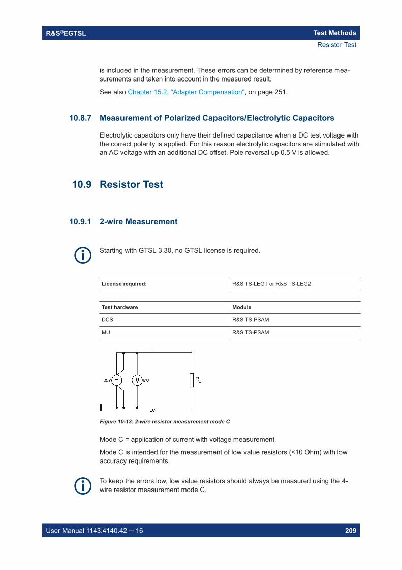
Test MethodsR&S®EGTSL
209User Manual 1143.4140.42 16
is included in the measurement. These errors can be determined by reference mea-surements and taken into account in the measured result.
See also Chapter 15.2, "Adapter Compensation", on page 251.
10.8.7 Measurement of Polarized Capacitors/Electrolytic Capacitors
Electrolytic capacitors only have their defined capacitance when a DC test voltage withthe correct polarity is applied. For this reason electrolytic capacitors are stimulated withan AC voltage with an additional DC offset. Pole reversal up 0.5 V is allowed.
10.9 Resistor Test
10.9.1 2-wire Measurement
Starting with GTSL 3.30, no GTSL license is required.
License required: R&S TS-LEGT or R&S TS-LEG2
Test hardware Module
DCS R&S TS-PSAM
MU R&S TS-PSAM
Figure 10-13: 2-wire resistor measurement mode C
Mode C = application of current with voltage measurement
Mode C is intended for the measurement of low value resistors (<10 Ohm) with lowaccuracy requirements.
To keep the errors low, low value resistors should always be measured using the 4-wire resistor measurement mode C.
Resistor Test
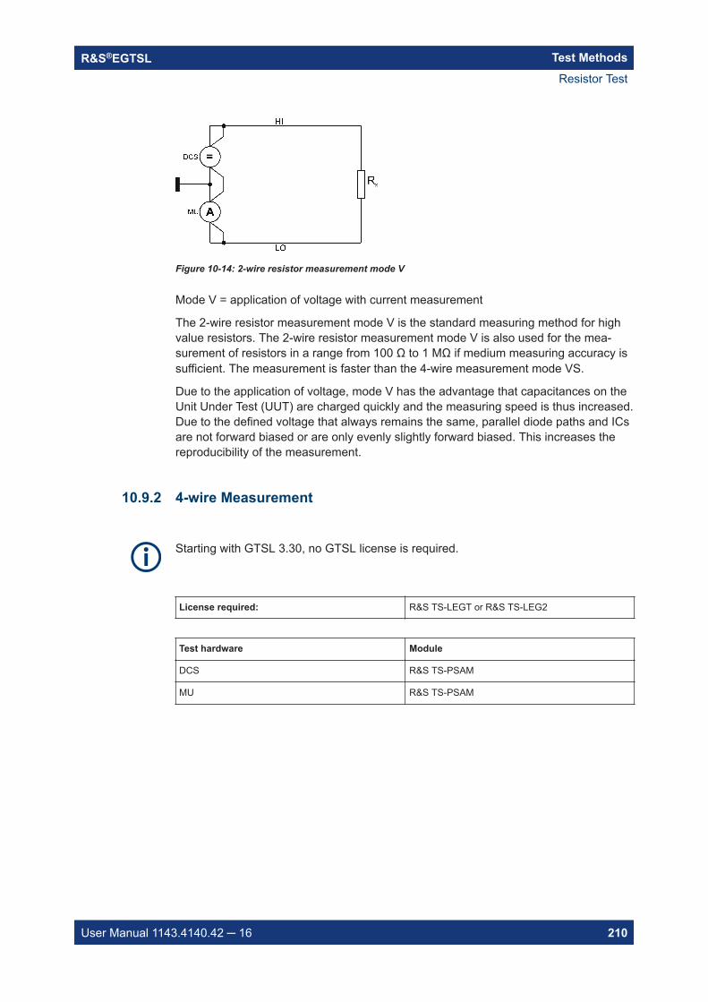
Test MethodsR&S®EGTSL
210User Manual 1143.4140.42 16
Figure 10-14: 2-wire resistor measurement mode V
Mode V = application of voltage with current measurement
The 2-wire resistor measurement mode V is the standard measuring method for highvalue resistors. The 2-wire resistor measurement mode V is also used for the mea-surement of resistors in a range from 100 Ω to 1 MΩ if medium measuring accuracy issufficient. The measurement is faster than the 4-wire measurement mode VS.
Due to the application of voltage, mode V has the advantage that capacitances on theUnit Under Test (UUT) are charged quickly and the measuring speed is thus increased.Due to the defined voltage that always remains the same, parallel diode paths and ICsare not forward biased or are only evenly slightly forward biased. This increases thereproducibility of the measurement.
10.9.2 4-wire Measurement
Starting with GTSL 3.30, no GTSL license is required.
License required: R&S TS-LEGT or R&S TS-LEG2
Test hardware Module
DCS R&S TS-PSAM
MU R&S TS-PSAM
Resistor Test
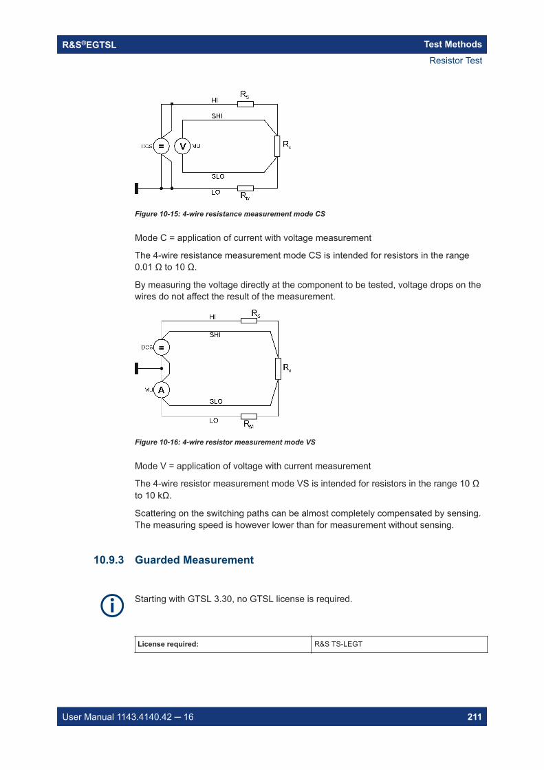
Test MethodsR&S®EGTSL
211User Manual 1143.4140.42 16
Figure 10-15: 4-wire resistance measurement mode CS
Mode C = application of current with voltage measurement
The 4-wire resistance measurement mode CS is intended for resistors in the range0.01 Ω to 10 Ω.
By measuring the voltage directly at the component to be tested, voltage drops on thewires do not affect the result of the measurement.
Figure 10-16: 4-wire resistor measurement mode VS
Mode V = application of voltage with current measurement
The 4-wire resistor measurement mode VS is intended for resistors in the range 10 Ωto 10 kΩ.
Scattering on the switching paths can be almost completely compensated by sensing.The measuring speed is however lower than for measurement without sensing.
10.9.3 Guarded Measurement
Starting with GTSL 3.30, no GTSL license is required.
License required: R&S TS-LEGT
Resistor Test
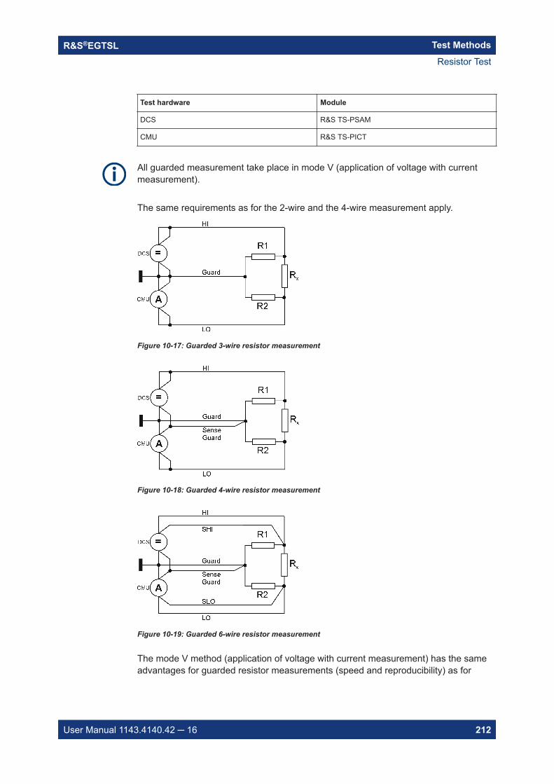
Test MethodsR&S®EGTSL
212User Manual 1143.4140.42 16
Test hardware Module
DCS R&S TS-PSAM
CMU R&S TS-PICT
All guarded measurement take place in mode V (application of voltage with currentmeasurement).
The same requirements as for the 2-wire and the 4-wire measurement apply.
Figure 10-17: Guarded 3-wire resistor measurement
Figure 10-18: Guarded 4-wire resistor measurement
Figure 10-19: Guarded 6-wire resistor measurement
The mode V method (application of voltage with current measurement) has the sameadvantages for guarded resistor measurements (speed and reproducibility) as for
Resistor Test
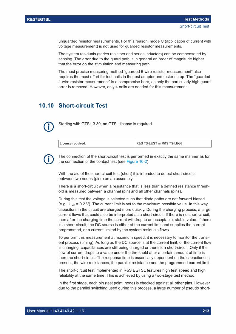
Test MethodsR&S®EGTSL
213User Manual 1143.4140.42 16
unguarded resistor measurements. For this reason, mode C (application of current withvoltage measurement) is not used for guarded resistor measurements.
The system residuals (series resistors and series inductors) can be compensated bysensing. The error due to the guard path is in general an order of magnitude higherthat the error on the stimulation and measuring path.
The most precise measuring method “guarded 6-wire resistor measurement” alsorequires the most effort for test nails in the test adapter and tester setup. The “guarded4-wire resistor measurement” is a compromise here, as only the particularly high guarderror is removed. However, only 4 nails are needed for this measurement.
10.10 Short-circuit Test
Starting with GTSL 3.30, no GTSL license is required.
License required: R&S TS-LEGT or R&S TS-LEG2
The connection of the short-circuit test is performed in exactly the same manner as forthe connection of the contact test (see Figure 10-2)
With the aid of the short-circuit test (short) it is intended to detect short-circuitsbetween two nodes (pins) on an assembly.
There is a short-circuit when a resistance that is less than a defined resistance thresh-old is measured between a channel (pin) and all other channels (pins).
During this test the voltage is selected such that diode paths are not forward biased(e.g. U set = 0.2 V). The current limit is set to the maximum possible value. In this waycapacitors in the circuit are charged more quickly. During the charging process, a largecurrent flows that could also be interpreted as a short-circuit. If there is no short-circuit,then after the charging time the current will drop to an acceptable, stable value. If thereis a short-circuit, the DC source is either at the current limit and supplies the currentprogrammed, or a current limited by the system residuals flows.
To perform this measurement at maximum speed, it is necessary to monitor the transi-ent process (timing). As long as the DC source is at the current limit, or the current flowis changing, capacitances are still being charged or there is a short-circuit. Only if theflow of current drops to a value under the threshold after a certain amount of time isthere no short-circuit. The response time is essentially dependent on the capacitancespresent, the wire resistances, the parallel resistance and the programmed current limit.
The short-circuit test implemented in R&S EGTSL features high test speed and highreliability at the same time. This is achieved by using a two-stage test method.
In the first stage, each pin (test point, node) is checked against all other pins. Howeverdue to the parallel switching used during this process, a large number of pseudo short-
Short-circuit Test
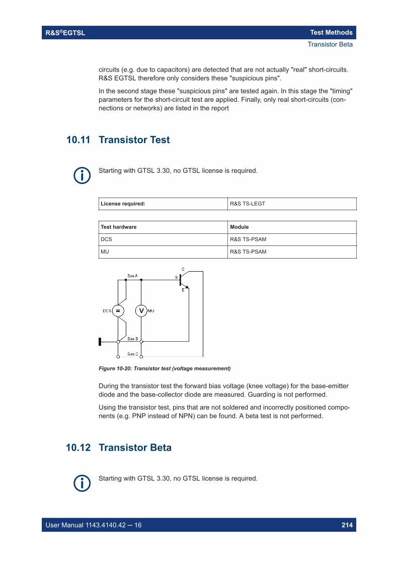
Test MethodsR&S®EGTSL
214User Manual 1143.4140.42 16
circuits (e.g. due to capacitors) are detected that are not actually "real" short-circuits.R&S EGTSL therefore only considers these "suspicious pins".
In the second stage these "suspicious pins" are tested again. In this stage the "timing"parameters for the short-circuit test are applied. Finally, only real short-circuits (con-nections or networks) are listed in the report
10.11 Transistor Test
Starting with GTSL 3.30, no GTSL license is required.
License required: R&S TS-LEGT
Test hardware Module
DCS R&S TS-PSAM
MU R&S TS-PSAM
Figure 10-20: Transistor test (voltage measurement)
During the transistor test the forward bias voltage (knee voltage) for the base-emitterdiode and the base-collector diode are measured. Guarding is not performed.
Using the transistor test, pins that are not soldered and incorrectly positioned compo-nents (e.g. PNP instead of NPN) can be found. A beta test is not performed.
10.12 Transistor Beta
Starting with GTSL 3.30, no GTSL license is required.
Transistor Beta
Test MethodsR&S®EGTSL
215User Manual 1143.4140.42 16
License required: R&S TS-LEGT
Test hardware Module
CH2 R&S TS-PSU / R&S TS-PSU12 (channel 2)
DCS R&S TS-PSAM
VMU R&S TS-PSAM
CMU R&S TS-PICT
Figure 10-21: Transistor Beta test
The voltage source R&S TS-PSU / R&S TS-PSU12 generates a voltage between thebase and collector of the transistor. Current limiting must be set high enough so thatthe source can provide sufficient current for the transistor and any branches wired inparallel that may be present.
The voltage source DCS generates a voltage between the base and emitter of the tran-sistor. Current limiting must be adjusted so that the source is working in constant cur-rent mode.
The forward bias voltage (knee voltage) over the base emitter diode is measured in thefirst measurement (voltage VBE, see Figure 10-21).
A constant current IE is impressed in the emitter branch with the DCS for the measure-ment of the current gain (Beta β, see Figure 10-21). At the same time the current IB ismeasured in the base branch. Then the emitter current is changed by a small amountand a second measurement of the base current is performed. The dynamic currentgain Beta β is calculated from these measurements as follows:
The current gain Beta β is calculated from the ratio of the change in current in the col-lector circuit to the change in current in the base circuit. The collector current can beexpressed as the difference between the emitter current and the base current.
In the event of a guarded measurement, all guard points are connected with theground reference point.
Transistor Beta
Test MethodsR&S®EGTSL
216User Manual 1143.4140.42 16
The measurement for PNP transistors runs in the same manner, with the differencethat the polarity of the two voltage sources is reversed.
10.13 Zener Diode
Starting with GTSL 3.30, no GTSL license is required.
License required: R&S TS-LEGT
Test hardware Module
CH1/CH2 R&S TS-PSU / R&S TS-PSU12
MU R&S TS-PSAM
Figure 10-22: Zener Diode test
Figure 10-23: Zener Diode test ( > 50 V / 12 V, cascaded)
During the zener diode test, the voltage source R&S TS-PSU / R&S TS-PSU12 gener-ates a voltage in the reverse direction of the diode which is somewhat above the Zenervoltage. Current limiting must be adjusted so that the voltage source is working in con-stant current mode. Now the working voltage (zener voltage) can be adjusted by thezener diode and measured with a voltmeter.
Zener Diode
Test MethodsR&S®EGTSL
217User Manual 1143.4140.42 16
WARNING!It is essential in Zener diode tests to ensure that no components of the Unit Under Testcan be damaged by the high stimulus voltages!
An individual channel of the voltage source R&S TS-PSU can produce a maximum of50 V (R&S TS-PSU12 : 12 V). To be able to test Zener diodes with higher voltages,both channels of the R&S TS-PSU / R&S TS-PSU12 must be cascaded (see Fig-ure 10-23). This cascading is not possible on the module itself. It must be provided inthe test adapter.
The connection is produced with the front multiplexer of the two channels CH1 andCH2. To do this, outputs CH2_HI4 and CH1_LO4 on front connector X10 of the R&STS-PSU / R&S TS-PSU12 module must be connected with each other (see Fig-ure 10-24).
The multiplexer outputs represented with Figure 10-24 hatched lines must not be usedif channels will be cascaded for a Zener diode test.
DANGER!When the two output channels are cascaded, voltages up to 100 V and dangerous totouch may occur! The adapter must be equipped with the appropriate warning signs.For measurements in circuits with voltages Vrms > 30 V, suitable measures should betaken to avoid any hazards. (using, for example, appropriate measuring equipment,fusing, current limiting, electrical separation, insulation).
Zener Diode
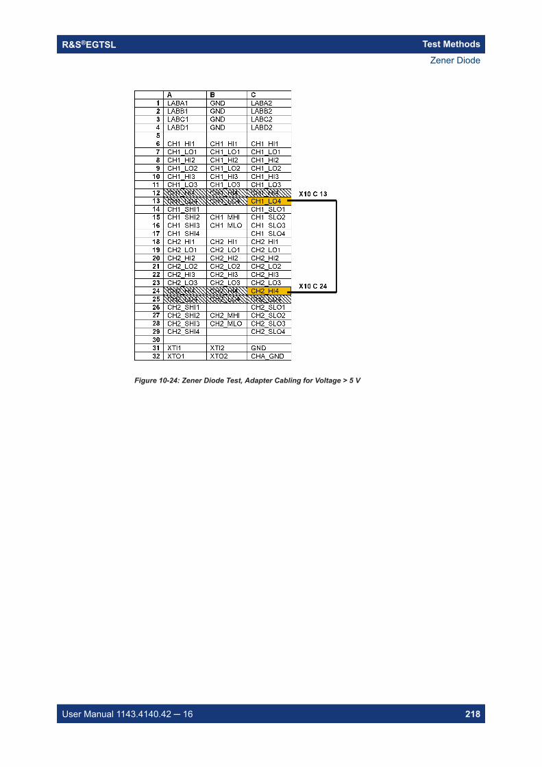
Test MethodsR&S®EGTSL
218User Manual 1143.4140.42 16
Figure 10-24: Zener Diode Test, Adapter Cabling for Voltage > 5 V
Zener Diode
Creating Test ProgramsR&S®EGTSL
219User Manual 1143.4140.42 16
11 Creating Test Programs
11.1 Program Groups
It is practical to divide the ICT program into several program groups. This is done auto-matically when an ICT program is created with the Automatic Test Generator ATG (seeChapter 9.3.1, "ICT Program", on page 183).
Figure 11-1: Program sub-window
When an ICT program is started with a function call of the ICT test library (e.g. from C-Program in production mode) the executable program group can be transferred as aparameter. Only the selected program group is executed. If, during the running of theprogram group, one or more errors occur (e.g. if the discharge or the contact for theunit under testing have failed), the testing of the unit can be immediately aborted. TheICT program does not have to run to the end. This way, unnecessary testing time canbe avoided.
Through the <Step Properties>, the Fail Count function can be activated for the pro-gram group (see Chapter 5.6.2.3, "Menu Command <Step Properties>", on page 121).
The call is made either through the menu command<Edit><Step Properties>, the key combination [Alt+Enter], the button Step Properties or the contextmenu.
When the Fail Count function is activated, the erroneous test steps in a program groupare counted. If the given number of erroneous test steps is reached, none of the sub-
Program Groups
Creating Test ProgramsR&S®EGTSL
220User Manual 1143.4140.42 16
sequent test steps in the program group are executed. The Fail Count function is onlyactive when an ICT program is started through the functions of the ICT test library.
An example of combining individual test steps into a program group and working withthe Fail Count function is the testing of resistor arrays. A test step is created for eachindividual resistor of the resistor array. The individual test steps are combined into aprogram group. The Fail Count of the program group is set to the value "1". If a resis-tor of the resistor array tests as "Failed", the testing of the other resistors in the pro-gram group is cancelled and the measured result of the entire program group is set to"Failed".
A further example of the use of the Fail Count function is the activation at the highestprogram group, i.e. for the entire ICT program. For the ICT program in Figure 11-1, thisis the program group ATG Example. As soon as an error occurs in one of the programgroups lower in the hierarchy, the testing of the further program groups is cancelledand the ICT program is terminated with the result “Failed” for the unit under test.
11.2 Variants
11.2.1 Use
By using variants, units under test which show only small deviations from one anothercan be tested with the same ICT program. Using a single ICT program has the follow-ing advantages:
One uniform ICT program for the same test steps or same test parts. Changes need only be carried out in one ICT program. Only one ICT program needs to be tested (Debugging).
Test steps (or groups) with variant definitions are used in the following cases in the ICTprogram:
A component is assembled in the original version but not in the variant XYZ. Thetest step is only executed in the original version.
A component has a different value range in the original version than in the variantXYZ. Thus, other measuring tolerances will result for the test step. In an extremecase, another test method is defined for the test step in the variant XYZ.
When using special test strategies, it may be practical to test a component withvarious test methods and measuring tolerances.
Using your own variant definition, test steps can be activated and deactivated whiledebugging the ICT program.
Variants can be defined for comments and non-executable test steps. During the automatic generation of an ICT program with the Automatic Test Gener-
ator ATG, the alternative proposals for measurements created by the ATG areidentified as variants (variant name: Proposal). Also see Chapter 9.3.2.2, "Alterna-tive Proposals from the ATG", on page 189.
Variants
Creating Test ProgramsR&S®EGTSL
221User Manual 1143.4140.42 16
11.2.2 Definition
Before a variant can be used, it must be defined in the <Program Properties> (seeChapter 5.6.1.6, "Menu Command <Program Properties>", on page 112). The call ismade using the menu command <File><Program Properties>. A name and a shortdescription are entered for the variant. The defined variants are valid for the entire ICTprogram.
11.2.3 Assignment
A variant can be assigned to a test step or a group. The assignment is made throughVariant Selection in <Step Properties> (see Chapter 5.6.2.3, "Menu Command<Step Properties>", on page 121).
The call is made through either the menu command<Edit><Step Properties>, the key combination [Alt+Enter], the Step Properties button or the contextmenu.
Test steps or groups to which a variant is assigned are identified in the debug mode(R&S EGTSL IDE) in the program sub-window with a "V" in the variant column.
Figure 11-2: Variant Identification
In the program sub-window, the deactivated variants are shown as crossed through.
Figure 11-3: Deactivated variants
Variants
Creating Test ProgramsR&S®EGTSL
222User Manual 1143.4140.42 16
11.2.4 Execution
When an ICT program is started through the functions of the ICT test library (e.g. fromC-Program in production mode), the executable variant can be transferred as a param-eter. The ICT program is executed with the selected variant.
When an ICT program is started in debug mode (R&S EGTSL IDE), the executablevariant is displayed in the Debug sub-window in the Variant menu. Also see Chap-ter 5.4.6, "Debug Subwindow", on page 46.
11.3 Limit Files
Through the use of limit files, it is possible to separate the limit values from the ICTprogram. The limit files can be stored and processed in a central place. By calling dif-ferent limit files with different limit values in an ICT program, a more detailed report onthe unit under test is possible (e.g. narrower measuring tolerances).
By using different limit values for an ICT program, variant control is also possible.Thus, identical units under test which differ from one another simply in the tolerancesof the assembled components, can be tested with the same ICT program.
Before an ICT program is started through the functions of the ICT test library, one ormore limit files can be loaded (e.g. from C-Program in production mode). The ICT pro-gram is executed with the loaded limit values.
In the limit files, only the limit values without units of measurement are stored. Theunits of measurement are stored in the ICT program.
When the limit files are loaded, only the limit values which are entered in the limit filesare temporarily changed in the ICT program. Test steps for which no limit values areentered in the limit files remain unchanged.
Further information for loading, import and export of the limit values in debug mode(R&S EGTSL IDE), and the format of the limit files can be seen in Chapter 5.6.1.7,"Menu Command <Limits>", on page 114.
11.4 Multiple Panel Testing
If components are manufactured in multiple panels, one ICT program is created for allpanels. This process does not differ from the creation of an ICT program for a singleunit (e.g. creation by the Automatic Test Generator ATG). It is not practical to create aseparate ICT program for each unit of the multiple panel. Using only one ICT programa has the following advantages:
One uniform ICT program for all panels. Changes need only be carried out in one ICT program. Only one ICT program needs to be tested (Debugging).
Multiple Panel Testing
Creating Test ProgramsR&S®EGTSL
223User Manual 1143.4140.42 16
Because, as a rule, the design and the assembly of the individual panels is identical,only the individual different contacts need to be adjusted.
The control of the ICT program for the individual panels is done through bench entriesin the Application Layer Configuration File (see example in section Chapter 11.4.1,"Example of an Application Layer Configuration File for Multiple Uses", on page 223).Each panel is assigned its own bench entry with its own I/O channel list. In the I/Ochannel lists, the different I/O channels of the matrix cards R&S TS-PMB are assignedto the identical test points (nodes). When possible, a unique matrix card R&S TS-PMBshould be used for the wiring of each individual panel.
When the ICT program is loaded, the bench which is to be executed must be entered.This also applies to a call through the functions of the ICT test library (e.g. from C-Pro-gram in production mode), and to a call through the R&S EGTSLloader (R&S EGTSLIDE in debug mode). Thus, all panels can be tested by calling the same ICT programwith different benches assigned.
11.4.1 Example of an Application Layer Configuration File for MultipleUses
When an ICT program is created by the Automatic Test Generator ATG, only onebench with one I/O channel list is generated. For use during a multiple panel test, theApplication Layer Configuration File must be processed in a text editor. The benchgenerated by the ATG must be copied and the individual entries adjusted.
[ResourceManager]; general trace settings (normally off)Trace = 0TraceFile = %GTSLROOT%\resmgr_trace.txt
;--------------------------------------------------------------------------------[LogicalNames]ICT_1 = bench->ICT_Panel_1ICT_2 = bench->ICT_Panel_2ICT_3 = bench->ICT_Panel_3ICT_4 = bench->ICT_Panel_4
;--------------------------------------------------------------------------------[bench->ICT_Panel_1]Description = ICT bench Panel 1 (Simulation)Simulation = 1Trace = 0ICTDevice1 = device->psamICTDevice2 = device->pictSwitchDevice1 = device->pmb1AppChannelTable = io_channel->ICT_Panel_1
[io_channel->ICT_Panel_1]GND = pmb1!P1INPUT = pmb1!P2
Multiple Panel Testing
Creating Test ProgramsR&S®EGTSL
224User Manual 1143.4140.42 16
OUTPUT = pmb1!P3TR1.B = pmb1!P4TR1.C = pmb1!P5TR1.E = pmb1!P6VCC = pmb1!P7
;--------------------------------------------------------------------------------[bench->ICT_Panel_2]Description = ICT bench Panel 2 (Simulation)Simulation = 1Trace = 0ICTDevice1 = device->psamICTDevice2 = device->pictSwitchDevice1 = device->pmb2AppChannelTable = io_channel->ICT_Panel_2
[io_channel->ICT_Panel_2]GND = pmb2!P1INPUT = pmb2!P2OUTPUT = pmb2!P3TR1.B = pmb2!P4TR1.C = pmb2!P5TR1.E = pmb2!P6VCC = pmb2!P7
;--------------------------------------------------------------------------------[bench->ICT_Panel_3]Description = ICT bench Panel 3 (Simulation)Simulation = 1Trace = 0ICTDevice1 = device->psamICTDevice2 = device->pictSwitchDevice1 = device->pmb3AppChannelTable = io_channel->ICT_Panel_3
[io_channel->ICT_Panel_3]GND = pmb3!P1INPUT = pmb3!P2OUTPUT = pmb3!P3TR1.B = pmb3!P4TR1.C = pmb3!P5TR1.E = pmb3!P6VCC = pmb3!P7
;--------------------------------------------------------------------------------[bench->ICT_Panel_4]Description = ICT bench Panel 4 (Simulation)Simulation = 1Trace = 0ICTDevice1 = device->psam
Multiple Panel Testing
Creating Test ProgramsR&S®EGTSL
225User Manual 1143.4140.42 16
ICTDevice2 = device->pictSwitchDevice1 = device->pmb4AppChannelTable = io_channel->ICT_Panel_4
[io_channel->ICT_Panel_4]GND = pmb4!P1INPUT = pmb4!P2OUTPUT = pmb4!P3TR1.B = pmb4!P4TR1.C = pmb4!P5TR1.E = pmb4!P6VCC = pmb4!P7
;--------------------------------------------------------------------------------
Multiple Panel Testing
DebuggerR&S®EGTSL
226User Manual 1143.4140.42 16
12 Debugger
12.1 Overview
The debugging of an ICT program in the Enhanced Generic Test Software Library R&SEGTSL is done in the R&S EGTSL user interface ( R&S EGTSL IDE). In the debugmode of the R&S EGTSL IDE
the ICT program can be executed test step by test step. the measured results can be analyzed. corrections can be made in the ICT program.
The ICT program is immediately ready to be executed after the changes, without hav-ing to be compiled and restarted.
The following actions are possible in debug mode:
starting and stopping of the ICT program stepwise execution of the ICT program continuation the ICT program at another position repeated execution of test steps in a loop entering and immediately executing test steps setting of stop conditions and breakpoints changing of measurement parameters analysis of measured values
In the following, the R&S EGTSL- user interface (R&S EGTSL IDE) is referred to asthe debugger.
12.2 Starting and Terminating the Debugger
For the debugging of an ICT program, the R&S EGTSL user interface (debugger) mustbe started. The debugger can be started in two ways.
1. Start the debugger from a test sequence through a function call from the ICT TestLibrary (see Chapter 13.1, "Starting Using a Function Call from the ICT TestLibrary", on page 236)
2. Start the debugger through the loader (see Chapter 13.2, "Starting Using the R&SEGTSL Loader", on page 239)
When the debugger is started from a test sequence, the ICT program is automaticallyopened with the appropriate bench. When the debugger is started through the R&SEGTSL loader, the ICT program must be manually opened with the menu command
Starting and Terminating the Debugger
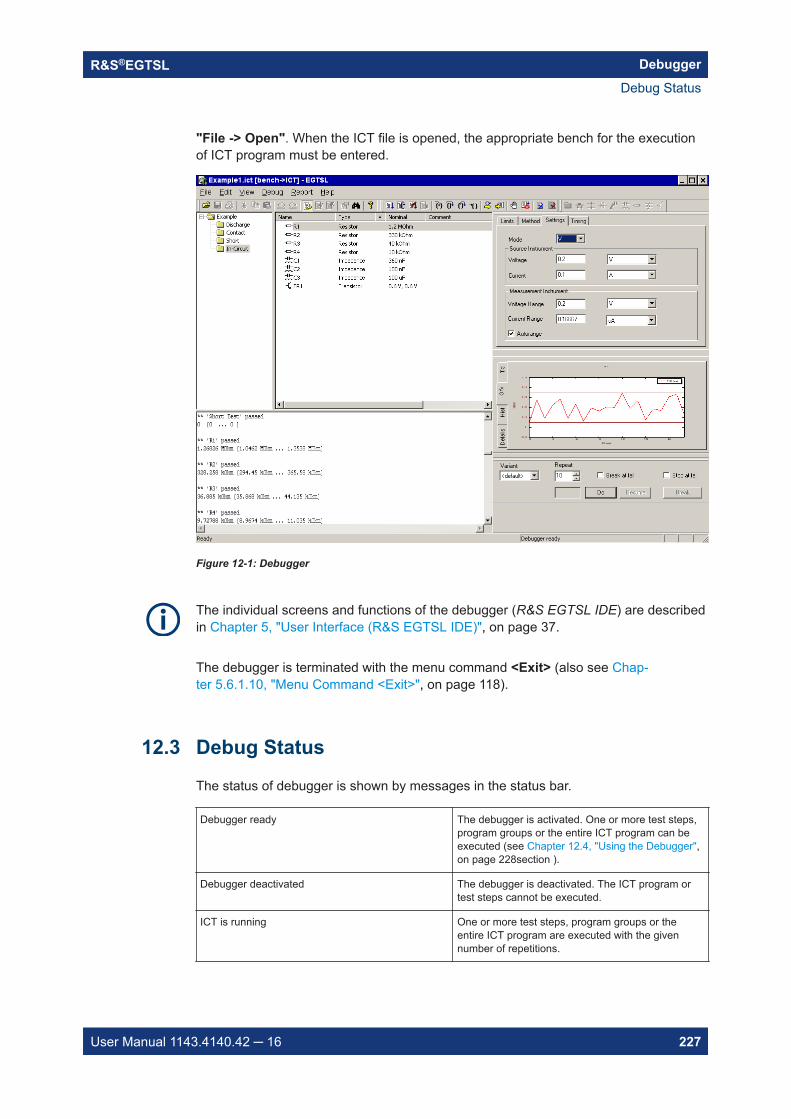
DebuggerR&S®EGTSL
227User Manual 1143.4140.42 16
"File -> Open". When the ICT file is opened, the appropriate bench for the executionof ICT program must be entered.
Figure 12-1: Debugger
The individual screens and functions of the debugger (R&S EGTSL IDE) are describedin Chapter 5, "User Interface (R&S EGTSL IDE)", on page 37.
The debugger is terminated with the menu command <Exit> (also see Chap-ter 5.6.1.10, "Menu Command <Exit>", on page 118).
12.3 Debug Status
The status of debugger is shown by messages in the status bar.
Debugger ready The debugger is activated. One or more test steps,program groups or the entire ICT program can beexecuted (see Chapter 12.4, "Using the Debugger",on page 228section ).
Debugger deactivated The debugger is deactivated. The ICT program ortest steps cannot be executed.
ICT is running One or more test steps, program groups or theentire ICT program are executed with the givennumber of repetitions.
Debug Status
DebuggerR&S®EGTSL
228User Manual 1143.4140.42 16
Total execution time for the last executed debugger command is shown in the statusbar.
12.4 Using the Debugger
The debugger is operated through the commands from the main menu item, or throughbuttons, function keys or key combinations.
If the debugger has stopped the ICT program, a yellow arrow on the left side points tothe test step to be executed next. The execution of the program will be continued atthis point.
The debugger stops the ICT program, if
the command has been executed, for example, a single step. a breakpoint is reached. a stop condition is fulfilled. a runtime error has occurred
Go[F5]
Executes the ICT program once from the test stepmarked with the yellow arrow (current debuggerexecution point) to the end. If the debugger is deac-tivated, the ICT program is executed from start tofinish.
Restart[Ctrl+Shift+F5]
With the debugger activated, executes the ICT pro-gram from the start to the finish.
Terminate[Shift+F5]
Stops the execution of the ICT program. The mark-ing with the yellow arrow (current debugger execu-tion point) is removed. The debugger is deactivated.
Break Interrupts the execution of the ICT program. Thetest step at which the interruption takes place ismarked with the yellow arrow (current debuggerexecution point) and displayed. Using the Go com-mand the execution of the ICT program can be con-tinued.
Repeat[F4]
With the debugger activated, starts the execution ofthe test steps marked (test steps with a color back-ground) with the number of repetitions given.
Resume[Shift+F4]
Continues the execution of the marked test steps(test steps with a color background) following aninterruption using the Break button.
Step Into[F11]
Executes the ICT program from the test stepmarked with the yellow arrow (current executionpoint of the debugger) in single steps. If the test stepis a group, automatically each test step of the groupwill be executed in single steps.
Using the Debugger
DebuggerR&S®EGTSL
229User Manual 1143.4140.42 16
Step Over[F10]
Executes the ICT program from the test stepmarked with the yellow arrow (current executionpoint of the debugger) in single steps. If the test stepis a group, all test steps in the group are performedautomatically.
Step Out[Shift+F11]
If the test step marked with the yellow arrow (currentexecution point of the debugger) is in a group, thegroup is left with this button. The test steps that fol-low in the group are performed automatically. If thetest step marked with the yellow arrow (current exe-cution point of the debugger) is at the top programlevel, all following test steps including groups areexecuted.
Run to Cursor[Ctrl+F10]
Executes the ICT program from the test stepmarked with the yellow arrow (current executionpoint of the debugger) to the test step marked withthe cursor. The test step marked by the position ofthe cursor is marked as the next test step that canbe executed using the yellow arrow.
Set Next Step [Ctrl+Shift+F10]
Marks the position of the cursor as the test step thatis to be executed next. A yellow arrow is displayedon the left beside the test step marked. The debug-ger is activated.
Show Next Step[Alt+F10]
Jumps to the current debugger execution position(test step marked with the yellow arrow). The teststep is the next that is executed.
Toggle Breakpoint[F9]
Sets a breakpoint at the cursor position. The break-point is deactivated when you click the button again.The third time you click the button, the breakpoint isdeleted (see alsoChapter 5.6.2.4, "Menu Point<Breakpoints>", on page 124 ).
Stop At Fail With this function activated, the ICT program execu-tion is stopped when the test step result was “Fail”.The program stops at the erroneous test step. TheStop at fail function applies to all debug commandswith the exception of the Repeat function.
Break At Fail With this function activated, the execution of the ICTprogram (test steps marked) is interrupted when thetest step result was “Fail”. The program stops at theerroneous test step. The Break at fail functionapplies only to the Repeat function.
Using the Debugger
DebuggerR&S®EGTSL
230User Manual 1143.4140.42 16
12.5 Breakpoints
The execution of the program in the debugger can be interrupted at predetermined points (test steps orprogram groups) by using the breakpoints. The debugger stops the ICT program at this point, before it exe-cutes the test step which has been assigned an activated breakpoint.
Toggle Breakpoint[F9]
Breakpoints are set, deactivated or deleted throughthe menu command , the function key [F9] or theToggle Breakpoint button.
Breakpoints are displayed on the left in the program sub-window next to the marked test step or on the leftnext to the marked program group. The debugger does not stop at deactivated breakpoints.
activated breakpoint
deactivated breakpoint
Using the menu command or the key combination [Alt+F9], a list of all breakpoints set in the ICT programcan be displayed. In the editing window, the breakpoints can be individually or totally deleted. In addition,you can jump to a selected breakpoint. Also see Chapter 5.6.2.4, "Menu Point <Breakpoints>",on page 124.
12.6 Stop Conditions
The execution of the program in the debugger can be interrupted when specified condi-tions occur.
Stop At Fail With this function activated, the ICT program execu-tion is stopped when the test step result was “Fail”.The program stops at the erroneous test step. TheStop at fail function applies to all debug commandswith the exception of the Repeat function.
Break At Fail With this function activated, the execution of the ICTprogram (test steps marked) is interrupted when thetest step result was “Fail”. The program stops at theerroneous test step. The Break at fail functionapplies only to the Repeat function.
12.7 Typical Debugging Procedure
The optimum procedure for testing an ICT program (debugging) is different for eachunit under test and thus for each ICT program. The debugging of a new ICT programshould be done with a reference unit under test (Reference UUT).
The following steps should only be used as a reference for a debugging procedure.The steps described apply to an ICT program created "by hand" as well as to one gen-erated by the Automatic Test Generator ATG.
1. Open a new ICT program with corresponding bench in the debugger.
Typical Debugging Procedure
DebuggerR&S®EGTSL
231User Manual 1143.4140.42 16
2. Check the proposals created as variants by the Automatic Test Generator ATG andselect the best variants for the test procedure as the standard test steps (also seeChapter 9.3.2.2, "Alternative Proposals from the ATG", on page 189).
3. Activate the function Stop At Fail and start the ICT program with the function GO(menu item, button or function key [F5]).
4. The debugger interrupts the execution of the ICT program at the Failed test step.The test step is shown by the yellow arrow (current execution position of thedebugger).
5. Repeat the Failed test step with the function Repeat (menu item, button or functionkey [F4]) (more than once, if necessary).
6. Check the measured results with the information from the Report sub-window andthe Results Tbl, Results Gfx, Results Hist and Results Details sub-windows.
7. Based on the information from the Report sub-window and the Results sub-win-dow, adjust the measurement parameters of the test step.
8. Start the further execution of the ICT program with the function GO (menu item,button or function key [F5]).
9. Repeat steps 4. to 8. until the ICT program runs without errors.
10. Start the ICT program with the function GO several times (menu item, button orfunction key [F5]) and let it run through (without errors).
11. Check the measured results for the entire ICT program with the information fromthe Report sub-window and the Results Tbl, Results Gfx, Results Hist andResults Details sub-windows (see section 12.9).
12. If the ICT program with the reference unit under test (Reference UUT ) functionswithout error, the step must be repeated with other units under test (UUT) until theICT program also runs without errors with these units under test.
13. If the ICT program can be run for several units under test (UUT) without the error, ameasuring time optimization can be carried out as a last step (see Chapter 12.8,"Measuring Time Optimization", on page 231).
12.8 Measuring Time Optimization
Through an exact analysis of the measured results in the Results Details sub-window,information on the measuring time (duration) and the status of the measuring hardwareused for the measurement can be ascertained.
A measuring time optimization can be achieved by:
Optimum selection of the measurement range of the measuring hardware used ateach test step.
Adjustment of the timing settings (Delay, Max.Wait Interval, Max.Wait accuracy,Average, Sample Interval) at each test step.
Measuring Time Optimization
DebuggerR&S®EGTSL
232User Manual 1143.4140.42 16
Selection of the appropriate testing method (2-wire measurement, 4-wire measure-ment, guarding) for each test step.
12.9 Interpretation of the Results Sub-window
The graphical display of the measured results of the individual test steps in the ResultsGfx and Results Hist sub-windows gives important information for optimization of theindividual measuring procedures. A few typical examples are shown below.
12.9.1 Results Gfx Sub-Window
Example:
Figure 12-2: Measurements with Transient Process
The graph in Figure 12-2 shows a measurement with transient process. The measuredresults are stable and lie within the given measuring tolerances only after the third runof the test step. For the optimization of this test step, the auto-delay technique wouldbe useful (see Chapter 5.5.12.1, "Timing", on page 103). By using this, you can ensurethat a correct measured result is obtained even for the first run of the test step.
Interpretation of the Results Sub-window
DebuggerR&S®EGTSL
233User Manual 1143.4140.42 16
Example:
Figure 12-3: Measurement with superimposed interference
The graph in Figure 12-3 displays a measurement with superimposed interference sig-nal. Through an exact circuit analysis, the source of interference can be determinedand eliminated with appropriate measures (e.g. another test method).
Interpretation of the Results Sub-window
DebuggerR&S®EGTSL
234User Manual 1143.4140.42 16
12.9.2 Results Hist Sub-Window
Example:
Figure 12-4: Measurements with wide scatter
Interpretation of the Results Sub-window
DebuggerR&S®EGTSL
235User Manual 1143.4140.42 16
Figure 12-5: Measurements with narrow scatter
The graphs in Figure 12-4 and Figure 12-5 show the distribution of the measured val-ues of a test step. The scatter of the measured results for the measurements in Fig-ure 12-4 is too wide. The cause of this wide scatter could be superimposed interfer-ence or non-optimum timing settings. The measurement can be improved with Max.Wait or Average settings (see Chapter 5.5.12.1, "Timing", on page 103).
Interpretation of the Results Sub-window
Running R&S EGTSL IDER&S®EGTSL
236User Manual 1143.4140.42 16
13 Running R&S EGTSL IDEThe Enhanced Generic Test Software Library R&S EGTSL can be executed in twoways:
1. By opening a function from the ICT test library.
2. Using the R&S EGTSL Loader.
Starting with GTSL 3.30, no GTSL license is required.
13.1 Starting Using a Function Call from the ICT TestLibrary
Figure 13-1: Opening R&S EGTSL IDE using test library (software structure)
Functions from the ICT test library are opened from the test sequence (e.g. testsequence in test stand or a dedicated C program). The test hardware available is man-aged using the resource manager with the aid of the configuration files(PHYSICAL.INI and APPLICATION.INI). The R&S EGTSL runtime engine nowopens the R&S EGTSL user interface R&S EGTSL) and the corresponding ICT pro-gram. The ICT program opened can now be debugged in the R&S EGTSL user inter-face (R&S EGTSL). Using the R&S EGTSL runtime engine the ICT program can beexecuted on the test hardware directly from the R&S EGTSL user interface.
13.1.1 Example
In the following example, functions from the ICT test library are opened from the C pro-gram. Among other aspects, the R&S EGTSL user interface (R&S EGTSL IDE ) can beopened.
Starting Using a Function Call from the ICT Test Library
Running R&S EGTSL IDER&S®EGTSL
237User Manual 1143.4140.42 16
#include <cviauto.h>#include <ansi_c.h>#include <userint.h>#include <cvirte.h>#include "ict.h"
// defines the drive and path for the example files#define PATH "C:\\Program Files\\Rohde&Schwarz\\GTSL\\EGTSL\\example\\"
int main (int argc, char *argv[]) short errorOccurred = FALSE; long errorCode; char errorMessage[GTSL_ERROR_BUFFER_SIZE] = ""; char userMessage[1024]; long resourceId = -1; long programId = -1; long compileErrors; long failCount; int response = 0;
// ActiveX must be initialized if the ICT library is used CA_InitActiveXThreadStyleForCurrentThread (0, COINIT_APARTMENTTHREADED); // load the configuration files if ( ! errorOccurred ) RESMGR_Setup (0, PATH "example_physical.ini", PATH "example1_application.ini", &errorOccurred, &errorCode, errorMessage);
// load the ICT library if ( ! errorOccurred ) ICT_Setup (0, "bench->ICT", &resourceId, &errorOccurred, &errorCode, errorMessage);
// load the ICT program if ( ! errorOccurred ) ICT_Load_Program (0, resourceId, PATH "example1.ict", "bench->ICT", &programId, &compileErrors, &errorOccurred, &errorCode, errorMessage);
Starting Using a Function Call from the ICT Test Library
Running R&S EGTSL IDER&S®EGTSL
238User Manual 1143.4140.42 16
do // start the program if ( ! errorOccurred ) if ( 1 == ConfirmPopup ( "EGTSL", "Start in debug mode?" ) ) // debug the program with EGTSL IDE ICT_Debug_Program (0, resourceId, programId, "", // no variant specified "", // no subtreee, run complete program 1, // stop at start of program 1, // stop at end of program 0, // don't stop at fail &failCount, &errorOccurred, &errorCode, errorMessage); else // run the program without EGTSL IDE ICT_Run_Program (0, resourceId, programId, "", // no variant specified "", // no subtree, run complete program &failCount, &errorOccurred, &errorCode, errorMessage);
// write the report to a text file if ( ! errorOccurred ) ICT_Write_Report (0, resourceId, programId, "ictreport.txt", 0, // 0 = overwrite, 1 = append &errorOccurred, &errorCode, errorMessage);
// ask the user to run the program again if ( ! errorOccurred ) sprintf ( userMessage, "%d tests failed\n\nTry again?", failCount ); response = ConfirmPopup ("EGTSL", userMessage ); else
Starting Using a Function Call from the ICT Test Library
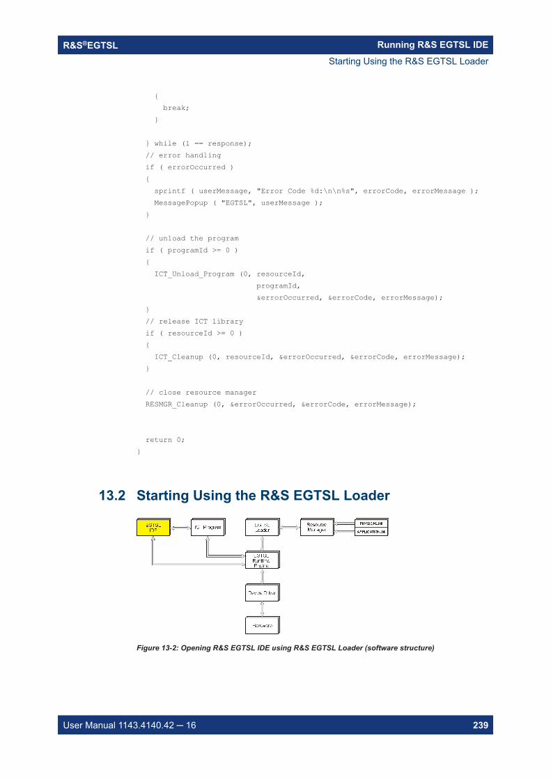
Running R&S EGTSL IDER&S®EGTSL
239User Manual 1143.4140.42 16
break; while (1 == response); // error handling if ( errorOccurred ) sprintf ( userMessage, "Error Code %d:\n\n%s", errorCode, errorMessage ); MessagePopup ( "EGTSL", userMessage );
// unload the program if ( programId >= 0 ) ICT_Unload_Program (0, resourceId, programId, &errorOccurred, &errorCode, errorMessage); // release ICT library if ( resourceId >= 0 ) ICT_Cleanup (0, resourceId, &errorOccurred, &errorCode, errorMessage);
// close resource manager RESMGR_Cleanup (0, &errorOccurred, &errorCode, errorMessage);
return 0;
13.2 Starting Using the R&S EGTSL Loader
Figure 13-2: Opening R&S EGTSL IDE using R&S EGTSL Loader (software structure)
Starting Using the R&S EGTSL Loader
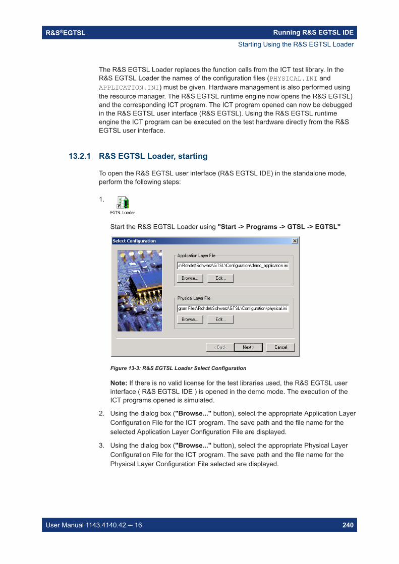
Running R&S EGTSL IDER&S®EGTSL
240User Manual 1143.4140.42 16
The R&S EGTSL Loader replaces the function calls from the ICT test library. In theR&S EGTSL Loader the names of the configuration files (PHYSICAL.INI andAPPLICATION.INI) must be given. Hardware management is also performed usingthe resource manager. The R&S EGTSL runtime engine now opens the R&S EGTSL)and the corresponding ICT program. The ICT program opened can now be debuggedin the R&S EGTSL user interface (R&S EGTSL). Using the R&S EGTSL runtimeengine the ICT program can be executed on the test hardware directly from the R&SEGTSL user interface.
13.2.1 R&S EGTSL Loader, starting
To open the R&S EGTSL user interface (R&S EGTSL IDE) in the standalone mode,perform the following steps:
1.
Start the R&S EGTSL Loader using "Start -> Programs -> GTSL -> EGTSL"
Figure 13-3: R&S EGTSL Loader Select Configuration
Note: If there is no valid license for the test libraries used, the R&S EGTSL userinterface ( R&S EGTSL IDE ) is opened in the demo mode. The execution of theICT programs opened is simulated.
2. Using the dialog box ("Browse..." button), select the appropriate Application LayerConfiguration File for the ICT program. The save path and the file name for theselected Application Layer Configuration File are displayed.
3. Using the dialog box ("Browse..." button), select the appropriate Physical LayerConfiguration File for the ICT program. The save path and the file name for thePhysical Layer Configuration File selected are displayed.
Starting Using the R&S EGTSL Loader
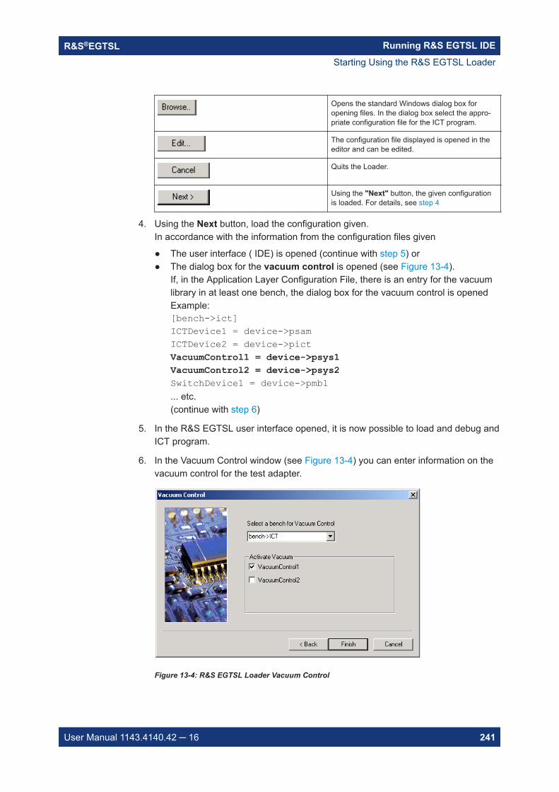
Running R&S EGTSL IDER&S®EGTSL
241User Manual 1143.4140.42 16
Opens the standard Windows dialog box foropening files. In the dialog box select the appro-priate configuration file for the ICT program.
The configuration file displayed is opened in theeditor and can be edited.
Quits the Loader.
Using the "Next" button, the given configurationis loaded. For details, see step 4
4. Using the Next button, load the configuration given.In accordance with the information from the configuration files given
The user interface ( IDE) is opened (continue with step 5) or The dialog box for the vacuum control is opened (see Figure 13-4).
If, in the Application Layer Configuration File, there is an entry for the vacuumlibrary in at least one bench, the dialog box for the vacuum control is openedExample:[bench->ict]ICTDevice1 = device->psamICTDevice2 = device->pictVacuumControl1 = device->psys1VacuumControl2 = device->psys2SwitchDevice1 = device->pmb1... etc.(continue with step 6)
5. In the R&S EGTSL user interface opened, it is now possible to load and debug andICT program.
6. In the Vacuum Control window (see Figure 13-4) you can enter information on thevacuum control for the test adapter.
Figure 13-4: R&S EGTSL Loader Vacuum Control
Starting Using the R&S EGTSL Loader
Running R&S EGTSL IDER&S®EGTSL
242User Manual 1143.4140.42 16
7. Select the bench for the vacuum control.All benches for this Application Layer Configuration File with at least one vacuumcontrol entry are displayed in the drop-down list box. In the list box select thebench that is to be relevant for the ICT program to be loaded.
8. Activate vacuum valves.The vacuum control entries in the selected bench are listed under "Activate Vac-uum". A maximum of four entries can be listed. By selecting the check box youcan activate the corresponding vacuum valve.
9.
Using the Finish button, open the R&S EGTSL user interface (R&S EGTSLIDE).
The Select Configuration window (see Figure 13-3) is opened again.
Quits the R&S EGTSL Loader.
Once the R&S EGTSL user interface has been quit, the opening dialog box (R&SEGTSL Loader Select Configuration or R&S EGTSL Loader Vacuum Control) is dis-played again. Using the "Cancel" button the R&S EGTSL Loader is quit.
Starting Using the R&S EGTSL Loader
Report FormatR&S®EGTSL
243User Manual 1143.4140.42 16
14 Report FormatFor each test step, a report entry is created in the Report sub-window. This consists ofthe following entries:
HeaderThe following entries are listed in the header:– Test Step name– ID number– Part ID
(the entry is only displayed if a Part ID is entered in the "Step Properties".)– Pass/Fail result
Measured resultThe measured result consists of the measured value and the units as well as (insquare brackets) the lower and upper limit.During the Diode and Transistor test steps, two lines with measured results are lis-ted, because two measurements are carried out during these tests.
Error text (displayed only in case the test step result was "Failed")In case the test step result was “Failed”, a line with the error text is listed. The Con-tact, Continuity, Discharge and Short test methods display information on the pins.All other test methods list the “Report Text” from the “Step Properties”.
Example:
Contact ** 'Contact'[70] failed <----<<<2 [0 ... 0 ]P22, P27Measured result: The number of the pins whichhave no contact is displayed. The lower and upperlimits are zero.
Error text: The error text displays the names of thepins which have no contact. A maximum of 10 pinnames are displayed.
Continuity ** 'GND track'[77] failed <----<<<1 [0 ... 0 ]P12 P13 / P89 P90Measured result: The number of interruptions isdisplayed. The lower and upper limits are zero.
Error text: The error text displays the names of thepins of the Contact test. Interruptions are markedwith a slash.
Report FormatR&S®EGTSL
244User Manual 1143.4140.42 16
Diode ** 'D1'[76] (123.456) failed <----<<<-0.769865 V [-0.8 V ... -0.6 V]-0.00103737 uA [0.2 uA ... 1 uA]D1 failedMeasured result 1: The measured forward biasvoltage (knee voltage) and, in brackets the lowerand upper limit, are displayed.
Measured result 2: The measured reverse biascurrent and, in brackets the upper and lower limit,are displayed.
Error text: The text which has been entered in the“Step Properties” in the “Report Text” field is dis-played.
Discharge ** 'Discharge'[18] failed <----<<<1 [0 ... 0 ]Timeout; DCH pin 'P13'Measured result: The number of the pins whichcould not be discharged is displayed. The lower andupper limits are zero.
Error text: The error text displays the pin which wasbeing discharged when the timeout occurred.
Fet ** 'FET4'[71] passed4.9725 V [4.5 V ... 5.5 V]0.0213 V [-0.5 V ... 0.5 V]Measured result 1: The measured drain-sourcevoltage of the FET while the FET is in switched offstate, and in brackets the lower and upper limits, aredisplayed.
Measured result 2: The measured drain-sourcevoltage of the FET while the FET is in switched onstate, and in brackets the lower and upper limits, aredisplayed.
Impedance ** 'Zx'[15] passed0.924677 uF [0.9 µF ... 1.1 µF]Measured result: The measured value of the impe-dance measurement, and in brackets the upper andlower limit, are displayed.
Resistor ** 'Rx'[30] (1234.5678.90) passed100.073 Ohm [99.9 Ohm ... 100.1 Ohm]Measured result: The measured value of the resist-ance measurement and, in brackets the upper andlower limit, are displayed.
Report FormatR&S®EGTSL
245User Manual 1143.4140.42 16
Short ** 'Short 10'[71] failed <----<<<5 [0 ... 0 ]P12 P13 P6 / P89 P90Measured result: The number of the pins involvedin the short circuit is displayed. The lower and upperlimits are zero.
Error text: The error text displays the names of thepins which have mutually short circuited. Short cir-cuits are separated from one another by a slash.
Transistor ** 'Transistor'[18] passed0.618934 V [0.6 V ... 0.8 V]0.760869 V [0.6 V ... 0.8 V]Measured result 1: The measured forward biasvoltage (knee voltage) of the base-emitter diode,and in brackets the lower and upper limit, are dis-played.
Measured result 2: The measured forward biasvoltage (knee voltage) the base-collector diode, andin brackets the lower and upper limit, are displayed.
Transistor Beta ** 'TR5'[97] passed0.722228 V [0.42 V ... 0.78 V]245.464 [100 ... 300 ]Measured result 1: The measured forward biasvoltage (knee voltage) of the base-emitter diode,and in brackets the lower and upper limit, are dis-played.
Measured result 2: The measured current gain(beta), and in brackets the lower and upper limit, aredisplayed.
Zener Diode ** 'ZD2'[95] passed27.3080 V [24.3 V … 29.7 V]Measured result: The measured Zener workingvoltage, and in brackets the lower and upper limit,are displayed.
User-defined test 'Filter'[15] failed-4.32 dB [-3.1 dB ... -2.9 dB]Filter attenuation test failedMeasured result: The measured value of the user-defined measurement, and in brackets the upperand lower limit, are displayed. The unit is specific tothe user-defined test method.
Error text: The error text is specific to the user-defined test method.
ICT Correction DataR&S®EGTSL
246User Manual 1143.4140.42 16
15 ICT Correction Data
15.1 System Residual Compensation
Due to the system residuals, the test system itself produces measuring errors. Usingthe program ICTCorrection all impedance measurements on a “typical pin” can be cor-rected. The data determined by the program are saved in an INI file and used for thecorrection of the measured values during the impedance measurements. As rule theICT Correction program must be started only once for each test system configured.Only when the configuration is changed is it necessary to run the program again, e.g.:
On the replacement of a– R&S TS-PSAM Source and Measurement Module– R&S TS-PICT In-Circuit Test Module
On the addition or removal of TS-PMB Matrix Module B. On the addition or removal of modules that access the analog bus.
15.1.1 Normal Operation
Start the program ICTCorrection using
"Start -> Programs -> R&S GTSL -> Tools -> ICT Correction"
System Residual Compensation
ICT Correction DataR&S®EGTSL
247User Manual 1143.4140.42 16
Figure 15-1: ICT Correction
A special test adapter is required for the determination of the correction data.The test adapter (ICTCorrection Load, SN. XXXX.XXXX.XX) is delivered together withthe R&S TS-PICT In-Circuit Test Module.The ICT-Correction must be executed only once configured with a TS-PMB moduleplaced in a slot next to to TS-PICT module.
"Last Correction" Indicates the date and time the last time the pro-gram ICT Correction was run.
"Physical INI-File" Indicates the save path and the file name for theselected Physical Layer Configuration File for thetest system to be calibrated. The information in thefield can be edited.
Opens the standard Windows dialog box for openingfiles. The Physical Layer Configuration File to suitthe configured test system is selected in the dialogbox.
The Physical Layer Configuration File indicated isopened in an editor and can be edited.
"TS-PSAM Module" The device entry (section) from the Physical LayerConfiguration File for the R&S TS-PSAM Sourceand Measurement Module must be entered in thisfield. As a rule there is only one R&S TS-PSAM inthe test system. If there are several R&S TS-PSAMmodules, the module used for the determination ofthe correction data must be given.
System Residual Compensation
ICT Correction DataR&S®EGTSL
248User Manual 1143.4140.42 16
"TS-PICT Module" The device entry (section) from the Physical LayerConfiguration File for the R&S TS-PICT In-CircuitTest Module must be entered in this field. As a rulethere is only one R&S TS-PICT in the test system. Ifthere are several R&S TS-PICT modules, the mod-ule used for the determination of the correction datamust be given.
"TS-PMB Module" The device entry (section) from the Physical LayerConfiguration File for the R&S TS-PMB Matrix Mod-ule B must be entered in this field. As there are gen-erally several R&S TS-PMB modules in the test sys-tem, the module for which the correction data are tobe determined must be given.
"Information" The program progress is indicated in this window.Any errors that occur are also displayed.
Starts the ICTCorrection program.
Opens the report generated after the ICTCorrectionprogram is run.
Quits the ICTCorrection program.
The following steps are necessary to determine the correction data:
1. Start ICTCorrection program.
2. Select the Physical Layer Configuration File for the test system to be calibrated.
3. Make device entries for the R&S TS-PSAM, R&S TS-PICT and R&S TS-PMB mod-ules.
4. Using the "Start Correction" button, start the program.
5. When the program is running, you will be prompted to fit the special test adapter tothe R&S TS-PMB module for which the correction data are to be determined.
6. If the program is run without errors, the file ICTCorrection.ini with the correc-tion data is generated and saved.
7. Quit the program using the "Quit" button.
While the program is running, an Application Layer Configuration File is generatedfrom the data given (Physical Layer Configuration File and device entries). Using theinformation from the Physical Layer Configuration File and the Application Layer Con-figuration File, a saved ICT program ( ICTCorrection.ict ) is opened automati-cally. Using this ICT program the correct function of the test adapter is checked and thecorrection data determined for various frequencies.
The following information is saved in the file ICTCorrection.ini :
The values measured by the ICT program ( ICTCorrection.ict ) The correction factors determined The entries made in the ICTCorrection program
System Residual Compensation
ICT Correction DataR&S®EGTSL
249User Manual 1143.4140.42 16
Before a new ICTCorrection.ini file is created, a backup of the previous version issaved as ICTCorrection.bak.
15.1.2 Silent Operation
The program ICTCorrection.exe version 1.13 or higher accepts two command-lineparameters.
15.1.2.1 Parameter
Table 15-1: Silent Operation parameters
Parameter Description
-silent runs the program in silent mode without user inter-action
-proceed the program calculates correction values even whenmeasurements fail in silent mode
Syntax:
ICTCorrection [–silent][-proceed]
In silent mode, no user interaction is possible. Additionally the program will not showthe user interface. Fit the test adapter “ICT Correction Load” to the configured switchmodule before starting the application in silent mode. When running the application insilent mode, the ICTCorrection.ini file must contain the following information:
[Report]PhysicalIni = "C:\Rohde-Schwarz\GTSL\Configuration\physical.ini"PSAM = "device->PSAM"PICT = "device->PICT"PMB = "device->PMB_6"
When executing the program with user interface, it generates this section automati-cally. In the main panel, you can enter the information.
15.1.2.2 Exit Codes
ICTCorrection returns one of the following exit codes in case of an error. Otherwise, itreturns zero.Table 15-2: Exit codes
Exit Code Description
1 Init CVIRTE reports out of memory error
2 Init ActiveX failed
3 Could not allocate memory for ini file
4 Unable to load the panel
5 Key ICTCorrection not found in registry
System Residual Compensation
ICT Correction DataR&S®EGTSL
250User Manual 1143.4140.42 16
Exit Code Description
6 Unable to generate report file name
7 Device entry must have format 'device->...'
8 Error creating application layer ini file
9 Resource manager setup failed
10 Resource manager read ROM failed
11 Verify license failed
12 ICT setup failed
13 ICT load program failed
14 Error finding frame and slot of switch module
15 ICT run program failed
16 ICT write report failed
17 ICT Correction Load check failed
18 ICT measurements failed
19 ICT load detailed report failed
20 Invalid number of measurement results
21 Invalid result string
22 Unable to generate backup file name
23 Unable to backup correction ini file
24 Unable to read correction ini file
25 Unable to write correction ini file
26 Unrecognized parameter in command line
15.1.2.3 Programming Example
The following example shows how to execute ICTCorrection from a program written inC programming language.
System Residual Compensation
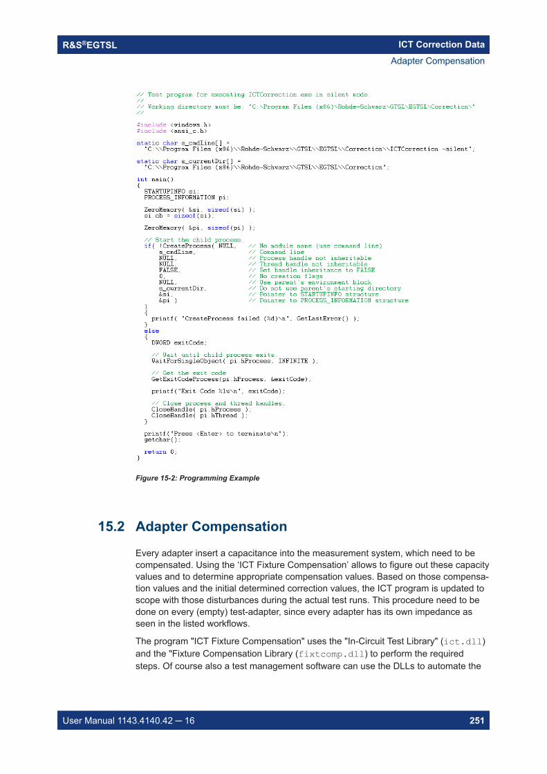
ICT Correction DataR&S®EGTSL
251User Manual 1143.4140.42 16
Figure 15-2: Programming Example
15.2 Adapter Compensation
Every adapter insert a capacitance into the measurement system, which need to becompensated. Using the ‘ICT Fixture Compensation’ allows to figure out these capacityvalues and to determine appropriate compensation values. Based on those compensa-tion values and the initial determined correction values, the ICT program is updated toscope with those disturbances during the actual test runs. This procedure need to bedone on every (empty) test-adapter, since every adapter has its own impedance asseen in the listed workflows.
The program "ICT Fixture Compensation" uses the "In-Circuit Test Library" (ict.dll)and the "Fixture Compensation Library (fixtcomp.dll) to perform the requiredsteps. Of course also a test management software can use the DLLs to automate the
Adapter Compensation
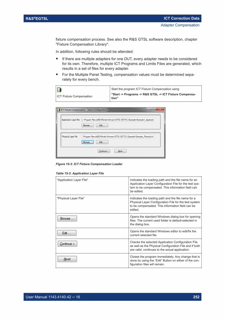
ICT Correction DataR&S®EGTSL
252User Manual 1143.4140.42 16
fixture compensation process. See also the R&S GTSL software description, chapter"Fixture Compensation Library".
In addition, following rules should be attended:
If there are multiple adapters for one DUT, every adapter needs to be consideredfor its own. Therefore, multiple ICT Programs and Limits Files are generated, whichresults in a set of files for every adapter.
For the Multiple Panel Testing, compensation values must be determined sepa-rately for every bench.
ICT Fixture Compensation
Start the program ICT Fixture Compensation using
"Start -> Programs -> R&S GTSL -> ICT Fixture Compensa-tion"
Figure 15-3: ICT Fixture Compensation Loader
Table 15-3: Application Layer File
"Application Layer File" Indicates the loading path and the file name for anApplication Layer Configuration File for the test sys-tem to be compensated. This information field canbe edited.
"Physical Layer File" Indicates the loading path and the file name for aPhysical Layer Configuration File for the test systemto be compensated. This information field can beedited.
Opens the standard Windows dialog box for openingfiles. The current used folder is default-selected inthe dialog box.
Opens the standard Windows editor to edit/fix thecurrent selected file.
Checks the selected Application Configuration Fileas well as the Physical Configuration File and if bothare valid, continues to the actual application.
Closes the program immediately. Any change that isdone by using the “Edit” Button on either of the con-figuration files will remain.
Adapter Compensation
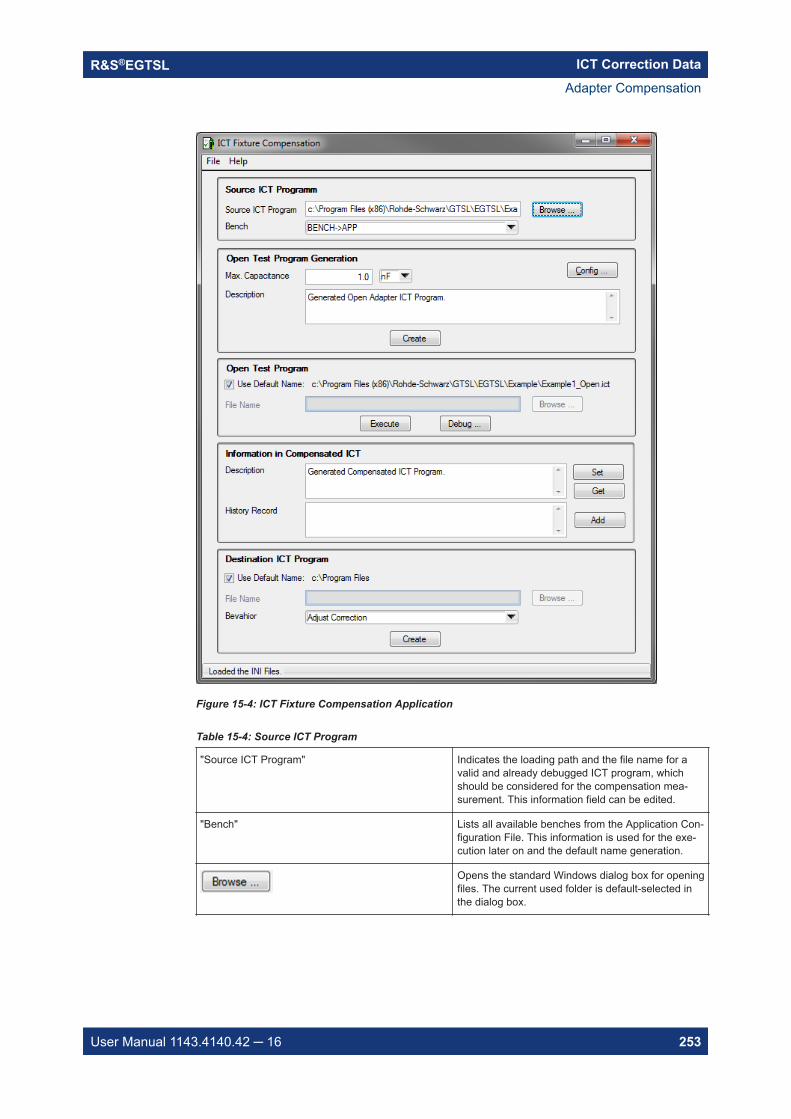
ICT Correction DataR&S®EGTSL
253User Manual 1143.4140.42 16
Figure 15-4: ICT Fixture Compensation Application
Table 15-4: Source ICT Program
"Source ICT Program" Indicates the loading path and the file name for avalid and already debugged ICT program, whichshould be considered for the compensation mea-surement. This information field can be edited.
"Bench" Lists all available benches from the Application Con-figuration File. This information is used for the exe-cution later on and the default name generation.
Opens the standard Windows dialog box for openingfiles. The current used folder is default-selected inthe dialog box.
Adapter Compensation
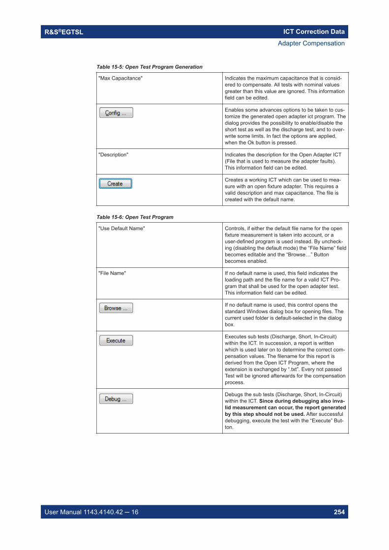
ICT Correction DataR&S®EGTSL
254User Manual 1143.4140.42 16
Table 15-5: Open Test Program Generation
"Max Capacitance" Indicates the maximum capacitance that is consid-ered to compensate. All tests with nominal valuesgreater than this value are ignored. This informationfield can be edited.
Enables some advances options to be taken to cus-tomize the generated open adapter ict program. Thedialog provides the possibility to enable/disable theshort test as well as the discharge test, and to over-write some limits. In fact the options are applied,when the Ok button is pressed.
"Description" Indicates the description for the Open Adapter ICT(File that is used to measure the adapter faults).This information field can be edited.
Creates a working ICT which can be used to mea-sure with an open fixture adapter. This requires avalid description and max capacitance. The file iscreated with the default name.
Table 15-6: Open Test Program
"Use Default Name" Controls, if either the default file name for the openfixture measurement is taken into account, or auser-defined program is used instead. By uncheck-ing (disabling the default mode) the “File Name” fieldbecomes editable and the “Browse…” Buttonbecomes enabled.
"File Name" If no default name is used, this field indicates theloading path and the file name for a valid ICT Pro-gram that shall be used for the open adapter test.This information field can be edited.
If no default name is used, this control opens thestandard Windows dialog box for opening files. Thecurrent used folder is default-selected in the dialogbox.
Executes sub tests (Discharge, Short, In-Circuit)within the ICT. In succession, a report is writtenwhich is used later on to determine the correct com-pensation values. The filename for this report isderived from the Open ICT Program, where theextension is exchanged by “.txt”. Every not passedTest will be ignored afterwards for the compensationprocess.
Debugs the sub tests (Discharge, Short, In-Circuit)within the ICT. Since during debugging also inva-lid measurement can occur, the report generatedby this step should not be used. After successfuldebugging, execute the test with the “Execute” But-ton.
Adapter Compensation
ICT Correction DataR&S®EGTSL
255User Manual 1143.4140.42 16
Table 15-7: Information in Compensated ICT
"Description" Indicates the description for the Compensated ICT(File that is in the end produced by this tool). Thisinformation field can be edited.
Set the text that is stated in the description field asdescription into the compensated ICT program. Anempty description cannot be added, and must betherefore avoided.
Receives the current set description in the Compen-sated ICT program. This is in first place the same asthe description, which is established in the initialICT.
"History Record" Indicates a text that is used as a new history recordin the compensated file. In contrast to the descrip-tion property, can the user add an empty record,since then a default entry is produced. This informa-tion field can be edited.
The information stated in the ‘History Record’ con-trol will be added as new History Record. If the fieldis empty, when the process is started, a defaultentry stating the date and bench information is gen-erated automatically.
Table 15-8: Destination ICT Program
"Use Default Name" Controls, if either the default file name for the Com-pensated ICT Program is taken into account, or auser-defined program is used instead. By uncheck-ing (disabling the default mode) the File Name fieldbecomes editable and the “Browse…” Buttonbecomes enabled.
"File Name" If no default name is used, this field indicates theloading path and the file name for a valid ICT Pro-gram that shall be used. This information field canbe edited.
"Behaviour" For adding the compensation values, two differentstrategies are valid. On the one hand, (“Adjust Cor-rection”) the correction values can be taken intoaccount and be adjusted if necessary. On the otherhand, (“Not Adjust Correction”) are compensationvalues were added directly.
Adds compensation values by parsing the report file,which was generated after the open adapter mea-surement. In succession is the actual ICT programfile written as filename, which is either the defaultname or a user specified name. In addition, a limitsfile is generated that holds information about thecompensation and correction values.
Adapter Compensation
ICT Correction DataR&S®EGTSL
256User Manual 1143.4140.42 16
Figure 15-5: Open Test Generation configuration
Table 15-9: Open Test Generation configuration
"Enable Short Test" If this option is set, the test “Short” of the incomingtest is put into the intermediate ICT program for the‘Open Adapter Measurement’.
(Default = on)
"EnableDischarge Test" If this option is set, the test “Discharge” of theincoming test is put into the intermediate ICT pro-gram for the ‘Open Adapter Measurement’.
(Default = off)
"Override Lower Limit" If this option is set, the default value for the lowerlimit is overwritten in the intermediate ICT programfor the ‘Open Adapter Measurement’.
(Default = 0.0pF)
"Override Upper Limit" If this option is set, the default value for the upperlimit is overwritten in the intermediate ICT programfor the ‘Open Adapter Measurement’.
(Default = 150.0pF)
A typical workflow to get a compensated ICT for one Adapter:
1. Start ICT Adapter Compensation tool.
2. Select the "Physical Layer Configuration File" as well as an "Application LayerConfiguration File", according to the ICT program, which shall be compensated.
3. Click on the "Continue >" button to check the validity of the configuration files andopen the actual application panel.
4. Select an already debugged ICT program choose the correct Bench, for which thecompensation should be executed.
5. Fill in a maximum limit for the nominal test values and add a description for theopen ICT program.
6. Create the Open Adapter ICT program file by clicking "Create".
7. Assure that the measurement adapter is empty.
8. Execute or debug the Open Adapter ICT Program.
Adapter Compensation
ICT Correction DataR&S®EGTSL
257User Manual 1143.4140.42 16
9. Add additional information to the resulting compensated program. First add a newdescription; otherwise, the description of the initial ICT is used. The history recordcan be added on purpose.
10. Choose the correct behavior for the handling of the compensation and correctionvalues.
11. Finally start the creation of the resulting compensated file by pushing the lower but-ton "Create".
During step 7 is an additional report file generated, which is necessary during additionof the compensation. This must be taken in consideration, if a user-defined Open ICTfile is used, since the report file name must be equal to this file name except the exten-sion.
A typical workflow to get compensated ICT’s for multiple Adapters:
1. Generate a compensated file for the first adapter by following instruction in theworkflow to gather compensation for one adapter.
2. For every additional adapter, follow those instructions again, whereby the compen-sated file of the first adapter should be used as base for the compensation proc-ess.
The ICT Fixture Compensation application is able to handle already given Correctionand Compensation values. This is due to the complexity of the correction value han-dling in the library, which automatically detects if any compensation value is estab-lished and use a different algorithm to integrate the correction value into the compen-sation calculation.
Adapter Compensation
Error MessagesR&S®EGTSL
258User Manual 1143.4140.42 16
16 Error MessagesStarting with GTSL 3.30, no GTSL license is required.
16.1 Compile Errors
Compile errors can occur in the following situations during the creation of the meta-code:
At the opening of an ICT program. At the creation or running of test steps. During the execution of the "Apply" (or
"Auto apply") function, a compile error is displayed for an erroneous test step.
Compile errors are displayed as text in the Report sub-window. Erroneous test stepsare marked in red in the Program sub-window.
The following list shows some common compile errors.
Unknown pin X A pin name was entered incorrectly. The pin name is not listed in the
application.ini file.
<Parameter> is out of range The value of the parameter entered lies outside thepermissible value range
No complementary path found for pins Xand Y
For 6-wire measurements, the „even/odd rule“ forForce and Sense pins was not adhered to. Theentered pins have either both even or both odd pinnumbers.
Device type 'pict' is missing The test method requires a R&S TS-PICT modulewhich was not configured in the bench as an ICTdevice.
TS-LEGT license required For the test method, a R&S TS-LEGT license isrequired.
16.2 Runtime Errors
Runtime errors occur during the execution of the program and are displayed in sepa-rate error windows.
Examples:
Runtime Errors
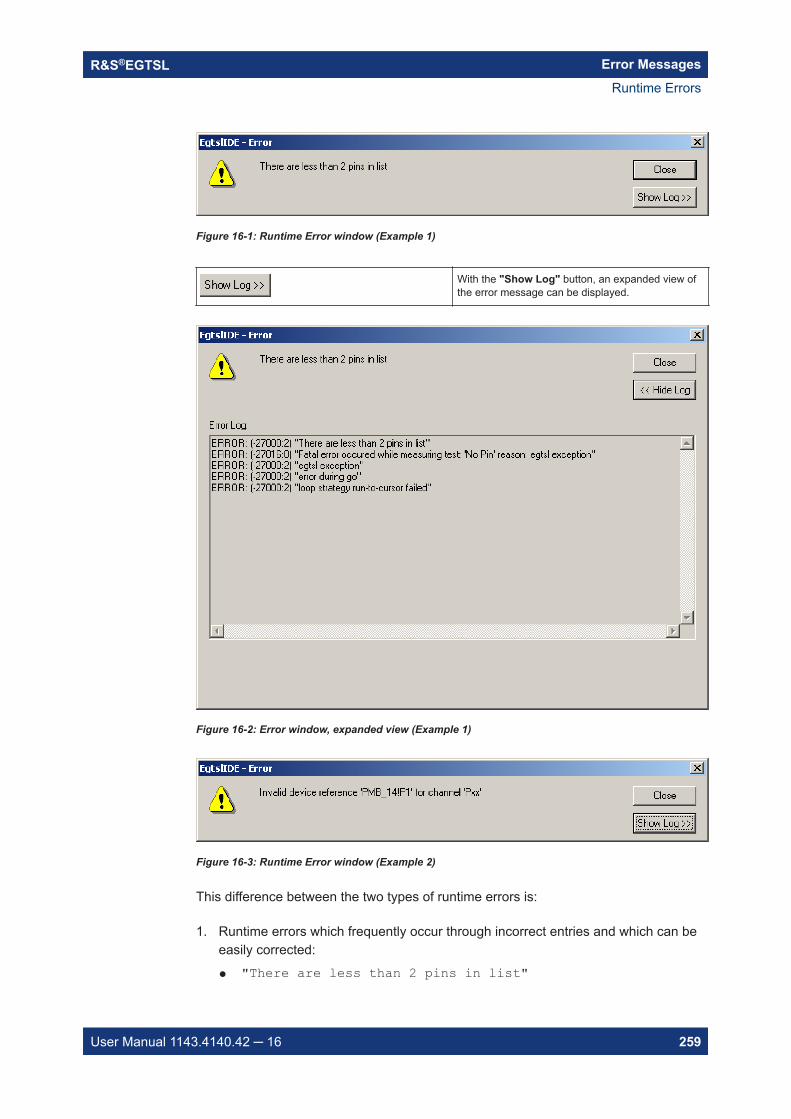
Error MessagesR&S®EGTSL
259User Manual 1143.4140.42 16
Figure 16-1: Runtime Error window (Example 1)
With the "Show Log" button, an expanded view ofthe error message can be displayed.
Figure 16-2: Error window, expanded view (Example 1)
Figure 16-3: Runtime Error window (Example 2)
This difference between the two types of runtime errors is:
1. Runtime errors which frequently occur through incorrect entries and which can beeasily corrected:
"There are less than 2 pins in list"
Runtime Errors
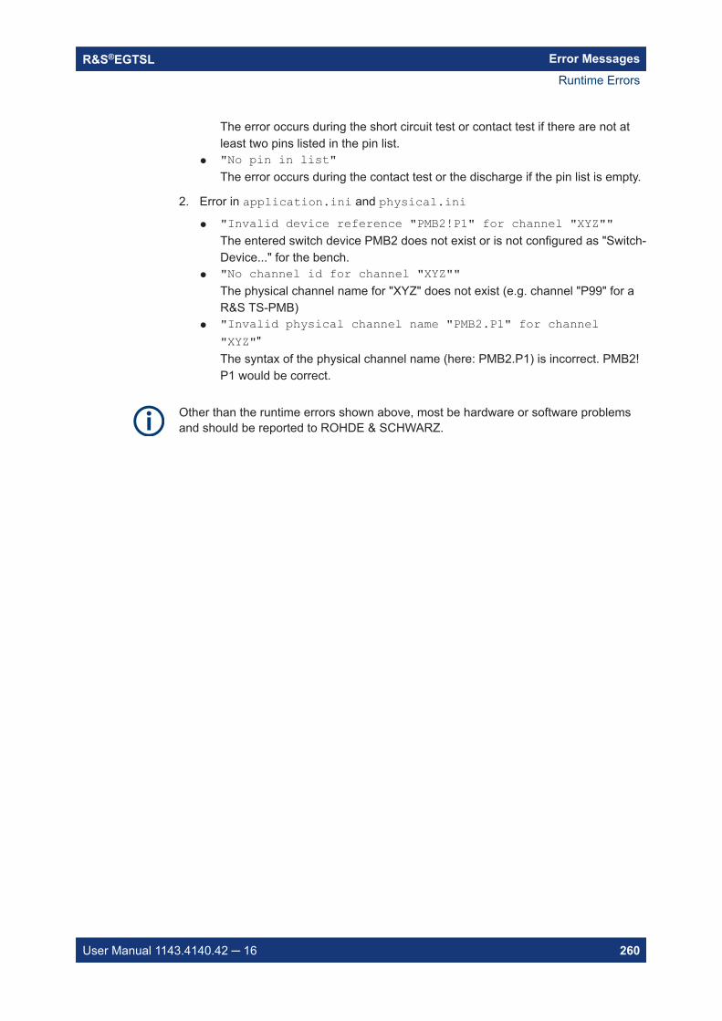
Error MessagesR&S®EGTSL
260User Manual 1143.4140.42 16
The error occurs during the short circuit test or contact test if there are not atleast two pins listed in the pin list.
"No pin in list"The error occurs during the contact test or the discharge if the pin list is empty.
2. Error in application.ini and physical.ini "Invalid device reference "PMB2!P1" for channel "XYZ""
The entered switch device PMB2 does not exist or is not configured as "Switch-Device..." for the bench.
"No channel id for channel "XYZ""The physical channel name for "XYZ" does not exist (e.g. channel "P99" for aR&S TS-PMB)
"Invalid physical channel name "PMB2.P1" for channel"XYZ""The syntax of the physical channel name (here: PMB2.P1) is incorrect. PMB2!P1 would be correct.
Other than the runtime errors shown above, most be hardware or software problemsand should be reported to ROHDE & SCHWARZ.
Runtime Errors
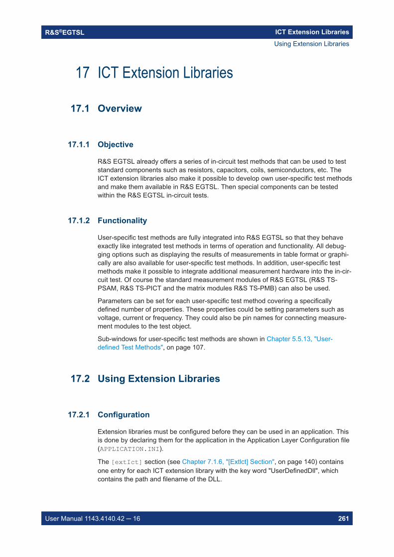
ICT Extension LibrariesR&S®EGTSL
261User Manual 1143.4140.42 16
17 ICT Extension Libraries
17.1 Overview
17.1.1 Objective
R&S EGTSL already offers a series of in-circuit test methods that can be used to teststandard components such as resistors, capacitors, coils, semiconductors, etc. TheICT extension libraries also make it possible to develop own user-specific test methodsand make them available in R&S EGTSL. Then special components can be testedwithin the R&S EGTSL in-circuit tests.
17.1.2 Functionality
User-specific test methods are fully integrated into R&S EGTSL so that they behaveexactly like integrated test methods in terms of operation and functionality. All debug-ging options such as displaying the results of measurements in table format or graphi-cally are also available for user-specific test methods. In addition, user-specific testmethods make it possible to integrate additional measurement hardware into the in-cir-cuit test. Of course the standard measurement modules of R&S EGTSL (R&S TS-PSAM, R&S TS-PICT and the matrix modules R&S TS-PMB) can also be used.
Parameters can be set for each user-specific test method covering a specificallydefined number of properties. These properties could be setting parameters such asvoltage, current or frequency. They could also be pin names for connecting measure-ment modules to the test object.
Sub-windows for user-specific test methods are shown in Chapter 5.5.13, "User-defined Test Methods", on page 107.
17.2 Using Extension Libraries
17.2.1 Configuration
Extension libraries must be configured before they can be used in an application. Thisis done by declaring them for the application in the Application Layer Configuration file(APPLICATION.INI).
The [extIct] section (see Chapter 7.1.6, "[Extlct] Section", on page 140) containsone entry for each ICT extension library with the key word "UserDefinedDll", whichcontains the path and filename of the DLL.
Using Extension Libraries
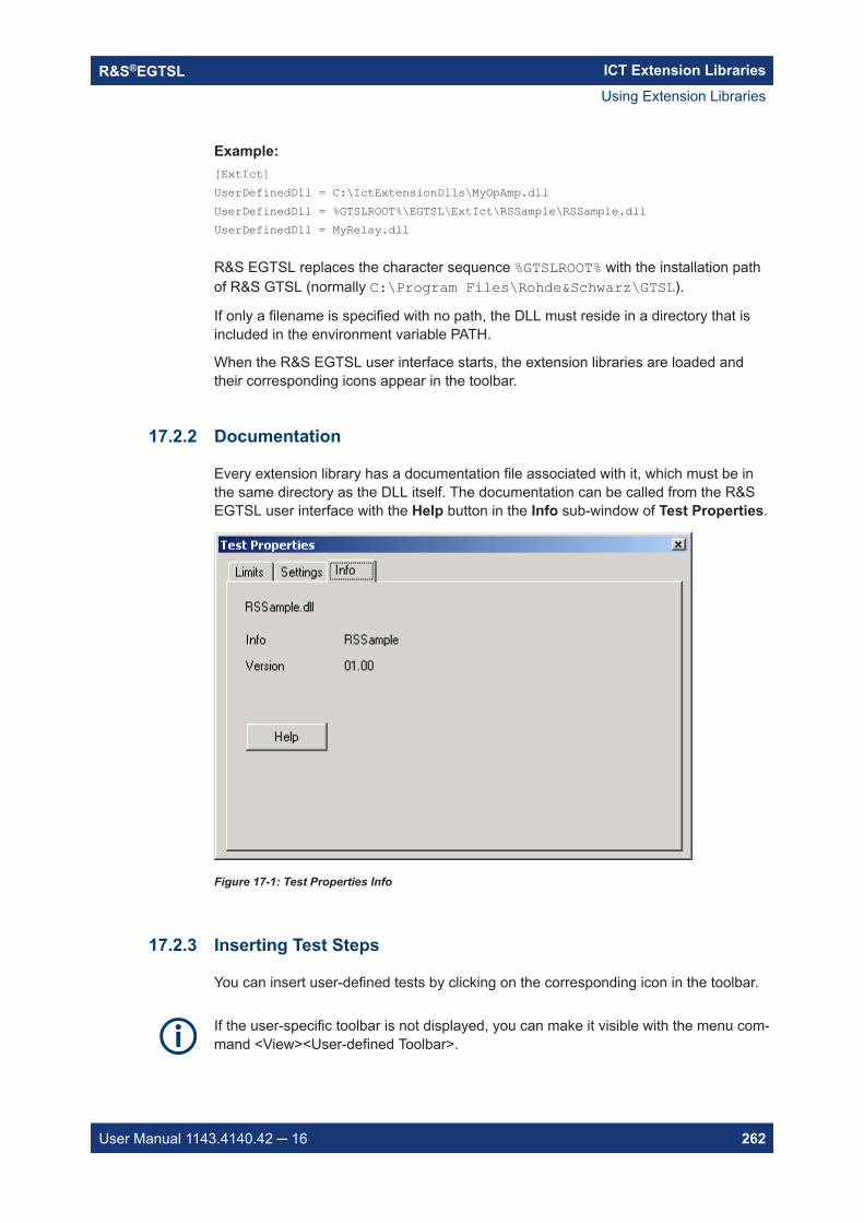
ICT Extension LibrariesR&S®EGTSL
262User Manual 1143.4140.42 16
Example: [ExtIct]UserDefinedDll = C:\IctExtensionDlls\MyOpAmp.dllUserDefinedDll = %GTSLROOT%\EGTSL\ExtIct\RSSample\RSSample.dllUserDefinedDll = MyRelay.dll
R&S EGTSL replaces the character sequence %GTSLROOT% with the installation pathof R&S GTSL (normally C:\Program Files\Rohde&Schwarz\GTSL).
If only a filename is specified with no path, the DLL must reside in a directory that isincluded in the environment variable PATH.
When the R&S EGTSL user interface starts, the extension libraries are loaded andtheir corresponding icons appear in the toolbar.
17.2.2 Documentation
Every extension library has a documentation file associated with it, which must be inthe same directory as the DLL itself. The documentation can be called from the R&SEGTSL user interface with the Help button in the Info sub-window of Test Properties.
Figure 17-1: Test Properties Info
17.2.3 Inserting Test Steps
You can insert user-defined tests by clicking on the corresponding icon in the toolbar.
If the user-specific toolbar is not displayed, you can make it visible with the menu com-mand <View><User-defined Toolbar>.
Using Extension Libraries
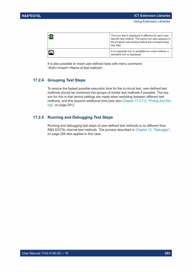
ICT Extension LibrariesR&S®EGTSL
263User Manual 1143.4140.42 16
The icon that is displayed is different for each user-specific test method. The same icon also appears inthe program sub-window before the correspondingtest step.
If no separate icon is available for a test method, astandard icon is displayed.
It is also possible to insert user-defined tests with menu command<Edit><Insert><Name of test method>.
17.2.4 Grouping Test Steps
To ensure the fastest possible execution time for the in-circuit test, user-defined testmethods should be combined into groups of similar test methods if possible. The rea-son for this is that device settings are made when switching between different testmethods, and this requires additional time (see also Chapter 17.3.7.5, "Prolog and Epi-log", on page 291).
17.2.5 Running and Debugging Test Steps
Running and debugging test steps of user-defined test methods is no different thanR&S EGTSL-internal test methods. The process described in Chapter 12, "Debugger",on page 226 also applies to this case.
Using Extension Libraries
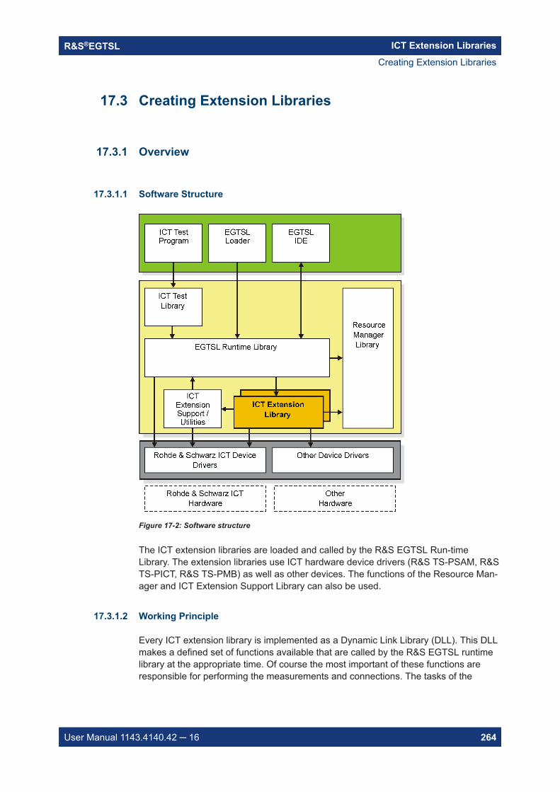
ICT Extension LibrariesR&S®EGTSL
264User Manual 1143.4140.42 16
17.3 Creating Extension Libraries
17.3.1 Overview
17.3.1.1 Software Structure
Figure 17-2: Software structure
The ICT extension libraries are loaded and called by the R&S EGTSL Run-timeLibrary. The extension libraries use ICT hardware device drivers (R&S TS-PSAM, R&STS-PICT, R&S TS-PMB) as well as other devices. The functions of the Resource Man-ager and ICT Extension Support Library can also be used.
17.3.1.2 Working Principle
Every ICT extension library is implemented as a Dynamic Link Library (DLL). This DLLmakes a defined set of functions available that are called by the R&S EGTSL runtimelibrary at the appropriate time. Of course the most important of these functions areresponsible for performing the measurements and connections. The tasks of the
Creating Extension Libraries
ICT Extension LibrariesR&S®EGTSL
265User Manual 1143.4140.42 16
remaining functions are to initialize and prepare hardware modules, verify user entriesand prepare the measurement value for display.
17.3.1.3 Integrating Hardware Modules
In the standard configuration, the ICT modules administered by R&S EGTSL, R&S TS-PSAM and R&S TS-PICT plus the matrix modules R&S TS-PMB are available for mea-surements and connections. They are already initialized and administered by R&SEGTSL, so there is no additional software overhead required in the ICT extensionlibrary.
The ICT Extension Support Library also offers functions for quickly connecting testobject pins to the analog busses of the R&S CompactTSVP using the R&S TS-PMBmatrix modules.
In addition, other measurement and stimulus modules can also be integrated. Thatcould include R&S CompactTSVP modules such as the R&S TS-PFG function genera-tor, but also any other modules or external devices such as power supply units.
17.3.1.4 File Structure
An ICT extension library generally consists of three files.
The Dynamic Link Library (DLL), which makes functionality available. A bitmap file with the same name and filename extension .BMP, containing the icon
associated with the test method. A file containing the documentation for the test method. Any file format can be
selected (for example HTML, PDF, HLP, CHM), provided there is a program on thetarget system that is linked with that format and is able to display it.
When assigning names to ICT extension libraries, care must be taken to ensure thenames are unique. We therefore recommend prefixing an abbreviation for your com-pany to the beginning of the name. This is the reason the sample project included withdelivery is called "RSSample", with RS standing for Rohde & Schwarz.
ICT extension libraries should be stored in a common directory (for exampleC:\IctExtensionDlls\). The directory should not be created within the R&S GTSLinstallation directory. This will prevent files from being overwritten when R&S GTSL isupdated or reinstalled.
Since the full directory name is generally listed in the APPLICATION.INI file, makecertain the directory is always in the same place for different test systems. Otherwisethe ICT extension libraries cannot be loaded on another test system.
17.3.2 Sample Projects
Two sample projects for ICT extension libraries are stored in the source code in folder…GTSL\EGTSL\ExtIct.
Creating Extension Libraries
ICT Extension LibrariesR&S®EGTSL
266User Manual 1143.4140.42 16
17.3.2.1 RSSample
The RSSample project is a fully functional example of an ICT extension library usingmodules R&S TS-PSAM and R&S TS-PFG.
The R&S TS-PSAM module is an example of modules administered by R&S EGTSL,and is relatively easy to use. The R&S TS-PFG module is not administered by R&SEGTSL and therefore requires greater programming overhead in RSSample. The filesfor this project reside in folder …GTSL\EGTSL\ExtIct\RSSample.
File Description
RSSample.c Source code of RSSample library
RSSample.dll Executable code of RSSample as Dynamic LinkLibrary
RSSample.lib Link library of RSSample
RSSample.bmp Bitmap file for the library’s icon
RSSample.pdf Description of RSSample library for the user
RSSample.prj LabWindows/CVI project RSSample
RSSample.dsp Microsoft Visual Studio project RSSample
ExtIctUtil.c, ExtIctUtil.h Source and header file for support functions (seeChapter 17.3.3.4, "Support Functions",on page 271)
17.3.2.2 RSSamplePSU
The RSSamplePSU project is similar to the RSSample project, but uses the R&S TS-PSU module instead of the R&S TS-PFG module.
This project is simpler than the RSSample project because the TS-PSU and TS-PSAMare both administered by R&S EGTSL.
The files for this project reside in folder ...GTSL\EGTSL\ExtIct\RSSamplePSU.
17.3.2.3 Framework
The Framework project represent a framework for an ICT extension library which userscan use to develop their own libraries.
Copy the files to a separate directory and change the filenames as appropriate to startthe development of a new ICT extension library.
Places to be completed are identified by the comment
/* TO BE DONE ... */
File Description
Framework.c Source code of the frame
Framework.bmp Bitmap file for the library’s icon
Creating Extension Libraries
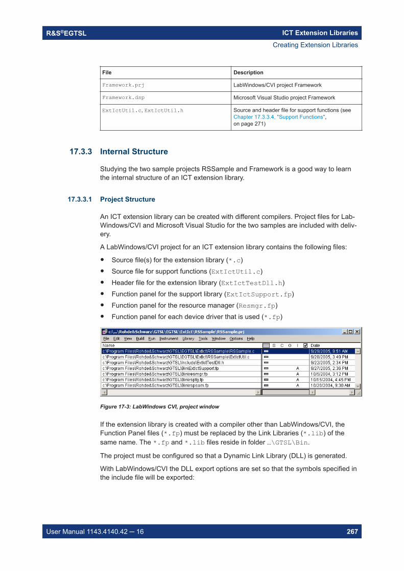
ICT Extension LibrariesR&S®EGTSL
267User Manual 1143.4140.42 16
File Description
Framework.prj LabWindows/CVI project Framework
Framework.dsp Microsoft Visual Studio project Framework
ExtIctUtil.c, ExtIctUtil.h Source and header file for support functions (seeChapter 17.3.3.4, "Support Functions",on page 271)
17.3.3 Internal Structure
Studying the two sample projects RSSample and Framework is a good way to learnthe internal structure of an ICT extension library.
17.3.3.1 Project Structure
An ICT extension library can be created with different compilers. Project files for Lab-Windows/CVI and Microsoft Visual Studio for the two samples are included with deliv-ery.
A LabWindows/CVI project for an ICT extension library contains the following files:
Source file(s) for the extension library (*.c) Source file for support functions (ExtIctUtil.c) Header file for the extension library (ExtIctTestDll.h) Function panel for the support library (ExtIctSupport.fp) Function panel for the resource manager (Resmgr.fp) Function panel for each device driver that is used (*.fp)
Figure 17-3: LabWindows CVI, project window
If the extension library is created with a compiler other than LabWindows/CVI, theFunction Panel files (*.fp) must be replaced by the Link Libraries (*.lib) of thesame name. The *.fp and *.lib files reside in folder …\GTSL\Bin.
The project must be configured so that a Dynamic Link Library (DLL) is generated.
With LabWindows/CVI the DLL export options are set so that the symbols specified inthe include file will be exported:
Creating Extension Libraries
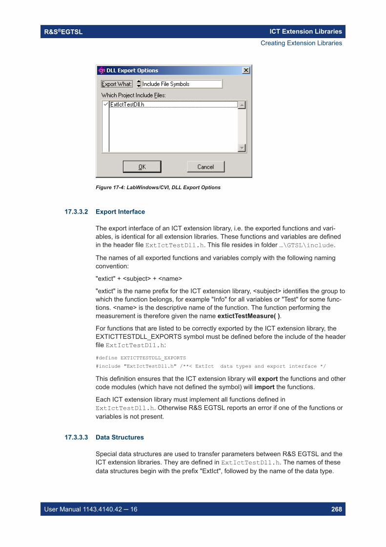
ICT Extension LibrariesR&S®EGTSL
268User Manual 1143.4140.42 16
Figure 17-4: LabWindows/CVI, DLL Export Options
17.3.3.2 Export Interface
The export interface of an ICT extension library, i.e. the exported functions and vari-ables, is identical for all extension libraries. These functions and variables are definedin the header file ExtIctTestDll.h. This file resides in folder …\GTSL\include.
The names of all exported functions and variables comply with the following namingconvention:
"extict" + <subject> + <name>
"extict" is the name prefix for the ICT extension library, <subject> identifies the group towhich the function belongs, for example "Info" for all variables or "Test" for some func-tions. <name> is the descriptive name of the function. The function performing themeasurement is therefore given the name extictTestMeasure( ).
For functions that are listed to be correctly exported by the ICT extension library, theEXTICTTESTDLL_EXPORTS symbol must be defined before the include of the headerfile ExtIctTestDll.h:
#define EXTICTTESTDLL_EXPORTS#include "ExtIctTestDll.h" /**< ExtIct data types and export interface */
This definition ensures that the ICT extension library will export the functions and othercode modules (which have not defined the symbol) will import the functions.
Each ICT extension library must implement all functions defined inExtIctTestDll.h. Otherwise R&S EGTSL reports an error if one of the functions orvariables is not present.
17.3.3.3 Data Structures
Special data structures are used to transfer parameters between R&S EGTSL and theICT extension libraries. They are defined in ExtIctTestDll.h. The names of thesedata structures begin with the prefix "ExtIct", followed by the name of the data type.
Creating Extension Libraries
ICT Extension LibrariesR&S®EGTSL
269User Manual 1143.4140.42 16
Strings
There are three data structures that write strings of differing length:
ExtIctString Strings with max. 256 characters, for example prop-erties and values
ExtIctInfoString Strings with max. 1024 characters, for error mes-sages
ExtIctBigString Strings with max. 4096 characters, for debugdetails.
typedef struct tagExtIctString char text[EXTICT_MAXSTRINGLENGTH]; ExtIctString;typedef struct tagExtIctInfoString char text[EXTICT_MAXINFOSTRINGLENGTH]; ExtIctInfoString;typedef struct tagExtIctBigString char text[EXTICT_MAXBIGSTRINGLENGTH]; ExtIctBigString;
There are support functions for writing these strings to ensure the maximum length isnot exceeded.
Status
The ExtIctStatus structure is composed of a numeric error code and an error mes-sage. This data structure is returned with most functions of the ICT extension library asthe result.
An error code of = 0 means that a function has been successfully completed. Errorsare reported as negative values.
In the case of success, the error message is empty. Otherwise the error text is entered.
typedef struct tagExtIctStatus int error; ExtIctInfoString message; ExtIctStatus;
Test Result
The structure ExtIctTestResult is composed of a status structure and the mea-surement result. This structure is returned as the result of functionextictTestMeasure.
The structure indicates whether the measurement function was completed success-fully. The error code is not set if a measurement value is outside the expected limits,however. Its purpose is rather to signal runtime errors.
Creating Extension Libraries
ICT Extension LibrariesR&S®EGTSL
270User Manual 1143.4140.42 16
If the measurement is successful, the variable "value" contains the result value. It iscompared with the upper and lower limit by R&S EGTSL. The comparison result in anevaluation of whether a test step is a "Pass" or a "Fail".
In addition to the measurement value, the unit of measure (for example "mV", "kHz" oran empty string in some cases) is transferred in the variable "unit". The charactersequence "info" can optionally be used to transfer non-numeric information. This infor-mation is added to the test report in the event a test fails (see also Section Chap-ter 17.3.8.2, "Non-numeric Test Results", on page 293).
typedef struct tagExtIctTestResult ExtIctStatus status; double value; ExtIctString unit; ExtIctString info; ExtIctTestResult;
Properties
The structure ExtIctPropertyList contains a list of all setting parameters and theirvalues. This structure contains an array of elements of the structureExtIctPropertyItem. The content of this structure is shown in the R&S EGTSLuser interface (see Section 5.5.10.2).
ExtIctPropertyItem is a pair of two strings. The variable "name" contains thename of the property and "value" contains its value.
ExtIctPropertyList contains a list of 256 of these properties in addition to thenominal value ("nominal"), the unit ("unit") and the number of properties actually used("size").
typedef struct tagExtIctPropertyItem ExtIctString name; ExtIctString value; ExtIctPropertyItem;typedef struct tagExtIctPropertyList double nominal; ExtIctString unit; int size; ExtIctPropertyItem items[EXTICT_MAXNUMPROPERTIES]; ExtIctPropertyList;
Administrative Data
When an ICT extension library is loaded and a test step is created, additional datastructures are also created. Their main purpose is for storing internal data.
A structure ExtIctTestInstance is created for each test step. In addition to proper-ties, it also contains a pointer to an internal data structure. This data structure is descri-bed in Section "SetupUserData" on page 274.
Creating Extension Libraries
ICT Extension LibrariesR&S®EGTSL
271User Manual 1143.4140.42 16
The structure ExtIxtSetup is created once for each test method. It contains theresource ID of the ICT program and also a pointer to an internal data structure. Thisdata structure is described in Section "TestUserData" on page 274.
typedef struct tagExtIctTestInstance void *userData; ExtIctPropertyList properties; ExtIctTestInstance;typedef struct tagExtIctSetup void *userData; int resourceId; ExtIctSetup;
17.3.3.4 Support Functions
Two support libraries are available to support ICT extension libraries:
The ICT Extension Support Library ( ExtIctSupport.dll) The ICT Extension Utilities (ExtIctUtil.c)
The ICT Extension Support Library offers functions of the R&S EGTSL RuntimeLibrary for use in ICT extension libraries. This includes especially connections of matrixmodules. The functions of this library are described in the corresponding online helpExtIctSupport.hlp in directory…\GTSL\Bin.
The ICT Extension Utilities offer functions to make it easy to handle special ExtIctdata types. In some cases they also use the ICT Extension Support Library. By con-trast, the ICT Extension Utilities are integrated into the source code. The functions ofthis library are described in source file ExtIctUtil.c. This file resides in folder…\GTSL\EGTSL\ExtIct\Framework.
To create a new ICT extension library, ExtIctUtil.c can be copied and easilyexpanded if additional functions are required.
ExtIctUtil contains functions for:
Setting and chaining strings, taking into consideration the maximum length. Handling error messages. Converting property values (Strings) into numeric or Boolean values. Handling pin names.
17.3.3.5 Bitmap
Each ICT extension library can make its own icon available in a bitmap file. This icon isdisplayed in the R&S EGTSL user interface for each test step of this test method. Theicon also appears in the toolbar.
Creating Extension Libraries
ICT Extension LibrariesR&S®EGTSL
272User Manual 1143.4140.42 16
The bitmap must be 16 x 16 pixels in size and can have a color depth of 16 or 256colors. The lowest row of pixels is not displayed, i.e. the available surface is 16 x 15pixels:
Figure 17-5: Bitmap Layout
If the bitmap file is not available, R&S EGTSL shows a default icon.
17.3.4 Description of Function
17.3.4.1 Header Files
An ICT extension library includes the following header files:
#define EXTICTTESTDLL_EXPORTS#include "ExtIctTestDll.h" /**< ExtIct data types and export interface */#include "ExtIctSupport.h" /**< ExtIct support library */#include "ExtIctUtil.h" /**< ExtIct utilities */
#include "resmgr.h" /**< GTSL Resource Manager */
#include "rspsam.h" /**< TS-PSAM device driver */#include "rspfg.h" /**< TS-PFG device driver */
ExtIctTestDll.h exports the interface of the ICT extension library and defines thenecessary data types.
ExtIctSupport.h and ExtIctUtil.h import the support functions.
resmgr.h imports the functions of the resource manager.
The corresponding header file is included for each device driver that is used, thus inthe example above for R&S TS-PSAM and R&S TS-PFG.
The header files reside in folder …\GTSL\include with the exception ofExtIctUtil.h, which is in the project folder.
17.3.4.2 Exported Variables
Each ICT extension library exports the following variables, whose names begin withextictInfo:
Creating Extension Libraries
ICT Extension LibrariesR&S®EGTSL
273User Manual 1143.4140.42 16
/** test name */EXTICTTESTDLL_API char extictInfoTestName[] = "RSSample";
/** component version */EXTICTTESTDLL_API char extictInfoVersion[] = "01.00";
/** help file for this component */EXTICTTESTDLL_API char extictInfoHelpFileName[] = "RSSample.pdf";
/** component bitmap is loaded from a file */EXTICTTESTDLL_API int extictInfoIconBitMap = -1;
extictInfoTestName
This string variable contains the unique name of the test method. This name appearsin the program sub-window with each test step and is displayed in the Test PropertiesInfo window (see Figure 17-1).
To ensure the name is unique system-wide, we recommend making it begin with thecompany initials or abbreviation. This is the reason the sample project included withdelivery is called "RSSample", with RS standing for Rohde & Schwarz.
extictInfoVersion
This string variable contains the version number of the ICT extension library. It is dis-played in the Test Properties Info window (see Figure 17-1).
extictInfoHelpFileName
This string variable contains the name of the documentation file for the ICT extensionlibrary. This file must reside in the same directory as the DLL. You can display it byclicking the Help button in the Test Properties Info window (see Figure 17-1).
The documentation can be available in any file format. The only thing that is importantis that a program that is called to display the file is linked with the file ending. Bringingup the documentation file from the R&S EGTSL user interface corresponds to doubleclicking this file in the Windows Explorer. The following common file formats are suita-ble for a documentation file:
File ending Linked display program
.pdf Adobe Reader
.html, .htm Internet Explorer
.hlp Windows Help
.chm HTML Help Executable
extictInfoIconBitMap
This integer variable normally contains the value -1. That value means that the icon forthe ICT extension library is present as a *.BMP file. In that case R&S EGTSL loads thebitmap from the file.
Creating Extension Libraries
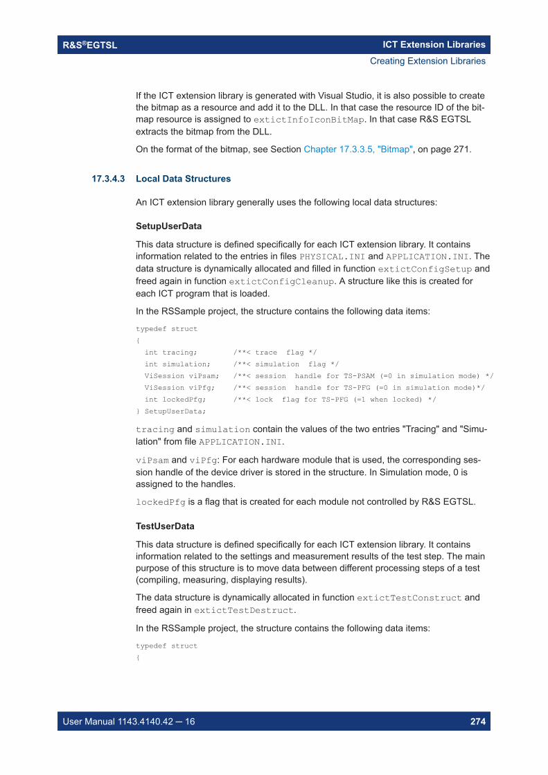
ICT Extension LibrariesR&S®EGTSL
274User Manual 1143.4140.42 16
If the ICT extension library is generated with Visual Studio, it is also possible to createthe bitmap as a resource and add it to the DLL. In that case the resource ID of the bit-map resource is assigned to extictInfoIconBitMap. In that case R&S EGTSLextracts the bitmap from the DLL.
On the format of the bitmap, see Section Chapter 17.3.3.5, "Bitmap", on page 271.
17.3.4.3 Local Data Structures
An ICT extension library generally uses the following local data structures:
SetupUserData
This data structure is defined specifically for each ICT extension library. It containsinformation related to the entries in files PHYSICAL.INI and APPLICATION.INI. Thedata structure is dynamically allocated and filled in function extictConfigSetup andfreed again in function extictConfigCleanup. A structure like this is created foreach ICT program that is loaded.
In the RSSample project, the structure contains the following data items:
typedef struct int tracing; /**< trace flag */ int simulation; /**< simulation flag */ ViSession viPsam; /**< session handle for TS-PSAM (=0 in simulation mode) */ ViSession viPfg; /**< session handle for TS-PFG (=0 in simulation mode)*/ int lockedPfg; /**< lock flag for TS-PFG (=1 when locked) */ SetupUserData;
tracing and simulation contain the values of the two entries "Tracing" and "Simu-lation" from file APPLICATION.INI.
viPsam and viPfg: For each hardware module that is used, the corresponding ses-sion handle of the device driver is stored in the structure. In Simulation mode, 0 isassigned to the handles.
lockedPfg is a flag that is created for each module not controlled by R&S EGTSL.
TestUserData
This data structure is defined specifically for each ICT extension library. It containsinformation related to the settings and measurement results of the test step. The mainpurpose of this structure is to move data between different processing steps of a test(compiling, measuring, displaying results).
The data structure is dynamically allocated in function extictTestConstruct andfreed again in extictTestDestruct.
In the RSSample project, the structure contains the following data items:
typedef struct
Creating Extension Libraries
ICT Extension LibrariesR&S®EGTSL
275User Manual 1143.4140.42 16
/* Source property values */
E_SOURCE_MODE sourceMode; /**< "Source Mode" decoded property value */ double voltage; /**< "Voltage" property value, in Volts */ double offset; /**< "Offset" property value, in Volts */ double frequency; /**< "Frequency" property value, in Hertz */
/* Measurement property values */ E_MEAS_FUNCTION measFunction; /**< "Measurement Function" decoded property value */ double range; /**< "Range" property value in V, A, or Ohms */ int autoRange; /**< "Autorange" property value - as Boolean */ double filter; /**< "Filter" property value in Hertz */ double delay; /**< "Delay" property value in seconds */ int average; /**< "Average" property value */ double sampleInterval; /**< "Sample Interval" property value */
/* Measurement data */
E_MEAS_STATE measState; /**< state of the measurement */ double measuredValue; /**< measured value, dependent on measFunction, in units of nominal value */ double measuredRange; /**< range in which measurement was taken, in units of nominal value */ double scalingFactor; /**< the value by which the measured value must be multiplied to obtain the value in the desired unit */ double duration; /**< duration of measurement */ int simulationMode; /**< 1 if simulation, 0 otherwise */
/* Switching information */
char busSourceHi [BUS_LEN]; /**< bus name for Pin Source HI */ char busSourceLo [BUS_LEN]; /**< bus name for Pin Source LO */ char busMeasHi [BUS_LEN]; /**< bus name for Pin Meas HI */ char busMeasLo [BUS_LEN]; /**< bus name for Pin Meas LO */
TestUserData; /**< test user data */
The elements of this structure can mainly be divided into three groups:
Sections "Source property values" and "Measurement property values" contain valuesof the setting values already converted into target format. FunctionextictTestCompile converts values and checks for valid value ranges. If the mea-surement function extictTestMeasure is called, values stored here can be transfer-red directly to the device driver. This ensures optimal performance, since the conver-sion and check are eliminated each time the measurement is performed.
Section "Measurement data" contains data from the last measurement. The data isstored here in the function extictTestMeasure. It is prepared for display in functionextictTestGetDebugDetails.
Creating Extension Libraries
ICT Extension LibrariesR&S®EGTSL
276User Manual 1143.4140.42 16
The last group, "Switching Information", contains information about the correct switch-ing path. This information is also determined earlier during extictTestCompile sothat it can be transferred directly to the device drivers for extictTestMeasure, thusguaranteeing a short execution time.
Table of Properties
All properties and their default values are combined together in a table. The tableappears as follows in the RSSample project:
/** table with properties and default values */static const ExtIctPropertyItem s_properties[] = /* property name default value */ "Source Mode", "DC" , "Voltage", "0.0" , "Offset", "0.0" , "Frequency", "1000.0" , "Measurement Function", "VDC" , "Range", "10.0" , "Autorange", "On" , "Filter", "40.0e3" , "Delay", "0.0" , "Average", "1" , "Sample Interval", "1.0e-3" , "Pin Source HI", "" , "Pin Source LO", "" , "Pin Meas HI", "" , "Pin Meas LO", "" ,;/** number of property entries in s_properties table */#define NUM_PROPS (sizeof(s_properties)/sizeof(s_properties[0]))
On the left side are the names of properties in the order in which they are also dis-played in the R&S EGTSL user interface. On the right side are their default values.When a new test step is created, all properties contain the corresponding default val-ues. Because of that, the default values specified here must be valid values.
Values are generally stored as ExtIctString, i.e. as a string with a maximum of 256characters. The data type for the individual properties is derived from the context, i.e.during the conversion and check in function extictTestCompile. Different types ofdata can be seen in the example, for example Voltage as a real number, Average asan integer, Autorange as a Boolean value and Source Mode as text.
Since it is not possible to specify default values for pin names, empty strings areassigned to them.
The NUM_PROPS macro automatically calculates the number of entries in thes_properties table.
A data type PROP_INDEX is defined for access to the property table. It defines con-stants for the indices of table entries. If changes are made to the s_propertiestable, PROP_INDEX must also be adjusted accordingly.
Creating Extension Libraries
ICT Extension LibrariesR&S®EGTSL
277User Manual 1143.4140.42 16
/** property enumeration = index into s_properties must be kept consistent with the s_properties table !*/typedef enum PROP_UNIT = -1, /* special value, see decodePropertyStringVal */
PROP_SOURCE_MODE = 0, /* 0 = first index in s_properties table */ PROP_VOLTAGE, PROP_OFFSET, PROP_FREQUENCY, PROP_MEAS_FUNCTION, PROP_RANGE, PROP_AUTO_RANGE, PROP_FILTER, PROP_DELAY, PROP_AVERAGE, PROP_SAMPLE_INTERVAL, PROP_PIN_SOURCE_HI, PROP_PIN_SOURCE_LO, PROP_PIN_MEAS_HI, PROP_PIN_MEAS_LO PROP_INDEX;
Tables for Value Conversions
As already explained in the previous section, values of properties are transferred asstrings. The strings are not converted to their actual data type until during a test step is"compiled". The code module extIctUtil.c makes conversion functions availablefor numeric data types (int, double) that check the converted value against both anupper and a lower limit.
Properties that allow a selection of multiple strings as a value are treated with specialconversion tables. Examples of these properties are mode settings ("Off", "AC", "DC")or physical units ("μV", "mV", "V"). A conversion table is created for each of these prop-erties that assigns an integer number to each permissible string value.
/** @brief Property string value -> integer conversion table. This table type holds pairs of permissible value strings and associated integer values. The table must end with an entry containing a NULL pointer for stringVal.*/typedef struct int intVal; /**< The associated integer value */ const char * stringVal; /**< The property value string */ ExtIctUtilPropTableEntry;
In the RSSample project, for example, the following conversion tables are defined:
Creating Extension Libraries
ICT Extension LibrariesR&S®EGTSL
278User Manual 1143.4140.42 16
/** property value table for Source Mode */static const ExtIctUtilPropTableEntry s_propsSourceMode[] = SOURCE_MODE_AC, "AC" , SOURCE_MODE_DC, "DC" , SOURCE_MODE_OFF, "OFF" , 0, NULL /**< always terminate the table with a NULL entry */;
/* property value table for Voltage units */static const ExtIctUtilPropTableEntry s_propsVoltageUnits[] = /* scaling exponent, unit */ 0, "V" , -3, "MV" , -6, "UV" , 0, NULL /**< always terminate the table with a NULL entry */;
The last entry in the tables must contain a NULL string.
Table s_propsSourceMode assigns an "enum" constant to each mode. Tables_propsVoltageUnits assigns an exponent to each unit. The exponent is used tocalculate the scaling factor. (1 mV = 10-3 V, 1 μV = 10-6 V).
Function decodePropertyStringVal from extIctUtil.c uses these tables toconvert and check properties.
17.3.4.4 Configuration Functions
Configuration functions are used to prepare hardware for use or to take them to adefined state after use.
All configuration functions have a pointer to a data structure ExtIctSetup as aparameter and return ExtIctStatus as a result.
extictConfigSetup
ExtIctStatus extictConfigSetup ( ExtIctSetup * pSetup )
The Setup function is called by R&S EGTSL when a test program is loaded. R&SEGTSL transfers the resource ID of the test program to pSetup->resourceId.
Tasks performed by function extictConfigSetup Allocate and initialize data structure SetupUserData and save its pointer to pSetup. Determine configuration data from APPLICATION.INI and PHYSICAL.INI and
store in SetupUserData, for example flags "Trace" and "Simulation". Determine session handles for hardware modules administered by and save in
SetupUserData. Initialization of device drivers for hardware modules not administered by .
Creating Extension Libraries
ICT Extension LibrariesR&S®EGTSL
279User Manual 1143.4140.42 16
Very little new code needs to be created for these tasks, with the exception of the last.Only in the case of loading and initializing device drivers not administered by R&SEGTSL is more overhead required. See also Section Chapter 17.3.7, "Additional Hard-ware Modules", on page 288.
extictConfigCleanup
ExtIctStatus extictConfigCleanup ( ExtIctSetup * pSetup )
The Cleanup function is called by R&S EGTSL when a test program is unloaded.
Tasks performed by function extictConfigCleanup Closing device drivers for hardware modules not administered by R&S EGTSL. Freeing the data structure SetupUserData.
Handling of device drivers for hardware module not administered by R&S EGTSL isdescribed in detail in Section Chapter 17.3.7, "Additional Hardware Modules",on page 288.
extictConfigProlog
ExtIctStatus extictConfigProlog ( ExtIctSetup * pSetup )
The purpose of the Prolog function is to prepare hardware modules to perform the nexttest step.
R&S EGTSL calls this function each time before executing a block of identical teststeps.
Tasks performed by function extictConfigProlog:
Call Prolog function of R&S EGTSL Locking of modules not administered by R&S EGTSL Reset of modules not administered by R&S EGTSL Preparing modules for the following test steps, for example closing the bus cou-
pling relays, configuring the ground relay, switching the measurement and stimulusmodules to the analog bus, any settings that are the same for all test steps.
See also Section Chapter 17.3.7.5, "Prolog and Epilog", on page 291.
extictConfigEpilog
The purpose of the Epilog function is to reset hardware modules to a defined stateafter the test steps have been performed.
R&S EGTSL calls this function each time after executing a block of identical test steps.
Tasks performed by function extictConfigEpilog:
Reset of modules not administered by R&S EGTSL Unlock modules not administered by R&S EGTSL Call Epilog function of R&S EGTSL
See also Section Chapter 17.3.7.5, "Prolog and Epilog", on page 291.
Creating Extension Libraries
ICT Extension LibrariesR&S®EGTSL
280User Manual 1143.4140.42 16
extictConfigErrorCleanup
The purpose of the ErrorCleanup function is to reset hardware modules to a definedstate after a runtime error.
R&S EGTSL calls this function when a runtime error has occurred in a test step of thisICT extension library.
Tasks performed by function extictConfigErrorCleanup:
Normally extictConfigErrorCleanup calls the two functionsextIctConfigEpilog and extIctConfigProlog one after the other to make cer-tain the hardware modules, coming from an unknown state, are prepared for the follow-ing test step.
17.3.4.5 Test-related Functions
The purpose of test-related functions is to check the settings for a test step, performthe test step and prepare the results for display.
extictTestConstruct
ExtIctStatus extictTestConstruct ( ExtIctTestInstance * pNewInstance, double * pLowerLimit, double * pUpperLimit )
The purpose of the Construct function is to create data structures for a new teststep.
R&S EGTSL calls this function if a new test step is inserted into the program or if a teststep is loaded from an ICT file.
Tasks performed by function extictTestConstruct Allocate and initialize data structure TestUserData and save its pointer to
pNewInstance. Copy content of table s_properties (property names and default values) to
pNewInstance. Set default values for nominal value, unit, upper and lower limit.
extictTestDestruct
ExtIctStatus extictTestDestruct ( ExtIctTestInstance * pTestInstance )
The purpose of the Destruct function is to free data structure TestUserData.
R&S EGTSL calls this function if a test step has been deleted from the program andwhen the ICT program is closed.
Tasks performed by function extictTestDestruct Free data structure TestUserData.
Creating Extension Libraries
ICT Extension LibrariesR&S®EGTSL
281User Manual 1143.4140.42 16
extictTestCompile
ExtIctStatus extictTestCompile ( ExtIctTestInstance * pTestInstance, ExtIctSetup * pSetup )
The purpose of the Compile function is to "compile" a test step, i.e. check the proper-ties for valid values and store the converted values in the TestUserData structure.
R&S EGTSL calls this function if a test step has been inserted or changed and whenan ICT program is loaded.
Tasks performed by function extIctTestCompile Check whether the required hardware modules are present Check the values of properties to ensure they are valid Check the values of properties for consistency among each other Search for switching paths for matrix modules Prepare structure TestUserData to perform the test.
extictTestMeasure
ExtIctTestResult extictTestMeasure ( ExtIctTestInstance * pTestInstance, ExtIctSetup * pSetup )
The purpose of the Measure function is to configure and connect the instruments, per-form the measurement and return the measurement results to R&S EGTSL.
R&S EGTSL calls this function when a test step is being performed.
Tasks performed by function extictTestMeasure Perform settings for hardware modules Create connection to test object Perform measurement Disconnect connection to test object Store data for "Debug Details" display in TestUserData Return measurement results to R&S EGTSL
extictTestGetDebugDetails
ExtIctBigString extictTestGetDebugDetails ( ExtIctTestInstance * pTestInstance )
The purpose of the GetDebugDetails function is to prepare details of the last mea-surement for output in the Debug Details window.
R&S EGTSL calls this function when a test step is being displayed.
Tasks performed by function extictGetDebugDetails Prepare data from the last measurement from TestUserData for output.
The following data items can be collected during the measurement and sent to DebugDetails:
Status information from stimulus devices, for example current limiting active.
Creating Extension Libraries
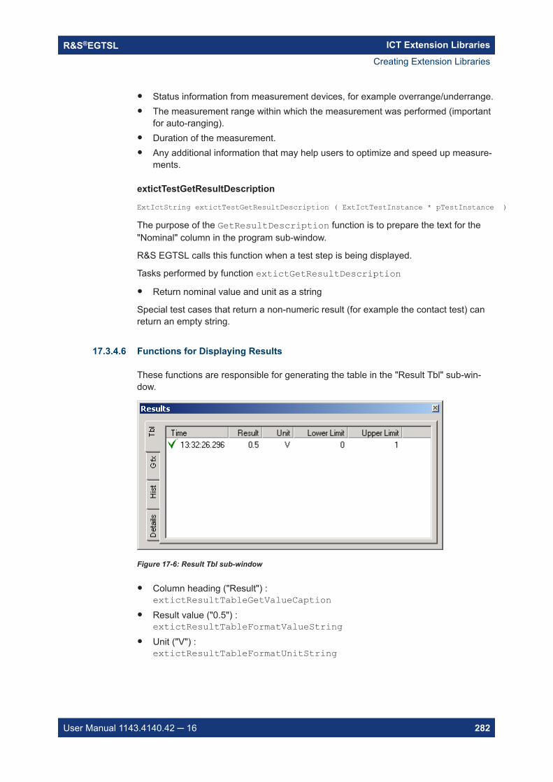
ICT Extension LibrariesR&S®EGTSL
282User Manual 1143.4140.42 16
Status information from measurement devices, for example overrange/underrange. The measurement range within which the measurement was performed (important
for auto-ranging). Duration of the measurement. Any additional information that may help users to optimize and speed up measure-
ments.
extictTestGetResultDescription
ExtIctString extictTestGetResultDescription ( ExtIctTestInstance * pTestInstance )
The purpose of the GetResultDescription function is to prepare the text for the"Nominal" column in the program sub-window.
R&S EGTSL calls this function when a test step is being displayed.
Tasks performed by function extictGetResultDescription Return nominal value and unit as a string
Special test cases that return a non-numeric result (for example the contact test) canreturn an empty string.
17.3.4.6 Functions for Displaying Results
These functions are responsible for generating the table in the "Result Tbl" sub-win-dow.
Figure 17-6: Result Tbl sub-window
Column heading ("Result") :extictResultTableGetValueCaption
Result value ("0.5") :extictResultTableFormatValueString
Unit ("V") :extictResultTableFormatUnitString
Creating Extension Libraries
ICT Extension LibrariesR&S®EGTSL
283User Manual 1143.4140.42 16
extictResultTableGetValueCaption
ExtIctString extictResultTableGetValueCaption ( void )
Function extictResultTableGetValueCaption returns the column heading of thetable’s second column in the "Result Tbl" sub-window.
The column heading should indicate what a test method returns, for example "Fre-quency" or "Resistance".
If a test method can return different results, for example RSSample, the defaultheading "Result" is used.
extictResultTableFormatValueString
ExtIctString extictResultTableFormatValueString ( double value )
Function extictResultTableFormatValueString returns the content of thetable’s second column in the "Result Tbl" sub-window as a string. The current mea-surement value is transferred in the parameter "value".
Normally the measurement value is formatted and returned as text with a functionsuch as sprintf.
extictResultTableFormatUnitString
xtIctString extictResultTableFormatUnitString ( char * unit )
Function extictResultTableFormatUnitString returns the content of the table’sthird column in the "Result Tbl" sub-window as a string. The current unit is transferredin the parameter "value".
Normally the unit that is transferred is returned as text.
17.3.5 Details of Implementation
17.3.5.1 Error Handling
Most functions of an ICT extension library return an ExtIctStatus structure as theresult. The error code is set to 0 and the error message is set to an empty string at thebeginning of each function.
ExtIctStatus status = 0, "" ;
If an error occurs while a function is running, function setError from extIctUtil.ccan be used to transfer an error code and an error message:
setError ( &status, ERR_MEMORY_ALLOCATION_FAILED, "SetupUserData memory allocation failed" );
The constants for error codes are defined at the beginning of the C module. The begin-ning of the numbering is based on GTSL_ERROR_BASE_EXTICT_USER. Starting atthis number, error codes are reserved specially for ICT extension libraries:
Creating Extension Libraries
ICT Extension LibrariesR&S®EGTSL
284User Manual 1143.4140.42 16
/* Error codes, based on GTSL_ERROR_BASE_EXTICT_USER = -300000 */#define ERR_INTERNAL_ERROR (GTSL_ERROR_BASE_EXTICT_USER )#define ERR_MEMORY_ALLOCATION_FAILED (GTSL_ERROR_BASE_EXTICT_USER - 1)#define ERR_MODULE_REQUIRED (GTSL_ERROR_BASE_EXTICT_USER - 2)#define ERR_INVALID_NUM_PROPERTIES (GTSL_ERROR_BASE_EXTICT_USER - 3)#define ERR_FUNCGEN_CONFIGURATION (GTSL_ERROR_BASE_EXTICT_USER - 4)
Error messages from R&S GTSL libraries such as the Resource Manager are forwar-ded directly to setError:
RESMGR_Lock_Device ( 0, pSetup->resourceId, RESMGR_KEY_FUNCTION_GENERATOR, LOCK_TIMEOUT, &errorOccurred, &errorCode, errorMessage );if ( 0 != errorCode ) setError ( status, errorCode, errorMessage );
Error messages from device drivers are somewhat more difficult to handle, since thedriver only returns an error code. This error code must be converted into an error mes-sage in an additional driver call. A function of this type, driverErrorXYZ is imple-mented in the RSSample project for each device driver:
driverStatus = rspsam_ConfigureGround ( viPsam, VI_TRUE );if ( VI_SUCCESS != driverStatus ) driverErrorPsam ( &status, viPsam, driverStatus, "rspsam_ConfigureGround" );
To make certain the following code is no longer executed after an error, the code isdivided into sections. The program checks whether an error has already occurredbefore each section is executed:
if ( 0 == status.error ) RESMGR_Lock_Device ( 0, pSetup->resourceId, RESMGR_KEY_FUNCTION_GENERATOR, LOCK_TIMEOUT, &errorOccurred, &errorCode, errorMessage ); if ( 0 != errorCode ) setError ( &status, errorCode, errorMessage ); else deviceLocked = 1;
if ( 0 == status.error ) /* etc. */
Error messages are handled differently depending on the function that returns them(see also Chapter 16, "Error Messages", on page 258):
Creating Extension Libraries
ICT Extension LibrariesR&S®EGTSL
285User Manual 1143.4140.42 16
extictTestCompile: The error message is generated as a "Compile Error" in thesub-window report.
extictTestMeasure: The error is reported as a runtime error. Execution of the testis aborted. In this case the status of the hardware modules is undetermined. Becauseof this, extictConfigErrorCleanup is called next.
extictConfigProlog: The error is reported as a runtime error. Execution of the testis aborted.
extictConfigSetup, extictTestConstruct: The error is reported as a runtimeerror. The ICT program cannot be loaded.
An error message is ignored and not displayed in the remaining functions.
Error messages should preferably be generated in extictTestCompile. They will bereported there as compile errors and that is where the user most expects to find them.Runtime errors should be avoided if possible, because they interrupt the test programthat is running or may even prevent it from being able to load.
That means the values of all setting parameters should already be tested for the hard-ware’s permissible upper and lower limits in extictTestCompile to avoid a drivererror while extictTestMeasure is running.
We also recommend not reporting errors in extictConfigSetup at all. Errors inextictConfigSetup prevent the ICT program from being able to load. Then the useris no longer able to change the program to prevent the error from occurring. Errors inextictConfigSetup in the RSSample project are only written to the trace file. If ahardware module cannot be configured or initialized, the only response is that its ses-sion handle is set to 0 in the SetupUserData. Then the extictTestCompile func-tion subsequently checks whether the session handles of the required device are non-zero. If they are equal to zero, a compile error is generated. This makes it possible todelay reporting errors that occur in extictConfigSetup until later inextictTestCompile.
17.3.5.2 Simulation
All R&S GTSL libraries as well as R&S EGTSL support a simulation mode. Users canturn simulation mode on in the APPLICATION.INI file. Simulation mode is also auto-matically set by R&S EGTSL, however, if there is no R&S TS-LEGT or R&S TS-LEG2license in the system.
Simulation mode is a good option for demonstrating software if no hardware is availa-ble.
No device drivers may be called when simulation mode is active. Libraries simulate thehardware and return a simulated measurement result.
The ICT extension libraries should also implement simulation mode. For this purpose,the simulation flag is read in extictConfigSetup and stored in theConfigUserData structure:
pSetupUserData->simulation = EXTICTSUPPORT_SimulationMode ( pSetup->resourceId );
Creating Extension Libraries
ICT Extension LibrariesR&S®EGTSL
286User Manual 1143.4140.42 16
The session handles of device drivers should also be set to 0 when simulation mode isactive.
This will cause device drivers to be called in all subsequent extict functions only ifno errors have occurred up to that point and the corresponding session handle is not 0:
if ( 0 == status.error && 0 != viPsam ) driverStatus = rspsam_ConfigureGround ( viPsam, VI_TRUE ); if ( VI_SUCCESS != driverStatus ) driverErrorPsam ( &status, viPsam, driverStatus, "rspsam_ConfigureGround" );
In this manner, driver calls will not be executed in simulation mode.
Function extictTestMeasure should return the nominal value as a result in simula-tion mode. (The result of the measurement seems even more realistic if some "back-ground noise" is overlaid).
if ( pSetupUserData->simulation ) /* pass nominal value and unit as result in simulation mode */ testResult.value = pTestInstance->properties.nominal; testResult.unit = pTestInstance->properties.unit; pTestUserData->measuredValue = testResult.value;
17.3.5.3 Tracing
In addition to simulation, tracing is a standard feature of R&S EGTSL. Trace outputs ofall R&S GTSL and R&S EGTSL libraries are recorded in a central file.
ICT extension libraries should also support tracing, since it represents an easy methodof troubleshooting. For this purpose, the trace flag is read in functionextictConfigSetup and stored in the ConfigUserData structure:
int traceFlag = EXTICTSUPPORT_TracingEnabled ( pSetup->resourceId );
pSetupUserData->tracing = traceFlag;
If tracing is active, output can be generated with the RESMGR_Trace function.
if ( traceFlag ) RESMGR_Trace ( ">>extictConfigSetup RSSample" );
Formatted output is first formatted into a local buffer and then passed toRESMGR_Trace:
sprintf ( traceBuffer, "RSSample Version %s", extictInfoVersion );RESMGR_Trace ( traceBuffer );
Creating Extension Libraries
ICT Extension LibrariesR&S®EGTSL
287User Manual 1143.4140.42 16
For more information on trace output options, please refer to Online Help in theResource Manager (file RESMGR.HLP).
17.3.5.4 Locking
All R&S GTSL libraries and R&S EGTSL are designed for multithreading. That meansseveral threads can run in parallel within a process and hardware modules can be con-trolled by different threads. Since one hardware module cannot be used by two threadsat the same time, however, there is an option to reserve it exclusively for a thread.
The Resource Manager makes the two functions RESMGR_Lock_Device andRESMGR_Unlock_Device available for this purpose. RESMGR_Lock_Device is usedto request exclusive access to a hardware module. If the function returns successfully,no other thread is able to access the module, i.e. the same call from another thread willresult in an error. RESMGR_Unlock_Device is used to unlock the module again.
ICT modules R&S TS-PSAM, R&S TS-PICT and matrix modules R&S TS-PMB in R&SEGTSL are locked as long as the in-circuit test is running. R&S EGTSL-internal Prologand Epilog functions call RESMGR_Lock_Device and RESMGR_Unlock_Device forthese modules.
ICT extension libraries should also implement these lock mechanisms for all hardwaremodules not administered by R&S EGTSL. To do this, RESMGR_Lock_Device mustbe called for each hardware module not administered by R&S EGTSL inextictConfigProlog and RESMGR_Unlock_Device must be called for each onein extictConfigEpilog.
17.3.6 R&S EGTSL-internal Hardware Modules
It is relatively easy to use hardware modules hardware modules administered by R&SEGTSL, R&S TS-PSAM, R&S TS-PICT and R&S TS-PMB, in an ICT extension library,since R&S EGTSL is already responsible for opening and closing the device drivers.The ExtIctSupport library makes functions available for determining session han-dles. The ICT extension library uses these session handles for all calls to the devicedriver.
The following additions to file Framework.c are all that is required to control an R&SEGTSL-internal hardware module:
Add an #include for the device driver’s header file Insert the device driver’s .FP file into the project Call EXTICTSUPPORT_GetSessionHandle to determine the session handle Insert the device driver calls for settings and measurements in
extictTestMeasure. If necessary, insert calls to device drivers for general settings in
extictConfigProlog.The R&S TS-PSAM module is used as an example of an R&S EGTSL-internal modulein the RSSample.c project.
Creating Extension Libraries
ICT Extension LibrariesR&S®EGTSL
288User Manual 1143.4140.42 16
17.3.7 Additional Hardware Modules
Additional code must be created for hardware modules that are not administered byR&S EGTSL for example function generator R&S TS-PFG, since the device drivermust be initialized and closed in the ICT extension library.
The R&S TS-PFG module is used as an example of a module monitored by R&SEGTSL in the RSSample.c project.
The following additions to file Framework.c are required to control a hardware mod-ule not administered by R&S EGTSL:
Add an #include for the device driver’s header file Insert the device driver’s .FP file into the project Open and close the device driver in extictConfigSetup and
extictConfigCleanup, taking into consideration the co-operative session con-cept (see Chapter 17.3.7.2, "Co-operative Session Concept", on page 289).
Prepare the module settings in extictConfigProlog and reset the module inextictConfigEpilog (see Chapter 17.3.7.4, "Cleanup", on page 290).
Insert the device driver calls for settings and measurements inextictTestMeasure.
17.3.7.1 Configuration of Hardware Modules
Before an ICT extension library can use a hardware module that is not administered byR&S EGTSL, it must first collect information about the module from theAPPLICATION.INI file.
The hardware modules and switching modules administered by R&S EGTSL aredeclared with the keywords ICTDevice and SwitchDevice. Keywords must bedefined separately for additional hardware modules. There are two ways to make thisdefinition:
For hardware modules that are also used in R&S GTSL libraries, keywords areavailable that are used by the libraries. Thus RSSample uses keyword Function-Generator for generator R&S TS-PFG because it is also used by R&S GTSLlibrary FUNCGEN.
New keywords can be defined specifically for hardware modules that are not usedin R&S GTSL libraries. The name of the ICT extension library can be used as aprefix and a descriptive suffix can be added, for example RSSampleSource.
Example:
--- APPLICATION.INI ---
[bench->ICT]Simulation = 0Trace = 1ICTDevice1 = device->PSAMICTDevice2 = device->PICTFunctionGenerator = device->PFG
Creating Extension Libraries
ICT Extension LibrariesR&S®EGTSL
289User Manual 1143.4140.42 16
; alternatively:RSSampleSource = device->PFGSwitchDevice1 = device->PMB1AppChannelTable = io_channel->ICT
--- PHYSICAL.INI ---
[device->PFG]Description = "TS-PFG Module 1"Type = PFGResourceDesc = PXI7::12::INSTRDriverDll = rspfg.dllDriverPrefix = rspfgDriverOption = "Simulate=0"SFTDll = sftmpfg.dllSFTPrefix = SFTMPFG
17.3.7.2 Co-operative Session Concept
Device drivers are generally opened in extictConfigSetup and closed inextictConfigCleanup. This applies only for the simple case, however, where theyare not already open somewhere else in the test application. That case only occurswhen a test program consists of both an in-circuit test and a function test part and thefunction test also uses the hardware module (for example the function generator R&STS-PFG). Then the device driver cannot simply be opened and closed with no furtherconsideration, since two instances of the same driver would then be open for the samehardware module.
The same rules thus apply to ICT extension libraries as to R&S GTSL libraries (see"Software Description R&S GTSL", Section 8.5.2). They must follow the co-operativesession concept. That concept has two rules:
Only one single instance of a driver may be open within an application for eachhardware module.
A device driver may only be closed if it is no longer required by any other R&SGTSL library or ICT extension library.
To ensure these rules are observed, opening and closing the device driver must be log-ged in to a central instance. The Resource Manager Library RESMGR is responsiblefor this task. It is used by all R&S GTSL and R&S EGTSL components.
Before a device driver can be opened, function RESMGR_Open_Session must becalled. This function reports whether the device driver is already open. If it is, it returnsthe session handle for the device driver. If the driver hasn’t been opened yet, it must benow. The session handle returned by the driver function must be transferred to theresource manager so it will be available for subsequent calls ofRESMGR_Open_Session.
Creating Extension Libraries
ICT Extension LibrariesR&S®EGTSL
290User Manual 1143.4140.42 16
The process for closing a device driver is the same but in reverse order: First the driversession is logged out with RESMGR_Close_Session. This function reports whetherany other sessions are still logged in. If any are, no further action is required. If the lastsession has just been logged out, however, the device driver must then be closed.
These actions are performed in the functions extictConfigSetup andextictConfigCleanup. In the RSSample.c project, sub-functionsopenFuncGenSession and closeFuncGenSession are responsible for thesetasks.
17.3.7.3 Setup
Function openFuncGenSession in RSSample.c is called byextictConfigSetup. It uses function generator R&S TS-PFG as an example of howa hardware module not administered by R&S EGTSL must be initialized in an ICTextension library. An outline of the sequence follows:
1. Find the "FunctionGenerator" entry in the bench
2. Check if the device type is "PFG"
3. Lock the device
4. Open a resource manager session. If a session already exists, proceed with 9.
5. Get the resource descriptor (mandatory) from the configuration file
6. Get the option string (optional) from the configuration file
7. Initialize the device driver
8. Store the session handle in the resource manager
9. Unlock the device
17.3.7.4 Cleanup
Function closeFuncGenSession in RSSample.c is called byextictConfigCleanup. It uses function generator R&S TS-PFG as an example ofhow a hardware module not administered by R&S EGTSL must be closed in an ICTextension library. An outline of the sequence follows:
1. Lock the device
2. Close the resource manager session. If this was not the last session, proceed withstep 4.
3. Close the device driver.
4. Unlock the device.
Creating Extension Libraries
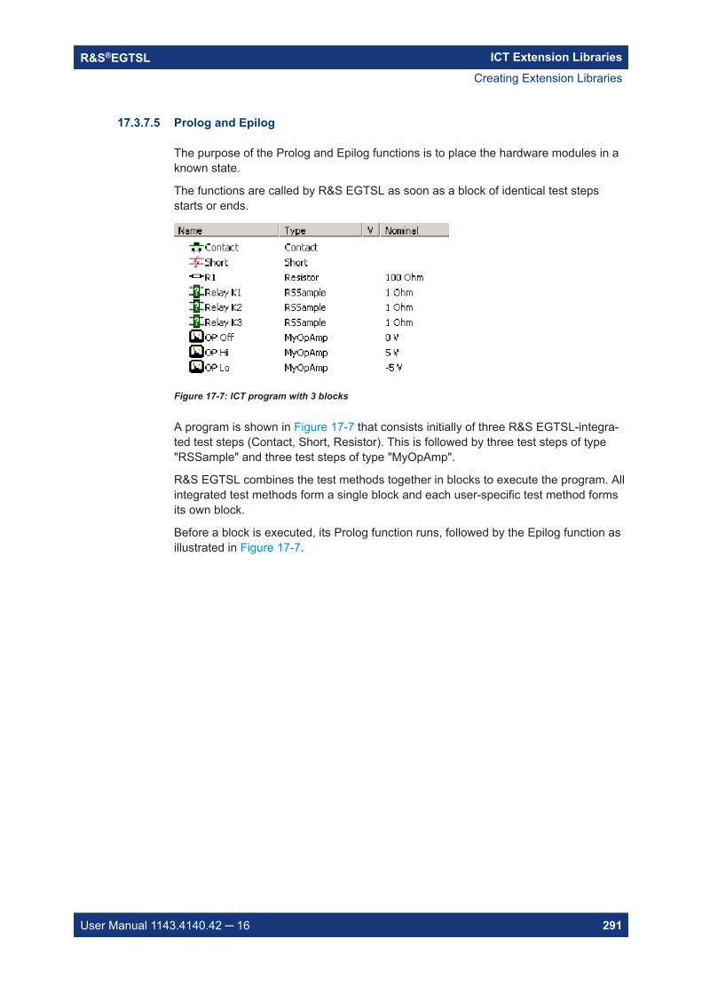
ICT Extension LibrariesR&S®EGTSL
291User Manual 1143.4140.42 16
17.3.7.5 Prolog and Epilog
The purpose of the Prolog and Epilog functions is to place the hardware modules in aknown state.
The functions are called by R&S EGTSL as soon as a block of identical test stepsstarts or ends.
Figure 17-7: ICT program with 3 blocks
A program is shown in Figure 17-7 that consists initially of three R&S EGTSL-integra-ted test steps (Contact, Short, Resistor). This is followed by three test steps of type"RSSample" and three test steps of type "MyOpAmp".
R&S EGTSL combines the test methods together in blocks to execute the program. Allintegrated test methods form a single block and each user-specific test method formsits own block.
Before a block is executed, its Prolog function runs, followed by the Epilog function asillustrated in Figure 17-7.
Creating Extension Libraries
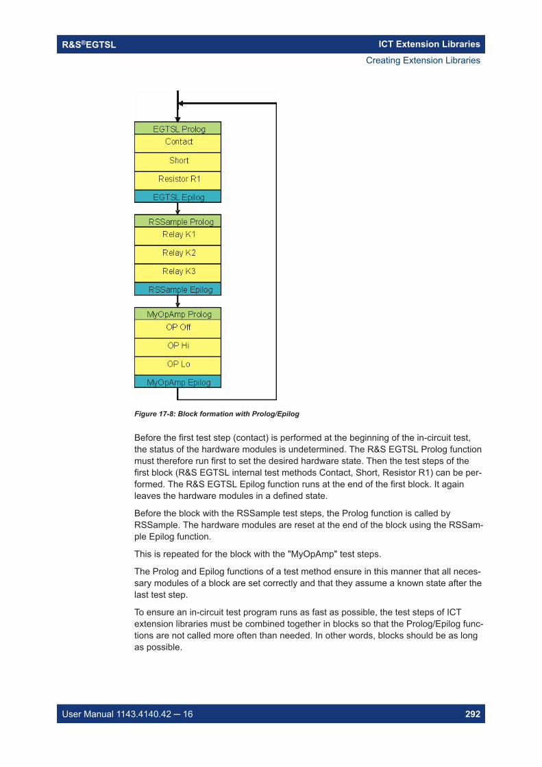
ICT Extension LibrariesR&S®EGTSL
292User Manual 1143.4140.42 16
Figure 17-8: Block formation with Prolog/Epilog
Before the first test step (contact) is performed at the beginning of the in-circuit test,the status of the hardware modules is undetermined. The R&S EGTSL Prolog functionmust therefore run first to set the desired hardware state. Then the test steps of thefirst block (R&S EGTSL internal test methods Contact, Short, Resistor R1) can be per-formed. The R&S EGTSL Epilog function runs at the end of the first block. It againleaves the hardware modules in a defined state.
Before the block with the RSSample test steps, the Prolog function is called byRSSample. The hardware modules are reset at the end of the block using the RSSam-ple Epilog function.
This is repeated for the block with the "MyOpAmp" test steps.
The Prolog and Epilog functions of a test method ensure in this manner that all neces-sary modules of a block are set correctly and that they assume a known state after thelast test step.
To ensure an in-circuit test program runs as fast as possible, the test steps of ICTextension libraries must be combined together in blocks so that the Prolog/Epilog func-tions are not called more often than needed. In other words, blocks should be as longas possible.
Creating Extension Libraries
ICT Extension LibrariesR&S®EGTSL
293User Manual 1143.4140.42 16
17.3.8 Advanced Topics
17.3.8.1 Debugging ICT Extension Libraries
Because they are Dynamic Link Libraries rather than executable files, ICT ExtensionLibraries cannot be started directly in the development environment. To be able todebug an ICT extension library, the following settings must therefore be made:
For LabWindows/CVI
In the project under menu item <Run><Select External Process…>, enter file…\GTSL\bin\EGTSLLoader.exe.
For Visual Studio
In the project settings under <Project><Settings><Debug> enter file…\GTSL\bin\EGTSLLoader.exe as "Executable for debug session".
Then the R&S EGTSL Loader can be started from the development environment.
When making an "UserDefinedDll" entry in the APPLICATION.INI file, make certainthe correct path is entered to the ICT extension library to be debugged.
17.3.8.2 Non-numeric Test Results
The measurement function of the ICT extension libraries returns a numeric value toR&S EGTSL as the result. It is also easy to imagine tests that do not return a numericresult. An example of this is the contact test in R&S EGTSL. In the event of an error,the contact test returns a list of pins that had no contact. In the case of "Pass", the listis empty.
In principle, however, the contact test also returns a numeric result like any other testthat is compared against an upper and lower limit. A look at the report makes thisclear:
** "Contact"[70] failed <----<<<2 [0 ... 0 ]P22, P27
The result of the contact test is a dimensionless number representing the number ofpins without contact. The upper and lower limit value is 0, i.e. as soon as a pin withouta contact is found, the test fails. In the case of "Fail", the contact test also returns a textcontaining the name of the pin that failed.
The same process can also be used in ICT extension libraries that return non-numericresults. The function extictTestMeasure returns the following results in this case:
testResult.value returns the "number of errors" testResult.unit is an empty string testResult.info contains the test result as text in the case of "Fail"
The following adjustments are also required:
Creating Extension Libraries
ICT Extension LibrariesR&S®EGTSL
294User Manual 1143.4140.42 16
0 is assigned to the two limits in extictTestConstruct extictTestGetResultDescription returns an empty string, so the "Nominal"
column in the display remains empty.
The text in testResult.info is only generated in the report by R&S EGTSL if thetest step was "Fail". If testResult.info contains an empty string in this case, thetext that is entered under "Step Properties, Test" is generated (see Figure 5-69).
17.3.8.3 Time Optimization
The goal of a good ICT extension library is to achieve the fastest measurement timepossible. R&S EGTSL already offers the necessary support for this. The followingitems contribute to optimal performance:
Separating the "compile" and "execution" of a test step Fast switching functions for R&S TS-PMB modules Block formation with Prolog/Epilog
The measurement should use as little time as possible for checking the setting valuesor converting strings into numeric values. Because of this, the "compile" and "measure"tasks are distributed over two different functions. The purpose of functionextictTestCompile is to convert the user’s entries and check them to make certainthey are valid. Therefore it only needs to be called if a new test step is being entered orif an existing test step is being changed. If extictTestCompile has run with noerrors, the values are correct and are available in the best format for further process-ing. Function extictTestMeasure does not require any additional tests. It forwardsthe checked values directly to the device driver.
The ICT Extension Support Library makes functions available to ensure rapid connec-tion of R&S TS-PMB switching modules. Connection tasks are split up betweenextictTestCompile and extictTestMeasure. During the "compile" task, pinnames are checked to ensure they are valid and the program searches for suitableswitching path. The connections are made in extictTestMeasure by the ICT Exten-sion Support Library without any time-consuming checks.
The distribution of tasks between the Prolog and the measurement function also con-tributes to the fastest possible execution time of measurements. Settings that are thesame for all test steps of an ICT extension library can already be performed in the Pro-log. Then they apply to all subsequent test steps. These settings also include above allconnecting stimulus and measurement devices to the analogue bus. The purpose ofthe Epilog function is then to undo that connection. The more test steps are included inthese blocks formed by Prolog/Epilog, the more time is saved.
17.3.8.4 Aspects of Compatibility
When developing an ICT extension library, there is no way to avoid making additions orcorrecting errors after ICT programs have already been written for the library. Whenthis happens, a few points must be observed so programs that already exist can still beused.
Creating Extension Libraries
ICT Extension LibrariesR&S®EGTSL
295User Manual 1143.4140.42 16
If changes are made to an ICT extension library, the version number should be incre-mented in variable extictInfoVersion. The version number serves as informationfor the user, but it is not stored in the ICT program.
Existing property names must not be deleted or renamed. The names are stored in theICT program and are assigned to the properties of an ICT extension library when theprogram is loaded. If it is not possible to make an assignment, an error message isgenerated and the ICT program cannot be loaded.
The order of entries in the property list is not critical. It can be changed without therebymaking any existing ICT programs incompatible.
New properties can be added later. If an ICT program is loaded that does not containthese properties yet, its default values are assigned to it as defined inextictTestConstruct.
When an ICT program is saved, all of its properties are saved with it. This makes itimpossible to load that program after that with an old version of the ICT extensionlibrary if a property has been added in the new version. ICT program are thus upwardlycompatible, but not downwardly.
17.3.8.5 Communication between ICT Extension Libraries
Test steps in R&S EGTSL are created according to the concept so that they stand bythemselves, i.e. independent of the preceding test steps of a measurement. If it shouldnevertheless become necessary to exchange information between the test steps of anICT extension library or even between different libraries, the following options are avail-able:
The most important functions of an ICT extension library have as a parameter a pointerto data structure ExtIctSetup. This data structure contains a pointer "userData" toan additional data structure that is the same for all test steps of an ICT as a extensionlibrary. Data elements to handle the exchange of information between test steps of thesame ICT extension library can be created in this structure.
The shared memory of the resource manager library is suitable for data exchangebetween different ICT extension libraries. These functions can be used to create globaldata structures with system-wide unique names that can be exchanged between libra-ries.
Creating Extension Libraries
Example 1R&S®EGTSL
296User Manual 1143.4140.42 16
AnnexA Example 1
All files for example 1 are saved in the folder ...\GTSL\EGTSL\Example.
A.1 Circuit for Example 1
Figure A-1: Circuit, example 1
A.2 BDL File for Example 1Example1.BDL
RESISTOR
NAME 'R1' VALUE 1.2 MOHM TOL+ 10% TOL- 10% I_LIM 100.0 MA PIN_1 'VCC' PIN_2 'TR1.B'
NAME 'R2' VALUE 330 KOHM TOL+ 10% TOL- 10% I_LIM 100.0 MA
BDL File for Example 1
Example 1R&S®EGTSL
297User Manual 1143.4140.42 16
PIN_1 'TR1.B' PIN_2 'GND'
NAME 'R3' VALUE 40 KOHM TOL+ 10% TOL- 10% I_LIM 100.0 MA PIN_1 'VCC' PIN_2 'TR1.C'
NAME 'R4' VALUE 10 KOHM TOL+ 10% TOL- 10% I_LIM 100.0 MA PIN_1 'TR1.E' PIN_2 'GND'
CAPACITOR
NAME 'C1' VALUE 360 NF TOL+ 10% TOL- 10% PIN_1 'INPUT' PIN_2 'TR1.B'
NAME 'C2' VALUE 100 NF TOL+ 10% TOL- 10% PIN_1 'TR1.C' PIN_2 'OUTPUT'
POL_CAP
NAME 'C3' VALUE 100 UF TOL+ 10% TOL- 10% PIN_A 'TR1.E' PIN_C 'GND'
TRANSISTOR
NAME 'TR1' NPN UBE 0.6 V TOL+ 30% TOL- 30% PIN_E 'TR1.E' PIN_B 'TR1.B' PIN_C 'TR1.C'
NODE
BDL File for Example 1
Example 1R&S®EGTSL
298User Manual 1143.4140.42 16
NAME 'TR1.E' DEV_NAME 'R4' PIN_1 DEV_NAME 'C3' PIN_A DEV_NAME 'TR1' PIN_E
NAME 'TR1.B' DEV_NAME 'R1' PIN_2 DEV_NAME 'R2' PIN_1 DEV_NAME 'C1' PIN_2 DEV_NAME 'TR1' PIN_B
NAME 'TR1.C' DEV_NAME 'R3' PIN_2 DEV_NAME 'C2' PIN_1 DEV_NAME 'TR1' PIN_C
NAME 'GND' DEV_NAME 'R2' PIN_2 DEV_NAME 'R4' PIN_2 DEV_NAME 'C3' PIN_C
NAME 'OUTPUT' DEV_NAME 'C2' PIN_2
NAME 'INPUT' DEV_NAME 'C1' PIN_1
NAME 'VCC' DEV_NAME 'R1' PIN_1 DEV_NAME 'R3' PIN_1
A.3 ICT Report Generated for Example 1Example1_Report.txt ATG REPORT==========Created: 2005-12-27 15:00:08ATG Version: ATG 02.10EGTSL Version: EGTSL 02.10Input:------Board Description: 'C:\Program Files\Rohde&Schwarz\GTSL\EGTSL\Example\Example1.BDL'Physical Layer: 'C:\Program Files\Rohde&Schwarz\GTSL\EGTSL\Example\Example_Physical.ini'Output:
ICT Report Generated for Example 1
Example 1R&S®EGTSL
299User Manual 1143.4140.42 16
-------ICT Program: 'C:\Program Files\Rohde&Schwarz\GTSL\EGTSL\Example\Example1.ict'Application Layer: 'C:\Program Files\Rohde&Schwarz\GTSL\EGTSL\Example\Example1_Application.ini'Report: 'C:\Program Files\Rohde&Schwarz\GTSL\EGTSL\Example\Example1_Report.txt'BDL Parser: 0 error(s) and 0 warning(s).BDL cross check: OK.>>> Message from TR1 <<<TS-PSU not configured in 'physical.ini', simple transistor test insertedTest coverage reportNumber Weight CoverageComponents 8Regular tests 7 1 87.5%Reduced tests 1 0.5 6.25%Short/Contact test only 0 0.1 0%Total test coverage 93.8%Wiring List info: Nodes mapped to a total number of 7 pin(s).
A.4 Application Layer Configuration File Generated forExample 1Example1_Application.ini[ResourceManager]; general trace settings (normally off)Trace = 0TraceFile = %GTSLROOT%\resmgr_trace.txt
;--------------------------------------------------------------------------------[LogicalNames]ICT = bench->ICT
;--------------------------------------------------------------------------------[bench->ICT]Description = ICT bench (Simulation)Simulation = 1Trace = 0ICTDevice1 = device->psamICTDevice2 = device->pictSwitchDevice1 = device->pmb1AppChannelTable = io_channel->ICTAppWiringTable = io_wiring->ICT
[io_channel->ICT]GND = pmb1!P1INPUT = pmb1!P2OUTPUT = pmb1!P3TR1.B = pmb1!P4TR1.C = pmb1!P5
Application Layer Configuration File Generated for Example 1
Example 1R&S®EGTSL
300User Manual 1143.4140.42 16
TR1.E = pmb1!P6VCC = pmb1!P7
;--------------------------------------------------------------------------------
[io_wiring->ICT]GND = F1 S15 X10A1INPUT = F1 S15 X10A2OUTPUT = F1 S15 X10A3TR1.B = F1 S15 X10A4TR1.C = F1 S15 X10A5TR1.E = F1 S15 X10A6VCC = F1 S15 X10A7
;--------------------------------------------------------------------------------
Application Layer Configuration File Generated for Example 1
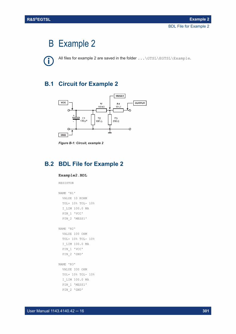
Example 2R&S®EGTSL
301User Manual 1143.4140.42 16
B Example 2All files for example 2 are saved in the folder ...\GTSL\EGTSL\Example.
B.1 Circuit for Example 2
Figure B-1: Circuit, example 2
B.2 BDL File for Example 2Example2.BDLRESISTOR
NAME 'R1' VALUE 10 KOHM TOL+ 10% TOL- 10% I_LIM 100.0 MA PIN_1 'VCC' PIN_2 'MESS1'
NAME 'R2' VALUE 100 OHM TOL+ 10% TOL- 10% I_LIM 100.0 MA PIN_1 'VCC' PIN_2 'GND'
NAME 'R3' VALUE 330 OHM TOL+ 10% TOL- 10% I_LIM 100.0 MA PIN_1 'MESS1' PIN_2 'GND'
BDL File for Example 2
Example 2R&S®EGTSL
302User Manual 1143.4140.42 16
NAME 'R4' VALUE 10 OHM TOL+ 10% TOL- 10% I_LIM 100.0 MA PIN_1 'MESS1' PIN_2 'OUT'
POL_CAP
NAME 'C1' VALUE 100 UF TOL+ 10% TOL- 10% PIN_A 'VCC' PIN_C 'GND'
NODE
NAME 'GND' DEV_NAME 'C1' PIN_C DEV_NAME 'R2' PIN_2 DEV_NAME 'R3' PIN_2
NAME 'OUT' DEV_NAME 'R4' PIN_2
NAME 'VCC' DEV_NAME 'C1' PIN_A DEV_NAME 'R1' PIN_1 DEV_NAME 'R2' PIN_1
NAME 'MESS1' DEV_NAME 'R1' PIN_2 DEV_NAME 'R4' PIN_1 DEV_NAME 'R3' PIN_1
B.3 ICT Report Generated for Example 2Example2_Report.txt
ATG REPORT==========
Created: 2005-12-27 15:02:19 ATG Version: ATG 02.10 EGTSL Version: EGTSL 02.10
ICT Report Generated for Example 2
Example 2R&S®EGTSL
303User Manual 1143.4140.42 16
Input:------Board Description: 'C:\Program Files\Rohde&Schwarz\GTSL\EGTSL\Example\Example2.BDL'Physical Layer: 'C:\Program Files\Rohde&Schwarz\GTSL\EGTSL\Example\Example_Physical.ini'
Output:-------ICT Program: 'C:\Program Files\Rohde&Schwarz\GTSL\EGTSL\Example\Example2.ict'Application Layer: 'C:\Program Files\Rohde&Schwarz\GTSL\EGTSL\Example\Example2_Application.ini'Report: 'C:\Program Files\Rohde&Schwarz\GTSL\EGTSL\Example\Example2_Report.txt'
BDL Parser: 0 error(s) and 0 warning(s).
BDL cross check: OK.
>>> Message from R1 6-Wire Test Proposal <<<Total error for 3-wire mode: 23.351% 6-wire mode: 3.1255%
>>> Message from R1 <<<Test only possible by exceeding the error limitsGuarding error limiting test quality
>>> Message from R4 4-Wire Test Proposal <<<Total error for 2-wire mode: 21.576% 4-wire mode: 1 %
>>> Message from R4 <<<Test only possible by exceeding the error limitsTest limits include system residuals of 2.124 Ohms
Test coverage report Number Weight CoverageComponents 5Regular tests 5 1 100%Reduced tests 0 0.5 0%Short/Contact test only 0 0.1 0%Total test coverage 100%
Wiring List info: Nodes mapped to a total number of 8 pin(s).
B.4 Application Layer Configuration File Generated forExample 2Example2_Application.ini
Application Layer Configuration File Generated for Example 2
Example 2R&S®EGTSL
304User Manual 1143.4140.42 16
[ResourceManager]; general trace settings (normally off)Trace = 0TraceFile = %GTSLROOT%\resmgr_trace.txt
;--------------------------------------------------------------------------------[LogicalNames]ICT = bench->ICT
;--------------------------------------------------------------------------------[bench->ICT]Description = ICT bench (Simulation)Simulation = 1Trace = 0ICTDevice1 = device->psamICTDevice2 = device->pictSwitchDevice1 = device->pmb1AppChannelTable = io_channel->ICTAppWiringTable = io_wiring->ICT
[io_channel->ICT]GND = pmb1!P1MESS1 = pmb1!P2OUT = pmb1!P3VCC = pmb1!P4
; nodes used for test proposals, which may be deleted, if the proposals are discarded; -----------------------------------------------------------------------------------GND.Sense = pmb1!P6MESS1.Sense = pmb1!P5OUT.Sense = pmb1!P7VCC.Sense = pmb1!P9
;--------------------------------------------------------------------------------
[io_wiring->ICT]GND = F1 S15 X10A1MESS1 = F1 S15 X10A2OUT = F1 S15 X10A3VCC = F1 S15 X10A4
; nodes used for test proposals, which may be deleted, if the proposals are discarded; -----------------------------------------------------------------------------------GND.Sense = F1 S15 X10A6MESS1.Sense = F1 S15 X10A5OUT.Sense = F1 S15 X10A7VCC.Sense = F1 S15 X10A9
;--------------------------------------------------------------------------------
Application Layer Configuration File Generated for Example 2
Example 2R&S®EGTSL
305User Manual 1143.4140.42 16
Application Layer Configuration File Generated for Example 2