Embed Size (px)
Citation preview
Phys. Status Solidi B 252, No. 3, 451–468 (2015) / DOI 10.1002/pssb.201451466
Feature Article
p s sbasic solid state physics
b
statu
s
soli
di
www.pss-b.comph
ysi
ca
Scanning probe microscopy andspectroscopy of graphene on metalsYuriy Dedkov*,1, Elena Voloshina2, and Mikhail Fonin3
1 SPECS Surface Nano Analysis GmbH, Voltastraße 5, 13355 Berlin, Germany2 Institut fur Chemie, Humboldt-Universitat zu Berlin, 10099 Berlin, Germany3 Fachbereich Physik, Universitat Konstanz, 78457 Konstanz, Germany
Received 2 September 2014, revised 1 December 2014, accepted 2 December 2014Published online 28 January 2015
Keywords atomic force microscopy, density functional theory, graphene, metal surfaces, scanning tunneling microscopy
∗ Corresponding author: e-mail [email protected], Phone: +49 30 467824 9339, Fax: +49 30 4642 083
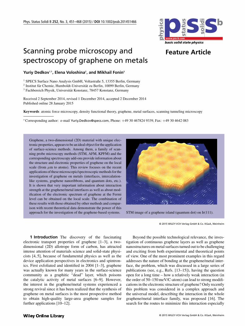
Graphene, a two-dimensional (2D) material with unique elec-tronic properties, appears to be an ideal object for the applicationof surface-science methods. Among them, a family of scan-ning probe microscopy methods (STM, AFM, KPFM) and thecorresponding spectroscopy add-ons provide information aboutthe structure and electronic properties of graphene on the localscale (from μm to atoms). This review focuses on the recentapplications of these microscopic/spectroscopic methods for theinvestigation of graphene on metals (interfaces, intercalation-like systems, graphene nanoribbons, and quantum dots, etc.).It is shown that very important information about interactionstrength at the graphene/metal interfaces as well as about mod-ification of the electronic spectrum of graphene at the Fermilevel can be obtained on the local scale. The combination ofthese results with those obtained by other methods and compar-ison with recent theoretical data demonstrate the power of thisapproach for the investigation of the graphene-based systems. STM image of a graphene island (quantum dot) on Ir(111).
© 2015 WILEY-VCH Verlag GmbH & Co. KGaA, Weinheim
1 Introduction The discovery of the fascinatingelectronic transport properties of graphene [1–3], a two-dimensional (2D) allotrope form of carbon, has attractedintense attention of materials science and solid-state physi-cists [4, 5], because of fundamental physics as well as thedevice application perspectives in electronics and spintron-ics. First exfoliated and identified in 2004 [1–3], graphenewas actually known for many years in the surface-sciencecommunity as a graphitic “dead” layer, which poisonsthe catalytic activity of metal surfaces [6–9]. However,the interest in the graphene/metal systems experienced astrong revival since it has been realized that the synthesis ofgraphene on metal surfaces is the most prospective methodto obtain high-quality large-area graphene samples forfurther applications [10–12].
Beyond the possible technological relevance, the inves-tigation of continuous graphene layers as well as graphenenanostructures on metal surfaces turned out to be challengingand exciting from both experimental and theoretical pointsof view. One of the most prominent examples in this regardaddresses the nature of bonding at the graphene/metal inter-face, the problem, which was discussed in a large series ofpublications (see, e.g., Refs. [13–15]), having the questionopen for a long time – how a relatively weak interaction (inthe order of 50–150 meV/C-atom) can lead to strong modifi-cations in the electronic structure of graphene? Only recentlythis problem was considered in a complex approach andthe universal model, describing the interaction in the wholegraphene/metal interface family, was proposed [16]. Thesearch for the routes to minimize this interaction especially
© 2015 WILEY-VCH Verlag GmbH & Co. KGaA, Weinheim
ph
ysic
a ssp stat
us
solid
i b
452 Yu. Dedkov et al.: Scanning probe microscopy of graphene on metals
aims at the preparation of the graphene nanoribbons [17–22]or epitaxial nanosized islands with different edge termina-tions [23–26], where the low-dimensional effects such asa bandgap width quantization and the edge-induced mag-netism are expected. Due to the truly 2D character of thecrystallographic and the electronic structure of graphene andthe localization of the interesting phenomena at the smallscale, the scanning probe microscopy (SPM) methods, i.e.,scanning tunneling microscopy (STM) and atomic forcemicroscopy (AFM) in combination with the correspond-ing spectroscopy techniques (STS and AFS), can provideimportant information about the properties of graphenenanostructures at the nanometer- and atomic-scale.
Yuriy Dedkov obtained his PhD inPhysics in 2004 (RWTH Aachen, Ger-many) and received his habilitation in2013 (TU Dresden, Germany). He was aresearch associate at TU Dresden and atthe Fritz Haber Institute. Since 2011 he isan application lab staff scientist at SPECSSurface Nano Analysis GmbH. He has abroad experience in many surface-sciencetechniques with specialization in spin-and angle-resolved photoelectron spec-
troscopy and scanning probe microscopy. In 2014 he was awardedthe Gaede Prize of the German Vacuum Society for a series ofworks on graphene–metal interfaces.
Elena Voloshina received her PhD inChemistry in 2001 (Rostov State Uni-versity, Russia). She was a postdoctoralresearch associate at RWTH Aachen, atthe Max Planck Institute for the physicsof complex systems in Dresden and at theFreie Universität Berlin, Germany. Since2013 she has been leading a researchsubgroup at the Humboldt-Universität zuBerlin (within the group “Solid-StateQuantum Chemistry/Catalysis”, led by
Prof. J. Sauer). She has a broad experience in the developmentand application of theoretical techniques for investigation of theelectronic structure of a wide range of systems.
Mikhail Fonin graduated in 1999 inChemistry and Materials Science fromthe Moscow State University, Russia andreceived his PhD in Physics in 2004 fromRWTH Aachen, Germany. He is a pro-fessor and deputy chair at the Universityof Konstanz, Germany. He is co-authorof more than 70 papers in internationalpeer-reviewed journals and several bookchapters. His research focuses on theinvestigation of electronic and magnetic
properties of novel materials, including half-metallic ferromag-nets, magnetic shape memory alloys, single molecule magnets andgraphene/metal interfaces.
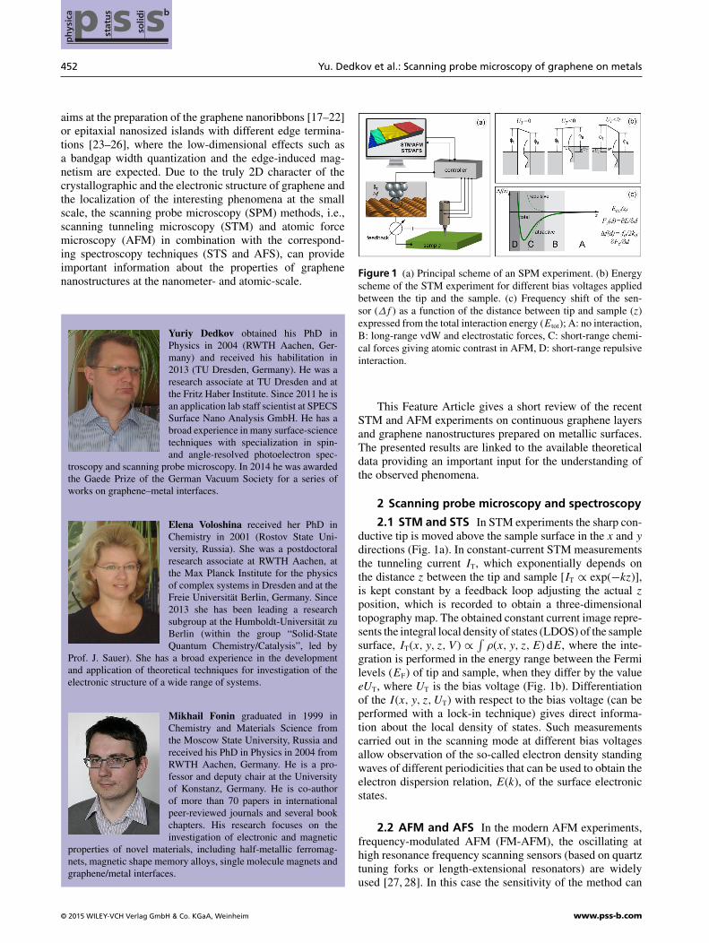
Figure 1 (a) Principal scheme of an SPM experiment. (b) Energyscheme of the STM experiment for different bias voltages appliedbetween the tip and the sample. (c) Frequency shift of the sen-sor (Δf ) as a function of the distance between tip and sample (z)expressed from the total interaction energy (Etot); A: no interaction,B: long-range vdW and electrostatic forces, C: short-range chemi-cal forces giving atomic contrast in AFM, D: short-range repulsiveinteraction.
This Feature Article gives a short review of the recentSTM and AFM experiments on continuous graphene layersand graphene nanostructures prepared on metallic surfaces.The presented results are linked to the available theoreticaldata providing an important input for the understanding ofthe observed phenomena.
2 Scanning probe microscopy and spectroscopy
2.1 STM and STS In STM experiments the sharp con-ductive tip is moved above the sample surface in the x and y
directions (Fig. 1a). In constant-current STM measurementsthe tunneling current IT, which exponentially depends onthe distance z between the tip and sample [IT ∝ exp(−kz)],is kept constant by a feedback loop adjusting the actual z
position, which is recorded to obtain a three-dimensionaltopography map. The obtained constant current image repre-sents the integral local density of states (LDOS) of the samplesurface, IT(x, y, z, V ) ∝ ∫
ρ(x, y, z, E) dE, where the inte-gration is performed in the energy range between the Fermilevels (EF) of tip and sample, when they differ by the valueeUT, where UT is the bias voltage (Fig. 1b). Differentiationof the I(x, y, z, UT) with respect to the bias voltage (can beperformed with a lock-in technique) gives direct informa-tion about the local density of states. Such measurementscarried out in the scanning mode at different bias voltagesallow observation of the so-called electron density standingwaves of different periodicities that can be used to obtain theelectron dispersion relation, E(k), of the surface electronicstates.
2.2 AFM and AFS In the modern AFM experiments,frequency-modulated AFM (FM-AFM), the oscillating athigh resonance frequency scanning sensors (based on quartztuning forks or length-extensional resonators) are widelyused [27, 28]. In this case the sensitivity of the method can
© 2015 WILEY-VCH Verlag GmbH & Co. KGaA, Weinheim www.pss-b.com
Feature
Article
Phys. Status Solidi B 252, No. 3 (2015) 453
be increased dramatically. Here, a tiny conductive tip con-nected to the resonator approaches the sample surface andthe interaction between them leads to the change of the res-onance frequency by value Δf : Fz(d) = ∂E/∂d, Δf (d) =−f0/2k0 · ∂Fz(d)/∂d, where E(d) and Fz(d) are the inter-action energy and the vertical force between a tip and thesample, respectively, f0 and k0 are the resonance frequencyand the spring constant of the sensor (Fig. 1c). The detectedfrequency shift, Δf , is used in the feedback loop and the cor-responding “topography” map can be obtained in such AFMmeasurements. The resulting interaction between the sampleand the tip is the sum of the long-range electrostatic (Fel) andvan der Waals (FvdW) contributions and the short-range chem-ical (Fchem) interaction. Similar to the STM experiments,Fchem
at short distances between tip and sample produces the atomiccontrast in AFM experiments and as was shown in a seriesof the recent works the observed imaging contrast dependson several factors, e.g., distance and the setting point for themeasurements (Fig. 1c). The locally measured Fz(d) curvescan be used for the calculation of the tip–sample interactionforces via methods developed by Giessibl [29] or Sader andJarvis [30].
As an add-on to AFM, the method of the Kelvin-probeforce microscopy (KPFM) allowing the local distributionof the electrostatic potential to be obtained was devel-oped [31, 32]. In this method the topographic measurementsare performed in AFM mode and at the same time the DC(UDC) and AC voltages are applied between the tip and sam-ple. Here, the lock-in technique is used and the first harmonicin the output signal, which is proportional to the differ-ence between UDC and the local contact potential difference(ULCPD) between conductive tip and sample, is nullified allow-ing extraction of the ULCPD(x, y) map of the sample surface.
2.3 3D AFM/STM The 3D STM/AFM measurementscan be performed in two ways. In the first case the dis-tance between the tip and sample is fixed with the feedbackloop completely switched off and the respective I(x, y) andΔf (x, y) maps are simultaneously collected. If the distancebetween the tip and sample is varied with regular steps,then the dense 3D data sets can be collected, I(x, y, z) andΔf (x, y, z). In the second approach the single I(z) and Δf (z)curves are measured on the (x, y)-grid and then they are com-bined in the 3D sets. Both measurement schemes are timeconsuming and here special attention should be paid to thepossible creep and thermal drifts of the piezodrive and theAFM sensor as well as to the postcorrection of the obtaineddata. Different schemes of 3D STM/AFM measurements andtheir (dis)advantages are discussed in Refs. [33–36].
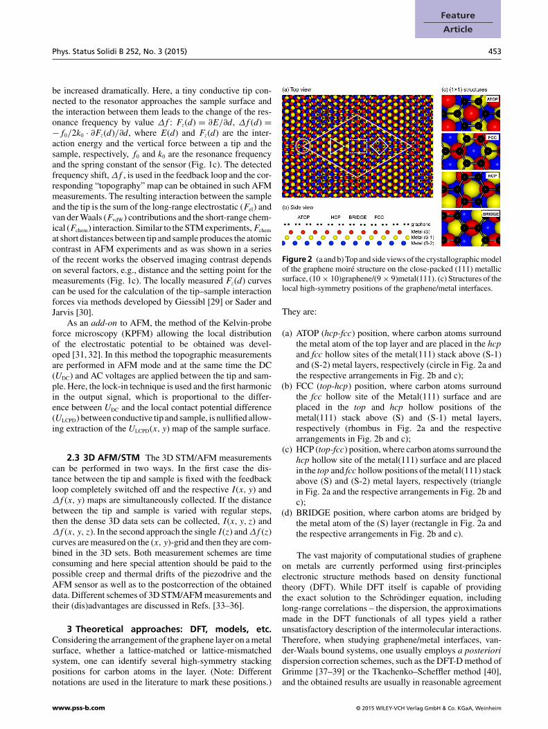
3 Theoretical approaches: DFT, models, etc.Considering the arrangement of the graphene layer on a metalsurface, whether a lattice-matched or lattice-mismatchedsystem, one can identify several high-symmetry stackingpositions for carbon atoms in the layer. (Note: Differentnotations are used in the literature to mark these positions.)
Figure 2 (a and b) Top and side views of the crystallographic modelof the graphene moire structure on the close-packed (111) metallicsurface, (10 × 10)graphene/(9 × 9)metal(111). (c) Structures of thelocal high-symmetry positions of the graphene/metal interfaces.
They are:
(a) ATOP (hcp-fcc) position, where carbon atoms surroundthe metal atom of the top layer and are placed in the hcpand fcc hollow sites of the metal(111) stack above (S-1)and (S-2) metal layers, respectively (circle in Fig. 2a andthe respective arrangements in Fig. 2b and c);
(b) FCC (top-hcp) position, where carbon atoms surroundthe fcc hollow site of the Metal(111) surface and areplaced in the top and hcp hollow positions of themetal(111) stack above (S) and (S-1) metal layers,respectively (rhombus in Fig. 2a and the respectivearrangements in Fig. 2b and c);
(c) HCP (top-fcc) position, where carbon atoms surround thehcp hollow site of the metal(111) surface and are placedin the top and fcc hollow positions of the metal(111) stackabove (S) and (S-2) metal layers, respectively (trianglein Fig. 2a and the respective arrangements in Fig. 2b andc);
(d) BRIDGE position, where carbon atoms are bridged bythe metal atom of the (S) layer (rectangle in Fig. 2a andthe respective arrangements in Fig. 2b and c).
The vast majority of computational studies of grapheneon metals are currently performed using first-principleselectronic structure methods based on density functionaltheory (DFT). While DFT itself is capable of providingthe exact solution to the Schrodinger equation, includinglong-range correlations – the dispersion, the approximationsmade in the DFT functionals of all types yield a ratherunsatisfactory description of the intermolecular interactions.Therefore, when studying graphene/metal interfaces, van-der-Waals bound systems, one usually employs a posterioridispersion correction schemes, such as the DFT-D method ofGrimme [37–39] or the Tkachenko–Scheffler method [40],and the obtained results are usually in reasonable agreement
www.pss-b.com © 2015 WILEY-VCH Verlag GmbH & Co. KGaA, Weinheim
ph
ysic
a ssp stat
us
solid
i b
454 Yu. Dedkov et al.: Scanning probe microscopy of graphene on metals
with experiment. Unlike these post-DFT corrections, ana priori way consists in utilization of nonlocal correlationfunctionals that approximately accounts for dispersioninteractions, the so-called vdW-DF [41, 42]. Although thelatter approach is expected to give more accurate results, itis shown to predict irrationally weak binding of grapheneon metals surfaces for all the studied cases [43].
A very important analysis of the surface atomic and elec-tronic structure is the simulation of STM images. Amongearly theoretical models to describe atomically resolved STMimages the Tersoff and Hamann approach [44] has foundparticular attention since it relates the observed contrastto a conceptually simple quantity of the surface, namelythe local density of states of valence or conduction elec-trons. While it provides a simple interpretation of the STMresults, this model ignores the influence of the tunnelingbarrier, the structural and electronic properties of the tipand its interaction with the sample surface. However, moreexact theoretical formulations of the STM problem (for areview, see Ref. [45]) were found to be much more timeconsuming. At the same time, in all studied graphene/metalcases the Tersoff–Hamann approach was found to be ratherreliable.
While STM can achieve atomic resolution, it probes thesurface electronic structure of the sample in a mode that doesnot provide a direct interpretation of the atomic structure.First-principles simulations of NC-AFM can enhance theinterpretation of experimental measurements; however, suchsimulations remain a challenge because they involve calcula-tions of the sample together with an atomic model of the AFMtip (see, e.g., Ref. [46]). Hence, the simulation can be verylaborious. An efficient scheme to simulate NC-AFM imagesusing inputs from first-principles calculations of the sampleonly without explicit modeling of the AFM tip was proposedby Chan et al. [47]. Both of these approaches were foundto work reasonably well for the considered graphene/metalsystems.
4 Graphene on metals: SPM/DFT of lattice-matched and lattice-mismatched systems The his-tory of the surface-science studies of graphene on metals canbe traced back to the middle of the 1960s. However, the firstSTM experiments on graphitic layers on metal surfaces wereperformed at the beginning of the 1990s when graphitic lay-ers on Ni(111) [48] and Pt(111) [9] were studied. It is worthnoting that already at that time the graphene moire structuresof different periodicities were identified on Pt(111).
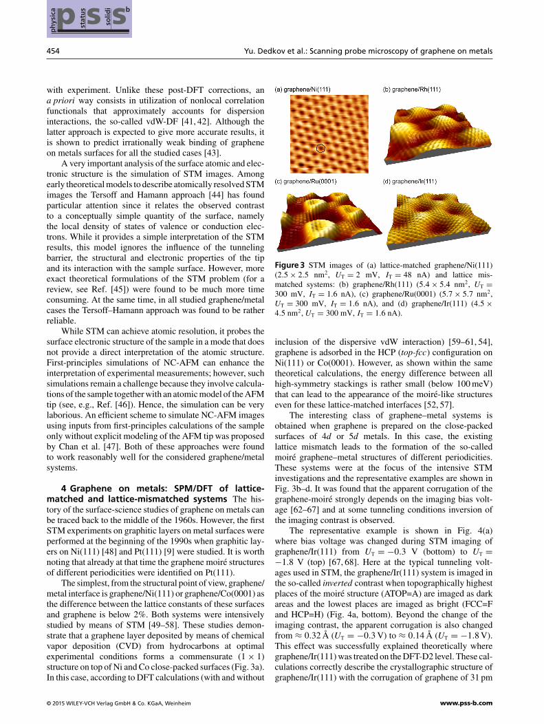
The simplest, from the structural point of view, graphene/metal interface is graphene/Ni(111) or graphene/Co(0001) asthe difference between the lattice constants of these surfacesand graphene is below 2%. Both systems were intensivelystudied by means of STM [49–58]. These studies demon-strate that a graphene layer deposited by means of chemicalvapor deposition (CVD) from hydrocarbons at optimalexperimental conditions forms a commensurate (1 × 1)structure on top of Ni and Co close-packed surfaces (Fig. 3a).In this case, according to DFT calculations (with and without
Figure 3 STM images of (a) lattice-matched graphene/Ni(111)(2.5 × 2.5 nm2, UT = 2 mV, IT = 48 nA) and lattice mis-matched systems: (b) graphene/Rh(111) (5.4 × 5.4 nm2, UT =300 mV, IT = 1.6 nA), (c) graphene/Ru(0001) (5.7 × 5.7 nm2,UT = 300 mV, IT = 1.6 nA), and (d) graphene/Ir(111) (4.5 ×4.5 nm2, UT = 300 mV, IT = 1.6 nA).
inclusion of the dispersive vdW interaction) [59–61, 54],graphene is adsorbed in the HCP (top-fcc) configuration onNi(111) or Co(0001). However, as shown within the sametheoretical calculations, the energy difference between allhigh-symmetry stackings is rather small (below 100 meV)that can lead to the appearance of the moire-like structureseven for these lattice-matched interfaces [52, 57].
The interesting class of graphene–metal systems isobtained when graphene is prepared on the close-packedsurfaces of 4d or 5d metals. In this case, the existinglattice mismatch leads to the formation of the so-calledmoire graphene–metal structures of different periodicities.These systems were at the focus of the intensive STMinvestigations and the representative examples are shown inFig. 3b–d. It was found that the apparent corrugation of thegraphene-moire strongly depends on the imaging bias volt-age [62–67] and at some tunneling conditions inversion ofthe imaging contrast is observed.
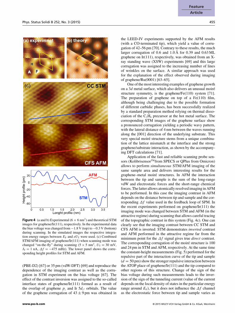
The representative example is shown in Fig. 4(a)where bias voltage was changed during STM imaging ofgraphene/Ir(111) from UT = −0.3 V (bottom) to UT =−1.8 V (top) [67, 68]. Here at the typical tunneling volt-ages used in STM, the graphene/Ir(111) system is imaged inthe so-called inverted contrast when topographically highestplaces of the moire structure (ATOP=A) are imaged as darkareas and the lowest places are imaged as bright (FCC=Fand HCP=H) (Fig. 4a, bottom). Beyond the change of theimaging contrast, the apparent corrugation is also changedfrom ≈ 0.32 A (UT = −0.3 V) to ≈ 0.14 A (UT = −1.8 V).This effect was successfully explained theoretically wheregraphene/Ir(111) was treated on the DFT-D2 level. These cal-culations correctly describe the crystallographic structure ofgraphene/Ir(111) with the corrugation of graphene of 31 pm
© 2015 WILEY-VCH Verlag GmbH & Co. KGaA, Weinheim www.pss-b.com
Feature
Article
Phys. Status Solidi B 252, No. 3 (2015) 455
Figure 4 (a and b) Experimental (6 × 6 nm2) and theoretical STMimages for graphene/Ir(111), respectively. In the experimental datathe bias voltage was changed from −1.8 V (top) to −0.3 V (bottom)during scanning. In the simulated images the respective integra-tion energy ranges between EF and eUT were used. (c) CombinedSTM/AFM imaging of graphene/Ir(111) when scanning mode waschanged “on-the-fly” during scanning (5 × 5 nm2, UT = 30 mV,IT = 1 nA, Δf = −475 mHz). The lower panel shows the corre-sponding height profiles for STM and AFM.
(PBE-D2) [67] or 35 pm (vdW-DFT) [69] and reproduce thedependence of the imaging contrast as well as the corru-gation in STM experiment on the bias voltage [67]. Theeffect of the contrast inversion was assigned to the so-calledinterface states of graphene/Ir(111) formed as a result ofthe overlap of graphene pz and Ir 5dz2 orbitals. The valueof the graphene corrugation of 43 ± 9 pm was obtained in
the LEED-IV experiments supported by the AFM results(with a CO-terminated tip), which yield a value of corru-gation of 42–56 pm [70]. Contrary to these results, the muchlarger corrugation of 0.6 and 1.0 A for 0.39 and 0.63 MLgraphene on Ir(111), respectively, was obtained from an X-ray standing wave (XSW) experiments [69] and this largecorrugation was assigned to the increasing number of linesof wrinkles on the surface. A similar approach was usedfor the explanation of the effect observed during imagingof graphene/Ru(0001) [63–65].
One of the most interesting examples of graphene growthon a 3d metal surface, which also delivers an unusual moirestructure symmetry, is the graphene/Fe(110) system [71].The preparation of graphene on top of a Fe(110) film,although being challenging due to the possible formationof different carbidic phases, has been successfully realizedby a standard preparation method relying on thermal disso-ciation of the C3H6 precursor at the hot metal surface. Thecorresponding STM images of the graphene surface showa pronounced corrugation yielding a periodic wavy pattern,with the lateral distance of 4 nm between the waves runningalong the [001] direction of the underlying substrate. Thisvery special moire structure stems from a unique combina-tion of the lattice mismatch at the interface and the stronggraphene/substrate interaction, as shown by the accompany-ing DFT calculations [71].
Application of the fast and reliable scanning probe sen-sors (KolibrisensorTMfrom SPECS or QPlus from Omicron)allows to perform simultaneous STM/AFM imaging of thesame sample area and delivers interesting results for thegraphene–metal moire structures. In AFM the interactionbetween the tip and sample is the sum of the long-rangevdW and electrostatic forces and the short-range chemicalforces. The latter allows atomically resolved imaging in AFMto be performed. In this case the imaging contrast in AFMdepends on the distance between tip and sample and the cor-responding Δf value used in the feedback loop of SPM. Inthe recent experiments performed on graphene/Ir(111) theimaging mode was changed between STM and AFM (in theattractive regime) during scanning that allows careful tracingof the topographic contrast in this system (Fig. 4c). One canclearly see that the imaging contrast between CC STM andCFS AFM is inverted: STM demonstrates inverted contrastand AFM performed in the attractive regime far from theminimum point for the Δf signal gives true direct contrast.The corresponding corrugation of the moire structure is 100and 24 pm in STM and AFM, respectively. At the same timethe constant-height measurements (Fig. 5) performed for therepulsive part of the interaction curve of the tip and sample(d = 50 pm) show the stronger repulsive interaction betweenthe ATOP place of graphene/Ir(111) and the tip compared toother regions of this structure. Change of the sign of thebias voltage during such measurements leads to the inver-sion of the sign of the tunneling current (value of the currentdepends on the local density of states in the particular energyrange around EF), but it does not influence the Δf channelas the electrostatic force between tip and sample varies as
www.pss-b.com © 2015 WILEY-VCH Verlag GmbH & Co. KGaA, Weinheim
ph
ysic
a ssp stat
us
solid
i b
456 Yu. Dedkov et al.: Scanning probe microscopy of graphene on metals
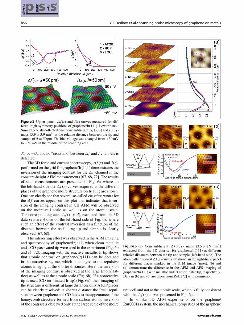
Figure 5 Upper panel: Δf (z) and I(z) curves measured for dif-ferent high-symmetry positions of graphene/Ir(111). Lower panel:Simultaneously collected pure constant-height Δf (x, y) and I(x, y)maps (3.9 × 3.9 nm2) at the relative distance between the tip andsample of d = 50 pm. The bias voltage was changed from +50 mVto −50 mV in the middle of the scanning area.
Fel ∝ −U2T and no “crosstalk” between Δf and I channels is
detected.The 3D force and current spectroscopy, Δf (z) and I(z),
performed on the grid for graphene/Ir(111) demonstrates theinversion of the imaging contrast for the Δf channel in theconstant-height AFM measurements [67, 68, 72]. The resultsof such measurements are presented in Fig. 6a where onthe left-hand side the Δf (z) curves acquired at the differentplaces of the graphene moire structure on Ir(111) are shown.One can clearly see that several so-called crossing points forthe Δf curves appear on this plot that indicates that inver-sion of the imaging contrast in CH AFM will be observedon the moire-cell scale as well as on the atomic scale.The corresponding cuts, Δf (x, y, d), extracted from the 3Ddata sets are shown on the left-hand side of Fig. 6a, wheresuch an effect of the contrast inversion as a function of thedistance between the oscillating tip and sample is clearlyobserved [67, 68].
The interesting effect was observed in the AFM imagingand spectroscopy of graphene/Ir(111) when clean metallicand a CO-passivated tip were used in the experiment (Fig. 6band c) [72]. Imaging with the reactive metallic Ir tip showsthat atomic contrast on graphene/Ir(111) can be obtainedin the attractive regime, which is changed to the repulsiveatomic imaging at the shorter distances. Here, the inversionof the imaging contrast is observed at the large (moire lat-tice) as well as at the atomic scale (Fig. 6b). If a nonreactivetip is used (CO-terminated Ir tip) (Fig. 6c), then imaging ofthe structure is different: at large distances only ATOP placescan be clearly resolved; at shorter distance the Pauli repul-sion between graphene and CO leads to the appearance of thehoneycomb structure formed from carbon atoms; inversionof the contrast is observed only at the large scale of the moire
Figure 6 (a) Constant-height Δf (x, y) maps (3.5 × 2.9 nm2)extracted from the 3D data set for graphene/Ir(111) at differentrelative distances between the tip and sample (left-hand side). Theatomically resolved Δf (z) curves are shown in the right-hand panelfor different places marked in the STM image (inset). (b) and(c) demonstrate the difference in the AFM and AFS imaging ofgraphene/Ir(111) with metallic and CO-terminated tip, respectively.Data in (b) and (c) are taken from Ref. [72] with permission.
unit cell and not at the atomic scale, which is fully consistentwith the Δf (z) curves presented in Fig. 6c.
In similar 3D AFM experiments on the graphene/Ru(0001) system, the mechanical properties of the graphene
© 2015 WILEY-VCH Verlag GmbH & Co. KGaA, Weinheim www.pss-b.com
Feature
Article
Phys. Status Solidi B 252, No. 3 (2015) 457
nanodomes, which are of the height of 1.1 A were investi-gated [73]. The CFS AFM images of this system demonstratethe vertical reversible deformation of the hill places of themoire structure. The systematic measurements and com-parison with theory allow estimation of the stiffness ofthe graphene nanomembrane to the value of kdome = 43.6 ±0.5 N/M with the resonance frequency of ∼ 2 THz and itwas suggested that such nanodomes can be used as nano-electromechanical resonators.
Graphene moire structures on the lattice-mismatchedmetal surfaces demonstrate also the local variation of thechemical potential. For example, on the strongly corrugatedgraphene/Rh(111) and graphene/Ru(0001) surfaces the peri-odic modulation of the local work function is 0.22 eV [74]and 0.52 eV [75], respectively, as obtained in the spectro-scopic measurements of the image potential states with STMabove different places of the graphene moire. These resultswere confirmed by DFT calculations for the strongly inter-acting graphene/Ru(0001) system with large corrugation [76]and explained by the different local interaction strength fortopographically high ATOP and low FCC and HCP posi-tions. For the weakly interacting graphene on Ir(111), whichhas small corrugations of ≈ 0.3 A with the mean distancebetween graphene and metal surface of 3.3 A, the variation ofthe local work function in the graphene moire is ≈ 100 meV,as measured from I(z) spectroscopy data in STM [77]. Atthe same time the KPFM measurements give a lower valueof 35 meV [68] that can be connected with the underestima-tion of this value in KPFM measurements on the nm-scale.DFT calculations for this system yield a value of 56 meV.
5 Properties of graphene–metal-based systems:Adsorption and intercalation Adsorption of grapheneon the metal surfaces modifies the electronic spectrum ofgraphene-related valence-band states around EF. There areseveral ways to tailor the properties of the graphene/metalinterface with the aim to control the electronic and magneticproperties of a graphene layer.
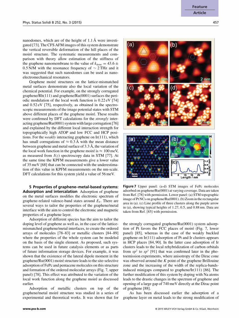
Adsorption of different species has the aim to tailor thedoping level of graphene as well as, in the case of the lattice-mismatched graphene/metal interfaces, to create the orderedarrays of molecules [78–83] or metallic clusters [84–89]where the properties of the whole system can be modeledon the basis of the single element. As proposed, such sys-tems can be used in future catalysis elements or as partsof future information storage devices. For example, it wasshown that the existence of the lateral dipole moment in thegraphene/Ru(0001) moire structure leads to the site-selectiveadsorption of FePc and pentacene molecules on this structureand formation of the ordered molecular arrays (Fig. 7, upperpanel) [78]. This effect was attributed to the variation of thelocal work function along the graphene moire as discussedearlier.
Adsorption of metallic clusters on top of thegraphene/metal moire structure was studied in a series ofexperimental and theoretical works. It was shown that for
Figure 7 Upper panel: (a-d) STM images of FePc moleculesadsorbed on graphene/Ru(0001) at varying coverage. Data are takenfrom Ref. [78] with permission. Lower panel: (a) STM topographicimage of Pt NCs on graphene/Ru(0001). (b) Zoom in the rectangulararea in (a). (c) Line profile of three clusters along the purple arrowin (a), showing typical heights of 1.27, 0.5, and 0.88 nm. Data aretaken from Ref. [85] with permission.
the strongly corrugated graphene/Ru(0001) system adsorp-tion of Pt favors the FCC places of moire (Fig. 7, lowerpanel) [85], whereas in the case of the weakly buckledgraphene on Ir(111) adsorption of Pt and Ir clusters appearsin HCP places [84, 90]. In the latter case adsorption of Irclusters leads to the local rehybridization of carbon orbitalsfrom sp2 to sp3 [91] that was confirmed later in the pho-toemission experiments, where anisotropy of the Dirac conewas observed around the K point of the graphene Brillouinezone and the increasing of the width of the replica-bands-induced minigaps compared to graphene/Ir(111) [86]. Thefurther modification of this system by doping with Na atomsleads to the drastic changes in the spectrum of graphene andopening of a large gap of 740 meV directly at the Dirac pointof graphene [88].
As has been discussed earlier the adsorption of agraphene layer on metal leads to the strong modification of
www.pss-b.com © 2015 WILEY-VCH Verlag GmbH & Co. KGaA, Weinheim
ph
ysic
a ssp stat
us
solid
i b
458 Yu. Dedkov et al.: Scanning probe microscopy of graphene on metals
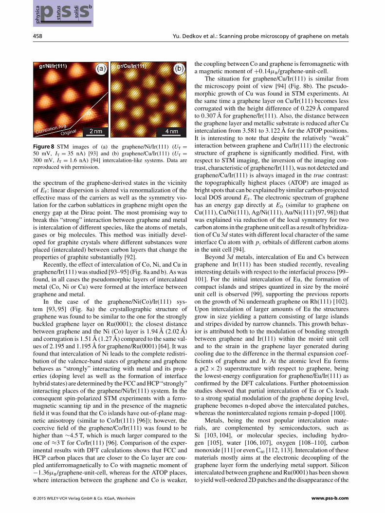
Figure 8 STM images of (a) the graphene/Ni/Ir(111) (UT =50 mV, IT = 35 nA) [93] and (b) graphene/Cu/Ir(111) (UT =300 mV, IT = 1.6 nA) [94] intercalation-like systems. Data arereproduced with permission.
the spectrum of the graphene-derived states in the vicinityof EF: linear dispersion is altered via renormalization of theeffective mass of the carriers as well as the symmetry vio-lation for the carbon sublattices in graphene might open theenergy gap at the Dirac point. The most promising way tobreak this “strong” interaction between graphene and metalis intercalation of different species, like the atoms of metals,gases or big molecules. This method was initially devel-oped for graphite crystals where different substances wereplaced (intercalated) between carbon layers that change theproperties of graphite substantially [92].
Recently, the effect of intercalation of Co, Ni, and Cu ingraphene/Ir(111) was studied [93–95] (Fig. 8a and b). As wasfound, in all cases the pseudomorphic layers of intercalatedmetal (Co, Ni or Cu) were formed at the interface betweengraphene and metal.
In the case of the graphene/Ni(Co)/Ir(111) sys-tem [93, 95] (Fig. 8a) the crystallographic structure ofgraphene was found to be similar to the one for the stronglybuckled graphene layer on Ru(0001); the closest distancebetween graphene and the Ni (Co) layer is 1.94 A (2.02 A)and corrugation is 1.51 A (1.27 A) compared to the same val-ues of 2.195 and 1.195 A for graphene/Ru(0001) [64]. It wasfound that intercalation of Ni leads to the complete redistri-bution of the valence-band states of graphene and graphenebehaves as “strongly” interacting with metal and its prop-erties (doping level as well as the formation of interfacehybrid states) are determined by the FCC and HCP “strongly”interacting places of the graphene/Ni/Ir(111) system. In theconsequent spin-polarized STM experiments with a ferro-magnetic scanning tip and in the presence of the magneticfield it was found that the Co islands have out-of-plane mag-netic anisotropy (similar to Co/Ir(111) [96]); however, thecoercive field of the graphene/Co/Ir(111) was found to behigher than ∼4.5 T, which is much larger compared to theone of ≈3 T for Co/Ir(111) [96]. Comparison of the exper-imental results with DFT calculations shows that FCC andHCP carbon places that are closer to the Co layer are cou-pled antiferromagnetically to Co with magnetic moment of−1.36μB/graphene-unit-cell, whereas for the ATOP places,where interaction between the graphene and Co is weaker,
the coupling between Co and graphene is ferromagnetic witha magnetic moment of +0.14μB/graphene-unit-cell.
The situation for graphene/Cu/Ir(111) is similar fromthe microscopy point of view [94] (Fig. 8b). The pseudo-morphic growth of Cu was found in STM experiments. Atthe same time a graphene layer on Cu/Ir(111) becomes lesscorrugated with the height difference of 0.229 A comparedto 0.307 A for graphene/Ir(111). Also, the distance betweenthe graphene layer and metallic substrate is reduced after Cuintercalation from 3.581 to 3.122 A for the ATOP positions.It is interesting to note that despite the relatively “weak”interaction between graphene and Cu/Ir(111) the electronicstructure of graphene is significantly modified. First, withrespect to STM imaging, the inversion of the imaging con-trast, characteristic of graphene/Ir(111), was not detected andgraphene/Cu/Ir(111) is always imaged in the true contrast:the topographically highest places (ATOP) are imaged asbright spots that can be explained by similar carbon-projectedlocal DOS around EF. The electronic spectrum of graphenehas an energy gap directly at ED (similar to graphene onCu(111), Cu/Ni(111), Ag/Ni(111), Au/Ni(111) [97, 98]) thatwas explained via reduction of the local symmetry for twocarbon atoms in the graphene unit cell as a result of hybridiza-tion of Cu 3d states with different local character of the sameinterface Cu atom with pz orbitals of different carbon atomsin the unit cell [94].
Beyond 3d metals, intercalation of Eu and Cs betweengraphene and Ir(111) has been studied recently, revealinginteresting details with respect to the interfacial process [99–101]. For the initial intercalation of Eu, the formation ofcompact islands and stripes quantized in size by the moireunit cell is observed [99], supporting the previous reportson the growth of Ni underneath graphene on Rh(111) [102].Upon intercalation of larger amounts of Eu the structuresgrow in size yielding a pattern consisting of large islandsand stripes divided by narrow channels. This growth behav-ior is attributed both to the modulation of bonding strengthbetween graphene and Ir(111) within the moire unit celland to the strain in the graphene layer generated duringcooling due to the difference in the thermal expansion coef-ficients of graphene and Ir. At the atomic level Eu formsa p(2 × 2) superstructure with respect to graphene, beingthe lowest-energy configuration for graphene/Eu/Ir(111) asconfirmed by the DFT calculations. Further photoemissionstudies showed that partial intercalation of Eu or Cs leadsto a strong spatial modulation of the graphene doping level,graphene becomes n-doped above the intercalated patches,whereas the nonintercalated regions remain p-doped [100].
Metals, being the most popular intercalation mate-rials, are complemented by semiconductors, such asSi [103, 104], or molecular species, including hydro-gen [105], water [106, 107], oxygen [108–110], carbonmonoxide [111] or even C60 [112, 113]. Intercalation of thesematerials mostly aims at the electronic decoupling of thegraphene layer form the underlying metal support. Siliconintercalated between graphene and Ru(0001) has been shownto yield well-ordered 2D patches and the disappearance of the
© 2015 WILEY-VCH Verlag GmbH & Co. KGaA, Weinheim www.pss-b.com
Feature
Article
Phys. Status Solidi B 252, No. 3 (2015) 459
strongly corrugated moire structure [114]. The latter obser-vation coupled to the results of the corresponding photoe-mission studies were considered as indicative of the efficientdecoupling of the graphene layer from the Ru substrate. Thismethod has recently been further expanded by the oxidationof the interfacial metal silicide layer, resulting in an insulatingSiO2 film separating graphene from the metal, as confirmedby the photoemission [104]. However, the investigations ofthe local crystallographic structure and electronic structureproperties of this system are still missing, thus making itdifficult to predict if this method can be used to efficientlydecouple graphene nanostructures from the metal substrates.
The effective decoupling of graphene from a metal-lic support can be achieved via intercalation of oxygen orCO [115, 108, 109, 111, 110]. These species intercalate ingraphene/Ir(111) either in the form of atomic oxygen form-ing p(2 × 1)-O layer [108] or CO-molecules with (3
√3 ×
3√
3)R30◦ structure [111] underneath graphene. Graphenein these systems is fully decoupled and it is p-dopedwith the position of the Dirac point at E − EF = 0.64 eVand E − EF = 0.6 eV, respectively. For graphene/Ru(0001)the results are contradictory [116, 117, 110]. These worksshow that oxygen can be placed underneath graphene, asconformed by STM and thermal-programmed-desorptionexperiments and forms a (2 × 2) or (2 × 1) superstructurebetween graphene and Ru(0001). However, STS experimentsshow that graphene in this system is n-doped with the positionof the Dirac point at E − EF = −0.48 eV [110] that is oppo-site to the ARPES results where graphene was found highlyp-doped with a Dirac point by ≈ 0.5 eV higher EF [117].
The interesting result was demonstrated in Ref. [112]where intercalation of C60 molecules in graphene/Ni(111)was assumed on the basis of spectroscopic data (photoelec-tron spectroscopy and electron energy loss spectroscopy).Later these results were examined with STM [113]. It wasfound that annealing of the thick layer of C60 molecules leadsto the desorption of most molecules, but also to its intercala-tion underneath graphene. The bias-dependent STM allowsdiscrimination between places of the graphene/C60/Ni(111)structure where intercalation took place and not. These mea-surements unambiguously show that C60 intercalates viacertain interfacial channels, which can be induced by strainrelaxation at defect sites of graphene/Ni(111).
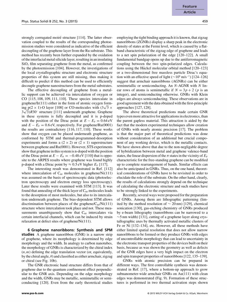
6 Graphene nanoribbons: Synthesis and SPMstudies A graphene nanoribbon (GNR) is a narrow stripof graphene, where its morphology is determined by edgemorphology and the width. In analogy to carbon nanotubes,the morphology of GNRs is characterized by the chiral index(n,m) defining the edge translation vector (or, equivalently,by the chiral angle, θ) and classified as either armchair, zigzagor chiral (see Fig. 10b).
The GNR electronic band structure differs from that ofgraphene due to the quantum confinement effect perpendic-ular to the GNR axis. Depending on the edge morphologyand the width, GNRs may be metallic, semimetallic or semi-conducting [120]. Even from the early theoretical studies
employing the tight binding approach it is known, that zigzagnanoribbons (ZGNRs) display a sharp peak in the electronicdensity of states at the Fermi level, which is caused by a flat-band characteristic of the zigzag edge of graphene and leadsto a net spin polarization of the edge [120–122]. A smallfundamental bandgap opens up due to the antiferromagneticcoupling between the two spin-polarized edges. Calcula-tions using the Huckel molecular orbital method [120–123]or a two-dimensional free massless particle Dirac’s equa-tion with an effective speed of light (∼106 m/s−1) [124–126]suggest that armchair nanoribbons (AGNRs) can be eithersemimetallic or semiconducting. An N-AGNR with N lin-ear rows of atoms is semimetallic if N = 3p + 2 (p is aninteger), and semiconducting otherwise. GNRs with Kleinedges are always semiconducting. These observations are ingood agreement with the data obtained with the first-principleapproaches [127, 128].
The above theoretical predictions made certain GNRtypes even more attractive for applications in electronics, thanthe parent gapless material. This attraction is aided by thefact that the modern experimental techniques allow creationof GNRs with nearly atomic precision [17]. The problemis that the major part of theoretical predictions was donewithout consideration of an additional but crucial compo-nent of any working device, which is the metallic contacts.We have shown above that due to the non-negligable degreeof hybridization between metal and graphene valence-bandstates, the linear dispersion of the π states in the vicinity of EF
characteristic for the free-standing graphene can be modifiedup to complete rearrangement of bands. Similar effects canalso be anticipated in GNRs. Thus, on the one hand, theoret-ical considerations of GNRs have to be revisited in order toelucidate the role of the substrate. On the other hand, clearly,the results of calculations strongly depend on the techniqueof calculating the electronic structure and such studies haveto be strongly linked to the experiments.
Recently, several ways were proposed for the preparationof GNRs. Among them are lithographic patterning (lim-ited by the method resolution of ∼ 20 nm) [129], chemicalsonication [130], gas-etching chemistry of GNRs producedby e-beam lithography (nanoribbons can be narrowed to a∼5 nm width) [131], cutting of a graphene layer along crys-tallographic axes by thermally activated metallic clusters ofFe or Ni [132–134], etc. However, all these methods haveeither limited spatial resolution that does not allow narrownanoribbons to be formed or they produce GNRs with edgesof uncontrollable morphology that can lead to uncertainty inthe electronic transport properties of the devices built on theirbasis, because as was shown the geometry as well as defectsof the GNR edges have a very high impact on the electronand spin transport properties of nanoribbons [122, 135–139].
GNRs with atomic precision can be prepared indifferent ways. The first controllable synthesis was demon-strated in Ref. [17], where a bottom-up approach to growsubnanometer-wide armchair GNRs on Au(111) with cleanedges was demonstrated (Fig. 9). Formation of these struc-tures is performed in two thermal activation steps shown
www.pss-b.com © 2015 WILEY-VCH Verlag GmbH & Co. KGaA, Weinheim

ph
ysic
a ssp stat
us
solid
i b
460 Yu. Dedkov et al.: Scanning probe microscopy of graphene on metals
Figure 9 (a) From top to bottom: (i) reaction scheme from pre-cursor 1 to straight N = 7 GNRs; (ii) STM image taken aftersurface-assisted C–C coupling at 200 ◦C but before the finalcyclodehydrogenation step, showing a polyanthrylene chain (left)(UT = 1.9 V, IT = 0.08 nA), and DFT-based simulation of the STMimage (right) with a partially overlaid model of the polymer (blue,carbon; white, hydrogen); (iii) overview STM image after cyclode-hydrogenation at 400 ◦C, showing straightN = 7 GNRs (RT) (UT =−3 V, IT = 0.03 nA). The inset shows a higher-resolution STMimage taken at 35 K (UT = −1.5 V, IT = 0.5 nA). (b) Top: reac-tion scheme from 6,11-dibromo-1,2,3,4-tetraphenyltriphenylenemonomer 2 to chevron-type GNRs; bottom: overview STM imageof chevron-type GNRs fabricated on a Au(111) surface (T = 35 K)(UT = −2 V, IT = 0.02 nA). The inset shows a high-resolutionSTM image (T = 77 K) (UT = −2 V, IT = 0.5nA) and a DFT-based simulation of the STM image (grayscale) with a partlyoverlaid molecular model of the ribbon (blue, carbon; white, hydro-gen). Images are reproduced from Ref. [17] with permission.
in panels (a) and (b) for two different organic precur-sors. In the second step the initially formed linear polymerchains undergo a surface-assisted cyclodehydrogenation andextended fully aromatic systems are formed. The exper-imental and simulated STM images of such GNRs areshown in Fig. 9. Subsequent STS measurements yield abandgap of 2.3 ± 0.1 eV for 7-AGNR (1.4 ± 0.1 eV for13-AGNRs [140]) compared to 2.3–2.7 eV obtained fromquasiparticle GW calculation corrected for the image chargeon the metallic substrate [18]. Parallel ARPES and IPESexperiments give for straight 7-AGNRs and 13-AGNRsvalues for the band gap of 2.8 ± 0.4 and 1.6 ± 0.4 eV, respec-tively. For the chevron-type GNRs (Fig. 9b), they give abandgap of 3.1 ± 0.4 eV. Also, these measurements showedthat electrons in GNRs cannot be considered as masslessDirac fermions as the carriers exhibit now a finite effectivemass m∗ = 0.21m0, where m0 is the free electron mass. Forthe ARPES experiments, which require the unidirectionalalignment of GNRs at the macroscopic scale, a similar growthprocedure was used on the stepped Au(788) surface that con-sists of the {111} terraces of 3.83 nm width [18, 19]. Aligned
assemblies of both types, straight and chevron-type, GNRscan be grown in such a case. Later, these results were exam-ined within DFT and many-body electron approaches [141].These calculations indicate that electron transfer exists fromany type of GNRs on Au(111) that leads to the surface polar-ization, that is responsible for the width of the bandgap ofGNRs. The calculated energy gaps are 2.85 and 2.96 eV for 7-AGNRs and chevron-type GNR, respectively, which agreeswell with the experimental data.
Another approach to obtain GNRs, the so-called unzip-ping of carbon nanotubes, allows flexible variation of GNRwidth, length, chirality, and substrate [118, 142] (Fig. 10a).In this method the nanotubes were placed in an organicsolution in the ultrasonic bath and then nanoribbons weredeposited on a Au(111) substrate and then their structureand electronic properties were studied with STM/STS [119](Fig. 10b). This method allows preparation of GNRs of dif-ferent chiralities (3.7◦ < θ < 16.1◦) and width (> 500 nm)on Au(111). As was found in STM the edge of GNRs is“bumped” indicating the effect of the GNR–metal inter-action (Fig. 10c). Spectroscopic studies (STS) across theedge of GNR (c and d) show the existence of two peakslocated around EF. The measured edge-state energy splittingshows a clear inverse correlation with GNR width (Fig. 10e)and the gap values tend to be smaller than those observedfor lithographically patterned GNRs (probably because ofuncertainty in the edge structure of lithographically obtainedGNRs [129]). The observed spectroscopic feature (i.e., adouble peak in the local density of states near EF close tothe edge with a peak distance scaling inversely with thewidth of the GNR) was ascribed to an antiferromagnetic cou-pling between opposite edges [143], as further evidenced bycomparison with results from a Hubbard model Hamilto-nian [119] [hopping integral, t = 2.7 eV; on-site Coulombrepulsion, U = 0.5t = 1.35 eV]. These theoretical studieswere extended for the wider range of θ and in the caseof θ = 30◦, i.e., AGNR, the edge states were not present.The latter is in agreement with the results on AGNR/metalsystems obtained by means of plane-wave DFT includingsemiempirical dispersion correction [144].
In agreement with the results by Tao et al. [119], otherexperimental studies provide direct or indirect evidence forthe presence of the edge states in supported GNRs [145, 146].Such edge states might be exploited for a multitude of spin-tronic applications, although it is not fully clear if the edgestates contribute to the measured transport properties ofnanostructures at all. To elucidate the role of the substrateand of edge termination, ZGNRs close to realistic width on(111) surfaces of Cu, Ag and Au were studied recently bymeans of DFT-D2 [147]. Although it was found that GNRspossess edge states, independent of whether they are H-freeor H-terminated, they do not exhibit a significant magnetiza-tion at the edge. These results are explained by the differentinteraction and charge transfer between the GNRs and thesubstrates and show that edge magnetism in zigzag GNRs canbe destroyed even upon deposition on a substrate that inter-acts weakly with graphene. Only in the case of H-terminated
© 2015 WILEY-VCH Verlag GmbH & Co. KGaA, Weinheim www.pss-b.com
Feature
Article
Phys. Status Solidi B 252, No. 3 (2015) 461
Figure 10 (a) Representation of the gradual unzipping of one wall of a carbon nanotube to form a nanoribbon. Oxygenated sites arenot shown. Reproduced from Ref. [118] with permission. (b) A schematic drawing of an (8,1) GNR. The chiral vector (n,m) connectingcrystallographically equivalent sites along the edge defines the edge orientation of the GNR (black arrow). The blue and red arrows are theprojections of the (8,1) vector onto the basis vectors of the graphene lattice. Zigzag and armchair edges have a corresponding chiral angleof θ = 0◦ and θ = 30◦, respectively, whereas the (8,1) edge has a chiral angle of θ = 5.8◦. Lower part shows STM images of a monolayerGNR on Au(111) at room temperature (left) (UT = 1.5 V, IT = 100 pA) and a higher-resolution STM image of a GNR at T = 7 K (right)(UT = 200 mV, IT = 30pA). (c) Atomically resolved STM of the terminal edge of an (8,1) GNR (UT = 300mV, IT = 60 pA). (d) dI/dV
spectra measured at different positions across the edge of GNR as shown in (c). (e) From top to bottom: edge state amplitude perpendicularand parallel to the edge of an (8,1) GNR and gap dependence on the width of GNRs. Data in (b–e) are reproduced from Ref. [119] withpermission.
GNRs on Au(111) was the interaction at the edge found tobe sufficiently weak to not affect the electronic and magneticproperties of the edge states significantly.
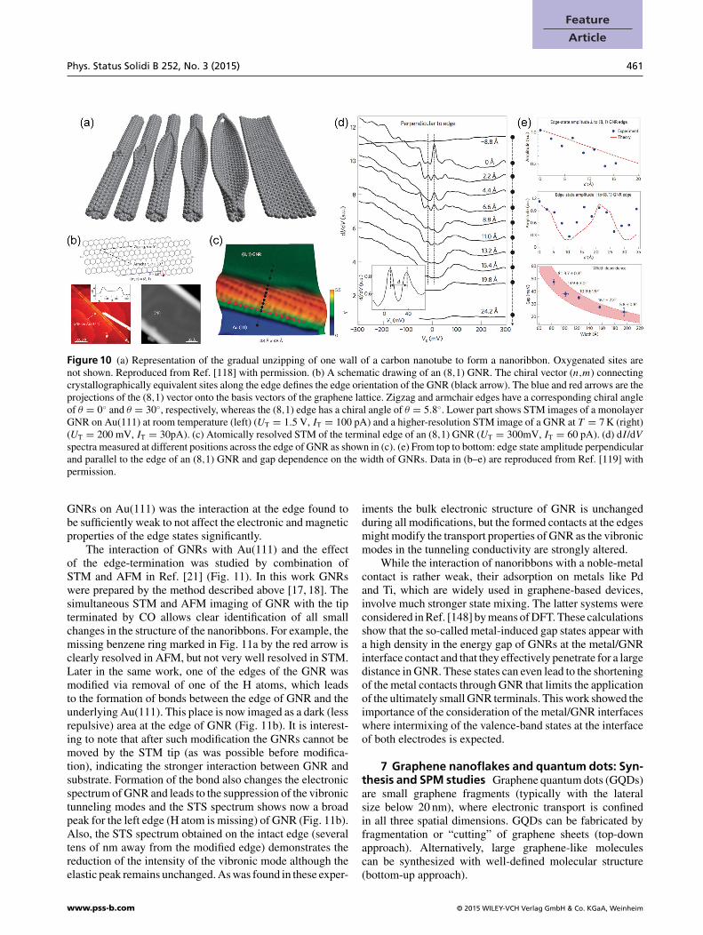
The interaction of GNRs with Au(111) and the effectof the edge-termination was studied by combination ofSTM and AFM in Ref. [21] (Fig. 11). In this work GNRswere prepared by the method described above [17, 18]. Thesimultaneous STM and AFM imaging of GNR with the tipterminated by CO allows clear identification of all smallchanges in the structure of the nanoribbons. For example, themissing benzene ring marked in Fig. 11a by the red arrow isclearly resolved in AFM, but not very well resolved in STM.Later in the same work, one of the edges of the GNR wasmodified via removal of one of the H atoms, which leadsto the formation of bonds between the edge of GNR and theunderlying Au(111). This place is now imaged as a dark (lessrepulsive) area at the edge of GNR (Fig. 11b). It is interest-ing to note that after such modification the GNRs cannot bemoved by the STM tip (as was possible before modifica-tion), indicating the stronger interaction between GNR andsubstrate. Formation of the bond also changes the electronicspectrum of GNR and leads to the suppression of the vibronictunneling modes and the STS spectrum shows now a broadpeak for the left edge (H atom is missing) of GNR (Fig. 11b).Also, the STS spectrum obtained on the intact edge (severaltens of nm away from the modified edge) demonstrates thereduction of the intensity of the vibronic mode although theelastic peak remains unchanged. As was found in these exper-
iments the bulk electronic structure of GNR is unchangedduring all modifications, but the formed contacts at the edgesmight modify the transport properties of GNR as the vibronicmodes in the tunneling conductivity are strongly altered.
While the interaction of nanoribbons with a noble-metalcontact is rather weak, their adsorption on metals like Pdand Ti, which are widely used in graphene-based devices,involve much stronger state mixing. The latter systems wereconsidered in Ref. [148] by means of DFT. These calculationsshow that the so-called metal-induced gap states appear witha high density in the energy gap of GNRs at the metal/GNRinterface contact and that they effectively penetrate for a largedistance in GNR. These states can even lead to the shorteningof the metal contacts through GNR that limits the applicationof the ultimately small GNR terminals. This work showed theimportance of the consideration of the metal/GNR interfaceswhere intermixing of the valence-band states at the interfaceof both electrodes is expected.
7 Graphene nanoflakes and quantum dots: Syn-thesis and SPM studies Graphene quantum dots (GQDs)are small graphene fragments (typically with the lateralsize below 20 nm), where electronic transport is confinedin all three spatial dimensions. GQDs can be fabricated byfragmentation or “cutting” of graphene sheets (top-downapproach). Alternatively, large graphene-like moleculescan be synthesized with well-defined molecular structure(bottom-up approach).
www.pss-b.com © 2015 WILEY-VCH Verlag GmbH & Co. KGaA, Weinheim
ph
ysic
a ssp stat
us
solid
i b
462 Yu. Dedkov et al.: Scanning probe microscopy of graphene on metals
Figure 11 (a) Clockwise: STM overview image showing freeGNRs (UT = 50 mV, IT = 5 pA); free GNR imaged with aCO-terminated tip (UT = 10 mV, IT = 5 pA); constant-height high-resolution nc-AFM images of the middle and the zigzag end of aGNR obtained with a CO-terminated tip (AFM set-point offset by30 pm); constant-height nc-AFM/STM images of 22 monomer unitlong GNR with a single missing benzene ring marked by the redarrow (AFM set-point offset by 48 pm). In the first image scale bar is10 nm, other scale bars are 1 nm. (b) Controlled atomic-scale modifi-cation of the GNR reduces vibronic coupling: high-resolution STMimage of a free GNR before (UT = 50 mV, IT = 5 pA) and after(UT = 50 mV, IT = 20 pA) a bias pulse has been used to modifythe left end of the GNR. Middle row, from left to right: Zoomed-inSTM images of the GNR ends after the modification (UT = 50 mV,IT = 50 pA; UT = 10 mV, IT = 2 pA); atomically resolved AFMimage of the contacted GNR (AFM set-point offset by 120 pm);AFM image of the same ribbon as in previous image, but with thetip 80 pm closer to the sample. Scale bar is 0.5 nm in all images.Lower row: dI/dV spectra recorded at the left and right ends of theGNR before (blue) and after (red) the modification. All the imagesand spectra have been acquired with a CO-terminated tip. All dataare reproduced from Ref. [21] with permission.
The early work on GQDs was dominated by the inves-tigation of their physical properties. More recently, GQDshave been chemically modified and used for the first timein applications in the area of energy conversion, bioanalysis,and sensors. Another exciting perspective is to use GQDs asspin qubits [149]. The basic prerequisite is a very long spin-coherence time, which might exist in graphene due to theabsence of hyperfine coupling in isotopically pure material
and the small spin–orbit coupling. However, since grapheneprovides no natural gap, it is difficult to control the elec-tron number. Moreover, the 2D sublattice symmetry makesthe QD properties very susceptible to the atomic edge con-figuration [149, 150] unlike conventional QDs. As a result,chaotic Dirac billiards have been predicted [151] and wereeven claimed to be realized [152]; i.e., the wave functionsare assumed to be rather disordered. To achieve improvedcontrol of GQDs, the QD edges must be well defined.
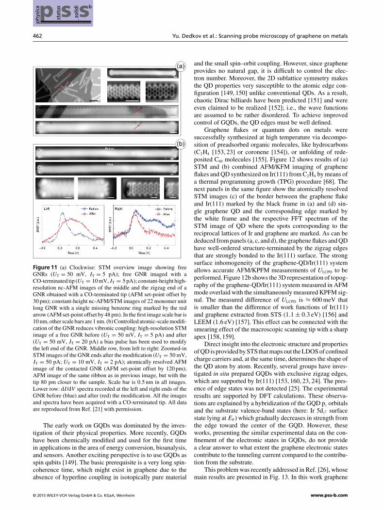
Graphene flakes or quantum dots on metals weresuccessfully synthesized at high temperature via decompo-sition of preadsorbed organic molecules, like hydrocarbons(C2H4 [153, 23] or coronene [154]), or unfolding of rede-posited C60 molecules [155]. Figure 12 shows results of (a)STM and (b) combined AFM/KFM imaging of grapheneflakes and QD synthesized on Ir(111) from C2H4 by means ofa thermal programming growth (TPG) procedure [68]. Thenext panels in the same figure show the atomically resolvedSTM images (c) of the border between the graphene flakeand Ir(111) marked by the black frame in (a) and (d) sin-gle graphene QD and the corresponding edge marked bythe white frame and the respective FFT spectrum of theSTM image of QD where the spots corresponding to thereciprocal lattices of Ir and graphene are marked. As can bededuced from panels (a, c, and d), the graphene flakes and QDhave well-ordered structure-terminated by the zigzag edgesthat are strongly bonded to the Ir(111) surface. The strongsurface inhomogeneity of the graphene-QD/Ir(111) systemallows accurate AFM/KPFM measurements of ULCPD to beperformed. Figure 12b shows the 3D representation of topog-raphy of the graphene-QD/Ir(111) system measured in AFMmode overlaid with the simultaneously measured KPFM sig-nal. The measured difference of ULCPD is ≈ 600 meV thatis smaller than the difference of work functions of Ir(111)and graphene extracted from STS (1.1 ± 0.3 eV) [156] andLEEM (1.6 eV) [157]. This effect can be connected with thesmearing effect of the macroscopic scanning tip with a sharpapex [158, 159].
Direct insight into the electronic structure and propertiesof QD is provided by STS that maps out the LDOS of confinedcharge carriers and, at the same time, determines the shape ofthe QD atom by atom. Recently, several groups have inves-tigated in situ prepared GQDs with exclusive zigzag edges,which are supported by Ir(111) [153, 160, 23, 24]. The pres-ence of edge states was not detected [25]. The experimentalresults are supported by DFT calculations. These observa-tions are explained by a hybridization of the GQD pz orbitalsand the substrate valence-band states (here: Ir 5dz2 surfacestate lying at EF) which gradually decreases in strength fromthe edge toward the center of the GQD. However, theseworks, presenting the similar experimental data on the con-finement of the electronic states in GQDs, do not providea clear answer to what extent the graphene electronic statescontribute to the tunneling current compared to the contribu-tion from the substrate.
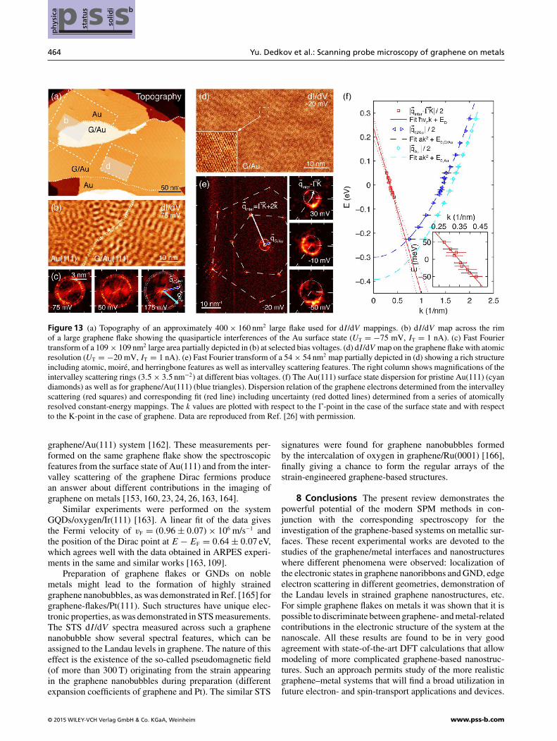
This problem was recently addressed in Ref. [26], whosemain results are presented in Fig. 13. In this work graphene
© 2015 WILEY-VCH Verlag GmbH & Co. KGaA, Weinheim www.pss-b.com
Feature
Article
Phys. Status Solidi B 252, No. 3 (2015) 463
Figure 12 (a and b) 3D views of the large scale STM (160 × 160 nm2, UT = 300 mV, IT = 0.8 nA) and AFM images (150 × 150 nm2,Δf = −670 mHz), respectively, of graphene flakes and QDs on Ir(111). In (b) the topography image is overlaid with the results of KPFMimaging obtained simultaneously during AFM scanning. (c) Atomically resolved border between graphene flake and Ir(111) marked in(a) by black rectangle (10 × 10 nm2, UT = −50 mV, IT = 30 nA). (d) STM image of the single zigzag-edge terminated GQD on Ir(111)(20.2 × 20.2 nm2, UT = 300 mV, IT = 1.5 nA). Right-hand side shows the zoomed area marked by the white rectangle (4.1 × 4.1 nm2,UT = 300 mV, IT = 1.5 nA) and the corresponding FFT spectrum of the STM image of GND/Ir(111).
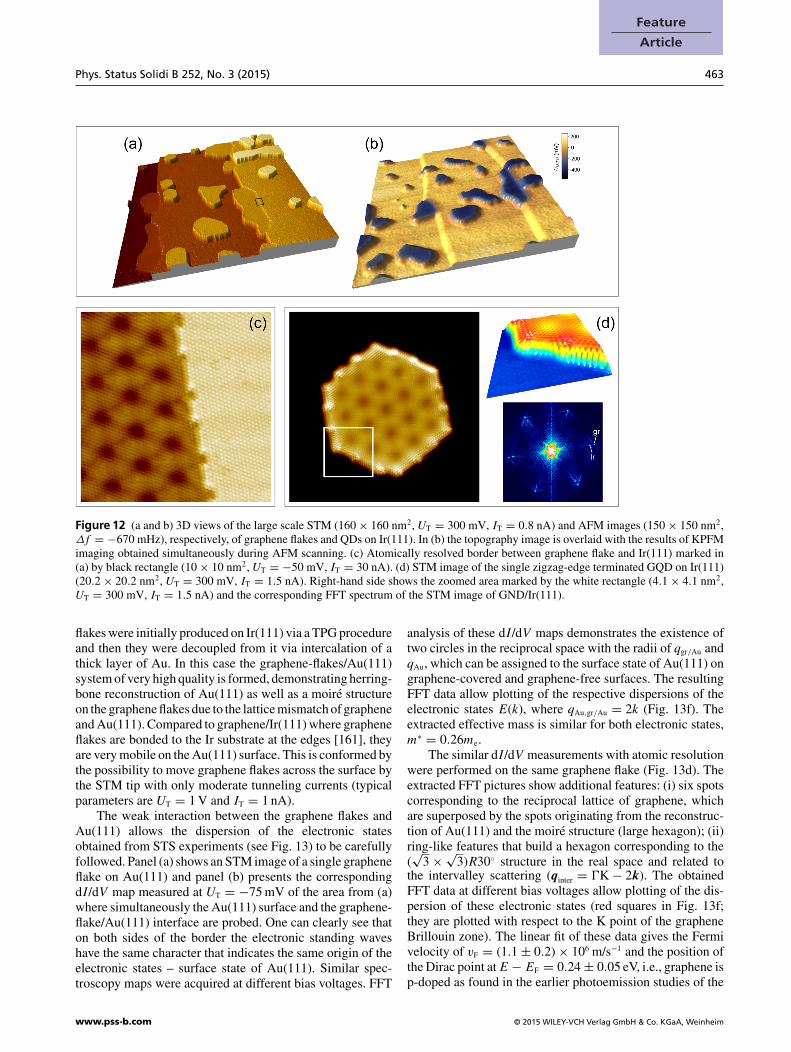
flakes were initially produced on Ir(111) via a TPG procedureand then they were decoupled from it via intercalation of athick layer of Au. In this case the graphene-flakes/Au(111)system of very high quality is formed, demonstrating herring-bone reconstruction of Au(111) as well as a moire structureon the graphene flakes due to the lattice mismatch of grapheneand Au(111). Compared to graphene/Ir(111) where grapheneflakes are bonded to the Ir substrate at the edges [161], theyare very mobile on the Au(111) surface. This is conformed bythe possibility to move graphene flakes across the surface bythe STM tip with only moderate tunneling currents (typicalparameters are UT = 1 V and IT = 1 nA).
The weak interaction between the graphene flakes andAu(111) allows the dispersion of the electronic statesobtained from STS experiments (see Fig. 13) to be carefullyfollowed. Panel (a) shows an STM image of a single grapheneflake on Au(111) and panel (b) presents the correspondingdI/dV map measured at UT = −75 mV of the area from (a)where simultaneously the Au(111) surface and the graphene-flake/Au(111) interface are probed. One can clearly see thaton both sides of the border the electronic standing waveshave the same character that indicates the same origin of theelectronic states – surface state of Au(111). Similar spec-troscopy maps were acquired at different bias voltages. FFT
analysis of these dI/dV maps demonstrates the existence oftwo circles in the reciprocal space with the radii of qgr/Au andqAu, which can be assigned to the surface state of Au(111) ongraphene-covered and graphene-free surfaces. The resultingFFT data allow plotting of the respective dispersions of theelectronic states E(k), where qAu,gr/Au = 2k (Fig. 13f). Theextracted effective mass is similar for both electronic states,m∗ = 0.26me.
The similar dI/dV measurements with atomic resolutionwere performed on the same graphene flake (Fig. 13d). Theextracted FFT pictures show additional features: (i) six spotscorresponding to the reciprocal lattice of graphene, whichare superposed by the spots originating from the reconstruc-tion of Au(111) and the moire structure (large hexagon); (ii)ring-like features that build a hexagon corresponding to the(√
3 × √3)R30◦ structure in the real space and related to
the intervalley scattering (qinter = �K − 2k). The obtainedFFT data at different bias voltages allow plotting of the dis-persion of these electronic states (red squares in Fig. 13f;they are plotted with respect to the K point of the grapheneBrillouin zone). The linear fit of these data gives the Fermivelocity of vF = (1.1 ± 0.2) × 106 m/s−1 and the position ofthe Dirac point at E − EF = 0.24 ± 0.05 eV, i.e., graphene isp-doped as found in the earlier photoemission studies of the
www.pss-b.com © 2015 WILEY-VCH Verlag GmbH & Co. KGaA, Weinheim
ph
ysic
a ssp stat
us
solid
i b
464 Yu. Dedkov et al.: Scanning probe microscopy of graphene on metals
Figure 13 (a) Topography of an approximately 400 × 160 nm2 large flake used for dI/dV mappings. (b) dI/dV map across the rimof a large graphene flake showing the quasiparticle interferences of the Au surface state (UT = −75 mV, IT = 1 nA). (c) Fast Fouriertransform of a 109 × 109 nm2 large area partially depicted in (b) at selected bias voltages. (d) dI/dV map on the graphene flake with atomicresolution (UT = −20 mV, IT = 1 nA). (e) Fast Fourier transform of a 54 × 54 nm2 map partially depicted in (d) showing a rich structureincluding atomic, moire, and herringbone features as well as intervalley scattering features. The right column shows magnifications of theintervalley scattering rings (3.5 × 3.5 nm−2) at different bias voltages. (f) The Au(111) surface state dispersion for pristine Au(111) (cyandiamonds) as well as for graphene/Au(111) (blue triangles). Dispersion relation of the graphene electrons determined from the intervalleyscattering (red squares) and corresponding fit (red line) including uncertainty (red dotted lines) determined from a series of atomicallyresolved constant-energy mappings. The k values are plotted with respect to the �-point in the case of the surface state and with respectto the K-point in the case of graphene. Data are reproduced from Ref. [26] with permission.
graphene/Au(111) system [162]. These measurements per-formed on the same graphene flake show the spectroscopicfeatures from the surface state of Au(111) and from the inter-valley scattering of the graphene Dirac fermions producean answer about different contributions in the imaging ofgraphene on metals [153, 160, 23, 24, 26, 163, 164].
Similar experiments were performed on the systemGQDs/oxygen/Ir(111) [163]. A linear fit of the data givesthe Fermi velocity of vF = (0.96 ± 0.07) × 106 m/s−1 andthe position of the Dirac point at E − EF = 0.64 ± 0.07 eV,which agrees well with the data obtained in ARPES experi-ments in the same and similar works [163, 109].
Preparation of graphene flakes or GNDs on noblemetals might lead to the formation of highly strainedgraphene nanobubbles, as was demonstrated in Ref. [165] forgraphene-flakes/Pt(111). Such structures have unique elec-tronic properties, as was demonstrated in STS measurements.The STS dI/dV spectra measured across such a graphenenanobubble show several spectral features, which can beassigned to the Landau levels in graphene. The nature of thiseffect is the existence of the so-called pseudomagnetic field(of more than 300 T) originating from the strain appearingin the graphene nanobubbles during preparation (differentexpansion coefficients of graphene and Pt). The similar STS
signatures were found for graphene nanobubbles formedby the intercalation of oxygen in graphene/Ru(0001) [166],finally giving a chance to form the regular arrays of thestrain-engineered graphene-based structures.
8 Conclusions The present review demonstrates thepowerful potential of the modern SPM methods in con-junction with the corresponding spectroscopy for theinvestigation of the graphene-based systems on metallic sur-faces. These recent experimental works are devoted to thestudies of the graphene/metal interfaces and nanostructureswhere different phenomena were observed: localization ofthe electronic states in graphene nanoribbons and GND, edgeelectron scattering in different geometries, demonstration ofthe Landau levels in strained graphene nanostructures, etc.For simple graphene flakes on metals it was shown that it ispossible to discriminate between graphene- and metal-relatedcontributions in the electronic structure of the system at thenanoscale. All these results are found to be in very goodagreement with state-of-the-art DFT calculations that allowmodeling of more complicated graphene-based nanostruc-tures. Such an approach permits study of the more realisticgraphene–metal systems that will find a broad utilization infuture electron- and spin-transport applications and devices.
© 2015 WILEY-VCH Verlag GmbH & Co. KGaA, Weinheim www.pss-b.com
Feature
Article
Phys. Status Solidi B 252, No. 3 (2015) 465
Acknowledgements We would like to acknowledge ourcolleagues for the useful discussions, in particular, K. Horn, S.Torbrugge, T. Hanke, M. Breitschaft, M. Breusing, R. Kremzow,N. Berdunov, Th. Konig, Th. Kampen, O. Schaff, A. Thissen, P.Leicht, J. Tesch, L. Zielke. E.N.V. and M.F. appreciate the supportfrom the German Research Foundation (DFG) through the PriorityProgramme (SPP) 1459 “Graphene” and European Science Foun-dation (ESF) via the EUROCORES Programme EuroGRAPHENE(Project “SpinGraph”).
References
[1] K. Novoselov, A. Geim, S. Morozov, D. Jiang, Y. Zhang,S. Dubonos, I. Grigorieva, and A. Firsov, Science 306, 666(2004).
[2] K. Novoselov, A. Geim, S. Morozov, D. Jiang, M. Katsnel-son, I. Grigorieva, S. Dubonos, and A. Firsov, Nature 438,197 (2005).
[3] Y. Zhang, Y. Tan, H. Stormer, and P. Kim, Nature 438, 201(2005).
[4] A. Castro Neto, F. Guinea, N. Peres, K. Novoselov, and A.Geim, Rev. Mod. Phys. 81, 109 (2009).
[5] A. Geim, Science 324, 1530 (2009).[6] S. Hagstrom, H. B. Lyon, and G. A. Somorjai, Phys. Rev.
Lett. 15, 491 (1965).[7] J. W. May, Surf. Sci. 17, 267 (1969).[8] J. T. Grant and A. Haas, Surf. Sci. 21, 76 (1970).[9] T. A. Land, T. Michely, R. Behm, J. C. Hemminger, and G.
Comsa, Surf. Sci. 264, 261 (1992).[10] X. Li, W. Cai, J. An, S. Kim, J. Nah, D. Yang, R. Piner, A.
Velamakanni, I. Jung, E. Tutuc, S. K. Banerjee, L. Colombo,and R. S. Ruoff, Science 324, 1312 (2009).
[11] S. Bae, H. Kim, Y. Lee, X. Xu, J. S. Park, Y. Zheng, J.Balakrishnan, T. Lei, H. R. Kim, Y. I. Song, Y. J. Kim, K.S. Kim, B. Ozyilmaz, J. H. Ahn, B. H. Hong, and S. Iijima,Nature Nanotechnol. 5, 574 (2010).
[12] L. Tao, J. Lee, M. Holt, H. Chou, S. J. McDonnell, D. A.Ferrer, M. G. Babenco, R. M. Wallace, S. K. Banerjee, andR. S. Ruoff, J. Phys. Chem. C 116, 24068 (2012).
[13] J. Wintterlin and M. L. Bocquet, Surf. Sci. 603, 1841 (2009).[14] E. Voloshina and Y. Dedkov, Phys. Chem. Chem. Phys. 14,
13502 (2012).[15] Y. S. Dedkov, K. Horn, A. Preobrajenskij, and M. Fonin,
in: Graphene Nanoelectronics, edited by H. Raza (Springer,Berlin, 2012).
[16] E. N. Voloshina and Y. S. Dedkov, Mater. Res. Express 1,035603 (2014).
[17] J. Cai, P. Ruffieux, R. Jaafar, M. Bieri, T. Braun, S. Blanken-burg, M. Muoth, A. P. Seitsonen, M. Saleh, X. Feng, K.Mullen, and R. Fasel, Nature 466, 470 (2010).
[18] P. Ruffieux, J. Cai, N. C. Plumb, L. Patthey, D. Prezzi, A.Ferretti, E. Molinari, X. Feng, K. Mullen, C. A. Pignedoli,and R. Fasel, ACS Nano 6, 6930 (2012).
[19] S. Linden, D. Zhong, A. Timmer, N. Aghdassi, J. Franke,H. Zhang, X. Feng, K. Mullen, H. Fuchs, L. Chi, and H.Zacharias, Phys. Rev. Lett. 108, 216801 (2012).
[20] L. Talirz, H. Sode, J. Cai, P. Ruffieux, S. Blankenburg, R.Jafaar, R. Berger, X. Feng, K. Mullen, D. Passerone, R. Fasel,and C. A. Pignedoli, J. Am. Chem. Soc. 135, 2060 (2013).
[21] J. van der Lit, M. P. Boneschanscher, D. Vanmaekelbergh,M. Ijas, A. Uppstu, M. Ervasti, A. Harju, P. Liljeroth, and I.Swart, Nature Commun. 4, 2023 (2013).
[22] Y. Zhang, Y. Zhang, G. Li, J. Lu, X. Lin, S. Du, R. Berger,X. Feng, K. Mullen, and H. J. Gao, Appl. Phys. Lett. 105,023101 (2014).
[23] D. Subramaniam, F. Libisch, Y. Li, C. Pauly, V. Geringer, R.Reiter, T. Mashoff, M. Liebmann, J. Burgdorfer, C. Busse,T. Michely, R. Mazzarello, M. Pratzer, and M. Morgenstern,Phys. Rev. Lett. 108, 046801 (2012).
[24] S. J. Altenburg, J. Kroger, T. O. Wehling, B. Sachs, A. I.Lichtenstein, and R. Berndt, Phys. Rev. Lett. 108, 206805(2012).
[25] Y. Li, D. Subramaniam, N. Atodiresei, P. Lazic, V. Caciuc,C. Pauly, A. Georgi, C. Busse, M. Liebmann, S. Blugel, M.Pratzer, M. Morgenstern, and R. Mazzarello, Adv. Mater.25, 1967 (2013).
[26] P. Leicht, L. Zielke, S. Bouvron, R. Moroni, E. Voloshina,L. Hammerschmidt, Y. S. Dedkov, and M. Fonin, ACS Nano8, 3735 (2014).
[27] F. J. Giessibl, Rev. Mod. Phys. 75, 949 (2003).[28] F. J. Giessibl, F. Pielmeier, T. Eguchi, T. An, and Y.
Hasegawa, Phys. Rev. B 84, 125409 (2011).[29] F. J. Giessibl, Appl. Phys. Lett. 78, 123 (2001).[30] J. E. Sader and S. P. Jarvis, Appl. Phys. Lett. 84, 1801 (2004).[31] M. Nonnenmacher, M. P. O’Boyle, and H. K. Wickramas-
inghe, Appl. Phys. Lett. 58, 2921 (1991).[32] W. Melitz, J. Shen, A. C. Kummel, and S. Lee, Surf. Sci.
Rep. 66, 1 (2011).[33] M. Abe, Y. Sugimoto, T. Namikawa, K. Morita, N. Oyabu,
and S. Morita, Appl. Phys. Lett. 90, 203103 (2007).[34] Y. Sugimoto, T. Namikawa, K. Miki, M. Abe, and S. Morita,
Phys. Rev. B 77, 195424 (2008).[35] B. J. Albers, T. C. Schwendemann, M. Z. Baykara, N. Pilet,
M. Liebmann, E. I. Altman, and U. D. Schwarz, NatureNanotechnol. 4, 307 (2009).
[36] Y. Sugimoto, K. Ueda, M. Abe, and S. Morita, J. Phys.:Condens. Matter 24, 084008 (2012).
[37] S. Grimme, J. Comput. Chem. 25, 1463 (2004).[38] S. Grimme, J. Comput. Chem. 27, 1787 (2006).[39] S. Grimme, J. Antony, S. Ehrlich, and H. Krieg, J. Chem.
Phys. 132, 154104 (2010).[40] A. Tkatchenko and M. Scheffler, Phys. Rev. Lett. 102,
073005 (2009).[41] M. Dion, H. Rydberg, E. Schroder, D. Langreth, and B.
Lundqvist, Phys. Rev. Lett. 92, 246401 (2004).[42] J. Klimes, D. R. Bowler, and A. Michaelides, J. Phys.: Con-
dens. Matter 22, 022201 (2009).[43] M. Vanin, J. J. Mortensen, A. K. Kelkkanen, J. M. Garcia-
Lastra, K. S. Thygesen, and K. W. Jacobsen, Phys. Rev. B81, 081408 (2010).
[44] J. Tersoff and D. R. Hamann, Phys. Rev. B 31, 805 (1985).[45] W. A. Hofer, A. S. Foster, and A. L. Shluger, Rev. Mod.
Phys. 75, 1287 (2003).[46] L. Kantorovich and C. Hobbs, Phys. Rev. B 73, 245420
(2006).[47] T. L. Chan, C. Wang, K. Ho, and J. Chelikowsky, Phys. Rev.
Lett. 102, 176101 (2009).[48] C. Klink, I. Stensgaard, F. Besenbacher, and E. Laegsgaard,
Surf. Sci. 342, 250 (1995).[49] Y. S. Dedkov, M. Fonin, U. Rudiger, and C. Laubschat, Phys.
Rev. Lett. 100, 107602 (2008).[50] D. Eom, D. Prezzi, K. T. Rim, H. Zhou, M. Lefenfeld, S.
Xiao, C. Nuckolls, M. S. Hybertsen, T. F. Heinz, and G. W.Flynn, Nano Lett. 9, 2844 (2009).
www.pss-b.com © 2015 WILEY-VCH Verlag GmbH & Co. KGaA, Weinheim
ph
ysic
a ssp stat
us
solid
i b
466 Yu. Dedkov et al.: Scanning probe microscopy of graphene on metals
[51] A. Varykhalov and O. Rader, Phys. Rev. B 80, 035437(2009).
[52] Y. S. Dedkov and M. Fonin, New J. Phys. 12, 125004(2010).
[53] J. Lahiri, T. Miller, L. Adamska, I. I. Oleynik, and M. Batzill,Nano Lett. 11, 518 (2011).
[54] L. V. Dzemiantsova, M. Karolak, F. Lofink, A. Kubetzka, B.Sachs, K. von Bergmann, S. Hankemeier, T. O. Wehling, R.Fromter, H. P. Oepen, A. I. Lichtenstein, and R. Wiesendan-ger, Phys. Rev. B 84, 205431 (2011).
[55] P. Jacobson, B. Stoger, A. Garhofer, G. S. Parkinson, M.Schmid, R. Caudillo, F. Mittendorfer, J. Redinger, and U.Diebold, J. Phys. Chem. Lett. 3, 136 (2012).
[56] P. Jacobson, B. Stoger, A. Garhofer, G. S. Parkinson, M.Schmid, R. Caudillo, F. Mittendorfer, J. Redinger, and U.Diebold, ACS Nano 6, 3564 (2012).
[57] F. Bianchini, L. L. Patera, M. Peressi, C. Africh, and G.Comelli, J. Phys. Chem. Lett. 5, 467 (2014).
[58] D. Prezzi, D. Eom, K. T. Rim, H. Zhou, S. Xiao, C. Nuckolls,T. F. Heinz, G. W. Flynn, and M. S. Hybertsen, ACS Nano8, 5765 (2014).
[59] G. Bertoni, L. Calmels, A. Altibelli, and V. Serin, Phys. Rev.B 71, 075402 (2004).
[60] M. Weser, E. N. Voloshina, K. Horn, and Y. S. Dedkov, Phys.Chem. Chem. Phys. 13, 7534 (2011).
[61] E. N. Voloshina, A. Generalov, M. Weser, S. Bottcher, K.Horn, and Y. S. Dedkov, New J. Phys. 13, 113028 (2011).
[62] A. T. N’Diaye, J. Coraux, T. N. Plasa, C. Busse, and T.Michely, New J. Phys. 10, 043033 (2008).
[63] A. L. Vazquez De Parga, F. Calleja, B. Borca, M. C. G.Passeggi, J. J. Hinarejos, F. Guinea, and R. Miranda, Phys.Rev. Lett. 100, 056807 (2008).
[64] D. Stradi, S. Barja, C. Dıaz, M. Garnica, B. Borca, J. Hinare-jos, D. Sanchez-Portal, M. Alcamı, A. Arnau, A. Vazquezde Parga, R. Miranda, and F. Martın, Phys. Rev. Lett. 106,186102 (2011).
[65] D. Stradi, S. Barja, C. Dıaz, M. Garnica, B. Borca, J. Hinare-jos, D. Sanchez-Portal, M. Alcamı, A. Arnau, A. L. VazquezDe Parga, R. Miranda, and F. Martın, Phys. Rev. B 85,121404 (2012).
[66] E. N. Voloshina, Y. S. Dedkov, S. Torbrugge, A. Thissen,and M. Fonin, Appl. Phys. Lett. 100, 241606 (2012).
[67] E. N. Voloshina, E. Fertitta, A. Garhofer, F. Mittendorfer,M. Fonin, A. Thissen, and Y. S. Dedkov, Sci. Rep. 3, 1072(2013).
[68] Y. Dedkov and E. Voloshina, Phys. Chem. Chem. Phys. 16,3894 (2014).
[69] C. Busse, P. Lazic, R. Djemour, J. Coraux, T. Gerber, N.Atodiresei, V. Caciuc, R. Brako, A. T. N’Diaye, S. Bluegel,J. Zegenhagen, and T. Michely, Phys. Rev. Lett. 107, 036101(2011).
[70] S. K. Hamalainen, M. P. Boneschanscher, P. H. Jacobse, I.Swart, K. Pussi, W. Moritz, J. Lahtinen, P. Liljeroth, and J.Sainio, Phys. Rev. B 88, 201406 (2013).
[71] N. Vinogradov, A. Zakharov, V. Kocevski, J. Rusz, K.Simonov, O. Eriksson, A. Mikkelsen, E. Lundgren, A. Vino-gradov, N. Martensson, and A. Preobrajenski, Phys. Rev.Lett. 109, 026101 (2012).
[72] M. P. M. Boneschanscher, J. J. van der Lit, Z. Z. Sun, I. I.Swart, P. P. Liljeroth, and D. D. Vanmaekelbergh, ACS Nano6, 10216 (2012).
[73] S. Koch, D. Stradi, E. Gnecco, S. Barja, S. Kawai, C. Dıaz,M. Alcamı, F. Martın, A. L. V. de Parga, R. Miranda, T.Glatzel, and E. Meyer, ACS Nano 7, 2927 (2013).
[74] B. Wang, M. Caffio, C. Bromley, H. Fruchtl, and R. Schaub,ACS Nano 4, 5773 (2010).
[75] B. Borca, S. Barja, M. Garnica, D. Sanchez-Portal, V. Silkin,E. Chulkov, C. Hermanns, J. Hinarejos, A. Vazquez de Parga,A. Arnau, P. Echenique, and R. Miranda, Phys. Rev. Lett.105, 036804 (2010).
[76] B. Wang, S. Gunther, J. Wintterlin, and M. L. Bocquet, NewJ. Phys. 12, 043041 (2010).
[77] S. J. Altenburg and R. Berndt, New J. Phys. 16, 053036(2014).
[78] H. Zhang, J. Sun, T. Low, L. Zhang, Y. Pan, Q. Liu, J. Mao,H. Zhou, H. Guo, S. Du, F. Guinea, and H. J. Gao, Phys.Rev. B 84, 245436 (2011).
[79] H. Zhang, W. D. Xiao, J. Mao, H. Zhou, G. Li, Y. Zhang,L. Liu, S. Du, and H. J. Gao, J. Phys. Chem. C 116, 11091(2012).
[80] K. Yang, W. D. Xiao, Y. H. Jiang, H. G. Zhang, L. W. Liu, J.H. Mao, H. T. Zhou, S. X. Du, and H. J. Gao, J. Phys. Chem.C 116, 14052 (2012).
[81] G. Li, H. T. Zhou, L. D. Pan, Y. Zhang, J. H. Mao, Q. Zou,H. M. Guo, Y. L. Wang, S. X. Du, and H. J. Gao, Appl. Phys.Lett. 100, 013304 (2012).
[82] S. K. Hamalainen, M. Stepanova, R. Drost, P. Liljeroth, J.Lahtinen, and J. Sainio, J. Phys. Chem. C 116, 20433 (2012).
[83] P. Jarvinen, S. K. Hamalainen, M. Ijas, A. Harju, and P.Liljeroth, J. Phys. Chem. C 118, 13320 (2014).
[84] A. T. N’Diaye, T. Gerber, C. Busse, J. Myslivecek, J. Coraux,and T. Michely, New J. Phys. 11, 103045 (2009).
[85] Y. Pan, M. Gao, L. Huang, F. Liu, and H. J. Gao, Appl. Phys.Lett. 95, 093106 (2009).
[86] S. Rusponi, M. Papagno, P. Moras, S. Vlaic, M. Etzkorn, P.Sheverdyaeva, D. Pacile, H. Brune, and C. Carbone, Phys.Rev. Lett. 105, 246803 (2010).
[87] C. Vo-Van, S. Schumacher, J. Coraux, V. Sessi, O. Fruchart,N. B. Brookes, P. Ohresser, and T. Michely, Appl. Phys. Lett.99, 142504 (2011).
[88] M. Papagno, S. Rusponi, P. M. Sheverdyaeva, S. Vlaic, M.Etzkorn, D. Pacile, P. Moras, C. Carbone, and H. Brune,ACS Nano 6, 199 (2012).
[89] J. Knudsen, P. Feibelman, T. Gerber, E. Granas, K. Schulte,P. Stratmann, J. Andersen, and T. Michely, Phys. Rev. B 85,035407 (2012).
[90] A. T. N’Diaye, S. Bleikamp, P. Feibelman, and T. Michely,Phys. Rev. Lett. 97, 215501 (2006).
[91] P. Feibelman, Phys. Rev. B 80, 085412 (2009).[92] M. Dresselhaus and G. Dresselhaus, Adv. Phys. 51, 1 (2002).[93] D. Pacile, P. Leicht, M. Papagno, P. M. Sheverdyaeva, P.
Moras, C. Carbone, K. Krausert, L. Zielke, M. Fonin, Y.S. Dedkov, F. Mittendorfer, J. Doppler, A. Garhofer, and J.Redinger, Phys. Rev. B 87, 035420 (2013).
[94] H. Vita, S. Bottcher, K. Horn, E. N. Voloshina, R. E.Ovcharenko, T. Kampen, A. Thissen, and Y. S. Dedkov, Sci.Rep. 4, 5704 (2014).
[95] R. Decker, J. Brede, N. Atodiresei, V. Caciuc, S. Blugel, andR. Wiesendanger, Phys. Rev. B 87, 041403 (2013).
[96] J. E. Bickel, F. Meier, J. Brede, A. Kubetzka, K. vonBergmann, and R. Wiesendanger, Phys. Rev. B 84, 054454(2011).
© 2015 WILEY-VCH Verlag GmbH & Co. KGaA, Weinheim www.pss-b.com
Feature
Article
Phys. Status Solidi B 252, No. 3 (2015) 467
[97] A. Varykhalov, M. Scholz, T. Kim, and O. Rader, Phys. Rev.B 82, 121101 (2010).
[98] A. Walter, S. Nie, A. Bostwick, K. S. Kim, L. Moreschini,Y. J. Chang, D. Innocenti, K. Horn, K. McCarty, and E.Rotenberg, Phys. Rev. B 84, 195443 (2011).
[99] S. Schumacher, D. F. Forster, M. Rosner, T. O. Wehling, andT. Michely, Phys. Rev. Lett. 110, 086111 (2013).
[100] S. Schumacher, T. O. Wehling, P. Lazic, S. Runte, D. F.Forster, C. Busse, M. Petrovic, M. Kralj, S. Blugel, N.Atodiresei, V. Caciuc, and T. Michely, Nano Lett. 13, 5013(2013).
[101] M. Petrovic, I. S. Rakic, S. Runte, C. Busse, J. T. Sadowski,P. Lazic, I. Pletikosic, Z.-H. Pan, M. Milun, P. Pervan, N.Atodiresei, R. Brako, D. Sokcevic, T. Valla, T. Michely, andM. Kralj, Nature Commun. 4, 2772 (2013).
[102] M. Sicot, P. Leicht, A. Zusan, S. Bouvron, O. Zander, M.Weser, Y. S. Dedkov, K. Horn, and M. Fonin, ACS Nano 6,151 (2012).
[103] L. Meng, R. Wu, H. Zhou, G. Li, Y. Zhang, L. Li, Y. Wang,and H. J. Gao, Appl. Phys. Lett. 100, 083101 (2012).
[104] S. Lizzit, R. Larciprete, P. Lacovig, M. Dalmiglio, F.Orlando, A. Baraldi, L. Gammelgaard, L. Barreto, M.Bianchi, E. Perkins, and P. Hofmann, Nano Lett. 12, 4503(2012).
[105] C. Riedl, C. Coletti, and U. Starke, J. Phys. D, Appl. Phys.43, 374009 (2010).
[106] X. Feng, S. Maier, and M. Salmeron, J. Am. Chem. Soc.134, 5662 (2012).
[107] X. Feng, S. Kwon, J. Y. Park, and M. Salmeron, ACS Nano7, 1718 (2013).
[108] E. Granas, J. Knudsen, U. A. Schroder, T. Gerber, C. Busse,M. A. Arman, K. Schulte, J. N. Andersen, and T. Michely,ACS Nano 6, 9951 (2012).
[109] R. Larciprete, S. Ulstrup, P. Lacovig, M. Dalmiglio, M.Bianchi, F. Mazzola, L. Hornekaer, F. Orlando, A. Baraldi,P. Hofmann, and S. Lizzit, ACS Nano 6, 9551 (2012).
[110] W. J. Jang, H. Kim, J. H. Jeon, J. K. Yoon, and S. J. Kahng,Phys. Chem. Chem. Phys. 15, 16019 (2013).
[111] E. Granas, M. Andersen, M. A. Arman, T. Gerber, B. Ham-mer, J. Schnadt, J. N. Andersen, T. Michely, and J. Knudsen,J. Phys. Chem. C 117, 16438 (2013).
[112] A. Shikin, Y. Dedkov, V. Adamchuk, D. Farias, and K.Rieder, Surf. Sci. 452, 1 (2000).
[113] A. Varykhalov, W. Gudat, and O. Rader, Adv. Mater. 22,3307 (2010).
[114] Y. Cui, J. Gao, L. Jin, J. Zhao, D. Tan, Q. Fu, and X. Bao,Nano Res. 5, 352 (2012).
[115] H. Zhang, Q. Fu, Y. Cui, D. Tan, and X. Bao, J. Phys. Chem.C 113, 8296 (2009).
[116] Y. Zhang, T. T. Tang, C. Girit, Z. Hao, M. C. Martin, A. Zettl,M. F. Crommie, Y. R. Shen, and F. Wang, Nature 459, 820(2009).
[117] P. Sutter, J. T. Sadowski, and E. A. Sutter, J. Am. Chem. Soc.132, 8175 (2010).
[118] D. V. Kosynkin, A. L. Higginbotham, A. Sinitskii, J. R.Lomeda, A. Dimiev, B. K. Price, and J. M. Tour, Nature458, 872 (2009).
[119] C. Tao, L. Jiao, O. V. Yazyev, Y. C. Chen, J. Feng, X. Zhang,R. B. Capaz, J. M. Tour, A. Zettl, S. G. Louie, H. Dai, andM. F. Crommie, Nature Phys. 7, 616 (2011).
[120] K. Nakada, M. Fujita, G. Dresselhaus, and M. Dresselhaus,Phys. Rev. B 54, 17954 (1996).
[121] M. Fujita, K. Wakabayashi, K. Nakada, and K. Kusakabe, J.Phys. Soc. Jpn. 65, 1920 (1996).
[122] K. Wakabayashi, M. Fujita, H. Ajiki, and M. Sigrist, Phys.Rev. B 59, 8271 (1999).
[123] M. Ezawa, Phys. Rev. B 73, 045432 (2006).[124] L. Brey and H. Fertig, Phys. Rev. B 73, 235411 (2006).[125] K. Sasaki, S. Murakami, and R. Saito, J. Phys. Soc. Jpn. 75,
074713 (2006).[126] D. Abanin, P. Lee, and L. Levitov, Phys. Rev. Lett. 96,
176803 (2006).[127] H. Lee, Y. W. Son, N. Park, S. Han, and J. Yu, Phys. Rev. B
72, 174431 (2005).[128] Y. W. Son, M. L. Cohen, and S. G. Louie, Phys. Rev. Lett.
97, 216803 (2006).[129] M. Han, B. Ozyilmaz, Y. Zhang, and P. Kim, Phys. Rev. Lett.
98, 206805 (2007).[130] X. Li, X. Wang, L. Zhang, S. Lee, and H. Dai, Science 319,
1229 (2008).[131] X. X. Wang and H. H. Dai, Nature Chem. 2, 661 (2010).[132] S. S. Datta, D. R. Strachan, S. M. Khamis, and A. T. C.
Johnson, Nano Lett. 8, 1912 (2008).[133] L. Ci, Z. Xu, L. Wang, W. Gao, F. Ding, K. F. Kelly, B. I.
Yakobson, and P. M. Ajayan, Nano Res. 1, 116 (2008).[134] L. C. Campos, V. R. Manfrinato, J. D. Sanchez-Yamagishi,
J. Kong, and P. Jarillo-Herrero, Nano Lett. 9, 2600(2009).
[135] L. Pisani, J. Chan, B. Montanari, and N. Harrison, Phys. Rev.B 75, 064418 (2007).
[136] A. Saffarzadeh and R. Farghadan, Appl. Phys. Lett. 98,023106 (2011).
[137] H. H. Fu and K. L. Yao, Appl. Phys. Lett. 100, 013502(2012).
[138] R. Farghadan and E. Saievar-Iranizad, J. Appl. Phys. 111,014304 (2012).
[139] P. Hawkins, M. Begliarbekov, M. Zivkovic, S. Strauf, andC. P. Search, J. Phys. Chem. C 116, 18382 (2012).
[140] Y. C. Chen, D. G. de Oteyza, Z. Pedramrazi, C. Chen, F. R.Fischer, and M. F. Crommie, ACS Nano 7, 6123 (2013).
[141] L. Liang and V. Meunier, Phys. Rev. B 86, 195404 (2012).[142] L. Jiao, X. Wang, G. Diankov, H. Wang, and H. Dai, Nature
Nanotechnol. 5, 321 (2010).[143] H. Feldner, Z. Y. Meng, T. C. Lang, F. F. Assaad, S. Wessel,
and A. Honecker, Phys. Rev. Lett. 106, 226401 (2011).[144] L. E. M. Steinkasserer, B. Paulus, and E. Voloshina, Chem.
Phys. Lett. 597, 148 (2014).[145] K. A. Ritter and J. W. Lyding, Nature Mater. 8, 235 (2009).[146] M. Pan, E. C. Girao, X. Jia, S. Bhaviripudi, Q. Li, J. Kong,
V. Meunier, and M. S. Dresselhaus, Nano Lett. 12, 1928(2012).
[147] Y. Li, W. Zhang, M. Morgenstern, and R. Mazzarello, Phys.Rev. Lett. 110, 216804 (2013).
[148] C. Archambault and A. Rochefort, ACS Nano 7, 5414(2013).
[149] B. Trauzettel, D. V. Bulaev, D. Loss, and G. Burkard, NaturePhys. 3, 192 (2007).
[150] S. Das Sarma, S. Adam, E. H. Hwang, and E. Rossi, Rev.Mod. Phys. 83, 407 (2011).
[151] A. Rycerz, J. Tworzydlo, and C. W. J. Beenakker, NaturePhys. 3, 172 (2007).
[152] L. A. Ponomarenko, F. Schedin, M. I. Katsnelson, R. Yang,E. W. Hill, K. S. Novoselov, and A. K. Geim, Science 320,356 (2008).
www.pss-b.com © 2015 WILEY-VCH Verlag GmbH & Co. KGaA, Weinheim

ph
ysic
a ssp stat
us
solid
i b
468 Yu. Dedkov et al.: Scanning probe microscopy of graphene on metals
[153] S. K. Hamalainen, Z. Sun, M. P. Boneschanscher, A. Uppstu,M. Ijas, A. Harju, D. Vanmaekelbergh, and P. Liljeroth, Phys.Rev. Lett. 107, 236803 (2011).
[154] J. Coraux, A. T. N’Diaye, M. Engler, C. Busse, D. Wall,N. Buckanie, F. J. M. Z. Heringdorf, R. V. Gastel, B.Poelsema, and T. Michely, New J. Phys. 11, 023006(2009).
[155] J. Lu, P. S. E. Yeo, C. K. Gan, P. Wu, and K. P. Loh, NatureNanotechnol. 6, 247 (2011).
[156] D. F. Forster, T. O. Wehling, S. Schumacher, A. Rosch, andT. Michely, New J. Phys. 14, 023022 (2012).
[157] E. Starodub, N. C. Bartelt, and K. F. McCarty, Appl. Phys.Lett. 100, 181604 (2012).
[158] H. O. Jacobs, P. Leuchtmann, O. J. Homan, and A. Stemmer,J. Appl. Phys. 84, 1168 (1998).
[159] R. Baier, C. Leendertz, M. Lux-Steiner, and S. Sadewasser,Phys. Rev. B 85, 165436 (2012).
[160] S. H. Phark, J. Borme, A. L. Vanegas, M. Corbetta, D.Sander, and J. Kirschner, ACS Nano 5, 8162 (2011).
[161] P. Lacovig, M. Pozzo, D. Alfe, P. Vilmercati, A. Baraldi, andS. Lizzit, Phys. Rev. Lett. 103, 166101 (2009).
[162] C. Enderlein, Y. S. Kim, A. Bostwick, E. Rotenberg, and K.Horn, New J. Phys. 12, 033014 (2010).
[163] W. Jolie, F. Craes, M. Petrovic, N. Atodiresei, V. Caciuc, S.Blugel, M. Kralj, T. Michely, and C. Busse, Phys. Rev. B 89,155435 (2014).
[164] A. Garcia-Lekue, T. Balashov, M. Olle, G. Ceballos, A.Arnau, P. Gambardella, D. Sanchez-Portal, and A. Mugarza,Phys. Rev. Lett. 112, 066802 (2014).
[165] N. Levy, S. A. Burke, K. L. Meaker, M. Panlasigui, A. Zettl,F. Guinea, A. H. C. Neto, and M. F. Crommie, Science 329,544 (2010).
[166] J. Lu, A. H. C. Neto, and K. P. Loh, Nature Commun. 3, 823(2014).
© 2015 WILEY-VCH Verlag GmbH & Co. KGaA, Weinheim www.pss-b.com


