Embed Size (px)
Citation preview

PHYSICAL REVIEW B 67, 235319 ~2003!
Scenario for the 0.7-conductance anomaly in quantum point contacts
Anton A. Starikov,1,2 Irina I. Yakimenko,1 and Karl-Fredrik Berggren11Department of Physics and Measurement Technology, Linko¨ping University, S-581 83 Linko¨ping, Sweden
2Kirensky Institute of Physics, 660036 Krasnoyarsk, Russia~Received 26 December 2002; published 23 June 2003!
Effects of spontaneous spin polarization in quantum point contacts~QPC’s! are investigated for a realisticsemiconductor device structure using the Kohn-Sham local spin-density formalism. At maximal polarization inthe contact area, there is a bifurcation into ground-state and metastable solutions. The conduction associatedwith the metastability is lower than for the normal state. With increasing temperature, the conductance shouldtherefore show an anomalous behavior as observed. For the present device we do not recover resonance orquasibound states.
DOI: 10.1103/PhysRevB.67.235319 PACS number~s!: 73.61.2r, 71.15.Mb, 71.70.Gm
doce
ini
of3.ttear
ern
etiotalutalikisrePveoangnufohuta
emdic
nin
on-sti-ablece
en
alor ade-. Onnsaly
e asThethe
alousure isC
ofonalion,. III.re-
on-seethe
the
ur-llythe
t en-he
I. INTRODUCTION
The ability to confine electrons spatially in a controlleway in layered semiconductor structures has led to theservation of remarkable properties of such structures. Aebrated example is the quantized conductanceG52e2n/h,n51,2,3, . . . . in quantum point contacts~QPC’s!.1,2 These‘‘normal’’ conductance steps are now well understoodterms of noninteracting ballistic electrons. However, therealso an anomalous narrow plateau at noninteger valuesn,the so-called ‘‘0.7 anomaly,’’ first studied in detail in Ref.Since then this phenomenon has attracted increasing ation with many attempts to explain its origin, its peculitemperature dependence, and response to magnetic fieldsource and drain bias, collectively referred to as the ‘‘zbias anomaly.’’ Recent summaries and highlights are foufor example, in Refs. 4–7 and references therein.
Already, Thomaset al.3 have pointed out the importancof spin. Consequently, spontaneous local spin polarizainduced by electron interactions is thought to be an impormechanism underpinning the anomaly.7,8 There are generadifficulties, however, in explaining the observed anomalotemperature dependence in short wires using a simple sspin polarization model. Measurements suggest a Kondo-mechanism9,10 and models have been formulated in thspirit.11,12 Of course, also a Kondo-related mechanismquires that there are localized moments related to the QIn the traditional Kondo picture these moments are, howeassociated with bound states. It is not immediately clear han open system such as a QPC may acquire bound stMeir et al.11 have circumvented this problem by assumithat there is a subset of scattering states that are resonaquasibound states and therefore effectively act as the bostates. On this basis, an Anderson-Hamiltonian may bemulated and a Kondo-like conductance is obtained. Otrecent propositions rely on a strictly one-dimensional Ltinger model.13 In this case one finds a singlet ground stateT→0 and a spin-polarized state above a characteristic tperatureTwire . Although suggestive, it is not straightforwarhow to extend the model to a real semiconductor devstructure.
In this paper, we will return to the model based on spotaneous spin-polarization using the Kohn-Sham local sp
0163-1829/2003/67~23!/235319~8!/$20.00 67 2353
b-l-
s
n-
andod,
nnt
stice
-C.r,wtes.
t orndr-er-s-
e
--
density functional method~LSDA!.14 In previous work,7 wesimulated a realistic heterostructure device with a QPC cnecting two relatively large dots. We also made rough emates of the conductance using an approximate separparabolic saddle potential. Artificial kinks in the conductanwere, however, introduced in this way.
Here we will extend the simulations to a QPC in betwetwo semi-infinite reservoirs~in practice, broad wires!. In par-ticular, we will study the nature of the QPC potential, locmagnetization, and the conductance scattering states ftypical GaAs/AlGaAs device structure. For the presentvice, we do not recover resonance or quasibound statesthe other hand, we find that solutions to the LSDA equatiobifurcate at a gate voltage at which the conductance anomis found. We suggest that these solutions, for ground statwell as for metastable states, have physical significance.conductance of the metastable states is lower than fornormal state. As a consequence, one foresees an anomtemperature dependence in the conductance as temperatraised. This is evidently a different scenario for the QPconductance anomaly.
Section II presents our model for the QPC, choiceexchange/correlation potentials, and selected computatiaspects. Computational results for potentials, conductmagnetization, and wave functions are discussed in SecFinally, Sec. IV contains a summary and concludingmarks.
II. THEORETICAL MODEL AND METHODOF CALCULATIONS
Quantum point contacts may be fabricated in modulatidoped heterostructure with patterned metallic top gate,Fig. 1. A negative voltage applied to the gate relative tosubstrate depletes the two-dimensional electron gas~2DEG!under the gated regions and leaves a conducting wire insplit-gate region.
The actual size of the quantum point contact and srounding semi-infinite sections can be varied lithographicaby changing the geometry of the gate as well as changingapplied voltage. The associated electrostatic confinemenergy eVg that derives from the gate is obtained from twell-known expression:15
©2003 The American Physical Society19-1

tehede,em
su
tw
ietwhendiny
en
t
stho
tro
ndtelf-may
rm
out
.
theted,nter
intes
dsers
e
s/
Cndted
n-re
STARIKOV, YAKIMENKO, AND BERGGREN PHYSICAL REVIEW B67, 235319 ~2003!
eVg~r ,z!51
2pE dr 8eVg~r 8,0!uzu
~z21ur2r 8u2!3/2, ~1!
whereVg(r 8,0) represents the potential on the different gaareas in Fig. 1~b!, z is the perpendicular distance between tgate and the 2DEG at the GaAs/AlGaAs interface, anr5(x,y) is the in-plane position. As indicated in the figurwe assume that there are four gated areas. The two sinfinite gates@with constantVg(r 8,0)5Vg] give rise to twovery wide straight channel areas that serve as electron revoirs and source and drain when a current is passed throthe system. The QPC itself is introduced by means of thesmaller gates and is controlled byVg(r 8,0)5Vsg .
To find the electronic configuration and related propertof the system we assume that the electron gas is strictlydimensional and that the donor layer is fully ionized. Tchemical potentialm is constant throughout the system amay be set equal to zero. We also assume the followboundary conditions:~i! the heterostructure is electricallneutral and the electric field vanishes at infinity;~ii ! there isa Schottky barrier for electrons at the interface with the mtallic gate (eVs50.9 eV); ~iii ! the wide source and drairegions are semi-infinite;~iv! at long distance from the QPCarea the potential energy takes a constant value insidetwo reservoirs.
Let us now consider the Kohn-Sham LSDA for our sytem. At zero temperature, the system is described byeffective one-electron equations for the two directionsspin s5↑,↓:
2h2
2m*¹2Cs~r !1@Uc~r !1Usc
s ~r !#Cs~r !5ECs~r !,
~2!
where Uc is the confinement potential energy andUsc theself-consistent potential energy related to electron-elecinteractions. The term
FIG. 1. ~a! Schematic view of a modulation-doped GaAAlGaAs heterostructure with a patterned metallic gate;~b! Top viewof the gate showing a narrow split-gate area that induces a QPthe GaAs/AlGaAs interface. Upper and lower ungated areas icate 2DEG reservoirs that serve as source and drain. To operadevice, two voltagesVg andVsg are applied separately to the gateregions;Vg andVsg regulate the effective width and electron desity of the reservoirs and the QPC, respectively. An electric curflows through the QPC when a voltage differenceVsd between thesource and drain is set up.
23531
d
i-
er-gho
so
g
-
he
-ef
n
Uc~r !5eVd1eVs1eVg~r ! ~3!
comprises contributions from gate~1!, surface stateseVs ,and the donor layer15
eVd52e2
ee0rdd~c1d/2!, ~4!
where rd5631017 cm23 is the density of donors, andc524 nm andd536 nm are the thicknesses of the cap athe donor layer, respectively, ande is the dielectric constanwhich we assume to be equal to 12.9 in this work. The sconsistent potential depends on electron densities andbe subdivided as
Uscs ~r !5Ue~r !1Uex
s ~r !1Ucrs ~r !, ~5!
whereUe is the Hartree potential energy,Ucrs is the correla-
tion potential~for details see Ref. 16!, and Uexs is the 2D
electron exchange potential, which in the LSDA has the fo
Uexs ~r !52
e2
ee0p3/2@rs~r !#1/2, ~6!
wherens(r ) is total density of electrons with spins. Uexs
may be corrected for mirror charges but the effect turnsto be numerically small and may be neglected.
The Hartree potential energyUe(r ) in Eq. ~6! has theform
Ue~r !51
4pee0E dr 8r~r 8!F 1
ur2r 8u2
1
Aur2r 8u214z2G ,
~7!
wherer(r )5r↑(r )1r↓(r ) is the total density of electronsThe right-hand side of Eq.~7! contains the contribution frommirror charges related to the 2DEG.
Because we are interested in conduction, we constructsolutions as scattering states consisting of initial, reflecand transmitted waves. Assume that the initial states efrom either the left~L! or from the right side~R! of the QPC.We write the first set of states asCLi
s (r ,ki), whereki is thewave number of an electron injected into the left reservoirthe i th spin subband. The total density for this kind of stawith spin s is therefore
rLs~r !5
1
2p (iE
0
kf iLs
uCLis ~r ,k!u2dk. ~8!
Index i in the summation runs over all occupied subbanand the integration is over the corresponding wave numbki with the associated Fermi wave numberskf iL
s . In the same
way, the density for states entering from the right is
rRs~r !5
1
2p (iE
0
kf iRs
uCRis ~r ,2k!u2dk. ~9!
The total 2D density ofs electrons in the active area of thdevice is then
ati-the
nt
9-2

nasrfrn
essta
th
in
h
celv
tinrg
he
it
e
ou
ndu
ee
-rid
aseess
ted.ere-thermich
are
e
o-ig.he
-
u-
lied
m-
ent
tstic.
o-red
SCENARIO FOR THE 0.7-CONDUCTANCE ANOMALY IN . . . PHYSICAL REVIEW B67, 235319 ~2003!
rs~r !5rLs~r !1rR
s~r !. ~10!
The decomposition into left- and right-going waves meathat also the total currentI is decomposed in the same wayI5IR1IL . By formulating the problem in this way it is cleahow one may incorporate self-consistently the effects ofinite biasVsd and nonlinearity in the LSDA procedure. Foour system, however, such computations easily becomemerically exceedingly cumbersome.
To solve Eq.~2! numerically, a self-consistent iterativprocess was implemented in a rather standard fashion. Awill see, the numerics turns out to be delicate in many caand for this reason we describe our procedure in more deFor given values ofVg and Vsg , we thus proceed in thefollowing way.
~i! For a given potentialUsc , Eq. ~2! is mapped onto afinite rectangular lattice located symmetrically aroundQPC. Transparent boundary conditions17 are used to matchthe corresponding solutions to the continuum scatterstates in the two open semi-infinite reservoirs.
~ii ! Assume that the bias voltageVsd is infinitesimallysmall. Hence numerical solutions are generated for all rigand left-going scattering states with energyE less than acommon Fermi energyEf ~in our caseEf50). States for 60equidistant values ofE were considered. Since the sourand drain areas are wide, the number of subbands invobecomes large. Typically, 64 subband states have beencluded. At the Fermi energy, up to about 20 are propagawaves while the rest are evanescent states. At lowest enejust a few of them are propagating states.
~iii ! The density of electrons with spins is obtained fromEq. ~10! and used to calculate a new potentialUsc
s new fromEq. ~5!.
~iv! The potential for the next iteration is obtained by tusual mixing procedure
~12a!Uscs new1aUsc
s →Uscs ,
which is inserted into Eq.~2!. The mixing parametera wasused in the common way to increase the stability of theeration process and was varied in a range [email protected];0.02#depending on the convergence properties.
~v! As a criterion for convergence, we have used
H (s5↑,↓ (
j 51
N
@Uscs new~ j !2Usc
s ~ j !#2J 1/2
/~2N!<g,
where j denotes all theN lattice points; typically g51027 eV.
~vi! To initiate the spin-relaxed iterative procedure, whave either let the first choice forUsc
s be arandompotentialor, when available, we have also chosen it from a previcalculation for a nearby value of the split-gate voltageVsg .
The above iteration process was used to find electroconfigurations, scattering states, potentials, and the contance for different values of the split-gate voltageVsg . Forthe cases reported here the voltageVg was set equal to 0.73V. Lithographic dimensions of the patterned gate have bchosen as 1003200 nm2 ~width and length! for the middle
23531
s
a
u-
weesil.
e
g
t-
edin-gies
-
s
icc-
n
channel in Fig. 1~b! and 500 nm for the width of the surrounding reservoirs. The size of the central numerical gwas typically 1003200.
Calculations were performed with~i! only the exchangeterm retained in the interaction potential, and with~ii ! bothexchange and correlation potentials included. The first cmay be regarded as more exploratory. The iteration procappears more stable than in case~ii ! and convergence isreadily achieved because spin splitting gets exaggeraAbout 300 iterations are needed for this case. We have thfore been able to follow the conductance behavior allway into the third plateau. When also the correlation teUcr
s is included about 500–600 iterations are required, whmakes the computations quite tedious. Numerically,Ucr
s ismuch smaller thanUex
s . In spite of this it gives rise to deli-cate features that takes much care to uncover. Detailsshown in the following section.
Finally, the conductanceG has been computed from thLanduaer-Bu¨ttiker formulaG5(2e2/h)Tr(TT1), whereT isa transmission matrix for the scattering solutions of Eq.~2! atthe Fermi level. The expression forG applies to the linearregime whenVsd→0, i.e., IR.2IL as assumed here.
III. COMPUTATIONAL RESULTS
An overview of the total self-consistent confinement ptential with exchange and correlation terms is shown in F2~a!. In this resolution, the potential looks the same for ttwo spin directions. Figure 2~b! displays the total electrondensityr. As it should,r is strongly reduced in the constriction. The behavior in the two reservoirs, wherer becomespractically constant as for a 2DEG, is also satisfactory. Nmerical values are typical for real QPC devices.
The calculated conductance as a function of the appgate voltageVsg is shown in Fig. 3. Case~a! represents thesimplified model with exchange only, while~b! accounts forboth exchange and correlation. Due to the numerical coplexity of the problem, the conductance for model~b! islimited to the first plateau. Anomalies are evidently presin both curves, but at different values ofG. The two lowestplateaus are well developed in case~a!.
Model with exchange only. Let us first look at case~a! inmore detail. The 0.5 plateau reconfirms previous resul18
although the present device modeling is much more realisThe value of 0.5 tells that the QPC is locally fully spin plarized and that only one spin channel transmits. Compa
FIG. 2. ~a! Typical total confinement potentialU5Uc1Uscs for
up-spin electrons at different grid points, and~b! electron densityrin the region of the quantum point contact atVsg520.723 V.
9-3
rop
exb
heun
yr-sute
a
neliengon
ior
for
ons,t byyle,sys-heisdttedlow.
r tonlye totherk-tionb-is aature
thec-
lehts.ith
ous
s,in
owe 4f
n
re-
STARIKOV, YAKIMENKO, AND BERGGREN PHYSICAL REVIEW B67, 235319 ~2003!
with experiments the anomalies are, however, too pnounced. Bare exchange thus appears to overdo spin sting. In spite of this, the results support the idea thatchange interactions and local magnetization mustinvolved in a crucial way. Further support comes from tadditional anomalies obtained for the second and third sbands in Fig. 3~a!. These are in good qualitative agreemewith experimental results8,19,20which show that the anomalresurfaces in steps of 2e2/h in higher subbands. As in obsevations, the anomaly gets much weaker in the secondband and is barely visible in the third. As to be expecfrom the discussion above, the conductance anomaliespear, however, at half values~actually 2.4 for the third sub-band due to increasing numerical inaccuracy at higher egies!. At any rate, the results for the conductance anomain the higher subbands give further support to an exchadriven mechanism and spontaneous local spin polarizati
Model with exchange and correlation. If we now turn tocase~b!, there are obvious striking differences from~a! inspite of the relative smallness of the additional correlatterm Ucr
s . The reason is that the system is now just mo
FIG. 3. Conductance versus gate voltageVsg : ~a! model withexchange potential only;~b! model with exchange and correlatiopotentials, ground-state solutions of Eq.~2! ~solid line!, and meta-stable states~dashed line and asterisks!.
23531
-lit--e
b-t
b-dp-
r-se.
ne
delicate. Whereas the self-consistent iteration schemecase~a! shows good convergence and stability, case~b! re-veals slower convergence and yieldsmore than one spin-polarized solution in a conspicuous range of voltages Vsg.Some of the solutions are stable against small perturbatiwhile others turn out to be metastable. This was found oua ‘‘numerical shaking’’ of the self-consistent solutions bmomentarily adding a small random potential. If metastaba solution then relaxes to a stable one as the perturbedtem is brought to self-consistency by further iterations. Tconductance obtained from the different kind of solutionsshown in Fig. 3~b!. The solid line refers to the stable grounstate. Metastable solutions, which are shown by the doline and by asterisks, are also important as discussed beThe solutions with asterisks are, however, much hardefind numerically and for this reason we are able to show oa limited set of points. These states are also more sensitivthe shake up procedure mentioned. A likely reason is thatcorresponding energy minima are very shallow. It is remaable that multisolutions appear at the apparent conducanomaly at;0.6 and persist in the region in which one oserves an anomalous temperature behavior, i.e., theresuppression of the measured conductance as the temperis raised.
Having said that, there is an obvious scenario for‘‘0.7-conduction’’ anomaly. At zero temperature the condutance is determined by the ground-state solution@solid curvein Fig. 3~b!# With increasing temperature also the metastabstates become populated with increasing statistical weigConsequently the conductance is gradually reduced wtemperature, which would explain the observed anomalbehavior, at this stage in a qualitative way.
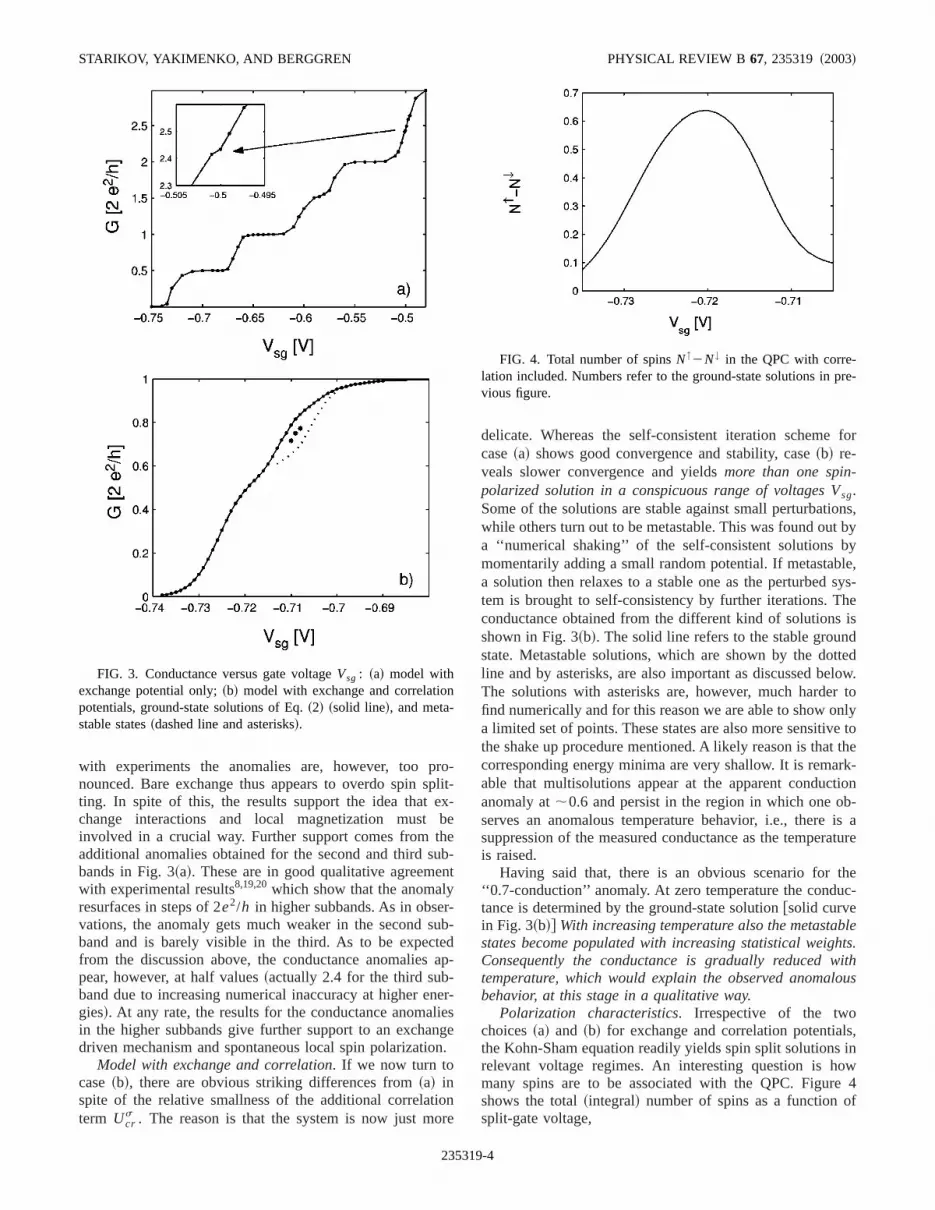
Polarization characteristics. Irrespective of the twochoices~a! and ~b! for exchange and correlation potentialthe Kohn-Sham equation readily yields spin split solutionsrelevant voltage regimes. An interesting question is hmany spins are to be associated with the QPC. Figurshows the total~integral! number of spins as a function osplit-gate voltage,
FIG. 4. Total number of spinsN↑2N↓ in the QPC with corre-lation included. Numbers refer to the ground-state solutions in pvious figure.
9-4

alithn-plhew
-cil
atminan-tx
e-only,l
nd
uti
h
-Iigs
blsa
utrd
odatesps
pldat,
ouren-po-und
he
SCENARIO FOR THE 0.7-CONDUCTANCE ANOMALY IN . . . PHYSICAL REVIEW B67, 235319 ~2003!
N↑2N↓5E drDrspin , ~11!
whereDrspin5r↑2r↓ is the local spin density. A maximumvalue;0.6 spins is obtained forVsg50.717 V, which is justthe voltage at which one finds the first conduction anomin Fig. 3~b!. The spin content is in good agreement wprevious estimates7,12 also based on the spin-polarized KohSham equations. Similar results are obtained for the halfteau in Fig. 3~a! and for the conductance structures in thigher subbands, although magnitudes become smallerincreasing subband index.
The spin polarization is mainly localized within the lithographic QPC region. It is accompanied by Friedel-like oslations in the outer regions. There is a qualitative changethe local magnetization as one proceeds from pinch-off20.74 V in Fig. 3~b! towards the conductance anomaly a20.717 V. At lowest voltages, there is a strong minimuright at the middle of the QPC. As the gate voltage iscreased this dip gets more shallow and gradually disappeFigures 5~a!–5~c! show the progression of the local spin desity as the gate voltageVsg is varied in the very regime awhich multisolutions appear and the magnetization mamizes. Just below the critical voltage20.717 V there is thusa slight minimum inDrspin @Fig. 5~a!#, which evolves into aflat peak at the bifurcation point@Fig. 5~b!#. On further in-crease ofVsg , the maximum is smoothly rounded. The rsults in Fig. 5 refer to the Kohn-Sham ground-state solutiwith the full exchange-correlation potential. Qualitativethe same results are also found for the exchange modeFig. 3~a!. The pattern is repeated for the two higher subbaalthough the magnitudes are smaller.
Local spin densities and the presence of a deep minimat certain voltages are also discussed in Refs. 7,12 forground-state subband. However, in the present case the mmum appears only at lowest electron concentrations. Tdifference might depend on different device geometries.
Potential characteristics. Figure 6 shows typical spinpolarized potentials along the middle transport direction.the two cases shown, there is a clear difference in the heof the transmission barriers for the two spin direction;1 meV and;1.5 meV for the ground-state and metastasolutions, respectively. There are also notable differencethe shape of potentials. For example, a flattened regionpears for the metastable solutions. The minima in the oregions are located at different distances from the centethe QPC. In both cases one finds, as to be expected, Frielike oscillation.
Transmission and wave-function characteristics. To ex-plain the zero-bias anomaly in the conductance, Meiret al.11
have recently proposed an Anderson model. Such a mrequires that there are some kind of localized bound stassociated with the QPC. For a wide and tall barrier thauthors have argued that there are, in addition to the exnentially increasing transparency, narrow transmission renances above the barrier. This would result from multireflections from the edges of the barrier, and are relatequasibound states, which can play the role of localized stin an Anderson model. This would be true for, let us say
23531
y
a-
ith
-int
-rs.
i-
s
ins
mheni-is
nht,einp-erofel-
eleseo-o-etoesa
sharp rectangular barrier. In the present case, however,simulations show that the barriers have soft features. In geral, they are more like a gentle parabolic saddle-pointtential, which does not display resonances from quasiboresonances.
FIG. 5. Local spin polarization along the transport axis in tmiddle of wire for different split-gate voltagesVsg520.720 ~a!,Vsg520.717~b!, Vsg520.714~c!.
9-5

sls
ncsth
ia
amn
ce
o
ena
theisust
re 9for
herrentes-hend,s tod asalso
PCent
in ain-
iohec
viained
ig.ddtry.
the
STARIKOV, YAKIMENKO, AND BERGGREN PHYSICAL REVIEW B67, 235319 ~2003!
To clarify this issue we have calculated transmission afunction of energy for different open transmission channeIn order not to miss some potentially very narrow resonapeaks, we have varied the energy in minute steps. Resultthe transmissions, which are shown in Fig. 7, refer toself-consistent ground-state solution in Fig. 3~b!. Irrespectiveof the energy resolution chosen we find that all the transmsions increase monotonously with energy. Hence, thereno traces of transmission peaks and oscillations. The squalitative picture is found also for the self-consitent potetials corresponding to different split-gate voltagesVsg . Wehave also investigated the higher states in Fig. 3~b! in thesame way. Also in this case the results are negative.We thusconclude that there are no quasibound states or resonanat least for the present realistic device parameters.
Although the self-consistent calculations also do not shquasibound states, the individual scattering states showtriguing features in the QPC region. The self-consiststates displayed in Fig. 8 are typical. Evidently, there is
FIG. 6. Spin-polarized self-consistant total potentials fors5↑~solid line! and s5↓ ~dashed line! along transport axis in themiddle of the device atVsg520.715 V; ~a! and ~b! refer to theground-state and the unstable solutions, respectively@solid anddashed curves in Fig. 3~b!#. ~Although oversimplified, we may saythat an incoming electron at the Fermi levelEf50 is essentiallydivided into ‘‘transverse’’ and ‘‘longitudinal motions.’’ Thus thelongitudinal motion is the one that determines the transmissTherefore we have full transmission for up-spin in the grapshown here, while it is strongly reduced for the opposite spin dirtion.
23531
a.efore
s-ree
-
s,
win-tn
accumulation of the individual transmitting states insideQPC in spite of the overall reduction of total density. Thfeature is generic, it applies to all scattering states and mnot be taken as an indication of quasibound states. Figushows a number of the scattering states in more detaildifferent spins and at two different voltages.
It is easy to understand why the accumulation within tQPC takes place. Each scattering state carries a cuwhich must be same for all cross sections. In the wide rervoirs the local longitudinal wave number is high while tlocal amplitude may be low. In the QPC, on the other hathe situation must be the reverse one if the total current ibe preserved. Thus the accumulation is easy to understana necessary consequence for current conservation. It isfound, however, for equilibrium situations such as a Qconnecting two quantum dots in which there is no currflow.7
IV. SUMMARY
We have simulated the zero-temperature conductancerealistic GaAs/AlGaAs split-gate QPC device using the sp
n.s-
FIG. 7. Transmission through a QPC for electrons injecteddifferent transfer modes and energy. The QPC potential is obtafrom the self-consistent calculations for the split-gate voltageVsg
520.715 V. The results refer to the ground-state solution in F3~b!. The labeling defines the different injection channels. For onumbers the channel transmission vanishes because of symme
FIG. 8. Absolute values of two typical scattering states alongsymmetry axis of the device. Electrons withE5Ef are injected inthe first ~thick line! and third modes~thin line! at Vsg520.715.
9-6

SCENARIO FOR THE 0.7-CONDUCTANCE ANOMALY IN . . . PHYSICAL REVIEW B67, 235319 ~2003!
FIG. 9. ~Color! Absolute valueof scattering states with energyE5Ef . ~a! Vsg520.715, s5↑,first mode. ~b! Vsg520.715, s5↑, second mode.~c! Vsg520.715, s5↑, third mode. ~d!Vsg520.715, s5↓, first mode.~e! Vsg520.715, s5↓, secondmode. ~f! Vsg520.715, s5↓,third mode. ~g! Vsg520.699,s5↑, first mode. ~h! Vsg
520.699, s5↑, second mode.~i! Vsg520.699, s5↑, thirdmode. ~j! Vsg520.699, s5↓,first mode. ~k! Vsg520.699,s5↓, second mode. ~l! Vsg
520.699,s5↓, third mode.
wn
wols
-a
w-o,ntnde
se-no
insu
re is, and
volt-may
themfor
atesunddobeh asions
12the
ara-n
relaxed Kohn-Sham equations. As in previous studies,recover conduction anomalies associated with local magtization that modifies the transmission barrier for the tspin directions in different ways. We have used two mode~a! with exchange only, and~b! with exchange and correlation potentials included. Both cases give rise to two anomlies although~a! overestimates the magnetization. It is, hoever, computationally relatively stable and we have therefalso been able to study higher subbands for the first timethe best of our knowledge. In accordance with experimewe recover smaller replicas in the second and third subba
In case~b! the introduction of correlation weakens thpolarization, and as a consequence the conductance icreased towards normal conduction. The simulations wcarried out with a variation of initial conditions for the iteration procedure. Making random choices of the initial potetial, we have found that there are multisolutions in a rangevoltages where an anomalous temperature dependenceconductance is observed. We have suggested that mea
23531
ee-
:
-
retos,s.
in-re
-fthere-
ments may be analyzed in these terms. As the temperaturaised the metastable states become thermally activatedas a consequence the conductance decreases for a givenage. We have also suggested that a similar mechanismtake place with increasing source-drain voltageVsd . Furtherwork should be performed along these lines includingeffects of magnetic field. Unfortunately, the Kohn-Shaequations for finite temperatures are not readily availablethe 2D systems discussed here.
We have also studied the nature of the scattering stbecause of the proposition of resonant or quasibostates.11,12 For the realistic split-gate device studied wenot recover this kind of states. This negative result mightrelated to device geometry. In our case there are as muc20 subbands in the source and drain regions, i.e., the regare effectively two dimensional, while in Refs. 11 andthere are just two channels in the leads. Therefore, inlatter case the system is more like a long two-channel pbolic wire with a local constriction. The difference betwee
9-7

eetthte
opnltais,hiu
hiri
ea
.oint
on
ishRe-ila-
STARIKOV, YAKIMENKO, AND BERGGREN PHYSICAL REVIEW B67, 235319 ~2003!
the two devices should make an interesting case for theperimentation of the role of geometry, electron densities,
Finally, one should add a few words of caution aboutKohn-Sham equations. Here we make use of excited stabut to be strict, the LSDA is designed for ground-state prerties. The form of correlation potential also raises questioAlthough numerically small, we have noticed that the resuare sensitive to this term. Different approximate algebrexpressions forUcr
s (r ) may therefore give different numberbut supposedly not a qualitatively different scenario. Tpoint should, of course, be tested in future work. In the simlations, we have allowed a collinear magnetism only. Twas done for computational convenience but there is no pcipal reason for not extending the modeling to noncollinsituations as well. Such work is in progress.
ie
mon
R
.t,
uV
23531
x-c.es,-s.sc
s-sn-r
Note added in proof.Recently P. S. Cornaglia and C. ABalseiro have studied the magnetic nature of quantum pcontacts and quasibound states.21 G. Seelig and K. A.Matveev have drawn attention to electron-phonscattering.22
ACKNOWLEDGMENTS
This work has been supported by the Royal SwedAcademy of Sciences and The Swedish Natural Sciencesearch Council NFR~now The Swedish Research CouncVR!. The computations were in part performed at the Ntional Supercomputer Center at Linko¨ping University.
d
.. B
ld,
1D.A. Wharam, T.J. Thornton, R. Newbury, M. Pepper, H. Ritchand G.A.C. Jones, J. Phys. C21, L209 ~1988!.
2B.J. van Wees, H. van Houten, C.W.J. Beenakker, J.G. Williason, L.P. Kouwenhoven, D. van der Marel, and C.T. FoxtPhys. Rev. Lett.60, 848 ~1988!.
3K.J. Thomas, J.T. Nicholls, M.Y. Simmons, M. Pepper, D.Mace, and D.A. Ritchie, Phys. Rev. Lett.77, 135 ~1996!.
4R. Fitzgerald, Phys. Today55~5!, 21 ~2002!.5K.-F. Berggren and M. Pepper, Phys. World15„10…, 37 ~2002!.6J. R. Minkel, Phys. Rev. Focus10, 24 ~2002!.7K.-F. Berggren and I.I. Yakimenko, Phys. Rev. B66, 085323
~2002!.8D.J. Reilly, T.M. Buehler, J.L. O’Brien, A.R. Hamilton, A.S
Dzurak, R.G. Clark, B.E. Kane, L.N. Pfeiffer, and K.W. WesPhys. Rev. Lett.89, 246801~2002!.
9P.E. Lindelof, Proc. SPIE4415, 77 ~2001!.10S.M. Cronenwett, H.J. Lynch, D. Coldhaber-Gordon, L.P. Ko
wenhoven, C.M. Marcus, K. Hirose, N.S. Wingreen, andUmansky, Phys. Rev. Lett.88, 226805~2002!.
,
-,
.
-.
11Y. Meir, K. Hirose, and N.S. Wingreen, Phys. Rev. Lett.89,196802~2002!.
12K. Hirose, Y. Meir, and N.S. Wingreen, Phys. Rev. Lett.90,026804~2003!.
13D. Schmeltzer, cond-mat/0211490~unpublished!.14R.G. Parr and W. Yang,Density-Functional Theory of Atoms an
Molecules~Oxford University Press, New York, 1989!.15J.H. Davies, Semicond. Sci. Technol.3, 995 ~1988!; J.H. Davies,
I.A. Larkin, and E.V. Sukhorukov, J. Appl. Phys.77, 4504~1995!.
16B. Tanatar and D.M. Ceperley, Phys. Rev. B39, 5005~1989!.17T. Ando, Phys. Rev. B44, 8017~1991!.18C.-K. Wang and K.-F. Berggren, Phys. Rev. B57, 4552~1998!.19K.J. Thomas, J.T. Nicholls, N.J. Appleyard, M.Y. Simmons, M
Pepper, D.R. Mace, W.R. Tribe, and D.A. Ritchie, Phys. Rev58, 4846~1998!.
20K.S. Pyshkin, C.J.B. Ford, R.H. Harrel, M. Pepper, E.H. Linfieand D.A. Ritchie, Phys. Rev. B62, 15 842~2000!.
21P. S. Cornaglia and C. A. Balseiro, cond-mat/0304168~unpub-lished!.
22G. Seelig and K. A. Matveev, Phys. Rev. Lett.90, 176804~2003!.
9-8


