Embed Size (px)
Citation preview
June 2007, published 15, doi: 10.1098/rsta.2007.2028365 2007 Phil. Trans. R. Soc. A
FreySaar Kirmayer, Eyal Aharon, Ekaterina Dovgolevsky, Michael Kalina and Gitti L semiconducting polymer nanocomposites
2 and SiO2, SnS2Self-assembled lamellar MoS
Referencesl.html#ref-list-1http://rsta.royalsocietypublishing.org/content/365/1855/1489.ful
This article cites 50 articles, 2 of which can be accessed free
Email alerting service herein the box at the top right-hand corner of the article or click Receive free email alerts when new articles cite this article - sign up
http://rsta.royalsocietypublishing.org/subscriptions go to: Phil. Trans. R. Soc. ATo subscribe to
on March 12, 2014rsta.royalsocietypublishing.orgDownloaded from on March 12, 2014rsta.royalsocietypublishing.orgDownloaded from
on March 12, 2014rsta.royalsocietypublishing.orgDownloaded from
Self-assembled lamellar MoS2, SnS2 and SiO2
semiconducting polymer nanocomposites
BY SAAR KIRMAYER, EYAL AHARON, EKATERINA DOVGOLEVSKY,MICHAEL KALINA AND GITTI L. FREY*
Department of Materials Engineering, Technion—Israel Institute ofTechnology, Haifa 32000, Israel
Lamellar nanocomposites based on semiconducting polymers incorporated into layeredinorganic matrices are prepared by the co-assembly of organic and inorganic precursors.Semiconductingpolymer-incorporated silica is prepared by introducing the semiconductingpolymers into a tetrahydrofuran (THF)/water homogeneous sol solution containing silicaprecursor species and a surface-active agent. Semiconducting polymer-incorporated MoS2and SnS2 are prepared by Li intercalation into the inorganic compound, exfoliation andrestack in the presence of the semiconducting polymer. All lamellar nanocomposite films areorganized in domains aligned parallel to the substrate surface plane. The incorporatedpolymers maintain their semiconducting properties, as evident from their opticalabsorption and photoluminescence spectra. The optoelectronic properties of thenanocomposites depend on the properties of both the inorganic host and the incorporatedguest polymer as demonstrated by integrating the nanocomposite films into light-emittingdiodes.Devices based on polymer-incorporated silica and polymer-incorporatedMoS2 showno diode behaviour and no light emission due to the insulating andmetallic properties of thesilica andMoS2 hosts. In contrast, diode performance and electroluminescence are obtainedfrom devices based on semiconducting polymer-incorporated semiconducting SnS2,demonstrating that judicious selection of the composite components in combination withthe optimization of material synthesis conditions allows new hierarchical structures to betailored for electronic and optoelectronic applications.
Keywords: nanocomposites; semiconducting polymers; layered structures;intercalation
Onelec
*A
1. Introduction
Conjugated polymers derive their semiconducting properties from the delocaliza-tion of electrons in the p (bonding) and p� (anti-bonding) bands, analogous to themobility of charge carriers in the valence and conduction bands of crystallineinorganic semiconductors. The unique combination of electrical properties, suchas semiconductivity, high carrier mobility and electroluminescence, with chemicaltunability and solution processability, provides the means to fabricate flexible,
Phil. Trans. R. Soc. A (2007) 365, 1489–1508
doi:10.1098/rsta.2007.2028
Published online 12 April 2007
e contribution of 12 to a Discussion Meeting Issue ‘Supramolecular nanotechnology for organictronics’.
uthor for correspondence ([email protected]).
1489 This journal is q 2007 The Royal Society
S. Kirmayer et al.1490
on March 12, 2014rsta.royalsocietypublishing.orgDownloaded from
cheap and large-area electronic applications (Reichmanis et al. 2005). However, inaddition to the electrical properties of the polymers, it was found that the deviceperformances are strongly dependent on the polymer film morphology. Solid-stateeffects such as polymer crystallinity, liquid crystallinity, aggregation, chain–chaininteractions and p–p stacking control the charge transport and excitation in thefilm, and, hence, the device performance (Schwartz 2003; Bredas et al. 2004).Therefore, attaining control over the morphology and hierarchal structure of thepolymer chains is expected to enhance device performance and provide an entryfor the design and fabrication of new types of devices.
One way to gain such command is by confining the polymer chains into thevoids of a porous matrix. The geometry and size of the voids are used to enforcedesired morphologies on the confined polymer. Encapsulation of the polymer isalso beneficial for its chemical, environmental and mechanical stability.Inorganic porous materials, with strong covalent interactions forming anextended robust framework, are suitable host matrices. In addition to theirhigh thermostability, the inorganic hosts also offer desirable solid-statecharacteristics, such as well-defined electronic properties and mechanicalresilience. The polymer/inorganic guest/host nanocomposites, therefore, harnessthe good processability and chemical tunability of the polymer component, incombination with high strength, stiffness and durability of the inorganiccomponent. Finally, the composite material is designed not only to improvethe properties of the polymer, but also to enhance or exhibit properties andfunctions unattainable in the individual phase by, for example, tailoring theorganic/inorganic interfacial interactions.
There are two types of host structures that offer well-defined vacant sites forpolymer hosting: three-dimensional scaffolds and two-dimensional scaffolds. Thethree-dimension scaffolds, such as zeolites and mesoporous materials, consist ofnanometre-sizeporesandchannels that canbefilledwithpolymerwithoutdestroyingtheir connectivity or framework structure. Incorporating semiconducting polymersinto the voids of a pre-formed scaffold is possible by polymer ormonomer infiltrationfollowed by in situ polymerization (McCaughey et al. 2003; Errien et al. 2005).Polymerization in the channels is sterically hindered by the size and geometry of thepores and results in low-molecularweight andhigh contamination levels of unreactedprecursors, leaving groupsandpolymerization catalysts.These contaminations oftendope the semiconducting polymers converting them to conductors.
Partial infiltration of conjugated polymers in mesoporous silica and titania hasbeen demonstrated for poly(phenylene-vinylene) (Nguyen et al. 2000, 2001; Xiet al. 2003; Pattantyus-Abraham & Wolf 2004) and polythiophene derivatives(Coakley et al. 2003; McCaughey et al. 2003). However, direct threading ofpolymers through the host galleries is difficult to control because it depends onboth partitioning of the polymer from the solvent and reptation into the pores,which can be slow due to diffusion limitations. Reptation of conjugated polymersis further restricted by their p-bonding rigidity. Indeed, the infiltration into hostmatrices of rigid-rod-conjugated polymers, such as the blue-emitting polyfluor-ene, has not been reported so far.
In another approach for the preparation of the guest/host nanocomposites, theinorganic framework is formed in the presence of the guest molecules, effectivelyencapsulating the guest species into the scaffold during its formation. This self-organization approach offers molecular-level command over interfaces, structure
Phil. Trans. R. Soc. A (2007)
1491Nanocomposites and semiconductivity
on March 12, 2014rsta.royalsocietypublishing.orgDownloaded from
and morphology, and provides new ways to introduce function and form intomaterials. The co-assembly of organic and inorganic precursors into ananocomposite material requires that both the inorganic precursor and theguest conjugated polymer are solvated in the precursor solution. This prerequisiteis hard to satisfy because conjugated polymers are highly hydrophobic and solublein solvents such as chloroform, xylene and toluene, while inorganic precursors aretypically soluble in polar solvents such as water and alcohol.
Recently, we have developed a robust new synthetic approach for thepreparation of mesoscopically ordered semiconducting polymer/silica nanocom-posites from a THF/water homogeneous solution. Thin films are depositedthrough the co-assembly of silica precursor, a surface-active amphiphilic agentand pre-polymerized semiconducting polymers. The developed process is generaland, in fact, several conjugated polymers were incorporated into mesostructuredsilica including poly(phenylene-vinylene) and rigid-rod polyfluorene derivatives.Depending on the surface-active agents selected, it was possible to prepare twodifferent mesophases: (i) a hexagonal mesophase silica with conjugated polymerguest species incorporated within the hydrophobic cylinders organized indomains aligned with the substrate surface plane; or (ii) a lamellar mesophasesilica with the layers oriented parallel to the substrate surface and the conjugatedpolymer guest incorporated into the hydrophobic layers. Lamellar structures areparticularly desirable because the geometry is expected to enforce planarmorphology on the confined polymer chains, which increases its conjugationlength and enhances carrier mobility.
Lamellar inorganic/conjugated polymer nanocomposites can also be preparedby incorporating the polymers into the galleries of two-dimension layeredcompounds. The two-dimension layered compounds are characterized by strongcovalent bonds within the layers and weak van der Waals forces between thelayers. This structure leads to extremely anisotropic mechanical, chemical andelectrical properties and a dangling-bond-free, inert, exposed surface. Theinterlayer space can be separated considerably to incorporate the guest polymerwhile preserving the integrity of the layer structure (Ruizhitzky 1993; Oriakhi1998; Pomogailo 2005). Numerous layered inorganic host materials are known,including clays and layered silicates, members of the transition metaldichalcogenide family (MoS2, WSe2 and NbS2), metal oxides (MoO3 and V2O5)and metal halides (PbCl2). While clays and metal oxides are optically andelectronically inactive host matrices, the transition metal dichalcogenides (MX2)offer a wide variety of electronic properties ranging from insulators like HfS2,through semiconductors and semimetals like WS2 and TiSe2, to true metals likeNbS2 (Wilson & Yoffe 1969). Therefore, developing a robust synthetic procedurefor semiconducting polymer-incorporated transition metal dichalcogenides offersa family of functional nanocomposites, with tunable properties through judiciousselection of the host and guest species.
Intercalation, i.e. the incorporation of guest species into layered compounds, ofconjugated polymers has been widely reported using mainly in situ oxidativepolymerization (Pomogailo 2005). This process requires that redox-activeconjugated monomers and other polymerization initiators are loaded intostrongly oxidizing layered hosts. Kanatzidis et al. (1987) reported the firstconjugated polymer/layered compound guest/host nanocomposite using thein situ polymerization of incorporated anhydrous pyrrole in the layered space of
Phil. Trans. R. Soc. A (2007)
S. Kirmayer et al.1492
on March 12, 2014rsta.royalsocietypublishing.orgDownloaded from
FeOCl (Kanatzidis et al. 1987). This method has been extended to polymerizepolyaniline, polythiophene and poly(phenylene-vinylene) in layered oxides,chlorides, silicates and phosphates (Ruizhitzky 1993; Gomez-Romero 2001).The strongly oxidizing host character required to induce the redox poly-merization limits the selection of the host material. Another disadvantage of thein situ polymerization process is that the formed polymer is in its dopedconductive state, in contrast to its pristine desirable semiconducting state.
These difficulties are overcome by the exfoliation–adsorption technique. In thiscase, the host material is delaminated into single inorganic sheets and thenrestacked, incorporating the polymer in between the layers. Layered host latticessuch as clay minerals, transition metal dichalcogenides, niobates or titanates canbe delaminated into single sheets suspended in suitable solvents. Some layeredlattices such as MoO3 and MoS2 may be pre-intercalated with highly reactivealkaline metal ions to enhance their delamination in a given solvent (Murphyet al. 1976; Divigalpitiya et al. 1989). The exfoliation process is usually assistedfurther by mechanical stirring or sonication. When a solution of the polymer ofinterest is added, the delaminated sheets spontaneously flocculate to formordered nanocomposites with the polymer trapped between the sheets.Intercalating pre-formed semiconducting polymers into the interlayer galleriesusing the exfoliation–adsorption technique is limited by the immiscibility of thehighly hydrophobic polymer guest in the aqueous exfoliation solution.
We recently reported the intercalation of the semiconducting polymerpoly(9,90-dioctylfluorene), PFO, into the galleries of layered MoS2 and SnS2 byexfoliating the Li-intercalated MS2 host in methanol rather than in water(Aharon et al. 2006a). Since methanol and xylene, a common solvent forsemiconducting polymers, are relatively miscible, it was possible to introduce axylene-conjugated polymer solution into the methanol MS2 single-layersuspension, without phase separation. The flocculation of the delaminated sheetseffectively traps the semiconducting polymer in between the inorganic sheetsforming the desired lamellar nanocomposite material.
In this report, two lamellar inorganic/semiconducting polymer nanocompositesystems are demonstrated. In both cases, the hierarchical structure is formedthrough the self-organization of inorganic precursors and the semiconductingpolymers. Two semiconducting polymers are used as guests: red-emittingpoly(2-methoxy-5-(20-ethyl-hexyloxy)-1,4-phenylene vinylene), MEHPPV; andpoly(9,9 0-dioctylfluorene), PFO. The incorporated polymers maintain theirsemiconducting properties, as evident from their optical absorption andphotoluminescence (PL) spectra. The optoelectronic properties of the layerednanocomposites, however, depend on the properties of both the inorganic host andthe incorporated guest polymer, as demonstrated by integrating the nanocompo-site films into light-emitting diode structures. The devices based on polymer-incorporated silica, i.e. semiconducting guest/insulating host, show poor diodebehaviour with low current densities at high fields, less than 50 mA mK2 at1!106 V mK1, and no light output. The devices based on semiconductingguest/metallic host nanocomposites, polymer-incorporated MoS2, show ohmiccharacter with no diode performance and no light output. In contrast, diodeperformance and electroluminescence are obtained from devices based onpolymer-incorporated SnS2 nanocomposites, with light turn-on at approximately6 V and luminance of 1 cd mK2 at approximately 9 V. SnS2 is a semiconductor
Phil. Trans. R. Soc. A (2007)
1493Nanocomposites and semiconductivity
on March 12, 2014rsta.royalsocietypublishing.orgDownloaded from
and maintains its semiconductivity upon polymer incorporation (Aharon et al.2006a). Therefore, the semiconducting polymer-incorporated SnS2 lamellarnanocomposite is effectively a continuous sequence of molecular semiconductor–semiconductor junctions.
The first part of this paper describes the synthesis and structuralcharacterization of a lamellar silica/semiconducting polymer nanocompositeprepared by the co-assembly of silica precursors and semiconducting polymersfrom a THF/water homogeneous solution. In the second part of the paper, wedescribe the preparation and characterization of semiconducting polymer-intercalated transition metal dichalcogenides, MoS2 and SnS2, prepared byexfoliation in methanol and restacked in presence of a xylene polymer solution.The optical properties of the polymers encapsulated in silica, MoS2 and SnS2 arereported and compared with those of the pristine polymer in view of theirintegration into light-emitting diodes. Finally, device performance of light-emitting diodes based on the lamellar nanocomposites is discussed.
2. Experimental
(a ) Materials
Conjugated polymers, poly[2-methoxy-5-(2 0-ethyl-hexyloxy)-1,4-phenylenevinylene] (MEHPPV, MWZ200 K) or poly(9,90-dioctylfluorene) (PFO, MWZ74 K), were supplied by American dye-sources (ADS). The surfactant used wasPEO20–PPO70–PEO20 (Pluronic P123 MnZ5750; PEO stands for polyethyleneoxide and PPO stands for polypropylene oxide).
For the synthesis of lamellar silica/semiconducting polymer nanocomposites,the sol solution was prepared by mixing THF, tetraethoxysilane (TEOS) andHCl 0.07 M in DI water. After mixing, the solution was positioned in anultrasonic bath for an hour. A second solution was prepared by dissolving thesurfactant, P123, and conjugated polymer, either PFO or MEHPPV, in THF.The surfactant/polymer solution was then added to silica sol solution to give thefinal molar ratio of 1 TEOS : 40.5 THF : 4.785 H2O : 6!10K3 HCl : 1.3!10K5
conjugated polymer, and 0.033 P123. Nanocomposite thin films were prepared bydip coating on glass, polyimide film or ITO substrates. All deposited thin filmswere approximately 250 nm in thickness, uniform and crack free.
For the synthesis of lamellar layered compound semiconducting polymernanocomposites, LixMoS2 and LixSnS2 were prepared by addition of BuLi (1.6 Min hexanes) to 2H-MoS2 or SnS2 powder under a nitrogen atmosphere followingthe procedure of Murphy et al. (1976). LixMS2 (MZMo; Sn) of 40–50 mg wereexfoliated in 7 ml methanol in an ultrasonic bath for 60 min. The suspension wascentrifuged and the sediment was subsequently redispersed in methanol. Thisprocess was repeated four times to ensure full removal of Li ions. To the Li-freeredispersed methanol suspension, 5–7 ml of 5 mg mlK1 PFO or MEHPPV ino-xylene were added, and the mixture was stirred for 4 days. The suspension wasthen recentrifuged and the sediment redispersed in o-xylene. This process wasrepeated until no traces of semiconducting polymer were found in the absorptionspectra of the supernatant solution, typically five to six times. Nanocompositethin films for absorption and PL measurements were prepared by drop castingfrom methanol.
Phil. Trans. R. Soc. A (2007)
S. Kirmayer et al.1494
on March 12, 2014rsta.royalsocietypublishing.orgDownloaded from
(b ) Characterization
X-ray powder diffraction (XRD) measurements of MX2 and semiconductingpolymer-intercalated MX2 were performed on a Philips X-Pert diffractometerusing a Cu Ka X-ray source (lZ1.5406 A). X-ray diffraction measurements ofsilica and semiconducting polymer-incorporated silica were performed on a BedeD3 X-ray diffractometer equipped with an 18 kWRigaku rotating anode generatorat q–2q scan mode in reflection geometry. A highly monochromatized Cu Ka1 linewith lZ1.5406 A was selected from the primary X-ray beam by means of twochannel-cut (220) Si crystals. Small-angle X-ray scattering measurements (SAXS)were performed using a small-angle diffractometer (Bruker Nanostar, KFFCU 2K-90) with Cu Ka radiation with lZ1.542 A. Pinhole collimation yielding abeam 100 mm in diameter and a 10!10 cm2 two-dimensional position-sensitivewire detector positioned 65 cm behind the sample were used. The patterns wererecorded using an acceleration voltage of 40 kV and an acceleration current of30 mA. The polyimide substrates were vertically located in the SAXSdiffractometer and patterns were recorded in transmission mode with the fixedincidence angle a (the angle between the incident beam and the sample surface) ofapproximately 28. This configuration, referred to as ‘glancing incidence’, mimicsthe ‘grazing incidence’ technique where the X-ray beam is incident at nearly thecritical angle. The two-dimension SAXS ‘glancing incidence’ scattering geometryshows diffracted intensity exclusively out of the film plane.
Transmission electron microscopy (TEM) measurements were performedusing a JEOL JEM 2010 transmission electron microscope operated at 200 keV.TEM samples were prepared by scratching the thin films and directly dispersingthe film fragments onto holey carbon copper grids. Scanning electron microscopy(SEM) measurements were performed using an FEI QUANTA 200 SEMequipped with an SE detector. The spot size, magnification, work distance andaccelerating voltage are indicated in the micrographs.
Optical absorption spectra were taken using a Varian Cary 100 Scan UV–visspectrophotometer. Photoluminescence spectra were collected at room tempera-ture with a Varian Cary Eclipse fluorimeter using excitation wavelengths of390 nm for PFO and 480 nm for MEHPPV.
3. Results and discussion
(a ) Lamellar silica/semiconducting polymer nanocomposites
The deposition of lamellar silica/semiconducting polymer nanocomposites isachieved by the evaporation-induced self-assembly (EISA) technique which wasdeveloped and extensively studied by Brinker and co-workers (Lu 1997; Brinkeret al. 1999). In the course of the EISA process, surfactants self-assemble intomicelles and lyotropic mesophases in ethanolic aqueous solutions. Compositesilica/surfactant thin films are deposited by dip coating. The ethanol evaporatesand the silica precursor and surfactant co-assemble into highly orderedmesophases which are subsequently fixed by silica polymerization. Surfactant-directed silica thin films prepared by EISA exhibit lamellar, two-dimensionhexagonal, three-dimension hexagonal or cubic mesostructures depending ondeposition conditions such as temperature, humidity and dipping rate, and the
Phil. Trans. R. Soc. A (2007)
1495Nanocomposites and semiconductivity
on March 12, 2014rsta.royalsocietypublishing.orgDownloaded from
concentration and chemical character of the surfactant (Alberius et al. 2002;Brinker 2004). Both ionic and non-ionic surfactants are used to template thesilica mesostructures; however, when integrating the functional nanocompositeinto electronic and optoelectronic devices is envisaged, ionic species should beavoided. In this study, a PEO20–PPO70–PEO20 block copolymer (Pluronic P123)is used because it is known to template the desired silica lamellar mesophasefrom ethanolic aqueous sol solutions (Alberius et al. 2002).
Functional hydrophobic molecules such as dyes were incorporated intoordered silica mesophases by adding them to the ethanolic aqueous sol solution(Minoofar et al. 2002; Scott et al. 2003; Bruhwiler & Calzaferri 2004; Meloshet al. 2004; Miled et al. 2004). Upon solvent evaporation, the dye moleculesconcentrate near the surfactant’s hydrophobic tail and are fixed into thehydrophobic regions of the mesophase by silica polymerization (Sanchez et al.2003). Semiconducting polymers, however, are insoluble in polar solvents andtheir addition to the sol solution results in massive polymer precipitation. Thesolution incompatibility of the silica precursor, the surfactant and the conjugatedpolymer is overcome by depositing the nanocomposite films from a THF/waterhomogeneous solution. Indeed, the preparation of transparent mesostructuredorganosilica in polymer membranes by in situ growth in THF solution was veryrecently reported, although no guest species were incorporated into thehierarchical structures (Valle et al. 2006).
Here, we extend this approach using a THF/water sol solution, including asilica precursor (TEOS), a semiconducting polymer and a commercial surfactantto form semiconducting polymer-incorporated lamellar silica. It is important tonote that the physiochemical processes in the THF/water precursor solutionhave not yet been investigated in detail and are expected to be different fromthose in the conventional ethanol/water sol precursor solution. Therefore, in thisstudy, we first prepared P123-directed silica films from a THF/water precursorsol solution without any semiconducting polymer in order to: (i) verify whetherordered mesophases could be altogether obtained from THF-based sol solutionsand (ii) determine the experimental conditions necessary to obtain a lamellarphase from the THF-based sol solutions. Further, the highly hydrophobicsemiconducting polymers were added to the precursor solution in order to obtainfunctional lamellar nanocomposites. The structure of the polymer-incorporatedsilica was determined to ensure that the addition of the guest polymer into theTHF sol solution did not alter the resulting mesophase (Huang et al. 2002).
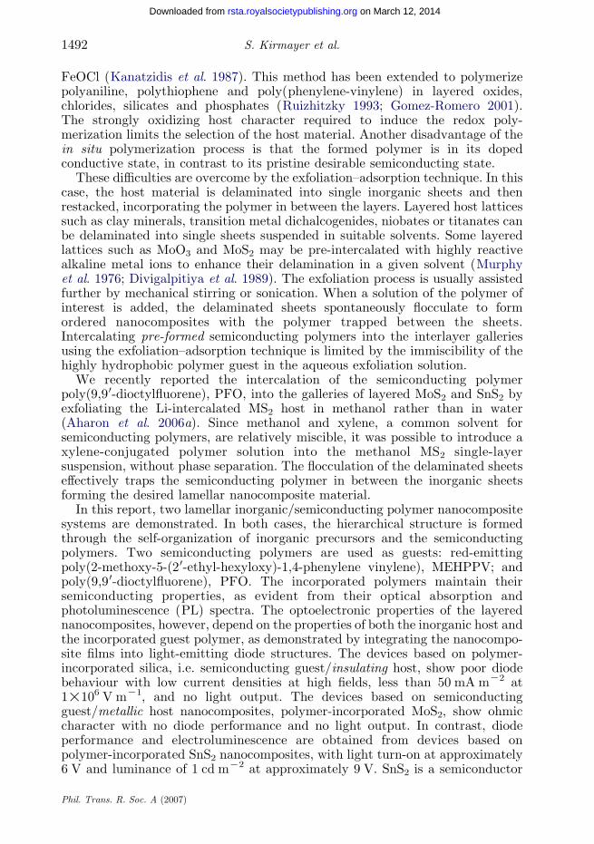
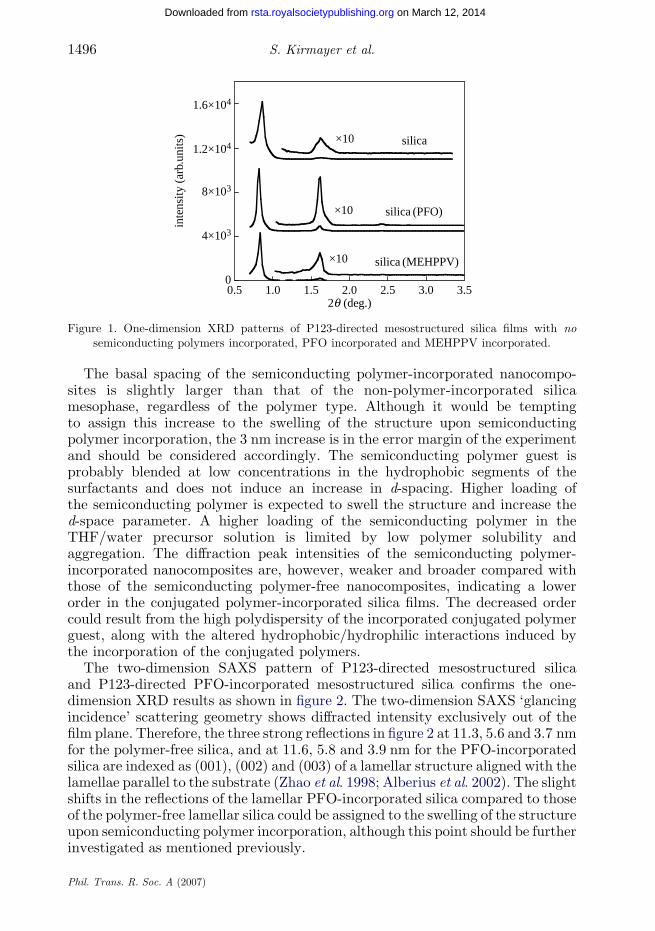
XRD patterns of P123-directed silica nanocomposite films prepared witheither no incorporated semiconducting polymers, PFO incorporated, orMEHPPV incorporated are shown in figure 1. All XRD patterns show tworeflections indexed as the (001) and (002) reflections of a highly ordered lamellarmesostructure with a basal spacing of approximately 10.3, 10.7 and 10.6 nm forthe silica, PFO-incorporated silica and MEHPPV-incorporated silica, respect-ively (Zhao et al. 1998; Alberius et al. 2002). The sharp reflection peaks of thesemiconducting polymer-free P123-directed nanocomposite films clearly showthat indeed an ordered silica mesophase can be deposited from a THF/waterprecursor sol solution. This finding is important not only for the furtherunderstanding of the silica/surfactant self-assembly process in non-aqueoussolutions, but also offers a new method to incorporate highly hydrophobic guestsinto mesostructured silica by their addition to the THF/water sol solution.
Phil. Trans. R. Soc. A (2007)
0
4×10³
8×10³
1.2×10⁴
1.6×10⁴
0.5 1.0 1.5 2.0 2.5 3.0 3.5
inte
nsity
(ar
b.un
its)
2q (deg.)
silica (MEHPPV)
silica (PFO)
silica×10
×10
×10
Figure 1. One-dimension XRD patterns of P123-directed mesostructured silica films with nosemiconducting polymers incorporated, PFO incorporated and MEHPPV incorporated.
S. Kirmayer et al.1496
on March 12, 2014rsta.royalsocietypublishing.orgDownloaded from
The basal spacing of the semiconducting polymer-incorporated nanocompo-sites is slightly larger than that of the non-polymer-incorporated silicamesophase, regardless of the polymer type. Although it would be temptingto assign this increase to the swelling of the structure upon semiconductingpolymer incorporation, the 3 nm increase is in the error margin of the experimentand should be considered accordingly. The semiconducting polymer guest isprobably blended at low concentrations in the hydrophobic segments of thesurfactants and does not induce an increase in d-spacing. Higher loading ofthe semiconducting polymer is expected to swell the structure and increase thed-space parameter. A higher loading of the semiconducting polymer in theTHF/water precursor solution is limited by low polymer solubility andaggregation. The diffraction peak intensities of the semiconducting polymer-incorporated nanocomposites are, however, weaker and broader compared withthose of the semiconducting polymer-free nanocomposites, indicating a lowerorder in the conjugated polymer-incorporated silica films. The decreased ordercould result from the high polydispersity of the incorporated conjugated polymerguest, along with the altered hydrophobic/hydrophilic interactions induced bythe incorporation of the conjugated polymers.
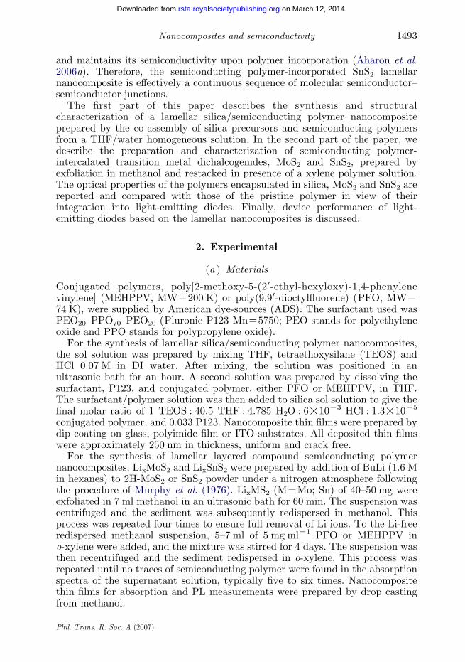
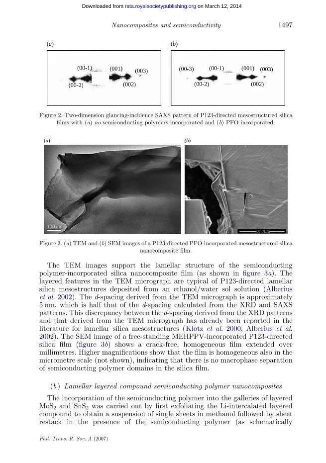
The two-dimension SAXS pattern of P123-directed mesostructured silicaand P123-directed PFO-incorporated mesostructured silica confirms the one-dimension XRD results as shown in figure 2. The two-dimension SAXS ‘glancingincidence’ scattering geometry shows diffracted intensity exclusively out of thefilm plane. Therefore, the three strong reflections in figure 2 at 11.3, 5.6 and 3.7 nmfor the polymer-free silica, and at 11.6, 5.8 and 3.9 nm for the PFO-incorporatedsilica are indexed as (001), (002) and (003) of a lamellar structure aligned with thelamellae parallel to the substrate (Zhao et al. 1998; Alberius et al. 2002). The slightshifts in the reflections of the lamellar PFO-incorporated silica compared to thoseof the polymer-free lamellar silica could be assigned to the swelling of the structureupon semiconducting polymer incorporation, although this point should be furtherinvestigated as mentioned previously.
Phil. Trans. R. Soc. A (2007)
100 nm50.0 µm
(a) (b)
100 nm
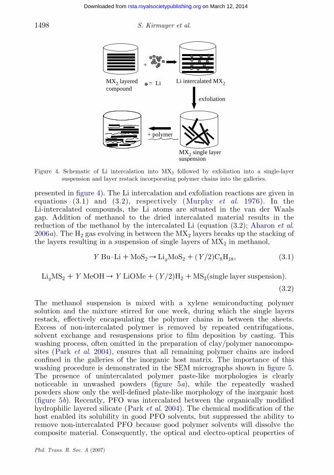
Figure 3. (a) TEM and (b) SEM images of a P123-directed PFO-incorporated mesostructured silicananocomposite film.
(a) (b)
(00-1)
(00-2)
(001) (003)
(002)
(00-1)
(00-2)
(00-3) (001) (003)
(002)
Figure 2. Two-dimension glancing-incidence SAXS pattern of P123-directed mesostructured silicafilms with (a) no semiconducting polymers incorporated and (b) PFO incorporated.
1497Nanocomposites and semiconductivity
on March 12, 2014rsta.royalsocietypublishing.orgDownloaded from
The TEM images support the lamellar structure of the semiconductingpolymer-incorporated silica nanocomposite film (as shown in figure 3a). Thelayered features in the TEM micrograph are typical of P123-directed lamellarsilica mesostructures deposited from an ethanol/water sol solution (Alberiuset al. 2002). The d-spacing derived from the TEM micrograph is approximately5 nm, which is half that of the d-spacing calculated from the XRD and SAXSpatterns. This discrepancy between the d-spacing derived from the XRD patternsand that derived from the TEM micrograph has already been reported in theliterature for lamellar silica mesostructures (Klotz et al. 2000; Alberius et al.2002). The SEM image of a free-standing MEHPPV-incorporated P123-directedsilica film (figure 3b) shows a crack-free, homogeneous film extended overmillimetres. Higher magnifications show that the film is homogeneous also in themicrometre scale (not shown), indicating that there is no macrophase separationof semiconducting polymer domains in the silica film.
(b ) Lamellar layered compound semiconducting polymer nanocomposites
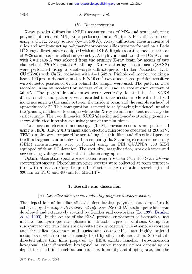
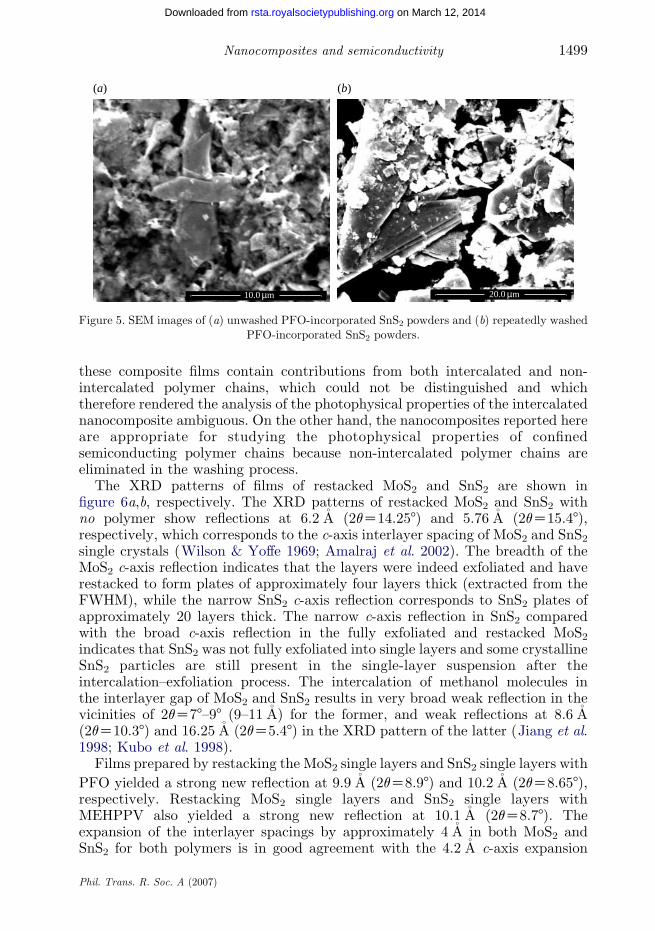
The incorporation of the semiconducting polymer into the galleries of layeredMoS2 and SnS2 was carried out by first exfoliating the Li-intercalated layeredcompound to obtain a suspension of single sheets in methanol followed by sheetrestack in the presence of the semiconducting polymer (as schematically
Phil. Trans. R. Soc. A (2007)
= Li
MX2 single layersuspension
MX2 layered compound
Li intercalated MX2
+
+ polymer
exfoliation
Figure 4. Schematic of Li intercalation into MX2 followed by exfoliation into a single-layersuspension and layer restack incorporating polymer chains into the galleries.
S. Kirmayer et al.1498
on March 12, 2014rsta.royalsocietypublishing.orgDownloaded from
presented in figure 4). The Li intercalation and exfoliation reactions are given inequations (3.1) and (3.2), respectively (Murphy et al. 1976). In theLi-intercalated compounds, the Li atoms are situated in the van der Waalsgap. Addition of methanol to the dried intercalated material results in thereduction of the methanol by the intercalated Li (equation (3.2); Aharon et al.2006a). The H2 gas evolving in between the MX2 layers breaks up the stacking ofthe layers resulting in a suspension of single layers of MX2 in methanol,
Y Bu–LiCMoS2/LiyMoS2CðY=2ÞC8H18; ð3:1Þ
LiyMS2 CY MeOH/Y LiOMeCðY=2ÞH2 CMS2ðsingle layer suspensionÞ:ð3:2Þ
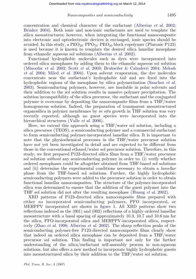
The methanol suspension is mixed with a xylene semiconducting polymersolution and the mixture stirred for one week, during which the single layersrestack, effectively encapsulating the polymer chains in between the sheets.Excess of non-intercalated polymer is removed by repeated centrifugations,solvent exchange and resuspensions prior to film deposition by casting. Thiswashing process, often omitted in the preparation of clay/polymer nanocompo-sites (Park et al. 2004), ensures that all remaining polymer chains are indeedconfined in the galleries of the inorganic host matrix. The importance of thiswashing procedure is demonstrated in the SEM micrographs shown in figure 5.The presence of unintercalated polymer paste-like morphologies is clearlynoticeable in unwashed powders (figure 5a), while the repeatedly washedpowders show only the well-defined plate-like morphology of the inorganic host(figure 5b). Recently, PFO was intercalated between the organically modifiedhydrophilic layered silicate (Park et al. 2004). The chemical modification of thehost enabled its solubility in good PFO solvents, but suppressed the ability toremove non-intercalated PFO because good polymer solvents will dissolve thecomposite material. Consequently, the optical and electro-optical properties of
Phil. Trans. R. Soc. A (2007)
(b)
20.0 µm
(a)
10.0 µm
Figure 5. SEM images of (a) unwashed PFO-incorporated SnS2 powders and (b) repeatedly washedPFO-incorporated SnS2 powders.
1499Nanocomposites and semiconductivity
on March 12, 2014rsta.royalsocietypublishing.orgDownloaded from
these composite films contain contributions from both intercalated and non-intercalated polymer chains, which could not be distinguished and whichtherefore rendered the analysis of the photophysical properties of the intercalatednanocomposite ambiguous. On the other hand, the nanocomposites reported hereare appropriate for studying the photophysical properties of confinedsemiconducting polymer chains because non-intercalated polymer chains areeliminated in the washing process.
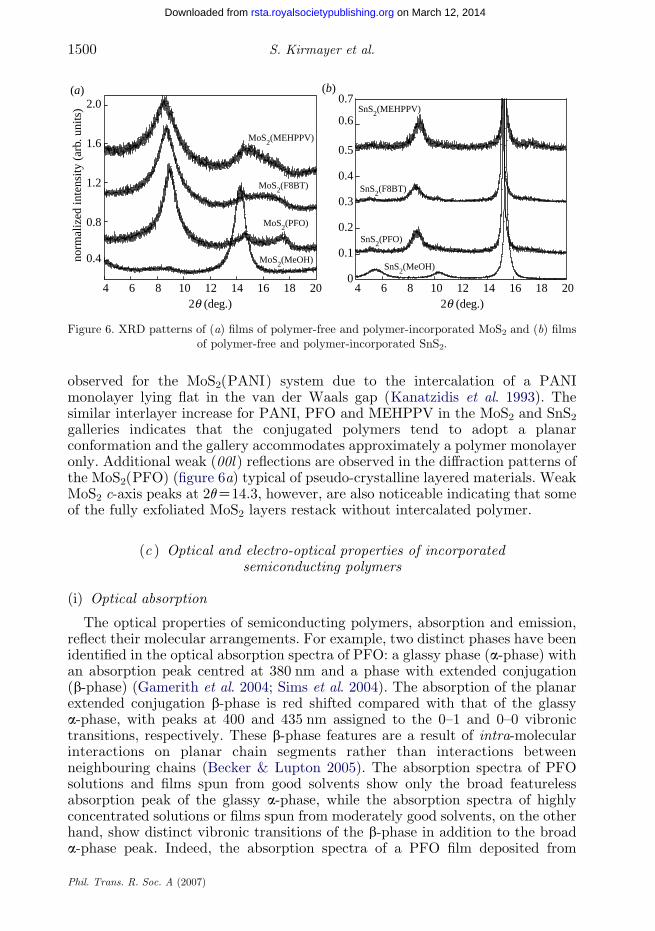
The XRD patterns of films of restacked MoS2 and SnS2 are shown infigure 6a,b, respectively. The XRD patterns of restacked MoS2 and SnS2 withno polymer show reflections at 6.2 A (2qZ14.258) and 5.76 A (2qZ15.48),respectively, which corresponds to the c-axis interlayer spacing of MoS2 and SnS2single crystals (Wilson & Yoffe 1969; Amalraj et al. 2002). The breadth of theMoS2 c-axis reflection indicates that the layers were indeed exfoliated and haverestacked to form plates of approximately four layers thick (extracted from theFWHM), while the narrow SnS2 c-axis reflection corresponds to SnS2 plates ofapproximately 20 layers thick. The narrow c-axis reflection in SnS2 comparedwith the broad c-axis reflection in the fully exfoliated and restacked MoS2indicates that SnS2 was not fully exfoliated into single layers and some crystallineSnS2 particles are still present in the single-layer suspension after theintercalation–exfoliation process. The intercalation of methanol molecules inthe interlayer gap of MoS2 and SnS2 results in very broad weak reflection in thevicinities of 2qZ78–98 (9–11 A) for the former, and weak reflections at 8.6 A(2qZ10.38) and 16.25 A (2qZ5.48) in the XRD pattern of the latter (Jiang et al.1998; Kubo et al. 1998).
Films prepared by restacking the MoS2 single layers and SnS2 single layers with
PFO yielded a strong new reflection at 9.9 A (2qZ8.98) and 10.2 A (2qZ8.658),respectively. Restacking MoS2 single layers and SnS2 single layers withMEHPPV also yielded a strong new reflection at 10.1 A (2qZ8.78). Theexpansion of the interlayer spacings by approximately 4 A in both MoS2 andSnS2 for both polymers is in good agreement with the 4.2 A c-axis expansion
Phil. Trans. R. Soc. A (2007)
(b)0.7
0.6
0.5
0.4
0.3
0.2
0.1
04 6 8 10 12 14 16 18 20
SnS2(MEHPPV)
SnS2(F8BT)
SnS2(PFO)
SnS2(MeOH)
2q (deg.)
(a)
2q (deg.)4 6 8 10 12 14 16 18 20
2.0
1.6
norm
aliz
ed in
tens
ity (
arb.
uni
ts)
1.2
0.8
MoS2(MEHPPV)
MoS2(F8BT)
MoS2(PFO)
MoS2(MeOH)0.4
Figure 6. XRD patterns of (a) films of polymer-free and polymer-incorporated MoS2 and (b) filmsof polymer-free and polymer-incorporated SnS2.
S. Kirmayer et al.1500
on March 12, 2014rsta.royalsocietypublishing.orgDownloaded from
observed for the MoS2(PANI) system due to the intercalation of a PANImonolayer lying flat in the van der Waals gap (Kanatzidis et al. 1993). Thesimilar interlayer increase for PANI, PFO and MEHPPV in the MoS2 and SnS2galleries indicates that the conjugated polymers tend to adopt a planarconformation and the gallery accommodates approximately a polymer monolayeronly. Additional weak (00l ) reflections are observed in the diffraction patterns ofthe MoS2(PFO) (figure 6a) typical of pseudo-crystalline layered materials. WeakMoS2 c-axis peaks at 2qZ14.3, however, are also noticeable indicating that someof the fully exfoliated MoS2 layers restack without intercalated polymer.
(c ) Optical and electro-optical properties of incorporatedsemiconducting polymers
(i) Optical absorption
The optical properties of semiconducting polymers, absorption and emission,reflect their molecular arrangements. For example, two distinct phases have beenidentified in the optical absorption spectra of PFO: a glassy phase (a-phase) withan absorption peak centred at 380 nm and a phase with extended conjugation(b-phase) (Gamerith et al. 2004; Sims et al. 2004). The absorption of the planarextended conjugation b-phase is red shifted compared with that of the glassya-phase, with peaks at 400 and 435 nm assigned to the 0–1 and 0–0 vibronictransitions, respectively. These b-phase features are a result of intra-molecularinteractions on planar chain segments rather than interactions betweenneighbouring chains (Becker & Lupton 2005). The absorption spectra of PFOsolutions and films spun from good solvents show only the broad featurelessabsorption peak of the glassy a-phase, while the absorption spectra of highlyconcentrated solutions or films spun from moderately good solvents, on the otherhand, show distinct vibronic transitions of the b-phase in addition to the broada-phase peak. Indeed, the absorption spectra of a PFO film deposited from
Phil. Trans. R. Soc. A (2007)
400
4.5
4.0
3.5
3.0
2.5
2.0
1.5
1.0440 480 520 560
wavelength (nm)
inte
nsity
(ar
b. u
nits
)
600 640 680
PFOSiO2(PFO)SnS2(PFO)SnS2
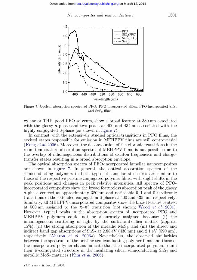
Figure 7. Optical absorption spectra of PFO, PFO-incorporated silica, PFO-incorporated SnS2and SnS2 films.
1501Nanocomposites and semiconductivity
on March 12, 2014rsta.royalsocietypublishing.orgDownloaded from
xylene or THF, good PFO solvents, show a broad feature at 380 nm associatedwith the glassy a-phase and two peaks at 400 and 434 nm associated with thehighly conjugated b-phase (as shown in figure 7).
In contrast with the extensively studied optical transitions in PFO films, theexcited states responsible for emission in MEHPPV films are still controversial(Kong et al. 2006). Moreover, the deconvolution of the vibronic transitions in theroom-temperature absorption spectra of MEHPPV films is not possible due tothe overlap of inhomogeneous distributions of exciton frequencies and charge-transfer states resulting in a broad absorption envelope.
The optical absorption spectra of PFO-incorporated lamellar nanocompositesare shown in figure 7. In general, the optical absorption spectra of thesemiconducting polymers in both types of lamellar structures are similar tothose of the respective pristine conjugated polymer films, with slight shifts in thepeak positions and changes in peak relative intensities. All spectra of PFO-incorporated composites show the broad featureless absorption peak of the glassya-phase centred at approximately 380 nm and noticeable 0–1 and 0–0 vibronictransitions of the extended conjugation b-phase at 400 and 435 nm, respectively.Similarly, all MEHPPV-incorporated composites show the broad feature centredat 500 nm assigned to the p–p� transition (not shown; Wood et al. 2001).However, typical peaks in the absorption spectra of incorporated PFO andMEHPPV polymers could not be accurately assigned because: (i) theinhomogeneous scattering of light by the surfactant/silica matrix (approx.15%), (ii) the strong absorption of the metallic MoS2, and (iii) the direct andindirect band gap absorptions of SnS2 at 2.88 eV (430 nm) and 2.1 eV (590 nm),respectively (Aharon et al. 2006a). Nevertheless, the observed similaritiesbetween the spectrum of the pristine semiconducting polymer films and those ofthe incorporated polymer chains indicate that the incorporated polymers retaintheir p-conjugated structure in the insulating silica, semiconducting SnS2 andmetallic MoS2 matrices (Kim et al. 2006).
Phil. Trans. R. Soc. A (2007)
S. Kirmayer et al.1502
on March 12, 2014rsta.royalsocietypublishing.orgDownloaded from
(ii) Photoluminescence
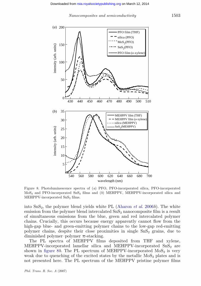
The optical absorption spectra of conjugated polymers reflect the morphologyof the entire polymer chain population, while the PL spectra reflect only thepolymer chain segments with the lowest band gap (i.e. high conjugation). This isa result of the efficient energy transfer which rapidly funnels the excited states(excitons) to the low-gap segments prior to the radiative emission (Bredas et al.2004). The PL spectra of PFO films deposited from THF and xylene, PFO-incorporated lamellar silica, PFO-incorporated MoS2 and PFO-incorporatedSnS2 are shown in figure 8a. The PL spectra of MEHPPV films deposited fromTHF and xylene, MEHPPV-incorporated lamellar silica and MEHPPV-incorporated SnS2 are shown in figure 8b. These PL spectra are similar tothose of pristine PFO films deposited from xylene and THF with a slight red shiftin the PL spectra of the intercalated polymers compared with that of pristinepolymer films, reflecting the longer extension of conjugated segments in theintercalated polymer. These results are in good agreement with the opticalabsorption measurements of semiconducting polymers infiltrated into silica andtitania (Wu et al. 1999; Coakley et al. 2003). Extended conjugation increasescarrier mobility and is desired for the improvement of polymer devices, such aslight-emitting diodes and field-effect transistors. It is important to note that allPL spectra of the confined polymers are similar to those of pristine polymer filmsdespite the distinctly different electronic properties of the inorganic hosts, i.e.insulating silica, metallic MoS2 and semiconducting SnS2. Organic/inorganicinterfacial interactions and associated optoelectronic processes, such as chargeseparation and energy transfer, are currently under investigation.
A pristine PFO film appears to consist mainly of the glassy a-phase, asreported in the literature and evident from the absorption spectra (figure 7;Gamerith et al. 2004; Yang 2004). Efficient energy transfer from the a-phase tothe smaller-gap b-phase results in emission mainly from the lowest vibronicenergy level of the b-phase at 440 nm (Ariu et al. 2003; Becker & Lupton 2005).Accordingly, the PL spectra of all PFO films and PFO-incorporated lamellarnanocomposites consist of peaks at approximately 440, 465 and 500 nm,associated with the 0–0, 0–1 and 0–2 vibronic transitions of the b-phase S1–S0transition, respectively. However, the peak-positions in the PL spectra of thePFO-incorporated silica, MoS2 and SnS2 are slightly red shifted compared withthose in the corresponding PFO film spectra, reflecting the longer extension ofconjugated segments in the b-phase in the incorporated polymer.
Heating PFO films in air or exposing them to UV radiation results in theappearance of a broad green emission band, accompanied by a reduction of theblue emission (Gamerith et al. 2004; Sims et al. 2004). This colour degradationfrom blue to green is also observed in PFO-based light-emitting diodes (Listet al. 2002). It was recently shown that incorporating PFO into the interlayerspacing of layered silicates (Park et al. 2004) and layered dichalcogenides(Aharon et al. 2006a) results in enhanced emission-colour purity. This improvedphotophysical stability was assigned to the inhibition of energy transfer from theblue-emitting PFO moieties to green-emitting defects. Reduced energy transferbetween polymer chains incorporated into layered hosts is further demonstratedby the incorporation of a tricolour polymer blend into SnS2. In contrast to thered PL observed from the non-incorporated polymer blend when incorporated
Phil. Trans. R. Soc. A (2007)
0
50
100
150
200
430 440 450 460 470 480 490 500 510
PFO film (THF)
silica (PFO)
MoS2(PFO)
SnS2(PFO)
PFO film (o-xylene)in
tens
ity (
arb.
uni
ts)
35MEHPPV film (THF)MEHPPV film (o-xylene)silica (MEHPPV)SnS2(MEHPPV)
30
25
20
15
inte
nsity
(ar
b. u
nits
)
10
5
540 560 580 600 620wavelength (nm)
640 660 680 700
(b)
(a)
Figure 8. Photoluminescence spectra of (a) PFO, PFO-incorporated silica, PFO-incorporatedMoS2 and PFO-incorporated SnS2 films and (b) MEHPPV, MEHPPV-incorporated silica andMEHPPV-incorporated SnS2 films.
1503Nanocomposites and semiconductivity
on March 12, 2014rsta.royalsocietypublishing.orgDownloaded from
into SnS2, the polymer blend yields white PL (Aharon et al. 2006b). The whiteemission from the polymer blend intercalated SnS2 nanocomposite film is a resultof simultaneous emissions from the blue, green and red intercalated polymerchains. Crucially, this occurs because energy apparently cannot flow from thehigh-gap blue- and green-emitting polymer chains to the low-gap red-emittingpolymer chains, despite their close proximities in single SnS2 grains, due todiminished polymer–polymer p-stacking.
The PL spectra of MEHPPV films deposited from THF and xylene,MEHPPV-incorporated lamellar silica and MEHPPV-incorporated SnS2 areshown in figure 8b. The PL spectrum of MEHPPV-incorporated MoS2 is veryweak due to quenching of the excited states by the metallic MoS2 plates and isnot presented here. The PL spectrum of the MEHPPV pristine polymer films
Phil. Trans. R. Soc. A (2007)
S. Kirmayer et al.1504
on March 12, 2014rsta.royalsocietypublishing.orgDownloaded from
shows two sub-bands centred at 580 and 630 nm in films deposited from THF,and 590 and 640 nm in films deposited from xylene. Both peaks are associatedwith interchain excitations in aggregated MEHPPV (Kong et al. 2006). Theintrachain exciton transition, at approximately 555 nm, is not observed in the PLof the polymer films due to energy transfer from the high-energy intrachainexcitation to the low-energy interchain state. The PL peak positions and the finestructure are sensitive to the solvents used, polymer concentration and filmdeposition method (Amautov et al. 2004). The red-shifted spectrum of the filmdeposited from xylene compared with that of the film deposited from THFindicates that the polymer chains deposited from xylene, a good polymer solvent,are in an extended conjugation morphology, while those deposited from THF, amoderate polymer solvent, are not.
Upon incorporation into silica, the PL spectrum of MEHPPV is retained witha slight red shift compared to the PL spectrum of the film deposited from THF.The slight red shift is associated with the extended conjugation imposed by thehost, as discussed in the absorption and emission spectra of incorporated PFO.The close resemblance between the PL of the silica-incorporated polymer chainsand that of the THF-deposited film indicates that the incorporated chains are nothighly conjugated probably due to their entanglement with the hydrophobicsegments of the surfactant.
The PL spectrum of MEHPPV intercalated into SnS2 is similar to that of apolymer film deposited from xylene. In this case, the interlayer galleryaccommodates approximately a polymer monolayer and no interchain statesare expected. However, the planar configuration enforced by the inorganic sheetsenhances conjugation which results in a red shift of both the absorption andemission spectra.
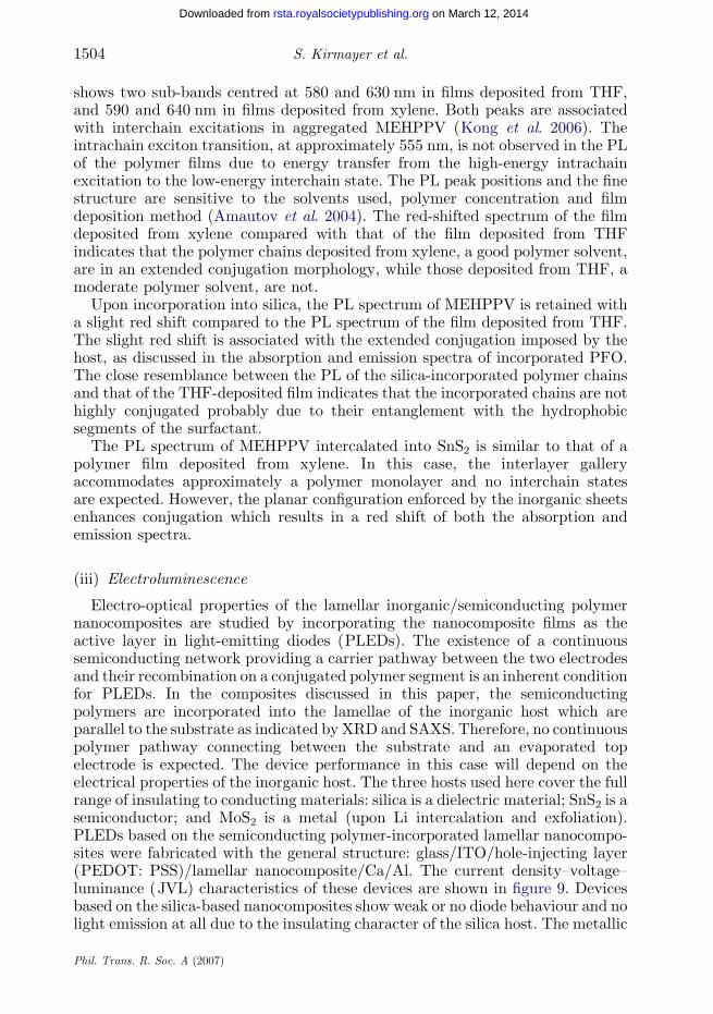
(iii) Electroluminescence
Electro-optical properties of the lamellar inorganic/semiconducting polymernanocomposites are studied by incorporating the nanocomposite films as theactive layer in light-emitting diodes (PLEDs). The existence of a continuoussemiconducting network providing a carrier pathway between the two electrodesand their recombination on a conjugated polymer segment is an inherent conditionfor PLEDs. In the composites discussed in this paper, the semiconductingpolymers are incorporated into the lamellae of the inorganic host which areparallel to the substrate as indicated by XRD and SAXS. Therefore, no continuouspolymer pathway connecting between the substrate and an evaporated topelectrode is expected. The device performance in this case will depend on theelectrical properties of the inorganic host. The three hosts used here cover the fullrange of insulating to conducting materials: silica is a dielectric material; SnS2 is asemiconductor; and MoS2 is a metal (upon Li intercalation and exfoliation).PLEDs based on the semiconducting polymer-incorporated lamellar nanocompo-sites were fabricated with the general structure: glass/ITO/hole-injecting layer(PEDOT: PSS)/lamellar nanocomposite/Ca/Al. The current density–voltage–luminance (JVL) characteristics of these devices are shown in figure 9. Devicesbased on the silica-based nanocomposites show weak or no diode behaviour and nolight emission at all due to the insulating character of the silica host. The metallic
Phil. Trans. R. Soc. A (2007)
1.5×10⁴
current density silica (PFO)
current density SnS2(PFO)
luminance silica(PFO)
luminance SnS2(PFO)
30
25
20in
tens
ity
(arb
. uni
ts)
15
10
5
400 450wavelength (nm)
500 550
1×10⁴
5×10³
0
0 2 4
applied bias (V)
6 8 10
1.2
1.0
0.8cu
rren
t den
sity
(A
m–2
)
lum
inan
ce (
cd m
–2)
0.6
0.4
0.2
0
Figure 9. Current density–applied bias–luminance curves of light-emitting diodes comprising PFO-incorporated silica and PFO-incorporated SnS2. The inset shows the electroluminescence spectrumof PFO-incorporated SnS2.
1505Nanocomposites and semiconductivity
on March 12, 2014rsta.royalsocietypublishing.orgDownloaded from
character of MoS2 resulted in no diode behaviour, but rather an ohmic J–Vdependence and no light emission (not shown).
Devices based on the semiconducting polymer-incorporated semiconductingSnS2 host exhibited typical diode behaviour with blue light turn-on atapproximately 6 V and luminance of 1 cd mK2 at approximately 9 V (as shownin figure 9). Moreover, it was found that the intercalation of PFO into SnS2stabilizes its blue light emission and the undesirable green emission associatedwith PFO-oxidation is inhibited (Aharon et al. 2006a). Finally, the efficacies ofpolymer-incorporated SnS2 were demonstrated in a simple single-layer polymerlight-emitting diode comprising the tricolour polymer blend interacted SnS2nanocomposites. The electroluminescence spectrum of the nanocomposite deviceis similar to its PL spectrum exhibiting white electroluminescence with nearlypure-white CIE coordinates (0.30, 0.30) (Aharon et al. 2006b).
4. Conclusions
In summary, lamellar inorganic/semiconducting polymer nanocomposites weresynthesized through the self-organization of inorganic precursors and semi-conducting polymers. The optical and electrical properties of the conjugatedpolymers are maintained upon incorporation, enabling their utilization inoptoelectronic applications. Indeed, judicious selection of the host based on itselectronic properties allowed the integration of a semiconducting polymer-incorporated semiconducting host into light-emitting diodes. Furthermore,encapsulation of the conjugated polymer species in the inorganic hosts couldoffer improved mechanical and environmental stability against external chemical
Phil. Trans. R. Soc. A (2007)
S. Kirmayer et al.1506
on March 12, 2014rsta.royalsocietypublishing.orgDownloaded from
and mechanical damage. Therefore, the new robust synthetic approach presentedhere for the preparation of optically responsive lamellar semiconducting polymer-incorporated inorganic host matrices is expected to be general and extendable toother hybrid material compositions, structures and devices.
References
Aharon, A., Kalina, M. & Frey, G. L. 2006a Stable blue emission from a polyfluorene/layered-
compound guest/host nanocomposite. Adv. Funct. Mater. 16, 980–986. (doi:10.1002/adfm.
200500458)
Aharon, E., Kalina, M. & Frey, G. L. 2006b Inhibition of energy transfer between conjugated
polymer chains in host/guest nanocomposites generates white photo- and electroluminescence.
J. Am. Chem. Soc. 128, 15 968–15 969. (doi:10.1021/ja066290m)Alberius, P. C. A., Frindell, K. L., Hayward, R. C., Kramer, E. J., Stucky, G. D. & Chmelka, B. F.
2002 General predictive syntheses of cubic, hexagonal and lamellar silica and titania
mesostructured thin films. Chem. Mater. 14, 3284–3294. (doi:10.1021/cm011209u)Amalraj, L., Sanjeeviraja, C. & Jayachandran, M. 2002 Spray pyrolysised tin disulphide thin film
and characterisation. J. Cryst. Growth 234, 683–689. (doi:10.1016/S0022-0248(01)01756-0)Amautov, S. A., Nechvolodova, E. M., Bakulin, A. A., Elizarov, S. G., Khodarev, A., Martyanov,
D. S. & Paraschuk, D. Y. 2004 Properties of MEH-PPV films prepared by slow solvent
evaporation. Synth. Met. 147, 287–291. (doi:10.1016/j.synthmet.2004.06.044)
Ariu, M., Sims, M., Rahn,M. D., Hill, J., Fox, A.M., Lidzey, D. G., Oda,M., Cabanillas-Gonzalez, J.
& Bradley, D. D. C. 2003 Exciton migration in b-phase poly(9,9-dioctylfluorene). Phys. Rev. B
67, 195 333. (doi:10.1103/PhysRevB.67.195333)
Becker, K. & Lupton, J. M. 2005 Dual species emission from single polyfluorene molecules:
signatures of stress-induced planarization of single polymer chains. J. Am. Chem. Soc. 127,
7306–7307. (doi:10.1021/ja051583l)Bredas, J. L., Beljonne, D., Coropceanu, V. & Cornil, J. 2004 Charge-transfer and energy-transfer
processes in conjugated oligomers and polymers. Chem. Rev. 104, 4971–5004. (doi:10.1021/
cr040084k)Brinker, C. J. 2004 Evaporation-induced self-assembly: functional nanostructures made easy. MRS
Bull. 29, 631.Brinker, C. J., Lu, Y. F., Sellinger, A. & Fan, H. Y. 1999 Evaporation-induced self-assembly:
nanostructures made easy. Adv. Mater. 11, 579–585. (doi:10.1002/(SICI)1521-
4095(199905)11:7!579::AID-ADMA579O3.0.CO;2-R)
Bruhwiler, D. & Calzaferri, G. 2004 Molecular sieves as host materials for supramolecular
organization. Micropor. Mesopor. Mater. 72, 1–23. (doi:10.1016/j.micromeso.2004.03.027)Coakley, K. M., Liu, Y. X., McGehee, M. D., Frindell, K. L. & Stucky, G. D. 2003 Infiltrating
semiconducting polymers into self-assembled mesoporous titania films for photovoltaic
applications. Adv. Funct. Mater. 13, 301–306. (doi:10.1002/adfm.200304361)
Divigalpitiya, W. M. R., Frindt, R. F. & Morrison, S. R. 1989 Inclusion systems of organic
molecules in restacked single-layer molybdenum disulfide. Science 246, 369–371. (doi:10.1126/
science.246.4928.369)Errien, N., Mevellec, J. Y., Louarn, G. & Froyer, G. 2005 Polymerization of diacetylene-
bis(toluenesulfonide) in a porous silica matrix: evidence of polymer chain self-orientation.
Chem. Mater. 17, 2803–2806. (doi:10.1021/cm0500657)Gamerith, S., Gadermaier, C., Scherf, U. & List, E. J. W. 2004 Emission properties of pristine and
oxidatively degraded polyfluorene type polymers. Phys. Status Solidi a-Appl. Res. 201,
1132–1151. (doi:10.1002/pssa.200404345)
Gomez-Romero, P. 2001 Hybrid organic-inorganic materials—in search of synergic activity. Adv.
Mater. 13, 163–174. (doi:10.1002/1521-4095(200102)13:3!163::AID-ADMA163O3.0.CO;2-U)
Phil. Trans. R. Soc. A (2007)
1507Nanocomposites and semiconductivity
on March 12, 2014rsta.royalsocietypublishing.orgDownloaded from
Huang, M. H., Kartono, F., Dunn, B. & Zink, J. I. 2002 Hexagonal to lamellar mesostructural
changes in silicate films caused by organic additives. Chem. Mater. 14, 5153–5162. (doi:10.1021/cm0207043)
Jiang, T., Ozin, G. A. & Bedard, R. L. 1998 Spectroscopic properties of microporous layered tinsulfide materials. J. Mater. Chem. 8, 1641–1648. (doi:10.1039/a801602j)
Kanatzidis, M. G., Tonge, L. M., Marks, T. J., Marcy, H. O. & Kannewurf, C. R. 1987 In situintercalative polymerization of pyrrole in FeOCl—a new class of layered, conducting polymer-
inorganic hybrid materials. J. Am. Chem. Soc. 109, 3797–3799. (doi:10.1021/ja00246a057)Kanatzidis, M. G., Bissessur, R., Degroot, D. C., Schindler, J. L. & Kannewurf, C. R. 1993 New
intercalation compounds of conjugated polymers. Encapsulation of polyaniline in MoS2. Chem.Mater. 5, 595–596. (doi:10.1021/cm00029a003)
Kim, D. Y., Grey, J. K. & Barbara, P. F. 2006 A detailed single molecule spectroscopy study of thevibronic states and energy transfer pathways of the conjugated polymer MEH–PPV. Synth.Met. 156, 336–345. (doi:10.1016/j.synthmet.2005.12.019)
Klotz, M., Albouy, P. A., Ayral, A., Menager, C., Grosso, D., Van der Lee, A., Cabuil, V.,
Babonneau, F. & Guizard, C. 2000 The true structure of hexagonal mesophase-templated silicafilms as revealed by X-ray scattering—effects of thermal treatments and of nanoparticle seeding.Chem. Mater. 12, 1721–1728. (doi:10.1021/cm991198t)
Kong, F., Wu, X. L., Yuan, R. K., Yang, C. Z., Siu, G. G. & Chu, P. K. 2006 Optical emission fromthe aggregated state in poly [2-methoxy-5-(20-ethyl-hexyloxy)-p-phenylene vinylene]. J. Vac.
Sci. Technol. A 24, 202–205. (doi:10.1116/1.2155531)Kubo, J., Mori, T. & Morikawa, Y. 1998 Intercalation of methanol and ethanol into
Na-fluorotetrasilicic mica: difference in formation of single and double layer intercalates.Chem. Lett. 12, 1243–1244. (doi:10.1246/cl.1998.1243)
List, E. J. W., Guentner, R., de Freitas, P. S. & Scherf, U. 2002 The effect of keto defect sites onthe emission properties of polyfluorene-type materials. Adv. Mater. 14, 374–378. (doi:10.1002/1521-4095(20020304)14:5!374::AID-ADMA374O3.0.CO;2-U)
Lu, Y. F. et al. 1997 Continuous formation of supported cubic and hexagonal mesoporous films by
sol gel dip-coating. Nature 389, 364–368. (doi:10.1038/38699)McCaughey, B., Costello, C., Wang, D. H., Hampsey, J. E., Yang, Z. Z., Li, C. J., Brinker, C. J. &
Lu, Y. F. 2003 Self-assembly of mesostructured conjugated poly (2,5-thienylene ethynylene)/silica nanocomposites. Adv. Mater. 15, 1266–1269. (doi:10.1002/adma.200304931)
Melosh, N. A., Steinbeck, C. A., Scott, B. J., Hayward, R. C., Davidson, P., Stucky, G. D. &Chmelka, B. F. 2004 Mesostructured silica/block copolymer composites as hosts for opticallylimiting tetraphenylporphyrin dye molecules. J. Phys. Chem. B 108, 11 909–11 914. (doi:10.
1021/jp040064m)Miled, O. B., Grosso, D., Sanchez, C. & Livage, J. 2004 An optical fibre pH sensor based on dye doped
mesostructured silica. J. Phys. Chem. Solids 65, 1751–1755. (doi:10.1016/j.jpcs.2004.05.005)Minoofar, P. N., Hernandez, R., Chia, S., Dunn, B., Zink, J. I. & Franville, A.-C. 2002 Placement
and characterization of pairs of luminescent molecules in spatially separated regions ofnanostructured thin films. J. Am. Chem. Soc. 124, 14 388–14 396. (doi:10.1021/ja020817n)
Murphy, D. W., Disalvo, F. J., Hull, G. W. & Waszczak, J. V. 1976 Lithium intercalationcompounds. Inorg. Chem. 15, 17–21. (doi:10.1021/ic50155a005)
Nguyen, T. Q., Wu, J. J., Doan, V., Schwartz, B. J. & Tolbert, S. H. 2000 Control of energytransfer in oriented conjugated polymer–mesoporous silica composites. Science 288, 652–656.
(doi:10.1126/science.288.5466.652)Nguyen, T. Q., Wu, J., Tolbert, S. H. & Schwartz, B. J. 2001 Control of energy transport in
conjugated polymers using an ordered mesoporous silica matrix. Adv. Mater. 13, 609–611.(doi:10.1002/1521-4095(200104)13:8!609::AID-ADMA609O3.0.CO;2-)
Oriakhi, C. 1998 Nano sandwiches. Chem. Br. 34, 59.Park, J. H., Lim, Y. T., Park, O. O., Kim, J. K., Yu, J. W. & Kim, Y. C. 2004 Stabilized blue
emission from polymer-dielectric nanolayer nanocomposites. Adv. Funct. Mater. 14, 377–382.(doi:10.1002/adfm.200305045)
Phil. Trans. R. Soc. A (2007)
S. Kirmayer et al.1508
on March 12, 2014rsta.royalsocietypublishing.orgDownloaded from
Pattantyus-Abraham, A. G. & Wolf, M. O. 2004 A PPV/MCM-41 composite material. Chem.Mater. 16, 2180–2186. (doi:10.1021/cm035303h)
Pomogailo, A. D. 2005 Hybrid intercalative nanocomposites. Inorg. Mater. 41, S47–S74. (doi:10.1007/s10789-005-0318-3)
Reichmanis, E., Katz, H., Kloc, C. & Maliakal, A. 2005 Plastic electronic devices: from materialsdesign to device applications. Bell Labs Tech. J. 10, 87–105. (doi:10.1002/bltj.20106)
Ruizhitzky, E. 1993 Conducting polymers intercalated in layered solids. Adv. Mater. 5, 334–340.(doi:10.1002/adma.19930050503)
Sanchez, C., Lebeau, B., Chaput, F. & Boilot, J. P. 2003 Optical properties of functional hybridorganic-inorganic nanocomposites. Adv. Mater. 15, 1969–1994. (doi:10.1002/adma.200300389)
Schwartz, B. J. 2003 Conjugated polymers as molecular materials: how chain conformation andfilm morphology influence energy transfer and interchain interactions. Annu. Rev. Phys. Chem.54, 141–172. (doi:10.1146/annurev.physchem.54.011002.103811)
Scott, B. J., Bartl, M. H., Wirnsberger, G. & Stucky, G. D. 2003 Energy transfer in dye-dopedmesostructured composites. J. Phys. Chem. A 107, 5499–5502. (doi:10.1021/jp026136w)
Sims, M., Bradley, D. D. C., Ariu, M., Koeberg, M., Asimakis, A., Grell, M. & Lidzey, D. G. 2004Understanding the origin of the 535 nm emission band in oxidized poly(9,9-dioctylfluorene): theessential role of inter-chain/inter-segment interactions. Adv. Funct. Mater. 14, 765–781. (doi:10.1002/adfm.200305149)
Valle, K., Belleville, P., Pereira, F. & Sanchez, C. 2006 Hierarchically structured transparenthybrid membranes by in situ growth of mesostructured organosilica in host polymer. Nat.Mater. 5, 107–111. (doi:10.1038/nmat1570)
Wilson, J. A. & Yoffe, A. D. 1969 The transition metal dichalcogenides discussion andinterpretation of the observed optical, electrical and structural properties. Adv. Phys. 18,193–335. (doi:10.1080/00018736900101307)
Wood, P., Samuel, I. D. W., Webster, G. R. & Burn, P. L. 2001 Investigating the effect ofconjugation in MEH–PPV. Synth. Met. 119, 571–572. (doi:10.1016/S0379-6779(00)01233-9)
Wu, J. J., Gross, A. F. & Tolbert, S. H. 1999 Host-guest chemistry using an oriented mesoporoushost: alignment and isolation of a semiconducting polymer in the nanopores of an ordered silicamatrix. J. Phys. Chem. B 103, 2374–2384. (doi:10.1021/jp984070s)
Xi, H. G., Wang, B. H., Zhang, Y. B., Qian, X. F., Yin, J. & Zhu, Z. K. 2003 Spectroscopic studieson conjugated polymers in mesoporous channels: influence of polymer side-chain length.J. Phys. Chem. Solids 64, 2451–2455. (doi:10.1016/j.jpcs.2003.08.002)
Yang, X. H. et al. 2004 Suppression of the keto-emission in polyfluorene light-emitting diodes:experiments and models. Adv. Funct. Mater. 14, 1097–1104. (doi:10.1002/adfm.200305012)
Zhao, D., Yang, P., Melosh, N., Feng, J., Chmelka, B. F. & Stucky, G. D. 1998 Continuousmesoporous silica films with highly ordered large pore structures. Adv. Mater. 10, 1380–1385.(doi:10.1002/(SICI)1521-4095(199811)10:16!1380::AID-ADMA1380O3.0.CO;2-8)
Phil. Trans. R. Soc. A (2007)


