Embed Size (px)
Citation preview

Seediscussions,stats,andauthorprofilesforthispublicationat:https://www.researchgate.net/publication/261534311
Self-AssemblyofSelectiveInterfacesinOrganicPhotovoltaics
ARTICLEinADVANCEDFUNCTIONALMATERIALS·APRIL2013
ImpactFactor:11.81·DOI:10.1002/adfm.201201874
CITATIONS
26
READS
43
7AUTHORS,INCLUDING:
ScottA.Mauger
NationalRenewableEnergyLaboratory
9PUBLICATIONS136CITATIONS
SEEPROFILE
LilianChang
UniversityofCalifornia,Davis
11PUBLICATIONS303CITATIONS
SEEPROFILE
DavidMarkHuang
UniversityofAdelaide
43PUBLICATIONS1,412CITATIONS
SEEPROFILE
AdamJMoulé
UniversityofCalifornia,Davis
63PUBLICATIONS2,447CITATIONS
SEEPROFILE
Availablefrom:AdamJMoulé
Retrievedon:04February2016

Self-assembly of selective interfaces in organic photovoltaics
Scott A. Mauger, Lilian Chang, Stephan Friedrich, Christopher W. Rochester,David M. Huang, Peng Wang, Adam J. Moulé∗
AbstractThe composition of polymer-fullerene blends is acritical parameter for achieving high efficiencies in bulk-heterojunction (BHJ) organic photovoltaics. Achievingthe "right" materials distribution is crucial for deviceoptimization as it greatly influences charge-carrier mo-bility. The effect of the vertical concentration profile ofmaterials in spin-coated BHJs on device properties hasstirred particularly vigorous debate. Despite availableliterature on this subject, the results are often contradic-tory and inconsistent, likely due to differences in samplepreparation and experimental considerations. We attemptto reconcile published results by studying the influence ofheating, surface energy, and solvent additives on verticalsegregation and doping in polymer-fullerene BHJ organicphotovoltaics using neutron reflectometry and nearedge x-ray absorption fine structure spectroscopy. Weshow that surface energies and solvent additives greatlyimpact heat-induced vertical segregation. We also findthat interface charging due to Fermi level mismatch in-creases PCBM-enrichment at the BHJ-cathode interface.Current-voltage measurements show that self-assemblyof interfaces affects the open circuit voltage, resulting inclear changes to the power conversion efficiency.
[*] Prof. A. J. Moulé, S. A. Mauger, L. Chang,C. W. RochesterDepartment of Chemical Engineering and MaterialsScienceUniversity of CaliforniaDavis, CA 95616, USAE-mail: [email protected]
Dr. S. FriedrichAdvanced Detector GroupLawrence Livermore National LaboratoryLivermore, CA 94550, USA
Dr. D. M. HuangSchool of Chemistry and PhysicsThe University of AdelaideSA 5005, Australia
Dr. P. WangManuel Lujan Neutron Scattering CenterLos Alamos National LaboratoryLos Alamos, NM 87545, USA
Keywords: Vertical Segregation, Solvent Additives, Sur-face Energy, Morphology, Organic Photovoltaics
1 IntroductionThe photo-active layer of polymer-based organic photo-voltaic (OPV) devices is typically a bulk heterojunction(BHJ), in which a polymer electron donor and fullereneelectron acceptor are cast from a common solution toform a mixed layer. The components form an interpene-trating, phase-separated network that provides a large in-terfacial area for charge separation and continuous path-ways for charge transport.[1, 2] The most studied donor-acceptor system is poly(3-hexylthiophene) (P3HT) and(6,6)-phenyl-C61-butyric acid methyl ester (PCBM). Ini-tial research showed that the nanoscale morphology ofthe BHJ plays a critical role in the efficiency of OPVdevices.[3] As a result, much of the subsequent researchon P3HT:PCBM BHJs focused on how processing condi-tions such as casting solvent, deposition method, anneal-ing method, and drying rate could be used to tune the mor-phology to maximize efficiency.[3, 4]
More recently, the focus has shifted to questions abouthow the concentration of P3HT and PCBM changes asa function of depth within the BHJ. Polymer-fullereneblends have been shown to vertically segregate due tolimited miscibility and interactions with adjacent lay-ers. There are a variety of techniques that have beenused measure composition of materials as a function ofdepth, henceforth referred to as the vertical concentra-tion profile (VCP). In P3HT:PCBM films spectroscopicellipsometry (SE) [5, 6], dynamic secondary ion massspectroscopy (DSIMS)[7–9], x-ray photoelectron spec-troscopy (XPS)[10, 11], near edge x-ray absorption finestructure spectroscopy (NEXAFS)[6, 9, 12], x-ray reflec-tometry (XRR)[13], and neutron reflectometry (NR)[14–17] have been used to measure VCP. Electron tomogra-phy has also been used to study the three-dimensionalstructure of BHJs and concentration profiles of the crys-tallinity of P3HT have be obtained [18], but to our knowl-edge this technique has not been used to generate a moregeneral VCP. Each of these techniques mentioned abovehas its own set of advantages and disadvantages that mustbe considered when trying to determine the VCP of the
1
BHJ.SE is attractive because measurements are non-
destructive and can be made easily in-house, but it hasseveral drawbacks. First, SE requires models of refrac-tive indexes of the pristine materials, which is compli-cated for P3HT due its anisotropy.[19] Furthermore, therefractive index of P3HT is highly dependent on the order-ing of the chains, so assumptions must be made as to howthe refractive index will change as a function of PCBMconcentration.[20] SE is also not well suited for this sys-tem because the contrast between P3HT and PCBM issmall. Finally, it is not possible to perform SE measure-ments underneath a metal capping electrode.
In comparison, DSMIS has advantages over SE be-cause the contrast is very high due to the ability to mea-sure unique mass signals from P3HT and PCBM and sinceDSIMS measures concentration, it is not sensitive to theanisotropy or ordering of P3HT.[7] However, the limita-tion of DSIMS is its depth resolution of approximately10 nm.[7] Furthermore, P3HT and PCBM have differentevaporation rates, which imposes further limits on depthresolution.[9] Finally, DSMIS is a destructive techniquedue to the sputtering process, so samples cannot be re-measured.
X-rays can also be used to measure the VCP, eitherthrough XPS or NEXAFS. Both methods allow for directmeasurement of the concentration of components fromthe peak intensities of the measured elements. The short-coming of these techniques is that they are surface sensi-tive. Thus, in order to measure at different depths ma-terial must be removed, which is not desirable. Onemethod of removal is ion sputtering, but due to differ-ent etch rates of BHJ materials it may cause artifacts.[10]Etching can also be used to remove material and exposeburied areas, but it is possible that the etching processwill alter the layer which is desired to be left intact. In-terfaces can also be exposed using delamination meth-ods, but in some cases some of the removed layer re-mains after delamination.[10] Concentration vs. depthinformation can be extracted from x-ray spectroscopymethods by varying the excitation energy (P3HT absorbsmore strongly at 245 eV than PCBM) and/or incidenceangle.[12] This data relates concentration and depth, butis not quantitative. Finally, it is not possible to performXPS or NEXAFS measurements underneath a thick metalcapping electrode, limiting these techniques to uncappedsamples.
Reflectometry techniques are nondestructive and un-like SE, neither XRR or NR are sensitive to polymeranisotropy. XRR is attractive because beam intensity ishigh, which allows for short measurement times. Unfortu-nately, the contrast between P3HT and PCBM is low dueto similarities in electron density. For NR, the situation isreversed; contrast between P3HT and PCBM is high due
to the low concentration of H atoms in PCBM[14, 15, 21],but neutron beams have low intensities, which result inlong measurement times. Another positive aspect of NRis that it can be used to measure samples with a metal cap-ping layer because neutrons are only scattered by nucleiwhich have similar scattering cross-sections for the entireperiodic table.[22] Also, it is possible to detect featureswith very small length scales. Researchers have been ableto measures features as small as 13 Å using NR.[23] How-ever, this is dependent on sample quality and contrast vari-ations within the sample.
There are several factors that may potentially influencethe VCP of the BHJ: casting solvent, solvent additives, thesurfaces in contact with the BHJ, layer thickness, and sol-vent/thermal annealing. In an effort to better understandhow these factors affect the VCP of P3HT/PCBM BHJsthe results of previous studies are summarized in Table 1and the sample processing conditions are included. Fromthis table it can be seen that the reported VCP results arequite inconsistent, with reported PCBM concentrationsranging from 0-72% at the top surface and 12-90% at thesubstrate interface. For all of the unannealed samples, theconcentration of PCBM at the top surface is low. Thisis because a skin of P3HT forms at the air interface dur-ing spin coating of the active layer. The interfacial freeenergy is minimized if P3HT, which has a lower surfacetension than PCBM, predominates at this interface. Thesurface energy of the substrate also controls the concen-tration of PCBM at the bottom interface. For samplesin which the substrate has a moderately high surface en-ergy (SiO2, glass, or PEDOT:PSS), PCBM is attracted tothe interface and has high concentration. In contrast, theP3HT concentration is higher when cast onto a low sur-face energy substrate, as reported by Campoy-Quilles etal.[5] and Germack et al.[6]. The data also indicates thatthe equilibrium concentration at the substrate is achievedduring coating as thermal and solvent annealing do not re-sult in significant changes in PCBM concentration at thesubstrate interface. It is equally apparent that solvent andthermal annealing cause changes in the concentration ofPCBM at the top surface and in the middle of the BHJ.[10]It should be noted, however, that the effect of annealingon the PCBM concentration at top interface of the BHJgives inconsistent results. Some reports show heatingleads to an increase in the PCBM concentration[10, 15],while in other cases, the PCBM concentration is shownto decrease [9, 10, 14]. Also, the role of casting sol-vent is not clear. For the majority of previous studies,chlorobenzene is used as the casting solvent and the re-sults are in good agreement. But Germack et al.[6] andXu et al.[10] use 1,2-dicholorobenzene and report differ-ing VCP after solvent annealing. Compared to the sam-ples cast from chlorobenzene, Germack et al.[6] reporta very high concentration of PCBM at the bottom sur-
2
face (81% measured using SE and 90% with NEXAFS),whereas Xu et al.[10] report a low concentration of PCBM(55-58% with XPS) at the same interface. Germack et al.solvent annealed their samples after spin coating, but forthe samples cast from chlorobenzene, solvent annealingwas shown to cause little change in the bottom concentra-tion of PCBM. The surface energies of the substrates usedin the studies should be comparable between studies sincethe BHJs were cast onto either quartz or SiO2. While allof these studies lay a solid foundation in the investigationof the factors controlling the VCP of P3HT/PCBM BHJs,there are clearly still questions to be answered.
One question is: what is the role of the metal elec-trode? Results from Orimo et al. shown in Table 1 showthat heating the BHJ after the deposition of an Al elec-trode results in an enrichment of PCBM at the top ofthe BHJ compared to a BHJ that was heated prior to Aldeposition.[11] This result was confirmed using DSIMSand NEXAFS in a subsequent study, and PCBM enrich-ment is shown to occur for very short heating times.[9]What is not clear from these studies is whether this en-richment is a universal trend for samples heated with anintact metal electrode or whether it is unique to an Al elec-trode. Also, a potential issue with these studies is that themeasurements were made after the Al electrode was re-moved. It is possible that the electrode removal processalso removes a portion of the BHJ or provides local heat-ing that changes the interface concentration ratio and castsdoubt on the generality of the results.
Another question that has not been answered is: whateffects do solvent additives have on the VCP? It is com-mon to add small concentrations of secondary solvents oradditives to the casting solution in an effort to improvethe efficiency of OPV devices.[24] The additives result inthe formation of aggregated domains upon casting, whichhave small length scales and result in a well mixed nanos-tructure. These domains are often interpenetrating, andbecause they form during casting the electrical contact isgood, resulting in good charge transport and charge col-lection efficiency. It is not known how these additives af-fect the thermal stability of the BHJ. When nitrobenzeneis used as an additive, the device properties of an as-castand heated samples are almost identical, indicating thatthe electrical properties of the device do not change sig-nificantly with heating.[25] Thermal stability of morphol-ogy is an important property to consider because OPV de-vices need to be able to withstand temperature cycles dueto daily changes in illumination and seasonal weather. Forthese reasons, we focus on samples that are cured usingnitrobenzene so that we can more easily compare IV andmorphology measurements between annealed and unan-nealed samples.
In this study, we answer these two questions. First, weuse NR to study how different metals and solvent addi-
tives affect the VCP of P3HT/PCBM BHJs. Since we areusing NR, we are able to measure the VCP of a BHJ un-der an intact metal electrode, which allows us to avoid anypossible artifacts introduced by electrode removal. Next,we use NEXAFS spectroscopy to determine the element-specific bonding structure in PCBM films capped withthin metal layers. These measurements are possible be-cause the 2-nm metal capping layer is thinner than theAuger electron escape depth. Finally, we connect ourfindings on the materials distribution in the BHJ and thechemistry at the BHJ–metal interface to device perfor-mance and PCBM aggregate formation. We show herethat a capping metal electrode has a profound influenceon the VCP. In particular, the VCP changes drasticallyupon mild heating of the BHJ layer due to interactionswith the capping layer. Thus, any conclusion about deviceperformance that have been based on the VCP of an ini-tially uncapped BHJ layer must be treated with caution.We show that solvent additives affect the VCP and thatnitrobenzene in particular improves the thermal stabilityof the BHJ morphology. Finally, we show that low workfunction capping metals will donate electrons to PCBMthrough interface charge-transfer and exohedral dopingand that this charging of the PCBM contributes to the finalVCP of the BHJ, and thereby to the JV characteristics.
2 Results and Discussion
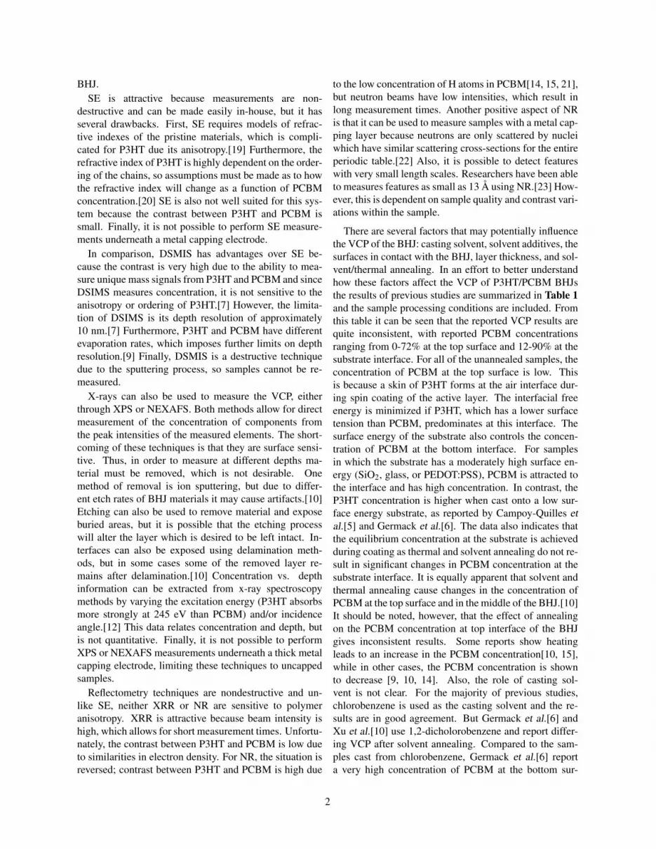
2.1 Measurement of Materials DistributionTo determine the effect of the metal electrode on theVCP in the active layer, NR measurements were per-formed on P3HT:PCBM BHJ (1:1 weight ratio) samplescast from chlorobenzene/nitrobenzene (2%) with Ag or Alelectrodes (henceforth referred to as Ag-capped and Al-capped, respectively) before and after heating at 150◦Cfor 5 min. The samples were cast on Si wafers, eventhough this geometry does not exactly represent a func-tional device. We note that this difference does signif-icantly affect our results. Using NR, Kiel et al. foundthat the profile of P3HT:PCBM BHJs cast on Si or PE-DOT:PSS are similar.[14] In addition, we have previ-ously published NR studies on P3HT:PCBM blends onPEDOT:PSS and find that the profiles obtained for thosesamples are similar to those obtained for this study.[17]Figure 1a and b shows the measured reflectivity spectrafor the Ag- and Al-capped samples, which were fit us-ing a slab model for the scattering length density (SLD)of the film. When fitting, the SLD of the metals, silicon,and native oxide were fixed at the values found using theNIST SLD calculator to decrease the number of fitting pa-rameters and reduce correlations.[27] The BHJ was repre-sented using 3 to 4 layers, depending on the sample. Thissimple model of the BHJ proved to be more useful than
3

Tabl
e1:
Sum
mar
yof
publ
ishe
dre
sults
ofco
ncen
trat
ion
ofPC
BM
with
inP3
HT
/PC
BM
BH
Js.V
alue
sar
ere
port
edas
afu
nctio
nof
mea
sure
men
ttec
hniq
ue,c
astin
gso
lven
t,tr
eatm
ent
(sol
vent
orth
erm
alan
neal
ing)
,and
top
and
botto
msu
rfac
e.PC
BM
conc
entr
atio
nva
lues
are
repo
rted
atth
eto
p,m
iddl
e,an
dbo
ttom
ofth
eB
HJ.
Ref
#te
chni
que
cast
ing
botto
mto
ptr
eatm
ent
%PC
BM
%PC
BM
%PC
BM
addi
tiona
lcom
men
tsso
lven
tsu
rfac
esu
rfac
eto
pm
iddl
ebo
ttom
[5]
SEC
B
quar
tzai
ras
-cas
t25
a63
a75
a
heat
ed50
a45
a74
aan
neal
ing
tem
pera
ture
140◦
C
PED
OT:
PSS
air
as-c
ast
25a
50a
65a
heat
ed50
a45
a74
aan
neal
ing
tem
pera
ture
140◦
C
quar
tzai
ras
-cas
t15
a63
a75
a50
00rp
m32
a60
a75
a30
00rp
m35
a50
a75
a70
0rp
mhy
drop
hobi
cSA
Mai
ras
-cas
t20
a48
a5a
SAM
:hex
amet
hyld
isila
zane
quar
tzai
rso
lven
t62
a45
a73
aso
lven
tann
eale
dfo
r1hr
[10]
XPS
DC
Bgl
ass
air
as-c
ast
3555
3000
rpm
heat
ed25
4930
00rp
m,1
10◦ C
10m
inas
-cas
t36
5880
0rp
mhe
ated
3660
800
rpm
,110
◦ C10
min
[11]
XPS
CB
PED
OT:
PSS
air
heat
ed36
150◦
C30
min
Al
72
[6]
SED
CB
SiO
2ai
rso
lven
t0
4181
20m
inso
lven
tann
eal
PED
OT:
PSS
041
54PT
T/N
afion
043
12
NE
XA
FSD
CB
SiO
2ai
rso
lven
t26
90PE
DO
T:PS
S26
PTT
/Nafi
on26
20
[9]
NE
XA
FSC
BPE
DO
T:PS
S
air
as-c
ast
12he
ated
8
Al
heat
ed41
5se
c,15
0◦C
441
min
,150
◦ C61
30m
in,1
50◦ C
[15]
NR
CB
SiO
2ai
ras
-cas
t15
3075
1:0.
7P3
HT:
PCB
Mm
ass
ratio
solv
ent
1530
75so
lven
tann
eale
d5
min
solv
ent+
ther
mal
3030
75so
lven
tann
eale
d5
min
+15
0◦C
1hr
[14]
NR
CB
SiO
2ai
ras
-cas
t28
50a
7080
0rp
mas
-cas
t37
50a
6525
00rp
mhe
ated
32a
45a
75a
2500
rpm
,140
◦ C[2
6]N
EX
AFS
CB
glas
sai
ras
-cas
t97
65fil
mde
lam
inat
ed,1
65◦ C
30m
ina
Val
uere
adfr
omgr
aph
4
Air AirBHJ BHJAg Al
Figure 1: Neutron reflectometry of metal-capped P3HT:PCBM bulk heterojunctions. Reflectivity spectra with fits for P3HT:PCBMBHJs with metal electrodes: (a) Ag, as-cast (�) and Ag, heated (•); (b) Al, as-cast (N) and Al, heated (�). The reflectivity profilegenerated from the fit (—) to the data is included for each sample. Spectra are offset for clarity. Modeled scattering length densityprofiles for the (c) Ag, as-cast (—) and Ag,heated (– – –) and (d) Al, as-cast (– · –) and Al, heated (– · · –) Depth increases fromthe substrate interface (0 nm) to the metal/air interface.
5

0.04 0.08 0.12 0.161E-9
1E-7
1E-5
1E-3
0.1
60 50 40 30 20 10 00
1
2
3
4
b)
a)
Ref
lect
ance
Momentum Transfer Vector /Å-1
no electrode Ca electrode fit
Sca
tterin
g le
ngth
den
sity
/10-6
Å-2
Thickness /nm
no electrode Ca electrode
Figure 2: Neutron reflectometry of P3HT:PCBM bulk hetero-junctions cast from chlorobenzene heated with (BHJ + Ca) andwithout (BHJ) a Ca electrode. The Ca layer was removed priorto measurement. a) Reflectivity spectra from the annealed un-capped BHJ (�) and Ca-capped (BHJ + Ca, •) samples withbest fit reflectivity data (—). Spectra are offset for clarity b)Modeled scattering length density profile for the BHJ (—) andBHJ + Ca (– – –).
more complex models (10 or more layers) as the com-plex models produced oscillatory profiles that were notphysically relevant. The resultant SLD profiles as a func-tion of sample thickness d are shown in Figure 1c andd, where d = 0 nm corresponds to the Si substrate. Atthe top of each sample the profiles show the Al and Aglayers. The top surface roughness of the samples and sur-face roughness with the metal layer removed were mea-sured using atomic force microscopy and are consistentwith the the values obtained from fitting the NR data. Inthe BHJ, high SLD values correspond to a high concen-tration of PCBM. The SLD profiles for the BHJ regions ofthe as-cast samples are very similar. At d = ∼67 nm and∼58 nm for the Al-capped and Ag-capped samples, re-spectively, there is a dip in the SLD, corresponding to theP3HT-rich skin formed during spin coating. This is con-sistent with previous studies of VCP reported in Table 1.The thickness of these skins are less than 3 nm, which ishard to resolve given the measured range of the momen-tum transfer vector (Q). To asses the significance of theseskin layers, the quality of the fits were compared to mod-els without a layer accounting for the P3HT skin. Whena layer was included to account for the skin, the χ2 val-ues for the Ag- and Al-capped samples were 9.3 and 10.9,respectively. When this skin layer was removed, the χ2
values increased to 23.7 and 16.4. This shows the signifi-cance the skin layer and validates its inclusion in the slabmodels. Beneath the P3HT skin is a region of increasedSLD due to PCBM enrichment. Finally, the bottom 20nm of the the BHJ shows an increase in SLD, which isalmost identical between the two samples. The high SLDis due to PCBM enrichment at the Si/SiO2 due to the highsurface energy of the oxide.[6]
Polymer:fullerene solar cells are often annealed to im-prove device performance.[28, 29] Samples are typicallyheated to 150◦C, which is above the glass transition tem-perature (Tg) of the mixture.[30] With heating, the P3HTand PCBM distributions change as the system tries tominimize free energy. After heating, there is an increasein SLD at the metal interfaces due to PCBM enrichmentand no indication of the P3HT-rich skin. Since this occursin both samples, it indicates that PCBM enrichment is aresult of heating with an intact cathode and is not uniqueto Al. Unlike the as-cast samples, which had very similarVCP for the BHJs, we see that there are significant dif-ferences between the profiles of the annealed Ag- and Al-capped samples (can also be seen in raw reflectance data).The differences between the samples clearly shows thatthe type of metal electrode influences phase segregationthroughout much of the BHJ, not just at the surface. Forthe heated Al-capped sample, the spike in SLD at ∼80 nmcorresponds to the growth of an aluminum oxide layer thatformed during heating. This layer complicated fitting thereflectivity spectrum because it resulted in significant at-
6

tenuation of the fringes at moderate values of the momen-tum transfer vector. This sample was also measured usingSE to confirm the thickness of the Al2O3 layer. The thick-nesses for the oxide and Al obtained through ellipsometryare consistent with those obtained from the fit to the NRdata. Since the fringes are attenuated, in order to asseswhether the interfacial roughness of the BHJ, Al, and ox-ide are indeed the best fit we did a systematic study. Thethickness of the interfacial roughness of the BHJ was in-creased from the value that produced the best fit, 0.5 Å, to20 Å. This value was fixed and the interfacial roughnessesof the Al and oxide were fitted along with the thicknessof the layers. The resulting roughness and χ2 values arereported in Table S1. We find that increasing the thick-ness of the interfacial roughness increases χ2. It can alsobe seen that the thicknesses of the other roughness valuesdo not change appreciably as the roughness of the BHJis changed indicating that they are indeed correct. At thesubstrate interface, the thickness and SLD of the PCBM-rich region does not appreciably change for either sample,again, consistent with prior results. Another indication ofthe accuracy of the fits is that for both the Al- and Ag-capped samples the thicknesses of the BHJ is the samebefore and after heating.
We also used NR to measure a P3HT:PCBM BHJ filmcast from pure chlorobenzene, heated with and withouta Ca electrode. These samples differ from the heatedAl-capped and Ag-capped samples in two ways: 1) theywere cast without a high boiling temperature solvent ad-ditive (nitrobenzene) and 2) the metal was removed priorto measurement for the Ca-capped sample. The Ca waswashed off with water prior to measurement because Cais quickly oxidized by air, which would create a mixedCa/CaO layer with unpredictable thickness and SLD,which would significantly decrease measurement accu-racy. The NR spectra with fits and modeled SLD pro-file are shown in Fig 2. Like the heated Al- and Ag-capped samples, the Ca-capped sample has high SLDs atboth interfaces indicating PCBM enrichment. In contrastto the samples annealed with electrodes, the heated, un-capped sample shows much reduced vertical segregationand air interface rich in P3HT. The differences betweenCa-capped and uncapped samples clearly show that themetal electrode influences phase segregation throughoutthe entire BHJ. As a consequence, measurements on BHJsamples heated without a cathode are not representativeof an actual device. Prior measurements of PCBM dif-fusion indicate that diffusion can occur at 50◦C, which iswithin the normal PV operating range.[7]
2.2 Connecting processing history to per-formance
To help relate the SLD profile of the BHJ to device per-formance we converted it to the corresponding PCBMvolume percentage within the BHJ. The volume percentPCBM (VPCBM) was calculated using
VPCBM =ρ(z)−ρP3HT
ρPCBM −ρP3HT, (1)
where ρ(z) is the SLD at a depth z, ρP3HT is the SLD forpure P3HT, and ρPCBM is SLD for pure PCBM.
The VCP is shown as a function of the normalizeddepth of the BHJ layer in Fig. 3a–c for the Ca-, Al-, andAg-capped samples, respectively. For all samples, theaverage PCBM concentration was calculated to be 44–48 vol%, which is consistent with the average concentra-tion of 46 vol% based on the casting solution. The PCBMconcentrations at the top, middle, and bottom of the BHJfor each of the samples are summarized in Table 2
The as-cast Al- and Ag-capped samples have similarVCPs, because the BHJ morphology at room temperatureis essentially fixed since the P3HT/PCBM mixture is be-low its T g and should not be substantially altered by depo-sition of the metal electrode. The concentration of PCBMat the bottom of the BHJ is 61-63 vol%. This value islower than what is more commonly reported (∼75 vol%[5, 14, 15]) likely due to the addition of nitrobenzene tothe casting solvent for our samples. This concentrationdoes not change with heating, which is consistent withmany of the other studies[5, 10, 15].
Interpretation of the data at the metal interface is signif-icantly more difficult. The as-cast PCBM concentrationat the metal interface is initially low, 45 vol% for Ag and14 vol% for Al. But it is not clear why the two concen-trations differ for as-cast layers. The difference betweenthese two values is likely influenced by roughness withthe capping metal leading to smearing of the interface.The P3HT skin layer is also quite thin and is barely re-solvable in the available Q-range of the NR data. If weassume no influence on the SLD from the metal, then theconcentration of PCBM at the Ag-BHJ interface increasesfrom 45 vol% to 72 vol%. For the Al-capped sample, thePCBM concentration at the metal interface increases from14% to 47 vol% with annealing. This result is consistentwith NEXAFS measurements of samples that were heatedfor similar lengths of time.[9]. For both samples the ap-parent change in concentration at the metal interfaces isan increase of 30 vol% PCBM. Can these results be rec-onciled? In the Ag-capped sample, Ag has a high SLD(3.47), so in an assumed mixture with the BHJ it will in-crease the overall SLD near the interface. In contrast, Alhas a much lower SLD (2.08), so it will not have as muchof an effect on the overall SLD as Ag does. Without a
7

1.0 0.8 0.6 0.4 0.20
20
40
60
80
100
1.0 0.8 0.6 0.4 0.2 1.0 0.8 0.6 0.4 0.2 0.0
-0.4 -0.2 0.0 0.2 0.4 0.6-15
-10
-5
0
5
-0.4 -0.2 0.0 0.2 0.4 0.6 -0.4 -0.2 0.0 0.2 0.4 0.6 0.8
b)a)
Normalized thickness
without nitrobenzene
Ca heated
Vo
lum
e %
PC
BM
c)
with nitrobenzene
Normalized thickness
Al as-cast heated
e)d)
with nitrobenzene with nitrobenzene with nitrobenzene
with nitrobenzene
Normalized thickness
Ag as-cast heated
f)
Cur
rent
Den
sity
/mA/
cm2
Voltage /V
Ca as-cast heated
Voltage/ V
Al as-cast heated
Voltage /V
Ag as-cast heated
Figure 3: Current density-voltage measurements and vertical concentration profile of P3HT:PCBM devices. a-c PCBM volumepercent as a function of normalized depth in the BHJ for as-cast and heated samples capped with metal layers: a) Ca (as-cast —,heated – – –), b) Al (as-cast —, heated – – –), and c) Ag (as-cast —, heated – – –).The shaded regions indicate the three differentconcentration ranges. The region from 20–38 vol% is the eutectic/metastable region. 47–73 vol% is the PCBM concentration whenlimited due to the use of nitrobenzene. 80–98 vol% is the maximum concentration of PCBM when there are no solvent additives.d-f Current-voltage curves for P3HT:PCBM OPV devices with different cathode metals: d) Ca, e) Al, and f) Ag. Devices weremeasured as-cast and after heating at 150 ◦C. P3HT:PCBM BHJ were cast from a solution of chlorobenzene with 2% nitrobenzeneto fix the BHJ morphology. Devices were measured under 1 Sun of simulated AM 1.5G light with no mismatch correction.
Table 2: PCBM volume concentration for P3HT:PCBM BHJ samples measured with neutron reflectometry. Values are reportedfor the top, middle (50% of normalized depth), and bottom of the BHJ layer. The BHJs were cast from pure chlorobenzene (CB)or a mix of chlorobenzene and nitrobenzene (NB). All heated samples were heated at 150◦C for 5 min.
casting top treatment % PCBM % PCBM % PCBMsolvent surface top middle bottom
CB/NBAg as-cast 45 35 61
heated 72 38 63
Al as-cast 14 39 63heated 47 24 63
CB air heated 38 56 55Ca 97 29 80
8

Table 3: Device parameters for P3HT:PCBM OPV de-vices. Open-circuit voltage (VOC), short-circuit current (JSC),fill factor (FF), and power conversion efficiency (PCE) forP3HT:PCBM devices with different metal electrodes measuredas-cast and following annealing at 150◦C. Devices were mea-sured under simulated 1 Sun AM 1.5G light with no mismatchfactor.
V OC J SC FF PCE(V) (mA/cm2) (%)
Al as-cast 0.45 11.06 0.45 2.08heated 0.63 11.10 0.58 3.77
Ag as-cast 0.50 11.28 0.50 2.63heated 0.21 10.37 0.35 0.72
Ca as-cast 0.56 10.56 0.61 3.35heated 0.61 10.71 0.57 3.45
priori knowledge of the concentration of one of the threecomponents at the interface, it is not possible to determinethe concentrations at the interface, as the problem is un-der specified. If it is assumed that the concentration of Agis 25 vol%, then we find that the PCBM concentration atthe top of the BHJ is initially 20 vol% and increases to51% with annealing, which is consistent with the previ-ous studies and is in better agreement with the Al-cappedsample. This data and discussion shows that PCBM dif-fuses to the metal interface and the P3HT skin disappearsafter heating because the metal interacts more favorablywith PCBM than with P3HT, as suggested by the highersurface energy γ of PCBM [31] compared with P3HT[32].This behavior is opposite to that expected at an air inter-face, where free energy is minimized by a predominanceof the lower surface-energy P3HT. Finally, even usingNR, it is not possible to unequivocally assign concentra-tion profiles at hetero-interfaces due to roughness effects.This data may reveal that the metal mixes more with theBHJ material than previously assumed.
For the heated-Ca-capped and heated-uncapped sam-ples, which were cast without nitrobenzene, the VCPs arevery different. The Ca-capped sample has a PCBM con-centration of 97 vol% at the top of the BHJ. At the bottomof the BHJ the PCBM concentration is 80 vol%, whichis in agreement with previous results.[5, 6, 14, 15] Aswas the case for the heated Ag- and Al-capped samples,there is no P3HT-rich top surface. The uncapped sampleis P3HT-rich at the interface, with a PCBM concentrationof 38 vol%, which is consistent with previous measure-ments of BHJs that were heated uncapped.[10, 11, 14, 15]
Despite large differences between the VCPs of heatedand unheated samples, all samples have a constant PCBMconcentration in the center, or bulk, of the layer of ∼24–40 vol% PCBM, which is consistent with the eutecticpoint and metastable regions for published P3HT:PCBM
phase diagrams.[33, 34] This concentration is also ob-served in solution-cast bi-layers and BHJ cast ontoPEDOT:PSS.[7, 9, 17] It is also worthy of note that al-though the metal does substantially affect the VCP, themagnitude of the surface energy of the metal (γ = 0.5J/m2, 1.15, and 1.25 J/m2 respectively for Ca, Al, and Ag[35]) does not appear to be an important factor. Fig. 3a–c and Table 2 show that the PCBM concentration is be-low 75 vol% at metal interfaces for both the Al- and Ag-capped samples while it is >95 vol% in the Ca-cappedsample at both interfaces, whereas surface energy consid-erations would predict a lower PCBM concentration at thelower surface-energy Ca interface.
Instead, the measured VCPs suggest that the interfacialPCBM concentration at the interfaces is strongly affectedby the presence of the solvent additive, nitrobenzene,which was used in casting the Al- and Ag-capped sam-ples, but not in the Ca-capped sample. The concentrationof PCBM at the metal and substrate interfaces is higherin the Ca-capped sample than in the Al- and Ag-cappedsamples. Nitrobenzene has been shown to reduce the dif-fusion rate of PCBM in P3HT, to increase the Tg of theBHJ mixture, increase P3HT crystallinity, and cause theformation of larger P3HT and PCBM domains.[25, 36]Fig. 4 presents a schematic to highlight the differencesbetween BHJs cast with and without nitrobenzene. Ourinterpretation of the interface concentration is as follows.When the samples are cast, the interface is rich in P3HTdue to the skin that forms upon coating. Just below thisskin, the PCBM concentration is above its solubility limitin P3HT and pure domains form. With heating above TgPCBM diffuses to the interface to minimize the free en-ergy of the surface. When nitrobenzene is added to thecasting solvent (Ag- and Al-capped) the total concentra-tion of PCBM is limited to below 70 vol% because ofthe high number of pre-formed P3HT aggregates restrictPCBM diffusion and PCBM molecules can only occupyspace between the aggregated P3HT domains that formduring casting. In contrast, when there is no solvent addi-tive (Ca-capped), the BHJ layer is initially much less crys-talline, as shown in Fig. 4. Heating allows PCBM diffu-sion towards the interfaces but there are fewer pre-formedP3HT fibers to limit diffusion so an almost pure PCBMlayer can form at the electrode. As mentioned above, theconcentration of the PCBM-enriched region at the sub-strate surface also indicates that the PCBM concentrationis controlled by the presence of nitrobenzene as the con-centration of PCBM at the SiO2 interface is much higherin the Ca-capped sample than for the Ag- and Al-cappedsamples.
But surface energy effects and solvent additives clearlyare not the only contributors to changes in vertical segre-gation with heating. If we consider the thickness of thePCBM-enriched layer at the metal interface, it is clear
9

Metal
Metal Metal
Metal
without nitrobenzene
with nitrobenzene
Figure 4: Schematic comparing the vertical concentration pro-file of P3HT:PCBM BHJ devices cast with and without the sol-vent additive nitrobenzene before and after heating. Note thatthe effects of charging by the metal are not included.
that Ca and Al have thick PCBM-rich layers (∼20% oftotal thickness) whereas the Ag-capped device has a thin-ner PCBM-enriched layer (∼10%) followed by a PCBM-depleted layer (∼10%).
2.3 Interfacial ChargingAnother possible contributor to the large change in VCPthat occurs with heating is a specific chemical/physicalinteraction between the metal and BHJ materials. To de-termine what interactions are present, we have used NEX-AFS spectroscopy to probe element-specific bonding. Be-cause the VCP data indicated an increased PCBM con-centration near the metal interface, experiments were per-formed on heated samples with metals and PCBM only tosimplify data interpretation.
To determine the effects that the electrode material mayhave on the carbon chemistry of PCBM, NEXAFS spec-tra by total electron yield (TEY) are taken on the carbonK-edge for a pure PCBM reference and for PCBM filmsunder thin metal electrodes. The spectra in Fig. 5 of purePCBM is consistent with previously publshed NEXAFSspectra of PCBM.[9, 12, 37, 38] The first two peaks at284.2 eV and 285.8 eV correspond to the π∗ transitionsand those above 292 eV σ∗ transitions of PCBM.[12]There are no significant differences between the purePCBM and PCBM–Ag spectra aside from a slight peakbroadening due to the stress induced by the Ag overlayer.In contrast, the PCBM–Al and PCBM–Ca spectra dif-
280 285 290 295 300 305
X-r
ay a
bsor
ptio
n /a
.u.
Pure PCBM PCBM-Ag
X-r
ay a
bsor
ptio
n /a
.u.
Pure PCBM PCBM-Al
X-r
ay a
bsor
ptio
n /a
.u.
Energy /eV
Pure PCBM PCBM-Ca
Figure 5: Carbon K-edge x-ray absorption of metal cappedPCBM samples. NEXAFS spectra measured in total electronyield for the pure PCBM (—) and PCBM capped with a) Ag(– – –), b) Al (– – –), and c) Ca (– – –). Samples were heated to150 ◦C for 10 min prior to measurement.
10

fer significantly from pure PCBM, indicating that PCBMhas undergone chemical changes. Most importantly, thefirst two π∗ peaks in both spectra have decreased in am-plitude, corresponding to a reduced number of unoccu-pied states in the lowest unoccupied molecular orbital(LUMO) of PCBM, and indicating that the Al and Caelectrodes are donating electrons to PCBM through eithera charge-transfer or doping process. In order for eitherof these processes to occur, the Fermi level of the metalmust be above (closer to the vacuum level) the LUMO ofthe matrix material.[39] The Fermi levels for the metalsused are -2.9 eV, -4.2 eV, and -4.6 eV for Ca, Al, andAg, respectively.[40] The LUMO of PCBM is -4.3 eV[41]. Since the Fermi levels of Al and Ca are above theLUMO of PCBM these metals should be able to donateelectrons to PCBM. This is exactly what is observed inthe x-ray spectra. The Fermi level of Ag[40] is lower thanthe LUMO of PCBM, so electrons do not move from Agto PCBM.
Both charge transfer to and doping of fullerenes bymetals are established phenomena. Charge transfer at theinterface between PCBM and Ca or Al has been shown tooccur spontaneously.[42] In this process, electrons tunnelacross the interface to align the energy levels of the metaland the BHJ. In the bulk doping process, the metal dif-fuses into the BHJ where it donates an electron(s) to thefullerene, which is easily able to accept the electron(s)because of the unsaturated C–C bonds.[43] This process,known as exohedral doping, results in a bound complexbetween the metal and the fullerene. To our knowledgeexohedral doping has not previously been shown to oc-cur in OPV devices. Since charge transfer occurs spon-taneously it is at least partially responsible for the struc-ture of the NEXAFS spectra for the Ca– and Al–cappedPCBM. But it is also possible that doping is also occurringin these samples.
To understand what interactions are taking place be-tween the metal and the PCBM we measured the NEX-AFS spectra at the Ca L-edge of PCBM samples with Caelectrodes present. With the electrode present, a clear Caspectrum is observed (Supporting Information, Fig. S1)in total electron yield (TEY), which is surface sensitive.The spectral fine structure, especially the strong pre-edgefeatures at 345.0 and 348.2 eV, indicate Ca oxidation, asexpected since it was exposed to atmosphere prior to mea-surement. The peaks are wider than those of pure com-mercial CaO and Ca(OH)2 model compounds because ox-idation in ambient air produces (hydr)oxides in differentconfigurations with slightly inhomogeneous characteris-tics. The air stable form of Ca is CaCO3, which is com-pletely unreactive. The NEXAFS scans were repeated ona PCBM sample whose Ca electrode had been washedoff (expected product CaCO3). As expected, a scan byTEY shows no structure at the Ca L-edge above the back-
ground, indicating a surface Ca concentration below 1vol%. A high-resolution superconducting tunnel junctionx-ray spectrometer with detection limits as low as 100ppm[44] was then used to retake the spectrum by partialfluorescence yield (PFY), which is a bulk-sensitive mea-surement. This spectrum shows a weak Ca signal, indicat-ing the presence of Ca inside the PCBM layer. This wasnot unexpected, as previous studies have shown that elec-trode materials can disperse throughout devices.[45, 46]Surprisingly, the pre-edge features at 345.0 and 348.2 eVdiffered from those of the oxidized Ca electrode, suggest-ing the presence of Ca in a different chemical state. Com-parisons to a CaC2O4 model compound and Ca L-edgespectra in literature indicate that the Ca ion is bound tocarbon.[47] This suggests exohedral doping is occurringbetween Ca and PCBM. The difference in the peak in-tensities of the Al-capped and Ca-capped NEXAFS spec-tra indicate that doping and charge transfer are occurringmore strongly with Ca than Al. This is to be expectedgiven the difference in Fermi levels of the metals.
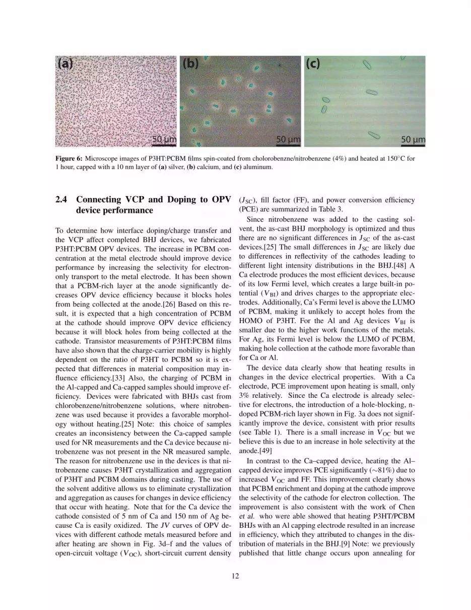
Since the NEXAFS data suggests that the metal is dif-fusing into the BHJ, it may be affecting the crystallinityof PCBM. The crystallinity of PCBM should be reducedif there are metals present in the BHJ as the metal ionswill act as defect sites and disrupt formation of extendedPCBM crystals. To determine if dissolved metal ions af-fect PCBM crystallization, we prepared capped, annealedBHJ samples and used reflection optical microscopy tosee if there is a difference in the size and number ofPCBM crystals. From the images shown in Figure 6 it canbe seen that the Ag-capped sample, heated under identicalconditions, has a higher number of visible crystals thanthe Al- or Ca-capped samples. This confirms the NEX-AFS result that the metal is in the BHJ and not just at thesurface. It also suggests that doping/charge transfer re-sults in a higher concentration of metal in the BHJ. Thismay explain why the profile of the heated Ag-capped sam-ple differs from the heated Al- and Ca-capped samples.This data along with the results for NR and NEXAFSsuggest that doping/charge transfer and metal diffusionis influencing the VCP. In the Ca– and Al–capped sam-ples where there is doping and charge transfer, the VCPof the heated samples (Fig. 3) do not show a PCBM-depleted region below the PCBM-enriched region at theinterface with the metal. In contrast, with Ag, where thedata shows no evidence of doping or charge transfer, thereis a PCBM-depleted region. This indicates that either thepresence of the metal in the BHJ or the charging near theinterface is influencing the VCP of the BHJ in annealedsamples.
11
50 μm 50 μm 50 μm
(a) (b) (c)
Figure 6: Microscope images of P3HT:PCBM films spin-coated from cholorobenzne/nitrobenzene (4%) and heated at 150◦C for1 hour, capped with a 10 nm layer of (a) silver, (b) calcium, and (c) aluminum.
2.4 Connecting VCP and Doping to OPVdevice performance
To determine how interface doping/charge transfer andthe VCP affect completed BHJ devices, we fabricatedP3HT:PCBM OPV devices. The increase in PCBM con-centration at the metal electrode should improve deviceperformance by increasing the selectivity for electron-only transport to the metal electrode. It has been shownthat a PCBM-rich layer at the anode significantly de-creases OPV device efficiency because it blocks holesfrom being collected at the anode.[26] Based on this re-sult, it is expected that a high concentration of PCBMat the cathode should improve OPV device efficiencybecause it will block holes from being collected at thecathode. Transistor measurements of P3HT:PCBM filmshave also shown that the charge-carrier mobility is highlydependent on the ratio of P3HT to PCBM so it is ex-pected that differences in material composition may in-fluence efficiency.[33] Also, the charging of PCBM inthe Al-capped and Ca-capped samples should improve ef-ficiency. Devices were fabricated with BHJs cast fromchlorobenzene/nitrobenzene solutions, where nitroben-zene was used because it provides a favorable morphol-ogy without heating.[25] Note: this choice of samplescreates an inconsistency between the Ca-capped sampleused for NR measurements and the Ca device because ni-trobenzene was not present in the NR measured sample.The reason for nitrobenzene use in the devices is that ni-trobenzene causes P3HT crystallization and aggregationof P3HT and PCBM domains during casting. The use ofthe solvent additive allows us to eliminate crystallizationand aggregation as causes for changes in device efficiencythat occur with heating. Note that for the Ca device thecathode consisted of 5 nm of Ca and 150 nm of Ag be-cause Ca is easily oxidized. The JV curves of OPV de-vices with different cathode metals measured before andafter heating are shown in Fig. 3d–f and the values ofopen-circuit voltage (V OC), short-circuit current density
(J SC), fill factor (FF), and power conversion efficiency(PCE) are summarized in Table 3.
Since nitrobenzene was added to the casting sol-vent, the as-cast BHJ morphology is optimized and thusthere are no significant differences in J SC of the as-castdevices.[25] The small differences in J SC are likely dueto differences in reflectivity of the cathodes leading todifferent light intensity distributions in the BHJ.[48] ACa electrode produces the most efficient devices, becauseof its low Fermi level, which creates a large built-in po-tential (V BI) and drives charges to the appropriate elec-trodes. Additionally, Ca’s Fermi level is above the LUMOof PCBM, making it unlikely to accept holes from theHOMO of P3HT. For the Al and Ag devices V BI issmaller due to the higher work functions of the metals.For Ag, its Fermi level is below the LUMO of PCBM,making hole collection at the cathode more favorable thanfor Ca or Al.
The device data clearly show that heating results inchanges in the device electrical properties. With a Caelectrode, PCE improvement upon heating is small, only3% relatively. Since the Ca electrode is already selec-tive for electrons, the introduction of a hole-blocking, n-doped PCBM-rich layer shown in Fig. 3a does not signif-icantly improve the device, consistent with prior results(see Table 1). There is a small increase in V OC but webelieve this is due to an increase in hole selectivity at theanode.[49]
In contrast to the Ca–capped device, heating the Al–capped device improves PCE significantly (∼81%) due toincreased V OC and FF. This improvement clearly showsthat PCBM enrichment and doping at the cathode improvethe selectivity of the cathode for electron collection. Theimprovement is also consistent with the work of Chenet al. who were able showed that heating P3HT/PCBMBHJs with an Al capping electrode resulted in an increasein efficiency, which they attributed to changes in the dis-tribution of materials in the BHJ.[9] Note: we previouslypublished that little change occurs upon annealing for
12

P3HT/PCBM Al-capped devices with a mixing ratio of3:2 and nitrobenzene.[? ] The samples here have a higherPCBM loading of 1:1, which appears to be significant.
The Ag–capped device is affected very differently byheating than the Al– and Ca–capped devices. The VCPin Fig. 3f shows that heating leads to PCBM enrichmentat the cathode, but the NEXAFS data shows that PCBMis not doped or charged at the interface. Based on theseobservations, we expected heating to improve efficiencybecause of the increased electron selectivity due to thePCBM enrichment at the cathode. However, we observethe opposite result; heating decreases efficiency in Ag-capped devices, mainly due to a 0.3 V drop in V OC. Thecause of this decrease in efficiency is the PCBM-depletedregion shown in the VCP at a depth of about 0.75 inFig. 3c. In this region the concentration of PCBM isdepleted below its concentration in the rest of the BHJ.Monte Carlo simulations of OPV devices have shown thata depleted region, like this one, commonly forms beneathan enriched region due to the loss of material.[50] Thisdepleted region forms a blocking layer which increasesbimolecular recombination. For P3HT:PCBM BHJs bi-molecular recombination is known to be a significant lossmechanism, which V OC is dependent upon.[51]
3 Conclusions
Our results show that the metal used as the cathode influ-ences the BHJ in ways not previously known. They dispelthe notion that an inverted device architecture is necessaryfor a favorable material distribution. Rather engineeringof the surface energy and electrostatic properties of theinterfaces will lead to an idealized vertical concentrationprofile. We show that the vertical concentration profileis altered by three separate forces. The effect of surfaceenergy has been previously demonstrated. We find thatvertical segregation of the BHJ can be reduced with theaddition of an additive to the casting solvent. The use ofnitrobenzene in the casting solvent reduces the concentra-tion of PCBM at both interfaces by ∼15%.
Additionally, we find that the choice of metal cappingelectrode affects the vertical concentration profile notonly through the surface energy, but also due to the FermiEnergy difference between materials. Low work functionmetals donate electrons to PCBM through both interfa-cial charge-transfer and exohedral doping. The presenceof charge in the PCBM during annealing affects the finalVCP and in turn the IV characteristics of completed OPVdevices. This results together show that it is necessary toconsider samples processed with intact electrodes for alldonor/acceptor pairs to fully understand the relationshipbetween the morphology and device efficiency. Further-more, the differences in VCP, doping, and device perfor-
mance highlight the sensitivity of OPV devices to samplehistory. This has broad implications to the organic elec-tronics community, most importantly that comparison ofdevices with different sample histories may lead to falseconclusions due to significant, but unknown differencesbetween samples.
Methods
For neutron reflectometry measurements, silicon waferswere cleaned by rinsing with acetone, isopropyl alcohol,and deionized water, then blow dried with nitrogen, and fi-nally cleaned in a UV/ozone plasma chamber. P3HT andPCBM solutions were prepared by dissolving the polymer(20 mg/ml) or fullerene (20 mg/ml) in chlorobenzene. Ni-trobenzene was added at 2% by volume. The solutionswere stirred on a hot plate set to 60 ◦C for 30 minutes.The P3HT and PCBM solutions were mixed together toachieve a 1:1 weight ratio (total solids concentration of20 mg/ml). The films were deposited via spin coating.Thickness variation over the entire sample area was lessthan ±2 nm, as verified with a stylus profilometer. Thefilms were not thermally or solvent annealed prior to elec-trode deposition. Metal electrodes were deposited by ther-mal evaporation at 0.2 Å/s for the first 5 nm and thenthe rate was increased to 1.5 Å/s. Neutron reflectom-etry measurements were performed on the Surface Pro-file Analysis Reflectometer (SPEAR) at Los Alamos Na-tional Laboratory.[23] Measurements were taken in airbefore and after heating on a hot plate set at 150 ◦C for10 minutes. Since the domain sizes that are formed in aP3HT:PCBM BHJ are ∼10 nm[52], the observed scatter-ing length density is representative of the average com-position of the layer. For the Ca sample the electrodewas washed off using deionized water prior to measure-ment. The measured reflectivity was fit to a slab model,in which the sample film was assumed to consist of aseries of n parallel layers, where layer i has a thicknessdi and constant scattering length density (SLD) ρi, sand-wiched between super- (air) and subphases (silicon) of in-finite extent. Interlayer "roughness” σi,i+1, which couldinclude contributions from actual roughness between lay-ers or from interlayer mixing, was accounted for by anerror function SLD profile centered at the interface con-necting the SLDs of the adjacent layers i and (i + 1 ). Slabmodel fitting to the measured data were carried out usingthe Refl1D software package.[53] The SLDs of air andsilicon were taken to be ρair= 0 and ρSi = 2.07 ×10⁶ Å2,respectively.[27] For the electrodes the SLDs were takenfrom the NIST SLD database with ρAl= 2.08 × 10⁶ Å2
and ρAg = 3.47 × 10⁶ Å2.[27]For conversion from SLD tovolume percent the pure species SLD were ρP3HT= 0.786×10⁶ Å2 and ρPCBM = 4.34 ×10⁶ Å2. ρP3HT was de-
13

termined from previous measurements of pure P3HT onsilicon and ρPCBM is calculated based upon previously re-ported data for deuterated PCBM.[14]
Spectroscopic ellipsometry measurements were con-ducted using a VASE model ellipsometer from the J.A.Woollam Co., Inc. and the data was fit within theWVASE32 software package. The data was fit only in therange of 700-1000 nm because in this wavelength rangethe BHJ is transparent and its refractive index can easilybe obtained using a Cauchy dispersion model. For the Allayer, tabulated values of the refractive index of aluminumcontained with in the software were used. The thermallygrown aluminum oxide was modeled using a Cauchy dis-persion model. The tabulated values for stoichiometricaluminum oxide (Al2O2) were not used as the SLD of theoxide layer obtained from the NR fits indicates it is notthe stoichiometric oxide.
Atomic force microscope measurements of the surfacesof the samples measured by NR were conducted in tap-ping mode with a Multimode model microscope fromVeeco.
For near edge x-ray absorption fine structure measure-ments, indium-tin oxide (ITO)-coated glass was ultrason-ically cleaned in acetone, Mucusol, and deionized water.Next they were sprayed with deionized water and driedwith nitrogen in a spin rinse drier followed by UV/ozoneplasma cleaning. Samples were fabricated by spin coatinga solution of PCBM (20 mg/mL) in 1,2-dichlorobenzene(20 mg/mL) onto the ITO glass. 2 nm of Ag, Al, and Cawere thermally evaporated at a rate of 0.3 Å/s. A purePCBM sample and a 2 nm Ag film without PCBM under-neath were made as references. All samples were heatedat 150 ◦C for 10 minutes on a hot plate. To minimizedegradation, the samples were transferred from our ni-trogen glove box in Davis, CA, to the Advanced LightSource (ALS) synchrotron in Berkeley, CA in sealed con-tainer. X-ray absorption spectra on the carbon K-edgeand were taken at beam line 6.3.1 of the Advanced LightSource synchrotron at Lawrence Berkeley National Lab-oratory. Spectra were acquired by total electron yield inrapid scanning mode, so that the time for a single scanfrom 270–320 eV was only 45 s. None of the sam-ples showed any signs of radiation damage during the 10scans that were averaged for improved statistics. CarbonK-edge scans over the clean Ag reference sample wereused as a measure of the incident flux I 0, to avoid anyartifacts from carbon contamination of the beam line. Asmall structure below the K-edge from second-order exci-tation of oxygen in the Al- and Ca-coated samples and alinear background in the K-edge region were subtracted,and the signals were normalized to unity at the energy of310 eV above the edge.
For optical microscope measurements, the sam-ples were fabricated by spin coating a solution
of P3HT:PCBM (1:1, 20 mg/mL) in chloroben-zene and 4% nitrobenzene by volume onto glasswhich was previously coated with poly(3,4-ethylenedioxythiophene):poly(styrenesulfonate) (PE-DOT:PSS, Clevios P VP AI 4083). Following depositionof 10 nm of metal by thermal evaporation, the sampleswere heated for 1 hour in a N2 glove box. Measurementswere conducted in reflection mode.
OPV devices were fabricated on etched ITO-coatedglass substrates. PEDOT:PSS was spin coated to achievea ∼40 nm layer. After spin coating, the films were an-nealed in air at 110 ◦C for 5 minutes and then transferredto a nitrogen glove box. P3HT and PCBM solutions wereprepared in the same manner that was used for neutronreflectometry measurements. The BHJ was spin coatedfrom the solution in the glove box. The films were notthermally or solvent annealed prior to electrode deposi-tion. Metal electrodes were deposited by thermal evap-oration. The metal was deposited at 0.2 Å/s for the first5 nm then the rate was increased to 1.5 Å/s. Device mea-surements were made under 1 Sun of simulated AM 1.5Glight with no mismatch correction. A certified referencecell was used to calibrate the intensity of the solar simu-lator.
AcknowledgementsThis work was supported by the US Department of EnergyEERE Solar America Initiative under Contract No. DE-FG3608GO18018. This work benefited from the use ofthe Lujan Neutron Scattering Center at LANSCE fundedby the DOE Office of Basic Energy Sciences and LosAlamos National Laboratory under DOE Contract DE-AC52-06NA25396 and were conducted under ProposalNos. 20102146 and 20111057. We would also like tothank Elke Arenholz for support with the NEXAFS mea-surements at the Advanced Light Source beam lines 4.0.2and 6.3.1.
References[1] G. Yu, J. Gao, J. C. Hummelen, F. Wudl, A. J. Heeger, Science
1995, 270, 1789–1791.
[2] J. J. M. Halls, C. A. Walsh, N. C. Greenham, E. A. Marseglia, R. H.Friend, S. C. Moratti, A. B. Holmes, Nature 1995, 376, 498–500.
[3] J. J. M. Halls, A. C. Arias, J. D. MacKenzie, W. S. Wu, M. In-basekaran, E. P. Woo, R. H. Friend, Adv. Mater. 2000, 12, 498–502.
[4] H. Hoppe, N. S. Sariciftci, J. Mater. Chem. 2006, 16, 45–61.
[5] M. Campoy-Quiles, T. Ferenczi, T. Agostinelli, P. G. Etchegoin,Y. Kim, T. D. Anthopoulos, P. N. Stavrinou, D. D. C. Bradley,J. Nelson, Nat. Mater. 2008, 7, 158–164.
14

[6] D. S. Germack, C. K. Chan, R. J. Kline, D. A. Fischer, D. J. Gund-lach, M. F. Toney, L. J. Richter, D. M. DeLongchamp, Macro-molecules 2010, 43, 3828–3836.
[7] N. D. Treat, M. A. Brady, G. Smith, M. F. Toney, E. J. Kramer,C. J. Hawker, M. L. Chabinyc, Adv. Energy Mater. 2011, 1, 82–89.
[8] D. Chen, F. Liu, C. Wang, A. Nakahara, T. P. Russell, Nano Letters2011, 11, 2071–2078.
[9] D. Chen, A. Nakahara, D. Wei, D. Nordlund, T. P. Russell, NanoLetters 2011, 11, 561–567.
[10] Z. Xu, L. M. Chen, G. W. Yang, C. H. Huang, J. H. Hou, Y. Wu,G. Li, C. S. Hsu, Y. Yang, Adv. Funct. Mater. 2009, 19, 1227–1234.
[11] A. Orimo, K. Masuda, S. Honda, H. Benten, S. Ito, H. Ohkita,H. Tsuji, Appl. Phys. Lett. 2010, 96, 043305.
[12] D. S. Germack, C. K. Chan, B. H. Hamadani, L. J. Richter, D. A.Fischer, D. J. Gundlach, D. M. DeLongchamp, Appl. Phys. Lett.2009, 94, 233303.
[13] B. Paci, A. Generosi, V. R. Albertini, P. Perfetti, R. de Bettignies,M. Firon, J. Leroy, C. Sentein, Appl. Phys. Lett. 2005, 87, 194110.
[14] J. W. Kiel, B. J. Kirby, C. F. Majkrzak, B. B. Maranville, M. E.Mackay, Soft Matter 2010, 6, 641–646.
[15] A. J. Parnell, A. D. F. Dunbar, A. J. Pearson, P. A. Staniec, A. J. C.Dennison, H. Hamamatsu, M. W. A. Skoda, D. G. Lidzey, R. A. L.Jones, Adv. Mater. 2010, 22, 2444–2447.
[16] K. H. Lee, P. E. Schwenn, A. R. G. Smith, H. Cavaye, P. E. Shaw,M. James, K. B. Krueger, I. R. Gentle, P. Meredith, P. L. Burn,Adv. Mater. 2011, 23, 766–770.
[17] C. Rochester, S. Mauger, A. Moulé, J. Phys. Chem. C 2012, 116,7287–7292.
[18] S. S. van Bavel, M. Barenklau, G. de With, H. Hoppe, J. Loos,Adv. Funct. Mater. 2010, 20, 1458–1463.
[19] A. Morfa, T. Barnes, A. Ferguson, D. Levi, G. Rumbles,K. Rowlen, J. van de Lagemaat, J. Polymer Sci. B: Polymer Phys.2011, 49, 186–194.
[20] M. Theander, O. Inganäs, W. Mammo, T. Olinga, M. Svensson,M. Andersson, J. Phys. Chem. B 1999, 103, 7771–7780.
[21] K. Lee, P. Schwenn, A. Smith, H. Cavaye, P. Shaw, M. James,K. Krueger, I. Gentle, P. Meredith, P. Burn, Adv. Mater. 2011, 23,766–770.
[22] J. Higgins, H. Benoît, Polymers and Neutron Scattering, Oxford:Clarendon Press, 1994.
[23] M. Dubey, M. S. Jablin, P. Wang, M. Mocko, J. Majewski, Eur.Phys. J. Plus 2011, 126, 110.
[24] A. Moulé, K. Meerholz, Adv. Funct. Mater. 2009, 19, 3028–3036.
[25] A. J. Moulé, K. Meerholz, Adv. Mater. 2008, 20, 240–245.
[26] H. Wang, E. Gomez, J. Kim, Z. Guan, C. Jaye, D. Fisher, A. Kahn,Y. Loo, Chem. Mater. 2011, 23, 2020–2023.
[27] N. I. of Standards and Technology (NIST) Center forNeutron Research, Scattering Length Density Calculator,http://www.ncnr.nist.gov/resources/sldcalc.html, AccessedSeptember 2011.
[28] F. Padinger, R. S. Rittberger, N. S. Sariciftci, Adv. Funct. Mater.2003, 13, 85–88.
[29] W. Ma, C. Yang, X. Gong, K. Lee, A. J. Heeger, Adv. Funct. Mater.2005, 15, 1617–1622.
[30] J. Zhao, A. Swinnen, G. Van Assche, J. Manca, D. Vanderzande,B. Van Mele, J. Phys. Chem. B 2009, 113, 1587–1591.
[31] C. M. Bjorstrom, A. Bernasik, J. Rysz, A. Budkowski, S. Nilsson,M. Svensson, M. R. Andersson, K. O. Magnusson, E. Moons, J.Phys.: Condens. Matter 2005, 17, L529–L534.
[32] X. J. Wang, T. Ederth, O. Inganas, Langmuir 2006, 22, 9287–9294.
[33] J. Y. Kim, D. Frisbie, J. Phys. Chem. C 2008, 112, 17726–17736.
[34] C. Müller, T. A. M. Ferenczi, M. Campoy-Quiles, J. M. Frost,D. D. C. Bradley, P. Smith, N. Stingelin-Stutzmann, J. Nelson,Adv. Mater. 2008, 20, 3510–3515.
[35] L. Vitos, A. V. Ruban, H. L. Skriver, J. Kollar, Surf. Sci. 1998, 411,186–202.
[36] L. Chang, H. W. A. Lademann, J.-B. Bonekamp, K. Meerholz,A. J. Moulé, Adv. Funct. Mater. 2011, 21, 1779–1787.
[37] A. Tillack, K. Nonne, N. D. MacLeod, B.A., K. Nagle, J. Bradley,S. Hau, H.-L. Yup, G. Jen, A.K.-Y. Seidler, G. D.S., ACS Appl.Mater. Interfaces 2011, 3, 726–732.
[38] A. Anselmo, L. Lindgren, J. Rysz, A. Bernasik, A. Budkowski,M. Andersson, K. Svensson, J. van Stam, E. Moons, Chem. Mater.2011, 23, 2295–2302.
[39] K. Walzer, B. Maennig, M. Pfeiffer, K. Leo, Chem. Rev. 2007, 107,1233–1271.
[40] C. Press in CRC Handbook of Chemistry and Physics (Ed.:W. Haynes), CRC Press/Taylor and Francis, Boca Raton, FL, 91sted., 2011, p. 114.
[41] M. C. Scharber, D. Wuhlbacher, M. Koppe, P. Denk, C. Waldauf,A. J. Heeger, C. L. Brabec, Adv. Mater. 2006, 18, 789–794.
[42] P. Sehati, S. Braun, L. Lindell, X. Liu, L. Andersson, F. M, IEEEJ. Selected Topics in Quantum Electronics 2010, 16, 1718–1724.
[43] L. Forró, L. Mihály, Rep. Prog. Phys. 2001, 64, 649–699.
[44] S. Friedrich, O. B. Drury, S. J. George, S. P. Cramer, Nucl. Instrum.Methods Phys. Res. Sect. A 2007, 582, 187–189.
[45] M. P. de Jong, L. J. van Ijzendoorn, M. J. A. de Voigt, Appl. Phys.Lett. 2000, 77, 2255–2257.
[46] F. C. Krebs, K. Norrman, Prog. Photovoltaics: Res. Appl. 2007,15, 697–712.
[47] S. J. Naftel, T. K. Sham, Y. M. Yiu, B. W. Yates, J. SynchrotronRadiat. 2001, 8, 255–257.
[48] A. Moulé, K. Meerholz, Appl. Phys. B 2007, 86, 771–777.
[49] D. M. Huang, S. A. Mauger, S. Friedrich, S. J. George,D. Dumitriu-LaGrange, S. Yoon, A. J. Moulé, Adv. Funct. Mater.2011, 21, 1657–1665.
[50] B. P. Lyons, N. Clarke, C. Groves, J. Phys. Chem. C 2011, 115,22572–22577.
15

[51] A. Maurano, R. Hamilton, C. Shuttle, A. Ballantyne, J. Nelson,B. O’Regan, W. Zhang, I. McCulloch, H. Azimi, M. Morana, C. J.Brabec, J. Durrant, Adv. Mater. 2010, 22, 4987–4992.
[52] W. Ma, C. Yang, X. Gong, K. Lee, A. J. Heeger, Adv. Funct. Mater.2005, 15, 1617–1622.
[53] P. A. Kienzle, J. Krycka, N. Patel, I. Sahin, Refl1D software suite(Version 0.6.19), http://reflectometry.org/danse.
16

Supporting Information for "Self assembly ofselective interfaces in organic photovoltaics"
Scott A. Mauger Lilian Chang Stephan FriedrichChristopher W. Rochester David M. Huang
Peng Wang Adam J. Moulé
September 10, 2012
Table S1: Roughness (σ) for top of BHJ, Al, and AlOx. The roughness of the BHJ, σBHJ, wasvaried systematically and fixed for fitting while the other roughness values, σAl and σAlOx werefit along with the layer thicknesses to minimize the χ2 error. The values in the first row are thebest fit achieved, when all roughness values were allowed to vary.
σBHJ (Å) σAl (Å) σAlOx (Å) χ2
0.5003 8.113 11.03 23.7402.0 7.89 10.70 23.755.0 7.69 10.70 23.763
10.0 8.11 10.28 23.80415.0 8.45 9.39 23.87920.0 6.55 9.08 23.963
Figure S1: Near edge x-ray absorption fine structure (NEXAFS) of the Ca L-edge. NEXAFSby total electron yield (TEY) on PCBM film with a Ca capping layer of Ca (—) and by partialfluorescence yield (PFY) a PCBM film with the Ca layer removed prior to measurement (—).TEY spectra of commercial model compounds CaO (—), Ca(OH)2 (—) and CaC2O4 (—) areincluded for comparison
1