Embed Size (px)
Citation preview
Si Tight-Binding Parameters from Genetic Algorithm Fitting
Gerhard Klimeck, R. Chris Bowen, Timothy B. Boykin*, Carlos Salazar-Lazaro, Thomas
A. Cwik, and Adrian Stoica
Jet Propulsion Laboratory, California Institute of Technology, Pasadena, CA 91109
* University of Alabama in Huntsville, Department of Electrical and Computer Engineering,
Huntsville, A L 35899
Abstract
Quantum mechanical simulations of carrier transport in Si require an accu-
rate model of the complicated Si bandstructure. Tight-binding models are an
attractive method of choice since they bear the full electronic structure sym-
metry in them and they can discretize a realistic device on an atomic scale.
However, tight-binding models are not simple to parameterize and to charac-
terize. This work addresses two issues: 1) the need for an automated fitting
procedure that maps tight-binding orbital interaction energies to physical ob-
servables such as effective masses and band edges, and 2) the capabilities
and accuracy of the nearest and second-nearest neighbor tight-binding sp3s*
models with respect to carrier transport in indirect bandgap materials. A
genetic algorithm approach is used to fit orbital interaction energies of these
tight-binding models in a 9 and 20 dimensional global optimization problem
for Si. A second-nearest neighbor sp3s* parameter set that fits all relevant
conduction and valence band properties with a high degree of accuracy is
presented. No such global fit was found for the nearest neighbor sp3s* model
and two sets, one heavily weighed for electron the other for hole properties are
presented. Bandstructure properties relevant for electron and hole transport
in Si derived from these three sets are compared to the seminal Vogl et al.
parameters.
I. INTRODUCTION
Appeal and problems of tight-binding models. Nano-scaled electronic devices are char-
acterized by material and charge density variations on the length scale of a few atoms.
Tight-binding models can resolve spatial material variations on an atomic scale and they
bear the full crystalline and electronic symmetry of semiconductor materials in them. This
ability to provide spatial resolution on an atomic scale with complete electronic structure
symmetry has led to an increased use of these tight-binding models for the simulation of
nano-scaled electronic devices [l-81. While the tight binding approach is systematically ap-
pealing, it bears a big problem in that the basic building constructs for the tight-binding
Hamiltonian are not conduction band edges and effective masses that are typically used for
electronic device modeling, but orbital interaction energies. The coupling of the discrete
orbitals with these interaction energies results in the formation of electronic bands. The
proper selection of the kind and number of basic orbitals (typically s, p, and d) and their
local and non-local coupling strength results in the proper representation of material charac-
teristics such as band energies and effective masses. The global bandstructure and effective
masses are therefore related to the interaction energies in a non-trivial manner.
Tight-binding parameters for global fits. Given the basic concept of the tight-binding
models, the first task was to verify that these models can represent electronic bandstruc-
ture properties that can be determined by measurement or other theoretical calculations
[9]. First systematic attempts [lo] to evaluate the tight-binding models focussed on the
parameter fitting to match global bandstructure data for bands which can be probed by
optical measurements. This work has been quite successful in showing that tight binding
models can represent electronic bandstructure with similar accuracy to other methods. The
parameterizations of Vogl et al. [lo] have provided inroads of the tight-binding models to
a variety of fields. In fact at this time a reference count engine shows that their paper has
2
been referenced 716 times [Ill.
Tight-binding parameters for electronic device modeling It is important to realize that the
tight-binding models do not include all the physics of electronic structure. Only a subset of
physical phenomena can be modeled within this framework. The accuracy of these models
strongly depends on the choice of orbitals that are included and the parameterization of
the orbital interaction energies. It is for example understood, but not widely appreciated,
that the sp3s" nearest neighbor model pathologically predicts an infinite transverse mass
at the X point [ 5 ] . Adding more orbitals to the basis or allowing second-nearest neighbor
coupling of the sp3s" orbitals eliminates this pathology. However, adding more orbitals or
more neighbors to the model adds more orbital interaction energies to the list of parameters
that need to be fitted and the numerical load is increased due to the increase in basis
size. With the limitations of the sp3s" model in mind it must be emphasized that early
parameterizations [lo] provided global band structure fits. The following two paragraphs
serve as a reminder which bandstructure properties must be properly represented for a
quantum mechanical carrier transport simulation.
Masses The propagation of electrons and holes is dominated by the properties of the
lowest conduction and highest three valence bands. Carriers typically do not propagate
in other valence and conduction bands. However these other bands shape the symmetries
of the conduction and valence bands of interest. The word shape is indeed of paramount
importance here. The curvature of the bands determines the effective mass, which is the
key parameter that determines the propagation of carriers. Most of the electronic device
properties such as current, charge densities, and state quantization scale directly or inversely
with the effective mass. Therefore a bandstructure model used for electronic transport must
reproduce the effective mass of the band of interest very well.
Tunneling An entire class of devices is designed around the physical effect that electrons
and holes can penetrate into the bandgap. This quantum mechanical tunneling effect enables
the functionality of electronic devices such as tunnel diodes and resonant tunneling diodes.
It also determines the current flow through thin CMOS gate dielectrics [8]. The penetration
3
of the electron wavefunction into the bandgap can be described by an exponential decay
constant. This decay constant depends directly on the conduction-to-valence-band-coupling
[6]. Even if quantum device is designed to be completely electronic in its basic operation (no
free holes), such a typical resonant tunneling diode, the conduction-to-valence-band-coupling
scales the confinement and tunneling properties exponentially [6].
Need for a fitting algorithm The success in the quantitative modeling [6,7] of high per-
formance resonance tunneling diodes with the Nanoelectronic modeling tool (NEMO) was
strongly dependent on the proper parameterization of the sp3s* tight-binding parameters
for materials such as InGaAs and InAlAs. To aid the fitting process, Boykin [12-141 has
provided analytical formulas for effective masses and band edges for nearest and second-
nearest sp3s* tight-binding models at the high symmetry point I?. This work enabled an
understanding which masses can and cannot be fit given the nearest and second-nearest
neighbor model. Since the equations are limited to high symmetry points and since they
do not invert into equations for the orbital interaction energies as a function of effective
masses and band edges, the fitting remains a tedious task. Another complication arises for
materials where the modeling of the X valley parameters is important. The conduction band
minimum in the X direction is typically not at the zone edge and no explicit expression for
the conduction band minimum and its curvature is known. The parameter optimization is
then completely dependent on a numerical technique.
Overview The following Section I1 describes our approach to the large dimensional, non-
linear global optimization problem to fit sp3s* tight-binding parameters to experimental
observables. Using our resulting parameter sets for Si presented in Section I11 we point out
the limitations of the sp3s* nearest and second nearest neighbor model. In Sections IV and
V we provide an outlook on electronic structure problems that we plan to solve using GAS
and a summary of this paper, respectively.
4
11. OPTIMIZATION PROCEDURE
Choice of Optimization Procedure Boykin’s equations [12-141 for effective masses as a
function of interaction energies at high symmetry points show rich non-linear behavior.
Off the main symmetry points no explicit effective mass formulas can be derived, but the
parameter dependence can safely be assumed highly non-linear as well. The number of “free”
parameters is large: the nearest and second nearest neighbor sp3s* tight-binding models for
elementary semiconductors such as Si and Ge have 9 and 20 orbital interaction parameters,
respectively. For compound semiconductors such as GaAs or InP the number of parameters
is 15 and 37. Within such a large, non-linear parameter space a global minimum for a best
fit to experimental data is to be found. Given the non-linearity and size of the problem,
it is expected that various local minima exist. This assumption was indeed verified during
the course of this research. To address the issue of global minimization we chose a genetic
algorithm (GA) approach. Brief and unsuccessful attempts were made to solve our problem
using a simulated annealing [15] algorithm.
Genetic Algorithm Optimization GA-based optimization employs stochastic methods
modeled on principles of natural selection and evolution of biological systems [16-181. They
are global, multi-parameter and do not require constraints on continuity of the solution
space. They have been introduced in electromagnetic design and modeling over the last 5
years [18-221 in the relatively diverse areas of antenna design, filter design and the design of
scattering structures. The work in electronic structure modeling and optimization is more
recent [23-251. At JPL an effort is underway to advance the capabilities for electromagnetic
and electronic structure modeling of select microdevice structures. A GA package that is
easy and flexible to use is part of this effort.
A GA optimization package consists of a sequence of procedures that lead to an optimized
result. This sequence is common among all GAS with variants at each stage [17]:
0 Model parameterization and gene encoding.
5
0 Initialization of population.
0 Evaluation of fitness function for population.
0 Selection of subset of population.
0 Reproduction through crossover and mutation.
0 Evaluation of fitness function and convergence check.
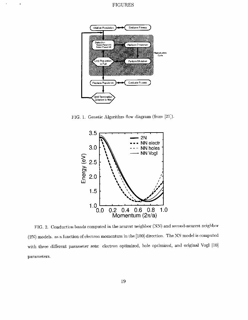
This process is diagrammed in Figure 1 and is the basis for a general package.
Parameterixation One of the most important stages of the optimization process is the
sound parameterization of the design and resultant encoding of the parameterization into
a chromosome. The parameters need to be chosen from the design space in an effective
manner, limited in range to a set that is physical, and encoded in a meaningful way. In the
case presented here, for example, the interaction energies do have a physical meaning, in
their relative sizes and signs. We have found that blind optimization, without controlling
the allowed range of energies for some of the parameters (like the spin orbit interaction
energies) unphysical results can be obtained. Similarly, how the parameter is encoded into a
gene is important. For example encoding a real parameter into a binary string or using real-
valued encoding is itself a tradeoff [6]. In general, efficient convergence of the optimization
algorithm will heavily depend upon the initial parameterization and encoding of the design.
For the optimization problem presented in this paper a custom real number encoding scheme
was chosen to control the range and mutation size of each parameter more closely. Each
parameter is represented by a double precision number without further discretization through
the typical representation as a binary string.
Choice of a Simulation Package A number of GAS and packages exist that fit the structure
outlined in Figure 1. The key needs for the work in this paper are that the package be flexible
enough to allow a range of design parameterizations and be able to exploit high performance
computers. First, the different parameterizations and gene encodings, as well as mutation
strategies need to be easily available. Secondly, because the parameter space is quite large,
6
a large gene pool needs to be explored. Utilization of massively parallel computers for the
fitness evaluation of the independent genes can lead to a dramatic speedup. These points are
encapsulated in PGAPack, a parallel genetic algorithm library [26]. This package consists of
a set of library routines supplying the user multiple levels of control over the optimization
process. The levels vary from default encodings, with simple initialization of parameters and
single statement execution, to the ability to modify, at a low-level, all relevant parameters in
the optimization process. User written routines for evaluation or crossover and mutation can
also be inserted if necessary. The package is written using the Message Passing Interface
(MPI) for parallel execution on a number of processors. A master process coordinates
the chromosome initialization, selection and reproduction while slave processes calculate the
fitness function, including the execution the electronic structure code on different processors.
Genetic Algorithm Parameters The GA parameters can be classified into two groups: 1)
parameter encoding and 2) the GA steering parameters such as population and replacement
sizes, crossover and mutation probabilities, stopping and restart conditions. The orbital
interaction energies are encoded into double precision numbers as mentioned above. Each
value is drawn randomly from a Gaussian distribution. The mean and standard deviation
are entered for each parameter. The Gaussian distribution can be clipped to a hard min-
imum or maximum. Each value has also a mutation size in percent of its current value
attached as an input parameter. For orbital interaction energies that are of the order of
single digit electron volts we typically prescribed a standard deviation of about 0.2-0.4 eV.
Smaller orbital interaction energies typically were assigned correspondingly smaller standard
deviations. A variety of different population and replacement sizes as well as crossover and
mutation probabilities were explored. Satisfactory fitness improvement is typically obtained
for populations of 100-200 elements per parameter, a replacement of 10-30 % per generation,
and mutation and crossover probabilities of 10-50%.
Fitness Evaluation There are two stages to the evaluation of the fitness of a particular
parameter set: 1) computation of all the relevant physical quantities, and 2) the assembly
of these physical quantities into a single real value that will be used in the optimization
7
’ for the ranking of this particular set. The details of these two stages for the tight-binding
interaction energy optimization problem are given in the following paragraphs.
Bandstructure and Efective Mass Calculation The NEMO software provides a database-
like access to materials that can be user-defined. User- defined materials are represented
in an ASCII character stream that can be parsed by the NEMO material database engine.
Once a new material is described by the orbital interaction energies, a variety of material
properties can be easily retrieved by simple queries. The database is programmable, where
function calls to the standard math library operations (+,-, sin, cos, min, max, etc.) and a
variety of NEMO functions can be included. Typical functions needed for this optimization
problem are computation of bandedges, effective masses as a function of band index and
electron momentum and the determination of the actual X and L point minima on the X
and L axis.
Fitness Function The fitness function provides a ranking algorithm that maps the physics-
based data into a single number. In the case presented here the fitness function is quite
simply the weighted sum of the normalized variances between that targeted and actual
physical values. The GA is driven to minimize this single number. A perfect fit corresponds
to a fitness of 0.0. If a “perfect” fit cannot be obtained the GA is driven towards the smalles
positive fitness value. As part of the input to the optimization package a list of physical
quantities such as bandedges, momentum minima, and effective masses is provided. Each
quantity has a weight associated with it. The choice of weights influences how individual
deviations are prioritized. Setting a weight of a quantity to zero takes that quantity out of the
optimization, but enables the monitoring of its values throughout the optimization process.
To restrict the stochastic search further we have also included an acceptable minimum and
maximum value to the physical quantity. If the computed value falls outside the acceptable
range a fitness value of 10,000 is assigned and all further evaluations of this gene are stopped.
Required CPU Time. The computation of the effective masses and band edges from the
tight binding Hamiltonian takes about 1 to second on an Origin 2000 and HP SPXX-2000.
With a population size of 5000, a replacement size of 1000 and an evolution over 1000
8
' generations this corresponds to about 280 CPU hours. These evolutions were typically run
on 16 or 32 CPU's, where communication overhead is still minimal. This corresponds to a
wall clock time of about 17.5 and 8.75 hours, respectively.
Restarting the Genetic Algorithm. The GA optimization may get stuck in a local mini-
mum, if a population diversity is not maintained. Restarting the GA may help to re-establish
a broad diverse population. We monitor the development of the best parameter set and
restart the algorithm if this parameter set does not change for 50 generations. Due to re-
strictions in the supercomputing queueing system we are also forced to resubmit jobs into
the queue that have not reached an optimal value. To preserve the best available parameter
set from one run to the next we write out a new input deck every generation. That input
deck contains the best parameter set as a starting point of the Gaussian distributed param-
eter set. Upon initialization of the population we also ensure that the parameter set fed in
from the input is explicitly included in the population.
111. RESULTS: OPTIMIZED ORBITAL INTERACTION ENERGIES
Orbital interaction energies for the nearest and second-nearest neighbor sp3s" model
describing Si were optimized with the GA described above. The first 2 columns of Table I
show the detailed material properties that were to be properly represented by the tight
binding model. The material properties were taken or derived from Si data published in
Reference [9]. The properties can be characterized into three categories: 1) band edge ener-
gies, 2) effective masses in various bands and crystal directions, and 3) crystal momentum
(A,,,) corresponding to the minimum conduction band energy in the X direction. The next
paragraphs step through the results of the optimization procedure.
Second-Nearest Neigbor sp3s* The third and fourth column of Table I show the material
properties that correspond to the optimized second-nearest neighbor (2N) model and the
relative deviation from the target value in percent. The optimal orbital interaction energies
are shown in Table 11. All targeted material properties are represented in the tight-binding
9
model within an accuracy of better than 4 percent. 12 out of 15 targets are matched to better
than one percent. Such agreement appears to be well within the experimental accuracy of
the bandstructure data. The sp3s* second-nearest neighbor model is found to be able to
represent the Si material parameters relevant to carrier transport well.
Nearest Neighbor sp3s” No such single, well optimized parameter set could be found for
the sp3s* nearest neighbor model for Si. With the same optimization weights used for the
second-nearest neighbor model, both electron and hole masses converged to values signifi-
cantly different from the experimental target values. Two separate numerical experiments
where the weights for electron masses were raised and lowered for the holes, and vice versa
resulted in two different “optimal” sets. The sets are labeled nearest-neighbor (NN) con-
duction band (CB) and Valence band (VB) and the material properties are tabulated in
columns 5/6 and 7/8 of Table I, respectively. The VB parameter set reproduces the hole
masses and bands reasonably well. The symmetry of the bands are reproduced properly.
This parameter set may be useful for for hole simulations using the NN tight-binding sp3s*
model.
Even with the focus on electron masses a good agreement with the transverse/light
electron mass could not be achieved. The deviation still remained over 50%. Table I1 shows
that the CB parameters contain an interaction energy V,, of 23 eV which is completely
unphysical. The reason for the usage of tight-binding models in electron transport, which is
the proper description of the electron wavefunction symmetry, will be lost. The optimization
drives this one parameter to such extreme values due to the pathology of the sp3s” nearest
neighbor model. Although the effective masses and bandedges for electrons look reasonable,
we urge for caution in using the sp3s* NN model to model electron transport in Si.
The material parameters that result from the standard Vogl parameters are included in
columns 9/10 of Table I for reference. These parameters do not include a spin-orbit inter-
action. The hole bands and masses are therefore not properly represented. The conduction
band properties agree reasonably well with the experimental data, considering the limits of
the model.
10
Graphical Comparisons Figure 2 depicts the conduction band minimum along the [loo] direction from the r to X point for the four parameter sets discussed above. All four curves
“look” reasonable in comparison to each other. Indeed Table I showed that the heavy
electron masses all agree within 20 percent to the experimental value. Note, however, that
a graph like this does not show any of the transverse momentum dependence that results in
the material property of the light electron mass.
The capability to model the light-electron mass in the nearest neighbor and second-
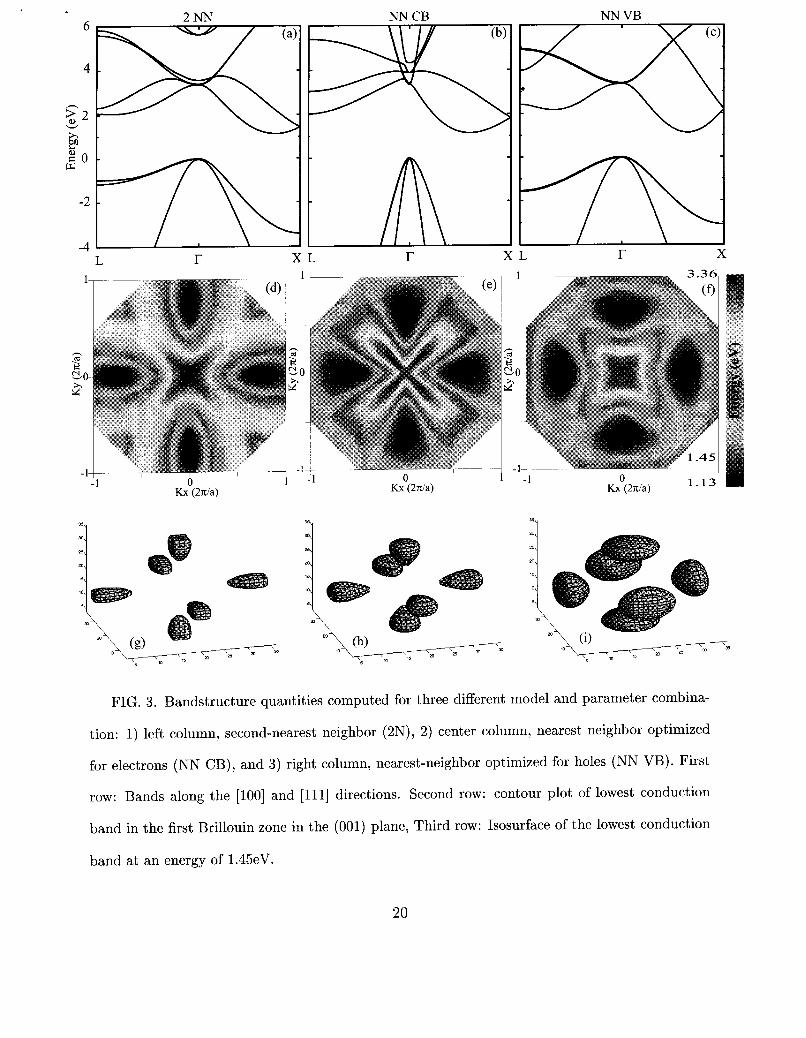
nearest neighbor tight-binding model is the theme of Figure 3. The columns of Figure 3 are
grouped by the parameter sets: l/left column) 2nd-nearest neighbor (2N), 2/center column)
nearest neighbor electron optimization (NN CB), and 3/right column) nearest neighbor hole
optimization (NN VB). The left column will be considered as a reference since it provides
the best agreement with experimental data. The upper row of Figure 3 shows the bands
along the [loo] and [lll] directions. Symmetry and curvatures of 3a) correspond to the
data shown for Si in reference [9]. Figure 3b) which stems from the electron optimized
parameters shows the lowest conduction band to be similar to 3a). The upper conduction
bands have been pushed to lower energies at the I’ point, providing more curavture to lowest
conduction band. In fact the minimum conduction band momentum (A,,,) on the [loo] line is pushed in from the target value of 0.75 to 0.597. Note that the hole band symmetry
is not well represented at all. The hole masses are clearly too light as indicated in Table I
as well. Figure 3c) shows quite similar behavior to Figure 3a) for the hole bands and the
lowest conduction band, however the upper conduction bands are quite modified.
The second row of Figure 3 shows the contour plots of the lowest conduction band in
the (001) plane of the first Brillouin zone. The dark blue colors correspond to the minimum
of the scale at about 1.13eV. The red color corresponds to the maximum resolved energy of
about 3.5eV. The third row shows the lowest conduction band isosurfaces in the first Brillouin
zone at an energy of 1.45eV. Figures 3d-f) and 3g-i) all show
conduction band minima. However, only 3d,g) show the correct
a correct light-electron and heavy-electron symmetry. Figures
11
the expected four and six
“cigar” shape representing
3f,i) show “pancake” like
’ conduction band surfaces, rather than the expected “cigar” shaped surfaces. In fact the
light electron mass is larger than the heavy electron mass (see also Table I). The shape of
the conduction band optimized nearest neighbor (CB NN) parameter set shows roughly the
right symmetry with the correct light / heavy electron ratio.
Figure 3f) shows clearly the complete pathology of the sp3s* model with respect to the
transverse electron mass. By the coloring it can be clearly seen that at the zone faces the
band edges are flat and the mass along these edges is indeed infinite. A finite transverse
effective mass can be obtained only by pushing the conduction band minimum away from
the zone edge. The deeper the conduction band minimum is pushed towards the r point,
the smaller the transverse effective mass can be made. This comes with the cost of bringing
the upper conduction bands much lower in energy and losing the proper masses for the
hole-bands. Also as noted above, one of the interaction energies becomes unphysically large
and electron and hole wavefunction symmetries are not expected to be correct.
For reference Figure 4 shows the lowest conduction band isosurface at 1.45eV in the
Brillouin zone computed with the standard Vogl parameters. The incorrect shape of the
conduction band minimum surface is clearly evident similar to Figure 3i).
Which model to use? The second-nearest neighbor sp3s* tight-binding model clearly
represents the complex Si bandstructure better than the nearest neighbor model. The better
model comes with a price of added dimensionality in the parameter fitting problem (9 to
20 parameters for elementary semiconductors, 15 to 37 for compound semiconductors) and
with the price of increased numerical complexity due to the increase of the size of the basis.
Despite its complications the second-nearest neighbor model is to be preferred over the
nearest neighbor model which lacks basic capabilities to simultaneously model electrons and
holes properly.
Use of nearest-neighbor model for indirect bandgap materials. Although the transverse
mass pathology in the nearest neighbor model is known, some researchers continue to use
[27] this model to simulate problems where the proper light electron mass is important, or
where the proper hole masses are important. We hope that Figures 3 and 4 clearly visualize
12
’ the limits of the nearest neighbor sp3s” model away from the r point. For existing research
software, where a rewrite of the underlying algorithms is impossible/impractical, we suggest
the usage of the two new parameter sets provided here as a sanity check for parameter
dependence in the simulation. For “pure” hole simulations the specialized nearest neighbor
parameter set may provide more physical answers.
Special caution needs to be taken with the electron parameter set, since it does include
an unphysically large interaction energy. This parameter set is to be seen as a warning
that this model should not be used for the modeling of indirect bandgap materials where
conduction band minima are in the X or L valley. Forcing the conduction band to a certain
curvature off the I7 point will lead to unphysical interaction energies.
IV. FUTURE WORK
The genetic algorithm (GA) based optimization scheme in its generality and flexibility
has enabled us to look at complex parameterizations of tight-binding models for electron
transport simulations. The second-nearest neighbor model hides some caveats with respect
to three-center interaction integrals and the scaling of these interaction energies with strain
becomes quite complicated. We are therefore exploring sp3d5 tight-binding models to prop-
erly represent the highest valence and lowest conduction bands under the inclusion of strain.
The GA approach has enabled us to consider sp3d5 tight binding models seriously, since
we can now overcome the fitting nightmare. Preliminary results show that the GA fitting
procedure works well for the sp3s5 models as well and result will be published elsewhere.
V. SUMMARY
This work has presented three major points needed for for the quantum mechanical
simulation of carrier transport in Si:
0 a genetic algorithm-based optimization scheme for the determination of orbital inter-
13
action energies for tight-binding models, given physical observables such as band edges
and effective masses.
0 3 new parameter sets to represent Si in the nearest and second-nearest sp3s* models
0 a clear visualization of the transverse X mass pathology of the nearest neigbor sp3s*
model
We hope that Figure 3 helps deterr the use of the nearest-neighbor sp3s* model for the
modeling of indirect bandgap materials such as Si or Ge.
VI. ACKNOWLEDEGEMENT
The work described in this publication was carried out by the Jet Propulsion Laboratory,
California Institute of Technology under a contract with the National Aeronautics and Space
Administration. The supercomputer used in this investigation was provided by funding from
the NASA Offices of Earth Science, Aeronautics, and Space Science. Part of the research
reported here was performed using HP SPP-2000 operated by the Center for Advanced
Computing Research at Caltech; access to this facility was provided by Caltech.
One of us (G.K.) would like to highlight and acknowledge the extensive PGApack work
by David Levine [26] including the variety of examples and software manual. His thor-
ough software development enabled our entry into the world of massively parallel GA-based
optimization.
14
REFERENCES
[l] Y. C. Chang and J. N. Schulman, Phys. Rev. B 25, 3975 (1982).
[2] J. N. Schulman and Y. C. Chang, Phys. Rev. B 31, 2056 (1985).
[3] J. N. Schulman, J. Appl. Phys. 60, 3954 (1986).
[4] D. Z. Y. Ting, E. T. Yu, and T. C. McGill, Phys. Rev. B 45, 3583 (1992).
[5] T. B. Boykin, J. P. A. van der Wagt, and J. S. Harris, Phys. Rev. B 43, 4777 (1991).
[6] R. C. Bowen et al., J. Appl. Phys 81, 3207 (1997).
[7] G. Klimeck, T. Boykin, R. C. Bowen, R. Lake, D. Blanks, T. S. NIoise, Y. C. Kao, and
W. R. Frensley in the 1997 55th Annual Device Research Conference Digest, (IEEE,
NJ, 1997), p. 92.
[8] C. Bowen et al., in IEDM 1997 (IEEE, New York, 1997), pp. 869-872.
[9] 0. Madelung, Semiconductors - Basic Data (Springer, Berlin, 1996).
[lo] P. Vogl, H. P. Hjalmarson, and J. D. DOW, J. Phys. Chem. Solids 44, 365 (1983).
[ll] Citiation Database, Institute for Scientific Information.
[12] T. B. Boykin, G. Klimeck, R. C. Bowen, and R. K. Lake, Phys. Rev. B 56, 4102 (1997).
[13] T. B. Boykin, Phys. Rev. B 56, 9613 (1997).
[14] T. B. Boykin, L. J. Gamble, G. Klimeck, and R. C. Bowen, Phys. Rev. B 59, 7301
(1999).
[15] Goffe, Ferrier, and Rogers, Journal of Econometrics 60, 65 (1994).
[16] J . Holland, Adaptation in Natural and Artificial Systems (The University of Michigan
Press, Ann Arbor, 1975).
[17] D. Goldberg, Genetic Algorithms in Search, Optimization and Machine Learning
15
(Addison- Wesley, New York, 1989).
[18] D. S. Weile and E. Michielssen, IEEE Trans. Antennas Propag. AP-45, 343 (1997)
[19] E. Michielssen, S. Ranjithan, and R. Mittra, in Optimal Multilayer Filter Design Using
Real Coded Genetic Algorithms (Proc. Inst. Elect. Eng., ADDRESS, 1992), No. 12, pp.
413-20.
[20] R. Haupt, IEEE Trans. Antennas Propag. AP-42, 939 (1994).
[21] J. Johnson and Y. Rahmat-Samii, IEEE Antennas and Propagation Magazine 939, 7
(1997).
[22] C. Zuffada and T. Cwik, IEEE Trans. Antennas Propag. 46, 657 (1998).
[23] F. Starrost, S. Bornholdt, C. Solterbeck, and W. Schattke, Physical Review B 53, 12549
(1996).
[24] J. Krause et al., Physical Review B 57, 9024 (1998)
[25] G. Klimeck, C. Salazar-Lazaro, A. Stoica, and T. Cwik, in Genetically Engineered
Nanostructure Devices (Material Research Society, New York, accepted for publication,
1999).
[26] D. Levine, Technical Report No. 95/18, Argonne Nat. Lab. (unpublished)
[27] K. Leung and E(. B. Whaley, Physical Review B 56, 7455 (1997).
16
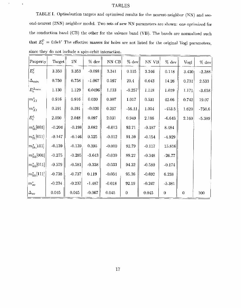
TABLES
TABLE I. Optimization targets and optimized results for the nearest-neighbor (NN) and sec-
ond-nearest (2NN) neighbor model. Two sets of new NN parameters are shown: one optimized for
the conduction band (CB) the other for the valence band (VB). The bands are normalized such
that E: = O.OeV The effective masses for holes are not listed for the original Vogl parameters,
since the do not include a E
Targe
3.350
0.750
1.130
0.916
0.191
2.050
-0.204
-0.147
-0.139
-0.275
-0.579
-0.738
-0.234
0.045
2N
3.353
0.758
1.129
0.916
0.191
2.048
-0.198
-0.146
-0.139
-0.285
-0.581
-0.737
-0.237
0.045
in-orbit interaction.
% dev
-0.098
- 1.067
0.0496
0.030
-0.020
0.097
3.082
0.525
0.395
-3.643
-0.338
0.119
-1.487
-0.067
NN CE
3.341
0.597
1.133
0.907
0.297
2.031
-0.013
-0.012
-0.010
-0.030
-0.033
-0.034
-0.018
0.045
% del
0.115
20.4
-0.257
1.017
-56.11
0.949
93.71
91.59
92.79
89.22
94.32
95.36
92.19
0
NN VE
3.346
0.643
1.118
0.531
1.054
2.186
-0.187
-0.154
-0.117
-0.348
-0.580
-0.692
-0.247
0.045
% det
0.118
14.26
1.019
42.06
-453.5
-6.643
8.484
-4.929
15.816
-26.77
-0.174
6.238
-5.381
0
Vogl
3.43(
0.731
1.171
0.742
1.62C
2.16C
0
% de7
-2.388
2.533
-3.658
19.07
-750.6
-5.38s
100
17
TABLE 11. Bandstructure model parameters for the nearest-neighbor (NN) and second-nearest
(2NN) neighbor model. Two sets of new NN parameters are shown: one optimized for the conduc-
tion banc :B) the other for the valence band (VB). All Darameters are in units of eV.
Vogl
-4.2000C
1.71500
6.68500
-8.3000C
1.71500
4.57500
5.72920
5.37490
0.00000
\ I
NN CB
-3.65866
1.67889
3.87567
-7.97142
1.69558
23.3241C
8.87467
5.41174
0.04500
NN VB
-3.3178C
1.67862
8.23164
-9.5989E
1.69552
4.77573
7.14230
7.25052
0.04500
2NN
-4.8134
1.77563
5.61342
-8.33251
1.69916
5.29091
5.86140
4.88308
0.04503
0.01591
0.08002
1.31699
-0.0057C
0.50103
0.00762
-0.10662
0.55067
-2.27784
18
FIGURES
Inltidim Population Evaluate Fitness -
Rspmduction Q C l S
FIG. 1. Genetic Algorithm flow diagram (from [21]).
0.0 0.2 0.4 0.6 0.8 1 .O Momentum (2da)
FIG. 2. Conduction bands computed in the nearest neighbor (NN) and second-nearest neighbor
(2N) models. as a function of electron momentum in the [loo] direction. The NN model is computed
with three different parameter sets: electron optimized, hole optimized, and original Vogl [lo]
parameters.
19
6
4
n
v 2 2
i?? 2 0
h
w
-2
-4
1
h . 8 0 x
2
- 1
2 N N
L r X
-1 0 Kx (2nla)
NN CB
L r X 1
$ 30 2
-1 n i
NN VB
m L r X
"Y
FIG. 3. Bandstructure quantities computed for three different model and parameter combina-
tion: 1) left column, second-nearest neighbor (2N), 2) center column, nearest neighbor optimized
for electrons (NN CB), and 3) right column, nearest-neighbor optimized for holes (NN VB). First
row: Bands along the [loo] and [lll] directions. Second row: contour plot of lowest conduction
band in the first Brillouin zone in the (001) plane, Third row: Isosurface of the lowest conduction
band at an energy of 1.45eV.
20
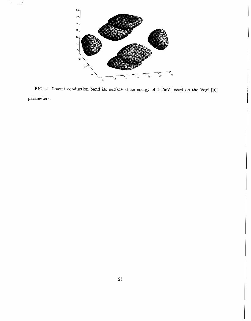
FIG. 4. Lowest conduction band is0 surface at an energy of 1.45eV based on the Vogl [lo]
parameters.
21


