Embed Size (px)
Citation preview
General rights Copyright and moral rights for the publications made accessible in the public portal are retained by the authors and/or other copyright owners and it is a condition of accessing publications that users recognise and abide by the legal requirements associated with these rights.
Users may download and print one copy of any publication from the public portal for the purpose of private study or research.
You may not further distribute the material or use it for any profit-making activity or commercial gain
You may freely distribute the URL identifying the publication in the public portal If you believe that this document breaches copyright please contact us providing details, and we will remove access to the work immediately and investigate your claim.
Downloaded from orbit.dtu.dk on: Jul 08, 2022
Silver-substituted (Ag1-xCux)2ZnSnS4 solar cells from aprotic molecular inks
Engberg, Sara; Gansukh, Mungunshagai; Martinho, Filipe; Stamate, Eugen; Hansen, Ole; Schou, Jørgen;Canulescu, Stela
Published in:Ceramics International
Link to article, DOI:10.1016/j.ceramint.2022.04.116
Publication date:2022
Document VersionPeer reviewed version
Link back to DTU Orbit
Citation (APA):Engberg, S., Gansukh, M., Martinho, F., Stamate, E., Hansen, O., Schou, J., & Canulescu, S. (Accepted/Inpress). Silver-substituted (Ag1-xCux)2ZnSnS4 solar cells from aprotic molecular inks. Ceramics International.https://doi.org/10.1016/j.ceramint.2022.04.116
Ceramics International xxx (xxxx) xxx
Please cite this article as: Sara Engberg, Ceramics International, https://doi.org/10.1016/j.ceramint.2022.04.116
Available online 15 April 20220272-8842/© 2022 The Authors. Published by Elsevier Ltd. This is an open access article under the CC BY license (http://creativecommons.org/licenses/by/4.0/).
Silver-substituted (Ag1-xCux)2ZnSnS4 solar cells from aprotic molecular inks
Sara Engberg a,*, Mungunshagai Gansukh a, Filipe Martinho a, Eugen Stamate b, Ole Hansen b, Jørgen Schou a, Stela Canulescu a
a DTU Fotonik, Technical University of Denmark, Frederiksborgvej 399, 4000, Roskilde, Denmark b DTU Nanolab, Technical University of Denmark, Ørsteds Plads, 2800 Kgs, Lyngby, Denmark
A R T I C L E I N F O
Keywords: Films (A) Microstructure-final (B) Impurities (B) X-ray methods (B)
A B S T R A C T
To battle the high open-circuit voltage deficit (VOC,def) in kesterite (Cu2ZnSnS4 or CZTS) solar cells, a current field of research relates to point defect engineering by cation substitution. For example, by partly replacing Cu with an element of a larger ionic radius, such as Ag, the degree of Cu/Zn disorder decreases, and likewise does the associated band tailing. In this paper, solution-processed (Ag1-xCux)2ZnSnS4 (ACZTS) samples are prepared through the aprotic molecular ink approach using DMSO as the solvent. The successful incorporation of silver into the CZTS lattice is demonstrated with relatively high silver concentrations, namely Ag/(Ag+Cu) ratios of 13% and 26%. The best device was made with 13% Ag/(Ag+Cu) and had an efficiency of 4.9%. The samples are compared to the pure CZTS sample in terms of microstructure, phase distribution, photoluminescence, and de-vice performance. In the XRD patterns, a decrease in the lattice parameter c/a ratio is observed for ACZTS, as well as significant peak splitting with Ag addition for several of the characteristic kesterite XRD reflections. In addition to the improvement in efficiency, other advantageous effects of Ag-incorporation include enhanced grain growth and an increased band gap. A too high concentration of Ag leads to the formation of secondary phases such as SnS and Ag2S as detected by XRD.
1. Introduction
In the pursuit for the solar cell materials of the future, Earth- abundancy and non-toxicity are key search criteria. Silicon photovol-taics fulfills these requirements and is currently dominating the solar market with a share of 95% [1] and a record power conversion efficiency of 26.7% [2], approaching its theoretical intrinsic limit of 29.4% [3]. Therefore, to further increase the efficiency of Si solar cells, novel concepts such as tandem devices should be considered [4], where either perovskite or thin-film solar cells are good companions to silicon. The commercialized thin-film solar cells, Cu(In,Ga)Se2 (CIGS) and CdTe, suffer from low abundance (In, Ga, and Te), which limits their future large-scale deployment, and stimulates the search for alternative materials.
One of the most studied thin-film absorber candidates is the kesterite (Cu2ZnSn(S1-xSex)4 or CZTSSe), which in addition to high abundance and environmental-friendliness, demonstrates good solar absorber qualities such as a direct, tunable band gap (EG) in the optimal region and a high absorption coefficient [5]. The kesterite’s resemblance to the commercialized CIGS thin-film solar cell, which has reached an
efficiency of 23.35% [2], also speaks to its promising potential. How-ever, the record efficiency of CZTSSe (EG = 1.13 eV) is 13.2% [6] and of its pure-sulfide counterpart Cu2ZnSnS4 (CZTS, EG = 1.5 eV) it is 11% [7], and thus more improvements are required before the materials are ready for market.
Currently, the main device parameter limiting the performance of the kesterites is a low open-circuit voltage (VOC) relative to the band gap of the absorber. This deficit in VOC is particularly large for the sulfide kesterites, which are the more suitable for tandem devices. No consensus exists as to the origin of the VOC-deficit, but there are a few hypotheses [8]. These relate to either the interfaces of the absorber, such as a non-Ohmic CZTS/Mo back contact, a non-optimal p-n junction [9], or to a high concentration of defects within the bulk of the absorber, which is the topic of this paper.
Theoretical calculations of the formation energies for defects within CZTS show that CuZn antisite displays the lowest formation energy of <0.25 eV and that the defect cluster containing [CuZn
− + ZnCu+ ] has a
formation energy of 0.2 eV [10], which explains that Cu–Zn disorder easily forms in CZTS [11]. Moreover, due to the similarities between Cu and Zn, such as atomic number (ZCu = 29 and ZZn = 30) and ionic radius
* Corresponding author. E-mail address: [email protected] (S. Engberg).
Contents lists available at ScienceDirect
Ceramics International
journal homepage: www.elsevier.com/locate/ceramint
https://doi.org/10.1016/j.ceramint.2022.04.116 Received 8 March 2022; Received in revised form 28 March 2022; Accepted 11 April 2022
Ceramics International xxx (xxxx) xxx
2
(rCu = 0.73 Å and rZn = 0.74 Å), they are hard to distinguish, which makes it difficult to quantify Cu–Zn disorder. At the moment, the dis-tribution of Cu and Zn is characterized by neutron diffraction [12] or nuclear magnetic resonance (NMR) [13], which are not applicable on thin-film device samples, but near resonance Raman could be a possible alternative [14]. A correlation was seen in features of the Raman spectra between the cooling rate and the degree of ordering [14], however, the relation also depends on the composition and the band gap of the kes-terite, and is thus not a globally suitable approach [11]. The effect of the Cu–Zn disorder is considered related to electrostatic potential fluctua-tions as a result of the charged CuZn
− and ZnCu+ point defects, as well as
bandgap fluctuations stemming from the uneven distribution of the [CuZn
− + ZnCu+ ] defect clusters [11,15]. These associated tail states will
cause a decrease in VOC, and thus limiting cation disorder should be a priority.
A few routes have been explored to minimize Cu–Zn disorder. One approach is to utilize low-temperature annealing to allow the sample to approach the dynamic equilibrium state of the perfectly ordered crystal as shown by Scragg et al. [14]. A more viable way to control the cation distribution is to substitute Cu and/or Zn with isoelectronic elements with smaller or larger ionic radii. By taking advantage of this size mismatch, a barrier for disorder arises, since the larger atom cannot easily jump into another position in the lattice. For example, by replacing Cu (0.73 Å) with an element of a larger ionic radius such as Ag (1.15 Å) into CZTS, the degree of Cu–Zn disorder is decreased because Ag is less likely to exchange positions with Zn. In other words, the for-mation energy of AgZn antisite defects is high inside (Ag1-xCux)2ZnSn (S1-ySey)4 (ACZTSSe) and thus reduces the probability of it happening. This approach was successfully used to improve the efficiencies for the associated CZTS, CZTSe, and CZTSSe devices [16–18], respectively. However, even though a wide range of extrinsic dopants has been applied to engineer the defect environment in the kesterite, the highest efficiency currently remains with the un-alloyed compounds. Therefore, more work is needed to understand the effect of the alloyed kesterites, their formation mechanism, and their defect nature.
Silver can be incorporated either as a metallic layer at the top [19] or back [20] CZTS interface. For vacuum-processed devices, Cui et al. [20] find that a thin 20 nm Ag interlayer at the back CZTS/Mo interface can inhibit the formation of MoS2, SnS2, and voids at the interface, which leads to improvements in series resistance and recombination. Addi-tionally, Gang et al. [19] show that a Ag layer on top of the CZTSSe is found to decrease antisite defects and related defect complexes, which in turn decreases band tailing, improves minority carrier lifetimes, and the diode quality. Ultimately, this leads to the best vacuum-processed ACZTSSe device of 12.07% [19]. The best efficiency of a vacuum-processed pure sulfide ACZTS device is 5.44% [21].
For CZTSSe, the best devices have since 2010 been made by solution- processing. First, the hydrazine-based approach resulted in a record device of 9.7% in 2010 [22], which by subsequent R&D improved to 12.6% in 2014 [23]. Even though solution processing is suitable for mass-production due to its inexpensive and large-scale potential, the work with hydrazine was terminated due to its very high toxicity and flammability. Nonetheless, the hydrazine approach was used as a model system for direct liquid coating methods for the future, which initiated research in the DMF, DMSO, and other aprotic molecular inks. Another advantage of solution-based semiconductor development is the ease of screening new reagents or additives, which could also explain the
current interest in the solution-based CZTSSe approaches. Today, the DMSO approach has resulted in the recent record of 13.2% for CZTSSe [6], by inclusion of an organic lithium salt additive. Recently, Gong et al. [17] showed that Ag in the form of AgNO3 can be added to DMSO so-lutions, which leads to ACZTSSe devices of 12.5%.
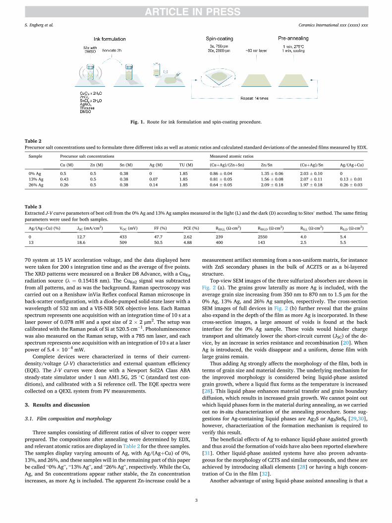
For pure-sulfide CZTS, the evolution of the best Ag-substituted de-vices can be seen in Table 1, with the current record device of 7.24% made by Guchhait et al. [16] for an un-graded absorber, while 8.24% was achieved with a ACZTS and K-doped CZTS double-layer [24]. In this work, we demonstrate a Ag-substituted CZTS device by using the same approach as the record ACZTSSe device made with DMSO. Three sam-ples were prepared consisting of 0%, 13%, and 26% Ag/(Ag+Cu). In this paper, the annealed absorbers and respective devices will be compared based on film composition and morphology, phase distribution, and device performance.
2. Experimental
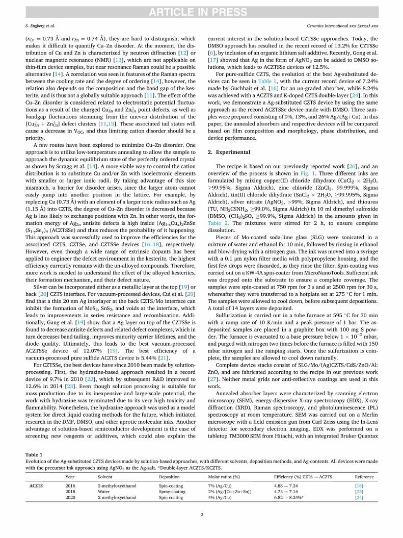
The recipe is based on our previously reported work [26], and an overview of the process is shown in Fig. 1. Three different inks are formulated by mixing copper(II) chloride dihydrate (CuCl2 × 2H2O, ≥99.95%, Sigma Aldrich), zinc chloride (ZnCl2, 99.999%, Sigma Aldrich), tin(II) chloride dihydrate (SnCl2 × 2H2O, ≥99.995%, Sigma Aldrich), silver nitrate (AgNO3, >99%, Sigma Aldrich), and thiourea (TU, NH2CSNH2, ≥99.0%, Sigma Aldrich) in 10 ml dimethyl sulfoxide (DMSO, (CH3)2SO, ≥99.9%, Sigma Aldrich) in the amounts given in Table 2. The mixtures were stirred for 2 h, to ensure complete dissolution.
Pieces of Mo-coated soda-lime glass (SLG) were sonicated in a mixture of water and ethanol for 10 min, followed by rinsing in ethanol and blow-drying with a nitrogen gun. The ink was moved into a syringe with a 0.1 μm nylon filter media with polypropylene housing, and the first few drops were discarded, as they rinse the filter. Spin-coating was carried out on a KW-4A spin-coater from MicroNanoTools. Sufficient ink was dropped onto the substrate to ensure a complete coverage. The samples were spin-coated at 750 rpm for 3 s and at 2500 rpm for 30 s, whereafter they were transferred to a hotplate set at 275 ◦C for 1 min. The samples were allowed to cool down, before subsequent depositions. A total of 14 layers were deposited.
Sulfurization is carried out in a tube furnace at 595 ◦C for 30 min with a ramp rate of 10 K/min and a peak pressure of 1 bar. The as- deposited samples are placed in a graphite box with 100 mg S pow-der. The furnace is evacuated to a base pressure below 1 × 10− 2 mbar, and purged with nitrogen two times before the furnace is filled with 150 mbar nitrogen and the ramping starts. Once the sulfurization is com-plete, the samples are allowed to cool down naturally.
Complete device stacks consist of SLG/Mo/(Ag)CZTS/CdS/ZnO/Al: ZnO, and are fabricated according to the recipe in our previous work [27]. Neither metal grids nor anti-reflective coatings are used in this work.
Annealed absorber layers were characterized by scanning electron microscopy (SEM), energy-dispersive X-ray spectroscopy (EDX), X-ray diffraction (XRD), Raman spectroscopy, and photoluminescence (PL) spectroscopy at room temperature. SEM was carried out on a Merlin microscope with a field emission gun from Carl Zeiss using the In-Lens detector for secondary electron imaging. EDX was performed on a tabletop TM3000 SEM from Hitachi, with an integrated Bruker Quantax
Table 1 Evolution of the Ag-substituted CZTS devices made by solution-based approaches, with different solvents, deposition methods, and Ag-contents. All devices were made with the precursor ink approach using AgNO3 as the Ag-salt. *Double-layer ACZTS/KCZTS.
Year Solvent Deposition Molar ratios (%) Efficiency (%) CZTS → ACZTS Reference
ACZTS 2016 2-methyloxyethanol Spin-coating 7% (Ag/Cu) 4.88 → 7.24 [16] 2018 Water Spray-coating 2% (Ag/[Cu+Zn+Sn]) 4.73 → 7.14 [25] 2020 2-methyloxyethanol Spin-coating 4% (Ag/Cu) 6.82 → 8.24%* [24]
S. Engberg et al.
Ceramics International xxx (xxxx) xxx
3
70 system at 15 kV acceleration voltage, and the data displayed here were taken for 200 s integration time and as the average of five points. The XRD patterns were measured on a Bruker D8 Advance, with a CuKα radiation source (λ = 0.15418 nm). The CuKα2 signal was subtracted from all patterns, and as was the background. Raman spectroscopy was carried out on a Renishaw inVia Reflex confocal Raman microscope in back-scatter configuration, with a diode-pumped solid-state laser with a wavelength of 532 nm and a VIS-NIR 50X objective lens. Each Raman spectrum represents one acquisition with an integration time of 10 s at a laser power of 0.078 mW and a spot size of 2 × 2 μm2. The setup was calibrated with the Raman peak of Si at 520.5 cm− 1. Photoluminescence was also measured on the Raman setup, with a 785 nm laser, and each spectrum represents one acquisition with an integration of 10 s at a laser power of 5.4 × 10− 4 mW.
Complete devices were characterized in terms of their current- density/voltage (J-V) characteristics and external quantum efficiency (EQE). The J-V curves were done with a Newport Sol2A Class ABA steady-state simulator under 1 sun AM1.5G, 25 ◦C (standard test con-ditions), and calibrated with a Si reference cell. The EQE spectra were collected on a QEXL system from PV measurements.
3. Results and discussion
3.1. Film composition and morphology
Three samples consisting of different ratios of silver to copper were prepared. The compositions after annealing were determined by EDX, and relevant atomic ratios are displayed in Table 2 for the three samples. The samples display varying amounts of Ag, with Ag/(Ag+Cu) of 0%, 13%, and 26%, and these samples will in the remaining part of this paper be called “0% Ag”, “13% Ag”, and “26% Ag”, respectively. While the Cu, Ag, and Sn concentrations appear rather stable, the Zn concentration increases, as more Ag is included. The apparent Zn-increase could be a
measurement artifact stemming from a non-uniform matrix, for instance with ZnS secondary phases in the bulk of ACZTS or as a bi-layered structure.
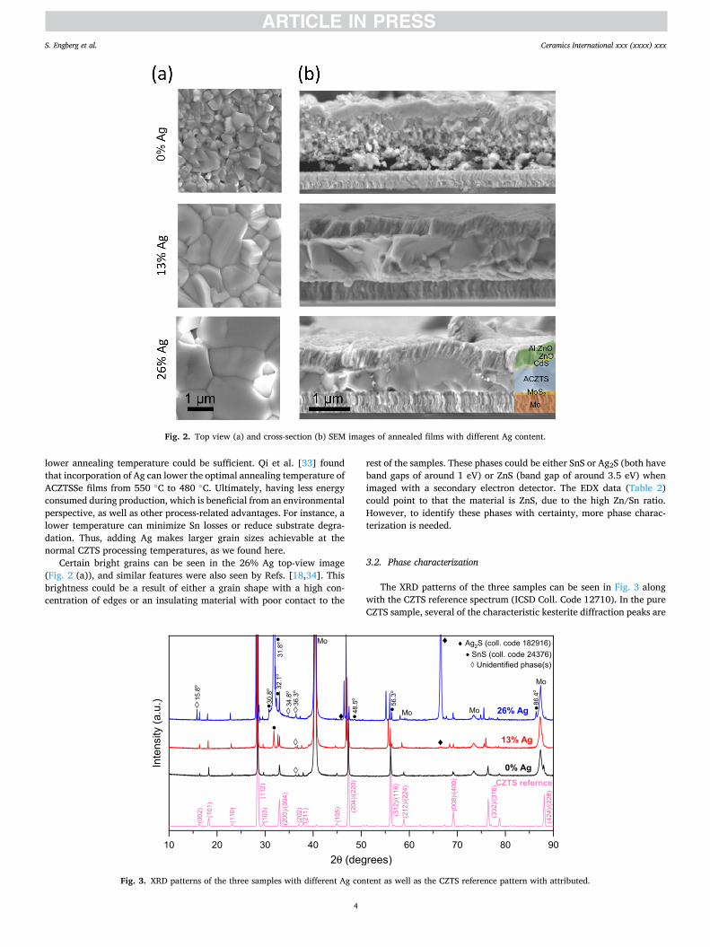
Top-view SEM images of the three sulfurized absorbers are shown in Fig. 2 (a). The grains grow laterally as more Ag is included, with the average grain size increasing from 350 nm to 870 nm to 1.5 μm for the 0% Ag, 13% Ag, and 26% Ag samples, respectively. The cross-section SEM images of full devices in Fig. 2 (b) further reveal that the grains also expand in the depth of the film as more Ag is incorporated. In these cross-section images, a large amount of voids is found at the back interface for the 0% Ag sample. These voids would hinder charge transport and ultimately lower the short-circuit current (JSC) of the de-vice, by an increase in series resistance and recombination [20]. When Ag is introduced, the voids disappear and a uniform, dense film with large grains remain.
Thus adding Ag strongly affects the morphology of the film, both in terms of grain size and material density. The underlying mechanism for the improved morphology is considered being liquid-phase assisted grain growth, where a liquid flux forms as the temperature is increased [28]. This liquid phase enhances material transfer and grain boundary diffusion, which results in increased grain growth. We cannot point out which liquid phases form in the material during annealing, as we carried out no in-situ characterization of the annealing procedure. Some sug-gestions for Ag-containing liquid phases are Ag2S or Ag8SnS6 [29,30], however, characterization of the formation mechanism is required to verify this result.
The beneficial effects of Ag to enhance liquid-phase assisted growth and thus avoid the formation of voids have also been reported elsewhere [31]. Other liquid-phase assisted systems have also proven advanta-geous for the morphology of CZTS and similar compounds, and these are achieved by introducing alkali elements [28] or having a high concen-tration of Cu in the film [32].
Another advantage of using liquid-phase assisted annealing is that a
Fig. 1. Route for ink formulation and spin-coating procedure.
Table 2 Precursor salt concentrations used to formulate three different inks as well as atomic ratios and calculated standard deviations of the annealed films measured by EDX.
Sample Precursor salt concentrations Measured atomic ratios
Cu (M) Zn (M) Sn (M) Ag (M) TU (M) (Cu+Ag)/(Zn+Sn) Zn/Sn (Cu+Ag)/Sn Ag/(Ag+Cu)
0% Ag 0.5 0.5 0.38 0 1.85 0.86 ± 0.04 1.35 ± 0.06 2.03 ± 0.10 0 13% Ag 0.43 0.5 0.38 0.07 1.85 0.81 ± 0.05 1.56 ± 0.08 2.07 ± 0.11 0.13 ± 0.01 26% Ag 0.26 0.5 0.38 0.14 1.85 0.64 ± 0.05 2.09 ± 0.18 1.97 ± 0.18 0.26 ± 0.03
Table 3 Extracted J-V curve parameters of best cell from the 0% Ag and 13% Ag samples measured in the light (L) and the dark (D) according to Sites’ method. The same fitting parameters were used for both samples.
Ag/(Ag+Cu) (%) JSC (mA/cm2) VOC (mV) FF (%) PCE (%) RSH,L (Ω⋅cm2) RSH,D (Ω⋅cm2) RS,L (Ω⋅cm2) RS,D (Ω⋅cm2)
0 12.7 433 47.7 2.62 239 2550 4.0 5.4 13 18.6 509 50.5 4.88 400 143 2.5 5.5
S. Engberg et al.
Ceramics International xxx (xxxx) xxx
4
lower annealing temperature could be sufficient. Qi et al. [33] found that incorporation of Ag can lower the optimal annealing temperature of ACZTSSe films from 550 ◦C to 480 ◦C. Ultimately, having less energy consumed during production, which is beneficial from an environmental perspective, as well as other process-related advantages. For instance, a lower temperature can minimize Sn losses or reduce substrate degra-dation. Thus, adding Ag makes larger grain sizes achievable at the normal CZTS processing temperatures, as we found here.
Certain bright grains can be seen in the 26% Ag top-view image (Fig. 2 (a)), and similar features were also seen by Refs. [18,34]. This brightness could be a result of either a grain shape with a high con-centration of edges or an insulating material with poor contact to the
rest of the samples. These phases could be either SnS or Ag2S (both have band gaps of around 1 eV) or ZnS (band gap of around 3.5 eV) when imaged with a secondary electron detector. The EDX data (Table 2) could point to that the material is ZnS, due to the high Zn/Sn ratio. However, to identify these phases with certainty, more phase charac-terization is needed.
3.2. Phase characterization
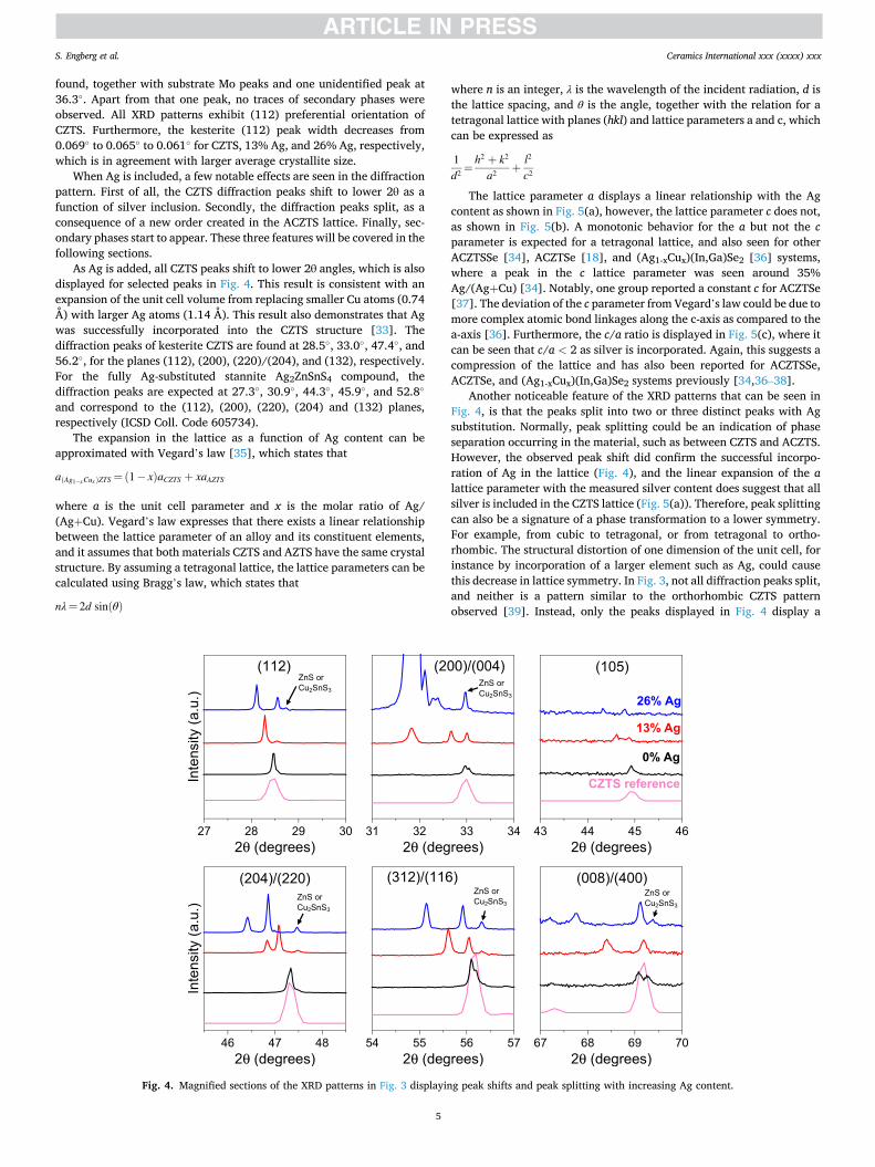
The XRD patterns of the three samples can be seen in Fig. 3 along with the CZTS reference spectrum (ICSD Coll. Code 12710). In the pure CZTS sample, several of the characteristic kesterite diffraction peaks are
Fig. 2. Top view (a) and cross-section (b) SEM images of annealed films with different Ag content.
Fig. 3. XRD patterns of the three samples with different Ag content as well as the CZTS reference pattern with attributed.
S. Engberg et al.
Ceramics International xxx (xxxx) xxx
5
found, together with substrate Mo peaks and one unidentified peak at 36.3◦. Apart from that one peak, no traces of secondary phases were observed. All XRD patterns exhibit (112) preferential orientation of CZTS. Furthermore, the kesterite (112) peak width decreases from 0.069◦ to 0.065◦ to 0.061◦ for CZTS, 13% Ag, and 26% Ag, respectively, which is in agreement with larger average crystallite size.
When Ag is included, a few notable effects are seen in the diffraction pattern. First of all, the CZTS diffraction peaks shift to lower 2θ as a function of silver inclusion. Secondly, the diffraction peaks split, as a consequence of a new order created in the ACZTS lattice. Finally, sec-ondary phases start to appear. These three features will be covered in the following sections.
As Ag is added, all CZTS peaks shift to lower 2θ angles, which is also displayed for selected peaks in Fig. 4. This result is consistent with an expansion of the unit cell volume from replacing smaller Cu atoms (0.74 Å) with larger Ag atoms (1.14 Å). This result also demonstrates that Ag was successfully incorporated into the CZTS structure [33]. The diffraction peaks of kesterite CZTS are found at 28.5◦, 33.0◦, 47.4◦, and 56.2◦, for the planes (112), (200), (220)/(204), and (132), respectively. For the fully Ag-substituted stannite Ag2ZnSnS4 compound, the diffraction peaks are expected at 27.3◦, 30.9◦, 44.3◦, 45.9◦, and 52.8◦
and correspond to the (112), (200), (220), (204) and (132) planes, respectively (ICSD Coll. Code 605734).
The expansion in the lattice as a function of Ag content can be approximated with Vegard’s law [35], which states that
a(Ag1− xCux)ZTS =(1 − x)aCZTS + xaAZTS
where a is the unit cell parameter and x is the molar ratio of Ag/ (Ag+Cu). Vegard’s law expresses that there exists a linear relationship between the lattice parameter of an alloy and its constituent elements, and it assumes that both materials CZTS and AZTS have the same crystal structure. By assuming a tetragonal lattice, the lattice parameters can be calculated using Bragg’s law, which states that
nλ= 2d sin(θ)
where n is an integer, λ is the wavelength of the incident radiation, d is the lattice spacing, and θ is the angle, together with the relation for a tetragonal lattice with planes (hkl) and lattice parameters a and c, which can be expressed as
1d2 =
h2 + k2
a2 +l2
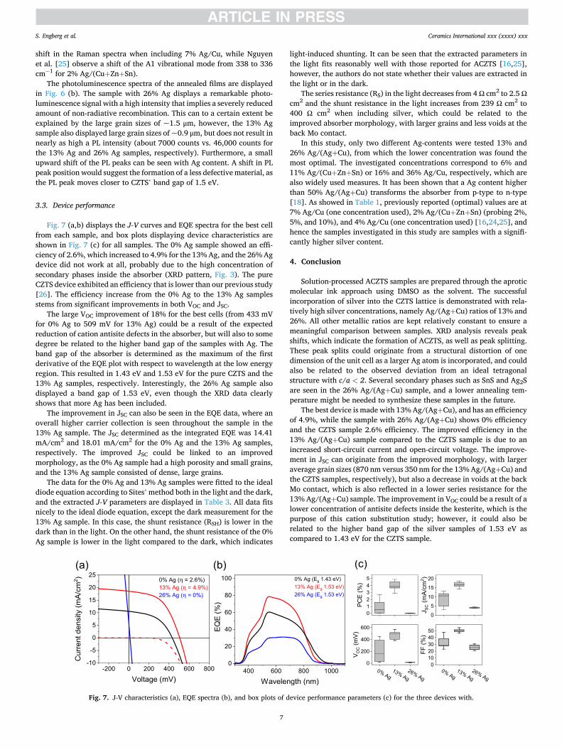
c2
The lattice parameter a displays a linear relationship with the Ag content as shown in Fig. 5(a), however, the lattice parameter c does not, as shown in Fig. 5(b). A monotonic behavior for the a but not the c parameter is expected for a tetragonal lattice, and also seen for other ACZTSSe [34], ACZTSe [18], and (Ag1-xCux)(In,Ga)Se2 [36] systems, where a peak in the c lattice parameter was seen around 35% Ag/(Ag+Cu) [34]. Notably, one group reported a constant c for ACZTSe [37]. The deviation of the c parameter from Vegard’s law could be due to more complex atomic bond linkages along the c-axis as compared to the a-axis [36]. Furthermore, the c/a ratio is displayed in Fig. 5(c), where it can be seen that c/a < 2 as silver is incorporated. Again, this suggests a compression of the lattice and has also been reported for ACZTSSe, ACZTSe, and (Ag1-xCux)(In,Ga)Se2 systems previously [34,36–38].
Another noticeable feature of the XRD patterns that can be seen in Fig. 4, is that the peaks split into two or three distinct peaks with Ag substitution. Normally, peak splitting could be an indication of phase separation occurring in the material, such as between CZTS and ACZTS. However, the observed peak shift did confirm the successful incorpo-ration of Ag in the lattice (Fig. 4), and the linear expansion of the a lattice parameter with the measured silver content does suggest that all silver is included in the CZTS lattice (Fig. 5(a)). Therefore, peak splitting can also be a signature of a phase transformation to a lower symmetry. For example, from cubic to tetragonal, or from tetragonal to ortho-rhombic. The structural distortion of one dimension of the unit cell, for instance by incorporation of a larger element such as Ag, could cause this decrease in lattice symmetry. In Fig. 3, not all diffraction peaks split, and neither is a pattern similar to the orthorhombic CZTS pattern observed [39]. Instead, only the peaks displayed in Fig. 4 display a
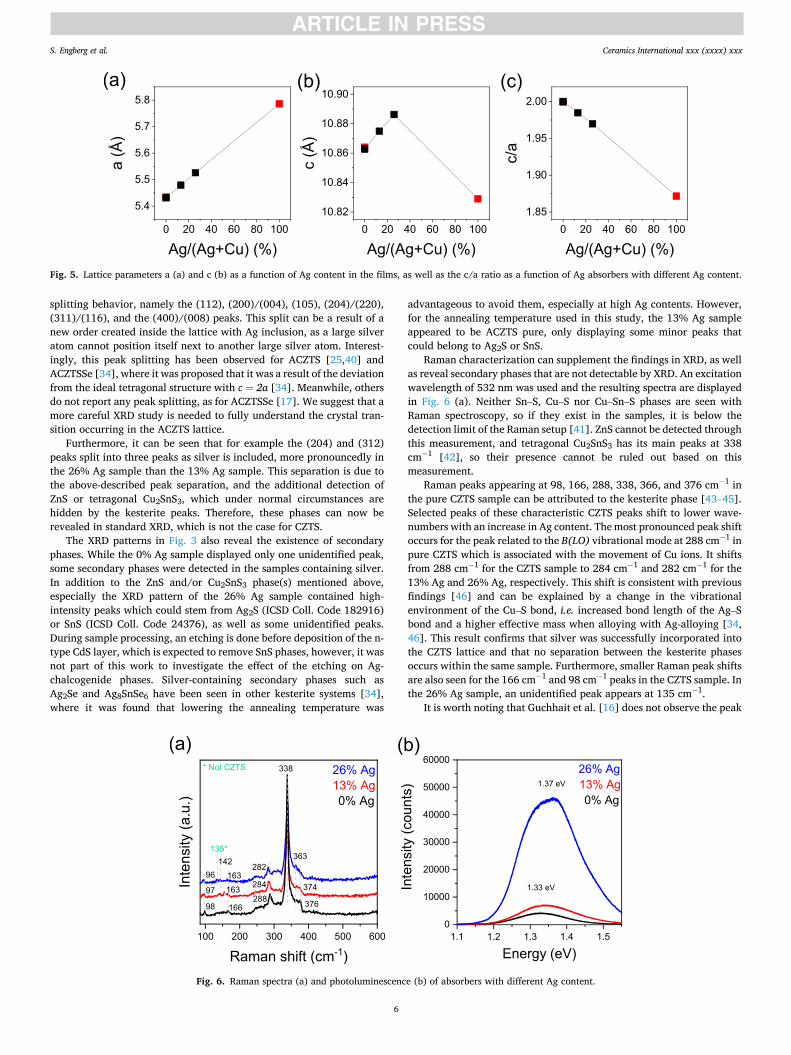
Fig. 4. Magnified sections of the XRD patterns in Fig. 3 displaying peak shifts and peak splitting with increasing Ag content.
S. Engberg et al.
Ceramics International xxx (xxxx) xxx
6
splitting behavior, namely the (112), (200)/(004), (105), (204)/(220), (311)/(116), and the (400)/(008) peaks. This split can be a result of a new order created inside the lattice with Ag inclusion, as a large silver atom cannot position itself next to another large silver atom. Interest-ingly, this peak splitting has been observed for ACZTS [25,40] and ACZTSSe [34], where it was proposed that it was a result of the deviation from the ideal tetragonal structure with c = 2a [34]. Meanwhile, others do not report any peak splitting, as for ACZTSSe [17]. We suggest that a more careful XRD study is needed to fully understand the crystal tran-sition occurring in the ACZTS lattice.
Furthermore, it can be seen that for example the (204) and (312) peaks split into three peaks as silver is included, more pronouncedly in the 26% Ag sample than the 13% Ag sample. This separation is due to the above-described peak separation, and the additional detection of ZnS or tetragonal Cu2SnS3, which under normal circumstances are hidden by the kesterite peaks. Therefore, these phases can now be revealed in standard XRD, which is not the case for CZTS.
The XRD patterns in Fig. 3 also reveal the existence of secondary phases. While the 0% Ag sample displayed only one unidentified peak, some secondary phases were detected in the samples containing silver. In addition to the ZnS and/or Cu2SnS3 phase(s) mentioned above, especially the XRD pattern of the 26% Ag sample contained high- intensity peaks which could stem from Ag2S (ICSD Coll. Code 182916) or SnS (ICSD Coll. Code 24376), as well as some unidentified peaks. During sample processing, an etching is done before deposition of the n- type CdS layer, which is expected to remove SnS phases, however, it was not part of this work to investigate the effect of the etching on Ag- chalcogenide phases. Silver-containing secondary phases such as Ag2Se and Ag8SnSe6 have been seen in other kesterite systems [34], where it was found that lowering the annealing temperature was
advantageous to avoid them, especially at high Ag contents. However, for the annealing temperature used in this study, the 13% Ag sample appeared to be ACZTS pure, only displaying some minor peaks that could belong to Ag2S or SnS.
Raman characterization can supplement the findings in XRD, as well as reveal secondary phases that are not detectable by XRD. An excitation wavelength of 532 nm was used and the resulting spectra are displayed in Fig. 6 (a). Neither Sn–S, Cu–S nor Cu–Sn–S phases are seen with Raman spectroscopy, so if they exist in the samples, it is below the detection limit of the Raman setup [41]. ZnS cannot be detected through this measurement, and tetragonal Cu2SnS3 has its main peaks at 338 cm− 1 [42], so their presence cannot be ruled out based on this measurement.
Raman peaks appearing at 98, 166, 288, 338, 366, and 376 cm− 1 in the pure CZTS sample can be attributed to the kesterite phase [43–45]. Selected peaks of these characteristic CZTS peaks shift to lower wave-numbers with an increase in Ag content. The most pronounced peak shift occurs for the peak related to the B(LO) vibrational mode at 288 cm− 1 in pure CZTS which is associated with the movement of Cu ions. It shifts from 288 cm− 1 for the CZTS sample to 284 cm− 1 and 282 cm− 1 for the 13% Ag and 26% Ag, respectively. This shift is consistent with previous findings [46] and can be explained by a change in the vibrational environment of the Cu–S bond, i.e. increased bond length of the Ag–S bond and a higher effective mass when alloying with Ag-alloying [34, 46]. This result confirms that silver was successfully incorporated into the CZTS lattice and that no separation between the kesterite phases occurs within the same sample. Furthermore, smaller Raman peak shifts are also seen for the 166 cm− 1 and 98 cm− 1 peaks in the CZTS sample. In the 26% Ag sample, an unidentified peak appears at 135 cm− 1.
It is worth noting that Guchhait et al. [16] does not observe the peak
Fig. 5. Lattice parameters a (a) and c (b) as a function of Ag content in the films, as well as the c/a ratio as a function of Ag absorbers with different Ag content.
Fig. 6. Raman spectra (a) and photoluminescence (b) of absorbers with different Ag content.
S. Engberg et al.
Ceramics International xxx (xxxx) xxx
7
shift in the Raman spectra when including 7% Ag/Cu, while Nguyen et al. [25] observe a shift of the A1 vibrational mode from 338 to 336 cm− 1 for 2% Ag/(Cu+Zn+Sn).
The photoluminescence spectra of the annealed films are displayed in Fig. 6 (b). The sample with 26% Ag displays a remarkable photo-luminescence signal with a high intensity that implies a severely reduced amount of non-radiative recombination. This can to a certain extent be explained by the large grain sizes of ~1.5 μm, however, the 13% Ag sample also displayed large grain sizes of ~0.9 μm, but does not result in nearly as high a PL intensity (about 7000 counts vs. 46,000 counts for the 13% Ag and 26% Ag samples, respectively). Furthermore, a small upward shift of the PL peaks can be seen with Ag content. A shift in PL peak position would suggest the formation of a less defective material, as the PL peak moves closer to CZTS’ band gap of 1.5 eV.
3.3. Device performance
Fig. 7 (a,b) displays the J-V curves and EQE spectra for the best cell from each sample, and box plots displaying device characteristics are shown in Fig. 7 (c) for all samples. The 0% Ag sample showed an effi-ciency of 2.6%, which increased to 4.9% for the 13% Ag, and the 26% Ag device did not work at all, probably due to the high concentration of secondary phases inside the absorber (XRD pattern, Fig. 3). The pure CZTS device exhibited an efficiency that is lower than our previous study [26]. The efficiency increase from the 0% Ag to the 13% Ag samples stems from significant improvements in both VOC and JSC.
The large VOC improvement of 18% for the best cells (from 433 mV for 0% Ag to 509 mV for 13% Ag) could be a result of the expected reduction of cation antisite defects in the absorber, but will also to some degree be related to the higher band gap of the samples with Ag. The band gap of the absorber is determined as the maximum of the first derivative of the EQE plot with respect to wavelength at the low energy region. This resulted in 1.43 eV and 1.53 eV for the pure CZTS and the 13% Ag samples, respectively. Interestingly, the 26% Ag sample also displayed a band gap of 1.53 eV, even though the XRD data clearly shows that more Ag has been included.
The improvement in JSC can also be seen in the EQE data, where an overall higher carrier collection is seen throughout the sample in the 13% Ag sample. The JSC determined as the integrated EQE was 14.41 mA/cm2 and 18.01 mA/cm2 for the 0% Ag and the 13% Ag samples, respectively. The improved JSC could be linked to an improved morphology, as the 0% Ag sample had a high porosity and small grains, and the 13% Ag sample consisted of dense, large grains.
The data for the 0% Ag and 13% Ag samples were fitted to the ideal diode equation according to Sites’ method both in the light and the dark, and the extracted J-V parameters are displayed in Table 3. All data fits nicely to the ideal diode equation, except the dark measurement for the 13% Ag sample. In this case, the shunt resistance (RSH) is lower in the dark than in the light. On the other hand, the shunt resistance of the 0% Ag sample is lower in the light compared to the dark, which indicates
light-induced shunting. It can be seen that the extracted parameters in the light fits reasonably well with those reported for ACZTS [16,25], however, the authors do not state whether their values are extracted in the light or in the dark.
The series resistance (RS) in the light decreases from 4 Ω cm2 to 2.5 Ω cm2 and the shunt resistance in the light increases from 239 Ω cm2 to 400 Ω cm2 when including silver, which could be related to the improved absorber morphology, with larger grains and less voids at the back Mo contact.
In this study, only two different Ag-contents were tested 13% and 26% Ag/(Ag+Cu), from which the lower concentration was found the most optimal. The investigated concentrations correspond to 6% and 11% Ag/(Cu+Zn+Sn) or 16% and 36% Ag/Cu, respectively, which are also widely used measures. It has been shown that a Ag content higher than 50% Ag/(Ag+Cu) transforms the absorber from p-type to n-type [18]. As showed in Table 1, previously reported (optimal) values are at 7% Ag/Cu (one concentration used), 2% Ag/(Cu+Zn+Sn) (probing 2%, 5%, and 10%), and 4% Ag/Cu (one concentration used) [16,24,25], and hence the samples investigated in this study are samples with a signifi-cantly higher silver content.
4. Conclusion
Solution-processed ACZTS samples are prepared through the aprotic molecular ink approach using DMSO as the solvent. The successful incorporation of silver into the CZTS lattice is demonstrated with rela-tively high silver concentrations, namely Ag/(Ag+Cu) ratios of 13% and 26%. All other metallic ratios are kept relatively constant to ensure a meaningful comparison between samples. XRD analysis reveals peak shifts, which indicate the formation of ACZTS, as well as peak splitting. These peak splits could originate from a structural distortion of one dimension of the unit cell as a larger Ag atom is incorporated, and could also be related to the observed deviation from an ideal tetragonal structure with c/a < 2. Several secondary phases such as SnS and Ag2S are seen in the 26% Ag/(Ag+Cu) sample, and a lower annealing tem-perature might be needed to synthesize these samples in the future.
The best device is made with 13% Ag/(Ag+Cu), and has an efficiency of 4.9%, while the sample with 26% Ag/(Ag+Cu) shows 0% efficiency and the CZTS sample 2.6% efficiency. The improved efficiency in the 13% Ag/(Ag+Cu) sample compared to the CZTS sample is due to an increased short-circuit current and open-circuit voltage. The improve-ment in JSC can originate from the improved morphology, with larger average grain sizes (870 nm versus 350 nm for the 13% Ag/(Ag+Cu) and the CZTS samples, respectively), but also a decrease in voids at the back Mo contact, which is also reflected in a lower series resistance for the 13% Ag/(Ag+Cu) sample. The improvement in VOC could be a result of a lower concentration of antisite defects inside the kesterite, which is the purpose of this cation substitution study; however, it could also be related to the higher band gap of the silver samples of 1.53 eV as compared to 1.43 eV for the CZTS sample.
Fig. 7. J-V characteristics (a), EQE spectra (b), and box plots of device performance parameters (c) for the three devices with.
S. Engberg et al.
Ceramics International xxx (xxxx) xxx
8
Declaration of competing interest
The authors declare that they have no known competing financial interests or personal relationships that could have appeared to influence the work reported in this paper.
Acknowledgement
This work was supported by a grant from the Innovation Fund Denmark (grant number 6154-00008A) and by a grant from the Energy Technology Development and Demonstration Program EUDP (grant number 64020-1088).
References
[1] Fraunhofer, Photovoltaics Report, 2020. [2] M.A. Green, E.D. Dunlop, J. Hohl-Ebinger, M. Yoshita, N. Kopidakis, X. Hao, Solar
cell efficiency tables (Version 58), Prog. Photovoltaics Res. Appl. (2021) 657–667, https://doi.org/10.1002/pip.3444.
[3] A. Richter, M. Hermle, S.W. Glunz, Reassessment of the limiting efficiency for crystalline silicon solar cells, IEEE J. Photovoltaics 3 (2013) 1184–1191, https:// doi.org/10.1109/JPHOTOV.2013.2270351.
[4] M.A. Green, Commercial progress and challenges for photovoltaics, Nat. Energy. 1 (2016) 1–4, https://doi.org/10.1038/nenergy.2015.15.
[5] K. Ito, An overview of CZTS-based thin-film solar cells, in: K. Ito (Ed.), Copp. Zinc Tin Sulfide-Based Thin-Film Sol. Cells, first ed., Wiley, Nagano, Japan, 2015, pp. 3–41, https://doi.org/10.1002/9781118437865.ch1.
[6] J. Zhou, X. Xu, B. Duan, H. Wu, J. Shi, Y. Luo, D. Li, Q. Meng, Regulating crystal growth via organic lithium salt additive for efficient Kesterite solar cells, Nano Energy 89 (2021), 106405, https://doi.org/10.1016/j.nanoen.2021.106405.
[7] C. Yan, J. Huang, K. Sun, S. Johnston, Y. Zhang, H. Sun, A. Pu, M. He, F. Liu, K. Eder, L. Yang, J.M. Cairney, N.J. Ekins-Daukes, Z. Hameiri, J.A. Stride, S. Chen, M.A. Green, X. Hao, Cu2ZnSnS4 solar cells with over 10% power conversion efficiency enabled by heterojunction heat treatment, Nat. Energy. 3 (2018) 764–772, https://doi.org/10.1038/s41560-018-0206-0.
[8] S.K. Wallace, D.B. Mitzi, A. Walsh, The steady rise of kesterite solar cells, ACS Energy Lett 2 (2017) 776–779, https://doi.org/10.1021/acsenergylett.7b00131.
[9] M. Gansukh, Z. Li, M.E. Rodriguez, S. Engberg, F.M.A. Martinho, S.L. Marino, E. Stamate, J. Schou, O. Hansen, S. Canulescu, Energy band alignment at the heterointerface between CdS and Ag-alloyed CZTS, Sci. Rep. 10 (2020), https:// doi.org/10.1038/s41598-020-73828-0.
[10] S. Chen, A. Walsh, X.G. Gong, S.H. Wei, Classification of lattice defects in the kesterite Cu2ZnSnS4 and Cu2ZnSnSe4 earth-abundant solar cell absorbers, Adv. Mater. 25 (2013) 1522–1539, https://doi.org/10.1002/adma.201203146.
[11] B. Duan, J. Shi, D. Li, Y. Luo, H. Wu, Q. Meng, Underlying mechanism of the efficiency loss in CZTSSe solar cells: disorder and deep defects, Sci. China Mater. 63 (2020) 2371–2396, https://doi.org/10.1007/s40843-020-1385-0.
[12] G. Gurieva, J.A. Marquez, A. Franz, C.J. Hages, S. Levcenko, T. Unold, S. Schorr, Effect of Ag incorporation on structure and optoelectronic properties of (Ag1-xCux) 2ZnSnSe4 solid solutions, Phys. Rev. Mater. 4 (2020), 054602, https://doi.org/ 10.1103/PhysRevMaterials.4.054602.
[13] L. Choubrac, M. Paris, A. Lafond, C. Guillot-Deudon, X. Rocquefelte, S. Jobic, Multinuclear (67Zn, 119Sn and 65Cu) NMR spectroscopy-an ideal technique to probe the cationic ordering in Cu2ZnSnS4 photovoltaic materials, Phys. Chem. Chem. Phys. 15 (2013) 10722–10725, https://doi.org/10.1039/c3cp51320c.
[14] J.J. Scragg, L. Choubrac, A. Lafond, T. Ericson, C. Platzer-Bjorkman, A low- temperature order-disorder transition in Cu2ZnSnS4 thin films, Appl. Phys. Lett. 104 (2014) 1–4, https://doi.org/10.1063/1.4863685.
[15] T. Gokmen, O. Gunawan, T.K. Todorov, D.B. Mitzi, Band tailing and efficiency limitation in kesterite solar cells, Appl, Phys. Lett. 103 (2013), https://doi.org/ 10.1063/1.4820250.
[16] A. Guchhait, Z. Su, Y.F. Tay, S. Shukla, W. Li, S.W. Leow, J.M.R. Tan, S. Lie, O. Gunawan, L.H. Wong, Enhancement of open-circuit voltage of solution- processed Cu2ZnSnS4 solar cells with 7.2% efficiency by incorporation of silver, ACS Energy Lett 1 (2016) 1256–1261, https://doi.org/10.1021/ acsenergylett.6b00509.
[17] Y. Gong, R. Qiu, C. Niu, J. Fu, E. Jedlicka, R. Giridharagopal, Q. Zhu, Y. Zhou, W. Yan, S. Yu, J. Jiang, S. Wu, D.S. Ginger, W. Huang, H. Xin, Ag incorporation with controlled grain growth enables 12.5% efficient kesterite solar cell with open circuit voltage reached 64.2% shockley–queisser limit, Adv. Funct. Mater. 4 (2021), 2101927, https://doi.org/10.1002/adfm.202101927.
[18] T. Gershon, Y.S. Lee, P. Antunez, R. Mankad, S. Singh, D. Bishop, O. Gunawan, M. Hopstaken, R. Haight, Photovoltaic materials and devices based on the alloyed kesterite absorber (AgxCu1- x)2ZnSnSe4, Adv. Energy Mater. 6 (2016), 1502468, https://doi.org/10.1002/aenm.201502468.
[19] M.G. Gang, V.C. Karade, M.P. Suryawanshi, H. Yoo, M. He, X. Hao, I.J. Lee, B. H. Lee, S.W. Shin, J.H. Kim, A facile process for partial Ag substitution in kesterite Cu2ZnSn(S,Se)4 solar cells enabling a device efficiency of over 12, ACS Appl. Mater. Interfaces 13 (2021) 3959–3968, https://doi.org/10.1021/ acsami.0c19373.
[20] H. Cui, X. Liu, F. Liu, X. Hao, N. Song, C. Yan, Boosting Cu2ZnSnS4 solar cells efficiency by a thin Ag intermediate layer between absorber and back contact, Appl. Phys. Lett. 104 (2014) 2–6, https://doi.org/10.1063/1.4863951.
[21] S. Yang, S. Wang, H. Liao, X. Xu, Z. Tang, X. Li, T. Wang, X. Li, D. Liu, The impact of different Ag/(Ag + Cu) ratios on the properties of (Cu1− xAgx)2ZnSnS4 thin films, J. Mater. Sci. Mater. Electron. 30 (2019) 11171–11180, https://doi.org/ 10.1007/s10854-019-01463-1.
[22] B.T.K. Todorov, K.B. Reuter, D.B. Mitzi, High-efficiency solar cell with earth- abundant liquid-processed absorber, Mater. Views. 22 (2010) 156–159, https:// doi.org/10.1002/adma.200904155.
[23] W. Wang, M.T. Winkler, O. Gunawan, T. Gokmen, T.K. Todorov, Y. Zhu, D.B. Mitzi, Device characteristics of CZTSSe thin-film solar cells with 12.6% efficiency, Adv. Energy Mater 4 (2014) 1–5, https://doi.org/10.1002/aenm.201301465.
[24] A. Ibrahim, A. Guchhait, S. Hadke, H.L. Seng, L.H. Wong, Silver and potassium incorporation in double-layer solution-processed Cu2ZnSnS4 solar cell, ACS Appl. Energy Mater. 3 (2020) 10402–10407, https://doi.org/10.1021/acsaem.0c01165.
[25] T.H. Nguyen, T. Kawaguchi, J. Chantana, T. Minemoto, T. Harada, S. Nakanishi, S. Ikeda, Structural and solar cell properties of a Ag-containing Cu2ZnSnS4 thin film derived from spray pyrolysis, ACS Appl. Mater. Interfaces. 10 (2018) 5455–5463, https://doi.org/10.1021/acsami.7b14929.
[26] S. Engberg, F. Martinho, M. Gansukh, A. Protti, R. Küngas, E. Stamate, O. Hansen, S. Canulescu, J. Schou, Spin-coated Cu2ZnSnS4 solar cells: a study on the transformation from ink to film, Sci. Rep. 10 (2020) 20749, https://doi.org/ 10.1038/s41598-020-77592-z.
[27] F. Martinho, S. Lopez-Marino, M. Espíndola-Rodríguez, A. Hajijafarassar, F. Stulen, S. Grini, M. Dobeli, M. Gansukh, S. Engberg, E. Stamate, L. Vines, J. Schou, O. Hansen, S. Canulescu, Persistent double-layer formation in kesterite solar cells: a critical review, ACS Appl. Mater. Interfaces 12 (2020) 39405–39424, https://doi. org/10.1021/acsami.0c10068.
[28] S. Engberg, S. Canulescu, J. Schou, Liquid phase assisted grain growth in Cu2ZnSnS4 nanoparticle thin films by alkali element incorporation, RSC Adv 8 (2018) 7152–7158, https://doi.org/10.1039/c7ra13472j.
[29] R.C. Sharma, Y.A. Chang, The Ag− S (Silver-Sulfur) system, Bull. Alloy Phase Diagrams 7 (1986) 263–269, https://doi.org/10.1007/BF02869003.
[30] Arashi Kitakaze, Phase relation of some sulfide systems-(1), Mem. Fac. Eng. Yamaguchi Univ. 66 (2015) 81–88.
[31] W. Li, X. Liu, H. Cui, S. Huang, X. Hao, The role of Ag in (Ag,Cu)2ZnSnS4 thin film for solar cell application, J. Alloys Compd. 625 (2015) 277–283, https://doi.org/ 10.1016/j.jallcom.2014.11.136.
[32] R. Scheer, H.-J. Lewerenz, Formation of secondary phases in evaporated CuInS2 thin films: a surface analytical study, J. Vac. Sci. Technol. A Vacuum, Surfaces, Film. 13 (1995) 1924–1929, https://doi.org/10.1116/1.579631.
[33] Y. Qi, Q. Tian, Y. Meng, D. Kou, Z. Zhou, W. Zhou, S. Wu, Elemental precursor solution processed (Cu1-xAgx)2ZnSn(S,Se)4 photovoltaic devices with over 10% efficiency, ACS Appl. Mater. Interfaces 9 (2017) 21243–21250, https://doi.org/ 10.1021/acsami.7b03944.
[34] W.C. Huang, S.Y. Wei, C.H. Cai, W.H. Ho, C.H. Lai, The role of Ag in aqueous solution processed (Ag,Cu)2ZnSn(S,Se)4 kesterite solar cells: antisite defect elimination and importance of Na passivation, J. Mater. Chem. A. 6 (2018) 15170–15181, https://doi.org/10.1039/c8ta02950d.
[35] A.R. Denton, N.W. Ashcroft, Vegard’s law, Phys. Rev. A. 43 (1991), https://doi. org/10.1002/pssb.19660180251.
[36] J.H. Boyle, B.E. McCandless, W.N. Shafarman, R.W. Birkmire, Structural and optical properties of (Ag,Cu)(In,Ga)Se2 polycrystalline thin film alloys, J. Appl. Phys. 115 (2014), https://doi.org/10.1063/1.4880243.
[37] L.P. Mwakyusa, L. Leist, M. Rinke, A. Welle, U.W. Paetzold, B.S. Richards, M. Hetterich, Impact of silver incorporation at the back contact of Kesterite solar cells on structural and device properties, Thin Solid Films 709 (2020), 138223, https://doi.org/10.1016/j.tsf.2020.138223.
[38] S. Nakamura, T. Maeda, T. Tabata, T. Wada, First-Principles study of indium-free photovoltaic compounds Ag2ZnSnSe4 and Cu2ZnSnSe4, IEEE (2011) 2–5.
[39] H. Jiang, P. Dai, Z. Feng, W. Fan, J. Zhan, Phase selective synthesis of metastable orthorhombic Cu2ZnSnS4, J. Mater. Chem. 22 (2012) 7502, https://doi.org/ 10.1039/c2jm16870g.
[40] X. Liang, P. Wang, B. Huang, Q. Zhang, Z. Wang, Y. Liu, Z. Zheng, X. Qin, X. Zhang, Y. Dai, Effects of Ag incorporation on the band structures and conductivity types of (Cu1-xAgx)2ZnSnS4 solid solutions, ChemPhotoChem 2 (2018) 811–817, https:// doi.org/10.1002/cptc.201800109.
[41] S. Engberg, J. Symonowicz, J. Schou, S. Canulescu, K.M.Ø. Jensen, Characterization of Cu2ZnSnS4 particles obtained by the hot-injection method, ACS Omega 5 (2020) 10501–10509, https://doi.org/10.1021/acsomega.0c00657.
[42] A. Crovetto, R. Chen, R.B. Ettlinger, A.C. Cazzaniga, J. Schou, C. Persson, O. Hansen, Dielectric function and double absorption onset of monoclinic Cu2SnS3: origin of experimental features explained by first-principles calculations, Sol. Energy Mater. Sol. Cells. 154 (2016) 121–129, https://doi.org/10.1016/j. solmat.2016.04.028.
[43] P.A. Fernandes, P.M.P. Salome, A.F. Da Cunha, Study of polycrystalline Cu2ZnSnS4 films by Raman scattering, J. Alloys Compd. 509 (2011) 7600–7606, https://doi. org/10.1016/j.jallcom.2011.04.097.
S. Engberg et al.

Ceramics International xxx (xxxx) xxx
9
[44] D.M. Berg, Kesterite Equilibrium Reaction and the Discrimination of Secondary Phases from Cu2ZnSnS4, University of Luxembourg, 2012.
[45] M. Dimitrievska, A. Fairbrother, X. Fontane, T. Jawhari, V. Izquierdo-Roca, E. Saucedo, A. Perez-Rodríguez, Multiwavelength excitation Raman scattering
study of polycrystalline kesterite Cu2ZnSnS4 thin films, Appl. Phys. Lett. 104 (2014), https://doi.org/10.1063/1.4861593.
[46] J. Kumar, S. Ingole, Optical phonons in pentanary compound (AgxCu1− x)2ZnSnS4 semiconductor: a Raman study, J. Alloys Compd. 865 (2021), https://doi.org/ 10.1016/j.jallcom.2020.158113.
S. Engberg et al.


