Embed Size (px)
Citation preview


4 SMT Magazine • September 2012
C l e a n i n g & C o at i n g
September 2012 Featured Content
pCb reliability:Cleaning Up Your Actby Yash Sutariya
maintaining Osp Coating Integrity During the Cleaning processby Umut Tosun, Naveen Ravindran, and Michael McCutchen
The removal of post-reflow flux residues is an integral part of the electronic assembly industry. When CFC-based solvents were pushed out, much of the commercial electronic assembly industry adopted a no-clean process, eliminating residue removal. Today, largely due to assembly miniaturization, increased component density and higher-temperature lead-free alloys, cleaning has once again rejoined the assembly process.
selecting the right potting Compound for Your Applicationsby Craig McClenachan, Fabrico and Jim Stockhausen
Ionic Cleanliness testing:the Ultimate process Optimization toolby Gregory Alexander
Facts About HCFC-225 Usage ban In 2015by Lindsey Shehan
18
28
38
48
52


6 SMT Magazine • September 2012
C o n t e n t S
SepTeMber 2012
voluMe 27
nuMber 9
www.smtmagazine.com
Articlesolder paste Deposits and the precision of Aperture sizesby Ahne Oosterhof and Stephan Schmidt
ShortS“breathing” battery saves energy for a rainy Day
NCKU team Designs New material for electronic packaging
New Way of Assembling particles Into Complex structures
Video interViewSAscentech Unveils Large-Format Cleaning machine
eU’s reACH and CLp Laws Come Into Question
top ten moSt-reAd newSmarket
supplier/New product
mil/Aero007
smtonline
64
26
63
83
36
56
46
58
78
84
engineering
SoluTionS
For pCb
ManuFaCTuring
columnSIt’s Worse than I thoughtby Ray Rasmussen
Can microstructure Indicate a Good solder Joint? part IIby Dr. Jennie S. Hwang
better togetherby Karla Osorno
It pays to be Frugalby Sjef van Gastel
Get a New View on X-ray:A brand New ballgameby Zulki Khan
extrASevents Calendar
Advertiser Index & masthead
8
14
60
74
80
88
89


8 SMT Magazine • September 2012
A recently retired aerospace engineer took the time to walk me through the long history of the problems associated with, and being com-pounded by, lead-free SAC solders. He and his team had been working on solving these prob-lems well before the lead-free mandate came into effect. What I took away from the conver-sation was that even with tin/lead solders, the challenges to building these complex and very critical systems were many.
The issues with traditional solders were well known, but a few surprises still lurked. But with lead-free, the challenges were becoming
so daunting that things were getting out of control. The ability of these aerospace en-
gineers to guarantee the operability of critical systems over the long
term was diminishing. Yes, they are exempt from
RoHS, for now, but lead-free regulations, combined with the commercial off-the-shelf (COTS) man-date, have put the high-reliability guys in a box. To build the systems of the future, they need to plug into the latest tech-nology the supply chain has to offer, and that’s where this
ever-increasing number of variables comes in, dramati-
cally reducing the chances of building a consistently reliable product. And, in approx-
imately seven years, the exemption for the mil/aero guys goes away. The clock is ticking!
Certified systemsThe good news is that aerospace require-
ments all but ensure that systems won’t fail in
SummAry: A solution to the problem of tin whiskers, at times, seems a far-off concept, but surely the problems caused by lead-free require-ments and SAc solders can be solved, right? A re-cent phone conversation with an engineer made it clear to editor ray rasmussen that the situation is quite dire.
A few months ago I wrote a column about the IPC Tin Whiskers Conference I attended in April. The column, “Chasing Our Tails,” appeared in the June 2012 issue of SMT Maga-zine and, from my 10,000-foot view, I couldn’t see how we were ever going to get this issue under control. There were just too many variables, which were ever-increasing as we learned more about SAC sol-ders and their shortcomings as they relate to high-reliabil-ity electronics. Maybe, some-day, we’ll find a solution to the actual whiskers problem, but as I looked at all the issues sur-rounding lead-free (which caused tin whiskers to become an issue again), I just couldn’t see how we were going to get on top of the whole thing. It seemed impossible or, at least, highly unlikely to me.
As a result of that column, I received a few comments, one of which turned into a phone conversation that left me stunned.
This issue is much worse than I thought.
by ray rasmusseni-ConneCT007
tHe WAY I see It
ColuMn
It’s Worse than I thought

October 2011 • SMT Magazine 7

10 SMT Magazine • September 2012
the air. We don’t have to worry too much about planes dropping out of the sky or military systems failing in the field. Very tough certification processes are required before a new system can come online. That was reassuring to hear. The real trouble will come when the system build-ers aren’t able to meet the requirements of the military aerospace systems of the near future. It’s becoming increasingly difficult to get these systems certified. Rather than working with a set of known materials and properties, lead-free variables are causing the industry to reinvesti-gate just about every piece in the supply chain, which basically means starting over after more than 50 years of known good processes and ma-terials.
the manhattan projectIt was suggested at a conference in Europe
four or five years ago that the high-reliability industry gather and focus on finding solutions to the critical issues by creating a Manhattan-like Project. After some discussions, they de-cided to move forward. A two-week meeting followed and top engineers from over a dozen major mil/aero OEMs came up with a plan. The only problem was that they needed $125 mil-lion to do the work. That’s where it sits today: waiting for funding. Just think: this problem would likely be behind us by now if they had acted back then. Too bad.
It’s politicalAfter listening to my new aerospace engi-
neer friend for more than an hour as he peeled back layer after layer of the reliability onion, I offered up that the problem was political in nature, not technical. He agreed. If there were sufficient resources, they—the engineers and scientists—could solve these problems. And,
since most ma-
terials suppli-ers cater to the other
90% of the industry with volume production, the high-re-
liability guys were going to have to solve this on their own. But, with program managers under substan-tial pressure to keep costs down, they
aren’t looking to spend too much money inves-tigating new ways to produce their products.
Moving to COTS was supposed to help keep costs down, which would have been the case if RoHS hadn’t been legislated. Now things are starting to come unglued. I grabbed the following from a PERM Consortium white paper, which puts the issues in a nutshell. PERM is the aerospace industry’s effort to get on top of this.
The reliability of SnPb interconnections is well known and meets the requirements of these more demanding applications. Based on the scientific in-formation available today, there are increased reli-ability risks in using Pb-free in high-performance electronics. These risks include the spontaneous for-mation of tin whiskers from Pb-free tin (Sn) based finishes, reduced Pb-free solder joint integrity, re-duced reliability by cross-contamination between the different alloys, and the potential component and board damage from the higher Pb-free process-ing temperatures.
Most of us know about these problems if we’re building high-reliability electronics. But even the consumer guys don’t want reliability issues. They need their products to be reliable for at least a couple years, so they have an in-terest in many of the same issues. Of course, people don’t die if an iPod stops working (un-less it’s my daughter), so the consumer indus-try doesn’t face these same pressures. They’re more interested in keeping costs down. Most consumer electronics don’t have a useful life beyond five years in any case. They aren’t going to push their suppliers to ensure reliability 10 to 20 years out. They don’t care.
The Way i See iT
It’s WOrse tHAN I tHOUGHt continues


12 SMT Magazine • September 2012
Getting smallerThe drive to get lighter and smaller yet still
be reliable is relentless. This was already putting pressure on the high-reliability industry before RoHS. With the great benefits of smaller, light-er and faster come problems. We have smaller spaces between leads and pads, which makes it even easier for whiskers to cause shorts and for voids to appear and joints to crack; smaller chip geometries (20nm), I’m told, are leading to long-term reliability issues with the chips themselves, which is something I wasn’t aware of. Add to that the problem with tin/lead-based legacy systems and counterfeit components and you can see the complexity of the issues.
the 10% solutionThe high-reliability guys are trapped more
and more in the consumer electronics world, which is driving technology and innovation. Unless the high-reliability industry gives up on COTS, they’ll be subject more frequently to the shortcomings of these technologies as they try to produce longer-term reliable systems.
If you match up the optimism and future-casting from a Steve DeWaters article on mili-tary photonics to this conversation I had with the aerospace engineer working in the trench-es, there’s a huge gulf. The military has incred-ible requirements for electronic systems going forward. The systems are very complex, able to crunch tons of data, running complicated battlefield scenarios meshing all types of real-time data into warfighter displays, command and control systems, weapons and much more. And, because of the politics and financial pres-sures associated, that chasm will get bigger and bigger.
The good news, paradoxically, is that at some point we won’t be able to build what’s needed. That’s when we’ll have the attention of top brass at the Pentagon along with the major politicians. Based on that early morning con-versation, without a crisis, we aren’t going to be able to bring the resources to bear. Maybe that’s the way it’s ultimately supposed to hap-pen. Only then will we have the complete at-tention of all the major players and access to all the money needed.
What’s missing?Courage. There’s a lot of bureaucracy in
these large defense and aerospace companies. Of course, the Pentagon is one of the inventors of bureaucratic systems that stifle the creative and innovative process. So we’re in a tough spot. Nobody wants to rock the boat, espe-cially when it’s sinking. It seems like a lot of folks know the boat’s taking on water, but are content to just float along, continuing to bail water as needed.
I do hope more folks will step up and talk about this issue. I know it’s risky for some, but we have to get on top of it as soon as we can. We literally have a lot riding on this. smt
It’s WOrse tHAN I tHOUGHt continues
ray rasmussen is the publisher and chief editor for i-Connect007 publications. he has worked in the industry since 1978 and is the former publisher and chief editor of CircuiTree Magazine. Contact rasmussen here.
12 SMT Magazine • September 2012
The Way i See iT

14 SMT Magazine • September 2012
Can microstructure Indicate a Good solder Joint? part II
by Dr. Jennie s. Hwang, ceoh-TeChnologieS group
smt perspeCtIVes AND prOspeCts
Summary: how does one examine solder joint microstructure? is the microstructure important? this month, dr. Jennie S. hwang continues a series that addresses the practical aspects of solder joint microstructure and what it can tell us about solder joint reliability.
Last month’s column ended with: “Addi-tionally, the microstructure of the solder joint is affected by the process used.” This month I’d like to address the impact of that process.
With all other conditions being equal—the same solder alloy, the same substrate surface
finishes, and the same components and PCB—the microstructure of solder joints can indeed vary with the process parameters. For a given system, the parameters affecting the formation of microstructure during the solder joint mak-ing process include both heating and cooling conditions. Let’s look at the heating stage and the cooling stage separately.
microstructure Versus solder Joint making Heating parameters
For the purpose of this discussion, we sepa-rate the PCB assemblies into two groups—one
group of assemblies that are prone to the formation of inter-metallic compounds (IMCs) at the inter-face and another group that are rela-tively sluggish in the formation of IMCs under commonly used soldering con-ditions. For a given solder alloy, the two groups are demarcat-ed by the material el-ements of the surface finish on the PCB and components. Immersion Sn, im-mersion Ag, OSP, and HASL belong to the former group, and Au/Ni and Au/Pd/Ni fall in the latter group, regardless of the architecture and
ColuMn


16 SMT Magazine • September 2012
type of component or the structure of the PCB in an assembly. The nature of the substrate and its metallurgical affinity to solder composition can affect the development of the microstruc-ture of solder joint.
In the heating stage of a process, key pa-rameters are the peak temperature and the time above liquidus. A higher peak temperature and/or a prolonged heating above liquidus tem-perature will produce excessive intermetallic compounds at the interface and in the interi-or of a solder joint for those material systems that are prone to metallurgical reactions. The excessiveness can be considered in three struc-tural areas: The interface, the bulk of the solder joint, and the surface of the solder joint. The conditions that promote the formation of ex-
SMT perSpeCTiveS and proSpeCTS
CAN mICrOstrUCtUre INDICAte A GOOD sOLDer JOINt? pArt II continues
Figure 1: an SeM micrograph of a 63Sn37pb solder joint.
Figure 2: an SaC305 solder joint consisting of the Sn grains and the CuxSny and Snxagy iMC precipitates.

September 2012 • SMT Magazine 17
SMT perSpeCTiveS and proSpeCTS
dr. hwang will present two lectures on “array package interconnection: Forward/backward Compatibility and reliability” and “preventing production defects and Fail-ures” at SMTa international
Conference on october 15, 2012, in or-lando, Florida.
dr. hwang, a pioneer and longstanding contributor to SMT manufacturing since its inception as well as to the lead-free develop-ment, has helped improve production yield and solved challenging reliability issues. among her many awards and honors, she has been inducted into the WiT international hall of Fame, elected to the national acad-emy of engineering and named an r&d Stars to Watch. having held senior executive positions with lockheed Martin Corporation, Sherwin Williams Co., SCM Corporation and ieM Corporation, she is currently Ceo of h-Technologies group providing business, technology and manufacturing solutions. She is a member of the u.S. Commerce department’s export Council, and serves on the board of Fortune 500 nySe compa-nies and civic and university boards. She is the author of 300+ publications and several textbooks and an international speaker and author on trade, business, education and social issues. Contact her at (216) 577-3284; e-mail [email protected].
CAN mICrOstrUCtUre INDICAte A GOOD sOLDer JOINt? pArt II continues
cessive IMCs increase the IMC thickness at the interface. When the peak temperature is high enough, and when the in-liquid state is pro-longed, IMCs will grow and migrate toward the interior of solder joint. As an illustration, in the case of Sn-based solder on OSP, the CuxSny compounds (commonly Cu6Sn5, Cu3Sn) formed at the interface may migrate into the interior of solder joint, resulting in additional CuxSny phases in the microstructure.
In extreme cases, IMCs may emerge on the free surface of the solder, causing the change in solder joint appearance. This change in ap-pearance is the direct reflection of change in microstructure. All three mechanisms and phe-nomena are expected to adversely affect the solder joint, either aesthetically or mechanical-ly. The mechanical properties in relation with microstructure will be discussed in a future column.
microstructure Versus solder Joint making Cooling parameters
As to the cooling effect, it is understood that the faster the cooling rate is applied, the finer the microstructure will result. For a SnPb eutec-tic alloy, a slow cooling rate renders the micro-structure to approach equilibrium conditions. The microstructure of eutectic composition normally consists of the characteristic lamellar colonies as exhibited in 63Sn37Pb. As the cool-ing rate increases, the degree of degeneration of lamellar colony structure increases and col-onies eventually disappear. For lead-free, such as SnAgCu, a faster cooling rate also results in finer Sn grains.
Although it is generally accepted that a faster cooling rate creates finer grain (phase) structure in bulk solders, this general rule is often complicated by the interfacial boundary and metallurgical reaction at the interface of solder joints. Figure 1 is an SEM micrograph of a 63Sn37Pb solder joint, comprising the light Pb-rich phase and the dark Sn-rich phases, and exhibits the compositional gradient from the interface toward the inte-rior bulk of the solder joint. Figure 2 shows an SAC305 solder joint consisting of the Sn grains and the CuxSny and SnxAgy IMC precipitates.
A picture is Worth a thousand WordsA microstructure obtained in the form of
a high-quality SEM or metallographic micro-graph fits well the adage: “A picture is worth a thousand words.” It provides sights and in-sights into the state of solder joint integrity and anticipated behavior. smt
reference:
1. Dr. Jennie S. Hwang, “Modern Solder Technology for Competitive Electronics Manu-facturing,” Chapter 6, McGraw-Hill, ISBN-0-07-031749-6.

18 SMT Magazine • September 2012
by Yash sutariyaSaTurn eleCTroniCS CorporaTion/SaTurn Flex SySTeMS
Summary: Bare board cleanliness is a serious matter, yet also a relatively new issue for the in-dustry. in addition to design, a product’s environ-ment causes ionic contamination to form dendritic growth. end-users should review both board de-sign and the environment to combat the issue.
I’ve written in the past regarding PCB reli-ability from a pure fabrication standpoint. Ex-amining the backbone procedures in the fab-rication process, we asserted that adherence to mechanical guidelines insured steadfast boards in the field. What I did not address, however, is the impact of surface cleanliness on long-term reliability in the field. The cleanliness of a com-pleted PCB is crucial.
As pioneering bare board cleanliness re-searchers would eventually discover, the ma-jor source of ionic contamination is the board itself! A circuit board with high levels of ionic contamination will result in deteriorated insu-lation resistance and dielectric strength. This environment causes dendrite growth across the surface of the PCB, which will ultimately reduce the field life of the end product.
Bare board cleanliness is a critical enough is-sue that some major users of PCBs have specific requirements for monitoring ionic contamina-tion, and in December 2009 IPC published a specification dedicated to this topic (IPC-5704).
If cleanliness requirements for unpopulated PCBs is fundamental enough that the IPC creat-ed the 5-32c Bare Board Cleanliness Assessment Task Group, which then developed the 5704 specification, the industry’s only requirements dedicated to printed board cleanliness, why is it not being called out in fabrication notes? The major source of ionic contamination is the board itself!
In performing research for this article, I came to the conclusion that, like any great product, cleanliness must be properly market-ed to achieve success. In many of my customer meetings, when the team presents how it com-bats ionic contamination, it’s not surprising to see many “deer in the headlights” expressions on visitors’ faces.
Long-term Impact of Ionic ContaminationLong-term PCB reliability is often measured
by the number of thermal cycles a PCB can pass without crossing a pre-established threshold of damage/performance degradation. Others measure PCB reliability through a cross-section examination of plated through holes and di-electric. The common theme here is that these methods are all testing mechanical functions or properties of the PCB.
With thermal cycling, the test methods are simulating operation over time through accel-erated testing. What this eliminates, though, is the testing of defects caused by time itself. One such defect is electrochemical migration, or dendritic growth.
PCB Reliability: Cleaning Up Your Act
18 SMT Magazine • September 2012
Cleaning & Coating

September 2012 • SMT Magazine 19
Dendritic GrowthIPC defines dendritic growth as the growth
of conductive metal filaments on a PCB through an electrolytic solution under the influence of a DC voltage bias. Essentially, water absorbs into the surface of the board over time in opera-tion, possibly connecting near proximity con-ductors. However, if the PCB surface has excess ionic contamination, this process is accelerated via the growth of dendrites, which are metallic filaments. As dendrites from isolated nets come into contact with each other on the PCB sur-face, performance degrades with effects ranging from intermittent operation to massive short-circuiting of the PCB.
This, of course, is a very simplified expla-nation of the failure mechanism. An excellent paper on this topic, “Electrochemical Migration on HASL Plated FR-4 Printed Circuit Boards,” was written by members of the Naval Surface Warfare Center in conjunction with the Univer-sity of Maryland.
The earliest information on dendritic growth via ionic contamination that we have found comes from the automotive industry. Historically, the auto industry incorporated lower-technology PCBs. However, as infotain-ment and vehicle intelligence requirements increased, the corresponding designs evolved to include new technologies which, in turn, drove down line width and spacing. As spacing decreased, validation test engineers began see-ing higher rates of failure during environmen-tal testing. Through much research, they found
that combinations of poor PCB cleaning and higher-humidity environments could acceler-ate these failures, leading to supplier require-ments that have, over time, morphed into the current IPC-5704 specification.
CauseDendritic growth is the culmination of
separate events rooted in the PCB fabrication process.
Since this is a surface cleanliness issue, sol-dermask plays a key role in dendritic growth. One of the properties of soldermask is that the material has pores in the surface. These pores can act as little “cups” that retain flux used in the hot air solder levelling (HASL) final finish process (SnPb and lead-free).
The flux, in turn, is the single largest source of ion contamination in the PCB fabrication process. The pores increase the volume of flux that is retained on the board surface after the HASL process.
measurement/DetectionIPC-5704 provides industry guidance on
both testing methods and acceptance criteria for bare board cleanliness. Through the use of ion chromatography, IPC-5704 establishes maximum levels of each component of ionic contamination, as set forth in Table 1.
Unfortunately, the application of this stan-dard as a method of internal control for PCB fab-ricators is not widespread due to the equipment required to provide such detailed test results.
Figure 1: Time-elapsed footage of dendrite growth on pCb surface.
September 2012 • SMT Magazine 19

20 SMT Magazine • September 2012
Most PCB fabricators test for total ionic con-tamination using an ionograph. Obtaining a detailed breakdown of total ionic contamina-tion for comparison to the above chart requires the use of an ion chromatograph. Fortunately, many third-party reliability testing laboratories offer this as a service for PCB fabricators and end-users.
solutionsThe easiest solution is to conformal coat
the assembly to freeze these contaminants in place. For many assemblers, though, this is not truly the easiest solution due to added costs and failure modes. The best way to solve for a dirty board is to clean it well in the first place.
As with anything, though, getting some-thing clean is easier when it’s less dirty. As such, we propose a multi-step approach to bare board cleanliness.
The first step is to address soldermask pores. An easy method for the PCB fab-ricator to eliminate, or at the very least minimize, these pores is to complete the cross-linking process within the solder-mask by applying a UV “bump” to the PCB during the fabrication process. This added process step has the effect of
closing off these pores in the soldermask surface, eliminating the primary retention mechanism of flux.
Below are ionic contamination results of two boards that went through identical processing with the exception of one having gone through a UV bump. The other board was withheld from this process step.
Now that we’ve minimized the opportu-nities for accumulations of flux, we need to address cleaning any residual flux from the HASL process from the surface of the PCB. This is a two-step method consisting of me-chanical obligations corresponding with chemical specifications.
mechanicalThe mechanical method involves the use
of industry-standard equipment that has been modified to provide a more aggressive approach to PCB surface cleaning.
A very robust cleaning unit, in our opinion, would include (See Table 3 and Figure 2):
The net result of the described process is to literally heat, beat, and scrub the flux from the PCB surface. Since industry-standard equip-ment meeting IPC-5704 standards does not ex-ist, customized, or custom-designed, cleaning equipment is required.
pCb reLIAbILItY: CLeANING Up YOUr ACt continues
table 2.
table 1.
Cleaning & Coating


22 SMT Magazine • September 2012
pCb reLIAbILItY: CLeANING Up YOUr ACt continues
table 3.
Figure 2.
Cleaning & Coating


24 SMT Magazine • September 2012
ChemicalWorking in conjunction with mechanical
means of cleaning is a chemical additive that acts as a cleaning agent to break up and dis-perse flux residue on the PCB surface. Note that while there may be other alternatives, my com-pany works with EnviroSense’s EnviroGold cleaning product. I asked EnviroSense’s Mark Palmer to describe the effect of a cleaning agent on flux:
Twenty years ago, when EnviroSense Inc. start-ed to sell to PCB fabricators, we found most fab houses were using city water only to clean HASL and/or fusing fluxes. Some companies that needed
a higher standard of cleanliness would use pow-dered detergents such as Cascade dish soap. In those days the geometries, spacing(s) were much larger and most PCBs did not have tight vias or high-density SMT placements. City water and off-the-shelf consumer detergents can contain ionic materials such as Na, NaCl, P, K, as well as other unwanted inorganics and organics. They also did not always rinse completely. Even if the detergents did rinse well, the subsequent use of city water as a rinsing media would reapply unwanted ionic species back on the panel/coupon.
EnviroSense’s products are saponifiers. Sa-ponifiers turn the acids in flux and plating residues into soaps. The saponification is per-formed by the mono-ethanol amine (MEA), and the lowered surface tension is supplied by the surfactants and glycols contained in our chemistry. All these combined compounds will attack the residues by chemical dissolution along with undermining/lifting these contami-nants from the surfaces being cleaned. The chemical properties of these compounds are highly water-soluble in the rinsing process.
Today cleaning chemistry needs to meet the following criteria:
• Low surface tension: Able to lower the wash solution to under 35 dyne per cm;• Extremely hydrophilic: Able to be rinsed after wash section;• Biodegradable;• Ease of disposal, pH adjust and/or treatment;• Low foaming;• Non-flammable;• Health and safety compliant;• Low volatile organic compounds (V.O.C.s);• Low odor;• In a high concentrate form (so customer is not paying freight for water content); and• Have a good “loading” (how much flux residue it can clean per panel/coupon per gallon of concentrate used.
Even if a chosen chemistry meets all of the above, the cleaning machinery’s layout is just as important. The following are basic parameters for a good layout:
pCb reLIAbILItY: CLeANING Up YOUr ACt continues
Cleaning & Coating

PRECISON ECONOMICALPOST ETCH PUNCH
Contact Gary Weidner+1 269 962 2231
4 camera system
New software
Faster cycle time
Improved visuals
Fixed die technology
The Pinlam PE4 maximizes accuracy and improves yield of multilayer production. Designed for simplicity, easy to use and maintain, set up is simplified, making the Pinlam PE4 much faster and easier.

26 SMT Magazine • September 2012
pCb reLIAbILItY: CLeANING Up YOUr ACt continues
yash Sutariya is vice president of Corporate Strategy at Saturn electronics Corporation (SeC) and owner/president of Saturn Flex Systems, inc. Since joining the team, SeC has successfully navigated from a low-mix,
high-volume automotive supplier to a high-mix, medium- to high-volume diversified sup-plier. as a result of the company’s transforma-tion, manufacturing capabilities now range from quick-turn prototypes to scheduled volume production while attending a broad cross-section of industries to include industrial controls, telecommunications, aerospace, and power supply industries.
• Deionized water—8 meg-ohm or better for both wash chemistry mixing and for the subsequent rinsing processes.• A minimum of two “cascading forward” rinse sections between/after any chemical wash or plating section(s). This will minimize cross-contamination of section(s).• Temperature capability, from 50°C to 70°C for both wash and rinse section(s).• Enough cleaning and rinsing space to accommodate the needed throughput per minute, per hour, per day for particular product.• Pumps and pump heads (designed in prior) to allow for needed delivery volume and pressures of wash and rinse sections.
Conclusion Bare board cleanliness is a serious matter
and also a relatively new issue. In addition to PCB design, the product’s environment causes ionic contamination to form dendritic growth. PCB end-users should review their designs and the environment in which the boards will be used. Based on positive findings, specifications should be modified to include adherence to
a new low-cost, “air-breathing” battery has the capacity to store between eight and 24 hours’ worth of energy. The rechargeable and eco-friendly battery uses the chemical energy generated by the oxidation of iron plates that are exposed to the oxygen in the air—a process similar to rusting.
“iron is cheap and air is free,” says Sri narayan, professor of chemistry at the university of Southern California (uSC). “it’s the future.”
iron-air batteries have been around for decades—they saw a surge in interest during the 1970s energy crisis, but suffered from a crippling problem: a competing chemical re-action of hydrogen generation that takes place inside the battery (known
as hydrolysis) sucked away about 50% of the bat-tery’s energy, making it too inefficient to be useful.
narayan and his team managed to reduce the energy loss down to 4%—making iron-air batter-ies that are about 10 times more efficient than their predecessors. The team did it by adding very small amount of bismuth sulfide into the battery. bismuth (which happens to be part of the active ingredient in pepto-bismol and helps give the pink remedy its name) shuts down the wasteful hydrogen generation.
adding lead or mercury might also have worked to improve the battery’s efficiency, but wouldn’t have been as safe, narayan says. “a very small amount of bismuth sulfide doesn’t compromise on the promise
of an eco-friendly battery that we started with,” he adds.
despite his success, narayan’s work is still ongoing. his team is working to make the battery store more energy with less material.
To view the full article, click here.
“Breathing” Battery Saves energy for a Rainy Day
IPC-5704. This will minimize the risk of latent field failures due to ionic contamination-related dendrite growth.
Finally, on-site auditing of PCB suppliers is recommended since industry-standard equip-ment and cleaning methods generally do not have enough effectiveness on the PCB to meet IPC-5704. smt
Cleaning & Coating


28 SMT Magazine • September 2012
by Umut tosun, Naveen ravindran, and michael mcCutchenZeSTron aMeriCa
Maintaining OSP Coating Integrity During the Cleaning Process
SummAry: oSp is a reliable surface finish method, but care must be taken during the Smt process to minimize surface thickness degradation, particularly due to reflow and cleaning. the results of this study detail the effect of chemically-assisted cleaning on oSp film thickness.
During the PCB manufacturing process, exposed copper traces must be treated with an anti-corrosion coating. Traditionally, it is coated with solder by hot air solder leveling (HASL). The HASL finish prevents oxidation of the underlying copper and therefore guarantees a solderable surface. Although this is a sound approach, organic solderability preservatives (OSPs) have become prevalent in the electron-ics industry as an alternative to the HASL pro-cess. Even though this is a reliable surface fin-ish method, care must be taken during the SMT process to minimize surface thickness degrada-tion, particularly due to reflow and cleaning.
Although OSP film integrity can be affected by various handling and processing procedures, this study focused on the potential removal of OSP through the use of a chemically assisted cleaning process. Many equipment options are available for cleaning PCBs; however, for pur-poses of this study, a spray-in-air inline cleaning system was selected. Additionally, two differ-ent cleaning agents varying in alkalinity values were used. Variables monitored for their effect on the OSP film thickness included concentra-tion and temperature of cleaning agent and conveyor belt speed, i.e., time of exposure to cleaning agent.
Finally, OSP coupons identified for this test were sourced from two different manufacturers. Film thickness was measured prior to process-ing to confirm a baseline thickness. The cou-
Cleaning & Coating

September 2012 • SMT Magazine 29
pons were reflowed using a lead-free profile. Subsequently, the film thickness was rechecked prior to cleaning to confirm any OSP change re-sulting from reflow as well as to re-define the baseline film thickness prior to cleaning.
The results of this study detail the effect of chemically assisted cleaning on OSP film thick-ness and quantify the impact of key variables.
Introduction In general, thin film coatings are used to in-
crease solderability as well as act as an oxida-tion inhibitor for the copper leads. While OSP is viewed as a viable alternative to the HASL process, thinning of its protective coating can occur at various stages throughout the SMT process and particularly through reflow and cleaning.
Today, a typical cleaning process involves the use of water-based organic chemicals in a spray-in-air system. This study focused first on determining the effect of reflow and secondly, the effect of the cleaning agent on OSP thin-ning, irrespective of solder pastes. Compat-ibility of the cleaning process (cleaning agent + process parameters) with the OSP layer will determine flexibility of the cleaning process in terms of effectively removing various types of flux residues.
A design of experiment (DOE) was devel-oped to explore the main factors affecting an OSP layer, including reflow and cleaning. Ad-ditionally, this study focused on optimizing the cleaning process in order to maintain OSP integrity. Conclusions were drawn based on changes in the OSP film thickness.
Design of experiment The main goal of this study was to deter-
mine the effect of the cleaning agent on OSP thinning. Two cleaning agents were selected and are identified as follows:
Cleaning Agent 1: Traditional surfactant based—Several surfactant molecules are re-quired to bond to one residue molecule.
Cleaning Agent 2: Dynamic surfactant based—Branch-like structure requiring fewer active ingredient molecules to bond to multiple residue molecules.
Also, it should be noted that Cleaning Agent 2 includes inhibitors with the same func-tional group as the OSP coating. Thus, the au-thors hypothesized that the effect on OSP layer due to the cleaning agent itself would be mini-mal.
Test vehicles used were high-temperature OSP-coated copper coupons and were sourced from two different vendors.
The DOE developed included 10 variables. Given the interest in determining the most in-fluential variable, the authors decided to use a full factorial matrix design. Therefore, a total of 36 tests were conducted (Table 1).
Test evaluation methodology and technique:
• OSP thickness measurements were taken using a Filmetrics F-42OSP measurement sys-tem [1]. Film thickness was determined by tak-ing three measurements from each coupon at various locations and averaging the values for use in the thickness analysis.
• The OSP layer thickness was measured be-fore and after reflow to determine the effect of reflow. Since all OSP coupons were reflowed for this DOE, post-reflow film thickness was used as the baseline for analysis following the cleaning process.
• Test results were analyzed using Minitab Statistical Software generating a quantitative comparison of all variables with main effects and interaction plots (Figures 1-4).
Test protocol:• The OSP coupons were reflowed using a
typical lead-free profile prior to cleaning to sim-
Cleaning agent 1 Traditional surfactant 2 dynamic surfactantConcentration 3 10% 4 15%Wash temperature 5 120°F 6 135°F 7 150°FConveyor belt speed/ 8 1ft/min/3minexposure time 9 2ft/min/1.5min 10 3ft/min/1min
table 1: Test variables.

30 SMT Magazine • September 2012
mAINtAINING Osp COAtING INteGrItY DUrING tHe CLeANING prOCess continues
Figure 1: Main effects plot; vendor a coupon.
ulate a worst-case scenario. The peak tempera-ture achieved was 245°F.
• All coupons were cleaned in a spray-in-air inline cleaner.
• Each trial within the DOE matrix was con-ducted using two coupons from each vendor for test repeatability of results.
The following cleaning equipment process parameters were maintained constant through-out the DOE (Table 2).
results and Analysis The effect of reflow on the OSP layer:
• The OSP-coated coupons from the two dif-ferent vendors yielded dramatically different results with regard to film thinning following reflow. The OSP layer was thinned by 3.67% on Vendor A coupons and 47.47% on Vendor B coupons. Thus the OSP vendor must be careful-
ly considered and their product evaluated in or-der to minimize the OSP thinning after reflow.
• Since all the coupons were reflowed for this DOE, the OSP thickness post-reflow was used as the baseline for judging the impact of the cleaning process post-reflow.
Cleaning process:Wash pressure (Top/bottom) 140 pSi/120 pSirinse:rinsing agent di-water (all sections)rinse Section pressure 100 pSi/80 pSirinse Temperature 150°F/65.5°CFinal rinse Flow rate 2 gal./min.Final rinse Temperature room TemperatureDrying:drying Method hot Circulated airdrying Temperature 160°F/71°C
table 2: Cleaning process.
Cleaning & Coating


32 SMT Magazine • September 2012
mAINtAINING Osp COAtING INteGrItY DUrING tHe CLeANING prOCess continues
Vendor A Coupon AnalysisFor this OSP type, the main effects plot
clearly indicated that cleaning agent selection had a major impact on film reduction. Dynam-ic surfactant is clearly the preferred cleaning agent.
Additionally, the OSP layer was negatively impacted as the concentration and temperature were increased and the belt speed was decreased.
Best results were achieved with the follow-ing process settings (Figure 1):
• Concentration: 10%• Temperature: 120°F• Belt Speed: 3 ft./min. (1 min. exposure time)
The interaction plot (Figure 2) reinforces that the dynamic surfactant is the preferred cleaning agent. The concentration of the dy-namic surfactant has minimal impact on the OSP coating. This is critical since it allows for flexibility in selecting the concentration level
based on the difficulty of solubilizing the flux residues.
Additionally, this plot demonstrates that lower temperatures and faster belt speeds (short-er wash time) reduce the impact on the OSP lay-er. However, even the most aggressive param-eters, i.e., 15% concentration, 150°F wash tem-perature and 1ft./min. belt speed, resulted in a significantly lower percentage of OSP reduction with the dynamic surfactant as compared to the traditional surfactant cleaner.
Vendor b Coupon AnalysisOnce again, the main effects plot indicates
that cleaning agent selection had a major im-pact on film thickness reduction and the dy-namic surfactant was clearly the preferred cleaning agent. With regard to the remaining variables, there was no significant impact on the OSP layer (Figures 3 and 4).
However, it should be noted that with this coupon, the film integrity was greatly affected by the reflow process itself.
Figure 2: interaction plot; vendor a coupon.
Cleaning & Coating


34 SMT Magazine • September 2012
mAINtAINING Osp COAtING INteGrItY DUrING tHe CLeANING prOCess continues
Figure 3: Main effects plot; vendor b coupon.
Figure 4: interaction plot; vendor b coupon.
Cleaning & Coating


36 SMT Magazine • September 2012
mAINtAINING Osp COAtING INteGrItY DUrING tHe CLeANING prOCess continues
Conclusion As demonstrated through this DOE, not all
OSP finishes are the same and film thickness can be greatly affected by reflow and cleaning pro-cesses. Vendor A’s OSP-coated coupons resulted in far less film thinning across all parameters. With regard to OSP thinning resulting from the cleaning agent, the authors’ original hypothesis proved true. Cleaning agent type proved to be most critical and clearly the dynamic surfactant based cleaning agent was preferred. Thus, when properly selected, the cleaning agent can mini-mize the effect on OSP stability while offering a wide process window with respect to concentra-tion, temperature and exposure time. This is a critical consideration for the electronics manu-facturer. smt
reference1. “Optical Reflectivity as a Nondestruc-
tive Measurement Technique for OSP Coating Thickness on Production PCBs,” CircuiTree.com, March, 2008.
umut Tosun, M.S. Chemical engineering, is the applica-tion technology manager at ZeSTron america. Questions and comments can be addressed to [email protected].
naveen ravindran, M.S. Chemi-cal engineering, is an application engineer at ZeSTron america. Questions and comments can be addressed to [email protected]. Michael McCutchen, M.a. Chemistry, is the vice presi-dent of ZeSTron americas and South asia. Questions and comments can be addressed to [email protected].
realtimewith.comCliCk
To View
Video Interview
randy allinson offers guest editor Steve gold a look at his company’s new gen3 cleaning machine, a large-format, quick-regenerating piece of equipment attract-ing industry attention.
Ascentech Unveils Large-Format Cleaning machine
by Real Time with...IPC APEX EXPO 2012
Cleaning & Coating

October 2011 • SMT Magazine 29

38 SMT Magazine • September 2012
by Craig mcClenachan, Fabrico and Jim stockhausen elanTaS pdg, inC.
SUMMARY: Many questions arise when trying to select an appropriate potting compound. An experi-enced materials expert can help identify the primary concerns, recommend materials, provide testing of the materials, and offer information on dielectric strength, adhesive characteristics, thermal conduc-tivity, and more, through the testing process.
Potting materials for electronics and electri-cal equipment industries cover a device or com-ponent to protect it from the surrounding en-vironment. Embedding a device or component in a compound can secure it in the assembly, as well as protect it from moisture, and electrically insulate it so that it will perform as designed.
Potting gets its name from the use of a “pot,” case, or shell that surrounds the device, into
which the liquid potting material/compound is introduced. Potting can be performed manually or using automated meter-mix-dispense (MMD) equipment.
potting ConsiderationsSelecting the appropriate potting com-
pound for your application prompts the follow-ing questions:
• What kind of device/component will be potted? What is the volume of the cavity, or pot, being filled (shot size)?• Is the device an electronic part, transformer, high-voltage component? Knowing the part characteristics is the first step in selecting the potting compound. While one material might be fine for an electronic part, it may not have the die- lectric properties or thermal conductivity
necessary for a high-voltage application.
Selecting the Right Potting
Compound for Your Application
Figure 1: high-tension starter coils potted
with a two-component epoxy system.
Cleaning & Coating

September 2012 • SMT Magazine 39
• What will the operating environment be like? Hot? Cold? Will there be exposure to moisture? Solvents or other chemicals? Vibration?• What is the acceptable curing time or gel time? What is the curing mechanism? UV? Room temperature? Oven?• What are the adhesive characteristics required by the application? Durable hard bonding? Flexible bonding? • What is the coefficient of thermal expansion (CTE) of the potting compound? CTE of differences between potting compounds and components may cause stress or even fracturing of fragile component parts. • Will the potting compound be applied manually or as part of an automated process? How many parts will be made per hour? What is the shot size?• Will the material need to be flame- retardant? • What is the desired hardness of the cured compound?• What is the overall cost? Component parts? Compound? Final product?
These are just a few examples of the con-siderations to be examined during the potting compound selection process. An experienced materials expert can help to identify the pri-mary concerns, recommend materials, provide testing of the materials, and offer information on dielectric strength, adhesive characteristics, thermal conductivity, and more, through the testing process.
types of potting CompoundsThere are a variety of potting and encapsu-
lating compounds to consider. The most popu-lar are: epoxy, hot melt, unsaturated polyesters, urethanes and silicones.
epoxyThe thermal properties of epoxy allow it
to work well in applications where it may be exposed to temperatures from 125°C to 155°C. In some cases, there are specially formulated epoxy systems that can be exposed to higher
temperatures up to 220°C. Epoxies are very predictable and stable before, during, and after processing. In addition, they offer good chemi-cal resistance with the exception of acids. They provide excellent strength and adhesion, espe-cially to metals and porous surfaces. Moreover, they have a full range of hardened properties depending on the formulation. UV cure ver-sions are available.
Standard rigid epoxies are not well-suited for high-impact applications, unless flexibil-izers are added to their formulations. Small cracks in a hardened epoxy can become large and easily spread. They are not well suited for PCBs with surface mount technology (SMT) components because they can be too rigid once cured. They do not bond well to flexible plastics and, when bent, the bond can be easily broken. They do not work well with low surface energy (LSE) plastics, as they do not adequately wet the plastic.
Hot meltHot melts are easy to use, fast to set, and
provide great gap filling. They can be easily re-moved for repair and rework. They have low heat resistance but good solvent resistance. Hot melts can be polyamide, polyurethane,
Figure 2: example of a two-component poly-urethane system offering electronic protection of the circuit board within the housing, which can be found in applications such as automotive elec-tronics, sensors and actuators, or safety devices.

40 SMT Magazine • September 2012
and polyolefin based. They have a low viscosity when applied at an elevated temperature and they set at room temperature. The polyolefin-based hot melts can be used with LSE plastics that are hard to bond.
Hot melts have a fast average set time of 60 seconds and an unlimited depth of application. They are a cost-effective material
Unsaturated polyester resinUnsaturated polyester resins are commonly
used in electrical potting applications. The for-mulas’ mechanical characteristics range from flexible to rigid and can be used in at tempera-tures up to 180°C. Chemical resistance of these materials is fair. Their adhesion to metals is good. Their applied cost is made more economi-cal with the addition of inorganic fillers. The ad-dition of fillers reduces shrinkage during cure.
UrethanesUrethanes have a broad range of hard-
ness characteristics. With a glass transition temperature (Tg) below -40°C, urethanes are a good choice for PCBs with SMT. Gel times can be easily changed with different formu-lations to speed up the process. They are suitable for use in applications with operat-ing temperatures up to 130°C. Some specially formulated urethanes can withstand operat-ing temperatures up to 150°C. Chemical re-sistance is good; however, they cannot be to-tally immersed in chemicals without failure. They do not work well with low-surface-en-ergy (LSE) plastics, as they do not adequately wet the plastic.
Urethanes can be rigid to flexible and cure at room temperature. They are ideal for potting applications that require flexible bonds.
seLeCtING tHe rIGHt pOttING COmpOUND FOr YOUr AppLICAtION continues
Figure 3: examples of two-component epoxy or polyurethane systems used in potting components such as eMC filters, capacitors, power semiconductors or led displays.
Cleaning & Coating


42 SMT Magazine • September 2012
siliconeSilicone is adaptable to temperatures
ranging from -65°C to 200°C. It has a Tg of -40°C, making it a good match for SMT appli-cations. They provide a soft, flexible bond that can be UV cured. Solvent resistance is good, and silicone has a shallow depth of cure and low strength. Adhesion without a primer can some-times be a problem. High cost is the biggest issue with silicone. It does not work well with LSE plas-tics, as they do not adequately wet the plastic.
UV Curing materialsAdvances in UV curing are allowing design
engineers to use different materials for given ap-plications. UV curing materials cure, or harden,
when exposed to UV light. The benefits of UV curing include:
• Faster curing: Reducing curing time from hours to minutes or seconds.• One-component solution: Eliminate two- component handling and mixing waste.• Longer work times: No time constraints on their use.
UV light sources should be selected for pow-er, spectral output, distance to the substrate, and age of the lamp. High-intensity lamps pro-duce more UV for faster cures, but they also in-crease heat and are not recommended for heat-sensitive applications.
seLeCtING tHe rIGHt pOttING COmpOUND FOr YOUr AppLICAtION continues
Figure 4: Small transformers potted with a two-component epoxy system.
Cleaning & Coating


44 SMT Magazine • September 2012
Applications for pottingNumerous potting applications exist, in-
cluding:
• Aerospace;• Automotive;• Industrial;• Optical;• Lighting;• PCB protection; and• Electronics.
As design engineers in all of these industries continue to make electronics assemblies that are denser and more powerful, the right selec-tion of potting compounds for the application is more important than ever.
Working with an experienced materials specialist
An experienced materials specialist can help design engineers test the materials for a specific application. This expert can investigate the ap-propriate potting formulations that will work with the substrate, end-use, and manufactur-ing process. With an in-house test laboratory, an experienced materials specialist and flexible materials converter, like Fabrico, can look at al-ternative compounds based on the customer’s specifications.
A materials specialist should offer full inte-gration with the customer’s engineering staff, including 2D and 3D CAD design capabilities, integration of the customer’s electronic draw-ings, and rapid prototyping capabilities for thorough design vetting before manufacturing.
In addition, the materials specialist should be able to qualify materials and compounds based on in-house laboratory testing for:
• Temperature resistance;• Performance at upper temperature limits;• Shear, tensile, and peel strength;• Outgassing;• Dielectric strength and electrical conductivity; and• Thermal conductivity.
For potting compounds, a materials special-ist must be able to provide packaging/repackag-
ing to fit the customer’s manufacturing process, including:
• Tubes, cartridges, cans, and bottles;• Single- and dual-component cartridges;• Custom blending of fluids, fillers, and solvents;• Precise pre-mix, pour-measure, and air-free materials;• Dispensing and curing equipment and supplies; and• Assembling, kitting, and custom packaging.
In addition, ongoing materials and com-pounds research will discover new solutions for customer applications in potting and encapsu-lating. smt
seLeCtING tHe rIGHt pOttING COmpOUND FOr YOUr AppLICAtION continues
Craig McClenachan has held the position of vice president, advanced assembly of Fabrico since May 2009. he was recently given the additional responsibil-ity for developing the company’s advanced assembly business unit
for high-value material and adhesive applica-tions. McClenachan received a Master of arts in Foreign policy studies in 1986 from university of virginia in Charlottesville and a bachelor of arts in government from St. lawrence univer-sity in Canton, new york.
Jim Stockhausen has held the position of business development Manager for the electronic and engineering Materials (e&eM) business line since joining elan-TaS pdg, inc. in January 2010.
his goals in this new position include an ag-gressive effort to identifying new growth, implementing processes for prioritizing the opportunities, and delivering new sales. Stock-hausen has over 20 years of chemical industry experience in business line management and marketing as well as manufacturing and r&d. Stockhausen received his ba in Chemical engi-neering from the university of Tennessee and a Mba from Washington university in St. louis, Missouri.
Cleaning & Coating

46 SMT Magazine • September 201246 SMT Magazine • September 2012
top ten market News Highlights
Global mobile phone shipments Hit 362m Units in Q2alex Spektor, associate director at Strategy analyt-ics, said, “ongoing macroeconomic challenges in mature markets like north america and Western eu-rope, tighter operator upgrade policies, and shifting consumer tastes were among the key reasons why global mobile phone shipments grew just 1% annu-ally to reach 362 million units in Q2 2012. Fuelled by surging demand for its popular galaxy models, Samsung was the star performer, shipping 93 million mobile phones worldwide and capturing a record 26% market share to solidify its first-place lead.”
Global tablet shipments Up in Q2; Apple ipad Lands 68% shareaccording to the latest research from Strategy an-alytics, global tablet shipments reached 25 million units in the second quarter of 2012. apple rose to 68% global market share, its highest level for almost two years. Microsoft tablets remain niche, but atten-tion is turning to the upcoming Windows 8 launches.
Wireless Drives Growth of semiconductor market in 2012Semiconductor revenue in the wireless communica-tions category for 2012 is projected to reach $72.6 billion, up 10.4% from $65.8 billion in 2011, accord-ing to an ihS iSuppli global Semiconductor Manu-facturing & Supply Market Tracker report from infor-mation and analytics provider ihS.
Consumers more Confident About Overall economyConsumer confidence about the overall economy increased in July, according to the latest Cea index released today by the Consumer electronics associa-tion (Cea®). Consumer confidence in technology fell from last month, but it was the second-highest recorded level for July since the creation of the Cea index.
price Drop of electronic Components spur buying Opportunitypricing for widely used components including capac-itors, crystals, filters, magnetics, oscillators, and pCbs all are set to decline at above-average rates in the third and fourth quarters. “electronic component pricing typically is stronger in the second half of the year, as suppliers strategically boost prices to take advantage of strong demand during the back-to-school and holiday build seasons,” said rick pierson, principal analyst, semiconductor pricing, for ihS.
smartphone shipments to Jump 31.6% in 2012according to TrendForce, in 2012 smartphone ship-ments are projected to reach 606 million units, a 31.6% increase compared to last year; tablet ship-ments are forecast at 94 million units, a 69% in-crease. desktops and notebooks are expected to see less than 5% yearly shipment growth, to 146 million and 206 million, respectively. undeniably, desktops and notebooks are no longer in the spotlight; smart-phones and tablets have taken center stage in the technology industry.
Automotive IC market to Grow 8% to $19.6 billion in 2012iC insights forecasts the automotive iC market will grow 8% to $19.6 billion in 2012, up from $18.2 billion in 2011. Furthermore, the company also fore-casts the automotive iC market will grow to $27.3 billion in 2015, which represents average annual growth of 11% from 2011-2015.
semiconductor Capital spending trend UpdateThough only six companies are expected to increase their capital spending this year, the total semicon-ductor capital spending forecast figure for 2012 was raised to $63.3 billion from $60.7 billion and total 2012 semiconductor industry capital expendi-tures are now forecast to decline only 3% this year as compared to the previous expectations of an 8% decline.
IDC: Global Chip revenues reach $315b in 2012Semiconductor revenues worldwide will grow 4.6% in 2012 to $315 billion according to the mid-year 2012 update of the Semiconductor applications Forecaster (SaF) from international data Corporation (idC). The SaF also forecasts that semiconductor revenues will grow 6.2% to $335 billion in 2013 and grow at a compound annual growth rate (Cagr) of 4.8% from 2011-2016, reaching $380 billion in 2016.
Consumer tech spending to reach $2.1t in 2012Consumers will spend $2.1 trillion worldwide on digital information and entertainment products and services in 2012, according to gartner, inc. This amounts to a $114 billion global increase compared with 2011, and spending will continue to grow at a faster rate than in the past, at around $130 billion a year, to reach $2.7 trillion by the end of 2016.


48 SMT Magazine • September 2012
SummAry: if you want to know how robust your product is before it goes into the field, you need to know how clean it is. if it isn’t as clean as it should be, there’s a problem upstream in the manufacturing process that needs correcting.
the rOse testCleanliness testing of PCBs, once of critical
importance during the reign of highly-activated fluxes, has become vital again with the conver-sion to lead-free soldering alloys and the threat of tin whisker and dendritic growth occasioned by the use of high-tin content solders.
Cleanliness of PCB assemblies is easily and accurately measured through the use of a con-taminometer, a test machine that complies with IPC-TM-650 2.3.25, the resistivity of sol-vents extracted (ROSE) test. This quick and easy test of no more than 15 minutes, on average, can be directly used to control a process, be-cause the test results will indicate that a process is either healthy, or veering out of control. The ROSE test method is designed to determine the proportion of ionic residues present on a circuit board, electronic component or assembly that are deleterious to the intended electrical perfor-mance. Thus, ROSE ionic cleanliness testing is a process optimization tool and a good way to ensure that electronic products will be robust and reliable in the field.
Why is rOse testing Needed?Lead-free soldering, continuing circuit min-
iaturization, and evermore hostile operating
by Gregory AlexanderaSCenTeCh, llC
environments for electronics conspire to de-mand cleaner assemblies. Typical service envi-ronments expose the circuit to humidity and, with the presence of electrical bias, excessive ionic contaminants on an assembly will cause problems such as shorting between board traces due to electrolytic dendrite growth, erosion of conductors, or loss of insulation resistance. In-creased miniaturization means shorter spaces between component leads; tin whiskers have a shorter distance to grow, and thus cause failure of the circuit sooner. More compact assemblies with smaller clearances are tougher to clean, and tougher to inspect for residues such as en-trapped flux.
If you want to know how robust your prod-uct is before it goes into the field, you need to know how clean it is. If it isn’t as clean as it should be, then there is a problem upstream in the manufacturing process that needs cor-rection, so that high or unacceptable levels of ionic contamination are not present on an as-sembled PCB when it’s shipped.
Ionic Cleanliness Testing: The Ultimate ProcessOptimization Tool
Dendrite.
Cleaning & Coating

September 2012 • SMT Magazine 49
sources of Ionic ContaminationCommon sources of ionic contamination in-
clude etching, plating, tinning or leveling resi-dues, poor soldermasks, undercured permanent or temporary solder masks, dust, moisture, oil pollution from finger prints, component pack-aging materials, and machine maintenance oils (especially from wave soldering conveyors). And remember that when we talk about “clean-liness” testing, we’re only talking about ionic contaminants, not overall cleanliness of the board. Many other types of contaminants can be present on a board, such as surfactants and even dirt, that have no ionic reactivity.
Lead-Free solderingThe most popular choice among manu-
facturers moving to lead-free soldering is Sn96.5Ag3.0Cu0.5. This ternary alloy melts at 219°C—far higher than the 183°C of eutectic tin/lead. The implications of this higher melt-ing point are many, but in essence, the effect is to almost vitrify the undesirable residues and thereby increase the cleaning challenge. Be-cause there is much less tolerance in the lead-free soldering process, dirty boards that could have once been soldered by using a more ag-gressive flux can no longer be tolerated.
Measuring the cleanliness of bare boards with ROSE testing ensures that those entering the process have the best chance of soldering without problems. The test also provides good feedback of many other process parameters, such as how well the storage process is work-ing. Test results will quickly identify trends in the manufacturing process that can be altered before they become a problem. For example, if flux composition begins to stray from the op-timum, the residues on the board will begin to change. The sensitivity of the contaminometer is such that this change will be detected well before soldering is affected.
Keeping “No-Clean” HonestROSE testing is required by DOD/MIL/IPC/
and most customer specs, but more impor-tantly, it is a powerful process optimization tool because undetected ionics (salts) on PCBs can lead to adverse electro-chemical reactions. If you want to be sure your conformal coating
remains attached, you must ensure board clean-liness. As Dr. Jack Brous summarizes in Circuit Board Ionic Cleanliness Measurement: What Does It Tell Us? [1], “This (ROSE) test can be used as a periodic check of the ability of the ‘no-clean’ process to leave residue amounts in a consis-tent range below levels that can seriously affect electrical characteristics. Significant increases of ionic levels, in a periodic testing program, would then indicate changes in the process which result in heavier residue levels and their associated effects on the electrical characteris-tics of the board surface.”
test solutionsContaminometer systems employ a test so-
lution that is a mixture of isopropyl alcohol (IPA) and deionized water polished via a mixed-resin filter bed comprising chelate-cation-anion resins. The resistivity of the test solution is mea-sured before, during and after the test. The re-sults are calculated to an equivalency factor of salt expressed as: < x μg/cm2 Ξ NaCl. The test solution temperature and resistivity value at start should be tared (zeroed).
Alcohol and deionized water is employed because salts dissolve in water and alcohol dis-solves substances that are not readily water-soluble (such as rosin-based fluxes). The ratio is essentially 75% propan-2-ol (IPA) with 25% deionized water. But there are arguments in fa-vor of a 50-50 ratio of IPA to water.
rOse tester OperationWhile the science behind contaminometers
is complex, operation needn’t be. This is espe-cially important if the equipment is going to be used as a process monitoring tool. In this situation, the machine likely will be operated by unskilled personnel. Modern machines are designed so that the only manual task is to in-sert the PCB at the beginning of the test and to remove it at the end. All other test cycle opera-tions are automated.
Typical testing starts with tank fill and so-lution preparation. The solution is pumped through a mixed-bed ion-exchange column until it reaches ultra-low conductivity. It is then homogenized. A mixed-resin filter strips out ionics as they pass through the medium.

50 SMT Magazine • September 2012
The test tank and its contents are cleaned to a determined conduc-tivity level, expressed as microsie-mens (μS).
To test, an operator inserts the test piece, causing a volume of solution to overflow into a cali-brated tank for measurement; the solution is pumped across the test piece via the measuring cell and the rise in conductivity is moni-tored. The test ends either at a preset time limit or when the con-ductivity level rises less than 1% of the absolute value over a peri-od of 48 seconds. Results are pro-cessed and analyzed via onboard computers.
The dissolved ionic substances alter the conductivity of the test solution; the test equipment pre-cisely measures the change and expresses it as μg/cm2 Ξ NaCl equivalence. The measure-ments are made in accordance with IPC/ANSI-J-STD001D and UK DEF-STD, and other interna-tional specifications.
A contamination test system uses either a static or dynamic test method, but the termi-nology “open loop” versus “closed loop” would be more appropriate. Static or open-loop test-ing takes a predetermined volume of solution to carry out the test. Dynamic or closed-loop testing recirculates the total volume of solution to a given surface test area. In operation, the tester automatically repurifies the solution each time a new test is run, using a regeneration or deionizing cartridge.
Some machines use a solid gold measuring cell, ballistic amplifier, and a vigorous pumping system to achieve measurement accuracy at low conductivity values. The machine is designed to avoid any polarization effects between elec-trodes that might otherwise occur when using DC test currents. Error signals caused by DC and AC currents are eliminated.
ConclusionA contaminometer using ROSE testing is ac-
curately and reliably able to measure contami-nation levels on bare boards and assemblies
quickly. Information is presented graphically, and it can be used for statistical analysis and process optimization. The degree of con-tamination directly correlates to the likelihood of a bare board suc-cessfully soldering or an assem-bly being soldered at less-than-optimum process parameters. Test results also can indicate whether the assembly is likely to suffer a field failure when exposed to con-ditions that promote growth of dendrites.
In an age where adherence to legislation, stringent process con-trols, high throughput of quality products, and low consumer tol-erance of failures pressure manu-facturing, the contaminometer is a reliable tool that makes this job
easier. More should be done to further develop both the test and the testing system to meet emerging challenges. smt
references1. Dr. Jack Brous, “Circuit Board Ionic Clean-
liness Measurement: What Does It Tell Us?” 1994.
2. Graham Naisbitt, “Cleanliness Testing on the Shop Floor,” SMT Magazine, March, 2008.
3. Graham Naisbitt, “How Clean Is Clean? Cleanliness Testing Moves from Lab to Shop Floor.”
4. Randy Allinson, Ascentech LLC, “Help With Ionic Cleanliness Testing – 101.”
gregory alexander has spent 15 years in electronics design and manufacturing for military and medical instrument companies. For the past 20+ years he has been in sales and marketing roles
for Tektronix, Mentor graphics, and, most recently, probot as director of sales. he is cur-rently a partner and CTo for ascentech llC, and is an active member of ipC standards com-mittees for solderability, Sir and CaF test, and ionic contamination test.
IONIC CLeANLINess testING: tHe ULtImAte prOCess OptImIzAtION tOOL continues
Detail of a dendrite.
Cleaning & Coating


52 SMT Magazine • September 2012
SummAry: the timeline for phase-out of hy-drochlorofluorocarbons (hcFcs) was created in 1997, per the montreal Amendment. to meet the 90% total reduction requirement for all hcFcs by 2015, this phase-out is now underway.
In 1974, Sherwood Rowland and Mario Mo-lina discovered that chlorofluorocarbons (CFCs) were depleting the ozone layer. In 1995, the pair received the Nobel Prize in Chemistry for this work. In response, the United Nations En-vironment Programme (UNEP) called an inter-national conference to discuss the issue. Shortly thereafter, the U.S. banned all non-essential uses of CFCs as propellants in aerosols. In 1987, the Montreal Protocol on Substances That De-plete the Ozone Layer was signed by 24 coun-tries, requiring all developed countries to begin the phase-out of CFCs by 1993 and reduce CFCs to 50% of the baseline (1989 amounts) by 1998. Since 1987, more than 190 countries have signed this treaty (United States Environmental Protection Agency Office of Air and Radiation, 2007).
A timeline for the phase-out of hydrochlo-rofluorocarbons (HCFCs) was created in 1997 per the Montreal Amendment. To meet the 90% total reduction requirement for all HCFCs by 2015, HCFC-225 is now being phased out
Facts About HCFC-225 Usage Ban In 2015by Lindsey shehan TeChSpray
Cleaning & Coating

September 2012 • SMT Magazine 53
(United States Environmental Protection Agen-cy, 2010).
How is the HCFC-225 phase-Out Defined?The Clean Air Act addresses the phase-out
of HCFC-225 in section 605(a). The first part covers the restriction of use and states, “Effec-tive January 1, 2015, it shall be unlawful for any person to introduce into interstate commerce or use any class II substance unless such substance has been used, recovered, and recycled; is used and entirely consumed (except for trace quanti-ties) in the production of other chemicals; or is used as a refrigerant in appliances manufac-tured prior to January 1, 2020.” In this case, “use” refers to the use of the controlled sub-stance (HCFC-225) and not to finished products containing HCFC-225. Therefore, end-users may use, and continue to purchase, products contain-ing HCFC-225 made before January 1, 2015. After that date, manufacturers of prod-ucts containing HCFC-225 can only make these products if the HCFC-225 has been used, recovered, and recycled.
What is HCFC-225?HCFC-225 is a mixture of two
isomers, HCFC-225ca and HCFC-225cb. A common source of HCFC-225 is from Asahi Glass Company and known as Asahiklin AK-225, a precision cleaning sol-vent. AK-225 has many unique properties, in-cluding its ability to form azeotropes (mixtures that act as one chemical, with unique and con-stant physical characteristics), good solvency, and thermal stability (making it good for use in vapor degreasing). AK-225 is non-flammable, and VOC (volatile organic compounds, which are smog producing and highly regulated) ex-empt, allowing for its use in California. AK-225 also has a low acute toxicity (the ex-posure level of AK-225 is 100 ppm 8h TWA compared to 200 ppm for trans), low viscosity (meaning that it flows well), high density (it’s heavier than water, so it will displace water), and low surface tension (meaning that it will flow well under low stand-offs). Unfortunately,
due to the ozone depleting potentials of HCFC-225ca and HCFC-225cb, 0.02 and 0.03, respec-tively, it is now being phased out (Daniel, et al., 2007). What are replacements for HCFC-225?
In 1994, the EPA implemented the Signifi-cant New Alternatives Policy (SNAP) program to assist in the transition to “safer, practical, and economically feasible alternatives across multi-ple industrial, consumer, and military sectors.” The SNAP program either accepts or rejects po-tential substitutes using the following process.
First, manufacturers submit information on substitutes to the EPA. The EPA then reviews these substitutes in terms of their health and environmental effects; the substitute’s ozone
depleting potential, global warming potential, toxicity, and flamma-
bility are considered. After the substitute has been reviewed, the EPA issues a listing for the substitute. To date, the EPA has approved more than 300 sub-stitutes for more than 60 differ-ent uses. Potential substitutes for HCFC-225 include DuPont Vertrel solvents, n-Propyl Bro-mide, Trichloroethylene, 3M
HFEs, and Techspray’s Precision-V solvents (United States Environ-
mental Protection Agency, 2010).
DuPont Vertrel SolventsDuPont Vertrel solvents have physical char-
acteristics very similar to HCFC-225; howev-er, they are also much more environmentally friendly and currently have no use restrictions. Vertrel solvents have exposure limits ranging from 190 to 200 ppm, over an eight-hour time-weighted average (TWA); HCFC-225’s limit is 100 ppm over an eight-hour TWA. Vertrel sol-vents have a lower cleaning efficiency than AK-225; however, Vertrel/trans blends are compat-ible in cleaning power to AK-225. Vertrel sol-vents also have similar materials compatibility to HCFC-225, which has broad materials com-patibility (DuPont, 2011).
Techspray offers the Precision-V line of products, containing Vertrel XF, as a replace-
To date, the EPA has approved more
than 300 substitutes for more than
60 different uses.
“
”

54 SMT Magazine • September 2012
ment for products containing AK-225. Products in the Precision-V line are Precision-V Vapor-Degreaser Parts Cleaner, and Precision-V Vapor-Degreaser Flux Remover. These solvents have a lower boiling point than most vapor-degreaser solvents. This reduces heat stress on compo-nents being cleaned and reduces energy con-sumption for the boil sump and chiller coils.
n-Propyl Bromide (nPB)Solvents containing nPB work well for dif-
ficult precision cleaning; however, they are not considered environmentally friendly. The ac-ceptable exposure limit for nPB solvents is 25 ppm over an eight-hour TWA (United States Environmental Protection Agency, 2010). Health hazards include damage to the repro-ductive system, liver, and nervous system. There is also evidence that nPB causes damage to the brain. These effects have been observed in animals with as little as 400 ppm exposure (Agency for Toxic Substances and Disease Reg-istry, 2001).
Trichloroethylene (TCE)From a health and environmental stand-
point, TCE is not a good replacement, as it has been a suspected carcinogen for years and breathing even small amounts may produce several unpleasant side effects, including head-aches, lung irritation, dizziness, poor coordina-tion, and difficulty concentrating (Agency for Toxic Substances and Disease Registry, 2001). TCE has an OSHA permissible exposure limit (PEL) of 100 ppm TWA. ACGIH recently reduced TCE’s threshold limit value (TLV) from 25 ppm to 10 ppm due to a recent EPA study that con-cluded, “…TCE poses a potential human health
hazard for noncancer toxicity to the central nervous system, kidney, liver, immune system, male reproductive system, and the developing fetus…The human evidence of carcinogenicity from epidemiologic studies of TCE exposure is strong for non-Hodgkin Lymphoma…” (United States Environmental Protection Agency, 2011). TCE is an aggressive cleaner; this makes it un-suitable for use with most plastics and elasto-mers. A positive quality of TCE is its cost, as it is much less expensive than some of the modern chemistries (DuPont).
3M’s HFEs (hydrofluoroethers) From an environmental standpoint, 3M
HFEs have been granted VOC exemption. They are described by 3M as having “no ozone-de-pleting components, a shorter atmospheric lifetime, and a lower global warming potential than CFCs” (3M, 2011).
What Does this mean to the end-User?The first section of the Clean Air Act 605(a)
restricts use. In this case, “use” refers to the use of the controlled substance, HCFC-225, not to products containing HCFC-225. Products con-taining HCFC-225 made before January 1, 2015, may continue to be sold and used by end users indefinitely.
For Techspray products, this means that all aerosol products containing HCFC-225 and all bulk blends containing HCFC-225 made prior to the cut-off may be sold after December 31, 2014. Sales and use of 1663-54G, -5G, and -G, will end on December 31, 2014. Beginning on January 1, 2015, HCFC-225 can only be used in the manufacture of cleaning products if it has been used, recovered, and recycled, per the
products in use after Jan. 1, 2015 made before Jan 1, 2015 made after Jan 1, 2015
blend of virgin aK225 in aerosol 4 8
pure (neat) virgin aK225 in aerosol 4 8
blend of virgin aK225 in bulk packaging 4 8
pure (neat) virgin aK225 in bulk packaging 8 8
reclaimed aK225 in any type of packaging 4 4
table 1.
FACts AbOUt HCFC-225 UsAGe bAN IN 2015 continues
Cleaning & Coating

56 SMT Magazine • September 2012
Clean Air Act 605(a). See Table 1 for a quick overview of how the HCFC-225 phase-out af-fects Techspray products.
exceptionsTo date, the U.S. EPA has not announced
any exceptions to the HCFC-225 ban. However, if history is any indicator, we can expect to see exemptions for military use, and possibly medi-cal use, for applications in which a replacement has not been identified. smt
references1. 3M™ Novec™ Engineered Fluids, 2011. 2. Agency for Toxic Substances and Disease
Registry, Toxic Substances Portal - Trichloroeth-ylene, July, 2001.
3. Daniel, J., Velders, G., Douglass, A., For-ster, P., Hauglustaine, D., Isaken, I., et al. Sci-entific Assessment of Ozone Depletion: 2006, Global Ozone Research and Monitoring Project, Report No. 50, Geneva, World Meteorological Organization, 2007.
4. DuPont Vertrel Product Comparison, April, 2011.
5. DuPont Vertrel Specialty Fluids, 2011. 6. Toxicological Review of Trichloroethyl-
ene, United States Environmental Protection Agency, Washington D.C., 2011.
7. Ozone Layer Protection, United States En-vironmental Protection Agency, Washington D. C., 2010.
8. Achievements in Stratospheric Ozone Protection, United States Environmental Pro-tection Agency Office of Air and Radiation, Washington D.C., 2007.
FACts AbOUt HCFC-225 UsAGe bAN IN 2015 continues
lindsey Shehan is a chemist for amarillo, Texas-based Techspray and is responsible for tracking regulations, product testing, and special projects. She has a b.a. in Chemistry from Texas
a&M university and is a member of SMTa.
realtimewith.comCliCk
To View
Video Interview
gallium arsenide (gaas) semiconductors are vital in today’s electronics products, especially where very high-frequency electrical signals are required. Many in the industry are concerned that the eu’s reaCh and Clp laws may enact restric-tions that will affect gaas unfairly, as these laws may not be based on science. John Sharp and his associates at TriQuint Semiconductor are working with the eu to correct this fault.
eU’s reACH and CLp Laws Come Into Questionby Real Time with...IPC APEX EXPO 2012
Cleaning & Coating


58 SMT Magazine • September 201258 SMT Magazine • September 2012
top ten most-read supplier/ New product Highlights
Agilent, Indium partner to trainUC Davis students agilent and indium have teamed with uC davis Col-lege of engineering to provide real-world experienc-es for uC davis students enrolled in a dual degree program for a bachelor of Science in Materials Sci-ence and Mechanical engineering.
ACe Now Offers New Lead tinning services aCe production Technologies, a leading developer and supplier of production systems for selective sol-dering and related processes, has announced the availability of lead tinning services—quick-turn, high-quality work from the recognized experts in selective soldering and tinning technology and systems.
Nordson YesteCH supplies FX AOI to CmInordson yeSTeCh, a subsidiary of nordson Corpora-tion and a leading supplier of automated optical and x-ray inspection systems for the electronics industry, has provided Fx Series automated optical inspection (aoi) systems to Cooper Microelectronics inc. (CMi), an odM and contract manufacturer, specializing in industrial controls and all electronics related services.
molex Custom LeD Assemblies providesmore OptionsMolex incorporated has ramped up engineering and production to bring custom led circuit assemblies into a broader range of electronic products—from appliances and computers to automotive and con-sumer electronics. Molex led solutions on pCb sub-strates are designed to meet high volume manufac-turing requirements in automotive, consumer, medi-cal, military/aerospace, telecommunications, trans-portation, and industrial equipment applications.
essemtec supports mowdenControls’ successSince 1965, Mowden Controls has been developing and producing exceptional electronics for custom-ers. long-term relationships with suppliers and cus-tomers, as well as flexibility and quality, have made the company successful. To continue this tradition, Mowden has selected machines from Swiss manufac-turer essemtec for production.
GOepeL Adds emst as AOI/AXIDistributor in India“india is one of the most seminal countries in terms of electronics manufacturing. Therefore, we have
decided to extend our market position in india by a new partnership for our aoi and axi products,” says alice goepel, international sales manager for goepel electronic’s aoi/axi systems. “We are very pleased winning such well-experienced supplier for electronic equipment like eMST Marketing pvt. ltd. and looking forward to our future business.”
manncorp Launches Valueflexturnkey Lineelectronics manufacturers who need the accuracy and dependability of a large SMT assembly line in a small footprint will find their needs met by Manncorp’s new valueflex turnkey line. perfect for production areas where space is at a premium, the valueflex line excels in short-run to mid-range high precision surface mount assembly, including high-mix runs.
smt place 2000 Ideal for batchsmtA & prototypingSpeed up manual assembly of surface-mount com-ponents on pCbs while improving product quality with the SMT place 2000 manual pick-and-place sys-tem. The SMT place 2000 enables operators to com-fortably place up to 800 components per hour using an easy-gliding positioning head and sliding armrest that steadies the arm for more accurate placements and reduced operator fatigue. intelligent, auto-on/auto-off vacuum helps the operator work at top ef-ficiency.
manncorp expands DesiccantCabinet Linerecognizing the growing market demand to protect SMT components from moisture damage, Manncorp has expanded its line of desiccant cabinets. “We are now geared to the needs of virtually all potential us-ers,” said Ceo henry Mann, “and since we’re stock-ing the cabinets in our San diego facility, they can be made available for time-critical delivery.”
electrolube Opens New Office in Indiaelectrolube, pioneers in materials manufacture for the electronics, automotive, and industrial manu-facturing industries, has announced the opening of a new office in india to service increasing market demand more effectively. The new warehouse and technical sales facility will be based in bangalore, sit-uated close to the major electronics manufacturing centres of Southern india.

Wherever technology takes youWe deliver
VENTEC designs, develops, manufactures and sells high quality copper clad laminates and pre preg bonding materials for the fabrication of a wide variety of PCB applications.
We deliver consistently high quality products utilizing world class equipment from Japan and Taiwan, in coordination with specifically designed plant layouts and production flows.. But it's not all about the products. As well as providing flexible production capacity and competitive cost manufacturing, our team is commited to delivering the the very best service and support to our customers.
To learn more about how we can deliver for you, please visit our website.
Ventec Europewww.ventec-europe.com
Ventec USAwww.ventec-usa.com
Ventec International Groupwww.venteclaminates.com

60 SMT Magazine • September 2012
SummAry: Simple solutions can support high-er yields in both productivity and quality, result-ing in lower final costs for the oem, the cm, and the end customer. in many cases the position of a single component can make the difference between an efficiently manufactured assembly and a spe-cial condition that requires additional handling, tooling, and labor.
As an OEM, it is critical to continually search for cost savings while providing the best-quality products and services to your custom-ers. Many OEMs look to partner with EMS pro-viders to achieve
by Karla Osornoee TeChnologieS, inC.
eVOLUtIONArY sOLUtIONs
NeW ColuMn
objectives of quality, service, and cost savings. This partnership can begin at different stages of the product life cycle, but most would agree the earlier the better. Three key actions should be taken to achieve long-term success: Collaborate early, collaborate for cost reductions, and col-laborate for improvement.
Collaborate earlyAn opportunity that is often neglected is
collaborating with the EMS provider during the early design phase of a new product to provide potential insights on how to design the product as cost-effectively as possible while simplifying manufacturing.
Simple solutions during the design phase can support higher yields in both productiv-ity and quality resulting in lower final costs for
the OEM, the contract manufacturer, and the end customer. In many
cases the position of a single component can
make the difference be-tween an efficiently manu-
factured assembly and a special condition that requires additional
handling, tooling, and labor. In one instance, collaborating with a
customer on an LED board resulted in a more stable product at a greatly reduced
cost. The EMS provider was able to recom-mend an alternative LED component with better lead time, price, and quality. This single change saved hundreds of thousands of dollars, improved time to market, and strength-ened the partnership between the OEM and the EMS provider.
While designers are cognizant of the re-quirements to make a product efficient to build, there is a wealth of potential in designing for a specific manufacturer and their equipment set
better together


62 SMT Magazine • September 2012
evoluTionary SoluTionS
that can take efficiency to the next level. Good EMS providers will share documented specifica-tions for design for manufacturability, test, ser-vice and reliability (DFX) to:
• Ensure the most reliable, cost-effective design solution.• Ensure manufacturability within production capabilities.• Improve repair and service turn-around time.• Ensure ease of test and function validation.• Improve product robustness and reliability.• Improve production cycle times.
Your EMS partner also brings years of indus-try experience as well as insight into industry trends and regulations that may have an impact on the product.
Collaborate for Cost reductionsThe automotive industry as part of the ad-
vanced product quality planning (APQP) pro-cess recognizes the value of overlapping the product design and development with the pro-cess design and development, but the lines of communication are not always clearly defined between the designer and external suppliers during the inception of a new product. Not be-ing able to collaborate during these valuable
early stages can be costly as the product be-comes more defined and documented.
Due to the increased number of processes and approvals required for each change to the design as it matures, the earlier a potential im-provement can be implemented, the more costs can be avoided, not only in future manufactur-ing costs but with engineering and design costs.
Changes that have come about as a result of the APQP process collaboration include chang-ing the board layout to reduce rework process steps. In one example of a board used in a popu-lar car model, two capacitors had limited space between them, requiring rework after the sur-face mount placement. With customer approv-al, the design was improved to create the need-ed spacing and eliminate the rework process step. This prevented cost increases down the road and also resulted in a better quality board.
Collaborate for ImprovementsHow does the CM benefit from collabora-
tion? Working with the designers can be benefi-cial to the contract manufacturers as well. Being able to provide inputs that can prevent quality issues during manufacture can reduce the need for troubleshooting and repairs and other non-value-added activities that add to the labor and overhead rates applied to all customers. Pre-venting or minimizing these not only makes more capacity available, but also increases the efficiency of the manufacturing facility so it can be more competitive.
For one project with a hard-to-find raw com-ponent that had significant proven failure rates, it was recommended to test the raw material prior to assembly. Test engineering was able to quickly develop a functional test and procedure to confirm the quality of the raw component. This quick test saved a tremendous amount of time and money, which more than covered the additional raw material test time.
In another example, a board layout failed to accommodate a required surface mount applied 2D matrix label. The team was able to collabo-rate to move components to allow for the lot traceability label. Further collaboration is oc-curring to move from the paper label to a laser etching process using new technology and ulti-mately saving $0.03 per board.
better tOGetHer continues

September 2012 • SMT Magazine 63
evoluTionary SoluTionS
better tOGetHer continues
Understanding the product design, criti-cal features, and its end users can also lead to ideas for improvement, particularly in the area of error elimination or at a minimum in process detection. A manufacturer may have additional data on component reliability in certain condi-tions that would be difficult to gain elsewhere.
Experience with many different compo-nents, manufacturers, and assembly processes aids EMS providers in providing unique and valuable information to OEMs.
When You Don’t CollaborateWhen OEMs and EMS providers do not col-
laborate, costs can increase for both parties. In some of these situations, when the partnership ends and the OEM looks for another EMS pro-vider, there is incomplete or non-existent docu-mentation. A strong EMS provider can step in to fill the gap and provide documentation for ex-isting products. This is clearly after the fact and adds to the costs of the product for the OEM. However, EMS providers offering this service add value and make the best of the situation.
Good senseWith technology reducing logistical issues
for meetings and other communications, some historical reasons for not meeting—travel costs and travel time—are gone, leaving no valid rea-sons why OEMs and EMS providers cannot col-laborate.
Tools like video conferencing and other chat services allow for face time and full communi-cation. It is said that communication breaks down to 7% verbal (words), 38% vocal (volume, pitch, rhythm, etc.), and 55% body movements (mostly facial expressions). Thus organizations choosing to collaborate using face time capture the non-verbal communication and will have more complete communication. This better communication leads to better collaboration and better results.
For all of these reasons, it makes good busi-ness sense for OEMs and EMS providers to work together from the design stage. Through collab-oration, we are better together. smt
Karla osorno is business de-velopment officer for ee Tech-nologies, inc., an eMS provider delivering complete engineering and manufacturing services with locations in nevada and Mexico.
With education and more than 20 years’ ex-perience in finance and operations, osorno drives completion of projects in marketing, business development, operations, and pro-cess improvement. her passions are to edu-cate and empower others to make changes and a daily difference in the world. Contact osorno here.
a research team led by lin Kwang-lung, professor of materials science and engineering at national Cheng Kung univer-sity (nCKu), southern Taiwan, has developed the Sn-Zn-ag-al-ga solder, a new material which excels in terms of reliability and low cost.
The properties of the new material have raised local in-dustry’s interest to trial run the
manufacturing of solder ball from the patented alloy. Collaborative efforts have successfully produced solder balls of industrial specification with diameters of 0.76 mm, 0.50 mm, and 0.30 mm.
The newly-developed material, which is weighted toward metals that are relatively cheaper, is about 15% less expensive than what is avail-able on the market, lin added. after more than seven years of research, he hopes to work with manufacturers to develop com-mercial applications of the new material soon.
nCKU team Designs new Material for electronic Packaging

64 SMT Magazine • September 2012
SummAry: the quality of a stencil may be mea-sured a number of ways: Smoothness of the cut wall, material quality, thickness and thickness uni-formity of the material, proper aperture location, and proper aperture size. here, through the testing of a dozen stencils acquired and manufactured us-ing different equipment and methods, the authors show that significant variability exists in aperture size precision between various stencil manufactur-ing sources.
Editor’s Note: This article was originally pub-lished in the Proceedings of IPC APEX EXPO, San Diego, California, February, 28–March 1, 2012.
Many articles have been published indicat-ing that 60 to 75% of all board assembly prob-lems stem from solder paste printing. The im-portant outcome from the printing process is to
get the correct amount of solder deposited in the right place. A significant part of that solu-tion is the stencil, and its correctness depends on how well the manufacturing process is con-trolled using proper machines, materials, meth-ods, and manpower (the 4M rule).
The quality of the stencil may be measured in a number of ways: Smoothness of the cut wall, material quality, thickness and thickness uniformity of the material, proper aperture lo-cation, and proper aperture size. This report will show that significant variability exists in aperture size precision between various stencil manufacturing sources.
reason for the testThe most significant predictor of paste
release from stencils is the area ratio (AR). This is the ratio of the aperture area over the aperture wall area and the larger the number, the higher the paste release percentage. There-fore, if the aperture area is off by a certain percentage, it will directly influence the AR and thereby the paste release from the stencil.
Historically, the lower limit for the AR has
by Ahne OosterhofeaSTWood ConSulTingand stephan schmidtlpKF laSer & eleCTroniCS
arTiCle

September 2012 • SMT Magazine 65
been 0.66. Below that, the paste deposit was ex-pected to be insufficient. How well the paste re-leases, even with a design limit of 0.66 or higher, depends to a large degree on the methods used and the performance of the equipment used to manufacture the stencil.
Figures 1 and 2 show apertures in different stencils made from the same data. The equip-ment, manufacturing method, and process con-trol of the operator can greatly influence the quality of the manufactured stencil, which, in turn, influences the accuracy of the solder paste deposit on the pad.
testFor this test, a dozen stencils were acquired
and manufactured using different equipment and methods (various laser brands and types, various manufacturing processes, as well as electroforming). These stencils were produced using normal production processes, some cut as sheets, others cut in a frame, without the ven-dors being aware of their purpose.
All stencils were scanned and measured us-ing a large, high-resolution (12,000 dpi) flatbed scanner (LPKF ScanCheck) and the resulting measurements were analyzed. Prior to use, the scanner was calibrated and had a maximum er-ror of ±5μm. All stencils were stored at room temperature.
The information obtained from the scan-ner included aperture location (X and Y coor-
dinates), aperture type, area, position error, and size error. Some debris is often still present in a few apertures of a new stencil and the Scan-Check machine does pick up this debris—it causes the area calculation of those apertures to be smaller than actual. With visual inspection of the ScanCheck data it is easy to recognize such apertures and to exclude them from the analysis.
By far the most commonly used stencil thickness these days is 125μm (5 mil), as are the stencils used in this test. The metal used is typi-cally available with a ±5% or ±6.4μm (0.25 mil) thickness tolerance. The stencil used in this test has an image size of about 325 mm x 500 mm and contains about 21,000 apertures; approxi-mately 14,000 of those are circles. In this analy-sis, only circles are used. For both the smallest circles and the smallest rectangles the AR was greater than 0.7.
precision of Apertures in a Large stencil The precision of the area of stencil apertures
and the material thickness determine how close the paste volume will be with respect to the de-sign goal. The dimensional precision of the aper-ture size depends on the stability, accuracy, use, and maintenance regimen of the laser system. In the case of the electroformed stencil, it depends on the exposure level of the film used, the expo-sure of the photosensitive material on the man-drel and the control of the chemical process.
Figure 1: example of stencil cut on a modern fiber laser stencil cutter.
Figure 2: example of stencil cut on a legacy lamp-pumped stencil cutter.

66 SMT Magazine • September 2012
test resultsThe distributions of the area errors of the
apertures for each stencil are shown in Figure 3. The vertical axis shows aperture quantities; the horizontal axis shows the percentage deviation from the aperture area design goal. The best results can be recognized by narrower distribu-tions resulting in higher peaks near 0%.
The data acquired from the ScanCheck system was analyzed and a tolerance of ±10% was chosen for area limits. This allowed calcu-
lating Cp and Cpk for the various stencils and the resulting distributions are shown in Figures 4 and 5.
Figure 4 shows the distribution of Cp from a high of 3.4 to a low of 0.97. This indicates that the width of the aperture size distribu-tion of these stencils ranges from near to much better than the width of the chosen spec limit and the width distribution of the best perform-er is more than three times as good as that of the worst performer.
Figure 5 shows the distribution of Cpk, which is the more sig-nificant quality indi-cator, as it shows how well the range of aper-ture sizes fits within the spec limits. Here and in Figure 3 we see that all stencils tended towards the smaller end of the spec range with several completely outside on the low end. Again, the quality of the best sten-cil far exceeded that of the worst stencil.
ImpactFrom the data we
can see that the Cpk of the worst stencil indi-cated that all its aper-tures were well outside the spec limits. The pro-cess mean for this sten-cil’s aperture area was -22%. The best stencil has a Cpk of 2.04, a pro-cess mean of -3.9%, and a Cp better than 3.38—very few of its apertures were outside the chosen area spec limit.
The smallest circular apertures in these sten-cils were 0.388 mm (15 mil), which for a stencil with a 125μm (5 mil)
Figure 3: distribution of aperture area for each stencil.
Figure 4: Cp range for aperture area distribution.
sOLDer pAste DepOsIts AND tHe preCIsION OF ApertUre sIzes continues

68 SMT Magazine • September 2012
thickness results in an AR of approximately 0.7. For the stencil with the worst process mean of -24%, the AR is reduced to 0.53, which means that half the apertures have an AR of better than 0.53, but the other half are worse than 0.53. This is well below the historic limit of 0.66 and will result in poor print performance.
root CausesA number of root causes influence the di-
mensional accuracy of an aperture in a solder paste stencil. The most significant source of avoidable inaccuracies in the industry is data processing. If the artwork file is processed with-out an exact consideration for the manufactur-ing method and knowledge of the laser system’s performance, this can lead to a significant im-pact on the Cpk.
Laser systems can operate with varying beam sizes, typically anywhere from 20 to 45μm de-pending on laser technology and system condi-tion and maintenance. In many cases, artwork files are processed with a standard beam size,
but remember, the laser beam is equivalent to the bit in a milling machine. The size of the bit determines where the cutting path should be in order to cut the proper opening. As the stencil could end up being cut on any of a number of different machines with varying laser beam siz-es, it is necessary to know the beam size when calculating the cutting path to get the correct aperture sizes.
Lacking this information, the result could be undersized apertures if calculating the cut-ting path using the large, standard beam size, but using a modern fiber laser-based system with typically a smaller laser beam. Similarly, oversized apertures would result if cutting on an older, lamp-pumped laser with a typically larger laser beam after calculating the cutting path but expecting to use a much smaller beam. To avoid these pitfalls it is important for a manufacturer to frequently monitor and adjust for the actual beam sizes of the equipment to be used.
Another cause of inaccuracies of aperture dimensions is the control and performance of
sOLDer pAste DepOsIts AND tHe preCIsION OF ApertUre sIzes continues
Figure 5: Cpk range for aperture area distribution.

How did you find theright PCB fabricator?
I found them onTHE PCB List!
Yes, THE PCB List is the best place to find
a PCB fabricator!
TM
THE best way to find a PCB fabricator, anywhere.

70 SMT Magazine • September 2012
the position system. Resulting errors typically show up as greater variance in aperture size and this is mostly impacting the Cp of the aperture dimension accuracy. Laser cutting systems, for instance, come in a wide variety of models and quality levels. The accuracy and stability of
the positioning system can vary greatly. Some lasers can also show beam shapes that are not round if not adjust-ed or maintained prop-erly. This leads to a dif-ferent size error in the X versus Y direction. It leads to round aper-tures showing an oval shape and square aper-tures becoming rectan-gular. This is, in most cases, a maintenance issue which should not be present on a proper-ly calibrated and main-tained system.
The best-perform-ing stencil (Graph I-G, Figure 3) was manufac-tured using a modern laser, which was well maintained and cali-brated. The data prepa-ration was performed specifically for this la-ser with exact knowl-edge of the beam size and shape. The pro-gram used for CAD data processing allows for corrections to accom-modate laser beam size and shape. Obeying the 4M rule does pay.
Photochemical pro-duction methods such as E-form also require very tight process con-trol to allow for higher Cp and Cpk values.
Laser systems have been in use to manufacture stencils since the mid-nineties and have improved significantly. To show continuous improvements, from the data above, two stencils (Graphs I-F and I-G) are compared, which are manufactured on the same brand, type, and family of machines (Fig-
sOLDer pAste DepOsIts AND tHe preCIsION OF ApertUre sIzes continues
Figure 6: Comparing Cp of two stencils made of similar machines.
Figure 7: Comparing Cpk of two stencils made of similar machines and different beam size compensation procedures.

September 2012 • SMT Magazine 71
ures 6 and 7). However, the second is the more modern updated version.
ConclusionThe above measurement results indicate that
without knowing the manufacturing method used to produce the stencil designed to meet an AR limit of 0.7, AR may vary between 0.7 and less than 0.53, likely resulting in very poor print performance.
However, based on paste release test results (Figure 8 and Reference 1) with the best choice of stencil manufacturing method and stencil material it still may be possible to get accept-able paste deposits even with these lower AR values.
In print tests represented by Figure 8, the vertical yellow line indicates the historic AR limit. Using the intersection of this line with the commonly used stainless steel (300 series)
line (light blue curve) yields a given paste vol-ume percentage. For the best material choice (fine grain stainless, red curve) that same per-centage allows an AR of 0.52. This means that for the tests described above, with the worst aperture sizes it is necessary to choose the very best stencil material to even have a chance of obtaining acceptable paste release.
Now that we have learned that the size of the apertures can vary significantly due to man-ufacturing methods, previous reports (Figure 9 and Reference 2) have shown that for the same reasons the aperture locations can vary greatly. For the same size and complexity of stencils lo-cation errors of up to 175μm (7 mil) have been measured.
In short, it is necessary to know how a sten-cil will be manufactured and the user needs to have to ability to verify the stencil quality, es-pecially measuring aperture size and location as
sOLDer pAste DepOsIts AND tHe preCIsION OF ApertUre sIzes continues
Figure 8: paste release test results.

72 SMT Magazine • September 2012
with the above test results and the referenced results it is clear that poor print results are not out of the question. smt
references:
1. Robert F. Dervaes, Jeff Poulos, and Scott Williams, “Conquering SMT stencil print-
ahne oosterhof obtained an elec-trical engineering degree from the hTS in leeuwarden, The nether-lands, in 1956. after many years as engineering manager at philips and Tektronix, oosterhof founded a-
laser. Currently, oosterhof consults for a-laser, Fine line Stencil, and lpKF laser & electronics north america.
Stephan Schmidt obtained a de-gree in electronic Test and Mea-surement from hanover Technical College in germany. after many years at lpKF laser & electronics ag, in hanover, germany, Schmidt
transferred to the u.S, where he is the president of lpKF laser & electronics north america, based in portland, oregon.
sOLDer pAste DepOsIts AND tHe preCIsION OF ApertUre sIzes continues
ing challenges with today’s miniature compo-nents,” Global SMT & Packaging, April, 2009.
2. Ahne Oosterhof and Stephan Schmidt, “Solder Paste Stencil Manufacturing Meth-ods and Their Impact on Precision and Accuracy,” SMTA Pan Pacific Conference, January, 2011.
Figure 9: variance of aperture size.

74 SMT Magazine • September 2012
SUMMARY: Low-energy electronics manufactur-ing equipment helps maintain production—more production for the same energy—and also saves money. A recent comparison suggests that an aver-age high-volume assembly plant could save nearly half a million dollars a year on energy-related costs alone, and that figure can only rise.
Electricity consumption by manufacturing equipment is rarely seen as a major manufac-turing cost. Materials and components, manu-facturing equipment, and the salaries of pro-duction personnel are traditionally thought of as the main cost concerns for a company. But is this true?
The price of energy and raw materials is quickly rising due to the growing scarcity of fos-sil fuels and materials combined with a growing demand from upcoming economies, particu-
by sjef van GastelaSSeMbléon neTherlandS b.v.
smt treNDs & teCHNOLOGIes
ColuMn
larly BRIC countries. Recent news from both India and China imparts that their economies are developing so fast that the electricity sup-ply from power plants is insufficient to fulfill energy needs (Figure 1). This unbalance results in frequent power cuts.
Low-energy electronics manufacturing equipment helps maintain production—more production for the same energy—and also saves money. A recent comparison suggests that an average high-volume assembly plant could save nearly half a million dollars a year on energy re-lated costs alone, and that figure can only rise.
First, the reflow Oven A typical SMT flow line consists of a sten-
cil printer, PCB handling equipment, pick-and-place machines, a reflow oven, and test and re-pair equipment. The reflow oven will use the
most energy, followed by the pick-and-place machines and test and repair sta-tions.
A few options can reduce the energy consumption of the reflow oven. First is optimizing the oven temperature profile. Reducing the oven belt speed by 10 to 12%, combined with reducing the peak oven temperature to approxi-mately 235 to 245°C, will reduce the reflow oven energy consumption by some 10 to 15%. Typical hourly energy consumption per reflow oven is 8 to 12 kWh. Of course you should verify on forehand if this belt speed reduction is acceptable in relation with the produc-tion needed. For instance: If 200 boards per hour are needed and the board length is 250 mm, this means that your belt speed should be higher than 0.833 m/min. Overall consumption is mainly determined by the number of heating zones in the oven and, hence, the oven
It pays to be Frugal
Figure 1: power shortages will occur frequently in strong- growing economies.

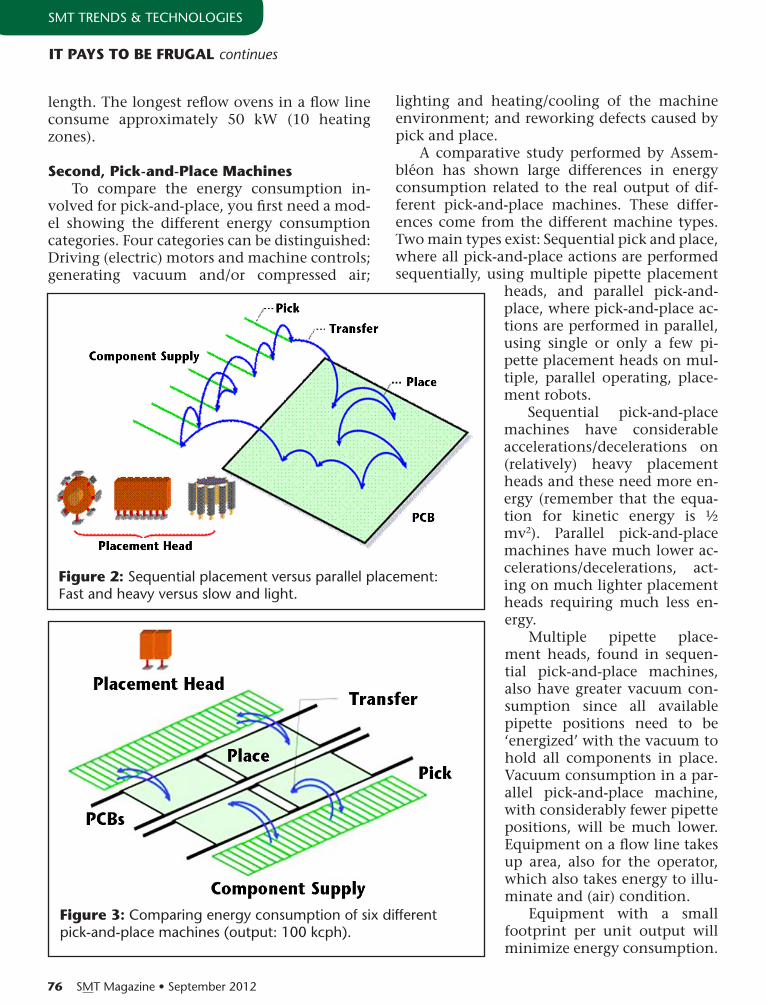
76 SMT Magazine • September 2012
SMT TrendS & TeChnologieS
length. The longest reflow ovens in a flow line consume approximately 50 kW (10 heating zones).
second, pick-and-place machinesTo compare the energy consumption in-
volved for pick-and-place, you first need a mod-el showing the different energy consumption categories. Four categories can be distinguished: Driving (electric) motors and machine controls; generating vacuum and/or compressed air;
lighting and heating/cooling of the machine environment; and reworking defects caused by pick and place.
A comparative study performed by Assem-bléon has shown large differences in energy consumption related to the real output of dif-ferent pick-and-place machines. These differ-ences come from the different machine types. Two main types exist: Sequential pick and place, where all pick-and-place actions are performed sequentially, using multiple pipette placement
heads, and parallel pick-and-place, where pick-and-place ac-tions are performed in parallel, using single or only a few pi-pette placement heads on mul-tiple, parallel operating, place-ment robots.
Sequential pick-and-place machines have considerable accelerations/decelerations on (relatively) heavy placement heads and these need more en-ergy (remember that the equa-tion for kinetic energy is ½ mv2). Parallel pick-and-place machines have much lower ac-celerations/decelerations, act-ing on much lighter placement heads requiring much less en-ergy.
Multiple pipette place-ment heads, found in sequen-tial pick-and-place machines, also have greater vacuum con-sumption since all available pipette positions need to be ‘energized’ with the vacuum to hold all components in place. Vacuum consumption in a par-allel pick-and-place machine, with considerably fewer pipette positions, will be much lower. Equipment on a flow line takes up area, also for the operator, which also takes energy to illu-minate and (air) condition.
Equipment with a small footprint per unit output will minimize energy consumption.
It pAYs tO be FrUGAL continues
Figure 2: Sequential placement versus parallel placement: Fast and heavy versus slow and light.
Figure 3: Comparing energy consumption of six different pick-and-place machines (output: 100 kcph).

September 2012 • SMT Magazine 77
SMT TrendS & TeChnologieS
in addition to playing the clarinet in two bands, assembléon’s Sjef van gastel has another passion: SMT. he has been with the com-pany since its start-up as a philips division in 1979. as the current
Manager for advanced development, he com-bines his experience as systems architect and machine designer to explore technical and business opportunities from emerging tech-nologies. van gastel holds many patents and is a frequent speaker at international confer-ences related to SMT. he is also the author of “Fundamentals of SMd assembly,” which has become a standard piece of literature in the industry.
It pAYs tO be FrUGAL continues
Small machines can also allow the use of smaller buildings with lower building costs…small is beautiful.
third, rework and repair stations
Finally, the defects per million placements of a pick-and-place ma-chine will have consid-erable influence on the rework rate and, hence, the number of rework stations needed. Com-pare a sequential ma-chine with a typical DPM rate of 30 with a parallel machine with a typical DPM rate of 10. Assuming that a typi-cal board contains 1,500 components, a DPM figure of 30 means that one board out of 22 will be defective. The literature shows that approxi-mately nine minutes are needed per rework ac-tion, including finding the defect, de-soldering, component and solder preparation, component placement, component soldering, and inspec-tion. Flow lines with a 20-second cycle time will, on average, generate a rework action (tak-ing an average of 540 seconds) every 444 sec-onds. This requires two rework stations!
If we compare this to parallel pick-and-place (DPM rate of 10), one board out of 66 will be defective, so generating a rework action every 1,333 seconds (again, average rework time 540 seconds). Only one rework station is needed. This not only saves space in the line, but also investment and energy costs (an average 2.5 kW per rework station).
energy savings of $420,000 Results from the study comparing different
pick-and-place machines on the market show big differences in energy consumption. Six models were compared (A to F). The most effi-cient model, a parallel machine, had an average annual energy consumption of 100,000 kWh (per 750M components placed) against 380,000 kWh (same number of components placed) for the least efficient model. This is a difference
of 280,000 kWh per year for pick-and-place alone. Add the potential savings from reflow soldering (estimated at 15%) and you end with total savings of approximately 300,000 kWh per year.
With the average U.S. industry energy price of $ 0.065 per kWh, this means saving $19,500 per year per line of 100,000 cph production capacity. Considering an average high-volume electronics manufacturing plant has approxi-mately 12 lines (average 30-second line cycle time), potential annual energy savings per plant are more than $420,000.
It pays to be frugal! smt
Figure 4.

78 SMT Magazine • September 2012
top ten most-read mil/Aero007 Highlights
78 SMT Magazine • September 2012
OnCore massachusetts Achieves As9100C Certification“being aS9100C compliant at Springfield confirms our commitment to our aerospace and defense custom-ers,” said dan perez, president and Ceo. “The continu-ous improvement of our Quality Management System is part of our customer commitment of providing com-plete solutions including total quality and regulatory compliance.”
OsI systems’ Q4 revenue Up 28% YoYdeepak Chopra, president and Ceo, stated, “We are pleased to report outstanding results for our fourth quarter and fiscal year. each of our divisions finished the year strong. This momentum, combined with a record year-end backlog of $1.1 billion, positions us well for continued strong top line growth and earnings expansion in fiscal 2013.”
sypris’ ems reports 15% sequential revenue Increase in Q2revenue for the company’s electronics group was $16.1 million in the second quarter compared to $16.2 million in the prior year period, but up 15.2% sequentially from the first quarter of 2012. gross profit for the quarter was $4.3 million, or 26.9% of revenue, compared to $1.0 million, or 6.4% of revenue for the same period in 2011, and up sequentially from $2.6 million, or 18.6% of revenue, from the first quarter of 2012.
Divsys Achieves IsO 9001:2008 registrationiSo 9001:2008 is just one of the many steps the com-pany is taking to set itself apart from other suppliers of pCbs. holding the certifications and registrations nec-essary to be “world-class” is the paper side of the coin. divSyS closes the loop with quality product tested in its indianapolis, indiana facility to provide the product assurance piece of the puzzle that many suppliers of bare boards are missing from the equation.
ApI technologies Names bel Lazar president and CeOapi Technologies Corporation recently announced the promotion of bel lazar to the position of president and chief executive officer. brian Kahn, who previously held the positions of chairman and chief executive of-ficer, will continue to serve as chairman of the board. bel lazar joined api on February 28, 2011, as president and chief operating officer.
Nortech systems posts sales of $28m in Q2; Up 7%nortech Systems incorporated has reported net sales of $28.0 million for the second quarter ended June 30, 2012, compared with net sales of $27.8 million for the second quarter of 2011. operating income for the second quarter of 2012 was $319,000, compared with $339,000 for the second quarter of 2011.
IeC reports record Q3 resultsW. barry gilbert, chairman of the board and Ceo, stat-ed, “For the second quarter in a row we have achieved financial results well above our historic metrics, spe-cifically gross margins of 20.6% and operating margin of 9.8%. during the third quarter, cost containment and product mix were important drivers of our higher margins. The gross and operating margin results were some of the best in the company’s history, and particu-larly strong for our industry.”
elecsys expects New spendingto boost ems salesThe short-term reduction in sales is expected to be temporary as the company continues to invest in new product development and sales and market develop-ment efforts. The company believes that these invest-ments will begin to impact results during the second half of the next fiscal year.
suntron Completes Audit by majorDefense CompanyThe audit assessed the company’s facility, personnel, and processes, and concluded that Suntron has very good equipment and a very experienced and educated process, test engineering, and Qa staff. The company was analysed in the following categories: Facility and equipment capabilities, receiving inspection process, aS9102, materials control and traceability, manufac-turing floor, test processes, personnel training, calibra-tion equipment, and supplier base controls. Suntron received high marks in each category.
partnertech posts Growth in Q1; Optimistic About 1H“despite somewhat of a slowdown from the first quarter, sales rose by 2% in local currency compared with the same quarter of 2011 and the operating profit was SeK 12 mil-lion. like many others, we were affected by market uncer-tainty during the second quarter. Some customers pulled back or postponed orders, but the underlying dynamics are positive,” said leif Thorwaldsson, president and Ceo.


80 SMT Magazine • September 2012
Summary: with pcB technologies dramatically escalating, it makes good business sense for the oem to get closer to its cm or emS provider and get a good handle on reading and understanding x-ray images for BGAs, cSps, and flip chips. Zulki Khan explains why.
It used to be that original equipment manu-facturers (OEMs) didn’t know much about X-ray at the PCB assembly stage—they didn’t care too much about it or it just wasn’t on their priority list as a key step for achieving PCB assembly re-liability. After all, X-ray is in the domain of the contract manufacturer (CM) or EMS pro-vider. There were other things to think about at the time for OEM engineers. That was back when device packaging was larger and simpler and there was a lot of room on the board. Back then, X-ray tech-nology effectively met PCB and package in-spection requirements. So, in effect, there were no worries.
Today it’s a brand new ballgame. Yes, you can say some PCB assembly aspects are still best left to the CM or EMS provider; however, consider that PCB technologies have dramatically es-calated and you’re now dealing with ever-shrinking boards packed on both sides with miniature device packages like microBGAs. Given these rapidly evolving circumstances it makes good business sense for you, the OEM, to get closer to your CM or EMS provider and get a good handle on reading and
ColuMn
understanding X-ray images for BGAs, CSPs, and flip chips. Here’s why.
Let’s say you’re developing a new product. You’ve made significant investments for newer system architecture and you certainly want to safeguard those investments. Toward the end of your development cycle you learn some of the BGA-packaged devices are experiencing problems. So, the question becomes: Do these problems stem from an unstable design or BGA placement at the PCB assembly stage?
This is the time when X-ray images and fig-ures come in handy. It could be there are inter-mittent connections, meaning sometimes the PCB works; other times, it doesn’t or something else is causing your board not to work prop-erly. When things are not working properly
you take the bull by the horns and start drilling down. You look at possible
suspects and one of the common suspects for products like yours is a BGA, CSP or flip chip.
As shown in Figure 1, X-ray is the best way to inspect the in-sides of these packages, verify the
integrity of the solder joints, and assure proper assembly. In the case of BGAs with balls, those balls are shown to be properly melted and soldered on the surface of the board. If land grid ar-rays (LGAs) with bumps are involved, the X-ray
image clearly shows the bumps are properly adhered
to surface mount pads on the board’s top surface.
Most often, however, things aren’t so rosy at closer inspection and, in most cases, it takes advanced X-ray sys-
by zulki KhannexlogiC TeChnologieS
zULKI’s pCb NUGGets
Get a New View on X-ray:A brand New ballgame

82 SMT Magazine • September 2012
ZulKi’S pCb nuggeTS
tems to get an even more detailed definition of the problem. Not only do you want to inspect BGA solder joints, but you also want to verify device packaging integrity. You want to inspect the chip inside the BGA and make sure all con-nections from the chip are properly connected to peripheral BGA balls or LGA bumps.
Aside from these potential problematic ar-eas, other emerging and hard-to-detect areas exist. For instance, head-on-pillow is a defect that regular X-ray has trouble detecting and in-terpreting. It doesn’t clearly show that solder hasn’t properly melted, so that a joint is not 100%. This means advanced X-ray systems with powerful image recognition features and well-trained technicians are critical in this instance to pinpoint such defects.
X-ray intensity level targeted at the board or package is another area with which you want to gain familiarity. Some defects can be spotted at low intensity or kV levels, but others, finer in nature and most difficult to uncover, can only be verified with a higher kV rating. In these cases, the most sophisticated, most powerful X-
ray systems have the capability of zooming in at a 1,000 or 2,000 X level. These systems can find those highly elusive defects due to their ex-tremely high kV levels.
Also, you want to look for images showing BGA delamination and voids. A high-end X-ray system ensures co-planarity of the device and also may identify whether or not there’s pack-age delamination. Voids, regardless of how dili-gent, careful, and precise placement practices are exercised, will still occur. According to IPC Standard A-610 (Acceptability of Electronic As-semblies), Revision E-2010 (Acceptability of Electronic Assemblies), and Section 8.3.12.4 (Surface Mount Area Array-Voids), a certain per-centage of voids is acceptable, normally up to 25%. Specifically, it states that 25% or less void-ing of any ball in the X-ray image area is accept-able for Class 1, 2, and 3.
A highly sophisticated X-ray system is able to not only detect and show voids, but can also determine the percentage of voids. Accord-ingly, the CM or OEM can therefore determine whether or not the percentage of voids meets
Get A NeW VIeW ON X-rAY: A brAND NeW bALLGAme continues
Figure 1.

September 2012 • SMT Magazine 83
ZulKi’S pCb nuggeTS
Get A NeW VIeW ON X-rAY: A brAND NeW bALLGAme continues
device specifications called out by OEM engi-neers. Take, for example, a BGA with 1,156 balls and 15 or 20 of those balls have voids. If those voids are within 5 to 10%, they are acceptable per IPC Class 2.
Even with the higher kV levels that state-of-the-art X-ray systems deliver, there’s still one more PCB area that demands the best of both man and machine. This involves a highly-populated, double-sided, BGA-popu-lated PCB. In this instance, the X-ray image focuses on a BGA on the board’s top side. How-ever, there are capacitors and resistors in the same spot, but directly on the bottom side, making the image complicated to review and analyze.
To the inexperienced technician’s eyes, the black-and-white image under inspection ap-pears as a composite of the top- and bottom- side images and he or she is deceived into thinking the image is that of a short, rather than a component on the other side. On the other hand, the experienced technician knows how to decipher the image. He or she can then clearly delineate BGA balls under inspection from the components on the other side, which aren’t associated with the correct and only im-age the technician is inspecting.
In summary, it’s to an OEM’s advantage to become savvy about X-ray on the PCB assembly floor. In some situations, you may find poorly trained technicians who can either misinterpret or be too casual about reading X-ray images. As a result, you get less than acceptable inspection
and, quite likely, defects that go undetected, leading to field failures.
Worst of all, an unscrupulous CM or EMS provider might try to pull a quick one;, they will try to pass a detected flaw or defect to avoid incurring extra time and costs and get your PCB project shipped out the door as fast as possible. But, if you are up to date and armed with plenty of know-how in terms of interpreting these images, you can stand your ground when it’s determined your product isn’t working. You can intelligently contest the design or assembly and make your case by questioning X-ray image results or actually demanding to view them as the way to resolve the issues keeping your product from working properly. smt
Zulki Khan is the founder and president of nexlogic Technolo-gies, inc., in San Jose, California, an iSo 9001:2008-certified com-pany, iSo 13485-certified for manufacturing medical devices
and a rohS-compliant eMS provider. prior to nexlogic, Khan was general manager for imagineering, inc. in Schaumburg, illinois. he has also worked on high-speed pCb designs with signal integrity analysis. he holds a b.S. in ee from ned university in Karachi, pakistan, and an M.b.a. from the university of iowa. he is a frequent author of contributed articles to eMS industry publications.
researchers at the university of pennsylvania have identified a simple new method to direct particle assem-bly based only on surface tension and particle shape. The research, led by Kathleen J. Stebe, professor in the department of Chemical and biomolecular engineering and the school’s deputy dean for research, relies on the simple fact that a liquid surface will tend to minimize its surface area.
Stebe’s lab used cylindrical particles made out of a common polymer. When placed on the surface of a thin
film of water, the cylinders produce a saddle-shaped de-formation: The water’s surface dips at each end of a par-ticle and rises up along their sides.
in the study, instead of two particles interacting, particles interact with a stationary post. The post pokes through the water’s surface, causing the surface to curve upward around it; the particles move so as to make the surface area as small as possible.
by changing the cross-sectional shape of the posts, the researchers were able to show fine control over how the particles moved and oriented. a circular post attracted particles in straight lines, whereas an elliptical post drew particles to the elongated ends. a square post produced the most complex behavior, drawing particles strongly to the corners, leaving the sides open.
new Way of Assembling Particles Into Complex Structures

84 SMT Magazine • September 2012
a New IpC president restructures Divisions, realigns staff
John Mitchell, president of ipC, says, “i want to provide a glimpse into some of the changes hap-pening internally at ipC. after a thorough review, i have decided to reorganize the staff into new divi-sions to facilitate better service to our members. i’d like to share them with you. There are some significant ideas in the mission that we are striving to achieve: global trade association, success of the members, technology enhancement and govern-ment relations.”
b sparton Accelerates Growth with management Changes
Sparton announces management appointments to further accelerate the implementation of its strategic growth plan. as stated in the strategic plan, the company will continue to provide com-
plex electronic and electromechanical devices and related services through niche opportunities in the military and aerospace, medical, and industrial markets. Much of Sparton’s growth will be driven by the acquisition of complementary businesses.
c smt magazine Announces New Advisory board members
The i-Connect007 family of publications is pleased to announce new editorial advisory board mem-bers for SMT Magazine. These industry experts from around the world will assist editors in provid-ing the most relevant and intelligent coverage of the global electronics assembly industry.
d standards set for potting, encapsulating boards
The ipC-hdbK-850 covers a broad range of pro-tective materials for printed boards, providing designers and users with an efficient tool to help select encapsulants for printed board assemblies.
Top Tenmost-read News Highlights from smtonline this month
84 SMT Magazine • September 2012

3 Online Auction Sales
LATE MODEL SMT, TELECOMMUNICATIONS and ELECTRONIC TEST & MEASUREMENT EQUIPMENT
Featuring:Telecommunication / Electronic Test Equipment:• Agilent E5515C / 8960 Series 10 and Rohde & Schwarz
CMU200 Communication Test Sets
• Agilent N4010A Wireless Connectivity Test Sets
• Rohde & Schwarz NRP-Z22 Power Sensors
• Agilent DSO3102A Digital Storage Oscilloscopes
• Spirent GSS6100 Signal Generators
• Agilent N9340B Handheld Spectrum Analyzers
• Agilent E3640A & 66309D Power Supplies
• VTI EX7204L Mainframes
SMT Process Equipment:• DEK Europa Screen Printers
• CyberOptics SE300 Ultra Solder Paste Inspection Systems
• Yestech F1 AOI System
• Conveyors, Bareboard Loaders, FIFO Conveyors by Nutek,
JOT, Flex Link
• Data I/O Roadrunner Inline Programmable Feeders
• Vitronics XPM3-1030, BTU Pyramax 150N & BTU Paragon
150 Reflow Ovens
• Nicolet NXR 1400 X-Ray System
• Air-Vac Onyx 29 Rework Stations
Surplus to ongoing operations of Celestica
Sale 2 - Sale Closing: Thursday, 27th September 2012 Location: Oradea, Romania
Sale 3 - Sale Closing: Thursday, 11th October 2012 Location: Senai, Malaysia
Featuring:Electronic Test & Measurement• Agilent E5515C / 8960 Series 10 Communication
Test Sets (Qty 40)
• Rohde & Schwarz CMU200 Communication Test
Sets (Qty 25)
• Agilent N4010A'Wireless Connectivity Test Set (Qty 19)
• Agilent 66309D Dual Output Mobile Communications
DC Source (Qty 43)
• National Instruments NI PXIe-1062Q Extended
Interface Frame (Qty19)
• Rohde & Schwarz NRP-Z22-1137.7506.02 Power
Sensor (Qty 31)
• Also Including - Camfil Farr Clean Air Filter Work Hoods With Simco Scorpion 3 Ionizer, Simco Orion & Top Gun Sidekick
Ionizers, Atlas Copco Etd M 20 Abl Electric Screwdrivers (2012), Quicher/ohtake Nj-12 Screw Feeder (Upto 2012), Mettler
Toledo Electronic Scales, Hakko Hot-air Blower Soldering Stations And Much More
Featuring:Telecom Test Equipment:• Agilent E5515C / 8960 Series 10 Communication Test Sets
• Agilent N4010A Wireless Connectivity Test Sets
• Rohde & Schwarz NRP-Z22 Power Sensors
• Agilent 66309D Power Supplies
SMT Process Equipment:• Nutek Buffer Conveyors
• Speedline 8000-1 FX Dispensers
• Yestech YTV-F1 F1 AOI Automated PCB Inspection System
• Data I/O Roadrunner Inline Programmable Feeders
• Cencorp 16000303 High Speed Depaneling System
Miscelleanous Equipment:• Start International Tda080-m Tape Dispensers
• Quicher Precision Screw Feeders
• Simco Orion And Topgun Ionizing Guns
• 'The' Ld5500 Label Dispenser
• Simco Aerostat Pc Ionizing Air Blower
• Micron Ionizing Cabinet & Self Powered Laminar
Flow Unit And Filter
Sale 1 - Sale Closing: Thursday, 20th September 2012 Location: Monterrey, Mexico
For further information, please contact:
www.go-dove.com
WILLIAM HLADY Tel: +1 248 514 3336 Email: [email protected]
For further information, please contact:
BOON CHUAY LEE Tel: +65 6334 4266 Email: [email protected]
For further information, please contact:
ROBERT PENDAL Tel: +44 7774 652 403 Email: [email protected]
RICHARD SIEBERER Tel: +43 676 843 813 105 Email: [email protected]
In Conjunction with

86 SMT Magazine • September 2012
The standard includes information on choosing, mixing, applying, and dispensing for each of the materials listed.
e IpC Launches Industry Guidelines for solder pastes Solder paste is a necessity for basically all pCbs, but it’s one of the most overlooked technologies in the electronics industry. ipC has completed the first standard that will help development teams improve the quality of their solder paste opera-tions, which could bring significant improvements in quality and reliability.
f ems Firms steer Focus to Dashboards
The difficulty of managing electronics manufactur-ing has grown exponentially as outsourcing, glo-balization, product complexity, and market shifts become the norm. The challenge for oeMs and eMS providers is keeping track of project status when components and production are globally sourced and shipped. Since data overload is as inefficient as not enough data, it is important to identify the right data to track and automate the process enough that critical issues are immediately evident.
g IpC Handbook Delves Into protective Coatings
Whether they’re protecting handheld products from moisture and the shock of drops or trying to improve the lifetimes of high-reliability circuit boards, more design and manufacturing teams are potting and encapsulating boards. as spacing di-mensions shrink, it’s becoming increasingly more important to pick the right materials to protect these boards in operating environments in which a conformal coating will not do the job.
h ems m&A Activity Drops sequentially in Q2
Four completed transactions occurred in Q2 2012. The four transactions show a decrease in the M&a activity compared to the nine transactions in the previous quarter. The recent softening in some de-veloped economies and a slowdown in China and india have created challenges for companies to pur-sue strategic investments within the eMS sector.
i Weak Q1 for Flextronics; transformation to Improve portfolio
“despite the challenging economic environment, we achieved our targeted operating margin and our adjusted epS improved 10% compared to the same quarter last year. We have accomplished a transformation of our business to our desired port-folio model, which will lead to further margin ex-pansion over the course of fiscal year 2013,” said Mike Mcnamara, Ceo.
j benchmark Overcomes slow market with solid Q2 results
“We are very pleased with the solid execution of our team for the second quarter in a weakening environment. notably, our revenue and margin improvements were achieved while supporting numerous program ramps from previous quarters’ bookings, as well as the ongoing Thailand recov-ery efforts,” said president and Ceo gayla J. delly.
smtonline.com For the latest SMT news—anywhere, anytime.86 SMT Magazine • September 2012
Top Ten ConTinueS


88 SMT Magazine • September 2012
for the ipc’s calendar of Events, click here.
for the smta calendar of Events, click here.
for the inEmi calendar, click here. for a complete listing of events, check out Smt magazine’s full events calendar here.
J-stD-001e: Requirement for Soldered Electrical and Electronic AssembliesSeptember 10-14, 2012 valencia, California pCIm south AmericaSeptember 11-13, 2012 Sao paulo, brazil West penn expo and tech ForumSeptember 13, 2012 Monroeville, pennsylvania eIpC summer ConferenceSeptember 13-14, 2012 Milan, italy the eCOC exhibitionSeptember 16-20, 2012 amsterdam, The netherlands Advancement in thermal management 2012September 18-19, 2012 denver, Colorado manufacturing in Guadalajara 2012September 18-20, 2012 guadalajara, Jalisco, Mexico IpC Workshop: Design for manufactureSeptember 19-20, 2012 Fredericksburg, virginia
88 SMT Magazine • September 2012
e v e n T S meDevice Forum san DiegoSeptember 19-20, 2012 San diego, California Northeast shingo prize Conference September 25-26, 2012 Worcester, Massachusetts modern Day marineSeptember 25-27, 2012 Quantico, virginia mepteC/smtA medical electronics symposiumSeptember 26-27, 2012 arizona State university, arizona Austin (CteA) expo and tech ForumSeptember 26, 2012 austin, Texas printed electronics Asiaoctober 2-3, 2012 Tokyo, Japan Dms Osakaoctober 3-5, 2012 osaka, Japan 21st Annual International electronics Forum october 3 - 5, 2012 yerevan, armenia NepCON Vietnam 2012october 4-6, 2012 ho Chi Minh City, vietnam plastic electronics Conference 2012 october 9-11, 2012 dresden, germany
Calendar

September 2012 • SMT Magazine 89
advErtisErs indEx
publiSher: bArrY [email protected]
publiSher: rAY rAsmUsseN(916) 294-7147; [email protected]
SaleS Manager: bArb HOCKADAY (916) 608-0660; [email protected]
EDITORIAL:group ediTorial direCTor: rAY rAsmUsseN(916) 294-7147; [email protected]
Managing ediTor: HOLLY COLLINs(252) 288-2751; [email protected]
TeChniCal ediTor: pete stArKeY+44 (0) 1455 293333; [email protected]
EDITORIAL ADVISORY BOARD:CrAIG HUNter, vishayJeNNIe s. HWANG, pH.D., h-Technologies inc.
EDITORIAL ADVISORY BOARD continued
mICHAeL KONrAD, aqueous Technologiess. mANIAN rAmKUmAr, pH.D., rochester institute of TechnologyrAY p. prAsAD, ray p. prasad Consultancy grouprObert rOWLAND, radiSys Corp.VerN sOLberG, independent Technical ConsultantGArY tANeL, electronics allianceHArALD WACK, pH.D., ZeSTron americaWILLIAm e. COLemAN, pH.D., photo Stencil
MAGAZINE PRODUCTION CREW:
produCTion Manager: sHeLLY steIN [email protected] layouT: rON meOGrOssIad deSign: sHeLLY steIN, brYsON mAttIesinnovaTive TeChnology: brYsON mAttIesCover arT: sHeLLY steIN, brYsON mAttIes
SMT® (Surface Mount Technology) is published by br publishing, inc., po box 50, Seaside, or 97138
©2012 br publishing, inc. does not assume and hereby disclaims any liability to any person for loss or damage caused by errors or omissions in the material contained within this publication, regardless of whether such errors or omissions are caused accidentally, from negligence or any other cause.
September 2012, Volume 27, Number 9 • SMT© (Surface Mount Technology©) is published monthly, by br publishing, inc.
aegis.................................... 51
basic electronics inc............. 33
blackfox............................... 23
Ca picard............................. 25
Calumet............................. 2, 3
eagle Circuits....................... 57
easybraid.............................. 13
ee Technologies.................... 47
epeC.................................... 67
goindustry (uK) limited....... 85
hunter Technology............... 79
i-Connect007....................... 87
imagineering..................... 7, 9
ipC................................ 27, 81
Manncorp............................. 5
nordson asymtek................. 41
one-Source group............... 43
p Kay Metal.......................... 11
prototron............................. 31
Semblant............................. 55
SMTa............................. 35, 73
Stebgo................................. 45
Stoelting.............................. 21
Technica uSa....................... 61
Technica (rehm).................. 75
The pCb list........................ 69
Total parts plus..................... 15
uS Circuit............................. 37
ventec uK............................ 59
next Month in SMt Magazine
The focus of the october issue is rohS, reaCh, and Weee compli-ance and current legislation, waste water management, and many other environmental concerns en-countered during manufacturing. oeM and eMS providers must be proactive and keep up with the latest changes in various countries to remain at the top of their game.
The october issue of SMT Magazine will bring readers a host of industry experts to address energy conservation, workplace safety, and sustainability issues; define green and green-washing legislation; present a conflict met-als update; and offer the latest concerning reaCh, rohS, and Weee and much more.
if you’re not yet a subscriber, don’t miss out! Click here to re-ceive SMT Magazine in your inbox each month.
See you in october!