Embed Size (px)
Citation preview
Soft-Error Filtering: A Solution to the Reliability Problem of Future VLSl Digital Circuits
lnvited Paper
As the semiconductor industry continues to scale down the feature sizes in VLSI digital circuits, soft errors will eventually limit the reliability of these circuits. An important source of these errors wi l l be the products of radioactive decay. It is proposed to combat these transient errors by a new technique called soft-error filtering (SEF). This is based on filtering the input to every latch in the VLSI circuit, thereby preventing these transients, generated by alpha particle hits in the combinational section, from being latched in the corresponding registers. Several approaches to the problem of designing filtering latches are compared. This comparison demon- strates the superiority of a doublefilter realization. The design for a CMOS implementation of the double-filter latch is presented. Not only is the design simple and efficient, but it can be expected to be tolerant to process variations. A comparison of SEF with conven- tional techniques for dealing with soft errors shows the former to be generally much more attractive, from the point of view of both area and time overhead.
I. INTRODUCTION
A soft error is a temporary, nonrecurrent phenomenon which is endemic to semiconductor circuits [I], [2]. For semiconductor memories, the use of error correcting codes is an elegant remedy [3], [4]. Unfortunately, this solution is not appropriate in general for very large scale integrated (VLSI) digital circuits. As will be argued below, soft errors may become the limiting factor for reliability as circuit feature sizes are reduced to yield higher circuit densities.
The simplest and most frequently used technique for dealing with soft errors in logic circuits consists of duplicat-
Manuscript received June 17, 1985; revised October 16, 1985. Y . Savaria was with the Department of Electrical Engineering,
McGill University, Montreal, Canada. He is now with Department de Genie Electrique, Ecole Polytechnique de Montreal, Montreal, Que., Canada H3C 3A7.
N. C. Rumin and V. K. Agarwal are with the Department of Electrical Engineering, McGill University, Montreal, Que., Canada H3A 2A7.
J , F. Hayes was with the Department of Electrical Engineering, McGill University, Montreal, Canada. He is now with the Depart- ment of Electrical Engineering, Concordia University, Montreal, Que., Canada H3M 1C8.
ing a basic machine [5]. Duplication works well as long as modules fail independently. An alternative general tech- nique called Soft-Error Filtering (SEF) i s proposed in this paper. In SEF, the redundancy takes the form of filters included between the output of a combinational logic network and the output register. The filters remove the short transients which cause soft errors. This approach permits a low hardware overhead since the logic function is not replicated. Moreover, if the transients are much shorter than the clock period, the time overhead is also small.
A. Sources o f Soft Errors and their Significance
The two main sources of soft errors are ionizing radiation and electromagnetic interference. Ionizing radiation can be separated further into alpha particles from the decay of uranium and thorium impurities [6] and cosmic rays [7]. Uranium and thorium are present as traces in a number of materials used to fabricate integrated circuits [8]. Cosmic rays contain penetrating particles which tend to generate cascades of secondary particles as they propagate through matter. The existing correlation between the particles in a cascade is often overlooked. In particular it is noteworthy that an imperfect radioactive shield formed by a layer of dense material increases the flux of secondary particles. SEF should be particularly effective in combatting errors due to products of radioactive decay, such as alpha particles.
The mechanism by which ionizing radiation causes errors is briefly described here. A charged particle interacts with matter by ionizing a number of atoms along its track. The number of particles ionized per unit length is determined by a number of parameters, including the velocity and the charge of the particle [7]. When charge is injected in an integrated circuit it can be collected by the circuit. The active devices sharing a common substrate in an integrated circuit are generally isolated by reverse-biased or unbiased (0-V) p-n junctions. When the charge is injected in the depletion region it i s rapidly collected by the drift mecha-
PROCEEDINGS OF THE IEEE, VOL. 74. NO. 5. MAY 1986
0018-9219/86/0500-0669801.00 61986 IEEE
669

nism [9]. The amplitude of the injected voltage transient is determined by a number of factors, including the geometry of the collecting structure, the angle of incidence of the particle [2], and the doping of the substrate [9], to name a few. For example, the current injection time, and the result- ing voltage transient may last for 200 ps and 1 ns, respec- tively. Reference [IO] contains a detailed discussion of the various interference sources and of the interaction mecha- nisms between ionizing radiation and integrated circuits.
The analysis in [IO] is restricted to MOS since it is likely to be the dominant VLSl technology. Moreover, since the intrinsic tolerance of static logic is better than that of dynamic logic due to the recovery capability of every node in the former, the SEF approach was developed for static circuits only. SEF does not work with dynamic logic.
Based on a number of reasonable assumptions, the soft error rate of a large VLSl chip (1 c d ) could be on the order of 10-4/h [IO]. The significance of this estimation is evident when it is compared to actual and projected random failure rates for the same chip. For commercial microprocessor chips, the measured failure rate is 3 X 10⁻⁷/h [ I l l . Assum- ing that the failure rate grows as the square root of the complexity [12], a large VLSl chip should have a failure rate of 10-'/h. However, there is a demand for integrated circuits with low failure rates; moreover, if acceptable yields are to be obtained from the newer VLSl processes, the quality must improve. These factors lead one to conclude that failure rates will decrease and, as a result, the soft error rate can become the dominant factor in determining relia- bility with the scaling down of the technology.
In theory, the effect of electromagnetic interference can be eliminated by the proper application of known tech-
obtained by a majority vote. Taking into account the voting process, this approach implies more than 200-percent hardware overhead. The most efficient solution obtained with the system level approach consists of duplicating the machine. In this case, tolerance is provided by a detection and retry mechanism. A duplicated machine requires at least a 100-percent hardware overhead.
In the remainder of the paper, the SEF approach to the problem of soft-error tolerance is presented and analyzed. In Section II the basic Soft-Error Filtering approach is de- scribed, and this is followed by an outline of the calculation of the reduction in the soft error rate which SEF yields, in the case where the errors are due to the products of radioactive decay. As will be seen, SEF borrows from both the physical level and the system level approaches dis- cussed earlier. The implementation of a filtering register, which is a critical component of a SEF machine, is pre- sented in Section Ill. Finally, the overhead incurred by Soft-Error Filtering is analyzed in Section IV.
II. SOFT-ERROR FILTERING
Soft-Error Filtering (SEF) permits the implementation of machines tolerant to soft errors, without the limitations of physical-level techniques and with less overhead than con- ventional system-level techniques. The basic model which is used to develop SEF is introduced in Section Il-A. This model establishes the need for a filtering latch, which is one that has been optimized for filtering transients in its input data. The effectiveness of SEF in decreasing the soft error rate due to the products of radioactive decay is dem- onstrated in Section 11-B.
niques [13]. However, the remaining error rate due to inter- ference is sti l l significant, as demonstrated by McConnel A. ~ a s ; c Mode/ et a/. [14], [15]. In practice, a number of interference sources can combine their effects to cause short transients. The SEF approach is effective for tolerating interference sources generating short transients. Unfortunately, the statistical properties of these interference sources makes the analysis of error rate reduction with SEF difficult.
6. Conventional Approaches to Soft Errors
Conventional techniques for decreasing the soft error rate fall into two categories: physical and system-level ap- proaches. Each has certain drawbacks which limits its util- ity. An example of a physical-level technique is coating the chip with a layer of material containing very little radioac- tive impurities. This layer has a sufficient thickness to ab- sorb alpha particles emitted by the packaging materials. This approach is relatively inexpensive but has a limited efficiency since the materials composing the circuit itself contain significant traces of radioactive elements [2].
A second example of a physical-level solution is increas- ing the capacitance of internal nodes to a level where the charge injected by alpha particles is insufficient to cause an error. This approach necessitates increased area and in- creased power which must be dissipated. These two exam- ples illustrate a general trend; physical approaches increase cost and are of decreasing value as the density of the circuits increases.
System level approaches consist of hardware or time redundancy. For example, Triple Modular Redundancy (TMR) uses three modules in parallel [12]. The final result is
A widely applicable model for digital machines is needed in order to develop a general method of tolerating soft errors. The finite-state machine, shown in Fig. l(a), is such a simple model which generalizes easily to a wide variety of digital machines. A two-phase clock is used and the first clock, CKI, stores the present state of the machine in the left-hand register R . The combinational network C/L com- putes the output OUTand the next state ST, on the basis of the contents of this register. During the second phase CK2 transfers the output of C/1, 0 , to the right-hand output register R. The state outputs ST of this register, as well as the primary inputs IN, are stored in the left-hand register by CKI. Fig. l(c) illustrates the clocking scheme. The results derived for this model can be easily extended to more complex register-transfer machines, such as a pipelined computer or a multiphase machine.
In reference to Fig. ?(a), a soft error is a nonrecurrent and temporary difference between the actual behavior and the specification, as observed on one of the output OUT or state ST lines. A transient could also be injected directly into the registers, therefore, the latches composing them must be intrinsically tolerant if the transient is to be masked. Assuming intrinsic tolerance of the latches, a soft error can only result from a transient injected in the combinational logic section, as illustrated in Fig. l(a) and (c), The transient must appear on one of the output lines of the combina- tional logic during the interval when the latch is sensitive, and its duration must exceed a certain minimum value related to the setup time of the latches Tu.
670 PROCEEDINGS O F THE IEEE, VOL. 74. NO 5 . M A Y 1986

n
CK1 CKZ \
I-
( 4 Fig. 1. (a) A conventional finite-state machine based on a two-phase clock CKI, CK2 and consisting of two registers R and a combinational logic block C/L. Only C/L is assumed to be sensitive to a hit by an alpha particle a. (b) A function- ally equivalent SEF machine in which the outputs 8 of C/L pass through filters F before being latched in the output register. (c) Timing diagram for the machine in (a), showing the effect of a 8 = 1 being corrupted by an alpha-induced transient of duration D during the register setup time T5,, (d) Same as (c) for the SEF machine in (b). Note that T,, is longer than in (c) necessitating a longer duration of CK2.
Assuming that most of the soft errors are due to short transients, an important reduction of the soft error rate would be achieved by filtering these transients, One way that this can be achieved is by making all the nodes inside the machine slower. However, considerations of efficiency, both in terms of speed and area, suggest that the number of nodes which have to behave like filters should be mini- mized.
As long as a logic network is combinational, an injected transient remains a transient after propagation. If a boundary encloses only combinational functions, the effect of all nodes behaving as filters can be achieved by filtering all the lines fanning out of this boundary. If the complete system is to be filtered, the places that yield the minimum number of filters for any machine are at the output of the combina- tional function. Such a SEF machine with filters (F> between every output of the combinational logic and the output register is shown in Fig. l(b). A timing diagram for this SEF machine is shown in Fig. l(d). Notice that the timing diagrams in Fig. l(c) and (d) are very similar. The propa- gation time A from the input of the first register to the output of the logic is the same for both machines. Only the setup time T,, of the SEF machine is longer. The disturbing transient on one of the 0 lines has the same duration D in both cases. However, for the SEF machine, the inertia accu-
mulated in the filtering register is sufficient to tolerate the effect of the injected transient. The filters force a slightly longer duration for the phase 2 clock.
In this paper the expression setup time is not used with its conventional meaning. The setup time T,, of a register reflects the time interval during which data are latched. Hence T,, i s normally defined as the time interval during which input data must not change, and is usually measured with respect to one of the clock edges. In the present case, this definition is relaxed to permit the momentary corrup- tion of input data by a short duration pulse. Therefore, T,, can be used as a measure of the register’s tolerance to soft errors. For convenience of analysis, the registers are as- sumed to be level-sensitive (as against edge-triggered) without any loss of generality. It turns out that all types of latches or flip-flops have a minimum time interval during which data should be stable in order to function properly.
To summarize, SEF consists of transforming a basic ma- chine by replacing its memory elements with filtering latches. The combinational logic network is not replicated, which reduces the hardware overhead. Since SEF uses logic elements as fast as in the basic machine, the performance of the machine is minimally affected by the inclusion of filters at the input of the latches. The difference between SEF and using a slow technology is that in the former a single slow node is included at the end of every propa- gation path, whereas in a slow technology every node is slow. The effect of SEF on the error rate due to the products of radioactive decay is discussed in the next section, and the resulting improvement in reliability of digital machines is demonstrated.
B. Products of Radioactive Decay; Error Rate Improvement with SEF
The calculation of the influence of SEF on the error rate due to the products of radioactive decay was presented earlier [IO], [16], and is simply summarized here. This calcu- lation is based on several well-established facts and a single key assumption. First, filtering registers are feasible, as established in the next section. Secondly, radioactive decay produces a flux of particles with a Poisson distribution. Therefore, intervals between hits are independent and ex- ponentially distributed. An important observation concerns the form of the transient induced by a hit. A hit may produce a transient composed of more than one pulse, because it may affect more than one node, and more than one sensitized path may exist. A logic path is sensitized if a transient on i ts input can propagate to its output. However, it i s assumed that the sum of the durations of the individual pulses is bounded by some relatively small value P, as shown in Fig. 2. This is the key assumption which permits an important simplification of the formulation. In the ab- sence of this assumption the SEF approach can still work, however, the error rate analysis is far more difficult.
Fig. 2. A transient composed of N pulses
SAVARIA e t a / . SOFT-ERROR FILlERINC 671
If the duration of the transient resulting from one hit is bounded, and i f the setup time of the latch is sufficiently long, a single hit will not cause an error. The necessary condition for an error to occur is, therefore, that two or more independent hits happen in the same clock period and with a proper timing relationship. In order to evaluate the tolerance of a SEF machine, bounds on the error prob- ability were calculated for a machine with and without SEF [IO]. These bounds are loose but, nevertheless, sufficient to demonstrate that SEF does effectively reduce the error rate to insignificant levels.
Let D be the maximum duration of a tolerable pulse, i.e., the duration of a pulse which is guaranteed not to be latched at the output of the combinational logic. The minimum number of hits that is required to cause an error is given by q = [ D/P] + , where [X] + is the smallest integer larger than X. For an error to occur, the pulses must fall in the sensitive time interval of the output register, in such a way that the line is at the wrong value for a duration longer than D. The bound on the error probability can be expressed as follows:
m
Pr(error) Pr( I hits). (1 1 1 - r l
Each filter tolerates independently the transients gener- ated in its fan-in. Therefore, the error rate is first calculated for a single output line. Since radioactive decay has a Poisson hit rate, the error probability is bounded by the following expression:
Pr(error per line) -
where
F effective flux in particles/cd . h As, sensitive area in the cone of the considered
output, in cm2 S D = T,, latch’s setup time, in s (The relationship be-
tween the setup time and D, the longest transient that can be tolerated, is thus ex- pressed explicitly.)
after propagation, in s
an error.
P maximum expected duration of a transient
rl minimum number of events necessary to cause
If there are R outputs then the error rate can be bounded as follows:
Soft error prob. per 1 FA,,,,( P + SD) cycle for the chip < 5 (?( 3600
where the subscript j refers to the region in the cone of the j t h output. This is a union bound since the Occurrence of errors on different outputs is not disjoint. Notice that the noisiest output line tends to determine the error probability when q > 1 because, in this case, the exponent amplifies the differences in average hit rate. In general, a first ap- proximation of the bound on the error rate can be com- puted by assuming that all the lines are as noisy as the noisiest one, in which case the summation is replaced by a multiplication by R .
When the machine is sensitive to a single hit ( q = 1) the
expression can be simplified as follows:
Soft error prob. ( F A s ( ~ ~ s D ) ) (4)
where A , i s the total sensitive area of the chip. The error rate per cycle of a sensitive chip is known to be
small, and was estimated in [IO] to be of the order of 10-4/h. Therefore, the error rate of a SEF machine, which is proportional to a power of the hit rate (per cycle), should be much smaller. The calculated error rate is on the order of 10-”/h [IO], [ I 4 when reasonable values are substituted in (3). This is much smaller than the random failure rate, which is expected to be on the order of IO-’/h [IO]. In conclusion, SEF is very effective for tolerating the effects of small but significant rates of short transients.
111 . THE DESIGN OF A FILTERING REGISTER
The SEF approach to the design of soft-error-tolerant digital systems is based on the assumption that it is possible to build a register which can filter out transients at its input. These transients can be significantly longer than the basic switching time of the technology used. Moreover, the space and time overhead associated with the registers must be acceptably low. Also, it is implicit in the SEF technique that the registers must be intrinsically tolerant to sources of soft errors such as direct alpha particle hits.
There exist a number of different approaches to the problem of designing an efficient filtering latch. Which one is most efficient is not clear unless every approach is analyzed and compared. A simple but inefficient means of making a filtering latch, is to slow down a standard one. This approach is considered in Section Ill-A. A design that permits a significant reduction of the time overhead relative to that of the slow latch is considered in Section Ill-6. This second latch is based on a single filter. Its optimization at the functional level is described, and the practical limita- tions of a circuit implementation are discussed. Finally, a double-filter configuration is analyzed and a practical reali- zation is proposed in Section Ill-C. The implementation of the double-filter configuration turns out to be simpler than the single-filter latch, and the design is more efficient than either of the other two.
In order to avoid having to make assumptions about a future hypothetical sensitive technology, it was decided to use the Northern Telecom 5-pm CMOS16 process as a benchmark. This choice follows from the fact that it is easier to scale up injected transients and their effects, than to predict all the parameters describing accurately a scaled- down technology. Moreover, the chosen process is avail- able to universities in Canada, and therefore it is possible to fabricate these devices and experimentally confirm the re- sults derived here.
A hypothetical 0.5-pm technology with a 1.5-V supply is used as the reference from which the scaling factors are derived. This represents a sensitive technology for which the appropriateness of the SEF approach is reasonably evident. Such a technology corresponds to first scaling CMOS16 at constant voltage by a factor of 3, which is representative of the state of the art, followed by a subse- quent scaling at constant field by another factor of 3. Consequently, the basic time constant of the 5-pm process is approximately 27 times longer than that of the 0.5-pm
672 PROCEEDINGS OF THE IEEE, VOL. 74. NO 5, M A Y 1986

process. The saturation currents for transistors with equiv- alent length/width ratios is roughly the same for both technologies. The capacitances on the 5-pm process are nine times higher than those of the 0.5-pm process, and the supply voltage is three times higher.
The duration of the injected current pulse resulting from an alpha particle hit is usually shorter than 0.25 ns [9]. It is demonstrated elsewhere [IO] that the duration of the volt- age transient after propagation may be significantly longer than the injection time. Consequently, a reasonable objec- tive .forthe filtering register in the 0.5-pm process is that it must filter out all pulses up to a duration of 1 ns. The I-ns transient serves as a reference for testing and comparing the different approaches to the design of filtering latches. Therefore, after scaling up this transient, the 5 g m imple- mentatiorrmust tolerate a transient of 27 ns.
If the register latches are to be tolerant to direct alpha particle hits then they must be able to tolerate an injected current pulse having the approximate form shown in Fig. 3.
300'0D 5 Sirnulafed inieckd current
250.00
200.00
1 Y 150.00
100.00
50.00
0.00 0.00 2.00 4.00 6.W 8.00 10.00 12.00 14.00
time(".)
Fig. 3. Approximation of the scaled up version of a current pulse injected by a direct alpha hit on a node.
The parameters of this pulse are based on an injected pulse in the 0.5-pm technology lasting as long as 0.5 ns [9]. This scaled up pulse injects a charge of 2.2 PC. Notice that the scaling factor for charge is 27, which can be interpreted as the same current with a duration 27 times longer, or an equivalent charge on a capacitor nine times larger when the supply voltage is three times higher.
The above events do not necessarily represent the worst possible case but are relatively large disturbances. If the design is to be conservative but efficient, it is essential to know accurately these worst possible events for a given process. One objective of this section is to demonstrate how a filtering latch can be designed for a given set of expected worst case events. An efficient filtering latch must be optimized for the level of tolerance required.
A. Slow Latch
It is well known that there is a minimum amount of energy that must be imparted to the input of a latch, for it to switch regeneratively to the opposite stable state. Thus if constant amplitude pulses are injected into the latch's in- put, there will be a threshold to the pulse duration below
which the contents of the latch will remain unaffected. This observation leads to the conclusion that a slower latch can tolerate pulses that are proportionately longer.
Consider the standard level-sensitive D latch shown in Fig. q a ) . One way to slow down the latch is by loading nodes 7 and 8 with a capacitor C as shown in Fig. qb). The value of C is chosen to render the latch tolerant to a direct hit on nodes 7 and 8, i.e., an injected charge of 2.2 PC must not cause the latch to change state.
CK
CK
(b)
Fig. 4. (a) A level-sensitive D latch. (b) The same latch modified to have a slower response.
The capacitor C does not have to be linear. This is important because many processes do not permit the fabri- cation of a linear capacitor. In the simulations discussed below, C was realized by the gates of two large MOS transistors in parallel. One of them is an n device, whereas the other is a p device. Both are 36 times larger than the corresponding minimum-size transistors which were used in the rest of the latch. This gives some measure of the area overhead which is required for intrinsic tolerance.
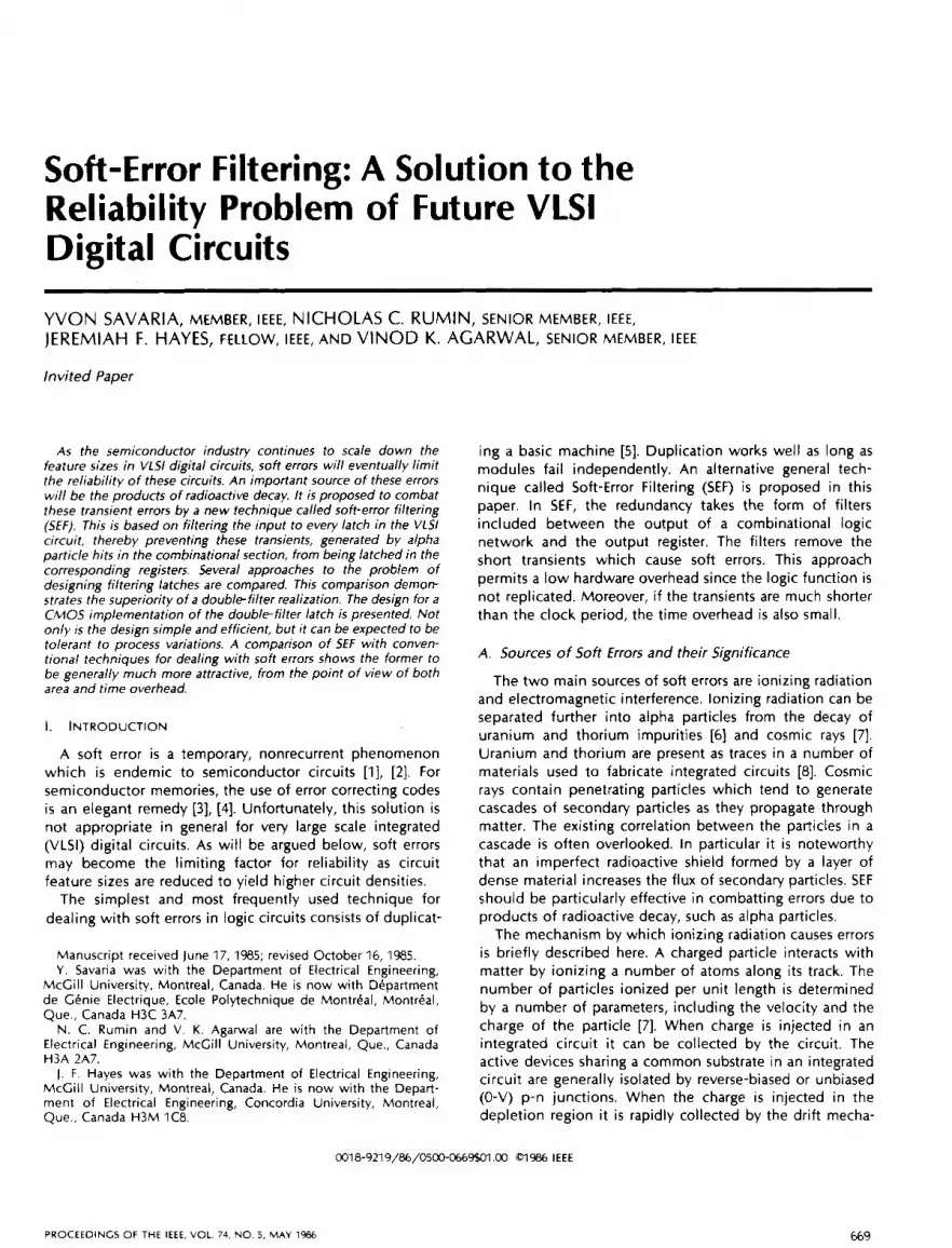
Fig. 5 shows some results of a simulated experiment with the slow latch, in which a 0 signal on its input is corrupted by a transient 1 having a duration of 27 ns. In Fig. 5(a) the clock pulsewidth is 91 ns. The figure shows the voltage on node 7 falling after the clock input is returned to zero and, indeed, a longer simulation confirms that node 7 settles to a 0 state. Hence, the slow latch recovers properly the input signal with a clock pulse of 9l ns. In Fig. 5(b), the clock pulse is only 2 ns shorter, but node 7 eventually reaches 5 V. Therefore the data are not recovered successfully with a clock pulse of 89 ns.
The filters in this paper are designed and compared using a performance measure called the security margin 5. This was defined in Section 11-6 through the relationship T,, =
SO. In view of the relaxed definition of T,, introduced in Section 11-A, 5 represents the factor by which T,, must exceed D for a corrupting pulse of width D not to cause the latch to malfunction. Since the latch failed with a clock pulse duration of less than 9 l ns, therefore, for the condi- tions depicted in Fig. 5, 5 = 9 /27 = 3.37.
A small value of S is associated with a more efficient filtering latch. However, it should be clear from Fig. 5 that if
SAVARIA ef d l . SOFT-ERROR FILTERING 673
- . 1 9 1 ’ ! ! ! ! ! ! ! . : ! ! ! ! ! ! : : : ! I 0.W 0.12 0.24 0.36 0.48 0.60 0.72 0.84 0.96 1.08 1-20
TIE (XloCxP -7 SEamS)
. . \c I \ ;
I \ I
-,19 . . . . . . . . . . . . . . . . . . . . . 0.00 0.12 0.24 0.36 0,48 0.60 0.n 0 . 8 4 0.96 1.08 1 . X
I I -.19 . . . . . . . . . . . . . . . . . . . . .
0.00 0.12 0.24 0.36 0.48 0.50 0.72 0.84 0.96 1.08 1-20 TIE (xlkxp -7 SEm)
4.14
3.06
0.00 0.12 0.24 0.36 0.48 0.60 0.72 0.84 0.96 1.08 1 . X TIE (xlocxp -7 SEamS)
L E v n SDSITIVE SLW D LATCH. 27, 83
(b) Fig. 5 . (a) Response of a slow latch (Fig. qb)) to a transient pulse of 27 ns for a clock signal lasting 91 ns. The input signal is a 0 corrupted by 1. The latch eventually recovers to the right output value. (b) Same as (a) with a clock pulse of 89 ns. The latch does not recover.
the corrupting transient had occurred earlier with respect to the clock’s falling edge, a value of 5 less than 3.37 would have been obtained. This is indeed what simulation shows.
Finding the worst time of occurrence for a pulse of constant width D is an expensive iterative process. The conditions shown in Fig. 5 in fact are not far from the worst case.
The security margin does not reflect one important prop- erty of a particular filtering latch design, namely, the time it takes the output to recover to a valid state. Thus the slow latch used to obtain the data in Fig. 5 has a worst case of 5 = 3.4, which is better than some alternative designs will be seen to be capable of yielding. However, note in Fig. 5(a), for example, that the output voltage on node 7 is still far from a valid 0, 120 ns after the rising edge of the clock pulse, a time which is more than four times the duration D of the disturbing transient.
This slow recovery of the latch in Fig. 4(b) illustrates one of i t s main weakness, namely, the direct dependence of the recovery time on the time constant of the latch. In other words, by making the latch slower not only are longer transient filtered, but the time necessary for restoring a valid level after the clock pulse is finished is also increased. This will be overcome with the double-filter implementa- tion proposed in Section Ill-C, which also yields lower values of 5.
B. Single- Filter Latch
Instead of simply slowing down the latch, the approach followed here is to place a filter at its input. Intuitively it is clear that the filter will be a source of overhead. If a single-filter latch can approach the optimum performance, in theory there should not be much room left for improve- ment unless the latch becomes significantly bigger. There- fore, this approach was explored.
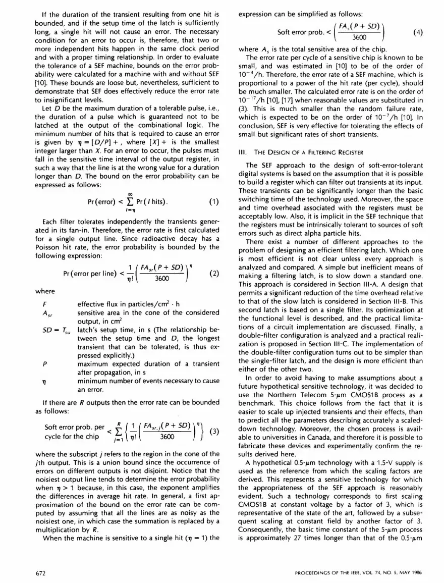
A model of a latch is needed to demonstrate the feasibil- ity of designing filtering registers. One which includes only logic elements such as gates and switches is not sufficient for this purpose. Fig. 6 shows a functional model of a latch which retains the necessary and sufficient features for a
WANTIZER
Fig. 6. Functional model of a latch.
functional optimization. The low-pass filter accounts for the property which determines the shortest event that can be latched. Another property which a latch possesses is logic level restoration, which is accounted for in the model by the quantizer. The memory element is, of course, the essential part of the latch. Because the registers are as- sumed to be immune to effects which cause soft errors, the memory cannot be based on charge storage as in a dynamic MOS register, and is implemented with a bistable latch.
If the only nonideal component in the latch is the filter, then the problem simplifies to optimizing it. Since the filter receives its input signal from a logic gate, it can be assumed that all signals and transients have an amplitude equal to the supply voltage which is normalized to 1. Consequently, there will be only two situations to analyze: a valid 1 disturbed by a transient 0, or a valid 0 disturbed by a 1 , as shown in Fig. 7. The origin of time has been taken, without loss of generality, as the moment when the data are known to be valid.
A lower bound on 5 can be estimated using the follow-
674 PROCEEDINGS O F THE IEEE, VOL. 74, NO. 5. M A Y 1986

CK I ---L - - L 0 _ _ A 0 --A t
IN 1 --'-H ' -- \ F"i 0 - - J
0 0 - -o SD
(a) (b) Fig. 7. Signals disturbed by transient pulses during the sen- sitive time of a latch. (a) A valid 1 disturbed by 0. (b) A valid 0 disturbed by 1.
ing simple argument. Assume that the probability of a 1 or a 0 occurring at the filter input is the same. Furthermore, assume that the distributions of expected transients of either polarity are equivalent and symmetrical. In such a case, if a signal has one polarity during more than half of some time interval, then the probability of making an error is minimized by choosing that polarity as the probable signal. In other words S must be greater than 2.
A bias in the distribution of transient polarities will, in fact, exist at the generation point. Nevertheless, the as- sumption of symmetrical distribution of the disturbing tran- sients is justified by the fact that, for a large machine, there is no a priori bias for an odd or even number of inversions from the generation point to the filter input.
A filter which has a potentially good performance is the ideal integrator. Assuming that the output of the integrator is reset to 0 at t = 0, the signals shown in Fig. 7 will be recovered properly if the following three conditions, dis- cussed below, are satisfied:
K D ( S - I ) Q I ( 5 )
KD( S - 1) > Th (6)
KD < Th ( 7)
where K is the gain of the integrator, D i s the previously defined maximum duration of a transient that the latch is designed to filter, and Th is the quantizer threshold.
Expression (5) ensures that the output remains within the range of the supply voltage when the signal is corrupted and, therefore, that clipping does not occur. Clipping is allowed to occur if the input signal is not corrupted, in which case the input signal is declared to be 1. Inequalities (6) and (7) correspond to the requirements for recovering valid data in the two possible situations depicted in Fig. 7(a) and (b), respectively. The solution of (6) and (7) yields S > 2 in agreement with the preceding argument.
It is convenient to compare filters in the present context on the basis of their discrimation, defined as the difference between the output values corresponding to the two con- ditions in Fig. 7, evaluated at the sampling time SD. This quantity is an important figure of merit because, in a practical implementation, the quantizer cannot be assumed to be perfect and, therefore, the larger the discrimination, the easier it i s to design a quantizer for signal recovery.
For the integrator, the discrimination is given by the difference between the left-hand sides of (6) and (9, i.e., KD(S - 2). Hence the maximum discrimination A,, which, from (5), corresponds to KD(S - 1) = 1, is given by
s - 2 A1 =-
s - 1
Even though the integrator achieves the lower bound on 5, as will be seen below, nevertheless it appears to be an
impractical solution from the point of view of both speed and chip-area overhead.
A logical alternative is the simple RC filter. Fig. 8 shows the response of this filter in the two situations depicted in Fig. 7, assuming that the initial voltage on the capacitor corresponds to the complement of the valid signal. It is important to note that the results obtained above for the
(a) (b) Fig. 8. Response of the RC filter to the input signal shown in Fig. 7, assuming an initial charge which i s the complement of the valid signal.
integrator are independent of where the corrupting tran- sient occurs in the time interval SD. On the other hand, the situation depicted in Fig. 7, namely, corruption of data just before sampling, is the worst case for the RC filter because of its exponential response.
Because of the symmetry of the two responses in Fig. 8, it follows that Th = 0.5 is the optimum. Also, because of the symmetry, it suffices to analyze only one case.
In the situation where a valid 1 is corrupted by a 0 transient (Fig. 8(a)), proper data recovery requires that
(I - e-(S-l)D/(RO)e-D/(RO > 112, ( 9) For a given ratio of D/RC, the maximum output occurs when
D InS -=- RC . S - I ' (1 0)
Substitution of (IO) into (9) yields a lower bound on S
s-1/(S-V - s - S A S - 1 ) > 1/2 (11)
which has a numerical solution 5 > 4.4035. The limiting case S = 4.4035 yields D/RC = 0.4355.
The maximum discrimination for the RC filter A, is easily shown to be given by
A - 2) rl/(S-l) - s-s/(s-1) - 1 2 - 2 ) . (1 2)
Fig. 9, which compares the dependance of A, and A? on 5, clearly illustrates the superiority of the integrator. Note that each point of the maximum discrimination curve represents the best performance of an RC filter with a different time constant. This comment also applies to the other curves derived later for RC filters. Therefore, an RC filter is opti- mum for only a single value of S, and the discrimination for this particular filter is smaller than the value given by (12) for all other values of 5.
The two principal reasons for the relatively poor dis- crimination of the RC filter are the exponential nature of the response and the absence of an initialization of the output voltage. Whereas the former is an intrinsic property of the circuit and can only be compensated for by the use of nonlinear elements, the latter can be corrected quite simply.
Fig. 10 shows the simplified circuit of an RC filter with
SAVARIA e t a / . SOFT-ERROR FILTERING 675

0.80
0.70
0.60
0.50 c 0 - 1 0.40 I :: 5 0.30
0.20
0.10
0.00, d
,/" A I /
- 7
, 2.b 3.00 3.50 4.00 4.50 5.W 5.50
S Fig. 9. Plots of the computed maximum discrimination as a function of S for the integrator A,, the pure RC filter A 2 , and the RC filter with precharge A 3 .
I N
7 Fig. 10. RC filter with precharge.
precharge. Simple intuitive reasoning shows that the capaci- tor should be initialized to a normalized voltage of Th = 0.5. An analysis which is completely analogous to that for the simple RC filter leads to the results that, for a given D/RC, the discrimination is maximized when
operated in the triode mode, which helps to minimize the degradation in discrimination associated with an exponen- tial response.
A transistor implementation of the single-filter latch has been obtained, using a conventional sense amplifier of a dynamic RAM as a basis [IO]. However, it suffers from a number of practical limitations. A very important one is the sensitivity of the performance to process fluctuations. In particular, achieving a good performance with the single- filter implementation requires an accurate match of the conductances of the p and n devices. The ratio of these conductances is precisely a characteristic which is not well controlled. This problem is complicated further by the fact that the absolute value of the load capacitance which determines the time constant cannot be accurately con- trolled. A second disadvantage of the single-filter realiza- tion is the complicated clocking scheme. Moreover, since precharging is used, there are significant time intervals where the output of the latch is not a valid logic level, which makes these latches difficult to use in a design.
In conclusion, even though the functional realization proposed in this section approaches the theoretical opti- mum performance, its transistor implementation has a num- ber of practical limitations. The double-filter realization overcomes most of these limitations and, despite what the simple intuitive argument in the preamble of this section suggests, this solution does not come at the cost of a larger area.
D l
RC 5 - 1 - = - In( :)
and the lower bound on 5 is given by
The solution of (14) is S = 2 which means that this filter has the same lower bound on performance as the integra- tor. Not surprisingly, (13) shows that, to achieve this perfor- mance, the condition RC* D must be satisfied, i.e., the filter should behave like an integrator.
Fig. 9 shows a comparison of the discrimination of the preceding three filters, where that of the RC filter with precharge is given by
5 -l /(S-l) -S/(S-l)
A 3 = Z ( i ) - ( 7 ) - I . ( 1 5 )
Clearly, the use of the precharge with the RC filter leads to a very significant improvement in performance.
Therefore, the RC filter with precharge is the best choice for a single-filter implementation, taking into account both circuit complexity and performance. In a monolithic IC design, the resistor is synthesized using transistors, and in the MOS technology in particular, it is replaced by a FET
C. Double- Filter Latch
Functional Design: A different realization for a latch capable of filtering long transients is considered here. The structure of this latch is shown in Fig. 11. It is demonstrated
- Fig. 11. Filtering latch with a double-integrator structure
later that this filter has the same lower bound for S as the one based on a single integrator. The first advantage of the present configuration over the simple integrator, as demon- strated below, is the larger discrimination for all values ofS.
If SD is the setup time of the double-filter latch in Fig. 11, then a corrupting transient pulse of duration D, occur- ring as shown in Fig. 7(a), results in an input to the quan- tizer which, at the sampling time, is given by
a = K ( S - l ) D - K D = K ( 5 - 2 ) D . (16)
Therefore, i f 5 > 2, the signal can be recovered if the threshold of the quantizer is 0. Notice that the problem is completely symmetric with respect to the polarity of the signal and, therefore, only one polarity needs to be analyzed. Furthermore, there is no difficulty with having a negative value of a, since it represents the difference between the output signals of the two integrators. Limiting the output of the integrators to within the supply range yields
676 PROCEEDINGS OF THE I E E E , VOL. 74, NO. 5 , M A Y 1986

K ( S - I ) D < l (1 7)
K O < 1. (1 8)
If 5 > 2, only (17) needs to be considered. Therefore, the maximum value of K is I / ( (S - 1)0), which yields the maximum discrimination A, for this configuration
s - 2
5 - 1 A 4 = 2--. (1 9)
The factor of two follows from the fact that the input signal with the opposite polarity yields a negative signal of the same amplitude. Comparing (19) with (8) shows that the double-filter realization yields a discrimination that is twice as large as that of the single-filter realization.
Fig. 12 shows, in a simplified form, a more practical realization of the filtering section. In a MOS IC the resistors
CK R crc p L " '
VCL R - IN - "2
Fig. 12. A realization of the integrator section of Fig. 11 based on switched RC networks.
will, in fact, be realized with transistors. Now a MOS transistor in its saturation region can be used to emulate quite accurately the behavior of an integrator, while in its triode region its behavior resembles more that of an RC network. Therefore, the performance possible with the cir- cuit in Fig. 12 can be thought of as a lower bound on the discrimination. It is not a bound in the sense that all implementations are better than the one based on an RC filter, but in the sense that a good one should perform at least as well as the best RC realization.
The circuit in Fig. 12 is nonlinear due to the presence of switches. Both capacitors are first discharged by the CI switches, after which they are left open. For the total duration of the setup time, the switches CK are closed. The input signal controls the remaining switch. If the input value is low, the supply is connected to the upper filter, and the reverse is true if the signal is high. The branch which is not connected to the supply is left floating. When the input signal is a 1 corrupted by 0 (Fig. 7(a)), the final values of V, and V, are
v, = 1 - e - o / R C
v, = 1 - e - ( S - l ) D / R C
( 20)
(21)
The useful signal is the difference between these two quantities, which is given by
v2 - v, = e - D / R C - e - ( S - l ) o / R C , (22)
The important design parameter is the ratio U = D/RC. If U i s too small, the deflection and the output signal are small. If the ratio i s too large, both V, and 4 given by (20)
and (21) are far into the exponential response and their difference, which composes the output signal, is also small. This shows the existence of an optimum for U. The proce- dure for determining it is very similar to the one followed in Section Il-B.
Assuming that S is fixed, and taking the derivative of (22) with respect to U, yields, after elementary manipulations
This equation has no explicit solution but can easily be solved using Newton's algorithm, yielding the optimum U for a given S. The maximum discrimination A 5 of the realization based on the switched RC filter is obtained by multiplying the result calculated from (22) by 2, where U is replaced by its optimum value for a given 5. Again the factor of 2 follows from the fact that the input signal with the opposite polarity yields exactly the same amplitude, but with the opposite sign.
The result of this calculation has been plotted in Fig. 13, together with the discriminations of all the other configura-
1 .a0 c 0 - - e 0.80
:: B 0.60
0.40
0.20
0.00 2.00 2.50 3.00 3.50 4.00 4.50 5.00 5.50 6.
S Fig. 13. Plots of the computed maximum discrimination as a function of the security margin S for the single integrator A , , the single RC filter A I , the RC filter with precharge (Fig. IO) A 3 , the double integrator (Fig. 11) A , , and the double switched-RC filter (Fig. 12) A s ,
0
tions. Note the rapid increase of A 5 near S = 2 which is to be compared with A 3 for the single RC filter with pre- charge. It means that the performance of the double-filter realization is much less sensitive to the exponential re- sponse of the RC filter and, therefore, the performance of the transistor realization should suffer much less from oper- ation in the triode region, yielding a larger discrimination.
Implementation of the Double-Filter Latch: Interest in the double-filter realization is further increased by the fact that it can be implemented very efficiently. Consider again the conventional level-sensitive D latch shown in Fig. 14(a), and the same circuit with two capacitors on the 5 and E lines, as shown in Fig. 14(b). With CK = 0, both capacitors are precharged to the supply voltage. With CK = 1, either
SAVARIA et af . SOFT-ERROR FILTERING 677
CK
- S
IN
rs
Fig. 14. Evolution of the double-filter latch. (a) A standard level-sensitive D latch. (b) The set and reset lines are used as filters. (c) The input NAND gates are converted to dynamic inverters.
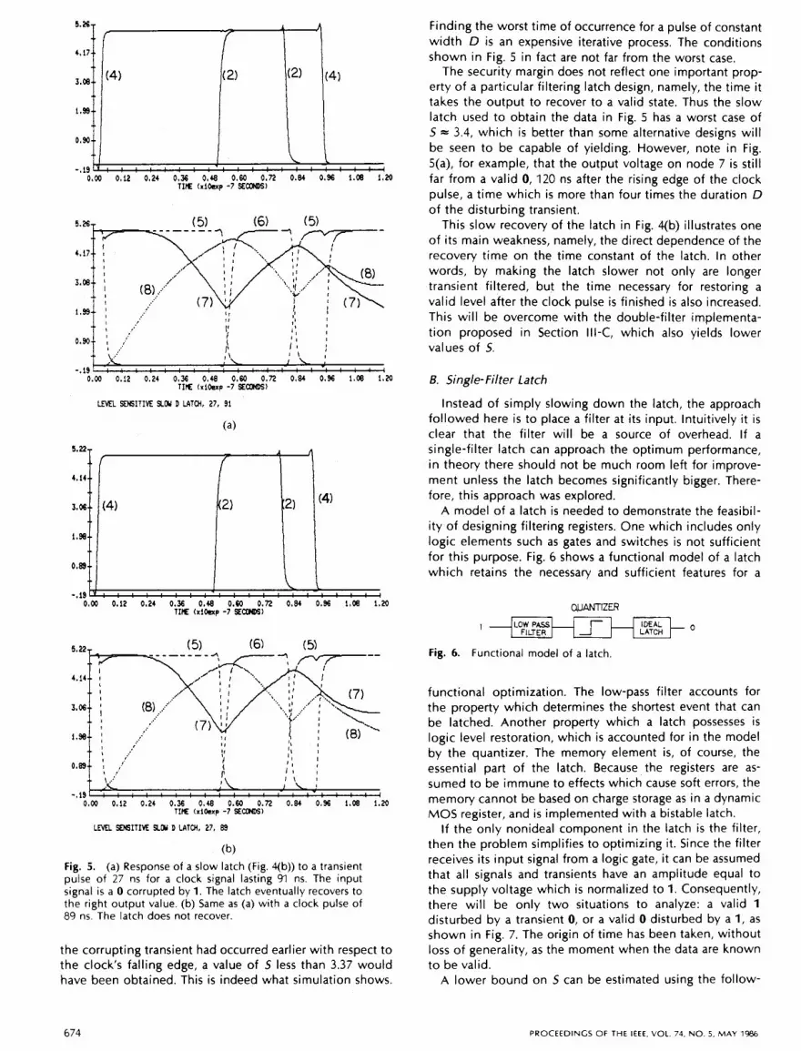
the 5 or ii line is ramped to a low value depending on IN. When a transient pulse corrupts the input, the wrong line ( i i for 1 corrupted by 0) starts to ramp exactly like the idealized network in Fig. 12, while the "good" line ramps back toward i ts precharged value. It is easy to show that this circuit cannot do better than S = 3. Removing the second p transistor in the input NAND gates, as in Fig. 14(c), neutralizes the ramping back during the pulse, leaving the "good" line in a floating state. It is easy to see that, except for a polarity inversion, this circuit is functionally equivalent to that of Fig. 12.
Fig. 15 shows the complete double-filter latch design. Two variations have been simulated: in the first, the chan- nel length of transistors 2, 3, 5 , and 6 was equal to 5-pm, while in the second it was 6-pm. The best design is the one
r
Fig. IS. Circuit of a practical CMOS double-filter latch. Transistor dimensions (length, width) in micrometers. 1 = 4
(5,60), 3 = 15 = 16 = 18 = (5,30), 2 = 3 = 5 = 6 = (5,s) for 5-pm version and (6,s) for 6-pm version.
= (5,s). 7 = 8 = 9 = 10 = (30,30), 11 = 12 = 14 = 17 =
I f -.XJotv:-: ! ! ! ! ! ! : ! ! ! ! ! ! ! ! ! ! I
L L
0.00 0.75 1.50 2.25 3.00 3.75 4 . 5 0 5.25 6.00 6.75 7.50 TIE (XlRxp -8 SECDOS)
*..f +
-.a ! ! ! ! ! ! ! ! ! ! ! ! ! ! ! ! ! ! ! ~ 0.00 0.m 1.50 2.23 3.00 3.75 4.50 5.23 6.00 6.75 7.50
TIE h l h p -E SEW)
L M L SEHSITIK D LAW WU). 27, 56
(a)
5.25,
4-16..
5-07..
I.!+
0.89 I 1 I I -.is
0.00 0.75 1,50 2.25 3.00 3.75 4.50 5.25 6.00 6.75 7.50
LEyn SDbITIVE D LATCH (XI) . 27, 55
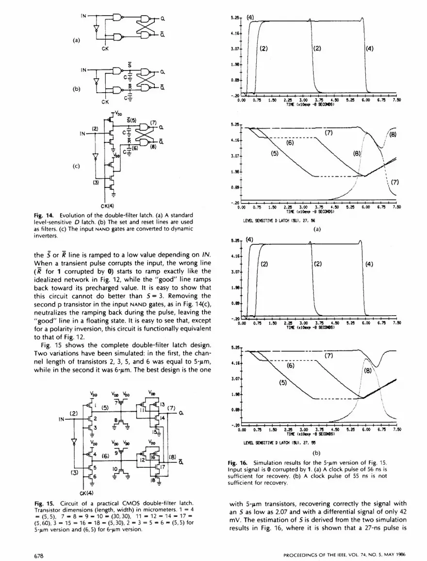
(b) Fig. 16. Simulation results for the 5-pm version of Fig. 15. Input signal is 0 corrupted by 1. (a) A clock pulse of 56 ns is sufficient for recovery. (b) A clock pulse of 55 ns is not sufficient for recovery.
with 5-pm transistors, recovering correctly the signal with an S as low as 2.07 and with a differential signal of only 42 mV. The estimation of S is derived from the two simulation results in Fig. 16, where it is shown that a 27-ns pulse is
678 PROCEEDINGS OF THE IEEE, VOL. 74, NO, 5, M A Y 1986

recovered with a clock pulse of 56 ns, whereas it is not recovered with a clock pulse of 55 ns. The input signal is a 0 corrupted by 1. Notice that only one polarity needs to be simulated since the response to a “set” is completely sym- metric to that of a “reset”; in other words, the definitions of “set“ and “reset” can be exchanged if the output defini- tions are interchanged.
The simulation results are summarized in Table 1. The circuit has been simulated in three slightly different config-
Table 1 Simulation Results for the Double-Filter Latch in Fig. 15
Delays* CK Output Normalized t o 1 t o o (ns) 5 (VI Discrim. (ns) (ns) (5 pm, not loaded) 55 2.04 - 0.044 - 0.01 76 56 2.07 0.042 0.01 68 0 9.2 57 2.11 0.1 28 0.051 2 0 8.7 57.5 2.1 3 0.1 72 0.06% 0 8.4 58 2.1 5 0.193 0.0772 0 8.3
(6 pm, not loaded) 58 2.1 5 0.260 0.104 59 2.1 9 0.328 0.1 31 60 2.22 0.387 0.1 55 0 4.2
(6 pm, loaded) 62 2.30 0.574 0.230 63 2.33 0.640 0.256 64 2.37 0.707 0.283 1.2 14.4 65 2.41 0.767 0.307 0.2 11.4
‘The thresholds for a valid 1 and 0 are taken to be, respectively. 2.85 and 1.35 V. These values are the input voltages corresponding to the
characteristlcs of CMOS NOR and NAND gates built with minimum size minimum and maximum unit-slope points, on the voltage transfer
transistors.
urations. For each configuration, the duration of the cor- rupting pulse on the input was kept constant, and the duration of the clock pulse was varied. The discrimination and the delays to valid levels after the trailing edge of the clock pulse are listed in the table. Table 1 also includes the performance of a loaded version of the circuit in Fig. 15. The load is a capacitor on each output, equal to those on the s and lines. Since the loaded version is slower, it requires a larger discrimination in order to recover the signal.
A comparison of the results listed in Table 1 with the theoretical results derived earlier is shown in Fig. 17. For large enough 5, the discrimination obtained falls between that of the integrator version (fig. 11) and the RC-filter circuit (Fig. 12) with the best performance. Note in Table 1 that for 5 = 2.15, the 6-pm version has a discrimination of 0.104, whereas the 5-pm version has only 0.077. Therefore, the 6-pm version yields a better discrimination. However, it requires 5 = 2.22, whereas 5 = 2.07 is sufficient for the 5-pm version, which means that the latter is more efficient.
The reason for the smaller discrimination of the 5-pm version comes from the fact that the deflection is larger, and the transistors 2, 3, 5, and 6 operate more in the triode region. Consequently, the exponential response begins to play a significant role. However, what makes the 5-pm version better is the characteristic of the quantizer. For the given choice of transistor dimensions, the threshold of the latch is such that the gain is higher for the 5-pm version.
SAVARIA el a/ . SOFT-ERROR FILTERING
,’ A 4 0.60 /’
0.40 1 0.20 1 /
0.00
,/’
-0.20 2.00 2.10 2.20 2.30 2.40 2.50 2.60 2.70 2.80 2.90 3.
S 0 5 microns X 6 microns +loodwd 6 microns
Fig. 17. Comparison of simulation results for the circuit in Fig. 15 with theoretical variation of discrimination with 5 for the circuits i n Figs. 11 and 12 ( A 4 and A s ) , respectively.
1 0 0
This means that the design could be refined further by shifting the threshold of the latch to a higher value. This was not done for two reasons: first, the point of diminishing return on investment has clearly been reached, and sec- ondly the effect of process fluctuations would be ne- glected. The observed difference is equivalent to the effect of a 20-percent difference in the time constant of the filters, which is typical of what should be expected in a real integrated circuit.
The 6-pm version is more conservative since a real imple- mentation is likely to use 5 = 2.3 in order to tolerate process fluctuations. The slower version can always be used successfully by lengthening the clock pulse, but the faster version can reach the point where the gain of the quantizer falls back again, in which case making the clock pulse longer will not help.
Notice that, unlike the idealized RCrealization in Fig. 12, the implementation in Fig. 1qc) has not two, but a single clock signal. Consequently, the precharging of the filters begins immediately at the end of the filtering period, when the signal is ready. The fact that a single clock is sufficient is an important advantage of the double-filter configuration.
If the common-mode bias on the signal puts the circuit in a low-gain region, the quantizer loses its efficiency. For these reasons, the common-mode signal on the outputs of the filter must not change too rapidly. Making the ramping back slow also buys tolerance to a transient on the clock line itself, at the expense of a dead time between the successive clock pulses. The reset slope was chosen nomi- nally equal to the filter slope.
The slow latch described in Section Ill-A would be very inefficient i f it were loaded in the manner described above for the double-filter design. Both the recovery time and 5 would increase substantially. The essential weakness of the slow latch vis a vis the double-filter one is that, in the former, the load capacitance also determines the time con- stant of the latch and its immunity to direct hits. In contrast, the capacitors at the filter outputs in the latter design set the time constant, while the sizes of the latch transistors are
679

chosen to harden the latch to direct hits and to handle larger capacitive loads.
In conclusion, the double-filter realization has the best performance, and since its performance does not depend on the relative conductance of different types of transistors, it is more robust than the single-filter design with respect to process fluctuations. Moreover, it requires a single clock pulse, and the output is not kept at invalid logic levels for long periods. Finally, it is not bigger than the single-filter version, because smaller capacitors can be used for harden- ing the latch to a direct hit. This is made possible by the relatively large signal swing at the output of the filters in the double-filter version.
IV. OVERHEAD ANALYSIS
Obtaining an accurate overhead estimation for a design methodology such as SEF requires a detailed design of a number of integrated circuits. Furthermore, even when a detailed implementation is available, determining what is overhead is not always easy. However, SEF can be regarded as a design style, which means that the sources of overhead can be identified at an early stage of the design process, and the details of implementation can be modified to decrease the overhead significantly.
The analysis to be presented in Section IV-A demon- strates that SEF is feasible in terms of overhead. Section IV-B demonstrates that SEF generally implies much less overhead than other techniques for tolerating transient errors. Finally, a number of practical considerations are presented in Sec- tion IV-C.
A. Overhead with SEF
The twc main aspects of the overhead analysis are: area overhead and time overhead. Area overhead is obtained'by comparing the area occupied by the redundant circuit with that occupied by an equivalent nonredundant one. Simi- larly, the time overhead reflects the increase of the clock period due to the longer setup time of the filtering latches.
Area Overhead: In an integrated circuit context, it is more realistic to measure overhead in area than in transistor count or gate count. By definition, the area overhead for SEF i s given by
A1 - A2 0, = - A ( 24)
where A, is the area occupied by the standard registers, A, is the area occupied by the filtering registers, and A i s the total area of the machine with standard registers. Notice that even though a filtering register requires no more global interconnection than a standard register, because the SEF registers are larger, the SEF machine is larger and, therefore, longer interconnections are required. Since there are no simple means of estimating the impact of a larger intercon- nection area on the size of the machine, except by a detailed design of two versions of a machine, (24) will be used in the following estimate of the area overhead.
In the following, a refinement of (24) i s obtained. The derivation, just like the hardware overhead estimation for Level-Sensitive Scan Design [18], assumes that a function is implemented as a network of gates. The new expression is a function of the following four, parameters:
Q
K
C
R
Ratio of the area occupied by one bit of the filtering register to that of a 2 input gate. Ratio of the number of gates needed to realize the combinational logic part of a machine to the number of standard register bits needed. Fraction of the area reserved for communication of data. It includes the area reserved for global routing plus that reserved for input-output pads. Ratio of the area for 1 bit of a SEF register to that of 1 bit of standard register.
Based on these definitions, the area of the non-SEF ma- chine A, measured in equivalent gates, and normalized to l bit of memory, is given by
Q K S -
A=- R 1 - C '
The difference between the area of 1 bit of filtering register and that of 1 bit of a standard register is the overhead. This quantity is expressed in equivalent gates as follows:
Q overhead = Q - -.
R ( 26)
Dividing (26) by (25) gives the area overhead 0, I 1 ,
(1 - C) Q(1 - - R ' 1
0, = n K + -
R Y
Equation (27) becomes interesting if upper and lower bounds on each of the parameters are known. The com- plexity of the filtering latch shown in Fig. 15 is at least 4 equivalent gates, and it should be possible to realize a layout smaller than the area of 8 gates, therefore 4 < Q < 8. From DasGupta [I81 the number of gates in the combina- tional logic per memory bit is usually in the interval 5 < K < 25. It is well known that the fraction of a chip reserved for communication can be more than 50 percent, but it can also be as low as 20 percent for regular structures, therefore 0.2 C < 0.5. Finally, considering Fig. 15 again, the area occupied by a filtering latch should be between twice the size of a standard level-sensitive D flip-flop, and some- where around 5 times the complexity of a C'MOS latch, consequently 2 < R < 5.
Using these upper and lower bounds for Q, K , C, and R , in ( 2 3 , yields upper and lower bounds for the area over- head. A typical value can also be calculated by using the medians of these bounds in (27). The results of these calculations are a typical value of 17 percent and an interval of 3.7 percent < 0, < 78 percent.
The interval for the area overhead is wide and obviously depends on the type of function being implemented. Obvi- ously, when a machine has relatively few memory elements, the area overhead is small. On the other hand, for memory intensive machines such as RlSC [19], the area overhead with a straight application of SEF may fall outside the interval calculated earlier.
Time Overhead: Errors can be tolerated by conventional methods which trade area overhead for execution time [12]. The same tradeoff between time and area overhead exists
680 P R O C E E D I N G S OF THE IEEE, VOL. 74. N O . 5, MAY 1986

with SEF, as discussed in the following. However, SEF can be implemented with low overhead in area and time simultaneously. The time overhead is defined to be the ratio between the difference of the clock periods of a SEF and a standard machine, divided by the clock period of the latter. Since the setup time of the registers is the only parameter that differentiates the SEF and the standard ma- chines, the time overhead 0, is given by
The setup time of the SEF machine is $0, and the setup time of the non-SEF machine is S,S, where 6 is the longest transient event that a standard latch will not memorize. It is clear from Section Ill that S, and S, are not equal in general, since the value of S depends on the structure of the latch. Also, D must be greater than P, the longest expected transient.
Equation (28) expresses the necessary condition for SEF to yield a low time overhead. Since D, the duration of the longest expected transient that the latch can tolerate, must be longer than P, the longest expected transient, P must be small by comparison to the clock period of the machine. For example, if the longest expected transient is 5 ns, and a filtering latch is used with S slightly larger than 2, if the standard machine has a 50-ns clock period, then the time overhead is approximately 20 percent.
The time overhead of a SEF machine could be within a fairly wide range. A time overhead of a few percent is possible if the clock period T is greater than 100 ns, and P is on the order of 1 ns. At the other extreme, a transient at the output of the logic could become longer than the clock period, if the injected transient is long, or if pulse spreading is important [IO]. Using SEF for combatting such a long transient results in more than 200-percent time overhead.
This discussion demonstrates that the time overhead can be small, but it is highly dependent on the machine to be hardened, and on the transient source to be combatted. Moreover, as will be discussed later, the general SEF theory can be “customized” to reduce the time overhead when it is too high.
6. Comparison with Alternatives
As mentioned in Section I, a number of alternative solu- tions to SEF are possible, including duplicated and trip- licated machines. Reference [IO] contains a discussion of how conventional fault-tolerance techniques can be spe- cialized for soft errors. These alternatives permit one to build a machine tolerant to independent transients injected at an exponential interval. The error rates are not exactly the same in each case, but the differences are not significant considering the failure rate. However, it is noteworthy that i f bursts of transients are expected, the conventional fault- tolerance techniques can be improved a great deal i f they are designed for this effect [IO].
A natural means of implementing a loosely coupled TMR machine is to use three off-the-shelf modules in parallel, and vote only on the final results. it implies a 200-percent area overhead for the two redundant machines, and on the basis of the gate count alone the voter appears to contrib- ute a small overhead.
The reason why the overhead in the voter appears small is because only final outputs are compared. For example, a IOOOO gate system may have 40 output lines. A voter can be implemented with an equivalent complexity of 4.5 gates. (The carry line of a I -b i t full adder is a voter, and the carry can be generated with 18 transistors, with 4 transistors counted as 1 equivalent gate.) If only the overhead contrib- uted by the gates is counted, voting on 40 lines requires a 2-percent overhead.
However, the real overhead in merging 3 times 40 out- puts to obtain the final result is not due to the gates themselves. Three input pads and one output pad are required for each bit of the voter. On a 5-pm technology one pad occupies an area larger than 10 gates. Moreover, when the technology is scaled down, the discrepancy be- tween the size of a pad and that of a gate grows as the square of the scaling factor. Therefore, the communication cost of voting is at least 10 times that of the gates which perform the voting operation.
Another practical consideration that is too easily over- looked is the fact that, for a chip with a low gate-to-pin ratio, such as a voter chip, the package is usually more expensive than the silicon die. Therefore, voting may end up accounting for 50 percent or more of the cost of the original nonredundant chip, which is higher than the typi- cal area overhead contributed by SEF. On the other hand, one good point in favor of loosely coupled TMR is the nominally zero time overhead, which follows from the fact that voting is not in the feedback path.
Estimating the overhead for tightly coupled machines becomes more difficult. Ignoring the communication costs, tightly coupled DMR and TMR require at least 100- and 200-percent overhead, respectively. However, it was clearly demonstrated earlier that in an integrated realization of a fault-tolerant machine, the communication cost of compar- ing and voting is not negligible. If the number of lines to be compared is small for loosely coupled TMR, it is no longer true for tightly coupled machines. Therefore, the overhead of tightly coupled machines could become much higher than it seems.
It i s of interest that when K , the number of gates per bit, decreases, the relative importance of the overhead intro- duced for comparing and voting grows for tightly coupled machines. Therefore, when the area overhead of SEF is high, comparators and voters also contribute a high overhead in tightly coupled machines.
The time overhead of a tightly coupled machine is not zero. A sufficient time for comparing and voting must be allocated, since it takes place on the feedback lines of the machine. Moreover, when the machine has to be imple- mented on more than one chip, the communication delays contribute further to the time overhead. Nevertheless, in contrast with SEF, this time overhead is not a function of the expected transient duration.
In conclusion, the area overhead for SEF is comparable or smaller than the communication costs of system alterna- tives. Therefore, not duplicating or tripling the logic func- tion is a straight advantage for SEF. However, the system solutions are generally better than SEF if the machine has to tolerate long transients. But if the transients are short, SEF has a comparable or smaller time overhead. Therefore, considering simu!taneously the time and area overheads,
SAVARIA eta / . : SOFT-ERROR FILTERING 681

SEF is the best approach for building a machine tolerant to short transients.
C. Practical Considerations
SEF as presented earlier is a general approach that may be refined when adaped to a particular situation. The context may easily change the order of significance of area and time overhead. This can be true even for different sections of the same machine. Thus the time overhead is not important for an output which is not on the critical propagation path, The importance of this observation can be amplified further by the fact that pulse spreading can be very different from one output line to the other. Therefore, a technique for ex- changing time overhead for area overhead could be useful. A n application of such a technique on the critical propa- gation paths would permit the reduction of the time over- head of a machine, by increasing the area overhead in selected regions.
Conventional techniques exist for transforming a critical propagation path into a noncritical one; for example, buffer- ing may be provided on the slow nodes, or pipelining may be introduced in order to allow more than one clock cycle for data propagation along the critical path. In addition to the standard techniques, delay equalization is a technique that permits one to exchange time overhead for area over- head. It was demonstrated in an earlier paper [20] that, for a technology with equal rise and fall times, an arbitrary logic function can always be redesigned with the same worst case propagation delay, but nominally with no pulse spreading. In contrast with conventional techniques, this is achieved by adding delays on the faster propagation paths in such a way that all path delays are equalized.
An aspect of SEF which requires special attention is the duration of transients generated by interference. These tran- sients can be so long that SEF becomes impractical in terms of time overhead. However, if SEF is used to complement standard electromagnetic shielding, it will handle efficiently the remaining short transients that may exist due to imper- fections of the shield, or that may be generated inside the shield. Therefore, in general, SEF should be supported with appropriate shielding.
Another important practical consideration related to SEF is the fact that transients injected by interference from outside the chip are usually much longer than those in- jected by ionizing radiation inside the chip. Therefore, the setup time of SEF latches should reflect this in order to minimize the time overhead. The fact that relatively long delays are required for off-chip connections is usually rec- ognized in VLSl systems, where a single bit can pass through a pin at each clock cycle. That cycle could be separated into a number of internal microcycles. For example, the clock period could be 50 ns, with a setup time of 10 ns for latches that include in their fanin a connection from outside the chip. The same machine could have an internal microcycle of 10 ns with internal setup times of 2 ns, resulting in a time overhead of only 20 percent, even though some latches have a setup time as long as the microcycle. This architec- ture would permit to filter out transients as long as 4 ns at the board level.
Finally, consider an example which illustrates that over- head can be wasted by requiring that the SEF latches be capable of tolerating every transient resulting from a single
hit. Suppose that the combinational logic block has a rela- tively small number of outputs which terminate paths with long propagation delays. Moreover, the fanin of these out- puts includes nodes that are the sources of transients much longer than those appearing on the rest of the outputs. This situation results in a large time overhead since the clock period must be longer than the sum of long setup times plus long propagation delays. If this situation occurs with a sufficiently small probability, using SEF latches optimized for the shorter transients can result in a soft error rate less than the failure rate. Thus ignoring the long transients would be justified in such a case and would, of course, lead to a lower area and time overhead.
v. CONCLUSIONS AND FURTHER WORK
Soft-Error Filtering (SEF) is an attractive technique for reducing the error rate due to transients induced in scaled- down VLSl digital circuits. This has been demonstrated by computing the error rate reduction that is achieved with SEF for transients generated by products of radioactive decay, which appear to be one of the most important source of soft errors. Furthermore, a detailed study of a number of techniques for filtering transients has yielded a simple and efficient CMOS implementation of a filtering latch, which itself is tolerant to direct hits by alpha particles. The signifi- cance of SEF i s supported by the overhead analysis, which has demonstrated that SEF is feasible with less overhead than conventional fault-tolerance techniques.
When short transients are expected at a rate that causes a significant error rate, SEF is the most appropriate tolerance technique that is generally applicable. Another practical application where SEF is potentially very attractive is for enhancing the reliability of machines with a degraded noise margin. For example, aging [21] and gamma ray [22] ex- posure both reduce the noise margin.
To the best of the authors’ knowledge, this is the first work specifically on soft-error tolerance in logic circuits. Moreover, the knowledge on which it is based covers many research fields, and several extensions of this work are possible. A question requiring further study is the interac- tion of ionizing particles with logic circuits. The work reported here extrapolates from the experimentally mea- sured characteristics of alpha particle hits on simple p-n junctions. However, it would be useful to know the ampli- tude and duration of injected transients on a more complex structure for various technologies. For example, a question which does not seem to have been answered is the extent to which a bipolar structure will amplify an injected charge, as a function of the polarization and the device geometry.
Another area of future study is the characterization of pulse spreading. Given that a transient is injected some- where on an internal node of a machine, what are its characteristics after propagation to the input of the latches? Such statistics have not been needed previously; therefore, these fundamental data are missing from the present work.
Moreover, as mentioned earlier, it is possible to exchange time and area overhead with a technique called delay equalization [20] which permits a reduction of the time overhead. In order for this technique to be practical, either a strict design methodology that yields circuits with low pulse spreading, or a silicon compiler capable of equalizing
682 PROCEEDINGS OF THE IEEE, VOL. 74, NO. 5, MAY 1986

the delay in a circuit is needed. This is another possible research direction.
A great deal of work is still needed on the filtering latch, since only CMOS realizations were considered, whereas SEF could be implemented with other technologies as well. Finally, in order to convince designers that SEF is a practical technique, the most important complementary work i s in the domain of overhead analysis. A good vehicle for this demonstration is to implement integrated circuits with built-in SEF. With that goal in mind, the redesign of an existing microprocessor with built-in SEF has been under- taken. This experiment will provide us with better intuition of where SEF can be used directly, and in which cases it should be adapted or complemented with another tech- nique.
REFERENCES
T. C. May and M. H. Woods, “A new physical mechanism for soft errors in dynamic memories,” in Proc. Int. Reliability Physics Symp., pp. 33-40, 1978. C. A. Sai-Halasz, M. R. Wordeman, and R. H. Dennard, “Al- pha-particle-induced soft error rate in VLSI circuits,” /E€€ /, Solid-State Circuits, vol. SC-17, pp. 355-361, Apr. 1982. R. J. McEliece, “The reliability of computer memories,” Scient. Amer., vol. 252, no. 1, pp. -95, Jan. 1985. D. B. Sarrazin and M. Malek, “Fault-tolerant semiconductor
1984. memories,’’ /€E€ Computer, vol. 17, no. 8, pp. 49-56, Aug.
G. Zorpette, “Computers that are ’never’ down,” / €E€ Spec- trum, vol. 22, no. 4, pp. 46-54, Apr. 1985. R . E. Lapp and H. L. Andrews, Nuclear Radiation Physics, 4th ed. Englewood Cliffs, NJ: Prentice-Hall, 1972. A. W. Wolfendale, Cosmic Rays. London: George Newnes, 1 %3. E. 5. Meieran, P. R. Engel, and T. C. May, “Measurement of alpha particle radioactivity in IC device packages,” in Proc. Int. Reliability Physics Symp., pp. 13-22, 1979. C. M. Hsieh, P. C. Murley, and R. R. O’Brien, “Dynamics of
charge collection from alpha-particle tracks in integrated cir- cuits,” in Proc. Int. Reliability Physics Symp., pp. 38-42, 1981 Y . Savaria, “The design of digital machines tolerant to soft errors,” Ph.D. dissertation, McCill University, Montreal, Que., Canada, Oct. 1985. C. Peattie, “Quality control for ICs,” I€€€ Spectrum, vol. 18, no. IO, pp. 93-97, Oct. 1981. D. P. Siewiorek and R . S. Swarz, The Theory and Practice of Reliable System Design. Billenca, MA: Digital Press, 1982. M. Mardiguian, hterference Control in Computers and Mi- croprocessor-lased Equipment. Don White Consultants, 1984. S. R. McConnel, D. P. Siewiorek, and M. M. Tsao, “The measurement and analysis of transient errors in digital com- puter systems,” in Proc. Int. Conf. on Fault Tolerant C o n puter Systems, pp. 67-70, 1979. S. R. McConnel, “Analysis and modeling of transient errors in digital computers,” Ph.D. dissertation, Carnegie-Mellon Uni- versity, Pittsburgh, PA, 1981. Y. Savaria, J. F. Hayes, N. Rumin, and V. K . Agarwal, “A theory for the design of soft-error tolerant VLSI circuits,” /. Selected Areas in Communication., Jan. 1986. Y. Savaria, V. K. Agarwal, N. Rumin, and J. F. Hayes, “A design for machines with built-in tolerance to soft errors,” in Proc. I€€€ Int. Test Conf., pp. 649-659, 1984. 5. DasGupta, P. Coel, R. C. Walther, and T. W. Williams, “A variation of LSSD and its implication on design and test pattern generation,” in Proc. I € € € Int. Test Conf., pp. 63-66, 1982. D. T. Fitzpatrick et dl., “VLSI implementation of a reduced instruction set computer,” in H. T. Kung, 8. Sproul, and C. Steele, VLSI Systems and Computations. Rockville, MD: Comput. Sci. Press, 1981, pp. 327-336. Y. Savaria, V. K. Agarwal, N. C. Rumin, and J. F. Hayes, “Delay equalisation for soft error tolerance of VLSl logic circuits,” in Proc. 7 9 8 4 Canadian Conf. on Very Large Scale Integration, pp. 1.2-1.5. I. Wood, “Reliability and degradation of silicon devices and integrated circuits,” in Reliability and Degradation, Semi- conductor Devices and circuits, M. J, Howes, and D. V. Morgan, Eds. New York: Wiley, 1981, ch. 4, pp, 191-236. R. T. Davis, M. H. Woods, W. E. Will, and P. R. Measel, “High-performance MOS resists radiation,” Electron., pp. 137-139, NOV. 17,1982.
SAVARIA eta / . SOFT-ERROR FILTERING 683


