Embed Size (px)
Citation preview
SOLAR PATIO UMBRELLA
By
Viren Mascarenhas
Christian Ngeleza
Luis Pe-Ferrer
Final Report for ECE 445, Senior Design, Spring 2016
TA: Brady Salz
04 May 2016
Project No. 37
ii
Abstract
The project aims at designing and building a Patio Umbrella that is solely powered by solar energy. The
system consists of a solar panel that uses a Maximum Power Point Tracker (MPPT) converter to
efficiently convert solar energy to be stored in the battery. The battery then powers up the lighting unit,
the charging unit and the sun tracking unit. The charging module has a USB port that can charge a
phone. The lighting module consists of a dimming circuit that is used to dim and brighten LEDs, and
lastly, the sun tracking module positions the solar panel to face maximum light from the sun. This paper
details the design, requirements, results and findings.
iii
Contents
1. Introduction .............................................................................................................................................. 1
1.1 Statement of Purpose ......................................................................................................................... 1
1.2 Objectives............................................................................................................................................ 1
1.2.1 Features ....................................................................................................................................... 1
1.2.2 Benefits ........................................................................................................................................ 1
2. Design ........................................................................................................................................................ 2
2.1 Power Module ..................................................................................................................................... 2
2.1.1 Solar Panel ................................................................................................................................... 2
2.1.2 MPPT ............................................................................................................................................ 2
2.1.3 Battery Bank ................................................................................................................................. 3
2.2 Charging Module ................................................................................................................................. 3
2.2.1 Charging Module Calculations ..................................................................................................... 3
2.2.2 Charging Module Parts ................................................................................................................. 5
2.2.3 Charging Module Results ............................................................................................................. 5
2.3 Sun Tracking Module ........................................................................................................................ 11
2.3.1 Light Dependent Resistors ......................................................................................................... 11
2.3.2 Micro Controller ......................................................................................................................... 12
2.4 Lighting Module ................................................................................................................................ 14
3. Design Verification .................................................................................................................................. 16
3.1 Solar Panel ........................................................................................................................................ 16
3.2 MPPT Controller (Genasun GV-5) ..................................................................................................... 16
3.3 Battery Bank ...................................................................................................................................... 16
3.4 Light Sensors ..................................................................................................................................... 16
3.5 Micro controller ................................................................................................................................ 16
3.6 Motor ................................................................................................................................................ 16
3.7 DC-DC buck converter ....................................................................................................................... 16
4. Costs ........................................................................................................................................................ 17
4.1 Parts .................................................................................................................................................. 17
4.2 Labor ................................................................................................................................................. 17
iv
4.3 Total Costs ......................................................................................................................................... 17
5. Conclusion ............................................................................................................................................... 18
5.1 Accomplishments .............................................................................................................................. 18
5.2 Uncertainties ..................................................................................................................................... 18
5.3 Ethical Considerations ....................................................................................................................... 18
5.4 Future work ....................................................................................................................................... 19
References .................................................................................................................................................. 20
Appendix A Requirement and Verification Table ................................................................................... 22
1- Output a voltage 22V +/- 2V ....................................................................................................... 22
Appendix B Full System Circuit Diagram ................................................................................................ 25
Appendix C PCB Layouts ......................................................................................................................... 26
C-A: Buck Converter Layout .................................................................................................................... 26
C-B Lighting Circuit Layout ...................................................................................................................... 27
Appendix D Micro-Controller Code ........................................................................................................ 28
D-A: Sun Tracking Module Code ............................................................................................................. 28
D-B Charging Module PWM output and control Code ........................................................................... 30
Appendix E Flow Chart for Buck Converter P-Control ........................................................................... 33
Appendix F Battery Charging Time Data ................................................................................................ 34
F-A Battery Charging on a Cloudy Day .................................................................................................... 34
F-B Battery Consumption ........................................................................................................................ 34

1
1. Introduction
1.1 Statement of Purpose In recent years, electricity prices have skyrocketed and will continue to increase in the future. What
better way to save money than to use solar energy. In addition to financial benefits, the use of
renewable energy, in particular, solar energy will benefit our environment. Nowadays, the majority of
the world depends on electricity supply generated from fossil fuels. These means of electrical
production have raised growing environmental concerns over the climate change risks. It is time to
make a change and Go Green!
The goal of this project is to develop a solar powered patio umbrella that has a multitude of features
that include USB ports, LED lighting system, and a solar tracking system for optimal power generation.
This product will be powered entirely on solar energy.
1.2 Objectives
1.2.1 Features
Currently, there is no product like this in the market. Unlike other commercially available solar powered
umbrellas, this patio umbrella will include several other features as discussed below:
1- Maximum power point tracking (MPPT) built in 2- LED lighting system 3- USB ports 4- Sun tracking ability
1.2.2 Benefits
1- Save the environment by using renewable energy
2- Save money
3- Charge devices anytime using the USB hub
4- Optimize solar power using the sun tracking capability
5- Lighting system that is controllable through a dimmer
6- Optimize the charging capabilities for the battery by using an MPPT control
2
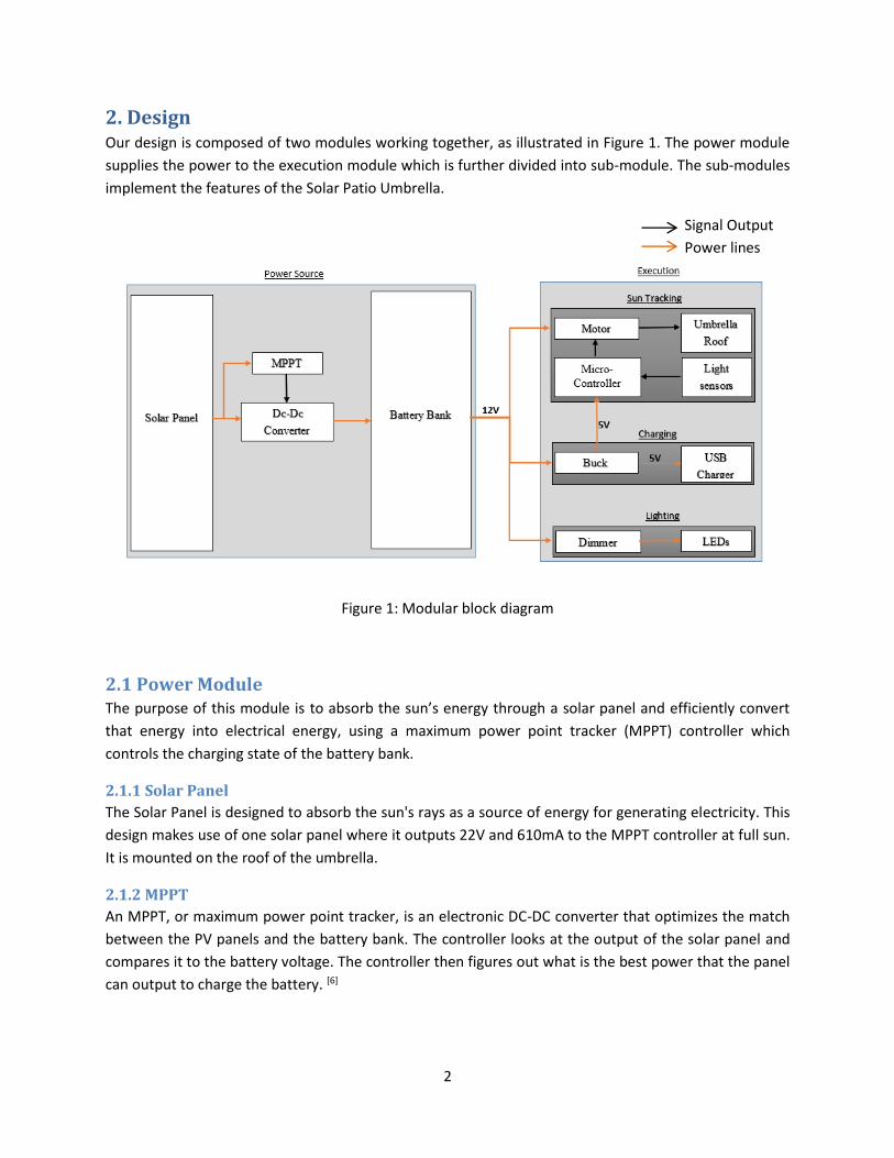
2. Design Our design is composed of two modules working together, as illustrated in Figure 1. The power module
supplies the power to the execution module which is further divided into sub-module. The sub-modules
implement the features of the Solar Patio Umbrella.
Signal Output
Power lines
Figure 1: Modular block diagram
2.1 Power Module The purpose of this module is to absorb the sun’s energy through a solar panel and efficiently convert
that energy into electrical energy, using a maximum power point tracker (MPPT) controller which
controls the charging state of the battery bank.
2.1.1 Solar Panel
The Solar Panel is designed to absorb the sun's rays as a source of energy for generating electricity. This
design makes use of one solar panel where it outputs 22V and 610mA to the MPPT controller at full sun.
It is mounted on the roof of the umbrella.
2.1.2 MPPT
An MPPT, or maximum power point tracker, is an electronic DC-DC converter that optimizes the match
between the PV panels and the battery bank. The controller looks at the output of the solar panel and
compares it to the battery voltage. The controller then figures out what is the best power that the panel
can output to charge the battery. [6]
3
The power point tracker works in way in which it takes the DC input from the solar panels, inverts it to a
high frequency AC and then converts it back to a different DC voltage and current that the battery needs
for it to be optimized.[6] The MPPT controller looks for maximum power point and then does the
voltage/current conversion to change it to what the battery needs to charge.
A Genasun GV-5-PB-12V, 5A MPPT controller was used in this design. The Genasun has a peak efficiency
from 96% to 99.85% with a built in DC-DC converter that steps down the voltage to charge the battery
and a smart controller for battery voltage monitoring.
2.1.3 Battery Bank
The function of this device was initially designed to store up to 22Ah of energy that it received from the
MPPT converter and distributes 12V and up to 45W of power to the other devices within the system.
However, we ended up using a 12V 7Ah lead-acid battery for our design due to availability.
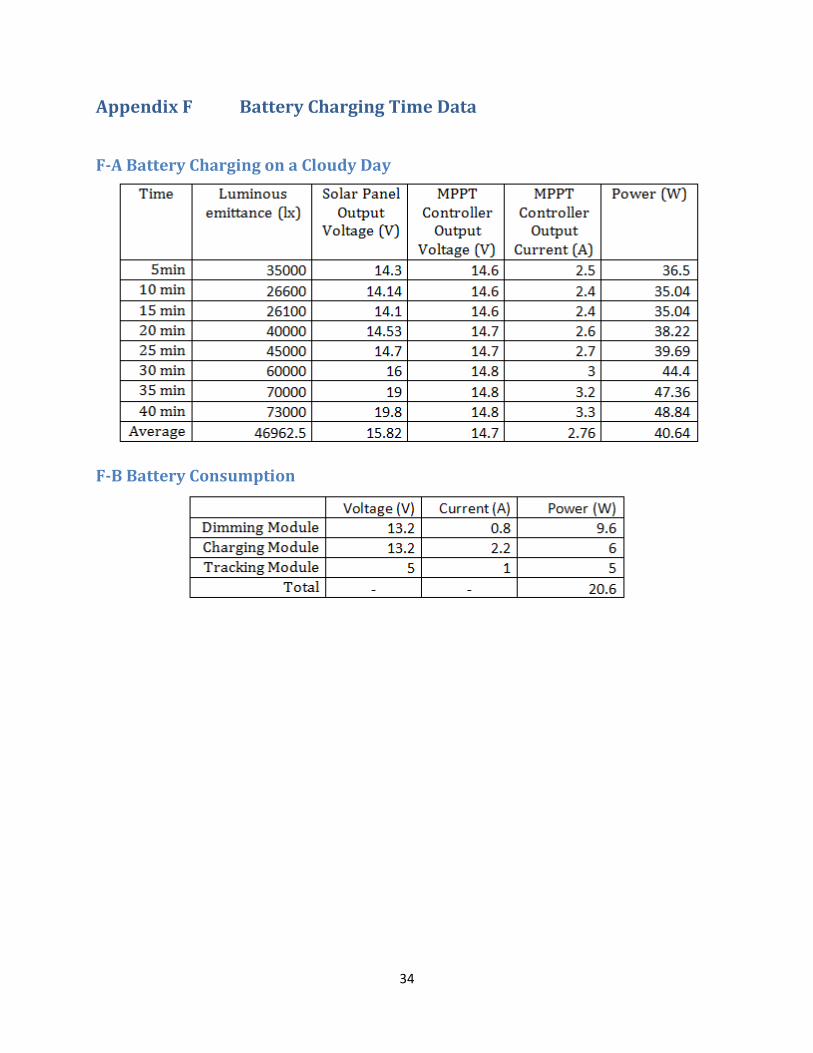
The data obtained to charge the battery and the consumption is showed in Appendix F. Based on the
data we collected, we estimate that the time spent to fully charge the battery would be 2.5 hours +/- 0.5
hours. In addition, the battery will be able to power the whole circuit for 4.5 hours +/- 0.5 hours.
2.2 Charging Module These modules provide the user the ability to charge various devices through a USB port. In order to
accomplish this, a buck converter was constructed such that it steps down the voltage from 12V, which
is supplied from the battery box to 5V which is needed to power up the USB charger. The buck converter
makes use of a switching component to transfer different energy from the input to the output; where
the duty cycle for this component determines the voltage obtained at the output as described in
Equation 1. The buck converter has two operating modes, discontinuous conduction mode (DCM) and
Continuous conduction mode (CCM). In this project, we focused our design for CCM. CCM produces a
continuous current pulse. [3]
2.2.1 Charging Module Calculations
All calculations for simulation purposes were made under the assumption that we have an ideal buck
converter. However, for the actual circuit design that was implemented, we assumed approximately
90% efficiency will be achieved; hence, the calculations below have been adjusted accordingly.
In order to design the charging module’s buck converter, we first begun by considering a various range
of operating frequency. The switching frequency is inversely proportion to the converter efficiency,
since a higher switching frequency translates to higher switching loss. However, switching frequency is
also directly proportion to the component sizes such as the inductor and the capacitors at the input and
output. With this factor in mind and the fact that we needed our components to be small such that our
charger may be portable, we decided to switch at the frequency shown below:
𝑓𝑠𝑤 = 200 𝑘𝐻𝑧
In order to charge the phone, the converter should be able to give out the following outputs displayed
below, where the cellphone (load) is be represented as a 5Ω resistor load. [4] [5] [6]
4
𝑃𝑖𝑛 = 5 𝑊 𝑃𝑜𝑢𝑡 = 5 𝑊
𝑉𝑖𝑛=12 𝑉 𝑉𝑜𝑢𝑡 = 5 𝑉
𝐼𝑖𝑛 = 0.417 𝐴 𝐼𝑜𝑢𝑡 = 1 𝐴
𝑅𝐿𝑜𝑎𝑑 = 5 Ω
Initially, we needed to determine the component sizes of the buck converter. To do this, we begin by
determining the needed duty ratio for the desired output voltage. Because the average inductor voltage
has to be equal to zero, we can apply the volt-second balance to the inductor voltage to obtain equation
1 below.
𝐷 =𝑉𝑜𝑢𝑡
𝜂∗ 𝑉𝑖𝑛=
5
12∗.9∗ 100 = 46.3% (1)
Next, we look to determine the critical inductor; we need to obtain the value of the inductor during
boundary between CCM and DCM.
𝐿𝑐𝑟𝑖𝑡 = 𝑅𝑙𝑜𝑎𝑑 𝑇 (1−𝐷)
2= 6.7 µ𝐻 (2)
< 𝑖𝐿 >= 1 𝐴 = 1
2 𝑖𝑝𝑒𝑎𝑘 => 𝑖𝑝𝑒𝑎𝑘 = ∆𝑖𝐿𝑝𝑝 = 2 𝐴 (MAX) (3)
With this minimum value for the inductor and assuming that the output current ripple will be kept at +/-
200mA or less, we can then obtain an approximate inductor size of as it is the inductor that determines
the output current ripple:
L =𝑉𝑜𝑢𝑡∗(𝑉𝑖𝑛−𝑉𝑜𝑢𝑡)
Δ𝐼𝐿∗𝑓𝑠∗𝑉𝑖𝑛=
5∗(12−5)
.2𝐴∗(200∗103)∗12= 73 𝑢𝐻 (4)
The next step is to determine the input capacitance of the buck converter. Assuming an input voltage
ripple of 1% of input voltage, we obtain:
𝐶𝑖𝑛 =𝐷𝑚𝑎𝑥 ∗ 𝐼𝑜𝑢𝑡
Δ𝑉𝑖𝑛∗𝑓𝑠𝑤 (4)
𝐶𝑖𝑛 =. 463 ∗ 1
. 12 ∗ 200 ∗ 103= 19.3 𝑢𝐹
For calculating, 𝐶𝑜𝑢𝑡 we know that < 𝑖𝑐 > = 0, so all the ripple voltage will go into the capacitor. We
can get ∆𝑉𝑐𝑝𝑝 without knowing the exact shape. Assuming a voltage capacitor ripple of 1%, we get:
0.05 𝑉 = ∆𝑉𝑐𝑝𝑝 = ∆𝑖𝐿𝑝𝑝
8 𝐶𝑜𝑢𝑡𝑓𝑠𝑤=> 𝐶𝑜𝑢𝑡 =
∆𝑖𝐿𝑝𝑝
8 ∆𝑉𝑐𝑝𝑝𝑓𝑠𝑤= 25 µ𝐹 (19)
As previously stated, the above calculations were made under the assumption that 90% efficiency will
be achieved. This estimate was made because the buck converter is not ideal because of the losses in its

5
components such as the MOSFET, Power Diode and the Switching Losses. One particular component is
the capacitor in the converter, more precisely the output capacitor. As a result, we added a resistor in
series commonly referred to as Equivalent Series Resistance (ESR) to the output capacitor because this
ESR determines the ripple in the output voltage. The ESR for the input capacitor was not computed, as it
is not very impactful. Looking at the datasheet, we have obtained the loss tangent based on the chosen
frequency and output voltage to determine the ESR as follows:
𝐸𝑆𝑅 = tan 𝛿
𝐶𝑜𝑢𝑡 𝜔= 0.6 𝛺 (20)
2.2.2 Charging Module Parts
Finally, the components of the Buck Converter chosen for this design are:
1- Input Capacitor: A 47μF capacitor is placed in order to filter out the input voltage ripple from
the battery bank. [13]
2- FET: A power MOSFET IRF520N due to its fast switching cycle and ultra-low on resistance
(.27Ω), since because this will help reduce the switching loss and improve efficiency.
3- Schottky Power Diode: In order to reduce losses in the diode when the switch is off, a
Schottky diode MBRB1045 was due to fact that they have a small voltage drop across them.
The diode is used to block the current when the MOSFET is conducting and provide an
inductor current path when the MOSFET is not conducting. [8]
4- Inductor: Based on the calculations of our buck converter, it was determined that the
minimum value of the inductor needed in order to keep the buck converter from operating
in DCM was approximately 6.7 µH. The inductor is the key element in determining the
boundary between DCM and CCM operation since it controls the output current. Therefore,
in order to avoid having the core from saturating and to reduce the output current ripple, a
larger inductor of 690 μH is used instead.
5- Output Capacitor: A 47μF electrolytic capacitor is used in this design. The initial choice for
the output capacitor was a parallel network of five ceramic capacitors because they have a
low equivalent series resistance (ESR). Hence, this will reduce the output voltage ripple (< 50
mVrms), therefore protecting the device being charged.
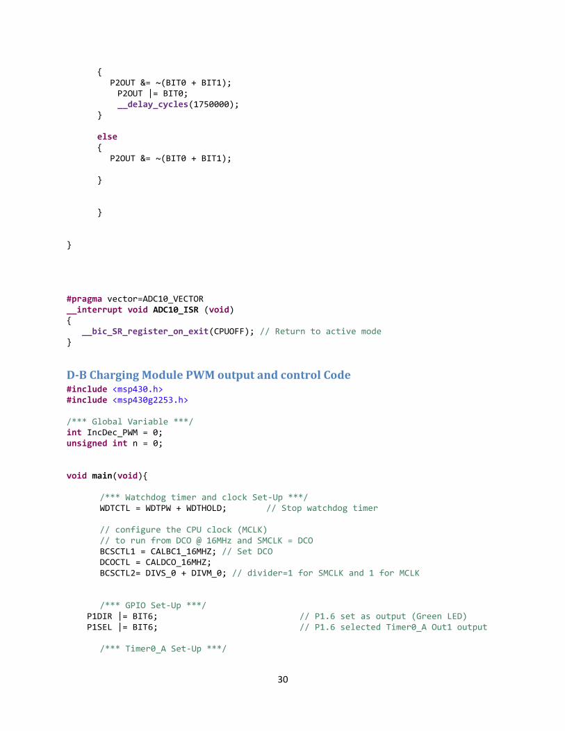
6- Micro-controller: TI-MSP430 is used in the project in order to generate the system’s PWM
and P-Control for the buck converter to both lowers the duty cycle if the output voltage is
higher than 5.25 V or increase the duty cycle if the output voltage is lower than 4.75 V
7- Voltage Regulator: The LM337 voltage regulator is used to power the micro-controller on
board.
2.2.3 Charging Module Results
With this design, we were able to accomplish 5V+/- .05V output and current output up to 1A. However,
this was not enough to allow the phone to charge as today’s smartphones have to perform “network”
checks to make sure that the device feeding it the voltage and current is truly a charge (See Figure 2). In
order overcome this, we first implemented the “Dedicated Charge” network which worked fine for
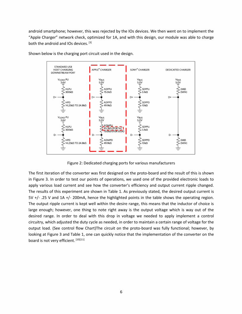
6
android smartphone; however, this was rejected by the IOs devices. We then went on to implement the
“Apple Charger” network check, optimized for 1A, and with this design, our module was able to charge
both the android and IOs devices. [3]
Shown below is the charging port circuit used in the design.
Figure 2: Dedicated charging ports for various manufacturers
The first iteration of the converter was first designed on the proto-board and the result of this is shown
in Figure 3. In order to test our points of operations, we used one of the provided electronic loads to
apply various load current and see how the converter’s efficiency and output current ripple changed.
The results of this experiment are shown in Table 1. As previously stated, the desired output current is
5V +/- .25 V and 1A +/- 200mA, hence the highlighted points in the table shows the operating region.
The output ripple current is kept well within the desire range, this means that the inductor of choice is
large enough; however, one thing to note right away is the output voltage which is way out of the
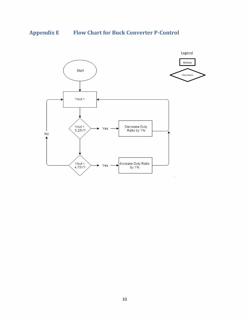
desired range. In order to deal with this drop in voltage we needed to apply implement a control
circuitry, which adjusted the duty cycle as needed, in order to maintain a certain range of voltage for the
output load. (See control flow Chart)The circuit on the proto-board was fully functional; however, by
looking at Figure 3 and Table 1, one can quickly notice that the implementation of the converter on the
board is not very efficient. [10][11]
7
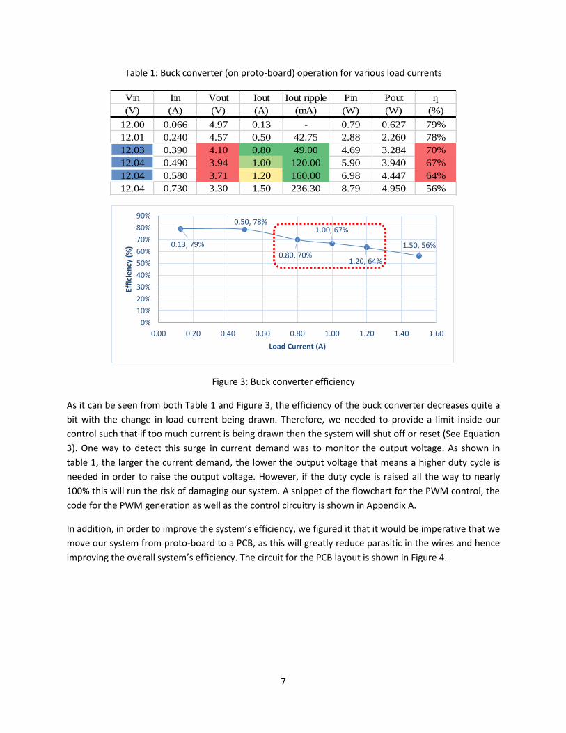
Table 1: Buck converter (on proto-board) operation for various load currents
Figure 3: Buck converter efficiency
As it can be seen from both Table 1 and Figure 3, the efficiency of the buck converter decreases quite a
bit with the change in load current being drawn. Therefore, we needed to provide a limit inside our
control such that if too much current is being drawn then the system will shut off or reset (See Equation
3). One way to detect this surge in current demand was to monitor the output voltage. As shown in
table 1, the larger the current demand, the lower the output voltage that means a higher duty cycle is
needed in order to raise the output voltage. However, if the duty cycle is raised all the way to nearly
100% this will run the risk of damaging our system. A snippet of the flowchart for the PWM control, the
code for the PWM generation as well as the control circuitry is shown in Appendix A.
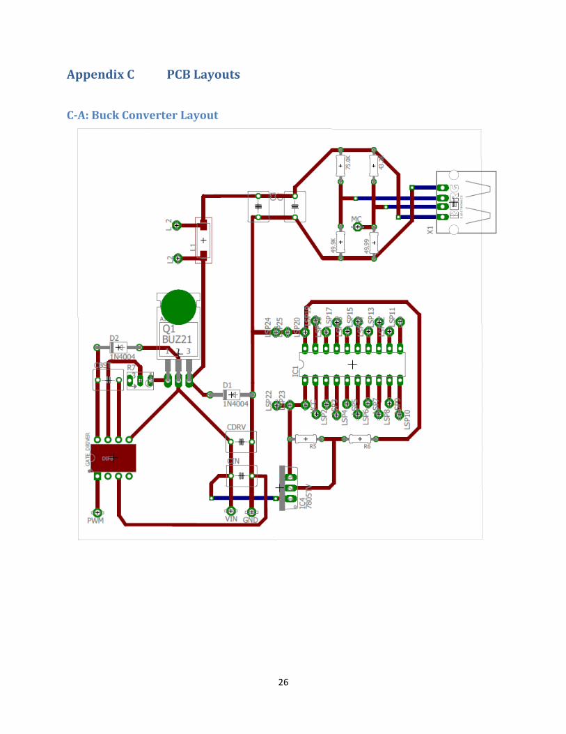
In addition, in order to improve the system’s efficiency, we figured it that it would be imperative that we
move our system from proto-board to a PCB, as this will greatly reduce parasitic in the wires and hence
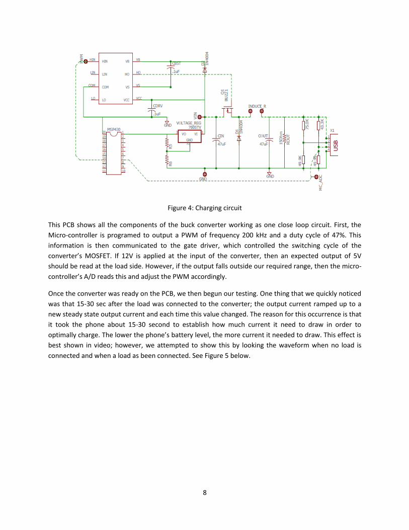
improving the overall system’s efficiency. The circuit for the PCB layout is shown in Figure 4.
Vin Iin Vout Iout Iout ripple Pin Pout ƞ
(V) (A) (V) (A) (mA) (W) (W) (%)
12.00 0.066 4.97 0.13 - 0.79 0.627 79%
12.01 0.240 4.57 0.50 42.75 2.88 2.260 78%
12.03 0.390 4.10 0.80 49.00 4.69 3.284 70%
12.04 0.490 3.94 1.00 120.00 5.90 3.940 67%
12.04 0.580 3.71 1.20 160.00 6.98 4.447 64%
12.04 0.730 3.30 1.50 236.30 8.79 4.950 56%
0.13, 79%
0.50, 78%
0.80, 70%
1.00, 67%
1.20, 64%
1.50, 56%
0%
10%
20%
30%
40%
50%
60%
70%
80%
90%
0.00 0.20 0.40 0.60 0.80 1.00 1.20 1.40 1.60
Effi
cie
ncy
(%
)
Load Current (A)
8
Figure 4: Charging circuit
This PCB shows all the components of the buck converter working as one close loop circuit. First, the
Micro-controller is programed to output a PWM of frequency 200 kHz and a duty cycle of 47%. This
information is then communicated to the gate driver, which controlled the switching cycle of the
converter’s MOSFET. If 12V is applied at the input of the converter, then an expected output of 5V
should be read at the load side. However, if the output falls outside our required range, then the micro-
controller’s A/D reads this and adjust the PWM accordingly.
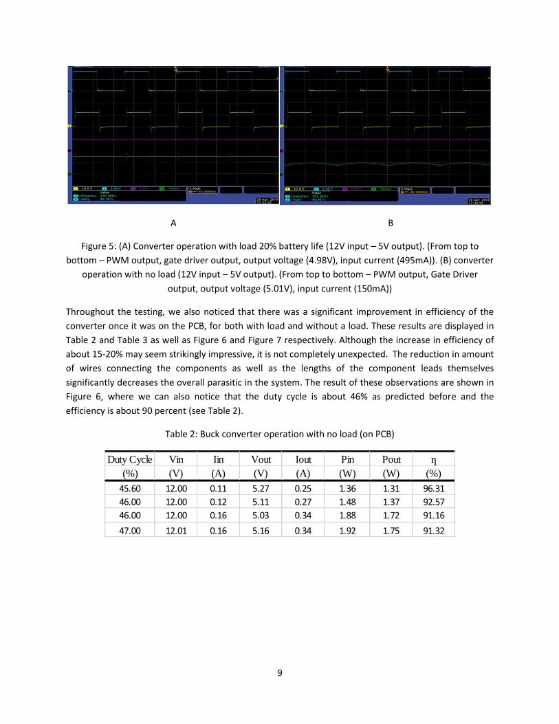
Once the converter was ready on the PCB, we then begun our testing. One thing that we quickly noticed
was that 15-30 sec after the load was connected to the converter; the output current ramped up to a
new steady state output current and each time this value changed. The reason for this occurrence is that
it took the phone about 15-30 second to establish how much current it need to draw in order to
optimally charge. The lower the phone’s battery level, the more current it needed to draw. This effect is
best shown in video; however, we attempted to show this by looking the waveform when no load is
connected and when a load as been connected. See Figure 5 below.
9
A B
Figure 5: (A) Converter operation with load 20% battery life (12V input – 5V output). (From top to
bottom – PWM output, gate driver output, output voltage (4.98V), input current (495mA)). (B) converter
operation with no load (12V input – 5V output). (From top to bottom – PWM output, Gate Driver
output, output voltage (5.01V), input current (150mA))
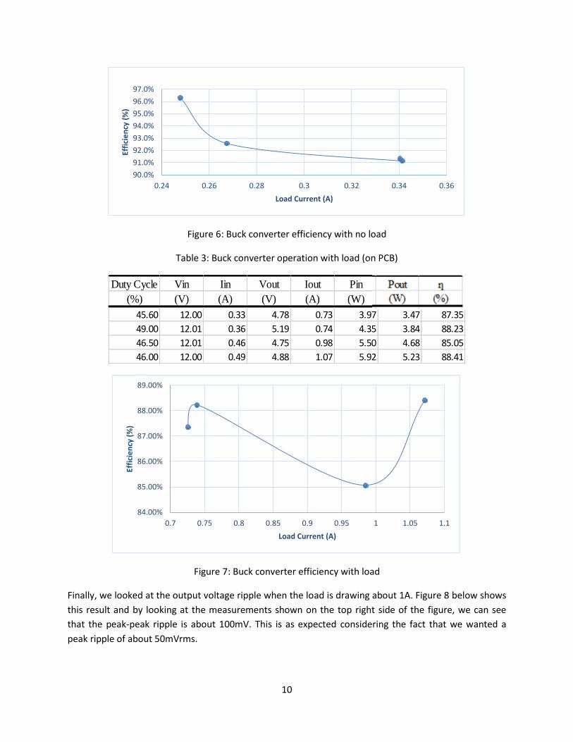
Throughout the testing, we also noticed that there was a significant improvement in efficiency of the
converter once it was on the PCB, for both with load and without a load. These results are displayed in
Table 2 and Table 3 as well as Figure 6 and Figure 7 respectively. Although the increase in efficiency of
about 15-20% may seem strikingly impressive, it is not completely unexpected. The reduction in amount
of wires connecting the components as well as the lengths of the component leads themselves
significantly decreases the overall parasitic in the system. The result of these observations are shown in
Figure 6, where we can also notice that the duty cycle is about 46% as predicted before and the
efficiency is about 90 percent (see Table 2).
Table 2: Buck converter operation with no load (on PCB)
Duty Cycle Vin Iin Vout Iout Pin Pout ƞ
(%) (V) (A) (V) (A) (W) (W) (%)
45.60 12.00 0.11 5.27 0.25 1.36 1.31 96.31
46.00 12.00 0.12 5.11 0.27 1.48 1.37 92.57
46.00 12.00 0.16 5.03 0.34 1.88 1.72 91.16
47.00 12.01 0.16 5.16 0.34 1.92 1.75 91.32
10
Figure 6: Buck converter efficiency with no load
Table 3: Buck converter operation with load (on PCB)
Figure 7: Buck converter efficiency with load
Finally, we looked at the output voltage ripple when the load is drawing about 1A. Figure 8 below shows
this result and by looking at the measurements shown on the top right side of the figure, we can see
that the peak-peak ripple is about 100mV. This is as expected considering the fact that we wanted a
peak ripple of about 50mVrms.
90.0%
91.0%
92.0%
93.0%
94.0%
95.0%
96.0%
97.0%
0.24 0.26 0.28 0.3 0.32 0.34 0.36
Effi
cie
ncy
(%
)
Load Current (A)
Duty Cycle Vin Iin Vout Iout Pin Pout ƞ
(%) (V) (A) (V) (A) (W) (W) (%)
45.60 12.00 0.33 4.78 0.73 3.97 3.47 87.35
49.00 12.01 0.36 5.19 0.74 4.35 3.84 88.23
46.50 12.01 0.46 4.75 0.98 5.50 4.68 85.05
46.00 12.00 0.49 4.88 1.07 5.92 5.23 88.41
84.00%
85.00%
86.00%
87.00%
88.00%
89.00%
0.7 0.75 0.8 0.85 0.9 0.95 1 1.05 1.1
Effi
cie
ncy
(%
)
Load Current (A)
11
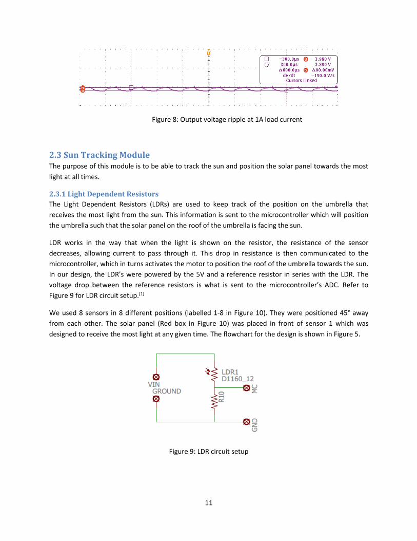
Figure 8: Output voltage ripple at 1A load current
2.3 Sun Tracking Module The purpose of this module is to be able to track the sun and position the solar panel towards the most
light at all times.
2.3.1 Light Dependent Resistors
The Light Dependent Resistors (LDRs) are used to keep track of the position on the umbrella that
receives the most light from the sun. This information is sent to the microcontroller which will position
the umbrella such that the solar panel on the roof of the umbrella is facing the sun.
LDR works in the way that when the light is shown on the resistor, the resistance of the sensor
decreases, allowing current to pass through it. This drop in resistance is then communicated to the
microcontroller, which in turns activates the motor to position the roof of the umbrella towards the sun.
In our design, the LDR’s were powered by the 5V and a reference resistor in series with the LDR. The
voltage drop between the reference resistors is what is sent to the microcontroller’s ADC. Refer to
Figure 9 for LDR circuit setup.[1]
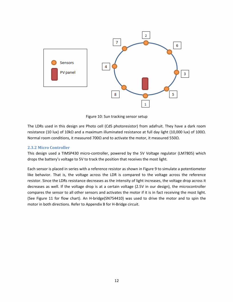
We used 8 sensors in 8 different positions (labelled 1-8 in Figure 10). They were positioned 45° away
from each other. The solar panel (Red box in Figure 10) was placed in front of sensor 1 which was
designed to receive the most light at any given time. The flowchart for the design is shown in Figure 5.
Figure 9: LDR circuit setup
12
Figure 10: Sun tracking sensor setup
The LDRs used in this design are Photo cell (CdS photoresistor) from adafruit. They have a dark room
resistance (10 lux) of 10kΩ and a maximum illuminated resistance at full day light (10,000 lux) of 100Ω.
Normal room conditions, it measured 700Ω and to activate the motor, it measured 550Ω.
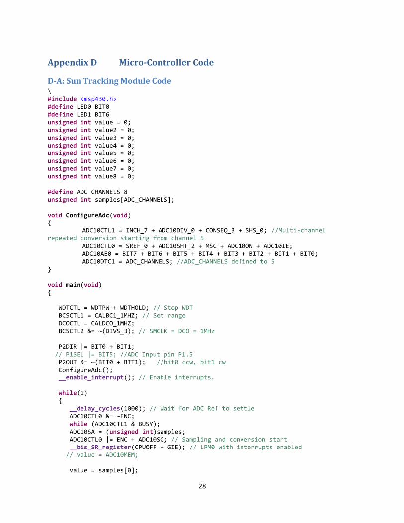
2.3.2 Micro Controller
This design used a TIMSP430 micro-controller, powered by the 5V Voltage regulator (LM7805) which
drops the battery’s voltage to 5V to track the position that receives the most light.
Each sensor is placed in series with a reference resistor as shown in Figure 9 to simulate a potentiometer
like behavior. That is, the voltage across the LDR is compared to the voltage across the reference
resistor. Since the LDRs resistance decreases as the intensity of light increases, the voltage drop across it
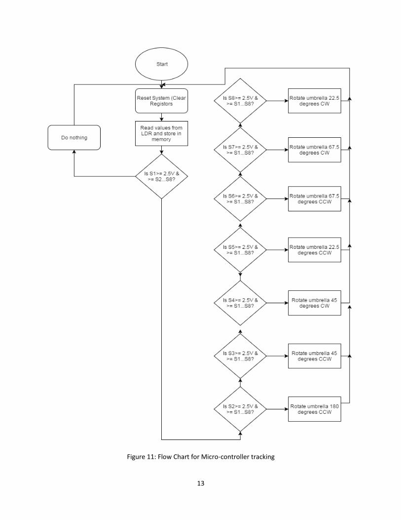
decreases as well. If the voltage drop is at a certain voltage (2.5V in our design), the microcontroller
compares the sensor to all other sensors and activates the motor if it is in fact receiving the most light.
(See Figure 11 for flow chart). An H-bridge(SN754410) was used to drive the motor and to spin the
motor in both directions. Refer to Appendix B for H-Bridge circuit.
13
Figure 11: Flow Chart for Micro-controller tracking
14
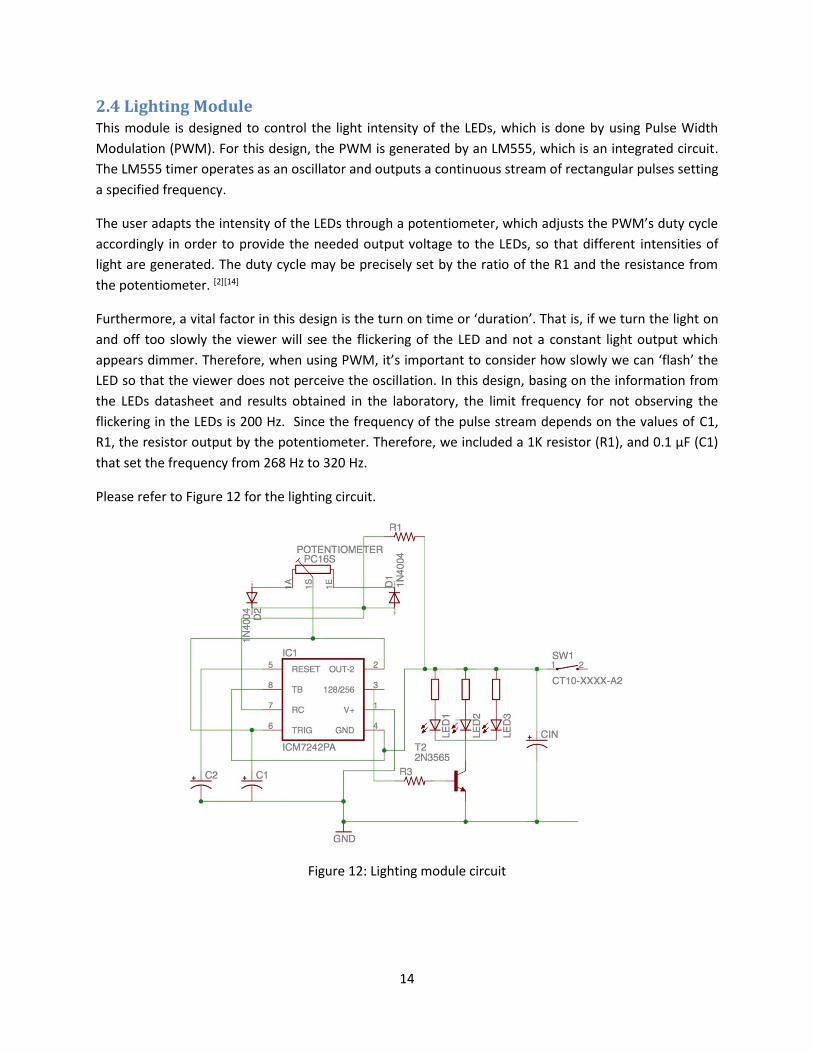
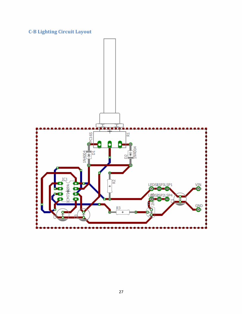
2.4 Lighting Module This module is designed to control the light intensity of the LEDs, which is done by using Pulse Width
Modulation (PWM). For this design, the PWM is generated by an LM555, which is an integrated circuit.
The LM555 timer operates as an oscillator and outputs a continuous stream of rectangular pulses setting
a specified frequency.
The user adapts the intensity of the LEDs through a potentiometer, which adjusts the PWM’s duty cycle
accordingly in order to provide the needed output voltage to the LEDs, so that different intensities of
light are generated. The duty cycle may be precisely set by the ratio of the R1 and the resistance from
the potentiometer. [2][14]
Furthermore, a vital factor in this design is the turn on time or ‘duration’. That is, if we turn the light on
and off too slowly the viewer will see the flickering of the LED and not a constant light output which
appears dimmer. Therefore, when using PWM, it’s important to consider how slowly we can ‘flash’ the
LED so that the viewer does not perceive the oscillation. In this design, basing on the information from
the LEDs datasheet and results obtained in the laboratory, the limit frequency for not observing the
flickering in the LEDs is 200 Hz. Since the frequency of the pulse stream depends on the values of C1,
R1, the resistor output by the potentiometer. Therefore, we included a 1K resistor (R1), and 0.1 μF (C1)
that set the frequency from 268 Hz to 320 Hz.
Please refer to Figure 12 for the lighting circuit.
Figure 12: Lighting module circuit
15
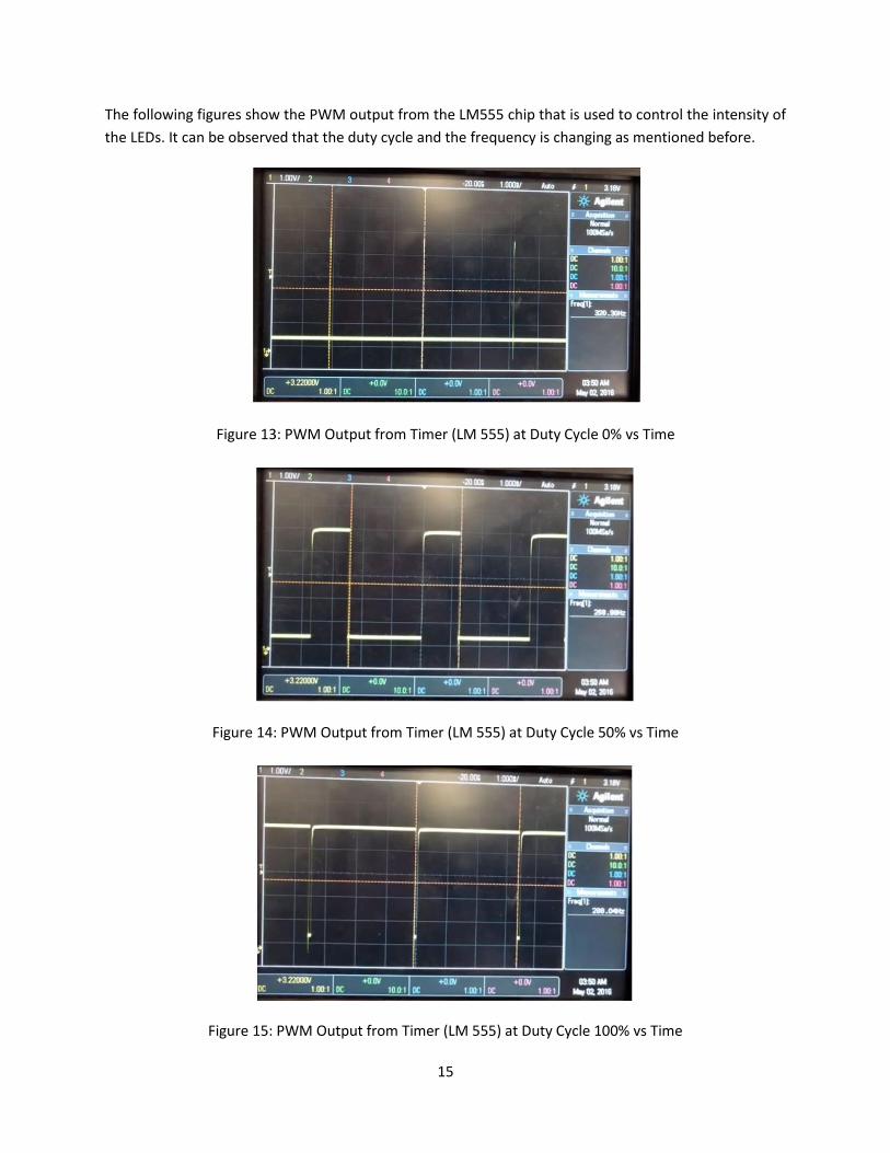
The following figures show the PWM output from the LM555 chip that is used to control the intensity of
the LEDs. It can be observed that the duty cycle and the frequency is changing as mentioned before.
Figure 13: PWM Output from Timer (LM 555) at Duty Cycle 0% vs Time
Figure 14: PWM Output from Timer (LM 555) at Duty Cycle 50% vs Time
Figure 15: PWM Output from Timer (LM 555) at Duty Cycle 100% vs Time

16
3. Design Verification
3.1 Solar Panel A working solar panel should be able to absorb sun radiation and depending on the intensity of this
radiation, it should provide a range of output voltages. For details on the specific requirements and
testing procedures, please see Appendix A.
3.2 MPPT Controller (Genasun GV-5) A working MPPT controller should be able to optimize the output from the Solar panel and provide this
to charge the battery bank at its optimal state. For details on the specific requirements and testing
procedures, please see Appendix A.
3.3 Battery Bank The battery bank needed to be able to supply with 12V ± 2V at up to 2.5 A at all times to the rest of the
system. For details on the specific requirements and testing procedures, please see Appendix A.
3.4 Light Sensors The resistance of the light sensors should be able to vary depending on the light intensity with a
reasonable accuracy. For details on the specific requirements and testing procedures, please see
Appendix A.
3.5 Micro controller A working micro-controller should be able to receive the analog voltage from both the sensors network
and the buck converts and using its A/D, provide the necessary outputs. A working micro-controller
reads the analog voltages from all 8 sensors around the umbrella, converts these voltages from analog
to digital, compares the obtained values and output the correct signal to rotate the umbrella and for
how long based on which sensor reading was the highest. A working micro-controller should be able to
receive the analog voltage from the buck converter, convert this reading from analog to digital, and
accurately adjusts the pulse width modulation (PWM) duty cycle and output the PWM signal. For details
on the specific requirements and testing procedures, please see Appendix D.
3.6 Motor The motor should be able to rotate the umbrella based on the signal output from the micro-controller
clockwise or anti-clockwise. For details on the specific requirements and testing procedures, please see
Appendix A.
3.7 DC-DC buck converter A working converter should be able to receive the voltage from the battery and step down this voltage
such that it may then be used to charge a phone. For details on the specific requirements and testing
procedures, please see Appendix A.
17
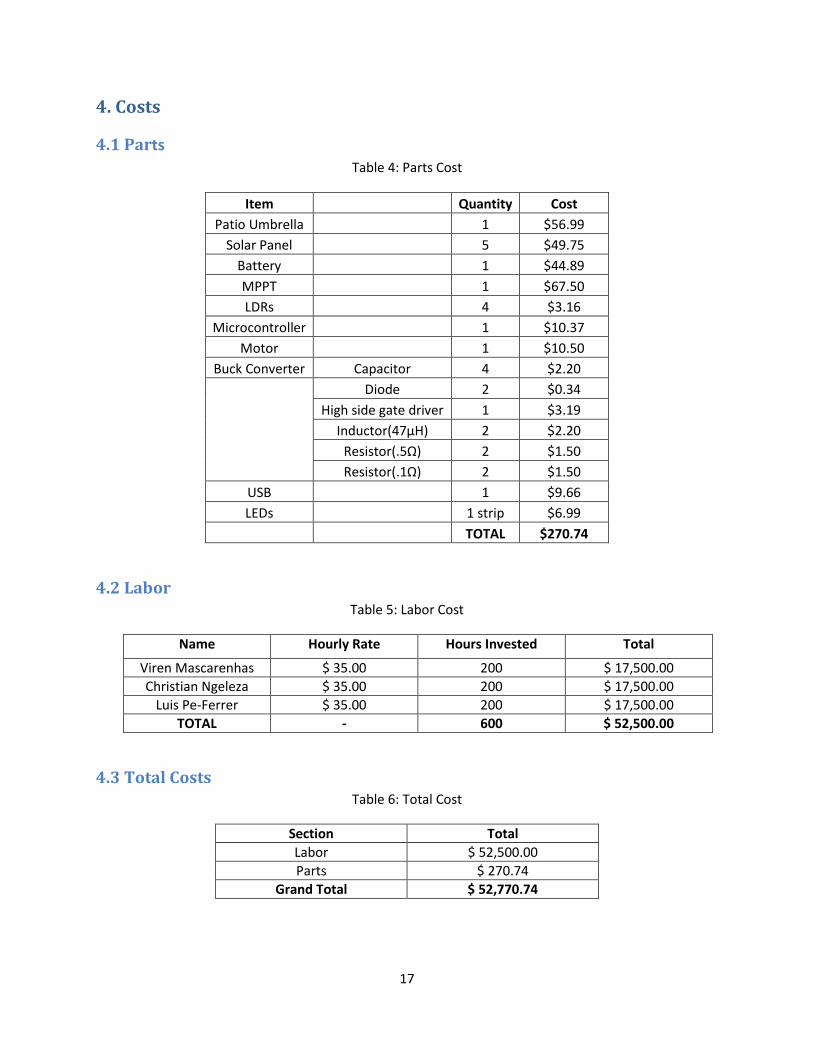
4. Costs
4.1 Parts
Table 4: Parts Cost
Item
Quantity Cost
Patio Umbrella
1 $56.99
Solar Panel
5 $49.75
Battery
1 $44.89
MPPT
1 $67.50
LDRs
4 $3.16
Microcontroller
1 $10.37
Motor
1 $10.50
Buck Converter Capacitor 4 $2.20
Diode 2 $0.34
High side gate driver 1 $3.19
Inductor(47µH) 2 $2.20
Resistor(.5Ω) 2 $1.50
Resistor(.1Ω) 2 $1.50
USB
1 $9.66
LEDs
1 strip $6.99
TOTAL $270.74
4.2 Labor Table 5: Labor Cost
Name Hourly Rate Hours Invested Total
Viren Mascarenhas $ 35.00 200 $ 17,500.00
Christian Ngeleza $ 35.00 200 $ 17,500.00
Luis Pe-Ferrer $ 35.00 200 $ 17,500.00
TOTAL - 600 $ 52,500.00
4.3 Total Costs Table 6: Total Cost
Section Total
Labor $ 52,500.00
Parts $ 270.74
Grand Total $ 52,770.74
18
5. Conclusion
5.1 Accomplishments At the end of this project, we completed a system that was shown in the block diagram. The only thing
that was not incorporated in the final demonstration was a standalone microcontroller. However, we
got the standalone microcontroller to work on individual modules. The sun tracking module accurately
tracked the best position with the maximum amount of light with an accuracy of +/- 2 degrees. The
charging unit was able to charge a phone with both Android and Apple operating systems with a buck
efficiency of approximately 90%. Lastly, we were able to dim the LED lighting system in our umbrella. All
these modules were powered by a battery that was charged by a solar panel using a MPPT charging
device.
5.2 Uncertainties We are uncertain of how long it will take our charging unit to fully charge a phone from 0% to 100%. In
addition, we are uncertain on how long our battery will last on a full charge. We have done the
calculations that it will last for 4 hours, however we have not tested it with our design.
5.3 Ethical Considerations Since this product is a commercial product that will be used by consumers in hotels etc., it is important
that it meets all safety requirements and its 100% safe to use. Therefore, as we go ahead and complete
this project, we will comply to the first code of ethic in IEEE Code of Ethics. [7] [9] [12]
1. To accept responsibility in making decisions consistent with the safety, health, ad welfare of the
public, and to disclose promptly factors that might endanger the public or the environment.
We learnt a lot on solar panels, MPPT, power converters and control mechanisms for solar tracking. This
relates to the 6th IEEE Code of Ethics
2. To maintain and improve our technical competence and to undertake technological tasks for
others only if qualified by training or experience, or after full disclosure of pertinent limitations.
In this class, we were required to peer review other groups and give our opinion on things. Also, we
needed help from other groups and TA’s to complete our project. This correlates to the 7th IEEE Code of
Ethics.
7. To seek, accept and offer honest criticism of technical work, to acknowledge and correct errors,
and to credit properly the contributions of others.
Our main objective is to stay safe and to ensure that everyone using our product remains safe as well.
This correlates to the 9th IEEE Code of Ethics.
9. To avoid injuring others, their property, reputation, or employment by false or malicious action.
Lastly, that being said, we promise comply to all the IEEE Code of Ethics regardless if its mentioned in
the above statement or not.

19
5.4 Future work Future work for this project involves refining the design and physical components. The first step would
be to build the lightning module on a Printed Circuit Board, which is already designed (See Appendix C-
B), in order to improve the efficiency of this module. Furthermore, the Buck Converter PCB should be
redesigned, since there are still some wires, which reduces its efficiency. Both changes would make both
systems more attractive for a possible future sale.
A future revision of the project would also include a design of an accurate control for the tracking
module in order to reach to the exact position and absorbing the greatest amount of energy possible.
Furthermore, the whole project should be tested for an extended period of time, and check how long
the mobile phone spends to be fully charged or how long the battery can be used.
Lastly, implement the project on an actual sized patio umbrella with all the components mounted on.
20
References
[1] Advanced Photonix, Inc, “Cds Photoconductive Photocells,” PDV-P8103 datasheet, [Revised March.
2006].
[2] “Controlling LED brightness using PWM,” waitingforfriday.com, April. 15, 2010. [Online] Available:
http://waitingforfriday.com/index.php/Controlling_LED_brightness_using_PWM. [Accessed Feb.
21, 2016].
[3] EDAC, Inc, “Waterproof USB Type A, 4P (Male),”690-W04-260-013 datasheet, April. 2014
[4] Falin, Jeff. "Disigning DC/DC Converters Based on ZETA Topology." Power Management (2010): 16-
23. Texas Instruments. Texas Instruments, 2010. Web. 16 Feb. 2016.
[5] Hauke, Brigitte. "Basic Calculation of a Buck Converter's Power Stage." Application Report (2015): 1-
8. Texas Instruments. Texas Instruments, Aug. 2015. Web. 16 Feb. 2016.
[6] Krein, Philip T. Elements of Power Electronics. New York: Oxford UP, 1998. Print.
[7] Krein, P.T. “Safety.” ECE 469-Power Electronics Laboratory. Urbana, IL: 2012.
<http://energy.ece.illinois.edu/ECE469Manual2012.pdf>
[8] ON Semiconductor, “Schottky Barrier Diodes,” NSR0320MW2T1G datasheet, [Revised Nov. 2011].
[9] Sauer, P. W. Krein, P. T. Chapman, P.L. “Safety.” ECE431-Electric Machinery Course Guide and
Laboratory Information. Urbana, IL: 2015
<http://ceme.ece.illinois.edu/files/2015/02/ECE431/LabManual2015.pdf>
[10] T. Agarwal, “Mobile cellphone battery charging circuit with explanation,” elprocu.com, [Online].
Available: http://www.elprocus.com/mobile-battery-charger-circuit-and-working-principle/.
[Accessed Feb. 27, 2016].
[11] “Timers and Clocks and PWM! Oh My!,” msp430launchpad.com, July 22, 2002. [Online]. Available:
http://www.msp430launchpad.com/2010/07/timers-and-clocks-and-pwm-oh-my.html [Accessed
Feb 23, 2016].
[12] United States. IEEE. 7.8. IEEE Code of Ethics. Washington DC: , 2013. Web.
[13] Vishay BCcomponents, “Aluminum Capacitors SMD(Chip), High Temperature, Low Impedance,”
Document number 28405, datasheet [Revised Dec. 2012].
[14] Joost Yervante Damad. (2012). Dimming a 12V LED strip with a mosfet and PWM [Online]. Available
FTP: http://joost.damad.be/2012/09/dimming-12v-led-strip-with-mosfet-and.html

21
[15] “The H-Bridge Circuit Control Design in DC Motor Application” circuitdiagramworld.com, Feb. 28,
2015 [Online]. Available:
http://www.circuitdiagramworld.com/control_circuit_diagram/The_H_Bridge_Circuit_Control_Desi
gn_in_DC_Motor_Application_15483.html. [Accessed Mar 09, 2016].
22
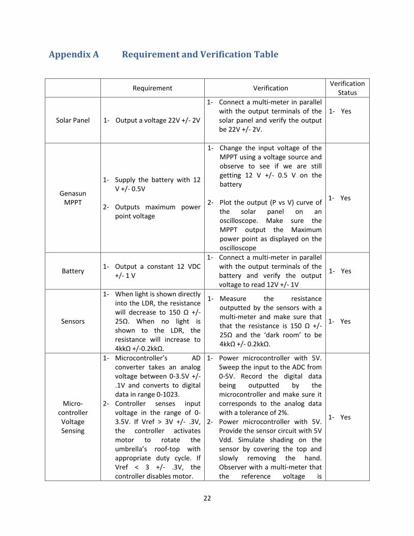
Appendix A Requirement and Verification Table
Requirement Verification Verification
Status
Solar Panel 1- Output a voltage 22V +/- 2V
1- Connect a multi-meter in parallel with the output terminals of the solar panel and verify the output be 22V +/- 2V.
1- Yes
Genasun MPPT
1- Supply the battery with 12 V +/- 0.5V
2- Outputs maximum power point voltage
1- Change the input voltage of the MPPT using a voltage source and observe to see if we are still getting 12 V +/- 0.5 V on the battery
2- Plot the output (P vs V) curve of the solar panel on an oscilloscope. Make sure the MPPT output the Maximum power point as displayed on the oscilloscope
1- Yes
Battery 1- Output a constant 12 VDC
+/- 1 V
1- Connect a multi-meter in parallel with the output terminals of the battery and verify the output voltage to read 12V +/- 1V
1- Yes
Sensors
1- When light is shown directly into the LDR, the resistance will decrease to 150 Ω +/- 25Ω. When no light is shown to the LDR, the resistance will increase to 4kkΩ +/-0.2kkΩ.
1- Measure the resistance outputted by the sensors with a multi-meter and make sure that that the resistance is 150 Ω +/- 25Ω and the ‘dark room’ to be 4kkΩ +/- 0.2kkΩ.
1- Yes
Micro-controller Voltage Sensing
1- Microcontroller’s AD converter takes an analog voltage between 0-3.5V +/- .1V and converts to digital data in range 0-1023.
2- Controller senses input voltage in the range of 0-3.5V. If Vref > 3V +/- .3V, the controller activates motor to rotate the umbrella’s roof-top with appropriate duty cycle. If Vref < 3 +/- .3V, the controller disables motor.
1- Power microcontroller with 5V. Sweep the input to the ADC from 0-5V. Record the digital data being outputted by the microcontroller and make sure it corresponds to the analog data with a tolerance of 2%.
2- Power microcontroller with 5V. Provide the sensor circuit with 5V Vdd. Simulate shading on the sensor by covering the top and slowly removing the hand. Observer with a multi-meter that the reference voltage is
1- Yes
23
fluctuating. If Vref > 3V, with a tolerance of 5%, then motor must be activated. If Vref < 3V, with also a tolerance of 5%, then the motor is not activated.
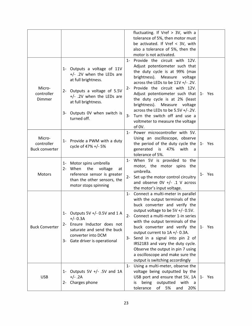
Micro-controller Dimmer
1- Outputs a voltage of 11V +/- .2V when the LEDs are at full brightness.
2- Outputs a voltage of 5.5V +/- .2V when the LEDs are at full brightness.
3- Outputs 0V when switch is turned off.
1- Provide the circuit with 12V. Adjust potentiometer such that the duty cycle is at 99% (max brightness). Measure voltage across the LEDs to be 11V +/- .2V.
2- Provide the circuit with 12V. Adjust potentiometer such that the duty cycle is at 2% (least brightness). Measure voltage across the LEDs to be 5.5V +/-.2V.
3- Turn the switch off and use a voltmeter to measure the voltage of 0V.
1- Yes
Micro-controller
Buck converter
1- Provide a PWM with a duty cycle of 47% +/- 5%
1- Power microcontroller with 5V. Using an oscilloscope, observe the period of the duty cycle the generated is 47% with a tolerance of 5%.
1- Yes
Motors
1- Motor spins umbrella 2- When the voltage at
reference sensor is greater than the other sensors, the motor stops spinning
1- When 5V is provided to the motor, the motor spins the umbrella.
2- Set up the motor control circuitry and observe 0V +/- .1 V across the motor’s input voltage.
1- Yes
Buck Converter
1- Outputs 5V +/- 0.5V and 1 A +/- 0.3A
2- Ensure Inductor does not saturate and send the buck converter into DCM
3- Gate driver is operational
1- Connect a multi-meter in parallel with the output terminals of the buck converter and verify the output voltage to be 5V +/- 0.5V.
2- Connect a multi-meter 1-in series with the output terminals of the buck converter and verify the output current to 1A +/- 0.3A.
3- Send in a signal into pin 2 of IRS2183 and vary the duty cycle. Observe the output in pin 7 using a oscilloscope and make sure the output is switching accordingly
1- Yes
USB 1- Outputs 5V +/- .5V and 1A
+/- .2A 2- Charges phone
1- Using a multi-meter, observe the voltage being outputted by the USB port and ensure that 5V, 1A is being outputted with a tolerance of 5% and 20%
1- Yes
24
accordingly. 2- Plug in phone and see that it is
charging.
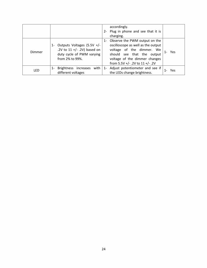
Dimmer
1- Outputs Voltages (5.5V +/- .2V to 11 +/- .2V) based on duty cycle of PWM varying from 2% to 99%.
1- Observe the PWM output on the oscilloscope as well as the output voltage of the dimmer. We should see that the output voltage of the dimmer changes from 5.5V +/- .2V to 11 +/- .2V
1- Yes
LED 1- Brightness increases with
different voltages 1- Adjust potentiometer and see if
the LEDs change brightness. 1- Yes
25
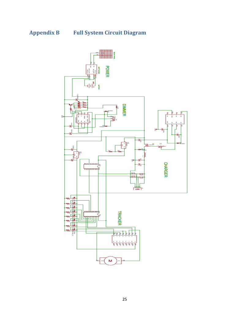
Appendix B Full System Circuit Diagram
26
Appendix C PCB Layouts
C-A: Buck Converter Layout
27
C-B Lighting Circuit Layout
28
Appendix D Micro-Controller Code
D-A: Sun Tracking Module Code \ #include <msp430.h> #define LED0 BIT0 #define LED1 BIT6 unsigned int value = 0; unsigned int value2 = 0; unsigned int value3 = 0; unsigned int value4 = 0; unsigned int value5 = 0; unsigned int value6 = 0; unsigned int value7 = 0; unsigned int value8 = 0; #define ADC_CHANNELS 8 unsigned int samples[ADC_CHANNELS]; void ConfigureAdc(void) ADC10CTL1 = INCH_7 + ADC10DIV_0 + CONSEQ_3 + SHS_0; //Multi-channel repeated conversion starting from channel 5 ADC10CTL0 = SREF_0 + ADC10SHT_2 + MSC + ADC10ON + ADC10IE; ADC10AE0 = BIT7 + BIT6 + BIT5 + BIT4 + BIT3 + BIT2 + BIT1 + BIT0; ADC10DTC1 = ADC_CHANNELS; //ADC_CHANNELS defined to 5 void main(void) WDTCTL = WDTPW + WDTHOLD; // Stop WDT BCSCTL1 = CALBC1_1MHZ; // Set range DCOCTL = CALDCO_1MHZ; BCSCTL2 &= ~(DIVS_3); // SMCLK = DCO = 1MHz P2DIR |= BIT0 + BIT1; // P1SEL |= BIT5; //ADC Input pin P1.5 P2OUT &= ~(BIT0 + BIT1); //bit0 ccw, bit1 cw ConfigureAdc(); __enable_interrupt(); // Enable interrupts. while(1) __delay_cycles(1000); // Wait for ADC Ref to settle ADC10CTL0 &= ~ENC; while (ADC10CTL1 & BUSY); ADC10SA = (unsigned int)samples; ADC10CTL0 |= ENC + ADC10SC; // Sampling and conversion start __bis_SR_register(CPUOFF + GIE); // LPM0 with interrupts enabled // value = ADC10MEM; value = samples[0];

29
value2 = samples[1]; value3 = samples[2]; value4 = samples[3]; value5 = samples[4]; value6 = samples[5]; value7 = samples[6]; value8 = samples[7]; if (value2>650 && value2 >= value && value2 >= value3 && value2 >= value4 && value2 >= value5 && value2 >= value6 && value2 >= value7 && value2 >= value8) //if sensor 2 has the most light, spin 90 CCW P2OUT &= ~(BIT0 + BIT1); P2OUT |= BIT0; __delay_cycles(7500000); else if (value3>650 && value3 >= value && value3 > value2 && value3 >= value4 && value3 >= value5 && value3 >= value6 && value3 >= value7 && value3 >= value8) //if sensor 3 has the most light, spin 45 CCW P2OUT &= ~(BIT0 + BIT1); P2OUT |= BIT1; __delay_cycles(3500000); else if(value4> 650 && value4 >= value && value4 > value2 && value4 > value3 && value4 >= value5 && value4 >= value6 && value4 >= value7 && value4 >= value8) P2OUT &= ~(BIT0 + BIT1); P2OUT |= BIT0; __delay_cycles(3500000); else if(value5> 650 && value5 >= value && value5 > value2 && value5 > value3 && value5 > value4 && value5 >= value6 && value5 >= value7 && value5 >= value8) P2OUT &= ~(BIT0 + BIT1); P2OUT |= BIT1; __delay_cycles(1750000); else if(value6> 650 && value6 >= value && value6 > value2 && value6 > value3 && value6 >> value4 && value6 >> value5 && value6 >= value7 && value6 >= value8) P2OUT &= ~(BIT0 + BIT1); P2OUT |= BIT1; __delay_cycles(5100000); else if(value7> 650 && value7 >= value && value7 > value2 && value7 > value3 && value7 >> value4 && value7 >> value5 && value7 >> value6 && value7 >= value8) P2OUT &= ~(BIT0 + BIT1); P2OUT |= BIT0; __delay_cycles(5100000); else if(value8> 650 && value8 > value && value8 > value2 && value8 > value3 && value8 >> value4 && value8 >> value5 && value8 >> value6 && value8 >> value7)
30
P2OUT &= ~(BIT0 + BIT1); P2OUT |= BIT0; __delay_cycles(1750000); else P2OUT &= ~(BIT0 + BIT1); #pragma vector=ADC10_VECTOR __interrupt void ADC10_ISR (void) __bic_SR_register_on_exit(CPUOFF); // Return to active mode
D-B Charging Module PWM output and control Code #include <msp430.h> #include <msp430g2253.h> /*** Global Variable ***/ int IncDec_PWM = 0; unsigned int n = 0; void main(void) /*** Watchdog timer and clock Set-Up ***/ WDTCTL = WDTPW + WDTHOLD; // Stop watchdog timer // configure the CPU clock (MCLK) // to run from DCO @ 16MHz and SMCLK = DCO BCSCTL1 = CALBC1_16MHZ; // Set DCO DCOCTL = CALDCO_16MHZ; BCSCTL2= DIVS_0 + DIVM_0; // divider=1 for SMCLK and 1 for MCLK /*** GPIO Set-Up ***/ P1DIR |= BIT6; // P1.6 set as output (Green LED) P1SEL |= BIT6; // P1.6 selected Timer0_A Out1 output /*** Timer0_A Set-Up ***/
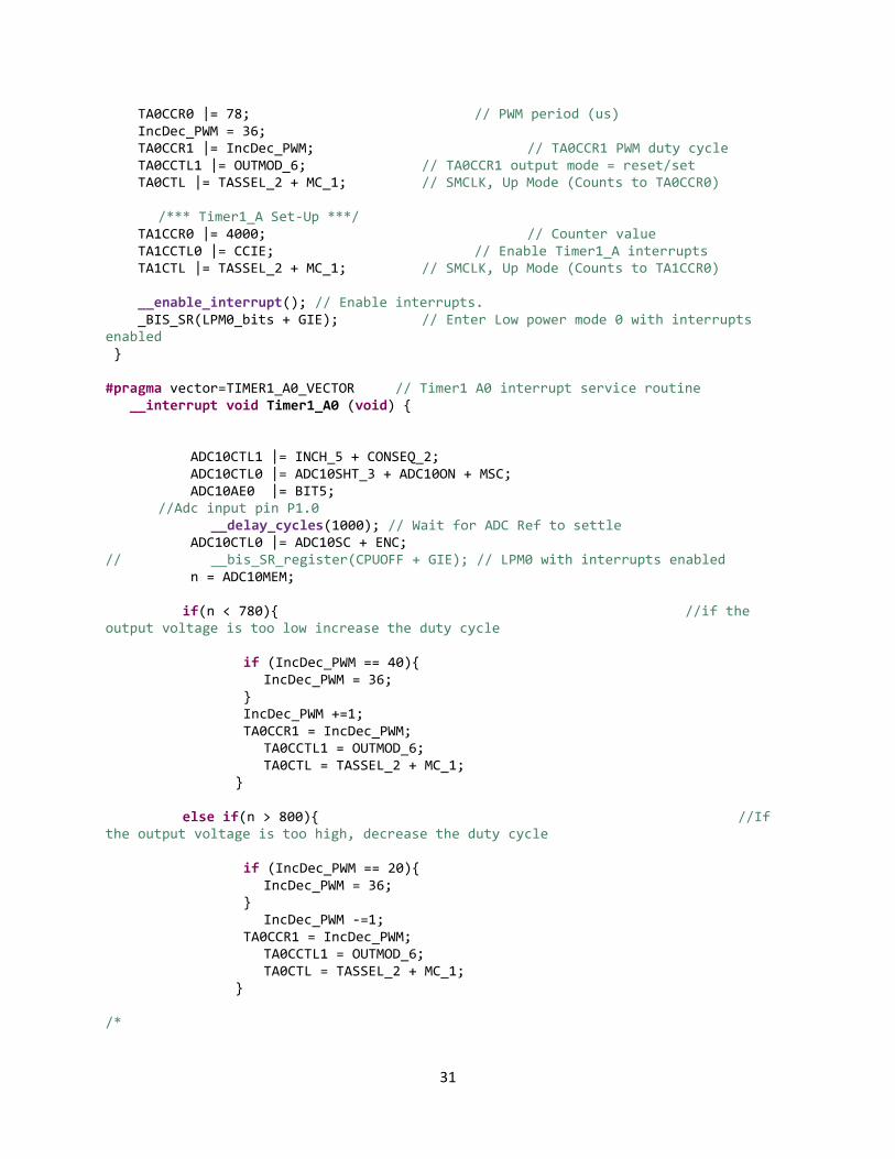
31
TA0CCR0 |= 78; // PWM period (us) IncDec_PWM = 36; TA0CCR1 |= IncDec_PWM; // TA0CCR1 PWM duty cycle TA0CCTL1 |= OUTMOD_6; // TA0CCR1 output mode = reset/set TA0CTL |= TASSEL_2 + MC_1; // SMCLK, Up Mode (Counts to TA0CCR0) /*** Timer1_A Set-Up ***/ TA1CCR0 |= 4000; // Counter value TA1CCTL0 |= CCIE; // Enable Timer1_A interrupts TA1CTL |= TASSEL_2 + MC_1; // SMCLK, Up Mode (Counts to TA1CCR0) __enable_interrupt(); // Enable interrupts. _BIS_SR(LPM0_bits + GIE); // Enter Low power mode 0 with interrupts enabled #pragma vector=TIMER1_A0_VECTOR // Timer1 A0 interrupt service routine __interrupt void Timer1_A0 (void) ADC10CTL1 |= INCH_5 + CONSEQ_2; ADC10CTL0 |= ADC10SHT_3 + ADC10ON + MSC; ADC10AE0 |= BIT5; //Adc input pin P1.0 __delay_cycles(1000); // Wait for ADC Ref to settle ADC10CTL0 |= ADC10SC + ENC; // __bis_SR_register(CPUOFF + GIE); // LPM0 with interrupts enabled n = ADC10MEM; if(n < 780) //if the output voltage is too low increase the duty cycle if (IncDec_PWM == 40) IncDec_PWM = 36; IncDec_PWM +=1; TA0CCR1 = IncDec_PWM; TA0CCTL1 = OUTMOD_6; TA0CTL = TASSEL_2 + MC_1; else if(n > 800) //If the output voltage is too high, decrease the duty cycle if (IncDec_PWM == 20) IncDec_PWM = 36; IncDec_PWM -=1; TA0CCR1 = IncDec_PWM; TA0CCTL1 = OUTMOD_6; TA0CTL = TASSEL_2 + MC_1; /*
32
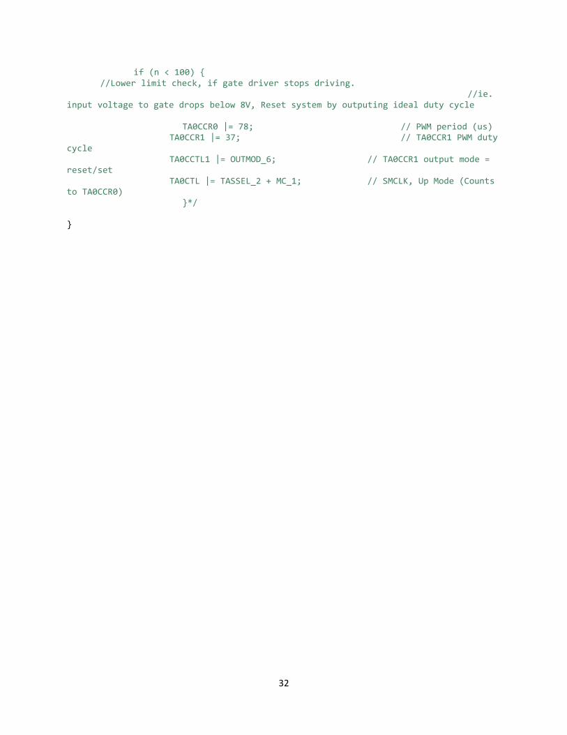
if (n < 100) //Lower limit check, if gate driver stops driving. //ie. input voltage to gate drops below 8V, Reset system by outputing ideal duty cycle TA0CCR0 |= 78; // PWM period (us) TA0CCR1 |= 37; // TA0CCR1 PWM duty cycle TA0CCTL1 |= OUTMOD_6; // TA0CCR1 output mode = reset/set TA0CTL |= TASSEL_2 + MC_1; // SMCLK, Up Mode (Counts to TA0CCR0) */
33
Appendix E Flow Chart for Buck Converter P-Control
34
Appendix F Battery Charging Time Data
F-A Battery Charging on a Cloudy Day
F-B Battery Consumption


