Embed Size (px)
Citation preview

SPARC64™ X / X+ Specification
Distribution: Public
Privilege Levels: Nonprivileged
Ver 29.0 2015/01/27
Fujitsu Limited
Fujitsu Limited 4-1-1 Kamikodanaka Nakahara-ku, Kawasaki, 211-8588 Japan
2 Ver 29.0 Jan. 2015
Copyright© 2007 - 2015 Fujitsu Limited, 4-1-1 Kamikodanaka, Nakahara-ku, Kawasaki, 211-8588, Japan. All rights reserved. This product and related documentation are protected by copyright and distributed under licenses restricting their use, copying, distribution, and decompilation. No part of this product or related documentation may be reproduced in any form by any means without prior written authorization of Fujitsu Limited and its licensors, if any. The product(s) described in this book may be protected by one or more U.S. patents, foreign patents, or pending applications. TRADEMARKS SPARC® is a registered trademark of SPARC International, Inc. Products bearing SPARC trademarks are based on an architecture developed by Oracle and / or its affiliates. SPARC64™ is a registered trademark of SPARC International, Inc., licensed exclusively to Fujitsu Limited. UNIX is a registered trademark of The Open Group in the United States and other countries. Fujitsu and the Fujitsu logo are trademarks of Fujitsu Limited. This publication is provided “as is” without warranty of any kind, either express or implied, including, but not limited to, the implied warranties of merchantability, fitness for a particular purpose, or noninfringement. This publication could include technical inaccuracies or typographical errors. Changes are periodically added to the information herein; these changes will be incorporated in new editions of the publication. Fujitsu Limited may make improvements and/or changes in the product(s) and/or the program(s) described in this publication at any time.

Index
1. Document Overview ................................................................................... 8 1.1. Fonts and Notations ....................................................................................................................................... 8
1.1.1. Font ................................................................................................................................................ 8 1.1.2. Notation .......................................................................................................................................... 8 1.1.3. Meaning of reserved and ........................................................................................................... 9 1.1.4. Access attributes ............................................................................................................................. 9 1.1.5. Informational Notes........................................................................................................................ 9
2. Definitions ................................................................................................. 11
3. Architectural Overview .............................................................................12
4. Data Formats ............................................................................................13 4.1. Densely Packed Decimal (DPD) Floating-Point Numbers ........................................................................... 13
4.1.1. Field ............................................................................................................................................. 13 4.1.2. Combination field (G) .................................................................................................................. 14 4.1.3. Trailing significand field (T) ........................................................................................................ 14 4.1.4. Cohort .......................................................................................................................................... 15 4.1.5. Normal and denormal DPD floating-point numbers ..................................................................... 15 4.1.6. Numbers that can be encoded by the DPD format ........................................................................ 15 4.1.7. Rounding modes ........................................................................................................................... 16
4.2. Packed BCD (Binary Coded Decimal) ......................................................................................................... 16 4.2.1. Fields ............................................................................................................................................ 16
4.3. Oracle floating-point numbers ..................................................................................................................... 17 4.3.1. Fields ............................................................................................................................................ 17 4.3.2. Sign (S) ........................................................................................................................................ 18 4.3.3. Exponent (exp) ............................................................................................................................. 18 4.3.4. Mantissa (significand) .................................................................................................................. 18 4.3.5. Special values ............................................................................................................................... 20 4.3.6. Normal and denormal numbers .................................................................................................... 20 4.3.7. Numbers that can be encoded as Oracle floating-point numbers .................................................. 20 4.3.8. Rounding modes ........................................................................................................................... 21 4.3.9. Extended exponent part (exp10) ................................................................................................... 21
5. Register .....................................................................................................23 5.1. Reserved Register Fields .............................................................................................................................. 23 5.2. General-Purpose R Registers ....................................................................................................................... 23
5.2.1. General-Purpose Integer Registers ............................................................................................... 23 5.2.2. Windowed R Registers ................................................................................................................. 23 5.2.3. Special R Registers ...................................................................................................................... 23
5.3. Floating-Point Registers ............................................................................................................................... 23 5.3.1. Floating-Point Register Number Encoding .................................................................................. 24 5.3.2. Using double-precision registers for single-precision operations ................................................. 24 5.3.3. Specifying registers for SIMD instructions .................................................................................. 25
5.4. Floating-Point State Register (FSR) ............................................................................................................ 26 5.5. Ancillary State Registers .............................................................................................................................. 31
5.5.1. 32-bit Multiply/Divide Register (Y) (ASR 0) ............................................................................... 31 5.5.2. Integer Condition Codes Register (CCR) (ASR 2) ...................................................................... 31 5.5.3. Address Space Identifier (ASI) Register (ASR 3) ........................................................................ 31 5.5.4. Tick (TICK) Register (ASR 4) ..................................................................................................... 31 5.5.5. Program Counters (PC, NPC) (ASR 5) ....................................................................................... 32 5.5.6. Floating-Point Registers State (FPRS) Register (ASR 6) ........................................................... 32 5.5.7. Performance Control Register (PCR) (ASR 16) .......................................................................... 32

4 Ver 29.0 Jan. 2015
5.5.8. Performance Instrumentation Counter (PIC) Register (ASR 17) ................................................. 33 5.5.9. General Status Register (GSR) (ASR 19) .................................................................................... 34 5.5.11. System Tick (STICK) Register (ASR 24) .................................................................................... 34 5.5.13. Pause Register (PAUSE) (ASR 27) ............................................................................................. 35 5.5.14. Extended Arithmetic Register (XAR) (ASR 29)........................................................................... 35 5.5.15. Extended Arithmetic Register Status Register (XASR) (ASR 30) ............................................... 37
6. Instruction Set Overview ..........................................................................40 6.1. Instruction Execution ................................................................................................................................... 40 6.2. Instruction Formats ...................................................................................................................................... 40 6.3. Instruction Categories .................................................................................................................................. 40
6.3.9 Floating-Point Operate (FPop) Instructions.................................................................................. 40 6.3.11 Reserved Opcodes and Instruction Fields .................................................................................... 41
7. Instructions ...............................................................................................42 7.1. ADD ............................................................................................................................................................. 51 7.2. Align Address............................................................................................................................................... 52 7.4. Three-Dimensional Array Addressing .......................................................................................................... 53 7.5. Byte Mask and Shuffle ................................................................................................................................. 54 7.6. Branch on Integer Condition Codes (Bicc) .................................................................................................. 55 7.7. Branch on Integer Condition Codes with Prediction (BPcc) ........................................................................ 56 7.8. Branch on Integer Register with Prediction (BPr) ........................................................................................ 57 7.9. Call and Link................................................................................................................................................ 58 7.10. Compare and Swap ...................................................................................................................................... 59 7.12. Edge Handling Instructions .......................................................................................................................... 61 7.13. Edge Handling Instructions (noCC) ............................................................................................................. 62 7.14. Convert Integer to Floating-Point ................................................................................................................ 63 7.15. Convert Between Floating-Point Formats .................................................................................................... 64 7.16. Convert Floating-Point to Integer ................................................................................................................ 66 7.17. Floating-Point Absolute Value ..................................................................................................................... 67 7.18. Floating-Point Add and Subtract .................................................................................................................. 68 7.19. Align Data .................................................................................................................................................... 70 7.20. Branch on Floating-Point Condition Codes (FBfcc) .................................................................................... 71 7.21. Branch on Floating-Point Condition Code with Prediction (FBPfcc) .......................................................... 72 7.22. Floating-Point Compare ............................................................................................................................... 73 7.23. Floating-Point Conditional Compare to Register ......................................................................................... 74 7.24. SIMD Compare (comforms to UA2011) ...................................................................................................... 76 7.25. Floating-Point Divide ................................................................................................................................... 77 7.26. Floating-Point Exponential Auxiliary .......................................................................................................... 78 7.27. FEXPAND ................................................................................................................................................... 80 7.28. Flush Instruction Memory ............................................................................................................................ 81 7.29. Flush Register Windows .............................................................................................................................. 82 7.30. Floating-Point Multiply-Add/Subtract ......................................................................................................... 83 7.31. Floating-Point Minimum and Maximum ..................................................................................................... 91 7.32. Floating-Point Move .................................................................................................................................... 93 7.33. Move Floating-Point Register on Condition (FMOVcc) .............................................................................. 94 7.34. Move Floating-Point Register on Integer Register Condition (FMOVR) .................................................... 95 7.35. Partitioned Multiply Instructions ................................................................................................................. 96 7.36. Floating-Point Multiply ................................................................................................................................ 97 7.37. Floating-Point Negative ............................................................................................................................... 98 7.38. FPACK ......................................................................................................................................................... 99 7.39. Fixed-point Partitioned Add ....................................................................................................................... 100 7.40. Integer Multiply-Add ................................................................................................................................. 102 7.41. FPMERGE ................................................................................................................................................. 103 7.42. Fixed-point Partitioned Subtract (64-bit) ................................................................................................... 104 7.43. F Register Logical Operate ........................................................................................................................ 106 7.44. Floating-Point Reciprocal Approximation ................................................................................................. 109 7.45. Move Selected Floating-Point Register on Floating-Point Register's Condition ........................................ 112 7.46. Floating-Point Square Root ........................................................................................................................ 113 7.47. Floating-Point Trigonometric Functions .................................................................................................... 114 7.48. Illegal Instruction Trap ............................................................................................................................... 119 7.49. Integer Logical Operation .......................................................................................................................... 120 7.51. Jump and Link............................................................................................................................................ 121 7.52. Load Integer ............................................................................................................................................... 122 7.53. Load Integer from Alternate Space ............................................................................................................ 123 7.54. Block Load ................................................................................................................................................. 124

7.55. Load Floating-Point ................................................................................................................................... 126 7.56. Load Floating-Point from Alternate Space ................................................................................................. 129 7.57. Short Floating-Point Load .......................................................................................................................... 132 7.58. Load-Store Unsigned Byte ......................................................................................................................... 133 7.59. Load-Store Unsigned Byte to Alternate Space ........................................................................................... 134 7.60. Load Integer Twin Word ............................................................................................................................ 135 7.61. Load Integer Twin Word from Alternate Space .......................................................................................... 136 7.62. Load Integer Twin Extended Word from Alternate Space .......................................................................... 138 7.63. Load Floating-Point State Register ............................................................................................................ 140 7.64. Memory Barrier ......................................................................................................................................... 141 7.65. Move Integer Register on Condition (MOVcc) .......................................................................................... 142 7.66. Move Integer Register on Register Condition (MOVr) .............................................................................. 143 7.67. Multiply Step ............................................................................................................................................. 144 7.68. Multiply and Divide (64-bit) ...................................................................................................................... 146 7.69. No Operation .............................................................................................................................................. 147 7.72. Partitioned Add .......................................................................................................................................... 148 7.73. Pixel Component Distance (with Accumulation) ....................................................................................... 149 7.74. Population Count ....................................................................................................................................... 150 7.75. Prefetch ...................................................................................................................................................... 151
7.75.1. Prefetch Variants ........................................................................................................................ 151 7.75.2. Weak versus Strong Prefetches................................................................................................... 152
7.76. Read Ancillary State Register (RDASR) .................................................................................................... 154 7.79. Return ........................................................................................................................................................ 155 7.80. SAVE and RESTORE ................................................................................................................................ 156 7.82. Signed Divide (64-bit÷32-bit) .................................................................................................................... 157 7.83. SETHI ........................................................................................................................................................ 158 7.85. Set Interval Arithmetic Mode ..................................................................................................................... 159 7.87. Shift............................................................................................................................................................ 160 7.88. Signed Multiply (32-bit) ............................................................................................................................ 161 7.89. Sleep .......................................................................................................................................................... 162 7.91. Store Barrier ............................................................................................................................................... 163 7.92. Store Integer ............................................................................................................................................... 164 7.93. Store Integer into Alternate Space .............................................................................................................. 165 7.94. Block Initializing Store .............................................................................................................................. 166 7.95. Block Store ................................................................................................................................................ 167 7.96. Store Floating-Point ................................................................................................................................... 169 7.97. Store Floating-Point into Alternate Space .................................................................................................. 171 7.98. Store Floating-Point Register on Register Condition (for SPARC64™ X) ................................................ 174 7.99. Store Partial Floating-Point ........................................................................................................................ 177 7.100. Store Short Floating-Point.......................................................................................................................... 178 7.101. Store Integer Twin Word ............................................................................................................................ 179 7.102. Store Integer Twin Word into Alternate Space ........................................................................................... 180 7.103. Store Floating-Point State Register ............................................................................................................ 181 7.104. Subtract ...................................................................................................................................................... 182 7.105. Swap Register with Memory ...................................................................................................................... 183 7.106. Set XAR (SXAR) ....................................................................................................................................... 184 7.107. Tagged Add and Subtract ........................................................................................................................... 185 7.108. Trap on Integer Condition Code (Tcc) ....................................................................................................... 186 7.109. Unsigned Divide (64-bit÷32-bit) ................................................................................................................ 187 7.110. Unsigned Multiply (32-bit) ........................................................................................................................ 188 7.111. Write Ancillary State Register (WRASR) .................................................................................................. 189 7.114. Cache Line Fill with Undetermined Values ................................................................................................ 190 7.115. DES support instructions............................................................................................................................ 192 7.116. AES support instructions............................................................................................................................ 197 7.117. Decimal Floating-Point Operations ............................................................................................................ 204 7.118. Oracle Floating-Point Operations ............................................................................................................... 209 7.119. Decimal Floating-Point Compare ............................................................................................................... 217 7.120. Oracle Decimal Floating-Point Compare ................................................................................................... 219 7.121. Decimal Floating-Point Convert ................................................................................................................ 220 7.122. Shift Mask Or (for SPARC64™ X) ............................................................................................................ 222 7.123. SIMD Compare (for SPARC64™ X) ......................................................................................................... 226 7.124. Leading Zero Detect................................................................................................................................... 230 7.125. Fixed-point Partitioned Add (64-bit) .......................................................................................................... 231 7.126. Fixed-point Partitioned Subtract (64-bit) ................................................................................................... 232 7.127. SIMD Unsigned Compare .......................................................................................................................... 233 7.128. Floating-Point Lexicographic Compare ..................................................................................................... 234

6 Ver 29.0 Jan. 2015
7.129. Floating-Point Negative Add ...................................................................................................................... 235 7.130. Floating-Point Negative Multiply .............................................................................................................. 237 7.131. WRPAUSE(PAUSE) .................................................................................................................................. 239 7.132. Load Entire Floating-Point State Register .................................................................................................. 241 7.133. Compare and Branch (CBcond) ................................................................................................................. 242 7.134. Partitioned Move Selected Floating-Point Register on Floating-Point Register’s Condition ..................... 243 7.135. 64-bit Integer Compare on Floaing-Point Register .................................................................................... 246 7.136. 64-bit Integer Shift on Floating-Point Register .......................................................................................... 247 7.137. Store Floating-Point Register on Register Condition (Extension of SPARC64™ X+) .............................. 248 7.138. Shift Mask Or (Extension of SPARC64™ X+) .......................................................................................... 252 7.139. SIMD Compare (Extension of SPARC64™ X+) ....................................................................................... 257 7.140. Fixed-Point Partitioned Add (128-bit) ........................................................................................................ 261 7.141. Integer Minimum and Maximum ............................................................................................................... 262 7.142. Move Integer Register to Floating-Point Register (for SPARC64™ X+) .................................................. 264
8. IEEE Std. 754-1985 Requirements for SPARC-V9 .................................. 265 8.1. Nonstandard Floating-Point Mode ............................................................................................................. 265
8.1.1. fp_exception_other(ftt = unfinished_FPop) ..................................................................... 265 8.1.2. Behavior when FSR.ns = 1 ....................................................................................................... 268
9. Memory Models ....................................................................................... 272
10. Address Space Identifiers ........................................................................ 273 10.3. ASI Assignment ....................................................................................................................................... 273
10.3.1. Supported ASIs........................................................................................................................... 273 10.3.2 . ASI access exceptions ......................................................................................................... 275
11. Performance Instrumentation ................................................................. 277 11.1. Overview .................................................................................................................................................... 277
11.1.1. Sample Pseudo-codes ................................................................................................................. 278 11.2. Description of PA Events ........................................................................................................................... 280
11.2.1. Instruction and Trap Statistics .................................................................................................... 286 11.2.2. MMU and L1 cache Events ........................................................................................................ 292 11.2.3. L2 cache Events ......................................................................................................................... 293 11.2.4. Bus Transaction Events .............................................................................................................. 295
11.3. Cycle Accounting ....................................................................................................................................... 296
12. Traps ........................................................................................................ 298 12.1. Virtual Processor Privilege Modes ............................................................................................................. 298 12.5. Trap list and priorities ................................................................................................................................ 298
12.5.1. Trap Descriptions ....................................................................................................................... 302 12.5.2. Special cases for priority ............................................................................................................ 310
13. Memory Management Unit ..................................................................... 311 13.1. Address types ............................................................................................................................................. 311 13.4. TSB Translation Table Entry (TTE) ........................................................................................................... 311 13.6. Context Registers ....................................................................................................................................... 312 13.8. Page sizes ................................................................................................................................................... 313
14. Opcode Maps ........................................................................................... 314
15. Assembly Language Syntax .................................................................... 323 15.1. Notation Used ............................................................................................................................................ 323
15.1.1. Other Operand Syntax ................................................................................................................ 323 15.2. HPC-ACE Notation.................................................................................................................................... 323
15.2.1. Suffixes for HPC-ACE Extensions ............................................................................................. 324

Preface
This document defines the logical specification of SPARC64™ X / SPARC64™ X+ and is based on Oracle SPARC Architecture 2011(UA2011). Differences from UA2011 are noted in this document or as references to other documents.
This specification refers to the following documents:. • Oracle SPARC Architecture 2011. Draft D0.9.6, May 2014. http://www.oracle.com/technetwork/server-storage/sun-sparc-enterprise/documentati
on/140521-ua2011-d096-p-ext-2306580.pdf We refer to this document as UA2011.
• SPARC64 VIIIfx Extensions. Ver 15, 26 Apr. 2010. http://img.jp.fujitsu.com/downloads/jp/jhpc/sparc64viiifx-extensions.pdf We refer to this document as SPARC64 VIIIfx Extensions.
• SPARC® Joint Programming Specification (JPS1): Commonality Release 1.0.4, 31 May 2002. http://www.fujitsu.com/downloads/PRMPWR/JPS1-R1.0.4-Common-pub.pdf We refer to this document as JPS1.

8 Ver 29.0 Jan. 2015
1. Document Overview
1.1. Fonts and Notations
1.1.1. Font • Arial font is used for registers and register fields (REG and REG.field, respectively).
This font is also used when reffering to the field of an ASI register. • Courier font is used for ASI names (ASI_NAME), which are prefixed by ASI_. We
avoid the use of the construction ASI_NAME.field. • Italic Arial font is used for exceptions (exception_name). • Uppercase Courier font is used for instructions (INSTRUCTION). • Courier font is used for CPU states (CPU_state). • Italic Times Roman font or “” is used for reserved, which indicates that a register
field is reserved for future expansion.
1.1.2. Notation The notation used in this document generally follws the notation used in JPS1.
Specifically, • Numbers are decimal unless otherwise indicated by a numeric subscript (for example,
10002). • Spaces may be inserted in long binary or hex numbers (for example, 1000 000016) to
improve readability. • Verilog notation may be used for some numbers. For example, the prefixes
“{bit_width}’B” and “{bit_width}’h indicate binary and hexadecimal numbers, respectively. When Verilog notation is used, there is no numeric subscript indicating the base.
• Numbered integer and floating-point registers are written as R[number] and F[number], respectively.
• Instruction names and various objects may contain the symbols {} | * and n. • A character string enclosed by {} is optional. For example,
ASI_PRIMARY{_LITTLE} expands to ASI_PRIMARY and ASI_PRIMARY_LITTLE.
• If there are | symbols inside the curly braces {}, one of the character strings separated by the vertical bars must be selected. For example, FMUL{s|d} expands to FMULs and FMULd. An empty charater string makes the alternatives inside the braces optional. For example, F{|N}sMULd is equivalent to F{N}sMULd.
• The * and n symbols indicate character string and numeric substitution, respectively, for all possible values. For example, DAE_* expands to DAE_invalid_asi, DAE_nc_page, DAE_nfo_page, DAE_privilege_violation, and DAE_side_effect_page. spill_n_normal expands to spill_0_normal, spill_1_normal,

spill_2_normal, spill_3_normal, spill_4_normal, spill_5_normal, spill_6_normal, and spill_7_normal.
• Bit strings are of the form <a> and <a:b>. • The double dolon (::) operator concatenates two bit strings. • ASCII characters are used.
1.1.3. Meaning of reserved and reserved or indicates that a bit field is reserved for future expansion and has an undefined value. reserved is used when future expansion is expected; a brief description of the field is provided. is used when the usage is undecided. No description is provided for fields marked with .
1.1.4. Access attributes Registers and register fields may have the access attributes shown in the table below.
Table 1-1 Access attributes
Access attribute
Object Operation Read Write
Field Undefined value Ignored. R Register and Field The value is read. Ignored. RO Register and Field The value is read. Not permitted. R0 Field Zero is read. Ignored. W Register and Field Undefined value The value is written. WO Register and Field Not permitted. The value is written. RW Register and Field The value is read. The value is written. RW1C Field The value is read. Writing 1 clears the
field.i RWQF Field The value is read. Register value indicates
condition, and a write of the same value is preserved in the register. Otherwise, the write is ignored.
RWS/R0WS Register The value is read. Or, zero is read.
Causes side effect. Value to be written is ignored.
1.1.5. Informational Notes This document contains several different types of information notes.
Compatibility Note Compatibility notes explain compatibility differences versus SPARC V8/V9, JPS1, SPARC64 VIIIfx Extensions, and UA2011.
Note Notes provide general information. i The bit range that is reset to 0 depends on the field.

10 Ver 29.0 Jan. 2015
Programming Note Programming notes provide information for writing software.

2. Definitions
For additional definitions, please refer to Chapter 2 of UA2011.
CPUID :
A CPUID is the unique logical ID of a strand in a system. The CPUID contains the LSBID (logical system board ID) and Chip ID (physical processor ID within a system board).
LSB (Logical System Board) :
A physical partition is a set of one or more system boards that work together as a single system. An LSB is a system board in a physical partition and is identified by the allocated logical ID.
VCPU (Virtual Processor):
A virtual processor (refer to Chapter 2 of UA2011). SPARC64™ X and SPARC64™ X+ have two VCPUs per physical CPU core.
12 Ver 29.0 Jan. 2015
3. Architectural Overview
Feature • HPC-ACE and SMT are supported. VA is 64-bits wide and has no hole bit. • RA is normally 64 bits wide. • Instructions only on local ROM can be executed for non-cacheable space. • NWINDOWS = 8 • MAXPTL = 2
Present parameter • 16 cores/chip and 2SMT/core • L1 instruction cache : 64KB/4way ; L1 data cache : 64KB/4way ; Unified L2 cache :
24MB/24way ; line size of all cache memories : 128 bytes • For main TLB, set-associative TLB only. instruction : 1024entries/4way ; data :
1024entries/4way ; page size : 4 sizes (8KB, 64KB, 4MB, 256MB)

4. Data Formats
Refer to UA2011 for Integer Data Formats, Floating-Point Data Formats, and VIS instruction set SIMD Data Formats.
Refer to 5.3 Floating-Point Registers in this document for the HPC-ACE SIMD Data Format.
4.1. Densely Packed Decimal (DPD) Floating-Point Numbers
SPARC64™ X / SPARC64™ X+ support decimal floating-point numbers encoded with the DPD (Densely Packed Decimal) format defined by IEEE754-2008 and instructions that operate on DPD floating-point numbers.
4.1.1. Field The value of a DPD floating-point number is given by the following expression, where S, the exponent, and the significand are integers. S has a value of 0 or 1.
exponentS dsignifican 10)1( ××−
A DPD floating-point number is encoded by a sign field S, a combination field G, and a trailing significand field T. The exponent is stored in the combination field G, and the significand is split between G and the trailing significand field T. The combination field G has additional structure, with two bit ranges that are 5-bits wide and W bits wide.
SPARC64™ X / SPARC64™ X+ support the DPD format for both single-precision and double-precision floating-point numbers.
Table 4-1 DPD format field widths
Single precision Double precision Entire data 32 bits 64 bits S 1 bit 1 bit G (W + 5) 11 bits 13 bits W 6 bits 8 bits T 20 bits 50 bits
S G T 31 30 20 19 0
Figure 4-1 DPD floating-point single-precision data format
S G T 63 62 50 49 0
14 Ver 29.0 Jan. 2015
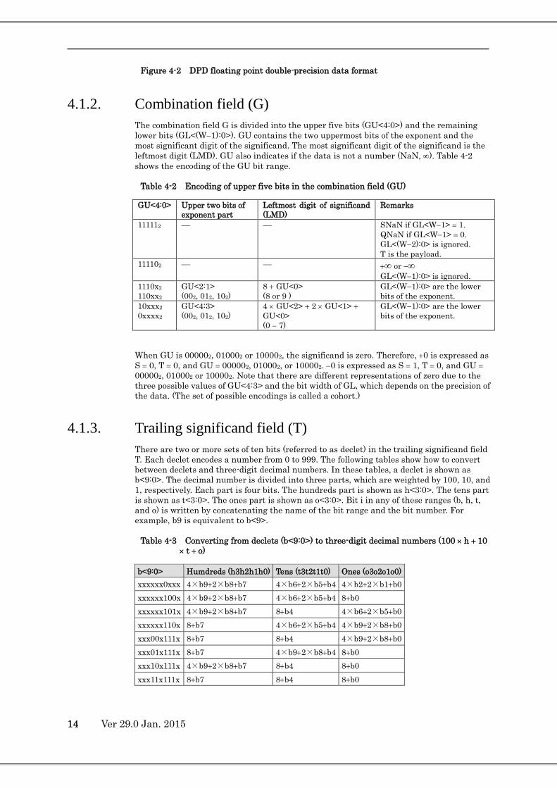
Figure 4-2 DPD floating point double-precision data format
4.1.2. Combination field (G) The combination field G is divided into the upper five bits (GU<4:0>) and the remaining lower bits (GL<(W−1):0>). GU contains the two uppermost bits of the exponent and the most significant digit of the significand. The most significant digit of the significand is the leftmost digit (LMD). GU also indicates if the data is not a number (NaN, ∞). Table 4-2 shows the encoding of the GU bit range.
Table 4-2 Encoding of upper five bits in the combination field (GU)
GU<4:0> Upper two bits of exponent part
Leftmost digit of significand (LMD)
Remarks
111112 SNaN if GL<W−1> = 1. QNaN if GL<W−1> = 0. GL<(W−2):0> is ignored. T is the payload.
111102 +∞ or −∞ GL<(W−1):0> is ignored.
1110x2 110xx2
GU<2:1> (002, 012, 102)
8 + GU<0> (8 or 9 )
GL<(W−1):0> are the lower bits of the exponent.
10xxx2 0xxxx2
GU<4:3> (002, 012, 102)
4 × GU<2> + 2 × GU<1> + GU<0> (0 − 7)
GL<(W−1):0> are the lower bits of the exponent.
When GU is 000002, 010002 or 100002, the significand is zero. Therefore, +0 is expressed as S = 0, T = 0, and GU = 000002, 010002, or 100002. −0 is expressed as S = 1, T = 0, and GU = 000002, 010002 or 100002. Note that there are different representations of zero due to the three possible values of GU<4:3> and the bit width of GL, which depends on the precision of the data. (The set of possible encodings is called a cohort.)
4.1.3. Trailing significand field (T) There are two or more sets of ten bits (referred to as declet) in the trailing significand field T. Each declet encodes a number from 0 to 999. The following tables show how to convert between declets and three-digit decimal numbers. In these tables, a declet is shown as b<9:0>. The decimal number is divided into three parts, which are weighted by 100, 10, and 1, respectively. Each part is four bits. The hundreds part is shown as h<3:0>. The tens part is shown as t<3:0>. The ones part is shown as o<3:0>. Bit i in any of these ranges (b, h, t, and o) is written by concatenating the name of the bit range and the bit number. For example, b9 is equivalent to b<9>.
Table 4-3 Converting from declets (b<9:0>) to three-digit decimal numbers (100 × h + 10 × t + o)
b<9:0> Humdreds (h3h2h1h0) Tens (t3t2t1t0) Ones (o3o2o1o0) xxxxxx0xxx 4×b9+2×b8+b7 4×b6+2×b5+b4 4×b2+2×b1+b0 xxxxxx100x 4×b9+2×b8+b7 4×b6+2×b5+b4 8+b0 xxxxxx101x 4×b9+2×b8+b7 8+b4 4×b6+2×b5+b0 xxxxxx110x 8+b7 4×b6+2×b5+b4 4×b9+2×b8+b0 xxx00x111x 8+b7 8+b4 4×b9+2×b8+b0 xxx01x111x 8+b7 4×b9+2×b8+b4 8+b0 xxx10x111x 4×b9+2×b8+b7 8+b4 8+b0 xxx11x111x 8+b7 8+b4 8+b0

Table 4-4 Converting from three-digit decimal numbers (100 × h + 10 × t + o) to declets (b<9:0>)
Hundreds h3 h2 h1 h0
Tens t3 t2 t1 t0
Ones o3 o2 o1 o0
b9 b8 b7 b6 b5 b4 b3 b2 b1 b0
0xxx 0xxx 0xxx h2 h1 h0 t2 t1 t0 0 o2 o1 o0
0xxx 0xxx 100x h2 h1 h0 t2 t1 t0 1 0 0 o0
0xxx 100x 0xxx h2 h1 h0 o2 o1 t0 1 0 1 o0 0xxx 100x 100x h2 h1 h0 1 0 t0 1 1 1 o0 100x 0xxx 0xxx o2 o1 h0 t2 t1 t0 1 1 0 o0 100x 0xxx 100x t2 t1 h0 0 1 t0 1 1 1 o0 100x 100x 0xxx o2 o1 h0 0 0 t0 1 1 1 o0 100x 100x 100x x x h0 1 1 t0 1 1 1 o0
Note that a declet b<9:0> can encode 1024 numbers, while a three-digit decimal number only encodes 1000 numbers. In other words, some decimal numbers convert to more than one declet of equivalent value. The bottom row of Table 4-4 shows the cases where b<9:8> may assume different values for the same decimal number.
The following table explicitly shows the decimal numbers with multiple declets.
b<9:0> Decimal number b<9:0> Decimal number 06E16, 16E16, 26E16, 36E16 888 0EE16, 1EE16, 2EE16, 3EE16 988 06F16, 16F16, 26F16, 36F16 889 0EF16, 1EF16, 2EF16, 3EF16 989 07E16, 17E16, 27E16, 37E16 898 0FE16, 1FE16, 2FE16, 3FE16 998 07F16, 17F16, 27F16, 37F16 899 0FF16, 1FF16, 2FF16, 3FF16 999
4.1.4. Cohort The encoding of a real number in the DPD floating-point format is not unique. For example, 1.000 × 102 = 10.00 × 101 = 100.0 × 100. The set of equivalent encodings is called a cohort. The number of cohort members for a DPD floating-point number depends on the value. For example, 1.000 × 10² has 7 cohort members in single precision and 16 members in double precision. As discussed in section 4.1.2, zero has multiple encodings due to the 3 possible values of GU and the width of GL. Note that +0 and −0 are different numbers and are not part of the same cohort.
When comparing DPD floating-point numbers, some members of a cohort are considered equivalent.
4.1.5. Normal and denormal DPD floating-point numbers A DPD floating-point number is normal if there is a cohort member with LMD greater than 0.
A number is denormal if the cohort member with the smallest exponent has an LMD of 0.
+/−0 and +/−∞ are neither normal nor denormal numbers.
4.1.6. Numbers that can be encoded by the DPD format Table 4-5 shows the numbers that can be expressed as DPD floating-point numbers.
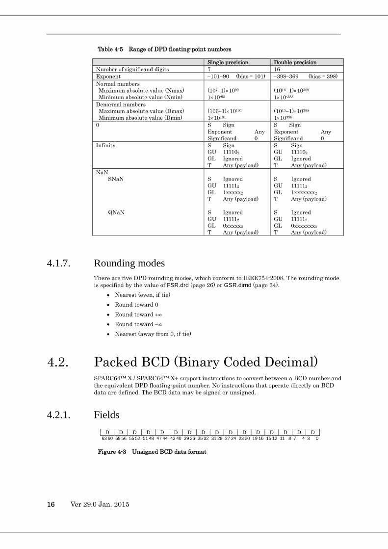
16 Ver 29.0 Jan. 2015
Table 4-5 Range of DPD floating-point numbers
Single precision Double precision Number of significand digits 7 16 Exponent −101−90 (bias = 101) −398−369 (bias = 398) Normal numbers Maximum absolute value (Nmax) Minimum absolute value (Nmin)
(107−1)×1090 1×10-95
(1016−1)×10369 1×10-383
Denormal numbers Maximum absolute value (Dmax)
Minimum absolute value (Dmin)
(106−1)×10101
1×10101
(1015−1)×10398
1×10398 0 S Sign
Exponent Any Significand 0
S Sign Exponent Any Significand 0
Infinity
S Sign GU 111102 GL Ignored T Any (payload)
S Sign GU 111102 GL Ignored T Any (payload)
NaN SNaN QNaN
S Ignored GU 111112 GL 1xxxxx2 T Any (payload) S Ignored GU 111112 GL 0xxxxx2 T Any (payload)
S Ignored GU 111112 GL 1xxxxxxx2 T Any (payload) S Ignored GU 111112 GL 0xxxxxxx2 T Any (payload)
4.1.7. Rounding modes There are five DPD rounding modes, which conform to IEEE754-2008. The rounding mode is specified by the value of FSR.drd (page 26) or GSR.dirnd (page 34).
• Nearest (even, if tie) • Round toward 0 • Round toward +∞ • Round toward −∞ • Nearest (away from 0, if tie)
4.2. Packed BCD (Binary Coded Decimal) SPARC64™ X / SPARC64™ X+ support instructions to convert between a BCD number and the equivalent DPD floating-point number. No instructions that operate directly on BCD data are defined. The BCD data may be signed or unsigned.
4.2.1. Fields
D D D D D D D D D D D D D D D D 63 60 59 56 55 52 51 48 47 44 43 40 39 36 35 32 31 28 27 24 23 20 19 16 15 12 11 8 7 4 3 0
Figure 4-3 Unsigned BCD data format

D D D D D D D D D D D D D D D S 63 60 59 56 55 52 51 48 47 44 43 40 39 36 35 32 31 28 27 24 23 20 19 16 15 12 11 8 7 4 3 0
Figure 4-4 Signed BCD data format
A number 0-9 is encoded by four bits in the BCD number. Each field "D" in Figure 4-3 and Figure 4-4 is one decimal digit. The signed BCD data format encodes 15 decimal digits, and the unsigned BCD data format encodes 16 decimal digits. If any field "D" has a value of A16 − F16, the data is not a BCD number.
In a signed BCD number, the least significant four bits S encode the sign of the number. Table 4-6 shows the relationship between the value of S and the sign. Note that SPARC64™ X / SPARC64™ X+ encode the plus sign as C16 and the minus sign as D16.
Table 4-6 Sign of BCD data
S Sign S Sign 016 + 816 + 116 + 916 + 216 + A16 + 316 + B16 − 416 + C16 + 516 + D16 − 616 + E16 + 716 + F16 +
4.3. Oracle floating-point numbers Compatibility Note The specification for Oracle floating-point numbers
may change in the future. This format should be used only for libraries targeting the SPARC64™ X and SPARC64™ X+ platforms.
SPARC64™ X / SPARC64™ X+ support Oracle floating-point numbers and instructions that operate on these numbers.
4.3.1. Fields An Oracle floating-point number consists of a sign S, an exponent exp, and a significand. S is an integer with value 0 or 1, exp is an integer with value -65 to 62, and the significand is a number with a fixed number of digits and value 0 to 99.999999999999. The value is given by the following expression.
exp)1( 100)1( ××− − dsignificanS
Table 4-7 Oracle floating-point fields widths
Oracle floating-point number Entire data 64 bits S 1 bit exp 7 bits Significand 56 bits
S exp Significand 63 62 56 55 0

18 Ver 29.0 Jan. 2015
Figure 4-5 Oracle floating-point data format
4.3.2. Sign (S) The field S encodes the sign. Table 4-8 shows the possible values of sign S.
Table 4-8 Sign encoding
S Sign 0 Negative 1 Positive
4.3.3. Exponent (exp) The exponent is stored in the field exp, which has a value in the range −65 to 62. The maximum exponent encoded by exp is infinity. The encoding of the exponent depends on the sign S. The field exp is encoded in ascending order if the sign is positive and in descending order if the sign is negative. The calculation of the exponent from integer exp<6:0> is shown in Table 4-9.
Table 4-9 Exponent calculation
S Exponent 0 (negative) 62-exp<6:0> 1 (positive) exp<6:0>-65
Table 4-10 shows the explicit encoding of the exponent.
Table 4-10 Exponent encoding
S exp<6:0> Exponent 0 (negative) 0 62 (or, −∞)
1 61 .. 62 0 ..
126 −64 127 −65
1 (positive) 0 −65 1 −64 .. 65 0 .. 126 61 127 62 (or, +∞)
4.3.4. Mantissa (significand) The significant consists of seven bytes. Each byte encodes an integer 0−99. The value of the significand in relation to these seven integers (digits) is given by the following expression.

∑=
−×6
0100
i
iidigit
digit0 digit1 digit2 digit3 digit4 digit5 digit6
55 48 47 40 39 32 31 24 23 16 15 8 7 0
Figure 4-6 Significand format
The encoding of these bytes depends on the sign S. The digits of a positive value are encoded in ascending order. The digits of a negative value are encoded in descending order. Each integer is expressed as digit<7:0> and is calculated as shown in Table 4-11
Table 4-11 Integer Calculation
S Integer 0 (negative) 101-digit<7:0> 1 (positive) digit<7:0>-1
Table 4-12 shows the explicit encoding of each digit.
Table 4-12 Encoding of digit<7:0 >
S digit<7:0> Number 0 (negative) 0 − 1 Outside the range (treated as 0)
2 99 3 98 4 97 .. 99 2 100 1 101 0 102 − 255 Outside the range (treated as 0)
1 (positive) 0 Outside the range (treated as 0) 1 0 2 1 3 2 . 98 97 99 98 100 99 101 − 255 Outside the range (treated as 0)
Note When a number with all digits outside the range is specified as an operand, it is generally treated as 0. In certain combinations where a digit has the value 0 or 101, the number may be treated as infinity. See Section 4.3.5.

20 Ver 29.0 Jan. 2015
4.3.5. Special values The values 0, −∞, +∞ and dNAN are special Oracle floating-point numbers. These values are expressed as a combination of several fields. The combination of these fields is shown below.
When an operation results in the special value 0, −∞, +∞, or dNAN, the resulting Oracle floating-point number has the format shown in Table 4-13.
Table 4-13 Output of special values
Special value S exp digit0 digit1-6 Remarks 0 1 (positive) 0 0 0 Negative 0 is never an output. −∞ 0 (negative) 0 0 0 +∞ 1 (positive) 127 101 0 dNAN 1 (positive) 0 0 0 Same as 0. It is not possible to
distinguish between dNAN and 0 from the result.
To use a special value as the operand of an operation, specify the Oracle floating-point number as described in Table 4-14. To input −∞ or +∞, specify S, exp, and digit0 as described in Table 4-14. To input 0, specify all digits with values treated as 0. The value dNAN cannot be specified.
Table 4-14 Input of special values
Special value
S exp digit0 digit1-6 Remarks
0 *0* *0* *0* is a value 0 − 1 or 101 − 255. −∞ 0
(negative) 0 0 Negative digit 0 is outside the range, as shown in
Table 4-12. +∞ 1 (positive) 127 101 Positive digit 101 is outside the range, as shown
in Table 4-12. dNAN Cannot be specified.
4.3.6. Normal and denormal numbers An Oracle floating-point number is normal if the value of digit0 of the significand is larger than 0. The number is denormal if the value of digit0 of the significand is 0.
The Oracle floating-point numbers 0 and +/-∞ are neither normal nor denormal.
Note In SPARC64™ X / SPARC64™ X+, most operations with Oracle floating-point numbers always output a normal number or one of the special values defined in Section 4.3.5. Operations can be denormal. A few instructions output the result without normalizing the value. Refer to the specification of each instruction for details.
4.3.7. Numbers that can be encoded as Oracle floating-point numbers Table 4-15 shows the numbers that can be expressed as Oracle floating-point numbers.

Table 4-15 Range of Oracle floating-point numbers
Oracle floating-point number Number of significand digits (decimal number)
7 (14)
Exponent −65 − 62 (bias = 65) Normal numbers Maximum absolute value (Nmax) Minimum absolute value (Nmin)
99.999999999999 × 10062
1 × 100-65 Denormal numbers Maximum absolute value (Dmax) Minimum absolute value (Dmin)
0.999999999999 × 10062
1 × 10071 Special values 0 −∞ +∞ dNaN
Refer to Section 4.3.5.
4.3.8. Rounding modes There are five rounding modes for Oracle floating-point numbers. The rounding mode is specified by the value of FSR.drd (page 26) or GSR.irnd (page 34).
• Nearest (even if tie) • Round toward 0 • Round toward +∞ • Round toward −∞ • Nearest (away from 0, if tie)
Note The least significant bit (LSB) of the significand is rounded after normalization. The LSB is the rightmost bit. When rounding, normalization ignores the limits imposed by the encoding of the exponent. If the rounded result is denormal, 0 is returned.
Example) 0.200000000001e-65
1) Normalizing this value gives the number 20.000000000100 e-66. (Remember that the exponent is a power of 100.) Note that the minimum possible exponent that can be encoded is -65.
2) Then the LSB of the normalized number is 0 and rounding does not change the value. After forcing the rounded number to satisfy the minimum value of the exponent, we recover the original number, whose most significant bit is 0. The result is denormal and 0 is returned.
Note Underflow is decided after rounding for Oracle floating-point numbers, unlike IEEE 754, where underflow is decided before rounding.
4.3.9. Extended exponent part (exp10) Certain instructions take an extended exponent as an operand. The extended exponent specifies the exponent as a power of 10 instead of 100 (see the formula in Section 4.3.1). It
22 Ver 29.0 Jan. 2015
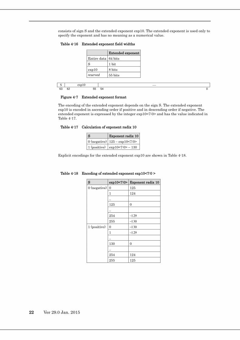
consists of sign S and the extended exponent exp10. The extended exponent is used only to specify the exponent and has no meaning as a numerical value.
Table 4-16 Extended exponent field widths
Extended exponent Entire data 64 bits S 1 bit exp10 8 bits reserved 55 bits
S exp10 63 62 55 54 0
Figure 4-7 Extended exponent format
The encoding of the extended exponent depends on the sign S. The extended exponent exp10 is encoded in ascending order if positive and in descending order if negative. The extended exponent is expressed by the integer exp10<7:0> and has the value indicated in Table 4-17.
Table 4-17 Calculation of exponent radix 10
S Exponent radix 10 0 (negative) 125 − exp10<7:0> 1 (positive) exp10<7:0> − 130
Explicit encodings for the extended exponent exp10 are shown in Table 4-18.
Table 4-18 Encoding of extended exponent exp10<7:0 >
S exp10<7:0> Exponent radix 10 0 (negative) 0 125
1 124 .. 125 0 ..
254 −129 255 −130
1 (positive) 0 −130 1 −129 .. 130 0 .. 254 124 255 125

5. Register
5.1. Reserved Register Fields Refer to Section 5.1 in UA2011.
Compatibility Note To preserve compatibility with previous platforms, some reserved fields will read as 0.
Programming Note When comparing values, reserved fields should be masked and excluded from the comparison.
5.2. General-Purpose R Registers
5.2.1. General-Purpose Integer Registers Refer to Section 5.2.1 in UA2011.
Global registers are referred to as R[0] – R[7] or g[0] – g[7] in this specification. There is no notation for indicating which set of global registers is currently selected by the GL register.
5.2.2. Windowed R Registers Refer to Section 5.2.2 in UA2011.
The number of windowed register sets, N_REG_WINDOWS, is 8.
5.2.3. Special R Registers Refer to Section 5.2.3 in UA2011.
5.3. Floating-Point Registers In addition to the floating-point registers defined in Section 5.3 Floating-Point Registers of UA2011, new double-precision floating-point registers Fd[64] – Fd[126] and Fd[256] – Fd[382] are added. Only even-numbered registers can be accessed. The XASR register is added to display the state of the additional registers. See “Extended Arithmetic Register Status Register (XASR)” (page 37) for details.
Fd[0] – Fd[126] are called the Basic Floating-Point Registers, and Fd[256] – Fd[382] are called the Extended Floating-Point Registers. In addition, Fd[0] – Fd[62] are also called V9 Floating-Point Registers.

24 Ver 29.0 Jan. 2015
5.3.1. Floating-Point Register Number Encoding Refer to Section 5.3.1 in UA2011.
We expand the encoding of floating-point registers defined in UA2011 to support the addition of the HPC-ACE floating-point registers.
The XAR register contains the urs1, urs2, urs3, and urd fields, which extend the rs1, rs2, rs3, and rd fields in an instruction word. A decoded HPC-ACE register number is a 9-bit number. The upper 3 bits are specified in the XAR and are concatenated with the decoded 6-bit register number. When an instruction uses HPC-ACE floationg-point registers, it must use double-precision floating-point registers. Then the least significant bit of the register number is always 0, and 128 even-numbered registers Fd[0] – Fd[126] and Fd[256] – Fd[382] can be specified by this encoding.
Figure 5-1 HPC-ACE Floating-Point Register Number Encoding
5.3.2. Using double-precision registers for single-precision operations In SPARC64™ X / SPARC64™ X+, double-precision registers can be used to perform single-precision operations. This applies not only to the registers added in SPARC64™ X / SPARC64™ X+ but also to the double-precision registers defined in SPARC V9. To use a double-precision register for a single-precision operation, it is sufficient to set XAR.v = 1 at execution time. Thus, a SIMD single-precision operation always uses double-precision registers.
When using a double-precision register for a single-precision operation, the following behavior differs from the SPARC V9 specification:
• The encoding of the instruction field is the same as for a double-precision operand in TABLE 5-3 of UA2011. Consequently, only even-numbered registers Fd[2n] (n = 0 – 63, 128 – 191) can be used.
• The upper 4 bytes of the register (bits <63:32>) are treated as a single-precision value, and the lower 4 bytes (bits <31:0>) are ignored.
• Execution results and load data are written in the upper 4 bytes, and zeroes are written in the lower 4 bytes.
b<4> b<3> b<2> b<1> b<5>
b<4> b<3> b<2> b<1> 0 b<5>
b<4> b<3> b<2> b<1> 0 b<5> u<1> u<0> u<2>
Encoded Register Number
Decoded Register Number
Decoded HPC-ACE Register Number
from XAR

Programming Note When XAR.v = 1 and XAR.urs1 = 0, the SPARC V9 double-precision register specified by rs1 is used to perform a single-precision operation. There are similar cases for rs2, rs3, and rd. In these situations, bits <31:0> of the register overlap an odd-numbered register, and will be written over with zeroes.
Endian conversion is done for each single-precision word; that is, endian conversion is done in 4-byte units.
5.3.3. Specifying registers for SIMD instructions
When XAR.v = 1 and XAR.SIMD = 1, the majority of instructions that use the floating-point registers become SIMD instructions. One SIMD instruction executes two floating-point operations. Registers used for SIMD instructions must be register pairs of the form Fd[2n] and Fd[2n+256] (n = 0 – 63). The Fd[2n] register number is specified by the instruction. An illegal_action exception is signalled when an unusable register is specified.
The SIMD instructions listed below are special: • FMADD: Registers Fd[2n+256] can be specified for rs1 and rs2. Refer to Section 7.30 for
details. • FSHIFTORX: Registers Fd[2n+256] can be specified for rs1. Refer to Section 7.122 and
Section 7.138 for details. • FAESENCX, FAESENCLX, FAESDECX, and FAESDECLX: Registers Fd[2n+256] can be
used for rs1. Refer to Section 7.116 for details.
Programming Note Single-precision floating-point instructions support SIMD execution; however, double-precision registers must be used. See Section 5.3.2 Using double-precision registers for single-precision operations (page 24) for details.
Of the existing floating-point instructions, the following instructions do not support SIMD execution. See Table 7-3 for the list of instructions that do support SIMD execution.
• FDIV(S,D), FSQRT(S,D) • Most VIS instructions that are not logical operations (FOR, FAND, etc.)
Note On SPARC64™ X+, some VIS instructions like FPADD16{|S} that are not logical operations support SIMD execution.
• Instructions that reference and/or update fcc, icc, xcc (FBfcc, FBPfcc, FCMP, FCMPE, FMOVcc, etc.)
• FMOVr
• Instructions that have both floating-point and integer operands (FCMPU{LE|NE|GT|EQ}8, etc.)
• Decimal Floating-Point Operations, Compare, and Convert • Oracle Floating-Point Operations and Oracle Decimal Floating-Point Compare
One SIMD floating-point instruction specifies two operations. The floating-point operation that stores its result in Fd[2n] is called the basic operation. The floating-point operation that stores its result in Fd[2n+256] is called the extended operation.
Endian conversion is performed separately for the basic and extended floating-point registers.

26 Ver 29.0 Jan. 2015
5.4. Floating-Point State Register (FSR)
drd fcc3 fcc2 fcc1 63 43 42 40 39 38 37 36 35 34 33 32 rd tem ns ver ftt qne fcc0 Aexc cexc
31 30 29 28 27 23 22 21 20 19 17 16 14 13 12 11 10 9 5 4 0
Bit Field Access Explanation 42:40 drd RW Specifies the rounding method for decimal floating
operations. Refer to “drd” (page 26) for details. 37:36 fcc3 RW Displays the result of a floating-point compare
instruction. Refer to “fccn” (page 27) for details. 35:34 fcc2 RW Displays the result of a floating-point compare
instruction. Refer to “fccn” (page 27) for details. 33:32 fcc1 RW Displays the result of a floating-point compare
instruction. Refer to “fccn” (page 27) for details. 31:30 rd RW Specifies the rounding method for floating-point
operations. 27:23 tem RW Controls whether a trap is generated for an IEEE-754
floating-point exception. Refer to “tem” (page 28) for details.
22 ns RW Specifies whether execution results conform to IEEE-754. Refer to “ns” (page 27) for details.
19:17 ver R Identifies the version of the floating-point processing unit. This field is 0 in the initial version of SPARC64™ X / SPARC64™ X+.
16:14 ftt R Displays information about a floating-point exception trap. Refer to “ftt” (pages 27-28) for details.
13 qne R Always 0. 11:10 fcc0 RW Display the result of a floating-point compare
instruction. Refer to “fccn” (page 27) for details. 9:5 aexc RW Accumulates all IEEE-754 floating-point exceptions
that occur while floating-point exception traps are disabled. Refer to “aexc” (page 28) for details.
4:0 cexc RW Displays the IEEE-754 floating-point exceptions for the most recently executed FPop instruction, regardless of whether floating-point exception traps are disabled. Refer to “cexc” (page 28) for details.
drd Bits 42-40 select the rounding direction for decimal floating-point results. The drd field is implemented in accordance with IEEE 754-2008 and its separate from the rd field, which is used for binary floating-point results. Five rounding methods defined in IEEE 754-2008 are supported. If GSR.dim = 1, then the value of FSR.drd is ignored and decimal floating-point results are instead rounded according to GSR.dirnd. Refer to Section 5.5.9 (page 34) for details.

Table 5-1 Decimal Rounding Direction Field of FSR
drd Round Toward 0 Nearest (even, if tie) 1 0 2 +∞ 3 -∞ 4 Nearest (away from 0, if tie) 5-7 reserved
The rounding result is undefined.
fccn Refer to Section 5.4.1 in UA2011.
Additionalily, execution of the following instructions updates one of the fccn fields in the FSR.
• FCMP and FCMPE • FCMP{td|Etd|od} • FLCMP and FPCMP{64X|U64X} (SPARC64™ X+ only)
ns The field ns specifies whether floating-point operations conform to IEEE754.
On SPARC64™ X, when ns = 0, all operation results and exceptions conform to IEEE754. When ns = 1, instead of generating a trap, a subnormal input or output is replaced by 0 (the sign is the same as the subnormal number).
On SPARC64™ X+, when XASR.fed = 0 and ns = 0, all operation results and exceptions conform to IEEE754. When XASR.fed = 1 or ns = 1, instead of generating a trap, a subnormal input or ouput is replaced by 0 (the sign is the same as the subnormal number).
Refer to Section 8, “IEEE std. 754-1985 Requirements for SPARC-V9” (page 265) for details.
Programming Note If the SIAM instruction is executed to set GSR.im = 1, settings for FSR.ns will be ignored and floating-point operations will behave as if FSR.ns = 0.
Compatibility Note XASR.fed is supported only on SPARC64™ X+. When XASR.fed = 1, FSR.ns is ignored and floating-point operations behave as if FSR.ns = 1. Values set by the SIAM instruction are ignored.
ftt (on SPARC64™ X or on SPARC64™ X+ with XASR.fed = 0) Refer to Section 5.4.6 in UA2011.
Compatibility Note Floating-point arithmetic exception disable mode is added in SPARC64™ X+. When XASR.fed = 0, the behavior of floating-point exception traps is the same as SPARC64™ X.
28 Ver 29.0 Jan. 2015
Note When an fp_exception_ieee_754 trap occurs for a non-SIMD instruction, the bit corresponding to the exception is set in cexc. For a SIMD instruction, one or two bits are set in cexc.
ftt (on SPARC64™ X+ with XASR.fed = 1) In SPARC64™ X+, fp_exception_ieee_754 and fp_exception_other(unfinished_FPop) traps are not generated when XASR.fed = 1. Also, because quad FPops are not implemented, hardware generates an illegal_instruction exception rather than fp_exception_other (invalid_fp_register). Then no floating-point exception traps are generated when XASR.fed = 1.
FSR.tem and FSR.ns are ignored.
Programming Note When XASR.fed = 1, values set by the SIAM instructions are ignored and floating-point operations behave as if FSR.ns = 1.
When FSR.tem = 0_00002 and FSR.ns = 1 is set, traps for fp_exception_ieee_754 and fp_exception_other (unfinished_FPop) are also not generated. However, the handling of FSR.aexc and FSR.cexc differs. The behavior of FSR.aexc and FSR.cexc observed by user software when XASR.fed = 1 is described below.
• FSR.aexc is not be updated • FSR.cexc is cleared when instructions that update FSR are executed.
When an unexpected floating-point exception occurs while XASR.fed = 1, there is no way to determine that an exception occurred, other than the result of the operation.
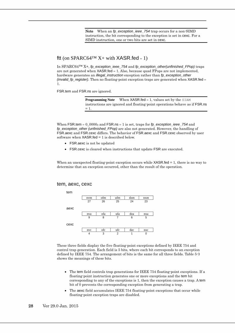
tem, aexc, cexc tem
nvm ofm ufm dzm nxm 27 26 25 24 23
aexc nva ofa ufa dza nxa 9 8 7 6 5
cexc nvc ofc ufc dzc nxc 4 3 2 1 0
These three fields display the five floating-point exceptions defined by IEEE 754 and control trap generation. Each field is 5 bits, where each bit corresponds to an exception defined by IEEE 754. The arrangement of bits is the same for all three fields. Table 5-3 shows the meanings of these bits.
• The tem field controls trap generations for IEEE 754 floating-point exceptions. If a
floating-point instruction generates one or more exceptions and the tem bit corresponding to any of the exceptions is 1, then the exception causes a trap. A tem bit of 0 prevents the corresponding exception from generating a trap.
• The aexc field accumulates IEEE 754 floating-point exceptions that occur while floating-point exception traps are disabled.
• The cexc field displays IEEE 754 floating-point exceptions generated by the most recently executed FPop instruction. The cexc bits corresponding to the exceptions are set, and the other bits are set to zero.
Programming Note If a floating-point exception generates a trap, the recovery software should set cexc appropriately before returning.
Table 5-2 shows the values of ftt, aexc and cexc corresponding to various floating-point exception conditions.
Table 5-2 Floating-Point Exceptions and Updates to the FSR
Events ftt cexc aexc IEEE 754 floating-point exceptions are not generated.
0 0 unchanged
IEEE 754 floating-point exceptions are generated but traps are masked.
0 Bits in the cexc field corresponding to the exceptions are set.
The new cexc field is ORed into the aexc field.
IEEE 754 floating-point exceptions and traps are generated.
1 Bits in the cexc field corresponding to the exceptions are set. For non-SIMD instructions, only one bit corresponding to the highest-priority exception is set. For SIMD instructions, one or two bits are set.
unchanged
The fp_exception_other exception and trap are generated
2ii unchanged unchanged
Table 5-3 Fields in aexc, cexc
Field Exception Notation enabled disabled
nva, nvc
An operand is improper for the operation to be performed. For example, 0.0 ÷ 0.0 and ∞ – ∞ are invalid. (1 = invalid operand(s), 0 = valid operand(s))
NV nv
ofa, ofc
The result, rounded as if the exponent range were unbounded, would be larger in magnitude than the destination format’s largest finite number. (1 = overflow, 0 = no overflow)
OF of
ufa, ufc
The rounded result is inexact and would be smaller in magnitude than the smallest normalized number in the indicated format; (1 = underflow, 0 = no underflow) Underflow is never indicated when the correct unrounded result is 0. Otherwise: • If FSR.tem.ufm = 0: Underflow occurs if a nonzero result is tiny
and a loss of accuracy occurs. • If FSR.tem.ufm = 1: Underflow occurs if a nonzero result is tiny.
UF uf
dza, dzc
X ÷ 0.0, where X is not 0.0 nor NaN. (1 = division by zero, 0 = no division by zero)
DZ dz
nxa, nxc
The rounded result of an operation differs from the infinitely precise unrounded result. (1 = inexact result, 0 = exact result)
NX nx
ii Hardware never sets ftt = 6 (invalid_fp_register).

30 Ver 29.0 Jan. 2015
Floating-point operations which cause an overflow (of) or underflow (uf) condition may also cause an "inexact" (nx) condition. For non-SIMD instructions, only one bit in cexc is set if the corresponding trap is enabled in the tem field. Otherwise, if the exceptions are masked, all bits corresponding to generated exceptions are set. Table 5-4 summarizes how FSR.cexc bits are set for various exceptions and masks.
Table 5-4 Setting of FSR.cexc bits for non-SIMD instructions
Condition Result Exception(s) detected in floating-point operation
Trap Enable Mask bits (in FSR.tem)
fp_exception_ieee_754 Trap Occurs?
Current Exception bits (in FSR.cexc)
of uf nx ofm ufm nxm ofc ufc nxc x x x no 0 0 0 x x 0 no 0 0 1 iii iii x 0 0 no 0 1 1
iv iv 0 x 0 no 1 0 1
x x 1 yes 0 0 1 iii iii x 0 1 yes 0 0 1
x 1 x yes 0 1 0 x 1 x yes 0 1 0
iv iv 1 x x yes 1 0 0
iv iv 0 x 1 yes 0 0 1
Updates to cexc and aexc for SIMD instructions For SIMD instructions, two bits might be set in cexc when traps are enabled.
Basic and extended operations are performed simultaneously. However, because the source operands are different, either operation or both could cause exceptions.
When only one operation causes an exception, the behavior is the same as for a non-SIMD instruction. When both operations cause exceptions, cexc, aexc and ftt are updated and traps are generated as shown below. For the purposes of illustration, let’s say the exception caused by the basic operation updates the hypothetical basic.aexc and basic.cexc fields. The exception caused by the extended operation updates the hypothetical extend.aexc and extend.cexc fields.
• When fp_exception_ieee_754 exceptions are detected for both basic and extended operations:
• Both exceptions are masked and no exception is signaled: The logical OR of basic.cexc and extend.cexc is displayed in FSR.cexc. The logical OR of basic.cexc and extend.cexc is accumulated in FSR.aexc. FSR.cexc ← basic.cexc | extend.cexc
FSR.aexc ← FSR.aexc | basic.cexc | extend.cexc
• Either the basic or extended operation signals an exception: The logical OR of basic.cexc and extend.cexc is displayed in FSR.cexc. FSR.aexc is unchanged. FSR.cexc ← basic.cexc | extend.cexc
iii Except for FRCPA{s|d}, when the underflow trap is disabled (FSR.tem.ufm = 0), underflow (uf) is always accompanied by inexact (nx). For FRCPA{s|d}, when the underflow trap is disabled (FSR.tem.ufm = 0), underflow (uf) is not accompanied by inexact (nx).
iv Overflow (of) is always accompanied by inexact (nx).

• Both basic and extended operations signal exceptions: The logical OR of basic.cexc and extend.cexc is displayed in FSR.cexc. FSR.aexc is unchanged. FSR.cexc ← basic.cexc | extend.cexc
• When fp_exception_ieee_754 is detected for one operation and fp_exception_other is detected for the other operation, the fp_exception_other exception is signalled with ftt = unfinished_FPop. Both FSR.aexc and FSR.cexc are unchanged.
Programming Note When an fp_exception_other exception is generated, it is impossible for hardware to determine whether an fp_exception_ieee_754 exception occurred simultaneously. System software must run an emulation routine to detect the second exception and update the necessary registers.
• When fp_exception_other exceptions are detected for both basic and extended operations, an fp_exception_other with ftt = unfinished_FPop is signalled. Both FSR.aexc and FSR.cexc are unchanged.
tem, cexc, aexc on SPARC64™ X+ with XASR.fed = 1 On SPARC64™ X+ with XASR.fed = 1, the value of tem is ignored and no floating-point exception traps are generated. Changing the value of tem has no effect on this behavior. In this case, the aexc and cexc fields are updated as follows.
• The aexc field is unchanged. • The cexc field is cleared when an instruction that updates FSR is executed.
FSR Conformance A SPARC V9 implementation may choose to implement the tem, cexc, and aexc fields in hardware in either of two ways (both of which comply with IEEE Std 754-1985). On SPARC64™ X / SPARC64™ X+, all three fields are implemented.
5.5. Ancillary State Registers
5.5.1. 32-bit Multiply/Divide Register (Y) (ASR 0) Refer to Section 5.5.1 in UA2011.
5.5.2. Integer Condition Codes Register (CCR) (ASR 2) Refer to Section 5.5.2 in UA2011.
5.5.3. Address Space Identifier (ASI) Register (ASR 3) Refer to Section 5.5.3 in UA2011.
5.5.4. Tick (TICK) Register (ASR 4)

32 Ver 29.0 Jan. 2015
npt Counter 63 62 0
The counter field of the TICK register is a 63-bit counter (SPARC V9 Impl. Dep. #105b) that counts processor clock cycles. Bit 63 of the TICK register is the nonprivileged trap (npt) bit, which controls access to the TICK register by nonprivileged software.
Compatibility Note Each thread in SPARC64™ X / SPARC64™ X+ has its own copy of the npt field and the counter field.
Nonprivileged software can read the TICK register, but only when nonprivileged access to TICK is enabled (TICK.npt = 0). If nonprivileged access is disabled (TICK.npt = 1), an attempt by nonprivileged software to read the TICK register causes a privileged_action exception. Table 5-5 shows the exceptions generated by reading or writing the TICK register.
Table 5-5 Exceptions when reading or writing the TICK register
RDTICK (WRTICK doesn't exist)
RDPR WRPR
OK (if TICK.npt = 0) privileged_action (if TICK.npt = 1)
privileged_opcode privileged_opcode
5.5.5. Program Counters (PC, NPC) (ASR 5) Refer to Section 5.5.5 in UA2011.
5.5.6. Floating-Point Registers State (FPRS) Register (ASR 6) Refer to Section 5.5.6 in UA2011.
5.5.7. Performance Control Register (PCR) (ASR 16) toe<7:0> ovf<7:0> ovro ulro nc su sl sc ht ut st priv 63 55 48 47 40 39 32 31 30 29 27 26 24 23 16 15 8 7 6 4 3 2 1 0
Bit Field R/W Description 55:48 toe<7:0> RW Controls whether an overflow exception is generated for
performance counters. A write updates the field, and a read returns the current settings. If PCR.toe<i> = 1 and the counter corresponding to PCR.ovf<i> overflows, PCR.ovf<i> is set to 1 and a pic_overflow exception is generated. If PCR.toe<i> = 0 and the counter corresponding to PCR.ovf<i> overflows, PCR.ovf<i> is set to 1 but a pic_overflow exception is not generated. When PCR.ovf<i> is already 1 and PCR.toe<i> is changed to 1 from 0, a pic_overflow exception is not generated.
39:32 ovf<7:0> RW Overflow Clear/Set/Status. A read by RDPCR returns the overflow status of the counters (if ovf = 1, the corresponding counter has overflowed). PCR.ovf<2n> and PCR.ovf<2n+1> refer to the lower counter (PIC<31:0>) and upper counter (PIC<63:32>), respectively, of the n-th

counter pair selected by PCR.sc. A write of 0 to an ovf bit clears the overflow status of the corresponding counter. Writing a 1 via software does not cause a pic_overflow exception.
U3 L3 U2 L2 U1 L1 U0 L0 7 6 5 4 3 2 1 0
31 ovro RW Overflow Read-Only. A write to the PCR register with write data containing a value of ovro = 0 updates the PCR.ovf field with the ovf write data. If the write data contains a value of ovro = 1, the ovf write data is ignored and the PCR.ovf field is not updated. A read of the PCR.ovro field returns 0. The PCR.ovro field allows PCR to be updated without changing the overflow status. Hardware maintains the most recent state in PCR.ovf such that a subsequent read of the PCR returns the current overflow status.
30 ulro RW SU/SL Read-Only. A write to the PCR register with write data containing a value of ulro = 0 updates the PCR.su and PCR.sl fields with the su/sl write data. If the write data contains a value of ulro = 1, the su/sl write data is ignored and the PCR.su and PCR.sl fields are not updated. A read of the PCR.ulro field returns 0.
26:24 nc RO Indicates the number of counter pairs. On SPARC64™ X / SPARC64™ X+, nc has a value of 3 (indicating 4 counter pairs). Writes to the PCR.nc are ignored.
23:16 su RW Selects the event counted by PIC<63:32>. A write updates the field, and a read returns the current setting.
15:8 sl RW Selects the event counted by PIC<31:0>. A write updates the field, and a read returns the current setting.
6:4 sc RW PIC Pair Selection. A write updates which PIC counter pair is selected, and a read returns the current selection.
3 ht RO If PCR.ht = 1, events are counted in hypervisor mode. PCR.ht can be read. Writes to PCR.ht are ignored.
2 ut RW Non-privileged Mode. When PSTATE.priv = 0 and PCR.ut = 1, events are counted.
1 st RW System Mode. When PSTATE.priv = 1 and PCR.st = 1, events are counted.
0 priv RW Privileged. If PCR.priv = 1, executing a RDPCR, WRPCR, RDPIC, or WRPIC instruction in non-privileged mode (PSTATE.priv = 0) causes a privileged_action exception. If PCR.priv = 0, a RDPCR, WRPCR, RDPIC, or WRPIC instruction can be executed in non-privileged mode. If PCR.priv = 0, a non-privileged (PSTATE.priv = 0) attempt to update PCR.priv (that is, to write a value of 1) via a WRPCR instruction causes a privileged_action exception.
5.5.8. Performance Instrumentation Counter (PIC) Register (ASR 17)
picu picl
63 32 31 0
Bit Field Access Explanation
63:32 picu RW 32-bit counter for the event selected by the su field of the Performance Control Register (PCR).
31:0 picl RW 32-bit counter for the event selected by the sl field of the Performance Control Register (PCR).

34 Ver 29.0 Jan. 2015
5.5.9. General Status Register (GSR) (ASR 19) Refer to Section 5.5.7 in UA2011.
mask dim dirnd im irnd reserved scale align 63 32 31 30 28 27 26 25 24 8 7 3 2 0
Bit Field Access Explanation 63:32 mask RW Refer to UA2011. 31 dim RW Interval Mode for decimal floating-point numbers.
When dim = 1, the value in FSR.drd is ignored. The processor rounds floating-point results according to GSR.dirnd.
30:28 dirnd RW Rounding direction to use in interval mode for decimal floating-point numbers. GSR.dirnd is valid when GSR.dim = 1. Refer to FSR.drd (page 26) for details.
27 im RW Refer to UA2011. 26:25 irnd RW Refer to UA2011. 24:8 reserved RO Reserved (undefined) 7:3 scale RW Refer to UA2011. 2:0 align RW Refer to UA2011.
Note A read of a reserved field returns an undefined value. Zeros must be written to reserved fields to preserve compatibility with future implementations.
5.5.11. System Tick (STICK) Register (ASR 24)
npt Counter 63 62 0
The counter field of the STICK register is a 63-bit counter that increments at a rate determined by a clock signal external to the processor. Bit 63 of the STICK register is the nonprivileged trap (NPT) bit, which controls access to the STICK register by nonprivileged software. A clock signal external to the processor is not defined in this specification.
Compatibility Note Each thread in SPARC64™ X / SPARC64™ X+ has its own copy of the npt field and the counter field.
Nonprivileged software can read the STICK register by using the RDSTICK instruction, but only when nonprivileged access to STICK is enabled (STICK.npt = 0). If nonprivileged access is disabled (STICK.npt = 1), an attempt by nonprivileged software to read the STICK register causes a privileged_action exception. Table 5-6 shows the exceptions generated when reading or writing the STICK register.
Table 5-6 Exceptions when reading or writing the STICK register

RDSTICK WRSTICK
OK (if STICK.npt = 0) privileged_action (if STICK.npt = 1)
illegal_instruction (differs from TICK register)
Compatibility Note In JPS1, writing the STICK register in nonprivileged mode generates a privileged_opcode exception.
A read of STICK.counter<6:0> always returns 0x7f.
5.5.13. Pause Register (PAUSE) (ASR 27)
Bit Field Access Description 63:15 reserved WO reserved 14:3 pause WO Pause VCPU for the specified number of processor
cycles. 2:0 reserved WO ignored
A virtual processor’s PAUSE register is used to pause execution on the virtual processor for the number of cycles specified by the WRPAUSE or PAUSE instruction. Software initiates a pause by writing the number of cycles to the bits PAUSE<14:0>. The lowest 3 bits of the PAUSE register are ignored. Then the maximum duration that can be specified by a WRPAUSE or PAUSE instruction is 32760 virtual processor cycles.
5.5.14. Extended Arithmetic Register (XAR) (ASR 29)
0 f_v 0 f_simd f_urd f_urs1 f_urs2 f_urs3 s_v 0 s_simd s_urd s_urs1 s_urs2 s_urs3 63 32 31 30 29 28 27 25 24 22 21 19 18 16 15 14 13 12 11 9 8 6 5 3 2 0
Bit Field Access Description
31 f_v RW Indicates whether the contents of fields beginning with f_ are valid. If f_v = 1, the contents of the f_ fields are applied to the instruction that executes first. After the 1st instruction completes, all f_ fields are cleared.
28 f_simd RW If f_simd = 1, the 1st instruction is executed as a SIMD instruction. If f_simd = 0, execution is non-SIMD.
27:25 f_urd RW Extends the rd field of the 1st instruction. 24:22 f_urs1 RW Extends the rs1 field of the 1st instruction. 21:19 f_urs2 RW Extends the rs2 field of the 1st instruction. 18:16 f_urs3 RW Extends the rs3 field of the 1st instruction. 15 s_v RW Indicates whether the contents of fields beginning
with s_ are valid. If s_v = 1, the contents of the s_ fields are applied to the instruction that executes second. After the 2nd instruction completes, all s_ fields are cleared.
12 s_simd RW If s_simd = 1, the 2nd instruction is executed as a SIMD instruction. If s_simd = 0, execution is non-SIMD.
11:9 s_urd RW Extends the rd field of the 2nd instruction. 8:6 s_urs1 RW Extends the rs1 field of the 2nd instruction.
pause 63 15 14 3 2 0

36 Ver 29.0 Jan. 2015
5:3 s_urs2 RW Extends the rs2 field of the 2nd instruction. 2:0 s_urs3 RW Extends the rs3 field of the 2nd instruction.
The XAR register extends the fields in an instruction word. It holds the upper 3 bits of an instruction’s register number fields (rs1, rs2, rs3, rd) and indicates whether the instruction is a SIMD instruction.
The register contains fields for two separate instructions. There are V (valid) bits for the first and second instructions; all other fields for a given instruction are valid only when v = 1. These register fields are mainly used to specify floating-point registers, except the *_urs3<1> fields, which are also used to disable hardware prefetch for integer and floating-point load/store instructions.
When a trap occurs, the contents of the XAR are saved to the TXAR[TL] register, and all fields in the XAR are set to 0. The saved value corresponds to the value of the XAR just before the instruction that caused the trap was executed.
Note If a Tcc initiates a trap, the contents of the XAR just before the Tcc instruction was executed are saved.
Aliases of XAR fields in this specification The fields described in Table 5-7 have the following aliases.
Table 5-7 Alias for memory access
Aliases Field Usage XAR.f_dis_hw_pf XAR.f_urs3<1> Disable hardware prefetch XAR.s_dis_hw_pf XAR.s_urs3<1> Disable hardware prefetch XAR.f_negate_mul XAR.f_urd<2> For SIMD FMA XAR.s_negate_mul XAR.s_urd<2> For SIMD FMA XAR.f_rs1_copy XAR.f_urs3<2> For SIMD FMA XAR.s_rs1_copy XAR.s_urs3<2> For SIMD FMA
XAR operations Only some instructions can reference the XAR register. In this document, instructions that can reference XAR are called “XAR-eligible instructions”. Refer to Table 7-3 (page 43) for details on which instructions are XAR eligible.
• An attempt to execute an instruction that is not XAR-eligible while XAR.v = 1
causes an illegal_action exception. • XAR-eligible instructions have the following behavior.
• If XAR.v = 1, the XAR.urs1, XAR.urs2, XAR.urs3 and XAR.urd fields are concatenated with the instruction fields rs1, rs2, rs3, and rd respectively, to specify floating-point registers. The XAR.urs3<1> fields may instead be used to disable hardware prefetch for integer and floating-point load/store instructions. Floating-point registers are referenced by 9-bit register numbers; the XAR fields specify the upper 3 bits. A double-precision encoded 5-bit instruction field is decoded to generate the lower 6 bits of the register number. Refer to “5.3.1 Floating-Point Register Number Encoding” (page 24) for details.

• If XAR.f_v = 1, the XAR.f_urs1, XAR.f_urs2, XAR.f_urs3 and XAR.f_urd fields are used.
• If XAR.f_v = 0 and XAR.s_v = 1, the XAR.s_urs1, XAR.s_urs2, XAR.s_urs3 and XAR.s_urd fields are used.
• The values of the f_ or s_ fields are only valid once. After the instruction referencing the XAR register completes, the referenced fields are set to 0.
• XAR-eligible instructions cause illegal_action exceptions in the following cases. • XAR urs1 ≠ 0 is specified for an instruction that does not use rs1. There are
similar cases for rs2, rs3 and rd. XAR urs1<1> ≠ 0 is specified for an instruction that uses rs1. There are similar cases for rs2, rs3 and rd. XAR.urs2 ≠ 0 is specified for an instruction whose rs2 field holds an immediate value (such as simm13 or fcn).
• A register number greater than or equal to F[256] is specified for the rd field of an FDIV{S|D} or FSQRT{S|D} instruction.
• XAR.simd = 1 for an instruction (including integer arithmetic) that does not support SIMD execution.
• XAR.simd = 1, and a register number greater than or equal to F[256] is specified. Some instructions (F{N}MADD{s|d}, F{N}MSUB{s|d}, FAES*X and so on) are exceptions to this rule; register numbers greater than or equal to F[256] can be specified. Refer to the specification for each instruction.
• XAR.urs3<2> ≠0 for a ld/st/atomic instruction.
When the XAR specifies register numbers for only one instruction, either the f_ or s_ fields can be used.
Programming Note If the WRXAR instruction is used, either XAR.f_v or XAR.s_v can be set to 1. The SXAR1 instruction sets XAR.f_v to 1.
If XAR.f_v = 0, the f_simd, f_urs1, f_urs2, f_urs3, and f_urd fields are ignored even when the fields contain non-zero values. The value of each field after execution is undefined. If XAR.s_v = 0, the s_simd, s_urs1, s_urs2, s_urs3, and s_urd fields are ignored even when the fields contain non-zero values. The value of each field after execution is undefined.
5.5.15. Extended Arithmetic Register Status Register (XASR) (ASR 30)
<SPARC64™ X> reserved xfd<5:4> reserved xfd<1:0>
63 6 5 4 3 2 1 0
Bit Field Access Description 63:6 reserved RO, RW reserved (undefined). <63:9> is RO, <8:6> is RW. 5:4 xfd<5:4> RW Updating a floating-point register (F[382] - F[256])
sets the appropriate bit to 1. Refer to xfd (page 39) for details.
3:2 reserved RW reserved (undefined) 1:0 xfd<1:0> RW Updating a floating-point register (F[126] - F[0])
sets the appropriate bit to 1. Refer to xfd (page 39) for details.
<SPARC64™ X+>

38 Ver 29.0 Jan. 2015
reserved fed reserved xfd<5:4> reserved xfd<1:0> 63 37 36 35 6
5 4 3 2 1 0
Bit Field Access Description 63:37 reserved RO Reserved (undefined).
36 fed RW Floating-Point Exception Disable mode. No floating-point exception traps are generated (supported from SPARC64™ X+).
35:6 reserved RO, RW reserved (undefined). <35:9> is RO, <8:6> is RW 5:4 xfd<5:4> RW Updating a floating-point register (F[382] - F[256])
sets the appropriate bit to 1. Refer to xfd (page 39) for details.
3:2 reserved RW reserved (undefined) 1:0 xfd<1:0> RW Updating a floating-point register (F[126] - F[0])
sets the appropriate bit to 1. Refer to xfd (page 39) for details.
Note A read of a reserved field returns an undefined value. Zeros must be written to reserved field to preserve compatibility for future implementation.
fed (supported on SPARC64™ X+)
Setting the fed field masks all floating-point exceptions. When XASR.fed = 0, the behavior of floating-point exceptions are the same as SPARC64™ X. This field is updated by the WRXASR instruction.
All floating-point exceptions are masked when XASR.fed = 1. That is, correspoinding traps are not generated. In addition, FSR.aexc is not updated and FSR.ftt is cleared by 0, regardless of the values of FSR.tem and FSR.ns. Refer to FSR (pages 27, 28) for details. Also, the FSHIFTORX instruction does not generate an illegal_instruction trap.
Exception XASR.fed = 0 XASR.fed = 1 fp_exception_ieee Behavior specified by
FSR.tem Trap is not generated. If an instruction that updates FSR is executed • FSR.cexc and FSR.ftt are cleared • FSR.aexc is not updated
fp_exception_other (unfinished_FPop)
Behavior specified by FSR.ns Trap is not generated.
illegal_instruction (FSHIFTORX)
illegal_instruction trap is generated depending on the value of Fd[rs3]
Trap is not generated. The value in Fd[rd] is undefined.
Operation results for fed = 1 are the same as fed = 0, FSR.tem = 0_00002 and FSR.ns = 1 except for the behavior of the FSHIFTORX instruction.
The use of this flag is determined solely by the compiler. In other words, user-privileged software routines generated by the compiler, and compiler startup routines or libraries can use this field.
The Compiler can freely choose to alter this flag or leave it untouched. Nonprivileged software not generated by the compiler (e.g., assembly language) should not alter this flag.
When modifying this field, it is caller’s responsibility to clear the flag before jumping to routines that are not generated by the compiler, such as OS library routines.

Note Minimizing the period where XASR.fed = 1 is recommended.
xfd
The xfd fields are used to determine whether any of the floating-point registers need to be saved during a context switch. Updating a register sets the appropriate bit to 1.
• There is no flag indicating an update to an integer register. • Updating a floating-point register sets the appropriate XASR.xfd<i> = 1. The
floating-point registers and corresponding xfd bits are shown below.
xfd bits Corresponding floating-point registers 0 F[0] - F[62]
1 F[64] - F[126]
2 Reserved 3 Reserved 4 F[256] - F[318]
5 F[320] - F[382]
6 Reserved
7 Reserved
Programming Note Updating a V9 floating-point register sets the xfd[0] bit of the XASR and also updates the V9 FPRS. For example, updating F[15] sets both FPRS.dl = 1 and XASR.xfd<0> = 1.
Programming Note The fields XASR.xfd<7:6> and XASR.xfd< 3:2> are undefined.

40 Ver 29.0 Jan. 2015
6. Instruction Set Overview
6.1. Instruction Execution Refer to Section 6.1 in UA2011.
6.2. Instruction Formats Refer to Section 6.2 in the SPARC64 VIIIfx extensions.
6.3. Instruction Categories Refer to Section 6.3 in UA2011.
6.3.4.3 CALL and JMPL Instructions
Compatibility Note When PSTATE.am = 1, the upper 32bits of %o7 are set to 0.
6.3.4.6 Trap Instruction (Tcc)
Compatibility Note Traps numbered 128 ~ 255 trap to hypervisor mode. It is not possible to trap directly from nonprivileged mode to hypervisor mode. The base address of the trap vector is HTBA.
6.3.9 Floating-Point Operate (FPop) Instructions FPop refers to floating-point execution instructions (except for FBfcc, FBPfcc, and load/store instructions). FPop1 and FPop2 are defined in Table 14-5 ~ Table 14-7 (page 317) and are FPop instructions. FPop also includes IMPDEP1 and IMPDEP2, which are described in the table below.
IMPDEP1 IMPDEP2
FADDtd, FSUBtd, FMULtd, FDIVtd, FCMP{E}td, FQUAtd, FADDod, FSUBod, FMULod, FDIVod, FCMPod, F{R}QUAod, FXADDod{LO|HI}, FXMULodLO, FbuxTOtd, FtdTObux, FbsxTOtd, FtdTObsx, FodTOtd, FtdTOod, FCMP{LE|LT|GE|GT|EQ|NE}{E}{s|d}, FMAX{s|d}, FMIN{s|d}, FRCPA{s|d}, FRSQRTA{s|d}, FTRISSELd, FTRISMULd, FEXPAd
F{N}MADD{s|d}, F{N}MSUB{s|d}, FTRIMADDd, FSELMOV{s|d}

6.3.11 Reserved Opcodes and Instruction Fields Compatibility Note An illegal_instruction exception is generated when an
attempt is made to execute an instruction where one or more reserved fields in the instruction word are not 0. In JPS1, this behavior was not clearly described in the footnote.

42 Ver 29.0 Jan. 2015
7. Instructions
This chapter describes instructions defined in SPARC64™ X / SPARC64™ X+. Refer to Chapter 7 of UA2011 for instructions not defined in this chapter.
Compatibility Note When the specification of an instruction in JPS1 differs from UA2011, SPARC64™ X / SPARC64™ X+ conform to UA2011. There are several differences between JPS1 and UA2011 that are not a result of the differences between sun4u and sun4v (for example, handling of reserved fields and the exceptions generated by quadruple-precision floating-point instructions).
Instruction definitions for SPARC64™ X / SPARC64™ X+ include the following descriptions.
• Table of opcodes for instructions defined in the subsection. This table also includes values for unique field(s) whether HPC-ACE features can be used with the instruction, and assembly language notation.
• Illustration of the applicable instruction format(s). Fields marked “reserved” are reserved for future expansion and must be set to 0 by software on SPARC64™ X / SPARC64™ X+. Refer to Section 1.1.3 (page 9) for details about the meaning of reserved and the em dash (―).
• Description of the instruction and restrictions.
Note Exceptional conditions are summarized in the table at the end of the subsection. Exceptions may be described in the description when further explanation is needed.
• For floating-point arithmetic instructions, a table relating input operands to the arithmetic result. The table also relates input operands to the arithmetic exceptions (OF, UF, DZ, NX, NV) defined by IEEE 754.
• Table of exceptions that can occur when the instruction is executed. Exceptions are listed in descending priority order. The highest-priority exception is listed first.
The following exceptions are not described in this table. • IAE_* exceptions can occur for all instructions • illegal_instruction exceptions occur for unimplemented instructions
XAR fields are shown without the f_ or s_ prefix, except when describing conditions that cause an illegal_action exception.
No timing information is described.
Table 7-3 shows the list of all instructions supported by SPARC64™ X / SPARC64™ X+. Certain instructions are marked with mnemonic superscripts. These superscripts are also used in Chapter 14, “Opcode Maps” (page 314). Table 7-1 lists these mnemonic superscripts and their meanings.
Table 7-1 Meaning of mnemonic superscripts

Superscript Meaning D Instruction should not be used (Deprecated) N Incompatible instruction PASI Privileged operation when bit 7 of ASI is 0. PASR Privileged operation depending on the ASR number PNPT Privileged operation when PSTATE.PRIV = 0 and {S}TICK.NPT = 1 PPIC Privileged operation when PCR.PRIV = 1 PPCR Privileged access when PCR.PRIV = 1 + Instruction not supported on SPARC64™ X.
The description of an instruction may use the notation described in Table 7-2 when referring to specific operands.
Table 7-2 Register notation for rs1 (same for rs2, rs3, and rd)
Notation Meaning XAR.v = 0 XAR.v = 1
R[rs1] Integer register encoded by the rs1 field of the instruction word
Integer register encoded by the rs1 field of the instruction word
Fs[rs1] Single-precision floating-point register encoded by the rs1 field of the instruction word
Single-precision floating-point register encoded by XAR.urs1 and the rs1 field of the instruction word
Fd[rs1] Double-precision floating-point register encoded by the rs1 field of the instruction word
Double-precision floating-point register encoded by XAR.urs1 and the rs1 field of the instruction word
F[rs1] Floating-point register encoded by the rs1 field of the instruction word (no distinction made between single precision, double precision, or quadruple precision)
Floating-point register encoded by XAR.urs1 and the rs1 field of the instruction word (no distinction made between single precision, double precision, or quadruple precision)
In the Table 7-3, the columns for HPC-ACE extension show which HPC-ACE features can be used with an instruction on SPARC64™ X / SPARC64™ X+.
• Regs. XAR-eligible instruction. The extended floating-point registers can be used. For memory access instructions, hardware prefetch can be disabled.
An instruction which has a ☆ in this column can specify Fd[0] - Fd[126] for the rd register but not Fd[256] - Fd[382] .
• SIMD Instruction can be specified as a SIMD instruction.
Instructions without checks in either of these two columns are not XAR eligible. Instructions that are not XAR eligible are described in "XAR operations" (page 36).
Table 7-3 Instruction set of SPARC64™ X / SPARC64™ X+

44 Ver 29.0 Jan. 2015
Instruction HPC-ACE extension Page Regs. SIMD
ADD (ADDcc) 51 ADDC (ADDCcc) 51 ALIGNADDRESS{_LITTLE} 52 AND (ANDcc) 120 ANDN (ANDNcc) 120 ARRAY{8|16|32} 53 BMASK 54 BPcc 56 BPr 57 BSHUFFLE 54
BiccD 55 CALL 58 CASAPASI, CASXAPASI ✓ 59
CWB{NE|E|G|LE|GE|L|GU|LEU|CC|CS|POS|NEG|VC|VS}+ 242
CXB{NE|E|G|LE|GE|L|GU|LEU|CC|CS|POS|NEG|VC|VS}+ 242 EDGE{8|16|32}{L}N 62 EDGE{8|16|32}{L}cc 61 FABSq ✓ 67 FABS{s|d} ✓ ✓ 67 FADDod ☆ 209 FADDq ✓ 68 FADD{s|d} ✓ ✓ 68 FADDtd ☆ 204 FAESDECLX ✓ ✓ 197 FAESDECX ✓ ✓ 197 FAESENCLX ✓ ✓ 197 FAESENCX ✓ ✓ 197 FAESKEYX ✓ ✓ 197 FALIGNDATA 70 FANDNOT{1|2}{s} ✓ ✓ 106 FAND{s} ✓ ✓ 106 FBPfcc 72 FBfccD 71 FCMP{E}{s|d|q} ✓ 73 FCMP{E}td ✓ 217 FCMP{LE|LT|GE|GT|EQ|NE}{E}{s|d} ✓ ✓ 74 FCMP{LE|NE|GT|EQ}{16|32} 76 FCMP{LE|GT}{8X|16X|32X|X} ☆ 226 FPCMP{LE|GT}{8X|16X|32X|64X}+ ✓ ✓ 257 FCMPod ✓ 219 FLCMP{s|d}+ ✓ 234 FDESENCX ✓ ✓ 192 FDESIIPX ✓ ✓ 192 FDESIPX ✓ ✓ 192 FDESKEYX ✓ ✓ 192 FDESPC1X ✓ ✓ 192

Instruction HPC-ACE extension Page FDIVod ☆ 209 FDIV{s|d|q} ☆ 77 FDIVtd ☆ 204 FEXPAd ✓ ✓ 78 FEXPAND 80 FLUSH 81 FLUSHW 82 FMADD{s|d} ✓ ✓ 83 FMAX{s|d} ✓ ✓ 91 FMIN{s|d} ✓ ✓ 91 FMOVq ✓ 93 FMOVcc 94 FMOVR 95 FMOV{s|d} ✓ ✓ 93 FMSUB{s|d} ✓ ✓ 83 FMUL8x16 96 FMUL8x16{AU|AL} 96 FMUL8{SU|UL}x16 96 FMULD8{SU|UL}x16 96 FMULod ☆ 209 FMULq ✓ 97 FMUL{s|d} ✓ ✓ 97 FMULtd ☆ 204 FNAND{s} ✓ ✓ 106 FNEGq ✓ 98 FNEG{s|d} ✓ ✓ 98 FNMADD{s|d} ✓ ✓ 83 FNMSUB{s|d} ✓ ✓ 83
FNADD{s|d}+ ✓ ✓ 235
FNMUL{s|d}+ ✓ ✓ 237
FNsMULd+ ✓ ✓ 237 FNOR{s} ✓ ✓ 106 FNOT{1|2}{s} ✓ ✓ 106 FONE{s} ✓ ✓ 106 FORNOT{1|2}{s} ✓ ✓ 106 FOR{s} ✓ ✓ 106 FPACK{16|32|FIX} 99 FPADD{16|32}{S} 100 FPADD{16|32}{S}+ ✓ ✓ 100
FPADD64+ ✓ ✓ 231
FPADD128XHI+ ✓ ✓ 261 FPMADDX{HI} ✓ ✓ 102
FPMAX{u}{32|64}+ ✓ ✓ 262
FPMIN{u}{32|64}+ ✓ ✓ 262 FPMERGE 103 FPSUB{16|32}{S} 104

46 Ver 29.0 Jan. 2015
Instruction HPC-ACE extension Page FPSUB{16|32}{S}+ ✓ ✓ 104 FPSUB64+ ✓ ✓ 232 F{R}QUAod ☆ 209 FQUAtd ☆ 204 FRCPA{s|d} ✓ ✓ 109 FRSQRTA{s|d} ✓ ✓ 109
FPSELMOV{8|16|32}X+ ✓ ✓ 243 FSELMOV{s|d} ✓ ✓ 112 FSHIFTORX ✓ ✓ 222
FSHIFTORX+ ✓ ✓ 252 FSQRT{s|d|q} ☆ 113 FSRC{1|2}{s} ✓ ✓ 106 FSUBod ☆ 209 FSUBq ✓ 68 FSUB{s|d} ✓ ✓ 68 FSUBtd ☆ 204 FTRIMADDd ✓ ✓ 114 FTRISMULd ✓ ✓ 114 FTRISSELd ✓ ✓ 114 FUCMP{LE|NE|GT|EQ}{8X|16X|32X|X} ☆ 226
FPCMPU{LE|NE|GT|EQ}{8X|16X|32X|64X}+ ✓ ✓ 257
FPCMPU{LE|NE|GT|EQ}8+ 233
FPCMP{64|U64}X+ ✓ 246 FXADDod{LO|HI} ☆ 209 FXMULodLO ☆ 209 FXNOR{s} ✓ ✓ 106 FXOR{s} ✓ ✓ 106 FZERO{s} ✓ ✓ 106 FdMULq ✓ 97 F{bsx|bux|od}TOtd ☆ 220 FqTO{i|x} ✓ 66 FsMULd ✓ ✓ 97 F{i|x}TOq ✓ 63 F{i|x}TO{s|d} ✓ ✓ 63 F{s|d}TOq ✓ 64 F{s|d}TO{i|x} ✓ ✓ 66 FsTOd, FdTOs ✓ ✓ 64 FtdTO{bsx|bux|od} ☆ 220 FqTO{s|d} ✓ 64 ILLTRAP 119 JMPL 121 LDBLOCKF ✓ 124 LDF, LDDF ✓ ✓ 126 LDQF ✓ 126
LDFAPASI, LDDFAPASI ✓ ✓ 129

Instruction HPC-ACE extension Page LDQFAPASI ✓ 129
LDFSRD ✓ 140 LDSHORTF 132 LDSTUB ✓ 133
LDSTUBAPASI ✓ 134
LDTWD ✓ 135
LDTWAD,PASI ✓ 136
LDTXAN ✓ 138 LDXEFSR+ ✓ 241 LDXFSR ✓ 140 LD{S|U}{B|H|W}, LDX ✓ 122
LD{S|U}{B|H|W}APASI, LDXAPASI ✓ 123 LZD 230 MEMBAR 141 MOVcc 142 MOVr 143
MOVwTOs+ ✓ 264
MOVxTOd+ ✓ 264
MULSccD 144 MULX 146 NOP 147 OR (Orcc) 120 ORN (ORNcc) 120 PADD32 148 PAUSE+ 239 PDIST 149 POPC 150
PREFETCH, PREFETCHAPASI ✓ 151 RDASI 154 RDCCR 154 RDFPRS 154 RDGSR 154 RDPC 154 RDPCRPPCR 154
RDPICPPIC 154
RDSTICKPNPT 154
RDTICKPNPT 154 RDXASR 154
RDYD 154
RDASRPASR 154 RESTORE 156 RETURN 155 ROLX 160 SAVE 156 SDIAM 159

48 Ver 29.0 Jan. 2015
Instruction HPC-ACE extension Page SDIVD (SDIVccD) 157 SDIVX 146 SETHI 158 SIAM 159 SLEEP 162 SLL, SLLX 160 FPSLL64X+ ✓ ✓ 247
SMULD (SMULccD) 161
SRA, SRAX 160
FPSRA64X+ ✓ ✓ 247
SRL, SRLX 160
FPSRL64X+ ✓ ✓ 247
STBARD 163
STBIN ✓ 166 STBLOCKF ✓ 167 STF, STDF ✓ ✓ 169 STQF ✓ 169
STFAPASI, STDFAPASI ✓ ✓ 171
STQFAPASI ✓ 171
STFSRD, STXFSR ✓ 181 STPARTIALF 177 STSHORTF 178 ST{B|H|W|X} ✓ 164
ST{B|H|W|X}APASI ✓ 165 ST{D}FR ✓ ✓ 174 ST{D}FR+ ✓ ✓ 248
STTWD ✓ 179
STTWAD,PASI ✓ 180
SUB (SUBcc) 182 SUBC (SUBCcc) 182
SWAPD, SWAPAD,PASI ✓ 183 SXAR{1|2} 184
TADDcc (TADDccTVD) 185
TSUBcc (TSUBccTVD) 185 Tcc 186 UDIVD (UDIVccD) 187 UDIVX 146 UMULD (UMULccD) 188 WRASI 189
WRASRPASR 189 WRCCR 189 WRFPRS 189 WRGSR 189
WRPAUSE+ 189

Instruction HPC-ACE extension Page WRPCRPPCR 189
WRPICPPIC 189 WRXAR 189 WRXASR 189
WRYD 189
XFILLN ✓ 190
XNOR (XNORcc) 120 XOR (XORcc) 120
In SPARC64™ X / SPARC64™ X+, certain instructions are defined as the combination of a specific ASI number with one of the instructions LDDFA, LDTWA, LDXA, STDFA, STTWA, STXA, LDSBA, LDSHA, LDSWA, LDUBA, LDUHA, or LDUWA. This combination is interpreted as a separate instruction, rather than an access to an alternate space. Table 7-4 shows these instructions. Refer to the instruction definition for details.
An empty column means that the combination of that ASI number with an instruction is not interpreted as a separate instruction. Those ASI numbers are invalid for LDDFA, LDTWA, LDXA, STDFA, STTWA, STXA, LDSBA, LDSHA, LDSWA, LDUBA, LDUHA, and LDUWA.

50 Ver 29.0 Jan. 2015
Table 7-4 Instructions defined as load/store to alternate space with special ASI.
ASI number
1616, 1716, 1E16, 1F16, F016, F116, F816, F916
E016, E116 F216, F316
2216, 2316, 2716, 2A16, 2B16, 2F16, E216, E316, EA16, EB16
C016 - C516, C816 - CD16
D016 - D316, D816 - DB16
E416 E516
LDDFA i = 0
LDBLOCKF
LDSHORTF i = 1
STDFA i = 0
STBLOCKF STBLOCKF XFILLN STPARTIALF
STSHORTF
i = 1
LDTWAD,PASI i = 0 LDTXAN
i = 1
STTWAD,PASI i = 0
XFILLN STBIN
i = 1
LDXA i = 0
i = 1
STXA i = 0
XFILLN STBIN
i = 1
LDSBA i = 0
i = 1
LDSHA i = 0
i = 1
LDSWA i = 0
i = 1
LDUBA i = 0
i = 1
LDUHA i = 0
i = 1
LDUWA i = 0
i = 1

7.1. ADD
Refer to Section 7.1 in UA2011.
Exception Target instruction
Condition
illegal_instruction All i = 0 and iw<12:5> ≠0 illegal_action All XAR.v = 1

52 Ver 29.0 Jan. 2015
7.2. Align Address
Refer to Section 7.5 in UA2011.
Note ALIGNADDR_LITTLE generates the opposite-endian byte ordering for a subsequent FALIGNDATA operation.
Exception Target
instruction Condition
fp_disabled All FPRS.fef = 0 or PSTATE.pef = 0 illegal_action All XAR.v = 1

7.4. Three-Dimensional Array Addressing Refer to Section 7.8 in UA2011.
Exception Target
instruction Condition
illegal_action All XAR.v = 1

54 Ver 29.0 Jan. 2015
7.5. Byte Mask and Shuffle Refer to Section 7.10 in UA2011.
Exception Target
instruction Condition
fp_disabled All FPRS.fef = 0 or PSTATE.pef = 0 illegal_action All XAR.v = 1

7.6. Branch on Integer Condition Codes (Bicc)
Refer to Section 7.9 in UA2011.
Note The Trap on Control Transfer feature is implemented on SPARC64™ X / SPARC64™ X+ (page 302).
Exception Target
instruction Condition
illegal_action All XAR.v = 1 control_transfer_instruction Excluding BN The branch is taken and PSTATE.tct = 1.
The conditional branch BA is always taken.

56 Ver 29.0 Jan. 2015
7.7. Branch on Integer Condition Codes with Prediction (BPcc) Refer to Section 7.11 in UA2011.
Note The Trap on Control Transfer feature is implemented on SPARC64™ X / SPARC64™ X+ (page 302).
Exception Target instruction Condition illegal_instruction All A reserved field is not 0.
(cc0 = 1) illegal_action All XAR.v = 1 control_transfer_instruction Excluding BPN The branch is taken and PSTATE.tct = 1.
The conditional branch BA is always taken.
Related Branch on Integer Register with Prediction (BPr) (page 57)

7.8. Branch on Integer Register with Prediction (BPr) Refer to Section 7.12 in UA2011.
Note The Trap on Control Transfer feature is implemented on SPARC64™ X / SPARC64™ X+ (page 302).
Exception Target
instruction Condition
illegal_instruction All When any of the following are true • rcond = 0002 or 1002 • iw<28> = 1
illegal_action All XAR.v = 1 control_transfer_instruction All The branch is taken and PSTATE.tct = 1.
Related Branch on Integer Condition Codes with Prediction (BPcc) (page 56)

58 Ver 29.0 Jan. 2015
7.9. Call and Link
Refer to Section 7.13 in UA2011.
Note When PSTATE.am = 1, the upper 32 bits of the PC are masked (set to 0) and written to R[15]. R[15] is updated immediately, and the delay instruction can use the modified value of R[15].
Note The Trap on Control Transfer feature is implemented in SPARC64™ X / SPARC64™ X+ (page 302).
Exception Target
instruction Condition
illegal_action All XAR.v = 1 control_transfer_instruction All PSTATE.tct = 1
Related JMPL (page 121)

7.10. Compare and Swap Opcode op3 Operation HPC-ACE Assembly Language Syntax
Regs. SIMD
CASAPASI 11 11002 Compare and Swap Word from Alternate Space
casa [regrs1] imm_asi, regrs2, regrd
casa [regrs1] %asi, regrs2, regrd
CASXAPASI 11 11102 Compare and Swap Extended Word from Alternate Space
casxa [regrs1] imm_asi, regrs2, regrd
casxa [regrs1] %asi, regrs2, regrd
Refer to Section 7.16 in UA2011.
The compare-and-swap instructions can be used with any of the following ASIs, subject to the privilege mode rules described for the privileged_action exception. Use of any other ASI with these instructions causes a DAE_invalid_asi exception.
ASIs valid for CASA and CASXA ASI_NUCLEUS ASI_NUCLEUS_LITTLE
ASI_AS_IF_USER_PRIMARY ASI_AS_IF_USER_PRIMARY_LITTLE
ASI_AS_IF_USER_SECONDARY ASI_AS_IF_USER_SECONDARY_LITTLE
ASI_REAL ASI_REAL_LITTLE
ASI_PRIMARY ASI_PRIMARY_LITTLE
ASI_SECONDARY ASI_SECONDARY_LITTLE

60 Ver 29.0 Jan. 2015
Exception Target instruction Condition
illegal_instruction All A reserved field is not 0. (i = 1 and iw<12:5> ≠ 0)
illegal_action All
XAR.v = 1 and any of the following are true • XAR.simd = 1 • XAR.urs1 ≠ 0 • XAR.urs2 ≠ 0 • XAR.urs3<2> ≠ 0 • XAR.urd ≠ 0
mem_address_not_aligned CASXA When the address indicated by R[rs1] is not
aligned on eight-byte boundary
CASA When the address indicated by R[rs1] is not aligned on four-byte boundary
privileged_action
All
PSTATE.priv = 0 and either of the following is true • i = 0 and ASI<7> = 0 • i = 1 and imm_asi<7> = 0
All
PSTATE.priv = 1 and either of the following is true
• i = 0 and 3016 ≤ ASI ≤ 7F16
• i = 1 and 3016 ≤ imm_asi ≤ 7F16 VA_watchpoint All Refer to 12.5.1.62. DAE_invalid_asi All Refer to 12.5.1.5 DAE_privilege_violation All Refer to 12.5.1.8
DAE_nc_page All Attempted access to non-cacheable space. Refer to 12.5.1.6
DAE_nfo_page All Refer to 12.5.1.7 DAE_side_effect_page All Refer to 12.5.1.9

7.12. Edge Handling Instructions Refer to Section 7.23 in UA2011.
Exception Target
instruction Condition
illegal_action All XAR.v = 1

62 Ver 29.0 Jan. 2015
7.13. Edge Handling Instructions (noCC) Refer to Section 7.24 in UA2011.
Exception Target instruction
Condition
illegal_action All XAR.v = 1

7.14. Convert Integer to Floating-Point Opcode opf Operation HPC-ACE Assembly Language
Syntax Regs. SIMD FiTOs 0 1100 01002 Convert 32-bit Integer to Single fitos fregrs2, fregrd
FiTOd 0 1100 10002 Convert 32-bit Integer to Double fitod fregrs2, fregrd FiTOq 0 1100 11002 Convert 32-bit Integer to Quad fitoq fregrs2, fregrd FxTOs 0 1000 01002 Convert 64-bit Integer to Single fxtos fregrs2, fregrd
FxTOd 0 1000 10002 Convert 64-bit Integer to Double fxtod fregrs2, fregrd
FxTOq 0 1000 11002 Convert 64-bit Integer to Quad fxtoq fregrs2, fregrd
Refer to Section 7.36 and Section 7.68 in UA2011.
Note Rounding is performed as specified by FSR.rd or GSR.irnd.
Exception Target instruction
Condition
illegal_instruction FiTOs, FiTOd, FxTOs, FxTOd
A reserved field is not 0.
FiTOq, FxTOq
Always. For these instructions, exceptions with priority lower than illegal_instruction are used for emulation.
fp_disabled All PSTATE.pef = 0 or FPRS.fef = 0 illegal_action FiTOs,
FiTOd, FxTOs, FxTOd
XAR.v = 1 and any of the following are true • XAR.urs1 ≠ 0 • XAR.urs2<1> ≠ 0 • XAR.urs3 ≠ 0 • XAR.urd<1> ≠ 0 • XAR.simd = 1 and XAR.urs2<2> ≠ 0 • XAR.simd = 1 and XAR.urd<2> ≠ 0
FiTOq, FxTOq
XAR.v = 1 and any of the following are true • XAR.simd = 1 • XAR.urs1 ≠ 0 • XAR.urs2<1> ≠ 0 • XAR.urs3 ≠ 0 • XAR.urd<1> ≠ 0
fp_exception_ieee_754 NX FxTOs, FxTOd, FiTOs
Conforms to IEEE754.
fp_exception_other (FSR.ftt = invalid_fp_register)
FqTOx, FqTOi
rs2<1> ≠ 0

64 Ver 29.0 Jan. 2015
7.15. Convert Between Floating-Point Formats
Opcode opf Operation HPC-ACE Assembly Language
Syntax Regs. SIMD FsTOd 0 1100 10012 Convert Single to Double fstod fregrs2, fregrd
FsTOq 0 1100 11012 Convert Single to Quad fstoq fregrs2, fregrd FdTOs 0 1100 01102 Convert Double to Single fdtos fregrs2, fregrd FdTOq 0 1100 11102 Convert Double to Quad fdtoq fregrs2, fregrd
FqTOs 0 1100 01112 Convert Quad to Single fqtos fregrs2, fregrd
FqTOd 0 1100 10112 Convert Quad to Double fqtod fregrs2, fregrd
Refer to Section 7.66 in UA2011.
Note Rounding is performed as specified by FSR.rd or GSR.irnd.
Exception Target instruction
Condition
illegal_instruction FsTOd, FdTOs
A reserved field is not 0.
FsTOq, FdTOq, FqTOs, FqTOd
Always. For these instructions, exceptions with priority lower than illegal_instruction are intended for emulation.
fp_disabled All PSTATE.pef = 0 or FPRS.fef = 0 illegal_action FsTOd,
FdTOs XAR.v = 1 and any of the following are true • XAR.urs1 ≠ 0 • XAR.urs2<1> ≠ 0 • XAR.urs3 ≠ 0 • XAR.urd<1> ≠ 0 • XAR.simd = 1 and XAR.urs2<2> ≠ 0 • XAR.simd = 1 and XAR.urd<2> ≠ 0
FsTOq, FdTOq, FqTOs, FqTOd
XAR.v = 1 and any of the following are true • XAR.simd = 1 • XAR.urs1 ≠ 0 • XAR.urs2<1> ≠ 0 • XAR.urs3 ≠ 0 • XAR.urd<1> ≠ 0
fp_exception_ieee_754 OF, UF, NX FqTOs, FqTOd, FdTOs
Conforms to IEEE754.
NV All F[rs2] is sNAN. fp_exception_other (FSR.ftt = invalid_fp_register)
FsTOq, FdTOq
rd<1> ≠ 0
FqTOs, FqTOd
rs2<1> ≠ 0
fp_exception_other (FSR.ftt = unfinished_FPop)
FsTOd, FdTOs
Refer to Chapter 8.

Compatibility Note fp_exception_other (FSR.ftt = invalid_fp_register) conforms to UA2011. In JPS1, the fp_exception_other (FSR.ftt = unimplemented_FPop) exception was detected when executing quadruple-precision instructions.

66 Ver 29.0 Jan. 2015
7.16. Convert Floating-Point to Integer Opcode opf Operation HPC-ACE Assembly Language
Syntax Regs. SIMD FsTOx 0 1000 00012 Convert Single to 64-bit Integer fstox fregrs2, fregrd
FdTOx 0 1000 00102 Convert Double to 64-bit Integer fdtox fregrs2, fregrd FqTOx 0 0100 00112 Convert Quad to 64-bit Integer fqtox fregrs2, fregrd FsTOi 0 1101 00012 Convert Single to 32-bit Integer fstoi fregrs2, fregrd
FdTOi 0 1101 00102 Convert Double to 32-bit Integer fdtoi fregrs2, fregrd
FqTOi 0 1101 00112 Convert Quad to 32-bit Integer fqtoi fregrs2, fregrd
Refer to Section 7.65 in UA2011.
Note The result is always rounded towards zero. FSR.rd and GSR.irnd are ignored.
Exception Target
instruction Condition
illegal_instruction FsTOx, FdTOx, FsTOi, FdTOi
A reserved field is not 0.
FqTOx, FqTOi
Always. For these instructions, exceptions with priority lower than illegal_instruction are intended for emulation.
fp_disabled All PSTATE.pef = 0 or FPRS.fef = 0 illegal_action FsTOx,
FdTOx, FsTOi, FdTOi
XAR.v = 1 and any of the following are true • XAR.urs1 ≠ 0 • XAR.urs2<1> ≠ 0 • XAR.urs3 ≠ 0 • XAR.urd<1> ≠ 0 • XAR.simd = 1 and XAR.urs2<2> ≠ 0 • XAR.simd = 1 and XAR.urd<2> ≠ 0
FqTOx, FqTOi
XAR.v = 1 and any of the following are true • XAR.simd = 1 • XAR.urs1 ≠ 0 • XAR.urs2<1> ≠ 0 • XAR.urs3 ≠ 0 • XAR.urd<1> ≠ 0
fp_exception_ieee_754 NV, NX All Conforms to IEEE754. fp_exception_other (FSR.ftt = invalid_fp_register)
FqTOx, FqTOi
rs2<1> ≠ 0
Compatibility Note fp_exception_other (FSR.ftt = invalid_fp_register) conforms to UA2011. In JPS1, the fp_exception_other (FSR.ftt = unimplemented_FPop) exception was detected when executing quadruple precision instructions.

7.17. Floating-Point Absolute Value Opcode opf Operation HPC-ACE Assembly Language
Syntax Regs. SIMD FABSs 0 0000 10012 Absolute value Single fabss fregrs2, fregrd FABSd 0 0000 10102 Absolute value Double fabsd fregrs2,fregrd FABSq 0 0000 10112 Absolute value Quad fabsq fregrs2,fregrd
Refer to Section 7.25 in UA2011.
Exception Target instruction
Condition
illegal_instruction FABSs, FABSd
A reserved field is not 0.
FABSq Always. For this instruction, exceptions with priority lower than illegal_instruction are intended for emulation.
fp_disabled All PSTATE.pef = 0 or FPRS.fef = 0 illegal_action FABSs,
FABSd XAR.v = 1 and any of the following are true • XAR.urs1 ≠ 0 • XAR.urs2<1> ≠ 0 • XAR.urs3 ≠ 0 • XAR.urd<1> ≠ 0 • XAR.simd = 1 and XAR.urs2<2> ≠ 0 • XAR.simd = 1 and XAR.urd<2> ≠ 0
FABSq XAR.v = 1 and any of the following are true • XAR.simd = 1 • XAR.urs1 ≠ 0 • XAR.urs2<1> ≠ 0 • XAR.urs3 ≠ 0 • XAR.urd<1> ≠ 0
fp_exception_other (FSR.ftt = invalid_fp_register)
FABSq When either of the following is true • rs2<1> ≠ 0 • rd<1> ≠ 0

68 Ver 29.0 Jan. 2015
7.18. Floating-Point Add and Subtract Opcode opf Operation HPC-ACE Assembly Language Syntax
Regs. SIMD FADDs 0 0100 00012 Add Single fadds fregrs1, fregrs2, fregrd
FADDd 0 0100 00102 Add Double faddd fregrs1, fregrs2, fregrd FADDq 0 0100 00112 Add Quad faddq fregrs1, fregrs2, fregrd FSUBs 0 0100 01012 Subtract Single fsubs fregrs1, fregrs2, fregrd
FSUBd 0 0100 01102 Subtract Double fsubd fregrs1, fregrs2, fregrd FSUBq 0 0100 01112 Subtract Quad fsubq fregrs1, fregrs2, fregrd
Refer to Section 7.26 and Section 7.67 in UA2011.
Note Rounding is performed as specified by FSR.rd or GSR.irnd.
Exception Target instruction
Condition
illegal_instruction FADDs, FADDd, FSUBs, FSUBd
A reserved field is not 0.
FADDq, FSUBq,
Always For these instructions, exceptions with priority lower than illegal_instruction are intended for emulation.
fp_disabled All PSTATE.pef = 0 or FPRS.fef = 0 illegal_action FADDs,
FADDd, FSUBs, FSUBd
XAR.v = 1 and any of the following are true • XAR.urs1<1> ≠ 0 • XAR.urs2<1> ≠ 0 • XAR.urs3 ≠ 0 • XAR.urd<1> ≠ 0 • XAR.simd = 1 and XAR.urs1<2> ≠ 0 • XAR.simd = 1 and XAR.urs2<2> ≠ 0 • XAR.simd = 1 and XAR.urd<2> ≠ 0
FADDq, FSUBq,
XAR.v = 1 and any of the following are true • XAR.simd = 1 • XAR.urs1<1> ≠ 0 • XAR.urs2<1> ≠ 0 • XAR.urs3 ≠ 0 • XAR.urd<1> ≠ 0
fp_exception_ieee_754 OF, UF, NX, NV
All Conforms to IEEE754.
fp_exception_other (FSR.ftt = invalid_fp_register)
FADDq FSUBq
When any of the following are true • rs1<1> ≠ 0 • rs2<1> ≠ 0 • rd<1> ≠ 0
fp_exception_other (FSR.ftt = unfinished_FPop)
FADDs, FADDd, FSUBs, FSUBd
Refer to Chapter 8.

Compatibility Note fp_exception_other (FSR.ftt = invalid_fp_register) conforms to UA2011. In JPS1, the fp_exception_other (FSR.ftt = unimplemented_FPop) exception was detected when executing quadruple-precision instructions.

70 Ver 29.0 Jan. 2015
7.19. Align Data Refer to Section 7.27 in UA2011.
Compatibility Note This instruction is referred to as “FALIGNDATAg” in UA2011.
Exception Target instruction
Condition
fp_disabled FALIGNDATA PSTATE.pef = 0 or FPRS.fef = 0 illegal_action FALIGNDATA XAR.v = 1

7.20. Branch on Floating-Point Condition Codes (FBfcc) Refer to Section 7.28 in UA2011.
Note The Trap on Control Transfer feature is implemented on SPARC64™ X / SPARC64™ X+ (page 302).
Exception Target
instruction Condition
fp_disabled All PSTATE.pef = 0 or FPRS.fef = 0 illegal_action All XAR.v = 1 control_transfer_instruction Excluding FBN The branch is taken and PSTATE.tct = 1.
The conditional branch FBA is always taken.

72 Ver 29.0 Jan. 2015
7.21. Branch on Floating-Point Condition Code with Prediction (FBPfcc)
Refer to Section 7.29 in UA2011.
Note The Trap on Control Transfer feature is implemented on SPARC64™ X / SPARC64™ X+ (page 302).
Exception Target
instruction Condition
fp_disabled All PSTATE.pef = 0 orFPRS.fef = 0 illegal_action All XAR.v = 1 control_transfer_instruction Excluding FBPN When the branch is taken and
PSTATE.tct = 1. The conditional branch FBPA is always taken.

7.22. Floating-Point Compare Instruction opf Operation HPC-ACE Assembly Language Syntax
Regs SIMD FCMPs 0 0101 00012 Compare Single fcmps %fccn, fregrs1, fregrs2 FCMPd 0 0101 00102 Compare Double fcmpd %fccn, fregrs1, fregrs2 FCMPq 0 0101 00112 Compare Quad fcmpq %fccn, fregrs1, fregrs2 FCMPEs 0 0101 01012 Compare Single and Exception if
Unordered. fcmpes %fccn, fregrs1, fregrs2
FCMPEd 0 0101 01102 Compare Double and Exception if Unordered.
fcmped %fccn, fregrs1, fregrs2
FCMPEq 0 0101 01112 Compare Quad and Exception if Unordered.
fcmpeq %fccn, fregrs1, fregrs2
Refer to Section 7.31 in UA2011.
Note The “compare and cause exception if unordered” (FCMPEs, FCMPEd, and FCMPEq) instructions cause an fp_exception_ieee_754 invalid (NV) exception if either operand is a sNaN or qNaN.
Note FCMP causes an fp_exception_ieee_754 invalid (NV) exception if either operand is a sNaN.
Exception Target instruction Condition illegal_instruction FCMPs, FCMPd,
FCMPEs, FCMPEd A reserved field is not 0.
FCMPq, FCMPEq Always For these instructions, exceptions with priority lower than illegal_instruction are intended for emulation.
fp_disabled All PSTATE.pef = 0 or FPRS.fef = 0 illegal_action All When XAR.v = 1 and any of the following are
true • XAR.simd = 1 • XAR.urs1<1> ≠ 0 • XAR.urs2<1> ≠ 0 • XAR.urs3 ≠ 0 • XAR.urd ≠ 0
fp_exception_ieee_754 NV All Conforms to IEEE754. fp_exception_other (FSR.ftt = invalid_fp_register)
FCMPq, FCMPEq When either of the following is true • rs1<1> ≠ 0 • rs2<1> ≠ 0

74 Ver 29.0 Jan. 2015
7.23. Floating-Point Conditional Compare to Register
Instruction opf Operation HPC-ACE Assembly Language Syntax
Regs SIMD FCMPEQd 1 0110 00002 Fd[rs1] = Fd[rs2] fcmpeqd fregrs1, fregrs2,
fregrd FCMPEQEd 1 0110 00102 Fd[rs1] = Fd[rs2]
Exception if Unordered fcmpeqed fregrs1, fregrs2,
fregrd FCMPLEEd 1 0110 01002 Fd[rs1] ≤< Fd[rs2]
Exception if Unordered fcmppeed fregrs1, fregrs2,
fregrd FCMPLTEd 1 0110 01102 Fd[rs1] < Fd[rs2]
Exception if Unordered fcmplteq fregrs1, fregrs2,
fregrd FCMPNEd 1 0110 10002 Fd[rs1] ≠ Fd[rs2] fcmpned fregrs1, fregrs2,
fregrd FCMPNEEd 1 0110 10102 Fd[rs1] ≠ Fd[rs2]
Exception if Unordered fcmpneed fregrs1, fregrs2,
fregrd FCMPGTEd 1 0110 11002 Fd[rs1] > Fd[rs2]
Exception if Unordered fcmpgted fregrs1, fregrs2,
fregrd FCMPGEEd 1 0110 11102 Fd[rs1] ≥ Fd[rs2]
Exception if Unordered fcmpgeed fregrs1, fregrs2,
fregrd FCMPEQs 1 0110 00012 Fs[rs1] = Fs[rs2] fcmpeqs fregrs1, fregrs2,
fregrd FCMPEQEs 1 0110 00112 Fs[rs1] = Fs[rs2]
Exception if Unordered fcmpeqes fregrs1, fregrs2,
fregrd FCMPLEEs 1 0110 01012 Fs[rs1] ≤ Fs[rs2]
Exception if Unordered fcmplees fregrs1, fregrs2,
fregrd FCMPLTEs 1 0110 01112 Fs[rs1] < Fs[rs2]
Exception if Unordered fcmpltes fregrs1, fregrs2,
fregrd FCMPNEs 1 0110 10012 Fs[rs1] ≠ Fs[rs2] fcmpnes fregrs1, fregrs2,
fregrd FCMPNEEs 1 0110 10112 Fs[rs1] ≠ Fs[rs2]
Exception if Unordered fcmpnees fregrs1, fregrs2,
fregrd FCMPGTEs 1 0110 11012 Fs[rs1] > Fs[rs2]
Exception if Unordered fcmpgtes fregrs1, fregrs2,
fregrd FCMPGEEs 1 0110 11112 Fs[rs1] ≥ Fs[rs2]
Exception if Unordered fcmpgees fregrs1, fregrs2,
fregrd
102 rd op3 = 11 01102 rs1 opf rs2 31 30 29 25 24 19 18 14 13 5 4 0
Description The above instructions compare the values in the floating-point registers specified by F[rs1]
and F[rs2]. If the condition specified by the instruction is met, then the floating-point register specified by F[rd] is written entirely with ones. If the condition is not met, then F[rd] is written entirely with zeroes. When the source operands are sNaN or qNaN, generated exceptions and instruction results are described below. The “exception” column indicates the value set in FSR.cexc when an fp_exception_ieee_754 exception occurs. The “F[rd]” column indicates the value stored in F[rd] when no exception occurs.

Instruction SNaN QNaN Exception F[rd] Exception F[rd]
FCMPGTE{s|d}, FCMPLTE{s|d}, FCMPGEE{s|d}, FCMPLEE{s|d}
NV all0 NV all0
FCMPEQE{s|d} NV all0 NV all0 FCMPNEE{s|d} NV all1 NV all1 FCMPEQ{s|d} NV all0 ― all0 FCMPNE{s|d} NV all1 ― all1
Programming Note These instructions can be efficiently used with FSELMOV{s|d}, STFR, STDFR, and the VIS logical instructions.
Exception Target
instruction Condition
fp_disabled All PSTATE.pef = 0 or FPRS.fef = 0 illegal_action All When XAR.v = 1 and any of the following are true
• XAR.urs1<1> ≠ 0 • XAR.urs2<1> ≠ 0 • XAR.urs3 ≠ 0 • XAR.urd<1> ≠ 0 • XAR.simd = 1 and XAR.urs1<2> ≠ 0 • XAR.simd = 1 and XAR.urs2<2> ≠ 0 • XAR.simd = 1 and XAR.urd<2> ≠ 0
fp_exception_ieee_754 NV All Unordered

76 Ver 29.0 Jan. 2015
7.24. SIMD Compare (comforms to UA2011) Refer to Section 7.54 and Section 7.55 in UA2011.
Refer to Section 7.127 regarding the SIMD Unsigned Compare instructions, FPCMPU{EQ|NE|LE|GT}8.
Compatibility Note There are three kinds of SIMD compare instructions. 1) SIMD compare instructions conforming to UA2011 (described in this section and 7.127) - The comparison result is stored in the least significant bits of R[rd]. - Source (Fd[rs1] and Fd[rs2]) and destination (R[rd]) registers cannot be extended by XAR. - The instruction mnemonic is FPCMP*{8|16|32} or FUCMP*{8|16|32}. - FPCMP{NE|EQ}8 are not defined on SPARC64™ X / SPARC64™ X+. 2) SIMD compare instructions as implemented on SPARC64™ X / SPARC64™ X+ (described in 7.123) - The comparison result is stored in the most significant bits of Fd[rd]. - Source (Fd[rs1] and Fd[rs2]) registers can be extended by XAR. The destination (Fd[rd]) register can be extended by XAR, but only basic floating-point registers (Fd[0] – Fd[126]) can be specified. HPC-ACE SIMD operations are not supported. - The instruction mnemonic is FCMP*{8|16|32|64}X or FUCMP*{8|16|32|}X. - FCMP{NE|EQ}{8|16|32|}X are not defined on SPARC64™ X / SPARC64™ X+. 3) SIMD compare instructions as implemented on SPARC64™ X+ (described in 7.139) - The comparison result is stored in the most significant bits of Fd[rd]. - Source (Fd[rs1] and Fd[rs2]) and destination (Fd[rd]) registers can be extended by XAR. HPC-ACE SIMD operations are supported. - The instruction mnemonic is FPCMP*{8|16|32|64}X or FPCMPU*{8|16|32|64}X. - FPCMP{NE|EQ}{8|16|32|64}X are not defined on SPARC64™ X / SPARC64™ X+.
Exception Condition fp_disabled PSTATE.pef = 0 or FPRS.fef = 0 illegal_action XAR.v = 1

7.25. Floating-Point Divide Instruction opf Operation HPC-ACE Assembly Language Syntax
Regs SIMD FDIVs 0 0100 11012 Divide Single Only basic : rd. fdivs fregrs1,fregrs2, fregrd FDIVd 0 0100 11102 Divide Double Only basic : rd. fdivd fregrs1,fregrs2,fregrd
FDIVq 0 0100 11112 Divide Quad Only basic : rd. fdivq fregrs1,fregrs2,fregrd
Refer to Section 7.32 in UA2011.
Note Rounding is performed as specified by FSR.rd or GSR.irnd field.
Exception Target instruction
Condition
illegal_instruction FDIVq Always For this instruction, exceptions with priority lower than illegal_instruction are intended for emulation.
fp_disabled All PSTATE.pef = 0 or FPRS.fef = 0 illegal_action All XAR.v = 1 and any of the following are true
• XAR.simd = 1 • XAR.urs1<1> ≠ 0 • XAR.urs2<1> ≠ 0 • XAR.urs3 ≠ 0 • XAR.urd<2:1> ≠ 0
fp_exception_ieee_754 OF, UF, DZ, NV, NX
All Conforms to IEEE754.
fp_exception_other (FSR.ftt = invalid_fp_register)
FDIVq When either of the following is true • rs1<1> ≠ 0 • rs2<1> ≠ 0
fp_exception_other (FSR.ftt = unfinished_FPop)
FDIVs, FDIVd
Refer to Chapter 8.

78 Ver 29.0 Jan. 2015
7.26. Floating-Point Exponential Auxiliary Instruction opf Operation HPC-ACE Assembly Language
Syntax Regs SIMD FEXPAd 1 0111 11002 Exponential Auxiliary fexpad fregrs2, fregrd
102 rd op3 = 11 01102 opf rs2
31 30 29 25 24 19 18 14 13 5 4 0
Description The FEXPAd instruction accelerates the series approximation of the exponential function exp(x). A table lookup is performed based on the lower bits of Fd[rs2], and the result is stored in Fd[rd].
Fd[rd] = 1'b0 ∶∶ Fd[rs2]<16:6> ∶∶ Texp[Fd[rs2]<5:0>]
If the FEXPAd instruction is executed, FSR.cexc and FSR.ftt are set to 0. FSR.aexc is not updated.
Texp is table of 64 entries that maintains the 52-bit significand of a double-precision number.
Table 7-5 Table of Texp [k]
k Texp[k] k Texp[k] k Texp[k] k Texp[k] 0 0x0000000000000 16 0x306FE0A31B715 32 0x6A09E667F3BCD 48 0xAE89F995AD3AD 1 0x02C9A3E778061 17 0x33C08B26416FF 33 0x6DFB23C651A2F 49 0xB33A2B84F15FB 2 0x059B0D3158574 18 0x371A7373AA9CB 34 0x71F75E8EC5F74 50 0xB7F76F2FB5E47 3 0x0874518759BC8 19 0x3A7DB34E59FF7 35 0x75FEB564267C9 51 0xBCC1E904BC1D2 4 0x0B5586CF9890F 20 0x3DEA64C123422 36 0x7A11473EB0187 52 0xC199BDD85529C 5 0x0E3EC32D3D1A2 21 0x4160A21F72E2A 37 0x7E2F336CF4E62 53 0xC67F12E57D14B 6 0x11301D0125B51 22 0x44E086061892D 38 0x82589994CCE13 54 0xCB720DCEF9069 7 0x1429AAEA92DE0 23 0x486A2B5C13CD0 39 0x868D99B4492ED 55 0xD072D4A07897C 8 0x172B83C7D517B 24 0x4BFDAD5362A27 40 0x8ACE5422AA0DB 56 0xD5818DCFBA487 9 0x1A35BEB6FCB75 25 0x4F9B2769D2CA7 41 0x8F1AE99157736 57 0xDA9E603DB3285 10 0x1D4873168B9AA 26 0x5342B569D4F82 42 0x93737B0CDC5E5 58 0xDFC97337B9B5F 11 0x2063B88628CD6 27 0x56F4736B527DA 43 0x97D829FDE4E50 59 0xE502EE78B3FF6 12 0x2387A6E756238 28 0x5AB07DD485429 44 0x9C49182A3F090 60 0xEA4AFA2A490DA 13 0x26B4565E27CDD 29 0x5E76F15AD2148 45 0xA0C667B5DE565 61 0xEFA1BEE615A27 14 0x29E9DF51FDEE1 30 0x6247EB03A5585 46 0xA5503B23E255D 62 0xF50765B6E4540 15 0x2D285A6E4030B 31 0x6623882552225 47 0xA9E6B5579FDBF 63 0xFA7C1819E90D8
FEXPAd does not treat Fd[rs2] as a floating-point number. Even if Fd[rs2] is NaN, it is not treated as a special value.

Exception Condition illegal_instruction A reserved field is not 0. fp_disabled PSTATE.pef = 0 or FPRS.fef = 0 illegal_action When XAR.v = 1 and any of the following are
true • XAR.urs1 ≠ 0 • XAR.urs2<1> ≠ 0 • XAR.urs3 ≠ 0 • XAR.urd<1> ≠ 0 • XAR.simd = 1 and XAR.urs2<2> ≠ 0 • XAR.simd = 1 and XAR.urd<2> ≠ 0
80 Ver 29.0 Jan. 2015
7.27. FEXPAND Refer to Section 7.33 in UA2011.
Exception Condition illegal_instruction A reserved field is not 0. fp_disabled PSTATE.pef = 0 or FPRS.fef = 0 illegal_action XAR.v = 1

7.28. Flush Instruction Memory
Refer to Section 7.38 in UA2011.
Note The specifications of the FLUSH instruction in JPS1 and UA2011 are slightly different. Differences between these specifications are noted. SPARC64™ X / SPARC64™ X+ mainly conform to the JPS1 specification.
Compatibility Note In both JPS1 and UA2011, the least siginificant 3 address bits are ignored, but JPS1 expects software to specify 0 for the least significant 2 address bits.
Note SPARC64™ X / SPARC64™ X+ guarantee consistency between the instruction cache and the data cache, so even if a FLUSH instruction is not executed, the values in both caches eventually become consistent. Therefore, the address specified by the instruction is not used, and exceptions related to the address fields are not generated. However, SPARC64™ X / SPARC64™ X+ execute instructions out of order, so an instruction might be sent the pipeline before the instruction cache is updated. Use the FLUSH instruction on SPARC64™ X / SPARC64™ X+ to guarantee consistency with instructions in the pipeline.
Exception Condition illegal_instruction A reserved field is not 0. illegal_action XAR.v = 1

82 Ver 29.0 Jan. 2015
7.29. Flush Register Windows
Refer to Section 7.39 in UA2011.
Exception Condition illegal_instruction A reserved field is not 0. illegal_action XAR.v = 1 spill_n_normal spill_n_other

7.30. Floating-Point Multiply-Add/Subtract Instruction var size Operation HPC-ACE Assembly Language Syntax
Regs SIMD FMADDs 002 012 Multiply-Add Single fmadds fregrs1,fregrs2,fregrs3,fregrd FMADDd 002 102 Multiply-Add Double fmaddd fregrs1,fregrs2,fregrs3,fregrd FMSUBs 012 012 Multiply-Subtract Single fmsubs fregrs1,fregrs2,fregrs3,fregrd FMSUBd 012 102 Multiply-Subtract Double fmsubd fregrs1,fregrs2,fregrs3,fregrd FNMSUBs 102 012 Negative Multiply-Subtract Single fnmsubs fregrs1,fregrs2,fregrs3,fregrd FNMSUBd 102 102 Negative Multiply-Subtract Double fnmsubd fregrs1,fregrs2,fregrs3,fregrd FNMADDs 112 012 Negative Multiply-Add Single fnmadds fregrs1,fregrs2,fregrs3,fregrd FNMADDd 112 102 Negative Multiply-Add Double fnmaddd fregrs1,fregrs2,fregrs3,fregrd
102 rd op3 = 1101112 rs1 rs3 var size rs2
31 30 29 25 24 19 18 14 13 9 8 7 6 5 4 0
SPARC64™ X / SPARC64™ X+ use IMPDEP2 opcodes to implement the Floating-Point Multiply-Add/Subtract (FMA) instructions. FMA instructions support SIMD execution, which is an HPC-ACE feature. This section first describes the behavior of non-SIMD FMA instructions and then explains the use of FMA instructions with HPC-ACE features.
Instruction Operation Multiply-Add F[rd] = F[rs1] × F[rs2] + F[rs3] Multiply-Subtract F[rd] = F[rs1] × F[rs2] − F[rs3] Negative Multiply-Subtract F[rd] = − (F[rs1] × F[rs2] − F[rs3]) Negative Multiply-Add F[rd] = − (F[rs1] × F[rs2] + F[rs3])
Non-SIMD execution
FMADD multiplies the floating-point registers specified by F[rs1] and F[rs2], adds the product to the floating-point register specified by F[rs3], and writes the result into the floating-point register specified by F[rd]. FMSUB multiplies the floating-point registers specified by F[rs1] and F[rs2], subtracts the floating-point register specified by F[rs3] from the product, and writes the result into the floating-point register specified by F[rd]. FNMADD multiplies the floating-point registers specified by F[rs1] and F[rs2], subtracts the floating-point register specified by F[rs3] from the product, negates this value, and writes the result into the floating-point register specified by F[rd]. FNMSUB multiplies the floating-point registers specified by F[rs1] and F[rs2], adds the product to the floating-point register specified by F[rs3], negates this value, and writes the result into the floating-point register specified by F[rd]. An FMA instruction is processed as a fused multiply-add/subtract operation. That is, the result of the multiply operation is not rounded and has infinite precision. For FM{ADD|SUB}{s|d}, rounding is done after addition/subtraction. For FNM{ADD|SUB}{s|d}, rounding is done after negation. Thus, at most one rounding error can occur. Table 7-6 describes how SPARC64™ X / SPARC64™ X+ handle traps generated by

84 Ver 29.0 Jan. 2015
Floating-point Multiply-Add/Subtract instructions. If the multiply detects a denormal source operand while FSR.ns = 0 and the invalid exception trap is not masked, the execution of the instruction is aborted, the invalid (NV) exception bit is set in FSR.cexc, and a trap for the exception is generated. FSR.aexc, is not updated.
Addition/subtraction is only done if the multiply does not generate an invalid exception trap. If addition/subtraction generates an IEEE754 exception trap, the exception is recorded in FSR.cexc. FSR.aexc is not updated. If addition/subtraction detects an IEEE754 exception that is masked, the exception is recorded in FSR.cexc and accumulated in FSR.aexc. The conditions that cause an unfinished_FPop exception for Floating-point Multiply-Add/Subtract instructions are the same as the conditions for the FMUL instruction for source operands F[rs1] and F[rs2], and the same as the FADD instruction for source operand F[rs3] and the destination F[rd].
Table 7-6 IEEE754 Exceptions for Floating-Point Multiply-Add/Subtract Instructions
FMUL FADD
IEEE754 trap (NV or NX only) ―
No trap IEEE754 trap
No trap No trap
cexc FMUL exception FADD exception FADD exception, masked
aexc No change No change Logical OR of cexc (above) and aexc
Table 7-7 and Table 7-8 describe the values of cexc for various conditions when exceptions are masked by FSR.tem and do not generate a trap. The IEEE exceptions are abbreviated as underflow (uf), overflow (of), invalid operation (inv), and inexact (nx).
Table 7-7 Masked exceptions in cexc when FSR.ns = 0
FADD
None nx of nx inv FMUL none None nx of nx inv
inv inv ― ― inv
Table 7-8 Masked exceptions in cexc when FSR.ns = 1
FADD
None nx of nx uf nx inv FMUL none None nx of nx uf nx inv
inv inv ― ― ― inv nx nx nx of nx uf nx inv nx
In the above tables, conditions marked “—” do not occur.
Programming Note The Floating-Point Multiply-Add/Subtract instructions are implemented using the SPARC V9 IMPDEP2 opcode space. These instructions are specific to SPARC64™ X / SPARC64™ X+ and cannot be used in any programs that will be executed on another SPARC V9 processor.
The results of FMADD{s|d}, FNMADD{s|d}, FMSUB{s|d}, and FNMSUB{s|d} differ from the specification of UA2011 when (1) either F[rs1] or F[rs2] is SNaN or (2) F[rs3] is QNaN.

When the result is exactly 0 and the rounding mode is 3 (towards -∞), the sign of the result is negative. When the result is exactly 0 and the rounding mode is not 3, the sign of the result is positive. The lowercase ”n ” in QNaNn, QSNaNn and SNaNn used in the following tables refer to the operand number (F[rsn]).
Table 7-9 FMADD{s|d}
F[rs3]
-∞ -N -0 +0 +N +∞ QNaN3 SNaN3
F[rs1] ×
F[rs2]
-∞ -∞
NV dQNaN
QNaN3
NV QSNaN3
-N
F[rs1] × F[rs2]
+ F[rs3]
Fd[rs1] × Fd[rs2]
F[rs1] × F[rs2]
+ F[rs3]i
-0
F [rs3]
-0
+0ii
F[rs3] +0
+0ii +0
+N
F[rs1] × F[rs2] + F[rs3]i
Fd[rs1] × Fd[rs2]
F[rs1] × F[rs2]
+ F[rs3]
+∞ NV dQNaN
+∞
QNaN1 QNaN1
QNaN2 QNaN2
QNaN (±0× ±∞)
NV dQNaN
NV QNaN3
QSNaN1 NV QSNaN1
QSNaN2 NV QSNaN2
i When the result is 0, footnote (ii) applies. ii When the rounding mode is towards −∞, the result is −0.

86 Ver 29.0 Jan. 2015
Table 7-10 FNMADD{s|d}
F[rs3]
-∞ -N -0 +0 +N +∞ QNaN3 SNaN3
F[rs1] ×
F[rs2]
-∞ +∞
NV dQNaN
QNaN3
NV QSNaN3
-N
-(F[rs1] × F[rs2])
- F[rs3]
-(Fd[rs1] × Fd[rs2])
-(F[rs1] × F[rs2])
- F[rs3]iii
-0
-F[rs3]
+0
+0iv
-F[rs3] +0
+0iv -0
+N
-(F[rs1] × F[rs2]) - F[rs3]iii
-(Fd[rs1] × Fd[rs2])
-(F[rs1] × F[rs2])
- F[rs3]
+∞ NV dQNaN
-∞
QNaN1 QNaN1
QNaN2 QNaN2
QNaN (±0× ±∞)
NV dQNaN
NV QNaN3
QSNaN1 NV QSNaN1
QSNaN2 NV QSNaN2
iii When the result is 0, footnote (iv) applies. iv When the rounding mode is towards −∞, the result is −0.

Table 7-11 FMSUB{s|d}
F[rs3]
-∞ -N -0 +0 +N +∞ QNaN3 SNaN3
F[rs1] ×
F[rs2]
-∞ NV dQNaN
-∞
QNaN3
NV QSNaN3
-N
F[rs1] × F[rs2]
- F[rs3]v
Fd[rs1] × Fd[rs2]
F[rs1] × F[rs2] - F[rs3]
-0
-F [rs3]
+0vi
-0
-F[rs3] +0
+0
+0vi
+N
F[rs1] × F[rs2] - F[rs3]
Fd[rs1] × Fd[rs2]
F[rs1] × F[rs2]
- F[rs3]v +∞
+∞ NV
dQNaN
QNaN1 QNaN1
QNaN2 QNaN2
QNaN (±0× ±∞)
NV dQNaN
NV QNaN3
QSNaN1 NV QSNaN1
QSNaN2 NV QSNaN2
v When the result is 0, footnote (vi) applies. vi When the rounding mode is towards −∞, the result is −0.

88 Ver 29.0 Jan. 2015
Table 7-12 FNMSUB{s|d}
F[rs3]
-∞ -N -0 +0 +N +∞ QNaN3 SNaN3
F[rs1] ×
F[rs2]
-∞
NV dQNaN
+∞
QNaN3
NV QSNaN3
-N
-(F[rs1] × F[rs2])
+ F[rs3]vii
-(Fd[rs1] × Fd[rs2])
-(F[rs1] × F[rs2])
+ F[rs3]
-0
F[rs3]
+0viii
+0
F[rs3] +0
-0
+0viii
+N
-(F[rs1] × F[rs2]) + F[rs3]
-(Fd[rs1] × Fd[rs2])
-(F[rs1] × F[rs2])
+ F[rs3]vii
+∞ -∞
NV dQNaN
QNaN1 QNaN1
QNaN2 QNaN2
QNaN (±0× ±∞)
NV dQNaN
NV QNaN3
QSNaN1 NV QSNaN1
QSNaN2 NV QSNaN2
SIMD execution In SPARC64™ X / SPARC64™ X+, the basic and extended operations of a SIMD instruction are executed independently. Because the basic operation uses registers in the range Fd[0] − Fd[126], the operation always sets the most significant bits of XAR.urs1, XAR.urs2, XAR.urs3, and XAR.urd to 0 (page 35). This restriction is relaxed for SIMD FMA instructions, so that operations that refer to both basic and extended registers can be executed.
Note The above limitation for SIMD instructions only applies when XAR.simd = 1. When XAR.simd = 0, rs1, rs2, rs3, and rd can use any of the floating-point registers.
For a SIMD FMA instruction, rs1 and rs2 can specify any of the floating-point registers Fd[2n] (n = 0 − 63, 128 − 191). When the basic operation specifies an extended register, the extended operation uses the corresponding basic register. That is, the basic operation uses registers Fd[2n] (n = 0 − 63, 128 − 191), and the extended operation uses Fd[(2n + 256) mod 512] (n = 0 − 63, 128 − 191). The limitations for rs3 and rd are the same as for other SIMD instructions. The basic operation must use registers Fd[0] − Fd[126], and the extended operation must use Fd[256] − Fd[382]. That is, urs3<2> and urd<2> are never used to specify registers. SIMD
vii When the result is 0, footnote (viii) applies. viii When the rounding mode is towards −∞, the result is −0.

FMA instructions use these bits to specify additional execution options; these bits should be 0 for all other SIMD instructions. When urs3<2> = 1, the register(s) specified by rs1 is used for both basic and extended operations. When urd<2> = 1,the sign of the product for the extended operation is reversed. The meanings of XAR.urs1, XAR.urs2, XAR.urs3, and XAR.urd for a SIMD FMA instruction are summarized below:
■ XAR.urs1<2> rs1<8> for the basic operation, ¬rs1<8> for the extended operation ■ XAR.urs2<2> rs2<8> for the basic operation, ¬rs2<8> for the extended operation ■ XAR.urs3<2> specifies whether the extended operation uses rs1<8> or ¬rs1<8> ■ XAR.urd<2> specifies whether the sign of the product is reversed for the extended operation
The rs1<8> bit described above is a bit in the decoded HPC-ACE register number for a double-precision register. Refer to Figure 5-1 (page 24) for details.
Table 7-13 shows these SIMD operations in more details. See Table 7-14 for the notation used in Table 7-13.
Table 7-13 SIMD operations
Instruction Basic operation Extended operation Fmadd frdb ← frs1 × frs2 + frs3b frde ← ( − 1 )n × ( c ? frs1 : frs1i ) × frs2i + frs3e Fmsub frdb ← frs1 × frs2 − frs3b frde ← ( − 1 )n × ( c ? frs1 : frs1i ) × frs2i − frs3e Fnmsub frdb ← − ( frs1 × frs2 - frs3b ) frde ← − ( ( − 1 )n × ( c ? frs1 : frs1i ) × frs2i − frs3e ) Fnmadd frdb ← − ( frs1 × frs2 + frs3b ) frde ← − ( ( − 1 )n × ( c ? frs1 : frs1i )× frs2i + frs3e )
Table 7-14 Notation used in Table 7-13
frs1: urs1<2:0>::rs1<5:1>::1'b0 frs1i: ¬urs1<2>::urs1<1:0>::rs1<5:1>::1'b0 frs2: urs2<2:0>::rs2<5:1>::1'b0 frs2i: ¬urs2<2>::urs2<1:0>::rs2<5:1>::1'b0 frs3b: 1'b0::urs3<1:0>::rs3<5:1>::1'b0 frs3e: 1'b1::urs3<1:0>::rs3<5:1>::1'b0 frdb: 1'b0:: urd<1:0>::rd<5:1>::1'b0 frde: 1'b1::urd<1:0>::rs3<5:1>::1'b0 c: urs3<2> n: urd<2>
Example 1: Multiplication of complex numbers
(a1 + i×b1) ×(a2 + i×b2 ) = (a1×a2 − b1×b2) + i×(a1×b2 + a2×b1)
/* * X: address of source complex number * Y: address of source complex number * Z: address of destination complex number */ /* Set up registers */ sxar2 ldd,s [X], %f0 /* %f0: a1, %f256: b1 */ ldd,s [Y], %f2 /* %f2: a2, %f258: b2 */ sxar1 fzero,s %f4 /* clear destination registers */ /* Perform calculation */ sxar2 fnmaddd,snc %f256, %f258, %f4, %f4 /* %f4 := -%f256 * %f258 - %f4 */ /* %f260 := %f256 * %f2 - %f260 */ fmaddd,sc %f0, %f2, %f4, %f4

90 Ver 29.0 Jan. 2015
/* %f4 := %f0 * %f2 + %f4 */ /* %f260 := %f0 * %f258 + %f260 */ /* Store results */. sxar1 std,s %f4, [Z]
Example 2: 2x2 matrix multiplication
/* * A: address of source matrix : a11, a12, a21, a22 * B: address of source matrix : b11, b12, b21, b22 * C: address of destination matrix : c11, c12, c21, c22 */ /* Set up registers */ sxar2 ldd,s [A], %f0 /* %f0: a11, %f256: a12 */ ldd,s [A+16], %f2 /* %f2: a21, %f258: a22 */ sxar2 ldd,s [B], %f4 /* %f4: b11, %f260: b12 */ ldd,s [B+16], %f6 /* %f6: b21, %f262: b22 */ sxar2 fzero,s %f8 /* %f8: c11, %f264: c12 */ fzero,s %f10 /* %f10: c21, %f266: c22 */ /* Perform calculation */ sxar2 fmaddd,sc %f0, %f4, %f8, %f8 /* %f8 := %f0 * %f4 + %f8 */ /* %f264 := %f0 * %f260 + %f264 */ fmaddd,sc %f256, %f6, %f8, %f8 /* %f8 := %f256 * %f6 + %f8 */ /* %f264 := %f256 * %f262 + %f264 */ sxar2 fmaddd,sc %f2, %f4, %f10, %f10 /* %f10 := %f2 * %f4 + %f10 */ /* %f266 := %f2 * %f260 + %f266 */ fmaddd,sc %f258, %f6, %f10, %f10 /* %f10 := %f258 * %f6 + %f10 */ /* %f266 := %f258 * %f262 + %f266 */ /* Store results */. sxar2 std,s %f8, [Z] std,s %f10, [Z+16]
Exception Target
instruction Condition
illegal_instruction All size = 112 and var ≠ 112 (Reserved for quadruple-precision FMA instructio)
fp_disabled All PSTATE.pef = 0 or FPRS.fef = 0 illegal_action XAR.v = 1 and any of the following are
true • XAR.urs1<1> ≠ 0 • XAR.urs2<1> ≠ 0 • XAR.urs3<1> ≠ 0 • XAR.urd<1> ≠ 0
fp_exception_ieee_754 NV, NX, OF, UF
All
fp_exception_other (FSR.ftt = unfinished_FPop)
All Refer to Chapter 8.

7.31. Floating-Point Minimum and Maximum Instruction opf Operation HPC-ACE Assembly Language Syntax
Regs SIMD FMAXd 1 0111 00002 Select Maximum Double fmaxd fregrs1, fregrs2, fregrd FMAXs 1 0111 00012 Select Maximum Single fmaxs fregrs1, fregrs2, fregrd FMINd 1 0111 00102 Select Minimum Double fmind fregrs1, fregrs2, fregrd FMINs 1 0111 00112 Select Minimum Single fmins fregrs1, fregrs2, fregrd
102 rd op3 = 11 01102 rs1 opf rs2
31 30 29 25 24 19 18 14 13 5 4 0
Description FMAX{s|d} compares the values in the floating-point registers specified by F[rs1] and F[rs2]. If F[rs1] > F[rs2], then F[rs1] is written to the floating-point register specified by F[rd]. Otherwise, F[rs2] is written to F[rd]. FMIN{s|d} compares the values in the floating-point registers specified by F[rs1] and F[rs2]. If F[rs1] < F[rs2], then F[rs1] is written to the floating-point register specified by F[rd]. Otherwise, F[rs2] is written to F[rd]. FMIN and FMAX ignore the sign of a zero value. When the value of F[rs1] is +0 or −0 and the value of F[rs2] is +0, −0, the value of F[rs2] is written to the destination register. When one of the source operands is QNaN and the other operand is neither QNaN nor SNaN, the value that is not QNaN is stored in F[rd].
Note Unlike other floating-point instructions, FMIN and FMAX do not propagate NaN.
When one or both of the source operands are SNaN, or both of the source operands are QNaN, the value defined in Table B-1 of JPS1 Commonality is written to F[rd]. Furthermore, when one of the source operands is QNaN or SNaN, SPARC64™ X / SPARC64™ X+ detect an fp_exception_ieee_754 exception.

92 Ver 29.0 Jan. 2015
Table 7-15 FMIN{s|d} and FMAX{s|d}
F[rs2]
−∞ −Fn −0 +0 +Fn +∞ QNaN SNaN
F[rs1]
−∞
min(F[rs1], F[rs2]), or max(F[rs1], F[rs2])
NV F[rs1]
NV QSNaN2
−Fn −0 +0 +Fn +∞
QNaN NV F[rs2]
SNaN NV QSNaN1
Exception Target
instruction Condition
fp_disabled All PSTATE.pef = 0 or FPRS.fef = 0 illegal_action All When XAR.v = 1 and any of the following are true
• XAR.urs1<1> ≠ 0 • XAR.urs2<1> ≠ 0 • XAR.urs3 ≠ 0 • XAR.urd<1> ≠ 0 • XAR.simd = 1 and XAR.urs1<2> ≠ 0 • XAR.simd = 1 and XAR.urs2<2> ≠ 0 • XAR.simd = 1 and XAR.urd<2> ≠ 0
fp_exception_ieee_754 NV All Unordered

7.32. Floating-Point Move Instruction opf Operation HPC-ACE Assembly Language
Syntax Regs SIMD FMOVs 0 0000 00012 Move Single fmovs fregrs2, fregrd FMOVd 0 0000 00102 Move Double fmovd fregrs2,fregrd FMOVq 0 0000 00112 Move Quad fmovq fregrs2,fregrd
102 rd op3 = 11 01002 opf rs2
31 30 29 25 24 19 18 14 13 5 4 0
Refer to Section 7.42 in UA2011.
Exception Target
instruction Condition
illegal_instruction FMOVs, FMOVd
A reserved field is not 0.
FMOVq Always For this instruction, exceptions with priority lower than illegal_instruction are intended for emulation.
fp_disabled All PSTATE.pef = 0 or FPRS.fef = 0 illegal_action FMOVs,
FMOVd XAR.v = 1 and any of the following are true • XAR.urs1 ≠ 0 • XAR.urs2<1> ≠ 0 • XAR.urs3 ≠ 0 • XAR.urd<1> ≠ 0 • XAR.simd = 1 and XAR.urs2<2> ≠ 0 • XAR.simd = 1 and XAR.urd<2> ≠ 0
FMOVq XAR.v = 1 and any of the following are true • XAR.simd = 1 • XAR.urs1 ≠ 0 • XAR.urs2<1> ≠ 0 • XAR.urs3 ≠ 0 • XAR.urd<1> ≠ 0
fp_exception_other (FSR.ftt = invalid_fp_register)
FMOVq When either of the following is true • rs2<1> ≠ 0 • rd<1> ≠ 0

94 Ver 29.0 Jan. 2015
7.33. Move Floating-Point Register on Condition (FMOVcc) Refer to Section 7.43 in UA2011.
Exception Target instruction Condition illegal_instruction FMOV{S|D}icc,
FMOV{S|D}xcc, FMOV{S|D}fcc
A reserved field is not 0.
FMOVQicc, FMOVQxcc, FMOVQfcc
Always For these instructions, exceptions with priority lower than illegal_instruction are intended for emulation.
When either of the following is true • opf_cc = 1012 • opf_cc = 1112
fp_disabled All PSTATE.pef = 0 or FPRS.fef = 0 illegal_action All XAR.v = 1 fp_exception_other (FSR.ftt = invalid_fp_register)
FMOVQicc, FMOVQxcc, FMOVQfcc
When either of the following is true • rs2<1> ≠ 0 • rd<1> ≠ 0

7.34. Move Floating-Point Register on Integer Register Condition (FMOVR)
Refer to Section 7.44 in UA2011.
Exception Target instruction Condition illegal_instruction FMOVR{s|d}Z,
FMOVR{s|d}LEZ, FMOVR{s|d}LZ, FMOVR{s|d}NZ, FMOVR{s|d}GZ, FMOVR{s|d}GEZ
A reserved field is not 0.
FMOVRqZ, FMOVRqLEZ, FMOVRqLZ, FMOVRqNZ, FMOVRqGZ, FMOVRqGEZ
Always For these instructions, exceptions with priority lower than illegal_instruction are intended for emulation.
When any of the following are true • rcond = 0002 • rcond = 1002 • opf_low : excluding 0 01012,
0 01102, and 0 01112 fp_disabled All PSTATE.pef = 0 or FPRS.fef = 0 illegal_action All XAR.v = 1 fp_exception_other (FSR.ftt = invalid_fp_register)
FMOVRqZ, FMOVRqLEZ, FMOVRqLZ, FMOVRqNZ, FMOVRqGZ, FMOVRqGEZ
When either of the following is true • rs2<1> ≠ 0 • rd<1> ≠ 0

96 Ver 29.0 Jan. 2015
7.35. Partitioned Multiply Instructions Refer to Section 7.45 in UA2011.
Exception Target instruction
Condition
fp_disabled all PSTATE.pef = 0 or FPRS.fef = 0 illegal_action all XAR.v = 1

7.36. Floating-Point Multiply Instruction opf Operation HPC-ACE Assembly Language Syntax
Regs SIMD FMULs 0 0100 10012 Multiply Single fmuls fregrs1, fregrs2, fregrd FMULd 0 0100 10102 Multiply Double fmuld fregrs1, fregrs2, fregrd FMULq 0 0100 10112 Multiply Quad fmulq fregrs1, fregrs2, fregrd FsMULd 0 0110 10012 Multiply Single to Double fsmuld fregrs1, fregrs2, fregrd FdMULq 0 0110 11102 Multiply Double to Single fdmulq fregrs1, fregrs2, fregrd
Refer to Section 7.46 in UA2011.
Note For FMUL{s|d|q}, rounding is performed as specified by FSR.rd or GSR.irnd.
Exception Target
instruction Condition
illegal_instruction FMULq, FdMULq
Always. For these instructions, exceptions with priority lower than illegal_instruction are intended for emulation.
fp_disabled All PSTATE.pef = 0 or FPRS.fef = 0 illegal_action FMULs,
FMULd, FsMULd
XAR.v = 1 and any of the following are true • XAR.urs1<1> ≠ 0 • XAR.urs2<1> ≠ 0 • XAR.urs3 ≠ 0 • XAR.urd<1> ≠ 0 • XAR.simd = 1 and XAR.urs1<2> ≠ 0 • XAR.simd = 1 and XAR.urs2<2> ≠ 0 • XAR.simd = 1 and XAR.urd<2> ≠ 0
FMULq, FdMULq
XAR.v = 1 and any of the following are true • XAR.simd = 1 • XAR.urs1<1> ≠ 0 • XAR.urs2<1> ≠ 0 • XAR.urs3 ≠ 0 • XAR.urd<1> ≠ 0
fp_exception_ieee_754 NV All Conforms to IEEE754. OF, UF, NX FMULs,
FMULd, FMULq
fp_exception_other (FSR.ftt = invalid_fp_register)
FMULq When any of the following are true • rs1<1> ≠ 0 • rs2<1> ≠ 0 • rd<1> ≠ 0
FdMULq rd<1> ≠ 0 fp_exception_other (FSR.ftt = unfinished_FPop)
FMULs, FMULd, FsMULd
Refer to Chapter 8.

98 Ver 29.0 Jan. 2015
7.37. Floating-Point Negative Instruction opf Operation HPC-ACE Assembly Language
Syntax Regs. SIMD FNEGs 0 0000 01012 Negate Single fnegs fregrs2, fregrd FNEGd 0 0000 01102 Negate Double fnegd fregrs2,fregrd FNEGq 0 0000 01112 Negate Quad fnegq fregrs2,fregrd
Refer to Section 7.48 in UA2011.
Exception Target instruction
Condition
illegal_instruction FNEGs, FNEGd
A reserved field is not 0.
FNEGq Always. For this instruction, exceptions with priority lower than illegal_instruction are intended for emulation.
fp_disabled All PSTATE.pef = 0 or FPRS.fef = 0
illegal_action FNEGs, FNEGd
XAR.v = 1 and any of the following are true
• XAR.urs1 ≠ 0 • XAR.urs2<1> ≠ 0 • XAR.urs3 ≠ 0 • XAR.urd<1> ≠ 0 • XAR.simd = 1 and XAR.urs2<2> ≠ 0 • XAR.simd = 1 and XAR.urd<2> ≠ 0
FNEGq XAR.v = 1 and any of the following are true
• XAR.simd = 1 • XAR.urs1 ≠ 0 • XAR.urs2<1> ≠ 0 • XAR.urs3 ≠ 0 • XAR.urd<1> ≠ 0
fp_exception_other (FSR.ftt = invalid_fp_register)
FNEGq When either of the following is true • rs2<1> ≠ 0 • rd<1> ≠ 0

7.38. FPACK Refer to Section 7.51 in UA2011.
Exception Target Instruction Condition illegal_instruction FPACK16, FPACKFIX iw<18:14> ≠ 0 fp_disabled All PSTATE.pef = 0 or FPRS.fef = 0 illegal_action All XAR.v = 1

100 Ver 29.0 Jan. 2015
7.39. Fixed-point Partitioned Add <SPARC64™ X> Instruction opf Operation HPC-ACE Assembly Language Syntax
Regs. SIMD FPADD16 0 0101 00002 Four 16-bit addition fpadd16 fregrs1, fregrs2, fregrd FPADD16S 0 0101 00012 Two 16-bit addition fpadd16s fregrs1, fregrs2, fregrd
FPADD32 0 0101 00102 Two 32-bit addition fpadd32 fregrs1, fregrs2, fregrd
FPADD32S 0 0101 00112 One 32-bit addition fpadd32s fregrs1, fregrs2, fregrd
<SPARC64™ X+> Instruction opf Operation HPC-ACE Assembly Language Syntax
Regs. SIMD FPADD16 0 0101 00002 Four 16-bit addition fpadd16 fregrs1, fregrs2, fregrd FPADD16S 0 0101 00012 Two 16-bit addition fpadd16s fregrs1, fregrs2, fregrd
FPADD32 0 0101 00102 Two 32-bit addition fpadd32 fregrs1, fregrs2, fregrd
FPADD32S 0 0101 00112 One 32-bit addition fpadd32s fregrs1, fregrs2, fregrd
Refer to Section 7.52 in UA2011.
Note FPADD{16|32}{S} do not update any fields in FSR.
Note SIMD is not available for these instructions on SPARC64™ X, but it is available on SPARC64™ X+.
Behavior of FPADD16
Behavior of FPADD16S
63
63
47 31 15
47 31 15
F[rs1]
F[rs2]
F[rd]
+ + + +63 47 31 15
0
0
0
31
31
15
15
F[rs1]
F[rs2]
F[rd]
+ +31 15
0
0
0

Behavior of FPADD32
Behavior of FPADD32S
<SPARC64™ X> Exception Condition fp_disabled PSTATE.pef = 0 or FPRS.fef = 0 illegal_action XAR.v = 1
<SPARC64™ X+> Exception Condition fp_disabled PSTATE.pef = 0 or FPRS.fef = 0 illegal_action XAR.v = 1 and any of the following are true
• XAR.urs1<1> ≠ 0 • XAR.urs2<1> ≠ 0 • XAR.urs3 ≠ 0 • XAR.urd<1> ≠ 0 • XAR.simd = 1 and XAR.urs1<2> ≠ 0 • XAR.simd = 1 and XAR.urs2<2> ≠ 0 • XAR.simd = 1 and XAR.urd<2> ≠ 0
63
63
31
31
F[rs1]
F[rs2]
F[rd]
+ +63 31
0
0
0
31
31F[rs1]
F[rs2]
F[rd]
+31
0
0
0
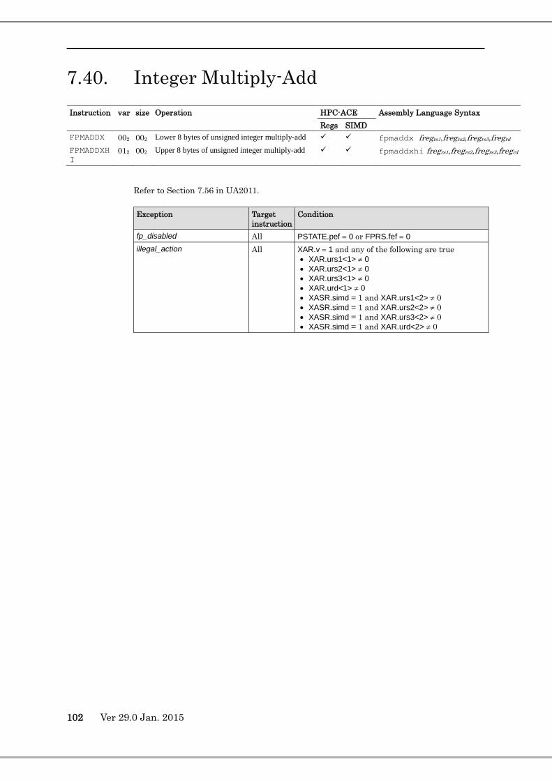
102 Ver 29.0 Jan. 2015
7.40. Integer Multiply-Add Instruction var size Operation HPC-ACE Assembly Language Syntax
Regs SIMD FPMADDX 002 002 Lower 8 bytes of unsigned integer multiply-add fpmaddx fregrs1,fregrs2,fregrs3,fregrd FPMADDXHI
012 002 Upper 8 bytes of unsigned integer multiply-add fpmaddxhi fregrs1,fregrs2,fregrs3,fregrd
Refer to Section 7.56 in UA2011.
Exception Target instruction
Condition
fp_disabled All PSTATE.pef = 0 or FPRS.fef = 0 illegal_action All XAR.v = 1 and any of the following are true
• XAR.urs1<1> ≠ 0 • XAR.urs2<1> ≠ 0 • XAR.urs3<1> ≠ 0 • XAR.urd<1> ≠ 0 • XASR.simd = 1 and XAR.urs1<2> ≠ 0 • XASR.simd = 1 and XAR.urs2<2> ≠ 0 • XASR.simd = 1 and XAR.urs3<2> ≠ 0 • XASR.simd = 1 and XAR.urd<2> ≠ 0

7.41. FPMERGE Refer to Section 7.57 in UA2011.
Exception Condition fp_disabled PSTATE.pef = 0 or FPRS.fef = 0 illegal_action XAR.v = 1

104 Ver 29.0 Jan. 2015
7.42. Fixed-point Partitioned Subtract (64-bit) <SPARC64™ X> Instruction opf Operation HPC-ACE Assembly Language Syntax
Regs. SIMD FPSUB16 0 0101 01002 Four 16-bit Subtract fpsub16 fregrs1, fregrs2, fregrd FPSUB16S 0 0101 01012 Two 16-bit Subtract fpsub16s fregrs1, fregrs2, fregrd
FPSUB32 0 0101 01102 Two 32-bit Subtract fpsub32 fregrs1, fregrs2, fregrd
FPSUB32S 0 0101 01112 One 32-bit Subtract fpsub32s fregrs1, fregrs2, fregrd
<SPARC64™ X+> Instruction opf Operation HPC-ACE Assembly Language Syntax
Regs. SIMD FPSUB16 0 0101 01002 Four 16-bit Subtract fpsub16 fregrs1, fregrs2, fregrd FPSUB16S 0 0101 01012 Two 16-bit Subtract fpsub16s fregrs1, fregrs2, fregrd
FPSUB32 0 0101 01102 Two 32-bit Subtract fpsub32 fregrs1, fregrs2, fregrd
FPSUB32S 0 0101 01112 One 32-bit Subtract fpsub32s fregrs1, fregrs2, fregrd
Refer to Section 7.58 in UA2011.
Note FPSUB{16|32}{S} do not update any fields in FSR.
Note SIMD is not available for these instructions on SPARC64™ X, but it is available on SPARC64™ X+.
Behavior of FPSUB16
Behavior of FPSUB16S
63
63
47 31 15
47 31 15
F[rs1]
F[rs2]
F[rd]
- - - -63 47 31 15
0
0
0
31
31
15
15
F[rs1]
F[rs2]
F[rd]
- -31 15
0
0
0

Behavior of FPSUB32
Behavior of FPSUB32S
<SPARC64™ X> Exception Condition fp_disabled PSTATE.pef = 0 or FPRS.fef = 0 illegal_action XAR.v = 1
<SPARC64™ X+> Exception Condition fp_disabled PSTATE.pef = 0 or FPRS.fef = 0 illegal_action XAR.v = 1 and any of the following are true
• XAR.urs1<1> ≠ 0 • XAR.urs2<1> ≠ 0 • XAR.urs3 ≠ 0 • XAR.urd<1> ≠ 0 • XAR.simd = 1 and XAR.urs1<2> ≠ 0 • XAR.simd = 1 and XAR.urs2<2> ≠ 0 • XAR.simd = 1 and XAR.urd<2> ≠ 0
63
63
31
31
F[rs1]
F[rs2]
F[rd]
- -63 31
0
0
0
31
31F[rs1]
F[rs2]
F[rd]
-31
0
0
0

106 Ver 29.0 Jan. 2015
7.43. F Register Logical Operate Instruction opf Operation HPC-ACE Assembly Language Syntax
Regs. SIMD FZERO 0 0110 00002 Zero fill fzero fregrd FZEROs 0 0110 00012 Zero fill, single precision fzeros fregrd
FONE 0 0111 11102 One fill fone fregrd FONEs 0 0111 11112 One fill, single precision fones fregrd FSRC1 0 0111 01002 Copy Fd[rs1] fsrc1 fregrs1, fregrd
FSRC1s 0 0111 01012 Copy Fs[rs1] fsrc1s fregrs1, fregrd
FSRC2 0 0111 10002 Copy Fd[rs2] fsrc2 fregrs2, fregrd
FSRC2s 0 0111 10012 Copy Fs[rs2] fsrc2s fregrs2, fregrd
FNOT1 0 0110 10102 Negate (1’s complement) Fd[rs1] fnot1 fregrs1, fregrd
FNOT1s 0 0110 10112 Negate (1’s complement) Fs[rs1] fnot1s fregrs1, fregrd
FNOT2 0 0110 01102 Negate (1’s complement) Fd[rs2] fnot2 fregrs2, fregrd
FNOT2s 0 0110 01112 Negate (1’s complement) Fs[rs2] fnot2s fregrs2, fregrd
FOR 0 0111 11002 Logical OR for fregrs1, fregrs2, fregrd
FORs 0 0111 11012 Logical OR, single precision fors fregrs1, fregrs2, fregrd
FNOR 0 0110 00102 Logical NOR fnor fregrs1, fregrs2, fregrd
FNORs 0 0110 00112 Logical NOR, single precision fnors fregrs1, fregrs2, fregrd
FAND 0 0111 00002 Logical AND fand fregrs1, fregrs2, fregrd
FANDs 0 0111 00012 Logical AND, single precision fands fregrs1, fregrs2, fregrd
FNAND 0 0110 11102 Logical NAND fnand fregrs1, fregrs2, fregrd
FNANDs 0 0110 11112 Logical NAND, single precision fnands fregrs1, fregrs2, fregrd
FXOR 0 0110 11002 Logical XOR fxor fregrs1, fregrs2, fregrd
FXORs 0 0110 11012 Logical XOR, single precision fxors fregrs1, fregrs2, fregrd
FXNOR 0 0111 00102 Logical XNOR fxnor fregrs1, fregrs2, fregrd
FXNORs 0 0111 00112 Logical XNOR, single precision fxnors fregrs1, fregrs2, fregrd
FORNOT1 0 0111 10102 (not Fd[rs1]) or Fd[rs2] fornot1 fregrs1, fregrs2, fregrd
FORNOT1s 0 0111 10112 (not Fs[rs1]) or Fs[rs2] fornot1s fregrs1, fregrs2, fregrd
FORNOT2 0 0111 01102 Fd[rs1] or (not Fd[rs2]) fornot2 fregrs1, fregrs2, fregrd
FORNOT2s 0 0111 01112 Fs[rs1] or (not Fs[rs2]) fornot2s fregrs1, fregrs2, fregrd
FANDNOT1 0 0110 10002 (not Fd[rs1]) and Fd[rs2] fandnot1 fregrs1, fregrs2, fregrd
FANDNOT1s 0 0110 10012 (not Fs[rs1]) and Fs[rs2] fandnot1s fregrs1, fregrs2, fregrd
FANDNOT2 0 0110 01002 Fd[rs1] and (not Fd[rs2]) fandnot2 fregrs1, fregrs2, fregrd
FANDNOT2s 0 0110 01012 Fs[rs1] and (not Fs[rs2]) fandnot2s fregrs1, fregrs2, fregrd
Refer to Sections 7.60, 7.61, and 7.62 in UA2011.
For the 64-bit versions of these instructions, the names of these instructions on SPARC64™ X / SPARC64™ X+ are different than the instruction names used in UA2011. UA2011 name SPARC64™ X / SPARC64™ X+ name
FZEROd FZERO
FONEd FONE
FSRC1d FSRC1

FSRC2d FSRC2
FNOT1d FNOT1
FNOT2d FNOT2
FORd FOR
FNORd FNOR
FANDd FAND
FNANDd FNAND
FXORd FXOR
FXNORd FXNOR
FORNOT1d FORNOT1
FORNOT2d FORNOT2
FANDNOT1d FANDNOT1
FANDNOT2d FANDNOT2

108 Ver 29.0 Jan. 2015
Exception Target instruction
Condition
fp_disabled All PSTATE.pef = 0 or FPRS.fef = 0 illegal_instruction FZERO,
FZEROs, FONE, FONEs
iw<18:14> ≠ 0 or iw<4:0> ≠ 0
FSRC1, FSRC1s, FNOT1, FNOT1s
iw<4:0> ≠ 0
FSRC2, FSRC2s, FNOT2, FNOT2s
iw<18:14> ≠ 0
illegal_action FZERO, FZEROs, FONE, FONEs
XAR.v = 1 and any of the following are true • XAR.urs1 ≠ 0 • XAR.urs2 ≠ 0 • XAR.urs3 ≠ 0 • XAR.urd<1> ≠ 0 • XASR.simd = 1 and XAR.urd<2> ≠ 0
FSRC1, FSRC1s, FNOT1, FNOT1s
XAR.v = 1 and any of the following are true • XAR.urs1<1> ≠ 0 • XAR.urs2 ≠ 0 • XAR.urs3 ≠ 0 • XAR.urd<1> ≠ 0 • XASR.simd = 1 and XAR.urs1<2> ≠ 0 • XASR.simd = 1 and XAR.urd<2> ≠ 0
FSRC2, FSRC2s, FNOT2, FNOT2s
• XAR.v = 1 and any of the following are true • XAR.urs1 ≠ 0 • XAR.urs2<1> ≠ 0 • XAR.urs3 ≠ 0 • XAR.urd<1> ≠ 0 • XASR.simd = 1 and XAR.urs2<2> ≠ 0 • XASR.simd = 1 and XAR.urd<2> ≠ 0
FOR, FORs, FNOR, FNORs, FAND, FANDs, FNAND, FNANDs, FXOR, FXORs, FXNOR, FXNORs, FORNOT1, FORNOT1s, FORNOT2, FORNOT2s, FANDNOT1, FANDNOT1s, FANDNOT2, FANDNOT2s
• XAR.v = 1 and any of the following are true • XAR.urs1<1> ≠ 0 • XAR.urs2<1> ≠ 0 • XAR.urs3 ≠ 0 • XAR.urd<1> ≠ 0 • XASR.simd = 1 and XAR.urs1<2> ≠ 0 • XASR.simd = 1 and XAR.urs2<2> ≠ 0 • XASR.simd = 1 and XAR.urd<2> ≠ 0

7.44. Floating-Point Reciprocal Approximation Instruction opf Operation HPC-ACE Assembly Language
Syntax Regs SIMD FRCPAd 1 0111 01002 Reciprocal Approximation Double frcpad fregrs2, fregrd FRCPAs 1 0111 01012 Reciprocal Approximation Single frcpas fregrs2, fregrd FRSQRTAd 1 0111 01102 Reciprocal Approximation of
Square Root, Double frsqrtad fregrs2, fregrd
FRSQRTAs 1 0111 01112 Reciprocal Approximation of Square Root, Single
frsqrtas fregrs2, fregrd
102 rd op3 = 11 01102 opf rs2
31 30 29 25 24 19 18 14 13 5 4 0
Description FRCPA{s,d} calculates the reciprocal approximation of the value in the floating-point register specified by F[rs2] and stores the result in the floating-point register specified by F[rd]. Although the result is an approximation, the calculation ignores FSR.rd. The resulting rounding error is less than 1/256, when the result is normalized. In other words,
2561
/1/1)(
<−
xxxfrcpa
Results and exceptions for FRCPA{s,d} are shown in Table 7-16. The upper row in each entry indicates the type(s) of exception if an exception is signalled, and the lower row in each entry indicates the result when an exception is not signalled. For more information on the causes of an fp_exception_ieee_754 exception, refer to Appendix B in JPS1 Commonality.

110 Ver 29.0 Jan. 2015
Table 7-16 FRCPA{s|d}
op2 Exceptions and results FSR.ns = 0 FSR.ns = 1
+∞ ― 0
― 0
+N (N ≥ 2126 for single, N ≥ 21022 for double)
UFix approximation of +1/N (denormal)x
UF, NX +0
+N (+Nmin ≤ N < 2126 for single, +Nmin ≤ N < 21022 for double)
― approximation of +1/N
― approximation of +1/N
+D unfinished_FPop ―
DZ +∞
+0 DZ +∞
DZ +∞
−0 DZ −∞
DZ −∞
−D unfinished_FPop ―
DZ −∞
-N (+Nmin ≤ N < 2126 for single, +Nmin ≤ N < 21022 for
double)
― approximation of -1/N
― approximation of -1/N
-N (N ≥ 2126 for single, N ≥ 21022 for double)
UFix approximation of -1/N (denormal)x
UF, NX −0
−∞ ― −0
― −0
SNaN NV QSNaN2
NV QSNaN2
QNaN ― op2
― op2
N Positive normal number (except for zero, NaN, and infinity) D Positive denormal number Nmin Minimum value of a positive normal number dNaN Sign of QNaN is 0 and all bits of the exponent and significand are 1 QSNaN2 Refer to TABLE B-1 in JPS1 Commonality
FRSQRTA{s|d} calculates the reciprocal approximation of the square root of the value in the floating-point register specified by F[rs2] and stores the result in the floating-point register specified by F[rd]. Although the result is an approximation, the calculation ignores FSR.rd. The resulting rounding error is less than 1/256. In other words,
( )( ) 256
1/1
/1)(<
−
xxxfrsqrta
Results and exceptions for FRSQRTA{s|d} are shown in Table 7-17. The upper row in each entry indicates the type(s) of exception if an exception is signalled, and the lower row in each entry indicates the result when an exception is not signalled. For more information on the causes of an fp_exception_ieee_754 exception, refer to Appendix B in JPS1 Commonality
ix When FSR.tem.ufm = 0, NX is not detected. x When the result is denormal, the rounding error may be larger than 1/256.

Table 7-17 FRSQRTA{s|d}
op2 Exceptions and results FSR.ns = 0 FSR.ns = 1
+∞ ― +∞
― +∞
+N ― ( )N/1+
― ( )N/1+
+D unfinished_FPop ―
― +0
+0 ― +0
― +0
−0 ― +0
― +0
−D NV dNaN
NV dNaN
−N NV dNaN
NV dNaN
−∞ NV dNaN
NV dNaN
SNaN NV QSNaN2
NV QSNaN2
QNaN ― op2
― op2
Exception Target instruction Condition illegal_instruction All A reserved field is not 0. (iw<18:14> ≠0) fp_disabled All PSTATE.pef = 0 or FPRS.fef = 0 illegal_action All XAR.v = 1 and any of the following are
true • XAR.urs1 ≠ 0 • XAR.urs2<1> ≠ 0 • XAR.urs3 ≠ 0 • XAR.urd<1> ≠ 0 • XAR.simd = 1 and XAR.urs2<2> ≠ 0 • XAR.simd = 1 and XAR.urd<2> ≠ 0
fp_exception_ieee_754 NV, DZ
FRCPAs, FRCPAd, FRSQRTs, FRSQRTAd
Conforms to IEEE754.
UF, NX
FRCPAs, FRCPAd Conforms to IEEE754.
fp_exception_other (FSR.ftt = unfinished_FPop)
All Refer to Chapter 8.

112 Ver 29.0 Jan. 2015
7.45. Move Selected Floating-Point Register on Floating-Point Register's Condition
Instruction var size Operation HPC-ACE Assembly Language Syntax
Regs SIMD FSELMOVd 112 002 Select and Move Double fselmovd fregrs1, fregrs2, fregrs3, fregrd FSELMOVs 112 112 Select and Move Single. fselmovs fregrs1, fregrs2, fregrs3, fregrd
102 rd op3 = 11 01112 rs1 rs3 var size rs2
31 30 29 25 24 19 18 14 13 9 8 7 6 5 4 0
Description FSELMOV{s|d} selects F[rs1] or F[rs2] according to the most-significant bit (MSB) of the floating-point register specified by F[rs3] and stores the value of the selected register in F[rd].
For FSELMOVd, if Fd[rs3]<63> is 1, Fd[rs1] is selected; if Fd[rd3]<63> is 0, Fd[rs2] is selected. For FSELMOVs, if Fs[rs3]<31> is 1, Fs[rs1] is selected; if Fs[rs3]<31> is 0, Fs[rs2] is selected.
Exception Target
instruction Condition
fp_disabled All PSTATE.pef = 0 or FPRS.fef = 0 illegal_action All XAR.v = 1 and any of the following are true
• XAR.urs1<1> ≠ 0 • XAR.urs2<1> ≠ 0 • XAR.urs3<1> ≠ 0 • XAR.urd<1> ≠ 0 • XAR.simd = 1 and XAR.urs1<2> ≠ 0 • XAR.simd = 1 and XAR.urs2<2> ≠ 0 • XAR.simd = 1 and XAR.urs3<2> ≠ 0 • XAR.simd = 1 and XAR.urd<2> ≠ 0

7.46. Floating-Point Square Root Instruction opf Operation HPC-ACE Assembly Language
Syntax Regs. SIMD FSQRTs 0 0010 10012 Square Root Single rd is basic
only. fsqrts fregrs2, fregrd
FSQRTd 0 0010 10102 Square Root Double rd is basic only.
fsqrtd fregrs2,fregrd
FSQRTq 0 0010 10112 Square Root Quad rd is basic only.
fsqrtq fregrs2,fregrd
Refer to Section 7.64 in UA2011.
Note Rounding is performed as specified by FSR.rd or GSR.irnd.
Exception Target instruction
Condition
illegal_instruction FSQRTs, FSQRTd
A reserved field is not 0.
FSQRTq Always For this instruction, exceptions with priority lower than illegal_instruction are intended for emulation.
fp_disabled All PSTATE.pef = 0 or FPRS.fef = 0 illegal_action All XAR.v = 1 and any of the following are true
• XAR.simd = 1 • XAR.urs1 ≠ 0 • XAR.urs2<1> ≠ 0 • XAR.urs3 ≠ 0 • XAR.urd<2:1> ≠ 0
fp_exception_ieee_754 NV, NX All Conforms to IEEE754. fp_exception_other (FSR.ftt = invalid_fp_register)
FSQRTq When either of the following is true • rs2<1> ≠ 0 • rd<1> ≠ 0
fp_exception_other (FSR.ftt = unfinished_FPop)
FSQRTs, FSQRTd
Refer to Chapter 8.

114 Ver 29.0 Jan. 2015
7.47. Floating-Point Trigonometric Functions Instruction op3 opf Operation HPC-ACE Assembly Language
Syntax Regs SIMD FTRIMADDd 11 01112 ― Trigonometric Multiply-Add
Double ftrimaddd fregrs1,
fregrs2, index, fregrd FTRISMULd 11 01102 1 0111 10102 Calculate starting value for
FTRIMADDd ftrismuld fregrs1,
fregrs2, fregrd FTRISSELd 11 01102 1 0111 10002 Select coefficient for final
calculation in Taylor series approximation FTRIMADDd
ftrisseld fregrs1, fregrs2, fregrd
102 rd op3 = 11 01112 rs1 index var = 102 size = 002 rs2
102 rd op3 = 11 01102 rs1 opf rs2
31 30 29 25 24 19 18 14 13 9 8 7 6 5 4 0
Instruction Operation FTRIMADDd Fd[rd] ← Fd[rs1] × abs(Fd[rs2]) + T[Fd[rs2]<63>][index] FTRISMULd Fd[rd] ← (Fd[rs2]<0> << 63) ^ (Fd[rs1] × Fd[rs1]) FTRISSELd Fd[rd] ← (Fd[rs2]<1> << 63) ^ (Fd[rs2] <0> ? 1.0 : Fd[rs1])
Description These instructions accelerate the calculation of the Taylor series approximation of the sine function sin(x). FTRIMADDd operates on the result of FTRISMULd, and the intermediate result is multiplied by the result of FTRISSELd. All three instructions are defined as double-precision instructions only. FTRIMADDd calculates series terms for either sin(x) or cos(x), where the argument is adjusted to be in the range -π/4 < x ≤ π/4. These series terms are used to perform the supporting operations shown in Figure 7-1. See the example at the end of this section for description of how to calculate sin(x) using these support operations.

Figure 7-1 Trigonometric functions assistance operation
FTRIMADDd multiplies Fd[rs1] and the absolute valueof Fd[rs2] and adds the product to a double-precision number obtained from a table. This double-precision number is specified by the index field. The result is stored in the double-precision register specified by Fd[rd]. FTRIMADDd is used to calculate series terms in the Taylor series of sin(x) or cos(x), where -π/4 < x ≤ π/4. FTRISMULd squares the value in the double-precision register specified by Fd[rs1]. The sign of the squared value is selected according to bit 0 of the double-precision register specified by Fd[rs2]. The result is written to the double-precision register specified by Fd[rd]. FTRISMULd is used to calculate the starting value of FTRIMADDd.
FTRISSELd checks bit 0 of the double-precision register specified by Fd[rs2]. Based on this bit, either the double-precision register specified by Fd[rs1] or the value 1.0 is selected. Bit 1 of Fd[rs2] indicates the sign; the exclusive OR of this bit and the selected value is written to the double-precision register specified by Fd[rd]. FTRISSELd is used to select the coefficient for calculating the last step in the Taylor series approximation.
To calculate the series terms of sin(x) and cos(x), the initial source operands of FTRIMADDd are zero for Fd[rs1] and x2 for Fd[rs2], where -π/4 < x ≤ π/4. FTRIMADDd is executed 8 times; this calculates the sum of 8 series terms, which gives the resulting number sufficient precision for a double-precision floating-point number. As show in Figure 7-1, the coefficients of the series terms are different for sin(x) and cos(x). FTRIMADDd uses the sign of Fd[rs2] to determine which set of coefficients to use.
• When Fd[rs2]<63> = 0, the coefficient table for sin(x) is used. • When Fd[rs2]<63> = 1, the coefficient table of cos(x) is used.
The expected usage for FTRIMADDd is shown in the example below. Coefficients are chosen to minimize the loss of precision; these differ slightly from the exact mathematical values. Table 7-18 and Table 7-19 show the coefficient tables for FTRIMADDd.
+
−
+
−
+
−
+
−⋅⋅=
−+−+−+−=
−+−+−+−≅
1!3
1!5
1!7
1!9
1!11
1!13
1!15
10
!151
!131
!111
!91
!71
!51
!311
!151
!131
!111
!91
!71
!51
!31sin
22222222
1412108642
1513119753
xxxxxxxxx
xxxxxxxx
xxxxxxxxx
+
−
+
−
+
−
+
−⋅⋅=
−+−+−+−≅
1!2
1!4
1!6
1!8
1!10
1!12
1!14
101
!141
!121
!101
!81
!61
!41
!211cos
22222222
1412108642
xxxxxxxx
xxxxxxxx

116 Ver 29.0 Jan. 2015
Table 7-18 Coefficient Table for sin(x) (Fd[rs2] <63> = 0)
Index Coefficient used for the operation Exact value of the coefficient Hexadecimal representation Decimal representation
0 3ff0 0000 0000 000016 1.0 = 1/1! 1 bfc5 5555 5555 554316 −0.1666666666666661 > −1/3! 2 3f81 1111 1110 f30c16 0.8333333333320002e−02 < 1/5! 3 bf2a 01a0 19b9 2fc616 −0.1984126982840213e−03 > −1/7! 4 3ec7 1de3 51f3 d22b16 0.2755731329901505e−05 < 1/9! 5 be5a e5e2 b60f 7b9116 −0.2505070584637887e−07 > −1/11! 6 3de5 d840 8868 552f16 0.1589413637195215e−09 < 1/13! 7 0000 0000 0000 000016 0 > −1/15!
Table 7-19 Coefficient Table for cos(x) (Fd[rs2] <63> = 1)
Index Coefficient used for the operation Exact value of the coefficient Hexadecimal representation Decimal representation
0 3ff0 0000 0000 000016 1.0 = 1/0! 1 bfe0 0000 0000 000016 −0.5000000000000000 = −1/2! 2 3fa5 5555 5555 553616 0.4166666666666645e−01 < 1/4! 3 bf56 c16c 16c1 3a0b16 −0.1388888888886111e−02 > −1/6! 4 3efa 01a0 19b1 e8d816 0.2480158728388683e−04 < 1/8! 5 be92 7e4f 7282 f46816 −0.2755731309913950e−06 > −1/10! 6 3e21 ee96 d264 1b1316 0.2087558253975872e−08 < 1/12! 7 bda8 f763 80fb b40116 −0.1135338700720054e−10 > −1/14!
The initial value in Fd[rs2] for FTRIMADDd is calculated using FTRISMULd, which is executed with Fd[rs1] set to x, where -π/4 < x ≤ π/4 and Fd[rs2] set to Q, as defined in Figure 7-2. FTRISMULd returns x2 as the result, where the sign bit specifies which set of coefficients to use to calculate the series terms. Q is an integer, not a floating-point number. Bits Fd[rs2]<63:1> are not used. An exception is not detected if Fd[rs2] is NaN.
The final step in the calculation of the Taylor series is the multiplication of the FTRIMADDd result and the coefficient selected by FTRISSELd. This coefficient is selected by executing FTRISSELd with Fd[rs1] set to x, where -π/4 < x ≤ π/4 and Fd[rs2] set to Q, as defined in Figure 7-2. Either x or 1.0 is selected, and the appropriate sign is affixed to the result. Q is an integer, not a floating-point number. Bits Fd[rs2]<63:2> are not used. An exception is not detected if Fd[rs2] is NaN.

Figure 7-2 Relationships for calculating sin(x)
Example: calculating sin(x)
/* * Input value: x * q: where (2q-1)*π/4 < x <= (2q+1)*π/4 * Q: q%4 * R: x - q * π/2 */ ftrismuld R, Q, M ftrisseld R, Q, N /* * M ←R2[63]=table_type, R2[62:0]=R2 * Because R2 is always positive, the sign bit (bit<63>) is always 0. * This sign bit indicates the table_type of ftrimaddd. ) * N ← coefficient used in final step; the value is (1.0 or R)* sign * S ←0 */ ftrimaddd S, M, 7, S ftrimaddd S, M, 6, S ftrimaddd S, M, 5, S ftrimaddd S, M, 4, S ftrimaddd S, M, 3, S ftrimaddd S, M, 2, S ftrimaddd S, M, 1, S ftrimaddd S, M, 0, S fmuld S, N, S /* * S ← result */
≤<−⋅−
⋅+≤<⋅−
442:
4mod:4
)12(4
)12(:
πππ
ππ
RqxR
qxqq
1=Q
0=Q2=Q
3=Q
)cos()sin( Rx =
)sin()sin( Rx =
)cos()sin( Rx −=
)sin()sin( Rx −=
4π
4π
−
π43
π43
−

118 Ver 29.0 Jan. 2015
Exception Target instruction Condition illegal_instruction FTRIMADDd index > 7 fp_disabled All PSTATE.pef = 0 or FPRS.fef = 0 illegal_action All XAR.v = 1 and any of the following are true
• XAR.urs1<1> ≠ 0 • XAR.urs2<1> ≠ 0 • XAR.urs3 ≠ 0 • XAR.urd<1> ≠ 0 • XAR.simd = 1 and XAR.urs1<2> ≠ 0 • XAR.simd = 1 and XAR.urs2<2> ≠ 0 • XAR.simd = 1 and XAR.urd<2> ≠ 0
fp_exception_ieee754 NV FTRIMADDd, FTRISMULd
Conforms to IEEE754. FTRISMULd : only rs1
NX FTRIMADDd, FTRISMULd
Conforms to IEEE754.
OF FTRIMADDd, FTRISMULd
Conforms to IEEE754.
UF FTRIMADDd, FTRISMULd
Conforms to IEEE754.
fp_exception_other (FSR.ftt = unfinished_FPop)
FTRIMADDd, FTRISMULd

7.48. Illegal Instruction Trap
Refer to Section 7.69 in UA2011.
Exception Target instruction
Condition
illegal_instruction All Always

120 Ver 29.0 Jan. 2015
7.49. Integer Logical Operation
Refer to Sections 7.7, 7.98, and 7.144 in UA2011.
Exception Target instruction
Condition
illegal_instruction All A reserved field is not 0. (i =0 and iw<12:5> ≠ 0)
illegal_action All XAR.v = 1

7.51. Jump and Link
Refer to Section 7.71 in UA2011.
Note SPARC64™ X / SPARC64™ X+ clear the most significant 32 bits of the PC value stored in R[rd] when PSTATE.am = 1. The updated value in R[rd] is visible to the delay slot instruction immediately.
Note If either of the two lowest bits of the jump address is nonzero, a mem_address_not_aligned exception occurs.
Exception Condition illegal_instruction A reserved field is not 0. illegal_action XAR.v = 1 mem_address_not_aligned When either of the two lowest bits of the target
address is not 0

122 Ver 29.0 Jan. 2015
7.52. Load Integer Instruction op3 Operation HPC-ACE Assembly Language Syntax
Regs SIMD LDSB 00 10012 Load Signed Byte ldsb [address], regrd LDSH 00 10102 Load Signed Halfword ldsh [address], regrd LDSW 00 10002 Load Signed Word ldsw [address], regrd LDUB 00 00012 Load Unsigned Byte ldub [address], regrd LDUH 00 00102 Load Unsigned Halfword lduh [address], regrd
LDUW 00 00002 Load Unsigned Word lduw [address], regrd
ld [address], regrd
LDX 00 10112 Load Extended Word ldx [address], regrd
Refer to Section 7.72 in UA2011.
Exception Target instruction Condition illegal_instruction All A reserved field is not 0. illegal_action All XAR.v = 1 and any of the following are
true • XAR.simd = 1 • XAR.urs1 ≠ 0 • XAR.urs2 ≠ 0 • XAR.urs3<2> ≠ 0 • XAR.urd ≠ 0
mem_address_not_aligned LDUH, LDSH, LDUW, LDSW, LDX
Refer to UA2011.
VA_watchpoint All Refer to 12.5.1.62 DAE_privilege_violation All Refer to 12.5.1.8 DAE_nfo_page All Refer to 12.5.1.7
Related LDTW (page 135)

7.53. Load Integer from Alternate Space Instruction op3 Operation HPC-ACE Assembly Language Syntax
Regs SIMD LDSBAPASI 01 10012 Load Signed Byte from Alternate Space ldsba [address] imm_asi, regrd
ldsba [address] %asi, regrd
LDSHAPASI 01 10102 Load Signed Halfword from Alternate Space ldsha [address] imm_asi, regrd ldsha [address] %asi, regrd
LDSWAPASI 01 10002 Load Signed Word from Alternate Space
ldswa [address] imm_asi, regrd ldswa [address] %asi, regrd
LDUBAPASI 01 00012 Load Unsigned Byte from Alternate Space
lduba [address] imm_asi, regrd lduba [address] %asi, regrd
LDUHAPASI 01 00102 Load Unsigned Halfword from Alternate Space
lduha [address] imm_asi, regrd lduha [address] %asi, regrd
LDUWAPASI 01 00002 Load Unsigned Word from Alternate Space
lduwa [address] imm_asi, regrd lduwa [address] %asi, regrd
lda [address] imm_asi, regrd lda [address] %asi, regrd
LDXAPASI 01 10112 Load Extended Word from Alternate Space
ldxa [address] imm_asi, regrd ldxa [address] %asi, regrd
Refer to Section 7.73 in UA2011.
Exception Target instruction Condition illegal_action All XAR.v = 1 and any of the following are true
• XAR.simd = 1 • XAR.urs1 ≠ 0 • XAR.urs2 ≠ 0 • XAR.urs3<2> ≠ 0 • XAR.urd ≠ 0
mem_address_not_aligned LDUHA, LDSHA, LDUWA, LDSWA, LDXA Refer to the UA2011. privileged_action All PSTATE.priv = 0 and ASI 0016 – 7F16 is specified VA_watchpoint All Refer to 12.5.1.62 DAE_invalid_asi All Refer to UA2011 and 12.5.1.5 DAE_privilege_violation All Refer to 12.5.1.8 DAE_nfo_page All Refer to 12.5.1.7
Related LDTWA (136Page)

124 Ver 29.0 Jan. 2015
7.54. Block Load Instruction ASI Operation HPC-ACE Assembly Language Syntax
Regs SIMD LDBLOCKF F016 64-byte block load from primary
address space ldda [regaddr] ASI_BLK_P, fregrd
ldda [reg_plus_imm] %asi, fregrd LDBLOCKF F116 64-byte block load from secondary
address space ldda [regaddr] ASI_BLK_S, fregrd
ldda [reg_plus_imm] %asi, fregrd LDBLOCKF F816 64-byte block load from primary
address space, little-endian ldda [regaddr] ASI_BLK_PL, fregrd
ldda [reg_plus_imm] %asi, fregrd LDBLOCKF F916 64-byte block load from secondary
address space, little-endian ldda [regaddr] ASI_BLK_SL, fregrd
ldda [reg_plus_imm] %asi, fregrd
Refer to Section 7.74 in UA2011.
The LDBLOCKF can only be used to access cacheable addresses, unlike a normal load. LDBLOCKF ASIs do not allow LDBLOCKF to access the non-cacheable space.
The effective address is “R[rs1] + R[rs2]” if i = 0, or “R[rs1] + sign_ext(simm13)” if i = 1.
When an exception is generated for a block load, register values may have been updated by the block load.
LDBLOCKF on SPARC64™ X / SPARC64™ X+ follow TSO. That is, the ordering between the preceding and following load/store/atomic instructions and the 8-byte loads comprising the block loads conforms to TSO.
LDBLOCKF on SPARC64™ X / SPARC64™ X+ preserves the order of register accesses in the same manner as any other load instruction. The cache behavior of LDBLOCKF is the same as for a normal load. A block load reads data from the L1D cache; if the data is not in the L1D cache, the L1D cache is updated with data from memory before being read.
A VA_watchpoint exception is detected only for the first eight bytes accessed by an LDBLOCKF instruction.

Exception Target instruction Condition illegal_instruction All Register number specified for rd is not a
multiple of 8. fp_disabled All PSTATE.pef = 0 or FPRS.fef = 0 illegal_action All XAR.v = 1 and any of the following are true
• XAR.simd = 1 • XAR.urs1 ≠ 0 • XAR.urs2 ≠ 0 • XAR.urs3<2> ≠ 0 • XAR.urd<1> ≠ 0
mem_address_not_aligned All Address is not aligned on a 64-byte boundary
VA_watchpoint All On access to lowest 8 bytes only Refer to 12.5.1.62
DAE_privilege_violation ASI F016, F116, F816, and F916
PSTATE.priv = 0 and TTE.p = 1 Refer to 12.5.1.8
DAE_nc_page All Access to non-cacheable space Refer to 12.5.1.6
DAE_nfo_page All Refer to 12.5.1.7

126 Ver 29.0 Jan. 2015
7.55. Load Floating-Point Instruction op3 rdxi Operation HPC-ACE Assembly Language Syntax
Regs SIMD LDF 10 00002 0 – 31 Load to Single Floating-Point
Register (XAR.v = 0) ld [address], fregrd
LDF 10 00002 0 – 126, 256 – 382
Load to Double Floating-Point Register (XAR.v = 1)
ld [address], fregrd
LDDF 10 00112 0 – 126, 256 – 382
Load to Double Floating-Point Register
ldd [address], fregrd
LDQF 10 00102 0 – 126, 256 – 382
Load to Quad Floating-Point Register
ldq [address], fregrd
Non-SIMD execution
Refer to Section 7.75 in UA2011.
LDF copies a word from memory into the 32-bit floating-point destination register F[rd]. If XAR.v = 0, LDF copies the word into a single-precision floating point register. If XAR.v = 1, LDF copies the word into the upper 32-bits of a double-precision floating point register.
SIMD execution
On SPARC64™ X / SPARC64™ X+, LDF and LDDF can be executed as SIMD instructions. A SIMD LDF and SIMD LDDF simultaneously execute basic and extended loads from the effective address for single-precision and double-precision data, respectively. Refer to Section 5.5.14 (page 35) for details on how to specify the registers.
A SIMD LDF loads 2 single-precision data aligned on a 4-byte boundary. Data from the lower 4-bytes of the address is loaded into the upper 4-bytes of Fd[rd], and data from the upper 4-byte of the address is loaded into the upper 4-bytes of Fd[rd+256]. Misaligned accesses cause a mem_address_not_aligned exception.
A SIMD LDDF instruction loads 2 double-precision data aligned on an 8-byte boundary. Data from the lower 8-bytes of the address is loaded into Fd[rd],,and data from the upper 8-bytes of the address is loaded into Fd[rd+256]. Misaligned accesses cause a mem_address_not_aligned exception.
Note A double-precision SIMD load that accesses data aligned on a 4-byte boundary but not an 8-byte boundary does not cause an LDDF_mem_address_not_aligned exception.
SIMD LDF and SIMD LDDF can only be used to access cacheable address spaces. An attempt to access a noncacheable address space using a SIMD LDF or SIMD LDDF causes a DAE_nc_page exception.
Like non-SIMD load instructions, memory access semantics for SIMD load instructions adhere to TSO. A SIMD load simultaneously executes basic and extended loads; however, the ordering between the basic and extended loads conforms to TSO.
xi Encoding defined in 5.3.1 "Floating-Point Register Number Encoding” (page 26).

For a SIMD load instruction, endian conversion is done separately for the basic and extended loads. When the basic and extended data are located on different pages with different endianness, conversion is only done for one of the loads. A watchpoint can be detected in both the basic and extended loads.

128 Ver 29.0 Jan. 2015
Exception Target instruction
Condition
illegal_instruction LDF, LDDF A reserved field is not 0. LDQF Always
For this instruction, exceptions with priority lower than illegal_instruction are intended for emulation.
fp_disabled All PSTATE.pef = 0 or FPRS.fef = 0 illegal_action LDF, LDDF XAR.v = 1 and any of the following are true
• XAR.urs1 ≠ 0 • XAR.urs2 ≠ 0 • XAR.urs3<2> ≠ 0 • XAR.urd<1> ≠ 0 • XAR.simd = 1 and XAR.urd<2> ≠ 0
LDQF XAR.v = 1 and any of the following are true • XAR.simd = 1 • XAR.urs1 ≠ 0 • XAR.urs2 ≠ 0 • XAR.urs3<2> ≠ 0 • XAR.urd<1> ≠ 0
fp_exception_other (FSR.ftt = invalid_fp_register)
LDQF rd<1> ≠ 0
LDDF_mem_address_not_aligned LDDF XAR.v = 0 or XAR.simd = 0, and address is 4-byte aligned but not 8-byte aligned
mem_address_not_aligned LDF, LDQF Address not 4- byte aligned LDDF When either of the following is true
• XAR.v = 0 or XAR.simd = 0, and address not 4-byte aligned
• XAR.v = 1, XAR.simd = 1, and address not 8-byte aligned
VA_watchpoint All Refer to the description and 12.5.1.62 DAE_privilege_violation All Refer to 12.5.1.8 DAE_nc_page All XAR.v = 1, XAR.simd = 1, and access to
non-cacheable space DAE_nfo_page All Refer to 12.5.1.7
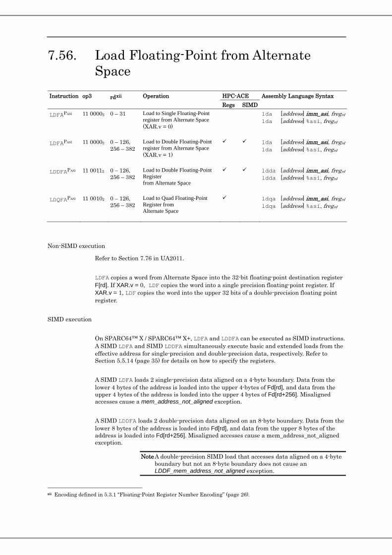
7.56. Load Floating-Point from Alternate Space
Instruction op3 rdxii Operation HPC-ACE Assembly Language Syntax
Regs SIMD LDFAPASI 11 00002 0 – 31 Load to Single Floating-Point
register from Alternate Space (XAR.v = 0)
lda [address] imm_asi, fregrd lda [address] %asi, fregrd
LDFAPASI 11 00002 0 – 126, 256 – 382
Load to Double Floating-Point register from Alternate Space (XAR.v = 1)
lda [address] imm_asi, fregrd lda [address] %asi, fregrd
LDDFAPASI 11 00112 0 – 126, 256 – 382
Load to Double Floating-Point Register from Alternate Space
ldda [address] imm_asi, fregrd ldda [address] %asi, fregrd
LDQFAPASI 11 00102 0 – 126, 256 – 382
Load to Quad Floating-Point Register from Alternate Space
ldqa [address] imm_asi, fregrd ldqa [address] %asi, fregrd
Non-SIMD execution
Refer to Section 7.76 in UA2011.
LDFA copies a word from Alternate Space into the 32-bit floating-point destination register F[rd]. If XAR.v = 0, LDF copies the word into a single precision floating-point register. If XAR.v = 1, LDF copies the word into the upper 32 bits of a double-precision floating point register.
SIMD execution
On SPARC64™ X / SPARC64™ X+, LDFA and LDDFA can be executed as SIMD instructions. A SIMD LDFA and SIMD LDDFA simultaneously execute basic and extended loads from the effective address for single-precision and double-precision data, respectively. Refer to Section 5.5.14 (page 35) for details on how to specify the registers.
A SIMD LDFA loads 2 single-precision data aligned on a 4-byte boundary. Data from the lower 4 bytes of the address is loaded into the upper 4-bytes of Fd[rd], and data from the upper 4 bytes of the address is loaded into the upper 4 bytes of Fd[rd+256]. Misaligned accesses cause a mem_address_not_aligned exception.
A SIMD LDDFA loads 2 double-precision data aligned on an 8-byte boundary. Data from the lower 8 bytes of the address is loaded into Fd[rd], and data from the upper 8 bytes of the address is loaded into Fd[rd+256]. Misaligned accesses cause a mem_address_not_aligned exception.
Note A double-precision SIMD load that accesses data aligned on a 4-byte boundary but not an 8-byte boundary does not cause an LDDF_mem_address_not_aligned exception.
xii Encoding defined in 5.3.1 "Floating-Point Register Number Encoding” (page 26).

130 Ver 29.0 Jan. 2015
SIMD LDFA and SIMD LDDFA can only be used to access cacheable address spaces. An attempt to access a non-cacheable address space using a SIMD LDFA or SIMD LDDFA causes a DAE_nc_page exception.
Like non-SIMD load instructions, memory access semantics for SIMD load instructions adhere to TSO. SIMD LDFA and SIMD LDDFA simultaneously execute basic and extended loads; however, the ordering between the basic and extended loads conforms to TSO.
For SIMD LDFA and SIMD LDDFA, endian conversion is done separately for the basic and extended loads. When the basic and extended data are located on different pages with different endianness, conversion is only done for one of the loads. A watchpoint can be detected in both the basic and extended loads.

Exception Target instruction Condition illegal_instruction LDQFA Always
For this instruction, exceptions with priority lower than illegal_instruction are intended for emulation.
fp_disabled All PSTATE.pef = 0 or FPRS.fef = 0 illegal_action LDFA, LDDFA XAR.v = 1 and any of the following are
true • XAR.urs1 ≠ 0 • XAR.urs2 ≠ 0 • XAR.urs3<2> ≠ 0 • XAR.urd<1> ≠ 0 • XAR.simd = 1 and XAR.urd<2> ≠ 0
LDQFA XAR.v = 1 and any of the following are true • XAR.simd = 1 • XAR.urs1 ≠ 0 • XAR.urs2 ≠ 0 • XAR.urs3<2> ≠ 0 • XAR.urd<1> ≠ 0
fp_exception_other (FSR.ftt = invalid_fp_register)
LDQFA rd<1> ≠ 0
LDDF_mem_address_not_aligned LDDFA XAR.v = 0 or XAR.simd = 0, and address 4-byte aligned but not 8-byte aligned
mem_address_not_aligned LDFA, LDQFA Address mot 4-byte aligned LDDFA When either of the following is true
• XAR.v = 0 or XAR.simd = 0, and address not 4-byte aligned
• XAR.v = 1, XAR.simd = 1, and address not 8-byte aligned
privileged_action All Refer to 12.5.1.49 VA_watchpoint All Refer to the description and 12.5.1.62 DAE_invalid_asi All Refer to the UA2011 and 12.5.1.5 DAE_privilege_violation All Refer to 12.5.1.8 DAE_nc_page All XAR.v = 1, XAR.simd = 1, and access to
non-cacheable space DAE_nfo_page All Refer to 12.5.1.7 DAE_side_effect_page All Refer to 12.5.1.9

132 Ver 29.0 Jan. 2015
7.57. Short Floating-Point Load
Refer to Section 7.78 in UA2011.
LDSHORTF is equivalent to LDDFA using ASIs D016 – D316 and D816 – DB16. No other ASIs can be used with LDSHORTF.
An ASI is specified by the imm_asi instruction field when i = 0, or the contents of the ASI register when i = 1. If i = 0, the effective address for these instructions is “R[rs1] + R[rs2]” and if i = 1, the effective address is “R[rs1] + sign_ext(simm13)”.
Programming Note LDSHORTF is typically used with the FALIGNDATA instruction.
Exception Condition fp_disabled PSTATE.pef = 0 or FPRS.fef = 0 illegal_action XAR.v = 1 mem_address_not_aligned Refer to UA2011 VA_watchpoint Refer to 12.5.1.62 DAE_privilege_violation Refer to 12.5.1.8 DAE_nfo_page Refer to 12.5.1.7

7.58. Load-Store Unsigned Byte Instruction op3 Operation HPC-ACE Assembly Language
Syntax Regs SIMD LDSTUB 00
11012 Load-Store Unsigned Byte ldstub [address], regrd
Refer to Section 7.79 in UA2011.
Exception Condition illegal_instruction A reserved field is not 0. illegal_action XAR.v = 1 and any of the following are true.
• XAR.simd = 1 • XAR.urs1 ≠ 0 • XAR.urs2 ≠ 0 • XAR.urs3<2> ≠ 0 • XAR.urd ≠ 0
VA_watchpoint Refer to 12.5.1.62 DAE_privilege_violation Refer to 12.5.1.8 DAE_nc_page Refer to 12.5.1.6 DAE_nfo_page Refer to 12.5.1.7
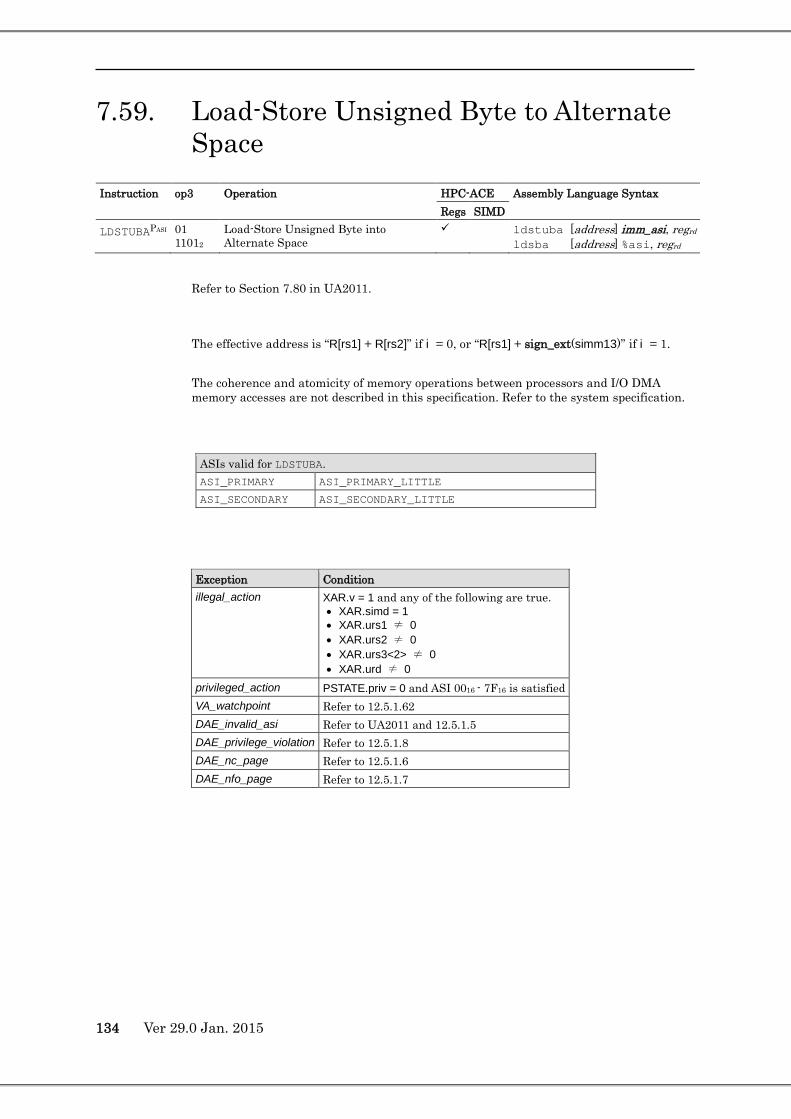
134 Ver 29.0 Jan. 2015
7.59. Load-Store Unsigned Byte to Alternate Space
Instruction op3 Operation HPC-ACE Assembly Language Syntax
Regs SIMD LDSTUBAPASI 01
11012 Load-Store Unsigned Byte into Alternate Space
ldstuba [address] imm_asi, regrd ldsba [address] %asi, regrd
Refer to Section 7.80 in UA2011.
The effective address is “R[rs1] + R[rs2]” if i = 0, or “R[rs1] + sign_ext(simm13)” if i = 1.
The coherence and atomicity of memory operations between processors and I/O DMA memory accesses are not described in this specification. Refer to the system specification.
ASIs valid for LDSTUBA. ASI_PRIMARY ASI_PRIMARY_LITTLE
ASI_SECONDARY ASI_SECONDARY_LITTLE
Exception Condition illegal_action XAR.v = 1 and any of the following are true.
• XAR.simd = 1 • XAR.urs1 ≠ 0 • XAR.urs2 ≠ 0 • XAR.urs3<2> ≠ 0 • XAR.urd ≠ 0
privileged_action PSTATE.priv = 0 and ASI 0016 - 7F16 is satisfied VA_watchpoint Refer to 12.5.1.62 DAE_invalid_asi Refer to UA2011 and 12.5.1.5 DAE_privilege_violation Refer to 12.5.1.8 DAE_nc_page Refer to 12.5.1.6 DAE_nfo_page Refer to 12.5.1.7

7.60. Load Integer Twin Word Instruction op3 Operation HPC-ACE Assembly Language
Syntax Regs SIMD LDTWD 00 00112 Load integer twin word ldtw [address], regrd
Refer to Section 7.81 in UA2011.
Exception Condition illegal_instruction When either of the following is true
• i = 0 and iw<12:5> ≠ 0 • LDTW refers to an odd-numbered destination register (rd).
illegal_action XAR.v = 1 and any of the following are true • XAR.simd = 1 • XAR.urs1 ≠ 0 • XAR.urs2 ≠ 0 • XAR.urs3<2> ≠ 0 • XAR.urd ≠ 0
mem_address_not_aligned Refer to UA2011 VA_watchpoint Refer to 12.5.1.62 DAE_privilege_violation Refer to 12.5.1.8 DAE_nfo_page Refer to 12.5.1.7
Related LDX (page 122) STTW (page 179)

136 Ver 29.0 Jan. 2015
7.61. Load Integer Twin Word from Alternate Space
Instruction op3 Operation HPC-ACE Assembly Language Syntax
Regs SIMD LDTWAD,PASI 01 00112 Load Twin word from Alternate Space ldtwa [address] imm_asi, regrd
ldtwa [address] %asi, regrd
112 rd op3 rs1 i = 0 imm_asi rs2
112 rd op3 rs1 i = 1 simm13 31 30 29 25 24 19 18 14 13 12 5 4 0
Refer to Section 7.82 in UA2011.
Note For instructions that specify ASI_TWINX* for LDTWA, refer to 7.62.
ASIs valid for LDTWA ASI_PRIMARY ASI_PRIMARY_LITTLE
ASI_SECONDARY ASI_SECONDARY_LITTLE
ASI_PRIMARY_NO_FAULT ASI_PRIMARY_NO_FAULT_LITTLE
ASI_SECONDARY_NO_FAULT ASI_SECONDARY_NO_FAULT_LITTLE
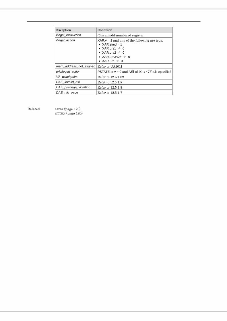
Exception Condition illegal_instruction rd is an odd-numbered register. illegal_action XAR.v = 1 and any of the following are true.
• XAR.simd = 1 • XAR.urs1 ≠ 0 • XAR.urs2 ≠ 0 • XAR.urs3<2> ≠ 0 • XAR.urd ≠ 0
mem_address_not_aligned Refer to UA2011 privileged_action PSTATE.priv = 0 and ASI of 0016 - 7F16.is specified VA_watchpoint Refer to 12.5.1.62 DAE_invalid_asi Refet to 12.5.1.5 DAE_privilege_violation Refer to 12.5.1.8 DAE_nfo_page Refer to 12.5.1.7
Related LDXA (page 123) STTWA (page 180)

138 Ver 29.0 Jan. 2015
7.62. Load Integer Twin Extended Word from Alternate Space
Instruction ASI Operation HPC-ACE Assembly Language Syntax Regs SIMD
LDTXAN E216 Load Integer Twin Extended Word from Alternate Space
ldtxa [regaddr]#ASI_TWINX_P, regrd
E316 Load Integer Twin Extended Word from Alternate Space
ldtxa [regaddr]#ASI_TWINX_S, regrd
EA16 Load Integer Twin Extended Word from Alternate Space
ldtxa [regaddr]#ASI_TWINX_PL, regrd
EB16 Load Integer Twin Extended Word from Alternate Space
ldtxa [regaddr]#ASI_TWINX_SL, regrd
112 rd op3 rs1 i = 0 imm_asi rs2
112 rd op3 rs1 i = 1 simm13
31 30 29 25 24 19 18 14 13 12 5 4 0
Refer to Section 7.83 in UA2011.
If i = 0, the LDTXA instruction contains the address space identifier (ASI) to be used for the load in its imm_asi field and the effective address for the instruction is “R[rs1] + R[rs2]”. If i = 1, the ASI to be used is contained in the ASI register and the effective address for the instruction is “R[rs1] + sign_ext(simm13)”.
A LDTXA instruction that performs a little-endian access behaves as if it comprises two 32-bit loads, each of which is byte-swapped independently before being written into its respective destination register.
A successful LDTXA instruction operates atomically.
Programming Note LDTXA can be used to read one entry of TSB TTE atomically.
ASIs E216, E316, EA16 and EB16 are used with LDTXA. An attempt to use other ASIs with LDTXA has the same result as LDTWA with those ASIs. ASIs E216, E316, EA16 and EB16 perform an access using a VA.

Exception Target instruction Condition illegal_instruction All rd is an odd-numbered register illegal_action All XAR.v = 1 and any of the following are true.
• XAR.simd = 1 • XAR.urs1 ≠ 0 • XAR.urs2 ≠ 0 • XAR.urs3<2> ≠ 0 • XAR.urd ≠ 0
mem_address_not_aligned All Address not 16-byte aligned VA_watchpoint ASI E216, E316,
EA16, and EB16 Only detected for first 8 bytes Refer to 12.5.1.62.
DAE_privilege_violation ASI E216, E316, E316, and EB16
When PSTATE.priv = 0 and access to page with TTE.p = 1
DAE_nc_page All Refer to 12.5.1.6 DAE_nfo All Refer to 12.5.1.7

140 Ver 29.0 Jan. 2015
7.63. Load Floating-Point State Register Instruction op3 rd Operation HPC-ACE Assembly Language
Syntax Regs SIMD LDFSRD 10
00012 0 Load Floating-Point State Register (Lower) ld [address], %fsr
LDXFSR 10 00012
1 Load Floating-Point State Register ldx [address], %fsr
10 00012
2 - 31
reserved
Refer to Section 7.77 and Section 7.84 in UA2011.
Exception Target instruction Condition illegal_instruction LDFSR, LDXFSR i = 0 and iw<12:5> ≠ 0.
rd = 2 - 31 fp_disabled All PSTATE.pef = 0 or FPRS.fef = 0 illegal_action All XAR.v = 1 and any of the following are
true • XAR.simd = 1 • XAR.urs1 ≠ 0 • XAR.urs2 ≠ 0 • XAR.urs3<2> ≠ 0 • XAR.urd ≠ 0
mem_address_not_aligned LDFSR Address not 4-byte aligned. LDXFSR Address not 8-byte aligned.
VA_watchpoint All Refer to 12.5.1.62 DAE_privilege_violation All Refer to 12.5.1.8 DAE_nfo_page All Refer to 12.5.1.7

7.64. Memory Barrier
Refer to Section 7.87 in UA2011.
Note mmask<3> has no effect on SPARC64™ X / SPARC64™ X+ because all stores are performed in program order.
Note mmask<1> has no effect on SPARC64™ X / SPARC64™ X+ because all stores are performed in program order and the ordering between a load and a store is guaranteed.
Note mmask<0> has no effect on SPARC64™ X / SPARC64™ X+ because all loads are performed in program order.
Note #StoreStore is equivalent to the deprecated STBAR instruction on SPARC64™ X / SPARC64™ X+.
Note #MemIssue is equivalent to #Sync on SPARC64™ X / SPARC64™ X+
Note #Lookaside is equivalent to #Sync on SPARC64™ X / SPARC64™ X+.
Exception Condition illegal_instruction iw<12:7> ≠ 0 illegal_action XAR.v = 1

142 Ver 29.0 Jan. 2015
7.65. Move Integer Register on Condition (MOVcc) Refer to Section 7.90 in UA2011.
Exception Target instruction Condition illegal_instruction All i = 0 and iw<10:5> ≠ 0
Either of the following is true • cc2::cc1::cc0 = 1012 • cc2::cc1::cc0 = 1112
fp_disabled MOVF* PSTATE.pef = 0 or FPRS.fef = 0 illegal_action All XAR.v = 1

7.66. Move Integer Register on Register Condition (MOVr)
Refer to Section 7.91 in UA2011.
Exception Target instruction
Condition
illegal_instruction All A reserved field is not 0. When either of the following is true
• rcond = 0002 • rcond = 1002
illegal_action All XAR.v = 1

144 Ver 29.0 Jan. 2015
7.67. Multiply Step Instruction op3 Operation HPC-ACE Assembly Language Syntax
Regs SIMD MULSccD 10
01002 Multiply Step and modify cc mulscc regrs1, reg_or_imm, regrd
102 rd op3 = 10 01002 rs1 i = 0 rs2
102 rd op3 = 10 01002 rs1 i = 1 simm13
31 30 29 25 24 19 18 14 13 12 5 4 0
Description MULScc is a deprecated instruction that assists in performing a multiplication operation. MULScc treats the less significant 32 bits of both R[rs1] and the Y register as a single 64-bit, right-shiftable doubleword register. The least significant bit of R[rs1] is treated as if it were adjacent to bit 31 of the Y register. The MULScc instruction adds, based on the least significant bit of Y.
Multiplication assumes that the Y register initially contains the multiplier, R[rs1] contains the most significant bits of the product, and R[rs2] contains the multiplicand. Upon completion of the multiplication, the Y register contains the least significant bits of the product.
Note A standard MULScc instruction has rs1 = rd.
1. The multiplicand is R[rs2] if i = 0, or sign_ext(simm13) if i = 1. 2. A 32-bit value is computed by shifting R[rs1] right by one bit with “CCR.icc.n xor
CCR.icc.v” replacing bit 31 of R[rs1]. (This is the proper sign for the previous partial product.)
3. If the least significant bit of Y = 1, the shifted value from step (2) and the multiplicand are added. If the least significant bit of the Y = 0, then 0 is added to the shifted value from step (2).
4. The following values are set to the register.
Register field Value set by MULScc CCR.icc Updated according to the addition performed in step 3. R[rd]<63:33> 0 R[rd]<32> CCR.icc.c R[rd]<31:0> The lower 32 bits of R[rd] of step 3. CCR.xcc.n 0 CCR.xcc.v 0 CCR.xcc.c 0 CCR.xcc.z Set to 1 if R[rd]=0. Otherwise, set to 0.
Compatibility Note In SPARC V9 and JPS1, the upper 32 bits of R[rd] and CCR.xcc were undefined.
5. The Y register is shifted right by one bit, with the least significant bit of the unshifted R[rs1] replacing bit 31of Y.

Exception Condition illegal_instruction A reserved field is not 0. illegal_action XAR.v = 1

146 Ver 29.0 Jan. 2015
7.68. Multiply and Divide (64-bit)
Refer to Section 7.95 in UA2011.
Exception Target instruction Condition illegal_instruction All A reserved field is not 0. illegal_action All XAR.v = 1 division_by_zero SDIVX, UDIVX Divisor is 0.

7.69. No Operation
Refer to Section 7.96 in UA2011.
Exception Target instruction Condition illegal_instruction All iw<29:25, 21:0> ≠ 0 illegal_action All XAR.v = 1

148 Ver 29.0 Jan. 2015
7.72. Partitioned Add Instruction opf Operation HPC-ACE Assembly Language Syntax
Regs. SIMD PADD32 0 1000
10012 Two 32-bit Add Two 32 bit addition padd32 regrs1, regrs2, regrd
102 rd op3 = 11 01102 rs1 opf rs2
31 30 29 25 24 19 18 14 13 5 4 0
Description PADD32 performs two 32-bit partitioned adds between the corresponding fixed-point values contained in the source operands (the 64-bit integer registers specified by rs1 and rs2). The result is placed in the 64-bit destination register specified by rd.
Exception Condition illegal_action XAR.v = 1

7.73. Pixel Component Distance (with Accumulation) Refer to Section 7.101 in UA2011.
Exception Condition fp_disabled PSTATE.pef = 0 or FPRS.fef = 0 illegal_action XAR.v = 1

150 Ver 29.0 Jan. 2015
7.74. Population Count Instruction op3 Operation HPC-ACE Assembly Language Syntax
Regs SIMD POPC 10
11102 Population Count popc reg_or_imm, regrd
Refer to Section 7.103 in UA2011.
Exception Condition illegal_instruction • iw<18:14 > ≠ 0.
• i = 0 and iw<12:5 > ≠ 0. illegal_action XAR.v = 1

7.75. Prefetch Instruction op3 Operation HPC-ACE Assembly Language Syntax
Regs SIMD PREFETCH 10
11012 Prefetch Data prefetch [address], prefetch_fcn
PREFETCHAPASI 11 11012
Prefetch Data from Alternate Space
prefetch [regaddr], imm_asi, prefetch_fcn prefetch [reg_plus_imm] %asi, prefetch_fcn
Refer to Section 7.104 in UA2011.
An arbitrary address can be specified for the address specified by the instruction. One cache line (128 bytes) or two cache lines (256 bytes), as specified by the instruction, are copied. The mem_address_not_aligned exception is never generated.
The PREFETCH{A} instruction becomes a NOP when the specified address is non-cacheable or in an undefined cacheable space.
ASIs that can be specified by the PREFETCHA instruction are shown in Table 7-20. When an ASI other than those listed below is specified, the PREFETCHA instruction becomes a NOP.
Table 7-20 ASIs valid for PREFETCHA
ASI_PRIMARY ASI_PRIMARY_LITTLE
ASI_SECONDARY ASI_SECONDARY_LITTLE
The prefetch instruction has no side effects other than bringing a data block into cache.
The prefetch instruction might not be executed due to a lack of hardware resources (prefetch lost). Whether a prefetch instruction has been executed or lost cannot be known.
7.75.1. Prefetch Variants Table 7-21 shows available fcns on SPARC64™ X / SPARC64™ X+ and describes their operation.

152 Ver 29.0 Jan. 2015
Table 7-21 fcns for PREFETCH and PREFETCHA
fcn JPS1 and UA2011 Definition Operation on SPARC64™ X / SPARC64™ X+ 0 Frequently used data is
prefetched for reading. 128-byte data is copied into the L1 data cache.
1 Infrequently used data is prefetched for reading.
128-byte data is copied into the U2 cache.
2 Frequently used data is prefetched for writing.
128-byte data is copied into the L1 data cache with exclusive ownership.
3 Infrequently used data is prefetched for writing.
128-byte data is copied into the U2 cache with exclusive ownership.
4 Page mapping performed by privileged software.
NOP
5 - 15 (0516 - 0F16)
An illegal_instruction exception is detected.
An illegal_instruction exception is detected.
16 - 19 (1016 - 1316)
Implementation dependent NOP
20 (1416) Frequently used data is prefetched for reading. Strong prefetch.
128-byte data is copied into the L1 data cache. Strong prefetch.
21 (1516) Infrequently used data is prefetched for reading. Strong prefetch.
128-byte data is copied into the U2 cache. Strong prefetch.
22 (1616) Frequently used data is prefetched for writing. Strong prefetch.
128-byte data is copied into the L1 data cache with exclusive ownership. Strong prefetch.
23 (1716) Infrequently used data is prefetched for writing. Strong prefetch.
128-byte data is copied into the U2 cache with exclusive ownership. Strong prefetch.
24 - 28 (1816 - 1C16)
Implementation dependent NOP
29 (1D16) 256 byte data aligned on 256-byte boundary is copied into the U2 cache. Strong prefetch.
30 (1E16) NOP
31 (1F16) 256-byte data aligned on 256-byte boundary is copied into the U2 cache with exclusive ownership. Strong prefetch.
7.75.2. Weak versus Strong Prefetches
Programming Note Strong prefetches might block subsequent load or store instructions. Therefore, strong prefetches should be used only when prefetched data is guaranteed to be accessed.

Exception Target instruction Condition illegal_instruction All When either of the following is true
• A reserved field is not 0. • fcn = 5 - 15
illegal_action All XAR.v = 1 and any of the following are true • XAR.simd = 1 • XAR.urs1 ≠ 0 • XAR.urs2 ≠ 0 • XAR.urs3<2> ≠ 0 • XAR.urd ≠ 0

154 Ver 29.0 Jan. 2015
7.76. Read Ancillary State Register (RDASR) Instruction rs1 Operation HPC-ACE Assembly Language Syntax
Regs SIMD RDYD 0 Read Y Register; deprecated (see A.71.9 in JPS1
Commonality) rd %y, regrd
RDCCR 2 Read Condition Codes Register rd %ccr, regrd
RDASI 3 Read ASI Register
rd %asi, regrd
RDTICKPNPT 4 Read Tick Register
rd %tick, regrd
RDPC 5 Read Program Counter
rd %pc, regrd
RDFPRS 6 Read Floating-Point Registers Status Register
rd %fprs, regrd
MEMBAR 15 MEMBAR (page 141).
RDPCRPPCR 16 Read Performance Control Registers (PCR)
rd %pcr, regrd
RDPICPPCR 17 Read Performance Instrumentation Counters (PIC)
rd %pic, regrd
RDGSR 19 Read Graphic Status Register (GSR)
rd %gsr, regrd
RDSTICKPNPT 24 Read System TICK Register
rd %stick, regrd
RDXASR 30 Read XASR
rd %xasr, regrd
RDASR copies the contents of an Ancillary State Register to R[rd]. For descriptions of Ancillary State Registers, see Section 5.5 (page 31). Though MEMBAR corresponds to rs1 = 15, MEMBAR is described on page 141 and not covered in this section.
• RDY reads the Y register into R[rd]. Instructions that reference the Y register should be avoided. (deprecated)
• RDFPRS waits for all pending FPops to complete before reading the FPRS register. • When PCR.priv = 1, an attempt to execute RDPCR or RDPIC in non-privileged mode
causes a privileged_action exception.
For exceptions when rd = 15, refer to MEMBAR.
Exception Target instruction
Condition
illegal_instruction All When any of the following are true • rs1 = 1, 7 - 14, 18, 20 - 21, 26 - 29 • i = 1 • iw<12:0> ≠ 0
fp_disabled RDGSR PSTATE.PEF = 0 or FPRS.FEF = 0 illegal_action All XAR.v = 1 privileged_action RDTICK PSTATE.priv = 0 and TICK.npt = 0
RDPCR, RDPIC PSTATE.priv = 0 and PCR.priv = 1 RDSTICK PSTATE.priv = 0 and STICK.npt = 1

7.79. Return Refer to Section 7.110 in UA2011.
Exception Condition illegal_instruction i = 0 and iw<29:25, 12:5> ≠ 0
i = 1 and iw<29:25> ≠ 0 illegal_action XAR.v = 1 fill_n_normal fill_n_other mem_address_not_aligned Effective address is not 4-byte aligned control_transfer_instruction PSTATE.tct = 1

156 Ver 29.0 Jan. 2015
7.80. SAVE and RESTORE Refer to Section 7.111 and Section 7.107 in UA2011.
<SAVE> Exception Condition illegal_instruction i = 0 and iw<12:5> ≠ 0 illegal_action XAR.v = 1 spill_n_normal spill_n_other clean_window
<RESTORE> Exception Condition illegal_instruction i = 0 and iw<12:5> ≠ 0 illegal_action XAR.v = 1 fill_n_normal fill_n_other

7.82. Signed Divide (64-bit÷32-bit) Refer to Section 7.113 in UA2011.
Exception Condition illegal_instruction i = 0 and iw<12:5> ≠ 0 illegal_action XAR.v = 1 division_by_zero Divisor is zero

158 Ver 29.0 Jan. 2015
7.83. SETHI Refer to Section 7.114 in UA2011.
Exception Condition illegal_action XAR.v = 1

7.85. Set Interval Arithmetic Mode Instruction
opf Operation HPC-ACE Assembly Language Syntax Regs SIMD
SIAM 0 1000 00012 Set the interval arithmetic mode fields in the GSR. siam siam_mode SDIAM 0 1000 01012 Set the decimal interval arithmetic mode fields in the
GSR sdiam siam_mode
SIAM
10 op3 = 11 01102 opf mode 31 30 29 25 24 19 18 14 13 5 4 3 2 0
SDIAM
10 op3 = 11 01102 opf mode 31 30 29 25 24 19 18 14 13 5 4 0
Refer to Section 7.116 in UA2011.
Description The SIAM instruction sets the GSR.im and GSR.irnd fields as follows:
GSR.im ← mode<2> GSR.irnd ← mode<1:0>
The SDIAM instruction sets the GSR.dim and GSR.dirnd fields as follows:
GSR.dim ← mode<4> GSR.dirnd ← mode<2:0>
Exception Target
instruction Condition
illegal_instruction SIAM A reserved field is not 0. SDIAM When either of the following is true
• A reserved field is not 0 • mode<3> ≠ 0
fp_disabled All PSTATE.PEF = 0 or FPRS.FEF = 0

160 Ver 29.0 Jan. 2015
7.87. Shift Instruction op3 X r Operation HPC-ACE Assembly Language Syntax
Regs SIMD SLL 10 01012 0 0 Shift left logical – 32 bits sll regrs1, reg_or_shcnt, regrd SRL 10 01102 0 0 Shift right logical – 32 bits srl regrs1, reg_or_shcnt, regrd
SRA 10 01112 0 0 Shift right arithmetic – 32 bits sra regrs1, reg_or_shcnt, regrd
SLLX 10 01012 1 0 Shift left logical – 64 bits sllx regrs1, reg_or_shcnt, regrd SRLX 10 01102 1 0 Shift right logical – 64 bits srlx regrs1, reg_or_shcnt, regrd
SRAX 10 01112 1 0 Shift right arithmetic – 64 bits srax regrs1, reg_or_shcnt, regrd
ROLX 10 01012 1 1 Rotate left – 64 bits rolx regrs1, reg_or_shcnt, regrd
102 rd op3 rs1 i = 0 x r rs2
102 rd op3 rs1 i = 1 x = 0 r = 0 shcnt32
102 rd op3 rs1 i = 1 x = 1 r shcnt64
31 30 29 25 24 19 18 14 13 12 11 10 6 5 4 0
Refer to Section 7.117 in UA2011.
ROLX rotates all 64 bits of the value in R[rs1] left(towards the higher-order bit positions) by the number of bits specified by the shift count. Unlike shift instructions, the rotate instruction replaces the vacated positions on the right (the lower-order bit positions) with the overflow bits from the left. The rotated result is written to R[rd].
Compatibility Note ROLX is a new instruction defined for SPARC64™ X / SPARC64™ X+. Bit 11 of the instruction word is reserved in SPARCV9.
Exception Target
instruction Condition
illegal_instruction All A reserved field is not 0. SLL, SLLX, ROLX
x = 0 and r = 1
SRL, SRA, SRLX, SRAX
r = 1
illegal_action All XAR.v = 1

7.88. Signed Multiply (32-bit) Refer to Section 7.118 in UA2011.
Exception Condition illegal_instruction i = 0 and iw<12:5> ≠ 0 illegal_action XAR.v = 1

162 Ver 29.0 Jan. 2015
7.89. Sleep Instruction Opf Operation HPC-ACE Assembly Language
Syntax Regs. SIMD SLEEP 0 1000 00112 VCPU is stopped during the fixed time. sleep
102 op3 = 11 01102 Opf
31 30 29 25 24 19 18 14 13 5 4 0
The SLEEP instruction stops the VCPU for a fixed period of time, unless there is a pending interrupt.
The stopped VCPU restarts execution when either of the following conditions is true. • A fixed period of time, which is implementation dependent, has passed. • An interrupt is pending or has occured.
Programming Note Software should not expect the SLEEP instruction to always stop a VCPU for a fixed amount of time.
Compatibility Note On SPARC64 VIIIfx, and earlier processors, execution was restarted when the interrupt occurs. In SPARC64™ X / SPARC64™ X+, execution is restarted when an interrupt is pending (for example, when the processor cannot accept interrupts). That is, execution may restart when an interrupt has not occurred.
Exception Condition illegal_instruction A reserved field is not 0. illegal_action XAR.v = 1

7.91. Store Barrier
Instruction op3 Operation HPC-ACE Assembly Language Syntax Regs. SIMD
STBAR 10 10002 nop stbar
102 0 00002 op3 = 10 10002 011112 i = 0
31 30 29 25 24 19 18 14 13 12 0
On SPARC64™ X / SPARC64™ X+, Store Barrier (STBAR) behaves as a NOP since the hardware memory model always enforces the semantics of this instruction for all memory accesses.
Exception Condition illegal_instruction iw<12:0> ≠ 0 illegal_action XAR.v = 1

164 Ver 29.0 Jan. 2015
7.92. Store Integer Refer to Section 7.119 in UA2011.
Exception Target Instruction Condition illegal_instruction All i = 0 and iw<12:5> ≠ 0 illegal_action All XAR.v = 1 and any of the following
are true • XAR.simd = 1 • XAR.urs1 ≠ 0 • XAR.urs2 ≠ 0 • XAR.urs3<2> ≠ 0 • XAR.urd ≠ 0
mem_address_not_aligned STH Effective address is not 2-byte aligned
STW Effective address is not 4-byte aligned
STX Effective address is not 8-byte aligned
VA_watchpoint All DAE_privilege_violation All DAE_nfo_page All
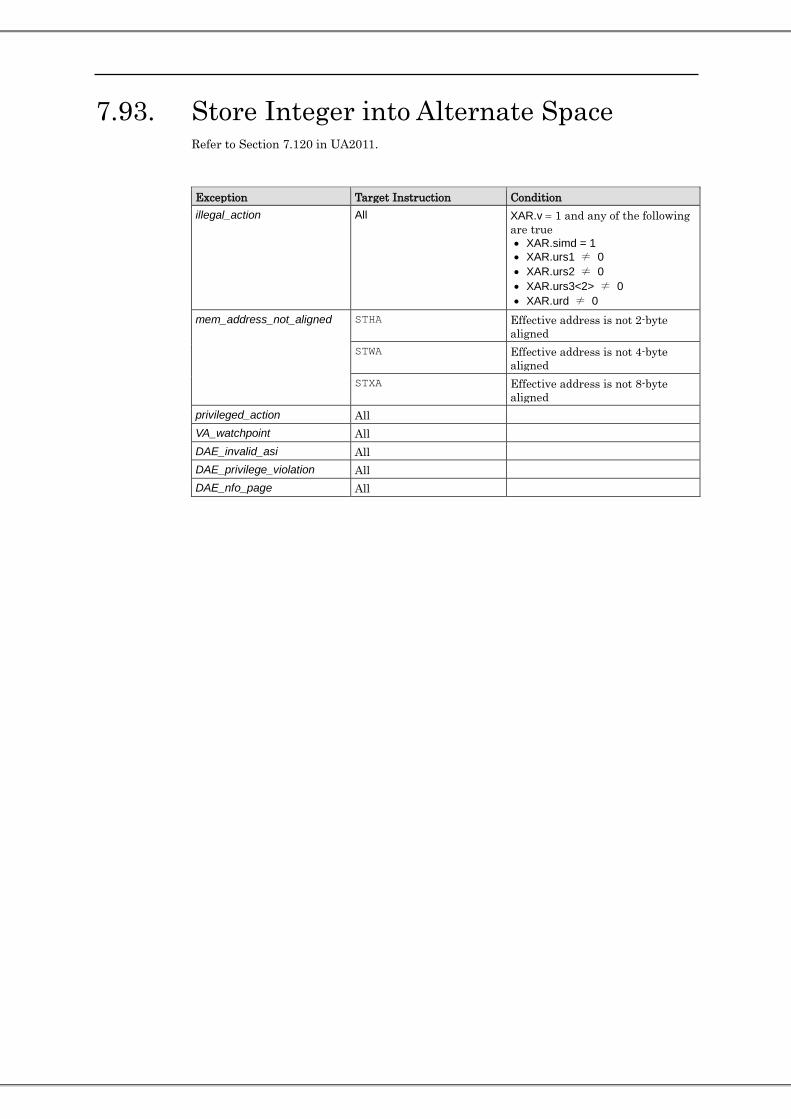
7.93. Store Integer into Alternate Space Refer to Section 7.120 in UA2011.
Exception Target Instruction Condition illegal_action All XAR.v = 1 and any of the following
are true • XAR.simd = 1 • XAR.urs1 ≠ 0 • XAR.urs2 ≠ 0 • XAR.urs3<2> ≠ 0 • XAR.urd ≠ 0
mem_address_not_aligned STHA Effective address is not 2-byte aligned
STWA Effective address is not 4-byte aligned
STXA Effective address is not 8-byte aligned
privileged_action All VA_watchpoint All DAE_invalid_asi All DAE_privilege_violation All DAE_nfo_page All

166 Ver 29.0 Jan. 2015
7.94. Block Initializing Store
UA2011 defines ASI_STBI_*. On SPARC64™ X / SPARC64™ X+, if ASI_STBI_* is specified for the STBA, STHA, STWA, STXA, and STTWA instructions, these stores behave as normal store instructions. For example, if ASI_STBI_P is specified for STBA, STBA behaves as if ASI_P was specified.
The behavior of Block Initializing Stores is shown below.
ASI number ASI name Integer store (STBA, STHA, STWA, STXA, STTWA) operation E216 ASI_STBI_P ASI_P
E316 ASI_STBI_S ASI_S EA16 ASI_STBI_PL ASI_PL EB16 ASI_STBI_SL ASI_SL
Only DAE_invalid_ASI and mem_address_not_aligned exceptions are generated. DAE _* exceptions, except for DAE_invalid_ASI, do not occur.

7.95. Block Store Instruction ASI Operation HPC-ACE Assembly Language Syntax
Regs SIMD STBLOCKF F016 64 bytes block store is executed to
primary address space. stda fregrd, [regaddr] ASI_BLK_P
stda fregrd, [reg_plus_imm] %asi STBLOCKF F116 64 bytes block store is executed to
secondary address space. stda fregrd, [regaddr] ASI_BLK_S
stda fregrd, [reg_plus_imm] %asi STBLOCKF F816 64 bytes block store is executed to
primary address space. Little endian.
stda fregrd, [regaddr] ASI_BLK_PL stda fregrd, [reg_plus_imm] %asi
STBLOCKF F916 64 bytes block store is executed to secondary address space. Little endian.
stda fregrd, [regaddr] ASI_BLK_SL stda fregrd, [reg_plus_imm] %asi
STBLOCKF E016 64 bytes block committing store is executed to primary address space.
stda fregrd, [regaddr] ASI_BLK_COMMIT_P stda fregrd, [reg_plus_imm] %asi
STBLOCKF E116 64 bytes block committing store is executed to secondary address space.
stda fregrd, [regaddr] ASI_BLK_COMMIT_S stda fregrd, [reg_plus_imm] %asi
Refer to Section 7.121 in UA2011.
The effective address is "R[rs1] + R[rs2]" if i = 0, or “R[rs1] + sign_ext(simm13)" if i = 1".
On SPARC64™ X / SPARC64™ X+, block store instruction and block committing store instruction behave exactly the same.
STBLOCKF on SPARC64™ X / SPARC64™ X+ follow TSO. That is, the ordering between the preceding and following load/store/atomic instructions and the 8-bytes stores comprising the block store conforms to TSO.
STBLOCKF on SPARC64™ X / SPARC64™ X+ preserves the order of register accesses in the same manner as any other store instruction.
The cache behavior of STBLOCKF is the same as for a normal store. If there is data in L1D cache, then the block store writes to the L1D cache. If there is no data in the L1D cache, the data is loaded into the L1D cache and then written.
A non-cacheable address can be specified for STBLOCKF.
A VA_watchpoint exception is detected only for the first eight bytes accessed by a STBLOCKF instruction.

168 Ver 29.0 Jan. 2015
Exception Target instruction Condition illegal_instruction All Register number specified by rd is not
a multiple of 8 fp_disabled All PSTATE.pef = 0 or FPRS.fef = 0 illegal_action All XAR.v = 1 and any of the following are
true • XAR.simd = 1 • XAR.urs1 ≠ 0 • XAR.urs2 ≠ 0 • XAR.urs3<2> ≠ 0 • XAR.urd<1> ≠ 0
mem_address_not_aligned All Address not aligned on a 64-byte boundary.
VA_watchpoint All On access to eight lowest bytes only. Refer to 12.5.1.62.
DAE_privilege_violation ASI E016, E116, F016, F116, F816, and F916.
PSTATE.priv = 0 and TTE.p = 1 Refer to 12.5.1.8
DAE_nfo_page All Refer to 12.5.1.7

7.96. Store Floating-Point Instruction op3 rdxiii Operation HPC-ACE Assembly Language
Syntax Regs SIMD STF 10 01002 0 − 31 Store single floating point register
(XAR.v = 0) st fregrd, [address]
STF 10 01002 0 – 126, 256 – 382
Store double floating point register (XAR.v = 1)
st fregrd, [address]
STDF 10 01112 0 − 126, 256 – 382
Store double floating point register std fregrd, [address]
STQF 10 01102 0 − 126, 256 – 382
Store quad floating point register to memory
stq fregrd, [address]
non-SIMD execution
Refer to Section 7.122 in UA2011.
STF copies 4 bytes in F[rd] to an address aligned on a 4-byte boundary. When XAR.v = 0, STF copies the contents of a single-precision floating-point register. When XAR.v = 1, STF copies the upper 4 bytes of a double-precision floating-point register.
The STQF instruction is defined by SPARC V9 but it is not implemented on SPARC64™ X / SPARC64™ X+. If STQF is executed, an illegal_instruction exception occurs.
SIMD execution On SPARC64™ X / SPARC64™ X+, STF and STDF can be executed as SIMD instructions. A SIMD STF and SIMD STDF simultaneously execute basic and extended stores for single-precision and double-precision data, respectively. Refer to Section 5.5.14 (page 35) for details on how to specify the registers.
A SIMD STF copies the upper 4 bytes of Fd[rd] to the lower 4 bytes of the address and copies the upper 4 bytes of Fd[rd + 256] to the upper 4 bytes of the address. The address must be aligned on an 8-byte boundary. Misaligned accesses cause a mem_address_not_aligned exception.
A SIMD STDF copies the 8 bytes of Fd[rd] to the lower 8 bytes of the address and copies the 8 bytes of Fd[rd + 256] to the upper 8 bytes of the address. The address must be aligned on a 16-byte boundary. Misaligned accesses cause a mem_address_not_aligned exception.
Note A SIMD STDF that accesses data aligned on a 4-byte boundary but not an 8-byte boundary does not cause an STDF_mem_address_not_aligned exception.
SIMD STF and SIMD STDF can only write to cacheable address. An attempt to access a non-cacheable space causes a DAE_nc_page exception.
Like non-SIMD store instructions, memory access semantics adhere to TSO. SIMD STF and SIMD STDF simultaneously execute basic and extended stores; however, the ordering between the basic and extended stores comforms to TSO.
A VA_watchpoint exception can be detected in either the basic or extended operation of a SIMD STF or SIMD STDF instruction.
xiii Encoding defined in 5.3.1 "Floating-Point Register Number Encoding” (page 26).

170 Ver 29.0 Jan. 2015
Exception Target instruction Condition illegal_instruction STF, STDF i = 0 and a reserved is not 0.
STQF Always For this instruction, exceptions with priority lower than illegal_instruction are intended for emulation.
fp_disabled All PSTATE.pef = 0 or FPRS.fef = 0 illegal_action STF, STDF XAR.v = 1 and any of the following are
true • XAR.urs1 ≠ 0 • XAR.urs2 ≠ 0 • XAR.urs3<2> ≠ 0 • XAR.urd<1> ≠ 0 • XAR.simd = 1 and XAR.urd<2> ≠ 0
STQF XAR.v = 1 and any of the following are true • XAR.simd = 1 • XAR.urs1 ≠ 0 • XAR.urs2 ≠ 0 • XAR.urs3<2> ≠ 0 • XAR.urd<1> ≠ 0
fp_exception_other (FSR.ftt = invalid_fp_register)
STQF rd<1> ≠ 0
STDF_mem_address_not_aligned STDF Address aligned on 4-byte boundary but not 8-byte boundary when XAR.v = 0 or XAR.simd = 0.
mem_address_not_aligned STF When either of the following is true • Address not aligned on 4-byte
boundary when XAR.v = 0 or XAR.simd = 0
• Address not aligned on 8-byte boundary when XAR.v = 1 and XAR.simd = 1
STDF When either of the following is true • Address not aligned on 4-byte
boundary when XAR.v = 0 or XAR.simd = 0
• Address not aligned on 16-byte boundary when XAR.v = 1 and XAR.simd = 1
STQF Address not aligned on 4-byte boundary. VA_watchpoint All Refer to the description and 12.5.1.62. DAE_privilege_violation All Refer to 12.5.1.8 DAE_nc_page All Access to non-cacheable space when
XAR.v = 1 and XAR.simd = 1 DAE_nfo_page All Refer to 12.5.1.7

7.97. Store Floating-Point into Alternate Space
Instruction op3 rdxiv Operation HPC-ACE Assembly Language Syntax
Regs SIMD STFAPASI 11 01002 0 − 31 Store single floating point
register into alternate space (xar.v = 0)
sta fregrd, [address] imm_asi sta fregrd, [address] %asi
STFAPASI 11 01002 0 − 126, 256 – 382
Store double floating point register into alternate space (xar.v = 1)
sta fregrd, [address] imm_asi sta fregrd, [address] %asi
STDFAPASI 11 01112 0 − 126, 256 – 382
Store double floating point register into alternate space
stda fregrd, [address] imm_asi stda fregrd, [address] %asi
STQFAPASI 11 01102 0 − 126, 256 – 382
Store quad floating point register into alternate space
stqa fregrd, [address] imm_asi stqa fregrd, [address] %asi
non-SIMD execution
Refer to Section 7.123 in UA2011.
STFA copies the 4-bytes in F[rd] to the 4-byte aligned address in the specified alternate space. When xar.v = 0, STFA copies the content of a single-precision floating-point register..When xar.v = 1, STFA copies the upper 4 bytes of a double-precision floating-point register.
The STQFA instruction is defined by SPARC V9 but is not implemented on SPARC64™ X / SPARC64™ X+. If STQFA is executed, an illegal_instruction exception occurs.
SIMD execution On SPARC64™ X / SPARC64™ X+, STFA and STDFA can be executed as SIMD instructions. SIMD STFA and SIMD STDFA simultaneously execute basic and extended stores for single-precision and double-precision data. Refer to Section 5.5.14 (page 35) for details on how to specify the registers.
SIMD STFA copies the upper 4 bytes of Fd[rd] to the lower 4 bytes of the address and copies the upper 4 bytes of Fd[rd + 256] to the upper 4 bytes of the address. The address must be aligned on an 8-byte boundary. Misaligned accesses cause a mem_address_not_aligned exception.
SIMD STDFA copies the 8bytes of Fd[rd] to the lower 8 bytes of the address and copies the 8 bytes of Fd[rd + 256] to the upper 8 bytes of the address. The address must be aligned on a 16-byte boundary. Misaligned addresses cause a mem_address_not_aligned exception.
Note A SIMD STDFA that access data aligned on a 4-byte boundary but not an 8-byte boundary does not cause an STDF_mem_address_not_aligned exception. Unlike SIMD LDDFA, a SIMD STDFA that accesses data aligned on an 8-byte boundary but not a 16-byte boundary causes a mem_address_not_aligned exception.
xiv Encoding defined in 5.3.1 "Floating-Point Register Number Encoding” (page 26).
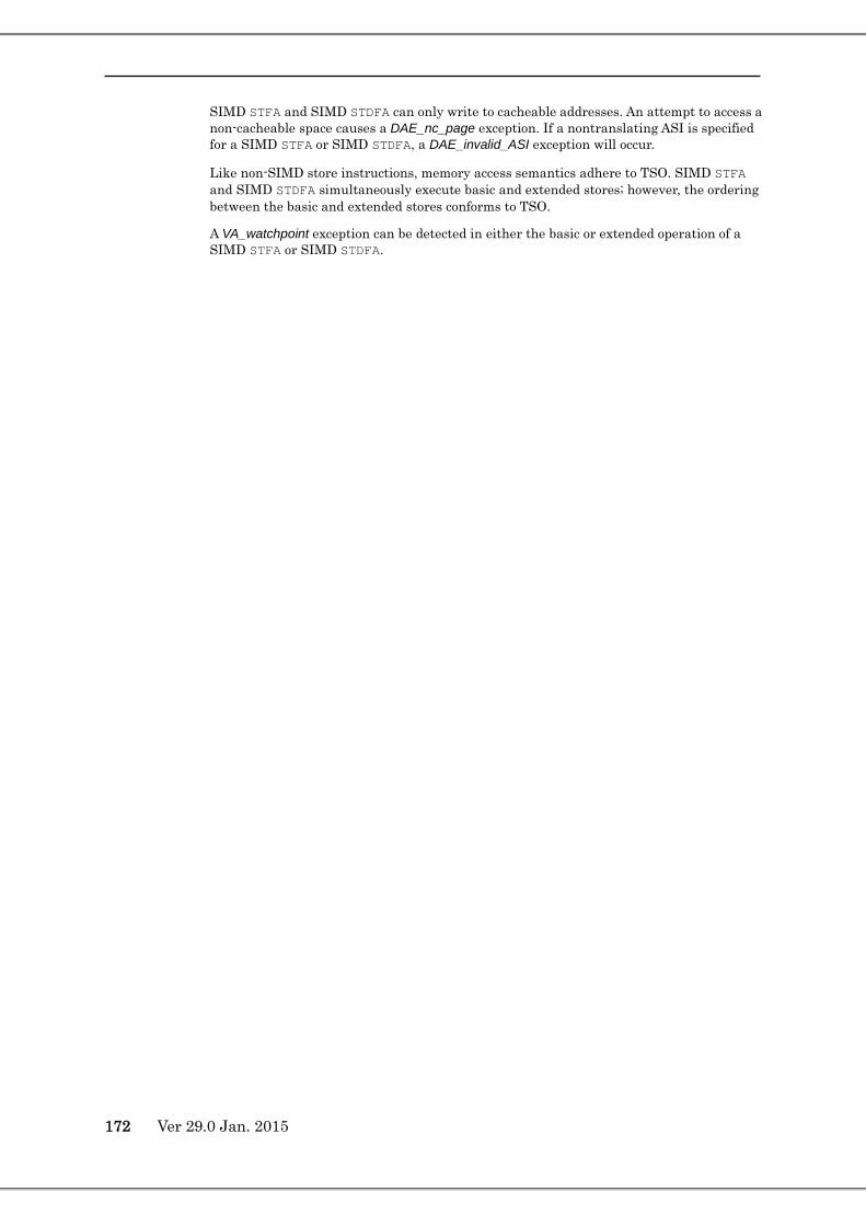
172 Ver 29.0 Jan. 2015
SIMD STFA and SIMD STDFA can only write to cacheable addresses. An attempt to access a non-cacheable space causes a DAE_nc_page exception. If a nontranslating ASI is specified for a SIMD STFA or SIMD STDFA, a DAE_invalid_ASI exception will occur.
Like non-SIMD store instructions, memory access semantics adhere to TSO. SIMD STFA and SIMD STDFA simultaneously execute basic and extended stores; however, the ordering between the basic and extended stores conforms to TSO.
A VA_watchpoint exception can be detected in either the basic or extended operation of a SIMD STFA or SIMD STDFA.
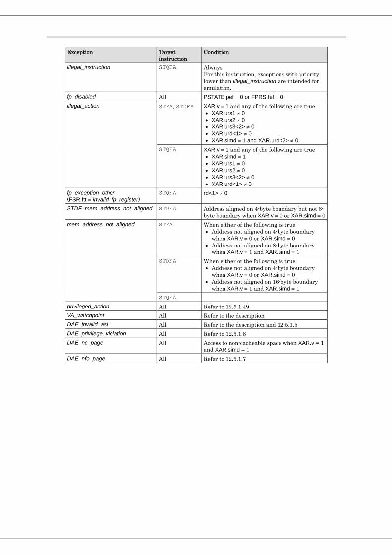
Exception Target instruction
Condition
illegal_instruction STQFA Always For this instruction, exceptions with priority lower than illegal_instruction are intended for emulation.
fp_disabled All PSTATE.pef = 0 or FPRS.fef = 0 illegal_action STFA, STDFA XAR.v = 1 and any of the following are true
• XAR.urs1 ≠ 0 • XAR.urs2 ≠ 0 • XAR.urs3<2> ≠ 0 • XAR.urd<1> ≠ 0 • XAR.simd = 1 and XAR.urd<2> ≠ 0
STQFA XAR.v = 1 and any of the following are true • XAR.simd = 1 • XAR.urs1 ≠ 0 • XAR.urs2 ≠ 0 • XAR.urs3<2> ≠ 0 • XAR.urd<1> ≠ 0
fp_exception_other (FSR.ftt = invalid_fp_register)
STQFA rd<1> ≠ 0
STDF_mem_address_not_aligned STDFA Address aligned on 4-byte boundary but not 8- byte boundary when XAR.v = 0 or XAR.simd = 0
mem_address_not_aligned STFA When either of the following is true • Address not aligned on 4-byte boundary
when XAR.v = 0 or XAR.simd = 0 • Address not aligned on 8-byte boundary
when XAR.v = 1 and XAR.simd = 1 STDFA When either of the following is true
• Address not aligned on 4-byte boundary when XAR.v = 0 or XAR.simd = 0
• Address not aligned on 16-byte boundary when XAR.v = 1 and XAR.simd = 1
STQFA privileged_action All Refer to 12.5.1.49 VA_watchpoint All Refer to the description DAE_invalid_asi All Refer to the description and 12.5.1.5 DAE_privilege_violation All Refer to 12.5.1.8 DAE_nc_page All Access to non-cacheable space when XAR.v = 1
and XAR.simd = 1 DAE_nfo_page All Refer to 12.5.1.7

174 Ver 29.0 Jan. 2015
7.98. Store Floating-Point Register on Register Condition (for SPARC64™ X)
Compatibility Note For the specification of this instruction on SPARC64™ X+, refer to page 248.
Instruction op3 rs2, rd Operation HPC-ACE Assembly Language Syntax
Regs SIMD STFR 10 11002 0 − 31 Store single floating point register
on condition (xar.v = 0) stfr fregrd, fregrs2, [regrs1]
STFR 10 11002 0 − 126, 256 – 382xv
Store single floating point register on condition (xar.v = 1)
stfr fregrd, fregrs2, [regrs1]
STDFR 10 11112 0 − 126, 256 – 382xv
Store double floating point register on condition
stdfr fregrd, fregrs2, [regrs1]
112 rd op3 rs1 i = 1 rs2
31 30 29 25 24 19 18 14 13 12 5 4 0
Programming Note This instruction does not execute a store operation if the MSB of the corresponding register F[rs2] or F[rs2+256] is 0. However, certain exception can still occur.
Non-SIMD execution
When XAR.v = 0 and the MSB (bit 31) of Fs[rs2] is 1, STFR copies the 4bytes of the single-precision register Fs[rd] to the specified address, which should be aligned on a 4-byte boundary. When XAR.v = 1, XAR.simd = 0, and MSB (bit 63) of Fd[rs2] is 1, STFR copies the upper 4bytes of the double-precision register Fd[rd] to the specified address, which should be aligned on a 4-byte boundary.
When the MSB (bit 63) of Fd[rs2] is 1, STDFR copies the 8 bytes of the double-precision register Fd[rd] to the specified address, which should be aligned on a 4-byte boundary.
These floating-point store instructions use implicit ASIs (refer to Section 6.3.1.3 in UA2011) to access memory. The effective write address is "R[rs1]".
STFR and STDFR cause a mem_address_not_aligned exception when writing to an address that is not aligned on a word boundary.
When executing a non-SIMD STDFR, the address needs to be aligned on a word boundary. However, if the address is aligned on a word boundary but is not aligned on a doubleword boundary, a STDF_mem_address_not_aligned exception will occur. The trap handler must emulate the STDFR instruction when this exception occurs.
Regardless of whether the store operation is actually executed, a VA_watchpoint exception is detected for STFR and STDFR if the address matches.
SIMD execution STFR and STDFR support SIMD execution on SPARC64™ X. SIMD STFR and SIMD STDFR simultaneously execute basic and extended stores for single-precision and double-precision data, respectively. Refer to Section 5.5.14 (page 35) for details on how to specify the registers.
xv Encoding defined in 5.3.1 "Floating-Point Register Number Encoding” (page 26)

A SIMD STFR copies the upper 4 bytes of Fd[rd] to the lower 4 bytes of the address when XAR.v = 1, XAR.simd = 1, and the MSB (bit 63) of Fd[rs2] is 1, and copies the upper 4 bytes of Fd[rd + 256] to the upper 4 bytes of the address when XAR.v = 1, XAR.simd = 1, and the MSB (bit 63) of Fd[rs2+256] is 1. The address must be aligned on an 8-byte boundary. Misaligned accesses cause a mem_address_not_aligned exception.
A SIMD STDFR copies Fd[rd] to the lower 8 bytes of the address when XAR.v = 1, XAR.simd = 1, and the MSB (bit 63) of Fd[rs2] is 1, and copies Fd[rd + 256] to the upper 8 bytes of the address when XAR.v = 1, XAR.simd = 1, and the MSB (bit 63) of Fd[rs2+256] is 1. The address must be aligned on a 16-byte boundary. Mialigned accesses cause a mem_address_not_aligned exception.
Note A SIMD STDFR does not cause a STDF_mem_address_not_aligned exception when writing to an address that is aligned on a 4-byte boundary but not an 8-byte boundary.
SIMD STFR and SIMD STDFR can only write to cacheable address spaces. An attempt to write a non-cacheable space causes a DAE_nc_page exception.
Like non-SIMD store instructions, memory access semantics adhere to TSO. SIMD STFR and SIMD STDFR simultaneously execute basic and extended stores; however, the ordering between the basic and extended stores conforms to TSO.

176 Ver 29.0 Jan. 2015
Exception Target instruction Condition illegal_instruction All i = 0 or a reserved field is not 0. fp_disabled All PSTATE.pef = 0 or FPRS.fef = 0 illegal_action All XAR.v = 1 and any of the following are
true • XAR.urs1 ≠ 0 • XAR.urs2<1> ≠ 0 • XAR.urs3<2> ≠ 0 • XAR.urd<1> ≠ 0 • XAR.simd = 1 and XAR.urs2<2> ≠ 0 • XAR.simd = 1 and XAR.urd<2> ≠ 0
STDF_mem_address_not_aligned STDFR Store to address aligned on 4-byte boundary but not an 8-byte boundary when XAR.v = 0 or XAR.v = 1 and XAR.simd = 0
mem_address_not_aligned STFR When either of the following is true • Store to address not aligned on 4-byte
boundary when XAR.v = 1 and XAR.simd = 0, or XAR.v = 0
• Store to address not aligned on 8-byte boundary when XAR.v = 1 and XAR.simd = 1
STDFR When either of the following is true • Store to address not aligned on 4-byte
boundary when XAR.v = 1 and XAR.simd = 0, or XAR.v = 0.
• Store to address not aligned on 16-byte boundary when XAR.v = 1 and XAR.simd = 1
VA_watchpoint All Refer to the description and 12.5.1.62 DAE_privilege_violation All Refer to 12.5.1.8 DAE_nc_page All Access to non-cacheable space when
XAR.v = 1 and XAR.simd = 1 DAE_nfo_page All Refer to 12.5.1.7

7.99. Store Partial Floating-Point Refer to Section 7.125 in UA2011.
Exception Condition illegal_instruction i = 1 fp_disabled PSTATE.pef = 0 or FPRS.fef = 0 illegal_action XAR.v = 1 STDF_mem_address_not_aligned Effective address is 4-byte aligned but not
8-byte aligned mem_address_not_aligned Effective address is 4-byte aligned VA_watchpoint DAE_privilege_violation DAE_nfo_page

178 Ver 29.0 Jan. 2015
7.100. Store Short Floating-Point Refer to Section 7.126 in UA2011.
Exception Target Instruction
Condition
fp_disabled All PSTATE.pef = 0 or FPRS.fef = 0 illegal_action All XAR.v = 1 mem_address_not_aligned ASI 0xD2,
0xD3, 0xDA,0x DB
Effective address is not 2-byte aligned
VA_watchpoint All DAE_privilege_violation All DAE_nfo_page All

7.101. Store Integer Twin Word Refer to Section 7.127 in UA2011.
Exception Condition illegal_instruction • rd is an odd numbered register
• i = 0 and iw<12:5> ≠ 0 illegal_action XAR.v = 1 and any of the following
are true • XAR.simd = 1 • XAR.urs1 ≠ 0 • XAR.urs2 ≠ 0 • XAR.urs3<2> ≠ 0 • XAR.urd ≠ 0
mem_address_not_aligned Effective address is not 8-byte aligned
VA_watchpoint DAE_privilege_violation DAE_nfo_page

180 Ver 29.0 Jan. 2015
7.102. Store Integer Twin Word into Alternate Space Refer to Section 7.128 in UA2011.
Exception Condition illegal_instruction rd is an odd numbered register illegal_action XAR.v = 1 and any of the following
are true • XAR.simd = 1 • XAR.urs1 ≠ 0 • XAR.urs2 ≠ 0 • XAR.urs3<2> ≠ 0 • XAR.urd ≠ 0
mem_address_not_aligned Effective address is not 8-byte aligned
privileged_action VA_watchpoint DAE_invalid_asi DAE_privilege_violation DAE_nfo_page

7.103. Store Floating-Point State Register Instruction op3 rd Operation HPC-ACE Assembly Language
Syntax Regs SIMD STFSRD 10 01012 0 Store FSR (Only lower 32 bits) st %fsr, [address] STXFSR 10 01012 1 Store FSR stx %fsr, [address] 10 01012 2 - 31 reserved
Refer to Section 7.124 and Section 7.129 in UA2011.
Exception Target instruction Condition illegal_instruction STFSR, STXFSR i = 0 and the reserved field is not 0.
rd = 2−31 fp_disabled All PSTATE.pef = 0 or FPRS.fef = 0 illegal_action All XAR.v = 1 and any of the following are
true • XAR.simd = 1 • XAR.urs1 ≠ 0 • XAR.urs2 ≠ 0 • XAR.urs3<2> ≠ 0 • XAR.urd ≠ 0
mem_address_not_aligned STFSR Address not aligned on 4-byte boundary STXFSR Address not aligned on 8-byte boundary.
VA_watchpoint All Refer to 12.5.1.62 DAE_privilege_violation All Refer to 12.5.1.8 DAE_nfo_page All Refer to 12.5.1.7

182 Ver 29.0 Jan. 2015
7.104. Subtract Refer to Section 7.130 in UA2011.
Exception Target
instruction Condition
illegal_instruction All A reserved field is not 0. (i = 0 and iw<12:5> = 0)
illegal_action All XAR.v = 1

7.105. Swap Register with Memory Refer to Section 7.131 and Section 7.132 in UA2011.
Exception Condition illegal_instruction i = 0 and iw<12:5> ≠ 0 illegal_action XAR.v = 1 and any of the following
are true • XAR.simd = 1 • XAR.urs1 ≠ 0 • XAR.urs2 ≠ 0 • XAR.urs3<2> ≠ 0 • XAR.urd ≠ 0
mem_address_not_aligned Effective address is not 4-byte aligned
VA_watchpoint DAE_privilege_violation DAE_nfo_page

184 Ver 29.0 Jan. 2015
7.106. Set XAR (SXAR) Instruction op2 cmb Operation HPC-ACE Assembly
Language Syntax
Regs SIMD
SXAR1 1112 0 Set XAR for the following instruction sxar1
SXAR2 1112 1 Set XAR for the following two instructions sxar2
002 cmb f_simd f_urd op2 = 1112 f_urs1 f_urs2 f_urs3 s_simd s_urd s_urs1 s_urs2 s_urs3
31 30 29 28 27 25 24 22 21 19 18 16 15 13 12 11 9 8 6 5 3 2 0
Description SXAR updates the XAR register. XAR holds values for up to two instructions. SXAR1 sets values for one instruction, and SXAR2 sets values for two instructions. Fields that start with f_ are used by the first instruction executed after SXAR, and fields that start with s_ are used by the second instruction executed after SXAR.
The fields of SXAR1 that starts with s_ must be 0. An illegal_instruction exception will occur if a value other than 0 is specified.
Compatibility Note In SPARC64 VIIIfx, values other than 0 in fields starting with s_ were ignored for SXAR1.
SXAR modifies the one or two instructions that are immediately executed after SXAR. The SXAR instruction is used to specify the HPC-ACE floating-point registers on SPARC64™ X / SPARC64™ X+, HPC-ACE SIMD operations with floating-point registers, and disabling hardware prefetch for memory access instructions. Even if the instruction fields, *_simd, *_urs1, *_urs2, *_urs3 and *_urd are all specified as 0, XAR.f_v is set to 1 after SXAR1 is executed; both XAR.f_v and XAR.s_v are set to 1 after SXAR2 is executed.
Performance may suffer if the SXAR instruction and the instructions that it modifies are not contiguous in memory. For example, if SXAR is placed in the delay slot of a branch instruction or a Tcc instruction is inserted after the SXAR.
SXAR itself is not XAR eligible. If XAR.v = 1 when executing SXAR, an illegal_action exception will occur.
Compatibility Note op = 002 and op2 = 1112 are reserved in SPARC V9, but SPARC V8 defines FBcc in these opcodes. When running a SPARC V8 application on SPARC64™ X / SPARC64™ X+, there is the possibility of different behavior.
Programming Note The SXAR instruction word contains the value to be set in the XAR register but this value is not shown in the assembly syntax of SXAR. Instead, HPC-ACE features are indicated by mnemonic suffixes appended to the instruction(s) that SXAR modifies, and the assembler generates the appropriate value for the SXAR instruction word.
Exception Target instruction Condition illegal_instruction SXAR1 s_* ≠ 0 illegal_action All XAR.v = 1

7.107. Tagged Add and Subtract Refer to Sections 7.133, 7.134, 7.136 and 7.137 in UA2011.
Exception Condition illegal_instruction i = 0 and iw<12:5> ≠ 0 illegal_action XAR.v = 1
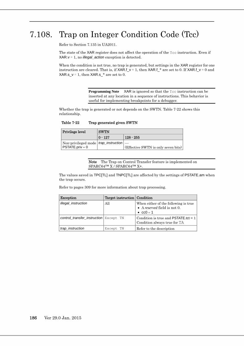
186 Ver 29.0 Jan. 2015
7.108. Trap on Integer Condition Code (Tcc) Refer to Section 7.135 in UA2011.
The state of the XAR register does not affect the operation of the Tcc instruction. Even if XAR.v = 1, no illegal_action exception is detected.
When the condition is not true, no trap is generated, but settings in the XAR register for one instruction are cleared. That is, if XAR.f_v = 1, then XAR.f_* are set to 0. If XAR.f_v = 0 and XAR.s_v = 1, then XAR.s_* are set to 0.
Programming Note XAR is ignored so that the Tcc instruction can be inserted at any location in a sequence of instructions. This behavior is useful for implementing breakpoints for a debugger.
Whether the trap is generated or not depends on the SWTN. Table 7-22 shows this relationship.
Table 7-22 Trap generated given SWTN
Privilege level SWTN 0 - 127 128 - 255
Non-privileged mode PSTATE.priv = 0
trap_instruction (Effective SWTN is only seven bits)
Note The Trap on Control Transfer feature is implemented on SPARC64™ X / SPARC64™ X+.
The values saved in TPC[TL] and TNPC[TL] are affected by the settings of PSTATE.am when the trap occurs.
Refer to pages 309 for more information about trap processing.
Exception Target instruction Condition illegal_instruction All When either of the following is true
• A reserved field is not 0. • cc0 = 1
control_transfer_instruction Except TN Condition is true and PSTATE.tct = 1 Condition always true for TA
trap_instruction Except TN Refer to the description
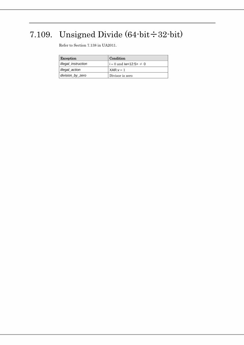
7.109. Unsigned Divide (64-bit÷32-bit) Refer to Section 7.138 in UA2011.
Exception Condition illegal_instruction i = 0 and iw<12:5> ≠ 0 illegal_action XAR.v = 1 division_by_zero Divisor is zero

188 Ver 29.0 Jan. 2015
7.110. Unsigned Multiply (32-bit) Refer to Section 7.139 in UA2011.
Exception Condition illegal_instruction i = 0 and iw<12:5> ≠ 0 illegal_action XAR.v = 1

7.111. Write Ancillary State Register (WRASR) Instruction rd Operation HPC-ACE Assembly Language Syntax
Regs SIMD WRYD 0 Write Y register. (deprecated. ) wr regrs1, reg_or_imm, %y WRCCR 2 Write CCR register wr regrs1, reg_or_imm, %ccr WRASI 3 Write ASI register wr regrs1, reg_or_imm, %asi WRFPRS 6 Write FPRS register wr regrs1, reg_or_imm, %fprs
WRPCRPPCR 16 Write PCR register wr regrs1, reg_or_imm, %pcr
WRPICPPCR 17 Write PIC register wr regrs1, reg_or_imm, %pic WRGSR 19 Write GSR register wr regrs1, reg_or_imm, %gsr WRPAUSE 27 Write PAUSE register wr regrs1, reg_or_imm, %pause WRXAR 29 Write XAR register wr regrs1, reg_or_imm, %xar WRXASR 30 Write XASR register wr regrs1, reg_or_imm, %xasr
Refer to Section 7.141 in UA2011.
The result of a WRASR instruction takes affect immediately. The new setting is visible to downstream instructions.
• An attempt to set values other than 0 to reserved fields of XAR using the WRXAR instruction generates an illegal_instruction exception. Note that, in this case, the priority of an illegal_action exception is higher than the illegal_instruction exception.
Exception Target instruction Condition illegal_instruction rd = 1, 4 − 5, 7 − 14, 18, 26 − 28
All i = 0 and iw<12:5> ≠ 0 fp_disabled WRGSR PSTATE.PEF = 0 or FPRS.FEF = 0 illegal_action All XAR.v = 1 privileged_action WRPCR PSTATE.priv = 0 and one of the following is true
• PCR.priv = 1 • PCR.priv = 0 and PCR.priv is set to 1
WRPIC PSTATE.priv = 0 and PCR.priv = 1

190 Ver 29.0 Jan. 2015
7.114. Cache Line Fill with Undetermined Values
Compatibility Note This instruction (and corresponding ASIs) is left to ensure compatibility with SPARC64 VIIIfx
Instruction ASI op3 Operation HPC-ACE Assembly Language Syntax
Regs SIMD XFILLN ASI_XFILL_P
ASI_XFILL_S 01 11102 01 01112 11 01112
nop ✓
stxa regrd , [reg_plus_imm] %asi stxa regrd , [regaddr] imm_asi sttwa regrd , [reg_plus_imm] %asi sttwa regrd , [regaddr] imm_asi stda fregrd , [reg_plus_imm] %asi stda fregrd , [regaddr] imm_asi
112 rd op3 rs1 i = 0 imm_asi rs2
112 rd op3 rs1 i = 1 simm13
31 30 29 25 24 19 18 14 13 12 5 4 0
Description This instruction is left for compatibility with SPARC64 VIIIfx. On SPARC64 VIIIfx, this instruction updated the entire cache line with an undefined value. On SPARC64™ X / SPARC64™ X+, it does not perform any memory or cache operations. However, exceptions related to memory accesses are detected.
XFILL for noncacheable space does not cause a DAE_nc_page exception.

Exception Target instruction
Condition
illegal_instruction op3 = 01 01112 (STTWA)
Odd-numbered destination register (rd)
fp_disabled op3 = 11 01112 (STDFA)
PSTATE.PEF = 0 or FPRS.FEF = 0
illegal_action op3 = 01 11102 (STXA) op3 = 01 01112 (STTWA)
XAR.v = 1 and any of the following are true • XAR.simd = 1 • XAR.urs1 ≠ 0 • XAR.urs2 ≠ 0 • XAR.urs3<2> ≠ 0 • XAR.urd ≠ 0
op3 = 11 01112 (STDFA)
XAR.v = 1 and any of the following are true • XAR.simd = 1 • XAR.urs1 ≠ 0 • XAR.urs2 ≠ 0 • XAR.urs3<2> ≠ 0 • XAR.urd<1> ≠ 0
STDF_mem_address_not_aligned op3 = 11 01112 (STDFA)
regaddr aligned on 4-byte boundary but not 8-byte boundary
mem_address_not_aligned op3 = 11 01112 (STDFA)
regaddr not aligned on 4-byte boundary
VA_watchpoint All When the watchpoint address matches any address in the cache line Refer to 12.5.1.62
DAE_privilege_violation All Refer to 12.5.1.8 DAE_nfo_page All Refer to 12.5.1.7

192 Ver 29.0 Jan. 2015
7.115. DES support instructions Compatibility Note Future compatibility of DES support instructions is
not guaranteed. These instructions should only be used in libraries for the SPARC64™ X or SPARC64™ X+ platform.
Instruction opf Operation HPC-ACE Assembly Language Syntax
Regs SIMD FDESENCX 0 1001 10002 DES operation fdesencx fregrs1, fregrs2, fregrd FDESPC1X 0 1001 10012 DES Permuted Choice 1 fdespc1x fregrs1, fregrd
FDESIPX 0 1001 10102 DES Initial Permutation fdesipx fregrs1, fregrd FDESIIPX 0 1001 10112 DES Inverse Initial Permutation fdesiipx fregrs1, fregrd FDESKEYX 0 1001 11002 DES Key Calculation fdeskeyx fregrs1, index, fregrd
FDESENCX
102 rd op3 = 11 01102 rs1 Opf rs2 31 30 29 25 24 19 18 14 13 5 4 0
FDESPC1X, FDESIPX, FDESIIPX 102 rd op3 = 11 01102 rs1 Opf 0 00002
31 30 29 25 24 19 18 14 13 5 4 0
FDESKEYX
102 rd op3 = 11 01102 rs1 Opf index 31 30 29 25 24 19 18 14 13 5 4 0
Description FDESENCX processes one round of the 16 rounds in the DES encoding and decoding algorithms. Given Fd[rs1] as the permuted input, we refer to the upper 32 bits as L and the lower 32 bits as R, Fd[rs2] is the key data, and the result is written in Fd[rd]. FDESENCX preforms the operation shown in the following expression.
Fd[rd] = Fd[rs1]<31:0> :: (Fd[rs1]<63:32> ^ f(Fd[rs1]<31:0>, PC2(Fd[rs2]<55:0>)) = R :: (L ^ f(R, PC2(KEY)))
Here, f() is the encoding or decoding function, which outputs 32-bit data. PC2() is the Permuted Choice2 function, which outputs 48-bit data. Both functions are defined in the DES specification.
Note FDESENCX applies PC2() to Fd[rs2]. That is, the key data specified for Fd[rs2] is not the result Kn of the key schedule defined in the DES specification. Instead, Fd[rs2] is the input for PC2(). This key data is calculated by the FDESKEYX instruction.
FDESPC1X operates on Fd[rs1] and writes the result in Fd[rd].
FDESPC1X executes PC1(), which is the Permuted Choice 1 function defined by the DES specification. PC1() chooses 56 bits from Fd[rs1] and writes the result in the lower 56 bits of Fd[rd]. Parity bits for Fd[rs1] are generated and written in the upper 8 bits of Fd[rd].
Fd[rd]<63>: ~^Fd[rs1]<63:56> Fd[rd]<62>: ~^Fd[rs1]<55:48> Fd[rd]<61>: ~^Fd[rs1]<47:40> Fd[rd]<60>: ~^Fd[rs1]<39:32> Fd[rd]<59>: ~^Fd[rs1]<31:24> Fd[rd]<58>: ~^Fd[rs1]<23:16>

Fd[rd]<57>: ~^Fd[rs1]<15:8> Fd[rd]<56>: ~^Fd[rs1]<7:0>
FDESIPX operates on Fd[rs1] and writes the result in Fd[rd].
FDESIPX performs the initial permutation, IP() defined by the DES specification. Table 7-23 shows how IP() permutes the input bits. The position of a bit in the output data Fd[rd]<63:0> is a binary number 0000002 - 1111112. We fix the upper or lower three bits of this binary number and let the other bits vary. That is, each row represents the positions in the output with the same upper three bits, and each column represents the positions with the same lower three bits. The intersection of a row and column shows the position of the bit in the input Fd[rs1]<63:0> that is written to that position in the output.
For example, the first row (111xxx2) shows the positions in the input data (bits 6, 14, ..., 62) corresponding to positions in the output data (bits 1111112, 1111102, ..., 1110002). The next row (110xxx2) shows the positions in the input data (bits 4, 12, ..., 60) corresponding to positions in the output data (bits 1101112, 1101102, ..., 1100002). Specifically, the cell in the first row and the first column, whose upper bits are 1112 and lower bits are 1112, has the value 6. That is, input bit Fd[rs1]<6> is written to output bit Fd[rd]<63>.
Table 7-23 FDESIPX bit permutation
Bit position in Fd[rd] Upper three bits Lower three bits xxx1112 xxx1102 xxx1012 xxx1002 xxx0112 xxx0102 xxx0012 xxx0002 111xxx2 6 14 22 30 38 46 54 62 110xxx2 4 12 20 28 36 44 52 60 101xxx2 2 10 18 26 34 42 50 58 100xxx2 0 8 16 24 32 40 48 56 011xxx2 7 15 23 31 39 47 55 63 010xxx2 5 13 21 29 37 45 53 61 001xxx2 3 11 19 27 35 43 51 59 000xxx2 1 9 17 25 33 41 49 57
FDESIIPX operates on Fd[rs1] and writes the result in Fd[rd].
FDESIIPX executes IP-1(), which is the inverse function of the initial permutation, as defined by the DES specification. Table 7-24 shows how IP-1() permutates the input bits. The position of a bit in the output data Fd[rd]<63:0> is a binary number 0000002 - 1111112. We fix the upper or lower three bits and let the other bits vary. That is, each row represents the positions in the output with the same upper three bits, and each column represents the positions with the same lower three bits. The intersection of a row and column shows the positions of the bit in the input Fd[rd]<63:0> that is written to that position in the output.
For example, the first row (111xxx2) shows the positions in the input data (bits 56, 24, ..., 0) corresponding to the positions in the output data (bits 1111112, 1111102, ..., 1110002). The next row (110xxx2) shows the positions in the input data (bits 57, 25, ..., 1) corresponding to the positions in the output data (bits 1101112, 1101102, ..., 1100002). Specifically, the cell in the first row and the first column, whose upper 3 bits are 1112 and lower 3 bits are 1112, has the value 56. That is, input bit Fd[rs1]<56> is written to output bit Fd[rd]<63>.

194 Ver 29.0 Jan. 2015
Table 7-24 FDESIIPX bit permutation
Bit position in Fd[rd] Upper three bits Lower three bits xxx1112 xxx1102 xxx1012 xxx1002 xxx0112 xxx0102 xxx0012 xxx0002 111xxx2 56 24 48 16 40 8 32 0 110xxx2 57 25 49 17 41 9 33 1 101xxx2 58 26 50 18 42 10 34 2 100xxx2 59 27 51 19 43 11 35 3 011xxx2 60 28 52 20 44 12 36 4 010xxx2 61 29 53 21 45 13 37 5 001xxx2 62 30 54 22 46 14 38 6 000xxx2 63 31 55 23 47 15 39 7
Note Table 7-24 difers from the table in the DES specification for the inverse function of the initial permutation because FDESIIPX is a composite operation that exchanges the upper and lower 32 bits in the pre-output and then applies IP-1().
FDESKEYX performs the operation specified by the index field on the input Fd[rs1] and writes the result in Fd[rd].
index Operation 0 Fd[rs1]<63:56> :: ROTL(Fd[rs1]<55:28>, 1) :: ROTL(Fd[rs1]<27:0>, 1) 1 Fd[rs1]<63:56> :: ROTL(Fd[rs1]<55:28>, 2) :: ROTL(Fd[rs1]<27:0>, 2) 2 − 1F16 reserved
In the above table, ROTL(x, y) is a function that rotates x left by y bits.
The DES key schedule takes 56 bits from the 64-bit key, permutes these bits by PC1(), and divides the result into two 28-bit data, C and D. Depending on the round, C and D are each rotated left by one or two bits and then merged. Merged data is permuted by PC2(). FDESKEYX does part of this processing. The FDESKEYX instruction assumes C and D as inputs, rotates each data based on the index, and outputs the merged result. C and D are generated by the FDESPC1X instruction.
Usage example
/* * DES encryption * * Input * %f0: Plaintext data * %f2: Key data * Output * %f0: Ciphertext data */ fdespc1x %f2, %f2 ! IP(key) fdeskeyx %f2, 0, %f4 ! K1 fdeskeyx %f4, 0, %f6 ! K2 fdeskeyx %f6, 1, %f8 ! K3 fdeskeyx %f8, 1, %f10 ! K4 fdeskeyx %f10, 1, %f12 ! K5 fdeskeyx %f12, 1, %f14 ! K6

fdeskeyx %f14, 1, %f16 ! K7 fdeskeyx %f16, 1, %f18 ! K8 fdeskeyx %f18, 0, %f20 ! K9 fdeskeyx %f20, 1, %f22 ! K10 fdeskeyx %f22, 1, %f24 ! K11 fdeskeyx %f24, 1, %f26 ! K12 fdeskeyx %f26, 1, %f28 ! K13 fdeskeyx %f28, 1, %f30 ! K14 fdeskeyx %f30, 1, %f32 ! K15 fdeskeyx %f32, 0, %f34 ! K16 fdesipx %f0, %f0 ! IP(data) fdesencx %f0, %f4, %f0 ! round 1 fdesencx %f0, %f6, %f0 ! round 2 fdesencx %f0, %f8, %f0 ! round 3 fdesencx %f0, %f10, %f0 ! round 4 fdesencx %f0, %f12, %f0 ! round 5 fdesencx %f0, %f14, %f0 ! round 6 fdesencx %f0, %f16, %f0 ! round 7 fdesencx %f0, %f18, %f0 ! round 8 fdesencx %f0, %f20, %f0 ! round 9 fdesencx %f0, %f22, %f0 ! round 10 fdesencx %f0, %f24, %f0 ! round 11 fdesencx %f0, %f26, %f0 ! round 12 fdesencx %f0, %f28, %f0 ! round 13 fdesencx %f0, %f30, %f0 ! round 14 fdesencx %f0, %f32, %f0 ! round 15 fdesencx %f0, %f34, %f0 ! round 16 fdesiipx %f0, %f0 ! IP-1(data) /* * DES decryption * * Input * %f0: Ciphertext data * %f2: Key data * Output * %f0: Plaintext data */ fdespc1x %f2, %f2 ! IP(key) fdeskeyx %f2, 0, %f4 ! K1 fdeskeyx %f4, 0, %f6 ! K2 fdeskeyx %f6, 1, %f8 ! K3 fdeskeyx %f8, 1, %f10 ! K4 fdeskeyx %f10, 1, %f12 ! K5 fdeskeyx %f12, 1, %f14 ! K6 fdeskeyx %f14, 1, %f16 ! K7 fdeskeyx %f16, 1, %f18 ! K8 fdeskeyx %f18, 0, %f20 ! K9 fdeskeyx %f20, 1, %f22 ! K10 fdeskeyx %f22, 1, %f24 ! K11 fdeskeyx %f24, 1, %f26 ! K12 fdeskeyx %f26, 1, %f28 ! K13 fdeskeyx %f28, 1, %f30 ! K14 fdeskeyx %f30, 1, %f32 ! K15 fdeskeyx %f32, 0, %f34 ! K16 fdesipx %f0, %f0 ! IP(data) fdesencx %f0, %f34, %f0 ! round 16 fdesencx %f0, %f32, %f0 ! round 15 fdesencx %f0, %f30, %f0 ! round 14 fdesencx %f0, %f28, %f0 ! round 13 fdesencx %f0, %f26, %f0 ! round 12 fdesencx %f0, %f24, %f0 ! round 11 fdesencx %f0, %f22, %f0 ! round 10 fdesencx %f0, %f20, %f0 ! round 9

196 Ver 29.0 Jan. 2015
fdesencx %f0, %f18, %f0 ! round 8 fdesencx %f0, %f16, %f0 ! round 7 fdesencx %f0, %f14, %f0 ! round 6 fdesencx %f0, %f12, %f0 ! round 5 fdesencx %f0, %f10, %f0 ! round 4 fdesencx %f0, %f8, %f0 ! round 3 fdesencx %f0, %f6, %f0 ! round 2 fdesencx %f0, %f4, %f0 ! round 1 fdesiipx %f0, %f0 ! IP-1(data)
Exception Target instruction Condition illegal_instruction FDESPC1X,FDESIPX,FDESII
PX iw<4:0> ≠ 0
FDESKEYX index = 0216 − 1F16 fp_disabled All PSTATE.PEF = 0 or FPRS.FEF = 0 illegal_action FDESENCX XAR.v = 1 and any of the following are
true • XAR.urs1<1> ≠ 0 • XAR.urs2<1> ≠ 0 • XAR.urs3 ≠ 0 • XAR.urd<1> ≠ 0 • XAR.simd = 1 and XAR.urs1<2> ≠ 0 • XAR.simd = 1 and XAR.urs2<2> ≠ 0 • XAR.simd = 1 and XAR.urd<2> ≠ 0
FDESPC1X,FDESIPX,FDESIIPX,FDESKEYX
XAR.v = 1 and any of the following are true • XAR.urs1<1> ≠ 0 • XAR.urs2 ≠ 0 • XAR.urs3 ≠ 0 • XAR.urd<1> ≠ 0 • XAR.simd = 1 and XAR.urs1<2> ≠ 0 • XAR.simd = 1 and XAR.urd<2> ≠ 0

7.116. AES support instructions Compatibility Note Future compatibility of AES support instructions is
not guaranteed. These instructions should only be used in libraries for the SPARC64™ X or SPARC64™ X+ platform.
Instruction opf Operation HPC-ACE Assembly Language Syntax
Regs SIMD FAESENCX 0 1001 00002 AES encryption operation faesencx fregrs1, fregrs2, fregrd FAESDECX 0 1001 00012 AES decryption operation faesdecx fregrs1, fregrs2, fregrd
FAESENCLX 0 1001 00102 AES final round of encryption faesenclx fregrs1, fregrs2, fregrd FAESDECLX 0 1001 00112 AES the final round of decryption faesdeclx fregrs1, fregrs2, fregrd
FAESKEYX 0 1001 01002 AES key generation faeskeyx fregrs1, index, fregrd
FAESENCX, FAESDECX, FAESENCLX, FAESDECLX 102 rd op3 = 11 01102 rs1 Opf rs2
31 30 29 25 24 19 18 14 13 5 4 0
FAESKEYX
102 rd op3 = 11 01102 rs1 Opf index 31 30 29 25 24 19 18 14 13 5 4 0
Description FAESENCX executes the four functions defined for each round of the AES encryption algorithm.
Fd[rd] = {MixColumns(ShiftRows(SubBytes({Fd[rd], Fd[rs1]})))<127:64> ^ Fd[rs2]}
Fd[rd] and Fd[rs1] are the 16-byte input data. Fd[rd] is the upper eight bytes, and Fd[rs1] is the lower eight bytes. Fd[rs2] is the upper eight bytes of the round key. First, SubBytes() operates on the input data. Second, ShiftRows() operates on the result. Third, MixColumns() operates on the result, and a 16-byte result is generated. Fourth, the upper eight bytes of this result are XORed with the round key in Fd[rs2]. This fourth step is called AddRoundKey() in the AES specification. This final 8-byte result is written in Fd[rd]. Note that Fd[rd] is used both as an input and as the output.
The operations performed by FAESENCX are symmetric for the upper and lower eight bytes of the input data. By exchanging the input, FAESENCX outputs a result which is the lower eight bytes for the round. That is, specify the lower eight bytes in Fd[rd] and the upper eight bytes in Fd[rs1]. Fd[rs2] is the lower eight bytes of the round key.
When using FAESENCX as a SIMD instruction, any floating-point register Fd[0] − Fd[126], Fd[256] − Fd[382] can be specified for Fd[rs1]. However, only basic registers Fd[0] − Fd[126] can be specified for Fd[rs2] and Fd[rd]. When an extended register Fd[256] − Fd[382] is specified for Fd[rs1], the corresponding basic register in Fd[0] − Fd[126] is used for the extended SIMD operation.
FAESENCLX executes the three functions defined for the final round of the AES encryption algorithm.
Fd[rd] = {ShiftRows(SubBytes({Fd[rd], Fd[rs1]}))<127:64> ^ Fd[rs2]}
Fd[rd] and Fd[rs1] are the 16-byte input data. Fd[rd] is the upper eight bytes, and Fd[rs1] is the lower eight bytes. Fd[rs2] is the upper eight bytes of the round key. First, SubBytes() operates on the input data. Second, ShiftRows() operates on the result, and a 16-byte result is generated. Third, the upper eight bytes of the result are XORed with the round key in
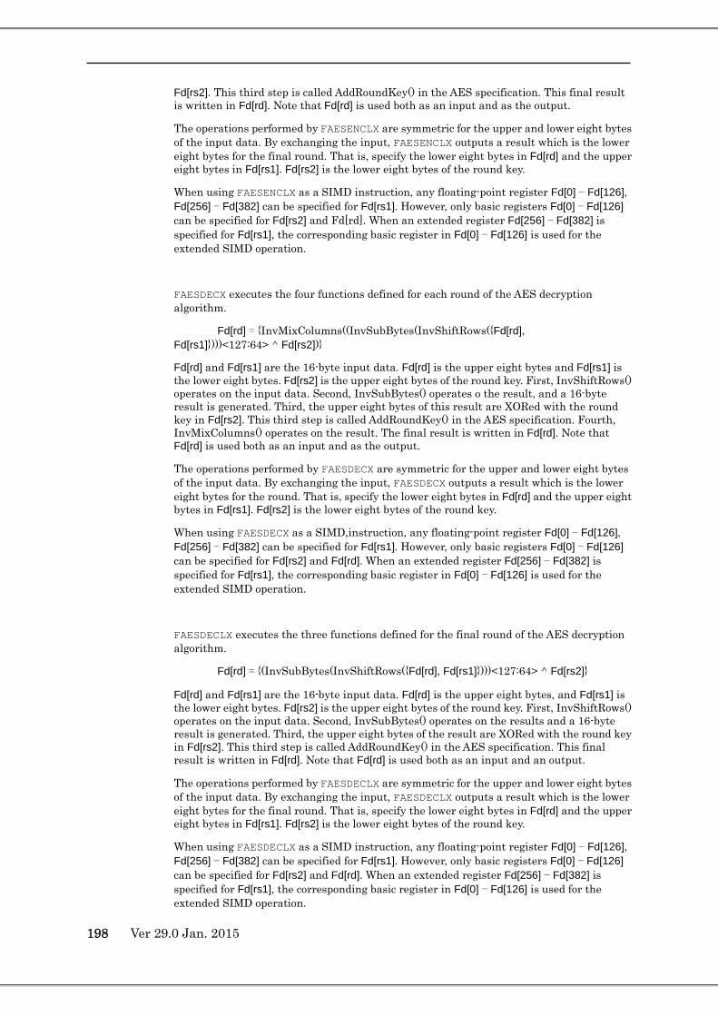
198 Ver 29.0 Jan. 2015
Fd[rs2]. This third step is called AddRoundKey() in the AES specification. This final result is written in Fd[rd]. Note that Fd[rd] is used both as an input and as the output.
The operations performed by FAESENCLX are symmetric for the upper and lower eight bytes of the input data. By exchanging the input, FAESENCLX outputs a result which is the lower eight bytes for the final round. That is, specify the lower eight bytes in Fd[rd] and the upper eight bytes in Fd[rs1]. Fd[rs2] is the lower eight bytes of the round key.
When using FAESENCLX as a SIMD instruction, any floating-point register Fd[0] − Fd[126], Fd[256] − Fd[382] can be specified for Fd[rs1]. However, only basic registers Fd[0] − Fd[126] can be specified for Fd[rs2] and Fd[rd]. When an extended register Fd[256] − Fd[382] is specified for Fd[rs1], the corresponding basic register in Fd[0] − Fd[126] is used for the extended SIMD operation.
FAESDECX executes the four functions defined for each round of the AES decryption algorithm.
Fd[rd] = {InvMixColumns((InvSubBytes(InvShiftRows({Fd[rd], Fd[rs1]})))<127:64> ^ Fd[rs2])}
Fd[rd] and Fd[rs1] are the 16-byte input data. Fd[rd] is the upper eight bytes and Fd[rs1] is the lower eight bytes. Fd[rs2] is the upper eight bytes of the round key. First, InvShiftRows() operates on the input data. Second, InvSubBytes() operates o the result, and a 16-byte result is generated. Third, the upper eight bytes of this result are XORed with the round key in Fd[rs2]. This third step is called AddRoundKey() in the AES specification. Fourth, InvMixColumns() operates on the result. The final result is written in Fd[rd]. Note that Fd[rd] is used both as an input and as the output.
The operations performed by FAESDECX are symmetric for the upper and lower eight bytes of the input data. By exchanging the input, FAESDECX outputs a result which is the lower eight bytes for the round. That is, specify the lower eight bytes in Fd[rd] and the upper eight bytes in Fd[rs1]. Fd[rs2] is the lower eight bytes of the round key.
When using FAESDECX as a SIMD,instruction, any floating-point register Fd[0] − Fd[126], Fd[256] − Fd[382] can be specified for Fd[rs1]. However, only basic registers Fd[0] − Fd[126] can be specified for Fd[rs2] and Fd[rd]. When an extended register Fd[256] − Fd[382] is specified for Fd[rs1], the corresponding basic register in Fd[0] − Fd[126] is used for the extended SIMD operation.
FAESDECLX executes the three functions defined for the final round of the AES decryption algorithm.
Fd[rd] = {(InvSubBytes(InvShiftRows({Fd[rd], Fd[rs1]})))<127:64> ^ Fd[rs2]}
Fd[rd] and Fd[rs1] are the 16-byte input data. Fd[rd] is the upper eight bytes, and Fd[rs1] is the lower eight bytes. Fd[rs2] is the upper eight bytes of the round key. First, InvShiftRows() operates on the input data. Second, InvSubBytes() operates on the results and a 16-byte result is generated. Third, the upper eight bytes of the result are XORed with the round key in Fd[rs2]. This third step is called AddRoundKey() in the AES specification. This final result is written in Fd[rd]. Note that Fd[rd] is used both as an input and an output.
The operations performed by FAESDECLX are symmetric for the upper and lower eight bytes of the input data. By exchanging the input, FAESDECLX outputs a result which is the lower eight bytes for the final round. That is, specify the lower eight bytes in Fd[rd] and the upper eight bytes in Fd[rs1]. Fd[rs2] is the lower eight bytes of the round key.
When using FAESDECLX as a SIMD instruction, any floating-point register Fd[0] − Fd[126], Fd[256] − Fd[382] can be specified for Fd[rs1]. However, only basic registers Fd[0] − Fd[126] can be specified for Fd[rs2] and Fd[rd]. When an extended register Fd[256] − Fd[382] is specified for Fd[rs1], the corresponding basic register in Fd[0] − Fd[126] is used for the extended SIMD operation.

FAESKEYX generates the round key. To calculate all 4-byte data W[i], which are the round keys used in each round, two 4-byte inputs W[i-1] and W[i-Nk] are needed from the previous rounds where Nk is the number of 4-byte words comprising the key data. FAESKEYX calculates both W[i] and W[i+1] at the same time. Specify W[i-2] in the upper four bytes of Fd[rs1] and W[i-1] in the lower four bytes. Specify W[i-Nk] in the upper four bytes of Fd[rd] and W[i-Nk+1] in the lower 4 bytes.. FAESKEYX performs the operation specified by the index field and the 32-bit result is output to temp.
index Operation 0016 temp = Fd[rd]<63:32> ^ Fd[rs1]<31:0> 0116 temp = Fd[rd]<63:32> ^ SubWord(Fd[rs1]<31:0>) 1016 temp = Fd[rd]<63:32> ^ SubWord(RotWord(Fd[rs1]<31:0>)) ^ 0100 000016 1116 temp = Fd[rd]<63:32> ^ SubWord(RotWord(Fd[rs1]<31:0>)) ^ 0200 000016 1216 temp = Fd[rd]<63:32> ^ SubWord(RotWord(Fd[rs1]<31:0>)) ^ 0400 000016 1316 temp = Fd[rd]<63:32> ^ SubWord(RotWord(Fd[rs1]<31:0>)) ^ 0800 000016 1416 temp = Fd[rd]<63:32> ^ SubWord(RotWord(Fd[rs1]<31:0>)) ^ 1000 000016 1516 temp = Fd[rd]<63:32> ^ SubWord(RotWord(Fd[rs1]<31:0>)) ^ 2000 000016 1616 temp = Fd[rd]<63:32> ^ SubWord(RotWord(Fd[rs1]<31:0>)) ^ 4000 000016 1716 temp = Fd[rd]<63:32> ^ SubWord(RotWord(Fd[rs1]<31:0>)) ^ 8000 000016 1816 temp = Fd[rd]<63:32> ^ SubWord(RotWord(Fd[rs1]<31:0>)) ^ 1B00 000016 1916 temp = Fd[rd]<63:32> ^ SubWord(RotWord(Fd[rs1]<31:0>)) ^ 3600 000016
After this calculation, temp is equivalent to W[i]. W[i+1] is calculated as "temp xor W[i-Nk+1]", which is equivalent to "temp xor Fd[rd]<31:0>". W[i] is written in the upper four bytes of Fd[rd] and W[i+1] is written in the lower four bytes.
Usage example, non SIMD
/* * AES-128 key generation * * Input: * %f0, %f2 : Key data * Output: * %f0, %f2 ... %f40, %f42: Round keys */ fmovd %f0, %f40 ! W[0],W[1] fmovd %f2, %f42 ! W[2],W[3] faeskeyx %f42, 0x10, %f40 fmovd %f40, %f4 ! W[4],W[5] faeskeyx %f40, 0x0, %f42 fmovd %f42, %f6 ! W[6],W[7] faeskeyx %f42, 0x11, %f40 fmovd %f40, %f8 ! W[8],W[9] faeskeyx %f40, 0x0, %f42 fmovd %f42, %f10 ! W[10],W[11] faeskeyx %f42, 0x12, %f40 fmovd %f40, %f12 ! W[12],W[13] faeskeyx %f40, 0x0, %f42 fmovd %f42, %f14 ! W[14],W[15] faeskeyx %f42, 0x13, %f40 fmovd %f40, %f16 ! W[16],W[17] faeskeyx %f40, 0x0, %f42 fmovd %f42, %f18 ! W[18],W[19] faeskeyx %f42, 0x14, %f40 fmovd %f40, %f20 ! W[20],W[21] faeskeyx %f40, 0x0, %f42

200 Ver 29.0 Jan. 2015
fmovd %f42, %f22 ! W[22],W[23] faeskeyx %f42, 0x15, %f40 fmovd %f40, %f24 ! W[24],W[25] faeskeyx %f40, 0x0, %f42 fmovd %f42, %f26 ! W[26],W[27] faeskeyx %f42, 0x16, %f40 fmovd %f40, %f28 ! W[28],W[29] faeskeyx %f40, 0x0, %f42 fmovd %f42, %f30 ! W[30],W[31] faeskeyx %f42, 0x17, %f40 fmovd %f40, %f32 ! W[32],W[33] faeskeyx %f40, 0x0, %f42 fmovd %f42, %f34 ! W[34],W[35] faeskeyx %f42, 0x18, %f40 fmovd %f40, %f36 ! W[36],W[37] faeskeyx %f40, 0x0, %f42 fmovd %f42, %f38 ! W[38],W[39] faeskeyx %f42, 0x19, %f40 ! W[40],W[41] faeskeyx %f40, 0x0, %f42 ! W[42],W[43] /* * AES-128 ECB mode encryption * * Input: * %f0, %f2 ... %f40, %f42: Round keys * %f50, %f52 : Plaintext data * Output: * %f60, %f62 : Ciphertext data */ fxor %f50, %f0, %f60 ! Round 0 fxor %f52, %f2, %f62 fmovd %f60, %f58 ! Round 1 faesencx %f62, %f4, %f60 faesencx %f58, %f6, %f62 fmovd %f60, %f58 ! Round 2 faesencx %f62, %f8, %f60 faesencx %f58, %f10, %f62 fmovd %f60, %f58 ! Round 3 faesencx %f62, %f12, %f60 faesencx %f58, %f14, %f62 fmovd %f60, %f58 ! Round 4 faesencx %f62, %f16, %f60 faesencx %f58, %f18, %f62 fmovd %f60, %f58 ! Round 5 faesencx %f62, %f20, %f60 faesencx %f58, %f22, %f62 fmovd %f60, %f58 ! Round 6 faesencx %f62, %f24, %f60 faesencx %f58, %f26, %f62 fmovd %f60, %f58 ! Round 7 faesencx %f62, %f28, %f60 faesencx %f58, %f30, %f62 fmovd %f60, %f58 ! Round 8 faesencx %f62, %f32, %f60 faesencx %f58, %f34, %f62 fmovd %f60, %f58 ! Round 9 faesencx %f62, %f36, %f60 faesencx %f58, %f38, %f62 fmovd %f60, %f58 ! Round 10 final round faesenclx %f62, %f40, %f60 faesenclx %f58, %f42, %f62 /*
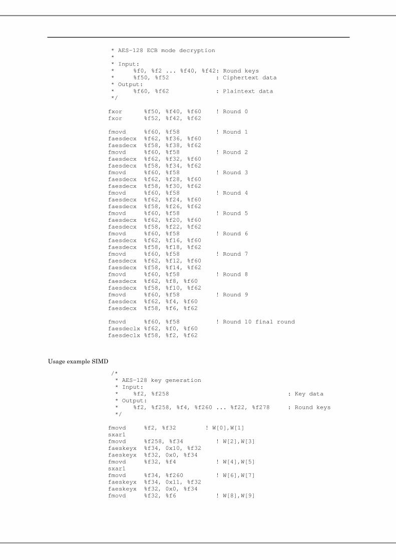
* AES-128 ECB mode decryption * * Input: * %f0, %f2 ... %f40, %f42: Round keys * %f50, %f52 : Ciphertext data * Output: * %f60, %f62 : Plaintext data */ fxor %f50, %f40, %f60 ! Round 0 fxor %f52, %f42, %f62 fmovd %f60, %f58 ! Round 1 faesdecx %f62, %f36, %f60 faesdecx %f58, %f38, %f62 fmovd %f60, %f58 ! Round 2 faesdecx %f62, %f32, %f60 faesdecx %f58, %f34, %f62 fmovd %f60, %f58 ! Round 3 faesdecx %f62, %f28, %f60 faesdecx %f58, %f30, %f62 fmovd %f60, %f58 ! Round 4 faesdecx %f62, %f24, %f60 faesdecx %f58, %f26, %f62 fmovd %f60, %f58 ! Round 5 faesdecx %f62, %f20, %f60 faesdecx %f58, %f22, %f62 fmovd %f60, %f58 ! Round 6 faesdecx %f62, %f16, %f60 faesdecx %f58, %f18, %f62 fmovd %f60, %f58 ! Round 7 faesdecx %f62, %f12, %f60 faesdecx %f58, %f14, %f62 fmovd %f60, %f58 ! Round 8 faesdecx %f62, %f8, %f60 faesdecx %f58, %f10, %f62 fmovd %f60, %f58 ! Round 9 faesdecx %f62, %f4, %f60 faesdecx %f58, %f6, %f62 fmovd %f60, %f58 ! Round 10 final round faesdeclx %f62, %f0, %f60 faesdeclx %f58, %f2, %f62
Usage example SIMD
/* * AES-128 key generation * Input: * %f2, %f258 : Key data * Output: * %f2, %f258, %f4, %f260 ... %f22, %f278 : Round keys */
fmovd %f2, %f32 ! W[0],W[1] sxar1 fmovd %f258, %f34 ! W[2],W[3] faeskeyx %f34, 0x10, %f32 faeskeyx %f32, 0x0, %f34 fmovd %f32, %f4 ! W[4],W[5] sxar1 fmovd %f34, %f260 ! W[6],W[7] faeskeyx %f34, 0x11, %f32 faeskeyx %f32, 0x0, %f34 fmovd %f32, %f6 ! W[8],W[9]

202 Ver 29.0 Jan. 2015
sxar1 fmovd %f34, %f262 ! W[10],W[11] faeskeyx %f34, 0x12, %f32 faeskeyx %f32, 0x0, %f34 fmovd %f32, %f8 ! W[12],W[13] sxar1 fmovd %f34, %f264 ! W[14],W[15] faeskeyx %f34, 0x13, %f32 faeskeyx %f32, 0x0, %f34 fmovd %f32, %f10 ! W[16],W[17] sxar1 fmovd %f34, %f266 ! W[18],W[19] faeskeyx %f34, 0x14, %f32 faeskeyx %f32, 0x0, %f34 fmovd %f32, %f12 ! W[20],W[21] sxar1 fmovd %f34, %f268 ! W[22],W[23] faeskeyx %f34, 0x15, %f32 faeskeyx %f32, 0x0, %f34 fmovd %f32, %f14 ! W[24],W[25] sxar1 fmovd %f34, %f270 ! W[26],W[27] faeskeyx %f34, 0x16, %f32 faeskeyx %f32, 0x0, %f34 fmovd %f32, %f16 ! W[28],W[29] sxar1 fmovd %f34, %f272 ! W[30],W[31] faeskeyx %f34, 0x17, %f32 faeskeyx %f32, 0x0, %f34 fmovd %f32, %f18 ! W[32],W[33] sxar1 fmovd %f34, %f274 ! W[34],W[35] faeskeyx %f34, 0x18, %f32 faeskeyx %f32, 0x0, %f34 fmovd %f32, %f20 ! W[36],W[37] sxar1 fmovd %f34, %f276 ! W[38],W[39] faeskeyx %f34, 0x19, %f22 ! W[40],W[41] sxar1 faeskeyx %f22, 0x0, %f278 ! W[42],W[43] /* * AES-128 ECB mode encryption (SIMD use) * * Input: * %f2, %f258, %f4, %f260 ... %f22, %f278 : Round keys * %f0, %f256 : Plaintext data * Output: * %f0, %f256 : Ciphertext data */
sxar2 fxor,s %f0, %f2, %f0 ! Round 0 faesencx,s %f256, %f4, %f0 ! Round 1 sxar2 faesencx,s %f256, %f6, %f0 ! Round 2 faesencx,s %f256, %f8, %f0 ! Round 3 sxar2 faesencx,s %f256, %f10, %f0 ! Round 4 faesencx,s %f256, %f12, %f0 ! Round 5 sxar2 faesencx,s %f256, %f14, %f0 ! Round 6 faesencx,s %f256, %f16, %f0 ! Round 7 sxar2 faesencx,s %f256, %f18, %f0 ! Round 8 faesencx,s %f256, %f20, %f0 ! Round 9

sxar1 faesenclx,s %f256, %f22, %f0 ! Round 10 final round /* * AES-128 ECB mode decryption (SIMD use) * * Input: * %f2, %f258, %f4, %f260 ... %f22, %f278 : Round keys * %f0, %f256 : Ciphertext data * Output: * %f0, %f256 : Plaintext data */
sxar2 fxor,s %f0, %f22, %f0 ! Round 0 faesdecx,s %f256, %f20, %f0 ! Round 1 sxar2 faesdecx,s %f256, %f18, %f0 ! Round 2 faesdecx,s %f256, %f16, %f0 ! Round 3 sxar2 faesdecx,s %f256, %f14, %f0 ! Round 4 faesdecx,s %f256, %f12, %f0 ! Round 5 sxar2 faesdecx,s %f256, %f10, %f0 ! Round 6 faesdecx,s %f256, %f8, %f0 ! Round 7 sxar2 faesdecx,s %f256, %f6, %f0 ! Round 8 faesdecx,s %f256, %f4, %f0 ! Round 9 sxar1 faesdeclx,s %f256, %f2, %f0 ! Round 10 final round
Exception Target instruction Condition illegal_instruction FAESKEYX index = 0216 − 0F16, 1A16 − 1F16 fp_disabled All PSTATE.PEF = 0 or FPRS.FEF = 0 illegal_action FAESKEYX XAR.v = 1 and any of the following are true
• XAR.urs1<1> ≠ 0 • XAR.urs2 ≠ 0 • XAR.urs3 ≠ 0 • XAR.urd<1> ≠ 0 • XAR.simd = 1 and XAR.urs1<2> ≠ 0 • XAR.simd = 1 and XAR.urd<2> ≠ 0
FAESENCX,FAESDECX, FAESENCLX,FAESDECLX
XAR.v = 1 and any of the following are true • XAR.urs1<1> ≠ 0 • XAR.urs2<1> ≠ 0 • XAR.urs3 ≠ 0 • XAR.urd<1> ≠ 0 • XAR.simd = 1 and XAR.urs2<2> ≠ 0 • XAR.simd = 1 and XAR.urd<2> ≠ 0

204 Ver 29.0 Jan. 2015
7.117. Decimal Floating-Point Operations Instruction Opf Operation HPC-ACE Assembly Language
Syntax Regs SIMD FADDtd 0 1010 00002 Add decimal floating point rd : basic
only faddtd fregrs1,
fregrs2, fregrd FSUBtd 0 1010 00012 Subtract decimal floating point rd : basic
only fsubtd fregrs1,
fregrs2, fregrd FMULtd 0 1010 00102 Multiply decimal floating point rd : basic
only fmultd fregrs1,
fregrs2, fregrd FDIVtd 0 1010 00112 Divide decimal floating point rd : basic
only fdivtd fregrs1,
fregrs2, fregrd FQUAtd 0 1010 01102 Significant digit conversion of
decimal floating point rd : basic
only fquatd fregrs1,
fregrs2, fregrd
102 rd op3 = 11 01102 rs1 opf rs2
31 30 29 25 24 19 18 14 13 5 4 0
Description FADDtd adds two double precision decimal floating point numbers, Fd[rs1] and Fd[rs2]. The result is written in Fd[rd]. When the operation result is exact, the preferred exponent is the smaller exponent of Fd[rs1] and Fd[rs2]. When the result is inexact, the preferred exponent is the closest value to the smaller exponent of Fd[rs1] and Fd[rs2] within the range and the precision of the output format. When the result is exactly zero, the sign of the result is negative if the rounding mode is 3 (towards −∞). Otherwise, the sign is positive.
Table 7-25 FADDtd
Fd[rs2]
−∞ −N −0 +0 +N +∞ QNaN SNaN
Fd[rs1]
−∞ −∞
NV dNaN
QNaN2 NV
QSNaN2
−N
Fd[rs1] + Fd[rs2]xvi
Fd[rs1]
Fd[rs1] + Fd[rs2]xvi
−0
Fd[rs2]
−0
+0xvii
Fd[rs2] +0
+0xvii
+0
+N Fd[rs1] + Fd[rs2]xvi
Fd[rs1]
Fd[rs1] + Fd[rs2]xvi
+∞ NV dNaN
+∞
QNaN QNaN1
SNaN NV QSNaN1
FSUBtd subtracts the double-precision decimal floating-point number in Fd[rs2] from the double-precision decimal floating-point number in Fd[rs1]. The result is written in Fd[rd]. When the result is exact, the preferred exponent is the smaller exponent of Fd[rs1] and Fd[rs2]. When the result is inexact, the preferred exponent is the closest value to the smaller exponent of Fd[rs1] and Fd[rs2] within the range and the precision of the output
xvi When the result is 0, footnote (xvii) applies. xvii When the rounding mode is towards −∞, the result is −0.

format. When the operation result is exactly zero, the sign of the result is negative if the rounding mode is 3 (towards −∞). Otherwise, the sign is positive.
Table 7-26 FSUBtd
Fd[rs2]
−∞ −N −0 +0 +N +∞ QNaN SNaN
Fd[rs1]
−∞ NV dNaN
−∞
QNaN2 NV
QSNaN2
−N
Fd[rs1] − Fd[rs2]xviii
Fd[rs1]
Fd[rs1] − Fd[rs2]xviii
−0
−Fd[rs2]
+0xix
−0
−Fd[rs2] +0
+0
+0xix
+N Fd[rs1] − Fd[rs2]xviii
Fd[rs1]
Fd[rs1] − Fd[rs2]xviii
+∞ +∞ NV
dNaN
QNaN QNaN1
SNaN NV QSNaN1
FMULtd multiplies two double-precision decimal floating-point numbers Fd[rs1] and Fd[rs2]. The result is written in Fd[rd]. When the result is exact, the preferred exponent is the sum of the exponents of Fd[rs1] and Fd[rs2]. When the operation result is inexact, the preferred exponent is the closest value to the sum of the exponents of Fd[rs1] and Fd[rs2] within the range and the precision of the output format.
Table 7-27 FMULtd
Fd[rs2]
−∞ −N −0 +0 +N +∞ QNaN SNaN
Fd[rs1]
−∞ +∞ NV
dNaN −∞
QNaN2 NV
QSNaN2
−N Fd[rs1] × Fd[rs2]
Fd[rs1] × Fd[rs2]
−0 NV
dNaN
+0
−0
NV dNaN
+0 −0
+0
+N Fd[rs1] × Fd[rs2]
Fd[rs1] × Fd[rs2]
+∞ −∞ NV
dNaN +∞
QNaN QNaN1
SNaN NV QSNaN1
xviii When the result is 0, the footnote (xix) applies.. xix When the rounding mode is towards −∞, the result is −0.

206 Ver 29.0 Jan. 2015
FDIVtd divides the double-precision decimal floating-point number Fd[rs1] by the double-precision decimal floating-point number Fd[rs2]. The result is written in Fd[rd]. When the result is exact, the preferred exponent is the difference of the exponents of Fd[rs1] and Fd[rs2]. When the result is inexact, the preferred exponent is the closest value to the difference of the exponents of Fd[rs1] and Fd[rs2] within the range and the precision of the output format. If the result of the operation is not within the range of the preferred exponent, the quotient is calculated until the remainder is zero or the maximum number of significant figures is reached. The exponent is then adjusted to be consistent with the quotient.
When the result is 0, the exponent is the preferred exponent and the significand is all zeros. However, if the result is 0 and the divisor is ∞, the exponent is all zeros as well.
Table 7-28 FDIVtd
Fd[rs2]
−∞ −N −0 +0 +N +∞ QNaN SNaN
Fd[rs1]
−∞ NV dNaN
+∞
−∞
NV dNaN
QNaN2 NV
QSNaN2
−N
+0xx
Fd[rs1] / Fd[rs2]
DZ +∞
DZ −∞
Fd[rs1] / Fd[rs2]
−0xx −0
+0xxi NV
dNaN
−0xxi
+0
−0xx
−0xxi
+0xxi
+0xx +N
Fd[rs1] / Fd[rs2] DZ −∞
DZ +∞
Fd[rs1] / Fd[rs2]
+∞ NV dNaN
−∞
+∞
NV dNaN
QNaN QNaN1
SNaN NV QSNaN1
FQUAtd converts the double-precision decimal floating-point number in Fd[rs1] into a cohort member whose exponent is the same as the double-precision decimal floating-point number in Fd[rs2]. The result is written in Fd[rd]. The preferred exponent is the exponent of Fd[rd], regardless of whether the result is exact or inexact.
On overflow, the output is QNaN with an NV exception. That is, an NV exception is generated when the result cannot be expressed using the specified exponent.
When the significand is 0 due to underflow or rounding, the result remains 0 to be consistent with the preferred exponent.
xx Significand is 0. Exponent after bias is 0. xxi Exponent is the preferred exponent.

Table 7-29 FQUAtd
Fd[rs2]
−∞ −Fn −0 +0 +Fn +∞ QNaN SNaN
Fd[rs1]
−∞ −∞
NV dNaN
−∞
QNaN2 NV
QSNaN2
−Fn
NV dNaN
Q(Fd[rs1] : Fd[rs2])
NV dNaN
−0
−0xxii
+0
+0xxii
+Fn Q(Fd[rs1] : Fd[rs2])
+∞ +∞
NV dNaN
+∞
QNaN QNaN1
SNaN NV QSNaN1
Instructions that operate on single-precision and quadruple-precision data are not defined.
The result is rounded as specified by GSR.dirnd when GSR.dim = 1, or FSR.drd when GSR.dim = 0.
The following table summarizes the preferred exponents for the decimal floating-point instructions.
Table 7-30 Preferred exponents
Instruction Result is exact Result is inexact FADDtd Smaller of Fd[rs1]
and Fd[rs2] exponents
Closest value to preferred exponent for an exact result
FSUBtd Smaller of Fd[rs1] and Fd[rs2] exponents
Closest value to preferred exponent for an exact result
FMULtd Sum of Fd[rs1] and Fd[rs2] exponents
Closest value to preferred exponent for an exact result
FDIVtd Difference of Fd[rs1] and Fd[rs2] exponents
Closest value to preferred exponent for an exact result If result is not within the range of the preferred exponent, quotient is calculated until remainder is zero or maximum significant figures reached. Exponent adjusted to be consistent with quotient.
FQUAtd Exponent of Fd[rs2] Exponent of Fd[rs2]
xxii Significand is 0. Exponent is exponent of rs2.

208 Ver 29.0 Jan. 2015
Exception Target instruction
Condition
fp_disabled All PSTATE.pef = 0 or FPRS.fef = 0 illegal_action All XAR.v = 1 and any of the following are true
• XAR.simd = 1 • XAR.urs1<1> ≠ 0 • XAR.urs2<1> ≠ 0 • XAR.urs3 ≠ 0 • XAR.urd<2:1> ≠ 0
fp_exception_ieee_754 OF, UF
FADDtd, FSUBtd, FMULtd, FDIVtd
Conforms to IEEE754-2008
NX, NV
All Conforms to IEEE754-2008
DZ FDIVtd Refer to table in description

7.118. Oracle Floating-Point Operations Compatibility Note Future compatibility of Oracle floating-point
operations is not guaranteed. These instructions should only be used in libraries for the SPARC64™ X / SPARC64™ X+ platforms.
Instruction Opf Operation HPC-ACE Assembly Language Syntax
Regs SIMD FADDod 0 1011 00002 Add Oracle floating point rd : basic
only faddod fregrs1, fregrs2, fregrd
FSUBod 0 1011 00012 Subtract Oracle floating point rd : basic only
fsubod fregrs1, fregrs2, fregrd
FMULod 0 1011 00102 Multiply Oracle floating point rd : basic only
fmulod fregrs1, fregrs2, fregrd
FDIVod 0 1011 00112 Divide Oracle floating point rd : basic only
fdivod fregrs1, fregrs2, fregrd
FXADDodLO
0 1011 10002 Exact add Oracle floating point (lower)
rd : basic only
fxaddodlo fregrs1, fregrs2, fregrd
FXADDodHI
0 1011 10012 Exact add Oracle floating point (upper)
rd : basic only
fxaddodhi fregrs1, fregrs2, fregrd
FXMULodLO
0 1011 10102 Exact multiply Oracle floating point (lower)
rd : basic only
fxmulodlo fregrs1, fregrs2, fregrd
FQUAod 0 1011 01102 Significant digit conversion of Oracle floating point
rd : basic only
fquaod fregrs1, fregrs2, fregrd
FRQUAod 0 1011 01112 Extended exponent conversion of Oracle floating point
rd : basic only
Frquaod fregrs1, fregrs2, fregrd
102 rd op3 = 11 01102 rs1 opf rs2
31 30 29 25 24 19 18 14 13 5 4 0
Description FADDod adds the Oracle floating-point numbers Fd[rs1] and Fd[rs2] and writes the result in Fd[rd]. The result is normalized.
Table 7-31 FADDod
Fd[rs2]
−∞ −N 0 +N +∞
Fd[rs1]
−∞ −∞ NV
dNaN
−N
Fd[rs1] + Fd[rs2]xxiii
Fd[rs1]
Fd[rs1] + Fd[rs2]xxiii
0 Fd[rs2]
0xxiv
Fd[rs2]
+N Fd[rs1] + Fd[rs2] xxiii
Fd[rs1]
Fd[rs1] + Fd[rs2] xxiii
+∞ NV dNaN
+∞
xxiii When the result is 0, footnote (xxiv) applies. xxiv When the rounding mode is towards −∞, the result is −0.

210 Ver 29.0 Jan. 2015
FSUBod subtracts the Oracle floating-point number Fd[rs2] from the Oracle floating-point number Fd[rs1] and writes the result in Fd[rd]. The result is normalized.
Table 7-32 FSUBod
Fd[rs2]
−∞ −N 0 +N +∞
Fd[rs1]
−∞ NV dNaN
−∞
−N
Fd[rs1] − Fd[rs2]xxv
Fd[rs1]
Fd[rs1] − Fd[rs2]xxv
0 − Fd[rs2]
0xxvi
− Fd[rs2]
+N Fd[rs1] − Fd[rs2]xxv
Fd[rs1]
Fd[rs1] − Fd[rs2]xxv
+∞ +∞ NV
dNaN
FMULod multiplies the Oracle floating-point numbers Fd[rs1] and Fd[rs2] and writes the result in Fd[rd]. The result is normalized.
Table 7-33 FMULod
Fd[rs2]
−∞ −N 0 +N +∞
Fd[rs1]
−∞ +∞ NV
dNaN −∞
−N Fd[rs1] × Fd[rs2]
Fd[rs1] × Fd[rs2]
0 NV dNaN
0
NV dNaN
+N Fd[rs1] × Fd[rs2]
Fd[rs1] × Fd[rs2]
+∞ −∞ NV
dNaN +∞
FDIVod divides the Oracle floating-point number Fd[rs1] by the Oracle floating-point number Fd[rs2] and writes the result in Fd[rd]. The result is normalized.
FDIVod generates a DZ exception if the divisor Fd[rs2] is 0. However, even if the divisor is 0, a DZ exception is not generated if the dividend Fd[rs1] is +∞, −∞ or 0. If the divisor is 0 and the dividend is +∞ or −∞, the result is +∞ and −∞, respectively. If the divisor is 0 and the dividend is 0, the result is dNaN with an NV exception.
xxv When the result is 0, footnote (xxvi) applies. xxvi When the rounding mode is towards −∞, the result is −0.

Table 7-34 FDIVod
Fd[rs2]
−∞ −N 0 +N +∞
Fd[rs1]
−∞ NV dNaN
+∞
−∞
−∞
NV dNaN
−N
0
Fd[rs1] / Fd[rs2]
DZ −∞
Fd[rs1] / Fd[rs2]
0 0 NV
dNaN
+N Fd[rs1] / Fd[rs2]
DZ +∞
Fd[rs1] / Fd[rs2]
+∞ NV dNaN
−∞
+∞
+∞
NV dNaN
FXADDodLO and FXADDodHI are used to calculate the exact sum of two Oracle floating-point numbers. Note that the FADDod instruction outputs a rounded result and generates an NX exception when the sum cannot be expressed precisely as an Oracle floating-point number. FXADDodHI and FXADDodLO, however, output the exact sum of two Oracle floating-point numbers. These instructions can be used to add and subtract with arbitrary precision.
FXADDodLO behaves differently depending on the difference of the exponents of the two Oracle floating-point numbers Fd[rs1] and Fd[rs2]. If the difference is less than or equal to seven, Fd[rs1] and Fd[rs2] are added and the lower digits of the result are written in Fd[rd]. If the difference is greater than seven, the number with the smaller exponent is selected and written in Fd[rd]. If either Fd[rs1] or Fd[rs2] is the special value 0, the special value 0 is written in Fd[rd], regardless of the difference of the exponents.
FXADDodHI behaves differently depending on the difference of the exponents of the two Oracle floating-point numbers Fd[rs2] and Fd[rs1]. If the difference is less than or equal to seven, Fd[rs1] and Fd[rs2] are added and the upper digits of the result are written in Fd[rd]. If the difference is greater than seven, the number with the larger exponent is selected and written in Fd[rd]. If either Fd[rs1] or Fd[rs2] is the special value 0, the other number which is not 0 is written in Fd[rd], regardless of the difference of the exponents. If both Fd[rs1] and Fd[rs2] are the special value 0, the special value 0 is written in Fd[rd].
The results of FXADDodLO and FXADDodHI are normalized.
For the FXADDodLO and FXADDodHI instructions, the rounding mode is set to 1 (towards 0). Results are rounded regardless of the settings in FSR and GSR.
Note To precisely express the sum of two values with opposite signs, the number of digits required is equal to the difference of the exponents.
0010 109999999999)101(101: ×=×−+×Example When adding two numbers of opposite signs where the difference of their exponents is large, the result exceeds the number of digits that can be saved in two registers. FXADDodLO and FXADDodHI preserve precision by saving the inputs when the difference of the exponents is greater than seven.
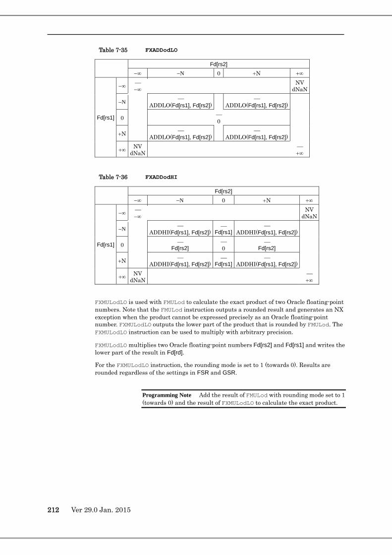
212 Ver 29.0 Jan. 2015
Table 7-35 FXADDodLO
Fd[rs2]
−∞ −N 0 +N +∞
Fd[rs1]
−∞ −∞ NV
dNaN
−N
ADDLO(Fd[rs1], Fd[rs2])
ADDLO(Fd[rs1], Fd[rs2])
0 0
+N ADDLO(Fd[rs1], Fd[rs2])
ADDLO(Fd[rs1], Fd[rs2])
+∞ NV dNaN
+∞
Table 7-36 FXADDodHI
Fd[rs2]
−∞ −N 0 +N +∞
Fd[rs1]
−∞ −∞ NV
dNaN
−N
ADDHI(Fd[rs1], Fd[rs2])
Fd[rs1]
ADDHI(Fd[rs1], Fd[rs2])
0 Fd[rs2]
0
Fd[rs2]
+N ADDHI(Fd[rs1], Fd[rs2])
Fd[rs1]
ADDHI(Fd[rs1], Fd[rs2])
+∞ NV dNaN
+∞
FXMULodLO is used with FMULod to calculate the exact product of two Oracle floating-point numbers. Note that the FMULod instruction outputs a rounded result and generates an NX exception when the product cannot be expressed precisely as an Oracle floating-point number. FXMULodLO outputs the lower part of the product that is rounded by FMULod. The FXMULodLO instruction can be used to multiply with arbitrary precision.
FXMULodLO multiplies two Oracle floating-point numbers Fd[rs2] and Fd[rs1] and writes the lower part of the result in Fd[rd].
For the FXMULodLO instruction, the rounding mode is set to 1 (towards 0). Results are rounded regardless of the settings in FSR and GSR.
Programming Note Add the result of FMULod with rounding mode set to 1 (towards 0) and the result of FXMULodLO to calculate the exact product.

Table 7-37 FXMULodLO
Fd[rs2]
−∞ −N 0 +N +∞
Fd[rs1]
−∞ +∞ NV
dNaN −∞
−N LO(Fd[rs1] × Fd[rs2])
LO(Fd[rs1] × Fd[rs2])
0 NV dNaN
0
NV dNaN
+N LO(Fd[rs1] × Fd[rs2])
LO(Fd[rs1] × Fd[rs2])
+∞ -∞ NV
dNaN +∞
Table 7-38 Multiplying rs1 = 99.99999999 × 10010 and rs2 = 99.99999999 × 10010
FMULod FXMULodLO
99.99999998 × 10021 00.0001 × 10014
Table 7-39 Output of FXMULodLO if lower bits of result is 0
Sign Exponent part Significand
Either of the inputs is 0
1 0 0x00000000000000
Neither of the inputs is 0
Same as multiplication result
Exponent of multiplication result minus 7
(Exponent <= −59: exponent −7+128)
(Exponent >= +70: exponent−7−128)
Sign is positive: 0x01010101010101
Sign is negative
0x65656565656565
FQUAod converts the Oracle floating-point number in Fd[rs1] into a cohort member whose exponent is the same as the Oracle floating-point number in Fd[rs2]. The result is written in Fd[rd]. The result is not normalized.
On overflow, the output is dNaN with an NV exception. That is, an NV exception is generated when the result cannot be expressed using the specified exponent.
When the significand is 0 due to underflow or rounding, the result remains 0. This 0 is not the special value 0. The sign is the same as Fd[rs1], the exponent is the same as Fd[rs2], and 0 corresponding to the sign is written in the significand.
The result of FQUAod is rounded as specified by GSR.dirnd when GSR.dim = 1, and FSR.drd when GSR.dim = 0.

214 Ver 29.0 Jan. 2015
Table 7-40 FQUAod
Fd[rs2]
−∞ −Fn 0 +Fn +∞
Fd[rs1]
−∞ −∞
NV dNaN
−∞
−Fn
NV dNaN
Q(Fd[rs1] : Fd[rs2])
NV dNaN 0
0
+Fn Q(Fd[rs1] : Fd[rs2])
+∞ +∞
NV dNaN
+∞
FRQUAod converts the Oracle floating-point number in Fd[rs1] into a cohort member with the extended exponent (page 21) is specified by Fd[rs2]. The rounded result is converted into an Oracle floating-point number and written in Fd[rd]. An extended exponent can be used to round an arbitrary digit of the decimal number. The result is not normalized.
When the exponent of Fd[rs1] more than double the extended exponent specified by Fd[rs2], Fd[rs1] is written in Fd[rd].
When the significand is 0 due to underflow or rounding, the result remains 0. This 0 is not the special value 0. The sign is the same as Fd[rs1], the exponent is the extended exponent specified by Fd[rs2], and 0 corresponding to the sign is written in the significand.
The result is rounded as specified by GSR.dirnd when GSR.dim = 1, amd FSR.drd when GSR.dim = 0.
The rounded result, which is expressed in terms of the extended exponent, is converted to an Oracle floating-point number and then written in Fd[rd].
• When the extended exponent is even, the converted Oracle floating-point number consists of the sign of the rounded result, an exponent equivalent to the extended exponent of the rounded result, and the significand of the rounded result.
• When the extended exponent is odd, the converted Oracle floating-point number consists of the sign of the rounded result, an exponent equivalent to the extended exponent of the rounded result minus one, and a significand which is the rounded result’s significand shifted left by one digit.
Table 7-41 FRQUAod
Fd[rs2]
exp10 ≤ exp(Fd[rs1]) × 2 exp10 > exp(Fd[rs1]) × 2
Fd[rs1]
−∞ NV dNaN
−Fn
Fd[rs1]
RQ(Fd[rs1] : Fd[rs2]) 0 +Fn
+∞ NV dNaN
Table 7-42 shows examples of FRQUAod when the exponent of Fd[rs1] is 10, the significand is 11.223344556677, and the rounding mode is 4 (towards nearest, away from 0 if tie) .

Table 7-42 Examples of FRQUAod
Fd[rs2] Processing Exp Extended Exp
Significand (underflow)
Remarks
Extended exponent 21
1) Convert to extended exponent 10.5 21 01.122334455667(7) Right shift 1 digit
2) Rounding process 10.5 21 01.122334455668 Round at 132110 −
3) Exponent correction 10 20 11.223344556680 Left shift 1 digit
Extended exponent 22
1) Convert to extended exponent 11 22 00.112233445566(7) Right shift 2 digits
2) Rounding process 11 22 00.112233445567 Round at 132210 −
3) Exponent correction 11 22 00.112233445567 No shift
Extended exponent 23
1) Convert to extended exponent 11.5 23 00.011223344556(6) Right shift 3 digits
2) Rounding process 11.5 23 00.011223344557 Round at 132310 −
3) Exponent correction 11 22 00.112233445570 Left shift 1 digit
Extended exponent 24
1) Convert to extended exponent 12 24 00.001122334455(6) Right shift 2 digits
2) Rounding process 12 24 00.001122334456 Round at 132410 −
3) Exponent correction 12 24 00.001122334456 No shift unnecessary.
Extended exponent 32
1) Convert to extended exponent 16 32 00.000000000011(2) Right shift 12 digits
2) Rounding process 16 32 00.000000000011 Round at 133210 −
3) Exponent correction 16 32 00.000000000011 No shift
Extended exponent 33
1) Convert to extended exponent 16.5 33 00.000000000001(1) Right shift 13 digits
2) Rounding process 16.5 33 00.000000000001 Round at 133310 −
3) Exponent correction 16 32 00.000000000010 Left shift 1 digit
Extended exponent 34
1) Convert to extended exponent 17 34 00.000000000000(1) Right shift 14 digits
2) Rounding process 17 34 00.000000000000 Round at 133410 −
3) Exponent correction 17 34 00.000000000000 No shift.
The results of FADDod, FSUBod, FMULod, FDIVod, FQUAod, and FRQUAod are rounded as specified by GSR.dirnd when GSR.dim = 1, or FSR.drd when GSR.dim = 0. The results of FXADDodLO, FXADDodHI, and FXMULodLO are rounded with rounding mode 1 (towards 0) regardless of the settings in FSR or GSR.

216 Ver 29.0 Jan. 2015
When the results of FADDod, FSUBod, FMULod, FDIVod, FXADDodLO, FXADDodHI, and FXMULodLO are zero after rounding, the ouput is the special value 0 (page 20). If the result is smaller than Nmin (page 20), the output is 0 or Nmin depending on the rounding mode. If the result is not a special value, the output is normalized, except for FQUAod and FRQUAod.
When either Fd[rs1] or Fd[rs2] is written to Fd[rd] as a result of FADDod, FSUBod, FMULod, FDIVod, FXADDodLO, FXADDodHI, FXMULodLO, FQUAod, or FRQUAod, the digits outside the range of the significand (page 18) are converted to the number 0.
Exception Target instruction
Condition
fp_disabled All PSTATE.pef = 0 or FPRS.fef = 0 illegal_action All XAR.v = 1 and any of the following are true
• XAR.simd = 1 • XAR.urs1<1> ≠ 0 • XAR.urs2<1> ≠ 0 • XAR.urs3 ≠ 0 • XAR.urd<2:1> ≠ 0
fp_exception_ieee_754 OF FADDod, FSUBod, FMULod, FDIVod, FXADDodHI, FXMULodLO, FRQUAod
Result is larger than Nmax (page 20)
UF FADDod, FSUBod, FMULod, FDIVod, FXADDodHI, FXADDodLO, FXMULodLO
Result is smaller than Nmin (page 20)
NX All Result cannot be expressed as an Oracle floating-point number For FXADDodHI, FXADDodLO and FXMULodLO, only when OF or UF.
NV All Refer to tables in the description DZ FDIVod Refer to the table in the description

7.119. Decimal Floating-Point Compare Instruction opf Operation HPC-ACE Assembly Language Syntax
Regs SIMD FCMPtd 0 1010 01002 Compare decimal floating
point numbers . fcmptd %fccn, fregrs1, fregrs2
FCMPEtd 0 1010 01012 Compare decimal floating point numbers (exception if non-ordinal).
fcmpetd %fccn, fregrs1, fregrs2
102 cc1 cc0 op3 = 11 01102 rs1 opf rs2
31 30 29 27 26 25 24 19 18 14 13 5 4 0
Description FCMPtd and FCMPEtd compare two double-precision decimal floating-point numbers Fd[rs2] and Fd[rs1]. The result is written in FSR.fccn. Cohorts members are considered equal.
When either number is SNaN, FCMPtd detects an exception.
When either number is SNaN or QNaN, FCMPEtd detects an exception.
Table 7-43 FCMPtd and FCMPEtd
rs2
−∞ −Fn −0 +0 +Fn +∞ QNaN SNaN
rs1
−∞ 0
1
−Fn 0, 1, 2
−0
0 +0
+Fn 2
0, 1, 2
+∞ 0
QNaN NVxxvii 3
SNaN NV 3
Instructions that compare single-precision or quadruple-precision decimal floating-point numbers are not defined.
xxvii FCMPEtd instruction only

218 Ver 29.0 Jan. 2015
Exception Target instruction
Condition
Illegal_instruction All A reserved field is not 0. (iw<29:27> ≠ 0)
fp_disabled All PSTATE.pef = 0 or FPRS.fef = 0 illegal_action All XAR.v = 1 and any of the following are true
• XAR.simd = 1 • XAR.urs1<1> ≠ 0 • XAR.urs2<1> ≠ 0 • XAR.urs3 ≠ 0 • XAR.urd ≠ 0
fp_exception_ieee_754 NV FCMPtd FSR.tem.nv ≠ 0, and either input is SNaN FCMPEtd FSR.tem.nv ≠ 0, and FSR.fccn ≠ 3

7.120. Oracle Decimal Floating-Point Compare Compatibility Note Future compatibility of Oracle decimal floating-point
compare is not guaranteed. This instruction should only be used in libraries for the SPARC64™ X or SPARC64 X+ platform.
Instruction opf Operation HPC-ACE Assembly Language Syntax
Regs SIMD FCMPod 0 1011 01002 Compare Oracle floating
point numbers fcmpod %fccn, fregrs1,
fregrs2
102 cc1 cc0 op3 = 11 01102 rs1 opf rs2 31 30 29 27 26 25 24 19 18 14 13 5 4 0
Description FCMPod compares two Oracle format floating-point numbers Fd[rs2] and Fd[rs1]. The result is written in FSR.fccn.
Table 7-44 Operation result of FCMPod
rs2
−∞ −Fn 0 +Fn +∞
rs1
−∞ 0
1
−Fn 0, 1, 2
0 0
+Fn 2
0, 1, 2
+∞ 0
Exception Target
instruction Condition
Illegal_instruction All A reserved field is not 0. (iw<29:27> ≠ 0)
fp_disabled All PSTATE.pef = 0 or FPRS.fef = 0 illegal_action All XAR.v = 1 and any of the following are true
• XAR.simd = 1 • XAR.urs1<1> ≠ 0 • XAR.urs2<1> ≠ 0 • XAR.urs3 ≠ 0 • XAR.urd ≠ 0

220 Ver 29.0 Jan. 2015
7.121. Decimal Floating-Point Convert Compatibility Note Future compatibility of Oracle floating-point
numbers is not guaranteed. This format should only be used for libraries for the SPARC64™ X or SPARC64 X+ platform.
Instruction opf Operation HPC-ACE Assembly Language Syntax
Regs SIMD FbuxTOtd 1 1010 11002 Convert decimal floating
point rd : basic only fbuxtotd fregrs2, fregrd
FtdTObux 1 1010 11012 Convert decimal floating point
rd : basic only ftdtobux fregrs2, fregrd
FbsxTOtd 1 1010 11102 Convert decimal floating point
rd : basic only fbsxtotd fregrs2, fregrd
FtdTObsx 1 1010 11112 Convert decimal floating point
rd : basic only ftdtobsx fregrs2, fregrd
FodTOtd 1 1011 11102 Convert decimal floating point
rd : basic only fodtotd fregrs2, fregrd
FtdTOod 1 1011 11112 Convert decimal floating point
rd : basic only ftdtood fregrs2, fregrd
102 rd op3 = 11 01102 opf rs2 31 30 29 25 24 19 18 14 13 5 4 0
Description FbuxTOtd converts a 64-bit unsigned BCD integer Fd[rs2] into a double-precision decimal floating point number. The result is written in Fd[rd]. The exponent of the decimal-floating point number after the conversion is 0 (bias only).
Because the range of values that can be represented by a decimal floating-point number is larger than the range of an unsigned BCD number, the conversion result is always exact.
When a digit outside the range 00002 − 10012 is present in the BCD integer, an NV exception is generated.
FbsxTOtd converts a 64-bit signed integer BCD Fd[rs2] into a double-precision decimal floating-point number. The result is written in Fd[rd]. The exponent of the decimal floating-point number after the conversion is 0 (bias only).
Because the range of values that can be represented by a decimal floating-point number is larger than the range of a signed BCD number, the conversion result is always exact.
The lowest four bits of the BCD integer encode the sign of the number. Table 4-6 shows how FbsxTOtd interprets the sign field.
When a digit outside the range 00002 − 10012 is present in a BCD integer, excluding the sign field, an NV exception is generated.
FtdTObux converts the significand of a double-precision decimal floating-point number Fd[rs2] into a 64-bit signed BCD integer. The result is written in Fd[rd]. Because the range that can be represented by an unsigned BCD number is the same as the range of the significand of a decimal floating-point number, the conversion result is always exact.
Programming Note Because FtdTObux ignores the exponent, first use FQUAtd to make the biased exponent 0.
If a special value (∞ or NaN) is input, the value of the Combination field (exponent, NaNs, and ∞) is ignored, and no exceptionis generated. When the LMD cannot be determined because the significand is ∞ or NaN, the LMD is treated as 0.

FtdTObsx converts the significand of a double-precision decimal floating-point number Fd[rs2] into a 64-bit signed BCD integer. The result is written in Fd[rd]. The exponent part is ignored.
A signed BCD can represent 15 decimal digits and has a smaller range than a decimal floating-point number, which has 16 digits. The number after conversion is the signed lower 15 digits of the decimal floating-point number. When the upper digit is thrown away, no exception is generated.
Note For F{sdq}TOi and F{sdq}TOx, an exception is generated if FSR.tem.nvm = 1. If FSR.tem.nvm = 0, the result is the maximum value (if negative, minimum value) that can be shown.
The left part of the significand is not a target of the conversion and is ignored. If a special value (∞ and NaN) is input, the value of the Combination field (exponent, NaNs, and ∞) is ignored, and no exception is generated. The LMD is not converted, so it doesn’t matter if the LMD cannot be determined because the significand is ∞ or NaN.
FodTOtd converts Oracle floating-point number Fd[rs2] into a double-precision decimal floating-point number. The result is written in Fd[rd]. No exceptions are generated.
• If a special value (∞, 0) is input The special value is converted to the corresponding value in the output format. When Fd[rs2] is 0, the significand is 0 and the exponent is the exponent of Fd[rs2].
FtdTOod converts a double-precision decimal floating-point number Fd[rs2] into an Oracle floating-point number. The result is written in Fd[rd].
• About OF and UF When the exponent of the rounded result of the conversion of Fd[rs2] is larger than Emax of the output format, an OF exception is generated. The result is ∞ or Nmax. When the exponent of the rounded result of the conversion of Fd[rs2] is smaller than Emin of the output format, a UF exception isgenerated. The result is 0 or Nmin.
• If a special value (∞, NaN) is input The special value is converted to the corresponding value in the output format. When the input is NaN, the results is dNaN, and an NV exception is generated.
Exception Target
instruction Condition
Illegal_instruction All A reserved field is not 0. (iw<18:14> ≠ 0)
fp_disabled All PSTATE.pef = 0 or FPRS.fef = 0 illegal_action All XAR.v = 1 and any of the following are true
• XAR.simd = 1 • XAR.urs1 ≠ 0 • XAR.urs2<1> ≠ 0 • XAR.urs3 ≠ 0 • XAR.urd<2:1> ≠ 0
fp_exception_ieee_754 OF FtdTOod Refer to the description UF FtdTOod Refer to the description NX FtdTOod Refer to the description NV FbuxTOtd,
FbsxTOtd, FtdTOod
Refer to the description

222 Ver 29.0 Jan. 2015
7.122. Shift Mask Or (for SPARC64™ X) Note For the specification of this instruction on SPARC64™ X+, refer to page 252.
Instruction var size Operation HPC-ACE Assembly Language Syntax
Regs SIMD FSHIFTORX 102 112 Concatenate two double-precision
floating-point registers fshiftorx fregrs1, fregrs2, fregrs3,
fregrd
102 rd op3 = 11 01112 rs1 rs3 var = 102 size = 112 rs2 31 30 29 25 24 19 18 14 13 9 8 7 6 5 4 0
Non-SIMD execution
FSHIFTORX shifts Fd[rs1] right or left and extracts part of the result. It also shifts Fd[rs2] right or left and extracts part of the result. The two extracted values are bitwise ORed, and this result is written in Fd[rd]. The shift count and shift direction are specified by Fd[rs3].
Table 7-45 Meaning of bits in Fd[rs3]
set_rs2_default rs1_mask_inv rs1_mask_offset rs1_mask_length rs1_shift_amount 63 62
57 56 55 48 47 40 39 32
rs2_mask_inv rs2_mask_offset rs2_mask_length rs2_shift_amount 31 25 24 23 16 15 8 7 0
Bit Field Description rs1 rs2 63 - set_rs2_default Specifies set of rs{1|2}_* fields to use for rs2
0: Use the rs2_* fields 1: Use values derived from the rs1_* fields
56 24 rs{1|2}_mask_inv Specifies whether to invert the mask 0: Do not invert 1: Invert
55:48 23:16 rs{1|2}_mask_offset Starting bit position in mask (number of bits from MSB), 8-bit signed integer
47:40 15:8 rs{1|2}_mask_length Mask bit length, 8-bit signed integer 39:32 7:0 rs{1|2}_shift_amount Shift count (positive: left shift, negative: right shift), 8-bit
signed integer
Note Specifying the following values in Fd[rs3] causes an illegal_instruction exception. 1) '1' in a reserved field 2) set_rs2_default = 1 and <31:0> ≠ 0 3) rs{1|2}_mask_offset, rs{1|2}_mask_length, or rs{1|2}_shift_amount ≠ multiple of 8
Note The FSHIFTORX instruction causes an illegal_instruction exception for certain values in the register Fd[rs3]. An fp_disabled or illegal_action exception may be detected before the register is read. That is, for this instruction, these exceptions may have higher priority than an illegal instruction exception.
The behavior of FSHIFTORX is divided into 1) shift, 2) mask and 3) OR operations.
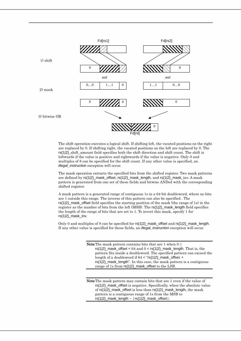
The shift operation executes a logical shift. If shifting left, the vacated positions on the right are replaced by 0. If shifting right, the vacated positions on the left are replaced by 0. The rs{1|2}_shift_amount field specifies both the shift direction and shift count. The shift is leftwards if the value is positive and rightwards if the value is negative. Only 0 and multiples of 8 can be specified for the shift count. If any other value is specified, an illegal_instruction exception will occur.
The mask operation extracts the specified bits from the shifted register. Two mask patterns are defined by rs{1|2}_mask_offset, rs{1|2}_mask_length, and rs{1|2}_mask_inv. A mask pattern is generated from one set of these fields and bitwise ANDed with the corresponding shifted register.
A mask pattern is a generated range of contiguous 1s in a 64-bit doubleword, where no bits are 1 outside this range. The inverse of this pattern can also be specified . The rs{1|2}_mask_offset field specifies the starting position of the mask (the range of 1s) in the register as the number of bits from the left (MSB). The rs{1|2}_mask_length field specifies the length of the range of bits that are set to 1. To invert this mask, specify 1 for rs{1|2}_mask_inv.
Only 0 and multiples of 8 can be specified for rs{1|2}_mask_offset and rs{1|2}_mask_length. If any other value is specified for these fields, an illegal_instruction exception will occur.
Note The mask pattern contains bits that are 1 when 0 ≤ rs{1|2}_mask_offset < 64 and 0 < rs{1|2}_mask_length. That is, the pattern fits inside a doubleword. The specified pattern can exceed the length of a doubleword if 64 < “rs{1|2}_mask_offset + rs{1|2}_mask_length”. In this case, the mask pattern is a contiguous range of 1s from rs{1|2}_mask_offset to the LSB.
Note The mask pattern may contain bits that are 1 even if the value of rs{1|2}_mask_offset is negative. Specifically, when the absolute value of rs{1|2}_mask_offset is less than rs{1|2}_mask_length, the mask pattern is a contiguous range of 1s from the MSB to rs{1|2}_mask_length − |rs{1|2}_mask_offset|.
1) shift
2) mask
3) bitwise OR
Fd[rs1]
0 0
0 0
0…0 1…1 0 1…1 0…0
and and
0
Fd[rs2]
0
Fd[rd]

224 Ver 29.0 Jan. 2015
Note The 64-bit mask pattern is all 0s when rs{1|2}_mask_offset and rs{1|2}_mask_length satisfy any of the conditions below. The mask pattern is all 1s under the same conditions when rs{1|2}_mask_inv is used to invert the mask pattern. - rs{1|2}_mask_length ≤ 0 - rs{1|2}_mask_offset + rs{1|2}_mask_length ≤ 0 - rs{1|2}_mask_offset ≥ 64
The values obtained from Fd[rs1] and Fd[rs2] using the shift and mask operations are bitwise ORed. The result is written in Fd[rd]. Table 7-46 shows an example of how to specify the bits in Fd[rs3].
Table 7-46 Example of how to specify bits in Fd[rs3]
Field Concatenate lower 32 bits of Fd[rs1] and lower 32 bits of Fd[rs2] (Fd[rs1]<31:0>::Fd[rs2]<31:0>)
set_rs2_default 0 (rs2_* fields areused. ) rs1_mask_inv 0 (Do not invert the rs1 mask) rs1_mask_offset 0 (Mask shifted rs1 register starting from MSB) rs1_mask_length 32 (Mask length is 32 bits) rs1_shift_amount 32 (Shift left 32 bits) rs2_mask_inv 0 (Do not invert the rs2 mask) rs2_mask_offset 32 (Mask shifted rs2 register starting from bit<31>) rs2_mask_length 32 (Mask length is 32 bits) rs2_shift_amount 0 (No shift)
If 1 is specified for set_rs2_default, the shift and mask operations use values for rs2_mask_inv, rs2_mask_offset, rs2_mask_length, and rs2_shift_amount that are derived from the corresponding rs1_* fields. This behavior is useful when concatenating lower bits of Fd[rs1] and upper bits of Fd[rs2], since only the rs1_* fields need to be specified. When set_rs2_default = 1 and values other than 0 are specified in the rs2_* fields, an illegal_instruction exception will occur.
Table 7-47 shows how the values for rs2_* are derived from the corresponding rs1_* fields. An example of how to specify the bits in Fd[rs3] when set_rs2_default = 1 is shown in Table 7-48.
Table 7-47 Derived values for rs2_* fields
Field Derived value rs2_mask_inv rs1_mask_inv rs2_mask_offset rs1_mask_offset rs2_mask_length rs1_mask_length rs2_shift_amount rs1_shift_amount − 64

Table 7-48 Example of how to specify bits in Fd[rs3] when set_rs2_defaul = 1t.
Field Concatenate lower 8 bits of Fd[rs1] and upper 24 bits of Fd[rs2] in this order.
(Fd[rs1]<7:0>::Fd[rs2]<63:40>) set_rs2_default 1 (Use rs1_* fields to derive values for rs2_*. ) rs1_mask_inv 0 (Do not invert the rs1 mask) rs1_mask_offset 0 (Mask shifted rs1 register starting from MSB) rs1_mask_length 32 (Mask length is 32 bits) rs1_shift_amount 56 (Shift left 56 bits) rs2_mask_inv Set value: 0 (Not used) Derived value: 0 (Do not invert the derived
rs2 mask) rs2_mask_offset Set value: 0 (Not used) Derived value: 0 (Mask shifted rs2 register
starting from MSB) rs2_mask_length Set value: 0 (Not used) Derived value: 32 (Mask length is 32 bits) rs2_shift_amount Set value: 0 (Not used) Derived value: -8 (Shift right eight bits)
SIMD execution When FSHIFTORX is used as a SIMD instruction, any floating point register Fd[0] − Fd[126], Fd[256] − Fd[382] can be specified for Fd[rs1]. If an extended register Fd[256] − Fd[382] is specified for Fd[rs1], the extended register Fd[n] is used for the basic operation and the basic register Fd[n − 256] is used for the extended operation. On the other hand, only basic registers Fd[0] − Fd[126] can be specified for Fd[rs2], Fd[rs3], and Fd[rd]. The basic operation uses the basic register Fd[n], and the extended operation uses the extended register Fd[n + 256].
Exception Target instruction
Condition
fp_disabled All PSTATE.pef = 0 or FPRS.fef = 0 illegal_action All When XAR.v = 1 and any of the following are true
• XAR.urs1<1> ≠ 0 • XAR.urs2<1> ≠ 0 • XAR.urs3<1> ≠ 0 • XAR.urd<1> ≠ 0 • XAR.simd = 1 and XAR.urs2<2> ≠ 0 • XAR.simd = 1 and XAR.urs3<2> ≠ 0 • XAR.simd = 1 and XAR.urd<2> ≠ 0
illegal_instruction All Refer to the description.

226 Ver 29.0 Jan. 2015
7.123. SIMD Compare (for SPARC64™ X) Note For the specification of this instruction on SPARC64™ X+, refer to page 257.
Instruction opf Operation HPC-ACE Assembly Language Syntax
Regs SIMD FCMPLE16X
0 1100 00002
Compare four 16 bit signed integer If src1 ≤ src2, then 1.
rd : basic only
fcmple16x fregrs1, fregrs2, fregrd
FUCMPLE16X
0 1100 00012 Compare four 16 bit unsigned integer If src1 ≤ src2, then 1
rd : basic only
fucmple16x fregrs1, fregrs2, fregrd
FUCMPNE16X
0 1100 00112 Compare four 16 bit unsigned integer. If src1 ≠ src2, then 1
rd : basic only
fucmpne16x fregrs1, fregrs2, fregrd
FCMPLE32X 0 1100 01002 Compare two 32 bit signed integer. If src1 ≤ src2, then 1
rd : basic only
fcmple32x fregrs1, fregrs2, fregrd
FUCMPLE32X
0 1100 01012 Compare two 32 bit unsigned integer If src1 ≤ src2, then 1
rd : basic only
fucmple32x fregrs1, fregrs2, fregrd
FUCMPNE32X
0 1100 01112 Compare two 32- bit unsigned integer. If src1 ≠ src2, then 1
rd : basic only
fucmpne32x fregrs1, fregrs2, fregrd
FCMPGT16X 0 1100 10002 Compare four 16- bit signed integer If src1 > src2, then 1
rd : basic only
fcmpgt16x fregrs1, fregrs2, fregrd
FUCMPGT16X
0 1100 10012 Compare four 16 bit unsigned integer. If src1 > src2, then 1
rd : basic only
fucmpgt16x fregrs1, fregrs2, fregrd
FUCMPEQ16X
0 1100 10112 Compare four 16 bit unsigned integer. If src1 = src2, then 1
rd : basic only
fucmpeq16x fregrs1, fregrs2, fregrd
FCMPGT32X 0 1100 11002 Compare two 32- bit signed integer If src1 > src2, then 1
rd : basic only
fcmpgt32x fregrs1, fregrs2, fregrd
FUCMPGT32X
0 1100 11012 Compare two 32 bit unsigned integer. If src1 > src2, then 1
rd : basic only
fucmpgt32x fregrs1, fregrs2, fregrd
FUCMPEQ32X
0 1100 11112 Compare two 32 bit unsigned integer. If src1 = src2, then 1
rd : basic only
fucmpeq32x fregrs1, fregrs2, fregrd
FCMPLE8X 0 1101 00002 Compare eight 8- bit signed integer If src1 ≤ src2, then 1
rd : basic only
fcmple8x fregrs1, fregrs2, fregrd
FUCMPLE8X 0 1101 00012 Compare eight 8 bit unsigned integer If src1 ≤ src2, then 1
rd : basic only
fucmple8x fregrs1, fregrs2, fregrd
FUCMPNE8X 0 1101 00112 Compare eight 8 bit unsigned integer. If src1 ≠ src2, then 1
rd : basic only
fucmpne8x fregrs1, fregrs2, fregrd
FCMPLEX 0 1101 01002 Compare 64- bit signed integer If src1 ≤ src2, then 1
rd : basic only
fcmplex fregrs1, fregrs2, fregrd

Instruction opf Operation HPC-ACE Assembly Language Syntax Regs SIMD
FUCMPLEX 0 1101 01012 Compare 64 bit unsigned integer If src1 ≤ src2, then 1
rd : basic only
fucmplex fregrs1, fregrs2, fregrd
FUCMPNEX 0 1101 01112 Compare 64 bit unsigned integer. If src1 ≠ src2, then 1
rd : basic only
fucmpnex fregrs1, fregrs2, fregrd
FCMPGT8X 0 1101 10002 Compare eight 8- bit signed integer If src1 > src2, then 1
rd : basic only
fcmpgt8x fregrs1, fregrs2, fregrd
FUCMPGT8X 0 1101 10012 Compare eight 8 bit unsigned integer If src1 > src2, then 1
rd : basic only
fucmpgt8x fregrs1, fregrs2, fregrd
FUCMPEQ8X 0 1101 10112 Compare eight 8 bit unsigned integer If src1 = src2, then 1
rd : basic only
fucmpeq8x fregrs1, fregrs2, fregrd
FCMPGTX 0 1101 11002 Compare 64- bit signed integer If src1 > src2, then 1
rd : basic only
fcmpgtx fregrs1, fregrs2, fregrd
FUCMPGTX 0 1101 11012 Compare 64- bit unsigned integer. If src1 > src2, then 1
rd : basic only
fucmpgtx fregrs1, fregrs2, fregrd
FUCMPEQX 0 1101 11112 Compare 64- bit unsigned integer. If src1 = src2, then 1
rd : basic only
fucmpeqx fregrs1, fregrs2, fregrd
102 rd op3 = 11 01102 rs1 opf rs2 31 30 29 25 24 19 18 14 13 5 4 0
Description
These instructions compare the elements (partitions) in the two floating-point registers Fd[rs1] and Fd[rs2]. The result is written in the floating-point register Fd[rd]. The comparison results for these elements are written in the most-significant bits of Fd[rd]. 0s are written in the other bits.
The number of elements in a 64-bit input register depends on the data type of the comparison. The number of elements and their bit ranges for each data type are shown in Table 7-49.

228 Ver 29.0 Jan. 2015
Table 7-49 Number of elements (#E) and their bit ranges (E) for each data type
Data Type #E E1 E2 E3 E4 E5 E6 E7 E8
8-bit signed integer 8 63:56 55:48 47:40 39:32 31:24 23:16 15:8 7:0
8-bit unsigned integer 8 63:56 55:48 47:40 39:32 31:24 23:16 15:8 7:0
16-bit signed integer 4 63:48 47:32 31:16 15:0
16-bit unsigned integer 4 63:48 47:32 31:16 15:0
32-bit signed integer 2 63:32 31:0
32-bit unsigned integer 2 63:32 31:0
64-bit signed integer 1 63:0
64-bit unsigned integer 1 63:0
Elements of Fd[rs1] and Fd[rs2] that occupy the same bit range are compared. The result is written in the corresponding bit of Fd[rd]. The bit positions of Fd[rd] corresponding to each element are shown in Table 7-50.
Table 7-50 Elements and corresponding bit positions in Fd[rd]
E1 E2 E3 E4 E5 E6 E7 E8 Fd[rd] 63 62 61 60 59 58 57 56
FCMPLE{8X,16X,32X,X} compares the elements of Fd[rs1] and Fd[rs2] as signed integers. If “element of Fd[rs1]” ≤ “element of Fd[rs2]”, the corresponding bit of Fd[rd] is set to 1.
FCMPGT{8X,16X,32X,X} compares the elements of Fd[rs1] and Fd[rs2] as signed integers. If “element of Fd[rs1]” > “element of Fd[rs2]”, the corresponding bit of Fd[rd] is set to 1.
FUCMPLE{8X,16X,32X,X} compares the elements of Fd[rs1] and Fd[rs2] as unsigned integers. If “element of Fd[rs1]” ≤ “element of Fd[rs2]”, the corresponding bit of Fd[rd] is set to 1.
FUCMPNE{8X,16X,32X,X} compares the elements of Fd[rs1] and Fd[rs2] as unsigned integers. If “element of Fd[rs1]” ≠ “element of Fd[rs2]”, the corresponding bit of Fd[rd] is set to 1.
FUCMPGT{8X,16X,32X,X} compares the elements of Fd[rs1] and Fd[rs2] as unsigned integers. If “element of Fd[rs1]” > “element of Fd[rs2]”, the corresponding bit of Fd[rd] is set to 1.
FUCMPEQ{8X,16X,32X,X} compares the elements of Fd[rs1] and Fd[rs2] as unsigned integers. If “element of Fd[rs1]” = “element of Fd[rs2]”, the corresponding bit of Fd[rd] is set to 1.

Note Instructions that compare whether signed integers are equal or not equal are not defined. These comparisons are equivalent to the FUCMPEQ{8X,16X,32X,X} and FUCMPNE{8X,16X,32X,X}) instrictions, which respectively compare whether unsigned integers are equal or not equal.
Exception Target
instruction Condition
fp_disabled All PSTATE.pef = 0 or FPRS.fef = 0 illegal_action All When XAR.v = 1 and any of the following are
true • XAR.simd = 1 • XAR.urs1<1> ≠ 0 • XAR.urs2<1> ≠ 0 • XAR.urs3 ≠ 0 • XAR.urd<2:1> ≠ 0

230 Ver 29.0 Jan. 2015
7.124. Leading Zero Detect Instruction opf Operation HPC-ACE Assembly Language
Syntax Regs. SIMD LZD 0 0001 01112 Counts number of 0 from left end of R[rs2] lzd regrs2, regrd
Refer to Section 7.85 in UA2011.
Compatibility Note In UA2011, the name of this instruction is LZCNT.
Exception Condition illegal_instruction iw<18:14> ≠ 0 illegal_action XAR.v = 1

7.125. Fixed-point Partitioned Add (64-bit)
Compatibility Note SPARC64™ X does not support this instruction. (An illegal_instruction exception will occur.)
Instruction opf Operation HPC-ACE Assembly Language Syntax
Regs. SIMD FPADD64 0 0100 00102 64-bit addition fpadd64 fregrs1, fregrs2, fregrd
Refer to Section 7.52 in UA2011.
FPADD64 adds the 8-byte integer in Fd[rs1] and the 8-byte integer in Fd[rs2]. The lower 8 bytes of the result is written in Fd[rd].
FPADD64 does not update any fields in FSR.
Exception Condition fp_disabled PSTATE.pef = 0 or FPRS.fef = 0 illegal_action XAR.v = 1 and any of the following are true.
• XAR.urs1<1> ≠ 0 • XAR.urs2<1> ≠ 0 • XAR.urs3 ≠ 0 • XAR.urd<1> ≠ 0 • XAR.simd = 1 and XAR.urs1<2> ≠ 0 • XAR.simd = 1 and XAR.urs2<2> ≠ 0 • XAR.simd = 1 and XAR.urd<2> ≠ 0

232 Ver 29.0 Jan. 2015
7.126. Fixed-point Partitioned Subtract (64-bit)
Compatibility Note SPARC64™ X does not support this instruction. (An illegal_instruction exception will occur.)
Instruction opf Operation HPC-ACE Assembly Language Syntax
Regs. SIMD FPSUB64 0 0100 01102 64-bit subtraction fpsub64 fregrs1, fregrs2, fregrd
Refer to Section 7.58 in UA2011.
FPSUB64 subtracts the 8-byte integer in Fd[rs2] from the 8-byte integer in Fd[rs1]. The lower 8 bytes of the result are stored in Fd[rd].
FPSUB64 does not update any fields in FSR.
Exception Condition fp_disabled PSTATE.pef = 0 or FPRS.fef = 0 illegal_action XAR.v = 1 and any of the following are true.
• XAR.urs1<1> ≠ 0 • XAR.urs2<1> ≠ 0 • XAR.urs3 ≠ 0 • XAR.urd<1> ≠ 0 • XAR.simd = 1 and XAR.urs1<2> ≠ 0 • XAR.simd = 1 and XAR.urs2<2> ≠ 0 • XAR.simd = 1 and XAR.urd<2> ≠ 0

7.127. SIMD Unsigned Compare
Compatibility Note SPARC64™ X does not support this instruction. (An illegal_instruction exception will occur.)
Refer to Section 7.55 in UA2011.
FPCMPU{LE|NE|GT|EQ}8 do not update any fields in FSR.
Compatibility Note FPCMPUNE8 and FPCMPUEQ8 on SPARC64™ X+ are compatible with FPCMP{|U}NE8 and FPCMP{|U}EQ8 in UA2011, respectively.
Exception Condition fp_disabled PSTATE.pef = 0 or FPRS.fef = 0 illegal_action XAR.v = 1
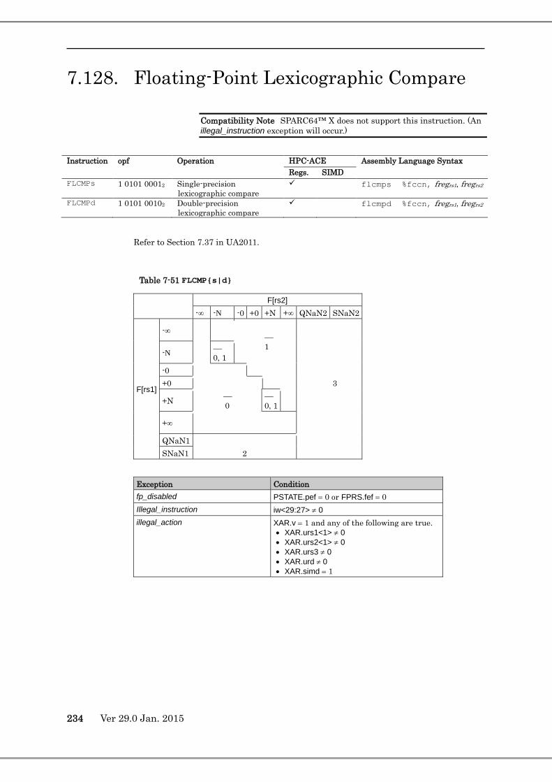
234 Ver 29.0 Jan. 2015
7.128. Floating-Point Lexicographic Compare
Compatibility Note SPARC64™ X does not support this instruction. (An illegal_instruction exception will occur.)
Instruction opf Operation HPC-ACE Assembly Language Syntax
Regs. SIMD FLCMPs 1 0101 00012 Single-precision
lexicographic compare flcmps %fccn, fregrs1, fregrs2
FLCMPd 1 0101 00102 Double-precision lexicographic compare
flcmpd %fccn, fregrs1, fregrs2
Refer to Section 7.37 in UA2011.
Table 7-51 FLCMP{s|d}
F[rs2]
-∞ -N -0 +0 +N +∞ QNaN2 SNaN2
F[rs1]
-∞
1
3
-N 0, 1
-0 +0
+N 0
0, 1
+∞
QNaN1 SNaN1 2
Exception Condition fp_disabled PSTATE.pef = 0 or FPRS.fef = 0 Illegal_instruction iw<29:27> ≠ 0 illegal_action XAR.v = 1 and any of the following are true.
• XAR.urs1<1> ≠ 0 • XAR.urs2<1> ≠ 0 • XAR.urs3 ≠ 0 • XAR.urd ≠ 0 • XAR.simd = 1
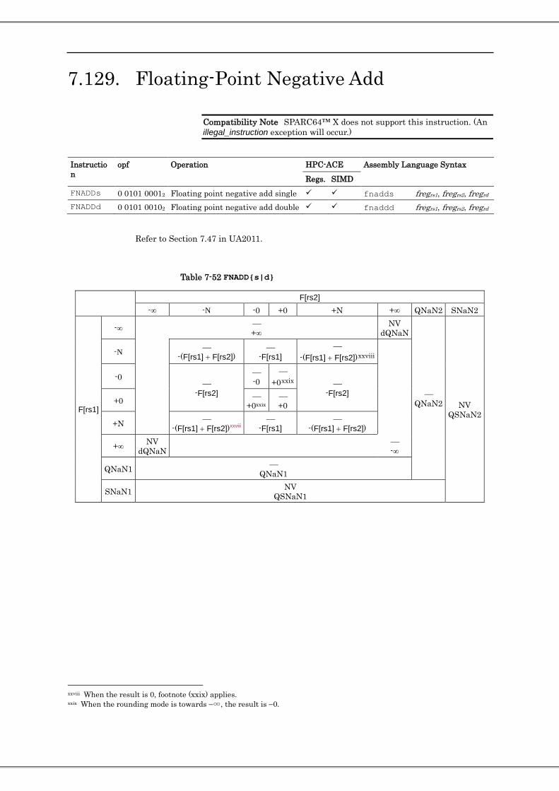
7.129. Floating-Point Negative Add
Compatibility Note SPARC64™ X does not support this instruction. (An illegal_instruction exception will occur.)
Instruction
opf Operation HPC-ACE Assembly Language Syntax Regs. SIMD
FNADDs 0 0101 00012 Floating point negative add single fnadds fregrs1, fregrs2, fregrd
FNADDd 0 0101 00102 Floating point negative add double fnaddd fregrs1, fregrs2, fregrd
Refer to Section 7.47 in UA2011.
Table 7-52 FNADD{s|d}
F[rs2]
-∞ -N -0 +0 +N +∞ QNaN2 SNaN2
F[rs1]
-∞ +∞
NV dQNaN
QNaN2 NV
QSNaN2
-N
-(F[rs1] + F[rs2])
-F[rs1]
-(F[rs1] + F[rs2])xxviii
-0
-F[rs2]
-0
+0xxix
-F[rs2] +0
+0xxix +0
+N -(F[rs1] + F[rs2])xxviii
-F[rs1]
-(F[rs1] + F[rs2])
+∞ NV dQNaN
-∞
QNaN1 QNaN1
SNaN1 NV QSNaN1
xxviii When the result is 0, footnote (xxix) applies. xxix When the rounding mode is towards −∞, the result is −0.

236 Ver 29.0 Jan. 2015
Exception Condition fp_disabled PSTATE.pef = 0 or FPRS.fef = 0 illegal_action XAR.v = 1 and any of the following are true.
• XAR.urs1<1> ≠ 0 • XAR.urs2<1> ≠ 0 • XAR.urs3 ≠ 0 • XAR.urd<1> ≠ 0 • XAR.simd = 1 and XAR.urs1<2> ≠ 0 • XAR.simd = 1 and XAR.urs2<2> ≠ 0 • XAR.simd = 1 and XAR.urd<2> ≠ 0
fp_exception_ieee_754 Same as FADD{s|d} fp_exception_other Same as FADD{s|d}

7.130. Floating-Point Negative Multiply
Compatibility Note SPARC64™ X does not support this instruction. (An illegal_instruction exception will occur.)
Instruction opf Operation HPC-ACE Assembly Language Syntax
Regs.
SIMD
FNMULs 0 0101 10012 Floating-point negative multiply single fnmuls fregrs1, fregrs2, fregrd
FNMULd 0 0101 1010 Floating-point negative multiply double fnmuld fregrs1, fregrs2, fregrd
FNsMULd 0 0111 1001 Floating-point negative multiply single to double
fnsmuld fregrs1, fregrs2, fregrd
Refer to Section 7.50 in UA2011.
Table 7-53 FNMUL{s|d}, FNsMULd
F[rs2]
-∞ -N -0 +0 +N +∞ QNaN2 SNaN2
F[rs1]
-∞ -∞ NV
dNaN +∞
QNaN2 NV
QSNaN2
-N -(F[rs1] × F[rs2])
-(F[rs1] × F[rs2])
-0 NV
dQNaN
-0
+0
NV dQNaN
+0 +0
-0
+N -(F[rs1] × F[rs2])
-(F[rs1] × F[rs2])
+∞ +∞ NV
dNaN -∞
QNaN1 QNaN1
SNaN1 NV QSNaN1

238 Ver 29.0 Jan. 2015
Exception Condition fp_disabled PSTATE.pef = 0 or FPRS.fef = 0 illegal_action XAR.v = 1 and any of the following are true
• XAR.urs1<1> ≠ 0 • XAR.urs2<1> ≠ 0 • XAR.urs3 ≠ 0 • XAR.urd<1> ≠ 0 • XAR.simd = 1 and XAR.urs1<2> ≠ 0 • XAR.simd = 1 and XAR.urs2<2> ≠ 0 • XAR.simd = 1 and XAR.urd<2> ≠ 0
fp_exception_ieee_754 Same as FMUL{s|d}, FsMULd fp_exception_other Same as FMUL{s|d}, FsMULd

7.131. WRPAUSE(PAUSE)
Note SPARC64™ X does not support this instruction. (An illegal_instruction exception will occur.)
Instruction op3 Operation HPC-ACE Assembly Language Syntax
Regs. SIMD WRPAUSE 11 00002 Pause VCPU for specified
number of cycles. wr regrs1, reg_or_imm, %pause
PAUSE 11 00002 Pause VCPU for specified number of cycles.
pause reg_or_imm
102 rd = 1 10112 op3 = 11 00002 rs1 i = 0 rs2
102 rd = 1 10112 op3 = 11 00002 rs1 i = 1 simm13 31 30 29 25 24 19 18 14 13 12 5 4 0
Description WRPAUSE and PAUSE stop the VCPU for the specified number of processor cycles.
The WRPAUSE and PAUSE instructions write the number of cycles in the PAUSE register (ASR27). The PAUSE register has the following fields.
— Pause —
63 15 14 3 2 0
Bit Field Access Description 63:15 Reserved WO Reserved 14:3 Pause WO Specifies the number of cycles the VCPU is
paused. Can be accessed in nonpriviledged mode. 2:0 Reserved WO Ignored
When i = 0, WRPAUSE writes (min(2^15 − 1, (R[rs1] xor R[rs2])) >> 3) into the pause field (PAUSE<14:3>) of the PAUSE register. When i = 1, WRPAUSE writes (min(2^15 − 1, (R[rs1] xor sign_ext(simm13))) >> 3) into the pause field.
When i = 0, PAUSE writes (min(2^15 − 1, R[rs2]) >> 3) into the pause field (PAUSE<14:3>) of the PAUSE register. When i = 1, PAUSE writes (min(2^15-1, sign_ext(simm13)) >> 3) into the pause field.
Programming Note The behavior of PAUSE is the same as WRPAUSE with rs1 = 0.
The number of cycles the VCPU will be paused is the lower 15 bits (PAUSE<14:0>) of the PAUSE register. However, bits PAUSE<2:0> are ignored. The pause field (PAUSE<14:3>) is decremented by 1 every 8 CPU clock cycles. Therefore, the maximum number of cycles which the VCPU can be paused is 32760 (and 32760 is written to PAUSE<14:0> if the specified value exceeds this number).
The paused VCPU will restart operation when either of the following conditions is true. • Value of the pause field (PAUSE<14:3>) in the PAUSE register is 0. • A disrupting exception causes a trap.

240 Ver 29.0 Jan. 2015
Note The VCPU stays paused if the exception is masked and no trap is generated.
When the VCPU restarts operation, the instruction specified by the NPC of the WRPAUSE or PAUSE instruction is executed. If a trap occurs while the VCPU is paused, the WRPAUSE or PAUSE instruction is not treated as the instruction that was disrupted by the trap.
Exception Condition Illegal_instruction i = 0 and iw<12:5> ≠ 0 illegal_action XAR.v = 1
7.132. Load Entire Floating-Point State Register
Compatibility Note SPARC64™ X does not support this instruction. (An illegal_instruction exception will occur.)
Instruction op3 rd Operation HPC-ACE Assembly Language Syntax
Regs SIMD LDXEFSR 10 00012 3 Read from memory to FSR ldx [address], %efsr
Refer to Section 7.84 in UA2011.
If an LDXEFSR exception generates a precise trap, FSR is not updated.
Exception Condition Illegal_instruction i = 0 and reserved ≠ 0 fp_disabled PSTATE.pef = 0 or FPRS.fef = 0 illegal_action XAR.v = 1 and any of the following are
true • XAR.urs1 ≠ 0 • XAR.urs2 ≠ 0 • XAR.urs3<2> ≠ 0 • XAR.urd ≠ 0 • XAR.simd = 1
mem_access_not_aligned Address not alilgned on 8 -byte boundary
VA_watchpoint Refer to 12.5.1.62 DAE_privilege_violation Refer to 12.5.1.8 DAE_nfo_page Refer to 12.5.1.7

242 Ver 29.0 Jan. 2015
7.133. Compare and Branch (CBcond)
Compatibility Note SPARC64™ X does not support this instruction. (An illegal_instruction exception will occur.)
Refer to Section 7.17 in UA2011.
Note The Trap on Control Transfer feature is implemented on SPARC64™ X+.
Exception Condition Illegal_instruction c_lo = 0002 illegal_action XAR.v = 1 control_transfer_instruction PSTATE.tct = 1 and CBcond causes a transfer
of control

7.134. Partitioned Move Selected Floating-Point Register on Floating-Point Register’s Condition
Instruction opf Operation HPC-ACE Assembly Language Syntax Regs. SIMD
FPSELMOV8X 0 1001 01012 Select eight 8-bit data from registers
fpselmov8x fregrs1, fregrs2, fregrd
FPSELMOV16X 0 1001 01102 Select four 16-bit data from registers
fpselmov16x fregrs1, fregrs2, fregrd
FPSELMOV32X 0 1001 01112 Select two 32-bit data from registers
fpselmov32x fregrs1, fregrs2, fregrd
102 rd op3 = 11 01102 rs1 opf rs2
31 30 29 25 24 19 18 14 13 5 4 0
Description The n most significant bits of Fd[rs1] select bit ranges from either Fd[rs2] or Fd[rd]. Selected bit ranges are written in Fd[rd]. If the (63 − n)th bit of Fd[rs1] is 1, the corresponding bit range in Fd[rs2] is selected and written to the same bit range in Fd[rd]. If the bit in Fd[rs1] is 0, the corresponding bit range in Fd[rd] is selected
The bit ranges of .Fd[rs2] and Fd[rd] that are selected by Fd[rs1] are shown below.
Note Bits Fd[rs1]<55:0> for FPSELMOV8X, Fd[rs1]<59:0> for FPSELMOV16X, and Fd[rs1]<61:0> for FPSELMOV32X are ignored and have no effect.
F[rs1]
bit 63
F[rs1]
bit 62
F[rs1]
bit 61
F[rs1]
bit 60
F[rs1]
bit 59
F[rs1]
bit 58
F[rs1]
bit 57
F[rs1]
bit 56
Corresponding bit ranges for FPSELMOV8X
<63:56> <55:48> <47:40> <39:32> <31:24> <23:16> <15:8> <7:0>
Corresponding bit ranges for FPSELMOV16X
<63:48> <47:32> <31:16> <15:0>
Corresponding bit ranges for FPSELMOV32X
<63:32> <31:0>

244 Ver 29.0 Jan. 2015
Example of FPSELMOV8X
Example of FPSELMOV16X
Example of FPSELMOV32X
Note The 64-bit FPSELMOV instruction is not defined because its behavior would be the same as FSELMOVd (page 112). However,FSELMOVd updates fields in FSR.
FPSELMOV{8|16|32}X do not update any fields in FSR.
63 62
63
63
31
3
F[rs1]
F[rs2]
F[rd
1 0
63 62
63
63
4
31 15
47 3
1
F[rs1]
F[rs2]
F[rd
1 0 0 1 61 60
63 62 56
63
63
55 4
31 23 15 7 39
55 47 3
23 1
7 39
F[rs1]
F[rs2]
F[rd
1 0 1

Exception Condition fp_disabled PSTATE.pef = 0 or FPRS.fef = 0 illegal_action XAR.v = 1 and any of the following are true
• XAR.urs1<1> ≠ 0 • XAR.urs2<1> ≠ 0 • XAR.urs3 ≠ 0 • XAR.urd<1> ≠ 0 • XAR.simd = 1 and XAR.urs1<2> ≠ 0 • XAR.simd = 1 and XAR.urs2<2> ≠ 0 • XAR.simd = 1 and XAR.urd<2> ≠ 0

246 Ver 29.0 Jan. 2015
7.135. 64-bit Integer Compare on Floaing-Point Register
Compatibility Note SPARC64™ X does not support this instruction. (An illegal_instruction exception will occur).
Instruction opf Operation HPC-ACE Assembly Language Syntax
Regs. SIMD FPCMP64X 1 0000 01002 Compare signed 64-bit
integers fpcmp64x %fccn, fregrs1, fregrs2
FPCMPU64X 1 0000 01012 Compare unsigned 64-bit integers
fpcmpu64x %fccn, fregrs1, fregrs2
102 cc1 cc0 op3 = 11 01102 rs1 opf rs2
31 30 29 27 26 25 24 19 18 14 13 5 4 0
cc1 cc0 Condition code 0 0 fcc0
0 1 fcc1 1 0 fcc2
1 1 fcc3
Description Compare the 64-bit integer values in the floating-point registers Fd[rs1] and Fd[rs2] and stores the result in the floating-point condition code field FSR.fccn specified by the instruction.
Comparison result Value of %fccn F[rs1] = F[rs2] 0 F[rs1] < F[rs2] 1 F[rs1] > F[rs2] 2 3 N/A
Programming Note FPCMP{64|U64}X is not an FPop. FSR.cexc and FSR.aexc are not updated, and fp_exception_other exceptions do not occur.
Exception Condition fp_disabled PSTATE.pef = 0 or FPRS.fef = 0 Illegal_instruction iw<29:27> ≠ 0 illegal_action XAR.v = 1 and any of the following are true
• XAR.urs1<1> ≠ 0 • XAR.urs2<1> ≠ 0 • XAR.urs3 ≠ 0 • XAR.urd ≠ 0 • XAR.simd = 1

7.136. 64-bit Integer Shift on Floating-Point Register
Compatibility Note SPARC64™ X does not support this instruction. (An illegal_instruction exception will occur).
Instruction opf Operation HPC-ACE Assembly Language Syntax
Regs. SIMD FPSLL64X 1 0000 01102 Shift left logical 64-bit integer fpsll64x fregrs1,
fregrs2, fregrd FPSRL64X 1 0000 01112 Shift right logical 64-bit integer fpsrl64x fregrs1,
fregrs2, fregrd FPSRA64X 1 0000 11112 Shift right arithmetic 64-bit
integer fpsra64x fregrs1,
fregrs2, fregrd
102 rd op3 = 11 01102 rs1 opf rs2
31 30 29 25 24 19 18 14 13 5 4 0
Description These instructions shift the data in Fd[rs1] right or left and store the result in Fd[rd]. The shift count is specified by the lowest 6 bits of Fd[rs2].
FPSLL64X shifts all 64 bits of Fd[rs1] left, replacing the vacated positions on the right with 0, and stores the result in Fd[rd].
FPSRL64X shifts all 64 bits of Fd[rs1] right, replacing the vacated positions on the left with 0, and stores the result in Fd[rd].
FPSRA64X shifts all 64 bits of Fd[rs1] right, replacing the vacated positions on the left with the MSB of Fd[rs1], and stores the result in Fd[rd].
FP{SLL|SRL|SRA}64X do not update any fields in FSR.
Exception Condition fp_disabled PSTATE.pef = 0 or FPRS.fef = 0 illegal_action XAR.v = 1 and any of the following are true
• XAR.urs1<1> ≠ 0 • XAR.urs2<1> ≠ 0 • XAR.urs3 ≠ 0 • XAR.urd<1> ≠ 0 • XAR.simd = 1 and XAR.urs1<2> ≠ 0 • XAR.simd = 1 and XAR.urs2<2> ≠ 0 • XAR.simd = 1 and XAR.urd<2> ≠ 0

248 Ver 29.0 Jan. 2015
7.137. Store Floating-Point Register on Register Condition (Extension of SPARC64™ X+)
Compatibility Note For the specification of this instruction on SPARC64™ X, refer to page 174.
Instruction op3 rs2, rd Operation HPC-ACE Assembly Language Syntax
Regs SIMD STFR 10 11002 0 − 31 Store single-precision
floating-point register on register condition (XAR.v = 0)
stfr fregrd, fregrs2, [regrs1]
STFR 10 11002 0 − 126, 256 − 382xxx
Store single-precision floating-point register on register condition (XAR.v = 1)
stfr fregrd, fregrs2, [regrs1]
STDFR 10 11112 0 − 126, 256 − 382xxx
Store double-precision floating-point register on register condition
stdfr fregrd, fregrs2, [regrs1]
112 rd op3 rs1 i = 1 rs2
31 30 29 25 24 19 18 14 13 12 5 4 0
non-SIMD execution
When XAR.v = 0 and the MSB (bit 31) of Fs[rs2] is 1, STFR writes the 4 bytes of the single-precision register Fs[rd] to the specified address, which should be aligned on a 4-byte boundary. When XAR.v = 1, XAR.simd = 0, and the MSB (bit 63) of F[rs2] is 1, STFR writes the upper 4 bytes of the double-precision register Fd[rd] to the specified address, which should be aligned on a 4-byte boundary.
When the MSB (bit 63) of Fd[rs2] is 1, STDFR writes the 8 bytes of the double-precision register Fd[rd] to the specified address, which should be aligned on an 4-byte boundary.
These floating-point store instructions use implicit ASIs (refer to Section 6.3.1.3 in UA2011) to access memory. The effective address is “R[rs1]”.
STFR and STDFR cause a mem_address_not_aligned exception when the address is not aligned on a word boundary.
When executing a non-SIMD STDFR, the address needs to be aligned on a word boundary. However, if the address is aligned on a word boundary but is not aligned on a doubleword boundary, a STDF_mem_address_not_aligned exception will occur. The trap handler must emulate the STDFR instruction when this exception occurs.
STFR does not cause any exceptions except illegal_instruction, fp_disabled, and illegal_action when XAR.v = 1, XAR.simd = 0, and the MSB (bit 63) of Fd[rs2] is 0; or when XAR.v = 0 and the MSB (bit 31) of Fs[rs2] is 0. STDFR does not cause any exceptions except illegal_instruction, fp_disabled, and illegal_action when the MSB (bit 63) of Fd[rs2] is 0.
xxx 5.3.1 Encoding which is defined in “Floating-Point Register Number Encoding”(page 26)

Exceptions that re always detected
Exceptions that are detected only when MSB of Fs[rs2] or MSB of Fd[rs2] is 1
Illegal_instruction fp_disabled illegal_action
mem_address_not_aligned STDF_mem_address_not_aligned VA_watchpoint DAE_privilege_violation DAE_nfo_page
SIMD execution STFR and STDFR support SIMD execution on SPARC64 X+. SIMD STFR and SIMD STDFR simultaneously execute basic and extended stores for single-precision and double-precision data, respectively. Refer to Section 5.5.15 (page 35) for details on how to specify the registers.
A SIMD STFR writes the upper 4 bytes of Fd[rd] to the lower 4 bytes of the address when XAR.v = 1, XAR.simd = 1, and the MSB (bit 63) of Fd[rs2] is 1, and writes the upper 4 bytes of Fd[rd + 256] to the upper 4 bytes of the address when XAR.v = 1, XAR.simd = 1, and the MSB (bit 63) of Fd[rs2+256] is 1. The address must be aligned on an 8-byte boundary. Misaligned accesses cause a mem_address_not_aligned exception.
SIMD STDFR writes Fd[rd] to the lower 8 bytes of the address when XAR.v = 1, XAR.simd = 1, and the MSB (bit 63) of Fd[rs2] is 1, and writes Fd[rd + 256] to the upper 8 bytes of the address when XAR.v = 1, XAR.simd = 1, and the MSB (bit 63) of Fd[rs2+256] is 1. The address must be aligned on a 16-byte boundary. Misaligned accesses cause a mem_address_not_aligned exception.
These floating-point store instructions use implicit ASIs (refer to Section 6.3.1.3 in UA2011) to access memory.
Note A SIMD STDFR does not cause a STDF_mem_address_not_aligned exception when the address is aligned on a word boundary but is not aligned on a doubleword boundary.
SIMD STFR and SIMD STDFR can only be used to access cacheable address spaces. An attempt to access a non-cacheable address space causes a DAE_nc_page exception.
Like non-SIMD store instructions, memory access semantics adhere to TSO. SIMD STFR and SIMD STDFR simultaneously execute basic and extended stores; however, the ordering between the basic and extended stores conforms to TSO.
SIMD STFR and SIMD STDFR always detect an illegal_instruction, fp_disabled, or illegal_action exception.
SIMD STFR and SIMD STDFR always detect mem_address_not_aligned or VA_watchpoint exceptions for both the basic and extended operations when the exception condition is detected and either of the following conditions is true.
1. Either MSB (bit 63) of basic register Fd[rs2] or extended register Fd[rs2+256] is 1.
2. Both MSBs (bit63) of Fd[rs2] and Fd[rs2+256] are 1.
SIMD STFR and SIMD STDFR detect an exception only for the corresponding basic or extended operation when the exception condition is detected (excluding illegal_instruction, fp_disabled, illegal_action, mem_address_not_aligned, VA_watchpoint) and the MSB (bit63) of basic register Fd[rs2] or the MSB (bit 63) of extended register Fd[rs2+256] is 1. The exception is detected for both operations only if both the MSBs of Fd[rs2] and Fd[rs2+256] are 1.

250 Ver 29.0 Jan. 2015
Exceptions that are always detected
Exceptions that are detected for both operatopns when either MSB in Fd[rs2] or Fd[rs2+256] is 1
Exceptions that are detected for the corresponding operation(s) when the MSB in Fd[rs2] or Fd[rs2+256] is 1
Illegal_instruction fp_disabled illegal_action
mem_address_not_aligned VA_watchpoint
DAE_privilege_violation DAE_nc_page DAE_nfo_page
Exceptions that are detected for both operations when either MSB in Fd[rs2] or Fd[rs2+256] is 1
Detected address
mem_address_not_aligned Address of basic operation (always)
VA_watchpoint The detected address. When detected for both operations, address of the basic operation
Exceptions that are detected for the corresponding operation(s) when the MSB in Fd[rs2] or Fd[rs2+256] is 1
Detected address
DAE_privilege_violation Address of basic operation (always)
DAE_nc_page Address of basic operation (always)
DAE_nfo_page Address of basic operation (always)

Exception Target instruction Condition illegal_instruction all i = 0 or the reserved field is not 0 fp_disabled all PSTATE.pef = 0 or FPRS.fef = 0 illegal_action all XAR.v = 1 and any of the following are
true • XAR.urs1 ≠ 0 • XAR.urs2<1> ≠ 0 • XAR.urs3<2> ≠ 0 • XAR.urd<1> ≠ 0 • XAR.simd = 1 and XAR.urs2<2> ≠ 0 • XAR.simd = 1 and XAR.urd<2> ≠ 0
STDF_mem_address_not_aligned STDFR MSB of Fd[rs2] is 1 and address aligned on a word boundary but not a doubleword boundary when XAR.v = 1 and XAR.simd = 0, or XAR.v = 0
mem_address_not_aligned STFR Either of the following conditions is true • Address not aligned on word
boundary when XAR.v = 0 and MSB of Fs[rs2] is 1
• Address not aligned on word boundary when XAR.v = 1, XAR.simd = 0, and MSB of Fd[rs2] is 1
• Address not aligned on a doubleword boundary when MSB of Fd[rs2] or Fd[rs2+256] is 1, XAR.v = 1 and XAR.simd = 1
STDFR Either of the following conditions is true • Address not aligned on a word
boundary when MSB of Fd[rs2] is 1 and XAR.v = 1 and XAR.simd = 0, or XAR.v = 0
• Address not aligned on a quadword boundary when MSB of Fd[rs2] or Fd[rs2+256] is 1 and XAR.v = 1 and XAR.simd = 1
VA_watchpoint all Refer to the description and 12.5.1.62 DAE_privilege_violation all Refer to the description and 12.5.1.8 DAE_nc_page all Access to non-cacheable space when
XAR.v = 1, XAR.simd = 1, and MSB of Fd[rs2] or Fd[rs2+256] is 1
DAE_nfo_page all Refer to the description and 12.5.1.7
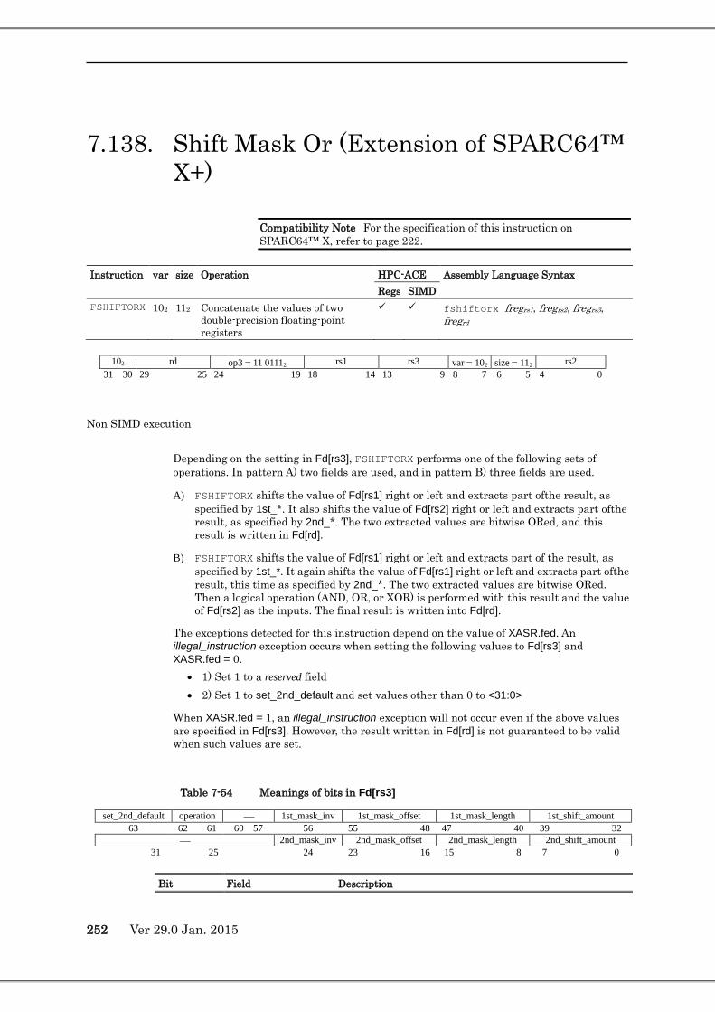
252 Ver 29.0 Jan. 2015
7.138. Shift Mask Or (Extension of SPARC64™ X+)
Compatibility Note For the specification of this instruction on SPARC64™ X, refer to page 222.
Instruction var size Operation HPC-ACE Assembly Language Syntax
Regs SIMD FSHIFTORX 102 112 Concatenate the values of two
double-precision floating-point registers
fshiftorx fregrs1, fregrs2, fregrs3, fregrd
102 rd op3 = 11 01112 rs1 rs3 var = 102 size = 112 rs2
31 30 29 25 24 19 18 14 13 9 8 7 6 5 4 0
Non SIMD execution
Depending on the setting in Fd[rs3], FSHIFTORX performs one of the following sets of operations. In pattern A) two fields are used, and in pattern B) three fields are used.
A) FSHIFTORX shifts the value of Fd[rs1] right or left and extracts part ofthe result, as specified by 1st_*. It also shifts the value of Fd[rs2] right or left and extracts part ofthe result, as specified by 2nd_*. The two extracted values are bitwise ORed, and this result is written in Fd[rd].
B) FSHIFTORX shifts the value of Fd[rs1] right or left and extracts part of the result, as specified by 1st_*. It again shifts the value of Fd[rs1] right or left and extracts part ofthe result, this time as specified by 2nd_*. The two extracted values are bitwise ORed. Then a logical operation (AND, OR, or XOR) is performed with this result and the value of Fd[rs2] as the inputs. The final result is written into Fd[rd].
The exceptions detected for this instruction depend on the value of XASR.fed. An illegal_instruction exception occurs when setting the following values to Fd[rs3] and XASR.fed = 0.
• 1) Set 1 to a reserved field • 2) Set 1 to set_2nd_default and set values other than 0 to <31:0>
When XASR.fed = 1, an illegal_instruction exception will not occur even if the above values are specified in Fd[rs3]. However, the result written in Fd[rd] is not guaranteed to be valid when such values are set.
Table 7-54 Meanings of bits in Fd[rs3]
set_2nd_default operation 1st_mask_inv 1st_mask_offset 1st_mask_length 1st_shift_amount 63 62 61 60 57 56 55 48 47 40 39 32
2nd_mask_inv 2nd_mask_offset 2nd_mask_length 2nd_shift_amount 31 25 24 23 16 15 8 7 0
Bit Field Description

rs1 rs2 63 set_2nd_default Specifies set of {1st|2nd}_* fields to use for the 2nd field
0: Use the rs2_* fields for the 2nd field 1: Use values derived from 1st_* fields
62:61 operation Specifies type of operation. Refer to Table 7-55 56 24 {1st|2nd}_mask_inv Specifies whether to invert the mask
0: Do not invert 1: Invert
55:48 23:16 {1st|2nd}_mask_offset Starting position in mask (number of bits from MSB) 8-bit signed integer
47:40 15:8 {1st|2nd}_mask_length Mask bit length,8-bit signed integer 39:32 7:0 {1st|2nd}_shift_amount Shift count (positive: left shift, negative: right shift), 8-bit
signed integer
Table 7-55 Operation Patterns
operation 1st
2nd field 3rd field
Logical operation of 3rd field and value generated from 1st and 2nd fields
002 rs1 rs2 012 rs1 rs1 rs2 AND 102 rs1 rs1 rs2 OR 112 rs1 rs1 rs2 XOR
Note FSHIFTORX detects an illegal_instruction exception for certains values in the register Fd[rs3]. An fp_disabled exception or illegal_action exception may be detected before the register is read. That is, for this instruction, these exceptions may have higher priority than an illegal_instruction exception.
The operation fields select one of two patterns for FSHIFTORX, which are divided into the operations shown below.
A: 1) Shift, 2) Mask, 3) OR
B: 1) Shift, 2) Mask, 3) OR, 4) Logical operation

254 Ver 29.0 Jan. 2015
The shift operation executes a logical shift. If shifting left, the vacated positions on the right are replaced by 0. If shifting right, the vacated positions on the left are replaced by 0. The {1st|2nd}_shift_amount field specifies the shift direction and shift count. The shift is leftwards if the value is positive and rightwards if the value is negative.
The mask operation extracts the specified bits from the shifted register. Two mask patterns are defined by {1st|2nd}_mask_offset, {1st|2nd}_mask_length, and {1st|2nd}_mask_inv. A mask pattern is generated from one set of these fields and bitwise ANDed with the corresponding shifted register.
A mask pattern is a generated range of contiguous 1s in a 64-bit doubleword, where no bits are 1 outside this range. The inverse of this pattern can also be specified. The {1st|2nd}_mask_offset field specifies the starting position of the mask (the range of 1s) as the number of bits from the left (MSB) . The {1st|2nd}_mask_length field specifies the length of the range of bits that are set to 1. To invert this mask, specify 1 for {1st|2nd}_mask_inv.
Note The mask pattern contains bits that are 1 when 0 ≤ {1st|2nd}_mask_offset < 64 and 0 < {1st|2nd}_mask_length. That is, the pattern fits inside a doubleword. The specified pattern can exceed the length of a doubleword if 64 ≤ “{1st|2nd}_mask_offset + {1st|2nd}_mask_length”. In this case, the mask pattern is a contiguous range of 1s from {1st|2nd}_mask_offset to the LSB.
Note The mask pattern may contain bits that are 1 even if the value of {1st|2nd}_mask_offset is negative. Specifically, when |{1st|2nd}_mask_offset |< {1st|2nd}_mask_length, the mask pattern is a contiguous range of 1s from the MSB to “{1st|2nd}_mask_length − |{1st|2nd}_mask_offset|”.
1) Shift
2) Mask
3) bitwise OR
Fd[rs1]
0 0
0 0
0…0 1…1 0 1…1 0…0
AND AND
0
Fd[rs1] or Fd[rs2]
0
Fd[rd]
4) AND, OR, XOR (example.: OR) ※Step 4 is only executed for pattern B)
Fd[rs2]
OR

Note The 64-bit mask pattern is all 0s when {1st|2nd}_mask_offset and {1st|2nd}_mask_length satisfy any of the conditions below. The mask pattern is all 1s under the same conditions when {1st|2nd}_mask_inv is used to invert the mask pattern. - {1st|2nd}_mask_length ≤ 0 - {1st|2nd}_mask_offset + rs{1|2}_mask_length ≤ 0 - {1st|2nd}_mask_offset ≥ 64
In pattern A), the bitwise OR operation is executed on the values obtained from Fd[rs1] and Fd[rs2] using the shift and mask operations . The result is written in Fd[rd]. In pattern B), the bitwise OR operation is executed on the two different values generated from Fd[rs1] using the shift and mask operations. A logical operation (in the example, an OR) is performed with this result and Fd[rs2] as the inputs. The final result is written in Fd[rd].
Table 7-56 shows an example of how to specify the bits in Fd[rs3]. In this example,
1. The lower 32 bits of Fd[rs1] (Fd[rs1]<31:0>) and the upper 24 bits of Fd[rs1] (Fd[rs1]<63:40>) are concatenated in the given order (Fd[rs1]<31:0>::Fd[rs2]<63:40>).
2. A bitwise OR of the concatenated value and Fd[rs2] is executed.
3. The final result is written in Fd[rd].
Table 7-56 Example of how to specify bits in Fd[rs3]
Field Concatenate lower 32 bits of Fd[rs1] and upper 24 bits of Fd[rs1] (Fd[rs1]<31:0>::Fd[rs1]<63:40>), then OR the result and Fd[rs2]
set_2nd_default 0 (2nd_* field are used) operation 01(OR of 3rd field and value generated from 1st and 2nd fields) 1st_mask_inv 0 (Do not invert 1st mask) 1st_mask_offset 32 (Mask shifted 1st field starting from bit<31>) 1st_mask_length 24 (Mask length is 24 bits) 1st_shift_amount -32 (Shift right 32 bits) 2nd_mask_inv 0 (Do not invert the 2nd mask) 2nd_mask_offset 0 (Mask shifted 2nd field starting from MSB) 2nd_mask_length 32 (Mask length is 32 bits) 2nd_shift_amount 32 (Shift left 32 bits)
SIMD execution When FSHIFTORX is executed as a SIMD instruction, any floating-point register Fd[0] − Fd[126], Fd[256] − Fd[382] can be specified for Fd[rs1]. If an extended register Fd[256] − Fd[382] is specified for Fd[rs1], the extended register Fd[n] is used for the basic operation and the basic register Fd[n − 256] is used for the extended operation. On the other hand, only basic registers Fd[0] − Fd[126] can be specified for Fd[rs2], Fd[rs3], and Fd[rd]. The basic operation uses the basic register Fd[n], and the extended operation uses the extended register Fd[n+256].
FSHIFTORX does not update any fields in FSR.

256 Ver 29.0 Jan. 2015
Exception Taget instruction
Condition
fp_disabled All PSTATE.pef = 0 or FPRS.fef = 0 illegal_action All XAR.v = 1 and any of the following are true
• XAR.urs1<1> ≠ 0 • XAR.urs2<1> ≠ 0 • XAR.urs3<1> ≠ 0 • XAR.urd<1> ≠ 0 • XAR.simd = 1 and XAR.urs2<2> ≠ 0 • XAR.simd = 1 and XAR.urs3<2> ≠ 0 • XAR.simd = 1 and XAR.urd<2> ≠ 0
illegal_instruction All Refer to the description.
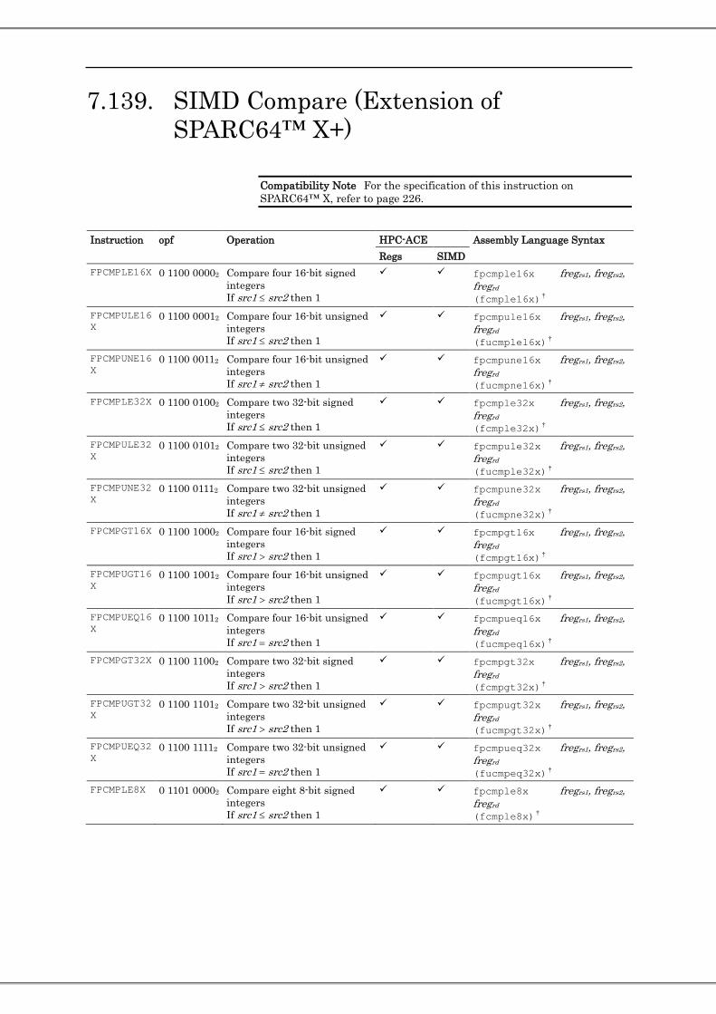
7.139. SIMD Compare (Extension of SPARC64™ X+)
Compatibility Note For the specification of this instruction on SPARC64™ X, refer to page 226.
Instruction opf Operation HPC-ACE Assembly Language Syntax
Regs SIMD FPCMPLE16X 0 1100 00002 Compare four 16-bit signed
integers If src1 ≤ src2 then 1
fpcmple16x fregrs1, fregrs2, fregrd (fcmple16x)†
FPCMPULE16X
0 1100 00012 Compare four 16-bit unsigned integers If src1 ≤ src2 then 1
fpcmpule16x fregrs1, fregrs2, fregrd (fucmple16x)†
FPCMPUNE16X
0 1100 00112 Compare four 16-bit unsigned integers If src1 ≠ src2 then 1
fpcmpune16x fregrs1, fregrs2, fregrd (fucmpne16x)†
FPCMPLE32X 0 1100 01002 Compare two 32-bit signed integers If src1 ≤ src2 then 1
fpcmple32x fregrs1, fregrs2, fregrd (fcmple32x)†
FPCMPULE32X
0 1100 01012 Compare two 32-bit unsigned integers If src1 ≤ src2 then 1
fpcmpule32x fregrs1, fregrs2, fregrd (fucmple32x)†
FPCMPUNE32X
0 1100 01112 Compare two 32-bit unsigned integers If src1 ≠ src2 then 1
fpcmpune32x fregrs1, fregrs2, fregrd (fucmpne32x)†
FPCMPGT16X 0 1100 10002 Compare four 16-bit signed integers If src1 > src2 then 1
fpcmpgt16x fregrs1, fregrs2, fregrd (fcmpgt16x)†
FPCMPUGT16X
0 1100 10012 Compare four 16-bit unsigned integers If src1 > src2 then 1
fpcmpugt16x fregrs1, fregrs2, fregrd (fucmpgt16x)†
FPCMPUEQ16X
0 1100 10112 Compare four 16-bit unsigned integers If src1 = src2 then 1
fpcmpueq16x fregrs1, fregrs2, fregrd (fucmpeq16x)†
FPCMPGT32X 0 1100 11002 Compare two 32-bit signed integers If src1 > src2 then 1
fpcmpgt32x fregrs1, fregrs2, fregrd (fcmpgt32x)†
FPCMPUGT32X
0 1100 11012 Compare two 32-bit unsigned integers If src1 > src2 then 1
fpcmpugt32x fregrs1, fregrs2, fregrd (fucmpgt32x)†
FPCMPUEQ32X
0 1100 11112 Compare two 32-bit unsigned integers If src1 = src2 then 1
fpcmpueq32x fregrs1, fregrs2, fregrd (fucmpeq32x)†
FPCMPLE8X 0 1101 00002 Compare eight 8-bit signed integers If src1 ≤ src2 then 1
fpcmple8x fregrs1, fregrs2, fregrd (fcmple8x)†

258 Ver 29.0 Jan. 2015
Instruction opf Operation HPC-ACE Assembly Language Syntax Regs SIMD
FPCMPULE8X 0 1101 00012 Compare eight 8-bit unsigned integers If src1 ≤ src2 then 1
fpcmpule8x fregrs1, fregrs2, fregrd (fucmple8x)†
FPCMPUNE8X 0 1101 00112 Compare eight 8-bit unsigned integers If src1 ≠ src2 then 1
fpcmpune8x fregrs1, fregrs2, fregrd (fucmpne8x)†
FPCMPLE64X 0 1101 01002 Compare 64-bit signed integers If src1 ≤ src2 then 1
fpcmple64x fregrs1, fregrs2, fregrd (fcmplex)†
FPCMPULE64X
0 1101 01012 Compare 64-bit unsigned integers If src1 ≤ src2 then 1
fpcmpule64x fregrs1, fregrs2, fregrd (fucmplex)†
FPCMPUNE64X
0 1101 01112 Compare 64-bit unsigned integers If src1 ≠ src2 then 1
fpcmpune64x fregrs1, fregrs2, fregrd (fucmpnex)†
FPCMPGT8X 0 1101 10002 Compare eight 8-bit signed integers If src1 > src2 then 1
fpcmpgt8x fregrs1, fregrs2, fregrd (fcmpgt8x)†
FPCMPUGT8X 0 1101 10012 Compare eight 8-bit unsigned integers If src1 > src2 then 1
fpcmpugt8x fregrs1, fregrs2, fregrd (fucmpgt8x)†
FPCMPUEQ8X 0 1101 10112 Compare eight 8-bit unsigned integers If src1 = src2 then 1
fpcmpueq8x fregrs1, fregrs2, fregrd (fucmpeq8x)†
FPCMPGT64X 0 1101 11002 Compare 64-bit signed integer If src1 > src2 then 1
fpcmpgt64x fregrs1, fregrs2, fregrd (fcmpgtx)†
FPCMPUGT64X
0 1101 11012 Compare 64-bit unsigned integer If src1 > src2 then 1
fpcmpugt64x fregrs1, fregrs2, fregrd (fucmpgtx)†
FPCMPUEQ64X
0 1101 11112 Compare 64-bit unsigned integer If src1 = src2 then 1
fpcmpueq64x fregrs1, fregrs2, fregrd (fucmpeqx)†
†the older mnemonic for this instruction (still recognized by the assembler)
102 rd op3 = 11 01102 rs1 opf rs2 31 30 29 25 24 19 18 14 13 5 4 0
Description These instructions compare the several elements (partitions) in the two floating-point registers Fd[rs1] and Fd[rs2]. The result is written in the floating-point register Fd[rd]. The comparison results for these elements are written in the most-significant bits of Fd[rd]. 0s are written in the other bits.
The number of elements in a 64-bit input register depends on the data type of the comparison. The number of elements and their bit ranges for each data type are shown in Table 7-57.

Table 7-57 Number of elements and their bit ranges for each data type
Data type Number of elements
Element 1
Element 2
Element 3
Element 4
Element 5
Element 6
Element 7
Element 8
8-bit signed integer
8 63:56 55:48 47:40 39:32 31:24 23:16 15:8 7:0
8-bit unsigned integer
8 63:56 55:48 47:40 39:32 31:24 23:16 15:8 7:0
16-bit signed integer
4 63:48 47:32 31:16 15:0
16-bit unsigned integer
4 63:48 47:32 31:16 15:0
32-bit signed integer
2 63:32 31:0
32-bit unsigned integer
2 63:32 31:0
64-bit signed integer
1 63:0
64-bit unsigned integer
1 63:0
Elements of Fd[rs1] and Fd[rs2] which occupy the same bit range are compared. The result is written in the corresponding bit of Fd[rd]. The bit positions of Fd[rd] corresponding to each element are shown in Table 7-58.
Table 7-58 Elements and corresponding bit positions in Fd[rd]
Element 1 Element 2 Element 3 Element 4 Element 5 Element 6 Element 7 Element 8 Fd[rd] 63 62 61 60 59 58 57 56
FPCMPLE{8X,16X,32X,64X} compare the elements of Fd[rs1] and Fd[rs2] as signed integers. If “elements of Fd[rs1]” ≤ “elements of Fd[rs2]”, the corresponding bits of Fd[rd] is set to 1.
FPCMPGT{8X,16X,32X,64X} compare the elements of Fd[rs1] and Fd[rs2] as signed integers. If “elements of Fd[rs1]” > “elements of Fd[rs2]”, the corresponding bits of Fd[rd] is set to 1.
FPCMPULE{8X,16X,32X,64X} compare the elements of Fd[rs1] and Fd[rs2] as unsigned integers. If “elements of Fd[rs1]” ≤ “elements of Fd[rs2]”, the corresponding bits of Fd[rd] is set to 1.
FPCMPUNE{8X,16X,32X,64X} compare the elements of Fd[rs1] and Fd[rs2] as unsigned integers. If “elements of Fd[rs1]” ≠ “elements of Fd[rs2]”, the corresponding bits of Fd[rd] is set to 1.
FPCMPUGT{8X,16X,32X,64X} compare the elements of Fd[rs1] and Fd[rs2] as unsigned integers. If “elements of Fd[rs1]” > “elements of Fd[rs2]”, the corresponding bits of Fd[rd] is set to 1.
FPCMPUEQ{8X,16X,32X,64X} compare the elements of Fd[rs1] and Fd[rs2] as unsigned integers. If “elements of Fd[rs1]” = “elements of Fd[rs2]”, the corresponding bits of Fd[rd] is set to 1.

260 Ver 29.0 Jan. 2015
Note Instructions that compare whether signed integers are equal or not equal are not defined. These comparisons are equivalent to the instructions FPCMPUEQ{8X,16X,32X,64X} and FPCMPUNE{8X,16X,32X,64X}, which respectively compare whether unsigned integers are equal or not equal.
Compatibility Note Differences from SPARC64™ X are the following: extended floating-point registers can be specified for non SIMD instructions, HPC-ACE SIMD execution is supported, and the instruction mnemonic is changed (FCMP*/FUCMP*→FPCMP*/FPCMPU*).
SIMD Compare does not update any fields in FSR.
Exception Taget instruction
Condition
fp_disabled All PSTATE.pef = 0 or FPRS.fef = 0 illegal_action All XAR.v = 1 and any of the following are true
• XAR.urs1<1> ≠ 0 • XAR.urs2<1> ≠ 0 • XAR.urs3 ≠ 0 • XAR.urd<1> ≠ 0 • XAR.simd = 1 and XAR.urs1<2> ≠ 0 • XAR.simd = 1 and XAR.urs2<2> ≠ 0 • XAR.simd = 1 and XAR.urd<2> ≠ 0
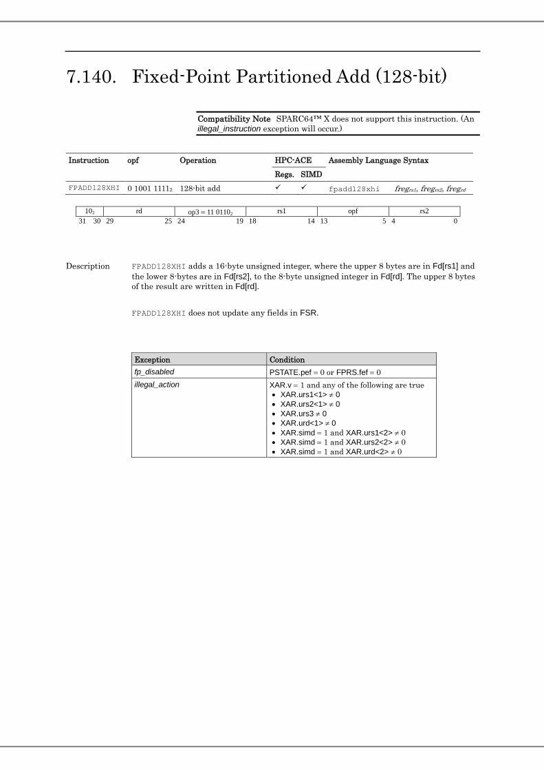
7.140. Fixed-Point Partitioned Add (128-bit)
Compatibility Note SPARC64™ X does not support this instruction. (An illegal_instruction exception will occur.)
Instruction opf Operation HPC-ACE Assembly Language Syntax
Regs. SIMD FPADD128XHI 0 1001 11112 128-bit add fpadd128xhi fregrs1, fregrs2, fregrd
102 rd op3 = 11 01102 rs1 opf rs2
31 30 29 25 24 19 18 14 13 5 4 0
Description FPADD128XHI adds a 16-byte unsigned integer, where the upper 8 bytes are in Fd[rs1] and the lower 8-bytes are in Fd[rs2], to the 8-byte unsigned integer in Fd[rd]. The upper 8 bytes of the result are written in Fd[rd].
FPADD128XHI does not update any fields in FSR.
Exception Condition fp_disabled PSTATE.pef = 0 or FPRS.fef = 0 illegal_action XAR.v = 1 and any of the following are true
• XAR.urs1<1> ≠ 0 • XAR.urs2<1> ≠ 0 • XAR.urs3 ≠ 0 • XAR.urd<1> ≠ 0 • XAR.simd = 1 and XAR.urs1<2> ≠ 0 • XAR.simd = 1 and XAR.urs2<2> ≠ 0 • XAR.simd = 1 and XAR.urd<2> ≠ 0

262 Ver 29.0 Jan. 2015
7.141. Integer Minimum and Maximum
Compatibility Note SPARC64™ X does not support this instruction. (Anillegal_instruction exception will occur.)
Instruction opf Operation HPC-ACE Assembly Language Syntax
Regs SIMD FPMAX64x 0 1110 11002 Max. of signed 64-bit integer fpmax64x fregrs1, fregrs2, fregrd FPMAXu64x 0 1110 11012 Max. of unsigned 64-bit integer fpmaxu64x fregrs1, fregrs2, fregrd FPMIN64x 0 1110 11102 Min. of signed 64-bit integer fpmin64x fregrs1, fregrs2, fregrd FPMINu64x 0 1110 11112 Min. of unsigned 64-bit integer fpminu64x fregrs1, fregrs2, fregrd FPMAX32x 0 1110 01002 Max. of signed 32-bit integer fpmax32x fregrs1, fregrs2, fregrd
FPMAXu32x 0 1110 01012 Max. of unsigned 32-bit integer fpmaxu32x fregrs1, fregrs2, fregrd
FPMIN32x 0 1110 01102 Min. of signed 32-bit integer fpmin32x fregrs1, fregrs2, fregrd
FPMINu32x 0 1110 01112 Min. of unsigned 32-bit integer fpminu32x fregrs1, fregrs2, fregrd
102 rd op3 = 11 01102 rs1 opf rs2
31 30 29 25 24 19 18 14 13 5 4 0
Description FPMAX64x compares Fd[rs1] and Fd[rs2] as signed 64-bit integers. If Fd[rs1] > Fd[rs2], then Fd[rs1] is written in Fd[rd], Otherwise, Fd[rs2] is written in Fd[rd].
FPMAXu64x compares Fd[rs1] and Fd[rs2] as unsigned 64-bit integers. If Fd[rs1] > Fd[rs2], then Fd[rs1] is written in Fd[rd]. Otherwise, Fd[rs2] is written in Fd[rd].
FPMIN64x compares Fd[rs1] and Fd[rs2] as signed 64-bit integers. If Fd[rs1] < Fd[rs2], then Fd[rs1] is written in Fd[rd]. Otherwise, Fd[rs2] is written in Fd[rd].
FPMINu64x compares Fd[rs1] and Fd[rs2] as unsigned 64-bit integers. If Fd[rs1] < Fd[rs2], then Fd[rs1] is written in Fd[rd]. Otherwise, Fd[rs2] is written in Fd[rd].
FPMAX32x compares Fd[rs1]<63:32> and Fd[rs2]<63:32> as signed 32-bit integers. If Fd[rs1]<63:32> > Fd[rs2]<63:32>, then Fd[rs1]<63:32> is written in Fd[rd]<63:32>.,Otherwise, Fd[rs2]<63:32> is written in Fd[rd]<63:32>. At the same time, Fd[rs1]<31:0> and Fd[rs2]<31:0> are compared as signed 32-bit integers. If Fd[rs1]<31:0> > Fd[rs2]<31:0>, then Fd[rs1]<31:0> is written in Fd[rd]. Otherwise, Fd[rs2]<31:0> is written in Fd[rd]<31:0>.
FPMAXu32x compares Fd[rs1]<63:32> and Fd[rs2]<63:32> as unsigned 32-bit integers. If Fd[rs1]<63:32> > Fd[rs2]<63:32>, then Fd[rs1]<63:32> is written in Fd[rd]<63:32>. Otherwise, Fd[rs2]<63:32> is written in Fd[rd]<63:32>. At the same time, Fd[rs1]<31:0> and Fd[rs2]<31:0> are compared as unsigned 32-bit integers. If Fd[rs1]<31:0> > Fd[rs2]<31:0>, then Fd[rs1]<31:0> is written in Fd[rd]<31:0>. Otherwise, Fd[rs2]<31:0> is written in Fd[rd]<31:0>.
FPMIN32x compares Fd[rs1]<63:32> and Fd[rs2]<63:32> as signed 32-bit integers. If Fd[rs1]<63:32> < Fd[rs2]<63:32>, then Fd[rs1]<63:32> is written in Fd[rd]<63:32>. Otherwise, Fd[rs2]<63:32> is written in Fd[rd]<63:32>. At the same time, Fd[rs1]<31:0> and Fd[rs2]<31:0> are compared as signed 32-bit integers. If Fd[rs1]<31:0> < Fd[rs2]<31:0>, then Fd[rs1]<31:0> is written in Fd[rd]<31:0>. Otherwise, Fd[rs2]<31:0> is written in Fd[rd]<31:0>.
FPMINu32x compares Fd[rs1]<63:32> and Fd[rs2]<63:32> as unsigned 32-bit integers. If Fd[rs1]<63:32> < Fd[rs2]<63:32>, then Fd[rs1]<63:32> is written in Fd[rd]<63:32>. Otherwise, Fd[rs2]<63:32> is written in Fd[rd]<63:32>. At the same time, Fd[rs1]<31:0> and Fd[rs2]<31:0> are compared as unsigned 32-bit integers. If Fd[rs1]<31:0> < Fd[rs2]<31:0>,

then Fd[rs1]<31:0> is written in Fd[rd]<31:0>. Otherwise, Fd[rs2]<31:0> is written in Fd[rd]<31:0>.
FPMAX{64x|u64x|32x|u32x} and FMIN{64x|u64x|32x|u32x} do not update any fields in FSR.
Exception Taget
instruction Condition
fp_disabled All PSTATE.pef = 0 or FPRS.fef = 0 illegal_action All XAR.v = 1 and any of the following are true
• XAR.urs1<1> ≠ 0 • XAR.urs2<1> ≠ 0 • XAR.urs3 ≠ 0 • XAR.urd<1> ≠ 0 • XAR.simd = 1 and XAR.urs1<2> ≠ 0 • XAR.simd = 1 and XAR.urs2<2> ≠ 0 • XAR.simd = 1 and XAR.urd<2> ≠ 0

264 Ver 29.0 Jan. 2015
7.142. Move Integer Register to Floating-Point Register (for SPARC64™ X+)
Compatibility Note SPARC64™ X does not support this instruction (An illegal_instruction exception will occur).
Opcode opf Operation HPC-ACE Assembly Language Syntax
Regs SIMD MOVwTOs 1 0001 10012 Copy lower 32 bits of integer
register to single precision register
movwtos regrs2, fregrd
MOVxTOd 1 0001 10002 Copy 64 bits of integer register to double precision register
movxtod regrs2, fregrd
102 rd op3 = 11 01102 opf rs2
31 30 29 25 24 19 18 14 13 5 4 0
Description The MOVwTOs instruction copies the lower 32 bits from the general-purpose register R[rs2] to the floating-point register Fs[rd]. No conversion is performed on the copied bits.
The MOVxTOd instruction copies 64 bits from the general-purpose register R[rs2] to the floating-point register Fd[rd]. No conversion is performed on the copied bits.
MOVwTOs and MOVxTOd do not update any fields in FSR.
Exception Target
instruction Condition
fp_disabled All PSTATE.pef = 0 or FPRS.fef = 0 illegal_instruction All iw<18:14> ≠ 0 illegal_action All XAR.v = 1 and any of the following are true
• XAR.urs1 ≠ 0 • XAR.urs2 ≠ 0 • XAR.urs3 ≠ 0 • XAR.urd<1> ≠ 0 • XAR.simd = 1

8. IEEE Std. 754-1985 Requirements for SPARC-V9
8.1. Nonstandard Floating-Point Mode This section describes the behavior of SPARC64™ X / SPARC64™ X+ in nonstandard floating-point mode, which does not conform to IEEE 754-1985. Nonstandard floating-point mode is enabled when FSR.ns = 1 (refer to page 27). The floating-point behavior depends on the value of FSR.ns. This section also describes the conditions that generate an fp_exception_other exception with FSR.ftt = unfinished_FPop, even though this exception only occurs in standard floating-point mode (FSR.ns = 0). SPARC64™ X / SPARC64™ X+ floating-point hardware only handles numbers in a specific range. If the hardware determines from the values of the source operands or the intermediate result that the final result may not be in the specified range, an fp_exception_other exception with FSR.ftt = 0216 (unfinished_FPop) is generated. Subsequent processing is handled by software; an emulation routine completes the operation in accordance with IEEE 754-1985 (impl. dep. #3).
8.1.1. fp_exception_other(ftt = unfinished_FPop) Almost all SPARC64™ X / SPARC64™ X+ floating-point arithmetic operations may cause an fp_exception_other exception with FSR.ftt = unfinished_FPop. Refer to the definition of the specific instruction for details. Conditions that generate this exception are described below.
1) When one operand is denormal and all other operands are normal (not zero, infinity, NaN), an fp_exception_other with unfinished_FPop occurs. The exception does not occur when the result is a zero or an overflow.
2) When all operands are denormal and the result is not a zero or an overflow, an fp_exception_other exception with unfinished_FPop occurs.
3) When all operands are normal, the result before rounding is denormal, TEM.ufm = 0, and the result is not a zero, an fp_exception_other exception with unfinished_FPop occurs.
When the result is expected to be a constant, such as zero or infinity, and the calculation can be handled by hardware, SPARC64™ X / SPARC64™ X+ performs the operation in hardware. An unfinished_FPop does not occur.
Table 8-1 describes the formulas used to estimate the exponent of the result so that hardware can determine whether to generate an unfinished_FPop. Here, Er is an

266 Ver 29.0 Jan. 2015
approximation of the biased exponent of the result before the significand is aligned and before rounding; Er is calculated using only the source exponents (esrc1, esrc2).
Table 8-1 Estimating the Exponent of the Result
Operation Formula
fmuls Er = esrc1 + esrc2 – 126
fmuld Er = esrc1 + esrc2 – 1022
fdivs Er = esrc1 – esrc2 + 126
fdivd Er = esrc1 – esrc2 + 1022 esrc1 and esrc2 are the biased exponents of the source operands. When a source operand is a denormal number, the corresponding exponent is 0. Once Er is calculated, eres can be obtained. eres is the biased exponent of the result after the significand is aligned and before rounding. That is, the significand is left-shifted or right-shifted so that an implicit 1 is immediately to the left of the binary point. eres is the value obtained from adding or subtracting the amount shifted to the value of Er. Table 8-2 describes the conditions under which each floating-point instruction generates an unfinished_FPop exception.
Table 8-2 unfinished_FPop Conditions
Instructions Conditions
FdTOs −25 < eres < 1 and TEM.ufm = 0
FsTOd The second operand (rs2) is denormal
FADD{s|d}, FSUB{s|d}, FNADD{s|d}
1) One operand is denormal, and the other operand is normal (not zero, infinity, NaN)i
2) Both operands are denormal 3) Both operands are normal (not zero, infinity, NaN), eres < 1, and TEM.ufm = 0
FMUL{s|d}, FNMUL{s|d} 1) One operands is denormal, the other operand is normal (not zero, infinity, NaN), and
single precision : -25 < Er double precision: -54 < Er
2) Both operands are normal (not zero, infinity, NaN), TEM.ufm = 0, and single precision : -25 < eres < 1 double precision: -54 < eres < 1
F{|N}sMULd 1) One operand is denormal, and the other operand is normal (not zero, infinity, NaN) 2) Both operands are denormal
FDIV{s|d} 1) The dividend (rs1) is normal (not zero, infinity, NaN), the divisor (rs2) is denormal, and
single precision : Er < 255 double precision: Er < 2047
2) The dividend (rs1) is denormal, the divisor (rs2) is normal (not zero, infinity, NaN), and
single precision : -25 < Er double precision: -54 < Er
3) Both operands are denormal 4) Both operands are normal (not zero, infinity, NaN), TEM.ufm = 0, and
single precision : -25 < eres < 1 double precision: -54 < eres < 1
i When the source operand is zero and denormal, the generated result conforms to IEEE754-1985.

FSQRT{s|d} The source operand (rs2) is positive, nonzero, and denormal
FMADD{s|d}, FMSUB{s|d}, FNMADD{s|d}, FNMSUB{s|d}
Multiply: 1) One operand is denormal, the other operand is normal (not zero, infinity, NaN),
and single precision : -25 < Er double precision: -54 < Er
2) Both operands are normal (not zero, infinity, NaN), TEM.ufm = 0, and single precision : -25 < eres < 1 double precision: -54 < eres < 1
Add: 1) F[rs3] is denormal and the multiplication result is normal (not zero, infinity, NaN) 2) Both F[rs3] and the multiplication result are denormal 3) F[rs3] is normal (not zero, infinity, NaN), TEM.ufm = 0, and
single precision : -25 < eres < 1 double precision: -54 < eres < 1
FTRIMADDd Same as FMUL{s|d} for the multiply. Not detected for the add.
FTRISMULd When rs1 is normal (not zero, infinity, NaN), TEM.ufm = 0, and -54 < eres < 1
FRCPA{s|d} When the operands are denormal
FRSQRTA{s|d} When the operands are positive, nonzero, and denormal
Conditions for a Zero Result
SPARC64™ X / SPARC64™ X+ generate a zero result when the result is a denormalized minimum or a zero, depending on the rounding mode (FSR.rd). This result is called a “pessimistic zero”. Table 8-3 shows the conditions for a zero result.
Table 8-3 Conditions for a Zero Result
Instructions Conditions
One operand is denormal ii Both are denormal Both are normal iii
FdTOs always ― ―
FMUL{s|d}, FNMUL{s|d}
single precision : Er ≤ -25 double precision: Er ≤ -54
always single precision : eres ≤ -25 double precision: eres ≤ -54
F{N}M{ADD|SUB}{s|d} Multiply: single precision : Er ≤ -25 double precision: Er ≤ -54
Add: F[rs3] is normal (not infinity, NaN), the multiplication result is denormal, and single precision : eres ≤ -25 double precision: eres ≤ -54
Multiply: always Add: never
Multiply: single precision : eres ≤ -25 double precision: eres ≤ -54
Add: single precision : eres ≤ -25 double precision: eres ≤ -54
FDIV{s|d} single precision : Er ≤ -25 double precision: Er ≤ -54
never single precision : eres ≤ -25 double precision: eres ≤ -54
FTRIMADDd Fd[rs2]<63> = 0 and index = 7 and Er ≤ -54
Fd[rs2]<63> = 0 and index = 7
Fd[rs2]<63> = 0 and index = 7 and eres ≤ -54
ii Except when both operands are zero, NaN, or infinity. iii And neither operand is NaN or infinity. If both operands are zero, eres is never less than zero.

268 Ver 29.0 Jan. 2015
FTRISMULd Fd[rs1] is denormal ― Fd[rs1] is normal and eres ≤ -54
Conditions for an Overflow Result
SPARC64™ X / SPARC64™ X+ assume the instruction causes an overflow for the conditions listed in Table 8-4.
Table 8-4 Conditions for an Overflow Result
Instructions Conditions
FDIVs The divisor (rs2) is denormal and Er ≥ 255
FDIVd The divisor (rs2) is denormal and Er ≥ 2047
8.1.2. Behavior when FSR.ns = 1
Compatibility Note In section 8.4 in UA2011, the behavior of some instructions (for example, FADD, FDIV, and FMUL) is required to follow IEEE Std. 754 at all times regardless of the value of FSR.ns. However, in SPARC64™ X / SPARC64™ X+, the behavior of all floating-point instructions is changed according to the value of FSR.ns (refer to page 27).
When FSR.ns = 1 (nonstandard mode), SPARC64™ X / SPARC64™ X+ replace all denormal source operands and denormal results with zeroes. This behavior is described below in greater detail:
• When one operand is denormal and none of the operands is zero, infinity, or NaN, the denormal operand is replaced with a zero of the same sign, and the operation is performed. After the operation, cexc.nxc is set to 1 unless one of the following conditions occurs; in which case, cexc.nxc = 0.
• A division_by_zero or an invalid_operation is detected for FDIV{s|d}.
• An invalid_operation is detected for FSQRT{s|d}.
• The operation is FRCPA{s|d} or FRSQRTA{s|d}.
When cexc.nxc = 1 and tem.nxm = 1 in FSR, an fp_exception_ieee_754 exception occurs.
• When the result before rounding is denormal, the result is replaced with a zero of the same sign. If tem.ufm = 1 in FSR, then cexc.ufc = 1; if tem.ufm = 0 and tem.nxm = 1, then cexc.nxc = 1. In both cases, an fp_exception_ieee_754 exception occurs. When tem.ufm = 0 and tem.nxm = 0, both cexc.ufc and cexc.nxc are set to 1.
When FSR.ns = 1, SPARC64™ X / SPARC64™ X+ do not generate unfinished_FPop exceptions and do not return denormal numbers as results.
Table 8-5 summarizes the exceptions generated by the floating-point arithmetic instructionsiv listed in Table 8-2. All possible exceptions and masked exceptions are listed in the "Result" column. The generated exception depends on the value of FSR.ns, the source operand type, the result type, and the value of FSR.tem; it can be found by tracing the
iv rs2 for FTRISMULd is not a floating-point number and cannot be denormal.

conditions from left to right. If FSR.ns = 1 and the source operands are denormal, refer to Table 8-6. In Table 8-5, the shaded areas in the “Result” column conform to IEEE754-1985.
Note In Table 8-5 and Table 8-6, lowercase exceptional conditions (nx, uf, of, dv, nv) do not signal IEEE 754 exceptions. Uppercase exceptional conditions (NX, UF, OF, DZ, NV) do signal IEEE 754 exceptions.
Table 8-5 Floating-Point Exceptional Conditions and Results
FSR.ns Source Denormal v
Result Denormal vi
Zero Result
Overflow Result
UFM OFM NXM Result
0 No Yes Yes ― 1 ― ― UF
0 ― 1 NX
0 uf + nx, a signed zero, or a signed Dminvii
No ― 1 ― ― UF
0 ― ― unfinished_FPopviii
No ― ― ― ― ― Conforms to IEEE754-1985
Yes ― Yes ― 1 ― ― UF
0 ― 1 NX
0 uf + nx, a signed zero, or a signed Dmin
No Yes ― 1 ― OF
― 0 1 NX
0 of + nx, a signed infinity, or a signed Nmaxix
No ― ― ― unfinished_FPop
1 No Yes ― ― 1 ― ― UF
0 ― 1 NX
0 uf + nx, a signed zero
No ― ― ― ― ― Conforms to IEEE754-1985
Yes ― ― ― ― ― ― Table 8-6
Table 8-6 describes SPARC64™ X behavior when FSR.ns = 1 (nonstandard mode). Shaded
v One operand is denormal, and the other operands are normal (not zero, infinity, NaN) or denormal. vi The result before rounding is denormal. vii Dmin = denormalized minimum. viii If the instruction is FADD{s|d} or FSUB{s|d} and the source operands are zero and denormal, SPARC64 X / SPARC64 X+ does not generate an unfinished_FPop; instead, the operation is performed conformant to IEEE754-1985. ix Nmax = normalized maximum.

270 Ver 29.0 Jan. 2015
areas in the “Result” column conform to IEEE754-1985.
Table 8-6 Operations with Denormal Source Operands when FSR.ns = 1
Instructions Source Operands FSR.tem Result
op1 op2 op3 UFM NXM DVM NVM
FsTOd ― Denorm ― ― 1 ― ― NX
0 ― ― nx, a signed zero
FdTOs ― Denorm ― 1 ― ― ― UF
0 1 ― ― NX
0 ― ― uf + nx, a signed zero
FADD{s|d}, FSUB{s|d}, FNADD{s|d}, FNSUB{s|d}
Denorm Normal ― ― 1 ― ― NX
0 ― ― nx, op2
Normal Denorm ― 1 ― ― NX
0 ― ― nx, op1
Denorm Denorm ― 1 ― ― NX
0 ― ― nx,a signed zero
FMUL{s|d}, FsMULd, FNMUL{s|d}, FNsMULd
Denorm ― ― ― 1 ― ― NX
0 ― ― nx,a signed zero
― Denorm ― 1 ― ― NX
0 ― ― nx,a signed zero
FDIV{s|d} Denorm Normal ― ― 1 ― ― NX
0 ― ― nx,a signed zero
Normal Denorm ― ― 1 ― DZ
0 ― dz, a signed infinity
Denorm Denorm ― ― ― 1 NV
0 nv, dNaNx
FSQRT{s|d} ― Denorm and op2 > 0
― ― 1 ― ― NX
0 ― ― nx, zero
Denorm and op2 < 0
― ― ― 1 NV
0 nv, dNaNx
FMADD{s|d}, FMSUB{s|d}, FNMADD{s|d}, FNMSUB{s|d},
Denorm ― Normal ― 1 ― ― NX
0 ― ― nx, op3
Denorm ― 1 ― ― NX
x A single-precision dNaN is 7FFFFFFF16, and a double-precision dNaN is 7FFFFFFFFFFFFFFF16.

FTRIMADDdxi
0 ― ― nx,a signed zero
― Denorm Normal ― 1 ― ― NX
0 ― ― nx, op3
Denorm ― 1 ― ― NX
0 ― ― nx,a signed zero
Normal Normal Denorm ― 1 ― ― NX
0 ― ― nx, op1 × op2xii
FTRISMULd Denorm ― ― ― 1 ― ― NX
0 ― ― nx, zero whose sign bit is op2<0>
FRCPA{s|d} ― Denorm ― ― ― 1 ― DZ
0 ― dz, a signed infinity
FRSQRTA{s|d} ― Denorm ― ― ― 1 ― DZ
0 ― dz, a signed infinity
xi op3 is obtained from a table in the functional unit and is always normal. xii When op1 × op2 is denormal, op1 × op2 becomes a zero with the same sign.

272 Ver 29.0 Jan. 2015
9. Memory Models
Refer to Chapter 9 in UA2011.

10. Address Space Identifiers
Refer to Chapter 10 in UA2011.
10.3. ASI Assignment
10.3.1. Supported ASIs ASIs supported on SPARC64™ X / SPARC64™ X+ are listed in Table 10-2. The notation for the Type and Sharing columns in Table 10-2 are described in Table 10-1.
Table 10-1 Notation used in Table 10-2
Column Symbol Meaning Type Trans. The translation mode is determined by the privilege level and MMU settings.
Real Address is treated as a real address (RA).
non-T Not translated by MMU. VA watchpoint not detected. Sharing (non-T only) Chip Register is shared by the entire CPU chip.
Core Register is shared by VCPUs in the same core. VCPU Each VCPU has its own copy of the register.
Table 10-2 ASI list
ASI VA ASI name Access Type Sharing Page 8016 ASI_PRIMARY(ASI_P) RW Trans. 8116 ASI_SECONDARY(ASI_S) RW Trans. 8216 ASI_PRIMARY_NO_FAULT(ASI_PNF) RO Trans. 8316 ASI_SECONDARY_NO_FAULT(ASI_SNF) RO Trans. 8416 ―
8716
8816 ASI_PRIMARY_LITTLE(ASI_PL) RW Trans. 8916 ASI_SECONDARY_LITTLE(ASI_SL) RW Trans. 8A16 ASI_PRIMARY_NO_FAULT_LITTLE(ASI_PNFL) RO Trans. 8B16 ASI_SECONDARY_NO_FAULT_LITTLE(ASI_SNF
L) RO Trans.
8C16 ―
BF16
C016 ASI_PST8_PRIMARY(ASI_PST8_P) WO Trans. 177, 276
C116 ASI_PST8_SECONDARY(ASI_PST8_S) WO Trans. 177, 276

274 Ver 29.0 Jan. 2015
ASI VA ASI name Access Type Sharing Page C216 ASI_PST16_PRIMARY(ASI_PST16_P) WO Trans. 177,
276 C316 ASI_PST16_SECONDARY(ASI_PST16_S) WO Trans. 177,
276 C416 ASI_PST32_PRIMARY(ASI_PST32_P) WO Trans. 177,
276 C516 ASI_PST32_SECONDARY(ASI_PST32_S) WO Trans. 177,
276 C616 ―
C716
C816 ASI_PST8_PRIMARY_LITTLE(ASI_PST8_PL) WO Trans. 177, 276
C916 ASI_PST8_SECONDARY_LITTLE(ASI_PST8_SL)
WO Trans. 177, 276
CA16 ASI_PST16_PRIMARY_LITTLE(ASI_PST16_PL)
WO Trans. 177, 276
CB16 ASI_PST16_SECONDARY_LITTLE(ASI_PST16_SL)
WO Trans. 177, 276
CC16 ASI_PST32_PRIMARY_LITTLE(ASI_PST32_PL)
WO Trans. 177, 276
CD16 ASI_PST32_SECONDARY_LITTLE(ASI_PST32_SL)
WO Trans. 177, 276
CE16 ―
CF16
D016 ASI_FL8_PRIMARY(ASI_FL8_P) RW Trans. 132, 178, 276
D116 ASI_FL8_SECONDARY(ASI_FL8_S) RW Trans. 132, 178, 276
D216 ASI_FL16_PRIMARY(ASI_FL16_P) RW Trans. 132, 178, 276
D316 ASI_FL16_SECONDARY(ASI_FL16_S) RW Trans. 132, 178, 276
D416 ―
C716
D816 ASI_FL8_PRIMARY_LITTLE(ASI_FL8_PL) RW Trans. 132, 178, 276
D916 ASI_FL8_SECONDARY_LITTLE(ASI_FL8_SL) RW Trans. 132, 178, 276
DA16 ASI_FL16_PRIMARY_LITTLE(ASI_FL16_PL) RW Trans. 132, 178, 276
DB16 ASI_FL16_SECONDARY_LITTLE(ASI_FL16_SL)
RW Trans. 132, 178, 276
DC16 ―
DF16
E016 ASI_BLOCK_COMMIT_PRIMARY(ASI_BLK_COMMIT_P)
WO Trans. 167, 276
E116 ASI_BLOCK_COMMIT_SECONDARY(ASI_BLK_COMMIT_S)
WO Trans. 167, 276

ASI VA ASI name Access Type Sharing Page E216 ASI_TWINX_P/ASI_STBI_P RW Trans. 138,
166 E316 ASI_TWINX_S/ASI_STBI_S RW Trans. 138,
166 E616 E816 ―
E916
EA16 ASI_TWINX_PL/ASI_STBI_PL RW Trans. 138, 166
EB16 ASI_TWINX_SL/ASI_STBI_SL RW Trans. 138, 166
EC16 ―
EE16
EF16 0016 ―
3816 ASI_LBSY, ASI_BST RW non-T VCPU
F016 ASI_BLOCK_PRIMARY(ASI_BLK_P) RW Trans. 124, 167, 276
F116 ASI_BLOCK_SECONDARY(ASI_BLK_S) RW Trans. 124, 167, 276
F216 ASI_XFILL_PRIMARY(ASI_XFILL_P) WO Trans. 190 F316 ASI_XFILL_SECONDARY(ASI_XFILL_S) WO Trans. 190 F416 ―
F716
F816 ASI_BLOCK_PRIMARY_LITTLE(ASI_BLK_PL) RW Trans. 124, 167, 276
F916 ASI_BLOCK_SECONDARY_LITTLE(ASI_BLK_SL)
RW Trans. 124, 167, 276
FA16 ―
FF16
10.3.2 . ASI access exceptions On SPARC64™ X / SPARC64™ X+, some exceptions that occur when an undefined ASI is specified or the combination of an instruction and an ASI is illegal are different from JPS1 Commonality.
10.3.2.1. Illegal combination of ASI and instruction Exceptions caused by illegal combinations of ASIs and instructions are explained below in the order generated. That is, the exceptions are listed by priority from high to low.
1. An illegal_instruction exception may occur for LDBLOCKF, STBLOCKF, and STPARTIALF. Refer to the definition of each instruction for details. (An Illegal_instruction exception also occurs for LDTWA, LDTXA, or STTWA when an odd-numbered register is specified for rd.)
2. The mem_address_not_aligned and *_mem_address_not_aligned exceptions occur when the access does not meet the alignment requirements for the instruction.
a) LDBLOCKF and STBLOCKF require 64-byte alignment, and mem_address_not_aligned occurs when accessing an address that is not

276 Ver 29.0 Jan. 2015
64-byte aligned. LDDF_mem_address_not_aligned and STDF_mem_address_not_aligned are never generated. (A mem_address_not_aligned exception is not generated when the Block Commit Store ASIs E016, and E116 are specified by LDDFA.)
b) The 16-bit LDSHORTF and STSHORTF instructions (ASIs D016, D116, D816, and D916) require 2-byte alignment, and mem_address_not_aligned occurs when accessing an address that is not 2-byte aligned. LDDF_mem_address_not_aligned and STDF_mem_address_not_aligned are never generated.
c) The 8-bit LDSHORTF and STSHORTF instructions (ASIs D216, D316, DA16, and DB16) require 1-byte alignment and do not cause any alignment violations.
d) STPARTIALF requires 8-byte alignment, and mem_address_not_aligned occurs when accessing an address that is not 8-byte aligned. LDDF_mem_address_not_aligned and STDF_mem_address_not_aligned are never generated. (A mem_address_not_aligned exception is not generated when the Partial Store ASIs C016 − C516, C816 − CD16 are specified by LDDFA.)
e) LDDF_mem_address_not_aligned and STDF_mem_address_not_aligned exceptions are generated when an ASI other than the instructions listed above is specified by LDDFA and STDFA, respectively, and the target address is 4-byte aligned but not 8-byte aligned.
f) A mem_address_not_aligned exception is generated if there is an alignment violation other than those described above.
3. A DAE_invalid_asi exception is generated when the combination of the ASI and the instruction is invalid. (DAE_invalid_asi is not generated for PREFETCHA, which is treated as a NOP in this case.)
10.3.2.2 . Undefined ASI space A privileged_action or DAE_invalid_asi exception is generated when an undefined ASI space is accessed. The exception that is generated is determined by the ASI number and the privileged mode at the time of access. Table 10-3 shows these exceptions. A privileged_action or DAE_invalid_asi exception is not generated when the access is misaligned, even if the ASI is undefined.
Table 10-3 Exceptions when an undefined ASI space is accessed
ASI Non-privileged 0016 - 2F16 privileged_action 3016 - 7F16 privileged_action 8016 - FF16 DAE_invalid_asi

11. Performance Instrumentation
11.1. Overview Performance counters comprise one “Performance Control Register (PCR) (ASR 16)” and multiple instances of “Performance Instrumentation Counter Register (PIC) (ASR 17)”.
SPARC64™ X / SPARC64™ X+ implement 4 PIC registers, which are selected by PCR.SC and accessed via ASR 17. Each PIC register contains two counters.
Performance Control Register (PCR) (ASR 16)
toe ovf ovro ulro nc su sl sc ht ut st priv 63 56 55 48 47 40 39 32 31 30 29 27 26 24 23 16 15 8 7 6 4 3 2 1 0
Bits Field Access Description 55:48 toe<7:0> RW Controls whether an overflow exception is generated
for performance counters. A write updates the field and a read returns the current settings. If toe<i> is 1 and the counter corresponding to ovf<i> overflows, ovf<i> = 1 and a pic_overflow exception is generated. If toe<i> is 0 and the counter corresponding to ovf<i> overflows, ovf<i> = 1 but a pic_overflow exception is not generated. When ovf<i> = 1 and the value of toe<i> is changed to 1, a pic_overflow exception is not generated.
39:32 ovf<7:0> RW Overflow Clear/Set/Status. A read by RDPCR returns the overflow status of the counters, and a write by WRPCR clears or sets the overflow status bits.The following figure shows the PIC counters corresponding to the OVF bits. A write of 0 to an OVF bit clears the overflow status of the corresponding counter.
U3 L3 U2 L2 U1 L1 U0 L0 7 6 5 4 3 2 1 0
31 ovro RW Overflow Read-Only. A write to the PCR register with write data containing a value of ovro = 0 updates the PCR.ovf field with the OVF write data. If the write data contains a value of ovro = 1, the OVF write data is ignored and the PCR.ovf field is not updated. Reads of the PCR.ovro field return 0. The PCR.ovro field allows PCR to be updated without changing the overflow status. Hardware maintains the most recent state in PCR.ovf such that a subsequent read of the PCR returns the current overflow status.
30 ulro RW su/sl Read-Only. A write to the PCR register with write data containing a value of ulro = 0 updates the PCR.su and PCR.sl fields with the su/sl write data. If the write data contains a value of ulro = 1, the su/sl write data is ignored and the PCR.su and PCR.sl

278 Ver 29.0 Jan. 2015
fields are not updated. Reads of the PCR.ulro field return 0. The PCR.ulro field allows the PIC pair selection field to be updated without changing the PCR.su and PCR.sl settings.
26:24 nc RO This read-only field indicates the number of PIC counter pairs.
23:16 su RW This field selects the event counted by PIC<63:32>. A write updates the setting, and a read returns the current setting.
15:8 sl RW This field selects the event counted by PIC<31:0>. A write updates the setting, and a read returns the current setting.
6:4 sc RW PIC Pair Selection. A write updates which PIC counter pair is selected, and a read returns the current selection. When a “1” is written to bit<6>, no counter pair is selected and a subsequent read returns “0”.
3 ht RO If ht = 1, events that occur while in hypervisor mode are counted. Writes to this field are ignored.
2 ut RW User Mode. When PSTATE.priv = 0 and ut = 1, events are counted.
1 st RW System Mode. When PSTATE.priv =1 and st =1, events are counted. If both PCR.ut and PCR.st are 1, all events are counted. If both PCR.ut and PCR.st are 0, counting is disabled. PCR.ut and PCR.st are global fields; that is, they apply to all PIC counter pairs.
0 priv RW Privileged. If PCR.priv = 1, executing a RDPCR, WRPCR, RDPIC, or WRPIC instruction in non-privileged mode (PSTATE.priv = 0) causes a privileged_action exception. If PCR.priv = 0, a non-privileged (PSTATE.priv = 0) attempt to update PCR.priv (that is, to write a value of 1) via a WRPCR instruction causes a privileged_action exception.
Performance Instrumentation Counter (PIC) Register (ASR 17) picu picl
63 32 31 0
Bits Field Access Description 63:32 picu RW 32-bit counter for the event selected by PCR.su. 31:0 picl RW 32-bit counter for the event selected by PCR.sl.
11.1.1. Sample Pseudo-codes
11.1.1.1. Counter Clear/Set
The counter fields in the PIC registers are read/write fields. Writing zero clears a counter; writing any other value sets the counter to that value. The following pseudo-code clears all PIC registers (assuming privileged access).
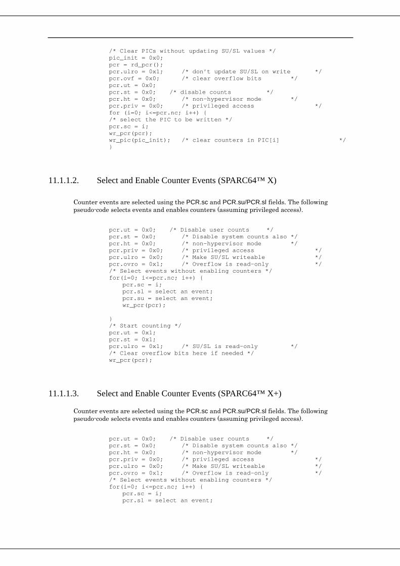
/* Clear PICs without updating SU/SL values */ pic_init = 0x0; pcr = rd_pcr(); pcr.ulro = 0x1; /* don’t update SU/SL on write */ pcr.ovf = 0x0; /* clear overflow bits */ pcr.ut = 0x0; pcr.st = 0x0; /* disable counts */ pcr.ht = 0x0; /* non-hypervisor mode */ pcr.priv = 0x0; /* privileged access */ for (i=0; i<=pcr.nc; i++) { /* select the PIC to be written */ pcr.sc = i; wr_pcr(pcr); wr_pic(pic_init); /* clear counters in PIC[i] */ }
11.1.1.2. Select and Enable Counter Events (SPARC64™ X)
Counter events are selected using the PCR.sc and PCR.su/PCR.sl fields. The following pseudo-code selects events and enables counters (assuming privileged access).
pcr.ut = 0x0; /* Disable user counts */ pcr.st = 0x0; /* Disable system counts also */ pcr.ht = 0x0; /* non-hypervisor mode */ pcr.priv = 0x0; /* privileged access */ pcr.ulro = 0x0; /* Make SU/SL writeable */ pcr.ovro = 0x1; /* Overflow is read-only */ /* Select events without enabling counters */ for(i=0; i<=pcr.nc; i++) { pcr.sc = i; pcr.sl = select an event; pcr.su = select an event; wr_pcr(pcr); } /* Start counting */ pcr.ut = 0x1; pcr.st = 0x1; pcr.ulro = 0x1; /* SU/SL is read-only */ /* Clear overflow bits here if needed */ wr_pcr(pcr);
11.1.1.3. Select and Enable Counter Events (SPARC64™ X+)
Counter events are selected using the PCR.sc and PCR.su/PCR.sl fields. The following pseudo-code selects events and enables counters (assuming privileged access).
pcr.ut = 0x0; /* Disable user counts */ pcr.st = 0x0; /* Disable system counts also */ pcr.ht = 0x0; /* non-hypervisor mode */ pcr.priv = 0x0; /* privileged access */ pcr.ulro = 0x0; /* Make SU/SL writeable */ pcr.ovro = 0x1; /* Overflow is read-only */ /* Select events without enabling counters */ for(i=0; i<=pcr.nc; i++) { pcr.sc = i; pcr.sl = select an event;

280 Ver 29.0 Jan. 2015
pcr.su = select an event; wr_pcr(pcr);
} /* Start counting */ pcr.ut = 0x1; pcr.st = 0x1; pcr.ulro = 0x1; /* SU/SL is read-only */ /* Clear overflow bits here if needed */ wr_pcr(pcr);
11.1.1.4. Stop Counter and Read
The following pseudo-code disables counters and reads their values (assuming privileged access).
pcr.ut = 0x0; /* Disable user counts */ pcr.st = 0x0; /* Disable system counts also */ pcr.ht = 0x0; /* non-hypervisor mode */ pcr.priv = 0x0; /* privileged access */ pcr.ulro = 0x1; /* Make SU/SL read-only */ pcr.ovro = 0x1; /* Overflow is read-only */ for(i=0; i<=pcr.nc; i++) { pcr.sc = i; wr_pcr(pcr); pic = rd_pic(); picl[i] = pic.picl; picu[i] = pic.picu; }
11.2. Description of PA Events
The performance counter (PA) events can be divides into the following groups:
1. Instruction and trap statistics 2. MMU and L1 cache events 3. L2 cache events 4. Bus transaction events
There are 2 types of events that can be measured on SPARC64™ X / SPARC64™ X+, standard and supplemental events. Standard events on SPARC64™ X / SPARC64™ X+ have been verified for correct behavior; they are guaranteed to be compatible with future processors. Supplemental events are primarily intended for debugging the hardware.
a. The behavior of supplemental events may not be fully verified. There is a possibility that some of these events may not behave as specified in this document.
b. The definition of these events may change without notice. Compatibility with future processors is not guaranteed.
Table 11-1 shows the PA events defined on SPARC64™ X. Table 11-2 shows the PA events defined on SPARC64™ X+. Shaded events are supplemental events.

For details of each event, refer to the descriptions in the following sections.Unless otherwise indicated, speculative instructions are also counted by PA events.

282 Ver 29.0 Jan. 2015
Table 11-1 PA Events and Encodings (SPARC64™ X)
Encoding (binary)
Counter pic u0 pic l0 pic u1 pic l1 pic u2 pic l2 pic u3 pic l3
0000_0000 cycle_counts 0000_0001 instruction_counts 0000_0010 instruction_
flow_counts only_this_ thread_active
single_mode_ cycle_counts
single_mode_ instruction_coun
instruction_ flow_counts d_move_wait cse_priority_wait xma_inst
0000_0011 iwr_empty w_cse_window_ empty w_eu_comp_wait w_branch_comp
_wait iwr_empty w_op_stv_wait w_d_move w_0endop
0000_0100 Reserved w_op_stv_wait_ nc_pend
w_op_stv_ wait_sxmiss
w_op_stv_wait_ sxmiss_ex Reserved w_fl_comp_wait w_cse_window_
empty_sp_full w_op_stv_ wait_ex
0000_0101 op_stv_wait 0000_0110 effective_instruction_counts 0000_0111 SIMD_load_stor
e_
SIMD_floating_ instructions
SIMD_fma_ instructions
sxar1_ instructions
sxar2_ instructions unpack_sxar1 unpack_sxar2 Reserved
0000_1000 load_store_instructions 0000_1001 branch_instructions 0000_1010 floating_instructions 0000_1011 fma_instructions 0000_1100 prefetch_instructions 0000_1101 Reserved ex_load_
instructions ex_store_ instructions
fl_load_ instructions
fl_store_ instructions
SIMD_fl_load_ instructions
SIMD_fl_store_ instructions Reserved
0000_1110 Reserved 0000_1111 Reserved 0001_0000 Reserved 0001_0001 Reserved 0001_0010 rs1 flush_rs Reserved 0001_0011 1iid_use 2iid_use 3iid_use 4iid_use Reserved sync_intlk regwin_intlk Reserved 0001_0100 Reserved 0001_0101 Reserved toq_rsbr_phantom Reserved flush_rs Reserved rs1 Reserved 0001_0110 trap_all Reserved trap_int_level trap_spill trap_fill trap_trap_inst Reserved Reserved
0001_0111 Reserved Reserved Reserved
0001_1000 only_this_ thread _active
both_ threads _active
both_ threads _empty Reserved op_stv_wait_
pfp_busy_swpf op_stv_ wait_sxmiss
0001_1001 Reserved 0001_1010 Reserved Reserved single_sxar_comm
it Reserved suspend_cycle
0001_1011 rsf_pmmi Reserved op_stv_wait_ nc_pend 0iid_use flush_rs Reserved decode_all_intlk
0001_1100 Reserved Reserved Reserved Reserved Reserved Reserved
0001_1101 op_stv_wait_ pfp_busy_ex Reserved op_stv_wait_
sxmiss_ex op_stv_wait_ nc_pend
cse_window_ empty_sp_full
op_stv_wait_ pfp_busy
both_ threads _ suspended Reserved

0001_1110 cse_window_ empty eu_comp_wait branch_comp_
wait 0endop op_stv_wait_ex fl_comp_wait 1endop 2endop 0001_1111 Reserved 3endop Reserved sleep_cycle op_stv_wait_swpf 0010_0000 ITLB_write DTLB_write uITLB_miss uDTLB_miss L1I_miss L1D_miss L1I_wait_all L1D_wait_all 0010_0001 Reserved 0010_0010 Reserved 0010_0011 L1I_thrashing L1D_thrashing Reserved 0010_0100 swpf_success_all swpf_fail_all Reserved swpf_lbs_hit Reserved 0010_0101 Reserved 0010_0110 Reserved 0010_0111 Reserved 0010_1000 Reserved 0010_1001 Reserved 0010_1010 Reserved 0010_1011 Reserved 0010_1100 Reserved 0010_1101 Reserved 0010_1110 Reserved 0010_1111 Reserved 0011_0000 Reserved L2_miss_dm L2_miss_pf L2_read_dm L2_read_pf L2_wb_dm L2_wb_pf
0011_0001 bi_counts cpi_counts cpb_counts cpd_counts cpu_mem_ read_counts
cpu_mem_ write_counts
IO_mem_ read_counts
IO_mem_ write_counts
0011_0010 L2_miss_wait_ dm_bank0
L2_miss_wait_ pf_bank0
L2_miss_counts_ dm_bank0
L2_miss_counts_ pf_bank0
L2_miss_wait_ dm_bank1
L2_miss_wait_ pf_bank1
L2_miss_counts_ dm_bank1
L2_miss_counts_ pf_bank1
0011_0011 L2_miss_counts_ dm_bank2
L2_miss_counts_ pf_bank2
L2_miss_wait_ dm_bank2
L2_miss_wait_ pf_bank2
L2_miss_counts_ dm_bank3
L2_miss_counts_ pf_bank3
L2_miss_wait_ dm_bank3
L2_miss_wait_ pf_bank3
0011_0100 lost_pf_pfp_full lost_pf_by_abort IO_pst_counts Reserved 0011_0101 Reserved 0011_0110 Reserved 0011_0111 Reserved 0011_1000 Reserved 0011_1001 Reserved 0011_1010 Reserved 0011_1011 Reserved 0011_1100 Reserved 0011_1101 Reserved 0011_1110 Reserved 0011_1111 Reserved 1111_1111 Disabled (Counter is not incremented)
※Encodings not shown are Reserved.

284 Ver 29.0 Jan. 2015
Table 11-2 PA Events and Encodings (SPARC64™ X+) Encoding (binary)
Counter pic u0 pic l0 pic u1 pic l1 pic u2 pic l2 pic u3 pic l3
0000_0000 cycle_counts 0000_0001 instruction_counts 0000_0010 instruction_
flow_counts only_this_ thread_active
single_mode_ cycle_counts
single_mode_ instruction_count
instruction_ flow_counts d_move_wait cse_priority_wait xma_inst
0000_0011 iwr_empty w_cse_window_ empty w_eu_comp_wait w_branch_comp
_wait iwr_empty w_op_stv_wait w_d_move w_0endop
0000_0100 Reserved w_op_stv_wait_ nc_pend
w_op_stv_ wait_sxmiss
w_op_stv_wait_ sxmiss_ex Reserved w_fl_comp_wait w_cse_window_
empty_sp_full w_op_stv_ wait_ex
0000_0101 op_stv_wait 0000_0110 effective_instruction_counts 0000_0111 SIMD_load_store_
instructions SIMD_floating_ instructions
SIMD_fma_ instructions
sxar1_ instructions
sxar2_ instructions unpack_sxar1 unpack_sxar2 Reserved
0000_1000 load_store_instructions 0000_1001 branch_instructions 0000_1010 floating_instructions 0000_1011 fma_instructions 0000_1100 prefetch_instructions 0000_1101 Reserved ex_load_
instructions ex_store_ instructions
fl_load_ instructions
fl_store_ instructions
SIMD_fl_load_ instructions
SIMD_fl_store_ instructions Reserved
0000_1110 Reserved 0000_1111 Reserved 0001_0000 Reserved 0001_0001 Reserved 0001_0010 rs1 flush_rs Reserved 0001_0011 1iid_use 2iid_use 3iid_use 4iid_use Reserved sync_intlk regwin_intlk Reserved 0001_0100 Reserved 0001_0101 Reserved toq_rsbr_phantom Reserved flush_rs Reserved rs1 Reserved 0001_0110 trap_all Reserved trap_int_level trap_spill trap_fill trap_trap_inst Reserved Reserved 0001_0111 Reserved Reserved Reserved
0001_1000 only_this_ thread _active
both_ threads _active
both_ threads _empty Reserved op_stv_wait_
pfp_busy_swpf op_stv_ wait_sxmiss
0001_1001 Reserved 0001_1010 Reserved Reserved single_sxar_commi
t Reserved suspend_cycle
0001_1011 rsf_pmmi Reserved op_stv_wait_ nc_pend 0iid_use flush_rs Reserved decode_all_intlk
0001_1100 Reserved Reserved Reserved Reserved Reserved Reserved
0001_1101 op_stv_wait_ pfp_busy_ex Reserved op_stv_wait_
sxmiss_ex op_stv_wait_ nc_pend
cse_window_ empty_sp_full
op_stv_wait_ pfp_busy
both_ threads _ suspended Reserved
0001_1110 cse_window_ empty eu_comp_wait branch_comp_
wait 0endop op_stv_wait_ex fl_comp_wait 1endop 2endop 0001_1111 Reserved 3endop Reserved sleep_cycle op_stv_wait_swpf 0010_0000 ITLB_write DTLB_write uITLB_miss uDTLB_miss L1I_miss L1D_miss L1I_wait_all L1D_wait_all

0010_0001 Reserved 0010_0010 Reserved 0010_0011 L1I_thrashing L1D_thrashing Reserved 0010_0100 swpf_success_all swpf_fail_all Reserved swpf_lbs_hit Reserved 0010_0101 Reserved 0010_0110 Reserved 0010_0111 Reserved 0010_1000 Reserved 0010_1001 Reserved 0010_1010 Reserved 0010_1011 Reserved 0010_1100 Reserved 0010_1101 Reserved 0010_1110 Reserved 0010_1111 Reserved 0011_0000 Reserved L2_miss_dm L2_miss_pf L2_read_dm L2_read_pf L2_wb_dm L2_wb_pf
0011_0001 bi_counts cpi_counts cpb_counts cpd_counts cpu_mem_ read_counts
cpu_mem_ write_counts
IO_mem_ read_counts
IO_mem_ write_counts
0011_0010 L2_miss_wait_ dm_bank0
L2_miss_wait_ pf_bank0
L2_miss_counts_ dm_bank0
L2_miss_counts_ pf_bank0
L2_miss_wait_ dm_bank1
L2_miss_wait_ pf_bank1
L2_miss_counts_ dm_bank1
L2_miss_counts_ pf_bank1
0011_0011 L2_miss_counts_ dm_bank2
L2_miss_counts_ pf_bank2
L2_miss_wait_ dm_bank2
L2_miss_wait_ pf_bank2
L2_miss_counts_ dm_bank3
L2_miss_counts_ pf_bank3
L2_miss_wait_ dm_bank3
L2_miss_wait_ pf_bank3
0011_0100 lost_pf_pfp_full lost_pf_by_abort IO_pst_counts Reserved 0011_0101 Reserved 0011_0110 Reserved 0011_0111 Reserved 0011_1000 Reserved 0011_1001 Reserved 0011_1010 Reserved 0011_1011 Reserved 0011_1100 Reserved 0011_1101 Reserved 0011_1110 Reserved 0011_1111 Reserved 1111_1111 Disabled (Counter is not incremented)
※Encodings not shown are Reserved.

286 Ver 29.0 Jan. 2015
11.2.1. Instruction and Trap Statistics Standard PA Events
1 cycle_counts Counts the number of cycles that the performance counter is enabled. This counter is similar to the TICK register but can count user cycles and system cycles separately, based on the settings of PCR.ut and PCR.st.
2 instruction_counts (Non-Speculative)
Counts the number of committed instructions, including SXAR1 and SXAR2. SPARC64™ X/SPARC64™ X+ commits up to 4 non-SXAR instructions per cycle and up to 2 SXAR instructions. That is, instruction_counts /cycle_counts can be greater than 4.
3 effective_instruction_counts (Non-Speculative)
Counts the number of committed non-SXAR instructions. Instructions per cycle (IPC) can be derived from this event and cycle_counts. IPC = effective_instruction_counts / cycle_counts If effective_Instruction_counts and cycle_counts are collected for user or system mode, the IPC in either user or system mode can be calculated.
4 load_store_instructions (Non-Speculative)
Counts the number of committed non-SIMD load/store instructions. Also counts atomic load-store instructions.
5 branch_instructions (Non-Speculative)
Counts the number of committed branch instructions. Also counts the CALL, JMPL, and RETURN instructions.
6 floating_instructions (Non-Speculative)
Counts the number of committed non-SIMD floating-point instructions. The counted instructions are FPop1, FPop2, FSELMOV{s|d}, and IMPDEP1 with opf<8:4> = 0A16, 0B16, 1616, or 1716.
7 fma_instructions (Non-Speculative)
Counts the number of committed non-SIMD floating-point multiply-and-add instructions. The counted instructions are FM{ADD|SUB}{s|d}, FNM{ADD|SUB}{s|d}, and FTRIMADDd. Two operations are executed per instruction; the number of operations is obtained by multiplying by 2.
8 prefetch_instructions (Non-Speculative)
Counts the number of committed prefetch instructions. 9 SIMD_load_store_instructions (Non-Speculative)
Counts the number of committed SIMD load/store instructions. 10 SIMD_floating_instructions (Non-Speculative)
Counts the number of committed SIMD floating-point instructions. The counted instructions are the same as floating_instructions. Two operations are executed per instruction; the number of operations is obtained by multiplying by 2.

11 SIMD_fma_instructions (Non-Speculative)
Counts the number of committed SIMD floating-point multiply-and-add instructions. The counted instructions are the same as fma_instructions. Four operations are executed per instruction; the number of operations is obtained by multiplying by 4.
12 sxar1_instructions (Non-Speculative)
Counts the number of committed SXAR1 instructions. 13 sxar2_instructions (Non-Speculative)
Counts the number of committed SXAR2 instructions. 14 trap_all (Non-Speculative)
Counts the occurrences of all trap events. The number of occurrences counted equals the sum of the occurrences counted by all trap PA events.
16 trap_int_level (Non-Speculative)
Counts the occurrences of interrupt_level_n. 17 trap_spill (Non-Speculative)
Counts the occurrences of spill_n_normal and spill_n_other. 18 trap_fill (Non-Speculative)
Counts the occurrences of fill_n_normal and fill_n_other. 19 trap_trap_inst (Non-Speculative)
Counts the occurrences of trap_instruction.
Supplemental PA Events
23 xma_inst (Non-Speculative) Counts the number of committed FPMADDX and FPMADDXHI instructions.
24 unpack_sxar1 (Non-Speculative)
Counts the number of unpacked SXAR1 instructions that are committed. 25 unpack_sxar2 (Non-Speculative)
Counts the number of unpacked SXAR2 instructions that are committed. 26 instruction_flow_counts (Non-Speculative)
Counts the number of committed instruction flows. On SPARC64™ X / SPARC64™ X+, some instructions are processed internally as several separate instructions, called instruction flows. This event does not count packed SXAR1 and SXAR2 instructions.
27 ex_load_instructions (Non-Speculative)
Counts the number of committed integer-load instructions. Counts the LD(S|U)B{A}, LD(S|U)H{A}, LD(S|U)W{A}, LDD{A}, and LDX{A} instructions.
28 ex_store_instructions (Non-Speculative)
Counts the number of committed integer-store and atomic instructions. Counts the STB{A}, STH{A}, STW{A}, STD{A}, STX{A}, LDSTUB{A}, SWAP{A}, and CAS{X}A instructions.

288 Ver 29.0 Jan. 2015
29 fl_load_instructions (Non-Speculative) Counts the number of committed non-SIMD floating-point load instructions. Counts the LDF{A}, LDDF{A}, and LD{X}FSR instructions. This event does not count LDQF{A}
30 fl_store_instructions (Non-Speculative)
Counts the number of committed non-SIMD floating-point store instructions. Counts the STF{A}, STDF{A}, STFR, STDFR, and ST{X}FSR instructions. This event does not count STQF{A}.
31 SIMD_fl_load_instructions (Non-Speculative)
Counts the number of committed SIMD floating-point load instructions. Counted instructions are LDF{A} and LDDF{A}.
32 SIMD_fl_store_instructions (Non-Speculative)
Counts the number of committed SIMD floating-point store instructions. Counted instructions are STF{A}, STDF{A}, STFR, and STDFR.
33 iwr_empty
Counts the number of cycles that the IWR (Issue Word Register) is empty. The IWR is a fourentry register that holds instructions during instruction decode; the IWR may be empty if an instruction cache miss prevents instruction fetch.
34 rs1 (Non-Speculative)
Counts the number of cycles in which normal execution is halted due to the following: ■ a trap or interrupt ■ update of privileged registers ■ to guarantee memory ordering ■ RAS-initiated hardware retry
35 flush_rs (Non-Speculative) Counts the number of pipeline flushes due to branch misprediction. Since SPARC64™ X / SPARC64™ X+ support speculative execution, instructions that should not have been executed may be in flight. When it is determined that the predicted path is incorrect, these instructions are cancelled. A pipeline flush occurs at this time. misprediction rate = flush_rs / branch_instructions
36 0iid_use
Counts the number of cycles where no instruction is issued. SPARC64™ X / SPARC64™ X+ issue up to four non-SXAR instructions per cycle; when no instruction is issued, 0iid_use is incremented. On SPARC64™ X / SPARC64™ X+, some instructions are processed internally as several separate instructions, called instruction flows. Each of these instruction flows is counted. SXAR instructions are also counted.
37 1iid_use
Counts the number of cycles where one instruction is issued.
38 2iid_use Counts the number of cycles where two instructions are issued.
39 3iid_use
Counts the number of cycles where three instructions are issued. 40 4iid_use
Counts the number of cycles where four instructions are issued.

41 sync_intlk Counts the number of cycles where instruction issue is blocked by a pipeline sync.
42 regwin_intlk
Counts the number of cycles where instruction issue is blocked by a register window switch. 43 decode_all_intlk
Counts the number of cycles where instruction issue is blocked by a static interlock condition at the decode stage. decode_all_intlk includes sync_intlk and regwin_intlk; stall cycles due to dynamic conditions (such as reservation station full) are not counted.
44 rsf_pmmi (Non-Speculative)
Counts the number of cycles where mixing single-precision and double-precision floating-point operations prevents instructions from issuing.
45 toq_rsbr_phantom
Counts the number of instructions that are predicted taken but are not actually branch instructions. Branch prediction on SPARC64™ X / SPARC64™ X+ is done prior to instruction decode; in other words, branch prediction occurs regardless of whether the instruction is actually a branch. Instructions that are not branch instructions may be incorrectly predicted as taken branches.
46 op_stv_wait (Non-Speculative)
Counts the number of cycles where no instructions are committed because the oldest, uncommitted instruction is a memory access waiting for data. op_stv_wait does not count cycles where a store instruction is waiting for data (atomic instructions are counted).
Note that op_stv_wait does not measure the cache-miss latency, since any cycles prior to becoming the oldest, uncommitted instruction are not included.
47 op_stv_wait_nc_pend (Non-Speculative) Counts op_stv_wait for non-cacheable accesses.
48 op_stv_wait_ex (Non-Speculative)
Counts op_stv_wait for integer memory access instructions. Does not distinguish between L1 cache and L2 cache misses.
49 op_stv_wait_sxmiss (Non-Speculative)
Counts op_stv_wait caused by an L2$ miss. Does not distinguish between integer and floating-point loads.
50 op_stv_wait_sxmiss_ex (Non-Speculative)
Counts op_stv_wait caused by an integer-load L2$ miss.
51 op_stv_wait_pfp_busy (Non-Speculative) Counts op_stv_wait caused by a memory access instruction that cannot be executed due to the lack of an available prefetch port.
52 op_stv_wait_pfp_busy_ex (Non-Speculative)
Counts op_stv_wait caused by an integer memory access instruction that cannot be executed due to the lack of an available prefetch port.
53 op_stv_wait_swpf (Non-Speculative)
Counts op_stv_wait caused by a prefetch instruction. 54 op_stv_wait_pfp_busy_swpf (Non-Speculative)

290 Ver 29.0 Jan. 2015
Counts op_stv_wait caused by a prefetch instruction that cannot be executed due to the lack of an available prefetch port.
55 cse_window_empty_sp_full (Non-Speculative)
Counts the number of cycles where no instructions are committed because the CSE is empty and the store ports are full.
56 cse_window_empty (Non-Speculative)
Counts the number of cycles where no instructions are committed because the CSE is empty. 57 branch_comp_wait (Non-Speculative)
Counts the number of cycles where no instructions are committed and the oldest, uncommitted instruction is a branch instruction. Measuring branch_comp_wait has a lower priority than measuring eu_comp_wait.
58 eu_comp_wait (Non-Speculative)
Counts the number of cycles where no instructions are committed and the oldest, uncommitted instruction is an integer or floating-point instruction. Measuring eu_comp_wait has a higher priority than measuring branch_comp_wait.
59 fl_comp_wait (Non-Speculative)
Counts the number of cycles where no instructions are committed and the oldest, uncommitted instruction is a floating-point instruction.
60 0endop (Non-Speculative)
Counts the number of cycles where no instructions are committed. 0endop also counts cycles where the only instruction that commits is an SXAR instruction.
61 1endop (Non-Speculative) Counts the number of cycles where one instruction is committed.
62 2endop (Non-Speculative)
Counts the number of cycles where two instructions are committed. 63 3endop (Non-Speculative)
Counts the number of cycles where three instructions are committed. 64 suspend_cycle (Non-Speculative)
Counts the number of cycles where the instruction unit is halted by a SUSPEND or SLEEP instruction.
65 sleep_cycle (Non-Speculative)
Counts the number of cycles where the instruction unit is halted by a SLEEP instruction 66 single_sxar_commit (Non-Speculative)
Counts the number of cycles where the only instruction committed is an unpacked SXAR instruction. These cycles are also counted by 0endop.
67 d_move_wait (non-speculative)
Counts the number of cycles where no instructions are committed while waiting for the register window to be updated.
68 cse_priority_wait
Counts the number of cycles where no instructions are committed because the SMT thread is waiting for commit priority. On SPARC64™ X / SPARC64™ X+, only one thread can

commit instructions in a given cycle, and the priority is switched every cycle as long as the other thread is active. The event is counted only when there is an instruction ready to be committed for that thread.
69 w_cse_window_empty (non-speculative)
Number of cycles where cse_window_empty for the thread that has commit priority. 70 w_eu_comp_wait (non-speculative)
Number of cycles where eu_comp_wait for the thread that has commit priority. 71 w_branch_comp_wait (non-speculative)
Number of cycles where branch_comp_wait for the thread that has commit priority. 72 w_op_stv_wait (non-speculative)
Number of cycles where op_stv_wait for the thread that has commit priority. 73 w_d_move_wait
Number of cycles where d_move_wait for the thread that does not have commit priority. 74 w_0endop (non-speculative)
Number of cycles where 0endop for the thread that does not have commit priority. 75 w_op_stv_wait_nc_pend (non-speculative)
Number of cycles where op_stv_wait_nc_pend for the thread that has commit priority. 76 w_op_stv_wait_sxmiss (non-speculative)
Number of cycles where op_stv_wait_sxmiss for the thread that has commit priority.
77 w_op_stv_wait_sxmiss_ex (non-speculative) Number of cycles where op_stv_wait_sxmiss_ex for the thread that has commit priority.
78 w_fl_comp_wait (non-speculative)
Number of cycles where fl_comp_wait for the thread that has commit priority. 79 w_cse_window_empty_sp_full (non-speculative)
Number of cycles where cse_window_empty_sp_full for the thread that has commit priority. 80 w_op_stv_wait_ex (non-speculative)
Number of cycles where op_stv_wait_ex for the thread that has commit priority.
81 only_this_thread_active Number of cycles while SMT is enabled where the CSE of this thread is not empty and the CSE of the other thread is empty.
82 single_mode_cycle_counts
Number of cycles that the thread is active in single-threaded mode (SMT disabled). 82 single_mode_instructions
Number of committed instructions in single-threaded mode (SMT disabled). 84 both_threads_active
Number of cycles while SMT is enabled where the CSEs of both threads are not empty. 85 both_threads_empty

292 Ver 29.0 Jan. 2015
Number of cycles where SMT is enabled where the CSEs of both threads are empty. 86 both_threads_suspended
Number of cycles where both threads in a core are in the suspended state.
11.2.2. MMU and L1 cache Events Standard PA Events
1 uITLB_miss Counts the occurrences of instruction uTLB misses.
2 uDTLB_miss
Counts the occurrences of data uTLB misses. 3 L1I_miss
Counts the occurrences of L1 instruction cache misses. 4 L1D_miss
Counts the occurrences of L1 data cache misses. 5 L1I_wait_all
Counts the total time spent processing L1 instruction cache misses (i.e., the total miss latency). On SPARC64™ X / SPARC64™ X+, the L1 cache is a non-blocking cache that can process multiple cache misses in parallel; L1I_wait_all only counts the miss latency for one of these misses. That is, the overlapped miss latencies are not counted.
6 L1D_wait_all
Counts the total time spent processing L1 data cache misses (i.e., the total miss latency). On SPARC64™ X / SPARC64™ X+, the L1 cache is a non-blocking cache that can process multiple cache misses in parallel; L1D_wait_all only counts the miss latency for one of these misses. That is, the overlapped miss latencies are not counted.
Supplemental PA Events
7 ITLB_write Counts the number of ITLB writes caused by an instruction fetch ITLB miss.
8 DTLB_write
Counts the number of DTLB writes caused by a data access DTLB miss. 9 swpf_success_all
Counts the number of prefetch instructions that are not lost in the SU and are sent to the SX. 10 swpf_fail_all
Counts the number of prefetch instructions that are lost in the SU. 11 swpf_lbs_hit
Counts the number of prefetch instructions that hit in the L1 cache. prefetch instructions sent to SU = swpf_success_all + swpf_fail_all + swpf_lbs_hit

12 L1I_thrashing
Counts the occurrences of an L2 read request being issued twice in the period between acquiring and releasing a store port. When instruction fetch causes an L1 instruction cache miss, the requested data is updated in the L1I$. This counter is incremented if the updated data is evicted before it can be read.
13 L1D_thrashing Counts the occurrences of an L2 read request being issued twice in the period between acquiring and releasing a store port. When a memory access instruction causes an L1 data cache miss, the requested data is updated in the L1D$. This counter is incremented if the updated data is evicted before it can be read.
14 L1D_miss_dm
Counts the occurrences of L1 data cache misses for a load/store instructions. 15 L1D_miss_pf
Counts the occurrences of L1 data cache misses for a prefetch instructions. 16 L1D_miss_qpf
Counts the occurrences of L1 data cache misses for hardware prefetch requests.
11.2.3. L2 cache Events
L2 cache events may be due to the actions of a VCPU, I/O or external requests. Events caused by VCPUs are counted separately for each VCPU; those caused by I/O or external requests are counted for all VCPUs. Most L2 cache events are categorized as either demand (dm) or prefetch (pf) events, but these categories do not directly correspond to load/store/atomic and prefetch instructions, for the following reasons.
■ When a load/store instruction cannot be executed due to a lack of resources needed to move data into the L1 cache, data is first moved into the L2 cache. Once L1 cache resources become available, the load/store instruction is executed. That is, the request to move data into the L2 cache is processed as a prefetch request.
■ The hardware prefetch mechanism generates prefetch requests. ■ L1 cache prefetch instructions are processed as demand requests. Instead, demand and prefetch L2 cache events correspond to the following:
■ A demand (dm) request to the L2 cache is an instruction fetch, load/store instruction, or L1 prefetch instruction that successfully acquired the resources needed to access memory.
■ A prefetch (pf) request to the L2 cache is an instruction fetch, load/store instruction, or L1 prefetch instruction that could not acquire the resources needed to access memory; L2 prefetch instructions and hardware prefetch are also considered prefetch requests.
Standard PA Events
1 L2_read_dm Counts the number of L2 cache references by demand requests. References by external requests are not counted.
2 L2_read_pf

294 Ver 29.0 Jan. 2015
Counts the number of L2 cache references by prefetch requests. 3 L2_miss_dm
Counts the number of L2 cache misses caused by demand requests. This counter is the sum of the L2_miss_counts_dm_bank{0,1,2,3}.
4 L2_miss_pf
Counts the number of L2 cache misses caused by prefetch requests. This counter is the sum of the L2_miss_counts_pf_bank {0, 1, 2, 3}.
5 L2_miss_counts_dm_bank {0, 1, 2, 3}
Counts the number of L2 cache misses for each bank caused by demand requests. When an L2 cache miss causes a prefetch request for an address to be issued and then a demand request for the same address is issued before the data is returned from memory or an external CPU, the demand request is not counted in L2_miss_counts_dm_bank{0,1,2,3}.
6 L2_miss_counts_pf_bank {0, 1, 2, 3}
Counts the number of L2 cache misses for each bank caused by prefetch requests. 7 L2_miss_wait_dm_bank {0, 1, 2, 3}
Counts the total time spent processing L2 cache misses for each bank caused by demand requests (i.e., the total miss latency for each bank). The latency of each memory access request is counted. When an L2 cache miss causes prefetch request for an address to be issued and then a demand request for the same address is issued before the data is returned from memory or an external CPU, the cycles after the demand request but before the data is received are counted in L2_miss_wait_dm_bank{0,1,2,3}.
8 L2_miss_wait_pf_bank {0, 1, 2, 3}
Counts the total time spent processing L2 cache misses for each bank caused by prefetch requests, (i.e., the total miss latency for each bank). The latency of each memory access request is counted. The L2 cache miss latency can be derived by summing L2_miss_wait_* and dividing by the sum of L2_miss_counts_*. If individual L2 cache-miss latencies are calculated for pf/dm requests, the value obtained for the miss latency of dm requests may be higher than expected.
9 L2_wb_dm
Counts the occurrences of writeback to memory caused by L2 cache misses for demand requests.
10 L2_wb_pf
Counts the occurrences of writeback to memory caused by L2 cache misses for prefetch requests.
Supplemental PA Events
11 lost_pf_pfp_full Counts the number of weak prefetch requests lost due to prefetch port full.
12 lost_pf_by_abort
Counts the number of weak prefetch requests lost due to L2-pipe abort.

11.2.4. Bus Transaction Events Standard PA Events
1 cpu_mem_read_counts Counts the number of memory read requests issued by the CPU. For this event, the same value is counted by all VCPUs.
2 cpu_mem_write_counts
Counts the number of memory write requests issued by the CPU. For this event, the same value is counted by all VCPUs.
3 IO_mem_read_counts
Counts the number of memory read requests issued by I/O. For this event, the same value is counted by all VCPUs.
4 IO_mem_write_counts
Counts the number of memory write requests issued by I/O. Only IO-FST is counted by this event. IO-PST can be counted using IO_pst_counts. For this event, the same value is counted by all VCPUs.
5 bi_counts
Counts the number of external cache-invalidate requests received by the CPU chip. Cache-invalidate requests caused by internal IO-FST/PST requests are also counted by this event. These requests do not check the cache data before invalidating. For this event, the same value is counted by all VCPUs.
6 cpi_counts
Counts the number of external cache-copy-and-invalidate requests received by the CPU chip. These requests copy updated cache data to memory before invalidating; cache data that is consistent with memory does not need to be copied and is invalidated. For this event, the same value is counted by all VCPUs.
7 cpb_counts Counts the number of external cache-copyback requests received by the CPU chip. These request copy updated cache data to memory. For this event, the same value is counted by all VCPUs.
8 cpd_counts
Counts the number of internal or external IO cache-read requests (DMA read requests) received by the CPU chip. For this event, the same value is counted by all VCPUs.
Supplemental PA Events
9 IO_pst_counts Counts the number of memory write requests (IO-PST) issued by I/O.
296 Ver 29.0 Jan. 2015
11.3. Cycle Accounting
Cycle accounting is a method used for analyzing performance bottlenecks. The total time (number of CPU cycles) required to execute an instruction sequence can be divided into time spent in various CPU execution states (executing instructions, waiting for a memory access, waiting for execution to complete, and so on). SPARC64™ X / SPARC64™ X+ define a large number of PA events that record detailed information about CPU execution states, enable efficient analysis of bottlenecks, and are useful for performance tuning. In this document, cycle accounting is specifically defined as the analysis of instructions as they are committed in order. SPARC64™ X / SPARC64™ X+ execute instructions out-of-order and have multiple execution units; the CPU is generally in a state where executing and waiting instructions are thoroughly mixed together. One instruction may be waiting for data from memory, another executing a floating-point multiply, and yet another waiting for confirmation of the branch direction. Simply analyzing the reasons why individual instructions are waiting is not useful. Instead, cycle accounting classifies cycles by the number of instructions committed; when a cycle commits no instructions, the conditions that prevented instructions from committing are analyzed. SPARC64™ X / SPARC64™ X+ commits up to 4 instructions per cycle. The more cycles that commit the maximum number of instructions, the better the execution efficiency. Cycles that do not commit any instructions have an extremely negative effect on performance, so it is important to perform a detailed analysis of these cycles. The main causes are:
■ Waiting for a memory access to return data. ■ Waiting for instruction execution to complete. ■ Instruction fetch is unable to supply the pipeline with instructions.
Table 11-3 highlights some useful PA events and describes how these PA events can be used to analyze execution efficiency. Figure 11-1 shows the relationship between the various op_stv_wait_* events. The PA events marked with a † in the table and in the figure are synthetic events, which are calculated from other PA events.
Figure 11-1 Breakdown of op_stv_wait
Table 11-3 Useful Performance Events for Cycle Accounting
Instructions Committed per Cycle
Cycles Remarks
4 cycle_counts N/A (maximum instructions committed)
op_stv_wait_pfp_busy_swpf
op_stv_wait_pfp_busy_f l†
op_stv_wait_f l† op_stv_wait_sxhit_ f l†
op_stv_wait_sxmiss_f l†
op_stv_wait_pfp_busy_ex
op_stv_wait_ex op_stv_wait_sxhit_ex†
op_stv_wait_sxmiss_ex
op_stv_wait_pfp_busy
op_stv_wait_sxmiss
op_stv_wait

- 3endop - 2endop - 1endop - 0endop
3 3endop 2 2endop 1 1endop 0 Execution:
eu_comp_wait + branch_comp_wait
eu_comp_wait = ex_comp_wait†+ fl_comp_wait
Instruction Fetch: cse_window_empy
cse_window_empty = cse_window_empty_sp_full + sleep_cycle + misc.†
L1D cache miss: op_stv_wait - L2 cache miss (see below)
L2 cache miss: op_stv_wait_sxmiss + op_stv_wait_nc_pend
Others: 0endop - op_stv_wait - cse_window_empy - eu_comp_wait - branch_comp_wait -(instruction_flow_counts - instruction_counts)

298 Ver 29.0 Jan. 2015
12. Traps
12.1. Virtual Processor Privilege Modes When a trap occurs, the privilege level is changed depending on the trap. Refer to Table 12-2 and Table 12-3 for details.
For a VCPU running at a higher privilege level, if the exception would lower the current privilege level, the trap will be pending until the privilege level is lower than the target privilege level of the exception. Refer to Section 12.1 in UA2011 for the relationship between privileged level and TL.
The possible values of the following registers depend on the privilege level. Refer to Section 5.7.7 and Section 5.7.9 in UA2011 respectively for details.
• TL • GL
12.5. Trap list and priorities
Symbol Description -x- Trap will not occur in this mode. P Change to privileged mode. P(ie) Change to privileged mode if PSTATE.ie = 1. H Changes to hyperprivileged mode.
Table 12-2 Trap list, by TT value
TT Trap name Type Priority Privilege level after the traps occurs
Definition
00016 reserved
00616 reserved
00716 reserved
00816 IAE_privilege_violation precise 3.1 H 305
00B16 IAE_unauth_access precise 2.7 H 306

TT Trap name Type Priority Privilege level after the traps occurs
Definition
00C16 IAE_nfo_page precise 3.3 H 305
00D16 reserved
00E16 reserved
00F16 reserved
01016 illegal_instruction precise 6.2 H 306
01116 privileged_opcode precise 7 P 308
01216 reserved
01316 reserved
01416 DAE_invalid_asi precise 12.1 H 302
01516 DAE_privilege_violation precise 12.5 H 303
01616 DAE_nc_page precise 12.6 H 303
01716 DAE_nfo_page precise 12.7 H 303
01816-01F16 reserved
02016 fp_disabled precise 8 P 305
02116 fp_exception_ieee_754 precise 11.1 P 305
02216 fp_exception_other precise 11.1 P 305
02316 tag_overflow precise 14 P 309
02416 clean_window precise 10.1 P 302
02516-02716 reserved
02816 division_by_zero precise 15 P 304
02916 reserved
02C16 reserved
02D16 reserved
02E16 reserved
02F16 reserved
03016 DAE_side_effect_page precise 12.7 H 304
03316 reserved
03416 mem_address_not_aligned precise 10.2 H 307
03516 LDDF_mem_address_not_aligned precise 10.1 H 307
03616 STDF_mem_address_not_aligned precise 10.1 H 309
03716 privileged_action precise 11.1 H 308
03816 reserved
03916 reserved
03C16 reserved
03D16 reserved

300 Ver 29.0 Jan. 2015
TT Trap name Type Priority Privilege level after the traps occurs
Definition
04116-04F16 interrupt_level_n (n = 1 - 15) (interrupt_level_15 same as pic_overflow)
disrupting 32-ni P(ie) 307
05016-05D16 reserved
06116 PA_watchpoint (RA_watchpoint) precise 12.9 H 307
06216 VA_watchpoint precise 11.2 H 310
06516-06716 reserved
06916-06B16 reserved
06D16-07016 reserved
07316 illegal_action precise 8.5 H 306
07416 control_transfer_instruction precise 11.1 P 302
07516 reserved
07816-07B16 reserved
07C16 cpu_mondo disrupting 16.8 P(ie) 302
07D16 dev_mondo disrupting 16.11 P(ie) 304
07E16 resumable_error disrupting 33.3 P(ie) 308
07F16 nonresumable_error (not generated by hardware)
307
08016-09C16 spill_n_normal (n = 0 - 7) precise 9 P 309
0A016-0BC16 spill_n_other (n = 0 - 7) precise 9 P 309
0C016-0DC16 fill_n_normal (n = 0 - 7) precise 9 P 304
0E016- 0FC16
fill_n_other (n = 0 - 7) precise 9 P 304
10016-17F16 trap_instruction precise 16.2 P 309
Table 12-3 Trap list, by priority
TT Trap name Type Priority Privilege level after the trap occurs
Definition
00B16 IAE_unauth_access precise 2.7 H 306
00816 IAE_privilege_violation precise 3.1 H 305
00C16 IAE_nfo_page precise 3.3 H 305
01016 illegal_instruction precise 6.2 H 306
01116 privileged_opcode precise 7 P 308
i In UA2011, the priorities of interrupt_level_15 and pic_overflow are different. On SPARC64 X / SPARC64 X+, both have a priority of 17.

TT Trap name Type Priority Privilege level after the trap occurs
Definition
02016 fp_disabled precise 8 P 305
07316 illegal_action precise 8.5 H 306
08016-09C16 spill_n_normal (n = 0 - 7) precise 9 P 309
0A016-0BC16 spill_n_other (n = 0 - 7) precise 9 P 309
0C016-0DC16 fill_n_normal (n = 0 - 7) precise 9 P 304
0E016- 0FC16
fill_n_other (n = 0 - 7) precise 9 P 304
02416 clean_window precise 10.1 P 302
03516 LDDF_mem_address_not_aligned precise 10.1 H 307
03616 STDF_mem_address_not_aligned precise 10.1 H 309
03416 mem_address_not_aligned precise 10.2 H 307
02116 fp_exception_ieee_754 precise 11.1 P 305
02216 fp_exception_other precise 11.1 P 305
03716 privileged_action precise 11.1 H 308
07416 control_transfer_instruction precise 11.1 P 302
06216 VA_watchpoint precise 11.2 H 310
01416 DAE_invalid_asi precise 12.1 H 302
01516 DAE_privilege_violation precise 12.5 H 303
01616 DAE_nc_page precise 12.6 H 303
01716 DAE_nfo_page precise 12.7 H 303
03016 DAE_side_effect_page precise 12.7 H 304
06116 PA_watchpoint (RA_watchpoint) precise 12.9 H 307
02316 tag_overflow precise 14 P 309
02816 division_by_zero precise 15 P 304
10016-17F16 trap_instruction precise 16.2 P 309
07C16 cpu_mondo disrupting 16.8 P(ie) 302
07D16 dev_mondo disrupting 16.11 P(ie) 304
04116-04F16 interrupt_level_n (n = 1 - 15) (interrupt_level_15 same as pic_overflow)
disrupting 32-nii P(ie) 307
07E16 resumable_error disrupting 33.3 P(ie) 308
07F16 nonresumable_error (not by hardware) 307
ii In UA2011, the priorities of interrupt_level_15 and pic_overflow are different. On SPARC64 X / SPARC64 X+, both have a priority of 17.

302 Ver 29.0 Jan. 2015
12.5.1. Trap Descriptions Refer to Section 12.7 in UA2011.
12.5.1.2. clean_window
TT 02416 − 02716 Priority 10.1 Trap category precise Privilege level transition
priv
Compatibility Note JPS1 and UA2011 allow hardware to clean the register windows (Impl. Dep. #102), but SPARC64™ X / SPARC64™ X+ generate the exception so that the windows can be cleaned by software.
12.5.1.3. control_transfer_instruction TT 07416 Priority 11.1 Trap category precise Privilege level transition
priv
The control transfer instruction exception occurs in the following conditions. • Conditional branch instructions (Bicc, BPcc, BPr, FBfcc, FBPfcc, CBcond) that are
taken • Unconditional branch instructions (BA, BPA, FBA, FBPA) • CALL, JMPL, RETURN, DONE, and RETRY instructions • Tcc instructions that are taken
12.5.1.4. cpu_mondo
TT 07C16 Priority 16.8 Trap category disrupting Privilege level transition
priv (if PSTATE.ie = 1)
This exception occurs when PSTATE.ie = 1 and the head of the CPU_MONDO queue is not the same as the tail.
12.5.1.5. DAE_invalid_asi

TT 01416 Priority 12.1 Trap category precise Privilege level transition
hpriv
12.5.1.6. DAE_nc_page
TT 01616 Priority 12.6 Trap category precise Privilege level transition
hpriv
This exception occurs when a non-cacheable space is accessed by an atomic load-store instruction, LDTXA, LDBLOCKF, a SIMD load instruction, or a SIMD store instruction.
Compatibility Note STPARTIALF does not generate this exception.
12.5.1.7. DAE_nfo_page
TT 01716 Priority 12.7 Trap category precise Privilege level transition
hpriv
This exception occurs when a page (TTE.nfo = 1) marked for access only by nonfaulting loads is accessed by any instruction except the following.
• Load instructions that specify ASI_PRIMARY_NO_FAULT{_LITTLE} or ASI_SECONDARY_NO_FAULT{_LITTLE}
• PREFETCH and PREFETCHA
In other word, this exception occurs for the following instructions. • Load instructions that do not specify ASI_PRIMARY_NO_FAULT{_LITTLE} or
ASI_SECONDARY_NO_FAULT{_LITTLE} • Store and atomic load-store instructions with any ASI • FLUSH instructions
Note When ASI_PRIMARY_NO_FAULT{_LITTLE} and ASI_SECONDARY_NO_FAULT{_LITTLE} are specified for store and atomic load-store instructions, DAE_invalid_asi is generated.
12.5.1.8. DAE_privilege_violation
304 Ver 29.0 Jan. 2015
TT 01516 Priority 12.5 Trap category precise Privilege level transition
hpriv
Note FLUSH and PREFETCH{A} do not generate DAE_privilege_violation.
12.5.1.9. DAE_side_effect_page
TT 03016 Priority 12.7 Trap category precise Privilege level transition
hpriv
12.5.1.16. dev_mondo
TT 07D16 Priority 16.11 Trap category disrupting Privilege level transition
priv (if PSTATE.ie = 1)
12.5.1.17. division_by_zero
TT 02816 Priority 15 Trap category precise Privilege level transition
priv
12.5.1.22. fill_n_normal, fill_n_other
TT 0C016, 0C416, 0C816, 0CC16, 0D016, 0D416, 0D816, 0DC16, 0E016, 0E416, 0E816, 0EC16, 0F016, 0F416, 0F816, 0FC16
Priority 9 Trap category precise Privilege level transition
priv

12.5.1.23. fp_disabled
TT 02016 Priority 8 Trap category precise Privilege level transition
priv
12.5.1.24. fp_exception_ieee_754
TT 02116 Priority 11.1 Trap category precise Privilege level transition
priv
Refer to FSR (page 26) regarding the trap enable mask for these exceptions.
12.5.1.25. fp_exception_other
TT 02216 Priority 11.1 Trap category precise Privilege level transition
priv
Refer to Section 8, “IEEE Std. 754-1985 Requirements for SPARC-V9" (page 265).
12.5.1.29. IAE_nfo_page
TT 00C16 Priority 3.3 Trap category precise Privilege level transition
hpriv
12.5.1.30. IAE_privilege_violation

306 Ver 29.0 Jan. 2015
TT 00816 Priority 3.1 Trap category precise Privilege level transition
hpriv
If instructions are fetched in non-privileged mode and TL > 0, this exception is generated. In this case, because the exception is detected independently of the MMU settings, the priority is different than the value shown in Table 12-2
12.5.1.31. IAE_unauth_access
TT 00B16 Priority 2.7 Trap category precise Privilege level transition
hpriv
12.5.1.32. Illegal_action
TT 07316 Priority 8.5 Trap category precise Privilege level transition
hpriv
This exception occurs when the instruction is not XAR eligible but XAR.v = 1, or the instruction is XAR eligible but the XAR settings are not correct. If XAR is set by SXAR, this exception occurs when the instruction modified by SXAR is executed.
While the illegal_instruction exception has higher priority, in some cases where either illegal_instruction or illegal_action could be generated, WRASR and FSHIFTORX will generate an illegal_action exception. Refer to page 189 for details regarding WRASR and pages 252 and 250 for details regarding FSHIFTORX.
12.5.1.33. Illegal_instruction
TT 01016 Priority 6.2 Trap category precise Privilege level transition
hpriv
12.5.1.41. interrupt_level_n (n = 1 − 15)
TT 04116 − 04F16 Priority 17 − 31 (32 − n) Trap category disrupting Privilege level transition
priv (if PSTATE.ie = 1 and PIL < n)
If PIL < 14, setting SOFTINT.sm = 1 or SOFTINT.tm = 1 generates an interrupt_level_14 exception.
interrupt_level_15 has the same priority and trap number as pic_overflow which is generated when a PA counter overflows.
12.5.1.43. LDDF_mem_address_not_aligned
TT 03516 Priority 10.1 Trap category precise Privilege level transition
hpriv
This exception occurs when an address accessed by a non-SIMD LDDF or LDDFA is word aligned but not doubleword aligned.
12.5.1.44. mem_address_not_aligned
TT 03416 Priority 10.2 Trap category precise Privilege level transition
hpriv
12.5.1.45. nonresumable_error
TT 07F16 Priority Trap category Privilege level transition
undetected
12.5.1.47. PIC_overflow

308 Ver 29.0 Jan. 2015
TT 04F16 Priority 17 Trap category disrupting Privilege level transition
priv (PSTATE.ie = 1 and PIL < 15)
This exception occurs when a PA counter overflows and the overflow exception is not masked. The priority and trap number is the same as interrupt_level_15 (page 306) on SPARC64™ X / SPARC64™ X+.
12.5.1.49. privileged_action
TT 03716 Priority 11.1 Trap category precise Privilege level transition
hpriv
A privileged_action exception is generated for cases where a privilege level violation cannot be determined solely from the opcode and PSTATE settings. For example,
• An attempt to use an ASI number that is not available at that privilege level. • An attempt to access registers (such as TICK, STICK, PIC, PCR) that are configured
to prevent non-privileged access.
12.5.1.50. privileged_opcode
TT 01116 Priority 7 Trap category precise Privilege level transition
priv
A privileged_opcode exception is generated for cases where the privilege level violation can be determined solely from the opcode and the PSTATE.priv setting. This exception is also generated if an instruction is executed in non-privileged mode and the executed opcode, while valid, cannot be executed when TL = 0.
12.5.1.53. resumable_error
TT 07E16 Priority 33.3 Trap category disrupting Privilege level transition
priv (if PSTATE.ie = 1)

This exception occurs when PSTATE.ie = 1 and the head of the RESUMABLE_ERROR queue is not the same as the tail.
12.5.1.56. spill_n_normal, spill_n_other
TT 08016, 08416, 08816, 08C16, 09016, 09416, 09816, 09C16 0A016, 0A416, 0A816, 0AC16, 0A016, 0A416, 0A816, 0AC16
Priority 9 Trap category precise Privilege level transition
priv
12.5.1.57. STDF_mem_address_not_aligned
TT 03616 Priority 10.1 Trap category precise Privilege level transition
hpriv
This exception occurs when an address accessed by a non-SIMD STDF, STDFA, or STDFR is word aligned but not doubleword aligned.
12.5.1.58. tag_overflow
TT 02316 Priority 14 Trap category precise Privilege level transition
priv
12.5.1.59. trap_instruction
TT 10016 – 17F16 Priority 16.2 Trap category precise Privilege level transition
priv

310 Ver 29.0 Jan. 2015
12.5.1.62. VA_watchpoint
TT 06216 Priority 11.2 Trap category precise Privilege level transition
hpriv
12.5.2. Special cases for priority When multiple exceptions occur, generally the exception with the highest priority shown in Table 12-2 is chosen, and a trap is generated for that exception.However, in come special cases an exception with lower priority can be chosen. These special cases are described below.
• The priority of illegal_action is 8.5, but in come cases it takes precedence over illegal_instruction, which has a priority of 6.2. Refer to WRASR (page 189) and to FSHIFTORX (page 222, 252) for details.
• The privileged_opcode exception, not the illegal_instruction exception, is generated when an instruction is executed in non-privileged mode and the opcode, while valid, cannot be executed when TL = 0. Such instructions include DONE, RETRY, RDPR, and WRPR.
13. Memory Management Unit
This chapter provides information about the SPARC64™ X / SPARC64™ X+ Memory Management Unit. It describes the internal architecture of the MMU and how to program it.
13.1. Address types The SPARC64™ X / SPARC64™ X+ MMUs support a 64-bit virtual address (VA) space (no VA hole) and a 48-bit real address space.
• VA(Virtual Address) Access to a virtual address is protected at the granularity of a page. A VA is 64 bits, and all 64 bits are available on SPARC64™ X / SPARC64™ X+ (no VA hole). It is identified by a context number.
• RA(Real Address) All 64 bits of an RA are valid for software, but only 48 bits are valid for hardware.
Refer to Section 14.1 in UA2011 for information on Virtual-to-Real Translation
Table 13-1 SPARC64™ X / SPARC64™ X+ address widths
VA RA Address width 64 bits 64 bits Legal address width
64 bits (no VA hole) 48 bits
13.4. TSB Translation Table Entry (TTE) A TSB TTE contains the VA to RA translation for a single page mapping.
TTE Tag context_id va<63:22>
63 48 47 42 41 0
TTE Data v nfo soft2 taddr<55:13> ie e cp cv p ep w soft size 63 62 61 56 55 13 12 11 10 9 8 7 6 5 4 3 0
Table 13-2 TSB TTE
Bit Field Description Tag 63:48 context_id Tag 41:0 va<63:22> Data 63 v Data 62 nfo Data 61:56 soft2

312 Ver 29.0 Jan. 2015
Data 55:13 taddr<55:13> Target address (RA). On SPARC64™ X / SPARC64™ X+, if bits taadr<55:48> are not zero, an invalid_TSB_entry exception is generated.
Data 12 ie The ie bit in the IMMU is ignored. Data 11 e Data 10 cp The cp bit is ignored on SPARC64™ X / SPARC64™ X+. Data 9 cv The cv bit is ignored on SPARC64™ X / SPARC64™ X+. Data 8 p Data 7 ep Data 6 w Data 5:4 soft Data 3:0 size Page size of this entry, encoded as shown in the table below.
Size<3:0> Page size
0000 8KB
0001 64KB
0010 reserved
0011 4MB
0100 reserved
0101 256MB
0110-1111 reserved
13.6. Context Registers SPARC64™ X / SPARC64™ X+ support a pair of primary context registers and a pair of secondary context registers per strand. These context registers are shared by the I- and D-MMUs. The size of the context ID field is 16 bits. Primary Context 0 and Primary Context 1 are the primary context registers. There is a hit in the TLB if a TLB entry for a translating primary ASI matches the context field of either Primary Context 0 or Primary Context 1. Secondary Context 0 and Secondary Context 1 are the secondary context registers. There is a hit in the TLB if a TLB entry for a translating secondary ASI matches the context field of either Secondary Context 0 or Secondary Context 1.
Compatibility Note In JPS1, a 13-bit context ID and a 51-bit VA are defined. In UA2011, a 16-bit context ID is defined.
Table 13-3 shows the usage of the context registers for the I-MMU and D-MMU.
Table 13-3 I-MMU and D-MMU Context Register Usage
TL ASI Instruction fetch
Data access
0 primary primary ASI_PRIMARY*, ASI_{BLOCK|PST*|FL*|WRBK|XFILL}_PRIMARY*, ASI_{TWINX|STBI}_P*, ASI_BLOCK_COMMIT_PRIMARY
N/A primary
ASI_SECONDARY*, ASI_{BLOCK|PST*|FL*|WRBK|XFILL}_SECONDARY*, ASI_{TWINX|STBI}_S*, ASI_BLOCK_COMMIT_SECONDARY
N/A secondary

13.8. Page sizes SPARC64™ X / SPARC64™ X+ support four page sizes: 8 KB, 64 KB, 4 MB, and 256 MB. The TLBs can hold translations for all four sizes concurrently.
Table 13-4 Page types supported on SPARC64™ X / SPARC64™ X+
Page type Virtual page number Offset in page Encoding 8KB page 51 bits 13 bits 0002 64KB page 48 bits 16 bits 0012 4MB page 42 bits 22 bits 0112 256MB page 36 bits 28 bits 1012

314 Ver 29.0 Jan. 2015
14. Opcode Maps
This chapter contains the instruction opcode maps for SPARC64™ X / SPARC64™ X+.
Opcodes marked with an em dash ‘’ are reserved; an attempt to execute a reserved opcode shall cause an exception (illegal_instruction).
In this chapter, certain opcodes are marked with mnemonic superscripts. These superscripts and their meanings are defined in Table 7-1 (page 42).
Table 14-1 op<1:0>
op<1:0> 0 1 2 3 Branches and SETHI Refer to Table 14-2
CALL Arithmetic & Miscellaneous Refer to Table 14-3
Memory access instructions Refer to Table 14-4
Table 14-2 Branches, SETHI, and SXAR (op<1:0> = 0)
op2<2:0> 0 1 2 3 4 5 6 7 ILLTRAP BPcc
Refer to Table 14-8
BiccD Refer to Table 14-8
BPr Refer to Table 14-9
SETHI, NOP
FBPfcc Refer to Table 14-8
FBfccD Refer to Table 14-8
SXAR1, SXAR2

Table 14-3 Arithmetic & Miscellaneous (op<1:0> = 2)
op3<3:0> op3<5:4> 0 1 2 3
0 ADD ADDcc TADDcc WRYD (rd = 0) WRCCR (rd = 2) WRASI (rd = 3) WRFPRS (rd = 6) WRPCRPPCR (rd = 16) WRPICPPIC (rd = 17) WRGSR (rd = 19) WRTICK_CMPRP (rd = 23) WRPAUSE+ (rd = 27) WRXAR (rd = 29) WRXASR (rd = 30)
1 AND ANDcc TSUBcc 2 OR ORcc TADDccTVD
3 XOR XORcc TSUBccTVD
4 SUB SUBcc MULSccD FPop1 (Refer to Table 14-5, Table 14-6)
5 ANDN ANDNcc SLL (x = 0, r = 0), SLLX (x = 1, r = 0), ROLX (x = 1, r = 1)
FPop2 (Refer to Table 14-7)
6 ORN ORNcc SRL (x = 0), SRLX (x = 1) IMPDEP1 (Refer to Table 14-13) 7 XNOR XNORcc SRA (x = 0), SRAX (x = 1) IMPDEP2 (Refer to Table 14-16) 8 ADDC ADDCcc RDYD (rs1 = 0, i = 0)
RDCCR (rs1 = 2, i = 0) RDASI (rs1 = 3, i = 0) RDTICKPNPT (rs1 = 4, i = 0) RDPC (rs1 = 5, i = 0) RDFPRS (rs1 = 6, i = 0) MEMBAR (rs1 = 15, rd = 0, i = 1) RDPCRPPCR (rs1 = 16, i = 0) RDPICPPIC (rs1 = 17, i = 0) RDGSR (rs1 = 19, i = 0) RDSTICK (rs1 = 24, i = 0) RDXASR (rs1 = 30, i = 0)
JMPL
9 MULX RETURN A16 UMULD UMULccD Tcc
B16 SMULD SMULccD FLUSHW FLUSH
C16 SUBC SUBCcc MOVcc SAVE D16 UDIVX SDIVX RESTORE E16 UDIVD UDIVccD POPC (rs1 = 0)
F16 SDIVD SDIVccD MOVR (rs1 = 0)

316 Ver 29.0 Jan. 2015
Table 14-4 Memory access instructions (op<1:0> = 3)
op3<3:0> op3<5:4> 0 1 2 3
0 LDUW LDUWAPASI LDF LDFAPASI 1 LDUB LDUBAPASI LDFSRD (rd = 0)
LDXFSR (rd = 1) LDXEFSR+ (rd = 3)
2 LDUH LDUHAPASI LDQF LDQFAPASI
3 LDTWD (rd even) LDTWAD,PASI (rd even) LDTXA (rd even)
LDDF LDDFAPASI
LDBLOCKF LDSHORTF
4 STW STWAPASI STF STFAPASI 5 STB STBAPASI STFSRD (rd = 0)
STXFSR (rd = 1)
6 STH STHAPASI STQF STQFAPASI
7 STTWD (rd even) STTWAD,PASI (rd even) STBIN
XFILLN
STDF STDFAPASI
STBLOCKF STPARTIALF STSHORTF
XFILLN 8 LDSW LDSWAPASI
9 LDSB LDSBAPASI
A16 LDSH LDSHAPASI
B16 LDX LDXAPASI
C16 STFR CASAPASI
D16 LDSTUB LDSTUBAPASI PREFETCH PREFETCHAPASI
E16 STX STXAPASI
STBIN
XFILLN
CASXAPASI
F16 SWAPD SWAPAD,PASI STDFR

Table 14-5 FPop1 (op<1:0> = 2, op3 = 3416) (1/2)
opf<8:4> opf<3:0> 0 1 2 3 4 5 6 7 0016 FMOVs FMOVd FMOVq FNEGs FNEGd FNEGq 0116 0216 0316 0416 FADDs FADDd FADDq FSUBs FSUBd FSUBq 0516 FNADDs+ FNADDd+
0616 0716 0816 FsTOx FdTOx FqTOx FxTOs 0916 0A16 0B16 0C16 FiTOs FdTOs FqTOs 0D16 FsTOi FdTOi FqTOi 0E16 - 1F16
Table 14-6 FPop1 (op<1:0> = 2, op3 = 3416) (2/2)
opf<8:4> opf<3:0> 8 9 A16 B16 C16 D16 E16 F16 0016 FABSs FABSd FABSq 0116 0216 FSQRTs FSQRTd FSQRTq 0316 0416 FMULs FMULd FMULq FDIVs FDIVd FDIVq 0516 FNMULs+ FNMULd+
0616 FsMULd FdMULq 0716 FNsMULd+
0816 FxTOd FxTOq 0916 0A16 0B16 0C16 FiTOd FsTOd FqTOd FiTOq FsTOq FdTOq 0D16 0E16 - 1F16
Table 14-7 FPop2 (op<1:0> = 2, op3 = 3516)
opf<8:4> opf<3:0> 0 1 2 3 4 5 6 7 8-F16 0016 FMOVs (fcc0) FMOVd (fcc0) FMOVq (fcc0) (Reserved variation of FMOVR)
0116 0216 FMOVRsZiii FMOVRdZiii FMOVRqZiii
iii iw<13> = 0

318 Ver 29.0 Jan. 2015
opf<8:4> opf<3:0> 0316 0416 FMOVs (fcc1) FMOVd (fcc1) FMOVq (fcc1) FMOVRsLEZiii FMOVRdLEZiii FMOVRqLEZiii
0516 FCMPs FCMPd FCMPq FCMPEsiii FCMPEdiii FCMPEqiii
0616 FMOVRsLZiii FMOVRdLZiii FMOVRqLZiii
0716 0816 FMOVs (fcc2) FMOVd (fcc2) FMOVq (fcc2) (Reserved variation of FMOVR)
0916 0A16 FMOVRsNZiii FMOVRdNZiii FMOVRqNZiii
0B16 0C16 FMOVs (fcc3) FMOVd (fcc3) FMOVq (fcc3) FMOVRsGZiii FMOVRdGZiii FMOVRqGZiii
0D16 0E16 FMOVRsGEZiii FMOVRdGEZiii FMOVRqGEZiii
0F16 1016 FMOVs (icc) FMOVd (icc) FMOVq (icc) 1116-1716 1816 FMOVs (xcc) FMOVd (xcc) FMOVq (xcc) 1916-1F16
Table 14-8 cond<3:0>
cond<3:0> BPcc op = 0 op2 = 1
Bicc op = 0 op2 = 2
FBPfcc op = 0 op2 = 5
FBfcc op = 0 op2 = 6
Tcc op = 2 op3 = 3A16
016 BPN BND FBPN FBND TN
116 BPE BED FBPNE FBNED TE
216 BPLE BLED FBPLG FBLGD TLE
316 BPL BLD FBPUL FBULD TL
416 BPLEU BLEUD FBPL FBLD TLEU
516 BPCS BCSD FBPUG FBUGD TCS
616 BPNEG BNEGD FBPG FBGD TNEG
716 BPVS BVSD FBPU FBUD TVS
816 BPA BAD FBPA FBAD TA
916 BPNE BNED FBPE FBED TNE
A16 BPG BGD FBPUG FBUGD TG
B16 BPGE BGED FBPGE FBGED TGE
C16 BPGU BGUD FBPUGE FBUGED TGU
D16 BPCC BCCD FBPLE FBLED TCC
E16 BPPOS BPOSD FBPULE FBULED TPOS
F16 BPVC BVCD FBPO FBOD TVC
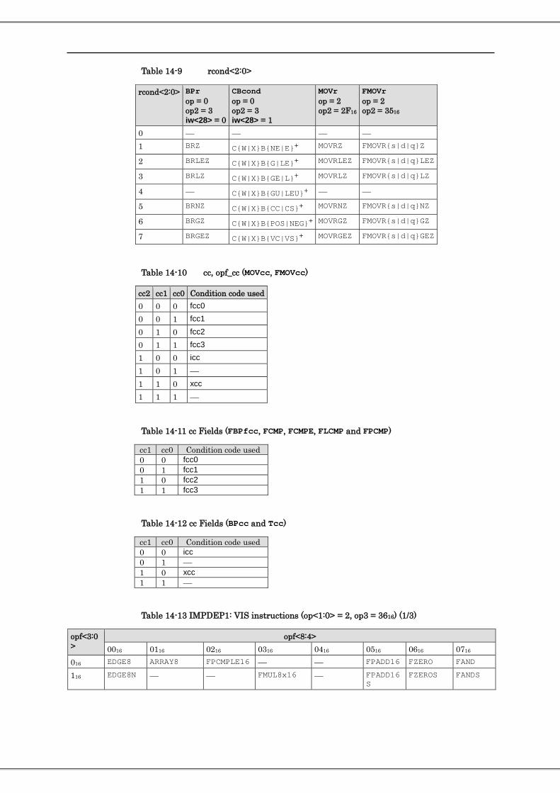
Table 14-9 rcond<2:0>
rcond<2:0> BPr op = 0 op2 = 3 iw<28> = 0
CBcond op = 0 op2 = 3 iw<28> = 1
MOVr op = 2 op2 = 2F16
FMOVr op = 2 op2 = 3516
0 1 BRZ C{W|X}B{NE|E}+ MOVRZ FMOVR{s|d|q}Z
2 BRLEZ C{W|X}B{G|LE}+ MOVRLEZ FMOVR{s|d|q}LEZ
3 BRLZ C{W|X}B{GE|L}+ MOVRLZ FMOVR{s|d|q}LZ
4 C{W|X}B{GU|LEU}+
5 BRNZ C{W|X}B{CC|CS}+ MOVRNZ FMOVR{s|d|q}NZ
6 BRGZ C{W|X}B{POS|NEG}+ MOVRGZ FMOVR{s|d|q}GZ
7 BRGEZ C{W|X}B{VC|VS}+ MOVRGEZ FMOVR{s|d|q}GEZ
Table 14-10 cc, opf_cc (MOVcc, FMOVcc)
cc2 cc1 cc0 Condition code used 0 0 0 fcc0
0 0 1 fcc1
0 1 0 fcc2
0 1 1 fcc3
1 0 0 icc
1 0 1 1 1 0 xcc
1 1 1
Table 14-11 cc Fields (FBPfcc, FCMP, FCMPE, FLCMP and FPCMP)
cc1 cc0 Condition code used 0 0 fcc0 0 1 fcc1 1 0 fcc2 1 1 fcc3
Table 14-12 cc Fields (BPcc and Tcc)
cc1 cc0 Condition code used 0 0 icc 0 1 1 0 xcc 1 1
Table 14-13 IMPDEP1: VIS instructions (op<1:0> = 2, op3 = 3616) (1/3)
opf<3:0>
opf<8:4> 0016 0116 0216 0316 0416 0516 0616 0716
016 EDGE8 ARRAY8 FPCMPLE16 FPADD16 FZERO FAND
116 EDGE8N FMUL8x16 FPADD16S
FZEROS FANDS

320 Ver 29.0 Jan. 2015
opf<3:0
opf<8:4> 216 EDGE8L ARRAY16 FPCMPNE16
FPCMPUNE16
FPADD64+ FPADD32 FNOR FXNOR
316 EDGE8LN FMUL8x16AU FPADD32S
FNORS FXNORS
416 EDGE16 ARRAY32 FPCMPLE32 FPSUB16 FANDNOT2 FSRC1
516 EDGE16N FMUL8x16AL FPSUB16S
FANDNOT2S
FSRC1S
616 EDGE16L FPCMPNE32 FPCMPUNE32
FMUL8sUx16 FPSUB64+ FPSUB32 FNOT2 FORNOT2
716 EDGE16LN
LZD FMUL8uLx16 FPSUB32S
FNOT2S FORNOT2S
816 EDGE32 ALIGNADDRES
FPCMPGT16 FMULD8sUx16
FALIGNDATA
FANDNOT1 FSRC2
916 EDGE32N BMASK FMULD8uLx16
FANDNOT1S
FSRC2S
A16 EDGE32L ALIGNADDRES _LITTLE
FPCMPEQ16 FPCMPUEQ16
FPACK32 FNOT1 FORNOT1
B16 EDGE32LN
FPACK16 FPMERGE FNOT1S FORNOT1S
C16 FPCMPGT32 BSHUFFLE FXOR FOR
D16 FPACKFIX FEXPAND FXORS FORS
E16 FPCMPEQ32 FPCMPUEQ32
PDIST FNAND FONE
F16 FNANDS FONES

Table 14-14 IMPDEP1: VIS instructions (op<1:0> = 2, op3 = 3616) (2/3)
opf<3:0> opf<8:4> 0816 0916 0A16 0B16 0C16 0D16 0E16 0F16
016 SHUTDOWN FAESENCX FADDtd FADDod FCMPLE16X
FPCMPLE16X+ FCMPLE8X
FPCMPLE8X+
116 SIAM FAESDECX FSUBtd FSUBod FUCMPLE16X
FPCMPULE16X+ FUCMPLE8X
FPCMPULE8X+
216 FAESENCLX FMULtd FMULod
316 SLEEP FAESDECLX FDIVtd FDIVod FUCMPNE16X
FPCMPUNE16X+ FUCMPNE8X
FPCMPUNE8X+
416 FAESKEYX FCMPtd FCMPod FCMPLE32X
FPCMPLE32X+ FCMPLE64X
FPCMPLE64X+ FPMAX
32X+
516 SDIAM FPSELMOV8
X+ FCMPEtd FUCMPLE32X
FPCMPULE32X+ FUCMPLE64X
FPCMPULE64X+ FPMAX
U32x+
616 FPSELMOV1
6X+ FQUAtd FQUAod FPMIN
32X+
716 FPSELMOV3
2X+ FRQUAod FUCMPNE32X
FPCMPUNE32X+ FUCMPNE64X
FPCMPUNE64X+ FPMIN
U32X+
816 FDESENCX FXADDodLO FCMPGT16X
FPCMPGT16X+ FCMPGT8X
FPCMPGT8X+
916 PADD32 FDESPC1X FXADDodHI FUCMPGT16X
FPCMPUGT16X+ FUCMPGT8X
FPCMPUGT8X+
A16 FDESIPX FXMULodLO
B16 FDESIIPX FUCMPEQ16X
FPCMPUEQ16X+ FUCMPEQ8X
FPCMPUEQ8X+
C16 FDESKEYX FbuxTOtd FCMPGT32X
FPCMPGT32X+ FCMPGT64X
FPCMPGT64X+ FPMAX
64X+
D16 FtdTObux FUCMPGT32X
FPCMPUGT32X+ FUCMPGT64X
FPCMPUGT64X+ FPMAX
U64X+
E16 FbsxTOtd FodTOtd FPMIN
64X+
F16 FPADD128X
HI+ FtdTObsx FtdTOod FUCMPEQ32X
FPCMPUEQ32X+ FUCMPEQ64X
FPCMPUEQ64X+ FPMIN
U64X+
Table 14-15 IMPDEP1: VIS instructions (op<1:0> = 2, op3 = 3616) (3/3)
opf<3:0> opf<8:4> 1016 1116 1216 1316 1416 1516 1616 1716 1816-1F16
016 FPCMPULE8+ FCMPEQd FMAXd
116 FLCMPs+ FCMPEQs FMAXs
216 FPCMPUNE8+ FLCMPd+ FCMPEQEd FMINd
316 FCMPEQEs FMINs 416 FPCMP64X+ FCMPLEEd FRCPAd
516 FPCMPU64X+ FCMPLEEs FRCPAs
616 FPSLL64X+ FCMPLTEd FRSQRTAd
716 FPSRL64X+ FCMPLTEs FRSQRTAs
816 MOVxTOd+ FPCMPUGT8+ FCMPNEd FTRISSELd
916 MOVwTOs+ FCMPNEs
A16 FPCMPUEQ8+ FCMPNEEd FTRISMULd

322 Ver 29.0 Jan. 2015
B16 FCMPNEEs C16 FCMPGTEd FEXPAd D16 FCMPGTEs E16 FCMPGEEd F16 FPSRA64X+ FCMPGEEs
Table 14-16 IMPDEP2: (op<1:0> = 2, op3 = 3716)
size var 0 1 2 3
016 FPMADDX FPMADDXHI FTRIMADDd FSELMOVd
116 FMADDs FMSUBs FNMSUBs FNMADDs
216 FMADDd FMSUBd FNMSUBd FNMADDd
316 FSHIFTORX FSELMOVs

15. Assembly Language Syntax 323
15. Assembly Language Syntax
15.1. Notation Used
15.1.1. Other Operand Syntax The syntax for software traps has been changed from JPS1 Commonality. The updated syntax is shown below.
software_trap_number
Can be any of the following:
regrs1 (equivalent to regrs1 + %g0)
regrs1 + simm8
regrs1 – simm8
simm8 (equivalent to %g0 + simm8)
simm8 + regrs1 (equivalent to regrs1 + simm8)
regrs1 + regrs2
Here, simm8 is a signed immediate constant that can be represented in 8 bits. The resulting operand value (software trap number) must be in the range 0 – 255, inclusive.
15.2. HPC-ACE Notation When an instruction is executed, the value of the XAR register determines whether the instruction uses any HPC-ACE features. Generally, these features are specified by combining an arithmetic instruction with SXAR. This section defines the assembly language syntax for specifying HPC-ACE features.
HPC-ACE extends the instruction definitions to support the use of HPC-ACE floating-point registers, SIMD execution, and hardware prefetch disable. While the SXAR instructions fully specify whether these features are used, the following notation is defined to facilitate easy reading of the assembly language:
(1) SXAR is written as sxar1 or sxar2. These instructions have no arguments.
(2) HPC-ACE floating-point registers are specified directly as arguments of the instruction.
(3) Other HPC-ACE features are specified by appending suffixes to the instruction mnemonic.

324 Ver 29.0 Jan. 2015
(4) The HPC-ACE features for a particular instruction are always specified by the closest preceding SXAR instruction. Another SXAR instruction in a sequence that branches to a point between an instruction and its corresponding SXAR never specifies features for that instruction.
An SXAR instruction must be placed 1 or 2 instructions before any instruction that uses the notation described in items (2) and (3). There are cases where the assembler cannot automatically determine that an SXAR needs to be inserted for an instruction that uses HPC-ACE features; thus, SXAR instructions cannot be omitted.
Whether a label can be inserted between an SXAR instruction and the instruction(s) that it modifies is not defined, as item (4) clearly defines which SXAR instruction specifies the HPC-ACE feature(s).
15.2.1. Suffixes for HPC-ACE Extensions A comma (,) is placed after the instruction mnemonic, and the alphanumeric character(s) that immediately follow the comma specify various HPC-ACE features. These suffixes are shown in Table 15-1.
Table 15-1 Suffixes for HPC-ACE Extensions
XAR Notation Suffix
XAR.simd s
XAR.dis_hw_pf d
XAR.negate_mul n
XAR.rs1_copy c
Suffixes are not case-sensitive. When two or more suffixes are specified, the suffixes may be specified in any order.
Example: SIMD instruction, HPC-ACE registers
sxar2
faddd %f0, %f2, %f510 /* HPC-ACE register specified, non-SIMD */
faddd,s %f0, %f2, %f4 /* SIMD, extended operation uses HPC-ACE registers */
Example 2: SIMD load
sxar1
ldd,s [%i1], %f0