Embed Size (px)
Citation preview
Int. J. Nanotechnol., Vol. 7, Nos. 9/10/11/12, 2010 833
Copyright © 2010 Inderscience Enterprises Ltd.
Structure and energetics of silicon clusters adsorbed on the Au(111) surface: a first principles study
Sudip Chakraborty Department of Electronic Science, University of Pune, Pune 411 007, India
and
Chemistry Division, Bhabha Atomic Research Center, Trombay, Mumbai 400 085, India E-mail: [email protected]
S.V. Ghaisas Department of Electronic Science, University of Pune, Pune 411 007, India E-mail: [email protected]
Chiranjib Majumder*Chemistry Division, Bhabha Atomic Research Center, Trombay, Mumbai 400 085, India E-mail: [email protected] *Corresponding author
Abstract: We report an extensive first-principles investigation of the structure and electronic properties of small Sin (n = 1, 2, 3, 4, and 6) clusters deposited on the Au(111) surface. The calculations were performed using a plane wave based pseudopotential method under the framework of density functional theory. The electron-ion interaction energy has been described using ultrasoft pseudopotentials (USPP) and the spin polarised GGA scheme was used for the exchange correlation energy. The results reveal that Si atom prefers to adsorb on the hcp site of the Au(111) surface with strong binding energy. For Si3, the closed triangle geometry of the bare cluster forms an open triangle by rupturing one of the three Si-Si bonds. Remarkable structural changes in the gas phase geometries were observed from Si4 onwards. For example, while the adsorption of rhombus in parallel and perpendicular orientation to the surface plane remains almost unaltered, the tetrahedral conformation becomes almost flat by the interaction of Au surface. The nature of chemical

834 S. Chakraborty et al.
bonding between Au surface and Si clusters was investigated from the charge distribution analysis and the electronic density of states (EDOS). Based on charge distribution analysis it is found that Si atoms transfer charges to the Au surface. Based on the results it is inferred that Si clusters deposition on the Au surface involves large energy release and would lead to coat the surface by spill over of Si atoms rather than island formation.
Keywords: Au surface; silicon cluster; adsorption; projected density of states; binding energy; charge transfer.
Reference to this paper should be made as follows: Chakraborty, S., Ghaisas, S.V. and Majumder, C. (2010) ‘Structure and energetics of silicon clusters adsorbed on the Au(111) surface: a first principles study’, Int. J. Nanotechnol., Vol. 7, Nos. 9/10/11/12, pp.833–842.
Biographical notes: Sudip Chakraborty received his Bachelor’s Degree in Physics from the University of Calcutta and his Master’s Degree in Physics from the University of Pune. He joined BARC-P.U. (Bhabha Atomic Research Center and Pune University) and pursuing PhD under the guidance of Dr. S.V. Ghaisas from the University of Pune and Dr. Chiranjib Majumder from Bhabha Atomic Research Center, specialising in simulation of nanotechnology. He is currently working on density functional theory based calculation of adsorption for silicon clusters on different substrates. He is also working on optical properties calculation of semiconductor quantum dots, especially silicon.
S.V. Ghaisas graduated from the University of Pune with PhD in Physics in 1981. He has been working on Molecular Beam Epitaxy (MBE) growth as one of the subjects of interest. He has worked on experimental as well as simulations of growth. He has developed various stochastic models to understand the non-equilibrium aspects of growth and also realistic growth models. His present focus is on understanding the behaviour of nanomaterials from the point of view of devices. He is Professor in Electronic Science at the University of Pune and is also holding the additional charge as Director, School of Energy studies.
Chiranjib Majumder joined Chemistry Division, Bhabha Atomic Research Centre in 1992 after graduating through 35th batch of training school. He has developed an in-house experimental facility to generate supersonic molecular beams in tandem with a time-of-flight mass spectrometer. He received his PhD in 2000 for the experimental and theoretical studies of metal clusters. During 2001–2002, he was at the Institute for Materials Research, Tohoku University, Japan, to carry out postdoctoral work with Professor Y. Kawazoe, where he has worked on the theoretical aspects of molecular electronics. Subsequently, he visited the laboratory of Professor P. Jena, at the Physics Department of Virginia Commonwealth University, USA, to work on the electronic and atomic structures of clusters. His current research interest is to design novel materials for catalysis by tuning the electronic properties of nano-materials and to underscore the mechanism of cluster–molecule interactions on a support matrix.

Structure and energetics of silicon clusters 835
1 Introduction
Cluster deposition on metal or metal oxide surface are of growing interest because of their important role in various technological applications such as metal–ceramic based gas sensors, microelectronic devices and oxide supported transition metal catalysts [1–10]. Understanding the nature of cluster/metal interfaces constitutes one of the most appealing challenges nowadays for material scientists. Among many nano-structures, the study of Si clusters is an active area of basic research, which is highly relevant to present advances of micro and nanoelectronics technology. Moreover, Sin clusters and nano-structures are widely studied due to their fundamental role in cluster physics and chemistry as well as their applications in materials science [11–15]. It is known that the electronics properties of Si clusters are a strong function of the size. Thus it is possible to tailor their activity by varying the size of clusters. The optical and electronic properties of these nano-systems are largely governed by the quantum size effect and distribution of Si clusters [15]. Cluster deposition has also come up as one of the powerful tool in fabricating nanoscale devices. Various methods are in use to deposit Si clusters in neutral or ionic form. These cluster depositions offer a large surface area and also inherent quantum confinement effect. This makes such deposited films very attractive for applications for fundamental studies.
The structures of clusters in vacuum are modified upon deposition on a substrate. It is known that such interactions lead to form self-assembled nanostructures [16,17]. In this work we have investigated the deposition of Si clusters on the Au surface. The objective of the current study is to
• identify the preferred adsorption sites and structure of deposited Si clusters, in particular, analyse the relaxed geometry in comparison to most stable gas-phase isomer
• to explore the nature of Si/AU bonding and to quantify the adsorption energy to obtain the competing information for clustering vis-à-vis wetting processes, a useful insight for heterogeneous catalysis.
Choice of Au as a model substrate is motivated by its chemical neutrality and use in Si based technology. Adsorption of single Si atom on Au surface has been studied earlier [18]. It is found that the Si atom prefers to be adsorbed on the hexagonal closed pack (hcp) site to other well-defined sites. The chemical bonding between the Si and Au atoms is governed through the covalent interaction. It is therefore of interest to find out how an Si cluster would behave on Au surface in terms of its relative placement with respect to underlying lattice. The concomitant changes in the electronic structure are expected to shade light on the chemical behaviour of such adsorbates.
2 Computational methods
All the calculations were performed using the density functional theory with ultrasoft-pseudopotentials (USPP) and plane wave basis set as implemented in VASP code [19]. The spin polarised Perdew-Wang generalised gradient approximation

836 S. Chakraborty et al.
(GGA) has been used to calculate the exchange-correlation energy [20]. A simple cubic supercell of side 15 Å has been used and the Brillouin zone integrations were carried out using only the gamma point. The self-consistent equations were solved with an iterative matrix diagonalisation scheme. Geometry optimisations were performed with the conjugate gradient algorithm [21,22] and the geometries were considered to be converged when the force on each atom became 0.01 eV/Å or less. The total-energy convergence was tested with respect to the plane-wave basis set size and simulation cell size, and the total energy was found to be accurate to within 1 meV.
Test calculations were done for Au bulk to verify the accuracy of our computational methodology. From our calculations the lattice parameters of the Au bulk was found to be 4.13 Å, which is quite close (~1% error) to the experimental value of 4.09 Å [23]. The bulk cohesive energy was estimated to be 3.61 eV/atom, which is close to the experimental value (3.81 eV/atom).
The Au(111) surface has been modelled by truncating the infinite bulk surface in the X-Y-direction with four layers in the Z-direction. Two neighbouring slabs were separated by 12 in the Z-direction. The Au(111) slab is constructed with total 100 atoms, where each layer contains 25 atoms. For the optimisation of this slab, while all atoms at the top three layers were optimised, the atoms at the bottom layers were kept fixed at the bulk values. The clean Au(111) surface was calculated using 8 × 8 × 1 Monkhorst-Pack k-point mesh, which corresponds to 52 special k points in the surface Brillouin zone. The adsorption energy of the system is calculated as Eadsorption = Eslab+cluster – Eslab – Ecluster.
3 Results and discussion
3.1 Si on the Au(111) surface
In order to obtain the most preferred Si adsorption site on the Au(111) surface, the geometry optimisation was carried out at two different levels. In the first step, the Si atom was placed at four well defined sites of the Au(111) surface (top, bridge, hcp and fcc) and in the second step, the Si atom was placed randomly at a height of 3.0 Å from the topmost layer of the Au(111) surface and allowed to relax. It is found that Si atom prefers to adsorb on the hcp site rather than other well-defined sites with adsorption energy of 4.24 eV. The smallest inter-atomic distance between the Au and Si is found to be 2.43 .
3.2 Si2 and Si3 on the Au(111)
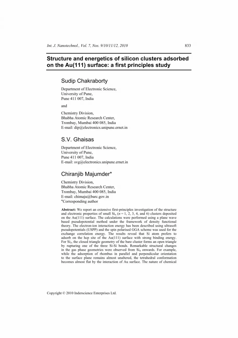
Figure 1(a) and (b) show the optimised geometries of the Si2 and Si3 clusters on the Au(111) surface. In both cases, it is seen that the Si atoms prefer to locate on the hcp site. However, the separation between two consecutive hcp sites on the Au surface is 2.80 Å. Hence, accommodating silicon cluster in Au plane requires rearranging Au surface atoms along with stretching of Si-Si bonds. In gas phase, the Si-Si bond lengths of Si2 and Si3clusters are 2.32 Å and 2.26 Å, respectively, which after deposition on the Au surface elongate up to 2.42 Å and 2.48 Å. This difference leads to local distortion of the Au surface in the vicinity of Si adsorption site. The adsorption energies of Si2 and Si3 clusters on the Au(111) surface are found to be 6.0 eV and 5.8 eV, respectively. The adsorption
Structure and energetics of silicon clusters 837
energy per atom decreases for Si3 due to the increase in bond length on adsorption, by about 23% over the isolated trimer.
Figure 1 Optimised geometries of (Figure 1(a)) Si2 and (Figure 1(b)) Si3 clusters on the Au(111) surface (see online version for colours)
(a) (b)
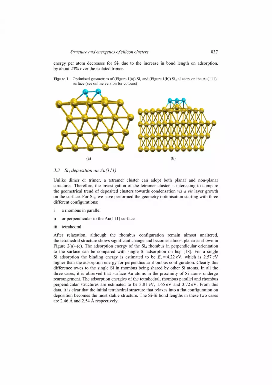
3.3 Si4 deposition on Au(111)
Unlike dimer or trimer, a tetramer cluster can adopt both planar and non-planar structures. Therefore, the investigation of the tetramer cluster is interesting to compare the geometrical trend of deposited clusters towards condensation vis a vis layer growth on the surface. For Si4, we have performed the geometry optimisation starting with three different configurations:
i a rhombus in parallel
ii or perpendicular to the Au(111) surface
iii tetrahedral.
After relaxation, although the rhombus configuration remain almost unaltered, the tetrahedral structure shows significant change and becomes almost planar as shown in Figure 2(a)–(c). The adsorption energy of the Si4 rhombus in perpendicular orientation to the surface can be compared with single Si adsorption on hcp [18]. For a single Si adsorption the binding energy is estimated to be Eb = 4.22 eV, which is 2.57 eV higher than the adsorption energy for perpendicular rhombus configuration. Clearly this difference owes to the single Si in rhombus being shared by other Si atoms. In all the three cases, it is observed that surface Au atoms in the proximity of Si atoms undergo rearrangement. The adsorption energies of the tetrahedral, rhombus parallel and rhombus perpendicular structures are estimated to be 3.81 eV, 1.65 eV and 3.72 eV. From this data, it is clear that the initial tetrahedral structure that relaxes into a flat configuration on deposition becomes the most stable structure. The Si-Si bond lengths in these two cases are 2.46 Å and 2.54 Å respectively.

838 S. Chakraborty et al.
Figure 2 Optimised geometries of Si4 rhombus along (Figure 2(a)) and perpendicular(Figure 2(b)) to the surface plane and tetrahedral (Figure 2(c)) (see online version for colours)
(a) (b)
(c)
3.4 Si6 deposition on Au(111)
We now consider the deposition of Si6 cluster on the Au(111) surface. Total four configurations were optimised viz.
i boat
ii planar
iii pivotal
iv prism.
Out of these, the planar configuration was found to form the most stable geometry. Figure 3(a) and (b) show the optimised structures of the planar and prism configurations on the Au surface. In case of planar isomer the silicon atoms tend to form dimer like structures and a layer is formed by aligning these dimers. In the case of prism, as shown in Figure 3(b), the relaxed structure consists of three standing dimer separated by relative distances of 2.55 Å. Thus, deposition of prism shaped Si6 cluster leads to form a double-layer as growth proceeds on the Au surface. The adsorption energy for

Structure and energetics of silicon clusters 839
the layered configuration is 5.54 eV per silicon atom. We note that this is higher than the adsorption energy of a silicon atom at the hcp site and indicates collective role of silicon atom in providing higher binding energy of the Si6 cluster.
Figure 3 Optimised geometries of Si6 cluster in layered (Figure 3(a)) and prism (Figure 3(b)) forms (see online version for colours)
(a) (b)
3.5 Electronic structure and charge transfer
In order to understand the effect of Sin cluster adsorption on the electronic structure of the substrates, we have compared the projected density of states (PDOS) of Au(111) surface, before and after adsorption. In general after deposition of Sin clusters, new peaks appear just below the Fermi level. To avoid repetition of discussion we will consider the electronic structure of Si4 cluster and Si4 cluster deposited on the Au(111) surface only. We have considered the most stable geometry of the Si4 cluster after deposition, which undergoes a structural transition from regular tetrahedron to a planar configuration. The preference of a planar configuration over tetrahedron is attributed to the strong adhesion of Si atoms with Au. Figure 4(a) shows the partial density of states for Au slab. As expected, the total DOS is largely contributed by the 5d electrons of Au with states extending continuously beyond fermi level. From the charge content in the s, pand d orbitals of individual atoms it is seen that on pure Au(111) slab, the surface atoms transfer some electrons in the bulk, creating a dipole layer. After the deposition of Si4 on the surface, the PDOS of the top layer Au atoms changes near the fermi energy as shown in Figure 4(b). Since valence electrons are primarily involved in the chemical interaction, region near fermi level is expected to show signature of such interaction. To clarify this situation we compare the PDOS between the inset in Figure 4(a) and (b). The comparison shows the modification induced due to the adsorption of Si4. Figure 4(c) shows similar plot from –5 eV to 5 eV for isolated Si4. Figure 4(d) shows the new states near EF in the PDOS of Si4 after deposition. Comparing Figure 4(b) and (d) it may be inferred that over the same range of energy i.e., –0.5 eV to 0.3 eV, the PDOS has similar pattern for d states of Au and p states of Si atoms. This implies that the bonding between Au and Si atoms takes place through p and d state mixing. The similarity of the patterns implies degeneracy in PDOS over both silicon and gold atoms indicating bond formation. A comparison of Figure 4(c) and (d) indicates that the mixing of d and p states results

840 S. Chakraborty et al.
in broadening and redistribution of states around Si atoms. In the process of adsorption, neighbouring Au atoms are shifted from the relaxed surface positions, which are indicated in Figure 2(c) by an arrow. Even for the other optimised structures the displaced Au atoms are pointed out by arrows. The charge content as calculated from PDOS for this atom is 10.223 and for another neighbouring atom in the same row, which is not displaced it is 10.212. This comparison shows that for displaced atoms, the charge content increases compared to other Au atoms. By noting the charge associated with different states on Si and Au, it is seen that charge is transferred from Si to Au. This is also verified from the shift in the core level orbital of Si in Figure 4(b)–(d), which shows a tighter binding due to charge transfer from Si to Au.
Figure 4 PDOS of (a) clean Au slab, (b) Au top layer after deposition of Si4 on Au (111), (c) Si4 bare cluster, (d) after deposition of Si on Au (111) (see online versionfor colours)
(a) (b)
(c) (d)

Structure and energetics of silicon clusters 841
4 Conclusions
Using first principles calculations we have investigated the structural and electronic properties of small Sin [n = 1, 2, 3, 4, 6] clusters deposited on the Au(111) substrate. The calculations have been carried out using plane wave based pseudo potential method under the density functional theory formalism. The effect of substrate interaction on the geometrical evolution of small Sin clusters is illustrated by comparing the isolated clusters with the deposit. While the Si2 and Si3 clusters are seen to retain the line and (isosceles or equilateral) triangle structure respectively on deposition, the Si4 and Si6clusters shows significant changes with different orientations with respect to Au(111) substrate. This results in different meta-stable states. We have presented results for most stable orientation. It is seen that layered Si6 has the highest binding energy per atom compared to all other orientation of the smaller clusters Sin (n = 1–4). This indicates a collective role by silicon atoms in improving the binding for a layered structure on Au(111) surface. The study of deposition of Si4 clusters shows that Au-Si interaction can be strong enough to distort the cluster geometry to a planar one. From the charge content analysis, it is observed that Si transfers charge to Au surface. The charge content of Au atoms in the proximity of Si is also modified. The changes in projected density of states (PDOS) are consistent with the bonding of Si with substrate. These changes collate well with the strength of bonding.
Acknowledgements
The author Sudip Chakraborty would like to thank DAE for financial support. The authors gratefully acknowledge the computational facility made available by C-DAC, Pune. Thanks to Dr. V. Sundararajan and S. Nanavati of C-DAC, Pune, India, and Professor S. Mahamuni and Ch. Rajesh of Department of Physics, University of Pune, India, for illuminating discussions.
References1 Valden, M., Lai, X. and Goodman, D.W. (1998) ‘Onset of catalytic activity of gold clusters
on Titania with the appearance of nonmetallic properties’, Science, Vol. 281, No. 5383, pp.1647–1650.
2 Haruta, M. (1997) ‘Size- and support-dependency in the catalysis of gold’, Catal. Today,Vol. 36, No. 1, pp.153–166.
3 Orlov, A.O., Amlani, I., Bernstein, G.H., Lent, C.S. and Snider, G.L. (1997) ‘Realization of a functional cell for quantum-dot cellular automata’, Science, Vol. 277, No. 5328, pp.928–930.
4 Andrew, R.P., Bein, T., Dorogi, M., Feng, S., Henderson, J.I., Kubiák, C.P., Mahoney, W., Osifchin, R.G. and Reifenberger, R. (1996) ‘‘Coulomb staircase’ at room temperature in a self-assembled molecular nanostructure’, Science, Vol. 272, No. 5266, pp.1323–1325.
5 Kim, T.W., Choo, D.C., Sim, J.H. and Kang, S.O. (2002) ‘Single-electron transistors operating at room temperature, fabricated utilizing nanocrystals created by focused-ion beam’, Appl. Phys. Lett., Vol. 80, No. 80, pp.2168–2170.
6 Sun, S., Murray, C.B., Weller, D., Folks, L. and Moser, A. (2000) ‘Monodisperse FePt nanoparticles and ferromagnetic FePt nanocrystal superlattices’, Science, Vol. 287, No. 5460, pp.1989–1992.

842 S. Chakraborty et al.
7 Solin, S.A., Hines, D.R., Rowe, A.C.H., Tsai, J.S., Pashkin, Y.A., Chung, S.J., Goel, N. and Santos, M.B. (2002) ‘Nonmagnetic semiconductors as read-head sensors for ultra-high-density magnetic recording’, Appl. Phys. Lett., Vol. 80, No. 21, pp.4012–4014.
8 Koide, T., Miyauchi, H., Okamoto, J., Shidara, T., Fujimori, A., Fukutani, H., Amemiya, K., Rakeshita, H., Yuasa, S., Katayama, T. and Suzuki, Y. (2001) ‘Determination of interfacial magnetic moments with a magnetic phase transition in co nanoclusters on Au (111)’, Phys. Rev. Lett., Vol. 87, No. 25, pp.25721–25724.
9 Petroff, P.M., Lorke, A. and Imamoglu, A. (2001) ‘Epitaxially self-assembled quantum dots’, Phys. Today, Vol. 54, No. 5, pp.46–52.
10 Zonechet, D., Micheel, C.M., Parak, W.J., Gerion, D. and Alivisatos, A.P. (2001) ‘Electrophoretic isolation of discrete Au nanocrystal/DNA conjugates’, Nano Lett., Vol. 1, No. 1, pp.32.
11 Lu, Z.Y., Wang, C.Z. and Ho, K.M. (2000) ‘Structures and dynamical properties of Cn,Sin, Gen, and Snn clusters with n up to 13’, Phys. Rev. B, Vol. 61, No. 3, pp.2329–2334.
12 Tománek, D. and Schlüter, M.A. (1986) ‘Calculation of magic numbers and the stability of small Si clusters’, Phys. Rev. Lett., Vol. 56, No. 10, pp.1055–1058.
13 Tománek, D. and Schlüter, M.A. (1987) ‘Structure and bonding of small semiconductor clusters’, Phys. Rev. B, Vol. 36, No. 2, pp.1208–1217.
14 Raghavachari, K. and Logovinsky, V. (1985) ‘Structure and bonding in small silicon clusters’, Phys. Rev. Lett., Vol. 55, No. 26, pp.2853–2856.
15 Pacchioni, G. and Koutecky, J. (1986) ‘Silicon and germanium clusters. A theoretical study of their electronic structures and properties’, J. Chem. Phys., Vol. 84, No. 6, pp.3301–3310.
16 Cho, J.H. and Gracias, D.H. (2009) ‘Self-assembly of lithographically patterned nanoparticles’, Nano Lett., Vol. 9, No. 12, pp.4049–4052.
17 Wang, X., Lin, Q., Li, R. and Zhu, Z. (2006) ‘First-principles calculations for the structural stabilities of ordered Nb4 clusters on the Cu(111) surface’, Phys. Rev. B, Vol. 73, No. 24, pp.245404–245410.
18 Mujumder, C. (2007) ‘Effect of Si adsorption on the atomic and electronic structure of Aun clusters (n = 1–8) and the Au (111) surface: first-principles calculations’, Phys. Rev. B,Vol. 75, No. 23, pp.235409–235416.
19 Vanderbilt, D. (1990) ‘Soft self-consistent pseudopotentials in a generalized eigenvalues formalism’, Phys. Rev. B, Vol. 41, No. 11, pp.7892–7895.
20 Perdew, J.P. and Wang, Y. (1986) ‘Accurate and simple density functional for the electronic exchange energy: generalised gradient approximation’, Phys. Rev. B, Vol. 33, No. 12, pp.8800–8802.
21 Kresse, G. and Hafner, J. (1993) ‘Ab initio molecular dynamics for liquid metals’, Phys. Rev. B, Vol. 47, No. 1, pp.558–561.
22 Kresse, G. and Furthmülar, J. (1996) ‘Efficiency of ab-initio total energy calculations for metals and semiconductors using a plane-wave basis set’, Comput. Mater. Sci.,Vol. 6, No. 6, pp.15–55.
23 Kittel, C. (1996) Introduction to Solid State Physics, 7th ed., Wiley, New York.


