Embed Size (px)
Citation preview
Citation: Gil-Corrales, J.A.; Vinasco,
J.A.; Mora-Ramos, M.E.; Morales
A.L.; Duque, C.A. Study of Electronic
and Transport Properties in
Double-Barrier Resonant Tunneling
Systems. Nanomaterials 2022, 12, 1714.
https://doi.org/10.3390/nano
12101714
AcademicEditors: Tzi-yi Wu and Ali
Belarouci
Received: 3 April 2022
Accepted: 13 May 2022
Published: 17 May 2022
Publisher’s Note: MDPI stays neutral
with regard to jurisdictional claims in
published maps and institutional affil-
iations.
Copyright: © 2022 by the authors.
Licensee MDPI, Basel, Switzerland.
This article is an open access article
distributed under the terms and
conditions of the Creative Commons
Attribution (CC BY) license (https://
creativecommons.org/licenses/by/
4.0/).
nanomaterials
Article
Study of Electronic and Transport Properties in Double-BarrierResonant Tunneling SystemsJohn A. Gil-Corrales 1 , Juan A. Vinasco 1, Miguel E. Mora-Ramos 2 , Alvaro L. Morales 3,*and Carlos A. Duque 1
1 Grupo de Materia Condensada-UdeA, Instituto de Física, Facultad de Ciencias Exactas y Naturales,Universidad de Antioquia UdeA, Calle 70 No. 52-21, Medellín 050022, Colombia;[email protected] (J.A.G.-C.); [email protected] (J.A.V.);[email protected] (C.A.D.)
2 Centro de Investigación en Ciencias-IICBA, Universidad Autónoma del Estado de Morelos,Av. Universidad 1001, Cuernavaca 62209, Morelos, Mexico; [email protected]
3 Grupo de Estado Sólido, Instituto de Física, Facultad de Ciencias Exactas y Naturales,Universidad de Antioquia Udea, Calle 70 No. 52-21, Medellín 050022, Colombia
* Correspondence: [email protected]
Abstract: Resonant tunneling devices are still under study today due to their multiple applicationsin optoelectronics or logic circuits. In this work, we review an out-of-equilibrium GaAs/AlGaAsdouble-barrier resonant tunneling diode system, including the effect of donor density and externalpotentials in a self-consistent way. The calculation method uses the finite-element approach andthe Landauer formalism. Quasi-stationary states, transmission probability, current density, cut-offfrequency, and conductance are discussed considering variations in the donor density and the widthof the central well. For all arrangements, the appearance of negative differential resistance (NDR)is evident, which is a fundamental characteristic of practical applications in devices. Finally, acomparison of the simulation with an experimental double-barrier system based on InGaAs withAlAs barriers reported in the literature has been obtained, evidencing the position and magnitude ofthe resonance peak in the current correctly.
Keywords: resonant tunneling diode; electronic transmission probability; Landauer formalism
1. Introduction
Resonant tunneling diodes (RTDs) are semiconductor devices that consist of a systemof two or more potential barriers that allow electron transport only for certain states knownas resonant states. The operating mechanism is fundamentally based on the tunnelingeffect of quantum mechanics. This type of system is characterized by developing one ormore NDR zones that are the fundamental peculiarity of RTDs that enable them to beused for various applications. These devices are experimentally developed in very thinlayers, which allows for an ultrafast operation speed, enabling them for applications evenin the terahertz range [1–4]. The first investigations in the field of resonant tunneling werecarried out around 50 years ago; some of these early developments are included in thereferences [5–12]. These studies have progressed continuously, characterizing RTDs bothexperimentally and theoretically. To mention some of the most recent work in this area,Citro and Romeo [13] studied a flux-tunable tunneling diode using a mesoscopic ringsubject to the Rashba spin–orbit interaction and sequentially coupled to an interactingquantum dot, in the presence of an Aharonov–Bohm flux. Wójcik et al. [14] studied the spin-and time-dependent electron transport in a paramagnetic resonant tunneling diode usingthe self-consistent Wigner–Poisson method. They found that under a constant bias, both thespin-up and spin-down current components exhibit the THz oscillations in two differentbias voltage regimes. In more recent works, Shinkawa et al. [15] studied the hole-tunneling
Nanomaterials 2022, 12, 1714. https://doi.org/10.3390/nano12101714 https://www.mdpi.com/journal/nanomaterials
Nanomaterials 2022, 12, 1714 2 of 19
in Si0.82 Ge0.18/Si asymmetric-double-quantum-well RTD with high-resonance current andsuppressed thermionic emission. Simultaneously, Encomendero et al. [16] investigated thepossibility of using degenerately doped contact layers to screen the built-in polarizationfields and recover symmetric resonant injection; they found negative differential conduc-tance (NDC) under both bias polarities of GaN/AlN RTDs. Several theoretical works thatapproach resonant tunneling systems by means of the non-equilibrium Green’s formalism(NEGF) for the calculation of the transmission function have been reported [17,18].
As an application of tunneling systems, Belkadi et al. [19] demonstrated the appear-ance of resonant tunneling effects in metal-double-insulator-metal-type diodes, by varyingthe thickness of insulators to modify the depth and width of the quantum well. Variousanalytical works [20–22] have sought an improvement in the efficiency, a decrease in thedissipation power, and the optimization of parameters to obtain the highest peak-to-valleycurrent ratio in resonant tunneling systems of various materials, which can improve theapplicability in practical devices. Finally, in recent reports [23,24], resonant systems areevidenced as possible direct applications in communication systems for frequencies of theorder of Gigahertz or the possibility of using RTDs as memory systems. Among the experi-mental developments in this area, in works such as those from Ryu and co-workers [25],asemitransparent cathode of indium tin oxide (ITO)/Ag/ITO is studied, developed as aresonant tunneling double-barrier structure for transparent organic light-emitting diodes.This was achieved by employing an e-beam evaporated ITO/Ag/ITO cathode due to thedouble quantum barriers of ITO and the quantum well of Ag. Their results include theobservation of a weak NDR in devices using a 100 nm thick ITO/Ag/ITO layer as a cathodein combination with a thin LiF/Al layer. In a later work, Ryu et al. [26] developed asemitransparent multilayered cathode of indium tin oxide (ITO)/Ag/tungsten oxide (WO3)for transparent organic light-emitting diodes (LEDs). The device showed a weak NDR,until the operating voltage of 8 V was reached.
It is worth mentioning some recent experimental and theoretical related works thathave sought to improve the efficiency of optoelectronic devices, including perovskite light-emitting diodes (PeLEDs) [27], solar cells that use resonant semiconductor nanoparticles(NPs) and improve both light trapping and scattering [28], multiple quantum well (MQW),and quantum dot (QD) nitride-based light-emitting diodes (LEDs) [29,30].
Over the years, knowledge about the operation and physics behind this type ofsemiconductor devices has expanded, thus allowing numerous applications, among whichwe can highlight: Wei and Shen’s work, where a novel universal threshold logic gates(UTLG) based on RTD with simple structure and fixed parameters are proposed, takingadvantage of the characteristics of NDR [31]. Jijun et al. analyzed the piezoelectric effectsin RTDs based on GaAs/InxGa1−xAs/AlAs for potential applications in micromachinedmechanical sensors, obtaining the result that the piezoresistive sensitivity of RTDs can beadjusted through the bias voltage [32]. Due to their particular NDR behavior, these systemsare excellent candidates for applications to nanoelectronics; in this sense, Malindretoset al. grew a GaAs/AlAs RTD by means of a molecular beam epitaxy; their results aresatisfactory and of good precision to fabricate RTDs suitable for application in robust digitallogic circuits [33]. Among all the applications of this type of system, it is worth highlightingapplications in detector devices that can filter in a varied range of frequencies by simplymodifying geometric or material parameters. To mention such a device, Dong et al. [34]developed an RTD based on In0.53Ga0.47. As for detection in the 1550 nm range, they foundthat the detector responsivity is nonconstant, it decreases with the increase of the incidentlight power density, which provides the basis for optimizing the RTD performance.
Resonant tunneling systems go beyond double-barrier-based systems. In 2020, MehmetBati [35] studied the effects of an intense laser field on the properties of resonant tunnel-ing in a double-well-structure parabolic reverse triple-barrier system, implementing themethod of finite differences combined with the Green function formalism to calculate thetransmission functions, obtaining the conclusion that the increment of the well width causes

Nanomaterials 2022, 12, 1714 3 of 19
the incident electron waves to be localized. Consequently, the transmittance decreases, andthe resonant peak becomes small or disappears.
In this problem, the Landauer approach has been chosen for the calculation of con-ductance, since it is a model that has a fairly broad theoretical development and that hasbeen studied in depth for more than 40 years. In 1981, Langreth D.C. and Abrahams E.presented a rigorous derivation of the conductance formula from the linear response theory(Kubo’s formula), giving a generalization to the case of many-scattering-channel and foundthat only in very special circumstances can the currents in different channels be decoupledin such a way as to give a simple conductance formula [36]. Six years later, S. Eränen andJ. Sinkkonen further generalized this formalism, studying the electrical current transportin conductor–insulator–conductor structures, where the charge carriers are assumed totraverse the insulating layer by tunneling. They self-consistently solved the coupled systemof Poisson and Boltzmann equations, the latter giving the form of temporary relaxation.An important conclusion of this work is that the tunneling current density comes from thecontribution of two effects: the first is the ordinary contribution of the Landauer formula inthe linear voltage regime, and the second is a correction term originated by the screening ofthe electric potential through the insulating layer. The contribution to the current due tothis screening term in most systems is negligible compared to the current generated by theeffect of resonant tunneling. These results are detailed in [37].
Apart from the effect of the charge redistribution caused by the ionized donors andthe external electric field applied to the contacts, it is possible to analyze the effect ofthe electronic spin dependence on the transport properties in magnetic RTD. The threecombined effects generate an effective modification in the profile associated with thebottom of the conduction band in the heterostructure that finally causes modificationsin the electronic transport properties. In the work of Havu et al. [38], the self-consistentspin-density-functional theory method was implemented within the Wigner formalismwith Green functions to analyze the properties of electronic transport in a magnetic RTDobtaining the electronic densities and potentials, studying the computational cost thatthis requires.
Over the years, research has continued to improve numerical techniques to make themmore efficient and extend theoretical developments in various physical situations. Takingadvantage of the versatility in terms of materials and external parameters with which itis possible to develop RTDs, our main interest is to develop a methodological approachto address these types of problems by first solving the effect of charge redistribution andelectron density in the system out of equilibrium to obtain in this way the profile at thebottom of the self-consistent conduction band. This will act as an input parameter for thepotential term in the Schrödinger equation, considering open boundary conditions in theeffective mass approximation, this equation, as well as the Poisson equation, is solvedthrough the finite-element method (FEM) to obtain a set of quasi-stationary states andprobabilities of electronic transmission in the system. Finally, with these transmissionfunctions, the Landauer formalism is implemented for the calculation of the density currentand conductance. In this study, we report the self-consistent potentials, quasi-stationaryelectronic states, tunneling currents, and conductances for different widths of the centralwell and different donor densities; then, a comparison is drawn between theoretical resultsof this procedure with recently reported experimental results. The article is organized asfollows: Section 2 presents the theoretical framework of the simulation. In Section 3, weshow and discuss the results obtained. Section 4 is devoted to the conclusions of the work.
2. Theoretical Model
Our system corresponds to an RTD (Resonant Tunneling Diode), consisting of a GaAscentral region (Quantum Well) of length Lw, surrounded by two Al0.3Ga0.7As barrierswith equal lengths Lb. There are two additional GaAs undoped spacers with lengths Ls;the purpose of these layers is to prevent electronically tunneling scattering effects due toimpurities in the contact region. Finally, two outer GaAs doped layers of length Ld. This

Nanomaterials 2022, 12, 1714 4 of 19
is the central system that is contacted with two electronic reservoirs or metal contacts oneach side, as presented in Figure 1. For this work, we consider a non-rectifying metal-semiconductor junction, which consists of a negligible relative resistance of the contactscompared to the resistance of the central device. In this case, it is considered that mobilityeffects are due solely to the electronic movement in the conduction band.
LdLsLbLwLbLs
GaA
s
Al 0.
3Ga 0.
7As
Al 0.
3Ga 0.
7As
GaA
s
GaA
s
GaA
s D
oped
GaA
s D
oped
Met
al c
onta
c
Met
al c
onta
c
LdFigure 1. Scheme of the resonant tunneling diode (RTD), with doping nd in the outer regions, twoAl0.3Ga0.7As barriers, a GaAs well, and two outer regions of the GaAs undoped with two metalcontacts in the external regions.
The system was solved through the finite-element method with the COMSOL-Multiphysics licensed software by (5.4, COMSOL AB, Stockholm, Sweden) [39–41], imple-menting the semiconductor module (“Semiconductor Module User’s Guide” COMSOLMultiphysics®) [42]. As a starting point, we must consider the effect on the potential of thedonor density and electron density in the system—this can be modeled by means of thePoisson equation,
~∇ · (ε0εr~∇V(x)) = −ρ(x), (1)
in this equation, εr and ε0 are the relative permittivity and vacuum permittivity, respectively,and the charge density ρ(x) has the form
ρ(x) = −qe(n(x)− Nd), (2)
in this equation, Nd is the number of donors which are considered to be fully ionized, andqe is the electronic charge. The electronic density has the form
n(x) = Ncγne−β (Ec−EF), (3)
in Equation (3), Ec is the bottom of the conduction band, which, due to the effect of theredistribution of charges, is not a straight line, but it is a function that can vary with position,EF is the quasi-Fermi level (for the system out of equilibrium) associated with the conductionband. The term Nc = 2(m∗/ 2πβh̄2)3/2 corresponds to the effective density of states, withm∗—the electron effective mass, kB is the Boltzmann constant, h̄ is the reduced Planckconstant, and β is the Boltzmann factor β = 1/kBT. In Equation (3), the term γn is equal to
γn = F1/2(β(EF − Ec))eβ(Ec−EF), (4)
where F1/2 is the Fermi–Dirac integral, kB is the Boltzmann constant, and T—the systemtemperature. In the non-degenerate states limit, the Fermi–Dirac distribution approachesthe Maxwell–Boltzmann distribution, and γn = 1. The values of the electronic affinityqe χ = E0− Ec (E0 is the vacuum level) and the bandgap Eg = Ec− Ev are input parametersassociated with the properties of the materials and necessary to establish the quasi-Fermi

Nanomaterials 2022, 12, 1714 5 of 19
level as a reference point during the calculations. The band energies in Equations (3) and (4)are related to the electrostatic potential V(x), as follows [43,44]:
Ec = −χ− qe V(x). (5)
The potential obtained in Equation (5) can be replaced in the Schrödinger equation toobtain the eigenfunctions and eigenvalues,
− h̄2~∇ ·(~∇ψi(~r)
2m∗
)+ U(~r)ψi(~r) = Eiψi(~r), (6)
h̄ is the reduced Planck constant, U(~r) = Ec is the conduction band profile obtained bysolving the system of Equations (1)–(5) in a self-consistent way, this includes the potentialband offset and the effect of the charge redistribution due to doping. Ec is depicted inFigure 2 for Lw = 4 nm, Lb = 3 nm, Ls = 3 nm, Ld = 12 nm and nd = 1.2× 1018 cm−3, thequasi-Fermi level calculated for this configuration is EF = 0.026 eV, as presented in Figure 2with the dashed line. ψi is the system wave function corresponding to the eigenvalue Ei, thesubscript i indicates the quasi-stationary states generated inside the device central quantumwell region. The solutions of Equation (6) for this system considering open boundaryconditions are plane waves,
ψi(~r) = A(~r)ei~ki ·~r + B(~r)e−i~ki ·~r. (7)
The functions A(~r) and B(~r) indicate that the amplitude of the wave that propagatesfrom left to right and from right to left depends directly on the point in the system at whichthey are calculated and the full wave function is a superposition of these waves, ki is themagnitude of the wave vector and is given by ki = (2m∗(Ei − Ec)/h̄2)1/2.
Knowing the amplitude of the wave function in all regions, it is possible to calculatethe transmission function T(E) through the device by
T(E) =|A(~r f )|2
|A(~ri)|2, (8)
where A(~ri) represents the wave amplitude that propagates from left to right evaluated atthe emitter (amplitude of the incident wave), and A(~r f ) is the amplitude of a wave thatpropagates from left to right, but is evaluated in the collector (amplitude of the transmittedwave). This function is proportional to the probability of electronic tunneling through thedouble-barrier system.
0 5 10 15 20 25 30 35 400.0
0.1
0.2
0.3
0.4
ener
gy (e
V)
x (nm)
V(x) EF
Figure 2. Conduction band profile. The dashed line correspond to the quasi-Fermi Level. Thecalculations are for Lw = 4 nm, Lb = 3 nm, Ls = 3 nm, Ld = 12 nm and nd = 1.2× 1018 cm−3.

Nanomaterials 2022, 12, 1714 6 of 19
Current-voltage characteristics of this device can be calculated using the Landauerformula, which gives the electronic tunneling current between the contacts,
I =e
πh̄
∫ ∞
−∞T(E)[Fem(E, Φ)−Fcol(E, Φ)]dE, (9)
in this equation, e is the electron charge and h̄ is the reduced Plank constant, the termsFem(E, Φ) and Fcol(E, Φ) correspond to the Fermi functions evaluated at the emitterand collector, respectively, given by Fem(E, Φ) = (1 + e(E−EF)/kBT)−1 and Fcol(E, Φ) =(1 + e(E−(EF−Φ))/kBT)−1 , where the term Φ is the bias voltage applied between both de-vice terminals.
At the zero bias limit (at low temperature), the Fermi functions take the form ofHeaviside functions and the Equation (9) reduces to the well-known Landauer equation forconductance [45],
G =e2
πh̄T(E), (10)
the term T(E) represents the transmission function between the contacts, which, in thiscase, corresponds to the two terminals of the device (emitter and collector).
2.1. A Device Macroscopically Large in the Transverse Directions
In most of these types of devices, it is reasonable to consider that the structure growthdirection is very small compared to the transverse directions of the device. Consideringthis statement, the electronic energy associated with their transverse directions is given by
εy,z =h̄2
2m∗(k2
z + k2y). (11)
With this expression, it is possible to calculate the electronic distribution, dependingonly on the device growth direction, obtaining,
F (E) = Sm∗
βπh̄2 ln(
1 + eβ(EF−E))
, (12)
where S is the cross-sectional area of the device and β = 1/kBT, with kB—the Boltzmannconstant and T—the device temperature. This expression is proportional to the numberof electrons with energy E. With these results, it is possible to calculate the total currentdensity through the device J = I/S, using Equation (9),
J =em∗
2βπ2h̄3
∫ ∞
0T(E) ln
(1 + eβ(EF−E)
1 + eβ(EF−E−Φ)
)dE. (13)
By means of this equation, it is possible to calculate the current-voltage characteristicsthrough the device, considering variations in electronic concentration and temperature.In this type of system, the electronic transport process is ballistic, that is, there are nodispersion mechanisms within the device; however, the current does not reach infinitevalues due to the electron reflection probability being different from zero, which acts as aresistance to the passage of charge carriers through the system [46].
In Figure 3, we can see the conduction band’s profile and the probability density thatcorresponds to the only quasi-stationary level within the central region. It is noteworthy thatthe energy corresponding to this level has an imaginary part, as it is expected for this typeof confinement in which the electrons do not remain indefinitely inside the well, but theymay eventually come out through tunneling through the walls of AlGaAs after a certainhalf-life that is proportional to the width of the transmission function peak, as will be seenlater. Since the state presented in this figure corresponds to the quasi-stationary state of thecentral region (that is, the free electrons have exactly the same energy as the state inside thewell), then it corresponds to a state of maximum tunneling probability, and therefore, the

Nanomaterials 2022, 12, 1714 7 of 19
wave function amplitude is not affected after the electrons cross the two barriers. For anyother free-electron energies in the emitter region, a decrease in the amplitude of the wavefunction occurs, which implies a decrease in the probability of transmission. The red dashedcurve corresponds to the quasi-stationary state with energy E0 = 0.147 eV; this is preciselythe energy for which there must be a maximum electron tunneling incident from the emitter.
0 5 10 15 20 25 30 35 400.0
0.1
0.2
0.3
0.4en
ergy
(eV)
x (nm)
V(x) EF
| 0(x)|2
E0
Figure 3. Potential energy for the system in equilibrium (bias voltage 0.0 V), the blue curve corre-sponds to the probability density of the resonant state, and the red dashed curve is the energy for thisstate E0. The quasi-Fermi level is also presented with the blue dashed curve. The calculations are forLw = 4 nm, Lb = 3 nm, Ls = 3 nm, Ld = 12 nm and nd = 1.2× 1018 cm−3.
2.2. Cut-Off Frequency Calculation
One way to characterize RTDs is through the cut-off frequency. The impedanceof unbiased RTDs is well described by an equivalent circuit (EC) consisting of parallel-connected resistance and capacitance and an additional resistance connected in series withthis parallel combination [47–49]. To calculate the cut-off frequency, it is necessary tocalculate the delay time of electrons in the quantum well of an RTD, τD. This time can becalculated by remembering that the energies associated with the quasi-stationary statesinside the central well are complex, E = ε + i Γ, where ε and Γ are the real part and theimaginary part of the energy, respectively. The imaginary component of energy can beassociated with the τD-time through the relation τD = h̄/Γ. In the case in which there isthe contribution of two conduction channels with associated delay times τ1 and τ2, thetotal time τD is obtained according to 1/τD = 1/τ1 + 1/τ2. We have calculated the cut-offfrequency based on the work of Alkeev et al. [50], obtaining the result of
(2π fC)2 =
1τ0 τD
(√1 + A2 − A
), (14)
with
A =τ2
0 + τ2D
2 τ0 τD. (15)
In Equation (14), fC corresponds to the cut-off frequency and τ0 is a parameter that forthis system takes estimated values between 0.1 ps and 0.2 ps, according to the results ofAlkeev et al. [50].
3. Results and Discussion
For the transmission calculation, except for the conductance, the following inputparameters have been used [51,52] at 300 K, for GaAs: electron effective mass m∗ = 0.067 m0(where m0 is the mass of the free electron), dielectric constant εr = 12.9, bandgap 1.42 eV,
Nanomaterials 2022, 12, 1714 8 of 19
and electronic affinity χ = 4.07 eV. For Al0.3Ga0.7As: electron effective mass m∗ = 0.0879 m0,dielectric constant εr = 12.048, bandgap 1.81 eV, and electronic affinity χ = 3.74 eV. Forthe conductance calculations at 5 K, the following parameters have been used, for GaAs:electron effective mass m∗ = 0.0665 m0, dielectric constant εr = 12.4, and bandgap 1.52 eV.For Al0.3Ga0.7As: electron effective mass m∗ = 0.0916 m0, dielectric constant εr = 11.56,and bandgap 1.95 eV. All the equations were solved through the finite-element methodconsidering the following parameters: 538 elements, 538 edge elements, 0.5149 elementlength radius, 400 as the maximum number of iterations of the self-consistent method, and10−6 as the absolute tolerance.
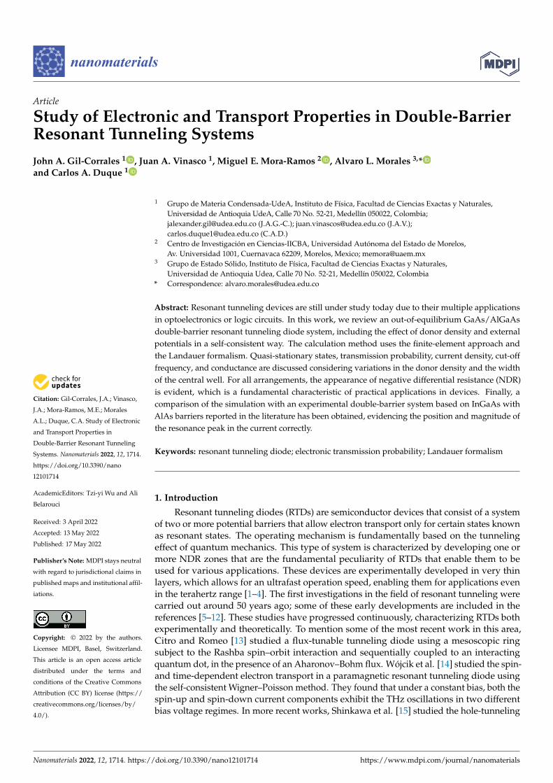
Figure 4 shows the self-consistent potential profile and how it changes and the resonantstate probability density as the potential difference between the emitter and the collectorincreases. The clear redshift of the resonant level must be highlighted and the decreasein the electronic probability density inside the quantum well, mainly due to the electricfield effect. For voltages higher than 0.4 V, the resonant state is very close to the bottom ofthe conduction band at the emitter, and therefore, from this limit, it no longer contributesto the transport properties in the system. From Figure 4d, it is possible to notice that, forhigh voltages, electronic current there will no longer exist in the system due to resonanttunneling, the incident electrons do not have a state inside the well to tunnel and therefore,their probability of passing to the collector must be significantly decreased. This occurs untilreaching a certain limit voltage from which the electrons will have two options—performresonant tunneling with a higher state of the system or perform non-resonant tunneling,which depends on both geometric characteristics and the materials involved in the system.
0 10 20 30 40-0.4
-0.2
0.0
0.2
0.4 0.1 V
ener
gy (e
V)
x (nm)
(a)
0 10 20 30 40-0.4
-0.2
0.0
0.2
0.4
ener
gy (e
V)
x (nm)
0.2 V(b)
0 10 20 30 40-0.4
-0.2
0.0
0.2
0.4
ener
gy (e
V)
x (nm)
0.3 V(c)
0 10 20 30 40-0.4
-0.2
0.0
0.2
0.4
ener
gy (e
V)
x (nm)
0.4 V(d)
Figure 4. Potential energy change with bias voltage from 0.0 V to 0.4 V, the blue curve corresponds tothe resonant state probability density and the red curve is the energy for this state E0. The quasi-Fermilevel is also presented by the dark blue dashed line for emitter and collector. The calculations are forLw = 4 nm, Lb = 3 nm, Ls = 3 nm, Ld = 12 nm, and nd = 1.2× 1018 cm−3.
In Figure 5, we see the transmission probability for different voltage values, as indi-cated by the arrow, the voltage varies from 0.0 V to 0.6 V, Figure 5a corresponds to a dopingnd = 1.2× 10¹⁸ [1/cm3], while in Figure 5b it is nd = 10× 1018 [1/cm3]. The red curve is fora 10 nm QW, and the black one is 4 nm. As indicated in Figure 5b, the quasi-Fermi level atthe emitter (shaded region) presents a higher value for the system that has higher doping,which means that there is a greater number of occupied states in the conduction band thatcan contribute to current through the device. In Figure 5a, the quasi-Fermi level at theemitter takes the value of EF = 0.026 eV, while in Figure 5b, it is of EF = 0.081 eV. For zerovoltage, the system with Lw = 4 nm presents a single resonant level in 0.147 eV, while forLw = 10 nm, there are two resonant peaks in 0.083 eV and 0.179 eV, respectively, where theone closest to the bottom of the band has a medium amplitude lower than the peak of thehighest quasi-steady state, this characteristic in the amplitudes of the peaks is maintainedapproximately, independent of the applied voltage. As the voltage is increased, as men-tioned in Figure 4, there is a redshift of the levels inside the well and, at the same time, adecrease in the transmission amplitude; this behavior is clearly evidenced in Figure 5a,b.In Figure 5b, where the system presents higher doping, for Lw = 4 nm now presents the

Nanomaterials 2022, 12, 1714 9 of 19
resonant state for the energy of 0.271 eV, that is, 0.124 eV higher than in the case of lowerdonor density presented in Figure 5a. A fundamental difference concerning the systemwith lower nd is that now, for Lw = 10 nm, there is only one resonant state inside the welland not two as occurs in the initial case, with an energy of 0.230 eV, which, as in Figure 5a,presents a much smaller mean amplitude than for the QW of Lw = 4 nm.
Tran
smission
energy (eV)
(a)
0.6 V
0.0 VTran
smission
energy (eV)
(b)
Figure 5. Transmission coefficient for different values of bias voltage, the black curve is for Lw = 4 nmand, the red curve is for Lw = 10 nm. (a) with nd fixed at 1.2× 10¹⁸ [1/cm3] and (b) with nd fixed at10× 1018 [1/cm3]. The shaded area indicates the region between the bottom of the conduction bandand the quasi-Fermi level at the emitter. As indicated by the arrow in (b), the voltage for each curvevaries from 0.0 V to 0.6 V in steps of 0.05 V.
In Figure 5, notice how as the voltage increases, the redshift of all the states occurs.For voltages higher than 0.05 V, the system with Lw = 10 nm presents a third resonant peakwell-defined of greater average width than the previous two; this does not happen for thesystem with Lw = 4 nm. The increase in the average width of each peak occurs becausethe upper states are “less stable”, that is, the lifetime of the electrons in these states is lessthan in the lower states, and this time is proportional to the imaginary part of the energyassociated with each of these states and the average width of the resonant peaks. The shadedarea indicates the region between the bottom of the conduction band and the quasi-Fermilevel at the emitter, as shown in Figure 5a; note how the first resonant peak reaches thequasi-Fermi level at the emitter faster for the system with less doping, at approximately0.1 V for Lw = 10 nm, and 0.3 V for Lw = 4 nm. In the case of higher doping, these valuesbecome 0.3 V and 0.45 V for Lw = 10 nm and Lw = 4 nm, respectively. This indicates thatthe system in Figure 5a will reach a peak in the current faster than the system in Figure 5b.
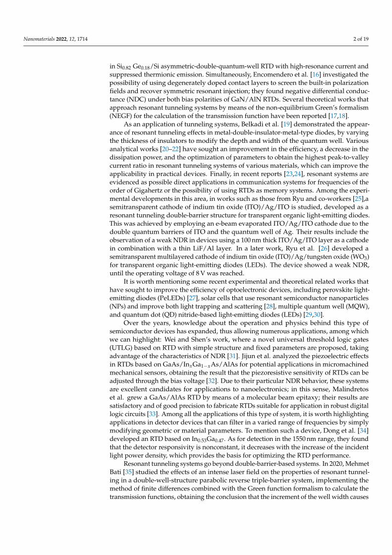
Figure 6 shows the transmission probability for 0.0 V red curve and for 0.4 V blackcurve, Figure 6a is for nd = 1.2× 10¹⁸ [1/cm3], Figure 6b is for nd = 10× 1018 [1/cm3]; frombottom to top, the results are indicated by increasing the width of the QW. The shadedarea indicates the region between the bottom of the conduction band and the quasi-Fermilevel at the emitter. As the width of the well increases, a new resonant state with higherenergy and higher mean amplitude emerges for both electron densities, this state appearsfor Lw ≥ 6 nm in the case of nd = 1.2× 10¹⁸ [1/cm3] and for Lw ≥ 8 nm in the case ofnd = 10× 1018 [1/cm3], as indicated in Figure 6a,b with the red curve. For larger Lw, thefirst quasi-stationary state appears closer to the bottom of the conduction band at the emitter(which corresponds to 0.0 energy), which generates the appearance of the first current
Nanomaterials 2022, 12, 1714 10 of 19
peak for lower voltages; this effect is more significant in the case of lower donor density.Concerning the increase in donor density, there is a slight shift in transmission peaks towardlower energies, which translates into reaching resonance slightly faster than for the lowerdensity. For the 0.4 V voltage, it is possible to see how the peaks have shifted, approachingthe bottom of the conduction band and presenting a decrease in intensity produced by theasymmetry of the potential generated by the effects of the applied electric field.
Lw = 10 nm
Lw = 8 nm
Lw = 6 nm
Lw = 4 nm
Lw = 2 nm
(a)
Tran
smission
energy (eV)
(b)
Tran
smission
energy (eV)Figure 6. Transmission coefficient for different values of Lw, the red curve corresponds to 0.0 V, andthe black curve corresponds to 0.4 V. (a) with nd fixed at 1.2× 10¹⁸ [1/cm3], and (b) with nd fixed at10× 1018 [1/cm3]. The shaded area indicates the region between the bottom of the conduction bandand the quasi-Fermi level at the emitter.
Figure 7 presents the tunneling current density calculated employing Equation (13)for two different values of Lw, Lw = 4 nm black points and Lw = 10 nm red points, asa function of the bias voltage with Lb = 3 nm. In Figure 7a nd = 1.2 × 10¹⁸ [1/cm3],in Figure 7b nd = 10× 1018 [1/cm3]. An increase in the magnitude of the current peak isevidenced for Lw = 4 nm compared to Lw = 10 nm; this is due to a greater amplitude inthe electron transmission probability associated with the only quasi-stationary level for thesmaller well compared to the amplitude for the larger system. This is evidenced in Figure 5acomparing the mean amplitudes of the resonant states for both systems, obtaining; as aresult, a higher mean amplitude for the system with lower Lw, that is, for Lw = 4 nm, thisbehavior holds for both electron densities. Note how there are two peaks associated withthe current for the system Lw = 10 nm one for 0.15 V and the other for 0.45 V, reachingcurrent density values of the order of 0.042 [mA/µm2] and 0.449 [mA/µm2], respectively.Note the difference in magnitude of these two current density peaks, and it is because thefirst maximum corresponds to the resonant transmission with the lower energy red peakin Figure 5, which, for non-zero voltages, when it reaches values below the quasi-Fermilevel at the emitter, this peak has a very low magnitude compared to that of the secondresonant peak. On the other hand, for Lw = 4 nm there is only one of greater magnitudefor 0.35 V, reaching a current density magnitude of 0.566 [mA/µm2]; this is because thelarger system has two quasi-stationary states (states inside the well), while the smallestsystem presents only one, as evidenced in Figure 6a with the red curves. The markeddifference concerning the magnitude of the current peaks associated with Lw = 10 nmis due to the difference in amplitude of the quasi-stationary states, the amplitude beingmuch smaller for the state of lower energy. For both well lengths, NDR occurs, that is, a

Nanomaterials 2022, 12, 1714 11 of 19
decrease in current density from a certain limit voltage. In Figure 7b, which corresponds toa higher donor density, it is evident that the system with Lw = 4 nm reaches the maximumcurrent density faster than the system with Lw = 10 nm. This is since in this system, thequasi-stationary state with the lowest energy reaches the bottom of the conduction bandat the emitter with a negligible amplitude and average width compared to the secondquasi-stationary state; this means that in Figure 7b, the peak presented at 0.6 V of the redcurve corresponds to a current of 0.102 [mA/µm2] is due to the resonance generated by thesecond state inside the well. For the system with Lw = 4 nm, the resonance with the onlyquasi-steady state is presented for a value of 0.5 V, which corresponds to a current densityvalue of 0.204 [mA/µm2]. For both values of Lw, with nd = 10× 1018 [1/cm3], NDR ispresented. For voltages higher than 0.6 V and 0.8 V in Figure 7a and Figure 7b, respectively,there is a monotonous increasing behavior in current density due to the combination oftwo processes, the first being tunneling, not resonant, that is, tunneling through a singlepotential barrier, and the second is a probable transmission of charge carriers in regionsabove the potential barriers.
0.0 0.2 0.4 0.60.0
0.2
0.4
0.6
0.8
1.0
1.2
Lw = 10 nm
Lw = 4 nm
Cur
rent
Den
sity
(mA
/ m
2 )
Voltage (Volts)
(a)
0 = 0.1 ps fC = 0.43 THz
0 = 0.2 ps fC = 0.37 THz
0 = 0.1 ps fC = 0.37 THz
0 = 0.2 ps fC = 0.33 THz
0.0 0.2 0.4 0.6 0.80.0
0.1
0.2
0.3
0.4
0.5
0.6
fC = 0.43 THzfC = 0.52 THz
fC = 0.39 THz0 = 0.2 ps
Lw = 10 nm
(b)
Cur
rent
Den
sity
(mA
/ m
2 )
Voltage (Volts)
Lw = 4 nm
0 = 0.1 ps
0 = 0.1 ps
0 = 0.2 ps
fC = 0.46 THz
0.05 0.10 0.15 0.20 0.250.0
0.2
0.4
0.6
0.8
1.0
0.0 0.1 0.20.0
0.2
0.4
0.6
Tran
smis
sion
energy (ev)
x = 0.2 x = 0.3 x = 0.4
(c)
Cur
rent
Den
sity
(mA
/m
2 )
Voltage (Volts)
Figure 7. Tunneling current density for two different values of Lw as a function of bias voltage, in(a) with nd = 1.2× 10¹⁸ [1/cm3], and (b) with nd = 10× 1018 [1/cm3]. Figure (c) shows the transmissionfor three different values of the Al concentration in the barriers, x = 0.2, 0.3, and 0.4 for a system ofthree regions AlxGa1−xAs/GaAs/AlxGa1−xAs. The inset shows the current density for these threesystems taking Lw = 4 nm and Lb = 3 nm. In figures (a,b), the cut-off frequencies have been includedfor all the arrangements calculated (black text corresponds to Lw = 4 nm and red text corresponds toLw = 10 nm) by taking two different values of τ0, 0.1 ps and 0.2 ps.
For comparison, Figure 7c shows the transmission for three different values of thealuminum concentration in the barriers, x = 0.2, 0.3, and 0.4, for a three-region systemof AlxGa1−xAs/GaAs/AlxGa1−xAs. The inset shows the current density for these threesystems taking Lw = 4 nm and Lb = 3 nm. We can note that the transmission peak width isinversely proportional to the x-percentage in the barrier region; this implies an increasein the system current density for the system with the lowest x-concentration, as can beseen in the inset of Figure 7c. On the other hand, it presents a blue shift proportionalto the x-percentage in the barriers; this is due to the fact that when the Al percentageincreases, there is an increase in the barrier heights and this displaces the quasi-stationarystate towards higher energies. In Figure 7a,b the cut-off frequencies values, fC, have beenincluded for all the arrangements calculated (black text corresponds to Lw = 4 nm and redtext corresponds to Lw = 10 nm) by taking two different values of the τ0-parameter, 0.1 psand 0.2 ps [50]. These frequencies were calculated according to Equation (14). The highestcut-off frequency occurs for the RTD of Lw = 10 nm and nd = 10× 1018 [1/cm3]. Takingτ0 = 0.1 ps, fC = 0.52 THz. On the contrary, the lowest cut-off frequency occurs for theRTD of Lw = 10 nm with nd = 1.2× 10¹⁸ [1/cm3], taking τ0 = 0.2 ps, with a value of 0.33 THz.Note how the cut-off frequency reaches higher values for τ0 = 0.1 ps than for τ0 = 0.2 ps forboth central well widths. On the other hand, the RTD with Lw = 4 nm does not present

Nanomaterials 2022, 12, 1714 12 of 19
significant changes in the cut-off frequency with the increase in carrier density nd, thelargest change is of the order of 0.03 THz for τ0 = 0.1 ps. For the RTD with Lw = 10 nm, thechange in cut-off frequency with increasing carrier density nd is more significant, reachinga maximum change of the order of 0.15 THz for τ0 = 0.1 ps.
The system conductance is proportional to the electronic probability transmission. Theproportionality constant is known in the literature as the conductance quantum and is givenby G0 = e2/πh̄2. Figure 8a shows the conductance as a function of the incident electronenergy for a well width Lw = 4 nm for T = 5 K, this function is calculated by means ofEquation (10), each curve corresponds to a different donor density level, the black solidcurve is for nd = 1.2× 10¹⁸ [1/cm3], and the red dashed curve is for nd = 10× 1018 [1/cm3].For the given value of Lw, the system presents a single resonant state; note that as thedonor density increases, a blue shift occurs in the conductance peaks, and these quasi-stationary states are ordered from the system with the lowest nd to the system with thehighest nd, 0.1213 eV, and 0.1299 eV, respectively. It should be noted that for both curves,the resonant peak average width remains approximately independent of the donor densityin the system. The intensity of the resonant peaks must reach the maximum value, thatis, a 100% probability of electronic transmission when the energy of the incident electronsexactly coincides with the energy of the quasi-stationary states inside the well; this resultwas expected since the system is in equilibrium or equivalently without applied fields.Figure 8b shows the self-consistent potential corresponding to each donor density withwhich the curves in Figure 8a were calculated. Notice how the height of the central regionchanges with the increase of nd, taking the quasi-stationary state towards higher energies.This figure also shows the position of the quasi-stationary states inside the well for eachnd. It must be taken into account that the conductance at the calculated temperature, thatis, T = 5 K, differs very little from the conductance at room temperature, which is inagreement with experimental results such as those mentioned in [53].
0.0 0.1 0.2 0.310-7
10-6
10-5
10-4
10-3
10-2
10-1
100
G (G
0)
energy (eV)
(a)
0 10 20 30 400.0
0.1
0.2
0.3
0.4
ener
gy (e
V)
x (nm)
(b)
Figure 8. (a) Conductance for Lw = 4 nm, for two different donor concentrations in units ofG0 = e2/πh̄2, solid black line nd = 1.2× 10¹⁸ [1/cm3], and dashed red line nd = 10× 1018 [1/cm3].(b) Corresponding self-consistent potentials. The curves were calculated at T = 5 K.
Table 1 presents in detail the value of the quasi-steady state corresponding to the twodonor concentrations calculated, as well as their difference ∆E. The value of the potentialin the center of the well and its difference for both configurations is also included. Asmentioned above, the highest energy state corresponds to the system with the highest

Nanomaterials 2022, 12, 1714 13 of 19
donor density. The energy difference between the states corresponding to the two concen-trations is 8.6 × 10⁻³ eV, while the potential difference reaches a value slightly greater than8.8 × 10−3 eV.
Table 1. Energy associated with the conductance peaks and potential at the center of the well andtheir differences ∆E for the two calculated concentrations, the data correspond to Figure 8.
nd (1018 [1/cm3]) 1.2 10 ∆E (10−3 eV)
V (eV) 0.0105 0.0193 8.8
E1 (eV) 0.1213 0.1299 8.6
Figure 9a shows the conductance as a function of the energy of the incident electron fora well width Lw = 10 nm and T = 5 K, each curve corresponds to a different donor densitylevel as in Figure 8 for Lw = 4 nm. The black solid curve is for nd = 1.2× 10¹⁸ [1/cm3],and the red dashed curve is for nd = 10× 1018 [1/cm3]. With the increase in the wellwidth, the number of resonant states in the system increases; this is evident by comparingFigures 8a and 9a. For this greater width, the same shift behavior of the states towardshigher energies occurs as the donor density increases. The two curves present a verysharp peak for the first state inside QW and two more peaks of greater amplitude for anintermediate energy state and for the state closer to the continuum.
0.0 0.1 0.2 0.310-7
10-6
10-5
10-4
10-3
10-2
10-1
100
G (G
0)
energy (eV)
(a)
0 10 20 30 400.0
0.1
0.2
0.3
0.4en
ergy
(eV)
x (nm)
(b)
Figure 9. (a) Conductance for Lw = 10 nm, for two different donor concentrations in units ofG0 = e2/πh̄2, solid black line nd = 1.2× 10¹⁸ [1/cm3], and dashed red line nd = 10× 1018 [1/cm3].(b) Corresponding self-consistent potentials. The curves were calculated at T = 5 K.
As detailed in Table 2, the system with nd = 1.2× 10¹⁸ [1/cm3] presents three peaks inconductance with energies of 0.046 eV, 0.143 eV, and 0.299 eV respectively, in the same way,the system with nd = 10× 1018 [1/cm3] also presents three peaks with energies of 0.056 eV,0.152 eV, and 0.308 eV respectively. For both configurations, there are three conductancepeaks. Table 2 also shows the energy difference ∆E between each of the states correspondingto the different configurations, as well as the potential difference in the center of the well.The difference in energy becomes smaller for the highest states, that is, the states closestto the continuum are practically unchanged by the difference in donor concentration. Animportant conclusion is that the average width of the conductance peaks is independent

Nanomaterials 2022, 12, 1714 14 of 19
of the density of donors in the system; what is modified is the position of the peaks,generating a shift towards higher energies. Figure 9b shows the self-consistent potentialprofile corresponding to each donor density with which the curves in Figure 9a werecalculated. For this greater well width, the central region height is modified in a moresignificant way as compared to the depth of the smaller well width as nd is increased. Thisfigure also shows the position of each of the states for the two calculated concentrations.
Table 2. Energy associated with the conductance peaks and potential at the center of the well andtheir differences ∆E for the two calculated concentrations, the data correspond to Figure 9.
nd (1018 [1/cm3]) 1.2 10 ∆E (10−3 eV)
V (eV) 0.0138 0.0235 9.7
E1 (eV) 0.0463 0.0558 9.5E2 (eV) 0.1432 0.1523 9.1E3 (eV) 0.2986 0.3076 9.0
Comparison with Experimental Data
One way to test the method is through comparison with experimental results. In thissubsection, a comparison is made with experimental results obtained by Muttlak et al. [54]in 2018, in which the authors presented an experimental study of InGaAs/AlAs resonanttunneling diodes designed to improve the diode characteristics by varying geometriccharacteristics. Figure 10 shows a diagram of the simulated device that is made up ofnine layers, of which the DBRTD (Double Barrier Resonant Tunneling Diode) zone, thespacer layers that are on both sides of the DBRTD zone, and zones 1, 2, and 8, 9, whichis where donors are added to the system. This arrangement of layers is connected to twoelectronic reservoirs that are also presented in the figure.
9
87
654
3
2
Bottom Electrode
Top Electrode
1
DBRTD
Figure 10. RTD structure composed of 9 layers that are expanded in detail in Table 3. DBRTD standsfor Double-Barrier Resonant Tunneling Diode.
Table 3 shows in detail the characteristics of the materials, as well as the layer dimen-sions and the donor densities corresponding to those presented in Figure 10. The outerregions are composed of In0.53Ga0.47As with large dimensions compared to the centralregion of the device, the DBRTD region is made up of two AlAs barriers with equal widthsof 1.1 nm and the QW region is In0.8Ga0.2As with a width of 3.5 nm.

Nanomaterials 2022, 12, 1714 15 of 19
Table 3. Parameters corresponding to each of the layers in Figure 10.
Parameters by Layer
Layer Material Dimensions (nm) Doping (n+ cm−3)
1 In0.53Ga0.47As 400 1 × 10¹⁹
2 In0.53Ga0.47As 25 3 × 10¹⁸
3 In0.53Ga0.47As 54 AlAs 1.15 In0.8Ga0.2As 3.56 AlAs 1.17 In0.53Ga0.47As 58 In0.53Ga0.47As 25 3 × 10¹⁸
9 In0.53Ga0.47As 45 2 × 10¹⁹
Figure 11 shows the self-consistent potential corresponding to the background of theconduction band obtained using the parameters presented in Table 3 at a temperatureof 300 K that comes from an experimental development. The white region in the figurecorresponds to the conduction band of the system, and the red segment indicates thefirst quasi-stationary state inside the well that has an energy of 0.67 eV and is near thebottom of the well. Note how the initially flat potential is modified considerably due tothe electronic redistribution generated by the self-consistent method that considers theeffect of the density of donors in the outer layers (regions 1, 2, 8, and 9). Note how thesystem is asymmetric concerning the center of the QW due to the asymmetry in the regionsoutside the DBRTD; these differences are both geometric and form the density of donors ineach layer.
ener
gy (e
V)
x (nm)
E0 = 0.67 eV
Figure 11. Self-consistent potential corresponding to the conduction band obtained numerically withthe experimental parameters detailed in Table 3.
Figure 12 shows a comparison between the results using our model for the self-consistent calculation of the conduction band bottom profile and later use it to calculate thetransmission through the Schrödinger equation in the system and finally using Equation (13)which corresponds to a Landauer approach, calculating the current density in the device.The red dots (a) correspond to the current density due to resonant tunneling, includingthe scattering effects simulated as additional resonances in the system, and the blue points(b) correspond to the current density obtained only by resonant tunneling, while theblack stars are the experimental points. The simulation parameters that correspond to thecharacteristics of the materials, the dimensions, as well as the donor density are presented

Nanomaterials 2022, 12, 1714 16 of 19
in Table 3 at a temperature of 300 K, which corresponds to the temperature reported on theexperimental level.
0.0 0.2 0.4 0.6 0.8 1.00
2
4
6
8
10
12 Muttlak et al. 2018 This work (a) This work (b)
Cur
rent
Den
sity
(mA
/ m
2 )
Voltage (Volts)
Figure 12. Comparison between simulated results using Equation (13) (red and blue dots) andexperimental results [54] (black stars).
In the region between 0 V and 0.46 V, there is a very good correspondence of thesimulated results with the experimental ones, with a change in the current density between0 and 10.9 [mA/µm2] approximately, which corresponds to the maximum value generatedby the resonance between the incident electrons and the first quasi-stationary state insidethe well shown in Figure 11. For values greater than 0.46 V, the simulation presents a dropin current density representing an NDR. For voltages higher than 0.5 V, the current in thesystem is mainly due to dispersion effects (this is evident due to the difference between theblue points and the red points in this region), due to possible impurities in the interlayerregions that can eventually contribute to electronic transport in the system. On the otherhand, because the experimental temperature is 300 K, it is important to consider dispersioneffects due to thermionic emission and electronic absorption of phonons, processes thatcan provide electrons with enough energy to tunnel through barriers and contribute tocurrent density [55,56]. These effects are included in the model by adding three additionalresonances to the simulated one at positions 1.02 eV, 1.12 eV, and 1.81 eV, respectively. Theseeffects correspond to the red dots in Figure 12 that generate a current peak between 0.5 Vand 0.7 V and exponential-like behavior for voltages higher t.
4. Conclusions
The wave functions, quasi-stationary states, and self-consistent potentials, amongother electronic properties in a double-barrier resonant tunneling diode system basedon GaAs and InGaAs, were calculated by solving the equations in each step using thefinite-element method. Employing the Schrödinger equation, the probabilities of electronictransmission were calculated considering variations in geometric parameters such as thewidth of the central well and non-geometric parameters such as the density of donors inthe layers outside the barrier region. Additionally, the system has been converged out ofequilibrium to analyze the response of the internal quasi-stationary states to an externalpotential difference applied to the contacts, obtaining a redshift in all transmission peaksregardless of the donor density used. A way has been found to tune the system, particularlythe position or quantity of quasi-stationary states inside the central well, by modifying thebias voltage, modifying the width of the central well, and modifying the density of donorsin the system. Once the system was characterized through the probability of electronictransmission, the Landauer formalism was used to calculate the electric current densitythat circulates through the diode for different well widths and different donor densities.

Nanomaterials 2022, 12, 1714 17 of 19
An important conclusion is that the first current peak is obtained for lower voltages in thecase of the narrower width of the central well. On the other hand, when the donor densityis lower, the current peaks reach a higher value for the simulated parameters. For the casesstudied, it is possible to show NDR. For the system under study, the cut-off frequencywas calculated, analyzing geometric and non-geometric variations. A maximum value of0.52 THz has been found for the RTD of Lw = 4 nm and nd = 10× 1018 [1/cm3].
The conductance in the double barrier system was calculated, changing the dimensionsof the well and the density of donors, obtaining multiple peaks of conductance for a widthof 10 nm and a single peak for a width of 2 nm. The increase in concentration only modifiesthe position of the peaks, but does not change the shape of the conductance function.Finally, the theoretical procedure was applied to an experimental system reported in recentliterature; this is a non-symmetric system based on InGaAs with AlAs barriers consistingof nine regions. The current density at room temperature for this system was compared,obtaining satisfactory results for calculating the position of the first resonance in the systemand the magnitude of the current density at this point. Likewise, the converged parametersfor the experimental comparison do not exceed 3% error compared to the same parametersreported in the literature. These results indicate that this system could be a good candidatefor potential applications in various science or engineering fields.
Author Contributions: J.A.G.-C. was responsible of the analytical and numerical calculations, formalanalysis, and writing of the manuscript; J.A.V. was responsible for the numerical calculations; M.E.M.-R. was responsible for writing of the manuscript; A.L.M. proposed the problem and was responsiblefor the formal analysis and writing of the manuscript; C.A.D. was responsible for the formal analysis.All authors have read and agreed to the published version of the manuscript.
Funding: The authors are grateful to the Colombian Agencies: CODI-Universidad de Antioquia(Estrategia de Sostenibilidad de la Universidad de Antioquia and projects “Propiedades magneto-ópticas y óptica no lineal en superredes de Grafeno”, “Estudio de propiedades ópticas en sistemassemiconductores de dimensiones nanoscópicas”, and “Propiedades de transporte, espintrónicas ytérmicas en el sistema molecular zinc-porfirina”), and Facultad de Ciencias Exactas y Naturales-Universidad de Antioquia (CAD and ALM exclusive dedication project 2021–2022). The authors alsoacknowledge the financial support from El Patrimonio Autónomo Fondo Nacional de Financiamientopara la Ciencia, la Tecnología y la Innovación Francisco José de Caldas (project: CD 111580863338, CTFP80740-173-2019).
Institutional Review Board Statement: Not applicable.
Informed Consent Statement: Not applicable.
Data Availability Statement: Not applicable.
Conflicts of Interest: The authors declare no conflict of interest.
References1. Brown, E.R.; Söderström, J.R.; Parker, C.D.; Mahoney, L.J.; Molvar, K.M.; McGill, T.C. Oscillations up to 712 GHz in InAs/AlSb
resonant-tunneling diodes. Appl. Phys. Lett. 1991, 58, 2291–2293. [CrossRef]2. Miyamoto, T.; Yamaguchi, A.; Mukai, T. Terahertz imaging system with resonant tunneling diodes. Jpn. J. Appl. Phys. 2016,
55, 032201. [CrossRef]3. Bezhko, M.; Suzuki, S.; Asada, M. Frequency increase in resonant-tunneling diode cavity-type terahertz oscillator by simulation-
based structure optimization. Jpn. J. Appl. Phys. 2020, 59, 032004. [CrossRef]4. Yachmeneva, A.E.; Pushkareva, S.S.; Reznikb, R.R.; Khabibullina, R.A.; Ponomarev, D.S. Arsenides-and related III-V materials-
based multilayered structures for terahertz applications: Various designs and growth technology. Prog. Cryst. GrowthCharact. Mater. 2020, 66, 100485. [CrossRef]
5. Andrews, A.M.; Korb, H.W.; Holonyak, N.; Duke, C.B.; Kleiman, G.G. Tunnel mechanisms and junction characterization in III-Vtunnel diodes. Phys. Rev. B 1972, 5, 2273–2295. [CrossRef]
6. Andrews, A.M.; Korb, H.W.; Holonyak, N.; Duke, C.B.; Kleiman, G.G. Photosensitive impurity-assisted tunneling in Au-Ge-dopedGa1−xAlxAs p-n diodes. Phys. Rev. B 1972, 5, 4191–4194. [CrossRef]
7. Frensley, W.R. Transient response of a tunneling device obtained from the Wigner function. Phys. Rev. Lett. 1986, 57, 2853–2856.[CrossRef]

Nanomaterials 2022, 12, 1714 18 of 19
8. Goldman, V.J.; Tsui, D.C.; Cunningham, J.E. Observation of intrinsic bistability in resonant-tunneling structures. Phys. Rev. Lett.1987, 58, 1256–1259. [CrossRef]
9. Kluksdahl, N.C.; Kriman, A.M.; Ferry, D.K.; Ringhofer, C. Self-consistent study of the resonant-tunneling diode. Phys. Rev. B 1989,39, 7720–7735. [CrossRef]
10. Tarucha, S.; Hirayama, Y.; Saku, T.; Kimura, T. Resonant tunneling through one- and zero-dimensional states constricted byAlxGa1−xAs/GaAs/AlxGa1−xAs heterojunctions and high-resistance regions induced by focused Ga ion-beam implantation.Phys. Rev. B 1990, 41, 5459–5462. [CrossRef]
11. Yoshimura, H.; Schulman, J.N.; Sakaki, H. Charge accumulation in a double-barrier resonant-tunneling structure studied byphotoluminescence and photoluminescence-excitation spectroscopy. Phys. Rev. Lett. 1990, 64, 2422–2425. [CrossRef] [PubMed]
12. Rahman M.; Davies, J.H. Theory of intrinsic bistability in a resonant tunneling diode. Semicond. Sci. Technol. 1990, 5, 168–176.[CrossRef]
13. Citro R.; Romeo, F. Aharonov-Bohm-Casher ring dot as a flux-tunable resonant tunneling diode. Phys. Rev. B 2008, 77, 193309.[CrossRef]
14. Wójcik, P.; Adamowski, J.; Wołoszyn, M.; Spisak, B.J. Intrinsic oscillations of spin current polarization in a paramagnetic resonanttunneling diode. Phys. Rev. B 2012, 86, 165318. [CrossRef]
15. Shinkawa, A.; Wakiya, M.; Maeda, Y.; Tsukamoto, T.; Hirose, N.; Kasamatsu, A.; Matsui, T.; Suda, Y. Hole-tunneling Si0.82Ge0.18/Siasymmetric-double-quantum-well resonant tunneling diode with high resonance current and suppressed thermionic emission.Jpn. J. Appl. Phys. 2020, 59, 080903. [CrossRef]
16. Encomendero, J.; Protasenko, V.; Rana, F.; Jena, D.; Xing, H.G. Fighting broken symmetry with doping: Toward polar resonanttunneling diodes with symmetric characteristics. Phys. Rev. Appl. 2020, 13, 034048. [CrossRef]
17. Almansour, S. Theoretical study of electronic properties of resonant tunneling diodes based on double and triple AlGaAs barriers.Results Phys. 2020, 17, 103089. [CrossRef]
18. Abedi, A.; Sharifi, M.J. Time-dependent quantum transport in the presence of elastic scattering. Superlattices Microstruct. 2020,139, 106383. [CrossRef]
19. Belkadi, A.; Weerakkody, A.; Moddel, G. Demonstration of resonant tunneling effects in metal-double-insulator-metal (MI2M)diodes. Nat. Commun. 2021, 12, 2925. [CrossRef]
20. Qian, H.; Li, S.; Hsu, S.-W.; Chen, C.-F.; Tian, F.; Tao, A.R.; Liu, Z. Highly-efficient electrically-driven localized surface plasmonsource enabled by resonant inelastic electron tunneling. Nat. Commun. 2021, 12, 3111. [CrossRef]
21. Ipsita, S.; Mahapatra, P.K.; Panchadhyayee, P. Optimum device parameters to attain the highest peak to valley current ratio(PVCR) in resonant tunneling diodes (RTD). Physica B 2021, 611, 412788. [CrossRef]
22. Althib, H. Effect of quantum barrier width and quantum resonant tunneling through InGaN/GaN parabolic quantum well-LEDstructure on LED efficiency. Results Phys. 2021, 22, 103943. [CrossRef]
23. Iwamatsu, S.; Nishida, Y.; Fujita, M.; Nagatsuma, T. Terahertz coherent oscillator integrated with slot-ring antenna using tworesonant tunneling diodes. Appl. Phys. Express 2021, 14, 034001. [CrossRef]
24. Ortega-Piwonka, I.; Piro, O.; Figueiredo, J.; Romeira, B.; Javaloyes, J. Bursting and excitability in neuromorphic resonant tunnelingdiodes. Phys. Rev. Appl. 2021, 15, 034017. [CrossRef]
25. Ryu, S.Y.; Jo, S.J.; Kim, C.S.; Choi, S.H.; Noh, J.H.; Baik, H.K.; Jeong, H.S.; Han, D.W.; Song, S.Y.; Lee, K.S. Transparent organiclight-emitting diodes using resonant tunneling double barrier structures. Appl. Phys. Lett. 2007, 91, 093515. [CrossRef]
26. Ryu, S.Y.; Noh, J.H.; Hwang, B.H.; Kim, C.S.; Jo, S.J.; Kim, J.T.; Hwang, H.S.; Baik, H.K.; Jeong, H.S.; Lee, C.H.; et al. Transparentorganic light-emitting diodes consisting of a metal oxide multilayer cathode. Appl. Phys. Lett. 2008, 92, 023306. [CrossRef]
27. Masharin, M.A.; Berestennikov, A.S.; Barettin, D.; Voroshilov, P.M.; Ladutenko, K.S.; Carlo, A.D.; Makarov, S.V. Giant Enhancementof Radiative Recombination in Perovskite Light-Emitting Diodes with Plasmonic Core-Shell Nanoparticles. Nanomaterials 2021,11, 45. [CrossRef] [PubMed]
28. Furasova, A.; Voroshilov, P.; Lamanna, E.; Mozharov, A.; Tsypkin, A.; Mukhin, I.; Barettin, D.; Ladutenko, K.; Zakhidov, A.;Carlo, A.D.; et al. Engineering the Charge Transport Properties of Resonant Silicon Nanoparticles in Perovskite Solar Cells.Energy Technol. 2019, 8, 1900877. [CrossRef]
29. Barettin, D.; der Maur, M.A.; di Carlo, A.; Pecchia, A.; Tsatsulnikov, A.F.; Sakharov, A.V.; Lundin, W.V.; Nikolaev, A.E.; Usov, S.O.;Cherkashin, N.; et al. Influence of electromechanical coupling on optical properties of InGaN quantum-dot based light-emittingdiodes. Nanotechnology 2017, 28, 015701. [CrossRef]
30. Barettin, D.; der Maur, M.A.; di Carlo, A.; Pecchia, A.; Tsatsulnikov, A.F.; Lundin, W.V.; Sakharov, A.V.; Nikolaev, A.E.; Korytov, M.;Cherkashin, N.; et al. Carrier transport and emission efficiency in InGaN quantum-dot based light-emitting diodes. Nanotechnology2017, 28, 275201. [CrossRef]
31. Wei, Y.; Shen, J. Novel universal threshold logic gate based on RTD and its application. Microelectron. J. 2011, 42, 851–854.[CrossRef]
32. Xiong, J.; Wang, J.; Zhang, W.; Xue, C.; Zhang, B.; Hu, J. Piezoresistive effect in GaAs/InxGa1−xAs/AlAs resonant tunnelingdiodes for application in micromechanical sensors. Microelectron. J. 2008, 39, 771–776.
33. Malindretos, J.; Förster, A.; Indlekofer, K.M.; Lepsa, M.I.; Hardtdegen, H.; Schmidt, R.; Lüth, H. Homogeneity analysis of ion-implanted resonant tunneling diodes for applications in digital logic circuits. Superlattice Microst. 2002, 31, 315–325. [CrossRef]

Nanomaterials 2022, 12, 1714 19 of 19
34. Dong, Y.; Wang, G.; Ni, H.; Chen, J.; Gao, F.; Li, B.; Pei, K.; Niu, Z. Resonant tunneling diode photodetector with nonconstantresponsivity. Opt. Commun. 2015, 355, 274–278. [CrossRef]
35. Bati, M. The effects of the intense laser field on the resonant tunneling properties of the symmetric triple inverse parabolic barrierdouble-well structure. Physica B 2020, 594, 412314. [CrossRef]
36. Langreth, D.C.; Abrahams, E. Derivation of the Landauer conductance formula. Phys. Rev. B 1981, 24, 2978–2984. [CrossRef]37. Eränen, S.; Sinkkonen, J. Generalization of the Landauer conductance formula. Phys. Rev. B 1987, 35, 2222–2227. [CrossRef]38. Havu, P.; Tuomisto, N.; Väänänen, R.; Puska, M.J.; Nieminen, R.M. Spin-dependent electron transport through a magnetic
resonant tunneling diode. Phys. Rev. B 2005, 71, 235301. [CrossRef]39. COMSOL. Multiphysics, v. 5.4; COMSOL AB: Stockholm, Sweden, 2020.40. COMSOL. Multiphysics Reference Guide; COMSOL: Stockholm, Sweden, 2012.41. COMSOL. Multiphysics Users Guide; COMSOL: Stockholm, Sweden, 2012.42. COMSOL. Multiphysics v. 5.2a Semiconductor Module User’s Guide; COMSOL AB: Stockholm, Sweden, 2016.43. Mohiyaddin, A.F.; Curtis, F.G.; Ericson, M.N.; Humble, T.S. Simulation of Silicon Nanodevices at Cryogenic Temperatures for
Quantum Computing. In Proceedings of the COMSOL Conference, Boston, MA, USA, 4–6 October 2017.44. Sze, S.M.; Kwok, K. Ng, Physics of Semiconductor Devices; John Wiley & Sons: Hoboken, NJ, USA, 2006; ISBN 9780471143239.45. Fenton, E.W. Effect of the electron-electron interaction on the Landauer conductance. Phys. Rev. B 1993, 47, 10135. [CrossRef]46. Mitin, V.V.; Kochelap, V.A.; Stroncio, M.A. Introduction to Nanoelectronics, Science, Nanotechnology, Engineering, and Applications;
Cambridge University Press: Cambridge, UK, 2007; ISBN 978051180909.47. Feiginov, M. Frequency Limitations of Resonant-Tunnelling Diodes in Sub-THz and THz Oscillators and Detectors. Int. J. Infrared
Millim. Waves 2019, 40, 365–394. [CrossRef]48. Ikeda, Y.; Kitagawa, S.; Okada, K.; Suzuki, S.; Asada, M. Direct intensity modulation of resonant-tunneling-diode terahertz
oscillator up to 30 GHz. IEICE Electron. Express 2015, 12, 1–10. [CrossRef]49. Asada, M.; Suzuki, S. Terahertz Emitter Using Resonant-Tunneling Diode and Applications. Sensors 2021, 21, 1384. [CrossRef]
[PubMed]50. Alkeev, N.; Averin, S.; Dorofeev, A.; Gladysheva, N. Factors reducing the cut-off frequency of resonant tunneling diodes. Int. J.
Microw. Wirel. Technol. 2012, 4, 605–611. [CrossRef]51. da Silva, A.F.; Persson, C.; Marcussen, M.C.B.; Veje, E.; de Oliveira, A.G. Band-gap shift in heavily doped n-type Al0.3Ga0.7As
alloys. Phys. Rev. B 1999, 60, 2463–2467. [CrossRef]52. Schlesinger, T.E. Gallium Arsenide. In Encyclopedia of Materials: Science and Technology; Elsevier: Amsterdam, The Netherlands,
2001; pp. 3431–3435.53. Asada, M.; Suzuki, S.; Fukuma, T. Measurements of temperature characteristics and estimation of terahertz negative differential
conductance in resonant-tunneling-diode oscillators. AIP Adv. 2017, 7, 115226. [CrossRef]54. Muttlak, S.G.; Abdulwahid, O.S.; Sexton, J.; Kelly, M.J.; Missous, M. InGaAs/AlAs resonant tunneling diodes for THz applications:
An experimental investigation. IEEE J. Electron Devices 2018, 6, 254–262. [CrossRef]55. Sun, J.P.; Haddad, G.I.; Mazumder, P.; Schulman, J.N. Resonant tunneling diodes: Models and properties. Proc. IEEE 1998, 86,
641–660.56. Chevoir, F.; Vinter, B. Calculation of incoherent tunneling and valley current in resonant tunneling structures. Surf. Sci. 1990, 229,
158–160. [CrossRef]


