Embed Size (px)
Citation preview
The acceptor level of vanadium in III–V compoundsB. Clerjaud, C. Naud, B. Deveaud, B. Lambert, B. Plot et al. Citation: J. Appl. Phys. 58, 4207 (1985); doi: 10.1063/1.336287 View online: http://dx.doi.org/10.1063/1.336287 View Table of Contents: http://jap.aip.org/resource/1/JAPIAU/v58/i11 Published by the American Institute of Physics. Related ArticlesA mirage study of CdSe colloidal quantum dot films, Urbach tail, and surface states J. Chem. Phys. 137, 154704 (2012) Optical transport through finite superlattice modulated with three-component quasiperiodic defect J. Appl. Phys. 112, 043524 (2012) On the origin of the 265nm absorption band in AlN bulk crystals Appl. Phys. Lett. 100, 191914 (2012) Apparent Raman spectral shifts from nano-structured surfaces Appl. Phys. Lett. 100, 173105 (2012) Epitaxial growth of thin films and nanodots of ZnO on Si(111) by pulsed laser deposition Appl. Phys. Lett. 100, 132109 (2012) Additional information on J. Appl. Phys.Journal Homepage: http://jap.aip.org/ Journal Information: http://jap.aip.org/about/about_the_journal Top downloads: http://jap.aip.org/features/most_downloaded Information for Authors: http://jap.aip.org/authors
Downloaded 01 Dec 2012 to 128.178.195.171. Redistribution subject to AIP license or copyright; see http://jap.aip.org/about/rights_and_permissions
The acceptor level of vanadium in III-V compounds B. Clerjaud and C. Naud Laboratoire d'Optique de la Matiere Condensee, (UA 800 du CNRS). Uniuersite Pierre et Marie Curie, Tour 13, 4 place Jussieu, F-75230 Paris Cedex 05, France
B. Deveaud, B. lambert, and B. Plot Centre National d'Etudes des Telecommunications (LAB/ICM), F-2230I Lannion, France
G. Bremond, C. Benjeddou, G. Guillot, and A. Nouailhat Institut National des Sciences Appliquees, Laboratoire de Physique de la Matiere, Batiment 502. F-6962I Villeurbanne, France
(Received 2 April 1985; accepted for publication 5 June 1985)
The positions of the acceptor level of vanadium in GaAs, GaP, and InP are estimated. This level is found to be at about Ee - 0.14 eV in GaAs and about Ee - 0.8 eV in GaP. It is above the conduction band edge in InP. These positions in the three hosts are in agreement with the trends proposed by Ledebo and Ridley. The finding of a very high acceptor level of vanadium in GaAs does not allow to explain the semi-insulating behavior of GaAs:V. Other possible compensating centers are considered.
I. iNTRODUCTION
The interest of vanadium doping of III-Y compounds partly has its origin in a series of papers,l-4 coming from different groups, showing that semi-insulating (SI) gallium arsenide had been obtained by vanadium doping. Furthermore, Kutt et aJ. 4 have recently shown that the diffusion and redistribution properties of vanadium in GaAs were less rapid than they are for chromium; therefore vanadium-doped GaAs could be a better candidate for integrated circuit substrates. However, a difference arose between the Bridgman material grown at the RTC Caen Laboratories5 that stayed n type on most of its length and the liquid-encapsulated Czochralski (LEC) material grown by Wacker Chemitronic4
or the epitaxial layers prepared by Terao et ae that were both observed to be semi-insulating.
As a matter of fact, besides EL2, only two levels close to the conduction band are observed by deep-level transient spectroscopy (DLTS) in the n-type RTC ingot5
•6 in agree
ment with the early results of Haisty and Cronin 7 who found an energy level at Ee - 0.22 eY. This would explain why the Bridgman material is not semi-insulating. In contrast, Terao et al. 3 did observe in their samples a hole trap at Eo + 0.58 eY, "almost certainly related to vanadium" that could explain the S1 behavior of GaAs when doped with vanadium.
Starting from this point, two groups did try to synthesize SI InP using vanadium as a compensating center. 8.9 Although vanadium was chemically detected in both cases, no compensation effect was observed: InP:V stays n-type. Lambert et al.8 did perform DLTS measurements down to 4 K and no level was detected in the forbidden gap. Vanadium was nevertheless detected in the y3+ charge state both in luminescence and in PLE9
-11 in this n-type material. This
shows that there is no acceptor level of vanadium in the band gap ofInP.
So, there are two contradictions in the published results: on GaAs some obtain SI behavior when some do not, some observe a deep level and others do not; in GaAs, stable SI material can be obtained and even can be purchased whereas
it is impossible to compensate InP with vanadium. The aim of the present work is to try to solve this double contradiction by confidently asserting the levels introduced by vanadium in III-Y materials. This has been done by working on different materials: GaAs, InP, and GaP, coming from different manufacturers (RTC, Wacker, and CNET), showing different types (n-type, SI) and characterized by a large set of experiments: chemical characterization [spark source mass spectroscopy (SSMS)], electron paramagnetic resonance (EPR), optical absorption (OA), photoluminescence (PL), photoluminescence excitation (PLE), luminescence decay time measurements, DLTS, deep-level optical spectroscopy (DLOS), and Hall effect measurements. Using all these experiments and comparing the results on the different materials with the help of the scheme proposed by Ledebo and Ridley 1
2 and Caldas and co-workers, 13 we will be able to give the position of the acceptor level (y2+ ;V3+) in these materials. Results obtained on the donor level of vanadium in InP will be presented elsewhere. 14 The main result of this work is that in GaAs the acceptor level of isolated vanadium is too high in the band gap to explain the SI behavior of GaAs:V.
II. EXPERIMENTS
A.Samples
We have used two sources of gallium arsenide samples: the first supplier is Wacker Chemitronic. GaAs:V is grown by the liquid encapsulated Czochralski method in quartz crucible. The procedure was described by Kaufmann et al. 2
All samples are semi-insulating (SI) (p> 1060. cm at room temperature). The second source of GaAs:Y is the RTC (Radiotechnique Compelec) company; Poiblaud has grown by the horizontal Bridgman method a vanadium-doped GaAs ingot in a quartz crucible. Vanadium (150 mg) was added for a total weight of 400 g (ingot No. RT 409). This ingot is n type over most of its length (seed end) and the tail part is much more resistive (p> 10"0 cm).5 Vanadium-doped InP polycrystals (CNET 65 and 73) have been synthesized at CNET Lannion in a conventional two-zone gradient freeze furnace by Toudic. 8 Experiments are performed on monocrystaHine
4207 J. Appl. Phys. 58 (11). 1 December 1985 0021-8979/85/234207-09$02.40 @ 1985 American Institute of Physics 4207
Downloaded 01 Dec 2012 to 128.178.195.171. Redistribution subject to AIP license or copyright; see http://jap.aip.org/about/rights_and_permissions
parts extracted from the ingots. Although the silicon content of the ingots is quite high (1.2X 1016 cm3
), samples containing more vanadium than silicon have been obtained but they do not show any compensation.8 Hall effect measurements indicate an electron concentration of (2-3) X 1016 cm3
, constant with temperature down to 4 K. The mobility ranges between 3000 and 5000 cm2 Y- 1 S -I at 300 K. The gallium phosphide samples that we have studied are the same ones than studied by Kaufmann et aU; they are all n type. Characteristics of the growth ofthese GaP:Y crystals have been given elsewhere.2
B. Experimental setups
Absorption measurements have been performed with a Michelson Fourier-transform interferometer (BOMEM DA 3.01) equipped with a tungsten quartz-halogen source, a quartz beam spl.itter, and a cooled indium antimonide detector associated with a cold filter. The samples are cooled in a continuous flow helium cryostat (Oxford Instruments CF 204) allowing temperatures down to 5 K.
The experimental arrangements for: (1) the optical. and electrical deep level transient spectroscopy (ODLTS and DLTS) and (2) the deep level optical spectroscopy DLOS which gives the optical photoionization (or photoneutralization) cross-section ~ (or~) have already been presented. 15
Recent improvements allow us to measure the absolute value of the optical photoionization cross section over the whole energy range ofthe III-Y band gap. 16
On n-type GaAs, the ohmic contacts are provided by small dots of Sn heated to 300 ·C under hydrogen flow; the Schottky barrier is provided by a semi-transparent gold layer evaporated on the surface of the samples after a standard cleaning and etching procedure.
8 -0;
GaAs:V E ~ Semi-insulating t-z UJ U u: u. UJ 0 6.2 u z 0 i= Il... IX: 0 VI
5 III ~
3.8
2.6
5000 8000
4208 J. Appl. Phys., Vol. 58. No. 11, 1 December 1965
On n-type InP, the proceeding is the same but before the gold Schottky barrier evaporation a very thin natural oxyde layer is necessary to improve the electrical characteristics of the diodes (to minimize the leakage current under reverse biased conditions).
Luminescence and PLE experimental setups have been described elsewhere. I7 For luminescence decay-time measurements, the crystals are cooled in a helium immersion cryostat and are excited by a cw argon laser which is externally chopped by an acousto-optic modulator. The pulse width and frequency are monitored by an external pulse generator. The resulting fall time of the excitation beam is less than 80 ns. The infrared emissions typical of vanadium with zero phonon line between 0.7 and 0.8 e Y in GaAs, GaP, and InP2.8 are selected by filter combinations and their decays are detected by a fast time constant InSb detector (fall time of about 100 ns) and analyzed by a boxcar system.
III. RESULTS The first idea that comes to mind in order to explain the
semi-insulating properties of vanadium-doped GaAs is the occurrence of an acceptor level of vanadium close to the middl.e of the band gap of GaAs. Such a level is used with chromium in GaAs or with iron in InP to compensate the residual shallow donors and so to pin the Fermi level far from the band edges. The level detected by Terao et aU at 0.58 eY from the valence band could explain the semi-insulating properties of GaAs: Y if it was related to the y2 + /V3 +
charge state of vanadium. However, why are only two levels dose to the conduction band edge detected by DLTS6 in ntype vanadium-doped GaAs? In order to clarify that point, we are first going to recall the main results that have been obtained with certainty on semi-insul.ating GaAs, then com-
9500 11000
ENERGY (em-I)
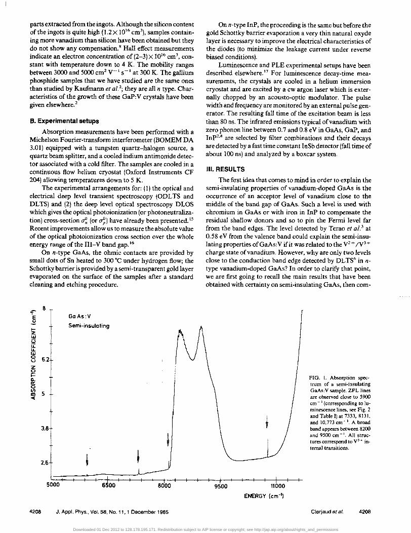
FIG. I. Absorption spectrum of a semi-insulating GaAs:V sample. ZPL lines are observed dooe to 5900 em - , (corresponding to luminescence lines, see Fig. 2 and Table I) at 7333,8131, and 10,773 em' '. A broad band appears between 8200 and 9500 cm -'. All structures correspond to y3 + intemal transitions.
Clerjaud et al. 4208
Downloaded 01 Dec 2012 to 128.178.195.171. Redistribution subject to AIP license or copyright; see http://jap.aip.org/about/rights_and_permissions
GaAs'\1
6385 6392.5 6400
I;:.'
...... .rI ;' \ ~~A,"", ~,~ . v' , .JVVV -v- \Av/' IV'-!1,#' ,<,,~"vv' \.j' i." ... ·r"'· .~ J V '. FI .:: ',," .. , V •
I I I I I I I I 5682 5689.5 5697 5704.5
ENERGY fem-')
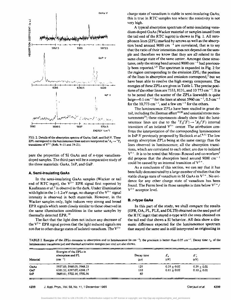
FIG. 2. Details of the absorption spectra ofGaAs. GaP, and InP:Y. These ZPL correspond to the luminescence lines and are interpreted as 3 A2 --+ 3 T2 transitions ofy3+ (Refs. 9-11 and 19-21).
pare the properties of SI GaAs and of n-type vanadiumdoped samples. The third part win be a comparative study of the three materials: GaAs, InP, and GaP.
A. Semi-insulating GaAs
In the semi-insulating GaAs samples (Wacker or tail end of RTC ingot), the y3+ EPR signal first reported by Kaufmann et al. 2 is observd in the dark. Under illumination with light in the 1-1.2-eY range, no change of the y3+ signal intensity is observed in both materials. However, in the Wacker samples only, light induces very strong and broad EPR signals which seem closely similar to those observed in the same illumination conditions in the same samples by thermally detected EPR 18
The fact that the light does not induce any decrease of the y3+ EPR signal proves that the light induced signals are not due to other charge states of isolated vanadium. The y3 +
charge state of vanadium is stable in semi-insulating GaAs; this is true in R TC samples too where the resistivity is not very high.
A typical absorption spectrum of semi-insulating vanadium-doped GaAs (Wacker material or samples issued from the tail end of the RTC ingots) is shown in Fig. 1. All zerophonon lines (ZPL) marked by arrows as well as the absorption band around 9000 cm - 1 are correlated; that is to say that the ratio of their intensities does not depend on the sample and therefore we know that they are all related to the same charge state of the same center. Amongst these structures, only the strong band around 9000 cm - I had previously been reported. 1
•5 The spectrum is expanded in Fig. 2 for
the region corresponding to the emission ZPL; the position of the lines in absorption and emission correspond,2 but we have been able to resolve the high energy component. The energies of these ZPLs are given in Table 1. The precise positionsofthe other lines are 7333,8131, and 10 773 cm- I
. It is to be noted that the scatter of the ZPLs linewidth is quite large-O.l cm - 1 for the lines at about 5960 cm -),0.5 cm -) for the 10,773 cm -I, and a few cm -) for the others.
The luminescence ZPLs have been studied in great detail, including the Zeeman effectl9
•20 and uniaxial stress mea
surements21; these experiments clearly show that the lumi
nescence lines are due to the 3T2eF) -+ 3A213F) internal transition of an isolated y3+ center. The attribution confirms the interpretation of the corresponding luminescence in InP: Y previously proposed by Skolnick et al.9
.)) The low energy absorption ZPLs being at the same energy than the lines observed in luminescence; all the absorption transitions, which are correlated to each other, are due to isolated y3+. It is to be noted that Mircea·-Roussel and co-workers5
did propose that the absorption band around 9000 cm - ) could be caused by an internal transition of y3+ .
As a conclusion of this section, we can say that it has been fully demonstrated by a large number of studies that the stable charge state of vanadium in SI GaAs in V3 +. No evidence for any other charge state of vanadium has been found. The Fermi level in those samples is then below y2+ /
y3 + acceptorlevel.
B. n-type GaAs
In this part of the study, we shall compare the results (EPR, OA, PL, PLE, and DLTS) obtained on the seed part of the R TC ingot that stayed n-type with the ones obtained on the tail end that shows a SI behavior. All data show a dramatic difference expected for the luminescence spectrum that stayed the same and is still interpreted as originating in
TABLE I. Energies of the ZPLs common to absorption and to luminescence (in em - '); the precision is better than 0.05 em - '. Decay time l' JI. of the luminescence transitions (,us) and thermal activation energies (see text) are also shown.
Energies of the ZPLs in absorption and PL Decay time EA E' A
Material (em-') ips) (eV) (eY)
GaAs 5957.85; 5968.05; 5968.25 125 0.29 ± 0.02 0.29 ± 0.D2 GaP 6381.52; 6397.07; 6398.17 110 0.11 ±0.02 0.10 ±0.02 InP 5689.81; 5702.14; 5702.56 80
4209 J. Appl. Phys., Vol. 56, No. 11, 1 December 1965 Clerjaud et al. 4209
Downloaded 01 Dec 2012 to 128.178.195.171. Redistribution subject to AIP license or copyright; see http://jap.aip.org/about/rights_and_permissions
1.3 1.2 11 10
Go As : V .n type
T = 1.7 K
1.0 11 1.2
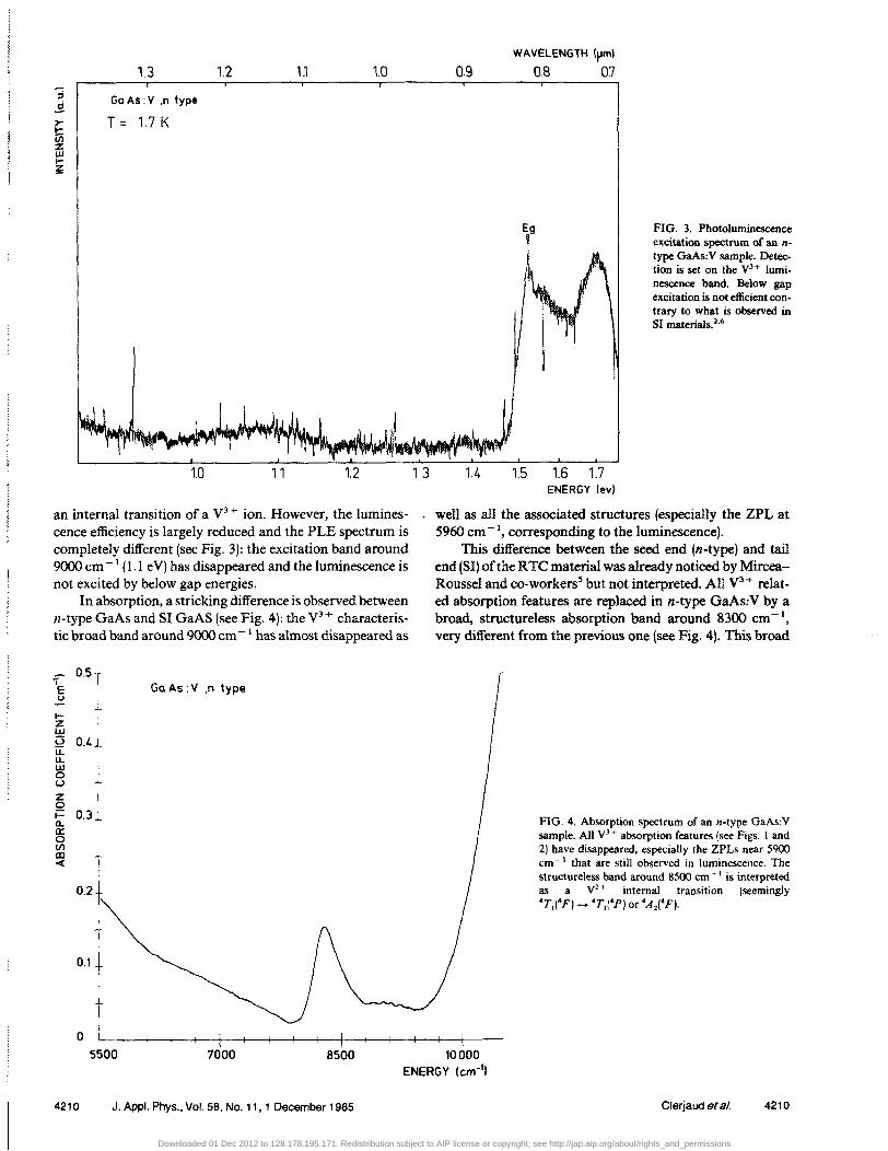
an internal transition of a y3+ ion. However, the luminescence efficiency is largely reduced and the PLE spectrum is completely different (see Fig. 3): the excitation band around 9000 cm - I (1.1 e Y) has disappeared and the luminescence is not excited by below gap energies.
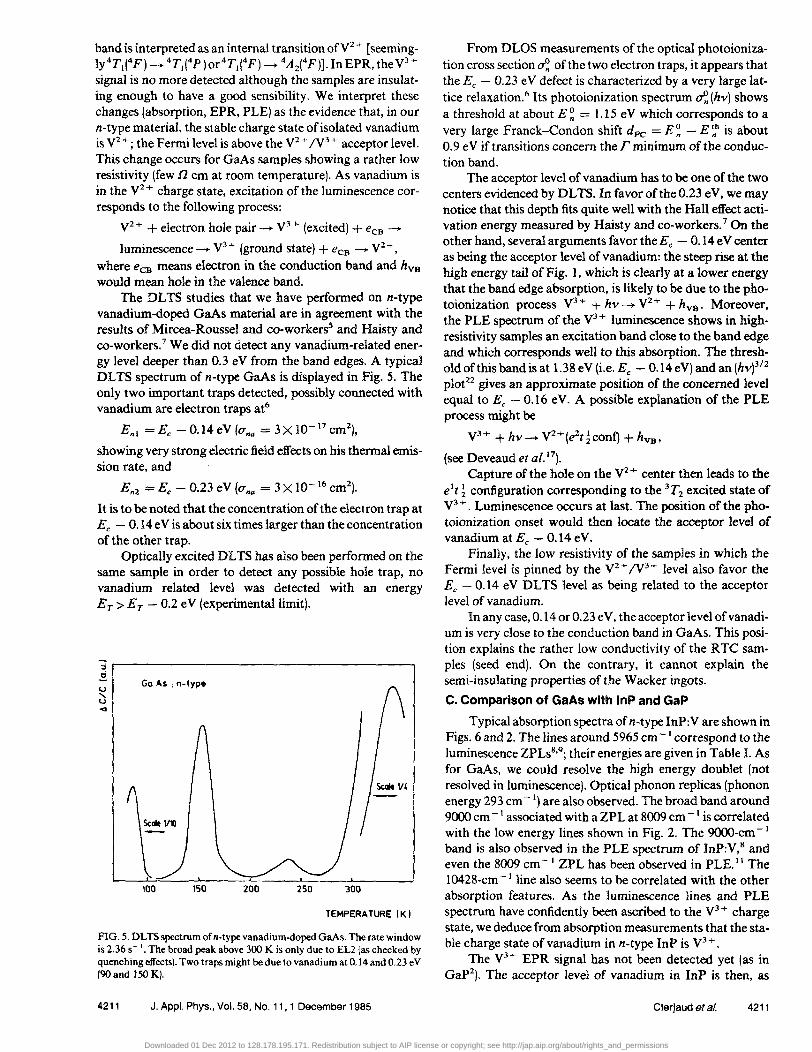
In absorption, a stricking difference is observed between n-type GaAs and SI GaAS (see Fig. 4): the y3+ characteristic broad band around 9000 cm - I has almost disappeared as
I OST
E Go As : V .n type u
t-Z UJ
0.4+ l3 u: u.. ! w 0 1 u z 0 t= 0.3+ a.. 0:: 0 III
t ID oct
0.2
+ 0.1 +
t 0 I
13
09
1.4
WAVELENGTH (pml
0.8 07
Eg
1.5 1.6 1.7 ENERGY levI
FIG. 3. Photoluminescence excitation spectrum of an ntype QaAs:V sample. Detection is set on the V3+ luminescence band. Below gap excitation is not efficient contrary to what is observed in SI materiaIs.2·6
wen as all the associated structures (especially the ZPL at 5960 cm -I, corresponding to the luminescence).
This difference between the seed end (n-type) and tail end (SI) of the RTC material was aJready noticed by MirceaRoussel and co-workers5 but not interpreted. All y3+ related. absorption features are replaced in n-type GaAs:Y by a broad, structureless absorption band around 8300 cm-I, very different from the previous one (see Fig. 4). This broad
I I
FIG. 4. Absorption spectrum of an n-type GaAs:Y sample. All y 3 + absorption features (see Figs. I and 2) have disappeared, especially the ZPLs near 5900 em -, that are still observed in luminescence. The structureless band around 8500 em - J is interpreted as a Y' + internal transition lseemingly 'T,(4F) _ 'TtP) or 4A 2(4F).
5500 7000 8500 10000 ENERGY (em-I)
4210 J. Appl. Phys., Vol. 58, No. 11, 1 December 1985 Clerjaud sf al. 4210
Downloaded 01 Dec 2012 to 128.178.195.171. Redistribution subject to AIP license or copyright; see http://jap.aip.org/about/rights_and_permissions
band is interpreted as an internal transition ofy2 + (seemingly 4Td4F ) -... 4TJ(4p )or4TJ(4F) -... 4A 2(4F)].InEPR, the y3+ signal is no more detected although the samples are insulating enough to have a good sensibility. We interpret these changes (absorption, EPR, PLE) as the evidence that, in our n-type material, the stable charge state of isolated vanadium is y2 +; the Fermi level is above the y2+ IV3 + acceptor level. This change occurs for GaAs samples showing a rather low resistivity (few n em at room temperature). As vanadium is in the y2+ charge state, excitation of the luminescence corresponds to the following process:
y2+ + electron hole pair ----+ y3+ (excited) + eCB ........
luminescence -... y3+ (ground state) + eCB -+ y2+, where eCB means electron in the conduction band and hVB would mean hole in the valence band.
The DLTS studies that we have performed on n-type vanadium-doped GaAs material are in agreement with the results of Mircea-Rousse1 and co-workers5 and Haisty and co-workers. 7 We did not detect any vanadium-related energy level deeper than 0.3 eY from the band edges. A typical DLTS spectrum of n-type GaAs is displayed in Fig. 5. The only two important traps detected, possibly connected with vanadium are electron traps at6
Enl = Ee - 0.14 eY (uno = 3 X 10- 17 cm2),
showing very strong electric field effects on his thermal emission rate, and
En2 = Ee - 0.23 eY (uno = 3 X 10- 16 cm2).
It is to be noted that the concentration of the electron trap at Ee - 0.14 e Y is about six times larger than the concentration of the other trap.
Optically excited DL TS has also been performed on the same sample in order to detect any possible hole trap, no vanadium related level was detected with an energy Er >Er - 0.2 eY (experimental limit).
~ r---------------------------------------~ ti ..., ..... ..., <I
Go As . n-type
100 150 200 250 300
TEMPERATURE (K I
FIG. 5. DLTS spectrum of IHype vanadium-doped GaAs. The rate window is 2.36 s - '. The broad peak above 300 K is only due to EL2 (as checked by quenching effects). Two traps might be due to vanadium at 0.14 and 0.23 eV (90 and 150 K).
4211 J. Appl. Phys., Vol. 58, No. 11, 1 December 1985
From DLOS measurements of the optical photoionization cross section d.: of the two electron traps, it appears that the Ee - 0.23 eY defect is characterized by a very large lattice relaxation.6 Its photoionization spectrum ~ (hv) shows a threshold at about E~ = 1.15 eY which corresponds to a very large Franck-Condon shift dpc = E~ - E~h is about 0.9 eY if transitions concern the F minimum of the conduction band.
The acceptor level of vanadium has to be one of the two centers evidenced by DL TS. In favor of the 0.23 eY, we may notice that this depth fits quite well with the Hall effect activation energy measured by Haisty and co-workers. 7 On the other hand, several arguments favor the Ee - 0.14 eY center as being the acceptor level of vanadium: the steep rise at the high energy tail of Fig. 1, which is clearly at a lower energy that the band edge absorption, is likely to be due to the photoionization process y3 + + hv ........ y2+ + hVB . Moreover, the PLE spectrum of the y3+ luminescence shows in highresistivity samples an excitation band close to the band edge and which corresponds well to this absorption. The threshold of this band is at 1.38 eY (i.e. Ee - 0.14 eY) and an (hV)3/2 plot22 gives an approximate position of the concerned level equal to Ee - 0.16 eY. A possible explanation of the PLE process might be
y3+ + hv ........ Y2+(e2t ~conf) + hVB'
(see Deveaud et al. 17). Capture of the hole on the y2+ center then leads to the
elt ~ configuration corresponding to the 3T2 excited state of y3+. Luminescence occurs at last. The position of the photoionization onset would then locate the acceptor level of vanadium at Ee - 0.14 eY.
Finally, the low resistivity of the samples in which the Fermi level is pinned by the y2+ IV3 + level also favor the Ec - 0.14 eY DLTS level as being related to the acceptor level of vanadium.
In any case, 0.14 or 0.23 eY, the acceptor level of van ad iurn is very close to the conduction band in GaAs. This position explains the rather low conductivity of the R TC samples (seed end). On the contrary, it cannot explain the semi-insulating properties of the Wacker ingots.
C. Comparison of GaAs with InP and GaP
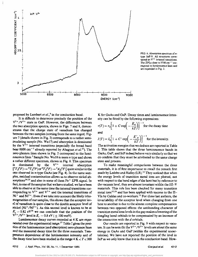
Typical absorption spectra of n-type InP:Y are shown in Figs. 6 and 2. The lines around 5965 em -I correspond to the luminescence ZPLSB,9; their energies are given in Table I. As for GaAs, we could resolve the high energy doublet (not resolved in luminescence). Optical phonon replicas (phonon energy 293 cm- I
) are also observed. The broad band around 9000 cm - I associated with a ZPL at 8009 cm - I is correlated with the low energy lines shown in Fig. 2. The 9OOO-cm- 1
band is also observed in the PLE spectrum of InP:Y,8 and even the 8009 cm - 1 ZPL has been observed in PLE. II The 1 0428-cm - I line also seems to be correlated with the other absorption features. As the luminescence lines and PLE spectrum have confidently been ascribed to the y 3+ charge state, we deduce from absorption measurements that the stable charge state of vanadi urn in n· type InP is y3 + .
The y3+ EPR signal has not been detected yet (as in GaP2). The acceptor level of vanadium in InP is then, as
Clerjaud et al. 4211
Downloaded 01 Dec 2012 to 128.178.195.171. Redistribution subject to AIP license or copyright; see http://jap.aip.org/about/rights_and_permissions
f"" E ::!/, tZ w 1.3 u:: u.. w o u z o i= Q.. a: o ~ 3.5 oc{
3
6 00 8 00
proposed by Lambert et al., 8 in the conduction band. It is difficult to determine precisely the position of the
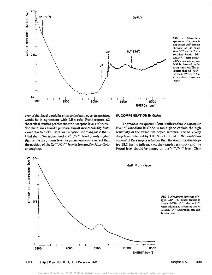
y2+ /V3+ state in GaP. However, the differences between the two absorption spectra, shown in Figs. 7 and 8, demonstrates that the charge state of vanadium has changed between the two samples (coming from the same ingot). Figure 7 (details shown in Fig. 2) corresponds to a rather semiinsulating sample (No. Wa17) and absorption is dominated by the y3+ internal transitions (especially the broad band bear 8800 cm -I already reported by Abagyan et al. 23). The zero-phonon lines shown in Fig. 2 correspond to the luminescence lines.2 Sample No. Wal8 is more n type and shows a rather different spectrum, shown in Fig. 8. This spectrum is dominated by the yH internal absorption eTI(4p) __ 4TI1
4P)or 4T.(4p) __ 4A2(4P)] quite similar to the one observed in n-type GaAs (see Fig. 4). In the same samples, residual contamination a1lows us to observe nickel absorptions24.25 and also in some of them Fe + EPR signal.. In fact, in one of the samples that we have studied, we have been able to observe at the same time the internal transitions corresponding to V2+ and y3+ and the internal transitions of Ni + and NF + . Even if we take into account the likely inhomogeneities of our samples, this shows that the acceptor level of vanadium is quite close to the double acceptor level of nickel (Ni + !NiH). As this second level is known to be at Ee - 0.82 ey26 we can conclude that the position of the y2+ /V3+ level is Ee - 0.8 eY ( ± 100 meY).
Luminescence decay curves recorded at 4 K are exponential over the experimental range.27 Table r gives the position of the luminescence (and absorption) zero-phonon lines and the measured decay time for the three materials. Temperature dependence of the luminescence intensity and of the decay time have been studied in the range 4 K < T < 300
4212 J. Appl. Phys., Vol. 58, No. 11, 1 December 1985
9 00 ENERGY (em-')
110 0
FIG. 6. Absorption spectrum of ntype InP:Y. All structures correspond to yH internal transitions. The ZPLs close to 5700 em - I correspond to luminescence lines and are expended in Fig. 2.
K for GaAs and GaP. Decay times and luminescence intensity can be fitted by the following expressions:
7'(T) = ro[ 1 + C exp( - :~) J - I for the decay time
and
I IT) = Io[ 1 + C I exp( _ ~;)] - 1 for the intensity.
The activation energies that we deduce are reported in Table I. This table shows that the three luminescence bands in GaAs, GaP, and InP indeed behave very similarly so that we do confirm that they must be attributed to the same charge state and process.
To make meaningful comparisons between the three materials, it is of first importance to recall the remark first made by Ledebo and Ridley (LR). 12 They noticed that when the energy levels of transition metal ions are plotted, not with respect to the band edges of the host but by reference to the vacuum level, they are almost invariant within the UI-y materials. This role has been checked for many transition metal ions 12.28 and has been applied with success to the IIVIs by Caldas and co-workers. 13 For these last authors, the invariability of the acceptor level when changing from one host to another is due to the almost complete compensation between two opposed effects: the antibonding character of transition metal ions leveJs in the gap makes a lowering of the dangling bond orbitals to be compensated by an increase of the interaction with the d orbitals.
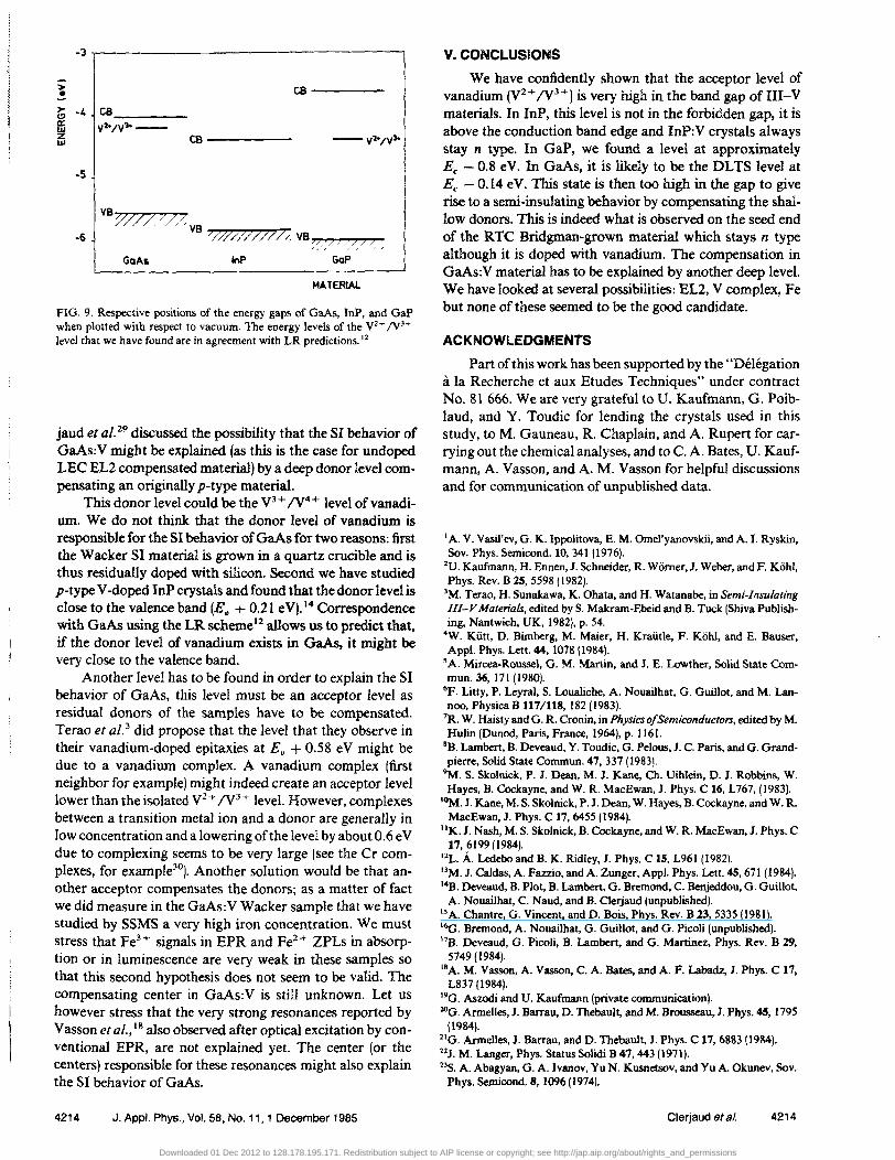
Our results are reported in Fig. 9 with respect to vacuum. It can be seen tht the y2 + /V3 + levels are aboutthe same energy in GaAs and GaP (within the experimental uncertainties). We have not reported the position of the level in InP as we only know that it is in the conduction band. How-
Clerjaud et al. 4212
Downloaded 01 Dec 2012 to 128.178.195.171. Redistribution subject to AIP license or copyright; see http://jap.aip.org/about/rights_and_permissions
"'e 2.3 u
IZ ~ ~
It UJ o u
~ i= &: o 1/1
~ 2.0
FIG. 7. Absorption spectrum of a vanadium-doped GaP sample showing at the same time y2+ and yJ+ absorption bands. Ni +
and Ni2 + internal transitions (see arrows) can both be detected on the same spectrum. This indicates that Ni + INi' +
level and y2+ /V3+ level are close to one an· other.
1.7 L-~--+--+--~~~~--~-+--+-~--~--b--r--+--+--~~~-r--~-+--+-~
5000 6 00 80 0
ever, if that level would be close to the band edge, its position would be in agreement with LR's rule. Furthermore, all theoretical studies predict that the acceptor levels of transition metal ions should go down almost monotonically from vanadium to nickel, with an exception for manganese (halffilled shell). We indeed find a V2 + /V3+ level plainly higher than is the chromium level, in agreement with the fact that the position oftheCr+ /cr3+ levelislowered by Jahn-Tel1-er coupling.
"i 8.5 e c.J
IZ UJ U u:: LL UJ o u z o i= CL. 0: o 1/1
~ 5.5
9500 11 00 ENERGY Icm-11
IV. COMPENSATiON IN GaAs
The main consequence of our studies is that the acceptor level of vanadium in GaAs is too high to explain the high reSistivity of the vanadium doped samples. The only very deep level detected by DLTS is EL2 but if the vanadium content of the samples is higher than the donor residual doping EL2 has no influence on the sample resisitivity and the Fermi level should be pinned on the V2+ /V3+ level. Cler-
Go P : V , n - type
FIG. 8. Absorption spectrum of /Itype GaP. The broad transition around 8500 cm - I is due to y2 + ;
weak additional structures due to residual yH absorption can also be observed.
JL--+--+--+---t--+I--+-I -+--+--+--+1 -+---+--+---+-+---1--+---+---+---I--j~ 5500 7000 8500 11500
ENERGY Icm-11
4213 J. Appl. Phys., Vol. 58, No. 11, 1 December 1985 Clerjaud et a/. 4213
Downloaded 01 Dec 2012 to 128.178.195.171. Redistribution subject to AIP license or copyright; see http://jap.aip.org/about/rights_and_permissions
-3r----------------------------------,
> • ~ -4 CB _____ _ I VZ·/V'lo_-
-5
CB-----
CB------
MATERIAl
FlG. 9. Respective positions of the energy gaps of GaAs, InP, and GaP when plotted with respect to vacuum. The energy levels of the V2+ /V3+ level that we have found are in agreement with LR predictions. 12
jaud et al. 29 discussed the possibility that the SI behavior of GaAs:Y might be explained (as this is the case for undoped LEC EL2 compensated material) by a deep donor level compensating an originally p-type material.
This donor level could be the y3+ /V4 + level of vanadium. We do not think that the donor level of vanadium is responsible for the SI behavior of GaAs for two reasons: first the Wacker SI material is grown in a quartz crucible and is thus residually doped with silicon. Second we have studied p-type Y -doped InP crystals and found that the donor level is close to the valence band (Eu + 0.21 ey).14 Correspondence with GaAs using the LR schemel 2 allows us to predict that, if the donor level of vanadium exists in GaAs, it might be very close to the valence band.
Another level has to be found in order to explain the SI behavior of GaAs, this level must be an acceptor level as residual donors of the samples have to be compensated. Terao et al? did propose that the level that they observe in their vanadium-doped epitaxies at Ev + 0.58 eY might be due to a vanadium complex. A vanadium complex (first neighbor for example) might indeed create an acceptor level lower than the isolated y2+ /V3+ level. However, complexes between a transition metal ion and a donor are generally in low concentration and a lowering of the level by about 0.6 e Y due to complexing seems to be very large (see the Cr complexes, for example30
). Another solution would be that another acceptor compensates the donors; as a matter of fact we did measure in the GaAs:Y Wacker sample that we have studied by SSMS a very high iron concentration. We must stress that Fe3 + signals in EPR and Fe2 + ZPLs in absorption or in luminescence are very weak in these samples so that this second hypothesis does not seem to be valid. The compensating center in GaAs: Y is stm unknown. Let us however stress that the very strong resonances reported by Yasson et al., 18 also observed after optical excitation by conventional EPR, are not explained yet. The center (or the centers) responsible for these resonances might also explain the SI behavior of GaAs.
4214 J. Appl. Phys., Vol. 58, No. 11, 1 December 1985
v. CONCLUSIONS
We have confidently shown that the acceptor level of vanadium (y2+ /V3+) is very high in the band gap of III-Y materials. In InP, this level is not in the forbidden gap, it is above the conduction band edge and InP:Y crystals always stay n type. In GaP, we found a level at approximately Ec - 0.8 eY. In GaAs, it is likely to be the DLTS level at Ec - 0.14 eY. This state is then too high in the gap to give rise to a semi-insulating behavior by compensating the shallow donors. This is indeed what is observed on the seed end of the RTC Bridgman-grown material which stays n type although it is doped with vanadium. The compensation in GaAs: Y material has to be explained by another deep level. We have looked at several possibilities: EL2, Y complex, Fe but none of these seemed to be the good candidate.
ACKNOWLEDGMENTS
Part of this work has been supported by the "Delegation a la Recherche et aux Etudes Techniques" under contract No. 81 666. Weare very grateful to U. Kaufmann, G. Poiblaud, and Y. Toudic for lending the crystals used in this study, to M. Gauneau, R. Chaplain, and A. Rupert for carrying out the chemical analyses, and to C. A. Bates, U. Kaufmann, A. Yasson, and A. M. Yasson for helpful discussions and for communication of unpUblished data.
'A. V. Vasil'ev, G. K. Ippolitova, E. M. Omel'yanovskii, and A. I. Ryskin, Sov. Phys. Semicond. 10, 341(1976).
2U. Kaufmann, H. Ennen, 1. Schneider, R. Womer, 1. Weber, and F. Kohl, Phys. Rev. B 25,5598 (1982).
3M. Terao, H. Sunakawa, K. Ohata, and H. Watanabe, in Semi-Insulating IIJ- V Materials, edited by S. Makrarn-Ebeid and B. Tuck (Shiva Publishing, Nantwich, UK, 1982), p. 54.
·W. Kutt, D. Bimberg, M. Maier, H. Krautle, F. Kohl, and E. Bauser, Appl. Phys. Lett. 44, 1078(1984).
'A. Mircea-Roussel, G. M. Martin, and 1. E. Lowther, Solid State Commun.36, 171 (1980).
6F. Litty, P. Leyral, S. Loualiche, A. Nouailhat, G. Guillot, and M. Lannoo, Physica B 1171118,182 (1983).
'R. W. Haisty and G. R. Cronin, in Physics of Semiconductors, edited by M. Hulin (Dunod, Paris, France, 1964), p. 1161.
8B. Lambert, B. Deveaud, Y. Toudic, G. Pelous, 1. C. Paris, and G. Grandpierre, Solid State Commun. 47,337 (1983). ~. S. Skolnick, P. J. Dean, M. 1. Kane, Ch. Uihlein, D. J. Robbins, W. Hayes, B. Cockayne, and W. R. MacEwan, J. Phys. C 16, L767, (1983).
10M. 1. Kane, M. S. Skolnick, P. 1. Dean, W. Hayes, B. Cockayne, and W. R. MacEwan, J. Phys. C 17, 6455 (1984).
"K. 1. Nash, M. S. Skolnick, B. Cockayne, and W. R. MacEwan, J. Phys. C 17,6199 (1984).
12L. A. Ledebo and B. K. Ridley, J. Phys. CIS, L961 (1982). 13M. J. Caldas,A. Fazzio,andA. Zunger, App\. Phys. Lett. 45, 671 (1984). '4B. Deveaud, B. Plot, B. Lambert, G. Bremond, C. Benjeddou, G. Guillot,
A. Nouailhat, C. Naud, and B. Clerjaud (unpublished). I, A. Chantre, G. Vincent, and D. Bois, Phys. Rev. B 23,5335 (1981). '6G. Bremond, A. Nouailhat, G. Guillot, and G. Picoli (unpUblished). 17B. Deveaud, G. Picoli, B. Lambert, and G. Martinez, Phys. Rev. B 29,
5749 (1984). IRA. M. Vasson, A. Vasson, C. A. Bates, and A. F. Labadz, J. Phys. C 17,
L837 (1984). 19G. Aszodi and U. Kaufmann (private communication I. 2OG. ArmelJes, J. Barrau, D. Thebault, and M. Brousseau, J. Phys. 45, 1795
(1984). 2'G. Armelles, J. Barrau, and D. Thebault, 1. Phys. C 17, 6883 (1984). 22J. M. Langer, Phys. Status Solidi B 47, 443 (1971). 23S. A. Abagyan, G. A. Ivanov, Yu N. Kusnetsov, and Yu A. Okunev, Sov.
Phys. Semicond. 8, 1096 (1974).
Clerjaud et al. 4214
Downloaded 01 Dec 2012 to 128.178.195.171. Redistribution subject to AIP license or copyright; see http://jap.aip.org/about/rights_and_permissions
2·U. Kaufmann, W. H. Koschel, J. Schneider, and J. Weber, Phys. Rev. B 19, 3343 (1979).
25Z. Liro and J. M. Baranowski, J. Phys. CIS, 4599 (1982). 26X. Z. Yang, L. Samuelson, and H. G. Grimmeiss, J. Phys. C 17,6521
(1984). 27G. Guillot, C. Benjeddou, P. Leyral, and A. Nouailhat, J. Lumin. 31/32,
439(1984).
4215 J. Appl. Phys., Vol. 58, No. 11, 1 December 1985
28p. Rojo, P. Leyral, G. Guillot, A. Nouailhat, B. Lambert, B. Deveaud, and R. Coquille, J. Appl. Phys. 55, 395 (1984).
29JJ. Clerjaud, C. Naud, C. Benjeddou, G. Guillot, P. Leyral, B. Deveaud, and B. Lambert, in Semi-Insulating IIl-V Materials, edited by D. C. Look and J. S. Blakemore (Shiva Publishing, Nantwich, UK, 1984), p. 484.
l<1J. Deveaud, B. Lambert, G. Picoli, and G. Martinez, J. Appl. Phys. 55, 4356 (1984).
Clerjaud et al. 4215
Downloaded 01 Dec 2012 to 128.178.195.171. Redistribution subject to AIP license or copyright; see http://jap.aip.org/about/rights_and_permissions