Embed Size (px)
Citation preview
University of Alberta
The Generalized Mach-Zehnder Interferorneter using Multimode Interference Couplers for Optical Communications
Networks
Neil Satish Lagali O
A thesis subrnitted to the Faculty of Graduate Studies and Research in partial fülfillment of the requirements for the degree of Doctor of Philosophy.
DEPARTMENT OF ELECTRICAL AND COMPUTER ENGINEERING
Edmonton, Alberta
Spring, 2000

National Library B i b l i i ue nationale % du Cana
A uisitions and Acquisiions et ~8io~raphio Services services bibiiographiquer 385 WeEnirgdori Street 395, nm Wellington CntawaON KiAON4 OtlawaON K 1 A W Canada Canada
The author has granted a non- L'auteur a accordé une licence non exclusive licence a l l h g the exclusive permettant à la National L'brary of Canada to Bibliothèque nationale du Canada de reproduce, loan, distn'bute or sell reproduirey prêter, dktri'buer on copies of this thesis in microfom~, vendre des copies de cette thèse sous paper or elechonic formats. la forme de microfiche/nIm, de
reproduction sur papier ou sur format électronique.
The author retriYis ownership of the L'auteur conserve la propriété du copyright in this thesis. Neither the droit d'auteur qui protège cette thèse. thesis nor substantial extracts fiom it Ni la thèse ni des e d t s substantiels may be p ~ t e d or otherwise de ceile-ci ne doivent être imprimés reproduced without the author's ou autrement reproduits sans son permission. autorisation,

"The voyage of discovery is not in seeking nav landscapes. but in having new Ces. "
- Marcel Proust

For m-v Parents. Sdhakar and Kokila.
Their love and support throtrgh the yeariv have made this work possible.

Abstract
The explosive growth in telecornmunications traffic in recent years has hastened the
emergence of optical communications networks. As the volume and complexity of network
trafic increases, efficient, flexible, and cost-effective methods of routing and distributing optical
signals are being sought. One method for meeting these requirernents is through the use of
integrated optics technology, which enables the realization of miniaturized optical components
and circuitry on a planar substrate surface.
In this work the integrated optic multiple-arm or generalized Mach-Zehnder
interferometer (GMZI) using multimode interference (MM[) couplers is studied. Through an
investigation into the principles governing the operation of this device, a mathematical theory
describing both its idealized and observed pmperties is developed. This theory predicü the
operation of the GMZI as a variable-ratio optical power splitter, which in specific instances
tùnctions as an optical switch. Both the power splitting and switching fùnctions of the GMZI are
usehl for efficient optical signal distribution, routing, and protection switching applications in
emerging optical communications networks.
The variable-ratio optical power splitting fünction allows an input optical signal to be
distributed in a controlled, dynamic manner to a number of output channels. This provides an
efficient and flexible means of broadcasting an optical signal to multiple users. The method of
operating this novel device is described and its strengths and limitations are assessed.
A consideration of the optical switch fùnction reveals that various levels of symmetry are
present in the operation of the GMZI. This symmetry is used to develop new designs for 1 x iV
optical switches with reduced operational requirements. Further consideration of the multiple-
input switch properties Ieads to new designs for non-blocking N x N optical switches that possess
the benefits of compactness and a simple design and fabrication procedure. The switches enable

optical signal routing and network protection and reconfigumtion switching to be realized with
compact components exhibiting Iow power consumption Ievels. The operation and performance
issues of these switches are examined in detail.
To demonstrate the feasibility of the manufacture and operation of the GMZI and the
validity of the theory upon which it is based, a number of integrated optical waveguide
components including MM1 couplers and GMZi devices have been realized. The devices were
fabricated in a high rehctive index contrast silicon oxynitride (SiON) based planar waveguide
system, utilizing the thermo-optic effect for active operation.
The measured device performance is reported, and demonstrations of efficient thermo-
optic operation, 1 x IV switching in 2 x 2 and 4 x 4 GMZI devices, and variable-ratio power
splitting and multi-port switching in a 4 x 4 GMZI device have been achieved. The obse~ed
device characteristics validate the tenets of the mathematical theory deveIoped in this work, and
demonstrate the feasibility of using the GMZI to perform the complex optical hnctions required
for state-of-the-an optical communications networks.

Acknowledgements
I would First like to express my most sincere hanks to my supervisor Dr. R. 1x1 MacDonald for introducing me into the field of optical communications and thereafter giving me the freedom to learn and grow, and for opening doors of opportunity that few students ever witness. 1 have had the extreme good fortune to share in his knowledge, insight, and vision both within and beyond the bounds of this work. I would also like to thank my CO-supervisor Dr. James N. McMullin for his heIp and mentorship as 1 prepared this work.
1 am indebted to my friend, colleague, and mentor Dr. Reza Paiam. He has provided the motivation for this research through pioneenng efforts in the area of MM1 coupIers and has offered critical insights and direction in this work Eiom its inception through to its completion. His hand is implicit in much of the work reported in these pages.
1 wish to express my gratitude to Dr. Alfred Driessen and Dr. Kentin W6rhofi. my collabonton in the experimental portion of this work. They have not only graciously provided me with the facilities of MESA and the Lightwave Devices Group at the University of Twente, The Netherlands, but their helphlness, enthusiasm and fnendship have brought much excitement into this work and provided me with a first-hand experience of the wonderful Dutch hospitality.
1 would like to thank my colleagues in Edmonton, Alberta at the Telecommunications Research Laboratories (TRLabs), David Boertjes, Ray DeCorby, Alan Hnatiw, and Craig Unick for their help in the early stages of this work. 1 would also like to acknowledge the help of Dr. James Broughton at the Alberta Microelectronic Center.
I am very gratehl to those at the University of Alberta, including my supervisory committee, for their diligence in examining this work. In particular, 1 would like to thank Michelle Lock for her tireless efforts in making things rurt smoothly while I've been thousands of kilometers away.
1 would also like to acknowledge the help of many people at JDS Uniphase in Nepean, Ontario, in particular Liz Nowak, Catherine Murphy, Vincent Delisle, Rajiv Iyer, Malcolm Smith, Suresh Mistry, Cynthia Wilson, Jim Yang, and Barrie Keyworth.
At the MESA Research Institute, 1 would like to th& Nicole, Gerard, Peter, and Johnny for their training and help in the clean room, and Bert Otter for producing the SEM images.
In the Lightwave Devices Group at the University of Twente, 1 would like to thank the many people who have provided a fun and exciting environment for both research and pursuits beyond. 1 am particularly grateful to Anton Hollink for his constant support and technical wizardry in hardware and software, and diligence in al1 manen optical, electrical, mechanical, and procedural. 1 would like to thank Toon Andringa for offering his expertise in the clean room and for his artfül work in wire bonding. Th& are also due to Erwin Ri ie rs and Chris RoeIofken for their help with the device characterization equipment. Thanks also to Sami Musa for graciously performing the transmission rneasurements for the annealed samples. Numerous others deserve mention: Marcel, Tjarko, Gregory, Dion, Simone, Rene, H m , Ton, Gert, Wim, Robert, Libor, Lin, Hugo, Henk, and Remco.
I would also t ike to acknowledge the University of Alberta, TIUabs, JDS Uniphase Inc., and the Natural Sciences and Engineering Research CounciI of Canada for their generous financial support.
I would Iike to express a very special thanks to Theresa, for her wisdom, patience, understanding, and kindness, and for teaching me to focus on what is really important in life.
Finally, I am very gratetùl to my family, my Parents, and my sister Pamela. Their constant Iove, support, and encouragement is a continuous source of joy and strength.

Table of Contents
1 . Introduction ................................................................................................................................ 1 1.1 Optical communications ....................................................................................................... 1
7 1.2 Optical networks .............................~....................................................................................... 1.3 Integrated optics ..................................................................................................................... 3 1.4 Integrated optical couplers ..................................................................................................... 4 1.5 Applications .............................,.......................................................................................... 5 1.6 Overview of this work ........................................................................................................... 7
2 . Theoretical foundations ............................................................................................................. 8 2.1 Introduction ........................... ,,, ............................................................................................ 8 2.2 The slab waveguide ...............,,.............................................................................................. 8
2.2.1 Air cladding .................... ,,, ........................................................................................... 1 1 2.2.2 Substrate effects ............................................................................................................ 12
2.3 Channel waveguides - the effective index method .............................................................. 12 2.4 Modal propagation analysis ................................................................................................. 13 2.5 The iV x N multimode interference coupler .......................................................................... 14
......................................................... 2.6 The N x N generalized Mach-Zehnder interferorneter 18
3 . Theory of variable-ratio power splittlng ................................................................................ 20 3.1 Introduction ........................... ,., ......................................................................................... 20 3.2 Transfer matrix of the N x N MM1 coupler ......................................................................... 20
33 3.3 The GMZI transfer matrix .................................................................................................... -- 33 3.3.1 Basic structure and operation of the GMZI .................................................................. -- 73 3.3.2 The GMZf transfer matrix ............................................................................................ --
3.4 Variable-ratio power splitting .............................................................................................. 23 3.4.1 Output intensity expressions ......................................................................................... 23 3.4.2 Numerical Analysis and Optimization Algorithm ........................................................ 25
................................................................................................................ 3.5 Tolerance analysis 26 3.5.1 Phase shift deviations .................................................................................................. 27 3.5.2 Theory of the non-ideal GMZI ..................................................................................... 27
3.5.2.1 Modified GMZI transfer matrix ............................................................................. 28 3.5.2.2 Output intensity expressions .................................................................................. 28 3.5.2.3 Non-ideal GMZI characteristic response ....................................... .,. .. 79
3.5.3 Variable-ratio power splitter tolerances .................................................................... 32
...................................... 4 . Theory of Ceneralized Mach-Zehnder Intederorneter Switching 35 4.1 tntroduction .....................,...................... ........................................................................... 35 4.2 Idealized 1 x N GMZI switching .............................................. .. ..................................... 35 4.3 Tolerances for GMZI switching ........................................................................................... 37 4.4 Multi-port blocking switches ....................................................................................... 3 9
4.4.1 Cross-connect pattern of the LV x N GMZI .................................................................... 40 ................................................................... 4.4.2 Tunable N x N MMi Phasar Multiplexer 41

4.5 Phase shifting requirements in the GMZI ................... ... ................................................. 42 4.5.1 Passive GMZl ............................................................................................................... 42
A . K even .......................................................................................................................... 43 ............................................................................................... . B K odd ................... ....... .. 45
4.5.2 Active GMZI ....................................,,,,.. ...................................................................... 47 4.6 Improved l x N Switch ........................................................................................................ 48
4.6.1 Theory and Design ........................................................................................................ 48 4.6.2 Examples of Improved 1 x N switch operation ............................................................ 49
4.6.2.1 Improved 1 x 4 Switch ...................... ... ............................................................. 49 4.6.2.2 Improved 1 x 6 Switch ........................................................................................... 50
4.7 N x N non-blocking switching ............................................................................................. 51 4.7.1 Cascaded Design .......................................................................................................... 52 4.7.2 Balanced Design ........................................................................................................... 54 4.7.3 Tolerance analysis of a balanced non-blocking switch ......................................... 5 8
5 . Device Design .............~.........~...~.........~...~......~.~~..~......~.......~~......~.........~~~~.~.....~....~~.................~. 59 5 . 1 Introduction .......................................................................................................................... 59 5.2 Choice of technology ........................................................................................................... 59 5.3 Waveguide Design ............................................................................................................... 60
..................................................................................................... 5.3.1 Design requirements 60 5.3.2 Choice of matenal system ............................................................................................. 61 5.3.3 Waveguide structure - optical properties ................................................................... 62 5.3.4 Waveguide structure - thermal properties ............................................................... 6 4
5.4 MM1 coupler design ........................................................................................................ 6 7 5.4.1 MM1 coupler dimensions ............................................................................................. 67 5.4.2 Access waveguide ben& .............................................................................................. 68 5.4.3 MMI coupler simulation ............................................................................................... 69
........................................................................................................................ 5.5 GMZI design 72 5.5.1 Phase shifting region ..................................................................................................... 72 5.5.2 GMZI simulation - variable ratio power splitting ........................................................ 74
5.6 Photomask Layout ........................................................................................................... 7 6
6 . Device Fabrication ................................................................................................................... 77 6.1 Introduction .........~........~.....~.~.......~..........~.....................~............~....~..~..~.......~..~~..~....~~..~~....~ 77 6.2 Film processing ................................................................................................................ 77
6.2.1 Substrate preparation ................................................................................................. 77 6.2.2 PECVD film growth ................................................................................................ 79 . . . 6.2.3 Film optirnization .......................................................................................................... 80
6.2.3.1 Parameter optimization ......................................................................................... 80 6.3.3.3 Film characterization .......................................................................................... 81 6.2.3.3 Heat treatrnent of SiON layer .................................................. ........ 8 3
6.2.4 Metal sputtering ............................................................................................................ 85 6.3 Photolithography and Etching .............................................................................................. 87
6.3.1 Photolithography ......................................................................................................... 87 6.3.2 Wet chemical etching .................... .. ......................................................................... 88 6.3.3 Reactive ion etching .................................................................................................... 88 6.3.4 Visuai charactenzation ................................................................. ... 9 1
6.4 Post-processing ................................................................................................................... 94

7 . Device Performance ..................o................................oo....o.o.o.....o............o...o.....o........o....o.o.. 97 . 7.1 Introduction ..........................~.....................~....~........................................~........................... 97
.............................................................................................. 7.2 Experimental procedure 9 7 7.2.1 Experimental setup ....................................................................................................... 98 7.2.2 Fiber-to-chip coupling .................................................................................................. 99
................................................................................ 7.3 Single-mode waveguide performance 101 7.3.1 Mode field ................................................................................................................... 101
....................................................................................................... 7.3.2 Propagation losses 102 7.4 MM1 coupler performance ................................................................................................. 104
.................................................................................................................. 7.4.1 Definitions 1 04 . ................................................................*................ 7.42 Performance vs imaging length 105
....................................................................................... 7.4.3 Performance vs . wavelength 106 ............................................................................................... 7.4.4 Visual characterization 107
... 7.5 GMZI performance ; ..................................................................................................... 1 07 7.5.1 The 2 x 2 GMZI .......................................................................................................... 107 7.5.2 The 4 x 4 GMZI .......................................................................................................... 1 10
7.5.2.1 1 x NGMZI switching ......................................................................................... 1 12 ............................................................................................ 7.5.2.2 Multi-port switching 1 15
.............................................................................. 7.5.2.3 Variable ratio power splitting 1 16
.......................................................................................... 8 . Summary and Future Directions L 18 8.1 Summary ........................................................................................................................... 1 18 8.2 Future Directions ............................................................................................................. 122 8.3 Conclusion ......................................................................................................................... 124

List of Tables
Table 3.1 Simulated tolerances of N = 4 variable-ratio power splitter for power splitting ratio (3.33)' including a f 3 % fluctuation in the applied phase shih. The 'am phase error' refers to an upper limit for the uncompensated phase error in the GMZI arms. ................................................................................................................................. 33
Table 3.2
Table 4.1
Table 4.2
Table 4 3
Table 4.4
Table 4.5
Table 4.6
Table 4.7
Table 4.8
Simulated tolerances of variable-ratio power splitter for N = 5 up to N = 10 for power splitting ratio (3.34). including a t 3 % fluctuation in the applied phase shifts. The imbalance and phase deviation for N = 5,6,7 are t 1 .O dB and & 3.5' and for N = 8, 9, 10 they are f 2.0 dB and t 9 O . respectively. The first and second lines for each value of N represent upper limits of O0 and + 5' for the uncompensated phase error in the GMZI anns ...................................................................................................... 34
Simulated tolerances of the crosstalk in a i x 4 GMZl switch assurning hlIy compensated phase erron in the arms ....................................................................... 38
The set of cross-connects in the 5 x 5 GMZl switch. A cross-connect of an input i to an output k is given by the pair (i , k), and each column represents the simultaneous cross-connects in the switch when N inputs are used. The states in each column are achieved by applying the phase shiRs in the comsponding column of (4.3) to the GMZI arms ................................................................................................................ 4 1
Wavelength routing table for the tunable 5 x 5 MM1 phasar multiplexer for i = 1. Each switch state of the 1 x 5 GMZI is denoted by a column, and corresponds to a re-ordenng of the wavelength positions at the output ports ...................................... 42
Design of a 3 x 3 non-blocking switch. The lefiohand side lists the cross-connect permutations needed, and the right-hand side lists the permutations available from a 3 x 3 GMZI. The three columns list the output ports to which inputs 1, 2, and 3 are cross-connected, respectively ................................................................................... 53
The cross-connect states (i , k) for the 4 x 4 GMZI. where each state corresponds to a single column. The set of al1 possible crossovers of the inputs i from one side of the bisection line (dashed line) to the outputs k on the other side is obtained within the
................................................................................................. four M I states. 5 5
Operation table for the 4 x 4 balanced non-blocking switch in Fig. 4.15. The 4 x 4 GMZI state corresponds to the relevant column in Table 4.5, and is abbreviated by the first pair (i, k). ..................................................................................................... 56
The cross-connect states (i , k) for the 8 x 8 GMZI, where each state corresponds to a single column. The set of al1 püssibk L T O ~ O Y L ~ of the i-puts i i f r o m one side of the bisection line (dashed Iine) to the outputs k on the other side is obtained within the eight GMZI states. ...........~................................................................................... 5 7
Tolerance analysis for the component GMZIs and the aggregate 4 x 4 balanced non- blocking switch in Fig. 4.15, calculated using the MPA technique. ......................... 58

Table 5.1 Design pmeters and simulation results for the 2 x 2 and 4 x 4 MMI couplers in this work .................................................................................................................... 7 1
Table 6.1 Process parameters for optimized deposition of thin films of P E C M SiO2 and SiON. 3 Note: 1 sccm = 1 standard cm /min. ........................................................................ 80
Table 6.2 Parameters of PECVD SiOl and SiON layers used in the fabrication of integrated ........................................... devices, measured using the prism coupling technique. 83
Table 7.1 Comparison of the performance of the devices in this work with other published ....................................................... results for silica-based thermo-optic switches. 1 15

List of Figures
7 Figure 1.1 Three basic information distribution topologies, link, hub, and network .....................-
Figure 1.2 The integrated optical directional coupler. ................................................................... 4
Figure 1.3 A schernatic of the multimode interference coupler. Joining the waveguides in the interaction region forms a wider region within which a self-imaging phenomenon occurs. ....................................................................................................................... 5
Figure 1.4 Optical network applications of the devices investigated in this work, indicating (a) optical protection switching, (b) optical crossîonnect switching, and (c) dynamic . . . ............................................................................ variable optical power distribution. 6
Figure 2.1 The asyrnrnetric three-layer dielectric slab waveguide .............................................. 8
Figure 2.2 Mode fieId patterns F,(.r) for the fint six bound modes of the syrnmetric slab waveguide. The modes are assumed to be confined within an effective width W,.
Figure 23 The effective index rnethod, shown here for a TM polarkation. In the fint step (a) the waveguide is divided into three slab regions with TM effective indices nd and nd , which in the second step (b) form a slab in the horizontal direction, wtiich mut be analyzed for a TE potarization, to arrive at a single TM effective index n, for each mode of the entire channel waveguide ..........................,................................... 13
Figure 2.4 Layout of the iV x N MM1 coupler in a raised-channel (rib) waveguide geometry. The case N = 4 is shown ................................................................................................... 15
Figure 2.5 Geometry of the N x iV MM1 coupler, showing the positions and numbering of the input and output single mode access waveguides. .................................................... 18
Figure 2.6 A 3 x 4 MMI coupler acting as (a) a 1 x 4 splitter, and (b) a combiner. .................... 18
Figure 2.7 The generalized Mach-Zehnder interferometer (GMZI) structure. ............................ 19
Figure 3.1 The N x N MM1 coupler. ..-...~.................~......~........................................................... 2 1
Figure 3.2 Response of an ideaI4 x 3 GMZI to a single phase shift applied to arm 4. ............... 30
Figure 3.3 bü?A simulation of a 4 x 4 MM1 coupler showing the imbalance and phase deviation .............. .......**.......*............... among the self-images for various coupler lengths ,. 30
Figure 3.4 Calculated deviation of the ideal response of port 3 fiom Fig. 3.2 for various ................................................... equivdent length deviations in the MMI couples 3 1
Figure 3 5 Calculated deviation of the ideal respowe of port 2 fiom Fig. 3.2 for various phase errors in the GMZI arms distniuted randomly between 0" and various upper bounds
........,.. ........*.*............*..**................................................................** as indicated ..,.,. 32

Figure 4.1
Figure 4.2
Figure 4.3
Figure 4.1
Figure 4.5
Figure 4.6
Figure 4.7
Figure 4.8
Figure 4.9
Xgital control of a 1 x 3 GMZI switch using a control word AB to apply phase shifts ..................................................................... fiom the ideaI switching matrix (4.2) 36
Variation in the number of distinct phase shift control levels and the maximum phase shift required for idealized I x N GMZI switch operation with the number of ports N .................................................................................................................... 3 7
Crosstalk in 1 x N GMZI switches as a function of N for various MM1 coupler imbalances, phase deviations, and fluctuations in the applied phase shih. The dashed, solid, and circled lines are for applied phase shifi fluctuations of O %, + 2 %,
............................................................................................. and k 4 %, respectively 38
General layout of a tunable N x iV MM1 phasar multiplexer. The arms have different lengths, chosen to achieve wavelength separation at the outputs. The phase shifiing regions are used to change the output wavelength assignrnent. ................................ 4 1
Geometry of the N x iV MM1 coupler illustrating the input and output port positions for the case where iV is even ................................................................................. 4 4
Geometry of the N x K MM1 coupler illustrating the input and output port positions ...................................................................................... for the case where K is even 44
When K is even, the passive N x iV GMZI functions as two superimposed K x K MM[ couplen with input and output ports in the same port set. ........................................ 15
Geometry of the N x iV MM1 coupler illustrating the input and output port positions for the case where N is odd. ................................... .................................................. 46
Geometry of the N x K MM1 coupler illustrating the input and output port positions .................................................................................. for the case where K is odd. 4 6
Figure 4.10 When K is odd, the passive N x N GMZI functions as two superimposed K x K MM1 couplen with input and output ports in different port sets ........................................ 47
Figure 4.1 I Improved 1 x iV switch design. The case where K is odd is show. Ports with a similar shading belong to the same K x K MM1 coupler. By switching a single input between GMZI inputs fiom different pon sets, the input can be crosssonnected to any output port using only simple phase shifts. ...................................................... 49
Figure 4.1 2 Operation of the improved 1 x 4 switch The 4 x 4 GMZI is controlled using a single binary bit B. An additionai bit A is required to control the 1 x 2 switch. A cross- connect to any output is therefore possible by applying a two-bit control word AB to the device. The derivation of the control logic is given in tabular form. ................. 50
Figure 4.13 Operation of an improved 1 x 6 nvitch using a three-bit control word ABC. .......... 5 t
Figure 4.14 General layout of the iV x N cascaded non-blocking switch. The switch is composed of smaller GMZIs arranged in descending order. ..................................................... 53

Figure 4.15 The 4 x 4 balanced non-blocking switch. The shaded regions indicate phase shiften. Three active 2 x 2 GMZIs and a central 4 x 4 GMZI allow 4-z3 = 32 output permutations to be achieved, with redundancy. The location of the passive 2 x 2 . . GMZI is chosen arbitranly ..................... .... ....................................................... 54
Figure 4.16 A balanced 8 x 8 non-blocking switch. Since the 8 x 8 GMZI is capable of every possible number of cmssovers of the imaginary bisection line (dashed Iine), non- blocking operation is ensured by connecting the ports on either side of this Iine by smaller balanced non-blocking switches .................................................................. 57
Figure 5.1 Cross-section of the rib waveguide design used in this work. The chrornium layer is used for thenno-optic phase shiAing in the arms of GMZI devices .......................... 62
Figure 5.2 Single-mode field profiles for TE A d TM modes for the waveguide structure in Fig. 5.1. The contours represent field amplitude values in steps of IO%, while the outermost contour represents a 1% field amplitude. The figure is to scale. ............ 63
Figure 5.3 Thermal simulation results for an optimized waveguide structure with an applied heater power of 100 mW, showing (a) the heat now, and (b) the AT distribution in the singie-mode nb waveguide. The figures are to scale. ........................................ 66
Figure 5.4 Use of fan-in and fan-out sections to increase the separation gap between access ........................................ waveguides to a pitch suitable for optical fiber coupling. 68
Figure 5.5 The S-bend geometry given by (5.8) is shown in the upper plot, while the lower plot shows the radius of cuwature as a fùnction of 2. ................................................... 69
Figure 5.6 MPA simulation results for (a) 2 x 2 and (b) 4 x 4 MM1 couplers, used in the detemination of the optimum coupler imaging length LiLsvde,. ............................. 70
Figure 5.7 MPA simulation of the light intensity pattern in the 4 x 4 MM1 coupler used in this work. The case of TM polarization for two different inputs is shown ..................... 72
Figure 5.8 Schematic diagram of two adjacent GMZI m s . The design is used to achieve a waveguide separation of d, in the phase-shifting region while eliminating transition losses, equalizing total losses among the arms, and maintaining equal arm lengths. ... .................................................................................................................................. 73
Figure 5.9 MPA simulation of the intensity profile at the output of a 4 x 4 GMZI. for the variable-ratio power splitting state in (5.10). The intensity distribution in the output waveguides for both polarizations is shown. .................................................... 7 5
Figure 5.10 MPA simulation of the intensity pattern in the 4 x 4 GMZI with applied phase shifts given by (S. 1 1). The result shown is for TE polarized light ................................. 75
Figure 5.11 Final mask layout of the 2 x 1 and 4 x 4 MMI couplers, 2 x 2 and 4 x 4 GMZIs, and reference waveguides. The devices are fabricated with a number of different M M
......... coupler imaging Iengths, and the nurnbers are used for device identification. 76

Figure 6.1
Figure 6 3
Figure 6.3
Figure 6.4
Figure 6.5
Figure 6.6
Figure 6.7
Figure 6.8
Figure 6.9
Steps in the fabrication of the integrated optical devices in this work. The silicon substrate is (a) thermally oxidiied, (b) dielectric thin films are then deposited using PECVD, (c) a chrornium metal layer is deposited, (d) a photoresist is spun ont0 the films and exposed to ultraviolet light through a photomask, (e) the photoresist is developed and excess chromium is etched away, ( f ) the dielectric layea are etched and the photoresist is removed, and finally (g) the devices are cleaved, mounted, and wire bonded ,....,...,.......,..+...,....,,.............,........................ ................................... 78
Schematic diagram of the PECVD systern used to deposit the dielectric films in this work. ......................................................................................................................... 79
............................. Illustration of the prism coupling principle for a slab waveguide. 8 1
Diagram of the prisrn coupling senip used for the experimental determination of refractive index and thickness of PECVD films. .................... .. ................................ 82
Spectral transmission characteristic of un-annealed and annealed SiON films. ......... 85
Schematic diagram of the 'Sputterke' system used for the deposition of chmmium layers. ........................................................................................................................ 86
Optical microscope photograph of the wafer cross-section after the film processing stage. A smooth transition between the thermal and PECVD oxide layen is evident. The chromium and SiON layers appear thicker than they actually are, due to the finite microscope resolution and the large arnount of light reflected by these regions. ................................................................................................................................. 86
Schematic of the interference technique used for monitoring and controlling the etch rate of a wafer during the RIE process ...................................................................... 89
Interference plot obtained from the etch rate control setup for the N E process, showing the approxirnate fringe locations of the SiO? cladding and SiON core layers. ........................................................................................................................ 90
Figure 6.10 Surface profile scan of a rib waveguide channel after the RIE process, indicating that the desired etch depth of 4.5 p has been achieved ........................................ 9 1
Figure 6.1 1 Cross-sectional view of a fabricated single-mode waveguide. ................................. 92
Figure 6.12 Two views of a fabricated 2 x 2 MM1 coupler. A top view (a) shows the access waveguides entering the coupler region, and a cross-section (b) of the access waveguides indicates the rectangular nature of the etch in this region. .................... 92
Figure 6.13 Two views of a fabricated 4 x 4 MM1 coupler. The M M coupler in (a) is cleaved near the region where the access waveguides enter the coupler, and in (b) the MM1 coupler is viewed in cross-section. ....................................................................... 3 3
Figure 6.14 SEM images of two different single-mode waveguides. .......................................... 93

Figure 6.15 SEM images of two different 4 x 4 MM1 couplen, showing (a) a top view of the MM1 coupler and access waveguides, and (b) detail of the sidewalls resulting from the etch process. ....................................................................................................... 9 4
Figure 6.16 Microscope images of single-mode waveguides afler (a) wafer sawing, (b) an imperfect cIeave, and (c) a good cleave (top view). ................................................ 95
Figure 6.17 Optical microscope images taken afler cleaving, showing (a) a 2 x 2 GMZI next to a d e r with adjacent markings separated by 500 pm, and (b) a 4 x 4 GMZl next to a standard paperclip. ................................................................................................ 95
Figure 6.18 Optical microscope photopphs showing (a) a mounted and wire-bonded 4 x 3 G W I , and (b) a magnified view of the thermo-optic heater contacts, made using wire bonds and conductive paint. ..................................................................... 9 6
Figure 7.1
Figure 7.2
Figure 7.3
Figure 7.4
Figure 7.5
Figure 7.6
Figure 7.7
Figure 7.8
Figure 7.9
Diagram of the experimental setup used to test the integrated devices in this work. For passive device measurement, the equipment in the dashed box is not used. ...... 98
Definition of the parameters used in the coupling loss caIculation (7.1) ................. 100
Coupling losses between the mode field of the single-mode waveguide used in this work ( L W , = 1.25 pm) and single-mode lensed fibers of varying field sizes, catculated using (7.1). Included are the coupling tosses for various axial displacements Sd between the mode fields .......................................................................................... 100
Infrared carnera image showing the light emerging fiom a fabricated single-mode waveguide. Cross-sections of the intensity variation through the centre of the mode in the vertical and horizontal directions are aIso shown. ........................................ 10 1
Measured insertion losses (data points) of a single-mode waveguide at A = 1550 nm for four different cleaved lengths, for the determination of propagation losses using the cutback technique. The lines are fitted to the data points by a Ieast-squares regression. ............................................................................................................... 1 03
Spectral dependence of the propagation losses in a single-mode waveguide, measured using the cutback technique. ................................................................................ 103
Measured (x and O) excess loss and imbalance in 2 x 2 and 4 x 4 MM1 couplers for five different coupler lengths, along with MPA simulation results (solid and dashed lines) reproduced fiom Fig. 5.6 ............................................................................... 105
Measured wavelength variation of excess l o s and imbalance in the fabricated MMi couplers. Results for the 2 x 3 and 4 x 4 MMI couplers are given by regdar and bold Iines, respectively, Results for the TE and TM polarizations are given by solid and dashed lines, respectively. ................................................................................ t 06
infiared camera image of the output plane of a 4 x 4 MMI coupler, and the resulting intensity scan through a line crossing the centers of the waveguide mode fields. .. 107
Figure 7.10 Diagram of the layout of the fabricated 2 x 2 GMZI ............................................. 1 07

Figure 7.1 1 Measwed switch characteristic of a fabricated 2 x 2 GMZI. ................................. 108
Figure 7.12 Oscilloscope trace showing the optical response of the 2 x 2 GMZI outputs to an applied square-wave heater voltage (top wavefom). The horizontal time scale is 5 mddiv ...,.......,.............,,.......................................................................... 109
Figure 7.13 Diagram of the Iayout of the fabricated 4 x 4 GMZI ............................................ 1 10
Figure 7.14 Measured response fiom a 4 x 4 GMZI to a single phase shiA applied to arm 4. The lines are fitted to the data points. ....................................................................... 1 1 1
Figure 7.15 The measured response of the 4 x 4 GMZI f?om Fig. 7.14 (dashed lines) supenmposed over the response of the ideal device from Fig. 3.2 (solid lines), for an
............................................................................... applied phase shift of up to 2n: 11 1
Figure 7.16 Superimposed line scans of the four switch states of the 4 x 4 GMZI taken tiom an infrared camera image. The phase shifier voltages were adjusted manuaily using an
........... iterative technique to maximize the output Iight emerging fiom each port. 1 13
Figure 7.17 Oscilloscope trace showing the optical response of two 4 x 4 GMZI outputs to an applied square-wave heater voltage (top waveform). The horizontal time scale is 2
....................................................................................... mddiv ........................ ....... 114
Figure 7.18 lnfrared camera images and line scans of the outputs fiom a 4 x 4 GMZI set in a switch state, for light launched into each of the input ports. The result is one of the N cross-connect permutations of the blocking switch, given in the first column of
................................................................................................................ Table 4.5. 1 15
Figure 7.19 Measured (dashed line) and MPA simulated (solid line) intensity variation at the outputs of a 4 x 4 GMZI for four variable-ratio power splitting states. The desired power ratios in percentages are given in square brackets, for output ports k = 1,2,3,4, respectively. ............................................................................................................ 1 16
Figure 7.20 Measured wavelength sensitivity of an arbitrary power splitting state in the 4 x 4 GMZI. ..................................................................................................................... 1 17

List of Symbols and Abbreviations
a.. a!. Y' rJ
Al, A2
AB, ABC
b
free design parameter for the lateral offset used in positioning the access ports of an MMI coupler
real field amplitude transfer coefficient of an MMI coupler, MM1 combiner
complex amplitude coefficient of the v-th nomalized mode in an optical waveguide
real-valued constants
binary logic control words
integer variable denoting the MM1 coupler image nurnber
speed of Iight in free space
complex nonnalization constant used in self-imaging analysis
etch depth during RIE process
GMZI m perpendicular separation distance
exponential; e = 2.7 1828 18.. . electric field
complex field amplitude at MM1 coupler input port i
complex field amplitude rit MM1 coupler output port j
tirne-dependent complex field or wave function
real-valued amplitude distribution of a modal field F of the v-th mode, normalized amplitude distribution
mode parameter, h of the v-th mode
height (maximum offset) of s-bend
magnetic field
identity matrix of order N
total input optical intensity
output optical intensity
index denothg the input ports of an MM1 coupler or GMZI
index denoting a specific MM1 coupler input port
index denoting the output ports ofan MM1 coupler or the arms of a GMZI
index denoting an MM1 coupler reference output port
Jri index denoting the output ports of a GMZI
comptimentary sets of GMZI output ports

index denoting a specific GMZI output port
index denoting the GMZI output port fiom which switched light emerges
free space wavenumber
number of self-images in a passive GMZI when N is even, such that Mand K have no common divisors
propagation length in a waveguide
length of s-bend
interaction Iength for a directional coupler
imaging Iength of a passive GMZI
M-th, Mold imaging length in an MM1 coupler
design length of MM1 coupler based on MPA
beat length
beat lengths for TE and TM polarizations
thermo-optic heater length
penod number of the periodic self-imaging length in an MM1 coupler, such that M and N have no common divisors
number of guided modes in an optical waveguide (Chapter 2), fnnge number (Chapter 6), integer variable
index of rehction, rehctive index of the I-th layer in a slab waveguide
slab effective index (transverse analysis) at the guiding region of a channel waveguide
slab effective index (transverse analysis) at the cladding region of a channel waveguide
effective index (longitudinal analysis) of a channel waveguide
effective index of tùndamental TE and TM waveguide modes
effective index birefnngence of channel waveguide
effective index of the v-th mode of a slab waveguide
cornplex rehctive index of a metal
rehctive index of a prism
real and imaginary parts of complex rehctive index of a metal
number of ports in an MM1 coupler, GMZI, or non-blocking switch
mode parameters (Chapter 2), interna1 GMZI arm index, p. q of the v-th mode
elements of MM1 coupler transfer matrices
trmsfer ma& of an N x N MMI coupler used as a combiner in a GMZI
transfer matrix of an N x N MM1 coupler
transfer matrix of phase shifts applied to GMZI arms

transfer matrix of an N x N MMI coupler used as a splitter in a GMZI
time
elements of the transfer matrix of a GMZI
complex fieid in an optical waveguide (Chapter 2), temperature (Chapter 5), matrix transpose operation (superscript), total transfer matrix of the GMZI
periodically extended field at the input plane of an MM1 coupler
half-widths of Gaussian field approximations to lundarnental guided modes
thickness of a slab waveguide, width of a rib waveguide
effective width of a multimode waveguide
numerical phase shifl iterate, solution vector
lateral position of self-image 6 at the output plane of an MM1 coupler
optimized phase shifi solution vector
Cartesian spatial coordinates
rnatrix of idealized switching phase shifts
vector containing fùnctions to be numerically minimized
Greek Symbols
thermo-optic coefficient (Chapter 5 ) , waveguide propagation loss
propagation constant, P of the v-th mode
complex propagation constant perturbation for four-layer substrate slab analysis
axial displacement between centers of hndarnental fiber and waveguide modes
phase deviation of a self-image in an MM1 coupler, MM1 combiner
phase error in a GMZI arm
deviation from the optimum imaging length in an MMI coupler
buffer layer thickness for maximum TM mode attenuation
phase difference of orthogonal polarïzation components of a reflected laser beam
change in propagation constant due to thermo-optic effect
active phase shifi applied to a GMZt arm
poiarization-dependent MMI coupler imaging length variation
difference between MM1 coupler beat lengths for TE and TM polarization
change in heater length due to thermal expansion
wavelength channel spacing of the MM1 phasar rnultiplexer

AlGaAs
APC
BPM
CCD
CF4
Cr
core-cladding refiactive index contrast
change in temperature
electric pemittivity of free space
complex dieiectnc constant of a metal
real and imaginary parts of complex dielectric constant o l a metal
constant offset value for phases of self-images in an MM1 coupler
acute pt-ism angle
phases of seif-image b at the output plane of an MM1 coupler
phase of a self image in an MM1 coupler
matrix of' phases of self-images of an MM1 coupler
applied phase shiti parameter
Free space wavelength
wavelength channel O t' the MM1 phasar multiplexer
laser wavelength in RIE etch depth measurement
magnetic permeability of free space
mode number or order
ratio of the circumference of a circle to its diameter; K = 3.14 159.. . angular parameter for GMZI waveguide arm design
incident beam angle at wafer sudace in RIE etch depth measwement
intemal, extemal resonant angles for prism coupling to the v-th mode ofa slab waveguide
polarization parameter for the !-th layer in a slab waveguidr
angular Frequency
function used in the denvation of GMZI cross-connect States
amplitude ratio of orthogonal poi~zation components of a reflected laser beam
Ab b reviations
Aluminum Gallium Arsenide
Angular Pressure Control
Bearn Propagation Method
Charge-Coupled Device
Carbon TetraQuoride
C hrorniurn

DC
EiM
GaAs
GMZI
H
HeNe
HMDS
mo3 H20
IR
L1rNbo3
MESA
MFD
MM1
MPA
N, N2
NA
NH;
N20
0 2
PECVD
phasar
RAE
RIE
SEM
Si
S i b
Si3N4
SiO,N-v , SiON
SiOl , SiO, , silica
TE
TM
WDM
Direct Current
Effective Index Method
Gallium Arsenide
Generalized Mach-Zehnder Interferorneter (using rnultimode interference couplers)
H ydrogen
Helium-Neon
Hexamethyldisilizane
Nitric Acid
water
Infrared
Lithium Niobate
Microelectronics, Materials Engineering, Sensors & Actuaton Research Institute
Mode Field Diameter
Multimode Interference
Modal Propagation Analysis
Nitrogen. Nitrogen Gas
Numerical Aperture
Ammonia
Nitrogen Oxide
Oxygen
Plasma Enhanced Chemical Vapor Deposition
Phased A m y
Rotating Analyzer Ellipsometer
Reactive Ion Etching
Scanning Electron Microscope
Silicon
Silane
Silicon Nitride
Silicon Oxynitride
Silicon Oxide
Transverse Electric
Transverse Magnetic
Wavelength Division Multiplexing
Chapter 1
Introduction
At the dawn of a new millennium. the trend towards an increasingfy information-based society is firmly entrenched Remarkabte technoiogicai achievements have in recent years brought about unparctlfeted progress in the communication of information. As developments continue. an arsociated rise in the thira for information is demanding an examination of new distribution mechanisms. This chapter defies the context of the present work within the broad Jeid of communication. and dismsses its roie in facifitating the eflcient dissemination of information.
1.1 Optical communications In modem society there is an ever-increasing demand for the acquisition, processing, and
sharing of information conceming the world and its funüe course. Major technological revolutions in the communication of knowledge have fueled this demand, and have continued to accelerate at an astounding Pace in recent years.
The motivation for the rapid developments in the field of communications technology can be traced back to significant advances in the electronic processing of information signals achieved in the past few decades. Miniaturization and mass production of electronic circuits had for the fint time provided the means For handling large quantities of data in a compact and cost- eficient rnanner. The ensuing advent of widespread voice, facsimile, video, computer, and intemet services created an appetite for data communication that pushed beyond the capacity limits of the information transmission media in use, the copper wire pair and coaxial cable.
Fortunately, a parallel set of developments in the field of optics emerged to provide a solution to this capacity problern, by combining the tremendous information capacity inherent in optical signals with a new transmission medium, the optical fiber. The first major development began with experiments by Kao in 1966 [Il, demonstrating that hi&-speed information could be sent down a narrow filament (fiber) of glass, confined by total intemal refiection. At about the same time, in a seemingly unrelated series of events, the semiconductor diode laser was invented [2]. Remarkable progress made in both optical signal generation and transmission, such as the development of powefil, low-con laser diodes and high-speed modulation techniques. and a reduction in optical fiber transmission losses by orders of magnitude, ushered in the era of modem optical communications.
The first generation of optical communication systems appeared in the 1970's and relied on light-emitting diode sources operating at visible wavelengths near 800 nm, transmitted through multimode optical fibea. These systems were capable of irmsmitting data at rates of about 100 Mbit/s over a single fiber span of about 10 km. For compmison, a standard telephone conversation requires a 64 kbit/s data rate, so a 100 Mbit/s signal can carry approximately 1500 simultaneous telephone calls. A switch to a transmission wavelength of 1300 nm in the early 1980's characterized the second generation of optical communication systems. At this wavelength, optical fibers exhibit lower signal attenuation and a zero dispersion. The elimination of modal dispersion eEécts by the use of singie-mode fiber combined with the development of serniconductor laser sources and detectors operating at this wavelength enabled data rates of about 400 Mbit/s to be sent over a 40 km fiber link. The third generation of optical communication systems emerged in the mid- 1980's to exploit the minimum attenuation regime of optical fiber occurring at a 1550 nm wavelength. Since this wavelength corresponds to a nonzero dispersion, special dispersion~cornpensated h r s and/or monochromatic laser sources were
utilized to realize single-mode optical fiber transmission rates up to the Gbitfs level over an optical fiber link length measwed in the hundreds of kilometers.
Modem optical communications systems build upon the results achieved in the third telecommunication window around 1550 m. The most notable advancements have been the introduction of rare-earth doped opticai fiber amplifiers providing optical signal gain in the 1550 nm region, and the introduction of wavelength division multiplexing (WDM). The latter technology expands the capacity of a system by simply transmitting several information-carrying signals - each corresponding to a distinct optical wavelength - simultaneousIy through a single optical fiber. This has the dramatic e k t of allowing every installed optical fiber cable to carry 10 or 100 times the traffic it was originaily designed for, by using densely multiplexed wavelength channels and connecting each fiber to multiple-wavelength sources and receivers. These and other recent technologies have combined to expand the transmission rate and fiber link distance such that present state-of-the-art systems have successfully achieved transmission rates of hundreds of Gbit/s or a few Tbit/s over fiber link lengths in the hundreds and even thousands of km Pl* [dl.
1.2 Optical networks The tremendous achievements in optical data transmission have resulted in a massive
global deployment of optical fiber transmission lines, spanning a total distance that must now be measured in the hundreds of millions of kilometers.
Up until very recently, the aory of the progress made in point-to-point optical fiber transmission has sufficed to capture al1 the interesting developments in modem optical communications. The dominant challenge was to build fiber links to support the growing amount of data trafic that needed to be transmitted.
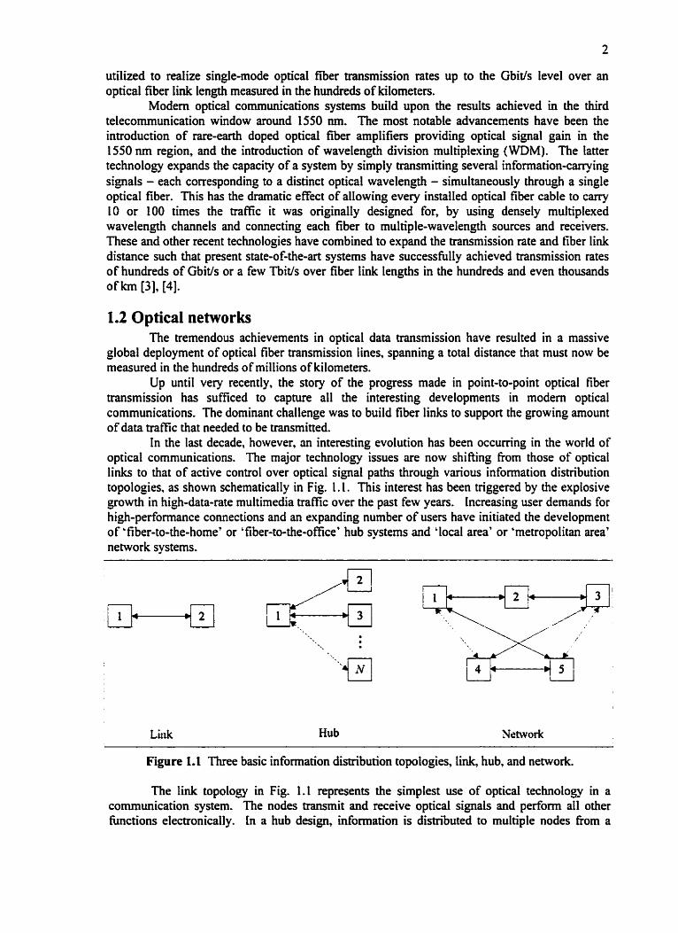
In the last decade, however, rui interesting evolution has been occumng in the world of optical communications. The major technology issues are now shifting Frorn those of optical links to that of active controt over optical signal paths through various information distribution topologies, as shown schematically in Fig. 1.1. This interest has been triggered by the explosive growth in high-data-rate multimedia traffIc over the past few years. Increasing user demands for hi&-performance connections and an expanding number of users have initiated the development of 'fiber-to-the-home' or 'fiber-to-the-office* hub systems and 'local area' or 'rnetropolitan area' network systems.
t u & Hub Xetwork
Figure 1. I Three basic information distribution topoiogies, t ink, hub, and network.
The Iink topology in Fig. 1.1 represents the simplest use of optical technology in a communication system. The nodes transmit and receive optical signals and perform al1 other tùnctions electronically. In a hub design, information is distniuted to multiple nodes fkom a

single transmitter. Optical technologies are now being deployed to realize such hubs, and a good example of this is the hub-type passive optical network emerging for the distribution of cable teIevision services. In these systems, fiber is used as the transmission medium, however, some optical functions such as passive signal distn'bution and wavelength mdtiplexing are beginning to permeate into the nodes Similarly, in the full network structure s h o w in Fig. 1.1, opticaI technologies are not only providing the links between the nodes, but within the nodes they are beginning to be utilized for signal processing functions (e.g., channel add/drop) and also to provide some switching capability.
The hub and network topologies in Fig. 1.1 need not be mutually exclusive and can be combined; both topologies will hereafter be referenced by the term 'optical network'.
As optical networks develop, an increasing need for such vital functions as signal distribution, switching, protection, and reconfiguration is evident, due to the volume and complexity of network trafic and the high cost of lost high-throughput links. In the fint generation of optical networks, these functions have been implemented electronically, with optical fiber simply replacing the old copper lines as a transmission medium. it is rapidly becoming apparent, however, that the information throughput of the network is Iimited by bottlenecks at the network nodes, where the electronic tiinctions are perfonned.
The second generation of optical networks is currently under active development, and aims to achieve optically transparent paths through a network by removing the electrical components and exploiting the unique properties of optics. Active node hnctions in these networks can be perfonned by means of micro-optic components where light Ieaves the fiber and is manipulated through the use of elements such as lenses or mimors while the beam is unguided, or by means of novel, integrated optical devices.
Unguided propagation technologies, however, suffer drawbacks such as optical coupling, reflection, and scattering losses as a beam passes through discrete components, sensitivity to environmental fluctuations, scaIabi1ity to Iarger capacities, and an increasing cost and cornplexity of manufacture.
1.3 Integrated optics To perform the required optical network node functions, an alternative technology has
been sought. The technology should be capable of synthesizing components such as beam splitters/combiners for bra.nching/combining optical signals, optical routen and switches for changing optical paths, wavelength multi/demultiplexers for combining/separating multiple waveIength channels, and channel add/drop elements for increased network flexibility. Furthemore, the components should meet practical requirements such as signal format and rate independence, Iow optical losses, polarkation insensitivity, low-power active operation, mal1 size, cost-effective manufacture, and reliability issues.
Recently, the technology of integrated optics is attracting much interest as a candidate to rneet these demanding requirements. Integrated optical devices are superior to many of their micro-optic or fiber-optic counterparts in tems of size, fieedom of design, ease of coupling between components, mass-production possibilities, device stability, and compatibility with integrated transceivers and electronic control circuitry [SI.
The concept of integrated optics was first proposed by S. E. Miller in a landmark paper in 1969 [6]. The idea was that using well-established processes fiom the integrated electronics industry, planar Iightwave circuits containhg p ~ k e and active grridcd-wave opti~ai components could be fabricated. Such circuits would contain many cornplex and diverse optical devices on a single wafer, Iinked together by transparent light conduits.
An analogy between integrated efectronics and integrated optics is often drawn, and the significant gains and widescale deployrnent achieved in integrated circuit technology are expected to one &y be paralleled in the reaim of mtegrated optics. So fx, integrated optics has
fallen somewhat short of these expectations, mainiy due to difficulties in obtaining ultra-low losses, an immature fabrication technology, and the costs associated with fiber-to-chip connections and packaging 171. Furthemore, the miniahirization of electronics cannot be similarly achieved in the optical realm, since optical cimuitry requires component sizes of the order of the wavelength of light use& which are much larger than electronic dimensions.
Significant research addmsing these areas continues and many gains have been made, leading to the widespread introduction of the first integrated optical components into the marketplace in the 1st two to three years. Research in the field of integrated optics continues to expand, exploiting the unique functions accessible through the use of planar optical guided-wave. or 'waveguide' cornponents.
It is the goal of this work to continue to expand the sphere of knowledge and applicability of integrated optics by proposing new integrated optical components for emerging optical networks and demonstrating the feasibility of their manufacture and use. As the components dealt with in this work are based upon the principles of integrated optical couplen, a brief introduction to this area is appropriate.
1.4 Integrated optical couplers A key component from which passive and active integrated optical waveguide devices
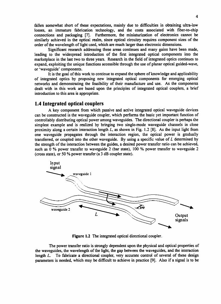
can be constructed is the waveguide coupler, which perforrns the basic yet important function of controllably distributing optical power among waveguides. The directional coupler is perhaps the simplest example and is realized by bringing two single-mode waveguide channels in close proximity dong a certain interaction length L, as shown in Fig. 1 .Z [SI. As the input light from one waveguide propagates through the interaction region, the optical power is gradually transferred or coupled into the other waveguide. By using a specific value of L detemined by the strength of the interaction between the guides, a desired power transfer ratio can be achieved, such as O % power tramfer to waveguide 2 (bar state), 100 % power transfer to waveguide 2 (cross state), or 50 % power transfer (a 3 dB coupler state).
Output signals
\ Figure 1.2 The integrated optical directional coupler.
The power transfer ratio is strongly dependent upon the physical and optical properties of the waveguides, the wavelength of the light, the gap between the waveguides, and the interaction length L. To fabricate a directional coupler, very accurate control of several of these design parameters is needed, which may be difficult to achieve in practice [9]. Also if a signal is to be
split into many signals or if many signals are to be combined, a number of directional couplers must be cascadeci, multing in large, lossy, and complex devices [IO].
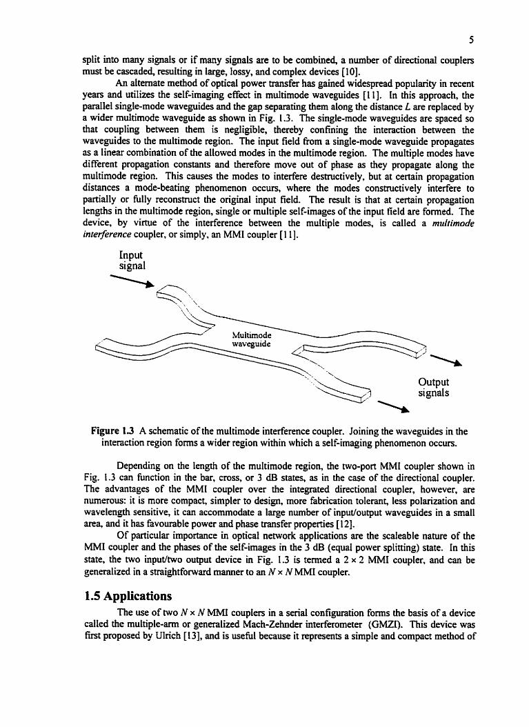
An alternate method of optical power transfer has gained widespread popularity in recent years and utilizes the self-imaging effect in mulbimode waveguides [1 Il . ln this approach, the parallel single-mode waveguides and the gap separating them along the distance L are replaced by a wider multimode waveguide as shown in Fig. 1.3. The single-rnode waveguides are spaced so that coupling between hem is negligible, thereby confïning the interaction between the waveguides to the multimode region. The input field fkom a single-mode waveguide propagates as a linear combination of the allowed modes in the multimode region. The multiple modes have different propagation constants and therefore move out of phase as they propagate along the multimode region. This causes the modes to interfere destnictively, but at certain propagation distances a mode-beating phenomenon occurs, where the modes constructively interfere to partially or fully reconstnict the original input field. The result is that at certain propagation lengths in the multimode region, single or multiple self-images of the input field are formed. The device, by virtue of the interference between the multiple modes, is called a rnziltimode inteference coupler, or simply. an MM1 coupler [l Il .
Input signal
Figure 13 A schematic of the multirnode interference coupler. Joining the waveguides in the interaction region forms a wider region within which a self-imaging phenomenon occua.
Depending on the length of the multimode region, the two-port MMI coupler shown in Fig. 1.3 can function in the bar, cross, or 3 dB States, as in the case of the directionai coupler. The advantages of the MM1 coupler over the integrated directional coupler, however, are numerous: it is more compact, simpler to design, more fabrication tolerant, less polarization and wavelength sensitive, it can accommodate a large number of inputfoutput waveguides in a small area, and it has favourable power and phase m s f e r properties [12].
Of particular importance in optical network applications are the scaieable nature of the MM1 coupler and the phases of the self-images in the 3 dB (equal power splitting) state. In this state, the two inputltwo output device in Fig. 1.3 is termed a 2 x 2 MM1 coupler, and can be generalized in a straightforward manner io an N x N MMi coupler.
1.5 Applications The use of two N x N MM1 couplers in a serial configuration foms the basis of a device
called the multiple-arm or generalized Mac h-Zehnder mterferometer (GMZI). This device was fim proposed by Ulrich [13], and is usehl because it represents a simple and compact method of
realizing an integrated optical L x N switch that can be controlled by applying, for instance, electrical signals to optical waveguides.
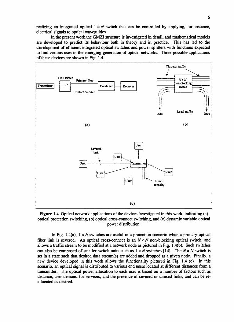
In the present work the GMZI structure is investigated in detail, and mathematical models are developed to predict its behaviour both in theory and in practice. This has led to the development of efficient integrated optical switches and power splitters with functions expected to find various uses in the emerging generation of optical networks. Three possible applications of these devices are s h o w in Fig. 1 -4.
t 1 L d trafic t
Add mJ ,
j L x t switch Primw fiber r
Figure 1.4 Optical network applications of the devices investigated in this work, indicating (a) optical protection switching, (b) optical cross-connect switching, and (c) dynamic variable optical
power distribution.
Corn biner f
In Fig. 1.4(a), 1 x N switches are usehl in a protection scenario when a primary optical fiber link is severed. An optical cross-connect is an Nx N non-blocking optical switch, and allows a trafic Stream to be rnodified at a network node as pictured in Fig. 1.4(b). Such switches can also be composed of srnaller switch units such as 1 x N switches [14]. The N x N switch is set in a state such that desired data strearn(s) are added and dropped at a given node. Finally, a new device deveioped in this work allows the bctionality picnired in Fig. 1.1 (c). In this scenario, an optical signal is dimibuted to various end users located at different distances fiom a üansmitter. The optical power allocation to each user is based on a number of factors such as distance, user demand for services, and the presence of severed or unused links, and can be re- allocated as desired.
Receiver
Protechon fier
1

1.6 Overview of this work Much of this work is devoted to the study of the integrated optical GMZI configuration
using N x N MMI couplers. As a logical starting point for the discussion, the fundamental principles of the integrated optical devices used in this work are presented in Chapter 2.
This forms a solid theoretical foundation for a mathematical description of the general properties of the GMZI, which is presented in Chapter 3. This has led to the interpretation of the device as a generalized or variable-ratio power splitter, the theoretical characteristics of which are discussed in detail. In a specific case of variable-ratio power splitting, the GMZI functions as the previously known optical switch. The switching properties of the GMZI are investigated in Chapter 4, and lead to several new designs for 1 x N and hi x N switches.
Demonstnition of the validity of the theory goveming the devices and the practicality of their implementation is achieved through the design, realization, and performance meanirement of the integrated optical GMZI. The design of a set of prototype integrated optical devices is described in Chapter 5. Much of this work was performed at the University of Alberta and the Telecommunications Research Laboratones, in Edmonton, Alberta.
Chapter 6 discusses the fabrication of the integrated devices which was perfotmed during a period as a visiting scientist at the MESA Research Institute, University of Twente, in The Netherlands. Some initial device characterizaiion has been perfomed as a student intern at JûS Uniphase Inc., in Nepean, Ontario.
The performance of the fabricated devices has been characterized during a second period as a visiting scientist at the University of Twente, using the facilities of the Lightwave Devices Group. The measurement results are presented in Chapter 7.
Finally. a general summary, future prospects for this work and concluding remarks are given in Chapter 8.
Chapter 2
Theoretical foundations
This chapter provides a description of the findamental physical principles upon which the integruted optical components in this work are bmed. The intent is not to reproduce a rigorour and detailed mathematical description of the underiying theory devefoped by others; /or this the interested reader rnay refr to the references cited herein. The emphmb of this chopter wiil instead be to give the necessary mathematicul and physical arguments to form un intuitive picture of light propagation in optical waveguides. the phenomenon of multimode interjrence, and the generalked Mach-Zehnder interferometer structure. This will sente to provide a proper foundation for an mderstanding of the concepts described in sttbsequent chapters.
2.1 Introduction We begin the discussion by considering the propagation of light in a medium. Since light
is a form of electromagnetic radiation, Maxwell's equations are the logical starting point in the analysis. In integrated optics, light is typically guided in media with smctural dimensions of the order of the wavelength of light used. An application of Maxwell's equations leads to the result that light becomes quantized into a set of allowed spatial1 y-invariant distributions, or modes. which can propagate through a light-guiding structure. The simplest such structure is the dielectric slab waveguide. An undentanding of the slab waveguide permits the analysis of more complicated waveguide structures, as well as providing insights into the self-imaging phenornenon exhibited by multimode interference (MMI) couplen. The propenies of the MM1 coupler in mm enable a description of the operation of the genenlized Mach-Zehnder interferometer (GMZl) configuration, which is at the hem of this work. We therefore mm our attention first to the slab waveguide.
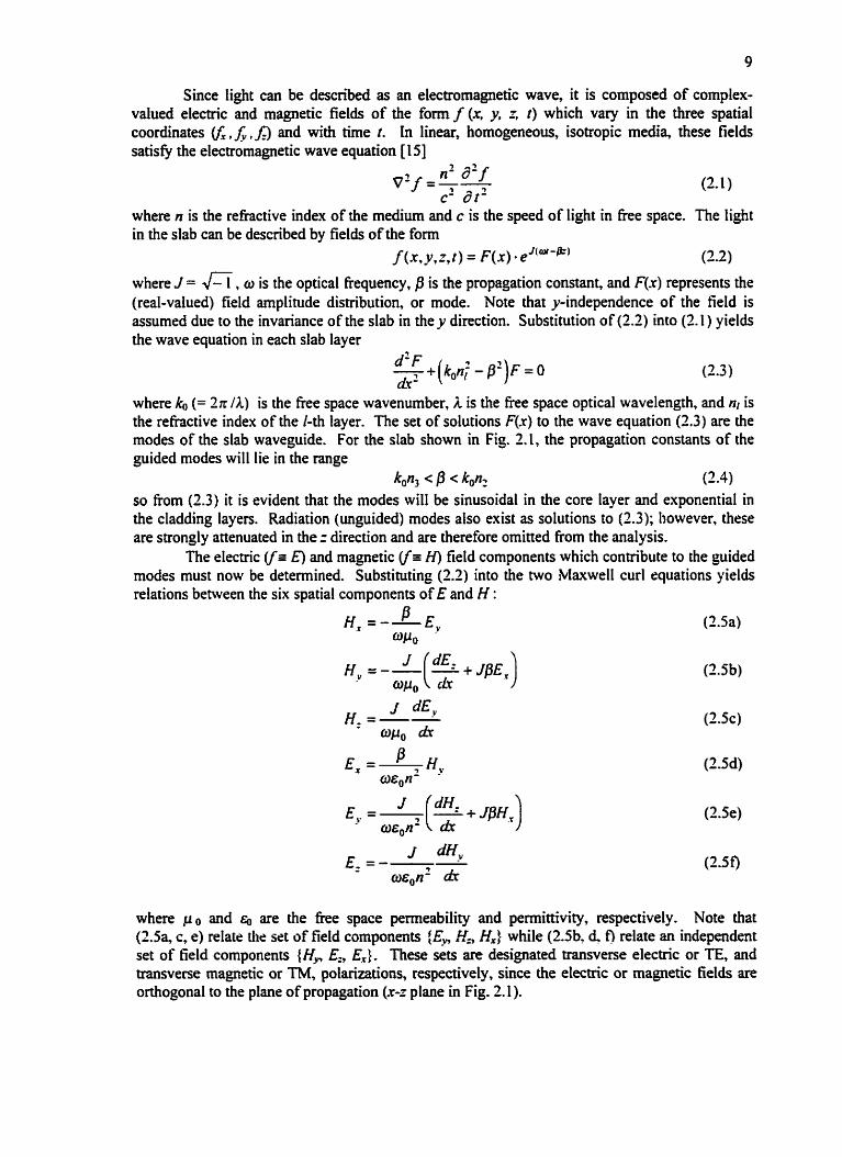
2.2 The slab waveguide A three-layer asymmetric (n, # n3, in general) dielectric slab waveguide is shown
schematically in Fig. 1.1. It consists of a core layer (n2) with a higher rehctive index than that of the sumunding cladding layers (nl , n3). Light propagates in the + z direction and in the plane of nt, confined by total intemal reflection at the core-cladding interfaces. For the analysis of this structure? the r = O origin is chosen at the n2 - n~ interface and it is assurned without Ioss of generality that n3 1 ni.
I
Figure 2.1 The asymmetric the-layer dielecaic slab waveguide with the rehctive index profile s h o w on the right.
Since light can be described as an electromagnetic wave, it is composed of complex- valued electric and magnetic fields of the fom f (x, y. z. t ) which Vary in the three spatial coordinates (fx .A ,&) and with tirne t. In linear, homogeneous, isotropie media, these fields satisfi the electromagnetic wave equation [15]
n' a'f v'f =-- c' dt'
where n is the rehctive index of the medium and c is the speed of light in k e space. The light in the slab can be descnbed by fields of the form
f (x, y, r, t ) = F ( x ) e'(a'fi' (2.2)
where J = fi, o is the optical frequency, is the propagation constant, and F(r) represents the (real-valued) field amplitude distribution, or mode. Note that pindependence of the field is assumed due to the invariance of the slab in the y direction. Substitution of (2.2) into (2.1 ) yields the wave equation in each slab layer
where ko (= 2n /A) is the Free space wavenumber, A is the free space optical wavelength, and ni is the rehctive index of the /-th layer. The set of solutions F(x) to the wave equation (2.3) are the modes of the slab waveguide. For the slab show in Fig. 2.1, the propagation constants of the guided modes will lie in the range
k0n3 < fi < kont (2.4) so fiom (2.3) it is evident that the modes will be sinusoidal in the core layer and exponential in the cladding layers. Radiation (unguided) modes also exist as solutions to (2.3); bowever, these are strongly attenuated in the 2 direction and are therefore omitted from the analysis.
The electric (fz E) and magnetic (f= H) field components which contribute to the guided modes must now be determined. Substituting (2.2) into the two Maxwell curl equations yields relations between the six spatial components of E and H :
where p 0 and F, are the fkee space pemeability and pemittivity, respectively. Note that (2Sq c, e) relate thé set of field componmts (Ep H, H,) while (2.5b, 6 O relate an independent set of field cornponents (H, El, Ex). Thae sets are designated transverse elecûic or TE, and transverse magnetic or TM; polarizations, respectively, since the elecnic or magnetic fields are orthogonal to the plane of propagation (-PZ plane in Fig. 2.1).

The solutions F(x) of (2.3) can therefore be represented simply by EJx) for the TE case and Hy(x) for the TM case. The solutions are found by solving (2.3) subject to the boundary conditions fiom electromagnetic theory, which require tangential components of F to be continuous across a dielectric discontinuity. From Fig. 2.1 this implies for TE fields that Ey and & must be continuous, and for TM fields that Hv and E, must be continuous. Frorn (2.5c, t ) this is equivalent to
dFv Fv and o, - continuous d~
across dielectric boundaries, where q = 1 for TE and a, = lln; for TM. For the slab in Fig. 2.1 the wave equation (2.3) can then be written as
upper cladding (x 1 W) :
d' F" iower cladding (x I 0) : -- , p l 5 = O
dr - Cornparing (2.3) and (2.7), the mode parameten q, h, and p are defined as
i i
4- = P - - ktn: (2. 8a)
h' = k i n ; - p' (2.8b) 7 i ? p- = P - - k-n-
O 3 (2.8~) where (2.4) has been utilized to ensure that h, q, and p are real.
The solutions to (2.7) are the bowid waveguide modes, written as upper cladding (x > W) : F(x) = A eqx (2.9a)
core(0 I x 5 W ) : F(x) = C O S ( ~ Y ) + .dl sin(h.r) (2.9b) Iower cladding (x I 0) : F(x) - F (2.9~)
where the constants A l and Ar are found by applying the boundary conditions (2.6) to the tields in (2.9):
Applying the boundary conditions (2.6) to the x = W boundary in (2.9) results in the following dispersion relation
which is a transcendental equation for a since q, h, and p are functions of in (2.8). This can be solved using numerical or graphical methods. Since the tangent function is penodic, a number of solutions may exist, each value of fi corresponding to a botmd mode of the slab waveguide. The order of the mode is denoted by v = 0, 1,2, ... , and the parameten P, , q, , hv , and p, determine the field Fv of the v-th mode in (2.9). As we shall see later, it is also usefiil to characterize each mode in terms of an effective rehctive index ne, defined as
The nurnber of guided modes is limited by the relation (2.4), and inmeases as the core width W increases, as the wavelength decreases, and as the core-cladding refiacîive index difference
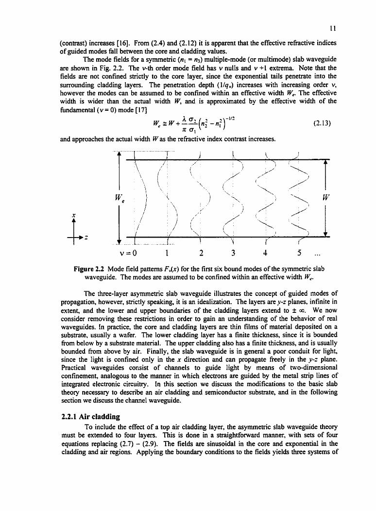
(contrast) increases [16]. From (2.4) and (2.12) it is apparent that the effective refiactive indices of guided modes fall between the core and cladding values.
The mode fields for a symmetric (nt = 4) multiple-mode (or multimode) slab waveguide are shown in Fig. 2.2. The v-th order mode field has v nulls and v +1 extrema. Note that the fields are not conhed strictly to the core layer, since the exponential tails penetrate into the surroundhg claddhg layers. The penetration depth (Vq,,) increases with increasing order v, however the modes can be assumed to be confined within an effective width Fe. The effective width is wider than the actual width W, and is approximated by the effective width of the fundamental ( v = O) mode [ 171
and approaches the actual width W as the rehctive index contrast increases.
Figure 2.2 Mode field patterns F4.r) for the first six bound modes of the symmetnc slab waveguide. The modes are assumed to be confined within an effective width W,.
The three-layer asymmetrîc slab waveguide illustrates the concept of guided modes of propagation, however, strictly speaking, it is an idealization. The layea are y-z planes, infinite in extent, and the lower and upper boundaries of the cladding layers extend to 2 a. We now consider rernoving these restrictions in order to gain an understanding of the behavior of real waveguides. In practice, the core and cladding layen are thin films of material deposited on a subsmte, usually a wafer. The lower cladding layer has a finite thickness, since it is bounded from below by a substrate material. The upper cladding also has a finite thickness, and is usually bounded kom above by air. Finally, the slab waveguide is in general a poor conduit for light, since the light is confined only in the x direction and can propagate freely in the y s plane. Practical waveguides consist of channels to guide light by means of MO-dimensional confinement, anaIogous to the manner in which eiectrons are guided by the metal strip Iines of integrated electronic circuitry. In this section we discw the modifications to the basic slab theory necessary to describe an air cladding and semiconductor substrate, and in the following section we discuss the channel waveguide,
2.2.1 Air cladding To include the effect of a top air cladding layer, the asymmetric slab waveguide theory
must be extended to four laym. This is done in a straightforward mariner* with sets of four equations replacing (2.7) - (2.9). The fields are sinusoidal in the core and exponential in the cladding and air regions. Applying the boundaty conditions to the fields yields three systems of
two equations, which can be reduced to a single system of two equations through back substitution [16]. The resulting dispersion relation can be solved for the 8, and hence the effective indices of the modes. In general, as the thickness of the top cladding layer increases, the air cladding has a diminishing effect on the waveguide mode.
2.2.2 Substrate effects Integrated optical devices are fabricated on various substratte materials, and in a number
of cases the refractive index of the substrate is higher than the indices of the corekladding films. Common examples are AlGaAs films on GaAs substrates and doped Si02 and SiO,N, films on Si substrates. For waveguiding to occur, the core layer must have a refractive index higher than that of the surroundhg layers. The presence of a high index substrate may result in the leakage of light from the waveguide core into the substrate, attenuating the field as it propagates. A nifficiently thick lower cladding, however, can serve as an effective isolation layer and prevent undesired substrate attenuation.
To determine the required minimum thickness of the isolation layer, the treatment of the slab waveguide is first extended to a four-layer system, where the fourth layer is the substrate. The high index substrate changes P for the waveguide mode from its value in the three-layer slab, and using a perturbation approach [16] this change can be accurately estimated. In this approach. the propagation constant is separated into two components, the (real) propagation constant Bo for the three-layer structure, plus a small change 6P ,
P = h w (3.14) where 6p is complrx. This form for P is substituted into the dispenion relation of the four-layer structure, and keeping terms to fint order in GP, an expression for SP can be derived. The real part of SB contributes to a change in the effective index, and the imaginary part contributes to an attenuation as the mode propagates in the r direction, as can be seen from (1.2). The minimum thickness for the isolation layer is the thickness for which the attenuation of the guided modes is negligible, i.e.. l e s than the expected matenal attenuation in the corekladding layers.
2.3 Channel waveguides - the effective index method To eficiently guide light in intepted optics, it is necessary to use channel waveguides
which confine light in the two directions (x and y) orthogonal to the propagation direction. Light cm then be directed on a planar surface by simply defining the path of the waveguide channel. Two-dimensional field confinement is achieved through the use of any of a number of possible waveguide geometries, such as ridge, rib, buried channel, and sûfp loaded [16], which are realized through a combination of planar (slab) wavekxide technology and lithographie techniques.
The solution of Maxwell's equations for the two-dimensional field profile in channe1 waveguides, however, does not have a simple, closed forrn solution. Nwnencal discretization schemes are generally used to solve for the modes; however, a simpler and more physicaliy intuitive technique known as the effective index method (EIM) can also be used [18] - [20]. Values of neK, calculated using the EIM are applicable for weakly and strongly confining channel structures [21] and are reasonably accurate if they are not too close to the cladding indices, i.e,, for well-guided modes.
To implement the EIM, it is necessary to recognize that the modes of the channel waveguide are no longer strictly TE or TM. The modes are hybrid, which means that the field components can no longer be grouped into two independent sets, so in generaI six field components are needed to desmie each mode. A simpliwg assurnption, however, can be made. For core widths greater than their thicknesses, certain field components dominate such that the modes are similar to TE and TM. These are referred to as quasi-TE and quasi-TM modes. In
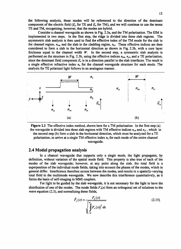
the following analysis, these modes wilI be referenced to the direction of the dominant component of the elecüic field (Ey for TE and Ex for TM), and we will continue to use the ternis TE and TM, recognipng, however, that the modes are hybrid.
Consider a channel waveguide as shown in Fig. 2.3% and the TM polarization. The EIM is implemented in two steps. In the fint step, the ricige is divided into three slab regions. The asymmetric slab analysis is then used to find the effective index of the TM mode for the slab in the channel region, nh, and the slab in the cladding region, m. These effective indices are then considered to form a slab in the horizontal direction as shown in Fig. 2.3b, with a core layer thickness equal to the channel width W. In the second step, a symmeaic slab analysis is performed on the structure in Fig. 2.3b. using the effective indices nCh, nc,, and a TE polarization, since the dominant field component E, is in a direction parallel to the slab interfaces. The result is a single effective refractive index ne for the channel waveguide structure for each mode. The analysis for TE polarized light follows in an analogous rnanner.
Figure 2.3 The effective index method, shown here for a TM polarization. In the first step (a) the waveguide is divided into three slab regions with TM effective indices nd and n,l, which in
the second step (b) form a slab in the horizontal direction, which mut be analyzed for a TE polarization, to arrive at a single TM effective index ne for each mode of the entire channel
waveguide.
2.4 Modal propagation analysis In a channel waveguide that supports only a single mode, the light propagates, by
definition, without variation of the spatial mode field. ïhis pmperty is also m e of each of the modes of the slab waveguide; however, at any point along the siab, the total field is a superposition of the individual mode fields, taking into account the phases of the modes, which in general differ. Interference thecefore occurs between the modes, and results in a spatially-varying total field in the multimode waveguide. We now describe this interference quantitatively, as it forms the basis of self-imaging in MM1 coupiers.
For light to be guided by the slab waveguide, it is not necessary for the light to have the distriiution of one of the modes. The mode fields F&) form an orthogonal set of solutions to the wave equation (2.3), and normalizing these fields,
an orthonormal set of mode functions F, (.Y) is obtained An arbitrary input field T(x, zo) launched into the slab waveguide at the point z = zo cm be written as a superposition of these mode fiinctions,
m-1
T ( X * zo ) = y- a, (x)
where rn is the number of guided modes and a, is the complex amplitude coefficient of the v-th mode, given by
and F: (x) is the complex conjugate of Fv (x). From (2.16), it is seen that the optical power is divided among the modes. in multimode waveguides, the number of guided modes is finite. Therefore. depending on the form of T(x. a), some of the power at the input may not be coupled to a guided mode. Power not coupled to propagation modes is radiated at the transition into the muItimode region. UsualIy, however. the radiated power is negligible and it is therefore ignored in the following analysis.
Since the different modes travel with different propagation constants j3, , the input field T(x , a) changes its transverse distribution as it travels through the waveguide in the z direction. The field at any longitudinal point r can be expressed as
where time dependence is implicit. This method of input field decornposition into a superposition of guided modes and the subsequent propagation of these modes is referred to as modal propagation analysis (MPA). Altematively, various numerical beam propagation methods (BPM) can be used to accurately simulate light propagation through waveguide structures, but these methods do not pmvide physical insights into the propagation mechanisms. While MPA is a simplet and more physical approach, it is applicable only where the refiactive indices or geometry in the x-y plane do not change significantly with z. Since the MM1 coupler is essentially a rectangular multimode waveguide region with a spatially-invariant structure. MPA is well-suited to the analysis of the MM1 coupler and serves as an excellent tool for the explanation of its behavior.
2.5 The N x N multimode interference coupler An N x N multimode interference (MMI) coupler consists of a multimode waveguide
with N single-mode waveguides at both the input and output planes, show in Fig. 2.4. It operates upon the pnnciple of self-irnaging, defined as "a pmperty of multirnode waveguides by which an input field profile is reproduced in single or multiple images at periodic intervals along the propagation direction of the guide" [22].
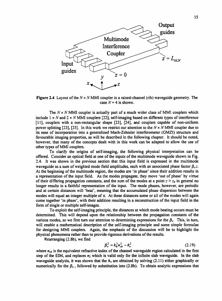
Figure 2.4 Layout of the N x N MM1 coupler in a raised-chamel (rib) waveguide geometry. The case N = 4 is shown.
The N x N MM1 coupler is actually part of a much wider class of MM1 couplen which include 1 x N and 2 x N MM1 couples [Z], self-imaging based on different types of interference [1 I l , couplen with a non-rectangular shape 1231, [24], and couplers capable of non-uniform power splining (231, [Z]. In this work we resaict our attention to the N x N MMI coupler due to its ease of incorporation into a generalized Mach-Zehnder interferometer (GMZI) structure and favourable imaging propetties, as will be described in the following chapter. It should be noted, however, that many of the concepts dealt with in this work can be adapted to allow the use of other types of MM1 couples.
To clan@ the origins of self-imaging, the following physical interpretation can be offered. Consider an optical field at one of the inputs of the multimode waveguide shown in Fig. 2.4. It was shown in the previous section that this input field is expressed in the multimode waveguide as a sum of weighted mode field ampiinides, each with an associated phase factor Pvz. At the beginning of the multimode region, the modes are 'in phase* since their addition results in a representation of the input field. As the modes propagate, they move 'out of phase' by virtue of their differing propagation constants, and the sum of the modes at a point z > 20 in general no longer results in a faithfiil representation of the input. The mode phases, however, are periodic and at certain distances will 'beat', meaning that the accurnulated phase dispersion between the modes will equal an integer multiple of r At these distances some or al1 of the modes will again come together 'in phase', with their addition resulting in a reconstruction of the input field in the fom of single or multiple self-images.
To exploit the self-imaging principle, the distances at which mode beating occurs must be determined. This will depend upon the relationship between the propagation constants of the various modes, so we first tum our attention to determining expressions for the f lv . This, in tum, will enable a mathematical description of the self-imaging principle and some simple formulae for designing MM1 couplers. Again, the emphasis of the discussion will be to highlight the physical phenomena rather than to provide rigorous derivations of the results.
Rearranging (2.8b), we find
where nh is the equivalent rehctive index of the channel waveguide region caiculated in the fim step of the EIM, and replaces n2 which is valid only for the infinite slab waveguide. In tiie slab waveguide analysis, it was shown that the h, are obtained by solving (2.1 1) either graphically or numericaily for the p, , followed by substitution into (2.8b). To obtain analytic expressions that

will greatly simpliQ our analysis, we consider a 'strongly guiding' approximation, wherein the mode fields in the multimode region are confined to the channel layer with negligible penetration into the cladding layers. This is achieved in practice by wing deeply etched rib waveguides to provide a hi& rehctive index contras& thereby confining the mode field within the bounds of the rib. An integer number of lobes are then present within the effective width W. of the channel (refer to Fig. 2.2), and the mode fields are well described by funetions of the form - -
where the approximation sign reflects the strongly guiding approximation used Comparing (3.20) to (2.9b), the parameter h, can be written as
h , z ~ ( v + i ) / W , (3.2 1 ) Substituting (2.21) into (2.19) and using the paraxial approximation h,' cc kir&, the binomial
expansion can be used to express pV as
indicating that the spacing of the propagation constants increases quadratically as the mode number increases. Self-imaging depends upon the length at which al1 the modes beat, which will be governed by the two modes which require the longest propagation length in order to beat. These are the modes with the most closely spaced propagation constants, which in view of (2.22) are the fundamental and fiat order modes. A characteristic beat Iength L, for a multimode waveguide c m therefore be defined as [ I l ]
n _ 4n&' L, i--- - B o - P i 3k
where (1.12) has been used to arrive at the second expression. The field at a distance z almg the multimode region given can now be expressed in tems
of this beat length by first factoring out a constant phase factor e-Jk from (2.18) and substitution of (2.22) and (2.23) to arrive at
At distances z = L.CL.V where
with M and IV positive integers with no common divisor, the argument of the phase term in (2.24) becomes an integer multiple of K. It can be shown that in these cases the field in the multimode region will be of the form [12]
,v-l
b=O
where T&) describes the field profile at the input of the multimode region, C is a complex normalization constant, and x b and ( ~ b describe the positions and phases, respectively, of 1V self- images at the output of the MM1 coupler. The self-images are positioned with a constant spacing between them. The parameter A4 describes a multiple of the imaging length that aIso resuits in iV self-images, since the self-imaw&g phenomenon is periodic. Usually the shortest devices are O btained w hen M = 1.
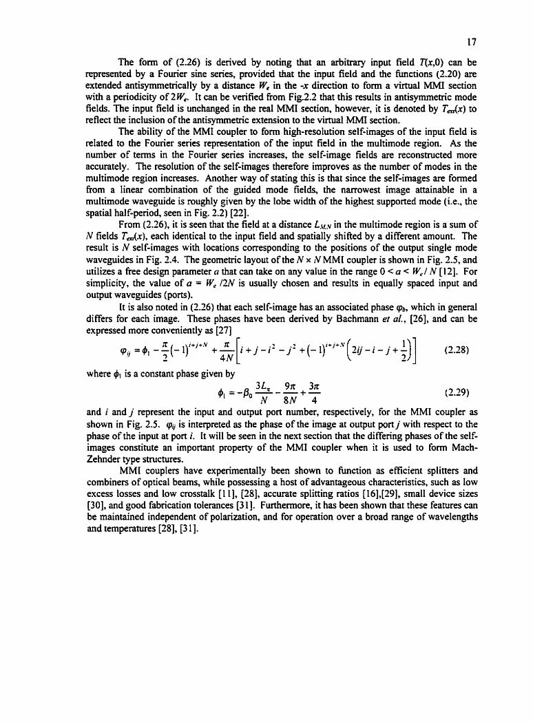
The fom of (226) is denved by noting that an arbitrary input field T(x,O) can be represented by a Fourier sine series, provided that the input field and the functions (2.20) are extended antisymrnetncally by a distance WC in the -x direction to form a virtual MMI section with a periodicity of 2We, It cm be venfied from Fig.22 that this results in antisyrnmetric mode fields. The input field is unchanged in the real MM1 section, however, it is denoted by Tdx) to reflect the inclusion of the antisymmetric extension to the virtual MM1 section.
The ability of the MMI coupler to form hi&-resolution self-images of the input field is related to the Fourier series representation of the input field in the multirnode region. As the number of terms in the Fourier series increases, the self-image fields are reconstructed more accurately. The resolution of the self-images therefore improves as the number of modes in the multimode region increases. Another way of stating this is that since the self-images are formed fiom a linear combination of the guided mode fields, the narrowest image attainable in a multimode waveguide is roughly given by the lobe width of the highest supported mode (Le., the spatial half-period, seen in Fig. 2.2) [22].
From (2.26), it is seen that the field at a distance L.lL.v in the muItimode region is a sum of N fields Ta(x), each identical to the input field and spatially shifted by a different amount. T'he result is N self-images with locations corresponding to the positions of the output single mode waveguides in Fig. 2.4. The geometric Iayout of the N x N MM1 coupler is shown in Fig. 2.5, and utiIizes a free design parameter a that can take on any value in the range O < a < WJ N [12]. For simplicity, the value of a = W, I2N is usually chosen and results in equally spaced input and output waveguides (ports).
It is also noted in (2.26) that each self-image has an associated phase (pb, which in general diffen for each image. These phases have been derived by Bachmann et al., [26], and can be expressed more conveniently as [27]
where 4, is a constant phase given by
and i and j represent the input and output port number, respectively, for the MM1 coupler as shown in Fig. 2.5. <pu is interpreted as the phase of the image at output port j with respect to the phase of the input at port i. It will be seen in the next section that the differing phases of the self- images constitute an important property of the MM1 coupIer when it is used to form Mach- Zehnder type structures.
MM1 couplers have experimentdly been shown to tùnction as efficient splitten and combiners of opticai beams, while possessing a host of advantageous characteristics, such as low excess losses and low crosstalk [ll], [28], accurate splitting ratios [16],[29], small device sizes [30], and good fabrication tolerances [3 11. Furthemore, it has been shown that these features can be maintained independent of polarization, and for operation over a broad range of wavelengths and temperatures [28], [3 1 1.
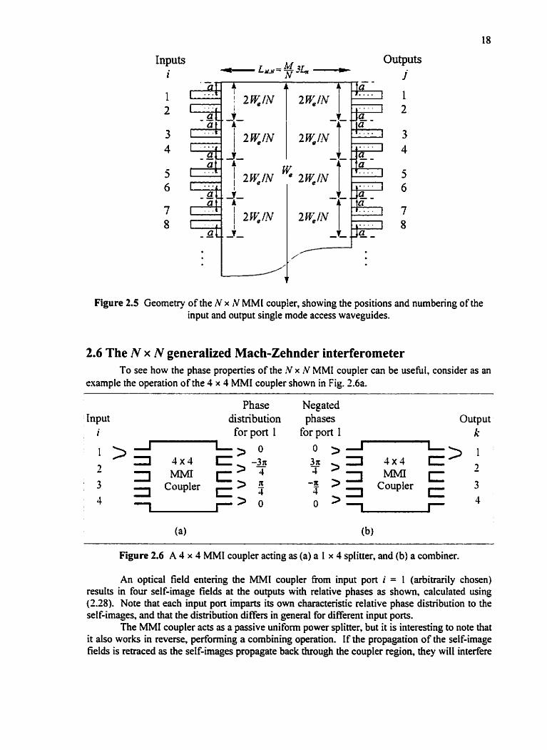
h p ~ b M OUQU~S i - L ~ ~ = - ~ L N -- i
Figure 2.5 Geornetry of the rV x N MM1 coupler, showing the positions and numbering of the input and output single mode access waveguides.
2.6 The N x N generalized Mach-Zehnder interferorneter To see how the phase properties of the ,V x N MM1 coupler can be useful, consider as an
exampie the operation of the 4 x 4 MM1 coupler shown in Fig. 2.6a.
Phase Neg ated Input distribution phases Output
I for port 1
7
-. O ' 1 4 x 4 C, -3 - I M 4
3 -1 Coupler 5
4 t 7 - > O
for port 1 k
O > 25 > Y W C
- -x > 3 I Coupler 3 = 4 O >-
Figure 2.6 A 4 x 4 MM1 coupler acting as (a) a 1 x 4 splitter, and (b) a combiner.
An optical field entering the MM1 coupler fiom input port i = 1 (arbitrarily chosen) results in four self-image fields at the outputs with relative phases as shown, caIcuIated using (2.28). Note that each input port imparts its own characteristic relative phase distribution to the self-images. and that the distribution differs in general for different input ports.
The MM1 coupler acts as a passive uniform power splitter, but it is interesting to note that it also works in reverse, performing a combining operation. If the propagation of the self-image fields is retraced as the self-images propagate back through the coupler region, they will interfixe
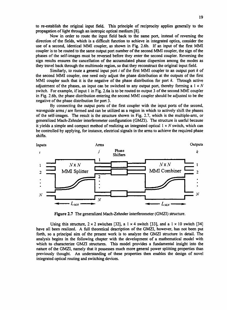
to re-establish the original input field This principle of reciprocity applies generally to the propagation of light through an isotropic optical medium 181.
Now in order to route the input field back to the same port, instead of reversing the direction of the fields, which is a difficult fwiction to achieve in integrated optics, consider the use of a second, identical MMI coupler, as shown in Fig. 2.6b. If an input of the first MMI coupler is to be routed to the sarne output port number of the second MM1 coupler, the sign of the phases of the self-images must be reversed before they enter the second coupler. Reversing the sign resuIts ensures the cancellation of the accusnuiated phase dispersion among the modes as they travel back through the multimode region so that they reconstnict the original input field.
Similarly, to route a general input port i of the fint MM1 coupler to an output port k of the second MM1 coupler, one need only adjust the phase dismiution at the outpua of the first MM1 coupler such that it is the negative of the phase distribution for port k. Through active adjustment of the phases, an input can be switched to any output port, thereby forming a I x N switch. For example, if input 1 in Fig. 2.6a is to be routed to output 3 of the second MM1 coupler in Fig. X b , the phase distribution entering the second MM1 coupler should be adjusted to be the negative of the phase distribution for port 3.
By connecting the output ports of the tim coupler with the input ports of the second, waveguide arms j are formed and can be utilized as a region in which to actively shift the phases of the self-images. ï he result is the structure shown in Fig. 2.7, which is the multiple-am, or generalized Mach-Zehnder interferorneter configuration (GMZI). The structure is usefiil because it yields a simple and compact method of realizing an integrated optical 1 x N switch, which can be controlled by applying, for instance, electrical signals in the arms to achieve the required phase shih.
Inputs .4ms Outputs
j Phase Shifiers
I 1 ?V x !V 3 L MMI splitter M M Combiner . 8 . b
8
N I
Figure 2.7 The generalized Mach-Sehnder interferorneter (GMZI) structure.
Using this structure, 2 x 2 switches [32], a 1 x 4 nvitch [33], and a I x 10 switch [34] have al1 been realized. A full theoretical description of the GMZI, however, has not been put forth, so a principal aim of the present work is to analyze the GMZI structure in detail. The analysis begins in the following chapter with the development of a mathematicai model with which to characterize GMZI structures. This model provides a hdarnental insight into the nature of the GMZI, namely that it possesses much more general power sptitting properties than previously thought. An understandhg of these properties then enables the design of novel integrated optical routing and switching devices.

Chapter 3
Theory of variable-ratio power splitting
In this chapter transfer matrk techniques are used to gain a deeper understanding of the self-imaging properties in the generalized Mach-Zehnder interferorneter (GMU). In the analysis, expressions ore derived and indiente that the GMW is a generalized N-wqy power splitter. A method enabling this mode of operation is developed and resrdts in a new integrated optic device based on the GMZI: the variable-ratio power splitter. The practical femibility of realking this device is assessed by modeling its operation in the presence of parameter variations and non- ideal eflects stemming fiom technologicd issues. This k accomplished through the introduction of mod~jkations into the basic transfer matrir theory to provide a model for the non-ideal GMU. Portions of rhis chapter have been reported in Photonics Technology Lettea [35]; a paper to appear in the Journal of Lightwave Technology [36]; and in a U.S. Patent Application [37].
3.1 Introduction The operation of the GMZI is based primarily upon the phases of the self-images
produced by the MM1 coupler. Since the MM1 coupler is capable of reproducing a field fiom any of the N inputs at al1 the N outputs, the phases of the self-images formed by an iV x rV coupler can be described by an N x iV matrix of relative phases. This matrix is used to form a transfer mamx for the coupler that describes how it operates on an arbin;uy input field.
The transfer matrix approach has in the past been applied to microwave directional couplen [38], [39], and has subsequently been used for integrated optical two-port directional couplen [40], [JI). Jenkins et al. [34] described the MM1 coupler using a transfer rnatrix. but only gave the maaix for N = 4, and its use was limited to the determination of the phase shifts necessary for the switching Function.
In this work, a simple and intuitive form for the transfer rnatrix of the N x N MM1 coupler is developed. This matrix is then used to develop the transfer matrix for the GMZI. The GMZI transfer rnatrix enables the design of variable-ratio N-way active or passive power splitters. We therefore begin our discussion by describing the m s f e r matrîx approach.
3.2 Transfer matrix of the N x N MM1 coupler Consider the N x iV MM1 coupler shown in Fig. 3.1. The coupler length given by (2.25)
can be expressed as
where the approximation fiom (2.23) has been used for the beat length Lx.
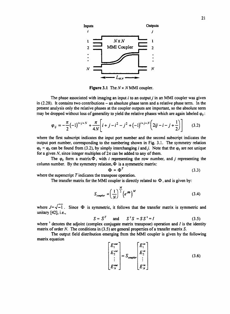
Figure 3.1 The N x IV MMI coupler.
The phase associated with irnaging an input i to an output j in an MM1 coupler was given in (2.28). It contains two contributions - an absolute phase term and a relative phase term. In the present analysis only the relative phases at the coupIer outputs are important, so the absolute term may be dropped without loss of generality to yield the relative phases which are again labeled qo, :
where the fint subscript indicates the input port number and the second subscript indicates the output port number, corresponding to the numbering show in Fig. 3.1. The symmeay relation <p, = <pi, cm be found fiom (3.2), by simply interchanging i and j. Note that the <p, are not unique for a given N, since integer multiples of 2ir can be added to any of them.
The <pv fom a matnx @ , with i representing the row number, and j representing the colurnn number. By the symmeû-y relation, <P is a symmeaic matrix:
@ = a T (3.3) where the superscript T indicates the transpose operation.
The transfer rnatrix for the MM1 coupler is directly related to 0. and is given by:
where J= f i . Since 0 is symmetric, it follows that the transfer rnatrix is symmetric and unitary [42], i.e.,
where ' denotes the adjoint (complex conjugate matrix transpose) operation and I is the identity matrix of order N. The conditions in (3.5) are general properties of a transfer matrix S.
The output field distribution emerging fiom the MM1 coupler is given by the following matrix equation

where E,! is the complex optical field amplitude at input port i and Ei"< is the optical field at
output port j. The optical field intensity, which is the measurable quantity, is directly
proportionai to 1 EI' .
3.3 The GMZI transfer m a t h
31.1 Basic structure and operation of the GMZI The basic layout of the N x N GMZI has been shown in Fig. 2.6. The structure consists
of three components: an N x N MM1 splitter, an active phase shifting region with iV phase shiftm, and an N x N MM1 combiner. The MMI splitter fonns N self-images of the input, which appear at the output ports, resulting in an equal distribution of the power to al1 arms of the phase shifting region.
î h e function of the active phase shifting elements is to modiQ the phases of the self- images such that a specific distribution of relative phases is obtained at the inputs to the MM1 combiner. The active phase shifters are indicated by shaded regions on the intemal m s , and can be operated by applying a driving signal (voltage, current, etc.) to shifi the phases of the light in the arms by virnie of any of a number of effects, such as the electro-optic or the thermo-optic effect [43].
The MM1 combiner perfonns the function of combining N inputs with equal intensities and differenr phases to form a specific power distribution at the outputs. The positions and intensities of the final output images depend upon the relative phases at the input to the MM1 combiner. Therefore light from an input port i can be distributed in a controlled way to the output ports k simply by adjusting the phase shifters to achieve the required pliase distribution at the combiner inputs.
3.3.2 The GMZI transfer matrix The splitter is represented by a matrix SspriIIYr gîven by (3.4) with elements su and the
combiner is represented an identical matrix SEMbnn with elements sjk . The active phase sh ik are applied independently and simply shift the phase cpi, in a given arm j by an amount A* The action of the phase shifters cm therefore be descnbed by a diagonal N x N transfer matrix [38]
and the optical fields at the output ports of the GMZI are given by
where T is the total transfer matrïx of the GMZI, given by
= smmbiner . Sshifî - slPiintr
3.4 Variable-ratio power splitting The GMZI transfer matrix can be used to derive two important results. The first is that
analytic expressions for the output field htensities in terms of the applied phase s h i h cm be denved by expanding (3.9). Secondly, the matrix equation (3.8) can be solved to yield the phase shifts A 9 required to achieve a given output intensity distribution. This is the pnnciple behind the operation of the variable-ratio power splitter.
Specificarion of the output intensity distniution is useful in nich applications as the tap function, where only a mal1 portion of the light is extracted from a channel for monitoring purposes [25], in ring lasers where the splitting ratio of the coupler dictates the operation of the laser [Ml, or in WDM devices where the spectral response can be improved through non-unifonn power splitting [27].
Variable-ratio power splitting also has interesting potential applications in emerging optical networks as shown in Fig. 1.4(c), where the nodes must optimally allocate and distribute signal power to numerous paths based on span length and/or changing demand. Such an application is envisioned in rnetropolitan optical networks which will deliver a mix of broadband data services in a fiber-to-the-X in~ tn ic tu re , where X may represent a region of a city. a neighborhood, a Street (curb) or a home. in this scheme, a central vansmission station may initially allocate signal power to various substations in an optimum manner, based on their distance and the number of customen demanding services at any given time. Alternatively, these altocations can be determined at the substation level or can be shared between both levels. Flexibility in setting the power ratio and the ability to quickly modiS this ratio are paramount, and the variable-ratio splitter can satisQ both requirements.
Passive, N-way power splitten using MM1 couplers have been realized [El; however, only a few fixed ratios are possible with these devices. Variable-ratio power splitting has been achieved in passive two-port devices using angled MM1 couplen [45] or the 'buttertly' MM1 geometry (231, however these devices have not been developed for a general N and in rnany cases the ratios cannot be set arbitrarily. The GMZI structure overcomes these dificulties, in that it provides passive or active variable-ratio power splitting for general N.
The procedure for detemining the optimum phase shifis needed to operate the variable- ratio power splitter is now given.
3.4.1 Output intensity expressions The elernents of the transfer matrix T , denoted by fjk , are found by substituting (3.4) and
(3.7) into (3.9):
where M = I has been used in (3.4). Note the syrnmetry relation t = tk. With a single input beam of optical intensity Io into port i, the intensity at an output port k is given by
Substituthg (3.10) into (3.1 1 ) and expanding the complex exponential tem yields
Expanding the squared terms and simpIiQing the resuIting expression yields

where p and q refer to the intemal amis j. Analytic expressions for the intensities at the various outputs in tems of the applied phase shifts Aq can be denved from (3.13). To illustrate this result, analytic expressions are explicitly developed for two speci tic cases.
First consider the 2 x 2 GMZI. Substituting N = 2 into (3.13) yields
where an input into port i = 1 has been (arbitrarily) chosen. The relative phase matrix is given by (3.2) with N = 2
r
where a global phase shift has been used for convenience. Substituting (3.16) into (3.14) and (3.1 5) yields
and
The intensity expressions in (3.17) and (3.18) are the standard result for the hvo-arm Mach- Zehnder interferorneter (see, for example [a]). As expected the classical Mach-Zehnder interferorneter is equivalent to a GMZI with N = 2.
The same analysis can be used to determine the analytic intensity functions for arbiüary iV. As N increases, however, the number of active phase shifiing elements and the number of tems in (3.13) also increase, resulting in output intensities which are complicated functions of multiple variables. For instance, the intensities at the outputs of the 3 x 3 GMZI are given by
where y, =- Aq, - < y, = A q -Amr. 73 =A@? - Aq3 * and an input into port i = 1 has again been arbitrarily chosen.
While the output power distribution for any given input and set of phase s h i h can be found using this anaiysis, the determination of the phase shifts needed to achieve a specified power splitting ratio becomes exceedingly difficult beyond the simplest (N = 2) case. For Iarger N, the phase s h i h needed to achieve a desired output power distribution must be determined nmerically. To address this issue a numerical approach is now introduced.
3.4.2 Numerical Analysis and Optimuation Algorithm In the variable-ratio power spIitter with a single input into port i, the goal is to arbitrarily
speciq the intensities at the outputs. The problem is to solve the vector analogue of (3.1 1):
where It,Ii is obtained from (3.13). Equation (3.20) is a system of N nonlinear equations with N unknowns: the phase shifts A<p, .
Equation (3.20) can be arranged to define a new vector Y:
so that the problem cm be recast as
~ ( x ) = O
where the required phase shifts are given by
and the vector notation is useci for convenience. The nonlinear system (3.12) has been solved nurnerically using an iterative procedure.
The numerical algorithm is descnied here only in general tenns; the details of the implementation are given in [46], [47]. An initial guess xo is made, alter which the following occun at each iteration: first, the partial derivatives of Y(.b) are calculated by a fmite diflerence approximation, using a systematic perturbation of each of the elernents of xo. The partial derivatives are then used in the Levenberg-Marquardt set of linear equations, to establish a direction in which to search for decreasing values of the function Y. A step is then taken in this direction, and the iterate is updated.
A limitation of this numerical method is that an iterate of x may sometimes settle into a local rather than a global minimum. To overcome this, the initial guess x o is perturbed significantly and the analysis is repeated. Confidence in the numerical solution is gained when it is consistentIy obtained from a variety of initial guesses.
Although the number of iterations required to achieve a solution depends upon the initial guess, the desired output intensities, and the value of N, a solution is generally found in under 100N iterations.
It m u t be noted, however, that for some intensity distributions where N > 1, a real solution to the nonlinear system may not exist. This effect occurs for a class of degenerate distributions, where one output intewity is near zem, and the others are not intensity extrema (Le., 0% or 100%). in these cases, the closest real solution is found, which in generd results in a
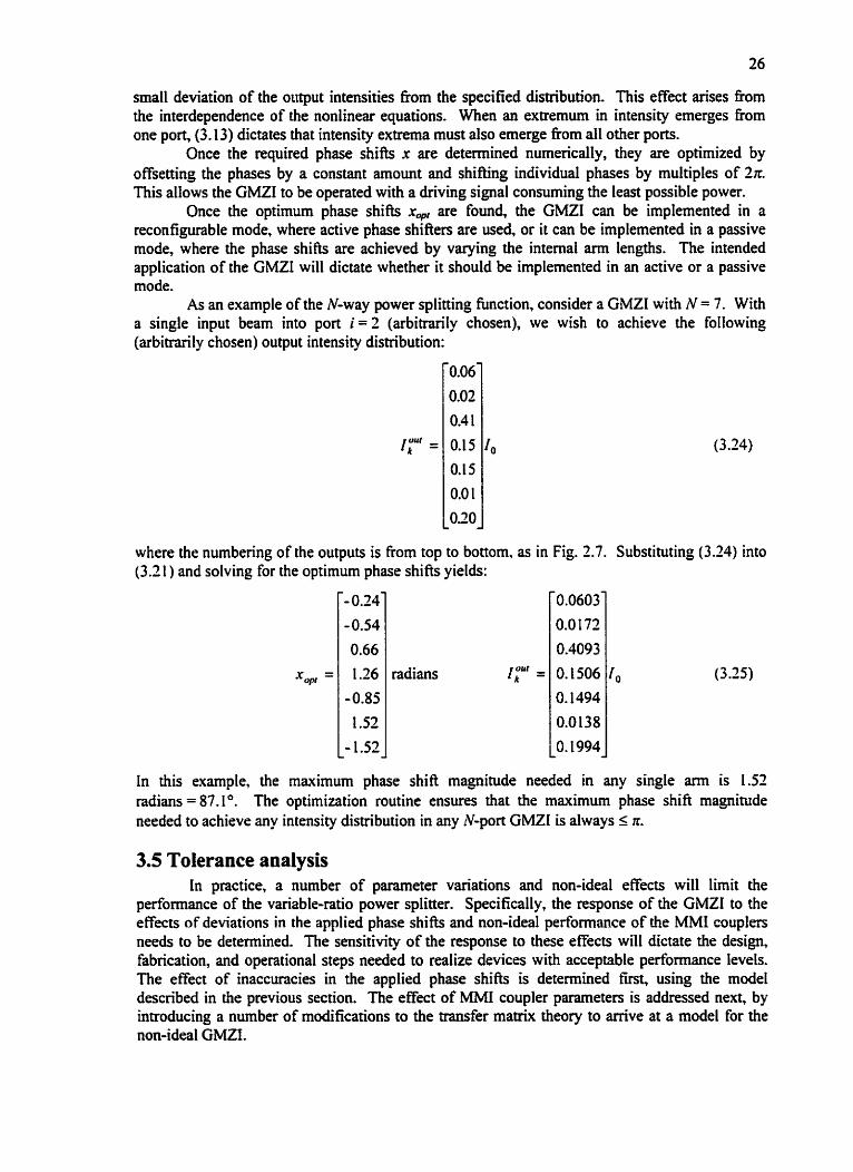
small deviation of the output intmsities fiom the specified distribution. This effect arises from the interdependence of the nonlinear equations. When an extremum in intensity emerges from one port. (3.13) dictates that intensity extrema must also emerge fiom al1 other ports.
Once the reguired phase shifls x are determined numerically, they are optimized by offsetting the phases by a constant arnount and shifting individual phases by multiples of 2 2 This allows the GMZI to be operated with a driving signal consuming the least possible power.
Once the optimum phase shifls x , are found, the GMZI can be implemented in a reconfigurable mode, where active phase shiften are useci, or it can be implemented in a passive mode, where the phase s h i h are achieved by varying the interna1 an^^ lengths. The intended application of the GMZi will dictate whether it should be implemented in an active or a passive mode.
As an example of the N-way power splitting function, consider a GMZI with N = 7. With a single input beam into port i = 2 (arbitrarily chosen), we wish to achieve the following (arbitrarily chosen) output intensity distribution:
In this example, the maximum phase shift magnitude needed in any single m is 1.52 radians = 87.1 O. The optimization routine ensures that the maximum phase shift magnitude needed to achieve any intensity distribution in any N-port GMZI is always 5 K.
where the numbering of the outputs is fiom top to bonom, as in Fig. 2.7. Substituting (3.24) into (3.2 1 ) and solving for the optimum phase sh ib yields:
3.5 Tolerance analysis In practice, a number of parameter variations and non-ideal effects will limit the
performance of the variable-ratio power splitter. Specifically, the response of the GMZI to the effects of deviations in the applied phase s h i h and non-ideal performance of the MM1 couplers needs to be determined. The sensitivity of the response to these effects will dictate the design, fabrication, and operational steps needed to realize devices with acceptable performance levels. The effect of inaccuracies in the applied phase shifis is determined fht, using the mode1 described in the previous section. The effect of MM1 coupler parameters is addressed next, by introducing a number of modifications to the d e r matrix theory to arrive at a mode1 for the non-ideal GMZI.
x = O P
- -0.0603
0.0 172 0.4093
O. 1506 O. 1494
0.0 138
o. 1994 - -
1,
- - - 0.24
- 0.54
0.66
1.26
- 0.85
t .52
- 1 S2 - -
radians 1" =

3.5.1 Phase shift deviations The phase shifts in (3.25) resuit in an intensity distribution with a maximum deviation of
0.38% from the distriiution specified in (3.24). To achieve this result, the phase s h i h must be applied to a precision of at least H.01 radians, which yields a tolerable phase enor of H.01 x 1801 r = H.57 O. As the precision of the applied phase s h i h diminishes, the output intensities deviate funher fiom the specified distribution; however, the deviation remains small for even a relatively large change in the applied phase shifts. In this examp!e, it is found that if only a H.1 radian (k5.7") precision in the phase shifts can be maintained, the intensity distribution will deviate by only 0.62% fiom the ideal values. In general, the accuracy of solutions varies with the chosen intensity distribution and the value of N.
This result is strictly only applicable for a single wavelength, because as multiple wavelengths mvel through a fixed-length region of modified refractive index, the phases of the different wavelengths are shifted by different amounts. This additional phase shift deviation is proportional to the change in wavelength. For example, over an 80 nm wavelength range (bandwidth) from 1510 nm to 1590 nm, the maximum phase shifi deviation is 2.6 % from the phase shift applied at 1550 nrn. The effect is also relative, so as the phase shiA in an arm approaches zero, it will be less wavelength sensitive. In the above example, it is found that over the entire 80 nm bandwidth the wavelength effect degrades the intensity distribution in (3.24) by a maximum of 0.74 % using an accuracy of fl.01 radians, and by a maximum of 1.63 % using an accuracy of M. 1 radians.
Although an arbitmy bandwidth has been used in the above example, it must be noted that the bandwidth of real devices cannot be arbitrarily specified. The actual bandwidth of the GMZI is limited by the finite bandwidth of the N x N MM1 coupler and is a result of both material parameters and device design [3 11.
3.5.2 Theory of the non-ideal GMZI Since the GMZI reIies upon the interference of modes and interactions among self-
images, its ultimate performance depends upon the accuracy of the amplitudes and phases of multiple beams within the device. This places d c t requirements on the performance of the constituent MM1 couplers. In practice, errors in the phases of the self-images and imbalance in the power splitting ratio are both present and can significantly degrade the performance and complicate the active control of devices based on the GMZI [33], [34], [48]. Furthemore, imperfect waveguide Fabrication is known to c a w additional phase errors [34], [49]. Since the m s of the GMZI are ofien relatively long to accommodate efficient phase shifting, the cumulative effects of these errors cm be significant. While the MM1 coupler performance i s also a function of the degree to which the theoretical relations in Chapter 2 are satisfied, the analysis here is mainly concemed with sources of non-ideality in addition to these fwidamental limits.
While an analysis of the non-ideal nature OF the GMZI is important for determining the performance limits of the variable-ratio power splitter, the results derived actually have a much wider applicability. This is because the number and complexity of applications using the GMZI continues to expand. In addition to switches [26], (341, the GMZI is used in a number of theoretical constructions such as multi-fiequency lasers [SOI, flat-response wavelength (de)multiplexers [5 11, and wavelength-selective switches [SZ].
In this section, a model for the non-ided GMZI is developed by incorporating non-ideal parameters into the m s f e r m a h appmach described in Sections 3.2 and 3.3. The model is then used to investigate the tolerances and scalability of the variable-ratio power splitter.

3.5.2.1 Modified GMW transfer matrix
Deviations in the phases of the self-images and imbalance in the power splitting ratio are the principal sources of non-ideal behaviour in MM1 couplen. These phenornena modiQ the transfer ma& (3.4) for the N x N M M coupler ScoMcr such that the element si/ can be described by
where a, is the (real) field amplitude transfer coefficient from input i to output j, 6% is the phase deviation of the image at output port j for an input into port i, and the tilde (-) is used to distinguish the parameters of the non-ideal device theory fiom the idealized theory. In a lossless device, the optical power at the output ports is conserved, Le.,
.Y
The imbalance in an output port (measured in dB units) is given by
where j4 is a reference output port. The effect of phase erron due to imperfect waveguide fabrication cm be incorporated
into the theory by introducing a phase error 6% in each am. The matrix modified to give
The total transfer matrix of the non-ideal GMZI is then given by .L - - Z
T = L b i m e r S,,, S3p/iner
3.5.2.2 Output intensity expressions
The eiements of the transfer matrix T are denoted by i,, and are found by substituting (3.26) and (3.29) into (3.30) to yield
'Y
where the prirned notation is used to distinguish the parameters of the MM1 combiner fiom that of the splitter. In general the amplitude transfer coefficients will differ and phase deviations will vary fiom coupler to coupler and arm to m. With a single input beam of optical intensity Io into port i, the intensity at an output port k is given by
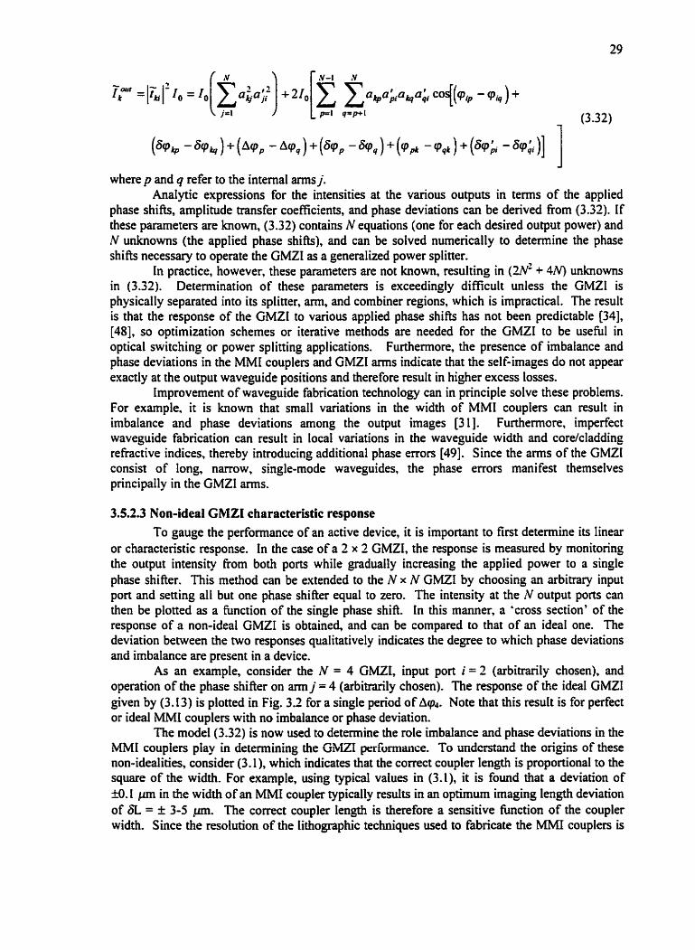
where p and q refer to the interna1 m s j. Analytic expressions for the intensities at the various outputs in tems of the applied
phase shifts, amplitude tmnsfer coefficients, and phase deviations can be denved from (3.32). If these parameters are known, (3.32) contains N equations (one for each desired output power) and N unknowns (the applied phase shih), and can be solved numerically to determine the phase shifts necessary to operate the GMZI as a generalized power splitter.
In practice, however, these parameters are not known, resulting in ( 2 ~ ' + 4N) unknowns in (3,32). Determination of these parameters is exceedingly dificult unless the GMZI is physically separated into its splitter, ami, and combiner regions, which is impractical. The result is that the response of the GMZI to various applied phase s h i h has not been predictable [34], [48], so optimization schemes or iterative methods are needed for the GMZI to be useful in optical switching or power splining applications. Furthermore, the presence of imbalance and phase deviations in the MM1 couplea and GMZI arms indicate that the self-images do not appear exactly at the output waveguide positions and therefore result in higher excess losses.
Improvement of waveguide fabrication technology can in principle solve these problems. For example, it is known that smaI1 variations in the width of MMI couplers can result in imbahce and phase deviations among the output images [3 11. Furthermore, imperfect waveguide fabrication can result in local variations in the waveguide width and corekladding rehctive indices, thereby introducing additional phase erron [49]. Since the arms of the GMZI consist of long, narrow, single-mode waveguides, the phase erroa rnanifest themselves principatly in the GMZI arms.
3.5.2.3 Non-ideal GMZI characteristic response To gauge the performance of an active device, it is important to first determine its Iinear
or characteristic response. In the case of a 2 x 2 GMZI, the response is measured by monitoring the output intensity From both ports while gradually increasing the applied power to a single phase shifier. This merhod cm be extended to the N x N GMZ? by choosing an arbitrary input port and setting al1 but one phase shifier equal to zero. The intensity at the N output ports can then be plotted as a function of the single phase shiR In this manner, a 'cross section' of the response of a non-ideal GMZI is obtained, and can be cornpared to that of an ideal one. The deviation between the two responses qualitatively indicates the degree to which phase deviations and imbalance are present in a device.
As an example, consider the N = 4 GMZI, input port i = 2 (arbitrarily chosen), and operation of the phase shifier on arm j = 4 (arbitranly chosen). The response of the ideal GMZI given by (3.13) is plotted in Fig. 3.2 for a single period of Aq4. Note that this result is for perfect or ideal MMI couplers with no imbalance or phase deviation.
The mode[ (3.32) is now used to determine the role imbalance and phase deviations in the MM1 couplers play in determining the Gb1Zi prrfwmance. To derstand the ongins of these non-idealities, consider (3.1 ), which indicates that the correct coupler Iength is proportional to the square of the width. For example, using typical values in (3.1). it is found that a deviation of kû. 1 pn in the width of an MMI coupler typically results in an optimum imaging length deviation of SL = k 3-5 p. The correct coupler length is therefore a sensitive function of the coupler width. Since the resolution of the lithopphic techniques used to fabricate the M M couplea is
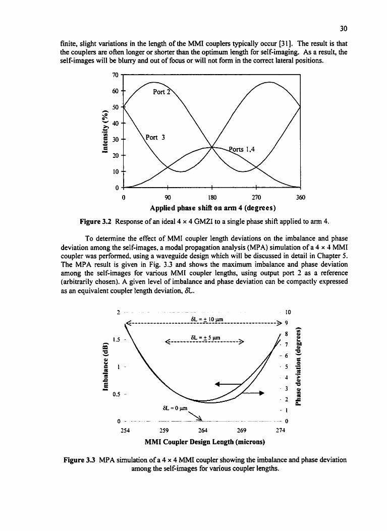
hi te , slight variations in the length of the MMI couplers typically occur [3 11. The result is that the couplers are often longer or shorter than the optimum length for self-imaging. As a result, the self-images will be blurry and out of focus or will not form in the correct lateral positions.
O 90 180 270 360
Applied phase s hiît on a m 4 (degrees)
Figure 3.2 Response of an ideal 4 x 4 GMZI to a single phase shift applied to ami 4.
To determine the effect of MMI coupler Iength deviations on the imbalance and phase deviation among the self-images, a modal propagation analysis (MPA) simulation of a 4 x 4 MMI coupler was perfonned, using a waveguide design which will be discussed in detail in Chapter 5. The MPA result is given in Fig. 3.3 and shows the maximum imbalance and phase deviation among the self-images for various MM1 coupler lengths, using output port 2 as a reference (arbitrarily chosen). A given Ievel of imbalance and phase deviation can be compactly expressed as an equivalent coupler length deviation, 6L.
MM1 Coupler Design Length (microns)
Figure 33 MPA simulation of a 4 x 4 MMi coupler showing the imbalance and phase deviation among the self-images for various coupler lengths.
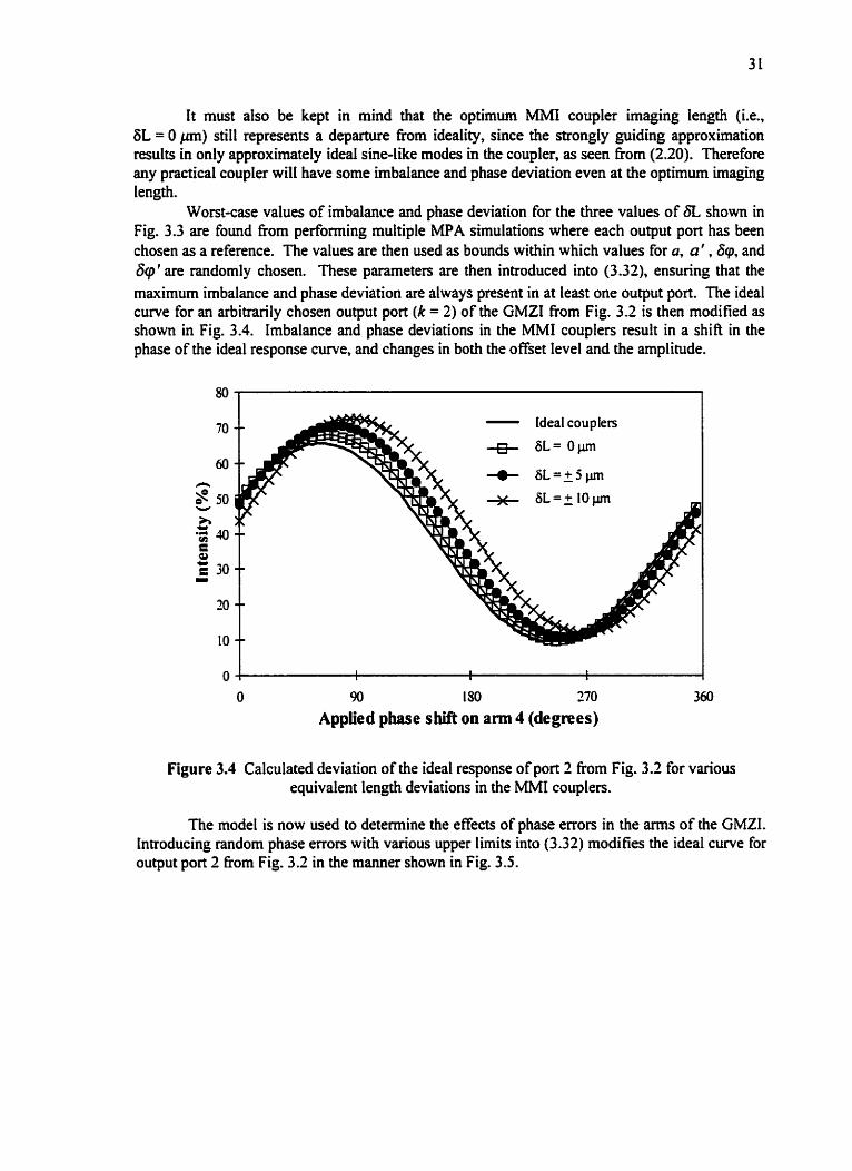
It must also be kept in mind that the optimum MMI coupler imaging length (i.e., 6L = O jm) still represents a departure from ideality, since the strongly guiding approximation results in only approximately ideal sine-like modes in the coupler, as seen fiom (2.20). Therefore any practical coupler will have some imbaiance and phase deviation even at the optimum imaging length.
Worst-case values of imbalance and phase deviation for the three values of 6L shown in Fig. 3.3 are found fiom perfonning multiple MPA simulations where each output port has been chosen as a reference. The values are then used as bounds within which values for a, a' ,&p, and 6q' are randomly chosen. These parameten are then introduced into (3.32), ensuring that the maximum imbalance and phase deviation are always present in at least one output port. The ideal curve for an arbitrarily chosen output port (k = 2) of the GMZI fiom Fig. 3.2 is then modified as shown in Fig. 3.4. Imbalance and phase deviations in the MM1 couplers result in a shift in the phase of the ideal response curve, and changes in both the offset level and the amplitude.
O 90 180 270
Appüed phase shût on a m 4 (degrees)
Figure 3.4 Calculated deviation of the ideal response of pon 2 from Fig. 3.1 for various equivalent length deviations in the M M couplers.
The mode1 is now used to determine the effects of phase errors in the arms of the GMZI. Inaoducing random phase erroa with various upper limits into (3.32) modifies the ideal curve for output port 2 Ekom Fig. 3.2 in the manner shown in Fig. 3.5.
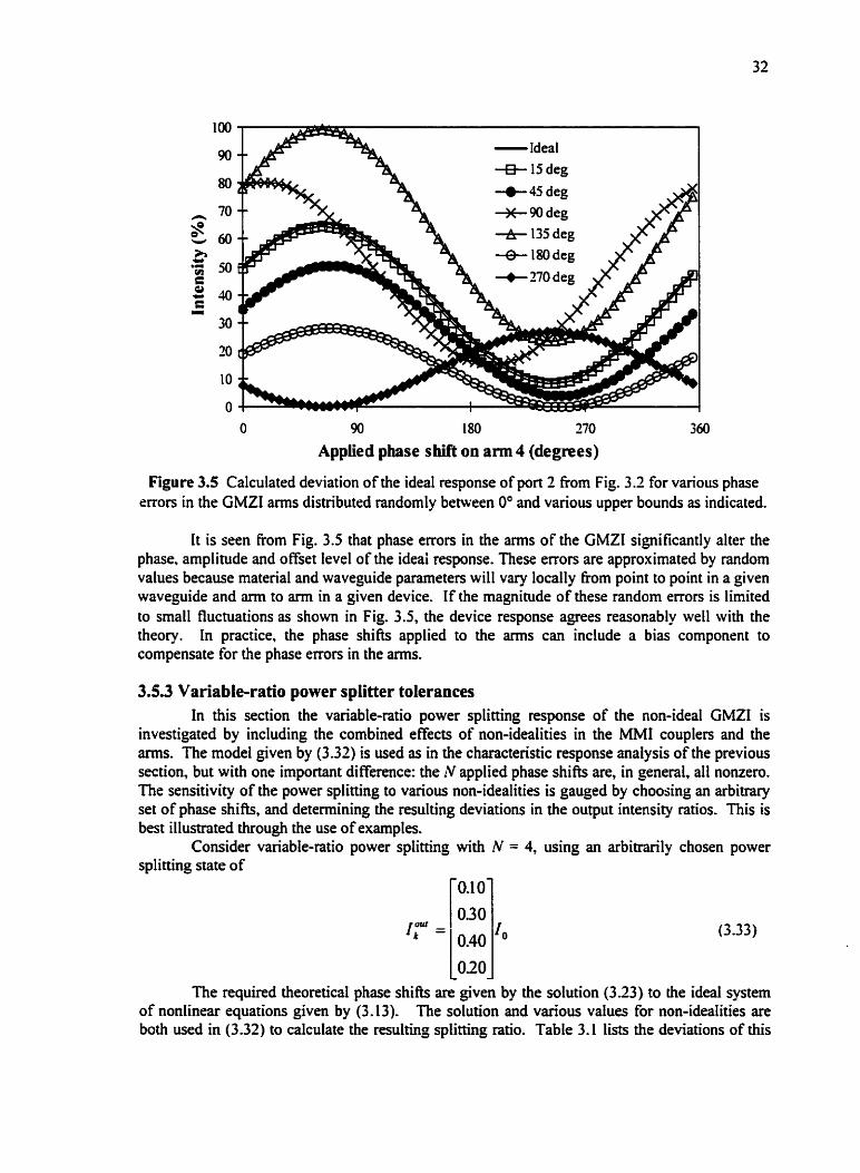
T E -8- 15 deg 1
Applied phase shifi on a m 4 (degmes)
Figure 3.5 Calculated deviation of the ideal response of port 2 from Fig. 3.2 for various phase errors in the GMZI amis distributed randomly between 0" and various upper bounds as indicated.
It is seen fiom Fig. 3.5 that phase mors in the arms of the GMZI significantly alter the phase, amplitude and offset level of the ideai response. These errors are approximated by random values because material and waveguide parameters will vary locally from point to point in a given waveguide and arm to arm in a given device. If the magnitude of these random errors is Iimited to srna11 fluctuations as show in Fig. 3.5, the device response agrees reasonably well with the theory. In practice, the phase shifts applied to the arms c m include a bias component to compensate for the phase errors in the arms.
3.5.3 Variableratio power splitter tolerances In this section the variable-ratio power splitting response of the non-ideal GMZI is
investigated by including the combined eKects of non-idealities in the MM1 couplea and the arms. The mode1 given by (3.32) is used as in the characteristic response analysis of the previous section, but with one important difference: the iV applied phase shifts are, in general, al1 nonzero. The sensitivity of the power splitting to various non-idealities is gauged by choosing an arbitrary set of phase shifts, and determining the resdting deviations in the output intensity ratios. This is best illustrated through the use of examples.
Consider variable-ratio power splitting with N = 4, using an arbitrarily chosen power splitting state of
The required theoretical phase s h i k are given by the solution (333) to the ideal system of nonlinear equations given by (3.13). The solution and various values for non-ideaIities are both used in (3.32) to calculate the resulting splitting ratio. Table 3.1 lists the deviations of this

ratio fiom the desired ratio given in (3.33). Various levels of imbalance and phase deviation in the MMI couplers have been introduced as equivalent deviations in the imaging length, given by the simulated results in Fig. 3.3. Al1 values in the table were calculated using a randorn fluctuation o f f 3 % of the value of the phase shiR This allows for the combined effects of a finite precision with which the phase shifts can be applied, phase shift deviations due to wavelength variations, and fluctuations in the power applied to the phase shiflers.
Equivalent 6L
4 x 4 MM1 coupler deviation (Fig. 3.2 - worst case fiom al1 reference
ports)
Table 3.1 Simulated toIerances of N = 4 variable-ratio power splitter for power splitting ratio (3.33), including a f 3 % fluctuation in the applied phase shifts. The 'am phase error' refers to
an upper limit for the uncompensated phase error in the GMZI arms.
A m phase error
It is seen in Table 3.1 that a degradation in the power splitting ratio occurs as the imaging in the MM1 couples worsens. tn this case, an acceptabIe level of deviation in the power splitting ratio is achieved if 6L for the 4 x 4 MM1 couplers is kept below i 5 p. As the level of uncompensated phase errors in the GMZI arms increases From O" to 5", the effect on the deviation in the power splitting ratio is small when the MM1 couplers are close to ideal; however, as the MM1 coupler imaging degrades, the effects of errors in the arms become more significant. For the operation of the power splitter it is therefore of prime importance to ensure that the MM1 couplers perform well.
To investigate the tolerance behaviour in larger devices, a similar analysis is perfonned for 1V = 5 up to N = 10 using an equal power splitting state in every case, i.e.,
Deviation in variable-ratio power splitting state above (+) and
below (-) desired value
Tmbalance (dB)
O
where k = 1, 2, ... , N. The results are shown in Table 3.2, To simulate scaling effects in real devices, a maximum MM1 coupler imbalance of -t 1.0 dB and phase deviation of + 3.5" are used for N = 5,6,7 and maximum imbalances and phase deviations of t 2.0 dB and + 9" , respectively, are used for N = 8,9,10. Imbalance values such as these have been measured in MM1 couplers with large LV [22], [29]. Table 3.2 also includes the phase shift fluctuations used in Table 3.1.
(degrees)
O
Phase Deviation (degrees)
O
(% of total ouvut intensity ) Port k = l
- 0.04
Port k = 2
- 0.37
Port k = 3
+ 0.71
Port k=4
- 0.30

Table 3.2 Simulated tolerances of variable-ratio power splitter for N = 5 up to N = 10 for power splitting ratio (3.34), including a t 3 % fluctuation in the applied phase shifts. The imbalance and phase deviation for N = 5.6, 7 are t 1 .O dB and f 3 S 0 and for N = 8.9, 10 they are + 2.0 dB and t goT respectively. The first and second lines for each value of N represent upper limits of 0' and
N
+ 5" for the uncompensated phase error in the GMZI a n s .
Deviation in equd power splitting state (% of total output intensity) Above (+) and below (-) desired value
Output Port k
Deviations in the power splitting ratio seen in Table 3.2 increase slowly with increasing iV. Maintaining a certain level of imbalance and phase deviations, however, becomes more dificult as iV increases. This is because the tolerable length deviation 6L required for a given level of imbalance and phase deviation in the MM1 coupler shrinks as N increases. This effect is partially taken into account in the analysis by using larger imbalance and phase deviations for iV = 8,9,10 than for N = 5,6,7. It is also seen in Table 3.2 that parn0ally uncompensated phase erron in the GMZI amis have only a small effect upon the power splitting ratio N, sometimes even improving the ratio due to partial compensation of the inaccuracies in the applied phase shifts.
The results of the tolerance analysis performed in this section indicate that the variabie- ratio power splitter can be operated even if the GMZI is non-ideal. Furthemiore. the power splining ratio remains stable and tolerant to parameter fluctuations even for moderate values of iV.
One effect not considered in the preceding analysis, however, is that of a reduction in the range of available power splitting ratios as the M M coupla irnaging degrades. This effect is rnost easily understood by considering the special cases where the GMZI is operated as a switch, In this mode of operation, al1 the light emerges from a single output and there is ideally no light at the other outputs. in practice, however, the MM1 coupler image plane does not perfectly coincide with the output ports (waveguides) and fuirhennoreT the self-images have a limited resolution due to the finite nurnber of modes available for self-imaging [53]. This resuits in some of the Iight emerging fkom unwanted ports, which is called crosstalk. The result is that a Iimited range of intensity values can emerge fiom a given port. Thus as the crosstdk increases, the range of available power splitting ratios decreases. The relation between crosstaik in the GMZI and various non-idealities is examined as part of the analysis in the next chapter, which deals with the special case of switching using the GMZI structureture
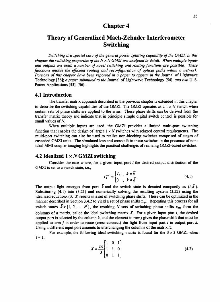
Chapter 4
Theory of Generalized Mach-Zehnder Interferorneter Switching
Switching is a special case of the general power spiitting capability of the GMZI. In this chapter the mvitching properties of the N x N GMU are anal'ed in detail. m e n multiple inputs and outpurs are useci, a number of novel switching and routing functions are possible. These fiincrions enable the efficient routing and reconfiguration of optical paths within a nehvork. Portions of this chapter have been reported in a paper to appear in the Journal of Lightwave Technology [36]; a paper szibmitted to the Journal of Lightwave Technology [54]; und two U. S . Patent Applications [55], [56].
4.1 Introduction The transfer matrix approach described in the previous chapter is extended in this chapter
to descnbe the switching capabilities of the GMZI. The GMZI operates as a 1 x N switch when certain sets of phase shifis are applied to the amis. These phase s h i h can be denved from the transfer matrix theory and indicate that in principle simple digital switch control is possible for small values of N.
When multiple inputs are useci, the GMZI provides a limited multi-port switching hnction that enables the design of larger 1 x N switches with relaxed control requirements. The multi-port switching c m also be used to realize non-blocking switches compnsed of stages of cascaded GMZI units. The simulated Ioss and crosstaik in these switches in the presence of non- ideal MM1 coupler imaging highiights the practical challenges of realizing GMZI-based switches.
4.2 Idealued 1 x N GMZI switching Consider the case where, for a given input port i the desired output distribution of the
GMZI is set to a switch state, Le., -
The output Iight emerges from port k and the switch state is denoted compactly as (4 k ). Substituting (4.1) into (3.21) and numencally solving the resulting system (322) using the idealized equatior~s (3.13) results in a set of switching phase shifts. These can be optimized in the manner described in Section 3.4.2 to yield a set of phase shifts xopt. Repeating this process for al1 switch States k ~ { l , 2 ,..., N} , the resulting N sets of switching phase s h i h .r,, form the
columns of a matrix, called the ideal switching matrix X. For a given input port i, the desired output port is selected by the column k, and the element in row j gives the phase shiR that must be applied to arm j in order to route (cross-connect) the light fiom input port i to output port k. Using a different input port amounts to interchanging the columns of the matrix ,Y.
For example, the following ideal switching ma& is found for the 3 x 3 GMZI when i = 1:
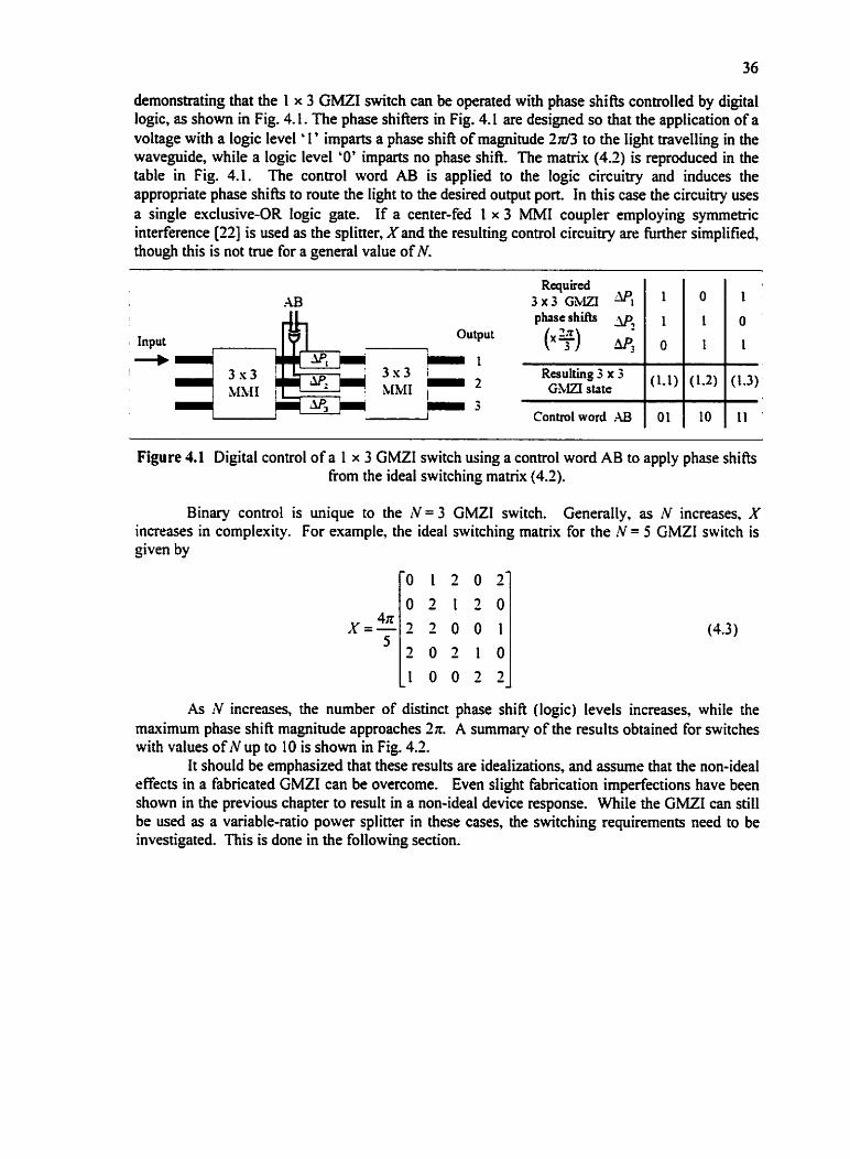
demonstrating that the 1 x 3 GMZl switch cm be operated with phase shifts controlled by digital logic, as s h o w in Fig. 4.1. The phase shifiers in Fig. 4.1 are designed so that the application of a voltage with a logic level ' 1 ' imparts a phase shift of magnitude 2 d 3 to the light travelling in the waveguide, while a logic level 'O' imparts no phase shiA. The ma& (4.2) is reproduced in the table in Fig. 4.1. The control word AB is applied to the logic circuitry and induces the appropriate phase shifts to route the light to the desired output pon. In this case the circuitry uses a single exclusive-OR logic gate. If a center-fed 1 x 3 MM1 coupler employing symmetnc interference [22] is used as the splitter, X and the resulting control circuitry are further simplified, though this is not true for a general value of N.
l Input +
Output
i l r Resulting 3 x 5 GbiZI sktc
Figure 4.1 Digital control of a I x 3 GMZI switch using a control word AB to apply phase sh ih from the ideai switching matrix (4.2).
Binary control is unique to the 1V= 3 GMZI switch. GeneraIly, as N increases, X increases in complexity. For example, the ideal switching matrix for the N = 5 GMZI switch is given by
As N increases, the number of distinct phase shifi (logic) ievels increases, while the maximum phase shift magnitude approaches 2x. A summary of the results obtained for switches with values of !V up to 10 is shown in Fig. 4.2.
It should be emphasized that these results are idealizations, and assume that the non-ideal rffects in a fabricated GMZI can be overcome. Even slight fabrication imperfections have been show in the previous chapter to result in a non-ideal device response. While the GMZI cm still be used as a variable-ratio power splitter in these cases, the switching requirements need to be investigated. This is done in the following section.
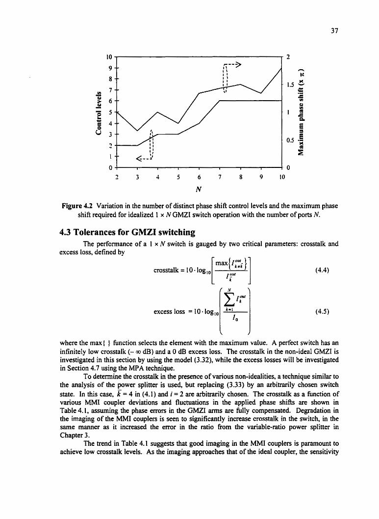
Figure 4.2 Variation in the number of distinct phase shift control levels and the maximum phase shift required for idealized 1 x N GMZI switch operation with the number of ports rV.
4.3 Tolerances for GMZI switching The performance of a I x N switch is gauged by two critical parameters: crosstalk and
excess loss, defined by
crosstalk = 1 0 - log ,,
excess loss = 1 O. log
where the max( function selects the element with the maximum value. A perfect switch has an infinitely low crosstalk (- m dB) and a O dB excess loss. The crosstalk in the non-ideal GMZI is investigated in this section by using the mode1 (3.32), while the excess losses will be investigated in Section 4.7 using the MPA technique.
To determine the crosstalk in the presence of various non-idealities, a technique similar to the analysis of the power splitter is used, but replacing (3.33) by an arbitrarily chosen switch state. In this case, k = 4 in (4.1 ) and i = 2 are arbitrarily chosen. The crosstalk as a fiuiction of various MMI coupler deviations and fluctuations in the applied phase sh ih are show in Table 4.1, assuming the phase ermn in the GMZI arrns are fully compensated Degradation in the imaging of the MM1 couplers is seen to significantly increase cmsstalk in the switch, in the same manner as it increased the emor in the ratio Eiom the variable-ratio power splitter in Chapter 3.
The trend in Table 4.1 suggests that good imaging in the MMI couplers is paramount to achieve low cmsstalk levels. As the Maging approaches that of the ideal coupler, the sensitivity
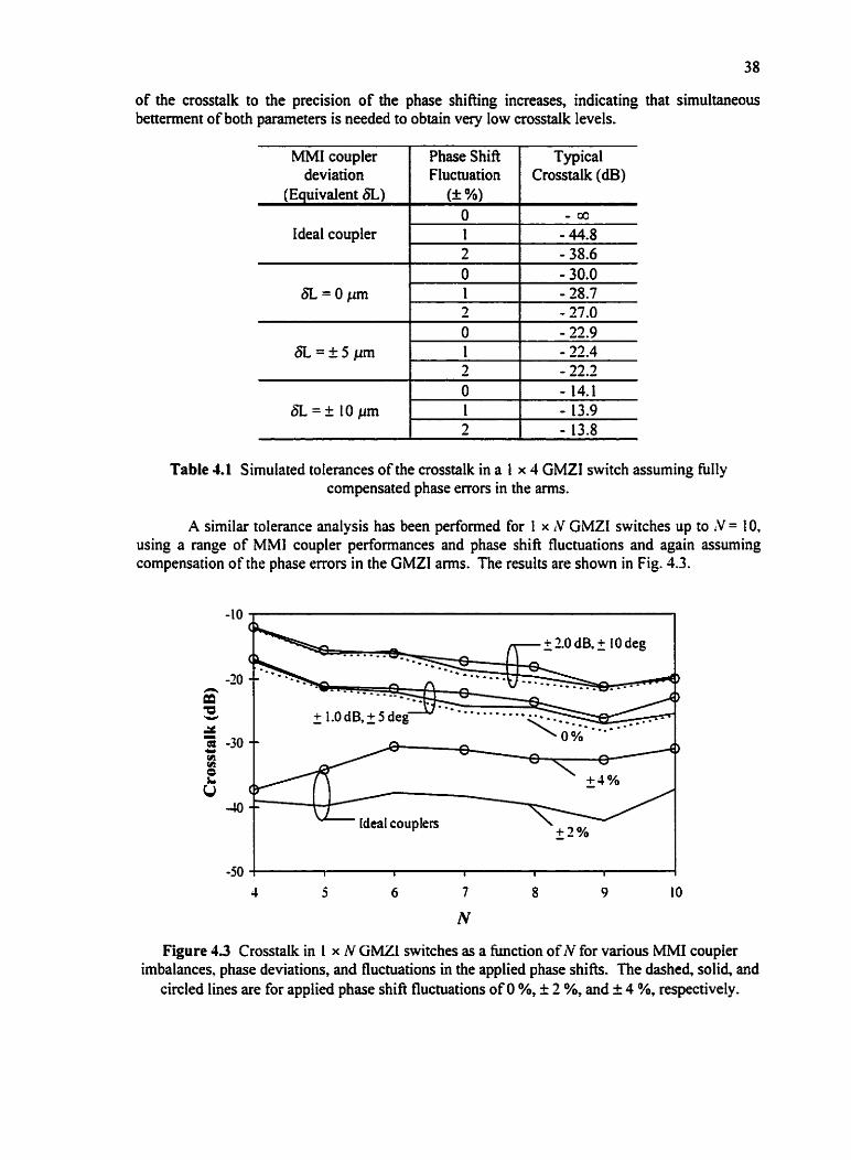
of the crosstalk to the precision of the phase shifting inmeases, indicating that simultaneous bettement of both parameters is needed to obtain very low crosstalk levels.
Table 4.1
A simi
MM1 coupler deviation
(Equivaient 6L)
Ideal coupler
Simulated tolemces of the crosstalk in a 1 x 4 GMZI switch assuming hlly compensated phase errors in the arms.
ar tolerance analysis has been perfonned for 1 x N GMZI switches up to iV = t O,
Phase Shifl Fluctuation (t %)
O 1 2
using a range of MM1 coupler performances and phase shift fluctuations and again assuming compensation of the phase errors in the GMZI arms. The results are shown in Fig. 4.3.
Typical Crosstalk (dB)
- 00
- 44.8 - 38.6
Figure 4 3 Crosstalk in 1 x N GMZI switches as a hc t ion of lt' for various M M coupIer imbalances, phase deviations, and fluctuations in the applied phase shifts. nie dashed, solid, and
circled lines are for applied phase shift fluctuations of O %, f 2 %, and h 4 %, respectively.
Since idealized switching demands that the phase shifts are exact values, additional fluctuations due tu variations in the parameters of fabricated phase shifiers (such as eIectrical resistance) are present. For this reason, an extra + 2 % (a technologicalIy feasible variation) is included to arrive at the f 4 % fluctuation in Fig. 4.3.
In Fig. 4.3 three levels of MMI coupler performance are shown. If a certain level of performance can be maintained as N increases (usuaily requiring tightened fabrication tolerances), the level of crosstak remains relatively constant. With perfect imaging in the MM1 couplea (no imbalance or phase deviation) low crosstaik values are possible, but even slight inaccuracies in the applied phase shifts can degrade the crosstalk significantly. For example, a k 2 % fluctuation in the applied phase shifts increases the crosstalk from - co dB (with no fluctuation) to about - 40 dB.
For a maximum imbalance of + 1.0 dB and phase deviation of f Y, the crosstalk is limited to about -28 dB, while increasing these values to + 2.0 dB and I IO0 degrades the crosstalk to about -20 dB. Again as in Table 4.1, the sensitivity of the crosstalk to the accuracy of the applied phase shifts increases as the imaging in the M M coupters improves.
It must be kept in mind that Fig. 4.3 shows typical results. Since the imbalance, phase deviation, and phase shift fluctuations are applied in a random manner, the exact position of a data point will vary slightly fiom simulation to simulation. The general trend from a large number of simulations indicates that the crosstalk improves slightly (< 5 dB) as N increases t?om 4 to 10. The reason for this is that the power in unwanted output ports is distributed among an increasing number of ports, thereby lowering the maximum crosstalk level. This effect is not seen for the ideal coupler since imbalance and phase deviations (the pnnciple sources of the crosstalk) are not present in this case.
The requirements for idealized switching are more stringent than for variable-ratio power splitting. Practical switches provide crosstalk levels in the -20 to -30 dB range, and can only be improved with very accurate device fabrication and control methods. To exploit the simplicity of the idealized phase shifts for switching, it is thus imperative that the device response be as close as possible to the ideal response.
4.4 Multi-port blocking smtches When light is introduced into multiple input ports, the GMZI provides a limited 'V x N
switching capability. This can be intuitively understood by considering the symmeûic nature of the (ideal) GMZI. The GMZI structure shown in Fig. 2.7 is the same when viewed upside-dom or from the fiont or behind the page. Physically, this means that input ports and output ports can be interchanged simply by launching light into the different ends of the device, and a port i can be considered to be port (N + 1 - i), depending upon the direction fiom which the GMZI is viewed. Mathematically, this can be seen fiom (3.10); the transfer matrix for the GMZI is unchanged when i is replaced by k or when i and k are replaced by (N + 1 - i) and (N + 1 - k).
This leads to the conclusion that if the state (i , k) is achieved by applying a certain set of phase shifis, then the sarne set of phase s h i b result in the state (k , i). If i + k , the switch is capable of supporting multiple simultaneous states (cross-connects). In this section the cross- connects available in the GMZI are derived from the GMZI nansfer matrix. It is shown that the same phase shifb and cross-connects which govem this switch also apply to a wavelen-eth division multiplexing (WDM) version of the switch, enabling both wavelength muItipIexing and sorting fùnctions to be performed with a singIe device.

4.4.1 Cross-connect pattern of the N x N GMZI When the N x N GMZI is used as a 1 x N switch, a single input cm be cross-co~ected to
any output using a set of optimum phase shifts given by the columns of the matrix X. In the case of multiple inputs, each column of X corresponds to a cross-connection of all input and output ports of the N x N GMZI in pairs. A different set of cross-connects is associated with each column of X, so an N x N GMZI has 1V distinct cross-connect sets. To determine these sets, consider the expression (3.13) for the intensities at the outputs of the GMZI, derived from the GMZI transfer ma&. A cross-connect (i, k) occurs when the argument of the cosine is an integer muItipIe of 2n, i.e.,
(9, - < P i q ) + ( ~ v p - A < P ~ ) + ( v ~ & - < P 9 k ) = Z m x (4.6)
where rn is an integer. It is easily verifîed that when (4.6) is substituted into (3.13), 1" = Io. Considenng the phase shifi in a m p = 1 as a reference and setting Acpl = O as a reference without affecting the generality of the analysis, (4.6) becomes
where A<p, are the phase s h i h needed to cross-connect input i to output k. Since al1 input ports and output ports are cross-connected in pain, the phase shift A<p, must also connect an input i' to an output k ' , where i' , k' E { I,2 , ... , iV ). Without loss of generality, we may choose i' = 1, which yields
Equating (4.7) and (4.8) and substituting for cp using (3.2)- after some manipulation we obtain:
To find the output pon k' to which input pon 1 is cross-connected, we define a usehl function y as follows:
yi,k = ( - 1 ) ~ ( 2 i - 1)+(-1)~(2k - 1)+ 1 (4.1 O)
We note from (4.10) the symmetry relation, i.e., the cross-connect set for (i, k) and (k, i ) are the same. Note also that yi.k always lies in the range -4N < lyi.4 < 4iV. From (4.9) and (4.10) an analytic expression for k ' is obtained:
The complete set of cross-connects for the N x N GMZI switch cm be determined by substituting any (i, k) pair into (4. IO), and using (4.1 1 ) to determine the output port k' to which input port 1 ( i' ) is cross-co~ected. As an example, Table 4.2 shows the set of cross-comects possible in the 5 x 5 GMZi switch.
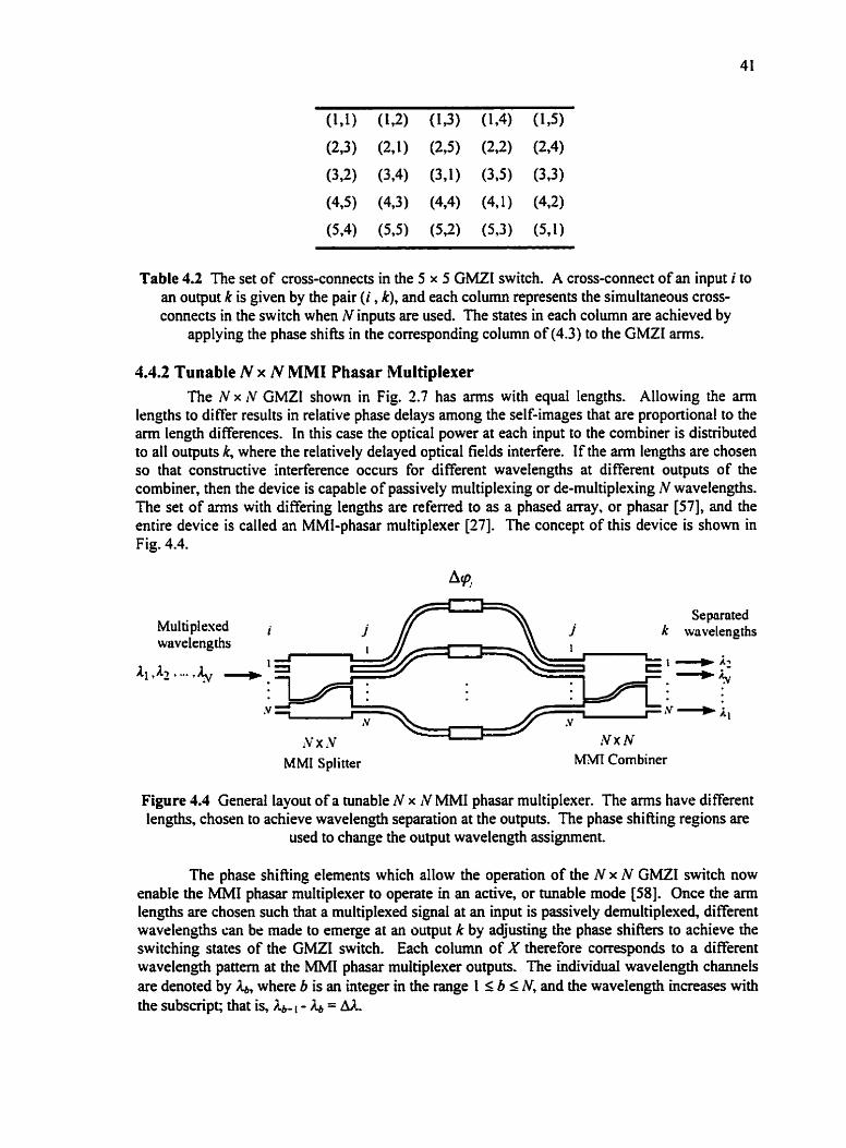
Table 4.2 The set of cross-connects in the 5 x 5 GMZI switch. A cross-connect of an input i to an output k is given by the pair (i , k), and each column represents the simultaneous cross- connects in the switch when N inputs are used. The states in each column are achieved by
applying the phase sh ih in the correspondhg column of (4.3) to the GMZI arms.
4.4.2 Tunable IV x N MM1 Phasar Multiplexer The N x IV GMZI shown in Fig. 2.7 has arms with equal lengths. Allowing the ann
lengths to differ results in relative phase delays among the self-images that are proportional to the a m length differences. In this case the optical power at each input to the combiner is distributed to ail ourputs k, where the relatively delayed optical fields interfere. If the arm lengths are chosen so that constructive interfierence occurs for different wavelengths at different outputs of the combiner, then the device is capable of passively rnultiplexing or de-rnultiplexing N wavelengths. The set of arms with differing lengths are referred to as a phased array, or phasar [57], and the entire device is called an MMi-phasar multiplexer [27]. The concept of this device is show in Fig. 4.4.
Seporated wvavelengths
MM1 Splitter M M Combiner
Figure 1.4 General layout of a tunable N x N MMI phasar multiplexer, ï h e arms have different lengths, chosen to achieve wavelength separation at the outputs. The phase shifting regions are
used to change the output wavelength assignment.
The phase shifiing elements which allow the operation of the N x N GMZI switch now enable the MM1 phasar multiplexer to operate in an active, or tunable mode [58]. Once the arm lengths are chosen such that a multiplexed signal at an input is passively demultiplexed, different wavelengths can be made to emerge ai an output k by adjusting the phase shifters to achieve the switching states of the GMZI switch. Each column of X therefore corresponds to a different wavelength pattern at the MM1 phasar multiplexer outputs. The individual wavelength channels are denoted by &, where b is an Uiteger in the range 1 I b I N, and the wavelength mcreases with the subscrïpt; that is, Ab- 1 - &, = M.


where L, is the beat length of the coupler given by (2.23), and M and N are any two positive integers without a common divisor. The shortest coupler length is obtained when M = 1.
Since al1 arms in the GMZl have equal Iengths, no relative phase shitl is imparted to the light in the arms of the passive device. The presence of the arms may therefore be disregarded entirely, resulting in the merging of the two MMI couplers into a single MM1 coupler with a length equal to twice the original coupler length:
Rearranging (4. I3), two alternate expressions for the GMZI length cm be found, 2
L,w = -3L, for N odd, (4.1 4) N
where LM = 1 has been used in (4.13), and M M LG.W = - 3 L, = - 3 L, for rV even,
(N 1 2 ) K where
N = 2K, K = 1,3,3 ,... , (4.16) and iM and K are any two positive integers without a common divisor. Comparing (4.12) and (4.14) it is clear that when N is odd the passive GMZl acts like a single MM1 splitter with iM = 2 and N output images. By contrast, upon comparison of (4.12) and (4.15) for N even, the passive GMZT functions as a single MM1 splitter with a reduced number (K) of output images.
In both cases, there are N output ports. For N odd, the action of the passive GMZI is trivial: the N output images emerge fiom the N output ports, since (4.14) is identical to (4.12) if LW = 2 is used in (4.12). Since this does not yieId any new information, our analysis will be restricted to the case of !V even. M e n N is even, there are N output ports and only K images. The output ports fiorn which the light emerges will depend upon both the input port and the value of K. Two cases must therefore be considered: K even and K odd,
A. K even Since the passive GMZI behaves as an M M coupler with K output ports, the geometry of
an MM1 coupler with an even number of output ports is analyzed. This geometry has been described by Bachmann et al. [12], and is s h o w in Fig. 4.5.
The spacing of the output images by intervals of length 2 W , N in the IV x N coupler are in the LV x K coupler described by intervals of length:
where (4.16) has been used, and IV, is the effective width of the coupler, defined by (2.13). The corresponding geometry for the N x K coupler is shown in Fig. 4.6.

NX N iMMI Coupler Inputs outputs
i - L w = - 3 k
I 1 2 2
3 3 3 4
5 5 6 6
7 7 8 8
Figure 4.5 Geometry of the N x N MM1 coupler illustrating the input and output port positions for the case where N is even.
In the iV x N coupler of Fig. 4.5, the fint input port (i =1) is located a distance n (a fiee design parameter) from the top edge of the coupler. The corresponding output images are located the same distance a inside both edges of every interval of length 2 WJN. The result is N self- images at the outputs.
inputs i
Figure 4.6 Geometry of the 1V x K MM1 coupler illustrating the input and output port positions for the case where K is even.
In the :V x K coupler, the same relation holds; however, the interval lengths are given by (4.17). Observing Fig. 1.6, the h e I t is that for an mput into pan i = 1, K self-images emerge fiom the set of output ports:
kl = (1,4,5,8,9,12,13, ...) (4.18)
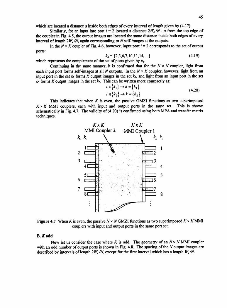
which are located a distance a inside both edges of every interval of length given by (4.17). Similarly, for an input into port i = 2 located a distance 2 We IN - a from the top edge of
the coupler in Fig. 4.5, the output Mages are located the same distance inside both edges of every interval of length 2 W,/N, again correspondhg to N selfiimages at the outputs.
In the N x K coupler of Fig. 4.6, however, input port i = 2 corresponds to the set of output ports:
= {2,3,6,7,10,11,14, ...) (4.19) which represents the complement of the set of ports given by ki.
Continuing in the same manner, it is confümed that for the N x N coupler, Iight fiom each input port foms self-images at al1 N outputs. In the N x K coupler, however, light lrom an input port in the set kl foms K output images in the set kl, and light fiom an input port in the set k2 foms K output images in the set k2. This cm be written more compactly as:
This indicates chat when K is even, the passive GMZI functions as two superimposed K x K MM[ couplers, each with input and output ports in the same set. This is shown schematically in Fig. 4.7. The validity of (4.20) is confirmed using both MPA and transfer matnx techniques.
Figure 4.7 When K is even, the passive N x N GMZI functions as two superimposed K x K MM1 couplers with input and output ports in the same port set.
B. K odd Now let us consider the case where K is odd The geometry of an N x N MMT coupler
with an odd number of output ports is shown in Fig. 4.8. The spacing of the N output images are descriied by intervals of Iength 2 WJV, except for the first interval which has a length W , N
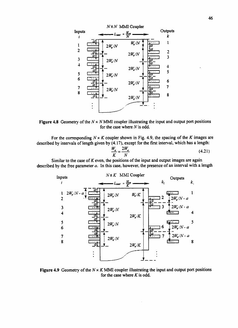
N x N MMI Coupler h p u r output3
*-Lw = - I N k
Figure 4.8 Geometry of the N x N MM1 coupler illustrating the input and output port positions for the case where N is odd.
For the corresponding N x K coupler s h o w in Fig. 4.9, the spacing of the K images are described by intervals of length given by (4.17), except for the k t interval, which has a Iength:
w, w', -=- (4.2 1 ) K N
Sirnilar to the case of K even, the positions of the input and output images are again descnbed by the fkee parameter a. In this case, however, the presence of an interval with a length
Inputs i
!VX K MM1 Coupler Outputs
--Lw = % -- k: k; K
Figure 4.9 Geometry of the N x K MM1 coupler illustrating the input and output pon positions for the case where K is odd.
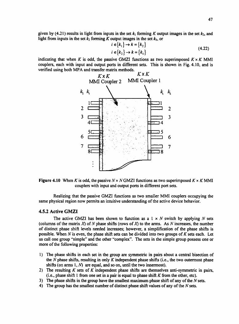
given by (43 1) results in light from inputs in the set kt forming K output images in the set k2, and light from inputs in the set k2 formmg K output images in the set kl, oi
i + k = I R - , } (4.22)
i ~ { k ~ } + k = { k , }
indicating that when K is odd, the passive GMZI hinctions as two superimposed K x K MM1 couplers, each with input and output ports in different sets. This is shown in Fig. 4.10, and is verified using both MPA and transfer matrix methods.
Figure 4.10 When K is odd, the passive N x NGMZI hctions as two superimposed K x K MM1 couplers with input and output ports in different port sets.
Realizing that the passive GMZI functions as two smaller MMI couplers occupying the same physical region now perrnits an intuitive understanding of the active device behavior.
4.5.2 Active GMZI The active GMZI has been shown to fiinction as a 1 x N switch by applying N sets
(columns of the matrix X ) of N phase s h i h (rows of X ) to the arms. As N increases, the number of distinct phase shift levels needed incrpases; however, a simplification of the phase shifts is possible. When N is even, the phase shifi sets can be divided into two groups of K sets each. Let us cal1 one group "simple" and the other "~omplex*~. The sets in the simple group possess one or more of the foliowing properties:
The phase shifis in each set in the group are symrnetrîc in pairs about a central bisection of the N phase shifts, resulting in only K independent phase shih (Le., the two outemost phase s h i h (on m s 1, N) are equaI, and so on, until the two innermost). The resulting K sets of K independent phase shitts are themselves ami-symmetric in pairs, (i.e., phase shift 1 from one set in a pair is equal to phase shift K from the other, etc). The phase s h i h in the group have the smallest maximum phase shift of any of the N sets. The group has the smallest number of distinct phase shifi values of any of the N sets.

Specifically, for K even, the simple group possesses at least the fint two properties, and for K odd, the simple group possesses al1 four properties. By contrast, the cornplex group possesses properties opposite to those stated above: they are in general neither symmeaic nor anti-symmetric, nor do they necessarily have the mallest maximum phase shifi or the mallest number of distinct values of any of the sets. These properties are best iilustrated through the use of examples, which will be given in the following section.
Since each set of phase sh ih cross-connects an input i to an output k, the simple and complex groups correspond to groups of simple and complex output ports. These can be interpreted as the output ports which can be accessed using simple phase s h i h and cornplex phase shifls, respectively. The simple and complex port numben can be compared to the analysis of the passive GMZI to arrive at the following design rule:
Cross-connecting light fiom any of the inputs of a gnten K x K coupler in a G i W to any of the outputs of the same K x K coupler can be accomplished using simple phase shl@s, while cross-connecting light from any of the inputs of a given K x K coupler to any of the outputs of a dixerent K x K coupler requires cornpiex phase shifs.
This rule is a simple, yet powerful tool which can be used to dramatically improve the control requirements of 1 x N GMZI switches. This is described in the following section.
4.6 Improved 1 x N Switch
4.6.1 Theory and Design The above design mle States that the simple and complex outputs correspond to either of
the sets kl or k2. Then for a single input and when N is even, the N x N active GMZI can be operated as a 1 x K switch, using only simple phase shifts. If, however, the restriction of a single input cm be removed - allowing the capability of switching between inputs from different sets - then the alternate K outputs can also be accessed. ï h e result is a 1 x rV switch that can be operated using only the K sets of simple phase shih. This is the principle of the improved 1 x N switch.
In practice, the restriction of a single input is removed by utilizing a I x 2 switch to connect a single input to any two GMZl inputs fiom different sets, corresponding to the set numbering given by (4.1 8) and (4.19). Any desired output is then accessed with simple phase shih, by operating the 1 x 2 switch such that the input pon of the GMZI corresponds to the same K x K coupler as the output port. This structure is shown schernatically in Fig. 4.1 1.
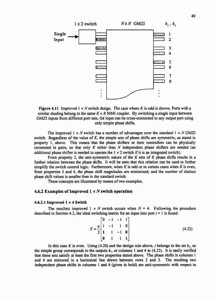
1 x 2 switch N x N GMZI k, y k2
Figure 4.1 1 Improved 1 x N switch design. The case where K is odd is shown. Ports with a similar shading belong to the same K x K MM1 coupler. By switching a single input between GMZI inputs from different port sets, the input can be cross-connected to any output port using
only simple phase shih.
The improved 1 x iV switch has a number of advantages over the standard 1 x IV GMZI switch. Regardless of the value of K, the simple sets of phase shifts are syrnmetric, as stated in property 1, above. This means that the phase shifters or their controllers can be physically connected in pairs, so that only K rather than N independent phase shiften are needed (an additional phase shifter is needed to operate the 1 x 2 switch if it is an integrated switch).
From property 2, the anti-symmetric nature of the K sets of K phase shifts results in a further relation beween the phase shifk. It will be seen that this relation can be used to m e r simplify the switch control logic. Furthemore, when K is odd or in certain cases when K is even, fiom properties 3 and 4, the phase shift magnitudes are minimized, and the number of distinct phase shift values is smaller than in the standard switch.
These concepts are iliustrated by means of two examples.
4.6.2 Examples of Improved 1 x N switch operation
4.6.2.1 Improved 1 x 4 Switch
The smallest improved 1 x N switch occurs when N = 4. Following the procedure described in Section 4.2, the ideai switching ma& for an input into port i = 1 is found:
y0 - 1 - 1 11
In this case K is even. Using (4.20) and the design nile above, i belongs to the set kl, so the simple group corresponds to the outputs kl. or columns 1 and 4 in (423). It is easily venfied that these sets satisfy at least the fim two properties stated above. The phase s h i h in columns 1 and 4 are mirrored in a horizontal Iine drawn between rows 2 and 3. The resulting two independent phase shifts in columns 1 and 4 (given in bold) are anti-symmetric with respect to
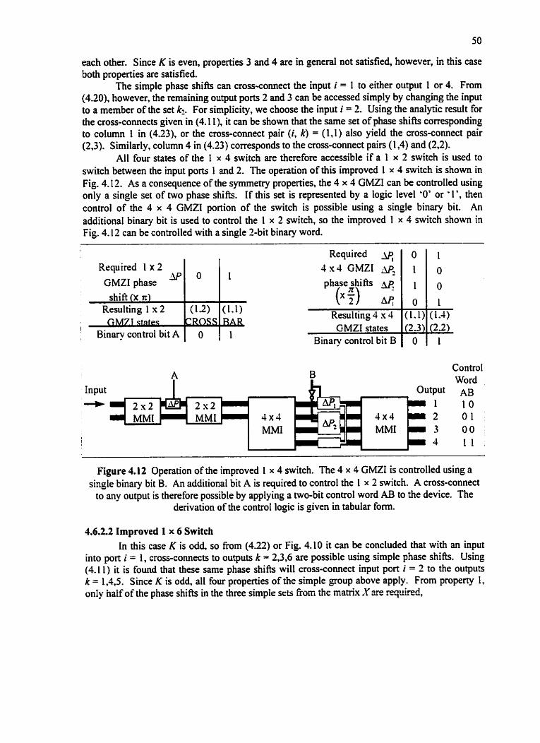
each other. Since K is even, properties 3 and 4 are in general not satisfied, however, in this case both properties are satisfied.
The simple phase sh ib c m cross-connect the input i = 1 to either output 1 or 4. From (4.20), however, the remaining output ports 2 and 3 can be accessed simply by changing the input to a member of the set k2. For simplicity, we choose the input i = 2. Using the analytic mult for the cross-connects given in (4.1 I), it can be shown that the sarne set of phase sh ih corresponding to column 1 in (4.23), or the cross-connect pair (i, k) = (1,l) also yield the cross-connect pair (2,3). Similarly, column 4 in (4.23) corresponds to the cross-co~ect pairs (1,4) and (2,2).
Al1 four states of the 1 x 4 switch are therefore accessible if a 1 x 2 switch is used to switch between the input pom 1 and 2. The operation of this improved 1 x 4 switch is show in Fig. 4.12. As a consequence of the symmetry properties, the 4 x 4 GMZI cm be contmlled using only a single set of two phase shifts. If this set is represented by a logic level 'O' or '1 ', then control of the 4 x 4 GMZI portion of the switch is possible using a single binary bit. An additional binary bit is used to control the 1 x 2 switch, so the improved 1 x 4 switch shown in Fig. 4.12 can be controlled with a single 2-bit binary word.
Required 1 x 2
GMZI phase
I B i n q control bit A
phase shifts gq
PI> D I P
A Input I
Controll Word
Figure 4.12 Operation of the improved 1 x 4 switch. The 4 x 4 GMZI is controlled using a single binary bit B. An additional bit A is required to control the 1 x 2 switch. A cross-connect
to any output is therefore possible by applying a two-bit control word AB to the device. The derivation of the conml logic is given in tabular form.
4.6.2.2 Improved 1 x 6 Switch In this case K is odd, so from (4.22) or Fig. 4.10 it can be concluded that with an input
into port i = 1, cross-connects to outputs k = 2,3,6 are possible using simple phase shih. Using (4.11) it is found that these same phase shifts will cross-connect input port i = 2 to the outputs k = 1,4,5. Since K is odd al1 four pmperties of the simple group above apply. From property 1, onIy half of the phase shitts in the three simpie sets h m the matrix X xe required,
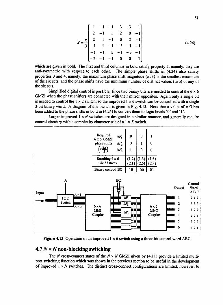
which are given in bold. The first and third colurnns in bold satis@ property 2, namely, they are anti-symmetnc with respect to each other. The simple phase shifts in (4.24) also satisfy properties 3 and 4, narnely, the maximum phase shifl magnitude (lr 13) is the smallest maximum of the six sets, and the phase shifts have the minimum number of distinct values (two) of any of the six sets.
Simplified digital control is possible, since two binary bits are needed to conaol the 6 x 6 GMZI when the phase shitten are connected with their rnirmr opposites. Again only a single bit is needed to control the 1 x 2 switch, so the improved 1 x 6 switch can be controlled with a single 3-bit binary word. A diagram of this switch is given in Fig. 4.13. Note that a value of 1r/3 has been added to the phase s h i h in bold in (4.24) to convert them to logic levels '0' and ' I *.
Larger improved 1 x N switches are designed in a similar manner, and generally require control circuitry with a complexity characteristic of a 1 x K switch.
Binary control BC
BC
. . .. . - ..
Figure 4.13 Operation of an improved 1 x 6 switch using a three-bit control word ABC.
Input
4.7 N x N non-blocking switching The N cross-connect states of the N x N GMZI given by (4.1 1) provide a limited multi-
port switching function which was shown in the previous section to be usefbi in the development of improved 1 x N switches. The distinct cross-connect configurations are limited, however, to
Control output Word
A B C A = l
: l
A-O 1
1 0 0 '
8 0 0 1
I
0 0 0
1 0 1
l x 2 Switch - 0 1 0 . - 1 1 0

only N possible permutations of the inputs to be achieved at the outputs. An exarnple of these permutations for the case of N = 5 was given in Table 4.2. Such switches, with Iirnited sets of cross-connect permutations, are commonly referred to as blockirzg switches. To understand this terni, cowider the situation in the switch where some input and output ports are cross-connected (occupied) and others are fke. Free input ports cannot be cross-comected at will to k e output ports, because their paths are set by the phase shifts currently being applied to the arms. Some cross-connects are therefore blocked, owing to the limited number of permutations available.
In a non-blocking switch architecture, however? the entire set of N! permutations of cross- connects are possible and thus any two free ports can be cross-connected whiIe preserving the cross-connect pattern of the occupied ports. Non-blocking mitches are therefore of prime importance in network apptications, where the maximum flexibility in cross-connect possibilities is desired [ 1 41.
Dilated versions of non-blocking switches have been proposed, in which a number of independently controlled 1 x N GMZI switches are used [33]. This design, however, requires 4N MM1 couplers, W' phase shifters, and numerous waveguide bends and crossings, resulting in a large switch with complicated design and controt requirements.
Et has been shown in the previous section that using a smaller (1 x 3) switch in conjunction with the N x LV GMZI greatly increases the flexibiIity of the 1 x IV switch. In a simikir manner, it is show in this section that smaller GMZIs can be used in conjunction with larger GMZIs to achieve N x N non-blocking operation in a simple and compact structure. Using this idea, two designs for the non-blocking switch are proposed: a cascaded design and a balanced design.
The tradeoff for the simplified non-blocking designs mentioned in this section is that the switches are only rearrangabiy non-blocking, meaning that any fiee pair of ports can be cross- connected only by rnomentarily disrupting the existing cross-connects. This arises because the mukiple cross-connects in the N x iV GMZf depend upon the state of a single phase shifter. Although numerous phase shifters are used in the dilated switch mentioned above, each phase shifter is associated with onIy one cross-connect. The result is that the dilated switch is srrictly non-blocking (fiee ports can be cross-connected without disnipting existing cross-connects). Strictly non-blocking switching may not be required, however, in certain network restoration and re-configuration applications where momentary disruptions may be tolerated. Furthemore, it has recently been s h o w [59] that blocking GMZI switches can be used as the building blocks of larger strictly non-blocking switch architectures.
4.7.1 Cascaded Design ï h e simplest GMZI is the 2 x 2 version, which is strictly non-blocking since a free input
and output port can be connected without disntpting an existing cross-connect, and the fuIl set of two permutations (bar and cross states) are attainable.
To create a 3 x 3 non-blocking switch, the six permutations listed on the lefi-hand side of TabIe 4.4 are required. The three columns list the output ports to which inputs 1, 2, and 3 are cross-connected, respectively. The 3 x 3 GMZi is capable of only three distinct output permutations, listed on the nght-hand side of Table 4.4. We only require the further capability of switching the two latter outpurs of the GMZI (second and third columns on the ri@-hand side) from ascending to descending order, and vice-versa, to obtain the entire set of six permutations. Fortunately, this is exactly the tirnction provided by a 2 x 2 GMZI.

Table 1.4 Design of a 3 x 3 non-blocking switch. The lefi-hand side Iists the cross-connect permutations needed, and the right-hand side lists the permutations available from a 3 x 3 GMZI.
The three columns list the output ports to which inputs 1,2, and 3 are cross-connected, respectively.
Output Permutations 1 2 3 1 3 2 2 1 3 2 3 1 3 1 2 3 2 1
The 3 x 3 non-blocking switch can therefore be realized using a 3 x 3 GMZI with two adjacent output ports fed into a 2 x 2 GMZI. ControI can be achieved using simple digital logic, as in the 1 x N switches. For instance, the 3 x 3 non-blocking switch can be contmlled using a three-bit binary word.
To create larger non-blocking switches, the sarne approach as above can be extended. For instance, a 4 x 4 non-blocking switch is realized by cascading a 4 x 4 GMZI, a 3 x 3 GMZI, and a 2 x 2 GMZI. In general, iV - 1 cascaded GMZIs are required to realize an N x N non- blocking switch, as shown in Fig. 4.14. Operation of the cascaded switch is sbliightfoward. The fint iV x N GMZI is set such that the port to appear at the N-th position of the desired permutation appeaa at the N-th output of the fim GMZI. Next, the port to appear at the (N-1 )-th position is cross-connected to the (N- 1 )-th output port of the second GMZI, and so forth.
3 x 3 GMZI States
1 3 2 2 1 3
3 2 1
Inputs outputs GMZI GMZI GMZI GMZI GMZI - - - - - - .
b . b . - - - - - - m N- 1 - Figure 4.14 General Iayout of the N x N cascaded non-blocking switch. The switch is composed
of srnaller GMZIs arranged in descending order.
The cascaded design is efficient since the number of possible switch states is equal to the number of possible output permutations, which ensures that there is no redundancy in the design. This enables the smallest number of MMI couplers, phase shifters, and waveguide crossings to be used to achieve the N! permutations. Specifically, W - 2 M M couplers, (N ' + N - 4112 phase shifiers, and no waveguide bends or crossings are needed.
A disadvantage of the cascaded design is that the paths traversed by the optical signals are not identical. The signal at the iV-th output has traversed two MMI couplers, while the signal at the (N - 1 )-th output has traversed four M M couplers, and so forth, while the signal at the first output has traversed al1 (2N - 2) MM1 couplers. Since each MM1 coupler has a finite excess loss,
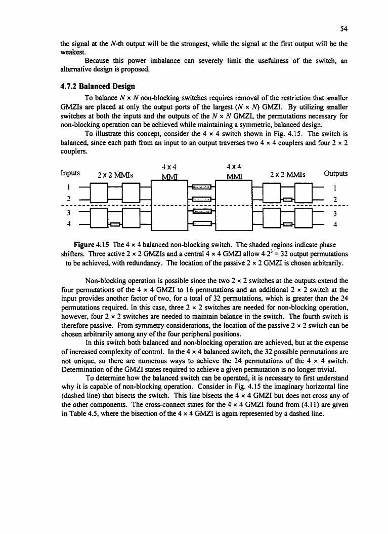
the signal at the N-th output will be the strongest, while the signal at the first output will be the weakest,
Because this power imbalance can severely limit the usefirlness of the switch, an alternative design is proposed.
4.7.2 Balanced Design To balance N x N non-blocking switches requires removal of the restriction that mialler
GMZIs are placed at only the output ports of the largest (N x N) GMZI. By utilizing smaller switches at both the inputs and the outputs of the N x N GMZI, the permutations necessary for non-blocking operation can be achieved while maintaining a symmetric, balanced design.
To illustrate this concept, consider the 4 x 4 switch shown in Fig. 4.1 5. The switch is balanced, since each path From an input to an output traverses two 4 x 4 couplers and four 2 x 2 couplers.
Figure 4.15 The 4 x 4 balanced non-blocking switch. The shaded regions indicate phase shifiers. Three active 2 x 2 GMZIs and a central 4 x 4 GMZI allow 4-z3 = 32 output permutations
to be achirved, with redundancy. The location of the passive 2 x 2 GMZI is chosen arbitrarily.
Non-blocking operation is possible since the two 2 x 2 switches at the outputs extend the four permutations of the 4 x 4 GMZI to 16 permutations and an additional 2 x 2 switch at the input provides another factor of two, for a total of 32 permutations, which is greater than the 24 permutations required. In this case, three 2 x 2 switches are needed for non-blocking operation, however, four 2 x 2 switches are needed to maintain balance in the switch. The fourth switch is therefore passive. From symmetry considerations, the location of the passive 2 x 2 switch can be chosen arbitrarily arnong any of the four peripheral positions.
In this switch both balanced and non-blocking operation are achieved, but at the expense of increased complexity of control. In the 4 x 4 balanced switch, the 32 possible permutations are not unique, so there are numerous ways to achieve the 24 permutations of the 4 x 4 switch. Determination of the G M P states required to achieve a given permutation is no longer trivial.
To determine how the balanced switch can be operated, it is necessary to first understand why it is capabk of non-blocking operation. Consider in Fig. 4.15 the imaginary horizontal line (dashed line) that bisects the switch. This line bisects the 4 x 4 GMZI but does not cross any of the other components. The cross-connect states for the 4 x 4 GMZI found fiom (4.1 1) are given in Table 4.5, where the bisection of the 4 x 4 GMZI is again represented by a dashed line.

Table 4.5 The cross-connect states ( i , k) for the 4 x 4 GMZI, where each state corresponds to a single column. The set of al1 possible crossovers of the inputs i from one side of the bisection line (dashed line) to the outputs k on the other side is obtained within the four GMZI states.
For non-blocking operation, the switch must be capable of cross-connecting every possible number of inputs Eom the top half of the switch to the bottom half, and vice-versa. This is because the 4 x 4 GMZI is the only region in the switch where inputs into the top half of the switch can be cross-connected to the bottom half, and vice-versa. The 2 x 3 switches are confined to the top or bottom half of the device, and therefore cannot perfonn this b'crossover" function. In this example, the GMZI must be capable of 0,1, and 2 crossovers of inputs from the top half to outputs in the bottom half, and vice-versa. Frorn the 1st row in Table 4.5 it is seen that the four states of the GMZI provide this full set of crossovers. This property of the GMZl results in the non-blocking operation of the balanced switch.
To operate the switch in Fig. 4.15, the required number of crossovers is determined and the 4 x 4 GMZI is set to the corresponding state in Table 4.5. The 2 x 2 GMns are then set in either the bar or cross state to achieve the desired permutation. In this manner an operation table for the 4 x 4 switch is derived. This is show in Table 4.6.
Now returning our attention for a moment to the bottom row of Table 4.5, it is seen that another design is possible. Note that one of the four GMZl states is redundant, in that it results in the same number of crossoven as another state. We may therefore choose either of these states, and operate the 4 x 4 GMZl with only three states. The efficiency of this approach, however, is obtained at the rxpense of operating the peripheral switches. Because we no longer have the flexibility of al1 four possible 4 x 4 GMZI states, al1 four 2 x 2 GMZIs must now be capable cf active operation.
Design of larger balanced non-blocking switches follows in a similar manner. A bisection line is first drawn through the N x N GMZI. The cross-connect capability of the GMZI ensures that every possible number of crossovers is achievable within the N states. The N x N balanced non-blocking switch is then formed by simply connecting the ports on both sides of the bisection line to N/2 x N/2 non-blocking switches.
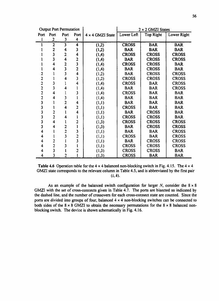
Output Port Permutation Port Port Port Port
1 2 3 4 4 x 4 GMZI State
56
2 x 2 GMZI States --
Lower Lefl
CROSS BAR
CROSS BAR
CROSS BAR BAR
CROSS CROSS
BAR CROSS
BAR BAR
CROSS BAR CROSS CROSS
BAR BAR
CROSS BAR
CROSS CROSS CROSS
Top Right
BAR BAR
CROSS CROSS CROSS CROSS CROSS CROSS
BAR BAR BAR BAR BAR BAR
CROSS CROSS CROSS CROSS
BAR BAR
CROSS CROSS CROSS
BAR
Lower Right
BAR BAR
CROSS CROSS
BAR BAR
CROSS CROSS CROSS CROSS
BAR BAR BAR BAR BAR BAR
CROSS CROSS CROSS CROSS CROSS CROSS
BAR BAR
Table 46 Operation table for the 4 x 4 balanced non-blocking switch in Fig. 4.15. The 4 x 4 GMZI state corresponds to the relevant column in Table 4.5, and is abbreviated by the first pair
u 9 k).
As an example of the balanced switch configuration for larger N, consider the 8 x 8 GMZI with the set of cross-connects given in Table 4.7. The ports are bisected as indicated by the dashed line, and the number of crossovers for each cross-connect state are counted. Since the ports are divided into groups of four, baIanced 4 x 4 non-blocking switches cm be connected to both sides of the 8 x 8 GMZI to obtain the necessary permutations for the 8 x 8 balanced non- blocking switch. The device is shown schematically in Fig. 3.16.
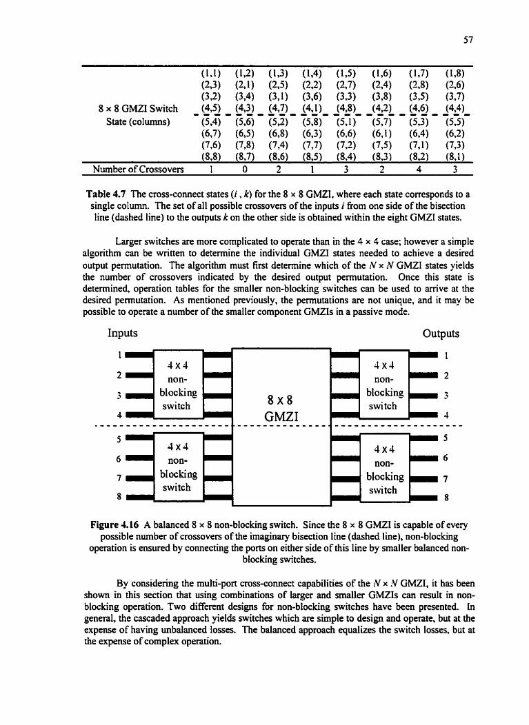
Table 4.7 The cross-connect states ( i , k) for the 8 x 8 GMZI, where each state corresponds to a single column. The set of al1 possible crossovea of the inputs i fiom one side of the bisection line (dashed line) to the outputs k on the other side is obtained within the eight GMZI states.
Larger switches are more complicated to operate than in the 4 x 4 case; however a simple algonthm can be written to determine the individual GMZI states needed to achieve a desired output permutation. The algorithm rnust first detennine which of the N x N GMZI states yields the nwnber of crossovers indicated by the desired output permutation. Once this state is determined operation tables for the smaller non-blocking switches cm be used to arrive at the desired permutation. As mentioned previously, the permutations are not unique, and it may be possible to operate a number of. the smaller component GMZls in a passive mode.
Inputs Outputs
1-- 4 x 4 - non-
; - blocking - switch
4-
blocking switch
8
non- 6
Figure 4.16 A balanced 8 x 8 non-blocking switch. Since the 8 x 8 GMZI is capable ofevery possible number of crossovers of the imaginary bisection line (dashed line), non-blocking
operation is ensured by connecting the ports on either side of this Iine by smaller balanced non- biocking switches.
By considering the multi-port cross-connect capabilities of the N x N GMZI, it has been shown in this section that using combinations of larger and mialler GMZIs can result in non- blocking operation. Two different designs for non-blocking switches have been presented. In generaI, the cascaded approach yields switches which are simple to design and operate, but at the expense of having unbalanced losses. The balanced approach equalizes the switch losses, but at the expense of complex operation.

The concepts discussed in this section are generally applicable, independent of a particular waveguide or material technology and device design. In real devices, however, these factors will play a critical role in determining the ultimate performance of the non-blocking switches. It has been shown in Section 4.3 that non-idealities cm severely limit the crosstalk attainable in a GMZI switch. It is therefore expected that when multiple GMZIs are use& the tolerances to parameter fluctuations are even more stringent. This is investigated M e r in the following section.
4-73 Toleraace analysis of a balanced non-blocking switch To realize GMZI switches with good crosstalk pe~ormance and low optical losses, it is
essential that the constituent MMI couplen impart accurate power splitting ratios and phases to the self-images. In this section the effects of M M coupler imbalance and phase deviations are quantified, enabling a tolerance analysis of a 4 x 4 balanced non-blocking switch to be made.
The balanced 4 x 4 non-blocking switch show in Fig. 4.15 is comprised of 2 x 2 and 4 x 4 GMZIs, each with a characteristic loss and crosstalk which is a hct ion of the imbalance and phase deviation present in the MM1 couplers. These effects arise from imperfect imaging in the coupler, which can occur when the fabncated length of the coupler differs from the designed value. It was shown in Chapter 3 that the length of an MM1 coupler is proportional to the square of its width, so it is therefore critical to control the coupler width during the fabrication process
The performance of 2 x 2 and 4 x 4 GMZIs for various deviations of the MMI coupler length has been simulated using MPA. While the analytic expression (3.32) can be used to fi nd the crosstalk the MPA approach has been chosen since it can also be used to determine excess losses. The details of the waveguide design used in the analysis will be given in the next chapter. The resulting worst-case channel loss and crosstalk values are given in Table 4.8, along with values for the 4 x 4 non-blocking switch, calculated by noting that each path through the switch traverses two 2 x 2 GMZIs and a 4 x 4 GMZI.
Table 4.8 Tolerance analysis for the component GMZIs and the aggregate 1 x 4 balanced non- blocking switch in Fig. 4.15, calculated using the MPA technique.
MM1 Coupler Length
Deviation
S L = O p n SL=+Spm s L = k l O ~ m
With the waveguide design chosen, the non-blocking switch is limited to a loss of 4 dB and a crosstalk Ievel of -20 dB, even with optimum coupler lengths. This is the result of a mal1 irnbalance and phase deviation present even at the optimum coupler length, due to the finite number of modes asailable for imaging in the multirnode region. Whrn the imaging in the couplers degrades, the l o s and crosstalk both increase. The situation becomes worse for Iarger switches, because the region of acceptable M M coupler length deviation for a given excess loss and crosstalk shrinks as N inmases, placing strîcter requirements on the fabrication technology [31]. To reaIize non-blocking switches with good performance, it is therefore hperative that MMI couplers with precise imaging and Iow excess losses are used.
2 x 2 GMZI
Channel Loss (dB)
0.90 0.96 1 .O4
Crosstalk (a) -26.8 -23.9 - 1 7.4
4 x 4 GMZI
Channel Loss (ds)
-2.19 -2.22 -2.43
4 x 4 balanced non- blocking switch
Crosstalk (dB) -22.0 -19.3 -13.3
Chamel Loss (dB)
3.99 4.14 4.5 1
Crosstalk (dB) -19.8 - 17.0 - 10.8

Chapter 5
Device Design
The theory of self-imaging in rnultimode waveguides and variable-ratio power splitting and srvitching in the GM27 have been presented in previous chapters. To verifi this theory and dernonstrate the practical feusibility of uchieving the predicted device jùnctions. a mrnber of prototype devices have been designed. This chapter describes the device design and modeling perjiormed ut the Telecomrnunicotions Research Laboratories in Edmonton, Alberta. which eulminoted in the developmenr of a photomask f iom which the devices con be fabricated. Portions of this chapter have been reported in Photonics Technology Leîters [35]; and in a paper presented at the International Conference on the Applications of Photonic Technology (ICAPT '98), in Ottawa, Canada [603.
5.1 Introduction To verifj the theoretical rsults developed in the earlier chapters, it is necessary for the
GMZI to be designed and fabricated. Perhaps the most important determinant of the performance of an integrated optical device, and a necessary prerequisite for its design, is the choice of material system From which it is to be fabricated. From the growing number of technology possibilities in which to realize integrated optical devices, a silica-based waveguide system has been chosen, for reasons which will be discussed in this chapter.
A strongIy guiding rib waveguide design has been used, and a number of stnictures such as single mode waveguides, 2 x 2 and 4 x 4 MM1 couplen, and 2 x 2 and 4 x 4 GMZls have been designed. The design requirements of these devices, the motivation for various choices and tradeoffs, the final design parameters chosen, and simulations of the device performance are desmbed in this chapter. This work serves the basis for the development of a photomask, which is used to speci@ the device designs during the fabrication process. The fabrication of the integrated devices is the subject of the next chapter.
5.2 Choice of technology Since the idea of integrated optics was first proposed in 1969 [6], extensive research has
been perfonned on a varie@ of optical matenals such as semiconductors, lithium niobate, silica- based glasses, and polymers, and to date much discussion exists over which system is the most suitable for integrated optical switching components. Each material system has its own advantages and drawbacks.
Semiconductors typically have a high rehctive index, aIlowing ultra-compact devices to be made. Large-scale single-wafer integration of semiconductor switches with sources, detectors, and optical amplifiers is also possible. Furthemore, through the carrier-induced electro-optic effect, very fast active operation is achieved using a relatively low electrical power [61]. The drawbacks of semiconductor devices include high couplhg losses to optical fiber, high material absorption losses, an expensive and cornplex material processing technology, and problems with reproducibility, Iong-term stability, and reliability [ t O].
Lithium niobate (Lm@) exhibits iower Iosses than semiconductors, has very good eIectr0i)ptic properties resulting in low power switching, has a very fast dynamic response, and exhibits useful nonlinear properties [8]; however the materials and processes involved make device fabrication dificult, the device size tends to be large, device stability and reliability are low, and coupling losses to optical fiber are stiH relatively hi& [10].
SiIica-based waveguide technology is a promising alternative for integrated optical devices. Silica (SiO?) is widely available, relatively inexpensive, has a very low transmission

los, low Fiber coupling loss, low polarization sensitivity , a simple and flexible fabrication technology, and a high stability and reproducibility (91, [10], [22]. Drawbacks of silica-based materials are larger device sizes compared with semiconductors, and active devices which are operated using the themiooptic effect, which is weak in silica-based materials and results in relatively low-speed and high-power switching [SI.
Polymer-based waveguide technology has been gaining considerable interest in recent years, due to the ease of fabrication (polymer layers cm be spin-coated), lower power active switching compared with silica, and good coupling to standard single mode fibers [62]. The drawbacks are the high material losses in polymers compared with silica-based glasses, a large thermal expansion cMcient , and the unproven long-tem stability and reliability of these materials.
In the present work, a very high switching speed is not required, because the reconfiguration function for optical networks will generaily occur on a time scale of milliseconds [oz]. Instead, achieving low-toss, low-power, polarization-insensitive operation for the given technology are more important, so the integrated optical devices will be fabricated in a silica- based system. Furthermore the device processing technotogy is well-developed and understood, and devices can be fabricated in a relatively straightforward manner [63].
5.3 Waveguide Design
53.1 Design requirements lntegrated optical switches and power splitters to be used within an optical fiber network
must satisfy rigorous loss, polarization, power, and functional requirements. To rneet each of these demands a number of choices and tradeoffs must be made, resulting in an optimum waveguide design for a given application. Each of these requirements will be discussed.
Since planar optical waveguide propagation tosses typically exceed the losses in an optical fiber by a factor of IO' or greater, it is imperative that integrated devices are kept small. Recall From Chapter 2 that waveguides with a large core-cladding rehctive index contrast support a larger number of modes for a given width. Small single mode and multimode waveguides can therefore be produced if the refractive index con- is large. Furthermore, it will be shown that integrated optical devices typically require waveguide bends; a high index contrat allows compact, low-Ioss ben& to be designed.
Integrated optical devices such as power splitters and switches are typically connected to optical fibers at both the input and output. The input light from a mer typically has an unknown state of polarization, so an integrated device must operate independent of polarization to rninimize polarization-dependent loss and response charactenstics. Effects such as waveguide eeornetry, core and cladding rehctive indices, and intrinsic material properties determine the C
degree of polarization dependence in a waveguide. These parameters must therefore be optimized in the waveguide design.
Active integrated components should be operable using low power levels, to minimize the cost of operation and the total power dissipation on a wafer, and to reduce the overall size of a packaged device. The choice of a siIica-based technology rules out the possibility of active control through the electro-optic or magneto-optic effects, because the strength of these effects is very low in silica-based materiais [43]. The thenno-optic effect in silica, however, is moderate, so this is the method chosen for active device operation in this work. The thermo-optic effect uses heat to change the optical properties of a waveguide, so a good waveguide design must direct heat 80w and confine it to desired locations in order to maximize speed while minimizing power consumption IeveIs.
Since the devices to be realized are based upon mulhode interference effects, a waveguide design which results in good imaging behavior in MMI couplers must be used in order

to minimize excess losses and phase deviations. Recall fiom Chapter 2 that the resolution of self- images in the MMI coupler increases as the number of modes in the coupler increases. This indicates that a hi& rehctive index contrast should be used to maximize the number of modes available for imaging. Furthemore, it has been show in Chapten 3 and 4 that in order to fabncate devices with acceptable performance levels, it is essential that the theoretical relations for the MMI coupler imaging length and the phases of the images are satisfied. Since these relations have been derived based upon the approximation of sinusoidal field distributions given by (2.20), it is essential that this approximation is accurate. A large rehctive index contrast is therefore required to ensure that the strongly-guiding approximation is valid in the multimode region.
The requirements described above are nurnerous and sometimes conflicting. For example, a metal heater is typically used for themo-optic devices and must be located suficiently far fiom the optical field to prevent interaction with the optical field which wiI1 lead to attenuation of the light by the metal. If the heater is far kom the optical field, however, the waveguide heating is inefficient and the heat can potentially spread to unwanted regions. This conflict will be addressed in Section 5.3.4.
Another example is the design of polarization-independent MMI-based devices. Devices such as the GMZI rely upon selFimaging in MM1 couplen and propagation in single-mode waveguide ams. If a polarization-independent single-mode waveguide is designed, then the MM1 couplers will be polarization dependent since their geometry differs from that of the single- mode waveguide. Conversely, if polarization-independent MM1 couplers are designed, the single-mode waveguides will exhibit polarization-dependent behavior. To resolve this issue while maintaining a simple waveguide design, a tradeoff must be made. In this work, a polarization-independent single-mode waveguide design is chosen because the polarization dependence in MM1 couplen is typically low [9], and the light in the devices propagates for only a short distance in the couplen (hundreds of pm), while the propagation distance in single-mode waveguides is much longer (mm to cm). Moreover, in a waveguide with a high rehctive index contrast, the light is strongly confined within the core region, allowing adjacent single-mode waveguides to be located in close proximity with negligible coupling between them. This results in MM1 couplen which cm be designed with closely-spaced input and output waveguides, thus minimizing the width and length of the couplers and in so doing improving their polarization behavior,
As a final example illustrating conflicting design requirements. consider al1 the benefits of srnal; devices with a high refiactive index contrast described above. In contrast to this, an optical fiber has a low rehctive index contrast and dimensions that are typically larger than those of ptanar single-mode waveguides. Since low-loss fiber-to-chip coupling requires rnatching the size and shape of the mode in a single-mode optical fiber to the waveguide mode, large mode- mismatch losses will occur at fiber-waveguide interfaces. To overcome this probiern a number of methods are avaiIabIe, such as increasing the waveguide mode size through adiabatic waveguide tapers in one or two dimensions [64], [65], using complex configurations of partially segmented waveguides [66], or using special fiben with reduced mode sizes [67]. In this work, the latter approach is chosen for its simplicity; however, in principle, other methods can be applied to the designs developed here.
53.2 Choice of material system To achieve the confinement and waveguiding of light, regions of differing rehctive
indices are needed Control over the rehctive index in SiOz is typically achieved by doping with a mal1 arnount of phosphorus, germanium, or titaniurn; however, the rehctive index connast attainable by these methods is typically very low [a, [68], [69]. As a result, silica-based devices tend to have a reIativeIy large size and exhibit weak optical cofinement.
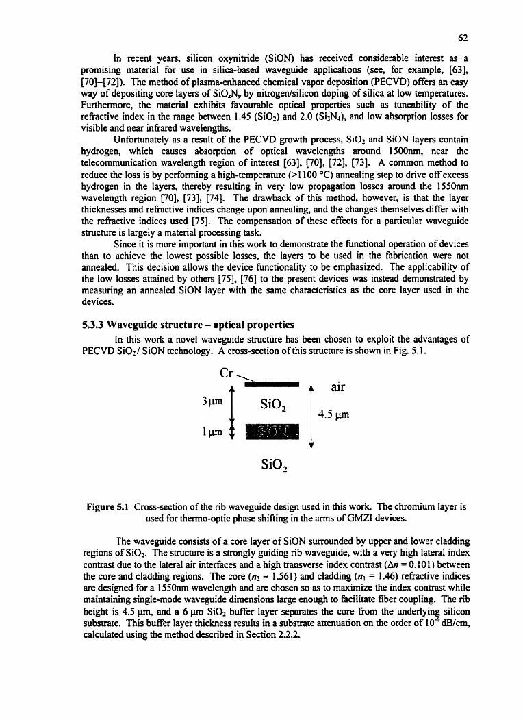
In recent years, silicon oxynitride (SiON) has received considerable interest as a promising matenal for use in silica-based waveguide applications (see, for example, [63], [70]-[72]). The method of plasma-enhanced chernical vapor deposition (PECVD) offers an easy way of depositing core layers of SiO& by nitrogentsilicon doping of silica at low temperatmes. Furthemore, the material exhibits favourable optical properties such as tuneability of the refractive index in the range between 1.45 (Si09 and 2.0 (Si3&), and low absorption losses for visible and near infrared wavelengths.
Unfortunately as a result of the PECVD growth process, SiOZ and SON layers contain hydrogen, which causes absorption of optical wavelengths around ISOOnm, near the telecommunication wavelength region of interest [63], [70], [72], [73]. A common method to reduce the loss is by performing a hi&-temperature (>II00 O C ) annealing step to drive off excess hydrogen in the layea, thereby resulting in very low propagation losses around the 1550nm wavelength region 1701, [73], [74]. The drawback of this method, however, is that the layer thicknesses and refractive indices change upon annealing, and the changes themselves differ with the refractive indices used [75]. The compensation of these effects for a particular waveguide structure is largely a material processing task.
Since it is more important in this work to demonstrate the functional operation of devices than to achieve the Iowest possible losses, the layers to be used in the fabrication were not annealed. This decision allows the device functionality to be emphasized. The applicability of the low losses attained by others (751, [76] to the present devices was instead demonstrated by meauring an annealed SiON layer with the sarne characteristics as the core layer used in the devices.
5.3.3 Waveguide structure - optical properties in this work a novel waveguide structure has been chosen to exploit the advantages of
PECM SiOr/ SiON technology. A cross-section of this structure is show in Fig. 5.1.
air
4.5 pn
SiO,
Figure 5.1 Cross-section of the rib waveguide design used in this work. The chromium layer is used for thermo-optic phase shifiing in the arms of GMZI devices.
The waveguide consists of a core layer of SiON surrounded by upper and Iower cladding regions of SiO?. The structure is a strongly guiding rib waveguide, with a very high lateral index contrast due to the lateral air interfaces and a high transverse index c o n m (An = 0.10 1 ) bctween the core and cladding regions. The core (nZ = 1.561) and cladding (nl = 1.46) refractive indices are designed for a 1550nm wavelength and are chosen so as to maximize the index conaast while maintainhg singlemode waveguide dimensions large enough to facilitate fiber coupling. The nb height is 4.5 pm, and a 6 pm SiOz b e e r layer separates the core fiom the underlying silicon substrate. This buffer layer thickness results in a substrate attenuation on the order of 1 O* dB/crn, calculated using the method described in Section 2.2.2.
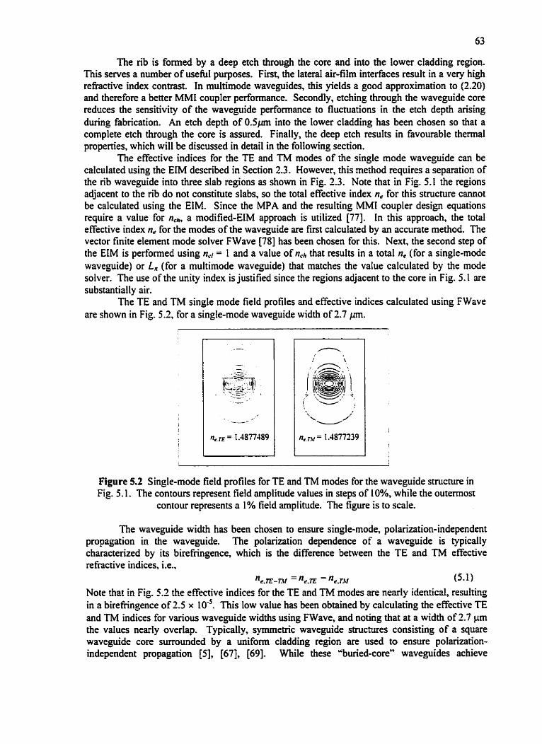
The rib is formed by a deep etch through the core and into the lower cladding region. This serves a number of usehl purposes. First, the lated air-film interfaces result in a very hi& refkactive index contrast. In multirnode waveguides, this yields a good approximation to (2.20) and thecefore a better MM1 coupler performance. Secondly, etching through the waveguide core reduces the sensitivity of the waveguide performance to fluctuations in the etch depth arising during fabrication. An etch depth of 0 . 5 ~ into the lower cladding has been chosen so that a complete etch through the core is assured. Finally, the deep etch results in favourable thermal properties, which will be discwed in detail in the following section.
The effective indices for the TE and TM modes of the single mode waveguide cari be calculated using the EiM described in Section 2.3. However, this method requires a separation of the rib waveguide into three slab regions as shown in Fig. 2.3. Note that in Fig. 5.1 the regions adjacent to the rib do not constitute slabs, so the total effective index ne for this structure cannot be calculated using the EIM. Since the MPA and the resulting MMI coupler design equations require a value for n,h, a modified-EIM approach is utilized [77]. In this approach, the total effective index ne for the modes of the waveguide are first calculated by an accurate method. The vector finite element mode solver FWave 1781 has been chosen for this. Next, the second step of the EIM is perfomed using nd = 1 and a value of nch that results in a total ne (for a single-mode waveguide) or L, (for a multimode waveguide) that matches the value calculated by the mode solver. The use of the unity index is justified since the regions adjacent to the core in Fig. 5.1 are substantially air.
The TE and TM single mode field profiles and effective indices calculated using FWave are shown in Fig. 5.2, for a single-mode waveguide width of 2.7 p.
Figure 5.2 Single-mode field profiles for TE and TM modes for the waveguide structure in Fig. 5.1. The contours represent fieid amplitude values in steps of 1 O%, while the outermost
contour represents a 1% field amplitude. The figure is to scale.
The waveguide width has been chosen to ensure single-mode, polarization-independent propagation in the waveguide. The polarization dependence of a waveguide is typically characterized by its birefnngence, which is the difference between the TE and TM effective rehctive indices, i.e.,
- ne.TE-TM - n r . ~ ~ - ne.TM (5.1)
Note that in Fig. 5.2 the effective indices for the TE and TM modes are nearly identical, resulting in a birefringence of 2.5 x 10". This Iow value has been obtained by calculating the effective TE and TM indices for various waveguide widths using FWave, and noting that at a width of 2.7 pm the values nearly overlap. Typically, symmetric waveguide structures consisting of a square waveguide core surrounded by a unifonn cladding region are used to ensure polarization- independent propagation [5], [67], [69]. While these b'bwied-coce" waveguides achieve

polarkation independence through symmetry in their geometry, the design in Fig. 5.1 uses a combination of geometry, etching, and refractive index contrast to achieve the same effect. Furthemore, as will be discussed in the following section, the present geometry has more favourabIe thermal properties than the buried-core structure.
The upper SiOZ cladding layer thickness in Fig. 5.1 is 3 pm. This value has been chosen for two reasons. First, the relatively thick top cladding serves to balance the thick lower cladding, maintaining symmetry in the waveguide. The result is that the mode fields shown in Fig. 5.2 are nearly circular in the rib, which will mult in lower coupling losses between the waveguide mode and the circular mode field of an optical fiber. Secondly, the thick top cladding serves to erectively isolate the waveguide mode from the chromium metal region used for active thermo- optic device control. This will be discwed further in the following section.
53.4 Waveguide structure - thermal properties In the GMZI devices described in Chaptea 3 and 4, the intensity in an output port is a
huiction of the phase shifts applied to the Iight in the waveguide arms. In silica-based waveguides, this phase shifiing is most eficiently achieved by the thermo-optic effect, wherein the phase of a mode in a waveguide arm is controlled by means of a temperature change in that arm.
SiO2 and SiON are thermo-optic materials, which means that the rehctive index is a function of the temperature of the material. The strength of this dependence is gauged by the magnitude of the thermo-optic coefficient a, which measures the change in refractive index in a material for a unit temperature change,
A change in rehctive index, following the discussion in Chapter 2, modifies the effective index of the mode in the waveguide. From (2.12), it is seen that this results in a modified propagation constant AS. Since the phase <p = P z in (2.2). the resulting phase shifi is given by
where L, is the propagation length in the region of modified temperature. The phase shift in (5.3) contains twuo tems: the first is a change in propagation constant due to the thermo-optic effect, and the second is a change in the physical length of the waveguide due to thermal expansion. Since the thermal expansion coefficient for silica is very low for moderate temperature increases [5], the second tenn in (5.3) may be ignoreci, while the fint term may be expanded to yield
where A is the wavelength and AT is the temperature increase in the waveguide. Using the generally accepted value of a = 1 x IO-^ O C' For SiO2 and SiON [SI, [71], [79], and a A = 1550 nm in (5.4), a phase shifi of R is expected for temperature increases of AT = 38.8 O C and 25.8 O C
in heater lengths of L, = 2 mm and L, = 3 mm, respectively. Ln Fig. 5.1 a 200 nm thick chrornium layer is situated on top of the nb to serve as a
thermooptic heating element in the waveguide arms of the GMZI. The ends of the heater are comected to electrodes and a voltage is supplied to induce an electrical current to flow through the chromium. The heater is thus a resistor that dissipates heat by ; ~ 1 m u n t proportional to the square of the current flowing through it, or by an amount linearly proportional to the electrical power applied.
Since the effective index of the waveguide mode must be altered to induce a phase shifl, the temperature in the region where the mode is guided m u t be increased. From Fig. 5.2, this corresponds to the waveguide core region and the immediately adjacent claddmg regiow. This
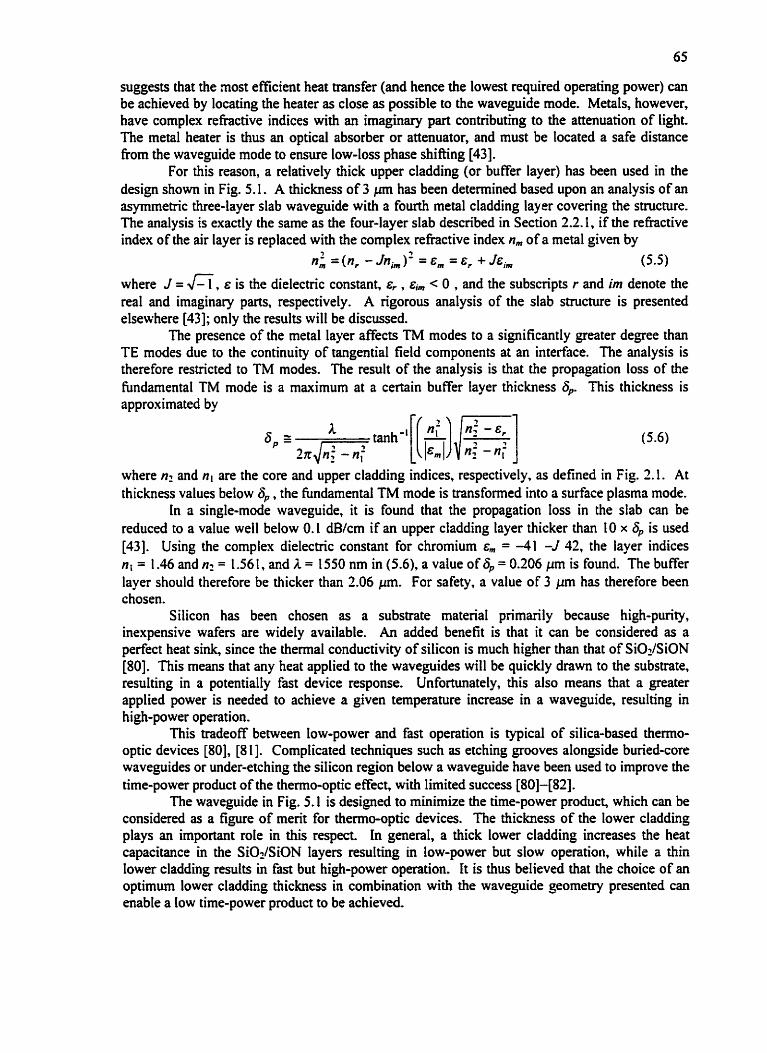
suggests that the most efficient heat transfer (and hence the lowest required operating power) can be achieved by locating the heater as close as possible to the waveguide mode. Metals, however, have complex refiactive indices widi an imaginary part contributing to the atîenuation of light. The metal heater is thus an optical absorber or attenuator, and must be Iocated a safe distance fkom the waveguide mode to ensure low-loss phase shifting 1431.
For this reason, a relatively thick upper cladding (or buffer layer) has been used in the design shown in Fig. 5.1. A thickness of 3 pn has been deterrnined based upon an analysis of an asymmetric three-layer slab waveguide with a fourth metal cladding layer covering the structure. The analysis is exactly the same as the four-layer slab descriied in Section 2.2.1, if the refractive index of the air layer is replaced with the complex refractive index n,,, of a metal given by
n i = (n, - ~n, ) ' = E,,, = E, + Jgi,,, (5 .5) where J = f i , E is the dielectnc constant, E, , E,,,, < O , and the subscripts r and im denote the real and imaginary parts, respectively. A rigomus analysis of the slab structure is presented elsewhere [43]; only the results will be discussed.
The presence of the metal layer affects TM modes to a significantly greater degree than TE modes due to the continuity of tangential field components at an interface. The analysis is therefore restricted to TM modes. The result of the analysis is that the propagation loss of the fundamental TM mode is a maximum at a certain buffer layer thickness 6,. This thickness is approximated by
where a and nl are the core and upper cladding indices, respectively, as defined in Fig. 2.1. At thickness values below 6'. the Fundamental TM mode is transformed into a surface plasma mode.
In a single-mode waveguide, it is found that the propagation loss in the slab can be reduced to a value well below 0.1 dBkm if an upper cladding layer thicker than 10 x 6' is used [43]. Using the cornpiex dielectric constant for chromium E,,, = -41 -J 42, the layer indices ni = 1.46 and n2 = 1.56 1, and A. = 1550 nm in (5.6), a value of 6' = 0.206 pm is found. The buffer layer should therefore be thicker than 2.06 prn. For safety, a value of 3 pm has therefore been chosen.
Silicon has been chosen as a substrate materia1 primarily because high-purity, inexpensive wafers are widely available. An added benefit is that it can be considered as a perfect heat sink, since the thermal conductivity of silicon is much higher than that of Si02/SiON [80]. This rneans that any heat applied to the waveguides will be quickly drawn to the substrate, resulting in a potentially fast device response. Unfortunately, this also means that a greater applied power is needed to achieve a given temperature increase in a waveguide, resulting in hi&-power operation.
This tradeoff between low-power and fast operation is typical of silica-based thermo- optic devices [go], [8 11. Complicated techniques such as etching grooves alongside bwied-core waveguides or under-etching the silicon region below a waveguide have been used to improve the time-power product of the thermo-optic effect, with Iimited success [go]-1821.
The waveguide in Fig. 5.1 is designed to minimize the time-power product, which cm be considered as a figure of merit for thenno-optic devices. The thickness of the Iower cladding plays an important mle in this respect. In general, a thick lower cladding increases the heat capacitance in the Si02/SiON Iayers cesulting in low-power but siow operation, while a thin lower cladding results in fast but high-power operation. It is thus believed that the choice of an optimum lower cladding thickness in combination with the waveguide geometry presented can enabte a low time-power product to be achieved.
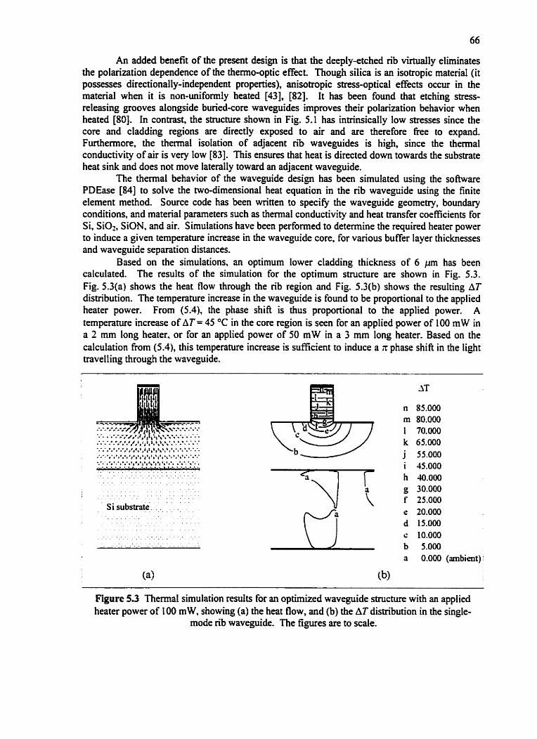
An added beneft of the present design is that the deeply-etched n i virtuaily eliminates the polarization dependence of the thermo-optic effect. Though silica is an isotropie material (it possesses directionally-independent properties), anisotropic stnss-optical effects occur in the material when it is non-uniformly heated [43], [82]. It has been found that etching stress- releasing grooves alongside buned-core waveguides improves their polarization behavior when heated [go]. In contrast, the structure show in Fig. 5.1 has intrinsically Iow stresses since the core and cladding regions are directly exposed to air and are therefore lkee to expand. Fwthennore, the thermal isolation of adjacent n i waveguides is high, since the thermal conductivity of air is very Iow [83]. This ensures that heat is directed down towards the substrate heat sink and does not move laterally toward an adjacent waveguide.
The thermal behavior of the waveguide design has been simulated using the software PDEase [84] to solve the two-dimensional heat equation in the rib waveguide using the finite element method Source code has been written to speciQ the waveguide geometry, boundary conditions, and matenal parameten such as thermal conductivity and heat transfer coefficients for Si, Si02, SiON. and air. Simulations have been perfonned to detemine the required heater power to induce a given temperature increase in the waveguide core, for various buffer layer thicknesses and waveguide separation distances.
Based on the simulations, an optimum lower cladding thickness of 6 Fm has been calculated. The results of the simulation for the optimum structure are shown in Fig. 5.3. Fig. 5.3(a) shows the heat flow through the rib region and Fig. 5.3(b) shows the resulting AT distribution. The temperature increase in the waveguide is found to be proportional to the applied heater power. From (5.4). the phase shiR is thus proportional to the applied power. A temperature increase of AT = 45 O C in the core region is seen for an applied power of 100 rnW in a 2 mm long heater. or for an applied power of 50 m W in a 3 mm long heater. Based on the calculation from ( S A ) , this temperature increase is suficient to induce a ir phase shifi in the light travelling through the waveguide.
Figurc 5 3 Thermal simulation results for an optimized waveguide strucbrre with an applied heater power of 100 mW, showing (a) the heat flow, and (b) the AT distribution in the single-
mode n i waveguide. The figures are to scale.

The heat flow diagram in Fig. 5.3fa) uidicates that most of the heat is confined to the nb region and is quickly drawn d o m to the silicon substrate which has a high thermal conductivity and acts as a heat sink. Since adjacent ribs are separated by air, the lateral heat dissipation is small and therefore large temperature gradients can be maintained over small lateral distances.
The temperature distribution in the rib waveguide in Fig. 5.3(b) indicates that the ambient temperature is maintained at a lateral distance of < 10 p fiom the rib. This absence of lateral hear conduction allows adjacent rib waveguides to be placed in close proximity, with a negligible temperature increase in an unheated waveguide. This allows for the design of compact active devices.
5.4 MMI coupler design
5.4.1 MMI coupler dimensions The optimum imaging length of an MM1 coupler m u t satisS the relation given in (2.25).
The coupler length is a hc t ion of the beat length of the two lowest order modes in the multimode region, which from (2.23) depends upon the propagation constants and hence the effective indices for these modes. The effective indices in tum, depend upon the waveguide geometry, and in particular the physical width W. Since the width of a multimode waveguide is larger than the width for polarkation-independent propagation shown in Fig. 5.2, polarization dependence among the TE and TM modes arises in the multimode region. This results in slightly different beat lengths and thus different imaging lengths for the two polarizations.
To minimize the polarization dependence, the coupler width must be kept as small as possible. The coupler should however, be wide enough to accommodate the N input and output single-mode (access) waveguides as show in Fig. 2.5, with a negligible power coupling between them. The choice of a suitable coupler width is therefore critical. The following design procedure has been used to determine the optimum coupler width.
First, FWave has been used to find the effective indices of the two lowest order TE and TM modes of the MM1 coupler, for various physical widths W. These are then used to End the beat length of the coupler for both polarizations, using (2.12) and (2.23). To minimize the polarkation-dependent coupler irnaging length requires the difference between these beat lengths, M x ,
= (Ln - ~ x . m 1 (5.7) to be minimized. Allowing a width to support at least N single-mode waveguides, optimum coupler widths of W = 8.0 pn and W = 16.0 p have been found for N = 2 and iV = 4, respectively. This results in minimized beat lmgth differences of AL, = 5.44 p (N = 2) and U, = 1 1.04 pm (N = 4). For short coupler lengths a value of M = 1 is chosen, so fiom (2.25), the polarization-dependent coupler imaging length variations are ALMIv = 8.16 p ((N= 2) and
= 8.28 pm (N = 4). These values represent the renilt of the tradeoff between polarization independence in the single-mode waveguides and in the MM1 couplers discussed earlier.
Next, the effective width W, is calculated fiom (2.13) for both TE and TM polarizations, and an average value is found. The waveguide positions are then calculated according to Fig. 2.5, using a k e parameter value of a = W, /2N so the waveguides are spaced as fat apart as possible. This results in an access waveguide spacing of 1.45 pn (N = 2) and 1.36 p (N = 4).
Finally, as mentioned earlier, the separation between adjacent access waveguides must be large enough to ensure negligiiie power coirpling between the waveguides. To ver@ this, FWave is used to find the two lowest order TE and TM effective indices of a system of two adjacent single-mode waveguides with the structure shown in Fig. 5.1, separated by a gap (in air) of 1.36 pm, as a worst case. The coupling length (or beat Iength), where the optical power in one waveguide is cornpletely trmsferred to the other waveguide, is found for both polarizations ushg
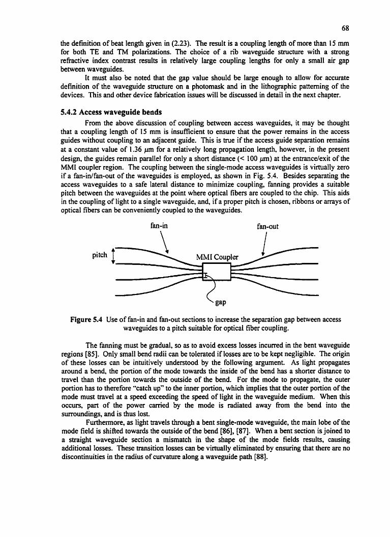
the definition of beat length given in (2.23). The result is a coupling Iength of more than 15 mm for both TE and TM polarizations. The choice of a ni waveguide structure with a strong rehctive index contrast results in relatively large coupling lengths for only a small air gap between waveguides.
It mut also be noted that the gap value should be large enough to allow for accurate definition of the waveguide structure on a photomask and in the lithographie patterning of the devices. This and other device fabrication issues will be discussed in detail in the next chapter.
5.4.2 Access waveguide bends From the above discussion of coupling between access waveguides, it may be thought
that a coupling Iength of 15 mm is insufficient to ensure that the power remains in the access guides without coupling to an adjacent guide. This is true if the access guide separation remains at a constant value of 1.36 pm for a relatively long propagation length. however, in the present design, the guides remain parallel for only a short distance (c 100 pm) at the entmnce/exit of the MMI coupler region. The coupling between the single-mode access waveguides is virtually zero if a fan-inIfan-out of the waveguides is mployed, as shown in Fig. 5.4. Besides separating the access waveguides to a safe lateral distance to minimize coupling, fanning provides a suitable pitch between the waveguides at the point where optical tibers are coupled to the chip. This aids in the coupling of light to a single waveguide, and, if a proper pitch is chosen, ribbons or arrays of optical fibers can be conveniently coupled to the waveguides.
fan-in fan-out
pitch
Figure 5.1 Use of fan-in and fan-out sections to increase the separation gap between access waveguides to a pitch suitable for optical fiber coupling.
The fanning m u t be gradual, so as to avoid excess losses incuned in the bent waveguide regions [85]. Only small bend radii can be tolerated if losses are to be kept negligible. The origin of these Iosses can be intuitively understood by the following argument, As light propagates around a bend the portion of the mode towards the inside of the bend has a shorter distance to travel than the portion towards the outside of the bend. For the mode to propagate, the outer portion has to therefore "catch up" to the imer portion, which irnplies that the outer portion of the mode must travel at a speed exceeding the speed of light in the waveguide medium. When this occurs, part of the power carried by the mode is radiated away fiom the bend into the surroundmgs, and is thus lost.
Furthemore, as light travels through a bent single-mode waveguide, the main lobe of the mode field is shifted towards the outside of the bend [86], [87]. When a bent section is joined to a straight waveguide section a mismatch in the shape of the mode fields resuits, causing additionai losses. These transition losses can be VKtUaily elirninated by ensuring that there are no discontinuities in the radius of curvature dong a waveguide path [88].
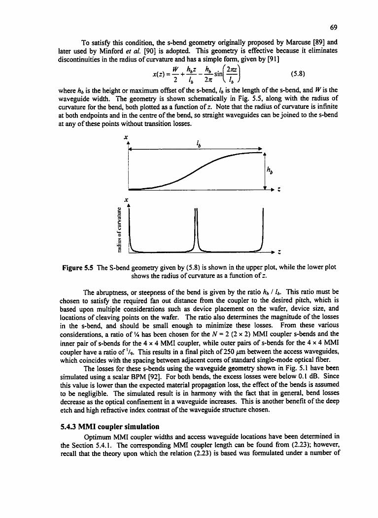
To satisfy this condition, the s-bend geometry originaily proposed by Marcuse [89] and later used by Minford et al. [go] is adopted. This geometry is effective because it elirninates discontinuities in the radius of curvatwe and has a simple form, given by [9 11
where hb is the height or maximum offset of the s-ben& lb is the iength of the s-bend, and W is the waveguide width. The geometry is shown schematically in Fig. 5.5, along with the radius of curvature for the ben& both plotted as a hnction of r Note that the radius of curvature is infinite at both endpoints and in the centre of the bend, so straight wavepides can be joined to the s-bend at any of these points without transition losses.
Figure 5.5 The S-bend geometry given by (5.8) is show in the upper plot, while the lower plot shows the radius of curvature as a function of z.
The abruptness, or steepness of the bend is given by the ratio h b / Ib. This ratio must be chosen to satisfy the required fan out distance kom the coupler to the desired pitch, which is based upon multiple considerations such as device placement on the wafer, device size, and locations of cleaving points on the wafer. The ratio also determines the magnitude of the losses in the s-bend, and should be small enough to rninimize these losses. From these various considerations, a ratio of l/l has bcen chosen for the N = 2 (2 x 2) MM1 coupler s-bends and the imer pair of s-ben& for the 4 x 4 MM1 coupler, while outer pairs of s-ben& for the 4 x 4 MMI coupler have a ratio of '/+ This results in a final pitch of 250 pm between the access waveguides, which coincides with the spacing between adjacent cores of standard single-mode optical fiber.
The Iosses for these s-ben& using the waveguide geometry shown in Fig. 5.1 have been simulated using a scalar BPM [92]. For both bends, the excess losses were below 0.1 dB. Since this value is lower than the expected material propagation los, the effect of the ben& is assumed to be negligible. The simulated result is in harmony with the fact that in general, bend losses decrease as the optical confinement in a waveguide increases. This is another benefit of the deep etch and hi& rehctive index contrast of the waveguide structure chosen.
5.4.3 MMI coupler simulation Optimum MMi coupler widths and access waveguide locations have been determined in
the Section 5.4.1. The corresponding MMI coupler length can be found h m (2.23); however, recall that the theory upon which the relation (223) is based was fomulated under a number of
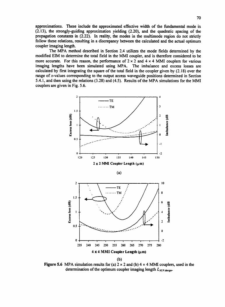
approximations. These include the approxirnated effective width of the fundamental mode in (2.13), the strongly-guiding approximation yielding (2.20), and the quadratic spacing of the propagation constants in (222). In reality, the modes in the multimode region do not strictly follow these relations, resulting in a discrepancy between the calculated and the actual optimum coupler imaging length.
The MPA method descnied in Section 2.4 utilizes the mode fields determined by the modified EiM to determine the total field in the MM1 coupler, and is therefore considered to be more accurate. For this reason, the performance of 2 x 2 and 4 x 4 MM1 couplers for various imaging lengths have been simulated using MPA. The imbalance and excess losses are calculated by frst integrating the square of the total field in the coupler given by (2.18) over the range of x-values correspondhg to the output access waveguide positions detennined in Section 5.4.1, and then using the relations (3.28) and (4.5). ResuIts of the MPA simulations for the MM1 coupIers are given in Fig. 5.6.
120 125 t30 135 140 145 150
2 x 2 h.likU Coupler Length (pm)
235 240 245 250 255 260 265 270 275 280
4 x 4 MM1 Coupler Lengtb (pm)
(b) Figure 5.6 MPA simulation results for (a) 2 x 2 and (b) 4 x 4 MM1 couplers, used in the
detemination of the optimum coupler imaging length

The polarization dependence in Fig. 5.6 manifests itself typically as a relative shifi in the curves. Note that the differences in optimum imaging length for the different polarizations are very close to the values of about 8 p predicted in Section 5.4.1.
From Fig. 5.6, it is ctear that there is no single optimum coupler length where excess loss, imbalance, and polarization dependence are minimized. Tradeoffs between the parametea must be made to arrive at a suitable imaging length. The final MMI coupler design lengths chosen are L.+li~duign = I3O p for the 2 x 2 MMI coupler and LJwnhiF = 253 pin for the 4 x 4 M M 1 coupler.
A summary of the design parameters for the MMi couplers, along with the excess losses and imbalances simulated using MPA, is given in Table. 5.1. The theoretical MM1 coupler lengths L , b t . ~ calculated using (2.23) are also given for cornparison. It is interesting to note that the MM1 coupler dimensions in Table 5.1 are actually smaller than MM1 couplers fabricated in high-contmt semiconductor waveguides [93], [94].
Parameter 2 x 2 MM1 coupler 4 x 4 MM1 coupler
1.36 16.0 16.3
338.35 (TE) 349.40 (TM)
1.45
U . r r . . v ( P ) L 56 .V daim (w)
L.tr..v (pm)
MPA Simulation Resul ts
Table 5.1 Design parametea and simulation results br the 2 x 2 and 4 x 4 MM1 couplen in this work.
Coupler width, W Effective width, W,
Beat Length, L,
Irnbalance (dB)
Excess loss (dB)
The total Iight intensity pattern in the 4 x 4 MM1 coupler calculated using MPA is shown in Fig. 5.7 for the TM polarization.
8.0 8.3
86.66 (TE) 92.1 1 (TM)
8.16 130.0
t 30.0 (TE) 138.2 (TM)
8.28 253 .O
253.8 (TE) 262.0 (TM)
O. 18 (TE) 0.32 (TM) 0.94 (TE) 0.90 (TM)
0.24 (TE) 0.40 (TM) 0.90 (TE) 0.83 (TM)
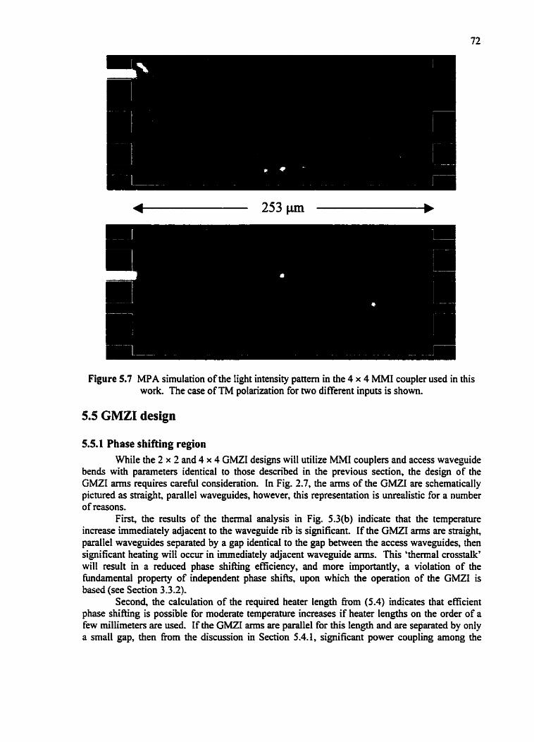
Figure 5.7 MPA simulation of the light intensity pattern in the 4 x 4 MM1 coupler used in this work. The case of TM polarization for two different inputs is shown.
5.5 GMZI design
5.5.1 Phase s hifting region While the 2 x 2 and 4 x 4 GMZI designs will utilize MI couplen and access waveguide
bends with pammetea identical to those described in the previous section, the design of the GMZI arms requires carefûl consideration. In Fig. 2.7, the arms of the GMZI are schematically pictured as straight, parallel waveguides, however, this representation is unrealistic for a number of reasons.
Fint, the results of the thermal analysis in Fig. 5.3(b) indicate that the temperature increase immediately adjacent to the waveguide ni is significant. If the GMZI amu are straight, paraIIel waveguides separated by a gap identicai to the gap between the access waveguides, then significant heating will occur in immediately adjacent waveguide arms. This 'thermal crosstalk' will result in a reduced phase shifting efficiency, and more importantly, a violation of the Fundamental property of independent phase shih, upon which the operation of the GMZI is based (see Section 3.3.2)-
Second, the calculation of the requtred heater lmgth nom (5.4) indicates that efficient phase shifting is possible for moderate temperature increases if heater lengths on the order of a few millimeters are used, If the GMZI arms are pardel for this length and are separated by only a small gap, then fiom the discussion in Section 5.4.1, significant power coupling among the

waveguides will occur. This violates the fundarnentd property of distinct self-images in the interferorneter anns.
Finally, if the waveguide arms are closely spaced for a distance of a few millimeters, the probability of fabrication errors occuning in this region is hi&. This is due to limitations in the resolution of the photolithographie and etching processes used to fom the waveguides. Examples of typicd fabrication errors for closely spaced parallel waveguides include:
1) a physical comection being formed (zero gap) at certain points along the waveguide length; 2) a shaIlow etch depth between the waveguides due to reduced visibility of the area between the
waveguides over a wide angular range; and 3) imperfect removal of chromiurn near the heater regions, resulting in "shorted-out" connections
between the waveguides.
These errors violate both fiindamental properties of the GMZI stated above. For these reasons, the GMZI arms m u t be separated by a sufficient lateral distance. The
most demanding critena to satisfy is the thermal isolation between waveguide ams; however, as indicated in Fig. 5.3(b), a separation of > 10 p effectively eliminates any thermal crosstalk. in the GMZI design to be used in this work a severely overestimated arm separation distance of d, = 250 pm is chosen to ensure that the waveguides are completely optically and thennally isolated,
As in the case of the access waveguides, this separation requires a fan-out and fan-in, and can only be achieved through the use of waveguide bends. In contrast to the access waveguides, however, the requirements for the waveguide m s are very strict. The waveguide arms must remain equal in length and in loss, so the ben& used must be identical. Furthemore, it is desirable to eliminate transition losses between the bent and straight waveguide sections. To satisS these requirements, the GMZI ami geometry shown in Fig. 5.8 is used.
......... Y.. ........... .,.. SJP hb /2 !
staight half s-bemd phare shifting haff s-bcnd '
section region region region .
Figure 5.8 Schematic diagram of two adjacent GMZI arms. The design is used to achieve a waveguide separation of d, in the phase-shifting region while eliminating transition losses,
equalizing total losses among the arms, and maintaining equal am lengths.
The arm design uses an s-bend described by (5.8) with a height-to-length ratio of 'A, but split in half to form two identical halfs-bend sections. Since the radius of curvature of the s-bend given by (5.8) is infinite at the centre, a natural transition into and out of the straight thermo-optic heater region occurs, thereby eliminating transition losses. The design also uses b&er sections of straight waveguides 50 pm in length to separate the haif s-bend from the MMI coupler and the phase shifiers, and a straight waveguide section to equaIize the total ami lengths.

The parameter 0 determines the angle of the waveguides in the thenno-optic phase shiffing region, and must be chosen such that the slope of the maight waveguide is equal to the slope of the tangent to the s-bend at its centre. This condition results in an equation which can be solved for 8 :
resulting in a value of 8 = 63.4".
5.5.2 GMZI simulation - variable ratio power spütting The switch behavior (loss and crosstalk) in the 2 x 2 and 4 x 4 GMZI with the parameters
listed in Table 5.1 have been simulated using MPA, and the results have been given in Table 4.8. The variable-ratio power splitting function can also be simulated using MPA, and an example of this fiinction is now given.
As an example of the N-way power splitting huiction, consider a GMZI with iV = 4. With a single input beam into port i = 2 (arbitrarily chosen), we wish to achieve the following (arbitrarily chosen) output intensity dismbution:
Solving for the optimum phase shifts x,, using the numerical procedure outlined in Section 3.4.2 yields, afier 187 iterations:
radians
In this example, the maximum phase shiA magnitude needed in any single arm is 1.37 radians = 78.5'. The phase s h i h given in (S. 1 1) are applied to the arms of the GMZI, and the resulûng optical Field profile at the output for both TE and TM polarized light at 1550 run is show in Fig. 5.9. The calculated excess loss of the device is 1.73 dB for TM and 2.01 dB for TE polarization, while a maximum deviation of 1.5 % in the power splitting ratio is observed. The conesponding intensity pattern in the GMZI is show in Fig. 5.10.
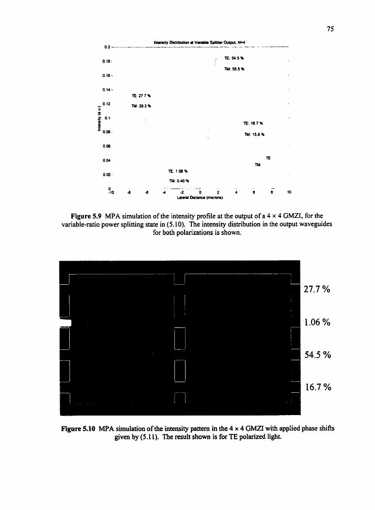
1 TE: 54.5 K 0.18-
O. t4-
TE: 277 9b
- 0.12 TM: 28.3 % a O -
TM: 55.5 W
TE: 16.7 %
TM: 15.8 %
TM: 0.40 %
Figure 5.9 MPA simulation of the intensity profile at the output of a 4 x 4 GMZI, for the variable-ratio power splitting state in (5.10). The intensity distribution in the output waveyides
for both polarizations is shown.
Figure 5.10 MPA simulation of the intensity pattern m the 4 x 4 GMZI with applied phase shifks givm by (5.1 1). The d t shown is for TE polarized light.
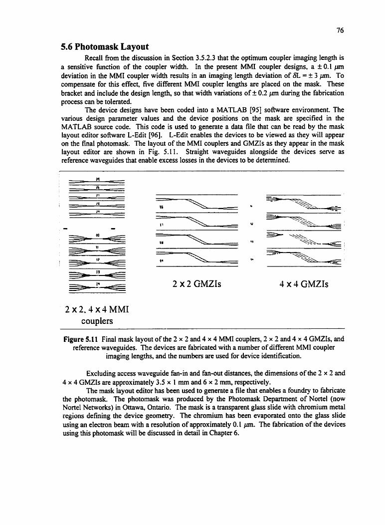
5.6 Photomask Layout Recall from the discussion in Section 3.5.2.3 that the optimum coupler imaging length is
a sensitive hc t ion of the coupler width. In the present MMI coupler designs, a + 0.1 p deviation in the MM1 coupler width results in a . imaging length deviation of 6L = t 3 p. To compensate for this effect, five different MM1 coupler lengths are placed on the mask. These bracket and include the design length so that width variations o f f 0.2 pm during the fabrication process can be tolerated.
The device designs have been coded into a MATLAB [95] software environment. The various design parameter values and the device positions on the mask are specified in the MATLAB source code. This code is used to generate a data file that can be read by the mask layout editor software L-Edit [96]. L-Edit enables the devices to be viewed as they will appear on the final photomask. The layout of the MM1 couplers and GMZIs as they appear in the mask layout editor are s h o w in Fig. 5.1 1. Straight waveguides alongside the devices serve as reference waveguides that enable excess losses in the devices to be determined.
2 x 2 . 4 x 4 M M I coupiers
2 x 2 GMZIs
Figure 5.1 1 Final mask layout of the 2 x 2 and 4 x 4 MMI couplen, 2 x 2 and 4 x 4 GMZL, and reference waveguides. The devices are fabricated with a number ofdifferent MM1 coupler
imaging lengths, and the numbers are used for device identification.
Excludinp access waveguide fan-in and fan-out distances, the dimensions of the 2 x 2 and 4 x 4 GMZIs are approximately 3.5 x 1 mm and 6 x 2 mm, respectively.
The mask layout editor has been used to generate a file that enables a foundry to fabricate the photornask, The photomask was produced by the Photomask Department of Nortel (now Nortel Networks) in Ottawa, Ontario. The mask is a transparent glass slide with chromiurn metal regions defining the device geometry. The chmmium has been evaporateà ont0 the giass slide using an electron beam with a resolution of approximately 0.1 p. The fabrication of the devices using this photomask will be discussed in detail in Chapter 6.
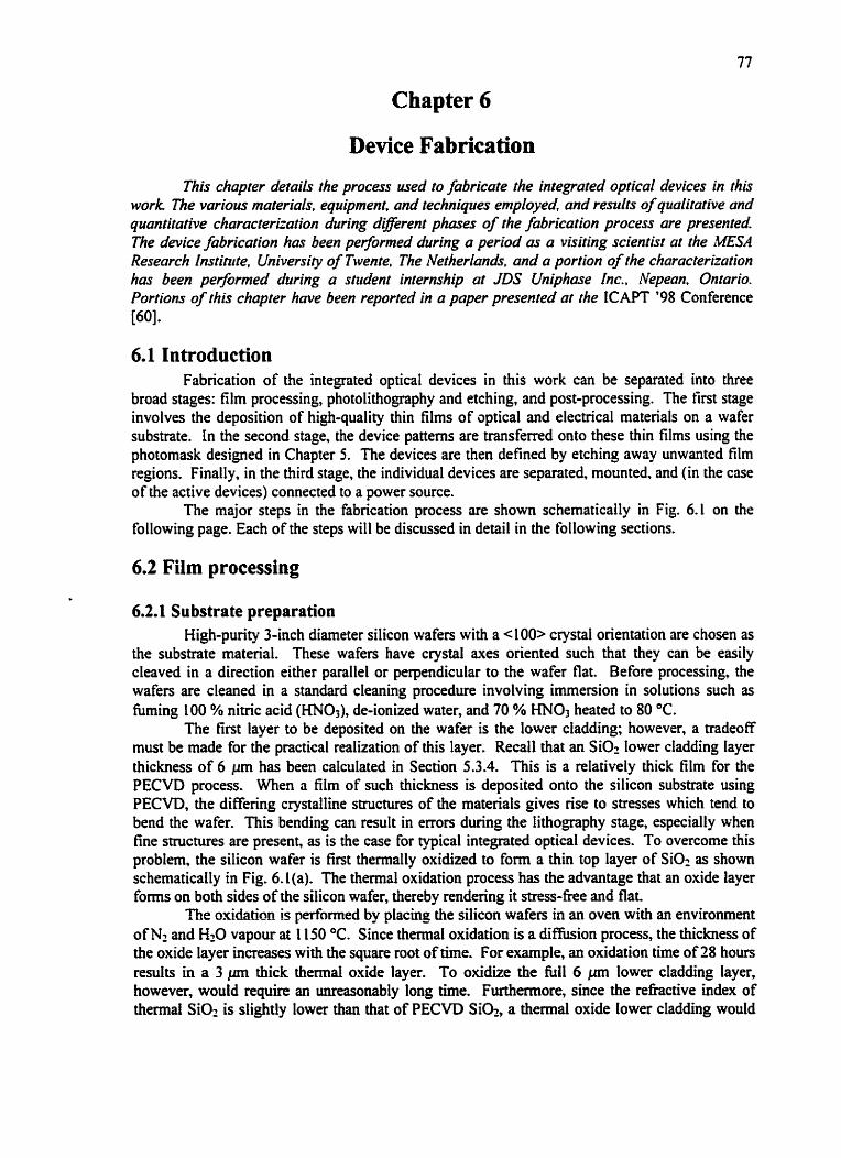
Chapter 6
Device Fabrication
This chopter detaiis the process used to fobricate the integrated optical devices in this work The various materials. equipment, and techniques employed, and results of quaiitative and quantitative characterization during dtrerent phases of the fabrication process are presented The device fabrication has been perfbrmed during a period as o visiting scienfist at the MESA Research Instinlte, University of Twente. The Netherlands. and a portion of the characteriration hm been performed during a student internship ut JDS Uniphase Inc.. Nepean. Ontario. Portions of this chapter have been reporteci in a paper presented at the ICAPT '98 Conference [601
6.1 Introduction Fabrication of the integrated optical devices in this work can be separated into three
broad stages: film processing, photolithography and etching, and post-processing. The tint stage involves the deposition of high-quality thin films of optical and electrical materials on a wafer substrate. In the second stage, the device patterns are transferred ont0 these thin films using the photomask designed in Chapter 5. The devices are then defîned by etching away unwanted film regions. Finally, in the third stage, the individual devices are separated mounted. and (in the case of the active devices) connected to a power source.
The major steps in the fabrication process are shown schematically in Fig. 6.1 on the following page. Each of the steps will be discussed in detail in the following sections.
6.2 Film processing
6.2.1 Substrate preparation High-purity 3-inch diameter silicon wafers with a < 100> crystal orientation are chosen as
the substrate material. These wafen have crystal axes oriented such that they can be easily cleaved in a direction either parallel or perpendicular to the wafer flat Before processing, the wafers are cleaned in a standard cleaning procedure involving immersion in solutions such as tùming 100 % nitric acid (HN03), de-ionized water, and 70 % HNOs heated to 80 O C .
The first layer to be deposited on the wafer is the lower cladding; however, a tradeoff mwt be made for the practical realization of this layer. Recall that an Si02 lower cladding layer thickness of 6 prn has been calculated in Section 5.3.4. This is a relatively thick film for the PECM process. When a film of such thickness is deposited ont0 the silicon substrate using PECM, the differing crystalline structures of the materials gives rise to stresses which tend to bend the wafer. This bending cm result in errors during the lithography stage, especially when fine structures are present, as is the case for typical integrated optical devices. To overcome this problem, the silicon wafer is first thermally oxidized to fom a thin top layer of SiO2 as shown schematically in Fig. 6.1(a). The thermal oxidation process has the advantage that an oxide layer fonns on both sides of the silicun wafer, thereby rendering it stress-free and flat.
The oxidation is perforrned by placing the silicon wafea in an oven with an environment of N2 and H20 vapour at 1 150 OC. Since thermal oxidation is a d i f i i o n process, the thickness of the oxide layer increases with the square mot of time. For example, an oxidation time of 28 hours results in a 3 pm thick thermal oride layer. To oxidize the full 6 pn lower cladding layer, however, would require an unreasonably long tirne. Furthmore, since the rehctive index of thermal SiO2 is slightly lower than that of PECVD Si@, a thermal oxide lower cladding would
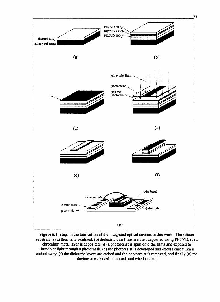
i 1 1 PECVD SiON ! PECVD Si0 1 themial SiOt
j siiioon substrare
photomask
positive photoresist
- . wire bond
Figurc 6.1 Steps in the fabrication of the integrated optical devices in this work The silicon substrate is (a) themîlly oxidized, (b) dielectric thin films are then deposited using PECVD, (c) û
chrorniurn rnetal layer is deposited, (d) a photomist is spun ont0 the films and exposed to ultraviolet light through a photomask, (e) the photoresist is developed and excess chrorniurn is
etched away, (4 the dielecaic layers are etched and the photoresist is rernoved, and finaily (g) the devices are cleaved, rnounted, and wire bonded,
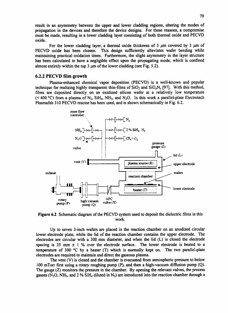
result in an asymmetry between the upper and lower cladding regions, altering the modes of propagation in the devices and therefore the device designs. For these reasons, a compromise must be made, resulting in a lower cladding laya consisting of both thermal oxide and PECVD oxide.
For the lower cladding layer, a thermal oxide thickness of 3 pn covered by 3 p of PECVD oxide has been chosen. This design sufficiently alleviates wafer bending while maintaining practical oxidation times. Furthemore, the siight asymmetry in the layer structure has been calculated to have a negligible effect upon the propagating mode, which is confined almost entirely within the top 3 p of the lower cladding (see Fig. 5.2).
6.2.2 PECVD füm growth Plasma-enhanced chernical vapor deposition (PECVD) is a well-known and popular
technique for realizing highly transparent thin-films of SiOz and SiO,N, [97]. With this rnethod, films are deposited directly on an oxidized silicon wafer at a relatively low temperature (< 400 OC) fiom a plasma of Na Sib , NH3, and N20. In this work a parallel-plate Electrotech Plasmafab 3 10 PECVD reactor has been used, and is shown schematically in Fig. 6.2.
pressure v alv t l i
Figure 6.2 Schematic diagram of the PECVD system used to deposit the dielectric films in this work.
Up to seven 3-inch wafers are placed in the reaction chamber on an anodized circular lower electrode plate, while the lid of the reaction chamber contains the upper electrode. The electrodes are circular with a 300 mm diameter, and when the lid (L) is closed the electrode spacing is 35 mm t 1 % ouer the elec?rede surface. The lower electrode is heated to a temperature of 300 OC by a heater (T) which is nonnally kept on. The two parallel-plate electrodes are required to maintain and direct the gaseous plasma
The vent (V) is closed and the chamber is evacuated fiom atmosphenc pressure to below 100 mTorr tùst using a rotary roughing pump (P), and then a hi&-vacuum diffusion pump (Q). The gauge (2) monitors the pressure in the chamber. By opening the relevant valves, the process gasses (N20, Mi3, and 2 % S i n diluted in Nz) are introduced into the reaction chamber through a
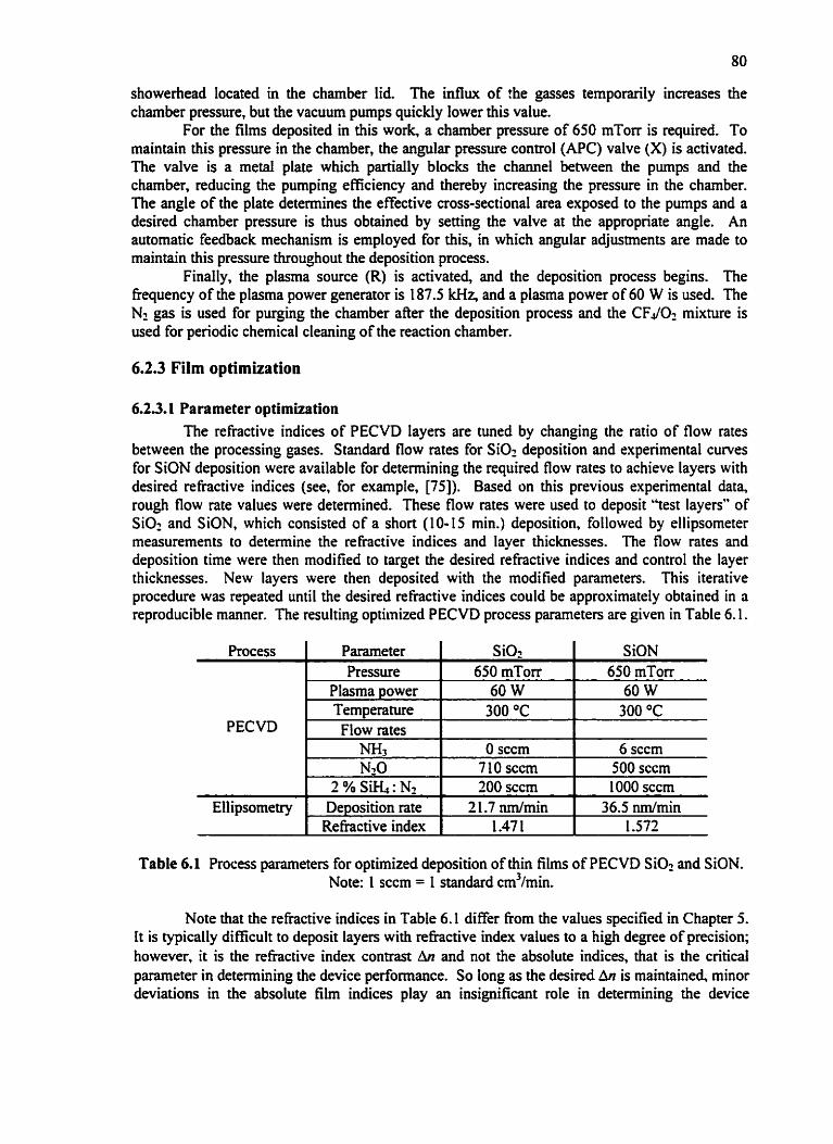
showerhead located in the chamber lid. The influx of the gasses temporarily increases the chamber pressure, but the vacuum purnps quickly lower this value.
For the films deposited in this work, a charnber pressure of 650 mTorr is required. To maintain this pressure in the chamber, the angular pressure control (APC) valve (X) is activated. The valve is a rnetal plate which partially blocks the channel between the pumps and the chamber, reducing the pumping efficiency and thereby increasing the pressure in the chamber. The angle of the plate determines the effective cross-sectional area exposed to the pumps and a desired chamber pressure is thus obtained by setting the valve at the appropriate angle. An automatic feedback mechanism is employed for this, in which angular adjustments are made to maintain this pressure throughout the deposition process.
Finally, the plasma source (R) is activated, and the deposition process begins. The fiequency of the plasma power generator is 187.5 kHz, and a plasma power of 60 W is used. The N2 gas is used for purging the chamber after the deposition process and the CFJO? mixture is used for periodic chemical cleaning of the reaction chamber.
6.2.3 Film optimization
6.2.3.1 Parameter optimization The refiactive indices of PECVD layers are tuned by changing the ratio of flow rates
between the processing gases. Standard flow rates for SiO2 deposition and expenmental curves for SiON deposition were available for determining the required flow rates to achieve layea with desired refractive indices (see, for example, [75]). Based on this previous experimental data, rough flow rate values were determined. These flow rates were used to deposit "test layers" of SiO? and SiON, which consisted of a short (10-15 min.) deposition, followed by ellipsorneter measurements to determine the refractive indices and layer thicknesses. The flow rates and deposition time were then rnodified to target the desired rehctive indices and control the layer thicknesses. New layers were then deposited with the modified parameters. This iterative procedure was repeated until the desired refractive indices could be approximately obtained in a reproducible rnanner. The resulting optimized PECVD process parameters are given in Table 6.1.
Table 6.1 Process parameters for optimized deposition of thin films of PECVD SiOz and SiON. Note: 1 sccm = I standard cm3/min.
Process
PECVD
Ellipsometry
Note that the refractive indices in Table 6.1 differ fiom the values specified in Chapter 5. it is typically difficult to deposit layers with refiactive index values to a high degree of precision; however, it is the refiactive index contrast An and not the absolute indices, that is the cntical parameter in detemining the device performance. So iong as the desired An is maintained, minor deviations in the absolute film indices play an insignificant role in determining the device
Parameter Pressure
Plasma power Temperature Flow rates
NH3 N20
2%SiH4:N2 Deposition rate
SiO2 650 mTorr 60 W 300 O C
O sccm 7 10 sccm 200 sccm
2 1.7 nm/min
SiON 650 mTorr 60 W 300 O C
6 sccm 500 sccm 1 O00 sccm
36.5 nm/min Rehctive index 1 1.47 1 1 .572
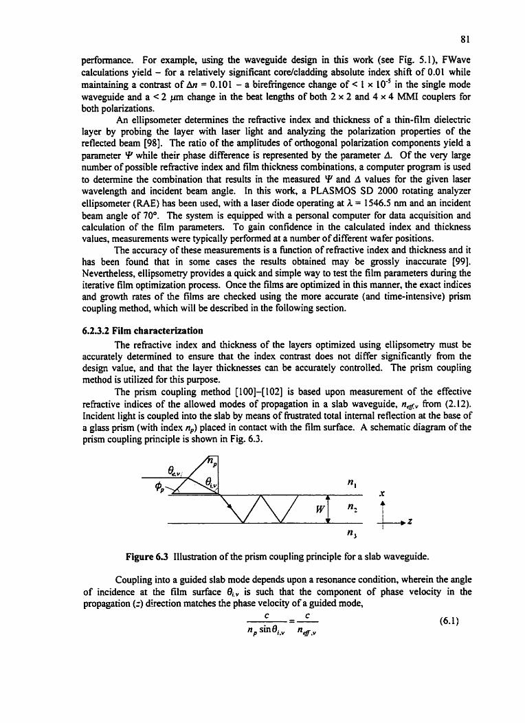
penonnance. For example, using the waveguide design in this work (see Fig. 5.1). FWave calculations yield - for a relatively significant core/cladding absolute index shifi of 0.01 while maintainhg a contrast of L\n = 0.101 - a birefnngence change of < 1 x 10⁵ in the single mode waveguide and a < 2 p change in the b a t lengths of both 2 x 2 and 4 x 4 MM1 couplers for both polarizations.
An ellipsometer determines the rehctive index and thickness of a thin-film dielectric layer by probing the layer with laser light and analyzing the polarization pmperties of the reflected beam 1981. The ratio of the amplitudes of orthogonal polarization components yield a parameter Y while their phase difference is represented by the parameter A. Of the very large number of possible rehctive index and film thickness combinations, a computer program is used to determine the combination that results in the measured Y and A values for the given laser wavelength and incident beam angle. In this work, a PLASMOS SD ZOO0 rotating analyzer ellipsometer (RAE) has been used, with a laser diode operating at A = 1546.5 nm and an incident beam angle of 70'. The system is equipped with a personal computer for data acquisition and calculation of the film parameten. To gain confidence in the calculated index and thickness values, measurements were typically performed at a nurnber of different wafer positions.
The accuracy of these measurements is a function of rehctive index and thickness and it has been found that in some cases the results obtained may be grossly inaccurate 1991, Nevenheless, ellipsometry provides a quick and simple way to test the film parameters during the iterative tilm optimization process. Once the films are optimized in this marner, the exact indices and growth rates of the films are checked using the more accurate (and time-intensive) pnsm coupling method, which will be descnied in the following section.
6.2.3.2 Film characterization The rehctive index and thickness of the iayers optimized using ellipsometry must be
accurately determined to ensure that the index contrast does not differ significantly fiom the design value, and that the layer thicknesses can be accurately controlled. The prism coupling rnethod is utilized for this purpose.
The prism coupling method [100]-[IO21 is based upon measurement of the effective refractive indices of the allowed modes of propagation in a slab waveguide, n d , from (2.12). Incident light is coupled into the slab by means of ûustrated total intemal reflection at the base of a glas pnsm (with index n,) placed in contact with the film surface. A schematic diagram of the pnsm coupling principle is shown in Fig. 6.3.
Figure 6 3 Illustration of the prism coupling principle for a slab waveguide.
Coupling into a guided slab mode depends upon a resonance condition, wherein the angle of incidence at the film surface eivv is such that the component of phase velocity in the propagation (2) direction matches the phase velocity of a guided mode,
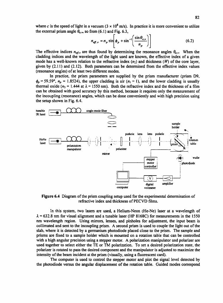
where c is the speed of light in a vacuum (3 x 10⁸ mfs). In practice it is more convenient to utilize the extemal prism angle Oe,, so fiom (6.1) and Fig. 6.3, [ - I(.i:"]] n,, = n, sin #, + sin- -
The effective indices negv are thus found by detenining the resonance angles 8 ,v . When the cladding indices and the wavelength of the light used are known, the effective index of a given mode has a well-known relation to the refraaive index (i) and thickness (W) of the core layer, given by (2.1 1) and (2.12). Both parameters can be detemined from the effective index values (resonance angles) of at least two different modes.
In practice, the prism parameters are supplied by the prism manufacturer (prism D9, #, = 59-59', n,, = 1.8524), the upper cladding is air (ni = 1), and the lower cladding is usually thermal oxide (n3 = 1.444 at A. = 1550 nm). Both the rehctive index and the thickness of a film can be obtained with good accuracy by this method, because it requires only the measurement of the incoupling (resonance) angles, which cm be done conveniently and with high precision using the setup shown in Fig. 6.4.
prnholt las Iens puiholr , ,A -, - , ,
~ - , L K L ; . . ,)..~...... . : : q .-... '.. . .
p~iii%?iihUl ' mpulator ' poianztr
niinor 1 , i è I ,-i-7 wafa -./
j photdode cmtruua I
I i ip/-i PA-:
J digital computa voImter
Figure 6.4 Diagram of the prism coupling setup used for the experimental determination of rehctive index and thickness of PECVD films.
In this system, two lasers are useci, a Helium-Neon (He-Ne) laser at a wavelength of A = 632.8 nm for visual alignmrnt and a tunable laser (HP 8168C) for measurernents in the 1550 nm wavelength region. Using mirroa, lenses, and pinholes for adjustment, the input beam is collimated and sent to the incoupling prism. A second pnsm is used to couple the Iight out of the slab, where it is detected by a germanium photodiode placed close to the prism. The sample and pnsms are fked to a sample holder which is mounted on a rotation table that can be controlled with a high angular precision using a stepper motor. A polarization manipulator and polarizer are used together to select either the TE or TM polarizution. Te set a desired plarizatim ctate, the polarizer is rotated to pass the desired component and the manipulator is adjusted to maximize the intensity of the bearn incident at the prism (visudl y, using a fI uorescent card).
The computer is used to control the stepper motor and plot the signa1 Ievel detected by the photodiode versus the angular displacement of the rotation table. Guided modes correspond

to peaks in the detected signal. The comsponding resonance angles are useci, along with the slab and prism data in a software program [IO31 to calculate the rehctive index and layer thickness. The accuracy of the prism coupling method has been studied 1991, [104] and errors of 2-6 x [O-' in rehctive index, 0.1 % in layer thickness, and 2 x IO-' in buefringence are found to be present.
The index and thickness of Iayers with the optimized PECVD parameters in Table 6.1 have been verified in the following manner. Fint, to satisQ the slab waveguide requirement for prism coupling, oxidized silicon wafen have been used. Secondly, the optimized layers of SiO2 and SiON have been deposited on separate oxidized wafers, with thicknesses chosen to ensure that at least two guided modes are present for both polarizations in the 1550 nm wavelength region. An SiOt layer thickness of about 6 pn (4.5 hour deposition time) and an SiON layer thickness of about 3 p (80 min. deposition time) have been targeted.
The pnsm coupling setup has been subsequently used to determine the rehctive index and thickness values for the layers using both TE and TM polarized light at wavelengths in the 1550 nm region. These results, along with the index contrast values and their associated uncertainties, are given in Table 6.2
Table 6.2 Parameters of PECVD SiOt and SiON layers used in the fabrication of integrated devices, measured using the prism coupling technique.
Parameter
Si02 layer
S iON Iayer
Index contrast An
Table 6.2 indicates that the desired index contrast (An = 0.101) is achieved with a maximum error of 2 x IO-', the layer thicknesses can be controlled to within 3.5 %, and the parameters are insensitive to wavelength in the 1550 nm region. Furthemore, the birefringence in the index contrast value is below the uncertainty limits of the measurement. Since the results are close to the design values, the PECVD parameters in Table 6.1 are adopted for layea to be used in the fabrication of devices.
Using these parameters, the three-layer slab shown schematically in Fig. 6 4 b ) is deposited on a number of oxidized silicon wafers in a single. continuous PECVD run. The slab consists of a 3 pm thick SiOt Iwer cladding, 3 1 pm &ick SON m e , and a 3 p thick SiO? upper cladding.
Layer thickness W ( p n )
6.233 Heat treatment of SiON Iayer
Wavelength (nm) 1548 1550 1552 1554 1548 1550 1552
TE 6.054 6.069 6.038 6.077 3.036 3.03 1 3.026
1550 1553 1554
Though the deposited films are highly transparent for visible wavelengths, there is significant absorption of light in the films for wavelengths in the infrared region, as discussed in
TM 6.180 6.1 49 6.1 16 6.164 3. 106 3.106 3.106
Refractive index nz TE 1 TM 1.4587 1.4594
0.100 IO.001 0.100 f 0.001 O. 100 f 0.00 1
1 -4588 1.4587 1.4587 1 S586 1.5587 1 S588
O. 1 O0 k 0.00 1 0.100 f 0.00 1 O. 1 O0 + 0.00 1
1.4595 1 -4595 1.4595 1 S593 1 .5593 1.5594

Section 5.3.2, This is due to the incorporation of hydrogen in the layers during the deposition process [73]. The hydrogen foms Si-H and N-H bonds in the films, which have a resonant energy coinciding with the energy of photons at a wavelength of 1508 nm. Thus the light at this and nearby wavelengths is absorbed by the films. This results in significant optical propagation loss in the films, which is defined as
The loss is measured in units of dS/cm, I is the rneasured optical intensity dong the propagation (z) direction, and lo is the propagation length in the waveguide.
For PECVD SiO, and SiON Iayers, typical propagation losses at A, = 1550 nm range fiom 3 - 10 dB/cm [los]. In Section 5.3.2, however, it was noted that a heat treatment process, or annealing, can significantly reduce these losses. In this process, the wafers are placed in an oven at a temperature typically > 1100 "C to drive off excess hydrogen fiorn the deposited layers. It has been confirmed that annealing reduces the number of Si-H and N-H bonds in the films [75], resulting in a corresponding decrease in the optical losses. Optical loss values of annealed SiOZ and SiON films are typically below 0.2 dB/cm 1701, [75] and losses below 0.1 dB/cm have been reported [76].
As mentioned in Section 5.3.2, the films to be used for devices in this work have not been annealed. To qualitatively determine the potential impmvement of the losses by annealing, the SiON film used in the prism coupler measurements above has been annealed. First, the wafer was cleaved into three sections. One section was not annealed, one section was annealed at 1 150 O C for one hour, and the final section was annealed at 1 150 O C for two hours. The sections to be annealed were placed in an oven with an N2 flow rate of 1200 sccm at a temperature of 400 OC. The temperature was then gradually increased to 1 150 O C over a 30 min. period, where it was maintained for the duration of the anneal, followed by a similar 30 min. cool-down period.
The spectral transmission in the films has been measured in a prism coupling setup using a broadband light source and a spectrum analyzer. The coupIing angle is fixed at a given mode, and the uutcoupled light intensity is measured as a function of wavelength. Next, the outcoupling prism is moved hrther from the incoupling prism, and the measurernent is repeated. ln this way, the spectral response of the film can be isolated. The results for the SiON films are given in Fig. 6.5.
The sample which has not been annealed shows a large absorption for wavelengths near 1500 nrn. For these wavelengths, the transmined intensity is near the noise limit of the specaum analyzer, resulting in the spurious fluctuations seen in Fig. 6.5. By cornparison, the sample annealed at 1150 O C for one hour shows a significant reduction in the losses ne= 1500 nn:, indicating that hydrogen has been effectively removed Liom the layers. Annealing at 1 150 OC for two hours induced significant bending in the wafer, so that prisrn coupling measurements for this sample could not be performed reliably. The result shown in Fig. 6.5 demonstrates that a simple heat treatment can dramaticaIly reduce the optical losses in the PECVD films used in this work.
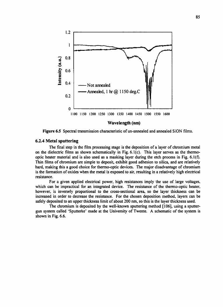
1.2 -
1 - -
? 0.8 2 V
h .= 0.6 V) r Q) Y
5 0.4 - No t annealed - Anneakd, I hr @ 1 150 degC
0.2
O 1100 1150 1200 1350 1300 1350 1400 1450 1500 1550 1600
Wavelength (nm)
Figure 6.5 SpectraI transmission characteristic of un-annealed and annealed SiON films.
6.2.4 Metal sputtering The final step in the Film processing stage is the deposition of a layer of chroinium metal
on the dielectric films as show schematically in Fig. 6 4 ~ ) . This layer serves as the thermo- optic heater material and is also used as a masking layer during the etch process in Fig. 6.l(f). Thin films of chromium are simple to deposit, exhibit good adhesion to silica, and are relatively hard, making this a good choice for thermo-optic devices. The major disadvantage of chromium is the formation of oxides when the metal is exposed to air, resulting in a relatively high electrical resistance.
For a given applied electrica1 power, high tesistances imply the use of Iarge voltages, which can be impractical for an integrated device. The resistance of the thenno-optic heater, however, is inversely proportional to the cross-sectional area, so the layer thickness can be increased in order to decrease the resistance. For the chosen deposition method, layers can be safely deposited to an upper thickness limit of about 200 nm, so this is the layer thickness used.
The chromium is deposited by the well-known sputtering method [106], using a sputter- gun system called 'Spunerke' made at the University of Twente. A schematic of the system is shown in Fig. 6.6.
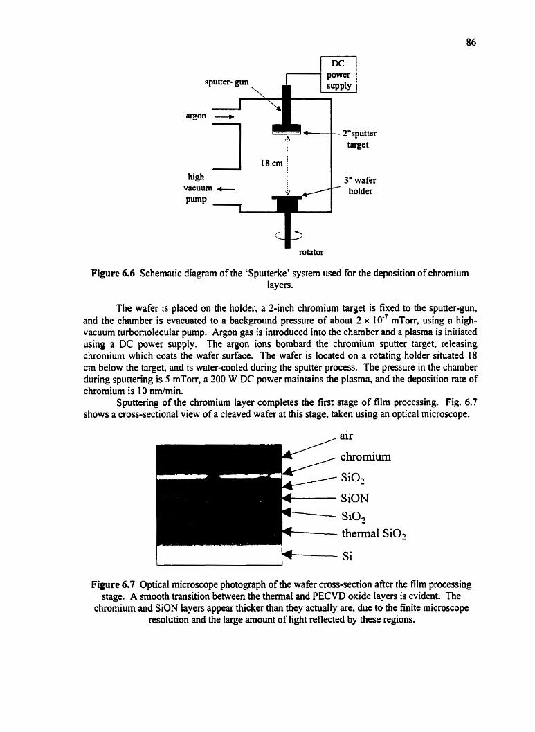
1-t power 1 sputter- gun
argon -+ 2"spuîter
3" wafer holder
Figure 6.6 Schematic diagram of the 'Sputterke' system uxd for the deposition of chromium layers.
The wafer is placed on the hoider, a î-inch chromium target is fixed to the sputter-gun, and the chamber is evacuated to a background pressure of about 2 x 10" mïorr, using a high- vacuum turbomolecular pump. Argon gas is introduced into the charnber and a plasma is initiated using a DC power supply. The argon ions bombard the chromium sputter target, releasing chromium which coats the wafer surface. The wafer is located on a rotating holder situated 18 cm below the target, and is water-cooled dunng the sputter process. The pressure in the chamber during sputtering is 5 m'torr, a 200 W DC power maintains the plasma. and the deposition rate of chromium is 10 nrnhin.
Sputtering of the chromium layer completes the first stage of film pmcessing. Fig. 6.7 shows a cross-sectional view of a cleaved wafer at this stage, taken using an optical microscope.
, air
Figure 6.7 Optical microscope photograph of the wafer cross-section after the film processing stage. A srnooth transition between the thermal and PECVD oxide layers is evident The
chromium and SiON layers appear thicker than they achially are. due to the finite microscope molution and the large amount of light d e c t e d by these regiona
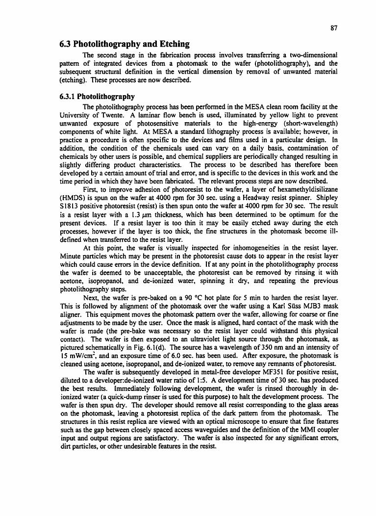
6.3 Photolithography and Etching The second stage in the fabrication process involves tramferring a two-dimensional
pattern of integrated devices 60m a photomask to the wafer (photolithography), and the subsequent structurai definition in the vertical dimension by removal of unwanted matenal (etching). ïhese processes are now described.
63.1 Photolithography The photolithography process has been performed in the MESA clean room facility at the
University of Twente. A laminar flow bench is used, illuminated by yellow light to prevent unwanted exposure of photosensitive materials to the high-energy (short-wavelength) components of white light. At MESA a standard lithography process is available; however, in practice a procedure is ofien specific to the devices and films used in a particular design. In addition, the condition of the chemicals used can v q on a daily basis, contamination of chemicals by other uses is possible, and chernical suppliea are periodically changed resulting in slightly diffenng product characteristics. The pmcess to be described has therefore been developed by a certain amount of trial and error, and is specific to the devices in this work and the time period in which they have been fabncated. The relevant process steps are now described.
First, to improve adhesion of photoresist to the wafer, a layer of hexamethyldisilizane (HMDS) is spun on the wafer at 4000 rpm for 30 sec, using a Headway resist spinner. Shipley S 18 13 positive photoresist (resist) is then spun ont0 the wafer at 4000 rpm for 30 sec. The result is a resist layer with a 1.3 pin thickness, which has been detennined to be optimum for the present devices. If a resist layer is too thin it may be easily etched away during the etch processes, however if the layer is too thick, the fine structures in the photomask become ill- defined when transkrred to the resist layer.
At this point, the wafer is visually inspected for inhomogeneities in the resist layer. Minute particles which may be present in the photoresist cause dots to appear in the resist layer which could cause errors in the device definition. If at any point in the photolithography process the wafer is deemed to be unacceptable, the photoresist can be removed by rinsing it with acetone, isopropanol, and de-ionized water, spinning it dry, and repeating the previous photolithography steps.
Next, the wafer is pre-baked on a 90 O C hot plate for 5 min to harden the resist layer. This is followed by alignment of the photomask over the wafer using a Karl Süss Mm3 mask aligner. This equipment moves the photomask pattern over the wafer, allowing for coarse or fine adjustments to be made by the user. Once the mask is aligned, hard contact of the rnask with the wafer is made (the pre-bake was necessary so the resist layer could withstand this physical contact). The wafer is then exposed to an ultraviolet light source through the photomask, as pictured schematically in Fig. 6.l(d). The source has a wavelength of 350 nm and an intensity of 15 m~/cm', and an exposure tirne of 6.0 sec. has been used. AAer exposure, the photomask is cleaned using acetone, isopropanol, and de-ionized water, to remove any remnants of photoresist.
The wafer is subsequently developed m rnetal-free developer MF35 1 for positive resist, diluted to a developer:de-ionized water ratio of 15. A development time of 30 sec. has produced the best renilts. Irnrnediately following development, the wafer is rinsed thoroughly in de- ionized water (a quick-dump rimer is used for this purpose) to halt the development process. The wafer is then spun dry. The developer should remove al1 resist corresponding to the g las mas on the photomask, leaving a photoresist replica of the dark pattern from the photornask The structures in this resist replica are viewed with an optical microscope to ensure that fine features such as the gap between closely spaced access waveguides and the definition of the MM1 coupler input and output regions are satisfactory. The wafer is also inspected for any signifiant errors, dirt particles, or other undesirable features in the resist.
The wafer is then post-baked for 1.5 hours on a 120 O C hot plate, to m e r harden the resist iayer prior to etching.
6.3.2 Wet chemical etching Before the structures on the wafer can be defined in the vertical direction by reactive ion
etching, excess chromiurn m u t first be removed from wafer regions not covered by the resist. Chromium is then present only under the resist, thereby serving as a seconday mask for the reactive ion etch while at the same time ensuring that the resulting waveguides are completely covered by the required thermo-optic layer. The secondary chromium mask has been show [107] to improve the smoothness and reproducibility of the vertical walls (sidewalls) created by the reactive ion etch.
The excess chromium is removed by a wet chernical etching procedure. The wafer is repeatedly immersed in the chromium etch solution Ce(NH&(N03),J HClOJ H-O (mixed in the ratio l6Sg / 42 mL / I litre) for a duration of 2 min. The etch rate of this solution is 10 nrdmin. The end of the etch process is readily visible since the underlying Si02 layer (which has a much Iower reflectivity) is exposed. The wafer is then rinsed in de-ionized water and baked for 5 min. on a 120 OC hot plate. The wafer at this stage is shown schematicaIly in Fig. 6.1 (e).
63.3 Reactive ion etching Reactive ion etching (EUE) is a dry etch procedure applied to define dielectric films in the
vertical direction in order to realize channel waveguide structures. To perform the RIE process, a PlasmaFab Electrotech PF340 machine has been used. The etch process is computer-controlled, and the general configuration of the equipment is similar to the PECVD system. Aithough up to three wafers can be placed on the lower electrode, in this work wafers have been placed centrally on the electrode and etched one at a time to improve the etch uniformity. The substrate is cooled, the chamber is evacuated, and the etching gas is introduced. The background pressure is set to a desired level by an APC valve, and a plasma is initiated. The etching gas dissociates into radicals that then perform the etching.
The selectivity of the process, defined as the ratio of the etch rates of the resist to the dielectnc films, is 1 :5 to 1 : 10 for silica-based films 11 071. This indicates that in the wont case, an etch depth of 6.5 pm is reached before the 1.3 pm resist layer is completely etched. From Fig. 5.1, however, an etch depth of only 4.5 pn is required. The chromium layer is used as a mask material under the resist for the purpose of increasing the channel definition and creating smooth sidewalls. However, it does not serve as an effective etch mask once the resist layer has been cornpletely etched. This has been confirmed by using a set of process parameters with a faster resist etch rate. Once the resist is completely etched, the chromium layer is attacked by the plasma and te-deposited around the wafer in a sputter-like process. The te-deposited chromium isIands serve as miniature masks, resulting in a severely scarred and pitted wafer surface. An adequate resist thickness is therefore crucial in the etch process.
The waveguide structures descnibed in earlier chapters consist of rectangular channels with vertical sidewalls. However, the RIE technolugy is capable of both isotropic (directionally- independent) and anisotropic (directionally-dependent) etching. Since the etch procedure must be highly directional in order to realize perfect verticality, anisotropic etching is required. A detailed investigation of the variation of RIE parameters in the etching of PECM SiOf and SiO,N,. has been perfonned [108], and a set of process parameters has been developed to achieve an anisotropic etch process. These parameters are described below.
The substrate is cooled to a temperature of 10 OC, 10 sccm of CHF3 gas is introduced into the chamber, a 10 mTorr background pressue is reached, and the plasma source is activated with a power of 6OW. The etch rate using these parameters is about 2.5 jmdhour; however, this rate is only approximate and c m Vary significantiy depending upon the wafer use& the previous
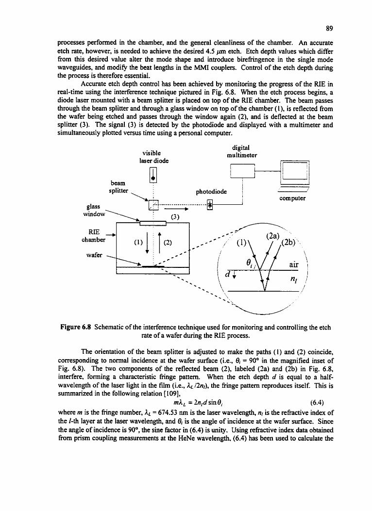
processes performed in the chamber, and the general cleanliness of the chamber. An accurate etch rate, however, is needed to achieve the desired 4.5 p etch. Etch depth values which differ from this desired value alter the mode shape and introduce birefringence in the single mode waveguides, and modify the beat lengths in the MMI couplers. Contml of the etch depth during the process is therefore essential.
Accurate etch depth control has been achieved by monitoring the progress of the RIE in real-time using the interference technique pictured in Fig. 6.8. When the etch process begins, a diode laser mounted with a beam splitter is placed on top of the RIE chamber. The beam passes through the beam splitter and through a glas window on top of the charnber (I), is reflected 60m the wafer being etched and passes through the window again (3, and is defïected at the beam splitter (3). ïhe signal (3) is detected by the photodiode and displayed with a multimeter and simultaneously plotted versus time using a persona1 cornputer.
Figure 6.8 Schematic of the interference technique used for monitoring and controlling the etch rate of a wafer during the EUE process.
digital visible mu ltimeter
laser di ode I 1 I I
The orientation of the beam splitter is adjusted to make the paths (1) and (2) coincide, corresponding to normal incidence at the wafer suface (Le., Bi = 90' in the rnagnified inset of Fig. 6.8). The hvo components of the reflected beam (2), labeled (Za) and (2b) in Fig. 6.8, interfixe, forming a characteristic fringe pattern. When the etch depth d is equal to a half- wavelength of the laser light in the film (i.e., Ar /2nl), the f i g e pattern reproduces itself. This is summarized in the following relation [ 1091,
mk, = Ln,d sin 0, (6.4)
beam photodiode
where m is the fringe number, AL = 674.53 nm is the laser wavelength, n~ is the rehctive index of the /-th layer at the laser wavelength, and Oi is the angle of incidence at the wafer surface. Since the angle of incidence is 90°, the sine factor in (6.4) is unity. Using refiactive index data obtained 60m prisrn coupling measurements at the HeNe wavelength, (6.4) has been used to calculate the
,-
corn puter i
, /-y-.. .
chambw m? . ., 1 # C * #ei:,;-, (1) , ,
wafer . e e 'l
Bi / \ air 1 *
; % . - v I 5 . . "1
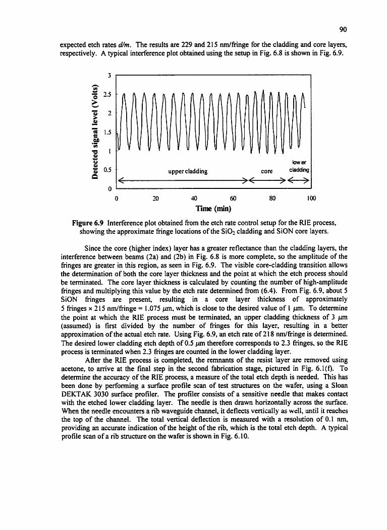
expected etch rates d m . The results are 229 and 21 5 d fk inge for the cladding and core layers, respectively. A typical interference plot obtained using the setup in Fig. 6.8 is shown in Fig. 6.9.
Y iow er
c iadding
.c;, O s
0.5 . upper claddmg COR? P >--
O 30 JO 60 80 100
Tirne (min)
Figure 6.9 interference plot obtained Rom the etch rate control setup for the RIE process, showing the approximate fnnge locations of the SiOt cladding and SiON core layers.
Since the core (higher index) layer has a greater reflectance than the cladding layers, the interference between beams (2a) and (2b) in Fig. 6.8 is more complete, so the amplitude of the fnnges are greater in this region, as seen in Fig. 6.9. The visible core-cladding transition allows the detennination of both the core layer thickness and the point at which the etch process should be terminated. The core layer thickness is calculated by counting the number of high-amplitude fnnges and multiplying this value by the etch rate detennined Frorn (6.4). From Fig. 6.9, about 5 SiON fringes are present, resulting in a core layer thickness of approximately 5 fringes x 11 5 ndfiinge = 1 .O75 Fm, which is close to the desired value of 1 W. To determine the point at which the RIE process must be tenninated, an upper cladding thickness of 3 pm (assumed) is first divided by the number of fnnges for this layer, resulting in a better approximation of the actual etch rate. Using Fig. 6.9, an etch rate of 11 8 nm/fnnge is detennined. The desired lower cladding etch depth of 0.5 pm therefore corresponds to 2.3 finges, so the RIE process is terminated when 2.3 fringes are counted in the lower cladding layer.
Afier the R E process is completed, the rernnants of the resist layer are removed using acetone, to arrive at the final step in the second fabrication stage, pictured in Fig. 6.1(f). To determine the accuracy of the RIE process, a measure of the total etch depth is needed. This has been done by performing a surface profile scan of test structures on the wafer, using a Sloan DEKTAK 3030 surface profiler. The profiler consists of a sensitive needle that makes contact with the etched lower cladding Iayer. The needle is then h w n horizontally across the surface. When the neede encounters a Rb waveguide chmel, it deflects verticdty as weii, until it reaches the top of the charnel. The total vertical deflection is measured with a resolution of 0.1 nm, providîng an accurate indication of the height of the rib, which is the total etch depth. A typical profile scan of a n'b structure on the wafer is show in Fig. 6.10.
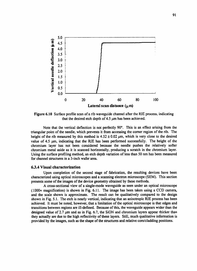
Lateral scan distance (p m)
Figure 6.10 Surface profile scan of a rib waveguide channel aRer the RIE process, indicating that the desired etch depth of 4.5 pm has been achieved.
Note that the vertical deflection is not perfectly 90'. This is an eRect ansing from the triangular point of the needle, which prevents it fiom accessing the corner region of the nb. The height of the rib measured by this method is 4.52 t 0.02 pm, which is very close to the desind value of 4.5 p, indicating that the RIE has been performed successfully. The height of the chromium layer has not been considered because the needle pushes the relatively sofier chromiurn metal aside as it is scanned horizontally, producing a scratch in the chromium layer. Using the surface profiling method an etch depth variation of less than 50 nm has been measured for channel structures in a 3-inch wafer area.
6.3.4 Visual characterization Upon completion of the second stage of fabrication, the resulting devices have been
characterized using optical microscopes and a scanning electron microscope (SEM). This section presents some of the images of the device geornetry obtained by these methods.
A cross-sectional view of a singlemode waveguide as seen under an optical microscope (1000~ magnification) is show in Fig. 6.1 1. The image has been taken using a CCD canera, and the scale shown is approximate. The result can be qualitatively compared to the design show in Fig. 5.1. The etch is nearly vertical, indicating that an anisotropic RIE process has been achieved. It must be noted, however, that a limitation of the optical microscope is that edges and transitions between regions are ill-defined. Because of this, the waveguide appears wider than the designed value of 2.7 p and as in Fig. 6.7, the SiON and chromium Iayers appear thicker than they actually are due to the high reflectivity of these layen. Still, much qualitative information is provided by the images, such as the shape of the structures and relative corekladding positions.
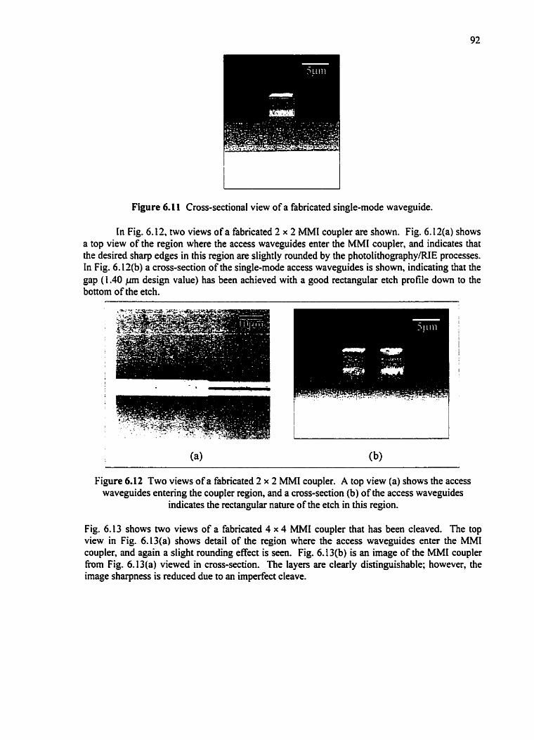
Figure 6.1 1 Cross-sectional view of a fabricated single-mode waveguide.
In Fig. 6.12, two views of a fabricated 2 x 2 MM1 coupler are shown. Fig. 6.1 Z(a) shows a top view of the region where the access waveguides enter the MM[ coupler, and indicates that the desired sharp edges in this region are slightly rounded by the photolithography/RIE processes. In Fig. 6.12(b) a cross-section of the single-mode access waveguides is shown, indicating that the gap ( 1.40 pm design value) has been achieved with a good rectangular etch profile down to the bottorn of the etch.
Figure 6.12 Two views of a fabricated 2 x 2 MMI coupler. A top view (a) shows the access waveguides entenng the coupler region, and a cross-section (b) of the access waveguides
indicates the rectangular nature of the etch in this region.
Fig. 6.13 shows two views of a fabricated 4 x 4 MM1 coupler that has been cleaved. The top view in Fig. 6.13(a) shows detail of the region where the access waveguides enter the MMI coupler, and again a slight rounding effect is seen. Fig. 6.13(b) is an image of the MM1 coupler fiom Fig. 6.13(a) viewed in cross-section. The Iayers are clearly distinguishable; however, the image sharpness is reduced due to an imperfect cleave.
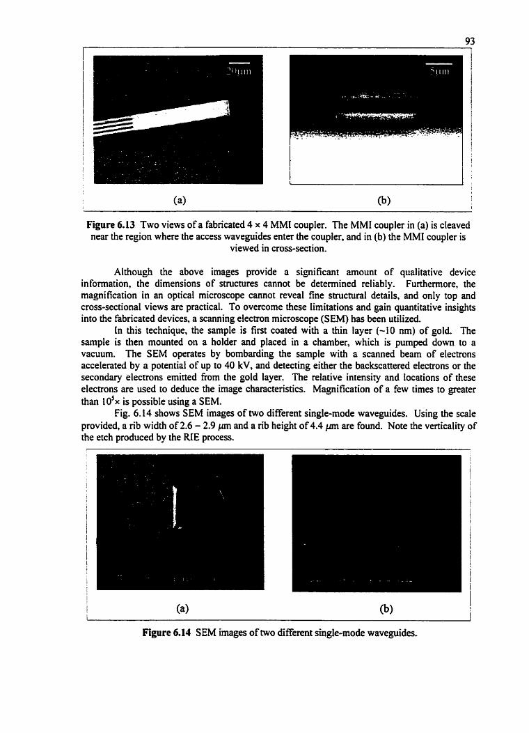
Figure 6.13 Two views of a fabncated 4 x 4 MM1 coupler. The MM1 coupler in (a) is cleaved near the region where the access waveguides enter the coupler, and in (b) the MM1 coupler is
viewed in cross-section.
Although the above images provide a significant amount of qualitative device information, the dimensions of structures cannot be determined reliably. Furthemore, the magnification in an optical microscope cannot reveal fine srruchiral details, and only top and cross-sectional views are practical. To overcome these limitations and gain quantitative insights into the fabricated devices, a scanning electron microscope (SEM) has been utilized.
In this technique, the sample is fim coated with a thin layer (-10 nm) of gold. The sample is then mounted on a holder and placed in a chamber, which is pumped down to a vacuum. The SEM operates by bombarding the sample with a scanned beam of electrons accelerated by a potential of up to 40 kV, and detecting either the backscattered electrons or the secondary electrons emined h m the gold layer. The relative intensity and locations of these electrons are used to deduce the image characteristics. Magnification of a few times to greater than 10% is possible using a SEM.
Fig. 6.14 shows SEM images of wo different single-mode waveguides. Using the scale provided, a rib width of 2.6 - 2.9 pm and a rib height of 4.4 p are found. Note the verticality of
etch produced by the RIE process.
Figure 6.14 SEM images of two k n t single-mode waveguides.
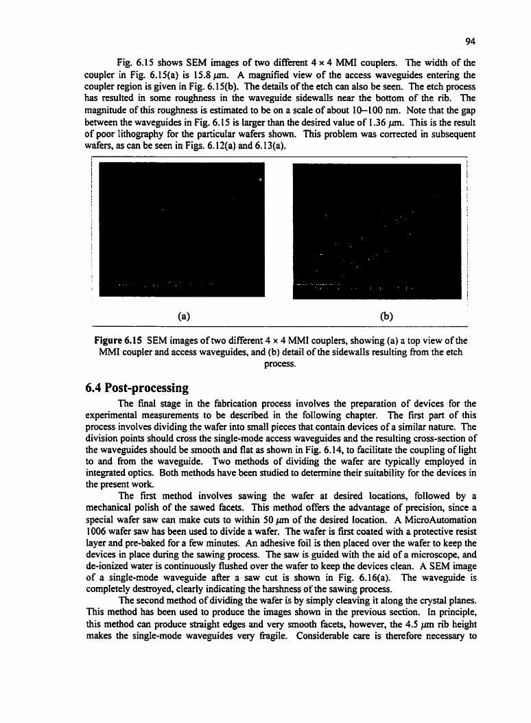
Fig. 6.15 shows SEM images of two different 4 x 4 MM[ couplers. 'ihe width of the coupler in Fig. 6.I5(a) is 15.8 p. A magnified view of the access waveguides entering the coupler region is given in Fig. 6.1 S(b). The details of the etch c m also be seen. The etch process has resulted in some roughness in the waveguide sidewalls near the bottom of the rib. The magnitude of this roughness is estimated to be on a scale of about 10-100 nm. Note that the gap between the waveguides in Fig. 6.15 is larger than the desired value of 1.36 pm. This is the result of poor lithography for the particular wafm shown. This problem was corrected in subsequent wafea, as can be seen in Figs. 6.12(a) and 6.13(a).
Figure 6.15 SEM images of two different 3 x 4 MM1 couplers, showing (a) a top view of the MM1 coupler and access waveguides, and (b) detail of the sidewalls resulting from the etch
process.
The final stage in the fabrication process involves the preparation of devices for the experimentai measurernents to be described in the following chapter. The first part of this process involves dividing the wafer into mal1 pieces that contain devices of a similar nature. The division points should cross the single-mode access waveguides and the resulting cross-section of the waveguides should be smooth and flat as shown in Fig. 6.14, to facilitate the couphg of light to and from the waveguide. Two methods of dividing the wafer are typically employed in integrated optics. Both methods have been studied to determine their suitability for the devices in the present work,
The first method involves sawing the waf'er at desired locations, followed by a mechanical polish of the sawed facets. This method offers the advantage of precision, since a special wafer saw can make cuts to within 50 p of the desired location. A MicroAutomation 1006 wafer saw has been w d to divide a wafer. The wafer is first coated with a protective resist layer and pre-baked for a few minutes. An adhesive foi1 is then placed over the wafer to keep the devices in place during the sawing process. The saw is guided with the aid of a microscope, and de-ionized water is continuously flushed ovw the wafer to keep the devices clean. A SEM image of a singe-mode waveguide after a saw cut is shown in Fig. 6,16(a). The waveguide is completely destroyed, clearly indicating the harshness of the sawing process.
The second method of dividing the wafer is by simply cleavhg it along the crystal planes. This method has been used to produce the images s h o w in the previous section. in principle, this method can produce straight edges and very smooth facets, however, the 4.5 p rib height makes the single-mode waveguides very fiagile. Considerable care is therefore necessary to
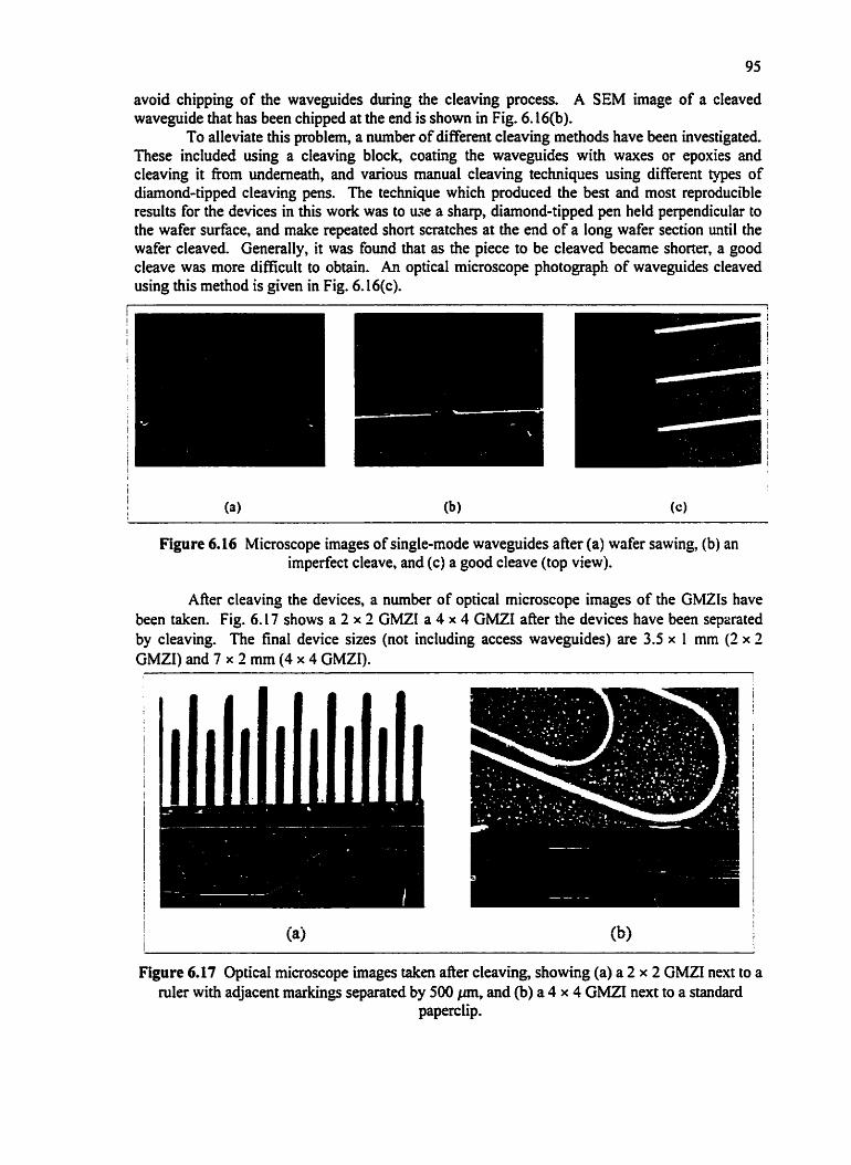
avoid chipping of the waveguides during the cleaving process. A SEM image of a cleaved waveguide that has been chipped at the end is shown in Fig. 6.16(b).
To alleviate this problem, a number of different cleaving methods have been investigated. These included using a cleaving block, coating the waveguides with waxes or epoxies and cleaving it fiom underneath, and various manual cieaving techniques using difierent types of diamond-tipped cleaving pens. The technique which produced the best and most reproducible results for the devices in this work was to use a sharp, diamond-tipped pen held perpendicular to the wafer surface, and make repeated short scratches at the end of a long wafer section until the wafer cleaved. Generaily, it was found that as the piece to be cleaved became shorter, a good cleave was more dificuit to obtain. An optical microscope photograph of waveguides cleaved using this method is given in Fig. 6.16(c).
Figure 6.16 Microscope images of singlemode waveguides after (a) wafer sawing, (b) an imperfect cleave, and (c) a good cIeave (top view).
After cleaving the devices, a number of optical microscope images of the GMZIs have been taken. Fig. 6.17 shows a 2 x 2 GMZl a 4 x 4 GMZI after the devices have been sepmted by cleaving. The fina1 device sizes (not induding access waveguides) are 3.5 x 1 mm (2 x 2 GMZI) and 7 x 2 mm (4 x 4 GMZI).
Figure 6.17 Optical mimcope images taken afker cleaving, showing (a) a 2 x 2 GMZI next to a d e r with adjacent markings separated by 500 p, and (b) a 4 x 4 GMZI next to a standard
paperc lip.
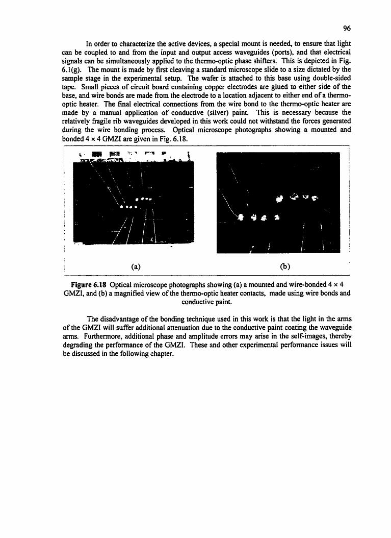
In order to characterize the active devices, a special mount is needed, to ensure that light can be coupled to and h m the input and output access waveguides (ports), and that electrical signals can be simultaneously applied to the thermo-optic phase shiften. This is depicted in Fig. 6.1 (g). The mount is made by first cleaving a standard microscope slide to a size dictated by the sample stage in the experirnental sehip. The wafer is attached to this base using double-sided tape. Small pieces of circuit board containing copper electrodes are giued to either side of the base, and wire bonds are made from the electrode to a location adjacent to either end of a thenno- optic heater. The final electrical connections from the wire bond to the thermosptic heater are made by a manual application of conductive (silver) paint. This is necessary because the relatively fragile rib waveguides developed in this work could not withstand the forces generated dunng the wire bonding process. ûptical microscope photographs showing a mounted and bonded 4 x 4 GMZI are given in Fig. 6.18.
Figure 6.18 Optical microscope photographs showing (a) a mounted and wire-bonded 4 x 4 GMZI, and (b) a magnified view of the thermo-optic heater contacts, made using wire bonds and
conductive paint.
The disadvantage of the bonding technique used in this work is that the light in the arms of the GMZI will suffer additional attenuation due to the conductive paint coating the waveguide anns. Funhennore, additional phase and amplitude erron may arise in the ~el~images, thereby degrading the performance of the GMZI. These and other experimental performance issues will be discussed in the following chapter.
Chapter 7
Device Performance
In this chapter the measured peflormance of the integrned devices fabricated in this work is presented Through demonstrations of the device operation. the principles of the theory developed in earlier chapters are verifed The work presented in this chapter was performed during a period as a visiting scientist in the Ligh~ave Devices Group at the University of Twente, The Netherlands. Portions of thk chapter have been reported in a post-deadline paper presented ut the European Conference on Integrated Optics (ECIO '99) in Turin, Italy [l IO]; in a paper tu oppear in the Journal of Lightwave Technology 1361; and in a paper submitted to the Journal of Lightwave Technology [54].
7.1 Introduction The realization of single-mode waveguides, MM1 couplers, and GMZIs in a high
refractive index contrast design using PECVD SiOZ/SiON technology has been desct-ibed in the previous chapter. To assess the validity of the theory of the GMZI and the integrated device designs developed in earlier chaptea, the expenmental operation of the fabricated devices rnust be demonstrated.
A principal aim of this chapter is to provide insights into the feasibility of attaining multimode interference-based devices providing new and usehl functions for optical network applications. A secondary goal is to show that the various choices made in the design and realization of the devices together provide the possibility of achieving compact. low-Ioss, polarization-insensitive silica-based devices that have a fast active mponse with low power consumption.
The results presented here are technology dependent and in many cases the device performance is sub-optimal with respect to some parameter. For example. relatively high propagation losses are seen because the films used have not been annealed. Imperfections in the fabncated waveguide sidewalls and thermo-optic contacts degrade the performance of the MM1 couplea and GMZI devices, but such issues are amenable to improvement through development of the fabrication technology. This work attempts to tread a 'middle ground' between demonstrating the validity of theoretical concepts such as variable-ratio power splitting and multi- port switching in the GMZI on the one hand, while on the other hand utilizing a new waveguide design to investigate the possibility of polarization-insensitive, fast, and low-power device operation.
OAen a number of iterative stages of device design, fabrication, and pertbrmance measurement are employed to meet the increasingly demanding requirements for the commercial viability of a new integrated optical device. It is the goal of this work to show that in a single iteration, the feasibility of realizing new types of devices can be assessed while simultaneously providing information into the technology possibilities available. It is the hope that this will considerably reduce the time firame for which these new devices can be employed in practical optical networks.
7.2 Experimental procedure The performance of the deiices iri diis work has been measured using the waveguide
characterization setup in the Lightwave Devices Group at the Universi*ty of Twente. The feattues of this setup will be desaîbed in this section. Also discussed here is the theory that has been used to estimate fiber-to-chip coupling losses in the senip. The coupling of Iight from a fiber into a plana. waveguide chip typicany resuIts in some level of optical loss. Estimation of the amount of
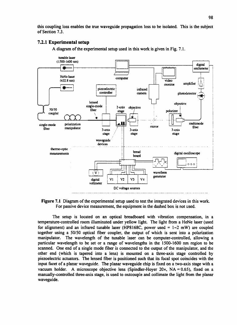
98
this coupling loss enables the tme waveguide propagation loss to be isolated. This is the subject of Section 7.3.
7.2.1 Experimental setup A diagram of the experimental setup used in this work is given in Fig. 7.1.
Figure 7.1 Diagram of the experimental setup used to test the integrated devices in this work. For passive device measurement, the equipment in the dashed box is not used.
The setup is located on an optical breadboard with vibration compensation, in a temperature-controlled room illuminated under yellow light. The light fiom a HeNe laser (used for alignment) and an infrared tunable laser (HP8168C, power used = 1-2 mW) are coupled together using a 50/50 optical fiber coupler, the output of which is sent into a polarization manipulator. The wavelength of the tunable laser can be computer-controlled, allowing a particular wavelength to be set or a range of wavelengths in the 1500-1600 nm region to be scanned. One end of a singIe mode fiber is comected to the output of the manipulator, and the other end (which is tapered into a lens) is mounted on a three-mis stage controlled by piezoelectric actuators. The lensed fiber is positioned such that its focal spot coincides with the input facet of a planar waveguide. The planar waveguide chip is f i e d on a two-axis nage with a vacuum holder. A microscope objective leus (Spinder-Hoyer ZOx, NA = 0.65), tixed on a manually-controlled three-axis stage, is used to outcouple and colIirnate the Iight fiom the planar waveguide.
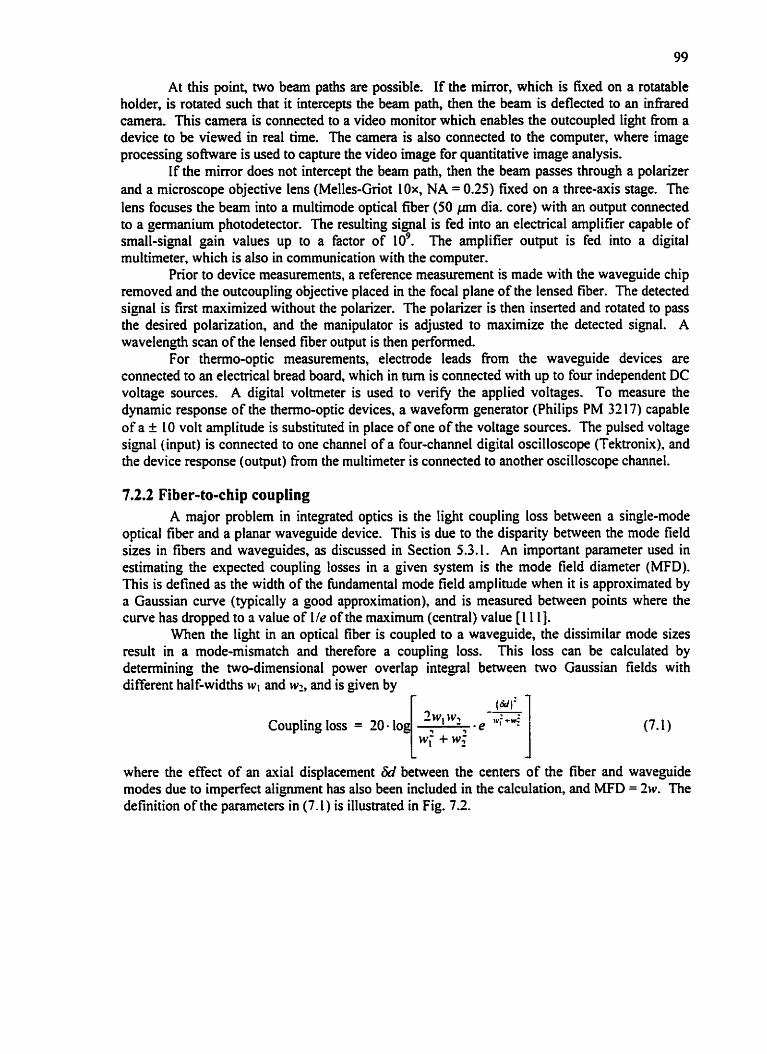
At this point two beam paths are possible. If the mirror, which is k e d on a rotatable holder, is rotated such that it intercepts the beam path, then the beam is deflected to an i n h e d camera. This camera is connected to a video rnonitor which enables the outcoupled light fiom a device to be viewed in real time. The carnera is also connected to the computer, where image processing software is used to capture the video image for quantitative image analysis.
If the mirror does not intercept the beam path, then the beam passes through a polarizer and a microscope objective lens (Melles-Gnot 1 Ox, NA = 0.25) fixed on a three-axis stage. The lens focuses the beam into a multimode optical fiber (50 pn dia. core) with an output connected to a germanium photodetector. The raulting signal is fed into an electrical amplifier capable of small-signal gain values up to a factor of 109. The amplifier output is fed into a digital multimeter, which is also in communication with the computer.
Prior to device measurements, a reference rneasurement is made with the waveguide chip rernoved and the outcoupling objective placed in the focal plane of the lensed fiber. The detected signal is first maximized without the polarizer. The polarizer is then inserted and rotated to pass the desired polarization, and the manipulator is adjusted to maximize the detected signal. A wavelength scan of the iensed fiber output is then performed.
For thenno-optic measurements, electrode leads fiom the waveguide devices are connected to an electrkal bread board, which in turn is connected with up to four independent DC voltage sources. A digital voltmeter is used to ver@ the applied voltages. To measure the dynamic response of the thermo-optic devices, a waveform generator (Philips PM 3217) capable of a t 10 volt amplitude is substituted in place of one of the voltage sources. The pulsed voltage signal (input) is connected to one channe1 of a four-charnel digital oscilloscope (Tektronix). and the device response (output) fiom the multimeter is connected to another oscilloscope channel.
7.2.2 Fiber-to-chip coupüng A major problem in integrated optics is the Iight coupling loss between a single-mode
optical fiber and a planar waveguide device. This is due to the disparity between the mode field sizes in fiben and waveguides, as discussed in Section 5.3.1. An important parameter used in estimating the expected coupling losses in a given system is the mode field diameter (MFD). This is defined as the width of the fundamental mode field amplitude when it is approximated by a Gaussian curve (typically a good approximation), and is measured between points where the curve has dropped to a value of' I/e of the maximum (central) value [ I I 11.
When the light in an optical fiber is coupled to a waveguide, the dissimilar mode sizes result in a mode-mismatch and therefore a coupling loss. This loss can be calculated by detennining the two-dimensional power overlap integral between two Gaussian fields with different half-widths iv , and w?, and is given by
Coupling loss = 20 10 wz + w;
where the effect of an axial displacement 6d between the centers of the fiber and waveguide modes due to imperfect alignment has ako been inchded in the calculation, and MFD = 2w. The definition of the parameters in (7.1) is illustrated in Fig. 7.2.
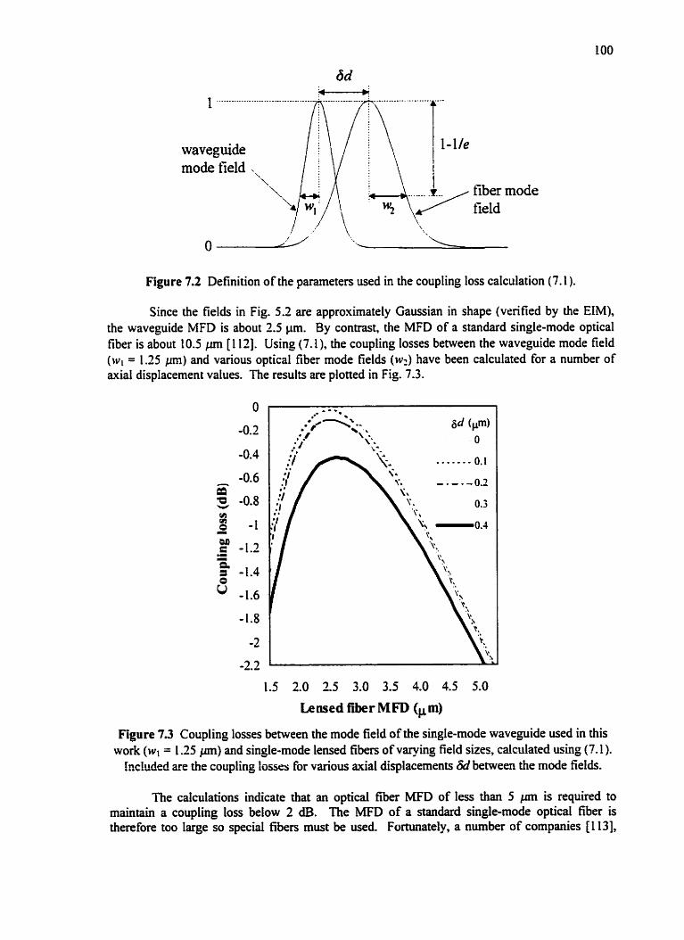
Figure 7.2 Definition OF the parameten w d in the coupling loss calculation (7.1 ).
Since the fields in Fig. 5.2 are approximately Gaussian in shape (vcrified by the EIM), the waveguide MFD is about 2.5 Pm. By contrast, the MFD of a standard single-mode optical fiber is about 10.5 p [ l 121. Using (7.1 ), the coupling losses between the waveguide mode field ( w , = 1.25 pm) and various optical fiber mode fields (w,) have been calculated for a number of axial displacement values. The results are plotted in Fig. 7.3.
1.5 2.0 2.5 3.0 3.5 4.0 4.5 5.0
Leosed fiber MFD
Figure 73 Coupling losses between the mode field of the single-mode waveguide used in this work (wl = 1.25 p) and singlemode lensed fibers of varying field sizes, calculated using (7.1).
Included are the coupling losses for various axial displacements 6d between the mode fields.
The calculations indicate that an optical mer MFD of Iess than 5 prn is required to maintain a coupling loss below 2 dB. The MFD of a standard single-mode optical fiber is therefore too large so special fibers must be used. Furhmately, a number of companies [113],
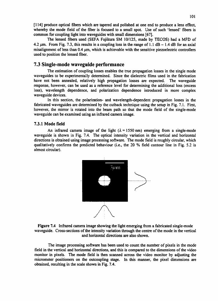
[114] produce optical fiben which are tapered and polished at one end to produce a lens effect, whereby the mode field of the fiber is focused to a mal1 spot Use of such 'lensed' fibers is common for coupling light into waveguides with small dimensions [67].
The lensed fiben used (SEFA F u j W SM 10/125, made by TECOS) had a MFD of 4.2 p. From Fig. 7.3, this results in a coupling loss in the range of 1.1 dB - 1.4 dB for an axial misalignrnent of less than 0.4 p, which is achievable with the sensitive piezoelectric controllen used to position the lensed fiber.
7.3 Single-mode waveguide performance The estimation olcoupling losses enables the m e propagation losses in the single mode
waveguides to be experimentally determined. Since the dielectric films used in the fabrication have not been annealed, relatively high propagation losses are expected. The waveguide response, however, can be used as a reference level for detennining the additional loss (excess loss), wavelength dependence, and polarization dependence introduced in more complex waveguide devices.
In this section, the polarkation- and wavelength-dependent propagation losses in the Fabricated waveguides are determined by the cutback technique using the setup in Fig. 7.1. Fint. however, the mirror is rotated into the beam path so that the mode field of the single-mode waveguide can be examined using an infrared camera image.
7.3.1 Mode field An i n h e d carnera image of the light (A = 1550 nm) emerging €rom a single-mode
waveguide is shown in Fig. 7.4. The optical intensity variation in the vertical and horizontal directions is obtained using image processing software. The mode field is roughly circular, which qualitatively confinns the predicted behaviour (i.e., the 20 % field contour line in Fig. 5.2 is almost circular).
Figure 7.4 Infrared camera image showing the light emerging fiom a fabncated single-mode waveguide. Cross-sections of the intensity variation through the centre of the mode in the vertical
and horizontal directions are also shown.
Tne image processing software has been used to count the number of pixels in the mode field in the vertical and horizontal directions, and this is compared to the dimensions of the video monitor in pixels. The mode field is then scanned across the video monitor by adjusting the micrometer positioners on the outcoupling stage. In this marner, the pixel dimensions are obtained, resulting in the scale show in Fig. 7.4.

A siight horizontal asymrnetry in the mode can be seen. The source of this is believed to be an imperfect EUE in some waveguides, resulting in a vertical waveguide sidewall on one side, and a slight angle in the sidewall on the other (see Fig. 6.14(a), for example). The measured MFD of the waveguide mode in Fig. 7.4 is 2.3 p (vertical direction) and 2.4 pm (horizontal direction). Note that since the MFD is being detennined fiom a field intensity scan, the values must be taken at the 1/e2 intensity points.
7.3.2 Propagation losses Propagation losses in the single-mode waveguides have been measured using the cutback
technique. In this technique, the ratio of the ûansmitted intensity through a waveguide to the intensity from the input fiber (reference) is measured, to arrive at the insertion loss:
OUI
Insertion loss = 10 log ,, (7.2)
The waveguide is subsequently cleaved to a shorter length and the new insertion loss is measured. This procedure is repeated several times. The insertion losses are then plotted venus the waveguide length, and the slope of the line is the propagation loss a in the waveguide, detined by (6.3) and typically measured in units o€dB/cm.
Though the cutback technique is straightforward in principle, it has the drawback that the accuracy of the method is dependent upon the reproducibility of both the waveguide cleaves and the alignment used to couple light to and from the waveguide. This uncertainty is, however. panially offset by repeating the cutback measurement a number of times, and using the slope of a line fitted to the expenmental points. To reduce the uncertainty further, the intercept of the fitted line with the loss axis has been fixed at a value based upon the fiber-to-chip coupling losses estimated from Fig. 7.3. The cutback measurement has been perfonned on a number of straight single-mode waveguides by cleaving the waveguides and performing the insertion loss measurement three times. The measured insertion Iosses for a typical single-mode waveguide at A= 1550 nm are plotted in Fig. 7.5 for both polarizations. The waveguide has been cleaved fiom its original Iength of 21 mm to 1 7.5 mm, 14 mm, and 10.5 mm. Also included are the lest squares regession lines fitted to the data points, and their equations.
A value of 1.5 dB has been chosen for the coupling losses Wintercept), based on the values in Fig. 7.3 and additional reflection losses at the waveguide input face! and at the 20x microscope objective lens. The large numerical aperture of this lens ensures that most of the light emerging fiom the output facet of the waveguide is collected, so fiuther losses are assumed to be negligible. Using this value, the dopes of the fitted lines yield waveguide propagation losses of 3.417 dB/m (TE) and 3.408 dB/cm (TM). These values indicate that the waveguide is relatively polarization insensitive, with a polarization dependent loss of less than 0.01 dB/cm. As expected. the losses in these waveguides are high since the films have not been annealed.
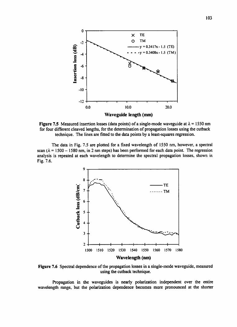
0.0 10.0 20.0
Waveguide length (mm)
Figure 7.5 Measured insertion losses (data points) of a single-mode waveguide at A = 1550 nm for four different cleaved lengths, for the determination of propagation losses using the cutback
technique. The lines are fitted to the data points by a least-squares regression.
The data in Fig. 7.5 are plotted for a fixed wavelength of 1550 nm, however, a spectral scan (A = 1500 - 1580 nm, in 2 nm steps) has been performed for each data point. The regression analysis is repeated at each wavelength to determine the spectral propagation losses, shown in Fig. 7.6.
Figure 7.6 Spectral dependence of the propagation iosses in a single-mode waveguide, meanved using the cutback technique.
Propagation in the waveguides is nearfy polarization independent over the entire wavelength range, but the polarization dependence becomes more pronounced at the shorter

wavelengths. The propagation losses in the waveguides dso increase at these shorter wavelengths. A loss maximum is evident, and corresponds to the weli-known absorption peak at A = 1508 nm due to N-H bond resonances in the un-annealed Si02 and SiON films [70], [72], In fact, the general shape of the curve in Fig. 7.6 is very similar to the transmission characteristic for the un-annealed SiON film in Fig. 6.5 in the same wavelength region. The curve is also similar to results reported by Wlirhoff et. al. [Ml, where it has been s h o w that annealing can reduce the propagation losses by an order of magnitude at A = 1550 nm.
A knowledge of the propagation losses in the fabricated single-mode waveguides enables the performance charactenstics of more complex devices such as MM1 couplers, to be determined.
7.4 MMI coupler performance
7.4.1 Definitions In previous chapters, it has been established that MMI couplers with low excess losses
and an equal power splitting ratio (low imbalance) are required for good GMZI performance. To gain an understanding of the GMZI response, it is thus necessary first to investigate the characteristics of the constituent MM1 couplers. In this section, the measured excess losses and imbalance of 2 x 2 and 4 x 4 MM1 couplers are compared to predicted values, thereby providing insights into the limitations of the device design and the fabrication process.
Irnbalance is a measure of the deviation in the power splitting ratio of the rV x iV MM1 coupler from the ideal case of equal power splitting. This has been defined in (3.28) in terms of field amplitude coefficients and is redefined here in ternis of the measured intensity,
where j refea to the output pon number in Fig. 3.1 and&. is a reference output port. Some ambiguity exists in (7.3), because an N x N MM1 coupler would have N - 1 imbalance values and these values differ depending upon the reference port chosen. To circurnvent this problem and anive at a single imbalance value for an N x N MM1 coupler, in the results presented here the largest magnitude fiom the set of N(N - 1) imbalances (where al1 ports are used as references) is used.
The excess loss for a switch was defined in ( 4 4 , however, the excess loss in the MM1 coupler is defined as the ratio of the total intensity at the MM1 coupler outputs to the output intensity from a reference single-mode waveguide running parallel to the MM1 coupler, i.e.,
Excess loss = 1 O log ,, 1 Y ? 1 This definition is used because it isolates the loss due to imperfect MM1 coupler imaging and does not include losses arising from the access waveguides. This enables a meaninw@ùl comparison of measured and the simulated coupler losses to be made, since the loss values fiom the MPA simulation performed in Chapter 5 assume no access waveguide losses.
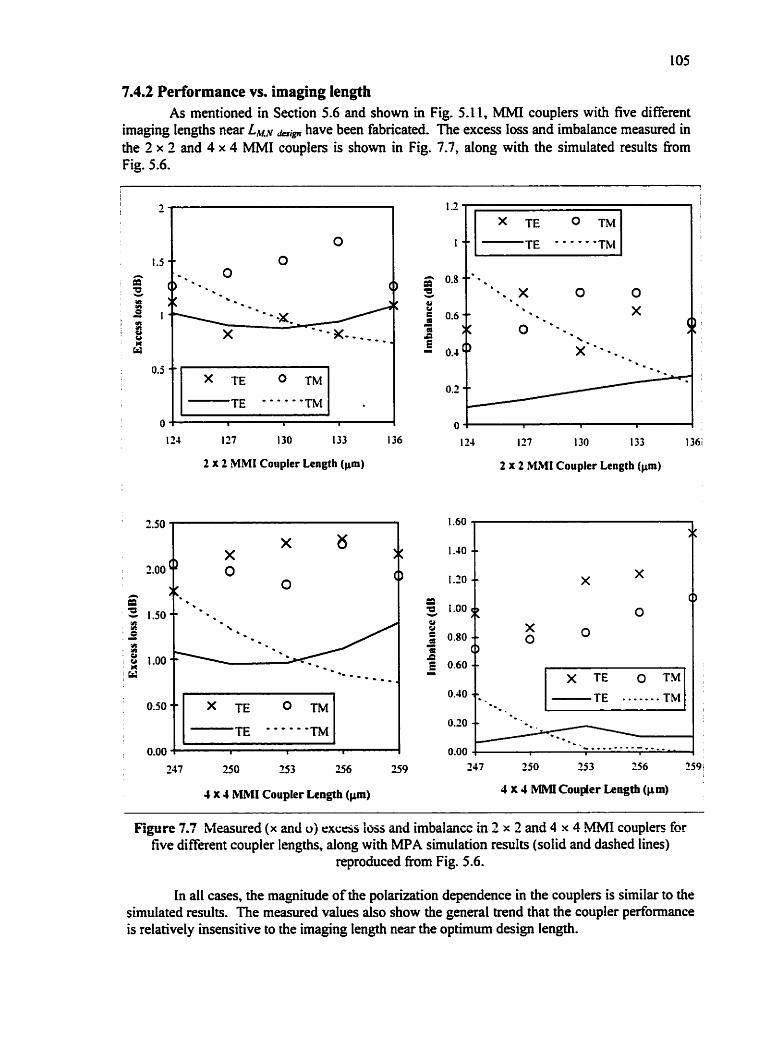
7.4.2 Performance vs. imaging length As mentioned in Section 5.6 and shown in Fig. 5.1 1, MMI couplers with five different
imaging Iengths near LALN k i p have been fabricated. The excess Ioss and imbalance measured in the 2 x 2 and 4 x 4 MM1 couplea is shown in Fig. 7.7, along with the simulated results from Fig. 5.6.
2 X 2 MM1 Coupler Length (pu)
247 250 253 256 259
4 x 4 RIMI Couplet Length (pm)
2 x 2 MM1 Coupler Length (pm)
4 X 4 M M Couper Length (pm)
- - - - - -- - - -
Figure 7.7 Measured (x and o) excess luss anil imbalancc Ui 2 x 2 and 4 x 4 MMI coupleo for five different coupler lengths, along with MPA simulation results (solid and dashed lines)
reproduced fiom Fig. 5.6.
In al1 cases, the magnitude of the polarkation dependence in the couplen is similar to the simulated results. The measured values also show the general trend that the coupler performance is relatively insensitive to the imaging length near the optimum design length.
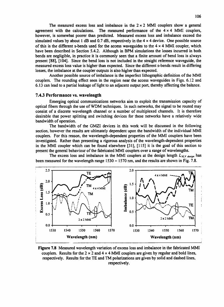
The measured excess loss and imbalance in the 2 x 2 MMI couplers show a general agreement with the calculations. The measured performance of the 4 x 4 MM1 couplers, however, is somewhat poorer than predicted Measured excess Ioss and imbalance exceed the simulated values by about 1 dB and 0.7 dB, respectively in the 4 x 4 device. One possible source of this is the different s-bends used for the access waveguides to the 4 x 4 MM1 coupler, which have been described in Section 5.4.2. Although in BPM simulations the losses incwred in both bends are negligible, in practice it is commonly seen that a fuiite amount of bend loss is always present [Ml, [104]. Since the bend l o s is not included in the straight reference waveguide, the measured excess loss value is higher than expected. Since the diRerent s-bends result in differing losses, the imbalance at the coupler outputs is also higher than expected.
Another possible source of imbalance is the imperfect lithographie definition of the MM1 couplers. The rounding effect seen in the region near the access waveguides in Figs. 6.12 and 6.13 can lead to a partial leakage oflight to an adjacent output port, thereby affecting the balance.
7.4.3 Performance vs. wavelength Emerging optical communications networks aim to exploit the transmission capacity of
optical fiben through the use of WDM techniques. In such networks. the signal to be routed may consist of a discrete wavelength channel or a number of multiplexed channels. It is therefore desirable that power splitting and switching devices for these networks have a relatively wide bandwidth of operation.
The bandwidth of the GMZI devices in this work will be discussed in the Following section, however the results are ultimately dependent upon the bandwidth of the individual MM1 couplen. For this reason, the wavelength-dependent properties of the MMI couplen have been investigated. Rather than pmenting a rigorous analysis of the wavelength-dependent properties in the MM1 coupler which cm be found elsewhere [31], [II51 it is the goal of this section to present the general behaviour of the fabricated MM? couplers over a range of wavelengths.
The excess loss and imbalance in the MM1 couplers at the design length L.tl.v bip has been measured for the wavelength range 1530 - 1570 nm, and the results are show in Fig. 7.8.
1530 1540 1550 1560 1570 1530 1540 1550 1560 1570
I Wavelength (nm) Wavelength (nm)
Figure 7.8 Measured wavelength variation of excess l o s and imbalance in the fabricated MMi couplers. Results for the 2 x 2 and 4 x 4 MMI couplers are givm by regular and bold lines, nspectively. Results for the TE and TM polarizations are given by solid and dashed lines,
respective1 y.
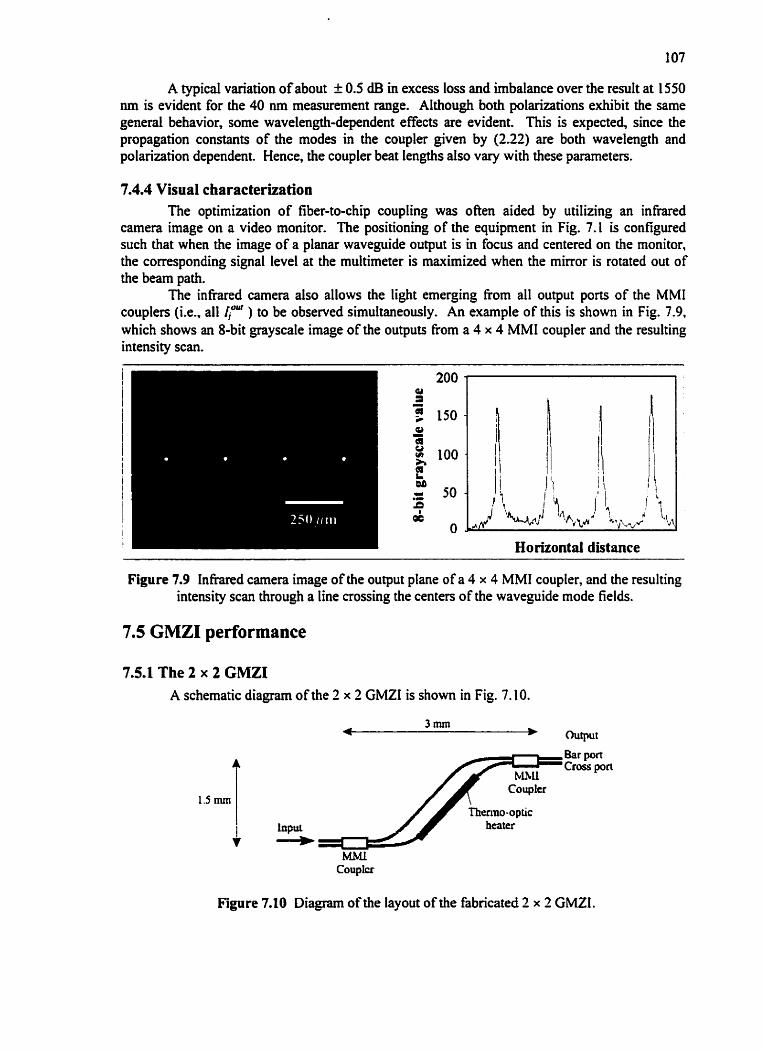
A typicai variation of about k 0.5 dB in excess loss and imbalance over the result at 1550 nm is evident for the 40 nm meaSUTement range. Although both polarizations exhibit the same general behavior, some wavelength-dependent effects are evident. This is expecteà, shce the propagation constants of the modes in the coupler given by (222) are both wavelength and polarization dependent. Hence, the coupler beat lengths also Vary with these parameters.
7.4.4 VisuaI characterization The optimization of fiber-to-chip coupling was ofien aided by utilizing an infiared
camera image on a video monitor. The positionhg of the equiprnent in Fig. 7.1 is configured such that when the image of a plana. waveguide output is in focus and centered on the monitor, the corresponding signal level at the multimeter is maximized when the mirror is rotated out of the beam path.
The infrared camera also allows the light emerging fiom al1 output ports of the MM1 couplers (i.e., al1 hoM ) to be observed simultaneously. An example of this is s h o w in Fig. 7.9, which shows an &bit grayscale image of the outputs from a 4 x 4 MM1 coupler and the resulting intensity scan.
Horizontal distance
Figure 7.9 Infrared camera image of the output plane of a 4 x 4 MME coupler, and the resulting intensity scan through a line crossing the centers of the waveguide mode fields.
7.5 GMZI performance
7.5.1 The 2 x 2 GMZI A schematic diagram of the 2 x 2 GMZI is shown in Fig. 7.10.
Bar port Cross port
Coupler
M W Couplcr
Figure 7.10 Diagram of the layout of the fabricated 2 x 2 GMZI.
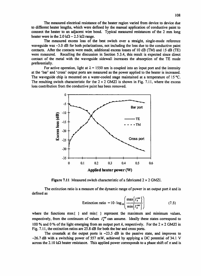
The measured electrical resistance of the heater region varied from device to device due to different heater lengths, which were defined by the manual application of conductive paint to connect the heater to an adjacent wire bond. Typical measured resistances of the 2 mm long heater were in the 2.0 kZT - 2.5 kR range.
The measured excess loss of the best switch over a straight, single-mode reference waveguide was -3.0 dB for both polarizations, not including the l o s due to the conductive paint contacts. AAer the contacts were made, additional excess losses of 10 dB (TM) and 15 dB (TE) were measured. Recalling the discussion in Section 5.3.4, this remlt is expected since direct contact of the rnetal with the waveguide sidewall increases the absorption of the TE mode pre ferentially .
For active operation, light at A = 1550 nm is coupled into an input port and the intensity at the 'bar' and 'cross' output ports are measured as the power applied to the heater is increased. The waveguide chip is mounted on a water-cooled stage maintained at a temperature of 15 OC. The resulting switch characteristic for the 2 x 2 GMZI is s h o w in Fig. 7.1 1, where the excess loss contribution from the conductive paint has been removed.
O
Appüed heater power (W)
Figure 7.1 1 Measured switch characteristic of a fabricated 2 x 2 GMZf.
The extinction ratio is a measure of the dynamic range of power in an output port k and is defined as
Extinction ratio = I O - log,, [ miniIf i J where the firnctions ma{ } and min( ) represent the maximum and minimum d u e s , respectively, from the continuum of values 1" cm assume. Ideally these *tes correspond to LOO % and O % of the light emerging nom an output port k, respectively. For the 1 x 2 GMZI in Fig. 7.1 1, the extinction ratios are 25.8 ci% for both the bar and cross ports.
The crosstaik at the output ports is -23.5 dB in the passive state, and improves to -26.7 dB with a switching power of 557 mW, achieved by applying a DC potential of 34.1 V across the 2.10 kS2 heater resistance. This applied power corresponds to a phase shift of R and is
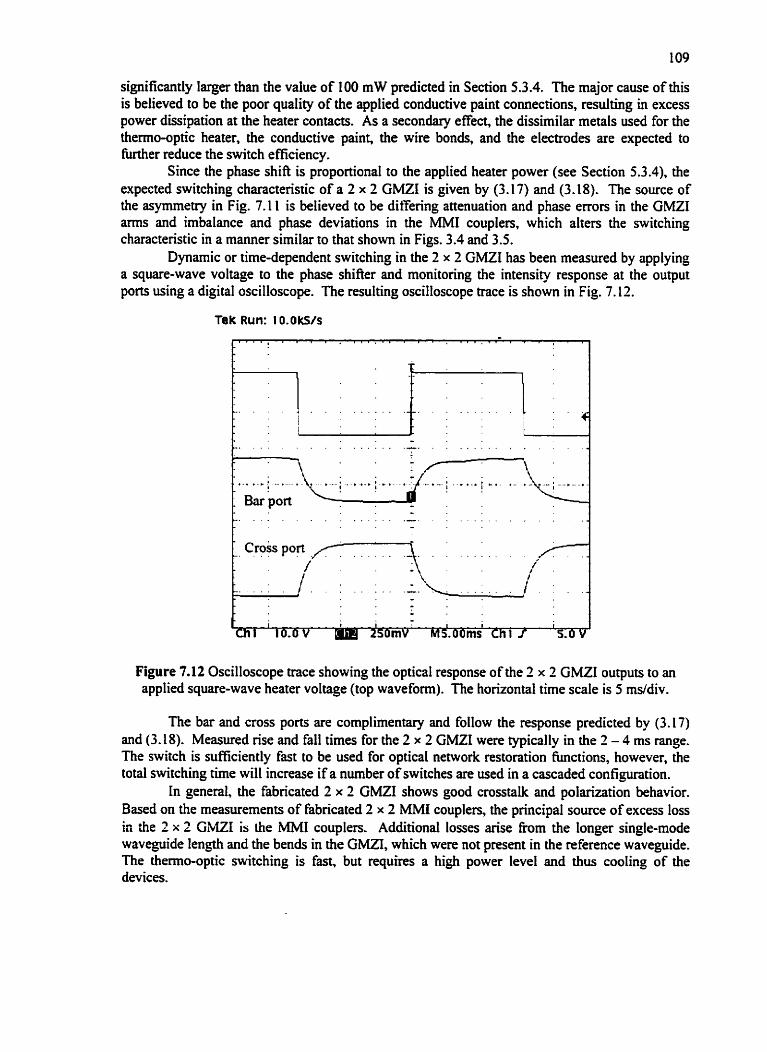
significantly larger than the value of 100 m W predicted in Section 5.3.4. The major cause of this is believed to be the poor quality of the applied conductive paint connections, resulting in excess power dissipation at the heater contacts. As a secondary effect, the dissimilar metals used for the thermooptic heater, the conductive paint, the wire bonds, and the electrodes are expected to M e r reduce the switch efficiency.
Since the phase shift is proportional to the applied heater power (see Section 5.3.4). the expected switching characteristic of a 2 x 2 GMZI is given by (3.17) and (3.1 8). The source of the asymmehy in Fig. 7.1 1 is believed to be diFering attenuation and phase erroa in the GMZl arrns and imbalance and phase deviations in the MM1 couplen, which alters the switching characteristic in a manner similar to that shown in Figs. 3.4 and 3.5.
Dynamic or rime-dependent switching in the 2 x 2 GMZI has been measured by applying a square-wave voltage to the phase shifter and monitoring the intensity response at the output ports using a digital oscilloscope. The msulting oscilloscope trace is shown in Fig. 7.12.
Tek Run: 1 O.OkS/s
; \il ...... C I . .......... '-.-,-.-..
Figure 7.12 Oscilloscope trace showing the optical response of the Z x 2 GMZl outputs to an applied square-wave heater voltage (top waveform). The horizontal time scale is 5 ms/div.
The bar and cross ports are complimentary and follow the response predicted by (3.17) and (3.18). Measured nse and fa11 times for the 2 x 2 GMZI were typically in the 1 - 4 ms range. The switch is sufficiently fast to be used for optical network restoration functions, however, the total switching time will increase if a number of switches are used in a cascaded configuration.
In general, the fabricated 2 x 2 GMZI shows good cmsstalk and polarization behavior. Based on the measurements of fabricated 2 x 2 M M couplers, the principal source of excess loss in the 2 r 2 GhEI is the MM1 couplen. Additionai losses *se from the longer single-mode waveguide length and the ben& in the GMZI, which were not present in the reference waveguide. The thenno-optic switching is fbt, but requkes a high power level and thus cooling of the devices.
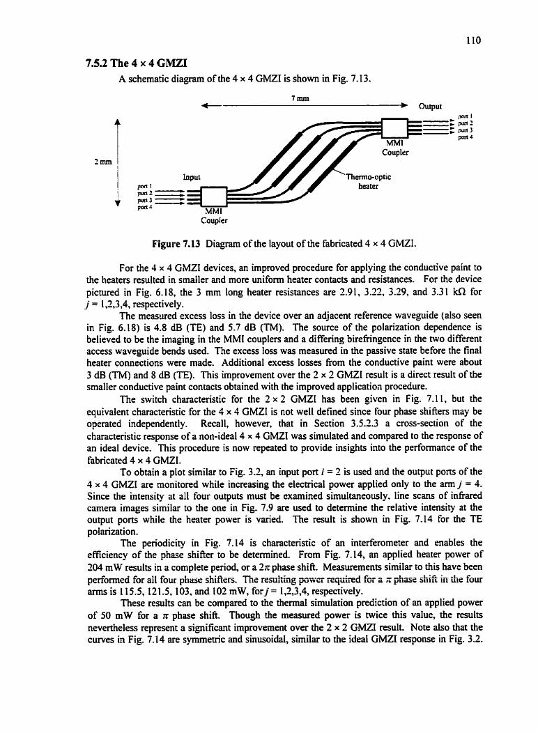
7.5.2 The 4 x 4 GMZI A schematic diagram of the 4 x 4 GMZI is shown in Fig. 7.13.
Coupler
Figure 7.13 Diagram of the layout of the fabricated 4 x 4 GMZI.
For the 4 x 4 GMZI devices, an improved procedure for applying the conductive paint to the heaters resulted in smaller and more unifonn heater contacts and resistances. For the device pictured in Fig. 6.18, the 3 mm long heater resistances are 2.91. 3.22. 3.29, and 3.3 1 kR for j = 1,2,3,4, respectively.
The measured excess loss in the device over an adjacent reference waveguide (also seen in Fig. 6.18) is 4.8 dB (TE) and 5.7 dB (TM). The source of the polarization dependence is believed to be the imaging in the MM1 couplers and a diffenng birefnngence in the two different access waveguide ben& used. The excess loss was measured in the passive state before the final heater connections were made. Additional excess Iosses fiom the conductive paint were about 3 dB ('TM) and 8 dB (TE). This improvement over the 2 x 2 GMZI result is a direct result of the smaller conductive paint contacts obtained with the improved applicatioii procedure.
The switch characteristic for the 2 x 2 GMZI has been given in Fig. 7.1 1, but the equivalent characteristic for the 4 x 4 GMZI is not well defined since four phase shifiers may be operated independently. Recall, however, that in Section 3.5.2.3 a cross-section of the characteristic response of a non-ideal 4 x 4 GMZI was simulated and compared to the response of an ideal device. This procedure is now repeated to provide insights into the performance of the fabricated 4 x 4 GMZI.
To obtain a plot similar to Fig. 3.2. an input port i = 2 is used and the output ports of the 4 x 4 GMZI are monitored while increasing the electrical power applied only to the am j = 4. Since the intensity at al1 four outputs must be examined simuitaneously. line scans of infiared camera images similar to the one in Fig. 7.9 are used to determine the relative intensity at the output ports while the heater power is vxied. The result is shown in Fig. 7.14 for the TE polarization.
The periodicity in Fig. 7.14 is characteristic of an interferorneter and enables the eficiency of the phase shifier to be determined. From Fig. 7.14, an applied heater power of 204 m W results in a complete penod, or a ZR phase shifi. Measurements similar to this have been performed for al1 four phase shifiers. The resuliing powa reqtiired for a a phase shifi in the four arms is 115.5, 121.5, 103, and 102 mW, for j= 1,2,3,4, respectively.
These results can be compared to the thermal simulation prediction of an applied power of 50 m W for a n phase shik Though the measured power is twice this value, the r a i t s nevertheless represent a significant improvement over the 2 x 2 GMZI result. Note also that the curves in Fig. 7.14 are symmetric and sinusoiciai, sirnilar to the ideal GMZI response in Fig. 3.2.
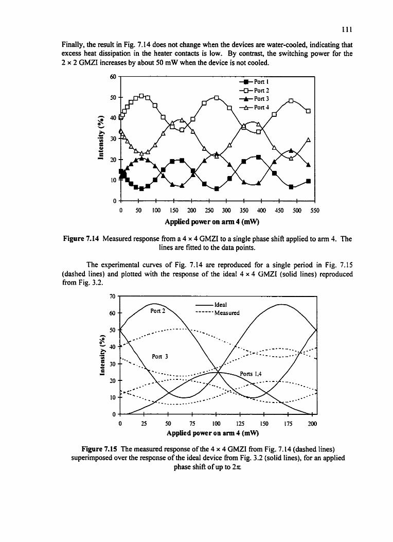
Finally, the result in Fig. 7.14 does not change when the devices are water-cooled, indicating that excess heat dissipation in the heater contacts is low. By contrast, the switching power for the 2 x 2 GMZI increases by about 50 m W when the device is not cooled.
O 50 100 150 200 250 300 350 400 450 500 550
Apptied power on a m 4 (mW)
Figure 7.14 Measured response fkom a 4 x 4 GMZI to a single phase shift applied to a m 4. The lines are titted to the data points.
The experimental curves of Fig. 7.14 are reproduced for a single period in Fig. 7.15 (dashed lines) and plotted with the response of the ideal 4 x 4 GMZI (solid lines) reproduced from Fig. 3.2.
O 50 75 100 125 150 175 200
Appüed power on arm 4 (mW)
Figure 7.15 The measured response of the 4 x 4 GMZI from Fig. 7.14 (dashed lines) superimposed over the response of the ideai device Eom Fig. 3.2 (solid lines), for an applied
phase shifi of up to 2 z

The measured device response is in general phase shiAed, the amplitude of intensity variations is diminished, and the level about which the intensity varies sinusoidally is offset with respect to the ideal device. Similar results were noted for the 2 x 2 GMZI. Consider for a moment a mathematical description of this result. Arbiûarily choosing the port k = 2 in Fig. 7.15, in the ideal GMZI the relative intensity in this port should Vary according to the result predicted by (3.13, i.e.,
The equation of the measured response for this port in Fig. 7.15, however, is given by I 1 -- = - [332 + 0.63 sin(Acp, - 0.45) + 03 cos(A<p, - 0.491 (7.7) 1 0 8
To understand the sources of this discrepancy, the result (7.7) should be compared to the theoretical mode1 of the non-ideal GMZI in (3.32). Phase deviations in the MM1 couplers and phase errors in the GMZI m s both contribute to the -0.45 radian shifl, the imbalance in the MM1 couplers contributes to the amplitude attenuation in the sine and cosine terms, and a combination of phase and imbalance effects contribute to the offset of 0.32 in the constant term in (7.7).
Note that phase errors and irnbalance arising fiom the conductive paint in the arms and the diffenng output access waveguide lengths have not been included in this analysis. Clearly, these factors also contribute to the obse~ed response.
A qualitative comparison of Fig. 7.15 with Fig. 3.4 confimis that MM1 coupler deviations are present in the fabricated device. Phase errors in the arms are also present and a comparison of Fig. 7.15 with Fig. 3.5 suggests they are distributed approximately randomly among a range of values between O and 2~ ,
7.5.2.1 1 x N GMZI switching The unknown (and likely large) random phase errors in the arms of the fabricated GMZI
mult in an unpredictable response for a given set of applied phase shifts. In Section 3.5 it was shown that the phase shitls applied to the GMZI arms can include a bias component to compensate for the phase errors in the m s . The response of the fabricated GMZI is thereby brought closer to the ideal response, so that the device behaves more predictably with an applied set of phase shifts. This enables the practical operation of the GMZI.
Since the phase errors in the GMZI arms are not known, the following experimental procedure utilized by Jenkins et. al. [34] is used to compensate for these phase errors. The device is first brought into a switching state, where ideally al1 of the output light emerges fiom a single port. This has been done in the 4 x 4 device by adjusting the voltage applied to the four thenno- optic phase shifters while monitoring the optical intensity emerging from the output ports using an i n b e d carneca. The camera signal is sent to a cornputer, where image processing software is used to provide a line scan of the image. An iterative manual phase shifi a d j m e n t technique is then used to bring the device to a switch state, correspondhg to maximizing the peak on the line scan for a given output. The bias phase s h i k are then the difference between the applied phase shifts and the theoretical phase shifts given by the relevant column of the ideal switching phase shifi matnx Xgiven in (4.23).
Using these bias values, the phase shifts necessary for the other switching states have been calculated and applied to the device, to obtain the remaining switch states. In practice, however, only approximate switch States are achieved by this method. It has been found that fine-tuning of the phase shifts is otten needed to improve the switch state. This can be understood intuitively by noting that the phase shifts from the ideal switching matrix are calculated by solving (3.13). The non-ideal device, however, includes MMI coupler deviations,
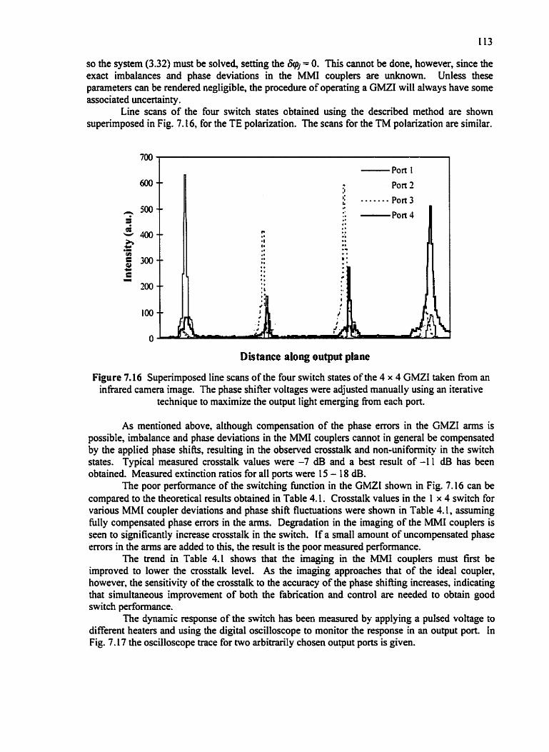
so the system (3.32) must be solved, seaing the aj = O. This cannot be done, however, since the exact imbalances and phase deviations in the MM1 couplers are unknown. Unless these parameters can be rendered negligible, the procedure of operating a GMZI will always have some associated uncertainty.
Line scans of the four switch states obtained using the described method are show supenmposed in Fig. 7.16, for the TE polarization. The scans for the TM polarization are similar.
Dis tance along output plane
Figure 7.16 Supenmposed line scans of the four switch states of the 4 x 4 GMZI taken Fiom an infrared camera image. The phase shifter voltages were adjusted manually using an iterative
technique to rnaximize the output light emerging fiom each port.
As mentioned above, although compensation of the phase erron in the GMZI amis is possible, imbalance and phase deviations in the MM1 couplers cannot in general be compensated by the applied phase shitts, resulting in the observed crosstalk and non-uniformity in the switch states. Typical measured crosstalk vaIues were -7 dB and a best result of -1 1 dB has been obtained. Measured extinction ratios for al1 ports were 15 - 18 dB.
The poor performance of the switching function in the GMZt shown in Fig. 7.16 cm be cornpared to the theoretical results obtained in Table 4.1. Crosstaik values in the 1 x 4 switch for vanous MM1 coupler deviations and phase shift fluctuations were shown in Table 4.1, asniming fully compensated phase erroa in the arms. Degradation in the imaging of the MM1 couplers is seen to significantly increase crosstalk in the switch. if a smail amount of uncompensated ph= errors in the arms are added to this, the result is the poor measured performance.
The trend in Table 4.1 shows that the irnaging in the MM1 couplers must first be improved to lower the crosstaik level. As the imaging approaches that of the ideal coupler, however, the sensitivity of the msstalk to the accuracy of the phase shifting increases, indicating that simultaneous improvement of both the fabrication and control are needed to obtain good switch performance.
The dynamic response of the switch has been measured by applying a pulsed voltage to different heaters and using the digital oscilloscope to monitor the response in an output port. ln Fig. 7.17 the oscilloscope trace for two arbitrarily chosen output ports is given.
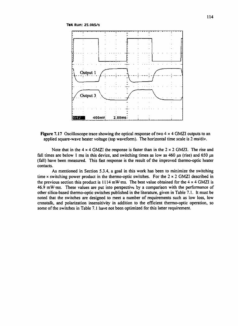
Figure 7.17 Oscilloscope trace showing the optical response of two 4 x 4 GMZI outputs to an applied square-wave heater voltage (top waveform). The horizontal time scale is 2 ms/div.
Note that in the 4 x 4 GMZI the response is faster than in the 2 x 2 GMZI. The rise and fa11 times are below 1 ms in this device, and switching times as low as 460 ps (nse) and 650 ps (fall) have been measured. This fast response is the result of the improved thenno-optic heater contacts.
As mentioned in Section 5.3.4, a goal in this work has been to minirnize the switching time x switching power product in the thermo-optic switches. For the 2 x 2 GMZI described in the previous section this product is 1 1 14 mW-ms. The best value obtained for the 4 x 4 GMZI is 46.9 mW.ms. These values are put into penpectivt by a cornparison with the performance of other silica-based thermo-optic switches published in the literature, given in Table 7.1. It must be noted that the switches are designed to meet a number of requirements such as low loss, low crosstalk, and polarization insensitivity in addition to the eficient thermo-optic operation, so some of the switches in Table 7.1 have not been optimized for this latter requirement.
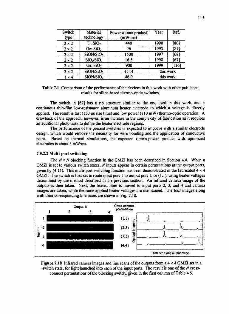
Switch type 2 x 3
TabIe 7.1 Comparison of the performance of the devices in this work with other published results for silica-based thermo-optic switches.
2 x 2 1 SiON/Si02
2 x 2 1 x 4
The switch in [67] has a rib structure similar to the one used in this work and a continuous thin-film low-resistance aluminum heater electrode to which a voltage is directly applied. The result is fast ( 150 p rire time) and low power ( i 10 mW) thermo-optic operation. A drawback of the approach, however, is an increase in the complexity OF fabrication as it requires an additional photomask to define the heater electrode regions.
The performance of the present switches is expected to improve with a similar electrode design, which would remove the necessity for wire bonding and the application of conductive paint. Based on thermal simulations, the expected time x power product with optimized electrodes is about 5 mW+ms.
Matenai technology
Ti: Si02
2 x 2
7.5.2.2 Multi-port switching The iV x N blocking function in the GMZI has been described in Section 1.4. When a
GMZI is set to various switch States, N inputs appear in certain permutations at the output ports, given by (4.1 1). This multi-port switching function has been demonstrated in the fabricated 4 x 4 GMZI. The switch is fint set to route input port 1 to output port 1, or ( 1 , l ), using heater voltages detennined by the method described in the previous section. An infrared camera image of the outputs is then taken. Next, the lensed fiber is moved to input ports 2, 3, and 4 and carnera images are taken, while the same applied heater voltages are maintained. The four images along with their corresponding Iine scans are shown in Fig. 7.18.
Year Power x t h e product (mWms)
440
[68] f67] SiOJSi02
1500 11997
Si0N/SiO2 SiON/SiOz
Figure 7.18 Infrared camera images and line scans of the outputs nom a 4 x 4 GMZI set in a switch state, for light launched into each of the input ports. The result is one of the LV cross-
connea permutations of the blocking switch, given in the fïrst column of Table 4.5.
Ref.
[116] 2 x 2 16.5
1990 1 1801
1998
11 14 46.9
Ge: Si02 1 900 this work this work
1999
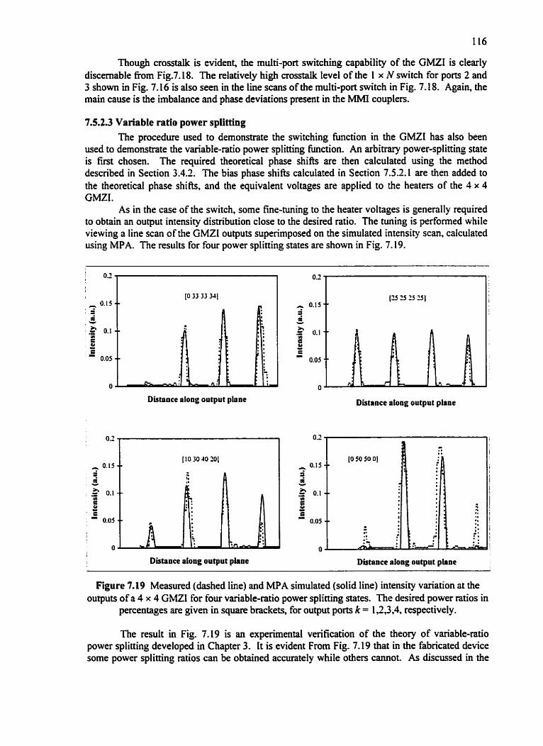
Though crosstalk is evident, the multi-port switching capability of the GMZI is clearly discemable fiom Fig.7.18. The relatively high crosstalk level of the 1 x N switch for ports 2 and 3 shown in Fig. 7.16 is also seen in the line scans of the dt i -por t switch in Fig. 7.18. Again, the main cause is the irnbalance and phase deviations present in the MM1 couples.
7.5.23 Variable ratio power spiitting The procedure used to demonstrate the switching function in the GMZI has also been
used to demonstrate the variable-ratio power splitting hction. An arbitrary power-splitting state is first chosen. The required theoretical phase shifts are then calculated using the method described in Section 3.4.2. The bias phase shih calculated in Section 7.5.2.1 are then added to the theoretical phase shifts, and the equivalent voltages are applied to the heaten of the 4 x 4 GMZI.
As in the case of the switch, some fine-tuning to the heater voltages is generally required to obtain an output intensity distribution close to the desired ratio. The tuning is performed while viewing a line scan of the GMZI outputs superirnposed on the simulated intensity scan. calculated using MPA. The results for four power splitting states are show in Fig. 7.19.
Distance dong output plane Distance dong output plane
I
Distance atong output phne Distance along output plane
Figure 7.19 Measured (dashed line) and MPA simulated (solid line) intensity variation at the outputs of a 4 x 4 GblZI for four variable-ratio power splitting states. The desired power ratios in
percentages are given in square brackets, for output ports k = 1,2,3,4, respectively.
The result in Fig. 7.19 is an experimental verification of the theory of variable-ratio power splitting developed in Chapter 3. [t is evident From Fig. 7.19 that in the fabricated device some power splitting ratios can be obtained accurately while others cannot. As discussed in the
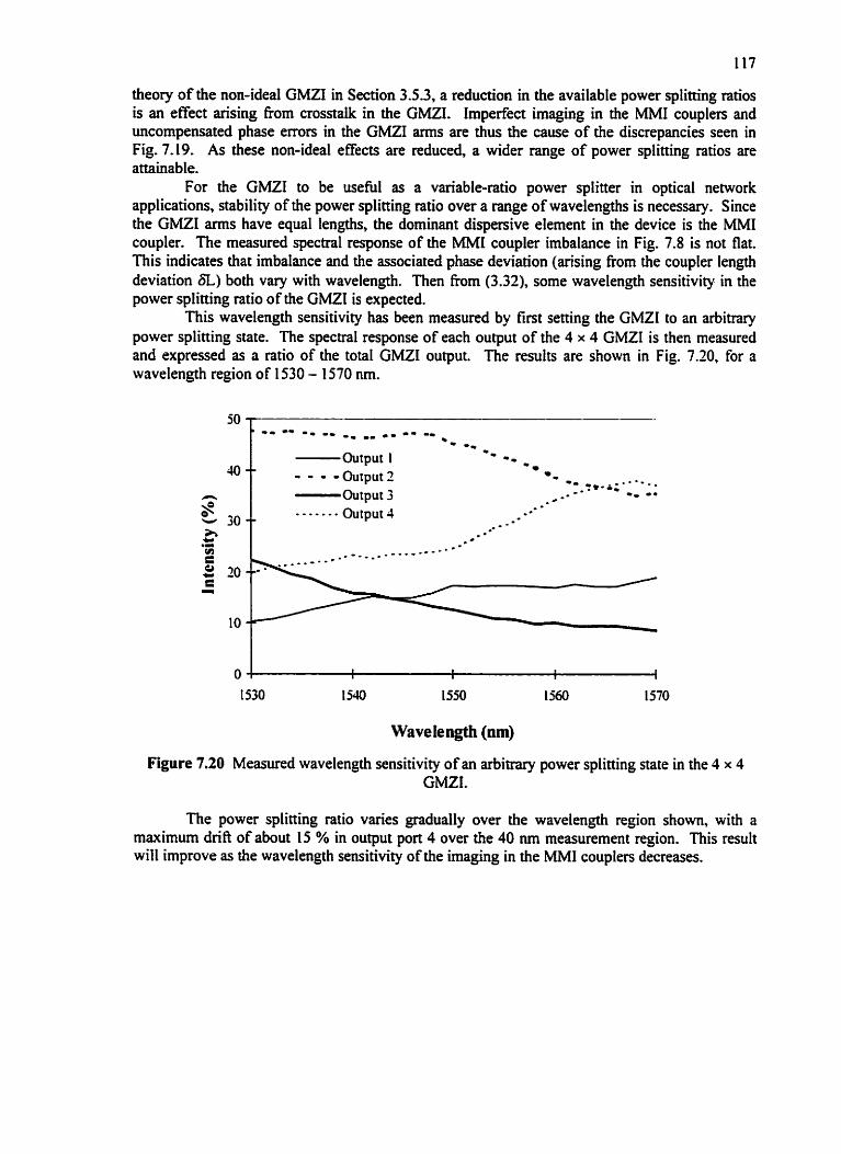
theory of the non-ideal GMZI in Section 3.5.3, a reduction in the available power splitting ratios is an effect arising from crosstak in the GMZI. Imperfect imaging in the MM1 couplers and uncompensated phase errors in the GMZI m s are thus the cause of the discrepancies seen in Fig. 7.19. As these non-ideal effects are reduced, a wider range of power splitting ratios are attainable.
For the GMZI to be usehl as a variable-ratio power splitter in optical network applications, stability of the power splitting ratio over a range of wavelengths is necessary. Since the GMZI arms have equal lengths, the dominant dispersive element in the device is the MM1 coupler. The measured spectral response of the MM1 coupler imbalance in Fig. 7.8 is not flat. This indicates that imbalance and the associated phase deviation (arising from the coupler length deviation 6L) both vary with wavelength. Then fiom (3.32), some wavelength sensitivity in the power splitting ratio of the GMZI is expected.
This wavelength sensitivity has been measured by fint sening the GMZI to an arbitmy power splitting state. The spectral response of each output of the 4 x 4 GMZI is then measured and expressed as a ratio of the total GMZI output. The results are shown in Fig. 7.20, for a wavelength region of 1530 - 1570 nm.
Output 1 -- -0 - - -Output 2 r
-0 ...;y-- * .
-Output 3 0- - 0
Wave length (nm)
Figure 7.20 Measured wavelength sensitivity of an arbinary power splitting state in the 4 x 4 GMZI.
The power splitting ratio varies gradudly over the waveiength region shown, with a maximum drift of about 15 % in output port 4 over the 40 nm measurement region. This result will improve as the wavelength sensitivity ofthe imaging in the MM1 couplers demeases.

Chapter 8
Summary and Future Directions
A concise summary of the important results obtained in this work is given in this chapter. Throughout the work a number of areas for modification und improvement have emerged. and can be applied to the devices developed in order to facilitate their timeiy incorporation into optical networks. Several of these possibiiities are dismssed. and provide the motivation fir continuation of this work along a m b e r of research and deveiopment directions.
8.1 Summary n i e previous chapten have dealt with the basic principles and theory, design, fabrication,
and characterization of new integrated optical devices based on the phenomenon of self-imaging exhibited in dielecaic optical waveguides. This phenornenon has been exploited in a generalized Mach-Zehnder interferorneter (GMZI) configuration employing multimode interference (MMI) couplers to develop devices that perform novel optical power splitting and switching hnctions usefiil for emerging optical networks.
Specifically, the integrated optical N x N GMZI that is at the heart of this work can be operated as a variable-ratio power splitter, a 1 x N switch, and an 1V x 1V multi-port switch. In Chapter 1 it has been indicated that these functions are usehl for re-routing signals through unaffected areas in the event of an intempted link in an optical fiber network. Dynarnic redistribution of optical power within a network c m also be achieved using the GMZI, thereby allowing the available optical power to be used in an efficient manner.
In Chapter 2 the basic principles of dielectric optical waveguides were presented. The effective index method (EIM), which enables the two-dimensional analysis of propagation in optical channel waveguides to be reduced to a single dimension, has been discussed. The EIM facilitates implementation of the modal propagation analysis (MPA) technique, which is a simple yet accurate tool that can be used to study the properties ofmultimode waveguides.
Beating between the modes in a multimode waveguide leads to a self-imaging phenomenon, whereby an input optical field is manifested in the form of multiple copies. This phenornenon can be exploited, and simple analytic equations detailing the design of a multirnode interference (MMI) coupler have been presented. One embodiment, the N x N MM1 coupler, is capable of producing selCimages of an optical field From any of N input waveguides at a11 N output waveguides. The phase transfer properties of this coupler were presented, and enable the design of an iVx N generalized Mach-Zehnder interferorneter (GMZI) structure which can spatially route and switch individuaI or multiple signals by means of active phase shifting.
The description of the specific contributions in this work begins with a formal tiamework for the analysis of the GMZI developed in Chapter 3. The operation of the N x N GMZI has been described mathematicaIly using transfer matrices, Ieading to the analytic expression (3.13) describing its optical response to a set of applied phase shih.
The converse mathematical problem, namely, finding the phase shifts necessary to achieve a specified optical response, has been solved by numerical techniques aided by the compact matrk expressions. ïhe physical interpretation of' the soiution is that the uptical intensity distribution at the N output ports of the N x N GMZI can be controlled through an application of an appropriate set of phase shifts. This new integrated optical device is called a variable-ratio power splitter. The methods derived here for controIling the GMZI to realize this device are a novel contribution of this work that is believed to be of considerable practical signi ficance,
A tolerance analysis of a typical device has revealed that with phase shift and wavelength variations of + 5.7 and k40 nm, respectively, the power-splitting ratio is altered by only 1 - 2 %. A more comprehensive tolerance analysis, however, would include inaccuracies stemming fiom the non-ideal behaviour of a fabricated GMZI. The non-ideal behaviow is the result of both technology limitations in the fabrication of integrated optical devices and hdamental theoretical limitations in the performance of MMI couplers.
Though the fundamental theoretical limitations of the MM1 coupler expressions were not addressed in this work, the technologically related non-ideal effects have been incorporated into the -fer matru< framework to develop the expression (3.32), which describes the behavior of a non-ideal GMZI. Using this expression, imbalance and phase deviation among the selfiimages in the MMI couplers and phase erron arising in the GMZI amis have been introduced, to determine their effect on the performance of the GMZI. The result is that the accuracy of the power- splitting ratio degrades as the imaging performance in the MMI couplers worsens. For N up to 10, the MM1 coupler imbalance and phase deviation must be kept to below + 1.0 dB and + 3 S 0 , respectively, for maximum splitting ratio deviations of a few percent. Furthermore, phase errors in the arms of the GMZI ofien occur randomly during device fabrication and must also be kept low to maintain an acceptable performance level. As the non-idealities in the GMZI increase, the power spliaing ratio not only degrades, but the predictability of the device response and the set of available ratios also diminishes.
In a special case of variable-ratio power splitting, the GMZI hnctions as a I x N switch. In Chapter 4 the switch properties were investigated using the transfer matrix h e w o r k , and a matrix describing the optimum phase shifts required for switching was derived. The crosstalk in non-ideal GMZI switches has been calculated using the theory developed in Chapter 3, and it was found that to achieve low crosstalk levels, a Iow imbalance and phase deviation in the MM[ couplen is of critical importance. As the MMI coupler operation improves, the msstalk then becomes a sensitive function of the precision of the applied phase shifts. A crosstalk analysis for 1 x iV switches for N up to 10 was performeci, with the result that the crosstaik is Iimited to the -20 dB to -30 dB range for MM1 couplers with imbalance and phase deviation levels of t 1 .O dB and 2 SO, respectively. Even with perfect MM1 coupler imaging, a + 2 % deviation in the applied phase shifts increases the crosstalk in the GMZl fiom -a dB to the -40 dB level.
When multiple inputs to the GMZI are use& a switch state of the 1 x N switch corresponds to a permutation of the N inputs at the output ports. Since N distinct permutations are possible, the multi-port GMZI switch is of the N x N blocking type. The analytic result (3.13) has been used to detive an expression (4.1 1) for the set of permutations possible in the blocking switch. This expression not only describes the operation of the blocking switch, but has been shown to predict the wavelength assignments in a tunable MM1 phasar wavelength multiplexer.
A detailed investigation of the imaging properties in the passive iV x N GMZI has led to an interpretation of this device as two smaller, superimposed MM1 couplers. The phase shifking requirements for the active N x N GMZI were then analyzed and show to be linked to the superimposed coupler interpretation. This resulted in the development of a design rule that has been used to create 1 x IV switches with dnimatically improved phase shifiing requirements. By comecting adjacent N x N GMZI inputs to a 1 x 2 switch, the number of independent phase shifts required for control are reduced by a factor of two and have a minimal number of distinct levels. Exarnples of the desig of these improved swi-tches have shown that the phase shifts required for I x 4 and 1 x 6 switches can be applied using two- and three-bit binary control words, respectively .
A deeper understanding of the multi-port switching capabilities of the GMZI has led to the development of new designs for N x N non-blocking integrated optical switches. These are based upon configurations utilizing multiple, mialler GMZI units in a building block fashion. While the switches are rearrangably and not strictly non-blocking, they nevertheless have the

advantage that they can be realized without the use of waveguide ben& or crossings, leading to very compact and potentially low-loss devices. Two embodiments of these switches have been conceived: a cascaded design and a balanced design. The cascaded design yields switches which are simple to design and operate, but have unbalanced losses, The balanced approach equalizes the losses, but at the expense of an increased complexity in the switch operation. î h e performance of a 4 x 4 balanced non-blocking switch has been simulated using MPA, and was shown to have an excess loss of 4 dB and a crosstalk level of -30 dB, even with accurate MM1 coupler imaging.
The primary goal of the latter half of this work has been to experimentally demonstrate the validity of the theoretical concepts presented. A secondary goal has been to show that compact, high-performance integrated optical devices can be realized through a careful consideration of various device design and technology alternatives. To meet these objectives, integrated optical devices such as MM1 couplers and GMZIs have been designed, fabricated, and characterized.
The design and simulation of these devices is the subject of Chapter 5. The devices in this work have been designed for fabncation in a silicon oxynitride (SiON) based waveguide technology. This represents a simple, flexible, and cost-effective process capable of realizing compact, low-loss, and polarization-insensitive devices with efficient thenno-optic active control.
To exploit the many potential advantages of this technology, the devices have been designed using a rib waveguide structure with a high rehctive index contrast in both the lateral and transverse directions. Simulations have shown that this provides a nearly circular single- mode field and a TE-TM effective index birefnngence of 2.5 x 10? The structure is also designed to direct heat to the rib region for low power active operation, and to efficiently remove heat fiom this region for a fast active response. Simulation of the thermal behavior of the waveguide has predicted a r phase shift in 2 mm and 3 mm-long waveguides under an applied electrical power of 100 m W and 50 mW, respectively.
The high refiactive index contrast has also resulted in the design of compact 2 x 2 and 4 x 4 MM1 coupIers with low polanzation sensitivity. The simulated excess loss and imbalance levels for both couplers were below 1 .O dB and 0.5 dB, respectively. The dimensions of the MM[ couplen are 8 x 130 p (2 x 2) and 16 x 253 pm (4 x 4). Using these MM1 couplea, 2 x 2 and 4 x 4 GMZIs have also been designed. Variable-ratio power splitting in the 4 x 4 GMZI bas been simuiated for the waveguide design chosen, with the results indicating excess losses below 2 dB, a maximum splitting ratio deviation of 1.5 %, and polarization-insensitive behaviour. Careful consideration of the design of the GMZI arms has resulted in the development of equal-length, equal-loss, thermally isolated waveguide arms with gradua1 bends and no transition losses.
The final device designs have been transferred to a photomask to be used in the device fabncation. The device fabrication process has been carried out at the MESA clean room facility at the University of Twente, in The Netherlands, and is described in detail in Chapter 6. The first stage of fabrication involved thin-film processing using plasma-enhanced chemical vapor deposition (PECVD) for the dielectric films and sputtet-ing for the metal film. The process parameters for the PECVD have been optimized by an iterative technique, to ensure the desired refractive index contrast of An = 0.10 1 and film thickness control could be achieved reproducibly. The film properties have been determined using prim coupling, and resulted in a measured refiactive index contrast of 0.100 + 0.001 for both polarizations in a region of wavelengths around 5 550 nm.
PECVD SiON films exhibit a high optical absorption l o s in the 1500-1600 nm region; however, it has been shown qualitatively in this work that an annealing treatment for ! hour at 1 150 OC can significantly reduce these losses,
The second stage of fabrication involved photolithography and etching. The photolithography process has been optïmized for the present devices, and the detailed procedurai
steps performed in this process have been presented. The devices have been defÏned in the vertical direction by reactive ion etching (RIE), and the process parameters and etch depth characterization have been discussed. Optical microscope and scanning electron microscope (SEM) images of the fabricated devices have been given, enabling physical device characteristics to be detennined both qualitatively and guantitatively. Single-mode waveguides with ni dimensions of 2.7 x 4.5 p were designed, while values of 2.6 - 2.9 pm x 4.4 pn were measured. ï h e lithographic process has, however, introduced rounding at the M M coupler input and output facets, and the RIE has produced waveguide sidewalls with a roughness on the order of 100 nm.
The final stage of the fabrication process involved cleaving and mounting the devices, followed by wire-bonding and the application of the final heater contacts. Microscope images of devices in these stages have been given, and indicate two major drawbacks of the fabricated devices. These are the Fragile nature of the rib structure, resulting in difficulty in device cleaving, and the absence of integrated thin-film heater contacts, resulting in additional optical attenuation and excess power dissipation.
The fabricated devices have been tested using the experimental characterization setup of the Lightwave Devices Group at the University of Twente. The measured performance results have been given in Chapter 7. An infrared camera image of the mode field emerging fiom a single-mode waveguide confimed the nearly circular shape, and measured MFD values of 2.3 - 2.4 pm cm be compared with the simulated value of 2.5 Fm. The propagation loss in the fabricated single-mode waveguides has been measured using the cutback technique. Loss values of 3-41 7 dB/cm (TE) and 3.408 dB/cm (TM) have been determined, and polarization insensitivity is confimed over the wavelength region t52O - 1580 nm.
The measured excess loss and imbalance in the fabricated 2 x 2 MM1 couplers were 1 .O - 1.5 dB and 0.4 - 0.8 dB, respectively. The polarization sensitivity in these couplen is minimal and the results are similar to those predicted by MPA. The measured excess loss and imbalance in the 4 x 4 MM1 couplea were 2.0 - 2.5 dB and 0.8 - 1.4 dB, respectively. These levels are higher than those predicted by MPA and are believed to be caused by imperfect lithographic definition of the couplen and bend losses in the access waveguides. The excess loss and imbalance of the 2 x 2 and 4 x 4 MM1 couplers exhibited some wavelength dependence, with a variation of about 1 dB in both parameters over the wavelength region 1530 - 1570 nm for both couplers.
The performance of the 2 x 2 GMZI has been investigated, and a minimum crosstalk level of -26.7 dB and an extinction ratio of 25.8 dB were measured. Excess losses were 3 dB for both polarizations. An applied electrical power of 557 m W induced a K phase shifi in a 2 mm long heater and switched the light fiom the cross to the bar port. The cause of this high switching power is believed to be excess power dissipation in the thermo-optic heater contacts which were applied manually using a crude procedure. The dynamic response of the 2 x 2 GMZI yielded rise and fall times of 2 - 4 ms.
The 4 x 4 GMZI exhibited excess losses of 4.8 dB (TE) and 5.7 dB (TM). An improved contact application procedure resulted in a K phase shiA in an arm for an applied electrical power as low as 102 mW. Response times below 1 ms and as low as 460 ps (rise) and 650 ps (fall) have been measured. The measured optical response of the 4 x 4 GMZI mimics the theoretical result (3.32) describing a non-ideal GMZT- This indicates the presence of MM1 coupler deviations and phase errors in the GMZI arms. The resuit is unpredictable device behavior, which was only partially compensated through the application of b i s phase shifts. The GMZI perfomance is ultimately limited by the quality of the imaging in the MM1 couplers.
Operation of a 1 x 4 GMZI switch has been demonstrated, with typical measured crosstaik vaIues of -7 dB and a lowest value of -1 I dB. Extinction ratios of 15 - 18 dB were

measured in the four ports. The high crosstalk is a direct consequence of imbalance and excess loss in the MMI couplers.
The multi-port switching capability of the 4 x 4 GMZI has been investigated, and the validity of (4.1 1) has been confirmed by demonstrating a cross-connect state. This result represents an experimental confirmation of the principle upon which the new switch designs described in Chapter 4 are based.
The variable-ratio power splitting function has also been demonstrated in the 4 x 4 GMZI. The theocy developed in Chapter 3 has been used along with bias voltage values to achieve desired power splitting States. The flexibility of the power splitting function has been demonstrated by the attainrnent of a number of different power splitting ratios. Drawbacks of the fabncated device were a small uncertainty in the applied phase shifts, and the inaccessibility of some power splitting ratios. The cause of this is believed to be non-ideal imaging in the MM1 couplen and additional phase erron and imbalance introduced in the GMZl arms as a result of the heater contacts. Finally, the wavelength dependence for an arbitrarily chosen power splitting ratio was measured, and a maximum variation of 15 % was observed over a 40 nm wavelength region.
8.2 Future Directions Throughout this work a number of improvernents, modifications, and avenues for
continued research have arisen. Perhaps the next logical step in continuing the work presented here is the optimization of the device performance. An annealing study of the PECW films would provide the required process parameters to achieve the desired refractive index contrast and layer thickness control, enabling in the realization of waveguides with a propagation loss of below 0.2 dB/cm. Single-mode reference waveguides closely matching the bends and propagation length in the devices can also be implemented to provide more accurate excess loss values. Optimization of the RIE pmcess to produce smooth waveguide sidewalls would ensure that scattering losses, bend tosses, and random phase erroa remain low.
It has also been shown recently [64] that adiabatic tapering of the waveguides in a single direction can significantly reduce the coupling losses of SiON waveguides to standard single- mode optical fiber, thereby allowing the integrated devices to be easily packaged.
It has been mentioned that the use of integrated thin-film thmo-optic heaters could significantly reduce the power consumption and response tirne of the active devices. Through a suitable design of the heater contacts, the attenuation and phase enors introduced by the metal in the GMZI arms can be completely eliminated. The chromium metal can also be replaced by aluminum or a titanium-gold alloy to reduce the heater resistance and achieve low-voltage, high- current heating [67], [ 1071.
The MM1 couplers Làbricated in this work have relatively high excess loss and imbalance, even in simulations. This is partially due to the narrow coupler widths use& which can only support a small number of modes, thereby sacrificing the imaging resolution. The mal1 couplen were used to maintain polarization insensitivity, however, accurate MM1 coupler imaging is more critical to the performance of the GMZI. Wider couplea with more widely spaced access waveguides can be used to impmve the imaging. If the access waveguide spacing is greater than about 10 pm the thermal isolation is sufficient and the bent arms of the GMZI are not required. Straight waveguide arms significantly simpli@ the GMZl design and can reduce polarization sensitivity and the overd1 device size, which is dominated by the phase shifting region.
To improve the fabrication tolerances of the MMI coupler, wider single-mode access waveguides can be utiiized [9]. This can be achieved by tapering the waveguides as they enter and exit the MM1 coupler region.

M M couplers and single-mode waveguides cm possibly both be designed to have polarization insensitive behaviour, by utilizing a cross-sectional waveguide geometry for the multimode waveguide region that is different from that of the single-mode access waveguides.
Employing many of these suggested improvements may improve the GMZI characteristics to a level where the variable-ratio power splitter, the improved 1 x N switches. and the N x N non-blocking switches presented in Chapters 3 and 4 become practical. This work can then be extended to the development of such devices, where values of N > 4 are utilized. Of course, the theory presented in this work is independent fkom the material system or active phase shifiing method employed. The devices can therefore be implemented in a different waveguide technology, which may posxss certain advantages over the silica-based system used for this work.
A concem for large-port GMZl devices, however, is the active phase shifiing requirements. Though the phase shifts applied to the GMZI have been controlled manualiy in this work, the task becomes impractical for devices with a larger number of phase shifiers. For such devices the phase shifts should be cornputer controlled, which offers the advantage that iterative algorithms for phase shiR optimization can be easily irnplemented.
The ultimate goal for integrated GMn-based devices is to realize a self-contained. packaged devicr. This would include user input of the desired state of the device in electrical form, which would be used with on-board processor electronics to detemine, apply. and maintain the necessary phase shifts to the GMZI m s . The algorithms developed in this work can be coded into the processor electronics to detemine appropriate phase shifts. For the devices based on idealized switching, the phase shifting can be reduced to the application of one of a set of quantized voltage levels. Voltages of only a few volts can induce a r phase shifi in a waveguide if low-resistance thermo-optic heatea are used [67], suggesting that standard integrated electronic circuitry is suitable for the application of the phase shih.
Maintenance of the desired optical output state of a device in the presence of environmental fluctuations is a key requirement for the practical feasibility of these devices, and a more general requirement for al1 interferometnc devices. This necessitates monitoring the optical output of a device and providing an appropriate feedback mechanism to determine and apply corrections to the phase shih. This rnust be achieved in a rninimally invasive manner, so as to protect the integrity of the optical signals. One method of monitoring utilizes optical tap ports to diven a srnall portion of the light from each output waveguide to a detector, which then drives the feedback electronics. This principle has recently been demonstrated for an integrated thermo- optic attenuator [117].
The above description of areas for continuation of this work is not exhaustive. but is designed to convey a flavour of the many doon of investigation which have been opened. Finally, in addition to the principal application of optical networking, it is the hope that the devices described in this body of work will fmd a wider and more far-reaching applicability. thereby furthering the dream of integrated optics and fueling the evolution of communication.
8.3 Conclusion In this work, a theory of the GMZI is developed and has been used to predict the ideal
and non-ideal response of this device. The theory has led to the development of new integrated optical devices: the variable-ratio power splitter, improved 1 x N switches, and N x N non- blocking switches. To determine the feasibility of the practical operation of these devices, GMZI devices have been fabricated in a high refractive index contrast silicon oxynitride waveguide system. The devices have been designed to provide the functionality required to verify the theoretical predictions while taking full advantage of the waveguide technology to demonstrate the possibility of achieving compact, low-loss GMZI-based devices that exhibit high-performance passive and active operation. The fabricated devices have been chmcterized, and the theory of the GMZI has been venfied through demonstrations of variable-ratio power splining and 1 x !V and multi-port switching. Measwement of the device response has also confirmed aspects of the theory of the non-ideal GMZI, which has provided insights into the sources of the non-ideal behaviour. The optical and thermal waveguide characteristics confirm the validity of the simulations used for their design and demonstrate the possibility of achieving compact, low-loss, polarization insensitive integrated dcvices with low power consumption levels and a fast response. Deviations in the performance of the fabricated dwices fiom the theoretical predictions indicate that imperfect imaging (imbalance and phase deviation) in the MM1 couplers is the principal mechanism responsible for poor GMZI performance. For the realization of commercially viable devices based on the GMZI, it is theret'ore essential that mechanisms for the improvement of the performance of the MM1 couplea are investigated m e r .
It is the belief then that with an improved robustness of the self-imaging phenornenon in multimode intederence couplers, the GMZI-based devices described herein will be invaluable components in the realization of efficient optical networks.
References
C. K. Hao and G. A. Hockham, "Dielectric-fiber swface waveguides for optical fiequencies," Proc. IEEEE, vol. 113, no. 7, pp. 1151-1 158, 1966.
R. Dupuis, N. Holonyak Jr., M. 1. Nathan and R H. Rediker, "Papes on early history of the semiconductor laser diode," IEEE J. Quantum Electron., vol. 23, no. 6, pp. 65 1-695, 1987.
S. Kawanishi, H. Takara, K. Uchiyama, I. Shake, and K. Mon, "3 Tbit/s (16OGbit.k x 19 channel) optical TDM and WDM transmission expenment?" Electron. Lett., vol. 35, no. 10. pp. 826-827, May 1999.
T. Matsuda, M. Murakami, and T. Imai, "340 Gbitls (34 x 10 Gbitls) WDM transmission over 8,5 14 km using broadband gain equalisation technique for transoceanic systems," Electron. Lett., vol. 35, no. 13, pp. 1 090- 1 09 1, June 1999.
M. Kawachi, "Silica waveguides on silicon and their application to integrated-optic components," Opt. Qiranturn Elecrron., vol. 22, pp. 39 1-4 16, 1990.
S. E. Miller, "Integrated optics: An introduction," Bell Syst. Tech. J.. vol. 48, no. 7, pp. 2059-2069, 1969.
E. Pennings. G. D. Khoe, M. K. Smit, and T. Staring, "Integrated-optic versus microoptic devices for fiber-optic telecommunication systems: a comparison," IEEE J. Select. Topics Qiiantzinz Electron.. vol. 2, pp. 15 1 - 164, June 1996, invited paper.
B. E. A. Saleh and M. C. Teich, Ftindamentak ofphotonics. New York: Wiley, 1991.
L. H. Spiekman, Compact integrated optical components for telecornmunication nerworks. PhD thesis, Del fi University of Technology, Del fi, the Netherlands, 1 996.
M. Okuno, N. Takato, T. Kitoh, and A. Sugita, "Silica-based thermo-optic switches," NTT Review, vol. 7, no. 5, pp. 57-63, Sept. 1995.
L. B. Soldano, F. B. Veerman, M. K. Smit, B. H. Verbeek, A. H. Dubost, and E. C. M. Pennings, "Planar Monomode Optical Couplen Based on Multimode Interference Effects," J. Lighhvave Technol., vol. 10, no. 12, pp. 1843- 1849, Dec. 1992.
M.Bachmann, P.A. Besse, and H. Melchior, "General self-imagaing properties in IV x N multimode interference couplets including phase relations," AppL Opt., vol, 33, no. 18, pp. 3905-39 1 1, June 1994.
R. Urich, U. K. Patent Application No, 1 525 492, 197&
[14] J. E. Midwinter, Ed., Photonics in nvirching. San Diego: Academic Press, 1993.
[IS] D. I. Griffiths, introduction tu Electrodynarnics, 2"' Ed, Prentice-Hall, NJ, 1989.
[16] J. T. Boyd, "Photonic Integrated Circuits," in Photonic Devices und Systems, R. G. Hunsperger, Edo, Marcel Dekker, N'Y, 1994.

[ 1 71 N. S. Kapany and J. J. Burke, Optical Wmeguides, Academic Press, NY, 1 972.
[18] K. S. Chiang, "Dual effective-index method for the analysis of rectangular dielectric waveguides," Appl. Opf., vol. 25, no. 13, pp. 2 169-2 174, 1986.
[19] A. Kumar, D. F. Clark, and B. Culshaw, "Explanation of errors inherent in the effective- index method for analyzing rectangular-core waveguides," Opt. Len., vol. 13, no. 12, pp. 1129-1 131, 1988.
[20] K. S. Chiang, "Performance of the effective-index method for the analysis of dielectric waveguides," Opt. Letî., vol. 16, no. 10, pp. 7 14-7 16, 199 1.
[21] P. C. Kendall, M. J. Adams, S. Ritchie, and M. J. Robertson, 'Theory for calculating approximate values for the propagation constant of an optical rib waveguide by weighting the rehctive indices," IEE Proceedings, vol. 134, Pt. A, no. 8, pp. 699-702, 1987.
[22] L. B. Soldano and E. C. M. Pennings, "Optical multi-mode interference devices based on self- imaging: principles and applications," J. Lightwave Technol., vol. 13, no. 4, pp. 615- 627, Apr. 1995, invited paper.
[23] P. A. Besse. E. Gini, M. Bachrnann, and H. Melchior, "New 2 x 2 and I x 3 multimode interference couplers with free selection of power splining ratios," J. Ligh~ave Technol., vol. 14, no. 10, pp. 2286-2293, Oct. 1996.
[24] D. S. Levy, R. Scarmoaino, and R M. Osgood, Jr., "Length reduction of tapered N x iV MM1 devices," IEEE Photon. Tech. Lett., vol. 10, no. 6, pp. 830-832, June 1998.
[25] M. Bachmann, P. A. Besse, and K. Melchior, "Overlapping-image multimode interference couplers with a reduced number of self-images for unifonn and nonuniform power splitting," Appl. Opr., vol. 34, no. 30, pp. 6898-69 10, Oct. 1995.
[26] P. A. Besse, M. Bachmann, and H. Melchior, "Phase relations in multi-mode interference couplers and their application to generalized integrated Mach-Zehnder optical switches," in Proc. ECIO '93, pp. 2.22-2.23, Apr. 1 993.
[27] M. R. Paiam and R. 1. MacDonald, "Design of phased-array wavelength division multiplexea using multimode interference couplers," Appi. Opt., vol. 36, no. 21, pp. 5097- 5 108, July 1997.
[ZS] E. C. M. Pe~ ings , R. J. Den, A. Scherer, R. Bhat, T. R. Hayes, N. C. Andreadakis, M. K. Smit, L. B. Soldano, and R. f . Hawkins, "Ultracompact, low-loss directional couplers on InP based on self-imaging by multimode interference," Appl. Phys. Lem, vol. 59, pp. 1926- 1928, 1991.
[29] M. A. Fardad and M. Fallahi, "Sol-gel multimode interkence power splitters," IEEE Photon. Tech. Lett., vol. 11, no. 6, pp. 697699, June 1999.
[30] L. H. Spiekman, Y. S. Oei, E. G. Metaal, F. H. Groen, 1. Moerman, and M. K. Smit, "Extremely Small Multimode Interference Couplers and Ultrashort Bends on InP by Deep Etching," IEEE Photon. Tech. Lett., vol. 6, no. 8, pp. 1008- 10 10, Aug. 1994.
[31] P. A. Besse, M. Bachmann, H. Melchior, L. B. Soldano, and M. K. Srnit, "Optical Bandwidth and Fabrication Tolerances of Multimode Interference Couplers," J. Lightwave Technol., vol. 12, no. 6, pp. 1004- 1009, June 1994.
[32] M. Bachmann, M. K. Smit, P. A. Besse, E. Girii, H. Melchior, and L. B. Soldano, "Polarization-insemitive low-voltage optical waveguide switch using InGaAsPflnP four- port Mach-Zehnder interferorneter," in OFC/IOOC '93 Technical Digest, pp. 32-33, paper m 3 .
[33] M. Bachmann, Ch. Nadler, P. A. Besse, and H. Melchior, "Compact Polarization- insensitive Multi-Leg 1 x 4 Mach-Zehnder Switch in inGaAsPflnP," in Proc. ECOC, Firenze, Italy, pp. 5 1 9-522, 1994.
1343 R. M. Jenkins, J. M. Heaton, D. R. Wight, J. T. Parker, J. C. H. Birbeck, G. W. Smith, and K. P. Hilton, "NoveI 1 x N and N x iV integrated optical sivitches using self-irnaging multimode GaAdAlGaAs waveguides," Appl. Phys. Leu., vol. 64. no. 6, pp. 684-686, Feb. 1994.
[35] N. S. Lagali, M. R. Paiam, and R. 1. MacDonald, "Theory of variable-ratio power sptitters using multimode interference coupIers," i E E Photon. Technol. Lett., vol. 1 I., no. 6, pp. 665-667, June 1999.
[36] N. S. Lagali, M. R. Paiam. R. 1. MacDonald, K. W6rho& and A. Dnessen, "Analysis of generalized Mach-Zehnder interferometers for variable-ratio power splitting and optimized switching," A Ligh~ave. Technoi.. to appear in Dec. 1999 issue.
[37] N. S. Lagaii, R. I. MacDonald, and M. R. Paiam, "Optical variable-ratio power splitter," U. S. Patent Application No. 091227939, Priority Date: Jan. 30, 1998, filed Jan. 11, 1999.
[38] C. G. Montgomery, R. H. Dicke, and E. M. Purcell, Eds., Princ@les of Microwave Circuits, 1 " Ed., McGraw-Hill, NY, 1 948.
[39] R. Levy, in A h c e s in Mcrowaves, L. Young, Ed., Academic Pms, NY, 1966.
[40] B. H. Verbeek, C. H. Henry, N. A. OIsson, K. J. Orlowsky, R. F. Kazarinov, and B. H. Johnson, "Integrated Four-Channel Mach-Zehnder Multi/DemultipIexer Fabricated with Phosphorous Doped SiO? Waveguides on Si," J L i g h ~ e Technol., vol. 6, no. 6, pp. IO1 1-1015, June 1988.
[41] K. Jinguji and M. Kawachi, "Synthesis of Coherent Two-Port Lanice-Form Optical Delay- Line Circuit," J. L i g h m e Technol., vol. 13, no. 1, pp. 73-82, Jan. 1995.
[42] G. Artken, Muthemutical Methodr for Physicists, 3" Ed., Academic Press, San Diego, 1985.
[43] H. Nishihara, M. H m a , and T. Suhua, Opticai Integrated Circuits, McGraw-Hill, NY, 19W.
[a] E. C. M. Pennings, R van Roijen, M. J. N. van Stralen, P. J. de Waard, R. G. M. P. Koumans and B. H. Verbeek, "Reflection Properties of Multirnode Interference Devices," lEEE Photon. Tech. Lett., vol. 6, no. 6, pp. 7 15-7 18, Jme f 994.

[45] Q. Lai, M. Bachmann, W. Hunnker, P. A. Besse and H. Melchior, "Arbitrary ratio power splitters using angled silica on silicon rndtimode interference couplen," Electron. Lert., vol. 32, no. 17, pp. 1576-1577, Aug. 1996.
[46] J. J. More, T h e Levenberg-Marquardt algorithm: implementation and theory," Numericd Anafysis, e b G. A. Watson, Lecture Notes in Mathematics 630, Springer-Verlag, pp. 105- 116, 1977.
[47] J. E. Demis, Ir., and R B. Schnabei, Numericaf methodr for unconstrained optimkation and noniinear equations. Englewood Cliffs, NJ: Prentice-Hall, 1983,
[48] P. A. Besse, M. Bachmann, Ch. Nadler, H. Melchior, ''The integrated prisrn interpretation of multileg Mach-Zehnder interferometen based on multimode interference couplers," Opt. Quanr. Electron., vol. 27, pp. 909-920, 1995.
[49] T. Goh, S. Suzuki. and A. Sugita, "Estimation of waveguide phase error in silica-based waveguides," J . Lighhvave Technoi., vol. 15, no. 1 1, pp. 2 107-2 1 13, Nov. 1997.
[SOI M. R. Paiam and R. 1. MacDonald, "A ltchannel phased-amy wavelength multiplexer with multimode interference couplen," IEEE Photon. Tech. Lett., vol. 10, no. 2, pp. 24 1 - 243, Feb. 1998.
[5 11 C. K. Madsen, "A multiport fiequency band selector with inherently low loss, flat passbands, and low crosstaw IEEE Phoron. Tech. Lett., vol. 10, no. 12, pp. 1766- 1768, Dec. 1998.
[52] T. Augustsson, 'Theoreticai investigation OF a wavelength selective switch architecture based on a Bragg-grating-assisted MMIMI configuration," IEEE Photon. Tech. Lett., vol. 1 1, no. 7, pp.839-84 1, JuIy 1999.
[53] R. Ulrich and T. Kamiya, "Resolution of self-images in planar optical waveguides," J. Opt. Soc. Am., vol. 68, no. 5, pp. 583-592, May 1978.
[54] N. S. Lagali, M. R. Paiam, R 1. MacDonald, K. Worhoff, and A. Driessen, " 1 x N and non- blocking N x N optical space switches based on multimode interference," submitted to Journal of Lightwmre Technology, received Oct. 1998, revised Sept. 1999.
[55] N. S.Lagali, R. 1-MacDonald, and M. R Paiam, "An integrated 1 x N optical switch," U. S. Patent Application No. 09/227856, Priority Date: Jan. 30, 1998, filed Jan. 1 1, 1999.
[56] N. S. Lagali, R. 1. MacDonald, and M. R Paiam, "An N x N non-blocking optical switch," U. S. Patent Application No. 09î227857, Priority Date: Jan. 30, 1998, filed Jan. 1 1, 1999,
[57] B. H. Verbeek, A. A. M. Staring, E. J. Jansen, R van Roijen, J. J. M. Binsma, T. van Dongen, M. R. Amersfoort, C. van Dam, and M. K. Smif "Large bandwidth polarization independen t and compact 8 channe1 PI4.ASA.R demu1 tiplexerl filter,', in Optical Fiber Communication Conference, Vol. 4 of 1994 OSA Technical Digest Senes (Optical Society of Amerka, Washington, D.C ., 1 994)- pp. PD 1 3- 1 -PD 1 3-4.
Jean-Pierre Weber, B. Stoltz, and 0. Oberg, "A new type of tunable demultiplexer using a multi-leg Mach-Zehnder interferorneter," ECiO'97 Proceedings, Stockhoim, pp. 272-275, 1997.
R 1. MacDonald, "Large modular, expandable optical switching matrices," IEEE Photon. Technol. Lett., vol. 1 1, no. 9, June t 999.
N. S. Lagali, R. 1. MacDonald, M. R. Paiam, K. Worhoff, and A. Driessen, "Silica-based rib waveguides for integrated optics using multimode interference," in Applications of photonic technology 3: closing the gap behveen theory, Dewloprnent, and application, G. A. Lampropoulos, and R. A. Lessard, Eds., Proc. SPK, vol. 349 1, pp. 380-385, 1998.
T. Uitterdijk, D. H. P. Maat, F. W. Groen, H. van Brug, C. G. M. Vreeburg, J. W. Pedersen, and 1. Moerman, "Dilated, polarization insensitive InP-based space switch," in Proc. ECIO '97, Stockholm, pp. 55 1-554, Apr. 1997.
T. A. Tumolillo, Jr., M. Donckers, and W. H, G. Horsthuis, "Solid state optical space switches for network cross-connect and protection applications," i E E Comm. Magazine, pp. 124-130, Feb. 1997.
R M. de Ridder, K. Worhoff, A. Driessen, P. V. Lambeck, and H. Albers, "Silicon oxynitride planar waveguiding structures for application in optical communication," IEEEJ. Select. Topics Quantum Elec~on., vol. 4, pp. 930-937, 1998.
K. Worhoff, P. V. Lambeck, and A. Driessen, "Design, tolerance analysis, and fabrication of silicon oxynitride based planar optical waveguides for communication devices," J . L i g h m e Technol., vol. 17, no. 8, pp. 140 1 - 1407, Aug. 1999.
C. T. Lee, M. L. Wu, L. G. Sheu P. L. Fan, and J. M. Hsu, "Design and analysis of completely adiabatic tapered waveguides by conformai mapping," J. Lighiwave Technol., vol. 15, no. 2, pp. 403410, Feb. 1997.
2. Weissman and 1. Hendel, "Analysis of periodically segmented waveguide mode expanders," J. Lighnvuve Technol., vol. 13, no. 10, pp. 2053-2058, Oct. 1995.
Q. Lai, W. Hwiker, and H. Melchior, "Low-power compact 2 x 2 thermooptic silica-on- silicon waveguide switch with fast response," IEEE Photon Technol. Len., vol. 10, no. 5, pp. 68 1-683, May 1998-
M. Hoffmann, P. Kopka, and E. Voges, "Low-loss fiber-matched low-temperature PECVD waveguides with small-core dimensions for optical communication systems," IEEE Photon Technol. Lett., vol. 9, no. 9, pp. 1238-1240, Sept. 1997.
K. Jinguji, "Optical devices For pmcessing optical signals as light without transforming them into electrical signals," M T Review, vol. 7, no. 1, pp. 80-86, Jan. 1995.
B. J. Ofiein, G. L. Bona, R. Germann, F. Krommendijk, 1. Massmek, àrid ii. W. M. Salemùik, "Hi& contrast and low loss SiON opticai waveguides by PECVD," in Proc. IEEEILEOS S v m Benelux cha~ter. 1996, DD. 290-293.
[7 11 D. Peters, K. Fischer, and I. Miiller, "Integrated optics based on silicon oxynitride thin films deposited on silicon substrates for sensor applications," Sens. Act. A, vols. 25-27, pp. 425- 431, 1991.
[72] M. H o f i a . and E. Voges, "Low temperature, nitrogen doped waveguides on silicon with mail core dimensions fabricated by PECVDIRIE," in Proc. f h EW- Conf: Integrated Optics @CIO ' 99 , pp.299-302,
1731 H. Bezzaoui and E. Voges, "Integrated optics combined with micromechanics on silicon," Sens. Act. A., vol. 29, pp. 2 19-223, 199 1.
[74] H. Albers, L, T. H. Hilderink, E. Sziligyi, F. Paszti, P. V. Lambeck, and Th. J. A. Popma, 'bBirefnngence compensation in double-core optical waveguides," in Proc IEEE/LEûS '95, San Francisco, CA, pp. 88-89.
[75] K. Worhoff, A. Driessen, P. V. Lambeck, L. T. H. Hilderink, P. W. C. Linders, and Th. J. A. Popma, "PECVD silicon oxynitride optimized for application in integrated optics," Sens. Act. A, vol. 74, pp. 9- 1 2, 1999.
[761 F. Horst, H. W. M. Salemink, R. Germann, B. J. Offrein, and G. L. Bona, "High quality ring resonators in high refiactive index contrast SiON waveguides," in Proc. IEEE/LEûS Symp. Benelm Chapter, 1998, pp.33-36.
[77] M. R. Paiam, Applications of MM7 couplers in WDM. PhD Thesis, University of Alberta, Edmonton, 1997.
1781 M. TayIor, FWave: hvo-dimensional mode solver, public domain, 1995.
[79] B. J. Offrein, G. L. Bona, F. Horst, H. W. M. Salemink, R. Beyeler, and R. Germann, "Wavelength tunable optical add-afier-drop filter with flat passband for WDM networks," IEEE Photon. Technol. Lett., vol. 1 1, no. 2, pp. 239-241, Feb. 1999.
1801 A. Sugita, K. Jinguji, N. Takato, K. Katoh, and M. Kawachi, "Bridge-suspended silica- waveguide thennooptic phase shifter and its appIication to Mach-Zehnder type optical switch," Trans. IEICE, vol. E73, no. 1, pp. 105-1 09, Jan. 1990.
[8 11 B. A. Meller. L. Jensen, C. Laurent-Lund, and C. Thirstrup, 'Silica-waveguide thermooptic phase shifter with low poww consumption and low laterd heat difiion," IEEE Photon. Technol. Lett., vol. 5, no. 2, pp. 1415-14 18, Dec. 1993.
[82] Y. Inoue, K. Katoh, and M. Kawachi, "Poiarization sensitivity of a siIica waveguide thermooptic phase shifter for planar lightwave circuits,', IEEE Photon. Technol. Lett., vol. 4, no. t ., pp. 36-38, Jan. 1992.
[83] D. R. Lide, Ed., CRC Handbook of Chemis~y and Phÿsics, 79" Ed.. New York: CRC Press, 1998.
[84] SPDE Inc.. PDEase2: Finite eiement annlysis for pmtiaI dijferentid equations. Bass Lake, CA, Copyright f 995.

[85] D. Marcuse, Light Transmission Optics. 2" Ed, New York: Van Nostrand Reinhold Co., 1982.
[86] E. A. J. Marcatili, "Bends in optical dielectric guides," Bell Syst. Tech. J., vol. 48, no. 7, pp. 2 103-2 132, Sept. 1969.
[87] F. Ladouceur and P. Labeye, "A new general approach to optical waveguide path design," J. Lightwme TechnoL, vol. 13, no. 3, pp. 48 1-492, March 1995.
[88] V. Subramaniam, G. N. De Brabander, D. H. Naghski, and J. T. Boyd "Measurement of mode field profiles and bending and transition losses in curved optical channel waveguides," J. Lightwave Technol., vol. 15, no. 6, pp. 990-997, June 1997.
[89] D. Marcuse, "Length optimization of an S-shaped transition between offset optical waveguides," Appl. Opt., vol. 17, pp. 763-768, 1978.
[90] W. 1. Minford, S. K. Korotky, and R. C. Alfemess, "Low-loss Ti:LiNbOi waveguide ben& at A = 1.3 jm," IEEE J. Quunrurn Electron., vol. QE-18, pp. 1802- 1806, 1982.
[91] M. T. Kauffman, C. J. Radens, and J. T. Boyd, "Length minimization in integrated optical circuits incorporating directional couplers and curved sections," J. Lightwave Technol., vol. 8, no. 10, pp. 1 504- 1 508, Oct. 1990.
[92] D. W. Boertjes and J. N. McMullin, "Novel Wide-Angle 3D-BPM Implemented on a Path- based Grid", Microwave and Optical Technology Lettea, Vol. 20, No. 5. pp. 287-290, March 5, 1999.
[93] L. H. Spiekman, Y. S. Oei, E. G. Metaal, F. H. Groen, 1. Moerman, M. K. Smit, and B. H. Verbeek, "Extremely small, fabrication-tolerant InP-based power-splitting and combining structures by deep etching," in Proc. European Conj: Opt. Commun. (ECOC). Firenze, Italy, Sept. 1994, paper We.C.2.3.
[94] E. C. M. Pennings, R. J. Deri, R. Bhat, T. R. Hayes, and N. C. Andreadakis, "Ultra-compact all-passive optical 90' hybnd on InP using ~el~irnaging," IEEE Photon. Technol. Lett.. vol. 6, no. 5, pp. 70 1-703, 1993.
[95] The Math Works, Inc., AM TUB 4.0, numerical computation software.
1961 Tanner Research Inc., L-Edit, Version 4.0.
[97] C. E. Morosanu, Thin films science und rechnology. Vol. 7, Amsterdam: Elsevier, 1990.
[98] R M. A. Azzam and N. M. Bashara, Ellipsometry and polarked light. Amsterdam: North- Holland, 1977.
[99] K WiirhoE. Optimized LPCYD Si0.N. waveguides covered with cukiareee for non- c r i t icd j phase-matched secondhmmon~c generation. Ph.D. Thesis, University of Twente, Enschede, The Netherlands, 1996.
[100] P. K. Tien and R Umch, Theory of prism-filrn coupler and thin-film light guides," J. Op. Soc. Am, vol. 60, no. 10, pp. 1325-1337, Oct. 1970.

[10 11 R Ulrich, "Theory of the prism-film coupler by plane-wave analysis," J. Opt. Soc. Am, vol. 60, no. 10, pp. 1337-1350, Oct. 1970.
[102] R. Uirich and R Torge, "Meanirement of thin film parameten with a p&m coupler," Appl. Opt., vol. 12, no. 12, pp. 290 1-2908, Dec. 1973
[103] 0. F. I. Noordman, I N D W I T , calcuIation software.
[ 1041 B. Sikken, Tuneable integrated optic waveiengrh filrer using Much-Zehnder interjèrorneters. M.Sc. Thesis, University of Twente, Enschede, The Netherlands, 1998.
[1 OS] M. V. Bazylenko, M. Gross, P. M. Allen, and P. L. Chu, "Fabrication of low-temperature PECVD chûnnel waveguides with significantly improved loss in the 1.50-1.55 pm wavelength range," IEEE Photon. Technol. Lett., vol. 7 , no. 7, pp.774-776, JuIy 1995.
[IO61 1. L. Vossen and W. L. Kem, Eds., Thin film processes. Orlando, FL: Academic Press, 1978.
[ 1071 F. Krommendijk, An integrated thermo-optical switch based on fateral index contrust modulation. M.Sc. Thesis, University of Twente, Enschede, The Netherlands, 1997.
[ 1 081 R. Legten berg, Elecrrosratic aChl0tOr.s fabricated by suface rnicrornachining techniques. Ph.D. Thesis, University of Twenete. Enschede, The Netherlands, 1996.
[IO91 F. L. Pedrotti and L. S. Pedrotti, Introduction to Optics. znd Ed., New Jersey: Prentice-Hall, 1993.
(1 101 N. S. Lagali, M. R. Paiam, R. 1. MacDonald, K. Worhoff, and A. Driessen, "4 x 4 variabie- ratio integrated optical power splitter," in Proc. Eur. Con$ on Int. Optics (ECIO '99), Torino, Italy, Postdeadline papers, pp. PD9-PD 12, Apr. 1999.
[ 1 1 11 J. Hecht, Understanding Fiber Optics. znd Ed., New Jersey: Prentice-Hall, 1 993.
[ I 121 Coming Optical Fiber Product Information Sheet PI1036, "Coming SMF-28 CPC6 single- mode optical fiber," http://pro.comingfiber.corn/librarylpi 1 O36.htm, Feb. 1998.
[ 1 131 TECOS pmduct information sheet, http9/www.tecos.de/products/lens.html
[ 1 141 Opto Speed, Monomode taper lensed fiber T M 1 O00 product information sheet, www.optospeed.ch
[ 1 1 51 L. B. Soldano, rbluftiimode interference couplers: design und applications. Ph.D. Thesis, Delfi University of Technology, Delft, The Netherlands, 1994.
[Il61 T. Goh, A. Himeno, M. O h , K. TAahashi, and K. Hanori, "High extinction ratio and low-los silica-based 8 x 8 strictly nonblocking thermooptic matrix switch," J. Lightwove Technol., vol. 17, no. 7, pp. 1 192- 1 199, July 1999.
[117] S. S. Lee, Y. S. Jin, Y. S. Son, and T. K. Yoo, "Polyrneric tunable optical attenuator with an optical monitoring tap for WDM transmission network," IEEE Photon. Technol. Lert., vol. I 1, no. 5, pp. 590-592, May 1999.


