Embed Size (px)
Citation preview
1
Educational Whitepaper
Thermal Management of RF and Digital Electronic Assemblies using Optimized Materials and PCB Designs
Sandy Kumar, Ph.D.
Director of Technology
American Standard Circuits, Inc.
475 Industrial Drive
West Chicago, IL 60185
www.asc-i.com
Email: [email protected]; Phone: 1-630-639-5444 (direct), 1-949-929-5119 (cell)
1. Introduction
As far as the cooling of electronic devices is concerned, the first question one would ask is “Why
are cooling and thermal management of these devices required, with so much hype associated
with it?” The simple answer to it is that in any electronic device, its performance, reliability,
efficiency and life expectancy are related inversely and exponentially to the magnitude of
increased temperature above its optimum operating range. As the semiconductor transistor
junction temperature rises, its life cuts down exponentially. For example, reducing the junction
temperature by only 5°C above its optimum operating temperature range will result in
approximately doubling the expected life of the component. Thus, considerable increase in
performance, efficiency and life expectancy can be achieved by a relatively small reduction in
operating temperature. These observations are well documented by Edwards Wyrwas et al (1)
and
also in an excellent free online tutorial on component reliability (2)
. On the other hand, for
extremely low environmental temperatures, such as in deep outer space, operation of
semiconductor-based devices and circuits has often been reported down to temperatures as low as
a few degrees above absolute zero (about −270 °C, the absolute zero, of course, being -273.15
°C). This includes devices based on Si, Ge, GaAs and other semiconductor materials. There
seems no reason to believe that the active device should not operate satisfactorily all the way
down to absolute zero. The problems at lower temperatures are thus not primarily due to the
electronic device itself, but rather on the properties of materials surrounding it, like those of
bonding interface, passive circuitry materials and other protective coatings surrounding the
device. However, these indirect lower temperature problems are not the topics of the current
paper, as they have no significance with the issues posed by the elevated operating temperatures.
To begin with, there are three main components in the discussion of thermal management of
electronics devices. These are:
2
(1) Thermal interface material (TIM): TIM is used to fill the gaps between the adjoining
surfaces, such as between the ground plane of the PCB and the heat sink, in order to
increase the efficiency of thermal transfer. An efficient thermal transfer from the active
electronic device region to the heat sink will obviously help in preventing excessive heat
build-up of electronic components. The space between the semiconductor device and heat
sink is normally filled with air, which, of course, is a very poor thermal conductor (4).
The heat generated by electronic devices must be dissipated to improve reliability and
prevent premature failure. This efficient heat dissipation is also required from the PCB as
the semiconductor devices are in direct thermal contact with them and PCB can get heated
easily due to due to the resistance in pathways of electrical and electronic signals.
Techniques for heat dissipation usually include heat sinks and fans for air-cooling as well
as liquid cooling. In each of these cases, an efficient heat transfer interface is required
That would quickly and completely transfer the heat from the circuitry to the heat
sink body.
In this paper, we will be talking about the thermal interface materials (TIM) which are
designed to transfer rapidly the heat generated from the semiconductor device to a
properly designed and sized heat sink. The TIM can be either both electrically and
thermally conducting or can be only thermally conducting but electrically insulating, and
the choice, of course, depends upon the application.
All electronic switches or devices are unfortunately imperfect in the sense that a
considerable amount of the energy used during signal transmission is wasted as heat. The
amount of heat generated depends on the device functionality, whether the signal
transmission is for RF communication, power amplifiers, power devices or LEDs, etc.
The semiconductor transistors and other electronic components used for various signal
transmission dissipate power internally during both the “on-state” and the “switching
between the on and off states.” Generally, the more the power is involved in any
electronic process, the more will be the dissipation and thus more will be the rise in
temperature. The maximum amount of power that is permissible to be allowed for
dissipation is dictated by the safe maximum operating temperature of the device, which
depends on the application of the device.
(2) Thermal time constants: The thermal mass of a heat sink can be considered as a capacitor
(storing heat instead of electrical charge) and the thermal resistance as an electrical
resistance (giving a measure of how fast stored heat can be dissipated). Together, these
two components form a thermal circuit (resistance capacitance, RC circuit) with an
associated time constant given by the product of R and C. This quantity can be used to
calculate the dynamic heat dissipation capability of a device, in a way analogous to the
electrical case. A specific type of TIM can be inserted between the heat sink and the heat
source (PCB, microprocessor chip, power source, etc.) to increase thermal throughput
and to stabilize its temperature via increased thermal mass and heat dissipation by
conduction, convection and radiation routes.
3
(3) Thermal resistance of devices: This is usually expressed as the thermal resistance from a
semiconductor junction to case of the semiconductor device. The unit of thermal
resistance is °C/W. For example, a heat sink rated at 10°C/W will get 10°C hotter than
the surrounding air when it dissipates 1 Watt of heat. Thus, a heat sink with a low °C/W
value is more efficient than a heat sink with a high °C/W value.
Depending on the type of electronic device, the allowable maximum junction
temperature values, in general, range (4) from:
• 115°C in microelectronics applications
• 180°C for some electronic control devices
• 65°C to 80°C for military and other special applications.
In the printed circuit board (PCB) fabrication process, if the materials’ selection and circuit
designing are done properly, it is possible to manage effectively the heat dissipation of the
electronics assembly without causing any harm to the system or degradation of its
performance. In this review, we will discuss various topics related to the thermal management
of electronic devices and the types of products offered by American Standard Circuits to
address successfully those issues.
The main objective of this paper is to provide a greater understanding and appreciation of
challenges posed in efficient thermal management of electronic assemblies and how to figure
out an optimized solution in terms of cost, volume production, product performance and
reliability.
2. Some basics on thermal management of electronic devices
2.1 Generation of Heat:
Power dissipation results in a rise in junction temperature and the more the temperature rises,
the more severe are the physical and chemical damages around the junction area. This would
proportionately shorten its life, increase erratic behavior and reduce the efficiency of the
device.
It is therefore of utmost importance that any electronic device runs below the maximum
permissible temperature limit dictated for that particular device application. It is also
necessary that the device temperature be maintained at less than its power dissipation
rating, including various thermal resistances associated with the device.
As an example, in the case of power semiconductors like rectifiers, the power dissipation
limitation rating can be easily translated in terms of current ratings for products such as,
diodes and thyristors, since in the on-state, the voltage drop is well defined. However, for
transistors, it is more complicated, since in its on-state it can operate at any voltage up to its
maximum rating depending on the circuit conditions. Thus, for transistors it is necessary to
specify a safe operating area that specifies the power dissipation limit for current and voltage
values. Usually the mounting base temperature is kept around 25 C. At higher temperatures,
4
it will be necessary to ensure that junction temperature does not exceed the allowed operating limit.
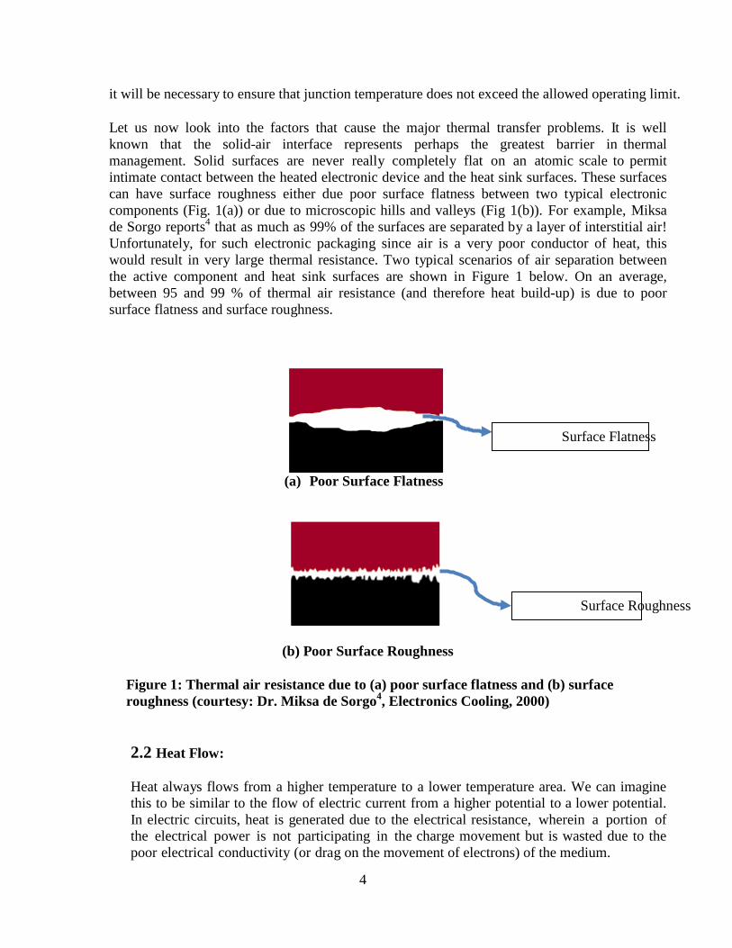
Let us now look into the factors that cause the major thermal transfer problems. It is well
known that the solid-air interface represents perhaps the greatest barrier in thermal
management. Solid surfaces are never really completely flat on an atomic scale to permit
intimate contact between the heated electronic device and the heat sink surfaces. These surfaces
can have surface roughness either due poor surface flatness between two typical electronic
components (Fig. 1(a)) or due to microscopic hills and valleys (Fig 1(b)). For example, Miksa
de Sorgo reports4
that as much as 99% of the surfaces are separated by a layer of interstitial air!
Unfortunately, for such electronic packaging since air is a very poor conductor of heat, this
would result in very large thermal resistance. Two typical scenarios of air separation between
the active component and heat sink surfaces are shown in Figure 1 below. On an average,
between 95 and 99 % of thermal air resistance (and therefore heat build-up) is due to poor
surface flatness and surface roughness.
Surface Flatness
(a) Poor Surface Flatness
Surface Roughness
(b) Poor Surface Roughness
Figure 1: Thermal air resistance due to (a) poor surface flatness and (b) surface
roughness (courtesy: Dr. Miksa de Sorgo4, Electronics Cooling, 2000)
2.2 Heat Flow:
Heat always flows from a higher temperature to a lower temperature area. We can imagine
this to be similar to the flow of electric current from a higher potential to a lower potential.
In electric circuits, heat is generated due to the electrical resistance, wherein a portion of
the electrical power is not participating in the charge movement but is wasted due to the
poor electrical conductivity (or drag on the movement of electrons) of the medium.
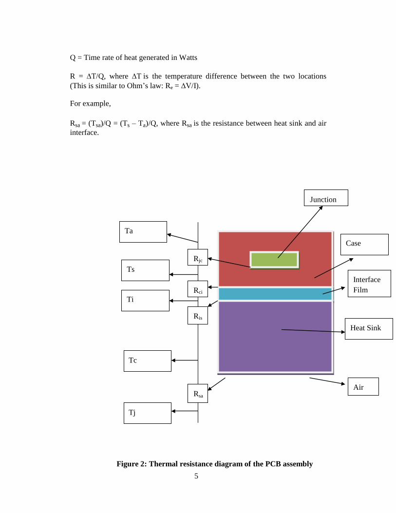
5
Ta
Q = Time rate of heat generated in Watts
R = ∆Τ/Q, where ∆Τ is the temperature difference between the two locations
(This is similar to Ohm’s law: Re = ∆V/I).
For example,
Rsa = (Tsa)/Q = (Ts – Ta)/Q, where Rsa is the resistance between heat sink and air
interface.
Junction
Ta
Rjc
Ts
Rci
Ti
Case
Interface
Film
Ris
Heat Sink
Tc
Rsa
Air
Tj
Figure 2: Thermal resistance diagram of the PCB assembly
6
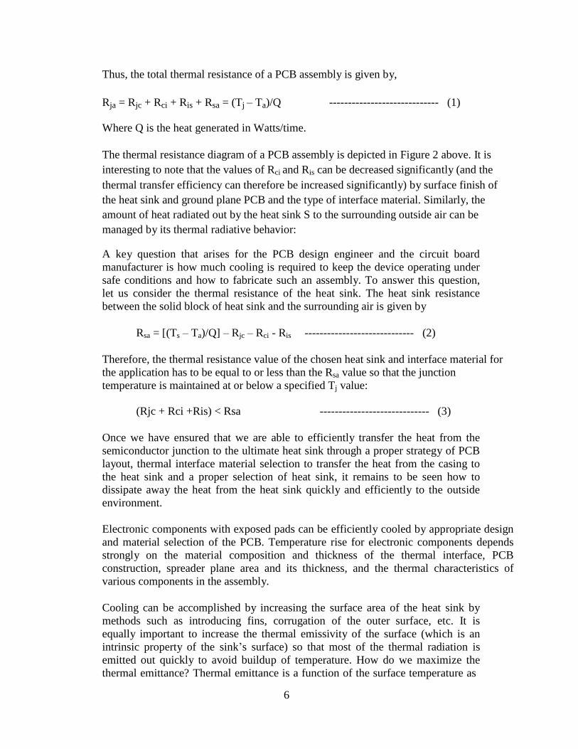
Thus, the total thermal resistance of a PCB assembly is given by,
Rja = Rjc + Rci + Ris + Rsa = (Tj – Ta)/Q ----------------------------- (1)
Where Q is the heat generated in Watts/time.
The thermal resistance diagram of a PCB assembly is depicted in Figure 2 above. It is
interesting to note that the values of Rci and Ris can be decreased significantly (and the
thermal transfer efficiency can therefore be increased significantly) by surface finish of
the heat sink and ground plane PCB and the type of interface material. Similarly, the
amount of heat radiated out by the heat sink S to the surrounding outside air can be
managed by its thermal radiative behavior:
A key question that arises for the PCB design engineer and the circuit board
manufacturer is how much cooling is required to keep the device operating under
safe conditions and how to fabricate such an assembly. To answer this question,
let us consider the thermal resistance of the heat sink. The heat sink resistance
between the solid block of heat sink and the surrounding air is given by
Rsa = [(Ts – Ta)/Q] – Rjc – Rci - Ris ----------------------------- (2)
Therefore, the thermal resistance value of the chosen heat sink and interface material for
the application has to be equal to or less than the Rsa value so that the junction
temperature is maintained at or below a specified Tj value:
(Rjc + Rci +Ris) < Rsa ----------------------------- (3)
Once we have ensured that we are able to efficiently transfer the heat from the
semiconductor junction to the ultimate heat sink through a proper strategy of PCB
layout, thermal interface material selection to transfer the heat from the casing to
the heat sink and a proper selection of heat sink, it remains to be seen how to
dissipate away the heat from the heat sink quickly and efficiently to the outside
environment.
Electronic components with exposed pads can be efficiently cooled by appropriate design
and material selection of the PCB. Temperature rise for electronic components depends
strongly on the material composition and thickness of the thermal interface, PCB
construction, spreader plane area and its thickness, and the thermal characteristics of
various components in the assembly.
Cooling can be accomplished by increasing the surface area of the heat sink by
methods such as introducing fins, corrugation of the outer surface, etc. It is
equally important to increase the thermal emissivity of the surface (which is an
intrinsic property of the sink’s surface) so that most of the thermal radiation is
emitted out quickly to avoid buildup of temperature. How do we maximize the
thermal emittance? Thermal emittance is a function of the surface temperature as
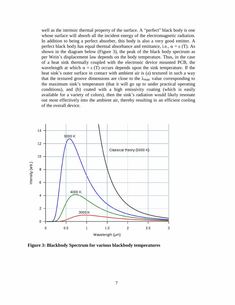
7
well as the intrinsic thermal property of the surface. A “perfect” black body is one
whose surface will absorb all the incident energy of the electromagnetic radiation.
In addition to being a perfect absorber, this body is also a very good emitter. A
perfect black body has equal thermal absorbance and emittance, i.e., α = ε (T). As
shown in the diagram below (Figure 3), the peak of the black body spectrum as
per Wein’s displacement law depends on the body temperature. Thus, in the case
of a heat sink thermally coupled with the electronic device mounted PCB, the
wavelength at which α = ε (T) occurs depends upon the sink temperature. If the
heat sink’s outer surface in contact with ambient air is (a) textured in such a way
that the textured groove dimensions are close to the λmax value corresponding to
the maximum sink’s temperature (that it will go up to under practical operating
conditions), and (b) coated with a high emissivity coating (which is easily
available for a variety of colors), then the sink’s radiation would likely resonate
out most effectively into the ambient air, thereby resulting in an efficient cooling
of the overall device.
Figure 3: Blackbody Spectrum for various blackbody temperatures
8
2.3 Thermal Modeling:
Thermal modeling of a PCB can give the circuit designer a good understanding of
various thermal issues that would affect the overall performance of the device. Using
appropriate modeling software the designer can figure out the optimum design and
placement of various components in the layout. At the most basic level, thermal
modeling can map several things: heat flow, heat sink design, and a method for
cooling effectively various active devices. Effective cooling will hold the electronic
device below the upper critical operating temperature limit. Using computer aided
design (CAD) the designer can design a prototype and evaluate its performance before
going for full volume production.
Equally important is that the thermal modeling gives the PCB designer a critical tool
for conducting the thermal fatigue failure analysis. In turn, these analyses can be
modeled to provide failure prediction models. While board failures may not occur in
near term future, the model can tell when various components of the device will start
failing in actual performance and thus help in deciding the selection of materials and
over design of the device.
2.4 Heat Sinks
Heat sinks are the most important component in managing the heat of a PCB. They
ensure that the devices are held at temperatures below their specified maximum
operating temperature. There are many versions, different designs and various ways
of optimizing heat sinks. Over time, the technology has progressed with the use of
new materials. For example, carbon fiber and boron nitride are recent materials
applied to heat sinks.
Unidirectional heat spread: High thermal conductivity carbon fiber spreads heat well
at 800 watt per meter Kelvin (W/m-K) in the direction of the fiber. However, along
the other two directions, the thermal conductivity is only about 0.5 W/m-K;
therefore, it does not spread heat in directions perpendicular to its lay out direction.
The heat is thus anisotropically spread only in one direction. Obviously, there would
be situations where this type of spread is required. If the fiber is crisscrossed along
the XY plane, one can achieve high directional thermal transfer on XY plane.
Another highly anisotropic thermal conducting material is graphite, since the heat
transfer phonons propagate very quickly along the tightly linked planes, but are
slower to hop from one plane to another.
Graphite is another promising candidate for directional heat transfer due to its
lamellar structure. Graphite obtained from various geographical locations is known to
have widely different thermal conductivities. A list of ultra-high thermal conductivity
materials that can be used to make thermally and electrically conducting bonding
interfaces is given below.
9
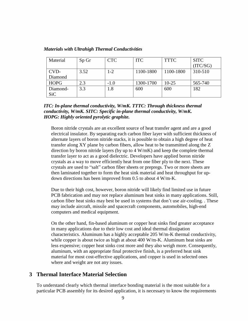
Materials with Ultrahigh Thermal Conductivities
Material Sp Gr CTC ITC TTTC SITC
(ITC/SG)
CVD- Diamond
3.52 1-2 1100-1800 1100-1800 310-510
HOPG 2.3 -1.0 1300-1700 10-25 565-740
Diamond- SiC
3.3 1.8 600 600 182
ITC: In-plane thermal conductivity, W/mK. TTTC: Through thickness thermal
conductivity, W/mK. SITC: Specific in-plane thermal conductivity, W/mK.
HOPG: Highly oriented pyrolytic graphite.
Boron nitride crystals are an excellent source of heat transfer agent and are a good
electrical insulator. By separating each carbon fiber layer with sufficient thickness of
alternate layers of boron nitride stacks, it is possible to obtain a high degree of heat
transfer along XY plane by carbon fibers, allow heat to be transmitted along the Z
direction by boron nitride layers (by up to 4 W/mK) and keep the complete thermal
transfer layer to act as a good dielectric. Developers have applied boron nitride
crystals as a way to move efficiently heat from one fiber ply to the next. These
crystals are used to “salt” carbon fiber sheets or prepregs. Two or more sheets are
then laminated together to form the heat sink material and heat throughput for up-
down directions has been improved from 0.5 to about 4 W/m-K.
Due to their high cost, however, boron nitride will likely find limited use in future
PCB fabrication and may not replace aluminum heat sinks in many applications. Still,
carbon fiber heat sinks may best be used in systems that don’t use air-cooling. . These
may include aircraft, missile and spacecraft components, automobiles, high-end
computers and medical equipment.
On the other hand, fin-based aluminum or copper heat sinks find greater acceptance
in many applications due to their low cost and ideal thermal dissipation
characteristics. Aluminum has a highly acceptable 205 W/m-K thermal conductivity,
while copper is about twice as high at about 400 W/m-K. Aluminum heat sinks are
less expensive; copper heat sinks cost more and they also weigh more. Consequently,
aluminum, with an appropriate final protective finish, is a preferred heat sink
material for most cost-effective applications, and copper is used in selected ones
where and weight are not any issues.
3 Thermal Interface Material Selection
To understand clearly which thermal interface bonding material is the most suitable for a
particular PCB assembly for its desired application, it is necessary to know the requirements
10
of the bonding material. The bonding interface should be able to handle the signal transfer
task with minimum overall cost. In digital applications, with increasing clock frequencies of
computers, the thermal load also increases thereby demanding a more efficient thermal
interface. In high frequency telecommunication applications, the complexity of circuits and
challenges posed by the environment in which they have to perform makes the bonding
material selection process quite challenging.
3.1 Bonding material considerations:
Several properties of the thermal interface bonding layer play crucial role in optimizing the
performance of the final device. Most materials have been developed to optimize one or
more of the following properties:
3.1.1. Relative Dielectric Constant, er: This property is a measure of the effect an insulating
material has on the capacitance of a conductor imbedded in or surrounded by it. It is also a
measure of the degree to which an electromagnetic wave is slowed down as it travels through
the insulating material. The higher the relative dielectric constant, the slower a signal travels
on a wire, the lower the impedance of a given trace geometry and the larger the stray
capacitance along a transmission line. Given a choice, lower dielectric constant is nearly
always better.
The dielectric constant of nearly all PCB dielectrics changes with frequency and usually goes
down as frequency goes up. This manifests itself in two ways in transmission lines. The
velocity of signals increases as the frequency goes up, resulting in phase distortion in
broadband amplifiers. Broadband RF and microwave amplifiers usually need to be made
from laminates with relative dielectric constants as flat with frequency as possible to
minimize this problem.
3.1.2. Loss tangent: Loss tangent is a measure of how much of the electromagnetic field
travelling through a dielectric is absorbed or lost in the dielectric. This property is one of the
least well understood of all those that characterize laminates. As a result, ultra-low loss
materials are often used in digital applications when they are not needed. This results in
increased PCB cost without a corresponding benefit.
4 Applications and Thermal Management Materials
Some key electronic devices where thermal management is critical are given below.
This list is by no means an exhaustive list, but it just exemplifies certain key electronic
products where thermal management plays a very crucial role.
1. Microprocessors used in various computers
2. Power semiconductor modules used in various industries such as, automotive,
aerospace, navy and space explorations.
3. High power laser diodes
4. High power RF modules
5. High brightness LEDs and LEDs with uniform color scale
6. High power laser and RF weapons with extreme temperature build ups.
11
For example, the recent technological advancements in the LED design and processes
can greatly increase the brightness of the LED assembly and the LED industry is now
rapidly emerging to capture the markets of CFL and incandescent lamps, Not only for
indoor usage that require much lower wattage but also exterior lighting such as
highway street lighting and which normally use typically 250 High Pressure sodium
Lamp. The new LEDs would have enough power to light up the entire streets and
these LEDs are capable of continually boosting light output to rival incandescent,
fluorescent and halogen light sources. In developing these high intensity LED
modules, the need to protect the LEDs against heat build-up is greater than ever
before. Power LEDs of greater than one-watt are usually surface mounted devices.
This is because the axial leads to the die in a leaded package do not conduct enough
heat away from the LED. Chip-on-board (COB), ceramic submounts and other
thermally efficient packages are emerging as the standard thermal management
packaging solution for Power LEDs.
New thermal management materials and techniques are continuously being added in
the PCB designs to meet heat dissipation demands introduced by new generations of
mostly analog and some digital ICs that dissipate high current and high power.
Thermal management focuses on effectively dissipating heat generated by those high-
power designs, on high thermal conductivity, and on maintaining low coefficients of
thermal expansion (CTE), while managing CTE mismatches between components,
their interconnects and the PCB.
Chipmakers use a variety of packaging such as plastic, ceramic, flip chip, leadless chip
carrier (LCC) and wafer-level packages (WLP). Each has a lower CTE than a standard PCB.
Consequently, a CTE mismatch occurs between device packaging and the PCB. Depending
on the application and associated cost budgets, PCB designers, hardware engineers and PCB
fabricators implement a variety of different materials and techniques to deal with those CTE
mismatches and manage thermal issues.
While chipmakers are doing their part to improve thermal management for their devices,
EMS providers are placing special attention on thermal management issues at the PCB
design level. In these instances, remedies range from using applicable board materials to
paying special attention to mounting holes. In between, there are several new as well as tried-
and-proven materials and methods to improve thermal conductivity and heat dissipation.
The industry continues to patent new inventions and offers a variety of new thermal
management materials and techniques. Those discussed here are prominent ones in the tool
kit of seasoned PCB designers and engineers. They include advanced thermal modeling
software, new heat sink material, new in-plane high conductivity carbon composite material,
special casing material and edge plating. Proven techniques include copper thieving,
increasing trace thickness, and ultimately and even exploiting the mounting holes to dissipate
heat.
12
Types of Thermal Interface Materials: There are basically four types of thermally
conducting interfaces. Further, in addition to being thermally conducting, these
interfaces can be either electrically conducting or electrically insulating. Accordingly,
these four types are:
1. Greases
2. Reactive compounds to give a hard bonding interface
3. Elastomeric compounds that give soft bonding interface
4. Pressure sensitive adhesives.
All are designed to conform to surface irregularities, thereby eliminating air voids
and improving heat flow.
1. Greases: Thermally conducting greases are filler compounds that replace the air with
the greasy compound. The surfaces to be joined are cleaned well with suitable
solvents and dried. A thin layer of grease is then applied and the two mating surfaces
are kept together. Most of the time, the two surfaces are held together by screws or
spring clips. The grease thus acts as a thermal transfer medium. Greases are used
when high thermal conductivity is required and thin bond lines that require intimate
contact between the substrates. These greases are formed by mixing thermally
conducting ceramic fillers (boron nitride, aluminum oxide, aluminum nitride, silicon
nitride, graphite, etc.) in silicone or hydrocarbon oil to form a paste of right
consistency that can properly fill the air gap between the mating surfaces. Most of the
time these greases do not provide electrical insulation, although it is possible to select
grease that can act only as a thermal transfer compound and remain electrically
insulating6. After the two surfaces are held in close proximity, the excess grease is
carefully wiped off from the sides. The thermal conductivity can be varied over a
wide range, typically from 0.6 W/mK to 220 W/mK depending upon the composition
(the thermally high conductive compounds, ≥ 10 W/mK, are typically electrically
conducting also). The important considerations that need to be kept in mind while
selecting particular grease are (a) its ability to fills the gaps and conforming to both
the component's and the heat sink's uneven surfaces. (b) good adherence to the
surfaces being joined, (c) to maintain the consistency over the device operating
temperature range, (d) ability to resist drying out or flaking over time, and (e) it must
not degrade due to oxidation or break down during the life time of the device.
2. Reactive hard compounds: These are generally thermosetting epoxy compounds,
also known as polyepoxides. The adhesives join by chemical reaction between an
epoxide resin and a polyamine hardening compound. The NH group of the amine
reacts with three ring atom ether epoxide, C1(R1R2):C2(R3R4):O to form a heavily
cross linked hardened polymer. The extent of polymerization (curing) is controlled by
temperature, curing time, resin type and hardening agent. The epoxy is dispersed with
suitable thermally conducting compounds to get the desired thermal conductivity and
made in a sheet form. The sheet is hot pressed using an appropriate press cycle to
bond the heat sink with the ground plane of the circuit board. Another advantage is
that there is no migration or bleeding issues like in greases. Before curing takes place,
13
the material flows freely as grease to eliminate the air voids and thus reduce any
thermal resistance caused by air voids. This type of thermal interface is ideal if the
two sides have comparable CTE values. If there is a CTE mismatch between the two
mating surfaces, then the shear forces will break the rigid thermoset bond and lead to
device failure; in such cases, one needs to use elastomeric (thermoplastic) bonding
compounds (see item 3 below) that can well accommodate the CTE mismatch and
allow lateral movement. We offer thermally conducting ThermEx bonding films.
3. Elastomeric compounds: Printed circuit boards used in aerospace and automotive
electronic assemblies operate in demanding environments with exposure to low and
high temperatures, and vibrational shocks. Our silicone based products described in
the following sections are a unique class of elastomeric thermal interface materials
that provide thermo-mechanical stress decoupling and a reliable heat transfer path.
Thermasil*
is electrically insulating and thermally conducting film and thus can
provide very good electrical insulation between surfaces that are different electrical
potential. As an example, it can be used for discrete power devices where electrical
isolation is required. On the other hand, Electrasil 1, 2 and 3 are thermally and
electrically conducting films. Both the thermally and electrically conducting and
thermally conducting – electrically insulating compounds are available over a wide
range of conductivities as shown in later sections. The bonding interface of this
composite will experience a high degree of shear force due to the relative movement
of the planar surfaces and the natural elastomeric properties of silicones will allow
independent planar movement, so that the shear forces are decoupled and thus prevent
bonding failure. Our silicone based Thermasil and Electrasil family of adhesives are
softer with more elongation than other class of organic adhesives like epoxies. The
soft character provides a cushion for the adjoining components that many customers
value because of increased device reliability. Further, the thermal cycling range of
silicone based bonding materials is over a much wider temperature range (-140 F to
+550 F) than epoxies (-76 F to +356 F). The higher temperature stability of silicones
arises from the fact that a stable Si-O bond results owing to the higher bond energy of
88-117 kcal/mol of the Si-O bond as compared to the 83-85 kcal/mol bond energy of
* All Thermasil and Electrasil materials are protected by the following ASC patents:
Thermally and Electrically Conductive Interface (United States Patent
7,527,873; Issued May 5, 2009)
Thermally and Electrically Conductive Interface (United States Patent
7,867,353B2: Issued June 18, 2008)
Thermally conductive interface (United States Patent US 7540081 B2; Issued
November 7, 2006).
14
the C-C bond. Also any oxidative attack is less for the primary H of CH3 in
silicone than the secondary or tertiary carbon atoms found in the epoxy
polymers.
4. Silicone elastomer pads filled with ceramic or metal particles. These are
available in thickness from about 3 MIL upward and if required, elastomers
pads can provide electrical insulation and be used between surfaces that are at
different electrical potential. Elastomers combine the advantages of not
exhibiting melt or flow during solder flow, and remain flexible after curing to
accommodate stress due to CTE differences. The thermal conductivity can be
tailored from about 0.5 –5.0 W/mK. Since the binder cures to a rubber, these
compounds do not have the migration or the dry joint problems associated with
thermal greases. Bonding compounds developed by American Standard Circuits
(ASC) uses a unique proprietary silicone. Our silicone does not have any low
molecular weight silicone (oil) that is normally present in routinely used
silicones to incorporate various additives, pigments, fillers etc. These low
molecular weight silicones are the prime cause for outgassing which is a serious
issue for normal silicones. We also do not introduce any reinforcing fillers or
carriers that are otherwise responsible for outgassing. More important is, we do
a vacuum post curing during our bonding process to eliminate completely any
possibility of outgassing. These silicones can also be used to fill large gaps
where greases would otherwise bleed from the joint on account of their
migratory nature. Clean-up is also simple as excess material is easily removed
by simple trimming after it curing and post curing steps have been completed.
5. Pressure sensitive adhesives: Pressure sensitive adhesives (PSAs) are used in
situations where any heating of the components to be joined may cause thermal
decomposition or degradation in the device performance. In such situations, the
parts are cleaned and conditioned, and the pressure sensitive adhesive is then
applied by simply applying the desired pressure over a certain period of time,
without heating the device. We provide double sided PSA films of thickness
ranging from 5 mil upwards, both for Electrasil* and Thermasil type of films
(i.e., whether the film should be both electrically and thermally conducting or
whether it should be only thermally conducting and electrically insulating). No
mechanical support to maintain the mechanical or thermal integrity is required.
The thermal and electrical conductivities can be varied over a wide range by
appropriate selection of the dispersing media.
Proper selection of thermal interface materials is decided by many
factors such as, power density to be transmitted, how much heat is going to
be dissipated, final thickness of the bonding adhesive, process requirements,
whether it needs attach-detach of the assembled parts in which case
the bonding should be only semi-permanent. In general pads and gels are
15
used in applications where there is large separation between the mating
surfaces or there are sensitive components that need cushioning. The
following are the main considerations to decide the selection of the
adhesive: (a) Thermal conductivity or thermal resistance, (b) Thickness of
the adhesive, (c) Mechanical properties such as elongation and flexural
strength, (d) Adhesion strength (e) Modulus of elasticity and Hardness and
(f) Curing or bonding conditions allowed by the device without suffering
any damage, such as, temperature, time and pressure during bonding stages.
High thermal conductivity of Electrasil type of materials can be obtained, for
example, by adding calcium carbide, calcium oxide, yttrium oxide and carbon.
Thermal conductivity of 180 W/mK has been reported to have been obtained in
AlN by adding these materials and hot pressing it (Y Kurokawa et al, J Am Cer
Soc 71,
588 (1988)). Similarly, thermal conductivity of as high as 107 W/mK has
been obtained by using diamond particle reinforced silicon carbide heat
spreader technology.
5 ASC Thermal Management Products
Regarding the selection of thermal interface materials for electronic packaging,
we can broadly divide the device applications into the following two areas. Each
one of this has its unique requirements.
(a) RF/Analog circuits
(b) Digital circuits
RF/Analog and Digital have somewhat different materials requirements.
RF/Analog applications invariably require lowest possible dielectric losses, a very
low leakage current, need to maintain a low and uniform dielectric constant under
the operating frequencies and other conditions, and should be accompanied by a
low
layer count. The PCBs used in such applications are usually much smaller than in
digital PCBs. Since the cost of the bonding material depends on the size of the
PCB
to be bonded and therefore would turn out to be low, its cost has much less bearing
on the overall cost of the complete assembly. As a result, using more expensive
materials to meet performance goals is acceptable. For this class of PCB, choosing
a material based on its dielectric constant characteristics and losses usually
dominates over other considerations.
Digital applications are characterized by high layer counts and large numbers of
drilled and plated holes. The processing costs associated with registering and
laminating many layers, coupled with drilling and plating ease usually dominate the
choice of bonding materials. Absolute dielectric constant value of the insulating
material is important, but less important than processing costs and dimensional
16
stability. Digital applications are nearly always subjected to pricing pressures, so
bonding materials choices must be made that just achieve performance
requirements without adding extra cost. The PCB design engineer should calculate
the thermal load for the design, which in turn decides which type and thickness of
ceramic filling will serve the purpose. This would result in considerable saving on
the overall cost. Please consult ASC for guidance in deciding which ASC bonding
material would meet your requirements without sacrificing the performance.
Obviously, the requirements in each of these two classes are quite different:
1. Digital Applications: For digital applications, epoxy based multilayer bonding
materials are most suitable since epoxies are well suited for multilayer bonding.
Because of their high hardness, they are well suited for multilayer stackup
symmetry and allowing good registration during drilling operations. They are
usually cheaper than other class of bonding materials, so for high layer count the
cost of using epoxy based materials is not an issue. However, for flexible digital
circuits, epoxies are obviously not good candidates and silicone based pliable
bonding films are recommended. For digital applications, all our epoxy based
bonding materials are thermally conducting dielectrics. Since these PCBs have
high layer count, they tend to become thick and soldering and reworking these
thick PCBs puts significant thermal stress on the vias and other plated through
holes on a PCB. The thermal conductivity can be varied over a wide range from
1.0 to 4.8 W/mK. The higher thermal conductive films are more expensive than
the lower thermal conductivity films. Based on the customers’ thermal load, we
will offer them the right type of bonding material and its thickness to come with
the most cost effective solution. For flexible digital applications, we offer pliable
silicones with a range of thermal conductivity dielectrics with thermal
conductivity ranging from 1.5 to 4.8 W/mK. Here again, price is decided by the
thermal conductivity. For complex shape (non-planar) circuits, we offer thermally
conducting dielectric putty whose conductivity
can be tailored as per customers’ requirements anywhere from 1.5 to 4.8 W/mK. In
all these three cases, depending upon the customers’ requirements, the curing time,
temperature and pressure can be varied over a wide range: from 40 minutes to
several hours; 100 to 300 C, a pressure from 100 to several hundred pounds per
square inch. The following is a list of thermally conducting dielectric bonding films
we offer:
a. Thermally conducting and electrically insulating silicone based flexible
bonding films for flexible PCBs (Thermasil).
b. Thermally conducting and electrically insulating epoxy based rigid bonding
films for rigid PCBs (ThermEx)
c. Highly thermally conducting and electrically insulating silicone in putty form
for complex surface contours (Thermasil-BNp).
The following table summarizes the physical properties of Thermasil and
Thermasil-BNp type materials.
17
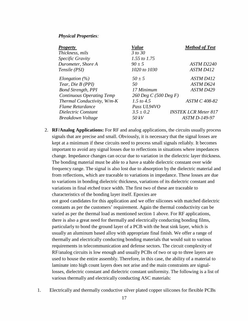
Physical Properties:
Property Value Method of Test Thickness, mils 3 to 30
Specific Gravity 1.55 to 1.75
Durometer, Shore A 90 ± 5 ASTM D2240
Tensile (PSI) 1020 to 1030 ASTM D412
Elongation (%) 50 ± 5 ASTM D412
Tear, Die B (PPI) 50 ASTM D624
Bond Strength, PPI 17 Minimum ASTM D429
Continuous Operating Temp 260 Deg C (500 Deg F) Thermal Conductivity, W/m-K 1.5 to 4.5 ASTM C 408-82
Flame Retardance Pass UL94VO Dielectric Constant 3.5 ± 0.2 INSTEK LCR Meter 817
Breakdown Voltage 50 kV ASTM D-149-97
2. RF/Analog Applications: For RF and analog applications, the circuits usually process
signals that are precise and small. Obviously, it is necessary that the signal losses are
kept at a minimum if these circuits need to process small signals reliably. It becomes
important to avoid any signal losses due to reflections in situations where impedances
change. Impedance changes can occur due to variation in the dielectric layer thickness.
The bonding material must be able to a have a stable dielectric constant over wide
frequency range. The signal is also lost due to absorption by the dielectric material and
from reflections, which are traceable to variations in impedance. These losses are due
to variations in bonding dielectric thickness, variations of its dielectric constant and
variations in final etched trace width. The first two of these are traceable to
characteristics of the bonding layer itself. Epoxies are
not good candidates for this application and we offer silicones with matched dielectric
constants as per the customers’ requirement. Again the thermal conductivity can be
varied as per the thermal load as mentioned section 1 above. For RF applications,
there is also a great need for thermally and electrically conducting bonding films,
particularly to bond the ground layer of a PCB with the heat sink layer, which is
usually an aluminum based alloy with appropriate final finish. We offer a range of
thermally and electrically conducting bonding materials that would suit to various
requirements in telecommunication and defense sectors. The circuit complexity of
RF/analog circuits is low enough and usually PCBs of two or up to three layers are
used to house the entire assembly. Therefore, in this case, the ability of a material to
laminate into high count layers does not arise and the main constraints are signal-
losses, dielectric constant and dielectric constant uniformity. The following is a list of
various thermally and electrically conducting ASC materials:
1. Electrically and thermally conductive silver plated copper silicones for flexible PCBs
18
(ELECTRASIL-1) 2. Electrically and thermally conductive silver plated copper epoxies for rigid PCBs
(ELECTRASIL-1A)
3. Highly electrically and thermally conductive pure silver silicones for flexible PCBs
(ELECTRASIL-2)
4. Highly electrically and thermally conductive pure silver epoxies for rigid PCBs
(ELECTRASIL-2A)
5. Electrically and thermally conductive graphite/nickel silicones for EMI Shielding
(ELECTRASIL-3)
6. Electrically and thermally conductive graphite/nickel epoxies for rigid PCBs
(ELECTRASIL-3A)
For all silicone based adhesives in the above list, by a proper selection of the curing
agents, it is possible to bond the heat sink permanently or temporarily, that is, attach
and detach the assembly whenever required. The bonding in the latter case will, of
course, be not permanent, but it would be strong enough to hold well the adjoining
surfaces together. Please contact us at [email protected] or [email protected]
(phone: 1-630-639-5444 / 1-949-929-5119) for more details and type of applications
of any of the above products.
Electrasil 1 and 1-A
Electrasil 1:
Electrasil 1 is a silicone based bonding sheet that contains silver plated copper particles to
give the desired thermal and electrical conductivity. The silver plated copper particles
uniformly dispersed in the cured silicone matrix give the desired thermally and
electrically conductivity as well as a strong bond between the PCB and metal carriers or
heat sinks. Although the formulation of this material was specifically targeted toward
meeting the critical requirements and performance goals for RF power amplifier
applications, it also lends itself extremely well to other high or low frequency applications
where specialized flexible PCBs need to be mounted to a metal surface or housing. As a
0.005” thick sheet of a thermoplastic elastomer material, it provides a uniformly thick and
strong bonding between the adjacent surfaces. Being an elastomer, it accommodates any
TCE mismatch of the bonded layers, so there is no residual stress left in the bonded
assembly. It can withstand a continuous operating temperature of 260°C (500°F) as well
as multiple excursions up to 288 °C (550 °F) for subsequent operations, such as solder
reflow for component installation. The ability to retain its bond strength and thermal and
electrical performance after multiple high temperature excursions at
these higher temperatures also lends itself very well to the use of higher temperature lead-
free solders. As a silicone elastomer, its flexible nature makes it ideally suited for improved
life cycle performance, without any delamination problems, when used with thermoplastic
circuit materials such as PTFE where large X and Y dimensional changes may occur
during the bonding process. This product is well suited for RF applications ranging from 15
GHz to 45 GHz. For Applications greater than 45 GHz please contact ASC sales for a
custom solution.
19
Physical Description: This adhesive is a silicone based thermoplastic elastomer that
utilizes both mechanical and chemical bonding mechanisms to insure reliable adhesion at
the bond-line interface. The high thermal and electrical conductivity is due to heavily
loaded silver plated copper that ensures very low electrical and thermal resistivity. With
the proven stability under adverse environmental conditions of the silicone adhesive (in
space, land or water), combined with excellent physical and electrical properties of the
silver plated copper, ElectrasilTM-1 bonded PCBs would consistently deliver high
performance over an extended life cycle.
Typical Applications of Electrasil 1: Electrasil-1 is used to bond PCBs to metal carriers (heat sink) prior to the assembly of components. If the customer prefers, American Standard Circuits offers the bonding
service to bond the PCB layer to the metal carrier. The bonding process requires a
minimum pressure of 50 PSI to be applied to the bonding surface and a heat source
capable of maintaining a bond line temperature of 150 °C (330 °F) for 15 minutes.
Pressure is applied through use of a Fixture Clamping Device, Heated Press or an
Autoclave. Heat sources include hot plate, I/R Oven, Convection Oven or an Autoclave.
American Standard Circuits has application engineers on staff to help design a
compatible bonding process for our customers. Once cured, ElectrasilTM-1 compresses
about 20% of its initial thickness.
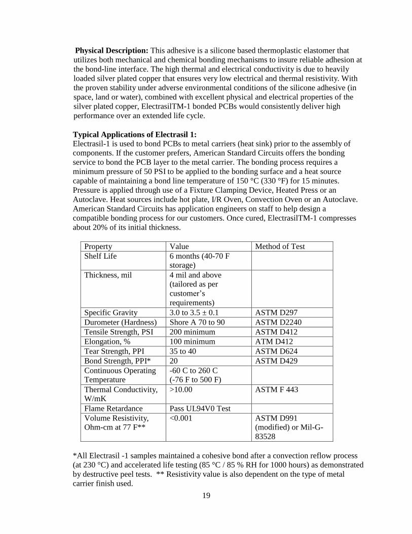
Property Value Method of Test
Shelf Life 6 months (40-70 F storage)
Thickness, mil 4 mil and above (tailored as per
customer’s
requirements)
Specific Gravity 3.0 to 3.5 ± 0.1 ASTM D297
Durometer (Hardness) Shore A 70 to 90 ASTM D2240
Tensile Strength, PSI 200 minimum ASTM D412
Elongation, % 100 minimum ATM D412
Tear Strength, PPI 35 to 40 ASTM D624
Bond Strength, PPI* 20 ASTM D429
Continuous Operating Temperature
-60 C to 260 C (-76 F to 500 F)
Thermal Conductivity, W/mK
>10.00 ASTM F 443
Flame Retardance Pass UL94V0 Test
Volume Resistivity, Ohm-cm at 77 F**
<0.001 ASTM D991 (modified) or Mil-G-
83528
*All Electrasil -1 samples maintained a cohesive bond after a convection reflow process
(at 230 °C) and accelerated life testing (85 °C / 85 % RH for 1000 hours) as demonstrated
by destructive peel tests. ** Resistivity value is also dependent on the type of metal
carrier finish used.
20
Electrasil 1-A:
In Electrasil 1-A, the bonding medium is an epoxy layer, instead of the silicone film.
Inasmuch as silicones are pliable and soft materials, epoxies on curing become hard and
rigid. Thus, whereas the silicones are ideal for flexible and soft circuit layers, epoxies are
most suited for rigid and flat PCBs. Epoxies are somewhat brittle also; therefore, it gets
cracked even under moderate mechanical shocks. Further, epoxies are not suitable for
high frequency PCB application due to high tangent losses. They are most suited for
digital PCBs. The epoxy layer is a thermoset layer that results in a highly rigid interface
between the bonded layers. Therefore epoxy bonding is not suitable for flexible circuits.
On the other hand, due to its high rigidity, the advantage is that any pressure applied on
the PCB surface during the assembly operations will not give any dents on the top copper
layer without showing any deformation on the top finished copper layer.
The epoxy bonds strongly the PCB layer and the heat sink. The bonded epoxy layer
containing silver plated copper particles provides a cost effective technique to create a
thermally and electrically conducting interface between the PCB and metal carrier or heat
sink. It can withstand a continuous operating temperature of 200°C as well as multiple
excursions up to 220 °C for subsequent operations, such as solder reflow for component
installation.
Physical Description: The adhesive is an epoxy based compound that utilizes both mechanical and chemical bonding mechanisms to insure reliable adhesion at the bond-line interface. The high
thermal and electrical conductivity is due to heavily loaded silver plated copper that
ensures very low electrical and thermal resistivity.
Typical Applications of Electrasil 1-A:
Electrasil-1A is used to bond PCBs to metal carriers (heat sink) prior to the assembly of
components when the electrical resistivity should be less than 0.001 but can be greater
than 0.0004. ASC can perform the bonding of the ground plane of the PCB with properly
finished heat sink. The bonding process requires a minimum pressure of 50 PSI to be
applied to the bonding surface and a heat source capable of maintaining a bond line
temperature of 150 °C (330 °F) for 15 minutes. Pressure is applied through use of a
fixture clamping device, heated press or an autoclave. Heat sources include hot plate, I/R
oven, convection oven or an autoclave. ASC staff can help design a compatible bonding
process for our customers. Once cured, the final thickness of Electrasil 1-A reduces to
about 80% of its initial thickness. The following table summarizes the physical
parameters of Electrasil 1-A
21
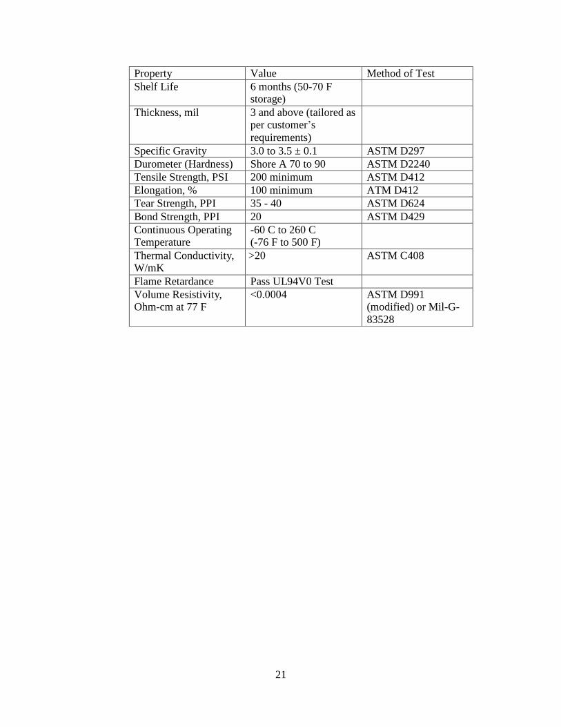
Property Value Method of Test
Shelf Life 6 months (50-70 F storage)
Thickness, mil 3 and above (tailored as per customer’s
requirements)
Specific Gravity 3.0 to 3.5 ± 0.1 ASTM D297
Durometer (Hardness) Shore A 70 to 90 ASTM D2240
Tensile Strength, PSI 200 minimum ASTM D412
Elongation, % 100 minimum ATM D412
Tear Strength, PPI 35 - 40 ASTM D624
Bond Strength, PPI 20 ASTM D429
Continuous Operating Temperature
-60 C to 260 C (-76 F to 500 F)
Thermal Conductivity, W/mK
>20 ASTM C408
Flame Retardance Pass UL94V0 Test
Volume Resistivity, Ohm-cm at 77 F
<0.0004 ASTM D991 (modified) or Mil-G-
83528
22
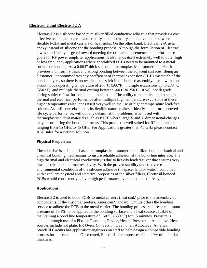
Electrasil 2 and Electrasil 2-A
Electrasil 2 is a silicone based pure silver filled conductive adhesive that provides a cost
effective technique to create a thermally and electrically conductive bond between
flexible PCBs and metal carriers or heat sinks. On the other hand, Electrasil 2-A uses
epoxy instead of silicone for the bonding process. Although the formulation of Electrasil
2 was specifically targeted toward meeting the critical requirements and performance
goals for RF power amplifier applications, it also lends itself extremely well to other high
or low frequency applications where specialized PCBs need to be mounted to a metal
surface or housing. As a 0.005” thick sheet of a thermoplastic elastomer material, it
provides a uniformly thick and strong bonding between the adjacent surfaces. Being an
elastomer, it accommodates any coefficient of thermal expansion (TCE) mismatch of the
bonded layers, so there is no residual stress left in the bonded assembly. It can withstand
a continuous operating temperature of 260°C (500°F), multiple excursions up to 288 °C
(550 °F), and multiple thermal cycling between -60 C to 250 C. It will not degrade
during solder reflow for component installation. The ability to retain its bond strength and
thermal and electrical performance after multiple high temperature excursions at these
higher temperatures also lends itself very well to the use of higher temperature lead-free
solders. As a silicone elastomer, its flexible nature makes it ideally suited for improved
life cycle performance, without any delamination problems, when used with
thermoplastic circuit materials such as PTFE where large X and Y dimensional changes
may occur during the bonding process. This product is well suited for RF applications
ranging from 15 GHz to 45 GHz. For Applications greater than 45 GHz please contact
ASC sales for a custom solution.
Physical Properties:
The adhesive is a silicone based thermoplastic elastomer that utilizes both mechanical and
chemical bonding mechanisms to insure reliable adhesion at the bond-line interface. The
high thermal and electrical conductivity is due to heavily loaded silver that ensures very
low electrical and thermal resistivity. With the proven stability under adverse
environmental conditions of the silicone adhesive (in space, land or water), combined
with excellent physical and electrical properties of the silver fillers, Electrasil bonded
PCBs would consistently deliver high performance over an extended life cycle.
Applications:
Electrasil 2 is used to bond PCBs to metal carriers (heat sink) prior to the assembly of
components. If the customer prefers, American Standard Circuits offers the bonding
service to adhere the PCB to the metal carrier. The bonding process requires a minimum
pressure of 50 PSI to be applied to the bonding surface and a heat source capable of
maintaining a bond line temperature of 150 °C (330 °F) for 15 minutes. Pressure is
applied through use of a Fixture Clamping Device, Heated Press or an Autoclave. Heat
sources include hot plate, I/R Oven, Convection Oven or an Autoclave. American
Standard Circuits has application engineers on staff to help design a compatible bonding
process for our customers. Once cured, Electrasil-2 compresses about 20% of its initial
thickness.
23
Electrasil 3 and Electrasil 3-A
Recently, American Standard Circuits has developed a new type of thermally and
electrically conducting bonding material to bond the PCB ground plane with the heat sink
for RF circuits and electromagnetic shielding applications. In this newly developed class of
materials, there are two types of such bonding materials: Electrasil 3, released in December
2011 and available to the customers; Electrasil 3-A which is in the final testing stages is
planned to be released around September 2012.
ASCI was an early participant in the thermal management of more demanding PCBs used
in telecommunication RF circuits, under-the-hood high end automobile customers, high
density LEDs and under water navigation, to name a few. ASC has much expertise and has
done considerable investment in this area, owning several material and process
patents in this area. Electrasil 3 is a silicone based elastomeric interface that is suitable for
bonding surfaces that have widely dissimilar values of coefficient of thermal expansion
(CTE). Being elastomeric in nature, Electrasil 3 can easily absorb mechanical shock or
dimensional changes due to changes in temperature, or other sudden movements. Thus, it
is ideally suited for components used under severe shocks, temperature extremes and
harsh atmospheric conditions. Some examples are military fighter planes, aerial spy
sensors or missiles. Such elastomeric bonding agents are also very pliable and are
therefore ideal for flexible circuitries, as silicones can be bent around without cracks or
disjoints.
Electrasil 3 can be supplied as bonding sheets of any thickness starting from 3 mils and
higher, or as a putty material that can easily fill circuitry involving complex shapes that
are not necessarily planar. Thus, the putty form is ideal to replace air in complex shaped
cavities between the heat sink body and the PCB ground layer. By changing the catalyst
of the curing process, the bonding characteristics of these interface materials can be
customized to suit the need for both permanent bonding and temporary bonding when the
components have to be assembled and disassembled multiple times, such as in rework
applications.
The thermal and electrical conductivities can be varied over a wide range. The properties
of Electrasil-3A are summarized in the tables below.
Table: Electrasil 3 (Silicone based elastomeric (flexible) thermally and electrically
conducting bonding film)

24
Property Value Method of Test
Shelf Life 6 months (50-70 F storage)
Thickness, mil 3 and above (tailored as per customer’s
requirements)
Specific Gravity 2.0 to 3.5 ± 0.1 ASTM D297
Durometer (Hardness) Shore A 68 to 77 ASTM D2240
Tensile Strength, PSI 180 minimum ASTM D412
Elongation, % 100 minimum ATM D412
Tear Strength, PPI 40 ASTM D624
Bond Strength, PPI 20 ASTM D429
Continuous Operating Temperature
-60 C to 260 C (-76 F to 500 F)
Thermal Conductivity, W/mK
5 to 8.5 ASTM C408
Flame Retardance Pass UL94V0 Test
Volume Resistivity, Ohm-cm at 77 F
0.05 Max ASTM D991 (modified) or Mil-G-
83528
25
Thermasil-1 and ThermEx
Both Thermasil and ThermEx class of materials are dielectrics in nature. In this class
of compounds, there are two important characteristics that play an important role in
the device performance: the dielectric breakdown voltage (DBV) and the moisture
absorption. DBV is a measure of an insulator’s ability to withstand the stress of high
voltages placed across it. Usually all of the commonly available laminates have DBV
values of at least 1000 volts per mil of thickness. This means that a 2 mil thick
laminate can withstand a voltage stress as high as 2000 volts, more than adequate to
meet the Telco specifications applied to many networking products.
Unlike silicone based systems, ThermEx is epoxy based. All epoxy systems absorb
some moisture or water when exposed to high humidity environments. This
absorption affects the PCB in two ways. Water has a relative dielectric constant of
approximately 73. If a laminate absorbs a significant amount of water the resulting
relative dielectric constant of the combination will be higher than normally used to
calculate impedance and can cause impedance mismatches.
A more important effect of moisture absorption is the increased leakage current.
Materials with high moisture absorption may exhibit leakages in excess of what the
circuits housed on them can withstand. In order to use high absorption materials in such
applications, it is often necessary to seal these ThermEx based PCBs with a protective
coating after first taking them dry. Of course, this represents an additional cost as well as
dealing with the problem of reworking, since the coating must be removed to do the
rework and then reapplied.
Thermasil-1
Thermasil 1 is a patented elastomeric dielectric adhesive that has the requisite thermal
interface properties that are particularly useful for making PCBs for (a) cooling of
power supplies, (b) aerospace components, (c) under-the-hood, (d) other automotive
PCBs and (e) various motor controls. The Thermasil type of bonding film is silicone
based which is very flexible and is therefore ideally suited for flexible PCBs. The
processing conditions and material properties of Thermasil are summarized below. This
material is especially suitable for devices that should properly function over wide
temperature ranges (from -100 F to +500 F). It also has high shear strength due to its
elastomeric nature, and thus would not crack or rupture between dissimilar CTE bonded
surfaces. The shelf life of uncured Thermasil-1 is 6 months, when stored between 32 F
and 42 F. The bonding is done by applying a pressure of 100 to 120 PSI at 330 F for 20
to 30 minutes. Depending on the filler used, the thermal conductivity can be tailored
from 0.6 to 4.8 W/mK. The other main characteristics of Thermasil-1 are given below:
1. Long Term Temperature Stability: -100 F to 500 F
2. Specific gravity of final product: 1.4 to 1.8
26
3. Durometer, Shore A: 60 to 90
4. Tensile Strength: 1200 to 1250 PSI
5. Tear Strength: 180 to 200 PPI
6. Elongation: 350 to 430 %
7. Flame Test: Pass UL 480 V0 Test
ThermEx
ThermEx is an epoxy based bonding dielectric material thermal interface. It is a rigid
bonding film and is therefore suitable for rigid PCBs. The bonding film thickness can be
varied over a wide range starting from 2.5 mil to any desired higher thickness. Being
epoxy based, its thermal stability is limited from -60 F to 350 F. It is particularly useful
for cooling of power supplies, under-the-hood and other automotive PCBs and various
motor controls that operate within the temperature range of -60 to 350 F. The processing
conditions and material properties of ThermEx are summarized below.
Shelf Life of uncured material: 6 months (stored at 32 F to 42 F)
Curing process: hold at 280 F at 100 PSI for 20 to 40 minutes
Thermal Conductivity: 0.6 to 4.8 W/mK
Long Term Temperature Stability: -60 F to 350 F
Specific gravity of final product: 1.3 to 1.9
Durometer, Rockwell R: 140 to150
Tensile Strength: 40-45 PSI
Tear Strength: 180 to 200 PPI
Flame Test: Pass UL 480 V0 Test
Power components have a maximum junction temperature, which must not be exceeded to
prevent damage to the device. Devices are encapsulated in packages, which have different
levels of thermal resistance. When designing power electronics, the heat dissipation of the
27
device, coupled with any heat sinks, as well as the maximum power dissipated by the device,
must be analyzed to insure that the device operates within allowable specified limits.
6. Conclusions:
In this White Paper we have summarized the origin of heat in electronic devices, some
basic concepts of thermal phenomenon, various parameters or properties that govern the
thermal management of the electronics assembly, selection and application of thermal
interface materials for various electronics components, criteria governing the selection of
thermal interface materials for RF and digital applications and a broad range of thermal
interface materials made and supplied by ASC for various applications in the RF and
digital industries including the emerging high intensity LEDs.
7. Acknowledgements:
The author would like to acknowledge the help of Mr. Anaya Vardya, CEO, American
Standard Circuits Inc., for offering several valuable suggestions during the course of
writing this paper.
8. References:
1. See, for example, “Accurate Quantitative Physics-of-Failure Approach to Integrated
Circuit Reliability” Edward Wyrwas, Lloyd Condra and Avshalom Hava
(http://www.dfrsolutions.com/uploads/publications/ICWearout_Paper.pdf)
2. Component Reliability Tutorial, please see the link:
http://www.odyseus.nildram.co.uk/Systems_And_Devices_Files/Component%20Reliab
ility%20Tutorial.pdf
3. Dr. Miksa de Sorgo, Electronics Cooling, 2000
4. S. Lee, Electronics Cooling, 1995
5. http://www.asc-i.com/pdf/Thermal_Management_for_Power_Electronics.pdf
6. http://www.asc-i.com/pdf/LED_THERMAL_MANAGEMENT.pdf
7. http://listserv.ipc.org/scripts/wa.exe?A2=DESIGNERCOUNCIL;7e89a36e.0509


