Embed Size (px)
Citation preview

North South University
Department of Electrical & Computer Engineering
CSE 351L: Analog Electronics II / Electronics II Lab
EEE/ETE 311L: Communications Electronics / Analog Electronics II Lab
LAB MANUAL Third Edition

This LAB MANUAL prepared by:
Tabia Hossain
(Lab Instructor/Officer , North South University)
Supervised by:
Mr. M Maksud Alam
(Lecturer, North South University).

This course will try to cover the following experiments: Experiment 1- Basic of Diode, BJT Transistor and Common-Emitter Amplifier.
Experiment 2- Study of class C Amplifier.
Experiment 3- Introduction to Op-Amp.
Experiment 4- Basic circuits of Op-Amp.
Experiment 5- Applications of Op-Amp.
Experiment 6- Frequencyresponse of Op-Amp.
Experiment 7-Study of Colpitts Oscillator.
The sequence at which the lab experiments are conducted might change but in such case the students will be notified before due time. Marks Distribution: Attendance + Class Performance = 10%
Lab Reports (consisting of Report, Questions & Answers and Discussion) = 10%
Quizzes = 15%
Final Practical Test = 15%
Final VIVA (Oral Test) = 10%
Final Written exam = 40%
You will be notified in class if there is a change in the distribution of marks.

Guidance for report writing:
After completion of a lab experiment, the Lab Report is due and should be submitted within 1
week during the next lab class. Each group should submit one lab report per experiment and
any late submissions will be penalized. Each group must also write the results and data
(collected practically from conducting the experiment) in a white A4 sheet of paper and get it
signed by the Faculty or the Lab Instructor. This paper will also contain the names and IDs of the
group members and must be attached with the Lab Report. It shall act as a physical proof that
the group completed their experiment successfully without manipulating any result. Below is a
detailed description of what each Lab Report must contain:
1. Cover Page- All lab reports should have a cover page and the same cover page should be
used for all the lab reports. A sample of a cover page is attached with this lab manual in
the end of this lab report guide. You can make photocopies of the cover page and use it
or you can make a print out that looks similar to the cover page given here.
2. Objective – You should briefly write what was the aim of the experiment. In other
words, write what you intent to achieve by doing the experiment.
3. List of Equipments– A simple list of all the apparatuses and Equipments you used to do
the lab experiment. Example: Signal Generator, Cathode Ray Oscilloscope (CRO), etc.
4. Theory – In this section of the Lab Report, you will specifically write only the things
taught during the lecture time of the class by the faculty. This section should be concise
and to the point. There is no need to make this section unnecessarily big by copy +
pasting from the internet; in fact you may get penalized for such acts. You may take help
from the lab manual but direct quoting from the lab manual is strictly prohibited. Marks
will be given based on your ability to explain what you understood during the class time.
Copying anything from another lab report of a different group will earn your group and
the group from which you have copied a straight zero. Copying anything from a lab
report of a past semester will also earn you a straight zero if caught.
5. Circuit Diagram – Give the circuit diagram for the experiment; it may be computer
composed or hand drawn but should be clean and legible. If a communication board is
used to do the experiment, then you should draw only the necessary part of the board
that we used to do the experiment. It is preferable to use Simulation Softwares like
PSIM, MultiSIM or CircuitLab for drawing the circuit.
6. Results/Data/Readings – This section of the lab report will contain the data that you
have collected practically and it should be presented in a tabular form. You should also
calculate any relevant percentage error or percentage difference from the practical data
and put here in this section. If it is possible to draw a graph to show the relationship
between two parameters you varied or used in the lab then you should put the graph in

this section. The graph may be hand-drawn or computer composed but must be very
clean and legible.
7. Questions and Answers: For each experiment there is a set of questions in the Lab
Manual, for each Lab Report there will be one set of Questions and Answers so the
number of questions that each member of the group will have to answer can be split
among the group members.
8. Discussion –This is one of the most important parts of the lab report. What you write
here proves how attentive and careful you were during the lab class. Copying a single
line from another person’s discussion or from a previous lab report will earn you a
straight zero if you get caught. In your discussion, simply write what you did during the
lab session (you may also write about small details), what you expected to see from the
theoretical knowledge you had and what you eventually saw in practice. Suggest a
legitimate reason for the possible fluctuation if any. You can also write about the
limitations and drawbacks of the experiment. You can also put your personal suggestion
(if you have any) how we can improve our experimental setup.Yourpersonal
observationand the order at which you write themare of utmost importance to score
good marks here. Each group will submit one set of Discussion so a team effort is most
desired in this section.
9. Attachment: Finally, you must attach the A4 sized white sheet of paper in which you
have written your collected data with the lab report. Each group member should write
their name and ID in it (if absent no one should write it for him/her). Marks might be
deducted if this sheet is not found with the lab report.
You should give headings and serial numbers in your lab report with the Objective heading as
serial number 1 (follow the sequence of headings given here). The Lab Report consist of 10
marks and should be completed with equal efforts from all of the group members. There should
be one set of Questions & Answers and one set of Discussion for each Lab Report. Individuals
may split their works.
The followingsare samples of the cover pages that you should use for your lab reports:
North South University
Department of Electrical & Computer Engineering
LAB REPORT
Subject Name:
Experiment Number:
Experiment Name:
Experiment Date:
Report Submission Date:
Section:
Group Number:
Student Name:
Student ID:
Score
Remarks:

North South University
Department of Electrical & Computer Engineering
LAB REPORT
Subject Name: EEE 311 Communications Electronics II Lab
Experiment Number: 01
Experiment Name:
Experiment Date: 1st of January, 2016
Report Submission Date: 7th of January, 2016
Section: 01
Group Number: 01
Basic of Diode, BJT Transistor and Common-Emitter Amplifier.
Student Name: First name Middle Name Last Name
Student ID: 0000000000000
Score
(This Section is for Instructor)
9/10 Remarks: (This section is for instructor) Student shouldgive proper attention to the discussion
writing. Because thatsection is most important to score
more.

EEE/ETE-311L Communications Electronics Lab
Experiment #01 Basic of Diode, BJT Transistor and Common-Emitter
Amplifier. Objectives:
1. Identifying the Anode and Cathode terminals of a Silicon Transistor.
2. Identifying the Base, Emitter and Collector terminals of a BJT NPN Transistor.
3. Setting the Q-point in the middle of the Load-line of a voltage-Divider Biasing network.
4. Determining the phase angle difference in between input and output waveforms of a
Common-Emitter amplifier.
5. Investigating of feasibility of a CE amplifier as a Power Amplifier.
Theory:-
Diode Checking:
A functioning diode will show an extremely high resistance (ideally an open) with reverse bias
and a very low resistance with forward bias. A defective open diode will show an extremely high
resistance (or open) for both forward and reverse bias. A defective shorted or resistive diode will
show zero or a low resistance for both forward and reverse bias. The condition of a diode can be
determined quickly using (1) a digital display meter (DDM) with a diode checking function, or
(2) the ohmmeter section of a digital multi-meter (DMM).
Fig. 01: Layered diagram and Electrical Symbol of a PN junction diode.
Testing a transistor:
The anodes and cathodes of a BJT NPN and PNP are shorted, respectively, shown in fig. 02. The
base-collector junction is one of the diodes and the base-emitter junction is the other one. Since
the transistor PN junction diodes are effective as regular diodes, the principles behind the diode
test can be applied to check if the junctions are working.
Fig. 02: Layered diagram, Electrical symbol and two-diode equivalent circuit of a BJT transistor.
Fixing the Q-point at middle of Load-line:
Voltage-Divider or Universal biasing network is playing important role in an amplifier circuit.
The bias configuration has the advantage of being virtually independent of β, which is sensitive
to temperature changes. In this configuration, the operating point or Q-point can be fixed so that
levels of IC and VCE remain constant despite variation in IB due to change in β. In order to get the

maximum possible output without distortion, the Q-point must be fixed at the middle of the dc
load line so that the full cycle of the input signal can appear at the output with maximum possible
swing.
Fig. 03: Voltage-Divider or Universal Biasing Network.
From the output equation and load-line diagram, shown in below, it’s clear that Q-point will be
at the mid-point of the line if and only if 𝑉𝐶𝐸 =1
2VCC .
𝑉𝐶𝐸 = VCC − IC(RC + RE)
Fig. 04: DC load-line.
CE Amplifier Circuit:

Equipment
Serial
no.
Component Name Specification Quantity
1 Resistor 3
2 Diode 1
3 BJT 1
4 Capacitor 2
5 Potentiometer 1
6 DC Power Supply 2
7 AC signal generator 1
8 Oscilloscope 1
9 Digital Multimeter 1
10 Trainer Board 1
Procedure
Testing a diode:
1. Measure the resistance across the diode using the digital multi-meter.
2. Reverse the placement of the leads and measure again
Testing a transistor:
1. Repeat the previous procedure for the base-emitter and base-collector junctions.
Bias fixing:
1. Construct the circuit shown in the diagram.
2. Keep VCC at about 20 V and adjust the POT until VCE = VCC/2.
Amplifier:
1. Apply a 1 kHz signal of magnitude 40 mV and check both the input and output
waveforms for any distortion.
2. Find the maximum signal that can be applied without distortion. See if this maximum can
be increased by readjusting the POT.

Data Collection
Measured Values:
R1 = ____________Ω
R2 = ______Ω to ______Ω
RC = ____________Ω
RE = ____________Ω
VCC = ____________V
Now apply input ac supply of
Vi(p-p) = ____________V
𝑓i = ____________Hz
Draw DC loadline in the graph 01 and waveforms of 𝑉𝑖(𝑃−𝑃) and 𝑉𝑜(𝑃−𝑃) in the graph 02.
Graph #01 Graph #02
Experimental Data:
Adjust R2 to get VCE = VCC/2.
Measure 𝑅2𝑉𝐶𝐸=𝑉𝑐𝑐 /2
𝑅2𝑉𝐶𝐸=𝑉𝑐𝑐 /2 = _____________Ω
Experimental Data:
𝑉𝑜(𝑃−𝑃) = ____________V
𝑓0 = ____________Hz
Observe both 𝑉𝑖(𝑃−𝑃) and 𝑉𝑜(𝑃−𝑃)
using Oscilloscope.
Measure phase relationship, θ.
Between 𝑉𝑖(𝑃−𝑃)and 𝑉𝑜(𝑃−𝑃).
𝜃 = ____________°

Report:
Solve the given circuit to answer the following questions:
1. If the POT is fixed at 10 kΩ, what is the Q-point (VCEQ)?
2. If the Q-point is in the middle (VCC/2), what is the value of the POT?
3. Calculate the voltage gain of the circuit (Vo/Vi).
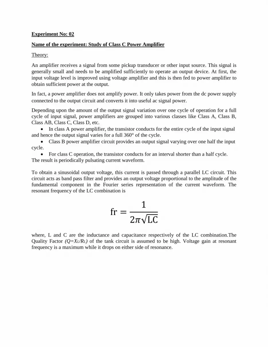
Experiment No: 02 Name of the experiment: Study of Class C Power Amplifier Theory: An amplifier receives a signal from some pickup transducer or other input source. This signal is
generally small and needs to be amplified sufficiently to operate an output device. At first, the
input voltage level is improved using voltage amplifier and this is then fed to power amplifier to
obtain sufficient power at the output. In fact, a power amplifier does not amplify power. It only takes power from the dc power supply
connected to the output circuit and converts it into useful ac signal power. Depending upon the amount of the output signal variation over one cycle of operation for a full
cycle of input signal, power amplifiers are grouped into various classes like Class A, Class B,
Class AB, Class C, Class D, etc.
In class A power amplifier, the transistor conducts for the entire cycle of the input signal
and hence the output signal varies for a full 360° of the cycle.
Class B power amplifier circuit provides an output signal varying over one half the input
cycle.
For class C operation, the transistor conducts for an interval shorter than a half cycle.
The result is periodically pulsating current waveform.
To obtain a sinusoidal output voltage, this current is passed through a parallel LC circuit. This
circuit acts as band pass filter and provides an output voltage proportional to the amplitude of the
fundamental component in the Fourier series representation of the current waveform. The
resonant frequency of the LC combination is
fr =1
2𝜋 LC
where, L and C are the inductance and capacitance respectively of the LC combination.The
Quality Factor (Q=XL/RL) of the tank circuit is assumed to be high. Voltage gain at resonant
frequency is a maximum while it drops on either side of resonance.

Equipments:
Serial Component Details Specification Quantity
no.
1. Transistors BC548 1 piece
2. Resistor 10kΩ, 1kΩ, 2 pieces 10kand 1
piece 1k
3. Capacitors
22 µF (polar) ,
100µF (polar),
0.1 µF 1 piece each for the
4. Inductor 136µH 1 unit
5. Oscilloscope 1 unit
6. AC Signal generator 1 unit
7. DC Power Supply 1 unit
8. Digital Multimeter 1 unit
9. Trainer Board 1 unit

Circuit Diagram 1:
Fig.1: Class C amplifier
Procedure 1:
1. Connect the circuit as shown in figure 1.
2. After the circuit connection has been done, attach the CRO probe to the input (Signal
Generator) and adjust the signal amplitude from the signal generator until you get a pure
sinusoidal input for 1kHz frequency.
3. Attach another CRO probe to the output .Observe output voltage Vo and draw the
output wave shape.
4. Similarly, observe emitter voltage Ve and emitter to collector voltage Vc and draw the
wave shapes.
5. Observe the waveform from the collector,emitter andand draw the output wave shape.
6. Plot Vo vs Vi and find out conduction angle of the amplifier.(Hint: On the CRO display,
find out how many divisions equal 180° and use that information to find the angle.

Data Collection # 01
Measured Values:
RB = ____________Ω
RC = ____________Ω
RE = ____________Ω
VCC = ____________V
Now apply input ac supply of
Vi(p-p) = ____________V
𝑓i = ____________Hz
Until get a pure sinosoidal input for 1KHz
Draw waveforms of 𝑉𝑖(𝑃−𝑃) and 𝑉𝑜(𝑃−𝑃) in the graph 01 and 𝑉𝐸(𝑃−𝑃) and 𝑉𝐶(𝑃−𝑃)on 02
Graph #01 Graph #02
Experimental Data:
𝑉𝑜(𝑃−𝑃) = ____________V
𝑓0 = ____________Hz
Observe both 𝑉𝑖(𝑃−𝑃) and 𝑉𝑜(𝑃−𝑃)
using Oscilloscope.
Measure phase angle of θi and θoof
𝑉𝑖(𝑃−𝑃) and 𝑉𝑜(𝑃−𝑃) respectively.
𝜃i = ____________°
𝜃0 = ____________°
𝑉𝐸(𝑃−𝑃) = ____________V
𝑓E = ____________Hz
𝜃E = ____________°
𝑉𝐶(𝑃−𝑃)= ____________V
𝑓C = ____________Hz
𝜃c = ____________°
Observe both 𝑉𝐸(𝑃−𝑃) and 𝑉𝐶(𝑃−𝑃)
using Oscilloscope.

Circuit Diagram 2:
Fig. 2: Class C amplifier with LC tank
Procedure 2:
1. Connect the circuit as shown in figure 2.
2. After the circuit connection has been done, attach the CRO probe to the input (Signal
Generator) and adjust the signal amplitude from the signal generator until you get a
pure sinusoidal input.
3. Vary the frequency until a distortion free outputVo is obtained. Draw the output
wave shape.
4. Make sure that collector voltage waveform is pure sinusoidal.
5. Vary the frequency above and below cut-off. Take readings of output voltages at
different frequencies.
6. Observe the waveform from the emitter VE and draw the output wave shape.
7. Observe the wavefrom across LC VLC and drawthe wave shape.
8. Vary the input signal frequency until you obtain the highest possible gain (the
highest peak-to-peak value of output voltage).

Data Collection # 02
Measured Values:
RB = ____________Ω
RE = ____________Ω
C = ____________F
L = ____________H
VCC = ____________V
Now apply input ac supply around 40 KHz of
Vi(p-p) = ____________V
𝑓i = ____________Hz
Calculate the resonant frequency,
𝑓r = ____________Hz
Experimental Data:
Observe 𝑉𝑜(𝑃−𝑃) using oscilloscope
and vary the input signal frequency
until obtain highest output voltage
𝑉𝑜(𝑃−𝑃) = ____________V
𝑓0 = ____________Hz
Observe both 𝑉𝑖(𝑃−𝑃) and 𝑉𝑜(𝑃−𝑃)
using Oscilloscope and make sure
that both of them are pure
sinusoidal.
Measure phase relationship, θ.
Between 𝑉𝑖(𝑃−𝑃)and 𝑉𝑜(𝑃−𝑃).
𝜃 = ____________°
𝑉𝐸(𝑃−𝑃) = ____________V
𝑓E = ____________Hz
𝑉𝐿𝐶(𝑃−𝑃)= ____________V
𝑓LC = ____________Hz
Observe both 𝑉𝐸(𝑃−𝑃) and 𝑉𝐿𝐶(𝑃−𝑃)
using Oscilloscope.

Draw waveforms of 𝑉𝑖(𝑃−𝑃) in the graph 01,𝑉𝑜(𝑃−𝑃) in the graph 02,𝑉𝐸(𝑃−𝑃)on graph 03
and 𝑉𝐿𝐶(𝑃−𝑃)on 04respectively.
Graph#01 Graph#02
Graph#03 Graph#04
Report:
1. Submit the wave shapes drawn at steps 2 and 3 (procedure 1) and explain the
sinusoidal and pulsating behaviour of the observed voltage waveforms.
2. Submit the wave shapes drawn at steps 2 and 4 (procedure 2) and explain the
sinusoidal and pulsating behaviour of the observed voltage waveforms.
3. Calculate the resonant frequency and compare it with the measured value. Plot
Output amplitude VsFrequency and verify that the maximum output is obtained
at resonant frequency.

Experiment No: 03 Name of the experiment: Introduction to OPAMPs Introduction: The operational amplifier (abbreviated as OPAMP) is a direct-coupled high-gain amplifier to
which feedback is added to control its overall response characteristic. It has very high (ideally ∞)
input impedance, very low (ideally 0) output impedance and large bandwidth and its
characteristics do not drift with temperature. It offers all the advantages of monolithic integrated
circuits: Small size, high reliability, reduced cost, temperature tracking and low offset voltage
and current. For these reasons, it has gained wide acceptance as a versatile, predictable and
economic system building block. An OPAMP may be used to perform many mathematical operations. Some of these basic
applications are studied in this experiment.
Offset Nulling:
When the feedback is not connected, both inverting and the non-inverting inputs are grounded,
then ideally the output of the op-amp is zero. But, practically there will be an error voltage
component present at the output due to the unavoidable imbalances inside the op-amp. This
small voltage at output is caused due to offset voltage.
By adjusting the pot we can null any offset error.
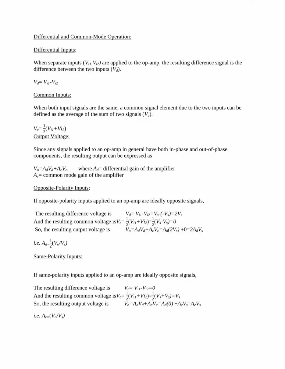
Differential and Common-Mode Operation:
Differential Inputs:
When separate inputs (Vi1,Vi2) are applied to the op-amp, the resulting difference signal is the
difference between the two inputs (Vd).
Vd= Vi1-Vi2
Common Inputs:
When both input signals are the same, a common signal element due to the two inputs can be
defined as the average of the sum of two signals (Vc).
Vc= 1
2(Vi1+Vi2)
Output Voltage:
Since any signals applied to an op-amp in general have both in-phase and out-of-phase
components, the resulting output can be expressed as
Vo=AdVd+AcVc, where Ad= differential gain of the amplifier
Ac= common mode gain of the amplifier
Opposite-Polarity Inputs:
If opposite-polarity inputs applied to an op-amp are ideally opposite signals,
The resulting difference voltage is Vd= Vi1-Vi2=Vs-(-Vs)=2Vs
And the resulting common voltage isVc= 1
2(Vi1+Vi2)=
1
2(Vs-Vs)=0
So, the resulting output voltage is Vo=AdVd+AcVc=Ad(2Vs) +0=2AdVs
i.e. Ad=1
2(Vo/Vs)
Same-Polarity Inputs:
If same-polarity inputs applied to an op-amp are ideally opposite signals,
The resulting difference voltage is Vd= Vi1-Vi2=0
And the resulting common voltage isVc= 1
2(Vi1+Vi2)=
1
2(Vs+Vs)=Vs
So, the resulting output voltage is Vo=AdVd+AcVc=Ad(0) +AcVs=AcVs
i.e. Ac=(Vo/Vs)

Common-Mode Rejection Ratio:
Having obtained AdandAc we can calculate a value for common-mode rejection ratio (CMMR),
which can be defined by
CMMR= Ad
Ac
The value of CMMR can also be expressed in logarithmic terms as
CMMR=20log10Ad
Ac , (dB)
Equipments:
Serial no. Component Details Specification Quantity
1. OPAMP 741 1 piece
2. Resistor 1 piece, 1piece
10kΩ, POT 10KΩ
3. Oscilloscope 1 unit
4. AC signal generator 1 unit
5. DC Power Supply 3 units
6. Digital Multimeter 1 unit
7. Trainer Board 1 unit

Circuit Diagram:
Fig 1: Circuit for offset nulling
Fig 2: Circuit for calculating Ad
Fig 3: Circuit for calculating Ac
Procedure:
Study of offset voltage:
1. Connect the circuit of figure 1 and obtain the value of V0. This is the offset voltage for
the op-amp
2. Adjust the 10K POT(entio)meter to its center position.
3. Connect the POT outside leads between pins 1 and 5 of the op-amp.Make sure that the power is
applied to the design application.
4. Connect the wiper of the POT to the negative supply voltage (pin4).
5. Ensure that input signals are zero or null and that pins 2 and 3 have a dc return to ground.
6. Measure the output with a dc meter and obtain zero null by adjusting the potentiometer.

Calculating Ac& Ad:
1. Connect the circuit shown in figure 2 and and measure the output voltage for Vcc
+15V/5V/10V and Vee -15V/-5V/-10V. Calculate the value of Adby using equation.
2.Connect the circuit shown in figure 3 and and measure the output voltage for Vcc
+15V/5V/10V and Vee -15V/-5V/-10V. Calculate the value of Ac by using equation.

Data Collection
Measured Values:
VCC = ____________V
VEE = ____________V
Now apply input voltage of
Vi = ____________V
Set, Vinv = 1 V &Vnon-inv = 1 V for
Calculating Ad
VCC = ____________V
VEE = ____________V
VCC = ____________V
VEE = ____________V
VCC = ____________V
VEE = ____________V
Set, Vinv = 0.5 V &Vnon-inv = -0.5 V for
Calculating Ac
VCC = ____________V
VEE = ____________V
VCC = ____________V
VEE = ____________V
VCC = ____________V
VEE = ____________V
Experimental Data:
𝑉𝑜 = ____________V
Nulling procedure,
𝑉𝑜𝑓𝑓𝑠𝑒𝑡 = _______0____V
POT, R2 = ____Ω to ____Ω
Set Voffset to 0 V and again measure
R2.
R2 = ____Ω
𝑉𝑜 = ____________V
Ad = ____________
𝑉𝑜 = ____________V
Ad = ____________
𝑉𝑜 = ____________V
Ad = ____________
𝑉𝑜 = ____________V
Ac = ____________
𝑉𝑜 = ____________V
Ac = ____________
𝑉𝑜 = ____________V
Ac = ____________

Report:
1. Calculate the value Ad and Ac.
2. What is the value of CMRR of an ideal Op-Amp?
3. Calculate the practical value of CMMR.

Experiment No: 04 Name of the experiment: Basic Circuits of OPAMPs
Inverting Amplifier:An inverting amplifier is a special case of the differential amplifier in which
that circuit's non-inverting input V2 is grounded, and inverting input V1 is identified with Vin
above. It invertingthe input voltage Vin and produces the inverse of this at the output Vout. The
closed-loop gain is Rf / Rin, hence
Unity Gain Amplifier:Unity gain produces same output as is applied to its input. The output
voltage follows the input voltage. That is why the gain of the amplifier is approximately unity.
Voltage Follower/ Buffer: Voltage follower produces almost the same output as is applied to its input. The input resistance
of a voltage follower circuit is very high (several mega ohms). Therefore, it draws negligible
current from a signal source. Thus it works as a voltage buffer that provides a means of isolating
an input signal from a load.
Summing Amplifier/ Inverting Adder: Summing amplifier or Inverting adder adds up the signals at its inverting input terminal and
produces the inverse of this summation at the output, provided, the value of the feedback
resistance and the resistance in series with the input signals are chosen correctly.
A summing amplifier sums several (weighted) voltages:
When , and independent
When
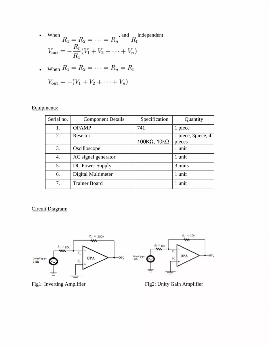
Equipments:
Serial no. Component Details Specification Quantity
1. OPAMP 741 1 piece
2. Resistor 1 piece, 3piece, 4
100KΩ, 10kΩ pieces
3. Oscilloscope 1 unit
4. AC signal generator 1 unit
5. DC Power Supply 3 units
6. Digital Multimeter 1 unit
7. Trainer Board 1 unit
Circuit Diagram:
Fig1: Inverting Amplifier Fig2: Unity Gain Amplifier

Fig3: Voltage Follower
Fig 4: Inverting Adder/Summing Amplifier
Procedure:
1. Study of inverting aplifier: i) Connect the circuit of figure 1 and obtain values of V0 for Vi 500mv (p-p) 1kHz.
ii) Calculate the close loop gain Av.
iii) Find out the phase angle.
2. Study of unity gain amplifier: i) Connect the circuit of figure 2 and obtain values of V0 for Vi =500mV(p-p)1kHz . It
can be done by placing R1=Rf-10K on figure 1
ii) Calculate the close loop gain Av.
iii) Find out the phase angle.

3. Study of the voltage follower:
i) Connect the circuit of figure 3 and measure V0 for Vi=2V (p-p) and 5V(p-p).
ii) Calculate the close loop gain Av.
iii) Find out the phase angle.
4. Study of Summing amplifier: i) Connect the circuit of figure 4 and measure Vo for E1=2V /5V and E2=-2V/5V.
ii) Calculate the close loop gain Av.
iii) Find out the phase angle.
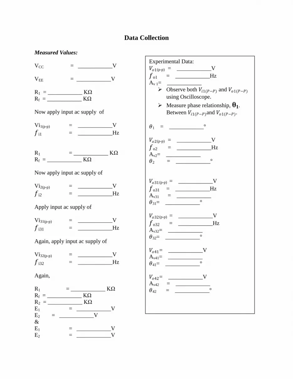
Data Collection
Measured Values:
VCC = ____________V
VEE = ____________V
R1 = ____________ KΩ
Rf = ____________ KΩ
Now apply input ac supply of
Vi1(p-p) = ____________V
𝑓i1 = ____________Hz
R1 = ____________ KΩ
Rf = ____________ KΩ
Now apply input ac supply of
Vi2(p-p) = ____________V
𝑓i2 = ____________Hz
Apply input ac supply of
Vi31(p-p) = ____________V
𝑓i31 = ____________Hz
Again, apply input ac supply of
Vi32(p-p) = ____________V
𝑓i32 = ____________Hz
Again,
R1 = ____________ KΩ
Rf = ____________ KΩ
R2 = ____________ KΩ
E1 = ____________V
E2 = ____________V
&
E1 = ____________V
E2 = ____________V
Experimental Data:
𝑉𝑜1(p-p) = ____________V
𝑓o1 = ____________Hz
Av 1= ____________
Observe both 𝑉𝑖1(𝑃−𝑃) and 𝑉𝑜1(𝑃−𝑃)
using Oscilloscope.
Measure phase relationship, θ1.
Between 𝑉𝑖1(𝑃−𝑃)and 𝑉𝑜1(𝑃−𝑃).
𝜃1 = ____________°
𝑉𝑜2(p-p) = ____________V
𝑓o2 = ____________Hz
Av2= ____________
𝜃2 = ____________°
𝑉𝑜31(p-p) = ____________V
𝑓o31 = ____________Hz
Av31 = ____________
𝜃31= ____________°
𝑉𝑜32(p-p) = ____________V
𝑓o32 = ____________Hz
Av32= ____________
𝜃32= ____________°
𝑉𝑜41= ____________V
Av41= ____________
𝜃41= ____________°
𝑉𝑜42= ____________V
Av42 = ____________
𝜃42 = ____________°

Report:
1) Why does the buffer circuit is known as unity follower?
2) Calculate all the output values from the inverting amplifier, unity gain amplifier voltage
followerand summng amplifier. Show both the theoretical and practical value. Calculate the
percentage error between them.

Experiment No: 05 Name of the experiment: Application of OPAMPS Theory: Integrator and Differentiator: OPAMPs can be used to perform mathematical operations like integrations and differentiation. The ideal performance equation for integrator(1/ is: )∫_
VO = - And that of differentiator is: VO = -RC ( ( _ ))/ In this experiment, a square wave is at first integrated to produce a triangular wave of same
frequency. This is then differentiated to reproduce the square wave.
Fig: input and output of integrator and differentiator
Equipments:
Serial no. Component Details Specification Quantity
1. OPAMP 741 2 pieces
2. Resistor 100KΩ, 10kΩ 2 pieces, 1 piece,
3. Capacitors 0.1µF, 0.01 µF 1 piece each
4. Oscilloscope 1 unit
5. AC Signal generator 1 unit
6. Digital Multimeter 1 unit
7. Trainer Board 1 unit

Circuit Diagram:
Fig: Integrator Fig: Differentiator Procedure:
1. Make the connections as shown in figure.
2. Apply a square wave of 500Hz to the input of the integrator. Observe the wave shape at
point A. This is the integrated output. The integrated output at point A should be a
triangular wave. Take reading of its amplitude. Draw the wave shape.
3. Observe the output (of the differentiator) and input (to the integrator) at dual mode of
oscilloscope. Notice the slightly damped output. Take reading of amplitudes. Draw the
wave shapes.

Data Collection
Measured Values:
VCC = ____________V
VEE = ____________V
R1 = ____________ KΩ
Rf = ____________ KΩ
Now apply input ac supply of
Vi1(p-p) = ____________V
𝑓i1 = ____________Hz
R2 = ____________ KΩ
Now apply input ac supply of
Vi2(p-p) = ____________V
𝑓i2 = ____________Hz
Draw waveforms of 𝑉𝑖1(𝑃−𝑃) and𝑉𝑜1(𝑃−𝑃)in the graph 01,𝑉𝑖2(𝑃−𝑃) and𝑉𝑜2(𝑃−𝑃)on graph 02.
Graph#01 Graph #02
Experimental Data:
𝑉𝑜1(p-p) = ____________V
𝑓o1 = ____________Hz
Observe both 𝑉𝑖1(𝑃−𝑃) and 𝑉𝑜1(𝑃−𝑃)
using Oscilloscope.
Again,
𝑉𝑜2(p-p) = ____________V
𝑓o2 = ____________Hz
Observe both 𝑉𝑖2(𝑃−𝑃) and 𝑉𝑜2(𝑃−𝑃)
using Oscilloscope.

Experiment No: 06
Name of the experiment: Frequency response of op-amp Introduction: We know that the bandwidth of an ideal op-amp is infinite, but in the case of a practical op-amp the Open loop gain starts rolling-off (decreases) at higher frequencies. What could be the reason for such decrease in the gain at higher frequencies? Obviously, it would be the capacitive effect across the output terminals of the op-amp whose reactance starts decreasing with increasing frequency and hence, the output voltage decreases at very high frequency and the gain gets drastically reduced.
Figure 1 : Frequency Response of Op-amp From the frequency response curve of op-amp, it is clearly seen that the open loop gain of op-amp is high and its roll-off starts at lower frequencies. But for closed-loop, gain is much lower than open-loop but roll-off is introduced later. However, the gain and bandwidth product is constant for both open-loop and closed-loop. Or we can say that the gain and bandwidth product of open loop is equal closed loop product. Equipments:
Serial no. Component Details Specification Quantity
1. OPAMP 741 1 piece
2. Resistor 100KΩ, 10KΩ, 3.3 KΩ 1 piece each
3. Oscilloscope 1 unit
4. AC signal generator 1 unit
5. DC Power Supply 1 unit
6. Digital Multimeter 1 unit
7. Trainer Board 1 unit

Circuit Diagram:
Rf=100k
+15V
7
2
R1=10k 741 Vout
6
3 4
-15V
Figure 2: Open-loop configuration Figure 3: Closed-loop configuration Procedure:
1. Connect the circuit of figure 2. 2. Adjust the input voltage .2 V and 10K Hz. 3. Observe and record the output voltage.
4. Decrease the frequency until the output voltage decreases and find out lower cutoff
frequency.
5. Then increase frequency until output voltage changes and find out higher cutoff frequency.
6. Record the frequencies in the table and plot gain vs. frequency in a semi-log graph paper.
Find out the cut-off frequency of the curve. 7. Repeat the steps for figure 3.

Data Collection
Measured Values:
VCC = ____________V
VEE = ____________V
Now apply input ac supply of
Vi1(p-p) = ____________V
𝑓i1 = ____________Hz
Again,
R1 = ____________ KΩ
Rf = ____________ KΩ
Now apply input ac supply of
Vi2(p-p) = ____________V
𝑓i2 = ____________Hz
Experimental Data:
𝑉𝑜1(p-p) = ____________V
𝑓o1 = ____________Hz
Observe both 𝑉𝑖1(𝑃−𝑃) and 𝑉𝑜1(𝑃−𝑃)
using Oscilloscope.
Frequency,𝑓i1 Vo1(v) Gain(open-
loop)
𝑓lower-cut = ____________Hz
𝑓higher-cut= ____________Hz Decrease the frequency until the
output voltage decreases and find out lower cutoff frequency.
Then increase frequency until output
voltage changes and find out higher cutoff
frequency
Again,
Frequency, 𝑓i2 Vo2(v) Gain(closed-
loop)
𝑓lower-cut = ____________Hz
𝑓higher-cut = ____________Hz

Draw open loop gain Vs fi1 in the graph 01, and closed loop gain Vs fi2on graph 02.
Graph #01 Graph#02
Experiment No: 07 Name of the experiment: Study of Colpitts Oscillator Introduction: Oscillators are circuits that produce an output waveform without an external signal source. Any
of various electronic devices that produce alternating electronic signal, commonly employing
tuned circuits (consist of capacitor and inductor) and amplifying components is known as
oscillators. Every oscillator has at least one active device. This active device acts as an amplifier.
There are many types of oscillator devices, but they all operate according to the same basic
principle: an oscillator always employs a sensitive amplifier whose output is fed back to the
input in phase. Thus, the signal regenerates and sustains itself. This is known as positive
feedback. A Colpitts oscillator is a discrete LC oscillator that uses a pair of tapped capacitors and an
inductor to produce regenerative feedback. Combination of inductor and capacitors determine
frequency of oscillator. It is type of feedback LC oscillator where feedback is supplied
capacitively. It is named after its inventor Edwin. H. Collpit. Better frequency stability can be
obtained through it. One of the key features of this type of oscillator is its simplicity (needs only
a single inductor) and robustness. A Colpitts oscillator is the electrical dual of a Hartley
oscillator. Essential components of Colpitts Oscillator are:
A resonator which consists of LC circuit, which is also known as frequency-determining
network (FDN) or tank circuit. Frequency of the Colpitts oscillator can be changed either
by varying the inductance of the coil or by varying the capacitance of the two capacitors
in the tank circuit. An amplifier/transistor whose function is to amplify the oscillations produced by the
resonator. We are going to BJT transistor as amplifier applying voltage divider bias. A positive feedback network (PFN) whose function is to transfer part of output energy to
the LC circuit in proper phase. The amount of energy fed back is sufficient to meet I²R
losses in LC circuit. The feedback needed for oscillation is taken from a voltage divider
made by the two capacitors. Sinusoidal wave output of frequency of large range can be
achieved through Colpitt oscillator. The ideal frequency of oscillation is:
Where the series combination of C1 and C2 is the effective capacitance of the LC tank and L is
inductance of tank circuit.

Equipments:
Serial no. Component Details Specification Quantity
1. BJT 1 piece
2. Resistor 1KΩ,4.7KΩ, 10kΩ 1 piece,2 pieces,1 piece
3. Capacitors 0.1µF, 0.01 µF 2 pieces,3 pieces
4. Oscilloscope 1 unit
5. DC power supply 1 unit
6. Digital Multimeter 1 unit
7. Trainer Board 1 unit Circuit Diagram:
Procedure: 4. Connect the circuit as shown in figure. 5. Observe the output. Draw the wave shapes. Take the reading of the output frequency. 6. Calculate the resonant frequency of the oscillator circuit. Compare it with the practical value.

Data Collection
Measure Value:
R1= KΩ
R2= KΩ
RC= KΩ
RE= KΩ
L= H
Vcc= V
Calculate resonant frequency of oscillator circuit.
𝑓r = ____________Hz
Draw the output waveform on graph given below .
Experimental Data:
𝑉𝑜 (p-p) = ____________V
𝑓o = ____________Hz
Observe 𝑉𝑜1(𝑃−𝑃) using
Oscilloscope.


