Embed Size (px)
Citation preview

1
TESLA Report 2008-03
LLRF System for FLASH Components Development (part 1)
Editors: Krzysztof T. Poźniak, Ryszard S. Romaniuk Institute of Electronic Systems, Warsaw University of Technology, ELHEP Laboratory, Nowowiejska 15/19, 00-665 Warsaw, Poland
www.desy.de/~elhep, [email protected], tel.+49-40-8998-1600 (1602), +48-22-234-79-86 (7744, 5110)
ABSTRACT The report presents recent results of research and technical work on LLRF control system development for FLASH and
XFEL. The report period covers approximately the last several months before the publication date. The report subject covers some of the chosen contributions by Elhep Lab. Most of the design efforts are supported by measurement results performed either at MTS or directly at the linac.
A part of the LLRF system cooperating with RF Gun requires even more stringent parameters in terms of quality. A complete measurement path was presented including I and Q detectors and fpga based, low latency digital controller. The system has standardized DOOCS gui. Input signal calibration procedure was added after practical control tests.
An alternative software solution to fpga based controller, supported by matlab was developed to investigate novel firmware implementation. The complex control algorithm is based on nonlinear system identification. The controller spans over the full cryomodule, and calculates vector sum for eight cavities.
A modular construction of the LLRF controller system PCB is presented. The module consists of a digital part residing on the base platform and exchangeable analog part positioned on a number of daughter-boards. Functional structure was presented and in particular the FPGA implementation with configuration and extension block for RF mezzanine boards. Application examples are given in the LLRF system of FLASH.
A universal, configurable PCB, PMC expansion module is presented. It is designed to increase the cooperation flexibility with other industrial systems via implemented numerable I/O standards. The system features: GPIB, I2C, LVDS, RS-232, reference clock, PCI, JTAG, IP.
A simple, cheap, low-count channel, high-quality, PMC standard DAQ, fpga based PCB was designed and fabricated. Sampling frequency is up to 100MHz. Signal cross talk was minimized. Analog and digital parts were carefully separated. Motherboard has optical fiber connectors, Ethernet, USB and two PMC I/Os. A prototype DAC VME PCB with vector modulator was designed and fabricated. As the connection with the ACB1 board QTE a connector from Samtec was used. It is high speed and RF board-to-board connector and is matched with the QSE part. It provides 40 I/Os and integral ground plane which can be also used for power. Data, SPI, clock and control signal interfaces are available.
Hardware and software concept of Universal Controller Module (UCM), a FPGA/PowerPC based embedded system designed to work as a part of VME system was designed and fabricated. UCM, provides access to the VME crate with industrial interfaces like GOL,GbE, USB, CAN. UCM is a well prepared platform for further investigations and development in IP cores field, in functionality expansion of PCI Mezzanine Card (PMC).
A new reconfigurable architecture created in FPGA was designed which is optimized for DSP algorithms like digital filters or digital transforms. The architecture tries to combine advantages of typical architectures like DSP processors and datapath architecture, while avoiding their drawbacks. The architecture is built from blocks called Operational Units (OU). Each Operational Unit contains the Control Unit (CU), which controls its operation. The Operational Units may operate in parallel, which shortens the processing time. This structure is also highly flexible, because all OUs may operate independently.
Compact Matlab script converter to C code is presented -M2C. The application is designed for embedded systems of very confined resources. The generated code is optimized for the weight and is transferable between different hardware platforms. The converter generates a code for Linux and for stand-alone applications. FLEX and BIZON tools were used. Example of M2C application was given. A flexible conversion of Matlab structures directly into FPGA implementable grid of parameterized and simple DSP processors is a next step of application development.
A new method of fpga address space management called the Component Internal Interface (CII) was introduced. An updatable and configurable environment provided by fpga fulfills technological and functional demands imposed on LLRF system. A purpose, design process and realization of the object oriented software application, written in the high level code is described.
Keywords: LLRF system, superconductive niobium cavity, FPGA, FPGA I/O, VHDL, Altera, Xilinx, communication interface, behavioral programming, FPGA systems parameterization and standardization, FPGA based systems for HEP experiments, multi-FPGA systems, DSP algorithms.

2
CONTENTS Introduction . . . . . . . . . . . . . . . . . . . . . . . . . . . . . . . . . . . 03 R.S.Romaniuk, K.T.Poźniak, ISE, WUT Measurement and control of field in RF GUN at FLASH . . . . . . . . . . . . . . . . 04 A.Brandt, M.Hoffman, DESY, Hamburg, W.Koprek, P.Pucyk, DESY, Hamburg and ISE, Warsaw Univ. of Technology (WUT), K.T.Pozniak, R.S.Romaniuk, WUT Multi-cavity complex controller with vector simulator for TESLA technology linear accelerator 12 T.Czarski, K.T.Pozniak, R.S.Romaniuk, J.Szewinski, WUT Versatile LLRF platform for FLASH laser . . . . . . . . . . . . . . . . . . . . . . 19 P.Strzalkowski, W.Koprek, K.T.Pozniak, R.S.Romaniuk, WUT FPGA based PCI mezzanine card with digital interfaces . . . . . . . . . . . . . . . . 27 K.Lewandowski, R.Graczyk, K.T.Pozniak, R.S.Romaniuk, WUT Data acquisition module implemented on PCI mezzanine card . . . . . . . . . . . . . . 33 L.Dymanowski, L.Graczyk, K.T.Pozniak, R.S.Romaniuk, WUT Vector modulator board for X-FEL LLRF system . . . . . . . . . . . . . . . . . . . 40 M.Smelkowki, P.Strzałkowski, K.T.Pozniak, WUT, M.Hoffman, DESY FPGA system development based on universal control module . . . . . . . . . . . . . . 47 R.Graczyk, K.T.Pozniak, R.S.Romaniuk, WUT DSP algorithms in FPGA – proposition of a new architecture . . . . . . . . . . . . . . 53 P.Kolasinski, W.Zabolotny, WUT Matlab script to C code converter for embedded processors; Application in LLRF system for FLASH laser . . . . . . . . . . . . . . . . . . . . . . . . . . . . . . . . . 57 K.Bujnowski, A.Siemionczyk, P.Pucyk, J.Szewinski, K.T.Poźniak, R.S.Romaniuk, WUT Decomposition of Matlab script for FPGA implementation of real time simulation algorithms for the LLRF system in the European XFEL . . . . . . . . . . . . . . . . . . . . . . 64 K.Bujnowski, WUT, P.Pucyk, DESY and WUT, K.T.Pozniak, R.S.Romaniuk, WUT FPGA control utility in Java . . . . . . . . . . . . . . . . . . . . . . . . . . . . 74 P.Drabik, K.T.Pozniak, WUT Copper TESLA structure – measurement and control . . . . . . . . . . . . . . . . . . 81 J.Główka, M.Maciaś, WUT

3
INTRODUCTION Subject of the report is current development of the Low Level Radio Frequency (LLRF) system for FLASH. The primary role of the LLRF system is to stabilize the amplitude and phase of high power (HP) 1,3GHz RF field in a superconducting Nb multicell cavity linear accelerator. The linac accelerates a bunched beam of electrons for FEL action. The stabilization is done via measurement of field changes in the cavity, calculation of an error, comparing with a set point and application of closed loop (FB) or open loop (FF) active control algorithms. Effective control requires near-real time or real-time time regime. The time axis is defined by the repetition of HP field loading in the accelerator which is 10Hz, loading time 800 µs, effective work time 500 µs, field decay and the rest is idle time. During the field stabilization time slot of 500µm a bunched beam of electrons, of fine temporal structure, is injected into the linac. Thus, the secondary aim of the LLRF system is to provide the best possible electron beam quality from the linac. Going further with this idea one may assume that the main aim of the FLASH machine is to provide the best quality photon beam to the FEL user. Thus, the ultimate aim of the LLRF system is to stabilize the photon beam, via the beam based feedback system. Now, we are still far away from such possibility. The ultimate control system for FEL may be multi-loop in the future and would consist of HP field stabilization sub-system but also beam based sub-systems for electron and photon beams alike.
The LLRF system consists functionally of several layers like: control and measurement, fast calculations, algorithm deposits, readout, transmission, diagnostics, signal processing, data acquisition, synchronization, etc. Not all of the mentioned layers have universal nature. Some of them depend on the approach to the system design. Generally, the LLRF system consists of closely cooperating hardware and software layers. And in this region there is hidden the biggest design freedom now. There can be observed large differences between LLRF system designers and experts views as to what parts of the system should be software and what should reside in the hardware. The consequences of hardware or software based approaches are quite serious. There is not easy answer since the development of programmable circuits is very abrupt. Initially, the LLRF systems were designed nearly solely as stiff hardware solutions. Then simple DSP µP were applied. Today we use fpga-dsp combos and fast optical transmission between the functional PCBs. The involved software and firmware layers get more complicated and split to low level and high level applications. At first sight, the control algorithm of a simple LC resonant cavity of very high finesse seems trivial. Even in the case, when the cavity detunes, due to Lorentz force, under the influence of HP loading field. The near future operator of the machine would require such options like: wide base exception handling capability, a lot of automation, system diagnostics, one button operation, extremely high availability of the machine for the user, absolute safety, full risk assessment, evaluation of breakdown points, and many more. This seems to complicate a lot. However, the electronics (in terms of hardware and software) able to accommodate all these needs and requirements is nearly at hand, and nearly at no excess cost. Thus, perhaps answering the question what put in hardware and what in software would soon have no major sense.
The Elhep Lab, closely cooperating with the DESY LLRF Team, publishes periodically technical reports gathering, for archival purposes, all the problems encountered on the research, design and technical path leading to the optimal controller choice for XFEL machine. The test fields were/are Chechia, TTF, MTS and FLASH. We see a deep sense to share this experience even with comparatively simple technical problems, which do not seem so simple when another team encounters them unexpectedly and struggles to solve them the next day. We also see a deep sense in writing good technical documentation of what has been done. This should be a good custom of all big projects. In this report we gathered a few technical notes concerning a variety of parallel threads, the work on the LLRF system goes on. We hope to continue to publish this series of technical notes. The notes are devoted to simple hardware and software solutions tried while developing the LLRF control system. This technical report gathers the work results on: software converters of Matlab scripts to C++ deigned for systems of very confined resources; software converters of Matlab scripts directly to fpga circuit; design and manufacturing of a number of variety of PCBs mainly of modular construction to provide design flexibility and software exchangeability; new advanced version on the flagship software product of the group – object oriented approach to the Internal Interface technology of fpga address space management; and many more.
Apart from technical problems, which we are mainly concerned with, some of the most important relevant mixed technical and non-technical questions concerning the development of LLRF for XFEL machine are: how to optimize costs for LLRF system for XFEL, how to choose the best cost/performance ratio, stay with VME standard or switch to promising ATCA or µTCA, how to assess all the risk associated with this switching, is the switching worth the expected gains, how to estimate the increase in machine availability, when at the latest decide to freeze to technology choice, what is the real effort in FTE required to do the job, choose full industrial solution or do all the job by the institutes and academic collaboration, would the involved academics provide sufficient work continuity, and many more. We are also participating, by the research on the system, in gathering sufficient knowledge and finding right clues to answer some of these questions. With the decision on realization of the high availability, automated, hot swappable version of the LLRF system in ATCA telecom standard, we hope that the next technical reports will be devoted to the relevant ATCA solutions. Acknowledgment The editors would like to thank DESY Directorate for providing excellent cooperation conditions for ELHEP ISE WUT team to work together with FLASH LLRF Collaboration. This concerns especially Ph.D. and M.Sc. students contributing to the common research and technical efforts.

4
Measurement and control of field in RF GUN at FLASH A. Brandt1, M. Hoffmann1, W. Koprek1,2, P. Pucyk1, 2, S. Simrock1, K T.Pozniak2, R.S. Romaniuk2
1) Deutsches Elektronen-Synchrotron, Notkestrasse 85, 22607 Hamburg, Germany 2) Warsaw University of Technology, Institute of Electronic Systems, Nowowiejska 15/19, 00665 Warsaw, Poland
ABSTRACT The paper describes the hardware and software architecture of a control and measurement system for electromagnetic field stabilization inside the radio frequency electron gun, in FLASH experiment. A complete measurement path has been presented, including I and Q detectors and FPGA based, low latency digital controller. Algorithms used to stabilize the electromagnetic field have been presented as well as the software environment used to provide remote access to the control device. An input signal calibration procedure has been described as a crucial element of measurement process.
Keywords: FLASH, FEL laser, linear accelerator, super conducting cavity controller, monitoring, FPGA, VHDL, Xilinx
1 INTRODUCTION The Free Electron Laser in Hamburg (FLASH) named before Vacuum Ultraviolet Free Electron Laser (VUV-FEL) is a linear accelerator for producing ultra-short high power laser flashes. A high brilliant coherent light is emitted from electron bunches passing undulator. This process is called Self-Amplified Spontaneous Emission (SASE). The light wavelength is in range from 100 to 3 nm. FLASH accelerator has been designed to accelerate electrons up to 1 GeV energy. Electrons bunches are produced in a radio frequency electron gun (RF GUN). Inside the gun they are accelerated close to the light velocity. Further acceleration in superconducting cavities increases only their energy. Electron bunches after the first accelerating module go through the first dispersive magnetic chicane called bunch compressor. In the bunch compressor they are compressed from rms length 2.2 mm to 50 um at the end. After first bunch compressor electrons beam passes several superconducting modules and another bunch compressor and finally reaches the undulator where SASE is generated. The whole experiment runs in pulse mode. The repetition rate is usually 5 Hz. It means, that five times per second all cavities in the accelerator are driven to resonance by feeding them with a 1.3 GHz high power wave with precise amplitude and phase. The more stable is the field in the cavity during the beam transport the more stable is the electron beam which passes it and the less energy is spread. A quality and stability of SASE strongly depends on stability of energy of bunches accelerated in section before first bunch compressor. In practice the phase of the gun rf has to be stabilized with accuracy bigger than 0.5°.
Fig. 1 presents setup of RF GUN and control system at FLASH. RF GUN is an one and a half cell copper, normal conducting, resonance cavity, cooled by water [1]. The resonance frequency of RF GUN can be tuned by changing the gun temperature via water flow [2]. Temperature in the gun can be stabilized up to 0.1 °C which corresponds to 2.3 kHz and an rf phase of 2°. More precise stabilization of the field in RF GUN can be done in this scheme only by control system which drives the klystron delivering power to the cavity. In order to correct field amplitude and phase in RF GUN controller needs information about current level of the field in order to regulate the power going to the RF GUN. The cavity used for RF GUN at FLASH has no probe which could be used as a field indicator. The only information about field in RF GUN is available indirectly. Directional coupler placed just in front of gun provides two signals; power going to the GUN and power reflected from it. Using these two signals and performing appropriate calibration, a probe signal of the cavity field can be calculated. The calculation of the field is done in FPGA. Measured forward and reflected powers are processed. They are down converted to the base band and I and Q components are separated in IQ detector. Decomposed signals are sampled with high speed ADCs and send to the main processing unit – FPGA chip. Digitized signals are calibrated inside FPGA. Due to phase shift and amplitude attenuation in measurement paths, the calibration must be done very precisely before field can be calculated. A calibration stage of FPGA controller is used to compensate these effects but all calibration coefficients must be set in software control system and appropriate calibration procedures must be applied.
FPGA based RF GUN controller (called SIMCON) [3] is an example of sophisticated control and measurement device, It is next version from series of electronic boards built for FLASH and X-FEL. The board consists of 10 analog-digital converters, 4 digital-analog converters, FPGA chip Xilinx Virtex II Pro. The board also contains digital input and outputs which are used for connection timing signals. It introduces a flexibility of changing its application by changing the firmware inside the FPGA chip. As a remotely controlled device, it has been equipped with appropriate control software. However, requirements for integrating the controller with High Energy Physics experiments and a spread of device applications forced the software solution to merge control system with engineering tools and dedicated, low level, high performance “software to hardware“ communication.
The following chapters describes devices and software used to measure power signals, calculate field in the cavity and apply fast feedback algorithm for stabilizing the field in the GUN.

5
Figure 1. Block diagram of rf gun setup in FLASH
2 ANALOG IQ DETECTORS The IQ-detector is used to convert the RF GUN signal from the high frequency range down to baseband. The baseband signals are sampled with an ADC for digital processing in the FPGA. With an IQ-detector the inphase (I) and quadrature (Q) or real and imaginary part of a rf signal are measured. The requirements for the measurement accuracy are 0.05 % for I and Q, and 0.05 %/0.05° for amplitude and phase respectively.
In industry there are a lot of detectors available, which are mainly from the mobile communication market and based on rf frequencies in the range of 800-900 MHz and around 2 GHz. The most known ICs for a frequency of 1.3 GHz are the AD8347 from Analog Devices and the LT5516 from Linear Technologies Inc. The AD8347 has a worse noise and linearity performance relative to the LT5516. The gain and phase imbalance of these two detectors are comparable.
Figure 2. A principle of an IQ-detector
The main advantage of using IQ-detectors unlike amplitude and phase detectors is the possibility to measure full 360° of phase change for a wide range of signal levels. Analog phase detectors are limited to 180° and digital phase detectors have linearity errors near the +/-180° region. The phase error increases for lower input levels due to noise effects of the detector.
The technical principle of an IQ-detector is depicted in Fig. 2. The RF signal at the input is spited with a 0°-power splitter and distributed to two multipliers/mixers. The local oscillator (LO) or reference signal is spited with a hybrid splitter. The phase shift between these two outputs is 90°. The mixer output with the 0° LO signal is the inphase (I) or real part of the RF input signal, while the mixer output with the 90° LO signal is the quadrature (Q) or imaginary part. The mixer outputs are filtered with low pass filters to suppress the high frequency mixing products.

6
Figure 3. Picture and block diagram of IQ-detector.
The design of the IQ-detector is shown in Fig. 3 and contains the detector chip LT5516 from Linear Technologies Inc. and a low noise dual operational amplifier IC (THS4032) from Texas Instruments. The operational amplifier is used for matching the detector output signal level to the wanted ADC input level (amplification). Additionally it is wired as a low pass filter to limit the bandwidth to 5 MHz and as a converter from differential to single-ended signals.
Table 1. IQ-detector parameters
Parameter Value Comments
RF input frequency 1.3 GHz
Output frequency DC - 5 MHz
VSWR / S11 1.2 / 20dB
LO input power -4 dBm (max. +10dBm)
RF input power +1 dBm (max. +10dBm) Linear operation
Linearity -60 dBc Distance to 2nd and 3rd Harmonic
Max. output voltage 2 V (peak-to-peak) In linear operation
Gain +9 dB Detector and amplifier
output voltage noise density 30 nV/sqrt(Hz) at 1kHz
output voltage noise 70 uV (DC - 5MHz)
Temperature drifts phase 0.12°/°C
Temperature drifts amplitude 0.43 V/°C
Phase imbalance +/- 1°
Amplitude imbalance 1-2%
The IQ-detector is designed for RF and LO frequency of 1.3 GHz and an output bandwidth of 5 MHz. Both high frequency input ports (RF and LO) are matched to 50 Ohm (VSWR = 1.2 / S11 ~ 20 dB). The optimal input power level for the LO port is -4 dBm. The optimal level is defined by the lowest phase and amplitude imbalance between the I and Q signal. The maximal input level for the RF input port for linear operation is +1 dBm. Linearity is defined, where the 2nd and 3rd harmonics of the output signal are 60 dBc below the carrier. This power level results in an output voltage of approx. 2 Vpp, which is the ADC full-scale input voltage.
The gain of the system (detector + amplifier) is approx. 9 dB, with a linearity of 60 dBc. The output voltage noise density at the I and Q outputs are 30 nV/sqrt(Hz) at an offset frequency of 1 kHz. Due to the band limit of 5 MHz the rms output voltage noise is ~67 uV (rms). Relating to the full-scale input voltage of the ADC of 2 Vpp the amplitude and phase resolution of this detector is less than 0.01 % and 0.005°. The measured temperature drifts (long term stability) are 0.12°/°C for phase and 0.43 V/°C for amplitude.
The phase between the I and Q output signal differs from the 90° by +/-1° depending on the RF input level. Furthermore the gain and offsets for I and Q differs about 1-2 %, too. The accuracy of the detector is limited by the resolution of the ADC, which is limited to 300-500 uV (rms). Therefore a new detector design is in progress, which combines the IQ-detector and the output amplifier with a 16bit ADC (LTC2203, Linear Technologies Inc.) on one PCB. The signal level between ADC and detector will be optimized and matched.

7
3 CONTROL AND MEASUREMENT FIRMWARE IN FPGA There are two IQ-detectors used in experiment. One detector measures amplitude of power forward signal - U for
* and the
second one measures amplitude of power reflected signal - Uref*
. The field in RF GUN is calculated from forward and reflected waves. The down converted signals are measured by ADCs from 1 to 4. Figure 4 shows a block diagram of VHDL software implemented in FPGA. A gray rectangle is the SIMCON 3.1 board and white one is a FPGA chip.
Figure 4. Block diagram of VHDL architecture in FPGA controller
Outputs of ADCs are connected directly to FPGA and all data processing is done in the chip. All signals go through calibration section. At first the offset of I/Q detectors is compensated by adding or subtracting some constant values from each signal. Next stages are rotation matrices. These components have two purposes – rotation and scaling of I-Q vectors of forward and reflected power. It is important to calibrate input signals very precisely, because quality of calculated field and in consequence quality of field regulation in rf gun strongly depend on that. Such calculated rf field is used in further part of controller and it is called later in the text a ‘virtual probe’.
As a field regulator PI controller was implemented. The control algorithm uses control tables to generate driving signal for vector modulator. Control tables like set-point, gain and feed forward consist of 1024 samples. Set-point and feed forward tables consist of pair of I and Q 1024 elements each. Each sample is processed every microsecond. It means that pulse length can be up to 1024 us. At first stage of controller, the ‘virtual probe’ is subtracted from set-point table giving the error signal. In the next step an error signal is filtered. The filter is used to suppress fast changing error signal components. An infinite impulse response low-pass filter was implemented. Equation (1) describes that filter:
where D is a filter coefficient between <0;1>, SP is a sample from set point table, V is a virtual probe. Filtered error signal is used in PI controller. Output control signal is described in discrete time domain by equation:
where nE is error signal after filtering, FF is a sample from feed forward table, GP is a gain sample for proportional controller and GI is a sample gain sample for integrator. Calculated signal is sent to the output stage of the controller.
( ) ( ) 2*1* −−−−= nnnn EDVSPDE (1)
∑=
++=n
mnnnnnn EGIEGPFFOUT
1
* (2)

8
Output stage has two elements. First one is a power limiter. This component calculates on-line amplitude of control signal from I and Q components and clips output control signal if it exceeds given value of amplitude. This component is used to avoid driving klystron with too much power regardless of hardware interlock system, which reacts on higher power levels. Next element in output stage is offset compensation which compensates offsets at the output of the vector modulator.
Feed forward signal in equation (2) is a sum of basic feed forward and correction table. Correction table is a result of adaptive feed forward algorithm which works between pulses. This algorithm is used to minimize repetitive errors from rf pulse to rf pulse. Correction tables are built over many pulses. One iteration of that algorithm is performed between two subsequent pulses. Final correction tables are accumulated values of many iterations of that algorithm.
Another important element of such control and measurement system is data acquisition subsystem. It is very important to get as much as possible information about processes inside FPGA to control system. DAQ system consists of many blocks of RAM in FPGA. During pulse data is recorded into these memories. There are 12 memories 1048 samples each. The data is recorded with frequency 1 MHz. After pulse the data is loaded through VME to control software and plot in diagnostic panels. The advantage of this DAQ system is big programmable multiplexer which allows to choose which signals can be recorded during next pulse. There are available 32 signals in FPGA controller which can be recorded during pulse. Within one pulse only 12 of them can be recorded but which of them are recorded can be decided in software. Next chapter describes the software environment used to control the SIMCON device and signals measurement.
4 CONTROL AND MEASUREMENT SOFTWARE ARCHITECTURE Every device in FLASH experiment, which can be controlled remotely, has its own dedicated control software which provides device parameters to the user. However all those applications run in one, unified software environment called DOOCS (Distributed, Object Oriented Control System) [4]. It has been developed in DESY for controlling the TESLA Test Facility and currently is the main control system for FLASH. DOOCS has been designed in client - server architecture. There are three main layers in the system: • Client applications. DOOCS provides a dedicated lightweight GUI editor (DDD – DOOCS Data Display) for creating
virtual instrument panels through which the user can access all device parameters. In addition there are libraries provided for major engineering tools like Matlab or LabVIEW. One can also develop separate application using provided interface APIs for various programming languages.
• Middle layer servers are used for massive data processing and acquisition (DAQ), run finite state machines (FSM) or databases.
• Front End servers (also called device servers) are dedicated, device-specific applications, which provide all hardware configuration parameters to clients.
4.1 Control software environment setup The SIMCON 3.1 board is connected with control system through VME bus. The control software is running on the VME embedded SUN computer with Solaris OS. The CPU board is placed in the same crate as SIMCON board. The SUN computer is connected to the gigabit Ethernet to provide communication with clients and other device servers.
4.2 Software architecture For FPGA based RF-GUN controller a dedicated DOOCS server and client have been developed. The general structure of the server has been presented in figure 5. The server provides device parameters to user applications. Those parameters can be divided into three main groups. First is a set of control algorithm parameters, which are used to calculate controller driving signals, filter coefficients, etc. These parameters do not have usually the direct equivalent in hardware registers. They are called first order parameter. The output of control algorithms is a set of second order parameters. These are directly downloaded into the device. The difference between first and second order parameters is not only in the logical meaning of data, but also the way they are implemented in the server [5].
The second group of parameters is a set of readout signals from SIMCON. They are used for monitoring, diagnostics and in some cases, also as input data for other algorithms. These data are available in read only mode. Third type of device properties is a set of controller configuration parameters. They mainly set the device in the specific state (reset, active, internal or external timing), adjust timing delays or switch on or off controller modules inside FPGA. These properties have raw format. They are available for advanced users and experts.
The memory space of FPGA is available to the server routines through dedicated interface. This interface uses mnemonic names [6] for register and memory addressing. All server routines use register names instead of its addresses. This solution ensures flexibility of FPGA memory arrangement without changing the server code. The lowest module is a communication library which provides low level communication with control system through VME bus. The communication interface is very flexible. One can connect to the board using not only VME bus, but also Ethernet, or RS232. It is achieved by only change in the configuration file of the server. No other changes or source code recompilations are needed.

9
Figure 5. General structure of DOOCS server.
4.3 User interface Figure 6 shows the top level GUI panel of the RF GUN controller prepared in DDD. The main logical blocks of data processing are displayed with their main parameters. The device has almost 100 configuration and operation parameters. It is essential for effective controller usage to provide logical, easy and consistent interface for users. This panel reflects the real data flow inside the measurement device. One can, by clicking buttons, open additional panels with detailed, expert parameters of each algorithm or view device internal signal plots. Using GUI widgets, there is possibility to change the resolution of displayed data as well as the resolution of calculations inside FPGA. There is also data archiving provided. The device after i.e. power failure can start up with the last set of parameters and continue operation. In addition, any network connection failures do not interrupt the device operation.
Figure 6. Top level graphic user interface of DOOCS server for RF GUN.

10
5 CALIBRATION PROCEDURES
The goal of the calibration procedure is to find complex numbers a,b that fulfill
where U for*
and Uref*
are the measured values of the forward and reflected waves that are afflicted with a calibration error compared to the “real values” U for and Uref . It is important to notice that for LLRF control, constant errors on the determined virtual probe U are not of interest, therefore rather the ratio c = b /a needs to be determined as calibration coefficient. From resonator theory, we know that the reflection coefficient for different detunings Γ =Uref /U for has to lie on a circle, [7]. For maximum detuning, the circle will go through the point (−1,0) , which is equivalent to total reflection. The measured reflection coefficient Γ
* =U for* /U for
* will lie on circle but not necessarily go through (−1,0) .
Further, it is usually hardly possible to fully detune a cavity. By partially detuning the cavity one can record enough reflection coefficients Γ* to reconstruct the full circle. With the constraint that the point (−1,0) needs to be enclosed by the border of the circle, one can calculate the calibration coefficient c .
There are several ways to detune a cavity. A change in temperature of 1°C causes a change in the resonance frequency of the FLASH photoinjector of a third half-bandwidth. With this, a significant fraction of the resonance circle can be covered. However, temperature scans are slow and interrupt operation. Another way to detune a cavity is to change the frequency of the drive rather than the center frequency of the cavity. This can be done by changing the frequency of the reference (master oscillator). An elegant way of detuning the cavity is to induce detuning by digital frequency synthesis directly at the output of the LLRF controller. This is done at FLASH as shown in figure 7. The beam pulse is followed by a secondary pulse of smaller gradient. The controller ensures that changes in gradient, phase or feedback-gain of the primary pulse do not change the secondary pulse. The secondary pulse is used to produce a slope on the phase in order to simulate different detunings. The reflection coefficients for different detunings are plotted in the right diagram of figure 7 and completed by a fitted circle. The calibration coefficient c is derived from the parameters of the circle.
Figure 7: The left side shows the beam pulse together with a secondary calibration pulse of lower gradient. The right side is
the evaluated and calibrated set of reflection coefficients.
6 MEASUREMENT The final test of field measurement quality was measurement of phase stability of beam going through RF GUN [8]. The quality of phase stability depends on field regulation in RF GUN. And the field regulation depends on measurement of that field. The best field regulation is when calibration of forward and reflected power is optimal. Otherwise all fluctuations of reflected power are visible on phase stability of the beam. Figure 9 presents two conditions when feedback is off. RF GUN is driven only with simple feed forward table and the second measurement is with feedback and fast adaptive feed forward algorithm.
Fig. 8 presents measurement in both conditions. Left plots presents measurement without feedback. Measurements were taken over 12 minutes. Phase of reflected power and phase of beam macro pulses was measured. Bottom plot is a phase of reflected power phase and top plot is a phase of beam going through RF GUN. Right plots present measurement with regulation and phase stability of beam is about 3 times better.
U = aU for* + bUref
* (3)

11
Figure 8. Beam phase stability measurement without (left) and with (right) regulation.
7 SUMMARY With the FPGA based control system and the implemented algorithms it is possible to measure precisely field in RF GUN. New analog IQ-detectors allow converting the RF GUN signal from the high frequency range down to base band with low noise output voltage at level of ~67 uV (rms). Such measured information of the field in RF GUN is used in feedback of controller. Calibration and control algorithms are implemented in VHDL and placed in FPGA Xilinx Virtex II Pro. Control algorithms based on feedback signal make field in RF GUN more stable and it has direct influence on phase stability of beam going through. Calibration procedures of forward and reflected power are crucial for precise field estimation and later for regulation. Whole process is controlled using DOOCS server which provides interface to users. New control system based on FPGA improved the beam stability going out of the RF GUN.
8 ACKNOWLEDGEMENTS We would like to thank Elmar Vogel and Holger Schlarb for providing us with a tool which allowed to measure beam phase stability as a final proof of the system performance.
This paper is partially supported of the European Community Research Infrastructure Activity under the FP6 "Structuring the European Research Area" program (CARE, contract number RII3-CT-2003-506395)
REFERENCES 1. Kotthaus D 2004 Design of the control for the radio frequency electron gun of the VUV-FEL linac, Master thesis at
TUHH 2. Baehr J, Bohnet I, Carneiro J P, Floettmann K, Han J H, v. Hartrottt M, Krasilnikov M, Krebs O, Lipka D,
Marhauser F, Miltchev V, Oppelt A, Petrossyan B, Schreiber S, Stephan F 2003 TESLA Note 2003-33 3. Giergusiewicz W, Jalmuzna W, Pozniak K, Ignashin N, Grecki M, Makowski D, Jezynski T, Perkuszewski K,
Czuba K, Simrock S, Romaniuk R S 2005 Low latency control board for LLRF system - SIMCON 3.1 Proc. of SPIE Vol. 5948 II, art. no. 59482C, pp. 1-6
4. Goloboroko S, Grygiel G, Hensler O, Kocharyan V, Rehlich K, Shevtsov P 1997 DOOCS: an Object-Oriented Control System as the Integrating Part for the TTF Linac, ICALEPCS 97, Beijing
5. Pucyk P 2006 DOOCS patterns, reusable software components for FPGA based RF GUN field controller Proc. of SPIE Vol. 6347 I, art. no. 63470A
6. Koprek W, Kaleta P, Szewinski J, Pozniak K T, Romaniuk R S 2006 Software layer for SIMCON ver. 2.1. FPGA based LLRF control system for TESLA FEL part I: system overview, software layers definition Proc. of SPIE Vol. 6159 I, art. no. 61590B
7. Ginzton E L 1957 Microwave measurements, McGraw-Hill, New York 8. Vogel E, Koprek W, Pucyk P 2006 FPGA based rf field control at the photo cathode rf gun of the DESY Vacuum
Ultraviolet Free Electron Laser EPAC Edinburgh

12
Multi-cavity complex controller with vector simulator for TESLA technology linear accelerator
Tomasz Czarski, Krzysztof T. Pozniak, Ryszard S. Romaniuk, Jaroslaw Szewinski Institute of Electronic Systems, Warsaw University of Technology
ABSTRACT A digital control, as the main part of the Low Level RF system, for superconducting cavities of a linear accelerator is presented. The FPGA based controller, supported by MATLAB system, was developed to investigate a novel firmware implementation. The complex control algorithm based on the non-linear system identification is the proposal verified by the preliminary experimental results. The general idea is implemented as the Multi-Cavity Complex Controller (MCC) and is still under development. The FPGA based controller executes procedure according to the prearranged control tables: Feed-Forward, Set-Point and Corrector unit, to fulfill the required cavity performance: driving in the resonance during filling and field stabilization for the flattop range. Adaptive control algorithm is applied for the feed-forward and feedback modes. The vector Simulator table has been introduced for an efficient verification of the FPGA controller structure. Experimental results of the internal simulation, are presented for a cavity representative condition.
Keywords: Free electron laser, FEL, accelerator, super conducting cavity, cavity vector simulator, cavity controller, monitoring, FPGA, VHDL, Xilinx, SIMCON system, fast multi-gigabit optical fiber links
1. INTRODUCTION In DESY [1] Hamburg, since over a decade, there is carried out an intense research on the technology of free electron lasers (FEL). After finishing TESLA Test Facility stage, now a user machine is in operation. FLASH laser [2] generates the most intense beam in the world of the wavelength 13nm, also with available 5th harmonic around 2,6nm [3]. The pulsed fs extreme UV radiation is used for time resolved biological investigations and in the material research.
FLASH laser is an intense source of coherent radiation of tunable wavelength, providing soon radiation up to 0,5nm. The luminosity overcomes other existing sources from this range by many orders of magnitude. The energy of electron beam is exchanged for the energy of a photon beam in a long precise, linear undulator [4]. The undulator is a set of alternating magnets, which enforce sinusoidal movements of dense, energetically and spatially coherent electron bunches. Electron path bending in a magnetic field is a source of the braking synchrotron radiation. The optical wavelength λ depends on undulator parameters and input velocity of electron bunches [5]:
The parameter uλ is a space period of the undulator. The Lorentz factor 1
221−
−−= cvγ expresses electron energy
combined with its velocity v relative to the light velocity in vacuum, in agreement with the relation 20 cmE γ= where
0m is a static mass of electron, The undulator factor cm
BeK
e
uu
πλ
2= depends on its geometry uλ , its maximum magnetic
induction uB static mass of the electron em . The laser frequency, from (1), is proportional to the kinetic energy of the electrons, via the factor γ , which are input to the undulator. This energy may be continuously changed. A linear accelerator is a source of bunched packets of electrons of proper energy and coherence (spatial and energetic). The accelerator is a single passage device. The target construction and operation parameters of the superconductive accelerator for FLASH laser under upgrading is gathered in table 1.
Tab. 1 Approximate parameters of the linear accelerator for FLASH laser [2] Parameter Unit Value
Energy GeV 1.0 Normalized emittance π*mm*mrad 2
Bunches per train #103/s 7.2 Repetition rate 1/s 10
Accelerating gradient (typical) MV/m 20 Accelerating length m 46
Cavities # 48 Klystrons # 3
)1(2
22 Ku +=
γλ
λ (4)

13
A linear accelerator (linac) is composed of RF stations supplying high power at 1.3GHz for the superconducting cavities contained by the contiguous cryomodules [1,6]. One control section may consists of many independent accelerating cavities (up to 32) driven by a common klystron in pulsed mode. The 10 MW klystron supplies the RF power to the cavities through the coupled wave-guide with a circulator. The Low Level RF system (fig. 1) is essential for producing high-quality particle beam. Its fundamental purpose is field regulation in RF cavities, it also serves as the primary interface between the operation team and the RF system as a whole. Fast amplitude and phase control of the cavity field is accomplished by modulation of a signal driving the klystron through a vector modulator. The cavities are driven with 1.3 ms pulses with frequency of 10 Hz. An average accelerating gradient is up to 20 MV/m. The cavity RF signal is down-converted to an intermediate frequency of 250 KHz, while preserving the amplitude and phase information. ADC and DAC converters link the analog and digital parts of the system with a sampling interval of 1 µs. Digital signal processing is executed in the FPGA system to obtain field vector detection, calibration and filtering. The control feedback system regulates the vector sum of the pulsed accelerating fields in multiple cavities. The FPGA based controller stabilizes the detected real and imaginary components of the incident wave according to a given control tables. Data acquisition (DAQ) internal memory stores selected data during the pulse for the estimation purpose between pulses. The klystron output signal is also considered for the system analysis. Control block employs the values of the process parameters, estimated in the identification system, and generates the required data for the controller.
Fig. 1. The functional block diagram of the LLRF control structure The system model was developed for investigating the efficient control method of achieving the required cavity performance: driving in the resonance during filling and the field stabilization for flattop range [6]. The control system was experimentally introduced in the first cryo-module with 8 cavities – ACC1 of the FLASH facility at DESY.
The hardware layer for the LLRF control system is realized by a module SIMCON 3.1 [7]. This is an integrated, ten channel version of the real-time control system with FPGA VirtexIIPro-30 circuit [8]. The unit was realized as a single PCB. Its construction is presented in fig. 1. FPGA is a central functional component on the board, what is shown in fig. 2. SIMCON 3.1 includes ten nondependent analog input channels with 14-bit ADCs AD6645 [9] and four analog output channels with 14-bit DACs AD97744 [10]. The FPGA has an embedded PowerPC CPU PC-407. The CPU was equipped with 128Mbit DRAM memory, RS232 serial interface for operator channel, Ethernet 100TBase link with BCM5221KPT circuit for the hardware layer of the protocol. The second FPGA-Altera-ACEX100K [11] circuit on the board services the VME-bus interface and provides automatic configuration of the VirexIIPro circuit. Two optical transceivers were implemented of maximal throughput 3.125Mb/s each. Optical links provide fast synchronous data transmission between PCBs, which leads to board cascades solutions or networks offering more channels. This leads to common servicing of more cryo-modules in the accelerators like ACC2 and ACC3.
The integrated firmware engine for high power EM field stabilization in resonant TESLA cavities was realized in a form of modular parameterized connected structure of functional blocks in the VHDL1 design environment. A functional structure of the system was presented in fig. 3.
1 Details of implementation development of the SIMCON system are in [6,12-14].
~1.3 GHz ~1.3 GHz
W a v e g u i d e MULTI-CAVITY
MODULE
Vector Modulator
CONTROL & IDENTIFICATION SYSTEM
C O N T R O L L E R
Multi-channel I/Q Detector
Amplifier
DAQ memory
Multi-channel Down-Converter ~250 KHz
CONTROL TABLES
Vector Sum
Couplers
Calibration
M u l t i – c h a n n e l ADC
Field sensors
Klystron
DAC
Master Oscillator
and Timing
Circulator
F P G A SYSTEM
RF SYSTEM

14
Fig. 2. SIMCON 3.1 controller board Fig. 3. SIMCON 3.1 – a functional diagram of system architecture
2. FPGA BASED INTEGRATED FIRMWARE ENGINE The software engine services simultaneously ten ADCs and four DACs. The module TIMING MANAGER receives central clock signals of the accelerator and synchronizes the work of digital data processing channel of the LLRF system. The core of the system is a module MULTI-CAVITY COMPLEX CONTROLLER. It executes a fast stabilization process for eight superconductive cavities in the real time. There were implemented hardware DSP algorithms based on fast, embedded multiplication 18x18bit components. These components realize a single operation in 5ns. The control values are taken from internal programmable registers and memory blocks of FPGA. The values are addressed by block CONTROL TABLES.
The communication layer of all blocks in SIMCON system is realized by block PARAMETRIZED INTERNAL COMMUNICATION INTERFACE with a supervising computer system. Hardware based data transmission channel by VME-BUS protocol via the block VME INTERFACE is implemented in FPGA ACEX-100K circuit [11]. Information distribution inside FPGA is based on the Internal Interface [15].
Fig. 4. Functional block diagram of the SIMCON firmware engine realized in VHDL
2 Due to the confined extent of this paper, the description of details is omitted here
Table 2 List of channels in switching matrix Channel Mnemonics description numeration TEST Internal saw tooth signal generator 0 TMOD(1,2) Two vectors of cavity simulator 1,2 SUMV_(I,Q) Vector sum I and Q 3,4 CTRL_(I,Q) Control signal I and Q 5,6 TXGAIN_(I,Q) Amplification table I and Q 7,8 TSETPOINT_(I,Q) Set Point table I and Q 9,10 TFEEDFORWARD_(I,Q) Feed Forward table I and Q 11,12 CTRL_DET_I Signals I after detection for 8 channels 13-20 CTRL_DET_Q Signals Q after detection for 8 channels 21-28 Exception Handling2 tables 29-32 CHAN_IN(1-10) Signals from 10 input channels 33-42

15
The block INPUT MULTIPLEXERS provides programmable choice of control signals for controller blocks and vector simulator. Internal, digital feedback loops may be realized due to the programmable system reconfigurability. Analog signals from ADCs or test vectors may be connected. The tests are initially programmed in block CAVITY VECTOR SIMULATOR. The block OUTPUT SWITCH MATRIX provides the choice of signals output to DACs or their registration in DATA ACQUISITION module. The list of channels was gathered in tab 2.
The block DATA ACQUISITION was divided to two parts. The channels 1-10 are connected to the block OUTPUT SWITCH MATRIX and provide simultaneous data acquisition of ten signals chosen in agreement with tab. 2. The channels 11-20 perform simultaneous signal values acquisition from all analog input channels.
The block CAVITY VECTOR SIMULATOR does the diagnostics for all the system and verifies the hardware control algorithm and identification algorithm. Two nondependent digital test vectors were implemented in a form of programmable TMOD memories (tab.2). The vectors are connected, during the test mode, to the chosen input channels, instead of the data from ADCs.
3. COMMUNICATION INTERFACE BETWEEN MATLAB AND FPGA Software used to communicate with the controller was based on client-server model, using TCP/IP network as a medium. During the tests, a TCP server was located on the SPARC CPU-56 computer embedded in the VME crate. As a client application, MATLAB has been used. To enable communication with the custom TCP server, it was necessary to write additional MATLAB Executable (MEX) modules.
Communication protocol has been designed to be textual, human readable bi-directional character stream. The protocol was made in shell-like manner, that it is possible to communicate with server directly using only the telnet application, which is extremely useful for debugging. More complex client applications (MATLAB MEXes) has to emulate commands entered by user, and parse human readable responses, which much easier than forcing user to enter and understand binary content. The implementation of protocol engine on the server side was made using BISON and FLEX tools. This technology makes possible to describe protocol as a formal grammar which make development and maintenance of the protocol very easy. Server application is portable, the requirements for platform to be able to host the server are following: C compiler, POSIX threads (pthreads), BSD sockets implementation. These requirements are fulfilled on most (if not all) UNIX, Linux, and MS Windows systems. Presented on fig. 5 solutions has been tested on the Linux, Solaris and MS Windows (server has been tested on Linux and Solaris, MEX files has been tested on MS Windows, Linux and Solaris).
Fig 5. Communication interface structure Communication with LLRF hardware using MATLAB have been used recently in FLASH experiment, but in this case, the main difference is that MATLAB (through MEXes) communicates with server over the TCP/IP network using the BSD sockets interface, instead communicating via dynamic libraries/shared objects, like it was made so far. This feature releases the requirement of running MATLAB on the system which has hardware attached (in this case SPARC CPU-56 machine). This opens new possibilities to control hardware with lower performance (embedded) CPUs, since there is no formal need for running whole MATLAB on such device. When system with MATLAB and system with attached hardware can be separated, new configurations becomes possible - for example a lightweight TCP server can be placed on an embedded platform (such as PowerPC405, MicroBalze, Nios, etc), while client may work on any PC/Workstation which is MATLAB capable, and has network connection with the server.
4. CONTROLLER ALGORITHM The functional diagram of the FPGA controller structure is presented in fig. 2. The FPGA-based controller executes procedure of feedback driving supported by feed-forward according to prearranged control tables. The 8-channel multiplexer MUX switches ADC or vector Simulator signals respectively to a given mode of operation. The digital
Server Core
Channel
FPGA based LLRF
hardware
BISON generated
parser
conf.file
map file
(other clinent)
telnet
Matlab
TCP
TCP
TCP

16
processing is performed in I/Q detector for signal of intermediate frequency 250 kHz for 8 channels. The controller algorithm is described by the equation for a step k as follows:
Fig. 6. The functional block diagram of the FPGA controller structure with channel numbers “[ ]” applied for selector (SEL) of DAQ readout and for output DAC
The resultant cavity voltage envelope Ui,k is calibrated according to given coefficients Ci for scaling and phasing of each “i” channel. The Vector Sum of 8 signals is considered for the actual control processing. Consequently, an average value of the cavities voltage envelope is compared to the reference phasor Set Point SPk creating an error phasor. The error phasor is multiplied in the Corrector unit by a complex value of the Gain table Gk and closes the feedback loop. Superposition of a feedback phasor and a Feed-Forward phasor FFk results in a controller output Vk. Two from 42 available signal channels can be chosen in the selector SEL for the output DAC. The data acquisition memory DAQ acquires selected data up to ten channels from [1:32] signal channels. Another dedicated part of DAQ memory acquires data of ten ADC channels.
4.1. Control procedure The FPGA controller is coupled to the MATLAB system via communication interface. The real time tests are carried out according to the schematic block diagram in fig. 6. Control data, generated by Matlab system, is loaded to the internal FPGA memory of the Control Tables and actuates the controller during a pulse. The input and output data of the Cavity System are acquired to the DAQ memory area during pulse operation. The acquired data is conveyed to Matlab system, for the parameters’ identification processing, between pulses. For the given model structure, the input-output relation of the real plant is considered with the least squares method. Estimated cavity parameters are taken as actual values for the required cavity performance and are applied to create the control tables for the next pulse. But new control tables modify the trajectory of the nonlinear process and again new parameters are estimated. This iterative processing quickly converges to the desired state of the cavity, assuming deterministic conditions for successive pulses.
The MATLAB system model of the cavity and controller is applied for the simulation of the described control procedure. All required data: control tables and 250 kHz cavity output, created by the simulation process is saved in a file. The FPGA controller can be activated in the internal mode of operation with vector Simulator table as the input instead of ADC channels. The MATLAB system actuates the simulation process by loading data from the file. The FPGA controller can run cyclically according to the given Control Tables and Simulator input. All signal channels can be monitored by respective selection for DAQ readout. The experimental results of the simulated control, are presented in fig. 8 for feed-forward and feedback driving. The cavity is activated with a pulse of 1.3 ms duration and repetition of 10 Hz. The “Klystron output” (cavity input) refers to the FPGA controller output. The “Cavity output envelope” refers to the detected signal of 250 kHz from the Simulator table. During the first stage of the operation (~0.5 ms filling), the cavity is driven with constant amplitude and modulated phase, so the input signal tracks the time varying resonance frequency of the cavity resulting in an exponential increase of the field under the resonance condition. When the cavity phasor has reached the required final value, the cavity is driven, so the input signal compensates the time varying cavity detuning resulting in stabilization of the field during the flattop range (~0.8 ms). Switching off the input signal yields an exponential decay of the cavity field.
−+= ∑
=
8
1,
ikiikkkk UCSPGFFV (5)
[1:32] SEL 1-10
Simulator [1:2]
ErrorCORRECTOR
Feedback +
[5:6]
Feed-Forward [11:12]
Set-Point[9:10]
I/Q DETECTOR
Gain [7:8]
Coefficients
MU
X
8 c
hann
els Vector
Sum
DAQ (11:20)
[3:4] Σ
[33:42] ADC
DAQ (01:10)
– +
I – [13:20] CALIBRATOR
Q – [21:28]
Controller out
I Q 10 channels ~250 KHz
M e m o r y
SEL 2 [1:42]
DAC

17
Fig 7. Adaptive control process for the cavity system driving
5. CONCLUSION The cavity control system for the super-conducting linear accelerator project is introduced in this paper. Digital control of the superconductive cavity has been performed by applying FPGA technology system. The adaptive control procedure based on system identification has been verified for the required cavity performance, i.e. driving on resonance during filling and field stabilization during flattop time. Feed-forward and feedback modes were successfully applied in operating the cavity. The FPGA controller structure can be tested efficiently applying the internal vector Simulator table instead of real ADC signals. Representative results of the simulation procedure with Simulator table are presented for the typical operational condition. Preliminary application tests of the FPGA controller have been carried out using the superconducting cavities in ACC1 module of the FLASH laser setup at DESY.
6. ACKNOWLEDGEMENTS This work was partially supported by the European Community Research Infrastructure Activity under the FP6 "Structuring the European Research Area" program (CARE – Coordinated Accelerator Research in Europe, contract number RII3-CT-2003-506395).
REFERENCES 1 http://www.desy.de/ - [DESY home page] 2 “SASE FEL at the TESLA Facility, Phase 2”, TESLA-FEL 2002-01, DESY; http://flash.desy.de/ [FLASH] 3 W. Ackermann, at al. (FLESH collaboration): ”Operation of a free electron laser from the extreme ultraviolet to the
water window”, Nature Photonics vol. 1, 336 – 342, 2007 4 http://www-hasylab.desy.de/facility/fel/ [HASYLAB - Facility - Free Electron Laser] 5 G.Materlik, Th.Tschentscher (Editors): “The X-Ray Free Electron Laser”, TESLA Technical Design Report, 2001 6 T.Czarski, K.T.Pozniak, R.S.Romaniuk, S.Simrock; “TESLA cavity modeling and digital implementation in FPGA
technology for control system development”, NIM-A, Vol. 556, pp. 565-576, 2006 7 Giergusiewicz W et al ”Low latency control board for LLRF system SIMCON 3.1”, Proc. SPIE 5948, index
59482C, 2005 8 http://www.xilinx.com/ [Xilinx Homepage] 9 http://www.analog.com/en/prod/0,2877,AD6645,00.html [AD6645 datasheet] 10 http://www.analog.com/en/prod/0%2C2877%2CAD9772A%2C00.html [AD9772 datasheet] 11 http://www.altera.com/ [Altera Homepage] 12 K.T.Pozniak, T.Czarski, R.S.Romaniuk: „SIMCON 1.0 Manual”, Tesla-FEL Report 2004-04, 2004 13 K.T.Pozniak, T.Czarski, W.Koprek, R.S.Romaniuk: „SIMCON 2.1. Manual”, Tesla Note 2005-02, 2005 14 K.T.Pozniak, T.Czarski, W.Koprek, R.S.Romaniuk: “SIMCON 3.0. Manual”, Tesla Note 2005-202005
CAVITY SYSTEM
CONTROLLER
CONTROL DATA determination
PARAMETERS identification
MATLAB SYSTEM
CONTROL TABLES
FPGA SYSTEM
DAQ MEMORY
DATA MATRIX
SYSTEM MODEL

18
15 K.T. Pozniak: “INTERNAL INTERFACE, I/O Communication with FPGA Circuits and Hardware Description Standard for Applications in HEP and FEL Electronics”, TESLA 2005-22, DESY, 2005
16 T.Czarski: Superconducting cavity control based on system model identification” , Meas. Sci. Technol. 18 (2007) 2328–2335
Fig. 8. Diagram of the LLRF control signals structure
0 500 1000 1500 2000-15
-10
-5
0
5
10
15
20
25
30
time [10-6 s]
Cavity output envelope
Vol
tage
[M
V]
0 500 1000 1500 2000-15
-10
-5
0
5
10
15
20
time [10-6 s]
Klystron output
Cur
ren
t [m
A]
0 500 1000 1500 2000-1.5
-1
-0.5
0
0.5
1
time [10-6 s]
Phase of cavity and klystron
Pha
se
[rad
]
0 500 1000 1500 2000-500
-400
-300
-200
-100
0
100
200
300
400
time [10-6 s]
Cavity detuning
Freq
uenc
y [H
z]
cavity
klystron
IQAbs
IQAbs
flattop
filling
decay
flattop
fillingdecay
19
Versatile LLRF platform for FLASH laser Paweł Strzałkowski, Waldemar Koprek*, Krzysztof T. Poźniak, Ryszard S. Romaniuk
Institute of Electronic Systems, Warsaw University of Technology, * also DESY, Hamburg
ABSTRACT Research in physics, biology, chemistry, pharmacology, material research and in other branches more and more frequently use free electron lasers as a source of very intense, pulsed and coherent radiation spanning from optical, via UV to X-ray EM beams. The paper presents FLASH laser, which now generates VUV radiation in the range of 10-50nm. The role of low level radio frequency (LLRF) control system is shown in a superconductive linear accelerator. The electron beam from accelerator is injected to the undulator, where it is “converted” to a photon beam. The used LLRF system is based on FPGA circuits integrated directly with a number of analog RF channels. Main part of the work describes an original authors’ solution of a universal LLRF control module for superconductive, resonant cavities of FLASH accelerator and laser. A modular construction of the module was debated. The module consists of a digital part residing on the base platform and exchangeable analog part positioned on a number of daughter-boards. The functional structure of the module was presented and in particular the FPGA implementation with configuration and extension block for RF mezzanine boards. The construction and chosen technological details of the backbone PCB were presented. The paper concludes with a number of application examples of the constructed and debugged module in the LLRF system of FLASH accelerator and laser. There are presented exemplary results of quality assessment measurements of the new system board. Keywords: FLASH laser, FEL, free electron laser, LLRF, control systems, FPGA, superconductive niobium cavities
1. INTRODUCTION Since over a decade, in DESY [1], there is carried out a developmental work on a free electron laser (FEL). The aim is to build a machine emitting hard Roentgen radiation. The program began with building TESLA Test Facility (TTF) and upgrading it to the third generation[4]. The result was a FEL of 100m in length. In parallel, a relevant infrastructure was built, which embraced manufacturing, clean-rooms, cavity electro-polishing and welding, installation and tests stands, cooling plants, controls, etc. Recent developments lead to extension of the TTF machine to approximately 300m and converting it to a users’ facility, called FLASH, from 2006. FLASH stands for a Free-Electron-LASer in Hamburg. FLASH is approximately a 1:10 model of a big, planned European X-Ray FEL. The construction of E-XFEL has just recently started. The length of FLASH superconductive accelerator is around 200m and the obtained electron energies are approximately 1GeV. The acceleration of electrons takes place in superconductive niobium cavities. The cavities work for 1,3GHz with very high voltages of the RF EM field of the order 20MV/m and more. The cavities work in temperature around 1,9K and are cooled by super-fluid liquid helium. The LLRF system, which is a subject of this paper, controls the stability of amplitude and phase of the high power accelerating EM field distributed in the superconductive cavity as a standing wave. The LLRF system consists of the following major functional parts (fig.1):
- Input circuits of frequency conversion; Measured values of 1,3GHz field amplitude and phase from individual cavities are subject to down-conversion in frequency to 250kHz,
- Digital controller combined with DAC and ADC circuits; The output signals from frequency mixers are converted to digital and further processed digitally to calculate the control I and Q signals for high power klystron. The output digital signals are converted again to the analog form.
- Vector modulator circuit of 1.3GHz; After amplification the analog signal from the vector modulator controls the phase and amplitude of high power RF signal. The inputs to the vector modulator are I and Q signals.
The final quality of the EM field stabilization system depends in a great degree on the analog part of the system. The analog circuits are susceptible to all harmful reactions as temperature changes, interference from digital signals, interference from analog signals from other neighboring devices. The perturbations and noise generated in the analog channel are compensated only in part in the digital layer of the controller. Advanced filtering algorithms have to be employed, what complicates the functional structure of the controller and introduces excess latency. Controller optimization includes analog circuit choice for maximum stability, immunity to interference, minimal nonlinearity, etc. The paper shows a particular solution of a universal hardware platform for LLRF control system. The platform enables the exchange of analog blocks to conveniently test novel circuits solutions. The digital platform is a laboratory and industrial set-up for precise measurements of analog signals and data acquisition for further off-line, computer based analysis. Its main purpose is development of photonic and electronic sub-systems for FLASH laser. For testing purposes, the hardware platform enables flexible forming of various versions of control circuits of different functionalities via a proper choice of the input and output analog blocks. The platform has a central programmable digital unit and communication channels. A distributed LLRF control structure is possible via the external fiber optic communication channels.

20
Fig.1. Block diagram of LLRF control system for FLASH laser
2. DESIGN OF TESTING PLATFORM The construction of a universal hardware LLRF platform consists of digital processing blocks and communication blocks as well as from standard on-board connectors to plug in analog devices. A basic block diagram of the LLRF hardware platform is presented in fig. 2. A central component of the versatile, hardware LLRF platform is a large FPGA circuit XILINX, VirtexIIPRO, C2VP20-5FF896C. Main task of the circuit is to process data from ADC converters and to calculate from this data control signals for DAC converters. The applied FPGA chip has 20880 logical cells, where each cell provides implementation of an arbitrary Boolean function of four variables. The circuit possesses additionally inbuilt 18x18 bits multiplication units, which enhance its numerical calculation capabilities and algorithms performance. FPGA
DAC
ADCCentral
processing unit
DACADC
ADC
Controller Frequency conversion circuits
Vector modulator
...
...
Synchronization
Klystron
Resonant cavity Resonant cavity
I Q
250kHz
1.3GHz
I Q controller
DA
C1.3GHz + 250kHz
1MHz
DA
C
Master oscillator
1.3GHz

21
circuit has I/O transceivers for such electrical standards like: LVCMOS 2.5V, LVCMOS 3.3V, LVPECL, LVDS and others. Maximum work frequency of these programmable circuits is above 400MHz. Thus, fast signal processing algorithms are possible of very small latency. The package of applied FPGA chip has 896 pins. The following groups of pins can be distinguished: power supply, circuit configuration, data transmission (defined by the user).
Fig.2. Functional and construction diagram of universal LLRF hardware test platform.
Daughter-boards contain analog part of the LLRF system optimally integrated with the circuits of digital conversion. Input digital data, via a connector are forwarded to the FPGA circuit, where they are subject to data analysis and acquisition. Calculated output data may be sent to a daughterboard with a DAC and with an output analog channel. To communicate with each daughterboard, there were output 40 programmable digital signals. This enables control of two 16-bit ADC or DAC converters. When the board works as a part of a larger distributed system, the data may be transferred via LVDS connectors to the controller. Here, the LVDS links may work with the rate of 300MHz. The user may communicate with FPGA via RS232 protocol, implemented in the chip. VME interface enables communication with other boards connected to the bus. The LLRF uses industrial system based on SUN controllers. Mechanical construction of the platform is compatible with a single VME slot. Power supply buffers convert voltages to be used by FPGA chip. A used GOLDPIN connector has 34 bidirectional communication lines for distribution of external signals. Particular lines may be used as signal sources for the controller and control outputs or for diagnostics. It is possible due to programmable configuration of pins in the FPGA chip, including the direction of signal flow. This ability can be programmed individually for each chip. The LLRF platform features SMA connectors. Nine lines were output, analogously to the above ones, using these connectors. These lines are connected to dedicated clock lines of VirtexIIPro circuit and to the internal clock bus of FPGA. Clock signals possess smaller jitter than the ones transmitted along general purpose lines.
2.1 Configuration of programmable circuits Functionalities of the universal LLRF platform is programmed via configuration of the FPGA circuit. FPGA chip can be re-programmed many times. The LLRF platform functionality may be designed only on a very general level and then fine tuned and changed to the current needs, in particular adjusted to hardware configurations. FPGA chip after re-programming is immediately ready for work with a newly implemented code. After switching off the power supply, all data, together with configuration are lost. A non-volatile EEPROM memory was applied for automatic configuration of the controller after power switch off. FPGA circuit and EEPROM memory are programmed via JTAG. These devices form a chain, what is presented in fig.3. A PC based software enables configuration of all elements of the chain. JTAG interface enables also checking of the configuration correctness sent to a device. Programming of FPGA circuit via EEPROM is done via 8 data lines (parallel programming), which shortens considerably the configuration process relative to programming via JTAG interface. It is possible to use two modes of programming for a hardware configuration presented in fig. 4 [2]: - Master SelectMAP: programming process is timed by an internal generator of FPGA circuit,
Calculation unit
FPGA VIRTEX 2 PRO
Analog circuit
VME
LVDS
ADC /
DAC
Analog circuit ADC /
DAC
Clock signal Clock signals
Local oscillator RS-232
Test connector
Connectors
EEPROM
22
- Slave SelectMAP: programming process is timed by an external generator. There are two variants of this way of programming in the applied solution:
o Clock signal is generated inside the memory circuit, o Clock signal is provided from an external circuit.
The choice of one of work modes is done in three stages: - Setting of the states of three FPGA outputs: signals M0, M1 and M2, - Setting of a jumper which is relevant to the work mode for clock signal, - Setting of one of two main modes in the programming options.
Fig. 3. FPGA chip configuration via the JTAG connector
Fig.4. Configuration of FPGA chip from EEPROM memory.
2.2 Construction of daughterboard A daughterboard is an exchangeable part of universal LLRF platform. It may realize different functions in the analog part of the accelerator control system like: frequency converter, vector modulator, I-Q detector and other. A general construction of the daughterboard was presented in fig.5.
Fig.5. Diagram of LLRF platform daughterboard
Each daughterboard is connected directly with FPGA circuit via a dedicated link of 40 bidirectional lines. Data flow direction depends on the type of signal converter, respectively DAC or ADC. The link provides a stable (low jitter) clock signal to the converters. Quality of the clock signal decides of the value of SNR in the converters.
The LLRF platform provides power supply to the daughterboard. The main board features GOLDPIN connectors linked with DC/DC converters. The daughterboards possess analogous connectors. Power supply is provided by wiring. It enables later connection of an external power supply and checking of supply signal parameters on the circuit performance.
ADC /
DAC
Analog circuits
Power supply Connector
Clock signals
Connectors
externalgenerator
FPGAEEPROM
3-bit switch
Programming data
Clock distribution direction
FPGAEEPROM
JTAG connector
TDOTDI
TCKTMS

23
Fig.6. Exemplary realization of a daughterboard integrated with the LLRF hardware platform.
Fig.6. shows an exemplary realization of a daughterboard. The board was manufactured in DESY. It is a circuit of frequency down-converter (left part of the board) integrated with a ADC (right part). Frequency mixer is input with a measurement signal of 1,3GHz and local oscillator signal 1,3025GHz. The intermediate frequency signal IF=250kHz, which is the frequency difference, is sampled in the ADC. A 16-bit converter LTC2207 by Linear Technology was applied. Maximum sampling frequency is 105MHz.
2.3 Construction of hardware platform PCB The universal LLRF hardware platform was fabricated as 12 layered PCB. A cross section through the board is presented in fig.7. There are 6 interconnection layers, 4 ground layers and 2 power supply layers. Each signal layer has a neighbor in a ground layer, which provides screening and minimizes signal crosstalk to the adjacent signal layers.
Fig. 7. Cross section via the LLRF hardware motherboard with layer description and functions.
The space under the daughterboard has to be populated in a special way to assure proper connections. It required optimal distribution of low and high components, what was presented in fig.8. The height of a connector pair is 1,1mm. The bottom side of daughterboard may feature integrated circuits. To provide electrical shield from external interference, the daughterboard is closed in a metal case. It reserves two mm for the circuits on the motherboard. An additional contraindication to position circuits below the metal case is lower cooling possibility. This may lead to local circuit overheating. Due to these reasons, some passive components like resistors and capacitors and low power active components like EEPROM memory and voltage 3.3V/1.8V converter (with max. current of 40mA) were placed below the case. As a consequence, in the upper layer, the area of component distribution was confined to the left part of the board, fig.10. The lower side has no components but resistors and capacitors, fig.10. The groups of functional components are marked respectively in figs. 9 and 10

24
Fig.8. Connection of the daughterboard with the LLRF motherboard with dimensions.
. Fig.9. Photo of the upper side of the PCB: a) power supply circuits, b) VME communication buffers, c) test switches, d) input SMA connectors, e) output SMA connectors, f) programmable circuits with non-volatile memory, g) programmable FPGA circuit, h) LVDS connector, i) test connector, j) connectors for daughterboards, k) RS-232 communication circuit. Fig. 10. Photo of the lower side of PCB: a) LVDS connector, b) connectors for daughterboards.
3. EXAMPLE OF PLATFORM APPLICATION IN LLRF SYSTEM OF FLASH LASER The presented, universal hardware platform was applied and tested in the LLRF system. The measurement set up was presented in fig. 11. The quality of frequency downconverter was estimated (chapter 2.2). The frequency downconverter transforms an input signal of 1,3GHz in frequency to an output signal of a set intermediate frequency (IF). The signal is digitized by a 16-bit ADC, LTC2207. The ADC is positioned on the daughterboard.
Fig.11. Measurement set up diagram for RF down converter module
Power supply for the ADC and analog circuits is connected from the motherboard via appropriate wiring. Clock signals are provided from external master oscillators, via SMA sockets. Data acquisition software was implemented in FPGA. It
1.1mm
Motherboard
Daughterboard in a metal package
VIRTEX 2 PRO
VM
E co
ntro
ller
Local oscillator
Generator of HF signal
Generator of sampling signal
mixer ADC LTC2207

25
registered in the internal BRAM memory up to 16384 samples with the frequency up to 100MHz. Stored data were sent via the VME controller to MatLab, where data analysis took place. The signal triggering data acquisition was generated from VME controller. The measurements were done for for an input signal of 1.3GHz, and for 1.309Ghz signal from the local oscillator. The IF signal was 9MHz. The sampling signal frequency was 27MHz. Fig.13 presents software panel realized in MatLab environment. It provides data visualization, its on-line analysis and graphical representation. There measured downconverter parameters in the LLRF system are presented in table:
Signal to noise ratio (SNR) -69.25 dB Amplitude stability (dA) 0.017 %
Phase stability (dPh) 0.012 deg The measuremd parameters of frequency downconvewrter are contained within the preset system requirements, which are 0,01% relative stability for amplitude and (0,02% for phase in the LLRF channel of FLASH laser. Application of ADCs integrated directly with the analog channel processing resulted in ENOB=13 bit. It is two bits more than in the previous solution of the system [4].
Fig. 12. Measurement data analysis performed and imaged in the MatLab environment, A) diagram of obtained samples; B) FFT done on measured samples, calculation of SNR; C) diagram of in-phase component; D) diagram of quadrature component; E) amplitude diagram, calculation of amplitude changes; F) phase diagram, calculation of phase changes.
4. CONCLUSIONS This work presents a universal, modular and programmable hardware platform for LLRF system, with usage of large FPGA circuit VirtexIIPRO by Xilinx. The hardware platform was realized in a form of a mother PCB with connectors for executing functional modules connected as daugtherboards. The daughterboards contain analog circuitry with ADC and DAC signal processing.
The hardware LLRF platform enables testing of digital and analog-digital modules. It provides a versatile hardware set up for testing of the quality of DAC and ADC signal processing. Connection of appropriate converters on the daughterboard enables testing fully analog module solutions. The user has a possibility to measure output signal from the analog module as well as excite the module with a programmed signal. The communication of MatLab software with
A B
C D
E F

26
VME controller enables changes of the excitation signal during work of the system. VME controller usage to distribute stored data provides fast data analysis and interactive graphical presentation.
The presented versatile hardware platform may be used as a stand-alone LLRF module as well as connected in a cascade via the LVDS links. Depending on the analog modules placed on the daughterboards, the system may perform a preset control process, respectively with a single superconductive cavity or with a group; of cavities.
5. ACKNOWLEDGMENT We acknowledge the support of the European Community Research Infrastructure Activity under the FP6 “Structuring the European Research Area” program (CARE, contract number RII3-CT-2003-506395).
REFERENCES 1. http://www.desy.de/ - [DESY home page] 2. http://www-hasylab.desy.de/facility/fel/ [HASYLAB - Facility - Free Electron Laser] 3. http://direct.xilinx.com/bvdocs/publications/ds123.pdf - Configuration 4. Giergusiewicz W., Jalmuzna W., Poźniak K.T., Ignashin N., Grecki M., Makowski D., Jezynski T., Perkuszewski
K., Czuba K., Simrock S., Romaniuk R. S.: “Low latency control board for LLRF system: SIMCON 3.1”, Proceedings of SPIE, Bellingham, WA, USA, Tom 5948, str. 710-715

27
FPGA based PCI Mezzanine card with digital interfaces Kamil Lewandowski, Rafal Graczyk, Krzysztof T. Pozniak, Ryszard S. Romaniuk
Institute of Electronic Systems, Warsaw University of Technology
ABSTRACT The paper describes a design of configurable interfaces bridge implemented on universal PMC expansion module, equipped with programmable VLSI FPGA circuits. The basic functional characteristics of the device and the possibilities of its usage in many work modes are presented. Realization of particular blocks of the device and new hardware layer solutions are also characterized.
Keywords: synchronous optical network, digital optoelectronic interfaces, interface bridge, standard, PMC, measurement systems, laser vias, FPGA, Wishbone interconnect, VHDL, Verilog, SoC, programmable circuits, universal interface.
1. INTRODUCTION Distributed measurement systems usually consist of many modules. The modules are situated close to controlled objects in industrial crates. More and more frequently the modules are linked with optical interconnections. The reliability of a big system depends largely on the quality of implemented interfaces. Engineers designed many interfaces adopted to various conditions such as electromagnetic noise, long distance, high speed transfer or low number of electric connections. Unfortunately, these features unable direct communication between different interfaces. To join them together it is necessary to use additional device which translates different “language” of an interface into comprehensible for another one etc. The aim of the project is to design the additional device called interface bridge, implemented on PMC module in order to give ability to communicate with other devices using different interfaces. The card will be used in a laboratory to simplify starting and testing process of new devices, especially based on FPGA and microprocessors, thanks to the fact that many popular interfaces are implemented on the board. This project is realized as an expansion card to “Configurable controller with fast synchronous optical network” described in details in paper [13].
2. FUNCTIONAL STRUCTURE The module is designed in the form of a base PCB, according to the mechanical standard IEEE 1386.1-2001 [1]. General functional diagram of the card is presented in Fig. 1. All functions are realized in the programmable circuit FPGA Altera Cyclone EP1C20 [2]. The chip offers over 20 thousands Logic Elements and each one may realize independently, an arbitrary programmed, four input logical function. The FPGA circuit supports LVTTL, LVCMOS, LVDS,SSTL-2, and SSTL-3 I/O standards. Owing to using the programmable FPGA chip there is a possibility of fast reconfiguration of implemented subsystems to adopt it to user’s current needs. The module communicates with a motherboard by 32-bits 33MHz-clocked PCI (Peripheral Component Interconnect [3]) which allows to transfer data up to 132MBps.There are also five other interfaces:
• GPIB - General Purpose Interface Bus according to IEC-625 standard – probably the most popular interface in measurement systems [4, 5]. It provides transmission rate up to 1MBps for 4 meter distance between two devices. The interface allows to execute sophisticated measurement procedures which are achieved by using equipment made by worldwide famous producers such as Hewlett-Packard, National Instruments or Agilent.
• Bus width of the universal interface may be configured up to 34 bits and logic levels are controlled by user. The interface may be used as a logic analyzer. Wide bus gives a possibility to analyze a number of signals at the same time. Another application of the universal interface is JTAG controller. Hardware resources enable to implement up to eight JTAG interfaces and use them to test, program and monitor other devices connected to JTAG chains.
• I²C - Inter-Integrated Circuit bus [6] – is often used to attach low-speed peripherals to the motherboard, embedded systems, or cell phones. Maximum of 112 nodes can communicate on the same bus. The most common I²C bus modes are the 100 kbps standard mode and the 10 kbps low-speed one. I²C gives possibility to connect, program and test many devices such as microcontroller (e.g.: P87C55x), memory (e.g.: PCF8570), LCD (e.g.: PCF2104, PFC2113x, ), RTC (e.g.: PCA856x, PCA857x), Controlled Clock Distribution (e.g.: PCK200x, PCK2057), A/D and D/A converters, IO ports (PCF955x), sensors (e.g.: LM75A).
• Four LVDS (Low Voltage Differential Signals) [7, 8] – two input and two output pairs, which may be used to high-speed data transfer – up to 640Mbps for each pair. These lines are controlled from FPGA chip and the user may exploit many different protocols suitable in the current situations. One of the applications of LVDS lines is the implementation of a SPACE-WIRE interface.
• Two RS-232C ports [5]. This continuously popular interface is quite simple in use, it provides connections up to 20 meter in length for the maximum transmission rate of 115,2 kbps. Owing to the fact that RS-232 is supported by a

28
number of software from small and simple like HyperTerminal included in Windows or Linux to multi-functional platforms like MATLAB, there are many convenient ways to execute required task quickly and easily. During module’s tests, the RS-232 has already allowed to check other parts included in the card.
Tri-s
tate
buf
fers
O
pen
drai
n/co
llect
or
buff
ers
FPG
A
EMI\
ESD
filte
rs
Fig. 2. GPIB – block diagram
Con
nect
or
DA
TA
8 bits
8 bits BU
S M
AN
AG
EMEN
T
Term
inat
ing
resi
stor
s
16 bits
8 bits
DIR
FPGA CYCLONE: EP1C20
OD Buffers Buffers OD Buffers Buffers Buffers
GPIB Univ. Int. I2C LVDS RS-232C
PCI
Wishbone interconnect
Fig. 1. General structure view of the interface bridge project for synchronous optical network
IEC625 Gold Pins Gold Pins
JTAGPCI target
Gold Pins
EPCS4 Power Supplies
PCI M
ezza
nine
Car
d
VME Module Controller PCI host JTAG
chain
Gold Pins

29
The implemented interfaces make this card especially useful in measurement and test systems. The card connects different kind of interfaces: both local as I²C, JTAG, PCI and these which may communicate in bigger area, like GPIB, LVDS or RS232C. The features mean that the designed module has a lot of applications in the laboratory where many devices, in particular containing FPGA chips or microprocessors, are designed, started and tested. The universal interface additionally expands functionality of the card. It is done by giving users the opportunity to adopt to untypical or rare applications quickly and easily.
3. HARDWARE SPECIFICATION 3.1. GPIB (General Purpose Interface Bus) A block diagram of the GPIB is shown in Fig. 2. GPIB bit stream consists of 16 signals - eight of them are used to data transfer and the rest to the bus management (see Fig. 2). To work properly, it is required to translate 3.3V voltage levels from FPGA to 5V levels used by GPIB. It is realized in two different ways: • data bus is connected to FPGA indirectly by tri-state buffers to achieve higher transfer rate [5] – up to 1MBps. The
mode of work of tri-state buffers – either working as input or output is controlled from FPGA by signal DIR (direction).
• bus management signals require open drain/collector buffers to support a wire-OR function. According to the IEC 625 standard, all lines (data and bus management) are terminated by resistors. The applied EMI/ESD filters protect inputs from electrostatic discharges and electromagnetic coupling with other high-speed devices. This solution is simple and cheap, but limits pass band to single megahertz. 3.2. Universal Interface The idea of Universal interface is shown in fig. 3.
The bus has 34 bits – 32bits are devoted to data transfer and the additional two signals to synchronize this communication. The data bus is divided into four parts, each of them has eight bits and is controlled by „DIR” signal. This solution enables user to set direction of each part independently and makes the interface more flexible. To improve the versatility, there is applied an adjustable voltage regulator controlled digitally by the user from FPGA chip by CTRL bus. This voltage regulator supplies the outer side of buffers which translates 3.3V levels form FPGA to the programmed voltage levels. The fact that there are used dual supply translating transceivers as buffers, one can set the I/O voltage standard from 1.5 to 5 Volts. To protect inputs from electrostatic discharges and electromagnetic coupling, the EMI/ESD filters are applied.
3.3. I²C (Inter-Integrated Circuit) Inter-Integrated Circuit consists of only four open drain/collector buffers and two pull-up resistors which are connected to FPGA chip. All functions are realized by I²C IP core implemented in Cyclone. The interface may work not only as a
Tri-s
tate
bu
ffer
FPG
A
EMI\
ESD
filte
rs
Fig. 3. The Idea of Universal Interface
8 bits
DIR
2 independent clocks DIR1 DIR2
Adjustable voltage regulator
Con
nect
or
CTRL
Tri-s
tate
bu
ffer
Tr
i-sta
te
buff
er
Tri-s
tate
bu
ffer
Tr
i-sta
te
buff
er
8 bits
DIR
8 bits
DIR
8 bits
DIR

30
master but also as a slave because of applying input and output buffers for a clock signal. I²C signals are slow enough to apply EMI/ESD filters.
3.4. LVDS (Low Voltage Differential Signal) lines. The FPGA chip controls a LVDS transmitter and receiver which is a separate integrated circuit situated on the PCB. Data, which is transmitted, has to be sent from FPGA chip by non-differential lines to the LVDS transmitter. Information is converted there and sent by differential lines to the output socket.
3.5. RS232C RS232C functions are realized by IP cores implemented in Altera. There are two different types of IP cores used to manage serial ports. First one is configured as a Wishbone [9] master and may control all subsystems implemented in the card or may be connected to the card. The second core is a Wishbone slave, and is able to carry out orders sent from the master interface. To work properly, the RS232 requires additional driver/receiver, which converts the voltage levels to RS232 compatible. The restricted card dimensions force using gold pins connectors instead of DB9.
Wishbone Interconnect Interfaces are implemented in FPGA as IP cores and joined together using Wishbone interconnect [9]. There are two master interfaces: PCI and a single RS-232C port. During the compilation there is a possibility to specify the way in which the two Wishbone Masters compete for the slave resource. The following options are available: • Round Robin – both masters have equal access to the slave • Priority – one of the masters has priority access over the other.
This solution enables control the module without its motherboard, from a personal computer using RS-232C standard. It is especially helpful during tests of other interfaces which are implemented onboard.
3.6. PCI (Peripheral Component Interconnect) The PCI bus is connected directly to the FPGA chip. Some of signals require a pull-up resistors to support the wire-or operation. The interface’s functions are realized in Cyclone by PCI Target bridge IP core compliant with Wishbone interconnect which is also configured as a Wishbone master – with higher priority than RS232 controller.
3.7. Configuration circuits The FPGA chip have to be configured after every power on of the system. Depending on the usage of the PCB module, the user chooses system initialization method from the following two possibilities: • programmable chip of EPROM type - EPCS4 [2, 10], which has a stable configuration program for Altera circuits.
EPCS4 content may be modified through new data transfer via ByteBlaster connector in active serial mode. This method is prepared primarily for the final FPGA configuration.
• JTAG connector [2, 10] enables direct connections between the programmable and monitoring circuits to FPGA. This connection is dedicated to servicing, maintenance works, debugging and testing new solutions.
3.8. Power Supplies The card requires connection of 5V and 12V to work properly. The power supply circuits provide the following four voltage levels: • 1.5V for supply FPGA Cyclone core circuit, • 3.3V used for powering of: FPGA IO banks, buffers from FPGA side and LEDs, • 5V for supply GPIB outer circuits, • from 1.5 to 5V obtained from adjustable voltage regulator and used to supply buffers from universal interface outer
side. 4. CARD CONSTRUCTION
The PCB size is 75 x 149 mm according to the PMC standard. Originally, the card was designed as a 6-layered PCB (4 layers for signals distribution and 2 plains for power supply) on the FR4 laminate [11], but to reduce the cost of manufacturing it was better to add two plain layers ([4] InternalPlane2 and [5] InternalPlane3) and send it with other board as one project. The cost of production was reduced by 40%. The final layer stack is presented in Fig. 4. The thickness of ‘[1] Top Layer’ is especially important because there are routed LVDS lines which need 100Ω of differential impedance and 50Ω impedance to GND [7, 8]. Fig. 5 shows a top layer of the PCB. Some more important blocks are marked. On the other side of the PCB many passive parts are placed. PMC standard has many restrictions connected with module dimensions and space area to front panel I/O. To fulfill these requirements, only a D-Sub connector (GPIB) is placed into the front panel I/O, while other connectors are soldered at the bottom side of PCB and will be connected to additional I/O front panel To increase the thermal capacity of the PCB, all unused surface of each layer is filled with polygons. A lot of vias are placed around and under the voltage regulator (shown in Fig. 6.) which dissipate plenty of heat energy. In consequence, there is no need to use additional radiators to the voltage regulators. They are soldered directly to the top layer.

31
5. CONCLUSIONS
The paper presents in short a functional idea and hardware realization of a universal, programmable, interface bridge implemented on PCI Mezzanine card. The module may work as an extension card with a Universal Module Controller [13] or can be controlled by the RS232 from a PC. It is also possible that the card is able to work as an independent system. The FPGA resources are big enough to contain an IP core of processor which may manage the interfaces according to a program written by user. The card simplifies the starting and testing process of new devices, especially those based on FPGA and microprocessors, owing to many implementations of different interfaces. The card has been already manufactured and debugged and now is during signal tests. Implemented RS232 controller works properly even with the highest transfer rate – 115.2 kbps. This interface allows to control card from MATLAB and it gives a chance to test new components written in hardware description language (see Fig. 7). Tests with applications written in lower level language (C#) show that time of sending long list of instructions through C# application is about 5 to 10 times shorter then time needed to do the same work controlled by Matlab. Of course, this way of control of the module resources may be used in the future during a standard work with the card.
Fig. 4. Cross section for PMC module
Fig. 5. PCB layout overview
Fig. 6. Vias around the voltage regulator.

32
In the near future, the universal interface will be adopted in such way that it will be used as a JTAG controller. The hardware resources enable to implement up to eight JTAG interfaces and use them independently to test, program and monitor other devices connected to separate JTAG chains.
6. ACKNOWLEDGMENT The authors thank Grzegorz Kasprowicz for valuable remarks concerning the realization of the described module and effective help during writing of this paper. We acknowledge the partial support of the European Community Research Infrastructure Activity under the FP6 “Structuring the European Research Area” program (CARE, contract number RII3-CT-2003-506395).
REFERENCES
1. “IEEE Standard Physical and Environmental Layers for PCI Mezzanine Cards (PMC)”, IEEE Std. 1386.1-2001
2. “Cyclone Device Handbook” http://www.altera.com/literature/hb/cyc/cyc_c5v1.pdf
3. PCI Local Bus Specification v2.3, PCI SIG, Portland, 2002 4. IEC-625.1 standard, IEEE-488.1 standard 5. “Organizacja komputerowych systemów pomiarowych” Winiecki, W., Warszawa 1997 6. “The I2C-Bus Specification”, v2.1, Philips Semiconductors, January 2000 7. “LVDS Application and Data Handbook“, Texas Instruments, November 2002 8. “LVDS Owner’s Manual Low-Voltage Differential Signaling”, National Semiconductor, 3rd Edition,
Spring 2004 9. “WISHBONE System-on-Chip (SoC) Interconnection Architecture for Portable IP Cores” Revision: B.3, Released:
September 7, 2002 10. Altera Configuration Handbook”
http://www.altera.com/literature/lit-config.jsp 11. “The Circuit Designer’s Companion” Williams, Tim, 2nd edition, Elsevier, Oxford 2005 12. “High-Speed Circuit Board Signal Integrity” Hall, Stephen H., Hall, Garret W., Artech House,
Norwood, 2004 13. “FPGA based, modular, configurable controller with fast synchronous optical network”, Rafal Graczyk, Krzysztof T.
Pozniak, Ryszard S. Romaniuk, Proc of SPIE, Vol. 6347, part one.
RS 232 controller IP core
PC with MATLAB
Tested IP Core
Wishbone interconnect IP core RS232
TX RX
GND
Fig. 7. Temporary test schema of module.
Output port
FPGA
>> s=serial('COM1','BaudRate',57600); >> fopen(s); >> fprintf(s, 'w 00000000 000000ff');
DATA
ADDRESS 8x LED

33
Data acquisition module implemented on PCI Mezzanine card Lukasz Dymanowski, Rafal Graczyk, Krzysztof T. Pozniak, Ryszard S. Romaniuk
Institute of Electronic Systems, Warsaw University of Technology
ABSTRACT The paper describes a VME-board extension Data Acquisition card with field-programmable gate array (FPGA) circuit, which controls four separate analog channels. There are discussed the basic functional characteristics, some resolution improvement solutions, FPGA configuration, PCI connection, power filtering and a new hardware layer technology. Keywords: optoelectronic measurement networks, data acquisition systems, measurement systems, PCI, PMC, DAC,
ADC, programmable circuits, FPGA, VHDL , Verilog, laser vias
1. INTRODUCTION A design and realization of a universal two-channel data acquisition PCB is presented. Sampling frequency is up to 100MHz. The design process was optimized against channel separation in the analog part, to minimize signal cross-talk and insulation of analog and digital parts. The major aim was to minimize digital noise. FPGA circuit was used for data processing and registration in the real time. The PCB was fabricated in PMC standard and connected to the motherboard [12] working in VME-6HE standard.
2. FUNCTIONAL STRUCTURE OF THE DOUGHTERBOARD
Fig. 1 presents the basic functional blocks of the system under concern. The daughterboard is placed on the VME board. It is the foundation of the whole system [12]. The motherboard contains FPGA Virtex II Pro with two PowerPC processors, optical-fibers connectors, Ethernet, USB, and two PMC extension card slots. The daughterboard card functionality is described in the following functional blocks, as presented in Fig. 1.
2.1 FPGA circuits and PCI bus The FPGA Cyclone EP1C20 was implemented as the main device of the daughter module. It provides data flow between PCI bus [7] and data conversion units. This device is a representative of the new generation circuits with the following resources [1]: Logic Elements 20.060 RAM bits 294.912 I/O pins 301 I/O standards LVDS (640Mbps), LVTTL, LVCMOS, SSTL-2, and SSTL-3, 311-Mbps RSDS PCI supporting 66- and 33-MHz, 64- and 32-bit standard PLL Two separated PLLS per device Clocks eight global clock lines with six clock resources Configuration low-cost serial configuration device, JTAG Memory supporting DDR SDRAM (133 MHz), FCRAM, and single data rate (SDR) SDRAM The application which contains FPGA circuit gives the opportunity to integrate most of the necessary functionalities in a single device. Furthermore, it ensures access to hardware from software level via JTAG. It is possible to reprogram FPGA during the work on the motherboard which makes the module very universal. FPGA controls also every part of the system: sets up sampling frequencies of data conversion units, enables/disables buffers etc. It also ensures the main interconnection between the mother and daughterboard which is realized via 32 bit 33 Mhz PCI interface [7] (up to 132
Fig. 1 – Basic functional blocks of module
32-b
it PC
I 33
MH
z
ADC
DAC
ADC IN1
IN2
OUT1
OUT2
PLL & CLKDistribution
Section CONFIG. DEVICE
BU
FFER
S
16
32
16
64JTAG PCI
MOTHERBOARD
DOUGHTERBOARD

34
Mb/s). This standard is supported by 1-st and 3-rd banks of FPGA and the bus is connected directly to these banks. Some PCI signals require only pull up resistors. 2.2 Data conversion units There are two Analog to Digital Converters: LTC2207 by Linear Technology [3], and one double channel Digital to Analog Converter: AD9777 by Analog Devices [4] on the daughterboard. These devices have the following features: Parameter LTC2207 AD9777 No of channels 1 2 Resolution [bits] 16 16 Sampling rate [Msps] 105 160/400* Spurious Free Dynamic Range [dB] 82 dB @ 250MHz 73 dB @ 2 MHz to 35 MHz
MhzfSNR SIG 5| = [dB] 77.9 79
Configuration 6 parallel lines SPI Other Optional Internal Dither
Optional Data Output Randomizer Optional Clock Duty Cycle Stabilizer Out-of-Range Indicator
Selectable 2×/4×/8× interpolating filter Programmable channel gain and offset adjustment Internal PLL clock multiplier Selectable internal clock divider
* - the maximum speed of digital data is 160 Mbytes per second, but thanks to the selectable 2x/4x/8x interpolating filter implemented in AD9777 the maximum output Sampling rate is up to 400 Msps.
To couple a differential analog I/O of data conversion units to a single ended SMA 50 Ohm connectors there were used dedicated (by producers) operational amplifiers: LTC6600-20 for ADC and AD8021 for DAC. This solution gives opportunity to transfer signals from DC to a single MHz. These coupling schematics are shown in Fig. 2 and Fig. 3
25R4
25R5
12pFC14
12pFC15
AGND
+8
-1
V+
3V
-6
+ 4
Vocm2
Vmid7
- 5
U4LTC6600
open / 18pFC7
402R6
402R3
10nFC5
AGND
Gain = 402/R4
AGND
open / 56R7
1uFC1
1kR1
open
R2
AGND
2.2uFC16
10nF
C6
AVCC3.3V
U3IN_P
U3IN_N
CON3
SMA
SENSE1
Vcm2
Vdd 3
Vdd 4
Vdd 12
Vdd 13
Vdd 14
GND 5
GND 8
GND 11
GND 15
GND 48
Ain-7
Ain+6
MODE45
GND 49
U3B
LTC2207
AVCC-5V
AVCC5V
AGND There might be two clock sources. First is FPGA and the second is an outside source connected to the goldpin connector. These clocks drive the MAX9452’s frequency reference inputs [5]. The input selection and output frequency are set via SPI interface. MAX9452 circuit is an integrated Phase Loop with Voltage controlled Crystal Oscillator. It’s task is jitter performance improvement. The producer guarantees the output jitter < 4ps. The PLL’s output clock is a differential one. It drives the first input channel of clock distribution device - AD9512 [6]. It is distributed among five output channels there. Each of these channels has a programmable divider and phase adjust. Three of AD9512 outputs signals drive differentially data conversion units, one of them goes back to the FPGA, and last one is led out to the goldpin connector, which will be helpful during the tests. This solution ensures a good jitter performance, but has one disadvantage: The minimum output frequency from MAX9452 is 15 MHz. This value, divided by 32, which is the maximal division factor in AD9512, gives the restriction of sampling frequency at the minimum level of 468 kHz.
To solve this problem there was projected an other clock connection directly between FPGA and AD9512, which is shown in Fig. 3 by dotted lines. If there is a need to sample at a lower frequency, the second source of the signal in AD9512 configuration registers should be set. In this case (because of low sampling frequency) the jitter is not critical, and the phase loop can be missed. This differential clock distribution solution connected with buffers and RC filters, saves very precious resolution of the data conversion units.
Fig. 2 – Analog SMA input to ADC coupling
AD
C

35
t
U
JitterUδ
Fig. 4 – Jitter influence on scatter of measured values
AVCC3.3V
AGND
500R59
#DIS8
LREF1
+Vs
7-V
s4
Vout 6-IN2
+IN3 Ccom
p5
U8AD8021
7pFC111
225R62
225R64 50/open
R63
open/225R68
500R65
AGND
1kR61
25R66
25R67
optional
C110
AGND
100nF
C105
10uF
C1041kR602k
R58
AGND
AGND
CON5
SMAREFIO 58
FSADJ2 59
FSADJ1 60
AVDD61
AVDD63
AVDD65
AVDD76
AVDD78
AVDD80
AGND62 AGND64 AGND66 AGND67 AGND70 AGND71 AGND74 AGND75 AGND77 AGND79
IoutB2 68IoutA2 69
IoutB1 72IoutA1 73
U7B
AD9777
AVCC5V
AVCC-5V
2.3 Clock distribution and resolution improvement Almost all projects containing data conversion units have to deal with a loss of resolution problem. It is generally caused by noises. The analog input range of the conversion unit divided by N2 , where N is maximum resolution of this unit, gives a single quant. If noise level in the system is higher than the quant a lost of resolution exist. The second reason of cutting resolution is jitter in the clock signal which drives the data conversion unit. In this case the loss of resolution is caused by irregularity in the sampling, and it highly depends on the kind and frequency of measured signal. This dependence is shown in Fig. 4. Generally, if the signal changes rapidly then the same jitter causes higher scatter of measured value what results in loss of the resolution. Practically, the loss of resolution takes place very often and its level depends on many factors such as: sampling frequency, signal frequency, signal character etc. In these cases some bits are useless. The quantity of remaining useful bits is called “real resolution”. To keep this resolution as high as possible in the project, there is a separation between FPGA and the data conversion units. This is very important because FPGA generates a lot of noise. It works very fast and it processes digital signals which generates a wide spectrum of harmonics. The PCB is divided into 2 parts: analog and digital. These sections have separated the power and the ground. Furthermore, there are buffers between FPGA and data conversion units to avoid noise propagation through the digital buses. For the bidirectional signals, which are slower, RC filters are used to cut-off the noise band. These solutions are shown in Fig. 5. The other source of technical problems with the resolution is jitter in the clock signals. Providing them by FPGA, even through buffers, is useless from this point of view. To ensure low jitter in clock signals which drive the data conversion units a separate section for clock improvement and distribution was projected. Fig. 6 presents this section.
2.4 FPGA configuration The FPGA has no internal non-volatile memory. That’s why it has to be configured after power on by an external device. The producer suggests two solutions of power start up: either Active or Passive Serial. In project there was chosen an Active Serial device - EPCS4 because it is cheap and easily available. Furthermore, there is a possibility to program the device through JTAG chain which is connected both to PCI bus, and to the goldpin connector. This solution gives the opportunity to program Cyclone without putting the module onto the motherboard, and because of the fact that JTAG has
DA
C
Fig. 3 – DAC to analog SMA outputs coupling
SECOND CHANNEL

36
DGND
a higher priority than Active Serial it is possible to reprogram FPGA during the work from a software level. This makes the module very universal, and easy to program even for those, who don’t like to go down to the hardware level. The used configuration schematics are available in chapter 13-45 of [2].
2.5 Power filtering Fig. 7 presents Power Supply diagram. It shows that there are three different Voltage sources which supplies the daughterboard: - V12± - supply Voltages for analog operational amplifiers, filtered by Hµ1 Ferrite Beads and stabilized to the levels of V5± .+5V – supply for all other components placed on both analog and digital area of the board. On the analog side it is stabilized to the level of +3.3V, and on the digital side: 1.5V for the FPGA Core and 3.3V for the other digital devices including FPGA I/O banks. There is also a ferrite bead before analog 3.3V regulator to avoid noise propagation through the power lines.
PHASE LOOP
MAX9452
CLOCK
DISTRIBUTION
AD9512
BUFFERS OR RC FILTERS
ADC
DAC
ADC
Fig. 6 – Clock Improvement and Distribution Section
Configuration Signals Clock Signals
AD
C
BU
FFER
DATA (fast)
CONFIG (slow)
DA
C BU
FFER
DATA (fast)
CONFIG (slow)
DGND
OE
OE
Fig. 5 – FPGA buffering and noise filtering for converting units

37
The ground planes are separated by ferrite bead into two parts: analog and digital. Digital ground is connected directly to the motherboard. This solution reduces the noises on the analog part caused by impulsive return current generated by digital parts.
3. PCB CONSTRUCTION Fig. 8 shows the top side of a PCB. It was designed in mechanical compatibility with single-size CMC specification (IEEE Std 1386-2001) fitted to VME motherboard (75 x 149 mm) [8]. The free surface of the PCB is perforated by vias. This solution increase the thermal conductivity. It is very important especially in the neighborhood of power regulators and data conversion units, where the power consumption reaches high level. The split ground plane is shown in the Fig.9. It is designed in such a way as to minimize the influence of eddy currents on critical parts (data conversion units, and clock distribution devices). These eddy currents ways are matched in the Fig. 9 by dotted lines.
The PCB contains 8 layers, on the FR4 laminate which are shown in Fig. 10. Four of them are signal layers and four of them are power and ground planes. Every pair of signal layers is separated by an equipotent plane, to reduce capacitance and avoid interference between them [9]. The thickness of Core and Prepreg are chosen to ensure 50 Ohm impedance to the ground, and also for LVDS signals 100 Ohm impedance between the differential lines [10],[11]. The bottom side of PCB contains mostly decoupling capacitors and power filtering inductors. There are also power regulators and two buffers. Some decoupling capacitors were able to place directly under the FPGA thanks to the “laser vias”, which connect top layer only with a plain situated directly under it. This solution makes the distance between power pin and its capacitor shorter, which is very important for areas, where the pulse power consumption is the biggest.
Fig. 8 – Top side of PCB
CO
NV
. U
NIT
S
BU
FFER
S
CLK IMPROOV. & DISTRIB.
PCI
FPGA.
L33 LM2940S-5.0
L33 LM2990S-5.0
L33 LM1086-3.3
LM1086-3.3
LM1086-ADJ
L33
ANALOG GROUND PLANE
DIGITAL GROUND PLANE
-12
+12
+5
GND
MO
THER
BO
AR
D
Operational Amplifiers +5V
-5V
+3.3V Conv. Units
FPGA, Buffers, etc.
FPGA core
+3.3V
+1.5V
Fig. 7 – Power supply

38
4. CONCLUSIONS
The paper shortly presents a functional idea and a hardware implementation of a PMC extension card with Analog to Digital and Digital to Analog converters. It might be used both as a Data Acquisition module and as a real-time Digital Signal Processing Unit. It will cooperate with existing VME board described in [12]. The FPGA will be programmed with Wishbone [13] IP cores during the tests and first measurements, to be able to estimate reached parameters, what will be done in the nearest future.
5. ACKNOWLEDGMENT Authors thank Grzegorz Kasprowicz for valuable remarks concerning realization of the module and active support during writing of this paper. We acknowledge the partial support of the European Community Research Infrastructure Activity under the FP6 “Structuring the European Research Area” program (CARE, contract number RII3-CT-2003-506395).
REFERENCES 1. http://www.altera.com/literature/hb/cyc/cyc_c5v1_01.pdf [Cyclone FPGA Family Datasheet] 2. http://www.altera.com/literature/lit-config.jsp [Altera Configuration Handbook] 3. http://www.linear.com/ [Linear Technology Homepage] 4. http://www.analog.com/UploadedFiles/Data_Sheets/AD9777.pdf [AD9777 Datasheet] 5. http://www.maxim-ic.com/quick_view2.cfm/qv_pk/5166 [MAX9452 Datasheet] 6. http://www.analog.com/en/prod/0,2877,AD9512,00.html [AD9512 Datasheet] 7. PCI Local Bus Specification v2.3, PCI SIG, Portland, 2002 8. “IEEE Standard Physical and Environmental Layers for PCI Mezzanine Cards (PMC)”, IEEE Std. 1386.1-2001
Fig.10 – PCB Layers
Inductor
PMC
C
ON
NEC
TOR
D I G I T A L G R O U N D
Fig. 9 – Eddy Currents on PCB

39
9. “High-Speed Circuit Board Signal Integrity” Hall, Stephen H., Hall, Garret W., Artech House, Norwood, 2004 10. LVDS Application and Data Handbook“, Texas Instruments, November 2002 11. “LVDS Owner’s Manual Low-Voltage Differential Signaling”, National Semiconductor, 3rd Edition,Spring 2004 12. “FPGA based, modular, configurable controller with fast synchronous optical network”, Rafal Graczyk, Krzysztof T. Pozniak, Ryszard S. Romaniuk, Proc of SPIE, Vol. 6347, part one 13. “WISHBONE System-on-Chip (SoC) Interconnection Architecture for Portable IP Cores” Revision: B.3, Released: September 7, 2002

40
Vector modulator board for X-FEL LLRF system M. Smelkowski, P.Strzalkowski, K.T.Pozniak
Institute of Electronics Systems, Warsaw University of Technology M. Hoffmann DESY, Hamburg
ABSTRACT This paper includes a description of a prototype DAC plus Vector Modulator board and process of starting the system up. The idea of vector modulation and its limitations are also discussed below. The board is a part of the LLRF system, which provides the control of a superconductive accelerator and free electron laser. The article describes the hardware project implementation of the system. The PCB structure of the designed board is presented. New ideas of improvements for the next version of high power klystron driver are discussed. Keywords: low level RF systems, free electron laser, control systems, FEL, XFEL,
1. INTODUCTION Low Level Radio Frequency (LLRF) system gathers information about a large number of signals and parameters which are either directly measurable as physical signals and those that are not directly measurable but must be derived from the direct measurements. LLRF system for X-FEL experiment [2] is divided into several modules. Each module consist of 8 superconductive cavities and a part of electronics to provide measurements and control. The basic idea of the whole system is shown in fig. 1. There is a need to detect three types of signals proportional to power: forward, reflected and probed by the field detector inside the cavity. After frequency down conversion and digitalization (3x8 ADC) the signals go to the Digital Control System (SIMCON 3.1 [5]), which is responsible for all algorithms and calculations. The response from the control system is converted back into analog signal and then modulated over to 1.3GHz and delivered to the klystron. The control loop is closed for feedback work and opened for feedforward.
Fig. 1: The LLRF system
The DAC plus Vector Modulator board is the part of electronics that can be seen in the upper left corner of fig. 1. Its functionality and construction are described in the next chapter. The output signal of the board can be presented as the formula (1). The I and Q represent the steering signal and the f0 is the frequency provided by the Master Oscillator. The basic information about the modulation are just below.
S(t)=I(t)cos(2πf0t)+Q(t)sin(2πf0t) (1) 1.1 Vector Modulation Classical modulation schemes use either amplitude or angle modulation. The modulators used can either generate angle modulation (frequency or phase) or amplitude modulation. The modulator does not allow both the angle and amplitude of the carrier to be altered. Vector modulation schemes allow a single modulator to control both amplitude and phase. The resulting modulation is usually drawn as an IQ diagram - hence the other common term, IQ modulation, used for this format.

41
The modulation is shown by plotting the amplitude and the phase of the modulated carrier compared to the un-modulated carrier. The plot shows the amplitude as a vector line whose length is proportional to the amplitude of the carrier at a given instance and the relative phase is shown as the angle between the horizontal axis and the vector. The resulting plot is called an IQ diagram (fig. 1). An IQ diagram has two axes. It makes use of the fact that a carrier with an arbitrary phase and amplitude can be described as being constructed from an in-phase signal (I) and a signal which is in phase quadrature with it (Q). By adding together these two signals and allowing negative amplitudes (i.e. signals 180o out of phase) any signal can be defined. One common method of generating vector signals makes use of this attribute - the IQ modulator.
Fig. 2: IQ diagram Table 1 : Signals 1.2 FM and AM on an IQ diagram Amplitude modulation can be represented as a vector whose length is modulated by the modulation waveform. It can be visualized as a fixed vector with an additional vector of the same phase whose amplitude varies in a positive or negative direction in agreement with the modulation source. Ideally, the phase of an amplitude modulated signal does not vary. Real amplitude modulators are likely to introduce some phase modulation as the amplitude is varied. Frequency modulation does not change the amplitude of the signal - it only changes its relative phase. A DC signal applied to an FM modulator will cause a frequency shift which is equivalent to a constant increase in phase. The IQ vector will therefore constantly rotate clockwise or anti-clockwise depending on whether the frequency shift is up or down. Generating FM signals with an IQ Modulator is not generally straight forward. 1.3 IQ Modulators An IQ modulator uses a 90o phase shifter, two mixers and an RF summing junction to generate the required arbitrary phase and amplitude of the RF signal. The two mixers are operated as amplitude control elements by using the local oscillator and RF ports as the inputs and output and the IF port as a control signal. With 0 volts on the IF port the mixer ideally generates no RF output. Applying a positive or negative signal to the IF port of the mixer results in a signal being generated in proportion to the applied signal level. A negative input signal produces an RF output which is 180o out of phase compared to the positive input signal. To provide an I and Q component the carrier applied to one mixer is phase shifted by 90o compared to the other mixer. By simply adding these signals together and providing the appropriate control signals any phase and amplitude of carrier can be generated.
Practical IQ modulators suffer from a number of problems. The mixers are not perfectly balanced so in practice with 0 volts applied to the I and Q inputs some residual carrier signal is present. This error source is referred to as Carrier Leak and dominates when the signal to be generated is close to the IQ origin (i.e. the signal level is very low). The two channels may not be exactly 90o apart and this will produce I and Q skew. The relative amplitudes of the two RF paths and the I and Q drives may not be exactly the same. This will result in IQ imbalance errors. The importance of each source of error is likely to be dependent upon the type of modulation being generated. Besides those problems there was an idea to create an analog vector modulator board with the LO frequency of 1.3GHz. It is as part of the RF-gun control system, which consists also of other boards like down-converters and ADCs boards. All of them are made as a mezzanine card. Mother board has main functionality of control algorithms with are implemented in FPGA. It also provides the various power supplies, collects and distributes digital data and generates a few clocks frequencies for ADCs and DAC. The format of the board is 160 x 233mm (6U format). It is designed for VME crate and provides additional two RS232 port and two LVDS connectors.
2. DAC AND VECTOR MODULATOR BOARD
The basic functionality of this board is to convert two channels of digital signals, each made of 16bits and represents adequately I and Q, to analog and then modulate the carrier RF signal 1,3GHz with them. The main elements of boards are shown in the fig. 3. As the connection with the ACB1 board QTE a connector from Samtec has been used. It is high speed and RF board-to-board connector and is matched with the QSE part. It is 8mm high, provides up to 40 I/Os and integral ground plane that can also be used for power. Table 1 shows the signals which are used to communicate with the mother-board [1].
Functionality Number of Pins I vector 16Q vector 16SPI_SDI 1SPI_SDO 1SPI_CLK 1SPI_CS 3SHDN 1DAC_CLK 1GND 40 80

42
Fig. 3: Functional block of Vector Modulator Board
Besides the main data signals, there are lines for SPI interface, clock for DAC and shut-down signal for logarithmic power detector, which has to be disabled during the normal operation stage.
Just after the connector, two 16-bits transceivers have been placed (SN74ALB16244 16-Bit buffer/driver with 3-state outputs form Texas Ins.). There are two functions that they are used for: as a LVDS buffer and to regenerate the signal levels. Because there are other signals in the connector as well witch need to be driven, five dual buffers NC7WZ16 from Fairchild's Ultra High Speed Series have been used. They are one direction components only, so in case if the line is driven or only read, that is the way they are placed.
Just before the DAC entrance there are the serial 22 Ω resistors on the data lines. With the path capacity to the ground it makes the low pass filter to eliminate the higher harmonics and reduce the noise.
One of the most interesting parts of the board is a digital analog converter. The AD977 is the 16-bit member of the AD977x pin compatible, high performance, programmable 2×/4×/8× interpolating TxDAC+ family. The AD9777 is manufactured on an advanced 0.35 micron CMOS process, operates from a single-supply of 3.1 V to 3.5 V, and consumes 1.2 W of power. The AD977x family features a serial port interface (SPI) that provides a high level of programmability, thus allowing for enhanced system level options. These options include: selectable 2×/4×/8× interpolation filters; fS/2, fS/4, or fS/8 digital quadrature modulation with image rejection; a direct IF mode; programmable channel gain and offset control; programmable internal clock divider; straight binary or twos complement data interface; and a single-port or dual-port data interface. With such abilities it is easy to make and automatic calibration using the SPI if only there is a measuring device after DAC to monitor the current/voltage level during the calibration. Dual high performance DAC outputs provide a differential current output programmable over a 2 mA to 20 mA range. The formula 2 shows the accuracy of the output current which we can control. All the parameters from the formula can be found and reprogram in the AD9777 register map.
(2) It was important to have a possibility to choose the source of the clock for DAC. We can choose between the clock signal generated by FPGA on the mother-board and the external clock signal. In this case it comes from a SMA connector. To obtain the best performance there is not any switch and header. There are pads for the zero Ω resistors in 0603 package. There is a need of unsolder and solder the SMA element to switch between the clock sources, but it is made very rarely, mainly just during the starting up the prototype board and during some basic tests. DAC needs the differential clock signal to achieve the performance and that is why there are transformer ATC4-1 and a few discrete elements.
The board was designed with the idea that the AD9777 would work in the standard dual mode without any interpolation filters. That is the mode witch is after powering up the DAC. In this situation it was thought to make it easy and be reliable. In this mode the input data are interpreted as signed.
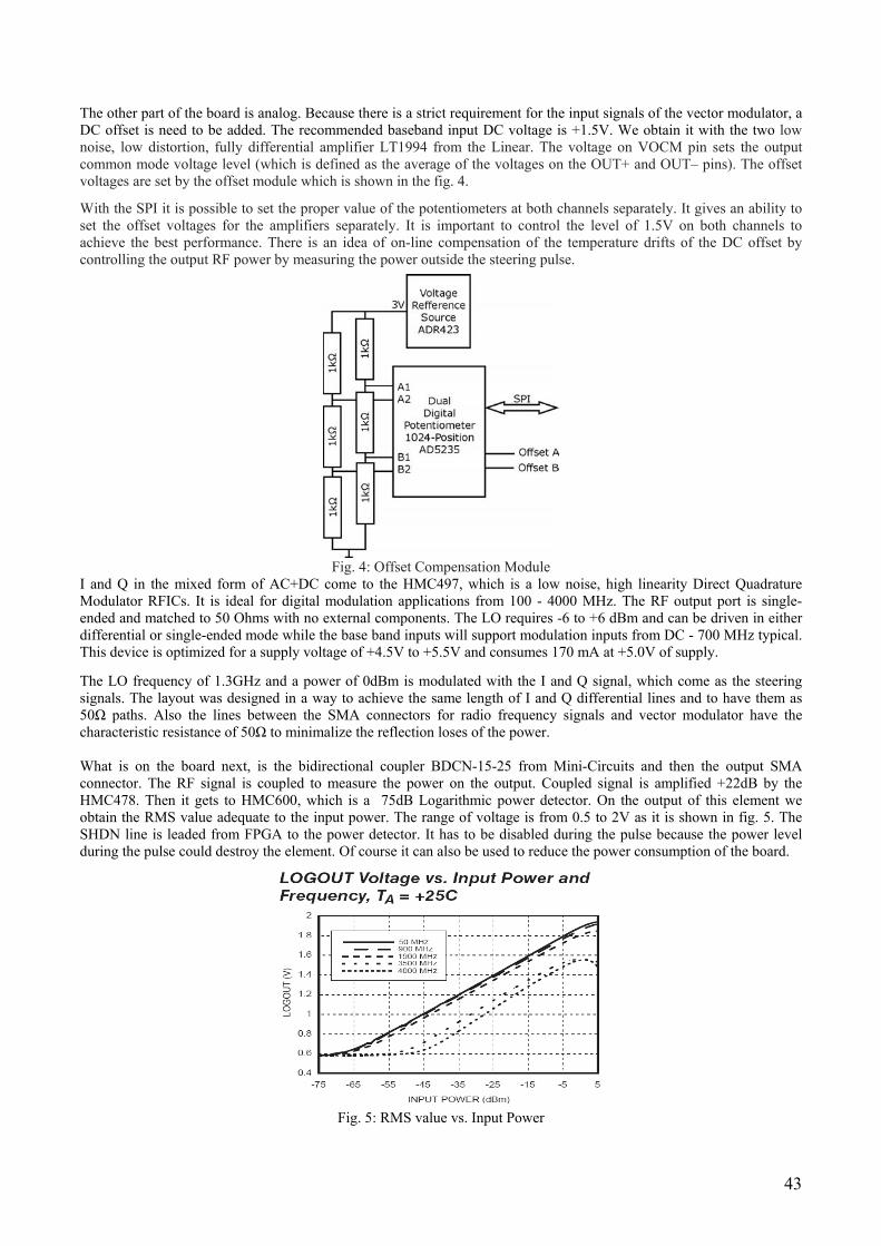
43
The other part of the board is analog. Because there is a strict requirement for the input signals of the vector modulator, a DC offset is need to be added. The recommended baseband input DC voltage is +1.5V. We obtain it with the two low noise, low distortion, fully differential amplifier LT1994 from the Linear. The voltage on VOCM pin sets the output common mode voltage level (which is defined as the average of the voltages on the OUT+ and OUT– pins). The offset voltages are set by the offset module which is shown in the fig. 4.
With the SPI it is possible to set the proper value of the potentiometers at both channels separately. It gives an ability to set the offset voltages for the amplifiers separately. It is important to control the level of 1.5V on both channels to achieve the best performance. There is an idea of on-line compensation of the temperature drifts of the DC offset by controlling the output RF power by measuring the power outside the steering pulse.
Fig. 4: Offset Compensation Module
I and Q in the mixed form of AC+DC come to the HMC497, which is a low noise, high linearity Direct Quadrature Modulator RFICs. It is ideal for digital modulation applications from 100 - 4000 MHz. The RF output port is single-ended and matched to 50 Ohms with no external components. The LO requires -6 to +6 dBm and can be driven in either differential or single-ended mode while the base band inputs will support modulation inputs from DC - 700 MHz typical. This device is optimized for a supply voltage of +4.5V to +5.5V and consumes 170 mA at +5.0V of supply. The LO frequency of 1.3GHz and a power of 0dBm is modulated with the I and Q signal, which come as the steering signals. The layout was designed in a way to achieve the same length of I and Q differential lines and to have them as 50Ω paths. Also the lines between the SMA connectors for radio frequency signals and vector modulator have the characteristic resistance of 50Ω to minimalize the reflection loses of the power. What is on the board next, is the bidirectional coupler BDCN-15-25 from Mini-Circuits and then the output SMA connector. The RF signal is coupled to measure the power on the output. Coupled signal is amplified +22dB by the HMC478. Then it gets to HMC600, which is a 75dB Logarithmic power detector. On the output of this element we obtain the RMS value adequate to the input power. The range of voltage is from 0.5 to 2V as it is shown in fig. 5. The SHDN line is leaded from FPGA to the power detector. It has to be disabled during the pulse because the power level during the pulse could destroy the element. Of course it can also be used to reduce the power consumption of the board.
Fig. 5: RMS value vs. Input Power

44
The RMS value is digitalized by the AD7683, which is 16-bit, 100 kSPS, charge redistribution successive-approximation Analog-to-Digital Converter. There is a need for the reference voltage to compare the RMS value too. The ADR420, precision 2.048 V bandgap voltage references respectively, featuring low noise, high accuracy, stability and low power consumption, is used in this case. ADC has the SPI to communicate with the FPGA. That is the last element witch uses the SPI. Fig. 6 describes the SPI architecture of the board. Other typical SPI architecture is Daisy Chain which serializes the components. It means that SDO pin is connected directly do SDI pin of the other component, etc. It makes the chain. CLK and CS pins are connected the same as in fig. 5. Daisy Chain allows us to program a few components by sending the data only once. The parts that we want to program have to be selected by CS=’1’.
Fig. 6: SPI architecture Fig. 7: Power module
The mother board provides a few supply voltages. The board takes external 3.3V (digital) and 5V (analog). Fig.7 shows the power supply module which gives all voltages the mezzanine board needs.
3. PROTOTYPE TEST PROCEDURE It is important at the beginning of the design to collect or find out if it is easy to get all the part one needs for the board. Also, the constrains are really an important part of the design. Each production firm has different technology abilities. The time you spent for preparing good constrains is never a waste of time. In the end, it is great if you have a friend or colleague who can check your schematic and layouts. It is common that the designer cannot find his/her own mistakes.
As a result of few weeks of designing the first version of the board appeared. It is a four layers PCB board. Top and the bottom ones are dedicated for the elements mounting and all the signals lines. The two middle layers of the board are for ground and power supplies. It was very important to separate the signal lines layers from each other to avoid any possible
cross-talks. Also it was designed as to minimize the layer changes on the signal patch. That is why firstly the digital signals are circulating around the bottom side of the board. After the conversion to anlog and adding the offset voltage to the signal, it goes to the top side and just strait to the vector modulator. The real photo of the board can be seen in fig.8.
Fig. 8: A photo of Vector-Modulator board
The whole procedure of starting up the board can be divided into a few stages. Each of them is shortly described below. Sometimes there is a need of repeating some of those tests in the loops to achieve the best result and correct values of elements in every iteration.
After first tests, the PCB board seems to work properly. DC tests have been made. All voltages are as they were expected to be. It means that all of power supply voltage and reference voltage are correct. A total current consumption during the off work state (without clocks and data signals) is under 100mA. It is expected that the consumption will rise up to a few hundreds of milliamps by reaching boundaries of performance possibilities.

45
The performance test are under preparation. Because the whole control is made by the FPGA, the VHDL code is need to be created. However, the first AC test have been made as well. The mother board provides the clock for DAC. It contains the 40MHz oscillator, which can be easily multiplied up to 100MHz. Such a signal can by delivered with the main QSE-QTE connector or by the SMA connectors.
The performance tests of clocks are needed to be taken to show which way of the clocking method is better. As it is written above there are two ways of providing clocks. The clock signal comes from the FPGA and makes the different way in both cases.
This one which goes by the SMA connectors avoids going through the buffers, what possibly can make it more reliable.
By the simple code of SINE generator the sinusoid signals can be made as 16bits vectors each. Such signals can be easily delivered to the DAC with the object of checking the proper operation of digital to analog converter. Those components have already been written.
The next step is to take control over the SPI interface. The special components are going to be written in the VHDL code. The main purpose is to read and change the registers in the DAC, ADC and Digital Potentiometer. There is a need of a proper SPI control in order to be able to make the last test.
The final step is to check the vector modulation. The LO signal is need to be delivered, modulated within the low frequency signal and the output RF signal is need to be observed. The spectrum analyzer is thought to be used. In that stage the control is made over the whole board. The loop of steering and reading the output power level is closed. By that we achieve the constant regulation of the offset voltages and get the best possible performance.
Finally, the LLRF system is going to be implemented. It will consist of other boards like ADCs and Down Converters and all calculation algorithms in the FPGA. Fig. 9 shows the testing stand: VME crate, Mother Board and the DAC-VM board under tests.
4. CONCLUSIONS A number of possible configurations for the LLRF system makes it multipurpose and flexible. Different daughter boards can be used. If there is a need of steering another device by the different signal type, all is needed to be done is to make a new single daughter board. It takes a short time to do that. The hardware for the LLRF has been prepared. It is based on the ACB1 board [1] and a few smaller boards. The next step is to make all needed algorithms, write the VHDL code, synthesize it and finally download it to the FPGA. After tests of the LLRF system in the laboratory stand it will be put into operation in the accelerator. The board which was shown above meets all the requirements for steering the klystron. Although there are new ideas how to improve the driver. Also new requirements have been made (listed below). Future will show what will be achieved. The system that is described above is designed in VME bus standard, originally developed for the Motorola 68000 line of CPUs, but later widely used for many applications and standardized by the IEC as ANSI/IEEE 1014-1987. It is physically based on the Eurocard sizes, mechanicals and connectors, but uses its own signaling system, which Eurocard does not define. It was first developed in 1981 and continues to see widespread use today. However nowadays the new standards of communication crates have been developed. One of them is the ATCA – Advanced Telecommunications Computing Architecture – is the largest specification effort in the history of the PIC Industrial Computer Manufactures Group, with more than 100 companies participating. Known as AdvancedTCA™ [3]. AdvancedTCA is targeted to requirements for the next generation of "carrier grade" communications equipment. This series of specifications incorporates the latest trends in high speed interconnect technologies, next generation processors, and improved Reliability, Availability and Serviceability. This system is based on an idea of hot-plugging mezzanine cards. There is of course the main PCB board, called carrier board. It consists of up to 8 mezzanine cards, depending on the configuration. The new idea of the vector modulator board is such, that the AMC (mezzanine card) which is a PCB, will be changed to the standard that follows the specification of the AdvancedMC™. The functionality of this board is thought to be much bigger. The main requirements for the new board are listed below: • Monolithic vector modulator • Output amplifier • Electronically switcheable step attenuator for adjustment of different cable losses • RF Gate – turn off the output power in case of internal or external malfunction • Diagnostics for proper operation of the whole vector modulator chain • Backup EEPROM containing a updatable “feedforward table” and switching logic in case of malfunctioning of the
main FPGA, it gives continues steering for the Klystron. • Controller for supervision (local FPGA) • Self test and self calibration function

46
• IMPI controller for ATCA system as the ATCA crate manager [3][7] • Two configuration bit-streams in the EEPROM • Standard communication interfaces, like: I2C, PCIe, JTAG, SPI
Fig. 9: System under tests.
5. ACKNOWLEDGEMENTS This work was partially supported by the European Community Research Infrastructure Activity under the FP6 "Structuring the European Research Area" program (CARE – Coordinated Accelerator Research in Europe, contract number RII3-CT-2003-506395).
REFERENCES [1] P. Strzałkowski, Base module of data acquisition for VUV-FEL accelerator, BSc thesis, Institute of Electronic Systems, WUT, 2007 [2] S. Simrock, Low-level RF control development for the European X-FEL (Proceedings Paper) SPIE Proc., Vol 5948, index 594804, 2005 [3] http://www.advancedtca.org/ [4] http://www.desy.de/ (http://www.xfel.net/en/) [5] Wojciech Giergusiewicz, Wojciech Jalmuzna, Krzysztof Pozniak, et al., Low latency control board for LLRF system: SIMCON 3.1 (Conference Proceedings Paper), SPIE Proc., Vol 5948, index 59482C, 2005 [6] W. Wolf, FPGA-Based System Design, Prentice Hall PTR, 2004 [7] http://www.intel.com/design/servers/ipmi/

47
FPGA systems development based on Universal Controller Module Rafał Graczyk, Krzysztof T. Poźniak, Ryszard S. Romaniuk
Institute of Electronic Systems, WUT
ABSTRACT This paper describes hardware and software concept of Universal Controller Module (UCM), a FPGA/PowerPC based embedded system designed to work as a part of VME system. UCM, on one hand, provides access to the VME crate with various laboratory or industrial interfaces like gigabit optical links, 10/100 Mbit Ethernet, Universal Serial Bus (USB), Controller Area Network (CAN), on the other hand UCM is a well prepared platform for further investigations and development in IP cores field, in functionality expansion by PCI Mezzanine Card (PMC). Keywords: embedded systems, gigabit interface, Xilinx field programmable gate array, hardware description language,
1. INTRODUCTION Embedded systems are playing more and more important role in today's world controlling and managing plenty of aspects of digital reality surrounding us. They serve restlessly with highest obedience in industrial, scientific, transportation applications and in everyday's life, everywhere around us. As scale of integration is getting larger (bear in mind Moore's law, despite some signs of phenomenon saturation, number of transistors in VLSI circuits doubles every eighteen months) systems designers are receiving more computational power they needed so far. As a side effect, new fields of embedded computing are revealed utilizing surplus of spare processor cycles.
As the systems functionality and complexity increases, the time-to-market (or time-to-operability in scientific projects) and designers effort, does it as well. Each embedded systems consists of more or less the same building blocks, that is central processing unit, optional co-processors (cryptography, media, digital signal processing), random access memories, solid state mass memories, communication interfaces, sensors and so on. The more of these blocks is used, the more time and work hours are needed for final version of system, the more design iterations have to be made, the more money is spent on development and wasted on bugs mitigation.
The continuous evolution of Field Programmable Gate Arrays (FPGAs)[1,2] for last two decades lead to the point where they offer such high amounts of configurable logic resources and additional features that allow to fit most of embedded system components in one chip, creating system-on-chip. This approach have some advantages. It is possible to test literally infinite number of ideas on the same hardware, it is possible to correct design mistakes, it is easy to compare implemented solutions and adjust design to changing functionality demand. As a disadvantage, FPGA chips are expensive, especially ones with lots of resources. But costs of FPGA development platform are much lower than that based on specialized components (number of necessary design iterations is much lower). System designers go further in exploiting FPGA circuits features, and decide to make them a base for end-user platform, which can be reconfigured as user demands and expectations change with time and experience.
In general description of FPGA based embedded system we would put FPGA in the heart of it, as a hub interconnecting different subcircuits realizing specialized functions (Fig. 1, FUNCtion1..4), often utilizing common on-board buses (like ISA, PCI, I2C, LVDS serials, to name a few, Illustration 1 – double line). FPGA device contains processor unit, bus interfaces and special data processing block. Modular approach gives developer flexibility to choose what solutions, in which variants, give enough performance or simplicity (EXPansion slots for example, depicted on Illustration 1)[3,4,5]. The Universal Controller Module (UCM) described in this paper is an attempt to create such a FPGA based embedded system for research purposes in PERG laboratory in Institute of Electronic Systems WUT.
2. UCM HARDWARE DESCRIPTION UCM is a laboratory computer compliant with VME electrical and mechanical specification. It's main purpose is to serve as a base for on-going embedded systems development and as a provider of variety means for VME crate connectivity. In other words to equip VME systems developer or end user with set of interfaces covering broad range of bitrates, applications and physical mediums. It also has a stand-alone mode easing debugging and software development process. Overview of UCM blocks is depicted below in Illustration 2.
Heart of UCM is Virtex II Pro FPGA, offering almost endless internal logic resources configurations and therefore plenty of possible functionalities. XC2VP30 contains many useful building blocks for embedded system-on-chip:
Fig.1: FPGA base embedded system

48
• 30,816 logic cells where each one of them compute 4 argument Boolean function and / or implement register, latch or flip-flop 8 RocketIO transceiver blocks for Gigabit serial communication (bitrate up to 3.125 Gbps) providing very easy way of connecting optical transceivers 2448 Kb of dual port RAM divided in 138 18kb independently configurable blocks 644 IO pads with configurable electrical characteristics – user adjustable IO standard, differential or single lines, digitally controlled impedance 136 18 x 18 bits multipliers with calculation time around 6-8ns, perfect for real-time DSP algorithms embedded serializers/deserializers for serial interfaces connectivity high performance clock management circuitry containing 8 Digital Clock Managers providing functions like de-skew, phase shift, frequency synthesis 2 hardwired RISC PowerPC 405 processor blocks (up to 300 MHz) offering common features of modern RISC processors like arithmetic unit, memory controller, set of general purpose registers. Additionally defining new commands to process data in customized hardware blocks is possible.
Virtex II Pro is a SRAM based device, therefore after power-up it it's configuration memory is blank. To allow system operation in varying circumstances several boot options are enabled [7,8,9,10]:
main development FPGA configuration is direct connection to JTAG chain with users programming device. It's easy but slow and not stand-alone way of configuring processing unit [16] second one is configuration downloaded from Compact Flash card using System Ace integrated circuit. Bit stream files for FPGA device remain stored in CF card, then, after power up, System Ace autonomously uploads data to host device. This solution is very flexible as System Ace offers microcontroller interface to FPGA that allows access to CF card on demand and therefore provides mass data storage possibility (Sold State Disk) [15] third one, the most embedded and stand-alone is to keep configuration file in specialized Flash memory, connected directly to FPGA and automatically configuring host device after power up [14]
Remaining parts of UCM system are communication interfaces and expansion interface. Communication interfaces provide various ways of data exchange and VME crate (or UCM itself) control. As it's certain that these interfaces will be used in almost every case it's been decided to make them internal (static) part of a UCM. Communication peripherals include:
Ethernet interface providing standard networking. Physical layer of protocol is managed by BCM5221KTP driver by Broadcom. Higher layers of protocol are implemented by specialized IP core in FPGA fabric and embedded PowerPC processor. Compatibility with 10BaseT i 100BaseTX standards assure optimal power consumption management, cable length sensing and proper noise levels. Additionally electrostatic discharge protection is implemented. CAN 2.0 interface allows industrial CAN bus usage [18]. Bit rate around 1 Mbit/s on 1 km distance (differential serial transmission). Interface accepts standard and extended data frames. Additionally Remote Data Requests are processed.
Fig. 2: UCM functional block diagram

49
CAN interface has message filter masks and provides 15 independent Message Centers (14 two way, and 1 read-only). This interface is able to conduct real-time data transfers. USB interface provides serial transmission with bitrates up to 1 MB/s. It is USB1.1 and USB 2.0 compatible. It provides simple and easy, 4 signal interface to FPGA and contains integrated FIFO queues as a buffers. It can work in bulk and isochronous modes. User can define parameters like VendorID, ProductID, SerialNumber, ProductDescription. This USB interface has been implemented in a way allowing external PC computer to detect UCM as a slave device. VME/VXI interface allows direct connection of UCM board to industrial VME-bus or VXI [11, 12]. This fact affects mechanical construction (dimensions constraints and restricted fields placement) of UCM board as it inserted in EURO-6HE-160 crate with VME backplane. Hardware implementation covers slave, master and controller modes of in -VME operation. EPP parallel port interface has simple hardware implementation. It allows node integration with older type measurement systems, in-house solutions, as well as PC computers. Achieved bitrates from 500 KB/s up to 2MB/s. Double RS-232C interface equip UCM with cheap and simple solution on maximal distance of 20 m, with maximal transmission rate of 115kbit/s. Like EPP, it provides simple mean of communication with other, often older, measurement and development devices.
Finally, last but not least part of UCM is an expansion circuitry. As it's often needed to add new functionality which cannot be implemented in FPGA like digital-to-analog or analog-to-digital converters, additional mass storage devices or special communication interfaces UCM must provide a way to incorporate them in whole system. That's why it's been decided to put PCI bus on board and place slots for two expansion cards. PCI on VME boards is very often realized through PMC (which stands for PCI Mezzanine Card) standard that defines mechanical constraints for daughterboards, placement and utilization of slots as well as keeping electrical signals compliant to old PCI standard (Manufactured and assembled unit of UCM is shown on Illustration 3.
3. UCM EMBEDDED SOFTWARE CONCEPT The flexibility and usefulness of UCM as an embedded system is twofold. On one hand it contains vast logic resources that allow user to implement functions in hardware, making data processing fast and parallel to other functions if necessary. Especially when dealing with communication interfaces, often working with high bit rates, it is much more
Fig. 3: UCM printed circuit board
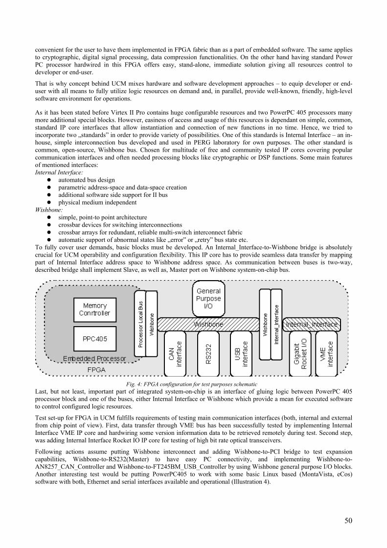
50
convenient for the user to have them implemented in FPGA fabric than as a part of embedded software. The same applies to cryptographic, digital signal processing, data compression functionalities. On the other hand having standard Power PC processor hardwired in this FPGA offers easy, stand-alone, immediate solution giving all resources control to developer or end-user.
That is why concept behind UCM mixes hardware and software development approaches – to equip developer or end-user with all means to fully utilize logic resources on demand and, in parallel, provide well-known, friendly, high-level software environment for operations.
As it has been stated before Virtex II Pro contains huge configurable resources and two PowerPC 405 processors many more additional special blocks. However, easiness of access and usage of this resources is dependant on simple, common, standard IP core interfaces that allow instantiation and connection of new functions in no time. Hence, we tried to incorporate two „standards” in order to provide variety of possibilities. One of this standards is Internal Interface – an in-house, simple interconnection bus developed and used in PERG laboratory for own purposes. The other standard is common, open-source, Wishbone bus. Chosen for multitude of free and community tested IP cores covering popular communication interfaces and often needed processing blocks like cryptographic or DSP functions. Some main features of mentioned interfaces: Internal Interface:
automated bus design parametric address-space and data-space creation additional software side support for II bus physical medium independent
Wishbone: simple, point-to point architecture crossbar devices for switching interconnections crossbar arrays for redundant, reliable multi-switch interconnect fabric automatic support of abnormal states like „error” or „retry” bus state etc.
To fully cover user demands, basic blocks must be developed. An Internal_Interface-to-Wishbone bridge is absolutely crucial for UCM operability and configuration flexibility. This IP core has to provide seamless data transfer by mapping part of Internal Interface address space to Wishbone address space. As communication between buses is two-way, described bridge shall implement Slave, as well as, Master port on Wishbone system-on-chip bus.
Last, but not least, important part of integrated system-on-chip is an interface of gluing logic between PowerPC 405 processor block and one of the buses, either Internal Interface or Wishbone which provide a mean for executed software to control configured logic resources.
Test set-up for FPGA in UCM fulfills requirements of testing main communication interfaces (both, internal and external from chip point of view). First, data transfer through VME bus has been successfully tested by implementing Internal Interface VME IP core and hardwiring some version information data to be retrieved remotely during test. Second step, was adding Internal Interface Rocket IO IP core for testing of high bit rate optical transceivers.
Following actions assume putting Wishbone interconnect and adding Wishbone-to-PCI bridge to test expansion capabilities, Wishbone-to-RS232(Master) to have easy PC connectivity, and implementing Wishbone-to-AN8257_CAN_Controller and Wishbone-to-FT245BM_USB_Controller by using Wishbone general purpose I/O blocks. Another interesting test would be putting PowerPC405 to work with some basic Linux based (MontaVista, eCos) software with both, Ethernet and serial interfaces available and operational (Illustration 4).
Fig. 4: FPGA configuration for test purposes schematic

51
Wishbone-to-PCI bridge is a fully open source Intellectual Property core. Both sides of bridge can operate at totally independent clock frequencies. It consists of two independent units, one handling transactions originating on the PCI bus, the other one handling transactions originating on the WISHBONE bus. Performance features include 32-bit bus interfaces on both sides, high level of performance and flexibility like burst data transfers, memory access optimizing command usage etc. The code is completely generic (except for RAM primitives), which makes the core easily retargetable for any FPGA [25]. To test this interface PMC daughter card will be mounted and basic card operation over PCI will be performed. PMC slots des not have to necessarily use PCI IP core on FPGA side. It can be virtually any bus, custom or standard, parallel or high-speed differential (only on specified lines), as long as daughterboard is compatible. For basic test purposes it is planned to implement (route out of FPGA device) Internal Interface as a medium of information interchange between UCM and daughterboard developed in simultaneously in PERG laboratory.
Wishbone-to-RS232 is a synthesizable soft core that allows debugging of peripherals connected to a Wishbone type of bus. Specifically, it lets the user write and read registers, and send out reset pulses, via an RS232 serial connection to a terminal software running on a PC (like Hyperterm, Docklight). It is completely scalable through parameter settings, to accommodate address and data buses of any arbitrary size. Furthermore, the Wishbone-to RS232 module can share the Wishbone bus with the master (presumably a processor of some kind). It implements a handshaking protocol with the master to "request" the bus. When the master grants access, the module bus cycles on its own, to report contents of registers and memory back to the user, in an easy-to-read hexadecimal format. This is very useful when debugging peripherals - contents of memory, registers can be set, and even step work of target processor can be applied. If desired, the Wishbone-to-RS232 can be the sole master of the Wishbone bus, to perform "human-speed" tests on peripherals (set a value, check a result) without having to connect the peripheral to a processor. [26]
The GPIO (General Purpose Input/Output) IP core is user-programmable general-purpose I/O controller. Its simple use is to implement functions that are not implemented with the dedicated controllers in a system and require simple input and/or output software controlled signals. It contains range of selectable I/O lines (up to 32) with configurable open drain or Z-buffered output type. All lines can be bi-directional. There is feature allowing a parallel connection of several Wishbone GPIOs [27]. This IP core can function as a stand-alone or can be adjusted to fit special needs.
The Wishbone-to-AN82527_CAN_Controller and Wishbone-to-FT245BM_USB_Controller are based on GPIO IP core. Both external interfaces utilize old-fashioned parallel data connection (and separate address bus in case of AN82527) and simple write / read / ready handshake. In order to fulfill timing and sequence constraints of AN82527 and FT245BM simple state machine combined with GPIO is implementation in Virtex configurable fabric. Solution is perfect for test purposes, but module for end-user should provide more sophisticated handling of interface functions.
Additionally, to maintain compatibility with previous developments a Wishbone-to-Internal_Interface bridge has to be implemented. The idea behind is simple – it is mapping one bus to another and vice-versa. This solution provides user a library of Internal_Interface IP cores like Rocket IO controller for high speed serial (i.e.: optical) communication and VME interface which is crucial for whole UCM operability and usefulness as a VME crate controller (which is primary objective of whole project).
Successful outcome of experiments described above prove that embedded and printed circuit board parts of UCM systems are correctly designed, or, at least, bring additional bug information needed for improvements in following versions.
4. CONCLUSION UCM described herein is an example of modern approach to embedded system, by implementing most of it's core functionality in FPGA chip. It's been shown that this is one of the ways to reduce costs and time needed for development. As well, extensive use of FPGA makes expected system lifetime much longer as it's configuration flexibility allows fast and effective response to changing end-user demands. Also a PMC expansion slots give user a tool to equip UCM with virtually any, additionally designed or bought, features.
UCM is platform for experiments with FPGA based embedded systems. It's a playground for software and hardware engineers. Hardware experts can implement their design in vast logic resources of configurable central processing unit or build other boards and connect them with PMC interface. Software experts can utilize two existing PowerPC processors or use a new one embedded in FPGA fabric to run popular Linux, eCos or other hard or soft real-time systems, code digital signal processing algorithms and so on.
UCM can be a base for control and measurement system utilizing VME backplane to connect with other system. It can play a role as a crate controller or as an any other normal subsystem. UCM can be also a base for further embedded system development either as a predecessor of more modern systems containing cutting-edge technology and offering even greater possibilities and computational power, or as a test-bed for smaller, smarter and a way more specialized sensor or control systems.

52
5. REFERENCES
1. http://www.xilinx.com/ [Xilinx Homepage] 2. http://www.altera.com/ [Altera Homepage] 3. Uwe Meyer-Baese: “Digital Signal Processing with Field Programmable Gate Arrays”, Wydanie drugie,
Springer, 2004, ISBN: 3540211195 4. http://www.altera.com/literature/technology/dsp/dsp-literature.pdf, “DSP Literature”, Altera Corporation, 2005 5. A.Athavale, C.Christensen: “High-Speed Serial I/O Made Simple, A Designer’s Guide with FPGA
Applications”, Preliminary Edition, 2005, Xilinx Connectivity Solutions, PN0402399 6. R.S.Romaniuk, K.T.Poźniak, G.Wrochna, S.Simrock: “Optoelectronics in TESLA, LHC, and pi-of-the-sky
experiments”, Proc. SPIE Vol. 5576, p. 299-309, 2005 7. “Xilinx Viretx 2 Pro PowerPC 405 Processor Block Reference Guide”, Xilinx, Inc.,
http://direct.xilinx.com/bvdocs/userguides/ug018.pdf 8. „Nios 3.0 CPU”, DS-NIOSCPU-2.1 Technical Note, Ver. 2.2, 2004, Altera Corporation,
http://www.altera.com/literature/ds/ds_nios_cpu.pdf 9. MicroBlaze Processor Reference Guide, UG081 (v5.3) October 5, 2005, Xilinx, Inc.,
http://www.xilinx.com/ise/embedded/mb_ref_guide.pdf 10. Xilinx Virtex 2 Pro RocketIO Transceiver user Guide, UG035 (v1.5), 2004, Xilinx, Inc.,
http://direct.xilinx.com/bvdocs/userguides/ug035.pdf 11. “VMEbus Card Form Factors”, http://www.interfacebus.com/Design_VME_Card_size.html 12. Wade D. Peterson, The VMEbus Handbook, 2nd edition, VITA 13. “Virtex-II Pro and Virtex-II Pro X Platform FPGAs:Complete Data Sheet”, 2005, Xilinx, Inc.,
http://direct.xilinx.com/bvdocs/publications/ds083.pdf 14. “Platform Flash PROM User Guide”, UG161 (v1.0), 2005, Xilinx, Inc.,
http://direct.xilinx.com/bvdocs/userguides/ug161.pdf 15. “System ACE Compact Flash Solution”, 2002, Xilinx, Inc.,
http://direct.xilinx.com/bvdocs/publications/ds080.pdf 16. “JTAG Programmer Guide” ”, 1999, Xilinx, Inc.,
http://www.xilinx.com/support/sw_manuals/2_1i/download/jtag.pdf 17. “ChipScope Pro Software and Cores User Guide (ChipScope Pro Software v8.1i)”, UG029 (v8.1), 2005, Xilinx,
Inc., http://www.xilinx.com/ise/verification/chipscope_pro_sw_cores_8_1i_ug029.pdf 18. CAN Specification 2.0 B, http://www.can-cia.org/downloads/specifications/ 19. “IEEE Standard Physical and Environmental Layers for PCI Mezzanine Cards (PMC)”, IEEE Std 1386.1-2001 20. PCI Local Bus Specification v2.3, PCI SIG, Portland, 2002 21. Tim Williams, The Circuit Designer’s Companion, 2nd edition, Elsevier, Oxford, 2005. 22. Stephen C. Thierauf, High-Speed Circuit Board Signal Integrity, Artech House, Norwood, 2004. 23. Stephen H. Hall, Garret W. Hall, High-Speed Digital System Design – A Handbook of Interconnect Theory and
Design Practices, John Wiley & Sons, New York, 2000. 24. Howard W. Johnson, Martin Graham, High-Speed Digital Design: A Handbook of Black Magic, Prentice Hall,
New Jersey 25. http://www.opencores.org/projects.cgi/web/pci/home 26. http://www.opencores.org/projects.cgi/web/rs232_syscon/overview 27. http://www.opencores.org/projects.cgi/web/gpio/overview

53
DSP Algorithms in FPGA - Proposition of a New Architecture Piotr Kolasinski, Wojciech Zabolotny
Institute of Electronic Systems, Warsaw University of Technology [email protected], +48 22 2347717
ABSTRACT
This paper presents a new reconfigurable architecture created in FPGA which is optimized for DSP algorithms like digital filters or digital transforms. The architecture tries to combine advantages of typical architectures like DSP processors and datapath architecture, while avoiding their drawbacks. The architecture is built from blocks called Operational Units (OU). Each Operational Unit contains the Control Unit (CU), which controls its operation. The Operational Units may operate in parallel, which shortens the processing time. This structure is also highly flexible, because all OUs may operate independently, executing their own programs. User may customize connections between units and modify architecture by adding new modules. Keywords: DSP, VHDL, FPGA, architecture
1. INTRODUCTION Field Programmable Gate Arrays (FPGA) are general-purpose devices. They are the most popular universal devices for many applications because of their programmability and reduced development costs. Today’s FPGAs contain not only the logic blocks, but also many specialized modules like DSP blocks and memory blocks.1 The FPGA allows the user to implement the arithmetical blocks well suited for the required precision of arithmetics (even though some “native” lengths of the data words are preferred). Additionally, the multilevel structure of internal interconnections allows to send multiple data in parallel, resulting in very high internal data throughput. These features makes the FPGA chips a very efficient platform for implementation of the DSP algorithms,2 however it is not easy to build an architecture offering both – high throughput and high flexibility.
1.1. Typical DSP architectures One of typical architectures used for DSP algorithms is a DSP processor. The performance of this architecture is limited by a few bottlenecks: o single program memory bus allows to read only one code word in a single clock cycle o small number of data buses (usually 1 or 2) allows to transfer only a few data words in a single clock cycle o small amount of data processing blocks (like “multiple and accumulate” (MAC) blocks) allows to perform only a few operations in parallel Another typical architecture used for the DSP applications is the “datapath” architecture. This structure offers high throughput (in every clock cycle new data words are read at the inputs, and new result is provided at the output). However this architecture is not flexible - each processing block is used only for one particular operation in the algorithm. The datapath architecture is also not suitable for algorithms which require iterative operations.
Therefore a need exists to create another architecture, able to combine highly parallel, pipelined operation of the “datapath” architecture with the flexibility of the DSP processor, where the same resource may be reused for different purposes in the different steps of the algorithm.
Figure 1. Two interconnected Operational Units with their internal structure.

54
2. PROPOSITION OF THE NEW ARCHITECTURE To avoid limitations of the typical DSP processor, the resources of the FPGA chips are divided between multiple Operational Units (OU), which may operate independently, in parallel. To allow reuse of the same resources for different purposes in different steps of the algorithm, each OU is equipped with the Control Unit (CU) (solution similar to the one described in Ref. 3). The CU executes its own program and controls what operations are performed by the OU in each cycle, where are the data read from, and where are the results stored. This solution creates the distributed code memory, which allows to overcome limitations resulting from single program memory bus in the DSP processor. The intermediate results of calculations are stored in the registers (implemented with FlipFlops, or distributed RAM), which create the distributed data memory.
2.1. The Operational Unit The Operational Unit contains arithmetical modules, registers and multiplexers. The general structure of the Operational Unit is shown in the Fig.1. The multiplexer at every input of the arithmetical module allows to select the source, from which the data should be received in the particular clock cycle.
The operations performed by the arithmetical module may be defined by the user, and depend on the hardware platform. In fact it is not necessary, that all OUs are the same, there may be a few OUs performing more complicated operations (e.g. division), and more OUs performing simple multiplications and additions (like “Elementary Mathematical Blocks” in Ref. 4).
The output of the arithmetical unit is connected with the register, and further with the inputs of multiplexers in the next blocks.
2.2. The Control Unit Different operations performed by the OU may require different number of clock cycles. It is also possible, that the OU may perform more complex calculations (e.g. calculation of square root) working iteratively. To implement such operations it is necessary to select the data source and the operation to be performed by the arithmetical block in each clock cycle.
Figure 2. Interconnections in the proposed architecture. All Operating Units are organized in the rectangular matrix of size N _ M, wrapped to create a torus-like structure. The inputs of the OU with coordinates (n,m) are connected to the outputs of shaded neighboring OUs.
This task is performed by the Control Unit. Each OU is equipped with the CU. The CU is a simple state machine, controlled by the microcode stored in its code memory (which may be either ROM or RAM, depending on the option set by the user when compiling the architecture).

55
The CU provides also synchronization with the other OUs, connected to its OU. To make it possible, the communication channels between OUs must also provide some handshake signals like “data available” and “data read acknowledge”
2.3. Interconnections between Operational Units Theoretically, the best flexibility is assured by the structure, where each OU is fully interconnected with all others OUs. However such a structure is usually not possible to implement in the FPGA, because the number of connections is very high (equal to N2 N for N Operating Units). Therefore another layout of interconnections has been proposed. All OUs are considered to form a rectangular structure with the edges joined to create a “torus”, as shown in the Figure 2.
The inputs of each OU are connected to the outputs of its 8 direct neighbors, with 4 neighbors located in the distance of 2 units, and with 4 neighbors located in the distance of 4 units. In this configuration each input multiplexer must have 16 inputs.
If the amount of OUs which can be implemented in the FPGA is small (e.g. less than 64), another interconnection scheme may be used (see Figure 3. In this configuration the inputs of each OU are connected to the outputs of its 8 direct neighbors, and with 4 neighbors located in the distance of 2 units. In this configuration 12-input multiplexers are needed.
Figure 3. Interconnections in the proposed architecture for lower amount of OUs. All Operating Units are organized in the rectangular matrix of size N _M, wrapped to create a torus-like structure. The inputs of the OU with coordinates (n,m) are connected to the outputs of shaded neighboring OUs.
Such dense net of interconnections allows to send many data in one cycle between the directly interconnected OUs. It is also possible to send data between more distant OUs, using other OUs as “relays”, but it requires more clock cycles. Due to this property of the proposed architecture, the speed of the processing significantly depends on the distribution of the processing tasks between different OUs. The tasks requiring intensive data exchange should be assigned to neighboring OUs. The decomposition of the algorithm into simple tasks and assignment of tasks to the particular OUs is a complex job, which requires specialized software support.
3. SOFTWARE SUPPORT The DSP algorithm, is typically written and tested in a C-like or script (Matlab or Scilab) language. To execute this algorithm on the proposed architecture, it is necessary to decompose it to the tasks which may be executed by a single OU, to assure the proper synchronization between different OUs, and finally to generate programs for particular CUs. This task could be done “by hand” in a simpler architecture,4 where the latencies introduced by arithmetical blocks were predictable and constant, and where the algorithm did not use any conditional, data-dependent operations.
However the new architecture offers possibilities to implement algorithms using the iterative operations, where latency

56
introduced by the operational unit is neither constant nor predictable (i.e. it may depend on the processed data).
The translator responsible for this task is currently under development. The translator must perform the following tasks: o Decompose the algorithm into simple operations which may be performed independently, in parallel by the OUs o Assign the operations to be performed to different OUs, so that the expected numbers of cycles required by all OUs to
execute their tasks are equal (load balancing) o Lay out the OUs so that as much data as possible may be transferred in the single cycle o Generate the code for each CU
The described procedure does not make any assumptions regarding the particular properties of the algorithm to be performed by the proposed architecture. However, if the user wants the architecture to perform only a particular class of algorithms, it should be possible additionally to optimize the architecture on the synthesis stage.
3.1. Synthesis stage optimization The proposed architecture is implemented in VHDL, however theoretically it can be ported to another Hardware Description Languages (Verilog, SystemC or others).
The architecture may be synthesized in a fully configurable form. In this case all CUs are controlled by the RAM stored code, all inputs of the multiplexers are available.
Sometimes the algorithms which will be implemented in the architecture do not require the dynamic change of the code executed by some CUs. In this case the code for this CUs may be stored in the inferred ROM instead of block RAM. If the CU code is fixed, some inputs of the multiplexers may be never used. In this case this inputs and associated logic may be optimized out, resulting in overall decrease of resources consumption and increase of performance. However it is still unclear how to implement the translator for such ”partially fixed” architecture, or how to write a translator which could automatically generate the ”partially fixed” architecture for the particular class of algorithms.
4. CONCLUSION The proposed architecture may find numerous applications in implementation of the DSP algorithms. It allows for optimal usage of the resources of FPGA, and simultaneously makes possible to perform multiple operations in parallel. The architecture is also flexible. The user may create his own modules which can be added to the architecture. The efficient system of interconnections allows sending much data in the same cycle between the neighboring nodes. Architecture can work in parallel systems and because of its flexibility it can be very quickly adopted to new applications and algorithms.
REFERENCES 1. “Stratix III Device Handbook .” http://www.altera.com/literature/hb/stx3/stratix3 handbook.pdf. 2. H. Lee and G. Sobelman, “Digit-serial reconfigurable FPGA logic block architecture,” Signal Processing Systems, 1998. SIPS 98. 1998 IEEE Workshop on , pp. 469–478, 1998. 3. P. Sinha, A. Sinha, and D. Basu, “A novel architecture of a re-configurable parallel DSP processor,” IEEE-NEWCAS Conference, 2005. The 3rd International , pp. 71–74, 2005. 4. W. M. Zabolotny, K. Bunkowski, T. Czarski, T. Jezynski, K. Pozniak, P. Rutkowski, S. Simrock, and R. Romaniuk, “FPGA based cavity simulator for tesla test facility,” Proceedings of SPIE 5484, pp. 139–147, 2004.

57
MatLab script to C code converter for embedded processors of FLASH LLRF control system
K.Bujnowski, A.Siemionczyk, P.Pucyk*, J.Szewiński, K.T.Poźniak, R.S.Romaniuk Institute of Electronic Systems, Warsaw University of Technology, * also DESY, Hamburg,
ABSTRACT
The low level RF control system (LLRF) of FEL serves for stabilization of the electromagnetic (EM) field in the superconducting niobium, resonant, microwave cavities and for controlling high power (MW) klystron. LLRF system of FLASH accelerator bases on FPGA technology and embedded microprocessors. Basic and auxiliary functions of the systems are listed as well as used algorithms for superconductive cavity parameters identification. These algorithms were prepared originally in Matlab. The main part of the paper presents implementation of the cavity parameters identification algorithm in a PowerPC processor embedded in the FPGA circuit VirtexIIPro. A construction of a very compact Matlab script converter to C code was presented, referred to as M2C. The application is designed specifically for embedded systems of very confined resources. The generated code is optimized for the weight. The code should be transferable between different hardware platforms. The converter generates a code for Linux and for stand-alone applications. Functional structure of the program was described and the way it is acting. FLEX and BIZON tools were used for construction of the converter. The paper concludes with an example of the M2C application to convert a complex identification algorithm for superconductive cavities in FLASH laser. Keywords: free electron laser, MatLab script, embedded processors, low level RF system, FLASH laser
1. INTRODUCTION
Free electron laser (FEL) is a machine which uses highly energetic, pulsed, coherent electron beam to generate a pulsed, coherent photon beam. FLASH FEL laser generates femtosecond VUV pulses for experimental applications in physics, biology, chemistry and material research. DESY [5] Research Center in Hamburg hosts a unique free electron laser - FLASH [18]. The machine emits fs VUV laser pulses. It is exploited now, as a user oriented system, for research purposes. In parallel, it serves also for laser development. Thus, there is a competition for machine time between laser users and laser developers.
Free electron laser consists of three main parts: electron gun, linear accelerator and undulator. The undulator region is where synchrotron radiation is generated from periodically undulating electrons in a magnetic field. Frequency of the optical field depends on electron energy. UV radiation is generated from bunched electrons of energies well above 1GeV. FLASH laser possesses 6 cryo-units, each with eight one meter long superconductive niobium cavities. The technology used is referred to worldwide as TESLA. A very stable, high voltage, high power electromagnetic field is distributed in the microwave, narrowband, high finesse, 1,3GHz cavities in the form of a standing wave. To obtain a highly coherent photon beam, the stability of EM field in accelerating cavities has to be as follows: amplitude 10-4 relative and phase 10-2 degree. Other parameters of the cavity are: finesse 10-9, bandwidth 200Hz. EM field intensity in cavities is of the order 20MV/m or above. EM power accumulated in a single cavity is 100kW or above. At these fields, mechanical dimensions of the cavity change due to Lorentz force. The narrowband cavity gets detuned, approximately by its own bandwidth. Detuning causes changes of the EM field amplitude and phase. Because of high EM power levels, the system works in a pulsed mode: around 100ms active and the rest inactive with repetition time 10Hz. The work cycle is: cavity loading in resonance condition, field stabilizing, cavity quenching. A classical feed-forward and feedback full loop control system is applied to stabilize the EM field in the cavity and then a vector sum of fields in many cavities. The system is referred to in this work and in the references as low level RF (LLRF) system [19].
The LLRF control systems for FLASH laser consists from three layers: software, hardware and cavity with couplers and field sensors as an object under control. This system was presented, simplified and schematically in fig.1. LLRF software was prepared in MatLab environment, because most of it bases on matrix calculations. MatLab libraries are characterized by high efficiency of algorithm realization. Laser system components were modeled in MatLab. MatLab environment communicates directly with the hardware via VME-BUS and via Ethernet and IP. The hardware layer is SIMCON system, described thoroughly elsewhere (SIMulator and cavity CONtroller) [20].
The hardware is based on FPGA technology and multi-gigabit optical fiber links. SIMCON provides execution of fast control algorithms, with closed loop, which is 500ns for a single laser pulse. Control procedures are associated with measurements. The data measured from the superconductive cavity are used in parallel by the algorithms of cavity parameters estimation and identification [21]. The cavity algorithm is based on a heuristic, mixed electrical and mechanical model. Identification algorithm was implemented in MatLab on an external (in reference to the control system) PC machine.

58
Fig.1. Functional diagram of the resonant cavity control system with the usage of a PC A serious drawback of such a solution, as presented in. fig.1 is presence of a necessary and unavoidable communication channel between the software layer and hardware layer. This channel introduces penalty excess latency into the laser control loop. A way out is to apply a PowerPC CPU present inside the FPGA chip on the SIMCON mother PCB. PowerPC is an ideal place for implementation of a communication algorithm and eliminate the latent communication channel altogether. A functional diagram of the modifiers laser control system, with the usage of embedded Power PC CPU was presented in fig. 2.
In order to transfer the LLRF control algorithm to SIMCON hardware, it is necessary to translate MatLab script to C code (in order to avoid MatLab environment installation directly on SIMCON where the resources are sparse). MatLab has an internal compiler mcc for this purpose. The compiler generates, using an external library MatLab Component Runtime – MCR, a C code basing on an available MatLab script. MCR is a mathematical engine encapsulated in a library form. It is also responsible for calculations run in the MatLab environment. MCR is a large collection of functions, combining nearly all available functionality of MatLab. A basic drawback of this library, from the point of view of compact applications, is its large dimension, which is over 250MB. This prevents application of this solution in an embedded system. MCR library is compiled and linked dynamically, what means that it requires a presence of a full flavored operational system, and again prevents applications in small, stand-alone software solutions. The only solution to solve this problem of efficient usage of embedded CPU was to prepare own converter translating MatLab scripts to C
Cavity (RF channel)
SYSTEM FPGA
Estimation algorithm for SC cavity parameters
Photonic and electronic LLRF controller - SIMCON
ETHERNET / VME
Fig. 2 Functional diagram of superconductive cavity control system with usage of PowerPC CPU.
Cavity Parameters Estimation Algorithm (C)
FPGA
INTERNAL INTERFACE
PowerPC 405 CPU
Cavity (RF channel)
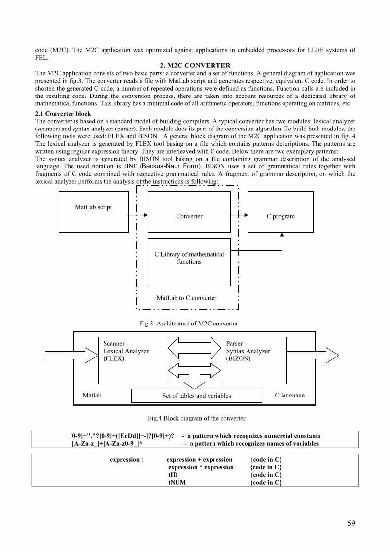
59
code (M2C). The M2C application was optimized against applications in embedded processors for LLRF systems of FEL.
2. M2C CONVERTER The M2C application consists of two basic parts: a converter and a set of functions. A general diagram of application was presented in fig.3. The converter reads a file with MatLab script and generates respective, equivalent C code. In order to shorten the generated C code, a number of repeated operations were defined as functions. Function calls are included in the resulting code. During the conversion process, there are taken into account resources of a dedicated library of mathematical functions. This library has a minimal code of all arithmetic operators, functions operating on matrices, etc. 2.1 Converter block The converter is based on a standard model of building compilers. A typical converter has two modules: lexical analyzer (scanner) and syntax analyzer (parser). Each module does its part of the conversion algorithm. To build both modules, the following tools were used: FLEX and BISON. A general block diagram of the M2C application was presented in fig. 4 The lexical analyzer is generated by FLEX tool basing on a file which contains patterns descriptions. The patterns are written using regular expression theory. They are interleaved with C code. Below there are two exemplary patterns: The syntax analyzer is generated by BISON tool basing on a file containing grammar description of the analysed language. The used notation is BNF (Backus-Naur Form). BISON uses a set of grammatical rules together with fragments of C code combined with respective grammatical rules. A fragment of grammar description, on which the lexical analyzer performs the analysis of the instructions is following:
[0-9]+"."?[0-9]+([EeDd][+-]?[0-9]+)? - a pattern which recognizes numercial constants [A-Za-z_]+[A-Za-z0-9_]* - a pattern which recognizes names of variables
expression : expression + expression code in C | expression * expression code in C | tID code in C | tNUM code in C
Converter
C program
MatLab script
C Library of mathematical
functions
MatLab to C converter
Fig.3. Architecture of M2C converter
Scanner - Lexical Analyzer (FLEX)
Parser - Syntax Analyzer (BIZON)
Set of tables and variables Matlab C language
Fig.4 Block diagram of the converter

60
Both modules act alternately in series. Lexical analyzer separates lexical units fitting sequence of signs to the patterns written according to the theory of regular expressions. Each pattern serves to recognize a particular element of the MatLab script, like: variable name, numerical constant, key word, etc. Formed lexical units are transferred to the input of the syntax analyzer. Syntax analyzer checks the conformity of a stream of lexemes with defined grammatical rules. During the passage through the grammatical rules, there are called C code fragments. Each generated C code fragment has a duty to further generate either a resultant code or storing certain key information. This information is used during the analysis and generation of successive instructions of the source code. A diagram of code generation by the converter is shown in fig.5. Fig.6 shows an example of the conversion process for a simple mathematical expression.
2.2 Mathematical library block Embedded systems may work with operational systems (like Linux) or stand-alone. In the latter case, a single executed program by the processor is the user’s application. Two separate, general, mathematical libraries were formed for these two work modes. Library matrix.c works with Linux, and library matrixsa.c is used in stand-alone applications. In both cases, the parser generates identical resulting code, and about the purpose to work in particular mode decides a library with which the code is compiled. A realized structure of the implementation of mathematical library is presented in fig.7.
Patterns description Grammar description
FLEX BISON
Source code of lexical analyzer
Source code of syntax analyzer
Lexical Analyzer Syntax Analyser
Matlab C language
Fig. 5 Diagram of data flow in the M2C converter
Lexical analyzis
Syntax analysis
matrix *A=NULL; matrix *B=NULL; matrix *C=NULL; matrix *TEMP_0=NULL; matrix *TEMP_R=NULL; matrix *TEMP_1=NULL; matrix *element[7]; TEMP_0=(matrix*)multiply_dgemm(B,C); element[4] = TEMP_0; TEMP_R = allocate_memory_matrix_one_by_one(TEMP_R,10,file,DOUBLE_TYPE); element[5]=TEMP_R; TEMP_1=(matrix*)add(TEMP_R,TEMP_0); element[6] = TEMP_1; free_matrix(&TEMP_R); if(A!=NULL) free_matrix(&A); A=TEMP 1;
Generated Code
Functions from mathematical library
Fig.6. Example of a conversion process for a simple arithmetic expression
A = 10 + B * C

61
Fig. 7. Implementation structure of mathematic library
All functions of the library for the stand-alone work mode were developed as proprietary tools by the authors. For the library for operational system work mode, only part of time critical functions were implemented with usage of GSL programming library. This library uses a collection of procedures BLAS [22]. The same collection of functions is used in LAPACK package. LAPACK is a foundation for MatLab mathematical engine. A diagram of relations between BLAS procedures and MatLab environment for the generated programs is presented in fig. 8.
Fig.8. Diagram of a relation between BLAS procedures for Matlab environment and for generated programs.
This solution enables similar efficiency of numerical calculations in Linux as in the MatLab environment. Both versions of the libraries (matrix.c oraz matrixsa.c) include the following functions:
• Operators (arithmetic, relation, logical), • Function generating matrixes, • Trigonometric functions, • DSP functions, • Elementary mathematical functions of MatLab environments, • Technical functions (error management, memory management, I/O management).
The library comprises around 100 different functions. In most cases, even for complex input algorithms, the generated code uses only a minute part of these functions. To confine the dimensions of the resultant program, there was implemented a mechanism of automatic reduction of the number of compiled functions. During the analysis of MatLab script, there is formed a list of used library functions. This method is used for both work modes, with Linux and stand-alone.
generated_code.c
matrix.
matrixsa.c
Linux
Stand-alone
Level 1
Level 2
BLAS
Level 3
LAPACK GNU Scientific Library
matrix.c
Generated code MATLAB
Matlab Engine / MCR

62
3. M2C CONVERTER APPLICATION IN LLRF SYSTEM OF FLASH LASER
The converter was used to generate a C language code for the algorithm of detuning estimation of a superconducting accelerator cavity. The algorithm was originally written in MatLab script [21]. The LLRF control algorithm contains around 150 cript lines and is organized in three MatLab files. It has around 30 different functions. After the conversion, a C code was obtained of around 3000 lines and organized in 6 files. Additionally, the generated code contains around 4000 lines of mathematical library. The result of C code, under the Linux OS, obtained from the source MatLab script was presented in fig.9.
Fig.9. Detuning estimation for SC cavity (LLRF controls) done by an algorithm in C code.
Fig.10 presents an absolute error in calculations between the source MatLab script and a C code obtained from translation. The calculations were done in MatLab environment. The error is less than 7x10⁻¹⁰. The obtained accuracy is sufficient for the calculation purposes of algorithms applied in the LLRF system.
0 200 400 600 800 1000 1200 1400 1600 1800 2000-5
0
5
10x 10
-10
Fig.10. Difference between the calculation results obtained in Matlab and in the C language based application translated
form Matlab. Calculations done for the algorithm results presented in fig.9.
4. CONCLUSIONS The paper presents a lightweight programming tool for conversion of MatLab script to C code for applications in embedded systems. A resultant code is obtained which is optimized against the weight, volume and mobility between various hardware platforms. The converter generates a software code working in two modes, with Linux (or equivalent OS) or stand-alone.
0 200 400 600 800 1000 1200 1400 1600 1800 2000-100
-50
0
50
100
150
200
250
Time [10-6 s]
[Hz]
Time [10-6 s]

63
The translator block accepts MatLab script syntax. MatLab script was used to write the LLRF algorithms for FLASH laser. As the experiments have shown, there is recognized the majority of mathematical operations and relative op[erations as well as indexing and concatenations. There are serviced all kinds of loops, and control instructions for program flows, together with multiple embedded loops. The programs generated by the converter use a library which contains a set of required operations, matrix generation, operator usage, complex calculation functions, and others. The converter possesses an open construction, what enables its development. A unified interface for mathematical functions was prepared what enables further development. There is predicted a service for complex numbers and generation of resulting code for DSP processors. The converter may be used for generation of C language codes which are executed on PC machines working under Linux and Windows. The tests showed a comparable efficiency of the C code with the MatLab script.
5. ACKNOWLEDGMENT
We acknowledge the support of the European Community Research Infrastructure Activity under the FP6 “Structuring the European Research Area” program (CARE, contract number RII3-CT-2003-506395).
REFERENCES
17 http://www.desy.de/ - [DESY home page] 18 “SASE FEL at the TESLA Facility, Phase 2”, TESLA-FEL 2002-01, DESY; http://flash.desy.de/ [FLASH] 19 T.Czarski, K.T.Pozniak, R.S.Romaniuk, S.Simrock.; “Cavity parameters identification for TESLA control system
development”, NIM-A, Vol. 548, pp. 283-297, 2005 20 Giergusiewicz W., Jalmuzna W., Poźniak K.T., Ignashin N., Grecki M., Makowski D., Jezynski T., Perkuszewski
K., Czuba K., Simrock S., Romaniuk R. S.: “Low latency control board for LLRF system: SIMCON 3.1”, Proceedings of SPIE, Bellingham, WA, USA, Vol. 5948, pp. 710-715
21 T.Czarski, K.T.Pozniak, R.S.Romaniuk, S.Simrock.; “Cavity parameters identification for TESLA control system development”, NIM-A, Vol. 548, pp. 283-297, 2005
22 www.netlib.org/blas/ [Basic Linear Algebra Subsystem]

64
Decomposition of MATLAB script for FPGA implementation of real time simulation algorithms for LLRF system in European XFEL
K. Bujnowskia, P.Pucykab, K. T. Pozniaka, R. S. Romaniuka aInstitute of Electronic Systems, Warsaw University of Technology, bDESY, Hamburg
ABSTRACT The European XFEL project uses the LLRF system for stabilization of a vector sum of the RF field in 32 superconducting cavities. A dedicated, high performance photonics and electronics and software was built. To provide high system availability an appropriate test environment as well as diagnostics was designed. A real time simulation subsystem was designed which is based on dedicated electronics using FPGA technology and robust simulation models implemented in VHDL. The paper presents an architecture of the system framework which allows for easy and flexible conversion of MATLAB language structures directly into FPGA implementable grid of parameterized and simple DSP processors. The decomposition of MATLAB grammar was described as well as optimization process and FPGA implementation issues.
Keywords: XFEL laser, LLRF system, FPGA circuits, MATLAB to VHDL code conversion, real-time processes
1. INTRODUCTION The LLRF system is responsible for keeping the amplitude and phase of the RF field in the cavity stable during the beam transmission time. It consists of analog input part, digital controller for fast control algorithms execution and analog output part, fig. 9. The input to the LLRF consists of 1.3GHz signals measured by an antenna inside the cavity (providing the information about the field inside the cavity), and directional couplers (providing signal information about the forward and reflected power in the waveguide feeding the cavity). Analog signals are mixed down in frequency in the LLRF system to intermediate frequency in the range of 10MHz to 50MHz. After the down conversion, all signals are sampled and processed by FPGA and DSP. The DAC converters produce output signals for vector modulator which drives the high power chain of preamplifiers and a klystron. The power is distributed to each of 32 cavities using directional couplers. Circulators prevents the reflected power from destroying the klystron. In addition there are more signals connected to the LLRF system which are used to control the field. These are signals for piezo control, piezo sensor which gives the information about the detuning of the cavity, special inputs for waveguide tuner, etc. The total number of the input signals coming to the LLRF system exceeds 100 channels.
Fig. 9. General scheme of the LLRF system of a single RF station
The complexity of the photonics, electronics and software used in the LLRF [0-4] system requires to search for a dedicated diagnostics and test environment which allows not only to test the particular hardware devices or software

65
algorithms but also of interaction between different components and overall performance of the system in the real operating conditions of the XFEL accelerator. An appropriate diagnostics need to be built not only for design verification during the development, but also for the later maintenance of the linac in order to minimize possible machine operation interrupts and performance degradation. The limited access to the real SRF facilities like FLASH [5] does not allow to fully test new designs and verify diagnostics procedures.
Therefore a different approaches in the testing and diagnostic methods for LLRF system must be used. One of them can be the real time, hardware simulation of the controlled RF station. For the LLRF system the “real time simulation” means that the time performance of the simulation must be in the same range as the time delay of the simulated system. This is specially important when the LLRF system works in the closed loop control mode, and the time delay of the simulation is an important parameter affecting the quality of simulation. Several projects concerning the real time, hardware simulation of RF station have been initiated [6]. The idea behind them is to implement mathematical models of RF station components like cavities, klystron, waveguides, circulators, piezo, etc. in dedicated hardware system using FPGA and DSP chips for fast, parallel data processing [7]. Such electronics with the RF input and output stage can create the real test bench simulating accelerator operation environment and, what is really important, is completely independent of the hardware and software technologies used to build the LLRF system,.
Fig. 10. The processing chain of proposed application
The flexibility of the FPGA technology allows to design more universal hardware which can be used in many applications. A strong difficulty in the implementation process is however the difference between languages used to model the systems and languages to describes the configuration of the FPGA. Since engineers use widely tools like MATLAB and SIMULINK to model the systems, some specialized tool have been created [8] in order to simplify the implementation models in FPGA architecture. These tools, however, have some limitations (vendor specific only, limited set of blocks from which one can create the model). Therefore, in this paper, a new, more general, and flexible approach is presented. The concept bases on parsing the MATLAB script language structures [9] instead of using dedicated SIMULINK blocks, fig.10. The parser is used to decompose the data and operations inside the script into fundamental DSP blocks. The optimization process analyzes the script in terms of parallel data processing and possible reduction of mathematical operations. The output of the parser is a file which is used by VHDL compiler. It configures the parameterized grid of simple processors with fundamental DSP operations which can implemented in FPGA. Following chapters describe in details the MATLAB language decomposition process as well as FPGA implementation related issues.
2. MATLAB BLOCKS DECOMPOSITION The execution of MATLAB routines inside the FPGA requires a decomposition of MATLAB script instructions into fundamental mathematical operations which can be performed by hardware processing units. The decomposition process is designed for parallel processing of data, though the optimization is done in order to achieve minimal execution time of the overall MATLAB script.
One of the possible ways of representing the MATLAB instructions in the process of decomposition is a binary tree. In this type of tree, each parent node can have at most two child nodes. This representation is convenient, since the processing unit can calculate one instruction with an argument at a single clock cycle. Moreover, the depth of the tree is equal to the number of cycles needed to execute all instructions in the script. The process of decomposition can be spit into two stages: interpreting MATLAB grammar and construction of the binary tree, fig. 11.

66
Fig. 11. Algorithm of MATLAB code decomposition to a sequence of micro-operations
3. DECOMPOSITION OF A HOMOGENEOUS EXPRESSION The emphasis has been put here on the process of decomposition and optimization of a tree. The following expression was decomposed as an example:
The binary tree for this operation has been shown in fig. 12. It is created by the parser, which recognizes MATLAB grammar. The presented tree structure is optimal if there is only one processing unit in the system. The number of clock cycles needed to execute (6) is equal to the depth of the tree (n-1), where n is the number of input elements. For the given MATLAB instruction there is only one binary tree representation. However, the instruction (6) can be rewritten in a different form: The result of (9) is the same as in (6), but now the statement can be decomposed into the tree with a reduced height, fig.13 and executed in the shorter time. In the first cycle, there can be executed four additions. These operations correspond to the most nested operations in the equation (9). The following operations correspond to less nested instruction up to the main addition. The created tree is well balanced. It means, that none of the leafs is deeper from the root than others. Not balanced trees can be transformed to balanced trees during the first stage of the processing - the MATLAB language interpretation. This transformation can be committed if the MATLAB expression is written with a balanced number of brackets. The balanced tree representation is convenient to detect the potential calculations that can be performed in parallel. In a more general case, for every set of n variables for which the same mathematical operation is executed, it is possible to transform a non balanced tree into a balanced one. The required number of cycles needed to execute that statement is then reduced from n-1 to ceil[log2n]. The balance of the tree can be achieved if the number of arguments is a power of 2. In case of a balanced tree the required number of processing unit p is equal to floor[n/2] in the first clock cycle. In the following cycles, the p is decreasing at least with the factor of two in each clock cycle
4. DECOMPOSITION OF A COMPLEX EXPRESSION Let us now consider a different instruction, with two types of operators (8). The corresponding binary tree for this statement has been presented in fig. 14.
The execution of all instructions in this statement requires 9 clock cycles. This tree can be decomposed into a subset of subtrees with the following property: Each subtree has leafs signed with the same operation and between every pair of
a = a1 + a2 + … + a8 (6)
a = (a1 + a2 + a3 + a4 ) * b1 * b2 * b3 * b4 + a5 + a6 (7)
a = (a1 + a2 + a3 + a4 ) * b1 * b2 * b3 * b4 + a5 + a6 (8)
Recognition of Matlab grammar
Forming of a source tree
Split of tree
Transformations of particular results of tree split
Tree unification
Code generation
decomposition

67
a1
+1
a2
1 cycle
2 cycle
3 cycle
+5
+7
a3
+2
a4 a1
+1
a2
+5
a3
+2
a4
leafs is connected using one path. Fig. 14 presents a method of this decomposition. One can see the nodes represented with different shapes which will be grouped in several subtrees.
Fig. 12. Binary tree for the summation expression of 8 components
Fig. 13. Balanced binary tree for summation of eight components
The tree in the example has been divided into three parts. Each subtree is transformed to a balanced tree. The result of this operation has been presented in fig. 14. Every subtree performs one and only one type of operation. The first and third subtrees are used to perform addition, while the second executes multiplication. All transformations lead to balanced trees, tab. 3. After transformation, the separated subtrees can be joined into one big tree as presented in fig. 15.
Tab. 3. Collection of subtrees for instruction (8) subtree I subtree II Subtree III
Before transformation (a1+a2 + a3 + a4) ([subtree I])* b1*b2* b3*b4 ([subtree II])+a5+a6
after transformation ((a1+a2) + (a3 + a4)) ([subtree I])* (b1*b2)* (b3*b4) ([subtree II])+(a5+a6)
The subtree 3 uses the result of execution of the subtree 1. This subtree can be executed in ceil[log24] = 2 clock cycles. Subtree 2 can be executed in 3 cycles and in that time, the result from subtree 1 will be already available. There is no waiting time here. However, the execution in subtree 3 must be delayed until the results from subtree 1 and 2 are available. The statement (8) required before decomposition 9 cycles for execution. After the decomposition and optimization the result can be available after 4 clock cycles using 5 processing units. The equivalent instruction for the final, optimized tree is (see fig. 16):
a = ( (a1 +1 a2) +5 (a3 +2 a4) ) +7 ( (a5 +3 a6 ) +6 (a7 +4 a8) ) (9)
+
+
+
a
+
a
+
a a
+
a a
+
1 cycle
2 cycle
3 cycle
4 cycle
5 cycle
6 cycle
7 cycle
aa

68
Fig. 14. Non-balanced binary tree for expression (8)
7. GENERATION OF MICROINSTRUCTION The most nested operations are performed in the first cycle, then used as a result for next calculations. The presented example shows the way to decompose the MATLAB instructions into binary trees representing fundamental operations. The next step in the process is the generation of the microcode for hardware implementation of the presented MATLAB instructions. From the decomposed and optimized tree one can estimate the maximum number of processing units required to execute the given statement as well as the required number of clock cycles.
The following example presents the decomposition of the statement (10) into the set pseudo commands. For the simplicity of the example (see tab. 4) it is assumed that the variables a1, a2, a3, a4, a5, a6, b1, b2, b3, b4 are stored in registers: RE1=a1, RE2=a2, RE3=a3, RE4=a4, RE5=a5, RE6=a6, RE7=b1, RE8=b2, RE9=b3, RE10=b4.
a = ((a1+a2) + (a3 + a4)) * ( (b1*b2) * (b3*b4) ) + (a5+a6) (10)
b1 b2 b3 b4 a5 a6
+
a2 a3 a4 a1
+
*
*
*
*+
+
+
a2 a1 a3 a4 b b b b a5 a6
+
*
*
*
*
+
+
+
+
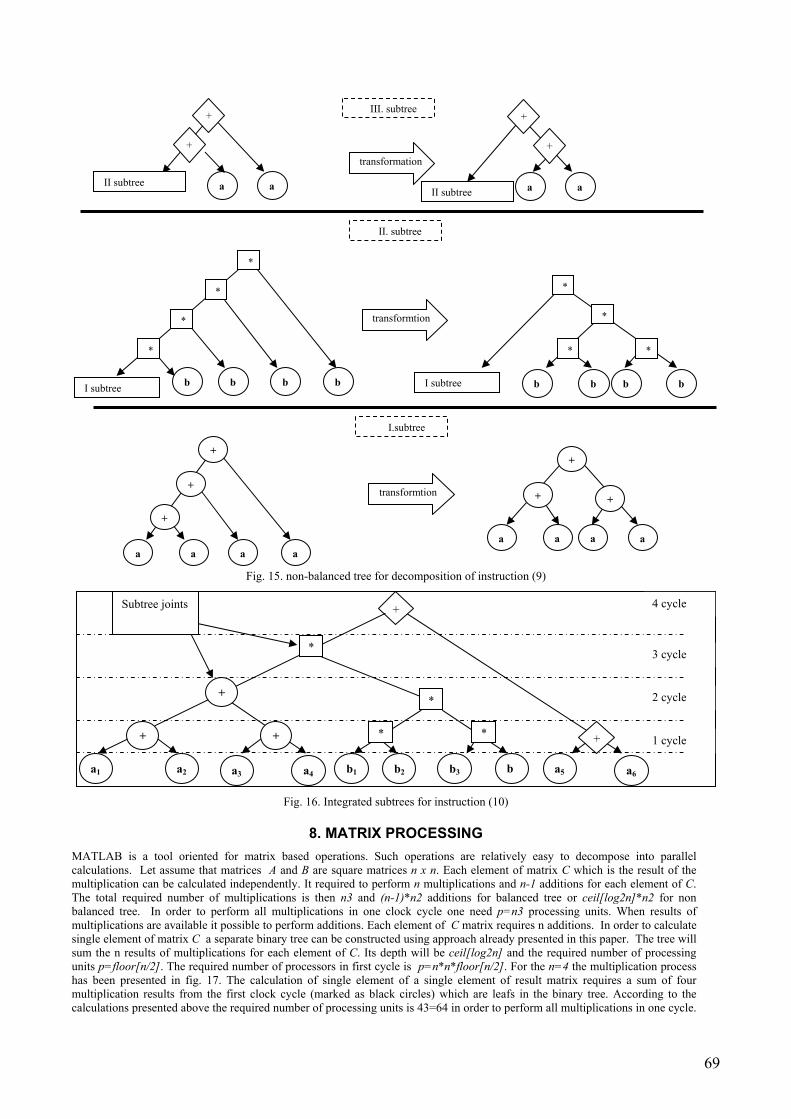
69
Fig. 15. non-balanced tree for decomposition of instruction (9)
Fig. 16. Integrated subtrees for instruction (10)
8. MATRIX PROCESSING MATLAB is a tool oriented for matrix based operations. Such operations are relatively easy to decompose into parallel calculations. Let assume that matrices A and B are square matrices n x n. Each element of matrix C which is the result of the multiplication can be calculated independently. It required to perform n multiplications and n-1 additions for each element of C. The total required number of multiplications is then n3 and (n-1)*n2 additions for balanced tree or ceil[log2n]*n2 for non balanced tree. In order to perform all multiplications in one clock cycle one need p=n3 processing units. When results of multiplications are available it possible to perform additions. Each element of C matrix requires n additions. In order to calculate single element of matrix C a separate binary tree can be constructed using approach already presented in this paper. The tree will sum the n results of multiplications for each element of C. Its depth will be ceil[log2n] and the required number of processing units p=floor[n/2]. The required number of processors in first cycle is p=n*n*floor[n/2]. For the n=4 the multiplication process has been presented in fig. 17. The calculation of single element of a single element of result matrix requires a sum of four multiplication results from the first clock cycle (marked as black circles) which are leafs in the binary tree. According to the calculations presented above the required number of processing units is 43=64 in order to perform all multiplications in one cycle.
I subtree
*
*
*
b b b b
*
b b b b
*
*
**
a a
+
+
+
+
a a a a
+
a a
+
+ +
transformation
transformtion
transformtion
III. subtree
a a
+
+
II subtree
I subtree
II. subtree
I.subtree
II subtree
aa
+
+
1 cycle
2 cycle
3 cycle
4 cycle
b1 b2 b3 b a5 a6 a2 a3 a4 a1
+
+ +
*
* *
*
Subtree joints

70
In the second cycle all sums are calculated. The total number processing units used in this stage is n*n*floor[n/2]=32. The last step requires 16 processing units. The minimum number of cycles required for multiplication of n x n matrices (assuming there is unlimited number of processing units available) is equal to 1+ceil[log2n
Tab. 4. Decomposition of instruction (8) to micro-operations Cycle number
Operation Comment
1
mov RE1, ALU11 mov RE2, ALU12 mov RE3, ALU21 mov RE4, ALU22 mov RE5, ALU31 mov RE6, ALU32 mov RE7, ALU41 mov RE8, ALU42 mov RE9, ALU51 mov RE10, ALU52
mode ALU1, + mode ALU2, + mode ALU3, + mode ALU4, * mode ALU5,
2
mov ALU1out, ALU11 mov ALU2out, ALU12 mov ALU3out, ALU31 mov ALU4out, ALU41 mov ALU5out, ALU42
mode ALU1, + mode ALU4, *
3
mov ALU1out, ALU11 mov ALU4out, ALU12
mode ALU1, *
4
mov ALU1out, ALU32
mode ALU3, +
The result is available in ALU3
A different method of matrix multiplication has been shown in fig. 18. Here two processor units are working in a pipeline. If the first unit performs only multiplications and the second one only additions, the overall number of required unit will be n2*2. The summing of multiplication results can be initiated after at least two multiplications. Thus, there is no need to perform all multiplications in one cycle (see fig. 18). Tab. 5 presents the number of required processing units and clock cycles required for 128x128 matrix multiplication.
Tab. 5. Collection of the number of processors and clock cycles for 128x128 matrix multiplication
Decomposition method Number of processors Number of clock cycles required for performing the operation of multiplication
Without confinement on the number of processing units
(fig.17)
1283 – in the first cycle 64*1282 – in the second cycle 1+ceil[log2128] = 8
With confinement on the number of processing units (fig.18)
2 * 1282 – in each cycle but the first one and the last one n+1=128 + 1 = 129
9. PARAMETERIZED NETWORK OF PROCESSORS IMPLEMENTED IN FPGA A dynamic development of FPGA circuits enables their usage in real-time data processing systems. The speed of these circuits has increased considerably and the resources measured by memory blocks and number of logical and DSP components, while the costs are constantly decreasing. The new generation of FPGA circuits have fast modules of multi-gigabit electrical and optical transmission. A wide offer of a variety of FPGA chips started to be available on the market during the last decade [10 - 12]. The offer is differentiated against prices and performance.
Forwarding the content of the external registers to the input of processing units
Setting the operation mode for each unit
Forwarding results of calculation back to the processing units
Setting operation modes for processing unit

71
This work uses FPGA circuits for fast, synchronous, hardware based, realization of previously decomposed MATLAB algorithms. In the result of calculations on the expressions presented above, there are obtained the following results: 1. a number of required processors with a set of needed mathematical and logical operations with auxiliary registers, 2. a number and dimensions of I/O communication ports, required for external transmission, 3. instruction sequence performed by particular processors, 4. data forwarding sequence via a network working in „switch-matrix” mode. A general functional model of the structure of process network is presented in fig. 19.
Fig. 17. Decomposition of 4x4 matrix multiplication
Each processor (PROC) has an arithmetic-logical unit (ALU) and a set of auxiliary registers (REG). A sequencer (SEQ) controls successive operations and distributes data. The SEQ chooses input data for the ALU via a multiplexer (MUX).
Source data is forwarded via input ports (INP), and the results are forwarded to output ports (OUT). Synchronous data distribution between the processors and I/O ports is realized by SWITCH MATRIX. Particular work cycles of all components are synchronized by a common clock CLK. A flag RUN is set to start the work of a processing module. A flag ready (RDY) is set to signalize end of the process.
c1=a1*b1
c2=a2*b2
c3=a3*b3
cn=an*bn
acc = acc + c1
acc = acc + c2
acc = acc + c3
acc = acc + cn
1 cycle
2 cycle
3 cycle
4 cycle
n+1 cycle
c1…cn – partial products acc - accumulator
Calculation of a value for a single element of the resulting matrix requires two processing units and n+1 clock cycles
+
+
+
Result matrix C
Single multiplication operation
Balanced binary tree

72
A module of process network was realized in VHDL in a form of parameterized behavioral description. The result of MATLAB description analysis is a configuration file containing parameters for particular execution blocks. VHDL code compilation gives the configuration of FPGA circuit, optimized against implemented expressions
Fig. 18. Decomposition of matrix multiplication for a confined number of processing units
Fig. 19. A general functional model of parameterized structure of process network
10. SUMMARY LLRF system for XFEL accelerator and laser will universally use programmable FPGA circuits [13]. They reduce the control loop latency, which confines the maximum available loop amplification. They provide parallel processing of many channels, fast and multi-channel data acquisition, hardware and software monitoring and exception handling. Fast, hardware DSP components residing in FPGA speed up realization of complex data processing algorithms. FPGA reconfigurability enables its usage for realization of completely different groups of algorithms.
This work presents a design of automatic algorithms conversion. The conversion is realized from the level of MATLAB directly to the FPGA structure. The expressions are decomposed to a sequence of separate instructions. Analysis of the expressions leads to elementary micro-orders. A set of orders is serialized, synchronized and processed in parallel. This level of data processing takes into account confined resources offered by a particular FPGA circuit.
There is presented a behavioral model of a universal, parameterized unit of numerical and logical data processing for realization in FPGA circuit. The aim of the work was to obtain automatic implementation of a MATLAB algorithm into
*
*
*
*acc
1 cycle
2 cycle
3 cycle
4 cycle
2 cycle
3 cycle
4 cycle
5 cycle
A and B matrix elements
Single element of resulting matrix C
+
+
+
+

73
the FPGA circuit. The task decomposition process takes into account required time of the process and available resources of FPGA.
11. ACKNOWLEDGEMENTS This work was partially supported by the European Community Research Infrastructure Activity under the FP6 "Structuring the European Research Area" program (CARE – Coordinated Accelerator Research in Europe, contract number RII3-CT-2003-506395).
REFERENCES 1. S.Simrock, Low level radio frequency system for the European X-FEL, Proc.SPIE, vol. 6347 (2006), pp.634701-1-6 2. W.Koprek, et al., Status of LLRF system development for European X-FEL, Proc. SPIE, vol 6347 (2006), pp. 634703-1-18 3. K.Perkuszewski, et.al., FPGA-based multichannel optical concentrator SIMCON4.0 for TESLA cavities LLRF control system, Proc.SPIE, vol. 6347 (2006), pp.634708-1-8 4. J.Szewinski et.al., Embedded system in FPGA-based LLRF controller for FLASH, Proc. SPIE, vol 6347 (2006), pp.63470B-1-6 5. http://flash.desy.de/ 6. T.Czarski, Superconducting cavity control based on system model identification, Meas. Sci. and Technol. (2007), Vol.18, No 8, pp. 2328-2335 7. S.Simrock, Measurements for low level RF control systems, Meas. Sci. and Technol. (2007), Vol.18, No 8, pp. 2320-2327 8. http://www.xilinx.com/ [Xilinx Homepage] System Generator for DSP sub-page 9. K.Bujnowski et al., MATLAB script to C code converter for embedded processors of FLASH LLRF control system, Proc. SPIE, this volume 10. http://www.altera.com/ [Altera Homepage] 11. http://www.actel.com/ [ACTEL homepage] 12. http://www.latticesemi.com/products/fpga/ [LATTICE FPGA products] 13. K.T Pozniak, “FPGA technology application in fast measurement and control system for TESLA superconducting cavity of FLASH free electron laser”, Meas. Sci. Technol. 18 (2007) 2336-2347

74
FPGA control utility in JAVA Paweł Drabik, Krzysztof T. Pozniak
Institute of Electronic Systems, Warsaw University of Technology
ABSTRACT Processing of large amount of data for high energy physics experiments is modeled here in a form of a multichannel, distributed measurement system based on photonic and electrical modules. A method to control such a system is presented in this paper. This method is based on a new method of address space management called the Component Internal Interface (CII). An updatable and configurable environment provided by FPGA fulfills technological and functional demands imposed on complex measurement systems of the considered kind. A purpose, design process and realization of the object oriented software application, written in the high level code described. A few examples of usage of the suggested application is presented. The application is intended for usage in HEP experiments and FLASH, XFEL lasers. Keywords: FLASH laser, photonic functional modules, component internal interface, FPGA,
1. INTRODUCTION The paper discusses a method to design complex, multichannel and distributed measurement systems. Accomplishment of technological, functional and monitoring demands are presented for the debated systems. The main purpose of the paper is to present the way how to handle complicated architectures, based on FPGA chips, by object oriented software.
Complex systems for high energy physics (HEP) applications require frequent modifications introduced on the design and the implementation levels [1-4]. These systems are designed in a modular and parameterized way. This approach facilitates further system modifications and maintains longer the compatibility with up-to-the-date technology.
Fig. 1 General concept of a complex, network oriented, measurement-control system
Fig. 1 presents a general idea for the design of a complex system, split to functional modules. A parameterized and behavioral description is common for the hardware and software. Thus, the communication may be easily established between the layers which are described in the same way. There were built numerable libraries describing hardware blocks and software applications as well as inter-layer interactions. The software is an exact mirror of the hardware assembly, and communication processes between the system layers. The communication medium between the software and hardware has a synchronous character.
Application n
Application 1
Application 4
AA HH DD LL,, VV HH DD LL,, VV EE RR II LL OO GG
Behavioral description
Hardware implementation
Software implementation
Behavioral description
Universal communication
layer
BLOCK 1
BLOCK 4
BLOCK n
CCOOMMMMUUNNIICCAATTIIOO
BBUUSS
CC,, CC++++,, JJ AA VV AA
PPAARRAAMMEETTEERRIISSEEDD DDEESSCCRRIIPPTTIIOONN

75
2. COMPONENT BASED INTERNAL INTERFACE The measurement systems for HEP experiments require more and more resources in terms of logical units, memory and speed, configurability and scalability. FPGAs fulfill these requirements now [8-8]. FPGAs contain relevant number of the LCELLs. While dealing with FPGAs, it is necessary to use specialized software tools, which allow object oriented description of hardware modules and blocks. The resources of FPGAs are still dynamically increasing and the future generations of complex measurement systems, based on fast optoelectronic networks, will extensively use them. Such complex, network oriented systems need multi-parameter, transparent and user-friendly management interface. Fig.2 represents the way of interface design with the usage of proprietary method called Component Internal Interface (CII).
Fig.2 System realization based on Internal Interface
A general concept of the II (Internal Interface) [9] is to establish a fast optical or electrical link between the hardware and software, which are configured in the same way. In order to achieve the communication, the software has to be configured just the same way as is the hardware. A configuration file, which contains a common description and sets of parameters for the hardware and software behavioral descriptions, does the job.
Fig.2 presents a general idea how the hardware is configurable via the VHDL and the software is configurable via C, C++, Matlab, and JAVA. The II is used as a hardware description standard for application in the CMS at LHC [10] and FLASH [11] photonics and electronics.
The Component version of the Internal Interface (CII) is a next step in managing complex, FPGA based systems. The main goals of the CII are as follows:
• Increase the efficiency of work with FPGA based, network oriented architectures. • Achieve a three dimensional component oriented circuit design instead of a flat system architecture. A flat
architecture is defined by the II in a form of a list. The list contains features of the internal structure of FPGA, like: work parameters, functions, registers, memory nodes. The component approach spreads this flat model into objects, groups and finally into components.
• The configuration description is more concise. It represents component dependencies and mutual relations. • Some components might be easily reused in different applications. • Establishment of communication with the chip, in this case via the TCP/IP protocol.
The CII enables interaction with the chip in a more advanced way, e.g. turn on/off some parts of the chip functionality or the entire component sub-tree. The CII parameterized communication interface is based on a configuration method similar to the II solution. Each of the parameters, dependencies, relations and model characters are derived from a single configuration file. These relations from the software are then imaged onto the hardware. The configuration process creates hardware configuration and
VV HH DD LL ccnnttrr:: pprroocceessss((ccllkk,, lloodd)) vvaarriiaabbllee ccoouunntteerr :: ssttdd__llooggiicc__vveeccttoorr((lleefftt ddoowwnnttoo 00));; vvaarriiaabbllee ccaarrrryy :: ssttdd__llooggiicc;; ---- iinntteerrnnaall vvaarriiaabbllee ttccaarrrryy :: ssttdd__llooggiicc;; ---- iinntteerrnnaall bbeeggiinn iiff llooaadd==''11'' tthheenn ccoouunntteerr ::== iinn__llooaadd;; oouuttppuutt <<== iinn__llooaadd;; ……
IIII
BBUUSS
CCOONNFFIIGGUURRAATTIIOONN FFIILLEE
Component description in VHDL
FPGA hardware
realization
GUI & JAVAobjects
Classes in JAVA
Internal Interface
JJAAVVAA ppuubblliicc ccllaassss CCIIII__VVeecc pprriivvaattee iinntt aacccc11;; pprriivvaattee IIIIttyyppee XX,,yy;; ppuubblliicc CCIIII__VVeeccttoorr zz;; ppuubblliicc SSttrriinngg aacccceessOO(()) SSttrriinngg rreett==””aaccccee””;; OOttrrhheerrAAcccc((rreett));; iiff ((XX iinnssttaanncceeooff IIII)) ……

76
Fig. 4 Physical representation of BITS (a,b,c) and WORD (d) allocation
Render
a b c b c
a
BUS
offset
dd
BITS WORD
software configuration in parallel. Data types, for both the Internal Interface and Component Internal Interface, are the same. These types are BITS, WORD and AREA [1]. Fig. 3 presents these types of data.
Fig. 3 Data types of Internal Interface The BITS, WORD and also AREA groups are defined with parameters for each component. Software and hardware interpretation of particular data structures is presented in fig.3. There are scaling parameters to interface this interpretation with a physical circuit. These parameters represent the main bus width and the number of items. The rendering process is performed automatically, what is presented in fig.4 [1].
The is adaptable to different physical environments. Fig.5. describes two scenarios for two data sets with different bus widths. The communication layer in the CII is transparent. The WORD data structures, grouped in the matrix of NxM elements are illustrated in these figures. There are marked different modes of their representation. The possible modes are: hexadecimal, integer, binary and ASCII string.
By configuring the software and hardware with the same parameters, the CII communication bus, is in the consequence transparent to any data.
3. TRANSPARENT COMMUNICATION CONCEPT OVERVIEW The application is based on the following assumptions. The application was designed is for better interaction between the software and hardware. The CII was written in JAVA, what was justified by platform independency. The application could be used as a tool to make future system development far faster, and more advanced.
BBiitt
BBiitt
BBiitt
BBiitt BBiitt
BBiitt
BBiitt
BBiitt
BBiitt
AARREE
WWOORRDD BBiitt

77
The concept of CII realization relies on setting the data in a hierarchical way from general to detail. Input data are collected from specially generated JAVA class. The class originates from the CII configuration process. That configuration class is a table which includes parameters and interfaces details for each component determined in the configuration file separately.
Fig. 5a Relations between Internal Interface parameterized descriptions and physical assembly
Fig. 5b Relations between Internal Interface parameterized descriptions and physical assembly - data width is shorter
The main class creates a graphical user interface (GUI), then allocates a special object named a CII_Vector. This object is an equivalent of a hardware configured component, the CII component. The CII_Vector creates CII component content which has parameters and interfaces.
The configured FPGA is open to communicate via interfaces (BITS, WORD, AREA) and the configuration is viewable via the parameters. The interfaces may be accessible to write or read, or both. The parameters are usually of the read only type.
Access to the component interfaces is achieved due to a specially designed link. The link is based on TCP/IP. The access method is presented in fig.4. It consists of JSserver JAVA class [Błąd! Nie można odnaleźć źródła odwołania.], directly attached to the rest of the application. Next it is connected to a specially designed server via the TCP/IP protocol. This server is able to exchange data with FPGA chip through the VME.
4. COMPONENTS STRUCTURE DESCRIPTION The application was written in JAVA language, which is object oriented for better development and future reuse. This application visualizes the CII architecture in a correct way. The CII_Vector is put on top of the hierarchy, as a component. Each component contains its parameters and interfaces. Each parameter has its own value (table, or matrix of values). Every interface has its access mode. The application delivers a comfortable user interface to manage the component interfaces (write or read). It is also able to save the read and previously written data. These data may be available for further inspection and usage.
The CII_Vector object is created directly from the configuration .java file. The future application development will allow its creation from the binaries. After validation of the file, the details are mapped with the String Tokenizer and are stored in the Vector structures as String. The vector of components is created, as a result of this operation. Each component forms also a vector with its parameters and interfaces descriptions. A brief listing of the input file is presented in table.
ffe12c0 ffe12c2
123534 123535
001011010 101011010 12353500101101 10101101
ffe12c2ffe12c0123534
ffffee1122cc00 ffffee1122cc22
112233553344 112233553355
000011001111001100 110011001111001100
parameters parameters
Internal Interface
N
M
Hardware description
Physical circuit Software description
ffe12c0 ffe12c2
123534 123535
001011010 101011010
ffffee1122cc00 ffffee1122cc22
112233553344 112233553355
000011001111001100 110011001111001100
parameters parameters
Internal Interface
N
M
Hardware description
Physical circuit Software description
ffe12c ffe12c2 12534 123535 0101101 10101101

78
Fig. 6 Connections and communication overview
public class CII_OPTO_cfg_tab private static final CCII_CONFIG_TABLE _tab[] = new CCII_CONFIG_TABLE( 0, “$CII_PART_DATA_TRANSCEIVER”, CIIlib.TABLE_TYPE.COMP, …), new CCII_CONFIG_TABLE( 0, “IPAR_PART_WIDTH”, CIIlib.TABLE_TYPE.IPAR, …), new CCII_CONFIG_TABLE( 0, “IPAR_PART_NUM”, CIIlib.TABLE_TYPE.IPAR, …), new CCII_CONFIG_TABLE( 0, “IPAR_CHECK_WIDTH”, CIIlib.TABLE_TYPE.IPAR, …), new CCII_CONFIG_TABLE( 0, “LPAR_TX_INPUT_REGISTERED”, CIIlib.TABLE_TYPE.LPAR, …), . . . new CCII_CONFIG_TABLE( 0, “IPAR_RX_DELAY_WIDTH”, CIIlib.TABLE_TYPE.IPAR, …), nneeww CCCCIIII__CCOONNFFIIGG__TTAABBLLEE(( 00,, ““WWOORRDD__TTEESSTT””,, CCIIIIlliibb..TTAABBLLEE__TTYYPPEE..WWOORRDD,, ……)),, nneeww CCCCIIII__CCOONNFFIIGG__TTAABBLLEE(( 00,, ““BBIITTSS__TTEESSTT””,, CCIIIIlliibb..TTAABBLLEE__TTYYPPEE..BBIITTSS,, ……)),, new CCII_CONFIG_TABLE( 1, “COMP_ID”, CIIlib.TABLE_TYPE.COMP, …), .
Each line consists of the parameters describing their own character. The bold print presents component details. The parameters of this component are shown by light gray background. A darker gray background depicts the interfaces determined by the types WORD and BITS.
The first task of the application is to gather these parameters and arrange it in the right order, so that the user can recognize it as a parameterized component. The classes contain all the needed data, like: definition of a component, a parameter or an interface, component index number, details about data width/size, data access mode, component parent index number, data type, and more. Each parameter and interface which belongs to a component is identified by a separate index number. This data structure informs the application about data accessibility and controllability.
5. INTERACTIVE USER COMPONENTS MONITOR Raw or processed data can be presented to the user via the graphical user interface. Since a single component can consist of subcomponents, the structure is presented in a form of a tree.
In fig. 7. there is an example of component tree structure. Some components possess sub-components. The tree presents component names, and the index number if more than one component with the same name appears. The user can browse the chip architecture. The tree is interactive for the user. When the user chooses a component, the parameters and interfaces are automatically shown directly from the component data structure. This process is presented in fig.8.
In fig.8, there is a panel displaying component details. The user may browse component content such as parameters and interfaces. To increase the efficiency of browsing the values of parameters are presented with their name. Many types of data representation are supported by the application to fulfill the CII assumptions.
The user may interact with each entity of the CII component. This was shown in a next pair of tables. Choosing one of these entities from fig.8 the user gains access to its details. This process is shown in fig.9 and fig.10
The user can access the interface in the read only mode. To interact with the FPGA the user is also able to write data. It is done by pressing the Modify button shown in fig.10 or from the access panel shown in fig.11. There are also shown the available access modes in these figs.
SSEERRVVEERR
FFPPGGAA
FPGA C O N T R O L
TCP
IInntteerrffaaccee
JJSSSSEERRVVEERR
VV MM EE
Hardware Internal Interface Communication
Software
P A R A ME T E R S
INTERFACES

79
Fig. 7 Components
Fig. 8. Component details
Via the Modify, Write, or WriteRead buttons, the user is able to interact with the FPGA registers and memory. The activated button triggers a specially designed access mode. For each column of the interface data set there is another one created. The first one has read only ability, while the second one is for delivering the values to be written. The write mode is presented in fig.12.
Each instance of data access results in saving the values in Excel or XML format. The format is chosen by the user for further usage
6. CONCLUSIONS Several tests were carried out with the FPGA control utility in JAVA. One of these tests was based on checking the correct communication with FPGA. There were some values written, and then they were checked for correctness.
Another test concerned 320 Mbps transceiver. There has been performed an experiment on configured transceiver system involving setting up flags by writing correct values to BITS registers, then write data to be sent as WORD data, trigger the communication with BITS again and check the outcome in the receiver component. These test proved, that the application works correctly.
Regarding the application, it is currently under constant evaluation in one of the HEP experiment systems in CERN. In the future this application may be a tool for handling the control of many CII configurations at one time and for the control its interactions. The application can build a workflow, allowing to separate the FPGA functions as logical objects. It can also combine separate functions originating in various FPGA circuits.
REFERENCES 1. Fernow R. C.: “Introduction to Experimental Particle Physics”, 2nd
edn (Cambridge: Cambridge University Press), 1989 2. Fruhwirth R., Regler M., Bock R. K., Grote H., Notz D., Ericson T.
and Landshoff P. Y.: “Data Analysis Techniques for High Energy Physics”, 2nd edn (Cambridge: Cambridge University Press), 2001
3. Lindenstruth V. and Kisel I.: “Overview of trigger systems”, Nucl. Instrum. Methods Phys. Res. A 535, pp. 48–56, 2004
4. Pozniak K.: ”Electronics and photonics for high energy physics experiments”, Proc. SPIE 5125, pp. 91-100, 2002
5. http://www.xilinx.com/ [Xilinx Homepage] 6. http://www.altera.com/ [Altera Homepage] 7. http://www.actel.com/ [ACTEL homepage] 8. http://www.latticesemi.com/products/fpga/ [LATTICE FPGA products] 9. Pozniak K. T.: “Internal Interface”, TESLA Report 2005-22, 2005 10. Pozniak K. T., Bartoszek M. and Pietrusinski M.: “Internal interface for RPC muon trigger electronic at CMS
experiment”, Proc. SPIE 5484, pp. 269–82, 2004 11. Pozniak K.: ” FPGA technology application in fast measurement and control system for TESLA superconducting
cavity of FLASH free electron laser“, Meas. Sci. Technol. 18, pp. 2336-2347, 2007 J. Szewinski: “VME-Java server for SUN system”, unpublished material, ISE-PERG laboratory, Warsaw, 200

80
Fig. 12 Writing mode panel
Fig. 9 Parameters operation panel
Fig. 10 Interfaces operation panel
Fig. 9 and 10 show the situation when the user accessed the MPAR_CTRL_CII parameter of the list with integer values and the BITS_MUX_CLK_INV interface. This panels is able to manage big size tables, and data values display determined by the user (integer, ASCII, binary, hexadecimal).
Fig. 11. Access mode panel
.

81
Copper TESLA structure - measurements and control Jakub Główka, Mateusz Maciaś
Warsaw University of Technology, Institute of Electronic Systems
ABSTRACT Phase and amplitude stabilization of accelerating field is a challenging task, which usually requires dedicated hardware and software. In this contribution, we introduce briefly parameters of an accelerating structure and basic measurements on the test stand with copper structure, helping to improve control systems required for stable operation of accelerating structures. Keywords: XFEL, copper structure, TESLA, quality factor calculation, RF-parameters, test stand
1. INTRODUCTION Free electron laser in Hamburg (FLASH) provides coherent VUV radiation (down to 2 nm) for various experiments in many scientific areas. It is also a pilot facility for the future European X-ray Free Electron Laser (XFEL). In addition, its superconducting linac TTF (TESLA Test Facility) was worldwide the first test bed for the implementation of superconducting technology to the e-e+ linear collider TESLA, which since August 2004 is called ILC, International Linear Collider [1, 2, 3]. The enormous progress in achievable gradients and intrinsic quality factors of the superconducting cavities over last 15 years led to many proposals based on the TESLA technology for new facilities generating high-energy charged particles or photons. In any of these machines, the stability of energy and phase of the accelerated beam is crucial for their performance. In a superconducting linear accelerator for electrons, bunches of electrons are produced usually in a laser-driven photoinjector. Subsequently, they are accelerated to final energy by superconducting (sc) accelerating structures. The sc structures, which are the core elements in the linac, are assembled in thermally isolated vacuum vessels, so called cryomodules. For the cost reason, each cryomodule houses several sc structures, which are connected to an RF-power source by the system of waveguides and directional couplers. The chain of structures supplied with the RF-power from a single source must provide the same energy gain to all accelerating bunches. Standard specifications, coming from the users requirement, for the energy spread and phase stability are <0.0005 and 0.01° respectively. The sc structures operate at very low temperature below 2K (usually they are immersed in the superfluid helium) and ultra high vacuum. The width of their accelerating resonance, when the loaded quality factor is matched for the reflection-free operation, is rather small (≤ 500 Hz). This makes them very sensitive to mechanical vibrations and the Lorentz force detuning. The specification and small resonance width cause that the electronic system for the stabilization (LLRF, Low Level RF) must be specially “tailored” to ensure the stable operation of a superconducting accelerator. In the following sections, we will describe fundamentals of the TESLA structure and our project to build the test stand for microwave measurements on the normal conducting copper model of the TESLA structure. The test stand will help us in the future to continue R&D programs for the LLRF electronics.
2. TESLA STRUCTURE AND ITS RF-PARAMETERS 2.1. The Structure The TESLA accelerating cavity is, from the microwave point of view, of the standing wave type. It consists of nine coupled cells. The cell-to-cell coupling kcc is 1.98%. The length of each cell equals to half of the free-space wavelength (at 1300 MHz λ/2=115.4mm). The cross-section of the structure, its photograph and cross-section of the copper model used in our test stand are shown in Figure 1. The structure is equipped with the fundamental power coupler (FPC) transferring energy from the RF-source, two higher order mode (HOM) couplers suppressing parasitic modes excited by the beam and pickup probe for the phase and amplitude monitoring during the operation. The accelerated beam traverses the cavity on or close to its axis.
The structure is made of niobium, which is the superconductor of type II. Its critical temperature and critical magnetic flux are Tc=9.2K and Bc=190mT respectively. There are various shapes of cells proposed for the ILC structure. In FLASH so-called TESLA shape is used (it was designed for the TESLA collider in 1992). Recently two new shapes for the ILC have been proposed, the re-entrant shape and low loss shape [10, 11]. RF- parameters for the 9-cell structure of the TESLA type [4] are listed in Table 1.
2.2. Modes In a real standing wave-structure, there is a residual traveling wave. This energy flux along the structure compensates for the energy dissipation in the wall and energy transfer to the accelerated beam (beam loading). Superposition of the dominating standing wave with residual traveling wave causes that the spatial wave pattern has minima, which do not equal 0, as it should take place in the lossless case. For our further analysis of the structure in the steady state, we can neglect presence of the traveling wave and consider the structure as the purely of the standing wave type.

82
Among an infinity number of resonant modes, a cylindrically symmetric cell can oscillate in transverse magnetic (TM) like modes, which have only transverse to the symmetry axis component of the magnetic field. The lowest frequency TM010 mode is usually used for the acceleration of charged particles. All components of its electric and magnetic field demonstrate cylindrical symmetry (no angular dependence in the cylindrical coordinate system: φ, r, z). In general, there are two allowed boundary conditions at the middle plane of each iris between cells: electrical short ≡ no transverse electric field at the mid plane (Fig. 2, left) magnetic short ≡ no transverse magnetic field at the mid plane (Fig. 2, right)
Figure 1: Cross-section of the TESLA structure, its photograph and cross-section of the copper prototype.
Table 1. RF-parameters of the 9-cell TESLA structure.
Symbol Parameter Unit Value
f Resonance frequency [MHz] 1300
Q0 Intrinsic quality at low Eacc [1010] 2
kcc Cell to cell coupling [%] 1.98
R/Q Characteristic impedance [Ω] 1012
ηE Ratio of peak electric field on the wall to accelerating gradient (Eacc)
- 1.98
ηB Ratio of peak magnetic flux on the wall to accelerating gradient (Eacc)
[mT/(MV/m)] 4.15
GFM Geometric factor - 271
Figure 2: Electric lines in the iris region for the electric (left) and magnetic (right) short in the middle plane
respectively
FPC port
HOM couplerPickup probe
8 irises
HOM coupler
HOM couplerPickup probe
9 cells
r
z
φ
r
z
φ

83
One should note that the electric field component Ez =0 at the plane with the magnetic short (Fig. 2 right). For a multi-cell cavity, various combinations of the electric and magnetic shorts on irises lead to diverse electromagnetic field patterns and related to them frequencies, so called pass-bands. The magnetic short at either iris in case of a single-cell with the geometry similar to that shown in Figure 1, results in the shortest wavelength for the TM010 pass-band.
Table 2: Examples of electric field amplitude on z-axis (symmetry axis) of the TESLA structurei.
Phase advance 1/9 π Phase advance 4/9 π Phase advance π
TESLA structure, hence it is made of 9 coupled cells (resonators), can oscillate in 9 different resonant modes in every passband. The 9 modes differ in their field patterns (cell-to-cell phase advance) and frequencies. The highest frequency mode in the TM010 passband is called π -mode because of its cell-to-cell phase advance. It is commonly used for the acceleration of particles which velocity is close to the velocity of light. From RF point of view, all irises in π-mode are the magnetic shorts. Some examples of the computed field profiles are shown in Table 2. Figure 3 displays measured frequencies of the TM010 passband for the copper model of the TESLA cavity.
Figure 3: Frequency characteristic showing 9 modes of the TM010 passband.
2.3 Field patterns and field flatness for the accelerating mode Strong longitudinal component Ez of the electric field on the axis and its synchronism with the traversing particles make the π-mode very suitable for the acceleration. Contours of the Er and Ez for this mode are shown in Fig. 4.
Figure 4: Transverse Er (left) and longitudinal Ez (right) electric field amplitude for the π-mode.
The most effective acceleration process in a multi-cell superconducting structure takes place when all cells have the same stored energy. The superconducting structures for cost reason are fabricated from thin niobium sheets, shaped by the deep-drawing technique to cups (half-cells) which later on are electro-beam welded to form the cells. The production process is very limited in the shape accuracy. After the cells are welded together and the structure underwent main chemical treatment, the cells must be tuned mechanically to adjust their frequencies to the frequency of the accelerating π-mode and to balance the field profile.

84
To achieve the flat field profile in the π-mode the geometry of end cells must be slightly different from the geometry of the inner cells to compensate for the presence of the beam tubes. A structure that is terminated with full-cells and designed to operate with the flat filed in the π-mode can not be tuned simultaneously to have well balanced field profile in any other mode from the TM010 passband [5]. This is to some extend possible for normal-conducting structures, when they are terminated with half-cells and when the beam tubes have very small diameter. Both are not practical for the superconducting cavities. One should note that in a multi-cell structure made of an even cell number, the even modes have fields in the end cells shifted practically by 180 deg. This causes positive feedback in the control system (algorithm). During the operation, these modes could be excited by the LLRF control system. 2.4 Quality factors Resonator with couplers is characterized by set of quality factors: Intrinsic quality factor:
cyclepercavityinlostEnergy
cavityinstoredEnergyQ π⋅=20
External quality factors (one for each coupler):
cyclepercircuitexternalinlostEnergy
cavityinstoredEnergyext
Q π⋅= 2
Loaded quality factor:
cyclepercircuitexternalinandcavityinlostenergyTotal
cavityinstoredEnergy
LQ π⋅= 2
They are linked by equation:
2
1
1
1
0
11
extQextQQLQ++=
3. LAYOUT OF THE CONTROL ELECTRONICS 3.1 Phase and amplitude control system The control system concept, we would like to implement, is based on that for accelerating modules of FLASH at DESY [6]. A test cavity (copper model) is coupled into the control loop via two antennae. One antenna, with a strong coupling, replaces the input power coupler, whereas the second one, placed on the other beam tube, couples weaker and is used as the pickup probe. The controller board has not been chosen yet, since there are a lot of concepts under development and the test stand will be able to operate with all of them (for example one of the SIMCON boards or AMC motherboard). The motherboard developed for the RF Gun controller is shown on Figure 5 only as an option [7].
Figure 5: Layout of the test stand based on the control system for the TESLA accelerating structure operating in
FLASH.
3.2 Antennas For the coupling between the RF-source and copper model in the test-stand we used a 50 Ω coaxial line and matched coaxial N-type connector, which inner conductor was extended with the silver coated copper rod for better penetration into the beam tube. The connector was located 45 mm apart from the end-cell (Fig. 7), at the same distance as the high power input coupler of the niobium TESLA structures [8]. The length of the rod could be easily adjusted to reach a
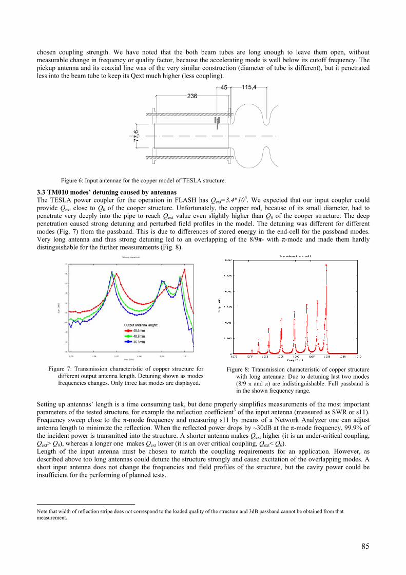
85
chosen coupling strength. We have noted that the both beam tubes are long enough to leave them open, without measurable change in frequency or quality factor, because the accelerating mode is well below its cutoff frequency. The pickup antenna and its coaxial line was of the very similar construction (diameter of tube is different), but it penetrated less into the beam tube to keep its Qext much higher (less coupling).
Figure 6: Input antennae for the copper model of TESLA structure.
3.3 TM010 modes’ detuning caused by antennas The TESLA power coupler for the operation in FLASH has Qext=3.4*106. We expected that our input coupler could provide Qext close to Q0 of the cooper structure. Unfortunately, the copper rod, because of its small diameter, had to penetrate very deeply into the pipe to reach Qext value even slightly higher than Q0 of the cooper structure. The deep penetration caused strong detuning and perturbed field profiles in the model. The detuning was different for different modes (Fig. 7) from the passband. This is due to differences of stored energy in the end-cell for the passband modes. Very long antenna and thus strong detuning led to an overlapping of the 8/9π- with π-mode and made them hardly distinguishable for the further measurements (Fig. 8).
Figure 7: Transmission characteristic of copper structure for
different output antenna length. Detuning shown as modes frequencies changes. Only three last modes are displayed.
Figure 8: Transmission characteristic of copper structure
with long antennae. Due to detuning last two modes (8/9 π and π) are indistinguishable. Full passband is in the shown frequency range.
Setting up antennas’ length is a time consuming task, but done properly simplifies measurements of the most important parameters of the tested structure, for example the reflection coefficient3 of the input antenna (measured as SWR or s11). Frequency sweep close to the π-mode frequency and measuring s11 by means of a Network Analyzer one can adjust antenna length to minimize the reflection. When the reflected power drops by ~30dB at the π-mode frequency, 99.9% of the incident power is transmitted into the structure. A shorter antenna makes Qext higher (it is an under-critical coupling, Qext> Q0), whereas a longer one makes Qext lower (it is an over critical coupling, Qext< Q0). Length of the input antenna must be chosen to match the coupling requirements for an application. However, as described above too long antennas could detune the structure strongly and cause excitation of the overlapping modes. A short input antenna does not change the frequencies and field profiles of the structure, but the cavity power could be insufficient for the performing of planned tests.
Note that width of reflection stripe does not correspond to the loaded quality of the structure and 3dB passband cannot be obtained from that measurement.

86
4. MEASUREMENTS AND SIMULATIONS 4.1 Quality factor measurements The intrinsic quality factor is one of the most important structure parameters. From the RF measurements theory it is known that the intrinsic quality factor cannot be measured directly, but it can be determined, for example, from the transmission characteristic. At first, one needs to measure the loaded quality factor QL, from the decay time (the superconducting case) or from the 3dB width of the resonance curve (normal conducting case – figure 10):
π
πf
fLQ
∆=
Having the coupler coefficient ß, which is defined as follows:
extQ
Q0=β
one can find value of the intrinsic quality factor: )ß1(LQ0Q +=
The value of ß could be calculated from the reflection coefficient s11:
11
11s1s1
+−
=β
for over-critical coupling.
11
11s1s1
−+
=β
for under-critical coupling To make the decision which formulae applies one needs to analyze in the time domain the reflected wave being the response to the rectangular pulse. We propose another and simpler method to determine the intrinsic quality factor Q0. The method is based on the measurement of the reflection coefficient in the complex space [9]. Structure in range of one mode can be represented by simple RLC circuit. We can evaluate expression of the normalized impedance depending as a function of Q0:
)f(Q2i1)f(z
0δβ
+≈
Where:
0
0f
ff)f( −=δ
and f0 is the frequency where s11 has its minimum. At a certain frequency, f+Qo , the 2Qδ(f) becomes equal to 1. Similarly, there is another frequency, f–Q0, at which the 2Qδ(f) becomes equal to -1. At these frequencies, the normalized impedance can be written as
ifz Q ±
=± 1)(
0
β
Determining the frequency, f–Q0 , is equivalent to finding the intersection of the function, T(f), with the locus of all points for which Im(z)=Re(z). Similarly, finding the frequency, f+Q0, is equivalent to finding the intersection of T(f) with the locus of all points for which -Im(z)=Re(z) (figure 10). Simple calculation leads to intrinsic quality factor:
00
00 2 Qff
fQ±−
=
Using equations with β it is easy to calculate Qext and QL.
The pickup probe coupling is very weak (very high Qext). The small amount of the out-coupled power can be neglected in the calculation of the intrinsic quality factor. The results of calculated Q0 and QL led to the conclusions that the input line is under-critical coupled (this result is shadowed in Table 5). 4.2 Time domain cavity response simulations There is a significant difference between the intrinsic quality factor of a copper structure and superconducting one. The loaded quality factor of a structure determine its filling time. Figure 12 shows transient (pickup-signals) for structures with high and low quality factor. Both structures were excited with signal displayed in the Figure 11. Envelope of the response for high Q0 is shown upper diagram of Fig. 12. The lower diagram illustrates response of a low Q0 structure. In general, shape of the response is different for these two cases. The flat top is similar but there are big differences in the

87
filling and decay time. Low quality structure responds much faster, and its filling is almost instantaneous (in µ-seconds range).
Figure 9: Reflection characteristic of copper structure for pi-
mode represented in complex space on Smith chart. Frequency at crossing with lines defined by Re(z(f))=±Im(z(f)) allow direct Q0 calculation.
Figure 10: Transmission characteristic of copper structure.
Only π-mode is in range. 3dB passband is marked.
Results of our measurements and calculations for the π-mode are presented in Tables 3-5.
Table 3. Reflection measuring
s11 B for over-critical B for under-critical
0.29516 1.83752 0.54421
Table 4. Transmission measuring
Parameter Value [GHz]
F0 1.2997600
f3db1 1.2997149
F3db2 1.2997921
Table 5. Calculations from transmission (final results are shadowed)
Parameter Over-critical case Under-critical case
QL 16836 16836
Q0 47773 25998
Qext 25998 47773
Table 6: Calculations from the Smith chart for under-critical coupling
Q0 Qext QL
24804 45578 16062
5. CONCLUSIONS AND FINAL REMARKS The presented methods of the antennae tuning and quality factor calculations are quite simply and accurate enough for the copper structure in our test stand. The loaded quality factor of the copper model when it is very weak (under-critical) coupled is determined mostly by the intrinsic quality factor, while the loaded quality factor of a superconducting structure in the over-coupled case is determined by the external quality factor (Qext of the input coupler). The discussed test stand is intended to help in the implementation of a new LLRF hardware and software for the European XFEL facility and other FEL projects. It should also serve in the future for the educational purposes.

88
Fig. 11: Simulation of input signals.
Fig. 12: Simulation of pickup signals. Superconducting structure with very high quality factor (upper diagram) and normal conducting structure with low quality factor (lower diagram).
6. ACKNOWLEDGMENT Authors would like to express gratitude to Jacek Sekutowicz for all consultations and help, to Tomasz Stanisławski for help with simulations and to people from ZiUAM that helped us with RF measurements. We acknowledge the support of the European Community Research Infrastructure Activity under the FP6 “Structuring the European Research Area” program (CARE, contract number RII3-CT-2003-506395).
REFERENCES 1. ILC Baseline Conceptual Design, http://www.linearcollider.org/wiki/, 2007. 2. D. Edwards, ”TESLA Test Facility Linac Design Report”, TESLA Rep. 95-01. 3. The European X-Ray Laser Project XFEL, http://xfel.desy.de/, 2007 4. J. Sekutowicz, “TESLA Superconducting Accelerating Structures” 5. Stan O. Schriber, “To Be Pi Or Non To Be Pi: That Is The Dilema” 6. Valeri Ayvazyan, Stefan Choroba, Alexander Matyushin, Guenter Moeller, Gevorg Petrosyan, Kay Rehlich, Stefan
N. Simrock, Petr Vetrov, “Digital Low Level RF Control System For The DESY TTF VUV-FEL Liniac”, TESLA-FEL Report 2005-06
7. Elmar Vogel, Waldemar Koprek, Piotr Pucyk, Stefan Simrock, “RF Gun Control”, CARE-Report-2007-009-SRF 8. W.-D. Moeller,“High Power Coupler For The Tesla Test Facility” 9. T. Berenc, C. Deibele, “Simulation and Measurement Considerations for Resonant Cavity Couplers and
Extrapolating Results to Multiple Cells and Varying Conductivities”, Fermilab RFNote #005 http://www-rfes.fnal.gov/global/technotes/TN/TN005.pdf
10. J. Sekutowicz, “Low Loss Cavity for the 12- GeV CEBAF Upgrade“, JLAB, TN-02-023, June 2002, VA, USA. 11. J. Sekutowicz, “Design of a Low Loss SRF Cavity for the ILC”, APS, Proceedings PAC06, May 2005, Knoxville,
TN, USA. 12. J. Sekutowicz, private communication. 13. J. Dobrowolski, consultations. All field simulations where made using FEM-code for the TESLA shape structure (courtesy of J. Sekutowicz).