Embed Size (px)
Citation preview
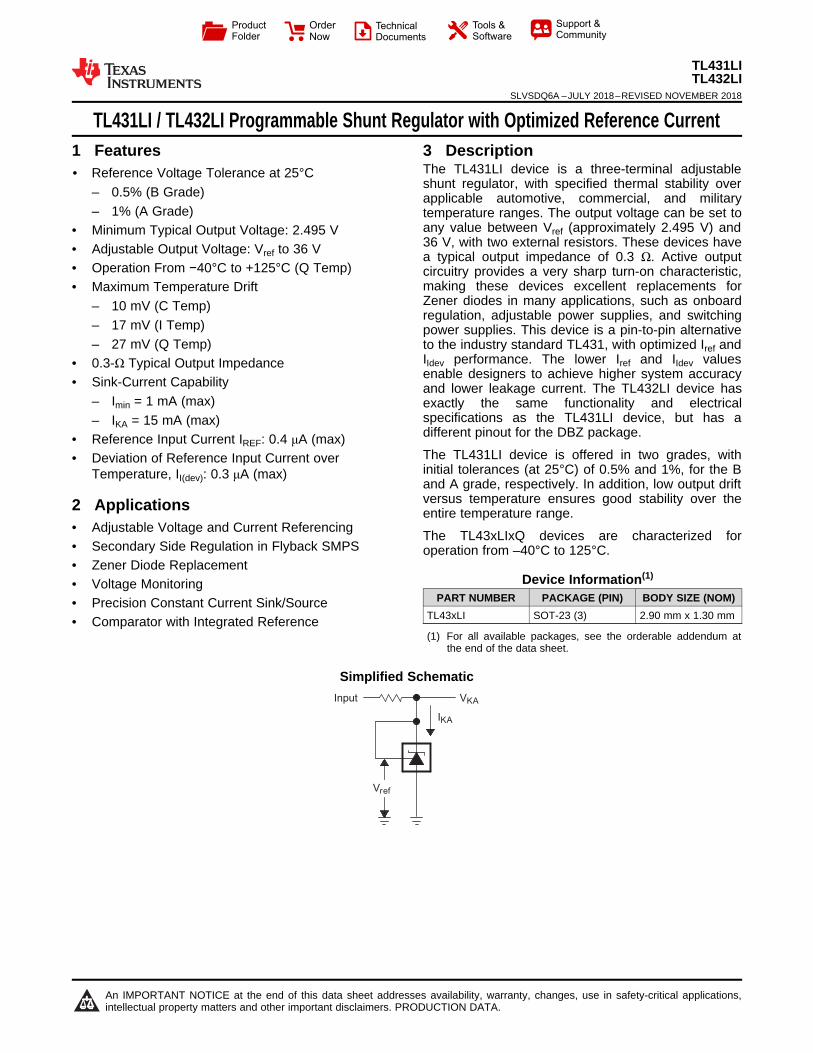
Vref
Input VKA
IKA
Product
Folder
Order
Now
Technical
Documents
Tools &
Software
Support &Community
An IMPORTANT NOTICE at the end of this data sheet addresses availability, warranty, changes, use in safety-critical applications,intellectual property matters and other important disclaimers. PRODUCTION DATA.
TL431LITL432LI
SLVSDQ6A –JULY 2018–REVISED NOVEMBER 2018
TL431LI / TL432LI Programmable Shunt Regulator with Optimized Reference Current
1
1 Features1• Reference Voltage Tolerance at 25°C
– 0.5% (B Grade)– 1% (A Grade)
• Minimum Typical Output Voltage: 2.495 V• Adjustable Output Voltage: Vref to 36 V• Operation From −40°C to +125°C (Q Temp)• Maximum Temperature Drift
– 10 mV (C Temp)– 17 mV (I Temp)– 27 mV (Q Temp)
• 0.3-Ω Typical Output Impedance• Sink-Current Capability
– Imin = 1 mA (max)– IKA = 15 mA (max)
• Reference Input Current IREF: 0.4 μA (max)• Deviation of Reference Input Current over
Temperature, II(dev): 0.3 μA (max)
2 Applications• Adjustable Voltage and Current Referencing• Secondary Side Regulation in Flyback SMPS• Zener Diode Replacement• Voltage Monitoring• Precision Constant Current Sink/Source• Comparator with Integrated Reference
3 DescriptionThe TL431LI device is a three-terminal adjustableshunt regulator, with specified thermal stability overapplicable automotive, commercial, and militarytemperature ranges. The output voltage can be set toany value between Vref (approximately 2.495 V) and36 V, with two external resistors. These devices havea typical output impedance of 0.3 Ω. Active outputcircuitry provides a very sharp turn-on characteristic,making these devices excellent replacements forZener diodes in many applications, such as onboardregulation, adjustable power supplies, and switchingpower supplies. This device is a pin-to-pin alternativeto the industry standard TL431, with optimized Iref andIIdev performance. The lower Iref and IIdev valuesenable designers to achieve higher system accuracyand lower leakage current. The TL432LI device hasexactly the same functionality and electricalspecifications as the TL431LI device, but has adifferent pinout for the DBZ package.
The TL431LI device is offered in two grades, withinitial tolerances (at 25°C) of 0.5% and 1%, for the Band A grade, respectively. In addition, low output driftversus temperature ensures good stability over theentire temperature range.
The TL43xLIxQ devices are characterized foroperation from –40°C to 125°C.
Device Information(1)
PART NUMBER PACKAGE (PIN) BODY SIZE (NOM)TL43xLI SOT-23 (3) 2.90 mm x 1.30 mm
(1) For all available packages, see the orderable addendum atthe end of the data sheet.
Simplified Schematic
2
TL431LITL432LISLVSDQ6A –JULY 2018–REVISED NOVEMBER 2018 www.ti.com
Product Folder Links: TL431LI TL432LI
Submit Documentation Feedback Copyright © 2018, Texas Instruments Incorporated
Table of Contents1 Features .................................................................. 12 Applications ........................................................... 13 Description ............................................................. 14 Revision History..................................................... 25 Device Comparison Table ..................................... 36 Pin Configuration and Functions ......................... 37 Specifications......................................................... 4
7.1 Absolute Maximum Ratings ...................................... 47.2 ESD Ratings.............................................................. 47.3 Thermal Information .................................................. 47.4 Recommended Operating Conditions....................... 47.5 Electrical Characteristics........................................... 57.6 Typical Characteristics .............................................. 6
8 Parameter Measurement Information .................. 98.1 Temperature Coefficient............................................ 98.2 Dynamic Impedance ............................................... 10
9 Detailed Description ............................................ 119.1 Overview ................................................................. 119.2 Functional Block Diagram ....................................... 11
9.3 Feature Description................................................. 129.4 Device Functional Modes........................................ 12
10 Applications and Implementation...................... 1310.1 Application Information.......................................... 1310.2 Typical Applications .............................................. 1310.3 System Examples ................................................. 21
11 Power Supply Recommendations ..................... 2412 Layout................................................................... 24
12.1 Layout Guidelines ................................................. 2412.2 Layout Example .................................................... 25
13 Device and Documentation Support ................. 2613.1 Related Links ........................................................ 2613.2 Documentation Support ........................................ 2613.3 Receiving Notification of Documentation Updates 2613.4 Community Resources.......................................... 2613.5 Trademarks ........................................................... 2713.6 Electrostatic Discharge Caution............................ 2713.7 Glossary ................................................................ 27
14 Mechanical, Packaging, and OrderableInformation ........................................................... 27
4 Revision History
Changes from Original (July 2018) to Revision A Page
• Changed TL43xLI status from Advance Information to Production Data release ................................................................. 1
1
2
3
REF
CATHODE
ANODE
1
2
3
CATHODE
REF
ANODE
3
TL431LITL432LI
www.ti.com SLVSDQ6A –JULY 2018–REVISED NOVEMBER 2018
Product Folder Links: TL431LI TL432LI
Submit Documentation FeedbackCopyright © 2018, Texas Instruments Incorporated
5 Device Comparison Table
DEVICE PINOUT INITIAL ACCURACY OPERATING FREE-AIR TEMPERATURE (TA)
TL431LITL432LI
A: 1%B: 0.5%
C: 0°C to 70°CI: -40°C to 85°C
Q: -40°C to 125°C
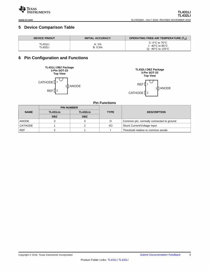
6 Pin Configuration and Functions
TL431LI DBZ Package3-Pin SOT-23
Top ViewTL432LI DBZ Package
3-Pin SOT-23Top View
Pin Functions
NAMEPIN NUMBER
TYPE DESCRIPTIONTL431LIx TL432LIxDBZ DBZ
ANODE 3 3 O Common pin, normally connected to groundCATHODE 1 2 I/O Shunt Current/Voltage inputREF 2 1 I Threshold relative to common anode
4
TL431LITL432LISLVSDQ6A –JULY 2018–REVISED NOVEMBER 2018 www.ti.com
Product Folder Links: TL431LI TL432LI
Submit Documentation Feedback Copyright © 2018, Texas Instruments Incorporated
(1) Stresses beyond those listed under Absolute Maximum Ratings may cause permanent damage to the device. These are stress ratingsonly, which do not imply functional operation of the device at these or any other conditions beyond those indicated under RecommendedOperating Conditions. Exposure to absolute-maximum-rated conditions for extended periods may affect device reliability.
(2) All voltage values are with respect to ANODE, unless otherwise noted.
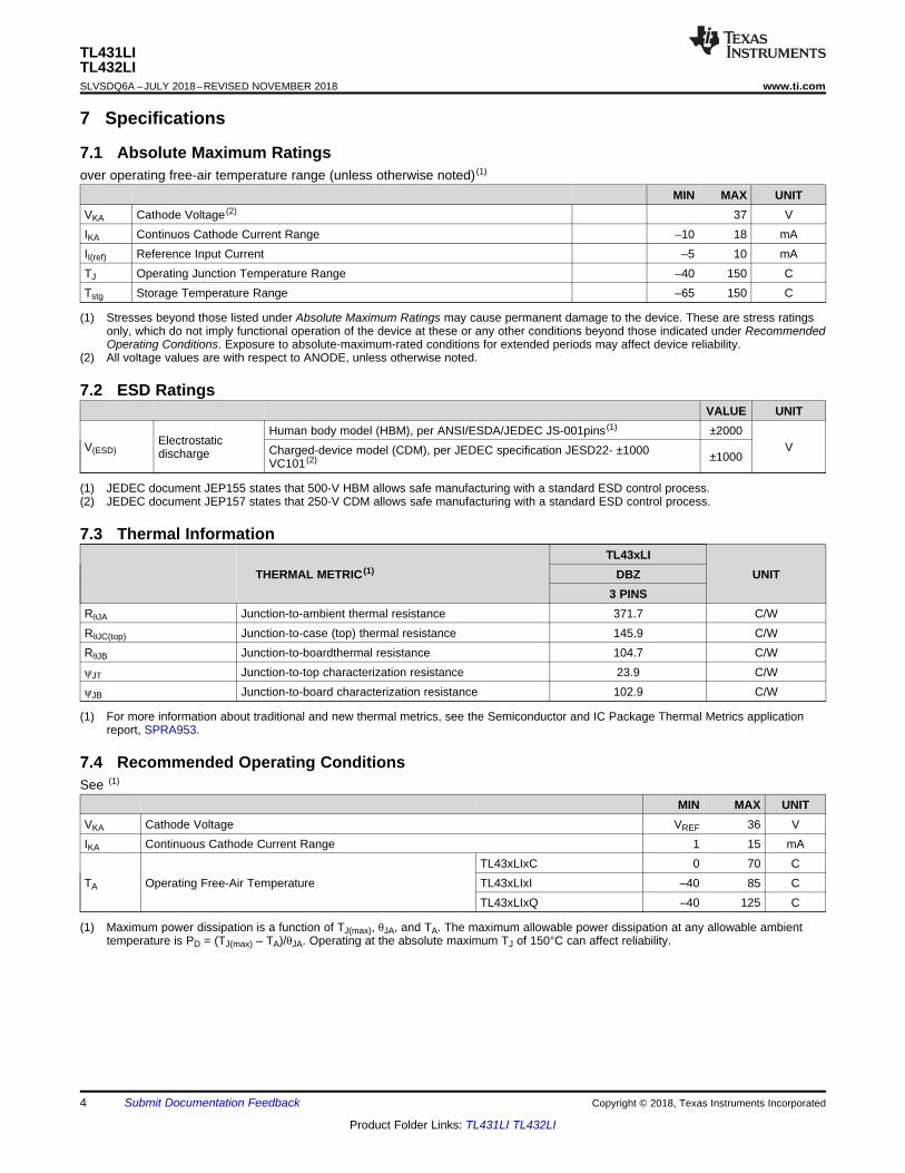
7 Specifications
7.1 Absolute Maximum Ratingsover operating free-air temperature range (unless otherwise noted) (1)
MIN MAX UNITVKA Cathode Voltage (2) 37 VIKA Continuos Cathode Current Range –10 18 mAII(ref) Reference Input Current –5 10 mATJ Operating Junction Temperature Range –40 150 CTstg Storage Temperature Range –65 150 C
(1) JEDEC document JEP155 states that 500-V HBM allows safe manufacturing with a standard ESD control process.(2) JEDEC document JEP157 states that 250-V CDM allows safe manufacturing with a standard ESD control process.
7.2 ESD RatingsVALUE UNIT
V(ESD)Electrostaticdischarge
Human body model (HBM), per ANSI/ESDA/JEDEC JS-001pins (1) ±2000VCharged-device model (CDM), per JEDEC specification JESD22- ±1000
VC101 (2) ±1000
(1) For more information about traditional and new thermal metrics, see the Semiconductor and IC Package Thermal Metrics applicationreport, SPRA953.
7.3 Thermal Information
THERMAL METRIC (1)TL43xLI
UNITDBZ3 PINS
RθJA Junction-to-ambient thermal resistance 371.7 C/WRθJC(top) Junction-to-case (top) thermal resistance 145.9 C/WRθJB Junction-to-boardthermal resistance 104.7 C/WψJT Junction-to-top characterization resistance 23.9 C/WψJB Junction-to-board characterization resistance 102.9 C/W
(1) Maximum power dissipation is a function of TJ(max), θJA, and TA. The maximum allowable power dissipation at any allowable ambienttemperature is PD = (TJ(max) – TA)/θJA. Operating at the absolute maximum TJ of 150°C can affect reliability.
7.4 Recommended Operating ConditionsSee (1)
MIN MAX UNITVKA Cathode Voltage VREF 36 VIKA Continuous Cathode Current Range 1 15 mA
TA Operating Free-Air TemperatureTL43xLIxC 0 70 CTL43xLIxI –40 85 CTL43xLIxQ –40 125 C
5
TL431LITL432LI
www.ti.com SLVSDQ6A –JULY 2018–REVISED NOVEMBER 2018
Product Folder Links: TL431LI TL432LI
Submit Documentation FeedbackCopyright © 2018, Texas Instruments Incorporated
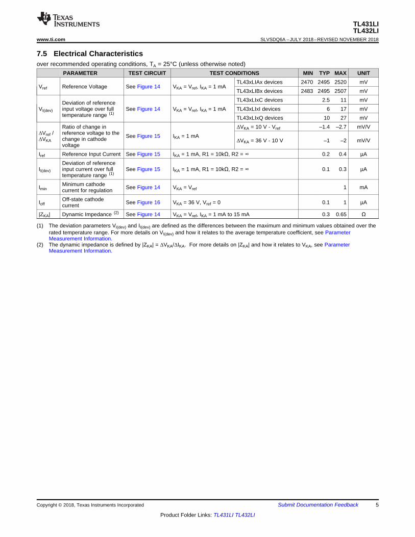
(1) The deviation parameters VI(dev) and II(dev) are defined as the differences between the maximum and minimum values obtained over therated temperature range. For more details on VI(dev) and how it relates to the average temperature coefficient, see ParameterMeasurement Information.
(2) The dynamic impedance is defined by |ZKA| = ΔVKA/ΔIKA. For more details on |ZKA| and how it relates to VKA, see ParameterMeasurement Information.
7.5 Electrical Characteristicsover recommended operating conditions, TA = 25°C (unless otherwise noted)
PARAMETER TEST CIRCUIT TEST CONDITIONS MIN TYP MAX UNIT
Vref Reference Voltage See Figure 14 VKA = Vref, IKA = 1 mATL43xLIAx devices 2470 2495 2520 mVTL43xLIBx devices 2483 2495 2507 mV
VI(dev)
Deviation of referenceinput voltage over fulltemperature range (1)
See Figure 14 VKA = Vref, IKA = 1 mATL43xLIxC devices 2.5 11 mVTL43xLIxI devices 6 17 mVTL43xLIxQ devices 10 27 mV
ΔVref /ΔVKA
Ratio of change inreference voltage to thechange in cathodevoltage
See Figure 15 IKA = 1 mA
ΔVKA = 10 V - Vref –1.4 –2.7 mV/V
ΔVKA = 36 V - 10 V –1 –2 mV/V
Iref Reference Input Current See Figure 15 IKA = 1 mA, R1 = 10kΩ, R2 = ∞ 0.2 0.4 µA
II(dev)
Deviation of referenceinput current over fulltemperature range (1)
See Figure 15 IKA = 1 mA, R1 = 10kΩ, R2 = ∞ 0.1 0.3 µA
IminMinimum cathodecurrent for regulation See Figure 14 VKA = Vref 1 mA
IoffOff-state cathodecurrent See Figure 16 VKA = 36 V, Vref = 0 0.1 1 µA
|ZKA| Dynamic Impedance (2) See Figure 14 VKA = Vref, IKA = 1 mA to 15 mA 0.3 0.65 Ω
Temperature (°C)
Y A
XIS
TIT
LE (
Uni
t)
-50 -25 0 25 50 75 100 125-1.8
-1.65
-1.5
-1.35
-1.2
-1.05VKA = 3 V to 36 V
D006D006D006
VKA - Cathode Voltage -V
I KA -
Cat
hode
Cur
rent
- m
A
0 0.5 1 1.5 2 2.5 3-3
0
3
6
9
12
15VKA = VrefTA = 25°C
D003TA - Free-Air Temperature - °C
I off
- O
ff-S
tate
Cat
hode
Cur
rent
- P
A
-50 -25 0 25 50 75 100 1250
0.008
0.016
0.024
0.032
0.04
0.048
0.056
0.064VKA = 36 VVREF = 0 V
D004
TA - Free-Air Temperature - °C
Vre
f - R
efer
ence
Vol
tage
- V
-50 -25 0 25 50 75 100 125 1502.4855
2.487
2.4885
2.49
2.4915
2.493
2.4945
2.496
2.4975
2.499
2.5005Vka = VrefIKA = 1 mA
BookD001TA - Free-Air Temperature - °C
I ref -
Ref
eren
ce C
urre
nt -
µA
-50 -25 0 25 50 75 100 1250
0.1
0.2
0.3
0.4
0.5
0.6
0.7
0.8
0.9
1IKA = 1 mA
D002
6
TL431LITL432LISLVSDQ6A –JULY 2018–REVISED NOVEMBER 2018 www.ti.com
Product Folder Links: TL431LI TL432LI
Submit Documentation Feedback Copyright © 2018, Texas Instruments Incorporated
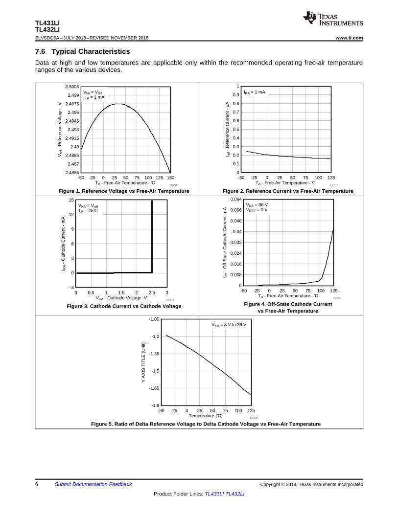
7.6 Typical CharacteristicsData at high and low temperatures are applicable only within the recommended operating free-air temperatureranges of the various devices.
Figure 1. Reference Voltage vs Free-Air Temperature Figure 2. Reference Current vs Free-Air Temperature
Figure 3. Cathode Current vs Cathode Voltage Figure 4. Off-State Cathode Currentvs Free-Air Temperature
Figure 5. Ratio of Delta Reference Voltage to Delta Cathode Voltage vs Free-Air Temperature
t - Time - Ps
Inpu
t and
Out
put V
olta
ge -
V
-1 0 1 2 3 4 5 6 70
1
2
3
4
5
6
Output
Input TA = 25qC
puls
220 Ω
50 Ω
GND
Output
Pulse
Generator
f = 100 kHz
f - Frequency - Hz
|ZK
A| -
Ref
eren
ce Im
peda
nce
- O
hms
0.1
0.20.30.5
1
235
10
203050
100
1k 10k 100k 1M
IKA = 10 mATA = 25°C
D005
1 kΩ
50 Ω
GND
Output
IKA
+
−
f - Frequency - Hz
AV -
Sm
all-S
igna
l Vol
tage
Am
plifi
catio
n -
dB
Pha
se -
Deg
rees
0 0
15 40
30 80
45 120
60 160
75 200
100 1k 10k 100k 1M 10M
GainGain
GainPhase
9 µF
GND
Output
232 Ω
8.25 kΩ
IKA15 kΩ
+
−
IKA = 10 mA
TA = 25°C
7
TL431LITL432LI
www.ti.com SLVSDQ6A –JULY 2018–REVISED NOVEMBER 2018
Product Folder Links: TL431LI TL432LI
Submit Documentation FeedbackCopyright © 2018, Texas Instruments Incorporated
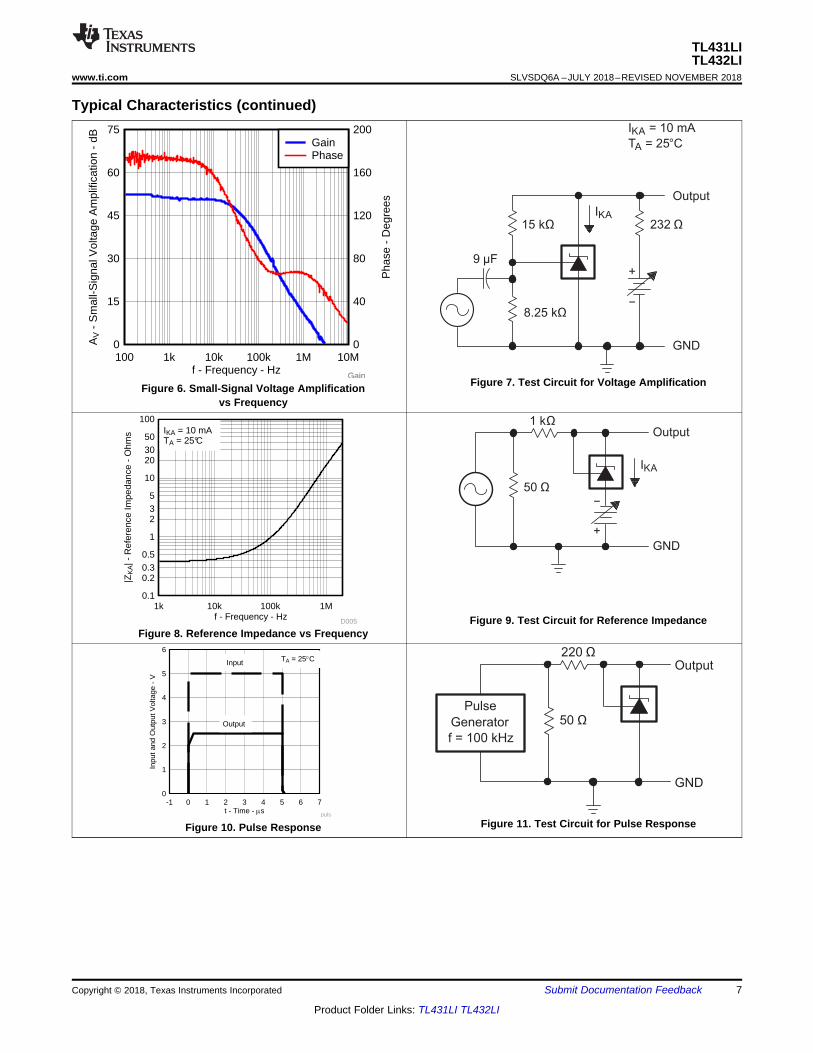
Typical Characteristics (continued)
Figure 6. Small-Signal Voltage Amplificationvs Frequency
Figure 7. Test Circuit for Voltage Amplification
Figure 8. Reference Impedance vs FrequencyFigure 9. Test Circuit for Reference Impedance
Figure 10. Pulse Response Figure 11. Test Circuit for Pulse Response
150 Ω
IKA
R1 = 10 kΩ
R2
CL
VBATT
IKA
CLVBATT
150 Ω
TEST CIRCUIT FOR CURVE A
TEST CIRCUIT FOR CURVES B, C, AND D
+
−
+
−
CL - Load Capacitance - µF
I KA -
Cat
hode
Cur
rent
- m
A
0
3
6
9
12
15
0.001 0.01 0.1 1 10
Stable Region
CopyTL43TL43
A VKA = VrefB VKA = 5 VC VKA = 10 V
8
TL431LITL432LISLVSDQ6A –JULY 2018–REVISED NOVEMBER 2018 www.ti.com
Product Folder Links: TL431LI TL432LI
Submit Documentation Feedback Copyright © 2018, Texas Instruments Incorporated
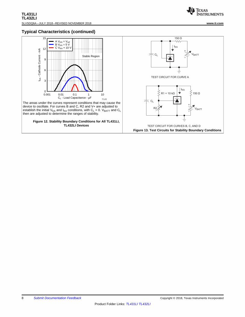
Typical Characteristics (continued)
The areas under the curves represent conditions that may cause thedevice to oscillate. For curves B and C, R2 and V+ are adjusted toestablish the initial VKA and IKA conditions, with CL = 0. VBATT and CLthen are adjusted to determine the ranges of stability.
Figure 12. Stability Boundary Conditions for All TL431LI,TL432LI Devices
Figure 13. Test Circuits for Stability Boundary Conditions
Ioff
VKAInput
Iref
IKA
VKAInput
Vref
R1
R2KA ref ref
R1V = V 1 + + I × R1
R2
æ öç ÷è ø
Vref
Input VKA
IKA
9
TL431LITL432LI
www.ti.com SLVSDQ6A –JULY 2018–REVISED NOVEMBER 2018
Product Folder Links: TL431LI TL432LI
Submit Documentation FeedbackCopyright © 2018, Texas Instruments Incorporated
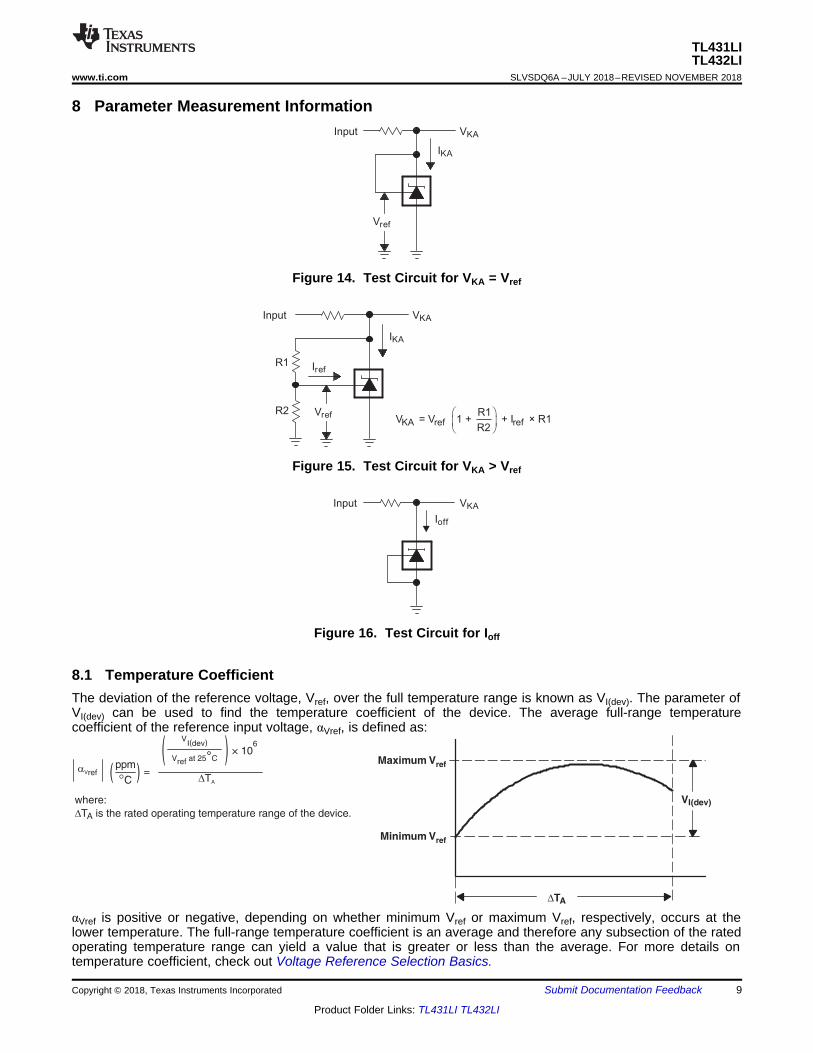
8 Parameter Measurement Information
Figure 14. Test Circuit for VKA = Vref
Figure 15. Test Circuit for VKA > Vref
Figure 16. Test Circuit for Ioff
8.1 Temperature CoefficientThe deviation of the reference voltage, Vref, over the full temperature range is known as VI(dev). The parameter ofVI(dev) can be used to find the temperature coefficient of the device. The average full-range temperaturecoefficient of the reference input voltage, αVref, is defined as:
αVref is positive or negative, depending on whether minimum Vref or maximum Vref, respectively, occurs at thelower temperature. The full-range temperature coefficient is an average and therefore any subsection of the ratedoperating temperature range can yield a value that is greater or less than the average. For more details ontemperature coefficient, check out Voltage Reference Selection Basics.
Ps
0 VKA (V)
I KA (
mA
)
Itest
IKA(min)
IKA
P/
KAR1
Z 1R2
§ ·¨ ¸
© ¹
Vz'
I'
'
KAKA
KA
VZ
I'
'
10
TL431LITL432LISLVSDQ6A –JULY 2018–REVISED NOVEMBER 2018 www.ti.com
Product Folder Links: TL431LI TL432LI
Submit Documentation Feedback Copyright © 2018, Texas Instruments Incorporated
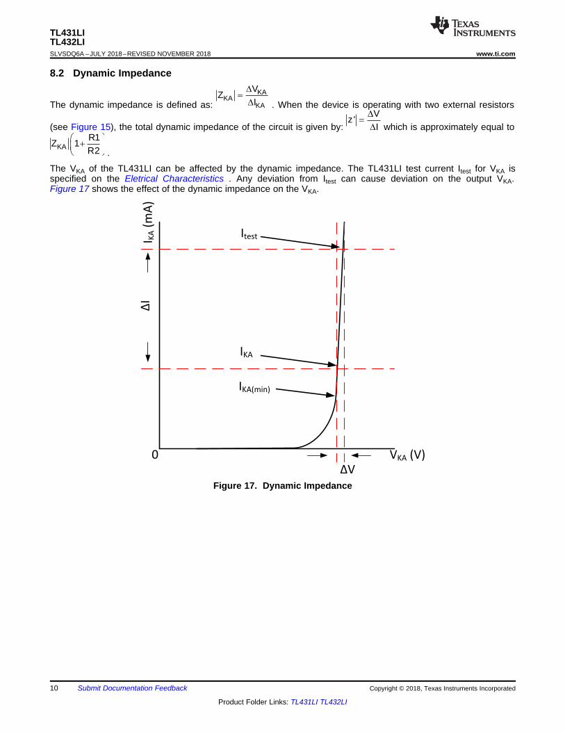
8.2 Dynamic Impedance
The dynamic impedance is defined as: . When the device is operating with two external resistors
(see Figure 15), the total dynamic impedance of the circuit is given by: which is approximately equal to
.
The VKA of the TL431LI can be affected by the dynamic impedance. The TL431LI test current Itest for VKA isspecified on the Eletrical Characteristics . Any deviation from Itest can cause deviation on the output VKA.Figure 17 shows the effect of the dynamic impedance on the VKA.
Figure 17. Dynamic Impedance
CATHODE
REF
ANODE
CATHODE
REF
ANODE
+
_
Vref
11
TL431LITL432LI
www.ti.com SLVSDQ6A –JULY 2018–REVISED NOVEMBER 2018
Product Folder Links: TL431LI TL432LI
Submit Documentation FeedbackCopyright © 2018, Texas Instruments Incorporated
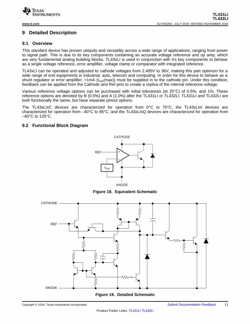
9 Detailed Description
9.1 OverviewThis standard device has proven ubiquity and versatility across a wide range of applications, ranging from powerto signal path. This is due to its key components containing an accurate voltage reference and op amp, whichare very fundamental analog building blocks. TL43xLI is used in conjunction with it's key components to behaveas a single voltage reference, error amplifier, voltage clamp or comparator with integrated reference.
TL43xLI can be operated and adjusted to cathode voltages from 2.495V to 36V, making this part optimum for awide range of end equipments in industrial, auto, telecom and computing. In order for this device to behave as ashunt regulator or error amplifier, >1mA (Imin(max)) must be supplied in to the cathode pin. Under this condition,feedback can be applied from the Cathode and Ref pins to create a replica of the internal reference voltage.
Various reference voltage options can be purchased with initial tolerances (at 25°C) of 0.5%, and 1%. Thesereference options are denoted by B (0.5%) and A (1.0%) after the TL431LI or TL432LI. TL431LI and TL432LI areboth functionally the same, but have separate pinout options.
The TL43xLIxC devices are characterized for operation from 0°C to 70°C, the TL43xLIxI devices arecharacterized for operation from –40°C to 85°C, and the TL43xLIxQ devices are characterized for operation from–40°C to 125°C.
9.2 Functional Block Diagram
Figure 18. Equivalent Schematic
Figure 19. Detailed Schematic
12
TL431LITL432LISLVSDQ6A –JULY 2018–REVISED NOVEMBER 2018 www.ti.com
Product Folder Links: TL431LI TL432LI
Submit Documentation Feedback Copyright © 2018, Texas Instruments Incorporated
9.3 Feature DescriptionTL43xLI consists of an internal reference and amplifier that outputs a sink current based on the differencebetween the reference pin and the virtual internal pin. The sink current is produced by the internal Darlingtonpair, shown in the above schematic (Figure 19). A Darlington pair is used in order for this device to be able tosink a maximum current of 15 mA.
When operated with enough voltage headroom (≥ 2.495 V) and cathode current (IKA), TL43xLI forces thereference pin to 2.495 V. However, the reference pin can not be left floating, as it needs IREF ≥ 0.4 µA (pleasesee Specifications). This is because the reference pin is driven into an npn, which needs base current in orderoperate properly.
When feedback is applied from the Cathode and Reference pins, TL43xLI behaves as a Zener diode, regulatingto a constant voltage dependent on current being supplied into the cathode. This is due to the internal amplifierand reference entering the proper operating regions. The same amount of current needed in the above feedbacksituation must be applied to this device in open loop, servo or error amplifying implementations in order for it tobe in the proper linear region giving TL43xLI enough gain.
Unlike many linear regulators, TL43xLI is internally compensated to be stable without an output capacitorbetween the cathode and anode. However, if it is desired to use an output capacitor Figure 12 can be used as aguide to assist in choosing the correct capacitor to maintain stability.
9.4 Device Functional Modes
9.4.1 Open Loop (Comparator)When the cathode/output voltage or current of TL43xLI is not being fed back to the reference/input pin in anyform, this device is operating in open loop. With proper cathode current (Ika) applied to this device, TL43xLI willhave the characteristics shown in Figure 18. With such high gain in this configuration, TL43xLI is typically usedas a comparator. With the reference integrated makes TL43xLI the preferred choice when users are trying tomonitor a certain level of a single signal. Look at SLVA987 for more details on open loop comparator applicationson the TL431LI.
9.4.2 Closed LoopWhen the cathode/output voltage or current of TL43xLI is being fed back to the reference/input pin in any form,this device is operating in closed loop. The majority of applications involving TL43xLI use it in this manner toregulate a fixed voltage or current. The feedback enables this device to behave as an error amplifier, computinga portion of the output voltage and adjusting it to maintain the desired regulation. This is done by relating theoutput voltage back to the reference pin in a manner to make it equal to the internal reference voltage, which canbe accomplished through resistive or direct feedback.
+
2.5V
CATHODE
ANODE
REFVIN
Vout
Vsup
Rsup
R1
R2
VL
RIN
13
TL431LITL432LI
www.ti.com SLVSDQ6A –JULY 2018–REVISED NOVEMBER 2018
Product Folder Links: TL431LI TL432LI
Submit Documentation FeedbackCopyright © 2018, Texas Instruments Incorporated
10 Applications and Implementation
NOTEInformation in the following applications sections is not part of the TI componentspecification, and TI does not warrant its accuracy or completeness. TI’s customers areresponsible for determining suitability of components for their purposes. Customers shouldvalidate and test their design implementation to confirm system functionality.
10.1 Application InformationAs this device has many applications and setups, there are many situations that this datasheet can notcharacterize in detail. The linked application notes help the designer make the best choices when using this part.
Application note Designing with the Improved TL431LI, SNOAA00 provides a deeper understanding of thisdevice's accuracy in a flyback optocoupler application. Application note Setting the Shunt Voltage on anAdjustable Shunt Regulator, SLVA445 assists designers in setting the shunt voltage to achieve optimumaccuracy for this device.
10.2 Typical Applications
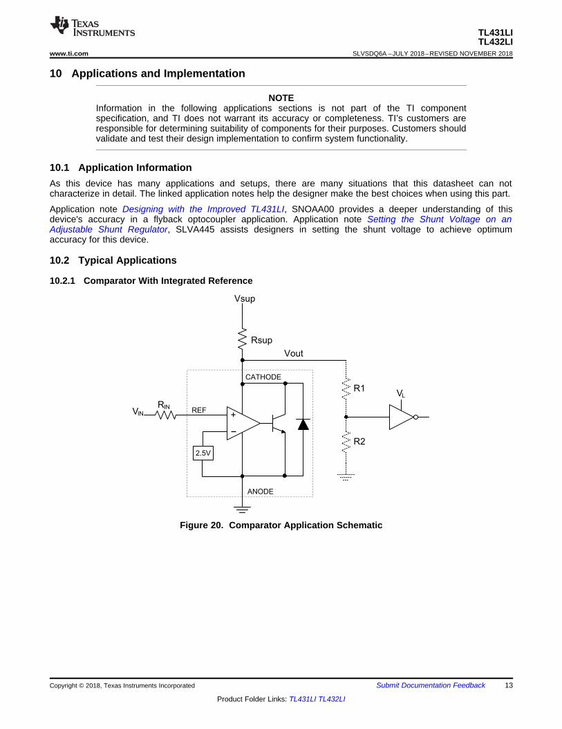
10.2.1 Comparator With Integrated Reference
Figure 20. Comparator Application Schematic
14
TL431LITL432LISLVSDQ6A –JULY 2018–REVISED NOVEMBER 2018 www.ti.com
Product Folder Links: TL431LI TL432LI
Submit Documentation Feedback Copyright © 2018, Texas Instruments Incorporated
Typical Applications (continued)10.2.1.1 Design RequirementsFor this design example, use the parameters listed in Table 1 as the input parameters.
Table 1. Design ParametersDESIGN PARAMETER EXAMPLE VALUE
Input Voltage Range 0 V to 5 VInput Resistance 10 kΩSupply Voltage 24 V
Cathode Current (Ik) 5 mAOutput Voltage Level ~2 V – VSUP
Logic Input Thresholds VIH/VIL VL
10.2.1.2 Detailed Design ProcedureWhen using TL43xLI as a comparator with reference, determine the following:• Input Voltage Range• Reference Voltage Accuracy• Output logic input high and low level thresholds• Current Source resistance
10.2.1.2.1 Basic Operation
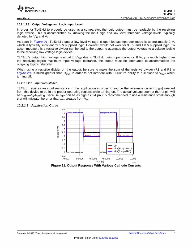
In the configuration shown in Figure 20 TL43xLI will behave as a comparator, comparing the VREF pin voltage tothe internal virtual reference voltage. When provided a proper cathode current (IK), TL43xLI will have enoughopen loop gain to provide a quick response. This can be seen in Figure 21, where the RSUP=10 kΩ (IKA=500 µA)situation responds much slower than RSUP=1 kΩ (IKA=5 mA). With the TL43xLI max Operating Current (IMIN)being 1 mA, operation below that could result in low gain, leading to a slow response.
10.2.1.2.1.1 Overdrive
Slow or inaccurate responses can also occur when the reference pin is not provided enough overdrive voltage.This is the amount of voltage that is higher than the internal virtual reference. The internal virtual referencevoltage will be within the range of 2.495 V ±(0.5% or 1.0%) depending on which version is being used. The moreoverdrive voltage provided, the faster the TL43xLI will respond.
For applications where TL43xLI is being used as a comparator, it is best to set the trip point to greater than thepositive expected error (that is +1.0% for the A version). For fast response, setting the trip point to >10% of theinternal VREF should suffice.
For minimal voltage drop or difference from Vin to the ref pin, TI recommends to use an input resistor <10 kΩ toprovide Iref.
Time (s)
Vol
tage
(V
)
-0.001 -0.0006 -0.0002 0.0002 0.0006 0.001-0.5
0
0.5
1
1.5
2
2.5
3
3.5
4
4.5
5
5.5
D001
VinVka(Rsup=10k:)Vka(Rsup=1k:)
15
TL431LITL432LI
www.ti.com SLVSDQ6A –JULY 2018–REVISED NOVEMBER 2018
Product Folder Links: TL431LI TL432LI
Submit Documentation FeedbackCopyright © 2018, Texas Instruments Incorporated
10.2.1.2.2 Output Voltage and Logic Input Level
In order for TL43xLI to properly be used as a comparator, the logic output must be readable by the receivinglogic device. This is accomplished by knowing the input high and low level threshold voltage levels, typicallydenoted by VIH and VIL.
As seen in Figure 21, TL43xLI's output low level voltage in open-loop/comparator mode is approximately 2 V,which is typically sufficient for 5 V supplied logic. However, would not work for 3.3 V and 1.8 V supplied logic. Toaccommodate this a resistive divider can be tied to the output to attenuate the output voltage to a voltage legibleto the receiving low voltage logic device.
TL43xLI's output high voltage is equal to VSUP due to TL43xLI being open-collector. If VSUP is much higher thanthe receiving logic's maximum input voltage tolerance, the output must be attenuated to accommodate theoutgoing logic's reliability.
When using a resistive divider on the output, be sure to make the sum of the resistive divider (R1 and R2 inFigure 20) is much greater than RSUP in order to not interfere with TL43xLI's ability to pull close to VSUP whenturning off.
10.2.1.2.2.1 Input Resistance
TL43xLI requires an input resistance in this application in order to source the reference current (IREF) neededfrom this device to be in the proper operating regions while turning on. The actual voltage seen at the ref pin willbe VREF=VIN-IREFRIN. Because IREF can be as high as 0.4 µA it is recommended to use a resistance small enoughthat will mitigate the error that IREF creates from VIN.
10.2.1.3 Application Curve
Figure 21. Output Response With Various Cathode Currents
TL43xLIx
RS
0.1%
IO
VI(BATT)
IO
Vref
RS=
Copyright © 2017, Texas Instruments Incorporated
16
TL431LITL432LISLVSDQ6A –JULY 2018–REVISED NOVEMBER 2018 www.ti.com
Product Folder Links: TL431LI TL432LI
Submit Documentation Feedback Copyright © 2018, Texas Instruments Incorporated
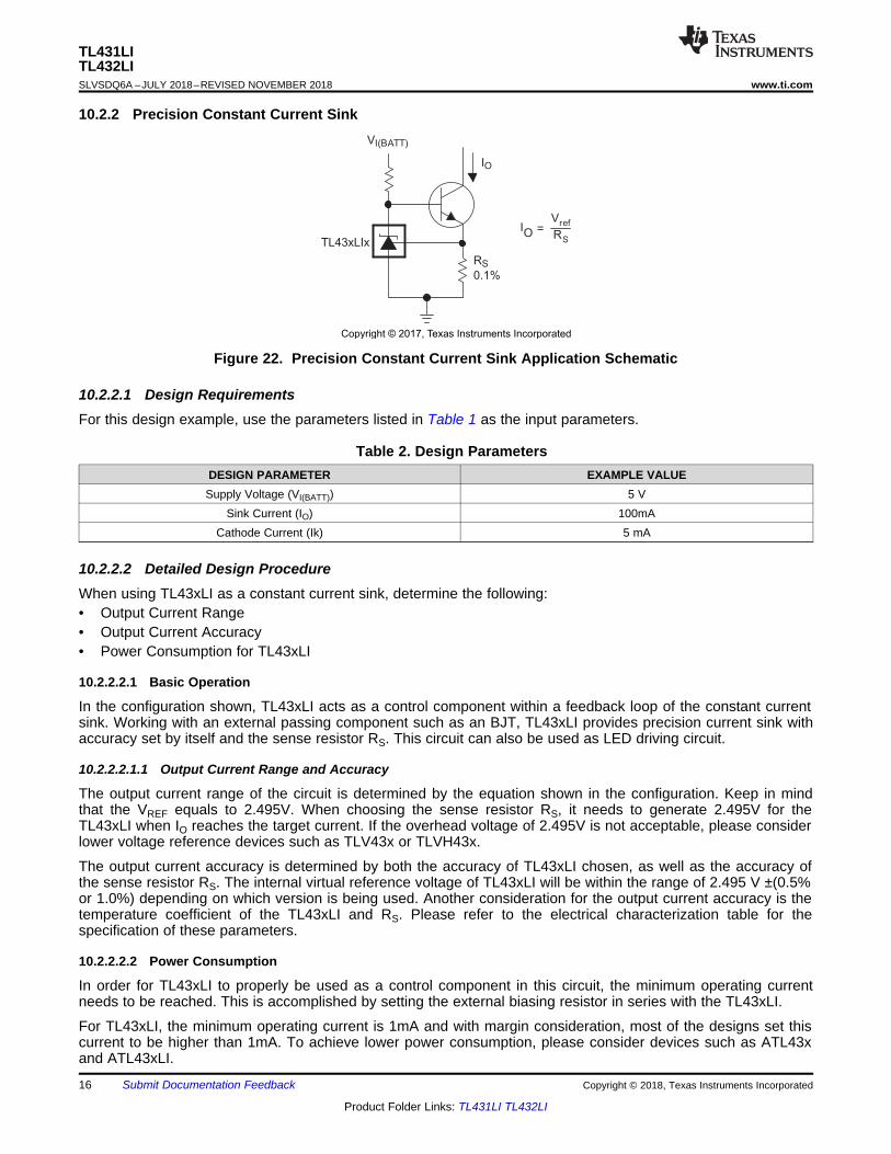
10.2.2 Precision Constant Current Sink
Figure 22. Precision Constant Current Sink Application Schematic
10.2.2.1 Design RequirementsFor this design example, use the parameters listed in Table 1 as the input parameters.
Table 2. Design ParametersDESIGN PARAMETER EXAMPLE VALUESupply Voltage (VI(BATT)) 5 V
Sink Current (IO) 100mACathode Current (Ik) 5 mA
10.2.2.2 Detailed Design ProcedureWhen using TL43xLI as a constant current sink, determine the following:• Output Current Range• Output Current Accuracy• Power Consumption for TL43xLI
10.2.2.2.1 Basic Operation
In the configuration shown, TL43xLI acts as a control component within a feedback loop of the constant currentsink. Working with an external passing component such as an BJT, TL43xLI provides precision current sink withaccuracy set by itself and the sense resistor RS. This circuit can also be used as LED driving circuit.
10.2.2.2.1.1 Output Current Range and Accuracy
The output current range of the circuit is determined by the equation shown in the configuration. Keep in mindthat the VREF equals to 2.495V. When choosing the sense resistor RS, it needs to generate 2.495V for theTL43xLI when IO reaches the target current. If the overhead voltage of 2.495V is not acceptable, please considerlower voltage reference devices such as TLV43x or TLVH43x.
The output current accuracy is determined by both the accuracy of TL43xLI chosen, as well as the accuracy ofthe sense resistor RS. The internal virtual reference voltage of TL43xLI will be within the range of 2.495 V ±(0.5%or 1.0%) depending on which version is being used. Another consideration for the output current accuracy is thetemperature coefficient of the TL43xLI and RS. Please refer to the electrical characterization table for thespecification of these parameters.
10.2.2.2.2 Power Consumption
In order for TL43xLI to properly be used as a control component in this circuit, the minimum operating currentneeds to be reached. This is accomplished by setting the external biasing resistor in series with the TL43xLI.
For TL43xLI, the minimum operating current is 1mA and with margin consideration, most of the designs set thiscurrent to be higher than 1mA. To achieve lower power consumption, please consider devices such as ATL43xand ATL43xLI.
REF
CATHODE
ANODE
R2
VSUP
RSUP
R1
VO (R1
Vref
0.1%
R2
0.1%
TL43xLIx
= 1 + Vref)
CL
Copyright © 2017, Texas Instruments Incorporated
17
TL431LITL432LI
www.ti.com SLVSDQ6A –JULY 2018–REVISED NOVEMBER 2018
Product Folder Links: TL431LI TL432LI
Submit Documentation FeedbackCopyright © 2018, Texas Instruments Incorporated
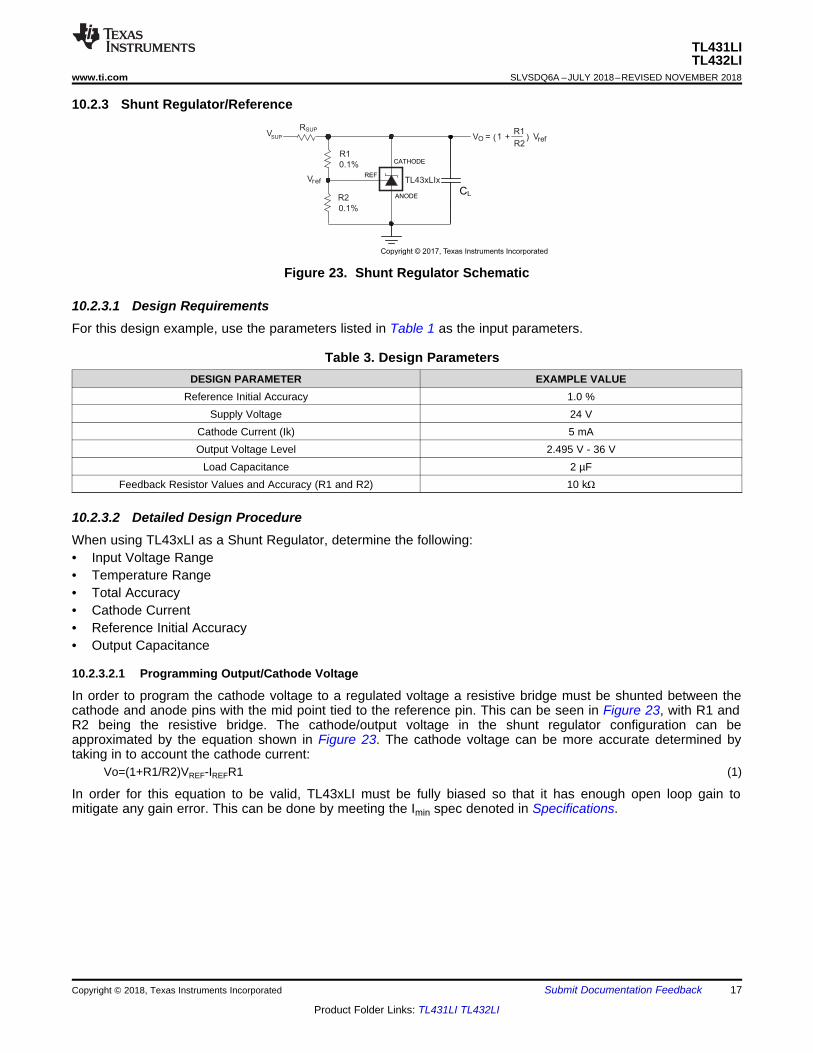
10.2.3 Shunt Regulator/Reference
Figure 23. Shunt Regulator Schematic
10.2.3.1 Design RequirementsFor this design example, use the parameters listed in Table 1 as the input parameters.
Table 3. Design ParametersDESIGN PARAMETER EXAMPLE VALUE
Reference Initial Accuracy 1.0 %Supply Voltage 24 V
Cathode Current (Ik) 5 mAOutput Voltage Level 2.495 V - 36 V
Load Capacitance 2 µFFeedback Resistor Values and Accuracy (R1 and R2) 10 kΩ
10.2.3.2 Detailed Design ProcedureWhen using TL43xLI as a Shunt Regulator, determine the following:• Input Voltage Range• Temperature Range• Total Accuracy• Cathode Current• Reference Initial Accuracy• Output Capacitance
10.2.3.2.1 Programming Output/Cathode Voltage
In order to program the cathode voltage to a regulated voltage a resistive bridge must be shunted between thecathode and anode pins with the mid point tied to the reference pin. This can be seen in Figure 23, with R1 andR2 being the resistive bridge. The cathode/output voltage in the shunt regulator configuration can beapproximated by the equation shown in Figure 23. The cathode voltage can be more accurate determined bytaking in to account the cathode current:
Vo=(1+R1/R2)VREF-IREFR1 (1)
In order for this equation to be valid, TL43xLI must be fully biased so that it has enough open loop gain tomitigate any gain error. This can be done by meeting the Imin spec denoted in Specifications.
Time (s)
Vol
tage
(V
)
-5E-6 -3E-6 -1E-6 1E-6 3E-6 5E-6-6
-3
0
3
6
9
12
15
18
21
24
27
D001
VsupVka=VrefR1=10k: & R2=10k:R1=38k: & R2=10k:
18
TL431LITL432LISLVSDQ6A –JULY 2018–REVISED NOVEMBER 2018 www.ti.com
Product Folder Links: TL431LI TL432LI
Submit Documentation Feedback Copyright © 2018, Texas Instruments Incorporated
10.2.3.2.2 Total Accuracy
When programming the output above unity gain (VKA=VREF), TL43xLI is susceptible to other errors that mayeffect the overall accuracy beyond VREF. These errors include:
• R1 and R2 accuracies• VI(dev) - Change in reference voltage over temperature• ΔVREF / ΔVKA - Change in reference voltage to the change in cathode voltage• |zKA| - Dynamic impedance, causing a change in cathode voltage with cathode current
Worst case cathode voltage can be determined taking all of the variables in to account. Application note Settingthe Shunt Voltage on an Adjustable Shunt Regulator, SLVA445 assists designers in setting the shunt voltage toachieve optimum accuracy for this device.
10.2.3.2.3 Stability
Though TL43xLI is stable with no capacitive load, the device that receives the shunt regulator's output voltagecould present a capacitive load that is within the TL43xLI region of stability, shown in Figure 12. Also, designersmay use capacitive loads to improve the transient response or for power supply decoupling. When usingadditional capacitance between Cathode and Anode, refer to Figure 12. Also, application note UnderstandingStability Boundary Conditions Charts in TL431, TL432 Data Sheet, SLVA482 provides a deeper understanding ofthis devices stability characteristics and aid the user in making the right choices when choosing a load capacitor.
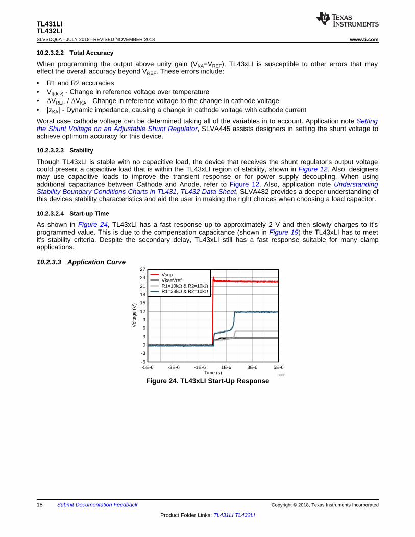
10.2.3.2.4 Start-up Time
As shown in Figure 24, TL43xLI has a fast response up to approximately 2 V and then slowly charges to it'sprogrammed value. This is due to the compensation capacitance (shown in Figure 19) the TL43xLI has to meetit's stability criteria. Despite the secondary delay, TL43xLI still has a fast response suitable for many clampapplications.
10.2.3.3 Application Curve
Figure 24. TL43xLI Start-Up Response
TL431LIBI
R1 = 40.2 lQ
R2 = 8.06 lQ
Rs
IREF
Copyright © 2017, Texas Instruments Incorporated
VOUT
Error|Iref
Error|Vref
UCC28740
PWM Controller
VIN AC
TL431LI
VOUT
VDD
VS
FB
HV
DRV
CS
GND
VDD
VSC
TBLK
VPC
DRV
UCC24636
SR Controller
Copyright © 2018, Texas Instruments Incorporated
19
TL431LITL432LI
www.ti.com SLVSDQ6A –JULY 2018–REVISED NOVEMBER 2018
Product Folder Links: TL431LI TL432LI
Submit Documentation FeedbackCopyright © 2018, Texas Instruments Incorporated
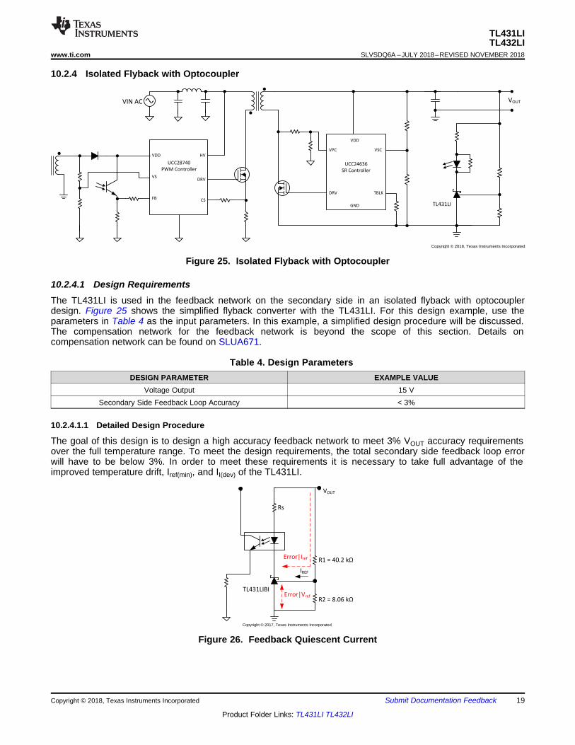
10.2.4 Isolated Flyback with Optocoupler
Figure 25. Isolated Flyback with Optocoupler
10.2.4.1 Design RequirementsThe TL431LI is used in the feedback network on the secondary side in an isolated flyback with optocouplerdesign. Figure 25 shows the simplified flyback converter with the TL431LI. For this design example, use theparameters in Table 4 as the input parameters. In this example, a simplified design procedure will be discussed.The compensation network for the feedback network is beyond the scope of this section. Details oncompensation network can be found on SLUA671.
Table 4. Design ParametersDESIGN PARAMETER EXAMPLE VALUE
Voltage Output 15 VSecondary Side Feedback Loop Accuracy < 3%
10.2.4.1.1 Detailed Design Procedure
The goal of this design is to design a high accuracy feedback network to meet 3% VOUT accuracy requirementsover the full temperature range. To meet the design requirements, the total secondary side feedback loop errorwill have to be below 3%. In order to meet these requirements it is necessary to take full advantage of theimproved temperature drift, Iref(min), and II(dev) of the TL431LI.
Figure 26. Feedback Quiescent Current
OUT Iref ref Vref ref I(dev)
OUT Iref
OUT
R1V (Error | ) V (Error | ) (1 ) R1 (I I )
R240.2k (1 0.5%)
V (Error | ) (2.495 V (1 0.5%) 0.017 V) (1 )8.06k (1 0.5%)
40.2k (1 0.5%) (0.4 A 0.3 A)
V 15.270 V
u u
:u u u
:u
:u u P P
ref Vref ref I(dev)
ref Vref
ref Vref
V (Error | ) V (1 Initial Accuracy) V ...
V (Error | ) 2.495 V (1 0.5%) 17mV ...
V (Error | ) 2.524 V
u
u
|
OUT ref ref
OUT
OUT
R1V V (1 ) R1 (I )
R240.2k
V (2.495 V) (1 ) 40.2k (0.4 A)8.06k
V 14.955 V
u u
: u :u P
:
20
TL431LITL432LISLVSDQ6A –JULY 2018–REVISED NOVEMBER 2018 www.ti.com
Product Folder Links: TL431LI TL432LI
Submit Documentation Feedback Copyright © 2018, Texas Instruments Incorporated
10.2.4.1.1.1 TL431 Feedback Loop Error Calculation
Figure 26 shows the simplified version of the feedback network. The accuracy of the output voltage is dependenton the regulation voltage accuracy of the TL431LI. A simplified VOUT can be seen in Equation 2 but this equationdoes not include errors that will deviate the output.
(2)
The primary sources of error are the Error|Vref and Error|Iref. The Error|Vref primarily consists of the errors thataffect the internal bandgap voltage reference of the TL431LI. This consists of errors from the initial accuracy,temperature drift, ratio of change in reference voltage to the change in cathode voltage, and dynamic impedance.The benefit of the TL431LI is its low temperature drift, VI(dev), which allows the Vref to be more accurate acrossthe full temperature range compared to typical TL431LI devices. Equation 3 shows a simplified worst case Vrefwith initial accuracy and temperature drift.
(3)
The Error|Iref in Figure 26 is dependent on the Iref and II(dev) along with R1. The TL431LI has improved Iref andII(dev) which allows the values of the resistor R1 to be increased to save power. Typically optocoupler feedbackdesign requires the Iref to be taken into account when doing VOUT calculations but the error comes from thedeviation from the maximum to typical value of Iref. In addition to this, the II(dev) is the temperature deviation onthe Iref current which will affect the overall reference current into the TL431LI. Equation 4 shows the VOUT of theTL431LI for Figure 26 which includes the improved Iref and II(dev). The VOUT equation assumes that the resistorsR1 and R2 have a 0.5% accuracy tolerance.
(4)
Comparing the calculated VOUT without and without error the expected worst case max error is 2.1% which meetsthe 3% error target.
VO
TL43xLIx
VI(BATT)
R1
R2
VO
1 R1R2
Vref= +( (
Copyright © 2017, Texas Instruments Incorporated
VO
TL43xLIx
VI(BATT)
uA7805
INOUT
Common R1
R2
VO
1 R1R2
Vref
Minimum VO
Vref 5 V
= +
= +
( (
Copyright © 2017, Texas Instruments Incorporated
R
(see Note A)
VOTL43xLIx
VI(BATT)
2N222
2N222
4.7 kΩ
R1
0.1%R2
0.1%
0.01 µF
30 Ω
O refR1
V = 1 + VR2
æ öç ÷è ø
Copyright © 2017, Texas Instruments Incorporated
21
TL431LITL432LI
www.ti.com SLVSDQ6A –JULY 2018–REVISED NOVEMBER 2018
Product Folder Links: TL431LI TL432LI
Submit Documentation FeedbackCopyright © 2018, Texas Instruments Incorporated
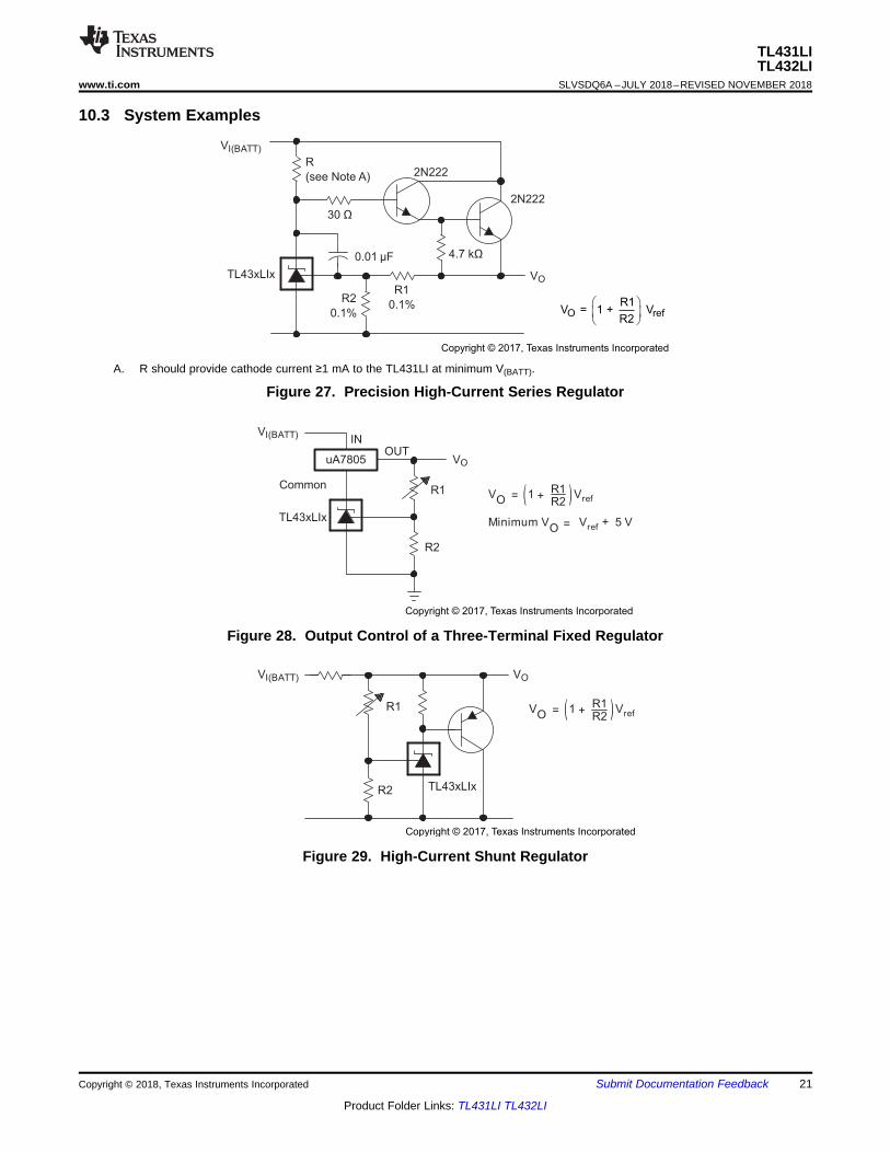
10.3 System Examples
A. R should provide cathode current ≥1 mA to the TL431LI at minimum V(BATT).
Figure 27. Precision High-Current Series Regulator
Figure 28. Output Control of a Three-Terminal Fixed Regulator
Figure 29. High-Current Shunt Regulator
VO ≈5 V
TL43xLIx
VI(BATT)
27.4 kΩ
0.1%
Rb
(see Note A)
27.4 kΩ
0.1%
Copyright © 2017, Texas Instruments Incorporated
VO ≈5 V, 1.5 A
TL43xLIx
VI(BATT) LM317IN OUT
Adjust243 Ω
0.1%
243 Ω
0.1%
8.2 kΩ
Copyright © 2017, Texas Instruments Incorporated
VO
TL43xLIx
VI(BATT)
R1
R2
C
(see Note A)
Copyright © 2017, Texas Instruments Incorporated
22
TL431LITL432LISLVSDQ6A –JULY 2018–REVISED NOVEMBER 2018 www.ti.com
Product Folder Links: TL431LI TL432LI
Submit Documentation Feedback Copyright © 2018, Texas Instruments Incorporated
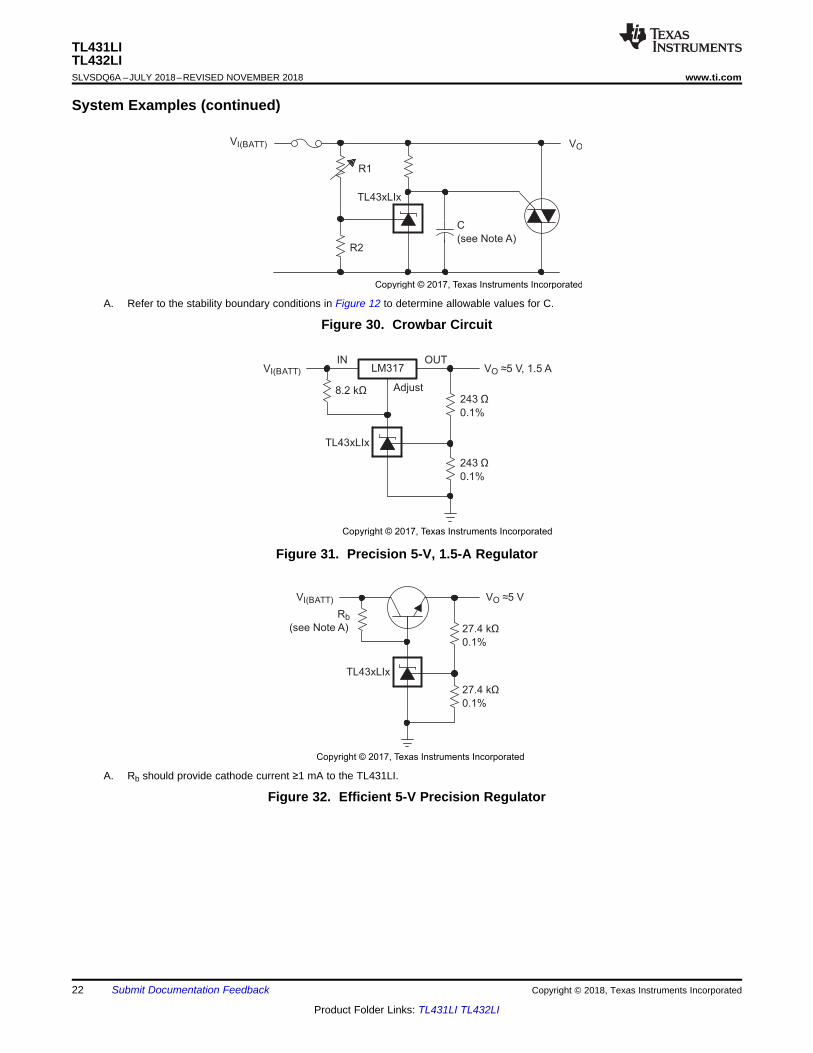
System Examples (continued)
A. Refer to the stability boundary conditions in Figure 12 to determine allowable values for C.
Figure 30. Crowbar Circuit
Figure 31. Precision 5-V, 1.5-A Regulator
A. Rb should provide cathode current ≥1 mA to the TL431LI.
Figure 32. Efficient 5-V Precision Regulator
TL43xLIx
650 Ω
2 kΩ
COn
Off
R
12 V
nref
12 VDelay = R × C × I
12 V – V
æ öç ÷ç ÷è ø
Copyright © 2017, Texas Instruments Incorporated
TL43xLIx
VI(BATT)
R3
(see Note A)
R1AR4
(see Note A)
R2BR2A
R1B
Low Limit = 1 + R1BR2B
Vref
High Limit = 1 + R1AR2A
Vref
LED on When Low Limit < VI(BATT) < High Limit
Copyright © 2017, Texas Instruments Incorporated
TL43xLIx
12 V
VCC
5 V
6.8 kΩ
10 kΩ
10 kΩ
0.1%
10 kΩ
0.1%
X
Not
Used
Feedback
TL598+
−
Copyright © 2017, Texas Instruments Incorporated
23
TL431LITL432LI
www.ti.com SLVSDQ6A –JULY 2018–REVISED NOVEMBER 2018
Product Folder Links: TL431LI TL432LI
Submit Documentation FeedbackCopyright © 2018, Texas Instruments Incorporated
System Examples (continued)
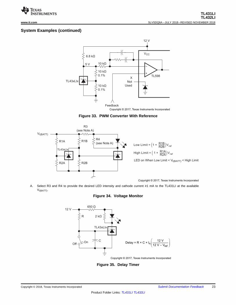
Figure 33. PWM Converter With Reference
A. Select R3 and R4 to provide the desired LED intensity and cathode current ≥1 mA to the TL431LI at the availableVI(BATT).
Figure 34. Voltage Monitor
Figure 35. Delay Timer
TL43xLIx
RS
0.1%
IO
VI(BATT)
IO
Vref
RS=
Copyright © 2017, Texas Instruments Incorporated
TL43xLIx
IORCL
0.1%
R1
VI(BATT) Iout
Vref
RCL
IKA
R1VI(BATT)
IO
hFE
IKA
+
+
=
=
Copyright © 2017, Texas Instruments Incorporated
24
TL431LITL432LISLVSDQ6A –JULY 2018–REVISED NOVEMBER 2018 www.ti.com
Product Folder Links: TL431LI TL432LI
Submit Documentation Feedback Copyright © 2018, Texas Instruments Incorporated
System Examples (continued)
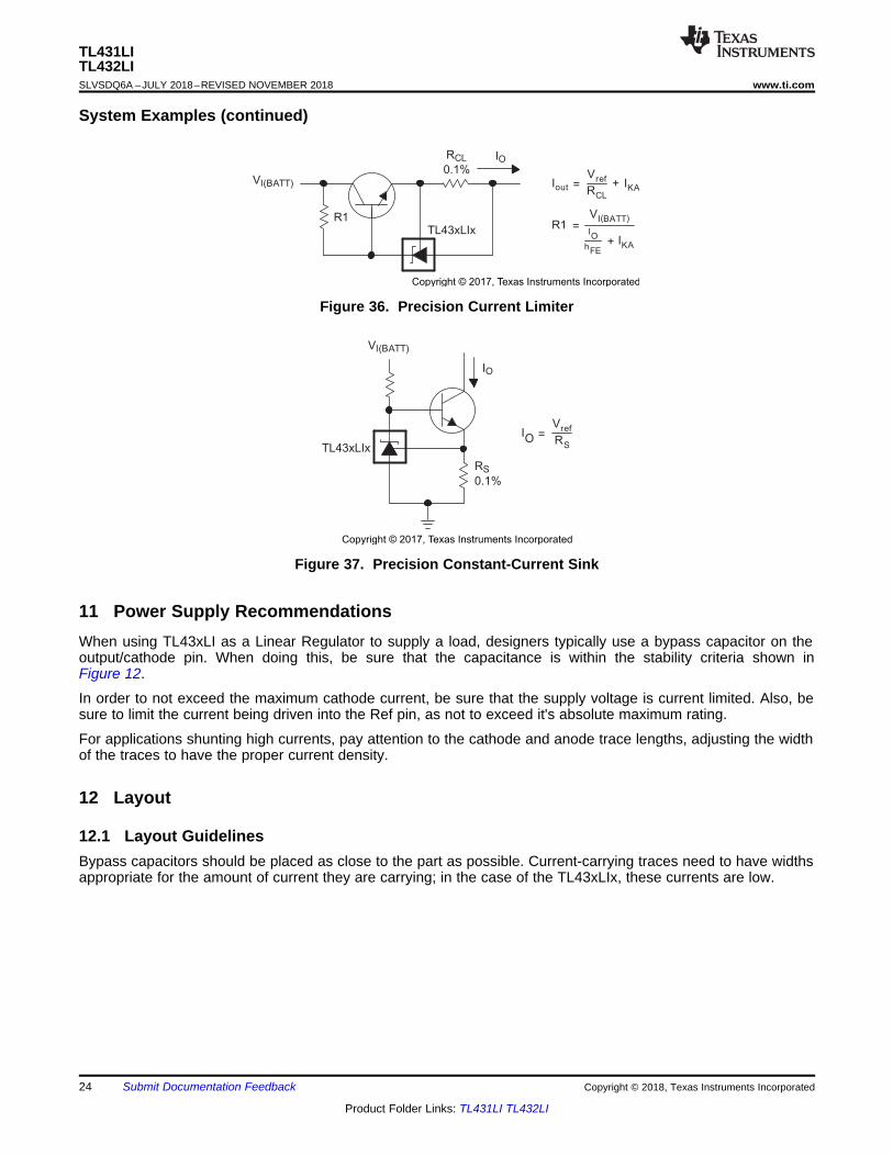
Figure 36. Precision Current Limiter
Figure 37. Precision Constant-Current Sink
11 Power Supply RecommendationsWhen using TL43xLI as a Linear Regulator to supply a load, designers typically use a bypass capacitor on theoutput/cathode pin. When doing this, be sure that the capacitance is within the stability criteria shown inFigure 12.
In order to not exceed the maximum cathode current, be sure that the supply voltage is current limited. Also, besure to limit the current being driven into the Ref pin, as not to exceed it's absolute maximum rating.
For applications shunting high currents, pay attention to the cathode and anode trace lengths, adjusting the widthof the traces to have the proper current density.
12 Layout
12.1 Layout GuidelinesBypass capacitors should be placed as close to the part as possible. Current-carrying traces need to have widthsappropriate for the amount of current they are carrying; in the case of the TL43xLIx, these currents are low.
TL43xLIx - DBZ
(TOP VIEW)
REF
1
CATHODE
2
3ANODE
Rsup
Rref
Vsup
CL
Vin
GND
GND
Copyright © 2017, Texas Instruments Incorporated
25
TL431LITL432LI
www.ti.com SLVSDQ6A –JULY 2018–REVISED NOVEMBER 2018
Product Folder Links: TL431LI TL432LI
Submit Documentation FeedbackCopyright © 2018, Texas Instruments Incorporated
12.2 Layout Example
Figure 38. DBZ Layout example
TL431LI X X XXX X
Product
Operating Free-Air
Temperature
Package
Type
Package
Quantity
Initial
Accuracy1: TL431LI
2: TL432LI*
B: 0.5%
A: 1%
DBZ: SOT-23-3C: 0°C to 70°C
I: -40°C to 85°C
Q: -40°C to 125°C
R: Tape & Reel
*(Cathode and REF
pins are switched)
26
TL431LITL432LISLVSDQ6A –JULY 2018–REVISED NOVEMBER 2018 www.ti.com
Product Folder Links: TL431LI TL432LI
Submit Documentation Feedback Copyright © 2018, Texas Instruments Incorporated
13 Device and Documentation Support
13.1 Related LinksThe table below lists quick access links. Categories include technical documents, support and communityresources, tools and software, and quick access to order now.
Table 5. Related Links
PARTS PRODUCT FOLDER ORDER NOW TECHNICALDOCUMENTS
TOOLS &SOFTWARE
SUPPORT &COMMUNITY
TL431LI Click here Click here Click here Click here Click hereTL432LI Click here Click here Click here Click here Click here
13.2 Documentation Support
13.2.1 Device NomenclatureTI assigns suffixes and prefixes to differentiate all the combinations of the TL43xLI family. More details andpossible orderable combinations are located in the Package Option Addendum.
13.2.2 Related DocumentationFor related documentation see the following:• Understanding Stability Boundary Conditions Charts in TL431, TL432 Data Sheet, SLVA482• Setting the Shunt Voltage on an Adjustable Shunt Regulator, SLVA445• Designing With the Improved TL431LI, SNOAA00
13.3 Receiving Notification of Documentation UpdatesTo receive notification of documentation updates, navigate to the device product folder on ti.com. In the upperright corner, click on Alert me to register and receive a weekly digest of any product information that haschanged. For change details, review the revision history included in any revised document.
13.4 Community ResourcesThe following links connect to TI community resources. Linked contents are provided "AS IS" by the respectivecontributors. They do not constitute TI specifications and do not necessarily reflect TI's views; see TI's Terms ofUse.
TI E2E™ Online Community TI's Engineer-to-Engineer (E2E) Community. Created to foster collaborationamong engineers. At e2e.ti.com, you can ask questions, share knowledge, explore ideas and helpsolve problems with fellow engineers.
Design Support TI's Design Support Quickly find helpful E2E forums along with design support tools andcontact information for technical support.
27
TL431LITL432LI
www.ti.com SLVSDQ6A –JULY 2018–REVISED NOVEMBER 2018
Product Folder Links: TL431LI TL432LI
Submit Documentation FeedbackCopyright © 2018, Texas Instruments Incorporated
13.5 TrademarksE2E is a trademark of Texas Instruments.
13.6 Electrostatic Discharge CautionThis integrated circuit can be damaged by ESD. Texas Instruments recommends that all integrated circuits be handled withappropriate precautions. Failure to observe proper handling and installation procedures can cause damage.
ESD damage can range from subtle performance degradation to complete device failure. Precision integrated circuits may be moresusceptible to damage because very small parametric changes could cause the device not to meet its published specifications.
13.7 GlossarySLYZ022 — TI Glossary.
This glossary lists and explains terms, acronyms, and definitions.
14 Mechanical, Packaging, and Orderable InformationThe following pages include mechanical, packaging, and orderable information. This information is the mostcurrent data available for the designated devices. This data is subject to change without notice and revision ofthis document. For browser-based versions of this data sheet, refer to the left-hand navigation.
PACKAGE OPTION ADDENDUM
www.ti.com 10-Dec-2020
Addendum-Page 1
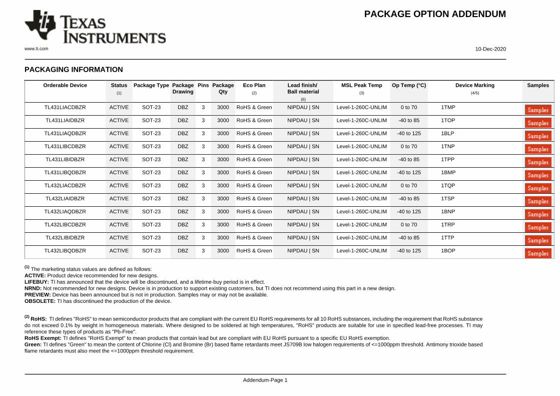
PACKAGING INFORMATION
Orderable Device Status(1)
Package Type PackageDrawing
Pins PackageQty
Eco Plan(2)
Lead finish/Ball material
(6)
MSL Peak Temp(3)
Op Temp (°C) Device Marking(4/5)
Samples
TL431LIACDBZR ACTIVE SOT-23 DBZ 3 3000 RoHS & Green NIPDAU | SN Level-1-260C-UNLIM 0 to 70 1TMP
TL431LIAIDBZR ACTIVE SOT-23 DBZ 3 3000 RoHS & Green NIPDAU | SN Level-1-260C-UNLIM -40 to 85 1TOP
TL431LIAQDBZR ACTIVE SOT-23 DBZ 3 3000 RoHS & Green NIPDAU | SN Level-1-260C-UNLIM -40 to 125 1BLP
TL431LIBCDBZR ACTIVE SOT-23 DBZ 3 3000 RoHS & Green NIPDAU | SN Level-1-260C-UNLIM 0 to 70 1TNP
TL431LIBIDBZR ACTIVE SOT-23 DBZ 3 3000 RoHS & Green NIPDAU | SN Level-1-260C-UNLIM -40 to 85 1TPP
TL431LIBQDBZR ACTIVE SOT-23 DBZ 3 3000 RoHS & Green NIPDAU | SN Level-1-260C-UNLIM -40 to 125 1BMP
TL432LIACDBZR ACTIVE SOT-23 DBZ 3 3000 RoHS & Green NIPDAU | SN Level-1-260C-UNLIM 0 to 70 1TQP
TL432LIAIDBZR ACTIVE SOT-23 DBZ 3 3000 RoHS & Green NIPDAU | SN Level-1-260C-UNLIM -40 to 85 1TSP
TL432LIAQDBZR ACTIVE SOT-23 DBZ 3 3000 RoHS & Green NIPDAU | SN Level-1-260C-UNLIM -40 to 125 1BNP
TL432LIBCDBZR ACTIVE SOT-23 DBZ 3 3000 RoHS & Green NIPDAU | SN Level-1-260C-UNLIM 0 to 70 1TRP
TL432LIBIDBZR ACTIVE SOT-23 DBZ 3 3000 RoHS & Green NIPDAU | SN Level-1-260C-UNLIM -40 to 85 1TTP
TL432LIBQDBZR ACTIVE SOT-23 DBZ 3 3000 RoHS & Green NIPDAU | SN Level-1-260C-UNLIM -40 to 125 1BOP
(1) The marketing status values are defined as follows:ACTIVE: Product device recommended for new designs.LIFEBUY: TI has announced that the device will be discontinued, and a lifetime-buy period is in effect.NRND: Not recommended for new designs. Device is in production to support existing customers, but TI does not recommend using this part in a new design.PREVIEW: Device has been announced but is not in production. Samples may or may not be available.OBSOLETE: TI has discontinued the production of the device.
(2) RoHS: TI defines "RoHS" to mean semiconductor products that are compliant with the current EU RoHS requirements for all 10 RoHS substances, including the requirement that RoHS substancedo not exceed 0.1% by weight in homogeneous materials. Where designed to be soldered at high temperatures, "RoHS" products are suitable for use in specified lead-free processes. TI mayreference these types of products as "Pb-Free".RoHS Exempt: TI defines "RoHS Exempt" to mean products that contain lead but are compliant with EU RoHS pursuant to a specific EU RoHS exemption.Green: TI defines "Green" to mean the content of Chlorine (Cl) and Bromine (Br) based flame retardants meet JS709B low halogen requirements of <=1000ppm threshold. Antimony trioxide basedflame retardants must also meet the <=1000ppm threshold requirement.
PACKAGE OPTION ADDENDUM
www.ti.com 10-Dec-2020
Addendum-Page 2
(3) MSL, Peak Temp. - The Moisture Sensitivity Level rating according to the JEDEC industry standard classifications, and peak solder temperature.
(4) There may be additional marking, which relates to the logo, the lot trace code information, or the environmental category on the device.
(5) Multiple Device Markings will be inside parentheses. Only one Device Marking contained in parentheses and separated by a "~" will appear on a device. If a line is indented then it is a continuationof the previous line and the two combined represent the entire Device Marking for that device.
(6) Lead finish/Ball material - Orderable Devices may have multiple material finish options. Finish options are separated by a vertical ruled line. Lead finish/Ball material values may wrap to twolines if the finish value exceeds the maximum column width.
Important Information and Disclaimer:The information provided on this page represents TI's knowledge and belief as of the date that it is provided. TI bases its knowledge and belief on informationprovided by third parties, and makes no representation or warranty as to the accuracy of such information. Efforts are underway to better integrate information from third parties. TI has taken andcontinues to take reasonable steps to provide representative and accurate information but may not have conducted destructive testing or chemical analysis on incoming materials and chemicals.TI and TI suppliers consider certain information to be proprietary, and thus CAS numbers and other limited information may not be available for release.
In no event shall TI's liability arising out of such information exceed the total purchase price of the TI part(s) at issue in this document sold by TI to Customer on an annual basis.
OTHER QUALIFIED VERSIONS OF TL431LI, TL432LI :
• Automotive: TL431LI-Q1, TL432LI-Q1
NOTE: Qualified Version Definitions:
• Automotive - Q100 devices qualified for high-reliability automotive applications targeting zero defects
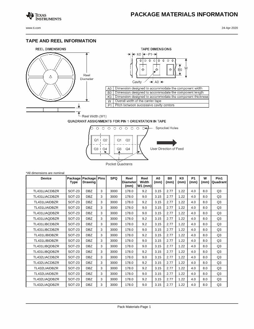
TAPE AND REEL INFORMATION
*All dimensions are nominal
Device PackageType
PackageDrawing
Pins SPQ ReelDiameter
(mm)
ReelWidth
W1 (mm)
A0(mm)
B0(mm)
K0(mm)
P1(mm)
W(mm)
Pin1Quadrant
TL431LIACDBZR SOT-23 DBZ 3 3000 178.0 9.2 3.15 2.77 1.22 4.0 8.0 Q3
TL431LIACDBZR SOT-23 DBZ 3 3000 178.0 9.0 3.15 2.77 1.22 4.0 8.0 Q3
TL431LIAIDBZR SOT-23 DBZ 3 3000 178.0 9.2 3.15 2.77 1.22 4.0 8.0 Q3
TL431LIAIDBZR SOT-23 DBZ 3 3000 178.0 9.0 3.15 2.77 1.22 4.0 8.0 Q3
TL431LIAQDBZR SOT-23 DBZ 3 3000 178.0 9.0 3.15 2.77 1.22 4.0 8.0 Q3
TL431LIAQDBZR SOT-23 DBZ 3 3000 178.0 9.2 3.15 2.77 1.22 4.0 8.0 Q3
TL431LIBCDBZR SOT-23 DBZ 3 3000 178.0 9.2 3.15 2.77 1.22 4.0 8.0 Q3
TL431LIBCDBZR SOT-23 DBZ 3 3000 178.0 9.0 3.15 2.77 1.22 4.0 8.0 Q3
TL431LIBIDBZR SOT-23 DBZ 3 3000 178.0 9.2 3.15 2.77 1.22 4.0 8.0 Q3
TL431LIBIDBZR SOT-23 DBZ 3 3000 178.0 9.0 3.15 2.77 1.22 4.0 8.0 Q3
TL431LIBQDBZR SOT-23 DBZ 3 3000 178.0 9.0 3.15 2.77 1.22 4.0 8.0 Q3
TL431LIBQDBZR SOT-23 DBZ 3 3000 178.0 9.2 3.15 2.77 1.22 4.0 8.0 Q3
TL432LIACDBZR SOT-23 DBZ 3 3000 178.0 9.0 3.15 2.77 1.22 4.0 8.0 Q3
TL432LIACDBZR SOT-23 DBZ 3 3000 178.0 9.2 3.15 2.77 1.22 4.0 8.0 Q3
TL432LIAIDBZR SOT-23 DBZ 3 3000 178.0 9.2 3.15 2.77 1.22 4.0 8.0 Q3
TL432LIAIDBZR SOT-23 DBZ 3 3000 178.0 9.0 3.15 2.77 1.22 4.0 8.0 Q3
TL432LIAQDBZR SOT-23 DBZ 3 3000 178.0 9.2 3.15 2.77 1.22 4.0 8.0 Q3
TL432LIAQDBZR SOT-23 DBZ 3 3000 178.0 9.0 3.15 2.77 1.22 4.0 8.0 Q3
PACKAGE MATERIALS INFORMATION
www.ti.com 24-Apr-2020
Pack Materials-Page 1
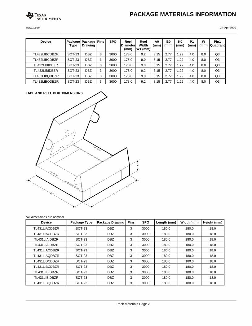
Device PackageType
PackageDrawing
Pins SPQ ReelDiameter
(mm)
ReelWidth
W1 (mm)
A0(mm)
B0(mm)
K0(mm)
P1(mm)
W(mm)
Pin1Quadrant
TL432LIBCDBZR SOT-23 DBZ 3 3000 178.0 9.2 3.15 2.77 1.22 4.0 8.0 Q3
TL432LIBCDBZR SOT-23 DBZ 3 3000 178.0 9.0 3.15 2.77 1.22 4.0 8.0 Q3
TL432LIBIDBZR SOT-23 DBZ 3 3000 178.0 9.0 3.15 2.77 1.22 4.0 8.0 Q3
TL432LIBIDBZR SOT-23 DBZ 3 3000 178.0 9.2 3.15 2.77 1.22 4.0 8.0 Q3
TL432LIBQDBZR SOT-23 DBZ 3 3000 178.0 9.0 3.15 2.77 1.22 4.0 8.0 Q3
TL432LIBQDBZR SOT-23 DBZ 3 3000 178.0 9.2 3.15 2.77 1.22 4.0 8.0 Q3
*All dimensions are nominal
Device Package Type Package Drawing Pins SPQ Length (mm) Width (mm) Height (mm)
TL431LIACDBZR SOT-23 DBZ 3 3000 180.0 180.0 18.0
TL431LIACDBZR SOT-23 DBZ 3 3000 180.0 180.0 18.0
TL431LIAIDBZR SOT-23 DBZ 3 3000 180.0 180.0 18.0
TL431LIAIDBZR SOT-23 DBZ 3 3000 180.0 180.0 18.0
TL431LIAQDBZR SOT-23 DBZ 3 3000 180.0 180.0 18.0
TL431LIAQDBZR SOT-23 DBZ 3 3000 180.0 180.0 18.0
TL431LIBCDBZR SOT-23 DBZ 3 3000 180.0 180.0 18.0
TL431LIBCDBZR SOT-23 DBZ 3 3000 180.0 180.0 18.0
TL431LIBIDBZR SOT-23 DBZ 3 3000 180.0 180.0 18.0
TL431LIBIDBZR SOT-23 DBZ 3 3000 180.0 180.0 18.0
TL431LIBQDBZR SOT-23 DBZ 3 3000 180.0 180.0 18.0
PACKAGE MATERIALS INFORMATION
www.ti.com 24-Apr-2020
Pack Materials-Page 2
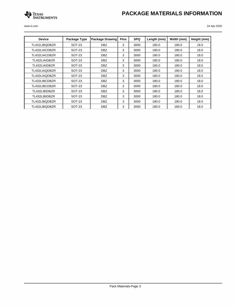
Device Package Type Package Drawing Pins SPQ Length (mm) Width (mm) Height (mm)
TL431LIBQDBZR SOT-23 DBZ 3 3000 180.0 180.0 18.0
TL432LIACDBZR SOT-23 DBZ 3 3000 180.0 180.0 18.0
TL432LIACDBZR SOT-23 DBZ 3 3000 180.0 180.0 18.0
TL432LIAIDBZR SOT-23 DBZ 3 3000 180.0 180.0 18.0
TL432LIAIDBZR SOT-23 DBZ 3 3000 180.0 180.0 18.0
TL432LIAQDBZR SOT-23 DBZ 3 3000 180.0 180.0 18.0
TL432LIAQDBZR SOT-23 DBZ 3 3000 180.0 180.0 18.0
TL432LIBCDBZR SOT-23 DBZ 3 3000 180.0 180.0 18.0
TL432LIBCDBZR SOT-23 DBZ 3 3000 180.0 180.0 18.0
TL432LIBIDBZR SOT-23 DBZ 3 3000 180.0 180.0 18.0
TL432LIBIDBZR SOT-23 DBZ 3 3000 180.0 180.0 18.0
TL432LIBQDBZR SOT-23 DBZ 3 3000 180.0 180.0 18.0
TL432LIBQDBZR SOT-23 DBZ 3 3000 180.0 180.0 18.0
PACKAGE MATERIALS INFORMATION
www.ti.com 24-Apr-2020
Pack Materials-Page 3
4203227/C
www.ti.com
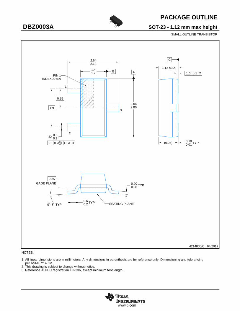
PACKAGE OUTLINE
C
TYP0.200.08
0.25
2.642.10
1.12 MAX
TYP0.100.01
3X 0.50.3
TYP0.60.2
1.9
0.95
TYP-80
A
3.042.80
B1.41.2
(0.95)
SOT-23 - 1.12 mm max heightDBZ0003ASMALL OUTLINE TRANSISTOR
4214838/C 04/2017
NOTES: 1. All linear dimensions are in millimeters. Any dimensions in parenthesis are for reference only. Dimensioning and tolerancing per ASME Y14.5M.2. This drawing is subject to change without notice.3. Reference JEDEC registration TO-236, except minimum foot length.
0.2 C A B
1
3
2
INDEX AREAPIN 1
GAGE PLANE
SEATING PLANE
0.1 C
SCALE 4.000
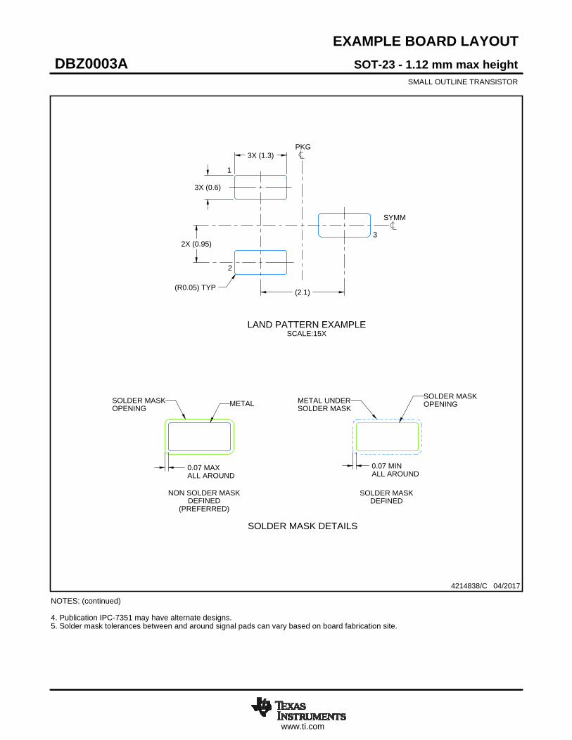
www.ti.com
EXAMPLE BOARD LAYOUT
0.07 MAXALL AROUND
0.07 MINALL AROUND
3X (1.3)
3X (0.6)
(2.1)
2X (0.95)
(R0.05) TYP
4214838/C 04/2017
SOT-23 - 1.12 mm max heightDBZ0003ASMALL OUTLINE TRANSISTOR
NOTES: (continued) 4. Publication IPC-7351 may have alternate designs. 5. Solder mask tolerances between and around signal pads can vary based on board fabrication site.
SYMM
LAND PATTERN EXAMPLESCALE:15X
PKG
1
3
2
SOLDER MASKOPENINGMETAL UNDER
SOLDER MASK
SOLDER MASKDEFINED
METALSOLDER MASKOPENING
NON SOLDER MASKDEFINED
(PREFERRED)
SOLDER MASK DETAILS
www.ti.com
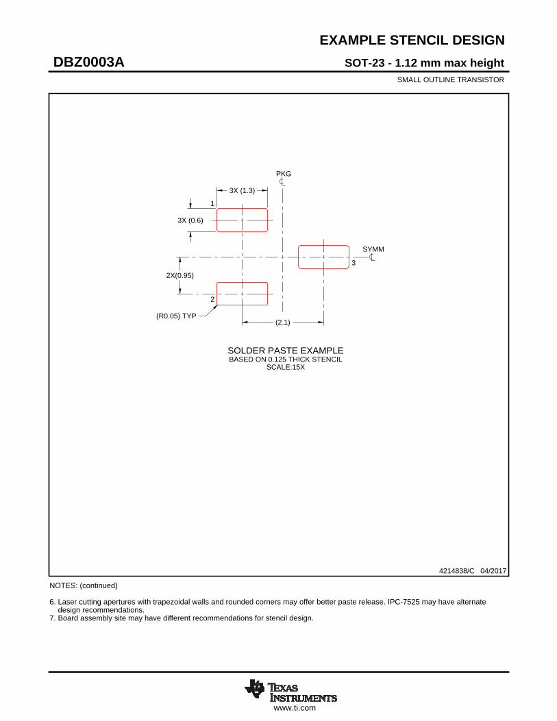
EXAMPLE STENCIL DESIGN
(2.1)
2X(0.95)
3X (1.3)
3X (0.6)
(R0.05) TYP
SOT-23 - 1.12 mm max heightDBZ0003ASMALL OUTLINE TRANSISTOR
4214838/C 04/2017
NOTES: (continued) 6. Laser cutting apertures with trapezoidal walls and rounded corners may offer better paste release. IPC-7525 may have alternate design recommendations. 7. Board assembly site may have different recommendations for stencil design.
SOLDER PASTE EXAMPLEBASED ON 0.125 THICK STENCIL
SCALE:15X
SYMM
PKG
1
3
2
IMPORTANT NOTICE AND DISCLAIMER
TI PROVIDES TECHNICAL AND RELIABILITY DATA (INCLUDING DATASHEETS), DESIGN RESOURCES (INCLUDING REFERENCE DESIGNS), APPLICATION OR OTHER DESIGN ADVICE, WEB TOOLS, SAFETY INFORMATION, AND OTHER RESOURCES “AS IS” AND WITH ALL FAULTS, AND DISCLAIMS ALL WARRANTIES, EXPRESS AND IMPLIED, INCLUDING WITHOUT LIMITATION ANY IMPLIED WARRANTIES OF MERCHANTABILITY, FITNESS FOR A PARTICULAR PURPOSE OR NON-INFRINGEMENT OF THIRD PARTY INTELLECTUAL PROPERTY RIGHTS.These resources are intended for skilled developers designing with TI products. You are solely responsible for (1) selecting the appropriate TI products for your application, (2) designing, validating and testing your application, and (3) ensuring your application meets applicable standards, and any other safety, security, or other requirements. These resources are subject to change without notice. TI grants you permission to use these resources only for development of an application that uses the TI products described in the resource. Other reproduction and display of these resources is prohibited. No license is granted to any other TI intellectual property right or to any third party intellectual property right. TI disclaims responsibility for, and you will fully indemnify TI and its representatives against, any claims, damages, costs, losses, and liabilities arising out of your use of these resources.TI’s products are provided subject to TI’s Terms of Sale (www.ti.com/legal/termsofsale.html) or other applicable terms available either on ti.com or provided in conjunction with such TI products. TI’s provision of these resources does not expand or otherwise alter TI’s applicable warranties or warranty disclaimers for TI products.
Mailing Address: Texas Instruments, Post Office Box 655303, Dallas, Texas 75265Copyright © 2020, Texas Instruments Incorporated


