Embed Size (px)
Citation preview
Toward on-chip X-ray analysis
Eduardo D. Greaves*ac and Andreas Manzbc
Received 14th October 2004, Accepted 7th February 2005
First published as an Advance Article on the web 18th February 2005
DOI: 10.1039/b415836a
The possibility of performing chemical analysis and structure determinations with the use of
X-rays in a microfluidic chip environment is explored. Externally generated radiation,
radioisotope irradiation and on-chip generated X-rays were considered as excitation means for the
performance of sample analysis with the techniques of X-ray fluorescence and diffraction. The
absorption properties of chip-building materials by different radiation sources are reviewed and
data on absorption coefficients calculated, upon which recommendations for optimisations with
the use of various X-ray sources may be made. The capabilities and limitations of on-chip X-ray
analysis are placed in perspective by preliminary experimental results of diffraction, fluorescence
and on-chip X-ray generation experiments.
1. Introduction
Microfluidic chips or micro total analysis systems (mTAS) have
shown powerful advantages of miniaturisation for the perfor-
mance of analytical tasks.1–3 A variety of physico-chemical
phenomena such as synthesis, component separation, detec-
tion and measurement have been adapted to on-chip pro-
cedures, leading to process improvement. Moreover, diverse,
well-established analytical techniques have been used as
sensors or transducers of chip behaviour; however, the power-
ful measurement techniques of X-ray fluorescence (XRF) for
elemental analysis4,5 or of X-ray diffraction6 (XRD) for
structure determination or compound identification have not
been reported for this application. There are three possibilities
which can be envisaged for on-chip X-ray sample excitation. In
the first, an external, conventional X-ray generator could be
used to generate a suitably collimated beam in order to strike a
micro-channel containing the analytes. A second possibility is
to use a radioisotope source incorporated inside the chip for
excitation, and the third one is to generate the excitation
X-rays locally on the chip. Both analytical techniques, XRF
and XRD, could be useful for on-chip analysis. They have in
common the use of X-rays for probing material properties, but
they have very different source characteristics, experimental
geometries and instrumental requirements. An XRF signal
from a microfluidic channel might provide elemental informa-
tion on inorganic solutions or metalloprotein-bearing fluids.
An XRD signal from gaseous or liquid suspensions of
particulate solid samples might provide information for
particle identification, separation or extent of mixing of solid
phases in the mm range of particle sizes. Likewise the
appropriate conditions for protein crystallization might be
detected by a sensitive, real-time, XRD signal ‘‘on-chip’’
instead of the ‘‘post-process’’ detection recently reported.7
The most straightforward technique for sample excitation is
the use of an external X-ray generator.8 The traditional heavy
and bulky X-ray generator requiring an attached cooling water
facility seems to be inadequate for the miniaturisation process
afforded by chip-based processes. However, this seems a
natural forward development and recently reported work
shows the potential of the method.7 Recent advances have
resulted in the availability of very compact X-ray sources.9–11
They rely on several developments: (i) the phase out of the
heavy transformer-based high voltage power supply giving
way to compact switching high voltage power supplies; (ii)
the use of grounded-cathode X-ray tubes which imposes
less stringent requirements on the tube’s power supply; (iii)
advances in the production of low-power tubes, which are air-
cooled; (iv) production of point-source tubes with X-ray spot
sizes in the 50–250 mm range; and (v) the use of poly-capillary
focusing optics or mono-capillary tubes. These developments
have led to the availability of small portable systems,12,13
which are capable of delivering an intense beam of X-rays
confined to a small spot size14,15 of hundreds or tens of mm,
eminently appropriate for use in a mTAS chip.
For the second possibility miniature radioactive sources can
be fashioned with high specific activities in the shape of needles
or ‘‘point’’ geometries compatible with this application and
incorporated in a chip so as to efficiently irradiate the sample
channel. For instance, 109Cd sources are very convenient
quasi-monochromatic sources with emission lines of 22.2 and
24.9 keV produced by the silver Ka and Kb X-ray lines. These
sources are used for analysis by exciting, with reasonably high
efficiency, the K lines of elements beginning approximately at
atomic number 14 (silicon), up through the transition elements
to atomic number 44 (ruthenium) and, by exciting the L lines,
all the other heavier elements with somewhat reduced
sensitivity. The isotope activity is usually electrodeposited on
discs or on annular shaped plates of silver to produce the
commercial sources used for XRF analysis. Electrodeposition
of 109Cd on the tip of a thin silver wire could be used
to produce a very small excitation source appropriate for an
on-chip analyser. The thin wire source could be placed in an
appropriate channel in a chip and excite a sample fluid.
The third analysis possibility is to produce the X-rays
directly on the chip. This seems an improbable task as X-rays
are generated by the deceleration of an electron beam, with
energies of tens of keV, on to a metallic anode material, thus*[email protected]
PAPER www.rsc.org/loc | Lab on a Chip
382 | Lab Chip, 2005, 5, 382–391 This journal is � The Royal Society of Chemistry 2005
requiring the application of a high voltage on the chip. The
production of the electron beam usually requires a heated
filament cathode and the process must be carried out under
high vacuum conditions to prevent filament burnout and to
avoid a plasma discharge. Moreover, the low efficiency of the
X-ray generating process (y1%) requires a means of dissipat-
ing the majority of the energy expended as heat to effect
photon emission. However, advantageous scaling laws may
result in very small energy dissipation requirements if the
radiation source is on the chip at sufficient proximity to
the target sample. Hence, cold cathode emission, which is the
basis of a recently available, commercial X-ray source,16 may
suffice. Relatively high voltages have been applied on a chip to
produce gas discharges for optical spectroscopy applications17
and recent developments indicate that X-ray emission can take
place in a gas at low pressure,18 allowing the construction of a
miniature generator that uses less than 300 mW power.19
In this paper we explore the three excitation possibilities
mentioned above and show preliminary experimental results
that give an indication of the potential of these alternatives.
2. Theoretical
X-rays scattered from materials contain the complete struc-
tural and compositional information of the material. The
interaction is two-fold: either the inelastic, incoherent interac-
tion which produces the Compton and photoelectric effects,
the latter of which leads to X-ray fluorescence (XRF), which
provides the chemical composition, or an elastic, coherent
interaction which leads to diffraction phenomena and provides
determination of structural information or the degree of
crystallinity if long range order exists. All elements in the
periodic table can, in principle, be detected by XRF; however,
the low value of the energy of the X-rays emitted by the lighter
elements generally precludes, with present technology, detec-
tion of the first 10–12 lightest elements.20 This limitation
prevents the elemental analysis of organic material, save the
cases in which the analyte compound contains some heavy
metal or transition element in its structure. The coherently
scattered radiation contains the structural information in two
different modes: (i) in the spatial anisotropy of the scattered
radiation field or (ii) in the energy anisotropy of the scattered
radiation field. These two modes lead to different instrumenta-
tion, both of which can be used to determine crystal structure.
The most common methods of structural analysis make use of
monochromatic incident radiation and the spatial anisotropy
of the scattered radiation. This is the basis of the majority of
standard X-ray diffraction (XRD) equipment. The use of a
polychromatic source and of the energy anisotropy of the
coherently scattered radiation allows the so-called energy-
dispersive X-ray diffraction method (EDXRD).6
X-ray generation
X-rays generated by electrons striking matter are isotropic.
They propagate in free space, decreasing in intensity according
to the inverse square of the distance. Hence, well known,
significant intensity enhancement factors of the order of
(Ro/r)2 are obtained when the source–sample distance of
macroscopic dimensions, Ro, is reduced to microscopic, r,
distances. If the usual centimetre distances in conventional
X-ray analysis devices are reduced between source and sample
to typical distances on the scale of microfluidic chips, of the
order of tens or hundreds of micrometers, the expected
intensity enhancement is between three and four orders of
magnitude. These advantageous scaling factors suggest the
possibility of offsetting the necessarily low power of on-chip
X-ray generation for XRF analysis applications. Furthermore,
the use of specially designed radioactive excitation sources
with appropriately minute dimensions, such as micrometer
diameter needles of high specific surface activity, may lead to
useful sensitivities for element identification in reaction or
process diagnosis.
X-ray absorption
In order to carry out any form of X-ray analysis on a chip the
exciting radiation has to enter through the chip construction
material in order to reach and interact with the analyte in a
sample micro-well or micro-channel. Likewise, the scattered
radiation, which contains the sought-after analytical informa-
tion, has to leave the sample, traverse the construction
material, and go out of the chip in order to reach the detector.
Radiation absorption considerations play a decisive rolel in the
choice of the radiation to be used, in the geometry and in the
materials for on-chip X-ray analysis. Hence, it is important to
consider carefully the radiation absorption process in order to
minimise its adverse effects.
Upon traversing a linear distance x inside matter the
radiation intensity decreases in an exponential fashion, given
by the well-known relation (ref. 5, p. 16):
I 5 Io exp 2 [m x] (1)
where the incident intensity Io (photons cm22) is reduced to the
emerging intensity I, and m is the total linear absorption
coefficient for the material. m itself is a sensitive function of
several factors, among which these are important: the
radiation energy, the atomic weights of the elements contained
and the density of the absorbing material. For a compound
with several elements i of fractional concentration Ci in the
material the relation becomes:
I 5 Io (Si Ci exp 2 [mi x]) (2)
where mi is the absorption coefficient of element i, which is a
function of the radiation energy. The dependence of the
absorption coefficient m, for a given material composition and
density, is also an approximately decreasing exponential
function of the energy. The measured absorption coefficients21
are well described by log m versus log E curves that are
approximately linear, save for sharp discontinuities at the
X-ray absorption edges of the elements contained in the
absorbing material. Table 1 shows the relevant properties
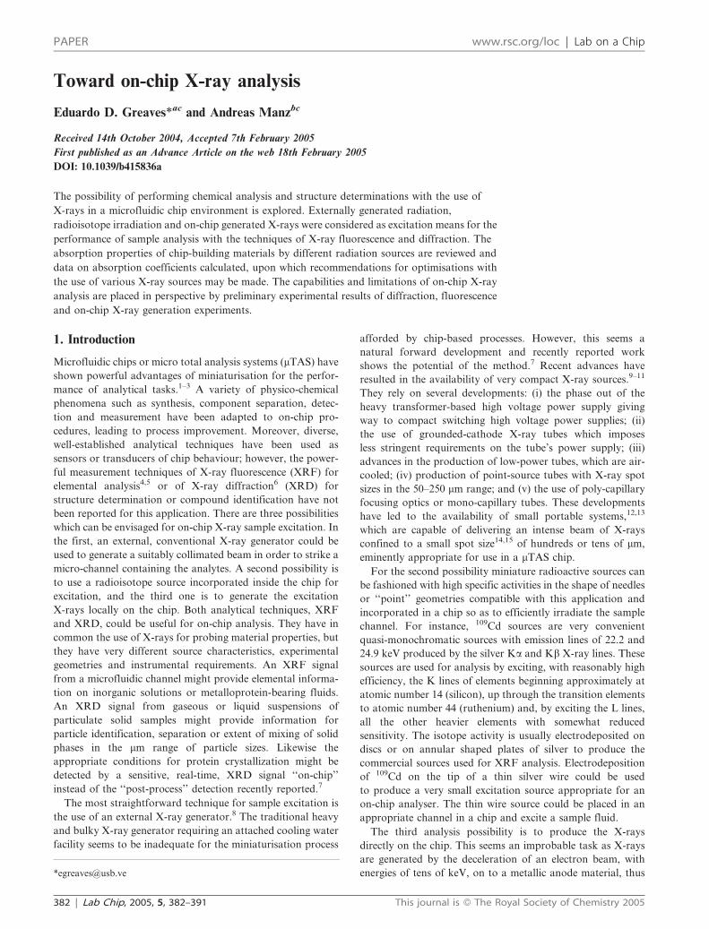
for the several well-established chip-building materials. Fig. 1
shows the results of calculating the absorption coefficient for
the materials in the table. Calculations were made with the
‘‘utilities’’ provided in the QXAS-AXIL software package.22
This figure shows that borosilicate glass has the highest
absorption coefficient. PDMS is very similar on account of the
This journal is � The Royal Society of Chemistry 2005 Lab Chip, 2005, 5, 382–391 | 383
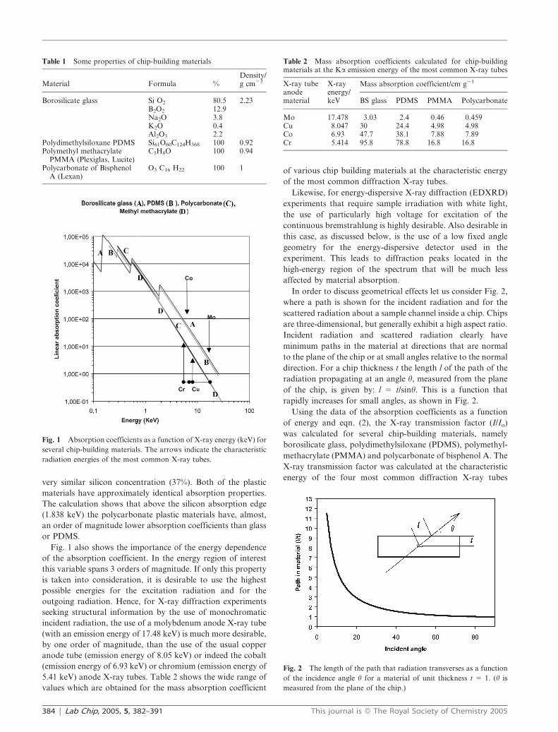
very similar silicon concentration (37%). Both of the plastic
materials have approximately identical absorption properties.
The calculation shows that above the silicon absorption edge
(1.838 keV) the polycarbonate plastic materials have, almost,
an order of magnitude lower absorption coefficients than glass
or PDMS.
Fig. 1 also shows the importance of the energy dependence
of the absorption coefficient. In the energy region of interest
this variable spans 3 orders of magnitude. If only this property
is taken into consideration, it is desirable to use the highest
possible energies for the excitation radiation and for the
outgoing radiation. Hence, for X-ray diffraction experiments
seeking structural information by the use of monochromatic
incident radiation, the use of a molybdenum anode X-ray tube
(with an emission energy of 17.48 keV) is much more desirable,
by one order of magnitude, than the use of the usual copper
anode tube (emission energy of 8.05 keV) or indeed the cobalt
(emission energy of 6.93 keV) or chromium (emission energy of
5.41 keV) anode X-ray tubes. Table 2 shows the wide range of
values which are obtained for the mass absorption coefficient
of various chip building materials at the characteristic energy
of the most common diffraction X-ray tubes.
Likewise, for energy-dispersive X-ray diffraction (EDXRD)
experiments that require sample irradiation with white light,
the use of particularly high voltage for excitation of the
continuous bremstrahlung is highly desirable. Also desirable in
this case, as discussed below, is the use of a low fixed angle
geometry for the energy-dispersive detector used in the
experiment. This leads to diffraction peaks located in the
high-energy region of the spectrum that will be much less
affected by material absorption.
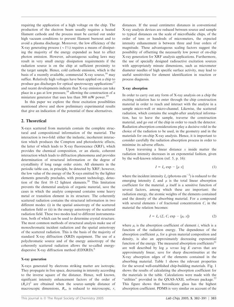
In order to discuss geometrical effects let us consider Fig. 2,
where a path is shown for the incident radiation and for the
scattered radiation about a sample channel inside a chip. Chips
are three-dimensional, but generally exhibit a high aspect ratio.
Incident radiation and scattered radiation clearly have
minimum paths in the material at directions that are normal
to the plane of the chip or at small angles relative to the normal
direction. For a chip thickness t the length l of the path of the
radiation propagating at an angle h, measured from the plane
of the chip, is given by: l 5 t/sinh. This is a function that
rapidly increases for small angles, as shown in Fig. 2.
Using the data of the absorption coefficients as a function
of energy and eqn. (2), the X-ray transmission factor (I/Io)
was calculated for several chip-building materials, namely
borosilicate glass, polydimethylsiloxane (PDMS), polymethyl-
methacrylate (PMMA) and polycarbonate of bisphenol A. The
X-ray transmission factor was calculated at the characteristic
energy of the four most common diffraction X-ray tubes
Table 1 Some properties of chip-building materials
Material Formula %Density/g cm23
Borosilicate glass Si O2 80.5 2.23B2O2 12.9Na2O 3.8K2O 0.4Al2O3 2.2
Polydimethylsiloxane PDMS Si61O60C124H368 100 0.92Polymethyl methacrylate
PMMA (Plexiglas, Lucite)C5H8O 100 0.94
Polycarbonate of BisphenolA (Lexan)
O3 C16 H22 100 1
Fig. 1 Absorption coefficients as a function of X-ray energy (keV) for
several chip-building materials. The arrows indicate the characteristic
radiation energies of the most common X-ray tubes.
Table 2 Mass absorption coefficients calculated for chip-buildingmaterials at the Ka emission energy of the most common X-ray tubes
X-ray tubeanodematerial
X-rayenergy/keV
Mass absorption coefficient/cm g21
BS glass PDMS PMMA Polycarbonate
Mo 17.478 3.03 2.4 0.46 0.459Cu 8.047 30 24.4 4.98 4.98Co 6.93 47.7 38.1 7.88 7.89Cr 5.414 95.8 78.8 16.8 16.8
Fig. 2 The length of the path that radiation transverses as a function
of the incidence angle h for a material of unit thickness t 5 1. (h is
measured from the plane of the chip.)
384 | Lab Chip, 2005, 5, 382–391 This journal is � The Royal Society of Chemistry 2005
mentioned above as a function of the length of the path or
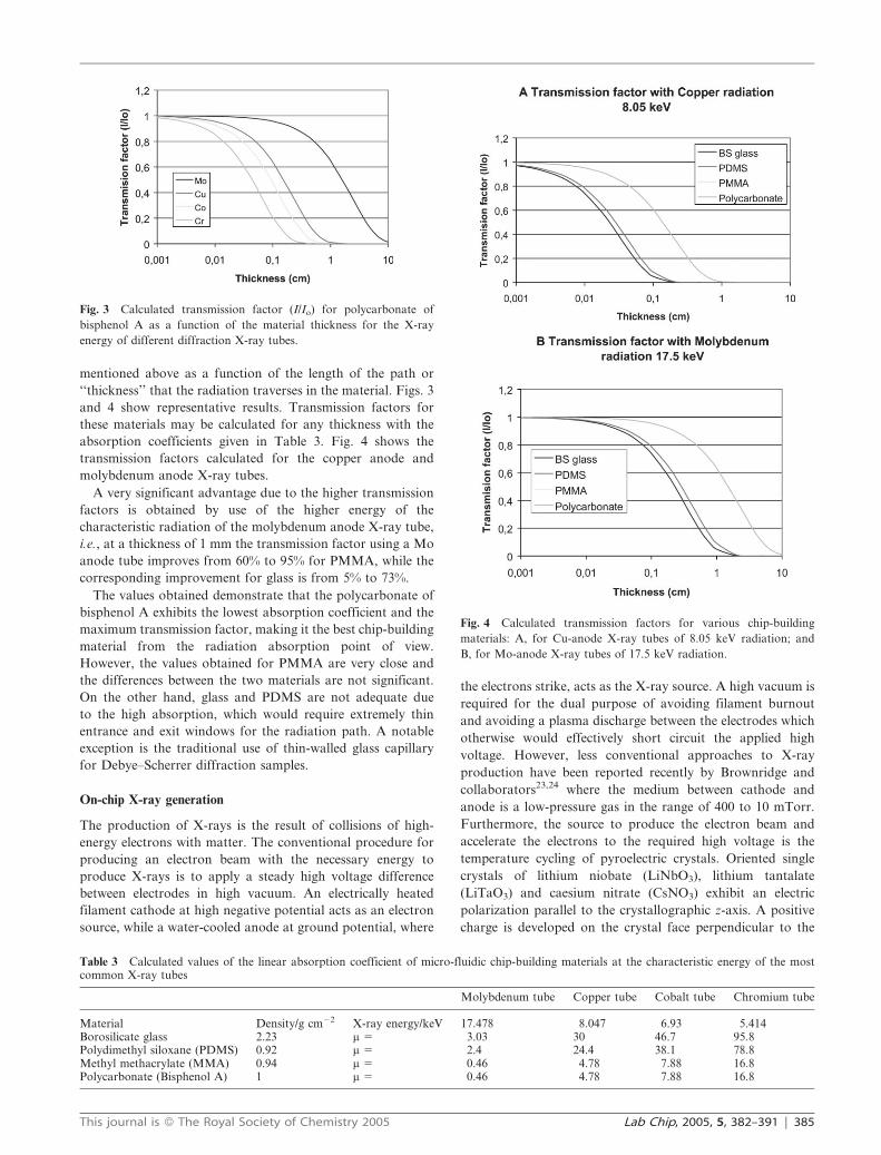
‘‘thickness’’ that the radiation traverses in the material. Figs. 3
and 4 show representative results. Transmission factors for
these materials may be calculated for any thickness with the
absorption coefficients given in Table 3. Fig. 4 shows the
transmission factors calculated for the copper anode and
molybdenum anode X-ray tubes.
A very significant advantage due to the higher transmission
factors is obtained by use of the higher energy of the
characteristic radiation of the molybdenum anode X-ray tube,
i.e., at a thickness of 1 mm the transmission factor using a Mo
anode tube improves from 60% to 95% for PMMA, while the
corresponding improvement for glass is from 5% to 73%.
The values obtained demonstrate that the polycarbonate of
bisphenol A exhibits the lowest absorption coefficient and the
maximum transmission factor, making it the best chip-building
material from the radiation absorption point of view.
However, the values obtained for PMMA are very close and
the differences between the two materials are not significant.
On the other hand, glass and PDMS are not adequate due
to the high absorption, which would require extremely thin
entrance and exit windows for the radiation path. A notable
exception is the traditional use of thin-walled glass capillary
for Debye–Scherrer diffraction samples.
On-chip X-ray generation
The production of X-rays is the result of collisions of high-
energy electrons with matter. The conventional procedure for
producing an electron beam with the necessary energy to
produce X-rays is to apply a steady high voltage difference
between electrodes in high vacuum. An electrically heated
filament cathode at high negative potential acts as an electron
source, while a water-cooled anode at ground potential, where
the electrons strike, acts as the X-ray source. A high vacuum is
required for the dual purpose of avoiding filament burnout
and avoiding a plasma discharge between the electrodes which
otherwise would effectively short circuit the applied high
voltage. However, less conventional approaches to X-ray
production have been reported recently by Brownridge and
collaborators23,24 where the medium between cathode and
anode is a low-pressure gas in the range of 400 to 10 mTorr.
Furthermore, the source to produce the electron beam and
accelerate the electrons to the required high voltage is the
temperature cycling of pyroelectric crystals. Oriented single
crystals of lithium niobate (LiNbO3), lithium tantalate
(LiTaO3) and caesium nitrate (CsNO3) exhibit an electric
polarization parallel to the crystallographic z-axis. A positive
charge is developed on the crystal face perpendicular to the
Fig. 3 Calculated transmission factor (I/Io) for polycarbonate of
bisphenol A as a function of the material thickness for the X-ray
energy of different diffraction X-ray tubes.
Fig. 4 Calculated transmission factors for various chip-building
materials: A, for Cu-anode X-ray tubes of 8.05 keV radiation; and
B, for Mo-anode X-ray tubes of 17.5 keV radiation.
Table 3 Calculated values of the linear absorption coefficient of micro-fluidic chip-building materials at the characteristic energy of the mostcommon X-ray tubes
Molybdenum tube Copper tube Cobalt tube Chromium tube
Material Density/g cm22 X-ray energy/keV 17.478 8.047 6.93 5.414Borosilicate glass 2.23 m 5 3.03 30 46.7 95.8Polydimethyl siloxane (PDMS) 0.92 m 5 2.4 24.4 38.1 78.8Methyl methacrylate (MMA) 0.94 m 5 0.46 4.78 7.88 16.8Polycarbonate (Bisphenol A) 1 m 5 0.46 4.78 7.88 16.8
This journal is � The Royal Society of Chemistry 2005 Lab Chip, 2005, 5, 382–391 | 385
+z axis when the temperature of the crystal is below the Curie
temperature. Upon heating or cooling the crystal there is a
change in the surface charge. Experiments have shown that
weak electron beams with energies as high as 160 keV may be
obtained.25,26 By temperature cycling of the pyroelectric
crystal in the appropriate geometry, X-rays are produced as
electrons alternatively strike the crystal or an anode target
separated a few millimetres from the crystal.27 The minute size
and low power of these unconventional X-ray generators
suggest a possible use as local sources for XRF analysis in
microfluidic chips.
Examination of the discharge properties of low pressure
gases shows that high voltages can be applied without
producing a gas discharge.28–30 If the applied voltage is in
the range of or above several thousand volts, the generation of
X-rays is feasible. For this phenomenon to take place it is
necessary to operate in the left side of the Paschen curve that is
applicable to the particular combination of gas, electrode
geometry and gas pressure. Operating in this regime the gas
exhibits a high resistance and charge flow takes place by the
so-called Townsend dark current. The detailed mechanism by
which the X-rays are produced under the above-described
conditions have, to our knowledge, not been advanced.
However, the experimental results obtained by generating the
high voltage and weak electron beams by means of the
polarising or depolarising of pyroelectric crystals, as reported
by Brownridge and collaborators, suggest that a very high
impedance potential source in the tens of kilovolts range could
substitute the pyroelectric crystal. Hence, a properly designed
chip configuration, so that the required conditions for gas
conduction under Townsend dark current are met, may lead to
X-ray generation from a miniaturized device in a micro-fluidic
chip, as reported below.
3. Experimental
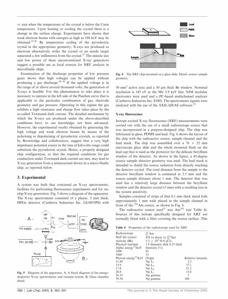
A system was built that contained an X-ray spectrometer,
facilities for performing fluorescence experiments and for on-
chip X-ray generation. Fig. 5 shows a diagram of the apparatus.
The X-ray spectrometer consisted of a planar, 5 mm thick,
HPGe detector (Canberra Industries Inc. GL0055PS) with
50 mm2 active area and a 50 mm thick Be window. Nominal
resolution is 145 eV at the Mn 5.9 keV line; NIM modular
electronics were used and a PC-based multichannel analyser
(Canberra Industries Inc. S100). The spectrometer signals were
analysed with the use of the AXIL-QXAS software.22
X-ray fluorescence
Isotope excited X-ray fluorescence (XRF) measurements were
carried out with the use of a small radioisotope source that
was incorporated in a purpose-designed chip. The chip was
fabricated in glass, PDMS and lead. Fig. 6 shows the layout of
the chip with the radioactive source, sample channel and the
lead mask. The chip was assembled over a 76 6 22 mm
microscope glass slide and the whole mounted flush on the
lead cap that is used as the protector for the delicate beryllium
window of the detector. As shown in the figure, a 45-degree
source–sample–detector geometry was used. The lead mask is
intended to shield the source radiation from directly reaching
the detector crystal. The total distance from the sample to the
detector beryllium window is estimated at 2.5 mm and the
source–sample distance about 1 mm. The detector that was
used has a relatively large distance between the beryllium
window and the detector crystal (5 mm) with a resulting loss in
the system sensitivity.
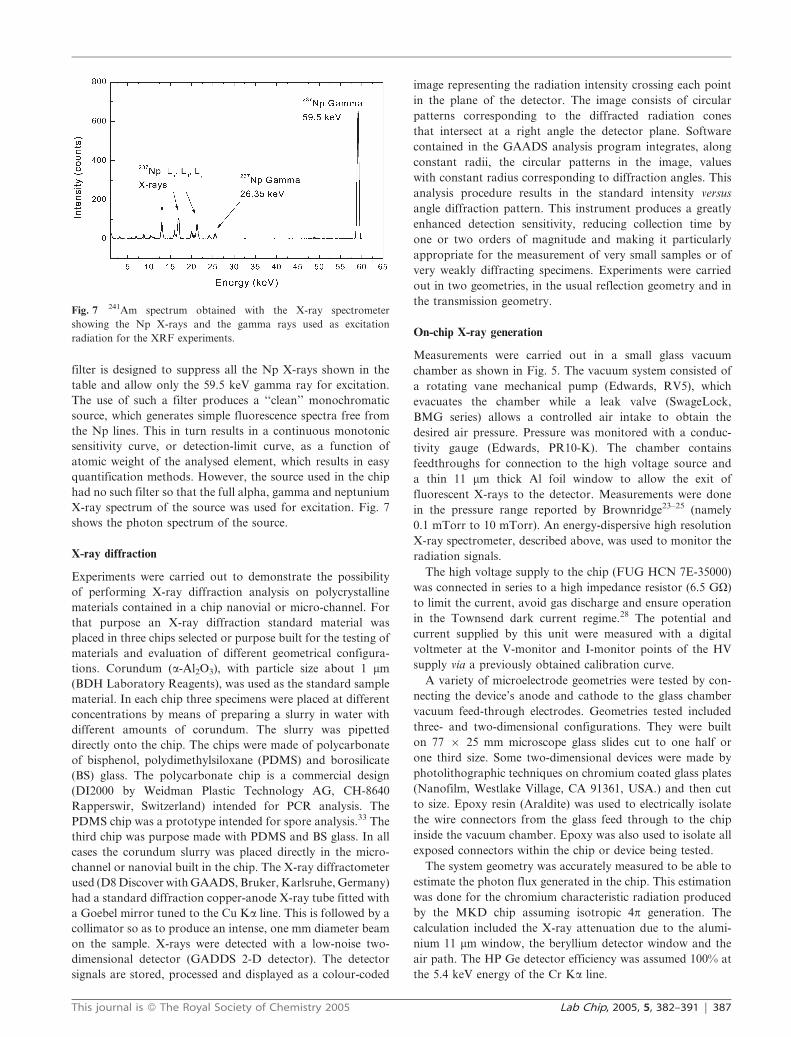
Samples consisted of strips of thin 0.1 mm thick metal foils
approximately 1 mm wide placed in the sample channel in
front of the 241Am source, as shown in Fig. 6
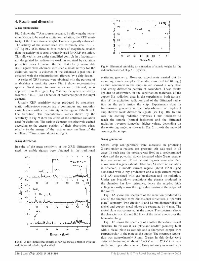
The radioactive source used31 was Am241 (see Table 4).
Sources of this isotope specifically designed for XRF are
normally fitted with a filter covering the source surface. This
Fig. 5 Diagram of the apparatus. A, A block diagram of the energy-
dispersive X-ray spectrometer and vacuum system. B, Glass chamber
detail.
Fig. 6 The XRF chip mounted on a glass slide. Detail: source–sample
geometry.
Table 4 Properties of the radioisotope used for XRF
Radioisotope 24195 Am
Half life (years) 458 (a decay to 23793 Np)
Activity (Bk) 3.3 6 104 (0.9 mCi)Physical size/mm 1.8 diameter disk 0.25 thickAlpha energy32/keV Intensity (%)5490 855440 13Photon energy32/keV Origin Relative intensity11.89 Np Ll 2.213.9 Np La 37.117.8 Np Lb 51.220.8 Np Lc 13.826.35 Np gamma 759.54 Np gamma 100
386 | Lab Chip, 2005, 5, 382–391 This journal is � The Royal Society of Chemistry 2005
filter is designed to suppress all the Np X-rays shown in the
table and allow only the 59.5 keV gamma ray for excitation.
The use of such a filter produces a ‘‘clean’’ monochromatic
source, which generates simple fluorescence spectra free from
the Np lines. This in turn results in a continuous monotonic
sensitivity curve, or detection-limit curve, as a function of
atomic weight of the analysed element, which results in easy
quantification methods. However, the source used in the chip
had no such filter so that the full alpha, gamma and neptunium
X-ray spectrum of the source was used for excitation. Fig. 7
shows the photon spectrum of the source.
X-ray diffraction
Experiments were carried out to demonstrate the possibility
of performing X-ray diffraction analysis on polycrystalline
materials contained in a chip nanovial or micro-channel. For
that purpose an X-ray diffraction standard material was
placed in three chips selected or purpose built for the testing of
materials and evaluation of different geometrical configura-
tions. Corundum (a-Al2O3), with particle size about 1 mm
(BDH Laboratory Reagents), was used as the standard sample
material. In each chip three specimens were placed at different
concentrations by means of preparing a slurry in water with
different amounts of corundum. The slurry was pipetted
directly onto the chip. The chips were made of polycarbonate
of bisphenol, polydimethylsiloxane (PDMS) and borosilicate
(BS) glass. The polycarbonate chip is a commercial design
(DI2000 by Weidman Plastic Technology AG, CH-8640
Rapperswir, Switzerland) intended for PCR analysis. The
PDMS chip was a prototype intended for spore analysis.33 The
third chip was purpose made with PDMS and BS glass. In all
cases the corundum slurry was placed directly in the micro-
channel or nanovial built in the chip. The X-ray diffractometer
used (D8 Discover with GAADS, Bruker, Karlsruhe, Germany)
had a standard diffraction copper-anode X-ray tube fitted with
a Goebel mirror tuned to the Cu Ka line. This is followed by a
collimator so as to produce an intense, one mm diameter beam
on the sample. X-rays were detected with a low-noise two-
dimensional detector (GADDS 2-D detector). The detector
signals are stored, processed and displayed as a colour-coded
image representing the radiation intensity crossing each point
in the plane of the detector. The image consists of circular
patterns corresponding to the diffracted radiation cones
that intersect at a right angle the detector plane. Software
contained in the GAADS analysis program integrates, along
constant radii, the circular patterns in the image, values
with constant radius corresponding to diffraction angles. This
analysis procedure results in the standard intensity versus
angle diffraction pattern. This instrument produces a greatly
enhanced detection sensitivity, reducing collection time by
one or two orders of magnitude and making it particularly
appropriate for the measurement of very small samples or of
very weakly diffracting specimens. Experiments were carried
out in two geometries, in the usual reflection geometry and in
the transmission geometry.
On-chip X-ray generation
Measurements were carried out in a small glass vacuum
chamber as shown in Fig. 5. The vacuum system consisted of
a rotating vane mechanical pump (Edwards, RV5), which
evacuates the chamber while a leak valve (SwageLock,
BMG series) allows a controlled air intake to obtain the
desired air pressure. Pressure was monitored with a conduc-
tivity gauge (Edwards, PR10-K). The chamber contains
feedthroughs for connection to the high voltage source and
a thin 11 mm thick Al foil window to allow the exit of
fluorescent X-rays to the detector. Measurements were done
in the pressure range reported by Brownridge23–25 (namely
0.1 mTorr to 10 mTorr). An energy-dispersive high resolution
X-ray spectrometer, described above, was used to monitor the
radiation signals.
The high voltage supply to the chip (FUG HCN 7E-35000)
was connected in series to a high impedance resistor (6.5 GV)
to limit the current, avoid gas discharge and ensure operation
in the Townsend dark current regime.28 The potential and
current supplied by this unit were measured with a digital
voltmeter at the V-monitor and I-monitor points of the HV
supply via a previously obtained calibration curve.
A variety of microelectrode geometries were tested by con-
necting the device’s anode and cathode to the glass chamber
vacuum feed-through electrodes. Geometries tested included
three- and two-dimensional configurations. They were built
on 77 6 25 mm microscope glass slides cut to one half or
one third size. Some two-dimensional devices were made by
photolithographic techniques on chromium coated glass plates
(Nanofilm, Westlake Village, CA 91361, USA.) and then cut
to size. Epoxy resin (Araldite) was used to electrically isolate
the wire connectors from the glass feed through to the chip
inside the vacuum chamber. Epoxy was also used to isolate all
exposed connectors within the chip or device being tested.
The system geometry was accurately measured to be able to
estimate the photon flux generated in the chip. This estimation
was done for the chromium characteristic radiation produced
by the MKD chip assuming isotropic 4p generation. The
calculation included the X-ray attenuation due to the alumi-
nium 11 mm window, the beryllium detector window and the
air path. The HP Ge detector efficiency was assumed 100% at
the 5.4 keV energy of the Cr Ka line.
Fig. 7 241Am spectrum obtained with the X-ray spectrometer
showing the Np X-rays and the gamma rays used as excitation
radiation for the XRF experiments.
This journal is � The Royal Society of Chemistry 2005 Lab Chip, 2005, 5, 382–391 | 387
4. Results and discussion
X-ray fluorescence
Fig. 7 shows the 241Am source spectrum. By allowing the neptu-
nium X-rays to be used as excitation radiation, the XRF sensi-
tivity of the lower atomic weight elements is greatly enhanced.
The activity of the source used was extremely small 3.3 6104 Bq (0.9 mCi), three to four orders of magnitude smaller
than the activity of sources ordinarily used for XRF excitation.
This allowed its use under simplified controls in a laboratory
not designated for radioactive work, as required by radiation
protection rules. However, the fact that clearly measurable
XRF signals were obtained with such a small activity for the
excitation source is evidence of the enhanced signal that is
obtained with the miniaturisation afforded by a chip design.
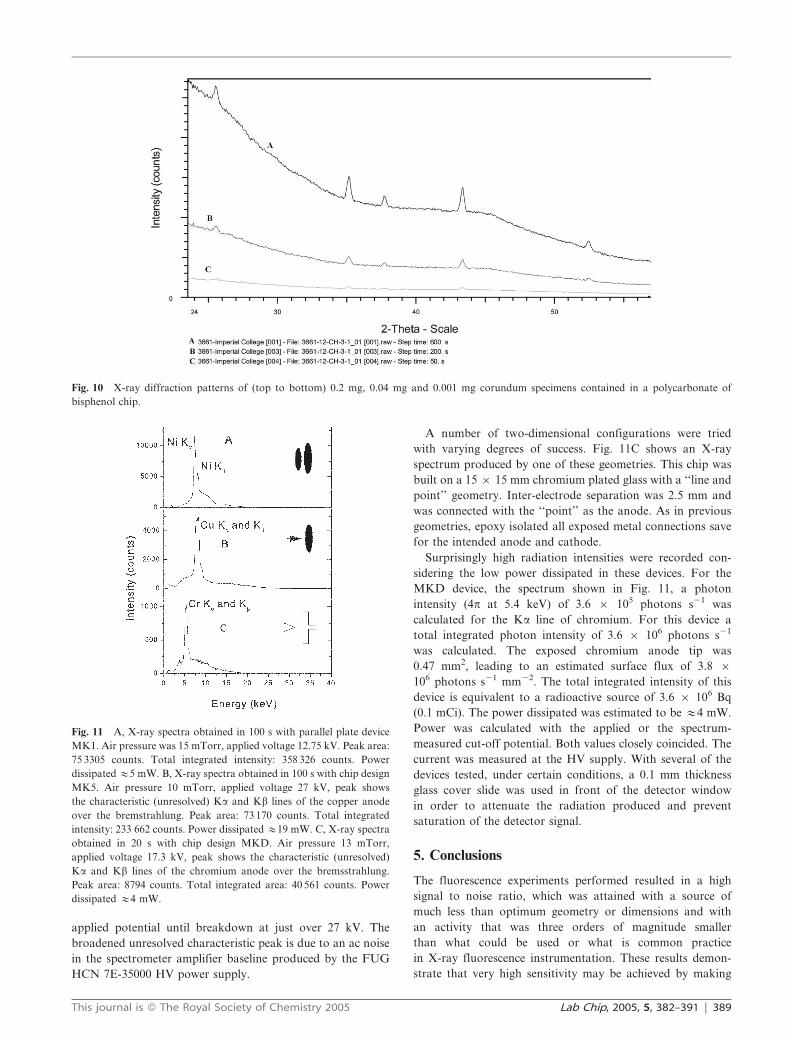
A series of XRF spectra were obtained with the purpose of
establishing a sensitivity curve. Fig. 8 shows representative
spectra. Good signal to noise ratios were obtained, as is
apparent from this figure. Fig. 9 shows the system sensitivity
(counts s21 mCi21) as a function of atomic weight of the target
element.
Usually XRF sensitivity curves produced by monochro-
matic radioisotope sources are a continuous and smoothly
variable curve with a discontinuity in the region of the K to L
line transition. The discontinuous values shown by the
sensitivity in Fig. 9 show the effect of the unfiltered radiation
used for excitation. The various elements are selectively excited
according to the energy position of their absorption edges
relative to the energy of the various emission lines of the
unfiltered 241Am source shown in Fig. 7.
X-ray diffraction
In spite of the great sensitivity of the XRD diffractometer
used, no usable signals were obtained in the traditional
scattering geometry. However, experiments carried out by
mounting minute samples of similar mass (#0.4–0.04 mg )
as that contained in the chips in air showed a very clear
and strong diffraction pattern of corundum. These results
are due to absorption, in the construction materials, of the
copper Ka radiation used in the experiments, both absorp-
tion of the excitation radiation and of the diffracted radia-
tion in the path inside the chip. Experiments done in
transmission geometry in the polycarbonate of bisphenol
chip showed weak diffraction signals (see Fig. 10). In this
case the exciting radiation traverses 1 mm thickness to
reach the sample (normal incidence) and the diffracted
radiation traverses somewhat higher values, depending on
the scattering angle, as shown in Fig. 2, to exit the material
covering the sample.
X-ray generation
Several chip configurations were successful in producing
X-rays under a reduced gas pressure. Air was used in all
cases. In each case the pressure was fixed at a predetermined
value and the potential slowly increased while X-ray genera-
tion was monitored. Three current regimes were identified:
a low current regime (about 0.01–0.06 mA) where no radiation
is observed, a middle current regime (about 0.2–0.6 mA)
associated with X-ray production and a high current regime
(.2 mA) associated with gas breakdown and no radiation.
Under gas breakdown conditions the plasma produced in
the chamber has low resistance, hence the supplied high
voltage is mostly across the high value resistor at the output of
the source.
Fig. 11A shows the spectrum of the radiation produced by
one of the simplest three dimensional structures, a ‘‘parallel
plate’’ geometry. Two circular 10 and 12 mm diameter discs of
nickel and copper metal plates are separated by 4 mm. The
nickel plate was connected as the anode. The spectrum shows
the characteristic Ka and Kb lines of the nickel anode over the
bremsstrahlung.
Fig. 11B shows the spectrum of another three-dimensional
structure. In this case it is a ‘‘plate and needle’’ geometry, built
with a nickel plate as cathode and a sharpened copper wire
perpendicular to the plate as the anode. The electrode separa-
tion was approximately 3 mm. X-rays in this device were
detected beginning at about 13.6 kV up to 27 kV in a very
stable and repeatable manner. X-ray intensity increased withFig. 8 X-ray fluorescence spectra of various metals obtained with the
radioisotope-loaded chip described.
Fig. 9 Elemental sensitivity as a function of atomic weight for the
radioisotope-excited chip XRF system.
388 | Lab Chip, 2005, 5, 382–391 This journal is � The Royal Society of Chemistry 2005
applied potential until breakdown at just over 27 kV. The
broadened unresolved characteristic peak is due to an ac noise
in the spectrometer amplifier baseline produced by the FUG
HCN 7E-35000 HV power supply.
A number of two-dimensional configurations were tried
with varying degrees of success. Fig. 11C shows an X-ray
spectrum produced by one of these geometries. This chip was
built on a 15 6 15 mm chromium plated glass with a ‘‘line and
point’’ geometry. Inter-electrode separation was 2.5 mm and
was connected with the ‘‘point’’ as the anode. As in previous
geometries, epoxy isolated all exposed metal connections save
for the intended anode and cathode.
Surprisingly high radiation intensities were recorded con-
sidering the low power dissipated in these devices. For the
MKD device, the spectrum shown in Fig. 11, a photon
intensity (4p at 5.4 keV) of 3.6 6 105 photons s21 was
calculated for the Ka line of chromium. For this device a
total integrated photon intensity of 3.6 6 106 photons s21
was calculated. The exposed chromium anode tip was
0.47 mm2, leading to an estimated surface flux of 3.8 6106 photons s21 mm22. The total integrated intensity of this
device is equivalent to a radioactive source of 3.6 6 106 Bq
(0.1 mCi). The power dissipated was estimated to be #4 mW.
Power was calculated with the applied or the spectrum-
measured cut-off potential. Both values closely coincided. The
current was measured at the HV supply. With several of the
devices tested, under certain conditions, a 0.1 mm thickness
glass cover slide was used in front of the detector window
in order to attenuate the radiation produced and prevent
saturation of the detector signal.
5. Conclusions
The fluorescence experiments performed resulted in a high
signal to noise ratio, which was attained with a source of
much less than optimum geometry or dimensions and with
an activity that was three orders of magnitude smaller
than what could be used or what is common practice
in X-ray fluorescence instrumentation. These results demon-
strate that very high sensitivity may be achieved by making
Fig. 10 X-ray diffraction patterns of (top to bottom) 0.2 mg, 0.04 mg and 0.001 mg corundum specimens contained in a polycarbonate of
bisphenol chip.
Fig. 11 A, X-ray spectra obtained in 100 s with parallel plate device
MK1. Air pressure was 15 mTorr, applied voltage 12.75 kV. Peak area:
75 3305 counts. Total integrated intensity: 358 326 counts. Power
dissipated #5 mW. B, X-ray spectra obtained in 100 s with chip design
MK5. Air pressure 10 mTorr, applied voltage 27 kV, peak shows
the characteristic (unresolved) Ka and Kb lines of the copper anode
over the bremstrahlung. Peak area: 73 170 counts. Total integrated
intensity: 233 662 counts. Power dissipated #19 mW. C, X-ray spectra
obtained in 20 s with chip design MKD. Air pressure 13 mTorr,
applied voltage 17.3 kV, peak shows the characteristic (unresolved)
Ka and Kb lines of the chromium anode over the bremsstrahlung.
Peak area: 8794 counts. Total integrated area: 40 561 counts. Power
dissipated #4 mW.
This journal is � The Royal Society of Chemistry 2005 Lab Chip, 2005, 5, 382–391 | 389
use of the scaling factors afforded by the minute chip
geometry and that further, significant improvements are
possible.
The results of the diffraction experiments done, seen in
the light of the X-ray absorption calculations contained
in Fig. 4, indicate that for on-chip X-ray diffraction it is
recommended: (i) the use of lower absorption coefficient
materials: (ii) that a transmission geometry must be used;
(iii) that any design must incorporate a very small thick-
ness of the chip if it is to be crossed by radiation (circa
100 mm); and (iv) the employment of high energy X-ray
radiation which results in smaller diffraction angles (i.e., a
molybdenum anode tube) in order to realise on-chip structure
analysis.
On-chip X-ray generation of very significant intensity has
been demonstrated in chip devices of various geometries
under reduced air pressure. Further development is required
to establish geometrical characteristics and other conditions
of sufficient stability to be able to use the phenomenon in
analytical applications. The detailed mechanism of the X-ray
production achieved is not quite clear and further work is
required.
X-ray fluorescence or diffraction detection limits depend
strongly on numerous factors pertaining to the particular
excitation geometry, radiation intensity, detector efficiency
and nature of the sample. It is unlikely that measurement
of trace element concentrations will be achieved by these
techniques in a chip. High and intermediate concentrations
should be possible: however, careful control of the relevant
factors will determine, in each case, how low a detection limit
will be reached.
Acknowledgements
This work was carried out during a sabbatical leave granted to
E.D.G. by the Universidad Simon Bolıvar, Caracas, Venezuela,
which is gratefully acknowledged. Also, the Deutsche
Forschungsgemeinschaft (DFG) of the Federal Republic of
Germany is gratefully acknowledged for the granting of a
Mercator Visiting Professorship. The authors are grateful to
Dr. Herbert Stori of Vienna University of Technology for
helpful discussions.
Eduardo D. Greaves*ac and Andreas Manzbc
aUniversidad Simon Bolıvar, Apartado 89000, Caracas 1080A,Venezuela. E-mail: [email protected] for Analytical Sciences, Bunsen-Kirchhoff-Strasse 11,D-44139 Dortmund, GermanycDepartmentt of Chemistry, Imperial College of London, London, UKSW7 2AZ
References
1 D. R. Reyes, D. Iossifidis, P. A. Auroux and A. Manz, Micro TotalAnalysis Systems. 1. Introduction, theory and technology, Anal.Chem., 2002, 74, 2623–2636.
2 P. A. Auroux, D. Iossifidis, D. R. Reyes and A. Manz, Micro TotalAnalisis Systems. 2. Analytical standard operations and applica-tions, Anal. Chem., 2002, 74, 2637–2652.
3 T. Vilkner, D. Janesek and A. Manz, Micro total Analysis Systems.Recent developments, Anal. Chem., 2004, 76, 3373–3386.
4 E. Van Grieken and R. A. Andrzej, Markowicz. Handbook ofX-Ray Spectrometry, Marcel Dekker, 1993, ISBN: 0824706005.
5 R. Klockenkamper, Total-Reflection X-Ray Fluorescence Analysis,Wiley, 1996, ISBN: 0-471-30524-3.
6 B. D. Cullity, Elements of X-Ray Diffraction, Wiley, 1978.7 B. Zheng, J. D. Tice, L. S. Roach and R. F. Ismagilov,
A droplet-based, composite PDMS/glass capillary microfluidicsystem for evaluating protein crystallization conditions bymicrobatch and vapor-diffusion methods with on-chip X-raydiffraction, Angew. Chem. Int. Ed., 2004, 43, 2508–2511.
8 P. J. Potts, A. T. Ellis, P. Kregsamer, J. Marshall, C. Streli,M. West and P. Wobrauschek, Atomic spectrometry update.X-ray fluorescence spectrometry, J. Anal. At. Spectrom., 2002, 17,10, 1439–1455.
9 S. Bichlmeier, K. Janssens, J. Heckel, D. Gibson, P. Hoffmann andH. M. Ortner, Component selection for a compact micro-XRFspectrometer, X-ray Spectrom., 2001, 30, 8–14.
10 T. C. Miller, M. R. Joseph, G. J. Havilla, C. Lewis andV. Majid, Capillary electrophoresis micro X-ray fluorescence:A tool for benchtop elemental analysis, Anal. Chem., 2003, 75,2048–2053.
11 C. Ribbing, N. Strid, P. Rangsten and J. Tirein, Miniature X-raysource- Development of a prototype, Biomed. Microdevices, 2002,4, 285–292.
12 U. Waldschlager, The analytical possibilities of a portable TXRFspectrometer, INTAX GmbH, Schwarzschildstr. 10, 12489 Berlin,Germany, (http://www.rontec.com/en/download/publikation_4.pdf).
13 J. L. Ferrero, C. Roldal, D. Juanes, E. Rollano and C. Morera,Analysis of pigments from Spanish works of art using aportable EDXRF spectrometer, X-ray Spectrom., 2002, 31,441–447.
14 H. Bronk, S. Rohrs, A. Bjeoumikhov, N. Langhoff, J. Schmalz,R. Wedell, H. E. Gorny, A. Herold and U. Waldschlager,ArtTAX—a new mobile spectrometer for energy-dispersive microX-ray fluorescence spectrometry on art and archaeological objects,Fresenius’ J. Anal. Chem., 2001, 371, 307–316.
15 S. Bichlmeier, K. Janssens, J. Heckel, P. Hoffmann andH. M. Ortner, Comparative material characterization of historicaland industrial samples by using a compact micro-XRF spectro-meter, X-ray Spectrom., 2002, 31, 87–91.
16 Laser-X, built by AMTEK Inc., Bedford, MA, USA, http://www.amptek.com.
17 J. C. T. Eijkel, H. Stoeri and A. Manz, A molecular emissiondetector on a chip employing a direct current microplasma, Anal.Chem., 1999, 71, 2600–2606.
18 J. D. Brownridge and S. Raboy, Investigations of pyroelectricgeneration of X-rays., J. Appl. Phys., 1999, 86, 640–647.wwThispaper discusses X-ray production in a low pressure gas.
19 Miniature X-ray Generator, built by AMTEK Inc., Bedford, MA,USA, http://www.amptek.com.
20 However, lighter elements down to boron have been reportedby C. Streli, P. Kregsamer, P. Wobrauschek, H. Gatterbauer,P. Pianetta, S. Pahlke, L. Fabry, L. Palmetshofer andM. Schmeling, Low-Z total reflection X-ray fluorescence analysis—Challenges and answers, Spectrochim. Acta, 1999, 54B,1433–1441.
21 Alpha, beta and gamma-ray spectroscopy, ed. K. Siegbahn,North-Holland Publishing Co., Amsterdam, 1965, vol. 1 and 2.
22 QXAS-AXIL, Quantitative X-ray Analysis System, InternationalAtomic Energy Agency (IAEA), Vienna, Austria.
23 J. D. Brownridge, Pyroelectric X-ray generator, Nature, 1992, 258,287–288.wThis is the first paper showing X-ray production in a gasat low pressure.
24 J. D. Brownridge and S. M. Shafroth, Self-focused electron beamsproduced by pyroelectric crystals on heating or cooling in dilutegases, Appl. Phys. Lett., 2001, 79, 3364–3366.
25 J. D. Brownridge and S. M. Shafroth, Pressure dependence ofenergetic (160 keV) focused electron beams arising from heated orcooled (Li Nb O3) pyroelectric crystals, Appl. Phys. Lett., 2003, 83,1477.
26 J. D. Brownridge, private communication, 2004.27 Cool-X, miniature X-ray generator by Amptex Inc. 6 Angelo
Drive, Bedford, MA 01730-2204, USA.28 Yu P. Raizer, Gas Discharge Physics, Springer-Verlag, Berlin,
1991, p. 134, ISBN 3-540-19462-2.wwPhenomenology allowing highvoltage in a chip is discussed here.
390 | Lab Chip, 2005, 5, 382–391 This journal is � The Royal Society of Chemistry 2005
29 J. M. Meek and J. D. Craggs, Electrical Breakdown of Gases,Clarendon Press, Oxford, 1953.
30 S. C. Brown, Basic data of plasma physics, Technology Press ofthe Massachusetts Institute of Technology and Chapman & Hall,New York and London, 1959.
31 Apollo fire detectors Ltd., 6 Solent Road, Havant, Hampshire,PO9 1JH, England.
32 C. M. Lederer, J. M. Hollander and I. Perlman, Table of Isotopes,John Wiley & Sons Inc., 6th edn. 1967, p 565.
33 O. Hofmann, K. Murray, A. S. Wilkinson, T. Cox andA. Manz, Extraction of DNA from bacterial spores usinglaser based disruption on a microchip, Gordon Conferenceon Microfluidics, 2003, Big Sky, MT, USA (submitted toAnal. Chem.).
This journal is � The Royal Society of Chemistry 2005 Lab Chip, 2005, 5, 382–391 | 391


